1
DLP PROJECTOR
SERVICE MANUAL
MODEL:PB6100 / PB6200
CAUTION
BEFORE SERVICING THE PROJECTOR,
READ THE SAFETY PRECAUTIONS IN THIS MANUAL.
1
Index
1. Safety Precautions -------------------------------- 3
2. Engineering Specification---------------------- 4
3. Spare Parts List ---------------------------------- 32
4. Block Diagram ------------------------------------ 36
5. Packing Description ---------------------------- 44
6. Factory OSD Operation ------------------------ 50
7. Firmware upgrade procedure --------------- 57
8. RS232 Communication Protocol ----------- 61
9. Trouble Shooting Guide ----------------------- 73
10.CUSTOMER ACCEPTANCE CRITERIA ---- 78
11. Schematics ---------------------------------------- 96
2
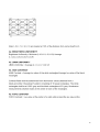
1. Safety Precautions
3
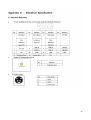
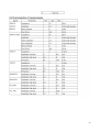
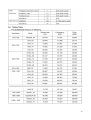
2. Engineering Specification
4
5
6
7
8
9
10
11
12
13
14
15
16
17
18
19
20
21
22
23
24
25
26
27
28
29
30
31
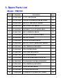
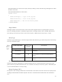
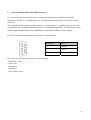
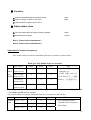
3. Spare Parts List
Model : PB6100
Item
Component
Description
Type
1
42.J8618.001 U/C PC+ABS PB6100
R
2
55.J7612.001 PCBA KEYPAD BD PB7200 BENQ850
2
3
54.J8612.001 BALLAST PHG201G16 PB6100
R
4
60.J8605.001 ASSY Lower Case PB6100
R
5
23.10102.001 BLOWER 12V 50*50*20MM ADDA
R
6
60.J8617.001 ASSY LAMPBOX PB6100
R
7
23.10103.001 FAN 12V 70*70*25AXIAL ADDA
R
8
60.J8604.001 ASSY R/C PB6100
R
9
55.J8608.001 PCBA REAR IR BD PB6100
2
10
65.J8602.001 ASSY AC INLET+THERM SW PB6100
R
11
55.J5019.001 PCBA THERMAL BD DX850
2
12
55.J5020.001 PCBA EMI BD DX850
2
13
55.J8601.001 PCBA MAIN BD PB6100
2
14
60.J8607.001 ASSY DOOR PB6100
R
15
55.J1313.001 PCB 1L SENSOR-B BD SL700 X MI
2
16
65.J8603.001 CW DIA44DEG110 PB6100 PRODISC
R
17
55.J5019.001 PCBA THERMAL BD DX850
2
18
55.J8623.001 PCBA CHIP BD PB6100
2
19
65.J7602.001 PL ZOOM PB7200 ASIA
R
20
71.08060.000 IC DMD 0.6SVGA 8060-624C 12DDR
R
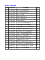
32
Model : PB6100
Item
Component
Description
Type
21
31.J8601.001 BADGE AL PLATE PB6100
R
22
60.J1334.001 ASSY CAP LENS SL700X
R
23
60.J8603.001 ASSY F/C PB6100
R
24
55.J8611.001 PCBA PFC BD PB6100
2
25
55.J8613.001 PCBA FAN BD PB6100
2
26
65.J5003.001 FOOT ADJ DX850
R
27
44.J0502.005 CTN 415*325*255 PB6100/BENQ VI
R
28
47.J8605.001 CUSHION FRONT EPE PB6100
R
29
47.J8606.001 CUSHION REAR EPE PB6100 PB6100
R
30
50.72920.011 C.A MIN-DIN 4P S-VIDEO W/S 150
R
31
50.J0508.503 SIGNAL/C 15/15P 20276 1800MM
R
32
50.J1303.501 CABLE
R
33
56.26J86.001 REMOTE CR14AI PB6100
R
34
42.20019.002 BAG PE 250*350 LD FP741/NEC
R
35
46.00003.012 CARD WARRANTY 7254E
R
36
49.J8601.001 MANUAL USER PB6100/ PB6200
R
37
53.J8601.001 CD MANUAL USER PB6100/ PB6200
R
38
60.J8618.CG1 ASSY Service LAMP 200W/U PB6100
0
39
60.J8621.001 ASSY S2+ EGN 12D PB6100
0
RCA Y/Y 1600MM BLK
33
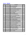
Model : PB6200
Item
Component
Description
Type
1
55.J8501.001 PCBA MAIN BD PB6200
2
2
42.J8618.001 U/C PC+ABS PB6100
R
3
55.J7612.001 PCBA KEYPAD BD PB7200 BENQ850
2
4
54.J8612.001 BALLAST PHG201G16 PB6100
R
5
55.J5020.001 PCBA EMI BD DX850
2
6
60.J8605.001 ASSY L/C PB6100
R
7
55.J8608.001 PCBA REAR IR BD PB6100
2
8
23.10103.001 FAN 12V 70*70*25AXIAL ADDA
R
9
60.J8607.001 ASSY DOOR PB6100
R
10
23.10102.001 BLOWER 12V 50*50*20MM ADDA
R
11
60.J8617.001 ASSY LAMPBOX PB6100
R
12
55.J1313.001 PCB 1L SENSOR-B BD SL700 X MI
2
13
65.J8603.001 CW DIA44DEG110 PB6100 PRODISC
R
14
60.J8621.001 ASSY S2+ EGN 12D PB6100
0
15
55.J8623.001 PCBA CHIP BD PB6100
2
16
71.08060.000 IC DMD 0.6SVGA 8060-624C 12DDR
R
17
31.J7601.061 NAME PLATE AL PB6200
R
18
55.J5019.001 PCBA THERMAL BD DX850
2
19
60.J1334.001 ASSY CAP LENS SL700X
R
20
60.J8603.001 ASSY F/C PB6100
R
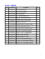
34
Model : PB6200
Item
Component
Description
Type
21
55.J8611.001 PCBA PFC BD PB6100
2
22
55.J8613.001 PCBA FAN BD PB6100
2
23
65.J5003.001 FOOT ADJ DX850
R
24
44.J7601.051 CTN AB PB6100/BENQ(VI)
R
25
45.L2701.011 LBL CTN 120*100 BLUE FP559
R
26
47.J8605.001 CUSHION FRONT EPE PB6100
R
27
22.91007.001 SKT PLUG 2/3P W/G
R
28
27.01818.000 CORD SVT#18*3C 10A125V 1830US
R
29
44.J0501.011 CTN ASSY 350*240*48 7765P
R
30
50.72920.011 C.A MIN-DIN 4P S-VIDEO W/S 150
R
31
50.J0508.503 SIGNAL/C 15/15P 20276 1800MM
R
32
50.J1303.501 CABLE
R
33
56.26J86.001 REMOTE CR14AI PB6100
R
34
46.00003.012 CARD WARRANTY 7254E
R
35
49.J8601.001 MANUAL USER PB6100/ PB6200
R
36
53.J8601.001 CD MANUAL USER PB6100/ PB6200
R
37
60.J8618.CG1 ASSY Service LAMP 200W/U PB6200
0
RCA Y/Y 1600MM BLK
35
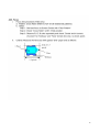
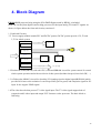
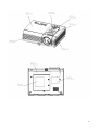
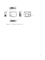
4. Block Diagram
PB6100 DMD projector being using the SGA DMD Engine made by BENQ, it included
front end circuitry that digitizes and scaling processes for the input analog VGA and TV signals. As
shown, in figure below the front end circuitry consists of :
1. Frond end Circuitry
1.1 Power supply module include PFC and DC/DC portion. DC/DC portion provide 12V, 5V and
3,3V for whole system.
12V
Lamp Fan1
PFC
Lamp Power
IGNITOR
AC IN
POWER SUPPLY
Module
Lamp Fan
Power Fan
DC to DC
EMI Filter
12V,5V,2.5V
For System
1.2 Pixelworks scaler(PW166) with x86 CPU, OSD and SDRAM is used for system control. It control
whole system operation and with crucial role of this system.(Include fan speed, inter-lock SW,….)
1.3 A/D-decoder(AD9883) is used for decoding VGA analog signal to digital signal(RGB 888) which
provide 24 bit true color resolution. It can accept SOG(sync on green) and composite signal for PC
input. It also support YPbPr signal.
1.4 The video decoder that process TV video signal input. The TV video signal support both of
composite and S-video input and output YUV format to scaler processor. The basic block as
following.
36
From Power Supply
Regulator(3.3v)
12V,5V,2.5V
EEPROM
(16K bit)
ThERMAL IC
SENSOR
Scaler (memory +cpu+osd)
RGB888 Signal
To DMD Driver
Power(12V,5V,2.5V)
To DMD Driver
Control Signal
To DMD Driver
D-Sub Input
AD Converter
S-Video& RCA input
DMD driver board that transfer PW166 scaler output RGB888 signal to DMD chip acceptable
signal for driving DMD mirror operation. The relate diagram as below:
RAMBUS CLOCK
GEN
400mHz
RAMBUS RDRAM
Data &
Address
2.
Video Decoder
60MHz
CLK
100MHz
DATA , CONTROL,60MHz
DATA-GY(7:0),RV(7:0),BU(7:0)
Front End
Circuit
VSync,HSync,ACTDATA
DDP 1000
PIXEL CLOCK(CLKIN)
Resetz,Poweron
Voltage
GEN
LampLitz
VBIAS
VRST
VCC2
SR16C
DMD
RESET DRIVER
MBRST
(15:0)
DMD Chip
(0.6 SVGA
DDR)
VCC2
SENSOR BOARD
CWindex
Control Signal
MOTOR DRIVER
CWY(1:3)
CWCTR
COLOR
Drum
Color
Wheel
37
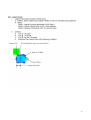
3. Whole system block diagram is show as below:
Lamp Module
Optical Device
PFC
Optical Engine
DMD
Lamp On
EMI Filter
Power Board and Ballast
Color Wheel
DC/DC
Ballast
2.5V, 5V, 12V
Data &
Control Signal
Fan/BD
Fan
Power &
Control Data
Control Signal
DMD Driver
RGB 888
DMD CHIP Board
Sensor Signal
Main
Board
Color Wheel
Sensor Board
Color Wheel
Sensor
PW166 Scaler
Keypad
A/D Converter
Video Decoder
D-Sub Input
Video Input
S-video Input
IR Rear Board
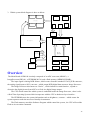
Overview
The Main Board of PB6100 is mainly composed of an ADC converter(AD9883) , a
ImageProcessor(PW166) , a EEPROM(24C16) and a flash memory (MBM29LV800B) .
The input signal is analog RGB format , which comes from the standard VGA D_SUB connector ,
the analog signal input to ADC converter , which output RGB digital data stream to Image Processor .
The Image Processor also known as “Scaler” , which indicate its main function , expand or
downsize the digital picture from ADC to a fixed size digital image output .
The CPU which control the whole system is embedded inside the Image Processor , there is also
a Real Time Operating System which incorporates with the CPU as hardware layer interface .
The EEPROM stores the system information such as brightness , contrast …which ensure the
system operates under the most user friendly circumstance .
The Flash memory stored the Software Program which control the system , the CPU will read the
Flash as its execution command .
38
Block Diagram
Below is the simple block diagram of PB6100 Main Board .
D_SUB
I2C
I2C
Analg Flat Panel
Interface
AD9883
EEPROM
RGB888 signals
Address
Control Signals
Image Processor
PW166
Flash
Data
I2C
S-Video
RCA
Video Decoder
SAA7118
YUV 422
Control Signals
Clock
GEN
Clock
signal
RGB 888
Signals
I2C
Control Signals
DMD Driver
As the diagram shown above , here is the function of every discrete blocks .
-
D_SUB input
Analog RGB data input , the standard maximum analog input resolution is SXGA .There also
some interface signals from the VGA cable , they are
ADHSYNC – Providing the Horizontal Synchronization signal to AD9883.
ADVSYNC - Providing the Vertical Synchronization signal AD9883.
DDC interface – Providing Digital Display Channel , which include VCC(Pin9) ,
SCL(Pin15) , SDA(Pin12) .
-
Analog Flat Panel Interface (ADC Converter) , AD9883
The ADC converter digitizes the input analog RGB data signal from D_SUB and output the
digital data streams to Image Processor .
The normal voltage level of analog RGB input signals is about 0.7V , while the ADC digital
signal output to Image Processor is LVTTL level , about 3.3V.
The ADC , AD9883 could supports up to pixel rate at about 140MHZ , which is about SXGA
75HZ analog input signal .
39
There are some other interface signals related to AD9883
SOGIN – Sync On Green input from Image Processor , the signal enable the PB6100 support
the very special VGA input signal .
GCOAST – Input signal from Image Processor , the signal enable the PB6100 support the
Machintosh analog input format .
GCLK – Output to Image Processor as Pixel Clock , providing the reference clock for Image
Processor .
GHS – Providing the Horizontal Synchronization signal to Image Processor .
GVS - Providing the Vertical Synchronization signal to Image Processor .
GRE,GGE,GBE – Digital data stream to Image Processor which is higher than SXGA
75HZ .
. Image Processor (PW166)
The most important IC is the image Processor , here below list its main function
- Supporting input digital data stream up to UVGA and output digital data up to SXGA
- Two input port , which are Graphic port ( VGA format ) and Video port ( video decoder format ) .
- Frame rate conversion , the output frame rate is independent from the input frame rate and
the
most important feature of the Image Processor is memory inside , there is no need
of external memory for frame rate convertion .
- Up and Down scaling of different input resolution , ensure the same output image size .
- Providing Bitmap OSD picture , which if more fancy than normal OSD chip .
- On chip Microprocessor
The Image Processor is a highly integrated circuit , it include MCU , Scaler , Memory , OSD . This
will increase the stability of the system .
There is some control signals list below
DCLK – pixel clock output to DMD driver BD , provided as a reference clock for DMD driver
DVS – Vertical synchronization signal output to DMD BD , provided as Vertical reference signal
for DMD driver .
DHS – Horizontal synchronization signal output to DMD BD , provided as Horizontal reference
signal for DMD driver .
DEN – Data enable signal output to DMD BD , provided as a valid data indicator signal for
DMD driver .
VCLK – V-port pixel clock .
VPEN – V-port data enable .
VVS – V-port Vertical Synchronization .
VHS – V-port Horizontal Synchronization .
VFILED – V-port Even/Odd frame indicator .
RESETZ – Output to DMD driver BD as RESETZ signal for DMD normal operation .
ABNORMAL – Input to CPU for indicating abnormal condition , if the CPU detects an
40
abnormal status , it will disable lamp ignition .
POWERON – Output to power to enable the other power source into normal working situation .
LAMPLIT – Input signal as an indicator that the Lamp is ON or OFF
LED1, LED2 – Output to enable the LED ON or OFF .
IRRCVR0 – System IR input to CPU as remote control signals .
MCKEXT – Memory clock to CPU .
DCKEXT – Data clock to for Scaling .
I2C_SDA , I2C_SCL – I2C format data transfer line .
. EEPROM
Store the system information for user friendly .
. Flash Memory
System software was stored in this chip , the memory size is 8M bits
. DDP1000
The DDP1000 transfer signal from PW166 to DMD for driving DMD mirror operation.
. Direct Rambus Memory
The DDP1000 utilizes a high speed Direct Rambus Memory. To support the RDRAM a
Direct Rambus clock generator CDCR83 is utilized. It can transfer input clock from 50MHz
to 400MHz.
IR Receiver schematic:
The IS1U621 is miniaturized receivers for infrared remote control systems. PIN diode and
pre-amplifier are assembled on lead frame, the epoxy package is designed as IR filter. The
demodulated output signal can directly be decoded by a microprocessor. The main benefit is the
reliable function even in disturbed ambient and the protection against uncontrolled output pulses.
Electronic System Protection for abnormal state:
The circuit of electronic system protection for abnormal state is used for the hardware light off and
power off in abnormal state of thermal and safety issues. If the protection function is active then the
software system will detect the abnormal signal.
41
Sensor BD:
The Sensor BD provides the color wheel index signal to DMD BD. The CWINDEX shall indicate the
beginning of the red light on the DMD device. The phase of the display data on the DMD based on the
CWINDEX signal. It can be configured to delay the CWINDEX for electronic alignment of the color
wheel. The timing of CWINDEX and the delayed CWINDEX is shown in Figure 1.
CWINDEX
DELAYED
CWINDEX
DMD COLOR
Red
FIGURE
1
42
PB6100 Lamp on Sequence
Signal
Voltage Change
POWERON LowÆHigh
Description
1. This signal should go from low to high after all
the DC supplies are within spec. Then RESETZ
can go high.
2. After the power key pressed 3 second
continuously, the POWERON signal will
activate.
RESETZ
LowÆHigh
DMD is working, when the DMD reset.
LAMPEN
LowÆHigh
Lamp lights up.
LAMPLIT
LowÆHigh
Indicate ”Lamp on”.
PB6100 Normal Lamp off
Signal
Sequence
Voltage Change
Description
RESETZ
HighÆLow
DMD is off.
LAMPEN
HighÆLow
Lamp is off.
LAMPLIT
HighÆLow
Indicate “lamp off“.
POWERON HighÆLow
Power down the system, but the peripherals of the
CPU still power on.
43
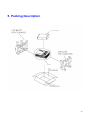
5. Packing Description
44
45
46
47
48
49
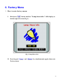
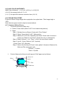
6. Factory Menu
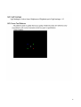
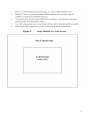
1. How to enter factory menu:
I.
Hold press "UP" button until the "Lamp hours info." OSD display on
bottom-right of screen (Fig-1)
(Fig-1) Lamp Hours Info
II. Press keypad <Power> and <Blank> key simultaneously again, then enter
Factory menu.
50
2. Factory layer:
I.
DMD layer (Fig-3):
(Fig-3) DMD layer
1. CW delay: Adjust color wheel delay.(Note this value before upgrade software)
2. White peak: Adjust DMD white peak.
In PC mode default value set 10, in Video mode is 0.
Software auto set this value as source find.
3. DLP Brightness: Adjust DLP Brightness.
Default setting is 36.Do not change this value.
4. DLP Contrast: Adjust DLP Contrast.
Default setting is 30.Do not change this value.
5. Burn-In Hour: set how many hours to burn-in.
Projector will enter burn-in mode on next selection.
6. Burn-In: After you set burn-in hours, set this selection to “On” and system will
enter going to burn-in immediately.
Projector will run color change (Red, Green, Blue, Black, White) on screen.
System will auto turn off after burn-in hour count down to 0 and burn-in
complete.
(You can also cancel burn-in sequence by set this selection to “Off”).
51
II.
1.
2.
3.
4.
5.
6.
III.
ADC layer (Fig-4): (only available when input source is analog RGB)
(Fig-4) ADC layer
ADC Brightness: ADC brightness auto calibration black.
ADC Contrast: ADC contrast auto calibration white.
ADC Offset RGB: value to tell you calibrate result.
ADC Gain RGB: value to tell you calibrate result.
Fac Brightness: adjust default brightness value in source PC.
Fac Contrast: adjust default contrast value in source PC.
Color layer (Fig-5):
(Fig-5) Color layer
52
1.
PbPr: enter PbPr color control Layer.
When Source is YPbPr (Never Change these setting)
(Note these values Before Upgrade Software)
PbPr G Offset : combine with user OSD brightness in YPbPr
PbPr G Gain: combine with user OSD contrast in YPbPr
PbPr R Offset: offset of color red
PbPr G Offset: offset of color green
PbPr R Gain: saturation R
PbPr B Gain: saturation B
2.
6500,11500 R,G,B: 6500K/11500k submenu
(Never Change these setting)
6500 R :gain of color red while color temp is 6500
6500 G :gain of color green while color temp is 6500
6500 B :gain of color blue while color temp is 6500
6500 R :gain of color red while color temp is 11500
11500 G :gain of color green while color temp is 11500
53
11500 B :gain of color blue while color temp is 11500
3.
PC 9300 and Video 9300: 9300K submenu.
(Never Change these setting)
PC 9300 R :gain of color red while PC color temp is 9300
PC 9300 G :gain of color green while PC color temp is 9300
PC9300 B :gain of color blue while PC color temp is 9300
Video 9300 R :gain of color red while Video color temp is 9300
Video 9300 G :gain of color green while Video color temp is 9300
Video 9300 B :gain of color blue while Video color temp is 9300
IV.
Optic layer (Fig-5):
(Fig-5) Optic layer
1. Test Pattern: system auto produce pattern for engineer test.
2. Spoke light: unit display full white.
3. Curtain Red: unit display full color red.
4. Curtain Green: unit display full color green.
54
5.
V.
Curtain Blue: unit display full color blue.
Lamp layer (Fig-6):
(Fig-6) Lamp layer
1. Interpolation: De-interlace Mode
2. Filter: system auto select Filter.
3. Lamp Hour: value to tell you lamp usage hours.
4. Usage Hour: value to tell you unit usage hours.
5. Fac Lamp Hours: Record all of the amp usage hours
6. Data Reset: Reset all data to default include factory assign value.
Never try to reset all data.
VI.
Others layer (Fig-7):
1.
2.
(Fig-7) YPbPr layer
Gamma index: system auto select DLP gamma index
Gray value: adjust here to check DMD fail pixel.
55
3.
4.
5.
6.
VII.
Blue value: adjust here to check DMD fail pixel.
Scaling: tell you what scaling mode is using now.
Pc/PbPr Mode: index of input timing
RS232: Enable / Disable RS232 control
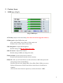
FAN Layer.
T1-DMD: DMD sensor temperature
T2-Lamp: Lamp sensor temperature
T3-Blwr: Blower sensor temperature
F1-Lamp:Lamp fan speed in RPM
F2-Blst: Blaster fan speed in RPM
F3-Blwr : Blower fan speed in RPM
Manual Fan Speed: Change fan speed by manual.
SOG Threshold : Change SOG threshold level of AD
More Options: Change to Fac7 submenu
(Fac7 Submenu)
( This menu only for control testing)
56
7. Firmware upgrade procedure
PB6100/PB6100 Download Procedure
Hardware required
1.
2.
3.
4.
5.
6.
7.
8.
D-sub download cable (full ping D-SUB P/N : 50.J2402.201)
Download board ( P/N : 55.J1316.001 )
PS2 Download cable from download BD to PC ( P/N : 50.J0510.5D1 )
(Cable/RS232D MD8PM/DS9PF 1800MM)
Adaptor for Download BD ( DC12 V)
DVD player with YPbPr (Progressive) output
PC timing/pattern generator
Personal computer or laptop computer
Software required
1. FlashUpgrader.exe (or FlashUpgraderNT.exe if you’re using Windows NT®)
2. pwSDK.inf
3. romcode.hex
4. configdata.hex
5. gui.hex
6. flasher.hex
Download procedure
1.
Record CW delay value in factory page 1 on the unit to be upgraded.
Fig. 1
57
2.
Record all Color Temperature values in factory page 3.
Fig. 2
3.
4.
Power down the projector and turn the power switch off after cooling.
Setup the download board as Fig. 3
PS2 Download cable to PC
P/N : 50.J0510.5D1
Download BD
P/N : 55.J1316.001
D-Sub connector to Projector
P/N : 50.J2402.201
Power supply DC 12 V
Fig. 3
5.
Connect the D-Sub to PC input of Projector.
58
6.
Run FlashUpgrader.exe and open the file pwSDK.inf. You can browse to locate it. Select the
correct COM port and use 115200 as the BAUD rate.(as Fig. 4)
Fig. 4
7.
Press the “Flash” button , and then turn on the power switch. (as Fig. 5)
Fig. 5
8.
Now the progress bar in the FlashUpgrader should be running.
9.
Download is complete ,Pls turn off power switch , and turn ON power switch.
10. Power on projector and the factory settings should be restored.
59
Calibration procedure
1.
Use any video pattern generator to output XGA 60Hz PC timing with 32 grayscale pattern.
Enter the factory OSD page 2 and execute ADC Brightness and ADC Contrast.(as Fig. 6)
Fig. 6
2. Restore CW delay value and color temperature values.
Verification
Check the version number in the factory OSD page 1.(as Fig. 1)
60
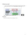
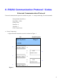
8. RS232 Communication Protocol / Codes
External Communication Protocol
External communication protocol include two parts:A. setup connecting, B. send command.
BenQ default Serial Port :
Baud Rate: 19200
Parity: none
Data bits: 8
Stop bits: 1
Flow Control:none
A. Setup Connecting
A typical Packet transaction session is shown in Figure 1
PC
BenQ Projector
Host System
Target
System
a
c
e
Packet to Target
Packet to Target
Packet to Target
=>
<=
ACK
<=
Packet to Host
b
=>
<=
ACK
<=
Packet to Host
d
=>
Figure 1
61
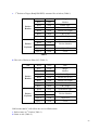
a. 1st Packet to Target (BenQ PB6XXX) structure like as below (Table 1)
Packet
Header
Packet
Payload
Byte0
0xBE
Byte1
0xEF
Magic
Number
Byte2
0x01
Packet Type
Byte3
0x05
Packet size (Low)
Byte4
0x00
Packet size (High)
Byte5
0xD1
CRC (Low)
Byte6
0xFA
CRC (High)
Byte7
0x01
System Info Type
Byte8
0x02
Byte9
0x00
Byte10
0x00
Object ID
Byte11
0x00
Level
Byte0
0x1E
PAK
Byte1
0xBE
Byte2
0xEF
Magic
Number
Byte3
0x01
Packet Type
Byte4
0x05
Packet size (Low)
Byte5
0x00
Packet size (High)
Byte6
0xD1
CRC (Low)
Byte7
0xFA
CRC (High)
Byte8
0x01
System Info Type
Byte9
0x02
Byte10
0x00
Byte11
0x00
Object ID
Byte12
0x00
Level
Version Number
Table 1
b. The Ack of Packet to Host (PC) (Table 2)
Ack
Packet
Header
Packet
Payload
Version Number
Table 2
PAK means that PC will follow the received Packet data
c. Packet same as 1st Packet (Table 1)
d. Same as Ack (Table 2)
62
e. Packet to Target (BenQ PB6XXX) structure (Table 3)
Packet
Header
Packet
Payload
Byte0
0xBE
Byte1
0xEF
Magic
Number
Byte2
0x01
Packet Type
Byte3
0x05
Packet size (Low)
Byte4
0x00
Packet size (High)
Byte5
0xA9
CRC (Low)
Byte6
0xC6
CRC (High)
Byte7
0x00
System Info Type
Byte8
0x00
Byte9
0x00
Byte10
0x00
Object ID
Byte11
0x00
Level
Version Number
Table 3
B. Send Command
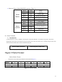
1. Introduction
Command packets consist of “Header” and “Payload”. The Packet Header is consistent for all packets. The Packet
Payload type and content varies based on the type of packet sent. The entire packet size is variable, being the sum of the
fixed-size Packet Header and variable-sized Packet Payload.
Packet Header (fixed size)
Packet Payload (variable size)
Figure 2 Packet Format
Packet Header Format
All Packets use the same Packet Header format illustrated Figure 3.
Byte 0
1
Magic Number
0xBE
0xEF
2
3
4
Type
Packet Payload Size
type
size_lo
size_hi
5
6
CRC
crc_lo
crc_hi
Figure 3 Packet Format
63
The Packet Header size is fixed at seven bytes (Intel byte ordering is used). The following code fragments are taken
from these source files
The Packet Header definition is shown below:
typedef struct
{
BYTE ePacketType; // type of the payload
WORD nPacketSize; // size of the payload
WORD nCRCPacket; // CRC for the entire packet
} PACKET_HEADER;
Magic Number
The Magic Number is a fixed value that is used to insure packet alignment if there are partial packets received or
bytes lost. The Magic Number is a WORD in length (2 bytes). The Magic Number value is 0xEFBE. Because Intel
byte ordering is used, the ls-byte of the word is sent first (byte0 = 0xBE), then the ms-byte (byte1 = 0xEF).
Packet Type
The Packet Type (ePacketType) is a BYTE in length number that defines the type of data in the packet. The following
entries are valid packet typess:
Table 4
Packet Type Name
Packet Type
Number
pt_INVALID
0
Invalid Packet Type
RESERVED
1
RESERVED
pt_EVENT
2
Host can send any event defined in BenQ PB6XXX
Packet
Types
Description
software.
pt_OPERATION
3
Host can send any operation defined in BenQ PB6XXX
software.
Packet Payload Size
The Packet Payload Size (nPacketSize) is a BYTE that defines the size of the Payload portion of the packet. If the
packet contains only header information, this is zero. Therefore, the total byte count of any packet = nPacketSize plus
7 (since the Packet Header is seven bytes long).
Packet Checksum (CRC)
Each packet is CRC’ed using the tables later in this document. This number is the CRC value for the complete packet
including the Packet Header and Packet Payload. The CRC is calculated with the nCRCPacket value initialized to
zero.
64
2. Packet Payload Definition
Event Packet Type
The Event packet is used by the host system to send virtual events (such as Zoom, Source, Auto Adjust, etc.) to the
target system. Packet payload size is 6 bytes.
Byte
Field Name
0-1
Field Value
Virtual Event
Description
Virtual Event ID as defined through
Configurator
2-5
Parameter
Parameter that can be associated with the
event.
. Table 5 Event Packet Type Format
The source code definition of the Message packet data structure is:
typedef struct
{
WORD
DWORD
eEvent;
dwParam;
} EVENT_MESSAGE;
This lets you send any event defined in Configurator to the system including all remote, IR, or special events
Operation Packet Type
The Operation packet is used by the host system to execute operations (such as Brightness, Contrast, Image
Position, etc) in the target system. The Operation packet payload size is 25 bytes.
Byte
Field Name
Field
Description
Value
0
Operation Type
1
OPERATION_SET
2
OPERATION_GET
3
OPERATION_INCREMENT
4
OPERATION_DECREMENT
5
OPERATION_EXECUTE
1-2
Operation
Operation ID as defined in Configurator
3-4
Is Avail
Operation is available
5-8
Operation Target
Used for Operation with Targets. These Targets are
defined in configurator. For instance,
op_BRIGHTNESS has a Target of either MAIN or
PIP window..
9-12
Operation Value
Value of the Set on a set or the Value of the
Get on a Return.
65
13-16
17-20
21-24
Operation Value of
The Minimum Value of the set for operation
minimum.
command.
Operation Value of
The Maximum Value of the set for operation
maximum
command.
Operation Value of
The Increment Value of the set for operation
Increment
command.
Table 6 Operation Packet Payload Format
The source code definition of the Operation packet data structure is:
typedef struct
{
eOPERATION_TYPE
eOpType;
WORD
eOperation;
WORD
bisAvail;
DWORD
dwTarget;
DWORD
dwValue;
DWORD
lmMin;
DWORD
lmMax;
DWORD
lmInc;
} OPERATION_MESSAGE;
This lets the user directly perform logical operations such as “Set Contrast = 80”.
66
3. Send Command
PC
BenQ PB6XXX
Host System
a
Packet to Target
Target System
=>
<=
ACK
b
Figure 4
a. The structure of Command (EX. input select) send to Target (BenQ PB6XXX) like as below
(Table 7)
Packet
Header
Packet
Payload
Byte0
0xBE
Byte1
0xEF
Magic
Number
Byte2
0x02
Packet Type
Byte3
0x06
Packet size (Low)
Byte4
0x00
Packet size (High)
Byte5
0x80
CRC (Low)
Byte6
0xC7
CRC (High)
Byte7
0xC9
Byte8
0x00
Byte9
0x00
Byte10
0x00
Byte11
0x00
Byte12
0x00
Virtual Event ID
Parameter
Table 7
b. Target return to Host (PC) Ack like as below Table 8
Ack
Byte0
0x06
ACK
Table 8
67
C.
Serial Communication Cable and Parameters
For external serial communication from a computer to BenQ projector, BenQ recommends
manfactures use RS-232 communations over a straight through serial cable a 9 pin female D-sub9
connector.
The standard D-sub9 connector on the computer is a male connector, and BenQ projector, too. The
wiring between the computer and BenQ projector is a straight through cable. A 9 pin female to 9 pin
female stright through cable is a very standard part and readily available in many lengths.
Female D-sub9 pinout numbering and definitions on both terminal :
Pin number
Name
2
Transmit
3
Receive
5
Ground
PW Serial uses the following default serial port settings:
. Baud Rate: 19200
. Parity: none
. Data bits: 8
. Stop bits: 1
. Flow Control: none
68
D. Software Flow Chart
Build serial communication port
Baud rate: 19200
Parity: none
Data bits: 8
Stop bits: 1
Transmit 1st Packet (see Table 1)
Delay 100ms
Transmit 2nd Packet (see Table1)
Delay 100ms
Transmit 3rd Packet (see Table3)
Transmit Command (see Table7)
69
Command List
Event Packet Type command:
Command
Packet Header (7 bytes) Packet Payload (6 bytes)
Power
BE EF 02 06 00 13 CE
AA 00 00 00 00 00
Auto
BE EF 02 06 00 F7 C8
8E 00 00 00 00 00
Input select
BE EF 02 06 00 C4 C8
8D 00 00 00 00 00
Menu
BE EF 02 06 00 26 C9
8F 00 00 00 00 00
Exit
BE EF 02 06 00 FE CA
97 00 00 00 00 00
Zoom +
BE EF 02 06 00 AD CD
B4 00 00 00 00 00
Zoom -
BE EF 02 06 00 7C CC
B5 00 00 00 00 00
PIP Source
BE EF 02 06 00 37 C6
CE 00 00 00 00 00
Freeze
BE EF 02 06 00 46 CE
AF 00 00 00 00 00
Ratio
BE EF 02 06 00 04 C6
CD 00 00 00 00 00
Force PC
BE EF 02 06 00 AE C6
C7 00 00 00 00 00
Force Video
BE EF 02 06 00 51 C6
C8 00 00 00 00 00
Force S-Video
BE EF 02 06 00 80 C7
C9 00 00 00 00 00
Force YPbPr
BE EF 02 06 00 B3 C7
CA 00 00 00 00 00
RS232 Power ON
BE EF 02 06 00 3E C4
D7 00 00 00 00 00
RS232 Power OFF
BE EF 02 06 00 C1 C4
D8 00 00 00 00 00
Blank
BE EF 02 06 00 1A CC
B3 00 00 00 00 00
Operation Packet Type command
PC Picture Controls
Command
Packet Header (7 bytes) Packet Payload (25 bytes)
Brightness +
BE EF 03 19 00 44 A0
03 C7 02 CC CC 00 00 00 00 CC×16
Brightness -
BE EF 03 19 00 2A 0A
04 C7 02 CC CC 00 00 00 00 CC×16
Contrast +
BE EF 03 19 00 2E 19
03 C5 02 CC CC 00 00 00 00 CC×16
Contrast -
BE EF 03 19 00 40 B3
04 C5 02 CC CC 00 00 00 00 CC×16
YPbPr Picture Controls
Command
Packet Header (7 bytes) Packet Payload (25 bytes)
Brightness +
BE EF 03 19 00 7B 14
03 D9 02 CC CC FF FF FF FF CC×16
Brightness -
BE EF 03 19 00 15 BE
04 D9 02 CC CC FF FF FF FF CC×16
Contrast +
BE EF 03 19 00 FA 6A
03 F1 02 CC CC FF FF FF FF CC×16
Contrast -
BE EF 03 19 00 94 C0
04 F1 02 CC CC FF FF FF FF CC×16
70
S-Video / Composite Video Picture Controls
Command
Packet Header (7 bytes) Packet Payload (25 bytes)
Brightness +
BE EF 03 19 00 E9 18
03 35 02 CC CC 00 00 00 00 CC x16
Brightness -
BE EF 03 19 00 87 B2
04 35 02 CC CC 00 00 00 00 CC x16
Contrast +
BE EF 03 19 00 16 FC
03 36 02 CC CC 00 00 00 00 CC x16
Contrast -
BE EF 03 19 00 78 56
04 36 02 CC CC 00 00 00 00 CC x16
Color +
BE EF 03 19 00 83 A1
03 37 02 CC CC 00 00 00 00 CC X16
Color -
BE EF 03 19 00 ED 0B
04 37 02 CC CC 00 00 00 00 CC x16
Tint +
BE EF 03 19 00 00 0F
03 4A 02 CC CC 00 00 00 00 CC x16
Tint -
BE EF 03 19 00 6E A5
04 4A 02 CC CC 00 00 00 00 CC x16
Sharpness +
BE EF 03 19 00 43 D0
03 38 02 CC CC 00 00 00 00 CC x16
Sharpness -
BE EF 03 19 00 2D 74
04 38 02 CC CC 00 00 00 00 CC x16
Misc Controls
Command
Packet Header (7 bytes) Packet Payload (25 bytes)
Color Temp –50 (0) BE EF 03 19 00 69 49
01 ED 02 CC CC 00 00 00 00 CE FF FF FF
CC CC CC CC CC CC CC CC CC CC CC CC
0 (10)
BE EF 03 19 00 1C 89
50 (20)
BE EF 03 19 00 69 1C
01 ED 02 CC CC 00 00 00 00 00 00 00 00
CC CC CC CC CC CC CC CC CC CC CC CC
01 ED 02 CC CC 00 00 00 00 32 00 00 00
CC CC CC CC CC CC CC CC CC CC CC CC
PIP Controls
PIP Size
Off
BE EF 03 19 00 15 02
Small
BE EF 03 19 00 E4 42
01 8C 02 CC CC 01 00 00 00 03 00 00 00
CC CC CC CC CC CC CC CC CC CC CC CC
01 8C 02 CC CC 01 00 00 00 00 00 00 00
CC CC CC CC CC CC CC CC CC CC CC CC
Medium
BE EF 03 19 00 74 83
01 8C 02 CC CC 01 00 00 00 01 00 00 00
CC CC CC CC CC CC CC CC CC CC CC CC
Large
BE EF 03 19 00 85 C3
01 8C 02 CC CC 01 00 00 00 02 00 00 00
CC CC CC CC CC CC CC CC CC CC CC CC
PIP Position
Upper-Left
BE EF 03 19 00 1D 66
01 43 02 CC CC 01 00 00 00 00 00 00 00
CC CC CC CC CC CC CC CC CC CC CC CC
Upper-Center
BE EF 03 19 00 8D A7
01 43 02 CC CC 01 00 00 00 01 00 00 00
CC CC CC CC CC CC CC CC CC CC CC CC
Upper-right
BE EF 03 19 00 7C E7
01 43 02 CC CC 01 00 00 00 02 00 00 00
71
CC CC CC CC CC CC CC CC CC CC CC CC
Mid-Left
BE EF 03 19 00 EC 26
01 43 02 CC CC 01 00 00 00 03 00 00 00
CC CC CC CC CC CC CC CC CC CC CC CC
Mid-Center
BE EF 03 19 00 DE 64
01 43 02 CC CC 01 00 00 00 04 00 00 00
CC CC CC CC CC CC CC CC CC CC CC CC
Mid-Right
BE EF 03 19 00 4E A5
01 43 02 CC CC 01 00 00 00 05 00 00 00
CC CC CC CC CC CC CC CC CC CC CC CC
Lower-Left
BE EF 03 19 00 BF E5
Lower-Center
BE EF 03 19 00 2F 24
Lower-Right
BE EF 03 19 00 DB 61
01 43 02 CC CC 01 00 00 00 06 00 00 00
CC CC CC CC CC CC CC CC CC CC CC CC
01 43 02 CC CC 01 00 00 00 07 00 00 00
CC CC CC CC CC CC CC CC CC CC CC CC
01 43 02 CC CC 01 00 00 00 08 00 00 00
CC CC CC CC CC CC CC CC CC CC CC CC
PIP Source
S-Video
BE EF 03 19 00 E8 36
Video
BE EF 03 19 00 DA 74
PIP Brightness
BE EF 03 19 00 FE 0B
01 DA 02 CC CC 01 00 00 00 03 00 00 00
CC CC CC CC CC CC CC CC CC CC CC CC
01 DA 02 CC CC 01 00 00 00 04 00 00 00
CC CC CC CC CC CC CC CC CC CC CC CC
-50 (48)
0 (126)
01 35 02 CC CC 01 00 00 00 CE FF FF FF
CC CC CC CC CC CC CC CC CC CC CC CC
BE EF 03 19 00 8B CB
01 35 02 CC CC 01 00 00 00 00 00 00 00
CC CC CC CC CC CC CC CC CC CC CC CC
50 (204)
BE EF 03 19 00 FE 5E
01 35 02 CC CC 01 00 00 00 32 00 00 00
CC CC CC CC CC CC CC CC CC CC CC CC
PIP Contrast
BE EF 03 19 00 01 EF
-50 (58)
0 (131)
01 36 02 CC CC 01 00 00 00 CE FF FF FF
CC CC CC CC CC CC CC CC CC CC CC CC
BE EF 03 19 00 74 2F
01 36 02 CC CC 01 00 00 00 00 00 00 00
CC CC CC CC CC CC CC CC CC CC CC CC
50 (204)
BE EF 03 19 00 01 BA
01 36 02 CC CC 01 00 00 00 32 00 00 00
CC CC CC CC CC CC CC CC CC CC CC CC
PIP Color
BE EF 03 19 00 94 B2
–50 (129)
01 37 02 CC CC 01 00 00 00 CE FF FF FF
CC CC CC CC CC CC CC CC CC CC CC CC
0 (157)
BE EF 03 19 00 E1 72
-50 (185)
BE EF 03 19 00 94 E7
PIP Tint -50 (0)
BE EF 03 19 00 17 1C
01 37 02 CC CC 01 00 00 00 00 00 00 00
CC CC CC CC CC CC CC CC CC CC CC CC
01 37 02 CC CC 01 00 00 00 32 00 00 00
CC CC CC CC CC CC CC CC CC CC CC CC
01 4A 02 CC CC 01 00 00 00 CE FF FF FF
CC CC CC CC CC CC CC CC CC CC CC CC
0 (128)
BE EF 03 19 00 62 DC
01 4A 02 CC CC 01 00 00 00 00 00 00 00
CC CC CC CC CC CC CC CC CC CC CC CC
50 (255)
BE EF 03 19 00 17 49
01 4A 02 CC CC 01 00 00 00 32 00 00 00
CC CC CC CC CC CC CC CC CC CC CC CC
72
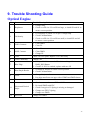
9. Trouble Shooting Guide
Optical Engine
No.
Item
Trouble Shooting Guide
Brightness
1. Change lamp
2. Check overfill size: If overfill too large, re-install SL and AL to
ensure correct position
2
Uniformity
1. If Uniformity is within 3% of spec: Change lamp
2. Check FM installation
3. Check overfill size: If overfill too small, re-install SL and AL
to ensure correct position
3
FOFO Contrast
1. Clean DMD
2. Clean PL
4
ANSI Contrast
1. Clean PL
2. Clean DMD
3. Change PL
5
Color
Check CW 50% point. Replace CW if necessary
6
Color Uniformity
Change CM
7
Blue Edge
1. Readjust LP: Make sure the LP end is touching with
DMD_HSG Datum
2. Check LP: If LP is crushed, replace with new LP
8
Blue/Purple Border
1. re-install SL and AL to ensure correct position
2. Check FM installation
9
Focus
1. Change Projection Lens
2. Put shim metal between upper side of DMD and DMD datum
10
Dust
Clean DMD
11
Horizontal/Vertical
Strips
1.
2.
3.
4.
5.
12
Pixel Fail
Change new DMD
1
Check connector between FPC and M/B
Re-install DMD with FPC
Check if any pin of C-Spring is missing or damaged
Change new FPC/C-Spring
Change new DMD
73
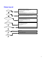
Main board
1.chk voltage input from F/B : 2.5V,5V,12V
2.chk oscillator Y2,Y3 output frequency (16.257MHz,10MHz)
3.chk MCLK(U24-5,130MHz) and DCLK(U25-5,40MHz)
4.chk U17 whether S/W inside or bad soldering
5.change U22(bad soldering)
6.chk Reset IC (U14)
7.chk Abnorm al signal
8.chk Resetz(RN25-5),Poweron(RN25-6) ,DVS(RN18-3),DEN(RN181),DHS(RN18-2),DCLK(RN18-4)
System no work
Yes
No
No data
1.chk output from U15(RN6,RN7,RN8,RN9,RN10,RN11) [graphics input]
2.chk output from U13 (Via VUV[0:7}&VY{0:7]) [video input]
3.chk U22 and its peripherals (as above block)
Yes
No
No im age when graphics
is the current input
1.chk D_SUB cable and L9
2.chk GHS(UH2-4),GVS(UH702-4)
3.chk U15 voltage source U12(3.3V),UB16(3.3V)
4.chk U15 GHS(64),GVS(63),GFBK(65),G CLK(66)
5.chk U15 soldering
6.change U15
Yes
No
No im age when video
is the current input
1.chk U13 voltage source U12,UA6
4.chk Y1 output frequency(24.576MHz)
5.chk U13 output signals to U22
6.chk U13 soldering
7.chagne U13
Yes
No
Unable to download
Yes
1.change U17
2.chk U711 enable pins(1,4)
No
Unable to save
O SD setting
Yes
1.change U21
1.chk RN725-RN728 soldering
2.chk U27,U28
No
Yes
Keypad
m alfunction
No
74
DMD Driver
Start
Yes
Power Voltage
1.chk J702,2.5V(4,,5,6),5V(3),12V(1)
2.chk bead L710-L714,L44
No
Yes
DDP 1000
function
No
Yes
1.LAMPEN Signal to Ballast.
2. 3.5s after LAMPLIT,DMD Become Active and
Display an Image .
No
1.chk clock frequency (unit:MHz)
a.Y901(30)b.Y5(20) C.UY1(100)
C.Motor Controller(8.33)
2.chk ACTDATA,POWERON,RESETZ,CLKIN,HSYNC,
VSYNC,SYNCVALID from Front End
3.chk CW spinning frequency 120Hz , if wrong, chk
MTRDATA , MTRCLK , MTRSELZ
Peripheral
Hardware
.
Yes
Image Color
No
Yes
Image Quality
No
Yes
Lamp On
No
1.chk CW spinning in cloclwise
2.chk CW tape position and width
3.chk cutrain displayed 220us after CW index
4.sequence color transition during CW spoke interval
1.Output from DAD1000 : VBIAS(22-25V),VRST(-26V),
VCC2(7.5V)
2.chk control signal of DMD chip from
U29(RN40,RN45)
3.chk data sequence from U29 to FPC(RN37~RN44)
4.chk JP2,JP3 soldering
1.chk CWINDEX
2.chk LAMPEN
3.chk LAMPLIT
75
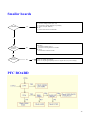
Smaller boards
FAN/BD
No
Fan control:
1.chk the voltage of Q F1 (5,6,7,8)
2.chk the fan voltage U502(2,15),U503(8)
3.check Y501(32.768kHz)
No 5V
1.Check Q 701 & therm al Breaker
Yes
Keypad
function
No
LED dark
1.chk LED voltage from J1
2.chk the m ounting direction of LEDs
No work
1.chk buttons contact to PCB
Yes
Rear Front IR
function
No
1.chk U1 voltage source(5V)
2.chk U1 output signal (always 5Vdc in regular tim e,no pulse voltage)
PFC BOARD
76
DC-DC BOARD
Appendix: Abbreviations
PWR
M/B
F/C
D/B
FPC
K/B
R/B
CW
S/W
S/B
F/B
AL
SL
FG
LP
FM
CM
PL
Power supply module
Main board
Front End Circuit
DMD Driver Circuit
FPC transmission board
Keypad board
Rear IR board
Color wheel
Software
Sensor board
Fan board
Aspherical Lens
Spherical Lens
Front Glass
Light Pipe
Fold Mirror
Concave Mirror
Projection Lens
77
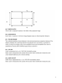
10. CUSTOMER ACCEPTANCE CRITERIA
CONTENT
1.0 SCOPE
2.0
PURPOSE
3.0
APPLICATION
4.0
DEFINITION
5.0
CLASSIFICATION OF DEFECTS
6.0
CLASSIFICATION OF DEFECTIVES
7.0 INSPECTION STANDARD
8.0
GENERAL RULES
9.0
TEST CONDITIONS
10.0 TEST EQUIPMENTS
PART Ⅰ INSPECTION CRITERIA
1. PACKING, MARKING AND ACCESSORY
2. APPEARANCE ON VISIBLE PARTS
3. INSTALLATION
4. FUNCTION
5. SAFETY DEFECT CLASSES
78
1.0 SCOPE
This document establishes the general workmanship standards and
functional acceptance criteria for PROJECTOR produced by BENQ.
2.0 PURPOSE
The purpose of this publication is to define a procedure for inspection of
the PROJECTOR by means of a customer acceptance test, the method of
evaluation of defects and rules for specifying acceptance levels.
3.0 APPLICATION
The "Customer Acceptance Criteria" is applicable to the inspection of the
PROJECTOR, completely packed and ready for dispatch to customers.
Unless otherwise specified, the customer acceptance inspection should
be conducted at manufacturer's site.
4.0 DEFINITION
The "Customer Acceptance Criteria" is the document defining the
process of examining, testing or otherwise comparing the product with a
given set of specified technical, esthetic and workmanship requirements
leading to an evaluation of the "degree of fitness for use", including
possible personal injury or property damage for the use of the product.
5.0 CLASSIFICATION OF DEFECTS
The defects are grouped into the following classes:
5.1 Critical defect
A critical defect is a defect which judgment and experience indicate
that there is likely to result in hazardous or unsafe conditions for
individuals using product.
5.2 Major defect
A major defect is a defect, other than critical one, is likely to result in
failure, or to reduce materially the usability of the product for its
intended purpose.
5.3 Minor defect
A minor defect is a defect that is not likely to reduce materially the
usability of its intended purpose, or is a departure from established
standards having little bearing on the effective use of operation of
the product.
79
6.0 CLASSIFICATION OF DEFECTIVES
A defective is a product which contains one or more defects. The
defective will be classified into following classes:
6.1 Critical defective
A critical defective contains one or more critical defects and may
also contain major and/or minor defects.
6.2 Major defective
A major defective contains one or more major defects and may also
contain minor defects but contains no critical defect.
6.3 Minor defective
A minor defective contains one or more minor defects but contains
no critical and major defects.
7.0 INSPECTION STANDARD
Unless otherwise specified, the inspection standard will be defined by
MIL-STD-105E, NORMAL INSPECTION LEVEL Ⅱ, SINGLE SAMPLING PLAN.
7.1 Acceptance Quality Level
7.1.1 Critical Defect:
When a critical defect is found, this must be reported immediately
upon detection, the lot or batch shall be rejected and further
shipments shall be held up pending instructions from the
responsible person in relevant department.
7.1.2
Under normal sampling
Critical Defective :
0% AQL
Major Defective : 0.65% AQL
Minor
Defective : 2.5% AQL
7.1.3 Under special sampling
Critical Defective :
0% AQL
Major
Defective : 1.0% AQL
Minor
Defective : 4.0% AQL
80
8.0 GENERAL RULES
8.1 The inspection must be carried out by trained inspectors who have
knowledge about the product.
good
8.2 The inspection must be based upon the documents concerning the completely
assembled and packed product.
8.3 When more defects appear with the same unit only the most serious
have to be taken into account.
defect
8.4 Defects found in accessory packed with the product such as Cable,
Connector, Manual, CD and the like, and being inspected as
a part of the complete product, must be included in the evaluation.
8.5 The evaluation must be within the limits of the product specification and, for
not specified characteristics, refer to the sample machine or the judgment of
BENQ QA Engineer. But any kind of proposals or judgments
must
be
reasonable and acceptable by both sides.
8.6 Faults must be able to be repeatedly demonstrated.
9.0 TEST CONDITIONS
Unless other prescription, the test conditions are as followings:
Nominal voltage : refer to operation manual
Environmental illumination variable from 400 to 700 lux
Temperature :
Operating
: 0~ 35 ℃
: -10~ 60 ℃
Storage
Humidity:
Operating
:
Storage
10 ~ 90 % RH
: 10 ~ 90 % RH
Altitude:
Operating
:
0 ~ 6000 ft above sea
level,
81
10.0 TEST EQUIPMENTS
10.1 Pentium with 32MB of system memory , 64M RAM and above are
recommended.
10.2 Win98 or later Operation Environment
10.3 VGA or any Windows compatible display with a resolution of at
least 640x480 pixels, and set to high color or true color
mode.
10.4
Quantum card/Chroma & Test pattern files
10.5
Dark room
10.6
29 points optical measure equipment
10.7
Pattern generators
10.8
DVD player
10.9
Mouse
82
PART Ⅰ INSPECTION CRITERIA
■ Packing, marking and accessory
△ Inner packing material broken.
minor
△ Carton damaged with hole over 1.5 cm in diameter.
minor
△ Carton crashed with dent over 5 cm in diameter.
minor
△ Printing of carton is illegible.
minor
△ Broken packing bag
minor
☆ Spec. label's serial number not the same as carton label's.
Major
☆ Packing model not the same as carton.
Major
☆ Marking missing/wrong.
Major
☆ Accessory shortage/wrong.
Major
☆ Projector missing(found none in carton).
Major
☆ Label on box missing or damaged
Major
☆ Strange objects in the box
Major
■ Appearance on visible parts
△ Poor printing on panel sticker(segment broken, illegible).
minor
△ Damage or deviation when viewed at a distance of 50 cm.
minor
△ Cover/case is dirty(removable).
minor
△ Cover/case exists black spot(irremovable).
minor
△ Cover/case is scratched.
minor
(Note 1)
△ Spec Label reverse, rugged, illegible printing.
minor
△ LED sink over 1 mm.
minor
☆ Label/screws shortage or missing.
Major
☆ Wrong logo of panel sticker.
Major
☆ Wrong spec. label printing.
Major
☆ Label on product wrong or missing
Major
■ Installation
☆ Any accessory which are failed
Major
to meet the installation purpose
83
■ Function
△ Abnormal sound during projection(from 50 cm).
minor
☆ LED won’t light / No power / can't work.
Major
☆ Other function test please refer to Note 2.
■ Safety defect class
☆ Any item which violates the approved safety standard.
major
★ Electrical shock or smoke.
Critical
Note 1 : Please refer to attachment 1.
Note 2 : Please refer to attachment 2.
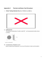
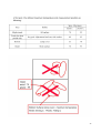
Attachment 1 Scratch Acceptance
Any scratch which exceeds the maximum allowance is treated as a minor defect.
2
Spec. (mm )
0.05 mm2 以下
Black between 2 cm
Soil
0.05 ~0.1mm2
Bubble between 5 cm
0.1~0 5m ㎡
Black spot, Soil, Bubble inspective standard
備註
A side
B side
C side
Accept
Accept
Accept 1. A、B、C side defineted as
4
5
6
3
4
5
3
4
Diagram - A1
2.. LOGO 周邊 2 cm 內不
可有 0.05m ㎡以上之斑點
(0.05m ㎡ 以內斑點不計)
between 5cm
0.2~0.3mm2
between 10cm
2
PS : Any kind of defect not seen from 45 cm(18 inches)(It’s about an arm’s length) with
15 seconds should not be a reject.
Any scratch which exceeds the maximum allowance is treated as a minor defect.
Spec. (mm)
A side
B side
C side
Scratch W<0.1 L<1
Dent
W<0.1 L<2
1
2
3
0
1
2
W<0.1 L<3
0
0
1
Remake
1. The separation distance
between defects must great
than 10mm.
84
Diagram - A1
Definition of Projector's sides
85
Attachment 2 Quality Specification of PB6100
Following item’s spec. will base on Engineering spec.
Item
1. Brightness
Spec
Minimum
2. Uniformity
Minimum
Remarks
1120
lumens
major
50 %
3. ANSI Contrast Ratio
4. FOFO contrast Ratio
major
150:1
700:1
major
major
5. Screen Size For Testing
60” at 2m
major
6 .Focus Range
1.5~6m
major
7. Keystone Distortion
<1.0%
8. Audible Noise Level
major
Typical
34dBA at 25°C
Maximum
35dBA at 25°C
major
IEC - 06
9. Power Connector
major
47” ±5% Diagonal at 2m
10. Throw Ratio
12. Power consumption
Typical
285W /
Standby
13. Blue Border
Purple Border
<2 lux with 40” (diagonal) image size
<4 lux with 40” (diagonal) image size
major
<15W
14. Light Leakage
In Active Area <1.5 lux within 47” (diagonal) image size
Light Leakage out of Active Area <5 lux between of 47” (diagonal) image size and 60”
(diagonal) area
15. IR Receiver ,
IR Receiver X 2 (Front, Rear)
16. Check the remote control function whether it is correct
17. Check the DVD image whether it is correct
86
18.Color Temprature
1.8.1 White
.298±.040
.318±.040
1.8.2 Red
.627±.040
.369±.040
1.8.3 Green
.333±.040
.559±.040
1.8.4 Blue
.137±.040
.061±.040
19. Focus
1.9.1 for PROT lens
1.Pattern:区 pattern
2.Observation:2m to screen(wide only)
3.Criteria:
1.pattern uniform and clear-------->OK
2.If can’t focus uniform and clear,switch to 区 pattern
and focus uniform clear all over screen (central must
clear than corner)
Measure flare and defocus
a.flare:R,G≦2.5
B≦3.5
b.defocus:≦2.5
(区 pattern: Chroma 84,flare and defocus pattern: chroma 34)
1.9.2 for AOCI
lens(A.17) (A.19)
20.Lateral Color
Flare :
Defocus
R <=4.5
R < = 2.0
G<=4.5
G < = 2.0
B<=4.5
B < = 2.0
Pattern(A.19)
Center of screen
All other area
R-G
<1/2
<1
G-B
<1/2
<1
R-B
<2/3
<1
21. Compatibility
21.1 PC
PC Compatible 640X400 Æ 1024X768, compressed
1280X1024; Composite-Sync; Sync-on-Green; Interlace
Mode (8514A);
Detailed Support Timing Specification refer to Appendix
E.1
PC Frequency
Limitation
H-Sync
24 ~ 88 KHz
V-Sync
48 ~ 100 Hz
Pixel Clock
140 MHz
21.2 Video
NTSC/ NTSC4.43/ PAL (Including PAL-M, PAL-N)/
SECAM/ PAL60/
21.3 YPbPr
NTSC 480i/ 480p, PAL 576i/ 720p, HDTV 720p/1080i
87
DMD Image Specification
1. SCOPE
This document specifies the image quality requirements applicable to the XGA RGBW
Palmtop Configuration F Component Kit. The Component Kit provides the XGA RGBW
Palmtop Projector with Digital Imaging functionality based on Digital Micromirror Device
(DMD) technology.
2. Definitions
2.1 Blemish
2.2
A blemish is an obstruction, reflection, or refraction of light that is visible, but out of
focus in the projected image under specified conditions of inspection (see Table 1).
It is caused by a particle, scratch, or other artifact located in the image illumination
path.
Dark pixel
A dark pixel is a single pixel or mirror that is stuck in the OFF position and is visibly
darker than the surrounding mirrors.
2.3 Bright pixel
A single pixel or mirror that is stuck in the ON position and is visibly brighter than
the surrounding mirrors.
2.4 Unstable pixel
A single pixel or mirror that does not operate in sequence with parameters loaded
2.5
2.6
2.7
2.8
into memory. The unstable pixel appears to be flickering asynchronously with the
image.
Adjacent
Two or more stuck pixels sharing a common border or common point , also referred
to as a cluster .
Streaks
Artifact resulting from localized variation in mirror tilt angle relative to surrounding
mirrors . They are similar in appearance to window scratches but appear at the
mirror
Level . Streaks appear as faint diagonal or arcing patterns in the image.
Sea of Mirrors ( SOM )
SOM is a rectangular array of off-state mirrors surrounding the active area.
Eyecatcher
A small localized light “spot” which haas high spatial frequency and high
differential
Brightness. These are due to various DMD window or window aperture “defects”
Including : digs , voids , particles and scratches.
88
2.9
Border Artifacts
All variations of these artifacts are acceptable under this image quality
specification.
Border artifacts are a general category of image artifacts that may show up on
screen in the area outside of the active array. Border artifacts include: Exposed
Bond Wires , Exposed Metal 2 , and Reflective Edge.
2.9.1 Bond Wires
Bond Wires attach the die to the superstructure. If visible, they will appear as
short light parallel lines outside of the Sea of Mirrors ( SOM ).
2.9.2 Exposed Metal 2 is due to a shift in positioning of either the die or the
window aperture which may allow light to be reflected off of the layer of
metal 2 that is below the super structure ( mirrors ). This defect is located at
the outer edge of the SOM.
2.9.3 Reflective Edge
Reflective Edge is light that may reflect from the edge of the DMD”s
window aperture onto the projection screen. It will appear as a thin diffuse
line outside of the SOM.
2.10 Two Zone Blue 60 Screen
The Two Zone Blue 60 screen is used to test for major dark blemishes. Refer to Figure
1 for configuration. All areas of the screen are colored a Microsoft Paintbrush blue 60
( green and red set at 0 , blue set at 60 ).
NOTE : If linear degamma table being used in order to generate an equivalent blue
level on the test screen image.
2.11 Two Zone Gray 10 Screen
The Two Zone Gray 10 screen is used to test for major light blemishes. Refer to Figure
1 for configuration. All areas of the screen are colored a Microsoft Paintbrush gray 10
( green , red , and blue set at 10 ).
NOTE : If linear degamma is not used then the Microsoft Paintbrush values must be
adjusted to match the degamma table being used in order to generate an equivalent
gray level on the test screen image.
89
3. ACCEPTANCE REQUIREMENTS
3.1 Conditions of Acceptance
All DMD image quality defects must be determined under the folloeing projected
image test conditions :
a. Projector degamma shall be linear.
b. Projector error diffusion shall be “off “.
c. Projector brightness and contrast settings shall be set to nominal.
d. The diagonal size of the projected image shall be a minimum of 60 inches.
e. The projection screen shall be 1X gain.
f. The image shall be in focus during all Table 1 tests.
g. The projected image shall be inspected from an 8 feet minimum viewing distance.
3.2 Test Sequence
Tests shall be run in the sequence listed in Table 1
TABLE 1.
SEQ
TEST
Image Quality Specification
SCREEN
ACCEPTANCE
CRITERIA
#
1
Major Dark
Blemish
Two Zone
Blue 60
1. No blemish will be darker than Microsoft Blue
60 in the Critical Zone
2. <=2 blemishes in the Non-Critical Zone
3. No blemish will be >1/2” long / diameter
2
Major Light
Blemish
Two Zone
Gray 10
1. No blemish will be lighter than Microsoft Gray
10 in the Critical Zone
2. <=2 blemishes in the Non Critical Zone
3. No blemish will be > 1/2” long / diameter
3
Eyecatcher
Gray 10
1. No eyecatcher will be lighter than Microsoft Gray
10
Streaks
Blue 60
Gray 10
White
1. No streaks
90
Projected
Image
Any screen
1. No adjacent pixels.
2. No bright pixels ( Active Area )
3. <= 1 bright pixel ( SOM )
4. ≤ 4 dark pixels
5. ≤ 6 minor blemishes.
6. No DMD window aperture shadowing on the
Active Area
7. No unstable pixels in Active Area
Notes :
1. Projected blemish numbers include the count for the shadow of the artifact in addition to
the artifact itself, so that the count usually represents a single artifact on the window.
2. No blemish shall be more than 5 inches long or have a total area of more than 5 square
inches on a 60 inch diagonal projected image. ( <= 1/2 inch for Major Blemish tests )
3. During all Table 1 tests , projected images shall be inspected in accordance with the
conditions of inspection specified in Section 3.
4. The rejection basis for all cosmetic DMD defects ( scratches , nicks , particles ) will be
the projected image tests referenced in Table 1.
5. Any other image quality issue not specifically defined in this document shall be
acceptable.
6. Black screens shall not be used as a basis for rejecting DMDs for image quality.
Figure 1. Major Blemish Two Zone Screen
Non Critical Zone
Critical Zone
center 25%
91
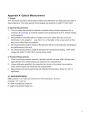
Optical Measurement
1.Scope:
This document describes critical optical related test definitions and Instructions for data or
video projectors. The other general terminologies are specified in ANSI IT7.228-1997.
2.General Requirements
1. The unit under test should be allowed to stabilize without further
adjustment for a minimum of 5 minutes, at nominal ambient room
temperature of 25°C, before making measurements.
2. Measurements shall take place in a light proof room, where the only
source of illumination is the projector. Less than 1 lux of the light
on the screen shall be from any source other than the projector.
3. All measurements shall be made on flat screens that do not provide
any advantage to the performance of the unit
4. All measurements shall be made at standard color temperature
setting, 100% white image (per ANSI IT7.228-1997), except
where noted
3.Practical Requirements
1. When measuring contrast manually, operators should not wear white clothing since
light reflected from white clothing can influence the measurement.
2. Unless otherwise specified, the projection lens is set in the widest zoom position since
zoom function can influence the measurement.
3. Measurement should be performed with Minolta Chromameter, Model CL-100, or
equivalent.
A1. ANSI BRIGHTNESS
ANSI Lumens = (L1+L2+L3+L4+L5+L6+L7+L8+L9)/9 (lux) x A(m^2)
A (Area) = W * H (m^2)
W: width of projected image (m)
H: height of projected image (m)
92
L11
L10
L1
L2
L3
L4
L5
L6
L7
L8
L13
L9
L12
Note: L10, L11, L12, L13 are located at 10% of the distance from corner itself to L5
A2. BRIGHTNESS UNIFORMITY
Brightness Uniformity = Minimum (L10,L11,L12,L13)/ Average (L1,L2,L3,L4,L5,L6,L7,L8,L9)
A3. JBMA UNIFORMITY
JBMA Uniformity = Average (L1,L3,L7,L9)/ L5
A4. ANSI CONTRAST
ANSI Contrast = Average lux value of the white rectangles/Average lux value of the black
rectangles
Contrast Ratio shall be determined from illuminance values obtained from a
black-and-white ”chessboard” pattern consisting of 16 equal rectangles. The white rectangles
shall be at 100% gray and the black rectangles at 0% gray. Illuminance measurements shall
be made at the center of each of the rectangles.
A5. FOFO CONTRAST
FOFO Contrast = Lux value at the center of a solid white screen/the lux value at the center of
a solid black screen
A6. JBMA CONTRAST
JBMA Contrast = Average (L1,L2,L3,L4,L5,L6,L7,L8,L9) under solid white / Average
(L1,L2,L3,L4,L5,L6,L7,L8,L9) under solid black
A7. LIGHT LEAKAGE
Leakage = The maximum light leakage under a solid black pattern in or outside of the
projected image
93
A8. IMAGE DISTORTION
Keystone = (W2-W1)/ (W1+W2) x 100%
Vertical TV dist = (H1+H2-2xH3)/2H2 x100%
Horizontal TV dist = (W1+W2-2xW3)/2W1 x100%
W1: image width at image bottom
W2: image width at image top
W3: image width at the half image height.
H1: image height at image left
H2: image height at image right
H3: image height at half image
Note:
1. Keystone and Vertical TV Distortion are recommended for Front Projection Display
2. Vertical and Horizontal TV Distortion are recommended for Rear Projection Display
A9. THROW RATIO
Throw ratio = projection distance / the width of the projected image
A10. ZOOM RATIO
Zoom ratio = maximum / minimum image diagonal size at a fixed projection distance
A11. FOCUS RANGE
The minimum/maximum focus distance is the minimum/maximum projection distance (The
distance between the outermost element of projection lens and screen), expressed in meter,
at which the image is still at its acceptable focus level.(acceptable focus level is specified by
FOCUS LIMIT SAMPLE approved by customer)
A12. COLOR
Color is expressed as (x, y) in 1931CIE chromaticity values
Note: Color is measured at the center of the screen that is entirely the measured color under
default brightness and contrast settings.
A13. ANSI COLOR
ANSI Color is expressed as (u, v) in 1976 CIE chromaticity values
Note: Color is measured at the center of the screen that is entirely the measured color under
default brightness and contrast settings.
A14. COLOR UNIFORMITY
Color Uniformity is the maximum color difference (△x, △y) between any two points out of
L1~L13
94
A15. ANSI COLOR UNIFORMITY
ANSI Color Uniformity: △u’v’= [(u’1-u’0)^2+(v’1-v’0)^2]^1/2
(u’0,v’0): the average color of L1~L13
(u’1,v’1): the spot with maximum deviation from (u’0,v’0)
A16. PROJECTION OFFSET
Projection Offset= Image height above projection lens optical axis / Total image height x
100%
Note: Optical engine should be kept horizontal attitude
A17. Customer Defined Focus
i. Focus test procedure (Wide only)
a. Pattern: Cross Hatch (Refer to A27 for all related test patterns)
b. Steps:
Step 1: Get best focus at Screen Center with “Phon Pattern”
Step 2: Check “Cross Hatch” at 60”, Wide position.
Step 3: Observe R, G, B color separately and check “Center and 4 corners of
screen” for “Defocus” and “Flare” (Check line only, no check point)
Step 4: Good (“Defocus” << A, “Flare” << B)Æ No more check needed
Step 5: LimitÆ Check “Defocus” (60” <A pixels)
Check “Flare” (60” <B pixels)
Step 6: Worst unit of the dayÆ Check “Letter pattern” (Screen to Observer 6m,
Wide and Tele same spec) with:
“Defocus” < C pixels
“Flare“ < D pixels
ii.
Criteria: Measure the flare size with agreed “Grid” paper and as follows:
Grid of 1.5
pixels
1 Pixel
Flare
Defocus
1.5 pixels
95
5
4
3
2
1
D
D
Screw Holes
1
1
5
1
1
GND
9
5
9
5
9
5
4
8
4
8
4
8
4
8
3
7
3
7
3
7
3
7
2
6
2
6
2
6
2
6
H1
H2
HOLE-V8
H3
HOLE-V8
9
POWER
H4
HOLE-V8
FAN
V12
VDD_F
HOLE-V8
C
SDA
SCL
FAN1_E
FAN2_B
GND
V12
V12
V DD_F
V DD_F
SDA
SCL
SDA
SCL
FAN1_E
FAN2_B
FAN1_E
FAN2_B
G ND
G ND
V12
VDD_F
C
SDA
SCL
FAN1_E
FAN2_B
GND
Optical Points
B
OP1
OP
OP2
OP
OP3
OP
OP4
OP
OP5
OP
OP6
OP
OP7
OP
OP8
OP
OP9
OP
OP10
OP
OP11
OP
OP12
OP
OP13
OP
OP14
OP
01_POWER
02_FAN
B
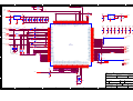
Benq Corporation
Project Code
Model Name
99.J8677.001
A
Title
4
3
2
PCB Rev. Document Number
S02
99.J8677.B12-C3-304-002
Wednesday, August 06, 2003
Sheet
Reviewed By
Prepared By
ANGEL HU
5
ODM
A
FAN BOARD
Size PCB P/N
<Size>
48.J8613.S02
Date:
OEM/ODM Model Name
PB6100
KEN JA CHEN
1
1
of
3
Approved By
JACK CHEN
Rev.
0
5
4
3
2
1
RS701
CS701
CS702
47
1000P K
2
9
3
+
C7301
470U 25V
2
3
D6301 US1M
D7301
10CTQ150S
2
J6302
D6302
18Vcc
2
R6307
1
47
W
1
W
DRILL-22
4
D6303
2
SS3H10
CS703
5
+
RS703
1
US1J
47
L7301
1
2
R6308
R6309
10KF
VDD
D7302
ES1D
2060089102
therm
47
47
CS704
10UH
C7302
470U 25V
R7313
1K
D
20D0049108
5
4
3
2
1
R7314
1K
+
C7305
220U
25V
J7302
20L2021005
FAN1_E
FAN1_E
FAN2_B
FAN2_B
G1
2200P J
2200P J
47
R7310
2.4K
C7308
220U
25V
+
G1
V12
5V
1
R7308
3.32KF
15K
6.8
2
47U 50V
1
1
C7310
10U
16V
+
LM431
GND
2
3
3
4
4
5
5
6
6
7
7
8
8
R7307
2
VDD
470
3
+
C6306
0.1U M
2
1
C6303
R7311
2.32KF
C7306
0.1U K
U7302
R6304
30K
R7312
30K F
2V5
1
2
G2
5
3
R6302
C7307
0.1U K
1
G1
1
C7309
1000P M
2
D7303
SS24
C
J7301
R7304
5.1K
R7306
4
V12
G2
2
3
C
PQ1CY1032Z
F
X
S
TOP247Y
180U K
2
ON
5
V12
2
1
4
VDD
D
L
RF5
1K
U6302
2V5
L7302
VOUT
PC123FY1
7
2
U6301
1
3300P Y1
RA603
680K
VIN
330
FB
U6305
R7305
1
C
4
CY6301
6
RA602
680K
C6302
47U 50V
2
+
RS704
GND G
1
600UH
C6304
1U Z
3
1
2
R702
8
SCL
SDA
FAN_P
G2
1
1
2
3
4
5
6
7
8
LAMP-SYNC
LAMPLIT
LAMP-RXD
G2
2
2
2062010103
R701
47K
C7303
470U 25V
+
5V
8
7
6
5
4
CA2
0.01U M
3
2
1
1
RA601
680K
VDD
1
C6301
0.01U M
R6301
47K
CA1
0.01U M
J7304
Q701
SI4431DY-T1
V12
1
1
2
3
47
2
D
1000P K
1
J6301
10
2
T6301
1
1
380Vdc
G1
RS702
20D0038108
VDD
R7309
2.32KF
B
B
R402
100
500 OHM
VDD
RF4
47K
380Vdc
RF1
47
+
CC602
100U
450V
+
RF2
2K
CF2
22U
16V
Title
RF3
2
ODM
A
FAN BOARD
PCB Rev. Document Number
S02
99.J8677.B12-C3-304-002
Wednesday, August 06, 2003
Sheet
Reviewed By
Prepared By
ANGEL HU
3
OEM/ODM Model Name
PB6100
Size PCB P/N
<Size>
48.J8613.S02
10K
Date:
4
Model Name
99.J8677.001
CF1
5
1
1
Benq Corporation
Project Code
A
0.1U M
1
Note:Bllast control Pin
QF2
MMST3904
1
R404
100
2
FAN_P
LAMP-SYNC
LAMP-RXD
VDD_F
3
NTC 5 OHM
2
NTC 5 OHM
CC601
0.47U K
TR602
1
8
7
6
5
1
TR601
1
2
t
2
t
SF10L60U
hsink2
FOR DC601
FOR U6301
3
2
1
LAMPLIT
G2
L1
1
IN
3
QF1
SI4431DY-T1
1
2
1
DC601
1
1
2
3
4
5
J7303
20L2021005
500 OHM
2
H6
L2
4
W2
IN
1
1
G1
TP1 TP2 TP3 TP4 TP5
R401
4.7K
KEN JA CHEN
1
2
of
3
Approved By
JACK CHEN
Rev.
0
3
2
10M
25.6KHZ
1
NC
FR
F
NC
ER
E
DR
D
SCL
SDA
RA501
4.7K
R510
VDD_F
Q504
2N3904
1
10K
R509
CD4049UBCM
10P J
2
10P J
2
2.2K
FAN4_P
C502
1
C501 Y501
2.4K
R508
2.2K
+ C505
22U RB501
2.2K
16V
V12
CA507
0.47U K
R517
4.7K
U502
14
12
SMBCLK
SMBDATA
11
ALERT
6
RESET
1
OUT1
VCC
VCC
15
2
DXP1
3
DXN
10
FG1
9
CLK
FAN1_B
C507
2200P K
5
OUT2
FG2
GND
GND
16
13
7
8
C508
2200P K
FAN1_P
FAN2_B
Q505
2N3904
1
R514
10K
R516
2.2K
VDD_F
R515
2.2K
G768B
32.768KHZ
R513
RA503
4.7K
FAN1_E
4
DXP2
D
Q506
2SB772S
3
FANSPIN1
FANSPIN4
Crystal generate the clock for fan control IC.
RB502
2.2K
+ C509
22U
16V
VDD_F
10K
2 fan speed control and 2 thermal sensor detect IC
C
C
3
2
1
680
FANSPIN2
FAN2_P
VDD_F
VDD_F
RA502
4
5.6K
8
7
6
5
C504
0.1U M
R504
10K
R520
0
FANSPIN2
U503
1
G2
FAN1_E
FAN1_B
Q502
2N3904
2
F.G.
R505
3
ON/OFF
2.2K
4
GND
VCC
A2
SDA
1
SDA
SDA
6
A1
SCL
2
SCL
SCL
7
A0
O.S.
3
VCC
8
8
SDA
7
SDA
SCLK
6
1
SCL
CLK
5
32.768KHZ
FANSPIN1
R506
820
1
FAN2_P
FAN4_P
FANSPIN4
2
+
RA505
2.2K
G760A
B
VDD_F
2
FAN1_P
G1
OUT
G751-2
5
3
R503
47K
J502
10
9
8
7
6
5
4
3
2
1
U505
GND
G1
Q501
SI4431DY-T1
C510
0.1U M
4
G2
RA504
V12
J501
4
3
2
1
20L2021004
B
R512
C519 220P J
3
3
R502
VDD
AR
A
BR
B
CR
C
VSS
4.7K
Q503
2SB772S
16
15
14
13
12
11
10
9
2
2M
R501
U501
1
2
3
4
5
6
7
8
OPEN
C506
0.1U M
1
CA508
0.1U M
32.768KHZ
R519
CA506
0.47U K
2
R507
V12
VDD_F
2.4K
1
VDD_F
D
R511
OPEN
C518 220P J
2
R518
V12
1
3
4
2
5
GND
C503
47U
16V
Thermal sensor
20L2021010
Fan control IC
Benq Corporation
Project Code
Model Name
99.J8677.001
A
Title
4
3
2
PCB Rev. Document Number
S02
99.J8677.B12-C3-304-002
Wednesday, August 06, 2003
Sheet
Reviewed By
Prepared By
ANGEL HU
5
ODM
A
FAN BOARD
Size PCB P/N
<Size>
48.J8613.S02
Date:
OEM/ODM Model Name
PB6100
KEN JA CHEN
1
3
of
3
Approved By
JACK CHEN
Rev.
0
5
4
3
2
1
D
D
DMD_CHIP
80*2_CONN
DD[63:0]
C
MBRST[15:0]
DCLK_L
DMDSER
SACCLK
SACBUS
SCTRL_L
LOADB_LZ
TRC_L
P3P3V
VCC2
GND
DD[63 :0]
MBRST[15:0]
DCLK_L
D MDSER
SACCLK
SACBUS
SCTRL_L
LOADB_LZ
TRC_L
P3P3V
V CC2
G ND
DD[63:0]
C
MBRST[15:0]
DCLK_L
DMDSER
SACCLK
SACBUS
SCTRL_L
LOADB_LZ
TRC_L
P3P3V
VCC2
GND
DMD_CHIP
80*2_CONN
B
B
Benq Corporation
A
Project Code
99.J8677.001
Title
4
3
2
ODM
PCB Rev. Document Number
S01
99.J8677.B12-C3-304-003
Wednesday, August 06, 2003
Sheet
Reviewed By
Prepared By
ANGEL HU
5
A
OEM/ODM Model Name
PB6100
CHIP BOARD
Size PCB P/N
<Size>
48.J8623.S01
Date:
Model Name
DAVID HN LIN
1
1
of
3
Approved By
KELVIN LIAO
Rev.
0
5
4
3
DD[63 :0]
DD[63 :0]
2
1
DD[63:0]
J1
D
P3P3V
TP25
P3P3V
SACCLK
SACBUS
SCTRL_L
TRC_L
SACCLK
SACBUS
SCTRL_L
TRC_L
D D62
D D60
D D58
D D56
D D54
D D52
C
D D50
D D48
D D46
D D44
D D42
D D40
D D38
D D36
2
4
6
8
10
12
14
16
18
20
22
24
TP24 26
28
30
TP27 32
TP29 34
TP31 36
TP32 38
40
TP34 42
TP36 44
46
TP38 48
TP40 50
52
TP42 54
TP44 56
58
TP46 60
TP48 62
64
TP50 66
TP52 68
70
TP54 72
TP56 74
76
TP58 78
TP60 80
D
1
3
5
7
9
11
13
15
17
19
21
23
25
27
29
31
33
35
37
39
41
43
45
47
49
51
53
55
57
59
61
63
65
67
69
71
73
75
77
79
TP17
TP21
TP23
BINSEL0
BINSEL1
BINSEL0
BINSEL1
VCC2
TP26
VCC2
TP28
TP30
D MDSER
LOADB_LZ
DMDSER
LOADB_LZ
TP33
DCLK_L
DCLK_L
TP35
TP37
D D63
D D61
TP39
TP41
D D59
D D57
TP43
TP45
D D55
D D53
TP47
TP49
D D51
D D49
TP51
TP53
D D47
D D45
TP55
TP57
D D43
D D41
TP59
TP61
D D39
D D37
TP63
TP65
D D35
D D33
TP69
TP73
D D31
D D29
TP79
TP83
D D27
D D25
TP88
TP92
D D23
D D21
TP97
TP101
D D19
D D17
TP107
TP109
D D15
D D13
TP111
TP113
D D11
DD9
TP115
TP117
DD7
DD5
TP121
TP124
DD3
DD1
TP126
TP128
TP130
TP132
MBRST15
MBRST13
MBRST11
MBRST9
C
20L1065080
J2
B
D D34
D D32
TP62
TP64
D D30
D D28
TP68
TP72
D D26
D D24
TP78
TP82
D D22
D D20
TP87
TP91
D D18
D D16
TP96
TP100
D D14
D D12
TP106
TP108
D D10
DD8
TP110
TP112
DD6
DD4
TP114
TP116
DD2
DD0
TP120
TP123
MBRST14
MBRST12
MBRST10
MBRST8
TP125
TP127
TP129
TP131
MBRST6
MBRST4
MBRST2
MBRST0
TP133
TP135
TP137
TP139
2
4
6
8
10
12
14
16
18
20
22
24
26
28
30
32
34
36
38
40
42
44
46
48
50
52
54
56
58
60
62
64
66
68
70
72
74
76
78
80
1
3
5
7
9
11
13
15
17
19
21
23
25
27
29
31
33
35
37
39
41
43
45
47
49
51
53
55
57
59
61
63
65
67
69
71
73
75
77
79
TP134
TP136
TP138
TP140
B
P3P3V
MBRST7
MBRST5
MBRST3
MBRST1
R1
1K
H1
GND
1
2
BINSEL0
BINSEL1
4
3
BINSEL0
BINSEL1
6240019001
BINSEL1
0
0
1
1
20L1065080
A
MBRST[15:0]
R2
1K
BINSEL0
0
1
0
1
DMD Bin
B
C
D
E
Benq Corporation
Project Code
99.J8677.001
MBRST[15:0]
Title
4
3
2
ODM
PCB Rev. Document Number
S01
99.J8677.B12-C3-304-003
Wednesday, August 06, 2003
Sheet
Reviewed By
Prepared By
ANGEL HU
5
A
OEM/ODM Model Name
PB6100
CHIP BOARD
Size PCB P/N
<Size>
48.J8623.S01
Date:
Model Name
DAVID HN LIN
1
2
of
3
Approved By
KELVIN LIAO
Rev.
0
5
2
TP1
T POINT A
TP2
T POINT A
D
1
1
E01
E03
E05
G01
C01
G03
D04
G05
C03
H02
A01
H04
D06
H06
D10
K06
B06
K04
B04
L05
C09
L03
C07
A03
A07
D12
B10
A09
B12
C13
A13
A15
U1A
D0
D1
D2
D3
D4
D5
D6
D7
D8
D9
D10
D11
D12
D13
D14
D15
D16
D17
D18
D19
D20
D21
D22
D23
D24
D25
D26
D27
D28
D29
D30
D31
MBRST[15:0]
DCLK_L
LOADB_LZ
MBRST_15
MBRST_14
MBRST_13
MBRST_12
MBRST_11
MBRST_10
MBRST_9
MBRST_8
MBRST_7
MBRST_6
MBRST_5
MBRST_4
MBRST_3
MBRST_2
MBRST_1
MBRST_0
DCLK_L
C15
DCLK
LOADB_LZ
B16
LOADB
SACCLK
SACBUS
SACCLK
SACBUS
SCTRL_L
TRC_L
SCTRL_L
TRC_L
AC25
AA25
N03
L01
AC23
Y08
K02
READ_OUT2
READ_OUT
SCAN_TEST
READ_OUT2
READ_OUT
AB22
AA23
M28
D MDSER
DMDSER
VCC2
VCC2A
VCC2B
VCC2C
VCC2D
VCC2E
VCC2F
VCC2G
VCC2H
N29
P02
P30
R01
R29
T02
T30
U01
EVCC0
EVCC1
Y22
AB08
V CC2
1
Y20
AB20
AA19
AC19
AA17
AC17
Y16
AB16
AB14
Y14
AC13
AA13
AC11
AA11
AB10
Y10
2
MBRST15
MBRST14
MBRST13
MBRST12
MBRST11
MBRST10
MBRST9
MBRST8
MBRST7
MBRST6
MBRST5
MBRST4
MBRST3
MBRST2
MBRST1
MBRST0
C1
+ 1U
16V
20%
VCC2
C2
0.1U M
C3
0.1U M
C4
0.1U M
C5
0.1U M
16V
16V
16V
16V
C
SAC_CLK
SAC_BUS
SCTRL
TRC
PRG_FUS_EN
BI_MODE
BI_TOF
Optical Points
D32
D33
D34
D35
D36
D37
D38
D39
D40
D41
D42
D43
D44
D45
D46
D47
D48
D49
D50
D51
D52
D53
D54
D55
D56
D57
D58
D59
D60
D61
D62
D63
MBRST[15:0]
1
DD[63 :0]
D
C
3
DD0
DD1
DD2
DD3
DD4
DD5
DD6
DD7
DD8
DD9
D D10
D D11
D D12
D D13
D D14
D D15
D D16
D D17
D D18
D D19
D D20
D D21
D D22
D D23
D D24
D D25
D D26
D D27
D D28
D D29
D D30
D D31
DD[63:0]
4
OP1
OP
OP2
OP
OP3
OP
OP4
OP
OP5
OP
OP6
OP
OP7
OP
OP8
OP
OP9
OP
OP10
OP
OP11
OP
OP12
OP
OP13
OP
OP14
OP
D D32
D D33
D D34
D D35
D D36
D D37
D D38
D D39
D D40
D D41
D D42
D D43
D D44
D D45
D D46
D D47
D D48
D D49
D D50
D D51
D D52
D D53
D D54
D D55
D D56
D D57
D D58
D D59
D D60
D D61
D D62
D D63
D16
B18
A19
A21
C19
D18
B22
B24
A25
C21
C25
M26
A27
K28
D22
K26
B30
K30
B28
J25
C27
J27
D26
J29
D24
G27
D28
G29
D30
F30
F28
F26
DMD 0.7XGA DDR
DD[63 :0]
Screw Holes
B
B
16V
16V
C9
0.1U M
C10
0.1U M
10V
16V
16V
2
1
C8
10U
+
C11
C13
C12
0.1U M
16V
0.1U M
16V
C14
0.1U M
16V
0.1U M
16V
U03
T28
R03
P28
P04
N27
M04
M02
L29
L27
L25
J05
J03
H28
H26
F04
F02
E29
9
5
9
5
9
5
4
8
4
8
4
8
4
8
3
7
3
7
3
7
3
7
2
6
2
6
2
6
2
6
H3
H4
H5
H6
HOLE-V8
HOLE-V8
HOLE-V8
HOLE-V8
Project Code
99.J8677.001
Title
Date:
2
A
OEM/ODM Model Name
PB6100
ODM
PCB Rev. Document Number
S01
99.J8677.B12-C3-304-003
Wednesday, August 06, 2003
Sheet
Reviewed By
Prepared By
ANGEL HU
3
Model Name
CHIP BOARD
Size PCB P/N
<Size>
48.J8623.S01
4
9
Benq Corporation
DMD 0.7XGA DDR
A
5
1
1
1
5
GND
GND
GND
GND
GND
GND
GND
GND
GND
GND
GND
GND
GND
GND
GND
GND
GND
GND
1
AC07
AB26
AB24
AB18
AB12
AB06
AA21
AA15
AA09
AA07
Y24
Y18
Y12
V02
U29
GND
GND
GND
GND
GND
GND
GND
GND
GND
GND
GND
GND
GND
GND
C7
0.1U M
P3P3V
P3P3V
P3P3V
P3P3V
P3P3V
P3P3V
P3P3V
P3P3V
P3P3V
P3P3V
P3P3V
P3P3V
P3P3V
P3P3V
P3P3V
P3P3V
P3P3V
B02
B08
B14
B20
B26
C05
C11
C17
C23
C29
D08
D14
D20
E27
C6
0.1U M
A05
A11
A17
A23
A29
D02
H30
J01
M30
N01
V30
W01
AC05
AC09
AC15
AC21
AC27
GND
GND
GND
GND
GND
GND
GND
GND
GND
GND
GND
GND
GND
GND
GND
U1B
P3P3V
P3P3V
GND
DAVID HN LIN
1
3
of
3
Approved By
KELVIN LIAO
Rev.
0
SDA
SCL
DGE[7:0]
DBE[7:0]
D HS
DVS
DCLK
D EN
POWERON
RESETZ
LAMPLITZ
3.3V_D
SDA0
SCL0
DGE[7:0]
DBE[7:0]
V12_D
DHS
DVS
VDD_D
3.3V_D
DCLK
DEN
2V5_D
VDD_D
3.3V_D
3
2V5_D
V12_D
2V5_D
LAMPEN
VDD_D
PAGE_3
002_DMD
3.3V_D
LAMPEN
VDD
ECO-MODE
V DD
LAMPEN
FAN_P
ECO-MODE
V12_D
POWERON
RESETZ
LAMPLITZ
GND
ECO-MODE
FAN_P
ECO-MODE
DBE[7:0]
V12_D
VDD_D
2V5_D
3.3V_D
LAMPEN
GND
FAN_P
SDA
SCL
2
ECO-MODE
3.3V
VDD
VDD
3.3V
V DD
3.3V
V DD
DBE[7:0]
DRE[7:0]
SCL
SDA
SCL
SDA
3.3V
DGE[7:0]
POWERON
RESETZ
LAMPLITZ
POWERON
RESETZ
LAMPLITZ
2
DRE[7:0]
DGE[7:0]
DCLK
D EN
DCLK
DEN
GND
DRE[7:0]
D HS
DVS
DHS
DVS
3
SDA0
SCL0
SDA
SCL
DRE[7:0]
PAGE_2
001_MAIN
E
4
PAGE_5
004_DISPLAY
LAMPLITZ
RESETZ
4
D
3.3V_D
C
SDA0
SCL0
B
GND
A
PAGE_4
003_POWER&LAMP&DETECT
Benq Corporation
Project Code
99.J8677.001
1
Title
Model Name
OEM/ODM Model Name
<OEM/ODM>
PB6100
Size PCB P/N
<Size>
48.J8601.S04
PCB Rev. Document Number
S04
99.J8677.B12-C3-304-004
Tuesday, October 07, 2003
Date:
Sheet
Reviewed By
Prepared By
ANGEL HU
A
B
C
D
1
MAIN BOARD
DAVID HN LIN
E
1
20
of
Approved By
KELVIN LIAO
R ev.
1
A
B
C
D
E
Regect RC1 and RC2 before connect DX660 main board with
INTERFACE board.
SCL
SDA
VDD
V33
CVBS
LUMA
CVBS
GND
SDA
SCL
SDA
SCL
AVDD
AVDD
3
HSYNC
HSYNC
RAIN_C
GAIN_C
BAIN_C
VSYNC_C
HSYNC
KEYSTONE
ROMWEn
ROMOEn
VPPEN
VPPEN
A0
BHENn
RESET
VVS
VFIELD
VPEN
VHS
VCLK
ROMOEn
VUV[7:0]
3.3V
VDD
VDD
4
POWERON
RESETZ
POWERON
RESETZ
DRO[7:0]
DRE[7:0]
DRE[7:0]
DGO[7:0]
DGE[7:0]
DGE[7:0]
DBO[7:0]
DBE[7:0]
DBE[7:0]
POWERON
RESETZ
DRE[7:0]
DGE[7:0]
3
V33
SCL
SDA
SCL
SDA
GRE[7:0]
GRE[7:0]
GRE[7:0]
GGE[7:0]
GGE[7:0]
GBE[7:0]
GHS
GVS
GBE[7:0]
GHS
GVS
GBLKSPL
GFBK
GCLK
GCOAST
VDD
GBLKSPL
GFBK
GCLK
GCOAST
GRE[7:0]
DBE[7:0]
D HS
DVS
D EN
DCLK
DHS
DVS
DEN
DCLK
V33
GBLKSPL
GFBK
GCLK
GCOAST
RAIN_C
GAIN_C
BAIN_C
VSYNC_C
VVS
VFIELD
VPEN
VHS
VCLK
VY[7:0]
A0
BHENn
D[0:7]
VVS
VFILD
VPEN
VHS
VCLK
GBE[7:0]
GHS
GVS
RAIN_C
GAIN_C
BAIN_C
VSYNC_C
VUV[7:0]
VVS
VFIELD
VPEN
VHS
VCLK
GGE[7:0]
RAIN_C
GAIN_C
BAIN_C
VSYNC_C
VY[7:0]
VUV[7:0]
KEYSTONE
CVBS
VY[7:0]
ROMWEn
LUMA
CHROMA
AVDD
CVBS
LUMA
VUV[7:0]
RAIN_V
GAIN_V
BAIN_V
LUMA
CHROMA
RAIN_V
GAIN_V RAIN_V
BAIN_V GAIN_V
BAIN_V
CHROMA
CHROMA
VY[7:0]
RESET
SDA
SCL
D[0:7]
LLC1
LLC2
D[0:15]
A[19:1]
3.3V
3.3V
D[0:15]
A[19:1]
PAGE_11
016_MISC
V33
POWERON
GND
3.3V
POWERON
GND
DCKEXT
MCKEXT
3.3V
KEYSTONE
3.3V
DCKEXT
MCKEXT
ROMWEn
ROMOEn
SCL
SDA
VDD
VPPEN
012_DECODE
VDD
SCL
SDA
A0
BHENn
VDD
RESET
RESETn
DECODE
D[0:15]
A[19:1]
VDD
GND
VDD
3.3V
4
DCKEXT
MCKEXT
VDD
SCL
SDA
014_MEMORY&KEYSTONE
PAGE_9
INPUT
SCL
SDA
DHS
DVS
DEN
DCLK
Note: To DDP1000 input port
GGE[7:0]
GBE[7:0]
GHS
GVS
LAMPLITZ
LAMPLITZ
LAMPLITZ
Note: Lamp on/off detect signal.
GBLKSPL
GFBK
GCLK
GCOAST
Note: PW164B RS232 I/O port connect with
PC ( for control ) and Ballast ( for lamp
stasus )
VDD
HSYNC
GND
ECO-MODE
ECO-MODE
ECO-MODE
FAN_P
FAN_P
PAGE_8
013_AFE
2
2
VDD
GND
VDD
IRR CVR
GND
PAGE_10
015_PW166
Benq Corporation
IRR CVR
CONTROL
CONTROL
Project Code
99.J8677.001
1
GND
Title
RXD
TXD
3.3V
3.3V
TCK
TMS
TDO
CS1n
CS0n
key8
RXD
TXD
3.3V
PAGE_12
017_KEY
CS1n
CS0n
AUDIO_MUT
AUDIO_VOL
3.3V
VDD
RESETn
D[0:7]
CS1n
CS0n
RESETn
D[0:7]
CS1n
CS0n
key8
IRRCVR
CONTROL
VDD
IRRCVR
FAN_P
RXD
TXD
RXD
TXD
Model Name
OEM/ODM Model Name
<OEM/ODM>
PB6100
Size PCB P/N
<Size>
48.J8601.S04
PCB Rev. Document Number
S04
99.J8677.B12-C3-304-004
Tuesday, October 07, 2003
Date:
Sheet
Reviewed By
Prepared By
011_INPUT
ANGEL HU
A
B
C
D
1
MAIN BOARD
DAVID HN LIN
E
2
20
of
Approved By
KELVIN LIAO
R ev.
1
5
4
3
1
DRE[7:0]
DRE[7:0]
DGE[7:0]
DGE[7:0]
DBE[7:0]
DBE[7:0]
DAD1000
V12_D
V12_D
V12_D
2V5_D
2V5_D
2V5_D
VDD_D
VDD_D
VDD_D
VDD
3.3V_D
3.3V_D
SR16ADDR0
SR16ADDR1
SR16ADDR2
SR16ADDR3
SR16MODE0
SR16MODE1
3.3V_D
SR16SEL0
SR16SEL1
SR16STROBE
GND
SR16OEZ
3.3V_D
3.3V_D
2V5_D
2V5_D
SCPDI
SCPDO
SCPCK
SCPENZ
SR16ADDR0
SR16ADDR1
SR16ADDR2
SR16ADDR3
D
SR16ADDR0
SR16ADDR1
SR16ADDR2
SR16ADDR3
MBRST[0:15]
SR16MODE0
SR16MODE1
SR16SEL0
SR16SEL1
SR16STROBE
SR16OEZ
SCPDI
SCPDO
SCPCK
SCPENZ
SCPDI
SCPDO
SCPCK
SCPENZ
EXT-ARSTZ
V12_D
V12_D
3.3V_D
3.3V_D
SCL0
SDA0
DMDSER
DCLK-L
TRC-L
LOADB-LZ
EXT-ARSTZ
DD[0:63]
IR QZ
SCTRL-L
SACCLK
SACBUS
SCTRL-L
3.3V_D
SACCLK
SACBUS
VDD
3.3V_D
VDD
GND
DMDSER
DMDSER
DCLK-L
TRC-L
LOADB-LZ
DCLK-L
TRC-L
LOADB-LZ
DD[0:63]
C
DD[0:63]
IRQZ
VCC2
SCL0
SDA0
SCTRL-L
SACCLK
SACBUS
GND
IRQZ
MBRST[0:15]
DDP1000_DATA
SR16SEL0
SR16SEL1
SR16STROBE
SR16OEZ
C
MBRST[0:15]
SR16MODE0
SR16MODE1
DRE[7:0]
V DD
DBE[7:0]
VDD
DGE[7:0]
D
2
SCL0
SDA0
VCC2
026_DMD_DAD1000
GND
ECO-MODE
RESETZ
POWERON
DEN
RESETZ
POWERON
D EN
RESETZ
POWERON
D EN
DHS
DVS
D HS
DVS
D HS
DVS
DCLK
DCLK
DCLK
From Pixelworks output
EXT-ARSTZ
CKMTR1
MTRSELZ
MTRCLK
MTRDATA
CWTACH
VDD_D
V12_D
VCC2
BINSEL0
BINSEL1
B
VDD_D
V12_D
GND
FSD16
PUM-ARSTZ
DHS
DVS
DCLK
EXT-ARSTZ
CKMTR1
MTRSELZ
MTRCLK
MTRDATA
CWATCH
FSD16
RQ[0:7]
DQA[0:8]
DQB[0:8]
CFM
CFMN
SCK
SCLKN
CMD
SIO
PCLKM
CTM
CTMN
REFCLK
VREF-RDRAM
RQ[0:7]
RQ[0:7]
DQA[0:8]
DQA[0:8]
DQB[0:8]
CFM
CFMN
SCK
SCLKN
CMD
SIO
PCLKM
CTM
CTMN
REFCLK
VREF-RDRAM
DQB[0:8]
CFM
CFMN
SCK
SCLKN
CMD
SIO
PCLKM
CTM
CTMN
REFCLK
VREF-RDRAM
PAGE_14
022_DMD_MEMORY
DRCGPDZ
FLASH-BUSYZ
RESETZ
POWERON
DEN
2V5_D
LAMPEN
LAMPLITZ
EXT-ARSTZ
CKMTR1
MTRSELZ
MTRCLK
MTRDATA
CWTACH
DRCGPDZ
PAGE_20
028_DMD_MOTOR
3.3V_D
LAMPEN
LAMPLITZ
FSD16
LAMPEN
LAMPLITZ
EXT-ARSTZ
CKMTR1
MTRSELZ
MTRCLK
MTRDATA
CWTACH
DRCGPDZ
VCC2
BINSEL0
BINSEL1
BINSEL0
BINSEL1
PAGR_21
029_DMD_CHIP
2V5_D
3.3V_D
GND
LAMPEN
LAMPLITZ
PAGE_13
021_DMD_DDP1000
PUM-ARSTZ
GND
PAGE_15
023_DMD_OSC&FAN
A
COSC
MOSC
CWINDEX
PUM-ARSTZ
COSC
MOSC
CWINDEX
FLASH-BUSYZ
B
COSC
MOSC
CWINDEX
FLASH-BUSYZ
COSC
MOSC
CWINDEX
BINSEL0
BINSEL1
3.3V_D
3.3V_D
ECO-MODE
025_DMD_DDP1000_DATA
VDD_D
VDD_D
ECO-MODE
2V5_D
2V5_D
3.3V_D
3.3V_D
Benq Corporation
Project Code
99.J8677.001
Title
OEM/ODM Model Name
<OEM/ODM>
PB6100
Size PCB P/N
<Size>
48.J8601.S04
PCB Rev. Document Number
S04
99.J8677.B12-C3-304-004
Tuesday, October 07, 2003
Date:
Sheet
Reviewed By
Prepared By
ANGEL HU
5
4
3
2
A
MAIN BOARD
GND
PAGE_16
024_DMD_RAMBUS
Model Name
DAVID HN LIN
1
3
20
of
Approved By
KELVIN LIAO
R ev.
1
A
B
C
D
J704
3
3 TP242
4
4
5
5 TP244
6
6
7
7
8
8
80 OHM
C828
10U M
20V
+
C824
0.1U K
R711
TP243
270
20D0049108
80 OHM L710
80 OHM L711
2V5_D
80 OHM L712
C829
22U
6.3V
+
C826
0.1U K
R784
10K
OPEN
4
VDD
ECO-MODE
2N3904
VDD_D
80 OHM
GND
OPEN
VDD
L713
VDD
1
C827
0.1U K
+
2
+
2
C821
10U M
20V
1
VDD
80 OHM
3
Q706
1
LAMP-SYNC
LAMPLIT
VDD_D
L744
20D0038108
L: ECO-MODE
H: Normal
2V5_D
2
TP245
TP246
TP247
TP248LAMP-SYNC
LMAPLIT
TP249
TP250
TP251
SCL_F
R783
SCL_F
TP252
SDA_F
10K
SDA_F
OPEN
FAN_P
FAN_P
3
2
2
G2
G2
V12_D
1
TP241
2
2
G1
4
1
2
3
4
5
6
7
8
V12_D
L714
1
G1
TP240
J702
1 1
E
C820
10U M
20V
C823
0.1U K
3.3V
SCL
SDA
1
2
3
4
SCL
SDA
RC3
10K
CP8
0.1U
UC2
8
7
6
5
NC
VCC
SCL0 SCL1
SDA0 SDA1
GND
EN
RC4
10K
3
SCL_F
SDA_F
SCL_F
SDA_F
PCA9515DP
U3
R735
R734
3.3V
0
0
2
VO
4
3.3V
+
2
CP1
0.1U
2
VO
4
1
C8
VOUT
0.1U
25V Z
LAMPLITZ connected to NPN collection pin
and R6 change to 0 ohm
3.3V_D
74AHC1G08
3.3V for DDP1000
C9
LAMPLITZ
0.1U
25V Z
LAMPLITZ
R5
100KF
U52
L: Lamp on
H: Lamp off
1
2
VIN
GND
3
VDD
3.3V_D
LD1117-3.3V
5
U4
3.3V
1
4
2
L: Lamp on
H: Lamp off
3
VDD_D
3.3V for main board
CP3
10U M
6.3V
LAMPLIT
2
MMBT2222A
Q1
Q4_C
3
R7
1M
1
VOUT
1
VIN
1
3
GND
LD1117-3.3V
2
+
2
LAMPLIT
C7
22U
25V
Generate 10mA and 0 mA to
ballast lamp sync signal
LAMP-SYNC
RESETZ
LAMPEN
LAMPEN
1
4
2
Benq Corporation
R11
100
UL1
74AHC1G08
Project Code
99.J8677.001
R12
2K
Q6
1
MMBT2222A
Title
Model Name
OEM/ODM Model Name
<OEM/ODM>
PB6100
PCB Rev. Document Number
S04
99.J8677.B12-C3-304-004
Tuesday, October 07, 2003
Date:
Sheet
Reviewed By
Prepared By
ANGEL HU
A
1
MAIN BOARD
Size PCB P/N
<Size>
48.J8601.S04
3
RESETZ
To repair lamp light detect signal from ballast before send to DDP1000 and main board.
3
1
L: Lamp on
H: Lamp off
2
5
3.3V_D
B
C
D
DAVID HN LIN
E
4
20
of
Approved By
KELVIN LIAO
R ev.
1
A
B
C
D
E
4
4
OPEN
SCL
SCL
R16
0
SCL0
3.3V_D
SCL0
3.3V_D
3
3
SCL
R19
4.7K
GND
TP14
TP15
TP16
SW1
2240138001
J2
3
2
1
20L2021003
1
2
3
1
2
3
4
5
6
4
5
6
R18
4.7K
SAD
OPEN
SDA
SDA
R21
0
SDA0
SDA0
SW1 is the switch to choice DDP1000 I2C would be connected with Pixelwork
I2C or not. J2 is the connector to DDP1000 I2C download by DDP1000 composer.
2
2
Benq Corporation
Project Code
99.J8677.001
1
Title
Model Name
OEM/ODM Model Name
<OEM/ODM>
PB6100
Size PCB P/N
<Size>
48.J8601.S04
PCB Rev. Document Number
S04
99.J8677.B12-C3-304-004
Tuesday, October 07, 2003
Date:
Sheet
Reviewed By
Prepared By
ANGEL HU
A
B
C
D
1
MAIN BOARD
DAVID HN LIN
E
5
20
of
Approved By
KELVIN LIAO
R ev.
1
A
B
C
VDD
2
2
2
DG1
3
3
3
BAV99
G2
PC-TXD
RG9
1
TZMC5V1
1
TZMC5V1
2
DG713
2
DG712
TP229
3
1
1
VDD
PC-TXD
1
DG9
1
DG10
2
150P J
1N4148
DDC5V_2
CG3
2
1N4148
4.7K
RG6
75
4.7K
RG7
75
RG10
4.7K
2
TZMC5V1
RG11
CG2
4.7K
2
TZMC5V1
470P K
U9
5
SDA
GND
4
6
SCL
A2
3
7
WP
A1
2
8
VCC
A0
1
R842
RG21
0
RAIN_C
RG22
0
GAIN_C
RG23
RG3
RG4
RG5
0
75
75
75
BAIN_C
RAIN_C
GAIN_C
BAIN_C
VDD
0.1U
4.7K
5
15
4
2
1N4148
CG1
2
UH2
R795
0
HSYNC
4
74AHCT1G14
HSYNC
73.07414.0J0
R796
2K
3
1
14
1
DG7
1
DG8
RG8
1
DG2
R841 CG701 VDD
0.1U
4.7K
5
13
2
1N4148
CG4
3
R797
4
74AHCT1G14
2
0.1U
OPEN
UH702
1K
VSYNC_C
73.07414.0J0
R798
2K
3
1
12
1
DG5
2
DG13
2
DG12
2
DG11
TP29
TP18
2
1
TP19 DG6
RED_GND
1N4148
TP20
RIN_2
TP21
GREEN_GND
TP22
GIN_2
TP23
BLUE_GND TP24
BIN_2
PC_5VIN_2
TP25 PC-RXD
PC-RXD
6
1
7
2
8
3
9
4
10
5
11
TP28
BAV99
1
2022014015
TP17
L9
1
TZMC5V1
1
TZMC5V1
1
TZMC5V1
G1
BAV99
TP27
E
VDD
DG3
DG4
4
D
AT24C02N-10SI-2.7
3.3V
3.3V
G1
TP280
R721
3.3K
BEAD
L720
2
CVBS
R722
3.3K
CONTROL
R705
3.3K
CVBS
1
J820
3
C804
220P J
2
VDD
1
C721
220P J
PC-RXD
R911
0
2
VDD
2
DG701
BAV99
R801
0
DN706
7
3
2
DN705
3
GND
3
BAV99
3.3V
1
1
BAV99
14
TP284
3
.
1
G3
C822
220P J
G2
.
2
C
4
BEAD LUMA
0
6
U711B
74LVC125A
LUMA
2
VDD
1
5
TXD
7
C722
220P J
DG702
BAV99
TP283
L722
BEAD
CHROMA
Benq Corporation
CHROMA
Project Code
3
G3
2210021551
L721
R910
3
Y
G2
1
PC-TXD
TP282
G1
G1
J821
RXD
U711A
74LVC125A
4
2
VDD
2
1
G2
2210278001
R706
3.3K
14
C803
220P J
R803
0
VDD
2
99.J8677.001
1
C723
220P J
Title
DG703
BAV99
Model Name
OEM/ODM Model Name
<OEM/ODM>
PB6100
Size PCB P/N
<Size>
48.J8601.S04
PCB Rev. Document Number
S04
99.J8677.B12-C3-304-004
Tuesday, October 07, 2003
Date:
Sheet
Reviewed By
Prepared By
ANGEL HU
A
B
C
D
1
MAIN BOARD
DAVID HN LIN
E
6
20
of
Approved By
KELVIN LIAO
R ev.
1
A
B
V33
R60
4.7K
R61
4.7K
D
E
DECOE
SCL
SDA
CA53 CA54 CA55 CA56 CA57 CA58 CA59 CA60 C300 C301
0.1U
0.1U
0.1U
0.1U
0.1U
0.1U
0.1U
0.1U
0.1U
0.1U
25V Z
AVDD
AVDD
4
1
CA20
10K
4
LD1117-3.3V
VOUT 2
VIN
VO
4
CA19
22U
25V
+
2
VO
UA6
3
0.1U
TDO
TDI
TRST
TCK
TMS
TEST19
TEST18
TEST17
TEST16
TEST15
TEST14
TEST13
TEST12
TEST11
TEST10
TEST9
TEST8
TEST7
TEST6
TEST5
TEST4
TEST3
TEST2
TEST1
AMXCLK
AMCLK
ALRCLK
ASCLK
SDA
SCL
INT_A
CE
RES
RTCO
RTS1
RTS0
LLC2
LLC
XTRI
A5
B5
C6
B6
D6
P13
P2
N14
N13
N3
N2
N1
D13
C14
C13
C12
C4
C3
B14
B13
B12
B2
A13
A12
M12
P11
P12
N11
P10
N9
P9
N4
P5
L10
N10
M10
N5
P4
B11
0.1U
VDD
V33
2
1
CA52
VOUT
GND
VIN
R59
1
3
VDD
V33
LLC2
LLC1
XRI
U12
LD1117-3.3V
GND
VDD
LLC2
LLC1
SCL
SDA
4
C
V33
LUMA
GAIN_V
CHROMA
CVBS
LUMA
GAIN_V
R56
RLUM
18
CA69
0.047U K
CHROMA R57
18
R CHR
CVBS
18
RCVBS
R58
3
BAIN_V
BAIN_V
CA70
0.047U K
CA61
0.047U K
CA62
0.047U
CA63
0.047U
CA64
0.047U
CA65
0.047U
AI11
AI1D
K
AI21
K
AI23
K
AI2D
K
CA71
0.047U K
CA66
AI3D
0.047U K
CA72
0.047U K
OPEN
R55
56
R53
R54
CA67
AI4D
0.047U K
56
56
10P J C925
RAIN_V
10P J C923
10P J C924
RAIN_V
AVDD
FSW
AI11
AI12
AI13
AI14
AI1D
AGND
AI21
AI22
AI23
AI24
AI2D
AI31
AI32
AI33
AI34
AI3D
AGNDA
AI41
AI42
AI43
AI44
AI4D
EXMCLR
AOUT
VSSA0
VSSA1
VSSA2
VSSA3
VSSA4
VDDA0
VDDA1
VDDA2
VDDA3
VDDA4
VDDA1A
VDDA2A
VDDA3A
VDDA4A
XRV
XRH
XRDY
XDQ
XCLK
XPD0
XPD1
XPD2
XPD3
XPD4
XPD5
XPD6
XPD7
HPD0
HPD1
HPD2
HPD3
HPD4
HPD5
HPD6
HPD7
ITRI
IGP1
IGP0
IGPV
IGPH
ITRDY
IDQ
ICLK
IPD0
IPD1
IPD2
IPD3
IPD4
IPD5
IPD6
IPD7
CLKEXT
ADP0
U13
SAA7118E
AVDD
D8
C7
A6
B7
A7
A8
B8
A9
B9
A10
B10
A11
C11
D14
E11
E13
E12
E14
F13
F14
G13
L12
K13
L14
K14
K12
N12
L13
M14
G14
G12
H11
H14
H13
J14
J13
K11
N6
N8
AVDD
AVDD
AVDD
AVDD
AVDD
AVDD
AVDD
AVDD
CA43
CA44
CA45
CA46
CA47
CA48
CA49
CA50
CA51
0.1U
0.1U
0.1U
0.1U
0.1U
0.1U
0.1U
0.1U
0.1U
3
VUV[7:0]
VUV[7:0]
VUV0
VUV1
VUV2
VUV3
VUV4
VUV5
VUV6
VUV7
ITRI
VFILD
VFILD
VVS
VHS
VCLK_A
V Y0
V Y1
V Y2
V Y3
V Y4
V Y5
V Y6
V Y7
R64
0
VVS
VHS
VPEN
VCLK
VPEN
VCLK
R63
10K
2
VY[7:0]
VY[7:0]
VSSD2
VSSD4
VSSD6
VSSD8
VSSD10
VSSD12
VDDD2
VDDD4
VDDD6
VDDD8
VDDD10
VDDD12
VSSD1
VSSD3
VSSD5
VSSD7
VSSD9
VSSD11
VSSD13
VDDD1
VDDD3
VDDD5
VDDD7
VDDD9
VDDD11
VDDD13
VSS(xtal)
VDD(xtal)
XTOUT
XTALO
XTALI
ADP8
ADP7
ADP6
ADP5
ADP4
ADP3
ADP2
ADP1
2
M13
J2
K1
K2
L3
K3
C2
G4
G3
H2
J3
H1
E3
F2
F3
G1
F1
L2
B1
D2
D1
E1
D3
P3
M1
M2
J4
H3
E4
C1
M3
K4
H4
F4
D4
L1
J1
G2
E2
GND
LLC2
LLC1
D7
D10
F11
J11
L5
L9
C8
C10
F12
J12
M5
M9
D5
D9
D11
G11
L4
L8
L11
C5
C9
D12
H12
M4
M8
M11
A4
B3
A2
A3
B4
P6
M6
L6
N7
P7
L7
M7
P8
LLC2
LLC1
1
V33
XTAL
XTALI
V33
CA68
+
Benq Corporation
2
22U
25V
Project Code
24.576MHZ
Y1
1
99.J8677.001
Title
C40
22P J
C41
22P J
Model Name
OEM/ODM Model Name
<OEM/ODM>
PB6100
Size PCB P/N
<Size>
48.J8601.S04
PCB Rev. Document Number
S04
99.J8677.B12-C3-304-004
Tuesday, October 07, 2003
Date:
Sheet
Reviewed By
Prepared By
ANGEL HU
A
B
C
D
1
MAIN BOARD
DAVID HN LIN
E
7
20
of
Approved By
KELVIN LIAO
R ev.
1
A
B
C
D
E
AVDD
AVDD_AD
OPEN
AVDD
AVDD
V33
PVDD
AVDD_AD
0
R860
1
PVDD
V33
3900P K 39N K
REF_A
0.1U
22U
25V
0.1U
0.1U
0.1U
0.1U
PVDD
For Batman DVD noise solution
2
0.1U
GVMID
AVDD_AD
V33
VIN
C62
LD1117-3.3V
VOUT
2
VO
4
PVDD
PVDD
1
AVDD_AD
VSYNC_C
R47
47
GCOAST
GBLKSPL
C61
C835
10U
16V
+
0.1U
2
VSYNC_C
HSYNC
GCOAST
GBLKSPL
C56
0.1U
GND
CD1
10P J
3
VDD
GFILT 3.3K
OPEN
C55
0.1U
UB16
SOGIN
RD2
3K
C54
0.1U
GND
VDD
1.5K
C53
0.1U
4
80 OHM 68.00173.0F1
RD1
C52
0.1U
0.1U
R565
GAIN_C
C51
1
OPEN
LD1
CA79 CA80 CB81 CB82 CB83 CB84
2
4
C77
+
C573
C850
10U
16V
+
1
C574
0.1U
25V Z
C63
C64
C65
C66
C68
0.1U
0.1U
0.1U
0.1U
0.1U
PVDD
GAIN_V
RN11
OPEN
77.62203.0C1
OPEN
1
5
GCLK
GFBK
GHS
GVS
B
1
2
3
7
8
33P
5
7
6
4
3
2
33P
CN3
8
1
5
4
3
Title
Model Name
OEM/ODM Model Name
<OEM/ODM>
PB6100
PCB Rev. Document Number
S04
99.J8677.B12-C3-304-004
Tuesday, October 07, 2003
Date:
Sheet
Reviewed By
Prepared By
D
1
MAIN BOARD
Size PCB P/N
<Size>
48.J8601.S04
4
3
2
6
5
8
6
7
2
99.J8677.001
C802
33P J
77.62203.0C1
C
2
GRE[7:0]
Benq Corporation
ANGEL HU
A
OPEN
Project Code
33P
6
7
CN6
8
OPEN
1
4
1
2
3
7
6
77.62203.0C1
22
GFBK
GHS
GVS
OPEN
GGE[7:0]
GRE0
GRE1
GRE2
GRE3
8GRE4
7GRE5
6GRE6
5GRE7
47
R812
3
33P
V33
RN12
47
RN10
8
7
6
5
1
2
3
4
5
RAIN_V
47
1
2
3
4
4
GAIN_V
V33
6
330
RAIN_V
AVDD_AD
BAIN_V
GBE[7:0]
77.62203.0C1
GRE[7:0]
4
3
2
1
330
BAIN_V
15P K C903
R791
330
OPEN
5
6
7
8
R792
GAIN_C
15P K C901
GAIN_C
RAIN_C
15P K C902
RAIN_C
R793
ADVS
ADSOG
ADHS
ADCK
AVDD_AD
BAIN_C
5
GND
VD
CLAMP
MIDSCV
GND
PVD
PVD
FILT
GND
VSYNC
HSYNC
COAST
GND
VD
VD
GND
GND
VDD
VDD
GND
2
BAIN_C
47
77.62203.0C1
3
0.1U
61
62
63
64
65
66
67
68
69
70
71
72
73
74
75
76
77
78
79
80
C81
8
AVDD_AD
CN2
AVDD_AD
4
3
2
1
1
GVREF
RN9
5
6
7
8
7
SCL
SDA
GBE[7:0]
GGE[7:0]
8
C80
GR IN
0.047U K
OPEN
GGE0
GGE1
GGE2
GGE3
GGE4
GGE5
GGE6
GGE7
2
GRIN_A
CN5
33P
47
4
3
2
1
CN8
22
5
6
7
8
77.62203.0C1
GBE0
GBE1
GBE2
GBE3
GBE4
GBE5
GBE6
GBE7
1
R877
1.8P J
47
4
3
2
1
5
C884
SCL
SDA
V33 RN8
ADGE0
ADGE1
ADGE2
ADGE3
ADGE4
ADGE5
ADGE6
ADGE7
33P
RAIN_C
RAIN_C
U15
AD9883AKST-140
6
AVDD_AD
AVDD_AD
4
SOGIN
7
C79
GGIN
0.047U K
C67
1000P K
3
GGIN_A
22
RN7
5
6
7
8
8
R876
1.8P J
4
3
2
1
2
C883
5
6
7
8
CN7
AVDD_AD
GAIN_C
GAIN_C
AVDD_AD
ADBE0
ADBE1
ADBE2
ADBE3
ADBE4
ADBE5
ADBE6
ADBE7
1
22
CN4
33P
RN6 47
20
19
18
17
16
15
14
13
12
11
10
9
8
7
6
5
4
3
2
1
OPEN
V33
BAIN_C
AVDD_AD
AVDD_AD
GBIN_A
C78
GBIN
0.047U K
GND
B0
B1
B2
B3
B4
B5
B6
B7
VDD
GND
G0
G1
G2
G3
G4
G5
G6
G7
GND
ADRE7
ADRE6
ADRE5
ADRE4
ADRE3
ADRE2
ADRE1
ADRE0
3
BAIN_C
1.8P J
R875
GND
VD
BAIN
GND
VD
VD
GND
GAIN
SOGIN
GND
VD
VD
GND
RAIN
A0
SCL
SDA
REF BYPASS
VD
GND
GND
VD
GND
VSOUT
SOGOUT
HSOUT
DATACK
GND
VDD
R7
R6
R5
R4
R3
R2
R1
R0
VDD
VDD
GND
C882
41
42
43
44
45
46
47
48
49
50
51
52
53
54
55
56
57
58
59
60
4
40
39
38
37
36
35
34
33
32
31
30
29
28
27
26
25
24
23
22
21
77.62203.0C1
DAVID HN LIN
E
8
20
of
Approved By
KELVIN LIAO
R ev.
1
A
B
C
D
E
OPEN
U17
A[19:1]
A0
A1
A2
A3
A4
A5
A6
A7
A8
A9
A10
A11
A12
A13
A14
A15
A16
A17
A18
FCEn
VCC
37
3.3V
D1
D2
D3
D4
D5
D6
D7
D8
D9
D10
D11
D12
D13
D14
D15
D16
29
31
33
35
38
40
42
44
30
32
34
36
39
41
43
45
GND
GND
46
27
R86
3
2N3906
C90
C305
D0
D1
D2
D3
D4
D5
D6
D7
D8
D9
D10
D11
D12
D13
D14
D15
0.1U
R87
1K
ROMOEn
ROMWEn
3.3V
ROMOEn
ROMWEn
R99
3.3K
R98
3.3K
D0
D1
R88
10K
Q11
2N3904
1
A0
VCC
8
2
A1
WP
7
3
A2
SCL
6
4
GND
SDA
5
4
SCL
SDA
1VP1
VPPON
R89
D[0:15]
VPPEN
VPPEN
R90
3.3K
D[0:15]
3.3V
CP5
0.1U
25V Z
3.3V
RA30
3.3K
RB1
10K
3
UI4
1
2
3
4
5
6
7
8
9
10
11
12
13
14
15
16
17
18
19
20
21
22
23
24
25
26
27
28
29
30
31
32
33
34
35
36
37
38
39
40
41
42
43
44
45
46
47
48
49
50
D2
D3
D4
D5
D6
D7
D8
D9
D10
D11
D12
D13
D14
D15
26
27
28
29
30
31
32
33
34
35
36
37
38
39
40
41
42
43
44
45
46
47
48
49
50
CA30
220P
5
CD RESET
4
NC
C330
1K
220P K
4 RB3
2
47
RESET
RESET
RESETn
RESETn
74V1G14S
UI5
47
OPEN
VDD
3.3V
VDD
74AHC1G32
3.3V
5
3.3V
4
ICEn
VCC
Y
A
1
A0
B
2
BHENn
GND
3
A0
2
BHENn
UI3
3.3V
UI2
5
PIXELWORKS SDK FOR TOSHIBA
VCC
Y
A
1
B
2
GND
3
ROMWEn
ROMWEn
74AHC1G32
3.3V
CP4
GND
0.1U
1
25V Z
5
R330
RB2
4
Benq Corporation
SW3
UI1
2
1
2 VCC GND 3
CI1 NCP302LSN31T1
0.1U
3.3V
20L2055050
1
2
4
4
3
Project Code
6240019001
74V1G14S
99.J8677.001
Model Name
OEM/ODM Model Name
<OEM/ODM>
PB6100
1
3
1
SCL
SDA
1M
AT49BV8192A(T)
1
2
3
4
5
6
7
8
9
10
11
12
13
14
15
16
17
18
19
20
21
22
23
24
25
C94
0.1U
25V Z
AT24C16N-10SI-1.8
VP2
JP1
2
VP3
1K
3.3V
U21
3.3V
0.1U
3
A1
A2
A3
A4
A5
A6
A7
A8
A9
A10
A11
A12
A13
A14
A15
A16
A17
A18
A19
2
Q10
1
A[19:1]
25
24
23
22
21
20
19
18
8
7
6
5
4
3
2
1
48
17
16
13
5
A1
A2
A3
A4
A5
A6
A7
A8
A9
A10
A11
A12
A13
A14
A15
A16
A17
A18
A19
VPP
3
3.3V
4
CE
OE
WE
RP
WP
BYTE
1
ROMWPn
26
28
11
12
14
47
3
ROMOEn
ROMWEn
3.3V
2
ROMOEn
ROMWEn
RESETn
VPP
Title
MAIN BOARD
Size PCB P/N
<Size>
48.J8601.S04
PCB Rev. Document Number
S04
99.J8677.B12-C3-304-004
Tuesday, October 07, 2003
Date:
Sheet
Reviewed By
Prepared By
ANGEL HU
A
B
C
D
DAVID HN LIN
E
9
20
of
Approved By
KELVIN LIAO
R ev.
1
A
B
C
GFBK
GGE0
GGE1
GGE2
GGE3
GGE4
GGE5
GGE6
GGE7
GBE0
GBE1
GBE2
GBE3
GBE4
GBE5
GBE6
GBE7
D16
A18
C17
B18
A19
B19
A20
D18
GBE0
GBE1
GBE2
GBE3
GBE4
GBE5
GBE6
GBE7
K20
L17
L18
L19
L20
M18
M17
M19
GRO0
GRO1
GRO2
GRO3
GRO4
GRO5
GRO6
GRO7
E17
C19
B20
C20
E18
F17
D19
D20
GGO0
GGO1
GGO2
GGO3
GGO4
GGO5
GGO6
GGO7
SDA
SCL
AUDIO_VOL
AUDIO_MUT
LAMPLITZ
CONTROL
VPPEN
U22A
D12
VCLK
VPEN
C13
VPEN
VVS
VHS
VFIELD
VY[7:0]
A14
B14
A15
VVS
VHS
VFIELD
Graphics Port
V Y0
V Y1
V Y2
V Y3
V Y4
V Y5
V Y6
V Y7
VUV[7:0]
VUV0 B9
VUV1 A9
VUV2 B10
VUV3 A10
VUV4 D11
VUV5 A11
VUV6 C12
VUV7 B13
GBO0
GBO1
GBO2
GBO3
GBO4
GBO5
GBO6
GBO7
NMI
D1
A3
C5
D6
B4
A4
C6
B5
A5
PORTB0
PORTB1
PORTB2
PORTB3
PORTB4
PORTB5
PORTB6
PORTB7
0
2K
47
47
TMS
TCK
TDO
V3P
V3P
X702
X703
X704
0
0
0
V25
Misc
D13
A6
CPUTMS
CPUTCK
W3
CPUTDO
A13
U5
B6
MODE0
MODE1
MODE2
V25
DRE0
DRE1
DRE2
DRE3
DRE4
DRE5
DRE6
DRE7
R19
T20
R18
R17
T18
U19
T17
V20
DGE0
DGE1
DGE2
DGE3
DGE4
DGE5
DGE6
DGE7
U18
V19
W20
W19
Y20
V17
U16
W18
DBE0
DBE1
PW166-10TK DBE2
DBE3
DBE4
Display Port DBE5
DBE6
DBE7
Y19
Y18
V16
U15
Y16
V15
W16
W15
DRO0
DRO1
DRO2
DRO3
DRO4
DRO5
DRO6
DRO7
Y12
W11
Y11
U10
V10
W10
Y10
W9
RN19 47
RRE0 5
DRE0
4
RRE1 6
DRE1
3
RRE2 7
DRE2
2
RRE3 8
DRE3
1
RRE4 5
DRE4
4
RRE5 6
DRE5
3
RRE6 7
DRE6
2
RRE7 8
DRE7
1
RN21 47
47 RN20
RGE0 5
DGE0
4
RGE1 6
DGE1
3
RGE2 7
DGE2
2
RGE3 8
DGE3
1
RGE4 8
DGE4
1
RGE5 7
DGE5
2
RGE6 6
DGE6
3
RGE7 5
DGE7
4
RN24 47
47 RN22
RBE0 8
DBE0
1
RBE1 7
DBE1
2
RBE2 6
DBE2
3
RBE3 5
DBE3
4
RBE4 8
1DBE4
RBE5 7
2DBE5
RBE6 6
3DBE6
RBE7 5
4DBE7
RN26
47
DRO0
DRO1
DRO2
DRO3
DRO4
DRO5
DRO6
DRO7
DGO0
DGO1
DGO2
DGO3
DGO4
DGO5
DGO6
DGO7
Y9
W8
V8
U8
Y8
Y7
W7
Y5
DGO0
DGO1
DGO2
DGO3
DGO4
DGO5
DGO6
DGO7
DBO0
DBO1
DBO2
DBO3
DBO4
DBO5
DBO6
DBO7
V6
U6
W5
Y4
V5
Y3
V4
Y2
DBO0
DBO1
DBO2
DBO3
DBO4
DBO5
DBO6
DBO7
D[0:15]
U22C
WRn
TP4
BHENn
ROMOEn
ROMWEn
TP5
TP6
CS0n
CS1n
RAMOEn
RAMWEn
CS0n
RD4
0
+
2
C7
C18
U20
V18
Y17
V12
V9
Y6
V3
K3
C95
10U M
6.3V
V3P
C97
0.1U
C98
0.1U
10U M
6.3V
C99
C100
0.1U
0.1U
C601
4.7U Z
V3P
V3P
V3P
V25
V25
V25
V25
V25
V25
C101
C102
C103
C104
C105
C106
C107
C108
C109
C110
0.1U
0.1U
0.1U
0.1U
0.1U
0.1U
0.1U
0.1U
0.1U
0.1U
KEYSTONE
LM317M
2
VOUT
+
U16_A
R602
D4
D7
D10
B11
A12
D14
D17
G17
K17
P17
T19
U17
W17
U14
W14
U12
U11
U9
U7
W6
W4
U4
L4
K4
G4
V3P
V25
V25
V25
V25
V25
C112
C113
C114
C115
C116
C117
C118
C119
C120
0.1U
0.1U
0.1U
0.1U
0.1U
0.1U
0.1U
0.1U
0.1U
0.1U
DGO[7:0]
DBO[7:0]
2
Title
Model Name
OEM/ODM Model Name
<OEM/ODM>
PB6100
Size PCB P/N
<Size>
48.J8601.S04
ANGEL HU
C
D
1
MAIN BOARD
PCB Rev. Document Number
S04
99.J8677.B12-C3-304-004
Tuesday, October 07, 2003
Date:
Sheet
Reviewed By
Prepared By
B
3
DRO[7:0]
Benq Corporation
GND
A
DBE[7:0]
2K
V25
C111
DGE[7:0]
R603
2K
99.J8677.001
V3P
4
C603
22U
25V
Project Code
V3P
DRE[7:0]
V25
VIN
Power and Ground
V3P
DCLK
DVS
DHS
DEN
U61
3
VDD
C96
+
1
V3P
VDD1
VDD2
VDD3
VDD4
VDD5
VDD6
VDD7
VDD8
VDD9
VDD10
C3
C10
C11
B12
C14
G18
K18
P18
V14
Y14
V11
V7
L3
G3
VCC1
VCC2
VCC3
VCC4
VCC5
VCC6
VCC7
VCC8
VCC9
VCC10
VCC11
VCC12
VCC13
VCC14
E2
PORTA0
PORTA1
PORTA2
PORTA3
PORTA4
PORTA5
U22D
PORTA6
PORTA7PW166-10TK
DEN
VDD
3.3V
U22E
EXTINT
C2
B1
B2
A1
C4
D5
B3
A2
Video Port
V3P
M3
M4
N2
M1
L2
L1
K2
M2
N1
IRRCVR0
IRRCVR1
0
AUDIO_VOLA
AUDIO_MUTA
4
3
2
1
47
4
3
2
1
47
R107
R105
R106
RD
WR
BHEN
ROMOE
ROMWE
RAMOE
RAMWE
CS0
CS1
RXD
TXD
E4
D2
PW166-10TK
VUV0
VUV1
VUV2
VUV3
VUV4
VUV5
VUV6
VUV7
D0
D1
D2
D3
D4
D5
D6
D7
D8
D9
D10
D11
D12
D13
D14
D15
C1
D3
V25
V3P
GND1
GND2
GND3
GND4
GND5
GND6
GND7
GND8
GND9
GND10
GND11
GND12
GND13
GND14
GND15
GND16
GND17
GND18
GND19
GND20
GND21
GND22
GND23
GND24
GND25
PW166-10TK
U22B
F4
F3
E1
F2
F1
G2
G1
H1
H4
H3
H2
J1
J2
J4
J3
K1
RXD
TXD
A[19:1]
R108
1K
L13
BEAD
R109
VY0
VY1
VY2
VY3
VY4
VY5
VY6
VY7
D0
D1
D2
D3
D4
D5
D6
D7
D8
D9
D10
D11
D12
D13
D14
D15
MCKEXT
DCKEXT
XTALI
XTALO
47
2K
RN23 5
6
7
8
RN25
RD5
RW703
R334
R808
A1
A2
A3
A4
A5
A6
A7
A8
A9
A10
A11
A12
A13
A14
A15
A16
A17
A18
A19
RESET
P3
P4
OPEN
R103
R104
P1
P2
N3
N4
R1
R2
T1
T2
R3
U1
U2
R4
T3
V1
W1
V2
T4
U3
Y1
W2
X700
X701
IRR CVR
RK6
POWERON 5
RESETZ
6
7
8
KEYSTONE
ECO-MODE
FAN_P
KEY8
W13
Y13
A0
A1
A2
A3
A4
A5
A6
A7
A8
A9
A10
A11
A12
A13
A14
A15
A16
A17
A18
A19
For 164B 10TK
V25P
27
D8
C8
B7
A7
B8
D9
C9
A8
SDA
SCL
AUDIO_VOL
AUDIO_MUT
LAMPLITZ
CONTROL
VPPEN
POWERON
RESETZ
VCLK
PW166-10TK
3.3V
V25
RXD
TXD
IRRCVR
KEYSTONE
F18
E19
E20
J18
H20
J19
J20
K19
B15
A16
C15
D15
B16
A17
C16
B17
MCKEXT
DCKEXT
RX2
1M F
GGE0
GGE1
GGE2
GGE3
GGE4
GGE5
GGE6
GGE7
2
MCKEXT
DCKEXT
X700
X701
GRE0
GRE1
GRE2
GRE3
GRE4
GRE5
GRE6
GRE7
E3
W12 R DK 5
V13 R DV 6
U13 R DH 7
8
Y15 R DE
RN18 47
4
3
2
1
1
3
RX1
1M F
RESET
2
GBE[7:0]
GBLKSPL
GCOAST
R102
RESET
2K
GND
GGE[7:0]
M20
N19
N18
N17
N20
P20
P19
R20
R101
2K
1
GRE0
GRE1
GRE2
GRE3
GRE4
GRE5
GRE6
GRE7
V25
H17
H18
F19
F20
GFBK
GREF
GBLKSPL
GCOAST
1
GRE[7:0]
GCLK
GPENSOG
GVS
GHS
DCLK
DVS
DHS
A0
2
H19
G20
J17
G19
GVS
GHS
1
E
3.3V 3.3V
GCLK
4
D
DAVID HN LIN
E
10
20
of
Approved By
KELVIN LIAO
R ev.
1
A
B
C
D
E
3.3V
4
3.3V
3.3V
3.3V
POWERON
POWERON
Y3
7
U25_X1
U25_X2
OE
VDD
2
6
4
S0
S1
CLK
5
1
8
X1
X2
GND
3
16.257MHZ
RD CK
R113
22
DCKEXT
65MHz
DCKEXT
Y2
16.257MHZ
C126
10P D
10P D
OE
VDD
2
6
4
S0
S1
CLK
5
1
8
X1
X2
GND
3
RMCK
R112
L28
MCKEXT
22
130MHz/41MHz
MCKEXT
Z10
68.00129.0D1
ICS501
R114
L29
Z10
GND
C123
10P D
68.00129.0D1
820K
C125
U24_X1
U24_X2
7
820K
ICS501
R115
U24
C122
0.1U
U25
4
C121
0.1U
C124
10P D
3
3
OPEN
3.3V
U18
G751-2
OPEN
5
A2
SDA
1
SDA
6
A1
SCL
2
SCL
O.S.
3
VCC
8
A0
0
3.3V
RK8
0
CP6
RK9
4.7K
0.1U
25V Z
3.3V
U20
C89
0.1U
4
2
S01 version I2C bus reversed and Pin8 connected to VDD
new version change to 3.3V
RK7
5
GND
7
3.3V
VDD
2
KEYSTON_A
1
4 RK1
0
2
VDD
RK3
OPEN
R95
R94
4.7K
C91
C92
C93
OPEN
RK5
OPEN
7
XFILT
6
YFILT
1
ST
2
T2
8
VDD
3
680K
RK4
3
VDD
XOUT
5
R93
0
YOUT
4
R92
OPEN
RK2
OPEN
COM
74AHC1G08
KEYSTON_A
Benq Corporation
VDD
U19
CK1
KEYSTONE
0.1U
Project Code
470N M470N M0.1U
99.J8677.001
1
Title
ADI: RK1, RK2, RK3, RK4, R92 OPEN
MEMSIC: R93, C91, R94, R95, R92, RK1, OPEN; RK2, RK3, RK4 0ohm
Note: keystone function IC and thermal senser IC, those two component should be placement as closed as possible.
Model Name
OEM/ODM Model Name
<OEM/ODM>
PB6100
Size PCB P/N
<Size>
48.J8601.S04
PCB Rev. Document Number
S04
99.J8677.B12-C3-304-004
Tuesday, October 07, 2003
Date:
Sheet
Reviewed By
Prepared By
ANGEL HU
A
B
C
D
1
MAIN BOARD
DAVID HN LIN
E
11
20
of
Approved By
KELVIN LIAO
R ev.
1
A
B
C
D
E
VDD
VDD
0
R858
0
3
2
1
R15
VDD
47
IRV CC
IROUT
R23
510
IRRCVR1
C12
TP48
TP49
C815
L802
240 OHM
R857
470P K C816
VS
GND
OUT
VDD
R22
10K
240 OHM
L801
J813
1
2
3
4
20L2021004
470P K
VDD
R813
4.7U Z
0
OPEN
U7
TP947
IROUT
IRV CC
R957
0
R958
TP948
TP949
0
20L2021020
J913
IRRCVR1
1
2
3
IRRCVR2
IRRCVR1
1
IRRCVR2
2
3
4
3
5
J4
CN704 470P
6
4
3
8
7
TP47
VDD
IRRCVR2
1
2
3
TP36
4
TP37
5
TP38 6
7
8
9
TP39
10
TP40
11
TP41
12
TP42
13
TP43
14
TP44
15
TP45
16
TP46
TP801 17
18
19
20
2
8
5
FM-6038LM-5A
U6
TP233
CN702
470P
7
1
6
2
5
3
5
4
6
77.62203.0C1
1
C801
470P K
6
120 OHM
KEY8
4
KEY8
RN727
77.62203.0C1
3
KEY[7:0]
8
7
6
5
8
7
6
5
120 OHM
1
2
3
4
1
2
3
4
7
3
RN726
2
KEY0
KEY1
KEY2
KEY3
KEY4
KEY5
KEY6
KEY7
120 OHM
4
RN728
7
1
2
3
4
3
8
7
6
5
TP35
4
IR receiver circuit
C811 0.1U
TP34
2
LED4
LED5
120 OHM
1
2
3
4
470P
8
8
7
6
5
CN703
1
RN725
LED0
LED1
LED2
LED3
TP231
TP232
CN701470P
1
8
LED[5:0]
C812
R744
0.1U
0
5
4
IRR CVR
IRRCVR
74AHC1G08
20D0049103
R745
0
In version 2 PCB the power for this block is VDD_D but it
is floating. I version 3 schematic we change to VDD net
for this block power source.
77.62203.0C1
3.3V
3.3V
D[0:7]
2
KEY[7:0]
KEY[7:0]
D[0:7]
D[0:7]
D[0:7]
2
3.3V
LED[5:0]
GND
D0
D1
D2
D3
D4
D5
D6
D7
3
4
7
8
13
14
17
18
D1
D2
D3
D4
D5
D6
D7
D8
CS1n
11
CLK
RESETn
1
CLR
VCC
20
74AHC244
D0
D1
D2
D3
D4
D5
D6
D7
Q1
Q2
Q3
Q4
Q5
Q6
Q7
Q8
2
5
6
9
12
15
16
19
LED0
LED1
LED2
LED3
LED4
LED5
GND
1G
2G
18
16
14
12
9
7
5
3
10
1
19
1Y1
1Y2
1Y3
1Y4
2Y1
2Y2
2Y3
2Y4
GND
1A1
1A2
1A3
1A4
2A1
2A2
2A3
2A4
10
CS0n
CS0n
2
4
6
8
11
13
15
17
VCC
U27
KEY0
KEY1
KEY2
KEY3
KEY4
KEY5
KEY6
KEY7
CP7
0.1U
U28
20
C127
0.1U
Benq Corporation
74LVC273
Project Code
99.J8677.001
1
Title
Model Name
OEM/ODM Model Name
<OEM/ODM>
PB6100
Size PCB P/N
<Size>
48.J8601.S04
PCB Rev. Document Number
S04
99.J8677.B12-C3-304-004
Tuesday, October 07, 2003
Date:
Sheet
Reviewed By
Prepared By
ANGEL HU
A
B
C
D
1
MAIN BOARD
DAVID HN LIN
E
12
20
of
Approved By
KELVIN LIAO
R ev.
1
A
B
C
D
E
2V5_D
4
DDP1000 BULK DECOUPLING CAPS
DDP1000 DECOUPLING FOR +3.3V
3.3V_D
1
C136
10U M
6.3V
+
2
2
+
3.3V_D
2V5_D
4
2V5_D
2V5_D
2V5_D
2V5_D
2V5_D
2V5_D
3.3V_D
1
3.3V_D
C128
0.1U
C137
10U M
6.3V
C129
0.1U
3.3V_D
C130
0.1U
3.3V_D
C138
0.1U
2V5_D
C139
0.1U
C140
0.1U
C131
0.1U
C132
0.1U
2V5_D
C133
0.1U
2V5_D
C141
0.1U
2V5_D
C142
0.1U
C143
0.1U
C134
0.1U
2V5_D
C144
0.1U
C135
0.1U
2V5_D
C145
0.1U
2V5_D
1
3.3V_D
2
+
C146
10U M
6.3V
3.3V_D
C147
0.1U
2V5_D
C148
0.1U
C149
0.1U
2V5_D
C155
0.1U
2V5_D
2V5_D
C150
0.1U
2V5_D
C151
0.1U
C152
0.1U
2V5_D
C153
0.1U
2V5_D
C154
0.1U
2V5_D
C156
0.1U
3
3.3V_D
U29D
3.3V_D
R533
0
R120
10K
R542
OPEN
SDA0
SCL0
L14
120 OHM
C157
0.1U
R122
10K
SD A0
S CL0
J1
AE19
AC19
AC22
AE24
USBCLK
USBDATP
USBDATN
SDA0
SCL0
PLL-VCCA
CRYSTAL EN
AB23
AC24
F2
F3
AD25
AE26
G4
APLLMD1
APLLMD0
MOSCN
MOSC
COSC
PLL_VCCA
CRYSTALEN
MOSC
COSC
MOSC
COSC
2V5_D
R121
10K
C158
0.1U
R124
OPEN
D RCGPDZ
S CPENZ
DRCGPDZ
SCPENZ
2
SCPDI
SCPDO
SCPCK
R124
Install
Non Install
SCP DI
S CPDO
SCPCK
MOSC Configuration
Crstal
Oscillator
BINSEL0
BINSEL1
MTRSELZ
MTRCLK
MTRDATA
FLASH-BUSYZ
GND
IRQZ
BINSEL0
BINSEL1
MTRSELZ
MTRCLK
MTRDATA
FLASH-BUSYZ
IR QZ
3.3V_D
U29E
DDP1000 DECOUPLING FOR+2.5V
R24
R23
P23
R25
T24
T23
U26
T25
U24
V26
U23
U25
V24
W26
V25
V23
W24
Y26
W25
W23
Y24
Y25
AB26
Y23
DIO0
DIO1
DIO2
DIO3
DIO4
DIO5
DIO6
DIO7
DIO8
DIO9
DIO10
DIO11
DIO12
DIO13
DIO14
DIO15
DIO16
DIO17
DIO18
DIO19
DIO20
DIO21
DIO22
DIO23
DDP1000-C
SR16STRB
SR16OEZ
H1
J3
SR16STROBE
S R16OEZ
SR16STROBE
SR16OEZ
SR16ADDR3
SR16ADDR2
SR16ADDR1
SR16ADDR0
SR16MODE1
SR16MODE0
G1
H3
J4
J2
H4
H2
SR16A DDR3
SR16A DDR2
SR16A DDR1
SR16A DDR0
SR16MODE1
SR16MODE0
SR16ADDR3
SR16ADDR2
SR16ADDR1
SR16ADDR0
SR16MODE1
SR16MODE0
SR16SEL1
SR16SEL0
K2
K4
SR16SEL1
SR16SEL0
SR16SEL1
SR16SEL0
DMDBIN3
DMDBIN2
DMDBIN1
DMDBIN0
E4
B1
C2
D3
SR16VCCEN
DMDVCCEN
VCC2EN
VBIASEN
VRSTEN
L3
L4
K1
K3
L2
TSTPNT3
TSTPNT2
TSTPNT1
TSTPNT0
OCLKA
OCLKB
VSOUTZ
FSD16
DMDLD
DCLKREF
PUM_ARSTZ
EXT_ARSTZ
EXT_ARST
DIO31
DIO30
DIO29
DIO28
DIO27
DIO26
DIO25
DIO24
Extra test point request by TI and
optical team phase-in at LP2
stage.
B23
B22
D21
A23
1
1
1
1
R490
D2
E3
P26
N24
M3
N2
D1
F4
E2
47
CKMTR1
FSD 16
FSD16
PUM-ARSTZ
EXT-ARSTZ
PUM-ARSTZ
EXT-ARSTZ
R733
AB24
AD26
AC25
AB25
AA23
AC26
AA25
AA24
CKMTR1
TP33
TP32
TP31
TP30
AC2
AB17
AB16
AB15
AB12
AB11
AB10
U22
U5
T22
T5
R22
R5
R1
M22
M5
L22
L5
K22
K5
E21
E20
E19
E17
E16
E15
E12
E11
E10
E8
E7
E6
B15
P2P5V
P2P5V
P2P5V
P2P5V
P2P5V
P2P5V
P2P5V
P2P5V
P2P5V
P2P5V
P2P5V
P2P5V
P2P5V
P2P5V
P2P5V
P2P5V
P2P5V
P2P5V
P2P5V
P2P5V
P2P5V
P2P5V
P2P5V
P2P5V
P2P5V
P2P5V
P2P5V
P2P5V
P2P5V
P2P5V
DDP1000-C
P2P5V
P2P5V
P2P5V
B26
B25
B19
B17
B14
B13
B11
B9
B8
B7
B5
B2
A26
A21
A16
A11
A6
A2
A1
GND
GND
GND
GND
GND
GND
GND
GND
GND
GND
GND
GND
GND
GND
GND
GND
GND
GND
GND
AB22
AB18
AB14
AB13
AB9
AB5
AA26
AA1
V22
V5
T26
T2
T1
P22
GND
GND
GND
GND
GND
GND
GND
GND
GND
GND
GND
GND
GND
GND
P11
P12
P13
P14
P15
P16
N11
N12
N13
N14
N15
N16
T11
T12
T13
T14
T15
T16
A10
A15
GND
GND
GND
GND
GND
GND
GND
GND
GND
GND
GND
GND
GND
GND
GND
GND
GND
GND
GND
GND
P3P3V
P3P3V
P3P3V
P3P3V
P3P3V
P3P3V
P3P3V
P3P3V
P3P3V
P3P3V
P3P3V
P3P3V
P3P3V
P3P3V
P3P3V
P3P3V
P3P3V
P3P3V
AB21
AB20
AB19
AB8
AB7
AB6
AA22
AA5
Y22
Y5
W22
W5
H22
H5
G22
G5
F22
F5
GND
GND
GND
GND
GND
GND
GND
GND
GND
GND
GND
GND
GND
GND
GND
AF26
AF25
AF21
AF16
AF15
AF11
AF6
AF1
AE25
AE2
AE1
AD24
AD3
AC23
AC4
GND
GND
GND
GND
GND
GND
GND
GND
GND
GND
GND
GND
GND
GND
GND
GND
P5
N22
N5
L26
L1
J22
J5
F26
F1
E22
E18
E14
E13
E9
E5
D23
GND
GND
GND
GND
GND
GND
GND
GND
GND
GND
GND
GND
GND
GND
GND
GND
D18
D16
D14
D12
D10
D6
D4
C24
C18
C17
C14
C11
C8
C6
C5
C3
GND
GND
GND
GND
GND
GND
GND
GND
GND
GND
GND
GND
GND
GND
GND
GND
GND
GND
R11
R12
R13
R14
R15
R16
M11
M12
M13
M14
M15
M16
L11
L12
L13
L14
L15
L16
3.3V_D
3
2
0
ECO-MODE
OPEN
C WTACH
CWINDEX
ECO-MODE
CWTACH
CWINDEX
P3P3V:AB21,AB20,AB19,AB8,AB7,AB6,AA22,AA5,Y22,Y5,W22,W5,H22,H5,G22,G5,F22,F5
GND:AF26,AF25,AF21,AF16,AF15,AF11,AF6,AF1,AE25AE2,AE1,AD24,AD3,AC23,AC4,AB22,AB18
GND:AB14,AB13,AB9,AB5,AA26,AA1,V22,V5,T26,T2,T1,P22,P5,N22,N5,L26,L1,J22,J5,F26
GND:F1,E22,E18,E14,E13,E9,E5,D23,D18,D16,D14,D12,D10,D6,D4,C24,C18,C17,C14,C11
GND:C8,C6,C5,C3,B26,B25,B19,B17,B14,B13,B11,B9,B8,B7,B5,B2,A26,A21,A16,A11,A6,A2,A1
P2P5V:AC2,AB17,AB16,AB15,AB12,AB11,AB10,U22,U5,T22,T5,R22,R5,R1,M22,M5,L22,L5
P2P5V:K22,K5,E21,E20,E19,E17,E16,E15,E12,E11,E10,E8,E7,E6,B15,
GND:P11,P12,P13,P14,P15,P16,N11,N12,N13,N14,N15,N16,T11,T12,T13,T14,T15,T16,
GND:R11,R12,R13,R14,R15,R16,M11,M12,M13,M14,M15,M16,L11,L12,L13,L14,L15,L16,A10,A15
1
1
Benq Corporation
Project Code
Model Name
99.J8677.001
Title
Size P CB P/N
<Size>
48.J8601.S04
D ate:
B
C
D
<OEM/ODM>
PCB Re v. Document Number
S04
99.J8677.B12-C3-304-004
Tuesday, October 07, 2003
Sheet
Prepared By
Reviewed By
ANGEL HU
A
OEM/ODM Model Name
PB6100
MAIN BOARD
DAVID HN LIN
E
13
20
of
Approved By
KELVIN LIAO
Rev.
1
A
B
C
D
E
FLDATA[0:15]
U29A
U30
4
FLDATA0
FLDATA1
FLDATA2
FLDATA3
FLDATA4
FLDATA5
FLDATA6
FLDATA7
FLDATA8
FLDATA9
FLDATA10
FLDATA11
FLDATA12
FLDATA13
FLDATA14
FLDATA15
AE23
AE22
AC21
AF23
AE21
AD21
AC20
AF22
AE20
AD20
AF20
AD19
AC18
AE18
AF19
AD18
FLDATA0
FLDATA1
FLDATA2
FLDATA3
FLDATA4
FLDATA5
FLDATA6
FLDATA7
FLDATA8
FLDATA9
FLDATA10
FLDATA11
FLDATA12
FLDATA13
FLDATA14
FLDATA15
FLASH INTERFACE
FLADDR19
FLADDR18
FLADDR17
FLADDR16
FLADDR15
FLADDR14
FLADDR13
FLADDR12
FLADDR11
FLADDR10
FLADDR9
FLADDR8
FLADDR7
FLADDR6
FLADDR5
FLADDR4
FLADDR3
FLADDR2
FLADDR1
FLADDR0
AD12
AE13
AF12
AF13
AD14
AD13
AF14
AE14
AC15
AD15
AC14
AE15
AD16
AC16
AF17
AE16
AD17
AF18
AC17
AE17
FL_OE
FL_WE
FL_CS
AD23
AD22
AF24
FLADDR19
FLADDR18
FLADDR17
FLADDR16
FLADDR15
FLADDR14
FLADDR13
FLADDR12
FLADDR11
FLADDR10
FLADDR9
FLADDR8
FLADDR7
FLADDR6
FLADDR5
FLADDR4
FLADDR3
FLADDR2
FLADDR1
FLADDR0
3.3V_D
FL-OEZ
FL-WEZ
FL-CSZ
3
DDP1000-C
D4
C3
B2
E6
D6
C6
A6
B6
D5
C5
A5
B5
A2
C2
D2
B1
A1
C1
D1
E1
A19
A18
A17
A16
A15
A14
A13
A12
A11
A10
A9
A8
A7
A6
A5
A4
A3
A2
A1
A0
B4
RESET
F6
BYTE
G1
A4
F1
OE
WE
CE
3.3V_D
VDD
G4
DQ15/A-1
DG14
DG13
DG12
DG11
DG10
DG9
DG8
DG7
DG6
DG5
DG4
DG3
DG2
DG1
DG0
NC
NC
NC
G6
F5
G5
F4
G3
F3
G2
F2
E5
H5
E4
H4
H3
E3
H2
E2
C4
D3
B3
GND
GND
H6
H1
RY/BY
A3
FLDATA15
FLDATA14
FLDATA13
FLDATA12
FLDATA11
FLDATA10
FLDATA9
FLDATA8
FLDATA7
FLDATA6
FLDATA5
FLDATA4
FLDATA3
FLDATA2
FLDATA1
FLDATA0
3.3V_D
4
3.3V_D
C159
0.1U K
FLASH +3.3V DECOUPLING CAPS
FLASH-BUSYZ
FLASH-BUSYZ
3
AM29LV800BB-120 GND:H6,H1
P3P3V:G4
NC:C4,B3,D3
PUM-ARSTZ
PUM-ARSTZ
U29B
RQ[0:7]
RQ[0:7]
VREF-RDRAM
R125
DVS
DHS
DCLK
DEN
110F
DVS
D HS
DCLK
D EN
R26
N25
N23
M23
M24
E23
N26
M26
P25
P24
3.3V_D
VREF-RDRAM
C160
0.1U
C161
0.1U
FSD16
LAMPLITZ
LAMPEN
FSD16
LAMPLITZ
LAMPEN
R126
R127
47
47
2
POWERON
RESETZ
POWERON
RESETZ
2V5_D
2V5_D
C162
0.1U
C163
68P J
RQ7
RQ6
RQ5
RQ4
RQ3
RQ2
RQ1
RQ0
DQA8
DQA7
DQA6
DQA5
DQA4
DQA3
DQA2
DQA1
DQA0
A3
B4
A4
B6
D7
A5
C7
D8
A7
DQA8
DQA7
DQA6
DQA5
DQA4
DQA3
DQA2
DQA1
DQA0
DQB8
DQB7
DQB6
DQB5
DQB4
DQB3
DQB2
DQB1
DQB0
A20
C19
B18
A19
D17
A18
B16
A17
C16
DQB8
DQB7
DQB6
DQB5
DQB4
DQB3
DQB2
DQB1
DQB0
RD_SCK
RD_CMD
PTSTENZ
RD_SIO
ICTSENZ
RD_CFM
IBMT_RI
RD_CFMN
IBMT_LT
RD_CTM
POSTST
RD_CTMN
LSSDEN
PCLKM
SCLKN
REFCLK
RAMBUS, JTAG, CUSTOMER INPUT
A22
B20
C20
A8
C9
C10
A9
C21
B21
D20
VSYNCZ
HSYNCZ
WCLK
IVALID
OLACT
SYNCVALID2/DI2
CTRL
FLDSYNC
LAMPSTAT
LAMPCTRL
E1
G3
PWRGOOD
SYSRSTZ
D9
D11
B12
B10
RD_VREF1
RD_VREF0
RD_AVDD0
RD_AVDD1
RQ7
RQ6
RQ5
RQ4
RQ3
RQ2
RQ1
RQ0
3.3V_D
R128
R129
GND
D13
C12
A12
A13
C13
A14
C15
D15
10K
TP9
1
TP10
1
TP11
TP12
TP13
1
1
1
TMS2
TMS1
10K
TDO2 C1
C23
TDO1 M4
B24
TD1 C22
TRSTZ D5
TCK C4
TDO2
TMS2
TDO1
TMS1
TDI
TRSTZ
TCK
DDP1000-C
R130
10K
ICTSENZ
1
B3
A24
AF2
AD2
K25
D19
DQA[0:8]
DQA[0:8]
2
DQB[0:8]
SCK
CMD
SIO
CFM
CFMN
CTM
CTMN
U5-C21 R131 39.2F
U5-B21 R132 39.2F
U5-D20 R133 39.2F
DQB[0:8]
SCK
CMD
SIO
CFM
CFMN
CTM
CTMN
PCLKM
SCLKN
REFCLK
Benq Corporation
Project Code
99.J8677.001
Title
Model Name
OEM/ODM Model Name
<OEM/ODM>
PB6100
Size PCB P/N
<Size>
48.J8601.S04
PCB Rev. Document Number
S04
99.J8677.B12-C3-304-004
Tuesday, October 07, 2003
Date:
Sheet
Reviewed By
Prepared By
ANGEL HU
A
B
C
D
1
MAIN BOARD
DAVID HN LIN
E
14
20
of
Approved By
KELVIN LIAO
R ev.
1
A
B
C
D
E
4
4
US2
3.3V_D
UY1
3.3V_D
7
OE
6
4
S0
S1
1
8
Y5
20MHZ
RY1
CLK
GND
L16
2
120 OHM
CK100M R136
5
3 L27
3.3V_D
39.2F MOSC
1
A
2
B
3
GND
MOSC
5
Y
4
CWINDEX
CWINDEX
74AHC1G32
C493
22P J
Z10
VDD_D
VCC
68.00129.0D1
ICS501
820K
C166
10P J
X1
X2
VDD
CWINDEXA
CWINDEXA
C167
10P J
3
3
3P3V
R518
open
0
VDD_D
TP55
CWSENSOR
OPDIODE
VDD_D
RS5
180
RS6
75K
JS1
3
2
1
R920
TP53
TP54
3.3V_D
0
R927
3P3V
C921
0.1U
C909
20L2021003
0
RS7
2K
4.7u
1
2
3
4
RS1
10K
C168
0.1U
C169
RS4
10K
CWINDEXA
US1
RS3
330K
10P J
SENSER_A
C170
0.1U
1
OUTPUT
Y901
3
V-
5
2
V+
3
INPUT+ INPUT-
4
LMC7225
R918
CWINDEXA
2
4
2
2.5VREF
XOUT
VDD
FRSEL
SSCLK
8
7
6
5
2
U902
CY25812SCT
CK60M R913
0
1
39.2F
COSC
COSC
3P3V
30MHZ
RS2
6.8K
XIN/CLKIN
VSS
S1
S0
C926
OPEN
10P J
C930 27P J
GND
C910 27P J
Benq Corporation
Project Code
99.J8677.001
1
Title
Model Name
OEM/ODM Model Name
<OEM/ODM>
PB6100
Size PCB P/N
<Size>
48.J8601.S04
PCB Rev. Document Number
S04
99.J8677.B12-C3-304-004
Tuesday, October 07, 2003
Date:
Sheet
Reviewed By
Prepared By
ANGEL HU
A
B
C
D
1
MAIN BOARD
DAVID HN LIN
E
15
20
of
Approved By
KELVIN LIAO
R ev.
1
A
B
C
VTERM
C171
150U
6.3V
2
R139 R140
10K 10K
4
5
6
7
8
VTERM
+
R138
10K
E
2V5_D
1
VDRCG
D
C172
0.1U
C173
0.1U
C174
0.1U
C175
0.1U
VDRCG
RN31 39
4
3
2
1RN33 39
5
4
6
3
7
2
8
1
DQB1
RQ3
RQ2
RQ6
RQ0
RQ1
RQ4
RQ7
RDRAM VDD DECOUPLING CAPS
2
7
6
REFCLK
SYNCLKN
PCLKM
CLK
VDD
VDD
MULT0
VDD
MULT1
VDD
NC
GND:4,5,8,17,21
S0
VDRCG:3,9,16,22
S1
NC:19
S2
GND
PWRDNB
GND
STOPB
GND
GND
VDDIR
GND
MULT0 15
MULT1 14
DRCGPDZ
24
23
13
2V5_D
12
11
STOPZ
10K
R143
1
2V5_D
10
3
C178
0.1U
VDDIPD
CLKB
20 U15-20
3
9
16
22
19
R141 110F
CTM
RQ[0:7]
R142
56.2F
K4R271669D-TCS8
R145 110F
CTMN
C179
0.1U
SIO
R147
10K
2V5_D
3.3V_D
CTM
CTMN
CFM
OPEN
VDRCG
L17
VDRCG
R150
C180
0.1U
SIO1
SIO0
CMD
SCK
J3
J5
A5
A3
SIO1
SIO0
CMD
SCK
CTM
CTMN
CFM
CFMN
E1
D1
C7
D7
D2
CTM
CTMN
CFM
CFMN
VREF
A2
J2
D6
B5
C3
E5
F3
G5
H5
R151
U7-C75
1
120 OHM
RQ0
RQ1
RQ2
RQ3
RQ4
RQ5
RQ6
RQ7
R149
39.2F
CDCR83 (DRCG) 3.3V DECOUPLING CAPS
3.3V_D
G1
F2
F6
F7
F1
E7
E6
E2
CTMN
CMD
SCK
GND
RQ0
RQ1
RQ2
RQ3
RQ4
RQ5
RQ6
RQ7
C177
0.1U
R144
56.2F
18 U15-18
2
+
C181
10U M
6.3V
RN34 39
4
3
2
1
C182
0.1U
C183
68P J
C184
0.1U
C185
68P J
C187
0.1U
C188
68P J
C189
0.1U
C190
68P J
DQB[0:8]
DQB[0:8]
U15-C76
C176
10P J
4
5
8
17
21
DQB0 5
DQB4 6
DQB5 7
DQB7 8
CTM
RQ[0:7]
REFCLK
SCLKN
PCLKM
RN32 39
4
3
2
1
4
CDCR83
U31
5
6
7
8
DQB2
DQB6
DQB3
DQB8
75F
C186
0.1U
75F
CFMN
R153 R154
75F
75F
2
R152
39.2F
VCMOS
VCMOS
VDDA
P2P5V
P2P5V
P2P5V
P2P5V
P2P5V
P2P5V
U32
NC1
DQB7
DQB6
DQB5
DQB4
DQB3
DQB2
DQB1
DQB0
J1
J7
H2
H6
H7
H1
G2
G6
G7
DQB8
DQB7
DQB6
DQB5
DQB4
DQB3
DQB2
DQB1
DQB0
DQA0
DQA1
DQA2
DQA3
DQA4
DQA5
DQA6
DQA7
NC2
C1
C2
C6
B1
B7
B6
B2
A7
A1
DQA0
DQA1
DQA2
DQA3
DQA4
DQA5
DQA6
DQA7
DQA8
GNDA
GND
GND
GND
GND
GND
GND
GND
GND
GND
D5
A6
B3
C5
D3
E3
F5
G3
H3
J6
3
R146 39.2F
R148 39.2F
2V5_D
VREF-RDRAM
VTERM R155
DQA2
DQA0
DQA1
RQ5
5
6
7
8
RN35 39
4
3
2
1
DQA7
DQA4
DQA6
DQA5
5
6
7
8
RN36 39
4
3
2
1
2
VREF-RDRAM
DQA[0:8]
DQA[0:8]
36.5F
VTERM
R156
121F
C192
0.1U
2V5_D
VTERM
C194
0.1U
C195
0.1U
C196
0.1U
C197
0.1U
Benq Corporation
VTERM
1
GND2
1
+
C200
100U
6.3V
Project Code
+
2
C199
0.1U
C193
0.1U
GND:A1,A9,A12,B4,C9,D4,D9
GND:E4,F9,G4,H4,J1,J9,J12
P2P5V:A4,B9,C1,C4,C12,D8
P2P5V:E9,F4,G1,G9,G12,H9,J4
VTERM
3
4
C198
10U M
6.3V
OUT
2
1
2
+
IN
2
1
1
GND1
U33 MIC39100-1.8BS
C191
0.1U
C201
100U
6.3V
99.J8677.001
Title
C202
0.1U
VTERM BULK DECOUPLING CAPS
C203
0.1U
VTERM
C204
0.1U
C205
0.1U
C206
0.1U
C207
0.1U
B
Size PCB P/N
<Size>
48.J8601.S04
<OEM/ODM>
PCB Rev. Document Number
S04
99.J8677.B12-C3-304-004
Tuesday, October 07, 2003
Date:
Sheet
Reviewed By
Prepared By
DECOUPLING CAPS
C
OEM/ODM Model Name
PB6100
D
1
MAIN BOARD
ANGEL HU
A
Model Name
DAVID HN LIN
E
16
20
of
Approved By
KELVIN LIAO
R ev.
1
A
B
C
D
E
DD[0:63]
U29C
DD[0:63]
ADD[63:0]
DD63
DD62
DD61
DD60
DD59
DD58
DD57
DD56
DD55
DD54
DD53
DD52
DD51
DD50
DD49
DD48
DD47
DD46
DD45
DD44
DD43
DD42
DD41
DD40
DD39
DD38
DD37
DD36
DD35
DD34
DD33
DD32
DD31
DD30
DD29
DD28
DD27
DD26
DD25
DD24
DD23
DD22
DD21
DD20
DD19
DD18
DD17
DD16
DD15
DD14
DD13
DD12
DD11
DD10
DD9
DD8
DD7
DD6
DD5
DD4
DD3
DD2
DD1
DD0
4
A25
D0
D22
D1
DGE[7:0]
DGE[7:0]
DGE7
DGE6
DGE5
DGE4
DGE3
DGE2
DGE1
DGE0
3
F24
F25
D26
F23
E25
D25
C26
E24
D24
C25
A9
A8
A7
A6
A5
A4
A3
A2
A1
A0
DRE7
DRE6
DRE5
DRE4
DRE3
DRE2
DRE1
DRE0
J25
J23
H24
G26
H25
H23
G24
G25
E26
G23
B9
B8
B7
B6
B5
B4
B3
B2
B1
B0
DBE7
DBE6
DBE5
DBE4
DBE3
DBE2
DBE1
DBE0
M25
L24
L23
K26
L25
K24
J26
K23
J24
H26
C9
C8
C7
C6
C5
C4
C3
C2
C1
C0
DRE[7:0]
DRE[7:0]
DBE[7:0]
DBE[7:0]
2
GND
DDP1000-C
DMDSER
DMDSER G2
DMDSERIN
1
DCLK_L
LOADB_LZ
SCTRL_L
TRC_L
DCLK_R
LOADB_RZ
SCTRL_R
TRC_R
SACBUS
SACCLK
P1
P2
R4
R3
P4
R2
T3
T4
U1
U3
V1
U4
U2
V3
W1
V2
V4
W3
Y1
W2
W4
Y3
Y2
AB1
Y4
AA3
AA2
AC1
AA4
AB2
AD1
AB3
AC3
AB4
AC5
AE3
AD4
AD5
AF3
AE4
AE5
AC6
AF4
AE6
AD6
AC7
AF5
AE7
AD7
AC8
AE8
AF7
AD8
AC9
AE9
AF8
AD9
AE10
AC10
AF9
AD10
AE11
AF10
AC11
AE12
AC12
AC13
AD11
P3
M1
N1
N3
M2
N4
ADD63
ADD62
ADD61
ADD60
ADD59
ADD58
ADD57
ADD56
ADD55
ADD54
ADD53
ADD52
ADD51
ADD50
ADD49
ADD48
ADD47
ADD46
ADD45
ADD44
ADD43
ADD42
ADD41
ADD40
ADD39
ADD38
ADD37
ADD36
ADD35
ADD34
ADD33
ADD32
ADD31
ADD30
ADD29
ADD28
ADD27
ADD26
ADD25
ADD24
ADD23
ADD22
ADD21
ADD20
ADD19
ADD18
ADD17
ADD16
ADD15
ADD14
ADD13
ADD12
ADD11
ADD10
ADD9
ADD8
ADD7
ADD6
ADD5
ADD4
ADD3
ADD2
ADD1
ADD0
RN37
ADD38
ADD33
ADD36
ADD40
ADD34
ADD37
ADD39
ADD42
1
2
3
4
5
6
7
8
ADD43
ADD46
ADD45
ADD41
ADD49
ADD44
ADD47
ADD50
1
2
3
4
5
6
7
8
RN38
16
15
14
13
12
11
10
9
DD38
DD33
DD36
DD40
DD34
DD37
DD39
DD42
ADD54
ADD52
ADD53
ADD48
ADD55
ADD51
ADD57
ADD56
16
15
14
13
12
11
10
9
DD43
DD46
DD45
DD41
DD49
DD44
DD47
DD50
ADD60 1
ADD61 2
ADD58 3
ADD63 4
ADD62 5
ADD59 6
ASACCLK 7
ASACBUS 8
22
RN39
ASACCLK
ASACBUS
22
RN41
ADD27
ADD29
ADD31
ADD30
ADD32
ADD35
1
2
3
4
5
6
7
8
ADD10
ADD11
ADD14
ADD12
ADD20
ADD23
ADD17
ADD24
1
2
3
4
5
6
7
8
16
15
14
13
12
11
10
9
4
DD54
DD52
DD53
DD48
DD55
DD51
DD57
DD56
22
RN40
DD60
16
DD61
15
DD58
14
DD63
13
DD62
12
DD59
11
10 SACCLK
9 SACBUS
SACCLK
SACBUS
22
RN42
16
15
14
13
12
11
10
9
DD27
DD29
DD31
DD30
DD32
DD35
ADD21
ADD28
ADD25
ADD15
ADD18
ADD19
ADD22
ADD26
16
15
14
13
12
11
10
9
DD10
DD11
DD14
DD12
DD20
DD23
DD17
DD24
ADD4
ADD13
ADD8
ADD16
ADD0
ADD3
ADD5
ADD7
1
2
3
4
5
6
7
8
1
2
3
4
5
6
7
8
22
RN43
16
15
14
13
12
11
10
9
DD21
DD28
DD25
DD15
DD18
DD19
DD22
DD26
16
15
14
13
12
11
10
9
D D4
DD13
D D8
DD16
D D0
D D3
D D5
D D7
3
22
RN44
22
22
2
RN45
ASCTRL-L
ALOADB-LZ
ATRC-L
ASCTRL-L
ALOADB-LZ
1
2
3
4
5
6
7
8
ATRC-L
ADD2
ADD6
ADD1
ADD9
16
15
14
13
12
11
10
9
SCTRL-L
LOADB-LZ
SCTRL-L
LOADB-LZ
TRC-L
D D2
D D6
D D1
D D9
TRC-L
22
ADCLK-L
R807
ADCLK-L
C807
ADCLK-L
ALOADB-LZ
ASCTRL-L
ATRC-L
1
2
3
4
5
6
7
8
ADCLK-L
ALOADB-LZ
ASCTRL-L
ATRC-L
10P J
22
DCLK-L
DCLK-L
C806
10P J
Benq Corporation
Project Code
99.J8677.001
ASACBUS
ASACCLK
Title
ASACBUS
ASACCLK
OEM/ODM Model Name
<OEM/ODM>
PB6100
PCB Rev. Document Number
S04
99.J8677.B12-C3-304-004
Tuesday, October 07, 2003
Date:
Sheet
Reviewed By
Prepared By
ANGEL HU
A
B
C
D
1
MAIN BOARD
Size PCB P/N
<Size>
48.J8601.S04
INPUT AND DMD
Model Name
DAVID HN LIN
E
17
20
of
Approved By
KELVIN LIAO
R ev.
1
A
B
C
4
D
E
4
The width of net MBRST[0:15] should be larger than
11mils and the distance between two net should be
larger than 11 mils.
3.3V_D
3.3V_D
TP217
R253
1K
TP220
TP218
TP219
MBRST[0:15]
TP221
MBRST[0:15]
U701
0
open
open
V12_D
L703
P12V_FLT
120 OHM
C712
0.1U Z
C711
0.1U Z
C710
0.1U Z
C709
0.1U Z
C708
4.7U Z
1
VBIAS
C714
0.1U Z
+
2
C715
0.1U Z
C713
3.3U
35V
VBIAS_SWL
2
DEV_ID1
DEV_ID0
OUT7
OUT6
OUT5
OUT4
OUT3
OUT2
OUT1
OUT0
39
37
34
32
29
27
24
22
MBRST7
MBRST6
MBRST5
MBRST4
MBRST3
MBRST2
MBRST1
MBRST0
IRQZ
43
VOFF_RAIL7
VOFF_RAIL6
VOFF_RAIL5
VOFF_RAIL4
VOFF_RAIL3
VOFF_RAIL2
VOFF_RAIL1
VOFF_RAIL0
VOFF
78
73
68
63
38
33
28
23
49
V5REG
47
VRST_RAIL7
VRST_RAIL6
VRST_RAIL5
VRST_RAIL4
VRST_RAIL3
VRST_RAIL2
VRST_RAIL1
VRST_RAIL0
76
75
66
65
36
35
26
25
VRST
13
DAD1000
RESETZ
OEZ
54
VCC
52
51
V12_SWL1
V12_SWL0
50
48
11
V12_3
V12_2
V12_1
80
71
70
61
40
31
30
21
VBIAS_RAIL7
VBIAS_RAIL6
VBIAS_RAIL5
VBIAS_RAIL4
VBIAS_RAIL3
VBIAS_RAIL2
VBIAS_RAIL1
VBIAS_RAIL0
9
VBIAS
8
VBIAS_SWL
1
7
14
20
41
46
53
55
60
1
2
+
C735
10U
16V
TP223
1K
3
VCC2
R726
C704
VRST_SWL
12
0.1U Z
10K
C705
0.1U Z
C706
4.7U Z
V5REG
C707
0.22U K
VRST
D701
VBIAS_LHI
TP222
R725
IRQZ
MBR0540T1
10
3.3V_D
VCC2
L701
22UH
VBIAS_LHI
1
45
44
59
6
EXT-ARSTZ
SR16OEZ
V12_D
A3
A2
A1
A0
MBRST15
MBRST14
MBRST13
MBRST12
MBRST11
MBRST10
MBRST9
MBRST8
2
VRST_SWL
2
R702
0
16
17
18
19
79
77
74
72
69
67
64
62
35V
3.3U
C701
C702
0.1U Z
C703
0.1U Z
1
R701
3
STORBE
MODE1
MODE0
SEL1
SEL0
OUT15
OUT14
OUT13
OUT12
OUT11
OUT10
OUT09
OUT08
1
3.3V_D
15
2
3
4
5
GND
GND
GND
GND
GND
GND
GND
GND
GND
3.3V_D
SR16ADDR3
SR16ADDR2
SR16ADDR1
SR16ADDR0
SCP_CLK
SCPDI
SCPDO
SCPENZ
2
SR16STROBE
SR16MODE1
SR16MODE0
SR16SEL1
SR16SEL0
56
57
42
58
+
SCPCK
SCPDI
SCPDO
SCPENZ
L702
22UH
Benq Corporation
Project Code
99.J8677.001
Title
1
OEM/ODM Model Name
<OEM/ODM>
PB6100
MAIN BOARD
Size PCB P/N
<Size>
48.J8601.S04
Date:
Model Name
PCB Rev. Document Number
S04
99.J8677.B12-C3-304-004
Tuesday, October 07, 2003
Sheet
Reviewed By
Prepared By
ANGEL HU
DAVID HN LIN
18
20
of
Approved By
KELVIN LIAO
R ev.
1
A
B
V12_D
D
E
L19
4
C234
0.1U M
C235
0.1U M
GND
L20
DN11
BAT54SW
2
2
3
DN12
BAT54SW
ALVDD
3
DN13
BAT54SW
3
1
VDD_D
VDD_D
3
1
DN14
BAT54SW
1
C233
0.1U M
C231
22U
25V
1
C232
0.1U M
+
2
80 OHM
2
1
V12_D
2
4
C
80 OHM
C236
0.1U K
U41
1
ALVDD
R198 R199 R200 R201 R202
C237
0.1U K
VDD_D
5
ALVDD
2
CKMTR1
Spare for reversed spin motor
U42
3
1K
1K
1K
1K
BRAKE
1
15
11
VBB
VDD
BRAKEZ
EXT-ARSTZ
MTRSELZ
MTRCLK
MTRDATA
16
20
21
22
23
OSC
RESETZ
CSZ
CLOCK
DATAIN
C D2
C WD
C D1
2
3
24
CD2
CWD
CD1
CRES
CST
12
4
CRES
CST
14
13
SECDAT
FILTER
1K
EXT-ARSTZ
MTRSELZ
MTRCLK
MTRDATA
C242
3300P K
C243
5600P K
C244
3300P K
C245
0.22U K
R194
150
C239
1000P K
R195
150
C240
1000P K
R196
150
R197 39.2F
4
74V1G14S
3
C238
1000P K
RX3
A8904SLB
RX4
OPEN
OUTA
OUTA
R203 1.5
OUTB
8
OUTB
R204 1.5
OUTC
9
OUTC
R205 1.5
CNTRTAP
10
CWCTR
DATAOUT
17
CWTACH
GNDA
GNDB
GNDC
GNDD
6
7
18
19
C246
1U K
3
TP57
OPEN
5
TP58
CWY2
TP59
20K2002004
CWY3
TP60
4
3
2
1
CWY1
CWCTR
JC1
CWTACH
C241
0.022U K
See Motor Timing CAP. Chart
MFILT
2
2
See Motor Timing CAP. Chart
R206 MFILT1
1.5MF
C247
0.022U K
C248
0.33U Z
Benq Corporation
Include Guard Ring Around
these components on top and
buttom layers
Project Code
99.J8677.001
1
Title
Model Name
OEM/ODM Model Name
<OEM/ODM>
PB6100
Size PCB P/N
<Size>
48.J8601.S04
PCB Rev. Document Number
S04
99.J8677.B12-C3-304-004
Tuesday, October 07, 2003
Date:
Sheet
Prepared By
Reviewed By
ANGEL HU
A
B
C
D
1
MAIN BOARD
DAVID HN LIN
E
19
20
of
Approved By
KELVIN LIAO
R ev.
1
A
B
C
D
E
DD[0:63]
DD[0:63]
JP2
DD62
DD60
DD58
DD56
DD54
DD52
DD50
DD48
3
DD46
DD44
DD42
DD40
DD38
DD36
DD34
DD32
DD30
DD28
DD26
DD24
DD22
DD20
2
DD18
DD16
DD14
DD12
DD10
D D8
D D6
D D4
D D2
D D0
GND
MBRST14
MBRST12
MBRST10
MBRST8
MBRST6
MBRST4
MBRST2
MBRST0
1
20L1066080
JP3
1
3
5
7
9
11
13
15
17
19
21
23
25
27
29
31
33
35
37
39
41
43
45
47
49
51
53
55
57
59
61
63
65
67
69
71
73
75
77
79
Screw Holes
4
BINSEL0
BINSEL1
VCC2
VCC2
DMDSER
LOADB-LZ
DCLK-L
DMDSER
LOADB-LZ
5
1
2
4
6
8
10
12
14
16
18
20
22
24
26
28
30
32
34
36
38
40
42
44
46
48
50
52
54
56
58
60
62
64
66
68
70
72
74
76
78
80
VDD
BINSEL0
BINSEL1
1
SACCLK
SACBUS
SCTRL-L
TRC-L
SACCLK
SACBUS
SCTRL-L
TRC-L
VDD
1
3.3V_D
3.3V_D
1
3
5
7
9
11
13
15
17
19
21
23
25
27
29
31
33
35
37
39
41
43
45
47
49
51
53
55
57
59
61
63
65
67
69
71
73
75
77
79
1
4
2
4
6
8
10
12
14
16
18
20
22
24
26
28
30
32
34
36
38
40
42
44
46
48
50
52
54
56
58
60
62
64
66
68
70
72
74
76
78
80
9
5
9
5
9
5
4
8
4
8
4
8
4
9
8
3
7
3
7
3
7
3
7
2
6
2
6
2
6
2
6
DCLK-L
DD63
DD61
DD59
DD57
DD55
DD53
H3
H4
H5
H6
HOLE-V8
HOLE-V8
HOLE-V8
HOLE-V8
DD51
DD49
3
DD47
DD45
DD43
DD41
DD39
DD37
Optical Points
MARK1
OP
MARK3
OP
MARK5
OP
MARK6
OP
MARK9
OP
MARK10
OP
MARK11
OP
MARK12
OP
MARK13
OP
MARK14
OP
MARK15
OP
MARK17
OP
MARK19
OP
MARK20
OP
DD35
DD33
DD31
DD29
DD27
DD25
DD23
DD21
2
DD19
DD17
DD15
DD13
DD11
D D9
D D7
D D5
D D3
D D1
MBRST15
MBRST13
MBRST11
MBRST9
Benq Corporation
Project Code
MBRST7
MBRST5
MBRST3
MBRST1
99.J8677.001
Title
OEM/ODM Model Name
<OEM/ODM>
PB6100
PCB Rev. Document Number
S04
99.J8677.B12-C3-304-004
MBRST[0:15]
MBRST[0:15]
Tuesday, October 07, 2003
Date:
Sheet
Prepared By
Reviewed By
ANGEL HU
A
B
C
D
1
MAIN BOARD
Size PCB P/N
<Size>
48.J8601.S04
20L1066080
Model Name
DAVID HN LIN
E
20
20
of
Approved By
KELVIN LIAO
R ev.
1