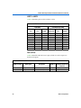
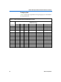
1
EPXA1 Development Board Hardware Reference Manual August 2002 Version 1.0 101 Innovation Drive San Jose, CA 95134 (408) 544-7000 http://www.altera.com MNL-EPXA1DEVBD-1.0 EPXA1 Development Board Hardware Reference Manual Copyright 2002 Altera Corporation. Altera, The Programmable Solutions Company, the stylized Altera logo, specific device designations, and all other words and logos that are identified as trademarks and/or service marks are, unless noted otherwise, the trademarks and service marks of Altera Corporation in the U.S. and other countries. All other product or service names are the property of their respective holders. Altera products are protected under numerous U.S. and foreign patents and pending applications, mask work rights, and copyrights. Altera warrants performance of its semiconductor products to current specifications in accordance with Altera’s standard warranty, but reserves the right to make changes to any products and services at any time without notice. Altera assumes no responsibility or liability arising out of the application or use of any information, product, or service described herein except as expressly agreed to in writing by Altera Corporation. Altera customers are advised to obtain the latest version of device specifications before relying on any published information and before placing orders for products or services. All rights reserved. ii Altera Corporation About this Manual This manual provides comprehensive information about the Altera® EPXA1 development board. Table 1 shows the manual revision history. Table 1. Revision History Date August 2002 How to Find Information ■ ■ ■ ■ Altera Corporation Description First publication The Adobe Acrobat Find feature allows you to search the contents of a PDF file. Click on the binoculars icon in the top toolbar to open the Find dialog box. Bookmarks serve as an additional table of contents. Thumbnail icons, which provide miniature previews of each page, provide a link to the pages. Numerous links, shown in green text, allow you to jump to related information. iii About this Manual How to Contact Altera EPXA1 Development Board Hardware Reference Manual For the most up-to-date information about Altera products, go to the Altera world-wide web site at http://www.altera.com. For technical support on this product, go to http://www.altera.com/mysupport. For additional information about Altera products, consult the sources shown in Table 2. Table 2. How to Contact Altera Information Type Technical support USA & Canada All Other Locations http://www.altera.com/mysupport/ http://www.altera.com/mysupport/ (800) 800-EPLD (3753) (7:00 a.m. to 5:00 p.m. Pacific Time) (408) 544-7000 (1) (7:00 a.m. to 5:00 p.m. Pacific Time) Product literature http://www.altera.com http://www.altera.com Altera literature services [email protected] (1) [email protected] (1) Non-technical customer service (800) 767-3753 (408) 544-7000 (7:30 a.m. to 5:30 p.m. Pacific Time) FTP site ftp.altera.com ftp.altera.com Note: (1) iv You can also contact your local Altera sales office or sales representative. Altera Corporation EPXA1 Development Board Hardware Reference Manual Typographic Conventions About this Manual The EPXA1 Development Board Hardware Reference Manual uses the typographic conventions shown in Table 3. Table 3. Conventions Visual Cue Meaning Bold Type with Initial Capital Letters Command names, dialog box titles, checkbox options, and dialog box options are shown in bold, initial capital letters. Example: Save As dialog box. bold type External timing parameters, directory names, project names, disk drive names, filenames, filename extensions, and software utility names are shown in bold type. Examples: fMAX, \QuartusII directory, d: drive, chiptrip.gdf file. Bold italic type Book titles are shown in bold italic type with initial capital letters. Example: 1999 Device Data Book. Italic Type with Initial Capital Letters Document titles are shown in italic type with initial capital letters. Example: AN 75 (High-Speed Board Design). Italic type Internal timing parameters and variables are shown in italic type. Examples: tPIA, n + 1. Variable names are enclosed in angle brackets (< >) and shown in italic type. Example: <file name>, <project name>.pof file. Initial Capital Letters Keyboard keys and menu names are shown with initial capital letters. Examples: Delete key, the Options menu. “Subheading Title” References to sections within a document and titles of Quartus II Help topics are shown in quotation marks. Example: “Configuring a FLEX 10K or FLEX 8000 Device with the BitBlaster™ Download Cable.” Courier type Signal and port names are shown in lowercase Courier type. Examples: data1, tdi, input. Active-low signals are denoted by suffix _n, e.g., reset_n. Anything that must be typed exactly as it appears is shown in Courier type. For example: c:\quartusII\qdesigns\tutorial\chiptrip.gdf. Also, sections of an actual file, such as a Report File, references to parts of files (e.g., the AHDL keyword SUBDESIGN), as well as logic function names (e.g., TRI) are shown in Courier. 1., 2., 3., and a., b., c.,... Numbered steps are used in a list of items when the sequence of the items is important, such as the steps listed in a procedure. ■ Bullets are used in a list of items when the sequence of the items is not important. The checkmark indicates a procedure that consists of one step only. The hand points to information that requires special attention. The angled arrow indicates you should press the Enter key. The feet direct you to more information on a particular topic. Altera Corporation v Notes: Contents About this Manual ..................................................................................iii How to Find Information ............................................................................................................iii How to Contact Altera .................................................................................................................. iv Typographic Conventions ............................................................................................................. v EPXA1 Development Board ........................................................................9 Features .............................................................................................................................................9 Functional Overview .......................................................................................................................9 EPXA1 Development Board Components .................................................................................10 EPXA1 Device .........................................................................................................................10 Prototyping Area ....................................................................................................................11 Interfaces .................................................................................................................................13 Development Board Expansion ...........................................................................................20 Jumper Configuration ...................................................................................................................23 Clocks ...............................................................................................................................................24 Jumper Configuration for the Clock Inputs .......................................................................26 Sources for the Stripe Clock Reference ...............................................................................27 Sources for CLK3 & CLK4 ....................................................................................................28 Device Configuration ....................................................................................................................28 Booting from Flash Memory ................................................................................................28 Using the Quartus II Software .............................................................................................29 JTAG Interfaces ..............................................................................................................................29 Power Supply .................................................................................................................................30 Test Points & Test Pads .................................................................................................................32 Signals ..............................................................................................................................................33 UART .......................................................................................................................................33 Expansion Headers ................................................................................................................34 Configuration/Debugging Interfaces .................................................................................37 Development Board Pin-Outs ......................................................................................................38 Configuration .........................................................................................................................39 SDR SDRAM Interface ..........................................................................................................40 EBI ............................................................................................................................................42 UART1 & UART2 ...................................................................................................................44 Fast I/O Pins ...........................................................................................................................44 Test Points ...............................................................................................................................45 Test Pads ..................................................................................................................................45 Prototyping Area ....................................................................................................................46 Expansion Header I/O Pins .................................................................................................47 General Usage Guidelines ............................................................................................................48 Altera Corporation vii Contents Excalibur EPXA1 Development Board Hardware Refewrence Manual Anti-Static Handling ..............................................................................................................48 Power Consumption ..............................................................................................................48 Test Core Functionality .........................................................................................................49 Environmental Requirements ..............................................................................................50 Operating Requirements .......................................................................................................50 Unused I/O Pins ....................................................................................................................50 viii Altera Corporation EPXA1 Development Board 1 ■ ■ ■ ■ ■ ■ ■ ■ Functional Overview Altera Corporation Powerful development board for embedded processor FPGA designs – Features an EPXA1F484 device – Supports intellectual property-based (IP-based) designs using a microprocessor Industry-standard interconnections – 10/100 megabits per second (Mbps) Ethernet – Two RS-232 ports Memory subsystem – 8 Mbytes of flash memory – 32 Mbytes of single data rate (SDR) SDRAM Multiple clocks for communications system design Multiple ports for configuration and debugging – IEEE Std. 1149.1 Joint Test Action Group (JTAG) – Support for configuring the EPXA1 device using flash memory, with a MasterBlaster™ or ByteBlasterMV™ cable – Multi-ICE header for debugging Expansion headers for greater flexibility and capacity – 5-V standard expansion header – 5-V long expansion card header Additional user-interface features – One user-definable 8-bit dual in-line package (DIP) switch block – Four user-definable push-button switches, plus reset switch – Ten user-definable LEDs, plus function-specific LEDs Test points provided to facilitate system development The EPXA1 development board is a powerful, low-cost, product which you can use as a desktop hardware platform to start developing embedded systems immediately. In addition, the board can be used for system prototyping, emulation, hardware and software development or other special requirements. The development board provides a flexible, powerful debug and development environment to support the development of systems using Excalibur™ devices. 9 Specifications Features EPXA1 Development Board Hardware Reference Manual EPXA1 Development Board Components This section describes the components on the EPXA1 development board, which is shown in Figure 1. Figure 1. EPXA1 Development Board Layout EPXA1 Device The EPXA1 development board features the lowest-cost member of the Excalibur family, the EPXA1. The EPXA1 device contains an ARM922T™ 32-bit RISC microprocessor combined with an APEX™ 20KE FPGA in a 484-pin FineLine BGA™ package. Table 1 on page 10 lists the main features of the device. Table 1. EPXA1 Device Features Feature Maximum system gates 263,000 Typical gates 100,000 LEs ESBs Maximum RAM bits 10 Capacity 4,160 26 53,248 Maximum macrocells 416 Maximum user I/O pins 186 Altera Corporation EPXA1 Development Board Hardware Reference Manual In addition, the EPXA1 device provides a variety of peripherals, as listed in Table 2. Table 2. EPXA1 Device Peripherals Peripheral Description ARM922T 32-bit RISC processor For speed grade –1: up to 200 MHz For speed grade –2: up to 166 MHz Interrupt controller Used for the interrupt system Internal single-port SRAM 32 Kbytes Internal dual-port SRAM 16 Kbytes SDRAM controller Interfaces between the internal system bus and SDRAM External SDRAM Refer to the Excalibur Devices Hardware Reference Manual for details of supported sizes Expansion bus interface (EBI) Interfaces to the flash memory and the Ethernet External flash memory Refer to the Excalibur Devices Hardware Reference Manual for details of supported sizes Watchdog timer Protects the system against software failure UART Facilitates serial communication Reset controller Resets the device Refer to the Excalibur Devices Hardware Reference Manual for details about EPXA1 devices. Prototyping Area This area can be used to develop and test custom circuitry, such as I/O interfaces, using the EPXA1 development board. The prototyping area has both 3.3-V and 5-V supply, plus ground connections, 32 I/O pins that facilitate connection to the Excalibur device, and a reset pin in a 6 × 15 matrix. Figure 2 shows the prototyping area on the development board. Altera Corporation 11 EPXA1 Development Board Hardware Reference Manual Figure 2. Prototyping Area on the EPXA1 Development Board A1 Figure 3 on page 13 shows how the pins are located in the prototyping area. 12 Altera Corporation EPXA1 Development Board Hardware Reference Manual Figure 3. Pin Layout in the Prototyping Area A PROTOIO_n B 5V C D NC E 3.3 V F GND G H J K L M N P RESET_n R 1 2 3 4 5 6 See Table 37 on page 46 for details of the prototyping area pin-outs. Interfaces Table 3 lists the interfaces supported by the EPXA1 development board. Table 3. Development Board Interfaces Interface Description 10/100 Ethernet with full- and halfduplexing This interface consists of an RJ45 connector and transformer connected to the EPXA1 using an external MAC/PHY device connected to the EBI Expansion headers These headers are used to connect Altera daughter cards or customerdesigned daughter cards to develop and test custom circuitry IEEE Std. 488 RS-232 serial interfaces This is a 250-kbps true RS-232 data terminal equipment (DTE) interface Debugging/programming ports Altera Corporation The board supports in-circuit debugging by means of the MasterBlaster, ByteBlasterMV, or Multi-ICE cables 13 EPXA1 Development Board Hardware Reference Manual Serial I/O Interfaces There can be two UARTs in the EPXA1 device. A dedicated UART is located in the embedded stripe; optionally, an additional IP UART can be implemented in the FPGA. If the IP UART is used, it is connected to 3.3-V standard EPXA1 I/O pins. Each UART is connected to a transceiver (U6 for the embedded stripe UART and U1 for the IP UART) to translate LVTTL voltage for RS-232 compatibility at up to 250 Kbps. Each UART also has its own DB9 male RS-232 connector wired as a DTE. The transceiver uses a 3.3-V power supply. If the RS-232 input pins are used as outputs, contention occurs because the bus transceiver is always active. If these pins are not used as part of a design, ensure that they remain in the high-impedance state. All unused I/O pins can be set to tri-state mode in the Quartus II software (see “Unused I/O Pins” on page 50). See Table 23 on page 33 for information on the RS-232 signals. Table 4 shows the UART interface characteristics. Table 4. UART Interface Characteristics Features I/O Pins Voltage (V) UART 1 TX, RX & Control 8 3.3 UART 2 TX, RX & Control 8 3.3 Table 5 lists the UART LEDs on the EPXA1 development board. Table 5. UART LEDs Board Reference 14 Signal Description D2 TXD This LED indicates activity on the line D3 RXD This LED indicates activity on the line D4 XA-TXD This LED indicates activity on the line D7 XA-RXD This LED indicates activity on the line Altera Corporation EPXA1 Development Board Hardware Reference Manual 10/100 Ethernet Parallel Interface On the EPXA1 development board, the Ethernet interface consists of an integrated MAC/PHY device and an RJ45 connector which includes the transformer and LEDs. Table 6 lists the LEDs built into the RJ45 connector. Table 6. Ethernet LEDs Board Reference Signal Description RJ1 LEDA LEDA Green LED. This defaults to being set on when the 10/100 link is detected (1) RJ1 LEDB LEDB Unused (1) Note: (1) Although the default setting for LEDA ‘10/100 link detected’, the user can program the LEDA and LEDB select signals by writing to the LED select signal registers. The Ethernet and flash memory device share addresses and data on the EBI. Memory Interfaces The EPXA1 development board supports the following types and capacities of on-board memory, as listed in Table 7. Table 7. Development Board Memory Characteristics Type Address Lines Data Lines Control Lines Memory Organization SDR SDRAM 13 16 10 4 M × 16 × 4 banks Flash 22 16 5 2 × 4 Mbytes Size 32 Mbytes; 16-bit 8 Mbytes Figure 4 on page 16 shows the location of the on-board memory. Altera Corporation 15 EPXA1 Development Board Hardware Reference Manual Figure 4. EPXA1 Development Board On-Board Memory Flash memory (pin 1s indicated) SDRAM (pin 1 indicated) Two flash memory chips, FLASH1 and FLASH2, are connected to the EBI of the EPXA1 development board (see Figure 5). Figure 5. Flash Memory Interface Flash Memory (2 x 4 Mbyte) EBI_CS0 EPXA1 A1-A22 D0-D15 EBI_CS1 A0-A21 FLASH1 FLASH2 PHY/MAC EBI OE, WE, CE 16 Altera Corporation EPXA1 Development Board Hardware Reference Manual LED & Switch Interfaces The EPXA1 development board provides a variety of LED and switch interfaces. Some are user-definable and some are function-specific. Figure 6 shows the location of LEDs and switches on the development board. Figure 6. Switches & LEDs on the EPXA1 Development Board Ethernet TX/RX LEDs UART LEDs NPOR SOFT_RESET_N SW6 (pin 1 indicated) Push-button switches SW2, SW3, SW4, SW5 Voltage LEDs User LEDs (LED 0 indicated) User-Defined LEDs On the EPXA1 development board, there are ten user-definable LEDs in a graph-type LED package, DG1. They connect directly to the EPXA1 device I/O pins and can be used for any kind of application. Table 8 on page 18 lists the user LEDs on the development board. Altera Corporation 17 EPXA1 Development Board Hardware Reference Manual Table 8. DG1 LED Interface Characteristics LED Reference EPXA1 I/O Pin Signal Voltage (V) W17 USER_LED9 3.3 DG1_J DG1_I W18 USER_LED8 3.3 DG1_H W20 USER_LED7 3.3 DG1_G W21 USER_LED6 3.3 DG1_F W22 USER_LED5 3.3 DG1_E Y17 USER_LED4 3.3 DG1_D Y18 USER_LED3 3.3 DG1_C Y19 USER_LED2 3.3 DG1_B Y20 USER_LED1 3.3 DG1_A Y21 USER_LED0 3.3 Function-Specific LEDs LEDs are also used for specific application functions, such as the configuration, RS-232 and Ethernet interfaces. Table 9 lists the functionspecific LEDs, their power supply status, their connection details, and their functions. Table 9. Function-Specific LED Usage Signal Board Reference EPXA1 I/O Pin (or Board Connector) INIT_DONE D15 K7 VCC_5V D12 5-V power indicator VCC_3V3 D13 3.3-V power indicator 3.3 VCC_1V8 D14 1.8-V power indicator 1.8 TXD D2 FPGA UART signal indicator 3.3 RXD D3 FPGA UART signal indicator 3.3 XA-TXD D4 Embedded stripe UART signal indicator 3.3 XA-RXD D7 Embedded stripe UART signal indicator 3.3 TX RJ1 Ethernet signal indicator 3.3 RX RJ1 Ethernet signal indicator 3.3 18 Description Voltage (V) Used by FPGA initialization; signifies that initialization is complete 3.3 5 Altera Corporation EPXA1 Development Board Hardware Reference Manual Switch Interfaces The EPXA1 development board provides eight user-definable, active-low switches in a dip-switch block, four debounced push-button switches, and two dedicated reset switches. Table 10 documents the interface characteristics of the dip-switch block, SW6. Table 10. SW6 Dip Switch Connections (Active-Low) Switch Name EPXA1 I/O Pin Signal Voltage (V) SW6_1 V20 USER_SW7 3.3 SW6_2 V19 USER_SW6 3.3 SW6_3 V18 USER_SW5 3.3 SW6_4 V17 USER_SW4 3.3 SW6_5 V16 USER_SW3 3.3 SW6_6 U21 USER_SW2 3.3 SW6_7 U20 USER_SW1 3.3 SW6_8 U19 USER_SW0 3.3 Tables 11 and 12 detail the push-button switches on the development board. Table 11. Push-Button Switches Push Button EPXA1 I/O Pin Signal Use Voltage (V) SW1 H1 NPOR Active-low switch that generates a full power-on reset when pressed for more than two seconds 3.3 SW7 R4 N_CONFIG Active-low switch that generates a warm reset 3.3 Table 12. User-Definable Push-Button Switches Push Button Altera Corporation EPXA1 I/O Pin Signal Voltage (V) SW2 U18 USER_PB0 3.3 SW3 U17 USER_PB1 3.3 SW4 U16 USER_PB2 3.3 SW5 T18 USER_PB3 3.3 19 EPXA1 Development Board Hardware Reference Manual Development Board Expansion The EPXA1 development board hosts the EPXA1 device and two 5-V expansion headers, which are implemented on the board for use with expansion cards. There are two types of expansion header on the EPXA1 development board: ■ ■ Standard expansion header—a set of three 0.1-inch, two-row header pins (7 × 2, 10 × 2, 20 × 2) Long expansion header—the same set of three 0.1-inch, two-row header pins (7 × 2, 10 × 2, 20 × 2) plus an extra 20 × 2 header pins Figure 7 on page 20 shows the location of the expansion headers on the EPXA1 development board. Figure 7. EPXA1 Development Board Expansion Header Connectors Pin 1 Pin 1 The expansion header interfaces can be used to interface to specialfunction daughter cards; contact your Altera representative for details of the daughter cards available for use with the expansion header interfaces. By using the EPXA1 I/O pins and the power-supply pins on the expansion headers, you can design expansion cards to your specific requirements using the I/O pins on the EPXA1 device and power supplies from the EPXA1 development board. 20 Altera Corporation EPXA1 Development Board Hardware Reference Manual The expansion headers are on a common 0.1-inch pitch/spacing to make it easier to use both headers together if desired. Standard Expansion Header The standard expansion header interface includes the following features: ■ ■ ■ ■ ■ ■ ■ ■ ■ ■ ■ 40 APEX® device general-purpose I/O signals A buffered, zero-skew copy of the on-board OSC output A buffered, zero-skew copy of the EPXA1’s PLL-output An APEX device clock-input (for daughter cards that drive a clock to the FPGA An active-low power-on-reset signal Three regulated 3.3-V power-supply pins One regulated 5-V power-supply pin Unregulated power-supply pin (connects directly to J1 power-input plug) Numerous ground connections Card-select I/O RC-filtered I/O Long Expansion Header The long expansion header interface shares the same characteristics as the standard interface, and has the following additional pins in use: ■ ■ ■ Two regulated 3.3-V power-supply pins Sixteen address pins Sixteen data pins Expansion Header Pin Details In addition, the following points apply to either standard or long expansion headers: ■ ■ ■ ■ ■ Altera Corporation J9.38 and J15.38 can be used as a global card-enable signal A low-current, 5-V power supply is presented on J4.2 and J11.2 The VREF voltage for the analog switches is presented on J10.3 and J3.3. The maximum current load on each header is 500 mA at 3.3 V, 50 mA at 5 V and 100 mA at 12 V The remaining pins on the expansion headers connect to user I/O pins on the EPXA1 device. Table 24 on page 34 lists the expansion header signal pin assignments 21 EPXA1 Development Board Hardware Reference Manual Difference Between Standard and Long Expansion Headers On the standard expansion header, there is an RC-filtered connection to EPXA1 device I/O pin AB5 from header pin J11.3. This circuit is suitable for producing a high-impedance, low-precision analog output if the appropriate pin is driven with a duty-cycle-modulated waveform by user logic. However, there is no RC-filtered connection to an EPXA1 device I/O pin from the long expansion header. Instead, header pin J4.3 supports an additional user I/O. EPXA1 Device Signal Definitions for the Expansion Headers Table 13 on page 22 shows the definitions for the EPXA1 device signals available to the standard expansion header interface. The definitions are used with Altera daughter cards. The general purpose I/O signals can be used as required. Table 13. Standard Expansion Header Signal Definitions Function Signals Number General purpose I/O H5V_IO[40..0] 41 Clock H5V_OSC H5V_CLK H5V_CLKOUT 3 Bias voltage input H5V_VEE 1 Reset H5V_RST_N 1 Supply voltage VCC_5V VCC_A VCC_3V3 1 1 3 See Table 24 on page 34 for standard expansion header pin-out details. The long expansion header includes the signals in Table 13, plus the additional signals in Figure 14. Table 14. Additional Signal Definitions for the Long Expansion Header Function Address 22 Signals Number eup_A[15..0] 16 Data eup_D[15..0] 16 Supply voltage VCC_5V VCC_A2 VCC_3V3 1 1 2 Altera Corporation EPXA1 Development Board Hardware Reference Manual See Table 25 on page 35 for long expansion header pin-out details. f Jumper Configuration Refer to the Nios Embedded Processor Development Board data sheet for further details about the expansion header interface. The jumpers on the EPXA1 development board serve several functions: ■ ■ ■ Clock distribution Enabling clocks JTAG configuration Figure 8 on page 23 shows the location of jumpers on the development board. Figure 8. Jumper Locations on the EPXA1 Development Board JSELECT (J5) CLKA Select (J13) CLKB Select (J14) Table 15 on page 24 lists the jumper settings and their uses. Altera Corporation 23 EPXA1 Development Board Hardware Reference Manual Table 15. Jumpers on the EPXA1 Development Board Jumper Function Pins 1-2 Connected Pins 2-3 Connected JSELECT (J5) (1) JTAG connector selection ARM922 TAP available on Multi- ARM922 TAP available on JTAG ICE connector connector CLKA Select (J13) Clock A input selection 25 MHz on-board oscillator selected Alternative 5-V DIL14 oscillator or SMA connector selected CLKB Select (J14) Clock B input selection 25 MHz on-board oscillator selected Alternative 5-V DIL14 oscillator or SMA connector selected Note: (1) Determines whether the JTAG chains operate in serial or parallel mode. Clocks There are three potential clock sources on the EPXA1 development board, which can be enabled and disabled according to your design requirements: ■ ■ ■ Dedicated on-board, 25-MHz crystal oscillator, X1 (default clock for all devices) Socket for alternative 5-V DIL14 crystal oscillator, XSKT1 Generator clock input via SMA connector, SMA1 The location of the clocks on the development board is shown in Figure 9. Figure 9. Clocks on the EPXA1 Development Board 24 Altera Corporation EPXA1 Development Board Hardware Reference Manual The only device for which you cannot change the clock input is the Ethernet. The Ethernet clock input is the 25-MHz oscillator, X1. Apart from selecting the clock inputs, you can also select the target devices for each clock input. If you plug in an alternative crystal oscillator, it drives the same clock line as the SMA connector. To drive a clock through the SMA connector, you must remove the alternative crystal oscillator. Table 16 on page 25 lists all the clock signals on the development board. Table 16. EPXA1 Development Board Clocks (Part 1 of 2) Clock Source EPXA1 Pin Signal Name (or Board Connection) Description Target Device CLK_REF (1) H7 CLK_REF Main clock used to drive the embedded stripe of EPXA1 the EPXA1. Dedicated input selected from either the SMA connector or the 25 MHz crystal oscillator using jumper CLKA Select (J13) CLKA_1 U1 CLK1p Dedicated pin that drives PLL1 EPXA1 CLKA_2 R21 CLK2p Dedicated pin that drives PLL2 EPXA1 CLKA_3 (OSC_BUFF1) (J3.9) H5V_OSC Clock to long expansion header Long expansion header CLKA_4 (OSC_BUFF2) (J11.9) H5V_OSC Clock to standard expansion header Standard expansion header CLKB_0 V1 CLK3p Dedicated pin that drives PLL3 EPXA1 CLKB_1 P21 CLK4p Dedicated pin that drives PLL4 EPXA1 OSC_25MHZ (U9:1) XTAL1 Clock to Ethernet; optionally used for other development board modules Ethernet CLKLK_ENA R6 CLKLK_ENA Clock-enable for PLL circuitry; permanently on EPXA1 CLKLK_OUT2p U22 Altera Corporation CLKLK_OUT2p Dedicated pin allowing PLL2 output to be driven Standard off-chip, providing the PLL clock to the expansion expansion headers as H5V_CLK header, Long expansion header 25 EPXA1 Development Board Hardware Reference Manual Table 16. EPXA1 Development Board Clocks (Part 2 of 2) Clock Source CLKLK_FB2p EPXA1 Pin Signal Name (or Board Connection) N21 CLKLK_FB2p Description Target Device Dedicated pin that allows external feedback to PLL2. Available on test pad T14 (see Table 36 on page 45) EPXA1 Note: (1) See “Jumper Configuration for the Clock Inputs” for details of selecting a source for the stripe CLK_REF pin. Up to two sources can be selected to clock the devices on the development board at any given time. Of the three sources available, the dedicated 25-MHz on-board oscillator cannot be varied in frequency. As detailed in Table 16, four of the clock buffer outputs drive dedicated inputs on the EPXA1 device. One is the dedicated input providing the embedded stripe reference clock CLK_REF. The four FPGA clocks service the ClockLock™ and ClockBoost™ circuitry on the Excalibur device. The clocks on the development board can be configured as required, depending on which devices are used. Two clocks drive each expansion header: two from the main clock buffer and two from buffered copies of the EPXA1 PLL2 outputs. Jumper Configuration for the Clock Inputs Jumpers CLKA Select (J13) and CLKB Select (J14) are used to select different clock inputs. CLKA Select is used to determine the clock supply to the EPXA1 device clock reference, two of the four PLLs in the FPGA, and the two expansion headers. CLKB Select can be used to route an additional, alternative clock input to the EPXA1 device. During development, if you need to run the clock at a rate other than 25 MHz, you can do so using the SMA connector or an alternative 5-V DIL14 oscillator. 26 Altera Corporation EPXA1 Development Board Hardware Reference Manual By selecting the position of jumpers CLKA Select and CLKB Select, as shown in Table 17, either the SMA connector or an alternative 5-V DIL14 oscillator can be used instead of the 25-MHz on-board oscillator. To use the SMA connector to drive a clock onto the board from an external source, the alternative 5-V DIL14 oscillator socket must not contain an oscillator. To use an alternative 5-V DIL14 oscillator, ensure that no clock is attached to the SMA connector . Table 17. CLKA Select & CLKB Select Jumper Settings Pin 1-2 Connected Pin 2-3 Connected CLKA Select 25-MHz on-board oscillator provides a clock to CLK_REF, EPXA1 dedicated inputs CLK1 and CLK2, and both expansion headers Alternative 5-V DIL14 oscillator or SMA connector selected provides CLK_REF, EPXA1 dedicated inputs CLK1 and CLK2, and both expansion headers CLKB Select 25-MHz on-board oscillator provides the clock to EPXA1 dedicated inputs CLK3 and CLK4 Alternative 5-V DIL14 oscillator or SMA connector provides the clock to EPXA1 dedicated inputs CLK3 and CLK4 Sources for the Stripe Clock Reference There are three options for providing a source for the EPXA1 embedded stripe clock reference, CLK_REF: ■ ■ ■ 25-MHz on-board oscillator SMA connector Alternative 5-V DIL14 oscillator Using the 25-MHz On-board Oscillator To use the 25-MHz on-board oscillator, set CLKA Select to position 1-2 to select it. Using the SMA Connector To select the SMA connector, follow the steps below: 1. Remove any alternative 5-V DIL14 oscillator from the socket, XSKT1. 2. Apply an external clock source to the SMA connector. 3. Altera Corporation The clock signal should be a maximum 5 VPP. Set CLKA Select to position 2-3. 27 EPXA1 Development Board Hardware Reference Manual Using the Alternative 5-V DIL14 Oscillator To use the alternative oscillator as the stripe clock reference, follow the steps below: 1. Remove any external clock input from the SMA connector. 2. Plug the DIL14 crystal oscillator package into XSKT1. 3. Set CLKA Select to position 2-3. The clock buffer converts the 5-V input from the alternative 5-V DIL14 oscillator to the 3.3 V required for the stripe. Sources for CLK3 & CLK4 Clock sources for CLK3 and CLK4 can be selected in the same way as for the embedded stripe clock sources. Follow the instructions given in “Sources for the Stripe Clock Reference” on page 27, but use jumper CLKB Select to select the clock source, instead of CLKA Select. Device Configuration There are two methods of programming and configuring the EPXA1 device: ■ ■ Booting from flash memory Using the Quartus® II software to configure the device via JTAG See “JTAG Interfaces” on page 29 for more details about using the JTAG interface. On the EPXA1 device, the settings of BOOT_FLASH, MSEL0, and MSEL1 determine the configuration mode and method. On the EPXA1 development board, BOOT_FLASH, MSEL0 and MSEL1 are tied to a setting that forces the device to boot from 16-bit flash memory. Booting from Flash Memory The Altera flash memory programmer (exc_flash_programmer.exe) is a utility that allows you to program flash memory on the EBI using the JTAG interface and the ByteBlasterMV or MasterBlaster download cable, so that you can boot from it. After reset, the processor boots up and executes the bootloader from flash memory. The bootloader configures the stripe, loads the user software into memory, configures the FPGA side of the EPXA1, and then begins to execute the user code. 28 Altera Corporation EPXA1 Development Board Hardware Reference Manual f For further details about booting the device from flash memory, refer to the Excalibur Devices Hardware Reference Manual. Using the Quartus II Software The Quartus II software can generate an SRAM object file (.sof) containing both hardware and software. The Quartus II programmer uses the .sof file to configure the EPXA1 device via JTAG, using either the MasterBlaster or ByteBlasterMV download cables. f JTAG Interfaces For further details of how to create a .sof file and configure the EPXA1 device via JTAG, consult the Quartus II Help. There are two JTAG connectors on the EPXA1 development board, as shown in Figure 10 Figure 10. JTAG Interfaces on the EPXA1 Development Board JTAG connectors (pin 1s indicated) The JTAG connector, J6, is used to connect an Altera ByteBlaster or MasterBlaster download cable. The Multi-ICE connector, J8, is used to connect a Multi-ICE cable or any other compatible cable. Altera Corporation 29 EPXA1 Development Board Hardware Reference Manual The JTAG connector can be used with both the flash programmer and the Quartus programmer. In addition, the MasterBlaster and ByteBlasterMV cables support in-circuit debugging on the JTAG connector, using the SignalTap® embedded logic analyzer. The JSELECT setting does not affect this. The JSELECT jumper, J5, determines whether a JTAG debugger can be connected to the JTAG connector or to the Multi-ICE connector. When using Altera-RDI via a ByteBlasterMV or MasterBlaster cable, the JSELECT jumper must be set to 2-3; when using Multi-ICE or a compatible device on the Multi-ICE connector, JSELECT must be set to 1-2. f For further details about jumper settings, refer to Table 15 on page 24. Tables 26 and 27 starting on page 37 list the pin-outs of the JTAG and Multi-ICE connectors. Power Supply A 12-V, 20-W supply unit powers the EPXA1 development board. The board has reverse-polarity protection and a 2-A fuse to provide overcurrent protection. Figure 11 on page 30 shows the location of the power supply inputs for the EPXA1 development board. Figure 11. Power Supply Inputs on the EPXA1 Development Board 30 Altera Corporation EPXA1 Development Board Hardware Reference Manual A voltage regulator regulates the main supplies for the board. The input supply is unregulated 12 V (±5%), which is reduced to 3.3 V for the I/O pins and to 1.8 V for the processor core. Voltage regulator U5 reduces the input to 5 V and distributes it to a pin on the expansion headers. The unregulated input is also routed to a pin on the expansion headers. The maximum current permitted on the expansion headers depends on the input voltage: for 3.3 V, it is 500 mA, and for 5 V, it is 50 mA. If the input supply is 12 V, the maximum current per header depends on how much power is consumed by the rest of the board, but should not exceed 100 mA. Three function-specific status LEDs indicate the presence of 1.8 V, 3.3 V, and 5 V to the board, as listed in Table 18 on page 31. Table 18. Power Supply LEDs Board Reference Signal Description D14 VCC_1V8 Indicates the presence of 1.8 V D13 VCC_3V3 Indicates the presence of 3.3 V D12 VCC_5V Indicates the presence of 5 V Tables 19 through 22 list the estimated maximum power-supply requirements for the development board modules. The typical power-supply requirement for the development board is 250 mA/500 mA. Table 19. 12-V Supply Requirements Module Expansion headers Max mA 100 per header Table 20. 5-V Supply Requirements Module CLK_REF Expansion headers Altera Corporation Max mA Alternative crystal oscillator—75 50 per header 31 EPXA1 Development Board Hardware Reference Manual Table 21. 3.3-V Supply Requirements Module Max mA EPXA1 I/O 500 (sum over all I/O pins) SDRAM 285 Flash memory 45 × 2 = 90 UARTs 20 Ethernet 140 LEDs 15 × 18 + (5 × 2) Crystal oscillator = = = 270 10 280 10 Clock buffers 37 + 22 = 59 Expansion headers 500 per header Table 22. 1.8-V Supply Requirements Module EPXA1 device core Test Points & Test Pads mA Depends on application (1.1 A maximum) Test points on the EPXA1 development board, annotated as TPx, are provided for voltages and ground connections; see Table 35 on page 45. For selected signals, test pads are provided on the board, annotated as Tx; they are listed in Table 36 on page 45. 32 Altera Corporation EPXA1 Development Board Hardware Reference Manual Signals Tables 23 through 27 document the device signals for the following peripherals: ■ ■ ■ UART Expansion headers Configuration/debugging interfaces UART Figure 12 shows the DB9 male connector used on the development board. Figure 12. UART DB9 Male Connector 1 2 6 4 3 7 8 5 9 Table 23 lists the UART DB9 signals. Table 23. DTE UART DB9 Male Connector Signals (1) Pin Signal Description 1 DCD Data carrier detect 2 RXD Receive data 3 TXD Transmit data 4 DTR Data terminal ready 5 GND Signal ground 6 DSR Data set ready 7 RTS Request to send 8 CTS Clear to send 9 RI Ring indicator Note: (1) The EPXA1 development board has two DB9 male connectors. Table 33 on page 44 lists pin-out information for the UARTs on the development board. Altera Corporation 33 EPXA1 Development Board Hardware Reference Manual Expansion Headers On the development board, there is a standard expansion header and a wide expansion header. Table 24 lists the signals on the standard expansion header. Table 24. Standard Expansion Header Signals Pin 7 × 2 Header, J11 10 × 2 Header, J10 20 × 2 Header, J15 Signal Pin Signal Pin Signal 1 GND 6 B_H5V_IO31 11 B_H5V_IO36 2 VCC_5V 7 B_H5V_IO32 12 B_H5V_IO37 3 H5V_VEE 8 B_H5V_IO33 13 B_H5V_IO38 4 B_H5V_IO29 9 B_H5V_IO34 14 B_H5V_IO39 5 B_H5V_IO30 10 B_H5V_IO35 1 Vcc_UNREG 8 GND 15 VCC_3V3 2 GND 9 H5V_OSC 16 GND 3 VCC_A2 10 GND 17 NC 4 GND 11 H5V_CLK 18 GND 5 VCC_3V3 12 GND 19 NC 6 GND 13 H5V_CLKOUT 20 GND 7 VCC_3V3 14 GND 1 H5_RST_N 15 B_H5V_IO12 29 B_H5V_IO21 2 GND 16 B_H5V_IO13 30 GND 3 B_H5V_IO0 17 B_H5V_IO14 31 B_H5V_IO22 4 B_H5V_IO1 18 B_H5V_IO15 32 B_H5V_IO23 5 B_H5V_IO2 19 GND 33 B_H5V_IO24 6 B_H5V_IO3 20 Removed 34 NC 7 B_H5V_IO4 21 B_H5V_IO16 35 B_H5V_IO25 8 B_H5V_IO5 22 GND 36 B_H5V_IO26 9 B_H5V_IO6 23 B_H5V_IO17 37 B_H5V_IO27 10 B_H5V_IO7 24 GND 38 H5_CS_N 11 B_H5V_IO8 25 B_H5V_IO18 39 B_H5V_IO28 12 B_H5V_IO9 26 GND 40 GND 13 B_H5V_IO10 27 B_H5V_IO19 14 B_H5V_IO11 28 B_H5V_IO20 Table 39 on page 48 lists pin-out information for the standard expansion header on development board. 34 Altera Corporation EPXA1 Development Board Hardware Reference Manual Table 25 lists the signals on the long expansion header. Table 25. Long Expansion Header Signals (Part 1 of 2) Pin 7 × 2 Header, J4 10 × 2 Header, J3 20 × 2 Header, J9 Altera Corporation 1 Signal GND Pin 6 Signal Pin Signal B_H5V_IO31 11 B_H5V_IO36 2 VCC_5V 7 B_H5V_IO32 12 B_H5V_IO37 3 B_H5V_IO40 8 B_H5V_IO33 13 B_H5V_IO38 14 B_H5V_IO39 4 B_H5V_IO29 9 B_H5V_IO34 5 B_H5V_IO30 10 B_H5V_IO35 1 Vcc_UNREG 8 GND 15 VCC_3V3 2 GND 9 H5V_OSC 16 GND 3 VCC_A 10 GND 17 NC 4 GND 11 H5V_CLK 18 GND 5 VCC_3V3 12 GND 19 NC 6 GND 13 H5V_CLKOUT 20 GND 7 VCC_3V3 14 GND 1 H5_RST_N 15 B_H5V_IO12 29 B_H5V_IO21 2 GND 16 B_H5V_IO13 30 GND 3 B_H5V_IO0 17 B_H5V_IO14 31 B_H5V_IO22 4 B_H5V_IO1 18 B_H5V_IO15 32 B_H5V_IO23 5 B_H5V_IO2 19 GND 33 B_H5V_IO24 6 B_H5V_IO3 20 Removed 34 NC 7 B_H5V_IO4 21 B_H5V_IO16 35 B_H5V_IO25 8 B_H5V_IO5 22 GND 36 B_H5V_IO26 9 B_H5V_IO6 23 B_H5V_IO17 37 B_H5V_IO27 10 B_H5V_IO7 24 GND 38 H5_CS_N 11 B_H5V_IO8 25 B_H5V_IO18 39 B_H5V_IO28 12 B_H5V_IO9 26 GND 40 GND 13 B_H5V_IO10 27 B_H5V_IO19 14 B_H5V_IO11 28 B_H5V_IO20 35 EPXA1 Development Board Hardware Reference Manual Table 25. Long Expansion Header Signals (Part 2 of 2) Pin 20 × 2 Header, J2 Signal Pin Signal Pin Signal 1 GND 15 B_eup_A5 29 B_eup_A11 2 GND 16 B_eup_D5 30 B_eup_D11 3 B_eup_A0 17 B_eup_A6 31 B_eup_A12 4 B_eup_D0 18 B_eup_D6 32 B_eup_D12 5 B_eup_A1 19 B_eup_A7 33 B_eup_A13 6 B_eup_D1 20 B_eup_D7 34 B_eup_D13 7 B_eup_A2 21 B_eup_A8 35 B_eup_A14 8 B_eup_D2 22 B_eup_D8 36 B_eup_D14 9 B_eup_A3 23 B_eup_A9 37 B_eup_A15 10 B_eup_D3 24 B_eup_D9 38 B_eup_D15 11 B_eup_A4 25 B_eup_A10 39 GND 12 B_eup_D4 26 B_eup_D10 40 GND 13 GND 27 GND 14 GND 28 GND Table 38 on page 47 lists pin-out information for the long expansion header on the development board. 36 Altera Corporation EPXA1 Development Board Hardware Reference Manual Configuration/Debugging Interfaces On the development board, there are interfaces for a MasterBlaster or ByteBlasterMV cable, and a Multi-ICE connector. Table 26 lists the signals on the MasterBlaster/ByteBlasterMV connector. Table 27 lists the signals on the Multi-ICE connector. Table 28 on page 39 lists pin-out information for the development board configuration and debugging interfaces. Table 26. MasterBlaster/ByteBlasterMV Female Connector Signals Pin JTAG Mode Signal Description 1 TCK Clock signal 2 GND Signal ground 3 TDO Data from device 4 VCC Power supply 5 TMS JTAG state machine control 6 VIO Reference voltage for MasterBlaster output driver 7 NC No connect 8 - No connection 9 TDI Data to device 10 GND Signal ground Table 27. Multi-ICE Connector Signals (Part 1 of 2) Pin Altera Corporation Signal Description Direction 1 VCC Power supply N/A 2 VCC Power supply 3 PROC_NTRTST Processor reset 4 GND Ground N/A 5 PROC_TDI Processor test data input Input 6 GND Ground N/A 7 PROC_TMS Processor test mode select Input 8 GND Ground N/A 9 PROC_TCK Processor test clock input Input 10 GND Ground N/A 11 GND Ground N/A 12 GND Ground N/A 13 PROC_TDO Processor test data output 14 GND Ground N/A Output O N/A 37 EPXA1 Development Board Hardware Reference Manual Table 27. Multi-ICE Connector Signals (Part 2 of 2) Pin Signal 15 NSRST Development Board Pin-Outs Description Warm reset Direction I/O 16 GND Ground N/A 17 NC No connection N/A 18 GND Ground N/A 19 NC No connection N/A 20 GND Ground N/A The main component of the EPXA1 development board is the EPXA1F484 device. The pins on the EPXA1 device are assigned to functions on the board. When generating IP cores for the EPXA1 device, the pins must be used as defined to avoid damaging the device and any unused pins should be tri-stated using the Quartus II software. The following sections list the interfaces and dedicated pins on the board. Any pins not used for a design should be left in a high-impedance state to avoid contention. This section details the pins on the EPXA1 device which are assigned to the following purposes: ■ ■ ■ ■ ■ ■ ■ ■ Configuration SDR SDRAM EBI—for the Ethernet and flash memory devices UARTs 1 and 2 Fast I/O pins Expansion headers Prototyping area Test pads Pin assignments are grouped into tables for control pins, address pins, and data bus pins where appropriate. The tables also detail signals passing across a connection. The remaining I/O pins on the EPXA1 device are listed at the end of this section. 38 Altera Corporation EPXA1 Development Board Hardware Reference Manual Configuration The EPXA1 device pins listed in Table 28 on page 39 are used exclusively for configuring the device. Refer to “Device Configuration” on page 28 for more information about EPXA1 configuration. Table 28. EPXA1 Device Configuration Pins (Part 1 of 2) Signal Name MSEL0 EPXA1 Device Pin Board Reference R5 Description Configuration mode select (tied to GND) MSEL1 T3 Configuration mode select (tied to GND) BOOT_FLASH J5 Tied high (mandatory boot from flash) NSTATUS AB12 Pulled high NCONFIG R4 Connected to SOFT_RESET line DCLK R16 Pulled high CONF_DONE V12 Pulled high INIT_DONE K7 Initialization complete LED nCE P19 Pulled low nCEO H3 Not connected DATA0 P18 Pulled low DATA1 K3 Unused. Used as general-purpose I/O DATA2 J1 DATA3 L5 DATA4 L4 DATA5 L6 DATA6 L22 DATA7 M18 TDI T20 J6.9 JTAG data input TDO J4 J6.3 JTAG data output (to next device in the chain TCK Y11 J6.1 JTAG clock TMS U11 J6.5 JTAG mode select TRST J6 PROC_TDI G7 J8.5 JTAG data input PROC_TDO G2 J8.13 JTAG data output (to next device in the chain) PROC_TCK G3 J8.9 JTAG clock PROC_TMS H6 J8.7 JTAG mode select PROC_TRST G6 J8.3 JTAG reset (pulled high) DEV_CLR_n R20 T15, T14 FPGA clear signal taken to test pad T15, placed next to grounded test pad T14 near SW1; allows use of this signal, if required Altera Corporation JTAG reset (pulled high) 39 EPXA1 Development Board Hardware Reference Manual Table 28. EPXA1 Device Configuration Pins (Part 2 of 2) Signal Name EPXA1 Device Pin Board Reference Description DEV_OE U16 Device output enable. GPIO nWS M21 Write strobe. GPIO nRS P16 Read strobe. GPIO nCS N20 Signal providing handshaking between devices. GPIO CS P17 Chip select. GPIO RDYnBSY K4 Ready/busy. GPIO CLKUSR L7 Clock signal. GPIO SDR SDRAM Interface The EPXA1 development board contains one 16-bit SDR SDRAM device connected to the EPXA1 SDRAM controller. f For further details about the SDRAM controller, refer to the Excalibur Devices Hardware Reference Manual. The SDRAM_DQM[1:0] lines are used as byte enables for both reading from and writing to the SDRAM. Table 29 shows the pin-outs for the SDR SDRAM control signals. Table 29. SDR SDRAM Control Signal Pin-Outs Signal Name EPXA1 Device Pin Board Reference U13.18 Description SD_RAS_N C14 Row address strobe SD_CAS_N A17 U13.17 Column address strobe SD_WE_N F14 U13.16 Write enable SD_CS0_N G15 U13.19 Chip select SD_CLKE E15 U13.37 Clock enable SD_CLK C15 U13.38 SDRAM clock SD_CLK_N(1) J16 SD_DQM[0] E21 U13.15 Data byte mask SD_DQM[1] J20 U13.39 Data byte mask SD_DQS[0](1) D22 Read data strobe input in SDR mode SD_DQM_ECC B13 Not used Read data strobe output in SDR mode Note: (1) 40 These pins are tied together to provide a data-read strobe. See the Excalibur Devices Hardware Reference Manual. Altera Corporation EPXA1 Development Board Hardware Reference Manual Table 30 lists the SDRAM data and address bus pin-outs. Table 30. SDR SDRAM Data Bank & Address Bus Pin-Outs Signal Name SD_DQ0 EPXA1 Device Pin Board Reference B20 U13.2 Signal Name EPXA1 Device Pin Board Reference SD_DQ1 C20 U13.4 SD_DQ2 F18 U13.5 SD_DQ3 C21 U13.7 SD_DQ4 E20 U13.8 SD_DQ5 F19 U13.10 SD_DQ6 F20 U13.11 SD_DQ7 G18 U13.13 SD_DQ8 H19 U13.42 SD_DQ9 G20 U13.44 SD_DQ10 E22 U13.45 SD_DQ11 H18 U13.47 SD_DQ12 G21 U13.48 SD_DQ13 H20 U13.50 SD_DQ14 H17 U13.51 SD_DQ15 H22 U13.53 SD_A0 B17 U13.23 SD_A1 G16 U13.24 SD_A2 D16 U13.25 SD_A3 F16 U13.26 SD_A4 A19 U13.29 SD_A5 E16 U13.30 SD_A6 B18 U13.31 SD_A7 F17 U13.32 SD_A8 C17 U13.33 SD_A9 D17 U13.34 SD_A10 B19 U13.22 SD_A11 D18 U13.35 SD_A12 D19 U13.36 SD_A13 C19 U13.20 SD_A14 E18 U13.21 Altera Corporation 41 EPXA1 Development Board Hardware Reference Manual EBI The EBI shares addresses and data with the flash and Ethernet MAC/PHY devices. Each device has separate chip-select lines. Table 31 shows the EPXA1 pin-outs for the EBI control signals and the board references for the flash memory and Ethernet. Table 31. EBI Control Signal Pin-Outs Signal Name EPXA1 Device Pin Ethernet Board Reference Flash Memory Board Reference Description EBI_BE0 D1 U9.96 EBI_BE1 H9 U9.97 Byte enable EBI_OE_N D2 U9.33 Output enable EBI_WE_N G8 U9.34 EBI_CS0 EBI_CS1 EBI_CS2 D3 EBI_CS3 C4 U9.43 EBI_CLK C3 U9.44 EBI_ACK B4 Byte enable FLASH1.11, FLASH2.11 Write enable C2 FLASH1.26 Chip select (flash memory 1) B3 FLASH2.26 Chip select (flash memory 2) Chip select (not used) Chip select (ethernet) EBI clock EBI acknowledge (not used) Table 32 shows the EPXA1 pin-outs for the EBI data bank and address bus and the board references for the flash memory and Ethernet. Table 32. EBI Data Bank and Address Bus Pin-Outs (Part 1 of 2) Signal Name EPXA1 Device Pin Ethernet Board Reference Flash Memory 1 Board Reference Flash Memory 2 Board Reference D10 U9.109 FLASH1.29 FLASH2.29 EBI_DQ1 F10 U9.108 FLASH1.31 FLASH2.31 EBI_DQ2 C10 U9.107 FLASH1.33 FLASH2.33 EBI_DQ3 E10 U9.106 FLASH1.35 FLASH2.35 EBI_DQ4 A10 U9.104 FLASH1.38 FLASH2.38 EBI_DQ5 G11 U9.103 FLASH1.40 FLASH2.40 EBI_DQ6 B10 U9.102 FLASH1.42 FLASH2.42 EBI_DQ7 F11 U9.101 FLASH1.44 FLASH2.44 EBI_DQ8 D11 U9.78 FLASH1.30 FLASH2.30 EBI_DQ9 E11 U9.77 FLASH1.32 FLASH2.32 EBI_DQ0 42 Altera Corporation EPXA1 Development Board Hardware Reference Manual Table 32. EBI Data Bank and Address Bus Pin-Outs (Part 2 of 2) Signal Name EPXA1 Device Pin Ethernet Board Reference Flash Memory 1 Board Reference Flash Memory 2 Board Reference EBI_DQ10 C11 U9.76 FLASH1.34 FLASH2.34 EBI_DQ11 B11 U9.75 FLASH1.36 FLASH2.36 EBI_DQ12 F12 U9.73 FLASH1.39 FLASH2.39 EBI_DQ13 A12 U9.72 FLASH1.41 FLASH2.41 EBI_DQ14 E12 U9.71 FLASH1.43 FLASH2.43 EBI_DQ15 B12 U9.70 FLASH1.45 FLASH2.45 EBI_A0 C5 (not used) EBI_A1 A4 U9.80 FLASH1.25 FLASH2.25 EBI_A2 D7 U9.81 FLASH1.24 FLASH2.24 EBI_A3 A5 U9.82 FLASH1.23 FLASH2.23 EBI_A4 E7 U9.83 FLASH1.22 FLASH2.22 EBI_A5 B6 U9.84 FLASH1.21 FLASH2.21 EBI_A6 C7 U9.85 FLASH1.20 FLASH2.20 EBI_A7 A6 U9.86 FLASH1.19 FLASH2.19 EBI_A8 F8 U9.87 FLASH1.18 FLASH2.18 EBI_A9 B7 U9.88 FLASH1.8 FLASH2.8 EBI_A10 D8 U9.89 FLASH1.7 FLASH2.7 EBI_A11 C8 U9.90 FLASH1.6 FLASH2.6 EBI_A12 E8 U9.91 FLASH1.5 FLASH2.5 EBI_A13 A7 U9.92 FLASH1.4 FLASH2.4 EBI_A14 G9 U9.93 FLASH1.3 FLASH2.3 EBI_A15 B8 U9.94 FLASH1.2 FLASH2.2 EBI_A16 F9 FLASH1.1 FLASH2.1 EBI_A17 A8 FLASH1.48 FLASH2.48 EBI_A18 E9 FLASH1.17 FLASH2.17 EBI_A19 C9 FLASH1.16 FLASH2.16 EBI_A20 D9 FLASH1.15 FLASH2.15 EBI_A21 B9 FLASH1.10 FLASH2.10 EBI_A22 H10 FLASH1.9 FLASH2.9 EBI_A23 A9 (not used) EBI_A24 G10 (not used) Altera Corporation 43 EPXA1 Development Board Hardware Reference Manual UART1 & UART2 Table 33 details the pins used for UARTs 1 and 2. Table 33. UARTs 1 & 2 I/O Pin-Outs FPGA UART EPXA1 I/O Pin Connector Pin K4 P1.4 Embedded Stripe UART Device Signal DTR EPXA1 Device Pin E6 Connector Pin P2.4 Device Signal XA_DTR J1 P1.3 TXD G5 P2.3 XA_TXD K5 P1.2 RXD F2 P2.2 XA_RXD L5 P1.6 DSR G4 P2.6 XA_DSR K3 P1.7 RTS E2 P2.7 XA_RTS L7 P1.9 RI F3 P2.9 XA_RI L6 P1.1 DCD F6 P2.1 XA_DCD L4 P1.8 CTS F1 P2.8 XA_CTS P1.5 GND P2.5 GND Fast I/O Pins Table 34 details the EPXA1 fast I/O pins, which are used as expansion header clock inputs. Table 34. EPXA1 Fast I/O Pins EPXA1 Pin Name Board Signal Description EPXA1 Pin Expansion Header Card Connector FAST1 H5V_CLKOUT Dedicated fast I/O pin J2 J3.13 FAST4 H5V_CLKOUT Dedicated fast I/O pin W12 J10.13 44 Altera Corporation EPXA1 Development Board Hardware Reference Manual Test Points Table 35 on page 45 lists the test points on the EPXA1 development board. Table 35. EPXA1 Development Board Test Points Test Point Connected To Test Point Connected To TP1 GND TP6 1V8 TP2 GND TP7 GND TP3 EBI_CLK TP8 GND TP4 GND TP9 5V TP5 3V3 TP10 GND Test Pads Table 36 lists the test pads on the EPXA1 development board. Table 36. EPXA1 Development Board Test Pads Test Pad Connected To Test Pad Connected To T1 EBI chip-select 3 T9 T2 EBI write enable T10 JTAG clock T3 Ethernet loopback active output T11 JTAG data output T4 EBI output enable T12 JTAG mode select T5 EBI chip-select 0 T13 JTAG data input T6 EBI chip-select 2 T14 Feedback clock to PLL2 T7 EBI byte enable 0 T15 25-MHz clock T8 EBI chip-select 1 Altera Corporation EBI byte enable 1 45 EPXA1 Development Board Hardware Reference Manual Prototyping Area Table 36 lists the pin assignments for the prototyping area on the EPXA1 development board. Table 37. EPXA1 Development Board Prototyping Area Pin-Outs Board Reference (EPXA1 Device Pin) Row/Column 1 2 3 4 5 6 A VCC_5V GND VCC_3V3 protoIO_29 (K15) protoIO_19 (L19) protoIO_9 (M22) B VCC_5V GND VCC_3V3 protoIO_28 (K17) protoIO_18 (L20) protoIO_8 (N16) C VCC_5V GND VCC_3V3 protoIO_27 (K18) protoIO_17 (L21) protoIO_7 (N20) D VCC_5V GND VCC_3V3 protoIO_26 (K19) protoIO_16 (L22) protoIO_6 (N22) E VCC_5V GND VCC_3V3 protoIO_25 (K20) protoIO_15 (M16) protoIO_5 (P16) F VCC_5V GND VCC_3V3 protoIO_24 (K21) protoIO_14 (M17) protoIO_4 (P17) G VCC_5V GND VCC_3V3 protoIO_23 (L15) protoIO_13 (M18) protoIO_3 (P20) H VCC_5V GND VCC_3V3 protoIO_22 (L16) protoIO_12 (M19) protoIO_2 (P22) J VCC_5V GND VCC_3V3 protoIO_21 (L17) protoIO_11 (M20) protoIO_1 (R22) K VCC_5V GND VCC_3V3 protoIO_20 (L18) protoIO_10 (M21) NC L VCC_5V GND VCC_3V3 NC NC NC M VCC_5V GND VCC_3V3 NC NC protoIO_32 (AA19) N VCC_5V GND VCC_3V3 NC NC protoIO_31 (AA20) P VCC_5V GND VCC_3V3 NC NC protoIO_30 (AB19) R VCC_5V GND VCC_3V3 NC NC RESET_n (H4) 46 Altera Corporation EPXA1 Development Board Hardware Reference Manual Expansion Header I/O Pins Tables 39 and 38 list the remaining I/O pins on the standard expansion header and long expansion header, respectively, and their connections on the EPXA1 device. Table 38. Development Board Long Expansion Header (Header 1) I/O Pin-Outs Board Connector J2.3 EPXA1 Device Board Connector EPXA1 Device Board Connector EPXA1 Device W3 J2.32 N3 J9.9 Y4 J2.4 R1 J2.33 R7 J9.10 Y3 J2.5 W2 J2.34 N2 J9.11 Y2 J2.6 P7 J2.35 R3 J9.12 W11 J2.7 W1 J2.36 N1 J9.13 W10 J2.8 P6 J2.37 R2 J9.14 W9 J2.9 V3 J2.38 M7 J9.15 W8 J2.10 P5 J4.3 AB9 J9.16 W7 J2.11 V2 J4.4 T10 J9.17 W5 J2.12 P4 J4.5 T9 J9.18 V11 J2.15 U4 J4.6 R10 J9.21 V10 J2.16 P3 J4.7 AB10 J9.23 V9 J2.17 U3 J4.8 M6 J9.25 V8 J2.18 P2 J4.9 M5 J9.27 V7 J2.19 U2 J4.10 M4 J9.28 V6 J2.20 P1 J4.11 M3 J9.29 V5 J2.21 T8 J4.12 L3 J9.31 V4 J2.22 N7 J4.13 L2 J9.32 U10 J2.23 T7 J4.14 L1 J9.33 U9 J2.24 N6 J9.3 Y10 J9.35 U8 J2.25 T6 J9.4 Y9 J9.36 U7 J2.26 N5 J9.5 Y8 J9.37 U6 J2.29 T5 J9.6 Y7 J9.39 T11 J2.30 N4 J9.7 Y6 AB8 J2.31 T4 J9.8 Y5 H5_CS_N (J15.38) Altera Corporation 47 EPXA1 Development Board Hardware Reference Manual Table 39. Development Board Standard Expansion Header (Header 2) I/O Pin-Outs Board Connector EPXA1 Device Board Connector J15.6 EPXA1 Device Y14 Board Connector J15.23 EPXA1 Device J11.4 AA14 T15 J11.5 AA12 J15.7 Y13 J15.25 T14 J11.6 AB4 J15.8 Y12 J15.27 T13 J11.7 AA10 J15.9 W16 J15.28 T12 J11.8 AA9 J15.10 W15 J15.29 R13 J11.9 AA8 J15.11 W14 J15.31 AB17 J11.10 AA7 J15.12 W13 J15.32 AB16 J11.11 AA6 J15.13 V15 J15.33 AB15 J11.12 AA5 J15.14 V14 J15.35 AB14 J11.13 AA4 J15.15 V13 J15.36 AA17 J11.14 AA3 J15.16 U15 J15.37 AA16 J15.3 Y22 J15.17 U14 J15.39 AA15 J15.4 Y16 J15.18 U13 AB6 J15.5 Y15 J15.21 U12 H5_CS_N (J9.38) General Usage Guidelines To use the development board properly, and to avoid damage to it, follow the guidelines in this section. Anti-Static Handling Before handling the development board, you should take proper antistatic precautions, otherwise it can be damaged. Power Consumption The level of power consumption in the EPXA1 development board depends on what peripherals are implemented in the FPGA, typically in relation to the following variables: ■ ■ ■ Number of interfaces used Density and speed of the device Population of the interfaces The board’s typical operating current while running diagnostics is approximately 250 mA. A 20-W power supply is supplied as part of the EPXA1 development kit. It is capable of meeting the maximum power requirement imposed by the board if all interfaces are used within specification. 48 Altera Corporation EPXA1 Development Board Hardware Reference Manual Test Core Functionality The EPXA1 board is supplied with a diagnostic software image directly programmed into flash memory. When the embedded processor boots, it configures the FPGA and runs the software using the test FPGA image. The software is controlled using a serial terminal connected to the board connector, P2, and the following PC communications port settings: baud rate 38400, 8 data bits, no parity, one stop bit and no flow control. Ensure that the serial terminal program is configured to output carriage return and line feeds—not all terminals default to these settings. The options on the software menu are as follows: e—Run Ethernet internal loopback test E—Run Ethernet external loopback test (requires loopback connector) h—Show this screen i—Show interrupt usage m—Run memory test t—Toggle terminal output between UARTS ■ ■ ■ The Ethernet internal loopback test checks that the Ethernet chip is working properly—the external loopback test is for manufacturing test only The toggle between the UARTS switches the output of the program between P1 and P2. P2 is connected to the UART in the EPXA1 embedded stripe; P1 is connected to a UART which has been programmed into the FPGA. After switching the port using the t command, you can connect the serial terminal to the currentlyunused serial connector (i.e., if you were using P2, you will now use P1), and type h↵ to invoke the help menu. The memory test tests the integrity of the SDRAM on the board. In addition, the LEDS and switches can be tested as follows: ■ ■ ■ ■ ■ Altera Corporation Each of the eight switches on the switch block can turn the corresponding LED on or off; for example, SW6_1 turns on the first LED When held down, SW5 toggles the 9th LED When held down, SW4 toggles the 10th LED When held down, SW3 inverts the current setting of all the LEDS SW2 shifts all the LEDS right (as viewed) by one place 49 EPXA1 Development Board Hardware Reference Manual Environmental Requirements The development board must be stored between –40 °C and 100 °C. Operating Requirements Operating temperatures must be between 0 °C and 55 °C. Unused I/O Pins Damage could result to the EPXA1 device, if all unused I/O pins are not set to tri-state mode in the Quartus II software. To set the unused I/O pins to tri-state mode, run the Quartus II software, open the appropriate project, and follow the steps below: 50 1. Choose Compile Mode (Processing menu). 2. Choose Compiler Settings (Processing menu). 3. Click the Chips & Devices tab. 4. Click Device & Pin Options. 5. Click the Unused Pins tab. 6. Select As inputs, tri-stated. 7. Click Apply. Altera Corporation