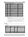
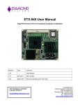
1
XTX 820
Computer On Module
Reference Manual
P/N 5001796A Revision B
Notice Page
NOTICE
No part of this document may be reproduced, transmitted, transcribed, stored in a retrieval system, or
translated into any language or computer language, in any form or by any means, electronic, mechanical,
magnetic, optical, chemical, manual, or otherwise, without the prior written permission of Ampro
Computers, Incorporated.
DISCLAIMER
Ampro Computers, Incorporated makes no representations or warranties with respect to the contents of
this manual or of the associated Ampro products, and specifically disclaims any implied warranties of
merchantability or fitness for any particular purpose. Ampro shall under no circumstances be liable for
incidental or consequential damages or related expenses resulting from the use of this product, even if it
has been notified of the possibility of such damages. Ampro reserves the right to revise this publication
from time to time without obligation to notify any person of such revisions. If errors are found, please
contact Ampro at the address listed below on the Notice page of this document.
TRADEMARKS
Ampro and the Ampro logo are registered trademarks, and CoreModule, EnCore, Little Board,
LittleBoard, MightyBoard, MiniModule, ReadyBoard, ReadyBox, ReadyPanel, and ReadySystem are
trademarks of Ampro Computers, Inc. All other marks are the property of their respective companies.
REVISION HISTORY
Revision
Reason for Change
Date
A, A
Initial Release
Mar/06
A, B
BIOS Update/Changes
Sept/06
Ampro Computers, Incorporated
5215 Hellyer Avenue
San Jose, CA 95138-1007
Tel. 408 360-0200
Fax 408 360-0222
www.ampro.com
© Copyright 2006, Ampro Computers, Incorporated
Audience Assumptions
This reference manual is for the person who designs computer related equipment, including but not
limited to hardware and software design and implementation of the same. Ampro Computers, Inc.
assumes you are qualified in designing and implementing your hardware designs and its related software
into your prototype computer equipment.
ii
Reference Manual
XTX 820
Contents
Chapter 1
About This Manual......................................................................................................... 1
Purpose of this Manual ...................................................................................................................... 1
Reference Material ............................................................................................................................. 1
Related Ampro Products .................................................................................................................... 2
Chapter 2
Product Overview .......................................................................................................... 5
ETX® Concept and XTX™ Extension .................................................................................................. 5
Product Description ............................................................................................................................ 6
Board Features .............................................................................................................................. 7
Block Diagram.............................................................................................................................. 10
Major Integrated Circuits (ICs) ..................................................................................................... 11
Connector Definitions................................................................................................................... 12
Specifications ................................................................................................................................... 13
Physical Specifications ................................................................................................................ 13
Mechanical Specifications............................................................................................................ 13
Power Specifications.................................................................................................................... 14
Environmental Specifications....................................................................................................... 14
Thermal/Cooling Solutions........................................................................................................... 14
Chapter 3
Hardware....................................................................................................................... 15
Overview ....................................................................................................................................... 15
CPU (U1) ....................................................................................................................................... 16
Celeron M Processor ................................................................................................................... 16
Pentium M Processors................................................................................................................. 16
Memory
....................................................................................................................................... 16
DDR2 SODIMM Socket (J5) ........................................................................................................ 16
Flash Memory (U17) .................................................................................................................... 16
Interrupt Channel Assignments (IRQs)........................................................................................ 16
Memory Map ................................................................................................................................ 17
I/O Address Map .......................................................................................................................... 18
PCI Bus Interface Connector (J1) .................................................................................................... 19
PCI Bus ....................................................................................................................................... 19
Universal Serial Bus (USB).......................................................................................................... 24
Serial Interrupt Request ............................................................................................................... 24
AC’97 Sound ................................................................................................................................ 24
PCI Express Interface (J2) ............................................................................................................... 29
PCI Express/ExpressCards ......................................................................................................... 29
Serial ATA .................................................................................................................................... 30
Additional Universal Serial Bus (USB) Ports ............................................................................... 30
AC'97/HDA CODEC..................................................................................................................... 31
LPC Interface ............................................................................................................................... 31
Extended System Management................................................................................................... 31
Primary I/O Interface (J3)................................................................................................................. 35
Floppy Port................................................................................................................................... 35
Parallel Port.................................................................................................................................. 36
Serial Ports 1 and 2 ..................................................................................................................... 37
Infrared (IrDA) Port ...................................................................................................................... 38
PS/2 Keyboard ............................................................................................................................. 38
XTX 820
Reference Manual
iii
Contents
PS/2 Mouse ..................................................................................................................................38
Video Interface .............................................................................................................................39
CRT Interface ...............................................................................................................................39
LVDS Interface .............................................................................................................................40
TV Out (Component and S-Video) ...............................................................................................42
IDE and Auxiliary Interface (J4) ........................................................................................................46
IDE Ports ......................................................................................................................................46
Ethernet Port Interface .................................................................................................................48
Power Control Signals ..................................................................................................................49
Power Management Signals ........................................................................................................49
Speaker ........................................................................................................................................49
Real Time Clock (RTC)/Battery....................................................................................................50
SMBus (I2C Bus)...........................................................................................................................50
Miscellaneous ...................................................................................................................................55
SDVO Port....................................................................................................................................55
Serial Console (Remote Access) .................................................................................................56
Temperature Monitoring ...............................................................................................................56
Watchdog Timer (WDT)................................................................................................................57
Power Input.......................................................................................................................................58
Power and Sleep States ...................................................................................................................58
Power-On Switch..........................................................................................................................58
Sleep States (ACPI) .....................................................................................................................59
Wake Up Activities........................................................................................................................60
Chapter 4
BIOS Setup Utility.........................................................................................................61
Introduction .......................................................................................................................................61
Accessing BIOS Setup Utility (VGA Display) ...............................................................................61
Accessing BIOS Setup Utility (Remote Access) ..........................................................................62
BIOS Menus......................................................................................................................................63
BIOS Main Setup Screen .............................................................................................................63
BIOS Advanced Setup Screen .....................................................................................................64
BIOS Boot Setup Screen..............................................................................................................81
BIOS Security Setup Screen ........................................................................................................84
BIOS Power Setup Screen ...........................................................................................................86
BIOS Exit Setup Screen ...............................................................................................................88
Appendix A Technical Support ........................................................................................................91
Appendix B LAN Boot Feature.........................................................................................................93
Introduction .......................................................................................................................................93
Accessing the LAN (PXE) Boot Feature...........................................................................................94
Alternate Method of Selecting LAN Boot......................................................................................95
Appendix C Connector Part Numbers.............................................................................................97
Index
........................................................................................................................................99
List of Figures
Figure 2-1. XTX 820 and Custom Baseboard ...................................................................................5
Figure 2-2. Typical Design Flow ........................................................................................................6
Figure 2-3. Functional Block Diagram .............................................................................................10
Figure 2-4. XTX 820 (Top view).......................................................................................................11
Figure 2-5. Connector Locations (Bottom view) ..............................................................................12
iv
Reference Manual
XTX 820
Contents
Figure 2-6.
Figure 4-1.
Figure 4-2.
Figure 4-3.
Figure 4-4.
Figure 4-5.
Figure 4-6.
XTX 820 Dimensions (Top, Through Board View) ....................................................... 13
BIOS Main Setup Screen.............................................................................................. 63
BIOS Advanced Setup Screen ..................................................................................... 64
BIOS Boot Setup Screen .............................................................................................. 81
BIOS Security Setup Screen ........................................................................................ 84
BIOS Power Setup Screen ........................................................................................... 86
BIOS Exit Setup Screen ............................................................................................... 88
List of Tables
Table 2-1. Major Integrated Circuit Description and Function ........................................................ 11
Table 2-2. Board Connector Descriptions ....................................................................................... 12
Table 2-3. Weight and Footprint Dimensions.................................................................................. 13
Table 2-4. Power Supply Requirements ......................................................................................... 14
Table 2-5. Environmental Requirements ........................................................................................ 14
Table 3-1. Interrupt Channel Assignments (IRQs).......................................................................... 17
Table 3-2. Memory Map .................................................................................................................. 17
Table 3-3. I/O Address Map ............................................................................................................ 18
Table 3-4. Simplified PCI Pin/Signal Descriptions (J1) ................................................................... 19
Table 3-5. Simplified USB Interface Pin/Signal Descriptions (J1) .................................................. 24
Table 3-6. Simplified Serial Interrupt Request (J1) ......................................................................... 24
Table 3-7. Simplified Audio Interface Pin/Signal Descriptions (J1)................................................. 25
Table 3-8. Complete J1 Interface Pin/Signal Descriptions (J1) ...................................................... 25
Table 3-9. PCI Express Interface Pin/Signal Descriptions (J2) ...................................................... 29
Table 3-10. Serial ATA Interface Pin/Signal Descriptions (J2) ....................................................... 30
Table 3-11. USB 4 & 5 Interface Pin/Signal Descriptions (J2)........................................................ 30
Table 3-12. Audio CODEC Interface Pin/Signal Descriptions (J2) ................................................. 31
Table 3-13. LPC Interface Pin/Signal Descriptions (J2).................................................................. 31
Table 3-14. Miscellaneous Interface Pin/Signal Descriptions (J2).................................................. 32
Table 3-15. Complete J2 Interface Pin/Signal Descriptions (J2) .................................................... 32
Table 3-16. Simplified Floppy Drive Interface Pin/Signal Descriptions (J3).................................... 35
Table 3-17. Simplified Parallel Interface (SPP) Pin/Signal Descriptions (J3) ................................. 36
Table 3-18. Simplified Serial Interface Pin/Signal Descriptions (J3)............................................... 37
Table 3-19. Simplified Keyboard, Mouse, and Infrared (IrDA) Port Pin/Signal Descriptions (J3)... 39
Table 3-20. Simplified CRT Interface Pin/Signal Descriptions (J3) ................................................ 40
Table 3-21. Simplified LVDS Interface Pin/Signal Descriptions (J3) .............................................. 41
Table 3-22. Simplified TV Out (S-Video) Interface Pin/Signal Descriptions (J3) ............................ 42
Table 3-23. Complete J3 Interface Pin/Signal Descriptions (J3) .................................................... 42
Table 3-24. Simplified Primary IDE Interface Pin/Signal Descriptions (J4) .................................... 46
Table 3-25. Simplified Ethernet Port Pin/Signal Descriptions (J4).................................................. 48
Table 3-26. Simplified Power Control and Miscellaneous Pin/Signal Descriptions (J4) ................. 50
Table 3-27. SMBus Reserved Addresses ....................................................................................... 51
Table 3-28. Complete J4 Interface Pin/Signal Descriptions (J4) .................................................... 51
Table 3-29. SDVO Interface Pin/Signal Descriptions (J6) .............................................................. 55
Table 3-30. Typical ATX Power Interface Pin/Signal Descriptions ................................................. 58
Table 3-31. Wake Up Activities and Conditions.............................................................................. 60
Table 4-1. BIOS Setup Utility Menus .............................................................................................. 62
Table 4-2. Exiting and Loading Default Keys.................................................................................. 63
Table 4-3. Local Flat Panel Type List.............................................................................................. 66
XTX 820
Reference Manual
v
Contents
Table A-1. Technical Support Contact Information..........................................................................91
Table C-1. Connector and Manufacture’s Part Numbers ................................................................97
vi
Reference Manual
XTX 820
Chapter 1
About This Manual
Purpose of this Manual
This manual is for designers of systems based on the XTX 820 Computer on Module (COM). This
manual contains information that permits designers to create an embedded system based on specific
design requirements.
Information provided in this reference manual includes:
• XTX 820 Specifications
• Environmental requirements
• Major integrated circuits (chips) and features implemented
• All connectors with pin numbers and definitions
• BIOS Setup Utility information
Information not provided in this reference manual includes:
• Detailed chip specifications
• Internal component operation
• Internal registers or signal operations
• Bus or signal timing for industry standard busses and signals
Reference Material
The following list of reference materials may be helpful for you to complete your design successfully.
Most of this reference material is also available on the Ampro web site in the Embedded Design
Resource Center. The Embedded Design Resource Center was created for embedded system developers
to share Ampro’s knowledge, insight, and expertise gained from years of experience.
Specifications
• ETX Component SBC™ Specification Revision 2.7, 2001
• ETX Component SBC™ Design Guide, Revision 1.5, 2001
For latest revision of the ETX specifications, contact the Working Group, at:
Web site: http://www.etx-ig.org
• XTX Interface Specification, Revision 1.0, July 13, 2005
• XTX Design Guide, Revision 1.0, February 22, 2006
For latest revision of the XTX specifications or design guide, contact the XTX Consortium, at:
Web site: http://www.xtx-standard.org
• PCI 2.1 Compliant Specifications
For latest revision of the PCI specifications, contact the PCI Special Interest Group Office at:
Web site: http://www.pcisig.com
XTX 820
Reference Manual
1
Chapter 1
About This Manual
Major Integrated Circuit (ICs or Chips) Specifications used on the XTX 820 COM:
• Intel Corporation and the Pentium® M 745, Pentium® M 738, or Celeron® M 373 processors
Web site: http://www.intel.com/design/mobile/datashts/302189.htm = Pentium M
Web site: http://www.intel.com/design/mobile/datashts/303110.htm = Celeron M
• Intel Corporation and the 82915GM and 82801FBM chips used for the Memory Hub/Video
controller and I/O Hub respectively.
Web site: http://www.intel.com/design/mobile/datashts/305264.htm = Memory Hub
Web site: http://www.intel.com/design/chipsets/specupdt/301474.htm = I/O Hub
• Winbond Electronics, Corp. and the W83627HG chip used for the Super I/O controller
Web site: http://www.winbondusa.com/products/winbond_products/pdfs/PCIC/W83627HF_F_HG_Ga.pdf
• Intel Corporation and the U82562GZ chip used for the Physical Ethernet controller
Web site: http://www.intel.com/design/network/products/lan/docs/82562_docs.htm
• Realtek Semiconductor, Corp's chip ALC655, used for the AC'97 Audio CODEC.
Web site: ftp://202.65.194.18/pc/ac97/alc655/ALC655_DataSheet_1.3.pdf
NOTE
If you are unable to locate the datasheets using the links provided, go
to the manufacturer's web site where you can perform a search using
the chip datasheet number or name listed, including the extension,
(htm for web page, pdf for files name, etc.
Related Ampro Products
The following items are directly related to successfully using the Ampro product you have just
purchased or plan to purchase. Ampro highly recommends that you purchase and utilize a XTX 820
QuickStart Kit or Development System.
XTX 820 Support Products
• XTX 820 QuickStart Kit (QSK)
The QuickStart Kit includes the XTX 820 module, RAM, a baseboard, and the XTX 820
Documentation and Software (Doc & SW) CD-ROM.
• XTX 820 Documentation and Software CD-ROM
The XTX 820 Documentation and Software (XTX 820 Doc & SW) CD-ROM is provided with
the XTX 820. The CD-ROM includes all of the XTX 820 documentation, including this
reference manual and the XTX 820 QuickStart Guide in PDF format, software utilities, board
support packages, and drivers for the unique devices used with Ampro supported operating
systems.
2
Reference Manual
XTX 820
Chapter 1
About This Manual
Ampro XTX Products
• XTX 800 – This high-performance, compact, rugged Computer-On-Module (COM) solution uses
Intel 1.8 GHz Pentium M 745, 1.4 GHz Pentium M 738, or 1.0 GHz Celeron M 373 with an Intel
852GM chipset. This XTX module comes standard with enhanced peripherals, including PCI
bus, two Serial ATA ports and one Ultra/DMA 33/66/100 EIDE controller for two EIDE drives,
six USB 2.0 ports, one shared EPP/ECP parallel/ floppy port, two serial ports with TTL levels,
one Infrared (IrDA) port, PS/2 keyboard and mouse interfaces, and an AC’97/HDA (High
Definition Audio) CODEC on the module. The XTX 800 also supports ACPI 2.0 Power
Management, 10/100BaseT Ethernet interface, up to 1 GB of DDR RAM in a single 200-pin
SODIMM slot, a 128-bit graphics controller for CRTs and LVDS flat panels, and a SDVO (Serial
Digital Video Output) interface.
Ampro ETX Products
• ETX 700 – This high-performance, compact, rugged Computer-On-Module (COM) solution uses
Intel® 650 MHz Low Voltage Celeron® or 400 MHz Ultra Low Voltage Celeron CPUs with up
to 512 kB Level 2 Cache on board. This ETX module comes with the standard peripherals,
including dual Ultra/DMA 33/66/100 IDE, floppy drive interface, PCI bus, ISA bus, serial,
parallel, PS/2 keyboard and mouse interfaces, 10/100BaseT Ethernet, USB ports, AGP 4X
equivalent video interface with up to 32 MB UMA Frame Buffer that supports built-in LVDS at
1600x1200 resolution, and AC’97 audio. It also supports up to 512 MB of SODIMM DRAM on
a 50% thicker PCB to meet your custom baseboard needs.
• ETX 802 – This high-performance, compact, rugged Computer-On-Module (COM) solution uses
Intel 1.4 GHz LV Pentium® M 738,1.0 GHz Celeron M 373, or 800 MHz ULV Celeron M CPUs
with an Intel 852GME chipset. This ETX module comes with the standard peripherals, including
dual Ultra/DMA 33/66/100 IDE, floppy drive interface, PCI bus, ISA bus, serial, parallel, PS/2
keyboard and mouse interfaces, 10/100BaseT Ethernet, USB 2.0 ports, 128-bit graphics
controller interface with up to 64 MB UMA Frame Buffer that supports CRT and LVDS at
1600x1200 resolution, and AC’97 audio. It also supports up to 1 GB of SODIMM DDR RAM
on a 50% thicker PCB to meet your custom baseboard needs.
Other Ampro Products
• CoreModule™ Family – These complete embedded-PC subsystems on single PC/104 or PC/104Plus form-factor (3.6"x3.8") modules feature 486, Celeron, or Celeron M CPUs. Each
CoreModule includes a full complement of PC core logic functions, plus disk controllers, and
serial and parallel ports. Most modules also include CRT and flat panel graphics controllers
and/or an Ethernet interface. The CoreModules also come with built-in extras to meet the critical
reliability requirements of embedded applications. These include onboard solid state disk
compatibility, watchdog timer, and smart power monitor.
• LittleBoard™ Family – These high-performance, highly integrated single-board computers use
the EBX form factor (5.75"x8.00"), and are available with the Intel Pentium M, Celeron M,
Pentium III, or Celeron processors. The EBX-compliant LittleBoard single-board computers
offer functions equivalent to a complete laptop or desktop PC system, plus several expansion
cards. Built-in extras to meet the critical requirements of embedded applications include onboard
solid state disk capability, watchdog timer, and smart power monitor.
• MightyBoard™ Family – These low-cost, high-performance single-board computers (SBC) use
the Mini-ITX form factor (6.75"x 6.75") and are available with Intel Celeron M or Pentium M
processors. MightyBoard products offer the equivalent functions of a complete laptop or desktop
PC system, including DDR memory, high performance graphics, USB 2.0, Gigabit Ethernet, plus
standard PCI expansion capability in one card slot.
XTX 820
Reference Manual
3
Chapter 1
About This Manual
• MiniModule™ Family – This line of peripheral interface modules compliant with
PC/104,PC/104-Plus, and/or PCI-104 form factor (3.6"x3.8") standards can be used with Ampro's
CoreModule, LittleBoard, and ReadyBoard single-board computers (SBCs) to expand the I/O
configuration of embedded systems. Ampro's highly reliable MiniModule products add value to
existing designs by adding I/O ports, such as IEEE 1394 (Firewire), or by adding support for
legacy boards, such as a PCI-to-ISA bridge adapter board.
• ReadyBoard™ Family – These low-cost, high-performance single-board computers (SBC) use the
EPIC form factor (4.5"x6.5") and are available with the Intel Pentium M, Celeron M, and Celeron
processors. ReadyBoard products offer functions equivalent to a complete laptop or desktop PC
system with standard PC-style connections, and features such as DDR or DDR2 memory, high
performance graphics, USB 2.0, Ethernet and Gigabit Ethernet ports, AC'97 Audio, plus several
expansion cards. Ampro also includes such features as watchdog timer, battery-free boot, a
customizable splash screen, Oops! jumper (BIOS recovery), and serial console
4
Reference Manual
XTX 820
Chapter 2
Product Overview
This introduction presents general information about the XTX Architecture and the XTX 820 ComputerOn-Module (COM). After reading this chapter you should understand:
• XTX Computer-On-Module concept
• XTX 820 architecture and features
• Major components
• Connectors
• Specifications
ETX® Concept and XTX™ Extension
The Embedded Technology eXtended (ETX) module concept is an off the shelf, multi vendor, singleboard-computer that integrates all the core components of a common PC and is mounted onto an
application specific baseboard. ETX modules have a standardized form factor of just 95 mm x 114 mm
and use an identical pin compatible connector on the four system connectors. The ETX module provides
most of the PC functional requirements for any application. These functions include, but are not limited
to, graphics, sound, keyboard/mouse, IDE, Ethernet, parallel, serial and USB ports. Four ruggedized
connectors provide the baseboard interface and carry all the I/O signals to and from the ETX module.
Baseboard designers can utilize as little or as many of the I/O interfaces as deemed necessary. The
baseboard can therefore provide all the interface connectors required to attach the system to the
application specific peripherals. This versatility allows the designer to create a dense and optimized
package, which results in a more reliable product while simplifying system integration. Most
importantly ETX applications are scalable, which means once a product has been created there is the
ability to diversify the product range through the use of different performance class ETX modules.
Simply unplug one module and replace it with another, no redesign is necessary.
XTX™ is an expansion and continuation of the well-established and highly successful ETX standard.
XTX offers the newest I/O technologies on this proven form factor. Currently, the ISA bus is found less
often in modern embedded applications that offer a greater array of features. Consequently, the X2
connector for XTX replaces ISA with features that are currently not found on the ETX platform. These
features include new serial high speed buses such as PCI Express™, ExpressCard, AC'97 HD audio, and
Serial ATA®. XTX also provides the AC'97 High Definition Audio (HDA) and two additional USB 2.0
ports, bringing the USB total to six USB ports. The USB 2.0 and PCI Express interfaces can also
support the next generation PCMCIA card in the ExpressCard. All the other signals found on the X1,
X3, and X4 connectors remain the same in accordance with the ETX standard (Rev. 2.7) and therefore
will be completely compatible. If the embedded application still requires the ISA bus, then a PCI-ISA
bridge can be implemented on the application specific baseboard. If this solution is too costly then the
readily available XTX LPC bus located the Ampro XTX module can be used.
ETX or XTX modules work like a high-integration chip, plugging into your custom circuit board design
to provide specific control for your logic application. See Figure 2-1.
XTX 820 Module
M2.5 PEM Nuts
Spacing 3mm (4)
Stack Connectors
(4 pairs)
Custom Baseboard Design
XTX820stack
M2.5 Screws (4)
Figure 2-1. XTX 820 and Custom Baseboard
XTX 820
Reference Manual
5
Chapter 2
Product Overview
The XTX flexibility enables designers to take an accelerated, low risk path with proven XTX module
designs. Your design flow might look similar to the one shown in Figure 2-2. This diagram gives a
Typical Design Flow of hardware and software functions.
CPU and Software
Design Path
Hardware
Design Path
Design applicationspecific baseboard
Select CPU
Fabricate baseboard
Select OS & Tools
Write and Test
Application Code
Revise baseboard
if necessary
Write drivers for
custom Logic
Integrate application code
XTX820designflw
Debug baseboard
Figure 2-2. Typical Design Flow
Product Description
The XTX 820 is an exceptionally high integration, high performance, rugged, and high quality
Computer-On-Module (COM), which contains all the component subsystems of a PC/AT motherboard
plus the equivalent of up to 5 expansion boards. The XTX 820 is based on the ultra high performance,
high-integration Intel Pentium M and Celeron M processors giving designers the choice of a complete,
high performance, rugged, embedded processor based on the XTX form factor that conforms to the ETX
V2.7 specification. The module plugs into a custom baseboard which has connectors and additional
circuitry to meet your application requirements.
Each XTX 820 incorporates an Intel® 915GM chipset (82915GM + 82801FBM). This includes the
Intel 82915GM Memory & Graphics Hub (Northbridge), which controls the memory and graphics
interface and the Intel 82801FBM I/O Hub (Southbridge) controller for some of the important I/O
functions. A Super I/O chip (83627HG) by Winbond Electronics, Corp controls most of I/O
functions. Together these three chips provide four x1 PCI Express Lanes, PCI bus, two Serial ATA
portsand one Ultra/DMA 33/66/100 EIDE controller for two EIDE drives, six USB 2.0 ports, one
shared EPP/ECP parallel/ floppy port, two serial ports with TTL levels, one Infrared (IrDA) port,
PS/2 keyboard and mouse interfaces, and an AC’97/HDA (High Definition Audio) CODEC on the
module. The XTX 820 also supports ACPI 2.0 Power Management, 10/100BaseT Ethernet interface,
up to 1 GB of DDR2 RAM in a single 200-pin SODIMM socket, and a 128-bit graphics controller,
which provides CRT (VGA), a dedicated LVDS port, TV Out, and two SDVO port interfaces.
The XTX 820 is particularly well suited to either embedded or portable applications and meets the size,
power consumption, temperature range, quality, and reliability demands of embedded system
applications. The XTX 820 requires only a single +5V power supply.
6
Reference Manual
XTX 820
Chapter 2
Product Overview
Board Features
• CPU features
♦
Intel Celeron M 373 1.0 GHz with 512 kbytes L2 cache
♦
Intel Pentium M 738 1.4 GHz with 2 Mbytes L2 cache
♦
Intel Pentium M 745 1.8 GHz with 2 Mbytes L2 cache
♦
All three CPUs use 400 MHz front side bus (FSB)
• Memory
♦
Single standard 200-pin DDR2 SODIMM socket
♦
Supports +1.8V RAM up to 1 GB
♦
Supports PC2 3200 DDR2 400 (400 Mbps, 200 MHz)
• Power Management
♦
Supports ACPI 2.0 with S3 (Suspend to RAM)
• PCI Bus
♦
PCI 2.1 compliant
♦
PCI Bus speed at 33 MHz
• PCI Express
♦
Supports 4 x1 PCI Express Lanes
♦
Supports PCI Express edge card or ExpressCards on custom baseboard
♦
Supports PCI Express specification v1.0a
• LPC Bus
♦
Provides low-bandwidth support through low pin count (LPC) bus
♦
Provides substitute for ISA bus with Super I/O chip on baseboard
• IDE/ATA Interfaces
♦
Supports two Serial ATA interfaces
♦
Supports one EIDE channel (UDMA 66/100)
♦
Supports ATAPI and DVD peripherals
♦
Supports IDE native and ATA compatibility modes
• Floppy Disk Interface
♦
Shares output connector with Parallel port
♦
Supports one standard (34-pin) floppy drive
♦
Supports all standard PC/AT formats: 360KB, 1.2MB, 720KB, 1.44MB
• Serial Ports
XTX 820
♦
Provides two buffered TTL serial ports with full handshaking (transceiver on baseboard)
♦
Provides 16550-equivalent controllers, each with a built-in 16-byte FIFO buffer
♦
Supports full modem capability
♦
Supports programmable word length, stop bits, and parity
♦
Supports 16-bit programmable baud-rate generator and a interrupt generator.
Reference Manual
7
Chapter 2
Product Overview
• Infrared Interface
♦
Supports a single IrDA 1.1 port
♦
Supports HPSIR and ASKIR infrared modes
• Parallel Port
♦
Shares output connector with Floppy controller
♦
Supports standard printer port
♦
Supports IEEE standard 1284 protocols of EPP and ECP outputs
♦
Bi-directional data lines
♦
Supports 16 byte FIFO for ECP mode.
• USB Ports
♦
Supports three root USB hubs
♦
Supports six USB ports
♦
Supports USB v2.0 (EHCI) and legacy v1.1
♦
Supports over-current fuses on board
• Keyboard/Mouse Interface
♦
Supports PS/2 keyboard
♦
Supports PS/2 mouse
• Audio interface
♦
Supports AC’97 standard
♦
AC’97 HDA (High Definition Audio) CODEC on board
♦
Supports audio amplifier on baseboard
• Ethernet Interface
♦
Supports one Ethernet port
♦
I/O Hub (Southbridge) provides MAC Ethernet Controller
♦
Intel 82562GZ provides the PHY Ethernet interface
♦
Requires magnetics and RJ45 connector on baseboard
♦
Supports IEEE 802.3 10BaseT/100BaseTX compatible physical layer
♦
Supports Auto-negotiation for speed, duplex mode, and flow control
♦
Supports full duplex or half-duplex mode
•
Full-duplex mode supports transmit and receive frames simultaneously
•
Supports IEEE 802.3x Flow control in full duplex mode
•
Half-duplex mode supports enhance proprietary collision reduction mode
• Video Interfaces (CRT/LVDS/TV Out/SDVO)
♦
♦
♦ Supports 8-bits for each RGB DAC or 24-bit RAMDACSupports up to 128 MB of
system memory
♦
System memory is allocated using Dynamic Video Memory Technology (DVMT) v3.0
♦
8
Support CRT resolutions up to 2048x1536 @ 75 Hz (QXGA)
Supports Dual independent display
Reference Manual
XTX 820
Chapter 2
Product Overview
♦
♦
Supports 25 to 112 MHz single/dual channel LVDS with Spread Spectrum Clocking (SSC)
Supports TFT format of 1x18 bpp per channel and 2x18 bpp for 2 channels
♦
Supports LVDS panel size up to UXGA (1600 x 1200)
♦
Provides TV Out to the baseboard
♦
Supports Composite and S-Video up to 1024 x 768 resolution for NTSC/PAL
♦
Supports Component Video in 480p/720p/1080i/1080p modes
♦
Provides two Intel compliant SDVO (Serial Digital Video Output) ports
♦
Supports SDVO pixel rates up to 200 MP/s (600 MB/s) transfer speed on each port
• Miscellaneous
XTX 820
♦
Provides Real-Time Clock (RTC) supported by external battery on baseboard
♦
Supports Remote Access (Serial Console or Console Redirection)
♦
Supports Watchdog Timer (WDT)
♦
Supports customizable Splash Screen (OEM Logo)
Reference Manual
9
Chapter 2
Product Overview
Block Diagram
Figure 2-3 shows the functional components of the board.
Intel
Pentium M
or Celeron M
CPU
J3(X3)
SDVO
CRT,
LVDS,
TV Out
Memory &
Graphics Hub
82915GM
(Northbridge)
Clock
Memory Bus
DDR2
SODIMM
Socket
SMBus
SDVO
DMI Interface
J1(X1)
RTC
I/O Hub
82801FBM
(Southbridge)
PCI Bus
ATA
J4(X4)
Power Ctrl &
Management
Audio
CODEC
1x IDE Primary
2
LPC Bus
J1(X1)
USB Port 0
USB USB Port 1
IrDA 1.1
Board
Controller
COM1
WDT
Keyboard,
Mouse
USB Port 3
USB Ports 4, 5
2 SATA
4 X1 PCI Express Lanes
Super I/O
W83627HG
J3(X3)
Floppy/
Parallel
USB Port 2
FWH
BIOS
WTD Trig
J2(X2)
J4(X4)
IC
Ethernet
PHY
82562
Fan Ctrl
COM2
AC’97/HDA Digital Audio
SPI
J1
X1
XTX 820 Connectors
J2
J3
J4
X2
X3
X4
Baseboard Connectors
XTX820BlkDiagm_a
Figure 2-3. Functional Block Diagram
10
Reference Manual
XTX 820
Chapter 2
Product Overview
Major Integrated Circuits (ICs)
Table 2-1 lists the major integrated circuits (ICs or chips), including a brief description, on the XTX 820
module and Figure 2-4 shows the location of the major chips.
Table 2-1. Major Integrated Circuit Description and Function
Chip Type
CPU (U6)
Mfg.
Intel
Model
Celeron M or
Pentium M
Description
CPUs at 1.0 GHz, 1.4 GHz,
and 1.8 GHz
Function
Embedded
CPU
Memory & Graphics
Hub (U8)
Intel
82915GM
(GMHC)
Northbridge functions plus
Video
Memory and
Video
I/O Hub (U4)
Intel
82801FBM
(ICH6M)
Provides most standard I/O
Southbridge functions plus
Ethernet MAC functions
I/O Functions
Plus Ethernet
Super I/O (U11)
Winbond
83627HG
Provides reminder of I/O
functions
I/O Functions
Ethernet (U3)
Intel
82562GZ
Uses MAC from I/O Hub to
provide Ethernet Controller
Physical
Ethernet
Audio (U21)
Realtek
ALC655
Audio CODEC controller
AC'97 Audio
Clock (U10)
I/O Hub (U4)
(Southbridge)
U10
U4
J5
DDR SODIMM
Socket (J5)
Ethernet (U3)
U8
U3
Memory Hub (U8)
(Northbridge)
U2
Super I/O (U11)
U6
U11
U16
XTX820_01a
CPU (U6)
Figure 2-4. XTX 820 (Top view)
XTX 820
Reference Manual
11
Chapter 2
Product Overview
Connector Definitions
Table 2-2 describes the connectors shown in Figures 2-4 and 2-5.
Table 2-2. Board Connector Descriptions
No.
Signals
Description
J1
PCI, USB, Audio
100-pin connector for 32-bit PCI, USB (4 ports), and Audio
J2
PCI Express, SATA
100-pin connector for PCI Express, 2x SATA, USB (2 ports), LPC,
ExpressCards (2), AC'97/HDA Audio, extended system management
J3
Video, I/O
100-pin connector for Video (VGA, LVDS) and I/O (Floppy/Parallel,
Serial Ports 1 & 2, and Infrared) signals
J4
IDE, Ethernet
100-pin connector for IDE (Primary & Secondary IDE), I2C bus,
Power Management, and the Ethernet port
J5
DDR2 Memory
200-pin socket for a DDR2 SODIMM RAM
J6
SDVO port
45-pin Serial Digital Video Output ports (2)
PCI, USB, Audio (J1)
PCI Express, SATA (J2)
J1
Flash
(U30)
J2
Audio
CODEC
(U21)
U21
U30
U25
SDVO
(J6)
U17
J6
J3
Video, I/O (J3)
J4
IDE, Ethernet (J4)
XTX820_02a
U28
Figure 2-5. Connector Locations (Bottom view)
12
Reference Manual
XTX 820
Chapter 2
Product Overview
Specifications
Physical Specifications
Table 2-3 gives the physical dimensions of the board and Figure 2-6 gives the mounting dimensions.
Table 2-3. Weight and Footprint Dimensions
Item
Dimension
Weight
0.11 kg. (0.249 lbs.)
(no SODIMM)
Height (overall)
12 cm (0.4")
Width
95 mm (3.74")
Length
114 mm (4.5")
Thickness
1.6 mm (0.062")
NOTE
Overall height is measured from the upper
board surface to the highest permanent
component (SODIMM socket, J5) on the
upper board surface. This measurement
does not include any heatsinks available
for this board. The heatsink will increase
this dimension.
Mechanical Specifications
108.6
-0.6
0.0
Figure 2-6 provides a through the board view of the XTX 820 with the mechanical mounting
dimensions.
Mounting Hole O 2.5
92.5
(+0/-0.2)
90.0
1
2
J4
J2
1
2
50.8
1
43.4
39.2
J3
XTX820_02b
2
J1
2
1
9.2
5.0
0.0
1
:Location peg O 1.0 +/-0.5mm
2 :Location
peg O 0.7 +/-0.5mm
108.0
111.0
-3.0
0.0
0.0
-2.5
Figure 2-6. XTX 820 Dimensions (Top, Through Board View)
NOTE
XTX 820
All dimensions are given in millimeters and all
dimensions without tolerance are +/-0.2 mm.
Reference Manual
13
Chapter 2
Product Overview
Power Specifications
Table 2-4 lists the power requirements for each XTX 820 CPU model as described below.
Table 2-4. Power Supply Requirements
Parameter
1.0 GHz ULV Celeron
M Characteristics
1.4 GHz LV Pentium M 1.8 GHz LV Pentium M
Characteristics
Characteristics
Input Type
Regulated DC voltages
Regulated DC voltages
Regulated DC voltages
In-rush Current*
14.20A
16.20A
14.16A
Typical BIT**
Current (W)
3.34A (16.71W)
3.89A (19.46W)
5.31A (26.57W)
Notes: *The In-rush current represents video, 256 MB RAM, and power only connected through the
Ampro baseboard. Typically, in-rush current reflects the short duration current spike associated with
charging large on-board bulk capacitance during power supply start up. However, the listed in-rush
current value is the result of placing a switch on the DC output of a fully 'ramped' power supply to
give a worst-case current value, which is much higher than the standard method. This in-rush value
should be regarded as a maximum design guideline, not a requisite value.
**The Burn-In-Test (BIT) current setup has CRT video, 256 MB RAM, floppy drive (1), IDE hard
disk drive (1), USB hard disk drive (1), USB CD-ROM (1), serial ports with loopbacks (3), keyboard,
mouse, USB compact flash card reader with compact flash card (64 MB) installed (1), USB Jumpdrive (1), and the Ethernet port (1) operating under Microsoft® Windows®™ XP (SP2). All current
measurements include the Ampro baseboard in the QuickStart Kit.
Environmental Specifications
Table 2-5 provides the most efficient operating and storage condition ranges required for this board.
Humidity
Temperature
Table 2-5. Environmental Requirements
Parameter
1.0 GHz ULV Celeron
M Conditions
1.4 GHz LV Pentium
M Conditions
1.8 GHz LV Pentium
M Conditions
Operating
+0° to +60°C
(32° to +158°F)
+0° to +60°C
(32° to +158°F)
+0° to +60°C
(32° to +140°F)
Storage
–20° to +75°C
(–4° to +185°F)
–20° to +75°C
(–4 °to +185°F)
–20° to +75°C
(–4° to +185°F)
Operating
5% to 95%
relative humidity,
non-condensing
5% to 95%
relative humidity,
non-condensing
5% to 95%
relative humidity,
non-condensing
Storage
5% to 95%
relative humidity,
non-condensing
5% to 95%
relative humidity,
non-condensing
5% to 95%
relative humidity,
non-condensing
Thermal/Cooling Solutions
The Pentium/Celeron M processors used on the XTX 820 make use of the thermal monitor feature to
help control the processor temperature. Refer to the Thermal Monitoring topic in Chapter 3, Hardware
for more information. The maximum core operating temperature for Pentium M and Celeron M
processors is 100°C. Both Pentium M and Celeron M processors and the Memory & Graphics Hub
(Northbridge) require individual heatsinks, but no fan. Ampro provides an optional heatspreader plate.
CAUTION
14
To prevent processor overheating, you must provide an additional form of
cooling when using the heatspreader provided. The heatspreader plate is
not a complete thermal solution for any of the processors listed.
Reference Manual
XTX 820
Chapter 3 Hardware
Overview
This chapter discusses the chips and features of the connectors in the following order:
• CPU (U1)
• Memory
• PCI Bus Interface (J1)
♦
USB Interface
♦
Audio Interface
• PCI Express (J2)
♦
Serial ATA (SATA)
♦
ExpressCards
♦
AC'97/HDA
♦
LPC bus
• Primary I/O Interface (J3)
♦
Floppy/Parallel Interface
♦
Serial Port Interfaces
♦
PS/2 Keyboard and Mouse
♦
Infrared (IrDA)
♦
Video Interfaces (CRT & LVDS)
• IDE and Auxiliary Interface (J4)
♦
Primary IDE Interface
♦
Ethernet Interface
♦
Time of Day (RTC)/Battery and Speaker
♦
Power Control and Management
♦
SMBus
• Miscellaneous
♦
Serial Console (Remote Access)
♦
Temperature Monitoring
♦
Watchdog timer
♦
Power
NOTE
XTX 820
Ampro Computers, Inc. only supports the features/options tested and listed in this
manual. The main integrated circuits (chips) used in the XTX 820 may provide
more features or options than are listed for the XTX 820, but some of these chip
features/options are not supported on the board and will not function as specified
in the chip documentation.
Reference Manual
15
Chapter 3
Hardware
CPU (U1)
The XTX 820 offers three Intel processor choices; high performance 1.0 GHz Ultra Low Voltage
(ULV) Celeron M CPU, 1.4 GHz Low Voltage (LV) Pentium M CPU, or 1.8 GHz Pentium M CPU.
Celeron M Processor
The Celeron M processor (Dothan core) at 1.0 GHz has 512 kB L2 Cache with a 400 MHz FSB
(front side bus). The 1.0 GHz Celeron M 373 processor use 90 nm architecture and requires a
heatsink, but no fan.
Pentium M Processors
The Pentium M 738 processor (Dothan core) at 1.4 GHz has 2 MB L2 Cache with a 400 MHz FSB
(front side bus). The 1.4 GHz Pentium M 738 processor uses 90 nm architecture and requires a
heatsink, but no fan.
The Pentium M 745 processor (Dothan core) at 1.8 GHz has 2 MB L2 Cache with a 400 MHz FSB
(front side bus). The 1.8 GHz Pentium M 745 processor uses 90 nm architecture and requires a
heatsink, but no fan below 60°C.
CAUTION
If you choose to use a heat-spreader plate instead of an individual
heatsink for the processor, then you must provide an additional form
of cooling. The heat-spreader plate is not a complete thermal
solution for any of the processors listed.
Memory
The XTX 820 memory consists of the following elements:
• DDR2 SODIMM socket
• Flash memory
DDR2 SODIMM Socket (J5)
The XTX 820 supports a single 200-pin DDR2 SODIMM socket.
• SODIMM socket (J5) can support up to 1 GB of DDR2 memory
• Supports PC2 3200 DDR 400 operating at 400 Mbps (200 MHz, 5 ns) or faster
• Supports +1.8V SDRAM
NOTE
Ampro recommends using PC2 3200 DDR2 400 (400 Mbps, 200 MHz),
+1.8V, 5 ns, 200-pin, SDRAM SODIMM, or faster. PC2 3200 provides
the best performance for these Intel processors.
Flash Memory (U17)
There is an 8-bit wide, 512 kB flash device used for system BIOS and is connected to the I/O Hub
(Southbridge), through an LPC bus transceiver. The flash memory is used to store system parameters for
battery-free boot capability when there is no battery present. The BIOS is re-programmable and the
features supported are detailed in Chapter 4, BIOS Setup Utility.
Interrupt Channel Assignments (IRQs)
The channel interrupt assignments are listed in Table 3-1.
16
Reference Manual
XTX 820
Chapter 3
Hardware
Table 3-1. Interrupt Channel Assignments (IRQs)
IRQ#
Available
Typical Interrupt Source
Connected to Pin
0
No
Counter 0
NA
1
No
Keyboard
NA
2
No
Cascade Interrupt from Slave PIC
NA
3
Note 1
Serial Port 2 (COM2) / Generic
IRQ3 via SERIRQ
4
Note 1
Serial Port 1 (COM1) / Generic
IRQ4 via SERIRQ
5
Note 2
Parallel Port 2 (LPT2) / Generic
IRQ5 via SERIRQ
6
Note 1
Floppy Drive Controller / Generic
IRQ6 via SERIRQ
7
Note 1
Parallel Port 1 (LPT1) / Generic
IRQ7 via SERIRQ
8
No
Real-time Clock
NA
9
Note 4
SCI / Generic
IRQ9 via SERIRQ
10
Note 2, 1
Serial Port 3 (COM3) / Generic
IRQ10 via SERIRQ
11
Note 2, 1
Serial Port 4 (COM4) / Generic
IRQ11 via SERIRQ
12
Note 1
PS/2 Mouse / Generic
IRQ12 via SERIRQ
13
No
Math processor
NA
14
Note 1, 3
IDE Controller 0 (IDE0) / Generic
IRQ14
15
Note 1, 3
IDE Controller 1 (IDE1) / Generic
IRQ15
Notes: In PIC mode, the PCI bus interrupt lines can be routed to any free IRQ.
1. Default, but can be changed to another interrupt. If disabled in BIOS Setup, the interrupt can
be used for another purpose.
2. Function described is available if the baseboard is equipped with the Super I/O controller
Winbond (W83627HG). This I/O controller is supported by the XTX 820 Embedded BIOS.
3. If the ATA/IDE configuration is set to enhanced mode in BIOS setup (serial ATA and
parallel ATA native mode operation), IRQ14 and 15 are free for PCI/LPC bus.
4. In ACPI mode, IRQ9 is used for the SCI (System Control Interrupt). The SCI can be shared
with a PCI interrupt line.
Memory Map
The following table provides the common PC/AT memory allocations. Memory below 000500h is used
by the BIOS.
Table 3-2. Memory Map
Address Range
(decimal)
Address Range
(hex)
Size
Description
(TOM-192kB) to TOM
NA
192 kB
ACPI reclaim, MPS and NVS area **
(TOM-8MB-192kB) to
(TOM-192kB)
NA
1 or 8 MB
VGA frame buffer *
1024 k to (TOM- 8MB
-192kB)
100000 - N.A
NA
Extended memory
869 k - 1024 k
E0000 - FFFFF
128 kB
Runtime BIOS
800 k - 869 k
CC000 - DFFFF
96 kB
Upper memory
640 k - 800 k
A0000 - CBFFF
160 kB
Video memory and Video BIOS
XTX 820
Reference Manual
17
Chapter 3
Hardware
Address Range
(decimal)
Address Range
(hex)
Size
Description
639 k - 640 k
9FC00 - 9FFFF
1 kB
Extended BIOS data
0 - 639k
00000 - 9FC00
512 kB
Conventional memory
Notes:
T.O.M. = Top of memory = max. DRAM installed
* VGA frame buffer can be reduced to 1MB in setup.
** Only if ACPI Aware OS is set to YES in setup.
I/O Address Map
Table 3-3 list the I/O address map.
Table 3-3. I/O Address Map
I/O Address (hex)
Size
Available
Description
0000 – 00FF
256 bytes
No
Baseboard resources
0100 – 0110
16 bytes
No
System Control
0170 – 0177
8 bytes
No
Secondary IDE channel
01F0 – 01F7
8 bytes
No
Primary IDE channels
0278 – 027F
8 bytes
Note 2
Parallel Port 2 (LPT2)
02E8 – 02EF
8 bytes
Note 2
Serial Port 4 (COM4)
02F8 – 02FF
8 bytes
Note 1
Serial Port 2 (COM2)
0376
1 byte
No
Secondary IDE channel command port
0377
1 byte
No
Secondary IDE channel status port
0378 – 037F
8 bytes
Note 1
Parallel Port 1 (LPT1)
03B0 – 03DF
16 bytes
No
Video system
03E8 – 03EF
8 bytes
Note 2
Serial Port 3 (COM3)
03F0 – 03F5
6 bytes
No
Floppy channel 1
03F6
1 byte
No
Primary IDE channel command port
03F7
1 byte
No
Primary IDE channel status port
03F8 – 03FF
8 bytes
Note 1
Serial Port 1 (COM1)
0480 – 04BF
64 bytes
No
Baseboard resources
04D0 – 04D1
2 bytes
No
Baseboard resources
0800 – 087F
128 bytes
No
Baseboard resources
0A00 – 0A0F
16 bytes
No
Baseboard resources
0CF8 – 0CFB
4 bytes
No
PCI configuration address register
0CFC – 0CFF
4 bytes
No
PCI configuration data register
Note 3
PCI / PCI Express bus
0D00 – FFFF
Notes: 1. Default, but can be changed to another address range.
2. When baseboard external Super I/O controller is present.
3. The BIOS assigns PCI and PCI Express I/O resources from FFF0h downwards. Non
PnP/PCI/PCI Express compliant devices must not consume I/O resources in that area.
18
Reference Manual
XTX 820
Chapter 3
Hardware
PCI Bus Interface Connector (J1)
The J1 connector has 100 pins and is used for the PCI bus, USB ports, IRQ lines, and Audio (AC’97)
interface connections.
Tables 3-4 to 3-7 provide the signals and descriptions in a simplified form and Table 3-8 provides the
complete pin-outs for the X1 connector.
PCI Bus
The Memory & Graphics Hub (Northbridge) chip (82915GM) integrates a PCI arbiter that supports up to
four external PCI masters.
• This interface carries all of the appropriate PCI signals
• Operates at clock speeds up to 33 MHz.
• PCI 2.1 Compliant, 32-bit 3.3V PCI interface with 5V tolerant inputs
Table 3-4. Simplified PCI Pin/Signal Descriptions (J1)
J1
Signal
Pin #
PCI
Pin #
Description
NC
TRST*
1 (A1)
Test Reset – This signal provides an asynchronous initialization of
the TAP controller. One of five pins used for the optional
JTAG/Boundary Scan and TAP function.
NC
+12V
2 (A2)
+12 Volt Power
NC
TMS
3 (A3)
Test Mode Select – This signal is used to control the state of the
TAP controller in the device. One of five pins used for the optional
JTAG/Boundary Scan and TAP function.
NC
TDI
4 (A4)
Test Data Input is used to serially shift test data and test instructions
into the device during TAP operation. One of five pins used for the
optional JTAG/Boundary Scan and TAP function.
NC
+5V
5 (A5)
+5 Volt Power
97
INTA*
6 (A6)
Interrupt A – This signal is used to request an interrupt.
95
INTC*
7 (A7)
Interrupt C – This signal is used to request an interrupt.
NC
+5V
8 (A8)
+5 Volt Power
Reserved
9 (A9)
Reserved
+3.3V I/O
10 (A10)
+3.3V I/O
Reserved
11 (A11)
Reserved
NC
Key (3.3V) 12 (A12)
+3.3V Key
NC
Key (3.3V) 13 (A13)
+3.3V Key
3.3Vaux
14 (A14)
3.3 Volt Auxiliary – This voltage is an optional power source that
delivers power to the PCI add-in card for generation of power
management events when the main power to the card has been turned
off by software. A system or add-in card that does not support PCI
bus power management must treat the 3.3Vaux pin as reserved.
PCIRST*
15 (A15)
(PCI Bus) Reset – This signal is used to bring PCI-specific registers,
sequencers, and signals to a consistent state. Anytime Reset is
asserted, all PCI output signals must be driven to the benign state.
93
+3.3V(I/O) 16 (A16)
XTX 820
+3.3V I/O
Reference Manual
19
Chapter 3
Hardware
J1
Signal
Pin #
PCI
Pin #
Description
GNT*
17 (A17)
Grant – This is a point-to-point signal and indicates to the agent that
access to the bus has been granted. Every master has its own GNT,
which must be ignored while RST is asserted.
Ground
18 (A18)
Ground
57
PME*
19 (A19)
Power Management Event – This signal is an optional signal that can
be used by a device to request a change in the device or system
power state.
91
AD30
20 (A20)
Address/Data bus 30 – These signals (AD31 – AD0) are multiplexed
on the same PCI connector pins. During the address phase of a PCI
cycle, AD31–AD0 contain a 32-bit address or other destination
information. During the data phase, AD31 – AD0 contain data.
+3.3V
21 (A21)
+3.3 Volt Power
87
AD28
22 (A22)
Address/Data bus 28 – Refer to Pin-20 (A20) for more information
86
AD26
23 (A23)
Address/Data bus 26 – Refer to Pin-20 (A20) for more information
Ground
24 (A24)
Ground
81
AD24
25 (A25)
Address/Data bus 24 – Refer to Pin-20 (A20) for more information)
60
DEVSEL
26 (A26)
Initialization Device Select – This signal is used as a chip select
during configuration read and write transactions.
+3.3V
27 (A27)
+3.3 Volt Power
77
AD22
28 (A28)
Address/Data bus 22 – Refer to Pin-20 (A20) for more information
75
AD20
29 (A29)
Address/Data bus 20 – Refer to Pin-20 (A20) for more information
Ground
30 (A30)
Ground
74
AD18
31 (A31)
Address/Data bus 18 – Refer to Pin-20 (A20) for more information
69
AD16
32 (A32)
Address/Data bus 16 – Refer to Pin-20 (A20) for more information
+3.3V
33 (A33)
+3.3 Volt Power
FRAME*
34 (A34)
PCI bus Frame access – This signal is driven by the current master to
indicate the start of a transaction and will remain active until the
final data cycle.
Ground
35 (A35)
Ground
TRDY*
36 (A36)
Target Ready – This signal indicates the selected device’s ability to
complete the current cycle of transaction. Both IRDY* and TRDY*
must be asserted to terminate a data cycle.
Ground
37 (A37)
Ground
STOP*
38 (A38)
Stop – This signal is driven by the current PCI target to request the
master to stop the current transaction.
+3.3V
39 (A39)
+3.3 Volt Power
Reserved*
40 (A40)
Reserved
Reserved*
41 (A41)
Reserved
Ground
42 (A42)
Ground
53
PAR
43 (A43)
PCI bus Parity bit – This signal is the even parity bit on AD[31:0]
and CBE[3:0]*.
47
AD15
44 (A44)
Address/Data bus 15 – Refer to Pin-20 (A20) for more information
+3.3V
45 (A45)
+3.3 Volt Power
65
61
64
20
Reference Manual
XTX 820
Chapter 3
Hardware
J1
Signal
Pin #
PCI
Pin #
Description
43
AD13
46 (A46)
Address/Data bus 13 – Refer to Pin-20 (A20) for more information
39
AD11
47 (A47)
Address/Data bus 11 – Refer to Pin-20 (A20) for more information
GND
48 (A48)
Ground
34
AD9
49 (A49)
Address/Data bus 9 – Refer to Pin-20 (A20) for more information
NC
Key
50 (A50)
+5 Volt Key
NC
Key
51 (A51)
+5 Volt Key
31
CBE0*
52 (A52)
PCI Bus Command/Byte Enable 0 – This signal line is one of four
signal lines multiplexed on the same pins, so that during the address
cycle, the command is defined and during the data cycle, the byte
enable is defined.
+3.3V
53 (A53)
+3.3 Volt Power
29
AD6
54 (A54)
Address/Data bus 06 – Refer to Pin-20 (A20) for more information
27
AD4
55 (A55)
Address/Data bus 04 – Refer to Pin-20 (A20) for more information
Ground
56 (A56)
Ground
26
AD2
57 (A57)
Address/Data bus 02 – Refer to Pin-20 (A20) for more information
23
AD0
58 (A58)
Address/Data bus 00 – Refer to Pin-20 (A20) for more information
+3.3V(I/O) 59 (A59)
+3.3V I/O
NC
REQ64*
60 (A60)
Request 64-bit Transfer – This signal, when asserted by the current
bus master, indicates it desires to transfer data using 64 bits. Not
used in 32-bit system.
NC
+5V
61 (A61)
+5 Volt Power
NC
+5V
62 (A62)
+5 Volt Power
NC
-12V
63 (B1)
-12 Volt Power
NC
TCK
64 (B2)
Test Clock – This signal is used to clock state information and test
data into and out of the device during operation of the TAP. One of
five pins used for the optional JTAG/Boundary Scan and TAP
function.
Ground
65 (B3)
Ground
NC
TDO
66 (B4)
Test Output – This signal is used to serially shift test data and test
instructions out of the device during TAP operation. One of five
pins used for the optional JTAG/Boundary Scan and TAP function.
NC
+5V
67 (B5)
+5 Volt Power
NC
+5V
68 (B6)
+5 Volt Power
98
INTB*
69 (B7)
Interrupt B – This signal is used to request an interrupt and only has
meaning on a multi-function device.
96
INTD*
70 (B8)
Interrupt D – This signal is used to request an interrupt and only has
meaning on a multi-function device.
NC
PRSNT1*
71 (B9)
Present 1 – These signals (Present 1::2) indicate to the motherboard
if an add-in board is physically present in the slot and, if one is
present, the total power requirements of the board. These signals are
required for add-in boards but are optional for motherboards.
Reserved
72 (B10)
Reserved
PRSNT2*
73 (B11)
Present 2 – See pin-71 (B9) for more information.
NC
XTX 820
Reference Manual
21
Chapter 3
Hardware
J1
Signal
Pin #
Description
Ground
74 (B12)
Ground
Ground
75 (B13)
Ground
Reserved
76 (B14)
Reserved
Ground
77 (B15)
Ground
CLK
78 (B16)
Clock – This signal provides timing for all transactions on the PCI
bus and is an input to every PCI device.
Ground
79 (B17)
Ground
REQ*
80 (B18)
Request – This is a point-to-point signal and indicates to the arbiter
that this agent desires use of the bus. Every master has its own
Request which must be tri-stated while Reset is asserted.
+3.3V(I/O) 81 (B19)
+3.3V I/O
94
AD31
82 (B20)
Address/Data bus 31 – Refer to Pin-20 (A20) for more information
90
AD29
83 (B21)
Address/Data bus 29 – Refer to Pin-20 (A20) for more information
Ground
84 (B22)
Ground
89
AD27
85 (B23)
Address/Data bus 27 – Refer to Pin-20 (A20) for more information
85
AD25
86 (B24)
Address/Data bus 25 – Refer to Pin-20 (A20) for more information
+3.3V
87 (B25)
+3.3 Volt Power
82
CBE3*
88 (B26)
Bus Command and Byte Enable 3 – Refer to Pin-52 (A52) for more
information.
79
AD23
89 (B27)
Address/Data bus 23 – Refer to Pin-20 (A20) for more information
Ground
90 (B28)
Ground
78
AD21
91 (B29)
Address/Data bus 21 – Refer to Pin-20 (A20) for more information
73
AD19
92 (B30)
Address/Data bus 19 – Refer to Pin-20 (A20) for more information
+3.3V
93 (B31)
+3.3 Volt Power
71
AD17
94 (B32)
Address/Data bus 17 – Refer to Pin-20 (A20) for more information
70
CBE2*
95 (B33)
Bus Command and Byte Enable 2 – Refer to Pin-52 (A52) for more
information.
Ground
96 (B34)
Ground
IRDY*
97 (B35)
Initiator Ready – This signal indicates the master’s ability to
complete the current data cycle of the transaction.
+3.3V
98 (B36)
+3.3 Volt Power
DEVSEL*
99 (B37)
Device Select – This signal is driven by the target device when its
address is decoded.
Ground
100 (B38) Ground
59
LOCK*
101 (B39) Lock – This signal indicates an operation that may require multiple
transactions to complete.
55
PERR*
102 (B40) Parity Error – This signal is driven by the PCI target during a write
to indicate a data parity error has been detected.
+3.3V
103 (B41) +3.3 Volt Power
SERR*
104 (B42) System Error – This signal is for reporting address parity errors.
+3.3V
105 (B43) +3.3 Volt Power
63
60
54
22
PCI
Pin #
Reference Manual
XTX 820
Chapter 3
Hardware
J1
Signal
Pin #
PCI
Pin #
Description
49
CBE1*
106 (B44) Bus Command and Byte Enable 1 – Refer to pin-52 (A52) for more
information.
45
AD14
107 (B45) Address/Data bus 14 – Refer to Pin-20 (A20) for more information
GND
108 (B46) Ground
41
AD12
109 (B47) Address/Data bus 12 – Refer to Pin-20 (A20) for more information
37
AD10
110 (B48) Address/Data bus 10 – Refer to Pin-20 (A20) for more information
NC
66 MHz/
Ground
111 (B49) 66 MHz Enable – This signal indicates to a device if the bus segment
is operating at 66 or 33 MHz.
Ground – If this pin is not used for 66 MHz operation, it is at ground
potential.
GND
112 (B50) Ground for +3.3V boards
GND
113 (B51) Ground for +3.3V boards
33
AD08
114 (B52) Address/Data bus 08 – Refer to Pin-20 (A20) for more information
32
AD07
115 (B53) Address/Data bus 07 – Refer to Pin-20 (A20) for more information
+3.3V
116 (B54) +3.3 Volt Power
30
AD05
117 (B55) Address/Data bus 05 – Refer to Pin-20 (A20) for more information
28
AD03
118 (B56) Address/Data bus 03 – Refer to Pin-20 (A20) for more information
Ground
119 (B57) Ground
AD01
120 (B58) Address/Data bus 01 – Refer to Pin-20 (A20) for more information
25
+3.3V(I/O) 121 (B59) +3.3V I/O
NC
ACK64*
122 (B60) Acknowledge 64-bit Transfer – This signal indicates the target is
willing to transfer data using 64 bits. Not used in 32-bit system.
NC
+5V
123 (B61) +5 Volt Power
NC
+5V
124 (B62) +5 Volt Power
Notes: The shaded area denotes power or ground. The signals marked with * = Negative true logic.
XTX 820
Reference Manual
23
Chapter 3
Hardware
Universal Serial Bus (USB)
The XTX 820 COM supports up to six USB ports on the baseboard and the supported features are listed
below.
• USB v2.0 backward compatible to legacy v.1.1
• Two root hubs and 4 ports on J1
• Two ports and 1 root hub on J2
• Supports USB boot of floppy disk drives, hard disk drives, CD-ROMs, or other USB boot devices
• Integrated physical layer transceivers
• Over-current detection status on USB ports 1 and 2
Table 3-5. Simplified USB Interface Pin/Signal Descriptions (J1)
J1
Pin #
Signal
Description
USBP
USB Power –
76
USB0-
Universal Serial Bus Port 0 Data Negative Polarity
88
USB0+
Universal Serial Bus Port 0 Data Positive Polarity
80
USB1-
Universal Serial Bus Port 1 Data Negative Polarity
92
USB1+
Universal Serial Bus Port 1 Data Positive Polarity
58
USB2-
Universal Serial Bus Port 2 Data Negative Polarity
66
USB2+
Universal Serial Bus Port 2 Data Positive Polarity
62
USB3-
Universal Serial Bus Port 3 Data Negative Polarity
72
USB3+
Universal Serial Bus Port 3 Data Positive Polarity
GND
USB Port ground
Note: The shaded area denotes power or ground.
Serial Interrupt Request
This SERIRQ signal is connected to serial request input on the I/O Hub (Southbridge) chip (82801FBM)
for the alternative LPC/PCI interrupts. If this feature is supported, then DMA2 (DAck2 and DRQ2)
shall not be supported by XTX 820 module.
Table 3-6. Simplified Serial Interrupt Request (J1)
J1 Pin # Signal
21
Description
SERIRQ Serial Interrupt Request – This pin is used to support the serial interrupt protocol.
AC’97 Sound
The XTX 820 module supports the AC’97 audio standard and the supported features are listed below.
• Provides Realtek ALC 655, AC'97/HDA (High Definition Audio CODECs)
• AC’97 Rev 2.2 compliant
• Supports audio amplifier on baseboard
• PC-Beep passthrough to Line Out while reset is held active low
• True Line Level Output with volume control independent of Line Out
• Digital 3V and 5V compliant
24
Reference Manual
XTX 820
Chapter 3
Hardware
Table 3-7. Simplified Audio Interface Pin/Signal Descriptions (J1)
J1 Pin # Signal
Description
38
AUXAL
Auxiliary A input Left – This signal is normally used for an external CD-ROM
analog output or similar live-level audio source. Minimum input impedance is
5k Ohms and nominal input level is 1 volt RMS.
40
MIC
Microphone reference signal – This microphone input signal has a minimum
input impedance of 5k Ohms, and the maximum input voltage is 0.15 Vp-p.
42
AUXAR
Auxiliary A input Right – This signal is normally used for an external CD-ROM
analog output or similar live-level audio source. Minimum input impedance is
5k Ohms and nominal input level is 1 volt RMS.
44
ASVCC
Analog Supply Voltage – This test voltage is used for the sound controller, but
is not available for customer use.
46
SNDL
Stereo Line Output Left channel – This output signal has a nominal level of 1
volt RMS into 10k impedance load. This output signal can not drive lowimpedance speakers directly.
48
ASGND
Analog Ground – This ground is used for the sound controller and an external
amplifier to achieved the lowest audio noise levels.
50
SNDR
Stereo Line Output Right channel – This output signal has a nominal level of 1
volt RMS into 10k impedance load. This output signal can not drive lowimpedance speakers directly
Note: The shaded area denotes power or ground.
Table 3-8. Complete J1 Interface Pin/Signal Descriptions (J1)
Pin #
1
Signal
GND
Description
Ground
2
GND
Ground
3
PCICLK3
PCI clock 3 – This signal line is one of four signal lines. These clock signals
provide the timing outputs for four external PCI devices and the timing for
all transactions on the PCI bus.
4
PCICLK4
PCI clock 4 – Refer to pin-3 for more information.
5
GND
Ground
6
GND
Ground
7
PCICLK1
PCI clock 1 – Refer to pin-3 for more information.
8
PCICLK2
PCI clock 2 – Refer to pin-3 for more information.
9
REQ3*
Bus Request 3 – This signal line is one of four signal lines. These signals
indicate to the arbitrator that the device desires use of the bus.
10
GNT3*
Grant 3 – This signal line is one of four signal lines. These signal lines
indicate access has been granted to the requesting device (PCI Masters).
11
GNT2*
Grant 3 – Refer to pin 10 for more information.
12
+3.3V
+3.3 volts +/-%5
13
REQ2*
Bus Request 0 – This signal line is one of three signal lines. These signals
indicate the device desires use of the bus to the arbitrator.
14
GNT1*
Grant 1 – Refer to pin 10 for more information.
15
REQ1*
Bus Request 1 – Refer to pin 9 for more information.
16
+3.3V
+3.3 volts +/-%5
XTX 820
Reference Manual
25
Chapter 3
26
Hardware
Pin #
17
Signal
GNT0*
Description
Grant 0 – Refer to pin 10 for more information.
18
NC
Not Connected (Reserved)
19
VCC0
+5 volts +/-%5
20
VCC1
+5 volts +/-%5
21
SERIRQ
Serial Interrupt Request – This signal is used to support the serial interrupt
protocol.
22
REQ0*
Bus Request 0 – Refer to pin 9 for more information.
23
AD0
Address/Data bus 0 – These signals (AD31 – AD0) are multiplexed on the
same PCI connector pins. During the address phase of a PCI cycle, AD31–
AD0 contain a 32-bit address or other destination information. During the
data phase, AD31 – AD0 contain data.
24
+3.3V
+3.3 volts +/-%5
25
AD1
Address/Data bus 1 – Refer to pin-23 for more information.
26
AD2
Address/Data bus 2 – Refer to pin-23 for more information.
27
AD4
Address/Data bus 4 – Refer to pin-23 for more information.
28
AD3
Address/Data bus 3 – Refer to pin-23 for more information.
29
AD6
Address/Data bus 6 – Refer to pin-23 for more information.
30
AD5
Address/Data bus 5 – Refer to pin-23 for more information.
31
CBE0*
PCI Bus Command/Byte Enable 0 – This signal line is one of four signal
lines multiplexed on the same pins, so that during the address cycle, the
command is defined and during the data cycle, the byte enable is defined.
32
AD7
Address/Data bus 7 – Refer to pin-23 for more information.
33
AD8
Address/Data bus 8 – Refer to pin-23 for more information.
34
AD9
Address/Data bus 9 – Refer to pin-23 for more information.
35
GND
Ground
36
GND
Ground
37
AD10
Address/Data bus 10 – Refer to pin-23 for more information.
38
AUXA_L
Auxiliary A Input Left – This signal is normally used for an external CDROM analog output or similar live-level audio source. Minimum input
impedance is 5k Ohms and nominal input level is 1 volt RMS.
39
AD11
Address/Data bus 11 – Refer to pin-23 for more information.
40
MIC
Microphone reference signal – This microphone input signal has a minimum
input impedance of 5k Ohms, and the maximum input voltage is 0.15 Vp-p.
41
AD12
Address/Data bus 12 – Refer to pin-23 for more information.
42
AUXA_R
Auxiliary A Input Right – This signal is normally used for an external CDROM analog output or similar live-level audio source. Minimum input
impedance is 5k Ohms and nominal input level is 1 volt RMS.
43
AD13
Address/Data bus 13 – Refer to pin-23 for more information.
44
VCCA_AUD Analog Supply Voltage – This test voltage is used for the sound controller,
but is not available for customer use.
45
AD14
Address/Data bus 14 – Refer to pin-23 for more information.
46
AOUT_L
Stereo Line Output Left channel – This output signal has a nominal level of
1 volt RMS into 10k impedance load. This output signal can not drive lowimpedance speakers directly.
Reference Manual
XTX 820
Chapter 3
Hardware
Pin #
47
Signal
AD15
Description
Address/Data bus 15 – Refer to pin-23 for more information.
48
ASGND
Analog Ground – This ground is used for the sound controller and an
external amplifier to achieved the lowest audio noise levels.
49
CBE1*
Bus Command and Byte Enable 1 – Refer to pin-31 for more information.
50
AOUT_R
Stereo Line Output Right channel – This output signal has a nominal level of
1 volt RMS into 10k impedance load. This output signal can not drive lowimpedance speakers directly
51
VCC2
+5 volts +/-%5
52
VCC3
+5 volts +/-%5
53
PAR
PCI bus Parity bit – This signal is the even parity bit on AD[31:0] and
CBE[3:0]*.
54
SERR*
System Error – This signal is for reporting address parity errors.
55
PERR*
Parity Error – This signal is driven by the PCI target during a write to
indicate a data parity error has been detected.
56
RESERVED
Reserved
57
PME*
Power Management Event – This signal is an optional signal that can be
used by a device to request a change in the device or system power state.
58
USB2-
Universal Serial Bus Port 2 Data Negative Polarity
59
LOCK*
Lock – This signal indicates an operation that may require multiple
transactions to complete.
60
DEVSEL*
Device Select – This signal is driven by the target device when its address is
decoded.
61
TRDY*
Target Ready – This signal indicates the selected device’s ability to
complete the current cycle of transaction. Both IRDY* and TRDY* must be
asserted to terminate a data cycle.
62
USB3-
Universal Serial Bus Port 3 Data Negative Polarity
63
IRDY*
Initiator Ready – This signal indicates the master’s ability to complete the
current data cycle of the transaction.
64
STOP*
Stop – This signal is driven by the current PCI target to request the master to
stop the current transaction.
65
FRAME*
PCI bus Frame access – This signal is driven by the current master to
indicate the start of a transaction and will remain active until the final data
cycle.
66
USB2+
Universal Serial Bus Port 2 Data Positive Polarity
67
GND
Ground
68
GND
Ground
69
AD16
Address/Data bus 16 – Refer to pin-23 for more information.
70
CBE2*
Bus Command and Byte Enable 2 – Refer to pin-31 for more information.
71
AD17
Address/Data bus 17 – Refer to pin-23 for more information.
72
USB3+
Universal Serial Bus Port 3 Data Positive Polarity
73
AD19
Address/Data bus 19 – Refer to pin-23 for more information.
74
AD18
Address/Data bus 18 – Refer to pin-23 for more information.
75
AD20
Address/Data bus 20 – Refer to pin-23 for more information.
XTX 820
Reference Manual
27
Chapter 3
Hardware
Pin #
76
Signal
USB0-
Description
Universal Serial Bus Port 0 Data Negative Polarity
77
AD22
Address/Data bus 22 – Refer to pin-23 for more information.
78
AD21
Address/Data bus 21 – Refer to pin-23 for more information.
79
AD23
Address/Data bus 23 – Refer to pin-23 for more information.
80
USB1-
Universal Serial Bus Port 0 Data Negative Polarity
81
AD24
Address/Data bus 24 – Refer to pin-23 for more information.
82
CBE3*
Bus Command and Byte Enable 3 – Refer to pin-31 for more information.
83
VCC4
+5 volts +/-%5
84
VCC5
+5 volts +/-%5
85
AD25
Address/Data bus 25 – Refer to pin-23 for more information.
86
AD26
Address/Data bus 26 – Refer to pin-23 for more information.
87
AD28
Address/Data bus 28 – Refer to pin-23 for more information.
88
USB0+
Universal Serial Bus Port 0 Data Positive Polarity
89
AD27
Address/Data bus 27 – Refer to pin-23 for more information.
90
AD29
Address/Data bus 29 – Refer to pin-23 for more information.
91
AD30
Address/Data bus 30 – Refer to pin-23 for more information.
92
USB1+
Universal Serial Bus Port 1 Data Positive Polarity
93
PCIRST*
PCI Bus Reset – This output signal is used to reset the entire PCI Bus and is
asserted during a system reset.
94
AD31
Address/Data bus 31 – Refer to pin-23 for more information.
95
INTC*
Interrupt C – This signal is used to request an interrupt and only has
meaning on a multi-function device.
96
INTD*
Interrupt D – This signal is used to request an interrupt and only has
meaning on a multi-function device.
97
INTA*
Interrupt A – This signal is used to request an interrupt.
98
INTB*
Interrupt B – This signal is used to request an interrupt and only has
meaning on a multi-function device.
99
GND
Ground
100
GND
Ground
Notes: The shaded area denotes power or ground. The signals marked with * = Negative true logic.
28
Reference Manual
XTX 820
Chapter 3
Hardware
PCI Express Interface (J2)
The J2 connector has 100 pins and is used for PCI Express, Serial ATA (SATA), USB, ExpressCard,
AC'97/HDA (High Definition Audio), and LPC bus.
PCI Express/ExpressCards
The I/O Hub (82801FBM) provides four x1 PCI Express lanes which can be configured to support
PCI Express edge cards or two ExpressCards. If ExpressCards are used, one dedicated USB port
and one dedicated PCI Express lane are required for each ExpressCard and SMBus is optional.
Table 3-9. PCI Express Interface Pin/Signal Descriptions (J2)
J2
Pin #
Signal
Description
69
PCIE0_RX-
PCI Express Lane 0, Receive Input, Negative Differential Line
71
PCIE0_RX+
PCI Express Lane 0, Receive Input, Positive Differential Line
75
PCIE0_TX-
PCI Express Lane 0, Transmit Output, Negative Differential Line
77
PCIE0_TX+
PCI Express Lane 0, Transmit Output, Positive Differential Line
53
PCIE1_RX-
PCI Express Lane 1, Receive Input, Negative Differential Line
55
PCIE1_RX+
PCI Express Lane 1, Receive Input, Positive Differential Line
59
PCIE1_TX-
PCI Express Lane 1, Transmit Output, Negative Differential Line
61
PCIE1_TX+
PCI Express Lane 1, Transmit Output, Positive Differential Line
39
PCIE2_RX-
PCI Express Lane 2, Receive Input, Negative Differential Line
37
PCIE2_RX+
PCI Express Lane 2, Receive Input, Positive Differential Line
33
PCIE2_TX-
PCI Express Lane 2, Transmit Output, Negative Differential Line
31
PCIE2_TX+
PCI Express Lane 2, Transmit Output, Positive Differential Line
17
PCIE3_RX-
PCI Express Lane 3, Receive Input, Negative Differential Line
15
PCIE3_RX+
PCI Express Lane 3, Receive Input, Positive Differential Line
11
PCIE3_TX-
PCI Express Lane 3, Transmit Output, Negative Differential Line
9
PCIE3_TX+
PCI Express Lane 3, Transmit Output, Positive Differential Line
5
PCIE_CLK_REF-
PCI Express Reference Clock, Negative Differential Line
3
PCIE_CLK_REF+ PCI Express Reference Clock, Positive Differential Line
41
EXC0_CPPE*
ExpressCard (capable card) Request (for slot 1)
43
EXC0_RST*
ExpressCard Reset Slot 1
21
EXC1_CPPE*
ExpressCard (capable card) Request (for slot 2)
23
EXC1_RST*
ExpressCard Reset (for slot 2)
63
PCE_WAKE*
PCI Express Wake Event
Notes: The shaded area denotes power or ground. The signals marked with * = Negative true logic.
XTX 820
Reference Manual
29
Chapter 3
Hardware
Serial ATA
The I/O Hub (82801FBM) provides two Serial ATA150 connections through the J2 connector. Serial
ATA is an enhancement of parallel ATA, but is not limited by the traditional restrictions of parallel
ATA. Serial ATA has higher performance characteristics with respect to speed and EMV. Serial ATA
starts with a transfer rate of 150 Mbytes/s as compared to the legacy Parallel ATA devices that were
limited to ATA133 (133MHz) or slower (33/66/100 MHz). In the future, it is hoped that SATA can be
expanded up to 600 Mbytes/s to accommodate future advanced developments. Serial ATA is
completely protocol and software compatible to parallel ATA.
Table 3-10. Serial ATA Interface Pin/Signal Descriptions (J2)
Pin # Signal
Description
4
SATA0_RX+
Serial ATA Channel 0, Receive Input, Positive Differential Line
6
SATA0_RX-
Serial ATA Channel 0, Receive Input, Negative Differential Line
12
SATA0_TX+
Serial ATA Channel 0, Transmit Output, Positive Differential Line
10
SATA0_TX-
Serial ATA Channel 0, Transmit Output, Negative Differential Line
16
SATA1_RX+
Serial ATA Channel 1, Receive Input, Positive Differential Line
18
SATA1_RX-
Serial ATA Channel 1, Receive Input, Negative Differential Line
24
SATA1_TX+
Serial ATA Channel 1, Transmit Output, Positive Differential Line
22
SATA1_TX-
Serial ATA Channel 1, Transmit Output, Negative Differential Line
28
SATA2_RX+
Serial ATA Channel 2, Receive Input, Positive Differential Line
30
SATA2_RX-
Serial ATA Channel 2, Receive Input, Negative Differential Line
40
SATA2_TX+
Serial ATA Channel 2, Transmit Output, Positive Differential Line
38
SATA2_TX-
Serial ATA Channel 2, Transmit Output, Negative Differential Line
44
SATA3_RX+
Serial ATA Channel 3, Receive Input, Positive Differential Line
46
SATA3_RX-
Serial ATA Channel 3, Receive Input, Negative Differential Line
54
SATA3_TX-
Serial ATA Channel 3, Transmit Output, Negative Differential Line
56
SATA3_TX+
Serial ATA Channel 3, Transmit Output, Positive Differential Line
58
IL_SATA*
Serial ATA Interlock Switch Input
50
SATALED*
Serial ATA Activity LED
Notes: The shaded area denotes power or ground. The signals marked with * = Negative true logic
Additional Universal Serial Bus (USB) Ports
The J2 connector supports two additional USB ports for a total of six USB ports for the baseboard. The
features for these two additional USB ports are the same as the four USB ports on the J1 connector.
• Supports USB v2.0 and legacy v.1.1
• Supports one root hub for these two ports on (J2)
Table 3-11. USB 4 & 5 Interface Pin/Signal Descriptions (J2)
Pin # Signal
Description
45
USBP4+
Universal Serial Bus Port 4, Positive Differential Line
47
USBP4-
Universal Serial Bus Port 4, Negative Differential Line
25
USBP5+
Universal Serial Bus Port 5, Positive Differential Line
27
USBP5-
Universal Serial Bus Port 5, Negative Differential Line
Note: The shaded area denotes power or ground.
30
Reference Manual
XTX 820
Chapter 3
Hardware
AC'97/HDA CODEC
The additional signals provided by J2 support AC'97 digital audio CODECs as well HDA (High
Definition Audio) audio CODECs.
Table 3-12. Audio CODEC Interface Pin/Signal Descriptions (J2)
Pin # Signal
Description
81
AC_RST*
AC'97/HDA CODEC Reset
85
AC_SYNC
AC'97/HDA Serial Bus Synchronization
89
AC_BIT_CLK
AC'97/HDA 12.228 MHz Serial Bit Clock from CODEC
82
AC_SDOUT
AC'97/HDA Audio Serial Data Output to CODEC
86
AC_SDIN0
AC'97/HDA Audio Serial Data Input from CODEC0
87
AC_SDIN1
AC'97/HDA Audio Serial Data Input from CODEC1
88
AC_SDIN2
AC'97/HDA Audio Serial Data Input from CODEC2
79
CODECSET
AC`97/HDA Disable onboard Audio CODEC
Notes: The shaded area denotes power or ground. The signals marked with * = Negative true logic.
LPC Interface
The LPC (Low Pin Count) bus is provided as a replacement for the increasingly less often used ISA bus.
The LPC bus is used on PC-style personal computers to connect low-bandwidth devices to the CPU,
such as the boot ROM, "legacy" I/O devices (supported by a Super I/O chip), and audio controllers. The
"legacy" I/O devices usually include serial and parallel ports, keyboard, mouse, and a floppy disk
controller. Due to the software compatibility of the LPC bus to the ISA bus, I/O devices such as
additional serial ports can be easily implemented on an application specific baseboard using the LPC
bus. There are also many devices available for the LPC bus.
Table 3-13. LPC Interface Pin/Signal Descriptions (J2)
Pin # Signal
Description
91
LPC_AD0
LPC Multiplexed Command, Address and Data Line 0
93
LPC_AD1
LPC Multiplexed Command, Address and Data Line 1
94
LPC_FRAME*
LPC Frame – Indicates start of a new or termination of a broken cycle.
95
LPC_AD2
LPC Multiplexed Command, Address and Data Line 2
96
LPC_DRQ0*
LPC Encoded DMA/Bus Master Request Line 0
97
LPC_AD3
LPC Multiplexed Command, Address and Data Line 3
98
LPC_DRQ1*
LPC Encoded DMA/Bus Master Request Line 1
Notes: The shaded area denotes power or ground. The signals marked with * = Negative true logic.
Extended System Management
The Extended System Management interface, implemented by the Super I/O chip (W83627HG), provide
additional signals and functions to further improve system management. One of these signals is an
output signal called FAN_PMOUT that allows system fan control using a PWM (Pulse Width
Modulation) Output. Additionally there is an input signal called FAN_TACHOIN that provides the
ability to monitor the system fan's RPMs (revolutions per minute).
XTX 820
Reference Manual
31
Chapter 3
Hardware
Table 3-14. Miscellaneous Interface Pin/Signal Descriptions (J2)
Pin #
Signal
Description
64
PCI_GNT#A
Reserved
66
PCI_REQ#A
Reserved
90
FAN_TACHOIN Fan Tachometer Input – This signal provides the speed (or tachometer)
input from the fan.
92
FAN_PWMOUT Fan Speed Control Out – This output signal uses the Pulse Width
Modulation (PWM) technique to control the fan's RPM.
48
WDTRIG
Watch Dog Trigger Input – This signal provides a watchdog (WDT)
trigger signal to the system.
49
SLP_S3*
S3 (Suspend to RAM) Sleep Control – Signal shuts off power to all noncritical systems when in S3, S4, or S5 states
32
SUS_STAT*
Suspend Status – This signal indicates the system will be entering a low
power state soon.
5V_SB
+5 Volt Standby – Additional suspend voltage. If power supply does not
provide standby voltage, connect this pin to VCC (+5V).
14, 20
19, 51, 52, VCC
74, 80, 83,
84
DC Power – +5VDC, ±5%
1, 2, 7, 8, GND
13, 26, 29,
35, 36, 42,
57, 67, 68,
73, 99, 100
Ground
34, 60, 62, NC
65, 70, 72,
76, 78,
Not connected (Reserved)
Notes: The shaded area denotes power or ground. The signals marked with * = Negative true logic.
Table 3-15. Complete J2 Interface Pin/Signal Descriptions (J2)
32
Pin #
Signal
Description
1, 2
GND
Ground
3
PCIE_CLK_REF+ PCI Express Reference Clock, Positive Differential Line
4
SATA0_RX+
Serial ATA Channel 0, Receive Input, Positive Differential Line
5
PCIE_CLK_REF-
PCI Express Reference Clock, Negative Differential Line
6
SATA0_RX-
Serial ATA Channel 0, Receive Input, Negative Differential Line
7, 8
GND
Ground
9
PCIE3_TX+
PCI Express Lane 3, Transmit Output, Positive Differential Line
10
SATA0_TX-
Serial ATA Channel 0, Transmit Output, Negative Differential Line
11
PCIE3_TX-
PCI Express Lane 3, Transmit Output, Negative Differential Line
12
SATA0_TX+
Serial ATA Channel 0, Transmit Output, Positive Differential Line
13
GND
Ground
14
5V_SB
+5 Volt Standby – Additional suspend voltage.
15
PCIE3_RX+
PCI Express Lane 3, Receive Input, Positive Differential Line
16
SATA1_RX+
Serial ATA Channel 1, Receive Input, Positive Differential Line
Reference Manual
XTX 820
Chapter 3
Hardware
Pin #
Signal
Description
17
PCIE3_RX-
PCI Express Lane 3, Receive Input, Negative Differential Line
18
SATA1_RX-
Serial ATA Channel 1, Receive Input, Negative Differential Line
19
VCC
DC Power – +5 VDC, ±5%
20
5V_SB
+5 Volt Standby – Additional suspend voltage.
21
EXC1_CPPE*
ExpressCard (capable card) Request Slot 2
22
SATA1_TX-
Serial ATA Channel 1, Transmit Output, Negative Differential Line
23
EXC1_RST#
ExpressCard Reset Slot 2
24
SATA1_TX+
Serial ATA Channel 1, Transmit Output, Positive Differential Line
25
USBP5+
Universal Serial Bus Port 5, Positive Differential Line
26
GND
Ground
27
USBP5-
Universal Serial Bus Port 5, Negative Differential Line
28
SATA2_RX+
Serial ATA Channel 2, Receive Input, Positive Differential Line
29
GND
Ground
30
SATA2_RX-
Serial ATA Channel 2, Receive Input, Negative Differential Line
31
PCIE2_TX+
PCI Express Lane 2, Transmit Output, Positive Differential Line
32
SUS_STAT*
Suspend Status
33
PCIE2_TX-
PCI Express Lane 2, Transmit Output, Negative Differential Line
34
NC
Not Connected - RESERVED
35, 36
GND
Ground
37
PCIE2_RX+
PCI Express Lane 2, Receive Input, Positive Differential Line
38
SATA2_TX-
Serial ATA Channel 2, Transmit Output, Negative Differential Line
39
PCIE2_RX-
PCI Express Lane 2, Receive Input, Negative Differential Line
40
SATA2_TX+
Serial ATA Channel 2, Transmit Output, Positive Differential Line
41
EXC0_CPPE*
ExpressCard (capable card) Request Slot 1
42
GND
Ground
43
EXC0_RST*
ExpressCard Reset Slot 1
44
SATA3_RX+
Serial ATA Channel 3, Receive Input, Positive Differential Line
45
USBP4+
Universal Serial Bus Port 4, Positive Differential Line
46
SATA3_RX-
Serial ATA Channel 3, Receive Input, Negative Differential Line
47
USBP4-
Universal Serial Bus Port 4, Negative Differential Line
48
WDTRIG
Watch Dog Trigger input
49
SLP_S3*
S3 (Suspend to RAM) Sleep Control
50
SATALED*
Serial ATA activity LED
51, 52
VCC
DC Power – +5 VDC, ±5%
53
PCIE1_RX-
PCI Express Lane 1, Receive Input, Negative Differential Line
54
SATA3_TX-
Serial ATA Channel 3, Transmit Output, Negative Differential Line
55
PCIE1_RX+
PCI Express Lane 1, Receive Input, Positive Differential Line
56
SATA3_TX+
Serial ATA Channel 3, Transmit Output, Positive Differential Line
57
GND
Ground
58
IL_SATA*
Serial ATA Interlock Switch Input
XTX 820
Reference Manual
33
Chapter 3
Hardware
Pin #
Signal
Description
59
PCIE1_TX-
PCI Express Lane 1, Transmit Output, Negative Differential Line
60
NC
Not Connected (Reserved )
61
PCIE1_TX+
PCI Express Lane 1, Transmit Output, Positive Differential Line
62
NC
Not Connected (Reserved )
63
PCE_WAKE*
PCI Express Wake Event
64
PCI_GNT#A
Reserved
65
NC
Not Connected (Reserved )
66
PCI_REQ#A
Reserved
67, 68
GND
Ground
69
PCIE0_RX-
PCI Express Lane 0, Receive Input, Negative Differential Line
70
NC
Not Connected (Reserved )
71
PCIE0_RX+
PCI Express Lane 0, Receive Input, Positive Differential Line
72
NC
Not Connected (Reserved )
73
GND
Ground
74
VCC
DC Power – +5 VDC, ±5%
75
PCIE0_TX-
PCI Express Lane 0, Transmit Output, Negative Differential Line
76
NC
Not Connected (Reserved )
77
PCIE0_TX+
PCI Express Lane 0, Transmit Output, Positive Differential Line
78
NC
Not Connected (Reserved )
79
CODECSET
AC`97/HDA Disable onboard Audio CODEC
80
VCC
DC Power +5VDC, ±5%
81
AC_RST*
AC'97/HDA CODEC Reset
82
AC_SDOUT
AC'97/HDA Audio Serial Data Output to CODEC
83, 84
VCC
DC Power – +5 VDC, ±5%
85
AC_SYNC
AC'97/HDA Serial Bus Synchronization
86
AC_SDIN0
AC'97/HDA Audio Serial Data Input from CODEC0
87
AC_SDIN1
AC'97/HDA Audio Serial Data Input from CODEC1
88
AC_SDIN2
AC'97/HDA Audio Serial Data Input from CODEC2
89
AC_BIT_CLK
AC'97/HDA 12.228 MHz Serial Bit Clock from CODEC
90
FAN_TACHOIN
Fan tachometer input
91
LPC_AD0
LPC Multiplexed Command, Address and Data line 0
92
FAN_PWMOUT
Fan speed control
93
LPC_AD1
LPC Multiplexed Command, Address and Data line 1
94
LPC_FRAME*
LPC Frame – Indicates start of a new or termination of a broken cycle.
95
LPC_AD2
LPC Multiplexed Command, Address and Data line 2
96
LPC_DRQ0*
LPC Encoded DMA/Bus Master Request line 0
97
LPC_AD3
LPC Multiplexed Command, Address and Data line 3
98
LPC_DRQ1*
LPC Encoded DMA/Bus Master Request line 1
99
GND
Ground
100
GND
Ground
Notes: The shaded area denotes power or ground. The signals marked with * = Negative true logic.
34
Reference Manual
XTX 820
Chapter 3
Hardware
Primary I/O Interface (J3)
The J3 connector has 100 pins and is used for Floppy or Printer port (LPT1), Serial ports (COM1 and
COM2) Mouse and Keyboard interfaces, Infrared (IrDA) port, and the video interfaces for standard CRT
video and LVDS ports.
Floppy Port
The floppy interface shares signal lines with the Parallel interface. The BIOS settings determine which
one is operational. A standard 34-pin floppy drive connector is listed in Table 3-16 for reference along
with the J3 connector pins. This type of connector can be located on the custom baseboard if desired.
• Supports only one floppy drive on floppy drive B
• 16 bytes of FIFO
• Data rate up to 1 Mbps
Table 3-16. Simplified Floppy Drive Interface Pin/Signal Descriptions (J3)
J3
Signal
Pin #
34-Pin
Cable
Description
51
LPT/FLPY* NC
Parallel/Floppy Select – This input signal selects the parallel or
floppy port signal. If this signal is Low at boot time, the floppy
drive is selected. If signal is High at boot time, the parallel port is
selected. This state can not be changed until the next boot cycle.
56
DENSEL
Drive Density Select (Bit 0) – This signal indicates when a low
(250/300kBps) or high (500/1kBps) data rate is selected.
2
NC
NC
4
NC
NC
KEY
6
Key – Not connected
80
INDEX*
8
Index – This signal indicates when head is positioned over the
beginning of a track or index hole.
86
MOT1*
16
Motor Control 1 – Select motor on drive 1.
55
Reserved
14
Reserved (Drive Select 0)
84
DRV1*
12
Drive Select 1 – Select drive 1.
58
Reserved
10
Reserved (Motor Control 0)
64
DIR*
18
Direction – Direction of head movement (0 = inward motion,
1 = outward motion).
70
STEP*
20
Step – Low pulse for each track-to-track movement of the head.
88
WDATA*
22
Write Data – Encoded data to the drive for write operations.
90
WGATE*
24
Write Gate – Signal to the drive to enable current flow in the write
head.
78
TRK0*
26
Track 0 – Sense detects the head is positioned over track 0.
76
WP*
28
Write Protect – Senses the diskette is write protected.
74
RDATA*
30
Read Data – Raw serial bit stream from the drive for read operations.
60
HDSEL*
32
Head Select – Selects the side for Read/Write operations (0 = side 1,
1 = side 0)
72
DSKCHG*
34
Disk Change – Senses the drive door is open or the diskette has been
changed since the last drive selection.
66
GND
all odd
Ground (1-33)
Notes: The shaded area denotes power or ground. The signals marked with * indicate active low.
XTX 820
Reference Manual
35
Chapter 3
Hardware
Parallel Port
Parallel port supports standard parallel, Bi-directional, ECP and EPP protocols. The Super I/O
(W83627HG) chip provides the parallel port interface signals.
• The Parallel interface shares signal lines with the Floppy interface. The BIOS settings determine
which one is operational.
• Supports Standard Printer Port (SPP), Enhanced Parallel Port (EPP) and Enhanced Capabilities
Port (ECP)
A Standard Parallel port cable pin-out is listed in Table 3-17 for reference along with the J3 connector
pins. A DB25 connector can be located on the custom baseboard if desired.
Table 3-17. Simplified Parallel Interface (SPP) Pin/Signal Descriptions (J3)
J3
Pin #
Signal
DB25
Pin #
51
LPT/FLPY* NC
Parallel/Floppy Select – This input signal selects the parallel or
floppy port signal. If this signal is Low at boot time, the floppy
drive is selected. If signal is High at boot time, the parallel port is
selected. This state can not be changed until the next boot cycle.
55
Strobe*
1
Strobe* – This output signal is used to strobe data into the printer.
I/O pin in ECP/EPP mode.
80
PD0
2
Parallel Port Data 0 – This signal (0 to 7) provides a parallel port
data signal and is the LSB of printer data.
78
PD1
3
Parallel Port Data 1 – Refer to pin-2 and 9 for more information.
76
PD2
4
Parallel Port Data 2 – Refer to pin-2 and 9for more information.
74
PD3
5
Parallel Port Data 3 – Refer to pin-2 and 9for more information.
72
PD4
6
Parallel Port Data 4 – Refer to pin-2 and 9for more information.
68
PD5
7
Parallel Port Data 5 – Refer to pin-2 and 9for more information.
62
PD6
8
Parallel Port Data 6 – Refer to pin-2 and 9for more information.
58
PD7
9
Parallel Port Data 7 – This signal provides a parallel port data signal
and is the MSB of printer data.
84
ACK*
10
Acknowledge * – This is a status input signal from the printer. A Low
State indicates it has received the data and is ready to accept new data.
86
BUSY
11
Busy – This is a status input signal from the printer. A high state
indicates the printer is not ready to accept data.
88
PE
12
Paper End – This is a status input signal from the printer. A high
state indicates it is out of paper.
90
SLCT
13
Select – This is a status output signal from the printer. A high state
indicates it is selected and powered on.
56
AFD*
14
Auto Feed * – This is a output signal from the printer to
automatically feed one line after each line is printed.
60
ERR*
15
64
INIT*
16
70
SLCTIN
17
Error – This is a status output signal from the printer. A low state
indicates an error condition on the printer.
Initialize * – This signal initializes the printer. Output in standard
mode, I/O in ECP/EPP mode.
Select In – This output signal is used to select the printer. I/O pin in
ECP/EPP mode.
66
GND
18-25
Description
Ground
Notes: The shaded area denotes power or ground. The signals marked with * indicate active low.
36
Reference Manual
XTX 820
Chapter 3
Hardware
Serial Ports 1 and 2
The Super I/O (W83627HG) provides the circuitry for two serial ports with TTL compatible. Serial
ports 1 (COM1) and 2 (COM2) are provided to the baseboard through connector J3. The serial port
features are:
• Two individual 16550-compatible UARTs
• Programmable word length, stop bits and parity
• 16-bit programmable baud rate generator
• Loop-back mode
• Two individual 16-bit FIFOs
The standard serial DB9 cable pin-outs are listed in Table 3-18 for reference along with the J3 connector
pins. DB9 connectors can be located on the custom baseboard, as application requires.
Table 3-18. Simplified Serial Interface Pin/Signal Descriptions (J3)
J3
Pin #
Pin # DB9
Signal
89
DCD1* Data Carrier Detect 1 – Indicates external serial device is detecting a carrier
signal (i.e., a communication channel is currently open). In direct connect
environments, this input is driven by DTR1 as part of the DTR1/DSR1
handshake.
1
(COM1)
Description
91
6
DSR1*
Data Set Ready 1 – Indicates external serial device is powered, initialized,
and ready. Used as hardware handshake with DTR1 for overall readiness.
83
2
RXD1
Receive Data 1 – Serial port 1 receive data in.
85
7
RTS1*
Request To Send 1 – Indicates Serial port 1 is ready to transmit data. Used
as hardware handshake with CTS1 for low level flow control.
95
3
TXD1
Transmit Data 1 – Serial port 1 transmit data out
93
8
CTS1*
Clear To Send 1 – Indicates external serial device is ready to receive data.
Used as hardware handshake with RTS1 for low level flow control.
87
4
DTR1*
Data Terminal Ready 1 – Indicates Serial port 1 is powered, initialized, and
ready. Used as hardware handshake with DSR1 for overall readiness.
97
9
RI1*
Ring Indicator 1 – Indicates external serial device is detecting a ring
condition. Used by software to initiate operations to answer and open the
communications channel.
5
GND
Ground
10
NC
KEY/NC Key/Not connected
71
1
DCD2* Data Carrier Detect 2 – Indicates external serial device is detecting a carrier
signal (i.e., a communication channel is currently open). In direct connect
environments, this input is driven by DTR2 as part of the DTR2/DSR2
handshake.
(COM2)
73
6
DSR2*
Data Set Ready 2 – Indicates external serial device is powered, initialized,
and ready. Used as hardware handshake with DTR2 for overall readiness.
63
2
RXD2
Receive Data 2 – Serial port 2 receive data in
67
7
RTS2*
Request To Send 2 – Indicates Serial port 2 is ready to transmit data. Used
as hardware handshake with CTS2 for low level flow control.
77
3
TXD2
Transmit Data 2 – Serial port 2 transmit data out
XTX 820
Reference Manual
37
Chapter 3
Hardware
J3
Pin #
Pin # DB9
Signal
Description
75
8
CTS2*
Clear To Send 2 – Indicates external serial device is ready to receive data.
Used as hardware handshake with RTS2 for low level flow control.
69
4
DTR2*
Data Terminal Ready 2 – Indicates Serial port 1 is powered, initialized, and
ready. Used as hardware handshake with DSR2 for overall readiness.
79
9
RI2*
Ring Indicator 2 – Indicates external serial device is detecting a ring
condition. Used by software to initiate operations to answer and open the
communications channel.
19
5
GND
Ground
20
NC
NC
Not connected
Notes: The shaded area denotes power or ground. The signals marked with * = Negative true logic.
Infrared (IrDA) Port
The Infrared Data Association (IrDA) port provides a two-way wireless communications port using
infrared as a transmission medium at the basic level. There are two basic infrared implementations
provided; the Hewlett-Packard Serial Infrared (HPSIR) and the Amplitude Shift Keyed Infrared
(ASKIR) methods. HPSIR is a serial implementation of infrared developed by Hewlett-Packard. The
IrDA (HPSIR and ASKIR) signals share Serial Port 2 with the modem and RS232 functions on the port.
This port can be enabled/disabled and configured for HPSIR or ASKIR signals in the BIOS Setup
Utility. Refer to Chapter 4, BIOS Setup Utility for more information.
The HPSIR method allows serial communication at baud rates up to 115k baud. Each word is sent
serially beginning with a zero value start bit. A zero is sent when a single infrared pulse is sent at the
beginning of the serial bit time. A one is sent when no infrared pulse is sent during the bit time.
The Amplitude Shift Keyed infrared (ASKIR) allows serial communication at baud rates up to 19.2k
baud. Each word is sent serially beginning with a zero value start bit. A zero is sent when a 500 kHz
waveform is sent for the duration of the serial bit time. A one is sent when no transmission is sent
during the serial bit time.
Both of these methods require an understanding of the timing diagrams provided in the Super I/O
controller chip (W83627HG) specifications available from the manufacture’s web site and referenced
earlier in this manual. For more information, refer to the Winbond Electronics, Corp. chip specifications
and the Infrared Data Association web site at http://www.irda.org.
NOTE
For infrared applications not covered in this brief description, refer to the
83627HG chip specifications by Winbond Electronics, Corp.
PS/2 Keyboard
The signal lines for a PS/2 keyboard are provided through the J3 connector from the Super I/O
(W83627HG). Refer to Table 3-19 for the Simplified PS/2 Keyboard Pin/Signal Descriptions.
PS/2 Mouse
The signal lines for a PS/2 mouse are provided through the J3 connector from the Super I/O
(W83627HG). Refer to Table 3-19 for the Simplified PS/2 Mouse Pin/Signal Descriptions.
38
Reference Manual
XTX 820
Chapter 3
Hardware
Table 3-19. Simplified Keyboard, Mouse, and Infrared (IrDA) Port Pin/Signal Descriptions (J3)
J3
Pin #
Signal
Description
98
KBDAT
Keyboard Data – This signal provides the keyboard data.
96
KBCLK
Keyboard Clock – This signal provides the clocks to the keyboard.
94
MSDAT
Mouse Data – This signal provides the mouse data.
92
MSCLK
Mouse Clock – This signal clocks the data from the mouse.
GND
Signal Ground
61
IRTX
IR Transmit Data (HPSIR or ASKIR)
59
IRRX
IR Receive Data (HPSIR or ASKIR)
Note: The shaded area denotes power or ground.
Video Interface
The Memory & Graphics Hub (Northbridge) chip (82915GM) provides the integrated video controller
for the CRT, LVDS, SDVO, and TV Out ports. The 82915GM video chip features are listed here and
with the specific video port on the following pages.
♦
See Table 3-20 for the CRT information.
♦
See Table 3-21 for the LVDS information.
♦
See Table 3-23 for the TV Out information.
♦
See Table 3-29 for the SDVO information.
Internal Graphics Features
• Supports up 128 MB of system memory dynamically allocated by Dynamic Video Memory
Technology (DVMT) 3.0
• Provides Intel® Dual-Frequency Graphics Technology
• Provides Intel® Smart 2D Display Technology
• Provides High Quality 3D Setup and Render Engine
• Provides High Quality Texture Engine
• Supports Dual Independent display pipes
Video Engine
• Supports Hardware Motion Compensation for MPEG2
• Provides Sub-Picture and De-interlacing support
• Provides Dynamic Bob and Weave support
• Provides Video Overlay support
CRT Interface
The CRT interface supports the following features:
• Supports maximum DAC frequency up to 400 MHz
• Supports 8-bits for each RGB DAC or 24-bit RAMDAC
• Supports up to 2048 x 1536 @ 75Hz (QXGA) and 1920 x 1080 @ 85Hz for HDTV
• Supports DDC2B compliance
Refer to Table 3-20 for the Simplified CRT Interface Pin/Signal Descriptions.
XTX 820
Reference Manual
39
Chapter 3
Hardware
Table 3-20. Simplified CRT Interface Pin/Signal Descriptions (J3)
J3
Signal
Pin #
VGA
15-Pin #
Description
3
RED
1
Red – This is the Red analog output signal to the CRT.
6
GREEN
2
Green – This is the Green analog output signal to the CRT.
4
BLUE
3
Blue – This is the Blue analog output signal to the CRT.
NC
NC
4
Not Connected
GND
5, 6, 7, 8, 10 Ground
NC
9
Not Connected
NC
11
Not Connected
10
DDDA
12
Display Data Channel Data – This signal line provides information to
the Memory & Graphics Hub about the monitor type, brand, model.
This is part of the Plug and Play standard developed by the VESA
trade association.
5
HSYNC
13
Horizontal Sync – This signal is used for the digital horizontal sync
output to the CRT.
7
VSYNC
14
Vertical Sync – This signal is used for the digital vertical sync output
to the CRT.
8
DDCK
15
Display Data Channel Clock – This signal line provides the data clock
signal to the Memory & Graphics Hub from the monitor. This is part
of the Plug and Play standard developed by the VESA trade
association.
NC
Note: The shaded area denotes power or ground.
LVDS Interface
The LVDS interface is dedicated and independent of the other video interfaces and provides the
following features:.
• Supports ANSI/TIA/EIA-644-2001 specification compliance
• Supports 25 to 112 MHz single/dual channel LVDS interface with Spread Spectrum Clocking (SSC)
NOTE
Spread Spectrum Clocking is controlled in BIOS Setup under the
Advanced menu. Refer to Chapter 4, BIOS Setup for the Clock
Configuration where you can set the Spread Spectrum Clock.
• Supports maximum TFT pixel format of 1x18 bpp for one channel and 2x18 bpp for 2 channels
• Supports flat panel size up to UXGA (1600 x 1200)
• Supports Wide panel size up to WUXGA (1920 x 1200)
• Provides Automatic Panel Detection using EPI (Embedded Panel Interface based
on VESA EDID™ 1.3)
• Supports Intel® Display Power Savings Technology 2.0
Refer to Table 3-21 for the Simplified LVDS Interface Pin/Signal Descriptions.
40
Reference Manual
XTX 820
Chapter 3
Hardware
Table 3-21. Simplified LVDS Interface Pin/Signal Descriptions (J3)
J3 Pin # Signal
Description
39, 40
VCC
DC Power – +5V +/- 5%
GND
Ground
37
LCDD00
LVDS Channel Data Line 0
35
LCDD01
LVDS Channel Data Line 1
38
LCDD02
LVDS Channel Data Line 2
36
LCDD03
LVDS Channel Data Line 3
29
LCDD04
LVDS Channel Data Line 4
31
LCDD05
LVDS Channel Data Line 5
32
LCDD06
LVDS Channel Data Line 6
30
LCDD07
LVDS Channel Data Line 7
23
NS
Not Supported (LCDD08)
25
NS
Not Supported (LCDD09)
26
LCDD10
LVDS Channel Data Line 10
24
LCDD11
LVDS Channel Data Line 11
19
LCDD12
LVDS Channel Data Line 12
17
LCDD13
LVDS Channel Data Line 13
20
LCDD14
LVDS Channel Data Line 14
18
LCDD15
LVDS Channel Data Line 15
11
LCDD16
LVDS Channel Data Line 16
13
LCDD17
LVDS Channel Data Line 17
12
NS
Not Supported (LCDD18)
14
NS
Not Supported (LCDD19)
41
FPDDC_DAT Flat Panel I2C Data – I2C data interface to flat panel
parameter EEPROM.
43
FPDDC_CLK
Flat Panel I2C Clock – I2C clock interface to flat panel
parameter EEPROM.
44
BLON*
Backlight On – Control signal for external flat panel
backlight power.
45
BIASON
BIAS ON – Flat panel contrast voltage control.
46
DIGON
Digital Power On – Controls digital flat panel power on.
9
NC
Not Connected (DETECT* = Panel hot-plug detection)
Notes: The shaded area denotes power or ground. NS = Not supported
XTX 820
Reference Manual
41
Chapter 3
Hardware
TV Out (Component and S-Video)
The TV interface provides an integrated TV encoder with the following features:
• Supports Composite and S-Video up to 1024 x 768 resolution for NTSC/PAL
• Supports Component Video in 480p/720p/1080i/1080p modes
Table 3-22. Simplified TV Out (S-Video) Interface Pin/Signal Descriptions (J3)
Pin # Signal Description
GND
Ground
47
Comp
Composite Analog Output – Composite Video output, or RGB Blue video (SCART).
48
Y
Y Analog S-Video Output – Y (Luminance) output for S-Video
49
NC
Not Connected (Composite Sync )
50
C
C Analog S-Video Output – C (Color/Chrominance) output for S-Video.
Note: The shaded area denotes power or ground.
Table 3-23. Complete J3 Interface Pin/Signal Descriptions (J3)
42
Pin #
Signal
Description
1, 2
GND
Ground
3
Red
Red – This is the Red analog output signal to the CRT.
4
Blue
Blue – This is the Blue analog output signal to the CRT.
5
HSYNC
Horizontal Sync – This is the digital horizontal sync output signal to the CRT.
6
Green
Green – This is the Green analog output signal to the CRT.
7
VSYNC
Vertical Sync – This is the digital vertical sync output signal to the CRT.
8
DDCK
Display Data Channel Clock – This signal line provides the data clock signal
to the Memory & Graphics Hub from the monitor. This is part of the Plug
and Play standard developed by the VESA trade association.
9
NC
Not Connected (DETECT* = Panel hot-plug detection)
10
DDDA
Display Data Channel Data – This signal line provides information to the
Memory & Graphics Hub about the monitor type, brand, model. This is part
of the Plug & Play standard developed by the VESA trade association.
11
LCDD16
LVDS Channel Data Line 16
12
NS
Not supported (LCDD18)
13
LCDD17
LVDS Channel Data Line 17
14
NS
Not supported (LCDD19)
15, 16
GND
Ground
17
LCDD13
LVDS Channel Data Line 13
18
LCDD15
LVDS Channel Data Line 15
19
LCDD12
LVDS Channel Data Line 12
20
LCDD14
LVDS Channel Data Line 14
21, 22
GND
Ground
23
NS
Not supported (LCDD8)
24
LCDD11
LVDS Channel Data Line 11
25
NS
Not supported (LCDD9)
Reference Manual
XTX 820
Chapter 3
Hardware
Pin #
Signal
Description
26
LCDD10
LVDS Channel Data Line 10
27, 28
GND
Ground
29
LCDD04
LVDS Channel Data Line 4
30
LCDD07
LVDS Channel Data Line 7
31
LCDD05
LVDS Channel Data Line 5
32
LCDD06
LVDS Channel Data Line 6
33, 34
GND
Ground
35
LCDD01
LVDS Channel Data Line 1
36
LCDD03
LVDS Channel Data Line 3
37
LCDD00
LVDS Channel Data Line 0
38
LCDD02
LVDS Channel Data Line 2
39, 40
VCC
DC Power – +5V +/- 5%
41
FPDDC_DAT Flat Panel I2C Data – I2C data interface to flat panel parameter EEPROM.
42
NC
Not connected (LTGIO)
43
FPDDC_CLK
Flat Panel I2C Clock – I2C clock interface to flat panel parameter EEPROM.
44
BLON*
Backlight On – Control signal for external flat panel backlight power.
45
NC
Not connected (BIASON)
46
DIGON
Digital Power On – This signal controls the digital flat panel power up.
47
COMP
Composite Analog Output
48
Y
TV Luminance for S-Video
49
NC
Not Connected (Composite Sync )
50
C
TV Chrominance for S-Video
51
LPT/FLPY*
Parallel/Floppy Select – This input signal selects the parallel or floppy port
signal. If this signal is Low at boot time, the floppy drive is selected. If this
signal is High at boot time, the parallel port is selected. This state can not be
changed until the next boot cycle.
52
NC
Not Connected (Reserved)
53
VCC
DC Power – +5V +/- 5%
54
GND
Ground
55
Strobe*
Parallel Strobe* – This output signal is used to strobe data into the printer.
I/O pin in ECP/EPP mode.
56
AFD*
Parallel Auto Feed * – This is a output signal from the printer to automatically
feed one line after each line is printed.
DENSEL
Floppy Drive Density Select – This signal indicates if a low (250/300kBps) or
high (500/1kBps) data rate is selected.
57
NC
Not Connected (Reserved)
58
PD7
Parallel Port Data 7 – This signal (0 to 7) provides a parallel port data signal
and is the printer data MSB.
59
IRRX
IR Receive Data (HPSIR or ASKIR)
XTX 820
Reference Manual
43
Chapter 3
Pin #
Signal
Description
60
ERR*
Parallel Error – This is a status output signal from the printer. A low state
indicates an error condition on the printer.
HDSEL*
Floppy Head Select – Selects the side for Read/Write operations (0 = side 1,
1 = side 0)
61
IRTX
IR Transmit Data (HPSIR or ASKIR)
62
PD6
Parallel Port Data 6 – This signal (0 to 7) provides a parallel port data signal
and is the printer data MSB.
63
RXD2
Receive Data 2 – Serial port 2 receive data in.
64
INIT*
Parallel Initialize* – This signal initializes the printer. Output in standard
mode, I/O in ECP/EPP mode.
DIR*
Floppy Direction – Direction of head movement (0 = inward motion,
1 = outward motion).
65, 66
GND
Ground
67
RTS2*
Request To Send 2 – Indicates Serial port 2 is ready to transmit data. Used
as hardware handshake with CTS2 for low level flow control.
68
PD5
Parallel Port Data 5 – Refer to pin-58 and 80 for more information.
69
DTR2*
Data Terminal Ready 2 – Indicates Serial port 1 is powered, initialized, and
ready. Used as hardware handshake with DSR2 for overall readiness.
70
SLCTIN*
Select In – This output signal is used to select the printer. I/O pin in
ECP/EPP mode.
STEP*
Floppy Step – Low pulse for each track-to-track movement of the head.
71
DCD2*
Data Carrier Detect 2 – Indicates external serial device is detecting a carrier
signal (i.e., a communication channel is currently open). In direct connect
environments, this input is driven by DTR2 as part of the DTR2/DSR2
handshake.
72
PD4
Parallel Port Data 4 – Refer to pin-58 and 80 for more information.
DSKCHG*
Floppy Disk Change – Senses the drive door is open or the diskette has been
changed since the last drive selection.
73
DSR2*
Data Set Ready 2 – Indicates external serial device is powered, initialized,
and ready. Used as hardware handshake with DTR2 for overall readiness.
74
PD3
Parallel Port Data 3 – Refer to pin-58 and 80 for more information.
RDATA*
Floppy Read Data – Raw serial bit stream from drive for read operations.
75
CTS2*
Clear To Send 2 – Indicates external serial device is ready to receive data.
Used as hardware handshake with RTS2 for low level flow control.
76
PD2
Parallel Port Data 2 – Refer to pin-58 and 80 for more information.
WP*
Floppy Write Protect – Senses the diskette is write protected.
77
TXD2
Transmit Data 2 – Serial port 2 transmit data out
78
PD1
Parallel Port Data 1 – Refer to pin-58 and 80 for more information.
TRK0*
Floppy Track 0 – Sense detects the head is positioned over track 0.
RI2*
Ring Indicator 2 – Indicates external serial device is detecting a ring
condition. Used by software to initiate operations to answer and open the
communications channel.
79
44
Hardware
Reference Manual
XTX 820
Chapter 3
Hardware
Pin #
Signal
Description
80
PD0
Parallel Port Data 0 – This pin (0 to 7) provides a parallel port data signal
and is the printer data LSB.
INDEX*
Floppy Index –Detects when the head is positioned over the beginning of the
track.
81, 82
VCC
DC Power – +5V +/- 5%
83
RXD1
Receive Data 1 – Serial port 1 receive data in.
84
ACK*
Parallel Acknowledge * – This is a status input signal from the printer. A
Low State indicates it has received the data and is ready to accept new data.
DRV*
Floppy Drive Select 1 – This signal selects drive 1.
85
RTS1*
Request To Send 1 – Indicates Serial port 1 is ready to transmit data. Used
as hardware handshake with CTS1 for low level flow control.
86
BUSY
Parallel Busy – This is a status input signal from the printer. A high state
indicates the printer is not ready to accept data.
MOT*
Floppy Motor Control 1 – This signal selects motor on drive 1.
87
DTR1*
Data Terminal Ready 1 – Indicates Serial port 1 is powered, initialized, and
ready. Used as hardware handshake with DSR1 for overall readiness.
88
PE
Parallel Paper End – This is a status input signal from the printer. A high
state indicates it is out of paper.
WDATA*
Floppy Write Data – Encoded data to the drive for write operations.
89
DCD1*
Data Carrier Detect 1 – Indicates external serial device is detecting a carrier
signal (i.e., a communication channel is currently open). In direct connect
environments, this input is driven by DTR1 as part of the DTR1/DSR1
handshake.
90
SLCT*
Parallel Select – This is a status output signal from the printer. A high state
indicates it is selected and powered on.
WGATE*
Floppy Write Gate – Signals drive to enable current flow in the write head.
91
DSR1*
Data Set Ready 1 – Indicates external serial device is powered, initialized,
and ready. Used as hardware handshake with DTR1 for overall readiness.
92
MSCLK
Mouse Clock – This signal clocks the data from the mouse.
93
CTS1*
Clear To Send 1 – Indicates external serial device is ready to receive data.
Used as hardware handshake with RTS1 for low level flow control.
94
MSDAT
Mouse Data – This signal provides the mouse data.
95
TXD1
Transmit Data 1 – Serial port 1 transmit data out
96
KBCLK
Keyboard Clock – This signal clocks the data from the keyboard.
97
RI1*
Ring Indicator 1 – Indicates external serial device is detecting a ring
condition. Used by software to initiate operations to answer and open the
communications channel.
98
KBDAT
Keyboard Data – This signal provides the keyboard data
99
GND
Ground
100
GND
Ground
Notes: The shaded area denotes power or ground. The signals marked with * = Negative true logic.
XTX 820
Reference Manual
45
Chapter 3
Hardware
IDE and Auxiliary Interface (J4)
The J4 connector has 100 pins and is used for Primary IDE, Secondary IDE, Ethernet port, RTC/Battery,
speaker, power management, SMBus, and power management interfaces.
IDE Ports
• Supports one Primary EIDE channel (Secondary IDE channel not connected)
• Supports EIDE Ultra DMA 33/66/100 in Master Mode
• Master mode PCI supporting EIDE devices
• Supports ATAPI compliant devices including DVD devices
• PIO IDE transfers up to 14 Mbytes/sec
• Bus Master IDE transfers up to 100 Mbps
The standard 40-pin cable pin-outs are listed in Table 3-24 for J3 connector pin reference. The single
Primary channel can be routed to the IDE connector on the custom baseboard per the application
requirements.
Table 3-24. Simplified Primary IDE Interface Pin/Signal Descriptions (J4)
46
J4
Signal
Pin #
40Pin #
Description
98
HDRST*
1
Hard Reset – Low active hardware reset (RSTDRV inverted)
GND
2
Ground
96
PIDE_D7
3
Disk Data – These signals (0 to 15) provide the disk data signals
92
PIDE_D8
4
Disk Data 8 – Refer to D7, pin-3, for more information.
88
PIDE_D6
5
Disk Data 6 – Refer to D7, pin-3, for more information.
86
PIDE_D9
6
Disk Data 9 – Refer to D7, pin-3, for more information.
84
PIDE_D5
7
Disk Data 5 – Refer to D7, pin-3, for more information.
80
PIDE_D10
8
Disk Data 10 – Refer to D7, pin-3, for more information.
78
PIDE_D4
9
Disk Data 4 – Refer to D7, pin-3, for more information.
76
PIDE_D11
10
Disk Data 11 – Refer to D7, pin-3, for more information.
74
PIDE_D3
11
Disk Data 3 – Refer to D7, pin-3, for more information.
72
PIDE_D12
12
Disk Data 12 – Refer to D7, pin-3, for more information.
70
PIDE_D2
13
Disk Data 2 – Refer to D7, pin-3, for more information.
68
PIDE_D13
14
Disk Data 13 – Refer to D7, pin-3, for more information.
64
PIDE_D1
15
Disk Data 1 – Refer to D7, pin-3, for more information.
62
PIDE_D14
16
Disk Data 14 – Refer to D7, pin-3, for more information.
60
PIDE_D0
17
Disk Data 0 – Refer to D7, pin-3, for more information.
58
PIDE_D15
18
Disk Data 15 – Refer to D7, pin-3, for more information.
GND
19
Ground
NC
Key
20
Key pin plug
56
PIDE_DRQ
21
DMA Request – Used for DMA transfers between host and drive
(direction of transfer controlled by IOR* and IOW*). Also used in
an asynchronous mode with ACK*. Drive asserts an IRQ when
ready to transfer or receive data.
Reference Manual
XTX 820
Chapter 3
Hardware
J4
Signal
Pin #
40Pin #
Description
GND
22
Ground
PIDE_IOW*
23
Drive I/O Write – Strobe signal for write functions. Negative edge
enables data from a register or data port of the drive onto the host
data bus. Positive edge latches data at the host.
GND
24
Ground
PIDE_IOR*
25
Drive I/O Read – Strobe signal for read functions. Negative edge
enables data from a register or data port of the drive onto the host
data bus. Positive edge latches data at the host.
GND
26
Ground
48
PIDE_RDY
27
I/O Channel Ready – When negated extends the host transfer cycle
of any host register access when the drive is not ready to respond to
a data transfer request. High impedance if asserted.
90
CBLID_P*
28
Cable ID Select – Used to detects the presence of an 80 conductor
IDE cable on the primary IDE channel. This allows BIOS or
system software to determine if is necessary to enable high-speed
transfer modes (DMA66 or DMA100).
46
PIDE_AK*
29
DMA Channel Acknowledge – Used by the host to acknowledge
data has been accepted or data is available. Used in response to
DMARQ asserted.
GND
30
Ground
54
52
44
PIDE_INTRQ 31
Drive Interrupt Request (IRQ 14)– Asserted by drive when it has
pending interrupt (PIO transfer of data to or from the drive to the
host).
NC
NC
32
Not Connected
40
PIDE_A1
33
Drive Address Bus 1 – Used (0 to 2) to indicate which byte in the
ATA command block or control block (register) is being accessed.
NC
PDIAG*
34
Not Connected (Passed Diagnostics)
38
PIDE_A0
35
Drive Address Bus 0 – Used (0 to 2) to indicate which byte in the
ATA command block or control block (register) is being accessed.
36
PIDE_A2
36
Drive Address Bus 2 – Used (0 to 2) to indicate which byte in the
ATA command block or control block (register) is being accessed.
32
PIDE_CS1*
37
Chip Select 1 – Used to select the host-accessible Command Block
Register.
30
PIDE_CS3*
38
Chip Select 3 – Used to select the host-accessible Command Block
Register.
NC
DASP*
39
Not Connected (Drive Active/Drive Present)
GND
40
Ground
Notes: The shaded area denotes power or ground. The signals marked with * = Negative true logic.
XTX 820
Reference Manual
47
Chapter 3
Hardware
Ethernet Port Interface
The Ethernet solution is provided by integrating the functions of I/O Hub (82801FBM) and the Intel
82562GZ Fast Ethernet PCI controller chip together. The Intel 82562GZ chip provides the physical
layer (PHY) and the I/O Hub provides the Media Access Controller (MAC).
• Routed to J4 connector
• Supports full duplex or half-duplex operation
• Supports full duplex operation at 10 Mbps and 100 Mbps
• Provides IEEE 802.3 10BaseT/100BaseT compatible physical layer and LAN connect interface
• Supports IEEE 802.3u Auto-Negotiation
• Supports IEEE 802.3x 100BASE-TX flow control
• Provides 10Base-T auto-polarity correction
• Provides PHY detection of polarity, MDI-X, and cable lengths
• Supports Auto MDI, MDIX crossover at all speeds
• Provides Digital Adaptive Equalization control
• Provides Link Status interrupt capability and XOR tree mode support
• Supports 3-port LEDs (speed, link, and activity)
• Supports diagnostic loopback mode
• Provides low power at 3.3 V (less than 300 mW in active transmit mode)
• Reduced power in "unplugged mode" (less than 50 mW)
• Provides automatic detection of "unplugged mode"
• Baseboard must provide the Ethernet RJ-45 connector and the magnetics
Table 3-25. Simplified Ethernet Port Pin/Signal Descriptions (J4)
J4
Signal
Pin #
Description
97
TX+
95
TX-
Analog Twisted Pair Ethernet Transmit Differential Pair – These pins
transmit the serial bit stream to the baseboard as differential signals.
93
RX
91
RX-
Analog Twisted Pair Ethernet Receive Differential Pair – These pins
receive the serial bit stream from the baseboard as differential signals.
GND
Ground
Link Integrity LED – The LINK LED pin indicates link integrity. If the
link is valid in either 10 or 100 Mbps, the LED is on; if the link is
invalid, the LED is off.
10
LILED
12
ACTLED Activity LED – The Activity LED pin indicates either transmit or receive
activity. When activity is present, the activity LED is on; when no
activity is present, the activity LED is off.
14
SPDLED
Speed LED – The speed LED pin indicates the speed. The speed LED
will be on at 100 Mbps and off at 10 Mbps.
Note: The shaded area denotes power or ground.
48
Reference Manual
XTX 820
Chapter 3
Hardware
Power Control Signals
The XTX 820 supports various power control signals provided by the baseboard to control the XTX
module. These signals are listed here and in Tables 3-26 and 3-23.
• The Power Good input signal (PWGIN) is provided from an external input typically from the
external power supply (ATX) to the baseboard. This signal is typically an active-high input to
the XTX board and indicates to the XTX board it can begin the boot process. This Power Good
signal can also be used as an active-low reset input to the XTX module.
• The Power Suspend signal (5V_SB) must be provided by a power supply capable of standby
operation, typically an ATX power supply. The power supply must provide a 5 volt 100 ma
stand-by power source for this function to be available.
• The Power On signal (PS_ON) is provided by the XTX module to the PS_ON input of an ATX
power supply allowing it to switch to the main output power from a standby state. This signal is
used in conjunction with the 5V_SB supplied to the XTX module from the ATX power supply.
• The Power Button Input signal (PWRBTN*) provides a ground temporarily through a
momentary-contact switch or through an open collector driver to the ATX power supply. This
signal is used in conjunction with the PS_ON and the 5V_SB signals from the ATX power supply
to activate the power control button function of the power supply.
• A voltage monitor on the XTX 820 tracks the VCC voltage (+5 volts) state by monitoring the
+3.3V generated on the XTX module. When the +3.3V drops below 3.0V or the Reset Button
signal goes low, the voltage monitor sends a reset pulse to the Memory & Graphics Hub
(Northbridge) chip (82915GM), the I/O Hub (Southbridge) chip (82801FBM), Super I/O
(W83627HG) chip and the CPU.
Power Management Signals
The XTX 820 supports various power management signals listed below and in Tables 3-20 and 3-22.
• The External System Management Interrupt (EXTSMI) signal is routed to the baseboard through
J4 to allow external circuitry to initiate an SMI for the EXT module.
• The Resume Reset input (RSMRST*) signal to the EXT module may be driven low by external
control circuitry to reset the power management logic on the XTX module.
• The System Management Bus Alert input (SMBALRT*) signal is used by SMBus devices to
indicate an event on the SMBus to the EXT module.
• The Battery Low input (BATLOW*) signal is used by external voltage monitoring circuitry to
indicate to the XTX module that the system battery is low.
NOTE
Refer also to the additional Power Management Signals on J2.
Speaker
The signal lines for a speaker port with 0.1-watt drive are provided through J4 connector to the
baseboard where the speaker may be located.
• The Super I/O (83627HG) provides the speaker output signal, but the output driver circuit must
be implemented on the baseboard
XTX 820
Reference Manual
49
Chapter 3
Hardware
Real Time Clock (RTC)/Battery
The XTX 820 supports a Real Time Clock (RTC) and CMOS RAM for the BIOS Setup Utility. The
RTC and 256 byte of CMOS RAM are included inside the I/O Hub (Southbridge) chip (82801FBM).
The RTC and CMOS are powered through pin-8 (BAT) on J4 with a Lithium Battery located on the
baseboard. If the battery is not present, the BIOS has a battery-free boot option to complete the boot
process. .
Table 3-26. Simplified Power Control and Miscellaneous Pin/Signal Descriptions (J4)
J4
Pin #
Signal
Description
3
5V_SB
5 volt Suspend – This control signal is sent to the ATX power supply for a
suspend or standby state.
4
PWGIN
Power Good In – This active high input signal indicates to the XTX 820, the
power is good and it can begin the boot process.
5
PS_ON
Power Supply On – This active-low output signal from the XTX 820 is sent
to the ATX power supply to turn it on.
7
PWRBTN*
Power Button – This signal provides a ground temporarily through an open
collector driver to the ATX power supply to change states (turn it on).
6
SPEAKER
Speaker – This PC speaker output signal must be connected to a speaker
(piezoelectric or dynamic) on the baseboard to hear the output (beeps).
11
RSMRST*
Resume Reset – This signal is driven low by external circuitry to reset the
power management logic on the XTX 820.
19
OVCR
Over Current Detect – This signal indicates a USB over-current condition.
8
BAT
Battery Voltage – This is the + battery connection to baseboard for +3 volt
lithium backup battery used for RTC operation and CMOS non-volatile
memory.
41
BATLOW*
Battery Low – This external signal to the XTX 820 indicates when the
external battery is low.
21
EXTSMI*
Extern System Management Interrupt – This signal is provided by external
circuitry to initiate an SMI event with the XTX 820.
23
SMBCLK
System Management Bus Clock – This signal is used to support internal and
external SMBus devices, such as temperature and battery monitoring.
24
SMBDATA
System Management Bus Data – This signal is used to support internal and
external SMBus devices, such as temperature and battery monitoring.
26
SMBALRT*
System Management Bus Alert – This signal is used by SMBus devices to
signal an event on the SM Bus.
Note: The shaded area denotes power or ground.
SMBus (I2C Bus)
The I/O Hub (82801FBM) contains an integrated SMBus controller with both a host and slave SMBus
port; but the host cannot access the slave internally. The slave port allows an external master access to
the I/O Hub (Southbridge) through the J4 connector. The master contained in the I/O Hub is used to
communicate with the Memory & Graphics Hub, DDR2 RAM EPROM, and the clock generator.
• The I2C slave address must not be the same as the I2C device on the baseboard.
50
Reference Manual
XTX 820
Chapter 3
Hardware
Table 3-27. SMBus Reserved Addresses
Matrix Component
Address Binary
Memory & Graphics Hub (82915GM)
1010,010xb
DDR2 RAM EPROM
1010,000xb
Clock Generator (UICS954201)
1101,001xb
I/O Hub (82801FBM)
0000,000xb (default) Programmable
Table 3-28. Complete J4 Interface Pin/Signal Descriptions (J4)
Pin #
Signal
1
GND1
Description
Ground
2
GND3
Ground
3
5V_SB
4
PWGIN
5
PS_ON
5 volt Suspend – This control signal is sent to the ATX power supply for a
suspended or standby state.
Power Good In – This active high input signal indicates to the XTX 820,
the power is good and it can begin the boot process.
Power Supply On – This active-low output signal from the XTX 820 is sent
to the ATX power supply from the to turn it on.
6
SPEAKER
Speaker – This PC speaker output signal must be connected to a speaker
(piezoelectric or dynamic) on the baseboard to hear the output (beeps).
7
PWRBTN*
Power Button – This signal provides a ground temporarily through an open
collector driver to the ATX power supply to change states (turn it on).
8
BATT
Battery Voltage – This is the + battery connection to the baseboard for +3
volt lithium backup battery used to power RTC operation and CMOS
non-volatile memory.
9
KBINH
Keyboard Inhibit – This pin disables data input from the keyboard when
asserted.
10
LILED
Link Integrity LED – The LINK LED pin indicates link integrity. If the
link is valid in either 10 or 100 Mbps, the LED is on; if the link is invalid,
the LED is off.
11
RSMRST*
Resume Reset – This signal is driven low by external circuitry to reset the
power management logic on the XTX 820.
12
ACTLED
Activity LED – The Activity LED pin indicates either transmit or receive
activity. When activity is present, the activity LED is on; when no activity
is present, the activity LED is off.
13
NC
Not Connected (ROMKBCS*)
14
SPDLED
Speed LED – The speed LED pin indicates the speed. The speed LED will
be on at 100 Mbps and off at 10 Mbps.
15
EXT_PRG
External Programming – This pin is used when handling external flash
programming.
16
I2CLK
I2C Clock – This clock line supports the I2C bus.
17
VCC1
+5 volts +/-5%
18
VCC3
+5 volts +/-5%
19
OVCR*
Over Current Detect – This signal indicates a USB over-current condition.
20
NC
Not Connected (GPCS*)
21
EXTSMI*
Extern System Management Interrupt – This signal is provided by external
circuitry to initiate an SMI event with the XTX 820.
XTX 820
Reference Manual
51
Chapter 3
Hardware
Pin #
52
Signal
2
Description
22
I DAT
I2C Data – This data line supports the I2C bus which supports external slave
devices only. The interface I2C bus is intended for support of EEPROMs
and other simple I/O-devices. The data rate is approximate 1-10kHz.
23
SMBCLK
System Management Bus Clock – This signal is used to support internal
and external SMBus devices, such as temperature and battery monitoring.
24
SMBDATA
System Management Bus Data – This signal is used to support internal and
external SMBus devices, such as temperature and battery monitoring.
25
NC
Not Connected (SIDE_CS3*)
26
SMBALRT*
System Management Bus Alert – This signal is used by SMBus devices to
signal an event on the SM Bus.
27
NC
Not Connected (SIDE_CS1*)
28
NC
Not Connected (DASP_S)
29
NC
Not Connected (SIDE_A2)
30
PIDE_CS3*
Primary Chip Select 3 – Selects host-accessible Command Block Register.
31
NC
Not Connected (SIDE_A0)
32
PIDE_CS1*
33
GND2
Primary Chip Select 1 – Selects host-accessible Command Block Register.
Ground
34
GND4
Ground
35
NC
Not Connected (PDIAG_S)
36
PIDE_A2
Primary Drive Address Bus 2 – Used (0 to 2) to indicate which byte in the
ATA command block or control block (register) is being accessed.
37
NC
Not Connected (SIDE_A1)
38
PIDE_A0
Primary Drive Address Bus 0 – Refer to PIDE_A2, pin-36, for more
information.
39
NC
Not Connected (SIDE_INTRQ)
40
PIDE_A1
Primary Drive Address Bus 1 – Refer to PIDE_A2, pin-36, for more
information.
41
BATLOW*
Battery Low – This external signal to the XTX 820 indicates when the
external battery is low.
42
GPE1*
General Purpose Power Management Event Input 1 – This signal may be
driven low by external circuitry to signal an external power management
event. This pin is commonly connected to the chipset’s LID# input.
43
NC
Not Connected (SIDE_AK*)
44
PIDE_INTRQ Primary Drive Interrupt Request (IRQ 14)– Asserted by drive when it has
pending interrupt (PIO transfer of data to or from the drive to the host).
45
NC
Not Connected (SIDE_RDY)
46
PIDE_AK*
Primary DMA Channel Acknowledge – Used by the host to acknowledge
data has been accepted or data is available. Used in response to
PIDE_DMARQ asserted.
47
NC
Not Connected (SIDE_IOR*)
48
PIDE_RDY
Primary I/O Channel Ready – When negated extends the host transfer cycle
of any host register access when the drive is not ready to respond to a data
transfer request. High impedance if asserted.
49
VCC2
+5 volts +/-5%
Reference Manual
XTX 820
Chapter 3
Hardware
Pin #
Signal
Description
50
VCC4
+5 volts +/-5%
51
NC
Not Connected (SIDE_IOW*)
52
PIDE_IOR*
Primary Drive I/O Read – Primary strobe signal for read functions.
Negative edge enables data from a register or data port of the drive onto the
host data bus. Positive edge latches data at the host.
53
NC
Not Connected (SIDE_DRQ)
54
PIDE_IOW*
Primary Drive I/O Write – Primary strobe signal for write functions.
Negative edge enables data from a register or data port of the drive onto the
host data bus. Positive edge latches data at the host.
55
NC
Not Connected (SIDE_D15)
56
PIDE_DRQ
Primary DMA Request – Used for DMA transfers between host and drive
(direction of transfer controlled by IOR* and IOW*). Also used in an
asynchronous mode with ACK*. Drive asserts an IRQ when ready to
transfer or receive data.
57
NC
Not Connected (SIDE_D0)
58
PIDE_D15
Primary Disk Data 15 – These signals (0 to 15) provide the Primary IDE
disk data signals.
59
NC
Not Connected (SIDE_D14)
60
PIDE_D0
Primary Disk Data 0 – Refer to pin-58 for more information.
61
NC
Not Connected (SIDE_D1)
62
PIDE_D14
Primary Disk Data 14 – Refer to pin-58 for more information.
63
NC
Not Connected (SIDE_D13)
64
PIDE_D1
65
GND5
Primary Disk Data 1 – Refer to pin-58 for more information.
Ground
66
GND7
Ground
67
NC
Not Connected (SIDE_D2)
68
PIDE_D13
Primary Disk Data 13 – Refer to pin-58 for more information.
69
NC
Not Connected (SIDE_D12)
70
PIDE_D2
Primary Disk Data 2 – Refer to pin-58 for more information.
71
NC
Not Connected (SIDE_D3)
72
PIDE_D12
Primary Disk Data 12 – Refer to pin-58 for more information.
73
NC
Not Connected (SIDE_D11)
74
PIDE_D3
Primary Disk Data 3 – Refer to pin-58 for more information.
75
NC
Not Connected (SIDE_D4)
76
PIDE_D11
Primary Disk Data 11 – Refer to pin-58 for more information.
77
NC
Not Connected (SIDE_D10)
78
PIDE_D4
Primary Disk Data 4 – Refer to pin-58 for more information.
79
NC
Not Connected (SIDE_D5)
80
PIDE_D10
Primary Disk Data 10 – Refer to pin-58 for more information.
81
VCC5
+5 volts +/-5%
82
VCC6
+5 volts +/-5%
XTX 820
Reference Manual
53
Chapter 3
Hardware
Pin #
Signal
Description
83
NC
Not Connected (SIDE_D9)
84
PIDE_D5
Primary Disk Data 5 – Refer to pin-58 for more information.
85
NC
Not Connected (SIDE_D6)
86
PIDE_D9
Primary Disk Data 9 – Refer to pin-58 for more information.
87
NC
Not Connected (SIDE_D8)
88
PIDE_D6
Primary Disk Data 6 – Refer to pin-58 for more information.
89
GPE2*
General Purpose Power Management Event Input 2. This signal may be
driven low by external circuitry to signal an external power management
event. This pin is commonly connected to the chipset’s RING# input.
90
CBLID_P*
Primary Cable ID Select – Used to detect the presence of an 80 conductor
IDE cable on the primary IDE channel. This allows BIOS or system
software to determine if is necessary to enable the high-speed transfer
modes (DMA66 or DMA100).
91
RXD-
Half of Ethernet Analog Twisted Pair Receive Differential Pair – This pin
and pin-93 make up the Receive twisted pair and receive the serial bit
stream on the Unshielded Twisted Pair Cable (UTP).
92
PIDE_D8
Primary Disk Data 8 – Refer to pin-58 for more information.
93
RXD+
Half of Ethernet Analog Twisted Pair Receive Differential Pair – Refer to
pin-91 for more information.
94
NC
Not Connected (SIDE_D7)
95
TXD-
Half of Ethernet Analog Twisted Pair Transmit Differential Pair – This pin
and pin-97 make up the Transmit twisted pair and transmit the serial bit
stream on the Unshielded Twisted Pair Cable (UTP).
96
PIDE_D7
Primary Disk Data 7 – Refer to pin-58 for more information.
97
TXD+
Half of Ethernet Analog Twisted Pair Transmit Differential Pair – Refer to
pin-95 for more information.
98
HDRST*
99
GND6
Hard Reset – Low active hardware reset (RSTDRV inverted)
Ground
100
GND8
Ground
Notes: The shaded area denotes power or ground. The signals marked with * = Negative true logic.
54
Reference Manual
XTX 820
Chapter 3
Hardware
Miscellaneous
SDVO Port
The SDVO (Serial Digital Video Output) ports are supported through the J6 connector located on the
underside of XTX 820. This interface supports external transmitters such as DVI, TV-Out, and LVDS,
etc. that are required to provide the respective signals.
• Provides two Intel compliant SDVO ports
• Supports pixel rates up to 200 MP/s (600 MB/s) transfer speed on each port
Table 3-29. SDVO Interface Pin/Signal Descriptions (J6)
Pin #
Signal
Description
1
GND
Ground
2
SDVOC_BCLKN
Serial Digital Video C clock complement
3
SDVOC_BCLKP
Serial Digital Video C clock
4
GND
Ground
5
SDVOC_GREEN*
Serial Digital Video C green complement.
6
SDVOC_GREEN
Serial Digital Video C green.
7
GND
Ground
8
SDVOB_BCLKN
Serial Digital Video B clock complement .
9
SDVOB_BCLKP
Serial Digital Video B clock.
10
GND
Ground
11
SDVOB_GREEN*
Serial Digital Video B green data complement.
12
SDVOB_GREEN
Serial Digital Video B green data.
13
GND
Ground
14
SDVOC_INT*
Serial Digital Video input interrupt complement.
15
SDVOC_INT
Serial Digital Video input interrupt.
16
GND
Ground
17
SDVOB_INT*
Serial Digital Video input interrupt complement.
18
SDVOB_INT
Serial Digital Video input interrupt.
19
GND
Ground
20
SDVOC_BLUE*
Serial Digital Video C blue complement.
21
SDVOC_BLUE
Serial Digital Video C blue data.
22
GND
Ground
23
SDVOC_RED*
Serial Digital Video C red data complement / alpha complement.
24
SDVOC_RED
Serial Digital Video C red data / SDVO B alpha.
25
GND
Ground
26
SDVOB_BLUE*
Serial Digital Video B blue data complement.
27
SDVOB_BLUE
Serial Digital Video B blue data
28
GND
Ground
29
SDVOB_RED*
Serial Digital Video B red data complement.
30
SDVOB_RED
Serial Digital Video B red data.
XTX 820
Reference Manual
55
Chapter 3
Hardware
Pin #
Signal
Description
31
GND
Ground
32
SDVO_FLDSTALL*
Serial Digital Video field stall complement.
33
SDVO_FLDSTALL
Serial Digital Video field stall.
34
GND
Ground
35
SDVO_TVCLKIN*
Serial Digital Video TV-Out synchronization clock complement.
36
SDVO_TVCLKIN
Serial Digital Video TV-Out synchronization clock.
37
GND
Ground
38
SDVOCTRL_CLK
I²C based control signal (Clock) for SDVO device. PU 2k2 3.3V
39
SDVOCTRL_DATA
I²C based control signal (Data) for SDVO device. PU 2k2 3.3V
40
PWRGD
Power Good tied to Pull Up 10k resistor at 3.3V
41
+5V
Power supply +5V
42
+5V
Power supply +5V
43
+5V
Power supply +5V
44
SDAOUFP1
Custom
45
SDAOUFP2
Custom
Notes: The shaded area denotes power or ground. The signals marked with * = Negative true logic.
Serial Console (Remote Access)
The XTX 820 supports the serial console (or console redirection) feature as Remote Access in the BIOS
Setup Utility. This I/O function can be accessed by an ANSI-compatible serial terminal, or the
equivalent terminal emulation software running on another system. This can be very useful when setting
up the BIOS on a production line for systems that are not connected to a keyboard and display.
Serial Console Setup
The serial console feature is implemented by connecting a standard null modem cable between one of
the serial ports, such as Serial 1 (COM1) or Serial 2 (COM2), and the serial terminal or a PC with
communications software. The BIOS Setup Utility controls the serial console settings for the XTX 820.
Refer to Chapter 4, BIOS Setup Utility for the Remote Access (serial console) settings, and the settings
for the serial terminal, or PC with communications software. A brief connection procedure is also
provided in Chapter 4, under Accessing BIOS Setup Utility (Remote Access).
Temperature Monitoring
Pentium/Celeron M processors make use of the thermal monitor feature to help control the processor
temperature. The maximum junction operating temperature for Pentium/Celeron M processors is 100°C.
The integrated TCC (Thermal Control Circuit) activates if the processor die reaches its maximum
operating temperature. The activation temperature used by the Intel Thermal Monitor activates the TCC,
but cannot be configured by the user nor is it software visible.
The Thermal Monitor can control the processor temperature through the use of two different methods
defined as TM1 and TM2. The TM1 method modulates (starts and stops) the processor clock at a 50%
duty cycle. The TM2 method initiates an Enhanced Intel Speedstep transition to the lowest performance
state once the processor silicon reaches the maximum operating temperature and is only supported by
Intel Pentium M processors. The TM2 mode should only be used for Intel Pentium M processors and is
not supported by Intel Celeron M processors.
The Thermal Monitor supports two modes (Automatic and On-Demand) to activate the TCC. The Intel
Thermal Monitor Automatic Mode must be enabled through a setup node in the BIOS. No additional
hardware, software, or handling routines are necessary when using Automatic Mode.
56
Reference Manual
XTX 820
Chapter 3
Hardware
To ensure the impact on processor performance is reduced to a minimum, the TCC can only be active for
short periods of time, which requires a properly designed thermal solution. The Intel Pentium/Celeron
M processor datasheet can provide you with more information.
The thermal trip signal is used by Intel's Pentium/Celeron M processors for catastrophic thermal
protection. If the processor's silicon reaches a temperature of approximately 125°C then the processor's
thermal trip signal will go active and the system will automatically shut down to prevent any damage to
the processor as a result of overheating. The thermal trip signal activation is completely independent
from processor activity and therefore does not produce any bus cycles.
NOTE
An ATX power supply is required to make use of the thermal trip
signal and automatically switch off the system.
Watchdog Timer (WDT)
The watchdog timer (WDT) restarts the system if an error or mishap occurs, allowing the system to
recover from the mishap, even though the error condition may still exist. Possible problems include
failure to boot properly, the application software’s loss of control, failure of an interface device,
unexpected conditions on the bus, or other hardware or software malfunctions.
The WDT (watchdog timer) can be used both during the boot process and during normal system
operation.
• During the Boot process – If the operating system fails to boot in the time interval set in the
BIOS, the system will reset.
The watchdog timer (WDT) is enabled and configured in the BIOS Setup Utility screen, Advanced
BIOS Features. Set the WDT for a time-out interval in seconds or minutes (between 30 sec to 30
min) in the Advanced BIOS Features screen. Ensure you allow enough time for the boot process to
complete and for the OS to boot. The OS or application must tickle (reset) the WDT before the
timer expires. This can be done by accessing the hardware directly or through a BIOS call.
• During System Operation – An application can set up the WDT hardware through a BIOS call, or
by accessing the hardware directly. Some Ampro Board Support Packages provide an API
interface to the WDT. The application must tickle (reset) the WDT before the timer expires or
the system will be reset.
• Watchdog Setup – Ampro has provided a System Utility which helps you set up the WDT. The
System Utility and its user guide are located on the XTX 820 Doc & SW CD-ROM. Refer also
to Ampro's Watchdog Timer Application Note.
XTX 820
Reference Manual
57
Chapter 3
Hardware
Power Input
The XTX 820 generates its own voltages on the board and only requires an external +5 volts through the
four connectors (X1, X2, X3, X4) on the custom baseboard. All the XTX 820 module voltages are
derived from the externally supplied +5 volts DC +/- 5%. The onboard voltages provide the CPU core
voltages as well as other voltages used on the module.
Table 3-30 gives the pin outs and signals for typical ATX Power supply connector.
Table 3-30. Typical ATX Power Interface Pin/Signal Descriptions
Pin # Signal
Description
Pin
#
Signal
Description
1
+3.3V
+3.3 volts DC +/- 5%
2
+3.3V
+3.3 volts DC +/- 5%
3
GND
Ground
4
+5V
+5.0 volts DC +/- 5%
5
GND
Ground
6
+5V
+5.0 volts DC +/- 5%
7
GND
Ground
8
PWROK
Power Ok or Good signal from ATX
Power supply
9
5V_SB
+5.0 suspend voltage
(+5V, 100mA Standby)
10
+12V
This +12V is are for BUS power only
(optional)
11
+3.3V
+3.3 volts DC +/- 5%
12
-12V
This -12V is are for BUS power only
(optional)
13
GND
Ground
14
PS_ON*
Enable signal for ATX power supply
15
GND
Ground
16
GND
Ground
17
GND
Ground
18
-5V
-5.0 volts DC +/- 5%
19
+5V
+5.0 volts DC +/- 5%
20
+5V
+5.0 volts DC +/- 5%
Notes: The shaded area denotes power or ground. The +12V and +3.3V on a typical ATX power input
connector are used for the PCI bus and LCD panels, and are supplied from the external ATX power
supply. The -5V and –12V are also supplied from the external ATX power supply.
NOTE
If you use a non-ATX type power supply (AT or lab power
supply) to power up the XTX baseboard, you must set the jumper
on the Ampro XTX Baseboard for a non-ATX power supply use.
Power and Sleep States
The following information only applies if an ATX power supply is connected to the XTX 820 and its
respective XTX baseboard. If a non-ATX power supply is used, then the XTX 820 is only controlled by
the Power-On/Off switch on the power supply and the various sleep states are not available. The ACPI
sleep states are OS dependent and not available if your OS does not support power management based
on the ACPI standard. The signals used for control of the ATX power supply and sleep states in general
are located in Table 3-30 and described in more detail under topics Power Control Signals and Power
Management Signals earlier in this chapter.
Power-On Switch
The Power-On switch on or connected to the XTX Baseboard, turns the XTX 820 and the attached
power supply to a fully On condition, if you are using an ATX power supply. If the operating system
(OS) supports sleep states, the OS will turn off the XTX 820 and its power supply during the OS shut
down process. Typically, the Power-On switch will also transition the XTX 820 and the power supply
between a fully powered on state and the various sleep states, including a fully powered off state. If the
OS does not support sleep states, then the Power-On switch only turns power, On or Off, to the XTX 820
and the baseboard.
58
Reference Manual
XTX 820
Chapter 3
Hardware
Typically, an OS that supports ACPI, also allows the Power-On switch to be configured through a user
interface. The Power-On switch for the XTX 820 must be provided on, or connected to the baseboard.
Sleep States (ACPI)
The XTX 820 supports the ACPI (Advanced Configuration and Power Interface) standard, which is a
key component of certain Operating Systems’ (OS’s) power management. The supported features (sleep
states) listed here are only available when an ACPI-compliant OS is used for the XTX 820, such as
Windows 2000/XP. The term “sleep state" refers to a low wake latency (reduced power consumption)
state, which can be re-started (awakened) restoring full operation to the XTX 820.
In these various sleep states, the computer appears to be off, indicated by such things as no display on
the attached monitor and no activity for the connected CD-ROM or hard drives. Normally, when a
computer detects certain activity (i.e. power switch, mouse, keyboard, serial port, or certain types of
LAN activity), it returns to a fully operational state.
NOTE
Currently, the Power-On switch, SMBus Alert, Wake-on-Ring, Wake-onLAN, Wake on PME, and Keyboard/Mouse activity are the only activities
that will wake the XTX 820 from a powered down state (soft off), such as
Standby (S1), Suspend-to-RAM (S3), Hibernate (S4) and Power Off (S5).
However, not all of the listed activities (called "wake events") will wake
each sleep state. Refer to Wake Up Activities and the XTX 820 Software
and Hardware Release Notes for more information.
The XTX 820 supports at least five ACPI power states, depending on the operating system used and its
ability to manage sleep states. Typically, the Power-On switch is used to wake up from a sleep state, or
transition from one state to another, but this is dependent on the operating system.
• 1st state is normal Power On (S0).
♦
To go to a fully powered on state, the XTX 820 must either be powered Off (S5), or in a sleep
state (S1 or S4), and then the Power-On switch is pressed for less than 4 seconds (default).
♦
The XTX 820 can transition from this state (S0) to the various states described below,
depending on the power management capability of the OS and how it is programmed.
• 2nd state is a standby state (S1).
In this state there are no internal operations taking place, except for the internal RTC (real time
clock) and the contents of RAM. This includes no activity for the CPU, CD-ROM, or hard disk
drives. The XTX 820 appears to be off including any power-on LED indicators.
♦
Normally, to enter this sleep state, the XTX 820 must be fully powered on (S0) and the OS
transitions the XTX 820 into this standby state (S1) under user control.
♦
To exit this sleep state a wake up event, such as the Power-On switch, is used to wake up the
XTX 820 and restore full operation, including any power LED indicators. Typically, pressing
the Power-On switch for less than 4 seconds (default) will restore full operation.
• 3rd state is a suspend-to-RAM state (S3).
In this state there are no internal operations taking place, except for the internal RTC (real time
clock) and the contents of RAM. This includes no activity for the CPU, CD-ROM, or hard disk
drives. The XTX 820 appears to be off including any power LED indicators.
XTX 820
♦
Normally, to enter this sleep state, the XTX 820 must be fully powered on (S0) and the OS
transitions the XTX 820 into this suspend-to-RAM (S3) state under user control.
♦
To exit this sleep state a wake up event, such as the Power-On switch, is used to wake up the
XTX 820 and restore full operation, including any power LED indicators. Typically, pressing
the Power-On switch for less than 4 seconds (default) will restore full operation.
Reference Manual
59
Chapter 3
Hardware
• 4th state is a hibernate or suspend-to-disk state (S4).
In this state there are no internal operations taking place, except for the internal RTC. This
includes no activity for the RAM, CPU, CD-ROM, or hard disk drives. The XTX 820 appears to
be off, including any power LED indicators. Your system will take longer to wake-up in this
sleep state, however, since your data is saved to the disk, it is more secure and should not be lost
in the event of a power failure.
♦
To enter a hibernate or suspend-to-disk state, the XTX 820 must be fully powered on and the
OS transitions the XTX 820 into this sleep state (S4) under user control.
♦
To exit this sleep state a wake up event, such as the Power-On switch, is used to wake up the
XTX 820 and restore full operation, including any power LED indicators. Typically, pressing
the Power-On switch for less than 4 seconds (default) will restore full operation.
• 5th state is the normal power Off or shutdown (S5).
All activity stops except the internal clock, unless the power cord is removed from the power source.
♦
To go to a fully powered down state (soft off), the XTX 820 must either be powered On, or in
a sleep state, and then the Power-On switch is pressed for more than 4-to-6 seconds.
♦
To go to a fully powered up state, press the Power-On switch for less than 4 seconds (default)
and full operation is restored.
The OS may provide additional programming features to change the activation time for each state, and to
shutdown or transition the XTX 820 at certain times. Refer to the OS vender’s documentation for power
management under the ACPI standard.
Wake Up Activities
The wake up events listed in Table 3-31 can be used to wake up the XTX 820 from S3 or any of the
other states mentioned.
Table 3-31. Wake Up Activities and Conditions
Signal/Device
Condition
SMBALRT*
When set to Always
GEP2* (RI*)
If this pin is configured as Sleep button in BIOS Setup.
GEP1*
If this pin is configured as a LID switch in BIOS Setup and used to transition
to S3. A release of this signal wakes the system from S3.
PCE_WAKE*
When set to Always
Integrated LAN
The LAN driver configuration allows the system to wake from S3/S4 and
even S5 through direct addressing, magic packets, or link status changes.
PS/2 Keyboard &
Mouse
If powered by standby voltage on baseboard.
Integrated USB
If configured as S3/S4 wake device in BIOS Setup and if powered by
standby voltage. Example, USB mouse could wake the system.
PME*
Activated by Windows ACPI system if the PCI driver indicates that it
manages a device capable of waking up the system.
Note: The signals marked with * = Negative true logic.
60
Reference Manual
XTX 820
Chapter 4
BIOS Setup Utility
Introduction
This chapter describes the BIOS Setup Utility menus and the various screens used for configuring the
XTX 820. Some features in the Operating System or application software may require configuration
in the BIOS Setup screens.
This section assumes the user is familiar with general BIOS Setup and does not attempt to describe the
BIOS functions. Refer to the appropriate PC reference manuals for information about the onboard
ROM-BIOS software interface. If Ampro has added to or modified the standard functions, these
functions will be described.
The options provided for the XTX 820 are controlled by BIOS Setup. BIOS Setup is used to configure
the board, modify the fields in the Setup screens, and save the results in the onboard configuration
memory. Configuration memory consists of portions of the CMOS RAM in the battery-backed real-time
clock chip and the flash memory.
The Setup information is retrieved from configuration memory when the board is powered up or when it
is rebooted. Changes made to the Setup parameters, with the exception of the time and date settings, do
not take effect until the board is rebooted.
Setup is located in the ROM BIOS and can be accessed while the board is in the Power-On Self Test
(POST) state, just before starting the boot process. Typically, the screen displays a message indicating
when you can press <Del> to enter the BIOS Setup Utility.
The XTX 820 BIOS Setup Utility is used to configure items in the BIOS using the following menus:
• Main
• Security
• Advanced
• Power
• Boot
• Exit
Table 4-1 summarizes the list of BIOS menus and some of the features available for XTX 820. The
BIOS Setup menu offers the menu choices listed above and the related topics and screens are described
on the following pages.
Accessing BIOS Setup Utility (VGA Display)
To access the BIOS Setup Utility using a VGA display for the XTX 820:
1. Turn on the VGA monitor and the power supply to the XTX 820 and baseboard assembly.
2. Start Setup by pressing the [Del] key, when the following message appears on the boot screen.
Hit <Del> if you want to run SETUP
NOTE
If the setting for Quick Boot is set to [Enabled], you may not see this prompt appear
on screen if the monitor is too slow to display it on start up. If this happens, press
the <Del> key early in the boot sequence to enter the BIOS Setup Utility.
3. Use the <Enter> key to select the screen menus listed in the Opening BIOS screen. See Figure 4-1.
4. Follow the instructions at the right of each screen to navigate through the selections and modify
any settings.
XTX 820
Reference Manual
61
Chapter 4
BIOS Setup Utility
Accessing BIOS Setup Utility (Remote Access)
Once you set up the BIOS Utility for Remote Access (serial console or console redirection) in VGA
mode, entering the BIOS in the remote access mode, is very similar to the method used in entering the
BIOS with a VGA display.
1. Turn on the power supply to the XTX 820 baseboard assembly and access the BIOS Setup Utility
in VGA mode.
2. Set the BIOS feature Remote Access to [Enabled] under the Advanced menu.
3. Accept the default options or make your own selections for the balance of the Remote Access
fields and record your settings.
4. Ensure you select the type of remote serial terminal you will be using and record your selection.
5. Select Save Changes and Exit and then shut down the XTX 820 baseboard assembly.
6. Connect the remote serial terminal (or the PC with communications software) to the COM port
you selected on the XTX baseboard using a standard null-modem serial cable.
7. Turn on the remote serial terminal (or the PC with communications software) and set it to the
settings you selected and recorded earlier in the BIOS Setup Utility.
COM1, 115200, 8 bits, 1 stop bit, no parity, no flow control, and always for Redirection after
BIOS Post are the default settings for the XTX 820.
8. Restore power to the XTX 820 baseboard assembly and look for the screen prompt shown below.
Hit ^C if you want to run SETUP
9. Press the CTRL–C keys early in the boot sequence if Quick Boot is set to [Enabled].
If Quick Boot is set to [Enabled], you may never see the screen prompt.
10. Use the <Enter> key to select the screen menus listed in the Opening BIOS screen. See Figure 4-1.
Table 4-1. BIOS Setup Utility Menus
62
BIOS Setup Utility Menu
Item/Topic
Main Settings
Date and Time
Advanced Settings
ACPI Configuration, PCI Configuration, Graphics Configuration, CPU
Configuration, Chipset Configuration, I/O Interface Configuration, Clock
Configuration, IDE Configuration, USB Configuration, Keyboard/Mouse
Configuration, Remote Access (Serial Console) Configuration, Hardware
Health Configuration, and Watchdog Configuration
Boot
Boot up Settings Configuration, Boot Device Priority, Removable Drives
Security
Setting or changing Supervisor/User Passwords, Boot Sector Virus
Protection, and Hard Disk Security
Power
Power Management (APM) and Resume Power conditions
Exit
Exiting with or without changing settings, Loading CMOS Defaults
Reference Manual
XTX 820
Chapter 4
BIOS Setup Utility
BIOS Menus
BIOS Main Setup Screen
BIOS Setup Utility
Main
Advanced
Boot
Security
System Time
System Date
Power
Exit
[15:21:33]
[Fri 09/08/2006]
: P915Rxxx
: S0xxxxxx
BIOS ID
OEM Version
Use [ENTER], [TAB]
or [SHIFT-TAB] to
select a field.
Processor
: Intel(R) Pentium(R) M processor 1.4 GHz
CPU Frequency : 1399MHz
System Memory : 1016MB
Board Information
Product Revision
Serial Number
BC Firmware Rev
Boot Counter
Running Time
: xx
: xxxxx
: xxx
: xxx
: xxxx
+ Tab
F1
F10
ESC
Select Screen
Select Item
Change field
Select Field
General Help
Save and Exit
Exit
V02.xx (C) Copyright 1985-2004, American Megatrends, Inc.
Figure 4-1. BIOS Main Setup Screen
System Time and Date
• System Time (hh:mm:ss) – This is a 24-hour clock setting in hours, minutes, and seconds
• System Date (day of week, mm:dd:yyyy) – This field requires the alpha-numeric entry of the day
of the week, calendar month, day of the month, and all 4 digits of the year, indicating the century
plus year (Fri 09/08/2006). The day of the week changes with the other settings.
The balance of this screen provides the characteristics or parameters of the XTX 820 module
installed on the XTX baseboard. These characteristics or parameters on screen can not be changed.
NOTE
The CMOS Default values are shown highlighted as bold text.
Refer to the right of the BIOS screens for the navigation instructions when
making selections.
Table 4-2. Exiting and Loading Default Keys
XTX 820
Key
Description
<ESC>
Discard Changes without leaving BIOS Setup Utility
F7
Discard Changes and Exit
F9
Load CMOS default settings.
F10
Save Changes and Exit BIOS Setup Utility
Reference Manual
63
Chapter 4
BIOS Setup Utility
BIOS Advanced Setup Screen
BIOS Setup Utility
Main
Advanced
Boot
Security
Power
Exit
Advanced Settings
ACPI Configuration
PCI Configuration
Graphics Configuration
CPU Configuration
Chipset Configuration
I/O Interface Configuration
Clock Configuration
IDE Configuration
USB Configuration
Keyboard/Mouse Configuration
Remote Access Configuration
Hardware Health Configuration
Watchdog Configuration
Enter
F1
F10
ESC
Select Screen
Select Item
Go to Sub Screen
General Help
Save and Exit
Exit
V02.xx (C) Copyright 1985-2004, American Megatrends, Inc.
Figure 4-2. BIOS Advanced Setup Screen
Advanced Settings
>ACPI Configuration
• ACPI Aware O/S – [No] or [Yes]
∗ If this field is set to [No], all of the following ACPI options do not appear on screen.
♦
ACPI 2.0 Features – [No] or [Yes]
♦
ACPI APIC support – [Disabled] or [Enabled]
♦
Suspend Mode – [S1 (POS)] or [S3 (STR)]
♦
USB Device Wakeup from S3/S4 – [Disabled] or [Enabled]
♦
Active Cooling Trip Point – [Disabled], [50°C], [60°C], [70°C], [80°C], or [90°C]
This field determines the CPU temperature at which the OS switches the fan On/Off.
♦
Passive Cooling Trip Point – [Disabled], [50°C], [60°C], [70°C], [80°C], or [90°C]
This field determines the CPU temperature at which the OS activates CPU Clock throttling.
♦
Critical Trip Point – [Disabled], [80°C], [85°C], [90°C], [95°C], [100°C], [105°C], or
[110°C]
This field determines the CPU temperature at which the OS shuts down the system.
♦
Watchdog ACPI Event – [Shutdown] or [Restart]
This field selects the even that is initiated by the WDT ACPI event. Either one of these
options will perform a critical but orderly OS shutdown or restart.
♦
GPE1 Function – [No Function] or [Lid Switch]
This field determines the function of the GPE1 pin on J4 (X4), pin-42 connector of the XTX 820.
64
Reference Manual
XTX 820
Chapter 4
BIOS Setup Utility
♦
GPE2 Function – [No Function] or [Sleep Button]
This field determines the function of the GPE2 pin on J4 (X4), pin-89 connector of the XTX 820.
>PCI Configuration
• Plug & Play O/S – [No] or [Yes]
∗ If [No] is selected, the BIOS is allowed to configure all the devices in the system.
∗ If [Yes] is selected, the Operating System (OS) is allowed to change the interrupt, I/O, and
DMA settings for the devices in the system. This is only used by Plug & Play capable OSs.
• PCI Latency Timer – [32], [64], [96], [128], [160], [192], [224], or [248]
This feature sets the latency of all PCI devices on the PCI bus. The various settings allow the
PCI Latency timer to be adjusted to the number of clock cycles specified. The default setting
[64] adjust the PCI Latency timer to 64 PCI clock cycles.
• Allocate IRQ to PCI VGA – [Yes] or [No]
This field allows or restricts the system from giving the VGA adapter card an interrupt address.
∗ If [Yes] is selected, the BIOS is allowed to allocate an IRQ to any VGA adapter card that uses
the PCI local bus.
>PCI IRQ Resource Exclusion
♦
IRQ3 – [Available] or [Reserved]
♦
IRQ4 – [Available] or [Reserved]
♦
IRQ5 – [Available] or [Reserved]
♦
IRQ6 – [Available] or [Reserved]
♦
IRQ7 – [Available] or [Reserved]
♦
IRQ9 – [Available] or [Reserved]
♦
IRQ10 – [Available] or [Reserved]
♦
IRQ11 – [Available] or [Reserved]
♦
IRQ12 – [Available] or [Reserved]
♦
IRQ14 – [Available] or [Reserved]
♦
IRQ15 – [Available] or [Reserved]
>PCI Interrupt Routing
♦
PIRQ A (VGA, Azalia, PCIEX1) – [Auto]. [3], [4], [5], [7], [9], [10], [11], [12], [14], or [15]
♦
PIRQ B (AC97, PCIEX2) – [Auto]. [3], [4], [5], [7], [9], [10], [11], [12], [14], or [15]
♦
PIRQ C (PATA, UHCI2, PCIEX3) – [Auto]. [3], [4], [5], [7], [9], [10], [11], [12], [14], or [15]
♦
PIRQ D (SATA, UHCI1, SMB, PCIEX4) – [Auto]. [3], [4], [5], [7], [9], [10], [11], [12], [14],
or [15]
♦
PIRQ E (INTA, Onboard LAN) – [Auto]. [3], [4], [5], [7], [9], [10], [11], [12], [14], or [15]
♦
PIRQ F (INTB) – [Auto]. [3], [4], [5], [7], [9], [10], [11], [12], [14], or [15]
♦
PIRQ G (INTC) – [Auto]. [3], [4], [5], [7], [9], [10], [11], [12], [14], or [15]
♦
PIRQ H (INTD, UHCI0, EHCI) – [Auto]. [3], [4], [5], [7], [9], [10], [11], [12], [14], or [15]
Definition of Terms
PCIEXn : PCI Express Root Port n
INTn
XTX 820
: External PCI Bus INTn Line
Reference Manual
65
Chapter 4
BIOS Setup Utility
PATA
: Parallel ATA in Enhanced/Native Mode
SATA
: Serial ATA in Enhanced/Native Mode
SMB
: System Management Bus Controller
Azalia
: Intel High Definition Audio
>Graphics Configuration
• Primary Video Device – [Internal VGA] or [PCI/Int-VGA]
• Internal VGA Mode Select – [Disabled], [Enabled, 1 MB], or [Enabled, 8 MB]
♦
Aperture Size Select – [256 MB] or [128 MB]
• DVMT Mode Select – [Fixed Mode], [DVMT Mode], or [Combo Mode]
♦
DVMT/Fixed Memory – [64 MB] or [128 MB]
• Boot Display Device – [Auto], [CRT only], [TV only], [SDVO only], [CRT + SDVO],
[LFP only], or [CRT + LFP]
• Local Flat Panel (LFP) Type [Auto] or [Select a pre-defined flat panel in Table 4-3]
Selecting [Auto] allows the BIOS to detect and configure the attached flat panel. Auto detection
is performed by reading an EDID data set over the video I2C bus.
Refer to Table 4-3 for the list of predefined LVDS flat panels with the supported resolutions and
flat panel types. Some LVDS panels may require video BIOS modifications. It you think this is
the case, or would like help in setting up your LVDS panel, contact Ampro for assistance with the
LVDS panel adaptation.
• Local Flat Panel Scaling – [Centering], [Expand Text], [Expand Graphics], or
[Expand Text & Graphics]
Table 4-3. Local Flat Panel Type List
#
Flat Panel Resolution
BITs
8
XGA (012h)
2x24
1x18
9
SXGA (00Ah)
2x24
VGA (013h)
1x18
10
UXGA (00Ch)
2x24
4
SVGA (004h)
1x18
11
Customized EDID™ 1
5
XGA (006h)
1x18
12
Customized EDID™ 2
6
XGA (007h)
2x18
13
Customized EDID™ 3
7
XGA (008h)
1x24
14
#
Flat Panel Resolution
1
Auto
2
VGA (002h)
3
BITs
Note: The characters in parenthesis (0xxh) represent the video I2C bus address for the respective flat
panel resolution.
• Backlight Control – [100%], [75.0%], [50%], [25%], or [0%]
• SDVO Port B Device – [None], [DVI], [TV], [CRT] ,or [LVDS]
This field selects the SDVO device connected to this SDVO port B. This SDVO port requires an
external transmitter that matches the SDVO device connected.
• SDVO Port C Device – [None], [DVI], [TV], [CRT] ,or [LVDS]
This field selects the SDVO device connected to this SDVO port C. This SDVO port requires an
external transmitter that matches the SDVO device connected.
• TV Standard – [VBIOS-Default], [NTSC], [PAL], [SECAM], [SMPTE240M],
[ITU-R Television], [SMPTE295M], [SMPTE296M], [EIA-770.2], or [EIA-770.3]
66
Reference Manual
XTX 820
Chapter 4
BIOS Setup Utility
>CPU Configuration
The following is an example CPU configuration, which is based on the model and configuration of
the XTX 820 COM.
Configure advanced CPU settings
Mobile version - 13.xx_______________________
Manufacture
: Intel
Brand String
: Intel® Pentium® M processor 1.40GHz
Frequency
: 1.40GHz
FSB Speed
: 400MHz
Cache L1
: 32kB
Cached L2
: 2048kB
• Execute Disable Bit – [Disabled] or [Enabled]
This feature is only appears for Celeron CPUs that support it.
∗ If [Disabled] is selected, it forces the XD feature flag to always return to 0.
• On Demand Clock Modulation – [Disabled], [25%], [50%], or [75%]
This feature uses on demand clock throttling or modulation to reduce the performance of
Celeron-M CPUs and is only supported by the Celeron-M CPUs. The % value indicates the
CLOCK ON to CLOCK OFF interval ratio. If 75% is selected, the CPU performance is
decreased by about 25%.
• Intel® SpeedStep™ Technology – [Maximum Speed], [Minimum Speed], [Automatic], or
[Disabled]
This feature only appears for the Pentium CPUs that support it.
Intel® Mobile Pentium® Processors with Intel® SpeedStep™ technology let you customize high
performance computing on your XTX 820 design project. Automatic allows the operating system
(OS) to control CPU speed and Disabled uses the default speed of the CPU. If the OS has the
control of the CPU speed, it can allow the processor to drop to a lower frequency (by changing
the bus ratios) and voltage, conserving battery life while maintaining a high level of performance,
when powered by a battery. This allows you to customize performance for the XTX 820 CPU.
• Max. CPU Frequency – [1800 MHz], [1600 MHz], [1400 MHz], [1300 MHz], [1200 MHz],
[1100 MHz], [1000 MHz], [900 MHz], [800 MHz], or [600 MHz]
This feature is only available for the Pentium CPUs and the default settings are based on the
frequency of the CPU (1800 MHz or 1400 MHz).
>Chipset Configuration
• Memory Hole – [Disabled] or [15MB-16MB]
• IOAPIC – [Disabled] or [Enabled]
This field sets the IOAPIC function on the I/O Hub (82801FBM) used on the XTX 820.
• APIC ACPI SCI IRQ – [Disabled] or [Enabled]
• C4 On C3 – [Disabled] or [Enabled]
∗ If this field is set to [Enabled], the CPU is put into C4 state when the ACPI OS initiates a
transition to C3 state. This results in an additional power savings when in desktop idle mode.
XTX 820
Reference Manual
67
Chapter 4
BIOS Setup Utility
>PCI Express Configuration
♦
Active State Power-Management – [Disabled] or [Enabled]
This field enables or disables PCI Express L0 and L1 link power states.
•
PCI Express Port 1 – [Disabled] or [Enabled]
•
PCI Express Port 2 – [Disabled] or [Enabled]
•
PCI Express Port 3 – [Disabled] or [Enabled]
•
PCI Express Port 4 – [Disabled] or [Enabled]
•
VC1 for Azalia & Root Ports – [Disabled] or [Enabled]
This field Enables or Disables Virtual Channel 1 for PCI Express Root Ports and the
Azalia controller (Intel High Definition Audio) to support true isochronous data transfers.
>I/O Interface Configuration
• Onboard Audio Controller – [Azalia], [AC97], or [Disabled]
∗ If this field is set to [AC97], the onboard AC'97 CODEC is selected.
∗ If this field is set to [Azalia], the onboard Intel High Definition Audio controller is selected.
• Onboard Ethernet Controller – [Disabled] or [Enabled]
This field must be set to [Enabled] to use the LAN Boot feature (PXE Boot to LAN).
• Onboard Floppy Controller – [Disabled] or [Enabled]
∗ If this field is [Enabled], the onboard floppy controller is selected over the Parallel Port and
the entry, 1st Floppy Drive, appears in the boot order under Boot Device Priority when Device
Type is selected. You must select a Floppy A type, typically [1.44 MB, 3 1/2"] to use this
feature. The Parallel Port can not be enabled since these two devices share the same pins to
the baseboard connector.
∗ If this field is [Disabled], the Parallel Port can be Enabled by selecting one of the Parallel port
address.
• Floppy A – [Disabled], [360 kB, 5 1/4 "], [1.2 MB, 5 1/4"], [720 kB, 3 1/2"], [1.44 MB, 3 1/2"], or
[2.88 MB, 3.5"]
• Serial Port 1 Configuration – [Disabled], [3F8/IRQ4], [3E8/IRQ4], or [2E8/IRQ3]
• Serial Port 2 Configuration – [Disabled], [2F8/IRQ3], [3E8/IRQ4], or [2E8/IRQ3]
♦
Serial Port 2 Mode – [Normal], [IrDA], or [ASK IR]
∗ If this field is set to [IrDA] or [ASK IR], the Infrared settings below appear on screen.
•
IR Duplex mode – [Half Duplex] or [Full Duplex]
•
IR I/O Pin select – [SINB/SOUTB] or [IRRX/IRTX]
• Parallel Port Address – [Disabled], [378], [278], or [3BC]
You can only change this feature from [Disabled] to another setting if the Onboard Floppy
Controller is set to [Disabled]. If [378], [278], or [3BC] are selected, the following items appear
on screen.
♦
Parallel Port Mode – [Normal], [Bi-Directional], [ECP], [EPP], or [ECP&EPP]
∗ If [Normal] is selected, the standard parallel port mode is used. This is the default setting.
∗ If [Bi-Directional] is selected, the data is sent to and received from the parallel port.
∗ If [ECP] is selected, the ECP Mode DMA Channel appears below. The ECP parallel port
can be used with devices adhering to the Extended Capabilities Port (ECP) specification.
68
Reference Manual
XTX 820
Chapter 4
BIOS Setup Utility
ECP uses the DMA protocol to achieve data transfer rates up to 2.5 Megabits per second.
ECP also provides symmetric bi-directional communication.
•
ECP Mode DMA Channel – [DMA0], [DMA1], or [DMA3]
∗ If [EPP] is selected, the EPP Version appears below. The EPP parallel port can be used
with devices adhering to the Enhanced Parallel Port (EPP) specification. EPP uses the
existing parallel port signals to provide asymmetric bi-directional data transfer driven by
the host device.
•
EPP Version – [1.9] or [1.7]
∗ If [ECP&EPP] is selected, all of the options for both appear below Parallel Port Mode.
♦
Parallel Port IRQ – [IRQ5] or [IRQ 7]
If you are not using Ampro's baseboard, the following fields may not be detected by the BIOS and
may not appear on screen. These fields are supported by the XTX 820 LPC bus and the Super I/O
chip on the Ampro baseboard.
• Serial Port 3 Configuration – [Disabled], [3F8/IRQ11], [2F8/IRQ10], [3E8/IRQ11], [2E8/IRQ10],
[3F8/IRQ10], [2F8/IRQ11], [3E8/IRQ10], or [2E8/IRQ11]
• Serial Port 4 Configuration – [Disabled], [3F8/IRQ11], [2F8/IRQ10], [3E8/IRQ11],
[2E8/IRQ10], [3F8/IRQ10], [2F8/IRQ11], [3E8/IRQ10], or [2E8/IRQ11]
• Parallel Port 2 Address – [Disabled], [378], [278], or [3BC]
If [378], [278], or [3BC] are selected, the following items appear on screen.
♦
Parallel Port 2 Mode – [Normal], [Bi-Directional], [ECP], [EPP], or [ECP & EPP]
∗ If [Normal] is selected, the standard parallel port mode is used. This is the default setting.
∗ If [Bi-Directional] is selected, the data is sent to and received from the parallel port.
∗ If [ECP] is selected, the ECP Mode DMA Channel appears below. The ECP parallel port
can be used with devices adhering to the Extended Capabilities Port (ECP) specification.
ECP uses the DMA protocol to achieve data transfer rates up to 2.5 Megabits per second.
ECP also provides symmetric bi-directional communication.
•
ECP Mode DMA Channel – [DMA0], [DMA1], or [DMA3]
∗ If [EPP] is selected, the EPP Version appears below. The EPP parallel port can be used
with devices adhering to the Enhanced Parallel Port (EPP) specification. EPP uses the
existing parallel port signals to provide asymmetric bi-directional data transfer driven by
the host device.
•
EPP Version – [1.9] or [1.7]
∗ If [ECP & EPP] is selected, all of the options for both appear below Parallel Port Mode.
♦
Parallel Port 2 IRQ – [IRQ5] or [IRQ 7]
>Clock Configuration
• Spread Spectrum – [Disabled] or [Enabled]
This field supports the LVDS interface with Spread Spectrum Clocking (SSC) and enables clock
modulation to reduce EMI.
XTX 820
Reference Manual
69
Chapter 4
BIOS Setup Utility
>IDE Configuration
• ATE/IDE Configuration – [Disabled], [Compatible], or [Enhanced]
This field configures the integrated parallel and serial ATA controllers on the XTX 820.
∗ If this field is set to [Disabled], both integrated parallel and serial ATA controllers onboard
the XTX 820 are prevented from operating and all IDE device fields below Legacy IDE
Channels disappear from the screen.
∗ If this field is set to [Compatible], both integrated parallel and serial ATA controllers operate
in legacy or compatible mode.
∗ If this field is set to [Enhanced], both integrated parallel and serial ATA controllers operate in
enhanced or native mode and the next field, Legacy IDE Channels, disappears from the screen.
♦
Legacy IDE Channels – [SATA Only], [SATA Pri, PATA Sec], or [PATA Only]
This field determines which IDE channels are used to attach the Serial ATA (SATA) and
Parallel ATA (PATA or EIDE HDDs) drives in BIOS Setup.
∗ If this field is set to [SATA Only], only the SATA (Serial ATA) drives can be attached to
the system and recognized by the BIOS.
∗ If this field is set to [SATA Pri, PATA Sec], the SATA drives are attached to the Primary IDE
channel and the EIDE hard disk drives (PATA) are attached to the Secondary IDE channel.
∗ If this field is set to [PATA Only], only the EIDE hard disk drives (PATA) can be
attached to the system and recognized by the BIOS.
>Primary IDE Master: – [Not Detected] or [Device Type]
∗ If the BIOS does not detect a device on the Primary IDE Master channel, [Not Detected] will be
displayed. You can still go to the submenu to set options for an IDE device.
∗ If the BIOS auto detects a IDE device, the device will be displayed [Hard Disk for example]
with the parameters automatically selected, because auto is used for the defaults.
♦
Type – [Not Installed], [Auto], [CD/DVD], or [ARMD]
This field sets the type of device the BIOS attempts to boot from after the Power On Self Test
(POST) has completed.
∗ If [Not Installed] is selected, the BIOS is prevented from searching for an IDE disk drive
on the specified channel.
∗ If [Auto] is selected, the BIOS auto detects any IDE disk drives on the specified channel.
This is the default setting and should be used for any IDE hard disk drive attached to the
baseboard.
∗ If [CD/DVD] is selected, the BIOS only searches for an IDE CD-ROM or IDE DVD
device on the Primary IDE channel. The BIOS will not attempt to search for other types
of IDE devices on the specified channel.
∗ If [ARMD] is selected, the BIOS detects an ATAPI Removable Media Device on the
specified IDE channel. This includes, but is not limited to ZIP drives and LS-120 drives.
♦
LBA/Large Mode – [Disabled] or [Auto]
This field sets the LBA (Logical Block Addressing) on the IDE disk drive. In LBA mode
with a setting of [Auto], the maximum drive capacity is greater than 137 GB.
♦
Block (Multi-Sector Transfer) – [Disabled] or [Auto]
This field sets the block mode multi-sector transfers option and allows the BIOS to auto detect
device support for Multi-Sector Transfers on the specified channel. Block mode boosts IDE
drive performance by increasing the amount of data transferred. Only 512 bytes of data can
be transferred per interrupt if block mode is not used. Block mode allows transfers of up to
64 kB per interrupt.
70
Reference Manual
XTX 820
Chapter 4
BIOS Setup Utility
∗ If [Auto] is selected, the BIOS will auto detect the number of sectors per block for transfer
from the hard disk drive to the memory. The data transfer to and from the device will
occur multiple sectors at a time.
♦
PIO Mode – [Auto], [0], [1], [2], [3], or [4]
This field sets the IDE PIO (Programmable I/O) mode and programs the timing cycles
between the IDE drive and the programmable IDE controller. As the PIO mode increases, the
cycle time decreases.
∗ If [Auto] is selected, the BIOS auto detects the PIO mode.
∗ If [0] is selected, the BIOS uses PIO mode 0, with a data transfer rate of 3.3 MBs.
∗ If [1] is selected, the BIOS uses PIO mode 1, with a data transfer rate of 5.2 MBs.
∗ If [2] is selected, the BIOS uses PIO mode 2, with a data transfer rate of 8.3 MBs.
∗ If [3] is selected, the BIOS uses PIO mode 3, with a data transfer rate of 11.1 MBs.
∗ If [4] is selected, the BIOS uses PIO mode 4, with a data transfer rate of 16.6 MBs.
♦
DMA Mode – [Auto], [SWDMA0], [SWDMA01], [SWDMA2], [MWDMA0], [MWDMA1],
[MWDMA2], [UDMA0], [UDMA1], [UDMA2], [UDMA3], [UDMA4], [UDMA5], or
[UDMA6]
This field allows you to select DMA modes and adjust the respective transfer rate. The list of
available DMA modes are dependent on the IDE device and its supported modes, including
the transfer speed and cable type (40-pin or 80-pin).
∗ If [Auto] is selected, the BIOS auto detects the DMA Mode. Use this value if the IDE
disk drive support cannot be determined.
∗ If [SWDMA0] is selected, the BIOS uses Single Word DMA mode 0, with a data transfer
rate of 2.1 MBs.
∗ If [SWDMA1] is selected, the BIOS uses Single Word DMA mode 1, with a data transfer
rate of 4.2 MBs.
∗ If [SWDMA2] is selected, the BIOS uses Single Word DMA mode 2, with a data transfer
rate of 8.3 MBs.
∗ If [MWDMA0] is selected, the BIOS uses Double Word DMA mode 0, with a data
transfer rate of 4.2 MBs.
∗ If [MWDMA1] is selected, the BIOS uses Double Word DMA mode 1, with a data
transfer rate of 13.3 MBs.
∗ If [MWDMA2] is selected, the BIOS uses Double Word DMA mode 2, with a data
transfer rate of 16.6 MBs.
∗ If [UDMA0] is selected, the BIOS uses Ultra DMA mode 0, with a data transfer rate of
16.6 MBs.
∗ If [UDMA1] is selected, the BIOS uses Ultra DMA mode 1, with a data transfer rate of
25 MBs.
∗ If [UDMA2] is selected, the BIOS uses Ultra DMA mode 2, with a data transfer rate of
33.3 MBs.
NOTE
If you select UDMA3, UDMA4, UDMA5, or UDMA6, an 80-conductor
ATA cable is required.
∗ If [UDMA3] is selected, the BIOS uses Ultra DMA mode 3, with a data transfer rate of
44.4 MBs. To use this mode, an 80-conductor ATA cable is required.
∗ If [UDMA4] is selected, the BIOS uses Ultra DMA mode 4, with a data transfer rate of
66.6 MBs. To use this mode, an 80-conductor ATA cable is required.
XTX 820
Reference Manual
71
Chapter 4
BIOS Setup Utility
∗ If [UDMA5] is selected, the BIOS uses Ultra DMA mode 5, with a data transfer rate of
99.9 MBs. To use this mode, an 80-conductor ATA cable is required.
∗ If [UDMA6] is selected, the BIOS uses Ultra DMA mode 6, with a data transfer rate of
133.2 MBs. To use this mode, an 80-conductor ATA cable is required.
♦
S.M.A.R.T. – [Auto], [Disabled], or [Enabled]
The Self-Monitoring Analysis and Reporting Technology (SMART) feature can help predict
impending drive failures.
∗ If [Auto] is selected, the BIOS auto detects hard disk drive support. Use this setting if the
IDE disk drive support cannot be determined.
∗ If [Disabled] is selected, the BIOS is prevented from using SMART feature.
∗ If [Enabled] is selected, the BIOS uses the SMART feature on the hard disk drives.
♦
32Bit Data Transfer – [Disabled] or [Enabled]
This field sets the 32-bit data transfer rate.
∗ If [Enabled] is selected, the BIOS uses 32-bit data transfers on the supported hard disk drive.
>Primary IDE Slave: – [Not Detected] or [Device Type]
The descriptions used for the Primary IDE Master are the same for the Primary IDE Slave except
where noted.
∗ If the BIOS does not detect a device on the Primary IDE Slave channel [Not Detected] will be
displayed. You can still go to the submenu to set options for an IDE device.
∗ If the BIOS auto detects a IDE device, the device will be displayed [Hard Disk for example]
with the parameters automatically selected.
♦
Type – [Not Installed], [Auto], [CD/DVD], or [ARMD]
∗ If [Not Installed] appears due to Not Detected, the balance of the options for Primary IDE
Slave may not appear on screen.
♦
LBA/Large Mode – [Disabled] or [Auto]
♦
Block (Multi-Sector Transfer) – [Disabled] or [Auto]
♦
PIO Mode – [Auto], [0], [1], [2], [3], or [4]
♦
DMA Mode – [Auto], [SWDMA0], [SWDMA01], [SWDMA2], [MWDMA0], [MWDMA1],
[MWDMA2], [UDMA0], [UDMA1], [UDMA2], [UDMA3], [UDMA4], [UDMA5], or
[UDMA6]
♦
S.M.A.R.T. – [Auto], [Disabled], or [Enabled]
♦
32Bit Data Transfer – [Disabled] or [Enabled]
>Secondary IDE Master: – [Not Detected] or [Device Type]
The descriptions used for the Primary IDE Master are the same for the Secondary IDE Master
except where noted.
∗ If the BIOS does not detect a device on the Secondary IDE Master channel [Not Detected] will
be displayed. You can still go to the submenu to set options for an IDE device.
∗ If the BIOS auto detects a IDE device, the device will be displayed [Hard Disk for example]
with the parameters automatically selected.
♦
Type – [Not Installed], [Auto], [CD/DVD], or [ARMD]
∗ If [Not Installed] appears due to Not Detected, the balance of the options for Secondary
IDE Master may not appear on screen.
72
Reference Manual
XTX 820
Chapter 4
BIOS Setup Utility
♦
LBA/Large Mode – [Disabled] or [Auto]
♦
Block (Multi-Sector Transfer) – [Disabled] or [Auto]
♦
PIO Mode – [Auto], [0], [1], [2], [3], or [4]
♦
DMA Mode – [Auto], [SWDMA0], [SWDMA01], [SWDMA2], [MWDMA0], [MWDMA1],
[MWDMA2], [UDMA0], [UDMA1], [UDMA2], [UDMA3], [UDMA4], [UDMA5], or
[UDMA6]
♦
S.M.A.R.T. – [Auto], [Disabled], or [Enabled]
♦
32Bit Data Transfer – [Disabled] or [Enabled]
>Secondary IDE Slave: – [Not Detected] or [Device Type]
The descriptions used for the Primary IDE Master are the same for the Secondary IDE Slave except
where noted.
∗ If the BIOS does not detect a device on the Secondary IDE Slave channel [Not Detected] will
be displayed. You can still go to the submenu to set options for an IDE device.
∗ If the BIOS auto detects a IDE device, the device will be displayed [Hard Disk for example]
with the parameters automatically selected.
♦
Type – [Not Installed], [Auto], [CD/DVD], or [ARMD]
∗ If [Not Installed] appears due to Not Detected, the balance of the options for Secondary
IDE Slave may not appear on screen.
♦
LBA/Large Mode – [Disabled] or [Auto]
♦
Block (Multi-Sector Transfer) – [Disabled] or [Auto]
♦
PIO Mode – [Auto], [0], [1], [2], [3], or [4]
♦
DMA Mode – [Auto], [SWDMA0], [SWDMA01], [SWDMA2], [MWDMA0], [MWDMA1],
[MWDMA2], [UDMA0], [UDMA1], [UDMA2], [UDMA3], [UDMA4], [UDMA5], or
[UDMA6]
♦
S.M.A.R.T. – [Auto], [Disabled], or [Enabled]
♦
32Bit Data Transfer – [Disabled] or [Enabled]
>Third IDE Master: – [Not Detected] or [Device Type]
The descriptions used for the Primary IDE Master are the same for the Third IDE Master except
where noted.
∗ If the BIOS does not detect a device on the Third IDE Master channel [Not Detected] will be
displayed. You can still go to the submenu to set options for an IDE device.
∗ If the BIOS auto detects a IDE device, the device will be displayed [Hard Disk for example]
with the parameters automatically selected.
♦
Type – [Not Installed], [Auto], [CD/DVD], or [ARMD]
∗ If [Not Installed] appears due to Not Detected, the balance of the options for Third IDE
Master may not appear on screen.
XTX 820
♦
LBA/Large Mode – [Disabled] or [Auto]
♦
Block (Multi-Sector Transfer) – [Disabled] or [Auto]
♦
PIO Mode – [Auto], [0], [1], [2], [3], or [4]
♦
DMA Mode – [Auto], [SWDMA0], [SWDMA01], [SWDMA2], [MWDMA0], [MWDMA1],
[MWDMA2], [UDMA0], [UDMA1], [UDMA2], [UDMA3], [UDMA4], [UDMA5], or
[UDMA6]
Reference Manual
73
Chapter 4
BIOS Setup Utility
♦
S.M.A.R.T. – [Auto], [Disabled], or [Enabled]
♦
32Bit Data Transfer – [Disabled] or [Enabled]
> Third IDE Slave: – [Not Detected] or [Device Type]
The descriptions used for the Primary IDE Master are the same for the Third IDE Slave except
where noted.
∗ If the BIOS does not detect a device on the Third IDE Slave channel, [Not Detected] will be
displayed. You can still go to the submenu to set options for an IDE device.
∗ If the BIOS auto detects a IDE device, the device will be displayed [Hard Disk for example]
with the parameters automatically selected.
♦
Type – [Not Installed], [Auto], [CD/DVD], or [ARMD]
∗ If [Not Installed] appears due to Not Detected, the balance of the options for Third IDE
Slave may not appear on screen.
♦
LBA/Large Mode – [Disabled] or [Auto]
♦
Block (Multi-Sector Transfer) – [Disabled] or [Auto]
♦
PIO Mode – [Auto], [0], [1], [2], [3], or [4]
♦
DMA Mode – [Auto], [SWDMA0], [SWDMA01], [SWDMA2], [MWDMA0], [MWDMA1],
[MWDMA2], [UDMA0], [UDMA1], [UDMA2], [UDMA3], [UDMA4], [UDMA5], or
[UDMA6]
♦
S.M.A.R.T. – [Auto], [Disabled], or [Enabled]
♦
32Bit Data Transfer – [Disabled] or [Enabled]
• Hard Disk Write Protect – [Disabled] or [Enabled]
>Fourth IDE Master: – [Not Detected] or [Device Type]
The descriptions used for the Primary IDE Master are the same for the Fourth IDE Master except
where noted.
∗ If the BIOS does not detect a device on the Fourth IDE Master channel, [Not Detected] will be
displayed. You can still go to the submenu to set options for an IDE device.
∗ If the BIOS auto detects a IDE device, the device will be displayed [Hard Disk for example]
with the parameters automatically selected.
♦
Type – [Not Installed], [Auto], [CD/DVD], or [ARMD]
∗ If [Not Installed] appears due to Not Detected, the balance of the options for Fourth IDE
Master may not appear on screen.
74
♦
LBA/Large Mode – [Disabled] or [Auto]
♦
Block (Multi-Sector Transfer) – [Disabled] or [Auto]
♦
PIO Mode – [Auto], [0], [1], [2], [3], or [4]
♦
DMA Mode – [Auto], [SWDMA0], [SWDMA01], [SWDMA2], [MWDMA0], [MWDMA1],
[MWDMA2], [UDMA0], [UDMA1], [UDMA2], [UDMA3], [UDMA4], [UDMA5], or
[UDMA6]
♦
S.M.A.R.T. – [Auto], [Disabled], or [Enabled]
♦
32Bit Data Transfer – [Disabled] or [Enabled]
Reference Manual
XTX 820
Chapter 4
BIOS Setup Utility
> Fourth IDE Slave: – [Not Detected] or [Device Type]
The descriptions used for the Primary IDE Master are the same for the Fourth IDE Slave except
where noted.
∗ If the BIOS does not detect a device on the Fourth IDE Slave channel [Not Detected] will be
displayed. You can still go to the submenu to set options for an IDE device.
∗ If the BIOS auto detects a IDE device, the device will be displayed [Hard Disk for example]
with the parameters automatically selected.
♦
Type – [Not Installed], [Auto], [CD/DVD], or [ARMD]
∗ If [Not Installed] appears due to Not Detected, the balance of the options for Fourth IDE
Slave may not appear on screen.
♦
LBA/Large Mode – [Disabled] or [Auto]
♦
Block (Multi-Sector Transfer) – [Disabled] or [Auto]
♦
PIO Mode – [Auto], [0], [1], [2], [3], or [4]
♦
DMA Mode – [Auto], [SWDMA0], [SWDMA01], [SWDMA2], [MWDMA0], [MWDMA1],
[MWDMA2], [UDMA0], [UDMA1], [UDMA2], [UDMA3], [UDMA4], [UDMA5], or
[UDMA6]
♦
S.M.A.R.T. – [Auto], [Disabled], or [Enabled]
♦
32Bit Data Transfer – [Disabled] or [Enabled]
• Hard Disk Write Protect – [Disabled] or [Enabled]
This field protects the hard disk drive from being overwritten.
∗ If [Disabled] is selected, the HDD operates normally, allowing Read, Write, and Erase
functions to be performed on the IDE hard disk drive.
∗ If [Enabled] is selected, the BIOS is prevents the IDE HDD from being erased.
• IDE Detect Time Out (Sec) – [0], [5], [10], [15], [20], [25], [30], or [35]
The field determines how long the BIOS searches for the available IDE devices on the specified
channels. Some IDE HDDs take the BIOS longer to locate than others, but this field allows you
fine-tune the settings to allow for faster boot times.
∗ If [0] is selected, the BIOS does not search for an IDE device. This is the best setting to use if
the onboard IDE controllers are set to a specific IDE HDD in the BIOS.
∗ If [5] is selected, the BIOS stops searching for an IDE device after 5 seconds. A large
majority of ultra ATA HDDs can be detected with within 5 seconds.
∗ If [10] is selected, the BIOS stops searching for an IDE device after 10 seconds.
∗ If [15] is selected, the BIOS stops searching for an IDE device after 15 seconds.
∗ If [20] is selected, the BIOS stops searching for an IDE device after 20 seconds.
∗ If [25] is selected, the BIOS stops searching for an IDE device after 25 seconds.
∗ If [30] is selected, the BIOS stops searching for an IDE device after 30 seconds.
∗ If [35] is selected, the BIOS stops searching for an IDE device after 35 seconds. This is the
default setting and is the recommended setting when all IDE connectors are set to Auto.
XTX 820
Reference Manual
75
Chapter 4
BIOS Setup Utility
• ATA (PI) 80 Pin Cable Detection – [Host & Device], [Host], or [Device]
This field selects the method used to detect the ATA (PI) 80-pin cable.
∗ If [Host & Device] is selected, the BIOS uses both the onboard IDE controller and the IDE
hard disk drive (HDD) to detect the type of IDE cable used.
∗ If [Host] is selected, the BIOS uses only the onboard IDE controller to detect the type of IDE
cable used.
∗ If [Device] is selected, the BIOS uses only the IDE hard disk drive (HDD) to detect the type
of IDE cable used.
NOTE
An 80-conductor ATA cable is required when operating with Ultra
ATA/66, Ultra ATA/100 and Ultra ATA/133 IDE hard disk drives. The
standard 40-conductor ATA cable cannot handle the higher speeds. Due to
the plug compatibility of the 80-conductor ATA cable to the standard 40conductor ATA cable, the BIOS must have a feature to set this or
determine if the 80-conductor ATA cable is present. The BIOS does this
by searching for a break (open) in one of the lines in the 80-conductor
ATA cable that is normally connected in the standard 40-conductor ATA
cable. If a faster speed is set in the BIOS than the connected cable can
support, the BIOS instructs the IDE HDD to run at the correct (or slower)
speed for the cable type detected.
>USB Configuration
Depending on the USB devices detected, examples similar to those listed below may be displayed.
Module Version - x.xx.xx-xx.x
Or
Module Version - x.xx.xx-xx.x
USB Devices Enabled:
2 Drives
USB Devices Enabled:
None:
• USB Function – [Disabled], [2 USB ports], [4 USB ports], or [6 USB ports]
• USB 2.0 Controller – [Disabled] or [Enabled]
• Legacy USB Support – [Disabled], [Enabled], or [Auto]
This field supports the USB mouse and USB keyboard when no USB drivers are loaded for the
operating system (OS). If this option is not enabled, the attached USB mouse and USB keyboard
will not be available until a USB compatible OS is fully booted with all the USB drivers loaded.
CAUTION
If this field is not set to [Enabled] or [Auto] the USB mouse and
USB keyboard will not be recognized by the BIOS until the OS is
fully booted and the USB drivers are loaded.
∗ If [Enabled] is selected, USB devices may be used during boot time and while using DOS.
∗ If [Auto] is selected, USB devices, such as a USB keyboard or USB mouse will be
automatically detected and if found, will be initialized and utilized during Boot time.
• USB Keyboard Legacy Support – [Disabled] or [Enabled]
• USB Mouse Legacy Support – [Disabled] or [Enabled]
• USB Storage Device Support – [Disabled] or [Enabled]
• Port 64/60 Emulation – [Disabled] or [Enabled]
∗ If this field is set to [Enabled], it allows the BIOS to provide full PS/2 based legacy support
for USB keyboard and mouse. It provides the PS/2 functionality such as keyboard lock,
password setting, scan code selection etc. to USB keyboards.
76
Reference Manual
XTX 820
Chapter 4
BIOS Setup Utility
• USB 2.0 Controller Mode – [Full Speed] or [Hi Speed]
This field configures the USB 2.0 controller for [Full Speed = 12 Mbps] or
[Hi Speed = 480 Mbps]
• BIOS EHCI Hand-Off – [Disabled] or [Enabled]
This field is used as work around for operating systems (OSs) that do not have EHCI hand-off
support. The EHCI ownership change should be claimed by the EHCI driver.
• USB Beep Message – [Disabled] or [Enabled]
∗ If this field is set to [Enabled], the BIOS issues a beep signal each time a USB device is
found and initialized during the boot sequence.
• USB Stick Default Emulation – [Auto] or [Hard Disk]
Use this field to select the (default) USB memory stick emulation type.
∗ If [Auto] is selected, the BIOS selects FDD or HDD emulation based on the storage size of
the memory stick. The emulation type can be manually reconfigured for each device using
the Mass Storage Device Configuration submenu. However, if [Auto] has not been selected,
the USB MASS Storage Device Configuration menu selection will not appear on screen,
which will not allow you to change the emulation type.
∗ If [Hard Disk] is selected, the USB memory stick will use hard disk drive (HDD) emulation.
• USB Mass Storage Reset Delay – [10 sec], [20 sec], [30 sec], or [40 sec]
This field determines the number of seconds POST waits after issuing a reset (start unit
command) to the USB mass storage device.
>USB MASS Storage Device Configuration
This field and all subsequent USB fields only appear on screen if USB Stick Default Emulation
is set to [Auto].
Every USB Mass Storage Device (MSD) recognized by the BIOS will have an emulation type
setup field. This field specifies the type of emulation the BIOS provides for the device.
CAUTION
To prevent USB boot problems, ensure you match the USB mass
storage device's formatted type and the emulation type provided by
the BIOS to boot properly.
♦
Device #1 – [Mfg + model] or [USB2.0 device type]
♦
Emulation Type – [Auto], [Floppy], [Forced FDD], [Hard Disk], or [CDROM]
This field allows you to override or manually set the USB emulation device type for USB
Device #1, listed above.
∗ If this field is set to [Auto], the BIOS will emulate USB devices less than 530 MB as
Floppy and devices larger than 530 MB as Hard Drives.
∗ If this field is set to [Floppy], the BIOS will emulate the device as a floppy drive.
∗ If this field is set to [Forced FDD], the BIOS will force the HDD formatted drive to be
emulated as FDD (except ZIP drives). This only functions for hard drives formatted with
FAT12, FAT16, or FAT32.
∗ If this field is set to [Hard Disk], the USB device is emulated as a hard disk drive.
∗ If this field is set to [CDROM], the BIOS assumes the device (CD-ROM) is formatted as a
bootable media, specified by the 'El Torito' Format Specification.
XTX 820
Reference Manual
77
Chapter 4
BIOS Setup Utility
The remaining fields listed below only appear if the BIOS detects additional USB mass storage
devices up to five more USB devices.
♦
Device #2 – [Mfg + model] or [USB2.0 device type]
♦
Emulation Type – [Auto], [Floppy], [Forced FDD], [Hard Disk], or [CDROM]
♦
Device #3 – [Mfg + model] or [USB2.0 device type]
♦
Emulation Type – [Auto], [Floppy], [Forced FDD], [Hard Disk], or [CDROM]
♦
Device #4 – [Mfg + model] or [USB2.0 device type]
♦
Emulation Type – [Auto], [Floppy], [Forced FDD], [Hard Disk], or [CDROM]
♦
Device #5 – [Mfg + model] or [USB2.0 device type]
♦
Emulation Type – [Auto], [Floppy], [Forced FDD], [Hard Disk], or [CDROM]
♦
Device #6 – [Mfg + model] or [USB2.0 device type]
♦
Emulation Type – [Auto], [Floppy], [Forced FDD], [Hard Disk], or [CDROM]
>Keyboard/Mouse Configuration
• Bootup Num-Lock – [Off] or [On]
This field enables or disables the Num-Lock (Number Lock) keypad, including the 10-key
numeric keys, to be turned on or off automatically when the system boots up. The field selection
will remain unchanged until the Num-Lock key on the keyboard is pressed to change the
Num-Lock state.
• Typematic Rate – [Slow] or [Fast]
• PS/2 Mouse Support – [Disabled], [Enabled], or [Auto]
∗ If [Disabled] is selected, the PS/2 Mouse will not have access to system resources and will
not be active after boot up.
∗ If [Enabled] is selected, the PS/2 Mouse can be used and will have access to system
resources after boot up.
∗
If [Auto] is selected, the BIOS will detect the PS/2 Mouse automatically, if present, during
the boot process. The PS/2 Mouse will have access to system resources and be active after
boot up.
>Remote Access Configuration (Serial Console or Console Redirection)
• Remote Access – [Disabled] or [Enabled]
This field enables Remote access (Serial Console or Console Redirection) through one of the
serial ports to a remote serial terminal. If this field is set to [Disabled], none of the supporting
features are listed on screen.
♦
Serial Port Number – [COM1] or [COM2]
Base Address, IRQ
♦
[3F8h, 4]
Serial Port Mode – [115200, 8, n, 1], [57600, 8, n, 1], [38400, 8, n, 1], [19200, 8, n, 1], or
[09600, 8, n, 1],
∗ If [57600, 8, n, 1] is selected, the remote access operates at 57.6 kHz baud rate and there
are 8 start bits, no parity, and 1 stop bit used.
♦
♦
Flow Control – [None], [Hardware], or [Software]
Redirection After BIOS Post – [Disabled], [Boot Loader], or [Always]
∗ If this field is set to [Disabled], the Serial Redirection function is disabled at the end of
BIOS POST.
78
Reference Manual
XTX 820
Chapter 4
BIOS Setup Utility
∗ If this field is set to [Always], all resources and interrupts associated with Serial
Redirection are protected and not released to DOS. This option lets Serial Redirection
permanently reside at base memory which allows the DOS console to be redirected.
However, the graphics output (VGA, SVGA, etc) from DOS programs is not redirected.
∗ If this field is set to [Boot Loader], Serial Redirection is active during the OS boot loader
process. This allows boot status messages to be redirected, but Serial Redirection will
terminate when the OS loads.
♦
Terminal Type – [ANSI], [VT100], or [VT-UTF8]
∗ If [VT-UTF8] is selected, the following field disappears from the screen.
•
VT-UTF8 Combo Key Support – [Disabled] or [Enabled]
This field enables VT-UFT8 combination key support for ANSI/VT100 terminals.
♦
Sredir Memory Display Delay – [No Delay], [Delay 1 sec], [Delay 2 sec] or [Delay 4 sec]
This fields sets the delay in seconds for the memory information to display on screen.
>Hardware Health Configuration
• H/W Health Function – [Disabled] or [Enabled]
Hardware Health Event Monitoring
♦
Board Temperature – [Current board temperature °C/°F]
♦
CPU Temperature – [Current processor die temperature °C/°F]
♦
VcoreA – [Current Core A reading]
♦
VcoreB – [Current Core B reading]
♦
+3.3Vin – [Current +3.3V reading]
♦
+5Vin – [Current +5V reading]
♦
VBAT – [Current VBAT (≈3.0V) reading]
>Watchdog Configuration
• Post Watchdog – [Disabled], [30 sec], [1 min], [2 min], [5 min], [10 min], or [30 min]
This watchdog is only active during the power-on-self-test (POST) of the system and provides a
facility to prevent errors during bootup by performing a reset.
* If this field is enabled by selecting a time interval (30 sec to 30 min) it will direct the
watchdog timer to reset the system if it fails to boot the OS properly. Refer to the watchdog
timer section in Chapter 3 for more information.
• Runtime Watchdog – [Disabled], [One-time trigger], [Single Event ], or [Repeated Event]
This field selects the operating mode of the runtime watchdog and will be initialized just before
the operating system starts booting.
∗ If this field is set to [One time trigger], the watchdog will be disabled after the first trigger.
∗ If this field is set to [Single event', every stage will be executed only once, then the watchdog
will be disabled.
∗ If this field is set to [Repeated event] the last stage will be executed repeatedly until a reset
occurs.
∗ If [Disabled] is selected the following options do not appear on screen.
♦
Delay – [Disabled], [10 sec], [30 sec], [1 min], [2 min], [5 min], [10 min], or [30 min]
This field selects the delay time before the runtime watchdog becomes active. This ensures
the operating system has enough time to load.
XTX 820
Reference Manual
79
Chapter 4
BIOS Setup Utility
♦
Event 1 – [NMI], [ACPI Event], [Reset], or [Power Button]
This field selects the type of event that will be generated when timeout 1 is reached.
♦
Event 2 – [Disabled], [NMI], [ACPI Event], [Reset], or [Power Button]
This field selects the type of event that will be generated when timeout 2 is reached.
♦
Event 3 – [Disabled], [NMI], [ACPI Event], [Reset], or [Power Button]
This field selects the type of event that will be generated when timeout 3 is reached.
♦
Timeout 1 – [0.5 sec], [1 sec], [2 sec], [5 sec], [10 sec], [30 sec] [1 min], or [2 min]
This field selects the timeout value for the first stage watchdog event.
♦
Timeout 2 – [0.5 sec], [1 sec], [2 sec], [5 sec], [10 sec], [30 sec] [1 min], or [2 min]
These fields select the timeout value for the second and third stage watchdog events.
♦
80
Timeout 3 – [0.5 sec], [1 sec], [2 sec], [5 sec], [10 sec], [30 sec] [1 min], or [2 min]
Reference Manual
XTX 820
Chapter 4
BIOS Setup Utility
BIOS Boot Setup Screen
BIOS Setup Utility
Main
Advanced
Boot
Boot Priority Selection
Security
Power
Exit
[Type Base]
Boot Device Priority
1st Boot Device
2nd Boot Device
3rd Boot Device
4th Boot Device
5th Boot Device
6th Boot Device
7th Boot Device
8th Boot Device
[USB Floppy]
[USB Removable Devi]
[USB Harddisk]
[Onboard LAN]
[Primary Master]
[Primary Slave]
[Secondary Master]
[Secondary Slave]
The device based boot
priority list allows
to select from a list
of currently detected
devices.
The type based boot
priority list allows
to select device types
even if a respective
device is not (yet)
present.
Boot Settings Configuration
Quick Boot
Quiet Boot
AddOn ROM Display Mode
Automatic Boot List Retry
Halt On Error
[Enabled]
[Disabled]
[Force BIOS]
[Disabled]
[Disabled]
+F1
F10
ESC
Select Screen
Select Item
Change Option
General Help
Save and Exit
Exit
V02.xx (C) Copyright 1985-2004, American Megatrends, Inc.
Figure 4-3. BIOS Boot Setup Screen
Boot Priority Selection – [Device Based] or [Type Based]
Use these fields to set the boot priority, which determines the sequence the BIOS uses when checking for
a boot device.
∗ If [Device Based] boot priority is selected, you can select from the list of currently detected
devices. The BIOS auto detects any devices that may be connected to the XTX 820 and
baseboard assembly, and will list the devices found including the Mfg and model.
∗ If [Type Based] boot priority is selected, you can select device types from a device list even if the
respective device is not connected yet.
Boot Device Priority
Use these fields to set the boot priority, which determines the sequence the BIOS checks for a
boot device. A BEV (Boot Entry Vector) device (Network or SCSI option-ROMs) can be used to
boot the system.
XTX 820
♦
1st Boot Device – [Disabled], [Primary Master], [Primary Slave], [Secondary Master],
[Secondary Slave], [Legacy Floppy], [USB Floppy], [USB Harddisk], [USB CDROM],
[USB Removable Device], [Onboard LAN], [External LAN], [PCI Mass Storage],
[PCI SCSI Card], [Any PCI BEV Device], [Third Master], or [Third Slave]
♦
2nd Boot Device – [Disabled], [Primary Master], [Primary Slave], [Secondary Master],
[Secondary Slave], [Legacy Floppy], [USB Floppy], [USB Harddisk], [USB CDROM],
[USB Removable Device], [Onboard LAN], [External LAN], [PCI Mass Storage],
[PCI SCSI Card], [Any PCI BEV Device], [Third Master], or [Third Slave]
♦
3rd Boot Device – [Disabled], [Primary Master], [Primary Slave], [Secondary Master],
[Secondary Slave], [Legacy Floppy], [USB Floppy], [USB Harddisk], [USB CDROM],
[USB Removable Device], [Onboard LAN], [External LAN], [PCI Mass Storage],
[PCI SCSI Card], [Any PCI BEV Device], [Third Master], or [Third Slave]
Reference Manual
81
Chapter 4
BIOS Setup Utility
♦
4th Boot Device – [Disabled], [Primary Master], [Primary Slave], [Secondary Master],
[Secondary Slave], [Legacy Floppy], [USB Floppy], [USB Harddisk], [USB CDROM],
[USB Removable Device], [Onboard LAN], [External LAN], [PCI Mass Storage],
[PCI SCSI Card], [Any PCI BEV Device], [Third Master], or [Third Slave]
♦
5th Boot Device – [Disabled], [Primary Master], [Primary Slave], [Secondary Master],
[Secondary Slave], [Legacy Floppy], [USB Floppy], [USB Harddisk], [USB CDROM],
[USB Removable Device], [Onboard LAN], [External LAN], [PCI Mass Storage],
[PCI SCSI Card], [Any PCI BEV Device], [Third Master], or [Third Slave]
♦
6th Boot Device – [Disabled], [Primary Master], [Primary Slave], [Secondary Master],
[Secondary Slave], [Legacy Floppy], [USB Floppy], [USB Harddisk], [USB CDROM],
[USB Removable Device], [Onboard LAN], [External LAN], [PCI Mass Storage],
[PCI SCSI Card], [Any PCI BEV Device], [Third Master], or [Third Slave]
♦
7th Boot Device – [Disabled], [Primary Master], [Primary Slave], [Secondary Master],
[Secondary Slave], [Legacy Floppy], [USB Floppy], [USB Harddisk], [USB CDROM],
[USB Removable Device], [Onboard LAN], [External LAN], [PCI Mass Storage],
[PCI SCSI Card], [Any PCI BEV Device], [Third Master], or [Third Slave]
♦
8th Boot Device – [Disabled], [Primary Master], [Primary Slave], [Secondary Master],
[Secondary Slave], [Legacy Floppy], [USB Floppy], [USB Harddisk], [USB CDROM],
[USB Removable Device], [Onboard LAN], [External LAN], [PCI Mass Storage],
[PCI SCSI Card], [Any PCI BEV Device], [Third Master], or [Third Slave]
Boot Settings Configuration
• Quick Boot – [Disabled] or [Enabled]
∗ If [Disabled] is selected, the BIOS is allowed to perform all POST test, but this slows the
boot process.
∗ If [Enabled] is selected, the BIOS is allowed to skip certain POST tests to boot faster.
• Quiet Boot – [Disabled] or [Enabled]
∗ If [Disabled] is selected, the BIOS displays normal POST messages on screen.
∗
If [Enabled] is selected, the BIOS displays the customized splash screen (OEM logo) on
screen The splash screen image (or OEM boot logo) will appear on the display instead of the
POST messages.
For more information about how to customized a splash screen (OEM boot logo), refer to the
System Utility and the System Utility Users Guide located on the XTX 820 Doc & SW CD-ROM
in the System Tools and Documentation directory under Software.
♦
Boot Display – [Clear] or [Maintain]
The Boot Display field only appears on screen when the Quiet Boot is set to [Enabled]. The boot
display field controls the end of the POST boot display and how it is handled.
∗ If Boot Display is set to [Clear], the BIOS will clear the screen and switch to VGA text mode.
∗ If Boot Display is set to [Maintain], the BIOS will maintain the current display contents
and graphics video used for POST display.
• Automatic Boot List Retry – [Disabled] or [Enabled]
• AddOn ROM Display Mode – [Force BIOS] or [Keep Current]
∗ If [Force BIOS] is selected, any third party BIOS or add-on ROM messages will be
displayed on screen during the boot process.
∗
82
If [Keep Current] is selected, no third party BIOS messages will be displayed on screen
during the boot process.
Reference Manual
XTX 820
Chapter 4
BIOS Setup Utility
• Halt On Error – [Disabled] or [Enabled]
∗ If [Disabled] is selected, this does not allow for user intervention if an error occurs. Use this
setting only when a known BIOS error will appear.
∗ If [Enabled] is selected, allows the BIOS to display an Error message indicating when an error
has occurred during POST (power on self test) and wait for you to respond by hitting the <F1>
key. Pressing <F1> will enter Setup and the BIOS setting can be adjusted to fix the problem.
• Hit 'DEL' Message Display – [Disabled] or [Enabled]
∗ If [Disabled] is selected, the BIOS will not place the “Hit Del to enter Setup" message on
screen during the boot process. If Quiet Boot is enabled, the Hit 'Del" message will not display.
∗
If [Enabled] is selected, the BIOS will place the “Hit Del to enter Setup" message on screen
during the boot process, to indicate when you may press “Del” to enter the BIOS Setup menus.
• Interrupt 19 Capture – [Disabled] or [Enabled]
∗ If [Disabled] is selected, the BIOS prevents option ROMs from trapping interrupt 19.
∗ If [Enabled] is selected, allows option ROMs to trap interrupt 19.
• PXE Boot to LAN – [Disabled] or [Enabled]
Use this field to turn on the LAN Boot feature. You will also need to reboot the system to see the
Intel Boot Agent device [Onboard LAN or Network: IBA…] in the Boot Device Priority Menu,
so it can be moved to the top of the boot order. Refer to Appendix B, LAN Boot Feature for more
information.
• Power Loss Control – [Remain Off], [Turn On], or [Last State]
Use this field to determine how the system responds after an AC power loss, but this feature only
operates with an ATX type power supply.
∗ If [Remain Off] is selected, the power is held off until the power button is pressed.
∗ If [Turn On] is selected, the power is restored to the computer, as soon as, AC power is available.
∗ If [Last State] is selected, power is restored to the previous power state before the power loss
actually occurred.
NOTE
This feature only operates with an ATX type power supply. The term
AC power loss used in this context refers to the loss of the standby
voltage on the 5V_SB pins and is continuously monitored after the
system is turned off. If the standby voltage is not detected after 30
seconds, then it is considered an AC power loss condition. If the
standby voltage remains stable for 30 seconds, then it is assumed that the
system was switched off properly.
If you use an inexpensive ATX power supply, you may experience a
short AC power sag, where the system turns off but does not switch back
on. This can occur even when the PS_ON# signal is asserted correctly
by the module. In this case, the internal circuitry of the ATX power
supply has become confused. Usually another AC power off/on cycle is
necessary to recover from this situation.
The XTX 820 does not require a CMOS battery to support the Power
Loss Control feature.
XTX 820
Reference Manual
83
Chapter 4
BIOS Setup Utility
BIOS Security Setup Screen
BIOS Setup Utility
Main
Advanced
Boot
Security
Power
Exit
Security Settings
Install or change
the password
Supervisor Password: Not installed
User Password:
Not installed
Change Supervisor Password
Change User Password
Boot Sector Virus Protection
[Disabled]
Hard Disk Security
Hard Disk Security User Passwords
Hard Disk Security Master Passwords
Enter
F1
F10
ESC
Select Screen
Select Item
Change
General Help
Save and Exit
Exit
V02.xx (C) Copyright 1985-2004, American Megatrends, Inc.
Figure 4-4. BIOS Security Setup Screen
Security Settings
• Supervisor Password – [Installed] or [Not Installed]
Indicates if a supervisor password has been set.
∗ If the password has been installed, Installed appears on screen.
∗ If no the password has be selected, then Not Installed appears on screen.
• User Password – [Installed] or [Not Installed]
Indicates if a user password has been set. If the password has been installed, Installed displays.
If not, Not Installed displays.
• Change Supervisor Password
a. Select Change Supervisor Password from the Security Setup menu.
b. Press <Enter> to access the pop-up menu, Enter New Password:
c. Type the password and press <Enter> again.
The screen will not display the password as you type.
d. Retype the password when prompted by the pop-up menu and press <Enter> again.
If the password is not confirmed when you retype it, an error message will appear. The
password is stored in NVRAM and you have successfully entered the password.
To clear Supervisor password: .
a. Press <Enter> to access the pop-up menu, Enter New Password:
b. Do not enter a password and press the <Enter> key, following the prompts.
c. Repeat this process until the old password is gone, which is indicated by Not Installed.
84
Reference Manual
XTX 820
Chapter 4
BIOS Setup Utility
If the Supervisor Password field has changed to “Installed”, the following item appears on the
screen.
♦
User Access Level – [No Access], [View Only], [Limited], or [Full Access]
• Change User Password
a. Select Change User Password from the Security Setup menu.
b. Press <Enter> to access the pop-up menu, Enter New Password:
c. Type the password and press <Enter> again.
The screen will not display the password as you type.
d. Retype the password when prompted by the pop-up menu and press <Enter> again.
If the password is not confirmed when you retype it, an error message will appear. The
password is stored in NVRAM and you have successfully entered the password.
If the Change User Password field is “Installed”, a Pop-Up screen, titled “Clear User
Password?” appears with these selections.
♦
Clear User Password – [OK] or [Cancel]
♦
Password Check – [Setup] or [Always]
• Boot Sector Virus Protection – [Disabled] or [Enabled]
This field displays a warning when any program (or virus) issues a Disk Format command or
attempts to write to the boot sector of the hard disk drive.
∗ If [Disabled] is selected, there is no Boot Sector Virus Protection warning displayed for the
hard disk drive. This allows you to install your OS without interruptions, but once installed,
enable this field to protect the boot sector from virus attacks.
CAUTION
To prevent boot sector virus attacks after installing your OS,
enable this field. Using this field to disable Boot Sector Virus
Protection allows you to install your OS without interruptions, but
leaves your system open to boot virus attacks.
∗ If [Enabled] is selected, a warning is displayed when any program (or virus) issues a Disk Format
command or attempts to write to the boot sector of the hard disk drive. A warning display also
appears if there is any attempt to format any cylinder, head, or sector of any hard disk drive.
The following display appears when a write is attempted to the boot sector.
Boot Sector Write!
Possible VIRUS: Continue (Y/N)?
You may have to type N several times to prevent the boot sector write.
The following appears after any attempt to format any cylinder, head, or sector of any hard
disk drive via the BIOS INT 13 Hard disk drive.
Service:
Format!!!
Possible VIRUS: Continue (Y/N)?
Hard Disk Security
>Hard Disk Security User Password – [Configure Hard Disk User Password]
∗ If there are no HDDs supporting these features, you will see "There are no supported Hard Disk".
>Hard Disk Security Master Password – [Configure Hard Disk Master Password]
XTX 820
Reference Manual
85
Chapter 4
BIOS Setup Utility
BIOS Power Setup Screen
BIOS Setup Utility
Main
Advanced
Boot
Security
Power
Exit
APM Configuration
Power Management/APM
Suspend Time Out
Video Power Down Mode
Hard Disk Power Down Mode
Keyboard & PS/2 Mouse
FDC/LPT/ COM Ports
Primary Master IDE
Primary Slave IDE
Secondary Master IDE
Secondary Slave IDE
[Enabled]
[Disabled]
[Suspend]
[Suspend]
[Monitor]
[Monitor]
[Monitor]
[Monitor]
[Monitor]
[Monitor]
Resume on Ring
Resume on PME#
Resume on RTC Alarm
[Disabled]
[Disabled]
[Disabled]
Power Button Mode
[ On/Off ]
Enable or Disable
APM
+ F1
F10
ESC
Select Screen
Select Item
Change field
General Help
Save and Exit
Exit
V02.xx (C) Copyright 1985-2004, American Megatrends, Inc.
Figure 4-5. BIOS Power Setup Screen
APM Configuration
• Power Management/APM – [Disabled] or [Enabled]
♦
Suspend Time Out – [Disabled], [1 Min], [2 Min], [4 Min], [8 Min], [10 Min],
[20 Min], [30 Min], [40 Min], [50 Min], or [60 Min]
∗ If [Disabled] is selected, the system is prevented from entering the suspend mode.
∗ If [1 to 60] is selected, the system enters suspend mode after being inactive for the
specified number of minutes, such as, 1 minute, 2 minutes, 4 minutes, etc.
♦
Video Power Down Mode – [Disabled], [Standby] or [Suspend]
∗ If [Disabled] is selected, the BIOS is prevented from initiating any power saving modes
related to the video display or the monitor.
∗ If [Standby] is selected, the monitor is placed into standby mode after the specified period
of display inactivity has expired. The monitor screen appears blacked out, but the monitor
remains powered in a low state.
∗ If [Suspend] is selected, the monitor is placed into a suspended mode after the specified
period of display inactivity has expired. The monitor screen appears blacked out, but the
monitor remains powered in a low state.
♦
Hard Disk Power Down Mode – [Disabled], [Standby] or [Suspend]
∗ If [Disabled] is selected, the hard disk drive (HDD) is prevented from going into a power
down mode.
∗ If [Standby] is selected, the hard disk drive (HDD) is stopped from spinning during this
standby mode.
∗ If [Suspend] is selected, the power to the hard disk drive (HDD) is removed during this
system suspend state.
86
Reference Manual
XTX 820
Chapter 4
BIOS Setup Utility
♦
Keyboard & PS/2 Mouse Monitoring – [Ignore] or [Monitor]
♦
FDC/LPT/COM Ports Monitoring – [Ignore] or [Monitor]
♦
Primary Master IDE Monitoring – [Ignore] or [Monitor]
♦
Primary Slave IDE Monitoring – [Ignore] or [Monitor]
♦
Secondary Master IDE Monitoring – [Ignore] or [Monitor]
♦
Secondary Slave IDE Monitoring – [Ignore] or [Monitor]]
• Resume On Ring – [Disabled] or [Enabled]
• Resume On PME# – [Disabled] or [Enabled]
This field sets the conditions for a PME# (PCI Management Event) used with ACPI power states.
♦
Resume on RTC Alarm – [Disabled] or [Enabled]
∗ If [Enabled] is selected the following options appear.
♦
•
RTC Alarm Date (Day) – [Every Day], [01], [02], [03], [04], [05], [06], [07], [08], [09],
[10], [11], [12], [13], [14], [15], [16], [17], [18], [19], [20], [21], [22], [23], [24], [25],
[26], [27], [28], [29], [30], or [31]
•
System Time – [12:30:30]
Power Button Mode – [On/Off] or [Suspend]
This field sets the function of the power button during On/Off power cycling or suspend/wake
transitions.
XTX 820
Reference Manual
87
Chapter 4
BIOS Setup Utility
BIOS Exit Setup Screen
BIOS Setup Utility
Main
Advanced
Boot
Security
Power
Exit
Exit Options
Exit System Setup
after saving the
changes.
Save Changes and Exit
Discard Changes and Exit
Discard Changes
F10 key can be used
for this operation
Load CMOS Defaults
Select Screen
Select Item
Enter Go to Sub Screen
F1
General Help
F10
Save and Exit
ESC
Exit
V02.xx (C) Copyright 1985-2004, American Megatrends, Inc.
Figure 4-6. BIOS Exit Setup Screen
Exit Options
• Save Changes and Exit
This selection allows you to leave Setup, saving your changes, and rebooting the system so the
new BIOS Setup configuration parameters can take effect.
•
Select Save Changes and Exit from the Exit Options menu and press <Enter>.
The following text appears on screen:
Save Configuration Changes and Exit Now?
[Ok][Cancel]
•
Select Ok to save changes and exit.
The < F10 > key can also be used for this operation.
• Discard Changes and Exit
This selection allows you to quit Setup without making any permanent changes to the BIOS
Setup system configuration.
•
Select Discard Changes and Exit from the Exit Options menu and press <Enter>.
The following text appears on screen:
Discard Changes and Exit Setup Now?
[Ok][Cancel]
•
Select Ok to discard changes and exit.
The < ESC > key can also be used for this operation.
88
Reference Manual
XTX 820
Chapter 4
BIOS Setup Utility
• Discard Changes
This selection allows you to discard any changes made to BIOS Setup without leaving BIOS Setup.
•
Select Discard Changes from the Exit menu and press <Enter>.
The following text appears on screen:
Discard Changes?
[Ok][Cancel]
•
Select Ok to discard changes.
The < F7 > key can also be used for this operation.
Loading Defaults
• Load CMOS Defaults
This selection automatically sets all BIOS Setup options to a complete set of default CMOS
settings determined by the factory.
•
Select Load CMOS Defaults from the Exit menu and press <Enter>.
The following text appears on screen:
Load CMOS Defaults?
[Ok][Cancel]
•
Select Ok to load CMOS defaults.
The < F9 > key can also be used for this operation.
XTX 820
Reference Manual
89
Chapter 4
90
BIOS Setup Utility
Reference Manual
XTX 820
Appendix A
Technical Support
Ampro Computers, Inc. provides a number of methods for contacting Technical Support listed in the
Table A-1 below. Requests for support through the Virtual Technician are given the highest priority,
and usually will be addressed within one working day.
• Ampro Virtual Technician – This is a comprehensive support center designed to meet all your
technical needs. This service is free and available 24 hours a day through the Ampro web site at
http://ampro.custhelp.com. This includes a searchable database of Frequently Asked Questions,
which will help you with the common information requested by most customers. This is a good
source of information to look at first for your technical solutions. However, you must register
online before you can log in to access this service.
• Personal Assistance – You may also request personal assistance by going to the "Ask a Question"
area in the Virtual Technician. Requests can be submitted 24 hours a day, 7 days a week. You
will receive immediate confirmation that your request has been entered. Once you have
submitted your request, you must log in to go to the "My Stuff" area where you can check status,
update your request, and access other features.
• Embedded Design Resource Center – This service is also free and available 24 hours a day at the
Ampro web site at http://www.ampro.com. However, you must be register online before you can
log in to access this service.
The Embedded Design Resource Center was created as a resource for embedded system
developers to share Ampro's knowledge, insight, and expertise gained from years of experience.
This page contains links to White Papers, Specifications, and additional technical information.
Table A-1. Technical Support Contact Information
Method
Contact Information
Virtual Technician
http://ampro.custhelp.com
Web Site
http://www.ampro.com
Standard Mail
Ampro Computers, Incorporated
5215 Hellyer Avenue
San Jose, CA 95138-1007, USA
XTX 820
Reference Manual
91
Appendix A
92
Technical Support
Reference Manual
XTX 820
Appendix B
LAN Boot Feature
The XTX 820 COM (Computer-On-Module) provides the LAN Boot feature, which can be enabled or
disabled in the XTX 820 BIOS Setup Utility. The balance of this appendix describes the LAN Boot
feature and briefly describes how to use the LAN Boot feature.
Introduction
LAN Boot is supported by the single Ethernet port on the XTX 820 baseboard, and is based on the
Preboot eXecution Environment (PXE), an open industry standard. PXE (pronounced “pixie”) was
designed by Intel, along with other hardware and software vendors, as part of the Wired for
Management (WfM) specification to improve management of desktop systems. This technology can
also be applied to the embedded system market place. PXE turns the XTX 820 Ethernet port into boot
device when connected over a network (LAN).
PXE boots the XTX 820 from the network (LAN) by transferring a "boot image file" from a server.
This image file is typically the operating system for the XTX 820, or a pre-OS agent that can perform
management tasks prior to loading the image file (OS). A management task could include scanning
the hard drive for viruses before loading the image file.
PXE is not operating system-specific, so the image file can load any OS. The most common
application of PXE (LAN Boot) is installing an OS on a brand new device (hard disk drive) that has no
operating system, (or reinstalling it when the operating system has failed or critical files have been
corrupted).
Using PXE prevents the user from having to manually install all of the required software on the
storage media device, (typically a hard disk drive) including the OS, which might include a stack of
installation CD-ROMs. Installing from the network is as simple as connecting the XTX 820 and its
baseboard to the network and powering it on. The server can be set up to detect new devices and
install software automatically, thereby greatly simplifying the management of small to large numbers
of systems attached to a network.
If the hard disk drive should crash, the network can be set up to do a hardware diagnostic check, and
once a software-related problem is detected, the server can re-install the defective software, or all the
XTX 820 software from the server. Booting from the network also helps insure a "clean" boot, with
no boot-time viruses or user-modified files. The boot files are stored on the PXE server, protected
from infection and user-modification.
To effectively make use of the Ampro supplied feature (LAN Boot), the XTX 820 requires a PXE boot
agent for set up and PXE components on the server side as well. These include a PXE server and
TFTP (Trivial File Transfer Protocol) server. The PXE server is designed to work in conjunction with
a Dynamic Host Configuration Protocol (DHCP) server. The PXE server can be shared with DHCP
server or installed on a different server. This makes it possible to add PXE to an existing network
without affecting the existing DHCP server or configuration. Refer to the web sites listed here for
sources of PXE boot agents and server components. For a more detailed technical description of how
PXE works go to, http://www.pxe.ca. For more detailed information concerning pre-OS agents, go to:
http://www.pre-OS.com.
Ampro provides an Intel® PXE boot agent integrated into the XTX 820 BIOS, but does not provide the
PXE server or its components. You will need to provide your own PXE server components on a
compatible PXE server, before making full use of the LAN Boot feature. After you change the BIOS
settings to enable the LAN Boot feature and move it to the top of the boot order, you will need to exit
BIOS Setup, saving your settings, and reboot the system before your changes take effect. Refer to the
next topic, Accessing the LAN (PXE) Boot Feature, for setup information.
XTX 800
Reference Manual
93
Appendix B
LAN Boot Feature
Accessing the LAN (PXE) Boot Feature
This section describes how to access Intel's PXE Boot agent integrated into the XTX 820 BIOS Setup
Utility. This version of Intel's PXE Boot agent only supports one protocol, the Wired for
Management (WfM) 2.0 specificaton for Preboot eXecution Environment (PXE).
If there is an Ethernet connection to the baseboard and the PXE Boot to LAN option is set to Enabled
in BIOS Setup, the BIOS auto detects the Ethernet connection and searches for the PXE server and
boot image as soon as you boot the system. However, the LAN Boot feature should be moved to the
top of the boot order, so the BIOS will detect the Ethernet connection as first boot device.
To use the LAN Boot feature, refer to this procedure:
1. Connect your LAN connection to the XTX baseboard so the BIOS will detect the Ethernet
connection.
2. Power on the XTX 820 and its baseboard to access the BIOS Setup Utility.
3. Press the DEL key early in the boot process to ensure access to the BIOS Setup Utility.
4. Go to the Boot menu and scroll down to PXE Boot to LAN [Disabled] under Boot Settings
Configuration and set it to [Enabled].
5. Scroll up to the Boot Device Priority and and select the 1st Boot Device by pressing the <Enter> key.
You should see a list of the available options. The Ethernet connection must be moved to the top
of the boot order to ensure it is the first boot device selected. Depending on the Boot Priority
Selection setting, the Ethernet connection will be listed as [Onboard LAN] for Type Base, and
[Network: IBA xx.xx.xx] for Device Base.
6. Scroll through the available selections for the 1st Boot Device and select [Onboard LAN] or
[Network: IBA xx.xx.x] depending on the settings.
7. Press F10 to Save and Exit the BIOS Setup.
This should reboot the system and you should see, however briefly, messages similar to the ones
shown below, indicating the PXE Boot Agent is being initialized. This message will appear if
PXE Boot to LAN has been Enabled.
Initializing Intel (R) Boot Agent FE v4.x.xx
PXE v2.0 Build 0xx (WfM 2.0),
Once the PXE Boot Agent has been initialized, it will make two attempts to find and load the
boot image using a DHCP server (PXE Server). If it does not locate the PXE Server, an error
message will appear as it looks for another boot device. Messages similar to the ones listed below
may appear, however briefly, on screen.
Intel (R) Boot Agent Version xx.x.xx
Copyright © 1997-2001, Intel Corporation
Intel Base Code PXE-2.1 (build 083)
Copyright © 1997-2001, Intel Corporation
Client Mac Addr: xx xx xx xx xx xx
DHCP ……/ (looking for PXE server and boot filename)
(If errors occur, you might see some of the following messages)
PXE-E53: No boot filename received (no boot filename found)
Or
PXE-E61: Media test failure, check cable (no cable connection)
PXE-M0F:
94
Exiting Intel Boot Agent
Reference Manual
XTX 800
Appendix B
LAN Boot Feature
Alternate Method of Selecting LAN Boot.
The boot process reveals an alternate method of accessing the Network (LAN Boot) if your monitor
powers up quickly enough. You will see a text line similar to the one shown below immediately after
the Press <Del> to enter BIOS Setup message displayed on screen.
Press F12 if you want to boot from the Network
If PXE Boot to LAN has been set to [Enabled], then you can use this feature to skip the other boot
devices and go immediately to the Network (PXE Boot Agent) to boot the system.
1. If you have not set PXE Boot to LAN to [Enabled], do so before continuing.
2. Press F10 to Save and Exit the BIOS Setup.
This should reboot the system and you should see, however briefly, the PXE initialization
message shown earlier.
3. Press F12 to boot the system using the LAN boot (PXE) feature.
This selects the network (Onboard LAN or Network: IDA …) ahead of the other boot devices for
the current boot and you will see the text line change to the following message.
Network selected as first boot device for the current boot
Once this text message appears on screen, you should see the system going through the cycle of booting
from the Network shown earlier.
XTX 800
Reference Manual
95
Appendix B
96
LAN Boot Feature
Reference Manual
XTX 800
Appendix C
Connector Part Numbers
The connector listed in Table C-1 is used for the onboard SDVO (Serial Digital Video Output)
connector, located on the bottom of the board. The manufacturer's part number can be used to
determine the mating connector when making your own cables.
Table C-1. Connector and Manufacture’s Part Numbers
Connector
Pin Number/Pin Spacing/
Orientation
Manufacturer
Manufacturer’s PN
J6 – SDVO
40-pin, 0.5 mm, Right Angle
Hirose
FH12-40S-0.5SH (55)
The following list provides the Manufacturer abbreviation used in this table and the web site where you
can locate the required mating connector information.
Hirose = Hirose Electric Co. Ltd @
XTX 820
http://www.hirose-connectors.com
Reference Manual
97
Appendix C
98
Connector Part Numbers
Reference Manual
XTX 820
Index
ACPI
Advanced Configuration and
Power Interface............................................ 59
allows reduced power consumption ................ 59
Ampro Products
CoreModule™ Family ....................................... 3
ETX 700 ............................................................ 3
ETX 802 ............................................................ 3
LittleBoard™ Family......................................... 3
MightyBoard™ Family...................................... 3
MiniModule™ Family ....................................... 4
ReadyBoard™ Family ....................................... 4
XTX 800............................................................ 3
BIOS Setup Utility
32-bit data transfer........................................... 72
accessing BIOS Setup in
console redirection mode............................. 62
remote access mode ..................................... 62
serial console mode ..................................... 62
VGA Display............................................... 61
ACPI
Feature settings............................................ 64
Power Button setting ................................... 87
Power Management settings........................ 87
Resume on PME# setting ............................ 87
Resume on Ring setting............................... 87
Resume on RTC Alarm settings .................. 87
additional parallel & port settings ................... 69
AddOn ROM Display mode setting ................ 82
ATA 80-pin cable settings............................... 76
ATE/IDE Configuration .................................. 70
Automatic Boot List Retry settings ................. 82
Azalia (High Definition Audio) setting ........... 66
block mode IDE drive transfers....................... 70
boot device priority.......................................... 81
Boot Sector Virus protection ........................... 85
Boot Setting configuration ........................ 81, 82
can’t see entry prompt ..................................... 61
Celeron CPU settings ...................................... 67
clearing supervisor password........................... 84
clearing user password .................................... 85
Clock (video) configuration ............................ 69
CMOS Exit settings......................................... 88
console redirection settings ............................. 78
CPU and module information.......................... 63
CPU temperature trip settings.......................... 64
CPU values ...................................................... 63
DMA mode...................................................... 71
Exit settings ..................................................... 88
Exit short cut keys ........................................... 88
flat panel (LVDS) settings............................... 66
floppy configuration ........................................ 68
Graphic configuration settings......................... 66
Halt On error setting........................................ 83
Hard Disk Power Down Mode settings ........... 86
XTX 820
Hard Disk Write Protect setting .......................75
Hardware Health configuration........................79
High Definition Audio (Azalia - Intel).......66, 68
I/O Hub settings ...............................................67
IDE Detect Time Out settings ..........................75
IDE/SATA channel settings.............................70
Infrared (IrDA) settings ...................................68
installing operating system without errors .......85
Interrupt 19 Capture setting .............................83
Keyboard/Mouse settings.................................78
LAN Boot (PXE Enable) settings ....................83
Legacy USB support settings ...........................76
Lid switch (GPE1) settings ..............................64
Loading default settings ...................................89
LVDS clock settings ........................................69
memory settings ...............................................67
Menu list ..........................................................62
onboard Audio controller settings ....................68
onboard Ethernet setting ..................................68
onboard Floppy setting.....................................68
OS power savings (C3) ....................................67
optimal/fail-safe values ....................................63
Parallel port settings.........................................68
PCI
Configuration settings ............................65, 67
Express settings............................................68
Interrupt routing ...........................................65
IRQ settings .................................................65
Latency timer setting....................................65
Pentium CPU settings ......................................67
PIO mode .........................................................71
Plug and Play enable ........................................65
Power Button setting........................................87
power loss feature defined ...............................83
Power Management settings ......................86, 87
Primary IDE Master settings............................70
Primary IDE Slave settings ..............................72
PXE Boot to LAN setting ................................83
Quick Boot settings..........................................82
Quiet Boot settings...........................................82
Remote Access configuration ..........................78
remote access terminal settings ........................79
S.M.A.R.T. for HDD........................................72
SDVO Port settings..........................................66
Secondary IDE Master settings........................72
Security settings ...............................................84
Serial console settings................................78, 79
serial port baud rate..........................................78
serial port settings ......................................68, 79
setting Boot Sector Virus protection ................85
Sleep button (GPE2) settings ...........................65
splash screen (OEM boot logo)....................9, 82
Spread Spectrum Clocking (SSC) ..............40, 69
supervisor password, setting ............................84
supported boot device list.................................81
Reference Manual
99
Index
Suspend Time Out settings .............................. 86
time and date settings ...................................... 63
TV Out settings................................................ 66
USB
Beep message setting................................... 77
Configuration settings.................................. 76
Mass storage device settings........................ 77
Memory stick setting ................................... 77
User password ................................................. 84
using BIOS Setup in remote access mode ....... 62
Video Power Down Mode settings .................. 86
watchdog timer (WDT) settings .......... 57, 64, 79
boot device
CD-ROM ......................................................... 81
Ethernet............................................................ 81
Floppy disk drive ............................................. 81
Hard disk drive ................................................ 81
LAN Boot ........................................................ 93
CAUTION
CPU thermal requirements .............................. 14
boot sector virus attacks .................................. 85
legacy USB devices not recognized................. 76
matching USB mass storage
type and emulation....................................... 77
CD-ROM
XTX 820 Doc & SW ......................................... 2
Celeron CPU
power requirements ......................................... 14
chip specifications
web sites ............................................................ 2
connectors
connector list ................................................... 12
SDVO part number.......................................... 97
Console redirection
accessing BIOS................................................ 62
serial port settings............................................ 62
serial terminal .................................................. 56
serial terminal emulation ................................. 56
supported feature ............................................. 56
terminal emulation software ............................ 56
terminal settings............................................... 79
See also serial console
See also remote access
CPUs
heatspreader..................................................... 14
power requirements ......................................... 14
require heatsink ............................................... 56
supported features............................................ 16
dimensions........................................................... 13
Documentation and Support
Software (Doc & SW) CD-ROM ...................... 2
EIDE/Parallel ATA drive settings ....................... 70
environmental specifications ............................... 14
Infrared (IrDA)
interface ........................................................... 38
settings............................................................. 68
supported features............................................ 38
web site information ........................................ 38
100
Intel Celeron M CPUs
features .........................................................7, 16
supported processors ....................................6, 16
Intel Pentium M CPU
features .........................................................7, 16
supported processor......................................6, 16
LAN Boot
BIOS settings ...................................................83
DHCP (Dynamic Host
Configuration Protocol) server.....................93
features .............................................................93
OS dependent ...................................................93
Pxe Boot to LAN..............................................83
TFTP (Trivial File Transfer
Protocol) server ............................................93
Lithium Battery
RTC..................................................................50
major integrated circuits (chip)
chip descriptions...............................................11
list of ...............................................................11
specifications......................................................2
web sites.............................................................2
memory
flash memory....................................................16
memory map ....................................................17
requirements.....................................................16
settings .............................................................67
NOTEs
BIOS Setup default settings .............................63
can't see boot prompts ......................................61
faster ATA hard drives require
80-pin cables ................................................76
installing operating system without errors .......85
power loss defined............................................83
PCI Bus
interface............................................................19
up to 33 MHz ...................................................19
Pentium CPU
features .............................................................16
power requirements ..........................................14
power
low voltage reset ..............................................58
requirements.....................................................14
Preboot Execution Environment (PXE) ...............93
pre-OS agent ........................................................93
processor requirements
heatsink required ..................................14, 16, 56
heatspreader ...............................................14, 16
PXE Boot
Boot agent ........................................................93
Preboot Execution Environment (PXE) ...........94
PXE Boot to LAN settings ...............................83
third party supplier ...........................................94
Wired for Management (WfM) ........................94
PXE server components .......................................93
QuickStart Kit
contents ..............................................................2
XTX 820 ............................................................2
Reference Manual
XTX 820
Index
Real Time Clock (RTC) ...................................... 50
reference material
ETX specifications ............................................ 1
infrared (IrDA) ................................................ 38
PCI 2.1 specifications........................................ 1
specifications ..................................................... 1
web sites ............................................................ 1
XTX specifications............................................ 1
Remote access
accessing BIOS................................................ 62
serial port settings............................................ 62
serial terminal .................................................. 56
serial terminal emulation ................................. 56
supported feature ............................................. 56
terminal emulation software ............................ 56
terminal settings .............................................. 79
See also console redirection
See also serial console
SDVO connector
part number...................................................... 97
pin-out listing .................................................. 55
Serial ATA drive settings .................................... 70
Serial Communications Software ........................ 56
serial console
accessing BIOS................................................ 62
serial port settings............................................ 62
serial terminal .................................................. 56
serial terminal emulation ................................. 56
supported feature ............................................. 56
terminal emulation software ............................ 56
terminal settings .............................................. 79
See also console redirection
See also remote access
serial terminal
ANSI-compatible............................................. 56
terminal emulation........................................... 56
sleep states (ACPI)
operating system (OS) power management ..... 59
reduced power consumption............................ 59
supported feature ............................................. 58
SMBus
supported features............................................ 50
specifications
ETX reference material ..................................... 1
Infrared (IrDA) ................................................ 38
PCI 2.1 reference material ................................. 1
reference material .............................................. 1
XTX reference material ..................................... 1
splash screen
customized image ............................................ 82
OEM boot logo................................................ 82
supported features
200-pin DDR2 SODIMM socket................. 7, 16
512kB flash memory ....................................... 16
AC’97 audio interface ................................. 8, 24
battery-free boot .............................................. 50
chip descriptions.............................................. 11
console redirection ................................ 9, 56, 79
XTX 800
CRT (VGA) interface.......................................39
customizable splash screen ..........................9, 82
current requirements
(measurement conditions) ............................14
Ethernet interface (1) ...................................8, 48
ExpressCards....................................................29
extended system management interface...........31
external (Lithium) Battery............................9, 50
flat panel configurations...................................66
floppy disk drive (1).....................................7, 35
HDA (High Definition Audio,
Intel - Azalia) .........................................31, 66
High Definition Audio (Azalia - Intel).......31, 66
I/O address map ...............................................18
IDE channels (3) ..........................................7, 46
Infrared (IrDA) interface........................8, 38, 68
Intel Celeron M CPUs..................................7, 16
Intel Pentium M CPUs .................................7, 16
Intel Speedstep ...........................................56, 67
IRQ assignments ..............................................16
LAN Boot (PXE) .............................................93
LAN Boot settings .....................................83, 94
LPC (Low Pin Count) bus............................7, 31
LVDS flat panel ...........................................8, 40
memory map ....................................................17
memory (PC2 3200 DDR2 400) ..................7, 16
OEM Logo (splash screen)...........................9, 82
PCI bus.........................................................7, 19
PCI Express......................................................29
Power control & management signals..............49
PS/2 keyboard interface ...............................8, 38
PS/2 mouse interface....................................8, 38
Real Time Clock (RTC) ...............................9, 50
Remote access........................................9, 56, 79
SDVO connector (part number) .................55, 97
Serial ATA (SATA) ...................................30, 70
serial console..........................................9, 56, 79
serial interrupt request not used if ....................24
serial ports, buffered TTL (2).......................7, 37
shared floppy/parallel port ................. 7, 8, 35, 36
sleep states (ACPI)...........................................58
SMBus interface...........................................9, 50
SODIMM DDR2 memory............................7, 16
speaker interface ..............................................49
splash screen (OEM boot logo)....................9, 82
thermal monitoring...............................14, 57, 64
thermal sensor ..................................................57
TV Out (Component and S-Video) ..................42
TV Out settings ................................................66
USB ports (6) .........................................8, 24, 30
video interface..................................................39
watchdog timer(WDT).................................9, 79
Technical Support
contact information ..........................................91
Embedded Design Resource Center.................91
Virtual Technician............................................91
terminal emulation software
console redirection ...........................................56
Reference Manual
101
Index
serial console ................................................... 56
remote access................................................... 56
thermal sensor
supported feature ............................................. 57
typical design flow................................................. 6
wake up activity
keyboard activity ............................................. 59
mouse activity.................................................. 59
power-on switch .............................................. 59
sleep states (ACPI) .......................................... 59
wake on LAN .................................................. 59
wake on Ring................................................... 59
watchdog timer (WDT)
30 sec to 30 min............................................... 57
functions .......................................................... 57
settings................................................. 57, 64, 79
System Utility .................................................. 57
WDT ................................................................ 57
web sites
audio chip specifications ................................... 2
chip specifications ............................................. 2
Ethernet chip specifications............................... 2
Infrared (IrDA) specifications ......................... 38
LAN boot information ..................................... 93
major integrated circuits (chip) specifications... 2
PXE specifications........................................... 93
reference material .............................................. 1
weight .................................................................. 13
Wired for Management (WfM) specification ...... 93
XTX 820
512 kB flash memory ...................................... 16
AC’97 audio .................................................... 24
ACPI features .................................................. 59
BIOS Setup Utility........................................... 61
block diagram .................................................. 10
board thickness ................................................ 13
can’t see BIOS entry prompt ........................... 61
Computer-On-Module concept.......................... 5
connectors........................................................ 12
console redirection........................................... 56
CRT (VGA) support ........................................ 39
current measurement conditions ...................... 14
dimensions....................................................... 13
Documentation and Support
Software (Doc & SW) CD-ROM................... 2
Ethernet interface (1) ....................................... 48
102
ExpressCards....................................................29
features ...............................................................7
floppy disk drive (1).........................................35
HDA (High Definition
Audio Intel - Azalia) ....................................31
I/O address map................................................18
IDE channels (3) ..............................................46
Infrared (IrDA) interface............................38, 39
Intel Celeron M CPU ...................................6, 16
Intel Pentium M CPUs .................................6, 16
IRQ assignments ..............................................16
LAN Boot.........................................................93
low voltage reset ..............................................58
LPC (Low Pin Count) bus................................31
LVDS (flat panel) interface..............................40
major integrated circuits (chips).......................11
memory ............................................................16
memory map ....................................................17
mounting dimensions .......................................13
parallel port connection....................................36
PCI bus interface .............................................19
PCI Express......................................................29
power control & management signals ..............49
power requirements ..........................................14
product description.............................................6
PS/2 keyboard ..................................................38
PS/2 mouse.......................................................38
QuickStart Kit ....................................................2
Real Time Clock (RTC) ...................................50
Serial ATA (SATA) ...................................30, 70
serial console....................................................56
serial interrupt request not used if ....................24
serial ports (2) ..................................................37
shared parallel/floppy.......................................36
SMBus interface...............................................50
speaker interface...............................................49
splash screen (OEM boot logo) ........................82
thermal monitoring...........................................57
thermal sensor ..................................................57
TV Out .............................................................42
USB ports (6) .............................................24, 30
wake up activity ...............................................59
watchdog timer (WDT) ..............................57, 79
weight...............................................................13
see also supported features
Reference Manual
XTX 820