1
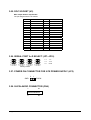
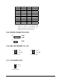
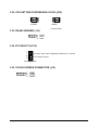
AR-B1660--SOCKET 370 PENTIUM III GRADE CPU
CARD WITH VGA/LCD/LAN
Operation Manual
Version 1.3
COPYRIGHT NOTICE
This document is copyrighted, 2001, by Acrosser Technology Co., Ltd. All rights are reserved. No part of
this manual may be reproduced, copied, transcribed, stored in a retrieval system, or translated into any
language or computer language in any form or by any means, such as electronic, mechanical, magnetic,
optical, chemical, manual or other means without the prior written permission of original manufacturer.
Acrosser Technology assumes no responsibility or warranty with respect to the content in this manual and
specifically disclaims any implied warranty of merchantability or fitness for any particular purpose.
Furthermore, Acrosser Technology reserves the right to make improvements to the products described in
this manual at any times without notice. Such revisions will be posted on the Internet
(WWW.ACROSSER.COM) as soon as possible.
Possession, use, or copy of the software described in this publication is authorized only pursuant to a valid
written license from Acrosser or an authorized sub licensor.
ACKNOWLEDGEMENTS
All other trademarks and registered trademarks mentioned herein are the property of their respective
owners.0
~ Page ii ~
1. INTRODUCTION .............................................................................. 1
1-1. ABOUT THIS MANUAL ...................................................................... 2
1-2. SYSTEM SPECIFICATION ................................................................... 3
1-3. SAFETY PRECAUTIONS ..................................................................... 4
2 TECHNICAL SUMMARY .......................................................................... 5
2-1. INTERRUPT MAP .......................................................................... 6
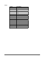
2-2. RTC & CMOS RAM MAP ..................................................................... 7
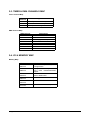
2-3. TIMER & DMA CHANNELS MAP ............................................................... 8
2-4. I/O & MEMORY MAP ....................................................................... 8
3. HARDWARE CONFIGURATION ................................................................... 10
3-1. JUMPER & CONNECTOR QUICK REFERENCE TABLE .............................................. 11
3-2. COMPONENT LOCATIONS ................................................................... 12
3-3. PACKING LIST .......................................................................... 12
3-4. HOW TO SET JUMPERS .................................................................... 12
3-5. RS232/485 SELECTION ................................................................... 13
3-6. DOC MEMORY ............................................................................ 13
3-7. SYSTEM CLOCK SELECT AND CPU SETTING ................................................... 14
3-8. SERIAL PORT A~D CONNECTOR (CN11) ...................................................... 14
3.9. PC/104 CONNECTOR ...................................................................... 15
3-10. PARALLEL PORT CONNECTOR (CN8) ........................................................ 17
3-11. FLOPPY DISK DRIVE CONNECTOR (CN7) .................................................... 17
3-12. HARD DISK DRIVE (IDE) CONNECTOR (CN2, CN6) ........................................... 18
3-13. LCD CONNECTOR FOR 36Bit (CN1) ........................................................ 19
3-14. EXTERNAL KEYBOARD & MOUSE CONNECTOR (CN16) ........................................... 21
3-15. RESET SWITCH (J1) .................................................................... 21
3-16. LED (LM1) ............................................................................ 21
3.17. INFRARED CONNECTOR (J5) .............................................................. 21
3-18. EXTERNAL SPEAKER HEADER (J11) ........................................................ 22
3-19. ETHERNET RJ-45 CONNECTOR (CN12) ...................................................... 22
3-20. VGA CRT CONNECTOR (DB1) .............................................................. 22
3-21. POWER CONTROL CONNECTOR (CN15) ....................................................... 23
3-22. UNIVERSAL SERIAL BUS CONNECTOR (J7) .................................................. 23
3-23. CPU FAN POWER CONNECTOR (J2) ......................................................... 23
3-24. BATTERY JUMPER (JP6) ................................................................. 23
3-25. DOC SOCKET (U3) ...................................................................... 24
3.26. SERIAL PORT A~D SELECT (JP7~JP10) .................................................... 24
3.27. POWER ON CONNECTOR FOR ATX POWER SUPPLY (JP3) ........................................ 24
3.28. 26-PIN AUDIO CONNECTOR (CN9) ......................................................... 24
3.29. POWER CONNECTOR (CN3) ................................................................ 25
3.30. HDD LED HEADER (J3, J12) ............................................................. 25
3.31. LCD POWER (JP1) ...................................................................... 25
3.32. CPU SETTING SYSTEM BUS CLOCK (JP4) ................................................... 26
3.33. RS-485 HEADER (J14) .................................................................. 26
3.34. PCI SELECT (JP12) .................................................................... 26
3.35. TOUCH SCREEN CONNECTOR (J15) ......................................................... 26
4. SOFTWARE UTILITIES ....................................................................... 27
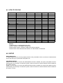
4-1. UTILITY CD FILE ....................................................................... 28
4-2. SETUP ................................................................................. 28
5. AMI BIOS SETUP ........................................................................... 29
5-1. BIOS SETUP OVERVIEW ................................................................... 30
5-2. STANDARD CMOS SETUP ................................................................... 31
5-3. ADVANCED CMOS SETUP ................................................................... 32
5-4. ADVANCED CHIPSET SETUP ................................................................ 36
5-5. POWER MANAGEMENT ...................................................................... 39
~ Page iii ~
5-6. PCI/PLUG AND PLAY ..................................................................... 41
5-7. PERIPHERAL SETUP ...................................................................... 43
5-8. AUTO-DETECT HARD DISKS ................................................................ 44
5-9. PASSWORD SETTING ...................................................................... 44
5-10. SETTING THE PASSWORD ................................................................. 44
5-11. PASSWORD CHECKING .................................................................... 44
5-12. LOAD DEFAULT SETTING ................................................................. 44
5-13. BIOS EXIT ............................................................................ 45
5-14. BIOS UPDATE .......................................................................... 46
~ Page iv ~
1. INTRODUCTION
This chapter describes:
! About This Manual
! System Specifications
! Safety precautions
Experienced users can skip to chapter 2 on page 5 for Quick Start.
~ Page 1 ~
1-1. ABOUT THIS MANUAL
Thanks for purchasing our AR-B1660--Socket 370 Pentium III Grade CPU Card with VGA / LCD / LAN
which is fully PC / AT compatible. This manual contains five chapters. By following the instructions herein,
you can easily use AR-B1660 CPU board.
Chapter 1 Introduction
This chapter notifies you how to avoid the damages against this CPU Card as well as describes the
background of this manual and the specification of AR-B1660..
Chapter 2 Technical Summary
This section gives you the information about the Technical maps.
Chapter 3 Hardware Configuration
This chapter outlines the components' locations and their functions. From this part, you can find how to set
jumper and configure this card, as you need.
Chapter 4 Software Utilities
Helpful information about the proper installations of the VGA and LAN function are provided in this chapter.
Chapter 5 AMI BIOS Setup
This chapter indicates you how to set up the BIOS configurations.
~ Page 2 ~
1-2. SYSTEM SPECIFICATION
CPU:
Supports Intel Socket 370 Pentium III up to 850 MHz or Celeron up to 800 MHz
CHIPSET:
INTEL 440BX
RAM MEMORY:
Supports 1 168-pin DIMM (PC-100 SDRAM) sockets, 256Mb max.
CACHE SIZE:
Internal 128KB L2 cache inside the CPU.
ETHERNET:
Uses RT8139C chipset, supports 10/100M Base T with RJ-45 connector built-in LED.
SUPER I/O:
2 PCI IDE---with one 2.54 mm 40-pin connectors, and one 2.0mm 44pin connector.
1 FDC---with 2.54mm 34 -pin connector.
1 Parallel--- with 2.0 mm 26-pin connector. Supports SPP/EPP/ECP mode.
4 RS-232C-COM ports with 2.54mm 40-pin connector located at bracket.
RS-232C/RS485 is selected by jumper and use the same connector.
IrDA uses 2.54mm 5-pin header.
BIOS:
AMI flash BIOS (256KB, including VGA/LCD/LAN BIOS) Supports utility program for easy to update new
version of BIOS.
KEYBOARD/MOUSE:
PS/2 compatible with 2.0mm 6-pin JST connector
BUS INTERFACE:
PC-104, PCI slot
VGA/LCD DISPLAY:
C&T 69000 with 2MB VRAM internally.
CRT-with 2.0mm 10-pin connector.
LCD-with DF9 1.0mm 51-pin connector (IIDA DF9-51P-1V)
SYSTEM POWER REQUIREMENT:
+5V,4.35A & +12V,0.15A (typical).
USB:
Built-in 2 ports USB interface with 2.54mm 10-pin headers.
RTC:
Chipset included. Supports ACPI Function with 10 years data retention.
SPEAKER:
Supports on-board buzzer and external speaker. (with 2.5mm 4-pin header).
FLASH DISK:
Supports 1 DiskOnChip Socket 144MB.
H/W MONITORING:
Built-in (Wilnbond WB83783) hardware monitoring chipset.
~ Page 3 ~
HEADERS:
2-pin Reset, hard disk LED, and power.
3-pin CPU cooling fan and Chassis cooling fan.
SWITCHES:
Use SMD DIP switch to select base clock and CPU clock multiplier.
CPU SP:
Separated Vcore and Vio.
CE DESIGN-IN:
Add EMI components to COM ports, Parallel port, CRT, USB, Keyboard, and PS/2 mouse.
Designed in accordance with EMC requirements.
PC BOARD:
6 layers, EMI considered, especially in switching power layout.
BOARD DIMENSION:
Compact size 203mm x 146mm (7.99" x 5.74")
1-3. SAFETY PRECAUTIONS
Follow the messages hereinafter to protect your systems from damage on all occasions.
Touch a grounded metal object to discharge the static electricity in your body (or ideally, wear a grounded
wrist strap)
Stay safe from the electric shock. Don‘t touch any components of this card when the card is on. Always
switch off power when the system is not in use.
Disconnect power when changing any hardware devices. For instance, when you connect a jumper or install
any cards, a surge of power may damage the electronic components or the whole system.
~ Page 4 ~
2 TECHNICAL SUMMARY
TECHNICAL SUMMARY
This chapter focuses on:
! Interrupt Map
! RTC & CMOS RAM Map
! Timer & DMA Channels Map
! I/O & Memory Map
~ Page 5 ~
2-1. INTERRUPT MAP
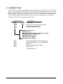
The equivalent of two 8259 Programmable Interrupt Controllers (PIC) are included on the AR-B1570
board. They accept requests from peripherals, resolve priorities on pending interrupts in service, issue
interrupt requests to the CPU, and provide vectors which are used as acceptance indices by the CPU to
determine which interrupt service routine to execute. These two controllers are cascaded with the
second controller representing IRQ8 to IRQ15, which is rerouted through IRQ2 on the first controller.
The following is the system information of interrupt levels:
Interrupt Level
NMI
CTRL1
IRQ0
IRQ1
IRQ2
Description
Parity check
CTRL2
System timer interrupt from timer 8254
keyboard output buffer full
Rerouting to IRQ8 to IRQ15
IRQ8:Real time clock
IRQ9:Reserved
IRQ10:LAN adapters(based on PCI INT routing)
IRQ12:Reserved for PS/2 mouse
IRQ13:Math.Co-processor
IRQ14:Hard disk adapter
IRQ15:Hard disk adapter
IRQ3
IRQ4
IRQ5
IRQ6
IRQ7
Serial port(depends on setup assignment)
Serial port(depends on setup assignment)
Reserved
Reserved for floppy disk adapter
Parallel port 1
Interrupt Controller
~ Page 6 ~
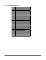
2-2. RTC & CMOS RAM MAP
CODE
00
01
02
03
04
05
06
07
08
09
0A
0B
0C
0D
0E
0F
10
11
12
13
14
15
16
17
18
30
31
32
33
34-3F
40-7f
ASSIGNMENT
Seconds
Second alarm
Minutes
Minutes alarm
Hours
Hours alarm
Day of week
Day of month
Month
Year
Status register A
Status register B
Status register C
Status register D
Diagnostic status byte
Shutdown byte
Floppy Disk drive type byte
Reserve
Hard Disk type byte
Reserve
Equipment byte
Base memory low byte
Base memory high byte
Extension memory low byte
Extension memory high byte
Reserved for extension memory low byte
Reserved for extension memory high byte
Date Century byte
Information Flag
Reserve
Reserved for Chipset Setting Data
~ Page 7 ~
2-3. TIMER & DMA CHANNELS MAP
Timer Channel Map:
Timer
Channel
0
1
2
Assignment
System timer interrupt
DRAM Refresh request
Speaker tone generator
DMA Channel Map:
DMA Channel
0
1
2
3
4
5
6
7
Assignment
Available
IBM SDLC
Floppy Disk adapter
Channel-3 Available
Cascade for DMA controller 1
Available
Available
Available
2-4. I/O & MEMORY MAP
Memory Map:
MEMORY MAP
0000000009FFFF
00A000000BFFFF
00C000000DFFFF
00E000000EFFFF
00F000000FFFFF
0100000FFFFFFF
~ Page 8 ~
ASSIGNMENT
System memory used by DOS
and application
Display buffer memory for VGA/
EGA / CGA / MONOCHROME
adapter
Reserved for I/O device BIOS
ROM or RAM buffer.
Reserved for PCI device ROM
System BIOS ROM
System extension memory
I/O Map:
I/O MAP
000-01F
020-021
022-023
040-05F
060-06F
070-07F
080-09F
0A0-0BF
0C0-0DF
0F0-0FF
1F0-1F8
278-27F
2B0-2DF
2F8-2FF
360-36F
378-37F
3B0-3BF
3C0-3CF
3D0-3DF
3F0-3F7
3F8-3FF
ASSIGNMENT
DMA controller (Master)
Interrupt controller (Master)
Chipset controller registers I/O
ports.
Timer control registers.
Keyboard interface controller
(8042)
RTC ports & CMOS I/O ports
DMA register
Interrupt controller (Slave)
DMA controller (Slave)
Math coprocessor
Hard Disk controller
Parallel port-2
Graphics adapter controller
Serial port-2
Net work ports
Parallel port-1
Monochrome & Printer adapter
EGA adapter
CGA adapter
Floppy disk controller
Serial port-1
~ Page 9 ~
3. HARDWARE CONFIGURATION
Four parts are included:
! Jumper & Connector Quick Reference Table
! Components’ Locations
! Configuration and Jumper settings
! Connector Pin Assignments
~ Page 10 ~
3-1. JUMPER & CONNECTOR QUICK REFERENCE TABLE
SWITCH & JUMPER:
DOC 2000 SEG ............................................................................ JP5
System Clock Select..................................................................... JP4
LCD Power ................................................................................... JP1
SERIAL PORT A~D Voltage Select.............................................. JP7~JP10
BATTERY JUMPER...................................................................... JP6
CONNECTOR:
PC/104 BUS ................................................................................ CN4, CN5
Reset Switch ............................................................................... J1
Floppy Disk Drive Connector ...................................................... CN7
Hard Disk Drive Connector (2.54mm 40pin) ................................ CN2
Hard Disk Drive Connector (2.0mm 44pin) .................................. CN6
Power LED & Hard Disk Drive LED Connector .......................... LM1
LCD Panel Connector ................................................................. CN1
Ethernet RJ-45 Connector .......................................................... CN12
External Audio Connector ........................................................... CN9
Printer Connector ........................................................................ CN8
CPU Fan Power Connector ........................................................ J2
VGA Connector ........................................................................... DB1
IR Connector ............................................................................... J5
Power on connector for ATX Supply ........................................... CN15
Power Control Connector ........................................................... CN3
External Keyboard & Mouse Connector ...................................... CN16
Memory Installing ........................................................................ DIMM1
Disk-On-Chip Socket .................................................................. U3
Serial Port A~D………………………………………………………..CN11
IDE Hard Disk Active LED……………………………………………J3, J12
KEYLOCK & LED CONN……………………………………………..J6
USB Connector………………………………………………………...J7
~ Page 11 ~
3-2. COMPONENT LOCATIONS
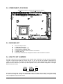
AR-B1660 Connector, Jumper and Component Locations
3-3. PACKING LIST
#
#
#
#
#
#
#
The quick setup manual
1 AR-B1660 CPU board
2 Hard disk drive adapter cable
1 Floppy disk drive adapter cable
1 Parallel port adapter cable mounted on one bracket
1 software utility CD
4 RS-232 and PS/2 Mouse & Keyboard interface cable mounted on bracket
3-4. HOW TO SET JUMPERS
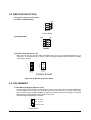
A jumper consists of two or three metal pins with a plastic base mounted on the card, and a small plastic
cap (with a metal contact inside) to connect the pins, so you can set up your hardware configuration by
"open" or close the pins. The jumper can be combined into sets, which called jumper blocks. When the
jumpers are all in the block, you have to put them together to set up the hardware configuration. The figure
below shows how it looks.
2 PIN
3 PIN
CAP
JUMPERS AND CAP
If a jumper has three pins, for example, labeled PIN1, PIN2, and PIN3, you can either connect PIN1 & PIN2
to create one setting and shorting or connect PIN2 & PIN3 to create another setting. The jumper setting
rules are applied throughout this manual.
~ Page 12 ~
3-5. RS232/485 SELECTION
The jumper settings are as follows:
(1) COM 1 & COM4 (RS232)
J10
J9
1
3
4
6
7
9
RS-232
Factory Preset
(2) COM 4(RS485)
J10
J9
1
3
4
6
7
9
RS-485
(3) RS-485 Terminator Select (J8)
When there is only one line the setting should be left, but if you are using multiple blocks on a
single line. This should be set to “ON” in order to properly terminate the connection for better
transmission of data.
1
2
1
2
OFF
ON
Factory Preset
Figure 0-6 J9: RS-485 Terminator Select
3-6. DOC MEMORY
(1) DOC Memory Mapping Selection (JP5)
A 32-pin DOC socket supports a DOC (Disk-on-Chip) up to 72Mb. This PnP Flash ROM DOC
can be installed as one of the user’s hard disk drive. And if set as Drive C, it can be used to boot
up the computer with MS-DOS installed. It offers much faster access than a floppy or hard disk
and greatly increases reliability under harsh environment.
The DOC Memory Mapping is as follows:
1
Place 1-2 :D000h
2
Place 2-3 :D400h
3
Don’t Place :D800h
Factory Preset
~ Page 13 ~
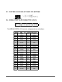
3-7. SYSTEM CLOCK SELECT AND CPU SETTING
1 3 5
1-3 & 2-4:100MHZ
3-5 & 4-6:66MHZ(DEAFAULT)
2 4 6
Factory Preset
3-8. SERIAL PORT A~D CONNECTOR (CN11)
CN1
1
39
# ###################
2 # # # # # # # # # # # # # # # # # # # # 40
The SERIAL PORT A~D Connector assignments are as follows:
SERIAL
~ Page 14 ~
PORT
A~D
CONNECTOR (CN11)
PIN
Signal
PIN
Signal
1
–DCD1F
2
–DSR1F
3
RXD1F
4
–RTS1F
5
TXD1F
6
–CTS1F
7
–DTR1F
8
–RI1F
9
VCOM1
10
GND
11
–DCD2F
12
–DSR2F
13
RXD2F
14
–RTS2F
15
TXD2F
16
–CTS2F
17
–DTR2F
18
–RI2F
19
VCOM2
20
GND
21
–DCD3F
22
–DSR3F
23
RXD3F
24
–RTS3F
25
TXD3F
26
–CTS3F
27
–DTR3F
28
–RI3F
29
VCOM3
30
GND
31
–DCD4F
32
–DSR4F
33
RXD4F
34
–RTS4F
35
TXD4F
36
–CTS4F
37
–DTR4F
38
–RI4F
39
VCOM4
40
GND
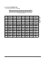
3.9. PC/104 CONNECTOR
(1) 64 Pin PC/104 Connector A & B (CN5)
2
64
1
63
64-Pin PC/104 Connector
PIN
Signal
PIN
Signal
PIN
Signal
PIN
Signal
1
–IOCHCK
2
GND
33
SA14
34
–DACK1
3
SD7
4
RSTDRV
35
SA13
36
DREQ1
5
SD6
6
VCC
37
SA12
38
–REFRESH
7
SD5
8
IRQ9
39
SA11
40
SYSCLK
9
SD4
10
Not Used
41
SA10
42
IRQ7
11
SD3
12
DREQ2
43
SA9
44
IRQ6
13
SD2
14
Not Used
45
SA8
46
IRQ5
15
SD1
16
–ZEROWS
47
SA7
48
IRQ4
17
SD0
18
(+12V)
49
SA6
50
IRQ3
19
IOCHRDY
20
GND
51
SA5
52
–DACK2
21
AEN
22
–SMEMW
53
SA4
54
TC
23
SA19
24
–SMEMR
55
SA3
56
BALE
25
SA18
26
–IOW
57
SA2
58
VCC
27
SA17
28
–IOR
59
SA1
60
OSC
29
SA16
30
–DACK3
61
SA0
62
GND
31
SA15
32
DREQ3
63
GND
64
GND
64
Pin
PC/1
04
Pin
Assi
gnm
ents
~ Page 15 ~
(2) 40 Pin PC/104 Connector C & D (CN4)
2
40
1
39
40 Pin PC/104 Pin Assignments
~ Page 16 ~
PIN
Signal
PIN
Signal
1
GND
2
GND
3
–SBHE
4
–MEMCS16
5
LA23
6
–IOCS16
7
LA22
8
IRQ10
9
LA21
10
IRQ11
11
LA20
12
IRQ12
13
LA19
14
IRQ15
15
LA18
16
IRQ14
17
LA17
18
–DACK0
19
–MEMR
20
DREQ0
21
–MEMW
22
–DACK5
23
SD8
24
DREQ5
25
SD9
26
–DACK6
27
SD10
28
DREQ6
29
SD11
30
–DACK7
31
SD12
32
DREQ7
33
SD13
34
VCC
35
SD14
36
–RMASTER
37
SD15
38
GND
39
Not Used
40
GND
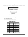
3-10. PARALLEL PORT CONNECTOR (CN8)
To use the parallel port, an adapter cable has to be connected to the CN8 connector (26 pin header type).
The adapter cable is mounted on a bracket and is included in your AR-B1600 package.
The connector for the parallel port is a 25 pin D-type female connector.
2
26
2
25
# # # # # # # # # # # # #
1 # # # # # # # # # # # # #
Parallel Port Connector (26 Pin header)
14
25
1
13
D-Type Connector
Parallel Port Pin Assignment
3-11. FLOPPY DISK DRIVE CONNECTOR (CN7)
FDD: Floppy Disk Drive Connector
You can use a 34-pin daisy-chain cable to connect a two-FDD. One end of this cable is to attach the
FDD on the board; the other end is to attach the two-FDD.
The pin assignments are as follows:
2
1
PIN
1
3
5
7
9
11
13
15
17
19
21
23
25
27
29
31
33
34
33
ASSIGNMENT
GND
GND
GND
GND
GND
GND
GND
GND
GND
GND
GND
GND
GND
GND
GND
GND
GND
PIN
2
4
6
8
10
12
14
16
18
20
22
24
26
28
30
32
34
ASSIGNMENT
DRVDEN0
NC
DRVDEN1
INDEX
MTR0
DRV1
DRV0
MTR1
DIR
STEP
WDATA
WGATE
TRK0
WRPRT
RDATA
SEL
DSKCHG
~ Page 17 ~
3-12. HARD DISK DRIVE (IDE) CONNECTOR (CN2, CN6)
IDE1: Hard Disk Drive Connector (CN2)
The AR-B1660 possesses two HDD connectors, IDE1 and IDE2. The pin assignments are as
follows:
2
1
40
39
PIN
SIGNAL
PIN
SIGNAL
1
-RESET
2
GROUND
3
DATA 7
4
DATA 8
5
DATA 6
6
DATA 9
7
DATA 5
8
DATA 10
9
DATA 4
10
DATA 11
11
DATA 3
12
DATA 12
13
DATA 2
14
DATA 13
15
DATA 1
16
DATA 14
17
DATA 0
18
DATA 15
19
GROUND
20
NOT USED
21
IDEDRQA
22
GROUND
23
-LOW A
24
GROUND
25
-LOR A
26
GROUND
27
-CHRDY A
28
GROUND
29
DACKA
30
GROUND
31
-IRQ 14
32
NOT USED
NOT USED
33
SA 1
34
35
SA 0
36
SA2
37
CS 0
38
SA1
39
HD LED A
40
NOT USED
IDE2: Hard Disk Drive Connector (CN6)
The pin assignments are as follows:
2
1
~ Page 18 ~
44
43
PIN
SIGNAL
PIN
SIGNAL
1
-RESET
2
GROUND
3
DATA 7
4
DATA 8
5
DATA 6
6
DATA 9
7
DATA 5
8
DATA 10
9
DATA 4
10
DATA 11
11
DATA 3
12
DATA 12
13
DATA 2
14
DATA 13
15
DATA 1
16
DATA 14
17
DATA 0
18
DATA 15
19
GROUND
20
NOT USED
21
IDEDRQA
22
GROUND
23
-LOW A
24
GROUND
25
-LOR A
26
GROUND
27
-CHRDY A
28
GROUND
29
DACKA
30
GROUND
31
-IRQ 14
32
NOT USED
33
SA 1
34
NOT USED
35
SA 0
36
SA2
37
CS 0
38
SA1
39
HD LED A
40
NOT USED
41
VCC
42
VCC
43
GROUND
44
GROUND
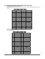
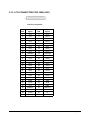
3-13. LCD CONNECTOR FOR 36Bit (CN1)
51
1
51
LCD Pin Assignment
PIN
Signal
PIN
Signal
1
FP0
2
FP16
3
FP1
4
FP17
5
FP2
6
FP18
7
FP3
8
FP19
9
FP4
10
FP20
11
FP5
12
FP21
13
FP6
14
FP22
15
FP7
16
FP23
17
LCDVDD
18
LCDVDD
19
FP8
20
FP24
21
FP9
22
FP25
23
FP10
24
FP26
25
FP11
26
FP27
27
FP12
28
FP28
29
FP13
30
FP29
31
FP14
32
FP30
33
FP15
34
FP31
35
FP34
36
FP32
37
FP35
38
FP33
39
M/DE
40
GND
41
VCC
42
FLM
43
VCC
44
GND
45
ENABLK
46
SHFCLK
47
ENAVEE
48
GND
49
(+12V)
50
LP
51
(+12V)
--
~ Page 19 ~
Flat Panel Display Interface (continued)
Mono Mono
Mono
Color
Color
Color Color
Color
Color
Color
SS
DD
DD
TFT
TFT
TFT
STN-SS
STN-SS
STN-DD STN-DD STN-DD
Pin Name 8-bit
8-bit
16-bit
9/12/16bit 18/24bit
36bit 18/24bit
8-bit(4bp)
16-bit(4bp) 8-bit(4bp) 16-bit(4bp) 24-bit
P0
D0
UD3
UD7
B0
B0
FB0
FB0
R1
R1
P1
D1
UD2
UD6
B1
B1
FB1
FB1
B1
P2
D2
UD1
UD5
B2
B2
FB2
FB2
G2
P3
D3
UD0
UD4
B3
B3
FB3
FB3
R3
P4
D4
LD3
UD3
B4
B4
FB4
SB0
P5
D5
LD2
UD2
G0
B5
FB5
P6
D6
LD1
UD1
G1
B6
SB0
P7
D7
LD0
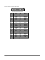
UD0
G2
B7
P8
LD7
G3
P9
LD6
P10
LD5
P11
TFT-HR
Color
Color
UR1
UR0
UR0
G1
UG1
UG0
UG0
B1
UB1
UB0
UB0
R2
UR2
UR1
LR0
B3
G2
LR1
LR0
LG0
SB1
G4
B2
LG1
LG0
LB0
SB2
R5
R3
LB1
LB0
UR1
SB1
SB3
B5
G3
LR2
LR1
UG1
G0
SB2
FG0
B3
UG1
UB1
G4
G1
SB3
FG1
R4
UB1
LR1
G5
G2
SB4
FG2
G4
UR2
LG1
LD4
R0
G3
SB5
FG3
B4
UG2
LB1
P12
LD3
R1
G4
FG0
SG0
R5
LG1
UR2
P13
LD2
R2
G5
FG1
SG1
G5
LB1
UG2
P14
LD1
R3
G6
FG2
SG2
B5
LR2
UB2
P15
LD0
R4
G7
FG3
SG3
R6
LG2
LR2
P16
R0
FG4
FR0
LG2
P17
R1
FG5
FR1
LB2
P18
R2
SG0
FR2
UR3
P19
R3
SG1
FR3
UG3
P20
R4
SG2
SR0
UB3
P21
R5
SG3
SR1
LR3
P22
R6
SG4
SR2
LG3
P23
R7
SG5
SR3
LB3
P24
FR0
P25
FR1
P26
FR2
P27
FR3
P28
FR4
P29
FR5
P30
SR0
P31
SR1
P32
SR2
P33
SR3
P34
SR4
P35
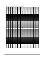
SR5
~ Page 20 ~
3-14. EXTERNAL KEYBOARD & MOUSE CONNECTOR (CN16)
EXPS2: External PS2 Connector
The pin assignments are as follows:
CN16
○○○○○○
1
PIN
1
2
3
4
5
6
6
1.
2.
3.
4.
5.
6.
MOUSE DATA
KB DATA
GND
VCC
MOUSE CLOCK
KB CLOCK
ASSIGNMENT
Mouse Data
KB Data
GND
VCC
Mouse Clock
KB Clock
3-15. RESET SWITCH (J1)
2 – RS
1 - GND
3-16. LED (LM1)
LM1
1
2
1-2:HDD LED(CN2)
3
4
6
3-4:HDD LED1(CN6)
5
5-6:PWR LED
3.17. INFRARED CONNECTOR (J5)
1 VCC
2 NC
J5
1
5
3 IR DATA RECIEVE
4 GND
5 IR DATA TRANSFER
~ Page 21 ~
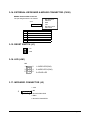
3-18. EXTERNAL SPEAKER HEADER (J11)
1 Vcc
2X
3 INT BZ
4 BUZ Z
1 Vcc
2X
3 INT BZ
4 BUZ Z
3-4 On
Enable Internal Buzzer
Enable External Buzzer
Factory Preset
3-19. ETHERNET RJ-45 CONNECTOR (CN12)
The pin assignments are as follows:
8
PIN
1
2
3
4
1
FUNCTION
TPTX+
TPTX+
TPRX+
NOT USED
PIN
5
6
7
8
ASSIGNMENT
NOT USED
TPRXNOT USED
NOT USED
3-20. VGA CRT CONNECTOR (DB1)
DB1 Connector Pin Assignment
~ Page 22 ~
PIN
Signal
PIN
Signal
1
RED
2
AGND
3
GREEN
4
GND
5
BLUE
6
AGND
7
V.S
8
DDCD
9
H.S
10
DDCK
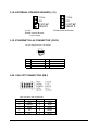
3-21. POWER CONTROL CONNECTOR (CN15)
1
1
2
2
3
3
for AT Power
PSON
+5VSB
for ATX Power
Factory Preset
3-22. UNIVERSAL SERIAL BUS CONNECTOR (J7)
2
10
1
9
1.Vcc0
2.Vcc1
3.DATA04.DATA1-
5.DATA0+
6.DATA1+
7.8. GND
9.10. GND
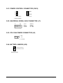
3-23. CPU FAN POWER CONNECTOR (J2)
1. GND
2. +12V
3 2 1 43.5 Fan Speed
3-24. BATTERY JUMPER (JP6)
1
2
3
1-2:EXTRNAL BATTERY
2-3:ON-BOARD BATTERY
Factory Preset
~ Page 23 ~
3-25. DOC SOCKET (U3)
DOC: 32pin Disk-on-chip Socket
The pin assignments are as follows:
PIN
1
2
3
4
5
6
7
8
9
10
11
12
13
14
15
16
ASSIGNMENT
NC
NC
NC
SA12
SA7
SA6
SA5
SA4
SA3
SA2
SA1
SA0
SD0
SD1
SD2
GND
PIN
17
18
19
20
21
22
23
24
25
26
27
28
29
30
31
32
ASSIGNMENT
SD3
SD4
SD5
SD6
SD7
CE
SA10
OE
SA11
SA9
SA8
NC
NC
VCC
WR
VCC
3.26. SERIAL PORT A~D SELECT (JP7~JP10)
1-2
3-4
5-6
+5V
+12V
GND
Factory Preset
3.27. POWER ON CONNECTOR FOR ATX POWER SUPPLY (JP3)
2
GND
1
PSON
3.28. 26-PIN AUDIO CONNECTOR (CN9)
1
25
●●●●●●●●●●●●●
●●●●●●●●●●●●●
2
~ Page 24 ~
26
PIN
1
3
5
7
9
11
13
15
17
19
21
23
25
SIGNAL
AUXAL
AUXAR
VCC
AUDIOL
AUDIOR
GND
NOT USED
GND
NOT USED
NOT USED
NOT USED
NOT USED
GND
PIN
2
4
6
8
10
12
14
16
18
20
22
24
26
SIGNAL
LINEL
LINEL
NOT USED
MICPH
PCSPKO
GND
NOT USED
GND
NOT USED
NOT USED
NOT USED
NOT USED
GND
Note: the connector does not contain the GAME
(MIDI) port signal. When AR-B9425 audio
card is used with this CPU board, the
GAME port function is not supported.
3.29. POWER CONNECTOR (CN3)
CN3
● ● ● ●
1
4
J13
1.+12V
2. GND
3. GND
4. +5V
1.-12V
2. GND
● ●
1 2
3.30. HDD LED HEADER (J3, J12)
J3
2 – VCC
1 – HD LED
CN2 HDD LED
J12
2 – VCC
1 – HD LED
CN6 HDD LED
3.31. LCD POWER (JP1)
1
2
3
1-2:USE +5V
2-3:USE +3.3V
Factory Preset
~ Page 25 ~
3.32. CPU SETTING SYSTEM BUS CLOCK (JP4)
1
1
2
2
100MHz
66MHz
Factory Preset
3.33. RS-485 HEADER (J14)
1 2 3
1
2
3
N485+
N485GND
3.34. PCI SELECT (JP12)
1
2
3
1-2 when riser card is applied, please set 1-2 close
2-3 Factory Preset
Factory Preset
3.35. TOUCH SCREEN CONNECTOR (J15)
1 2 3
~ Page 26 ~
1 GND
2 TXDF
3 RXDF
4. SOFTWARE UTILITIES
Sections includes:
! Utility CD File List
! Setup
~ Page 27 ~
4-1. UTILITY CD FILE
1660_DRV#1
1660_DRV 2
FREEBSD
WFW311
LINUX
NT351
NDIS2DOS
MSLANMAN.DOS
NDIS2OS2
MSLANMAN.OS2
NWCLIENT
NWSERVER/311
NWSERVER/4X NWSERVER/312
NWSERVER/500 NWSERVER/40
RTSPKT
CLIENT32
SCO
UW7
TXT
WIN95A
WIN2000
WINDIAG/WIN2000
W95OSR2
WINDIAG/WIN9X
WIN98
WINNT4
FILEPATH.LST
MAINNENU.TXT
RSET8139.EXE
VERSION.TXT
HELP8139.EXE
NETRTS.INF
OEMSETUP.INF
README.TXT
RELEASE.DOC
1660_DRV#3 1660_DRV#4 1660_DRV#5 1660_DRV#6
DMI
INTEL/95
SCSIDRV
MANUAL.PDF
WINDIAG/WIN4 INTEL/NT
W95VGA
BROM
WINNTVGA
MACOS
WD
RTOS
W98600.EXE
Remark:
1.W98600.EXE is a WIN98 DRIVER for VGA.
2.DRV#1~DRV#2 is ETHERNET DRIVER disk.
3.DRV#4 DISK is INTEL CHIPSET 440BX PIIX4 SETUP DRIVER
4.DRV#5 DISK is SCSI DRIVER FOR WIN95, NT AND WIN98, NT DRIVERS
4-2. SETUP
WIN95 VGA SETUP
To update display driver by choosing display interface card, put disk#5 in driver A, the driver of 65548 will be
found, and reboot your system after setup will be ok.
PIIX4 DRIVER SETUP
WIN95: The first step is to execute the INTEL\95\SETUP.EXE in DISK#4, the system will update the driver
automatically, the next step is to reboot the system, and then the driver of PIIX4 CHIPSET will be installed to
the system correctly.
WINNT: The first step is to execute the INTEL\NT\SETUP.EXE in DISK#4, the system will update the driver
automatically, the next step is to reboot the system, and then the driver of PIIX4 CHIPSET will be installed to
the system correctly.
~ Page 28 ~
5. AMI BIOS SETUP
The following topics are covered:
!
BIOS Setup Overview
!
Standard CMOS Setup
!
Advanced CMOS Setup
!
Advanced Chipset Setup
! Power Management
! PCI/Plug and Play
!
Peripheral Setup
!
Hardware Monitor Setup
!
Auto-Detect Hard Disks
!
Password Setting
!
Load Default Setting
!
BIOS Exit
!
BIOS Update
~ Page 29 ~
5-1. BIOS SETUP OVERVIEW
The BIOS is a program used to initialize and set up the I/O system of the computer, which includes the PCI
bus and connected devices such as the video display, diskette drive, and the keyboard.
The BIOS provides a menu-based interface to the console subsystem. The console subsystem contains
special software, called firmware that interacts directly with the hardware components and facilitates
interaction between the system hardware and the operating system.
The BIOS Default Values ensure that the system will function at its normal capability. In the worst situation
the user may have corrupted the original settings set by the manufacturer.
After the computer is turned on, the BIOS will perform diagnostics on the system and display the size of the
memory that is being tested. Press the [Del] key to enter the BIOS Setup program, and then the main menu
will show on the screen.
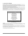
The BIOS Setup main menu includes some options. Use the [Up/Down] arrow key to highlight the option
that you wish to modify, and then press the [Enter] key to select the option and configure the functions.
AMIBIOS HIFLEX SETUP UTILITY - VERSION 1.30
(C) 2000 American Megatrends, Inc. All Rights Reserved
Standard CMOS Setup
Advanced CMOS Setup
Advanced Chipset Setup
Power Management Setup
PCI/Plug and Play Setup
Peripheral Setup
Hardware Monitor Setup
Auto-Detect Hard Disks
Change User Password
Change Supervisor Password
Auto Configuration with Defaults
Save Settings and Exit
Exit Without Saving
Exit without saving the current settings
ESC: Exit ↑↓: Sel F2/F3: Color F10: Save & Exit
BIOS: Setup Main Menu
CAUTION:
1. The factory-default setting of AR-B1660 is the <Auto Configuration with Optimal Settings>. Acrosser
recommends you using the BIOS default settings unless you are very familiar with the settings function. Or you
can contact the technical support engineers (FAE).
2. If the BIOS loses the settings, the CMOS will detect the <Auto Configuration with Fail Safe Settings> to
boot the operating system. This option will reduce the performance of the system. Acrosser recommends
you choosing the <Auto Configuration with Optimal Settings> in the main menu. This option gives best-case
values that should optimize system performance.
3. The BIOS settings are described in detail in this section.
~ Page 30 ~
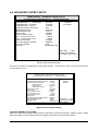
5-2. STANDARD CMOS SETUP
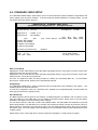
The <Standard CMOS Setup> option allows you to record some basic system hardware configurations and
set the system clock and error handling. If the CPU board is already installed in a working system, you will
not need to select this option anymore.
AMIBIOS SETUP – STANDARD CMOS SETUP
(C) 2000 American Megatrends, Inc. All Rights Reserved
Date (mm:dd:yyyy): Tue, Jul 03, 2001
Base Memory: 640 KB
Time (hh:mm:ss): 15:07:14
Extd Memory: 127 MB
Floppy Drive A:
Floppy Drive B:
1.44MB 3 1/2
Not Installed
Type
Size
Pri Mater: Not Installed
Pri Slave: Not Installed
Sec Master: Not Installed
Sec Slave: Not Installed
Boot Sector Virus Protection
Month: Jan – Dec
Day:
01 – 31
Year: 1901 – 2099
Cyln
Head
Wpcom
LBA
BLK
PIO
32 Bit
Sec Mode Mode Mode Mode
Disabled
ESC: Exit
↑↓: Sel
PgUp/ PgDn: Modify
F1: Help F2/F3: Color
BIOS: Standard CMOS Setup
Date & Time Setup
Highlight the <Date> field and then press the [Page Up] /[Page Down] or [+]/[-] keys to set the current date.
Follow the month, day and year format.
Highlight the <Time> field and then press the [Page Up] /[Page Down] or [+]/[-] keys to set the current date.
Follow the hour, minute and second format.
The user can bypass the date and time prompts by creating an AUTOEXEC.BAT file. For information
about how to create this file, please refer to the MS-DOS manual.
Floppy Setup
The <Standard CMOS Setup> option records the types of floppy disk drives installed in the system. The
available options for drives A and B are:
To enter the configuration value for a particular drive, highlight its corresponding field and then select the
drive type using the left-or right-arrow key.
Hard Disk Setup
The BIOS supports various types for user settings, The BIOS supports <Pri Master> and <Pri Slave> so the
user can install up to two hard disks. For the master and slave jumpers, please refer to the hard disk’s
installation descriptions and the hard disk jumper settings.
You can select <AUTO> under the <TYPE> and <MODE> fields. This will enable auto detection of your IDE
drives during bootup. This will allow you to change your hard drives (with the power off) and then power on
without having to reconfigure your hard drive type. If you use older hard disk drives, which do not support
this feature, then you must configure the hard disk drive in the standard method as described above by the
<USER> option.
Please set as “Auto” if slave IDE device, which carries FAT16 partition, is used to boot up system.
~ Page 31 ~
Boot Sector Virus Protection
This option protects the boot sector and partition table of your hard disk against accidental modifications. Any
attempt to write to them will cause the system to halt and display a warning message. If this occurs, you can either
allow the operation to continue or use a bootable virus-free floppy disk to reboot and investigate your system. The
default setting is <Disabled>. This setting is recommended because it conflicts with new operating systems.
Installation of new operating systems requires that you disable this to prevent write errors.
5-3. ADVANCED CMOS SETUP
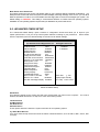
The <Advanced CMOS Setup> option consists of configuration entries that allow you to improve your
system performance, or let you set up some system features according to your preference. Some entries
here are required by the CPU board’s design to remain in their default settings.
AMIBIOS SETUP – ADVANCED CMOS SETUP
(C) 2000 American Megatrends, Inc. All Rights Reserved
Quick Boot
Enabled
Available Options:
1st Boot Device
IDE-1
Disabled
2nd Boot Device
CDROM
$ Enabled
3rd Boot Device
Disabled
4th Boot Device
Disabled
Try Other Boot Devices
Yes
Floppy Access Control
Read-Write
Hard Disk Access Control
Read-Write
S.M.A.R.T. for Hard Disks
Disabled
BootUp Num- Lock
On
Floopy Drive Swap
Disabled
Floopy Drive Seek
Disabled
PS/2 Mouse Support
Enabled
Typematic Rate
Fast
System Keyboard
Absent
Primary Display
VGA/ EGA
PASSWORD Check
Setup
ESC: Exit
↑↓: Sel
Boot TO OS/ 2 > 64 MB
No
PgUp/ PgDn: Modify
Wait For ‘F1’ If Error
Disabled
F1: Help F2/F3: Color
Hit ‘DEL’ Message Display Enabled
Advanced CMOS Setup
Quick Boot
This category speeds up the <Power On Self Test> (POST) after you power on the computer. If it is set to
Enabled, the BIOS will shorten or skip some check items during POST.
1st Boot Device
2nd Boot Device
3rd Boot Device
4th Boot Device
These options determine where the system looks first for an operating system.
Try Other Boot Devices
If you have other bootup device other than the above mentioned devices, such as IDE-0, IDE-1, IDE-3, IDE4, Floppy.
~ Page 32 ~
Floppy Access Control
This option determines the floppy access method, which can be either read only or normal (read/write).
When it is set, the data in the floppy is being read instead of being written.” Normal” allows the floppy to be
read or written.
HDD Access Control
This option determines the hard disk access method, which can be either read only or normal (read/write).
When it is set to read only, the data in the hard disk is being read instead of being written.” Normal” allows
the floppy to be read or written.
Available options: Disabled, Enabled
S.M.A.R.T for hard Disks
S.M.A.R.T is abbreviation of Self-Monitoring Analysis and Reporting Technology. It is reliable and
precautious technology. When Hard Disk is in disorder, it prevents Hard Disk from the loss of data.
BootUp Num-Lock
This item is used to activate the Num-Lock function upon system boot. If the setting is on, after a boot, the
Num-Lock light is lit, and the user can automatically use the number keys.
Floppy Drive Swap
The option reverses the drive letter assignments of your floppy disk drives in the Swap A, B setting,
otherwise you leave the setting to Disabled (No Swap). This works separately from the BIOS Features and
floppy disk swap feature. It is functionally the same as physically interchanging the connectors of the
floppy disk drives. When <Enabled>, the BIOS swaps the floppy drive assignments so that Drive A becomes
Drive B, and Drive B becomes Drive A under DOS.
Floppy Drive Seek
If the <Floppy Drive Seek> item is set to Enabled, the BIOS will seek the floppy <A> drive one time upon
bootup.
PS/2 Mouse Support
The setting of Enabled allows the system to detect a PS/2 mouse on bootup. If it is detected, IRQ12 will be
used for the PS/2 mouse. IRQ 12 will be reserved for expansion cards if a PS/2 mouse is not detected.
Disabled will reserve IRQ12 for expansion cards and therefore the PS/2 mouse will not function.
Typematic Rate
This item specifies the speed at which a keyboard keystroke is repeated.
System Keyboard
The setting of <Absent> allows the system to boot without a keyboard attached to the computer, while the
setting of <Present> is in the contrary.
Primary Display
The setting of <Absent> allows the system to boot without a Primary Display attached to the computer,
while the setting of <Present> is in the contrary.
Password Check
This option enables password checking every time the computer is powered on or every time the BIOS
Setup is executed. If Always is chosen, a user password prompt appears every time the computer is
turned on. If Setup is chosen, the password prompt appears if the BIOS are executed.
Boot to OS/2 >64MB
When using the OS/2 operating system with DRAM of greater than 64MB installed, you need to Enabled this
option; otherwise leave this on the setup default of Disabled.
~ Page 33 ~
Wait for ‘F1’ If Error
AMIBIOS POST error messages are followed by:
Press <F1> to continue
If this option is set to Disabled, the AMIBIOS does not wait for you to press the <F1> key after an error
message.
~ Page 34 ~
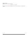
Hit ‘DEL’ Message Display
Set this option to Disabled to prevent the following message:
Hit ‘DEL’ if you want to run setup
It will prevent the message from appearing on the first BIOS screen when the computer boots.
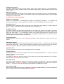
Internal Cache
This option specifies the caching algorithm used for the L1 internal cache memory. The settings are:
Setting
Disabled
WriteBack
WriteThru
Description
Neither L1 internal cache memory on the CPU or
L2 secondary cache memory is enabled.
Use the write-back caching algorithm.
Use the write-through caching algorithm.
Internal Cache Setting
External Cache
This option specifies the caching algorithm used for the L2 secondary cache memory. The settings are:
Setting
Disabled
WriteBack
WriteThru
Description
Neither L1 internal cache memory on the CPU or
L2 secondary cache memory is enabled.
Use the write-back caching algorithm.
Use the write-through caching algorithm.
External Cache Setting
Shadow
These options control the location of the contents of the 16KB of ROM beginning at the specified memory
location. If no adapter ROM is using the named ROM area, this area is made available to the local bus.
The settings are:
SETTING
Disabled
Enabled
Cached
DESCRIPTION
The video ROM is not mapped to RAM. The
contents of the video ROM cannot be read from or
written to cache memory.
The contents of C000h - C7FFFh are written to the
same address in system memory (RAM) for faster
execution.
This option specifies the size of the memory area
reserved for legacy ISA adapter cards.
Shadow Setting
~ Page 35 ~
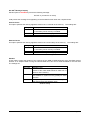
5-4. ADVANCED CHIPSET SETUP
AMIBIOS SETUP – ADVANCED CHIPSET SETUP
(C) 2000 American Megatrends, Inc. All Rights Reserved
Configure SDRAM Timing by SPD
Enabled
Available Options:
SDRAM RAS# to CAS# delay
2 SCLKS
Disabled
SDRAM RAS# Percharge
2 SCLKS
$ Enabled
SDRAM CAS# Latency
2 SCLKS
SDRAM Leadoff Cmd Timing
Auto
DRAM Integrity Mode
Non-ECC
DRAM Refresh Rate
15.6 us
Memory Hole
Disabled
Graphics Aperture Size
64 MB
8 bit I / O Recovery Time
1 Sysclk
16 bit I / O Recovery Time
1 Sysclk
Assign IRQ for USB
Enabled
ATX Power Supply Controller
Disabled
LCD CRT Selection
Both
LCD Type
#6 640x480 18bit
ESC: Exit
↑↓: Sel
PgUp/ PgDn: Modify
F1: Help F2/F3: Color
BIOS: Advanced Chipset Setup
This option controls the configuration of the board’s chipset. Control keys for this screen are the same as
for the previous screen.
AMIBIOS SETUP - ADVANCED CHIPSET SETUP
(C) 1999 American Megatrends, Inc. All Rights Reserved
Configure SDRAM Timeing by SPD
SDRAM RAS# to CAS# delay
RAS# Precharge
CAS# Latency
Loadoff Cmd Timing
DRAM Integrity Mode
Memory Hole
Graphics Aperture Size
8bit I/O Recovery Time
16bit I/O Recovery Time
USB Function
USB Keyboard / Mouse Legacy Support
ATX Power Supply Controller
LCD CRT Selection
LCD Type
Available Options :
Disabled
Enabled
Enabled
2 SCLKs
2 SCLKs
3 SCLKs
Auto
Non-ECC
Disabled
64MB
1 Sysclk
1 Sysclk
Enabled
Enabled
ESC:Exit ↑↓:Sel
Disabled
Both
PgUp/PgDn:Modify
#5 640x480 TFT F2/F3:Color
BIOS: Advanced Chipset Setup
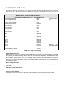
Configure SDRAM Timing by SPD:
SPD is the abbreviation Serial Presence Detect. SPD takes accord the chip types, capacity, timing, voltage
data. The system can auto adjust memory according to the data to reach the best situation.
~ Page 36 ~
SDRAM RAS# to CAS# delay:
When CPU saveS data from memory, it has to deliver RAS single first, and then CAS single. The item is to
set up the interval between two singles.
RAS# Precharge:
This item is the time when RAS has to re-locate.
CAS# Latency:
This item is to set up a certain period of time for the memory to start writing and reading data when memory
receives one CAS single.
Loadoff Cmd Timing:
It is the first read-write action under burst pattern
Memory Hole:
This reserves the 15MB to 16MB memory address space for use of ISA expansion cards.
Graphics Aperture Size:
The item is to set up AGP display to use a certain amount of memory to save Texture Data.
8 bit I/O Recovery Time:
The item is to set up CPU to demand ISA Bus 8 bit for the time it recovers.
16 bit I/O Recovery Time:
The item is to set up CPU to demand ISA Bus 16 bit for the time it recovers.
~ Page 37 ~
Memory Hole at 15-16 MB
This option specifies the range 15MB to 16MB in memory that cannot be addressed on the ISA bus.
USB Function
This option can enable or disable USB function
USB Keyboard/Mouse Legacy Support
These options are used to <Enabled> the USB function and it’s only useful in the DOS mode.
ATX Power Supply Controller
If the ATX Power Supply Controller function is <Enabled>, the system will get more functions such as
shutting down the power by using software.
LCD CRT Selection
This item determines to either use LCD Monitor or CRT Monitor in the system.
LCD Type
This option specifies the resolution of LCD.
~ Page 38 ~
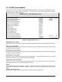
5-5. POWER MANAGEMENT
This section is used to configure the power management features. This <Power management Setup>
option allows you to reduce power consumption. This feature turns off the video display and shuts down
the hard disk after a period of inactivity.
AMIBIOS SETUP - Power Management Setup
( C ) 2000 American Megatrends.Inc. All Rights Reserved
Power Management/APM
Green PC Monitor Power State
Video Power Down Mode
Hard Disk Power Down Mode
Hard Disk Time Out (Minute)
Standby Time Out (Minute)
Suspend Time Out (Minute)
Display Activity
Device 6 (Serial port 1)
Device 7 (Serial port 2)
Device 8 (Parallel port)
Device 5 (Floppy disk)
Device 0 (Primary master IDE)
Device 1 (Primary slave IDE)
Device 2 (Secondary master IDE)
Device 3 (Secondary slave IDE)
Disabled
Enabled
Enabled
Disabled
Disabled
Monitor
Monitor
Monitor
Ignore
Monitor
Monitor
Monitor
Monitor
ON
Last State
Disabled
Available
Disabled
Enabled
Options
ESC:Exit ↑↓:Sel
PgUp/PgDn:Modify
BIOS: Power Management Setup
Power Management /APM
Enabled this option is to enable the power management and APM (Advanced Power Management) features.
Video Power Down Mode
This option specifies the power management that states the video subsystem enters after a specific period
of display inactivity has expired.
Hard Disk Power Down Mode
This option specifies the power management that states the hard disk drive enters after the specified period
of display inactivity has expired.
Hard Disk time out (minute)
This item is used to set up the initial value of the waiting timer. The Hard Disk will turn into the suspend
mode when the time is out if no operation applied to Hard Disk.
Power Down Time Out (minute)
This item is used to set up the initial value of the waiting timer. The System will turn into the Power Down
mode when the time is out if no operation applied to system.
Device
These options enable event monitoring. When the computer is in a power saving mode, the activity on the
named interrupt request line is monitored by BIOS. When any activity occurs, the computer enters Full On
mode.
Restore on AC/Power Loss
This item is to set up the system to restore the last setting after the AC\Power Loss.
~ Page 39 ~
Ring Resume From Soft Off
This item is to set up the function of waking up the system from suspend mode and a ring bell while any
access coming from Modem.
Lan Resume From Soft Off
This item is to set up the function of waking up the system from suspend mode. When encountering an
access, the function will be available if system is fixed with an Ethernet card.
~ Page 40 ~
5-6. PCI/PLUG AND PLAY
This section is used to configure PCI / Plug and Play features. The <PCI & PNP Setup> option configures
the PCI bus slots. All PCI bus slots on the system use INTA#, thus all installed PCI cards must be set to
this value.
AMIBIOS SETUP - PCI/PLUG AND PLAY SETUP
( C ) 2000 American Megatrends, Inc.
Plug and Play Aware O/S
Reset Configuration Data
PCI Latency Timer (PCI Clocks)
Primary GraphicS Adapter
PCI VGA Palette Snoop
DMA Channel 0
DMA Channel 1
DMA Channel 3
DMA Channel 5
DMA Channel 6
DMA Channel 7
IRQ 3
IRQ 4
IRQ 5
IRQ 7
IRQ 9
IRQ 10
IRQ 11
IRQ 12
IRQ 14
IRQ 14
IRQ 15
Reserved Memory Size
Reserved Memory Address
All Rights Reserved
NO
NO
64
PCI
Disabled
PnP
PnP
PnP
PnP
PnP
PnP
ISA/EISA
ISA/EISA
PCI/PnP
ISA/EISA
PCI/PnP
ISA/EISA
ISA/EISA
PCI/PnP
ISA/EISA
PCI/PnP
PCI/PnP
32K
CC000
Available Options
NO
YES
ESC:Exit ↑↓:Sel
PgUp/PgDn:Modify
F2/F3:Color
BIOS: PCI / Plug and Play Setup
Plug and Play Aware O/S
Set this option to <No> if the operating system installed in the computer is Plug and Play-aware. The BIOS
only detects and enables PnP ISA adapter cards that are required for system boot. The Windows 95 (and
above) operating system detects and enables all other PnP-aware adapter cards. Windows 95 (and above)
is PnP-aware. Set this option to <yes> if the operating system (such as DOS, OS/2, Windows 3.x) does not
use PnP. You must set this option correctly or PnP-aware adapter cards installed in your computer will not
be configured properly.
Reset Configuration Data
This sets the operating mode of the boot block area of the BIOS FLASH ROM to allow programming in the
Yes setting.
PCI Latency Timer (PCI Clocks)
This option sets latency of all PCI devices on the PCI bus. The settings are in units equal to PCI clocks.
Primary Graphic Adapter
This option is set to use PCI bus or AGP. The AGP mode will get system a faster processing speed.
~ Page 41 ~
PCI VGA Palette Snoop
This item is for BIOS to snoop the appearance of VGA palette, and modify it when it is necessary.
DMA & IRQ
These options specify the bus that the named IRQs/DMAs lines are used on. These options allow you to
specify IRQs/DMAs for use by legacy ISA adapter cards. These options determine if the BIOS should
remove an IRQ/DMA from the pool of availability of IRQs/DMAs passed to the BIOS configurable devices.
If more IRQs/DMAs must be removed from the pool, the end user can use these PCI/PnP Setup options to
remove the IRQ/DMA by assigning the option to the ISA/EISA setting. The onboard I/O is configurable with
BIOS.
Reserved Memory Size
This option specifies the size of the memory area reserved for legacy ISA adapter cards.
Reserved Memory Address
This option specifies the beginning address (in hex) of the reserved memory area. The specified ROM
memory area is reserved for use by legacy ISA adapter cards.
~ Page 42 ~
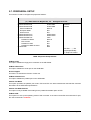
5-7. PERIPHERAL SETUP
This section is used to configure the peripheral features.
AMIBIOS SETUP - PERIPHERAL SETUP
( C ) 2000 American Megatrends, Inc. All Rights Reserved
OnBoard FDC
Enabled
Available Options:
OnBoard Serial PortA
3F8h/COM1
Disabled
OnBoard Serial PortB
2F8h/COM2
Enabled
Serial PortB Mode
Normal
IR Duplex Mode
N/A
IrDA Protocol
N/A
OnBoard Serial PortC
3E8h/COM3
OnBoard Serial PortD
2E8h/COM4
OnBoard Parallel Port
378h
Parallel Port Mode
Normal
EPP Version
N/A
Parallel Port IRQ
N/A
Parallel Port DMA Channel
N/A
OnBoard IDE
Both
ESC:Exit ↑↓:Sel
PgUp/PgDn:Modify
F1: Help F2/F3:Color
BIOS: Peripheral Setup Defaults
OnBoard FDC
This option enables the floppy drive controller on the AR-B1660.
OnBoard Serial Port
This option enables the serial port on the AR-B1660.
IR Port support
This item is to activate the function of Infra-red.
OnBoard Parallel Port
This option enables the parallel port on the AR-B1660.
Parallel Port Mode
This option specifies the parallel port mode. ECP and EPP are both bi-directional data transfer schemes
that adhere to the IEEE1284 specifications.
Parallel Port DMA Channel
This option is only available if the setting for the parallel Port Mode option is ECP.
OnBoard IDE
This option is to set up the operating mode of IDE controller. If the main board offer the enhanced I/O port,
the choice should be <enabled> .
~ Page 43 ~
5-8. AUTO-DETECT HARD DISKS
This option detects the parameters of an IDE hard disk drive, and automatically enters them into the
Standard CMOS Setup screen.
5-9. PASSWORD SETTING
This BIOS Setup has an optional password feature. The system can be configured so that all users must
enter a password every time the system boots or when BIOS Setup is executed. The user can set either a
Supervisor password or a User password.
5-10. SETTING THE PASSWORD
Select the appropriate password icon (Supervisor or User) from the Security section of the BIOS Setup main
menu. Enter the password and press [Enter]. The screen does not display the characters entered. After
the new password is entered, retype the new password as prompted and press [Enter].
If the password confirmation is incorrect, an error message appears. If the new password is entered
without error, press [Esc] to return to the BIOS Main Menu. The password is stored in CMOS RAM after
the BIOS is exited and saved. Next time the system boots, you are prompted for the password function
presented and enabled.
Enter new supervisor password:
5-11. PASSWORD CHECKING
The password check option is enabled in Advanced Setup by choosing either Always (the password prompt
appears every time the system is powered on) or Setup (the password prompt appears only when BIOS
runs). The password is stored in CMOS RAM. The user can enter a password by typing on the keyboard. As
the user selects Supervisor or User, the BIOS prompts for a password. Then the user must set the
Supervisor password before he can set the User password. Enter a 1 to 6 characters password. The
password does not appear on the screen when being typed. Make sure you write it down.
5-12. LOAD DEFAULT SETTING
This section permits users to select a group of settings for all BIOS Setup options. Not only can you use
these items to quickly set system configuration parameters, you can also choose a group of settings that
has a better chance of working when the system is having configuration related problems.
5-12-1. Auto Configuration with Optimal Setting
The user can load the optimal default settings for the BIOS. The Optimal default settings are best-case
values that should optimize system performance. If CMOS RAM is corrupted, the optimal settings are
loaded automatically.
Load high performance setting (Y/N) ?
~ Page 44 ~
5-12-2. Auto Configuration with Fail Safe Setting
The user can load the Fail-Safe BIOS Setup option settings by selecting the Fail-Safe item from the Default
section of the BIOS Setup main menu.
The Fail-Safe settings provide far from optimal system performance, but are the most stable settings. Use
this option as a diagnostic aid if the system behaves erratically.
Load failsafe settings (Y/N) ?
5-13. BIOS EXIT
This section is used to exit the BIOS main menu. After making your changes, you can either save them or
exit the BIOS menu without saving the new values.
5-13-1. Save Settings and Exit
This item is in the <Standard CMOS Setup>, <Advanced CMOS Setup>, <Advanced Chipset Setup> and
the new password (if it has been changed) will be stored in the CMOS. The CMOS checksum is calculated
and written into the CMOS.
When you select this function, the following message will appear at the center of the screen to assist you to
save data to CMOS and Exit the Setup.
Save current settings and exit (Y/N) ?
5-13-2. Exit Without Saving
When you select this option, the following message will appear at the center of the screen to help to
abandon all the modified data and Exit Setup.
Quit without saving (Y/N) ?
~ Page 45 ~
5-14. BIOS UPDATE
The BIOS program instructions are contained within computer chips called FLASH ROMs that are located
on your system board. The chips can be electronically reprogrammed, allowing you to upgrade your BIOS
firmware without removing and installing chips.
The AR-B1682 provides the FLASH BIOS update function for you to easily update a newer BIOS version.
Please follow these operating steps to update new BIOS:
Step 1:
Turn on your system and don’t detect the CONFIG.SYS and AUTOEXEC.BAT files.
Step 2:
Insert the FLASH BIOS diskette into the floppy disk drive.
Step 3:
In the MS-DOS mode, you can type the FLASH812 program.
A:\>FLASH812
Step 4:
Press [ALT+F], The <File> box will show the following message, this message will be
highlighted.
BIOS Filename Loading … .
After typing in the File name you must press<ENTER> or press <ESC> to exit.
Step 5:
Please enter the file name to the <Enter File Name> box. And the <Message> box will
show the following notice.
Are you sure to write this BIOS into flash ROM?
Step 6:
Press the <Enter> key to update the new BIOS.
Then the <Message> box will show the <Programming now …>.
Step 7:
When the BIOS update is successful, the message will show <Flash ROM Update
Completed - Pass>.
Note:
If the content in Setting is inconsistent with CD-ROM. Please refer to the Setting as priority.
~ Page 46 ~