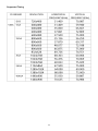
1
Acer AL1702W
Service Guide
1
Service Guide Version and Revision
Version
A00
Release Date
Revision History
TPV model
Initial Release
T77HRDNBGWAFN
Mar.-23-2007
2
Copyright
Copyright © 2003 by Acer Incorporated. All rights reserved. No part of this publication may be reproduced,
Transmitted, transcribed, stored in a retrieval system, or translated into any language or computer language, in
any form or by any means, electronic, mechanical, magnetic, optical, chemical, manual or otherwise, without
the prior written permission of Acer Incorporated.
Disclaimer
The information in this guide is subject to change without notice. Acer Incorporated makes no representations or
warranties, either expressed or implied, with respect to the contents hereof and specifically disclaims any warranties
of merchantability or fitness for any particular purpose. Any Acer Incorporated software described in this manual is
sold or licensed "as is". Should the programs prove defective following their purchase, the buyer (and not Acer
Incorporated, its distributor, or its dealer) assumes the entire cost of all necessary servicing, repair, and any
incidental or consequential damages resulting from any defect in the software.
Intel is a registered trademark of Intel Corporation.
Pentium and Pentium II/III are trademarks of Intel Corporation.
Other brand and product names are trademarks and/or registered trademarks of their respective holders.
Trademarks
Acer is a registered trademark of Acer Incorporated.
All other trademarks are property of their respective owners.
Conventions
The following conventions are used in this manual:
Screen messages
Denotes actual messages that appear on screen.
Note
Gives bits and pieces of additional information related to the current topic.
Warning
Alerts you to any damage that might result from doing or not doing specific actions.
Caution
Gives precautionary measures to avoid possible hardware or software problems.
Important
Remind you to do specific actions relevant to the accomplishment of procedures.
3
Preface
Before using this information and the product it supports, please read the following general information.
1. This Service Guide provides you with all technical information relating to the BASIC CONFIGURATION decided
for Acer's "global" product offering. To better fit local market requirements and enhance product competitiveness,
your regional office may have decided to extend the functionality of a machine (e.g. add-on card, modem, or extra
memory capability). These LOCALIZED FEATURES will NOT be covered in this generic service guide. In such
cases, please contact your regional offices or the responsible personnel/channel to provide you with further
technical details.
2. Please note WHEN ORDERING FRU PARTS, that you should check the most up-to-date information available on
your regional web or channel. If, for whatever reason, a part number change is made, it will not be noted in the
printed Service Guide. For ACER-AUTHORIZED SERVICE PROVIDERS, your Acer office may have a
DIFFERENT part number code to those given in the FRU list of this printed Service Guide. You MUST use the list
provided by your regional Acer office to order FRU parts for repair and service of customer machines.
Warning: (For FCC Certified Models)
Note: This equipment has been tested and found to comply with the limits for a Class B digital device, pursuant to
Part 15 of the FCC Rules. These limits are designed to provide reasonable protection against harmful interference in
a residential installation. This equipment generates, uses and can radiate radio frequency energy, and if not installed
and used in accordance with the instructions, may cause harmful interference to radio communications. However,
there is no guarantee that interference will not occur in a particular installation. If this equipment does cause harmful
interference to radio or television reception, which can be determined by turning the equipment off and on, the user
is encouraged to try to correct the interference by one or more of the following measures:
1. Reorient or relocate the receiving antenna.
2. Increase the separation between the equipment and receiver.
3. Connect the equipment into an outlet on a circuit different from that to which the receiver is connected.
4. Consult the dealer or an experienced radio/TV technician for help.
Notice:
1. The changes or modifications not expressly approved by the party responsible for compliance could void the
user's authority to operate the equipment.
2. Shielded interface cables and AC power cord, if any, must be used in order to comply with the emission limits.
3. The manufacturer is not responsible for any radio or TV interference caused by unauthorized modification to this
equipment. It is the responsibility of the user to correct such interference.
As ENERGY STAR® Partner our company has determined that this product meets the ENERGY STAR®
guidelines for energy efficiency.
Warning:
To prevent fire or shock hazard, do not expose the monitor to rain or moisture. Dangerous high voltages are present
inside the monitor. Do not open the cabinet. Refer servicing to qualified personnel only.
4
Precautions
z Do not use the monitor near water, e.g. near a bathtub, washbowl, kitchen sink, laundry tub, swimming pool or in
a wet basement.
z Do not place the monitor on an unstable trolley, stand, or table. If the monitor falls, it can injure a person and
cause serious damage to the appliance. Use only a trolley or stand recommended by the manufacturer or sold
with the monitor. If you mount the monitor on a wall or shelf, uses a mounting kit approved by the manufacturer
and follow the kit instructions.
z Slots and openings in the back and bottom of the cabinet are provided for ventilation. To ensure reliable
operation of the monitor and to protect it from overheating, be sure these openings are not blocked or covered.
Do not place the monitor on a bed, sofa, rug, or similar surface. Do not place the monitor near or over a radiator
or heat register. Do not place the monitor in a bookcase or cabinet unless proper ventilation is provided.
z The monitor should be operated only from the type of power source indicated on the label. If you are not sure of
the type of power supplied to your home, consult your dealer or local power company.
z The monitor is equipped with a three-pronged grounded plug, a plug with a third (grounding) pin. This plug will fit
only into a grounded power outlet as a safety feature. If your outlet does not accommodate the three-wire plug,
have an electrician install the correct outlet, or use an adapter to ground the appliance safely. Do not defeat the
safety purpose of the grounded plug.
z Unplug the unit during a lightning storm or when it will not be used for long periods of time. This will protect the
monitor from damage due to power surges.
z Do not overload power strips and extension cords. Overloading can result in fire or electric shock.
z Never push any object into the slot on the monitor cabinet. It could short circuit parts causing a fire or electric
shock. Never spill liquids on the monitor.
z Do not attempt to service the monitor yourself; opening or removing covers can expose you to dangerous
voltages and other hazards. Please refer all servicing to qualified service personnel
z To ensure satisfactory operation, use the monitor only with UL listed computers which have appropriate
configured receptacles marked between 100 - 240V AC, Min. 5A.
z The wall socket shall be installed near the equipment and shall be easily accessible.
Special Notes On LCD Monitors
The following symptoms are normal with LCD monitor and do not indicate a problem.
Notes
z Due to the nature of the fluorescent light, the screen may flicker during initial use. Turn off the Power Switch and
then turn it on again to make sure the flicker disappears.
z You may find slightly uneven brightness on the screen depending on the desktop pattern you use.
z The LCD screen has effective pixels of 99.99% or more. It may include blemishes of 0.01% or less such as a
missing pixel or a pixel lit all of the time.
z Due to the nature of the LCD screen, an afterimage of the previous screen may remain after switching the image,
when the same image is displayed for hours. In this case, the screen is recovered slowly by changing the image
or turning off the Power Switch for hours.
5
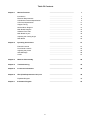
Table Of Contents
Chapter 1
Monitor Features
…………………………………………
7
Introduction
………………………………………
7
Electrical Requirements
………………………………………
8
LCD Monitor General Specification
………………………………………
9
LCD Panel Specification
………………………………………
11
Support Timing
………………………………………
13
Monitor Block Diagram
………………………………………
14
Main Board Diagram
………………………………………
15
Software Flow chart
………………………………………
16
Main Board Layout
………………………………………
18
Adjusting the viewing angle
………………………………………
19
Rear Bezel
………………………………………
20
Operating Instructions
………………………………………
21
External Controls
………………………………………
21
Front Panel Controls
………………………………………
22
Adjusting the picture
………………………………………
23
OSD Message
………………………………………
26
LOGO
………………………………………
27
Chapter 3
Machine Disassembly
………………………………………
28
Chapter 4
Troubleshooting
………………………………………
34
Chapter 5
Connector Information
………………………………………
38
Chapter 6
FRU (Field Replacement Unit) List
………………………………………
39
Exploded Diagram
………………………………………
40
Schematic Diagram
………………………………………
43
Chapter 2
Chapter 7
6
Chapter 1
Monitor Features
Introduction
Scope
This specification defines the requirements for the 17” MICROPROCESSOR based Multi-mode supported high
resolution color LCD monitor. This monitor can be directly connected to general 15-pin D-sub VGA connector, also
supports VESA DPMS power management and plug & play function. There is a build-in stereo audio amplifier with
OSD control to drive a pair of speakers.
Description
The LCD monitor is designed with the latest LCD technology to provide a performance oriented product with no
radiation. This will alleviate the growing health concerns. It is also a space saving design, allowing more desktop
space, and comparing to the traditional CRT monitor, it consumes less power and gets less weight in addition MTBF
target is 50k hours or more.
Chart of AL1702W
Panel
HSD170MGW1-A01
Signal Interface
D-Sub 15-pin
Sync Type
Separate / Compatible
Color Temp User Adjust
Support
DDC
DDC2B
Speaker
No
Headphone Jack
No
Microphone Jack
No
USB Hub
Not support
Tilt / Swivel
Yes / No
7
Electrical Requirements
Standard Test Conditions
All tests shall be performed under the following conditions, unless otherwise specified.
Ambient light
:
Dark room
Viewing distance
:
40 cm for LCD performance, 20 cm for LCD failures
All specifications
:
>30 minutes
Measuring equipment
:
Chroma 7120 signal generator or equivalent, directly
Warm up time
Connected to the monitor under test.
Minolta CA100 photometer, or equivalent
Control settings
User brightness control
:
Set to Factory preset value (cut off raster)
User contrast control
:
Set to factory preset value, which allows that the brightest two of
32 linear distributed gray-scales (0~ 700mv) can be
distinguished.
User red/white balance,
Green/white balance and
Blue/white balance control
:
In the center (unless otherwise specified)
Power input
:
230V± 5%
Ambient temperature
:
20+5℃
Display mode
:
1440x900, 60 Hz, all white
Measurement systems
The units of measure stated in this document are listed below:
1 gamma = 1 nano tesla
1 tesla = 10,000 gauss
cm = in x 2.54
Lb = kg x 2.2
Degrees F = [°C x 1.8] + 32
Degrees C = [°F - 32]/1.8
u' = 4x/(-2x + 12y + 3)
v' = 9y/(-2x + 12y + 3)
x = (27u'/4)/[(9u'/2) - 12v' + 9]
y = (3v')/[(9u'/2) - 12v' + 9]
nits = cd/(m2) = Ft-L x 3.426
lux = foot-candle x 10.76
8
LCD Monitor General Specification
9
10
LCD Panel Specification
General Specifications
Mechanical Information
11
Optical Specifications
12
Supported Timing
13
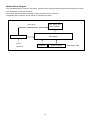
Monitor Block Diagram
The LCD MONITOR will contain a main board, a power board, and keypad board which house the flat panel control
logic, brightness control logic and DDC.
The Inverter board will drive the backlight of panel and the DC-DC conversion,
The Adapter will provide the 12V DC-power to inverter/power board.
Flat Panel and
CCFL Drive.
CCFL backlight
Inverter Board
AC-IN
100V-240
Main Board
Keyboard
14
HOST Computer
Video signal, DDC
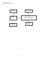
Main Board Diagram
LCD Interface
Crystal
24MHZ
MCU
Scalar: RTD2025L QFN-48
RTD2120L-LF
(Include: ADC, OSD etc)
D-SUB
OSD Control
Connector
Interface (Keypad)
15
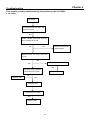
Software Flow Chart
1
Y
2
3
N
N
4
N
5
Y
6
N
7
8
Y
Y
9
N
10
11
Y
N
12
N
13
Y
Y
N
14
15
Y
17
18
N
19
Y
16
16
Remark:
1) MCU initializes.
2) Is the EEPROM blank?
3) Program the EEPROM by default values.
4) Get the PWM value of brightness from EEPROM.
5) Is the power key pressed?
6) Clear all global flags.
7) Are the AUTO and SELECT keys pressed?
8) Enter factory mode.
9) Save the power key status into EEPROM.
Turn on the LED and set it to green color.
Scalar initializes.
10) In standby mode?
11) Update the lifetime of back light.
12) Check the analog port, are there any signals coming?
13) Does the scalar send out an interrupt request?
14) Wake up the scalar.
15) Are there any signals coming from analog port?
16) Display "No connection Check Signal Cable" message. And go into standby mode after the
message disappears.
17) Program the scalar to be able to show the coming mode.
18) Process the OSD display.
19) Read the keyboard. Is the power key pressed?
17
Main Board Layout
Symbol
Description
Symbol
X401
Description
U201
AP1117E33LA
U401
IC MCU RTD2120L-LF REALTEK
CN201
WAFER 9P RIGHT ANELE PITCH
U402
AZ431AN-A-E1
CN202
WAFER
U501
SCALER IC RTD2025L QFN-48
CN601
CONN W TO B12P*2 P*2.0 4505-2
18
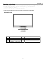
24MHZ/30PF/49US
Adjusting the viewing angle
19
Rear Bezel
Item
1.
Description
Item
Power Cable
2.
20
Description
Signal Cable
Chapter 2
Operating Instructions
Press the power button to turn the monitor on or off. The other control buttons are located at front panel of the
monitor. By changing these settings, the picture can be adjusted to your personal preferences.
• The power cord should be connected.
• Connect the video cable from the monitor to the video card.
• Press the power button to turn on the monitor position. The power indicator will light up.
External Controls
Item
Description
Item
Description
1.
Auto Config / Exit
4.
>
2.
<
5.
MENU/ENTER
3.
Power Button / Power Indicator
21
Front Panel Control
22
Adjusting the Picture
How to Adjust a Setting
1. Press the MENU-button to activate the OSD window.
2. Press <or >to select the desired function.
3. Press the MENU-button to select the function that you want to adjust.
4. Press < or > to change the settings of the current function.
5. To exit and save, select the exit function. If you want to adjust any other function, repeat steps 2-4
Analog –Only Model
23
b. The Description For Function Control LEDS
24
25
OSD Message
a. Outline
b. The Description For OSD Message
Item
Description
Auto Config
When Analog signal input, if User Press Hot-Key “Auto”, will show this message, and the
Please Wait
monitor do the auto config function.
Input Not
When the Hsync Frequency, Vsync Frequency or Resolution is out of the monitor
Supported
support range, will show this message. This message will be flying.
Cable Not
Analog-Only Model: When the video cable is not connected, will show this message.
Connected
This message will be flying.
No Signal
Analog-Only Model: When the video cable is connected, but there is no active signal
input, will show this message, then enter power saving.
26
Logo
When the monitor is power on, the LOGO will be showed in the center, and disappear slowly.
How To Optimize The DOS-Mode
Plug And Play
Plug & Play DDC2B Feature
This monitor is equipped with VESA DDC2B capabilities according to the VESA DDC STANDARD. It allows the
monitor to inform the host system of its identity and, depending on the level of DDC used, communicate additional
information about its display capabilities.
The DDC2B is a bi-directional data channel based on the I²C protocol. The host can request EDID information over
the DDC2B channel.
This monitor will appear to be non-functional if there is no video input signal. In order for this monitor to
operate properly, there must be a video input signal.
This monitor meets the Green monitor standards as set by the Video Electronics Standards Association (VESA)
and/or the United States Environmental Protection Agency (EPA) and The Swedish Confederation Employees
(NUTEK). This feature is designed to conserve electrical energy by reducing power consumption when there is no
video-input signal present. When there is no video input signals this monitor, following a time-out period, will
automatically switch to an OFF mode. This reduces the monitor's internal power supply consumption. After the video
input signal is restored, full power is restored and the display is automatically redrawn. The appearance is similar to
a "Screen Saver" feature except the display is completely off. Pressing a key on the keyboard, or clicking the mouse
restores the display.
Using The Right Power Cord
The accessory power cord for the Northern American region is the wallet plug with NEMA 5-15 style and is UL listed
and CSA labeled. The voltage rating for the power cord shall be 125 volts AC.
Supplied with units intended for connection to power outlet of personal computer: Please use a cord set consisting of
a minimum No. 18 AWG, type SJT or SVT three conductors flexible cord. One end terminates with a grounding type
attachment plug, rated 10A, 250V, and CEE-22 male configuration. The other end terminates with a molded-on type
connector body, rated 10A, 250V, having standard CEE-22 female configuration.
Please note that power supply cord needs to use VDE 0602, 0625, 0821 approval power cord in European counties.
27
Chapter 3
Machine Disassembly
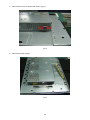
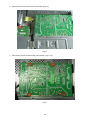
This chapter contains step-by-step procedures on how to disassemble the monitor for
maintenance.
Disassembly Procedure
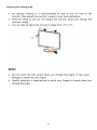
1. Remove the screws to release base stand and gemel. (Fig 1-3)
Fig 1
Fig 2
28
Fig 3
2. Remove the screws to remove the back cover. (Fig 4)
Fig 4
29
3. Remove the screws to remove the shield . (Fig 5)
Fig 5
4. Remove the bezel. (Fig 6)
Fig 6
30
5. Remove the screws to remove the panel. (Fig 7-9)
Fig 7
Fig 8
Fig 9
31
6. Remove the screw to remove the main board. (Fig 10)
Fig 10
7. Remove the screws to remove the power board. ( Fig 11-12 )
Fig 11
32
Fig 12
33
Chapter 4
Troubleshooting
This chapter provides troubleshooting information for the AL1702W:
1. No Power
No power
Press power key and look if the
picture is normal
NG
Please reinsert and make sure the
AC of 100-240 is normal
NG
OK
Reinsert or check the
power section
Measure U201 Pin 3=5V, U201 Pin
2=3.3V
NG
Measure CN201 Pin3=5V?
OK
OK
Check if X401 oscillate
waveforms are normal
Replace U201
NG
OK
Replace X401
Replace U401
if the picture is normal
NG
Replace U501
34
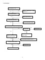
2. No Picture
No picture
Measure U201 PIN2=3.3V
OK
NG
Replace U201
Check if X401oscillate waveforms are
normal
OK
NG
Replace X401
Check if the sync signal from
computer is output and video cable
is connected normally
NG
Input the sync signal of computer, or
OK
change the cable
Replace U401,U501
35
3. Panel Power Circuit
Check the PPWR panel power relative circuit Q601, Q602
Check CN601 PIN 23-24 should have
response from 0V to 5V When we
NG
switch the power switch from on to off
In normal operation, when LED =green, R601 =5 V,
If PPWR no-response when the power switch
Turn on and turn off, replace the U401- RTD2120L
OK
Replace panel
4. Keypad Board
OSD is unstable or not working
NG
Connect Keypad Board
Is Keypad board connecting normally?
OK
NG
Is Button Switch normally?
Replace Button Switch
OK
NG
Is Keypad board normally?
Replace Keypad Board
OK
Check main board
36
5. No Backlight
Check C802 (+) =12V
OK
NG
Change
FB801,Check
Q805
Q808, Q810
Check ON/OFF signal
NG
OK
Check Interface board
Check IC801 pin12=5V?
NG
Change Q805.Q808 or Q810
OK
Check the pin9&10 of IC801 have PWM wave
NG
NG
Change IC801
OK
OK
CheckQ801/Q802/Q804/
Q811or /Q812
Check the resonant wave
of pin6 & pin1 for PT801
OK
NG
Check Q809Q801/Q802/Q811/Q812
Check the output of PT801
OK
NG
Change PT801
Check connecter & lamp
37
Replace IC801
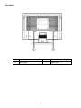
Chapter 5
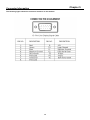
Connector Information
The following figure shows the connector locations on the monitor:
38
Chapter 6
FRU (Field Replaceable Unit) List
This chapter gives you the FRU (Field Replaceable Unit) listing in global configurations of AL1702W.Refer to this
chapter whenever ordering for parts to repair or for RMA (Return Merchandise Authorization).
NOTE: Please note WHEN ORDERING FRU PARTS, that you should check the most up-to-date information
available on your regional web or channel (http://aicsl.acer.com.tw/spl/). For whatever reasons a part number
change is made, it will not be noted in the printed Service Guide. For ACER AUTHORIZED SERVICE
PROVIDERS, your Acer office may have a DIFFERENT part number code from those given in the FRU list of
this printed Service Guide. You MUST use the local FRU list provided by your regional Acer office to order
FRU parts for repair and service of customer machines.
NOTE: To scrap or to return the defective parts, you should follow the local government ordinance or regulations on
how to dispose it properly, or follow the rules set by your regional Acer office on how to return it.
39
Exploded Diagram (Model: AL1702W)
40
Part List
Above picture show the description of the following component.
Item
Picture
Description
1
Base
2
shield
3
Key board
4
Panel
41
5
Power Board
6
Main Board
42
Chapter 7
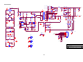
Schematic Diagram
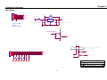
Main Board
CN201
1
2
3
4
5
6
7
8
9
CMVCC
CMVCC
CMVCC
BKLT-VBRI
BKLT-EN
C_PANEL_INDEX
Volume#
Mute
MVCC
DIM#
{4}
PANEL_ID#
Volume#
Mute
{4}
{4}
{4}
FB202
NC
CMVCC
FB201
3
VIN
CONN
2
+
C204
C205
AP1117E33LA
C203
100uF/25V
+
1
C202
100uF/25V
VOUT
VSS
120 '07-01-10 change to Elite
VCC3
U201
0.1uF/16V
0.1uF/16V
'07-01-10 change to Elite
Panel ID(3.3V PWM)
Back light
Dimming(3.3V PWM)
VCC3
* BKLT-EN High ON(3.3V)
BKLT-EN
R202
4K7 1/16W
R201
200 1/16W
C206
0.1uF/16V
Q202
PMBS3904
INV_ON#
{4}
VCC3
R207
120R 1/16W
R208
120R 1/16W
'06-12-29-3 Change R207,R208 Value
from 470ohm to 120ohm
'06-11-3 Remove R209(470 ohm)
CN202
KEY 0
KEY 1
POWER_KEY #
LED_G
LED_R
1
2
3
4
5
6
Q204
PMBS3906
R210
KEY 0
{4}
KEY 1
{4}
POWER_KEY # {4}
10K 1/16W
R213
ZD203
NC
2
C201
ZD201
NC
LED_G
10K 1/16W
LED_G#
{4}
Q205
PMBS3906
C210
0.1uF/16V
0.1uF/16V
1
C209
0.1uF/16V
1
1
NC
2
2
ZD202
{4}
LED_R
'06-12-29-3 Remove R211,R212(470ohm)
CONN
LED_R#
Near to Connect
Title
POWER
Size
B
Date:
43
Document Number
Rev
2
G2498-A-AC-X-1-070307
Wednesday , March 07, 2007
Sheet
2
of
6
DSUB_V
{4}
R301 100R 1/16W
R303 100R 1/16W
RTD_H
RTD_V
{5}
{5}
2
2
R302 0R05 1/16W
R304
ZD302
UDZS5.6B
R305
2.2K 1/16W
2.2K 1/16W
ZD303
UDZS5.6B
C302 C303
FB302
22pF
1
R311 100R 1/16W
DSUB_CONNECT {4}
16
RTD_B+
13
DDC1_SDA
12
11
VGA_BVGA_B+
VGA_GVGA_G+
VGA_RVGA_R+
2
DSUB_5V
C305
5pF/50V
{5}
RTD_B-
{5}
RTD_G+
{5}
RTD_G-
{5}
RTD_R+
{5}
RTD_R-
{5}
R308 100R 1/16W C306
RTD_B-
ZD305
ZD304
0.047uF
UDZS5.6B
UDZS5.6B
FB301
VGA_G+
1
R309 100R 1/16W C307
2
RTD_G+
BEAD
17
ZD307
UDZS5.6B
DB15
R310
75R 1/16W
1
ZD301
UDZS5.6B
C308
5pF/50V
0.047uF
R312 100R 1/16W C309
VGA_G-
RTD_G0.047uF
FB303
VGA_R+
1
R313 100R 1/16W C301
2
RTD_R+
BEAD
R314
75R 1/16W
C310
5pF/50V
0.047uF
R315 100R 1/16W C311
D301
BAV99
3 VGA_B+
3
3
VGA_R+
VGA_G+
VGA_R-
D302
BAV99
RTD_R0.047uF
D303
BAV99
1
2
2
1
CMVCC
2
1
RTD_B+
0.047uF
VGA_B-
1
DSUB_H
75R 1/16W
VGA_CON
DSUB_5V
2
14
2
DDC1_SDA
10
5
9
4
8
3
7
2
6
1
15
R307
1
DDC1_SCL
DDC1_SCL
2
2
CN301
DSUB_V
{4}
1
BEAD
1
{4}
1
VGA_B+
12/29 change
ZD302 ZD303
from NC to
insert
R306 100R 1/16W C304
22pF
C315
0.1uF/16V
Title
INPUT
Size
B
Date:
44
Document Number
Rev
2
G2498-A-AC-X-1-070307
Wednesday , March 07, 2007
Sheet
3
of
6
CMVCC
D401
BAT54C(NC)
2
1
Reserve for powerBoard
CMVCC=3V
MCU_VCC
3
DSUB_5V CMVCC
'06-11-24 D402 change
Value from BAT54 to
BAV70
C402
D402
BAV70
1uF 10V
Q401
PMBS3904
MCU_VCC_S
MCU_VCC
C404
C412
R405 R406 R407
U403
3
U402
AZ431AN-AE1
1
2
3
4
R404
10K 1/16W
1
2
BAT54C
NC VCC
NC WC
NC SCL
VSS SDA
8
7
6
5
NC/4K7 1/16W
NC/0.22uF
NC/4K7 1/16W
R403
1uF 10V
3.9K 1/16W
NC/4K7 1/16W
R402
1K 1/16W
R408
R409
R410
NC/100R 1/16W
NC/100R 1/16W
NC/100R 1/16W
WP
IICSCL
IICSDA
NC/M24C16
MCU_VCC
2006-11/23 change R413-4, pull high pin
from DSUB_VCC ,DVI_VCC to MCU_VCC
MCU_VCC
40
39
38
37
36
35
34
33
P1.0/T2
P1.1
P1.2
P1.3
P1.4
P1.5
P1.6
P1.7
41
4
RTD2120L
P6.7
P6.6/CLKO1
P6.5
P6.4
P6.3/ADC3
P6.2/ADC2
P6.1/ADC1
P6.0/ADC0
32
31
30
29
28
27
26
25
24
23
22
21
20
R425
10K 1/16W
DSUB_V1
R427
0R05 1/16W DSUB_V
R429
0R05 1/16W CRY STAR_OUT
DSUB_CONNECT
R433 100R 1/16W
R434 100R 1/16W
R435 100R 1/16W
POWER_KEY #
KEY 1
KEY 0
NC
NC
XO
XI
R415
MCU_VCC
VSY NC
42
43
PANEL_VCC
LED_G#
LED_R#
P3.2/INT0
P3.3/INT1
P3.4/T0
P3.5/T1
P7.6/CLKO2
P7.7
15
16
LED_G#
LED_R#
9
10
11
12
13
14
ASCL1/P3.0/RXD
ASDA1/P3.1/TXD
RTD_SD3/SDI {5}
RTD_SCLK
{5}
C409
NC(22pF/16V)
NC
NC
NC
NC
NC
NC
5
8
P5.0/PWM0
P5.1/PWM1
P5.2/PWM2
P5.3/PWM3
P5.4/PWM4
P5.5/PWM5
DSCL2/P5.6
DSDA2/P5.7
NC
NC
22R 1/16W
22R 1/16W
VCC
from
44
45
46
47
48
1
2
3
2006-11/7 change R426,R428 from
100 ohm to 22 ohm
{2}
{2}
R412
4K7 1/16W
IICSDA
IICSCL
WP
RTD_SD3/SDI
RTD_SCLK
18
19
R426
R428
U401
RST
2K2 1/16W
2007-1-15 change R413, R414
4.7K to 2.2K
0.1uF/16V
6
7
DDC1_SCL
DDC1_SDA
R414
C406
10uF/50V
VSS
DDC1_SCL
DDC1_SDA
R451 R413
C405
+
17
{3}
{3}
1K 1/16W
Volume#
Mute
PANEL_ID#
DIM#
PPWR_ON#
INV_ON#
1K 1/16W
{2}
{2}
{2}
{2}
{6}
{2}
2006-11/7 R423-R424
change from 100R to
1K
Volume#
R420
100R 1/16W
R422
100R 1/16W
Mute
R423
1K 1/16W
PANEL_ID#
DIM#
R424
1K 1/16W
PPWR_ON#
R430
100R 1/16W
INV_ON#
R432
100R 1/16W
R454 R453
4K7 1/16W
2006-11/7 Add pull high R451 to MVCC
,R453,R454 pull up MCU_VCC
R411
4K7 1/16W
MCU_VCC_S
2K2 1/16W
VCC3
DSUB_V
{3}
CRY STAR_OUT {5}
DSUB_CONNECT {3}
POWER_KEY # {2}
KEY 1
{2}
KEY 0
{2}
MVCC
R431
6K8 1/16W
2006-11-3 change R431 from 1K to 6.8K
RTD2120L-LF
6K8 1/16W
R416
10K 1/16W
24mhz
X401
C403
0.1uF/16V
1
2007-01-11 ADD
Closed to X'tal
R437
3.9K 1/16W
R439
6K8 1/16W
R401
3.9K 1/16W
2
2007-1/3 change ref from Y401
to X401
R438
10K 1/16W
R436
10K 1/16W
C410
0.1uF/16V
MCU_VCC
2006-12-8 change R437,R401 from 10K to 3.9K
C401
10pF
C411
10pF
2007-1/18 change X401 to 75
Degree
Closed to MCU
Title
MCU/RTD2120
Size
B
Date:
45
Document Number
Rev
2
G2498-A-AC-X-1-070307
Wednesday , March 07, 2007
Sheet
4
of
6
{3}
{3}
{3}
{3}
TXO0+
RXO0-
RXO0+
37
DGND
39
38
TXO0-
PGND
{4}
RTD_SCLK
{4}
R1.8DVCC
40
VCCK
RTD_SD3/SDI
RTD_SCLK
42
SCL
43
DDCSDA/PWM1/IRQ
44
41
CRYSTAR_OUT
XIN
46
47
VCLK/RX2P
TMDS_VDD
RTD_SD3/SDI
TXO3-
RTD2025L QFN-48
AVS
TXO3+
AHS
TXE0-
ADC_GND
TXE0+
B-
TXE1-
17
18
19
20
R1.8DVCC
BJT_B
R1.8DVCC
DGND
24
16
RTD_R+
RTD_GRTD_G+
RTD_RRTD_R+
36
RXO1-
35
RXO1+
34
RXO2-
33
RXO2+
32
RXOC-
31
RXOC+
30
RXO3-
29
RXO3+
28
RXE0-
27
RXE0+
26
RXE1-
25
RXE1+
RXOCRXOC+
LVDS_O0
LVDS_O1
LVDS_O2
LVDS_O3
LVDS_O4
LVDS_O5
RXO0RXO0+
RXO1RXO1+
RXO2RXO2+
LVDS_O6
LVDS_O7
LVDS_O8
LVDS_O9
RXOCRXOC+
RXO3RXO3+
LVDS_E0
LVDS_E1
LVDS_E2
LVDS_E3
RXE0RXE0+
RXE1RXE1+
LVDS_E4
LVDS_E5
LVDS_E6
LVDS_E7
LVDS_E8
LVDS_E9
RXE2RXE2+
RXECRXEC+
RXE3RXE3+
LVDS_O[0..9]
{6}
LVDS_E[0..9]
{6}
TXE2-
TXE1+
RXE2-
B+
TXE2+
12
V7/RXCN
TXE3-
11
RTD_B+
TXOC+
23
{3} RTD_B+
RTD_B-
V6/RXCP
22
{3} RTD_B-
9
10
TXOC-
RXE2+
DGND
V5/RX0N
RXE3-
RTD_H
{3} RTD_H
8
TXO2+
TXE3+
RTD_V
{3} RTD_V
V4/RX0P
21
7
TXO2-
RXE3+
6
TXO1+
PGND
5
TXO1-
VCCK
DGND
U501
V3/RX1N
BJT_B
4
SDA
CRYSTAR_OUT
{4}
3
V2/RX1P
ADC_VDD
0.1uF/16V
0.1uF/16V
0.1uF/16V
V1/REXT
G-
22uF/50V
2
R+
C501
15
C507
RTD_R-
C506
C505 +
R-
1
FB503
120 14
MMBT2907AK
13
3.3 2W
G+
Q502
R507
RTD_G+
VCC3
R1.8DVCC
Q501
MMBT2907AK
RTD_G-
1.8AVCC
V0/RX2N
48
BJT_B
TMDS_VDD
C503
0.1uF/16V
DDCSCL/PWM0
FB502
120 45
VCC3
R1.8DVCC
Title
RTD2525L
Size
B
Date:
46
Document Number
Rev
2
G2498-A-AC-X-1-070307
Wednesday , March 07, 2007
Sheet
5
of
6
LVDS Panel ( Normal Type )
{5}
CN601
LVDS_O[0..9]
{5}
LVDS_E[0..9]
LVDS_O0
LVDS_O1
LVDS_O2
LVDS_O3
LVDS_O4
LVDS_O5
RXO0RXO0+
RXO1RXO1+
RXO2RXO2+
LVDS_O6
LVDS_O7
LVDS_O8
LVDS_O9
RXOCRXOC+
RXO3RXO3+
LVDS_E0
LVDS_E1
LVDS_E2
LVDS_E3
RXE0RXE0+
RXE1RXE1+
LVDS_E4
LVDS_E5
LVDS_E6
LVDS_E7
LVDS_E8
LVDS_E9
RXE2RXE2+
RXECRXEC+
RXE3RXE3+
RXO0RXO1RXO2RXOCRXO3RXE0RXE1RXE2RXECRXE3-
1
3
5
7
9
11
13
15
17
19
21
23
2
4
6
8
10
12
14
16
18
20
22
24
CONN
RXO0+
RXO1+
RXO2+
RXOC+
RXO3+
RXE0+
RXE1+
RXE2+
RXEC+
RXE3+
PANEL_VCC
R602
330R 1/8W
R606
NC(R0805)
C602
0.01uF/25V
'07-01-04 Add R606(NC)
3D
CMVCC
1
G
R605
4K7 1/16W
R601
AO3401L
C603
R604
10K 1/16W
2
S
PANEL_VCC
0.1uF/16V
PANEL_VCC
2006-11-7 Add pull up 4K7 to MVCC
47K 1/16W
{4}
PPWR_ON#
PPWR_ON#
Q601
AO3401
FB601
Q602
PMBS3906
120 C604
47uF/25V
+
Title
OUTPUT
Size
A
Date:
47
Document Number
Rev
2
G2498-A-AC-X-1-070307
Wednesday , March 07, 2007
Sheet
6
of
6
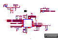
Power board
100 1/4W R918
L904
BD901
KBP208G
C912
0.001uF
+
!
R941 R945
1K 1/4W
1K 1/4W
C922
470uF/25V +
100 1/4W R920
2
C917
680uF/25V
3
2
!
1
-
C918
680uF/25V
C907
100uF/450V
R904
300K 1/4W
R905
NC
5
7
0.1uF
1K 1/4W
R943
1K 1/8W
1K 1/4W
Q903
PMBS3904
D906
SP10100
ZD901
NC
R908
C906
1500pF/1KV
1
4
+
!
9
C930
R946
+
T901
4
ZD902
RLZ13B
R944
+
3
+12V
1.1uH
2
1
100 1/4W R919
C932
100K 2W
R935 100 1/4W
3
R939
NC
1
1000pF
!
!
R915
2
12
5
6
7
8
R910
10 1/4W
ZD905
RLZ18B
LD7552BPS
D907
NC
R940
33K 1/10W
R924
N.C
150R 1/8W
ZD922
RLZ5.1B
1
ZD921
RLZ13B
R927
3.6K 1% 1/10W
!
Q901
2SK2645-54MR
R938
10K 1/8W
100K 1/8W
IC903
PC123X2Y FZOF
!
FB901
BEAD
R925
1K 1/8W
D916
D915
LL4148WP
LL4148WP
C924
0.1uF
1
2 L901 3
+
C915
470uF/16V
POWER X'FMR
D903 LL4148WP
RT
NC
VCC
CS
COMP VCC
GND OUT
3
C939
1000uF/16V
2
C908
22uF/50V
R907
NC
IC901
4
3
2
1
8
1
R933
300K 1/4W
6
1
FUSE
1
+
R909
5.1 1/4W
+5V
+ C940
1000uF/16V
2
C901
0.001uF/250V
D901
FR103
+
2
ZD906
RLZ22B
4
C905
0.1uF
F903
L903
1.1uH
R962 100 1/4W
3
C902
0.001uF/250V
C929
0.001uF
1
!
7.0mH
R961 100 1/4W
11
D905
SP1060
10
2
3
6
4
2
4
D900
FR107
R906
NC
1
SG901 NC
1 L902 2
R932
300K 1/4W
SG902 NC
C938
1500pF/1KV
4
2
R912
1
!
220 1/4W
R926
1K 1/10W 1%
R914
0.47 2W
C928
0.01uF
4.0mH
R942
1K 1/10W 1%
IC904
KIA431A-AT/P
C909
470pF/25V
!
C903
0.47uF/275V
C925
R930
CN902
NC
C921
3300PF/250V
!
R900
!
!
R902
680K 1/4W
R901
680K 1/4W
GND1
GND
680K 1/4W
VAR901
Varistor N.C
0.1uF
CONNECTOR
FG
HS2
HEAT SINK(D906)
NR901
NTCR
!
!
F901
FUSE
2
VOL
1
2
MUTE
HS3
HEAT SINK(Q901)
3
t
+5V
DIM
ON/OFF
C916
1
2
!
2.43K 1% 1/10W
1
2
3
4
5
6
7
8
9
10
Title
1
2
1
G2545-1-X-X-4-070316
Size
CN901
SOCKET
!
Date:
48
Document Number
Thursday , March 15, 2007
Rev
Sheet
1
of
2
CN801
1
2
C839
1000pF
6
FB801
F801
+12V
1
T801
POWER X'FMR
7
R817
10K 1/10W
R855
33 1/4W
D805
LL4148WP
3
4
2
CONN
C801
15pF/3KV
BEAD
R821
1K 1/10W 1%
C819
0.0022uF
2
3
1
0R05 1/4W
R804
100 1/8W
D810
NC
Q808
PDTA144WK
2
R839
22R 1/8W
ON/OFF
C807
0.1uF/25V
C824
0.1uF
Q802
AM9945N-T1-PF
1
8
S
D
Q804
PMBS3906
1
C825
0.1uF/25V
3
4
2
Q805
PDTC144WK
C802
470uF/25V +
Q801
PMBS3904
G
D
S
D
G
D
R856
33 1/4W
7
1
8
R801
1K 1/10W 1%
D801
BAV99
C838
1000pF
6
2
1
5
R828
10K 1/10W
R822
1K 1/10W 1%
CN802
CONN
3
2
Q811
PMBS3904
DIM
D807
LL4148WP
3
1
R814
1K 1/10W 1%
R811
4.7K 1/10W
D802
BAV99
D811
NC
ZD801
RLZ6.8C
R850
22R 1/8W
3
1
Q812
PMBS3906
1
2
2
D813
LL4148WP
DTC
Q810
RK7002
C823
0.0022uF
R813
1K 1/10W
R827
1K 1/10W 1%
Q806
PMBS3904
R853
68K 1/10W
C835
NC
D817
LL4148WP
R841
68K 1% 1/10W
R851
C842
0.01uF
R802
91K 1/10W
R829
22R 1/8W
5.1K 1/10W
R825
22R 1/8W
R837
47K 1/10W
R830
NC
C822
1uF/25V
R832
10K 1/10W
R807
10K 1/10W
IC801
1
2
3
4
5
6
7
8
D812
LL4148WP
R823
0 1/10W
IN1+
IN1FB
DTC
CT
RT
GND
C1
IN2+
IN2VREF
CONT
VCC
C2
E2
E1
16
15
14
13
12
11
10
9
R818
1K 1/10W 1%
D806
LL4148WP
KA7500CDTF
C821
0.1uF/25V
R820
10K 1/10W
R863
10K 1/10W
R831
1K 1/8W
R810
R865
51K 1% 1/8W
NC
C820
220pF
穝糤
R861
NC
Q807
NC
R864
NC
穝糤
R854
NC
Q809
RK7002
R826
1K 1/8W
R824
R803
10M 1/10W
R808
1K 1/10W 1%
C846
NC
1K 1/10W 1%
C817
NC
C845
2.2uF/16V
R862
1M 1/10W 5%
C834
0.1uF/25V
R835
1M 1/10W 5%
D814
LL4148WP
Title
Size
Date:
49
G2545-1-X-X-4-070316
Document Number
Custom 1.0
Thursday , March 15, 2007
Rev
Sheet
2
of
2