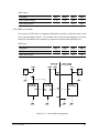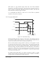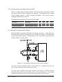
1
GR64 GSM/GPRS Modem Integrators Manual The information contained in this document is the proprietary information of Sony Ericsson Mobile Communications International. The contents are confidential and any disclosure to persons other than the officers, employees, agents or subcontractors of the owner or licensee of this document, without the prior written consent of Sony Ericsson Mobile Communications International, is strictly prohibited. Further, no portion of this publication may be reproduced, stored in a retrieval system, or transmitted in any form or by any means, electronic or mechanical, including photocopying and recording, without the prior written consent of Sony Ericsson Mobile Communications International, the copyright holder. First Edition (March 2006) Sony Ericsson Mobile Communications International publishes this manual without making any warranty as to the content contained herein. Further Sony Ericsson Mobile Communications International reserves the right to make modifications, additions and deletions to this manual due to typographical errors, inaccurate information, or improvements to programs and/or equipment at any time and without notice. Such changes will, nevertheless be incorporated into new editions of this manual. All rights reserved. © Sony Ericsson Mobile Communications International, 2006 Publication number: LZT 123 1834 Printed in US LZT 123 1834 2 Contents Overview....................................................................................................... 8 1 Introduction............................................................................................ 9 1.1 TARGET USERS........................................................................................................... 9 1.2 PREREQUISITES........................................................................................................... 9 1.3 MANUAL STRUCTURE ................................................................................................. 9 1.4 NOTATION............................................................................................................... 10 1.5 ACKNOWLEDGEMENTS ............................................................................................. 10 2 GR64 Wireless Modem .......................................................................... 11 2.1 ABOUT THE GR64 .................................................................................................... 11 2.2 WIRELESS MODEMS IN A COMMUNICATION SYSTEM .................................................. 12 2.3 FEATURES ................................................................................................................ 14 2.3.1 TYPES OF MOBILE STATION ............................................................................... 14 2.3.3 VOICE CALLS..................................................................................................... 15 2.3.5 GPRS MULTI-SLOT SUPPORT.............................................................................. 16 2.3.2 2.3.4 2.3.6 2.3.7 2.3.8 2.4 SHORT MESSAGE SERVICE.................................................................................. 14 DATA................................................................................................................ 15 SIM CARD ......................................................................................................... 16 POWER CONSUMPTION...................................................................................... 16 OTHER FEATURES.............................................................................................. 17 SERVICE AND SUPPORT ............................................................................................ 18 2.4.1 WEB PAGES ....................................................................................................... 18 2.4.3 M2MPOWER APPLICATION GUIDE....................................................................... 18 2.4.2 2.4.4 AT COMMANDS MANUAL .................................................................................. 18 DEVELOPER’S KIT .............................................................................................. 18 2.5 PRECAUTIONS .......................................................................................................... 19 2.6 GUIDELINES FOR SAFE AND EFFICIENT USE................................................................ 19 2.6.1 2.6.2 GENERAL USAGE ............................................................................................... 19 RADIO FREQUENCY (RF) EXPOSURE AND SAR ..................................................... 20 LZT 123 1834 3 2.6.3 2.6.4 3 PERSONAL MEDICAL DEVICES ............................................................................ 21 DISPOSAL OF OLD ELECTRONIC EQUIPMENT ...................................................... 21 Abbreviations ....................................................................................... 22 Integrating the Wireless Modem.................................................................. 24 4 Mechanical Description ......................................................................... 25 4.1 INTERFACE DESCRIPTION ......................................................................................... 25 4.2 PHYSICAL DIMENSIONS ............................................................................................ 27 5 System Connector Interface .................................................................. 29 5.1 OVERVIEW................................................................................................................ 29 5.2 DEALING WITH UNUSED PINS.................................................................................... 32 5.3 GENERAL ELECTRICAL AND LOGICAL CHARACTERISTICS ........................................... 34 5.3.1 5.3.1.1 5.3.1.2 5.4 LEVEL SHIFTER INTERFACES............................................................................... 34 COMMON LEVEL SHIFTER INTERFACE ............................................................. 34 I2C LEVEL SHIFTER INTERFACE ....................................................................... 36 GROUNDS ................................................................................................................ 37 5.4.1 5.4.2 ANALOGUE GROUND (AREF) .............................................................................. 37 COMMON GROUND (GND) ................................................................................. 37 5.5 REGULATED POWER SUPPLY INPUT (VCC) .................................................................. 38 5.6 VOLTAGE REFERENCE (VREF) .................................................................................... 39 5.6.1 5.6.2 5.7 VREF AS AN OUTPUT ......................................................................................... 39 VREF AS AN INPUT ............................................................................................ 40 BATTERY CHARGING INPUT (CHG_IN) ....................................................................... 41 5.7.1 CHARGING PROCESS ......................................................................................... 42 5.7.3 BATTERY SELECTION ......................................................................................... 43 5.7.2 5.8 POWERING THE MODULE ON AND OFF (ON/OFF) ...................................................... 47 5.8.1 5.8.2 5.9 SERIES DIODE.................................................................................................... 43 TURNING THE MODULE ON ............................................................................... 47 TURNING THE MODULE OFF .............................................................................. 48 ANALOGUE AUDIO ................................................................................................... 50 LZT 123 1834 4 5.9.1 AUXILIARY AUDIO TO MOBILE STATION (AUXI)................................................... 51 5.9.3 MICROPHONE SIGNALS (MICIP, MICIN) ............................................................... 52 5.9.2 AUXILIARY AUDIO FROM MOBILE STATION (AUXO) ............................................. 52 5.9.4 SPEAKER SIGNALS (EARP, EARN)......................................................................... 53 5.10 PCM DIGITAL AUDIO (SSP)..................................................................................... 53 5.11 SERIAL DATA INTERFACES..................................................................................... 55 5.10.1 5.11.1 PCM DATA FORMAT .......................................................................................... 53 UART1 .............................................................................................................. 56 5.11.2 5.11.2.1 5.11.2.2 5.11.3 5.11.3.1 SERIAL DATA SIGNALS (DTM1, DFM1) ................................................................ 56 SERIAL DATA FROM WIRELESS MODEM (DFM1) ............................................... 57 SERIAL DATA TO WIRELESS MODEM (DTM1).................................................... 57 CONTROL SIGNALS (RTS1, CTS1, DTR1, DSR1, DCD1, RI) ................................... 57 HARDWARE FLOW CONTROL RTS1 AND CTS1................................................. 57 5.11.3.2 REQUEST TO SEND (RTS1) .............................................................................. 57 5.11.3.4 DATA TERMINAL READY (DTR1) ..................................................................... 58 5.11.3.3 5.11.3.5 5.11.3.6 5.11.3.7 5.11.4 5.11.4.1 5.11.4.2 CLEAR TO SEND (CTS1).................................................................................. 58 DATA SET READY (DSR1) ............................................................................... 58 DATA CARRIER DETECT (DCD1) ..................................................................... 58 RING INDICATOR (RI) ..................................................................................... 58 UART3 (DTM3, DFM3) ....................................................................................... 59 TRANSMITTED DATA (DTM3) ......................................................................... 59 RECEIVED DATA (DFM3)................................................................................. 59 5.11.5 USB................................................................................................................... 60 5.11.6 SIM CARD INTERFACE........................................................................................ 61 5.11.7 SIM DETECTION (SIMDET) .................................................................................. 62 5.12 SERVICE/PROGRAMMING ...................................................................................... 62 5.13 BUZZER ................................................................................................................ 63 5.14 LED ...................................................................................................................... 63 5.15 GENERAL PURPOSE IO ........................................................................................... 65 5.15.1 5.15.2 5.15.3 EMBEDDED APPLICATIONS................................................................................. 66 LED/IO6 CAPABILITIES....................................................................................... 66 ADC4................................................................................................................ 66 5.16 DIGITAL TO ANALOGUE CONVERTER – DAC .......................................................... 67 5.17 ANALOGUE TO DIGITAL CONVERTERS (ADIN1, ADIN2, ADIN3, ADIN4) ................... 67 5.18 I2C SERIAL CONTROL BUS ..................................................................................... 69 LZT 123 1834 5 5.19 BURST TRANSMISSION (TX_ON) ............................................................................. 70 5.20 REAL TIME CLOCK ................................................................................................ 70 5.20.1 5.20.2 5.20.2.1 5.20.3 REAL TIME CLOCK BACKUP SUPPLY (VRTC)......................................................... 71 RTC ALARM (ALARM)......................................................................................... 72 ALARM OUTPUT FROM THE MODULE.............................................................. 72 ALARM UTILIZATION AS A WAKE-UP.................................................................. 73 6 Antenna Connector ............................................................................... 74 7 Hints for Integrating the Wireless Modem ............................................. 75 7.1 SAFETY ADVICE AND PRECAUTIONS ......................................................................... 75 7.1.1 GENERAL .......................................................................................................... 75 7.2 SIM CARD ................................................................................................................ 76 7.3 ANTENNA ................................................................................................................ 76 7.4 INSTALLATION OF THE WIRELESS MODEM................................................................. 77 7.4.1 7.4.1.1 7.4.1.2 7.4.1.3 7.4.1.4 7.4.2 WHERE TO INSTALL THE WIRELESS MODEM ........................................................ 77 ENVIRONMENTAL CONDITIONS ...................................................................... 77 SIGNAL STRENGTH ........................................................................................ 78 CONNECTION OF COMPONENTS TO WIRELESS MODEM ................................... 78 NETWORK AND SUBSCRIPTION ....................................................................... 78 HOW TO INSTALL THE WIRELESS MODEM ........................................................... 79 7.4.2.1 POWER SUPPLY .............................................................................................. 79 7.4.2.3 AUDIO........................................................................................................... 79 7.4.2.2 7.4.2.4 7.5 GROUNDS...................................................................................................... 79 SOFTWARE UPGRADE ..................................................................................... 79 ANTENNA ................................................................................................................ 80 7.5.1 GENERAL .......................................................................................................... 80 7.5.3 ANTENNA PLACEMENT ...................................................................................... 81 7.5.2 7.5.4 7.5.5 8 ANTENNA TYPE ................................................................................................. 80 THE ANTENNA CABLE........................................................................................ 81 POSSIBLE COMMUNICATION DISTURBANCES ...................................................... 81 Embedded Applications ........................................................................ 83 8.1 FEATURES ................................................................................................................ 83 8.2 IMPLEMENTATION .................................................................................................... 83 8.2.1 LIMITATIONS..................................................................................................... 83 LZT 123 1834 6 8.2.2 9 M2MPOWER IDE (INTEGRATED DEVELOPMENT ENVIRONMENT) ........................... 84 TCP/IP Stack ......................................................................................... 85 9.1 IMPLEMENTATION .................................................................................................... 85 10 Technical Data ................................................................................... 86 10.1 MECHANICAL SPECIFICATIONS .............................................................................. 86 10.2 POWER SUPPLY VOLTAGE, NORMAL OPERATION .................................................... 87 10.3 RADIO SPECIFICATIONS ........................................................................................ 87 10.4 SIM CARD............................................................................................................. 87 10.5 ENVIRONMENTAL SPECIFICATION.......................................................................... 88 11 Regulatory Notices ............................................................................. 90 Developers Kit ............................................................................................ 91 12 Introduction to the Universal Developer’s Kit ..................................... 92 LZT 123 1834 7 Overview LZT 123 1834 8 1 Introduction 1.1 Target Users The GR64 wireless modems are designed to be integrated into machine-to-machine or man-to-machine communications applications. They are intended to be used by manufacturers, system integrators, applications developers and developers of wireless communications equipment. 1.2 Prerequisites It is assumed that the person integrating the wireless modem into an application has a basic understanding of the following: • GSM networking; • Wireless communication and antennas (aerials) • AT commands • ITU-T standard V.24/V.28 • Micro controllers and programming • Electronic hardware design 1.3 Manual Structure This manual is composed of three parts. Part 1- Overview This section provides a broad overview of the Gx64 family and includes a list of abbreviations used in the manual. Part 2 - Integrating the Wireless modem This section describes each of the signals available on the GR64 wireless modem, along with mechanical information. The section also provides you with design guidelines and what is needed to commercialize an application from a regulatory point of view. LZT 123 1834 9 Part 3 – Developer’s Kit This section lists the contents of the Developer’s Kit and provides the information to setup and use the equipment. 1.4 Notation The following symbols and admonition notation are used to draw the readers attention to notable, or crucially-important information. Note Draws the readers attention to pertinent, useful or interesting information NOTE Tip Provides advice, suggestions, guidance or recommendations which augment the formal text TIP Caution Cautionary information must be heeded, it draws the readers attention to the need for understanding, care or watchfulness in relation to the CAUTION ! WARNING information provided Warning Notes marked warning must be heeded, they alert readers to precautionary measures, risks, hazards or safety information which directly effects equipment function, warranty or personnel safety Danger This information must be heeded, it identifies information and cautionary behavior that otherwise ignored could result in catastrophic DANGER equipment failure, bodily injury or death 1.5 Acknowledgements Parts of this document, including text passages, tables, and illustrations, are reproduced from copyright information by kind permission of Agere Systems Inc. LZT 123 1834 10 2 GR64 Wireless Modem 2.1 About the GR64 The Sony Ericsson Gx64 family of devices are Quad Band GSM/GPRS wireless modems operating in the GSM 850/900/1800/1900 bands. These products belong to a new generation of Sony Ericsson wireless modems, and are intended to be used in machine-to-machine applications and man-to-machine applications. They are used when there is a need to send and receive data (by SMS, CSD, or GPRS), and make voice calls over the GSM network. The GR64 conforms to the European Union (EU) Restriction of Hazardous Substances (RoHS) directive 2002/95/EC. The GR64 is available in four variants. Table 1: GR64 Variants lists the hardware and software features for each variant. The device is available in two hardware variants. Each hardware variant is available in two software variants. The first hardware variant (/10 and /30) is equipped with PCM compatible pins but does not have a USB interface or an integrated SIM card holder. The second hardware variant (/20 and /40) is equipped with a USB interface and an integrated SIM card holder, but does not have PCM compatible pins. Table 1: GR64 Variants PCM SIM Card Embedded Variant Compatible VREF Input USB DPY 102 1494/10 Yes No No No No DPY 102 1494/20 No Yes Yes Yes No DPY 102 1494/30 Yes No No No Yes DPY 102 1494/40 No Yes Yes Yes Yes PINS Holder Applicatio ns One software variant is designed to be controlled from a micro-controller situated on the host application. The other software variant offers the option to run applications embedded onto the module itself. When using the embedded application version the controlling script can be run internal to the module, with or without the use of an external control. A typical application, involves a micro-controller and a wireless modem, in which the micro-controller sends AT commands to the wireless modem via an RS232 communications link. LZT 123 1834 11 2.2 Wireless modems in a Communication System Figure 2.2-1 and Figure 2.2-2 illustrate the main blocks of a wireless communication system using the wireless modem. Figure 2.2-1 shows the communication system when the script is embedded on the wireless modem and Figure 2.2-2 shows the communication system when a micro-controller is used. They also show the communication principles of the system and the interface between the wireless modem and the application. The definitions in the figures, as used elsewhere in this manual, are in accordance with the recommendations of 3GPP TS 27.007. The MS (mobile station) represents the wireless modem and SIM card. The wireless modem excluding SIM card, is known as the ME (mobile equipment). The DTE (data terminal equipment) is the controlling application. This can be either an external host or an internal embedded application. The DCE (data circuit terminating equipment) is the serial communication interface of the MS. MS GSM NETWORK SIM SIM SYSTEM INTERFACE DC POWER GSM GSM ENGINE ENGINE STATUS & RESPONSE DCE DCE EMBEDDED APPLICATION DTE DTE COMMAND & CONTROL Figure 2.2-1 Main Blocks in a Wireless System (embedded application) LZT 123 1834 12 MS GR64 SIM GSM NETWORK SIM STATUS & RESPONSE SYSTEM INTERFACE DC POWER DTE DTE GSM GSM ENGINE ENGINE DCE DCE COMMAND & CONTROL Figure 2.2-2 Main Blocks in a Wireless System (external micro-controller) In accordance with the recommendations of ITU-T (International Telecommunication Union - Telecommunications Standardization Sector) V.24, the TE communicates with the MS over a serial interface. The functions of the wireless modem follow the recommendations provided by 3GPP (3rd Generation Partnership Project) and ITU-T. 3GPP is a collaboration agreement that was established in December 1998. The collaboration agreement brings together a number of telecommunications standards bodies which are known as Organizational Partners. The current Organizational Partners are ARIB, CCSA, ETSI, ATIS, TTA, and TTC. 3GPP specifies a set of AT commands for controlling the GSM element of the wireless modem; these commands are supplemented by Sony Ericsson specific commands. To find out how to work with AT commands, see the AT Commands Manual. LZT 123 1834 13 2.3 Features The wireless modem performs a set of telecom services (TS) according to 3GPP release 99 and ITU-T. The functions of the wireless modem are implemented by issuing AT commands over a serial interface. 2.3.1 Types of Mobile Station The GR64 is a fully Quad Band capable GSM/GPRS mobile station with the characteristics shown in the table below. Feature GSM850 E-GSM900 GSM1800 GSM1900 Tx 824-849 880-915 1710-1785 1850-1910 Rx 869-894 925-960 1805-1880 1930-1990 200kHz 200kHz 200kHz 200kHz Number of channels 124 174 374 299 Number of TD slots 8 8 8 8 Duplex spacing 45MHz 45MHz 95MHz 80MHz GSM power class 4 (2W) 4 (2W) 1 (1W) 1 (1W) Frequency range (MHz) Channel spacing Modulation Receive sensitivity GMSK <-102dBm at antenna connector GPRS multi-slot class Class 10 2.3.2 Short Message Service The wireless modem supports the following SMS services: • Sending; MO (mobile-originated) with both PDU (protocol data unit) and text mode supported • Receiving; MT (mobile-terminated) with both PDU and text mode supported • CBM (cell broadcast message); a service in which a message is sent to all subscribers located in one or more specific cells in the GSM network (for example, traffic reports) • SMS status report according to 3GPP TS 23.40 The maximum length of a text mode SMS message is 160 characters using 7-bit encoding. The wireless modem supports up to six concatenated messages to extend this function. Concatenation is performed by the host application. LZT 123 1834 14 2.3.3 Voice Calls The wireless modem offers the capability of MO (mobile originated) and MT (mobile terminated) voice calls, as well as supporting emergency calls. Multi-party, call waiting and call divert features are available. Some of these features are networkoperator specific. For the inter-connection of audio, the wireless modem offers both single ended and balanced analogue input and output lines. Direct interface to the digital PCM (pulse code modulation) bus used within the wireless modem is available, thus by-passing the internal analogue circuitry. The wireless modems support HR, FR, EFR and AMR vocoders. 2.3.4 Data The wireless modem supports the following data protocols: • GPRS (General Packet Radio Service) The wireless modem is a Class B terminal. The wireless modem is GPRS multi-slot class10 (4+2) enabled, capable of receiving at a maximum of four timeslots per frame (down link), and transmitting in two timeslots per frame (up link). See section 2.3.5 for multi-slot allocation by class. • CSD (Circuit Switched Data) The GR64 wireless modem is capable of establishing a CSD communication at 9.6 kbps over the air. LZT 123 1834 15 2.3.5 GPRS Multi-Slot Support GSM Multi-slot classes supported by Gx64 devices Multislot Maximum slot allocation Allowable Class Downlink Uplink Active Configuration 8 4 1 5 1 up; 4 down 1 up; 4 down 10 4 2 5 2 up; 3 down Max data rate 8-12Kbps Send 32-48Kbps Receive 8-12Kbps Send 32-48Kbps Receive 16-24Kbps Send 24-36Kbps Receive 2.3.6 SIM Card The GR64 supports an external SIM card through its system connector. A variant of the GR64 also supports an on-card SIM. For dual SIM support, automated SIM- switching is available. Both 3V and 1.8V SIM technology is supported. Older, 5V SIM technology is not supported. A mechanical variant of the GS64 also supports an on-card SIM. support, automated SIM-switching is available. For dual SIM Only one SIM is active at any one time, it is not possible to concurrently register on more than one network. 2.3.7 Power Consumption Sleep Mode Feature GSM850 & E-GSM900 GSM1800 & GSM1900 DRX 8 Voice/CSD Data (GPRS) Voice/CSD Data (GPRS) Idle Mode Transmit Operation 1.6 mA 17 mA 2000 mA 1.6 mA 16 mA 1450 mA The power consumption figures shown represent typical average current for maximum transmitted power, single uplink (transmit) slot, and single downlink (receive) slot. The module will consume more average power in different multi-slot configurations, the worst case being that of two uplink and three downlink slots. LZT 123 1834 16 2.3.8 Other Features The GR64 supports many other features, including: • 3GPP TS 27.010 multiplexing • GPS interoperability • SIM application tool kit, class 2 release 99 compliant • On board TCP/IP stack In addition, customers have the option of a GS64 software variant which adds embedded application functionality. LZT 123 1834 17 2.4 Service and Support 2.4.1 Web Pages Visit the Sony Ericsson M2M extranet web site for the following information: • Where to buy wireless modems or for recommendations concerning accessories and components • Local contact details for customer support in your region • FAQs (frequently asked questions) Access to the Sony Ericsson extranet site requires a user account and password. Accounts can be arranged through your local account manager. The extranet web site address is: https://extranet.sonyericsson.com/collaborationarea/m2m/default.aspx 2.4.2 AT Commands Manual The AT Commands Manual provides users with all the AT commands that can be used with the wireless modem. AT commands appear in logical groups and contain the command, a description of its functionality and an example of use. 2.4.3 M2mpower Application Guide The M2mpower Application Guide provides users with all the information they need to build an application using the M2mpower support environment. This manual is supplied as part of the M2mpower package. 2.4.4 Developer’s Kit Sony Ericsson provides the developer’s kit to get you started quickly. The kit includes the following hardware which is required to begin the development of an application: • This Integrator’s Manual • RS232 cable • Developer’s kit hardware • Headset • Developer’s kit accessories • Antenna • Power supply LZT 123 1834 18 Make sure to order the M2M module(s) that are applicable to the needs of your organization. Also, ensure that you have computer or micro-controller. The AT command manual provides the necessary command and control reference to drive the module. 2.5 Precautions The wireless modems are ESD protected up to ±15kV on all 2.8V IO pins. All other pins are protected up to ±2kV. Integrators must follow electronic device handling precautions when working with any electronic device system to ensure no damage occurs to the host or the wireless modem. In the section ‘Integrating the Wireless modem’, users will find more information about safety and product care. Do not exceed the environmental and electrical limits as specified in ‘Technical Data’ section. 2.6 Guidelines for Safe and Efficient Use Users must follow the general usage outlined in this chapter before using the GR64 for any purpose. 2.6.1 General Usage • Always treat the product with care and keep it in a clean and dust-free place. • Do not expose the product to liquid. • Avoid exposing the product to moisture or high humidity environments. • Do not expose the product to extreme high or low temperatures beyond those specified for operation and storage. • Do not expose the product to open flames or lit tobacco products. • Do not drop, throw or try to bend the product. • Do not paint the product. • Do not use the product near medical equipment without requesting permission. • Do not use the product when in, or around aircraft, or areas posted “turn off two-way radio”. LZT 123 1834 19 • Do not use the product in an area where a potentially explosive atmosphere exists. • Do not place the product or install wireless equipment in the area above a vehicle’s air bag. • Do not attempt to disassemble the product; only Sony Ericsson authorized personnel should perform servicing. 2.6.2 Radio Frequency (RF) exposure and SAR Your wireless modem device is a low-power radio transmitter and receiver (transceiver). When it is turned on, it emits low levels of radio frequency energy (also known as radio waves or radio frequency fields). Governments around the world have adopted comprehensive international safety guidelines, developed by scientific organizations, e.g. ICNIRP (International Commission on Non-Ionizing Radiation Protection) and IEEE (The Institute of Electrical and Electronics Engineers Inc.), through periodic and thorough evaluation of scientific studies. These guidelines establish permitted levels of radio wave exposure for the general population. The levels include a safety margin designed to assure the safety of all persons, regardless of age and health, and to account for any variations in measurements. Specific Absorption Rate (SAR) is the unit of measurement for the amount of radio frequency energy absorbed by the body when using a transceiver. The SAR value is determined at the highest certified power level in laboratory conditions, but the actual SAR level of the transceiver while operating can be well below this value. This is because the transceiver is designed to use the minimum power required to reach the network. The GR64 wireless modem device has been approved for applications where the antenna is located >20cm from the body. In all other configurations the integrator is responsible for meeting the local SAR regulations. Integrators of the GR64 wireless modem device are responsible for ensuring that they meet the SAR regulatory requirements of the countries in which they intend to operate the device, and that their documentation contains the relevant SAR declaration, certification information, and user guidance as appropriate. More information on radio frequency exposure and SAR can be found at www.sonyericsson.com. LZT 123 1834 20 2.6.3 Personal Medical Devices Wireless modem devices may affect the operation of cardiac pacemakers, hearing aids and certain other implanted equipment. If a minimum distance of 15 cm (6 inches) is maintained between the GR64 module’s radiating antenna and a pacemaker, the risk of interference is limited. If the integrator’s application is likely to be situated in the vicinity of personnel, a suitable warning should be contained in the equipment manual to this effect. 2.6.4 Disposal of Old Electronic Equipment This symbol on the product or on its packaging indicates that this product shall not be treated as household waste. Instead it shall be handed over to an appropriate collection point for the recycling of electrical and electronic equipment. By ensuring this product is disposed of correctly, you will help prevent potential negative consequences for the environment and human health, which could otherwise be caused by inappropriate waste handling of this product. The recycling of materials will help to conserve natural resources. For more detailed information about recycling of this product, please contact your local city office, your household waste disposal service or the Sony Ericsson regional sales office. LZT 123 1834 21 3 Abbreviations Abbreviation Explanation AMR Adaptive Multi Rate ATMS Audio to Mobile Station AFMS Audio from Mobile Station CBM Cell Broadcast Message CBS Cell Broadcast Service CSD Circuit Switched Data DCE Data Circuit Terminating Equipment DK Developer’s Kit DTE Data Terminal Equipment DTMF Dual Tone Multi Frequency EA Embedded Application EFR Enhanced Full Rate EMC Electro-Magnetic Compatibility ETSI European Telecommunication Standards Institute FR Full Rate GPRS General Packet Radio Service GPS Global Positioning System GSM Global System for Mobile Communication HR Half Rate IDE Integrated Development Environment IP Internet Protocol ITU-T International Telecommunication Union – Telecommunications (Standardization Sector) LDO Low-Dropout M2mpower Sony Ericsson’s powerful support environment ME Mobile Equipment MMCX Micro Miniature Coax MO Mobile Originated MS Mobile Station MT Mobile Terminated PCM Pulse Code Modulation PDU Protocol Data Unit RF Radio Frequency LZT 123 1834 22 Abbreviation Explanation RFU Reserved for Future Use RLP Radio Link Protocol RTC Real Time Clock SDP Service Discovery Protocol SIM Subscriber Identity Module SMS Short Message Service TCP Transport Control Protocol UDP User Datagram Protocol LZT 123 1834 23 Integrating the Wireless Modem LZT 123 1834 24 4 Mechanical Description 4.1 Interface Description The pictures below show the mechanical design of the wireless modem along with the positions of the different connectors and mounting holes. The wireless modem is protected with tin coated steel ASI 1008/1010 covers that meet the environmental and EMC requirements. system connector wireless modem shielded circuits Figure 4.1-1 Wireless modem viewed from below mounting hole & ground connection antenna connector integrated SIM holder Figure 4.1-2 Wireless modem, viewed from above (Integrated SIM holder variant) LZT 123 1834 25 Please note the following: • Mounting holes positioned at the corners make it possible to securely bolt the wireless modem into your application. • Keypad, display, microphone, speaker and battery are not part of the wireless modem. • For the GR64 variant without an integrated SIM holder, the SIM card is mounted in the user application, external to the wireless modem (this is also an option for the integrated SIM holder variant). • The GS64 variant without an integrated SIM holder has no components mounted on the top-side. • The System Connector is a 60-pin, standard 0.05 in (1.27 mm) pitch type. The pins and their electrical characteristics are described in Section 5, together with the System Connector Interface. • Information about the Antenna Connector is found in Section 6. • Antenna Connector details are found in Section 6. LZT 123 1834 26 4.2 Physical Dimensions Figure 4.2-1 Dimensions of the Wireless modem (Integrated SIM variant) LZT 123 1834 27 Figure 4.2-2 Dimensions of the Wireless modem (Legacy variant) Measurements are given in millimeters. See also Technical Data, in Section 10. LZT 123 1834 28 5 System Connector Interface 5.1 Overview Electrical connections to the wireless modem (except the antenna), are made through the System Connector Interface. The system connector is a 60-pin, standard 0.05 in (1.27 mm) pitch device. The system connector allows both board-to-board and board-to-cable connections to be made. Use a board-board connector to connect the wireless modem directly to a PCB, and a board-cable connector to connect the radio device via a cable. Surface mount mating connectors for the 60-pin system connector are available from Harwin (part number M50-3113022). Figure 5.1-1 below shows the numbering of the connector pins. A ground connection is provided at the mounting hole next to the RF connector on the wireless modem as shown below. Connect this ground point to the DGND pins of the wireless modem by the shortest, low-impedance path possible. The purpose of this connection is to allow any antenna ESD strikes to bypass the wireless modem’s internal ground path. ground connection pin 59 pin 60 pin 1 pin 2 Figure 5.1-1 Wireless modem, viewed from underneath The following table gives the pin assignments for the system connector interface and a short description for each signal. LZT 123 1834 29 Table 5.1-1 Pin Assignments Pin Name Function DC power Yes Ground Yes DC power Yes Ground Yes DC power Yes Ground Yes DC power Yes Ground Yes DC power Yes Ground Yes 1 VCC Input 2 GND - 3 VCC Input 4 GND - 5 VCC Input 6 GND - 7 VCC Input 8 GND - 9 VCC Input 10 GND - 11 CHG_IN 12 GND 13 PIN Direction Input - ADIN4 Input GPIO5 In/Out 14 ON/OFF Input 15 SIMVCC Output 16 SIMDET Input 17 SIMRST 18 Connection Required Battery charger power Ground Yes ADC Input 4 General purpose IO Device on/off control Yes 1.8V or 3.0V SIM card supply Yes1 SIM presence detection Yes1 Output SIM card reset signal Yes1 SIMDAT In/Out SIM card data Yes1 19 SIMCLK Output SIM card clock signal Yes1 20 DAC Output Pulse width modulated signal 21 GPIO1 In/Out General purpose IO 22 GPIO2 In/Out General purpose IO 23 GPIO3 In/Out General purpose IO 24 GPIO4 In/Out General purpose IO 25 VRTC Input DC supply for real time clock 26 ADIN1 Input ADC Input 1 27 ADIN2 Input ADC Input 2 28 ADIN3 Input ADC Input 3 29 SDA In/Out I2C data 30 SCL Output I2C clock signal 31 BUZZER Output Buzzer Output DSR1 Output Data Set Ready (UART1) GPIO7 In/Out General purpose IO 32 LZT 123 1834 Yes2 30 Pin Name Direction Function LED Output LED control signal GPIO6 In/Out General purpose IO 34 VREF In (Out) Core voltage reference 35 TX_ON Output Transmit indication RI Output Ring Indicator GPIO8 In/Out General purpose IO DTR1 Input 33 36 37 38 39 40 Data Terminal Ready (UART1) GPIO10 In/Out General purpose IO DCD1 Output Data Carrier Detect (UART1) GPIO11 In/Out General purpose IO RTS1 Input Ready To Send (UART1) GPIO9 In/Out General purpose IO CTS1 Output Clear To Send (UART1) GPIO12 In/Out General purpose IO PIN Connection Required Yes Yes2 Yes2 Yes2 41 DTM1 Input Data To Module from host (UART1) Yes3 42 DFM1 Output Data From Module to host (UART1) Yes3 43 DTM3 Input Data To Module from host (UART3) 44 DFM3 Output Data From Module to host (UART3) 45 USBDP In/Out USB data positive Yes4 46 USBDN In/Out USB data negative Yes4 47 SSPDTM Input Serial PCM data to module from host 48 SSPDFM Output Serial PCM data from module to host 49 VUSB 50 ALARM Output RTC alarm 51 SSPFS In/Out Serial PCM frame synchronization 52 SSPCLK In/Out Serial PCM clock 53 MICIP Input Microphone input positive 54 MICIN Input Microphone input negative 55 EARP Output Earpiece output positive 56 EARN Output Earpiece output negative 57 AUXO Output Auxiliary audio from module to host 58 SERVICE Input Flash programming enable signal 59 AUXI Input Auxiliary audio to module from host 60 AREF - LZT 123 1834 Input USB DC power Yes4 Analogue reference 31 1 2 - These signals are required if the external SIM interface is used - These pin connections are required for sleep mode operation 3, 4 - At least one of these interfaces is required to be connected NOTE 5.2 Dealing with Unused pins Integrators applications may connect all of the GR64 signals pins, or just those necessary for minimal operation, or most commonly some other permutation. If GR64 signal pins are not connected to the host application you should terminate them in the following manner. Table 5.2-1 Unused Pin Termination Pin Name Unused pin termination 1, 3, 5, 7, 9 VCC Must be connected 2, 4, 6, 8, 10, 12 GND Must be connected 11 CHG_IN Leave Open 13 ADIN4/GPIO5 Ground 14 ON/OFF Must be connected 15 SIMVCC Leave Open 16 SIMDET Leave Open 17 SIMRST Leave Open 18 SIMDAT Leave Open 19 SIMCLK Leave Open 20 DAC Leave Open 21 GPIO1 Connect to VREF 22 GPIO2 Connect to VREF 23 GPIO3 Connect to VREF 24 GPIO4 Connect to VREF 25 VRTC Leave Open 26 ADIN1 Ground 27 ADIN2 Ground 28 ADIN3 Ground 29 SDA Leave Open 30 SCL Leave Open 31 BUZZER Leave Open LZT 123 1834 32 LZT 123 1834 Pin Name Unused pin termination 32 DSR1/GPIO7 Connect to VREF 33 LED/GPIO6 Connect to VREF 34 VREF Must be connected 35 TX_ON Leave Open 36 RI/GPIO8 Connect to VREF 37 DTR1/GPIO10 Connect to VREF 38 DCD1/GPIO11 Connect to VREF 39 RTS1/GPIO9 Connect to VREF 40 CTS1/GPIO12 Connect to VREF 41 DTM1 Connect to VREF 42 DFM1 Leave Open 43 DTM3 Connect to VREF 44 DFM3 Leave Open 45 USBDP Leave Open 46 USBDN Leave Open 47 SSPDTM Connect to VREF 48 SSPDFM Leave Open 49 VUSB Leave Open 50 ALARM Leave Open 51 SSPFS Leave Open 52 SSPCLK Leave Open 53 MICIP Connect to AREF 54 MICIN Connect to AREF 55 EARP Leave Open 56 EARN Leave Open 57 AUXO Leave Open 58 SERVICE Ground 59 AUXI Connect to AREF 60 AREF Leave Open 33 5.3 General Electrical and Logical Characteristics The core digital IO is based upon 1.8V technology in the baseband chipset. All external IO signals undergo bi-directional level shifting on the physical module to provide flexibility to users of different voltage technology. An internal core IO regulator is used as a reference for the module-side logic, whilst the application (host-side) reference is fed by VREF in one of two implementations. In order to provide legacy users a migration path to GR64, the module IO is made compatible with 2.8V (or level-adapted 3.0V) controllers, popular in older technology applications. This arrangement is implemented in variant products DPY 102 1494/10 & DPY 102 1494/30. In these products the 2.8V VREF is derived from an internal voltage regulator, distributed to the host-side level shifters and also output on the VREF signal pin. The arrangement differs in non-legacy variant GR64 products DPY 102 1494/20 & DPY 102 1494/40. In these products the internal voltage regulator is disconnected and the user application provides the VREF as a reference to the host-side level shifters. The range of VREF voltages is specified in sections 5.6.1 & 5.6.2. Many of the signals indicated in Table 5.1-1 are high-speed CMOS logic inputs or outputs powered by the 1.8V internal core regulators, and then subsequently level shifted at the system interface. All serial NOTE interfaces and general purpose IO fall in to this category. 5.3.1 Level Shifter Interfaces Two different level shifter circuits are implemented in GR64. The ‘common’ interface is used on all level-shifted IO with the exception of the I2C signals, SDA & SCL. 5.3.1.1 Common Level Shifter Interface The common level shifter used within the GR64 is a Maxim MAX3001EEBP-T, which has a specified maximum data rate of 4Mbps. The level shifter has ESD protection to ±15kV (HBM). LZT 123 1834 34 Figure 5.3-1 Common Level Shifter Circuit (VREF as an Output) The output impedance of the Maxim chip is 6kohm, so you must ensure that your application impedance to ground or supply is high enough to allow for full voltage swing. A minimum application impedance of 56kohm should be assumed. Similarly, where a GPIO is used as an input, your application driver output impedance must not exceed 680 ohm. The GR64 VREF can be configured as an output (to the host application) or an input (from the host application), as defined in section 5.6. Any GPIO that is used truly bi-directional cannot be open drain type on both sides. At least one side needs to be able to drive the signal both high and low. NOTE Table 5.3-1 Level shifter IO logic levels Parameter Min IO input voltage high threshold (VIHC) IO input voltage low threshold (VILC) Max Unit VREF-0.4 V 0.4 IO output voltage high threshold (VOHC) IO output voltage low threshold (VOLC) Nom V VREF-0.4 0.4 V V The level shifter IO interfaces have typical input and output rise/fall times of 25ns. LZT 123 1834 35 5.3.1.2 I2C Level Shifter Interface Because of the nature of the I2C interface signals, SDA (data) & SCL (clock), they utilize a different type of level-shifting technology to that of the ‘common’ IO. The I2C level shifter IC uses an open drain construction with no direction pin, ideally suited to bi- directional low voltage (such as the GR64 1.8 V processor) I2C port translation to the normal 3.3 V or 5.0 V I2C-bus signal levels. Unlike the common level shifters, the I2C level shifters have a very low (6.5ohm RDSON) resistance between input and output pins. The I2C level shifters use VREF as the host-side voltage reference and the internal 1.8V digital IO core as the module-side reference. LZT 123 1834 36 5.4 Grounds Pin Name Direction Function 2 GND - Ground 4 GND - Ground 6 GND - Ground 8 GND - Ground 10 GND - Ground 12 GND - Ground 60 AREF - Analogue reference There are two ground connections in the wireless modem, AREF (analogue ground) and GND (digital ground). Pin assignments are shown in the table above. AREF and GND are connected at a single point inside the wireless modem, however they must not be joined together in the user application. NOTE 5.4.1 Analogue Ground (AREF) AREF is the return signal, or analogue audio reference, for AUXI and AUXO. These two signals provide a single-ended auxiliary audio input (host to module) and output (module to host). AREF is connected to the common GND inside the wireless modem only. The application must not connect GND and AREF. Parameter Limit Unit Maximum current (IMAX) 12.5 mA 5.4.2 Common Ground (GND) GND is the reference, or return signal, for all system interface digital signals, radio section power, and is also the DC return for the power supply, VCC. To carry the high current drawn by the wireless modem, the user application circuitry should connect all GND pins together. Parameter Per Pin Total Unit Maximum current (IMAX) 600 3600 mA Maximum average current (IAVG) 100 600 mA LZT 123 1834 37 5.5 Regulated Power Supply Input (VCC) Pin Name Direction Function 1 VCC Input DC power 3 VCC Input DC power 5 VCC Input DC power 7 VCC Input DC power 9 VCC Input DC power Power is supplied to the wireless modem VCC pins, from an external source. User application circuitry should connect all VCC pins together in to carry the current drawn by the wireless modem. The electrical characteristics for VCC are shown in the following table. Parameter Mode Limit VCC Supply voltage Nominal 3.6 V Min 3.2 V Max 4.5 V Absolute maximum voltage range Maximum supply ripple Maximum allowable voltage drop Maximum current consumed ! WARNING Transmission burst Full power (2W) transmit (single uplink slot) -0.3V to 6.5V <100mV @<200kHz <20mV @>200kHz 200mV 2050 mA peak 330mA average Stresses in excess of the absolute maximum limits can cause permanent damage to the device. These are absolute stress ratings only. Functional operation of the device is not implied at these or any other conditions in excess of those given in the operational sections of the data sheet. Exposure to absolute maximum ratings for extended periods can adversely affect device reliability. LZT 123 1834 38 The wireless modem has insufficient internal capacitance to supply the large current peaks during GSM burst transmission - use the following TIP general guidelines in designing the application power supply. • Fit a low ESR electrolytic capacitor close to the wireless modem (>1,000 µF, with an ESR < 100 mΩ) • Ensure power supply to wireless modem line resistance is < 200 mΩ The module has approximately 40µF of internal capacitance across the VCC pins. During initial power-up the host power supply will have to CAUTION charge this capacitance to the operating voltage. This initial in-rush current may exceed the module’s normal peak current, sometimes greater than an order of magnitude higher (depending upon the power supply design) for a short duration (generally a few microseconds). 5.6 Voltage Reference (VREF) Pin Name Direction Function 34 VREF Input (Output) Core voltage reference GR64 provides a voltage reference interface for user applications. Level shifters are integrated in the GR64 product. The integrated level shifters are referenced to an internal IO regulator on the module side and to an application voltage on the user side of the interface. There are two implementation of VREF, dependent upon the users’ GR64 variant; • VREF as an output (DPY 102 1494/10 & DPY 102 1494/30 variants) • VREF as an input (DPY 102 1494/20 & DPY 102 1494/40 variants) 5.6.1 VREF as an Output The version of GR64 without an integrated SIM holder provides a 2.8V reference to the host side level shifter devices. This enables legacy users, and users of older interface technology to connect directly to the GR64’s IO. The same reference voltage is provided as an output on VREF. In this arrangement VREF can be used as a further level shifter reference in the users application circuits, or to power external circuits, since it has a 75mA current sourcing capability. LZT 123 1834 39 VREF output Parameter Min Nom Max Unit VREF output voltage 2.74 2.8 2.86 V 75 mA VREF load current 5.6.2 VREF as an Input The version of GR64 with an integrated SIM holder provides a reference input to the host side level shifter devices. This enables users of varying technologies to connect directly to the GR64’s IO by providing a reference from their own application IO. VREF Input Parameter Min VREF input voltage 1.8 VREF load current Typ 0.1 Max Unit 5.2 V 50 µA Figure 5.6-1 Level shifter arrangement LZT 123 1834 40 5.7 Battery Charging Input (CHG_IN) Pin Name 11 CHG_IN Direction Input Function Battery charger power For battery powered applications, the GR64 provides a charge input (CHG_IN) pin to aid and support battery charging. A typical application would power the wireless modem directly from a battery source connected to VCC (pins 1, 3, 5, 7, 9) then provide a dc power source to the CHG_IN connection (pin 11). The GR64 can control an internal switching FET which creates a charging pathway to the battery. While power is provided at CHG_IN, the battery charge can be maintained. If the power should fail or be removed at CHG_IN, the application will be supported by the battery alone. When CHG_IN voltage returns, the battery charging and maintenance will commence once more. The GR64 module supports only one mode of charging, microprocessor supervised pulsed-charging. Also, the module only supports one battery cell type as standard. Users may, if they wish, develop charging algorithms and control through the Sony Ericsson M2mpower Embedded Applications. Users wishing to attempt charging of battery types not supported by the standard type, indicated in this document, do so at their own risk. Battery charging algorithms are unique to different battery types. Sony Ericsson Mobile Communications will not accept any responsibility or DANGER liability for damage, product failures, even death or injury occurring as a result of incompatible battery and charging algorithms being applied. Safety considerations must be taken into account when using the battery charge function of the GR64; for example, monitoring the temperature of the battery. If the temperature of the battery exceeds its specification limits, battery charging must be stopped immediately. If the battery temperature continues to rise the application should be suspended or the battery disconnected. Battery temperature can be monitored with a suitable detection circuit, using the GR64 ADC inputs. When charging Lithium batteries, the battery pack must have an internal protection circuit in accordance with the manufacturer's instructions. CAUTION LZT 123 1834 41 During microprocessor supervised mode, the GR64 takes a current-limited voltage source at the CHG_IN pin to implement constant-current charging of a single Li-Ion cell connected to the VCC pins. CHG_IN 3.6V 3.6V 50mA 50mA CHARGE FET C1 D1 + VCC MAX CURRENT DETECTION - V REF1 SINGLE CELL Li-ION + VOLTAGE SOURCE BATTERY BATTERY CHARGER CHARGER CONTROL CONTROL TIMER TIMER TO uPC SUI SUI - V REF2 ADC ADIN1 Figure 5.7-1 Typical application for pulse charging a battery 5.7.1 Charging Process Figure 5.7-1 shows a typical battery charging implementation. The voltage source must be current limited (500 mA max). A reverse current protection diode prevents external fault conditions from draining the battery. A small (typ 10µF) capacitor should be placed close to the CHG_IN pin. In the application shown, a conditioning phase slowly raises the voltage of a deeply discharged battery cell to a level suitable for fast-charging. After cell conditioning is complete, the microprocessor uses the GR64’S ADC converter to monitor the cell’s status and uses the power management block to control the charge-FET. A charge request is initiated when an external voltage source is applied to the CHG_IN pin. However, before this request is passed to the microprocessor, CHG_IN is verified to be greater than VCC by 150 mV, and at least 3.7 V. If the latter criteria is not met, the module limits charging to the conditioning phase. If the former criteria is not met, the charge request is ignored and all charging is disabled. If the CHG_IN voltage exceeds the upper limit of 6.3 V it will be detected by the module, but charging is not inhibited. In this case, however, CHG_IN is outside the normal operating range of the device, so the software will not initiate charging if CHG_IN > 6.3 V is detected. LZT 123 1834 42 The delta between CHG_IN and VCC is continuously monitored; however, the valid to invalid detection has a delay of 46 ms. When CHG_IN exceeds VCC by 150 mV, it is considered to be at a valid relative level. It is considered to have an invalid relative level if it subsequently falls below VCC by 50 mV. If the relative voltage of CHG_IN goes invalid and remains invalid for the duration of the detection delay, charging is terminated. As a safety precaution, the battery cell voltage must be at least 2.5 V before fastcharge is allowed to take place. If the battery cell voltage is less than 2.5 V, it is considered either deeply discharged or shorted. To protect a Li-ion cell from the damage that may occur if it is fast-charged from this state, a 3.6 V trickle-charge source is used to safely condition the battery cell. The conditioning charge current is limited to 50 mA, which for most Li-ion cells is 10% or less of the recommended CC fast-charge current. In most instances, the battery cell voltage will be greater than 2.5 V at the time the charge request is initiated, resulting in the conditioning phase being skipped. There is always a small chance that the charge management block in the GR64 power management ASIC will malfunction or fail, which could CAUTION lead to over-charging of the battery. It is strongly recommended that any battery chosen for use with your application has its own additional protection. integrated over-current and over-voltage 5.7.2 Series Diode When charging is disabled, the potential for rapid cell discharge through the body diode inherent in the Enhancement-mode charging FET, a Schottky diode must be placed in between the external source and the CHG_IN pin. The diode should have a forward current and power dissipation rating consistent with its intended use, and a maximum forward voltage drop of 0.6V. 5.7.3 Battery Selection Whilst there are several rechargeable battery technologies commercially available, including Nickel Cadmium (NiCd), Nickel Metal Hydride (Ni-MH), Lithium-Polymer (LiPolymer) and Lithium-Ion (Li-Ion), the only technology recommended and supported for use with the GS64 is Li-Ion. Li-Ion provides a good combination of high energy (3.7v) and long cycle life, which lead to low overall energy cost. LZT 123 1834 43 The weight of lithium ion batteries is approximately one half compared with a nickel cadmium or nickel metal hydride battery of similar capacity. The volume of lithium ion batteries is 40 to 50% smaller than that of nickel cadmium, and 20 to 30% smaller than that of a nickel metal hydride. The lithium ion battery is free from the so-called memory effect, a phenomenon associated with nickel cadmium in which the apparent battery capacity decreases when shallow charge and discharge cycles are repeated. A single lithium ion cell has a voltage of 3.7V (mean value), which is equal to either three nickel cadmium or nickel-metal hydride cells connected in series. This voltage is close to the nominal VCC of the GR64 device. Li-Ion batteries generally provide long storage life with few limiting condition, and offer problem-free charge after long storage. Under normal conditions, the lithium ion battery has a life of more than 500 charge/discharge cycles. Also, Li-Ion batteries have a slow self-discharge rate (typically 1.3% per month, compared with Ni-MH batteries which can exceed 50% per month). Lithium ion batteries are environmentally friendly, inasmuch as they do not contain any heavy metal pollution substances such as cadmium, lead, or mercury. There are many manufacturers of Li-Ion batteries worldwide. Sony Ericsson make no recommendations with regard to specific vendors, but here are some considerations for GR64 users which may prove to be useful in the selection process and implementation: • Li-Ion batteries marketed for cellular (mobile) phone use may make a good choice • battery manufacturers with heritage in supplying the cellular (mobile) phone industry could make a good choice, especially for high-volume requirements • look carefully for batteries which are rated at temperatures that the GR64 is likely to operate at (many batteries are only specified for -20°C to +65°C operation which may not be sufficient) • small form-factor (typically handset-sized) Li-Ion battery capacity varies considerably, some batteries are rated as high as 3200mAh (600mAh to 1800mAH are more commonly available) • weight is generally not a problem with typical GR64 user application, even so small form-factor Li-Ion batteries (up to 1800mAh) can vary between 10 to 40 grams LZT 123 1834 44 • size is generally a factor of capacity, since larger capacity batteries naturally have more material/cells, and will range between 2750mm3 to 18000mm3 for small form-factor Li-Ion batteries • the speed by which lithium-ion ages is governed by temperature and stateof-charge; high temperatures and deep discharge will effect useful life • if possible avoid frequent full discharges because this puts additional strain on the battery, partial discharges with frequent recharges are better • never short circuit the terminals of a Li-Ion battery • do not expose Li-Ion batteries to moisture or rain • monitor battery temperature during charging using a thermistor placed on or near the battery wired to an ADC input on the module • Li-Ion batteries have a higher ESR (compared to Ni-Cd or Ni-MH), although this should not be a limiting factor for peak current delivery, any battery should be capable of at least 50% greater than the GR64 demands (~3A pk) To determine battery life, on a full charge, the following rule of thumb can be applied: Standby time = Battery Capacity (mAh) / Idle current (mA) Call time (voice or data) = Battery Capacity (mAh) / Call current (mA) Example 1 – Standby time: A 600mAh rated Li-Ion battery, from fully charged (around 4.2V) to the module cutoff point (3.2V) will provide around 95% of its total charge capacity. For a standby (idle) current of 18mA, the module will typically provide 600*0.95/18 = 32 hours standby time Example 2 – Call time: An 1800mAh rated Li-Ion battery fully charged, transmitting maximum power on a low-band (850/900MHz) channel may consume an average 320mA, therefore the module would typically provide 1800*0.95/320 = 5 hours 20 mins call time LZT 123 1834 45 Example 3 – Typical Operation: A module performing periodic network data transfers and communicating intervallic status information to its host would spend its non-active periods in sleep mode. If the module spends 30 mins each day on call (320mA), 30 second each hour performing housekeeping, monitoring and status tasks (110mA), and sleeps (2.1mA) during the intervening periods, an 1800mAh rated Li-Ion battery fully charged would typically provide 1800*0.95/([0.5hr*320]+[0.2hr*110]+[23.3hr*2.1]) = 7 days 6 hrs operation The above examples are given for guidance, the actual battery life will depend upon variables such as battery condition, number of previous charge/discharge cycles, operating temperature, series resistance CAUTION LZT 123 1834 between battery and the module, and manufacturing tolerances 46 5.8 Powering the Module ON and OFF (ON/OFF) Pin Name 14 ON/OFF Direction Input Function Device on/off control 5.8.1 Turning the Module On Figure 5.8-1 Power On timing The GR64 power ON sequence is shown above. ON/OFF and VREF, shown by solid lines. The significant signals are VCC, The other signals (in dashed lines) are internal to the module and are shown for reference purposes only. Initially, power is supplied to the VCC pins. The presence of power raises the ON/OFF through a pull-up resistor to VCC potential. In order to power the module, ON/OFF is pulled to ground. Once ON/OFF has been held low for 125ms (denoted by t1) the primary LDOs power up; the VREF signal comes from one of the primary LDOs. For module variants where VREF supplies a reference voltage to the host, it acts as a useful indicator that the baseband is powered. When the VREF is configured as an input, it cannot be used as a power indicator. NOTE LZT 123 1834 47 VREF exceeds it’s reset threshold approx 500µs later, then 250ms afterwards (denoted by t2) the RESET line goes high. The microprocessor can latch the power on state by setting the power keep (PWR_KEEP) high after the RESET goes high and before the power on (ON/OFF) signal is released. It is recommended that ON/OFF is held low for at least 450ms to guarantee completion of the power up sequence. 5.8.2 Turning the Module Off VCC ON/OFF VREF reset threshold t3 (RESET) (PWR_KEEP) P_ON pulled low Power down sequence complete power removed Figure 5.8-2 Power Down timing Powering the GR64 power down sequence is shown above. The significant signals are VCC, ON/OFF and VREF, shown by solid lines. The other signals (in dashed lines) are internal to the module and are shown for reference purposes only. With the module powered normally, ON/OFF is pulled-up to VCC potential. In order to power down the module, ON/OFF is pulled to ground. Once ON/OFF has been held low for at least 125ms the shut-down procedure begins. Although ON/OFF can be held low for longer, it will delay completion of the shut-down event. If the module is registered on a GSM network, the de-registration process will complete; this may last between 3 to 30 seconds. The power latch (PWR_KEEP) is released and approximately 70ms later the LDO outputs fall. For module variants where VREF is an output, the absence of VREF is a useful indicator that the network de-registration and shut-down is complete. Once VREF is no longer present, the application can safely remove VCC. LZT 123 1834 48 the RTC can continue to operate even though VCC is removed, provided that a sufficiently charged backup device is connected to the VRTC. Refer to section 5.18.1 for details. NOTE The relevant characteristics of the ON/OFF Power control interface are shown in the table below. Parameter Input current LZT 123 1834 Conditions Min Typ Max Unit Input low (0V), VCC = 3.6V -60 -25 -12 µA 1 µA Input high (VCC), VCC = 3.6V 0 49 High-level Low-level 5.9 Analogue Audio Pin Name Direction Function 53 MICIP Input Microphone input positive 54 MICIN Input Microphone input negative 55 EARP Output Earpiece output positive 56 EARN Output Earpiece output negative 57 AUXO Output Auxiliary audio from module to host 59 AUXI Input Auxiliary audio to module from host 60 AREF - Analogue reference The analogue audio signals comprise of two audio inputs to the module, and two audio output from the module. The Auxiliary interface signals are single-ended, whilst the MIC and EAR interface signals are differential. Analogue audio can be used for various configurations, including a car kit mode, portable hands free and speakerphone (with an additional output gain stage). Five audio profiles are available for GR64 users to configure various modes of operation. Each profile is factory set to represent different modes, typical of general usage. The customer can modify profiles to optimize acoustic performance to their specific application. The analogue inputs and outputs share common uplink and downlink chains which are multiplexed, and selectively switched by the user through AT-commands. LZT 123 1834 50 There five factory-set audio profiles as follows: • Portable hands free Low-level is recommended. • Handset Low-level is recommended. • Car kit Low-level is recommended. • Speakerphone High-level is recommended. • Headset Low-level or High-level can be used with headset, depending on requirements. Portable hands free is the factory-set default profile. The modification, configuration, manipulation and storage of audio profiles is achieved with the AT*E2EAMS (Audio Profile Modification) and AT*E2APR (Audio Profile). 5.9.1 Auxiliary Audio to Mobile Station (AUXI) AUXI is a single-ended auxiliary analogue audio input to the wireless modem. Internally, the signal is routed to the CODEC (COder/DECoder), where it is converted to digital audio and mapped to an internal bus. AUXI provides a DC bias when it is used as the microphone input in Portable Handsfree applications. All other sources must be AC-coupled to avoid attenuation of low frequencies, and to prevent incorrect biasing or damage to the AUXI input. Use a capacitor greater than the value shown in the table below. The AUXI input is a passive network followed by the transmit part of the CODEC. Parameter Input voltage full scale Frequency response Output dc bias level AC coupling capacitance LZT 123 1834 Conditions Min Typ Max Unit max input gain 142 158 178 mVrms min input gain 447 501 564 mVrms -3dB cut-off 300 3400 Hz 2.64 V 2.16 1 2.4 µF 51 5.9.2 Auxiliary Audio from Mobile Station (AUXO) AUXO is a single-ended auxiliary analogue audio output from the wireless modem and may be used to drive a speaker or an earpiece. The interface has an internal 100nF coupling capacitor; a load of 10kohm will provide a near full-scale output capability between 300 to 4300 Hz. The table below shows the audio signal levels for AUXO. Parameter Conditions Min Typ Max Unit Output voltage full scale RL =10kΩ 670 750 840 mVrms Frequency response 225 -3dB cut-off (RL =10kΩ) Hz 5.9.3 Microphone Signals (MICIP, MICIN) MICP and MICN are balanced differential microphone input pins. These inputs are compatible with an electret microphone. The microphone contains a FET buffer with an open drain output, which is supplied with at 2.4V ±10% relative to ground by the wireless modem as shown below. Figure 5.9-1 Microphone connections to the wireless modem The input low-noise amplifier stage is constructed out of standard low-noise op amps. External resistors set the gain of this stage. The input gain is scaled by the input resistors to be around 18, which provides optimal performance for many standard types of electret microphones. The module provides a microphone bias at 2.4V, and can supply at least 1mA of current. LZT 123 1834 52 Parameter Input voltage full scale Frequency response Conditions Min Typ Max Unit max input gain 14 16 18 mVrms min input gain 45 50 56 mVrms 3400 Hz 2.64 V -3dB cut-off Output dc bias level 300 2.16 2.4 5.9.4 Speaker Signals (EARP, EARN) EARP and EARN are the speaker output signals. These are differential-mode outputs. With a full-scale PCM input to the CODEC, 0 dB audio output gain setting, and a differential load RL = 30Ω, the output voltage between EARP and EARN is 1.5 V rms. For load resistances less than 30Ω, the full-scale output needs is limited using the modules internal programmable gain attenuator. The electrical characteristics are given in the table below. Parameter Conditions Min Typ Max Unit RL = 30Ω 1.34 1.5 1.68 Vrms RL = 16 Ω 1.41 Vrms RL = 8Ω 1.24 Vrms -3dB cut-off 300 Input voltage full scale Frequency response 3400 Hz 5.10 PCM Digital Audio (SSP) Pin Name Direction Function 48 SSPDFM Output Serial PCM data from module to host 47 SSPDTM Input Serial PCM data to module from host 51 SSPFS In/Out Serial PCM frame synchronization 52 SSPCLK In/Out Serial PCM clock The SSP (Synchronous Serial Port) digital interface is configured to provide a PCM (digital) audio interface. This interface can be used to process PCM digital audio signals as an alternative to routing signals to the CODECs through the analogue uplink and downlink chains. 5.10.1 PCM Data Format The PCM digital audio interface for GR64 is based upon the Texas Instruments SSI standard. The SSP is a versatile interface which can be programmed for different clock rates and data frame sizes between 4 to 16 bits. LZT 123 1834 53 PCMCLK (bit clock) and PCMSYNC (frame synchronization) are both generated by the DSP within the wireless modem. The DSP within the wireless modem in this instance is the master for all external PCM, so clocks and data from external devices must be synchronized to it. For standard GSM voice a 13-Bit PCM data word is embedded in a 16-bit word frame, as shown in Figure 5.10-1 below. sample LSB justified MSB LSB D15 D0 13-bit sample occupies these frame bits Figure 5.10-1 Typical 16-bit PCM Voice Sample Word Format Typical PCM data transfer is shown in the following figures. SSPCLK SSPFS SSPDTM SSPDFM Q MSB LSB MSB LSB Q Figure 5.10-2 PCM Frame format for a single transfer SSPCLK SSPFS SSPDTM LSB MSB LSB MSB SSPDFM LSB MSB LSB MSB Frame n-1 Frame n Frame n+1 Figure 5.10-3 PCM Frame format for a continuous transfer LZT 123 1834 54 The PCM interface has a Slave mode, however the allocated DSP buffer size limits the maximum data rate available. A separate Application Note describing slave mode implementation can be obtained from Sony Ericsson through Customer Support. 5.11 Serial Data Interfaces The serial channels consist of two UARTs and a USB port. communication links to the application or accessory units. These provide The serial channels can be used in differing configurations, depending upon the users requirements and application. described: However, the common configuration options are • UART1 has full RS-232 functionality and is used for all on- and off –line communication (modem sleep & wake functional control is an integral component of this interface). Its intended use is that of the primary command (AT) interface. • UART3 behaves as a general-purpose serial data link. It can be used for data logging and de-bugging purposes. A GPS device can be used with UART3 as part of an embedded application. • The USB port provides a convenient general purpose peripheral (slave) port for use with host devices which have USB controllers. LZT 123 1834 55 5.11.1 UART1 Pin Name Direction Function 32 DSR1 Output Data Set Ready (UART1) 36 RI Output Ring Indicator 37 DTR1 Input 38 DCD1 Output 39 RTS1 Input Ready To Send (UART1) 40 CTS1 Output Clear To Send (UART1) 41 DTM1 Input Data To Module from host (UART1) 42 DFM1 Output Data From Module to host (UART1) Data Terminal Ready (UART1) Data Carrier Detect (UART1) UART1 is a full featured Universal Asynchronous Receiver Transmitter providing fullduplex asynchronous communication. UART1 has the following features: • 32 bytes of FIFO for both receive and transmit • FIFO threshold interrupts • 1 start bit, 7 or 8 data bits, 1 optional parity bit, 1 or 2 stop bits • Programmable baud rate • Auto-configuration mode with auto-baud and auto-format operation • Hardware flow control • Software flow control. UART1 signals replicate a 9-pin RS232 (V.24) serial port. However, UART1 signal levels are not compliant with the RS232 (V.28) standard. Conversion between the wireless modem CMOS levels and RS232 levels can be achieved using a standard interface IC, such as the Maxim Integrated Products MAX3237. The relationship between the levels is shown in the following table: DTM, DFM RI,RTS,CTS,DSR,DTM,DCD RS232 level GR64 level 1 OFF <-3V VREF-0.4V 0 ON >+3V 0.4V 5.11.2 Serial Data Signals (DTM1, DFM1) The default baud rate of the UARTs is auto-baud. Baud rates of between 600 bauds to 460 kbauds are possible. The wireless modem also supports 3GPP TS 27.010 multiplexing protocol, which starts when the appropriate command is sent. LZT 123 1834 56 5.11.2.1 Serial Data From Wireless modem (DFM1) DFM1 is an output signal that the wireless modem uses to send data via UART1 to the host application. The electrical characteristics of this level-shifted signal are described in section 5.3.1. 5.11.2.2 Serial Data To Wireless modem (DTM1) DTM1 is an input signal, used by the application to send data via UART1 to the wireless modem. The electrical characteristics of this level-shifted signal are described in section 5.3.1. 5.11.3 Control Signals (RTS1, CTS1, DTR1, DSR1, DCD1, RI) Depending upon the user application, some, all, or none of the control signals may be needed. Each of the control signals can alternatively be configured as a general purpose IO. When hardware flow control is not used in communications between the application and the wireless modem, some applications may require RTS and CTS to be connected to each other at the wireless modem. themselves with the specific implementation of their UART. Users should familiarize UART1 converted signals, together with GND, DTM1 and DFM1 form a 9-pin RS232 data port. The electrical characteristics of these level-shifted signals are described in section 5.3.1. 5.11.3.1 Hardware flow control RTS1 and CTS1 RTS and CTS provide a hardware flow control mechanism. 5.11.3.2 Request to Send (RTS1) RTS is used to condition the DCE for data transmission. The default level is high by internal pull up. The application must pull RTS low to enable data transmission from the wireless modem. Similarly, the wireless modem asserts CTS low, indicating it is ready to receive data transmission from the host. LZT 123 1834 57 5.11.3.3 Clear To Send (CTS1) CTS is asserted by the DCE to indicate that the host (DTE) may transmit data. When CTS is high, the host (DTE) is not permitted to transmit data. The table below shows the load characteristics for this signal. 5.11.3.4 Data Terminal Ready (DTR1) DTR indicates that the DTE is ready to receive data. It also acts as a hardware ‘hang- up’, terminating calls when switched high. The signal is active low. To define the exact behavior of DTR, use an AT&D command. 5.11.3.5 Data Set Ready (DSR1) DSR indicates that the DCE is ready to receive data. The signal is active low. To define the behavior, use an AT&S command. 5.11.3.6 Data Carrier Detect (DCD1) DCD indicates that the DCE is receiving a valid carrier (data signal) when low. To define the exact behavior of DCD use an AT&C command 5.11.3.7 Ring Indicator (RI) RI indicates that a ringing signal is being received by the DCE when low. To define the exact behavior of RI, use using the AT*E2SMSRI command, which includes the option of asserting the RI signal to flag an incoming SMS. LZT 123 1834 58 5.11.4 UART3 (DTM3, DFM3) Pin Name Direction Function 43 DTM3 Input Data To Module from host (UART3) 44 DFM3 Output Data From Module to host (UART3) UART 3 consists of a full duplex serial communication port with transmission and reception lines. Timing and electrical signals characteristics are the same as for UART1, DTM1 and DFM1, including the baud rate range and the capability to auto-baud. 5.11.4.1 Transmitted Data (DTM3) DTM3 is used by the application to send data to the wireless modem via UART3. It has the same electrical characteristics the equivalent signal in UART1. 5.11.4.2 Received Data (DFM3) DFM3 is used to send data to the application via UART3. It has the same electrical characteristics as the equivalent signal in UART1. LZT 123 1834 59 5.11.5 USB Pin Name Direction 45 USBDP In/Out USB data positive 46 USBDN In/Out USB data negative 49 VUSB Input Function USB DC power The USB interface is compliant with the USB2.0 standard for a full speed (12Mbps) endpoint device. Together with VUSB and GND it creates a standard USB 4-pin interface. VUSB (VBUS in the USB standard) is nominally 5.0V. USB is not available on legacy variant GR64 devices (DPY 102 1494/10 & DPY 102 1494/30 products). On these products, the signal connections can be left un-terminated. NOTE The USB interface has the following features: • Full-speed (12 Mbits/s) device operation • 16 unidirectional endpoints • Each endpoint capable of supporting control, interrupt, isochronous and bulk transfer • Programmable endpoint types and FIFO sizes and internal 1120-byte logical (2240-byte physical for dual-packet mode) shared FIFO storage allow a wide variety of configurations. • Dual-packet mode of FIFOs reduces latency • USB reset can be programmed to clear device address. • Firmware ability to wake up and reset a suspended device • 8, 16, 32, and 64-byte FIFO sizes for non-isochronous transfers • 64, 256, 512, and 1024-byte FIFO sizes for isochronous transfers • Firmware downloading • Trace debug port for module diagnostics The USB interface supports 3GPP TS 27.010 multiplexing, and may be used as the primary AT-command interface. Internally, the USBDP line is pulled up by a 1.5K resistor, in accordance with the USB standard, to indicate that it’s a full-speed capable device to the USB controller. To implement successful applications using the GR64 USB interface, users should familiarize themselves with the USB specification. LZT 123 1834 60 5.11.6 SIM Card Interface Pin Name Direction Function 15 SIMVCC Output 16 SIMDET Input 17 SIMRST Output SIM card reset signal 18 SIMDAT In/Out SIM card data 19 SIMCLK Output SIM card clock signal 1.8V or 3.0V SIM card supply SIM presence detection This interface allows the user to communicate with the smart (SIM) card in the user application. The GR64 offers alternative arrangements for accessing the SIM depending on which variant of the GR64 is used. Both variants provide this interface through the system connector, referred to as the external or remote SIM interface to distinguish it from the integrated SIM interface. The maximum distance between the SIM card holder and the wireless modem is 70cm. SIM holders placed further than this distance may not meet the SIM interface performance specification. This SIM interface allows the use of 3 V and 1.8 V SIM cards (5V is unsupported). The wireless modem automatically detects the SIM type, switching the signal voltages accordingly. Signal Parameter SIM supply voltage SIMVCC Quiescent Supply Current Max Unit 1.8V 1.71 1.8 1.89 V 3.0V 2.75 2.9 3.05 V 50 mA 10 3.0V 20 µA 0.3 2 µF Output Capacitor ESR 0.01 1.0 Ω 1.8V 0.7xSIMVCC V 3.0V 0.7xSIMVCC V SIMDAT High level output voltage (VOH) Low level output voltage (VOL) LZT 123 1834 Typ Output Capacitance Low level input voltage (VIL) SIMRST Min Short circuit current High level input voltage (VIH) SIMCLK Mode High level output voltage (VOH) Low level output voltage (VOL) 1.8V 0.2xSIMVCC V 3.0V 0.4 V 1.8V 0.8xSIMVCC V 3.0V 0.8xSIMVCC V 1.8V 0.4 V 3.0V 0.4 V 1.8V 0.9xSIMVCC V 3.0V 0.9xSIMVCC V 1.8V 0.4 V 3.0V 0.4 V 61 5.11.7 SIM Detection (SIMDET) SIMDET is used to determine whether a SIM card has been inserted into or removed from the SIM card holder. You should normally wire it to the ‘card inserted switch’ of the SIM card holder, but different implementations are possible. When left open, an internal pull-up resistor maintains the signal high and means ‘SIM card missing’ to the wireless modem. When pulled low the radio device assumes a SIM card is inserted. SIMDET is a Digital IO signal input with characteristics defined in paragraph 5.3.1. In order to meet regulatory approval requirements, the SIMDET function must be implemented in the host application. NOTE 5.12 Service/Programming Pin Name Direction Function 58 SERVICE Input Flash programming enable signal The SERVICE interface is flash programming enable input. The SERVICE pin is driven active high by the host application using either a logic control input or applying a dc voltage (common in legacy applications) to begin a flash download. This pin should be pulled low or grounded during normal use. The SERVICE signal drives an N-channel FET switch which has a resistive divider on the input. Figure 5.12-1 SERVICE Pin Interface LZT 123 1834 62 Signal Mode Value Active High SERVICE Inactive Low Minimum input voltage 2.5 V Maximum input voltage 12.0 V Maximum input voltage 0.8 V There are two methods for updating the firmware in the GR64: Sony Ericsson Emma III and Updater. The Emma III system is a web based tool that accesses a Sony Ericsson server from which signed software can be downloaded. The Updater is a local application NOTE that downloads a signed image provided by SEMC. 5.13 Buzzer Pin Name 31 BUZZER Direction Output Function Buzzer Output Connecting the BUZZER signal to an inverting transistor-buffer followed by a piezoelectric transducer enables the wireless modem to play pre-programmed melodies or sounds. 5.14 LED Pin Name 33 LED Direction Output Function LED control signal The LED interface is intended to operate a status LED, which can be programmed on and off, or for a particular blink sequence. The LED signal is derived from a standard GPIO and does not have sufficient drive capability to operate an LED directly, so it requires the user to implement some form of transistor circuit. implementation is shown below. LZT 123 1834 A recommended 63 Figure 5.14-1 Recommended circuit for an LED LZT 123 1834 64 5.15 General Purpose IO Pin Name Default Alternate function 21 GPIO1 GPIO1 22 GPIO2 GPIO2 23 GPIO3 GPIO3 24 GPIO4 GPIO4 13 GPIO5 ADIN4 ADC Input 4 33 GPIO6 LED LED control signal 32 GPIO7 DSR1 Data Set Ready (UART1) 36 GPIO8 RI Ring Indicator 39 GPIO9 RTS1 Ready To Send (UART1) 37 GPIO10 DTR1 Data Terminal Ready (UART1) 38 GPIO11 DCD1 Data Carrier Detect (UART1) 40 GPIO12 CTS1 Clear To Send (UART1) All general purpose IO (GPIO) is programmable by the user. Some GPIO has alternate functionality already associated with it; this is indicated in the default column. GPIO which has alternate function is effectively multiplexed, so that the user chooses through AT commands the appropriate configuration for their application. GPIO is programmable for the following features: • An input or output • Level-sensitive or transition-sensitive • Open drain or direct drive • Polarity (inversion) • Internal pull-up resistors If pins labeled in the table above are not being used for the indicated alternative function they may be used as general purpose inputs or outputs; they are not constrained to work in only one direction. All GPIO is level shifted on the GR64, and has the characteristics defined in paragraph 5.3.1. GPIO has a number of sharing (configuration) options. Sharing means that it is not feasible to operate all the alternative features concurrently, however, with care, dynamic switching from one feature to another is possible. Users should note that if flow control is required for UART1 then GPIOs 7 to 12 inclusive cannot be configured for general purpose use. LZT 123 1834 65 Some GPIO is configured to provide a keyboard interface (details are covered in the next section). In the GR64, all IO undergoes level shifting to maintain backward compatibility with older interface technology. Users should not that GPIO that is used truly bi- directional cannot be open drain type on both sides. At least one side needs to be able to drive the signal both high and low. 5.15.1 Embedded Applications When a particular IO feature is required, the user sets the state of the relevant IO blocks by disabling one set before enabling others. The wireless modem checks the state of the IO when the user requests a new function. The new function is rejected if the current function is not released first. The states of GPIOn to GPIOm are retained for the next power up. For example, inputs remain as inputs and outputs remain as outputs. The voltage of a defined output pin will still drop to 0 Volts in the wireless modem power down state. 5.15.2 LED/IO6 Capabilities The LED function pin can be used as a general purpose digital I/O when the flashing LED function is not required. However, this pin does not have an on-board pull-up resistor. It is required that an external pull-up or pull-down resistor be provided by the host circuitry when either not used or when used as a digital input. 5.15.3 ADC4 A further ADC input (in addition to the three dedicated pins) is created by multiplexing one of the GPIO signals (GPIO5). In order to use ADC4 as a GPIO interface you must insert a 1kohm series resistor between the host circuit and the module on this pin. LZT 123 1834 66 5.16 Digital to Analogue Converter – DAC Pin Name Direction 20 DAC Output Function Pulse width modulated signal The GPIOx has dual functionality. In addition of being a fully programmable GPIO it also has the capability of becoming a PWM output. This PWM can be used as a DAC by implementing an RC-filter followed by an optional buffer. Figure 5.16-1 Typical arrangement for adapting PWM for a DAC function 5.17 Analogue to Digital Converters (ADIN1, ADIN2, ADIN3, ADIN4) Pin Name Direction Function 26 ADIN1 Input ADC Input 1 27 ADIN2 Input ADC Input 2 28 ADIN3 Input ADC Input 3 13 ADIN4 Input ADC Input 4/GPIO5 ADC pins is converted and stored in a register inside the wireless modem. When the appropriate AT command is received by the wireless modem, the digital value stored in the register is read. LZT 123 1834 67 The module has a single precision 10-bit ADC, shared by a number of functions within the module and also through the external interface connections (three dedicated, one shared). The ADC sharing arrangement is shown below. Figure 5.17-1 ADC sharing arrangement ADC sampling frequency and sampling source selection can be set up and controlled with AT-commands by the user. ADC samples requires up to 5 clock (ADCLK) cycles to process. The ADC also performs some system-level sampling. These two factors limit the maximum practical sampling rate to around 20ksps. Parameter Condition Min Resolution Differential Nonlinearity Integral Nonlinearity Full-scale Error Offset Error ADC output=000h High-level Input Voltage ADC output=3FFh ADC Sample Delay LZT 123 1834 bit 3FF Hex –1 1 lsb –10 10 lsb –3 3 % –14 14 lsb Conversion Intercept* Low-level Input Voltage Unit 000 Conversion Gain* ADC Conversion Time Max 10 Coding: Unsigned Magnitude ADC Clock (ADCLK) Typ 421 lsb/V –9 lsb 2.45 260 325 2.59 V 390 kHz 12 ADCLK 5 ADCLK 68 5.18 I2C Serial Control Bus Pin Name Direction Function 29 SDA In/Out I2C data 30 SCL Output I2C clock The I2C interface comprises two signals; data (SDA) and clock (SCL). Both SDA and SCL have pull-up resistors. Therefore, when the bus is free, both SDA and SCL are in a HIGH state. The GR64 implementation of I2C supports only a single master mode, with the module being the master. The output stages of SDA and SCL must have an open- drain or open-collector to perform a wired-AND function. The wired-AND function provides the I2C bus ability to perform clock synchronization on the SCL line. Due to the wired-AND function, the SCL line will be held LOW by the device with the longest LOW period. Therefore, the device with the shorter LOW period will be in a HIGH wait-state during this time. Clock synchronization can be used as a handshaking mechanism, to enable receivers to cope with fast data transfers. On a byte level, a slave (host application-side) I2C device may be able receive a data transfer, but need time to store the byte received before it is ready to receive another byte. The slave/receiver will therefore hold the SCL line low, after sending the acknowledge bit following the byte received, thereby forcing the master into a wait state. Once the SCL is released by the slave/receiver, the wait state of the master will end. This feature of the I2C standard is known as clock-stretching and is supported by the GR64. The I2C interface supports Standard-mode (100kbps) and Fast-mode (400kbps). It also supports Normal (7-bit) addressing and Extended (10-bit) addressing. Fast-mode signal characteristics Parameter SCL clock frequency Min 0 Typ Max Unit 400 kHz LOW period of the SCL clock 1.3 µs HIGH period of the SCL clock 0.6 µs Data hold time Capacitive load for each bus line LZT 123 1834 0 0.9 µs 400 pF 69 5.19 Burst Transmission (TX_ON) Pin Name Direction 35 TX_ON Output Function Transmit indication Burst transmission is the period during which the GSM transceiver is transmitting RF signals. TX_ON is an indicator that the module is transmitting. A typical application may use TX_ON to blank adjacent receiver circuitry as a means of protecting sensitive input stages. TX_ON is active HIGH. 5.20 Real Time Clock The real-time clock (RTC) is driven by a 32.768 kHz clock from an internal crystal oscillator. The clock is divided by 32,768 to generate a clock with a 1 second period that increments a 29-bit seconds counter. In addition, it can generate interrupts at a programmed time. The following are the features of RTC: • 17-year time interval with 1 second resolution. • Programmed time alarm interrupt • Alarm output pin An RTC alarm can be set by loading an appropriate value into the seconds alarm register and enabling an interrupt via an AT-command. The RTC relies on an uninterrupted 1.5 V (nominal) power supply (VRTC), whether the module is powered off or on. The RTC alarm operates from the VRTC supply, and therefore utilize 1.5 V logic. Users have the responsibility to provide a backup battery to provide uninterrupted VRTC function when the module is powered down. RTC Accuracy Parameter Condition Max Unit RTC accuracy Ambient (+25±2°C) operation 52.6 Secs/month RTC accuracy Extreme temperatures 65.2 Secs/month LZT 123 1834 70 5.20.1 Real Time Clock Backup Supply (VRTC) Pin Name Direction 25 VRTC Input Function DC supply for real time clock VRTC provides an input connection to the module which allows the user to power the real time clock (RTC) within the GR64 by way of a coin cell or charged capacitor. When the module is powered, an internal LDO regulator provides a 200µA source designed to supply the microprocessor’s RTC block. It is also intended to recondition a rechargeable coin cell that supplies the RTC module when the main battery is removed, or has insufficient energy. Because this LDO is always on, even when the module is powered down, it features very low quiescent current. It also offers reverse current protection, with low leakage, when the coin cell is powering the RTC block. The RTC LDO is primarily designed to charge manganese-silicon lithium batteries. Rechargeable coin cells with different chemical composition may also be charged, provided their charging requirements are consistent with the RTC LDO’s electrical characteristics. The VRTC output is nominally 1.5 V. VRTC LDO characteristics Parameter Condition Min Typ Max Output Voltage Tolerance IOUT = 10 µA 1.45 1.5 1.55 Maximum Output Current 200 Unit V µA Short-circuit Current Limit VRTC to GND 0.7 1.6 2.9 mA Output Resistance IOUT = 10 µA 75 100 150 Ω Line Regulation IOUT = 10 µA 5 mV 1 µA Off Reverse Leakage Current 0.1 In the backup condition the RTC block will function to as low as 1.1V on the VRTC pin. The RTC draws 10µA typically during powered backup (15µA max). Figure 5.20-1 shows the VRTC connectivity arrangement. LZT 123 1834 71 Figure 5.20-1 VRTC connection 5.20.2 RTC Alarm (ALARM) Pin Name 50 ALARM Direction Output Function RTC Alarm The Alarm output is logic output from the module which is supplied from the RTC circuitry block. This block is in turn supplied either from the main supply of the module or from a backup battery if the main supply is not available. 5.20.2.1 ALARM Output from the Module The ALARM time is set by the use of an AT-command. The output is normally at VRTC level and will go low for one second when the ALARM becomes active. Since the VRTC interface is operable down to 1.1V, transistor circuitry must be used on the host side. It is recommended that integrators use an FET to minimize current consumption. If a suitable FET, operating at the low voltage necessary, cannot be found then bi-polar must be used. The resistors shall be kept as high impedance as possible to minimize current consumption. LZT 123 1834 72 Figure 5.20-2 Typical host-side circuit for ALARM output VRTC is specified to work down to 1.1V across the environmental operating conditions of the GR64. Integrators may discover in controlled environments that the VRTC interface will function reliably as low as 0.8V, so best practice would be to design the circuitry to operate down to 0.7V. 5.20.3 ALARM Utilization as a Wake-up The ALARM output can be used by the host application to wake up from standby or hibernation mode, but it can also be used to completely power up the host application. The example below shows how the ALARM output (marked Out on Figure 5.20-2, and In on Figure 5.20-3) triggers the enabling of the main power to the application. The application has a parallel hold transistor (V4), and a Start Button. Figure 5.20-3 Example of host wake-up circuit LZT 123 1834 73 6 Antenna Connector The wireless modem’s antenna connector allows transmission of the radio frequency (RF) signals from the wireless modem to an external customer supplied antenna. The connector is a micro-miniature coaxial MMCX through hole mounted socket. A number of suitable MMCX type, mating plugs are available from the following manufacturers: • Amphenol • Suhner • IMS Connector Systems The nominal impedance of the antenna interface is 50 ohms. Feature GSM850 E-GSM900 GSM1800 GSM1900 Frequency range (MHz) 824-894 880-960 1710-1880 1850-1990 Maximum power 33dBm (2W) 33dBm (2W) 30dBm (1W) 30dBm (1W) Antenna Connector impedance Antenna VSWR 50 ohms 2.5:1 max To bypass the MMCX connector, a pair of PCB landing pads are available on the underside of the module. You can probe these pads or solder a coaxial cable directly to them. Sony Ericsson; however, cannot NOTE guarantee absolute performance when connecting to the antenna in this way due to the attenuation such a connection could potentially cause. When connecting in this way, proceed with care. 5.20-4 RF Antenna Pad Dimensions LZT 123 1834 74 7 Hints for Integrating the Wireless Modem This chapter gives you advice and helpful hints on how to integrate the wireless modem into your application from a hardware perspective. Make sure you read and consider the information under the following headings before starting your integration work: • Safety advice and precautions • Installation of the wireless modem • Antenna 7.1 Safety Advice and Precautions 7.1.1 General Always ensure that use of the wireless modem is permitted. The radio device may present a hazard if used in proximity to personal medical electronic devices. As a rule, the wireless modem must not be used in hospitals or onboard aircraft. You are responsible for observing your country’s safety standards, and where applicable the relevant wiring rules. Never use the wireless modem at a gas station, refueling point, blasting area or in any other environment where combustible vapors or explosives may be present. Operating the wireless modem close to other electronic devices, such as antennas, television sets, and radios may cause electromagnetic interference. Never try to dismantle the wireless modem yourself. There are no components inside the wireless modem that can be serviced by the user. If you attempt to dismantle the wireless modem, you may invalidate the warranty. To protect the power supply cables and meet the fire safety requirements, it is recommended that the electrical circuits are supplied with a power regulator. The power regulator should be placed as close to the terminals of the power supply as possible. LZT 123 1834 75 Do not connect any incompatible component or product to the module. ! Sony Ericsson does not warrant against defects, malfunction, non- conformities or deviation caused by the connection of incompatible components or products to the GR64. WARNING The connection/disconnection method for the development board is by means of the DC power jack. For this reason, the mains supply should be situated close to the development board and be easily accessible. 7.2 SIM Card Before handling any SIM card, users should ensure that they are not charged with static electricity. Use proper precautions to avoid electrostatic discharges. The wireless modem must be switched off before the SIM card is installed or uninstalled. When the SIM card holder is opened, the SIM card connections lie exposed under the SIM card holder. CAUTION: Do not touch these connections! Failure to heed this advice may release an electrical discharge that could damage the wireless modem or the SIM card. When designing applications, the SIM card’s accessibility should be taken into account. Sony Ericsson recommends that users protect SIM card access by a PIN code. This will ensure that the SIM card cannot be used by an unauthorized person. 7.3 Antenna If the antenna is to be mounted outside, consider the risk of lightning. Always follow the instructions provided by the antenna manufacturer. Never connect more than one wireless modem to a single antenna. The wireless modem can be damaged by radio frequency energy from the transmitter of another adjacent wireless transmitter. LZT 123 1834 76 Like any mobile station, the antenna of the wireless modem emits radio frequency energy. To avoid EMI (electromagnetic interference), users must determine whether the application itself, or equipment in the application’s proximity, requires further protection against radio emission and the disturbances it might cause. Protection is secured either by shielding the surrounding electronics or by moving the antenna away from the electronics and the external signals cable. The wireless modem and antenna may be damaged if either come into contact with ground potentials other than the one in the users application. potential are not always what they appear to be. Beware, ground In the final application, the antenna must be positioned more than 20 cm away from human bodies. When this rule cannot be applied, the application designer is responsible for providing the SAR measurement test report and declaration. Even if SAR measurements are not required, it is considered good practice to insert a warning in any manual produced, indicating it is a radio product and that care should be taken. 7.4 Installation of the Wireless modem 7.4.1 Where to Install the Wireless modem The following conditions need to be taken into consideration when designing your application as they might affect the wireless modem and its function: • Environmental conditions • Signal strength • Connection of components to wireless modem • Network and subscription 7.4.1.1 Environmental Conditions The wireless modem must be installed so that the environmental conditions stated in the Technical Data chapter, such as temperature, humidity and vibration are satisfied. Additionally, the electrical specifications in the Technical Data section must not be exceeded. LZT 123 1834 77 7.4.1.2 Signal Strength The wireless modem has to be placed in a way that ensures sufficient signal strength. To improve signal strength, the antenna can be moved to another position. Signal strength may depend on how close the wireless modem is to a radio base station. You must ensure that the location at which you intend to use the wireless modem, is within the network coverage area. Degradation in signal strength can be the result of a disturbance from another source, for example an electronic device in the immediate vicinity. More information about possible communication disturbances can be found in section 8.3.5, page 59. When an application is completed, you can verify signal strength by issuing the AT command AT+CSQ or AT*E2EMM. See the AT Commands Manual for further details. Before installing the wireless modem, use an ordinary mobile telephone to check a possible location for it. In determining the location for the radio device and antenna, you should consider signal strength as well TIP as cable length. 7.4.1.3 Connection of Components to Wireless modem The integrator is responsible for the final integrated system. Incorrectly designed or installed, external components may cause radiation limits to be exceeded. For instance, improperly made connections or improperly installed antennas can disturb the network and lead to malfunctions in the wireless modem or equipment. 7.4.1.4 Network and Subscription Before the integrator’s application is used, the user must ensure that their chosen network provides the necessary telecommunication services. contact their service provider to obtain the necessary information. Integrators should Integrators intending to use SMS in the application should ensure this is included in their (voice) subscription. Similarly, integrators intending to use GPRS for data services should also ensure that this service is available on their network and in their account plan. Users should consider the choice of the supplementary services described in section 2.3.2 Short Message Service, on page 14. LZT 123 1834 78 7.4.2 How to Install the Wireless modem 7.4.2.1 Power Supply Use a high-quality power supply cable with low resistance. This ensures that the voltages at the connector pins are within the allowed range, even during the maximum peak current. An electrolytic capacitor should be placed close to the power supply pins of the wireless modem to supply the peak currents during burst transmission. See 5.5 Regulated Power Supply Input (VCC), page 38. 7.4.2.2 Grounds A ground connection is provided at the mounting hole next to the RF connector on the wireless modem (see Figure 5.1, page 19). Connect this ground point to the GND pins of the wireless modem by the shortest, low impedance path possible. The purpose of this connection is to allow any ESD picked up by the antenna to bypass the wireless modem’s internal ground path. It is recommended that you use a cable with a maximum resistance of 5 milliohm for the ground connection. AREFand GND are connected at a single point inside the wireless NOTE modem. They must not be joined together in your application. 7.4.2.3 Audio Use a coupling capacitor in AUXI line if the application does not use the wireless modem’s bias voltage. See also Figure 5.9-1 Microphone connections to the wireless modem, page 52. 7.4.2.4 Software Upgrade There are two ways of updating the firmware in the GR64. There is a web-based tool that can access a Sony Ericsson server from where SW can be downloaded. There also is an Updater, which is a local application that downloads an image provided by SEMC. LZT 123 1834 79 7.5 Antenna 7.5.1 General The antenna is the component in the users system that maintains the radio link between the network and the wireless modem. Since the antenna transmits and receives electromagnetic energy, its efficient function will depend on: • Type of antenna (for example, circular or directional) • Placement of the antenna • Communication disturbances in the vicinity in which the antenna operates In the sections below, issues concerning antenna type, antenna placement, antenna cable, and possible communication disturbances are addressed. In any event, users should contact their local antenna manufacturer for additional information concerning antenna type, cables, connectors, antenna placement, and the surrounding area. Users should also determine whether the antenna needs to be grounded or not. Usually, a local antenna manufacturer should be able to design a special antenna suitable for the integrators application and environment. 7.5.2 Antenna Type Users should ensure that they choose the right type of antenna for the wireless modem. The antenna must be designed for the frequency bands deployed in the regions that the wireless modem is being used. For fixed locations this may be dual bands (for example E-GSM900/GSM1800 in Europe; GSM850/GSM1900 in North America). For applications which are mobile, users should consider whether three or all four GSM bands could be encountered. Other factors in choosing antenna are equally important: • Impedance of the antenna and antenna cable must be 50 ohms at all frequencies being used • Antenna output-power handling capability must be a minimum of 2 W • Antenna VSWR value should be less than 3:1 to avoid damage to the radio device LZT 123 1834 80 7.5.3 Antenna Placement The antenna should be placed away from electronic devices or other antennas. The recommended minimum distance between adjacent antennas, operating in a similar radio frequency band, is at least 50 cm. If signal strength is weak, it is useful to face a directional antenna at the closest radio base station. This can increase the strength of the signal received by the wireless modem. The wireless modem’s peak output power can reach 2 W. RF field strength varies with antenna type and distance. At 10 cm from the antenna the field strength may be up to 70 V/m and at 1m it will have reduced to 7 V/m. In general, CE-marked products for residential and commercial areas, and light industry can withstand a minimum of 3 V/m. 7.5.4 The Antenna Cable Use 50 ohm impedance low-loss cable and high-quality 50 ohm impedance connectors (frequency range up to at least 2 GHz) to avoid RF losses. Ensure that the antenna cable is as short as possible. The effectiveness of the antenna, cable and connectors is determined by their quality. All connectors, adaptors and cables should be of the highest quality, lowest loss, lowest VSWR rating that is affordable to the user. Minimize the use of extension cables, connectors and adapters. Each additional cable, connector or adapter will result in additional loss of signal power. 7.5.5 Possible Communication Disturbances Communication disturbances can adversely effect the quality of wireless links, including the following causes: • Noise can be caused by electronic devices and radio transmitters. • Path-loss occurs as the strength of the received signal steadily decreases in proportion to the distance from the transmitter. • Shadowing is a form of environmental attenuation of radio signals caused by hills, buildings, trees or even vehicles. This can be a particular problem inside buildings, especially if the walls are thick and reinforced. LZT 123 1834 81 • Multi-path fading is a sudden decrease or increase in the signal strength. This is the result of interference caused when direct and reflected signals reach the antenna simultaneously. reflect signals. LZT 123 1834 Surfaces such as buildings, streets, vehicles, etc., can 82 8 Embedded Applications The wireless modem has the capability to store and run customer written code in the form of a script during the processor’s idle time, through the use of an on board interpreter. 8.1 Features Main features of embedded applications are as follows: • C-based scripting language (Sony Ericsson specific) • Over the air upgrade of scripts (NOT GSM software) • Library of intrinsic functions • 2 scripts can be stored in the memory at any time (but only 1 can be active) 8.2 Implementation The wireless modem has up to 128k of space available for storage of two scripts in the scripting language and 100k of operating RAM. Structures included in this language are: • If - then - else statements • While loops • For loops All hardware interfaces that are normally available to the wireless modem through the AT commands are available to the embedded application. Further drivers have been written such as M bus, keypad, SPI and I2C for use by the embedded application (EA) through the use of the I/O pins. 8.2.1 Limitations Since the wireless modem is processing the script using its own memory, limitations are placed onto the scripts that are run. A direct comparison cannot be made to a fully compiled C program in terms of size, but a gauge of script size is that if each line were 128 characters long in the script then the script could be about 1600 lines long. LZT 123 1834 83 Processing power is something that needs to be considered as the script is run as a low priority process within the software. However, controller mode stops GSM operation and provides all the processing power for the script to be run. See the M2mpower Application Guide for more details. Code cannot be ported directly from an existing application and loaded directly onto the wireless modem. It must be re-written in the Sony Ericsson Mobile script language so that the wireless modem interpreter can function correctly. 8.2.2 M2mpower IDE (Integrated Development Environment) The IDE is a Windows based package which allows the user to write, simulate, debug and download the application into a wireless modem with the embedded application (EA) software. The standard version is designed to run on Windows XP and 2000. The M2mpower Application Guide is available for implementing applications using the developer’s kit and the embedded application (EA) functionality. This is a required package to be able to implement an embedded application (EA). For further information please contact Sony Ericsson Mobile Communications customer support. LZT 123 1834 84 9 TCP/IP Stack An on board IP/TCP/UDP stack has been integrated into the software negating the need for the customer to implement one in their own code base. This is accessible by using an embedded application (see section 9) using intrinsic functions. 9.1 Implementation The following types of commands allow various functions: • Open/closing IP connections - Negotiates/closes an IP address with the web server. • Send/Receive TCP packets - Performs all TCP operations to send and receive packets. • Send/Receive UDP packets - Performs all UDP operations to send and receive packets. • Resolve URL to an IP address - Similar to nslookup command in DOS When the unit is set up and controlled using the embedded applications. The embedded applications or an external application can generate data to be sent and pass it to the wireless modem for transmission. This effectively provides a transparent communication link from the application to an internet server over GPRS. LZT 123 1834 85 10 Technical Data 10.1 Mechanical Specifications Refer to Figure 4.2-1 & Figure 4.2-2 for reference to mechanical features. Mechanical Feature Variant Value Length 50 mm Width 33 mm Thickness (see illustration below) without SIM holder 3.3 mm with SIM holder 5.9 mm Weight 3.3 Figure 10.1-1 Thickness of module variant without SIM holder 5.9 Figure 10.1-2 Thickness of module variant with SIM holder LZT 123 1834 86 10.2 Power supply voltage, normal operation Parameter Mode Limit VCC Supply voltage Nominal 3.6 V Min 3.2 V Max 4.5 V Absolute maximum -0.3V to 6.5V voltage range <100mV @<200kHz Maximum supply ripple Maximum allowable voltage drop Transmission burst Maximum current consumed Full power (2W) transmit <20mV @>200kHz 200mV 2250 mA (peak) 2100 mA (avg) Stresses in excess of the absolute maximum limits can cause permanent ! damage to the device. These are absolute stress ratings only. Functional operation of the device is not implied at these or any other conditions in WARNING excess of those given in the normal Min & Max values stated. Exposure to absolute maximum ratings for extended periods can adversely affect device reliability. 10.3 Radio specifications Feature Frequency range (MHz) Maximum power GSM850 E-GSM900 GSM1800 GSM1900 824-894 880-960 1710-1880 1850-1990 33dBm (2W) 33dBm (2W) 30dBm (1W) 30dBm (1W) Antenna impedance 50 ohms 10.4 SIM card Parameter 1.8V 3.0V 5.0V External SIM support Yes Yes No Integrated SIM support (optional) Yes Yes No LZT 123 1834 87 10.5 Environmental Specification Test Case Test Summary Ref Standard Temp: max storage Heat Test Cold Test Humidity: nominal Duration: 16 hours Temp: min storage Duration: 16 hours IEC 60068-2-2 IEC 60068-2-1 Temp (low) : min storage Temp (high) : max storage Temperature Cycling 2 hrs dwell at each extreme 6 hrs transition between temps IEC 60068-2-14 Duration: 5 cycles x 16 hours (80 hrs total) Temp (low) : min storage Temp (high) : max storage Thermal Shock Test 6 min dwell at each extreme 0.5 to 3 min transition IEC 60068-2-14 Duration: 30 cycles (Group 2,3) Temp (low) : nominal ambient Temp (high) : max operating Humidity (high) : 95% ±5% RH Moist Heat Cyclic Test Humidity (low) : 93% ±5% RH 9 hr dwell at each temperature IEC 60068-2-30 3 hr transition between temps Duration: 6 cycles x 24 hours (144 hrs total) SIM insertion : 500 cycles Operational Durability System connector : 10,000 cycles Flips/Hinges : 1,000 cycles 1/52 41-FEA 202 8370 RF connector : 5,000 1m drop height on to concrete - all sides Free Fall Test - all faces - all corners IEC 60068-2-32 Test Ed - any extended features LZT 123 1834 88 Test Case Test Summary Ref Standard Freq: 10-60 Hz, constant displacement ≡±0.35mm Freq : 60-500 Hz, constant Sinusoidal Vibration acceleration ≡ 5 g Sweep velocity: 1 oct/min IEC 60068-2-6 Sweeps: 5 per axis Axis: 3 axis (x, y, z) per device Power Spectral Density: 5 Hz 0.10 m2/s3 12 Hz Random Vibration 2.20 m2/s3 20 Hz 2.20 m2/s3 200 Hz 0.04 m2/s3 IEC 60068-2-34 500 Hz 0.04 m2/s3 Duration : 2 hrs each axis Axis : 3 axis (x, y, z) per device Pulse shape: Half-sine Amplitude: 30 g±15% Mechanical Shock Test Duration: Axis: 6 ms ±x, ±y, ±z No. shocks: 3 each direction IEC 60068-2-27 Test Ea (18 total) Mixed Plug-in Connector LZT 123 1834 Mechanical force : 50 N in ±x, -y, ±z directions 100 N in +y (mating axis) 1/152 41-FEA 202 8370 89 11 Regulatory Notices The GR64 described in this manual conforms to the Radio and Telecommunications Terminal Equipment (R&TTE) directive 99/5/EC with requirements covering EMC directive 89/336/EEC and Low Voltage directive 73/23/EEC. The product fulfils the requirements according to 3GPP TS 51.010-1, EN 301 489-7 and EN60950. This device complies with Part 15 of the FCC rules. Operation is subject to the following two conditions: (1) This device may not cause harmful interference, and (2) The device must accept any interference received, including interference that may cause undesired operation. FCC ID PYB7BC051021 This product has not yet received GCF or FCC approval IC: 4170B-BC051021 Append Declaration LZT 123 1834 90 Developers Kit LZT 123 1834 91 12 Introduction to the Universal Developer’s Kit The Sony Ericsson M2M universal developer’s kit (UDK) is designed to get you started quickly. It contains all the hardware you will need to begin the development of an application. The only items you need to provide are; a wireless modem, a computer, a SIM card with a network subscription, and a knowledge of programming with AT commands. The main hardware of the UDK is an open board onto which you plug the wireless modem, using an adaptor board where necessary. Connectors, switches, jumpers and SIM card holder are provided to allow you to configure and access all the functions of the radio device. Two version of the UDK exists; the first-generation UDK is designed for legacy M2M products available during 2003 to 2005; a second-generation Universal Developers Kit Mk 2 is available for M2M products from 2006 onwards. Components, adaptor boards and peripheral interfaces are not inter-changeable between the two UDK products. A separate user manual describes the set-up and use of the UDK. This can be downloaded from the Sony Ericsson M2M Extranet web pages or obtained from your local sales support representative upon request. LZT 123 1834 92