1
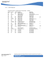
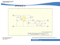
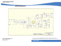
Gx64 APPLICATION NOTE
Power Management
Reference: WI_DEV_Gx64_APN_007
Version: 001
Date: 2007/01/31
Trademarks
®, WAVECOM®, WISMO®, Open AT®, Wireless CPU®, Wireless Microprocessor® and certain
other trademarks and logos appearing on this document, are filed or registered trademarks
of Wavecom S.A. in France or in other countries. All other company and/or product names
mentioned may be filed or registered trademarks of their respective owners.
Copyright
This manual is copyrighted by WAVECOM with all rights reserved. No part of this manual may
be reproduced in any form without the prior written permission of WAVECOM.
No patent liability is assumed with respect to the use of the information contained herein.
No Warranty
WAVECOM publishes this manual without making any warranty as to the content contained
herein. Further Wavecom Inc reserves the right to make modifications, additions and
deletions to this manual due to typographical errors, inaccurate information, or
improvements to programs and/or equipment at any time and without notice. Such changes
will, nevertheless be incorporated into new editions of this manual.
Gx64 APPLICATION NOTE
Power Management
Page: 2/30
This document is the sole and exclusive property of WAVECOM. Not to be distributed or divulged without prior written agreement.
Ce document est la propriété exclusive de WAVECOM. Il ne peut être communiqué ou divulgué à des tiers sans son autorisation préalable
Table of Contents
1
Introduction ............................................................................................ 5
1.1 ABBREVIATIONS ............................................................................................................ 5
1.2 NOTATION.................................................................................................................... 6
1.3 ACKNOWLEDGEMENTS .................................................................................................. 6
2
Block Diagrams ....................................................................................... 7
2.1 SYSTEM POWER MANAGEMENT BLOCK DIAGRAM ........................................................... 7
2.2 POWER MANAGEMENT BLOCK DIAGRAM ........................................................................ 8
2.2.1
GS64.................................................................................................................. 8
2.2.3
GR64002 ......................................................................................................... 10
2.2.2
3
GR64001 ........................................................................................................... 9
Implementation Recommendations ....................................................... 11
3.1 APPLYING POWER ON VCC........................................................................................... 11
3.2 POWER STATE CONTROL OF THE WIRELESS CPU........................................................... 12
3.2.1
ON/OFF ........................................................................................................... 13
3.2.3
EXTERNAL PON_H............................................................................................. 14
3.2.2
INTERNAL CHGDET........................................................................................... 14
3.2.4
ALARM............................................................................................................. 15
3.2.6
AT*E2RESET ..................................................................................................... 16
3.2.5
AT+CFUN ........................................................................................................ 16
3.3 HOW TO LOWER POWER CONSUMPTION ...................................................................... 16
3.4 CHARGING.................................................................................................................. 17
3.5 HOW TO USE VREF ...................................................................................................... 17
3.5.1
3.5.2
VREF AS OUTPUT IN GS64 AND GR64001 ......................................................... 17
VREF AS INPUT IN GR64002.............................................................................. 18
3.6 MONITOR “POWER ON” STATE ..................................................................................... 19
3.6.1
GS64 AND GR64001 HW-DETECTION ............................................................... 19
3.6.2
GR64002 HW-DETECTION ................................................................................ 20
Gx64 APPLICATION NOTE
Power Management
Page: 3/30
This document is the sole and exclusive property of WAVECOM. Not to be distributed or divulged without prior written agreement.
Ce document est la propriété exclusive de WAVECOM. Il ne peut être communiqué ou divulgué à des tiers sans son autorisation préalable
3.7 VRTC AND ALARM ...................................................................................................... 22
3.7.1
4
USING ALARM AS PERIODIC POWER ON ............................................................. 22
Reference Designs ................................................................................ 24
4.1 DISCLAIMER ................................................................................................................ 24
4.2 DC/DC POWER SUPPLY ................................................................................................ 24
4.2.1
BILL OF MATERIAL ............................................................................................ 24
4.3 AC/DC POWER SUPPLY ................................................................................................ 25
4.3.1
SPECIFICATIONS ............................................................................................... 25
4.3.3
BILL OF MATERIAL ............................................................................................ 27
4.3.2
DESIGN SUMMARY............................................................................................ 25
Appendix A ................................................................................................. 28
Appendix B ................................................................................................. 29
Table of Figures
Figure 1: System Block Diagram ........................................................................................... 7
Figure 2: GS64 Power Management Block Diagram ............................................................... 9
Figure 3: GR64001 Power Management Block Diagram ......................................................... 9
Figure 4: GR64002 Power Management Block Diagram ....................................................... 10
Figure 5: GR/GS64 HW On/Off Sequence Logic................................................................... 12
Figure 6: Power Management State Diagram....................................................................... 13
Figure 7: Interface circuit implementation for GS64............................................................ 18
Figure 8: Typical VREF level translation implementation in a GR64002 ............................... 19
Figure 9: GR64002 Power State detection........................................................................... 20
Figure 10: ALARM application example .............................................................................. 22
Gx64 APPLICATION NOTE
Power Management
Page: 4/30
This document is the sole and exclusive property of WAVECOM. Not to be distributed or divulged without prior written agreement.
Ce document est la propriété exclusive de WAVECOM. Il ne peut être communiqué ou divulgué à des tiers sans son autorisation préalable
1
Introduction
This document describes how to apply power, control power states (On/Off), and give
other hints on how to optimise the Wireless CPU implementation.
1.1
Abbreviations
Abbreviation
CSD
CPS
DRX
Description
Circuit Switched Data
Charging Power Supply. Indicates the voltage and current limited
supply connected to CHG_IN when battery charging is used.
Discontinuous Receive. This indicates how often the Wireless CPU
has to wake up and look for a page. The mode can be between 2
and 9 and is determined by the base station.
FAE
Field Application Engineer
PSC
Power Supply and Indicator
PSI
Power State Change signal
RTC
Real-Time-Clock residing in the Wireless CPU.
TP
UVLD
Gx64 APPLICATION NOTE
Power Management
Page: 5/30
Temperature Protection. Built-in temperature protection of the
Power Management ASIC.
Under Voltage Level Detect. Voltage level detection of VCC.
This document is the sole and exclusive property of WAVECOM. Not to be distributed or divulged without prior written agreement.
Ce document est la propriété exclusive de WAVECOM. Il ne peut être communiqué ou divulgué à des tiers sans son autorisation préalable
1.2
Notation
The following symbols and admonition notation are used to draw the reader’s
attention to notable or crucially-important information.
Note
Draws the readers attention to pertinent, useful or interesting
information
NOTE
Tip
Provides advice, suggestions, guidance or recommendations which
augment the formal text
TIP
Caution
Cautionary information must be heeded, it draws the readers attention
to the need for understanding, care or watchfulness in relation to the
CAUTION
!
WARNING
information provided
Warning
Notes marked warning must be heeded, they alert readers to
precautionary measures, risks, hazards or safety information which
directly effects equipment function, warranty or personnel safety
Danger
This information must be heeded, it identifies information and
cautionary behaviour that otherwise ignored could result in
DANGER
1.3
catastrophic equipment failure, bodily injury or death
Acknowledgements
Parts of this document, including text passages, tables, and illustrations, are
reproduced from copyright information by kind permission of Agere Systems Inc.
Gx64 APPLICATION NOTE
Power Management
Page: 6/30
This document is the sole and exclusive property of WAVECOM. Not to be distributed or divulged without prior written agreement.
Ce document est la propriété exclusive de WAVECOM. Il ne peut être communiqué ou divulgué à des tiers sans son autorisation préalable
2
Block Diagrams
2.1
System Power Management Block Diagram
The GR/GS64 Wireless CPUs have a number of signals in the system connector that
affect the power state. The signals in Figure 1 show the signals for all types and
variants of the GR/GS64 family of Wireless CPUs.
Table 1 below lists what features are available for the different types and variants.
Figure 1: System Block Diagram
VREF is implemented differently in the two different GR64 variants. VREF is either an
input or an output and are obviously mutually exclusive. Figure 1 only shows VREF as
an output, which is the way it is implemented in the GR64001 and GS64.
The signal can be divided into two types:
•
Power Supplies and indicators (PSI)
•
Power state change signals (PSC)
The CHG_IN signal is both a PSI and a PSC.
Gx64 APPLICATION NOTE
Power Management
Page: 7/30
This document is the sole and exclusive property of WAVECOM. Not to be distributed or divulged without prior written agreement.
Ce document est la propriété exclusive de WAVECOM. Il ne peut être communiqué ou divulgué à des tiers sans son autorisation préalable
Table 1: Type / Variant Configuration
GR64002
GS64
Type
VCC
PSI
√
1,3,5,7,9
√
1,3,5,7,9
√
2,4,6,8,10,12
CHG_IN
PSI/PSC
√
11
√
11
√
13
VUSB
PSI
√
49
√
34
VREF as input
VREF as output
2.2
GR64001
Feature
PSI
VRTC
PSI
ALARM
PSC
PON_H
PSC
ON/OFF
PSC
Pin(s)
√
√
√
34
25
14
Pin(s)
√
34
Pin(s)
√
65
√
25
√
31
√
50
√
32
√
21
√
33
√
14
Power Management Block Diagram
This section describes the individual implementations in the three different designs;
GS64, GR64001, and GR64002.
Detailed information on the PSC-implementation can be found in 3.2 below
2.2.1
GS64
The GS64 implementation uses all PSC-options listed in Table 1. If a signal is not
used it should be left floating.
The “PM ON/OFF Sequence Logic” block diagram can be found in Figure 5.
Gx64 APPLICATION NOTE
Power Management
Page: 8/30
This document is the sole and exclusive property of WAVECOM. Not to be distributed or divulged without prior written agreement.
Ce document est la propriété exclusive de WAVECOM. Il ne peut être communiqué ou divulgué à des tiers sans son autorisation préalable
Figure 2: GS64 Power Management Block Diagram
2.2.2
GR64001
This variant of GR64 only implements two PSC-options, ON/OFF and CHG_IN.
Figure 3: GR64001 Power Management Block Diagram
The “PM ON/OFF Sequence Logic” block diagram can be found in Figure 5.
Gx64 APPLICATION NOTE
Power Management
Page: 9/30
This document is the sole and exclusive property of WAVECOM. Not to be distributed or divulged without prior written agreement.
Ce document est la propriété exclusive de WAVECOM. Il ne peut être communiqué ou divulgué à des tiers sans son autorisation préalable
2.2.3
GR64002
This variant of GR64 implements all four PSC-options, ON/OFF, PON_H, ALARM and
CHG_IN.
Figure 4: GR64002 Power Management Block Diagram
The “PM ON/OFF Sequence Logic” block diagram can be found in Figure 5.
Gx64 APPLICATION NOTE
Power Management
Page: 10/30
This document is the sole and exclusive property of WAVECOM. Not to be distributed or divulged without prior written agreement.
Ce document est la propriété exclusive de WAVECOM. Il ne peut être communiqué ou divulgué à des tiers sans son autorisation préalable
3
Implementation Recommendations
This section describes how to implement features related to the Power Management
of the Wireless CPUs.
3.1
Applying power on VCC
Main power is applied to VCC using GND as reference. The source can be any of the
following listed types:
•
Li-Ion battery (3.7V nominal)
•
AC/DC power supply (3.6V nominal)
•
DC/DC power supply (3.6V nominal)
Reference designs for AC/DC and DC/DC supplies can be found in Appendix A and B
at the end of this document.
Parameter
VCC
Condition
Supply voltage level
Limits
Avg.
Max.
3.2
3.6
4.5
V
2100 1
mA
2100 2
mA
350
mA
560
mA
35
mA
3.5
mA
Voice/CSD call (1up, 1down)
IPEAK
at max power (32dBm), 4.7ms duration
GSM850, GPRS, Class 10 (2up, 3down)
at max power (32dBm), 9.4ms duration
Voice/CSD call (1 up, 1 down)
at max power (32dBm), 4.7ms duration
IRMS
Unit
Min.
GSM850, GPRS, Class 10 (2 up, 3 down)
at max power (32dBm), 9.4ms duration
Standby (locked on channel)
15
Sleep mode
1.4
25
1,2
This is the average maximum current during the transmit pulse. The absolute maximum current can
be up to 2500mA, but is only available for a couple of microseconds.
Gx64 APPLICATION NOTE
Power Management
Page: 11/30
This document is the sole and exclusive property of WAVECOM. Not to be distributed or divulged without prior written agreement.
Ce document est la propriété exclusive de WAVECOM. Il ne peut être communiqué ou divulgué à des tiers sans son autorisation préalable
3.2
Power state control of the Wireless CPU
There are a maximum of six signals that affects the HW power state of the GR/GS64
family of Wireless CPUs; four HW and two SW:
•
ON/OFF (HW, all Wireless CPUs)
•
CHG_IN (HW, all Wireless CPUs)
•
PON_H (HW, GS64 only)
•
ALARM (HW, GS64 and GR64002 as external, all as internal)
•
AT+CFUN (SW, all Wireless CPUs)
•
AT*E2RESET (SW, all Wireless CPUs)
Under normal operating conditions, the die temperature should not
exceed 125°C. In the event of an external fault or as a result of device
misuse, the die temperature could exceed this value by a large margin.
CAUTION
Should the die temperature exceed 155°C while the unit is powered up,
the thermal protection circuit will shut-down all functions and remain
disabled until the temperature drops below 130°C, at which point the
device can be restarted. This feature is listed as TP (Thermal
Protection) througout this document.
To power up the hardware VCC must be within 3.2V to 4.5V, and the Power
Management ASIC die temperature must be below 130°C.
Figure 5: GR/GS64 HW On/Off Sequence Logic
Gx64 APPLICATION NOTE
Power Management
Page: 12/30
This document is the sole and exclusive property of WAVECOM. Not to be distributed or divulged without prior written agreement.
Ce document est la propriété exclusive de WAVECOM. Il ne peut être communiqué ou divulgué à des tiers sans son autorisation préalable
The two SW power state control signals are not included in Figure 5. This figure only
shows the HW-signals.
Figure 6: Power Management State Diagram
Figure 6 shows the impact five of the six control signals, listed above, have on the
Power Management status of the Wireless CPU.
The AT*E2RESET is described
individually in 3.2.6 below.
If a PSC-signal is held active (PON_H high, ON/OFF low, etc.) while the Wireless CPU is
active, it is not possible for another PSC-signal to generate a power down request.
Any such request will be denied. If a valid power down request is generated while a
CPS is available, the Wireless CPU will be set to “Charge Only”-mode.
3.2.1
ON/OFF
This system connector signal provides a power up feature similar to a normal cell
phone on/off button, i.e. a low pulse will toggle between On-state and Off-state.
This signal is weekly pulled up to VCC in the Power Management ASIC by a constant
current source.
Table 2: ON/OFF signal characteristics
Parameter
IIL
IIH
Description
Input current
VIL
Low level detection limit
VIH
High level detection limit
tLow
Required time for detection
Gx64 APPLICATION NOTE
Power Management
Page: 13/30
Input Characteristics
Unit
Min.
Avg.
Max.
-60
-25
-12
μA
1
μA
0.2*VCC
V
0
0.8*VCC
V
450
ms
This document is the sole and exclusive property of WAVECOM. Not to be distributed or divulged without prior written agreement.
Ce document est la propriété exclusive de WAVECOM. Il ne peut être communiqué ou divulgué à des tiers sans son autorisation préalable
The signal should be held low for at least tLow time for the Wireless CPU to be able to
detect and respond with a power hold signal (PWR_KEEP). The signal can be held low
for an unspecified amount of time but it is not recommended since it prevents the
Wireless CPU from respond to any other power state signal request.
3.2.2
Internal CHGDET
A charge request is initiated on INT_CHGDET when the voltage on CHG_IN is <6.3V,
>3.7V, and is 150mV higher than the voltage level of VCC. This signal is active as
long as a valid CPS is available on CHG_IN.
If the Wireless CPU is in “Power Down”-state when a CPS becomes available, it will
automatically place itself in “Charge Only”-mode. If the Wireless CPU is in “Active”mode it will remain there. For more information on charging see the “GR/GS64 Series
Application Note - Charging Interface”-document.
3.2.3
External PON_H
This system connector signal is an active high power on signal similar to ON/OFF, but
with the exception that it should be kept active high to keep the Wireless CPU in
“Active”-mode. This signal is weakly pulled down to GND in the Power Management
ASIC by a constant current source.
To power on the Wireless CPU this signal should be tied to VCC. It should remain at
VCC until the Wireless CPU should be powered down. To power down the Wireless
CPU PON_H should be set low or high impedance. This will start the power down
process and place the Wireless CPU in either “Power Down” or “Charge Only”-mode
depending on the internal INT_CHGDET-status.
Table 3: PON_H signal characteristics
Parameter
IIL
IIH
Description
Input current
VIL
Low level detection limit
VIH
High level detection limit
Gx64 APPLICATION NOTE
Power Management
Page: 14/30
Input Characteristics
Unit
Min.
Avg.
Max.
8
20
60
μA
0
μA
0.2*VCC
V
-1
0.8*VCC
V
This document is the sole and exclusive property of WAVECOM. Not to be distributed or divulged without prior written agreement.
Ce document est la propriété exclusive de WAVECOM. Il ne peut être communiqué ou divulgué à des tiers sans son autorisation préalable
3.2.4
ALARM
The ALARM-signal can be both an internal and external signal for all Wireless CPUs
except GR64001 where it is only an internal signal. Internal means that the RTC is
capable of waking up the main processor as long as VCC is available. External means
that the signal is provided in the system connector. The external availability enables
the application to use an alarm to fully power on not only the Wireless CPU but also
itself, see 3.7.1 below.
The ALARM feature uses the “Time Commands” found in the AT-manual.
commands consist of:
•
AT+CCLK (Set Clock and Date)
•
AT+CTZU (Automatic Time Zone Update)
•
AT*EDST (Daylight Saving Time)
•
AT+CALA (Set Alarm)
•
AT+CALD (Alarm Delete)
These
The clock must be set to the correct time for the alarm to work properly in absolute
mode.
The easiest way to setup the clock correctly is to enable the Automatic
Time Zone Update by sending AT+CTZU=1 followed by AT&W. The
clock will get the time reported by the network. This eliminates the
TIP
need to manually setup the clock using the AT+CCLK-command.
AT*EDST does not have to be used if AT+CTZU=1 is sent since the
correct time will periodically be sent to the Wireless CPU from the base
station.
The automatic time zone feature is network dependent. It is not
necessarily available in all markets, or might not be enabled in certain
base stations. The safest way to get proper time setup correctly is to
CAUTION
have the application update the time using the AT+CCLK-command at
a regular interval.
Gx64 APPLICATION NOTE
Power Management
Page: 15/30
This document is the sole and exclusive property of WAVECOM. Not to be distributed or divulged without prior written agreement.
Ce document est la propriété exclusive de WAVECOM. Il ne peut être communiqué ou divulgué à des tiers sans son autorisation préalable
3.2.5
AT+CFUN
This AT-command is used to change the power state of the Wireless CPU.
See the AT-command manual for more details.
3.2.6
AT*E2RESET
This AT-command will de-register from network and do the normal shut-down
sequence, but instead of powering down jump to the reset vector.
See the AT-command manual for more details.
3.3
How to lower power consumption
The Wireless CPUs are capable of being set to low current consumption mode where
the average current consumption can be as low as 1.4mA. This mode is referred to as
“sleep mode”. The actual current consumed depends on the base station DRX-mode
setting, which cannot be controlled by the Wireless CPU.
The features that determine the “sleep mode”-setting are the communication
channels UART and USB. The reason for this is that they cannot operate unless the
main 13MHz clock is available. To get the power consumption down the Wireless CPU
must disable the 13MHz clock and instead run of the 32kHz RTC. This means that a
handshake method has to be used for the UART (see GR/GS64 Series Application Note
- UART Sleep Protocol), and USB has to support “suspend-resume”.
The USB feature is not supported in all SW-versions. Contact your local FAE if USBsupport is needed. USB will have its own Application Note. Ensure that the USBinterface is disabled if is not used (AT*USB=0).
Power State
Condition
Current
Unit
Power down
VRTC open (no backup battery)
<10
μA
Power down
VRTC active (backup battery available)
<1.6
mA
Sleep mode
DRX 2
<3.5
mA
UART active, USB inactive (AT*USB=0)
~25
mA
UART active, USB active (AT*USB=1)
~35
mA
Standby
Gx64 APPLICATION NOTE
Power Management
Page: 16/30
This document is the sole and exclusive property of WAVECOM. Not to be distributed or divulged without prior written agreement.
Ce document est la propriété exclusive de WAVECOM. Il ne peut être communiqué ou divulgué à des tiers sans son autorisation préalable
The numbers given above are approximations. The real current levels might differ,
but should most often be less than what is listed.
3.4
Charging
A CPS should be connected to CHG_IN only if a single Li-Ion battery is used as main
power supply. In any other configuration CHG_IN must be left open (not connected).
For more information about charging see the “GR/GS64 Series Application Note -
Charging Interface”-document.
3.5
How to use VREF
VREF operates in two different ways depending on what Wireless CPU is used. In GS64
and GR64001VREF is an output signal and in GR64002 it is an input signal.
3.5.1
VREF as output in GS64 and GR64001
VREF is providing the application with its logic level supply. The application can use
this signal in two ways:
1.
Reference voltage for application interface logic (required)
2.
Wireless CPU Power On Indication (optional)
As indicated, the application logic interface must be referenced to VREF.
The
application cannot supply an active high level in to the Wireless CPU on any signal
unless VREF is active high. The logic interface must also be the same level as VREF.
For GS64 this level is 1.8V, and for GR64001 it is 2.8V.
Gx64 APPLICATION NOTE
Power Management
Page: 17/30
This document is the sole and exclusive property of WAVECOM. Not to be distributed or divulged without prior written agreement.
Ce document est la propriété exclusive de WAVECOM. Il ne peut être communiqué ou divulgué à des tiers sans son autorisation préalable
Figure 7: Interface circuit implementation for GS64
The level translator type used in Figure 7 can be either ST2378E from ST
Microelectronics, MAX3001E from Maxim, or any other applicable type.
Figure 7
shows a GS64 implementation, but the same figure can be used for a GR64001
solution if the 1.8V regulator is replaced with a 2.8V regulator.
VREF can furthermore be used by the application as an indicator whether the Wireless
CPU is powered on or not. An active high >1.65V indicates power on, while a low
<0.4V indicates power off.
If PON_H or ON/OFF are held active (high and low respectively) while VCC is slowly
increased from <2.7V to 3.3V, VREF will go active when VCC is at 3.050V, while the
SW starts executing when VCC is at 3.135V. This hysteresis is built-in to ensure that
the VREF is within specified levels when SW starts executing.
3.5.2
VREF as input in GR64002
In this variant of GR64 using VREF as an input offers the integrator a flexible interface
solution. The application should apply its logic interface voltage directly onto VREF as
long as it is between 1.8V and 5.0V. The application does not have to implement its
own level translation. It is all done inside the Wireless CPU.
Gx64 APPLICATION NOTE
Power Management
Page: 18/30
This document is the sole and exclusive property of WAVECOM. Not to be distributed or divulged without prior written agreement.
Ce document est la propriété exclusive de WAVECOM. Il ne peut être communiqué ou divulgué à des tiers sans son autorisation préalable
Figure 8: Typical VREF level translation implementation in a GR64002
One drawback of this solution is that VREF cannot be used by the application to
determine whether the Wireless CPU is powered on or not. See 3.6.2 below for more
information.
3.6
Monitor “Power On” State
The power state of the Wireless CPU can be verified in two ways; either HW or SW.
The HW-determination depends on what product and variant is used, but the SWdetermination is the same for all products (AT+CFUN).
specification for more information on the AT+CFUN-command.
3.6.1
See AT-command
GS64 and GR64001 HW-detection
These products can determine the HW status of the Wireless CPU by monitoring the
VREF signal. A high level VREFHIGH-0.3V indicates unit powered on. A low level <0.4V
indicates unit powered off.
VREFHIGH
Gx64 APPLICATION NOTE
Power Management
Page: 19/30
GR64001
GS64
Unit
2.8
1.8
V
This document is the sole and exclusive property of WAVECOM. Not to be distributed or divulged without prior written agreement.
Ce document est la propriété exclusive de WAVECOM. Il ne peut être communiqué ou divulgué à des tiers sans son autorisation préalable
3.6.2
GR64002 HW-detection
In GR64002, where VREF is an input to the Wireless CPU the HW-detection of the
power state must use SIMDET instead of VREF.
The SIMDET-signal is pulled up inside the Wireless CPU to its internal supply voltage
(1.8V). It does not go through the built-in level translators as the other logic signals.
This can be used to determine the state of the Wireless CPU. It also means that the
SIMDET-signal cannot be used to determine whether a physical SIM is inserted
properly into the external SIM-holder.
Figure 9: GR64002 Power State detection
As can be seen in Figure 9, the SIMDET-signal can be used to determine the power
state of the GR64002. Instead of routing the signal to the physical detection pin of
the SIM-holder, it is routed to a detection circuitry that translates the level from 1.8V
to whatever logic level the Application is using. The “Reference Voltage, R1 and R2
must be selected so that the transition levels correspond to the levels indicated in
Table 4 below.
The pull up resistor that is built in to the Wireless CPU RPU is typically 200k. The
application must ensure that it does not a load that affects the signal.
It is
recommended to keep the load (RL) ≥2 Mohm.
Gx64 APPLICATION NOTE
Power Management
Page: 20/30
This document is the sole and exclusive property of WAVECOM. Not to be distributed or divulged without prior written agreement.
Ce document est la propriété exclusive de WAVECOM. Il ne peut être communiqué ou divulgué à des tiers sans son autorisation préalable
Table 4: Power state transition levels
Wireless CPU Power status
SIMDET level
Power ON
>1.5V
Power OFF
<0.4V
It is possible to connect the SIMDET-signal directly to the Application
processor, but the integrator must ensure that no voltage is applied
onto SIMDET (through pull-up resistors etc.). The Wireless CPU might
CAUTION
malfunction If the application applies a voltage level onto SIMDET after
the Wireless CPU has been powered down.
If the application supports SIM removal HW-detection, the SIMDET must
be used to detect the SIM availability status to pass the type approval.
HW-detection of the power state will in this case not be possible. The
CAUTION
affected test cases are:
•
•
•
•
26.2.2 -p2 - GSM Protocol
26.7.4.2.4 p5 - GSM Protocol
31.6.2.1 - Supplementary Services
44.2.3.1.4 - GRPS Protocol
These test cases may not pass the certification tests without the SIM
detect line enabled, and PICS/PIXIT 3GPP TS 51010-1 A.25/40 set to
Supported. Currently, the GR64 and GS64 products do not support SIM
removal without power down, so A.25/40 is set to Not Supported which
allows these test cases to pass.
Gx64 APPLICATION NOTE
Power Management
Page: 21/30
This document is the sole and exclusive property of WAVECOM. Not to be distributed or divulged without prior written agreement.
Ce document est la propriété exclusive de WAVECOM. Il ne peut être communiqué ou divulgué à des tiers sans son autorisation préalable
3.7
VRTC and ALARM
These are the two system connector signals that relate to the RTC. VRTC is powered
from VCC.
If the application wants the RTC to operate even if VCC is removed it
has to add a 1.5V “button cell” or capacitor on VRTC as a backup power
source. A recommended battery to use is 0.2mAh Pb-free TS414H
TIP
3.7.1
from Seiko.
Using ALARM as periodic power on
It is possible to use the ALARM feature to fully power up the application.
The
example in Figure 10 shows an implementation usable with a GS64 and GR64002
Wireless CPUs. This implementation is useful in applications where there is limited
power supply and the Wireless CPU only periodically needs to send updated
information to a server etc.
Figure 10: ALARM application example
Gx64 APPLICATION NOTE
Power Management
Page: 22/30
This document is the sole and exclusive property of WAVECOM. Not to be distributed or divulged without prior written agreement.
Ce document est la propriété exclusive de WAVECOM. Il ne peut être communiqué ou divulgué à des tiers sans son autorisation préalable
The power supply should be an efficient converter that takes the VIN supply from
whatever voltage level the source is providing and converts it to the recommended
VCC voltage level. To minimise power consumption this regulator is only enabled
when the Wireless CPU is supposed to be active.
After the application is installed the “StartUp” button is pressed to initialise the
product.
This will only have to be done once.
perform its own power control.
After that, the Wireless CPU will
The shorting of ON/OFF to GND at the initial “StartUp” will enable the regulator
causing VCC to go high. When the Wireless CPU powers on, VREF goes high which
creates a regulator hold signal. The application is now running normally. The backup
“Button Cell” for VRTC is charged by the Wireless CPU with a minimum of 200uA as
long as VCC is active.
When the application is ready to power down it sets up the ALARM wakeup time using
“AT+CALA”-command, then shuts the Wireless CPU down using the “AT+CFUN=0”command. When the Wireless CPU has de-registered from the network and powered
down properly, VREF will go inactive low removing the hold signal from the VCC
regulator causing the regulator to turn off and VCC to go low. The application is now
in extreme low power mode with only VRTC being held active by the “Button Cell”,
which in turn keeps the RTC active.
When the RTC alarm time has expired, the RTC sets the ALARM-signal low. This will
enable the VCC regulator and automatically power on the Wireless CPU.
The
application can now perform its scheduled activities before setting the alarm-time,
de-register, and power down.
It should be noted that the ALARM-output is referenced to VRTC. VRTC
is specified to operate down to 1.1V, but it has been tested to work
reliably down to as low as 0.8V. If the application wants the RTC to
TIP
work all the way down to that voltage it has to make sure that the
transistors used on the ALARM-output can operate reliably at such low
voltage.
Gx64 APPLICATION NOTE
Power Management
Page: 23/30
This document is the sole and exclusive property of WAVECOM. Not to be distributed or divulged without prior written agreement.
Ce document est la propriété exclusive de WAVECOM. Il ne peut être communiqué ou divulgué à des tiers sans son autorisation préalable
4
Reference Designs
4.1
Disclaimer
Wavecom Inc is not responsible for the charger power supplies reference design. The
integrator should refer technical questions regarding the charger power supplies
listed below directly to National Semiconductors.
4.2
DC/DC Power Supply
The implementation shown in Appendix A is the reference design of a 3.6V DC/DC
buck regulator from National Semiconductors.
6VDC to 20VDC.
Semiconductors.
4.2.1
The input voltage can be between
For more information on the design please contact National
Bill Of Material
Gx64 APPLICATION NOTE
Power Management
Page: 24/30
This document is the sole and exclusive property of WAVECOM. Not to be distributed or divulged without prior written agreement.
Ce document est la propriété exclusive de WAVECOM. Il ne peut être communiqué ou divulgué à des tiers sans son autorisation préalable
4.3
AC/DC Power Supply
The implementation shown in Appendix B is the reference design of a 3.6V AC/DC
flyback regulator from National Semiconductors. The input voltage can be between
85VAC to 265VAC.
Semiconductors.
4.3.1
For more information on the design please contact National
Specifications
Parameter
Condition
Limit
Unit
VINmin
85
VAC
VINmax
265
VAC
3.65
VDC
140
KHz
VOUT
500mA (2.5A peak)
Switching Frequency
4.3.2
Design Summary
This design utilizes the LM5021 AC-DC Current Mode PWM Controller to implement a
single output offline flyback switching power converter. The dc input voltage to the
converter is generated by rectifying and smoothing a 50 or 60Hz, 85 to 265V ac
mains voltage to produce a steady dc voltage of 120 to 375V.
The flyback converter is a topology in which a MOSFET and a rectifier are switched
on and off at a high frequency to successively and periodically connect a transformer
and capacitors in two (or three) topological states such that the input voltage is
changed efficiently to an output voltage of different average value and/or polarity.
During the first part of the switching cycle energy is stored in the transformer’s
magnetizing inductance by applying the input voltage across the transformer’s
primary winding through a MOSFET Q101. In the second part of the cycle the input
voltage is disconnected from the transformer and some or all of the stored energy is
transferred from its secondary winding to a load through the output rectifier D106
and the output capacitors. This cycle keeps repeating at a frequency of 140 KHz.
Gx64 APPLICATION NOTE
Power Management
Page: 25/30
This document is the sole and exclusive property of WAVECOM. Not to be distributed or divulged without prior written agreement.
Ce document est la propriété exclusive de WAVECOM. Il ne peut être communiqué ou divulgué à des tiers sans son autorisation préalable
The circuit attains a periodic steady-state in which the volt-seconds across the
transformer due to the input voltage are exactly balanced by the volt-seconds due to
the output voltage. For continuous conduction operation (in which the rectifier current
never falls to zero), the output voltage is given by:
Equation 1: Output voltage level
Vo =
D
V
(1 − D )N in
In Equation 1 above, D is the duty ratio, defined as the fraction of the total switching
interval that MOSFET
is on, charging the transformer, N is the primary-to-secondary
transformer turns ratio, and is the input voltage.
The gate of the MOSFET is pulsed by the LM5021 PWM controller which requires a
supply voltage at its VCC pin of between 8 and 15V to power it. To start up the IC
energy is trickled charged into C105 via R101 and R104 from the input voltage. This
energy is applied to an internal linear regulator whose input is the VIN-pin and whose
output, regulated at about 8V, is the VCC pin.
Once the circuit is running the
capacitor C105 is kept charged by a bias winding on the transformer through diode
D102 and resistor R100. The bias voltage is related to the output voltage by the turn
ratio between it and the secondary winding, and is therefore insensitive to changes in
the input voltage.
The output voltage is regulated against changes in the input voltage and the load
current by the voltage reference and error amplifier REF100 and the opto-coupler
U101 which send a correction signal across the primary-secondary isolation barrier to
the LM5021. This signal allows the LM5021 to keep the output voltage constant by
adjusting the duty ratio of the pulses it sends to the gate of the MOSFET.
Other essential functions implemented by the LM5021 are soft-start (via C106),
switching frequency setting (via R108) and MOSFET/ transformer current sensing (via
C107, R109 and R110).
Some of the component values in the circuit are just place-holders. The components
to the left of the bridge rectifier comprise an EMI and transient voltage filter. The
thermistor R116 is an inrush current limiter. The diodes across the primary of the
transformer, and the series capacitor-resistor pairs across the drain of the FET and
across the output rectifier all serve to reduce ringing and spiking in the circuit, and to
reduce EMI. The values of all these components should be determined depending on
the application implementation.
Gx64 APPLICATION NOTE
Power Management
Page: 26/30
This document is the sole and exclusive property of WAVECOM. Not to be distributed or divulged without prior written agreement.
Ce document est la propriété exclusive de WAVECOM. Il ne peut être communiqué ou divulgué à des tiers sans son autorisation préalable
4.3.3
Bill Of Material
Gx64 APPLICATION NOTE
Power Management
Page: 27/30
This document is the sole and exclusive property of WAVECOM. Not to be distributed or divulged without prior written agreement.
Ce document est la propriété exclusive de WAVECOM. Il ne peut être communiqué ou divulgué à des tiers sans son autorisation préalable
APPENDIX A
Gx64 APPLICATION NOTE
Power Management
Page: 28/30
This document is the sole and exclusive property of WAVECOM. Not to be distributed or divulged without prior written agreement.
Ce document est la propriété exclusive de WAVECOM. Il ne peut être communiqué ou divulgué à des tiers sans son autorisation préalable
APPENDIX B
Gx64 APPLICATION NOTE
Power Management
Page: 29/30
This document is the sole and exclusive property of WAVECOM. Not to be distributed or divulged without prior written agreement.
Ce document est la propriété exclusive de WAVECOM. Il ne peut être communiqué ou divulgué à des tiers sans son autorisation préalable
WAVECOM S.A. - 3 esplanade du Foncet - 92442 Issy-les-Moulineaux Cedex - France - Tel: +33(0)1 46 29 08 00 - Fax: +33(0)1 46 29 08 08
Wavecom, Inc. - 4810 Eastgate Mall - Second Floor - San Diego, CA 92121 - USA - Tel: +1 858 362 0101 - Fax: +1 858 558 5485
Wavecom, Inc. - 430 Davis Dr. Suite 300 - Research Triangle Park, NC 27709 - USA - Tel: +1 919 237 4000 - Fax: +1 919 237 4140
nd
WAVECOM Asia Pacific Ltd. - Unit 201-207, 2 Floor - Bio-Informatics Centre - No. 2 Science Park West Avenue - Hong Kong Science Park,
Shatin - New Territories, Hong Kong - Tel: +852 2824 0254 - Fax: +852 2824 0255