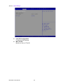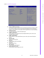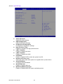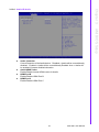
1
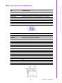
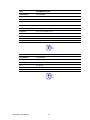
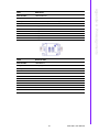
User Manual MIO-5251 Intel® Celeron® J1900 & Atom™ E3825, 3.5" MI/O-Compact SBC, DDR3L, VGA, HDMI/DP, 48-bit LVDS/eDP, 2GbE, Mini PCIe, mSATA/SD card, iManager, MIOe Copyright The documentation and the software included with this product are copyrighted 2014 by Advantech Co., Ltd. All rights are reserved. Advantech Co., Ltd. reserves the right to make improvements in the products described in this manual at any time without notice. No part of this manual may be reproduced, copied, translated or transmitted in any form or by any means without the prior written permission of Advantech Co., Ltd. Information provided in this manual is intended to be accurate and reliable. However, Advantech Co., Ltd. assumes no responsibility for its use, nor for any infringements of the rights of third parties, which may result from its use. Acknowledgements Intel® is a trademark of Intel® Corporation. AMI is a trademark of American Megatrends, Inc. IBM, PC, PS/2 and VGA are trademarks of International Business Machines Corporation. Microsoft Windows®, DirectX® is a registered trademark of Microsoft Corp. All other product names or trademarks are properties of their respective owners. For more information on this and other Advantech products, please visit our websites at: http://www.advantech.com http://www.advantech.com/eplatform For technical support and service, please visit our support website at: http://support.advantech.com/ This manual is for the MIO-5251. MIO-5251 User Manual Part No. 2006525110 Edition 1 Printed in China September 2014 ii Product Warranty (2 years) Advantech warrants to you, the original purchaser, that each of its products will be free from defects in materials and workmanship for two years from the date of purchase. This warranty does not apply to any products which have been repaired or altered by persons other than repair personnel authorized by Advantech, or which have been subject to misuse, abuse, accident or improper installation. Advantech assumes no liability under the terms of this warranty as a consequence of such events. Because of Advantech’s high quality-control standards and rigorous testing, most of our customers never need to use our repair service. If an Advantech product is defective, it will be repaired or replaced at no charge during the warranty period. For outof-warranty repairs, you will be billed according to the cost of replacement materials, service time and freight. Please consult your dealer for more details. If you think you have a defective product, follow these steps: 1. Collect all the information about the problem encountered. (For example, CPU speed, Advantech products used, other hardware and software used, etc.) Note anything abnormal and list any onscreen messages you get when the problem occurs. 2. Call your dealer and describe the problem. Please have your manual, product, and any helpful information readily available. 3. If your product is diagnosed as defective, obtain an RMA (return merchandize authorization) number from your dealer. This allows us to process your return more quickly. 4. Carefully pack the defective product, a fully-completed Repair and Replacement Order Card and a photocopy proof of purchase date (such as your sales receipt) in a shippable container. A product returned without proof of the purchase date is not eligible for warranty service. 5. Write the RMA number visibly on the outside of the package and ship it prepaid to your dealer. iii MIO-5251 User Manual Declaration of Conformity CE This product has passed the CE test for environmental specifications. Test conditions for passing included the equipment being operated within an industrial enclosure. In order to protect the product from being damaged by ESD (Electrostatic Discharge) and EMI leakage, we strongly recommend the use of CE-compliant industrial enclosure products. FCC Class A This equipment has been tested and found to comply with the limits for a Class A digital device, pursuant to part 15 of the FCC Rules. These limits are designed to provide reasonable protection against harmful interference when the equipment is operated in a commercial environment. This equipment generates, uses, and can radiate radio frequency energy and, if not installed and used in accordance with the instruction manual, may cause harmful interference to radio communications. Opera- thin of this equipment in a residential area is likely to cause harmful interference in which case the user will be required to correct the interference at his own expense. Caution! There is a danger of a new battery exploding if it is incorrectly installed. Do not attempt to recharge, force open, or heat the battery. Replace the battery only with the same or equivalent type recommended by the manflatterer. Discard used batteries according to the manufacturer's instructions. Technical Support and Assistance 1. 2. Visit the Advantech website at http://support.advantech.com where you can find the latest information about the product. Contact your distributor, sales representative, or Advantech's customer service center for technical support if you need additional assistance. Please have the following information ready before you call: – Product name and serial number – Description of your peripheral attachments – Description of your software (operating system, version, application software, etc.) – A complete description of the problem – The exact wording of any error messages MIO-5251 User Manual iv Packing List Before you begin installing your card, please make sure that the following materials have been shipped: 1 x MIO-5251 SBC 1 x SATA Cable 30cm (p/n: 1700006291) 1 x SATA Power Cable 35cm (p/n: 1700018785) 1 x Audio Cable 20cm (p/n: 1700019584) 2 x COM Cable 22cm (p/n: 1701200220) 1 x Heatsink (19mm) (p/n: 1960062791T001) 1 x Startup manual (p/n: 2006525100) 1 x Mini Jumper(10pcs package) (p/n: 9689000002) 1 x Screw Kit (4pcs screws for miniPCIe) (p/n: 9666525100E) 1 x SUSIAccess Pro package (p/n: 968EMLSAP1) If any of these items are missing or damaged, contact your distributor or sales representative immediately. Optional MIOe Module Part Number MIOe-210-D6A1E MIOe-220-B3A1E MIOe-230-L0A1E MIOe-DB5000-01A1E MIOe-3674-AE MIOe-3680-AE MIOe-PWR1-00E MIOe-PWR2 Description 4 x RS232/422/485, 2x RS422/485, 8-bit GPIO 3 x Intel® Gigabit Ethernet with PCIe Switch DisplayPort or 48-bit LVDS, 2 x USB2.0 MI/O extension evaluation board 4-port PoE ports 2-Port CAN-Bus with Isolation Protection 12-24V wide range power module (by cable, not via MIOe) 9-36V wide range power module (by cable, not via MIOe) Optional Accessories Part number 1960065073N001 1757003995 1703100264 Description Heat spreader 16.7mm height AC-to-DC Adapter 12V/5A, 0-40°C Internal 1-Port USB cable 22.5cm v MIO-5251 User Manual MIO-5251 User Manual vi Contents Chapter 1 General Information ............................1 1.1 1.2 Introduction ............................................................................................... 2 Specifications ............................................................................................ 2 1.2.1 Functional Specifications .............................................................. 2 1.2.2 OS support.................................................................................... 4 1.2.3 Mechanical Specifications............................................................. 4 1.2.4 Electrical Specifications ................................................................ 4 1.2.5 Environmental ............................................................................... 4 Block Diagram........................................................................................... 5 Board layout: dimensions.......................................................................... 5 Figure 1.1 MIO-5251 Mechanical Drawing (Top Side) ................ 5 Figure 1.2 MIO-5251 Mechanical Drawing (Bottom Side) ........... 6 Figure 1.3 MIO-5251 Mechanical Drawing (Coastline)................ 6 1.3 1.4 Chapter 2 Installation............................................7 2.1 Jumpers & Switches.................................................................................. 8 Table 2.1: Jumpers & Switches ................................................... 8 Connectors................................................................................................ 8 Table 2.2: Connectors ................................................................. 8 Locating Connectors ................................................................................. 9 Figure 2.1 MIO-5251 Connector Locations (Top Side)................ 9 Figure 2.2 MIO-5251 Connector Locations (Bottom Side)........... 9 Setting Jumpers ...................................................................................... 10 2.4.1 Auto Power On Setting (J2) ........................................................ 10 Table 2.3: Auto Power On Setting (J2)...................................... 10 2.4.2 LCD Power (J5) .......................................................................... 10 Table 2.4: LCD Power (J5) ........................................................ 10 2.4.3 Clear CMOS (SW2) .................................................................... 11 Table 2.5: Clear CMOS (SW2) .................................................. 11 2.2 2.3 2.4 Chapter 3 AMI BIOS Setup .................................13 3.1 Entering Setup ........................................................................................ 15 3.1.1 Main Setup.................................................................................. 15 3.1.2 Advanced BIOS Features Setup................................................. 16 3.1.3 Chipset Configuration ................................................................. 29 3.1.4 Security ....................................................................................... 36 3.1.5 Boot............................................................................................. 37 3.1.6 Save & Exit ................................................................................. 38 4 MIOe Installation ................................39 4.1 Quick Installation Guide: ......................................................................... 40 Appendix A Pin Assignments ...............................41 A.1 A.2 Jumper List.............................................................................................. 42 Connector Pin Definition ......................................................................... 43 Chapter vii MIO-5251 User Manual Appendix B System Assignments........................ 63 B.1 System I/O Ports..................................................................................... 64 Table B.1: System I/O Ports ...................................................... 64 1st MB Memory Map............................................................................... 64 Table B.2: 1st MB Memory Map ................................................ 64 Interrupt Assignments ............................................................................. 65 Table B.3: Interrupt assignments............................................... 65 B.2 B.3 Appendix C EC Watchdog Timer Sample Code .. 67 C.1 EC Watchdog Timer sample code .......................................................... 68 MIO-5251 User Manual viii Chapter 1 1 General Information This chapter gives background information on the MIO-5251. Sections include: Introduction Specifications Block diagram Board layout and dimensions 1.1 Introduction MIO-5251 is designed using MI/O Extension form factor (compact series, 146 x 102 mm) and powered by the latest generation of Intel® Celeron® J1900 and Atom™ E3825 processors which have low power features but also good performance computing, especially for multimedia capabilities compared to earlier generations. Meanwhile, MIO-5251 offers flexible expansion possibilities: two full-size mini PCIe, 2nd LVDS through MIOe-230, SD card, SIM holder, MIOe with PCIex1, SMBus, 3xUSB2.0, LPC, line out, DisplayPort, and power interface. MIO-5251 supports various display interfaces including HDMI/DisplayPort, VGA, 48bit LVDS/eDP, and rich I/O: 2 x GbE, SATA, mSATA/SD card, 4xSerial Ports, USB 3.0 and 4 x USB 2.0. 1.2 Specifications 1.2.1 Functional Specifications Processor: – Celeron® J1900 2.0GHz (burst frequency 2.42GHz), Quad Cores, Four Threads – Atom™ E3825 1.33GHz, Dual Cores, Two Threads – Cache Hierarchy * 32 KB 8-way L1 instruction cache and 24 KB 6-way L1 data cache per core * 1 MB, 16-way L2 cache, shared per two cores – Supported C-states: C0, C1, C6, C7 – Advanced Technologies * Intel® Virtualization Technology (VT-x) * Intel® 64 Architecture * Enhanced Intel SpeedStep Technology * Intel® Trusted Execution Engine (TXE) – Power Management * ACPI 5.0 * System sleep states: S0, S3, S4, S5 System Memory Support – Non-ECC, DDR3L SODIMM up to 8GB – 64 bit data bus – x8 and x16 DDR3L SDRAM device data widths – DDR3L with 1066 MT/s data rates for E3825, total memory bandwidth 8.5GB/s – DDR3L with 1333 MT/s data rates for J1900, total memory bandwidth can be scalable to 21.3GB/s – Aggressive power management to reduce power consumption Graphic and Media Engine – Intel® 7th generation (Gen 7) graphics and media encode/decode engine – GFX: Normal 688 MHz / Burst 854 MHz for J1900, Normal 533 MHz for E3825 – Graphic Features: * 3D HW Acceleration: DirectX11, OpenGL3.2, OpenCL1.2 * HW Video Decode: H.264, MPEG2, MVC, VC-1, WMV9, MJPEG and VP8 * HW Video Encode: H.264, (MPEG2 and MVC only for J1900) – Multi-display interfaces: VGA, HDMI/DisplayPort (default HDMI), 48-bit LVDS/eDP (default LVDS). MIOe's DisplayPort interface is shared with DisplayPort on rear I/O. MIO-5251 User Manual 2 – Specification and Resolution * VGA: 2560 x 1600 at 60Hz * HDMI/DisplayPort: HDMI 1.4a with audio, up to 1080P at 60Hz. DisplayPort is supported standard version 1.1a with audio, up to 2560x1600 at 60Hz * LVDS/eDP: 48-bit dual channel LVDS up to WUXGA 1920x1200 at 60Hz via Gigabit Ethernet – Controller: Intel® i210 * 10/100/1000 BASE-T * IEEE 802.3az Energy Efficient Ethernet (EEE), which defines Low Power Idle (LPI) state * IEEE 1588/802.1AS precision time synchronization * 9.5 KB Jumbo frames supported (Full-duplex) * Flow Control supported * Magic packet wake-up enable with unique MAC address Peripheral interface – MIOe Expansion DisplayPort (Supported by T-P/N due to shared with the DisplayPort on rear I/O) 1 PCIe x1 3 USB 2.0 LPC HD Audio: Line out SMBus Power: +5 Vsb/+12 Vsb, Power On, Reset – 1 Serial-ATA port, up to 3.0Gb/s transfer rate (300 MB/s), supports independent DMA operation * SATA Power: 5V / 12V – 1 x USB 3.0 & 4 x USB2.0 * One USB3.0 and three USB2.0 on rear I/O, one internal USB2.0 * USB3.0 SuperSpeed (SS), implements xHCI software host controller interface * Multiplexed with EHCI controller that are High-Speed/Full-Speed (HS/FS) * USB source: USB3.0 and USB2.0's dual port on rear I/O's USB signal directly from CPU, USB2.0 dual port on rear I/O + internal USB + mini PCIe from USB hub1, mSATA + 3xUSB3.0 for MIOe from USB hub2 * Support wake-up from sleeping state S3 * Power supply: 0.5A @ 5V for USB2.0, 1A @ 5V for USB3.0 – 2 RS-232 for COM1/2, 2 RS-232/422/485 for COM3/4 (ESD protection: air gap ±15kV, contact ±8kV – 8-bit Programmable General Purpose Input/ Output from iManager (5V tolerance) – 1 SMBus / I2C channel from iManager – Watchdog timer: Output System Reset, Programmable counter from 1 ~ 255 minutes/ seconds – Mini PCIe / mSATA 1 Full-size Mini PCIe with SIM holder (with PCIe and USB interface) 1 Full-size mSATA (with SATA and USB interface) Power supply: 1.1 A @ 3.3 V, 0.375 A @ 1.5 V 3 MIO-5251 User Manual General Information CH7511, eDP is supported standard version 1.3 with audio up to 2560 x1600 at 60Hz * Inverter power: 1A @ 5V/12V – 3D HW Acceleration: OGL4.0, DirectX 11.1 – HW Video Decode: H.264, MPEG2, VC-1, VP8 – HW Video Encode: H.264, MPEG2 (max at 1080p) Chapter 1 * Supports Extend/ Clone Mode with multi-display device * Dual display: any two combination between VGA, HDMI/DisplayPort/MIOe's DisplayPort, LVDS/eDP – SD slot: supported by T-P/N, shared the location with mSATA High Definition Audio: – Intel® High Definition Audio Interface – High Definition Audio Codec with Realtek proprietary loss-less content protection technology – Supports 1 Line-input, 1 Line output, 1 Mic-input BIOS – AMI UEFI 64 Mbit, BIOS for 64 or 32bit is different, default version is for 64bit – Default setting is Legacy boot, that can be manually changed to UEFI boot. If default setting to UEFI is needed, that can be done by T-P/N 1.2.2 OS support MIO-5251 supports Win8, Win7, WES8, WES7, WEC7, Linux kernel 3.x, VxWorks 6.9.3.3, Android Kit Kat 4.4 Win7 only supports Legacy mode and Win8 for UEFI mode. For further information about OS support of MIO-5251, please Advantech website: http://support.advantech.com.tw/ or contact the technical support center. 1.2.3 Mechanical Specifications Dimensions: 146 x 102 mm (5.7 x 4 inches) Height: top side 19mm, PCB 1.6mm, bottom side 6.8mm, total 27.4mm Weight: 0.5 kg (reference weight of total package) 1.2.4 Electrical Specifications Power Requirement: Single +12V DC ± 10% power input Power Consumption: – Max load * MIO-5251J-U0A1E: 1.16A @ 12V (13.92W) * MIO-5251E-S3A1E: 0.81A @ 12V (9.72W) – Idle mode * MIO-5251J-U0A1E: 0.62A @ 12V (7.44W) * MIO-5251E-S3A1E: 0.42A @ 12V (5.04W) Power Consumption Conditions: – Test software: 3DMark 2006 – Max. load: Measure the maximum current value which system under maximum load (CPU: Top speed, RAM &Graphic: Full loading) – Idle mode: Measure the current value when system in windows mode and without running any program RTC Battery: – Typical Voltage: 3.0 V – Normal discharge capacity: 210 mAh 1.2.5 Environmental Operating temperature: 0 ~ 60°C (32 ~ 140°F) Operating Humidity: 40°C @ 85% RH Non-Condensing Storage Temperature: Storage temperature: -40~85°C Storage Humidity: Relative humidity: 95% @ 60°C MIO-5251 User Manual 4 Chapter 1 1.3 Block Diagram General Information 65.50 64.27 59.19 46 39.85 28.45 27 25.02 17.30 12.11 8.34 5.18 3.30 0 122.38 146 142.70 140.66 1.4 Board layout: dimensions 102 98.70 102 97.05 92.70 70.10 86.70 76 60.13 51.67 27.20 27.73 20.50 11.06 8.37 15.19 6.50 3.30 0 34.06 65.50 56.10 69.96 85.70 99.56 119.70 0 146 142.70 142.48 137.70 0 Figure 1.1 MIO-5251 Mechanical Drawing (Top Side) 5 MIO-5251 User Manual 146 128.63 107.63 112.43 89.93 77.65 0 5.58 102 102 84.03 85.94 2-M2-NUT 68.51 51.63 49.68 3.20 6-Ø 6-Ø 6 .4 LE HO 0 PA D 146 107.55 54.66 0 0 0 Figure 1.2 MIO-5251 Mechanical Drawing (Bottom Side) 30 Ø Ø 5. 25 3 156.14 Figure 1.3 MIO-5251 Mechanical Drawing (Coastline) MIO-5251 User Manual 6 Chapter 2 2 Installation This chapter explains the setup procedures of the MIO-5251 hardware, including instructions on setting jumpers and connecting peripherals, switches and indicators. Be sure to read all safety precautions before you begin the installation procedure. 2.1 Jumpers & Switches The MIO-5251 has a number of jumpers that allow you to configure your system to suit your application. The table below lists the functions of the various jumpers. Table 2.1: Jumpers & Switches J2 Auto Power On J5 LCD Power SW2 Clear CMOS 2.2 Connectors Onboard connectors link the MIO-5251 to external devices such as hard disk drives, a keyboard, or floppy drives. The table below lists the function of each of the connectors. Table 2.2: Connectors Label Function CN1 12V Power Input CN4 SD Card CN6 SODIMM CN7 Power Switch CN9 Reset CN10 GPIO CN11 VGA CN12 HDMI (Optional DP) CN13 SATA Power CN14 SATA CN15 Mini PCIe CN16 mSATA CN17 SIM Holder CN18 External USB2.0 CN19 External USB3.0+USB2.0 CN20 COM1/2: RS-232 CN21 COM3/4: RS-232/422/485 CN24 GbE CN27 Audio CN29 MIOe CN30 Inverter Power CN31 LVDS CN32 eDP CN33 SMBus/I2C CN34 Internal USB2.0 FAN1 System Fan MIO-5251 User Manual 8 Chapter 2 2.3 Locating Connectors Installation Figure 2.1 MIO-5251 Connector Locations (Top Side) Figure 2.2 MIO-5251 Connector Locations (Bottom Side) 9 MIO-5251 User Manual 2.4 Setting Jumpers You may configure your card to match the needs of your application by setting jumpers. A jumper is a metal bridge used to close an electric circuit. It consists of two metal pins and a small metal clip (often protected by a plastic cover) that slides over the pins to connect them. To “close” a jumper, you connect the pins with the clip. To “open” a jumper, you remove the clip. Sometimes a jumper will have three pins, labeled 1, 2 and 3. In this case you would connect either pins 1 and 2, or 2 and 3. The jumper settings are schematically depicted in this manual as follows: open closed closed 2-3 A pair of needle-nose pliers may be helpful when working with jumpers. If you have any doubts about the best hardware configuration for your application, contact your local distributor or sales representative before you make any changes. Generally, you simply need a standard cable to make most connections. 2.4.1 Auto Power On Setting (J2) Table 2.3: Auto Power On Setting (J2) Setting Function (Open) Power Button for Power On (Close)* Auto Power On * Default 2.4.2 LCD Power (J5) Table 2.4: LCD Power (J5) Setting Function (1-3)* +3.3V (3-5) +5V (3-4) +12V MIO-5251 User Manual 10 Chapter 2 2.4.3 Clear CMOS (SW2) Table 2.5: Clear CMOS (SW2) Installation Setting Function (1)* Normal (3) Clear CMOS 11 MIO-5251 User Manual MIO-5251 User Manual 12 Chapter 3 AMI BIOS Setup 3 AMIBIOS has been integrated into a plethora of motherboards for decades. With the AMIBIOS Setup program, you can modify BIOS settings and control the various system features. This chapter describes the basic navigation of the MIO-5251 BIOS setup screens. AMI BIOS ROM has a built-in Setup program that allows users to modify the basic system configuration. This information is stored in battery-backed CMOS so it retains the Setup information when the power is turned off. MIO-5251 User Manual 14 Turn on the computer and check for the patch code. If there is a number assigned to the patch code, it means that the BIOS supports your CPU. If there is no number assigned to the patch code, please contact an Advantech application engineer to obtain an up-to-date patch code file. This will ensure that your CPU‘s system status is valid. After ensuring that you have a number assigned to the patch code, press <DEL> and you will immediately be allowed to enter Setup. When you first enter the BIOS Setup Utility, you will encounter the Main setup screen. You can always return to the Main setup screen by selecting the Main tab. There are two Main Setup options. They are described in this section. The Main BIOS Setup screen is shown below. The Main BIOS setup screen has two main frames. The left frame displays all the options that can be configured. Grayed-out options cannot be configured; options in blue can. The right frame displays the key legend. Above the key legend is an area reserved for a text message. When an option is selected in the left frame, it is highlighted in white. Often a text message will accompany it. System time / System date Use this option to change the system time and date. Highlight System Time or System Date using the <Arrow> keys. Enter new values through the keyboard. Press the <Tab> key or the <Arrow> keys to move between fields. The date must be entered in MM/DD/YY format. The time must be entered in HH:MM:SS format. 15 MIO-5251 User Manual AMI BIOS Setup 3.1.1 Main Setup Chapter 3 3.1 Entering Setup 3.1.2 Advanced BIOS Features Setup Select the Advanced tab from the MIO-5251 setup screen to enter the Advanced BIOS Setup screen. You can select any of the items in the left frame of the screen, such as CPU Configuration, to go to the sub menu for that item. You can display an Advanced BIOS Setup option by highlighting it using the <Arrow> keys. All Advanced BIOS Setup options are described in this section. The Advanced BIOS Setup screens is shown below. The sub menus are described on the following pages. MIO-5251 User Manual 16 Chapter 3 3.1.2.1 ACPI Settings AMI BIOS Setup Enable ACPI Auto Configuration Enable or disable BIOS ACPI auto configuration. Enable Hibernation Enables or Disables System ability to Hibernate (OS/S4 Sleep State). This option may be not effective with some OS. ACPI Sleep State Select the highest ACPI sleep state the system will enter when the SUSPEND button is pressed. Lock Legacy Resources Enables or Disables Lock of Legacy Resources 17 MIO-5251 User Manual 3.1.2.2 Super I/O Configuration Serial Port 1 Configuration Set Parameters of Serial Port 1 (COMA). Serial Port 2 Configuration Set Parameters of Serial Port 2 (COMB). Serial Port 3 Configuration Set Parameters of Serial Port 3 (COMC). Serial Port 4 Configuration Set Parameters of Serial Port 4 (COMD). MIO-5251 User Manual 18 Chapter 3 3.1.2.3 Embedded Controller Configuration AMI BIOS Setup EC Hardware Monitor This page display all information about system Temperature/Voltage/Current. iManager WatchDog IRQ This item allows users to set the IRQ number of EC watchdog. Backlight Enable Polarity This item allows users to set backlight mode. EC Power Saving Mode This item allows users to set board’s power saving mode when off. EC Watch Dog Function This item allows users to select EC watchdog timer. 19 MIO-5251 User Manual 3.1.2.4 S5 RTC Wake Settings Wake system from S5 Enable or disable System wake on alarm event. Select FixedTime, system will wake on the hr::min::sec specified. MIO-5251 User Manual 20 Chapter 3 3.1.2.5 Serial Port Console Redirection AMI BIOS Setup Console Redirection This item allows users to enable or disable console redirection for Microsoft Windows Emergency Management Services (EMS). Console Redirection This item allows users to configuration console redirection detail settings. 21 MIO-5251 User Manual 3.1.2.6 CPU Configuration Limit CPUID Maximum Disabled for Windows XP. Execute Disable Bit XD can prevent certain classes of malicious buffer overflow attacks when combined with a supporting OS (Windows Server 2003 SP1, Windows XP SP2, SuSE Linux 9.2, RedHat Enterprise 3 Update 3.) Hardware Prefetcher Enable the mid level cache(L2) streamer prefetcher. Adjacent Cache Line Prefetch Enable the mid level cache(L2) prefetching of adjacent cache lines. Intel Virtualization Technology When enabled, a VMM can utilize the additional hardware capabilities provided by Vanderpool Technology. Power Technology Enable the power management features. MIO-5251 User Manual 22 Chapter 3 3.1.2.7 PPM Configuration AMI BIOS Setup CPU C state Report Enable/Disable CPU C state report to OS. Max CPU C-state This option controls Max C state that the processor will support. S0ix Enable/Disable CPU S0ix state. 23 MIO-5251 User Manual 3.1.2.8 IDE Configuration Serial-ATA (SATA) Enable / Disable Serial ATA. SATA Speed Support SATA Speed Support Gen1 or Gen2. SATA ODD Port SATA ODD is Port0 or Port1. SATA Mode Select IDE / AHCI. Serial-ATA Port 0 / Port1 Enable / Disable Serial ATA Port0 / Port1. SATA Port 0 / Port1 HotPlug Enable / Disable SATA Port0 / Port1 hotplug function. MIO-5251 User Manual 24 Chapter 3 3.1.2.9 CSM Configuration AMI BIOS Setup CSM Support Enable/Disable CSM Support. GateA20 Active UPON REQUEST - GA20 can be disabled using BIOS services. ALWAYS - do not allow disabling GA20; this option is useful when any RT code is executed above 1MB. Option ROM Messages Set display mode for Option ROM. INT19 Trap Response BIOS reaction on INT19 trapping by Option ROM: IMMEDIATE - execute the trap right away; POSTPONED - execute the trap during legacy boot. Boot option filter This option controls Legacy/UEFI ROMs priority. Network Controls the execution of UEFI and Legacy PXE OpROM. Storage Controls the execution of UEFI and Legacy Storage OpROM. Video Controls the execution of UEFI and Legacy Video OpROM. Other PCI devices Determines OpROM execution policy for devices other than Network, Storage, or Video. 25 MIO-5251 User Manual 3.1.2.10 Trusted Computing Trusted Computing Enables or Disables BIOS support for security device. O.S. will not show Security Device. TCG EFI protocol and INT1A interface will not be available. MIO-5251 User Manual 26 Chapter 3 3.1.2.11 USB Configuration AMI BIOS Setup Legacy USB Support Enables Legacy USB support. AUTO option disables legacy support if no USB devices are connected. DISABLE option will keep USB devices available only for EFI applications. XHCI Hand-off This is a workaround for OSes without XHCI hand-off support. The XHCI ownership change should be claimed by XHCI driver. EHCI Hand-Off This is a workaround for OSes without EHCI hand-off support. The EHCI ownership change should claim by EHCI driver. USB Mass Storage Driver Support Enable/Disable USB Mass Storage Driver Support. USB transfer time-out Time-out value for control, Bulk, and interrupt transfers. Device reset time-out USB mass storage device start unit command time-out. Device power-up delay Maximum time the device will take before it properly reports itself to the Host Controller. 'Auto' uses default value: for a Root port it is 100 ms, for a Hub port the delay is taken from Hub descriptor. 27 MIO-5251 User Manual 3.1.2.12 Security Configuration TXE TXE HMRFPO Disable TXE Firmware Update TXE EOP Message Send EOP Message Before Enter OS TXE Unconfiguration Perform Revert TXE settings to factory defaults MIO-5251 User Manual 28 Chapter 3 3.1.3 Chipset Configuration AMI BIOS Setup North Bridge Details for North Bridge items. South Bridge Details for South Bridge items. 29 MIO-5251 User Manual 3.1.3.1 North Bridge Intel IGD Configuration Config Intel IGD Settings. Max TOLUD Maximum Value of TOLUD. MIO-5251 User Manual 30 Chapter 3 3.1.3.2 Intel IGD Configuration AMI BIOS Setup Primary IGFX Boot Display Select the Video Device which will be activated during POST. This has no effect if an external graphics present. Secondary boot display selection will appear based on your selection. VGA modes will be supported only on primary display. LVDS Panel Type This item allow user to select LVDS panel type. DVMT Pre-Allocated Select DVMT 5.0 Pre-Allocated (Fixed) Graphics Memory size used by the Internal Graphics Device. DVMT Total Gfx Mem Select DVMT 5.0 Total Graphic Memory size used by the Internal Graphics Device. Aperture Size Select the Aperture Size. DOP CG Enable/Disable DOP clock gating. GTT Size Select the GTT Size IGD Thermal Enable/Disable IGD Thermal. Spread Spectrum clock Enable/Disable Spread Spectrum clock. 31 MIO-5251 User Manual 3.1.3.3 South Bridge Azalia HD Audio Azalia HD Audio Options. USB Configuration USB Configuration Settings. PCI Express Configuration PCI Express Configuration settings. High Precision Timer Enables or disables the high precision timer. LAN1 Controller Enable or Disable the LAN1. LAN2 Controller Enable or Disable the LAN2. PCIE Wake Enable or Disable PCIE to wake the system from S5. Restore AC Power Loss Select AC power state when power is re-applied after a power failure. Serial IRQ Mode Configure Serial IRQ Mode. Global SMI Lock Enable or Disable SMI lock. BIOS Read/Write Protection Enable or Disable BIOS SPI region read/write protect. MIO-5251 User Manual 32 Chapter 3 3.1.3.4 Azalia HD Audio AMI BIOS Setup Audio Controller Control Detection of the Azalia device. Disabled = Azalia will be unconditionally disabled. Enabled = Azalia will be unconditionally Enabled. Auto = Azalia will be enabled if present disabled otherwise. Azalia HDMI Codec Enable/Disable internal HDMI codec for Azalia HDMI Port B Enable/Disable HDMI Port B HDMI Port C Enable/Disable HDMI Port C 33 MIO-5251 User Manual 3.1.3.5 USB Configuration OS Selection OS Selection to choose Windows 8.X / Windows 7. XHCI Mode Mode of operation of xHCI controller. USB 2.0(EHCI) Support Control the USB EHCI (USB 2.0) functions. One EHCI controller must always be enabled. USB Per Port Control Control each of the USB ports (0~3). Enable: Enable USB per port; Disable: Use USB port X settings. MIO-5251 User Manual 34 Chapter 3 3.1.3.6 PCI Express Configuration AMI BIOS Setup PCI Express Port0 / Port2 Enable or Disable the PCI Express Port0 / Port 2 in the Chipset. Speed Configure PCIe Port Speed. 35 MIO-5251 User Manual 3.1.4 Security Select Security Setup from the MIO-5251 Setup main BIOS setup menu. All Security Setup options, such as password protection and virus protection are described in this section. To access the sub menu for the following items, select the item and press <Enter>: Change Administrator / User Password Select this option and press <ENTER> to access the sub menu, and then type in the password. MIO-5251 User Manual 36 Chapter 3 3.1.5 Boot AMI BIOS Setup Setup Prompt Timeout Number of seconds that the firmware will wait before initiating the original default boot selection. A value of 0 indicates that the default boot selection is to be initiated immediately on boot. A value of 65535(0xFFFF) indicates that firmware will wait for user input before booting. This means the default boot selection is not automatically started by the firmware. Bootup NumLock State Select the keyboard NumLock state. Quiet Boot Enables or disables Quiet Boot option. Boot Option #1 Sets the system boot order. 37 MIO-5251 User Manual 3.1.6 Save & Exit Save Changes and Exit This item allows you to exit system setup after saving the changes. Discard Changes and Exit This item allows you to exit system setup without saving any changes. Save Changes and Reset This item allows you to reset the system after saving the changes. Discard Changes and Reset This item allows you to rest system setup without saving any changes. Save Changes This item allows you to save changes done so far to any of the options. Discard Changes This item allows you to discard changes done so far to any of the options. Restore Defaults This item allows you to restore/load default values for all the options. Save as User Defaults This item allows you to save the changes done so far as user defaults. Restore User Defaults This item allows you to restore the user defaults to all the options. Boot Override Boot device select can override your boot priority. MIO-5251 User Manual 38 Chapter 4 MIOe Installation 4 The MI/O compact form factor SBC is a new-generation SBC design with a variety of mechanical improvements. Here is the quick installation guide for our thermal design and MIOe module installation. 4.1 Quick Installation Guide: 1. There is a Heatsink / Cooler in the white box inside the package. Carefully remove the release paper from the thermal pad before installation. Remove Release Paper PAD XR-Pe 13.9x13.9x1mm 2. There are six screws and six studs inside the white box, please install the heatsink into place as per illustration below: MIO-5251 User Manual 40 Appendix A A Pin Assignments This appendix contains information of a detailed or specialized nature. Sections include: Jumper and Connector Tables A.1 Jumper List J2 Auto Power On Setting Part Number 1653002101 Footprint HD_2x1P_79_D Description PIN HEADER 2*1P 180D(M)SQUARE 2.0mm DIP W/O Pb Setting Function NC Power Button for Power On (1-2)* Auto Power On J5 LCD Power Part Number 1653003260 Footprint HD_3x2P_79 Description PIN HEADER 3x2P 2.0mm 180D(M) SMD 21N22050 Setting Function (1-3)* +3.3V (3-5) +5V (3-4) +12V SW2 Clear CMOS Part Number 1600000071 Footprint SW_3P_CJS-1201TA1 Description CJS-1201TA1 Pin Pin Name 1 NC 2 RTC_TEST# 3 GND MIO-5251 User Manual 42 CN1 12V Power Input Part Number 1655003865 Footprint WF_2x2P_165_BOX_RA_D_740SP Description ATX PWRCONN 2x2P 4.2mm 90D(M) DIP 740-77-04TS50 Pin Pin Name 1 GND 2 GND 3 +12V 4 +12V CN4 SD Card Part Number 1654010952-01 Footprint SDCARD_15P_SDC5-15M1-KNM0-0 Description SD Card 15P SMD G/F SDC5-15M1-KNM0-01 Pin Pin Name 1 DAT3 2 CMD 3 VSS1 4 VDD 5 CLK 6 VSS2 7 DAT0 8 DAT1 9 DAT2 10 NC 11 NC 12 NC 13 NC 14 SD3_CD# 15 SD3_WP 43 MIO-5251 User Manual Appendix A Pin Assignments A.2 Connector Pin Definition CN6 SODIMMDDR3_204 Part Number 1651002088 Footprint SODIMMDDR3_204P_AS0A626-HA Description DDR3 SODIMM H=9.2mm 204P SMD AS0A626-HASN-7H CN7 Power Switch Part Number 1655302020 Footprint WF_2P_79_BOX_R1_D Description WAFER BOX 2P 2.0mm 180D(M) DIP A2001WV2-2P Pin Pin Name 1 PSIN 2 GND CN9 Reset Part Number 1655302020 Footprint WF_2P_79_BOX_R1_D Description WAFER BOX 2P 2.0mm 180D(M) DIP A2001WV2-2P Pin Pin Name 1 RESET# 2 GND MIO-5251 User Manual 44 GPIO Part Number 1653004099 Footprint HD_5x2P_79_23N685B-10M10 Description BOX HEADER 5x2P 2.00mm 180D(M) SMD 23N685B-10M10 Pin Pin Name 1 +5V 2 GPIO4 3 GPIO0 4 GPIO5 5 GPIO1 6 GPIO6 7 GPIO2 8 GPIO7 9 GPIO3 10 GND CN11 VGA Part Number 1654000055 Footprint DBVGA-VF5MS Description D-SUB Conn. 15P 90D(F) DIP 070242FR015S200ZU Pin Pin Name 1 RED 2 GREEN 3 BLUE 4 NC 5 GND 6 GND 7 GND 8 GND 9 NC 10 GND 11 NC 12 DDAT 13 HSYNC 14 VSYNC 15 DCLK 45 MIO-5251 User Manual Appendix A Pin Assignments CN10 CN12 HDMI/DP Part Number 1654010203 Footprint HDMICON_21P_845-002-217CRL Description HDMI+DISPLAY Conn. 20P 90D(M) DIP 845-002-217CRL Pin Pin Name 1 ML_Lane0(p)/TMDS Data2+ 2 GND/TMDS Data2 Shield 3 ML_Lane0(n)/TMDS Data2– 4 ML_Lane1(p)/TMDS Data1+ 5 GND/TMDS Data1 Shield 6 ML_Lane1(n)/TMDS Data1– 7 ML_Lane2(p)/TMDS Data0+ 8 GND/TMDS Data0 Shield 9 ML_Lane2(n)/TMDS Data0– 10 ML_Lane3(p)/TMDS Clock+ 11 GND/TMDS Clock Shield 12 ML_Lane3(n)/TMDS Clock– 13 CONFIG1/Reserved 14 CONFIG2/Reserved 15 AUX CH(p)/SCL 16 GND/SDA 17 AUX CH(n)/DDC Ground 18 Hot Plug Detect/+5V Power 19 GND/Hot Plug Detect 20 +3.3V MIO-5251 User Manual 46 SATA Power Part Number 1655001154 Footprint WF_4P_98_BOX_R1_D Description WAFER BOX 4P 2.50mm 180D(M) DIP 24W1170-04S10-01 Pin Pin Name 1 +5V 2 GND 3 GND 4 +12V CN14 SATA Part Number 1654007578 Footprint SATA_7P_WATF-07DBN6SB1U Description Serial ATA 7P 1.27mm 180D(M) SMD WATF-07DBN6SB1U Pin Pin Name 1 GND 2 TX+ 3 TX- 4 GND 5 RX- 6 RX+ 7 GND 47 MIO-5251 User Manual Appendix A Pin Assignments CN13 CN15 Mini PCIE Part Number 1654002538 Footprint FOX_AS0B226-S68K7F Description MINI PCI E 52P 6.8mm 90D SMD AS0B226-S68Q-7H Pin Pin Name 1 WAKE# 2 +3.3VSB 3 NC 4 GND 5 NC 6 +1.5V 7 NC 8 UIM_PWR 9 GND 10 UIM_DATA 11 REFCLK- 12 UIM_CLK 13 REFCLK+ 14 UIM_RESET 15 GND 16 UIM_VPP 17 NC 18 GND 19 NC 20 W_DISABLE# 21 GND 22 PERST# 23 PERn0 24 +3.3VSB 25 PERp0 26 GND 27 GND 28 +1.5V 29 GND 30 SMB_CLK 31 PETn0 32 SMB_DAT 33 PETp0 34 GND 35 GND 36 USB D- 37 GND 38 USB D+ 39 +3.3VSB 40 GND 41 +3.3VSB MIO-5251 User Manual 48 NC 43 SEL 44 NC 45 NC 46 NC 47 NC 48 +1.5V Appendix A Pin Assignments 42 49 NC 50 GND 51 NC 52 +3.3VSB CN16 mSATA Part Number 1654002538 Footprint FOX_AS0B226-S68K7F Description MINI PCI E 52P 6.8mm 90D SMD AS0B226-S68Q-7H Pin Pin Name 1 NC 2 +3.3V 3 NC 4 GND 5 NC 6 +1.5V 7 NC 8 NC 9 GND 10 NC 11 NC 12 NC 13 NC 14 NC 15 GND 16 NC 17 NC 18 GND 19 NC 20 NC 21 GND 22 NC 23 B+ 24 +3.3V 49 MIO-5251 User Manual 25 B- 26 GND 27 GND 28 +1.5V 29 GND 30 SMB_CLK 31 A- 32 SMB_DAT 33 A+ 34 GND 35 GND 36 USB D- 37 GND 38 USB D+ 39 +3.3V 40 GND 41 +3.3V 42 NC 43 NC 44 NC 45 NC 46 NC 47 NC 48 +1.5V 49 NC 50 GND 51 NC 52 +3.3V MIO-5251 User Manual 50 SIM Holder Part Number 1654010809-01 Footprint SIM_6P_5210622-SINR03 Description SIM card conn. 6p 2.54mm 90D(F) SMD 5210622-SINR Pin Pin Name C1 UIM_PWR C2 UIM_RESET C3 UIM_CLK C5 GND C6 UIM_VPP C7 UIM_DATA CN18 External USB Part Number 1654009513 Footprint USB_8P_UB1112C-8FDE-4F Description USB CONN. 8P 2.0mm 90D DIP UB1112C-8FDE-4F Pin Pin Name 1 +5V 2 D- 3 D+ 4 GND 5 +5V 6 D- 7 D+ 8 GND 51 MIO-5251 User Manual Appendix A Pin Assignments CN17 CN19 External USB2.0+USB3.0 Part Number 1654010199 Footprint USB_13P_UEA1112C-UHS6-4F Description USB Conn. 2.0+3.0 13P 90D(F) DIP UEA1112C-UHS6-4 Pin Pin Name 1 +5V 2 D- 3 D+ 4 GND 5 SSRX- 6 SSRX+ 7 GND 8 SSTX- 9 SSTX+ 10 +5V 11 D- 12 D+ 13 GND MIO-5251 User Manual 52 COM1/COM2 Part Number 1653004793 Footprint HD_10x2P_79_23N685B-20M10 Description BOX HEADER 10x2P 2.0mm 180D(M)SMD 23N685B-20M10B Pin Pin Name 1 DCD1# 2 DSR1# 3 RXD1 4 RTS1# 5 TXD1 6 CTS1# 7 DTR1# 8 RI1# 9 GND 10 GND 11 DCD2# 12 DSR2# 13 RXD2 14 RTS2# 15 TXD2 16 CTS2# 17 DTR2# 18 RI2# 19 GND 20 GND 53 MIO-5251 User Manual Appendix A Pin Assignments CN20 CN21 COM3/COM4 Part Number 1653004793 Footprint HD_10x2P_79_23N685B-20M10 Description BOX HEADER 10x2P 2.0mm 180D(M)SMD 23N685B-20M10B Pin Pin Name 1 422TX3-/485D3-/DCD3# 2 DSR3# 3 422TX3+/485D3+/RXD3 4 RTS3# 5 422RX3+/TXD3 6 CTS3# 7 422RX3-/DTR3# 8 RI3# 9 GND 10 GND 11 422TX4-/485D4-/DCD4# 12 DSR4# 13 422TX4+/485D4+/RXD4 14 RTS4# 15 422RX4+/TXD4 16 CTS4# 17 422RX4-/DTR4# 18 RI4# 19 GND 20 GND MIO-5251 User Manual 54 GbE Part Number 1652003274 Footprint RJ45_14P_RTA-195AAK1A Description PHONE JACK RJ45 28P DIP RTB-19GB9J1A Pin Pin Name 1 TX+(10/100),BI_DA+(GHz) 2 TX-(10/100),BI_DA-(GHz) 3 RX+(10/100),BI_DB+(GHz) 4 BI_DC+(GHz) 5 BI_DC-(GHz) 6 RX-(10/100),BI_DB-(GHz) 7 BI_DD+(GHz) 8 BI_DD-(GHz) CN27 Audio Part Number 1653004099 Footprint HD_5x2P_79_23N685B-10M10 Description BOX HEADER 5x2P 2.00mm 180D(M) SMD 23N685B-10M10 Pin Pin Name 1 LOUTR 2 LINR 3 GND 4 GND 5 LOUTL 6 LINL 7 GND 8 GND 9 MIC1R 10 MIC1L 55 MIO-5251 User Manual Appendix A Pin Assignments CN24 CN29 MIOe Part Number 1654006235 Footprint MIOE_CPUSIDE Description B/B Conn. 40x2P 0.8mm 180D(F) SMD QSE-040-01-L-D Pin Pin Name 1 GND 2 GND 3 PCIE_RX0+ 4 PCIE_TX0+ 5 PCIE_RX0- 6 PCIE_TX0- 7 GND 8 GND 9 PCIE_RX1+ 10 PCIE_TX1+ 11 PCIE_RX1- 12 PCIE_TX1- 13 GND 14 GND 15 PCIE_RX2+ 16 PCIE_TX2+ 17 PCIE_RX2- 18 PCIE_TX2- 19 GND 20 GND 21 PCIE_RX3+ 22 PCIE_TX3+ 23 PCIE_RX3- 24 PCIE_TX3- 25 GND 26 GND 27 PCIE_CLK+ 28 LOUTL 29 PCIE_CLK- 30 LOUTR 31 GND 32 AGND 33 SMB_CLK 34 NC 35 SMB_DAT 36 NC 37 PCIE_WAKE# 38 NC 39 RESET# 40 NC 41 SLP_S3# MIO-5251 User Manual 56 CLK33M 43 NC 44 LPC_AD0 45 DDP_HPD 46 LPC_AD1 47 GND 48 LPC_AD2 Appendix A Pin Assignments 42 49 DDP_AUX+ 50 LPC_AD3 51 DDP_AUX- 52 LPC_DRQ#0 53 GND 54 LPC_SERIRQ 55 DDP_D0+ 56 LPC_FRAME# 57 DDP_D0- 58 GND 59 GND 60 USB0_D+ 61 DDP_D1+ 62 USB0_D- 63 DDP_D1- 64 GND 65 GND 66 USB1_D+/USB_SSTX+ 67 DDP_D2+ 68 USB1_D-/USB_SSTX- 69 DDP_D2- 70 GND 71 GND 72 USB2_D+/USB_SSRX+ 73 DDP_D3+ 74 USB2_D-/USB_SSRX- 75 DDP_D3- 76 GND 77 GND 78 USB_OC# 79 +12VSB 80 +12VSB 83 GND 84 GND 85 GND 86 GND 87 +5VSB 88 +5VSB 89 +5VSB 90 +5VSB 57 MIO-5251 User Manual CN30 Inverter Power Part Number 1655000453 Footprint WHL5V-2M-24W1140 Description WAFER BOX 2.0mm 5P 180D(M) DIP WO/Pb JIH VEI Pin Pin Name 1 +12V 2 GND 3 ENABKL 4 VBR 5 +5V CN31 LVDS Part Number 1653920200 Footprint SPH20X2 Description B/B Conn. 40P 1.25mm 90D SMD DF13-40DP-1.25V(91) Pin Pin Name 1 +5V or +3.3V 2 +5V or +3.3V 3 GND 4 GND 5 +5V or +3.3V 6 +5V or +3.3V 7 LVDS0_D0- 8 LVDS1_D0- 9 LVDS0_D0+ 10 LVDS1_D0+ 11 GND 12 GND 13 LVDS0_D1- 14 LVDS1_D1- 15 LVDS0_D1+ 16 LVDS1_D1+ 17 GND MIO-5251 User Manual 58 GND 19 LVDS0_D2- 20 LVDS1_D2- 21 LVDS0_D2+ 22 LVDS1_D2+ 23 GND 24 GND 25 LVDS0_CLK- 26 LVDS1_CLK- 27 LVDS0_CLK+ 28 LVDS1_CLK+ 29 GND 30 GND 31 NC 32 NC 33 GND 34 GND 35 LVDS0_D3- 36 LVDS1_D3- 37 LVDS0_D3+ 38 LVDS1_D3+ 39 NC 40 NC Appendix A Pin Assignments 18 59 MIO-5251 User Manual CN32 eDP Part Number 1653910261 Footprint SPH10X2 Description B/B Conn 10x2P 1.25mm 180D(M)SMD DF13-20DP-1.25V Pin Pin Name 1 GND 2 GND 3 D0- 4 D3- 5 D0+ 6 D3+ 7 GND 8 NC 9 D1- 10 GND 11 D1+ 12 AUX- 13 GND 14 AUX+ 15 D2- 16 GND 17 D2+ 18 Hot Plug Detect 19 +5V or +3.3V 20 +5V or +3.3V MIO-5251 User Manual 60 SMBus/I2C Part Number 1655904020 Footprint FPC4V-125M Description WAFER 4P 1.25mm 180D(M) SMD 85205-04001 Pin Pin Name 1 GND 2 SMB_DAT 3 SMB_CLK 4 +5V CN34 Internal USB Part Number 1653003718 Footprint HD_5x2P_79_RA_N10_21N22050 Description PIN HEADER 5x2P 2.00mm 90D(M) SMD 21N22050 Pin Pin Name 1 +V5SB_USB_UTC 2 NC 3 USB6_HUB1_z_P- 4 NC 5 USB6_HUB1_z_P+ 6 NC 7 GND 8 NC 9 GND 61 MIO-5251 User Manual Appendix A Pin Assignments CN33 FAN1 System Fan Part Number 1655003010 Footprint WHP3VA Description Wafer 2.54mm 3P 180D(M) DIP 22-27-2031 Pin Pin Name 1 GND 2 +V12 3 N/A MIO-5251 User Manual 62 Appendix B B System Assignments This appendix contains information of a detailed nature. Sections include: System I/O Ports 1st MB Memory Map Interrupt Assignments B.1 System I/O Ports Table B.1: System I/O Ports Addr. Range (Hex) Device 20–2D Interrupt Controller 2E – 2F Motherboard resources 30 – 3D Interrupt Controller 40 – 43 System timer 4E – 4F Motherboard resources 50 – 53 System timer 61 – 67 Motherboard resources 70 - 7F System CMOS/real time clock 80 - 92 Motherboard resources A0 – B1 Interrupt Controller B2 – B3 Motherboard resources B4 – BD Interrupt Controller 272 – 273 Motherboard resources 290 – 29F Embedded Controller resources 2E8 – 2EF COM4 2F8 – 2FF COM2 3B0 – 3DF Intel® HD Graphics 3E8 – 3EF COM3 3F8 – 3FF COM1 400 – 47F Motherboard resources 4D0 – 4D1 Interrupt Controller 500 – 57F Motherboard resources B.2 1st MB Memory Map Table B.2: 1st MB Memory Map Addr. Range (Hex) Device A0000h - BFFFFh Intel® HD Graphics A0000h - BFFFFh PCI Bus C0000h - DFFFFh PCI Bus E0000h - FFFFFh PCI Bus 90400000 – 905FFFFF Intel® Trusted Execution Engine Interface E0000000 - FEFFFFFF System resources MIO-5251 User Manual 64 Table B.3: Interrupt assignments Interrupt# Interrupt source NMI Parity error detected IRQ0 System timer IRQ1 Using SERIRQ, Keyboard Emulation IRQ2 Slave controller INTR output IRQ3 Communications Port (COM2) IRQ4 Communications Port (COM1) IRQ5 Communications Port (COM4) / iManager WatchDog IRQ IRQ6 Available IRQ7 Communications Port (COM3) IRQ8 Internal RTC or HPET IRQ9 Microsoft ACPI-Compliant System IRQ10 Available IRQ11 Available IRQ12 Available IRQ13 Numeric data processor IRQ14 SATA controller IRQ15 SATA controller 65 MIO-5251 User Manual Appendix B System Assignments B.3 Interrupt Assignments MIO-5251 User Manual 66 Appendix C C EC Watchdog Timer Sample Code C.1 EC Watchdog Timer sample code EC_Command_Port = 0x29Ah EC_Data_Port = 0x299h Write EC HW ram = 0x89 Watch dog event flag = 0x57 Watchdog reset delay time = 0x5E Reset event = 0x04 Start WDT function = 0x28 ==================================================== .model small .486p .stack 256 .data .code org 100h .STARTup mov dx, EC_Command_Port mov al,89h ; Write EC HW ram. out dx,al mov dx, EC_Data_Port mov al, 5Fh ; Watchdog reset delay time low byte (5Eh is high byte) index. out dx,al mov dx, EC_Data_Port mov al, 30h ;Set 3 seconds delay time. out dx,al mov dx, EC_Command_Port mov al,89h ; Write EC HW ram. out dx,al mov dx, EC_Data_Port mov al, 57h ; Watch dog event flag. out dx,al mov dx, EC_Data_Port mov al, 04h ; Reset event. out dx,al mov dx, EC_Command_Port mov al,28h ; start WDT function. out dx,al .exit END MIO-5251 User Manual 68 Appendix C EC Watchdog Timer Sample Code MIO-5251 User Manual 69 www.advantech.com Please verify specifications before quoting. This guide is intended for reference purposes only. All product specifications are subject to change without notice. No part of this publication may be reproduced in any form or by any means, electronic, photocopying, recording or otherwise, without prior written permission of the publisher. All brand and product names are trademarks or registered trademarks of their respective companies. © Advantech Co., Ltd. 201