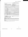
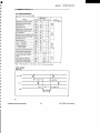
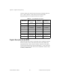
1
PC-DIO-96/PnP
User Manual
Digital I/O Board for ISA
September 1996 Edition
Part Number 320289C-01
© Copyright 1990, 1996 National Instruments Corporation. All Rights Reserved.
Internet Support
GPIB: [email protected]
DAQ: [email protected]
VXI: [email protected]
LabVIEW: [email protected]
LabWindows: [email protected]
HiQ: [email protected]
VISA: [email protected]
Lookout: [email protected]
E-mail: [email protected]
FTP Site: ftp.natinst.com
Web Address: http://www.natinst.com
Bulletin Board Support
BBS United States: (512) 794-5422 or (800) 327-3077
BBS United Kingdom: 01635 551422
BBS France: 01 48 65 15 59
FaxBack Support
(512) 418-1111
Telephone Support (U.S.)
Tel: (512) 795-8248
Fax: (512) 794-5678
International Offices
Australia 03 9879 5166, Austria 0662 45 79 90 0, Belgium 02 757 00 20,
Canada (Ontario) 905 785 0085, Canada (Québec) 514 694 8521,
Denmark 45 76 26 00, Finland 90 527 2321, France 01 48 14 24 24,
Germany 089 741 31 30, Hong Kong 2645 3186, Israel 03 5734815, Italy 02 413091,
Japan 03 5472 2970, Korea 02 596 7456, Mexico 95 800 010 0793, Netherlands 0348 433466,
Norway 32 84 84 00, Singapore 2265886, Spain 91 640 0085, Sweden 08 730 49 70,
Switzerland 056 200 51 51, Taiwan 02 377 1200, U.K. 01635 523545
National Instruments Corporate Headquarters
6504 Bridge Point Parkway Austin, TX 78730-5039 Tel: (512) 794-0100
Important Information
Warranty
The PC-DIO-96/PnP is warranted against defects in materials and workmanship for a period of one year from the date
of shipment, as evidenced by receipts or other documentation. National Instruments will, at its option, repair or replace
equipment that proves to be defective during the warranty period. This warranty includes parts and labor.
The media on which you receive National Instruments software are warranted not to fail to execute programming
instructions, due to defects in materials and workmanship, for a period of 90 days from date of shipment, as evidenced
by receipts or other documentation. National Instruments will, at its option, repair or replace software media that do
not execute programming instructions if National Instruments receives notice of such defects during the warranty
period. National Instruments does not warrant that the operation of the software shall be uninterrupted or error free.
A Return Material Authorization (RMA) number must be obtained from the factory and clearly marked on the outside
of the package before any equipment will be accepted for warranty work. National Instruments will pay the shipping
costs of returning to the owner parts which are covered by warranty.
National Instruments believes that the information in this manual is accurate. The document has been carefully
reviewed for technical accuracy. In the event that technical or typographical errors exist, National Instruments reserves
the right to make changes to subsequent editions of this document without prior notice to holders of this edition. The
reader should consult National Instruments if errors are suspected. In no event shall National Instruments be liable for
any damages arising out of or related to this document or the information contained in it.
EXCEPT AS SPECIFIED HEREIN, NATIONAL INSTRUMENTS MAKES NO WARRANTIES, EXPRESS OR IMPLIED, AND
SPECIFICALLY DISCLAIMS ANY WARRANTY OF MERCHANTABILITY OR FITNESS FOR A PARTICULAR PURPOSE.
CUSTOMER’S RIGHT TO RECOVER DAMAGES CAUSED BY FAULT OR NEGLIGENCE ON THE PART OF NATIONAL
INSTRUMENTS SHALL BE LIMITED TO THE AMOUNT THERETOFORE PAID BY THE CUSTOMER. NATIONAL INSTRUMENTS
WILL NOT BE LIABLE FOR DAMAGES RESULTING FROM LOSS OF DATA, PROFITS, USE OF PRODUCTS, OR INCIDENTAL OR
CONSEQUENTIAL DAMAGES, EVEN IF ADVISED OF THE POSSIBILITY THEREOF. This limitation of the liability of National
Instruments will apply regardless of the form of action, whether in contract or tort, including negligence. Any action
against National Instruments must be brought within one year after the cause of action accrues. National Instruments
shall not be liable for any delay in performance due to causes beyond its reasonable control. The warranty provided
herein does not cover damages, defects, malfunctions, or service failures caused by owner’s failure to follow the
National Instruments installation, operation, or maintenance instructions; owner’s modification of the product;
owner’s abuse, misuse, or negligent acts; and power failure or surges, fire, flood, accident, actions of third parties, or
other events outside reasonable control.
Copyright
Under the copyright laws, this publication may not be reproduced or transmitted in any form, electronic or mechanical,
including photocopying, recording, storing in an information retrieval system, or translating, in whole or in part,
without the prior written consent of National Instruments Corporation.
Trademarks
LabVIEW®, NI-DAQ®, and SCXI™ are trademarks of National Instruments Corporation.
Product and company names listed are trademarks or trade names of their respective companies.
WARNING REGARDING MEDICAL AND CLINICAL USE OF NATIONAL INSTRUMENTS PRODUCTS
National Instruments products are not designed with components and testing intended to ensure a level of reliability
suitable for use in treatment and diagnosis of humans. Applications of National Instruments products involving
medical or clinical treatment can create a potential for accidental injury caused by product failure, or by errors on the
part of the user or application designer. Any use or application of National Instruments products for or involving
medical or clinical treatment must be performed by properly trained and qualified medical personnel, and all traditional
medical safeguards, equipment, and procedures that are appropriate in the particular situation to prevent serious injury
or death should always continue to be used when National Instruments products are being used. National Instruments
products are NOT intended to be a substitute for any form of established process, procedure, or equipment used to
monitor or safeguard human health and safety in medical or clinical treatment.
Table
of
Contents
About This Manual
Organization of This Manual ........................................................................................ ix
Conventions Used in This Manual ............................................................................... x
National Instruments Documentation ........................................................................... xii
Related Documentation ................................................................................................ xiii
Customer Communication ............................................................................................ xiii
Chapter 1
Introduction
About the PC-DIO-96/PnP ........................................................................................... 1-1
What You Need to Get Started ..................................................................................... 1-2
Software Programming Choices ................................................................................... 1-3
LabVIEW and LabWindows/CVI Application Software .............................. 1-3
NI-DAQ Driver Software ............................................................................... 1-3
Register-Level Programming ......................................................................... 1-5
Optional Equipment ...................................................................................................... 1-5
Custom Cabling .............................................................................................. 1-5
Unpacking ..................................................................................................................... 1-7
Chapter 2
Installation and Configuration
Installation .................................................................................................................... 2-1
Hardware Configuration ............................................................................................... 2-3
Plug and Play .................................................................................................. 2-3
Base I/O Address and Interrupt Selection ....................................... 2-3
Non-Plug and Play ......................................................................................... 2-3
Chapter 3
Signal Connections
I/O Connector Pin Description ..................................................................................... 3-1
I/O Connector Signal Connection Descriptions ........................................................... 3-3
Port C Pin Assignments ................................................................................. 3-4
Cable Assembly Connectors ......................................................................................... 3-4
© National Instruments Corporation
v
PC-DIO-96/PnP User Manual
Table of Contents
Digital I/O Signal Connections .....................................................................................3-7
Power Connections ........................................................................................................3-9
Digital I/O Power-up State Selection ............................................................................3-9
High DIO Power-up State ...............................................................................3-9
Low DIO Power-up State ...............................................................................3-11
Timing Specifications ...................................................................................................3-12
Mode 1 Input Timing ......................................................................................3-14
Mode 1 Output Timing ...................................................................................3-15
Mode 2 Bidirectional Timing .........................................................................3-16
Chapter 4
Theory of Operation
Data Transceivers ..........................................................................................................4-2
PC I/O Channel Control Circuitry .................................................................................4-2
Plug and Play Circuitry .................................................................................................4-2
Interrupt Control Circuitry ............................................................................................4-2
82C55A Programmable Peripheral Interface ................................................................4-3
82C53 Programmable Interval Timer ...........................................................................4-3
Digital I/O Connector ....................................................................................................4-4
Appendix A
Specifications
Appendix B
OKI 82C55A Data Sheet
Appendix C
OKI 82C53 Data Sheet
Appendix D
Register-Level Programming
Appendix E
Using Your PC-DIO-96 (Non-PnP) Board
Appendix F
Customer Communication
PC-DIO-96/PnP User Manual
vi
© National Instruments Corporation
Table of Contents
Glossary
Index
Figures
Figure 1-1.
The Relationship between the Programming Environment,
NI-DAQ, and Your Hardware .............................................................. 1-4
Figure 2-1.
PC-DIO-96PnP Parts Locator Diagram ................................................ 2-1
Figure 3-1.
Figure 3-2.
Digital I/O Connector Pin Assignments ............................................... 3-2
Cable Assembly Connector Pin Assignments for Pins 1 through 50
of the PC-DIO-96/PnP I/O Connector .................................................. 3-5
Cable Assembly Connector Pin Assignments for Pins 51 through 100
of the PC-DIO-96/PnP I/O Connector .................................................. 3-6
Digital I/O Connections ........................................................................ 3-8
DIO Channel Configured for High DIO Power-up State
with External Load ................................................................................ 3-10
DIO Channel Configured for Low DIO Power-up State
with External Load ................................................................................ 3-11
Figure 3-3.
Figure 3-4.
Figure 3-5.
Figure 3-6.
Figure 4-1.
PC-DIO-96PnP Block Diagram ............................................................ 4-1
Figure D-1.
Figure D-2.
Figure D-3.
Figure D-4.
Figure D-5.
Figure D-6.
Control Word Formats for the 82C55A ................................................ D-5
Control Word Format for the 82C53 .................................................... D-7
Port C Pin Assignments, Mode 1 Input ................................................ D-16
Port C Pin Assignments, Mode 1 Output .............................................. D-19
Port A Configured as a Bidirectional Data Bus in Mode 2 .................. D-21
Port C Pin Assignments, Mode 2 .......................................................... D-23
Figure E-1.
Figure E-2.
Figure E-3.
Figure E-4.
PC-DIO-96 Block Diagram .................................................................. E-2
PC-DIO-96 Parts Locator Diagram ...................................................... E-3
Example Base I/O Address Switch Settings ......................................... E-6
Interrupt Jumper Setting for IRQ5 (Default Setting) ............................ E-9
© National Instruments Corporation
vii
PC-DIO-96/PnP User Manual
Table of Contents
Tables
Table 3-1.
Table 3-2.
Port C Signal Assignments ....................................................................3-4
Timing Signal Descriptions ...................................................................3-13
Table D-1.
Table D-2.
Table D-3.
PC-DIO-96/PnP Address Map ..............................................................D-2
Port C Set/Reset Control Words ............................................................D-6
Mode 0 I/O Configurations ...................................................................D-12
Table E-1.
Table E-2.
Table E-3.
Comparison of Characteristics ..............................................................E-1
PC-DIO-96 Factory-Set Switch and Jumper Settings ...........................E-4
Switch Settings with Corresponding Base I/O Address and
Base I/O Address Space ........................................................................E-7
PC-DIO-96/PnP User Manual
viii
© National Instruments Corporation
About
This
Manual
This manual describes the mechanical and electrical aspects of the
PC-DIO-96/PnP and contains information concerning its operation and
programming.
The PC-DIO-96PnP is a member of the National Instruments PC Series
of I/O channel expansion boards for ISA computers. These boards are
designed for high-performance data acquisition and control for
applications in laboratory testing, production testing, and industrial
process monitoring and control.
This manual also applies to the PC-DIO-96, a non-Plug and Play device.
The boards are identical except for the differences listed in Appendix E,
Using Your PC-DIO-96 (Non-PnP) Board.
Organization of This Manual
The PC-DIO-96/PnP User Manual is organized as follows:
•
Chapter 1, Introduction, describes the PC-DIO-96/PnP; lists what
you need to get started; describes software programming choices,
optional equipment, and custom cables; and explains how to
unpack the PC-DIO-96/PnP.
•
Chapter 2, Installation and Configuration, describes how to install
and configure the PC-DIO-96PnP board.
•
Chapter 3, Signal Connections, includes timing specifications and
signal connection instructions for the PC-DIO-96/PnP I/O
connector.
•
Chapter 4, Theory of Operation, contains a functional overview of
the PC-DIO-96PnP board and explains the operation of each
functional unit making up the PC-DIO-96PnP.
•
Appendix A, Specifications, lists the specifications of the
PC-DIO-96/PnP.
•
Appendix B, OKI 82C55A Data Sheet, contains the manufacturer
data sheet for the OKI 82C55A (OKI Semiconductor) CMOS
© National Instruments Corporation
ix
PC-DIO-96/PnP User Manual
About This Manual
programmable peripheral interface. This interface is used on the
PC-DIO-96/PnP board.
•
Appendix C, OKI 82C53 Data Sheet, contains the manufacturer
data sheet for the OKI 82C53 integrated circuit (OKI
Semiconductor). This circuit is used on the PC-DIO-96/PnP board.
•
Appendix D, Register-Level Programming, describes in detail the
address and function of each of the PC-DIO-96/PnP control and
status registers. This appendix also includes important information
about register-level programming the PC-DIO-96/PnP along with
program examples written in C and assembly language.
•
Appendix E, Using Your PC-DIO-96 (Non-PnP) Board, describes
the differences between the PC-DIO-96PnP and PC-DIO-96
boards, the PC-DIO-96 board configuration, and the installation of
the PC-DIO-96 into your computer.
•
Appendix F, Customer Communication, contains forms you can use
to request help from National Instruments or to comment on our
products.
•
The Glossary contains an alphabetical list and description of terms
used in this manual, including abbreviations, acronyms, metric
prefixes, mnemonics, and symbols.
•
The Index alphabetically lists the topics in this manual, including
the page where you can find each one.
Conventions Used in This Manual
The following conventions are used in this manual:
82C53
82C53 refers to the OKI 82C53 (OKI Semiconductor) CMOS
programmable interval timer.
82C55A
82C55A refers to the OKI 82C55A (OKI Semiconductor) CMOS
programmable peripheral interface.
<>
Angle brackets containing numbers separated by an ellipses represent a
range of values associated with a bit or signal name (for example,
ACH<0..7>).
bold
Bold text denotes the names of menus, menu items, or dialog box
buttons or options.
bold italic
Bold italic text denotes a note, caution, or warning.
italic
Italic text denotes emphasis, a cross reference, or an introduction to a
key concept.
PC-DIO-96/PnP User Manual
x
© National Instruments Corporation
About This Manual
monospace
Text in this font denotes text or characters that are to be literally input
from the keyboard, sections of code, programming examples, and
syntax examples. This font is also used for the proper names of disk
drives, paths, directories, programs, subprograms, subroutines, device
names, functions, operations, variables, filenames, and extensions, and
for statements and comments taken from program code.
NI-DAQ
NI-DAQ refers to the NI-DAQ software for PC compatibles unless
otherwise noted.
PC-DIO-96/PnP PC-DIO-96/PnP refers to both the Plug and Play and non-Plug and Play
compatible versions of the board.
PC-DIO-96PnP PC-DIO-96PnP refers to the Plug and Play version of the
PC-DIO-96/PnP.
PC-DIO-96
PC-DIO-96 refers to the non-Plug and Play version of the
PC-DIO-96/PnP.
PnP
PnP (Plug and Play) refers to a device that is fully compatible with the
industry standard Plug and Play ISA Specification. All bus-related
configuration is performed through software, freeing the user from
manually configuring jumpers or switches to set the product’s base
address and interrupt level. Plug and Play systems automatically
arbitrate and assign system resources to a PnP product.
non-PnP
Non-PnP (non-Plug and Play) refers to a device that requires a user to
configure the product’s base address and interrupt level with switches
and jumpers. This configuration must be performed prior to installing
the product in the computer.
PPI x
PPI x, where the x is replaced by A, B, C, or D, refers to one of the four
programmable peripheral interface (PPI) chips on the PC-DIO-96/PnP.
SCXI
SCXI stands for Signal Conditioning eXtensions for Instrumentation
and is a National Instruments product line designed to perform frontend signal conditioning for National Instruments plug-in DAQ boards.
Abbreviations, acronyms, metric prefixes, mnemonics, and symbols are
listed in the Glossary.
© National Instruments Corporation
xi
PC-DIO-96/PnP User Manual
About This Manual
National Instruments Documentation
The PC-DIO-96/PnP User Manual is one piece of the documentation
set for your data acquisition (DAQ) system. You could have any of
several types of manuals, depending on the hardware and software in
your system. Use the different types of manuals you have as follows:
PC-DIO-96/PnP User Manual
•
Getting Started with SCXI—If you are using SCXI, this is the first
manual you should read. It gives an overview of the SCXI system
and contains the most commonly needed information for the
modules, chassis, and software.
•
Your SCXI hardware user manuals—If you are using SCXI, read
these manuals next for detailed information about signal
connections and module configuration. They also explain in greater
detail how the module works and contain application hints.
•
Your DAQ hardware user manuals—These manuals have detailed
information about the DAQ hardware that plugs into or is
connected to your computer. Use these manuals for hardware
installation and configuration instructions, specification
information about your DAQ hardware, and application hints.
•
Software documentation—Examples of software documentation
you may have are the LabVIEW, LabWindows®/CVI, and NI-DAQ
documentation sets. After you set up your hardware system, use
either the application software (LabVIEW or LabWindows/CVI)
documentation or the NI-DAQ documentation to help you write
your application. If you have a large and complicated system, it is
worthwhile to look through the software documentation before you
configure your hardware.
•
Accessory installation guides or manuals—If you are using
accessory products, read the terminal block and cable assembly
installation guides or accessory board user manuals. They explain
how to physically connect the relevant pieces of the system.
Consult these guides when you are making your connections.
•
SCXI Chassis User Manual—If you are using SCXI, read this
manual for maintenance information on the chassis and installation
instructions.
xii
© National Instruments Corporation
About This Manual
Related Documentation
If you are a register-level programmer, the following documents
contain information that you may find helpful as you read this manual:
•
Your computer technical reference manual
•
Plug and Play ISA Specification
Customer Communication
National Instruments wants to receive your comments on our products
and manuals. We are interested in the applications you develop with our
products, and we want to help if you have problems with them. To make
it easy for you to contact us, this manual contains comment and
configuration forms for you to complete. These forms are in
Appendix F, Customer Communication, at the end of this manual.
© National Instruments Corporation
xiii
PC-DIO-96/PnP User Manual
Chapter
1
Introduction
This chapter describes the PC-DIO-96/PnP; lists what you need to get
started; describes software programming choices, optional equipment,
and custom cables; and explains how to unpack the PC-DIO-96/PnP.
About the PC-DIO-96/PnP
Thank you for purchasing the National Instruments PC-DIO-96/PnP.
PnP refers to the Plug and Play technology used in this board. See the
Conventions Used in this Manual section in About This Manual for an
explanation. The PC-DIO-96/PnP is a 96-bit, parallel, digital I/O
interface for ISA computers. Four 82C55A programmable peripheral
interface (PPI) chips control the 96 bits of digital I/O. The 82C55A can
operate in either a unidirectional or bidirectional mode and can generate
interrupt requests to the host computer. You can program the 82C55A
for almost any 8-bit or 16-bit digital I/O application. All digital I/O
communication is through a standard, 100-pin, male connector. The
PC-DIO-96/PnP also includes an 82C53 counter/timer that can send
periodic interrupts to the host system.
If you have the non-PnP version of the PC-DIO-96/PnP, see
Appendix E, Using Your PC-DIO-96 (Non-PnP) Board, for the
differences between the PnP version and the non-PnP version.
You can use the PC-DIO-96/PnP in a wide range of digital I/O
applications. With the PC-DIO-96/PnP, you can interface any PC to any
of the following:
•
© National Instruments Corporation
Other computers
–
Another PC with a National Instruments PC-DIO-96/PnP,
PC-DIO-24, or AT-DIO-32F
–
IBM Personal System/2 with a National Instruments
MC-DIO-24 or MC-DIO-32F
1-1
PC-DIO-96/PnP User Manual
Chapter 1
Introduction
Note:
–
Macintosh II with a National Instruments NB-DIO-24,
NB-DIO-32F, or PCI-DIO-96
–
Any other computer with an 8-bit or 16-bit parallel interface
•
Centronics-compatible printers and plotters
•
Panel meters
•
Instruments and test equipment with BCD readouts and/or controls
•
Optically isolated, solid-state relays and I/O module mounting
racks
The PC-DIO-96/PnP cannot sink sufficient current to drive the
SSR-OAC-5 and SSR-OAC-5A output modules. However, it can drive the
SSR-ODC-5 output module and all SSR input modules available from
National Instruments.
If you need to drive an SSR-OAC-5 or SSR-OAC-5A, you can either use a
non-inverting digital buffer chip between the PC-DIO-96/PnP and the SSR
backplane, or you can use a DIO-23F or MIO Series board with
appropriate connections (for example, SC-205X and cables).
With the PC-DIO-96/PnP, a PC can serve as a digital I/O system
controller for laboratory testing, production testing, and industrial
process monitoring and control.
Detailed specifications of the PC-DIO-96/PnP are in Appendix A,
Specifications.
What You Need to Get Started
To set up and use your PC-DIO-96/PnP, you will need the following:
❑ PC-DIO-96/PnP board
❑ PC-DIO-96/PnP User Manual
❑ One of the following software packages and documentation:
NI-DAQ for PC Compatibles
LabVIEW for Windows
LabWindows/CVI
❑ Your computer
PC-DIO-96/PnP User Manual
1-2
© National Instruments Corporation
Chapter 1
Introduction
Software Programming Choices
There are several options to choose from when programming your
National Instruments DAQ and SCXI hardware. You can use
LabVIEW, LabWindows/CVI, NI-DAQ, or register-level
programming. NI-DAQ version 4.6.1 or earlier supports LabWindows
for DOS.
LabVIEW and LabWindows/CVI Application Software
LabVIEW and LabWindows/CVI are innovative program development
software packages for data acquisition and control applications.
LabVIEW uses graphical programming, whereas LabWindows/CVI
enhances traditional programming languages. Both packages include
extensive libraries for data acquisition, instrument control, data
analysis, and graphical data presentation.
LabVIEW features interactive graphics, a state-of-the-art user
interface, and a powerful graphical programming language. The
LabVIEW Data Acquisition VI Library, a series of VIs for using
LabVIEW with National Instruments DAQ hardware, is included with
LabVIEW. The LabVIEW Data Acquisition VI Library is functionally
equivalent to the NI-DAQ software.
LabWindows/CVI features interactive graphics, a state-of-the-art user
interface, and uses the ANSI standard C programming language. The
LabWindows/CVI Data Acquisition Library, a series of functions for
using LabWindows/CVI with National Instruments DAQ hardware, is
included with the NI-DAQ software kit. The LabWindows/CVI Data
Acquisition Library is functionally equivalent to the NI-DAQ software.
Using LabVIEW or LabWindows/CVI software will greatly reduce the
development time for your data acquisition and control application.
NI-DAQ Driver Software
The NI-DAQ driver software is included at no charge with all National
Instruments DAQ hardware. NI-DAQ is not packaged with SCXI or
accessory products, except for the SCXI-1200. NI-DAQ has an
extensive library of functions that you can call from your application
programming environment. These functions include routines for analog
input (A/D conversion), buffered data acquisition (high-speed A/D
conversion), analog output (D/A conversion), waveform generation,
© National Instruments Corporation
1-3
PC-DIO-96/PnP User Manual
Chapter 1
Introduction
digital I/O, counter/timer operations, SCXI, RTSI, self-calibration,
messaging, and acquiring data to extended memory.
NI-DAQ has both high-level DAQ I/O functions for maximum ease of
use and low-level DAQ I/O functions for maximum flexibility and
performance. Examples of high-level functions are streaming data to
disk or acquiring a certain number of data points. An example of a lowlevel function is writing directly to registers on the DAQ device.
NI-DAQ does not sacrifice the performance of National Instruments
DAQ devices because it lets multiple devices operate at their peak
performance.
NI-DAQ also internally addresses many of the complex issues between
the computer and the DAQ hardware such as programming interrupts
and DMA controllers. NI-DAQ maintains a consistent software
interface among its different versions so that you can change platforms
with minimal modifications to your code. Whether you are using
conventional programming languages, LabVIEW, or
LabWindows/CVI, your application uses the NI-DAQ driver software,
as illustrated in Figure 1-1.
Conventional
Programming
Environment
(PC, Macintosh, or
Sun SPARCstation)
LabVIEW
(PC, Macintosh, or
Sun SPARCstation)
LabWindows/CVI
(PC or
Sun SPARCstation)
NI-DAQ
Driver Software
DAQ or
SCXI Hardware
Personal
Computer
or
Workstation
Figure 1-1. The Relationship between the Programming Environment,
NI-DAQ, and Your Hardware
PC-DIO-96/PnP User Manual
1-4
© National Instruments Corporation
Chapter 1
Introduction
Register-Level Programming
The final option for programming any National Instruments DAQ
hardware is to write register-level software. Writing register-level
programming software can be very time-consuming and inefficient, and
is not recommended for most users.
Even if you are an experienced register-level programmer, consider
using NI-DAQ, LabVIEW, or LabWindows/CVI to program your
National Instruments DAQ hardware. Using the NI-DAQ, LabVIEW, or
LabWindows/CVI software is easier than, and as flexible as, registerlevel programming, and can save weeks of development time.
Optional Equipment
National Instruments offers a variety of products to use with your
PC-DIO-96/PnP board, including cables, connector blocks, and other
accessories, as follows:
•
Cables and cable assemblies
•
Connector blocks and unshielded 50-pin screw terminals
•
SCXI modules and accessories for isolating, amplifying, exciting,
and multiplexing signals for relays and analog output. With SCXI
you can condition and acquire up to 3,072 channels.
•
Low channel count signal conditioning modules, boards, and
accessories, including conditioning for strain gauges and RTDs,
simultaneous sample and hold, and relays.
For more specific information about these products, refer to your
National Instruments catalog or call the office nearest you.
Custom Cabling
National Instruments offers cables and accessories for you to prototype
your application or to use if you frequently change board
interconnections.
You can interface the PC-DIO-96/PnP to a wide range of printers,
plotters, test instruments, I/O racks and modules, screw terminal panels,
and almost any device with a parallel interface. The PC-DIO-96/PnP
digital I/O connector is a standard, 100-pin header connector. Adapters
for this header connector expand the interface to four 50-pin ribbon
cables, each of which has the pinout of a PC-DIO-24. The pin
assignments of the expansion cables are compatible with the standard
© National Instruments Corporation
1-5
PC-DIO-96/PnP User Manual
Chapter 1
Introduction
24-channel I/O module mounting racks (such as those manufactured by
Opto 22 and Gordos).
The CB-100 cable termination accessory is available from National
Instruments for use with the PC-DIO-96/PnP board. This kit includes
two 50-conductor, flat-ribbon cables and a connector block. You can
attach signal input and output wires to screw terminals on the connector
block and therefore connect signals to the PC-DIO-96/PnP I/O
connector.
The CB-100 is useful for initial prototyping of an application or in
situations where PC-DIO-96/PnP interconnections are frequently
changed. Once a final field wiring scheme has been developed,
however, you may want to develop your own cable. This section
contains information for the design of custom cables.
The PC-DIO-96/PnP I/O connector is a 100-pin, Centronics-style, male,
ribbon-cable header connector. The manufacturer and the appropriate
part number for this connector is as follows:
•
Robinson Nugent (part number P50E-100P1-RR1-TG)
The mating connector for the PC-DIO-96/PnP is a 100-position,
polarized, Centronics-style, female, ribbon-socket connector with
strain relief. National Instruments uses a polarized (keyed) connector to
prevent inadvertent upside-down connection to the PC-DIO-96/PnP.
This 100-pin connector attaches to two 50-pin cables, each of which can
be connected to a 50-pin connector on the other end. The recommended
manufacturer and the appropriate part number for the 100-pin mating
connector is as follows:
•
Robinson Nugent (part number P50E-100S-TG)
The recommended manufacturer part numbers for 50-pin, female,
ribbon-socket connectors suitable for use with the preceding connector
are:
PC-DIO-96/PnP User Manual
•
Electronic Products Division/3M (part number 3425-7650)
•
T&B/Ansley Corporation (part number 609-5041CE)
1-6
© National Instruments Corporation
Chapter 1
Introduction
Recommended manufacturers and the appropriate part numbers for the
standard ribbon cable (50-conductor, 28 AWG, stranded) that can be
used with both the 100-pin and the 50-pin connectors are:
•
Electronic Products Division/3M (part number 3365/50)
•
T&B/Ansley Corporation (part number 171-50)
Unpacking
Your PC-DIO-96/PnP board is shipped in an antistatic package to
prevent electrostatic damage to the board. Electrostatic discharge can
damage several components on the board. To avoid such damage in
handling the board, take the following precautions:
•
Ground yourself via a grounding strap or by holding a grounded
object.
•
Touch the antistatic package to a metal part of your computer
chassis before removing the board from the package.
•
Remove the board from the package and inspect the board for loose
components or any other sign of damage. Notify National
Instruments if the board appears damaged in any way. Do not
install a damaged board into your computer.
•
Never touch the exposed pins of connectors.
© National Instruments Corporation
1-7
PC-DIO-96/PnP User Manual
Chapter
Installation and
Configuration
2
This chapter describes how to install and configure the PC-DIO-96PnP
board.
Installation
Note:
You should install your driver software before installing your hardware.
Refer to your NI-DAQ release notes for software installation instructions.
1
2
3
1
Serial Number
2
W1
3
F1
Figure 2-1. PC-DIO-96PnP Parts Locator Diagram
© National Instruments Corporation
2-1
PC-DIO-96/PnP User Manual
Chapter 2
Installation and Configuration
Note:
The PC-DIO-96PnP uses 100 kΩ resistors for polarity selection at powerup. These signals are pulled up to VCC (+5 VDC, factory default) or pulled
down to GND by selection of jumper W1. The location of W1 is shown in
Figure 2-1. For more information, see the Digital I/O Power-up State
Selection section in Chapter 3, Signal Connections.
You can install the PC-DIO-96PnP in any available expansion slot in
your computer. The following are general installation instructions, but
consult your computer user manual or technical reference manual for
specific instructions and warnings.
1.
Turn off and unplug your computer.
2.
Remove the top cover or access port to the I/O channel.
3.
Remove the expansion slot cover on the back panel of the
computer.
4.
Insert the PC-DIO-96PnP board into any 8-bit or 16-bit slot. It may
be a tight fit, but do not force the board into place.
5.
Screw the mounting bracket of the PC-DIO-96PnP board to the
back panel rail of the computer.
6.
Visually verify your installation.
7.
Replace the cover.
8.
Plug in and turn on your computer.
Your PC-DIO-96PnP is now installed.
PC-DIO-96/PnP User Manual
2-2
© National Instruments Corporation
Chapter 2
Installation and Configuration
Hardware Configuration
Plug and Play
The PC-DIO-96PnP is fully compatible with the industry-standard
Intel/Microsoft Plug and Play Specification. A Plug and Play system
arbitrates and assigns resources through software, freeing you from
manually setting switches and jumpers. These resources include the
board base I/O address and interrupt channels. Each PC-DIO-96PnP is
configured at the factory to request these resources from the Plug and
Play Configuration Manager.
The Configuration Manager receives all of the resource requests at
startup, compares the available resources to those requested, and
assigns the available resources as efficiently as possible to the Plug and
Play boards. Application software can query the Configuration
Manager to determine the resources assigned to each board without
your involvement. The Plug and Play software is installed as a device
driver or as an integral component of the computer BIOS.
Base I/O Address and Interrupt Selection
To change base I/O address or interrupt selection, refer to the NI-DAQ
Configuration Utility online help file. You can configure the
PC-DIO-96PnP to use base addresses in the range of 100 to 3E0 hex.
Each board occupies 16 bytes of address space and must be located on
a 16-byte boundary. Therefore, valid addresses include 100, 110,
120…, 3E0 hex.
The PC-DIO-96PnP can use interrupt channels 3, 4, 5, 6, 7, and 9.
Non-Plug and Play
To configure the non-Plug and Play PC-DIO-96 board, refer to
Appendix E, Using Your PC-DIO-96 (Non-PnP) Board.
© National Instruments Corporation
2-3
PC-DIO-96/PnP User Manual
Chapter
3
Signal Connections
This chapter includes timing specifications and signal connection
instructions for the PC-DIO-96/PnP I/O connector.
Warning: Connections that exceed any of the maximum ratings of input or output
signals on the PC-DIO-96/PnP can damage the board and the computer.
The description of each signal in this section includes information about
maximum input ratings. National Instruments is NOT liable for any
damages resulting from any such signal connections.
I/O Connector Pin Description
Figure 3-1 shows the pin assignments for the PC-DIO-96/PnP digital
I/O connector.
© National Instruments Corporation
3-1
PC-DIO-96/PnP User Manual
Chapter 3
Signal Connections
APC7
BPC7
APC6
BPC6
APC5
BPC5
APC4
BPC4
APC3
BPC3
APC2
BPC2
APC1
BPC1
APC0
BPC0
APB7
BPB7
APB6
BPB6
APB5
BPB5
APB4
BPB4
APB3
BPB3
APB2
BPB2
APB1
BPB1
APB0
BPB0
APA7
BPA7
APA6
BPA6
APA5
BPA5
APA4
BPA4
APA3
BPA3
APA2
BPA2
APA1
BPA1
APA0
BPA0
+5 V
GND
1
2
3
4
5
6
7
8
9
10
11
12
13
14
15
16
17
18
19
20
21
22
23
24
25
26
27
28
29
30
31
32
33
34
35
36
37
38
39
40
41
42
43
44
45
46
47
48
49
50
51
52
53
54
55
56
57
58
59
60
61
62
63
64
65
66
67
68
69
70
71
72
73
74
75
76
77
78
79
80
81
82
83
84
85
86
87
88
89
90
91
92
93
94
95
96
97
98
99
100
CPC7
DPC7
CPC6
DPC6
CPC5
DPC5
CPC4
DPC4
CPC3
DPC3
CPC2
DPC2
CPC1
DPC1
CPC0
DPC0
CPB7
DPB7
CPB6
DPB6
CPB5
DPB5
CPB4
DPB4
CPB3
DPB3
CPB2
DPB2
CPB1
DPB1
CPB0
DPB0
CPA7
DPA7
CPA6
DPA6
CPA5
DPA5
CPA4
DPA4
CPA3
DPA3
CPA2
DPA2
CPA1
DPA1
CPA0
DPA0
+5 V
GND
Figure 3-1. Digital I/O Connector Pin Assignments
PC-DIO-96/PnP User Manual
3-2
© National Instruments Corporation
Chapter 3
Signal Connections
I/O Connector Signal Connection Descriptions
Pin
Signal Name
Description
1, 3, 5, 7, 9, 11, 13, 15
APC<7..0>
Bidirectional Data Lines for Port C of
PPI A—APC7 is the MSB, APC0 the LSB.
17, 19, 21, 23, 25, 27, 29, 31
APB<7..0>
Bidirectional Data Lines for Port B of
PPI A—APB7 is the MSB, APB0 the LSB.
33, 35, 37, 39, 41, 43, 45, 47
APA<7..0>
Bidirectional Data Lines for Port A of
PPI A—APA7 is the MSB, APA0 the LSB.
2, 4, 6, 8, 10, 12, 14, 16
BPC<7..0>
Bidirectional Data Lines for Port C of
PPI B—BPC7 is the MSB, BPC0 the LSB.
18, 20, 22, 24, 26, 28, 30, 32
BPB<7..0>
Bidirectional Data Lines for Port B of
PPI B—BPB7 is the MSB, BPB0 the LSB.
34, 36, 38, 40, 42, 44, 46, 48
BPA<7..0>
Bidirectional Data Lines for Port A of
PPI B—BPA7 is the MSB, BPA0 the LSB.
51, 53, 55, 57, 59, 61, 63, 65
CPC<7..0>
Bidirectional Data Lines for Port C of
PPI C—CPC7 is the MSB, CPC0 the LSB.
67, 69, 71, 73, 75, 77, 79, 81
CPB<7..0>
Bidirectional Data Lines for Port B of
PPI C—CPB7 is the MSB, CPB0 the LSB.
83, 85, 87, 89, 91, 93, 95, 97
CPA<7..0>
Bidirectional Data Lines for Port A of
PPI C—CPA7 is the MSB, CPA0 the LSB.
52, 54, 56, 58, 60, 62, 64, 66
DPC<7..0>
Bidirectional Data Lines for Port C of
PPI D—DPC7 is the MSB, DPC0 the LSB.
68, 70, 72, 74, 76, 78, 80, 82
DPB<7..0>
Bidirectional Data Lines for Port B of
PPI D—DPB7 is the MSB, DPB0 the LSB.
84, 86, 88, 90, 92, 94, 96, 98
DPA<7..0>
Bidirectional Data Lines for Port A of
PPI D—DPA7 is the MSB, DPA0 the LSB.
49, 99 (see note below)
+5 V
+5 Volts—These pins are connected to the
computer’s +5 VDC supply.
50, 100
GND
Ground—These pins are connected to the
computer’s ground signal.
Note:
Pins 49 and 99 are connected to the +5 V PC power supply via a 1 A self-resetting
fuse.
© National Instruments Corporation
3-3
PC-DIO-96/PnP User Manual
Chapter 3
Signal Connections
Port C Pin Assignments
The signals assigned to port C depend on the mode in which the
82C55A is programmed. In mode 0, port C is considered as two 4-bit
I/O ports. In modes 1 and 2, port C is used for status and handshaking
signals with zero, two, or three lines available for general-purpose
input/output. The following table summarizes the signal assignments of
port C for each programmable mode. Consult Appendix D, RegisterLevel Programming, for programming information.
Warning: During programming, note that each time a port is configured, output
ports A and C are reset to 0, and output port B is undefined.
Table 3-1.
Programming
Mode
Port C Signal Assignments
Group A
PC7
PC6
Group B
PC5
PC4
PC3
PC2
PC1
PC0
Mode 0
I/O
I/O
I/O
I/O
I/O
I/O
I/O
I/O
Mode 1 Input
I/O
I/O
IBFA
STBA*
INTRA
STBB*
IBFBB
INTRB
Mode 1 Output
OBFA*
ACKA*
I/O
I/O
INTRA
ACKB*
OBFB*
INTRB
Mode 2
OBFA*
ACKA*
IBFA
STBA*
INTRA
I/O
I/O
I/O
* Indicates that the signal is active low
Cable Assembly Connectors
The cable assembly referred to in Optional Equipment in Chapter 1,
Introduction, is an assembly of two 50-pin cables and three connectors.
Both cables are joined to a single connector on one end and to
individual connectors on the free ends. The 100-pin connector that joins
the two cables plugs into the I/O connector of the PC-DIO-96/PnP. The
other two connectors are 50-pin connectors, one of which is connected
to pins 1 through 50 and the other is connected to pins 51 through 100
of the PC-DIO-96/PnP I/O connector. The cable with the label on it is
connected to pins 1 through 50. Figures 3-2 and 3-3 show the pin
assignments for the 50-pin connectors on the cable assembly.
PC-DIO-96/PnP User Manual
3-4
© National Instruments Corporation
Chapter 3
APC7
1
2
BPC7
APC6
3
4
BPC6
APC5
5
6
BPC5
APC4
7
8
BPC4
APC3
9
10
BPC3
APC2
11 12
BPC2
APC1
13 14
BPC1
APC0
15 16
BPC0
APB7
17 18
BPB7
APB6
19 20
BPB6
APB5
21 22
BPB5
APB4
23 24
BPB4
APB3
25 26
BPB3
APB2
27 28
BPB2
APB1
29 30
BPB1
APB0
31 32
BPB0
APA7
33 34
BPA7
APA6
35 36
BPA6
APA5
37 38
BPA5
APA4
39 40
BPA4
APA3
41 42
BPA3
APA2
43 44
BPA2
APA1
45 46
BPA1
APA0
47 48
BPA0
+5 V
49 50
GND
Signal Connections
Figure 3-2. Cable Assembly Connector Pin Assignments for Pins 1 through 50
of the PC-DIO-96/PnP I/O Connector
© National Instruments Corporation
3-5
PC-DIO-96/PnP User Manual
Chapter 3
Signal Connections
CPC7
1
2
DPC7
CPC6
3
4
DPC6
CPC5
5
6
DPC5
CPC4
7
8
DPC4
CPC3
9
10
DPC3
CPC2
11 12
DPC2
CPC1
13 14
DPC1
CPC0
15 16
DPC0
CPB7
17 18
DPB7
CPB6
19 20
DPB6
CPB5
21 22
DPB5
CPB4
23 24
DPB4
CPB3
25 26
DPB3
CPB2
27 28
DPB2
CPB1
29 30
DPB1
CPB0
31 32
DPB0
CPA7
33 34
DPA7
CPA6
35 36
DPA6
CPA5
37 38
DPA5
CPA4
39 40
DPA4
CPA3
41 42
DPA3
CPA2
43 44
DPA2
CPA1
45 46
DPA1
CPA0
47 48
DPA0
+5 V
49 50
GND
Figure 3-3. Cable Assembly Connector Pin Assignments for Pins 51 through 100
of the PC-DIO-96/PnP I/O Connector
PC-DIO-96/PnP User Manual
3-6
© National Instruments Corporation
Chapter 3
Signal Connections
Digital I/O Signal Connections
Pins 1 through 48 and pins 51 through 98 of the I/O connector are digital
I/O signal pins. The following specifications and ratings apply to the
digital I/O lines.
Absolute maximum voltage rating -0.5 to +5.5 V with respect to GND
Digital input specifications (referenced to GND):
Input logic high voltage
2.2 V min
5.3 V max
Input logic low voltage
-0.3 V min
0.8 V max
Maximum input current
(0 < Vin < 5 V)
-1.0 µA min
1.0 µA max
Digital output specifications (referenced to GND):
Output logic high voltage
at Iout = -2.5 mA
3.7 V min
5.0 V max
Output logic low voltage
at Iout = 2.5 mA
0.0 V min
0.4 V max
Output current
at VOL = 0.5 V
2.5 mA min
—
Output current
at VOH = 2.7 V
2.5 mA min
—
Figure 3-4 depicts signal connections for three typical digital I/O
applications.
© National Instruments Corporation
3-7
PC-DIO-96/PnP User Manual
Chapter 3
Signal Connections
+5 V
+5 V
LED
Jumper
Selectable (W1)
100 kΩ
100 kΩ
100 kΩ
100 kΩ
41
PPI A
Port A
APA<3..0>
43
45
47
100 kΩ
100 kΩ
100 kΩ
100 kΩ
67
69
TTL Signal
PPI C
Port B
CPB<7..4>
71
73
+5 V
Switch *
50, 100
GND
I/O Connector
PC-DIO-96/PnP
* Complex switch circuitry is not shown in order to simplify the figure.
Figure 3-4. Digital I/O Connections
In Figure 3-4, PPI A, port A is configured for digital output, and PPI C,
port B is configured for digital input. Digital input applications include
receiving TTL signals and sensing external device states such as the
state of the switch in Figure 3-4. Digital output applications include
sending TTL signals and driving external devices such as the LED
shown in Figure 3-4.
PC-DIO-96/PnP User Manual
3-8
© National Instruments Corporation
Chapter 3
Signal Connections
Power Connections
Pins 49 and 99 of the I/O connector are connected to the +5 V supply
from the PC power supply. These pins are referenced to GND and can
be used to power external digital circuitry. This +5 V supply has a 1 A
protection fuse in series. This fuse is self-resetting. Simply remove the
circuit causing the heavy current load and the fuse will reset itself. For
more information on these output pins, see Output Signals in
Appendix A, Specifications.
0.5 A per pin at +5 V ±10%
Power rating
Warning: Under no circumstances should these +5 V power pins be connected
directly to ground or to any other voltage source on the PC-DIO-96/PnP or
any other device. Doing so may damage the PC-DIO-96/PnP and the PC.
National Instruments is NOT liable for damage resulting from such a
connection.
Digital I/O Power-up State Selection
You may want to power up the PC-DIO-96/PnP’s digital I/O lines in a
user-defined state. The PC-DIO-96/PnP facilitates user-configurable
pull-up or pull-down. Each DIO channel is connected to a 100 kΩ
resistor and can be pulled high or low using jumper W1. You can use
W1 to pull all 96 DIO lines high or low. However, if all lines are high,
you may want to pull some lines low. To do this properly, you must
understand the nature of the drive current on those lines and adhere to
TTL logic levels.
High DIO Power-up State
If you select the pulled-high mode, each DIO line will be pulled to VCC
(+5 VDC) with a 100 kΩ resistor. If you want to pull a specific line low,
connect between that line and ground a pull-down resistor (RL) whose
value will give you a maximum of 0.4 VDC. The DIO lines provide a
maximum of 2.5 mA at 3.7 V in the high state. Use the largest possible
resistor so that you do not use more current than necessary to perform
the pull-down task.
Also, make sure the resistor’s value is not so large that leakage current
from the DIO line along with the current from the 100 kΩ pull-up
resistor drives the voltage at the resistor above a TTL low level of
0.4 VDC.
© National Instruments Corporation
3-9
PC-DIO-96/PnP User Manual
Chapter 3
Signal Connections
PC-DIO-96/PnP +5 V
100 kΩ
82C55
Digital I/O Line
RL
GND
Figure 3-5. DIO Channel Configured for High DIO Power-up State with External Load
Example:
At power up, the board is configured for input and, by default, all DIO
lines are high. To pull one channel low, follow these steps:
1.
Install a load (RL). Remember that the smaller the resistance, the
greater the current consumption and the lower the voltage (V).
2.
Using the following formula, calculate the largest possible load to
maintain a logic low level of 0.4 V and supply the maximum
driving current (I).
V = I * RL ⇒ RL = V / I, where:
V= 0.4 V
; Voltage across RL
I = 46 µA + 10 µA
; 4.6 V across the 100 kΩ pull-up
resistor and 10 µA from 82C55
leakage current
Therefore:
RL = 7.1 kΩ
; 0.4 V / 56 µA
This resistor value, 7.1 kΩ, provides a maximum of 0.4 V on the DIO
line at power up. You can substitute smaller resistor values, but they
will draw more current, leaving less drive current for other circuitry
connected to this line. The 7.1 kΩ resistor reduces the amount of a logic
high source current by 0.4 mA with a 2.8 V output.
PC-DIO-96/PnP User Manual
3-10
© National Instruments Corporation
Chapter 3
Signal Connections
Low DIO Power-up State
If you select pulled-low mode, each DIO line will be pulled to GND
(0 VDC) using a 100 kΩ resistor. If you want to pull a specific line high,
connect a pull-up resistor that will give you a minimum of 2.8 VDC.
The DIO lines are capable of sinking a maximum of 2.5 mA at 0.4 V in
the low state. Use the largest possible resistance value so that you do
not to use more current than necessary to perform the pull-up task.
Also, make sure the pull-up resistor value is not so large that leakage
current from the DIO line along with the current from the 100 kΩ pulldown resistor brings the voltage at the resistor below a TTL high level
of 2.8 VDC.
PC-DIO-96/PnP
+5 V
RL
82C55
Digital I/O Line
100 kΩ
GND
Figure 3-6. DIO Channel Configured for Low DIO Power-up State with External Load
© National Instruments Corporation
3-11
PC-DIO-96/PnP User Manual
Chapter 3
Signal Connections
Example:
At power up, the board is configured for input and jumper W1 is set in
the low DIO power-up state, which means all DIO lines are pulled low.
If you want to pull one channel high, follow these steps:
1.
Install a load (RL). Remember that the smaller the resistance, the
greater the current consumption and the lower the voltage (V).
2.
Using the following formula, calculate the largest possible load to
maintain a logic high level of 2.8 V and supply the maximum sink
current (I).
V = I * RL ⇒ RL = V / I, where:
V = 2.2 V
; voltage across RL
I = 28 µA + 10 µA
; 2.8 V across the 100 kΩ pull-up
resistor and 10 µA from 82C55
leakage current
Therefore:
RL = 5.7 kΩ
; 2.2 V / 38 µA
This resistor value, 5.7 kΩ, provides a minimum of 2.8 V on the DIO
line at power up. You can substitute smaller resistor values but they will
draw more current, leaving less sink current for other circuitry
connected to this line. The 5.7 kΩ resistor will reduce the amount of a
logic low sink current by 0.8 mA with a 0.4 V output.
Timing Specifications
This section lists the timing specifications for handshaking with the
PC-DIO-96/PnP. The handshaking lines STB* and IBF synchronize
input transfers. The handshaking lines OBF* and ACK* synchronize
output transfers.
The signals in Table 3-2 are used in the timing diagrams later in this
chapter.
PC-DIO-96/PnP User Manual
3-12
© National Instruments Corporation
Chapter 3
Table 3-2.
Name
Signal Connections
Timing Signal Descriptions
Type
Description
STB*
Input
Strobe Input—A low signal on this handshaking line loads data
into the input latch.
IBF
Output
Input Buffer Full—A high signal on this handshaking line indicates
that data has been loaded into the input latch. This is an input
acknowledge signal.
ACK*
Input
Acknowledge Input—A low signal on this handshaking line
indicates that the data written to the port has been accepted. This
signal is a response from the external device indicating that it has
received the data from the PC-DIO-96/PnP.
OBF*
Output
Output Buffer Full—A low signal on this handshaking line
indicates that data has been written to the port.
INTR
Output
Interrupt Request—This signal becomes high when the 82C55A
requests service during a data transfer. The appropriate interrupt
enable bits must be set to generate this signal.
RD*
Internal
Read Signal—This signal is the read signal generated from the
control lines of the computer I/O expansion bus.
WR*
Internal
Write Signal—This signal is the write signal generated from the
control lines of the computer I/O expansion bus.
DATA
Bidirectional
Data Lines at the Specified Port—This signal indicates the
availability of data on the data lines at a port that is in the output
mode. If the port is in the input mode, this signal indicates when the
data on the data lines should be valid.
© National Instruments Corporation
3-13
PC-DIO-96/PnP User Manual
Chapter 3
Signal Connections
Mode 1 Input Timing
The following figure illustrates the timing specifications for an input
transfer in mode 1.
T1
T2
T4
STB*
T7
IBF
T6
INTR
RD*
T3
T5
DATA
Name
Description
T1
STB* pulse width
T2
Minimum
Maximum
100
–
STB* = 0 to IBF = 1
–
150
T3
Data before STB* = 1
20
–
T4
STB* = 1 to INTR = 1
–
150
T5
Data after STB* = 1
50
–
T6
RD* = 0 to INTR = 0
–
200
T7
RD* = 1 to IBF = 0
–
150
All timing values are in nanoseconds.
PC-DIO-96/PnP User Manual
3-14
© National Instruments Corporation
Chapter 3
Signal Connections
Mode 1 Output Timing
The following figure illustrates the timing specifications for an output
transfer in mode 1.
T3
WR*
T4
OBF*
T1
T6
INTR
T5
ACK*
DATA
T2
Name
Description
Minimum
Maximum
T1
WR* = 0 to INTR = 0
–
250
T2
WR* = 1 to output
–
200
T3
WR* = 1 to OBF* = 0
–
150
T4
ACK* = 0 to OBF* = 1
–
150
T5
ACK* pulse width
100
–
T6
ACK* = 1 to INTR = 1
–
150
All timing values are in nanoseconds.
© National Instruments Corporation
3-15
PC-DIO-96/PnP User Manual
Chapter 3
Signal Connections
Mode 2 Bidirectional Timing
The following figure illustrates the timing specifications for
bidirectional transfers in mode 2.
T1
WR*
T6
OBF*
INTR
T7
ACK*
T3
STB*
T10
T4
IBF
RD*
T2
T5
T8
T9
DATA
Name
Description
Minimum
Maximum
T1
WR* = 1 to OBF* = 0
–
150
T2
Data before STB* = 1
20
–
T3
STB* pulse width
100
–
T4
STB* = 0 to IBF = 1
–
150
T5
Data after STB* = 1
50
–
T6
ACK* = 0 to OBF = 1
–
150
T7
ACK* pulse width
100
–
T8
ACK* = 0 to output
–
150
T9
ACK* = 1 to output float
20
250
T10
RD* = 1 to IBF = 0
–
150
All timing values are in nanoseconds.
PC-DIO-96/PnP User Manual
3-16
© National Instruments Corporation
Chapter
4
Theory of Operation
This chapter contains a functional overview of the PC-DIO-96PnP
board and explains the operation of each functional unit making up the
PC-DIO-96PnP.
The block diagram in Figure 4-1 illustrates the key functional
components of the PC-DIO-96PnP board.
PC I/O Channel
8
Data
Transceivers
82C55A PPI
Port C 8
PC I/O Channel
Control Circuitry
82C55A PPI
Port C 8
Plug and Play
82C55A PPI
8
16
Port A 8
Port B 8
PC I/O Interrupt
Address Circuitry
82C55A PPI
6
Port A 8
Port B 8
Port C 8
Port A 8
Port B 8
Digital I/O Connector
8
Port A 8
Port B 8
Port C 8
INT
Interrupt
Control
Circuitry
82C53 Timer
+5 VDC
1 A Fuse
Figure 4-1. PC-DIO-96PnP Block Diagram
© National Instruments Corporation
4-1
PC-DIO-96/PnP User Manual
Chapter 4
Theory of Operation
The PC I/O channel consists of an address bus, a data bus, interrupt
lines, and several control and support signals.
Data Transceivers
The data transceivers control the sending and receiving of data to and
from the PC I/O channel.
PC I/O Channel Control Circuitry
The I/O channel control circuitry monitors and transmits the PC
I/O channel control and support signals. The control signals identify
transfers as read or write, memory or I/O, and 8-bit, 16-bit, or 32-bit
transfers. The PC-DIO-96PnP uses only 8-bit transfers.
Plug and Play Circuitry
The board’s Plug and Play circuitry automatically arbitrates and assigns
system resources. All bus-related configuration, such as setting the
board’s base address and interrupt level, is performed through software.
Interrupt Control Circuitry
The interrupt channel used by the PC-DIO-96PnP is selected by the
Plug and Play circuitry. Two software-controlled registers determine
which devices, if any, generate interrupts. Each of the four 82C55A
devices has two interrupt lines, PC3 and PC0, connected to the interrupt
circuitry.
PC-DIO-96/PnP User Manual
4-2
© National Instruments Corporation
Chapter 4
Theory of Operation
The 82C53 device has two of its three counter output signals connected
to the interrupt circuitry. Any of these 10 signals can interrupt the host
computer if the interrupt circuitry is enabled and the corresponding
enable bit is set (see Appendix D, Register-Level Programming, for
more information). Normally, PC3 and/or PC0 of the 82C55A devices
are controlled by the handshaking circuitry; however, either of these
two lines can be configured for input and used as external interrupts. An
interrupt occurs on the low-to-high transition of the signal line. Refer to
Appendix D, Register-Level Programming, Appendix B, OKI 82C55A
Data Sheet, or Appendix C, OKI 82C53 Data Sheet, for more detailed
information.
82C55A Programmable Peripheral Interface
The four 82C55A PPI chips are the heart of the PC-DIO-96PnP. Each
of these chips has 24 programmable I/O pins that represent three 8-bit
ports: PA, PB, and PC. Each port can be programmed as an input or an
output port. The 82C55A has three modes of operation: simple I/O
(mode 0), strobed I/O (mode 1), and bidirectional I/O (mode 2). In
modes 1 and 2, the three ports are divided into two groups: group A and
group B. Each group has eight data bits and four control and status bits
from port C (PC). Modes 1 and 2 use handshaking signals from port C
to synchronize data transfers. Refer to Appendix D, Register-Level
Programming, or to Appendix B, OKI 82C55A Data Sheet, for more
detailed information.
82C53 Programmable Interval Timer
The 82C53 Programmable Interval Timer generates timed interrupt
requests to the host computer. The 82C53 has three 16-bit counters,
which can each be used in one of six different modes. The
PC-DIO-96PnP uses two of the counters to generate interrupt requests;
the third counter is not used and is not accessible to the user. Refer to
Appendix D, Register-Level Programming, or to Appendix C, OKI
82C53 Data Sheet, for more detailed information.
© National Instruments Corporation
4-3
PC-DIO-96/PnP User Manual
Chapter 4
Theory of Operation
Digital I/O Connector
All digital I/O is transmitted through a standard, 100-pin, male
connector. Pins 49 and 99 are connected to +5 V through a protection
fuse (F1). See Figure 2-1 in Chapter 2, Installation and Configuration,
for its location. This +5 V supply is often required to operate I/O
module mounting racks. Pins 50 and 100 are connected to ground. See
the Optional Equipment section in Chapter 1, Introduction, as well as
Chapter 2, Installation and Configuration, and Chapter 3, Signal
Connections, for additional information.
PC-DIO-96/PnP User Manual
4-4
© National Instruments Corporation
Appendix
A
Specifications
This appendix lists the specifications of the PC-DIO-96/PnP. These
specifications are typical at 25° C, unless otherwise stated. The
operating temperature range is 0° to 70° C.
Digital I/O
Number of channels ...........................96 I/O
Compatibility .....................................TTL
Absolute max voltage rating ..............-0.5 to +5.5 V with respect to
GND
Handshaking ......................................Requires 1 port
Power-on state ...................................Configured as inputs, high
(jumper selectable)
Data transfers.....................................Interrupts, programmed I/O
Digital logic levels .............................
Level
Min
Input low voltage
-0.3 V
0.8 V
Input high voltage
2.2 V
5.3 V
Input low current
(Vin= 0.8 V)
—
-1.0 µA
—
1.0 µA
0V
0.4 V
3.7 V
5.0 V
-1.0 µA
1.0 µA
Input high current
(Vin= 2.4 V)
Output low voltage
(Iout = 2.5 mA)
Output high voltage
(Iout= -2.5 mA)
Input current
(0 < Vin < 5 V)
© National Instruments Corporation
A-1
Max
PC-DIO-96/PnP User Manual
Appendix A
Specifications
Output signals
Pin 49 (at +5 V) .......................... 0.5 A max
Pin 99 (at +5 V) .......................... 0.5 A max
Note:
The total combined current output from pins 49 and 99 may be limited by
the available current from your computer power supply. To determine the
available current, subtract the maximum power consumption of the board
from the maximum current per slot. The difference, if less than 1 A, is the
maximum combined current available to pins 49 and 99. If the difference
is equal to or greater than 1 A, the maximum current available is restricted
by the limitations of the connector, as shown previously. If your external
circuitry requires 0.5 to 1 A of current, connect pins 49 and 99 in parallel
to distribute the current.
Transfer rates .................................... Up to 780 kbytes/s
Note:
The upper limit on maximum transfer rates is constrained primarily by the
software and operating system rather than hardware interface for
non-DMA boards such as the PC-DIO-96/PnP. The maximum transfer rate
listed here was obtained using inline assembly C code on a 90 MHz
Pentium-based computer. Transfer rates will be significantly lower under
typical high-level software environments and will vary.
Power Requirement
+5 VDC (±10%) ................................ 0.45 A typ, 1 A max
Physical
Dimensions ....................................... 16.5 by 9.9 cm (6.5 by 3.9 in.)
I/O connector .................................... 100-pin male, ribbon-cable
Environment
Operating temperature ....................... 0° to 70° C
Storage temperature........................... -55° to 150° C
Relative humidity .............................. 5% to 90% noncondensing
PC-DIO-96/PnP User Manual
A-2
© National Instruments Corporation
Appendix
OKI 82C55A Data Sheet
B
This appendix contains the manufacturer data sheet for the
OKI 82C55A* (OKI Semiconductor) CMOS programmable peripheral
interface. This interface is used on the PC-DIO-96/PnP board.
*
© National Instruments Corporation
Copyright © OKI Semiconductor 1993. Reprinted with permission of copyright
owner. All rights reserved. OKI Semiconductor Data Book Microprocessor,
Seventh Edition, March 1993.
B-1
PC-DIO-96/PnP User Manual
Appendix
OKI 82C53 Data Sheet
C
This appendix contains the manufacturer data sheet for the OKI 82C53*
integrated circuit (OKI Semiconductor). This circuit is used on the
PC-DIO-96/PnP board.
*
© National Instruments Corporation
Copyright © OKI Semiconductor 1995. Reprinted with permission of copyright
owner. All rights reserved. OKI Semiconductor Data Book Microprocessor, Eighth
Edition, January 1995.
C-1
PC-DIO-96/PnP User Manual
Appendix
Register-Level
Programming
D
This appendix describes in detail the address and function of each of the
PC-DIO-96/PnP control and status registers. This appendix also
includes important information about register-level programming on
the PC-DIO-96/PnP along with program examples written in C and
assembly language.
Note:
If you plan to use a programming software package such as
LabWindows/CVI or NI-DAQ with your PC-DIO-96/PnP board, you need
not read this appendix.
Introduction
Note:
You can configure your PC-DIO-96/PnP board to use base addresses in the
range of 100 to 3E0 hex. Your PC-DIO-96/PnP board occupies 16 bytes of
address space and must be located on a 16-byte boundary. Therefore, valid
addresses include 100, 110, 120..., 3E0 hex. The base I/O address is
software configured and does not require you to manually change any
settings on the board. For more information on configuring the
PC-DIO-96PnP, see Chapter 2, Installation and Configuration.
The three 8-bit ports of the 82C55A are divided into two groups of 12
signals each: group A and group B. One 8-bit control word selects the
mode of operation for each group. The group A control bits configure
port A (A7 through A0) and the upper 4 bits (nibble) of port C (C7
through C4). The group B control bits configure port B (B7 through B0)
and the lower nibble of port C (C3 through C0). These configuration
bits are defined in the Register Description for the 82C55A section later
in this appendix. Because there are four 82C55A PPI devices on the
board, they are referenced as PPI A, PPI B, PPI C, and PPI D when
differentiation is required.
The three 16-bit counters of the 82C53 are accessed through individual
data ports and controlled by one 8-bit control word. The control word
selects how the counter data ports are accessed and what mode the
© National Instruments Corporation
D-1
PC-DIO-96/PnP User Manual
Appendix D
Register-Level Programming
counter uses. The configuration bits are defined in the Register
Description for the 82C53 section later in this appendix.
In addition to the 82C55A devices and the 82C53 device, there are two
registers that select which onboard signals are capable of generating
interrupts. There are two interrupt signals from each of the four 82C55A
devices and two interrupt signals from the 82C53 device. Individual
enable bits select which of these 10 signals can generate interrupts.
Also, a master enable signal determines whether the board can actually
send a request to the host computer. The configuration bits for these
registers are defined in the Register Description for the Interrupt
Control Registers section later in this appendix.
Register Map
The following table lists the address map for the PC-DIO-96/PnP.
Table D-1.
Register Name
PC-DIO-96/PnP Address Map
Offset Address
(Hex)
Size
Type
PORTA Register
00
8-bit
Read-and-write
PORTB Register
01
8-bit
Read-and-write
PORTC Register
02
8-bit
Read-and-write
CNFG Register
03
8-bit
Write-only
PORTA Register
04
8-bit
Read-and-write
PORTB Register
05
8-bit
Read-and-write
PORTC Register
06
8-bit
Read-and-write
CNFG Register
07
8-bit
Write-only
82C55A Register Group
PPI A
PPI B
PC-DIO-96/PnP User Manual
D-2
© National Instruments Corporation
Appendix D
Table D-1.
Register Name
Register-Level Programming
PC-DIO-96/PnP Address Map (Continued)
Offset Address
(Hex)
Size
Type
PORTA Register
08
8-bit
Read-and-write
PORTB Register
09
8-bit
Read-and-write
PORTC Register
0A
8-bit
Read-and-write
CNFG Register
0B
8-bit
Write-only
PORTA Register
0C
8-bit
Read-and-write
PORTB Register
0D
8-bit
Read-and-write
PORTC Register
0E
8-bit
Read-and-write
CNFG Register
0F
8-bit
Write-only
PORTA Register
10
8-bit
Read-and-write
PORTB Register
11
8-bit
Read-and-write
PORTC Register
12
8-bit
Read-and-write
CNFG Register
13
8-bit
Write-only
Register 1
14
8-bit
Write-only
Register 2
15
8-bit
Write-only
PPI C
PPI D
82C53 Register Group
Interrupt Control Register Group
© National Instruments Corporation
D-3
PC-DIO-96/PnP User Manual
Appendix D
Register-Level Programming
Register Descriptions
The register descriptions for the devices on the PC-DIO-96/PnP,
including the 82C55A, the 82C53, and each of the interrupt control
registers, are given on the pages that follow.
Register Description for the 82C55A
Figure D-1 shows the two control word formats used to completely
program the 82C55A. The control word flag determines which control
word format is being programmed. When the control word flag is 1,
bits 6 through 0 select the I/O characteristics of the 82C55A ports.
These bits also select the mode in which the ports are operating (that is,
mode 0, mode 1, or mode 2). When the control word flag is 0, bits 3
through 0 select the bit set/reset format of port C.
PC-DIO-96/PnP User Manual
D-4
© National Instruments Corporation
Appendix D
Group A
D7
D6
D5
Register-Level Programming
Group B
D4
D3
D2
D1
D0
Control Word
Flag
Port C
(low nibble)
1 = input
0 = output
1 = mode set
Mode Selection
00 = mode 0
01 = mode 1
1X = mode 2
Port B
1 = input
0 = output
Mode Selection
0 = mode 0
1 = mode 1
Port A
1 = input
0 = output
Port C
(high nibble)
1 = input
0 = output
a. Mode Set Word Format
D7
D6
D5
D3
D4
D2
D1
Control Word
Flag
0 = bit set/reset
D0
Bit Set/Reset
1 = set
0 = reset
Bit Select
(000)
(001)
(010)
:
:
(111)
Unused
b. Bit Set/Reset Word Format
Figure D-1. Control Word Formats for the 82C55A
Warning: During programming, note that each time a port is configured, output
ports A and C are reset to 0, and output port B is undefined.
© National Instruments Corporation
D-5
PC-DIO-96/PnP User Manual
Appendix D
Register-Level Programming
Table D-2 shows the control words for setting or resetting each bit in
port C. Notice that bit 7 of the control word is cleared when
programming the set/reset option for the bits of port C.
Table D-2.
Port C Set/Reset Control Words
Bit Number
Bit Set Control
Word
Bit Reset
Control Word
The Bit Set or
Reset in Port C
0
0xxx0001
0xxx0000
xxxxxxxb
1
0xxx0011
0xxx0010
xxxxxxbx
2
0xxx0101
0xxx0100
xxxxxbxx
3
0xxx0111
0xxx0110
xxxxbxxx
4
0xxx1001
0xxx1000
xxxbxxxx
5
0xxx1011
0xxx1010
xxbxxxxx
6
0xxx1101
0xxx1100
xbxxxxxx
7
0xxx1111
0xxx1110
bxxxxxxx
Register Description for the 82C53
Figure D-2 shows the control word format used to completely program
the 82C53. Bits 7 and 6 of the control word select the counter to be
programmed. Bits 5 and 4 select the mode by which the count data is
written to and read from the selected counter. Bits 3, 2, and 1 select the
mode for the selected counter. Bit 0 selects whether the counter counts
in binary or BCD format.
PC-DIO-96/PnP User Manual
D-6
© National Instruments Corporation
Appendix D
D7
D6
D5
D4
D3
D2
D1
Register-Level Programming
D0
BCD
1 = count in BCD
0 = count in binary
Counter Select
00 = counter 0
01 = counter 1
10 = counter 2
11 = illegal
Access Mode
00 = latch counter value
01 = access LSB only
10 = access MSB only
11 = access LSB, then MSB
Mode Select
000 = mode 0
001 = mode 1
010 = mode 2
011 = mode 3
100 = mode 4
101 = mode 5
110 = mode 2
111 = mode 3
Figure D-2. Control Word Format for the 82C53
Register Description for the Interrupt Control Registers
There are two interrupt control registers on the PC-DIO-96/PnP. One of
these registers has individual enable bits for the two interrupt lines from
each of the 82C55A devices. The other register has a master interrupt
enable bit and two bits for the timed interrupt circuitry. Of the latter two
bits, one bit enables counter interrupts, while the other selects counter 0
or counter 1. The bit maps and signal definitions are listed as follows.
© National Instruments Corporation
D-7
PC-DIO-96/PnP User Manual
Appendix D
Register-Level Programming
Interrupt Control Register 1
D7
D6
D5
D4
D3
D2
D1
D0
DIRQ1
DIRQ0
CIRQ1
CIRQ0
BIRQ1
BIRQ0
AIRQ1
AIRQ0
Bit
Name
Description
7
DIRQ1
PPI D Interrupt Request for Port B—If this bit and the
INTEN bit in Interrupt Control Register 2 are both set,
PPI D sends an interrupt, INTRB, to the host
computer. If this bit is cleared, PPI D does not send
the interrupt INTRB to the host computer, regardless
of the setting of INTEN.
6
DIRQ0
PPI D Interrupt Request for Port A—If this bit and the
INTEN bit in Interrupt Control Register 2 are both set,
PPI D sends an interrupt, INTRA, to the host
computer. If this bit is cleared, PPI D does not send
the interrupt INTRA to the host computer, regardless
of the setting of INTEN.
5
CIRQ1
PPI C Interrupt Request for Port B—If this bit and the
INTEN bit in Interrupt Control Register 2 are both set,
PPI C sends an interrupt, INTRB, to the host
computer. If this bit is cleared, PPI C does not send the
interrupt INTRB to the host computer, regardless of
the setting of INTEN.
4
CIRQ0
PPI C Interrupt Request for Port A—If this bit and the
INTEN bit in Interrupt Control Register 2 are both set,
PPI C sends an interrupt, INTRA, to the host
computer. If this bit is cleared, PPI C does not send the
interrupt INTRA to the host computer, regardless of
the setting of INTEN.
3
BIRQ1
PPI B Interrupt Request for Port B—If this bit and the
INTEN bit in Interrupt Control Register 2 are both set,
PPI B sends an interrupt, INTRB, to the host
computer. If this bit is cleared, PPI B does not send the
interrupt INTRB to the host computer, regardless of
the setting of INTEN.
PC-DIO-96/PnP User Manual
D-8
© National Instruments Corporation
Appendix D
Register-Level Programming
Bit
Name
Description (Continued)
2
BIRQ0
PPI B Interrupt Request for Port A—If this bit and the
INTEN bit in Interrupt Control Register 2 are both set,
PPI B sends an interrupt, INTRA, to the host
computer. If this bit is cleared, PPI B does not send the
interrupt INTRA to the host computer, regardless of
the setting of INTEN.
1
AIRQ1
PPI A Interrupt Request for Port B—If this bit and the
INTEN bit in Interrupt Control Register 2 are both set,
PPI A sends an interrupt, INTRB, to the host
computer. If this bit is cleared, PPI A does not send
the interrupt INTRB to the host computer, regardless
of the setting of INTEN.
0
AIRQ0
PPI A Interrupt Request for Port A—If this bit and the
INTEN bit in Interrupt Control Register 2 are both set,
PPI A sends an interrupt, INTRA, to the host
computer. If this bit is cleared, PPI A does not send
the interrupt INTRA to the host computer, regardless
of the setting of INTEN.
© National Instruments Corporation
D-9
PC-DIO-96/PnP User Manual
Appendix D
Register-Level Programming
Interrupt Control Register 2
D7
D6
D5
D4
D3
D2
D1
D0
X
X
X
X
X
INTEN
CTRIRQ
CTR1
Bit
Name
Description
7–3
X
Don’t Care Bit.
2
INTEN
Global Interrupt Enable Bit—If this bit is set, the
PC-DIO-96/PnP can interrupt the host computer. If
this bit is cleared, the PnP version of this board cannot
interrupt the host computer. With the non-PnP
version, the interrupt line is put into high-impedance
mode, so other devices can use the interrupt channel
selected by jumper W1.
1
CTRIRQ
Counter Interrupt Enable Bit—If this bit is set, the
82C53 counter outputs can interrupt the host
computer. If this bit is cleared, the counter outputs
have no effect.
0
CTR1
Counter 1 Enable Bit—If this bit is set, the output
from counter 1 of the 82C53 is connected to the
interrupt request circuitry. In this mode, counter 0 of
the 82C53 acts as a frequency scaler for counter 1,
which generates the interrupt. If CTR1 is cleared, the
output from counter 0 of the 82C53 is connected to the
interrupt request circuitry. In this mode, counter 0
generates the interrupt. For more information, see the
section later in this chapter on programming interrupts
using the 82C53.
PC-DIO-96/PnP User Manual
D-10
© National Instruments Corporation
Appendix D
Register-Level Programming
Programming Considerations for the 82C55A
Modes of Operation for the 82C55A
The three basic modes of operation for the 82C55A are as follows:
•
Mode 0—Basic I/O
•
Mode 1—Strobed I/O
•
Mode 2—Bidirectional bus
The 82C55A also has a single bit set/reset feature for port C, which is
programmed by the 8-bit control word. For additional information, refer
to Appendix B, OKI 82C55A Data Sheet.
Mode 0
This mode can be used for simple input and output operations for each
of the ports. No handshaking is required; data is simply written to or
read from a specified port.
Mode 0 has the following features:
•
Two 8-bit ports (A and B) and two 4-bit ports (upper and lower
nibbles of port C).
•
Any port can be input or output.
•
Outputs are latched, but inputs are not latched.
Mode 1
This mode transfers data that is synchronized by handshaking signals.
Ports A and B use the eight lines of port C to generate or receive the
handshake signals. This mode divides the ports into two groups
(group A and group B) and includes the following features:
•
Each group contains one 8-bit data port (port A or port B) and one
4-bit control/data port (upper or lower nibble of port C).
•
The 8-bit data ports can be either input or output, both of which are
latched.
•
The 4-bit ports are used for control and status of the 8-bit data ports.
•
Interrupt generation and enable/disable functions are available.
© National Instruments Corporation
D-11
PC-DIO-96/PnP User Manual
Appendix D
Register-Level Programming
Mode 2
This mode can be used for communication over a bidirectional 8-bit
bus. Handshaking signals are used in a manner similar to mode 1.
Mode 2 is available for use in group A only (port A and the upper nibble
of port C). Other features of this mode include the following:
•
One 8-bit bidirectional port (port A) and a 5-bit control/status port
(port C).
•
Latched inputs and outputs.
•
Interrupt generation and enable/disable functions.
Single Bit Set/Reset Feature
Any of the eight bits of port C can be set or reset with one control word.
This feature generates control signals for port A and port B when these
ports are operating in mode 1 or mode 2.
Mode 0—Basic I/O
Mode 0 can be used for simple I/O functions (no handshaking) for each
of the three ports. Each port can be assigned as an input or an output
port. The 16 possible I/O configurations are shown in Table D-3. Notice
that bit 7 of the control word is set when programming the mode of
operation for each port.
Table D-3.
Mode 0 I/O Configurations
Control Word
Group A
Group B
C1
Port B
Port C2
Number
Bit
76543210
Port A
Port
0
10000000
Output
Output
Output
Output
1
10000001
Output
Output
Output
Input
2
10000010
Output
Output
Input
Output
3
10000011
Output
Output
Input
Input
4
10001000
Output
Input
Output
Output
5
10001001
Output
Input
Output
Input
6
10001010
Output
Input
Input
Output
7
10001011
Output
Input
Input
Input
8
10010000
Input
Output
Output
Output
PC-DIO-96/PnP User Manual
D-12
© National Instruments Corporation
Appendix D
Table D-3.
Register-Level Programming
Mode 0 I/O Configurations (Continued)
Control Word
Group A
Group B
Number
Bit
76543210
Port A
Port C1
Port B
Port C2
9
10010001
Input
Output
Output
Input
10
10010010
Input
Output
Input
Output
11
10010011
Input
Output
Input
Input
12
10011000
Input
Input
Output
Output
13
10011001
Input
Input
Output
Input
14
10011010
Input
Input
Input
Output
15
10011011
Input
Input
Input
Input
1Upper
2Lower
nibble of port C
nibble of port C
Mode 0 Programming Example
The following example shows how to configure PPI A for various
combinations of mode 0 input and output. This code is strictly an
example and is not intended to be used without modification in a
practical situation.
Main() {
#define
#define
#define
#define
#define
BASE_ADDRESS
APORTAoffset
APORTBoffset
APORTCoffset
ACNFGoffset
0x180
0x00
0x01
0x02
0x03
/*
/*
/*
/*
/*
Board located at address 180 */
Offset for PPI A, port A */
Offset for PPI A, port B */
Offset for PPI A, port C */
Offset for PPI A, CNFG */
unsigned int porta, portb, portc, cnfg;
char valread;
/* Variable to store data read from a port */
/* Calculate register
porta = BASE_ADDRESS +
portb = BASE_ADDRESS +
portc = BASE_ADDRESS +
cnfg = BASE_ADDRESS +
© National Instruments Corporation
addresses */
APORTAoffset;
APORTBoffset;
APORTCoffset;
ACNFGoffset;
D-13
PC-DIO-96/PnP User Manual
Appendix D
Register-Level Programming
/* EXAMPLE 1*/
outp(cnfg,0x80);
outp(porta,0x12);
outp(portb,0x34);
outp(portc,0x56);
/*
/*
/*
/*
Ports
Write
Write
Write
A, B, and C are
data to port A.
data to port B.
data to port C.
outputs. */
*/
*/
*/
/*
/*
/*
/*
Port A is input; ports B and C are outputs. */
Write data to port B. */
Write data to port C. */
Read data from port A. */
/* EXAMPLE 2*/
outp(cnfg,0x90);
outp(portb,0x22);
outp(portc,0x55);
valread = inp(porta);
/* EXAMPLE 3 */
outp(cnfg,0x82);
/* Ports A and C are outputs;
port B is an input. */
/* EXAMPLE 4 */
outp(cnfg,0x89);
/* Ports A and B are outputs;
port C is an input. */
}
Mode 1—Strobed Input
In mode 1, the digital I/O bits are divided into two groups: group A and
group B. Each of these groups contains one 8-bit port and one 4-bit
control/data port. The 8-bit port can be either an input or an output port,
and the 4-bit port is used for control and status information for the 8-bit
port. The transfer of data is synchronized by handshaking signals in the
4-bit port.
The control word written to the CNFG Register to configure port A for
input in mode 1 is shown as follows. Bits PC6 and PC7 of port C can be
used as extra input or output lines.
PC-DIO-96/PnP User Manual
D-14
© National Instruments Corporation
Appendix D
Register-Level Programming
D7
D6
D5
D4
D3
D2
D1
D0
1
0
1
1
1/0
X
X
X
Port C bits PC6 and PC7
1 = input
0 = output
The control word written to the CNFG Register to configure port B for
input in mode 1 is shown as follows. Notice that port B does not have
extra input or output lines from port C.
D7
D6
D5
D4
D3
D2
D1
D0
1
X
X
X
X
1
1
X
During a mode 1 data read transfer, the status of the handshaking lines
and interrupt signals can be obtained by reading port C. The port C
status-word bit definitions for an input transfer are shown as follows.
Port C status-word bit definitions for input (port A and port B):
D7
D6
D5
D4
D3
D2
D1
D0
I/O
I/O
IBFA
INTEA
INTRA
INTEB
IBFB
INTRB
Bit
Name
Description
7–6
I/O
Input/Output—These bits can be used for generalpurpose I/O when port A is in mode 1 input. If these
bits are configured for output, the port C bit set/reset
function must be used to manipulate them.
5
IBFA
Input Buffer for Port A—A high setting indicates that
data has been loaded into the input latch for port A.
4
INTEA
Interrupt Enable Bit for Port A—Setting this bit
enables interrupts from port A of the 82C55A. This bit
is controlled by setting/resetting PC4.
3
INTRA
Interrupt Request Status for Port A—When INTEA
and IBFA are high, this bit is high, indicating that an
interrupt request is pending for port A.
© National Instruments Corporation
D-15
PC-DIO-96/PnP User Manual
Appendix D
Register-Level Programming
Bit
Name
Description (Continued)
2
INTEB
Interrupt Enable Bit for Port B—Setting this bit
enables interrupts from port B of the 82C55A. This bit
is controlled by setting/resetting PC2.
1
IBFB
Input Buffer for Port B—A high setting indicates that
data has been loaded into the input latch for port B.
0
INTRB
Interrupt Request Status for Port B—When INTEB
and IBFB are high, this bit is high, indicating that an
interrupt request is pending for port B.
At the digital I/O connector, port C has the following pin assignments
when in mode 1 input. Notice that the status of STBA* and the status of
STBB* are not included in the port C status word.
Group A
Group B
PC7
I/O
PC6
I/O
PC5
IBFA
PC4
STBA*
PC3
INTRA
PC2
STBB*
PC1
IBFB
PC0
INTRB
Figure D-3. Port C Pin Assignments, Mode 1 Input
Mode 1 Input Programming Example
The following example shows how to configure PPI A for various
combinations of mode 1 input. This code is strictly an example and is
not intended to be used without modification in a practical situation.
Main() {
#define
#define
#define
#define
#define
BASE_ADDRESS
APORTAoffset
APORTBoffset
APORTCoffset
ACNFGoffset
PC-DIO-96/PnP User Manual
0x180
0x00
0x01
0x02
0x03
/*
/*
/*
/*
/*
D-16
Board located at address 180 */
Offset for PPI A, port A */
Offset for PPI A, port B */
Offset for PPI A, port C */
Offset for PPI A, CNFG */
© National Instruments Corporation
Appendix D
Register-Level Programming
unsigned int porta, portb, portc, cnfg;
char valread;
/* Variable to store data read from a port */
/*
Calculate register addresses */
porta
portb
portc
cnfg
=
=
=
=
BASE_ADDRESS
BASE_ADDRESS
BASE_ADDRESS
BASE_ADDRESS
+
+
+
+
APORTAoffset;
APORTBoffset;
APORTCoffset;
ACNFGoffset;
/* EXAMPLE 1–port A input */
outp(cnfg,0xB0);
while (!(inp(portc) & 0x20));
/* Port A is an input in mode 1. */
/* Wait until IBFA is set,
indicating that data has been
loaded in port A. */
/* Read the data from port A. */
valread = inp(porta);
/* EXAMPLE 2–Port B input */
outp(cnfg,0x86);
while (!(inp(portc) & 0x02));
/* Port B is an input in mode 1. */
/* Wait until IBFB is set,
indicating that data has been
loaded in port B. */
valread = inp(portb);
}
Mode 1—Strobed Output
The control word written to the CNFG Register to configure port A for
output in mode 1 is shown as follows. Bits PC4 and PC5 of port C can
be used as extra input or output lines.
D7
D6
D5
D4
D3
D2
D1
D0
1
0
1
0
1/0
X
X
X
Port C bits PC4 and PC5
1 = input
0 = output
The control word written to the CNFG Register to configure port B for
output in mode 1 is shown as follows. Notice that port B does not have
extra input or output lines from port C.
© National Instruments Corporation
D-17
PC-DIO-96/PnP User Manual
Appendix D
Register-Level Programming
D7
D6
D5
D4
D3
D2
D1
D0
1
X
X
X
X
1
0
X
During a mode 1 data write transfer, the status of the handshaking lines
and interrupt signals can be obtained by reading port C. Notice that the
bit definitions are different for a write and a read transfer.
Port C status-word bit definitions for output (port A and port B):
D7
D6
D5
D4
D3
D2
D1
D0
OBFA*
INTEA
I/O
I/O
INTRA
INTEB
OBFB*
INTRB
Bit
Name
Description
7
OBFA*
Output Buffer for Port A—A low setting indicates that
the CPU has written data to port A.
6
INTEA
Interrupt Enable Bit for Port A—Setting this bit
enables interrupts from port A of the 82C55A. This bit
is controlled by setting/resetting PC6.
5–4
I/O
Input/Output—These bits can be used for generalpurpose I/O when port A is in mode 1 output. If these
bits are configured for output, the port C bit set/reset
function must be used to manipulate them.
3
INTRA
Interrupt Request Status for Port A—When INTEA
and OBFA* are high, this bit is high, indicating that an
interrupt request is pending for port A.
2
INTEB
Interrupt Enable Bit for Port B—Setting this bit
enables interrupts from port B of the 82C55A. This bit
is controlled by setting/resetting PC2.
1
OBFB*
Output Buffer for Port B—A low setting indicates that
the CPU has written data to port B.
0
INTRB
Interrupt Request Status for Port B—When INTEB
and OBFB* are high, this bit is high, indicating that an
interrupt request is pending for port B.
PC-DIO-96/PnP User Manual
D-18
© National Instruments Corporation
Appendix D
Register-Level Programming
At the digital I/O connector, port C has the following pin assignments
when in mode 1 output. Notice that the status of ACKA* and the status
of ACKB* are not included when port C is read.
Group A
Group B
PC7
OBFA*
PC6
ACKA*
PC5
I/O
PC4
I/O
PC3
INTRA
PC2
ACKB*
PC1
OBFB*
PC0
INTRB
Figure D-4. Port C Pin Assignments, Mode 1 Output
Mode 1 Output Programming Example
The following example shows how to configure PPI A for various
combinations of mode 1 output. This code is strictly an example and is
not intended to be used without modification in a practical situation.
Main() {
#define
#define
#define
#define
#define
BASE_ADDRESS
APORTAoffset
APORTBoffset
APORTCoffset
ACNFGoffset
0x180
0x00
0x01
0x02
0x03
/*
/*
/*
/*
/*
Board located at address 180 */
Offset for PPI A, port A */
Offset for PPI A, port B */
Offset for PPI A, port C */
Offset for PPI A, CNFG */
unsigned int porta, portb, portc, cnfg;
char valread;
/* Variable to store data read from a port */
/*
Calculate register addresses */
porta
portb
portc
cnfg
=
=
=
=
BASE_ADDRESS
BASE_ADDRESS
BASE_ADDRESS
BASE_ADDRESS
© National Instruments Corporation
+
+
+
+
APORTAoffset;
APORTBoffset;
APORTCoffset;
ACNFGoffset;
D-19
PC-DIO-96/PnP User Manual
Appendix D
Register-Level Programming
/* EXAMPLE 1–port A output */
outp(cnfg,0xA0);
while (!(inp(portc) & 0x80));
/* Port A is an output in mode 1.*/
/* Wait until OBFA* is set,
indicating that the data last
written to port A has been
read.*/
/* Write data to port A. */
outp(porta,0x12);
/* EXAMPLE 2–port B output */
outp(cnfg,0x84);
while (!(inp(portc) & 0x02));
/* Port B is an output in mode 1.*/
/* Wait until OBFB* is set,
indicating that the data last
written to port B has been
read.*/
/* Write the data to port B. */
outp(portb,0x34);
}
PC-DIO-96/PnP User Manual
D-20
© National Instruments Corporation
Appendix D
Register-Level Programming
Mode 2—Bidirectional Bus
Mode 2 has an 8-bit bus that can transfer both input and output data
without changing the configuration. The data transfers are synchronized
with handshaking lines in port C. This mode uses only port A; however,
port B can be used in either mode 0 or mode 1 while port A is configured
for mode 2.
The control word written to the CNFG Register to configure port A as
a bidirectional data bus in mode 2 is shown as follows. If port B is
configured for mode 0, then PC2, PC1, and PC0 of port C can be used
as extra input or output lines.
D7
D6
D5
D4
D3
D2
D1
D0
1
1
X
X
X
1/0
1/0
1/0
Port C
(PC2-PC0)
1 = input
0 = output
Port B
1 = input
0 = output
Group B Mode
0 = mode 0
1 = mode 1
Figure D-5. Port A Configured as a Bidirectional Data Bus in Mode 2
During a mode 2 data transfer, the status of the handshaking lines and
interrupt signals can be obtained by reading port C. The port C statusword bit definitions for a mode 2 transfer are shown as follows.
© National Instruments Corporation
D-21
PC-DIO-96/PnP User Manual
Appendix D
Register-Level Programming
Port C status-word bit definitions for bidirectional data path (port A
only):
D7
D6
D5
D4
D3
D2
D1
D0
OBFA*
INTE1
IBFA
INTE2
INTRA
I/O
I/O
I/O
Bit
Name
Description
7
OBFA*
Output Buffer for Port A—A low setting indicates that
the CPU has written data to port A.
6
INTE1
Interrupt Enable Bit for Port A Output Interrupts—
Setting this bit enables output interrupts from port A
of the 82C55A. This bit is controlled by
setting/resetting PC6.
5
IBFA
Input Buffer for Port A—A high setting indicates that
data has been loaded into the input latch of port A.
4
INTE2
Interrupt Enable Bit for Port A Input Interrupts—
Setting this bit enables input interrupts from port A of
the 82C55A. This bit is controlled by setting/resetting
PC4.
3
INTRA
Interrupt Request Status for Port A—If INTE1 and
IBFA are high, then this bit is high, indicating that an
interrupt request is pending for port A input transfers.
If INTE2 and OBFA* are high, then this bit is high,
indicating that an interrupt request is pending for
port A output transfers.
2–0
I/O
Input/Output—These bits can be used for generalpurpose I/O lines if group B is configured for mode 0.
If group B is configured for mode 1, refer to the bit
explanations shown in the preceding mode 1 sections.
PC-DIO-96/PnP User Manual
D-22
© National Instruments Corporation
Appendix D
Register-Level Programming
At the digital I/O connector, port C has the following pin assignments
when in mode 2. Notice that the status of STBA* and the status of
ACKA* are not included in the port C status word.
Group A
Group B
PC7
OBFA*
PC6
ACKA*
PC5
IBFA
PC4
STBA*
PC3
INTRA
PC2
#
PC1
#
PC0
#
# The three port C lines associated with group B function are based on the
mode selected for group B; that is, if group B is configured for mode 0,
PC2-PC0 function as general-purpose input/output, but if group B is
configured for mode 1 input or output, PC2-PC0 function as handshaking
lines as shown in the preceding mode 1 sections.
Figure D-6. Port C Pin Assignments, Mode 2
Mode 2 Programming Example
The following example shows how to configure PPI A for mode 2 input
and output and how to use the handshaking signals to control data flow.
This code is strictly an example and is not intended to be used without
modification in a practical situation.
Main() {
#define
#define
#define
#define
#define
BASE_ADDRESS
APORTAoffset
APORTBoffset
APORTCoffset
ACNFGoffset
0x180
0x00
0x01
0x02
0x03
/*
/*
/*
/*
/*
Board located at address 180 */
Offset for PPI A, port A */
Offset for PPI A, port B */
Offset for PPI A, port C */
Offset for PPI A, CNFG */
unsigned int porta, portb, portc, cnfg;
char valread;
/* Variable to store data read from a port */
© National Instruments Corporation
D-23
PC-DIO-96/PnP User Manual
Appendix D
/*
Register-Level Programming
Calculate register addresses */
porta
portb
portc
cnfg
=
=
=
=
BASE_ADDRESS
BASE_ADDRESS
BASE_ADDRESS
BASE_ADDRESS
+
+
+
+
APORTAoffset;
APORTBoffset;
APORTCoffset;
ACNFGoffset;
/* EXAMPLE 1*/
outp(cnfg,0xC0);
while (!(inp(portc) & 0x80));
/* Port A is in mode 2. */
/* Wait until OBFA* is set,
indicating that the data last
written to port A has been read.
*/
/* Write the data to port A. */
/* Wait until IBFA is set,
indicating that data is
available in port A to be read.
*/
/* Read data from port A. */
outp(porta,0x67);
while (!(inp(portc) & 0x20));
valread = inp(porta);
}
Interrupt Programming Examples for the 82C55A
The following examples show the process required to enable interrupts
for several different operating modes. The interrupt handling routines
and interrupt installation routines for the 82C55A are not included;
however, sample routines for the 82C53 are included later in the
appendix. These routines can be modified to function for the 82C55A.
Consult your computer’s technical reference manual for additional
information. Also, if you generate interrupts with the PC3 or PC0 lines
of the 82C55A devices, you must maintain the active high level until the
interrupt service routine is entered. Otherwise, the host computer
considers the interrupt a spurious interrupt and routes the request to the
channel responsible for handling spurious interrupts. To prevent this
problem, try using some other I/O bit to send feedback to the device
generating the interrupt. In this way, the interrupting device can be
signaled that the interrupt service routine has been entered. For further
information on using PC3 and PC0 for interrupts, see the Interrupt
Handling section later in this appendix.
Main() {
#define
#define
#define
#define
BASE_ADDRESS
APORTAoffset
APORTBoffset
APORTCoffset
PC-DIO-96/PnP User Manual
0x180
0x00
0x01
0x02
/*
/*
/*
/*
D-24
Board located at address
Offset for PPI A, port A
Offset for PPI A, port B
Offset for PPI A, port C
180 */
*/
*/
*/
© National Instruments Corporation
Appendix D
#define ACNFGoffset
#define IREG1offset
#define IREG2offset
0x03
0x14
0x15
Register-Level Programming
/* Offset for PPI A, CNFG */
/* Offset for Interrupt Reg. 1 */
/* Offset for Interrupt Reg. 2 */
unsigned int porta, portb, portc, cnfg, ireg1, ireg2;
char valread;
/* Variable to store data read from a port */
/*
Calculate register addresses */
porta
portb
portc
cnfg
ireg1
ireg2
=
=
=
=
=
=
BASE_ADDRESS
BASE_ADDRESS
BASE_ADDRESS
BASE_ADDRESS
BASE_ADDRESS
BASE_ADDRESS
+
+
+
+
+
+
APORTAoffset;
APORTBoffset;
APORTCoffset;
ACNFGoffset;
IREG1offset;
IREG2offset;
/* EXAMPLE 1–Set up interrupts for mode 1 input for port A. Enable the
appropriate interrupt bits. */
outp(cnfg,0xB0);
outp(cnfg,0x09);
outp(ireg1,0x01);
outp(ireg2,0x04);
/*
/*
/*
/*
Port A is an input in mode 1. */
Set PC4 to enable interrupts from 82C55A. */
Set AIRQ0 to enable PPI A, port A interrupts. */
Set INTEN bit. */
/* EXAMPLE 2–Set up interrupts for mode 1 input for port B. Enable the
appropriate interrupt bits. */
outp(cnfg,0x86);
outp(cnfg,0x05);
outp(ireg1,0x02);
outp(ireg2,0x04);
/*
/*
/*
/*
Port B is an input in mode 1. */
Set PC2 to enable interrupts from 82C55A. */
Set AIRQ1 to enable PPI A, port B interrupts. */
Set INTEN bit. */
/* EXAMPLE 3–Set up interrupts for mode 1 output for port A. Enable the
appropriate interrupt bits. */
outp(cnfg,0xA0);
outp(cnfg,0x0D);
outp(ireg1,0x01);
outp(ireg2,0x04);
/*
/*
/*
/*
Port A is an output in mode 1. */
Set PC6 to enable interrupts from 82C55A. */
Set AIRQ0 to enable PPI A, port A interrupts. */
Set INTEN bit. */
/* EXAMPLE 4–Set up interrupts for mode 1 output for port B. Enable the
appropriate interrupt bits. */
outp(cnfg,0x84);
outp(cnfg,0x05);
outp(ireg1,0x02);
outp(ireg2,0x04);
© National Instruments Corporation
/*
/*
/*
/*
Port B is an output in mode 1. */
Set PC2 to enable interrupts from 82C55A. */
Set AIRQ1 to enable PPI A, port B interrupts. */
Set INTEN bit. */
D-25
PC-DIO-96/PnP User Manual
Appendix D
Register-Level Programming
/* EXAMPLE 5–Set up interrupts for mode 2 output transfers. Enable the
appropriate interrupt bits. */
outp(cnfg,0xC0);
outp(cnfg,0x0D);
outp(ireg1,0x01);
outp(ireg2,0x04);
/*
/*
/*
/*
Mode 2 output. */
Set PC6 to enable interrupts from 82C55A. */
Set AIRQ0 to enable PPI A, port A interrupts. */
Set INTEN bit. */
/* EXAMPLE 6–Set up interrupts for mode 2 input transfers. Enable the
appropriate interrupt bits. */
outp(cnfg,0xD0);
outp(cnfg,0x09);
outp(ireg1,0x01);
outp(ireg2,0x04);
}
/*
/*
/*
/*
Mode 2 input. */
Set PC4 to enable interrupts from 82C55A. */
Set AIRQ0 to enable PPI A, port A interrupts. */
Set INTEN bit. */
Programming Considerations for the 82C53
A general overview of the 82C53 and how it is configured on the
PC-DIO-96/PnP are presented as follows. This section also includes an
in-depth example of handling interrupts generated by the 82C53.
General Information
The 82C53 contains three counter/timers, each of which can operate in
one of six different modes. As the PC-DIO-96/PnP is designed,
however, only counter 0 and counter 1 are configured for operation;
counter 2 is not connected, nor is it available on the external I/O
connector. In addition, counter 0 and counter 1 are wired to the interrupt
circuitry in such a way that only four of the modes are available for use.
The source for counter 0 is a 2 MHz clock. If counter 0 is used for
interrupting the host computer, configure the counter for rate
generation, or mode 2. If counter 1 is used for interrupting the host
computer, counter 0 is used as a frequency scaler which feeds the source
input for counter 1. In this case, configure both counters for rate
generation, or mode 2. To determine the time between pulses generated
by counter 0, multiply the load value by 500 ns (1/(2 MHz)). To
determine the time between pulses generated by counter 1, multiply the
load value by the time between pulses of counter 0. A sample
configuration procedure is presented in the next section.
PC-DIO-96/PnP User Manual
D-26
© National Instruments Corporation
Appendix D
Register-Level Programming
Interrupt Programming Example for the 82C53
An in-depth example of handling interrupts generated by the 82C53 is
presented as follows. The main program is presented in C, while sample
interrupt routines are presented in assembly language.
Main() {
#define
#define
#define
#define
#define
#define
BASE_ADDRESS
CTR0offset
CTR1offset
CTRCNFGoffset
IREG1offset
IREG2offset
0x180
0x10
0x11
0x13
0x14
0x15
/*
/*
/*
/*
/*
/*
Board located at address 180 */
Offset for counter 0 */
Offset for counter 1 */
Offset for 82C53 CNFG
*/
Offset for Interrupt Reg. 1 */
Offset for Interrupt Reg. 2 */
#define channel
5
/* Interrupt channel selected */
#define use_ctr1
#define ctr0_data
#define ctr1_data
0
10000
1000
/* 0 for ctr0, 1 for ctr1 */
/* Pulse every 5 msec */
/* Pulse every 5 sec */
unsigned int ctr0, ctr1, cnfg, ireg1, ireg2;
/*
Calculate register addresses */
ctr0
ctr1
cnfg
ireg1
ireg2
=
=
=
=
=
BASE_ADDRESS
BASE_ADDRESS
BASE_ADDRESS
BASE_ADDRESS
BASE_ADDRESS
+
+
+
+
+
CTR0offset;
CTR1offset;
CTRCNFGoffset;
IREG1offset;
IREG2offset;
/* Disable interrupts */
outp(ireg1,0x00);
outp(ireg2,0x00);
/* Disable all 82C55A interrupts */
/* Disable counter interrupts */
/* Set up the counter modes--do not write out the counter load values at this
time, as this starts the counter. */
outp(cnfg,0x34);
if (use_ctr1) {
outp(cnfg,0x74);
outp(ireg2,0x07);
}
else outp(ireg2, 0x06);
/* Set counter 0 to mode 2 */
/* Set counter 1 to mode 2 */
/* Enable interrupts, enable counter interrupts,
and select counter 1's output */
/* Enable interrupts, enable counter interrupts,
and select counter 0's output */
/* At this point, you should install your interrupt service routine using the
interrupt channel selected. */
/* install_isr(channel,...); */
© National Instruments Corporation
D-27
PC-DIO-96/PnP User Manual
Appendix D
Register-Level Programming
/* Now write out the counter load values for the selected counters. */
if (use_ctr1) {
outp(ctr1, ((unsigned char) (ctr1_data & 0x00ff)));
/* Send the least significant byte of
data for counter 1 */
outp(ctr1, ((unsigned char) ((ctr1_data & 0xff00) >> 8)));
/* Send the most significant byte of
data for counter 1 */
}
outp(ctr0, ((unsigned char) (ctr0_data & 0x00ff)));
/* Send the least significant byte of
data for counter 0 */
outp(ctr0, ((unsigned char) ((ctr0_data & 0xff00) >> 8)));
/* Send the most significant byte of
data for counter 0 */
the counter
the counter
the counter
the counter
/* As soon as the last byte is written to counter 0, the counter begins
counting, and the PC-DIO-96/PnP starts to interrupt the host computer. At
this point, you can run other code.... */
/* call_foreground_code(...); */
/* When you are ready to exit your program, you should deactivate the counters
and interrupts as shown below. */
if (use_ctr1) outp(cnfg,0x70);
outp(cnfg,0x30);
outp(ireg2,0x00);
/* Turn off counter 1 */
/* Turn off counter 0 */
/* Disable PC-DIO-96/PnP interrupts */
/* After you have deactivated interrupts, you must remove your interrupt
service routine before exiting your program--do this now. */
/* remove_isr(); */
Sample code for the functions install_isr() and remove_isr() is
presented as follows. Be sure to pass a 32-bit structure pointer to the
install_isr() function, because the main program's data will
probably be stored in a different memory segment than the one where
the interrupt functions are located. In addition, if you call the
installation function from a language besides C, make sure the
parameters are passed in the proper order. C pushes parameters on the
stack from right to left, but most other languages, most notably Pascal,
push parameters from left to right. Finally, be sure to make the calls to
the functions using 32-bit addresses, because all of the code assumes
data is offset with respect to a 32-bit return address. The code can be
modified to use 16-bit addresses by changing far to near and
PC-DIO-96/PnP User Manual
D-28
© National Instruments Corporation
Appendix D
Register-Level Programming
decrementing all references to the base page register, bp, by two in
install_isr() and remove_isr() only. Do not modify
isr_handler().
; assemble this file with the following command:
;
masm /MX filename;
;
/MX preserves case sensitivity
;
;
; function prototypes:
;
;
void
install_isr(int level, isr_block_type far * isr_block);
;
;
on input, level indicates the interrupt level that is to be modified
;
on input, isr_block points to the data structure that will be used by
;
the isr_handler function
;
;
void
isr_handler(void);
;
;
the isr_handler() function will never be called from C.....
;
;
void
remove_isr(void);
;
public _install_isr, _isr_handler, _remove_isr
_DATA
segment word public 'DATA'
; declarations
ackm
acks
eoi
maskm
masks
equ
equ
equ
equ
equ
00020h
000a0h
00020h
00021h
000a1h
int_addr
int_mask
isrb_addr
slave_ack
vect_num
dd
dw
dd
db
db
0
0
0
0
0
_DATA
ends
© National Instruments Corporation
D-29
PC-DIO-96/PnP User Manual
Appendix D
_TEXT
;
;
;
;
;
;
;
;
;
Register-Level Programming
segment word public 'CODE'
assume cs:_TEXT, ss:_TEXT, ds:_DATA
install_isr
bp reg
ret addr ofs
ret addr seg
level
isr_block ofs
isr_block seg
_install_isr
at
at
at
at
at
at
[bp+0]
[bp+2]
[bp+4]
[bp+6]
[bp+8]
[bp+10]
proc
cli
push
mov
push
push
push
push
push
push
mov
mov
far
bp
bp,sp
ax
bx
cx
dx
ds
es
ax,seg _DATA
ds,ax
; save the pointer for the isr_block structure--used in isr_handler
mov
ax,[bp+8]
; Get ofs into ax
mov
word ptr isrb_addr[0],ax
; Save address in variable
mov
ax,[bp+10]
; Get seg into ax
mov
word ptr isrb_addr[2],ax
; Save address in variable
; set interrupt vector--save the current vector before writing out new one
mov
cmp
ja
add
jmp
PC-DIO-96/PnP User Manual
ax,[bp+6]
al,7
short slave
al,008h
short setvec
;
;
;
;
;
Get interrupt level
Check to see if it belongs to master
or slave interrupt chip
Offset for master vector list
Go set the vector
D-30
© National Instruments Corporation
Appendix D
Register-Level Programming
slave:
add
mov
al,068h
slave_ack,1
; Offset for slave vector list
; Flag for slave channel
push
mov
int
pop
mov
mov
cmp
jne
cmp
je
ax
; Save vector number for later
ah,35h
; Get current vector
21h
; Get previous int_addr in es:bx
ax
; Restore vector number
cx,cs
; Prep to compare current/new vectors
dx,es
dx,cx
; See if vector is already there
short ii_0
bx,offset _isr_handler
short ii_exit
; Vector already installed--exit
mov
mov
mov
push
mov
mov
mov
int
pop
vect_num,al
; Save vector number for remove_isr
word ptr int_addr[0],bx ; Save the address
word ptr int_addr[2],es
ds
; Save the data segment
ds,cx
; Copy cx (== cs) into ds
dx,offset _isr_handler
; ds:dx points to new handler
ah,25h
21h
; Install the handler in the system
ds
setvec:
ii_0:
; mask interrupt level in the interrupt controller register and store
;
the original setting of the mask bit for the selected interrupt level
mov
mov
shl
mov
not
in
jmp
and
and
out
jmp
in
jmp
and
© National Instruments Corporation
cx,[bp+6]
bx,1
bx,cl
cx,bx
bx
al,maskm
$+2
cl,al
al,bl
maskm,al
$+2
al,masks
$+2
ch,al
; Get interrupt level
; Generate some masks
;
;
;
;
;
;
cx has 1 in bit pos of int-level
bx has 0 in bit pos of int-level
Get mask data from master chip
Delay--wait for data transfer
Determine setting of mask bit
Enable interrupts for selected level
;
;
;
;
Delay--wait for data transfer
Get mask data from slave chip
Delay--wait for data transfer
Determine setting of mask bit
D-31
PC-DIO-96/PnP User Manual
Appendix D
Register-Level Programming
and
out
mov
al,bh
masks,al
int_mask,cx
; Enable interrupts for selected level
; Save the previous value of the mask
; restore saved registers
ii_exit:
pop
pop
pop
pop
pop
pop
pop
sti
ret
_install_isr
;
;
;
;
;
;
es
ds
dx
cx
bx
ax
bp
endp
remove_isr
bp reg
ret addr ofs
ret addr seg
_remove_isr
proc
cli
push
push
push
push
push
push
mov
mov
PC-DIO-96/PnP User Manual
at [bp+0]
at [bp+2]
at [bp+4]
far
ax
bx
cx
dx
ds
es
ax,seg _DATA
ds,ax
D-32
© National Instruments Corporation
Appendix D
Register-Level Programming
; see if our vector is installed--if not, do not remove the vector
cmp
jz
mov
mov
int
mov
mov
cmp
jne
cmp
jne
vect_num,0
; See if vect_num was ever set
short ri_exit
; Our vector never installed--exit
al,vect_num
; Get vector number
ah,35h
; Get current vector from DOS
21h
; Get previous int_addr in es:bx
cx,cs
; Prep to compare old/current vectors
dx,es
dx,cx
; See if our vector is already there
short ri_exit
; Different vector segment--exit
bx,offset _isr_handler
short ri_exit
; Different vector offset--exit
; restore old mask and vector values
mov
cx,int_mask
in
al,maskm
jmp
$+2
or
al,cl
out
maskm,al
jmp
$+2
in
al,masks
jmp
$+2
or
al,ch
out
masks,al
jmp
$+2
mov
al,vect_num
mov
ah,25h
lds
dx,int_addr
int
21h
© National Instruments Corporation
;
;
;
;
;
;
;
;
;
;
;
;
Get the old mask value
Get current master mask
Delay--wait for data transfer
OR in old mask value
Send out new setting
Delay--wait for data transfer
Get current slave mask
Delay--wait for data transfer
OR in old mask value
Send out new setting
Delay--wait for data transfer
al holds interrupt level
; ds:dx points to new handler
; Install the old vector
D-33
PC-DIO-96/PnP User Manual
Appendix D
Register-Level Programming
; restore saved registers
ri_exit:
pop
pop
pop
pop
pop
pop
sti
ret
_remove_isr endp
es
ds
dx
cx
bx
ax
; isr_handler
;
_isr_handler proc
cli
push
push
far
ax
ds
; service interrupt
; Your code here...
;
if this was not your interrupt, jump to 'ih_0'
;
if this was your interrupt, service it as appropriate;
;
the pointer for the data structure 'isr_block' is stored
;
at _DATA:isrb_addr; to access the structure, use the
;
following steps:
;
;
mov
ax,seg _DATA
;
mov
ds,ax
;
lds
si,isrb_addr
;
;
you need not use ds:si, but be sure to save any
;
registers you use...
PC-DIO-96/PnP User Manual
D-34
© National Instruments Corporation
Appendix D
Register-Level Programming
; acknowledge the interrupt
ih_0:
mov
mov
mov
cmp
je
out
jmp
ax,seg _DATA
ds,ax
al,eoi
slave_ack,0
short ih_1
acks,al
$+2
out
ackm,al
; Signify end of interrupt
; See if we need to acknowledge slave
; Jump if not
; Send slave acknowledge
; Delay--wait for data transfer
ih_1:
; Send master acknowledge
; restore saved registers
pop
pop
sti
iret
ds
ax
_isr_handler
_TEXT
endp
ends
end
Interrupt Handling
The INTEN bit of Interrupt Register 2 must be set to enable interrupts
from the PC-DIO-96/PnP. This bit must first be cleared to disable
unwanted interrupts. After all sources of interrupts have been disabled
or placed in an inactive state, you can set INTEN.
To interrupt the host computer using one of the 82C55A devices,
program the selected 82C55A for the I/O mode desired. In mode 1, set
either the INTEA or the INTEB bit to enable interrupts from port A or
port B, respectively. In mode 2, set either INTE1 or INTE2 for
interrupts on output or input transfers, respectively. The INTE1 and
INTE2 interrupt outputs are cascaded into a single interrupt output for
port A. After interrupts have been enabled from the 82C55A, set the
appropriate enable bit for the selected 82C55A; for example, if you
selected both mode 2 interrupts for PPI C, you would set CIRQ0 in
order to interrupt the host computer.
© National Instruments Corporation
D-35
PC-DIO-96/PnP User Manual
Appendix D
Register-Level Programming
To interrupt the host computer using one of the 82C53 counter outputs,
program the counter(s) as described in the section, Interrupt
Programming Example for the 82C53, of this chapter.
External signals can be used to interrupt the PC-DIO-96/PnP when
port A or port B is in mode 0 and the low nibble of port C is configured
for input. If port A is in mode 0, use PC3 to generate an interrupt; if
port B is in mode 0, use PC0 to generate an interrupt. Once you have
configured the selected 82C55A, you must set the corresponding
interrupt enable bit in Interrupt Register 1. If you are using PC3, set
xIRQ0; if you are using PC0, set xIRQ1. When the external signal
becomes logic high, an interrupt request occurs. Although the host
computer’s interrupt-monitoring circuitry is triggered by the positivegoing edge of the interrupt signal, the signal must remain high until the
interrupt routine has been entered and interrupts have been masked out.
Make sure your external interrupt signal meets these qualifications. To
disable the external interrupt, clear the appropriate xIRQy bit or clear
the INTEN bit.
PC-DIO-96/PnP User Manual
D-36
© National Instruments Corporation
Appendix
Using Your PC-DIO-96
(Non-PnP) Board
E
This appendix describes the differences between the PC-DIO-96PnP
and PC-DIO-96 boards, the PC-DIO-96 board configuration, and the
installation of the PC-DIO-96 into your computer. Read this appendix
only if you do not have the Plug and Play version of the board.
Differences between the PC-DIO-96PnP
and the PC-DIO-96
The PC-DIO-96PnP is a Plug and Play upgrade from a legacy board, the
PC-DIO-96. Legacy refers to the original board with switches and
jumpers used to set the addresses. The original legacy board was
replaced with a backwards-compatible, revised PC-DIO-96 that has the
same functionality as the Plug and Play version (except for the base
address and interrupt selection), but differs somewhat from the original
board. The following list compares the specifications and functionality
of the newer boards with the obsolete legacy board.
Table E-1.
Comparison of Characteristics
Functional Changes
Legacy PC-DIO-96
Revised PC-DIO-96
Assembly number
181170B-01
183549X-02
183549X-01
I/O base address
selection
Uses switches
Uses switches
Plug and Play
compatible
Interrupt request
selection
Uses jumpers
Uses jumpers
Plug and Play
compatible
5 V supply fuse
Nonresettable
Self-resetting
Self-resetting
Power-up state
DIO lines pulled
HIGH (100 kΩ)
Jumper for pull-up
(factory default)
or pull-down
Jumper for pull-up
(factory default)
or pull-down
© National Instruments Corporation
E-1
PC-DIO-96PnP
PC-DIO-96/PnP User Manual
Appendix E
Using Your PC-DIO-96 (Non-PnP) Board
Configuration and Installation of the PC-DIO-96
Port A 8
82C55A PPI
Port B 8
Port C 8
Port A 8
21
Data
Transceiver
82C55A PPI
Port B 8
Port C 8
Port A 8
PC I/O
Channel
Control
82C55A PPI
Port B 8
Port C 8
Port A 8
6
Interrupt
Control
Circuitry
82C55A PPI
I/O Connector
PC I/O Channel
8
Port B 8
Port C 8
82C53 Timer
+5 VDC
1 A Fuse
Figure E-1. PC-DIO-96 Block Diagram
The block diagram in Figure E-1 illustrates the key functional
components of the PC-DIO-96 board.
Board Configuration
The PC-DIO-96 contains one jumper and one DIP switch to configure
the PC bus interface settings. The DIP switch U16 sets the base I/O
address. Jumper W2 selects the interrupt level. The DIP switch and
jumper are shown in the parts locator diagram in Figure E-2.
PC-DIO-96/PnP User Manual
E-2
© National Instruments Corporation
Appendix E
3
2
1
2
W2
U16
Using Your PC-DIO-96 (Non-PnP) Board
4
5
1
3
4
6
Serial Number
W1
5
6
J1
F1
Figure E-2. PC-DIO-96 Parts Locator Diagram
© National Instruments Corporation
E-3
PC-DIO-96/PnP User Manual
Appendix E
Using Your PC-DIO-96 (Non-PnP) Board
The PC-DIO-96 is configured at the factory to a base I/O address of
hex 180 and to interrupt level 5. These settings (shown in Table E-2)
are suitable for most systems. However, if your system has other
hardware at this base I/O address or interrupt level, you need to change
these settings on the PC-DIO-96 (as instructed on the following pages)
or on the other hardware. Record your settings in the PC-DIO-96/PnP
Hardware and Software Configuration Form in Appendix F, Customer
Communication.
Table E-2.
PC-DIO-96
Board
Base I/O
Address
PC-DIO-96 Factory-Set Switch and Jumper Settings
Default Settings
Hardware Implementation
Hex 180
(factory setting)
U16
A8
2
A7
3
A6
4
A5
5
Interrupt level 5 selected
(factory setting)
1
Interrupt
Level
OFF
A9
W2: Row 5
Base I/O Address Selection
An onboard switch setting determines the board base address. The
address on the PC I/O channel bus is monitored by the address decoder,
which is part of the I/O channel control circuitry. If the address on the
bus matches the selected I/O base address of the board, the board is
enabled and the corresponding register on the PC-DIO-96 is accessed.
PC-DIO-96/PnP User Manual
E-4
© National Instruments Corporation
Appendix E
Using Your PC-DIO-96 (Non-PnP) Board
The base I/O address for the PC-DIO-96 is determined by the switches
at position U16 (see Figure E-2). The switches are set at the factory for
the I/O address hex 180. With this default setting, the PC-DIO-96 uses
the I/O address space hex 180 through 19F.
Note:
Verify that this space is not already used by other equipment installed in
your computer. If any equipment in your computer uses this I/O address
space, you must change the base I/O address for the PC-DIO-96 or for the
other device.
Each switch in U16 corresponds to one of the address lines A9 through
A5. Thus, the range for possible base I/O address settings is hex 000
through 3E0. Base I/O address values hex 000 through 0FF are reserved
for system use. Base I/O values hex 100 through 3FF are available on
the I/O channel. A4, A3, A2, A1, and A0 are used by the PC-DIO-96 to
decode accesses to the onboard registers. On the U16 DIP switch, press
the side marked OFF to select a binary value of 1 for the corresponding
address bit. Press the other side of the switch to select a binary value of
0 for the corresponding address bit. Figure E-3 shows two possible
switch settings. The black side indicates the side of the switch that is
pushed down.
© National Instruments Corporation
E-5
PC-DIO-96/PnP User Manual
Appendix E
Using Your PC-DIO-96 (Non-PnP) Board
U16
1
OFF
A9
2
A8
3
A7
4
A6
5
A5
Switches Set to Default Setting (Base I/O Address Hex 180)
U16
1
OFF
A9
A8
2
A7
3
A6
4
A5
5
Switches Set to Base I/O Address Hex 2A0
Figure E-3. Example Base I/O Address Switch Settings
Table E-3 shows all possible switch settings and their corresponding
address ranges.
PC-DIO-96/PnP User Manual
E-6
© National Instruments Corporation
Appendix E
Table E-3.
Switch Settings with Corresponding Base I/O Address and
Base I/O Address Space
Switch Setting
A9 A8 A7 A6 A5
© National Instruments Corporation
Using Your PC-DIO-96 (Non-PnP) Board
Base I/O
Address (hex)
Base I/O Address
Space Used (hex)
0
0
0
0
0
000
000–01F
0
0
0
0
1
020
020–03F
0
0
0
1
0
040
040–05F
0
0
0
1
1
060
060–07F
0
0
1
0
0
080
080–09F
0
0
1
0
1
0A0
0A0–0BF
0
0
1
1
0
0C0
0C0–0DF
0
0
1
1
1
0E0
0E0–0FF
0
1
0
0
0
100
100–11F
0
1
0
0
1
120
120–13F
0
1
0
1
0
140
140–15F
0
1
0
1
1
160
160–17F
0
1
1
0
0
180
180–19F
0
1
1
0
1
1A0
1A0–1BF
0
1
1
1
0
1C0
1C0–1DF
0
1
1
1
1
1E0
1E0–1FF
1
0
0
0
0
200
200–21F
1
0
0
0
1
220
220–23F
1
0
0
1
0
240
240–25F
1
0
0
1
1
260
260–27F
1
0
1
0
0
280
280–29F
1
0
1
0
1
2A0
2A0–2BF
1
0
1
1
0
2C0
2C0–2DF
1
0
1
1
1
2E0
2E0–2FF
1
1
0
0
0
300
300–31F
E-7
PC-DIO-96/PnP User Manual
Appendix E
Using Your PC-DIO-96 (Non-PnP) Board
Table E-3.
Switch Settings with Corresponding Base I/O Address and
Base I/O Address Space (Continued)
Switch Setting
A9 A8 A7 A6 A5
Base I/O
Address (hex)
Base I/O Address
Space Used (hex)
1
1
0
0
1
320
320–33F
1
1
0
1
0
340
340–35F
1
1
0
1
1
360
360–37F
1
1
1
0
0
380
380–39F
1
1
1
0
1
3A0
3A0–3BF
1
1
1
1
0
3C0
3C0–3DF
1
1
1
1
1
3E0
3E0–3FF
Note:
Base I/O address values 000 through 0FF hex are reserved
for system use. Base I/O address values 100 through 3FF
hex are available on the I/O channel.
Interrupt Selection
There is one set of jumpers for interrupt selection on the PC-DIO-96
board. Use W2 for selecting the interrupt level. The location of this
jumper is shown in Figure E-2.
The PC-DIO-96 board can connect to any one of six interrupt lines of
the PC I/O Channel: IRQ3, IRQ4, IRQ5, IRQ6, IRQ7, or IRQ9. Select
the interrupt line by setting a jumper on W2. The default interrupt line
is IRQ5. To change to another line, remove the jumper from IRQ5 and
place it on the pins for another request line. Figure E-4 shows the
default factory setting for IRQ5.
PC-DIO-96/PnP User Manual
E-8
© National Instruments Corporation
Appendix E
Using Your PC-DIO-96 (Non-PnP) Board
W2
IRQ9
IRQ7
IRQ6
IRQ5
IRQ4
IRQ3
Figure E-4. Interrupt Jumper Setting for IRQ5 (Default Setting)
The PC-DIO-96 can share interrupt lines with other devices because it
uses a tri-state driver to drive its selected interrupt line. For information
on how to disable this driver, see Appendix D, Register-Level
Programming.
Installation
You can install the PC-DIO-96 in any unused 8-bit, 16-bit, or 32-bit
expansion slot in your computer. To optimize the board’s noise
performance, install the board away from the video card and leave a slot
vacant on each side of the PC-DIO-96, if possible. After you make any
necessary changes and verify the switch and jumper settings, record
them using the PC-DIO-96/PnP Hardware and Software Configuration
Form in Appendix F, Customer Communication. You are now ready to
install the PC-DIO-96.
The following are general installation instructions, but consult your
computer’s user manual or technical reference manual for specific
instructions and warnings. If you want to install this board in an EISAclass computer, you can obtain a configuration file for the board by
contacting National Instruments.
1.
Turn off your computer.
2.
Remove the top cover or access port to the I/O channel.
3.
Remove the expansion slot cover on the back panel of the
computer.
4.
Insert the PC-DIO-96 in an unused 8-bit, 16-bit, or 32-bit slot. It
may be a tight fit, but do not force the board into place.
5.
Screw the mounting bracket of the PC-DIO-96 to the back panel
rail of the computer.
© National Instruments Corporation
E-9
PC-DIO-96/PnP User Manual
Appendix E
Using Your PC-DIO-96 (Non-PnP) Board
Note:
6.
Visually verify the installation.
7.
Replace the cover to the computer.
If you have an ISA-class computer and you are using a configurable
software package, such as NI-DAQ, you may need to reconfigure your
software to reflect any changes in jumper or switch settings. If you have an
EISA-class computer, you need to update the computer's resource
allocation (or configuration) table by reconfiguring your computer. See
your computer’s user manual for information about updating the
configuration table.
The PC-DIO-96 board is now installed and ready for operation.
PC-DIO-96/PnP User Manual
E-10
© National Instruments Corporation
Appendix
Customer Communication
F
For your convenience, this appendix contains forms to help you gather the information necessary
to help us solve your technical problems and a form you can use to comment on the product
documentation. When you contact us, we need the information on the Technical Support Form
and the configuration form, if your manual contains one, about your system configuration to
answer your questions as quickly as possible.
National Instruments has technical assistance through electronic, fax, and telephone systems to
quickly provide the information you need. Our electronic services include a bulletin board
service, an FTP site, a FaxBack system, and e-mail support. If you have a hardware or software
problem, first try the electronic support systems. If the information available on these systems
does not answer your questions, we offer fax and telephone support through our technical support
centers, which are staffed by applications engineers.
Electronic Services
Bulletin Board Support
National Instruments has BBS and FTP sites dedicated for 24-hour support with a collection of
files and documents to answer most common customer questions. From these sites, you can also
download the latest instrument drivers, updates, and example programs. For recorded instructions
on how to use the bulletin board and FTP services and for BBS automated information, call
(512) 795-6990. You can access these services at:
United States: (512) 794-5422 or (800) 327-3077
Up to 14,400 baud, 8 data bits, 1 stop bit, no parity
United Kingdom: 01635 551422
Up to 9,600 baud, 8 data bits, 1 stop bit, no parity
France: 1 48 65 15 59
Up to 9,600 baud, 8 data bits, 1 stop bit, no parity
FTP Support
To access our FTP site, log on to our Internet host, ftp.natinst.com, as anonymous and use
your Internet address, such as [email protected], as your password. The support files
and documents are located in the /support directories.
© National Instruments Corporation
F-1
PC-DIO-96/PnP User Manual
FaxBack Support
FaxBack is a 24-hour information retrieval system containing a library of documents on a wide
range of technical information. You can access FaxBack from a touch-tone telephone at
(512) 418-1111.
E-Mail Support (currently U.S. only)
You can submit technical support questions to the appropriate applications engineering team
through e-mail at the Internet addresses listed below. Remember to include your name, address,
and phone number so we can contact you with solutions and suggestions.
GPIB: [email protected]
LabVIEW: [email protected]
DAQ: [email protected]
HiQ: [email protected]
VXI: [email protected]
VISA: [email protected]
LabWindows: [email protected]
Lookout: [email protected]
Fax and Telephone Support
National Instruments has branch offices all over the world. Use the list below to find the technical
support number for your country. If there is no National Instruments office in your country,
contact the source from which you purchased your software to obtain support.
Telephone
Australia
Austria
Belgium
Canada (Ontario)
Canada (Quebec)
Denmark
Finland
France
Germany
Hong Kong
Israel
Italy
Japan
Korea
Mexico
Netherlands
Norway
Singapore
Spain
Sweden
Switzerland
Taiwan
U.K.
03 9879 5166
0662 45 79 90 0
02 757 00 20
905 785 0085
514 694 8521
45 76 26 00
90 527 2321
01 48 14 24 24
089 741 31 30
2645 3186
03 5734815
02 413091
03 5472 2970
02 596 7456
95 800 010 0793
0348 433466
32 84 84 00
2265886
91 640 0085
08 730 49 70
056 200 51 51
02 377 1200
01635 523545
Fax
03 9879 6277
0662 45 79 90 19
02 757 03 11
905 785 0086
514 694 4399
45 76 26 02
90 502 2930
01 48 14 24 14
089 714 60 35
2686 8505
03 5734816
02 41309215
03 5472 2977
02 596 7455
5 520 3282
0348 430673
32 84 86 00
2265887
91 640 0533
08 730 43 70
056 200 51 55
02 737 4644
01635 523154
Technical Support Form
Photocopy this form and update it each time you make changes to your software or hardware, and
use the completed copy of this form as a reference for your current configuration. Completing
this form accurately before contacting National Instruments for technical support helps our
applications engineers answer your questions more efficiently.
If you are using any National Instruments hardware or software products related to this problem,
include the configuration forms from their user manuals. Include additional pages if necessary.
Name __________________________________________________________________________
Company _______________________________________________________________________
Address ________________________________________________________________________
_______________________________________________________________________________
Fax ( ___ )___________________ Phone ( ___ ) _______________________________________
Computer brand ________________ Model ________________ Processor __________________
Operating system (include version number) ____________________________________________
Clock speed _____ MHz RAM _____ MB
Mouse ___yes ___no
Display adapter __________________________
Other adapters installed _______________________________________
Hard disk capacity _____ MB
Brand _____________________________________________
Instruments used ________________________________________________________________
_______________________________________________________________________________
National Instruments hardware product model________________ Revision __________________
Configuration ___________________________________________________________________
National Instruments software product__________________________ Version_______________
Configuration ___________________________________________________________________
The problem is: _________________________________________________________________
_______________________________________________________________________________
_______________________________________________________________________________
_______________________________________________________________________________
_______________________________________________________________________________
_______________________________________________________________________________
List any error messages: ___________________________________________________________
_______________________________________________________________________________
_______________________________________________________________________________
The following steps reproduce the problem: ___________________________________________
_______________________________________________________________________________
_______________________________________________________________________________
_______________________________________________________________________________
_______________________________________________________________________________
PC-DIO-96/PnP Hardware and Software
Configuration Form
Record the settings and revisions of your hardware and software on the line to the right of each
item. Also fill out the hardware and software configuration forms for all modules in the chassis,
all relevant DAQ boards, and all other chassis in the application. By completing these forms
accurately, our applications engineers will be able to answer your questions efficiently.
National Instruments Products
DAQ hardware _______________________________________________________________
Interrupt level of hardware ______________________________________________________
Base I/O address of hardware ____________________________________________________
Programming choice ___________________________________________________________
NI-DAQ, LabVIEW, or LabWindows/CVI version ___________________________________
Other boards in system _________________________________________________________
Base I/O address of other boards _________________________________________________
DMA channels of other boards __________________________________________________
Interrupt level of other boards ___________________________________________________
Other Products
Computer make and model ______________________________________________________
Microprocessor _______________________________________________________________
Clock frequency or speed _______________________________________________________
Type of video board installed ____________________________________________________
Operating system version _______________________________________________________
Operating system mode ________________________________________________________
Programming language _________________________________________________________
Programming language version __________________________________________________
Other boards in system _________________________________________________________
Base I/O address of other boards _________________________________________________
DMA channels of other boards __________________________________________________
Interrupt level of other boards ___________________________________________________
Documentation Comment Form
National Instruments encourages you to comment on the documentation supplied with our
products. This information helps us provide quality products to meet your needs.
Title:
PC-DIO-96/PnP User Manual
Edition Date:
September 1996
Part Number:
320289C-01
Please comment on the completeness, clarity, and organization of the manual.
_______________________________________________________________________________
_______________________________________________________________________________
_______________________________________________________________________________
_______________________________________________________________________________
_______________________________________________________________________________
_______________________________________________________________________________
_______________________________________________________________________________
If you find errors in the manual, please record the page numbers and describe the errors.
_______________________________________________________________________________
_______________________________________________________________________________
_______________________________________________________________________________
_______________________________________________________________________________
_______________________________________________________________________________
_______________________________________________________________________________
_______________________________________________________________________________
Thank you for your help.
Name _________________________________________________________________________
Title __________________________________________________________________________
Company _______________________________________________________________________
Address _______________________________________________________________________
_______________________________________________________________________________
Phone (
)_____________________________________________________________________
Mail to: Technical Publications
National Instruments Corporation
6504 Bridge Point Parkway
Austin, TX 78730-5039
Fax to:
Technical Publications
National Instruments Corporation
(512) 794-5678
Glossary
Prefix
Meaning
Value
n-
nano-
10-9
µ-
micro-
10-6
m-
milli-
10-3
k-
kilo-
103
M-
mega-
106
°
degrees
Ω
ohms
%
percent
+5 V
+5 volt signal
A
amperes
ACK*
acknowledge input signal
AIRQ0
PPI A interrupt request bit for Port A
AIRQ1
PPI A interrupt request bit for Port B
APA
bidirectional data lines for Port A of PPI A
APB
bidirectional data lines for Port B of PPI A
APC
bidirectional data lines for Port B of PPI A
BCD
binary-coded decimal
BIRQ0
PPI B interrupt request bit for Port A
BIRQ1
PPI B interrupt request bit for Port B
© National Instruments Corporation
G-1
PC-DIO-96/PnP User Manual
Glossary
BPA
bidirectional data lines for Port A of PPI B
BPB
bidirectional data lines for Port B of PPI B
BPC
bidirectional data lines for Port C of PPI B
C
Celsius
CIRQ0
PPI C interrupt request bit for Port A
CIRQ1
PPI C interrupt request bit for Port B
CMOS
complementary metal-oxide semiconductor
CPA
bidirectional data lines for Port A of PPI C
CPB
bidirectional data lines for Port B of PPI C
CPC
bidirectional data lines for Port C of PPI C
CTR1
counter 1 enable bit
CTRIRQ
counter interrupt enable bit
DATA
data lines at the specified port signal
DIO
digital input/output
DIRQ0
PPI D interrupt request bit for Port A
DIRQ1
PPI D interrupt request bit for Port B
DMA
direct memory access
DPA
bidirectional data lines for Port A of PPI D
DPB
bidirectional data lines for Port B of PPI D
DPC
bidirectional data lines for Port C of PPI D
EISA
Extended Industry Standard Architecture
GND
ground
hex
hexadecimal
Hz
hertz
IBF
input buffer full signal
IBFA
input buffer bit for Port A
PC-DIO-96/PnP User Manual
G-2
© National Instruments Corporation
Glossary
IBFB
input buffer bit for Port B
in.
inches
INTE1
interrupt enable bit for Port A output interrupts
INTE2
interrupt enable bit for Port A input interrupts
INTEA
interrupt enable bit for Port A
INTEB
interrupt enable bit for Port B
INTEN
global interrupt enable bit
INTR
interrupt request signal
INTRA
interrupt request status bit for Port A
INTRB
interrupt request status bit for Port B
I/O
input/output or input/output bit
Iout
output current
ISA
Industry Standard Architecture
kbytes
1,024 bytes
LSB
least significant bit
m
meters
MB
megabytes of memory
MSB
most significant bit
OBF*
output buffer full signal
OBFA*
output buffer bit for Port A
OBFB*
output buffer bit for Port B
PnP
Plug and Play
PPI
programmable peripheral interface
RD*
read signal
REXT
external resistance
RL
load resistance
© National Instruments Corporation
G-3
PC-DIO-96/PnP User Manual
Glossary
RTSI
Real-Time System Integration
s
seconds
SCXI
Signal Conditioning eXtensions for Instrumentation
STB
strobe input signal
TTL
transistor-to-transistor logic
V
volts
VDC
volts direct current
VEXT
external volt
Vin
volts in
VOH
volts, output high
VOL
volts, output low
WR*
write signal
PC-DIO-96/PnP User Manual
G-4
© National Instruments Corporation
Index
Numbers
Port C status-word bit
definitions for input,
D-15 to D-16
programming example,
D-16 to D-17
mode 1 strobed output, D-17 to D-20
control word written to CNFG
Register (figure),
D-17 to D-18
Port C pin assignments
(figure), D-19
Port C status-word bit
definitions for output, D-18
programming example,
D-19 to D-20
mode 2 operation
bidirectional bus, D-21 to D-24
control word written to CNFG
Register, D-21
Port C pin assignments
(figure), D-23
Port C status-word bit
definitions, D-22
programming example,
D-23 to D-24
purpose and use, D-12
single-bit reset feature, D-12
theory of operation, 4-3
82C55A Register Group
control word formats (figure), D-5
description, D-4 to D-6
Port C set/reset control words (table), D-6
register map, D-2 to D-3
+5 V signal. See also fuses.
connection to ground or other voltage
source (warning), 3-9
description (table), 3-3
82C53 Programmable Interval Timer
OKI 82C53 data sheet, C-1 to C-12
register-level programming,
D-26 to D-35
general information, D-26
interrupt programming example,
D-27 to D-35
theory of operation, 4-3
82C53 Register Group
control-word formats (figure), D-7
description, D-6 to D-7
register map, D-3
82C55A Programmable Peripheral Interface
OKI 82C55A data sheet, B-1 to B-17
register-level programming,
D-11 to D-26
interrupt programming examples,
D-23 to D-26
mode 0 operation
basic I/O, D-12 to D-14
I/O configurations (table),
D-12 to D-13
programming example,
D-13 to D-14
purpose and use, D-11
mode 1 operation, D-11
mode 1 strobed input, D-14 to D-17
control words written to CNFG
Register (figure), D-15
Port C pin assignments
(figure), D-16
© National Instruments Corporation
I -1
PC-DIO-96/PnP User Manual
Index
A
INTRA, D-15, D-18, D-22
INTRB, D-16, D-18
I/O, D-15, D-18, D-22
OBFA*, D-18, D-22
OBFB*, D-18
block diagram
PC-DIO-96, E-2
PC-DIO-96/PnP, 4-1
board configuration. See configuration.
BPA<7..0> signal (table), 3-3
BPB<7..0> signal (table), 3-3
BPC<7..0> signal (table), 3-3
bulletin board support, F-1
ACK* signal
description (table), 3-13
mode 1 output timing (figure), 3-15
mode 2 bidirectional timing (figure), 3-16
AIRQ0 bit, D-9
AIRQ1 bit, D-9
APA<7..0> signal (table), 3-3
APB<7..0> signal (table), 3-3
APC<7..0> signal (table), 3-3
B
base I/O address settings
PC-DIO-96, E-4 to E-8
example settings (figure), E-6
factory settings (figure), E-4
switch settings and corresponding
address ranges (table), E-7 to E-8
verifying usage by other equipment
(note), E-5
PC-DIO-96/PnP, 2-3
programming considerations (note), D-1
BIRQ0, D-9
BIRQ1 bit, D-8
bits
AIRQ0, D-9
AIRQ1, D-9
BIRQ0, D-9
BIRQ1 bit, D-8
CIRQ0, D-8, D-35
CIRQ1, D-8
CTR1, D-10
CTRIRQ, D-10
DIRQ0, D-8
DIRQ1, D-8
IBFA, D-15, D-22
IBFB, D-16
INTE1, D-22, D-35
INTE2, D-22, D-35
INTEA, D-15, D-18, D-35
INTEB, D-16, D-18, D-35
INTEN, D-10, D-35
© National Instruments Corporation
C
cable assembly connectors, 3-4 to 3-6
pins 1-50 (figure), 3-5
pins 51-100 (figure), 3-6
cabling for PC-DIO-96/PnP, 1-5 to 1-7
CIRQ0 bit
description, D-8
interrupt handling, D-35
CIRQ1 bit, D-8
configuration. See also signal connections.
PC-DIO-96, E-3 to E-9
base I/O address settings, E-4 to E-8
example settings (figure), E-6
programming considerations
(note), D-1
switch settings and
corresponding address ranges
(table), E-7 to E-8
verifying usage by other
equipment (note), E-5
block diagram, E-2
factory-set switch and jumper
settings (table), E-4
interrupt level selection, E-8 to E-9
IRQ5 default setting
(figure), E-9
parts locator diagram, E-3
I -2
PC-DIO-96/PnP User Manual
Index
digital I/O specifications, A-1 to A-2
digital logic level specifications, A-1
digital power-up state selection. See digital I/O
power-up state selection.
DIRQ0 bit, D-8
DIRQ1 bit, D-8
documentation
conventions used in manual, x-xi
National Instruments documentation, xii
organization of manual, ix-x
related documentation, xiii
DPA<7..0> signal (table), 3-3
DPB<7..0> signal (table), 3-3
DPC<7..0> signal (table), 3-3
PC-DIO-96/PnP hardware configuration
base I/O address and interrupt
selection, 2-3
plug and play, 2-3
control words
Port C set/reset control words (table), D-6
written to CNFG Register
mode 1 strobed input (figure), D-15
mode 1 strobed output (figure),
D-17 to D-18
mode 2 operation, D-21
control-word formats
82C53 Register Group (figure), D-7
82C55A Register Group (figure), D-5
CPA<7..0> signal (table), 3-3
CPB<7..0> signal (table), 3-3
CPC<7..0> signal (table), 3-3
CTR1 bit, D-10
CTRIRQ bit, D-10
custom cabling for PC-DIO-96/PnP,
1-5 to 1-7
customer communication, xiii, F-1 to F-2
E
electronic technical support, F-1 to F-2
e-mail support, F-2
environment specifications, A-2
equipment for PC-DIO-96/PnP, optional, 1-5
F
D
fax and telephone technical support, F-2
FaxBack support, F-2
FTP support, F-1
fuses
+5 V signal
comparison of PC-DIO-96/PnP and
PC-DIO-96 (table), E-1
protection fuse in series, 3-9,
4-4, A-2
self-resetting (table), 3-3
block diagram
PC-DIO-96, E-2
PC-DIO-96/PnP, 4-1
parts locator diagram
PC-DIO-96, E-3
PC-DIO-96/PnP, 2-1
DATA signal
description (table), 3-13
mode 1 input timing (figure), 3-14
mode 1 output timing (figure), 3-15
mode 2 bidirectional timing (figure), 3-16
data transceivers, 4-2
digital I/O connector. See also signal
connections.
pin assignments (figure), 3-2
theory of operation, 4-4
digital I/O power-up state selection,
3-9 to 3-12
high DIO power-up state, 3-9 to 3-10
low DIO power-up state, 3-11 to 3-12
PC-DIO-96/PnP User Manual
I -3
© National Instruments Corporation
Index
G
INTEN bit
description, D-10
interrupt handling, D-35
Interrupt Control Register Group, D-7 to D-10
Interrupt Control Register 1, D-8 to D-9
Interrupt Control Register 2, D-10
overview, D-7
register map, D-3
interrupt handling, D-35 to D-36
interrupt level selection
PC-DIO-96, E-8 to E-9
factory settings (table), E-4
IRQ5 default setting (figure), E-9
PC-DIO-96/PnP, 2-3
interrupt programming examples
82C53 Programmable Interval Timer,
D-27 to D-35
82C55A Programmable Peripheral
Interface, D-23 to D-26
INTR signal
description (table), 3-13
mode 1 input timing (figure), 3-14
mode 1 output timing (figure), 3-15
mode 2 bidirectional timing (figure), 3-16
INTRA bit, Port C status-word definitions
mode 1 strobed input, D-15
mode 1 strobed output, D-18
mode 2 bidirectional data path, D-22
INTRB bit, Port C status-word definitions
mode 1 strobed input, D-16
mode 1 strobed output, D-18
I/O bits, Port C status-word definitions
mode 1 strobed input, D-15
mode 1 strobed output, D-18
mode 2 bidirectional data path, D-22
I/O connector. See digital I/O connector.
GND signal (table), 3-3
H
hardware configuration. See configuration.
high DIO power-up state, 3-9 to 3-10
I
IBF signal
description (table), 3-13
mode 1 input timing (figure), 3-14
mode 2 bidirectional timing (figure), 3-16
IBFA bit, Port C status-word definitions
mode 1 strobed input, D-15
mode 2 bidirectional data path, D-22
IBFB bit, D-16
installation. See also configuration.
PC-DIO-96, E-9 to E-10
PC-DIO-96/PNP
general procedure, 2-2
parts locator diagram, 2-1
unpacking, 1-7
INTE1 bit
interrupt handling, D-35
Port C status-word definitions for
bidirectional data path, D-22
INTE2 bit
interrupt handling, D-35
Port C status-word definitions for
bidirectional data path, D-22
INTEA bit
interrupt handling, D-35
Port C status-word definitions
mode 1 strobed input, D-15
mode 1 strobed output, D-18
INTEB bit
interrupt handling, D-35
Port C status-word definitions
mode 1 strobed input, D-16
mode 1 strobed output, D-18
© National Instruments Corporation
I -4
PC-DIO-96/PnP User Manual
Index
J
mode 1 strobed output, 82C55A
Programmable Peripheral Interface,
D-17 to D-20
control word written to CNFG Register
(figure), D-17 to D-18
Port C pin assignments (figure), D-19
Port C status-word bit definitions for
output, D-18
programming example, D-19 to D-20
purpose and use, D-11
mode 2 bidirectional timing (figure), 3-16
mode 2 operation, 82C55A Programmable
Peripheral Interface
bidirectional bus, D-21 to D-24
control word written to CNFG
Register, D-21
Port C pin assignments (figure), D-23
Port C status-word bit definitions, D-22
programming example, D-23 to D-24
purpose and use, D-12
single-bit reset feature, D-12
jumper and switch settings, PC-DIO-96
base I/O address, E-4 to E-8
example switch settings (figure), E-6
factory settings (table), E-4
switch settings with corresponding
address ranges (table), E-7 to E-8
interrupt level, E-8 to E-9
factory settings (figure), E-4
IRQ5 default setting (figure), E-9
L
LabVIEW and LabWindows/CVI application
software, 1-3
low DIO power-up state, 3-11 to 3-12
M
manual. See documentation.
mode 0 operation, 82C55A Programmable
Peripheral Interface
basic I/O, D-12 to D-14
I/O configurations (table), D-12 to D-13
programming example, D-13 to D-14
purpose and use, D-11
mode 1 input timing (figure), 3-14
mode 1 output timing (figure), 3-15
mode 1 strobed input, 82C55A Programmable
Peripheral Interface, D-14 to D-17
control words written to CNFG Register
(figure), D-15
Port C pin assignments (figure), D-16
Port C status-word bit definitions for
input, D-15 to D-16
programming example, D-16 to D-17
purpose and use, D-11
PC-DIO-96/PnP User Manual
N
NI-DAQ driver software, 1-3 to 1-4
O
OBF* signal
description (table), 3-13
mode 1 output timing (figure), 3-15
mode 2 bidirectional timing (figure), 3-16
OBFA* bit, Port C status-word bit definitions
mode 1 strobed output, D-18
mode 2 bidirectional data path, D-22
OBFB* bit, D-18
OKI 82C53 data sheet, C-1 to C-12
OKI 82C55A data sheet, B-1 to B-17
operation of PC-DIO-96/PnP. See theory of
operation.
optional equipment for PC-DIO-96/PnP, 1-5
output signal specifications, A-2
I -5
© National Instruments Corporation
Index
P
power connections, 3-9
power requirements, A-2
programming. See register-level
programming.
parts locator diagram
PC-DIO-96, E-3
PC-DIO-96/PNP, 2-1
PC-DIO-96
compared with PC-DIO-96/PnP, E-1
configuration. See configuration.
installation, E-9 to E-10
PC-DIO-96/PnP
block diagram, 4-1
cabling, 1-5 to 1-7
compared with PC-DIO-96, E-1
driving SSR-OAC-5 or SSR-OAC-5A
output modules (note), 1-2
interface with other devices, 1-1 to 1-2
optional equipment, 1-5
overview, 1-1 to 1-2
parts locator diagram, 2-1
requirements for getting started, 1-2
software programming choices, 1-3 to 1-5
LabVIEW and LabWindows/CVI
application software, 1-3
NI-DAQ driver software, 1-3 to 1-4
register-level programming, 1-5
unpacking, 1-7
physical specifications, A-2
Plug and Play circuitry, 4-2
Port C
pin assignments
mode 1 strobed input (figure), D-16
mode 1 strobed output (figure), D-19
mode 2 operation (figure), D-23
set/reset control words (table), D-6
signal assignments
programmable mode signal
assignments (table), 3-4
programming modes, 3-4
status-word bit definitions
mode 1 strobed input, D-15 to D-16
mode 1 strobed output, D-18
mode 2 operation, D-22
© National Instruments Corporation
R
RD* signal
description (table), 3-13
mode 1 input timing (figure), 3-14
mode 2 bidirectional timing (figure), 3-16
register-level programming, D-1 to D-36. See
also registers.
82C53 Programmable Interval Timer,
D-26 to D-35
general information, D-26
interrupt programming example,
D-27 to D-35
82C55A Programmable Peripheral
Interface, D-11 to D-26
interrupt programming examples,
D-23 to D-26
mode 0 operation
basic I/O, D-12 to D-14
I/O configurations (table),
D-12 to D-13
programming example,
D-13 to D-14
purpose and use, D-11
mode 1 operation, D-11
mode 1 strobed input, D-14 to D-17
control words written to CNFG
Register (figure), D-15
Port C pin assignments
(figure), D-16
Port C status-word bit
definitions for input,
D-15 to D-16
programming example,
D-16 to D-17
I -6
PC-DIO-96/PnP User Manual
Index
mode 1 strobed output, D-17 to D-20
control word written to CNFG
Register (figure),
D-17 to D-18
Port C pin assignments
(figure), D-19
Port C status-word bit
definitions for output, D-18
programming example,
D-19 to D-20
mode 2 operation
bidirectional bus, D-21 to D-24
control word written to CNFG
Register, D-21
Port C pin assignments
(figure), D-23
Port C status-word bit
definitions, D-22
programming example,
D-23 to D-24
purpose and use, D-12
single-bit reset feature, D-12
compared with other software
applications, 1-5
interrupt handling, D-35 to D-36
overview, D-1 to D-2
registers
82C53 Register Group
control-word formats (figure), D-7
description, D-6 to D-7
82C55A Register Group
control word formats (figure), D-5
description, D-4 to D-6
Port C set/reset control words
(table), D-6
Interrupt Control Register Group,
D-7 to D-10
Interrupt Control Register 1,
D-8 to D-9
Interrupt Control Register 2, D-10
overview, D-7
register map, D-2 to D-3
PC-DIO-96/PnP User Manual
reset
Port C set/reset control words (table), D-6
single-bit reset feature, D-12
S
signal connections, 3-1 to 3-16
cable assembly connectors, 3-4 to 3-6
pins 1-50 (figure), 3-5
pins 51-100 (figure), 3-6
digital I/O power-up state selection
high DIO power-up state, 3-9 to 3-10
low DIO power-up state,
3-11 to 3-12
digital I/O signal connections, 3-7 to 3-8
specifications, 3-7
typical I/O connections (figure), 3-8
exceeding maximum ratings
(warning), 3-1
I/O connector pin assignments
(figure), 3-2
Port C pin assignments, 3-4
power connections, 3-9
signal descriptions (table), 3-8
timing specifications, 3-12 to 3-16
mode 1 input timing, 3-14
mode 1 output timing, 3-15
mode 2 bidirectional timing, 3-16
signals (table), 3-13
single-bit reset feature, 82C55A
Programmable Peripheral Interface, D-12
software programming choices, 1-3 to 1-5
LabVIEW and LabWindows/CVI
application software, 1-3
NI-DAQ driver software, 1-3 to 1-4
register-level programming, 1-5
specifications
digital I/O, A-1 to A-2
digital logic levels, A-1
environment, A-2
physical, A-2
power requirements, A-2
transfer rates, A-2
I -7
© National Instruments Corporation
Index
W
SSR-OAC-5 or SSR-OAC-5A output
modules, driving with PC-DIO-96/PnP
(note), 1-2
starting to use PC-DIO-96/PnP, 1-2
STB* signal
description (table), 3-13
mode 1 input timing (figure), 3-14
mode 2 bidirectional timing (figure), 3-16
switches. See jumper and switch settings,
PC-DIO-96.
WR* signal
description (table), 3-13
mode 1 output timing (figure), 3-15
mode 2 bidirectional timing (figure), 3-16
T
technical support, F-1 to F-2
theory of operation, 4-1 to 4-4
82C53 Programmable Interval Timer, 4-3
82C55A Programmable Peripheral
Interface, 4-3
data transceivers, 4-2
digital I/O connector, 4-4
interrupt control circuitry, 4-2
PC I/O channel control circuitry, 4-2
PC-DIO-96/PnP block diagram, 4-1
Plug and Play circuitry, 4-2
timing specifications, 3-12 to 3-16
mode 1 input timing, 3-14
mode 1 output timing, 3-15
mode 2 bidirectional timing, 3-16
signals (table), 3-13
transfer rate specifications, A-2
© National Instruments Corporation
I -8
PC-DIO-96/PnP User Manual