1
Mitsubishi Safety
Programmable Logic
Controller
QSCPU
User's Manual
(Function Explanation, Program Fundamentals)
U
QSCPU User's Manual (Function Explanation, Program Fundamentals)
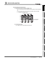
MODEL
QSCPU-U-KP-E
MODEL
CODE
13JR93
Mitsubishi Safety Programmable Logic Controller
QSCPU
User's Manual
(Function Explanation, Program Fundamentals)
SH(NA)-080627ENG-A(0609)MEE
HEAD OFFICE : TOKYO BUILDING, 2-7-3 MARUNOUCHI, CHIYODA-KU, TOKYO 100-8310, JAPAN
NAGOYA WORKS : 1-14 , YADA-MINAMI 5-CHOME , HIGASHI-KU, NAGOYA , JAPAN
When exported from Japan, this manual does not require application to the
Ministry of Economy, Trade and Industry for service transaction permission.
Specifications subject to change without notice.
QS001CPU
SAFETY PRECAUTIONS
(Always read these instructions before using this equipment.)
Before using this product, please read this manual, the relevant manuals introduced in this manual,
standard PLC manuals, and the safety standards carefully and pay full attention to safety to handle the
product correctly.
In this manual, the safety instructions are ranked as "DANGER" and "CAUTION".
DANGER
Indicates that incorrect handling may cause hazardous conditions,
resulting in death or severe injury.
CAUTION
Indicates that incorrect handling may cause hazardous conditions,
resulting in medium or slight personal injury or physical damage.
Note that the
CAUTION level may lead to a serious consequence according to the circumstances.
Always follow the instructions of both levels because they are important to personal safety.
Please save this manual to make it accessible when required and always forward it to the end user.
A-1
[Design Precautions]
DANGER
When a safety PLC detects an error in an external power supply or a failure in PLC main module, it
turns off all the outputs.
Create an external circuit to securely stop the power of hazard by turning off the outputs. Incorrect
configuration may result in an accident.
Create short current protection for a safety relay, and a protection circuit such as a fuse, and breaker,
outside a safety PLC.
When data/program change, or status control is performed from a PC to a running safety PLC,
create an interlock circuit outside the sequence program and safety PLC to ensure that the whole
system always operates safely.
For the operations to a safety PLC, pay full attention to safety by reading the relevant manuals
carefully, and establishing the operating procedure.
Furthermore, for the online operations performed from a PC to a safety CPU module, the corrective
actions against a communication error due to a cable connection fault, etc. should be predetermined
as a system.
All output signals from a safety CPU module to the CC-Link Safety system master module are
prohibited to use.
These signals can be found in the CC-Link Safety System Master Module User's Manual.
Do not turn ON or OFF these signals by sequence program, since turning ON/OFF these output
signals of the PLC system may cause malfunctions and safety operation cannot be guaranteed.
When a safety remote I/O module has detected a CC-Link Safety error, it turns off all the outputs.
Note that the outputs in a sequence program are not automatically turned off.
If a CC-Link Safety error has been detected, create a sequence program that turns off the outputs in
the program.
If the CC-Link Safety is restored with the outputs on, it may suddenly operate and result in an
accident.
To inhibit restart without manual operation after safety functions was performed and outputs were
turned OFF, create an interlock program which uses a reset button for restart.
CAUTION
Do not bunch the wires of external devices or communication cables together with the main circuit or
power lines, or install them close to each other. They should be installed 100 mm (3.94 inch) or more
from each other. Not doing so could result in noise that would cause erroneous operation.
A-2
[Installation Precautions]
CAUTION
Use a safety PLC in the environment that meets the general specifications described in this manual.
Using this PLC in an environment outside the range of the general specifications could result in
electric shock, fire, erroneous operation, and damage to or deterioration of the product.
While pressing the installation lever located at the bottom of module, insert the module fixing tab into
the fixing hole in the base unit until it stops. Then, securely mount the module with the fixing hole as
a supporting point.
Incorrect loading of the module can cause a failure or drop.
Secure the module to the base unit with screws.
Tighten the screw in the specified torque range.
If the screws are too loose, it may cause a drop of the screw or module.
Over tightening may cause a drop due to the damage of the screw or module.
Completely turn off the externally supplied power used in the system before mounting or
removingthe module.
Not doing so could result in damage to the product.
Do not directly touch the module's conductive parts or electronic components.
Doing so may cause malfunctions or a failure.
[Wiring Precautions]
DANGER
Be sure to shut off all phases of the external supply power used by the system before wiring.
Not completely turning off all power could result in electric shock or damage to the product.
When energizing or operating the module after installation or wiring, be sure to close the attached
terminal cover.
Not doing so may result in electric shock.
A-3
[Wiring Precautions]
CAUTION
Be sure to ground the FG terminals and LG terminals to the protective ground conductor.
Not doing so could result in electric shock or erroneous operation.
Use a solderless terminal with insulation sleeve for wiring of a terminal block.
Use up to two solderless terminals for a single terminal.
Use applicable solderless terminals and tighten them with the specified torque.
If any solderlessspade terminal is used, it may be disconnected when the terminal screw comes
loose, resultingin failure.
Wire the module correctly after confirming the rated voltage and terminal layout.
Connecting a power supply of a different rated voltage or incorrect wiring may cause a fire or failure.
Tighten a terminal block mounting screw, terminal screw, and module mounting screw within the
specified torque range.
If the terminal block mounting screw or terminal screw is too loose, it may cause a short circuit, fire,
or malfunctions.
If too tight, it may damage the screw and/or the module, resulting in a drop of the screw or module, a
short circuit or malfunctions.
If the module mounting screw is too loose, it may cause a drop of the screw or module.
Over tightening the screw may cause a drop due to the damage of the screw or module.
Be sure there are no foreign substances such as sawdust or wiring debris inside the module.
Such debris could cause a fire, failure, or erroneous operation.
The module has an ingress prevention label on its top to prevent foreign matter, such as wire offcuts,
from entering the module during wiring.
Do not peel this label during wiring. Before starting system operation, be sure to peel this label
because of heat dissipation.
Install our PLC in a control panel for use.
Wire the main power supply to the power supply module installed in a control panel through a
distribution terminal block.
Furthermore, the wiring and replacement of a power supply module have to be performed by a
maintenance worker who acquainted with shock protection.
(For the wiring methods, refer to the QSCPU User's Manual (Hardware Design, Maintenance and
Inspection))
A-4
[Startup and Maintenance precautions]
DANGER
Do not touch the terminals while power is on.
Doing so could cause shock or erroneous operation.
Correctly connect the battery. Also, do not charge, disassemble, heat, place in fire, short circuit, or
solder the battery.
Mishandling of battery can cause overheating or cracks which could result in injury and fires.
Turn off all phases of the external supply power used in the system when cleaning the module or
retightening the terminal block mounting screws, terminal screws, or module mounting screws.
Not doing so could result in electric shock. Tighten a terminal block mounting screw, terminal screw,
and module mounting screw within the specified torque range.
If the terminal block mounting screw or terminal screw is too loose, it may cause a short circuit, fire,
or malfunctions.
If too tight, it may damage the screw and/or the module, resulting in a drop of the screw or module, a
short circuit or malfunctions.
If the module mounting screw is too loose, it may cause a drop of the screw or module.
Over tightening the screw may cause a drop due to the damage of the screw or module.
A-5
[Startup and Maintenance precautions]
CAUTION
The online operations performed from a PC to a running safety PLC (Program change when a safety
CPU is RUN, device test, and operating status change such as RUN-STOP switching) have to be
executed after the manual has been carefully read and the safety has been ensured.
Following the operating procedure predetermined at designing, the operation has to be performed by
an instructed person.
When changing a program while a safety CPU is RUN (Write during RUN), it may cause a program
breakdown in some operating conditions.
Fully understand the precautions described in the GX Developer's manual before use.
Do not disassemble or modify the modules.
Doing so could cause a failure, erroneous operation, injury, or fire.
If the product is repaired or remodeled by other than the specified FA centers or us, the warranty is
not covered.
Use any radio communication device such as a cellular phone or a PHS phone more than 25cm(9.85
inch) away in all directions of the PLC.
Not doing so can cause a malfunction.
Completely turn off the externally supplied power used in the system before mounting or
removingthe module.
Not doing so could result in damage to the product.
Restrict the mounting/removal of a module, base unit, and terminal block up to 50 times
(IEC61131-2-compliant), after the first use of the product.
Failure to do so may cause the module to malfunction due to poor contact of connector.
Do not drop or give an impact to the battery mounted to the module.
Doing so may damage the battery, causing the battery fluid to leak inside the battery.
If the battery is dropped or given an impact, dispose of it without using.
Before touching the module, always touch grounded metal, etc. to discharge static electricity
fromhuman body, etc.
Not doing so can cause the module to fail or malfunction
A-6
[Disposal Precautions]
CAUTION
When disposing of this product, treat it as industrial waste.
[Transportation Precautions]
CAUTION
When transporting lithium batteries, make sure to treat them based on the transport regulations.
(For details of the controlled models, refer to Appendix 5.)
A-7
REVISIONS
The manual number is given on the bottom left of the back cover.
Print Date
Manual Number
Revision
Sep., 2006
SH(NA)-080627ENG-A First edition
Jun.,2007
SH(NA)-080627ENG-B
Partial correction
Section 3.7.1, 3.7.2, 3.7.3, 4.2.2, 5.3.3, 6.10, 9.1, 9.2, 9.2.4, 9.2.8, 9.5
Japanese Manual Version SH-080608-B
This manual confers no industrial property rights or any rights of any other kind, nor does it confer any patent licenses.
Mitsubishi Electric Corporation cannot be held responsible for any problems involving industrial property rights which may
occur as a result of using the contents noted in this manual.
C
A-8
2004 MITSUBISHI ELECTRIC CORPORATION
INTRODUCTION
Thank you for choosing the Mitsubishi MELSEC-QS Series of Safety Programmable Controllers.
Before using the equipment, please read this manual carefully to develop full familiarity with the functions
and performance of the QS series PLC you have purchased, so as to ensure correct use.
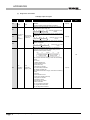
CONTENTS
CHAPTER1 OVERVIEW
1 - 1 to 1 - 11
1.1
Features •••••••••••••••••••••••••••••••••••••••••••••••••••••••••••••••••••••••••••••••••••••••••••••••••••••••••••••• 1 - 3
1.2
Program Storage and Operation ••••••••••••••••••••••••••••••••••••••••••••••••••••••••••••••••••••••••••••••••• 1 - 7
1.3
Devices and Instructions Convenient for Programming ••••••••••••••••••••••••••••••••••••••••••••••••••••• 1 - 9
1.4
How to Check the Serial No. and Function Version •••••••••••••••••••••••••••••••••••••••••••••••••••••••• 1 - 10
CHAPTER2 PERFORMANCE SPECIFICATION
CHAPTER3 SEQUENCE PROGRAM EXECUTION
3.1
2 - 1 to 2 - 2
3 - 1 to 3 - 18
Sequence Program ••••••••••••••••••••••••••••••••••••••••••••••••••••••••••••••••••••••••••••••••••••••••••••••••• 3 - 2
3.1.1
3.1.2
Sequence program description method••••••••••••••••••••••••••••••••••••••••••••••••••••••••••••••••••• 3 - 3
Sequence program operation ••••••••••••••••••••••••••••••••••••••••••••••••••••••••••••••••••••••••••••••• 3 - 4
3.2
Concept of Scan Time ••••••••••••••••••••••••••••••••••••••••••••••••••••••••••••••••••••••••••••••••••••••••••••• 3 - 5
3.3
Operation Processing •••••••••••••••••••••••••••••••••••••••••••••••••••••••••••••••••••••••••••••••••••••••••••••• 3 - 7
3.3.1
3.3.2
3.3.3
3.3.4
Initial processing••••••••••••••••••••••••••••••••••••••••••••••••••••••••••••••••••••••••••••••••••••••••••••••• 3 - 7
CC-Link Safety, MELSECNET/H refresh ••••••••••••••••••••••••••••••••••••••••••••••••••••••••••••••••• 3 - 7
I/O refresh •••••••••••••••••••••••••••••••••••••••••••••••••••••••••••••••••••••••••••••••••••••••••••••••••••••• 3 - 8
END processing ••••••••••••••••••••••••••••••••••••••••••••••••••••••••••••••••••••••••••••••••••••••••••••••• 3 - 8
3.4
RUN, STOP Operation Processing•••••••••••••••••••••••••••••••••••••••••••••••••••••••••••••••••••••••••••••• 3 - 9
3.5
Operation Processing during Momentary Power Failure •••••••••••••••••••••••••••••••••••••••••••••••••• 3 - 11
3.6
Data Clear Processing ••••••••••••••••••••••••••••••••••••••••••••••••••••••••••••••••••••••••••••••••••••••••••• 3 - 12
3.7
Numeric Values which can be Used in Sequence Programs••••••••••••••••••••••••••••••••••••••••••••• 3 - 13
3.7.1
3.7.2
3.7.3
BIN (Binary Code)••••••••••••••••••••••••••••••••••••••••••••••••••••••••••••••••••••••••••••••••••••••••••• 3 - 16
HEX (Hexadecimal)••••••••••••••••••••••••••••••••••••••••••••••••••••••••••••••••••••••••••••••••••••••••• 3 - 17
BCD (Binary Coded Decimal)••••••••••••••••••••••••••••••••••••••••••••••••••••••••••••••••••••••••••••• 3 - 18
CHAPTER4 I/O NUMBER ASSIGNMENT
4 - 1 to 4 - 9
4.1
Definition of I/O Number ••••••••••••••••••••••••••••••••••••••••••••••••••••••••••••••••••••••••••••••••••••••••••• 4 - 1
4.2
Concept of I/O Number Assignment •••••••••••••••••••••••••••••••••••••••••••••••••••••••••••••••••••••••••••• 4 - 2
4.2.1
4.2.2
4.3
I/O numbers of base unit••••••••••••••••••••••••••••••••••••••••••••••••••••••••••••••••••••••••••••••••••••• 4 - 2
I/O number of remote station ••••••••••••••••••••••••••••••••••••••••••••••••••••••••••••••••••••••••••••••• 4 - 2
I/O Assignment by GX Developer ••••••••••••••••••••••••••••••••••••••••••••••••••••••••••••••••••••••••••••••• 4 - 4
A-9
4.3.1
4.3.2
4.3.3
4.4
Purpose of I/O assignment by GX Developer••••••••••••••••••••••••••••••••••••••••••••••••••••••••••••4 - 4
Concept of I/O assignment using GX Developer••••••••••••••••••••••••••••••••••••••••••••••••••••••••4 - 5
Examples of I/O Number Assignment •••••••••••••••••••••••••••••••••••••••••••••••••••••••••••••••••••••4 - 8
Checking the I/O Numbers ••••••••••••••••••••••••••••••••••••••••••••••••••••••••••••••••••••••••••••••••••••••••4 - 9
CHAPTER5 MEMORIES AND FILES HANDLED BY CPU MODULE
5.1
5 - 1 to 5 - 18
Memories by CPU Module ••••••••••••••••••••••••••••••••••••••••••••••••••••••••••••••••••••••••••••••••••••••••5 - 1
5.1.1
5.1.2
5.1.3
5.1.4
Memory configuration and storable data••••••••••••••••••••••••••••••••••••••••••••••••••••••••••••••••••5 - 1
Program memory ••••••••••••••••••••••••••••••••••••••••••••••••••••••••••••••••••••••••••••••••••••••••••••••5 - 3
Standard ROM •••••••••••••••••••••••••••••••••••••••••••••••••••••••••••••••••••••••••••••••••••••••••••••••••5 - 7
Standard ROM program execution (boot run) and writing•••••••••••••••••••••••••••••••••••••••••••••5 - 9
5.2
Program File Structure ••••••••••••••••••••••••••••••••••••••••••••••••••••••••••••••••••••••••••••••••••••••••••• 5 - 14
5.3
File Operation by GX Developer and Handling Precautions•••••••••••••••••••••••••••••••••••••••••••••• 5 - 16
5.3.1
5.3.2
5.3.3
5.3.4
File operation••••••••••••••••••••••••••••••••••••••••••••••••••••••••••••••••••••••••••••••••••••••••••••••••• 5 - 16
Precautions for handling files ••••••••••••••••••••••••••••••••••••••••••••••••••••••••••••••••••••••••••••• 5 - 16
Memory capacities of files ••••••••••••••••••••••••••••••••••••••••••••••••••••••••••••••••••••••••••••••••• 5 - 17
File size units••••••••••••••••••••••••••••••••••••••••••••••••••••••••••••••••••••••••••••••••••••••••••••••••• 5 - 18
CHAPTER6 FUNCTIONS
6 - 1 to 6 - 62
6.1
Function List •••••••••••••••••••••••••••••••••••••••••••••••••••••••••••••••••••••••••••••••••••••••••••••••••••••••••6 - 1
6.2
Safety CPU Operation Mode •••••••••••••••••••••••••••••••••••••••••••••••••••••••••••••••••••••••••••••••••••••6 - 2
6.2.1
6.2.2
6.2.3
6.2.4
6.2.5
Safety CPU operation mode ••••••••••••••••••••••••••••••••••••••••••••••••••••••••••••••••••••••••••••••••6 - 2
Checking safety CPU operation mode ••••••••••••••••••••••••••••••••••••••••••••••••••••••••••••••••••••6 - 5
Safety CPU operation mode switching••••••••••••••••••••••••••••••••••••••••••••••••••••••••••••••••••••6 - 8
Operation of each function in each safety CPU operation mode and CPU operation status • 6 - 14
Online operations that can be executed on the CPU module from GX Developer ••••••••••••• 6 - 16
6.3
CPU access password ••••••••••••••••••••••••••••••••••••••••••••••••••••••••••••••••••••••••••••••••••••••••••• 6 - 18
6.4
PLC memory initialization ••••••••••••••••••••••••••••••••••••••••••••••••••••••••••••••••••••••••••••••••••••••• 6 - 21
6.5
Setting to prevent continuous RUN in TEST MODE ••••••••••••••••••••••••••••••••••••••••••••••••••••••• 6 - 25
6.6
Checking the ROM write count ••••••••••••••••••••••••••••••••••••••••••••••••••••••••••••••••••••••••••••••••• 6 - 27
6.7
Self-diagnostics Function•••••••••••••••••••••••••••••••••••••••••••••••••••••••••••••••••••••••••••••••••••••••• 6 - 28
6.7.1
6.7.2
LED display for error•••••••••••••••••••••••••••••••••••••••••••••••••••••••••••••••••••••••••••••••••••••••• 6 - 31
Cancel the error ••••••••••••••••••••••••••••••••••••••••••••••••••••••••••••••••••••••••••••••••••••••••••••• 6 - 31
6.8
Recording the operation contents and self-diagnostics error occurrence contents (operation · error
history function) ••••••••••••••••••••••••••••••••••••••••••••••••••••••••••••••••••••••••••••••••••••••••••••••••••• 6 - 34
6.9
Constant scan ••••••••••••••••••••••••••••••••••••••••••••••••••••••••••••••••••••••••••••••••••••••••••••••••••••• 6 - 38
6.10 Setting of Output (Y) Status when Changing between STOP and RUN ••••••••••••••••••••••••••••••• 6 - 41
6.11 Clock Function••••••••••••••••••••••••••••••••••••••••••••••••••••••••••••••••••••••••••••••••••••••••••••••••••••• 6 - 44
6.12 Remote Operation •••••••••••••••••••••••••••••••••••••••••••••••••••••••••••••••••••••••••••••••••••••••••••••••• 6 - 47
6.12.1
6.12.2
6.12.3
Remote RUN/STOP •••••••••••••••••••••••••••••••••••••••••••••••••••••••••••••••••••••••••••••••••••••••• 6 - 47
Remote RESET•••••••••••••••••••••••••••••••••••••••••••••••••••••••••••••••••••••••••••••••••••••••••••••• 6 - 50
Relationship of remote operation and CPU's RUN/STOP status •••••••••••••••••••••••••••••••••• 6 - 52
6.13 Monitor Function •••••••••••••••••••••••••••••••••••••••••••••••••••••••••••••••••••••••••••••••••••••••••••••••••• 6 - 53
6.14 Writing in Program during CPU Module RUN ••••••••••••••••••••••••••••••••••••••••••••••••••••••••••••••• 6 - 54
A - 10
6.14.1
Online change in ladder mode•••••••••••••••••••••••••••••••••••••••••••••••••••••••••••••••••••••••••••• 6 - 54
6.15 Watchdog Timer (WDT) ••••••••••••••••••••••••••••••••••••••••••••••••••••••••••••••••••••••••••••••••••••••••• 6 - 58
6.16 CPU Module System Display by GX Developer •••••••••••••••••••••••••••••••••••••••••••••••••••••••••••• 6 - 60
6.17 LED Display •••••••••••••••••••••••••••••••••••••••••••••••••••••••••••••••••••••••••••••••••••••••••••••••••••••••• 6 - 62
6.17.1
Method to turn off the LED •••••••••••••••••••••••••••••••••••••••••••••••••••••••••••••••••••••••••••••••• 6 - 62
CHAPTER7 COMMUNICATION WITH INTELLIGENT FUNCTION MODULE
7 - 1 to 7 - 2
7.1
Communication with CC-Link Safety master module •••••••••••••••••••••••••••••••••••••••••••••••••••••••• 7 - 1
7.2
Communications with MELSECNET/H module ••••••••••••••••••••••••••••••••••••••••••••••••••••••••••••••• 7 - 2
CHAPTER8 PARAMETERS
8 - 1 to 8 - 12
8.1
PLC Parameters •••••••••••••••••••••••••••••••••••••••••••••••••••••••••••••••••••••••••••••••••••••••••••••••••••• 8 - 2
8.2
Network Parameters ••••••••••••••••••••••••••••••••••••••••••••••••••••••••••••••••••••••••••••••••••••••••••••• 8 - 10
CHAPTER9 DEVICE EXPLANATION
9 - 1 to 9 - 35
9.1
Device List•••••••••••••••••••••••••••••••••••••••••••••••••••••••••••••••••••••••••••••••••••••••••••••••••••••••••••• 9 - 1
9.2
Internal User Devices •••••••••••••••••••••••••••••••••••••••••••••••••••••••••••••••••••••••••••••••••••••••••••••• 9 - 2
9.2.1
9.2.2
9.2.3
9.2.4
9.2.5
9.2.6
9.2.7
9.2.8
9.2.9
9.2.10
9.2.11
9.2.12
9.3
Input (X) ••••••••••••••••••••••••••••••••••••••••••••••••••••••••••••••••••••••••••••••••••••••••••••••••••••••••• 9 - 5
Output (Y)••••••••••••••••••••••••••••••••••••••••••••••••••••••••••••••••••••••••••••••••••••••••••••••••••••••• 9 - 7
Internal relay (M) •••••••••••••••••••••••••••••••••••••••••••••••••••••••••••••••••••••••••••••••••••••••••••••• 9 - 8
Annunciator (F) •••••••••••••••••••••••••••••••••••••••••••••••••••••••••••••••••••••••••••••••••••••••••••••••• 9 - 9
Edge relay (V)•••••••••••••••••••••••••••••••••••••••••••••••••••••••••••••••••••••••••••••••••••••••••••••••• 9 - 14
Link relay (B) ••••••••••••••••••••••••••••••••••••••••••••••••••••••••••••••••••••••••••••••••••••••••••••••••• 9 - 15
Link special relay (SB) ••••••••••••••••••••••••••••••••••••••••••••••••••••••••••••••••••••••••••••••••••••• 9 - 17
Timer (T) •••••••••••••••••••••••••••••••••••••••••••••••••••••••••••••••••••••••••••••••••••••••••••••••••••••• 9 - 18
Counter (C) ••••••••••••••••••••••••••••••••••••••••••••••••••••••••••••••••••••••••••••••••••••••••••••••••••• 9 - 24
Data register (D)••••••••••••••••••••••••••••••••••••••••••••••••••••••••••••••••••••••••••••••••••••••••••••• 9 - 28
Link register (W) ••••••••••••••••••••••••••••••••••••••••••••••••••••••••••••••••••••••••••••••••••••••••••••• 9 - 29
Link special register (SW) ••••••••••••••••••••••••••••••••••••••••••••••••••••••••••••••••••••••••••••••••• 9 - 31
Internal System Devices••••••••••••••••••••••••••••••••••••••••••••••••••••••••••••••••••••••••••••••••••••••••• 9 - 32
9.3.1
9.3.2
Special relay (SM)••••••••••••••••••••••••••••••••••••••••••••••••••••••••••••••••••••••••••••••••••••••••••• 9 - 32
Special register (SD) ••••••••••••••••••••••••••••••••••••••••••••••••••••••••••••••••••••••••••••••••••••••• 9 - 33
9.4
Nesting (N) ••••••••••••••••••••••••••••••••••••••••••••••••••••••••••••••••••••••••••••••••••••••••••••••••••••••••• 9 - 34
9.5
Constants••••••••••••••••••••••••••••••••••••••••••••••••••••••••••••••••••••••••••••••••••••••••••••••••••••••••••• 9 - 35
9.5.1
9.5.2
Decimal constant (K) ••••••••••••••••••••••••••••••••••••••••••••••••••••••••••••••••••••••••••••••••••••••• 9 - 35
Hexadecimal constant (H) ••••••••••••••••••••••••••••••••••••••••••••••••••••••••••••••••••••••••••••••••• 9 - 35
CHAPTER10 CPU MODULE PROCESSING TIME
10.1
Scan Time •••••••••••••••••••••••••••••••••••••••••••••••••••••••••••••••••••••••••••••••••••••••••••••••••••••••••• 10 - 1
10.1.1
10.1.2
10.1.3
10.2
10 - 1 to 10 - 7
structure and calculation of scan time••••••••••••••••••••••••••••••••••••••••••••••••••••••••••••••••••• 10 - 1
Time required for each processing included in scan time ••••••••••••••••••••••••••••••••••••••••••• 10 - 2
Factors that increase the scan time ••••••••••••••••••••••••••••••••••••••••••••••••••••••••••••••••••••• 10 - 5
Other Processing Times ••••••••••••••••••••••••••••••••••••••••••••••••••••••••••••••••••••••••••••••••••••••••• 10 - 7
A - 11
CHAPTER11 PROCEDURE FOR WRITING PROGRAM TO CPU MODULE 11 - 1 to 11 - 4
11.1
Items to be examined for program creation•••••••••••••••••••••••••••••••••••••••••••••••••••••••••••••••••• 11 - 1
11.2
Procedure for writing program •••••••••••••••••••••••••••••••••••••••••••••••••••••••••••••••••••••••••••••••••• 11 - 2
11.3
Boot run procedure ••••••••••••••••••••••••••••••••••••••••••••••••••••••••••••••••••••••••••••••••••••••••••••••• 11 - 4
APPENDICES
App - 1 to App - 25
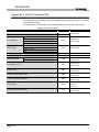
Appendix 1
Special Relay List •••••••••••••••••••••••••••••••••••••••••••••••••••••••••••••••••••••••••••••••••••••• App - 1
Appendix 2
Special Register List••••••••••••••••••••••••••••••••••••••••••••••••••••••••••••••••••••••••••••••••••• App - 5
Appendix 3
List of Parameter No.•••••••••••••••••••••••••••••••••••••••••••••••••••••••••••••••••••••••••••••••••App - 20
Appendix 4
Restrictions on Using MELSECNET/H Module in the Safety CPU Module••••••••••••••••App - 22
Appendix 5
Precautions for Battery Transportation •••••••••••••••••••••••••••••••••••••••••••••••••••••••••••App - 25
INDEX
A - 12
INDEX - 1 to INDEX - 2
(Related manual)..................
QSCPU User's Manual (Hardware Design, Maintenance and Inspection)
CONTENTS
CHAPTER1 OVERVIEW
1.1
Features
CHAPTER2 SYSTEM CONFIGURATION
2.1
System Configuration
2.2
Configuration of Peripheral Devices
2.3
Confirming Serial No. and Function Version
CHAPTER3 GENERAL SPECIFICATIONS
CHAPTER4 CPU MODULE
4.1
Performance Specifications
4.2
Part Names
4.3
Switch Operation after Writing a Program
4.4
Reset Operation
CHAPTER5 POWER SUPPLY MODULE
5.1
Specifications
5.2
Precaution when connecting the uninterruptive power supply
5.3
Names of Parts and Settings
CHAPTER6 BASE UNIT
6.1
Specification
6.2
Part Names
CHAPTER7 BATTERY
7.1
Battery (Q6BAT)
7.1.1
7.1.2
Battery Specifications
Installation of Battery
CHAPTER8 CPU MODULE START-UP PROCEDURES
8.1
Procedure before Operating in the SAFETY MODE
A - 13
CHAPTER9 EMC AND LOW VOLTAGE DIRECTIVES
9.1
Requirements for Conformance to EMC Directive
9.1.1
9.1.2
9.1.3
9.1.4
9.1.5
9.2
Standards relevant to the EMC Directive
Installation instructions for EMC Directive
Cables
Power Supply Module
Others
Requirement to Conform to the Low Voltage Directive
9.2.1
9.2.2
9.2.3
9.2.4
9.2.5
9.2.6
Standard applied for MELSEC-QS series PLC
MELSEC-QS series PLC selection
Power supply
Control panel
Grounding
External wiring
CHAPTER10 LOADING AND INSTALLATION
10.1
Calculating Heat Generation of PLC
10.2
Module Installation
10.2.1
10.2.2
10.2.3
10.3
Precaution on installation
Instructions for mounting the base unit
Installation and removal of module
Wiring
10.3.1
10.3.2
The precautions on the wiring
Connecting to the power supply module
CHAPTER11 MAINTENANCE AND INSPECTION
11.1
Daily Inspection
11.2
Periodic Inspection
11.3
Battery Life and Replacement Procedure
11.3.1
11.3.2
Battery lives of CPU modules
Replacement Procedure of the CPU Module Battery
11.4
When PLC Has been Stored without a Battery
11.5
When Battery Has Gone Flat during Storage of a PLC
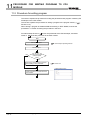
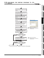
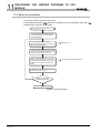
CHAPTER12 TROUBLESHOOTING
12.1
Troubleshooting Basics
12.2
Troubleshooting Flowchart
12.2.1
12.2.2
12.2.3
12.2.4
12.2.5
12.2.6
12.2.7
A - 14
Troubleshooting category flow
Flowchart for when the ERR terminal (negative logic) is off (opened)
Flowchart for when the "POWER" LED is off
When the "ALIVE" LED does not come on or is off
Flowchart for when the "RUN" LED is off
When the "RUN" LED is flashing
Flowchart for when the "ERR." LED is on/flashing
12.2.8
12.2.9
12.2.10
12.2.11
12.3
When the "USER" LED is on
When the "BAT." LED is on
Flowchart for when a program cannot be read
Flowchart for when a program cannot be written
Error Code List
12.3.1
12.3.2
12.3.3
12.3.4
12.3.5
12.3.6
12.3.7
12.3.8
Error codes
Reading an error code
Error code list (1000 to 1999)
Error code list (2000 to 2999)
Error code list (3000 to 3999)
Error code list (4000 to 4999)
Error code list (5000 to 5999)
Error code list (8000 to 9000)
12.4
Canceling Errors
12.5
Error codes returned to request source during communication with CPU module
12.6
Special Relay List
12.7
Special Register List
APPENDICES
Appendix 1 External Dimensions
Appendix 1.1 CPU module
Appendix 1.2 Power supply module
Appendix 1.3 Main base unit
Appendix 2 Precautions for Battery Transportation
INDEX
A - 15
ABOUT MANUALS
Introduction Manual
Before constructing or designing the safety-related system, be sure to read the following
manual.
Manual No.
Manual Name
(Model Code)
Safety Application Guide
Explains the overview and construction method of the safety-related system, laying and wiring examples,
SH-080613ENG
(13JR90)
application programs and others.
(Sold separately)
The following manuals are also related to this product.
In necessary, order them by quoting the details in the tables below.
Related Manuals
Manual Number
Manual Name
(Model Code)
QSCPU User's Manual (Hardware Design, Maintenance and Inspection)
Explains the specifications of the QSCPU, safety power supply modules, safety base unit and other.
(Sold separately)
QSCPU Programming Manual (Common Instructions)
SH-080626ENG
(13JR92)
SH-080628ENG
Explains how to use the sequence instructions and application instructions.
(Sold separately)
(13JW01)
CC-Link Safety System Master Module User's Manual
QS0J61BT12
Explains the specifications, procedures and settings up to operation, parameter settings and troubleshooting of
the QS0J61BT12 type CC-Link Safety system master module.
SH-080600ENG
(13JR88)
(Sold separately)
CC-Link Safety System Remote I/O Module User's Manual
QS0J65BTB2-12DT
Explains the specifications, procedures and settings up to operation, parameter settings and troubleshooting of
the CC-Link Safety system remote I/O module.
SH-080612ENG
(13JR89)
(Sold separately)
Q Corresponding MELSECNET/H Network System Reference Manual (PLC to PLC network)
Explains the specifications for a MELSECNET/H network system for PLC to PLC network. It explains the
procedures and settings up to operation, setting the parameters, programming and troubleshooting.
SH-080049
(13JF92)
(Sold separately)
GX Developer Version 8 Operating Manual
Explains the online functions of the GX Developer, such as the programming, printout, monitoring, and
SH-080373E
(13JU41)
debugging methods.
(Sold separately)
GX Developer Version 8 Operating Manual (Safety PLC)
SH-080576ENG
Explains the added and updated GX Developer functions to support the safety PLC.
(Sold separately)
(13JU53)
Remark
Printed materials are separately available for single item purchase. Order the
manual by quoting the manual number on the table above (Model code).
A - 16
HOW TO SEE THIS MANUAL IS ORGANIZED
Reference destination
Chapter heading
A reference destination or
reference manual is marked
.
The index on the right side of the page
shows the chapter of the open page at a
glance.
Section title
The section of the open page is shown at a
glance.
A - 17
In addition, this manual provides the following explanations.
POINT
Explains the matters to be especially noted, the functions and others related to the
description.
Remark
Provides the reference destination related to the description on that page and the
convenient information.
A - 18
HOW TO USE THIS MANUAL
This manual is prepared for users to understand memory map, functions, programs and
devices of the CPU module when you use QS Series PLCs.
The manual is classified roughly into three sections as shown below.
1) Chapters 1
Describe the outline of the CPU module.
2) Chapters 2 to 5
Describe the performance specifications, executable program, I/O
No. and memory of the CPU module.
3) Chapter 6
Describes the functions of the CPU modules.
4) Chapter 7
Describes communication with intelligent function modules.
5) Chapters 8 and 9
Describe parameters and devices used in the CPU modules.
6) Chapter 10
Describes the CPU module processing time.
7) Chapter 11
Describes the procedure for writing parameters and programs
created at the GX Developer to the CPU module.
Remark
This manual does not explain the functions of power supply modules, base units,
extension cables, memory cards and batteries of CPU module.
For these details, refer to the manual shown below.
QSCPU User's Manual (Hardware Design, Maintenance and Inspection)
A - 19
GENERIC TERMS AND ABBREVIATIONS
Unless otherwise specified, this manual uses the following generic terms and
abbreviations to explain the QS series CPU modules.
Generic Term/Abbreviation
PLC
Safety PLC
Standard PLC
QS series
Description
Abbreviation for Programmable Logic Controller.
General name for safety CPU module, safety power supply module, safety main base
unit, CC-Link safety master module and CC-Link safety remote I/O module.
General name of each module for MELSEC-Q series, MELSEC-QnA series, MELSEC-A
series and MELSEC-FX series. (Used for distinction from safety PLC.)
Abbreviation for Mitsubishi safety PLC MELSEC-QS series, MELSEC-QnA series,
MELSEC-A series and MELSEC-FX series. (Used for distinction from safety PLC.)
QS001CPU
Abbreviation for the QS001CPU type safety CPU module.
CPU module
Other name for the QS001CPU.
GX Developer
QS034B
General product name for the models SW8D5C-GPPW, SW8D5C-GPPW-A,
SW8D5C-GPPW-V and SW8D5C-GPPW-VA.
Abbreviation for the QS034B type safety main base unit.
Base unit
Other name for the QS034B.
QS061P
Abbreviation for the QS061P-A1 and QS061P-A2 type safety power supply modules.
Power supply module
Other name for the QS061P.
QS0J61BT12
Abbreviation for the QS0J61BT12 type CC-Link Safety system master module.
CC-Link Safety master module
Other name for the QS061BT12.
MELSECNET/H module
General name for the QJ71LP21-25, QJ71LP21S-25, QJ71LP21G and QJ71BR11 type
MELSECNET/H network modules.
Intelligent function module
General name for the CC-Link Safety master module and MELSECNET/H module.
QS0J65BTB2-12DT
Abbreviation for the QS0J65BTB2-12DT type CC-Link Safety remote I/O module.
CC-Link Safety remote I/O
module
Other name for the QS0J65BTB2-12DT.
General name for the Q00JCPU, Q00CPU, Q01CPU, Q02CPU, Q02HCPU, Q06HCPU,
Q series CPU module
Q12HCPU, Q25HCPU, Q12PHCPU, Q25PHCPU, Q12PRHCPU and Q25PRHCPU
modules.
Standard CPU module
Battery
Blank cover
GOT
A - 20
Other name for the Q series CPU module. (Used for distinction from safety CPU
modules.)
Abbreviation for the Q6BAT type battery.
Abbreviation for the QG60 type blank cover.
General name for the Mitsubishi Graphic Operation Terminal GOT-A*** series, GOT-F***
series and GOT1000 series.
1
OVERVIEW
1
This manual describes the programs, I/O number assignment method, functions and
devices of the QS Series CPU Modules (QS001CPU).
Overview
CHAPTER1 OVERVIEW
2
For the power supply modules, base units and batteries, refer to the manual below.
Performance
Specification
QSCPU User's Manual (Hardware Design, Maintenance and Inspection)
Sequence Program
Configuration and
Execution Conditions
3
I/O Nunber Assignment
4
Memories and Files
Handled by CPU Module
5
Functions
6
Communication with
Intelligent Function
Module
7
1-1
Parameters
8
1
OVERVIEW
(1) List of QS Series CPU Module manuals
The QS series CPU module manuals are as shown below.
For details such as manual numbers, refer to "ABOUT MANUALS" in this manual.
Table1.1 List of manuals of QS Series CPU module
Hardware
(Packed)
Purpose
QSCPU CPU
Module User's
Manual (Hardware)
Maintenance
and
Inspection
QSCPU User's
Manual (Hardware
Design,
Maintenance and
inspection)
Program
Fundamentals
QSCPU User's
Manual (Function
Explanation,
Program
Fundamentals)
Common
Instructions
QSCPU
Programming
Manual (Common
Instruction)
Confirmation of part names and
specifications of the CPU module
Details
Outline
Outline
Confirmation of connection methods
for the power supply module, base
unit and I/O module
Details
Outline
Construction of the single CPU
system (confirmation of start-up
procedure and I/O number
Details
assignment)
Confirmation of the sequence program
Details
configuration and memory
Confirmation of the functions,
parameters, and devices of the CPU
Details
module
Confirmation of the troubleshooting
and error codes
Details
Confirmation of usage of sequence
instructions, basic instructions,
application instructions, etc.
1-2
Details
OVERVIEW
1
1.1 Features
Overview
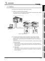
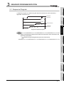
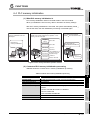
The QS series CPU module has the following new features:
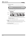
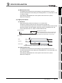
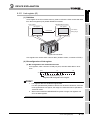
(1) Safety PLC system can be constructed
2
Performance
Specification
The QS series PLCs have obtained the highest safety level (IEC61508 SIL3, EN9541/ISO13849-1 Category 4) applicable to PLCs.
Power supply/CPU/CC-Link Safety master module
Sequence Program
Configuration and
Execution Conditions
3
CC-Link Safety remote I/O station
I/O Nunber Assignment
4
CC-Link Safety
GX Developer
(Version 8.40S or later)
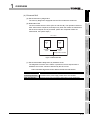
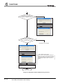
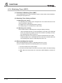
(2) The safety CPU operation mode is equipped for safe system operation
The CPU module is equipped with two safety CPU operation modes. "SAFETY
MODE" for safe system operation and "TEST MODE" for system construction and
maintenance.
These two modes prevent the user's erroneous operations for safe system operation.
(a) SAFETY MODE
SAFETY MODE is a mode for safe system operation. This mode prohibits the
write operation from a programming tool and the device test operation during the
system operation.
(b) TEST MODE
TEST MODE is a mode for maintenance. This mode enables the write operation
from a programming tool and the device test operation to debug or maintain the
sequence program.
6
Functions
Figure 1.1 Safety PLC system
7
Communication with
Intelligent Function
Module
Light curtain
Memories and Files
Handled by CPU Module
5
Emergency stop switch
8
1.1 Features
1-3
Parameters
1
1
OVERVIEW
(3) Enriched operation history and error history
The CPU module can record a total of 3000 operation/error history entries for the
details of the CPU module operation by the user and for the errors occurred in the
CPU module or the CC-Link Safety system.
Recording the details of the CPU module operation by the user into the operation/
error history clarifies the occurrence order of operations and errors. Troubleshooting
becomes easier by confirming the error/operation history.
The contents recorded in the operation/error history are shown in Table1.2.
Table1.2 Recorded contents of operation/error history
Information
Operation
history
information
Contents
User's operations for the CPU module are
stored as a history.
(Operations which change the CPU module
status are recorded.)
History Information per Entry
• Operation code
• Operation message
• Operation execution date
• Result code
• Operation attached information
• Error code
The following errors are stored as a history.
Error history
• Error/failure detected by self-diagnostics
information
• Hardware error
• Error detected by CC-Link Safety system
• Error message
• Occurrence date
• Error information category (common
information/individual information)
• Error information (common
information/individual information)
1-4
1.1 Features
OVERVIEW
1
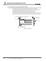
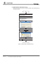
(4) Enhanced RAS
Overview
(a) Enhanced memory diagnostics
The memory diagnostics equipped with the CPU module are enhanced.
3
CPU
B
4
Operation
result
I/O Nunber Assignment
Compare
Output when matched
Figure 1.2 Redundant CPU
(c) Enhanced hardware diagnostics by hardware circuit
The diagnostic functions of the Table1.3 prevents incorrect outputs when a
5
hardware error which cannot be detected by the OS occurs.
Table1.3 Hardware diagnostics function added to the QS series CPU module
Diagnostics
Overvoltage/
Diagnosis Contents
Overvoltage or undervoltage is detected for the power supply voltage
provided from the power supply module to the CPU module.
Clock stop detection
The input clock stop to the CPU module internal circuit is detected.
6
Functions
undervoltage detection
Memories and Files
Handled by CPU Module
Operation
result
Sequence Program
Configuration and
Execution Conditions
CPU module
CPU
A
2
Performance
Specification
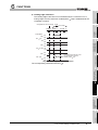
(b) Redundant CPU
The CPU module has two CPUs (CPU A and CPU B). The operation results of
CPU A/CPU B are compared, and output only when the results are matched so
that incorrect outputs can be prevented. (When the compared results are
mismatched, the system stops.)
Communication with
Intelligent Function
Module
7
8
1.1 Features
1-5
Parameters
1
1
OVERVIEW
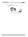
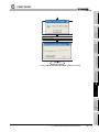
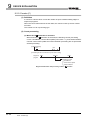
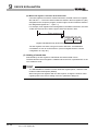
(5) USB interface is equipped
The CPU module is equipped with the USB interface to communicate with a
programming tool.
USB
Personal computer
Figure 1.3 Connection to a personal computer using USB
1-6
1.1 Features
1
OVERVIEW
1
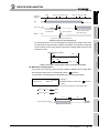
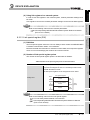
(1) Program storage
2
Performance
Specification
(a) Storage of program created by GX Developer
The program created by GX Developer can be stored into the program memory or
standard ROM of the CPU module.Note1
Overview
1.2 Program Storage and Operation
Program memory
3
Parameter
Sequence Program
Configuration and
Execution Conditions
Program
Device comment
Standard ROM *1
4
CPU module
I/O Nunber Assignment
Parameter
Program
Device comment
Memories and Files
Handled by CPU Module
5
* 1 : The standard ROM is used to ROM the program memory.
Diagram 1.4 Memory configuration and storage destinations
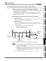
(b) Program execution
The CPU module operates the program stored in the program memory.
Program memory
Parameter
6
Execution of program
in program memory
Program
Functions
Device comments
For program comment display
by GX Developer
Communication with
Intelligent Function
Module
7
Diagram 1.5 Execution of stored program
Note1
1.2 Program Storage and Operation
1-7
Parameters
8
1
OVERVIEW
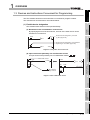
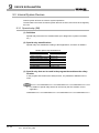
(c) Execution of program stored in standard ROM
Programs and data can also be stored into the standard ROM.
The programs stored in the standard ROM can be booted (read) to the program
memory and executed when the PLC is powered ON or the CPU module is
reset.Note2
Execution of program booted from the
standard ROM to the program memory.
Program
memory
Parameter
Boot
Standard ROM
Program
Device
comment
Diagram 1.6 Boot run
Note2
1-8
1.2 Program Storage and Operation
OVERVIEW
1
1.3 Devices and Instructions Convenient for Programming
Overview
The CPU module has devices and instructions convenient for program creation.
The main devices and instructions are outlined below.
2
(1) Flexible device designation
CPU modules allow devices to be specified flexibly.
Performance
Specification
(a) Word device bits are handled as contacts/coils
By specifying the bit of the word device, each bit of the word device can be
handled as a contact/coil.
Word device bit designation (Turns ON
(1) Bit 5 (b5) of D0.)
X100
3
Sequence Program
Configuration and
Execution Conditions
D0.5
Word device bit designation (Turns ON/OFF
depending on 1/0 of Bit 5 (b5) in D0.)
D0.5
Y100
4
Diagram 1.7 Designation of word device bit
(b) Input need not be pulsed by use of differential contact
An input need not be pulsed by use of a differential contact(
/
).
Differential contact
X100 X102
X100
Y100
PLS
M0
Y100
M0
X102
Y100
ON at leading
edge of X100
Y100
I/O Nunber Assignment
SET
5
Memories and Files
Handled by CPU Module
SET
6
Functions
Diagram 1.8 Use of differential contact
Communication with
Intelligent Function
Module
7
8
1.3 Devices and Instructions Convenient for Programming
1-9
Parameters
1
1
OVERVIEW
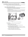
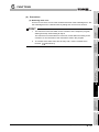
1.4 How to Check the Serial No. and Function Version
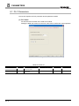
The serial No. and function version of the CPU module can be checked on the rating plate
or in the system monitor of GX Developer.
(1) Checking on rating plate
The rating plate is on the side face of the CPU module.
PASSED
MODEL
Serial No. (first 5 digits)
function version
SERIAL 080910000000000-A
Standard symbol for
conformance is described.
MADE IN JAPAN
Diagram 1.9 Rating plate
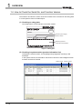
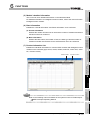
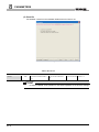
(2) Checking in system monitor (product information list)
To display the system monitor, choose [Diagnostics] [System monitor] on GX
Developer.
In the system monitor, the serial Nos. and function versions of the intelligent function
modules can also be checked.
Serial number function version
Diagram 1.10 System monitor
1 - 10
1.4 How to Check the Serial No. and Function Version
OVERVIEW
1
2
Performance
Specification
The serial No. described on rating plate and that displayed in product information list
of GX Developer may be different.
• The serial No. on rating plate shows the management information of
products.
• The serial No. displayed in product information list of GX Developer
shows the functions of products.
The functions of products are updated when a function is added.
Overview
POINT
Sequence Program
Configuration and
Execution Conditions
3
I/O Nunber Assignment
4
Memories and Files
Handled by CPU Module
5
Functions
6
Communication with
Intelligent Function
Module
7
8
1.4 How to Check the Serial No. and Function Version
1 - 11
Parameters
1
2
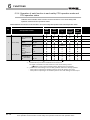
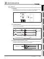
PERFORMANCE SPECIFICATION
CHAPTER2 PERFORMANCE SPECIFICATION
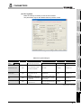
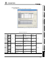
Table2.1 shows the performance specifications of the CPU module.
Table2.1 Performance Specifications
Item
Control method
QS001CPU
Repetitive operation of stored program
Remarks
----
I/O control mode
Refresh mode*3
----
Relay symbol language, function block.
----
0.10 s
----
0.35 s
----
Program
Sequence control
language
Processing speed
language
LD X0
(sequence
instruction)
Constant scan
MOV D0 D1
(Function for keeping regular scan
time)
Program capacity *1
Program memory
Memory
(drive 0)
capacity*1
Standard ROM
(drive 4)
1 to 2000ms
(Setting available in1ms unit.)
Setting by parameters.
14k steps
Section 5.1.1
(56k bytes)
Section 5.1.2
128k bytes
Section 5.1.2
128k bytes
Section 5.1.3
Max. number of
Program memory
3*2
Section 5.1.2
files stored
Standard ROM
3*2
Section 5.1.3
No. of times of writing data into the
standard ROM
Max.100000 times
No. of I/O device points
6144 points(X/Y0 to 17FF)
No. of I/O points
1024 points(X/Y0 to 3FF)
*1
: The maximum number of executable sequence steps is as shown below.
(Program capacity) - (File heade size (default: 34 steps))
Refer to CHAPTER 5 for details of the program capacity and file.
*2
: Each of parameter, sequence program, SFC program, and device comment files can be stored.
*3
: The refresh mode batch-accesses I/O modules before start of sequence program operation.
2-1
----
No. of points usable on
program
No. of points accessible
to the actual I/O module
2
PERFORMANCE SPECIFICATION
1
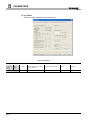
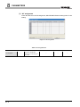
Table2.1 Performance Specifications (Continue)
QS001CPU
6144 points by default (M0-6143) (changeable)
Link relay [B]
2048 points by default (B0 to 7FF) (changeable)
Remarks
Overview
Item
Internal relay [M]
512 points by default (T0 to 511) (changeable)
(Sharing of low- and high-speed timers)
2
The low- and high-speed timers are specified by the instructions.
Timer [T]
The measurement unit of the low- and high-speed timers is set up by
parameters.
The low- and high-speed retentive timers are specified by the instructions.
Retentive timer [ST]
The measurement unit of the low- and high-speed retentive timers is set
can be changed within
the setting range.
Section 9.2
Sequence Program
Configuration and
Execution Conditions
up by parameters.
(Low-speed retentive timer: 1 to 1000ms, 1ms unit, 100ms by default)
(High-speed retentive timer: 0.1 to 100ms, 0.1ms unit, 10ms by default)
Counter [C]
• Normal counter: 512 points by default (C0 to 511) (changeable)
Data register [D]
6144 points by default (D0 to 6143) (changeable)
Link register [W]
2048 points by default (W0 to 7FF) (changeable)
Annunciator [F]
1024 points by default (F0 to 1023) (changeable)
Edge relay [V]
1024 points by default (V0 to 1023) (changeable)
Link special relay [SB]
1536 points (SB0 to 5FF)
Link special register [SW]
1536 points (SW0 to 5FF)
Special relay [SM]
5120 points (SM0 to 5119)
Special register [SD]
4
The number of device
points is fixed.
5120 points (SD0 to 5119)
One contact can be set up in X0 to 17FF for each of RUN. No PAUSE
RUN/PAUSE contact
contact.
Setting by parameters.
Year, month, date, hour, minute, second and day-of-week
(leap year automatically identified)
Timer function
Accuracy: -3.18 to +5.25s (TYP. +2.14s) / d at 0
Section 6.11
Accuracy: -3.18 to +2.59s (TYP. +2.07s) / d at 25
Accuracy: -12.97 to +3.63s (TYP. -3.16s) / d at 55
period
5VDC internal current consumption
----
0.43A
----
H
98mm
----
W
55.2mm
----
D
115mm
----
0.29kg
----
IP2X
----
Weight
Protection of degree
6
7
Remark
Refer to the following manual for the general specifications.
QSCPU User's Manual (Hardware Design, Maintenance and Inspection)
Communication with
Intelligent Function
Module
External dimensions
Varies depending on the power supply module
5
Functions
Allowable instantaneous power failure
3
I/O Nunber Assignment
(changeable)
The number of points
Memories and Files
Handled by CPU Module
0 point by default (sharing of the low- and high-speed retentive timers)
8
2-2
Parameters
No. of device points
(High-speed timer: 0.1 to 100ms, 0.1ms unit, 10ms by default)
Performance
Specification
(Low-speed timer: 1 to 1000ms, 1ms unit, 100ms by default)
3
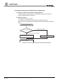
SEQUENCE PROGRAM EXECUTION
CHAPTER3 SEQUENCE PROGRAM EXECUTION
The CPU module executes a program in the following order
Initial processing
CC-Link Safety Master module,
MELSECNET/H module refresh
I/O module refresh processing
Program operation processing
END processing
Diagram 3.1 Program execution order
3-1
SEQUENCE PROGRAM EXECUTION
1
3.1 Sequence Program
Overview
A sequence program is created using the sequence instructions, basic instructions,
application instructions, etc.
2
Sequence
instruction
X100
M0
K100
T0
Performance
Specification
T0
Y100
Basic instruction
X140
BIN K4X120
D0
3
Application
instruction
X141
D1
D2
Sequence Program
Configuration and
Execution Conditions
WAND D0
Diagram 3.2 Sequence program
Remark
4
I/O Nunber Assignment
Refer to the following manual for the sequence instructions, basic instructions and
application instructions.
QSCPU Programming Manual (Common Instructions)
Memories and Files
Handled by CPU Module
5
Functions
6
Communication with
Intelligent Function
Module
7
8
3.1 Sequence Program
3-2
Parameters
3
3
SEQUENCE PROGRAM EXECUTION
3.1.1 Sequence program description method
The sequence program is created with the ladder mode of GX Developer.
The ladder mode is based on the concept of a sequence circuit of relay control. It
enables programming in representation close to a sequence circuit.
In the ladder mode, programming is performed in ladder block units.
A ladder block is the minimum unit for performing sequence program operation, which
starts from the left side vertical bus bar and ends at the right side vertical bus bar.
Left side vertical bus bar N/O contact N/C contact
Coil (output)
X100
Y120
0
Step number 2
X101 X102 X103
Y121
Y122
Y123
8
X104 X105
Y124
Y124
X100 to 105 indicate inputs.
Y120 to 124 indicates outputs.
Diagram 3.3 Ladder mode
3-3
3.1 Sequence Program
3.1.1 Sequence program description method
Right side
vertical bus bar
Ladder block
SEQUENCE PROGRAM EXECUTION
1
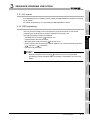
The CPU module calculates in order from the left to the right side vertical bus and
from top to bottom.
2
[Ladder mode]
From left to right
8)
9)
0
10)
Y110
From top
to bottom
3)
4)
X102 X103
6)
Performance
Specification
7)
2)
X100 X101 X105 X106 X107
5)
X104
3
Sequence Program
Configuration and
Execution Conditions
11)
END
10
1) to 11) indicate operation order of
sequence program.
Diagram 3.4 Comparison between ladder mode and list mode
(1) Execution operation of sequence program
The sequence program is executed from Step 0 to the END instruction, where
END processing is performed.
After the END processing, the program restarts operation from Step 0.
Step 0
Indicates execution of program.
Sequence
program
4
I/O Nunber Assignment
1)
Overview
3.1.2 Sequence program operation
END
Memories and Files
Handled by CPU Module
5
END
END
processing
Diagram 3.5 Sequence program
Functions
6
Communication with
Intelligent Function
Module
7
8
3.1 Sequence Program
3.1.2 Sequence program operation
3-4
Parameters
3
3
SEQUENCE PROGRAM EXECUTION
3.2 Concept of Scan Time
(1) Scan time
Scan time is a period from the time when the CPU module starts the sequence
program operation from Step 0 until it executes Step 0 of the same sequence program
again.
The scan time consists of the sequence program execution time and the END
processing time.
(a) Scan time storage location
The CPU module measures the current value and minimum and maximum values
of the scan time and stores them into the special registers (SD520, SD521,
SD524 to 527).
The scan time can be checked by monitoring SD520, SD521 and SD524 to 527.
Current value
SD520
SD521
Minimum value
SD524
SD525
Maximum value
SD526
SD527
Stores scan time of 1ms or less (unit s).
Stores scan time in 1ms units.
Diagram 3.6 Scan time storage location
When SD520 is 3 and SD521 is 400, the scan time is 3.4ms.
(b) Accuracy and measurement of scan time
The accuracy of each scan time stored into the special registers is
0.1ms.
(c) Scan time watch
The CPU module has scan time watch timers (watchdog timers). (
section)
3-5
3.2 Concept of Scan Time
(2) in this
SEQUENCE PROGRAM EXECUTION
1
(2) WDT (Watchdog timer)
Overview
The watchdog timer (hereafter abbreviated to the WDT) watches the scan time.
The default value is 200ms.
3
Sequence Program
Configuration and
Execution Conditions
(b) WDT Setting
The WDT setting can be changed within a range of 10ms to 2000ms in the PLC
RAS of the PLC parameter dialog box. (Setting unit: 10ms)
2
Performance
Specification
(a) WDT error
A WDT error is 10ms.
When the WDT (t) is set to 10ms, a "WDT ERROR" occurs within a scan time
range of 10ms<t<20ms.
4
I/O Nunber Assignment
Diagram 3.7 PLC RAS (WDT Setting)
(3) Function that repeats program at fixed intervals
The constant scan function (
Section 6.9) allows a program to be executed
repeatedly at fixed intervals.
When the constant scan is set, a program is executed at intervals of the preset
constant scan time.
Memories and Files
Handled by CPU Module
5
Functions
6
Communication with
Intelligent Function
Module
7
8
3.2 Concept of Scan Time
3-6
Parameters
3
3
SEQUENCE PROGRAM EXECUTION
3.3 Operation Processing
This section explains the operation processing of the CPU module.
3.3.1 Initial processing
Initial processing is a preprocessing for execution of the sequence program operation.
When the PLC is power-on or the CPU module reset is canceled, the following processing
is executed only once.
• System setting
• Boot from the standard ROM*
• Safety CPU operation mode setting
• Self-diagnostics
• CC-Link Safety data setting
• Start of the MELSECNET/H network information setting and network communication
• CPU operation status determination
When the initial processing is completed, the CPU module is placed in the operation status
set by the RUN/STOP/RESET switch. (
Section 3.4)
*: In SAFETY MODE, booting is executed from the standard ROM regardless of the PLC
parameter boot file settings.
In TEST MODE, booting is executed from the standard ROM if booting from the
standard ROM is set at the PLC parameter boot file setting.
POINT
1.
The CPU module’s RUN/STOP/RESET switche is shown in the figure below.
RUN/STOP/RESET switch
STOP
PULL
STOP
RESET
2.
RUN
RESET
RUN
When a parameter or program has been changed in the STOP status, reset
the CPU with the RUN/STOP/RESET switch.
3.3.2 CC-Link Safety, MELSECNET/H refresh
Refresh is executed in the refresh range set with CC-Link and MELSECNET in the
network parameters.
CC-Link Safety and MELSECNET/H refresh is executed before the start of sequence
program operations.
When constant scan is executed, CC-Link Safety and MELSECNET/H refresh is executed
at each constant scan time.
3-7
3.3 Operation Processing
3.3.1 Initial processing
SEQUENCE PROGRAM EXECUTION
1
I/O data between CC-Link Safety master module and MELSECNET/H module is refreshed
by I/O refresh.
I/O refresh is followed by CC-Link Safety and MELSECNET/H refresh.
Overview
3.3.3 I/O refresh
2
Performance
Specification
3.3.4 END processing
This is a post-processing to return the sequence program execution to step 0 after
completing the whole sequence program operation processing once.
The END processing includes the following.
• Watchdog timer reset processing (
Section 6.15)
• Setting values in the special relays/special registers in the set timing END processing.
(
Appendix 1,
Appendix 2)
• Constant wait processing
Sequence Program
Configuration and
Execution Conditions
3
• Self-diagnostic processing (
Section 6.7)
• Communication with GX Developer
When the constant scan function(
Section 6.9) is set, result at END
processing is stored until when END processing is completed or the next scan
starts.
I/O Nunber Assignment
4
POINT
Memories and Files
Handled by CPU Module
5
Functions
6
Communication with
Intelligent Function
Module
7
8
3.3 Operation Processing
3.3.3 I/O refresh
3-8
Parameters
3
3
SEQUENCE PROGRAM EXECUTION
3.4 RUN, STOP Operation Processing
CPU module has two types of operation status; RUN and STOP status.
CPU module operation processing is explained below:
(1) RUN Status Operation Processing
RUN status indicate that the sequence program operation is performed from step 0 to
END instruction to step 0 repeatedly.
(a) Output status when changing into RUN status
When changing into the RUN status, the CPU module either outputs the output
(Y) status saved in the STOP status or outputs the operation result after one scan
depending on the STOP RUN-time output mode setting of the parameter dialog
box. (
Section 6.10)
(b) Processing time before operation start
The processing time taken from switching STOP to RUN until the operation start
of the sequence program varies with the system configuration and parameter
settings. (Normally 0.1 s)
(2) STOP Status Operation Processing
The STOP status means that the sequence program operation is stopped by the
RUN/STOP/RESET switch or the remote STOP function. (
Section 6.12.1)
The CPU module is also placed in the STOP status when a stop error occurs.
(a) Output status when changing into STOP status
When changing into the STOP status, the CPU module saves the output (Y)
status and turns all output points OFF.
The device memory of other than the output (Y) is retained.
3-9
3.4 RUN, STOP Operation Processing
3
SEQUENCE PROGRAM EXECUTION
1
(3) CPU module operation processing at switch operation
Overview
Note3
Table3.1 Operation processing at switch operation
M,T,C,D
Y
processing
Executes up to
RUN
STOP
the END
instruction and
stops.
Saves the output (Y)
Saves the device memory
status immediately
before switching to the
STOP status, and turns
all points OFF.
status immediately before
switching to the STOP
status.
Uses the device memory
"STOP RUN-time
status when the CPU module
Starts at step 0. output mode" in the
PLC parameter dialog
box.
status immediately
before switching to
the STOP status, and
turns all points OFF.
Determined by the
Determined by the
STOP RUN
Saves the output (Y)
had been set to STOP status.
"STOP RUN-time
output mode" in the
PLC parameter
dialog box.
(
Section 6.10)
POINT
3
4
5
6
Functions
The CPU module performs the following in any of RUN and STOP status:
• I/O refresh processing
• Automatic refresh processing of CC-Link Safety
• MELSECNET/H module refresh processing
• Self-diagnostic processing
• Communication processing with GX Developer
If placed in the STOP status, therefore, the CPU module can perform I/O monitor
and test operation using GX Developer.
Performance
Specification
External output
Sequence Program
Configuration and
Execution Conditions
program
operation
I/O Nunber Assignment
status
Memories and Files
Handled by CPU Module
RUN/STOP
2
CPU module operation processing
Device memory
Sequence
Communication with
Intelligent Function
Module
7
Note3
3.4 RUN, STOP Operation Processing
3 - 10
Parameters
8
3
SEQUENCE PROGRAM EXECUTION
3.5 Operation Processing during Momentary Power Failure
When the input voltage supplied to the power supply module drops below the specified
range, the CPU module detects a momentary power failure and performs the following
operation.
(1) When momentary power failure occurs for a period shorter than the
permitted power failure time
The output is maintained when the momentary power failure occurs, and error history
are logged. Then the system interrupts the operation processing.
(The timer clock continues.)
(a) When recovered from momentary power failure
When a momentary power failure ends, the operation processing is resumed.
(b) Watchdog timer (WDT) measurement during momentary power failure
Even if the operation is interrupted due to momentary power failure, the watchdog
timer (WDT) measurement continues. For example, if the GX Developer PLC
parameter mode WDT setting is set at 200 ms, when a momentary power failure
of 15 ms occurs at scan time 190 ms, the watchdog timer error is set.
Momentary power
failure occurrence
END 0
Power recovery
END 0
END
CPU module interrupts
the operation.
Diagram 3.8 Operation during momentary power failure
(2) When momentary power failure occurs for a period longer than the
permitted power failure time
CPU module starts initially.
The same operation processing as that after the following operation occurs.
• Power ON
• Resetting using RUN/STOP/RESET switch.
• Remote setting using GX Developer
3 - 11
3.5 Operation Processing during Momentary Power Failure
SEQUENCE PROGRAM EXECUTION
1
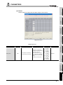
3.6 Data Clear Processing
Overview
This section explains how to clear CPU module data
(1) Data clear methods
2
There are the following six ways to clear CPU module data.
(a) Reset with the RUN/STOP/RESET switch, GX Developer.
Performance
Specification
(b) Restarting the PLC System
(c) PLC memory clear using GX Developer
(d) PLC memory format using GX Developer
(2) Data That Can and Cannot Be Cleared with Each Data Clearing Method.
Table3.2 shows which data can and cannot be cleared by the methods shown in (1)
(a) to (f).
Table3.2 That Can and Cannot Be Cleared with Each Data Clearing Method
Reset
operation
Data clear methods
PLC memory PLC memory PLC memory
Power restart
Clear history
clear
format
initialization
Program memory
data
Standard ROM
data*1
Device data
*2
Operation and error
history
ROM write count
*3
: Data cleared
*4
6
: Data not cleared
* 1 : When the program memory is copied into ROM using GX Developer, the standard ROM data is
first cleared, then the program memory is written into standard ROM
* 2 : When PLC memory initialization is executed, the safety CPU operation mode becomes TEST MODE.
* 3 : After the history is erased, the following PLC memory initialization operation and error history is
recorded.
• OP005 : FSYSTEM INITIALIZE PLC MEMORY
• OP100 : POWER ON
• 2200 : MISSING PARAMETER
* 4 : After the operation and error history is erased, the following operation history is recorded.
• OP200 : CLEAR OPERATION/ERROR LOG
Remark
For details on GX Developer operation methods, refer to the following manual.
Functions
Safety CPU
operation mode
CPU access
password
Clock data
Memories and Files
Handled by CPU Module
5
7
Communication with
Intelligent Function
Module
Data item
4
I/O Nunber Assignment
(f) History clear using GX Developer (operation and error history clear)
Sequence Program
Configuration and
Execution Conditions
3
(e) PLC memory initialization using GX Developer
8
GX Developer Version 8 Operating Manual
GX Developer Version 8 Operating manual (Safety PLC)
3.6 Data Clear Processing
3 - 12
Parameters
3
3
SEQUENCE PROGRAM EXECUTION
3.7 Numeric Values which can be Used in Sequence Programs
Numeric and alphabetic data are expressed by "0" (OFF) and "1" (ON) numerals in the
CPU module.
This expression form is called "binary code" (BIN).
The hexadecimal (HEX) expression form in which BIN data are expressed in 4-bit units,
and the BCD (binary coded decimal) expression form are applicable to the CPU module.
Table3.3 shows the numeric expressions of BIN, HEX, BCD and DEC (decimal).
Table3.3 BIN, HEX, BCD, and Decimal Numeric Expressions
DEC (Decimal)
0
1
2
3
HEX (Hexadecimal)
0
1
2
3
•
•
•
9
10
11
12
13
14
15
16
17
•
•
•
47
•
•
•
•
•
•
9
A
B
C
D
E
F
10
11
•
•
•
2F
•
•
•
32766
32767
-32768
-32767
•
•
•
-2
-1
7FFE
7FFF
8000
8001
•
•
•
FFFE
FFFF
3 - 13
BIN (Binary)
0
1
10
11
BCD(Binary Coded Decimal)
0
1
10
11
10
•
•
•
1001
1010
1011
1100
1101
1110
1111
0000
0001
•
•
•
1111
100
•
•
•
1001
0000
0001
0010
0011
0100
0101
0110
0111
•
•
•
0111
--0000 0000
0000 0000
0000
0001
1
1
0111
0111
1000
1000
1111
1111
0000
0000
1111
1111
0000
0000
1110
1111
0000
0001
1111
1111
1111
1111
1111
1111
1110
1111
3.7 Numeric Values which can be Used in Sequence Programs
1
1
1
1
1
1
1
1
1000
1000
---
SEQUENCE PROGRAM EXECUTION
1
(b) below)
(b) How to enter numeric value without taking into account BIN notation
Use the BIN instruction to convert the data set in BCD into BIN used in the CPU
module.
Using the BIN instruction allows users to set numeric value data from the outside
without taking into account BIN notation.
4
CPU module
[Numeric data designation]
Digital switch
4
X10F
3
2
to
BINP K4X100 D0
1
X100
3
BCD input
BIN data
BCD D5 K4Y130
I/O Nunber Assignment
(
2
Performance
Specification
(a) Numeric values handled in CPU module
The CPU module performs operation in BIN (binary).
If the value set in BCD is used as-is, the CPU module recognizes the set value as
a BIN and performs operation.
Hence, operation is performed using the value different from the set value.
Sequence Program
Configuration and
Execution Conditions
When setting a numeric value from an external digital switch or similar device to the
CPU module, BCD (binary coded decimal) can be used as the same setting in DEC
(decimal) by the method given in (b).
Overview
(1) Numeric value input from outside to CPU module
5
Memories and Files
Handled by CPU Module
Diagram 3.9 Import of data from digital switch to CPU module
Remark
Refer to the following manual for details of the BIN instruction.
QSCPU Programming Manual (Common Instructions)
Functions
6
Communication with
Intelligent Function
Module
7
8
3.7 Numeric Values which can be Used in Sequence Programs
3 - 14
Parameters
3
3
SEQUENCE PROGRAM EXECUTION
(2) Numeric value output from CPU module to outside
A digital display or similar device is available to externally display the numeric value
operated by the CPU module.
(a) How to output numeric value
The CPU module performs operation in BIN.
If binary values used in the CPU module are output as they are to a digital display,
they will not displayed correctly.
Therefore, the BCD instruction is used to convert the data operated in BIN into
BCD used by the external display or similar device.
Using the BCD instruction allows the same display as in DEC (decimal) to be
provided on the external display or similar device.
CPU module
BINP K4X100 D0
[Numeric data designation]
Digital display
Y13F
BCD D5 K4Y130
to
Y130
BCD output
BIN data
Diagram 3.10 Display of CPU module operation data by digital display
Remark
Refer to the following manual for details of the BCD instruction.
QSCPU Programming Manual (Common Instructions)
3 - 15
3.7 Numeric Values which can be Used in Sequence Programs
SEQUENCE PROGRAM EXECUTION
1
Binary date is represented by 0 (OFF) and 1 (ON).
Decimal notation uses the numerals 0 through 9. When counting beyond 9, a 1 is
placed in the 10s column and a 0 is placed in the 1s column to make the number 10.
In binary notation, the numerals 0 and 1 are used. A carry occurs after 1 and the
number becomes 10 (decimal 2).
Table3.4 shows the numerical notation by BIN and DEC.
Table3.4 Comparison between Binary and Decimal Notations
Sequence Program
Configuration and
Execution Conditions
3
BIN (Binary)
0000
0001
0010
0011
0100
0101
0110
0111
1000
1001
1010
1011
Carry
Carry
I/O Nunber Assignment
4
Carry
5
(2) Binary numeric expression
(a) Bit configuration in BIN notation used in CPU module
Each CPU module register (data registers, link registers, etc.) consists of 16 bits.
(b) Numeric data available for CPU module
Each CPU module register can store numeric values of -32768 to 32767.
Diagram 3.11 shows the numeric notation for CPU module registers.
Memories and Files
Handled by CPU Module
DEC (Decimal)
0
1
2
3
4
5
6
7
8
9
10
11
2
Performance
Specification
(1) Binary code
Overview
3.7.1 BIN (Binary Code)
6
Most significant bit (for positive/negative discrimination)
2 15 2 14 2 13 2 12 2 11 2 10 29
Decimal value
28
27 26
-32768 16384 8192 4096 2048 1024 512 256 128
64
25
24
23
22
32
16
8
4
2 1 20
2
1
Functions
b15 b14 b13 b12 b11 b10 b9 b8 b7 b6 b5 b4 b3 b2 b1 b0
Bit name
7
Communication with
Intelligent Function
Module
Negative value" when most significant bit is "1".
Diagram 3.11 Numeric Expressions for CPU module Registers
POINT
To each bit of each register, a 2n value is assigned.
Note that the most significant bit is used for distinction of sign (positive or
negative).
1) When most significant bit is "0"...Positive
2) When most significant bit is "1"...Negative
3.7 Numeric Values which can be Used in Sequence Programs
3.7.1 BIN (Binary Code)
8
3 - 16
Parameters
3
3
SEQUENCE PROGRAM EXECUTION
3.7.2 HEX (Hexadecimal)
(1) Hexadecimal notation
In hexadecimal notation, 4 binary bits are expressed in 1 digit.
If 4 binary bits are used in binary notation, 16 different values from 0 to 15 can be
represented.
Since hexadecimal notation represents 0 to 15 in 1 digit, letters AH to FH are used to
represent the numbers 10 to 15.
Then, a carry occurs after FH.
Table3.5 shows the numeric expressions of BIN, HEX and DEC (decimal).
Table3.5 Comparison of BIN, HEX, and DEC Numeric Expressions
DEC (Decimal)
HEX (Hexadecimal)
BIN (Binary)
0
1
2
3
•
•
•
9
0
1
2
3
•
•
•
9
0
1
10
11
•
•
•
1001
10
11
12
13
14
15
16
17
•
•
•
47
A
B
C
D
E
F
10
11
•
•
•
2F
1010
1011
1100
1101
1110
1111
1 0000
1 0001
•
•
•
10 1111
Carry
(2) Hexadecimal numeric expression
CPU module registers (data registers, link registers, etc.) consist of 16 bits.
For 16 bits, 0 to FFFFH can be specified in hexadecimal.
POINT
The CPU module regards data stored in HEX as BIN.
For example, if FFFFH is stored into a register in HEX, the CPU module performs
operation, regarding the value of a register as -1.
3 - 17
3.7 Numeric Values which can be Used in Sequence Programs
3.7.2 HEX (Hexadecimal)
SEQUENCE PROGRAM EXECUTION
1
(1) BCD notation
BCD (binary coded decimal) is a numbering system in which one digit of DEC
(decimal) is expressed in BIN (binary).
Though it uses 4-bit representation like hexadecimal notation, it dose not use letters
AH to FH.
Overview
3.7.3 BCD (Binary Coded Decimal)
2
Performance
Specification
Table3.6 shows the numeric expressions of BIN, BCD and DEC.
Table3.6 Comparison of BIN, BCD, and DEC Numeric Expressions
0000
0001
0010
0011
0100
0101
0110
0111
1000
1001
1010
1011
1100
(Binary Coded Decimal)
0
1
10
11
100
101
110
111
1000
1001
1 0000
1 0001
1 0010
Sequence Program
Configuration and
Execution Conditions
0
1
2
3
4
5
6
7
8
9
10
11
12
3
BCD
4
I/O Nunber Assignment
BIN (Binary)
Carry
5
Memories and Files
Handled by CPU Module
DEC (Decimal)
(2) BCD numeric expression
CPU module registers (data registers, link registers, etc.) consist of 16 bits.
In case of 16 bits, 0 to 9999 can be specified in BCD.
6
7
Communication with
Intelligent Function
Module
The CPU module regards value stored in BCD as BIN.
For example, if 8000 is stored in BCD, the CPU module performs operation,
regarding the value as -32768.
When performing arithmetic operation between values stored in BCD and any
values in the CPU module, use the operation instruction of the BCD.
Functions
POINT
8
3.7 Numeric Values which can be Used in Sequence Programs
3.7.3 BCD (Binary Coded Decimal)
3 - 18
Parameters
3
4
I/O NUMBER ASSIGNMENT
CHAPTER4 I/O NUMBER ASSIGNMENT
This chapter explains the I/O number assignment required for the CPU module to
communicate data with I/O modules and/or intelligent function modules.
4.1 Definition of I/O Number
I/O numbers indicate the addresses used in a sequence program to input or output ON/
OFF data between the CPU module and other modules.
(1) Input and output of ON/OFF data
Input (X) is used to input ON/OFF data to the CPU module, and output (Y) is used to
output ON/OFF data from the CPU module.
(2) I/O number expressions
I/O numbers are expressed as hexadecimal.
4-1
4.1 Definition of I/O Number
I/O NUMBER ASSIGNMENT
1
4.2 Concept of I/O Number Assignment
Overview
4.2.1 I/O numbers of base unit
When two CC-Link Safety master modules and one MELSECNET/H module are mounted
on the main base unit, the I/O numbers are as shown in Diagram 4.1
32
32
32
3
3
Slot number
Sequence Program
Configuration and
Execution Conditions
2
I/O point
4
00H 20H 40H
I/O number
1FH 3FH 5FH
Diagram 4.1 I/O number assignment example
If the base unit has empty slots mounted with no CC-Link Safety master modules or no
MELSECNET/H module are mounted, the points designated at the "I/O assigment" tab
screen in the "(PLC) Parameter" dialog box are assigned to the empty slots. (Default
value is 16 points.)
Remark
The head I/O can be changed for each slot with the GX Developer I/O assignment.
I/O Nunber Assignment
1
5
Memories and Files
Handled by CPU Module
0
MELSECNET/H
module
CPU
CC-Link Safety
master module
Base unit
2
Performance
Specification
At power-on or reset cancel, the CPU module assigns I/O numbers.
I/O numbers are assigned automatically from the right side of the CPU module of the main
base unit.
CC-Link Safety
master module
6
In the CC-Link Safety system, CPU module input (X) and output (Y) can be assigned to
remote station I/O modules and controlled.
Functions
4.2.2 I/O number of remote station
When two CC-Link Safety master modules and one MELSECNET/H module are mounted
on the main base unit, X/Y0 - X/Y5F are used.
When using CPU module input (X) and output (Y) for remote station I/O numbers, use X/
Y60 or later.
Communication with
Intelligent Function
Module
7
(1) CPU module I/O numbers that can be used at remote stations
8
4.2 Concept of I/O Number Assignment
4.2.1 I/O numbers of base unit
4-2
Parameters
4
4
I/O NUMBER ASSIGNMENT
CC-Link Safety
master module
CC-Link Safety
master module
MELSECNET/H
module
[System configuration]
32
32
32
CC-Link Safety system
Remote station
Remote station
CC-Link Safety system
Remote station
Remote station
[I/O number assignment]
Input/output(X/Y)
X/Y0
I/O numbers assigned to CC-Link
Safety master module and
MELSECNET/H network module
X/Y5F
Empty
X/Y100
Refresh destination for
the first CC-Link Safety
master module
Refresh destination for
the second CC-Link
Safety master module
MELSECNET/H link I/O
(LX, LY) refresh
destination
I/O numbers which can be assigned to
remote stations
There are no restrictions on the order
of the I/O numbers assigned to I/O
number specified to refresh
destination of CCLink Safety master
modules and MELSECNET/H
modules.
X/Y17FF
Diagram 4.2 Remote station I/O number assignment
Remark
"Empty" can be assigned in the following areas.
• Refresh area between the first CC-Link Safty master module and the
second CC-Link Safety master module.
• Refresh area between the second CC-Link Safty master module and the
MELSECNET/H module.
POINT
1.
2.
3.
4-3
Inputs (X) and outputs (Y) can be used for MELSECNET/H network module
link I/O (LX, LY) refresh destinations (devices on the CPU module side).
When using multiple CC-Link Safety master modules, make sure that refresh
destination I/O numbers are not duplicated.
When using a CC-Link Safety master module and a MELSECNET/H module,
make sure that refresh destination I/O numbers are not duplicated.
4.2 Concept of I/O Number Assignment
4.2.2 I/O number of remote station
I/O NUMBER ASSIGNMENT
1
4.3 I/O Assignment by GX Developer
Overview
This section describes the I/O assignment using GX Developer.
4.3.1 Purpose of I/O assignment by GX Developer
2
Performance
Specification
Perform I/O assignment setting by GX Developer in the following cases.
(1) Preventing I/O numbers from changing when converting modules
You can avoid the change in the intelligent function module is removed due to a
malfunction.
When the designed program's I/O numbers are different from the actual system I/O
numbers, each module's I/O number of base units can be set to program-I/O number.
POINT
4
Memories and Files
Handled by CPU Module
5
6
Functions
2.
The I/O assignment setting becomes valid when the PLC is powered OFF
and then ON or the CPU module is reset.
If an intelligent function module breaks down without making I/O assignment
settings using GX Developer, it may lead to malfunction of the module,
changing I/O numbers of the modules after the broken one.
Therefore, it is recommended to make I/O assignment setting using GX
Developer.
7
Communication with
Intelligent Function
Module
1.
I/O Nunber Assignment
(2) Changing the I/O numbers to those used in the program
Sequence Program
Configuration and
Execution Conditions
3
8
4.3 I/O Assignment by GX Developer
4.3.1 Purpose of I/O assignment by GX Developer
4-4
Parameters
4
4
I/O NUMBER ASSIGNMENT
4.3.2 Concept of I/O assignment using GX Developer
In I/O assignment, the "Type (module type)", "Points (I/O points)" and "Start XY" (starting I/
O number) can be set for each slot of the base units.
For example, to change the number of occupied I/O points of the designated slot, only the
number of occupied I/O points can be designated.
The items other than designated are set to the status where the base unit is installed.
(1) I/O assignment
The I/O assignment is conducted at the "I/O assignment" tab screen in the "(PLC)
Parameter" dialog box.
(a)
(b)
(c)
(d)
(e)
Diagram 4.3 I/O assignment
(a) Slot
The slot number and what number of the main base unit the slot is are displayed.
What number of the main base unit the slot is means the number of slots from 0
slot of the main base unit.
(b) Type
Select "Intelli." for the slot mounting CC-Link Safety master module and
MELSECNET/H module.
For an empty slot, select empty.
If the type is not designated, the type of the actually mounted module is used.
4-5
4.3 I/O Assignment by GX Developer
4.3.2 Concept of I/O assignment using GX Developer
I/O NUMBER ASSIGNMENT
(c) Model name
Set the mounted module model name within 16 characters.
The specified model name is not used for the CPU module. (It is used as a user's
memo.)
2
(d) Points
To change the number of occupied I/O points of each slot, select it from the
followings:
Performance
Specification
• 32(32 points)
• 128(128 points)
• 1024(1024 points)
(2) Precautions for I/O assignment
(a) Slot status after I/O assignment
When I/O assignment setting has been made to a slot, that setting has
precedence over the mounted module.
1) When the preset number of points is less than the number of mounted
intelligent function module points
"MODULE LAYOUT ERROR" occurs.
2) Mounted module and I/O assigned module type
The mounted module type and the set type in the I/O assignment setting must
be the same.
If not, normal operation will not be performed.
For the intelligent function module, make sure that the numbers of I/O points
are the same.
Table4.1 describes the operations performed when the mounted module type
differs from the one in the I/O assignment setting.
Result
setting
Intelli.
Empty
6
Communication with
Intelligent Function
Module
Empty slot
All modules
I/O assignment
5
7
Table4.1 List of operations performed when mounted module differs from I/O assignment
Mounted module
4
I/O Nunber Assignment
(e) Start XY
When the I/O number of each slot is changed, you should designate the head I/O
number according to the change.
If Start XY is not designated for a slot, the I/O number continuing from the last
number of the currently designated slot is assigned.
3
Sequence Program
Configuration and
Execution Conditions
If the number of occupied I/O points is not designated for a slot, the one of the
actually mounted module is used.
Memories and Files
Handled by CPU Module
• 16(16 points)
• 64(64 points)
• 512(512 points)
Functions
• 0(0 point)
• 48(48 points)
• 256(256 points)
Overview
1
Empty slot
Empty slot
8
4.3 I/O Assignment by GX Developer
4.3.2 Concept of I/O assignment using GX Developer
4-6
Parameters
4
4
I/O NUMBER ASSIGNMENT
3) Last I/O number
In I/O assignment, set the last I/O number not to exceed the maximum value
(
CHAPTER 2) of the I/O points.
An error ("MODULE LAYOUT ERROR") will occur if the last I/O number
exceeds the maximum value of the I/O points. (System monitor of GX
Developer shows "***" as an I/O address.)
(b) Precautions for automatic start XY assignment by CPU module
When the start XY is not yet entered, the CPU module automatically assigns it. In
the case of 1) or 2) below, therefore, the start XY setting of each slot may overlap
the one assigned by the CPU module.
1) Settings of I/O numbers were exchanged in the start XY
2) There are slots with start XY setting and those without start XY setting
(automatically assigned slot)
The following example Diagram 4.4 shows overlapping start XY.
Diagram 4.4 I/O assignment with overlapping start XY
Automatically
assigned slot
0
1
2
CC-Link Safety
master module
MELSECNET/H
module
CPU
CC-Link Safety
master module
Base unit
32
32
32
3
Slot number
Number of I/O points
40H 20H 40H
I/O number
5FH 3FH 5FH
Start XY overlaps!
Diagram 4.5 Start XY set by above I/O assignment
Be extremely careful not to overlap the start XY of each slot.
Overlapping start XY will result in an error ("MODULE LAYOUT ERROR").
4-7
4.3 I/O Assignment by GX Developer
4.3.2 Concept of I/O assignment using GX Developer
I/O NUMBER ASSIGNMENT
1
The following example shows I/O number assignment made when I/O assignment setting
is performed using GX Developer.
Set slots where CC-Link Safety master module or MELSECNET/H module is mounted
to 32 points so that the I/O numbers do not change when the module is removed due
to the breakdown of CC-Link Safety master module or MELSECNET/H module.
(a) System configuration and I/O number assignment
2
MELSECNET/H
module
32
32
32
3
3
Slot number
Sequence Program
Configuration and
Execution Conditions
1
I/O point
00H 20H 40H
I/O number
4
1FH 3FH 5FH
Diagram 4.6 System configuration and I/O number assignment
(b) I/O assignment with GX Developer
Set slots No. 0 to 2 on the GX Developer I/O assignment setting screen to "32
points".
I/O Nunber Assignment
0
CC-Link Safety
master module
Base unit
Performance
Specification
2
(1) When setting the number of I/O points for mounted modules
CPU
Overview
4.3.3 Examples of I/O Number Assignment
CC-Link Safety
master module
Memories and Files
Handled by CPU Module
5
Select 32 points. (When
the type is not selected,
the type of the installed
module will be selected.)
Functions
6
Communication with
Intelligent Function
Module
7
8
Diagram 4.7 I/O assignment
4.3 I/O Assignment by GX Developer
4.3.3 Examples of I/O Number Assignment
4-8
Parameters
4
4
I/O NUMBER ASSIGNMENT
4.4 Checking the I/O Numbers
The modules mounted on the main base unit and their I/O numbers can be checked using
the GX Developer system monitor. (
4-9
4.4 Checking the I/O Numbers
4.3.3 Examples of I/O Number Assignment
Section 6.16)
MEMORIES AND FILES HANDLED BY CPU MODULE
1
Overview
CHAPTER5 MEMORIES AND FILES HANDLED BY CPU
MODULE
5.1 Memories by CPU Module
2
This section explains the memories handled by the CPU module and the data that can be
stored into the memories.
Performance
Specification
5.1.1 Memory configuration and storable data
3
Sequence Program
Configuration and
Execution Conditions
(1) Memory configuration
Program memory
Parameter
Program
4
I/O Nunber Assignment
Device comment
Standard ROM
CPU module
5
Program
Device comment
Diagram 5.1 Data handled by CPU module
(a) Program memory (
Section 5.1.2)
The program memory stores the program used by the CPU module to perform
operation.
6
Functions
(b) Standard ROM (
Section 5.1.3)
The standard ROM is used to execute boot run by the CPU module.
Memories and Files
Handled by CPU Module
Parameter
Communication with
Intelligent Function
Module
7
8
5.1 Memories by CPU Module
5.1.1 Memory configuration and storable data
5-1
Parameters
5
5
MEMORIES AND FILES HANDLED BY CPU MODULE
(2) Data that can be stored into memories
Table5.1 indicates the data that can be stored into the program memory, standard
RAM and standard ROM and the corresponding drive Nos.
Table5.1 Storable data and storage locations
Drive No.
CPU module built-in memories
Program memory
Standard ROM
0
4
File name and
extension
Parameter
PARAM.QPA
Sequence program
MAIN.QPG
Device comment
MAIN.QCD
User setting system
--
area*1
: Necessary data,
* 1 : Set the area used by the system. (
: Storable data,
: Unstorable data
Section 5.1.2(3) (b))
(3) Memory capacities and formatting necessities
Table5.2 indicates the memory capacity and formatting necessity of each memory.
Table5.2 Formatting necessity
QS001CPU
Formatting
Program memory
128k byte
Necessary*1
Standard ROM
128k byte
Unnecessary
* 1 : Before use, be sure to format the memory using GX Developer.
5-2
5.1 Memories by CPU Module
5.1.1 Memory configuration and storable data
MEMORIES AND FILES HANDLED BY CPU MODULE
1
(2) Storable data
The program memory can store parameters, programs, device comments, and user
setting system area data.
Refer to Section 5.1.1 (2) for the list of data that can be stored into program memory.
POINT
If the total volume of the data to be stored into the program memory exceeds its
capacity, examine reducing the user setting system area data.
2
Performance
Specification
The program memory stores the program used by the CPU module to perform
operation.
The program stored in the standard ROM is booted (read) to the program memory to
perform operation.
3
Sequence Program
Configuration and
Execution Conditions
(1) Definition of program memory
Overview
5.1.2 Program memory
Before using the program memory, be sure to format it by GX Developer.
5
Memories and Files
Handled by CPU Module
(a) Formatting
When formatting, display the PLC memory format screen with GX Developer
[Online] [Format PLC memory]. This is done selecting "Program memory/
Device memory" as the target memory on the PLC memory format screen.
I/O Nunber Assignment
4
(3) Before using the program memory
Functions
6
7
Communication with
Intelligent Function
Module
Diagram 5.2 Program memory formatting
8
5.1 Memories by CPU Module
5.1.2 Program memory
5-3
Parameters
5
5
MEMORIES AND FILES HANDLED BY CPU MODULE
(b) Create a user setting system area
When formatting the program memory, set the user setting system area capacity.
1) Do not create a user setting system area
The program memory is formatted without the user setting system area being
created.
2) Create a user setting system area
The user setting system area is created during formatting.
There are the following user setting system areas (Table5.3).
Table5.3 User setting system area type
System area type
Online change area of
Description
Setting this area enables multiple blocks of data to be changed online.
multiple blocks
Refer to the following manual for the number of blocks to which online
(Online change area of
change can be made in this area setting.
FB definition)
GX Developer Operating Manual
POINT
When the user setting system area is created, the available area decreases by
the number of created area steps.
The memory capacity can be checked from the Read from PLC screen of GX
Developer. (
5-4
5.1 Memories by CPU Module
5.1.2 Program memory
(3) (c) in this section)
MEMORIES AND FILES HANDLED BY CPU MODULE
(c) Checking the memory capacity after formatting
To check the memory capacity, choose [Online] [Read from PLC] on GX
Developer.
1) Select "Program memory/Device memory" as the target memory on the Read
from PLC screen.
Overview
1
2
2) Click the Free space volume button.
Performance
Specification
3) The memory capacity appears in the Total free space volume field.
1) Select target memory.
Sequence Program
Configuration and
Execution Conditions
3
I/O Nunber Assignment
4
3) Memory capacity is displayed.
Diagram 5.3 Memory capacity checking procedure
5
Memories and Files
Handled by CPU Module
2) Click Free space volume button.
Functions
6
Communication with
Intelligent Function
Module
7
8
5.1 Memories by CPU Module
5.1.2 Program memory
5-5
Parameters
5
5
MEMORIES AND FILES HANDLED BY CPU MODULE
(4) Write to program memory
When writing data to program memory, display the writing to PLC screen with GX
Developer [Online] [Write to PLC].
Select "Program memory/Device memory" as the target memory on the Write to PLC
screen and write data to the PLC.
Diagram 5.4 Write to PLC screen
POINT
The file size has the minimum unit. (
Section 5.3.4)
The occupied memory capacity may be greater than the actual file size.
5-6
5.1 Memories by CPU Module
5.1.2 Program memory
MEMORIES AND FILES HANDLED BY CPU MODULE
1
(1) Definition of standard ROM
The standard ROM is used to execute boot run by the CPU module.
The standard ROM is used to save programs and parameters without battery backup.
The program stored in the standard ROM is booted (read) to the program memory
2
(2) Storable data
The standard ROM can store parameters, programs and device comments.
Refer to Section 5.1.1 (2) for the list of data that can be stored into each memory.
Performance
Specification
Section 5.1.2) to perform operation.
3
(3) Checking the memory capacity
To check the memory capacity, choose [Online]
Developer.
[Read from PLC] on GX
1) Select "Standard ROM" as the target memory on the Read from PLC screen.
2) Click the Free space volume button.
Sequence Program
Configuration and
Execution Conditions
(
Overview
5.1.3 Standard ROM
4
I/O Nunber Assignment
3) The memory capacity appears in the Total free space volume field.
1) Select target memory.
Memories and Files
Handled by CPU Module
5
Functions
6
2) Click Free space volume button.
3) Memory capacity is displayed.
7
Communication with
Intelligent Function
Module
Diagram 5.5 Memory capacity checking procedure
8
5.1 Memories by CPU Module
5.1.3 Standard ROM
5-7
Parameters
5
5
MEMORIES AND FILES HANDLED BY CPU MODULE
(4) Write to standard ROM
For details on writing to the standard ROM, refer to Section 5.1.4 (3).
POINT
The file size has the minimum unit. (
Section 5.3.4)
The occupied memory capacity may be greater than the actual file size.
(5) How to use the program stored in the standard ROM
Since operation cannot be executed by the program stored in the standard ROM, use
that program by booting (reading) it to the program memory. (
5-8
5.1 Memories by CPU Module
5.1.3 Standard ROM
Section 5.1.4)
MEMORIES AND FILES HANDLED BY CPU MODULE
1
5.1.4 Standard ROM program execution (boot run) and writing
Overview
(1) Standard ROM program execution (boot run)
(a) Standard ROM program execution
The CPU module performs operation of the program stored in the program
memory.
It does not operate the program stored in the standard ROM.
The program stored in the standard ROM is booted (read) to the program memory
to perform operation.
Performance
Specification
2
3
Sequence Program
Configuration and
Execution Conditions
Program
memory
Boot
Standerd
ROM
1) SAFETY MODE
In SAFETY MODE, boot run is executed regardless of the boot settings made
by GX Developer.
2) TEST MODE
Boot run can be executed by setting "Execute boot run" in the boot settings
made by GX Developer and writing to the standard ROM.
POINT
6
Functions
In TEST MODE, when debugging was executed with the program memory
parameters and program, write to the standard ROM at the time of switching from
the TEST MODE to the SAFETY MODE.
5
Memories and Files
Handled by CPU Module
Diagram 5.6 Boot run
I/O Nunber Assignment
4
Communication with
Intelligent Function
Module
7
8
5.1 Memories by CPU Module
5.1.4 Standard ROM program execution (boot run) and writing
5-9
Parameters
5
5
MEMORIES AND FILES HANDLED BY CPU MODULE
(2) Procedure up to boot run and stopping boot run (in TEST MODE)
(a) Procedure for boot run
The following provides the procedure for boot run.
1) Program creation by GX Developer
Create a program for executing boot run.
2) Boot file by GX Developer
Set "Do boot from Standard ROM" in the Boot file of the PLC parameter dialog
box.
Diagram 5.7 Boot file
5 - 10
5.1 Memories by CPU Module
5.1.4 Standard ROM program execution (boot run) and writing
MEMORIES AND FILES HANDLED BY CPU MODULE
3) Write to standard ROM by GX Developer
• Choose [Online] [Write to PLC] on GX Developer and write the files to
the program memory.
• Choose [Online] [Write to PLC (Flash ROM)] [Write the program
memory to ROM...] on GX Developer, and write to the standard ROM the
(3) in this section)
Performance
Specification
4) Program execution
When you carry out the following operations, the system boots from the
standard ROM.
• Restarting the PLC power
• Reset end with the CPU module RUN/STOP/RESET switches.
• Remote reset using GX Developer.
1) Remove the checkmark from "Boot from standard ROM" in the PLC parameter
boot file settings.
2) Write parameters and sequence program data to the program memory.
[Write to PLC (Flash ROM)]
[Write the program memory
(c) Precautions for standard ROM program execution
1) Files stored into standard ROM
Before executing boot run, store the following files into the standard ROM.
• Parameter *1
• Program *1
• Device comment
Sequence Program
Configuration and
Execution Conditions
(b) Operation to stop boot run
Perform the following operation using GX Developer to stop boot run and execute
operation by the parameter program written to the program memory.
3
4
I/O Nunber Assignment
5) Check for normal boot completion
Whether the boot is normally completed or not can be checked by the special
relay (SM660) status.
Refer to Appendix 1 for the special relay.
3) Choose [Online]
to ROM...].
2
5
Memories and Files
Handled by CPU Module
files written to the program memory. (
Overview
1
6
Hence, write the program to the standard ROM (
the CPU module is put in a STOP status.
(3) in this section) when
3) When program memory contents change at power OFF ON or reset
When you write the PLC program into program memory and switch the PLC
power OFF ON or end the CPU module reset, if the contents of the program
memory change, it is possible that boot operations are being used.
Refer to "(2)(b) Operation to stop boot run" in this section, and stop the boot
run.
5.1 Memories by CPU Module
5.1.4 Standard ROM program execution (boot run) and writing
5 - 11
7
Communication with
Intelligent Function
Module
2) Online change during boot run
If online change is made to a program in the program memory during boot run
from the standard ROM, the change is not updated on the program in the boot
source standard ROM.
Functions
* 1 : Must be stored into the standard ROM.
8
Parameters
5
5
MEMORIES AND FILES HANDLED BY CPU MODULE
(3) Write to standard ROM
The program memory files are written to the standard ROM by batch-copying them to
the standard ROM.
(a) Before write
Check the following points before writing the files to the standard ROM.
1) Saving the standard ROM files
When files are written to the standard ROM, all files previously stored in the
standard ROM are automatically deleted.
Before writing files to the standard ROM, choose [Online] [Read from PLC]
on GX Developer and save the stored files using GX Developer in advance.
2) Preparation of files to be written
Since all files stored in the standard ROM are automatically deleted when files
are to be written to the standard ROM, prepare all files to be stored in
advance.
(b) Write procedure
The procedure to write files to the standard ROM will be explained.
1) Choose [Online] [Write to PLC (Flash ROM)]
data into ROM] on GX Developer.
[Copy program memory
2) The Write the program memory to ROM screen appears.
Diagram 5.8 Copy program memory data into ROM screen
3) Select the write destination and copy the program memory files to the standard
ROM.
5 - 12
5.1 Memories by CPU Module
5.1.4 Standard ROM program execution (boot run) and writing
MEMORIES AND FILES HANDLED BY CPU MODULE
1
Since all files stored in the standard ROM are automatically deleted when files are to
be written to the standard ROM, additions/changes to the stored files cannot be made
directly.
Observe the following steps.
Overview
(4) Additions/changes to standard ROM files (in TEST MODE)
2
3) Write the modified files to the program memory.
4) Choose [Online] [Write to PLC (Flash ROM)] [Write the program memory
to ROM...], and copy these files to the program memory.
(5) Precautions (in TEST MODE)
4
I/O Nunber Assignment
(a) Setting of check at communication time of GX Developer
When files are written to the standard ROM with the communication time check
time set to 180 seconds or less on GX Developer, they are checked 180 seconds.
3
Sequence Program
Configuration and
Execution Conditions
2) Make necessary additions/changes to the read files.
Performance
Specification
1) Choose [Online] [Read from PLC] on GX Developer and read all files from
the standard ROM.
Memories and Files
Handled by CPU Module
5
Functions
6
Communication with
Intelligent Function
Module
7
8
5.1 Memories by CPU Module
5.1.4 Standard ROM program execution (boot run) and writing
5 - 13
Parameters
5
5
MEMORIES AND FILES HANDLED BY CPU MODULE
5.2 Program File Structure
A program file consists of a file header, execution program and allocate memory for online
change.
Program file structure
34 steps
(dafult)
File header
Execution program
Allocate memory
for online program
change
Area is secured in file size units.
Section 5.3.4 )
(
500 steps
(dafult)
Diagram 5.9 Program file structure
(1) Structure details
The capacity of the program stored in the program memory of the CPU module is the
total of the above three areas.
(a) File header
This area stores the file name, size, creation date, etc.
The file header size ranges from 26 to 35 steps (104 to 140 bytes) depending on
the device setting of the PLC parameter dialog box.
(Default: 34 steps)
(b) Execution program
This area stores the created program.
(c) Allocate memory for online change
This area is used when online change that increases the number of steps is
performed by GX Developer.
When such an online change is performed by GX Developer, the number of
remaining allocate memory for online change is displayed.
1) Default number of allocate memory for online change
The default setting is 500 steps (2000 bytes).
2) Changing the number of allocate memory for online change
The number of allocate memory for online change can be changed by GX
Developer (by choosing [Online] [Write to PLC] <Program>‚ tab).
When the number of steps is insufficient for online change, it can be set again.
(
5 - 14
5.2 Program File Structure
Section 6.14.1)
MEMORIES AND FILES HANDLED BY CPU MODULE
1
During programming by GX Developer, the program capacity (sum of the file header
capacity and the numbers of steps in the created program) is displayed in terms of the
number of steps as shown in Diagram 5.10.
When a program is created, the capacity of the crea.ted program can be confirmed.
Overview
(2) Display of program capacity by GX Developer
2
Performance
Specification
Program capacity display
POINT
1.
The program capacity displayed during programming by GX Developer is the
capacity of the file header and execution program and does not include the
capacity of the allocate memory for online change (500 steps).
(Example) The capacity of the program having the execution program area of
491 steps is displayed on GX Developer as shown below. (The file header
default is 32 steps.)
34 steps
Execution program
491 steps
5
Memories and Files
Handled by CPU Module
File header
Display on GX Developer:
34 steps + 491 steps = 525 steps.
Diagram 5.11 File status on GX Developer
Since a file is stored in file size units on the program memory, the program
capacity displayed during programming by GX Developer may differ from the
Section 5.3.4)
Functions
capacity of the program file on the CPU module. (
6
7
Communication with
Intelligent Function
Module
2.
4
I/O Nunber Assignment
Diagram 5.10 Program capacity display
Sequence Program
Configuration and
Execution Conditions
3
8
5.2 Program File Structure
5 - 15
Parameters
5
5
MEMORIES AND FILES HANDLED BY CPU MODULE
5.3 File Operation by GX Developer and Handling Precautions
5.3.1 File operation
The files stored in program memory and the standard ROM can be operated with GX
Developer online operations.
However, the file operations that can be executed depend on the safety CPU operation
mode and the CPU module RUN/STOP status.
(
Refer to Section 6.2.5)
5.3.2 Precautions for handling files
(1) About power-off (including resets) during file operations
When the PLC is power-off or a CPU module is reset during file operations with GX
Developer, the files in each memory become uncertain.
During file operations with GX Developer, do not power-off the PLC or reset a CPU
module.
5 - 16
5.3 File Operation by GX Developer and Handling Precautions
5.3.1 File operation
5
MEMORIES AND FILES HANDLED BY CPU MODULE
1
When using the program memory or standard ROM, calculate the rough size of each file
according to Table5.4.
Overview
5.3.3 Memory capacities of files
2
Table5.4 Memory capacity calculation for files
Performance
Specification
Rough file capacity (unit: byte)
70
Default: 316 (increases depending on the parameter setting)
Reference
Boot setting
100
MELSECNET/H setting made
CC-Link setting made
22 + 572
safety remote stations) + 4
Sequence program
134*+
(4
3
Max. 156 increased
(number of modules of CC-Link Safety) + 76
(number of
(number of safety remote station parameter settings)
((number of steps) + (number of allocate memory for online change)))
80 + (sum of comment data sizes of devices)
Device comment
• Comment data size of one device = 10 + 10210 a + 40
b
4
• a : Quotient of ((device points)/256)
Value set at formatting (0/1.25k/2.5k)
* : 134 is the default value (It can be increased or decreased by parameter setting.)
Memories and Files
Handled by CPU Module
5
Functions
6
7
Communication with
Intelligent Function
Module
program change
I/O Nunber Assignment
• b : Remainder of ((device points)/256)
Multi-block online
Sequence Program
Configuration and
Execution Conditions
Parameter
8
5.3 File Operation by GX Developer and Handling Precautions
5.3.3 Memory capacities of files
5 - 17
Parameters
Function
Drive heading
5
MEMORIES AND FILES HANDLED BY CPU MODULE
5.3.4 File size units
(1) What is file size unit?
The minimum unit for writing a file to a memory area is called as a file size unit.
The CPU module file size unit is 4 bytes.
Program memory, Standard ROM
Parameter
Program
The area is secured in 4-byte unit.
The area is secured in 4-byte (1 step) units.
Diagram 5.12 Program memory, standard ROM file size units
5 - 18
5.3 File Operation by GX Developer and Handling Precautions
5.3.4 File size units
6
FUNCTIONS
1
Overview
CHAPTER6 FUNCTIONS
Function of CPU module is as follows:
6.1 Function List
2
Table6.1 CPU module function list
Reference
3
This function selects whether to normally operate the
CPU module as part of the safety device or to carry out
Section 6.2
maintenance on the CPU module using program
changes and device test functions.
This function prevents incorrect operations from GX
Section 6.3
Developer connected by mistake.
This function erases user data written to the CPU
PLC memory initialization
module. When the PLC memory is initialized, data is
Section 6.4
returned to its factory settings status.
Setting for preventing continuous RUN This function prevents the PLC system from running
in TEST MODE
ROM write count check
Self-Diagnosis function
Section 6.5
continuously for long periods in TEST MODE.
This function checks the number of writing to ROM.
Section 6.6
This function enables the CPU module to check for
Section 6.7
failures.
5
This function recordsthe the operations that have been
Operation/error history
executed to the CPU module from the outside and the
Section 6.8
self-diagnostics errors that have occurred in the CPU
module in the past.
Constant scan
This function executes the program at a constant
This function selects the output Y status (output before
transition from STOP status to RUN
STOP/output after the calculation execution) when the
status
CPU module is set from STOP status to RUN status.
Clock function
Remote RUN/STOP
Remote RESET
Section 6.9
frequency.
Output status selection function for
Section
6.10
Section
This function executes the CPU module internal clock.
Section
module.
6.12.1
This function resets the CPU module when the CPU
Section
module is in a STOP status.
6.12.2
Section
devices on the CPU module by operating from the GX
6.13
Developer.
Online change
Watchdog timer
System display
LED display
6
6.11
This function stops and starts operating the CPU
This function monitors the status of programs and
Monitoring function
4
Memories and Files
Handled by CPU Module
CPU access password
This function writes programs when the CPU module is
Section
in the RUN status.
6.14
This function monitors operational delays caused by
Section
CPU module's hardware and program errors.
6.15
This function connects to the GX Developer and
Section
monitors system configuration.
6.16
This function enables the front-mounted LEDs to
Section
indicate the operating conditions of the CPU module.
Functions
Safety CPU operation mode
Sequence Program
Configuration and
Execution Conditions
TEST
MODE
I/O Nunber Assignment
SAFETY
MODE
7
Communication with
Intelligent Function
Module
Description
8
6.17
: Available
6.1 Function List
: N/A
6-1
Parameters
Item
Safety CPU operation
mode
Performance
Specification
Functions of CPU module are listed in Table6.1.
The Nos. in the "CPU module" field correspond to the CPU modules as indicated below.
6
FUNCTIONS
6.2 Safety CPU Operation Mode
6.2.1 Safety CPU operation mode
The safety CPU operation mode has "SAFETY MODE" and "TEST MODE".
Switch the safety CPU operation mode by operations from GX Developer.
(1) SAFETY MODE
This mode is used for the main operation of the safety-related system.
In SAFETY MODE, to protect this system while it is operating, operations that change
safety PLC control, such as writing to PLC and device test, are prohibited.
CPU module
(Execute the program operations)
CC-Link Safety master module
Program,
parameters, and
device data cannot
be changed.
Program
Parameter
Device data
CC-Link Safety system
Input from the
controlled system.
GX Developer
Diagram 6.1 SAFETY MODE operation
6-2
6.2 Safety CPU Operation Mode
6.2.1 Safety CPU operation mode
Output the program
operation results.
Controlled system
FUNCTIONS
1
This mode is used for system start-up and maintenance.
In this mode, all the GX Developer functions, such as PLC writing and device testing,
can be used.
Overview
(2) TEST MODE
2
Performance
Specification
CPU module
(Execute the program operations)
CC-Link Safety master module
Sequence Program
Configuration and
Execution Conditions
3
Program
Program,
parameters, and
device data can be
changed.
Parameter
Device data
CC-Link Safety system
Controlled system
Diagram 6.2 TEST MODE operation
Remark
For details on the GX Developer operations that can be executed in SAFETY
MODE and in TEST MODE, refer to the GX Developer Operating Manual (Safety
PLC).
5
Memories and Files
Handled by CPU Module
GX Developer
I/O Nunber Assignment
4
Output the program
operation results.
Input from the
controlled system.
Functions
6
Communication with
Intelligent Function
Module
7
8
6.2 Safety CPU Operation Mode
6.2.1 Safety CPU operation mode
6-3
Parameters
6
6
FUNCTIONS
(3) Safety CPU operation mode switching
Diagram 6.3 shows the state when the safety CPU operation mode is switched.
At the factory
When safety CPU operation mode becomes
unstable due to low battery voltage.
Safety CPU operation mode switching
(SAFETY MODE to TEST MODE)
TEST MODE
PLC power-on
CPU module reset
cancel
Safety CPU operation mode switching
(SAFETY MODE (wait-for-restart) to
TEST MODE)
Safety CPU operation mode switching
(TEST MODE to SAFETY MODE)
SAFETY MODE
PLC power-on
CPU module reset
cancel
SAFETY MODE
PLC power-on
CPU module reset
cancel
SAFETY MODE
(wait-forrestart)
Diagram 6.3 State when the safety CPU operation mode is switched
POINT
1.
2.
3.
6-4
Safety CPU operation mode information is retained by the CPU module
battery.
When using the CPU module, connect the battery included in the CPU
module.
Programs cannot be executed in "SAFETY MODE (wait-for-restart)".
(Even if the RUN/STOP/RESET switch is operated STOP RUN or a remote
RUN is executed from GX Developer, the safety CPU module does not go into
the Run status.)
In the following cases, the unit starts up in TEST MODE
• The first power-on after the unit is purchased.
• When the safety CPU operation mode became unstable due to low
battery. (The operation contents "OP001:SYSTEM INITIALIZE
OPERATION MODE" are stored in the operation/error history.)
6.2 Safety CPU Operation Mode
6.2.1 Safety CPU operation mode
FUNCTIONS
1
(1) Checking with the LEDs on the front of the CPU module
The current safety CPU operation mode can be checked with the "ALIVE" LED and
"TEST" LED on the front of the CPU module.
3
SAFETY MODE
ON
ON
ON
ALIVE
TEST
ALIVE
TEST
ALIVE
TEST
RUN
USER
RUN
USER
RUN
USER
ERR.
BAT.
ERR.
BAT.
ERR.
BAT.
Flashing
ON
OFF
4
I/O Nunber Assignment
SAFETY MODE (wait-for-restart)
Sequence Program
Configuration and
Execution Conditions
Table6.2 Checking safety CPU operation mode with the "ALIVE" LED and "TEST" LED
TEST MODE
2
Performance
Specification
The safety CPU operation mode of the CPU module can be checked with the following
methods.
• Checking with the LEDs on the front of the CPU module
• Checking with the GX Developer online operation screen
• Checking with a special relay or a special register
Overview
6.2.2 Checking safety CPU operation mode
Memories and Files
Handled by CPU Module
5
Functions
6
Communication with
Intelligent Function
Module
7
8
6.2 Safety CPU Operation Mode
6.2.2 Checking safety CPU operation mode
6-5
Parameters
6
6
FUNCTIONS
(2) Checking with the GX Developer online operation screen
The current safety CPU operation mode of the CPU module is displayed on the GX
Developer online operation screen (PLC diagnostics, remote operation, etc.)
The safety CPU operation mode can be checked when executing remote operations
etc. with GX Developer.
The current safety CPU
operation mode is displayed.
Diagram 6.4 Safety CPU operation mode display using GX Developer
6-6
6.2 Safety CPU Operation Mode
6.2.2 Checking safety CPU operation mode
FUNCTIONS
1
Device name
Name
Description
Shows whether the current safety CPU operation
mode is TEST MODE or not.
SM560
TEST MODE flag
• OFF: SAFETY MODE or SAFETY MODE (wait-forrestart)
• ON: TEST MODE
Shows the current safety CPU operation mode.
operation mode
• 1: TEST MODE
4
I/O Nunber Assignment
• 0: SAFETY MODE
3
• 2 : SAFETY MODE (wait-for-restart)
Memories and Files
Handled by CPU Module
5
Functions
6
7
Communication with
Intelligent Function
Module
SD560
Safety CPU
Performance
Specification
Table6.3 Special relay/special register for confirming safety CPU operation mode
2
Sequence Program
Configuration and
Execution Conditions
The current safety CPU operation mode is stored in the special relay SM560 (TEST
MODE flag) and special register SD560 (safety CPU operation mode) in the CPU
module.
The safety CPU operation mode can be externally displayed using SM560 or SD560
in a program.
The safety CPU operation mode can be also checked by monitoring SM560 or SD560
with GX Developer.
Overview
(3) Checking with a special relay or a special register
8
6.2 Safety CPU Operation Mode
6.2.2 Checking safety CPU operation mode
6-7
Parameters
6
6
FUNCTIONS
6.2.3 Safety CPU operation mode switching
To switch the safety CPU operation mode, execute the GX Developer "safety CPU
operation mode switching" operation.
(1) Safety CPU operation mode switching conditions
The safety CPU operation mode can be switched in the states shown in Table6.4.
Table6.4 Conditions under which the safety CPU operation mode can be switched
Safety CPU operation mode switching conditions
CPU operation status
Program and parameters of GX Developer and program
memory:
Other GX Developer operations, such as PLC writing and
device testing:
Other safety CPU operation mode switching operations
using GX Developer:
6-8
6.2 Safety CPU Operation Mode
6.2.3 Safety CPU operation mode switching
TEST MODE to
SAFETY MODE to
SAFETY MODE
STOP status (which does
TEST MODE
STOP status (which
not include one due to stop
includes one due to
error)
stop error)
Should be the same.
-
Should not be executed.
-
Should not be executed.
Should not be
executed.
FUNCTIONS
1
(2) Safety CPU operation mode switching procedure
Overview
This explains the procedure for switching the safety CPU operation mode by
operating the GX Developer "safety CPU operation mode switching".
2
Performance
Specification
(a) TEST MODE to SAFETY MODE switching
Diagram 6.5 shows the procedure for TEST MODE to SAFETY MODE switching
using GX Developer.
Start
3
Set the CPU module to STOP.
Sequence Program
Configuration and
Execution Conditions
Set the CPU module RUN/STOP/RESET
switch to the STOP position.
Display safety CPU operation mode screen
The safety CPU operation mode screen is displayed
with the following operations.
[Online] [Safety CPU operation]
[Switch operation mode]
I/O Nunber Assignment
4
Memories and Files
Handled by CPU Module
5
Safety CPU operation mode switching execution
Click the switching Execute switch button.
6
Functions
Select Safety CPU operation mode switching execution
Click the Yes button.
7
1)
Continued to the next page
Communication with
Intelligent Function
Module
Diagram 6.5 TEST MODE to SAFETY MODE switching
8
6.2 Safety CPU Operation Mode
6.2.3 Safety CPU operation mode switching
6-9
Parameters
6
6
FUNCTIONS
1)
Are the programs and
parameters of GX Developer the same
with those of program memory?
NO
YES
Stopping switching TEST MODE to SAFETY MODE
Click the OK button.
Are the parameters and
programs of the program memory and
those of standard ROM the same?
YES
NO
2)
Continued to the next page
Checking completion of the switch to SAFETY MODE
Click the OK button.
SAFETY MODE (wait-for-restart)
You can return to TEST MODE by switching the
safety CPU operation mode using GX Developer
Switching the safety CPU operation mode using
GX Developer enables to return to the TEST
MODE.
Restart-up
Reset the CPU module or restart-up the safety
PLC system power
Completed
Diagram 6.5 TEST MODE to SAFETY MODE switching (continued)
6 - 10
6.2 Safety CPU Operation Mode
6.2.3 Safety CPU operation mode switching
FUNCTIONS
1
Overview
2)
Performance
Specification
2
Select copying program memory data into ROM
Click the Yes button.
Sequence Program
Configuration and
Execution Conditions
3
4
Execute copying program memory data into ROM
I/O Nunber Assignment
Click the OK button.
Checking completion of the switch to SAFETY MODE
Click the OK button.
6
Functions
SAFETY MODE (wait-for-restart)
You can return to TEST MODE by switching the
safety CPU operation mode using GX Developer
Switching the safety CPU operation mode using
GX Developer enables to return to the TEST
MODE.
Memories and Files
Handled by CPU Module
5
Restart-up
7
Communication with
Intelligent Function
Module
Reset the CPU module or restart-up the safety
PLC system power
Completed
Diagram 6.5 TEST MODE to SAFETY MODE switching (continued)
8
6.2 Safety CPU Operation Mode
6.2.3 Safety CPU operation mode switching
6 - 11
Parameters
6
6
FUNCTIONS
(b) SAFETY MODE to TEST MODE switching
Diagram 6.6 shows the procedure for SAFETY MODE to TEST MODE switching
using GX Developer.
Start
Set the CPU module to STOP
Set the CPU module RUN/STOP/RESET switch
to the STOP position
Display safety CPU operation mode screen
The safety CPU operation mode screen is displayed
with the following operations.
[Online] [Safety CPU operation]
[Switch operation mode]
Safety CPU operation mode switching execution
Click the switching Execution switch button.
Select Safety CPU operation mode switching execution
Click the Yes button.
1)
Continued to the next page
Diagram 6.6 SAFETY MODE to TEST MODE switching
6 - 12
6.2 Safety CPU Operation Mode
6.2.3 Safety CPU operation mode switching
FUNCTIONS
1
Overview
1)
Performance
Specification
2
Check the completion of the switch to TEST MODE
Click the OK button.
Sequence Program
Configuration and
Execution Conditions
3
I/O Nunber Assignment
4
Completed
Figure 6.6 SAFETY MODE to TEST MODE switching (continued)
Memories and Files
Handled by CPU Module
5
Functions
6
Communication with
Intelligent Function
Module
7
8
6.2 Safety CPU Operation Mode
6.2.3 Safety CPU operation mode switching
6 - 13
Parameters
6
6
FUNCTIONS
6.2.4 Operation of each function in each safety CPU operation mode and
CPU operation status
Table6.5 shows whether each function can be executed or not in each safety CPU
operation mode and CPU operation status.
Table6.5 Whether each function can be executed or not in each safety CPU operation mode and CPU operation status
Safety CPU operation mode
No.
1
2
CPU operation status
RUN
Stop
Stop error
status
status
*1
during
switching
from STOP
to RUN
During
initial
processing
Execution of program
CC-Link Safety
CPU
CC-Link
refresh
RY, RWw
CC-Link
refresh
RX, RWr
SB, SW
RY to external
output
external output to
RX
CPU
Operation of CCLink remote I/O
station
3
Test mode
MELSECNET/H
*2
SB, SW
CPU
MELSECNET/H
refresh
B, W
MELSECNET/H
CPU refresh
B, W
(OFF output)
SB, SW
SB, SW
: The function operates.
: The function does not operate.
: This combination does not exist.
* 1: Indicates the stop error due to moderate error or severe error.
For details on moderate errors and severe errors, refer to the following manual.
QSCPU User’s Manual (Hardware Design, Maintenance and Inspection)
* 2: [Case of CPU STOP setting] of CC-Link Safety parameter leads to the following operation.
• When [Clears compulsorily] is selected at [Case of CPU STOP setting]: OFF output
• When [Clears compulsorily] is not selected at [Case of CPU STOP setting]: RY status output
6 - 14
6.2 Safety CPU Operation Mode
6.2.4 Operation of each function in each safety CPU operation mode and CPU operation status
FUNCTIONS
1
Overview
6
2
RUN
STOP
Stop error
status
status
*1
during
switching
from STOP
to RUN
Safety mode
During
initial
processing
(OFF output)
RUN
STOP
Stop error
status
status
*1
during
switching
from STOP
to RUN
During
initial
processing
3
Sequence Program
Configuration and
Execution Conditions
(OFF output)
(OFF output)
Performance
Specification
Safety mode (wait-for-restart)
(OFF output)
: The function operates.
: The function does not operate.
: This combination does not exist.
I/O Nunber Assignment
4
5
Memories and Files
Handled by CPU Module
* 1: Indicates the stop error due to moderate error or severe error.
For details on moderate errors and severe errors, refer to the following manual.
QSCPU User’s Manual (Hardware Design, Maintenance and Inspection)
Functions
6
Communication with
Intelligent Function
Module
7
6.2 Safety CPU Operation Mode
6.2.4 Operation of each function in each safety CPU operation mode and CPU operation status
6 - 15
Parameters
8
6
FUNCTIONS
6.2.5 Online operations that can be executed on the CPU module from GX
Developer
Table6.6 shows the online operations that can be executed on the CPU module from GX
Developer.
Table6.6 Online operations that can be executed on the CPU module from GX Developer
Safety CPU operation mode
No.
CPU operation status
Test mode
RUN
STOP
Stop error
status
status
*1
during
switching
from STOP
to RUN
During
initial
processing
Write to PLC
1
File operation
Read from PLC
Verify with PLC
Delete PLC data
Arrange PLC memory
Format PLC memory
2
Drive operation
Drive title registration
Drive title deletion
Write the program memory to ROM
3
PLC memory
operation
Clear PLC memory
Writing in Program during CPU
4
Proguram change
Module RUN
Writing in T/C set value during CPU
Module RUN
Ladder monitor
Device batch monitor
5
Monitor
Entry data monitor
Buffer memory batch
Program monitor list
6
Device test
7
Remote operation Remote STOP
Remote RUN
Remote RESET
8
Reading Time Data
Set clock
Changing the clock data
PLC diagnostics
Operation . error history clear
9
Diagnostics
MELSECNET(II)/10/H diagnostics
CC-Link / CC-Link/LT diagnostics
System monitor
10
11
12
Safety CPU
Test mode to safety mode switching
operation
Safety mode to test mode switching
CPU Access
Registering a CPU access password
password
Changing a CPU access password
Safety CPU
Operation
PLC memory initialization
: The function operates.
: The function does not operate. -: This combination does not exist.
* 1: Indicates the stop error due to moderate error or severe error.
For details on moderate errors and severe errors, refer to the following manual.
QSCPU User’s Manual (Hardware Design, Maintenance and Inspection)
6 - 16
6.2 Safety CPU Operation Mode
6.2.5 Online operations that can be executed on the CPU module from GX Developer
FUNCTIONS
1
Overview
6
2
RUN
STOP
Stop error
status
status
*1
during
switching
from STOP
to RUN
Safety mode
During
initial
processing
RUN
STOP
Stop error
status
status
*1
during
switching
from STOP
to RUN
During
initial
processing
Performance
Specification
Safety mode (wait-for-restart)
Sequence Program
Configuration and
Execution Conditions
3
I/O Nunber Assignment
4
Memories and Files
Handled by CPU Module
5
Functions
6
Communication with
Intelligent Function
Module
7
: The function operates.
: The function does not operate. -: This combination does not exist.
8
QSCPU User’s Manual (Hardware Design, Maintenance and Inspection)
6.2 Safety CPU Operation Mode
6.2.5 Online operations that can be executed on the CPU module from GX Developer
6 - 17
Parameters
* 1: Indicates the stop error due to moderate error or severe error.
For details on moderate errors and severe errors, refer to the following manual.
6
FUNCTIONS
6.3 CPU access password
(1) What a CPU access password is
To prevent incorrect operations from a GX Developer connected by mistake, the CPU
module authenticates access using a password.
This password for authenticating access is called as the CPU access password.
The CPU access password must be set in both the GX Developer project and the
CPU module.
When an operation changing control (for example, a program change) is executed
from GX Developer, the CPU module compares the GX Developer project and CPU
module passwords.
The operation from GX Developer is permitted only when the passwords match.
CPU access password
"ABC123"
Operation is possible because the
CPU access password matches
Operation is not possible because the
CPU access password does not match
CPU access password
"ABC123"
GX Developer
Project A
CPU access password
"DEF123"
GX Developer
Diagram 6.7 CPU access password
6 - 18
6.3 CPU access password
Project B
FUNCTIONS
1
2
Performance
Specification
(a) CPU access password setting
The CPU access password is set on the CPU access password registration/
change screen of GX Developer.
The CPU access password set is registered in the project.
For details on CPU access password registration/change operations, refer to the
GX Developer Manual (Safety PLC).
Overview
(2) CPU access password setting and characters that can be used
4
I/O Nunber Assignment
For registering CPU
access password on the
QS001CPU
3
Sequence Program
Configuration and
Execution Conditions
For CPU access password
setting/change
Diagram 6.8 CPU access password registration/change screen
Memories and Files
Handled by CPU Module
5
Functions
6
Communication with
Intelligent Function
Module
7
8
6.3 CPU access password
6 - 19
Parameters
6
6
FUNCTIONS
(b) Types and number of characters that can be used for CPU access
passwords
Set a CPU access password made up of 6 - 14 single-byte Latin letters, numbers,
and symbols (the shaded section of Table6.7).
(Uppercase and lowercase letters are differentiated.)
Table6.7 Characters that can be used for CPU access passwords
MSD
LSD
0
1
2
3
4
5
6
7
000
001
010
011
100
101
110
111
(SP)
0
@
P
`
p
q
0
0000
NUL
DLE
1
0001
SOH
DC1
!
1
A
Q
a
2
0010
STX
DC2
“
2
B
R
b
r
3
0011
ETX
DC3
#
3
C
S
c
s
4
0100
EOT
DC4
$
4
D
T
d
t
5
0101
ENQ
NAK
%
5
E
U
e
u
6
0110
ACK
SYN
&
6
F
V
f
v
7
0111
BEL
ETB
‘
7
G
W
g
w
8
1000
BS
CAN
(
8
H
X
h
x
9
1001
HT
EM
)
9
I
Y
i
y
A
1010
LF
SUB
*
:
J
Z
j
z
B
1011
VT
ESC
+
;
K
[
k
{
C
1100
FF
FS
,
<
L
¥
l
|
D
1101
CR
GS
-
=
M
]
m
}
E
1110
SO
RS
.
>
N
^
n
~
F
1111
SI
US
/
?
O
_
o
DEL
POINT
1.
2.
3.
4.
6 - 20
At the factory setting, CPU access password is not set in the CPU module.
When using the CPU module, set the CPU access password with GX
Developer and register it in the CPU module.
(GX Developer online operation is not possible unless the CPU access
password is registered to the CPU module.)
The user must manage the CPU access password carefully.
If a CPU access password has already been set in the CPU module, writing to the
PLC is not possible unless that same password is set in the GX Developer project.
Also, the set password cannot be changed.
If you lose the CPU access password, it is necessary to initialize the CPU module
by initializing the PLC memory, then write the project to the PLC again.
For details on how to initialize the PLC memory, refer to Section 6.4.
The CPU access password can be registered to the CPU module in the
following cases.
• CPU operation mode: TEST MODE
• CPU operation status: STOP status
Set a different CPU access password for each CPU module.
6.3 CPU access password
6
FUNCTIONS
1
6.4 PLC memory initialization
Overview
(1) What PLC memory initialization is
PLC memory initialization erases user data written in the CPU module.
When you initialize the PLC memory, data is returned to its factory settings.
2
Execute PLC
memory initialization
CPU access
password
Operation and
error history
OP100:POWER ON
2200:MISSING PARAMETER
QSCPU
QSCP
Clock data
Set to no
password
4
After initialization to 0
incidents, record the
operation history*
Initialize to
2005/1/1 00.00.00
QSCPU
Reset
reset cancel
*: OP005:SYSTEM INITIALIZE PLC MEMORY is recorded in the operation error history.
5
Memories and Files
Handled by CPU Module
Diagram 6.9 PLC memory initialization operation overview
(2) Contents of PLC memory initialization processing
Table6.8 shows the contents of PLC memory initialization processing.
Table6.8 Contents of PLC memory initialization processing
Item
Program memory
Standard ROM
6
Contents of initialization processing
The data is erased.(State in which not even one file exists)
The data is erased.(State in which not even one file exists)
CPU access password
Not registered
Safety CPU operation mode Enters TEST MODE.
Operation/error history
After the history is erased, the following operation/error history is
recorded.
7
• OP005: SYSTEM INITIALIZE PLC MEMORY
Communication with
Intelligent Function
Module
• OP100: POWER ON
• 2200: MISSING PARAMETER
Clock data
ROM write count
Initializes to 2005/01/01 00:00:00.
2 is added
8
6.4 PLC memory initialization
6 - 21
Parameters
GX Developer
Erase data
Standard ROM Erase data
3
I/O Nunber Assignment
Program
memory
The QSCPU automatically
resets and cancels the reset.
Sequence Program
Configuration and
Execution Conditions
The QSCPU initializes the program memory, standard
ROM, CPU access password, the operation error
history, and the clock data.
Functions
This selects execution of PLC
memory initialization with GX
Developer.
Performance
Specification
After PLC memory initialization is executed, the system automatically resets
cancels the reset, then the initialization processing is executed again.
6
FUNCTIONS
(3) PLC memory initialization execution possible/not possible
PLC memory initialization can be executed in the following cases.
Safety CPU operation mode
SAFETY MODE
CPU operation status
PLC memory initialization
RUN
STOP
SAFETY MODE
(wait-for-restart)
STOP
TEST MODE
RUN
STOP
execution possible/not
possible
: Can be executed,
6 - 22
6.4 PLC memory initialization
: Cannot be executed
FUNCTIONS
1
Diagram 6.10 shows the PLC memory initialization procedure with GX Developer.
Start
Overview
(4) PLC memory initialization procedure
2
Set the CPU module to the STOP status.
Performance
Specification
Set the CPU module RUN/STOP/RESET switch to
the STOP position.
Display PLC memory initialization screen.
The PLC memory initialization screen is
displayed with the following operations.
[Online] [Safety CPU operation]
[PLC memory initialization]
Sequence Program
Configuration and
Execution Conditions
3
I/O Nunber Assignment
4
Execute PLC memory initialization.
Click the Yes button.
5
NO
Memories and Files
Handled by CPU Module
Are the CPU access passwords of the
GX Developer and the CPU module
the same?
YES
6
Is PLC memory initialization
executed as mandatory?
Functions
YES
NO
1)
Continued to the next page
Communication with
Intelligent Function
Module
7
End
8
Diagram 6.10 PLC memory initialization procedure
6.4 PLC memory initialization
6 - 23
Parameters
6
6
FUNCTIONS
1)
During PLC memory initialization
The "ALIVE" LED on the front of the CPU module
lights up and the other LEDs flash.
ON
Flashing
ALIVE
TEST
USER
BAT.
ERR.
PLC memory initialization completed
The "ALIVE" LED on the front of the CPU module
lights up and "ERR." LED flashes.
(For a battery error, the "BAT." LED lights up.)
ON
ON
ALIVE
TEST
RUN
USER
ERR.
BAT.
Flashing
End
Figure 6.10 PLC memory initialization procedure (continued)
(5) Precautions
(a) PLC memory initialization when the CPU module error occurs
If the PLC memory is initialized when the errors like [INTERNAL CPU
COMMUNICATION ERROR] (error code: 8070 to 8074) occur, the
communication error may occur at the time of writing from the GX Developer to
the CPU module. Initialize the PLC memory after confirming that the abovementioned error does not occur.
For how to deal with [INTERNAL CPU COMMUNICATION ERROR] (error code:
8070 to 8074), refer to the error code list described in the QSCPU User's Manual
(Hardware Design, Maintenance and Inspection).
(b) Communication with GX Developer during PLC memory initialization
Online operation from GX Developer to the CPU module cannot be executed
during the PLC memory initialization.
Execute online operation from GX Developer after the PLC memory initialization
is completed.
6 - 24
6.4 PLC memory initialization
FUNCTIONS
1
(1) What the setting to prevent continuous RUN in TEST MODE is
Power-off/
Reset
0
0
STOP
status
to
n1
Start
measurement
0
RUN
status
0
to
Start
measurement
RUN
status
Continuous RUN operation
time in TEST MODE
n2
0
Start
measurement
to
Measurement of
the continuous
RUN time in
TEST MODE
continues
n3,(n3+1)
to
"TEST MODE TIME EXCEEDED"
of the continuation error
5
6
Stop Measurement
Clear measurement value
Diagram 6.11 Measurement period for continuous RUN operation time in TEST MODE
Functions
Measurement
value of
the continuous
RUN time
RUN
status
4
Remark
1.
2.
The continuous RUN operation time in TEST MODE is not measured during
operation in SAFETY MODE.
Measurement of the continuous RUN time in TEST MODE continues even if
the operating time in TEST MODE exceeds the set continuous RUN tolerance
time and the "TEST MODE TIME EXCEEDED" (error code: 8100)
continuation error occurs.
7
Communication with
Intelligent Function
Module
Operation
status
STOP
status
Power-on/
Reset cancel
Sequence Program
Configuration and
Execution Conditions
(b) Measurement stop
When the CPU module goes into the state below, the measurement of the
continuous RUN operation time in TEST MODE is stopped and the measurement
value is cleared.
• When the CPU module is put into the STOP status
• When the PLC is power-off
• When the CPU module is reset
3
I/O Nunber Assignment
(a) Measurement start
When the CPU module goes into RUN status in TEST MODE, the measurement
of the RUN continuous time in TEST MODE starts.
Memories and Files
Handled by CPU Module
(2) Measuring the continuous RUN operation time in TEST MODE
Power-on/
Reset cancel
2
Performance
Specification
The setting to prevent continuous RUN in TEST MODE is for preventing a continuous
RUN for a long time in TEST MODE.
If the RUN state in TEST MODE exceeds the restriction time (continuous RUN
tolerance time in TEST MODE), the "TEST MODE TIME EXCEEDED" (error code:
8100) continuation error occurs.
Overview
6.5 Setting to prevent continuous RUN in TEST MODE
8
6.5 Setting to prevent continuous RUN in TEST MODE
6 - 25
Parameters
6
6
FUNCTIONS
(3) Setting the TEST MODE continuous RUN tolerance time
The continuous RUN tolerance time in TEST MODE is set with the PLC parameter
safety setting screen.
Setting the continuous RUN tolerance time in TEST MODE
Settable range: 1 to 86400 (1 to 86,400 seconds)
Default: 10 (10 seconds)
Diagram 6.12 PLC parameter safety setting screen
(4) Checking the continuous RUN operation time in TEST MODE
The continuous RUN operation time in TEST MODE is stored in special registers
SD561 and SD562.
The continuous RUN operation time in TEST MODE can be checked by monitoring
special registers SD561 and SD562.
Also, if the "TEST MODE TIME EXCEEDED" continuation error occurs, special relay
SM561 turns ON.
Table6.9 Special relay and special registers storing the results of measuring the TEST MODE continuous RUN time
Special relay,
special register
Description
Remark
number
• Turns ON when the continuous RUN operation
SM561
time in TEST MODE exceeds the continuous
RUN tolerance time that has been set.
• The continuous RUN operation time in TEST
SD561
MODE is stored as a binary value.(in seconds)
• The data is stored in the range 1 to
2147483647.
• When the measured value is cleared, SD561
SD562
and SD562 are also cleared.
• Updated when changed.
• When the error is canceled, SM561 is
turned OFF.
• Updated in the processing for the end of
each scan
• Continues storing of the measured
values into memory even if the "TEST
MODE TIME EXCEEDED" continuation
error occurs.
• When the error is canceled, SD561 and
SD562 are cleared.
6 - 26
6.5 Setting to prevent continuous RUN in TEST MODE
6
FUNCTIONS
1
(1) Method for checking the ROM write count
Table6.10 ROMwrite count check special relay and special registers
Special relay,
Description
Remark
number
-
100,000.
The ROM write count is stored as a binary value.
The ROM write count continues to be
stored even if it exceeds 100,000.
(2) Operation counted as ROM writes
5
Below are the operations counted as a ROM write.
(a) Writing parameters or program to the standard ROM
There are two types of writing parameters and programs to ROM
• Writing program memory to ROM using GX Developer
• Writing program memory to ROM when switching from TEST MODE to
SAFETY MODE
(b) Registering the CPU access password from GX Developer
6
POINT
1.
2.
The following shows the count value at the time of writing to ROM.
• Writing the program memory to ROM:6
• Registration/change of the CPU access password from GX developer :2
• PLC memory initialization:2
At the factory, the OS etc. are written to the ROM of the safety CPU module.
Therefore, the ROM write count is increased by the number of ROM writes at
the factory.
Functions
(c) PLC memory initialization
7
Communication with
Intelligent Function
Module
SD232
SD233
I/O Nunber Assignment
4
Turns ON if the ROM write count exceeds
8
6.6 Checking the ROM write count
6 - 27
Parameters
SM232
Memories and Files
Handled by CPU Module
special register
3
Sequence Program
Configuration and
Execution Conditions
The ROM write count is stored in special registers SD232 and SD233.
The current ROM write count can be checked by monitoring special registers SD232
and SD233.
Also, if the ROM write count exceeds 100,000, special relay SM232 turns ON.
2
Performance
Specification
The ROM write count is up to 100,000.
When the ROM write count exceeds 100,000, the continuation error "EXCEED MAX
FLASH ROM REWRIT. ERR." (error code: 1610) occurs.
When the [EXCEED MAX FLASH ROM REWRIT. ERR.] (error code: 1610) occurs, the
CPU may not write to the ROM, which needs to replace the CPU module.
Overview
6.6 Checking the ROM write count
6
FUNCTIONS
6.7 Self-diagnostics Function
(1) What the self-diagnostics function is
The self-diagnostics function diagnoses presence or absence of an error in the CPU
module by itself.
The objectives of the self-diagnostics function are the prevention of malfunction of the
CPU module and preventive maintenance.
(2) Self-diagnostics timing
If an error occurs when the CPU module is power on or while the CPU module is
running, the self-diagnostics function detects and displays the error, and executes the
CPU module operations stop etc.
(3) Checking an error
(a) LEDlit
When the CPU module detects an error, it lights up the "ERR." LED.
(b) The storage destination and checking of the error definition
If the CPU module detects an error, it turns ON special relays (SM0 and SM1) and
stores the error definition (error code)in a special register (SD0).
If the CPU module detects multiple errors, it stores the error code of the latest
error into SD0.
Use the special relay and the special register in a program to establish the PLC or
mechanical system interlock.
(4) Checking the operation/error history
The CPU module records 3000 incidents of the operation/error history.
(
Section 6.8)
The operation/error history can be checked by using GX Developer [Diagnostics]
[PLC diagnostics].
The operation/error history is backed up by battery even if the PLC is power-off.
(5) CPU module operation when an error is detected (Stop error/
continuation error)
When an error is detected by the self-diagnostics, the CPU module has the following
two types of operations.
(a) When an error that stops CPU module operations is detected
At the point when the CPUmodule detects the error, it stops operations and turns
all external output OFF. (Device memory output (Y) is held.)
The error which stops operation is referred to as a stop error.
(b) When an error that allows CPU module operations to continue is detected
Even when the CPUmodule detects the error, it continues to execute the program.
The error which continues operation is referred to as a continuation error.
6 - 28
6.7 Self-diagnostics Function
6
FUNCTIONS
1
Here is a list of the self-diagnostics executed by the CPU module.
The error messages in the "Error message" column in Table6.11 can be checked
[PLC Diagnostics].
2
Table6.11 Self-diagnostics list
timing
When power-on
When reset
Is the CPU module internal memory destroyed? canceled
3
4
F/W diagnostics
Is F/W stored in ROM corrupted?
When power-on
When reset
canceled
8060
When an END
instruction executed
Operation circuit
diagnostics
Are the operation circuits for sequential
processing in the CPU module working
correctly?
When power-on
When reset
canceled
1210
When an END
instruction executed
Program verify
Are any files stored in program memory
corrupted?
5
Output data verify
Do the operation results that are output from
CPUs A/B match?
6
Time monitoring
Do CPUs A/B have the same OS execution
state?
Microcomputer diagnostics
Are the registers used with the CPU module
working correctly?
When power-on
When reset
canceled
3
INCORRECT FIRMWARE
OPERATION CIRCUIT ERROR
4
8031
INCORRECT FILE
When an END
8032
instruction executed
When an END
8050
instruction executed
Always
8020
When an END
8021
instruction executed
When power-on
8000
When reset
canceled
When an END
8010
instruction executed
SAFETY OUTPUT VERIFY
ERROR
CPU A & B CAN'T BE
SYNCHRONIZED
5
INTERNAL REGISTER
ERROR
INTERNAL BUS ERROR
8
Power supply voltage
monitoring
Is the safety CPU module operating at a voltage
Always
within the range for which operation is assured?
9
Power supply voltage
monitoring circuit
diagnostics
Are the circuits that monitor the power supply
voltage working correctly?
When an END
8090
instruction executed
VOLTAGE DIAGNOSIS
ERROR
10
Clock stop detection
Is input clock to the CPU module internal circuit
stopped?
Always
8120
WDT CLOCK CHECK ERROR
11
CPU module OS
Check that the main CPU is not going out of
control but is operating normally.
Always
1000, 1006
MAIN CPU DOWN
12
CPU module hardware
Is the hardware below for the CPU module
working correctly?
• Main CPU
• Clock element
• RUN/STOP/RESET switch
Functions
7
RAM ERROR
1141,1142,1143,
1146
Always
2
1131,1132,1133,
1136,1137
Performance
Specification
RAM diagnostics
Diagnostics description
Error occurring when error is detected
Error code
Error message
Sequence Program
Configuration and
Execution Conditions
1
Diagnostics subject
Diagnostics
I/O Nunber Assignment
No.
Detailed item/
Memories and Files
Handled by CPU Module
using GX Developer [Diagnostics]
Overview
(6) Self-diagnostics list
Always
1001, 1002,
1003, 1004
MAIN CPU DOWN
7
13
Power supply module
Has the power supply module failed?
Always
1009
MAIN CPU DOWN
14
Program
Was the END instruction executed at the end of
the user program?
When an END
1010
instruction executed
END NOT EXECUTE
15
CPU module, base unit,
CC-Link Safety master
module, MELSECNET/H
module
Was an invalid interrupt generated within the
CC-Link Safety master module, MELSECNET/
H module, base unit, or CPU module?
During interrupt
1311
I/O INTERRUPT ERROR
When power-on
When reset
canceled
1401
Module state during
operation
Are the CC-Link Safety master module and
MELSECNET/H module operating normally?
6
Communication with
Intelligent Function
Module
POWER SUPPLY ERROR
8
When an END
1403
instruction executed
INTELLIGENT FUNCTION
MODULE DOWN
(Continued to the next page)
6.7 Self-diagnostics Function
6 - 29
Parameters
16
8080
6
FUNCTIONS
Table 6.11 Self-diagnostics list (continued)
No.
Detailed item/
Diagnostics subject
17
Route for communications
with CC-Link Safety Master
module, MELSECNET/H
module
18
Input power supply to
power supply module
19
Battery
20
ROM write count
21
Module mounting state
during operation
22
Module configuration
Diagnostics description
• Are communications with the CC-Link Safety
master module and the MELSECNET/H
module normal?
• Is the base unit operating normally?
• Is input power supply being supplied normally
to the power supply module?
• Has a momentary power failure occurred in
the input power supply to the power supply
module?
Is the voltage of the battery mounted to the
CPU module at least at the standard value?
Is the ROM write count within the assured write
count (100,000)?
Has the status of the CC-Link Safety master
module or MELSECNET/H module as mounted
or not mounted changed since the power-on or
the reset canceled?
• Are the CC-Link Safety master module and
MELSECNET/H module mounted according
to the PLC parameter I/O assignment
settings?
• Do CC-Link Safety master module and
MELSECNET/H module exceed number of
mountable modules?
• Are head I/O numbers of CC-Link Safety
master module and MELSECNET/H module
duplicated?
Does the mounting module exceed the number
of I/O points?
Is a module that cannot be used (I/O module,
intelligent function module, GOT) mounted?
23
Parameter configuration
Are there parameters in the CPU module?
Do the PLC parameter settings follow the
specifications?
24
Parameter setting
Do the [MELSECNET/H] network parameter
settings follow the specifications?
Do the CC-Link Safety parameter settings
follow the specifications?
Is the program instruction code correct?
(Are program instruction codes corrupted?)
Diagnostics
timing
When power-on
When reset
1411
canceled
Always
1413
When an END
1414, 1415
instruction executed
CONTROL-BUS ERROR
Always
1500
AC DOWN
Always
1600
BATTERY ERROR
When an END
1610
instruction executed
EXCEED MAX FLASH ROM
REWRIT. ERR.
When an END
2000
instruction executed
MODULE VERIFY ERROR
When power-on
When reset
canceled
2100, 2106,
2107
MODULE LAYOUT ERROR
2124
MODULE LAYOUT ERROR
2125
MODULE LAYOUT ERROR
2200
MISSING PARAMETER
3000, 3001,
3003, 3004,
3008
PARAMETER ERROR
3100, 3101
3102, 3104
NETWORK PARAMETER
ERROR
3105, 3106
3107
CC-LINK PARAMETER
ERROR
4000
INSTRUCTION CODE ERROR
4002, 4003,
4004
INSTRUCTION CODE ERROR
4010
MISSING END INSTRUCTION
When instruction is
executed
4100, 4101
OPERATION ERROR
Always
5001
WDT ERROR
Always
5010
When power-on
When reset
canceled
When power-on
When reset
canceled
When power-on
When reset
canceled
When power-on
When reset
canceled
When power-on
When reset
canceled
When power-on
When reset
canceled
When power-on
When reset
canceled
For STOP
Is the program extended instruction
(S.QSABORT instruction) format correct?
25
Program
26
Scan time
27
Operation time in TEST
MODE
6 - 30
6.7 Self-diagnostics Function
RUN
When power-on
When reset
canceled
For STOP
When instructions are executed, does the input
data handed over to the instruction follow the
instruction specifications?
Is the scan time within the WDT time limit
setting?
When a constant scan time is set, can one scan
be ended within the constant scan time?
Is the operation time in TEST MODE within the
restriction value?
RUN
When power-on
When reset
canceled
For STOP
Is there an END instruction in the program?
Error occurring when error is detected
Error code
Error message
RUN
When an END
8100
instruction executed
PROGRAM SCAN TIME OVER
TEST MODE TIME
EXCEEDED
6
FUNCTIONS
1
6.7.1 LED display for error
Section 6.17)
Continuation error corresponding to bit number of
continuation error
Bit number
Error factor
0
Instantaneous power failure
1
Battery low
2
Standard ROM write count excess
3
Test mode continuous RUN tolerance
SD81
Error code
Error message
1500
AC/DC DOWN
1600
BATTERY ERROR
1610
EXCEED MAX FLASH ROM REWRIT.ERR.
8100
TEST MODE TIME EXCEEDED
5010
PROGRAM SCAN TIME OVER
4
timeout
Scan timeout
5
Annunciator ON
9000
6
Safety remote station detection error
Safety remote station product information
8300
CC-LINK REMOTE DETECTION ERROR
8310
CC-LINK PRODUCT INFO. MISMATCH
9
Initial monitoring timeout error
8320
Safety monitoring timeout
8321
Error menitoring timeout error
8322
Safety remote station command error
8330
Safety remote station data split error
8331
Safety remote station link ID error
8332
Safety remote station running number error
8333
Safety remote station reception data error
8334
CC-LINK DATA RECEPTION TIMEOUT
6
CC-LINK RECEIVED DATA ERROR
(1) Error canceling procedure
7
Cancel an error with the following procedure.
1) Read out SD81 with GX Developer and check the cause of the current
continuation error occurring in the CPU module.
2) Eliminate the cause of the error.
3) Store the canceling error code in special register SD50.
4) Turn special relay SM50 OFF
5
Functions
8
mismatch
number.)
4
Communication with
Intelligent Function
Module
7
F**** (**** indicates the annunciator
Sequence Program
Configuration and
Execution Conditions
Bit number of SD81/error factor corresponding to
I/O Nunber Assignment
Table6.12 Error factor/error code corresponding to bit number of SD81
3
Memories and Files
Handled by CPU Module
The CPU module can carry out the operations canceling errors in programs as long as the
error allows the program operations to continue.
The occurring continuation error can be checked by the bit which is turned "1" of SD81
(error factor). Error factor/continuation error corresponding to the bit number of SD81 is
shown in Table6.12.
Performance
Specification
2
6.7.2 Cancel the error
8
ON.
5) Again read out SD81 with GX Developer and check that the bit corresponding
to the current continuation error canceled is OFF.
6.7 Self-diagnostics Function
6.7.1 LED display for error
6 - 31
Parameters
(
Overview
When an error occurs, the LEDs on the front of the CPU module light up and flash.
6
FUNCTIONS
6) Turn special relay SM50 OFF.
(a) Error canceling procedure for multiple errors
Because the description of the error information special relays/registers (SM0,
SM1, SM5, SM16, SD0 to 26) are cleared when the last error to occur (the error
stored in special register SD0) is canceled, the information on errors that have not
been canceled cannot be obtained from the special relays/registers.
Cancel errors that have not been canceled by obtaining errors that have occurred
in the past from the error history (
Section 6.8).
(2) State after error canceled
If the CPU module is recovered by canceling the error, the special relays, special
registers, and LEDs related to errors return to the pre-error states.
The error history does not change.
If the same error occurs again after it has been canceled, it is recorded into the error
history again.
(3) Canceling annunciator
When canceling multiple detected annunciators, only the F number first detected is
canceled.
(4) Canceling errors when multiple erros occur
When multiple continuation errors occur and an error is canceled, the CPU module
LED display and error information are as follows.
LED display Åñ1
(ERR. LED, BAT.LED, USER LED)
Error canceling state
Error information
(SM0, SM15, SM16, SD0 - 26)
Before error canceled
ON
The error information for the continuation
error that occurred last is stored.
The continuation error that occurred
last is canceled.
(There are continuation errors
remaining that have not been
canceled.)
ON
Returns to the no-error state.
A continuation error other than the
last one is canceled.
(There are continuation errors
remaining that have not been
canceled.)
ON
No change
(The error information for the continuation
error that occurred last is retained.)
All the continuation errors are
canceled.
OFF
No error
* 1: (1) When error code: 1600("BATTERY ERROR") occurs, only the "BAT." LED lights up.
When error code: 1600 is canceled, the "BAT." LED goes out.
(2) When error code: 9000(F****) occurs, only the "USER" LED lights up.
When error code: 9000 is canceled, the "USER" LED goes out.
6 - 32
6.7 Self-diagnostics Function
6.7.2 Cancel the error
FUNCTIONS
1
Performance
Specification
2
Sequence Program
Configuration and
Execution Conditions
3
I/O Nunber Assignment
4
Memories and Files
Handled by CPU Module
5
6
Functions
2.
When the error code for the error to be canceled is stored in SD50 and the
error is canceled, the bottom 1-digit code number is ignored.
(Example)
If error code 2100 or 2106 occurred, when error code 2100 is canceled, error
code 2106 is canceled too.
If error code 2100 or 2125 occurred, even when error code 2100 is canceled,
error code 2125 is not canceled.
If an error occurred due to a cause other than the CPU module, even if the
error is canceled using a special relay (SM50) and special register (SD50),
the cause of the error cannot be eliminated.
(Example)
For "INTELLIGENT FUNCTION MODULE DOWN", because this error
occurred in the base unit, intelligent module, or the like, even if the error is
canceled using a special relay (SM50) and special register (SD50), the cause
of the error cannot be eliminated.
Refer to the error code list in the QSCPU User's Manual (Hardware Design,
Maintenance and Inspection) and eliminate the cause of the error.
7
Communication with
Intelligent Function
Module
1.
Overview
POINT
8
6.7 Self-diagnostics Function
6.7.2 Cancel the error
6 - 33
Parameters
6
6
FUNCTIONS
6.8 Recording the operation contents and self-diagnostics error
occurrence contents (operation/error history function)
(1) What the operation/error history function is
The operation/error history function records the operations that have been executed
to the CPU module from the outside and the self-diagnostics errors that have
occurred in the CPU module in the past. The objective of this function is to make
troubleshooting easier.
(2) Data stored in the operation/error history area
The CPU module stores the operations that have been executed to the CPU module
from the outside and the self-diagnostics errors in the operation/error history area.
CPU module
Operation error history
Operation error
occurred
WDT error occurred
4101:OPERATION ERROR
Record selfdiagnostics
5001:WDT ERROR
error
OP161:SWITCH TO STOP
REMOTERY
Record
Operation
from
outside
Remote STOP
GX Developer
Diagram 6.13 Recording the operation/error history to the CPU module
(a) Operations executed to the CPU module from the outside
The following are stored as operations executed to the CPU module from the
outside.
• Online operations from GX Developer
• Operations with the CPU module RUN/STOP/RESET
• Input power supply ON/OFF
Table6.13 shows the operations stored in the operation/error history.
6 - 34
6.8 Recording the operation contents and self-diagnostics error occurrence contents (operation/error history
function)
6
FUNCTIONS
1
OP004
OP005
OP006
System (CPU
operation status)
OP010
OP011
Power supply
operation
OP100
POWER ON
Drive operation
OP144
WRITE PRGRAM MEMORY TO ROM
OP160
SWITCH TO RUN REMOTELY
OP161
SWITCH TO STOP REMOTELY
Safety CPU
operation mode
operation
OP180
SWITCH SAFETY PC OPERATION
MODE
History operation
OP200
CLEAR OPERATION/ERROR LOG
Clock operation
OP210
ADJUST SYSTEM CLOCK
CPUaccess
password
operation
OP220
MODIFY ACCESS PASSWORD
Remote
operation
The PLC was power-on.Or the CPU
module reset was canceled.
The write to ROM of program memory data
standard ROM was executed.
The remote RUN operation was executed.
The remote STOP operation was
executed.
The safety CPU operation mode was
switched.
The operation/error history in the CPU
module was cleared.
The CPU module clock was set.
In the CPU module, the CPU access password was set.
(b) Self-diagnostics error
The contents of the self-diagnostics error detected by the CPU module are stored.
For details on self-diagnostics errors, refer to the following manual.
QSCPU User’s Manual (Hardware Design · Maintenance and Inspection)
(3) Operation · history capacity
The contents of 3000 operations and errors can be stored in the operation/error
history of the CPU module.
When the total number of operations and errors exceeds 3000, the oldest content is
overwritten with the latest one in order.
6.8 Recording the operation contents and self-diagnostics error occurrence contents (operation/error history
function)
6 - 35
Performance
Specification
3
Sequence Program
Configuration and
Execution Conditions
OP003
2
4
I/O Nunber Assignment
System
Because the program memory contents
SYSTEM INITIALIZE PROGRAM
are not retained correctly, the CPU module
MEMORY
formatted the program memory.
Because the operation/error history
SYSTEM INITIALIZE OPE./ERROR
contents are not retained correctly, the
LOG
operation/error history was initialized into 0
incidents.
Because the system clock data is not
SYSTEM INITIALIZE SYSTEM CLOCK correct, the CPU module initialized the
system clock data.
The CPU module executed the PLC
SYSTEM INITIALIZE PLC MEMORY
memory initialization function.
Because the write to ROM information is
SYSTEM INITIALIZE ROM WRITE INF. not retained correctly, the CPU module
initialized the ROM information.
The CPU operation status of the CPU
SYSTEM SWITCH TO RUN
module switched to the RUN state.
The CPU operation status of the CPU
SYSTEM SWITCH TO STOP
module switched to the STOP state.
5
Memories and Files
Handled by CPU Module
OP002
SYSTEM INITIALIZE OPERATION
MODE
Operation description
Because the safety CPU operation mode is
not retained correctly, the CPU module
initialized the safety CPU operation mode
in TEST MODE.
6
Functions
OP001
Operation message
7
Communication with
Intelligent Function
Module
Operation code
8
Parameters
Classification
Overview
Table6.13 Operations stored in the operation/error history
6
FUNCTIONS
(4) Displaying operation/error history using GX Developer
The contents of the operation/error history can be displayed on the GX Developer
PLC diagnostics screen.
(a) PLC diagnostics screen display
Table6.14 shows the display of the operation/error history on the GX Developer
PLC diagnostics screen.
Table6.14 Contents of the PLC diagnostics screen and the operation/error history item
PLC diagnostics screen
Item
Description of PLC diagnostics screen
Description
The history type is displayed.
Type
Ope: Operation history
No.
Err: Error history
The operation/error number is displayed.
The 4-digit code corresponding to the operation history and
Detailed code
the CC-Link Safety remote I/O unit error history is displayed.
If there is no detailed code, ---- is displayed.
The operation content · error message recorded in the
Present error/Error
Message
operation/error history is displayed.
If the history is damaged, "BROKEN OPERATION/ERROR
LOG" is displayed.
(b) Operation/error history details screen
When double-clicking a history in the history list or an error currently occurring on
the PLC diagnostics screen, the detailed information in Diagram 6.14 can be
displayed.
(a) Operation history
(b) Error history
Diagram 6.14 Operation history/Error history details screen
6 - 36
6.8 Recording the operation contents and self-diagnostics error occurrence contents (operation/error history
function)
6
FUNCTIONS
1
3
4
I/O Nunber Assignment
The operation/error history is retained by the CPU module battery.
At the power-on or the reset cancel, the CPU module checks if the operation/error
history has not been lost or damaged.
When the CPU module detects that the operation/error history has been lost or
damaged due to battery low etc., the CPU module initializes the operation/error
history.
When the CPU module initializes the operation/error history, operation contents
OP003 : "SYSTEM INITIALIZE OPE./ERROR LOG" is stored in the operation/
error history.
Performance
Specification
POINT
2
Sequence Program
Configuration and
Execution Conditions
The operation/error history of the CPU module can be cleared by pressing the "Clear
log" button on the GX Developer PLC Diagnostics screen.
The operation/error history clear operation is only valid when the CPU module safety
CPU operation mode is TEST MODE. When the operation/error history is cleared, the
CPU module stores the operation contents OP200 : "CLEAR OPERATION/ERROR
LOG" in the operation/error history.
Overview
(5) Operation/error history clear
Memories and Files
Handled by CPU Module
5
Functions
6
Communication with
Intelligent Function
Module
7
6.8 Recording the operation contents and self-diagnostics error occurrence contents (operation/error history
function)
6 - 37
Parameters
8
6
FUNCTIONS
6.9 Constant scan
(1) Definition of Constant Scan
The scan time differs because the processing time differs depending on whether the
instruction, which is used in the sequence program, is executed or not.
Constant scan is a function to execute the sequence program repeatedly while
maintaining the scan time at a constant time.
(2) Applications of constant scan
I/O refresh is performed before sequence program execution.
Using the constant scan function, the I/O refresh intervals can be made constant if the
sequence program execution time varies.
Scan time when constant scan is not used
Sequence program
END 0
END
5ms
0
END processing
END 0
END 0
5ms
6ms
Scan time when constant scan setting is set to 7 ms
Sequence program
END
END 0
END processing
END
0
END
0
0
Waiting time
5ms
2ms
7ms
6ms
1ms
7ms
Diagram 6.15 Constant scan operation
6 - 38
6.9 Constant scan
5ms
7ms
2ms
FUNCTIONS
1
The constant scanning time is set at the "PLC RAS" tab screen in the "(PLC)
Parameter" dialog box.
The constant scan time can be set in the range of 1 to 2000 ms (in units of 1 ms).
2
Performance
Specification
When executing constant scanning, set the constant scanning time.
When not executing a constant scanning, leave the constant scanning time blank.
Overview
(3) Setting the constant scanning time
Setting the constant
scanning time
Sequence Program
Configuration and
Execution Conditions
3
I/O Nunber Assignment
4
Memories and Files
Handled by CPU Module
5
Diagram 6.16 When constant scanning time is set to 10ms
Functions
6
Communication with
Intelligent Function
Module
7
8
6.9 Constant scan
6 - 39
Parameters
6
6
FUNCTIONS
(a) Setting time condition
As the constant scan time, set a value that satisfies the following relational
expression.
(WDT Set Time) > (Constant Scan Set Time)
> (Sequence Program maximum Scan Time)
If the sequence program scan time is longer than the constant scan setting time,
the CPU module detects "PROGRAM SCAN TIME OVER" (error code: 5010).
In this case, the constant scan setting is ignored and the sequence program is
executed based on its scan time.
Constant scan setting
Constant
scan
Sequence
program
0
0
1
3
4
END
0
2
3.5ms
4ms
1
2
3
4
5
1
END 0
0.5ms
3
4
END
0
2
3.5ms
5.3ms
4ms
1
3
2
END
4 ms
0
0.5ms
3.4ms
0.6ms
4ms
Scan where the constant scan is not normal
Diagram 6.17 Operation when the Scan Time is longer than the Constant Scan setting time
If the sequence program scan time is longer than the WDT setting time, the CPU
module detects a WDT error.
In this case, the program execution is stopped.
(4) Waiting time from when END processing is executed until next scan
starts
Sequence program processing is stopped during the waiting time from when the END
processing of a sequence program is executed until the next scan starts.
(5) Constant scan accuracy
Refer to CHAPTER 10 for the constant scan accuracy.
6 - 40
6.9 Constant scan
FUNCTIONS
1
Overview
6.10 Setting of Output (Y) Status when Changing between STOP and
RUN
When changed from the RUN status to the STOP status, the CPU module stores the
output (Y) in the RUN status into the PLC and turns all outputs (Y) OFF.
Status when changing from STOP to RUN can be selected from the following two
options with parameters in GX Developer.
• The output (Y) status prior to STOP is output.
• The output (Y) is cleared.
Using a holding circuit or similar, it is possible to select whether the output is resumed
from the previous status or not when the STOP status is changed to the RUN status.
Start Stop
button button
X102
Sequence Program
Configuration and
Execution Conditions
3
(2) Setting applications
X100
2
Performance
Specification
(1) Definition
Y110
4
I/O Nunber Assignment
Y110
Diagram 6.18 Holding circuit
• When the output (Y) status prior to STOP is set to output
ON
RUN
STOP
STOP
RUN
5
Memories and Files
Handled by CPU Module
X100 OFF
X102 ON
ON
Y110 OFF
Diagram 6.19 Timing chart when output (Y) status prior to STOP is set to output
6
• When output (Y) is set to clear
RUN
STOP
STOP
RUN
Functions
ON
X100 OFF
7
X102 ON
Communication with
Intelligent Function
Module
ON
Y110 OFF
Diagram 6.20 Timing chart when output (Y) is set to clear
8
6.10 Setting of Output (Y) Status when Changing between STOP and RUN
6 - 41
Parameters
6
6
FUNCTIONS
(3) Operation switching from STOP status to RUN status
(a) Output (Y) status prior to STOP is output (Default)
After the output (Y) status before the STOP status is output, the sequence
program calculations are performed.
(b) Output is cleared
The output becomes OFF status.
The output (Y) is output after the operation of sequence program.
Refer to (5) for the operation when performing forced ON of output(Y) at STOP
status.
STOP status
RUN status
NO (Set "Recalculate".)
Is "Previous state" set?
YES (Set "Previous state". (default))
Output the output (Y) status right
before changing to STOP status.
Clear the output (Y) status.
Execute the sequence
program calculations.
Diagram 6.21 Processing when Change from STOP Status to RUN Status
6 - 42
6.10 Setting of Output (Y) Status when Changing between STOP and RUN
FUNCTIONS
(4) Setting the Output (Y) Status when Changing from STOP Status to RUN
Status
Set the output (Y) status when changing from the STOP status to the RUN status in
the PLC system of the PLC parameter dialog box.
Overview
1
Performance
Specification
2
Output mode at
STOP to RUN
Sequence Program
Configuration and
Execution Conditions
3
I/O Nunber Assignment
4
Diagram 6.22 PLC system screen
When performing forced ON at STOP status of the CPU module, the output at
switching from STOP status to RUN status is as shown in Table6.15.
.
Table6.15 Output at switching from STOP status to RUN status after performing forced ON to output (Y)
Output mode at switching
from STOP to RUN
Output (Y) status prior to
Output at switching from STOP status to RUN status
Memories and Files
Handled by CPU Module
5
(5) Precaution
6
Output the status before STOP
If the output (Y) is OFF before STOP, ON status is not maintained
Outputs (Y) is cleared.
Maintain ON status
Functions
STOP is output
Communication with
Intelligent Function
Module
7
8
6.10 Setting of Output (Y) Status when Changing between STOP and RUN
6 - 43
Parameters
6
6
FUNCTIONS
6.11 Clock Function
(1) Definition of Clock Function
The clock function reads the internal clock data of the CPU module to use it for time
management.
The clock data is used by the CPU module system to perform time management, e.g.
storage of date into the operation/error history.
(2) Clock operation at power OFF and momentary power failure
Clock operation is continued by the internal battery of the CPU module during power
OFF of the PLC or when a power failure longer than the permissible momentary
power failure time occurs.
(3) Clock Data
Clock data is used in the CPU module and includes the data indicated in Table6.16.
Table6.16 Clock data details
Data Name
Year
Month
Day
Hour
Minute
Second
Day of the week
6 - 44
6.11 Clock Function
0
1
2
3
4
5
6
Contents
Four digits in AD (Countable from 1980 to 2079)
1 to 12
1 to 31 (Automatic leap year calculation)
0 to 23 (24 hours)
0 to 59
0 to 59
Sunday
Monday
Tuesday
Wednesday
Thursday
Friday
Saturday
FUNCTIONS
1
2
Performance
Specification
(a) Changing the clock data
Clock data are changed with GX Developer.
Using [Online] [Set clock], GX Developer displays the clock setting window
where the CPU module clock data is changed.
Overview
(4) Changing and reading the clock data
Sequence Program
Configuration and
Execution Conditions
3
Diagram 6.23 Clock data write from GX Developer
(a) Initial clock data setting
The clock data is not factory-set.
The clock data is used by the CPU module system for error · operation history, etc.
When using the CPU module for the first time, be sure to set the precise time.
(b) Clock data when battery is low
The CPU measures the time even if the power fails module, using a battery
mounted on the CPU module.
Therefore, if the CPU module's battery capacity falls, the clock data value may
become inaccurate.
When the PLC power-on or the CPU module reset is canceled, the CPU module
checks if the clock data value is within the range shown in this Section (3).
If the clock data value is incorrect, the clock data value is initialized to January 1,
2005, 00:00:00.
At this time, the CPU module records OP004: "SYSTEM INITIALIZE SYSTEM
CLOCK" in the operation/error history.
(The time recorded in the operation/error history is the value of the clock data after
the clock data was initialized.)
6.11 Clock Function
6 - 45
Memories and Files
Handled by CPU Module
(5) Precautions
5
6
Functions
(b) Reading Time Data
The special relay (SM213) and special registers (SD210-213) read clock data.
For details on the special relay, refer to Appendix 1; for details on the special
registers, refer to Appendix 2.
7
Communication with
Intelligent Function
Module
When the CPU module clock data is changed using GX Developer, the CPU
module records OP210: "ADJUST SYSTEM CLOCK" in the operation/error
history.
I/O Nunber Assignment
4
POINT
8
Parameters
6
6
FUNCTIONS
(6) Accuracy of Clock Data
The accuracy of the clock function differs with the ambient temperature, as shown
below:
Table6.17 Accuracy of clock data
Ambient Temperature (°C)
0
+ 25
+ 55
6 - 46
6.11 Clock Function
Accuracy (Day difference, S)
- 3.18 to + 5.25(TYP.+ 2.14)
- 3.18 to + 5.29(TYP.+ 2.07)
- 12.97 to + 3.63(TYP.-3.16)
FUNCTIONS
1
Remote operation changes the operating status of the CPU module by the operation
performed from outside (e.g. GX Developer, remote contact).
2
The following two options are available for remote operations:
:
Section 6.12.1
• Remote RESET
:
Section 6.12.2
Performance
Specification
• Remote RUN/STOP
Overview
6.12 Remote Operation
(1) Definition of Remote RUN/STOP
The remote RUN/STOP performs RUN/STOP of the CPU module externally with the
CPU module RUN/STOP/RESET switch at RUN.
(2) Applications of remote RUN/STOP
Using remote RUN/STOP for the following remote operations are useful:
• When the CPU module is at a position out of reach
• When performing RUN/STOP of the control board CPU module externally
3
Sequence Program
Configuration and
Execution Conditions
6.12.1 Remote RUN/STOP
I/O Nunber Assignment
4
The program calculation that performs remote RUN/STOP is as follows:
(a) Remote STOP
Executes the program to the END instruction and enters the STOP status.
(b) Remote RUN
When remote RUN is performed while in the STOP status using remote STOP, the
status changes to RUN and executes the program from step 0.
5
Memories and Files
Handled by CPU Module
(3) Calculations during Remote RUN/STOP
Functions
6
Communication with
Intelligent Function
Module
7
8
6.12 Remote Operation
6.12.1 Remote RUN/STOP
6 - 47
Parameters
6
6
FUNCTIONS
(4) Method with Remote RUN/STOP
Remote RUN/STOP operation can be performed either by the RUN contact or by GX
Developer.
(a) Method with RUN contact
The RUN contact is set at the PLC system tab screen in the (PLC) Parameter
dialog box of GX Developer.
The range of devices that can be set is input X0 to 17FF.
By turning the set RUN contact ON/OFF, the remote RUN/STOP can be
performed.
• When the RUN contact is OFF, the CPU module enters the RUN status.
• When the RUN contact is ON, the CPU module enters the STOP status.
Step 0
Step 0
END
END
0
ON
OFF
Remote RUN contact
STOP
RUN
CPU module: RUN/STOP status
STOP status
Diagram 6.24 Time Chart for RUN/STOP with RUN Contact
(b) Method by GX Developer
RUN/STOP of the CPU module can be executed by performing remote RUN/
STOP operation with GX Developer.
Operate GX Developer by choosing [Online]
[Remote operation].
END
Step 0
Step 0
ON
GX Developer
Remote STOP
command
Remote RUN
command
RUN/STOP
status
OFF
ON
OFF
STOP
RUN
STOP status
Diagram 6.25 Remote RUN/STOP by GX Developer
6 - 48
6.12 Remote Operation
6.12.1 Remote RUN/STOP
END
0
FUNCTIONS
1
(a) Timing of changing to STOP status
The CPU module is put in the STOP status when remote STOP is executed from
any of the followings: RUN contact, GX Developer.
(b) To put CPU module in RUN status again after remote STOP
When placing the CPU module in the RUN status again after putting it in the
STOP status by remote STOP, perform remote RUN in the order that remote
STOP was executed first.
2
Performance
Specification
Take note of the following, because STOP has priority in CPU module:
Overview
(5) Precautions
4
I/O Nunber Assignment
1 . The RUN/STOP status is described below:
• RUN Status....................Status in which the calculations are repeatedly
executed from step 0 to the END/FEND
instruction in the sequence program.
• STOP Status..................Status in which the sequence program
calculations are stopped and the output (Y) is all
OFF.
2 . After being reset, the CPU module is put to RUN/STOP status according to the
RUN/STOP/RESET switch setting.
Sequence Program
Configuration and
Execution Conditions
3
POINT
Memories and Files
Handled by CPU Module
5
Functions
6
Communication with
Intelligent Function
Module
7
8
6.12 Remote Operation
6.12.1 Remote RUN/STOP
6 - 49
Parameters
6
6
FUNCTIONS
6.12.2 Remote RESET
(1) Definition of Remote RESET
A remote reset is an operation that resets the CPU module using GX Developer when
the CPU module is in the STOP status.
Even if RUN/STOP/RESET switch is in RUN, the reset can be performed when the
CPU module is stopped and an error that can be detected by the self-diagnosis
function occurs.
(2) Applications of remote RESET
A remote reset can reset the CPU module using GX Developer when an error that is
beyond the reach of the CPU module occurs.
(3) Remote RESET method
Remote RESET operation can be performed by only GX Developer.
To perform the remote RESET, follow the following steps:
• When the CPU module is in RUN status, use remote STOP to arrange the STOP
status.
• Reset CPU module by the remote RESET operation.
For the GX Developer, this is performed by [Online] [Remote operation.]
(4) Precautions
(a) Remote RESET in RUN status
Remote RESET cannot be performed when the CPU module is in RUN status.
Perform remote RESET after placing the CPU module in the STOP status by
performing remote STOP or similar operation.
(b) Status after reset processing completion
After the reset processing is complete, the CPU module will enter operation status
set by the RUN/STOP/RESET switch.
• With the RUN/STOP/RESET switch in the STOP position, the CPU module
enters into the STOP status.
• With the RUN/STOP/RESET switch in the RUN position, the CPU module
enters into the RUN status.
(c) When error occurs due to noise
Take care that Remote RESET does not reset CPU module if an error occurs in
the CPU module due to noise.
When the CPU module cannot be reset by the remote reset, either reset with the
RUN/STOP/RESET switch or restart-up the PLC.
6 - 50
6.12 Remote Operation
6.12.2 Remote RESET
FUNCTIONS
1
Performance
Specification
2
Sequence Program
Configuration and
Execution Conditions
3
I/O Nunber Assignment
4
Memories and Files
Handled by CPU Module
5
6
Functions
2.
If remote RESET is performed with the CPU module stopping due to an error,
note that the CPU module is placed in the operation status set by the RUN/
STOP/RESET switch upon completion of the reset processing.
Remote processing in GX Developer can be completed without setting
Remote reset to "Allow" in the PLC system setting screen of PLC parameter.
However, the reset processing is not performed to the CPU module,
accordingly the CPU module will not be reset.
When the CPU module status does not change with Remote reset in GX
Developer, check if the Remote reset on the "PLC system" setting screen is
set to "Allow".
7
Communication with
Intelligent Function
Module
1.
Overview
POINT
8
6.12 Remote Operation
6.12.2 Remote RESET
6 - 51
Parameters
6
6
FUNCTIONS
6.12.3 Relationship of remote operation and CPU's RUN/STOP status
(1) Relationship of the Remote Operation and CPU module Switch
The CPU module operation status is as shown in Table6.18 with the combination of
remote operations to RUN/STOP switch.
Table6.18 Relation between RUN/STOP status and remote operation
RUN/STOP status
Remote operation
RUN
*1
STOP
RUN
RUN
STOP
STOP
STOP
STOP
RESET
Cannot
operate *2
RESET *3
* 1 : When performing the operation with RUN contact, "RUN-PAUSE contact" must be set at the "PLC
system" tab screen in the "(PLC) Parameter" dialog box.
* 2 : RESET can be performed if the CPU module changed to the STOP status by a remote operation.
* 3 : This includes a situation where the CPU module is stopped due to error.
(2) Remote Operations from the Same GX Developers
When remote operations are performed from the same GX Developer, the status of
the remote operation that is executed last will be effective.
6 - 52
6.12 Remote Operation
6.12.3 Relationship of remote operation and CPU's RUN/STOP status
FUNCTIONS
1
(2) Monitor request processing timing and displayed data
3
4
I/O Nunber Assignment
The CPU module performs the END processing to handle monitor requests from GX
Developer.
The results of CPU module END processing are displayed on the GX Developer side.
2
Performance
Specification
This is a function to read the program, device and intellignet function module status of
the CPU module by using GX Developer.
The monitor functions that can be executed are shown below.
• Ladder monitor
• Device/buffer memory batch monitor
• Device registration monitor
• Device test
• Program monitor list
• Ladder registration monitor
For details on GX Developer monitor functions, refer to the following manual.
• GX Developer Operating Manual
Sequence Program
Configuration and
Execution Conditions
(1) Definition of Monitoring Function
Overview
6.13 Monitor Function
Memories and Files
Handled by CPU Module
5
Functions
6
Communication with
Intelligent Function
Module
7
8
6.13 Monitor Function
6 - 53
Parameters
6
6
FUNCTIONS
6.14 Writing in Program during CPU Module RUN
With the CPU module, writing during RUN is possible in ladder mode.
6.14.1 Online change in ladder mode
(1) Writing data in the circuit mode during RUN Status
Writing data in the circuit mode during RUN is a function to write a program during the
CPU module RUN status.
Writing data in the circuit mode during RUN can be executed only at TEST MODE.
The program can be changed without stopping the process in CPU module program
by performing writing data in the circuit mode during RUN status.
X100 X102
Y100
X104
X106 X108
SET M10
X104
END
GX Developer
Change by GX Developer and write in
CPU module at the conversion
Diagram 6.26 Outline of online change in ladder mode
(2) Precautions
Take a note of the following when online change is performed:
(a) Memory enabled for online change
The memory that can be written during RUN is only program memory.
(b) Online change performed during boot run
When writing during RUN is executed, the boot source program is not changed.
Write the contents of program memory to standard ROM before the PLC power-off
or the CPU module reset after writing during RUN.
(c) Number of steps enabled for online change at once
A maximum of 512 steps can be written at once during RUN.
6 - 54
6.14 Writing in Program during CPU Module RUN
6.14.1 Online change in ladder mode
FUNCTIONS
3) Scan time increased when allocate memory for online change are set
again
The scan time increases, when the online change reserve step is re-set in
online change.
For increased scan time, refer to Section 10.1.3.
Performance
Specification
2) When program file capacity increases from the secured capacity
If the capacity secured for the program file capacity (capacity including the
allocate memory for online change) is exceeded at the time of online change,
the allocate memory for online change can be re-set for online change.
Hence, online change can be executed when the user memory area has a free
area.
2
3
Sequence Program
Configuration and
Execution Conditions
1) The allocate memory for online change
A program file has steps secured for online change to support online change
that changes the program file capacity.
The program file capacity is the sum of the created program capacity and
"allocate memory for online change".
4
I/O Nunber Assignment
(d) Changing the "allocate memory for online change" for online change
The following explains the precautions for changing the "allocate memory for
online change" for online change.
Overview
1
Memories and Files
Handled by CPU Module
5
Functions
6
Communication with
Intelligent Function
Module
7
8
6.14 Writing in Program during CPU Module RUN
6.14.1 Online change in ladder mode
6 - 55
Parameters
6
6
FUNCTIONS
(e) Instructions do not operate normally at online change
When online change is performed, the following instructions do not operate
normally.
• Trailing edge instruction
• Leading edge instruction
1) Trailing edge instruction
The trailing edge instruction is executed when the instruction is in a writing
range even the execution condition(ON OFF) is not established at the
completion of online change.
Completion of online change
END 0
X100
[ PLF M0 ]
A END 0
A END 0
1 scan
X100 status
X100
OFF
OFF
M0
X100
ON
ON
M0
ON
OFF
ON
Trailing edge instruction is
executed even the execution
condition is OFF OFF.
OFF
ON
OFF
ON
OFF
ON
X100
OFF
ON
OFF
ON
M0
OFF
Diagram 6.27 Trailing edge instruction operation
The corresponding instructions are LDF,ANDF,ORF,MEF,PLF.
6 - 56
6.14 Writing in Program during CPU Module RUN
6.14.1 Online change in ladder mode
FUNCTIONS
2) Leading edge instruction
The leading edge instruction is not executed when the instruction is in a
writing range even the execution condition(OFF ON) is established at the
completion of online.
END 0
X100
2
[ PLS M0 ]
A END 0
A END 0
Performance
Specification
Completion of online change
1 scan
X100 status
ON
X100
OFF
ON
X100
ON
3
OFF
ON
M0
OFF
Sequence Program
Configuration and
Execution Conditions
OFF
OFF
ON M0 ON
OFF
ON
OFF
ON
ON
M0
4
The leading edge instruction is not
executed even the execution
condition is OFF ON.
OFF
I/O Nunber Assignment
X100
Overview
1
OFF
Diagram 6.28 Leading edge instruction operation
The corresponding instructions are PLS, P.
Memories and Files
Handled by CPU Module
5
Functions
6
Communication with
Intelligent Function
Module
7
8
6.14 Writing in Program during CPU Module RUN
6.14.1 Online change in ladder mode
6 - 57
Parameters
6
6
FUNCTIONS
6.15 Watchdog Timer (WDT)
(1) Definition of Watchdog Timer (WDT)
The watchdog timer is an internal sequence timer to detect CPU module hardware
and sequence program error.
(2) Watchdog Timer Setting and Reset
(a) Watchdog timer setting
The watchdog timer setting can be changed at the "PLC RAS" tab screen in the
"(PLC) Parameter" dialog box.
The default value of the watchdog timer is 200 ms.
The setting range is 10 to 2000 ms (in 10ms units).
(b) Watchdog timer resetting
CPU module resets the watchdog timer during the END processing.
• When the END instruction is executed within the set value of the watchdog
timer in the sequence program and the CPU module is operating correctly,
the watchdog timer does not time out.
• When the scan time of a sequence program is extended due to the CPU
module hardware error, and END instruction cannot be executed within the
set watchdog timer value, the watchdog timer times out.
(3) When watchdog timer expires
When the watchdog timer expires, a watchdog timer error occurs.
The CPU module responds to the watchdog timer error as follows:
1) The CPU module turns off all outputs.
2) The front-mounted "RUN" LED turned off, and the "ERR." LED starts flicking.
3) SM0, SM1 turns ON and the error code 5001 ("WDT ERROR") is stored into
SD0.
6 - 58
6.15 Watchdog Timer (WDT)
FUNCTIONS
1
POINT
1.
The scan time is the time taken for the execution of the sequence program,
starting from step 0 and ending at step 0.
The scan time is not the same for each scan, which differs according to the
execution or non-execution of the instructions used in the program.
2.
To execute at the same scan time at every scan, use the constant scan
Sequence Program
Configuration and
Execution Conditions
Section 6.9)
3
I/O Nunber Assignment
4
Memories and Files
Handled by CPU Module
5
Functions
6
7
Communication with
Intelligent Function
Module
function. (
2
Performance
Specification
(a) Watchdog timer error
An error of 0 to 10 ms occurs in the measurement time of the watchdog timer. Set
the watchdog timer for a desired value by taking such an error into account.
Overview
(4) Precautions
8
6.15 Watchdog Timer (WDT)
6 - 59
Parameters
6
6
FUNCTIONS
6.16 CPU Module System Display by GX Developer
After GX Developer is connected to the CPU module, the following items can be
checked in the system monitor.
• Installed status
• Parameter status
• Module's detailed information
• Product information
(1)
(3)
(2)
(4)
(5)
(6)
(7)
Diagram 6.29 System monitor screen
(1) Installed status
The names and number of modules mounted on the base unit can be checked.
"Not mounted" is displayed for slots in which no module is mounted.
For slots for which "empty" is set in the PLC parameter I/O assignment, even if a
module is mounted, the module name is not displayed.
(2) Parameter status
The I/O numbers, module type, and points for the each slot of the base unit can be
checked.
If an assignment error or empty 0 is displayed for the operation status, the PLC
parameter I/O assignment is different from the loading status.
Match the PLC parameter I/O assignments to the loading status.
(3) Base
The state of the mounted modules and the base unit can be checked.
When even one error module exists, the module column becomes the state color for
that module.
(4) Diagnostics
This function is used to confirm the status of the CPU module and errors.
6 - 60
6.16 CPU Module System Display by GX Developer
FUNCTIONS
1
This is used to check detailed information on the selected module.
For detailed information on intelligent function modules, refer to the manual for each
intelligent function module.
Overview
(5) Module's detailed information
2
(6) Base information
(7) Product Information List
Enables the individual information for mounted CPU modules and intelligent function
modules to be confirmed (type, series, model, number, head I/O, control PLC, serial
No., function version.)
Serial number
Function version
3
Sequence Program
Configuration and
Execution Conditions
(b) Base information
Enables the base name, the number of slots, the base type and the number of
modules mounted onto the base for the selected base unit to be confirmed.
4
I/O Nunber Assignment
(a) Overall information
Enables the number of base units in use and the number of modules mounted on
the base units to be confirmed.
Performance
Specification
Enables the "Overall Information" and "Base Information" to be confirmed.
Memories and Files
Handled by CPU Module
5
Functions
6
Remark
Refer to the following manual for details of the system monitor of GX Developer.
GX Developer Operating Manual
Communication with
Intelligent Function
Module
7
Diagram 6.30 Product information list
8
6.16 CPU Module System Display by GX Developer
6 - 61
Parameters
6
6
FUNCTIONS
6.17 LED Display
The LEDs on the front of the CPU module show the CPU module operation status.
QS001CPU
ALIVE
RUN
ERR.
TEST
USER
BAT.
Diagram 6.31 LED on CPU module front
Remark
Refer to the following manual for details of the LED indications.
QSCPU User's Manual (Hardware Design, Maintenance and Inspection)
6.17.1 Method to turn off the LED
The LED that is on can be turned off by the following operation. (Except for the
reset operation.)
Table6.19 LED turning off method
Method to Turn LED Off
ERR.
Applicable LED
USER
BAT.
BOOT
After the cause of error is resolved, cancel the error by
operating the special relay SM50 and special register
SD50. (Only for the operation continue errors.) *1
: Valid
* 1 : Special relay and special register contents
SM50•••When switch from OFF to ON, the error is canceled for the error code stored
in the SD50.
SD50•••The error code for the error to be canceled is stored.
Refer to the following manual for the error codes.
QSCPU User's Manual (Hardware Design/Maintenance and Inspection)
6 - 62
6.17 LED Display
6.17.1 Method to turn off the LED
: Invalid
1
Overview
CHAPTER7 COMMUNICATION WITH INTELLIGENT
FUNCTION MODULE
7.1 Communication with CC-Link Safety master module
Remark
For details on the network parameter CC-Link settings, refer to the manual below.
CC-Link Safety System Master Module User's Manual
3
Sequence Program
Configuration and
Execution Conditions
Communication between the CPU modules and the CC-Link Safety master module is
executed by auto refresh.
When auto refresh is executed, the remote input, remote output, and remote register
refresh devices are set with the GX Developer network parameter CC-Link settings.
For details on the items set in the network parameter CC-Link settings, refer to
Section 8.2.
Performance
Specification
2
I/O Nunber Assignment
4
Memories and Files
Handled by CPU Module
5
Functions
6
Communication with
Intelligent Function
Module
7
8
7.1 Communication with CC-Link Safety master module
7-1
Parameters
7
COMMUNICATION WITH INTELLIGENT FUNCTION
MODULE
7
COMMUNICATION WITH INTELLIGENT FUNCTION
MODULE
7.2 Communications with MELSECNET/H module
Communication between CPU modules and the MELSECNET/H module is carried out
with auto refresh.
When executing auto refresh, the refresh parameters are set with the GX Developer
network parameter MELSECNET settings.
For details on the items set in the MELSECNET settings, refer to Section 8.2.
POINT
When using a MELSECNET/H module with a safety CPU module, the functions
that can be used are restricted.
For details on the restrictions when using a MELSECNET/H module, refer to
Appendix 4.
Remark
For details on the network parameter MELSECNET settings, refer to the manual
below.
Q Corresponding MELSECNET/H Network System Reference Manual (PLC
to PLC Networks)
7-2
7.2 Communications with MELSECNET/H module
8
PARAMETERS
1
Overview
CHAPTER8 PARAMETERS
This chapter explains the parameters that are set when a PLC system is configured.
• PLC parameter (
Section 8.1)
Set when the PLC is used independently.
• Network parameter (
Section 8.2)
Set when the CC-Link Safety master modules and MELSECNET/H module are
used in combination with the PLC.
(2) Parameter setting method
Set the parameters by GX Developer.
Refer to the following manual for the setting operation on GX Developer.
For details on basic operations using GX Developer, refer to the following manual.
3
Sequence Program
Configuration and
Execution Conditions
There are the following CPU module parameters.
Performance
Specification
2
(1) Parameter types
POINT
In GX Developer, since the functions are not available to the CPU module being
used, it is not necessary to set the setting items displayed in gray (cannot be
selected) that are not explained in this section.
I/O Nunber Assignment
4
GX Developer Operating Manual
Remark
6
Functions
• When an error occurs in the parameter setting, the corresponding
parameter No. indicated in the tables of this chapter is stored into the
special register (SD16 to 26).
Refer to Appendix 3 for the list of the parameter No.
• Refer to CHAPTER 11 for the parameter reflection procedure.
Memories and Files
Handled by CPU Module
5
Communication with
Intelligent Function
Module
7
8-1
Parameters
8
8
PARAMETERS
8.1 PLC Parameters
This section explains the PLC parameter list and parameter details.
(1) PLC name
Set the label and comment of the used CPU module.
Setting the label and comment in the PLC name does not affect the actual operation.
Diagram 8.1 PLC name
Table8.1 PLC name list
Item
Parameter No.
Description
Label
0000H
Set the label (name, application)
of the CPU module.
Max. 10 characters
No setting
----
Comment
0001H
Set the comment of the CPU
module label.
Max. 64 characters
No setting
----
8-2
8.1 PLC Parameters
Setting range
Default value
Reference
8
PARAMETERS
1
(2) PLC system
Overview
Make the settings necessary to use the CPU module.
The parameters may be the default values to perform control.
Performance
Specification
2
Sequence Program
Configuration and
Execution Conditions
3
I/O Nunber Assignment
4
Diagram 8.2 PLC system
Description
Setting range
Default value
Reference
1ms to 1000ms (1ms unit)
100ms
Section 9.2.8
0.1ms to 100.0ms (0.1ms unit)
10.0ms
Section 9.2.8
1000H
Set the time limit of the low
speed timer/high speed timer.
RUN-PAUSE contact
1001H
Set the contact that controls
RUN of the CPU module.
X0 to 17FF
No setting
Section 6.12.1
Remote reset
1002H
Set enable/disable of remote
reset operation from GX
Developer.
Enable/Disable
Enable
Section 6.12.2
Output mode at STOP to
Run
1003H
Set the output (Y) status when
the STOP status is switched to
the RUN status.
Provide output (Y) status before
STOP/Clear output (Y) (output
one scan later)
Provide output (Y)
Section 6.10
status before STOP
Points occupied by empty
slot
1007H
Set the number of empty slots on
the main base unit.
0 points/16 points/32 points/64
points/128 points/256 points/512
points/1024 points
16 points
High speed
6
Functions
Parameter No.
7
Section 4.2.1
(Continued on next page)
Communication with
Intelligent Function
Module
Low speed
8
8.1 PLC Parameters
8-3
Parameters
Item
Timer limit
setting
Memories and Files
Handled by CPU Module
5
Table8.2 PLC system setting list
8
PARAMETERS
(3) PLC RAS
Make the various settings for the RAS function.
Diagram 8.3 PLC RAS
Table8.3 PLC RAS list
Item
WDT
(watchdog
timer)
setting
WDT
setting
Constant scanning
8-4
Parameter No.
Description
3000H
Set the watchdog timer value of
the CPU module.
10ms to 2000ms (10ms unit)
200ms
Section 3.2
3003H
Set the constant scan time.
1ms to 2000ms (1ms unit)
No setting
Section 6.9
8.1 PLC Parameters
Setting range
Default value
Reference
8
PARAMETERS
1
(4) Device
Overview
Set the number of used points and latch range for each device.
Performance
Specification
2
Sequence Program
Configuration and
Execution Conditions
3
I/O Nunber Assignment
4
Diagram 8.4 Device
Default value
X (6k points), Y (6k points),
1536, SB (1536 points) and SW
(1536 points) are fixed.
Can be set within the range of
total 12384 words, including the
above number of points (2400
words).
• 1 device: Max. 32k points
X
Y
M
B
F
SB
V
T
ST
C
D
W
SW
: 6k points
: 6k points
: 6k points
: 2k points
: 1k points
: 1536 points
: 1k points
: 512 points
: 0k points
: 512 points
: 6k points
: 2k points
: 1536 points
Reference
6
Section 9.1
Functions
Set the number of used device
points according to the system.
Setting range
7
Communication with
Intelligent Function
Module
2000H
Description
8
8.1 PLC Parameters
8-5
Parameters
Device points
Parameter No.
Memories and Files
Handled by CPU Module
5
Table8.4 Device list
Item
8
PARAMETERS
(5) Boot file
Set whether a boot from the standard ROM will be executed or not.
Diagram 8.5 Boot file
Table8.5 Boot file list
Item
Boot file
Parameter No.
7000H
Description
At TEST MODE, set whether to
boot from the standard ROM or
not.
Setting range
Do not execute boot/Execute
boot
Default value
Reference
Do not execute boot Section 5.1.4
POINT
In SAFETY MODE, boot operation is executed regardless of the boot file settings.
8-6
8.1 PLC Parameters
8
PARAMETERS
1
(6) I/O assignment
Overview
Set the mounting status of each module in the system.
Performance
Specification
2
Sequence Program
Configuration and
Execution Conditions
3
I/O Nunber Assignment
4
Diagram 8.6 I/O assignment
Default value
Type
Empty/intelli.
No setting
Model
name
Set the model name of the
mounted module. (User memo.
Not used for the CPU module.)
16 characters
No setting
points
Set the number of points of each
slot.
0 points/16 points/32 points/
48 points/64 points/
128 points/256 points/
512 points/1024 points
No setting
Start XY
(Start I/O
No.)
Set the start I/O number of each
slot.
0H to 3F0H
No setting
Base
model
name
Set the model name of the used
main base unit. (User memo. Not
used for the CPU module.)
16 characters
No setting
Power
model
name
Set the model name of the
power supply module mounted
on the main base unit. (User
memo. Not used for the CPU
module.)
16 characters
No setting
Extension
cable
Set the extension cable model
name. (User memo. Not used for
the CPU module.)
16 characters
Slots
Set the number of slots of the
main base unit.
0400H
Switch setting
0401H
0407H
Unusable
Reference
6
Section 4.3
Functions
Setting range
7
Communication with
Intelligent Function
Module
Description
Set the type of the mounted
module.
I/O
assignment
Standard
setting
Parameter No.
Section 4.4
No setting
4
Unusable
8
No setting
----
8.1 PLC Parameters
----
8-7
Parameters
Item
Memories and Files
Handled by CPU Module
5
Table8.6 I/O assignment list
8
PARAMETERS
(7) X/Y assignment
Check the data set in the I/O assignment, MELSECNET/Ethernet setting and CC-Link
setting.
Diagram 8.7 X/Y assignment
Table8.7 X/Y assignment list
Item
X/Y assignment
8-8
Parameter No.
----
Description
The data set in the I/O
assignment, MELSECNET
setting and CC-Link setting can
be checked.
8.1 PLC Parameters
Setting range
Default value
Reference
----
----
----
8
PARAMETERS
1
Set the operation settings in continuous RUN in test mode and for remote station error
status.
Overview
(8) Safety settings
Performance
Specification
2
Sequence Program
Configuration and
Execution Conditions
3
I/O Nunber Assignment
4
Diagram 8.8 Safety settings
6000H
Setting range
Default value
1 second to 86400 seconds
10 seconds
Set the operation settings for
remote station errors
Stop/Continue
Continue
Reference
Section 6.5
----
6
Functions
Operation settings for
remote station error
status
Description
Set the continuous RUN
tolerance time in TEST MODE.
7
Communication with
Intelligent Function
Module
Parameter No.
8
8.1 PLC Parameters
8-9
Parameters
Item
Continuous RUN in test
mode
Memories and Files
Handled by CPU Module
5
Table8.8 Safety settings
8
PARAMETERS
8.2 Network Parameters
This section explains the network parameter list and parameter details.
mn, N and M in the Parameter No. field of this section
mn, N and M in the Parameter No. field of this section indicate the following.
mn
N
M
: Indicates a "start I/O No.
16" value.
: Indicates the module number.
: Indicates the network type.
Table8.9 In the case of MELSECNET/H setting (
M
2H
Network type
MELSECNET/10 mode (Normal station), MELSECNET/H mode (Normal station),
MELSECNET/H. Extended mode (Normal station)
Table8.10 In the case of CC-Link setting (
M
0H
8 - 10
(1) in this section)
(2) in this section)
Network type
Master station
8.2 Network Parameters
8
PARAMETERS
1
(1) MELSECNET/H setting
Overview
Set the MELSECNET/H network parameters.
Performance
Specification
2
Sequence Program
Configuration and
Execution Conditions
3
Diagram 8.9 Network parameters Setting the number of MNET/10H
Table8.11 MELSECNET/H setting list
Network No.
Group No.
5NM0H
05mnH
Mode
5NM0H
Refresh parameters
5NM1H
Setting range
Default value
Reference
5
Set the MELSECNET/H network
parameters.
Refer to the Q Corresponding
MELSECNET/H Manual.
----
Memories and Files
Handled by CPU Module
Starting I/O No.
Description
----
6
Functions
5000H
7
Communication with
Intelligent Function
Module
Parameter No.
8
8.2 Network Parameters
8 - 11
Parameters
Item
Nunber of MELSECNET
I/O Nunber Assignment
4
8
PARAMETERS
(2) CC-Link setting
Set the CC-Link parameters.
Diagram 8.10 Network parameters Setting the CC-Link list
Table8.12 Network parameters Setting the CC-Link list
Item
Parameter No.
Number of CC-Link
Description
Setting range
Default value
Reference
----
----
C000H
Starting I/O No.
Operational settings
Mode setting
Transmission settings
Safety refresh monitoring
time
CNM2H
Link ID
All connect count
Remote input (RX)
Set the CC-Link safety
parameters.
Remote output (RY)
Remote register (RWr)
Remote register (RWw)
Refer to the CC-Link safety
Manual.
CNM1H
Special relay (SB)
Special register (SW)
Retry count
Automatic reconnection
station count
Scan mode setting
CNM2H
Station information
setting
(Continued on next page)
8 - 12
8.2 Network Parameters
9
DEVICE EXPLANATION
9
Device Explanation
CHAPTER9 DEVICE EXPLANATION
This chapter describes all devices that can be used in the CPU module.
9.1 Device List
Parameter
Reference
Device Name
Internal user
Input
Output
Internal relay
Annunciator
Edge relay
Link relay
Special link relay
6144 points
6144 points
6144 points
1024 points
1024 points
2048 points
1536 points
X0 to 17FF
Y0 to 17FF
M0 to 6143
F0 to 1023
V0 to 1023
B0 to 7FF
SB0 to 5FF
Hexadecimal
Hexadecimal
Decimal
Decimal
Decimal
Hexadecimal
Hexadecimal
devices
Timer*1
512 points
T0 to 511
Decimal
0 points
--
Decimal
512 points
C0 to 511
Decimal
Section 9.2.9
6144 points
2048 points
D0 to 6143
W0 to 7FF
Decimal
Hexadecimal
Section 9.2.10
Section 9.2.11
1536 points
SW0 to 5FF Hexadecimal
Section 9.2.12
Special relay
5120 points
SM0 to 5119
Decimal
Section 9.3.1
Special register
5120 points
SD0 to 5119
Decimal
Class
Type
Points
Bit
devices
Retentive timer*1
Word
devices
Counter*1
Data register
Link register
Link special
register
Internal
system
devices
Bit
devices
Word
devices
Nesting
--
Constants
--
Designated
Range Used
Setting Range
Changeable
within
12384 words.*2
Section
Section 9.2.1
Section 9.2.2
Section 9.2.3
Section 9.2.4
Section 9.2.5
Section 9.2.6
Section 9.2.7
Section 9.2.8
Unchangeable
Nesting
Decimal constants
Hexadecimal
constants
15 points
Section 9.3.2
N0 to 14
Decimal
Unchangeable
K-2147483648 to 2147483647
H0 to FFFFFFFF
Section 9.4
Section 9.5.1
Section 9.5.2
* 1 : For the timers, retentive timers and counters, their contacts and coils are bit devices and their
current values are word devices.
* 2 : Can be changed in the PLC parameter dialog box of GX Developer. (Except the input, output, step
relay, link special relay and link special register.) (
Section 9.2)
9.1 Device List
9-1
11
Procedure for Writing
Program to CPU Module
Default Values
Number of
Appendices
Table9.1 Device List
Index
The names and data ranges of devices which can be used in the CPU module are shown
in Table9.1.
CPU Module Processing
Time
10
9
DEVICE EXPLANATION
9.2 Internal User Devices
(1) Definition
Internal user devices can be used for various user applications.
The "number of usable points" setting is designated in advance (default value) for
internal user devices.
However, this setting can be changed at the "Device" tab screen in the "(PLC)
Parameter" dialog box.
Default value
For device whose number of
points can be changed, number
of used points can be changed.
Diagram 9.1 Device in PLC parameter dialog box
(2) Internal user device setting range
The number of used points of internal user devices other than CPU module input (X),
output (Y), link special relay (SB), or link special register (SW) can be changed within
the range of 9.75k words with the PLC parameter device settings.
The following gires more information.
(a) Setting range
The number of device points is designated in 16-point units.
A maximum of 32 k points can be designated for one device.
1 point is calculated as 2 points (1 for coil, 1 for contact) for the timer, retentive
timer, and counter.
9-2
9.2 Internal User Devices
DEVICE EXPLANATION
(3) Memory capacity
Use the following expression to obtain the memory capacity of an internal user device.
(Bit device capacity) + (Word device capacity) + (Timer, retentive timer and
12384 words
CPU Module Processing
Time
10
(a) For bit devices:
For bit devices, 16 points are calculated as 1 word.
(Bit device capacity) =
(Total number of points of X, Y, M, B, F, SB, V)
(words)
16
(b) For timer (T) retentive timer (ST), and Counter (C):
For the timer, retentive timer, and counter, 16 points are calculated as 18 words.
(Timer, retentive, counter capacity) =
(Total number of points of T, ST, C)
18 (words)
16
11
Procedure for Writing
Program to CPU Module
counter capacity)
Device Explanation
9
(Word device capacity) =
Appendices
(c) For word devices:
For data registers (D), link registers (W), and special register(SD), 16 points are
calculated as 16 words.
(Total number of points of D, W, SD)
16 (words)
16
POINT
When the number of used points of internal user devices is changed with the PLC
parameters, any sequence program created with the pre-change parameters
cannot be used as it is.
When the number of used points of internal user devices is changed, write the
parameters and sequence program to the CPU module.
9.2 Internal User Devices
9-3
Index
9
9
DEVICE EXPLANATION
(4) Device point assignment example
A device point assignment example is shown in Table9.2.
Table9.2 Device point assignment example
Device
name
Input relay
Symbol
Numeric
notation
Number of device points*1*2
Number of points
Number
Restriction check
Capacity (Word)*3
Number of bit points*2
X
16
6k (6144) points X0000 to 17FF
16
384 words
1
6144 points
Output relay Y
16
6k (6144) points Y0000 to 17FF
16
384 words
1
6144 points
M
10
8k (8192) points M0 to 8191
16
512 words
1
8192 points
B
16
1k (1024) points B0000 to 03FF
16
64 words
1
1024 points
Annunciator F
10
1k (1024) points F0 to 1023
16
64 words
1
1024 points
16
96 words
1
1536 points
Internal
relay
Link relay
Link special
SB
16
Edge relay
V
10
1k (1024) points V0 to 1023
16
64 words
1
1024 points
Timer
T
10
1k (1024) points T0 to 1023
18
16
1152 words
2
2048 points
ST
10
1k (1024) points ST0 to 1023
18
16
1152 words
2
2048 points
C
10
1k (1024) points C0 to 1023
18
16
1152 words
2
2048 points
D
10
4k (4096) points D0 to 4095
1
4096 words
--
Link register W
16
1k (1024) points W0000 to 03FF
1
1024 words
--
16
1.5k (1536) points SW0000 to 05FF
1
1536 words
--
relay
Retentive
timer
Counter
Data
register
Link special
register
SW
1.5k (1536) points SB0000 to 05FF
11680 words
Device total
(12384 words or less)
31232 points
*1:
The hatched number of points is fixed. (Unchangeable)
* 2 : The maximum number of points of one device is 32k points.
* 3 : Enter the value that is obtained by multiplying (or dividing) the number of device points by the
numeral indicated in the capacity (Word) field.
9-4
9.2 Internal User Devices
DEVICE EXPLANATION
9.2.1 Input (X)
(1) Definition
Push-button switch
Selector switch
Input (X)
Sequence
operation
Procedure for Writing
Program to CPU Module
11
Digital switch
1
2
10
CPU Module Processing
Time
Inputs transmit commands or data to the CPU module from an external device such
as push-button switches, selector switches, limit switches, digital switches.
Device Explanation
9
3
Diagram 9.2 Commands from external devices to CPU module
(2) Concept of input (X)
Appendices
If the input point is the Xn virtual relay inside the CPU module, the program uses the
Xn's N/O contact or N/C contact.
Virtual relay
PB1
X100
X100
LS2
Programmable
controller
X102
X102
PB8
X108
X108
Index
9
Input ladder (external device)
Program
Diagram 9.3 Inputs(X)
(3) Number of used N/O and N/C contacts
There are no restrictions on the number of Xn N/O contacts and N/C contacts used in
a program, provided the program capacity is not exceeded.
X100 X104
No restrictions on the
quantity used.
X100 X102 X104
Y101
X100
Y100
Y101
Y102
Diagram 9.4 Input(X) Used in Program
9.2 Internal User Devices
9.2.1 Input (X)
9-5
9
DEVICE EXPLANATION
POINT
When debugging a program, an input (X) can be set to ON/OFF as described
below.
• GX Developer test operation
• OUT Xn instruction
OUTX100
ON/OFF command
X100
Diagram 9.5 Input(X) ON/OFF by the OUT Xn instruction
9-6
9.2 Internal User Devices
9.2.1 Input (X)
DEVICE EXPLANATION
9.2.2 Output (Y)
(1) Definition
Signal lamp
Output (Y)
10
CPU Module Processing
Time
Outputs give out the program control results to the external devices such as solenoid,
electromagnetic switch, signal lamp and digital display.
Outputs give out the result equivalent to one N/O contact.
Device Explanation
9
Digital display
11
Procedure for Writing
Program to CPU Module
Sequence
operation
Contact
Diagram 9.6 Output from CPU module to external devices
There are no restrictions on the number of output Yn N/O contacts and N/C contacts
used in a program, provided the program capacity is not exceeded.
Programmable
Programmabe
logic
controller
controller
No restrictions on the quantity used.
Appendices
(2) Number of used N/O and N/C contacts
Load
X100
M51
Y100
Y100
X102
Y100
Y100
X106
X104
Y101
Index
9
Y102
Program
Out ladder (external device)
Diagram 9.7 Use of output (Y) in program
(3) Using outputs as internal relays (M)
An output (Y) corresponding to a region with no module mounted can be used in place
of an internal relay (M).
Empty slots
OUT Yn
Eguivalent to internal relay
Diagram 9.8 Substitute for internal relay
9.2 Internal User Devices
9.2.2 Output (Y)
9-7
9
DEVICE EXPLANATION
9.2.3 Internal relay (M)
(1) Definition
Internal relays are auxiliary relays used in the CPU module.
All internal relays are switched OFF at the following times:
• When the PLC is powered OFF and then ON
• When the CPU module is reset
(2) Number of used N/O and N/C contacts
There are no restrictions on the number of contacts (N/O contacts, N/C contacts) used
in the program, provided the program capacity is not exceded.
No restrictions on the quantity used.
M0 switches ON at X100 OFF to ON.
X100
SET M0
M0
K20
T0
Y100
The internal relay (M0) ON can only be used for
internal CPU module processing, and cannot be
output externally.
M0 ON/OFF information is output from the CC-Link
safety remote I/O unit to an external destination.
X102 M0
M100
X104 M0
M2047
Diagram 9.9 Use of internal relays in program
(3) Procedure for external outputs
Outputs (Y) are used to output sequence program operation results to an external
destination.
9-8
9.2 Internal User Devices
9.2.3 Internal relay (M)
DEVICE EXPLANATION
9.2.4 Annunciator (F)
(1) Definition
Annunciators are internal relays used for fault detection programs created by the user.
Device Explanation
9
• Special relay
: SM62
• Special register : SD62
•••••
•••••
Switches ON if even one annunciator switches ON.
No. of first annunciator which switched ON is stored
SD63
•••••
here.
The number (quantity) of annunciators which are
SD64 to 79 • • •
ON is stored here.
Annunciator Nos. are stored in the order in which
they switched ON.
(The same annunciator No. is stored at SD62 and
SD64.)
11
Procedure for Writing
Program to CPU Module
When annunciators switch ON, a special relay (SM62) switches ON, and the Nos. and
quantity of the annunciators which switched ON are stored at the special registers
(SD62 to 79).
CPU Module Processing
Time
10
(2) Special relay and special registers at annunciator ON
POINT
Even if multiple annunciators are switched ON while the PLC is power-on, only
one annunciator number is stored in the operation • error history storage area.
When an error is ended on a CPU module, the other annunciator numbers that
are ON can be stored in the error history storage area.
(3) Applications of annunciators
Using annunciators for a fault detection program, an equipment fault or fault
presence/absence (annunciator number) can be checked by monitoring the special
register (SD62 to 79) when the special relay (SM62) switches ON.
Example
The program which outputs the No. of the ON annunciator (F5).
[Fault detection program]
X100 X102
SET F5
SM62
BCDP SD62 K4X120
Output of annunciator
No. which switched ON
SM62
SD62
SD63
SD64
SD65
OFF to ON
0 to 5
0 to 1
0 to 5
0
SD79
0
Annunciator ON detection
Diagram 9.10 Detection and storage of annunciator ON
9.2 Internal User Devices
9.2.4 Annunciator (F)
9-9
Appendices
Annunciator numbers stored in SD62 are also recorded in the operation • error history
storage area.
Index
9
9
DEVICE EXPLANATION
(4) Number of used N/O and N/C contacts
There are no restrictions on the number of contacts (N/O contacts, NC contacts) used
in the program, provided the program capacity is not exceeded.
(5) Annunciator ON procedure
(a) Annunciator ON procedure
The annunciator can be turned ON by either of the following instructions.
1) SET F
instruction
The SET F instruction turns ON the annunciator only on the leading edge
(OFF to ON) of the input condition.
If the input condition turns OFF, the annunciator is held ON.
The scan time can be reduced by using many annuciators, compared with the
OUT F
2) OUT F
instruction.
instruction
The annunciator can be turned ON/OFF by the OUT F
Basic
Note9.1
takes longer time than the SET F
every scan.
instruction, but it
instruction since it performs processing
If the annunciator is turned OFF by the OUT F
instruction, the RST F
instruction must be executed. For these reasons, use the SET F
to turn ON the annunciator.Note1
instruction
POINT
If switched ON by any method other than the SET F and OUT F instructions,
the annunciator functions in the same way as the internal relay.
Does not switch ON at SM62, and annunciator Nos. are not stored at SD62, SD64
to 79.
Note1
9 - 10
9.2 Internal User Devices
9.2.4 Annunciator (F)
DEVICE EXPLANATION
1) Data stored at special registers (SD62 to 79)
• Nos. of annunciators which switched ON are stored in order at SD64 to
79.
• The annunciator No. which was stored at SD64 is stored at SD62.
• "1" is added to the SD63 value.
SET F25 SET F1023
SD62
0
50
50
50
SD63
0
1
2
3
SD64
0
50
50
50
SD65
0
0
25
25
SD66
0
0
0
1023
SD67
0
0
0
0
SD79
0
0
0
0
11
Up to 16 annunciator
No. can be stored.
Procedure for Writing
Program to CPU Module
SET F50
10
CPU Module Processing
Time
(b) Processing at annunciator ON
Device Explanation
9
Diagram 9.11 Processing at annunciator ON
Appendices
2) Processing at CPU
The "USER" LED on the module front turns ON.
Index
9
9.2 Internal User Devices
9.2.4 Annunciator (F)
9 - 11
9
DEVICE EXPLANATION
(6) Annunciator OFF procedure and processing content
(a) Annunciator OFF procedure
The annunciator can be turned OFF by any of the following instructions.
1) RST F
instruction
The RST F instruction turns OFF an annunciator at leading eggs (OFF to
ON) of the input condition.
If an annunciator is turned OFF by the RST F instruction, processing at
annunciator OFF shown in 9.2.4(6)(b) will be performed.
2) OUT F
instruction
Although an annunciator can be turned ON/OFF by OUT F
takes time longer than when using the RST F
processed.
instruction, it
instruction since every scan is
However, if an annunciator is switched OFF by the OUT F instruction, the
"processing at annunciator OFF" ( (6)(b) in this section) is not performed.
Execute the RST F
by the OUT F
instruction after the annunciator has been switched OFF
instruction.
• When turning OFF annunciator 5 (F5)
Fault detection program
(Annunciator ON program)
Display reset input
RST F5
Program that turns OFF
annunciator 5 (F5)
Diagram 9.12 Example of turning OFF the annunciators
Remark
Refer to the following manual for details of each instruction.
QSCPU Programming Manual (Common Instructions)
9 - 12
9.2 Internal User Devices
9.2.4 Annunciator (F)
DEVICE EXPLANATION
1) Special register (SD62 to 79) data operation when annunciator is tunred
OFF by executing the RST F instruction
• The annunciator No. specified by the RST instruction is deleted, and the
stored annunciator Nos. after the deleted annunciator No. are shifted up.
• If the annunciator No. stored at SD64 was switched OFF, the new
annunciator No. which is stored at SD64 is stored at SD62.
• 1 is subtracted from the SD63 value.
• If the SD63 value is "0", SM62 is switched OFF.
SET F25 SET F1023 RST F25
0
50
50
50
50
SD63
0
1
2
3
2
SD64
0
50
50
50
50
SD65
0
0
25
25
1023
SD66
0
0
0
1023
0
SD67
0
0
0
0
0
SD79
0
0
0
0
0
Diagram 9.13 Processing at annunciator OFF (when RST F
11
Procedure for Writing
Program to CPU Module
SD62
instruction is executed)
2) LED indication
When the annunciator Nos. in SD64 to 79 all turn OFF, the "USER" LED,
which was turned ON as the annunciator turned ON, turns OFF.
Appendices
SET F50
10
CPU Module Processing
Time
(b) Processing at annunciator OFF
Device Explanation
9
Index
9
9.2 Internal User Devices
9.2.4 Annunciator (F)
9 - 13
9
DEVICE EXPLANATION
9.2.5 Edge relay (V)
(1) Definition
An edge relay is a device which stores the operation results (ON/OFF information)
from the beginning of the ladder block.
Edge relays can only be used at contacts, and cannot be used as coils.
X100 X102 X104
V1
Edge relay
Stores the X100, X102 and
X104 operation results
Diagram 9.14 Edge relay
(2) Precautions
The edge relay of the same No. cannot be set in multiple steps of a program.
9 - 14
9.2 Internal User Devices
9.2.5 Edge relay (V)
DEVICE EXPLANATION
(1) Definition
Link relays are CPU module side relays used when refreshing the link relay (LB) data
of the MELECNET/H module, etc. to the CPU module or when refreshing the CPU
module data to the link relays (LB) of the MELECNET/H module, etc.
CPU module
MELSECNET/H module
Link relay
Link relay
B0
LB0
Link refresh
setting range
Link refresh
10
CPU Module Processing
Time
9.2.6 Link relay (B)
Device Explanation
9
Appendices
Procedure for Writing
Program to CPU Module
11
Diagram 9.15 Link refresh
(2) Number of used N/O and N/C contacts
There are no restrictions on the number of contacts (N/O contacts, N/C contacts) used
in the program.
No restrictions on the quantity used.
B0 switches ON at X100 OFF to ON.
Index
9
X100
SET B0
B0
K20
T0
Y100
The link relay (B0) ON can only be used for
internal CPU module processing, and cannot be
output externally.
B0 ON/OFF information is output from the CC-Link
Safety remote I/O unit to an external destination.
X102 B0
B100
X104 B0
B1FFF
Diagram 9.16 Link Relay
9.2 Internal User Devices
9.2.6 Link relay (B)
9 - 15
9
DEVICE EXPLANATION
(3) Using link relays in the network system
In order to use link relays in the network system, a network parameter setting is
required.
The link relay range where network parameter setting has not been made (not used
by the MELSECNET/H network system, etc.) is available as the internal relays.
POINT
The MELSECNET/H module includes 16384 link relay points, while the CPU
module includes 2048 points (default).
When using the link relays after the above points, change the number of link relay
points in the device setting of the PLC parameter dialog box.
Remark
Refer to the following manual for the network parameters.
Q Corresponding MELSECNET/H Network System Reference Manual
(PLC to PLC network)
9 - 16
9.2 Internal User Devices
9.2.6 Link relay (B)
DEVICE EXPLANATION
(1) Definition
The link special relays show the communication status • error detection of the CC-Link
Safety master module and MELSECNET/H module.
ON/OFF of the link special relays are controlled by various causes that occur during
data link.
By monitoring the link special relays, the communication status, error status and
others of data link can be grasped.
(2) Number of link special relay points
The number of link special relay points is as described in Table9.3.
Number of link special relay points
1536 points (SB0 to 5FF).
512 points are assigned to link special relays for the CC-Link
Procedure for Writing
Program to CPU Module
11
Table9.3 Number of link special relay points of each CPU module
CPU module
10
CPU Module Processing
Time
9.2.7 Link special relay (SB)
Device Explanation
9
Safety master module and MELSECNET/H module.
The link special relays can be assigned as shown below.
Safety CPU
For 1st network module
512
points
For 2nd network module
512
points
For 3rd network module
512
points
SB1FF
SB200
SB3FF
SB400
SB5FF
Appendices
Link special relay
SB0
1536
points
Index
9
Remark
Refer to the following manual for the link special relay.
CC-Link Safety Master Module User's Manual
Q Corresponding MELSECNET/H Network System Reference Manual
(PLC to PLC network)
9.2 Internal User Devices
9.2.7 Link special relay (SB)
9 - 17
9
DEVICE EXPLANATION
9.2.8 Timer (T)
(1) Definition
A timer (T) is a device that starts counting when its coil turns ON, and times-out and
turns ON its contact when the current value reaches or exceeds the set value.
The timer is of an up-counting type.
The current value matches the set value when a "time-out" occurs.
(2) Timer types
There are two types of timers: a low/high speed that allows the current value to return
to "0" when a timer coil switches OFF, and a retentive timer that retains the current
value even when a timer coil switches OFF.
Timers
Timers
Low speed timers
High speed timers
Retentive
timers
Low speed retentive timers
High speed retentive timers
Diagram 9.17 Timer types
(3) How to use timers
With a timer setting (instruction format), a device is assigned for a low speed timer or
high speed timer. The OUT T0 instruction is used to assign a device for a low -speed
timer. The OUTH T0 instruction is used to assign a device for a high speed timer.
With a timer setting (instruction format), a device is assigned for a low speed retentive
timer or high speed retentive timer. The OUT T0 instruction is used to assign a device
for a low speed retentive timer. The OUTH T0 instruction is used to assign a device
for a high speed retentive timer.
(4) Low-speed timers
(a) Definition
Low-speed timers perform counting in 1 to 1000ms units.
The timer is valid only while its coil is ON.
The time measurement begins when the timer's coil switches ON, and the contact
switches ON when a "time-out" occurs. When the timer's coil switches OFF, the
current value becomes "0", and the contact switches OFF.
[Ladder example]
X100
K10
T0
When X100 switches ON, the T0 coil switches ON, and
the contact switches ON 1 second later. (The low-speed
timer measures time in 100 ms units.)
[Time chart]
ON
X100
OFF
T0 coil
OFF
ON
1s
ON
T0 contact
OFF
Diagram 9.18 Ladder example and timing chart of low-speed timer
9 - 18
9.2 Internal User Devices
9.2.8 Timer (T)
DEVICE EXPLANATION
(a) Definition
High-speed timers performs counting in 0.1 to 100ms units.
The timer is valid only while its coil is ON, and has a symbol "H".
The time measurement begins when the timer's coil switches ON, and the contact
switches ON when the time elapses. When the timer's coil switches OFF, the
current value becomes "0", and the contact switches OFF.
[Ladder example]
High-speed timer display
H
K50
T200
X100
When X100 switches ON, the T200 coil switches ON,
and the contact switches ON 0.5 second later. (The
high-speed timer measures time in 10 ms units.)
CPU Module Processing
Time
(5) High-speed timers
10
11
Procedure for Writing
Program to CPU Module
(b) Measurement units
The default time measurement units setting for low speed timers is 100 ms.
The time measurement units setting can be designated in 1 ms units within a 1 ms
to 1000 ms range.
This setting is designated at the "PLC system" tab screen in the "(PLC)
Parameter" dialog box.
Device Explanation
9
[Time chart]
OFF
T200 coil
OFF
Appendices
ON
X100
ON
0.5s
T200 contact
ON
OFF
Diagram 9.19 Ladder example and timing chart of high-speed timer
(b) Measurement units
The default time measurement units setting for high speed timers is 10 ms.
The time measurement units setting can be designated in 0.1ms units within a 0.1
ms to 100 ms range.
This setting is designated at the "PLC system" tab screen in the "(PLC)
Parameter" dialog box.
9.2 Internal User Devices
9.2.8 Timer (T)
9 - 19
Index
9
9
DEVICE EXPLANATION
(6) Retentive timers
(a) Definition
Retentive timers measure the "coil ON" time.
The measurement begins when the timer coil switches ON, and the contact
switches ON when a time-out (coil OFF) occurs.
Even when the timer coil is OFF, the current value and the contact ON/OFF status
are saved. When the coil is switched ON again, the time measurement resumes
from the current value which was saved.
(b) Retentive timer types
There are 2 retentive timer types: low speed retentive timer, and high speed
retentive timer.
(c) Retentive timer clear
The RST ST
contact OFF.
instruction is used to clear (reset) the current value and switch the
[Ladder example]
X100
X100 ON time is measured as 20 seconds
when the timer measures time in 100 ms units.
K200
ST0
Retentive timer display
X102
RST ST0
When X102 switches ON, the ST0 contact is
reset, and the current value is cleared.
[Time chart]
ON
X100
OFF
ST0 coil
OFF
ON
15s
ST0 present value
0
OFF
ST0 contact
1
to
5s
150
Present value is saved
when coil switches.
Contact remains ON when coil switches.
151 to 200
0
ON
Instruction execution
RST ST0 instruction
ON
X102
OFF
Diagram 9.20 Ladder example and timing chart of retentive timer
(d) Measurement units
The measurement units settings for retentive timers are the same as those for low
speed timers and high speed timers.
• Low speed retentive timer : Same as low speed timer
• High speed retentive timer : Same as high speed timer
POINT
In order to use retentive timers, a retentive timer "number of points used" setting
must be designated at the "Device" tab screen in the "(PLC) Parameter" dialog
box.
9 - 20
9.2 Internal User Devices
9.2.8 Timer (T)
DEVICE EXPLANATION
(a) Processing method
When an OUT T instruction is executed, the following is processed: timer coil
ON/OFF, current value update and contact ON/OFF processing. Timer current
value update and contact ON/OFF processing are not performed at END
processing.
[Ladder example]
K10
T0
X100
11
[Processing at execution of OUT T0 instruction]
OUT T0
END
Procedure for Writing
Program to CPU Module
Sequence
program
END
10
CPU Module Processing
Time
(7) Timer Processing and accuracy
Device Explanation
9
Processing content
Coil ON/OFF
Current value update
Contact ON/OFF
Appendices
Diagram 9.21 Processing at execution of OUT TO instruction
Index
9
9.2 Internal User Devices
9.2.8 Timer (T)
9 - 21
9
DEVICE EXPLANATION
(b) Accuracy
Measured value at END instruction is added to the current value when the
OUT T
instruction is executed.
If the timer coil is OFF when the OUT T
is not updated.
instruction is executed, the current value
[Ladder example]
H
X100
K8
T0
[Current value update timing]
OUT T0
OUT T0
OUT T0
OUT T0
OUT T0
OUT T0
END
END
END
END
END
END
processing processing processing processing processing processing
Program
ON
X100 external input OFF
ON
CPU module's X100 OFF
ON
T0 coil
OFF
T0 contact
OFF
ON
1
2
1
2
3
1
2
1
2
3
1
2
1
2
3
10ms measurement
Measured value at
END instruction
T0 current value
2
3
2
3
0+2=2
2+3=5
5+2=7
Input reading timing
(+1 scan)
2
3
7+3=10
Timer accuracy
- (1 scan time + timer time limit setting)
to (1 scan time)
Diagram 9.22 Timer accuracy (For 10ms)
The timer response accuracy from when reading input (X), until when outputing it
is + (2-scan time + timer time limit setting).
9 - 22
9.2 Internal User Devices
9.2.8 Timer (T)
DEVICE EXPLANATION
Device Explanation
9
The following are a few precautions regarding timer use:
(a) Use of the same timer
A given timer cannot be designated (by OUT T ) more than once in a single
scan.
This designation results in measurement, since the timer current value is updated
OUT
T
OUT
T
OUT
T END
OUT
T
OUT
T
11
Current value
is updated.
1 scan
Diagram 9.23 When the same timer is used
(b) When set value is 0
If the timer set value is "0", the contact turnes ON when the OUT T
executed.
instruction is
(c) When set value is changed after time-out
If the set value changes to a value which is higher than the current value following
a timer "time-out", the "time-out" status will remain in effect, and timer operation
will not be performed.
Procedure for Writing
Program to CPU Module
Sequence
program
END
instruction.
Appendices
at execution of each OUT T
10
CPU Module Processing
Time
(8) Precautions for using timers
Index
9
9.2 Internal User Devices
9.2.8 Timer (T)
9 - 23
9
DEVICE EXPLANATION
9.2.9 Counter (C)
(1) Definition
A counter is a device which counts the number of input condition leading edges in
sequence programs.
When the count value matches the set value, the counter counts up and its contact
turns ON.
The counter is of an up-counting type.
(2) Count processing
(a) When OUT C
instruction is executed
When and OUT C instruction is executed, the following counter processing
occurs: coil ON/OFF, current value update (count value + 1), and contact ON/OFF.
Counter current value update and contact ON/OFF processing are not performed
at END processing.
[Ladder example]
X100
K10
C0
[Processing at OUT C0 Instruction (X100: OFF to ON)]
Sequence
program
END
OUT C0
END
Processing content
Coil ON/OFF
Current value update
Contact ON/OFF
Diagram 9.24 Execution and processing of OUT C
9 - 24
9.2 Internal User Devices
9.2.9 Counter (C)
instruction
DEVICE EXPLANATION
(b) Current value update (count value + 1)
The current value update (count value + 1) is performed at the leading edge (OFF
instruction.
The current value is not updated in the following OUT C
OFF, ON to ON, ON to OFF
[Ladder example]
X100
instruction statuses:
10
K10
C0
[Current value update timing]
OUT C0
END
OUT C0
END
OUT C0
ON
X100
OFF
Coil C0
OFF
11
Procedure for Writing
Program to CPU Module
END
Sequence
program
CPU Module Processing
Time
to ON) of the OUT C
Device Explanation
9
ON
Current value update
Current value update
Appendices
Diagram 9.25 Current value update timing
Index
9
9.2 Internal User Devices
9.2.9 Counter (C)
9 - 25
9
DEVICE EXPLANATION
(c) Resetting the counter
Counter current values are not cleared even if the OUT C
instruction switches
OFF. Use the RST C instruction to clear the counter's current value and switch
the contact OFF.
The count value is cleared and the contact is switched OFF at execution of when
the RST C
instruction.
[Ladder example]
X100
RST C0
[Counter reset timing]
END
Sequence
program
RST C0
END
RST C0
END
RST C0
ON
X100
OFF
Execution
RST C0
OFF
instruction
Count value cleared
& contact OFF
Count value cleared
& contact OFF
Diagram 9.26 Counter resetting
1) Precautions for resetting the counter
When the RST C
instruction is executed, the coil of C
also turns OFF.
If the execution condition of the OUT C
instruction is still ON after execution
of the RST C
is turned ON at the execution of the
OUT C
1).
instruction, the coil of C
instruction to update the current value (increment the count value by
[Ladder example]
M0
K10
C0
C0
RST C0
Diagram 9.27 Counter resetting ladder example
In the above ladder example, when M0 turns from OFF to ON, the coil of C0
turns ON, updating the current value. When C0 reaches the preset value
finally, the contact of C0 turns ON, and the execution of the RST C0 instruction
clears the current value of C0. At this time, the coil of C0 also turns OFF.
When M0 is still ON in the next scan, the current value is updated since the
coil of C0 turns from OFF to ON at the execution of the OUT C0 instruction.
(The current value turns to 1.)
9 - 26
9.2 Internal User Devices
9.2.9 Counter (C)
DEVICE EXPLANATION
9
OUT C0 RST C0 END
Device Explanation
OUT C0 RST C0 END
ON
OFF
10
ON
Coil of C0 OFF
Current value update
& contact ON
RST C0
Current value is updated
since coil of C0 turns
from OFF to ON.
Coil of C0 OFF
OFF
Count value cleared & contact OFF
Diagram 9.28 Current value update timing
To prevent the above, it is recommended to insert the N/C contact of the OUT
C0 instruction as the execution condition of the RST C0 instruction so that the
coil of C0 does not turn OFF while the execution condition (M0) of the OUT C0
instruction is ON.
[Modified ladder example]
CPU Module Processing
Time
M0
11
Procedure for Writing
Program to CPU Module
END
Sequence
program
K10
C0
M0
C0
M0
Diagram 9.29 Counter resetting ladder example (recommended example)
(d) Maximum counting speed
The counter can count only when the input condition ON/OFF time is longer than
Appendices
RST C0
the execution interval of the corresponding OUT C instruction.
The maximum counting speed is calculated by the following expression:
n
Maximum counting
=
speed (Cmax)
100
1
[times/s]
T
n: Duty(%)*1
T: Execution interval of the OUT C
instruction
(sec)
* 1 : The "duty" is the count input signal's ON-OFF time ratio expressed as a percentage value.
When T1
When T1
T2
T1+T2
T1
T2, n=
T1+T2
T2, n=
100%
100%
T1
T2
ON
Count input signal OFF
Diagram 9.30 Duty ratio
9.2 Internal User Devices
9.2.9 Counter (C)
9 - 27
Index
9
9
DEVICE EXPLANATION
9.2.10 Data register (D)
(1) Definition
Data registers are memory devices which store numeric data (-32768 to 32767, or
0000H to FFFFH).
(2) Bit configuration of data register
(a) Bit configuration and read and write units
Data registers, which consist of 16 bits per point, read and write data in 16-bit
units.
to
b15
b0
Dn
The most significant bit is sign bit.
Diagram 9.31 Bit configuration of data register
POINT
Data register data are handled as signed data.
For HEX (hexadecimal), 0000H to FFFFH can be stored. However, since the most
significant bit is a sign bit, the range of a value that can be specified is -32768 to
32767.
(b) When data register is used for 32-bit instruction
If the data registers are used for 32-bit instructions, the data will be stored in
registers Dn and Dn + 1. The lower 16 bits of data are stored at the data register
No. (Dn) designated in the sequence program, and the higher 16 bits of data are
stored in the designated register No. + 1 (Dn + 1). For example, if register D12 is
designated in the DMOV instruction, the lower 16 bits are stored in D12, and the
upper 16 bits are stored in D13.
DMOV K500000 D12
Processing object: D12, D13
D13
D12
Upper 16 bits Lower 16 bits
Diagram 9.32 Data transfer by 32-bit instruction and storage destination
Two data registers can store a range of numeric data from -2147483648 to
2147483647 or from 0H to FFFFFFFFH. (The most significant bit in a 32-bit
configuration is a sign bit.)
(3) Holding of stored data
The data stored in the data register is held until the other data is stored.
The data stored in the data register is initialized when the PLC is powered OFF or the
CPU module is reset.
9 - 28
9.2 Internal User Devices
9.2.10 Data register (D)
DEVICE EXPLANATION
9.2.11 Link register (W)
(1) Definition
A link register is the CPU module memory used to refresh the CPU module with data
from the link registers (LW) of MELSECNET/H module.
MELSECNET/H module
Link register
Link register
LW0
W0
Link refresh
setting range
Link refresh
10
CPU Module Processing
Time
CPU module
Device Explanation
9
Procedure for Writing
Program to CPU Module
11
Link registers are used to store numeric data (-32768 to 32767, or 0000H to FFFFH).
(2) Bit configuration of link register
Appendices
Diagram 9.33 Link refresh
(a) Bit configuration and read and write units
Link registers, which consist of 16 bits per point, read and write data in 16 bit
units.
b15
to
b0
Index
9
Wn
The most significant bit is sign bit.
Diagram 9.34 Bit configuration of link register
POINT
1.
2.
Link register data are handled as signed data.
For HEX (hexadecimal), 0000H to FFFFH can be stored. However, since the
most significant bit is a sign bit, the range of a value that can be specified is
-32768 to 32767.
When used outside the MELSECNET/H system's range, link registers can
serve as data registers.
9.2 Internal User Devices
9.2.11 Link register (W)
9 - 29
9
DEVICE EXPLANATION
(b) When link register is used for 32-bit instruction
If the link registers are used for 32-bit instructions, the data is stored in registers
Wn and Wn + 1. The lower 16 bits of data are stored in the link register No. (Wn)
designated in the sequence program, and the higher 16 bits of data are stored in
the designated register No. + 1 (Wn + 1).
For example, if link register W12 is designated in the DMOV instruction, the lower
16 bits are stored in W12, and the upper 16 bits are stored in W13.
DMOV K500000 W12
Processing object: W12, W13
W13
W12
Upper 16 bits Lower 16 bits
Diagram 9.35 Data transfer by 32-bit instruction and storage destination
Two link registers can store a range of numeric data from -2147483648 to
2147483647 or from 0H to FFFFFFFFH. (The most significant bit in a 32-bit
configuration is a sign bit.)
(3) Holding of stored data
Data stored by the link register is maintained until another data is save.
The data stored in the link register is initialized when the PLC is powered OFF or the
CPU module is reset.
POINT
The MELSECNET/H module includes 16384 link register points , while the CPU
module includes 2048 points (default).
When using the link registers after the above points, change the number of link
register points in the device setting of the PLC parameter dialog box.
9 - 30
9.2 Internal User Devices
9.2.11 Link register (W)
DEVICE EXPLANATION
(4) Using link registers in a network system
In order to use link registers in the network system, network parameter settings must
be made.
Link registers not set in the network parameter settings can be used as data registers.
Device Explanation
9
Refer to the following manual for the network parameters.
Q Corresponding MELSECNET/H Network System Reference Manual
(PLC to PLC network)
CPU Module Processing
Time
10
Remark
(1) Definition
The link special register stores the CC-Link Safety master module and MELSECNET/
H module communication status • error definition.
Because the data link information is stored as numeric data, the link special registers
serve as a tool for identifying the locations and causes of faults.
Procedure for Writing
Program to CPU Module
11
9.2.12 Link special register (SW)
(2) Number of link special register points
Appendices
The number of link special register points is as described in Table9.4.
Table9.4 Number of link special register points of each CPU module
CPU module
Number of link special relay points
1536 points (SW0 to 5FF).
512 points are assigned to each CC-Link Safety master module
and MELSECNET/H module.
The link special registers can be assigned as shown below.
Index
9
Link special register
Safety CPU
SW0
SW1FF
SW200
SW3FF
SW400
For the 1st network
module
For the 2nd network
module
For the 3rd network
module
SW5FF
512
points
512
points
1536
points
512
points
Remark
Refer to the following manual for the link special register.
CC-Link Safety Master Module User's Manual
Q Corresponding MELSECNET/H Network System Reference Manual
(PLC to PLC network)
9.2 Internal User Devices
9.2.12 Link special register (SW)
9 - 31
9
DEVICE EXPLANATION
9.3 Internal System Devices
Internal system devices are used for system operations.
The allocations and sizes of internal system devices are fixed, and cannot be changed by
the user.
9.3.1 Special relay (SM)
(1) Definition
Special relay stores the CPU module states (error diagnostics, system information,
etc.).
(2) Special relay classifications
Special relays are classified according to their applications, as shown in Table9.5.
Table9.5 Special relay classification list
Classification
Special relay
Diagnostics information
SM0 to 99
System information
SM200 to 399
System clock/system counter
SM400 to 499
Safety CPU
SM560 to 599
Boot
SM600 to 699
Instruction related
SM700 to 799
CC-Link Safety
SM1000 to 1299
(3) Special relay that can be used in the program that achieves the safety
function
In the program that achieves the safety function, only SM1000 to SM1299 can be
used.
Remark
For details on special relays which can be used by the CPU module, refer to
Appendix 1.
9 - 32
9.3 Internal System Devices
9.3.1 Special relay (SM)
DEVICE EXPLANATION
(1) Definition
A special register is used to store CPU module status data (error diagnostics and
system information).
(2) Special register classifications
Special registers are classified according to their applications, as shown in Table9.6.
Table9.6 Special register classification list
Diagnostics information
Special register
11
SD0 to 99
System information
SD200 to 399
System clock/system counter
SD400 to 499
Scan information
SD500 to 559
Safety CPU
SD560 to 599
Memory
SD600 to 699
CC-Link Safety
SD1000 to 1299
Procedure for Writing
Program to CPU Module
Classification
10
CPU Module Processing
Time
9.3.2 Special register (SD)
Device Explanation
9
In the program that achieves the safety function, only SD1000 to SD1299 can be
used.
Appendices
(3) Special register that can be used in the program that achieves the safety
function
Remark
For details on special relays refer to Appendix 2.
Index
9
9.3 Internal System Devices
9.3.2 Special register (SD)
9 - 33
9
DEVICE EXPLANATION
9.4 Nesting (N)
(1) Definition
Nesting is a device used in the master control instruction (MC instruction, MCR
instruction) to program operation conditions in a nesting structure.
(2) Specifying method in master control instruction
The master control instruction opens/closes a common ladder bus to create a
sequence program of efficient ladder switching.
Specify nesting in ascending order (in order of N0 to N14), starting from the outside of
the nesting structure.
Refer to the following manual for how to use nesting.
QSCPU Programming Manual (Common Instructions)
Designated in
ascending No. order
A
MC
N0
N0
M15
M15
B
MC
N1
N1
M16
M16
C
MC
N0 nesting
control range
N1 nesting
control range
N2 nesting
control range
N2
Executed when
condition "A" is
satisfied.
N2
M17
MCR
N2
M17
Executed when
conditions "A" and
"B" are satisfied.
Designated in
descending No. order
Executed when
condition "A", "B" and
"C" are satisfied.
Executed when
conditions "A" and
"B" are satisfied.
MCR
N1
Executed when
condition "A" is
satisfied.
MCR
N0
Executed regardless
of A, B, C condition
statuses.
Diagram 9.36 Program example using nesting
9 - 34
9.4 Nesting (N)
DEVICE EXPLANATION
9
Device Explanation
9.5 Constants
(1) Definition
Decimal constants are devices that designate decimal data in sequence programs.
Specify it as K
(example: K1234) in a sequence program.
It is stored in binary (BIN) into the CPU module. (
Section 3.7.1)
(2) Designation range
The designation ranges for decimal constants are as follows:
10
CPU Module Processing
Time
9.5.1 Decimal constant (K)
11
Procedure for Writing
Program to CPU Module
• For word data (16 bits)••••••••••••••••••••••••••K-32768 to 32767
• For 2-word data (32 bits) •••••••••••••••••••••••K-2147483648 to 2147483647
POINT
The most significant bit is a sign bit.
(1) Definition
Hexadecimal constants are devices which designate hexadecimal or BCD data in
sequence programs.
(For BCD data designations, 0 to 9 digit designations are used.)
Hexadecimal constants are designated as "H
(
Appendices
9.5.2 Hexadecimal constant (H)
" settings (e.g. H1234).
Section 3.7.2)
(2) Designation range
Index
9
The setting ranges for hexadecimal constants are as follows:
• For word data (16 bits)••••••••••••••••••••••••••H0 to FFFF
(H0 to 9999 for BCD)
• For 2-word data (32 bits) •••••••••••••••••••••••H0 to FFFFFFFF
(H0 to 99999999 for BCD)
9.5 Constants
9.5.1 Decimal constant (K)
9 - 35
10
CPU MODULE PROCESSING TIME
CHAPTER10 CPU MODULE PROCESSING TIME
This chapter explains the CPU module processing time.
10.1 Scan Time
This section explains the scan time structures and CPU module processing time.
10.1.1 structure and calculation of scan time
(1) Scan time structure
The CPU module scan time consists of the followings processings.
The CPU module performs the following processings cyclically in the RUN status.
Processing in RUN status
Program check
MELSECNET/H refresh
Module refresh time
(
Section 10.1.2)
CC-Link Safety refresh
I/O refresh time
(
Section10.1.2 (2))
I/O refresh
Program execution
Instruction execution time
(
Section10.1.2 (3))
Is program terminated?
1
YES
Various function compatibility
processing 2
Service processing
NO
Scan time
Execution time of various
functions processed at END
(
Section10.1.2 (4))
Service processing time
(
Section10.1.2 (5))
Constant wait processing
(No processing performed when not set)
WDT reset scan time calculation
Common processing time
STOP status
STOP processing
Operation status identification
(
Section10.1.2 (6))
RUN status
Hardware and system
information check (update)
* 1 : Program end indicates the timing when the END, S.QS ABORT instruction is executed.
* 2 : Indicates a calendar update or error clear.
Diagram 10.1 Scan time structure Safety CPU
10 - 1
10.1 Scan Time
10.1.1 structure and calculation of scan time
CPU MODULE PROCESSING TIME
Device Explanation
9
(2) Calculation of scan time
The scan time is calculated from the following formula.
SM = Tru + Tio + Tie + Tend + Ts + Tc (ms)
10
• SM :Scan time
CPU Module Processing
Time
• Tru :Module refresh time
• Tio :I/O refresh time
• Tie :Instruction execution time
• Tend:Execution time for each function processed by the END
:Service processing time
• Tc
:Common processing time
11
10.1.2 Time required for each processing included in scan time
This section explains how to calculate the processing and execution times shown in
Section 10.1.1.
Procedure for Writing
Program to CPU Module
• Ts
(1) Module refresh time
(a) Refresh of MELSECNET/H
This indicates the time taken to refresh data between the link devices of the
MELSECNET/H network and those of the CPU module.
The reffesh time (Tmnet) of MELSECNET/H is calculated from the following
Appendices
The module refresh time is the total of the time for the auto refresh of the
MELSECNET/H and the CC-Link Safety set with the network parameters.
formula.
Tmnet = 1.85 (number of refresh wors) + 1000 ( s)
Refer to the following manual for the number of refresh wors.
Q Corresponding MELSECNET/H Network System Reference Manual
(PLC to PLC network)
(b) Auto refresh of CC-Link
This indicates the time taken to refresh data between the CC-Link Safety master
module and CPU module.
Refer to the following manual for the auto refresh time of CC-Link Safety.
CC-Link Safety System Master Module User's Manual
(2) I/O refresh time
The I/O refresh time is the refresh time for I/O data between the CC-Link Safety
master module and MELSECNET/H module.
I/O reffesh time (Tio) is calculated from the following formula.
Tio = (number I/O points) 0.224 + 310 ( s)
10.1 Scan Time
10.1.2 Time required for each processing included in scan time
10 - 2
Index
10
10
CPU MODULE PROCESSING TIME
(3) Instruction execution time
The instruction execution time is the sum of processing times of the instructions used
in the program to be executed by the CPU module.
Refer to the following manual for the processing time of each instruction.
QSCPU Programming Manual (Common Instructions)
(4) Execution time of various functions processed at END
The execution time for each function processed with END is the total of the time
required for reading out the clock data and error ending.
(a) Reading out the clock data processing time
This is the time for reading out the clock data in END processing when a clock
data read request (SM213 ON) is executed.
Table10.1 Calendar update processing time
When clock data read request
CPU module
is issued
QS001CPU
0.02ms
(b) Error clear processing
This indicates the time taken to clear the continuation error stored in SD50 when
SM50 (error clear) rises (changes from OFF to ON).
Table10.2 Error clear processing time
CPU module
Error clear processing time
0.13ms
QS001CPU
(5) Service processing time
Service processing indicates the processing for communication with GX Developer
• Monitor by GX Developer
This indicates the processing time taken to execute monitor by GX
Developer.
Table10.3 Monitor processing time by GX Developer
Function
Read of program from
QS001CPU
PLC*1
1.4ms
Device monitor*2
1.0ms
Online change*3
4.0ms
Operation/error history display*4
6.1ms
* 1 : Time taken to read an 8k-step program from the program memory.
* 2 : Time taken when 32 points have been set in registration monitor.
* 3 : Time taken when a 100-step ladder is added.
* 4 : Time taken to update the display, specifying [All log].
10 - 3
10.1 Scan Time
10.1.2 Time required for each processing included in scan time
CPU MODULE PROCESSING TIME
Device Explanation
9
(6) Common processing time
This indicates the processing time common to the CPU modules.
Table10.4 shows the common processing time for each CPU module model.
10
CPU module
Common processing time
6.2 to 8.2ms
Procedure for Writing
Program to CPU Module
11
Appendices
QS001CPU
CPU Module Processing
Time
Table10.4 Common processing time
Index
10
10.1 Scan Time
10.1.2 Time required for each processing included in scan time
10 - 4
10
CPU MODULE PROCESSING TIME
10.1.3 Factors that increase the scan time
When the following functions or operations are performed, this will increase the scan time
of the CPU module.
When executing any of them, make sure to allow for the processing time (the value given
in this section to the value calculated in Section 10.1.2).
(1) Online change executed in ladder mode
The scan time increases by the value indicated in Table10.5 after online change.
Table10.5 Increased time when online change is in ladder mode
CPU module model name
QS001CPU
Allocate memory for online change
No change
Re-setting
Max. 1.7ms
Max. 36ms
(2) Functions that increase scan time
The scan time also increases by use of the following functions.
• System monitor
• General data processing
(3) Salf-diagnostics executed in certain cycle
The CPU module has the salf-diagnostics processing in a certain cycle (10ms)
regardless of the scan.
Table10.6 Processing time for salf-diagnostics in a certain cycle
CPU module model name
QS001CPU
Processing time
0.2 to 3.0ms
Therfore, scan time changes due to processing time for salf-dingnostics processing in
a certain cycle.
When scan time calculated from calculating formula in Section 10.1.1 is 15ms,
change of scan time due to sale-diagnostics processing in a certain cycle is shown in
Diagram 10.2.
10 - 5
10.1 Scan Time
10.1.3 Factors that increase the scan time
CPU MODULE PROCESSING TIME
9
10ms
3ms
Device Explanation
10
10ms
7ms
3ms
7ms
3ms
1ms
Self-diagnostics
processing in a
certain cycle
CPU Module Processing
Time
10
Instruction execution,
END processing
Scan time = 24ms
11
10ms
0.2ms
9.8ms
Procedure for Writing
Program to CPU Module
(a) When the processing time for self-diagnostics processing in a certain cycle is maximum
10ms
0.2ms
5.2ms
4.8ms
0.2ms
Self-diagnostics
processing in a
certain cycle
Appendices
Instruction execution,
END processing
Scan time = 15.4ms
(b) When the processing time for self-diagnostics processing in a certain cycle is minimum
Index
Diagram 10.2 Change of scan time due to processing time for self-diagnostics processing in a certain cycle
10.1 Scan Time
10.1.3 Factors that increase the scan time
10 - 6
10
CPU MODULE PROCESSING TIME
10.2 Other Processing Times
This section explains the processing times other than those described in Section 10.1.
(1) Constant scan accuracy
Table10.7 indicates the constant scan accuracy.
Table10.7 Constant scan accuracy
CPU module
Constant scan accuracy
QS001CPU
With monitor :
2ms
Indicates the status in which monitor is being executed with GX Developer
connected.
Without monitor : Indicates the status in which monitor is not executed by GX Developer.
10 - 7
10.2 Other Processing Times
This chapter describes the procedure for writing program created at the GX Developer to
the CPU module.
The CPU module startup procedure is not described in this manual.
Refer to the following manuals for the CPU module startup procedure.
QSCPU User's Manual (Hardware Design, Maintenance and Inspection)
11.1 Items to be examined for program creation
(1) Program size considerations
Consider whether a program can be stored within the program capacity that can be
Procedure for Writing
Program to CPU Module
11
To create a program with the CPU module, the program capacity, the number of device
points used, etc. must be determined in advance.
executed with CPU modules (14 k steps) or not. (
10
CPU Module Processing
Time
CHAPTER11 PROCEDURE FOR WRITING PROGRAM TO
CPU MODULE
Device Explanation
9
Section 5.3.3)
(2) Applications of devices and setting of their numbers of points
Consider the applications of the devices used in a program and their number of
points. (
CHAPTER 9)
Appendices
11
PROCEDURE FOR WRITING PROGRAM TO CPU
MODULE
(3) Boot operation considerations
When boot operation is executed in TEST MODE, set the PLC parameter boot file
settings.
(In SAFETY MODE, execute boot run regardless of the PLC parameter boot file
settings.)
Section 5.1.4,
Section 11.3)
11.1 Items to be examined for program creation
Index
(
11 - 1
11
PROCEDURE FOR WRITING PROGRAM TO CPU
MODULE
11.2 Procedure for writing program
This section explains the procedure for writing the parameters and program created by GX
Developer to the CPU module.
This section explains the procedure for writing a program to the program memory (
Section 5.1.2).
When storing a program in standard ROM and booting in TEST MODE, execute the
procedure in 11.3 after executing the procedure in this item.
Procedural steps shown in
shown in
boxes are performed at the GX Developer, and those
boxes are performed in the CPU module.
Start
Start GX Developer.
GX Developer Operating Manual
Set the project.
NO
Do you
change the number
of device points
used?
YES
Change the number of device points in
device setting of PLC parameter.
Section
Section 9.2
9.2
Ladder (write) screen
Create a program to be executed in the
CPU module.
1)
11 - 2
11.2 Procedure for writing program
............
9
Device Explanation
1)
Connect the personal computer, which is
installed with GX Developer, to the CPU
module.
CPU Module Processing
Time
10
Set the RUN/STOP/RESET switch to the
STOP position, and power ON the PLC
(the "ERR". LED turns on).
Set the CPU access password in GX
Developer and register it in the CPU
module.
Choose [Online] [Format PLC memory]
on GX Deveoper, and format the program
memory.
Switch the PLC power OFF&drarroON or
end the CPU module reset.
Write to PLC screen
............
Appendices
Choose [Online] [Write to PLC] on GX
Deveoper, select "Program memory",
and write the parameters, created
program to the program memory.
Procedure for Writing
Program to CPU Module
11
QSCPU User's Manual
(Hardware Design, Maintenance
and Inspection)
Set the RUN/STOP/RESET switch to
the RUN position to place the CPU
module in the RUN status.
NO
Is the "ERR". LED
of the CPU module
on (flickering)?
Index
11
PROCEDURE FOR WRITING PROGRAM TO CPU
MODULE
YES
Choose [Diagnostics] [System Monitor]
on GX Developer or perform [PLC
Diagnostics] to check the error factor, and
remove the error factor.
NO
End
QSCPU User's Manual
(Hardware Design, Maintenance
and Inspection)
Boot operation
in TEST MODE?
YES
To Section 11.3
Diagram 11.1 Flowchart for writing program
11.2 Procedure for writing program
11 - 3
11
PROCEDURE FOR WRITING PROGRAM TO CPU
MODULE
11.3 Boot run procedure
This section explains a boot run procedure.
In the following procedure,
indicates the operation on the GX Developer side, and
indicates that on the CPU module side.
Section 11.1.3)
11.2
Start (Continued from Section
When the RUN/STOP/RESET switch is
in the RUN position, set the switch to
the STOP position.
In the boot file setting of the PLC
parameter dialog box, specify "Execute
boot from standard ROM".
Section 5.1.4
Choose [Online] [Write to PLC] on GX
Deveoper, and write the parameters and
program to the program memory.
Choose [Online] [Write to PLC (Flash
ROM) [Write the program memory to
ROM...] on GX Developer, and write the
program memory data to the standard
ROM.
GX Developer Operating Manual
Switch the PLC power OFF&drarroON or
end the CPU module reset.
NO
Has the special relay
(SM660) turned ON?
YES
End
Diagram 11.2 Boot run flowchart
11 - 4
11.3 Boot run procedure
APPENDICES
9
Device Explanation
APPENDICES
Special relays, SM, are internal relays whose applications are fixed in the PLC.
For this reason, they cannot be used by sequence programs in the same way as the
normal internal relays.
However, they can be turned ON or OFF as needed in order to control the CPU module
and remote I/O modules.
The heading descriptions in the following special relay lists are shown in TableApp.1.
TableApp.1 Descriptions of the special relay lists headings
• Indicates name of special register
Meaning
• Indicates contents of special register
Explanation
• Discusses contents of special register in more detail
• Indicates whether the relay is set by the system or user, and, if it is set by the system, when setting is performed.
<Set by>
S
: Set by system
U
: Set by user (sequence programs or test operations from GX Developer)
S/U
: Set by both system and user
<When set>
Indicated only for registers set by system
Every END
: Set during every END processing
Initial
: Set only during initial processing (when power supply is turned ON, or when going from STOP to RUN)
Status change
: Set only when there is a change in status
Error
: Set when error occurs
Instruction execution : Set when instruction is executed
Request
: Set only when there is a user request (through SM, etc.)
Procedure for Writing
Program to CPU Module
Name
For details on the following items, refer to the following manuals:
• Networks
CC-Link Safety Master Module User's Manual
Q Corresponding MELSECNET/H Network System Reference Manual
(PLC to PLC network)
Index
Set by
(When set)
11
Function of Item
• Indicates special register number
Appendices
Item
Number
10
CPU Module Processing
Time
Appendix 1 Special Relay List
POINT
In the program that achieves the safety function, only SM1000 to SM1299 can be
used.
Special relay other than SM1000 to SM1299 cannot be used in the program that
achieves the safety function.
Appendix 1 Special Relay List
App - 1
APPENDICES
(1) Diagnostic Information
TableApp.2 Descriptions of the special relay headings
Number
SM0
App - 2
Name
Diagnostic
errors
Meaning
Explanation
Set by
(When Set)
OFF : No error
ON : Error
• Turns ON when an error is detected by
diagnostics
(Includes when an annunciator is ON)
• Remains ON if the condition is restored to
normal thereafter.
S (Error)
S (Error)
SM1
Self-diagnosis
error
OFF : No self-diagnosis
errors
ON : Self-diagnosis
• Turns ON when an error is detected by selfdiagnostics
(Does not include when an annunciator is
ON)
• Remains ON if the condition is restored to
normal thereafter.
SM5
Error common
information
OFF : No error common
information
ON : Error common
information
• When SM0 is ON, ON if there is error
common information
S (Error)
SM16
Error individual
information
OFF : No error individual
information
ON : Error individual
information
• When SM0 is ON, ON if there is error
individual information
S (Error)
SM50
Error reset
OFF
• Conducts error reset operation
ON: Error reset
U
QS
SM51
Battery low
latch
OFF : Normal
ON : Battery low
• ON if battery voltage at CPU module or
memory card drops below rated value.
• Remains ON if the battery voltage returns to
normal thereafter.
• Synchronous with BAT. LED
SM52
Battery low
OFF : Normal
ON : Battery low
• Same as SM51, but goes OFF subsequently
when battery voltage returns to normal.
S (Error)
SM53
AC DOWN
detection
OFF : AC DOWN not
detected
ON : AC DOWN
detected
• Turns ON if an instantaneous power failure of
within 20ms occurs during use of the AC
power supply module.
Reset when the power supply is switched
OFF, then ON.
S (Error)
SM56
Operation error
OFF : Normal
ON : Operation error
• ON when operation error is generated
• Remains ON if the condition is restored to
normal thereafter.
S (Error)
SM61
I/O module
verify error
OFF : Normal
ON : Error
• Turns ON if the I/O module differs from the
status registered at power on.
• Remains ON if the condition is restored to
normal thereafter.
S (Error)
SM62
Annunciator
detection
OFF : Not detected
ON : Detected
• Goes ON if even one annunciator F goes ON.
Appendix 1 Special Relay List
Corresponding
CPU
S (Error)
S (Instruction
execution)
APPENDICES
(2) System information
TableApp.3 Special relay
Meaning
Explanation
SM203
STOP contact
STOP status
• Goes ON at STOP status
SM213
Clock data read
request
OFF : Ignored
ON : Read request
• When this relay is ON, clock data is read to
SD210 to SD213 as BCD values.
SM232
Number of
writes to ROM
OFF : Within the number
of writes
ON : Over the number of
writes
• Turns ON when the number of writes to ROM
exceeds 100,000.
Set by
(When Set)
Corresponding
CPU
S (Status change)
10
U
QS
S (Error)
11
(3) System clocks/counters
TableApp.4 Special relay
Name
Meaning
Explanation
Set by
(When Set)
SM400
Always ON
ON
OFF
• Normally is ON
S (Every END)
SM401
Always OFF
ON
OFF
• Normally is OFF
S (Every END)
SM402
After RUN, ON
for 1 scan only
ON
OFF
1 scan
• After RUN, ON for 1 scan only.
S (Every END)
SM403
After RUN, OFF
for 1 scan only
ON
OFF
1 scan
• After RUN, OFF for 1 scan only.
S (Every END)
SM410
0.1 second
clock
0.05s
SM411
0.2 second
clock
0.1s
SM412
1 second clock
0.5s
SM413
2 second clock
1s
2n second
clock
SM414
0.05s
0.1s
QS
• Repeatedly changes between ON and OFF
at each designated time interval.
• When PLC power supply is turned OFF or a
CPU module reset is performed, goes from
OFF to start.
S (Status change)
• This relay alternates between ON and OFF at
intervals of the time (unit: s) specified in
SD414.
• When PLC power supply is turned OFF or a
CPU module reset is performed, goes from
OFF to start.
S (Status change)
Index
0.5s
Corresponding
CPU
Appendices
Number
1s
ns
ns
(4) Safety CPU
TableApp.5 Special relay
Number
Name
CPU Module Processing
Time
Name
Procedure for Writing
Program to CPU Module
Number
Device Explanation
9
Meaning
Explanation
SM560
TEST MODE
flag
OFF : Other than TEST
MODE
ON : TEST MODE
• Turns ON when operating on the TEST
MODE.
• Turns OFF when operating on the other
mode (SAFETY MODE, SAFETY MODE
(wait-for-restart)).
SM561
Continuous
RUN of
tolerance time
setting for the
TEST MODE
OFF : Within the setting
time
ON : Over the setting
time
• Turns ON when the continuous RUN of
tolerance time set for the TEST MODE in the
parameter is exceeded.
Set by
(When Set)
Corresponding
CPU
S (Status change)
QS
S (Error)
Appendix 1 Special Relay List
App - 3
APPENDICES
(5) Boot operation
TableApp.6 Special relay
Number
SM660
Name
Boot operation
Meaning
Explanation
OFF : Program memory
execution
ON : During boot
operation
(On the TEST MODE)
• Turns ON during the boot operation from
standard ROM.
• Turns OFF when the boot operation from
standard ROM is not run.
(On the SAFETY MODE)
• Always ON
Set by
(When Set)
Corresponding
CPU
S (Initial)
QS
(6) Instruction-Related Special Relays
TableApp.7 Special relay
Number
SM722
Name
Meaning
Explanation
Set by
(When Set)
Corresponding
CPU
BIN/DBIN
instruction error
disabling flag
OFF : Error detection
performed
ON : Error detection not
performed
• Turned ON when "OPERATION ERROR" is
suppressed for BIN or DBIN instruction.
U
QS
Explanation
Set by
(When Set)
Corresponding
CPU
The safety station refresh communication
atatus is stored. (The status of each station are
stored in SD1004 to SD1007.)
S (Status change)
(7) CC-Link Safety
TableApp.8 Special relay
App - 4
Number
Name
Meaning
SM1004
Safety station
refresh
communication
status
(Safety master
module 1)
OFF : Nomal
ON : Communication
error
SM1204
Safety station
refresh
communication
status
(Safety master
module 2)
OFF : Nomal
ON : Communication
error
QS
Appendix 1 Special Relay List
The safety station refresh communication
status is stored. (The status of each station are
stored in SD1204 to SD1207.)
S (Status change)
APPENDICES
The special registers, SD, are internal registers with fixed applications in the PLC.
For this reason, it is not possible to use these registers in sequence programs in the same
way that normal registers are used.
However, data can be written as needed in order to control the CPU modules and remote I/
O modules.
Data stored in the special registers are stored as BIN values if no special designation has
been made to the contrary.
The heading descriptions in the following special register lists are shown in TableApp.9.
TableApp.9 Descriptions of the special register list headings
• Indicates name of special register
Meaning
• Indicates contents of special register
Explanation
• Discusses contents of special register in more detail
• Indicates whether the relay is set by the system or user, and, if it is set by the system, when setting is performed.
<Set by>
S
: Set by system
U
: Set by user (sequence programs or test operations from GX Developer)
S/U
: Set by both system and user
<When set>
Indicated only for registers set by system
Every END
: Set during every END processing
Initial
: Set only during initial processing (when power supply is turned ON, or when going from STOP to RUN)
Status change
: Set only when there is a change in status
Error
: Set when error occurs
Instruction execution : Set when instruction is executed
Request
: Set only when there is a user request (through SM, etc.)
Writing to ROM
: Set when writing to ROM
For details on the following items, refer to the following manuals:
• Networks
CC-Link Safety Master Module User's Manual
Q Corresponding MELSECNET/H Network System Reference Manual
(PLC to PLC network)
POINT
In the program that achieves the safety function, only SD1000 to SD1299 can be
used.
Special register other than SD1000 to SD1299 cannot be used in the program that
achieves the safety function.
Appendix 2 Special Register List
App - 5
Procedure for Writing
Program to CPU Module
• Indicates special register number
Name
Appendices
Number
Set by
(When set)
11
Function of Item
Index
Item
10
CPU Module Processing
Time
Appendix 2 Special Register List
Device Explanation
9
APPENDICES
(1) Diagnostic Information
TableApp.10 Special register
Number
SD0
Name
Diagnostic
errors
Meaning
Diagnosis error
code
Set by
(When set)
Explanation
• Error codes for errors detected by diagnostics are stored as
BIN data.
• Contents identical to latest fault history information.
Corresponding
CPU
S (Error)
• Stores the year (last two digits) and month when SD0 data
was updated as BCD 2-digit code.
SD1
SD2
b15 to
b8 b7 to
b0
Year (0 to 99) Month (1 to 12)
Clock time for
diagnosis
error
occurrence
Clock time for
diagnosis error
occurrence
(Example) September, 2006
H0609
• Stores the day and hour when SD0 data was updated as BCD
2-digit code.
b15 to
b8 b7 to
b0
Day (1 to 31) Hour (0 to 23)
(Example) 10 a.m. on 25th
H2510
S (Error)
• Stores the minute and second when SD0 data was updated
as BCD 2-digit code.
SD3
b15
to
b8 b7
to
b0
Minutes (0 to 59) Seconds (0 to 59)
(Example) 35 min. 48 sec.
H3548
Category codes to identify what type of error information is
stored in the common information (SD5 to SD15) or in the
individual information (SD16 to SD26).
b15
b8 b7
b0
to
to
Individual information Common information
category codes
category codes
SD4
App - 6
Error
information
categories
Error
information
category code
• The common information category codes store the following
codes:
0 : No error
1: Module No./Base No.
2: File name/Drive name
3: Time (value set)
4: Program error location
9: CC-Link Safety information
10: Module No./Station No.
• The individual information category codes store the following
codes:
0: No error
2: File name/Drive name
3: Time (value actually measured)
4: Program error location
5: Parameter number
6: Annunciator (F) number
9: Error information
10: CC-Link Safety information
11: Program abort information
12: File diagnostics information
Appendix 2 Special Register List
QS
S (Error)
APPENDICES
TableApp.10 Special register
Name
Meaning
Set by
(When set)
Explanation
Corresponding
CPU
SD5
Number
SD5
SD6
SD7
SD8
SD9
SD10
SD11
SD12
SD13
SD14
SD15
SD7
SD8
SD9
Error
common
information
Error common
information
SD11
CPU Module Processing
Time
SD6
Meaning
Slot No./Base No. 1
I/O No. 2
11
(Empty)
*1: When instruction was executed on the module of the last slot
or later can be loaded, 255 is stored in SD5 (Slot No.).
When storing the base number to SD5, store 0 (main base
unit).
*2: When 0FFFFH is stored into SD6 (I/O No.), the I/O No.
cannot be identified due to overlapping I/O No., etc. in the I/O
assignment setting of the PLC parameter dialog box.
Therefore, identify the error location using SD5.
2) File name/Drive name
S (Error)
QS
(Example) File name =
Number
Meaning
MAIN.QPG
SD5
Drive
b15 to b8 b7 to b0
SD6
41H(A) 40H(M)
SD7
File name
43H(N) 49H(I)
SD8
(ASCII code: 8 characters)
20H(SP) 20x(SP)
SD9
20H(SP) 20H(SP)
SD10 Extension 3
2EH(.)
51H(Q) 2EH(.)
SD11 (ASCII code: 3 characters)
47H(G) 50H(P)
SD12
SD13
(Empty)
SD14
SD15
SD12
SD13
SD14
Appendices
SD10
10
• Common information corresponding to the error codes (SD0)
is stored here.
• The following six types of information are stored here:
1) Module No./Base No.
Procedure for Writing
Program to CPU Module
Number
Device Explanation
9
Index
SD15
Remark
*3 : Extensions are shown in TableApp.11.
TableApp.11 Extension name
SDn
Higher 8 bits
SDn+1
Extension
File type
name
Lower 8 bits
Higher 8 bits
51H
50H
41H
QPA
Parameters
51H
50H
47H
QPG
Sequence program
51H
43H
44H
QCD
Device comment
Appendix 2 Special Register List
App - 7
APPENDICES
TableApp.10 Special register
Number
Name
Meaning
Explanation
3)
SD6
4)
SD8
SD10
SD11
SD12
SD13
Error
common
information
Error common
information
Program error location
Number
SD5
SD6
SD7
SD8
SD9
SD10
SD11
SD12
SD13
SD14
SD15
SD16
Meaning
Error classification 5
Error item 5
Link ID
Station No.
System area 1
System area 2
System area 3
System area 4
System area 5
System area 6
System area 7
System area 8
*5: The error classification and error item are stored only when
the error code is 8300 (CC-LINK REMOTE DETECTION
ERROR).
0 is stored when the error coad is other than 8300.
10) Module No./Station No.
Number
SD5
SD6
SD7
SD8
SD9
SD10
SD11
SD12
SD13
SD14
SD15
SD14
SD15
App - 8
QS
(Empty)
*4: "0" is stored to the block number and the step number.
9) CC-Link Safety information
SD9
S (Error)
Meaning
Time : 1 s units (0 to 999 s)
Time : 1ms units (0 to 65535ms)
Meaning
Number
SD5
File name
SD6
(ASCII code: 8 characters)
SD7
SD8
2EH(.)
SD9 Extension 3
(ASCII code: 3 characters)
SD10
SD11
(Empty)
SD12
Block No. 4
SD13
Step No. 4
Sequence step No. (L)
SD14
Sequence step No. (H)
SD15
SD7
Corresponding
CPU
Time (value set)
Number
SD5
SD6
SD7
SD8
SD9
SD10
SD11
SD12
SD13
SD14
SD15
SD5
Set by
(When set)
Appendix 2 Special Register List
Meaning
Slot No.
I/O No.
Station No.
(Empty)
APPENDICES
TableApp.10 Special register
Name
Meaning
Corresponding
CPU
• Individual information corresponding to error codes (SD0) is
stored here.
• There are the following nine different types of information are
stored.
(Example) File name =
MAIN.QPG
b15 to b8 b7 to b0
41H(A) 40H(M)
43H(N) 49H(I)
20H(SP) 20x(SP)
20H(SP) 20H(SP)
51H(Q) 2EH(.)
47H(G) 50H(P)
Meaning
Number
SD16
Drive
SD17
File name
SD18
SD19 (ASCII code: 8 characters)
SD20
2EH(.)
SD21 Extension 3
SD22 (ASCII code: 3 characters)
SD23
SD24
(Empty)
SD25
SD26
SD17
SD18
3)
SD20
4)
Error
individual
information
Meaning
Time : 1 s units (0 to 999 s)
Time : 1ms units (0 to 65535ms)
(Empty)
Program error location
Number
Meaning
SD16
SD17
File name
SD18
(ASCII code: 8 characters)
SD19
2EH(.)
SD20 Extension 3
(ASCII code: 3 characters)
SD21
SD22
(Empty)
SD23
Block No. 6
SD24
Step No. 6
Sequence step No. (L)
SD25
Sequence step No. (H)
SD26
Error individual
information
SD22
11
Time (value Actually measured)
Number
SD16
SD17
SD18
SD19
SD20
SD21
SD22
SD23
SD24
SD25
SD26
SD19
CPU Module Processing
Time
File name/Drive name
Procedure for Writing
Program to CPU Module
2)
10
Appendices
SD16
SD21
Set by
(When set)
Explanation
S (Error)
QS
Index
Number
*6: "0" is stored to the block number and the step number.
SD23
5)
SD24
SD25
SD26
Parameter No.
Number
SD16
SD17
SD18
SD19
SD20
SD21
SD22
SD23
SD24
SD25
SD26
9)
6)
Meaning
Parameter No.
(Empty)
Annunciator number
Number
SD16
SD17
SD18
SD19
SD20
SD21
SD22
SD23
SD24
SD25
SD26
Meaning
No.
(Empty)
Error information
Number
SD16
SD17
SD18
SD19
SD20
SD21
SD22
SD23
SD24
SD25
SD26
Device Explanation
9
Meaning
Error information 1
Error information 2
Error information 3
Error information 4
Error information 5
Error information 6
Error information 7
Error information 8
Error information 9
Error information 10
Error information 11
Appendix 2 Special Register List
App - 9
APPENDICES
TableApp.10 Special register
Number
Name
Meaning
Set by
(When set)
Explanation
Corresponding
CPU
10) CC-Link Safety information
SD16
Meaning
Number
SD16 Number of items for individual information
individual information 1
SD17
individual information 2
SD18
individual information 3
SD19
individual information 4
SD20
individual information 5
SD21
individual information 6
SD22
individual information 7
SD23
individual information 8
SD24
individual information 9
SD25
individual information 10
SD26
SD17
SD18
SD19
11) Program abort information
SD20
SD21
Error
individual
information
Error individual
information
SD22
Meaning
Abort code 5
Number
SD16
SD17
SD18
SD19
SD20
SD21
SD22
SD23
SD24
SD25
SD26
S (Error)
(Empty)
*5 : The specified abort code is stored by the S.QSABORT
instruction.
12) File diagostics information
SD23
Number
SD16
SD24
Meaning
Error
Drive No.
information
SD17
File name
SD18
SD19 (ASCII code: 8 characters)
SD20
2EH(.)
SD21 Extension 3
SD22 (ASCII code: 3 characters)
SD23
Error information 2
SD24
SD25
Error information 3
SD26
SD25
SD26
(Example) File name =
MAIN.QPG
b15 to b8 b7 to b0
41H(A) 40H(M)
43H(N) 49H(I)
20H(SP) 20x(SP)
20H(SP) 20H(SP)
51H(Q) 2EH(.)
47H(G) 50H(P)
SD27
Diagnostics
error CPU
identifier
CPU identifier
(CPU A/CPU B)
• The CPU identifier which the CPU issues diagnostics error
SD0 to SD26 is stored
0001H : CPU A
0002H : CPU B
SD50
Error reset
Error number
that performs
error reset
• Stores error number that performs error reset
Battery low
latch
Bit pattern
indicating
where
battery voltage
drop occurred
SD51
SD52
Battery low
Bit pattern
indicating
where
battery voltage
drop occurred
SD53
AC DOWN
detection
Number of
times
for AC DOWN
detection
App - 10
QS
S (Error)
U
• All corresponding bits go 1(ON) when battery voltage drops.
• Subsequently, these remain 1(ON) even after battery voltage
has been returned to normal.
b15
to
0
S (Error)
b1 b0
CPU module battery error
• Same configuration as SD51 above
• Turns to 0 (OFF) when the battery voltage returns to normal
thereafter.
S (Error)
• Every time the input voltage falls to or below 85% (AC power)
of the rating during calculation of the CPU module, the value
is incremented by 1 and stored in BIN code.
S (Error)
Appendix 2 Special Register List
APPENDICES
TableApp.10 Special register
Meaning
Set by
(When set)
Explanation
SD61
I/O module
verify error
number
I/O module
verify error
module number
• The lowest I/O number of the module where the I/O module
verification number took place.
SD62
Annunciator
number
Annunciator
number
• The first annunciator number (F number) to be detected is
stored here.
S (Instruction
execution)
SD63
Number of
annunciators
Number of
annunciators
• Stores the number of annunciators searched.
S (Instruction
execution)
SD64
SD68
SD69
11
Procedure for Writing
Program to CPU Module
SD67
SET SET SET RST SET SET SET SET SET SET SET RST
F50 F25 F99 F25 F15 F70 F65 F38 F110 F151 F210 F50
SD70
SD73
10
• The F numbers turned OFF by RST F are deleted from
SD64 - SD79, and the F numbers stored after the deleted F
numbers are shifted to the preceding registers.
After 16 annunciators have been detected, detection of the
17th will not be stored from SD64 through SD79.
SD66
SD72
S (Error)
• When F goes ON due to OUT F or SET F , the F numbers
which go progressively ON from SD64 through SD79 are
registered.
SD65
SD71
Corresponding
CPU
CPU Module Processing
Time
Name
Table of
detected
annunciator
numbers
SD62 0 50 50 50 50 50 50 50 50 50 50 50 99 (Number
detected)
Annunciator
detection
number
SD74
SD75
SD76
SD77
SD78
SD79
SD63 0
SD64
SD65
SD66
SD67
SD68
SD69
SD70
SD71
SD72
SD73
SD74
SD75
SD76
SD77
SD78
SD79
1
2
3
2
3
4
5
6
7
8
9
8 (Number of
annunciators
detected)
0 50 50 50 50 50 50 50 50 50 50 50 99
0 0 25 25 99 99 99 99 99 99 99 99 15
0 0 0 99 0 15 15 15 15 15 15 15 70
0 0 0 0 0 0 70 70 70 70 70 70 65
0 0 0 0 0 0 0 65 65 65 65 65 38
0 0 0 0 0 0 0 0 38 38 38 38 110
0 0 0 0 0 0 0 0 0 110 110 110 151
0 0 0 0 0 0 0 0 0 0 151 151 210
0 0 0 0 0 0 0 0 0 0 0 210 0
0 0 0 0 0 0 0 0 0 0 0 0 0
0 0 0 0 0 0 0 0 0 0 0 0 0
0 0 0 0 0 0 0 0 0 0 0 0 0
0 0 0 0 0 0 0 0 0 0 0 0 0
0 0 0 0 0 0 0 0 0 0 0 0 0
0 0 0 0 0 0 0 0 0 0 0 0 0
0 0 0 0 0 0 0 0 0 0 0 0 0
S (Instruction
execution)
(Number
detected)
QS
Bit No.
SD81
Cause of
error
Cause of error
Index
• When a continuation error occurs, the corresponding bits are
all set to ON.
• Canceling the error, starting up the safety PLC power or
canceling the safety CPU module reset after eliminating the
cause of the error makes the bits go OFF.
Name of the cause
0
Instantaneous power failure
1
Battery low
2
Standard ROM write count excess
3
TEST MODE continuous RUN tolerance timeout
4
Scan timeout
5
Annunciator ON
6
Safety remote station detection error
7
Safety remote station product information mismatch
8
Initial monitoring timeout error
S (Error)
Safety monitoring timeout error
Error monitoring timeout error
9
Safety remote station data split error
Safety remote command error
Safety remote station link ID error
Safety remote station running number error
Safety remote station reception data error
10 to 15
Appendices
Number
Device Explanation
9
Empty (fixed to 0)
Appendix 2 Special Register List
App - 11
APPENDICES
TableApp.10 Special register
Number
Name
Meaning
Explanation
SD152
I/O module
verify error
SD153
Corresponding
CPU
S (Error)
QS
Set by
(When set)
Corresponding
CPU
• When I/O modules, of which data are different from those
entered at power-on, have been detected, the I/O module
numbers (in units of 16 points) are entered in bit pattern.
(Preset I/O module numbers set in parmeters when parameter
setting has been performed.)
SD150
SD151
Set by
(When set)
Bit pattern, in
units of 16
points,
indicating the
modules with
verify errors.
0: No I/O verify
errors
1: I/O verify
error present
b15 b14 b13 b12 b11 b10 b9 b8 b7 b6 b5 b4 b3 b2 b1 b0
1
0 0 0 0 0 0 0 0 0 0 0 0 0 0 (X Y)
0
1
SD151 0
0 0 0 0 0 ( X Y) 0 0 0 0 0 0 0 0 0
SD150 0
190
SD153 0
1
XY
(3E0
)
0
0
0
0
0
0
0
0
0
0
0
0
0
0
Indicates an I/O module verify error
• Not cleared even if the blown fuse is replaced with a new one.
This flag is cleared by error resetting operation.
(2) System information
TableApp.12 Special register
Number
Name
Meaning
Explanation
• The CPU switch status is stored in the following format.
to
b15
SD200
Status of
switch
Status of CPU
switch
b4 b3
to
b0
1)
Empty
S (Every END)
0: RUN
1: STOP
2: RESET
1): CPU switch status
• The following bit patterns are used to store the statuses of the
LEDs on the CPU module:
• 0 is off, 1 is on, and 2 is flicker.
b15
SD201
LED status
Status of
CPU-LED
to
8)
b12b11
7)
1): RUN
2): ERR.
3): USER
4): BAT.
to
6)
b8 b7
5)
to
4)
b4 b3
3)
to
2)
b0
1)
S (Status
change)
5): Empty
6): Empty
7): TEST
8): Empty
QS
• The CPU operating status is stored as indicated in the
following figure:
b15
to
b12 b11
to
b8 b7
to
2)
SD203
App - 12
Operating
Operating
status of CPU status of CPU
1): Operating status
of CPU
2): STOP cause
b4 b3
to
b0
1)
0: RUN
2: STOP
0: Instruction in remote operation program
from RUN/STOP/RESET switch
1: Remote contact
2: Remote operation from GX Developer/
serial communication, etc.
4: Error
Note stores the above-mentioned factors from the smallest
number in priority to the largest one. However, "4:error" is treated
as the highest priority.
Appendix 2 Special Register List
S (Every END)
APPENDICES
TableApp.12 Special register
Number
Name
Meaning
Set by
(When set)
Explanation
Corresponding
CPU
• The year (last two digits) and month are stored as BCD code
at SD210 as shown below:
Clock data
Clock data
(year, month)
b15 to b12 b11 to
b8 b7 to
b4 b3 to
10
b0 Example:
September, 2006
0609H
Year
CPU Module Processing
Time
SD210
Month
• The day and hour are stored as BCD code at SD211 as shown
below:
Clock data
Clock data
(day, hour)
b15 to b12 b11 to
b8 b7 to
b4 b3 to
b0 Example:
25st, 10 a.m.
2510H
Day
11
Hour
Procedure for Writing
Program to CPU Module
SD211
• The minutes and seconds (after the hour) are stored as BCD
code at SD212 as shown below:
SD212
Clock data
Clock data
(minute, second)
b15 to b12 b11 to
b8 b7
b4 b3
to
to
b0 Example:
S (Request)
35 min., 48 sec.
3548H
Minute
Device Explanation
9
QS
Second
• Stores the year (two digits) and the day of the week in SD213
in the BCD code format as shown below.
b15 to b12 b11 to
b8 b7
to
b4 b3
to
b0 Example:
SD232
Clock data
2001H
Day of the week
0
Sunday
1
Monday
2
Tuesday
3 Wednesday
4 Thursday
5
Friday
6 Saturday
Higher digits of year (0 to 99)
SD233
ROM write
count
ROM write
count up to now
• Store the ROM write count up to now.
SD240
Base mode
0: Automatic
mode
• Stores the base mode.(0 fixed)
S (Initial)
SD241
Extension
stage number
0: Main base
only
• Stores the maximum number of the extension bases being
installed. (0 fixed)
S (Initial)
S (Writing to
ROM)
Appendix 2 Special Register List
Index
SD213
Appendices
2006, Monday
Clock data
(later digits of
year, day of
week)
App - 13
APPENDICES
TableApp.12 Special register
Number
SD242
Name
Installed Q
base
presence/
absence
Meaning
Base type
differentiation
0: Base not
installed
1: QS**B is installed
b15
to
Empty
SD244
No. of base
slots
(Operation
status)
SD246
SD250
S (Initial)
to
Main
Empty
SD244
No. of base slots
b4 b3 to b0
S (Initial)
• As shown above, each area stores the number of slots being
installed.
(Number of set slots when parameter setting has been made)
to
b4 b3 to b0
No. of base
slots
(Mounting
status)
No. of base slots
Loaded
maximum I/O
Loaded maximum
I/O No.
• The upper 2 digits of the final I/O number plus 1 of the
modules loaded are stored as BIN values.
Number of
modules installed
• Indicates the number of mounted MELSECNET/H module.
I/O No.
• Indicates I/O number of mounted MELSECNET/H module
SD254
SD255
SD256
b1 b0
Empty
SD243
b15
SD245
Corresponding
CPU
Main base unit
b15
SD243
Set by
(When set)
Explanation
SD245
SD246
Empty
Main
Empty
S (Initial)
• As shown above, each area stores the numbers of modulemounted slots of the base unit (actual number of slots of the
installed base unit).
MELSECNET
Network No.
/H
information
• Indicates network No. of mounted MELSECNET/H module
SD257
Group number
• Indicates group No. of mounted MELSECNET/H module
SD258
Station No.
• Indicates station No. of mounted MELSECNET/H module
SD290
Number of points
allocated for X
• Stores the number of points currently set for X devices
SD291
Number of points
allocated for Y
• Stores the number of points currently set for Y devices
SD292
Number of points
allocated for M
• Stores the number of points currently set for M devices
SD294
Number of points
allocated for B
• Stores the number of points currently set for B devices
SD295
Number of points
allocated for F
• Stores the number of points currently set for F devices
Number of points
allocated for SB
• Stores the number of points currently set for SB devices
Number of points
allocated for V
• Stores the number of points currently set for V devices
Number of points
allocated for T
• Stores the number of points currently set for T devices
SD300
Number of points
allocated for ST
• Stores the number of points currently set for ST devices
SD301
Number of points
allocated for C
• Stores the number of points currently set for C devices
SD302
Number of points
allocated for D
• Stores the number of points currently set for D devices
SD303
Number of points
allocated for W
• Stores the number of points currently set for W devices
SD304
Number of points
allocated for SW
• Stores the number of points currently set for SW devices
S (Initial)
S (Initial)
QS
SD296
SD297
SD299
App - 14
Device
allocation
(Same as
parameter
contents)
Appendix 2 Special Register List
S (Initial)
APPENDICES
(3) System clocks/counters
TableApp.13 Special register
Meaning
Explanation
SD412
1 second
counter
Number of
counts in 1second units
• Following programmable controller CPU module RUN, 1 is
added each second
• Count repeats from 0 to 32767 to -32768 to 0
SD414
2n second
clock setting
2n second
clock units
• Stores value n of 2n second clock (Default is 30)
• Setting can be made between 1 to 32767
SD420
Scan counter
Number of
counts in each
scan
• Incremented by 1 for each scan execution after the CPU
module is set to RUN.
• Count repeats from 0 to 32767 to -32768 to 0
Set by
(When set)
Corresponding
CPU
10
S (Status
change)
U
QS
S (Every END)
11
(4) Scan information
TableApp.14 Special register
SD520
Current scan
time
Meaning
Current scan
time (in 1 ms
units)
SD521
Current scan
time (in 100 s
units)
SD524
Minimum scan
time (in 1 ms
units)
Minimum
scan time
SD525
Minimum scan
time (in 100 s
units)
SD526
Maximum scan
time (in 1 ms
units)
Maximum
scan time
SD527
Maximum scan
time (in 100 s
units)
SD540
END
processing time
(in 1 ms units)
Explanation
Set by
(When set)
• The current scan time is stored into SD520 and SD521.
(Measurement is made in 100 s units.)
SD520: Stores the value of ms. (Storage range: 0 to 6553)
SD521: Stores the value of s. (Storage range: 0 to 900)
(Example) When the current scan time is 23.6ms, the following
values are stored.
SD520 = 23
SD521 = 600
• The accuracy of processing time of scantime is
0.1ms.
S (Every END)
• Stores the minimum value of the scan time into SD524 and
SD525. (Measurement is made in 100 s units.)
SD524: Stores the ms place. (Storage range: 0 to 6553)
SD525: Stores the s place. (Storage range: 0 to 900)
• The accuracy of processing time of scantime is 0.1ms.
S (Every END)
• Stores the maximum value of the scan time into SD526 and
SD527. (Measurement is made in 100 s units.)
SD526: Stores the ms place. (Storage range: 0 to 6553)
SD527: Stores the s place. (Storage range: 0 to 900)
• The accuracy of processing time of scantime is 0.1ms.
S (Every END)
Corresponding
CPU
Appendices
Name
Index
Number
QS
END
processing
time
SD541
END
processing time
(in 100 s
units)
SD542
Constant scan
wait time (in 1
ms units)
SD543
SD548
SD549
Constant
scan wait
time
Scan
program
execution
time
Constant scan
wait time (in
100 s units)
Scan program
execution time
(in 1 ms units)
Scan program
execution time
(in 100 s
units)
CPU Module Processing
Time
Name
Procedure for Writing
Program to CPU Module
Number
Device Explanation
9
• Stores the time from when the scan program ends until the
next scan starts into SD540 and SD541.
(Measurement is made in 100 s units.)
SD540: Stores the ms place. (Storage range: 0 to 6553)
SD541: Stores the s place. (Storage range: 0 to 900)
• The accuracy of NED processing time is
0.1ms.
S (Every END)
• Stores the wait time for constant scan setting into SD542 and
SD543.
(Measurement is made in 100 s units.)
SD542: Stores the ms place. (Storage range: 0 to 6553)
SD543: Stores the s place. (Storage range: 0 to 900)
• The accuracy of constant scan wait time is
0.1ms.
S (Every END)
• Stores the execution time of a scan program during one scan
into SD548 and SD549.
(Measurement is made in 100 s units.)
SD548: Stores the ms place. (Storage range: 0 to 6553)
SD549: Stores the s place. (Storage range: 0 to 900)
• Stored every scan.
• The accuracy of scan program execution time is
0.1ms.
S (Every END)
Appendix 2 Special Register List
App - 15
APPENDICES
(5) Safety CPU
TableApp.15 Special register
Number
Name
Meaning
Set by
(When set)
Explanation
Corresponding
CPU
• Stores the safety CPU operation mode.
SD560
SD561
SD562
Safety CPU
operation
mode
TEST MODE
continuous
RUN time
to
Empty
b15
Safety CPU
operation mode
TEST MODE
continuous
RUN time
(seconds)
b2 b1b0
00 : SAFETY MODE
01 : TEST MODE
10 : SAFETY MODE
(Wait-for-restart)
• Stores the TEST MODE continuous RUN time. (Measured in
seconds)
(RUN time in TEST MODE. Start measurement when STOP &
RUN (Time when operation is STOP is not included.)
• Stores the measurment valve with the range of 1 to
2147483647.
S (Status
change)
QS
S (Every END)
(6) Memory
TableApp.16 Special register
Number
Name
Meaning
Explanation
Set by
(When set)
Corresponding
CPU
• Indicates the type of built-in memory.
b15
SD620
Memory type
Memory type
to
0
b8 b7 to
b4 b3 to
0
b0
S (Initial)
Fixed at
Drive 4
(Standrd ROM) "3 (FLASH ROM)"
SD623
App - 16
Drive 4
(ROM)
capacity
Drive 4 capacity
• Drive 4 capacity is stored in 1 kbyte units.
Appendix 2 Special Register List
QS
S (Initial)
APPENDICES
(7) CC-Link Safety
TableApp.17 Special register
Number
Name
Meaning
Set by
(When set)
Explanation
Corresponding
CPU
• The specified status of safety remote station is stored.
• "0" is stored for the standard remote station.
Safety remote
station
specification
(CC-Link
Safety master
module 1)
0: No safety
remote station
specification
1: Safety remote
station
specification
10
b15
b14
-
b1
b0
SD1000
16
15
to
2
1
SD1001
32
31
to
18
17
SD1002
48
47
to
34
33
SD1003
64
63
to
50
49
CPU Module Processing
Time
SD1000
to
SD1003
S (Initial)
11
1 to 64 in the table indicate station numbers.
• The refresh communication status of safety remote station is
stored.
• "0" is stored for the standard remote station.
b15
b14
-
b1
b0
SD1004
16
15
to
2
1
SD1005
32
31
to
18
17
SD1006
48
47
to
34
33
SD1007
64
63
to
50
49
Procedure for Writing
Program to CPU Module
SD1004
to
SD1007
0: Normal,
Reserved
Safety station
station
refresh
specified,
communication
Unused,
status (CC-Link
Standard
Safety master
remote station
module 1)
1: Safety station
communication
error
Device Explanation
9
S (Status
changel)
S (Status
changel)
Index
SD1008
to
SD1071
QS
Bit corresponding to the station number turns 1 when the master
station goes to the interlock status after the error was detected
at the master station.
SD1072
to
SD1075
Safety station
interlock
status
(CC-Link
Safety master
module 1)
0: Interlock is
not executed
1: During
interlock
b15
b14
-
b1
b0
SD1072
16
15
to
2
1
SD1073
32
31
to
18
17
SD1074
48
47
to
34
33
SD1075
64
63
to
50
49
Appendices
1 to 64 in the table indicate station numbers.
• The status of communication with each safety remote station
is stored.
• SD1008: Station number 1 to SD1071: Station number 64 (0
fixed in the case of standard remote station, reserved station
specified, or without connection)
0: At normal communication
10: At initial
20: During internal information access
Safety station
The status of
30: Link error
communication
communication
status (CC-Link
8300: Link error (Safety remote station detection error)
with safety
Safety master
station is stored. 8310: Link error (Product information mismatch)
module 1)
8320: Link error (Initial monitor timeout)
8321: Link error (Safety monitor timeout)
8322: Link error (Error monitor timeout)
8330: Link error (Command error)
8331: Link error (Data numbering error)
8332: Link error (Link ID error)
8333: Link error (Running number error)
8334: Link error (Received data error)
S (Status
changel)
1 to 64 in the table indicate station numbers.
Appendix 2 Special Register List
App - 17
APPENDICES
TableApp.17 Special register
Number
Name
Meaning
Set by
(When set)
Explanation
Corresponding
CPU
Cancel the I/O interlock of safety station by changing the bit of
register from 0 to 1.
SD1076
to
SD1079
Safety station
interlock
cancel request
(CC-Link
Safety master
module 1)
0: Not cancel the
I/O interlock
of safety
station
1: Cancel the I/O
interlock of
safety station
b15
b14
-
b1
SD1076
16
15
to
2
b0
1
SD1077
32
31
to
18
17
SD1078
48
47
to
34
33
SD1079
64
63
to
50
49
U (Request)
1 to 64 in the table indicate station numbers.
• The specified status of safety remote station is stored.
• "0" is stored for the standard remote station.
SD1200
to
SD1203
Safety remote
station
specification
(CC-Link
Safety master
module 2)
0: No safety
remote station
specification
1: Safety remote
station
specification
b15
b14
-
b1
SD1000
16
15
to
2
b0
1
SD1001
32
31
to
18
17
SD1002
48
47
to
34
33
SD1003
64
63
to
50
49
S (Initial)
1 to 64 in the table indicate station numbers.
SD1204
to
SD1207
0: Normal,
Reserved
Safety station
station
refresh
specified,
communication
Unused,
status (CC-Link
Standard
Safety master
remote station
module 2)
1: Safety station
communication
error
• The refresh communication status of safety remote station is
stored.
• "0" is stored for the standard remote station.
b15
b14
-
b1
b0
SD1204
16
15
to
2
1
SD1205
32
31
to
18
17
SD1206
48
47
to
34
33
SD1207
64
63
to
50
49
S (Status
changel)
1 to 64 in the table indicate station numbers.
SD1208
to
SD1271
App - 18
• The status of communication with each safety remote station
is stored.
• SD1208: Station number 1 to SD1271: Station number 64 (0
fixed in the case of standard remote station, reserved station
specified, or without connection)
0: At normal communication
10: At initial
20: During internal information access
Safety station
The status of
30: Link error
communication
communication
8300: Link error (Safety remote station detection error)
status (CC-Link
with safety
Safety master
8310: Link error (Product information mismatch)
station is stored.
module 2)
8320: Link error (Initial monitor timeout)
8321: Link error (Safety monitor timeout)
8322: Link error (Error monitor timeout)
8330: Link error (Command error)
8331: Link error (Data numbering error)
8332: Link error (Link ID error)
8333: Link error (Running number error)
8334: Link error (Received data error)
Appendix 2 Special Register List
S (Status
changel)
QS
APPENDICES
TableApp.17 Special register
Name
Meaning
Set by
(When set)
Explanation
Corresponding
CPU
Bit corresponding to the station number turns 1 when the master
station goes to the interlock status after the error was detected
at the master station.
SD1272
to
SD1275
Safety station
interlock
status (CCLink
Safety master
module 2)
0: Interlock is
not executed
1: During
interlock
b15
b14
-
b1
b0
SD1272
16
15
to
2
1
SD1273
32
31
to
18
17
SD1274
48
47
to
34
33
SD1275
64
63
to
50
49
10
S (Status
changel)
QS
1 to 64 in the table indicate station numbers.
b15
b14
-
b1
b0
SD1276
16
15
to
2
1
SD1277
32
31
to
18
17
SD1278
48
47
to
34
33
SD1279
64
63
to
50
49
S (Request)
1 to 64 in the table indicate station numbers.
Appendices
0: Not cancel the
I/O interlock
of safety
station
1: Cancel the I/O
interlock of
safety station
Index
SD1276
to
SD1279
Safety station
interlock
cancel request
(CC-Link
Safety master
module 2)
11
Procedure for Writing
Program to CPU Module
Cancel the I/O interlock of safety station by changing the bit of
register from 0 to 1.
CPU Module Processing
Time
Number
Device Explanation
9
Appendix 2 Special Register List
App - 19
APPENDICES
Appendix 3 List of Parameter No.
The parameter No. is stored into the special register (SD16 to 26), when an error occurs in
the parameter settings.
The table for the parameter No. and parameter setting area is shown in this section.
TableApp.18 List of parameter No.
Item
Label
Comment
Type
Model name
points
Start XY (Start I/O No.)
Base model name
Power model name
Extension cable
I/O assignment
Basic setting
Parameter No.
0000H
0001H
0400H
Referance
Section 8.1(1)
Section 4.3
Section 8.1(6)
0401H
Section 8.1(6)
0.5mnH
0407H
Section 8.2(1)
Section 8.1(6)
Section 8.1(2)
Slots
Group No.
Switch setting
Timer limit setting
Low speed
High speed
1000H
RUN-PAUSE contact
1001H
Remote reset
1002H
Output mode at STOP to RUN
1003H
Points occupied by empty slot
1007H
Device points
2000H
Section 9.2.8
Section 6.12.1
Section 8.1(2)
Section 6.12.2
Section 8.1(2)
Section 6.10
Section 8.1(2)
Section 4.2.1
Section 8.1(2)
Section 8.1(4)
Section 9.1
Section 9.2
WDT (watchdog timer) setting
3000H
Section 3.2
Section 8.1(3)
(Continued on next page)
App - 20
Appendix 3 List of Parameter No.
APPENDICES
TableApp.18 List of parameter No.
Constant scanning
3003H
Nunber of MELSECNET
Starting I/O No.
MELSECNET/H
Network No.
setting
Mode
Refresh parameters
Continuous RUN in test mode
5000H
Operation mode at the time of a remote station error
setting
Section 8.2(1)
6000H
Section 6.5
Section 8.1(8)
11
Section 5.1.4
Section 8.1(5)
C000H
CNM1H
Section 8.2(2)
Appendices
CC-Link
10
5NM0H
5NM1H
7000H
Number of CC-Link
Remote input (RX)
Remote output (RY)
Remote register (RWr)
Remote register (RWw)
Special relay (SB)
Special register (SW)
Operational settings
Mode setting
Transmission settings
Safety refresh monitoring time
Link ID
All connect count
Retry count
Automatic reconnection station count
Scan mode setting
Station information setting
Section 8.1(3)
CNM2H
Index
Boot file setting
5NM0H
Referance
Section 6.9
CPU Module Processing
Time
Parameter No.
Procedure for Writing
Program to CPU Module
Item
Device Explanation
9
Appendix 3 List of Parameter No.
App - 21
APPENDICES
Appendix 4 Restrictions on Using MELSECNET/H Module in the
Safety CPU Module
(1) Network parameter which can be set in the safety CPU module
When using MELSECNET/H module in the safety CPU module, network parameter of
MELSECNET/H which can be set in GX Developer is shown in TableApp.19.
TableApp.19 List for network parameter which can be set in GX Developer
Parameter setting item
MNET/H mode (control station), MNET/H EX (control station)
Use permitted/prohibited
MNET/H mode (normal station), MNET/H EX (normal station)
Network type
MNET/10 mode (control station)
MNET/10 mode (normal station)
MNET/H standby station
Starting I/O No.
Network No.
Total number of (slave) stations
Group No.
Mode
Network range assignment (common parameters)
Station inherent parameters
Refresh parameters
Interrupt setting
Control station return setting
Standby station compatible module
Redundant setting
Inter-link data transfer
Routing parameters
Valid unit in access to another station
: Available,
: Not available
Remark
For network parameter of MELSECNET/H, refer to the following manual.
Q Corresponding MELSECNET/H Network System Reference Manual (PLC
to PLC network)
App - 22
Appendix 4 Restrictions on Using MELSECNET/H Module in the Safety
CPU Module
APPENDICES
(2) Function of MELSECNET/H network system that can be used in the
safety CPU module
The function of MELSECNET/H network system and the function which can be used
in the safety CPU module are shown in TableApp.20.
Use permitted/prohibited
Communication using LB/LW
Communication using LX/LY
MELSECNET/H extended mode
Refresh parameter
11
Common parameter
Procedure for Writing
Program to CPU Module
Cyclic transmission function
CPU Module Processing
Time
10
TableApp.20 Function of MELSECNET/H network system and its availability in the safety CPU module
Function
Device Explanation
9
Station inherent parameter
Inter-link data transfer function
Designation of reserved station
Low-speed cyclic transmission function
Redundant system function
Communication function
Routing function
Group function
Message transmission function using logical channel numbers
Appendices
Data sending/receiving (SEND/RECV)
Transient transmission function
Other station word device read/write (READ/SREAD/WRITE/SWRITE)
Other station transient request (REQ)
Other station word device read/write (ZNRD/ZNWR)
Remote RUN/Remote STOP (RRUN/RSTOP)
Reading and writing other station CPU module's clock data (RTMRD/
RTMWR)
Automatic return function
Index
Control station switch function
Control station return control function
Loopback function (optical loop system)
RAS function
Prevention of station failure by using external power supply (Optical
loop system)
Station detach function (coaxial bus system)
Transient transmission enabled even at CPU module error
Checking transient transmission abnormal detection time
Diagnostic function
Direct access to link devices
Starting interrupt sequence program
Multiplex transmission function (optical loop system)
Simple dual-structured network
Stopping/restarting of cyclic transmission and stopping link refresh (network test)
Increasing number of send points by installing multiple modules with the same network number
Multiple CPU system supported
Remote I/O network system.
Redundant system supported
Network diagnostic (line monitor)
: used,
Appendix 4 Restrictions on Using MELSECNET/H Module in the Safety
CPU Module
: unused
App - 23
APPENDICES
Remark
For the function of MELSECNET/H, refer to the following manual.
Q Corresponding MELSECNET/H Network System Reference Manual (PLC
to PLC network)
App - 24
Appendix 4 Restrictions on Using MELSECNET/H Module in the Safety
CPU Module
APPENDICES
Appendix 5 Precautions for Battery Transportation
When transporting lithium batteries, make sure to treat them based on the transport
regulations.
Device Explanation
9
TableApp.21 Models subject to transportation regulations
Product name
Model
Q series battery
Q6BAT
Product supply status
Lithium battery
Classification for
transportation
Non-dangerous
goods
(2) Transport guidelines
Index
Appendices
Comply with IATA Dangerous Goods Regulations, IMDG code and the local transport
regulations when transporting products after unpacking or repacking, while Mitsubishi
ships products with packages to comply with the transport regulations.
Also, contact the transporters.
11
Procedure for Writing
Program to CPU Module
The batteries for the QS Series CPU module (including memory cards) are classified
as shown in TableApp.21.
CPU Module Processing
Time
10
(1) Controlled models
Appendix 5 Precautions for Battery Transportation
App - 25
INDEX
[0] to [9]
5VDC internal current consumption . . . . . . . . . . . 2-2
[A]
Accuracy . . . . . . . . . . . . . . . . . . . . . . . . . . . . . . . 9-22
Accuracy of scan time . . . . . . . . . . . . . . . . . . . . . 3-5
Allowable instantaneous power failure period . . . 2-2
Annunciator (F)
Processing at anunciator OFF . . . . . . . . . . . . 9-13
Processing at anunciator ON . . . . . . . . . . . . . 9-11
Annunciator [F] . . . . . . . . . . . . . . . . . . . . . . . . . . . 2-2
[B]
B (Link relay) . . . . . . . . . . . . . . . . . . . . . . . . . . . 9-15
BCD (binary coded decimal). . . . . . . . . . . . . . . . 3-18
BIN (binary code) . . . . . . . . . . . . . . . . . . . . . . . . 3-16
Boot file setting . . . . . . . . . . . . . . . . . . . . . . . . . . 5-10
Boot run . . . . . . . . . . . . . . . . . . . . . . . . . . . . . . . . 5-9
[C]
Cancel the error . . . . . . . . . . . . . . . . . . . . . . . . . 6-31
Changing the clock data . . . . . . . . . . . . . . . . . . . 6-45
Clearing
Retentive timer clear . . . . . . . . . . . . . . . . . . . . 9-20
Clock function . . . . . . . . . . . . . . . . . . . . . . . . . . . 6-44
Concept of I/O assignment . . . . . . . . . . . . . . . . . . 4-5
Constant scan. . . . . . . . . . . . . . . . . . . . . . . . 2-1,6-38
Constant scanning . . . . . . . . . . . . . . . . . . . . . . . 6-18
Continuation error . . . . . . . . . . . . . . . . . . . . . . . . 6-28
Control method . . . . . . . . . . . . . . . . . . . . . . . . . . . 2-1
Counter (C) . . . . . . . . . . . . . . . . . . . . . . . . . . . . . 9-24
Count processing . . . . . . . . . . . . . . . . . . . . . . 9-24
Resetting the counter . . . . . . . . . . . . . . . . . . . 9-26
Counter [C] . . . . . . . . . . . . . . . . . . . . . . . . . . . . . . 2-2
CPU module
Performance specifications . . . . . . . . . . . . . . . . 2-1
[D]
Data register (D) . . . . . . . . . . . . . . . . . . . . . . . . . 9-28
Data register [D] . . . . . . . . . . . . . . . . . . . . . . . . . . 2-2
Data that can be stored into memories. . . . . . . . . 5-2
Decimal constant (K) . . . . . . . . . . . . . . . . . . . . . 9-35
Device
Annunciator [F] . . . . . . . . . . . . . . . . . . . . . . . . . 2-2
Counter [C] . . . . . . . . . . . . . . . . . . . . . . . . . . . . 2-2
Data register [D] . . . . . . . . . . . . . . . . . . . . . . . . 2-2
Edge relay [V] . . . . . . . . . . . . . . . . . . . . . . . . . . 2-2
Internal relay [M] . . . . . . . . . . . . . . . . . . . . . . . . 2-2
Link register [W] . . . . . . . . . . . . . . . . . . . . . . . . 2-2
Link relay [B] . . . . . . . . . . . . . . . . . . . . . . . . . . . 2-2
Link special register [SW] . . . . . . . . . . . . . . . . . 2-2
Link special relay [SB]. . . . . . . . . . . . . . . . . . . . 2-2
Special register [SD] . . . . . . . . . . . . . . . . . . . . . 2-2
Index - 1
Special relay [SM] . . . . . . . . . . . . . . . . . . . . . . . 2-2
Timer [T] . . . . . . . . . . . . . . . . . . . . . . . . . . . . . . 2-2
Device list . . . . . . . . . . . . . . . . . . . . . . . . . . . . . . . 9-1
Device setting . . . . . . . . . . . . . . . . . . . . . . . . . . . . 8-5
Drive Nos . . . . . . . . . . . . . . . . . . . . . . . . . . . . . . . 5-2
Duty . . . . . . . . . . . . . . . . . . . . . . . . . . . . . . . . . . 9-27
[E]
Edge relay (V). . . . . . . . . . . . . . . . . . . . . . . . . . . 9-14
Edge relay [V] . . . . . . . . . . . . . . . . . . . . . . . . . . . . 2-2
Extension . . . . . . . . . . . . . . . . . . . . . . . . . . . . . . . 5-2
[F]
F (Annunciator) . . . . . . . . . . . . . . . . . . . . . . . . . . . 9-9
Features . . . . . . . . . . . . . . . . . . . . . . . . . . . . . . . . 1-3
File . . . . . . . . . . . . . . . . . . . . . . . . . . . . . . . . . . . 5-14
File size units . . . . . . . . . . . . . . . . . . . . . . . . . . . 5-18
Formatting necessities . . . . . . . . . . . . . . . . . . . . . 5-2
[H]
H (Hexadecimal constant) . . . . . . . . . . . . . . . . .
HEX (Hexadecimal) . . . . . . . . . . . . . . . . . . . . . .
Hexadecimal constant (H) . . . . . . . . . . . . . . . . .
High speed retentive timer.. . . . . . . . . . . . . . . . .
High-speed timers. . . . . . . . . . . . . . . . . . . . . . . .
How to check the function version . . . . . . . . . . .
How to Check the Serial No.. . . . . . . . . . . . . . . .
9-35
3-17
9-35
9-20
9-19
1-10
1-10
[I]
I/O assignment . . . . . . . . . . . . . . . . . . . . . . . . . . .
I/O assignment setting . . . . . . . . . . . . . . . . . . . . .
I/O control mode . . . . . . . . . . . . . . . . . . . . . . . . . .
I/O number . . . . . . . . . . . . . . . . . . . . . . . . . . . . . .
I/O number assignment . . . . . . . . . . . . . . . . . . . .
I/O refresh. . . . . . . . . . . . . . . . . . . . . . . . . . . . . . .
Initial processing . . . . . . . . . . . . . . . . . . . . . . . . . .
Input (X) . . . . . . . . . . . . . . . . . . . . . . . . . . . . . . . .
Internal current consumption . . . . . . . . . . . . . . . .
Internal relay (M). . . . . . . . . . . . . . . . . . . . . . . . . .
Internal relay [M] . . . . . . . . . . . . . . . . . . . . . . . . . .
Internal User Devices . . . . . . . . . . . . . . . . . . . . . .
4-4
4-4
2-1
4-1
4-1
3-8
3-7
9-5
2-2
9-8
2-2
9-2
[K]
K (Decimal constant) . . . . . . . . . . . . . . . . . . . . . 9-35
[L]
LED
LED display . . . . . . . . . . . . . . . . . . . . . . . . . . . 6-62
Method to turn off the LED . . . . . . . . . . . . . . . 6-62
LED display for error
. . . . . . . . . . . . . . . . . . . . . . . . . . . . . . . . . . . . 6-31
Link register (W) . . . . . . . . . . . . . . . . . . . . . . . . . 9-29
Link register [W] . . . . . . . . . . . . . . . . . . . . . . . . . . 2-2
Link relay (B). . . . . . . . . . . . . . . . . . . . . . . . . . . . 9-15
[N]
N (Nesting) . . . . . . . . . . . . . . . . . . . . . . . . . . . . . 9-34
Nesting (N) . . . . . . . . . . . . . . . . . . . . . . . . . . . . . 9-34
Network parameters . . . . . . . . . . . . . . . . . . . . . . 8-10
No. of device points . . . . . . . . . . . . . . . . . . . . . . . . 2-2
No. of I/O device points . . . . . . . . . . . . . . . . . . . . . 2-1
Number of empty slots. . . . . . . . . . . . . . . . . . . . . . 8-3
[O]
Output (Y) status when changing from
the STOP status to the RUN status. . . . . . . . . . . 6-43
[P]
Parameter
Network Parameters . . . . . . . . . . . . . . . . . . . . 8-10
PLC Parameters . . . . . . . . . . . . . . . . . . . . . . . . 8-2
PLC name setting . . . . . . . . . . . . . . . . . . . . . . . . . 8-2
PLC parameters . . . . . . . . . . . . . . . . . . . . . . . . . . 8-2
Precautions
Design Precautions . . . . . . . . . . . . . . . . . . . . . . A-2
Disposal Precautions . . . . . . . . . . . . . . . . . . . . . A-7
Installation Precautions . . . . . . . . . . . . . . . . . . . A-3
Startup and Maintenance precautions . . . . . . . . A-5
Wiring Precautions. . . . . . . . . . . . . . . . . . . A-3,A-4
Procedure
Procedure for boot run . . . . . . . . . . . . . . . . . . . 5-10
Write procedure . . . . . . . . . . . . . . . . . . . . . . . . 5-12
Processing method . . . . . . . . . . . . . . . . . . . . . . . 9-21
Processing speed . . . . . . . . . . . . . . . . . . . . . . . . . 2-1
Program capacity. . . . . . . . . . . . . . . . . . . . . . . . . . 2-1
Program language . . . . . . . . . . . . . . . . . . . . . . . . . 2-1
Program memory. . . . . . . . . . . . . . . . . . . . . . . . . . 5-3
Purpose of I/O assignment . . . . . . . . . . . . . . . . . . 4-4
[T]
T (Timer) . . . . . . . . . . . . . . . . . . . . . . . . . . . . . . . 9-18
Timer [T] . . . . . . . . . . . . . . . . . . . . . . . . . . . . . . . . 2-2
Timer function . . . . . . . . . . . . . . . . . . . . . . . . . . . . 2-2
Timer limit setting. . . . . . . . . . . . . . . . . . . . . . . . . . 8-3
Device Explanation
11
[U]
User setting system area . . . . . . . . . . . . . . . . . . . . 5-4
[V]
V (Edge relay) . . . . . . . . . . . . . . . . . . . . . . . . . . . 9-14
[W]
W (Link register) . . . . . . . . . . . . . . . . . . . . . . . . . 9-29
Watchdog timer setting . . . . . . . . . . . . . . . . . . . . 6-58
Write
Write to program memory . . . . . . . . . . . . . . . . . 5-6
[X]
X (Input) . . . . . . . . . . . . . . . . . . . . . . . . . . . . . . . . . 9-5
X/Y assignment check . . . . . . . . . . . . . . . . . . . 8-8,8-9
[Y]
[R]
10
CPU Module Processing
Time
Safety settings . . . . . . . . . . . . . . . . . . . . . . . . . . . . 8-9
SB (Link special relay) . . . . . . . . . . . . . . . . . . . . . 9-17
Scan time. . . . . . . . . . . . . . . . . . . . . . . . . . . . . . . . 3-5
SD (Special register) . . . . . . . . . . . . . . . . . . . . . . 9-33
Self-diagnostics . . . . . . . . . . . . . . . . . . . . . . . . . . 6-28
Sequence Program . . . . . . . . . . . . . . . . . . . . . . . . 3-1
Serial No. . . . . . . . . . . . . . . . . . . . . . . . . . . . . . . . 1-10
SM (Special relay) . . . . . . . . . . . . . . . . . . . . . . . . 9-32
Special register (SD) . . . . . . . . . . . . . . . . . . . . . . 9-33
Special register [SD] . . . . . . . . . . . . . . . . . . . . . . . 2-2
Special Register List . . . . . . . . . . . . . . . . . . . . .App-5
Special relay (SM) . . . . . . . . . . . . . . . . . . . . . . . . 9-32
Special relay [SM] . . . . . . . . . . . . . . . . . . . . . . . . . 2-2
Special Relay List . . . . . . . . . . . . . . . . . . . . . . . App-1
Specifications. . . . . . . . . . . . . . . . . . . . . . . . . . . . . 2-1
ST(Retentive timer) . . . . . . . . . . . . . . . . . . . . . . . 9-20
Standard ROM. . . . . . . . . . . . . . . . . . . . . . . . . 2-1,5-7
Stop error. . . . . . . . . . . . . . . . . . . . . . . . . . . . . . . 6-28
STOP status . . . . . . . . . . . . . . . . . . . . . . . . . . . . . 3-9
SW (Link special register) . . . . . . . . . . . . . . . . . . 9-31
System configuration
Sequence control language . . . . . . . . . . . . . . . . 2-1
System monitor . . . . . . . . . . . . . . . . . . . . . . . . . . 6-60
Procedure for Writing
Program to CPU Module
M (Internal relay) . . . . . . . . . . . . . . . . . . . . . . . . . . 9-8
Max. number of files stored . . . . . . . . . . . . . . . . . . 2-1
Maximum counting speed . . . . . . . . . . . . . . . . . . 9-27
Memory capacities of files . . . . . . . . . . . . . . . . . . 5-17
Memory capacity . . . . . . . . . . . . . . . . . . . . . . . . . . 2-1
Memory configuration . . . . . . . . . . . . . . . . . . . . . . 5-1
Momentary Power Failure . . . . . . . . . . . . . . . . . . 3-11
Monitor. . . . . . . . . . . . . . . . . . . . . . . . . . . . . . . . . 6-53
[S]
9
Appendices
[M]
RUN status . . . . . . . . . . . . . . . . . . . . . . . . . . . . . . 3-9
RUN/PAUSE contact . . . . . . . . . . . . . . . . . . . . . . . 2-2
Y (Output) . . . . . . . . . . . . . . . . . . . . . . . . . . . . . . . 9-7
Reading time data . . . . . . . . . . . . . . . . . . . . . . . . 6-45
Recording . . . . . . . . . . . . . . . . . . . . . . . . . . . . . . 6-34
Resetting
Resetting the counter. . . . . . . . . . . . . . . . . . . . 9-26
Index - 2
Index
Link relay [B] . . . . . . . . . . . . . . . . . . . . . . . . . . . . . 2-2
Link special register (SW) . . . . . . . . . . . . . . . . . . 9-31
Link special register [SW] . . . . . . . . . . . . . . . . . . . 2-2
Link special relay (SB). . . . . . . . . . . . . . . . . . . . . 9-17
Link special relay [SB] . . . . . . . . . . . . . . . . . . . . . . 2-2
Low speed retentive timer, . . . . . . . . . . . . . . . . . 9-20
Low-speed timers . . . . . . . . . . . . . . . . . . . . . . . . 9-18
WARRANTY
Please confirm the following product warranty details before using this product.
1. Limited Warranty and Product Support.
a. Mitsubishi Electric Company ("MELCO") warrants that for a period of eighteen (18) months after date of delivery from the point
of manufacture or one year from date of Customer's purchase, whichever is less, Mitsubishi MELSEC Safety programmable
logic controllers (the "Products") will be free from defects in material and workmanship.
b. At MELCO's option, for those Products MELCO determines are not as warranted, MELCO shall either repair or replace them or
issue a credit or return the purchase price paid for them.
c. For this warranty to apply:
(1)
Customer shall give MELCO (i) notice of a warranty claim to MELCO and the authorized dealer or distributor from whom
the Products were purchased, (ii) the notice shall describe in reasonable details the warranty problem, (iii) the notice shall
be provided promptly and in no event later than thirty (30) days after the Customer knows or has reason to believe that
Products are not as warranted, and (iv) in any event, the notice must given within the warranty period;
(2)
Customer shall cooperate with MELCO and MELCO's representatives in MELCO's investigation of the warranty claim,
including preserving evidence of the claim and its causes, meaningfully responding to MELCO's questions and
investigation of the problem, grant MELCO access to witnesses, personnel, documents, physical evidence and records
concerning the warranty problem, and allow MELCO to examine and test the Products in question offsite or at the
premises where they are installed or used; and
(3)
If MELCO requests, Customer shall remove Products it claims are defective and ship them to MELCO or MELCO's
authorized representative for examination and, if found defective, for repair or replacement. The costs of removal,
shipment to and from MELCO's designated examination point, and reinstallation of repaired or replaced Products shall be
at Customer's expense.
(4) If Customer requests and MELCO agrees to effect repairs onsite at any domestic or overseas location, the Customer will
pay for the costs of sending repair personnel and shipping parts. MELCO is not responsible for any re-commissioning,
maintenance, or testing on-site that involves repairs or replacing of the Products.
d. Repairs of Products located outside of Japan are accepted by MELCO's local authorized service facility centers ("FA Centers").
Terms and conditions on which each FA Center offers repair services for Products that are out of warranty or not covered by
MELCO's limited warranty may vary.
e. Subject to availability of spare parts, MELCO will offer Product repair services for (7) years after each Product model or line is
discontinued, at MELCO's or its FA Centers' rates and charges and standard terms in effect at the time of repair. MELCO
usually produces and retains sufficient spare parts for repairs of its Products for a period of seven (7) years after production is
discontinued.
f. MELCO generally announces discontinuation of Products through MELCO's Technical Bulletins. Products discontinued and
repair parts for them may not be available after their production is discontinued.
2. Limits of Warranties.
a. MELCO does not warrant or guarantee the design, specify, manufacture, construction or installation of the materials,
construction criteria, functionality, use, properties or other characteristics of the equipment, systems, or production lines into
which the Products may be incorporated, including any safety, fail-safe and shut down systems using the Products.
b. MELCO is not responsible for determining the suitability of the Products for their intended purpose and use, including
determining if the Products provide appropriate safety margins and redundancies for the applications, equipment or systems
into which they are incorporated.
c. Customer acknowledges that qualified and experienced personnel are required to determine the suitability, application, design,
construction and proper installation and integration of the Products. MELCO does not supply such personnel.
d. MELCO is not responsible for designing and conducting tests to determine that the Product functions appropriately and meets
application standards and requirements as installed or incorporated into the end-user's equipment, production lines or systems.
e. MELCO does not warrant any Product:
(1) repaired or altered by persons other than MELCO or its authorized engineers or FA Centers;
(2) subjected to negligence, carelessness, accident, misuse, or damage;
(3) improperly stored, handled, installed or maintained;
(4) integrated or used in connection with improperly designed, incompatible or defective hardware or software;
(5) that fails because consumable parts such as batteries, backlights, or fuses were not tested, serviced or replaced;
(6) operated or used with equipment, production lines or systems that do not meet applicable and commensurate legal,
safety and industry-accepted standards;
(7) operated or used in abnormal applications;
(8) installed, operated or used in contravention of instructions, precautions or warnings contained in MELCO's user,
instruction and/or safety manuals, technical bulletins and guidelines for the Products;
(9) used with obsolete technologies or technologies not fully tested and widely accepted and in use at the time of the
Product's manufacture;
(10) subjected to excessive heat or moisture, abnormal voltages, shock, excessive vibration, physical damage or other
improper environment; or
(11) damaged or malfunctioning due to Acts of God, fires, acts of vandals, criminals or terrorists, communication or power
failures, or any other cause or failure that results from circumstances beyond MELCO's control.
f. All Product information and specifications contained on MELCO's website and in catalogs, manuals, or technical information
materials provided by MELCO are subject to change without prior notice.
g. The Product information and statements contained on MELCO's website and in catalogs, manuals, technical bulletins or other
materials provided by MELCO are provided as a guide for Customer's use. They do not constitute warranties and are not
incorporated in the contract of sale for the Products.
h. These terms and conditions constitute the entire agreement between Customer and MELCO with respect to warranties, remedies
and damages and supersede any other understandings, whether written or oral, between the parties. Customer expressly
acknowledges that any representations or statements made by MELCO or others concerning the Products outside these terms
are not part of the basis of the bargain between the parties and are not factored into the pricing of the Products.
i. THE WARRANTIES AND REMEDIES SET FORTH IN THESE TERMS ARE THE EXCLUSIVE AND ONLY WARRANTIES AND
REMEDIES THAT APPLY TO THE PRODUCTS.
j. MELCO DISCLAIMS THE IMPLIED WARRANTIES OF MERCHANTABILITY AND FITNESS FOR A PARTICULAR PURPOSE.
3. Limits on Damages.
a. MELCO'S MAXIMUM CUMULATIVE LIABILITY BASED ON ANY CLAIMS FOR BREACH OF WARRANTY OR CONTRACT,
NEGLIGENCE, STRICT TORT LIABILITY OR OTHER THEORIES OF RECOVERY REGARDING THE SALE, REPAIR,
REPLACEMENT, DELIVERY, PERFORMANCE, CONDITION, SUITABILITY, COMPLIANCE, OR OTHER ASPECTS OF THE
PRODUCTS OR THEIR SALE, INSTALLATION OR USE SHALL BE LIMITED TO THE PRICE PAID FOR PRODUCTS NOT AS
WARRANTED.
b. Although MELCO has obtained the certification for Product's compliance to the international safety standards IEC61508,
EN954-1/ISO13849-1 from TUV Rheinland, this fact does not guarantee that Product will be free from any malfunction or
failure. The user of this Product shall comply with any and all applicable safety standard, regulation or law and take appropriate
safety measures for the system in which the Product is installed or used and shall take the second or third safety measures
other than the Product. MELCO is not liable for damages that could have been prevented by compliance with any applicable
safety standard, regulation or law.
c. MELCO prohibits the use of Products with or in any application involving power plants, trains, railway systems, airplanes, airline
operations, other transportation systems, amusement equipments, hospitals, medical care, dialysis and life support facilities or
equipment, incineration and fuel devices, handling of nuclear or hazardous materials or chemicals, mining and drilling, and
other applications where the level of risk to human life, health or property are elevated.
d. MELCO SHALL NOT BE LIABLE FOR SPECIAL, INCIDENTAL, CONSEQUENTIAL, INDIRECT OR PUNITIVE DAMAGES,
FOR LOSS OF PROFITS, SALES, OR REVENUE, FOR INCREASED LABOR OR OVERHEAD COSTS, FOR DOWNTIME OR
LOSS OF PRODUCTION, FOR COST OVERRUNS, OR FOR ENVIRONMENTAL OR POLLUTION DAMAGES OR CLEAN-UP
COSTS, WHETHER THE LOSS IS BASED ON CLAIMS FOR BREACH OF CONTRACT OR WARRANTY, VIOLATION OF
STATUTE, NEGLIGENCE OR OTHER TORT, STRICT LIABILITY OR OTHERWISE.
e. In the event that any damages which are asserted against MELCO arising out of or relating to the Products or defects in them,
consist of personal injury, wrongful death and/or physical property damages as well as damages of a pecuniary nature, the
disclaimers and limitations contained in these terms shall apply to all three types of damages to the fullest extent permitted by
law. If, however, the personal injury, wrongful death and/or physical property damages cannot be disclaimed or limited by law or
public policy to the extent provided by these terms, then in any such event the disclaimer of and limitations on pecuniary or
economic consequential and incidental damages shall nevertheless be enforceable to the fullest extent allowed by law.
f. In no event shall any cause of action arising out of breach of warranty or otherwise concerning the Products be brought by
Customer more than one year after the cause of action accrues.
g. Each of the limitations on remedies and damages set forth in these terms is separate and independently enforceable, notwithstanding
the unenforceability or failure of essential purpose of any warranty, undertaking, damage limitation, other provision of these
terms or other terms comprising the contract of sale between Customer and MELCO.
4. Delivery/Force Majeure.
a. Any delivery date for the Products acknowledged by MELCO is an estimated and not a promised date. MELCO will make all
reasonable efforts to meet the delivery schedule set forth in Customer's order or the purchase contract but shall not be liable for
failure to do so.
b. Products stored at the request of Customer or because Customer refuses or delays shipment shall be at the risk and expense of
Customer.
c. MELCO shall not be liable for any damage to or loss of the Products or any delay in or failure to deliver, service, repair or
replace the Products arising from shortage of raw materials, failure of suppliers to make timely delivery, labor difficulties of any
kind, earthquake, fire, windstorm, flood, theft, criminal or terrorist acts, war, embargoes, governmental acts or rulings, loss or
damage or delays in carriage, acts of God, vandals or any other circumstances reasonably beyond MELCO's control.
5. Choice of Law/Jurisdiction.
These terms and any agreement or contract between Customer and MELCO shall be governed by the laws of the State of New
York without regard to conflicts of laws. To the extent any action or dispute is not arbitrated, the parties consent to the exclusive
jurisdiction and venue of the federal and state courts located in the Southern District of the State of New York. Any judgment there
obtained may be enforced in any court of competent jurisdiction.
6. Arbitration.
Any controversy or claim arising out of, or relating to or in connection with the Products, their sale or use or these terms, shall be
settled by arbitration conducted in accordance with the Center for Public Resources (CPR) Rules for Non-Administered Arbitration
of International Disputes, by a sole arbitrator chosen from the CPR's panels of distinguished neutrals. Judgment upon the award
rendered by the Arbitrator shall be final and binding and may be entered by any court having jurisdiction thereof. The place of the
arbitration shall be New York City, New York. The language of the arbitration shall be English. The neutral organization designated
to perform the functions specified in Rule 6 and Rules 7.7(b), 7.8 and 7.9 shall be the CPR.
Mitsubishi Safety
Programmable Controller
QSCPU
User's Manual
(Function Explanation, Program Fundamentals)
MODEL
QSCPU-U-KP-E
MODEL
CODE
13JR93
SH(NA)-080627ENG-B(0706)MEE
HEAD OFFICE : TOKYO BUILDING, 2-7-3 MARUNOUCHI, CHIYODA-KU, TOKYO 100-8310, JAPAN
NAGOYA WORKS : 1-14 , YADA-MINAMI 5-CHOME , HIGASHI-KU, NAGOYA , JAPAN
When exported from Japan, this manual does not require application to the
Ministry of Economy, Trade and Industry for service transaction permission.
Specifications subject to change without notice.