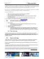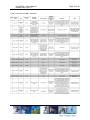
1
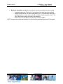
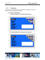
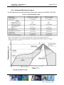
Anaren Integrated Radio A110LR09x User’s Manual Release Date 10/31/11 THIS PAGE LEFT INTENTIONALLY BLANK iii USERS MANUAL Models A110LR09A and A110LR09C Contents 1. Overview .......................................................................................................................................................... 5 1.1. A110LR09A ................................................................................................................................................5 1.2. A110LR09C.................................................................................................................................................5 1.3. Features.......................................................................................................................................................6 1.4. Theory of Operation..................................................................................................................................6 1.4.1. Typical Flow ........................................................................................................................................9 1.5. Applications ............................................................................................................................................. 11 2. Product Approvals ........................................................................................................................................ 12 2.1. USA (Federal Communications Commission, FCC) .......................................................................... 12 2.1.1. FCC Labeling Requirements ............................................................................................................. 12 2.1.2. End User Manual .............................................................................................................................. 13 2.2. Canada (Industry Canada, IC) .............................................................................................................. 13 2.2.1. IC Labeling Requirements ................................................................................................................. 14 2.3. Europe (Conformité Européenne, ) .................................................................................................. 15 2.4. Potential Interference Sources ............................................................................................................... 16 2.4.1. Time critical data ............................................................................................................................... 16 2.5. Approved Usage ..................................................................................................................................... 16 2.5.1. US & Canada .................................................................................................................................... 17 2.5.2. Europe ............................................................................................................................................... 18 3. Electrical Characteristics .............................................................................................................................. 25 3.1. Absolute Maximum Ratings .................................................................................................................. 25 3.2. Operating Conditions ............................................................................................................................. 26 3.3. Pin Out ...................................................................................................................................................... 26 3.4. Recommended Layout............................................................................................................................ 28 3.5. Power Supply Considerations ............................................................................................................... 30 4. Mechanical and Process ................................................................................................................................ 31 4.1. Dimensions............................................................................................................................................... 31 4.1.1. A110LR09A ...................................................................................................................................... 31 4.1.2. A110LR09C ...................................................................................................................................... 31 4.2. Packaging ................................................................................................................................................. 32 4.2.1. Matrix Tray Packaging ..................................................................................................................... 32 4.2.2. Tape-Reel Packaging ......................................................................................................................... 33 4.3. Soldering................................................................................................................................................... 34 4.3.1. Manual Mounting Procedure ........................................................................................................... 34 4.3.2. Automated Mounting Procedure ...................................................................................................... 35 THIS PAGE LEFT INTENTIONALLY BLANK A110LR09x – User’s Manual Release Date 10/31/11 Page 5 of 38 1. Overview The A110LR09A and A110LR09C are surface mount modules – each with an integrated crystal, internal voltage regulator, matching circuitry and filtering. The A110LR09A has an integral antenna, whereas the A110LR09C utilizes an external antenna through a U.FL connector (see Table 1). The modules operate in the European 868 – 870MHz and US 902 – 928MHz ISM bands and are ideal for achieving low power wireless connectivity without having to deal with extensive RF, antenna design and regulatory compliance, allowing quick time to market. The modules are 100% tested to provide consistent performance. The A110LR09A and A110LR09C have received regulatory approvals for modular devices in Europe and in the US. The modular approval allows the OEM or end user to place either an A110LR09A or an A110LR09C with an approved antenna inside a finished product without having to perform costly regulatory testing for an intentional radiator. Section 2 has information on the requirements for the end user/integrator must fulfill to use the modules without intentional radiator regulatory testing. The receiver section of the modules has been evaluated and approved as Category II receiver for use in Europe. The A110LR09A and A110LR09C are based on the CC110L transceiver IC from Texas Instruments. All control lines for the transceiver are provided at module level for full control of its operation. Please see the CC110L data sheet (www.ti.com) for how to control the modules. Please see section 2.5 for the recommended register settings to achieve optimal performance and regulatory compliance. The A110LR09A measure 9x16x2.5mm and A110LR09C measures 9x12x2.5mm. The modules are footprint compatible with each other. 1.1. A110LR09A The A110LR09A has an integral antenna, providing high efficiency and near omni-directional radiation pattern. This approach offers the lowest system cost when the application allows collocation of radio and antenna. 1.2. A110LR09C The A110LR09C has a compact antenna connector that allows for locating the antenna away from the module due to form/function or in order to exit a metal enclosure, see figure 6 – 9 for more information on antenna location and enclosure considerations. A110LR09x – User’s Manual Release Date 10/31/11 Page 6 of 38 1.3. Features Features: Benefits Summary: Frequency range: 868-870MHz & 902928MHz Ultra small package size A110LR09C : 9mm x 12mm x 2.5mm A110LR09A : 9mm x 16mm x 2.5mm Impedance controlled multi-layer PCB 27 MHz Crystal Frequency Shielded Package 1.8 to 3.6 V operation SPI Interface ROHS Compliant LGA Footprint Low Power Consumption Regulatory approvals for ETSI, FCC and IC Digital RSSI output Programmable channel filter bandwidth Programmable output power up to +12 dBm High sensitivity (–112 dBm at 1.2 kBaud, 1% packet error rate) Low current consumption (14.7 mA in RX, 1.2kBaud, input well above sensitivity limit) Fast startup time: 240µs from SLEEP to Rx or Tx mode Separate 64 byte Rx and Tx FIFOs Programmable data rate from 0.6 to 600 kBaud. Please note that only approved configurations are allowed under the current certification. Sleep state: 0.4µA Idle State: 1.7mA 1.4. Operating temperature -40 to +85C 100% RF Tested in production Common footprint for all family members No RF engineering experience necessary Only requires a 2 layer PCB implementation Excellent receiver selectivity and blocking Performance Suited for systems compliant with ETSI EN 300 220, FCC 15.247, and IC RSS210 and RSS-Gen No regulatory “Intentional radiator” testing is required to integrate the module into an end product. Simple certification labeling replaces testing. Theory of Operation The A110LR09A and A110LR09C are for low power wireless applications in the European 868 – 870MHz, and US 902 – 928MHz ISM band. The devices can be used to implement a variety of networks, including; point to point, point to multipoint, peer to peer and mesh networks. The A110LR09A and A110LR09C both interface to an application microcontroller via an SPI bus. Physical and MAC layer functionality are accessed via the SPI bus through addressable registers as well as execution commands. Data received, or to be transmitted, are also A110LR09x – User’s Manual Release Date 10/31/11 Page 7 of 38 accessed through the SPI bus and are implemented as a FIFO register (64 bytes each for Tx and Rx). To transmit, a frame of data is placed in the FIFO; this may include a destination address. A transmit command is given, which will transmit the data according to the initial setup of the registers. To receive data, a receive command is given, which enables the unit to “listen” for a transmission; when such a transmission occurs, it places the received frame in the FIFO. When neither transmit nor receive is required, the device can enter either an Idle mode, from which it can quickly re-enter a receive/transmit mode, or a low power sleep mode from which a crystal startup is required prior to transmit or receive operation. Below is a block diagram for each of the A110LR09A and A110LR09C modules. Antenna o The antenna couples energy between the air and the AIR module. For applications where installations are done by an end user (non-professional), an omni-directional antenna pattern is desired such that the application will work equally well in every direction. Similarly for peer to peer or point to multipoint applications, an omni-directional pattern is desired such that all nodes have a fair chance of communicating. The A110LR09A module has an integral antenna that is near omni-directional, whereas the A110LR09C has approved antenna options ranging from near omni-directional to shaped front/back patterns (useful for inline, professional installations). Note that the end radiation pattern depends not only on the antenna, but also on the ground plane, enclosure and installation environment. Filtering o Filtering removes spurious signals to comply with regulatory intentional radiator requirements. Matching o Matching provides the correct loading of the transmit amplifier to achieve the highest output power, as well as the correct loading for the receive LNA to achieve the best sensitivity. Physical o The physical layer provides conversions between data, symbol and RF signal. MAC o The MAC layer is part of the Logical Link Layer and provides frame handling, addressing and medium access services. For CE operations, part of the MAC is implemented in the S/W. Microcontroller Interface o The microcontroller interface exposes registers and commands for the physical and MAC layers to a microcontroller. Power Management o Power management ensures a stable supply for the internal functions, as well as providing means for a low power sleep mode (in which case, most of the transceiver is power off). Page 8 of 38 A110LR09x – User’s Manual Release Date 10/31/11 Figure 1 The functionality of the A110LR09A, using an integral antenna Figure 2 The functionality of the A110LR09C, using an external antenna. A110LR09x – User’s Manual Release Date 10/31/11 Page 9 of 38 Figure 3 Transceiver IC block diagram. 1.4.1. Typical Flow After initial setup of registers for desired behavior, the normal operation flow diagram is shown in Figure 4. In applications of infrequent data transmissions, the transceiver would be in “sleep” mode to save power (400nA). From there it would wake up and then enter “idle” mode. As part of the wake up process the crystal oscillator is started (~240μs) and the digital microcontroller interface is powered up. Before transmit or receive, the frequency synthesizer needs to be started (“FS_Wakeup”) and, having been powered off (or idle for a while), the control loop of the VCO/PLL needs to be calibrated (“calibrate”). A data frame is loaded into the transmit FIFO and the “TX” mode is entered. The transceiver will transmit the data and enter “idle” mode after completion. When transmit is complete “RX” mode is entered to wait for the acknowledge frame. Once a frame is received, the transceiver will again enter “idle” mode. If no acknowledge frame is received within a given timeout, the data frame would be re-transmitted. If the acknowledge frame indicates that the data was received, the next data frame will be transmitted. After the last data frame has been transmitted successfully, the transceiver will again be put in “sleep” mode. Page 10 of 38 A110LR09x – User’s Manual Release Date 10/31/11 Medium access Figure 4 Transceiver state diagram A110LR09x – User’s Manual Release Date 10/31/11 1.5. Page 11 of 38 Applications Ultra low-power wireless applications, operating in the European 868-870 MHz and US 902-928 MHz ISM bands. Wireless alarm and security systems Industrial monitoring and control Wireless sensor networks AMR – Automatic Meter Reading Home and building automation Existing applications where simple upgrade to wireless is desired A110LR09x – User’s Manual Release Date 10/31/11 Page 12 of 38 2. Product Approvals The A110LR09A and A110LR09C have been designed to meet most national regulations for worldwide ISM-band use. In particular, the radio modules have been certified to the following standards. 2.1. USA (Federal Communications Commission, FCC) The A110LR09A, with integrated antenna, as well as the A110LR09C, used with the antenna listed in Table 1 below, have been tested to comply with FCC Part 15 - 15.247 “Intentional Radiators.” The devices meet the requirements for modular transmitter approval as detailed in FCC public notice DA 00-1407 Released: June 26, 2000. The A110LR09A and A110LR09C modules can be integrated into a finished product without obtaining subsequent FCC approvals for intentional radiators. (15.19a3) The module complies with part 15 of the FCC rules. Operation is subject to the following two conditions: (1) this device may not cause harmful interference, and (2) this device must accept any interference received, including interference that may cause undesired operation. Table 1 Approved Antennae Item 1 2 Part Number Integral part of A110LR09A 66089-8906 Manufacturer Anaren Anaren Type Integral Antenna Monopole whip, 6 mm lead Gain 0 dBi 2 dBi 2.1.1. FCC Labeling Requirements The A110LR09A and A110LR09C modules have been labeled with their own FCC ID number and if the FCC ID is not visible when the module is installed inside another device, then the outside of the finished product into which the module is installed must also display a label referring to the enclosed module. This exterior label can use wording such as the following: A110LR09x – User’s Manual Release Date 10/31/11 Page 13 of 38 Contains Transmitter Module FCC ID: X7J-A11072401 -orContains FCC ID: X7J-A11072401 This device complies with Part 15 of the FCC Rules. Operation is subject to the following two conditions: (1) this device may not cause harmful interference, and (2) this device must accept any interference received, including interference that may cause undesired operation. 2.1.2. End User Manual The end user manual should include the following statement: This equipment has been tested and found to comply with the limits for a Class B digital device, pursuant to part 15 of the FCC Rules. These limits are designed to provide reasonable protection against harmful interference in a residential installation. This equipment generates, uses, and can radiate radio frequency energy and, if not installed and used in accordance with the instructions, may cause harmful interference to radio communications. However, there is no guarantee that interference will not occur in a particular installation. If this equipment does cause harmful interference to radio or television reception, which can be determined by turning the equipment off and on, the user is encouraged to try to correct the interference by one or more of the following measures: Reorient or relocate the receiving antenna. Increase the separation between the equipment and receiver. Connect the equipment into an outlet on a circuit different from that to which the receiver is connected. Consult the dealer or an experienced radio/TV technician for help. 2.2. Canada (Industry Canada, IC) The A110LR09A and A110LR09C modules have been certified for use in Canada under Industry Canada (IC) Radio Standards Specification (RSS) RSS-210 and RSS-Gen. From section 3.2 RSS-Gen, Issue 3, December 2010, Modular Approval for Category I Equipment or Category II Equipment: “Modular approval permits the installation of the same module in a host device or multiple host devices without the need to recertify the device. Equipment certification for a modular device may be sought for either Category I equipment or Category II equipment. Page 14 of 38 A110LR09x – User’s Manual Release Date 10/31/11 Transmitters designed as modules for the installation in a host device may obtain equipment certification as a modular device provided that the applicable RSS is met and the following conditions in this section are met.” In section 7.1.2 Transmitter Antenna, it has been mentioned that the user manuals for transmitters shall display the following notice in a conspicuous location: Notice: Under Industry Canada regulations, this radio transmitter may only operate using an antenna of a type and maximum (or lesser) gain approved for the transmitter by Industry Canada. To reduce potential radio interference to other users, the antenna type and its gain should be so chosen that the equivalent isotropically radiated power (e.i.r.p.) is not more than that necessary for successful communication. Avis: Sous la réglementation d'Industrie Canada, ce transmetteur radio ne peut fonctionner qu’en utilisant seulement une antenne d'un type et d’un maximum (ou moins) de gain approuvé pour l'émetteur par Industrie Canada. Pour réduire des potentielles interférences radio pour les autres utilisateurs, le type d'antenne et son gain doivent être choisis de sorte que la puissance isotrope rayonnée équivalente (PIRE) ne dépasse pas ce qui est nécessaire pour une communication réussie. In section 7.1.2 Transmitter Antenna, it has been mentioned that the user manuals for transmitters equipped with detachable antennas shall also contain the following notice in a conspicuous location: Notice: This radio transmitter (IC: 8975A-A11072401) has been approved by Industry Canada to operate with the antenna types listed below with the maximum permissible gain and required antenna impedance for each antenna type indicated. Antenna types not included in this list, having a gain greater than the maximum gain indicated for that type, are strictly prohibited for use with this device. Avis: Cet émetteur radio (IC: 8975A-A11072401) a été approuvé par Industrie Canada pour fonctionner avec les types d'antennes énumérés ci-dessous avec le gain maximal admissible et l’impédance d'antenne requise pour chaque type d'antenne indiqué. Les types d'antennes ne figurant pas dans cette liste, ayant un gain supérieur au gain maximal indiqué pour ce type, sont strictement interdits pour l'utilisation avec cet appareil. 2.2.1. IC Labeling Requirements From section 3.2.1, RSS-Gen, Issue 3, December 2010, Labeling Requirements for the Host device: “The host device shall be properly labelled to identify the modules within the host device. The Industry Canada certification label of a module shall be clearly visible at all times when installed in the host device, otherwise the host device must be labelled to display the Industry Canada certification number of the module, preceded by the words “Contains transmitter module”, or the word “Contains”, or similar wording expressing the same meaning, as follows: Contains transmitter module IC: XXXXXX-YYYYYYYYYYY where XXXXXX-YYYYYYYYYYY is the module’s certification number. The applicant for equipment certification of the module shall provide with each unit of the module either a label such as described above, or an explanation and instructions to the user as to the host device labelling requirements.” A110LR09x – User’s Manual Release Date 10/31/11 Page 15 of 38 Label: Contains/Contient IC: 8975A-A11072401 Notice: This device complies with Industry Canada licence-exempt RSS standard(s). Operation is subject to the following two conditions: (1) this device may not cause interference, and (2) this device must accept any interference, including interference that may cause undesired operation of the device. Avis: Cet appareil est conforme avec Industrie Canada RSS standard exempts de licence (s). Son fonctionnement est soumis aux deux conditions suivantes: (1) cet appareil ne peut pas provoquer d'interférences et (2) cet appareil doit accepter toute interférence, y compris les interférences qui peuvent causer un mauvais fonctionnement du dispositif. From section 7.1.4, RSS-Gen, Issue 3, December 2010, Radio Apparatus Containing Digital Circuits (ICES003): “Radio apparatus containing digital circuitry which can function separately from the operation of a transmitter or an associated transmitter, shall comply with ICES-003. In such cases, the labeling requirements of the applicable RSS apply, rather than the labelling requirements in ICES-003.” For more information see: Industry Canada http://www.ic.gc.ca/ 2.3. Europe (Conformité Européenne, ) The A110LR09A and A110LR09C modules have been certified for use in European countries. The following testing has been completed: Test standard ETSI EN 300 220-2 V2.3.1 (2010-02) Frequency Error (Normal and Extreme Conditions) Conducted Average Power (Normal and Extreme Conditions) Effective Radiated Power Spread Spectrum Spectral Power Density Transient Power Modulation Bandwidth TX/RX Spurious Emissions Receiver Sensitivity Receiver LBT Threshold Receiver Blocking Test standards ETSI EN 301 489-3 V1.4.1 (2002-08), ETSI EN 62311:2008 and ETSI EN 60950-1:2006 Radiated Emissions Electro-Static Discharge Radiated RF Susceptibility A110LR09x – User’s Manual Release Date 10/31/11 Page 16 of 38 A helpful document that can be used as a starting point in understanding the use of short range devices (SRD) in Europe is the European Radio Communications Committee (ERC) Recommendation 70-03 E, downloadable from the European Radio Communications Office (ERO) http://www.ero.dk. The end user is responsible for ensuring compliance with harmonized frequencies and labeling requirements for each country in which the end device is marketed and sold. For more information see: Radio And Telecommunications Terminal Equipment (R&TTE) http://ec.europa.eu/enterprise/rtte/index_en.htm European Conference of Postal and Telecommunications Administrations (CEPT) http://www.cept.org/ European Telecommunications Standards Institute (ETSI) http://www.etsi.org/ European Radio Communications Office (ERO) http://www.ero.dk/ 2.4. Potential Interference Sources Alarm systems o These typically use low duty cycles and are therefore easy to avoid using acknowledge/retransmit methods Car alarms (internal motion sensors) Video surveillance o These are typically operated on a fixed channel determined at installation time and can be avoided by using clear channel assessment. It may be useful to change the channel used by the video surveillance equipment also, if possible. 2.4.1. Time critical data If the user requires specific time critical data throughput that cannot tolerate the delays of potentially many re-transmissions, the user is encouraged to implement an environment-aware algorithm that periodically monitors/scans the frequency band and maintain a list of “best available” channels. 2.5. Approved Usage These radio modules can be used in a variety of physical layer configurations; the following restricts the use to maintain compliance with the above referenced certification bodies. The user is encouraged to use minimum power required to establish a link, thus minimizing interference. Changes or modifications to the module and/or operation outside the limits set forth below are prohibited and could void the user’s authority to operate the modules. Uses of these radio modules are limited to the specific register settings that are optimized for performance and compliance. Register setting files are provided online at www.anaren.com. A110LR09x – User’s Manual Release Date 10/31/11 Page 17 of 38 2.5.1. US & Canada Within the US and Canada, the modules have been approved for use as digitally modulated transmitters. In the US, the occupied bandwidth (6dB BW) should be greater than 500 kHz, whereas in Canada, the max BW (99% BW) should be 0.5% of the center frequency. Table 2 shows the configurations that have been approved for use both in the US and Canada. Table 2 FCC/IC Approved Configurations Code Modulation Type Datarate(kbps) ML4 ML5 ML6 ML7 2-FSK 2-FSK 2-FSK 2-FSK Deviation (kHz) Max Output Power(dBm[Hex]) 237 237 237 237 7 [0xCD] 8 [0xCA] 10 [0xC4] 12 [0xC0] 1.2 38.4 100 250 Due to FCC power spectral density requirements, the output power must be limited by the given value for each modulation types. The given hex value in Table 2 represents the PA Table setting for the module to ensure the correct maximum output power. Table 3 gives a list of available output powers that the module has along with the corresponding PA Table register values. Table 3 Output Power vs. PA Table Value Power (dBm) 12 11 10.5 10.3 10 9.6 9.2 9 8.6 8.2 8 7.6 7.2 7 6.2 5 4.8 4.6 4.4 PA_Table(Hex) 0xC0 0xC1 0xC2 0xC3 0xC4 0xC5 0xC6 0xC7 0xC8 0xC9 0xCA 0xCB 0xCC 0xCD 0xCE 0x80 0x81 0x82 0x83 Power (dBm) 4.2 4 3.6 3.4 3 2.5 2 1 0 -0.5 -1 -2 -2.2 -5 -10 -15 -20 -25 -30 PA_Table(Hex) 0x84 0x85 0x86 0xCF 0x88 0x8A 0x8B 0x8D 0x8E 0x70 0x60 0x40 0x62 0x67 0x6D 0x24 0x22 0x14 0x03 A110LR09x – User’s Manual Release Date 10/31/11 Page 18 of 38 The operating frequency must be selected in such a way that the complete modulated signal stays within the band of 902 - 928MHz. The modules can be operated at any frequency between the lowest and highest frequencies in the band. The lowest and highest frequencies are given as follow: Lowest Frequency: 902.7MHz Highest Frequency: 927.377MHz 2.5.2. Europe Table 4 ETSI Approved configurationsshows the approved configurations for use in Europe. All configurations are optimized for the best sensitivity. In order to meet different customer needs, a variety of datarates from 600 Baud to 600 kBaud has been provided. Table 4 ETSI Approved configurations Code Modulation Type Datarate(kbps) M4 M5 M6 M7 M11 M12 M13 M14 ML1 ML2 ML3 2-FSK 2-FSK GFSK GFSK 2-FSK GFSK GFSK 4-FSK GFSK GFSK 4-FSK 1.2 10 10 38 0.6 4.8 19.2 600 50 100 200 Dev / Ph. Tran. Channel Spacing(kHz) RX BW (kHz) 26.4 kHz 36 kHz 13 kHz 18 kHz 16.5 kHz 13.2 kHz 13.2 kHz 237/263 kHz(Tx/Rx) 25 50 50 50 50 50 50 50 50 50 50 50 50 50 84 121 60 70 60 60 60 844 120 211 211 Within the European 868-870 MHz ISM band, there are several sub-bands with different requirements. A summary of these bands is given in Table 5. Considering the modulation bandwidth of each modulation type, frequency drift of the module in the extreme working conditions, and the channel spacing for each configuration, usable channels for each modulation is obtained for the sub-bands. Table 6 lists the approved configurations and applicable channels for each sub-band. Table 7 shows list of available channels along with the corresponding frequencies and register settings. A110LR09x – User’s Manual Release Date 10/31/11 Table 5 ETSI 868-878 MHz sub-bands Page 19 of 38 A110LR09x – User’s Manual Release Date 10/31/11 Page 20 of 38 Table 6 Applicable Channels for Sub-Bands Band Code Base Frequency (MHz) Channel Spacing (kHz) 1 1 1 1 1 1 1 1 2 2 2 4 4 4 4 4 4 4 4 6 6 6 6 6 6 6 6 10 10 10 10 10 10 12 12 12 12 12 12 12 13 13 13 13 13 13 13 M4 M5 M6 M7 M11 M12 M13 ML1 M14 ML2 ML3 M4 M5 M6 M7 M11 M12 M13 ML1 M4 M5 M6 M7 M11 M12 M13 ML1 M4 M6 M7 M11 M12 M13 M4 M6 M7 M11 M12 M13 ML1 M4 M6 M7 M11 M12 M13 ML1 868 868 868 868 868 868 868 868 868 868 868 868 868 868 868 868 868 868 868 868 868 868 868 868 868 868 868 868 868 868 868 868 868 868 868 868 868 868 868 868 868 868 868 868 868 868 868 50 50 50 50 50 50 50 50 50 50 50 50 50 50 50 50 50 50 50 50 50 50 50 50 50 50 50 50 50 50 50 50 50 50 50 50 50 50 50 50 50 50 50 50 50 50 50 First Applicable Channel Number 2 3 1 2 2 2 1 2 12 4 5 2 3 1 2 2 2 2 2 16 17 16 16 16 16 16 17 30 30 30 30 30 30 36 36 36 36 36 36 36 36 36 36 36 36 36 36 Last Applicable Channel Number 37 35 37 37 37 37 37 36 26 35 34 9 7 9 9 9 9 9 8 21 19 21 21 21 21 21 20 30 30 30 30 30 30 37 37 37 37 37 37 36 37 37 37 37 37 37 36 A110LR09x – User’s Manual Release Date 10/31/11 Page 21 of 38 Table 7 ETSI Channel numbers with corresponding frequency value and register settings Channel # 1 2 3 4 5 6 7 8 9 10 11 12 13 14 15 16 17 18 19 20 21 22 23 24 25 26 27 28 29 30 31 32 33 34 35 36 37 Frequency (MHz) 868.052 868.104 868.156 868.208 868.259 868.311 868.363 868.415 868.467 868.519 868.571 868.623 868.675 868.727 868.779 868.831 868.882 868.934 868.986 869.038 869.09 869.142 869.194 869.246 869.298 869.35 869.402 869.453 869.505 869.557 869.609 869.661 869.713 869.765 869.817 869.869 869.921 FREQ0 (hex) 0x6B 0xE9 0x67 0xE5 0x63 0xE1 0x5F 0xDD 0x5B 0xD9 0x57 0xD5 0x53 0xD1 0x4F 0xCD 0x4B 0xC9 0x47 0xC5 0x43 0xC1 0x3F 0xBD 0x3B 0xB9 0x37 0xB5 0x33 0xB1 0x2F 0xAD 0x2B 0xA9 0x27 0xA5 0x23 FREQ1 (hex) 0x26 0x26 0x27 0x27 0x28 0x28 0x29 0x29 0x2A 0x2A 0x2B 0x2B 0x2C 0x2C 0x2D 0x2D 0x2E 0x2E 0x2F 0x2F 0x30 0x30 0x31 0x31 0x32 0x32 0x33 0x33 0x34 0x34 0x35 0x35 0x36 0x36 0x37 0x37 0x38 FREQ2 (hex) 0x20 0x20 0x20 0x20 0x20 0x20 0x20 0x20 0x20 0x20 0x20 0x20 0x20 0x20 0x20 0x20 0x20 0x20 0x20 0x20 0x20 0x20 0x20 0x20 0x20 0x20 0x20 0x20 0x20 0x20 0x20 0x20 0x20 0x20 0x20 0x20 0x20 A110LR09x – User’s Manual Release Date 10/31/11 Page 22 of 38 In order to comply with the output power limitations in Europe, the maximum values given in Table 8 below must be observed. Modulations M14, ML2 and ML3 are considered to be wideband modulations and therefore subject to the power spectral density requirements. Lower power levels for these configurations ensure compliance to the specifications. The limits are given based on the maximum allowed power level in a specific band and temperature conditions. Table 8 CW Output Powers Low Temp Power (dBm[Hex]) Normal Temp Power (dBm[Hex]) High Temp Power (dBm[Hex]) 14 dBm Limit 12 (C0) 12 (C0) 12 (C0) 10 dBm Limit 8.6 (C8) 9.6 (C5) 10 (C4) 7 dBm Limit 4.6 (82) 6.2 (CE) 7 (CD) M14 4.4 (83) 6.2 (CE) 7 (CD) ML2 -2 (40) 0 (8E) 1 (8D) ML3 -2 (40) -1 (60) 0 (8E) 2.5.2.1. Spectrum Access and Mitigation Requirements As part of the requirements for compliance, the applications must observe the restrictions that are listed in Table 5. Specifically, the spectrum access and mitigation requirements (e.g. Duty Cycle or LBT+AFA) have to be met. Some sub-bands (see Table 5) allow limited Duty cycling while some others let the user choose between limited Duty cycling and LBT+AFA implementation. In case of LBT+AFA, AFA (Adaptive Frequency Agility) has to be implemented in the customer’s SW stack since there is no specific hardware support for this functionality. 2.5.2.1.1. Duty Cycling Table 5 lists all sub-bands together with the usage requirements. In this table, Duty Cycling requirements are listed under “Restrictions” column. It applies to all transmitters excluding those with a LBT facility with AFA (explained in the next sub-section). The Duty Cycle is defined as the ratio, expressed as a percentage, of the maximum transmitter “ON” time monitored over one hour, relative to a one hour period. The device may be triggered either automatically or manually. And, depending on how the device is triggered, the duty cycle is either fixed or random. For automatic operated devices, either software controlled or pre-programmed devices, the OEM integrator or end product developer shall declare the duty cycle class or classes in the end-product user manual or user guide. For manual operated or event-dependent devices, with or without software controlled functions, the integrator shall declare whether the device once triggered, follows a pre-programmed cycle, or whether the transmitter remains on until the trigger is released or the device is manually reset. The integrator shall also give a description of the application for the device and include a typical usage pattern. The typical usage pattern as declared by the integrator shall be used to determine the duty cycle and hence the duty class. A110LR09x – User’s Manual Release Date 10/31/11 Page 23 of 38 Where an acknowledgement is required, the additional transmitter on-time shall be included and declared by the integrator. In a period of 1 hour, the duty cycle shall not exceed the spectrum access and mitigation requirement values as given in Table 5. For frequency agile devices without LBT, the duty cycle shall apply to the total transmission time as given in Table 5, or shall not exceed 0.1 % per channel in a period of 1 hour. 2.5.2.1.2. LBT & AFA Listen Before Talk (LBT) is used to share spectrum between SRD transceiver equipment with similar power and bandwidth. In order to make maximum use of the available channels, intelligent or polite equipment may use a Listen Before Talk (LBT) protocol with a preferred option of Adaptive Frequency Agility (AFA). AFA is defined as the capability of an equipment to dynamically change channel within its available frequencies for proper operation. LBT (Listen Before Talk) functionality is built in the A110LR09X modules, and the approved configurations are made to meet the LBT Threshold limits. However, LBT timing parameters, specific to the end product, have to be established through controlling software and declared by the OEM integrator or end-product developer in the product user manual or user guide. A brief description and limits of these parameters are given as follows: Minimum Transmitter off-time is the period where a specific transmitter shall remain off after a transmission or a communication dialogue between units or a polling sequence of other units on the same frequency. The minimum TX off-time has to be greater than 100 ms. LBT minimum listening time is the minimum time that the equipment listens for a received signal at or above the LBT threshold level immediately prior to transmission to determine whether the intended channel is available for use. LBT minimum listening time, tL, has two parts: the fixed part, tF, and the pseudo random part, tPS. tL = tF + tPS. The fixed part of the minimum listening time is 5 ms. The pseudo random part has to be randomly varied between 0 ms and 5 ms or more in equal steps of 0.5 ms as the following: o o If the channel is free from traffic at the beginning of the listen time, and remains free throughout the fixed part of the listen time, then tPS is automatically set to zero by the equipment itself If the channel is occupied by traffic when the equipment either starts to listen or during the listen period, then the listen time commences from the instant that the intended channel is free. In this situation the total listen time tL shall comprise tF and the pseudo random part, tPS. Algorithmic details and values have to be declared by the provider of the equipment. Maximum dead time is the period between the end of the listening time and the start of the transmission. The maximum dead time cannot exceed 5 ms. Page 24 of 38 A110LR09x – User’s Manual Release Date 10/31/11 Maximum transmitter on-time is the maximum time the transmitter can be on during: o o A single transmission. The limit is 1 s, and the actual value has to be declared. Multiple transmissions and acknowledgements for a communication dialogue or polling sequence of other units under the condition that the channel is free. The limit is 4 s, and the actual value has to be declared. o Within 1 hour for any 200 kHz of spectrum. The limit is 100 s. NOTE: Longer accumulated transmission time is possible by implementing more AFA channels. A110LR09x – User’s Manual Release Date 10/31/11 Page 25 of 38 3. Electrical Characteristics 3.1. Absolute Maximum Ratings Under no circumstances must the absolute maximum ratings given in Table 9 be violated. Stress exceeding one or more of the limiting values may cause permanent damage to the device. Caution! ESD sensitive device. Precaution should be used when handling the device in order to prevent permanent damage. Caution! This assembly contains moisture sensitive devices and requires proper handling per IPC/JEDEC J-STD-033 Table 9 Absolute Maximum Ratings A110LR09x – User’s Manual Release Date 10/31/11 Page 26 of 38 3.2. Operating Conditions Table 10 Operating Conditions 3.3. Pin Out The A110LR09A and A110LR09C radio modules share a common pin-out and foot print, that is also shared by Anaren modules using other frequencies -- thus enabling easy changeover from one to another, e.g. if changing the frequency or antenna scheme is desired. Below the common footprint are shown. NC = NO Connection. connected internally. Pin is NOT DNC = Do Not Connect. Internal connection used during assembly, do not connect. A110LR09x – Users Manual Release Date 10/31/11 Page 27 of 38 Table 11 Pin Descriptions Pin # 1 Pin Name DNC Pin Type NC 2 DNC NC 3 DNC NC 4 NC NC 5 NC NC 6 NC NC 7 Vdcoup1 Analog 8 9 10 GND SCLK MISO/GDO1 11 12 13 MOSI _CSN GDO0 14 15 GDO2 Vdcoup2 Ground Digital Input Digital Output Digital Input Digital Input Digital I/O (Analog output) Digital I/O Analog 16 NC NC 17 18 GND Vdd 19 NC Ground Power Supply NC 20 NC NC 21 NC NC 22 DNC NC 23 DNC NC 24 DNC NC Description Internal GND connection used during testing, not recommended to connect to main GND. Internal RF output connection used during test. Connecting this pin to anything will require recertification for intentional radiators. Internal GND connection used during testing, not recommended to connect to main GND. Pin is not connected internally, but is reserved for future expansion. It is recommended not to connect this pin to anything. Pin is not connected internally, but is reserved for future expansion. It is recommended not to connect this pin to anything. Pin is not connected internally, but is reserved for future expansion. It is recommended not to connect this pin to anything. Optional decoupling of the modules internal Vdd supply. It is recommended to not connect anything to this pin. In particular noisy environment this pin can be used to further reduce the noise on the modules internal Vdd, please see section 3.5 for further information. One of two primary ground pins SPI bus clock signal SPI bus data out from radio when CSN is low, and general purpose I/O pin when CSN is high SPI bus data into radio SPI bus select (active low) General purpose port General purpose port Optional decoupling of the modules internal Vdd supply. It is recommended to not connect anything to this pin. In particular noisy environment this pin can be used to further reduce the noise on the modules internal Vdd, please see section 3.5 for further information. No Connect, the pin is not connected internally, but is reserved for future expansion. It is recommended not to connect this pin to anything. One of two primary ground pins Power supply pin Pin is not connected internally, but is reserved for future expansion. It is recommended not to connect this pin to anything. Pin is not connected internally, but is reserved for future expansion. It is recommended not to connect this pin to anything. Pin is not connected internally, but is reserved for future expansion. It is recommended not to connect this pin to anything. Internal GND connection used during testing, not recommended to connect to main GND. Pin is not connected internally, but is reserved for future expansion. It is recommended not to connect this pin to anything. Internal GND connection used during testing, not recommended to connect to main GND. A110LR09x – Users Manual Release Date 10/31/11 Page 28 of 38 3.4. Recommended Layout Figure 5 Recommended PCB layout. A110LR09x – Users Manual Release Date 10/31/11 Figure 6 Mounting the module in a corner Figure 8 Mounting the module along an edge with overhang. This option is not generally recommended, but is a method to save PCB in an environmentally benign environment Page 29 of 38 Figure 7 Mounting the module along an edge Figure 9 Mounting the module along an edge, with a ground plane cut-out. This option degrades range slightly. A110LR09x – Users Manual Release Date 10/31/11 Page 30 of 38 3.5. Power Supply Considerations Noise on the power supply line reduces the sensitivity of a receiver and modulates onto a transmitter’s signal, both of which causes a degradation of link quality and hence a reduction in range. The A110LR09A and A110LR09C radio modules each have an integral ferrite bead in the supply line from pin 18 (Vdd) and decoupling capacitance to reduce any noise on the incoming power supply line. This arrangement will eliminate most supply voltage noise. In particularly noisy environments (switching regulators, motor controls, etc.), it may be necessary to add additional noise reduction means. Pin 7 (Vdcoup1) is connected to the modules internal supply line after the ferrite bead and decoupling capacitors and can be used to probe the noise at module level. The noise level measured on pin 7 should not exceed 120mVpp when in transmit or receive mode; it may however exceed this value when setting up or accessing data to/from the FIFOs, while not actively transmitting or receiving. If the level measured is exceeding the above limit, steps should be taken to ensure maximum range, including: Adding decoupling capacitance to pin 7 (Vdcoup1). Adding additional filtering in the supply line. Adding an LDO in the supply line (the TPS734xxx low Dropout Regulator from TI is recommended). A110LR09x – Users Manual Release Date 10/31/11 4. Mechanical and Process 4.1. Dimensions 4.1.1. A110LR09A 4.1.2. A110LR09C Page 31 of 38 A110LR09x – Users Manual Release Date 10/31/11 Page 32 of 38 4.2. Packaging AIR modules are available in Matrix Tray and Tape & Reel packaging for high-volume assembly. Details of packaging provided below: 4.2.1. Matrix Tray Packaging A110LR09A00GM Matrix Tray Packaging Detail (30/Tray) A110LR09C00GM Matrix Tray Packaging Detail (40/Tray) A110LR09x – Users Manual Release Date 10/31/11 4.2.2. Tape-Reel Packaging A110LR09A00GR Tape-Reel Packaging Detail (500/Reel) A110LR09C00GR Tape-Reel Packaging Detail (500/Reel) Page 33 of 38 A110LR09x – Users Manual Release Date 10/31/11 Page 34 of 38 4.3. Soldering AIR Modules may be mounted either manually (for prototyping or low volume production), or automatically for high-volume production. A no-clean tin/silver/copper (SAC) solder is recommended, however lead based no-clean pastes may also be used. CAUTION: AIR Modules are designed for no-clean fluxes only. DO NOT use waterbased fluxes that require aqueous cleaning after solder. Spot cleaning with a flux remover and toothbrush may be performed with care. 4.3.1. Manual Mounting Procedure The recommended soldering method is reflow of a paste solder on a hot plate. This method works provided the bottom of the board where the AIR module is to be mounted is accessible, and there are no bottom-side components in the way. An aluminum or copper block may be placed on the hot plate surface to transfer heat to a localized area on the board where the AIR module is mounted - Set the hot plate to the reflow temperature solder manufacturer’s recommended Apply solder paste to the pads on the board receiving the AIR module Place the AIR module carefully onto the dispensed solder Using tweezers or another holding device, carefully place board with AIR module onto the hot plate surface (or metal block) Apply heat until reflow occurs, per solder paste manufacturer’s recommendations Carefully remove the board and place on a heat-resistant surface to cool Check assembly electrically to confirm there are no opens or shorts A110LR09x – Users Manual Release Date 10/31/11 Page 35 of 38 4.3.2. Automated Mounting Procedure The AIR Radio Module recommended solder reflow profile is based on IPC/JEDEC J-STD-020. Page 36 of 38 A110LR09x – Users Manual Release Date 10/31/11 A110LR09x – Users Manual Release Date 10/31/11 Page 37 of 38 HISTORY Date 08/26/11 10/02/11 10/11/11 10/21/11 Author Sula Richardson Sula Sula 10/25/11 10/28/11 Sula Sula 10/31/11 Richardson Change Note No./Notes Initial Draft Initial Release Figure 3 modified Industry Canada section was updated by notices in French Antenna Gain modified RF Exposure Sections removed from FCC and IC Removed FCC logo Thank you for learning more about the Anaren Integrated Radio (AIR) module line. If you have additional questions, need samples, or would like a quote – please do not hesitate to email the AIR team at [email protected] or contact any of these authorized distributors of the AIR product line. Worldwide North America Anaren Microwave, Inc. 6635 Kirkville Road East Syracuse, NY 13057 Tel: +1 315 432 8909 +1 800 411 6596 Fax: +1 315 432 8970 Anaren Microwave (Europe), Inc. 12 Somerset House, Suite 16 & 17 Hussar Court, Waterlooville Hampshire, England P07-7SG Tel: +44 2392 232392 Fax: +44 2392 251369 Worldwide Anaren Communication Suzhou Co. Ltd. No. 5 Chun Hui Road Wei Ting, Suzhou Industrial Park Suzhou 215122, PR China Tel: +86 512 6287 6400 Fax: +86 512 6274 9283