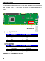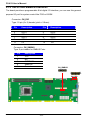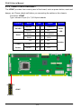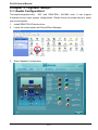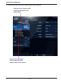
1
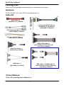
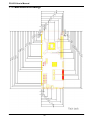
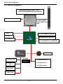
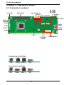
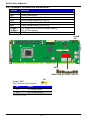
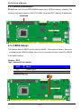
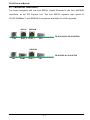
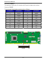
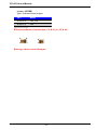
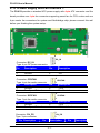
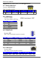
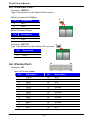
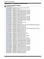
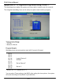
FS-A74
PICMG1.3 Full-size CPU Card
User’s Manual
Edition 1.5
2014/05/15
FS-A74 User’s Manual
Copyright
Copyright 2011, all rights reserved. This document is copyrighted and all rights are
reserved. The information in this document is subject to change without prior notice to
make improvements to the products.
This document contains proprietary information and protected by copyright. No part of
this document may be reproduced, copied, or translated in any form or any means
without prior written permission of the manufacturer.
All trademarks and/or registered trademarks contains in this document are property of
their respective owners.
Disclaimer
The company shall not be liable for any incidental or consequential damages resulting
from the performance or use of this product.
The company does not issue a warranty of any kind, express or implied, including
without limitation implied warranties of merchantability or fitness for a particular purpose.
The company has the right to revise the manual or include changes in the specifications
of the product described within it at any time without notice and without obligation to
notify any person of such revision or changes.
Trademark
All trademarks are the property of their respective holders.
Any questions please visit our website at http://www.commell.com.tw
TU
UT
-1-
FS-A74 User’s Manual
Packing List:
Please check the package content before you starting using the board.
Hardware:
FS-A74 PICMG1.3 Full-size CPU Card motherboard x 1
Cable Kit:
SATA Cable x 2
(OALSATA3-L)/ (1040529)
DVI module with bracket x 1
(BADPDVIP_A & OALDVI-P)
(4120008021 & 1040075)
PS/2 Keyboard & Mouse Cable x 1
(OALPS2/MKN)/ (1040551)
4-pin to 3-pin ATX cable x 1
(OAL-ATX-C)/ (1040184)
DB25 & DB9 cable x 1
(FS-A74TDG/ FS-A74FTDG Only)
(OAL1S1P)/ (1040041)
Audio Port Cable x 1
(OALPJ-HD)/ (1040120)
USB Cable x 1
DB9 cable x 1 & DB25 cable x 1
(FS-A74TDG2/ FS-A74FTDG2 Only)
(OAL2S1P)/ (1040191)
(OALUSBA-1)/ (1040172)
Printed Matters:
Driver CD (Including User’s Manual) x 1
-2-
FS-A74 User’s Manual
Index
Chapter 1 <Introduction> .............................................................6
1.1 <Product Overview>..................................................................................... 6
1.2 <Product Specification>................................................................................ 7
1.3 <Mechanical Drawing>................................................................................. 9
1.4 <Block Diagram>........................................................................................ 10
Chapter 2 <Hardware Setup> .................................................. 11
2.1 <Connector Location> ................................................................................ 11
2.2 <Jumper Location & Reference>................................................................ 12
2.3 <Connector Reference> ............................................................................. 13
2.3.1 <Internal Connectors> .............................................................. 13
2.3.2 <External Connectors> ............................................................. 13
2.4 <CPU and Memory Setup> ........................................................................ 14
2.4.1 <CPU Setup> ............................................................................. 14
2.4.2 <Memory installation> ............................................................... 15
2.5 <CMOS & ATX Setup> ............................................................................... 15
2.6 <Serial ATA Interface> ................................................................................ 16
2.7 <Ethernet Interface>................................................................................... 17
2.8 <Onboard Display Interface> ..................................................................... 18
2.8.1 <Analog Display>....................................................................... 18
2.8.2 <DVI Display > ........................................................................... 19
2.9 <Integrated Audio Interface> ...................................................................... 20
2.10 <USB Interface>....................................................................................... 22
2.11 <Serial Port>............................................................................................. 24
2.12 <GPIO and SMBUS Interface>................................................................. 26
2.13 <Power Supply and Fan Interface > ......................................................... 27
2.14 <Switch and Indicator>............................................................................. 28
Chapter 3 <System Setup> .......................................................29
3.1 <Audio Configuration>................................................................................ 29
3.2 <Display Properties Setting> ...................................................................... 30
-3-
FS-A74 User’s Manual
Chapter 4 <BIOS Setup> .............................................................32
Appendix A <I/O Port Pin Assignment> ..........................34
A.1 <Serial ATA Port> .......................................................................................34
A.2 <IrDA Port>.................................................................................................34
A.3 <VGA Port> ................................................................................................34
A.4 <LAN Port>.................................................................................................34
A.5 <LAN LED Port>.........................................................................................35
A.6 <Parallel Port>............................................................................................35
Appendix B <Flash BIOS> .........................................................36
B.1 <Flash Tool>...............................................................................................36
B.2 <Flash BIOS Procedure> ...........................................................................36
Appendix C <System Resources> ......................................37
C.1 <I/O Port Address Map>.............................................................................37
C.2 <Memory Address Map> ............................................................................39
C.3 <System IRQ Resources> .........................................................................40
Appendix D <Programming GPIO’s> .................................41
Appendix E <Programming Watchdog Timer > .........42
Contact Information .......................................................................43
-4-
FS-A74 User’s Manual
(This page is left for blank)
-5-
FS-A74 User’s Manual
Chapter 1 <Introduction>
1.1 <Product Overview>
FS-A74 the 2nd Generation Intel of the PICMG1.3 Full-size CPU Card motherboard,
nd
supports 2
Generation Intel® Core™ i7, Core™ i5, Core™ i3 and Pentium/Xeon ®
Desktop Processor and features Intel Q67 chipset, integrated HD Graphics, DDR3
memory, REALTEK High Definition Audio, Serial ATA and Intel Gigabit LAN.
Intel® FCLGA1155 processor
The Intel® I3/I5/I7/Pentium/Xeon® processor now comes with a new form factor with
1155-pin FCLGA package, for 1066/1333MHz front-side-bus, 12MB L2 cache, for 65nm
and 45nm manufacturing technology, the PLGA processor without pin header on solder
side can make user installing the processor on the socket easier.
Intel® Q67 PCH chipset
The Intel Q67 integrates DDR3 1066/1333MHz for memory, and HD Graphic technology
for new graphic engine. The Q67 integrates with up to 8 USB2.0 interfaces, and serial
ATA II interface with RAID function.
-6-
FS-A74 User’s Manual
1.2 <Product Specification>
General Specification
Form Factor
CPU
Memory
Chipset
BIOS
Green Function
Watchdog Timer
Real Time Clock
Serial ATAII
PICMG1.3 Full-size CPU Card
2nd Generation Intel® Core™ I3/I5/I7/Pentium/Xeon® processor
With LGA1155 socket
Package type: FCLGA 1155
2 x 240-pin DDR3 1066/1333MHz SDRAM up to 16GB
Unbufferred, none-ECC memory supported only
Intel® BD82Q67 PCH
Phoenix 16Mb SPI flash BIOS
Power saving mode includes doze, standby and suspend modes.
ACPI version 1.0 and APM version 1.2 compliant
System reset programmable watchdog timer with 1 ~ 255 sec./min.
of timeout value
Chipset built-in RTC with lithium battery
Intel® Q67 PCH integrates 4 Serial ATA II interface& 2 Serial ATA IIl
RAID 0, 1,5,10 Intel Matrix Storage Technology supported
Multi-I/O Port
Chipset
Serial Port
USB Port
IrDA Port
K/B & Mouse
GPIO
Smart Fan
Intel® Q67 PCH with Winbond® W83627DHG-P Controller
Four RS-232 and one RS232/422/485 serial ports
Eight Hi-Speed USB 2.0 ports with 480Mbps of transfer rate
One IrDA compliant Infrared interface supports SIR
External PS/2 keyboard and mouse ports on rear I/O panel
One 12-pin Digital I/O connector with 8-bit programmable I/O
Interface
One CPU fan connectors for fan speed controllable
VGA Display Interface
Chipset
Frame Buffer
Display Type
Connector
Intel® Clear Video integrated HD Graphics Technology
Up to 1.7GB shared with system memory
CRT, LCD monitor with analog display
Onboard DVI interface
External DB15 female connector on rear I/O panel
Onboard 26-pin DVI Connector
Ethernet Interface
Controller
Type
Connector
One Intel 82574L Gigabit Ethernet controller
One Intel 82579LM Gigabit Ethernet controller
(FS-A74TDG&FS-A74FTDG Only)
Triple speed 10/100/1000Base-T
Auto-switching Fast Ethernet
Full duplex, IEEE802.3U compliant
Two External RJ45 connectors with LED on rear I/O panel
-7 -
FS-A74 User’s Manual
Expansive Interface
PCI-Express
PCI
One X16 and one X4 or X1 on PICMG 1.3 Interface
Four PCI bus master on PICMG 1.3 Interface
Audio Interface
Chipset
Interface
Connector
Intel® integrated Q67with Realtek ALC888HD Audio
Intel High Definition Audio compliance
2 channels sound output
Internal 10-pin header for line-out, MIC-in, 4-pin header for CD-IN
Power and Environment
Power
Requirement
Dimension
Temperature
+5V, +12 DC input & 5VSB Requirement
338 (L) x 126 (W) mm
Operating within 0 ~ 60OC (32 ~ 140OF)
Storage within –20 ~ 85OC (-4 ~ 185OF)
p
P
P
p
P
p
P
p
Ordering Code
FS-A74TDG
Onboard VGA, DVI, 8 x USB2.0, 6 x serial Port, 6 x SATA, HD Audio,
GPIO, 2 x PCI Express mini card, 4 x PCI Bus master,
1 x Giga LAN (82579LM)
Support Four X1 & One X16 PCI Express interface
FS-A74FTDG
Onboard VGA, DVI, 8 x USB2.0, 6 x serial Port, 6 x SATA, HD Audio,
GPIO, 2 x PCI Express mini card, 4 x PCI Bus master,
1 x Giga LAN (82579LM)
Support One X4 & One X16 PCI Express interface
FS-A74TDG2
Onboard VGA, DVI, 8 x USB2.0, 6 x serial Port, 6 x SATA, HD Audio,
GPIO, 2 x PCI Express mini card, 4 x PCI Bus master, 2 x Giga LAN
Support Four X1 & One X16 PCI Express interface
FS-A74FTDG2
Onboard VGA, DVI, 8 x USB2.0, 6 x serial Port, 6 x SATA, HD Audio,
GPIO, 2 x PCI Express mini card, 4 x PCI Bus master, 2 x Giga LAN
Support One X4 & One X16 PCI Express interface
The specifications may be different as the actual production.
-8 -
FS-A74 User’s Manual
1.3 <Mechanical Drawing>
-9 -
FS-A74 User’s Manual
1.4 <Block Diagram>
2nd Generation Intel® Core™
I3/I5/I7/Pentium/Xeon® processor
1 x PCI Express x 16
2 x 240-pin DDR3
1066/1333MHz up to
16GB
1 x DVI
2 x PCI Express mini card
1 x CRT
4 x SATAII & 2 x SATA III
8 x USB 2.0
Intel Q67
1 x Intel 82574L & 1 x 82579LM
4 x RS232
W83627D-P
SPI BIOS
2 x Serial ports
25Q64CV
1 x PCI Express x4 or
4 x PCI Express x1
IrDA
4 x PCI Bus master
8-bit GPIO
Parallel port
-10-
FS-A74 User’s Manual
Chapter 2 <Hardware Setup>
2.1 <Connector Location>
CN_USB1
DDR3_A&B
CN_USB2
CN_USB3
CN_USB4
SATA1/2/3/4/5/6
CN_LPT
MINI_CARD1&2
CN_DIO
CDIN
CN_AUDIO
SYSFAN
CPUFAN
CN_PS
JACT1
JSPD1
JACT2
JSPD2
DC_IN
CN_12V
JFRNT
CN_DVI
CN_SMBUS
CN_IR
FS-A74TDG2 & FS-A74FTDG2
PS2
RJ45_2
RJ45_1
CRT
FS-A74TDG & FS-A74FTDG
PS2
COM1
RJ45_1
CRT
-11-
COM6/5/4/3/2/1
FS-A74 User’s Manual
2.2 <Jumper Location & Reference>
Jumper
JRTC
JAT
JP1
JP2
JP3
JP4
JCSEL1
JCSEL2
JVUSB
Function
CMOS Operating/Clear Setting
Power mode select
Com1 Voltage Setting (For Pin 9)
Com2 Voltage Setting (For Pin 9)
Com3 Voltage Setting (For Pin 9)
Com4 Voltage Setting (For Pin 9)
CN_COM2 RS-232 RS422 RS485 Setting
CN_IR IrDA Setting
USB Voltage Setting
JVUSB
JAT
JRTC
JCSEL2 JP4 JP3 JCSEL1 JP2 JP1
Jumper: JAT
Type: Onboard 3-pin jumper
JAT
1-2
2-3
JAT
1
Mode
AT Power mode
ATX Power mode
Default setting
-12-
3
FS-A74 User’s Manual
2.3 <Connector Reference>
2.3.1 <Internal Connectors>
Connector
CPU
DDRIIIA&B
SATA 1/2
SATA 3/4/5/6
CN_12V
CN_AUDIO
CDIN
CN_DIO
CN_USB 1/2/3/4/5/6
CPUFAN
SYSFAN
CN_IR
CN_COM1/2/3/4/5/6
JFRNT
Mini-Card1/2
CN_LPT
JSPD 1/2
JACT 1/2
CN_DVI
Function
LGA1155 CPU socket
240 –pin DDR3 SDRAM DIMM socket
7-pin Serial ATAIII connector
7-pin Serial ATAII connector
4-pin +12V additional power supply connector
5 x 2-pin audio connector
4-pin CD-ROM audio input connector
6 x 2-pin digital I/O connector
5 x 2-pin USB connector
4-pin CPU cooler fan connector
4-pin system cooler fan connector
5-pin IrDA connector
9-pin com connector
14-pin front panel switch/indicator connector
2 x 52-pin Mini-PCIE socket
13 x 2-pin printer connector
LAN Speed LED connector
LAN Activity LED connector
13 x 2-pin DVI connect
Remark
2.3.2 <External Connectors>
Connector
RJ45 1/2
CRT
PS/2
Function
1 x RJ45 LAN connector
DB15 and analog VGA connector
PS/2 keyboard and mouse connector
-13-
Remark
FS-A74 User’s Manual
2.4 <CPU and Memory Setup>
2.4.1 <CPU Setup>
FS-A74 has a LGA1155 CPU socket onboard; please check following steps to install the
processor properly.
Attention
If FS-A74 need RMA please Keep CPU socket cover on the CPU Socket.
Warning
If CPU Socket internal Pin damage We could not provide warranty.
2nd Generation Intel® Core™
I3/I5/I7/Pentium/Xeon® processor
Package type: 1155 pin FCLGA
FSB: 1066/1333MHz
Checked point
1. Lift this bar
2. Uncover this plate
3. Place the CPU on the top of
the pins
4. Lock this bar
3. Cover this plate
Notice: Please place the CPU on the pins tenderly to avoid bending the pins
14
FS-A74 User’s Manual
2.4.2 <Memory installation>
FS-A74 has two 240-pin DDR3 DIMM support up to 16GB of memory capacity. The
memory frequency supports 1066/1333 MHz. Only Non-ECC memory is supported.
DDRIIIA&B
2.5 <CMOS Setup>
The board’s data of CMOS can be setting in BIOS. If the board refuses to boot due
to inappropriate CMOS settings, here is how to proceed to clear (reset) the CMOS
to its default values.
Jumper: JRTC
Type: Onboard 3-pin jumper
JRTC
Mode
1-2
Clear CMOS
2-3
Normal Operation
Default setting: 2-3
JRTC
1
-15-
3
FS-A74 User’s Manual
2.6 <Serial ATA Interface>
FS-A74 has Four Serial ATA II & Two Serial ATA III interfaces with RAID function, the
transfer rate of the Serial ATA II can be up to 300MB/s & Serial ATA III can be up to
600MB/s. Please go to http://www.serialata.org/ for more about Serial ATA technology
information. Based on Intel® PCH, it supports Intel® Matrix Storage Technology with
combination of RAID 0,1,5 and 10. The main features of RAID on Intel® Q67 PCH are
listed below:
1.
Supports for up to RAID volumes on a single, two-hard drive RAID array.
2.
Supports for two, two-hard drive RAID arrays on any of six Serial ATA ports.
3.
Supports for Serial ATA ATAPI devices.
4.
Supports for RAID spares and automatic rebuild.
5.
Supports on RAID arrays, including NCQ and native hot plug.
For more information please visit Intel’s official website.
For more about the system setup for Serial ATA, please check the chapter of SATA
configuration.
SATA1/2/3/4/5/6
-16-
FS-A74 User’s Manual
2.7 <Ethernet Interface>
The board integrates with one Intel 82574L Gigabit Ethernet & one Intel 82579LM
controllers, as the PCI Express bus. The Intel 82574L supports triple speed of
10/100/1000Base-T, with IEEE802.3 compliance and Wake-On-LAN supported.
82574L
82579LM
RJ45_2
RJ45_1
FS-A74 TDG2 & FS-A74FTDG2
PS2
CRT
82579LM
FS-A74TDG & FS-A74FTDG
PS2
COM1
RJ45_1
CRT
-17-
FS-A74 User’s Manual
2.8 <Onboard Display Interface>
Based on Intel Q67 chipset with built-in graphics, the board provides one DB15
Connector on real external I/O port and the board also provides 26-pin DVI interface
Notice: When you install any PCI Graphic card, the onboard graphics would be disabled
automatically.
2.8.1 <Analog Display>
Please connect your CRT or LCD monitor with DB15 male connector to the onboard
DB15 female connector on rear I/O port.
FS-A74TDG2 & FS-A74FTDG2
CRT
FS-A74TDG & FS-A74FTDG
CRT
-18-
FS-A74 User’s Manual
2.8.2 <DVI Display >
The board also comes with a DVI interface with Chrontel for digital video interface.
Connector: CN_DVI
Connector type: 26-pin header connector (pitch = 2.00mm)
Pin Number
1
3
5
7
9
11
13
15
17
19
21
23
25
Assignment
TX1+
Ground
TXC+
Ground
N/C
TX2+
Ground
TX0+
N/C
DDCDATA
GND
N/C
N/C
Pin Number
2
4
6
8
10
12
14
16
18
20
22
24
26
2
1
26
CN_DVI
-19-
25
Assignment
TX1Ground
TXCPVDD
N/C
TX2Ground
TX0HPDET
DDCCLK
N/C
N/C
N/C
FS-A74 User’s Manual
2.9 <Integrated Audio Interface>
The board integrates onboard audio interface with REALTEK ALC888 codec, with Intel
next generation of audio standard as High Definition Audio, it offers more vivid sound
and other advantages than former HD audio compliance.
The main specifications of ALC888 are:
z
High-performance DACs with 100dB S/N ratio
z
2 DAC channels support 16/20/24-bit PCM format for 2 audio solution
z
16/20/24-bit S/PDIF-OUT supports 44.1K/48K/96kHz sample rate
z
Compatible with HD
z
Meets Microsoft WHQL/WLP 2.0 audio requirements
The board provides 2 channels audio phone jacks on rear I/O port, Line-in/MIC-in ports
for front I/O panel through optional cable.
CN_AUDIO
10
9
CDIN
1
-20-
4
2
1
FS-A74 User’s Manual
Connector: CN_AUDIO
Type: 10-pin (2 x 5) header (pitch = 2.54mm)
Pin
1
3
5
7
9
Description
MIC_L
MIC_R
Speaker_R
SENSE
Speaker_L
Pin
2
4
6
8
10
Connector: CDIN
Type: 4-pin header (pitch = 2.54mm)
Pin
Description
1
CD – Left
2
Ground
3
Ground
4
CD – Right
-21-
2
10
1
9
Description
Ground
N/C
MIC Detect
N/C
Speaker Detect
4
1
FS-A74 User’s Manual
2.10 <USB Interface>
FS-A74 integrates eight USB2.0 ports. The specifications of USB2.0 are listed
below:
Interface
USB2.0
Controller
Intel® Q67
Transfer Rate
Up to 480Mb/s
Voltage
5V
CN_USB2
CN_USB1
10
2
CN_USB3
CN_USB4
2
10
9
1
1
Connector: CN_USB1/2/3/4
Type: 10-pin (2 x 5) header (pitch = 2.54mm)
Pin
1
3
5
7
9
Description
VCC (5V_SB/ 5V)
Data0Data0+
Ground
Ground
Pin
2
4
6
8
10
-22-
Description
VCC (5V_SB/ 5V)
Data1Data1+
Ground
N/C
9
2
JVUSB
6
1
5
FS-A74 User’s Manual
Jumper: JVUSB
Type: Onboard 6-pin jumper
JAT
4-6 & 3-5
2-4 & 1-3
Mode
+5V_SB
+5V
Default setting
Effective patterns of connection: 1-3 & 2-4 or 3-5 & 4-6
2
6
2
6
1
5
1
5
Warning: others cause damages
-23-
FS-A74 User’s Manual
2.11 <Serial Port>
The board supports five RS232 serial port and one jumper selectable RS232/422/485 serial
ports. The jumper JCSEL1 & JCSEL2 can let you configure the communicating modes for
COM2.
10
9
2
1
CN_COM6/5/4/3/2/1
Connector: CN_COM1/3/4/5/6
Type: 9-Pin box header
Pin
Description
1
DCD
3
TXD
5
GND
7
RTS
9
RI
Pin
2
4
6
8
10
Description
RXD
DTR
DSR
CTS
N/C
Connector: CN_COM2
Type: 9-Pin box header
Pin
Description
1
DCD/422TX-/4853
TXD/422RX+
5
GND
7
RTS
9
RI
Pin
2
4
6
8
10
Description
RXD/422TX+/485+
DTR/422RXDSR
CTS
N/C
Setting RS-232 & RS-422 & RS-485 for COM2
24
FS-A74 User’s Manual
Function
IrDA
12
2
8
7
2
8
11
1
1
2 JCSEL1 JP212
7JCSEL2 JP4 JP3
JP1
JCSEL2
1
2
1
JCSEL1 11
2
12
11
8
7
2
1
1
8
7
2
12
2
1
1
11
RS-422
RS-232
Default setting:
RS-485
JCSEL1: (1-3, 2-4, 7-9, 8-10) JCSEL2: (1-2)
Jumper: JP1/JP2/JP3/JP4 (COM1/2/3/4)
Type: onboard 6-pin header
Power Mode
JP1/2/3/4
Pin 9 with 5V Power
1-2
Pin 9 with 12V Power
3-4
Standard COM port
5-6
Default setting (5-6)
25
FS-A74 User’s Manual
2.12 <GPIO and SMBUS Interface>
The board provides a programmable 8-bit digital I/O interface; you can use this general
purpose I/O port for system control like POS or KIOSK.
Connector: CN_DIO
Type: 12-pin (6 x 2) header (pitch = 2.0mm)
Pin
1
3
5
7
9
11
Description
Ground
GP10
GP11
GP12
GP13
5V
Pin
2
4
6
8
10
12
Description
Ground
GP14
GP15
GP16
GP17
12V
Connector: CN_SMBUS
Type: 5-pin header for SMBUS Ports
Pin
1
2
3
4
5
Description
VCC
N/C
SMBDATA
SMBCLK
Ground
CN_SMBUS
1
-26-
5
1
2
CN_DIO
11
12
FS-A74 User’s Manual
2.13 <Power Supply and Fan Interface >
The FS-A74 provides a standard ATX power supply with 4-pin ATX connector and the
board provides one 4-pin fan connector supporting smart fan for CPU cooler and one
4-pin cooler fan connectors for system and Northbridge chip. please connect this well
before you finishing the system setup.
4
DC_IN
Connector: DC_IN
1
Type: 4-pin DC power connector
Pin
Description
Pin
1
+12V
2
3
Ground
4
Connector: CPUFAN
Type: 4-pin fan wafer connector
Pin
Description
1
Ground
3
Fan Speed Detection
Description
Ground
+5V
4
CPUFAN
1
Pin
2
4
Description
+12V
Fan Control
4
Connector: SYSFAN
Type: 3-pin fan wafer connector
Pin
Description
1
Ground
3
Fan Speed Detection
Connector: CN_PS
Type: 3-pin connector
Pin Description
1
5VSTBY
SYSFAN
1
Pin
2
4
Description
+12V
Will be defined
3
CN_PS
1
Pin
2
Description
Ground
-27-
Pin
3
Description
PSON
FS-A74 User’s Manual
2.14 <Switch and Indicator>
The JFRNT provides front control panel of the board, such as power button, reset and
beeper, etc. Please check well before you connecting the cables on the chassis.
Connector: JFRNT
Type: onboard 14-pin (2 x 7) 2.54-pitch header
Function
Signal
PIN
Signal
HDLED+
1
2
PWRLED+
HDLED-
3
4
N/C
Reset+
5
6
PWRLED-
Reset-
7
8
SPK+
N/C
9
10
N/C
Power
PWRBT+
11
12
N/C
Button
PWRBT-
13
14
SPK-
IDE LED
Function
Power
LED
Reset
Speaker
14
13
JFRNT
2
1
-28-
FS-A74 User’s Manual
Chapter 3 <System Setup>
3.1 <Audio Configuration>
The board integrates Intel®
Q67 with REALTEK® ALC888 code. It can support
2-channel sound under system configuration. Please follow the steps below to setup
your sound system.
1.
Install REALTEK HD Audio driver.
2.
Lunch the control panel and Sound Effect Manager.
3.
Select Speaker Configuration
-29-
FS-A74 User’s Manual
3.2 <Display Properties Setting>
Based on Intel Q67 with HD Graphic, the board supports two DACs for display device as
different resolution and color bit.
Please install the Intel Graphic Driver before you starting setup display devices.
1. Click right button on the desktop to lunch display properties
2. Click Advanced button for more specificity setup.
Click Graphics Properties... for
advanced setup
-30-
FS-A74 User’s Manual
3. This setup options can let you define each device settings.
Click Monitor to setup the CRT
monitor for Resolution and
Refresh Rate
Click Intel® Dual Display
Clone to setup the dual
display mode as same screen
-31-
FS-A74 User’s Manual
Chapter 4 <BIOS Setup>
The motherboard uses the Phoenix BIOS for the system configuration. The Phoenix
BIOS in the single board computer is a customized version of the industrial standard
BIOS for IBM PC AT-compatible computers. It supports Intel x86 and compatible CPU
architecture based processors and computers. The BIOS provides critical low-level
support for the system central processing, memory and I/O sub-systems.
The BIOS setup program of the single board computer let the customers modify the basic
configuration setting. The settings are stored in a dedicated battery-backed memory,
NVRAM, retains the information when the power is turned off. If the battery runs out of
the power, then the settings of BIOS will come back to the default setting.
The BIOS section of the manual is subject to change without notice and is provided here
for reference purpose only. The settings and configurations of the BIOS are current at
the time of print, and therefore they may not be exactly the same as that displayed on
your screen.
To activate CMOS Setup program, press <DEL> key immediately after you turn on the
system. The following message “Press DEL to enter SETUP” should appear in the lower
left hand corner of your screen. When you enter the CMOS Setup Utility, the Main Menu
will be displayed as Figure 4-1. You can use arrow keys to select your function, press
<Enter> key to accept the selection and enter the sub-menu.
Figure 4-1 CMOS Setup Utility Main Screen
-32-
FS-A74 User’s Manual
(This page is left for blank)
-33-
FS-A74 User’s Manual
Appendix A <I/O Port Pin Assignment>
A.1 <Serial ATA Port>
Connector: SATA1/2/3/4/5/6
Type: 7-pin wafer connector
1
2
7
3
4
5
1
6
7
GND RSATA_TXP1 RSATA_TXN1 GND RSATA_RXN1 RSATA_RXP1 GND
A.2 <IrDA Port>
Connector: CN_IR
Type: 5-pin header for SIR Ports
Pin
1
2
3
4
5
JCSEL1 must jump to “SIR”
Description
VCC
N/C
IRRX
Ground
IRTX
1
5
A.3 <VGA Port>
6
1
2
3
4
5
Connector: CRT
Type: 15-pin D-sub female connector on bracket
11
12
13
14
15
10
Pin
1
2
3
4
5
Description
RED
GREEN
BLUE
N/C
Ground
Pin
6
7
8
9
10
Description
Ground
Ground
Ground
N/C
Ground
Pin
11
12
13
14
15
Description
N/C
DDCDA
HSYNC
VSYNC
DDCCLK
A.4 <LAN Port>
Connector: RJ45
Type: RJ45 connector with LED on bracket
Pin
Description
1
2
3
4
MI0+
MI0-
MI1+
MI2+
-34-
8
5
6
MI2- MI1-
1
7
8
MI3+
MI3-
FS-A74 User’s Manual
A.5 <LAN LED Port>
Connector: JSPD1/2
Type: 5-pin header for LAN Speed LED connector
When Lan speed 10/100Mbps
Pin
1
2
1
2
Description
LEDLED+
When Lan speed 1Gbps
Pin
1
2
Description
LED+
LED-
2
Connector: JATC1/2
Type: 5-pin header for LAN Activity LED connector
Pin
1
2
1
Description
LEDLED+
A.6 <Parallel Port>
14
26
1
13
Connector: LPT
Type: 26-Pin box header
Pin
1
2
3
4
5
6
7
8
9
10
11
12
13
Description
-PSTB
PRO0
PRO1
PRO2
PRO3
PRO4
PRO5
PRO6
PRO7
ACKBUSY
PE
SLCT
Pin
14
15
16
17
18
19
20
21
22
23
24
25
26
-35-
Description
AFDERRINTSLINGround
Ground
Ground
Ground
Ground
Ground
Ground
Ground
N/C
FS-A74 User’s Manual
Appendix B <Flash BIOS>
B.1 <Flash Tool>
The board is based on Phoenix BIOS and can be updated easily by the BIOS auto
flash tool. You can download the tool online at the address below:
http://www.phoenix.com/en/home/
http://www.commell.com.tw/Support/Support_SBC.htm
File name of the tool is “Pflash.exe”, it’s the utility that can write the data into the
BIOS flash ship and update the BIOS.
B.2 <Flash BIOS Procedure>
1. Please make a bootable floppy disk.
2. Get the last .bin files you want to update and copy it into the disk.
3. Copy Pflash.exe to the disk.
4. Power on the system and flash the BIOS.
(Example: C:/Pflash/bbl/cvar/sa XXX.bin)
5. Restart the system.
Any question about the BIOS re-flash please contact your distributors or visit the
web-site at below:
http://www.commell.com.tw/support/support.htm
UT
-36-
FS-A74 User’s Manual
Appendix C <System Resources>
C.1 <I/O Port Address Map>
-37-
FS-A74 User’s Manual
-38-
FS-A74 User’s Manual
C.2 <Memory Address Map>
Memory:
-39-
FS-A74 User’s Manual
C.3 <System IRQ Resources>
IRQ:
-40-
FS-A74 User’s Manual
Appendix D <Programming GPIO’s>
The GPIO’can be programmed with the MSDOS debug program using
simple IN/OUT commands.The following lines show an example how to
do this.
GPIO0…..GPIO7 bit0……bit7
-o 2 E 87
;enter configuration
-o 2E 87
-o 2E 07
-o 2F 09
;enale GPIO function
-o 2E 30
-o 2F 02
;enable GPIO configuration
-o 2E F0
-o 2F xx
;set GPIO as input/output; set ‘1’ for input,’0’for
output
-o 2E F1
-o 2F xx
;if set GPIO’s as output,in this register its value can
be set
Optional :
-o 2E F2
-o 2F xx
; Data inversion register ; ‘1’ inverts the current valus
of the bits ,’0’ leaves them as they are
-o 2E 30
-o 2F 01
; active GPIO’s
For further information, please refer to Winbond W83627DHG-P datasheet.
-41-
FS-A74 User’s Manual
Appendix E <Programming Watchdog Timer >
The watchdog timer makes the system auto-reset while it stops to work for a period.
The integrated watchdog timer can be setup as system reset mode by program.
Timeout Value Range
- 1 to 255
- Second or Minute
Program Sample
Watchdog timer setup as system reset with 5 second of timeout
2E, 87
2E, 87
2E, 07
2F, 08
Logical Device 8
2E, 30
Activate
2F, 01
2E, F5
Set as Second*
2F, 00
2E, F6
Set as 5
2F, 05
* Minute: bit 3 = 0; Second: bit 3 = 1
You can select Timer setting in the BIOS, after setting the time options, the system
will reset according to the period of your selection.
-42-
FS-A74 User’s Manual
Contact Information
Any advice or comment about our products and service, or
anything we can help you please don’t hesitate to contact with us.
We will do our best to support you for your products, projects and
business.
Taiwan Commate Computer Inc.
19F., No.94, Sec. 1, Xintai 5th Rd., Xizhi Dist., New Taipei
Address
City 22102, Taiwan
TEL
+886-2-26963909
FAX
+886-2-26963911
http://www.commell.com.tw
Website
TU
UT
[email protected] (General Information)
TU
UT
E-Mail
[email protected] (Technical Support)
TU
Facebook
Twitter
UT
https://www.facebook.com/pages/Taiwan-Commate-Computer-Inc/547993955271899
https://twitter.com/Taiwan_Commate
Commell is a brand name of Taiwan commate computer Inc.
-43-