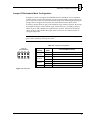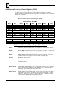
1
VMIVME-5565
Ultrahigh-Speed Fiber-Optic
Reflective Memory with Interrupts
Product Manual
(256) 880-0444
w
12090 South Memorial Parkway
Huntsville, Alabama 35803-3308, USA
(800) 322-3616 w Fax: (256) 882-0859
500-005565-000 Rev. A
(256) 880-0444
w
12090 South Memorial Parkway
Huntsville, Alabama 35803-3308, USA
(800) 322-3616 w Fax: (256) 882-0859
COPYRIGHT AND TRADEMARKS
© Copyright 2002. The information in this document has been carefully checked and is believed to be entirely reliable.
While all reasonable efforts to ensure accuracy have been taken in the preparation of this manual, VMIC assumes no
responsibility resulting from omissions or errors in this manual, or from the use of information contained herein.
VMIC reserves the right to make any changes, without notice, to this or any of VMIC’s products to improve reliability,
performance, function, or design.
VMIC does not assume any liability arising out of the application or use of any product or circuit described herein; nor
does VMIC convey any license under its patent rights or the rights of others.
For warranty and repair policies, refer to VMIC’s Standard Conditions of Sale.
AMXbus, BITMODULE, COSMODULE, DMAbus, IOMax, IOWorks Foundation, IOWorks Manager, IOWorks Server,
MAGICWARE, MEGAMODULE, PLC ACCELERATOR (ACCELERATION), Quick Link, RTnet, Soft Logic Link, SRTbus,
TESTCAL, “The Next Generation PLC”, The PLC Connection, TURBOMODULE, UCLIO, UIOD, UPLC, Visual Soft Logic
Control(ler), VMEaccess, VMEbus Access, VMEmanager, VMEmonitor, VMEnet, VMEnet II, and VMEprobe are
trademarks and The I/O Experts, The I/O Systems Experts, The Soft Logic Experts, and The Total Solutions Provider are
service marks of VMIC.
(I/O man figure)
(IOWorks man figure)
The I/O man figure, IOWorks, IOWorks man figure, UIOC, Visual IOWorks and the VMIC logo are registered
trademarks of VMIC.
ActiveX, Microsoft, Microsoft Access, MS-DOS, Visual Basic, Visual C++, Win32, Windows, Windows NT, and XENIX
are registered trademarks of Microsoft Corporation.
MMX is trademarked, Celeron, Intel and Pentium are registered trademarks of Intel Corporation.
PICMG and CompactPCI are registered trademarks of PCI Industrial Computer Manufacturers’ Group.
Other registered trademarks are the property of their respective owners.
VMIC
All Rights Reserved
This document shall not be duplicated, nor its contents used for any
purpose, unless granted express written permission from VMIC.
(256) 880-0444
w
12090 South Memorial Parkway
Huntsville, Alabama 35803-3308, USA
(800) 322-3616 w Fax: (256) 882-0859
Table of Contents
List of Figures . . . . . . . . . . . . . . . . . . . . . . . . . . . . . . . . . . . . . . . . . . . . . . . . . . . . . . . . . . . . . . . . . . . . . 9
List of Tables . . . . . . . . . . . . . . . . . . . . . . . . . . . . . . . . . . . . . . . . . . . . . . . . . . . . . . . . . . . . . . . . . . . . . 11
Overview . . . . . . . . . . . . . . . . . . . . . . . . . . . . . . . . . . . . . . . . . . . . . . . . . . . . . . . . . . . . . . . . . . . . . . . . . 13
Features . . . . . . . . . . . . . . . . . . . . . . . . . . . . . . . . . . . . . . . . . . . . . . . . . . . . . . . . . . . . . . . . 13
Specification Compliances . . . . . . . . . . . . . . . . . . . . . . . . . . . . . . . . . . . . . . . . . . . . . . . . . . . . . . . . . 14
VMEbus Compliance . . . . . . . . . . . . . . . . . . . . . . . . . . . . . . . . . . . . . . . . . . . . . . . . . . . . . . . . . . 14
Reference Material List. . . . . . . . . . . . . . . . . . . . . . . . . . . . . . . . . . . . . . . . . . . . . . . . . . . . . . . . . . . . 17
Safety Summary . . . . . . . . . . . . . . . . . . . . . . . . . . . . . . . . . . . . . . . . . . . . . . . . . . . . . . . . . . . . . . . . . 18
Ground the System . . . . . . . . . . . . . . . . . . . . . . . . . . . . . . . . . . . . . . . . . . . . . . . . . . . . . . . . . . . 18
Do Not Operate in an Explosive Atmosphere . . . . . . . . . . . . . . . . . . . . . . . . . . . . . . . . . . . . . . . 18
Keep Away from Live Circuits . . . . . . . . . . . . . . . . . . . . . . . . . . . . . . . . . . . . . . . . . . . . . . . . . . . 18
Do Not Service or Adjust Alone . . . . . . . . . . . . . . . . . . . . . . . . . . . . . . . . . . . . . . . . . . . . . . . . . . 18
Do Not Substitute Parts or Modify System. . . . . . . . . . . . . . . . . . . . . . . . . . . . . . . . . . . . . . . . . . 18
Dangerous Procedure Warnings . . . . . . . . . . . . . . . . . . . . . . . . . . . . . . . . . . . . . . . . . . . . . . . . . 18
Safety Symbols Used in This Manual . . . . . . . . . . . . . . . . . . . . . . . . . . . . . . . . . . . . . . . . . . . . . . . . . 19
Chapter 1 - Theory of Operation . . . . . . . . . . . . . . . . . . . . . . . . . . . . . . . . . . . . . . . . . . . . . . . . . . . . . . 21
Basic Operation . . . . . . . . . . . . . . . . . . . . . . . . . . . . . . . . . . . . . . . . . . . . . . . . . . . . . . . . . . . . . . . . . 22
Front Panel LED Indicators . . . . . . . . . . . . . . . . . . . . . . . . . . . . . . . . . . . . . . . . . . . . . . . . . . . . . 22
VMIVME-5565 Register Sets . . . . . . . . . . . . . . . . . . . . . . . . . . . . . . . . . . . . . . . . . . . . . . . . . . . . . . . 23
Reflective Memory RAM . . . . . . . . . . . . . . . . . . . . . . . . . . . . . . . . . . . . . . . . . . . . . . . . . . . . . . . . . . . 24
Parity Function . . . . . . . . . . . . . . . . . . . . . . . . . . . . . . . . . . . . . . . . . . . . . . . . . . . . . . . . . . . . . . . 24
Interrupt Circuits . . . . . . . . . . . . . . . . . . . . . . . . . . . . . . . . . . . . . . . . . . . . . . . . . . . . . . . . . . . . . . . . . 25
Network Interrupts . . . . . . . . . . . . . . . . . . . . . . . . . . . . . . . . . . . . . . . . . . . . . . . . . . . . . . . . . . . . 27
Redundant Transfer Mode of Operation . . . . . . . . . . . . . . . . . . . . . . . . . . . . . . . . . . . . . . . . . . . . . . . 28
Rogue Packet Remove Operation . . . . . . . . . . . . . . . . . . . . . . . . . . . . . . . . . . . . . . . . . . . . . . . . 28
5
VMIVME-5565 Ultrahigh-Speed Fiber-Optic Reflective Memory with Interrupts
Byte Ordering: Big Endian / Little Endian . . . . . . . . . . . . . . . . . . . . . . . . . . . . . . . . . . . . . . . . . . . . . 29
Endian Conversion Hardware . . . . . . . . . . . . . . . . . . . . . . . . . . . . . . . . . . . . . . . . . . . . . . . . . . . 31
Chapter 2 - Configuration and Installation . . . . . . . . . . . . . . . . . . . . . . . . . . . . . . . . . . . . . . . . . . . . . .33
Unpacking Procedures . . . . . . . . . . . . . . . . . . . . . . . . . . . . . . . . . . . . . . . . . . . . . . . . . . . . . . . . . . . 34
Switch/Jumper Configuration and Location . . . . . . . . . . . . . . . . . . . . . . . . . . . . . . . . . . . . . . . . . . . . 36
Node ID Switch . . . . . . . . . . . . . . . . . . . . . . . . . . . . . . . . . . . . . . . . . . . . . . . . . . . . . . . . . . . . . . 36
Jumper E5 Redundant Mode Configuration . . . . . . . . . . . . . . . . . . . . . . . . . . . . . . . . . . . . . . . . 37
Registers and Memory Configuration Switches. . . . . . . . . . . . . . . . . . . . . . . . . . . . . . . . . . . . . . . . . 38
CSR Address Space/Access Select Switches (S7, S4 and S3) . . . . . . . . . . . . . . . . . . . . . . . . . 39
Memory Address/Access Select Switch (S8) . . . . . . . . . . . . . . . . . . . . . . . . . . . . . . . . . . . . . . . 40
Example 1: Register and Memory Select . . . . . . . . . . . . . . . . . . . . . . . . . . . . . . . . . . . . . . . . . . 41
Example 2: Register and Memory Select . . . . . . . . . . . . . . . . . . . . . . . . . . . . . . . . . . . . . . . . . . 42
Example 3: Register and Memory Select . . . . . . . . . . . . . . . . . . . . . . . . . . . . . . . . . . . . . . . . . . 43
Physical Installation . . . . . . . . . . . . . . . . . . . . . . . . . . . . . . . . . . . . . . . . . . . . . . . . . . . . . . . . . . . . . . 44
Front Panel Description . . . . . . . . . . . . . . . . . . . . . . . . . . . . . . . . . . . . . . . . . . . . . . . . . . . . . . . . . . . 45
Cable Configuration. . . . . . . . . . . . . . . . . . . . . . . . . . . . . . . . . . . . . . . . . . . . . . . . . . . . . . . . . . . . . . 46
Cable Specification: . . . . . . . . . . . . . . . . . . . . . . . . . . . . . . . . . . . . . . . . . . . . . . . . . . . . . . . 46
Connector Specification:. . . . . . . . . . . . . . . . . . . . . . . . . . . . . . . . . . . . . . . . . . . . . . . . . . . . 46
VMIVME-5565 Connectivity. . . . . . . . . . . . . . . . . . . . . . . . . . . . . . . . . . . . . . . . . . . . . . . . . . . . . . . . 47
Chapter 3 - Programming . . . . . . . . . . . . . . . . . . . . . . . . . . . . . . . . . . . . . . . . . . . . . . . . . . . . . . . . . . . .49
RFM Control and Status Registers . . . . . . . . . . . . . . . . . . . . . . . . . . . . . . . . . . . . . . . . . . . . . . . . . . 50
Board Revision Register . . . . . . . . . . . . . . . . . . . . . . . . . . . . . . . . . . . . . . . . . . . . . . . . . . . . . . . 50
Board ID Register . . . . . . . . . . . . . . . . . . . . . . . . . . . . . . . . . . . . . . . . . . . . . . . . . . . . . . . . . . . . 50
Node ID Register. . . . . . . . . . . . . . . . . . . . . . . . . . . . . . . . . . . . . . . . . . . . . . . . . . . . . . . . . . . . . 51
Local Control and Status Register . . . . . . . . . . . . . . . . . . . . . . . . . . . . . . . . . . . . . . . . . . . . . . . 51
Local Interrupt Control Registers (LISR and LIER) . . . . . . . . . . . . . . . . . . . . . . . . . . . . . . . . . . . 54
Local Interrupt Status Register . . . . . . . . . . . . . . . . . . . . . . . . . . . . . . . . . . . . . . . . . . . . . . . 54
Local Interrupt Enable Register . . . . . . . . . . . . . . . . . . . . . . . . . . . . . . . . . . . . . . . . . . . . . . 56
RFM Network Registers . . . . . . . . . . . . . . . . . . . . . . . . . . . . . . . . . . . . . . . . . . . . . . . . . . . . . . . . . . 57
Network Target Data Register (NTD) . . . . . . . . . . . . . . . . . . . . . . . . . . . . . . . . . . . . . . . . . . . . . 57
Network Target Node Register (NTN). . . . . . . . . . . . . . . . . . . . . . . . . . . . . . . . . . . . . . . . . . . . . 57
Network Interrupt Command Register (NIC) . . . . . . . . . . . . . . . . . . . . . . . . . . . . . . . . . . . . . . . . 57
Interrupt 1 Sender ID FIFO . . . . . . . . . . . . . . . . . . . . . . . . . . . . . . . . . . . . . . . . . . . . . . . . . . . . . 58
Interrupt 1 Sender Data FIFO . . . . . . . . . . . . . . . . . . . . . . . . . . . . . . . . . . . . . . . . . . . . . . . . . . . 58
Interrupt 2 Sender ID FIFO . . . . . . . . . . . . . . . . . . . . . . . . . . . . . . . . . . . . . . . . . . . . . . . . . . . . . 58
Interrupt 2 Sender Data FIFO . . . . . . . . . . . . . . . . . . . . . . . . . . . . . . . . . . . . . . . . . . . . . . . . . . . 58
Interrupt 3 Sender Data FIFO . . . . . . . . . . . . . . . . . . . . . . . . . . . . . . . . . . . . . . . . . . . . . . . . . . . 58
6
Table of Contents
Interrupt 4 Sender ID FIFO . . . . . . . . . . . . . . . . . . . . . . . . . . . . . . . . . . . . . . . . . . . . . . . . . . . . . 58
Interrupt 4 Sender Data FIFO . . . . . . . . . . . . . . . . . . . . . . . . . . . . . . . . . . . . . . . . . . . . . . . . . . . 59
Example of Network Interrupt Handling . . . . . . . . . . . . . . . . . . . . . . . . . . . . . . . . . . . . . . . . . . . . . . . 60
Interrupt Setup Routine: . . . . . . . . . . . . . . . . . . . . . . . . . . . . . . . . . . . . . . . . . . . . . . . . . . . . . . . . 60
Servicing Network Interrupts: . . . . . . . . . . . . . . . . . . . . . . . . . . . . . . . . . . . . . . . . . . . . . . . . . . . . 61
Universe II Registers . . . . . . . . . . . . . . . . . . . . . . . . . . . . . . . . . . . . . . . . . . . . . . . . . . . . . . . . . . . . . 62
Universe II Control and Status Registers . . . . . . . . . . . . . . . . . . . . . . . . . . . . . . . . . . . . . . . . . . . . . . 63
VMEbus Interrupt Enable Register (VINT_EN) . . . . . . . . . . . . . . . . . . . . . . . . . . . . . . . . . . . . . . 63
VMEbus Interrupt Status Register (VINT_STAT). . . . . . . . . . . . . . . . . . . . . . . . . . . . . . . . . . . . . 66
VME Interrupt Map 0 Register (VINT_MAP0) . . . . . . . . . . . . . . . . . . . . . . . . . . . . . . . . . . . . . . . 68
VME Interrupt Map 1 Register (VINT_MAP1) . . . . . . . . . . . . . . . . . . . . . . . . . . . . . . . . . . . . . . . 69
Interrupt Status/ID Out Register (STATID). . . . . . . . . . . . . . . . . . . . . . . . . . . . . . . . . . . . . . . . . . 70
Universe II DMA Registers . . . . . . . . . . . . . . . . . . . . . . . . . . . . . . . . . . . . . . . . . . . . . . . . . . . . . . . . . 71
DMA Transfer Control Register (DCTL) . . . . . . . . . . . . . . . . . . . . . . . . . . . . . . . . . . . . . . . . . . . . 71
DMA Transfer Byte Count Register (DTBC) . . . . . . . . . . . . . . . . . . . . . . . . . . . . . . . . . . . . . . . . 72
DMA PCI Bus Address Register (DLA) . . . . . . . . . . . . . . . . . . . . . . . . . . . . . . . . . . . . . . . . . . . . 73
DMA VMEbus Address Register (DVA) . . . . . . . . . . . . . . . . . . . . . . . . . . . . . . . . . . . . . . . . . . . . 74
DMA Command Packet Pointer (DCPP) . . . . . . . . . . . . . . . . . . . . . . . . . . . . . . . . . . . . . . . . . . . 75
DMA General Control and Status Register (DGCS) . . . . . . . . . . . . . . . . . . . . . . . . . . . . . . . . . . 76
Mailbox 0 Register (MBOX0) . . . . . . . . . . . . . . . . . . . . . . . . . . . . . . . . . . . . . . . . . . . . . . . . . . . . 78
Mailbox 2 Register (MBOX2) . . . . . . . . . . . . . . . . . . . . . . . . . . . . . . . . . . . . . . . . . . . . . . . . . . . . 78
DMA Source and Destination Addresses . . . . . . . . . . . . . . . . . . . . . . . . . . . . . . . . . . . . . . . . . . . . . . 79
Transfer Size . . . . . . . . . . . . . . . . . . . . . . . . . . . . . . . . . . . . . . . . . . . . . . . . . . . . . . . . . . . . . . . . 79
Transfer Data Width . . . . . . . . . . . . . . . . . . . . . . . . . . . . . . . . . . . . . . . . . . . . . . . . . . . . . . . . . . . 80
DMA Command Packet Pointer . . . . . . . . . . . . . . . . . . . . . . . . . . . . . . . . . . . . . . . . . . . . . . . . . . 81
DMA Initiation. . . . . . . . . . . . . . . . . . . . . . . . . . . . . . . . . . . . . . . . . . . . . . . . . . . . . . . . . . . . . . . . 81
DMA VMEbus Ownership . . . . . . . . . . . . . . . . . . . . . . . . . . . . . . . . . . . . . . . . . . . . . . . . . . . . . . 81
DMA Completion and Termination . . . . . . . . . . . . . . . . . . . . . . . . . . . . . . . . . . . . . . . . . . . . . . . . 82
DMA Transfer Operation . . . . . . . . . . . . . . . . . . . . . . . . . . . . . . . . . . . . . . . . . . . . . . . . . . . . . . . 84
Example of a DMA Operation for the VMIVME-5565. . . . . . . . . . . . . . . . . . . . . . . . . . . . . . . . . . 86
Maintenance . . . . . . . . . . . . . . . . . . . . . . . . . . . . . . . . . . . . . . . . . . . . . . . . . . . . . . . . . . . . . . . . . . . . . . 87
Maintenance . . . . . . . . . . . . . . . . . . . . . . . . . . . . . . . . . . . . . . . . . . . . . . . . . . . . . . . . . . . . . . . . . . . . 87
Maintenance Prints . . . . . . . . . . . . . . . . . . . . . . . . . . . . . . . . . . . . . . . . . . . . . . . . . . . . . . . . . . . . . . . 88
7
VMIVME-5565 Ultrahigh-Speed Fiber-Optic Reflective Memory with Interrupts
8
List of Figures
Figure 1
VMIVME-5565 Block Diagram
.................................................................................................
15
Figure 2
Typical Reflective Memory Network .......................................................................................... 16
Figure 1-1
VMIVME-5565 Interrupt Circuitry Block Diagram .....................................................................
Figure 1-2
Byte Relationships Using the Little Endian Pentium Microprocessor
Figure 1-3
Byte Relationships Using the Big Endian 68040 Microprocessor ............................................. 30
Figure 2-1
VMIVME-5565 Location of User Configurable Switches and Jumpers ....................................
35
Figure 2-2
Switch S6 Example Node ID .....................................................................................................
36
Figure 2-3
Jumper E5 .................................................................................................................................
37
Figure 2-4
Control and Status Registers VMEbus Interface Block Diagram ..............................................
39
Figure 2-5
SDRAM Memory VMEbus Interface Block Diagram .................................................................
40
Figure 2-6
Typical Installation Using the VMIVME-5565 and VMIPCI-5565
44
Figure 2-7
VMIVME-5565 Front Panel ....................................................................................................... 45
Figure 2-8
‘LC’ Type Multimode Fiber-Optic Cable Connector
Figure 2-9
Example: Six Node Ring Connectivity
26
....................................... 29
..............................................
..................................................................
46
......................................................................................
47
Figure 3-1
Block Diagram of the Network Interrupt Reception Circuitry ....................................................
59
Figure 3-2
DMA Transfer Operation ...........................................................................................................
84
9
VMIVME-5565 Ultrahigh-Speed Fiber-Optic Reflective Memory with Interrupts
10
List of Tables
Table 1-1
VMEbus Byte Assignment to the Data Lines . . . . . . . . . . . . . . . . . . . . . . . . . . . . . . . . . . . . . . . . . . . . . . . . . 31
Table 2-1
Example Node ID Switch S6 . . . . . . . . . . . . . . . . . . . . . . . . . . . . . . . . . . . . . . . . . . . . . . . . . . . . . . . . . . . . . . . . 36
Table 2-2
Jumper E5 Configuration . . . . . . . . . . . . . . . . . . . . . . . . . . . . . . . . . . . . . . . . . . . . . . . . . . . . . . . . . . . . . . . . . . . . 37
Table 2-3
Example 1. for Control and Status/Memory Switch Configuration . . . . . . . . . . . . . . . . . . . . . . . . . . . . . . 41
Table 2-4
Example 2. for Control and Status/Memory Switch Configuration . . . . . . . . . . . . . . . . . . . . . . . . . . . . . . 42
Table 2-5
Example 3. for Control and Status/Memory Switch Configuration . . . . . . . . . . . . . . . . . . . . . . . . . . . . . . 43
Table 2-6
LED Descriptions . . . . . . . . . . . . . . . . . . . . . . . . . . . . . . . . . . . . . . . . . . . . . . . . . . . . . . . . . . . . . . . . . . . . . . . . . . . 45
Table 3-1
Memory Map of the Local Control and Status Registers . . . . . . . . . . . . . . . . . . . . . . . . . . . . . . . . . . . . . . 50
Table 3-2
Local Control and Status Register Bit Map. . . . . . . . . . . . . . . . . . . . . . . . . . . . . . . . . . . . . . . . . . . . . . . . . . . . 51
Table 3-3
Local Interrupt Status Register Bit Map . . . . . . . . . . . . . . . . . . . . . . . . . . . . . . . . . . . . . . . . . . . . . . . . . . . . . . . 54
Table 3-4
Local Interrupt Enable Register Bit Map . . . . . . . . . . . . . . . . . . . . . . . . . . . . . . . . . . . . . . . . . . . . . . . . . . . . . . 56
Table 3-5
Network Interrupt Command Register Interrupt Codes . . . . . . . . . . . . . . . . . . . . . . . . . . . . . . . . . . . . . . . . 57
Table 3-6
Universe II Register Map . . . . . . . . . . . . . . . . . . . . . . . . . . . . . . . . . . . . . . . . . . . . . . . . . . . . . . . . . . . . . . . . . . . . 62
Table 3-7
VMEbus Interrupt Enable Register (VINT_EN) . . . . . . . . . . . . . . . . . . . . . . . . . . . . . . . . . . . . . . . . . . . . . . . . 63
Table 3-8
VMEbus Interrupt Status Register (VINT_STAT) . . . . . . . . . . . . . . . . . . . . . . . . . . . . . . . . . . . . . . . . . . . . . . 66
Table 3-9
VME Interrupt Map 0 Register (VINT_MAP0) . . . . . . . . . . . . . . . . . . . . . . . . . . . . . . . . . . . . . . . . . . . . . . . . . 68
Table 3-10
VME Interrupt Map 1 Register (VINT_MAP1) . . . . . . . . . . . . . . . . . . . . . . . . . . . . . . . . . . . . . . . . . . . . . . . . . 69
Table 3-11
Interrupt Status/ID Out Register (STATID) . . . . . . . . . . . . . . . . . . . . . . . . . . . . . . . . . . . . . . . . . . . . . . . . . . . . 70
Table 3-12
DMA Transfer Control Register (DCTL) . . . . . . . . . . . . . . . . . . . . . . . . . . . . . . . . . . . . . . . . . . . . . . . . . . . . . . 71
Table 3-13
DMA Transfer Byte Count Register (DTBC) . . . . . . . . . . . . . . . . . . . . . . . . . . . . . . . . . . . . . . . . . . . . . . . . . . 72
Table 3-14
DMA PCI Bus Address Register (DLA) . . . . . . . . . . . . . . . . . . . . . . . . . . . . . . . . . . . . . . . . . . . . . . . . . . . . . . . 73
Table 3-15
DMA VMEbus Address Register (DVA). . . . . . . . . . . . . . . . . . . . . . . . . . . . . . . . . . . . . . . . . . . . . . . . . . . . . . . 74
Table 3-16
DMA Command Packet Pointer Register (DCPP) . . . . . . . . . . . . . . . . . . . . . . . . . . . . . . . . . . . . . . . . . . . . . 75
Table 3-17
DMA General Control/Status Register (DGCS) . . . . . . . . . . . . . . . . . . . . . . . . . . . . . . . . . . . . . . . . . . . . . . . 76
Table 3-18
Mailbox 0 Register (MBOX0) . . . . . . . . . . . . . . . . . . . . . . . . . . . . . . . . . . . . . . . . . . . . . . . . . . . . . . . . . . . . . . . . 78
Table 3-19
Mailbox 2 Register (MBOX2) . . . . . . . . . . . . . . . . . . . . . . . . . . . . . . . . . . . . . . . . . . . . . . . . . . . . . . . . . . . . . . . . 78
11
VMIVME-5565 Ultrahigh-Speed Fiber-Optic Reflective Memory with Interrupts
12
Overview
Contents
Specification Compliances . . . . . . . . . . . . . . . . . . . . . . . . . . . . . . . . . . . . . . . . . . . . . . . . 14
Reference Material List . . . . . . . . . . . . . . . . . . . . . . . . . . . . . . . . . . . . . . . . . . . . . . . . . . . 17
Safety Summary . . . . . . . . . . . . . . . . . . . . . . . . . . . . . . . . . . . . . . . . . . . . . . . . . . . . . . . . 18
Safety Symbols Used in This Manual . . . . . . . . . . . . . . . . . . . . . . . . . . . . . . . . . . . . . . 19
Introduction
The VMIVME-5565 is the VMEbus-based member of VMIC’s family of Reflective
Memory, real-time fiber-optic network products. The VMIVME-5565 is a
standardized VMEbus 6U Eurocard form factor board. The VMIVME-5565, along
with the other members of this family (VMIPMC-5565 and VMIPCI-5565), can be
integrated into a network using standard fiber-optic cables. Each board in the network
is referred to as a node.
Reflective Memory allows computers, workstations, PLCs and other embedded
controllers with different architectures and dissimilar operating systems to share data
in real-time. The VMIxxx-5565 family of Reflective Memory is fast, flexible and easy to
operate. Data is transferred by writing to memory (SDRAM), which appears to reside
globally in all boards on the network. On-board circuitry automatically performs the
transfer to all other nodes with little or no involvement of any host processor or
system. A block diagram of the VMIVME-5565 is shown in Figure 1 on page 15.
Features
• High-speed, easy-to-use fiber-optic network (2.12 Gbaud serially)
• Standard 6U Eurocard form factor
• No host processor involvement in the operation of the network
• Up to 256 nodes
• Connectivity with multimode fiber up to 300 m, single-mode fiber up to 10 km
• Dynamic packet size, 4 to 64 bytes of data per packet
• Transfer rate 43 Mbytes/sec (4 byte packet) to 174 Mbyte/sec (64 byte packet)
• Up to 128 Mbyte SDRAM Reflective Memory with parity
• VMEbus DMA support
• Four general purpose network interrupts with 32 bits of data each
• Error detection
13
VMIVME-5565 Ultrahigh-Speed Fiber-Optic Reflective Memory with Interrupts
Specification Compliances
VMEbus Compliance
The VMIVME-5565 complies with requirements of the VMEbus specification
(ANSI/IEEE STD 1014-1987, IEC 821 and 297), with the following mnemonics:
A32:A24;D32/D16/D08 (EO): Slave: 39/3D:09/0D
14
Overview
Reflective Memory
Network
RX
TX
2.125 Gb/s Fiber-Optic Link
66 MHz
32-Bit
33 MHz, 32-bit PCI Bus
SDRAM
Data Bus
Reflective Memory Circuitry
and Transceivers
Tundra
Universe IIB
VME-to-PCI
Bridge
VMEbus
64 or 128
Mbytes of
SDRAM
VMEbus - P1 and P2 Connectors
Figure 1 VMIVME-5565 Block Diagram
15
VMIVME-5565 Ultrahigh-Speed Fiber-Optic Reflective Memory with Interrupts
VM
IV
5565ME
VMIVME-5565
VM
IV
5565ME
VMIPCI-5565
NODE 0
PCI WorkStation
with
VMIPCI-5565
VMEbus Chassis
with
VMIVME-5565
NODE 1
VMIPMC-5565
5
5
6
5
VMEbus Computer
Nodes can be
VMEbus-Based
Computers or
Computers with
VMEbus I/O
NODE 2
Channels. Such as
Harris Nighthawk,
Concurrent, Silicon
Graphics, Data
General, Motorola
Delta Series,
Encore 91 series or
any VMEbus Chassis.
Up to 300 m
between nodes
Figure 2 Typical Reflective Memory Network
16
VMEbus Chassis
with
VMIPMC-5565
NODE 255
Overview
Reference Material List
For a detailed description of the VMEbus, refer to The VMEbus Specification and
Handbook available from:
VMEbus International Trade Association (VITA)
7825 Gelding Dr. Suite No. 104
Scottsdale, AZ 85620-3415
(602) 951-8866
Fax: (602) 951-0720
e-mail: [email protected]
Internet: www.vita.com
For a detailed explanation of the PCI-to-VMEbus Bridge (CA91C142), refer to the
Universe II User Manual from:
Tundra Semiconductor Corp.
603 March Road
Kanata, Ontario, Canada
K2K 2M5
Ph: (613) 592-0714
Toll-Free: (800) 267-7231
FAX: (613) 592-1320
Technical Documentation Request: [email protected]
Physical Description and Specifications, refer to Product Specification, 800-005565-000
available from:
VMIC
12090 South Memorial Pkwy.
Huntsville, AL 35803-3308, USA
(256) 880-0444
(800) 322-3616
FAX: (256) 882-0859
www.vmic.com
17
VMIVME-5565 Ultrahigh-Speed Fiber-Optic Reflective Memory with Interrupts
Safety Summary
The following general safety precautions must be observed during all phases of the
operation, service, and repair of this product. Failure to comply with these
precautions or with specific warnings elsewhere in this manual violates safety
standards of design, manufacture and intended use of this product.
VMIC assumes no liability for the customer’s failure to comply with these
requirements.
Ground the System
To minimize shock hazard, the chassis and system cabinet must be connected to an
electrical ground. A three-conductor AC power cable should be used. The power
cable must either be plugged into an approved three-contact electrical outlet or used
with a three-contact to two-contact adapter with the grounding wire (green) firmly
connected to an electrical ground (safety ground) at the power outlet.
Do Not Operate in an Explosive Atmosphere
Do not operate the system in the presence of flammable gases or fumes. Operation of
any electrical system in such an environment constitutes a definite safety hazard.
Keep Away from Live Circuits
Operating personnel must not remove product covers. Component replacement and
internal adjustments must be made by qualified maintenance personnel. Do not
replace components with power cable connected. Under certain conditions,
dangerous voltages may exist even with the power cable removed. To avoid injuries,
always disconnect power and discharge circuits before touching them.
Do Not Service or Adjust Alone
Do not attempt internal service or adjustment unless another person, capable of
rendering first aid and resuscitation, is present.
Do Not Substitute Parts or Modify System
Because of the danger of introducing additional hazards, do not install substitute
parts or perform any unauthorized modification to the product. Return the product
to VMIC for service and repair to ensure that safety features are maintained.
Dangerous Procedure Warnings
Warnings, such as the example below, precede only potentially dangerous procedures
throughout this manual. Instructions contained in the warnings must be followed.
STOP: Dangerous voltages, capable of causing death, are present in this system. Use
extreme caution when handling, testing and adjusting.
18
Overview
Safety Symbols Used in This Manual
STOP: This symbol informs the operator the that a practice or procedure should not
be performed. Actions could result in injury or death to personnel, or could result in
damage to or destruction of part or all of the system.
WARNING: This sign denotes a hazard. It calls attention to a procedure, a practice, a
condition, which, if not correctly performed or adhered to, could result in injury or
death to personnel.
CAUTION: This sign denotes a hazard. It calls attention to an operating procedure, a
practice, or a condition, which, if not correctly performed or adhered to, could result
in damage to or destruction of part or all of the system.
NOTE: Calls attention to a procedure, a practice, a condition or the like, which is
essential to highlight.
19
VMIVME-5565 Ultrahigh-Speed Fiber-Optic Reflective Memory with Interrupts
20
CHAPTER
1
Theory of Operation
Contents
Basic Operation . . . . . . . . . . . . . . . . . . . . . . . . . . . . . . . . . . . . . . . . . . . . . . . . . . . . . . . . . 22
VMIVME-5565 Register Sets . . . . . . . . . . . . . . . . . . . . . . . . . . . . . . . . . . . . . . . . . . . . . . 23
Reflective Memory RAM . . . . . . . . . . . . . . . . . . . . . . . . . . . . . . . . . . . . . . . . . . . . . . . . . 24
Interrupt Circuits . . . . . . . . . . . . . . . . . . . . . . . . . . . . . . . . . . . . . . . . . . . . . . . . . . . . . . . 25
Redundant Transfer Mode of Operation . . . . . . . . . . . . . . . . . . . . . . . . . . . . . . . . . . . . 28
Byte Ordering: Big Endian / Little Endian . . . . . . . . . . . . . . . . . . . . . . . . . . . . . . . . . . 29
Introduction
The following section describes the functionality of the VMIVME-5565 Reflective
Memory board. A description of the major sub-circuits and their operation are
included. This section will also occasionally mention Control and Status registers
related to operations. To see a detailed description of these Control and Status
registers refer to Chapter 3 “Programming” of this manual.
21
1
VMIVME-5565 Ultrahigh-Speed Fiber-Optic Reflective Memory with Interrupts
Basic Operation
Each node (VMIxxx-5565 Reflective Memory boards) in the network is interconnected
using fiber-optic cables in a daisy chain loop. The transmitter of the first board must
be tied to the receiver of the second board. The transmitter of the second board is tied
to the receiver of the third, and so on, until the loop is completed back at the receiver
of the first board. Each node must have a unique node ID, which is accomplished
using a bank of eight (8) on-board switches. The order of the node IDs is unimportant;
they just have to be unique (i.e. no two nodes can have the same node ID).
A transfer of data over the network is initiated by a write to on-board SDRAM from
the VMEbus host system. The write can be as simple as a VMEbus write, or it can be
due to a cycle by the DMA engine. When the write to the SDRAM is occurring,
circuitry on the VMIVME-5565 automatically writes the data, along with other
pertinent information, into the transmit FIFO. From the transmit FIFO, a transmit
circuit retrieves the data and forms it into variable length packets sizes from 4 to 64
bytes, which pass over the fiber-optic interface to the receiver of the next board. When
data is received, a circuit opens the packets and stores the data in the board’s receive
FIFO. From the receive FIFO, a third circuit writes the data into local on-board
SDRAM at the same relative location in memory as that of the originating node. The
third circuit also simultaneously routes the data into the board’s own transmit FIFO.
From there, the process is repeated until the data returns to the receiver of the
originating node. At the originating node, the data packet is removed from the
network.
Front Panel LED Indicators
The VMIVME-5565 has three LED indicators located on the front panel. The bottom
red LED is a status indicator, its power up default state is “ON”. The status LED may
be toggled “OFF” or “ON” by writing to a bit (Bit 31 of the Control and Status
register), which indicates a user defined board status. The middle yellow LED is the
signal detect indicator. The signal detect LED turns “ON” if the receiver detects light.
It can be used as a simple method of checking that the optical network is properly
connected to the receiver. The top green LED is the OWN DATA indicator. When a
board detects its own data returning on the network, it sets this LED “ON”.
NOTE: Ensure that the fiber-optic cables are completely connected to the receiver to
avoided errors. The signal detect LED will come on even when the cable is partially
connected.
22
VMIVME-5565 Register Sets
1
VMIVME-5565 Register Sets
To go beyond the simple read and write operation of the board, the user must
understand and manipulate bits within two register sets. The two register sets are
referred to as:
• Universe II Registers
• Reflective Memory (RFM) Control and Status Registers
Universe II Registers - This set of registers are the Universe II Device Specific Control
and Status and DMA Control Registers, residing in the VMEbus bridge. The Universe
II Control and Status Registers facilitate host system configuration and allow the user
to control VMEbus bridge operational characteristics. The VMEbus bridge registers
have little-endian byte-ordering. The DMA Control Registers are used to operate the
DMA engine. These registers are located at $0 offset from base. The base address is
determined using switches S7, S4 and S3.
Reflective Memory (RFM) Control and Status Registers – The RFM Control and
Status Registers implement the functions unique to the VMIxxx-5565 Reflective
Memory board. These functions include RFM operation status, detailed control of the
RFM sources for the VMEbus interrupt, and network interrupt access. These registers
are located at $1200 offset from base. The base address is determined using switches
S7, S4 and S3.
23
1
VMIVME-5565 Ultrahigh-Speed Fiber-Optic Reflective Memory with Interrupts
Reflective Memory RAM
The actual on-board Reflective Memory SDRAM is available in two sizes: 64 Mbytes
or 128 Mbytes with parity. The SDRAM starts at the location specified by switch S8.
Unlike the previous versions of VMIC’s Reflective Memory products, the RFM
Control and Status Registers do NOT replace the first $40 locations of RAM.
Parity Function
The parity function is not enabled at power up and must be enabled by setting Bit 13
in the RFM CSR’s Local Interrupt Enable (LIER) register at offset $14. To use the parity
function, writes must occur on 32-bit (Lword) or 64-bit (Qword) boundaries. While
parity is active, 8-bit (byte) writes and 16-bit (word) writes are prohibited. In addition,
since the RAM does not power up in a valid parity state, any location that is to be read
with parity must first be initialized by a write of some data pattern. Otherwise the
read will assert an erroneous parity error.
24
Interrupt Circuits
1
Interrupt Circuits
The VMIVME-5565 has a single programmable VMEbus interrupt output. One or
more events on the VMIVME-5565 can cause the interrupt. The sources of the
VMEbus interrupt can be individually enabled and monitored through several
registers.
The VMIVME-5565 interrupts are selected and monitored through the two RFM CSRs
referred to as the Local Interrupt Status Register (LISR) and the Local Interrupt Enable
Register (LIER). For a detailed description of the two registers refer to the
Programming section. A block diagram of the main interrupt circuitry is shown in
Figure 1-1 on page 26.
25
1
VMIVME-5565 Ultrahigh-Speed Fiber-Optic Reflective Memory with Interrupts
Network
Receiver
Circuitry
RFM Control and Status Registers
Network
Interrupt FIFO's
RFM
Fault/Status
Events
4
Local Interrupt Enable Register (LIER)
(Offset $14)
Local Interrupt Status Register (LISR)
(Offset $10)
+
LINT0
Universe II Registers
DMA
Bit 0
Bit 08
VMEbus Interrupt Enable Register (VINT_EN)
(Offset $310)
VMEbus Interrupts (1 thru 7)
Figure 1-1 VMIVME-5565 Interrupt Circuitry Block Diagram
26
Interrupt Circuits
1
Network Interrupts
The VMIVME-5565 has the capability of passing interrupt packets over the network in
addition to data. The network interrupt packets can be directed to a specific node or
broadcast globally to all nodes on the network. Each network interrupt packet
contains the sender’s node ID, the target (destination) node ID, the interrupt type
information and 32 bits of user defined data.
The types of network interrupts include four (4) general purpose interrupts. The
sending node specifies the target (destination) node, the interrupt type and 32 bits of
data using three RFM Control and Status registers. Each receiving node evaluates the
interrupt packets as they pass through. If the interrupt is directed to that node, then
the sender’s node ID is stored in the appropriate Sender ID FIFO (one of four). The
Sender ID FIFO is 127 locations deep. The data will be stored in a companion 127
locations deep data FIFO.
If enabled through the LISR, LIER and VINT_EN registers, any of the four possible
network interrupts can also generate a host VMEbus interrupt at each receiving node.
27
1
VMIVME-5565 Ultrahigh-Speed Fiber-Optic Reflective Memory with Interrupts
Redundant Transfer Mode of Operation
The VMIVME-5565 is capable of operating in a Redundant Transfer mode. The board
is configured for redundant mode when pins 1 and 2 of jumper E5 has the shunt
removed. While in the redundant transfer mode, each packet will be transferred
twice, regardless of the dynamic packet size. The receiving node evaluates each of the
redundant transfers. If no errors are detected in the first transfer, it is used to update
the on-board memory and the second transfer is discarded. If however the first
transfer does contain an error, the second transfer is used to update the on-board
memory provided it has no transmission errors. If errors are detected in both
transfers, the transfers will not be used and the data is completely removed from the
network. The Bad Data bit (Bit 01 of the LCSR) will be set if an error is detected in
either transfer.
Redundant transfer mode greatly reduces the chance that any data is dropped from
the network. However, the redundant transfer mode also reduces the effective
network transfer rates. The single Lword (4 byte) transfer rate drops from the
non-redundant rate of 43 Mbyte/sec. to approximately 20 Mbytes/sec. The 16 Lword
(64 byte) transfer rate drops from the non-redundant rate of 174 Mbyte/sec. to the
redundant rate of 87 Mbyte/sec.
Rogue Packet Remove Operation
A rogue packet is a packet that does not belong to any node on the network. Recalling
the basic operation of Reflective Memory, one node originates a packet on the
network in response to a memory write from the host. The packet is transferred
around the network to all nodes until it returns to the originating node. It is then a
requirement of the originating node to remove the packet from the network. If,
however, the packet somehow gets altered as it passes through another node or if the
originating node begins to malfunction, then the originating node may fail to
recognize the packet as its own and will not remove the packet from the network. In
this case the packet will continue to pass around the network.
Rogue packets are extremely rare. Their existence indicates a malfunctioning board
due to true component failure or due to operation in an harsh environment. Normally,
the solution is to isolate and replace the malfunctioning board and/or improve the
environment. However, some users prefer to tolerate sporadic rogue packets rather
than halt the system for maintenance provided the rogue packets are removed from
the network.
To provide tolerance to rogue packet faults, the VMIVME-5565 can operate as one of
two rogue masters. A rogue master alters each packet as it passes from one node to
another. When the packet returns to the rogue master a second time, the rogue master
recognizes that it is a rogue packet and removes it from the ring. When a rogue packet
is detected, a rogue packet fault flag is set in the Local Interrupt Status Register (LISR).
The assertion of the rogue packet fault bit may optionally assert a VMEbus interrupt
to inform the host that the condition exists.
Rogue Master 0 and Rogue Master 1, are provided to cross check each other. Rogue
Master 0 is enable removing the jumper shunt from E5 pins 3 and 4. Rogue Master 1 is
enable by removing the jumper shunt from E5 pins 5 and 6. See “VMIVME-5565
Location of User Configurable Switches and Jumpers” on page 35.
NOTE: Two boards in the network should not be set as the same rogue master.
Otherwise, one of the two will erroneously remove packets originated by the other.
28
Byte Ordering: Big Endian / Little Endian
1
Byte Ordering: Big Endian / Little Endian
The byte-ordering issue exists due to the different traditions at the major
microprocessor manufacturers, Motorola and Intel. VMEbus boards are designed
around Motorola’s 680X0 processors and compatibles, which store multiple-byte
values in memory with the most significant byte at the lowest byte address. This
byte-ordering scheme became known as “Big Endian” ordering. On the other hand,
Intel’s 80X86 microprocessors, store multiple-byte values in memory with the least
significant byte in the lowest byte address, earning the name “Little Endian” ordering.
The VMIVME-5565’s PCI-to-VMEbus interface uses an Intel based or equivalent
bridge chip, which uses Little Endian byte ordering. Byte arrangement and the byte
relationship between data in the processor and transferred data in memory are shown
in Figure 1-2.
.
.
.
Lword (32-bit) Transfer
MSB
LSB
D31-D24
BYTE $03
MSB
BYTE $02
BYTE $01
BYTE $00
LSB
Data Within
Memory
D23-D16 D15-D08 D07-D00
Data Within the Pentium Microprocessor
Figure 1-2 Byte Relationships Using the Little Endian Pentium Microprocessor
Note that in Little Endian devices, the Memory’s least significant byte is stored in the
lowest byte address after a multiple-byte write (such as the Lword transfer
illustrated), while the Reflective Memory’s most significant byte is stored in the
highest byte address after such transfers. Conversely, the processor considers data
retrieved from the lowest byte address to be the least significant byte after a
multiple-byte read. Data retrieved from the highest byte address is considered to be
the most significant byte.
Contrast the behavior of the Little Endian Pentium in Figure 1-2 with the same Lword
transfer using a Big Endian processor like the Motorola 68040 in Figure 1-3 on
page 30.
Note that the Big Endian 68040 handles the same Lword transfer in a completely
different manner than the Little Endian Pentium microprocessor. During a
multiple-byte transfer like the Lword transfer illustrated, a Big Endian processor
writes its least significant byte in the highest byte address in memory, while its most
significant byte is written to the lowest address. The converse is true during read
operations: the data in the lowest byte address is considered to be the most significant,
while the byte in the highest address is considered to be the least significant.
29
1
VMIVME-5565 Ultrahigh-Speed Fiber-Optic Reflective Memory with Interrupts
.
.
.
Lword (32-bit) Transfer
BYTE $03
LSB
BYTE $02
BYTE $01
BYTE $00
MSB
Data Within
Memory
MSB
LSB
D31-D24
D23-D16 D15-D08 D07-D00
Data Within the 68040 Microprocessor
Figure 1-3 Byte Relationships Using the Big Endian 68040 Microprocessor
The VMEbus Specification does not specify which byte of a multiple-byte transfer is
most significant. The VMEbus Specification does, however, require certain byte lanes
to be associated with certain byte addresses. As shown in Table 1-1 on page 31, byte(0)
must be transferred on data lines D31-D24 during a Lword transfer while byte(3)
must be transferred on lines D7-D0. This byte and address alignment is exactly the
same as that for a Big Endian processor such as the Motorola 68040.
If a Little Endian device were to have its data bus directly connected to the VMEbus
(i.e., D31 to D31, D30 to D30, etc.), then the most significant byte data supplied to the
VMEbus D31-D24 byte lane during a Lword write would be stored by the VMEbus in
the lowest of the four destination byte addresses – opposite that expected by the
Pentium microprocessor. This poses no problem if the 32-bit value written is always
read back using a similar Lword transfer (i.e., all four bytes at once), since the
swapped data gets swapped again and appears to the Host exactly as it should.
However, if the data written by the 32-bit Lword transfer were to be retrieved using
any other method, for example, using four separate byte transfers creates a problem.
The data at the lowest byte address would be incorrectly assumed to be the least
significant, while it is actually the most significant.
The problem cannot be solved by simply connecting the VMIVME-5565 to the
VMEbus with its byte lanes crossed. For example, the VMIVME-5565 uses D0-D7 to
transfer a byte to address $00, while the VMEbus requires D8-D15 be used. For this
reason, special hardware has been incorporated into the VMIVME-5565
PCI-to-VMEbus interface to facilitate different kinds of byte swapping for varying
circumstances.
30
Byte Ordering: Big Endian / Little Endian
1
Table 1-1 VMEbus Byte Assignment to the Data Lines
DTB Cycle Type
D31-D24
D23-D16
D15-D08 Even D07-D00 Odd
Address
Address
D08(EO) Even or Odd
Single Odd Byte(3)
Byte(3)
Single Even Byte(2)
Byte(2)
Single Odd Byte(1)
Byte(1)
Single Even Byte(0)
Byte(0)
D08(O) Odd Only
Single Odd Byte(3)
Byte(3)
Single Odd Byte(1)
Byte(1)
D16
Double Byte(2-3)
Double Byte(0-1)
Byte(2)
Byte(3)
Byte(0)
Byte(1)
Byte(2)
Byte(3)
D32
Quad Byte(0-3)
Byte(0)
Byte(1)
Endian Conversion Hardware
The Universe II chip performs Address Invariant translation between the PCI and
VMEbus interfaces. Address Invariant mapping or “Non-endian conversion” mode
maintains the byte ordering between the two interfaces (i.e. data originating in
Little Endian mode on the PCI side will remain in Little Endian mode on the VMEbus
side of the interface). However, the VMIVME-5565 PCI-to-VMEbus interface has
external endian conversion logic which allows the application to perform
independent master/slave hardware endian conversion.
31
1
32
VMIVME-5565 Ultrahigh-Speed Fiber-Optic Reflective Memory with Interrupts
CHAPTER
2
Configuration and Installation
Contents
Unpacking Procedures . . . . . . . . . . . . . . . . . . . . . . . . . . . . . . . . . . . . . . . . . . . . . . . . . . . 34
Switch/Jumper Configuration and Location . . . . . . . . . . . . . . . . . . . . . . . . . . . . . . . . 36
Physical Installation. . . . . . . . . . . . . . . . . . . . . . . . . . . . . . . . . . . . . . . . . . . . . . . . . . . . . . 44
Front Panel Description . . . . . . . . . . . . . . . . . . . . . . . . . . . . . . . . . . . . . . . . . . . . . . . . . . 45
Cable Configuration . . . . . . . . . . . . . . . . . . . . . . . . . . . . . . . . . . . . . . . . . . . . . . . . . . . . . 46
VMIVME-5565 Connectivity . . . . . . . . . . . . . . . . . . . . . . . . . . . . . . . . . . . . . . . . . . . . . . 47
Introduction
This chapter describes the installation and configuration of the board. Cable
configuration, jumper/switch configuration and board layout are illustrated in this
chapter.
33
2
VMIVME-5565 Ultrahigh-Speed Fiber-Optic Reflective Memory with Interrupts
Unpacking Procedures
CAUTION: Some of the components assembled on VMIC’s products may be sensitive
to electrostatic discharge and damage may occur on boards that are subjected to a
high-energy electrostatic field. When the board is placed on a bench for configuring,
etc., it is suggested that conductive material should be inserted under the board to
provide a conductive shunt. Unused boards should be stored in the same protective
boxes in which they were shipped.
Upon receipt, any precautions found in the shipping container should be observed.
All items should be carefully unpacked and thoroughly inspected for damage that
might have occurred during shipment. The board(s) should be checked for broken
components, damaged printed circuit board(s), heat damage, and other visible
contamination. All claims arising from shipping damage should be filed with the
carrier and a complete report sent to VMIC together with a request for advice
concerning the disposition of the damaged item(s).
34
Switch S3
(Register Set, A23:A16)
ON
OFF
NOTE: Switch Pos, ON is up or right and is a zero (0).
Switch Pos OFF is down or to the left and is a one (1)
1 2 3 4 5 6 7 8
1 2 3 4 5 6 7 8
VM
IV
556 ME
5
1 2 3 4 5 6 7 8
ON
OFF
Pos 8 = A31
Pos 7 = A30
Pos 6 = A29
Pos 5 = A28
Pos 4 = A27
Pos 3 = A26
ON
OFF
Positions 1 and 2 Address Modifier
Pos 2: Supervisory, OFF = Enabled
Pos 1: Nonprivileged, OFF = Enabled
Switch S4
(Register Set)
Positions 1 and 2 are the Address Modifiers
Pos 1 = Nonprivileged, OFF = Enable
Pos 2 = Supervisory, OFF = Enable
Pos 3 = Address Space A32/A24, ON = A32
Pos 4 thru 6 are reserved (Must be OFF)
Pos 7 and 8 = A14 and A15
Switch S7
(Register Set, A31:A24)
ON
OFF
1 2 3 4 5 6 7 8
Jumper E5
(Redundant Mode)
2 4 6 8
Switch S6
(Node ID Switch)
ON (Up) = Zero
OFF (Down) = One
1 2 3 4 5 6 7 8
1 3 5 7
2
NOTE: The Factory Default Configuration for Jumper E5
is all jumper shunts installed. Jumper Shunts will either
be removed or remain installed for your desired Configuration.
Pos 1 = A24
Pos 2 = A25
Pos 3 = A26
Pos 4 = A27
Pos 5 = A28
Pos 6 = A29
Pos 7 = A30
Pos 8 = A31
Unpacking Procedures
Figure 2-1 VMIVME-5565 Location of User Configurable Switches and Jumpers
Switch S8
(Memory Switch)
Pos 1 = A23
Pos 2 = A22
Pos 3 = A21
Pos 4 = A20
Pos 5 = A19
Pos 6 = A18
Pos 7 = A17
Pos 8 = A16
35
2
VMIVME-5565 Ultrahigh-Speed Fiber-Optic Reflective Memory with Interrupts
Switch/Jumper Configuration and Location
Node ID Switch
Prior to installing the VMIVME-5565 in the host chassis, the desired node ID must be
set by configuring Switch S6. Each node in network must have a unique node ID. See
Figure 2-1 on page 35 for the location of Switch S6. Switch S6 is an eight position
switch, which corresponds to 8 node ID select signal lines. The 8 node ID select lines
permit any node ID from 0 to $FF (255 decimal). Switch S6, position 1 corresponds to
the least significant node ID line and position 8 corresponds to the most significant
node ID line. Setting the switch position to ON sets the node ID line low (0), while
setting the position to OFF sets the node ID line high (1).
Table 2-1 below provides examples of possible node IDs. Figure 2-2 below is an
illustration of the Node ID switch S6.
Table 2-1 Example Node ID Switch S6
S6
POS 1
S6
POS 2
S6
POS 3
S6
POS 4
S6
POS 5
S6
POS 6
S6
POS 7
S6
POS 8
Node ID
Hex (Dec.)
On
On
On
On
On
On
On
On
$0 (0)
Off
On
On
On
On
On
On
On
$1 (1)
On
Off
On
On
On
On
On
On
$2 (2)
On
On
Off
On
On
On
On
On
$4 (4)
On
On
On
Off
On
On
On
On
$8 (8)
On
On
On
On
Off
On
On
On
$10 (16)
On
On
On
On
On
Off
On
On
$20 (32)
On
On
On
On
On
On
Off
On
$40 (64)
On
On
On
On
On
On
On
Off
$80 (128)
Off
Off
Off
Off
Off
Off
Off
Off
$FF (255)
Switch S6
(Node ID Switch)
OFF (Down) = One
ON (Up) = Zero
1 2 3 4 5 6 7 8
With all positions OFF (down),
the board would be set for
a Node ID of $FF or Node 255.
This is the Factory Default Setup.
Figure 2-2 Switch S6 Example Node ID
NOTE: No two boards in a network should have the same node ID.
36
Switch/Jumper Configuration and Location
2
Jumper E5 Redundant Mode Configuration
Jumper E5 is used to configure the VMIVME-5565 for redundant or non-redundant
transfer modes as well as the selection of roque master. Installing a jumper shunt on
pins 1 and 2 selects the non-redundant (fast) transfer mode. Removing (Omitting) the
jumper shunts configures the board for the redundant network transfer mode.
Installing a jumper shunt on pins 3 and 4 disables rogue master 0 function. Removing
the jumper from pins 3 and 4 enables rogue master 0 function. Installing a jumper
shunt on pins 5 and 6 disables the rogue master 1 function. Removal of the jumper
shunt on pins 5 and 6 enables the rogue master 1 function. See Table 2-2 below to
configure Jumper E5.
NOTE: The factory configuration is all jumper shunts installed, with the exception of
pins 7 and 8, which are currently not used.
Table 2-2 Jumper E5 Configuration
Jumper E5
(Redundant Mode)
2
4
6
8
Jumper
Position
1 and 2
1
3
5
7
3 and 4
Jumper
State
Function/Mode Selected
Installed
Non-redundant (Fast) transfer mode
Omitted
Redundant transfer mode
Installed
Rogue master 0 disabled
Omitted
Rogue master 0 enabled
Installed
Rogue master 1 disabled
5 and 6
Omitted
Rogue master 1 enabled
7 and 8
Omitted
Reserved, Not Used
Figure 2-3 Jumper E5
37
2
VMIVME-5565 Ultrahigh-Speed Fiber-Optic Reflective Memory with Interrupts
Registers and Memory Configuration Switches
The VMIVME-5565 occupies two separate address spaces on the VMEbus (Control
and Status Register and SDRAM Memory Address spaces). The Control and Status
Register Space can be set-up for Extended Address Space (A32) or Standard Address
Space (A24) and configured to respond to either supervisory, nonprivileged or both
mode accesses.
The SDRAM Memory Space can be set-up for Extended Address Space (A32) and
configured to respond to either supervisory, nonprivileged or both mode accesses.
NOTE: It is important that the two address configurations do not overlap each other
or any other board in the system in order to work properly.
If a switch is ON, the associated Address bit is set to 0.
If a switch is OFF, the associated Address bit is set to 1.
In some cases, as in example 1, some switches are not used. If the Control and Status
Registers are configured in A24 space, switch S7 is not used, since address lines A31
through A24 are not used for A24 space.
Refer to Table 2-3 on page 41 through Table 2-5 on page 43, for examples on setting up
and configuring the register and memory switches.
NOTE: If neither Supervisory nor Nonprivileged access is enabled, the board will not
respond to any VMEbus accesses.
38
Registers and Memory Configuration Switches
2
CSR Address Space/Access Select Switches (S7, S4 and S3)
The following switches are used to configure the Control and Status Register address
and access mode:
• S7 – Selects VMEbus addresses A32 thru A24
• S3 – Selects VMEbus addresses A23 thru A16
• S4 – Selects VMEbus addresses A15 thru A14
• S4 – Selects VMEbus access mode
S7
S3
S4
On
Off
On
Off
On
Off
S3
2
Pos 1 = A24
Pos 2 = A25
Pos 3 = A26
Pos 4 = A27
Pos 5 = A28
Pos 6 = A29
Pos 7 = A30
Pos 8 = A31
Pos 1 = A23
Pos 2 = A22
Pos 3 = A21
Pos 4 = A20
Pos 5 = A19
Pos 6 = A18
Pos 7 = A17
Pos 8 = A16
3
1
S7
S4
Pos 1 = Nonprivileged, OFF = Enabled
Pos 2 = Supervisory, OFF = Enabled
Pos 3 = Address Space A32/A24, ON = A32
4
Pos 4 thru 6 = Reserved (Must be OFF)
5
6
Pos 7 = A14
Pos 8 = A15
7
8
VMEbus
Interface
Hardware
Registers
VMIVME-5565 Registers
Located in VMEbus A32, A24
Addressing Space for
Control and Status
Figure 2-4 Control and Status Registers VMEbus Interface Block Diagram
39
2
VMIVME-5565 Ultrahigh-Speed Fiber-Optic Reflective Memory with Interrupts
Memory Address/Access Select Switch (S8)
Switch S8 is used to configure the SDRAM Memory address and access mode:
• S8 – Selects VMEbus addresses A32 thru A26
• S8 – Selects VMEbus access mode
S8
On
Extended
Off
1
2
3
4
5
6
7
8
DRAM
A32
D32, D16, D08
BLT
Pos 8 = A31
Pos 7 = A30
Pos 6 = A29
Pos 5 = A28
Pos 4 = A27
Pos 3 = A26
Pos 2 = Supervisory, OFF = Enabled
Pos 1 = Nonprivileged, OFF = Enabled
Figure 2-5 SDRAM Memory VMEbus Interface Block Diagram
40
SDRAM
VMEbus A32
Addressing used for
Reflective Memory data
Registers and Memory Configuration Switches
2
Example 1: Register and Memory Select
The Control and Status Registers are mapped at Standard Address $00400000 and
responds to Supervisory Mode access only.
The SDRAM reflected memory is mapped at Extended Address $80000000 and
responds to either Supervisory or Nonprivileged Mode accesses.
Table 2-3 Example 1. for Control and Status/Memory Switch Configuration
SW
S7
Control and Status Register
Address/Access Configuration
SW
SDRAM Memory Address/Access
Configuration
S7 position 8 – NA (not used)
S8 position 8 – OFF (A31 = 1)
S7 position 7 – NA (not used)
S8 position 7 – ON (A30 = 0)
S7 position 6 – NA (not used)
S8 position 6 - ON (A29 = 0)
S7 position 5 – NA (not used)
S8
S8 position 5 – ON (A28 = 0)
S7 position 4 – NA (not used)
S8 position 4 – ON (A27 = 0)
S7 position 3 – NA (not used)
S8 position 3 – ON (A26 = 0)
S7 position 2 – NA (not used)
S8 position 2 - OFF (Supervisory Mode)
S7 position 1 – NA (not used)
S8 position 1 - OFF (Nonprivileged Mode)
S3 position 1 – ON (A23 = 0)
S3 position 2 – OFF (A22 = 1)
S3 position 3 – ON (A21 = 0)
S3
S3 position 4 – ON (A20 = 0)
S3 position 5 – ON (A19 = 0)
S3 position 6 – ON (A18 = 0)
S3 position 7 – ON (A17 = 0)
S3 position 8 – ON (A16 = 0)
S4 position 8 – ON (A15 = 0)
S4 position 7 – ON (A14 = 0)
S4
S4 position 3 = OFF (A24 Space)
S4 position 2 - OFF (Supervisory Mode)
S4 position 1 - ON (Nonprivileged Mode)
NOTE: It is important that the two address configurations do not overlap each other
or any other board in the system in order to work properly.
41
2
VMIVME-5565 Ultrahigh-Speed Fiber-Optic Reflective Memory with Interrupts
Example 2: Register and Memory Select
The Control and Status Registers are mapped at Extended Address $30000000 and
responds to Supervisory mode access only.
The SDRAM reflected memory is mapped at Extended Address $40000000 and
responds to Nonprivileged mode access only.
Table 2-4 Example 2. for Control and Status/Memory Switch Configuration
SW
S7
Control and Status Register
Address/Access Configuration
SW
SDRAM Memory Address/Access
Configuration
S7 position 8 – ON (A31 = 0)
S8 position 8 – ON (A31 = 0)
S7 position 7 – ON (A30 = 0)
S8 position 7 – OFF (A30 = 1)
S7 position 6 – OFF (A29 = 1)
S8 position 6 - ON (A29 = 0)
S7 position 5 – OFF (A28 = 1)
S8
S8 position 5 – ON (A28 = 0)
S7 position 4 – ON (A27 = 0)
S8 position 4 – ON (A27 = 0)
S7 position 3 – ON (A26 = 0)
S8 position 3 – ON (A26 = 0)
S7 position 2 – ON (A25 = 0)
S8 position 2 - ON (Supervisory Mode)
S7 position 1 – ON (A24 = 0)
S8 position 1 - OFF (Nonprivileged Mode)
S3 position 1 – ON (A23 = 0)
S3 position 2 – ON (A22 = 0)
S3 position 3 – ON (A21 = 0)
S3
S3 position 4 – ON (A20 = 0)
S3 position 5 – ON (A19 = 0)
S3 position 6 – ON (A18 = 0)
S3 position 7 – ON (A17 = 0)
S3 position 8 – ON (A16 = 0)
S4 position 8 – ON (A15 = 0)
S4
S4 position 7 – ON (A14 = 0)
S4 position 3 - ON (A32 Space)
S4 position 2 - OFF (Supervisory Mode)
S4 position 1 - ON (Nonprivileged Mode)
NOTE: It is important that the two address configurations do not overlap each other
or interfere with the operation of any other board in the system.
42
Registers and Memory Configuration Switches
2
Example 3: Register and Memory Select
The Control and Status Registers are mapped at Extended Address $70000000 and
respond to either Supervisory or Nonprivileged mode accesses.
The SDRAM reflected memory is mapped at Extended Address $78000000 and
responds to either Supervisory or Nonprivileged mode accesses.
Table 2-5 Example 3. for Control and Status/Memory Switch Configuration
SW
S7
Control and Status Register
Address/Access Configuration
SW
SDRAM Memory Address/Access
Configuration
S7 position 8 – ON (A31 = 0)
S8 position 8 – ON (A31 = 0)
S7 position 7 – OFF (A30 = 1)
S8 position 7 – OFF (A30 = 1)
S7 position 6 – OFF (A29 = 1)
S8 position 6 - OFF (A29 = 1)
S7 position 5 – OFF (A28 = 1)
S8
S8 position 5 – OFF (A28 = 1)
S7 position 4 – ON (A27 = 0)
S8 position 4 – OFF (A27 = 1)
S7 position 3 – ON (A26 = 0)
S8 position 3 – ON (A26 = 0)
S7 position 2 – ON (A25 = 0)
S8 position 2 - OFF (Supervisory Mode)
S7 position 1 – ON (A24 = 0)
S8 position 1 - OFF (Nonprivileged Mode)
S3 position 1 – ON (A23 = 0)
S3 position 2 – ON (A22 = 0)
S3 position 3 – ON (A21 = 0)
S3
S3 position 4 – ON (A20 = 0)
S3 position 5 – ON (A19 = 0)
S3 position 6 – ON (A18 = 0)
S3 position 7 – ON (A17 = 0)
S3 position 8 – ON (A16 = 0)
S4 position 8 – ON (A15 = 0)
S4
S4 position 7 – ON (A14 = 0)
S4 position 3 - ON (A32 Space)
S4 position 2 - OFF (Supervisory Mode)
S4 position 1 - OFF (Nonprivileged Mode)
NOTE: It is important that these two address configurations do not overlap each
other or any other board in the system in order to work properly.
43
2
VMIVME-5565 Ultrahigh-Speed Fiber-Optic Reflective Memory with Interrupts
Physical Installation
CAUTION: Do not install or remove the board while power is applied.
The following procedure outlines the installation of the VMIVME-5565 in a VMEbus
chassis and the set-up of the network ring topology. The VMIVME-5565 can be
installed in any slot with the exception of slot one, which normally is reserved for the
system controller.
1. Before installation of the board in the chassis, ensure that all switches are set for
the desired mode of operation. Refer to Switch/Jumper Configuration and Location
on page 36.
2. With the power turned OFF, install the VMIVME-5565 into the chassis, making
sure that the board connectors are firmly mated to the backplane connectors.
3. Secure the VMIVME-5565 to the chassis using the two screws located at the top
and bottom of the front panel.
4. Connect the fiber-optic cables to the TX and RX connectors.
5. Route the fiber-optic cable connected to TX to the RX connector of the next board
in the ring. Connect the fiber-optic cable from that board’s TX to the RX
connector of the next board. Repeat this step until the last node in the ring routes
its TX to the RX of the first node. Refer to Figure 2-9 on page 47 for an example of
a six node ring.
VMEbus
Chassis
(Available from VMIC)
VMIC's
VMIVME-5565
UltraHigh-Performance
Reflective Memory
Board
VM
IV
5565ME
VM
IV
5565ME
VMIPCI-5565
Standard P.C.
System with a
VMIPCI-5565 (available
from VMIC)
Installed
Multimode or Single Mode
Fiber-Optic Cable
Figure 2-6 Typical Installation Using the VMIVME-5565 and VMIPCI-5565
44
Front Panel Description
2
Front Panel Description
The VMIVME-5565 has an optical transceiver located on the front panel. Figure 2-7
below is an illustration of the front panel. The Reflective Memory board has three LED
indicators located on the front panel. Table 2-6 below outlines the front panel LEDs.
The port labeled “RX” is the receiver and the port labeled “TX” is the transmitter. The
VMIVME-5565 uses “LC” type fiber-optic cables either single-mode or multimode.
CAUTION: When the fiber-optic cables are not connected, install the supplied dust
caps to keep dust and dirt out of the optics. Do not power up the VMIVME-5565
without the fiber-optic cables installed. To avoid potential eye injuries, do not look
directly into the transmitters when power is applied.
VMIVME
5565
The status LEDs power up default state is “ON”. The LED is a user defined board
status indicator. The status LED can be toggled “ON” or “OFF” by writing to Bit 31 of
the Control and Status register. The signal detect LED turns “ON” if the receiver
detects light and it can be used as a simple method of verifying the optical network is
properly connected to the receiver. The Own Data LED is turned “ON” when the
board detects its own data returning over the network.
Table 2-6 LED Descriptions
LED
Color
Description
Own Data
Green
Detects when own data is received.
SIG. DET.
Yellow
Indicates optical network connection.
Status
Red
User defined board status indicator.
TX
RX
OWN DATA
SIG. DET.
STATUS
VMEbus
Figure 2-7 VMIVME-5565 Front Panel
45
2
VMIVME-5565 Ultrahigh-Speed Fiber-Optic Reflective Memory with Interrupts
Cable Configuration
The VMIVME-5565 is available with a multimode or single-mode fiber-optic interface.
Figure 2-8 is an illustration of the ‘LC’ type multimode or single-mode fiber-optic
cable connector.
Cable Specification:
• Simplex, multimode, graded index glass fiber
• Core diameter = 62.5 ±3 µm
• Cladding diameter = 125 ±2 µm
• Jacket outer diameter = 3.0 mm ±.1mm
• Attenuation: 4.0 dB/km (max) at 850nm, 1.75dB/km (max) at 1300nm
• Bandwidth: 160 to 300 MHz-Km (min) at 850 nm, 300 to 700 MHz-km (min) at
1300 nm
• UL type OFNR, CSA type OFN FT4
Connector Specification:
• Compatible with NTT LC standard and JIS C 5973 compliant
• Ceramic ferrule
• Insertion loss: 0.35 dB (max) multimode
• Fiber clad diameter: 125 µm
• Jacket diameter: 3.0 mm
• Temperature range: -20 °C to +85 °C
0.84 (21.23)
(2.9mm)
0.49
(1.25)
Dimensions: inches (mm)
Figure 2-8 ‘LC’ Type Multimode Fiber-Optic Cable Connector
46
VMIVME-5565 Connectivity
2
VM
IV
556ME
5
Node 4
VM
IV
556ME
5
Node 5
VM
IV
556ME
5
Node 6
VM
IV
556ME
5
VM
IV
556ME
5
Node 1
Node 2
VM
IV
556ME
5
Node 3
VMIVME-5565 Connectivity
Figure 2-9 Example: Six Node Ring Connectivity
47
2
48
VMIVME-5565 Ultrahigh-Speed Fiber-Optic Reflective Memory with Interrupts
CHAPTER
3
Programming
Contents
RFM Control and Status Registers . . . . . . . . . . . . . . . . . . . . . . . . . . . . . . . . . . . . . . . 50
RFM Network Registers . . . . . . . . . . . . . . . . . . . . . . . . . . . . . . . . . . . . . . . . . . . . . . . . 57
Example of Network Interrupt Handling . . . . . . . . . . . . . . . . . . . . . . . . . . . . . . . . . 60
Universe II Registers . . . . . . . . . . . . . . . . . . . . . . . . . . . . . . . . . . . . . . . . . . . . . . . . . . . 62
Universe II Control and Status Registers . . . . . . . . . . . . . . . . . . . . . . . . . . . . . . . . . . 63
Universe II DMA Registers . . . . . . . . . . . . . . . . . . . . . . . . . . . . . . . . . . . . . . . . . . . . . 71
DMA Source and Destination Addresses . . . . . . . . . . . . . . . . . . . . . . . . . . . . . . . . . 79
Introduction
Basic read and write operations of the VMIVME-5565 require little or no software. The
board will power up in a functional mode. For operations beyond the basic setup,
such as enabling or disabling interrupts or performing DMA cycles, the user must
know the specific bit assignments of the registers within the register sets. All other
registers are subsets of these two registers.
The register sets are:
• Universe II Registers
• RFM Control and Status Registers
49
3
VMIVME-5565 Ultrahigh-Speed Fiber-Optic Reflective Memory with Interrupts
RFM Control and Status Registers
The RFM Control and Status registers for the VMIVME-5565 are located at offset $1200
of the Control and Status register space specified by Switches S3, S4 and S7. The space
reserved for this group of registers is 64 bytes.
Table 3-1 Memory Map of the Local Control and Status Registers
Offset
Mnemonic
$0
BRV
$1
BID
$3…2
--
$4
NID
Description
Access
Comments
Board Revision
Read Only
Current board revision/model
Board ID Register
Read Only
BID is $65 for VMIVME-5565
Reserved
Node ID Register
$7…5
--
$B…8
LCSR
Reserved
$F...C
--
$13…10
LISR
Local Control & Status Reg.
Reserved
Local Interrupt Status Reg.
-Read Only
Set by 8 board jumpers
-Read/Write
Some bits reserved. Some bits read-only.
-Read/Write
Some bits reserved. Some bits read-only.
$17…14
LIER
Local Interrupt Enable Reg.
Read/Write
$1B…18
NTD
Network Target Data
Read/Write
32 Data bits for network target
$1C
NTN
Network Target Node
Read/Write
Target node ID for network Int.
$1D
NIC
Network Interrupt Command
Read/Write
Select Int type and initiate interrupt
$1F…1E
--
$23…20
ISD1
Int. 1 Sender Data
Reserved
Read/Write
127 loc. By 32 bit FIFO for network Int. 1
$24
SID1
Int. 1 Sender ID
Read/Write
127 loc. Deep FIFO/ write clears pointers
$27…25
--
Reserved
--
--
$2B…28
ISD2
Int. 2 Sender Data
Read/Write
127 loc. By 32 bit FIFO for network Int. 2
$2C
SID2
Int. 2 Sender ID
Read/Write
127 loc. Deep FIFO/ write clears pointers
$2F…2D
--
$33…30
ISD3
Reserved
--
Int. 3 Sender Data
Read/Write
127 loc. By 32 bit FIFO for network Int. 3
Int. 3 Sender ID
Read/Write
127 loc. Deep FIFO/ write clears pointers
$34
SID3
$37...35
--
$3B.38
ISD4
Int. 4 Sender Data
Read/Write
127 loc. By 32 bit FIFO for opt. Data
$3C
SID4
Int. 4 Sender ID
Read/Write
127 loc. Deep FIFO/ write clears pointers
$3F.3D
--
Reserved
Reserved
--
Board Revision Register
Board Revision (BRV) (Offset $0): An 8-bit register used to represent revisions or
model numbers. This register is read only.
Board ID Register
Board ID (BID) (Offset $1): An 8-bit register which contains an 8-bit code unique to
the VMIVME-5565 type board. The code is $65. This register is read-only.
50
RFM Control and Status Registers
3
Node ID Register
Node ID (NID) (Offset $4): An 8-bit register containing the node ID of the board. This
register reflects the setting of switch S6. Each board on a network must have a unique
node ID.
Local Control and Status Register
Table 3-2 Local Control and Status Register Bit Map
Local Control and Status Register (LCSR): Offset $8, Read/Write, Lword, Word, Byte
Bit 31
Bit 30
Bit 29
Bit 28
Bit 27
Bit 26
Bit 25
Bit 24
Status LED
Off
Transmitter
Disabled
Dark-onDark Enable
Loopback
Enabled
Local Bus
Parity Enabled
Redundant
Mode Enabled
Roque
Master 1
Enabled
Roque
Master 0
Enabled
Bit 23
Bit 22
Reserved
Bit 15
Bit 14
Bit 21
Bit 20
Bit 19
Config 1
Config 0
Bit 13
Bit 12
Bit 18
Reserved
Bit 17
Bit 16
Offset 1
Offset 0
Bit 11
Bit 10
Bit 09
Bit 08
Reserved
Bit 07
Bit 06
Bit 05
Bit 04
Bit 03
Bit 02
Bit 01
Bit 00
TX FIFO
Empty
TX FIFO
Almost Full
Latched RX
FIFO Full
Latched RX
FIFO Almost
Full
Latched Sync
Loss
RX Signal
Detect
Bad Data
Own Data
Local Control and Status Register Bit Definitions
Bit 31:
Status LED Off – The board contains a user defined RED status LED. Setting
this bit low (0) turns off the LED. The default state of this bit after reset is high
(1) and the LED will be ON.
Bit 30:
Transmitter Disabled – Setting this bit high (1) will manually turn off the
board’s transmitter. The default state of this bit after reset is low (0) and the
transmitter is enabled.
Bit 29:
Dark-on-Dark Enabled – When this bit is set high (1), the board’s transmitter
will be turned OFF if the board’s receiver does not detect a signal or if the
receiver detects invalid data patterns. The dark-on-dark feature is useful in
hub configurations.
Bit 28:
Loopback Enabled – When this bit is set high (1), the fiber optic transmitter
and receiver are disabled and the transmit signal is looped back to the
receiver circuit internally. This allows basic functional testing with or without
an external cable.
51
3
VMIVME-5565 Ultrahigh-Speed Fiber-Optic Reflective Memory with Interrupts
Local Control and Status Register Bit Definitions (Continued)
Bit 27:
Local Bus Parity Enabled – When this bit is set high (1), parity is enabled on
all on-board memory accesses. While the parity is enabled, writes to the
memory are only allowed as 32-bit Lwords or 64-bit Qwords. Write accesses
as 16-bit words or 8-bit bytes shall be prohibited.
Bit 26:
Redundant Mode Enabled - When this read-only bit is set high (1), the
redundant transfer mode is enabled. Redundant mode is enabled by
removing the jumper shunt on pins 1 and 2 of E5.
Bit 25:
Rogue Master 1 Enabled - When this read-only bit is set high (1), the board is
operating as Rogue Master 1. Rogue Master 1 is enable by removing the
jumper from pins 5 and 6 of E5.
Bit 24:
Rogue Master 0 Enabled - When this read-only bit is set high (1), the board is
operating as Rogue Master 0. Rogue Master 0 is enable by removing the
jumper from pins 3 and 4 of E5.
Bits 23 and 22:
Reserved - These bits are reserved.
Bits 21 and 20:
Config 1 and Cofig 0 – These two bits indicate the memory size as defined in
the following table. The two bits are read-only.
Config 1
Config 0
Memory Size
0
0
64 Mbytes
0
1
128 Mbytes
1
0
Reserved
1
1
Reserved
Bits 19 and 18:
Reserved - These bits are reserved.
Bits 17 and 16:
Offset 1 and Offset 0 – When the host system writes to the on-board memory
and initiates a packet over the network, Offset 1 and Offset 0 will apply an
offset to the network address as it is sent or received over the network. The
offset does not appear on local access to the memory, and the offset does not
alter network packets as they pass through the board. Offset 1 and Offset 0
provide four possible binary increments of 64 Mbytes each through the 256
Mbytes network address range. When the address and offset exceeds the 256
Mbytes network address range, the address bits beyond 256 Mbytes will be
truncated. This causes the write to wrap around into a lower memory
location. Offsets 1 and 0’s bits correspond to the network address bits A27
and A26 respectively.
Offset 1
Offset 0
Offset Applied
0
0
0
0
1
$4000000
1
0
$8000000
1
1
$C000000
Bits 15 through 08: Reserved - These bits are reserved.
Bit 07:
52
TX FIFO Empty – A logic high (1) indicates the TX FIFO is currently empty.
This bit provides immediate status only (not latched) and is read only.
RFM Control and Status Registers
3
Local Control and Status Register Bit Definitions (Concluded)
Bit 06:
TX FIFO Almost Full – A logic high (1) indicates the TX FIFO is currently
almost full. This bit provides immediate status only (not latched) and is read
only. Periodic assertion of this bit is normal.
Bit 05:
Latched RX FIFO Full – A logic high (1) indicates the RX FIFO has
experienced a full condition at least once. This bit is read only within this
register. To clear this condition write to the corresponding bit within the Local
Interrupt Status Register.
NOTE: The occurrence of the Latched RX FIFO Full signal is a fault condition due to a
board malfunction and indicates that the received data may have been lost.
Bit 04:
Latched RX FIFO Almost Full – A logic high (1) indicates the RX FIFO is
operating at the maximum acceptable rate. Under normal operating
conditions, this event should not occur. This bit is read only within this
register. To clear this condition, write to the corresponding bit within the
Local Interrupt Status Register.
Bit 03:
Latched Sync Loss – This is a read-only bit. A logic high (1) indicates the
receiver circuitry has detected the loss of a valid signal at least once since the
last time the flag has been cleared. Under normal operating conditions, this
event should not occur and may indicate a loss of data. A logic high may
indicate the receiver’s link was intentionally or unintentionally disconnected.
Bit 02:
RX Signal Detect – A logic high (1) indicates the board receiver is currently
detecting light. This bit provides immediate status only (not latched) and is
read only.
Bit 01:
Bad Data – A logic high (1) indicates the board receiver circuit has detected
bad (invalid) data at least once since power up or since the flag had
previously been cleared. Under normal operating conditions, this event
should not occur and may indicate a loss of data. This bit is read only within
this register. To clear this condition, write to the corresponding bit within the
Local Interrupt Status Register.
Bit 00:
Own Data – A logic high (1) indicates the board has detected the return of its
own data packet at least once since this bit has previously been cleared. This
bit serves as an indicator that the link is intact. The Own Data bit should be
set anytime a write to the on-board memory occurs or any time network
interrupt is initiated. This bit is both read and write accessible.
53
3
VMIVME-5565 Ultrahigh-Speed Fiber-Optic Reflective Memory with Interrupts
Local Interrupt Control Registers (LISR and LIER)
The VMIVME-5565 contains a number of sources for the VME interrupt. Interrupts
generated from local on-board devices are called the Local Interrupt Status Register
(LISR) as shown in Table 3-3 below and the Local Interrupt Enable Register (LIER)
shown in Table 3-4 on page 56. All Local Interrupts are logically “ORed” together into
the single interrupt input to the device. This input is called LINT0. The control and
status of local interrupts are implemented in the two local registers (LISR and LIER).
Local Interrupt Status Register
The LISR contains a group of interrupt status flags, while the LIER contains a
corresponding group of enables. Before any local interrupt can cause a LINT0
interrupt, the status bit, its enable and the Global Enable must all be asserted.
Table 3-3 Local Interrupt Status Register Bit Map
Local Interrupt Status Register (LISR): Offset $10, Read/Write, Lword, Word or Byte access
Bit 31
Bit 30
Bit 29
Bit 28
Bit 27
Bit 26
Bit 25
Bit 24
Bit 19
Bit 18
Bit 17
Bit 16
Reserved
Bit 23
Bit 22
Bit 21
Bit 20
Reserved
Bit 15
Bit 14
Bit 13
Bit 12
Bit 11
Bit 10
Bit 09
Bit 08
Auto Clear
Flag
Global
Interrupt
Enable
Local Mem.
Parity Error
Mem. Write
Inhibited
Latched Sync
Loss
RX FIFO Full
RX FIFO
Almost Full
Bad Data
Bit 07
Bit 06
Bit 05
Bit 04
Bit 03
Bit 02
Bit 01
Bit 00
INT4
Rogue
Packet Fault
INT3
INT2
INT1
Reserved
Local Interrupt Status Register Bit Definitions
Bits 31 through 16: Reserved - These bits are reserved.
54
Bit 15:
Auto Clear Flag – This bit is a read-only status indicator of the corresponding
bit the LIER Register. When this bit is high (1), the Global Interrupt Enable
(Bit 14) will automatically be cleared as this register (LISR) is being read.
Clearing the Global Interrupt Enable de-asserts the LINT0 and, in turn,
releases the PCI Interrupt.
Bit 14:
Global Interrupt Enable – This read/Write bit must set high (1) in addition to
any interrupt flag and its associated enable bit in the LIER before the LINT0
line is asserted and a PCI interrupt can result. If the Auto Clear enable bit in
the LIER is set high (1), the Global Interrupt Enable bit will automatically be
cleared as this register (LISR) is being read. This bit is read and write
accessible with this register and thus allows a single read-modify-write
operation to service the local interrupts.
RFM Control and Status Registers
3
Local Interrupt Status Register Bit Definitions (Continued)
Bit 13:
Local Memory Parity Error – When this bit is high (1), one or more parity
errors have been detected on local memory accesses. This bit is latched. Once
set, it must be cleared by writing a zero to this bit location. Note that Bit 27 of
the LCSR1 must be set high before parity is active. Also note that parity
works only on Lword and Qword accesses. Word (16-bit) and byte (8-bit)
memory write access are inhibited.
Bit 12:
Mem. Write Inhibited – When this bit is high (1), a 16-bit word or an 8-bit
byte write to local memory was attempted and inhibited while the board was
in the parity enabled mode. This bit is latched. Once set, it must be cleared by
writing a zero to this bit location.
Bit 11:
Latched Sync Loss – When this bit is high (1), the receiver circuit has lost
synchronization with the incoming signal one or more times. This bit is
latched. Once set, it must be cleared by writing a zero to this bit location. The
assertion of the Latched Sync Loss usually indicates the receiver link was or
is disconnected, either intentionally or unintentionally, and data may have
been lost. This event will also occur if the upstream node tied to the receiver
is powered off or is disabled.
Bit 10:
RX FIFO Full – When this bit is high (1), the RX FIFO has been full one or
more times. This bit is latched. Once set, it must be cleared by writing a zero
to this bit location. This is a fault condition and data may have been lost.
Bit 09:
RX FIFO Almost Full – When this bit is high (1), the RX FIFO has been
almost full one or more times. This bit is latched. Once set, it must be cleared
by writing a zero to this bit location.The assertion of the RX FIFO Almost Full
bit indicates the receiver circuit is operating at maximum capacity and,
under normal operating conditions, this event should not occur. If it does
occur, the PCI bus master should temporarily suspend all write and read
operations to the board.
Bit 08:
Bad Data – When this bit is high (1), the receiver circuit has detected invalid
data one or more times. This bit is latched. Once set, it must be cleared by
writing a zero to this bit location.
Bit 07:
INT4 – When this bit is high (1), one or more type 4 network interrupts have
been received. To see the sender data and sender node ID(s), read the
Interrupt Sender Data 4 (ISD4) FIFO at offset $38 and the Interrupt Sender ID
(SID4) FIFO at offset $3C respectively.
Bit 06:
Rogue Packet Fault - When this bit is set high (1), the board is operating as
Rogue Master 0 or 1 and has detected and removed a rogue packet. This bit is
latched. Once set, it must be cleared by writing a zero to this bit location.
Bits 05 through 03: Reserved - These are reserved.
55
3
VMIVME-5565 Ultrahigh-Speed Fiber-Optic Reflective Memory with Interrupts
Local Interrupt Status Register Bit Definitions (Concluded)
NOTE: Reading the interrupts will clear status if SID# FIFO is empty. This can cause a
loss of data in the data register, if not read first.
Bit 02:
INT3 – When this bit is high (1), one or more type 3 network interrupts have
been received. To see the sender data and sender node ID(s), read the
Interrupt Sender Data 3 (ISD3) FIFO at offset $30 and the Interrupt Sender ID
(SID3) FIFO at offset $34 respectively.
Bit 01:
INT2 – When this bit is high (1), one or more type 2 network interrupts have
been received. To see the sender data and sender node ID(s), read the
Interrupt Sender Data 2 (ISD2) FIFO at offset $2B and the Interrupt Sender ID
(SID2) FIFO at offset $2C respectively.
Bit 00:
INT1 – When this bit is high (1), one or more type 1 network interrupts have
been received. To see the sender data and sender node ID(s), read the
Interrupt Sender Data 1 (ISD1) FIFO at offset $20 and the Interrupt Sender ID
(SID1) FIFO at offset $24 respectively.
Local Interrupt Enable Register
Table 3-4 Local Interrupt Enable Register Bit Map
Local Interrupt Enable Register (LIER): Offset $14, Read/Write, Lword, Word or Byte access
Bit 31
Bit 30
Bit 29
Bit 28
Bit 27
Bit 26
Bit 25
Bit 24
Bit 19
Bit 18
Bit 17
Bit 16
Reserved
Bit 23
Bit 22
Bit 21
Bit 20
Reserved
Bit 14
Bit 13
Bit 12
Bit 11
Bit 10
Bit 09
Bit 08
Auto Clear
Enable
Bit 15
Reserved
Enable Int on
Local Mem.
Parity Error
Enable Int on
Mem Write
Inhibit
Enable Int on
Latched Sync
Loss
Enable Int on
RX FIFO Full
Enable Int on
RX FIFO
Almost Full
Enable Int on
Bad Data
Bit 07
Bit 06
Bit 05
Bit 04
Bit 03
Bit 02
Bit 01
Bit 00
Enable Int on
Roque
Packet Fault
INT3
INT2
INT1
INT4
56
Reserved
RFM Network Registers
3
RFM Network Registers
The NTD, NTN and the NIC registers described below are involved with the
generation of network interrupts. Three pairs of registers described in the following
paragraphs are involved with receiving those network interrupts.
Network Target Data Register (NTD)
The Network Target Data (NTD) register is an 32-bit register located at offset $18 that
contains the data associated with one of the four network interrupts that will be sent
to the target (destination) node. Writing data to this register does not initiate the
actual interrupt; only writing to the Network Interrupt Command (NIC) register will
do so. The NTD register is both read and write accessible.
Network Target Node Register (NTN)
The Network Target Node (NTN) register is an 8-bit register located at offset $1C that
contains the node ID of the target (destination) node. Writing to the NTN register does
not initiate the actual network interrupt. This register is both read and write
accessible. The NTN register can be written or read with the Network Interrupt
Command Register (NIC) as a single 16-bit word.
Network Interrupt Command Register (NIC)
The Network Interrupt Command (NIC) register is an 8-bit register located at offset
$1D that contains a four bit code, which defines the type of network interrupt that is
issued. See Table 3-5 below for a definition of the possible codes. The NIC is both read
and write accessible. Writing to the NIC register, only initiates the network interrupt.
Table 3-5 Network Interrupt Command Register Interrupt Codes
Network Interrupt Command Register (NIC): Offset $1D, Read/Write Lword, Word, Byte
NIC[3,2,1,0]
Function
X000
Reserved
X001
Network Interrupt 1 (stored in a 127 deep FIFO at the receiving node)
X010
Network Interrupt 2 (stored in a 127 location deep FIFO at the receiving node)
X011
Network Interrupt 3 (stored in a 127 deep FIFO at the receiving node)
X100
Reserved (Setting to this type will only set the OWN DATA bit in the CSR1)
X101
Reserved (Setting to this type will only set the OWN DATA bit in the CSR1)
X110
Reserved (Setting to this type will only set the OWN DATA bit in the CSR1)
X111
Interrupt 4 (stored in a 127 deep FIFO at the receiving node)
1XXX
Global enable. Send to all nodes regardless of Network Target Node Reg (NTN)
57
3
VMIVME-5565 Ultrahigh-Speed Fiber-Optic Reflective Memory with Interrupts
Interrupt 1 Sender ID FIFO
Each time one node issues a network interrupt, it includes its own node ID as part of
the packet. At each other network node, the interrupt packet is evaluated. If the
network interrupt is directed to that node, and if the network interrupt is of type 1,
then the sender’s node ID is stored in a 127 location deep FIFO called the Interrupt 1
Sender ID FIFO or SID1. The SID1 is accessed at offset $24. Like any normal FIFO,
each time the SID1 is read, the FIFO address pointer automatically increments to the
next location in the FIFO. Therefore, each sender ID can only be read once from the
SID1 FIFO. Writing any data to the SID1 FIFO causes the SID1 FIFO to be cleared to
zero and set to empty. Note that the value of zero is NOT a true indicator that the
FIFO is empty since zero is also a valid node ID. To see if network interrupts are
pending, examine bits 07, 02, 01 and 00 in the LISR register. Reading this FIFO will
clear the corresponding bit in the LISR register.
Interrupt 1 Sender Data FIFO
The 32 bit Interrupt 1 Sender Data (ISD1) FIFO is located at offset $20. It contains up to
127 Lwords of data, which have been sent to this node in type 1 network interrupt
packets. The function of the 32 bits of data is user defined. The ISD1 is a 127 location
deep FIFO, but it is coupled and slaved to the companion FIFO SID1. Essentially, there
is only one address pointer for both FIFOs and that pointer is only effected by access
to the Sender ID 1 (SID1) FIFO. For this reason, each location within the data (ISD1)
FIFO can be read multiple times without incrementing the address pointer, while
reading the companion SID1 FIFO increments the pointer for both FIFO’s. For this
same reason, the user must read the data (ISD1) before the Sender ID (SID1) or the
corresponding data will be lost.
Interrupt 2 Sender ID FIFO
The Interrupt 2 Sender ID FIFO (SID2) is located at offset $2C and functions just like
SID1, except it responds only to type 2 network interrupts.
Interrupt 2 Sender Data FIFO
The Interrupt 2 Sender Data (ISD2) FIFO is located at offset $28 and functions just like
ISD1, except it responds only to type 2 network interrupts.
Interrupt 3 Sender ID FIFO
The Interrupt 3 Sender ID FIFO (SID3) is located at offset $34 and functions just like
SID1, except it responds only to type 3 network interrupts.
Interrupt 3 Sender Data FIFO
The Interrupt 3 Sender Data (ISD3) FIFO is located at offset $30 and functions just like
ISD1, except it responds only to type 3 network interrupts.
Interrupt 4 Sender ID FIFO
The Interrupt 4 Sender ID FIFO (SID4) is located at offset $3C and functions just like
SID1, except it responds only to type 4 network interrupts.
58
RFM Network Registers
3
Interrupt 4 Sender Data FIFO
The Interrupt 4 Sender Data (ISD4) FIFO is located at offset $38 and functions just like
ISD1, except it responds only to type 4 network interrupts.
Network
Input
Transmitter
Circuitry
Receiver
Circuitry
Network
Output
Interrupt Detection and Routing Circuitry
Network
Interrupt 1
Sender ID
FIFO
127 Loc.
x
8 Bits
Network
Interrupt 1
Data
FIFO
127 Loc.
x
32 Bits
Network
Interrupt 2
Sender ID
FIFO
127 Loc.
x
8 Bits
Network
Interrupt 2
Data
FIFO
127 Loc.
x
32 Bits
Network
Interrupt 3
Sender ID
FIFO
127 Loc.
x
8 Bits
Network
Interrupt 3
Data
FIFO
127 Loc.
x
32 Bits
Network
Interrupt 4
Sender ID
FIFO
127 Loc.
x
8 Bits
Network
Interrupt 4
Data
FIFO
127 Loc.
x
32 Bits
VMEbus Interface
VMEbus
Figure 3-1 Block Diagram of the Network Interrupt Reception Circuitry
59
3
VMIVME-5565 Ultrahigh-Speed Fiber-Optic Reflective Memory with Interrupts
Example of Network Interrupt Handling
The following is an example of the steps necessary to set up the VMIVME-5565 to
generate an VMEbus interrupt in response to one of the three basic network
interrupts. This example also list the steps necessary to service that interrupt. When
using this example, it is advisable to examine Figure 1-1 on page 26 and Figure 3-1 on
page 59 to obtain a visual sense of the circuitry involved.
Interrupt Setup Routine:
1. Disable all interrupts by writing zero (0) to the LIER at RFMCSRBase + offset
$14.
2. Clear any prior unscheduled interrupts in the SID1 FIFO by writing zero (0) to
the SID1 at RFMCSRBase + offset $24.
3. Clear any prior unscheduled interrupts in the SID2 FIFO by writing zero (0) to
the SID2 at RFMCSRBase + offset $2C.
4. Clear any prior unscheduled interrupts in the SID3 FIFO by writing zero (0) to
the SID3 at RFMCSRBase + offset $34.
5. Clear any prior unscheduled interrupts in the SID4 FIFO by writing zero (0) to
the SID4 at RFMCSRBase + offset $3C.
6. Write the value $4000 to the LISR register at RFMCSRBase + offset $10. The value
$4000 sets the global interrupt enable (Bit 14) high (1) and clears any unrelated
sources. You may prefer to use a read-modify-write operation if other sources in
the LISR are to remain unchanged.
7. Write the desired VMEbus interrupt level (1 through 7) to Bits 3 through 0 of the
VINT_MAP0 register at UniverseIIBase + offset $318.
8. Write the desired VMEbus interrupt vector (1 through 255, odd values only) to
Bits 31 through 24 of the STATID register at Base + offset $320
9. Using a read-modify-write operation, set Bits 7, 2, 1 and 0 high (1) in the LIER
register at RFMCSRBase + offset $14. This allows any one of the four basic
network interrupts to assert the local interrupt.
10. Write a one (1) th the VINT_EN register at UniverseIIBase + offset $310 to allow
the local interrupt to generate a VMEbus interrupt.
60
Example of Network Interrupt Handling
3
Servicing Network Interrupts:
1. Read LISR register at RFMCSRBase + offset $10. Determine if the pending
Network Interrupt 4 (Bit 07), Network Interrupt 3 (Bit 02), Network Interrupt 2
(Bit 01) or Network Interrupt 1 (Bit 00) is high (1).
2. Assuming, for example, the previous step indicates Network Interrupt 2 is
pending, read the Interrupt 2 Sender Data FIFO at RFMCSRBase + offset $28 and
place the value in the desired user location. If the user is not passing data with
the interrupt, then this step is unnecessary and may be skipped.
3. Read the Interrupt 2 Sender ID FIFO at RFMCSRBase + offset $2C and place the
value in the desired location. This value is the node ID of the source of the
network interrupt. Provided that there are no additional network interrupts
stored in the Sender ID FIFO, the act of reading this value will de-assert the
Pending Network Interrupt 2 bit (Bit 01) in the LISR, which in turn de-asserts the
LINT0 line. De-asserting the LINT0 line will de-assert the PCI interrupt.
4. Write a one (1) to the VINT_STAT register at UniverseIIBase + offset $314. This
will de-assert the VMEbus interrupt.
61
3
VMIVME-5565 Ultrahigh-Speed Fiber-Optic Reflective Memory with Interrupts
Universe II Registers
The Universe II registers facilitate host system configuration and allow the user to
control Universe II operational characteristics. The registers are divided into two
groups located within a 4 kbyte boundary: The Universe II registers begin at offset $0
of the Control and Status register space specified by switches S3, S4 and S7.
• Universe Control and Status registers starting at offset $310
• DMA transfer registers starting at offset $200
The registers in Table 3-6 below are listed in sequence according to there offset
address. The Universe II Control and Status registers will be discuss first, since they
are used to control and monitor Interrupts and Interrupt Status on the VMEbus. The
Universe II DMA Control registers, which are a user controlled feature to enable DMA
transfers to and from the RFM and VMEbus will be discuss after the Universe II
Control registers.
Table 3-6 Universe II Register Map
Offset
Mnemonic
Description
Access
Comments
Universe II DMA Control Registers
$200
DCTL
DMA Transfer Control
Read/Write
Controls maximum data width and
VMEbus cycle type
$204
DTBC
DMA Transfer Byte Count
Read/Write
Specifies the number of bytes to be
transferred
$208
DLA
DMA PCI Bus Address
Read/Write
PCI bus address bits
$210
DVA
DMA VMEbus Address
Read/Write
VMEbus address bits
$218
DCPP
DMA Command Packet
Pointer
Read/Write
Pointer into the current command
packet
$220
DGCS
DMA General Control/
Status
Read/Write
Controls initiation and operation of
the DMA
Universe II Control and Status Registers
62
$310
VINT_EN
VMEbus Interrupt Enable
Read/Write
Enables various sources of VMEbus
Interrupts
$314
VINT_STAT
VMEbus Interrupt Status
Read/Write
Status of Interrupt. Write to Clear
$318
VINT_MAP0
VMEbus Interrupt Map 0
Read/Write
Maps various interrupt sources
$31C
VINT_MAP1
VMEbus Interrupt Map1
Read/Write
Maps various interrupt sources
$320
STATID
Interrupt Status/ID Out
Read/Write
8-bit status ID
$348
MBOX0
Mailbox 0
Read/Write
Location of firmware revision
$350
MBOX2
Mailbox 2
Read/Write
Location of the Local PCI address
Universe II Control and Status Registers
3
Universe II Control and Status Registers
VMEbus Interrupt Enable Register (VINT_EN)
This register enables the various sources of VMEbus interrupts. SW_INT can be
enabled with the VME64AUTO power-up option.
Table 3-7 VMEbus Interrupt Enable Register (VINT_EN)
VINT_EN: Offset $310, Read/Write
Bit 31
Bit 30
Bit 29
Bit 28
Bit 27
Bit 26
Bit 25
Bit 24
SW_INT7
SW_INT6
SW_INT5
SW_INT4
SW_INT3
SW_INT2
SW_INT1
Reserved
Bit 23
Bit 22
Bit 21
Bit 20
Bit 19
Bit 18
Bit 17
Bit 16
MBOX3
MBOX2
MBOX1
MBOX0
Bit12
Bit 11
Bit 10
Bit 09
Bit 08
SW_INT
Reserved
VERR
LERR
DMA
Bit 04
Bit 03
Bit 02
Bit 01
Bit 00
Reserved
Bit 15
Bit 14
Bit 13
Reserved
Bit 07
Bit 06
Bit 05
Reserved
LINT0
VMEbus Interrupt Enable Register Bit Definitions
Bit 31:
SW_INT7 (Read/Write): VME Software 7 Interrupt Mask
0 = VME Software 7 Interrupt masked
1 = VME Software 7 Interrupt enabled
A zero-to-one transition will cause a VME level 7 interrupt to be generated.
Subsequent zeroing of this bit will cause the interrupt to be masked, but will
not clear the VME Software 7 Interrupt Status bit.
Bit 30:
SW_INT6 (Read/Write): VME Software 6 Interrupt Mask
0 = VME Software 6 Interrupt masked
1 = VME Software 6 Interrupt enabled
A zero-to-one transition will cause a VME level 6 interrupt to be generated.
Subsequent zeroing of this bit will cause the interrupt to be masked, but will
not clear the VME Software 6 Interrupt Status bit.
A zero-to-one transition will cause a VME level 5 interrupt to be generated.
Subsequent zeroing of this bit will cause the interrupt to be masked, but will
not clear the VME Software 5 Interrupt Status bit.
63
3
VMIVME-5565 Ultrahigh-Speed Fiber-Optic Reflective Memory with Interrupts
VMEbus Interrupt Enable Register Bit Definitions (Cont.)
Bit 29:
SW_INT5 (Read/Write): VME Software 5 Interrupt Mask
0 = VME Software 5 Interrupt masked
1 = VME Software 5 Interrupt enabled
A zero-to-one transition will cause a VME level 5 interrupt to be generated.
Subsequent zeroing of this bit will cause the interrupt to be masked, but will
not clear the VME Software 5 Interrupt Status bit.
Bit 28:
SW_INT4 (Read/Write): VME Software 4 Interrupt Mask
0 = VME Software 4 Interrupt masked
1 = VME Software 4 Interrupt enabled
A zero-to-one transition will cause a VME level 4 interrupt to be generated.
Subsequent zeroing of this bit will cause the interrupt to be masked, but will
not clear the VME Software 4 Interrupt Status bit.
Bit 27:
SW_INT3 (Read/Write): VME Software 3 Interrupt Mask
0 = VME Software 3 Interrupt masked
1 = VME Software 3 Interrupt enabled
A zero-to-one transition will cause a VME level 3 interrupt to be generated.
Subsequent zeroing of this bit will cause the interrupt to be masked, but will
not clear the VME Software 3 Interrupt Status bit.
Bit 26:
SW_INT2 (Read/Write): VME Software 2 Interrupt Mask
0 = VME Software 2 Interrupt masked
1 = VME Software 2 Interrupt enabled
A zero-to-one transition will cause a VME level 2 interrupt to be generated.
Subsequent zeroing of this bit will cause the interrupt to be masked, but will
not clear the VME Software 2 Interrupt Status bit.
Bit 25:
SW_INT1 (Read/Write): VME Software 1 Interrupt Mask
0 = VME Software 1 Interrupt masked
1 = VME Software 1 Interrupt enabled
A zero-to-one transition will cause a VME level 1 interrupt to be generated.
Subsequent zeroing of this bit will cause the interrupt to be masked, but will
not clear the VME Software 1 Interrupt Status bit.
64
Bit 24 thru 20:
Reserved - Write to zero
Bit 19:
MBOX3 (Read/Write): Mailbox 3 Mask
0 = MBOX3 Interrupt masked
1 = MBOX3 Interrupt enabled
Bit 18:
MBOX2 (Read/Write): Mailbox 2 Mask
0 = MBOX2 Interrupt masked
1 = MBOX2 Interrupt enabled
Bit 17:
MBOX1 (Read/Write): Mailbox 1 Mask
0 = MBOX1 Interrupt masked
1 = MBOX1 Interrupt enabled
Universe II Control and Status Registers
3
VMEbus Interrupt Enable Register Bit Definitions (Concluded)
Bit 16:
MBOX0 (Read/Write): Mailbox 0 Mask
0 = MBOX0 Interrupt masked
1 = MBOX0 Interrupt enabled
Bits 15 thru 13:
Reserved - Write to zero
Bit 12:
SW_INT (Read/Write): “VME Software Interrupt” Mask
0 = VME Software Interrupt masked
1 = VME Software Interrupt enabled
A zero-to-one transition will cause a VME level 1 interrupt to be generated.
Subsequent zeroing of this bit will cause the interrupt to be masked, but will
not clear the VME Software 1 Interrupt Status bit.
Bit 11:
Reserved - Write to zero
Bit 10:
VERR (Read/Write): VERR Interrupt Mask
0 = PCI VERR Interrupt masked
1 = PCI VERR Interrupt enabled
Bit 09:
LERR (Read/Write): LERR Interrupt Mask
0 = PCI LERR Interrupt masked
1 = PCI LERR Interrupt enabled
Bit 08:
DMA (Read/Write): DMA Interrupt Mask
0 = PCI DMA Interrupt masked
1 = PCI DMA Interrupt enabled
Bits 07 thru 01:
Reserved - Write to zero
Bit 00:
LINT0 (Read/Write): PCI Interrupt Mask
0 = LINT0 Interrupt masked
1 = LINT0 Interrupt enabled
NOTE: LINT0 is connected directly to the RFM board interrupt generation circuitry
and is the only LINTx used, all others are reserved.
65
3
VMIVME-5565 Ultrahigh-Speed Fiber-Optic Reflective Memory with Interrupts
VMEbus Interrupt Status Register (VINT_STAT)
SW_INT can be set with the VME64AUTO power-up option.
Table 3-8 VMEbus Interrupt Status Register (VINT_STAT)
VINT_STAT: Offset $314, Read/Write
Bit 31
Bit 30
Bit 29
Bit 28
Bit 27
Bit 26
Bit 25
Bit 24
SW_INT7
SW_INT6
SW_INT5
SW_INT4
SW_INT3
SW_INT2
SW_INT1
Reserved
Bit 23
Bit 22
Bit 21
Bit 20
Bit 19
Bit 18
Bit 17
Bit 16
MBOX3
MBOX2
MBOX1
MBOX0
Bit12
Bit 11
Bit 10
Bit 09
Bit 08
SW_INT
Reserved
VERR
LERR
DMA
Bit 04
Bit 03
Bit 02
Bit 01
Bit 00
Reserved
Bit 15
Bit 14
Bit 13
Reserved
Bit 07
Bit 06
Bit 05
Reserved
LINT0
VMEbus Interrupt Status Register Bit Definitions
66
Bit 31:
SW_INT7 (Read/Write 1 to clear): VME Software 7 Interrupt Status/Clear
0 = no VME Software 7 Interrupt
1 = VME Software 7 Interrupt active
Bit 30:
SW_INT6 (Read/Write 1 to clear): VME Software 6 Interrupt Status/Clear
0 = no VME Software 6 Interrupt
1 = VME Software 6 Interrupt active
Bit 29:
SW_INT5 (Read/Write 1 to clear): VME Software 5 Interrupt Status/Clear
0 = no VME Software 5 Interrupt
1 = VME Software 5 Interrupt active
Bit 28:
SW_INT4 (Read/Write 1 to clear): VME Software 4 Interrupt Status/Clear
0 = no VME Software 4 Interrupt
1 = VME Software 4 Interrupt active
Bit 27:
SW_INT3 (Read/Write 1 to clear): VME Software 3 Interrupt Status/Clear
0 = no VME Software 3 Interrupt
1 = VME Software 3 Interrupt active
Bit 26:
SW_INT2 (Read/Write 1 to clear): VME Software 2 Interrupt Status/Clear
0 = no VME Software 2 Interrupt
1 = VME Software 2 Interrupt active
Bit 25:
SW_INT1 (Read/Write 1 to clear): VME Software 1 Interrupt Status/Clear
0 = no VME Software 1 Interrupt
1 = VME Software 1 Interrupt active
Bit 24 thru 20:
Reserved - Write to zero
Universe II Control and Status Registers
3
VMEbus Interrupt Status Register Bit Definitions (Cont.)
Bit 19:
MBOX3 (Read/Write 1 to clear): Mailbox 3 Status/Clear
0 = no MBOX3 Interrupt
1 = MBOX3 Interrupt active
Bit 18:
MBOX2 (Read/Write 1 to clear): Mailbox 2 Status/Clear
0 = no MBOX2 Interrupt
1 = MBOX2 Interrupt active
Bit 17:
MBOX1 (Read/Write 1 to clear): Mailbox 1 Status/Clear
0 = no MBOX1 Interrupt
1 = MBOX1 Interrupt active
Bit 16:
MBOX0 (Read/Write 1 to clear): Mailbox 0 Status/Clear
0 = no MBOX0 Interrupt
1 = MBOX0 Interrupt active
Bits 15 thru 13:
Reserved - Write to zero
Bit 12:
SW_INT (Read/Write 1 to clear): VME Software Interrupt Status/Clear
0 = VME Software Interrupt inactive
1 = VME Software Interrupt active
Bit 11:
Reserved - Write to zero
Bit 10:
VERR (Read/Write 1 to clear): VERR Interrupt Status/Clear
0 = VME VERR Interrupt masked
1 = VME VERR Interrupt enabled
Bit 09:
LERR (Read/Write 1 to clear): LERR Interrupt Status/Clear
0 = VME LERR Interrupt masked
1 = VME LERR Interrupt enabled
Bit 08:
DMA (Read/Write 1 to clear): DMA Interrupt Status/Clear
0 = VME DMA Interrupt masked
1 = VME DMA Interrupt enabled
Bits 07 thru 01:
Reserved - Write to zero
Bit 00:
LINT0 (Read/Write 1 to clear): LINT0 Interrupt Status/Clear
0 = LINT0 Interrupt masked
1 = LINT- Interrupt enabled
NOTE: LINT0 is connected directly to the RFM board interrupt generation circuitry
and is the only LINTx used, all others are reserved.
67
3
VMIVME-5565 Ultrahigh-Speed Fiber-Optic Reflective Memory with Interrupts
VME Interrupt Map 0 Register (VINT_MAP0)
This register maps various interrupt sources to one of the seven VMEbus interrupt
pins. A value of 001 maps the corresponding interrupt source to VIRQ*[1], a value of
002 maps to VIRQ*[2], etc. A value of 000 effectively masks the interrupt since there is
no corresponding VIRQ*[0].
Table 3-9 VME Interrupt Map 0 Register (VINT_MAP0)
VINT_MAP0: Offset $318, Read/Write
Bit 31
Bit 30
Bit 29
Bit 28
Bit 27
Bit 26
Bit 25
Bit 24
Bit 19
Bit 18
Bit 17
Bit 16
Bit 11
Bit 10
Bit 09
Bit 08
Bit 03
Bit 02
Bit 01
Bit 00
Reserved
Bit 23
Bit 22
Bit 21
Bit 20
Reserved
Bit 15
Bit 14
Bit 13
Bit12
Reserved
Bit 07
Bit 06
Bit 05
Bit 04
Reserved
LINT0
VME Interrupt Map 0 Register Bit Definitions
Bit 31 thru 03:
Reserved - Write to zero
Bits 02 thru 00:
LINT0 (Read/Write): VMEbus interrupt level LINT0 interrupt source
NOTE: LINT0 is connected directly to the RFM board interrupt generation circuitry
and is the only LINTx used, all others are reserved.
68
Universe II Control and Status Registers
3
VME Interrupt Map 1 Register (VINT_MAP1)
This register maps various interrupt sources to one of the seven VMEbus interrupt
pins. A value of 001 maps the corresponding interrupt source to VIRQ*[1], a value of
002 maps to VIRQ*[2], etc. A value of 000 effectively masks the interrupt since there is
no corresponding VIRQ*[0].
Table 3-10 VME Interrupt Map 1 Register (VINT_MAP1)
VINT_MAP1: Offset $31C, Read/Write
Bit 31
Bit 30
Bit 29
Bit 28
Bit 27
Bit 26
Bit 25
Bit 24
Bit 19
Bit 18
Bit 17
Bit 16
Bit 11
Bit 10
Bit 09
Bit 08
Reserved
Bit 23
Bit 22
Bit 21
Bit 20
Reserved
Bit 15
Bit 14
Bit 13
Bit12
Reserved
Bit 07
Bit 06
Reserved
Bit 05
VERR
Bit 04
LERR
Bit 03
Bit 02
Reserved
Bit 01
Bit 00
DMA
VME Interrupt Map 1 Register Bit Definitions
Bits 31 thru 11:
Reserved - Write to zero
Bits 10 thru 08:
VERR (Read/Write): VMEbus Error interrupt destination
Bit 07:
Reserved - Write to zero
Bits 06 thru 04:
LERR (Read/Write): PCI Bus Error interrupt destination
Bit 03:
Reserved - Write to zero
Bits 02 thru 00:
DMA (Read/Write): DMA interrupt destination
69
3
VMIVME-5565 Ultrahigh-Speed Fiber-Optic Reflective Memory with Interrupts
Interrupt Status/ID Out Register (STATID)
When the Universe II responds to an interrupt acknowledge cycle on the VMEbus, it
returns an 8-bit STATUS/ID (often refer to as a VECTOR). STATID [7:1] can be written
by software to uniquely identify the VMEbus module within the system.
Table 3-11 Interrupt Status/ID Out Register (STATID)
STATID: Offset $320, Read/Write
Bit 31
Bit 30
Bit 29
Bit 28
Bit 27
Bit 26
Bit 25
STATID [7:0]
Bit 23
Bit 22
Bit 21
Bit 20
Bit 24
Reserved
Bit 19
Bit 18
Bit 17
Bit 16
Bit 11
Bit 10
Bit 09
Bit 08
Bit 03
Bit 02
Bit 01
Bit 00
Reserved
Bit 15
Bit 14
Bit 13
Bit12
Reserved
Bit 07
Bit 06
Bit 05
Bit 04
Reserved
Interrupt Status/ID Out Register Bit Definitions
70
Bits 31 thru 25:
STATID [7:1] (Read/Write): Bits [7:1] of the STATUS/ID byte are returned
when the Universe II responds to a VMEbus IACK cycle.
Bits 24 thru 00:
Reserved - Write to zero
Universe II DMA Registers
3
Universe II DMA Registers
The Universe II has a DMA controller for high performance data transfer between the
RFM and VMEbus. It is operated through a series of registers that control the source
and destination for the data, length of the transfer and the transfer protocol to be
used.
The DMA registers reside in a block starting at offset $200. They describe a single
DMA transfer: where to transfer data from; where to transfer data to; how much data
to transfer; and the transfer attributes to use on the VMEbus. A final register contains
status and control information for the transfer. While the DMA is active, the registers
are locked against any changes so that any writes to the registers will have no impact.
NOTE: In direct-mode operation, these registers would be programmed directly by
the user. For advanced use, see Universe II Tundra manual.
DMA Transfer Control Register (DCTL)
The VCT bit determines whether or not the Universe II VME Master will generate BLT
transfers. The value of this bit only has meaning if the address space is A24 or A32
and the data width is not 64 bits. If the data width is 64 bits the Universe II may
perform MBLT transfers independent of the state of the VCT bit.
Table 3-12 DMA Transfer Control Register (DCTL)
DCTL: Offset $200, Read/Write
Bit 31
Bit 30
Bit 29
Bit 28
L2V
Bit 27
Bit 26
Bit 25
Bit 24
Bit 18
Bit 17
Bit 16
Reserved
Bit 23
Bit 22
Bit 21
VDW
Bit 15
Bit 19
Reserved
Bit 14
Bit 13
PGM
Bit 07
Bit 20
Bit 12
VAS
Bit 11
SUPER
Bit 06
Bit 05
Bit 10
Bit 09
Bit 08
Reserved
Bit 04
LD64EN
Bit 03
Bit 02
VCT
Bit 01
Bit 00
Reserved
DMA Transfer Control Register Bit Definitions
Bit 31:
L2V (Read/Write): Direction 0 = Transfer from VMEbus to PCI Bus,
1 = Transfer from PCI Bus to VMEbus
Bits 30 thru 24:
Reserved - Write to zero
Bits 23 and 22:
VDW (Read/Write): VMEbus Maximum Datawidth, 00 = 8-bit data width,
01 = 16 bit data width, 10 = 32-bit data width, 11 = 64-bit data width
71
3
VMIVME-5565 Ultrahigh-Speed Fiber-Optic Reflective Memory with Interrupts
DMA Transfer Control Register Bit Definitions (Cont.)
Bits 21 thru 19:
Reserved - Write to zero
Bits 18 thru 16:
VAS (Read/Write): VMEbus Address Space, 000 = A16, 001 = A24, 010 = A32,
011 = Reserved, 100=Reserved, 101 = Reserved, 110 = User1, 111 = User2
Bits 15 and 14:
PGM (Read/Write): Program/Data AM Code, 00 = Data, 01 = Program,
others = Reserved
Bits 13 and 12:
SUPER (Read/Write): Supervisor/User AM Code, 00 = Non-Privileged,
01 = Supervisor, others = Reserved
Bits 11 thru 09:
Reserved - Write to zero
Bit 08:
VCT (Read/Write): VMEbus Cycle Type, 0 = no BLTs on VMEbus, 1 = BLTs on
VMEbus
Bit 07:
LD64EN (Read/Write): Enable 64-bit PCI Bus Transactions 0 = Disable,
1 = Enable
Bits 06 thru 00:
Reserved - Write to zero
DMA Transfer Byte Count Register (DTBC)
This register specifies the number of bytes to be moved by the DMA before the start of
the DMA transfer, or the number of remaining bytes in the transfer while the DMA is
active. This register is programmed from either bus. In direct mode the user must
reprogram the DTBC register before each transfer.
Table 3-13 DMA Transfer Byte Count Register (DTBC)
DTBC: Offset $204, Read/Write
Bit 31
Bit 30
Bit 29
Bit 28
Bit 27
Bit 26
Bit 25
Bit 24
Bit 19
Bit 18
Bit 17
Bit 16
Bit 11
Bit 10
Bit 09
Bit 08
Bit 03
Bit 02
Bit 01
Bit 00
Reserved
Bit 23
Bit 22
Bit 21
Bit 20
DTBC
Bit 15
Bit 14
Bit 13
Bit 12
DTBC
Bit 07
Bit 06
Bit 05
Bit 04
DTBC
DMA Transfer Byte Count Register Bit Definitions
72
Bits 31 thru 24:
Reserved - Write to zero
Bits 23 thru 00:
DTBC (Read/Write): DMA Transfer Byte Count
Universe II DMA Registers
3
DMA PCI Bus Address Register (DLA)
This register is programmed from either bus or by the DMA Controller when it loads
a command packet. In direct mode the user must reprogram the DLA register before
each transfer. In linked-list mode, this register is only updated when the DMA is
stopped, halted, or at the completion of processing a command packet.
After a Bus Error, a Target-Abort, or a Master-Abort, the value in the DLA register
must not be used to reprogram the DMA because it has no usable information. Some
offset from its original value must be used.
Address bits [2:0] must be programmed the same as those in the DVA.
Table 3-14 DMA PCI Bus Address Register (DLA)
DLA: Offset $208, Read/Write
Bit 31
Bit 30
Bit 29
Bit 28
Bit 27
Bit 26
Bit 25
Bit 24
Bit 19
Bit 18
Bit 17
Bit 16
Bit 11
Bit 10
Bit 09
Bit 08
Bit 03
Bit 02
Bit 01
Bit 00
LA
Bit 23
Bit 22
Bit 21
Bit 20
LA
Bit 15
Bit 14
Bit 13
Bit 12
LA
Bit 07
Bit 06
Bit 05
Bit 04
LA
DMA PCI Bus Address Register Bit Definitions
Bits 31 thru 00:
LA (Read/Write): PCI Bus Address
73
3
VMIVME-5565 Ultrahigh-Speed Fiber-Optic Reflective Memory with Interrupts
DMA VMEbus Address Register (DVA)
This register is programmed from either bus or is programmed by the DMA
Controller when it loads a command packet. In direct mode the user must reprogram
the DVA register before each transfer. In linked-list operation, this register is only
updated when the DMA is stopped, halted, or at the completion of processing a
command packet.
After a Bus Error, a Target-Abort, or a Master-Abort, the value in the DLA register
must not be used to reprogram the DMA because it has no usable information. Some
offset from its original value must be used.
Address bits [2:0] must be programmed the same as those in the DLA.
Table 3-15 DMA VMEbus Address Register (DVA)
DVA: Offset $210, Read/Write
Bit 31
Bit 30
Bit 29
Bit 28
Bit 27
Bit 26
Bit 25
Bit 24
Bit 19
Bit 18
Bit 17
Bit 16
Bit 11
Bit 10
Bit 09
Bit 08
Bit 03
Bit 02
Bit 01
Bit 00
VA
Bit 23
Bit 22
Bit 21
Bit 20
VA
Bit 15
Bit 14
Bit 13
Bit 12
VA
Bit 07
Bit 06
Bit 05
Bit 04
VA
DMA VMEbus Address Register Bit Definitions
Bits 31 thru 00:
74
VA (Read/Write): VMEbus Address
Universe II DMA Registers
3
DMA Command Packet Pointer (DCPP)
This register contains the pointer into the current command packet. Initially it is
programmed to the starting packet of the linked-list, and is updated with the address
to a new command packet at the completion of a packet. The packets must be aligned
to a 32-byte address.
Table 3-16 DMA Command Packet Pointer Register (DCPP)
DVA: Offset $218, Read/Write
Bit 31
Bit 30
Bit 29
Bit 28
Bit 27
Bit 26
Bit 25
Bit 24
Bit 19
Bit 18
Bit 17
Bit 16
Bit 11
Bit 10
Bit 09
Bit 08
Bit 03
Bit 02
Bit 01
Bit 00
DCPP
Bit 23
Bit 22
Bit 21
Bit 20
DCPP
Bit 15
Bit 14
Bit 13
Bit 12
DCPP
Bit 07
Bit 06
DCPP
Bit 05
Bit 04
Reserved
DMA Command Packet Pointer Register Bit Definitions
Bits 31 thru 05:
DCPP[31:5] (Read/Write): DMA Command Packet Pointer
75
3
VMIVME-5565 Ultrahigh-Speed Fiber-Optic Reflective Memory with Interrupts
DMA General Control and Status Register (DGCS)
The DMA General Control and Status Register (DGCS in Table 3-17) contains a
number of fields that control initiation and operation of the DMA as well as actions to
be taken on completion.
Table 3-17 DMA General Control/Status Register (DGCS)
DGCS: Offset $220, Read/Write
Bit 31
Bit 30
Bit 29
Bit 28
Bit 27
Bit 26
Bit 25
Bit 24
GO
STOP_REQ
HALT_REQ
0
CHAIN
0
0
0
Bit 23
Bit 22
Bit 21
Bit 20
Bit 19
Bit 18
Bit 17
Bit 16
Reserved
VON
VOFF
Bit 15
Bit 14
Bit 13
Bit12
Bit 11
Bit 10
Bit 09
Bit 08
ACT
STOP
HALT
0
DONE
LERR
VERR
P_ERR
Bit 07
Bit 06
Bit 05
Bit 04
Bit 03
Bit 02
Bit 01
Bit 00
0
INT_STOP
INT_HALT
0
INT_DONE
INT_LERR
INT_VERR
INT_P_ERR
DMA General Control and Status Register Bit Definitions
76
Bit 31:
GO (Write/Read 0): DMA GO bit , 0 = No effect, 1 = Enable DMA transfers.
Bit 30:
STOP_REQ (Write/Read 0): DMA stop request, 0 = No effect, 1 = Stop DMA
transfer when all buffered data has been written.
Bit 29:
HALT_REQ (Write/Read 0): DMA Halt Request, 0=No effect, 1=Halt the
DMA transfer at the completion of the current command packet.
BIT 28:
Reserved - Write to zero
Bit 27:
CHAIN (Read/Write): DMA Chaining 0 = DMA Direct Mode, 1 = DMA
Linked List mode.
Bits 26 thru 23:
Reserved - Write to zero
Bits 22 thru 20:
VON (Read/Write): VMEbus “On” counter 000 = Until done, 001 = 256 bytes,
010 = 512 bytes, 011 = 1024 bytes, 100 = 2048 bytes, 101 = 4096 bytes, 110 =
8192 bytes, 111 = 16384 bytes, others = Reserved
Bits 19 thru 16:
VOFF (Read/Write): VMEbus “Off” Counter 0000 = 0µs, 0001 = 16µs, 0010 =
32µs, 0011 = 64µs, 0100 = 128µs, 0101 = 256µs, 0110 = 512µs, 0111 = 1024µs,
1000 = 2µs, 1001 = 4µs, 1010 = 8µs, others = Reserved. The DMA will not
re-request the VME Master until this timer expires.
Universe II DMA Registers
3
DMA General Control and Status Register Bit Definitions (Cont.)
Bit 15:
ACT (Read Only): DMA Active Status Bit, 0 = Not Active, 1 = Active
Bit 14:
STOP (Read/Write 1 to Clear): DMA Stopped Status Bit, 0 = Not Stopped,
1 = Stopped
Bit 13:
HALT (Read/Write 1 to Clear): DMA Halted Status Bit, 0 = Not Halted,
1 = Halted
Bit 12:
Reserved - Write to zero
Bit 11:
DONE (Read/Write 1 to Clear): DMA Done Status Bit, 0 = Not Complete,
1 = Complete
Bit 10:
LERR (Read/Write 1 to Clear): DMA PCI Bus Error Status Bit, 0 = No Error,
1 = Error
Bit 09:
VERR (Read/Write 1 to Clear): DMA VMEbus Error Status Bit, 0 = No Error,
1 = Error
Bit 08:
P_ERR (Read/Write 1 to Clear): DMA Programming Protocol Error Status Bit.
Asserted if PCI master interface disabled or lower three bits of PCI and VME
addresses differ, 0 = No Error, 1 = Error
Bit 07:
Reserved - Write to zero
Bit 06:
INT_STOP (Read/Write): Interrupt when Stopped, 0=Disable, 1=Enable
Bit 05:
INT_HALT (Read/Write): Interrupt when Halted, 0 = Disable, 1 = Enable
Bit 04
Reserved - Write to zero
Bit 03:
INT_DONE (Read/Write): Interrupt when Done, 0 = Disable, 1 = Enable
Bit 02:
INT_LERR (Read/Write): Interrupt on LERR, 0 = Disable, 1 = Enable
Bit 01:
INT_VERR (Read/Write): Interrupt on VERR, 0 = Disable, 1 = Enable
Bit 01:
INT_P_ERR (Read/Write): Interrupt on Master Enable Error, 0 = Disable,
1 = Enable
NOTE: STOP, HALT, DONE, LERR, VERR, and P_ERR must be cleared before the GO
bit is enabled.
77
3
VMIVME-5565 Ultrahigh-Speed Fiber-Optic Reflective Memory with Interrupts
Mailbox 0 Register (MBOX0)
Table 3-18 Mailbox 0 Register (MBOX0)
MBOX0: Offset $348, Read/Write
Bit 31
Bit 30
Bit 29
Bit 28
Bit 27
Bit 26
Bit 25
Bit 24
Bit 19
Bit 18
Bit 17
Bit 16
Bit 11
Bit 10
Bit 09
Bit 08
Bit 03
Bit 02
Bit 01
Bit 00
MBOX0
Bit 23
Bit 22
Bit 21
Bit 20
MBOX0
Bit 15
Bit 14
Bit 13
Bit12
MBOX0
Bit 07
Bit 06
Bit 05
Bit 04
MBOX0
Mailbox 0 Bit Definitions
Bits 31 thru 00:
MBOX0 - This register contains the current revision level of the firmware.
Mailbox 2 Register (MBOX2)
Table 3-19 Mailbox 2 Register (MBOX2)
MBOX2: Offset $350, Read/Write
Bit 31
Bit 30
Bit 29
Bit 28
Bit 27
Bit 26
Bit 25
Bit 24
Bit 19
Bit 18
Bit 17
Bit 16
Bit 11
Bit 10
Bit 09
Bit 08
Bit 03
Bit 02
Bit 01
Bit 00
MBOX2
Bit 23
Bit 22
Bit 21
Bit 20
MBOX2
Bit 15
Bit 14
Bit 13
Bit12
MBOX2
Bit 07
Bit 06
Bit 05
Bit 04
MBOX2
Mailbox 2 Bit Definitions
Bits 31 thru 00:
78
MBOX2 - This register contains the Local PCI bus address. This is the address
used when doing DMA transfers. The address is added to the offset address
of the Reflective Memory.
DMA Source and Destination Addresses
3
DMA Source and Destination Addresses
The source and destination addresses for the DMA reside in two registers: the DMA
PCI bus Address Register (DLA register, ), and the DMA VMEbus Address Register
(DVA register in ). The determination of which is the source address, and which is the
destination is made by the L2V bit in the DCTL register (Table 3-12 on page 71). When
set, the DMA transfers data from the PCI to the VMEbus. Hence DLA becomes the
PCI source register and DVA becomes the VMEbus destination register. When cleared,
the DMA transfers data from the VMEbus-to-PCI bus and DLA becomes the PCI
destination register; DVA becomes the VMEbus source register.
The Local PCI bus address of the Reflective Memory can be read from the Mailbox 2
register at offset $350. This value must be added to the Reflective Memory offset for a
DMA transfer.
The PCI address may be programmed to any byte address in PCI Memory space. It
cannot transfer to or from PCI I/O or Configuration spaces.
The VMEbus address may also be programmed to any byte address, and can access
any VMEbus address space from A16 to A32 in supervisory or non-privileged space,
and data or program space. The setting of address space, A16, A24 or A32, is
programmed in the VAS field of the DCTL register (Table 3-12 on page 71). The
sub-spaces are programmed in the PGM and SUPER fields of the same register.
NOTE: Although the PCI and VMEbus addresses may be programmed to any byte
aligned address, they must be 8-byte aligned to each other (for example, the low three
bits of each must be identical). If not programmed with aligned source and
destination addresses and an attempt to start the DMA is made, the DMA will not
start, it will set the protocol error bit (P_ERR) in the DCSR register, and if enabled to,
generate an interrupt.
The user must reprogram the source and destination address registers (DMA, DLA)
before each transfer. These registers are not updated automatically. If read during
DMA activity, they will return the number of bytes remaining to transfer on the PCI
side. All of the DMA registers are locked against any changes by the user while the
DMA is active. When stopped due to an error situation, the DLA and DVA registers
should not be used, but the DTBC is valid.
Transfer Size
The DMA may be programmed through the DMA Transfer Byte Count register
(DTBC register in Table B-100) to transfer any number of bytes from 1 byte to
16 Mbytes. There are no alignment requirements to the source or destination
addresses. Should the width of the data turnovers (8- through 64-bit on VMEbus and
32- or 64-bit on PCI) not align to the length of the transfer or the source/destination
addresses, the DMA will insert transfers of smaller width on the appropriate bus. For
example, if a 15-byte transfer is programmed to start at address $1000 on the VMEbus,
and the width is set for D32, the DMA will perform three D32 transfers, followed by a
D16 transfer, followed by a D08 transfer. The Universe II does not generate unaligned
transfers. On a 32-bit PCI bus, if the start address was $2000, the DMA would generate
three data beats with all byte lanes enabled, and a fourth with three byte lanes
enabled.
79
3
VMIVME-5565 Ultrahigh-Speed Fiber-Optic Reflective Memory with Interrupts
The DTBC register is not updated while the DMA is active (indicated by the ACT bit
in the DGCS register). At the end of a transfer it will contain zero. However, if stopped
by the user (via the STOP bit in the DGCS register) or the DMA encounters an error,
the DTBC register contains the number of bytes remaining to transfer on the source
side.
Starting the DMA while DTBC=0 will result in one of two situations. If the CHAIN bit
in the DGCS register is not set, the DMA will not start; it will perform no action. If the
CHAIN bit is set, then the DMA loads the DMA registers with the contents of the
command packet pointed to by the DCPP register. Note that the DCPP[31:5] field of
the DCPP register implies that the command packets be 32-byte aligned (bits 4:0 of
this register must be 0).
Transfer Data Width
The VMEbus and PCI bus data widths are determined by three fields in the DCTL
register (Table 3-12 on page 71). These fields affect the speed of the transfer. They
should be set for the maximum allowable width that the destination device is capable
of accepting.
On the VMEbus, the DMA supports the following data widths:
• D08(EO)
• D16
• D16BLT
• D32
• D64
• D32BLT
• D64BLT (MBLT)
The width of the transfer is set with the VDW field in the DCTL register. The VCT bit
determines whether or not the Universe II VMEbus Master will generate BLT
transfers. The value of this bit only has meaning if the address space is A24 or A32
and the data width is not 64 bits. If the data width is 64 bits the Universe II may
perform MBLT transfers independent of the state of the VCT bit.
The Universe II may perform data transfers smaller than that programmed in the
VDW field in order to bring itself into alignment with the programmed width. For
example if the width is set for D32 and the starting VMEbus address is 0x101, the
DMA will perform a D08 cycle followed by a D16 cycle. Only once it has achieved the
alignment set in the VDW field does it start D32 transfers. At the end of the transfer,
the DMA will also have to perform more low-width transfers if the last address is not
aligned to VDW. Similarly, if the VCT bit is set to enable block transfers, the DMA
may perform non-block transfers to bring itself into alignment.
On the PCI bus, the DMA provides the option of performing 32- or 64-bit PCI
transactions through the LD64EN bit in the DCTL register If the Universe II has
powered-up on a 32-bit bus, this bit will have no effect. If powered-up on a 64-bit bus,
this bit can provide some performance improvements when accessing 32-bit targets
on that bus. Following the PCI specification, before a 64-bit PCI initiator starts a 64-bit
transaction, it engages in a protocol with the intended target to determine if it is 64-bit
capable. This protocol typically consumes one clock period. To save bandwidth, the
LD64EN bit can be cleared to bypass this protocol when it is known that the target is
only 32-bit capable
80
DMA Source and Destination Addresses
3
DMA Command Packet Pointer
The DMA Command Packet Pointer (DCPP in Table 3-16 on page 75) points to a
32-byte aligned address location in PCI Memory space that contains the next
command packet to be loaded once the transfer currently programmed into the DMA
registers has been successfully completed. When it has been completed (or the DTBC
register is zero when the GO bit is set) the DMA reads the 32-byte command packet
from PCI memory and executes the transfer it describes.
DMA Initiation
Once all the parameters associated with the transfer have been programmed (source/
destination addresses, transfer length and data widths, and if desired, linked lists
enabled), the DMA transfer is started by setting the GO bit in the DGCS register. This
causes the DMA first to examine the DTBC register. If it is non-zero, it latches the
values programmed into the DCTL, DTBC, DLA, and DVA registers and initiates the
transfer programmed into those registers. If DTBC=0, it checks the CHAIN bit in the
DGCS register and if that bit is cleared it assumes the transfer to have completed and
stops. Otherwise, if the CHAIN bit is set, it loads into the DMA registers the
command packet pointed to by the DCPP register and initiates the transfer described
there.
If the GO bit is set, but the Universe II has not been enabled as a PCI master with the
BM (bus master enable) bit in the PCI_CSR register, or if the DVA and DLA contents
are not 64-bit aligned to each other, the transfer does not start, a protocol error is
indicated by the P_ERR bit in the DGCS register and, if enabled, an interrupt is
generated.
If the DMA has been terminated for some reason (stopped, halted, or error), all DMA
registers contain values indicating where the DMA terminated. Once all status bits
have been cleared, the DMA may be restarted from where it left off by simply setting
the GO bit. The GO bit will only have an effect if all status bits have been cleared.
These bits include STOP, HALT, DONE, LERR, VERR, and P_ERR; all in the DGCS
register. These bits are all cleared by writing “one” to them, either before or while
setting the GO bit.
The GO bit always returns a zero when read independent of the DMA’s current state.
Clearing the bit has no impact at any time. The ACT bit in the DGCS register indicates
whether the DMA is currently active. It is set by the DMA once the GO bit is set, and
cleared when the DMA is idle. Generally, when the ACT bit is cleared, one of the other
status bits in the DGCS register is set (DONE, STOP, HALT, LERR, VERR, or P_ERR),
indicating why the DMA is no longer active.
DMA VMEbus Ownership
Two fields in the DGCS register determine how the DMA will share the VMEbus with
the other two potential masters in the Universe II (PCI Target Channel, and Interrupt
Channel), and with other VMEbus masters on the bus. These fields are: VON and
VOFF.
VON affects how much data the DMA will transfer before giving the opportunity to
another master (either the Universe II or an external master) to assume ownership of
the bus. The VON counter is used to temporarily stop the DMA from transferring
data once a programmed number of bytes have been transferred (256 bytes, 512 bytes,
81
3
VMIVME-5565 Ultrahigh-Speed Fiber-Optic Reflective Memory with Interrupts
1K, 2K, 4K, 8K, or 16K). When performing MBLT transfers on the VMEbus, the DMA
will stop performing transfers within 2048 bytes after the programmed VON limit has
been reached. When not performing MBLT transfers, the DMA will stop performing
transfers within 256 bytes once the programmed limit has been reached. When
programmed for Release-When-Done operation, the Universe II will perform an early
release of BBSY* when the VON counter reaches its programmed limit. VON may be
disabled by setting the field to zero. When set as such, the DMA will continue
transferring data as long as it is able.
There are other conditions under which the DMA may relinquish bus ownership.
VOFF affects how long the DMA will wait before re-requesting the bus after the VON
limit has been reached. By setting VOFF to zero, the DMA will immediately re-request
the bus once the VON boundary has been reached. Since the DMA operates in a
round-robin fashion with the PCI Target Channel, and in a priority fashion with the
Interrupt Channel, if either of these channels require ownership of the VMEbus, they
will receive it at this time.
VOFF is only invoked when VMEbus tenure is relinquished due to encountering the
VON boundary. When the VMEbus is released due to other conditions (e.g., the
DMAFIFO has gone full while reading from the VMEbus), it will be re-requested as
soon as that condition is cleared. The VOFF timer can be programmed to various time
intervals from 0µs to 1024µs.
DMA Completion and Termination
Normally, the DMA will continue processing its transfers and command packets until
either it completes everything it has been requested to, or it encounters an error. There
are also two methods for the user to interrupt this process and cause the DMA to
terminate prematurely: Stop and Halt. Stop causes the DMA to terminate
immediately, while halt causes the DMA to terminate when it has completed
processing the current command packet.
When the STOP_REQ bit in the DGCS register is set by the user, it tells the DMA to
cease its operations on the source bus immediately. Remaining data in the FIFO
continues to be written to the destination bus until the FIFO is empty. Once the FIFO
is empty, the STOP bit in the same register is set and, if enabled, an interrupt
generated. The DMA registers will contain the values that the DMA stopped at: the
DTBC register contains the number of bytes remaining in the transfer, the source and
destination address registers contain the next address to be read/written, the DCPP
register contains the next command packet, and the DCTL register contains the
transfer attributes.
If read transactions are occurring on the VMEbus, then setting a stop request can be
affected by the VOFF timer. If the STOP_REQ bit is set while the DMA is lying idle
waiting for VOFF to expire before recommencing reads, then the request remains
pending until the VOFF timer has expired and the bus has been granted.
Halt provides a mechanism to interrupt the DMA at command packet boundaries. In
contrast, a stop requests the DMA to be interrupted immediately, while halt takes
effect only when the current command packet is complete. A halt is requested of the
DMA by setting the HALT_REQ bit in the DGCS register. This causes the DMA to
complete the transfers defined by the current contents of the DMA registers and, if the
CHAIN bit is set, load in the next command packet. The DMA then terminates, the
HALT bit in the DGCS register is set, and, if enabled, an interrupt generated.
82
DMA Source and Destination Addresses
3
After a stop or halt, the DMA can be restarted from the point it left off by setting the
GO bit; but before it can be re-started, the STOP and HALT bits must both be cleared.
Regardless of how the DMA stops—whether normal, bus error or user interrupted—
the DMA will indicate in the DGCS register why it stopped. The STOP and HALT bits
get set in response to a stop or halt request. The DONE bit gets set when the DMA has
successfully completed the DMA transfer, including all entries in the linked-list if
operating in that mode. There are also three bits that are set in response to error
conditions: LERR in the case of Target-Abort encountered on the PCI bus; VERR in the
case of a bus error encountered on the VMEbus; and P_ERR in the case that the DMA
has not been properly programmed (the DMA was started with the BM bit in the
PCI_CSR register not enabled, or the DLA and DVA registers were not 64-bit aligned.
Before the DMA can be restarted, each of these status bits must be cleared.
When the DMA terminates, an interrupt may be generated to VMEbus or PCI bus.
The user has control over which DMA termination conditions will cause the interrupt
through the INT_STOP, INT_HALT, INT_DONE, INT_LERR, INT_VERR, and
INT_P_ERR bits in the DGCS register.
83
3
VMIVME-5565 Ultrahigh-Speed Fiber-Optic Reflective Memory with Interrupts
DMA Transfer Operation
The Universe II DMA is set through manual register programming. Once the transfer
described by the DVA, DLA, DTBC and DCTL registers has been completed, the DMA
sits idle awaiting the next manual programming of the registers. Figure 3-2 describes
the steps involved in operating the DMA transfer.
Program DGCS
with Tenure and
Interrupt Requirements
Get RFM PCI
Address add to
RFM Offset
Program Source/
Destination Addr and
Transfer Size/Attributes
Ensure Status bits are Clear
Set GO bit
Await Termination
of DMA
Normal
Termination
NO
Handle Error
YES
YES
More
Transfers
Required?
NO
Done
Figure 3-2 DMA Transfer Operation
84
DMA Source and Destination Addresses
3
In Step 1, the DGCS register is set up: the CHAIN bit is cleared, VON and VOFF are
programmed with the appropriate values for controlling DMA VMEbus tenure, and
the interrupt bits (INT_STOP, INT_HALT, INT_DONE, INT_LERR, INT_VERR, and
INT_P_ERR) are programmed to enable generation of interrupts based on DMA
termination events. DMA interrupt enable bits in the VINT_EN should also be
enabled as necessary.
In Step 2, get the RFM PCI address from Mailbox 2 register at $350. Add this address
to the RFM Offset address.
In Step 3, the actual transfer is programmed into the DMA: source and destination
start addresses into the DLA and DVA registers, transfer count into the DTBC register,
and transfer width, direction and VMEbus address space into the DCTL register.
These should be reprogrammed after each transfer.
In Step 4, ensure that if any status bits (DONE, STOP, HALT, LERR, VERR, or P_ERR)
remain set from a previous transfer they are cleared. P_ERR must not be updated at
the same time as Step 5, otherwise the P_ERR that may be generated by setting GO
may be missed (see Step 5). These bits may be cleared as part of Step 1.
In Step 5, with the transfer programmed, the GO bit in DGCS must be set. If the DMA
has been improperly programmed, either because the BM bit in the PCI_CSR has not
been set to enable PCI bus mastership, or the source and destination start addresses
are not aligned, then P_ERR will be asserted. Otherwise, the ACT bit will be set, and
the DMA will then start transferring data, sharing ownership of the VMEbus with the
PCI Target and Interrupt channels and the PCI bus with the VMEbus Slave Channel.
In Step 6, one waits for termination of the DMA transfers. The DMA will continue
with the transfers until it:
• completes all transfers,
• is terminated early with the STOP_REQ bit, or
• encounters an error on the PCI bus or VMEbus.
Each of these conditions will cause the ACT bit to clear, and a corresponding status bit
to be set in the DGCS register. If enabled in Step 1, an interrupt will also be generated.
Once the software has set the GO bit, the software can monitor for DMA completion
by either waiting for generation of an interrupt, or by polling the status bits. It is
recommended that a background timer also be initiated to time-out the transfer. This
will ensure that the DMA has not been hung up by a busy VMEbus, or other such
system issues.
If an early termination is desired, perhaps because a higher priority operation is
required, the STOP_REQ bit in the DGCS register can be set. This will stop all DMA
operations on the source bus immediately, and set the STOP bit in the same register
when the last piece of queued data in the DMA FIFO has been written to the
destination bus. Attempting to terminate the transfer with the HALT_REQ bit will
have no effect since this bit only requests the DMA to stop between command
packets.
When the software has detected completion, it should verify the status bits in the
DGCS register to see the reason for completion. If one of the error bits have been set, it
proceeds into an error handling routine. If the STOP bit was set, the software should
take whatever actions were desired when it set the STOP_REQ bit. For example, if it
was stopped for a higher priority transfer, it might record the DLA, DVA and DTBC
registers, and then reprogram them with the higher priority transfer. When that has
completed, it can restore the DVA, DLA and DTBC registers to complete the
remaining transfers.
85
3
VMIVME-5565 Ultrahigh-Speed Fiber-Optic Reflective Memory with Interrupts
If the DONE bit was set, it indicates that the DMA completed its requested transfer
successfully, and if more transfers are required, the software can proceed to Step 3 to
start a new transfer.
NOTE: Prior to using the DMA feature on the Universe II chip it is necessary to map
the DMA interrupt to the VMEbus and set the VMEbus vector used. See VINT_MAP1
and the STATID registers in this section for more information on how to program
these registers.
Example of a DMA Operation for the VMIVME-5565
1. Write an Lword to DMA VMEbus Address Register (DVA) at offset $210. This is
the VMEbus address.
2. Get the RFM PCI address from Mailbox 2 register (MBOX2) at offset $350. Add
this address to the RFM offset.
3. Write an Lword to DMA PCI Bus Address Register (DLA) at offset $208. This is
the PCI address.
4. Write an Lword to DMA Transfer Byte Count Register (DTBC) at offset $204.
This will set the DMA Transfer Byte Count.
5. Write an Lword to DMA Transfer Control Register (DCTL) at offset $200.
6. Enable DMA interrupts by writing $6F at offset $220, which is the Universe
DMA General Control and Status register.
7. Enable Universe DMA interrupts by writing $100 at offset $310. This is the
VMEbus Enable register (VINT_EN) bit 8. Bit 8 of this register is the DMA
Interrupt Mask bit.
NOTE: Write $100 to enable the DMA only. LINT0 must be enabled to see interrupts.
86
Maintenance
Maintenance
This section provides information relative to the care and maintenance of VMIC’s
products. If the product malfunctions, verify the following:
• System power
• Software
• System configuration
• Electrical connections
• Jumper or configuration options
• Boards are fully inserted into their proper connector location
• Connector pins are clean and free from contamination
• No components of adjacent boards are disturbed when inserting or removing
the board from the chassis
• Quality of cables and I/O connections
If products must be returned, contact VMIC for a Return Material Authorization
(RMA) Number. This RMA Number must be obtained prior to any return.
Contact VMIC Customer Service at 1-800-240-7782, or
E-mail: [email protected]
87
VMIVME-5565 Ultrahigh-Speed Fiber-Optic Reflective Memory with Interrupts
Maintenance Prints
User level repairs are not recommended. The drawings and tables in this manual are
for reference purposes only.
88