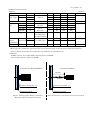
1
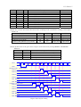
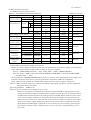
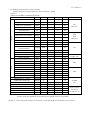
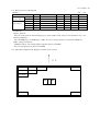
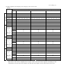
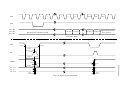
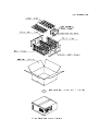
RECORDS OF REVISION
MODEL
SPEC
No:LQ070Y5DG06
No
NO.
2008.1.16
:LCY−07084A
PAGE
SUMMARY
NOTE
-
-
1st Issue
LCY‑07084A‑1
TFT−LCD MODULE
L Q 0 7 0 Y 5 D G 0 6
DEVICE SPECIFICATIONS
CONTENTS
(1)
(2)
(3)
(4)
(5)
(6)
(7)
(8)
(9)
(10)
(11)
(12)
(13)
(14)
Fig.1
Fig.2
Fig3-1
Fig3-2
Fig.4
Summary
p3
Features
p3
Structure and module external
p3
Mechanical specifications
p3
I/O terminal name and functions
p4
Absolute maximum ratings
p6
Electrical characteristics
p7
Input signals, basic display color and gray scale of each p11
color
Optical characteristics
p12
Mechanical characteristics
p15
Display quality
p15
Handling instruction of TFT-LCD module
p15
Packing form
p18
Reliability test contents
p19
Outline dimensions
p20
Structure of TFT-LCD module
p21
Timing characteristics of input signals
p22
Timing characteristics of input signals
p23
Package form
p24
Appendix Adjustment method of VCDC
p25
LCY‑07084A‑2
NOTICE
This publication is the proprietary of SHARP and is copyrighted, with all rights reserved. Under
the copyright laws, no part of this publication may be reproduced or transmitted in any form or by
any means, electronic or mechanical for any purpose, in whole or in part, without the express
written permission of SHARP. Express written permission is also required before any use of this
publication may be made by a third party.
The application circuit examples in this publication are provided to explain the representative
applications of SHARP's devices and are not intended to guarantee any circuit design or permit any
industrial property right or other rights to be executed.
SHARP takes no responsibility for any problems related to any industrial property right or a third
party resulting from the use of SHARP's devices, except for those resulting directly from device
manufacturing processes.
In the absence of confirmation by device specification sheets, SHARP takes no responsibility for any
defects that occur in equipment using any of SHARP's devices, shown in catalogs, data books, etc.
Contact SHARP in order to obtain the latest device specification sheets before using any SHARP's
device.
SHARP reserves the right to make changes in the specifications, characteristics, data, materials,
structures and other contents described herein at any time without notice in order to improve
design or reliability. Contact SHARP in order to obtain the latest specification sheets before using
any SHARP's device. Manufacturing locations are also subject to change without notice.
Observe the following points when using any device in this publication. SHARP takes no
responsibility for damage caused by improper use of the devices.
The devices in this publication are designed for use in general electronic equipment designs , such
as:
・Car Navigation system
・Automotive auxiliary information display
・Automotive audio visual equipment
The appropriate design measures should be taken to ensure reliability and safety when SHARP's
devices are used for equipment such as:
・Transportation control and safety equipment(i.e.,aircraft,trains,automobiles,etc.)
・Traffic signals ・Gas leakage sensor breakers ・Alarm equipment ・Various safety devices etc.
SHARP's devices shall not be used for equipment that requires extremely high level of reliability,
such as:
・Military and space applications ・Nuclear power control equipment
・Medical equipment for life support
Contact a SHARP representative, in advance, when intending to use SHARP's devices for any
"specific" applications other than those recommended by SHARP.
Contact and consult with a SHARP representative if there are any questions about the contents of
this publication.
LCY‑07084A‑3
(1) Summary
This TFT-LCD module is a color active matrix LCD module incorporating amorphous silicon TFT.
An outline of the module is given in Table 4-1.
(2) Features
・Utilizes a panel with a 15:9 aspect ratio, which makes the module suitable for use in wide-screen
systems.
・The 7.0 screen produces a high resolution image that is composed of 384,000 pixels elements in a
stripe arrangement.
・Graphics and texts can be displayed on a 800×RGB×480 dots panel with 262,144 colors
by supplying 18 bit data signals(6 bit/color).
・Wide viewing field angle technology is employed.(The most suitable viewing angle is in the 6 o'clock
direction.)
・By adopting an active matrix drive, a picture with high contrast is realized.
・Reduced reflection as a result of low reflection black matrix and an AG(antiglare) polarizer being
adopted.
・By COG method, realized a slim, lightweight, and compact module.
・Transparent intensity is raised by adoption of the rate LCD panel of a high aperture, a high
transparently color filter, and a high transparently polarizing plate.
・The quality picture of natural color reproducibility is realized by adoption in TN normally white mode
excellent in color reproducibility.
・An inverted video display in the vertical and horizontal directions is possible.
(3) Structure and Outline Dimensions
Outline dimensions of the module are given in Fig.1.
Structure of the TFT-LCD module are given in Fig.2.
This TFT-LCD module is composed of the color TFT-LCD panel, driver ICs, FPC, frame, shielding front
case and backlight unit.( circuit to drive the LEDbacklight is not built into this module.)
(4) Mechanical Specifications
Table4-1
Parameter
Specifications
Units
Screen size (Diagonal)
17.7 [7.0”]
cm
Active area
152.40(W) × 91.44(H)
mm
Display format
800 × RGB(W) × 480(H)
dots
Dot pitch
0.0635(W) × 0.1905(H)
mm
Pixel configuration
R,G,B Stripe configuration
Outline dimension
170.0(W) × 104.0(H) × 8.0(D)
mm
Mass
210±15
g
【Note4-1】Typical values are shown.
For detailed measurements and tolerances, please refer to Fig.1.
( FPC(LED/LCD),FPC fixation sheet are excepted.)
Remarks
【Note4-1】
LCY‑07084A‑4
(5) I/O Terminal Name and Functions
5-1) TFT-LCD Panel Driving Part
Table5-1 I/O terminal name and functions
Pin No.
Symbol
i/o
Description
1
2
3
4
5
6
7
8
9
10
11
12
13
14
15
16
17
18
19
20
21
22
23
24
25
26
27
28
29
30
31
32
33
34
35
36
37
38
39
40
41
42
43
44
GND
SPL
V10
V9
V8
V7
V6
V5
V4
V3
V2
V1
V0
VSHA
VSHA
GND
GND
R5
R4
R3
R2
R1
R0
GND
G5
G4
G3
G2
G1
G0
GND
B5
B4
B3
B2
B1
B0
LS
LBR
GND
CK
GND
VSHD
SPR
−
i/o
i
i
i
i
i
i
i
i
i
i
i
i
i
−
−
i
i
i
i
i
i
−
i
i
i
i
i
i
−
i
i
i
i
i
i
i
i
−
i
−
i
o/i
GND
Start signal2 of Source driver
The power supply of gray image
The power supply of gray image
The power supply of gray image
The power supply of gray image
The power supply of gray image
The power supply of gray image
The power supply of gray image
The power supply of gray image
The power supply of gray image
The power supply of gray image
The power supply of gray image
Power supply of Source driver
Power supply of Source driver
GND
GND
RED data signal (MSB)
RED data signal
RED data signal
RED data signal
RED data signal
RED data signal (LSB)
GND
GREEN data signal (MSB)
GREEN data signal
GREEN data signal
GREEN data signal
GREEN data signal
GREEN data signal (LSB)
GND
BLUE data signal (MSB)
BLUE data signal
BLUE data signal
BLUE data signal
BLUE data signal
BLUE data signal (LSB)
Date transfer signal of Source driver
Change signal of direction of scan for source driver
GND
Clock signal of Source driver
GND
Power supply of Source driver
Start signal1 of Source driver
45
46
47
48
49
50
MODE1
MODE2
CLS
SPS
U/L
GND
i
i
i
i
i
−
Output mode setting signal 1 of gate driver
Output mode setting signal 2 of gate driver
Clock signal of gate driver
Start signal of gate driver
Change signal of direction of scan for gate driver
GND
Remarks
[Note5-1]
[Note5-1]
[Note5-1]
[Note5-2]
[Note5-2]
[Note5-1]
LCY‑07084A‑5
Pin No.
Symbol
i/o
Description
51
52
53
54
55
56
57
58
59
60
VCOM
VCOM
CS
N.C.
VDD
N.C.
VEE
VCC
N.C.
VSS
i
i
i
−
i
−
−
i
−
−
Common electrode driving signal
Common electrode driving signal
CS driving signal
OPEN
Power supply of gate driver
OPEN
Power supply of gate driver
Power supply of gate driver
OPEN
Power supply of gate driver
Remarks
[Note5-1] A vertical, horizontal direction of the scanning can be controlled according to this signal.
Table 5-2
Display mode
U/L
LBR
SPL
SPR
Normal displayed
Lo
Hi
Input mode Output mode
Right/Left reverse mode
Lo
Lo
Output mode Input mode
Up/Down reverse mode
Hi
Hi
Input mode Output mode
Right/Left & Up/Down reverse mode
Hi
Lo
Output mode Input mode
Caution) Lo=GND , Hi=VSHD
[Note5-2] The mode of the gate driver output can be selected by setting MODE1 and MODE2.
Table5-3
MODE1
MODE2
Output mode
Hi
Hi
Normal mode(1 line writing)
Lo
Hi
Out of use
Hi
Lo
2 line simultaneous writing mode
Lo
Lo
All output terminal is fixed at the VEE level.
Caution) Lo=GND , Hi=VSHD
CLS
1
2
3
4
5
6
7
SPS
Normal mode (1 pulse mode)
Dummy
Dummy
Dummy
Dummy
DH1(DH480)
DH2(DH479)
Interlace 2 pulse mode
Dummy
Dummy
Dummy
Dummy
DH1(DH480)
DH2(DH479)
Fig. A
Gate output timing chart
Fig.5-1 Gate output timing
8
9
LCY‑07084A‑6
5-2)Backlight fluorescent tube driving part
Table5-4
Pin No.
Symbol
Description
1
2
3
4
5
6
7
8
A1
A2
NC
K1
K2
K3
NC
NC
Remarks
Input terminal (Anode 1)
Input terminal (Anode 2)
Input terminal (Cathode 1)
Input terminal (Cathode 2)
Input terminal (Cathode 3)
(6) Absolute maximum ratings
Teble6-1 Absolute maximum ratings
GND=0V
Parameter
Symbol
MIN
MAX
Unit
Remark
Power supply
Analog
VSHA
−0.3
+6.0
V
Ta=25℃
of source driver
Digital
VSHD
−0.3
+6.0
V
〃
Power supply
VDD
−0.3
+35.0
V
〃
of gate driver
VCC−VSS
−0.3
+6.0
V
〃
VEE−VSS
−0.3
+35.0
V
〃
VDD−VEE(VSS)
−0.3
+35.0
V
〃
Input signal Digital
VID
−0.3
VSHD+0.3
V
〃,[Note6-1]
Analog
VIA
−0.3
VSHA+0.3
V
〃,[Note6-2]
Common electrode
VCOM
−4
+6
V
〃
driving signal
Storage temperature
Tstg
−40
85
℃ [Note6-3,4]
Operating temperature
Topr1
−30
85
℃ [Note6-5,6]
(LCD panel surface)
Operating temperature
Topr2
−30
65
℃ [Note6-6]
(Ambient temperature)
Current of LED
If
−
150
mA
Ta=25℃
[Note6-1] SPL、SPR、R0〜R5、G0〜G5、B0〜B5、LS、CK、LBR、MODE1、MODE2、U/L、SPS、CLS
[Note6-2] V0、V1、V2、V3、V4、V5、V6、V7、V8、V9、V10
[Note6-3] This rating applies to all parts of the module and should not be exceeded.
[Note6-4] Maximum wet-bulb temperature is 57℃. Avoid dew condensation on the module.
Otherwise electrical current leaks will occur , and it cannot meet the specifications.
[Note6-5] The operating temperature guarantees only operation of the circuit. For contrast, speed of
response, and other factors related to display quality are determined in the circumstances
with Ta=+25℃.
[Note6-6] Ambient temperature when the backlight is lit (reference value).
LCY‑07084A‑7
(7) Electrical Characteristics
7-1) TFT-LCD panel driving section
Table7-1 Recommended operating conditions
GND=0V , Ta=25℃
Parameter
Symbol
MIN
TYP
MAX
Unit
Remarks
Power supply
Analog
VSHA
+5.0
+5.3
+5.6
V
of source driver Digital
VSHD
+2.5
+3.3
+3.6
V
Power supply
TFT
Hi
VDD
+14.8
+15.0
+15.2
V
of gate driver driving Lo AC VEEAC
−
COM AC
−
Vp-p [Note7-1]
DC VEEDC
−11.8
−12.0
−12.2
V
Hi
VCC
VSS+VSHD VSS+VSHD VSS+VSHD V [Note7-2]
Logic
−0.3
+0.3
Lo
VSS
−17.0
−17.4
−17.8
V
Power supply of gray image
V0〜V10
0
−
VSHA
V [Note7-3]
Input voltage
Hi input
VIHS
0.8×VSHD
−
VSHD
V [Note7-4]
of source driver Lo input
VILS
GND
−
0.2×VSHD V
Input current
Hi input
IIHS
−
−
10
µA [Note7-4]
of source driver Lo input
IILS
−
−
10
µA
Input voltage
Hi input
VIHG
0.8×VSHD
−
VSHD
V
of gate driver Lo input
VILG
GND
−
0.2×VSHD V [Note7-5]
Input current
Hi input
IIHG
−
−
1.0
µA
of gate driver Lo input
IILG
−
−
1.0
µA
Common
AC component COM AC
−
±3.6
±4.0
Vp-p [Note7-6]
electrode
DC component COM DC
+0.5
−
+2.5
V
driving signal
CS driving
AC component
VCSAC
−
±3.6
±4.0
Vp-p [Note7-1]
signal
DC component
VCSDC
−5.3
−5.5
−5.7
V
[caution] Notes when power supply is turned on.
Please do a power supply on and the power-off in a simultaneous each power supply or the following
order. And, please input the signal after turning on all power supplies.
Turn on VSHD,VSHA,VSS,VCC → Logic signal ,VEE → VDD → MODE1,MODE2
Turn off VDD → VEE , Logic signal(Include MODE1 and MODE2) → VCC,VSS,VSHA,VSHD
* Condition VSS < VCC
At the terminals of MODE1/MODE2 signals, input low voltage when applying the power supply, and
hold low voltage for more than 2 vertical synchronous terms after VDD rises completely.
Then, either or both of them should hold high voltage until the power supply is turned off.
[Note7-1] This is must be made into common electrode driving signal, this phase, and this amplitude.
And please keep VSS≦VEE.
[Note7-2] Condition: VSHD=3.3V
[Note7-3] It is a standard power supply for gray scale.
Whenever the polarity of common electrode drive signal (VCOM) is changed, please also
change this standard voltage.V0 (black) power supply becomes the reverse characteristic of
VCOM, and V10(white) becomes the same polarity as VCOM. Please shift the center value
of each power supply amplitude to the plus(+) direction according to the characteristic of
liquid crystal as it will go to white side like V1,V2,V3,V4,V5,V6,V7,V8,V9,V10, if the center
value of each power supply amplitude is based on the center value of V0(black). After DC
adjustment of VCOM signal is adjusted in case of the V0 gray scale display, please adjust
this amount of shifts so that a flicker does not occur in the power supply display of each
gray scale.
LCY‑07084A‑8
[Note7-4] Apply to terminal of R0〜R5,G0〜G5,B0〜B5,SPR,SPL,CK,LS and LBR.
[Note7-5] Apply to terminal of CLS,SPS,MODE1,MODE2 and U/L.
[Note7-6] Please switch polarity of amplitude COMAC by center value of amplitude that is COMDC
for every one level scan and every one vertical scan. Moreover, please adjust COMDC so
that contrast becomes the maximum and a flicker becomes the minimum for every module.
7-2) Backlight unit driving section
Table7-2
Parameter
LED voltage
LED voltage
difference of lines of LED voltage
LED current
Power consumption
Symbol
Vf
Vf-30
⊿Vf
If
Wf
MIN
16.0
−
−
−
−
TYP
17.3
−
−
90
5
MAX
21.3
22.8
1.4
95
−
Unit
Ⅴ
V
V
mA
W
Remarks
Ta=25℃,If=90mA
Ta=-30℃,If=90mA
LCY‑07084A‑9
7-3) Timing characteristics of input signals
Timing diagrams of input signal are shown in Fig3-1, Fig3-2.
Table7-3
VSHA=5.3V,VSHD=3.3V,GND=0V,Ta=25℃
Parameter
Symbol MIN TYP
MAX
Unit
Source
Operating Clock frequency
fck
−
33.2
34.6
MHz
High level clock width
Tcwh
12
−
−
ns
Low level clock width
Tcwl
13
−
−
ns
Clock rise time
Tcr
−
−
4
ns
Clock fall time
Tcf
−
−
4
ns
Start pulse frequency
fsp
−
31.5
31.8
kHz
Start pulse set up time
Tsusp
4
−
−
ns
Start pulse hold time
Thsp
0
−
−
ns
Terminal
CK
[Note7-7]
SPR
SPL
[Note7-8]
Gate
Start pulse width
Twsp
1/fck
1/fck
1.5/fck
ns
LS pulse frequency
flp
−
fsp
−
kHz
LS pulse set up time (CLS) Tsulp
5.0
−
−
μs
LS pulse set up
LS
Tsulpsp 1/fck
−
−
ns
time(SPL,SPR)
LS pulse hold time(DCLK) Thlpck
20
−
−
ns
High level LS pulse wide
Twlp
1/fck
−
−
ns
Data set up time
Tsud
15
−
−
ns
R0〜R5,G0〜
G5,B0〜B5
Data hold time
Thd
10
−
−
ns
Operating Clock frequency
fcls
−
fsp
−
kHz
Clock pulse with
Twl
5.5
−
−
μs
CLS
Clock rise time
Trcl
−
−
1/fck
ns
Clock fall time
Tfcl
−
−
1/fck
ns
Start pulse frequency
fsps
−
60
65
Hz
Start pulse set up time
Tsusps
100
−
−
ns
SPS
Start pulse hold time
Thsps
300
−
−
ns
Start pulse rise time
Trsps
−
−
100
ns
Start pulse fall time
Tfsps
−
−
100
ns
COM signal set up time
Tsucom
3
−
−
μs
VCOM
COM signal hold time
Thcom
0
−
−
μs
CS
COM signal rise time
Trcom
−
−
2
μs
COM signal fall time
Tfcom
−
−
2
μs
V0〜V10 signal set up time
Tsuv0
3
−
−
μs
V0,V1,V2,V3,
V0〜V10 signal hold time
Thv0
0
−
−
μs
V4,V5,V6,
V0〜V10 signal rise time
Trv0
−
−
2
μs
V7,V8,V9,V10
V0〜V10 signal fall time
Tfv0
−
−
2
μs
[Note7-7] It is also possible that Tcr,Tcf exceeds the maximum value when the clock frequency
doesn't reach the maximum value. But please confirm there is no problem.
[Note7-8] The rising pulse in CK is existed only 1 time during Hi period (Twsp) on start pulse.
LCY‑07084A‑10
7-4) Electric power consumption
Table7-4
Ta = 25℃
Parameter
symbol Voltage conditiion
MIN
TYP
MAX
Unit
Current for
Analog
ISHA VSHA=+5.3V
−
40
95
mA
source driver Digital
ISHD VSHD=+3.3V
8.0
19
mA
Current for
Hi
IDD VDD=+15.0V
−
0.2
0.35
mA
gate driver
Lo
IEE VEE=−12.0±3.6V
−
−0.2
−0.35
mA
Logic Hi
ICC VCC=−14.1V
−
0.05
0.1
mA
Logic Lo
ISS VSS=−17.4V
−
−0.1
−0.2
mA
*Conditions
Display pattern:
Vertical stripe pattern alternating 21 gray scale (GS21) with 42 gray scale (GS42) every 1 dot.
Driving condition:
fck=33.2MHz,fsp=30.3kHz,fsps=60Hz, In case of using exclusive control-IC (LZ9JG17)
Other voltage conditions
VCOM=7.2Vp-p, V0=4.88Vp-p(The opposite phase of VCOM),
V10=3.04Vp-p(equal to phase of VCOM)
7-5) Input Data Signals and Display Position on the screen
UP
D1,DH1
D2,DH1
D1,DH2
D2,DH2
D3,DH1
D800,DH1
D1,DH3
R G B
D1,DH480
Display position of input data〔H,V〕
D800,DH480
LCY‑07084A‑11
(8) Input signals, basic display color and gray scale of each color
Table8-1
Colors &
Data signal
0 :Low level voltage
Gray scale Gray
Scale
1 :High level voltage
R0
R1
R2
R3
R4
R5
G0
G1
G2
G3
G4
G5
B0
B1
B2
B3
B4
B5
Basic color
Gray Scale of red
Black
Blue
Green
Cyan
Red
Magenta
Yellow
White
−
−
−
−
−
−
−
−
0
0
0
0
1
1
1
1
0
0
0
0
1
1
1
1
0
0
0
0
1
1
1
1
0
0
0
0
1
1
1
1
0
0
0
0
1
1
1
1
0
0
0
0
1
1
1
1
0
0
1
1
0
0
1
1
0
0
1
1
0
0
1
1
0
0
1
1
0
0
1
1
0
0
1
1
0
0
1
1
0
0
1
1
0
0
1
1
0
0
1
1
0
0
1
1
0
1
0
1
0
1
0
1
0
1
0
1
0
1
0
1
0
1
0
1
0
1
0
1
0
1
0
1
0
1
0
1
0
1
0
1
0
1
0
1
0
1
0
1
0
1
0
1
Black
GS0
GS1
GS2
0
1
0
0
0
1
0
0
0
0
0
0
0
0
0
0
0
0
0
0
0
0
0
0
0
0
0
0
0
0
0
0
0
0
0
0
0
0
0
0
0
0
0
0
0
0
0
0
0
0
0
0
0
0
×
Darker
×
Ø
Brighter
Ø
Red
Black
Gray Scale of green
×
Darker
×
Ø
Brighter
Ø
Green
Black
Gray Scale of bleu
×
Darker
×
Ø
Brighter
Ø
Bleu
È
È
GS61
GS62
GS63
È
È
È
È
1
0
1
0
1
1
1
1
1
1
1
1
1
1
1
1
1
1
0
0
0
0
0
0
0
0
0
0
0
0
0
0
0
0
0
0
0
0
0
0
0
0
0
0
0
0
0
0
0
0
0
0
0
0
GS0
GS1
GS2
0
0
0
0
0
0
0
0
0
0
0
0
0
0
0
0
0
0
0
1
0
0
0
1
0
0
0
0
0
0
0
0
0
0
0
0
0
0
0
0
0
0
0
0
0
0
0
0
0
0
0
0
0
0
È
È
GS61
GS62
GS63
0
0
0
0
0
0
0
0
0
0
0
0
0
0
0
0
0
0
1
0
1
0
1
1
1
1
1
1
1
1
1
1
1
1
1
1
0
0
0
0
0
0
0
0
0
0
0
0
0
0
0
0
0
0
GS0
GS1
GS2
0
0
0
0
0
0
0
0
0
0
0
0
0
0
0
0
0
0
0
0
0
0
0
0
0
0
0
0
0
0
0
0
0
0
0
0
0
1
0
0
0
1
0
0
0
0
0
0
0
0
0
0
0
0
1
1
1
1
1
1
1
1
1
È
È
GS61
GS62
GS63
È
È
È
È
È
È
È
È
0
0
0
0:Low level voltage
0
0
0
0
0
0
È
È
È
È
0
0
0
0
0
0
0
0
0
0
0
0
0
0
0
0
0
0
È
È
0
0
0
0
0
0
0
0
0
1
0
1
0
1
1
1
1
1
1:High level voltage
Each basic color can be displayed in 64 gray scales from 6 bit data signals. According to the
combination of total 18 bit data signals, the 262,144-color display can be achieved on the screen.
LCY‑07084A‑12
(9) Optical characteristics
Table9-1
Parameter
Symbol
Viewing
Horizontal θ21, θ22
angle range
θ11
Vertical
θ12
Contrast ratio
CRmax
Response
Rise time
τr
time
Fall time
τd
Rise time
τr
Fall time
τd
Panel surface brightness
Y0
Panel
no
surface
impression
chromaticity
LED lifetime +25℃
Condition
TYP
60
55
50
310
9
17
35
80
540
MAX
−
−
−
−
x
y
If=90mA
(at LED 1line)
(no signal input)
If=90mA
(at LED 1line)
MIN
50
45
35
150
−
−
−
−
400
0.257
0.268
0.307
0.318
0.357
0.368
−
continuation
10,000
−
−
CR≧10
θ=0°
θ=0°
Ta=25℃
θ=0°
Tp=-20℃
50
100
−
Ta=25℃
Unit
Remarks
°(degree) [Note9-1]
°(degree)
°(degree)
[Note9-2]
[Note9-3]
ms
ms
ms
ms
cd/m2
[Note9-4]
[Note9-5]
Hour
[Note9-6]
*Measured after 30minutes operation. The optical characteristic is measured by using the method of
fig.10-1 and fig.10-2 under the condition of the darkroom or equivalent to it.
Conditions
VCOM=7.2Vp-p, V0=4.88Vp-p(The opposite phase of VCOM),
V10=3.04Vp-p(equal to phase of VCOM)
Photodetector(EZ-CONTRAST)
Photodetector(BM-7)
400mm
Field=1°
Center of screen(θ=0°)
Center of screen(θ=0°)
TFT-LCD module
TFT-LCD module
Fig.10-1 Viewing angle / Range / Contrast /
Response time measurement method
Fig.10-2 Luminance / Chromaticity measurement method
LCY‑07084A‑13
[Note 9-1] Viewing angle range is defined as follows.
Normal line
θ22
θ11
θ12
θ21
6 o’clock direction
[Note 9-2] Contrast ratio is defined as follows:
Contrast ratio(CR)=
Photo detector output with LCD being "white(GS63)"
Photo detector output with LCD being "black(GS0)"
[Note 9-3] Response time is defined as follows:
Response time is obtained by measuring the transition time of photo detector output, when input
signals are applied so as to make the area "black" to and from "white".
White
Black
White
100%
90%
Photodetector Output (relative Value)
10%
0%
τr
τd
Time
LCY‑07084A‑14
[Note 9-4] Definition of panel surface brightness
Measured on the center area of the panel at a viewing cone 1-degree by TOPCON luminance
meter BM-7.(After 30 minutes operation)
[Note 9-5] Definition of panel surface chromaticity
Measured on the center area of the panel at a viewing cone 1-degree by TOPCON luminance
meter BM-7.(After 30 minutes operation) If=90mA at LED 1line
[Note 9-6] LED life time (continuous lighting)
Lamp life time is defined as the time when the center brightness of LCD module becomes 50% of
the following conditions.
If = 90mA(at LED 1line)
PWM brightness control : 5 ~ 100%
LCY‑07084A‑15
(10) Mechanical characteristics
10-1) External appearance
Do not exist extreme defects. (See Fig. 1)
10-2) Panel toughness
The panel should not be broken, when press to the center of the panel by 19N power using smooth
surface with 15mm diameter.
Caution: If the pressure is added on the active area of the panel over the long time, even if the
pressure is very small weight , the functional damage might occur in the panel.
10-3) I/O connector performance
A) Input/output connectors to control the LCD module
1) Applicable Connector : FH28−60S−0.5SH (HIROSE)
2) FPC flexibility
: Slit on the film cover lay coat part of one side printing.
If it had been tested bending under radius nothingness and bending
angle 180degrees, the FPC should not be cut. (It should be bend by
hand and only at once.)
The film cover lay coat part of one side printing.
Do not disconnect by 30 times or less after examining the winding on
the following conditions.
condition : winding radius 0.6mmR and condition of 90° in winding angle
B) I/O connector of backlight driving circuit
1) Corresponding connector : CFP1508-0101F (SMK)
2) FPC flexibility
: The same as A) Input/output connectors to control the LCD module
(11) Display quality
The display quality of the color TFT-LCD module is applied to the Incoming Inspection Standard.
(12) Handling instruction of TFT-LCD module
12-1) Handling of FPC
①Please bend FPC only at the film cover lay slit part of one side printing or the film cover lay coat
part of one side printing.
②Please do not hang a LCD module or do not apply excessive power for FPC.
12-2) Installation of TFT-LCD module
①When incorporating the TFT-LCD module, be sure to fix the module on the same plane, and be
careful not to add the stress of wraps or twists to the module.
Do not add the pressure to the module by force of pushing parts on the set side (touch-switches
,etc.)directly, otherwise display images may be disordered.
②Attachment of input/output FPC and removal should surely turn off the power supply of a set.
LCY‑07084A‑16
12−3) Precautions in mounting
①Polarizer adhering to the surface of the LCD is made of a soft material and susceptible to flaw,
it must be handled carefully. Protection sheet is applied on the surface to protect. It against
scratches and dirties. It is recommended to remove the protection sheet immediately before the
use, taking care of static electricity.
②Precautions in removing the protection sheet
A) Work environment
When the protection sheet is removed off, static electricity may cause dust to stick to the
polarizer surface. To avoid this, the following working environment is desirable.
a) Floor : Conductive treatment of 1MΩ or more on the tile.
( conductive mat or conductive paint on the tile)
b) Clean room free form dust and with an adhesive mat on the doorway
c) Advisable humidity:50%〜70%
Advisable temperature:15℃〜27℃
d) Workers shall wear conductive shoes, conductive work clothes, conductive gloves and an
earth band.
B) Working procedures
Wind direction of the blower
Antistatic Blower
Within 20cm
Module
edge of the protection sheet
a) Direct the wind of discharging blower somewhat downward to ensure that module is blown
sufficiently. Keep the distance between module and discharging blower within 20 cm.
b) Attach edge of the protection sheet part near discharging blower so as to protect
polarizer against flaw.
c) Remove the protection sheet , pulling edge of the protection sheet slowly to your side.
d) On removing off the protection sheet, pass the module to the next work process to prevent the
module to get dust.
e) Method of removing dust from polarizer
・Blow off dust with N2 blower for which static electricity preventive measure has been taken.
・Since polarizer is vulnerable, wiping should be avoided.
But when the panel has stain or grease, we recommend using adhesive tape to softly remove
them from the panel.
LCY‑07084A‑17
③When metal part of the TFT-LCD module (shielding case) soiled, wipe it with soft dry cloth.
For stubborn dirt, wipe the part after breathing on there. For water drops or finger grease, wipe
off immediately. Long contact with water may cause discoloration or spots.
④TFT-LCD module uses glass which breaks or cracks easily if dropped or bumped on hard surface.
Handle with care. The LCD used in the module is made of glass. If drop the module or bump it on
hard surface, the LCD should be broken.
⑤Since CMOS LSI is used in this module, take care of static electricity and earth your body when
handling the module.
12-4) Caution of product design
①Protect the LCD module from water/salt-water by the waterproof cover, etc.
②Take measures against electromagnetic shield so that interferential radiation from the module
should not affect peripheral appliances.
12-5) Other
①Do not expose the module to direct sunlight or intensive ultraviolet rays for many hours. Liquid
crystal is deteriorated by ultraviolet rays.
②Store the module at a temperature near the room temperature. At lower than the rated storage
temperature, liquid crystal solidifies, causing the panel to be damaged. At higher than the rated
storage temperature, liquid crystal turns into isotropic liquid and may not recover.
③If LCD panel breaks, there may be a possibility that the liquid crystal escapes from the panel.
Since the liquid crystal is injurious, do not put it into the eyes or mouth. When liquid crystal
sticks to hands, feet or clothes, wash it out immediately with soap.
④Be sure to adjust DC bias voltage of common electrode driving signal(COM DC) in the state
of the last product. When not adjusted, it becomes the cause of a deterioration of display quality.
⑤Observe all precautionary requirements of general electronic components.
LCY‑07084A‑18
(13) Package form
13-1) Package form (Refer to Fig.4)
13-2) Carton keeping conditions
①The cartons can be piled up maximum 10 layers.
②Environments
Temperature
: 0〜40℃
Humidity
: 60%RH or less(at 40℃)
No dew condensation at low temperature and high humidity.
Atmosphere
: Harmful gas such as acid or alkaline that bites electronic components
or wires, must not be detected.
Periods
: About 3 months
Opening of
: In order to prevent the LCD module from breakdown by electrostatic
the package
charges, please control the humidity over 50%RH and open the package
taking sufficient countermeasures against electrostatic charges, such as
earth, etc.
(14) Reliability test contents
The reliability test condition of This LCD module is shown in Table 14-1.
(15) Other
15-1) Indication of the lot number
The lot number is shown on a label. Attached location is shown in Fig.1 (Outline Dimensions).
Indicated contents of the label :
LQ070Y5DG06 ○○○○○○○○○
Model name
lot number
Contents of the lot number
the 1st figure
production year
the 2nd figure
production month
the 3rd〜8th figure
serial number
the 9th figure
revision marks
ex. 2008 ⇒ 8
1,2,3,‥‥‥,9,X,Y,Z
000001〜
Blank,A,B,C ・・・
LCY‑07084A‑19
Table14-1 Reliability test conditions
Table 12
Temperature condition is based on operating temperature condition
No.
Test items
Test condition
1 High temperature strong test
Ta = +85℃
240h
2 Low temperature strong test
Ta =−40℃
240h
3 High temperature and high
Tp = +60℃, 90%RH
240h
humidity operation test
4 Hi temperature operating test
Tp = +85℃
240h
5 Low temperature operating test Ta =−30℃
240h
6 Electro static discharge test
±200V・200pF(0Ω) 1 time for each terminals
7 Shock test
980m/s2・6ms, ±X;±Y;±Z 3 times for each direction
(JIS C0041, A-7 Condition C)【caution】
8 Vibration test
Frequency : 8〜33.3Hz , Stroke : 1.3mm
Frequency : 33.3Hz〜400Hz,Acceleration : 29.4m/s2
Cycle
: 15 minutes
X,Z 2 hours for each directions,4 hours for Y direction
(total 8 hours) 【caution】(JIS D1601)
9 Heat shook test
−30℃ 〜 +85℃ / 200 cycles
(0.5h)
(0.5h)
【Note】
Ta = Ambient temperature, Tp = Panel temperature
【Check items】
In the standard condition, there shall be no practical problems that may
affect the display function.
【caution】
Definition of X,Y,Z direction is shown as follows
Z
X
Y
LCY‑07084A‑20
Fig1.Outline dimensions
1/fck
CLD
0.8VSHD
0.8VSHD
LAST−1
LAST
0.2VSHD
0.8VSHD
Tcwl
0.8VSHD
1
0.2VSHD
2
0.2VSHD
Tcr
Twlp
Thlpck
LP
Tcwh
Tcf
0.8VSHD
0.8VSHD
0.2VSHD
1/flp
Tsusp
Thsp
Tsulpsp
0.8VSHD
SPR(SPL)
0.2VSHD
0.8VSHD
Twsp
1/fsp
Tsud
R0〜R5
G0〜G5
B0〜B5
Thd
0.8VSHD
0.8VSHD
(D1、n)
(D2、n)
0.2VSHD
0.2VSHD
*n=DH1、DH2・・DH480
Twl
Tfcl
Trcl
0.8VSHD
CLS
0.2VSHD
Tfsps
0.2VSHD
0.2VSHD
Trsps
Thsps
1/fcls
0.8VSHD
0.2VSHD
0.2VSHD
0.8VSHD
0.2VSHD
1/fsps
Fig.3-1. Input signal waveform
0.2VSHD
LCY-07084A-22
SPS
Tsusps
0.2VSHD
0.8VSHD
CLS
1
2
7
8
9
486
487
488
・・
SPS
R0〜R5
G0〜G5
B0〜B5
Horizontal invalid data period
(m,DH1)
(m,DH2)
(m,DH479) (m,DH480)
Horizontal invalid
data period
*m=D1〜D800
CLS
0.2VSHD
0.2VSHD
Tsulp
LP
0.8VSHD
Tsucom
VCOM
90%
Tfcom
90%
10%
10%
Trcom
Thv0
90%
90%
10%
10%
Trv0
(Tfv0)
Tfv0
(Trv0)
Fig.3-2. Input signal waveform
LCY-07084A-23
Tsuv0
V0、V3、
V5、V7、
V9、V10
Thcom
LCY‑07084A‑25
(Appendix)
Adjusting method of optimum DC bias voltage of common electrode driving signal
Photoelectric devices are very effective to obtain optimum DC bias voltage of common electrode driving
signal accurately, and theaccuracy is with 0.1V. (In visual examination method, the accuracy is about
0.5V because of the difference among individuals.)
Adjusting method of DC bias voltage using the photoelectric devices is as follows
Measurement of flicker
Adjust the DC baias voltage so as to minimize flicker at NTSC : 60Hz(30Hz) / PAL : 50Hz(25Hz).
Photo-electric device
Output voltage
VCDC
Oscilloscope
LCD module
Fig. A Measurement system
Adjusting method of DC bias voltage
Measure the output voltage from Photoelectric device using the oscilloscope at the measurement
system of Fig. A.
Then, change the DC bias voltage in small steps, and adjust it so as to minimize the flicker at
NTSC 60Hz(30Hz) / PAL : 50Hz(25Hz). (Fig.B)
DC bias : Optimum
Fig. B
DC bias : Optimum + 1
Waveforms of flicker