1
OP7100
Serial Graphic Display
User’s Manual
019–0065 • 070831–O
OP7100 User’s Manual
Part Number 019-0065 • 070831-O • Printed in U.S.A.
© 1999–2007 Rabbit Semiconductor Inc. • All rights reserved.
Rabbit Semiconductor reserves the right to make changes and
improvements to its products without providing notice.
No part of the contents of this manual may be reproduced or transmitted in any form or by any
means without the express written permission of Rabbit Semiconductor.
Permission is granted to make one or more copies as long as the copyright page contained
therein is included. These copies of the manuals may not be let or sold for any reason without
the express written permission of Rabbit Semiconductor.
Trademarks
• Dynamic
C®
is a registered trademark of Rabbit Semiconductor Inc.
• Windows® is a registered trademark of Microsoft Corporation
• PLCBus™ is a trademark of Rabbit Semiconductor Inc.
The latest revision of this manual is available on the Rabbit Semiconductor Web site,
www.rabbit.com, for free, unregistered download.
Rabbit Semiconductor Inc.
www.rabbit.com
TABLE OF CONTENTS
About This Manual
vii
Chapter 1: Overview
11
Introduction .......................................................................................... 12
Features ................................................................................................ 13
Options ............................................................................................ 13
Development and Evaluation Tools ..................................................... 14
Software .......................................................................................... 14
CE Compliance .................................................................................... 15
Chapter 2: Getting Started
17
Initial OP7100 Setup ............................................................................ 18
Parts Required ................................................................................. 18
Setting Up the OP7100 ................................................................... 18
Connecting the OP7100 to a Host PC .................................................. 20
Running Dynamic C ............................................................................. 22
Chapter 3: Hardware
23
OP7100 Subsystems Overview ............................................................ 24
Computing Module ......................................................................... 24
Power Management ............................................................................. 25
ADM691 Supervisor Chip .............................................................. 26
Handling Power Fluctuations ........................................................ 26
Watchdog Timer ........................................................................... 27
Power Shutdown and Reset .......................................................... 28
PFI “Early Warning” ..................................................................... 28
Memory Protection ....................................................................... 29
Battery Backup ............................................................................. 29
System Reset ................................................................................... 29
Liquid Crystal Display (LCD) ............................................................. 30
Contrast Adjustment ........................................................................ 30
Background ..................................................................................... 31
Coordinate Systems ......................................................................... 32
LCD Controller Chip ...................................................................... 32
Keypad Interface .................................................................................. 34
OP7100
Table of Contents
iii
Digital I/O ............................................................................................ 35
Serial Communication .......................................................................... 36
RS-232 Communication .................................................................. 38
Receive and Transmit Buffers ....................................................... 38
CTS/RTS Control ......................................................................... 39
Modem Communication ............................................................... 39
RS-485 Communication .................................................................. 40
Developing an RS-485 Network ................................................... 40
Use of the Serial Ports ..................................................................... 42
Z180 Serial Ports .......................................................................... 43
Asynchronous Serial Communication Interface ................................... 45
ASCI Status Registers ..................................................................... 45
/DCD0 (Data Carrier Detect) ........................................................ 45
TIE (Transmitter Interrupt Enable) ............................................... 45
TDRE (Transmitter Data Register Empty) ................................... 45
CTS1E (CTS Enable, Channel 1) ................................................. 46
RIE (Receiver Interrupt Enable) ................................................... 46
FE (Framing Error) ....................................................................... 46
PE (Parity Error) ........................................................................... 46
OVRN (Overrun Error) ................................................................ 46
RDRF (Receiver Data Register Full) ............................................ 46
ASCI Control Register A ................................................................ 47
MOD0–MOD2 (Data Format Mode Bits) .................................... 47
MPBR/EFR (Multiprocessor Bit Receive/Error Flag Reset) ........ 47
/RTS0 (Request to Send, Channel 0) ............................................ 47
CKA1D (CKA1 Disable) .............................................................. 47
TE (Transmitter Enable) ............................................................... 47
RE (Receiver Enable) ................................................................... 48
MPE (Multiprocessor Enable) ...................................................... 48
ASCI Control Register B ................................................................ 48
SS (Source/Speed Select) ............................................................. 48
DR (Divide Ratio) ........................................................................ 49
PEO (Parity Even/Odd) ................................................................ 49
/CTS/PS (Clear to Send/Prescaler) ............................................... 49
MP (Multiprocessor Mode) .......................................................... 49
MPBT (Multiprocessor Bit Transmit) .......................................... 49
Chapter 4: Software
51
Supplied Software ................................................................................ 52
Digital I/O ............................................................................................ 53
Real-Time Clock (RTC) ....................................................................... 54
Display ................................................................................................. 55
Flash EPROM ................................................................................. 55
iv
Table of Contents
OP7100
Dynamic C 32 Libraries ....................................................................... 56
OP71HW.LIB .................................................................................. 56
Keypad Programming ..................................................................... 65
Using Dynamic C v. 5.xx ..................................................................... 66
EZIOOP71.LIB ............................................................................... 66
GLCD.LIB ...................................................................................... 66
KP_OP71.LIB ................................................................................. 70
SYS.LIB .......................................................................................... 72
Upgrading Dynamic C ......................................................................... 73
New LCD Controller Chip .............................................................. 73
Chapter 5: Graphics Programming
75
Initialization ......................................................................................... 76
Drawing Primitives .............................................................................. 76
Plot a Pixel ...................................................................................... 76
Plot a Line ....................................................................................... 77
Plot a Circle .................................................................................... 77
Plot a Polygon ................................................................................. 77
Fill a Circle ..................................................................................... 77
Fill a Polygon .................................................................................. 77
Draw a Bitmap ................................................................................ 77
Font and Bitmap Conversion ............................................................... 78
Using the Font/Bitmap In Your Program ........................................ 79
Printing Text ......................................................................................... 80
Keypad Programming .......................................................................... 81
Initialization .................................................................................... 81
Scanning the Keypad ....................................................................... 81
Reading Keypad Activities .............................................................. 81
Chapter 6: Installation
83
Grounding ............................................................................................ 84
Installation Guidelines ......................................................................... 85
Mounting .............................................................................................. 86
Bezel-Mount Installation ................................................................. 86
General Mounting Recommendations ............................................. 87
Appendix A: Troubleshooting
89
Out of the Box ...................................................................................... 90
Dynamic C Will Not Start .................................................................... 91
Dynamic C Loses Serial Link .............................................................. 91
OP7100 Repeatedly Resets .................................................................. 91
Common Programming Errors ............................................................. 92
OP7100
Table of Contents
v
Appendix B: Specifications
93
Electrical and Mechanical Specifications ............................................ 94
LCD Dimensions ............................................................................. 94
Bezel Dimensions ........................................................................... 94
General Specifications .................................................................... 95
Header and Jumper Configurations ..................................................... 96
Appendix C: Memory, I/O Map, and Interrupt Vectors
99
OP7100 Memory ............................................................................... 100
Execution Timing .......................................................................... 101
Memory Map ..................................................................................... 102
Input/Output Select Map ............................................................... 102
Z180 Internal Input/Output Registers Addresses 00-3F ................ 102
Epson 72423 Timer Registers 0x4180–0x418F ............................ 104
Other Registers .............................................................................. 105
Interrupt Vectors ................................................................................ 106
Power-Failure Interrupts ............................................................... 107
Interrupt Priorities ......................................................................... 107
Appendix D: Serial Interface Board
109
Introduction ........................................................................................ 110
External Dimensions .......................................................................... 111
Appendix E: Backup Battery
113
Battery Life and Storage Conditions .................................................. 114
Replacing the Lithium Battery ........................................................... 114
Battery Cautions ................................................................................ 115
Index
117
Schematics
125
vi Table of Contents
OP7100
ABOUT THIS MANUAL
This manual provides instructions for installing, testing, configuring, and
interconnecting the Rabbit Semiconductor OP7100 touchscreen operator
interface. Instructions are also provided for using Dynamic C functions.
Assumptions
Assumptions are made regarding the user's knowledge and experience in
the following areas.
•
Ability to design and engineer the target system that interfaces with the
OP7100.
•
Understanding the basics of operating a software program and editing
files under Windows on a PC.
•
Knowledge of the basics of C programming.
For a full treatment of C, refer to the following texts.
The C Programming Language by Kernighan and Ritchie
and/or
C: A Reference Manual by Harbison and Steel
•
Knowledge of basic assembly language and architecture for the Z180
microprocessor.
For documentation from Zilog, refer to the following texts.
Z180 MPU User's Manual
Z180 Serial Communication Controllers
Z80 Microprocessor Family User's Manual
OP7100
About This Manual
vii
Acronyms
Table 1 lists and defines the acronyms that may be used in this manual.
Table 1. Acronyms
Acronym
Meaning
EPROM
Erasable Programmable Read-Only Memory
EEPROM
Electronically Erasable Programmable Read-Only Memory
LCD
Liquid Crystal Display
LED
Light-Emitting Diode
NMI
Nonmaskable Interrupt
PIO
Parallel Input/Output Circuit
(Individually Programmable Input/Output)
PRT
Programmable Reload Timer
RAM
Random Access Memory
RTC
Real-Time Clock
SIB
Serial Interface Board
SRAM
Static Random Access Memory
UART
Universal Asynchronous Receiver Transmitter
Icons
Table 2 displays and defines icons that may be used in this manual.
Table 2. Icons
Icon
Meaning
Icon
Note
Refer to or see
Please contact
Caution
FD
viii
Meaning
Tip
Tip
High Voltage
Factory Default
About This Manual
OP7100
Conventions
Table 3 lists and defines the typographical conventions that may be used in
this manual.
Table 3. Typographical Conventions
Example
Description
while
Courier font (bold) indicates a program, a fragment of a
program, or a Dynamic C keyword or phrase.
// IN-01…
Program comments are written in Courier font, plain face.
Italics
Indicates that something should be typed instead of the
italicized words (e.g., in place of filename, type a file's
name).
Edit
Sans serif font (bold) signifies a menu or menu selection.
...
An ellipsis indicates that (1) irrelevant program text is
omitted for brevity or that (2) preceding program text may
be repeated indefinitely.
[ ]
Brackets in a C function’s definition or program segment
indicate that the enclosed directive is optional.
< >
Angle brackets occasionally enclose classes of terms.
a | b | c
A vertical bar indicates that a choice should be made from
among the items listed.
Pin Number 1
A black square indicates
pin 1 of all headers.
Pin 1
J1
Measurements
All diagram and graphic measurements are in inches followed by millimeters enclosed in parenthesis.
OP7100
About This Manual
ix
x About This Manual
OP7100
CHAPTER 1:
OVERVIEW
Chapter 1 provides an overview and a brief description of the OP7100
features.
OP7100
Overview
11
Introduction
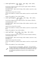
The OP7100 is a serial graphic display in a compact, easy to integrate
module. The OP7100 features an LCD that has a white background with
blue images. The LCD has pixel graphics and provides two-color (monochrome) displays. Five standard fonts are included in the supplied software. Additional custom fonts are easily created to meet the needs of an
application.
The OP7100 can operate with Rabbit Semiconductor single-board computers or other serial displays over an RS-485 network. The OP7100 also
supports RS-232 communication.
The OP7100 display terminal uses display technologies that require minimal mounting depth and offer maximum viewing angles. The memory
allows up to 25 application-screen bitmaps (240 × 320) to be stored without compression in a 256K flash EPROM. A further 256K is available for
the application in a second flash EPROM.
J5
LCD
R15
R14
JP1
J3
Y2
R19 R18
C48
JP5
R31
R35
R54
C61
C60
MV1
R23
C56
RS-232
U26
C3
C59
C39
C40
C42
C52
U27
R55
C30
C32
D1
C38
J8
D5
D2
U19
RN3
J7
C47
Power,
RS-485
485+
C44
485
C6
U28
DCIN
GND
C43
U18
R32
RS232
R29 R30
C33
U17
U24
C46
C12
J10
R25 R26
C2
C45
C13
U4
R51R52
Flash
U16
U15
RS485
TERM.
R24
Contrast
Adjustment
JP4
C57
U25
R28 R27
R53
U6
C37
C26
C54
R13
JP10
U30
Flash
RN2
C31
JP9
Z180
C34
C7
U13
C29
JP8
C100
C51
C105
C4
LCD
C96
R62
Y1 R61
C98
J9
C36
JP3
RTC
U14
C11
R1
C99
JP6
LCD
Control
J1C101
JP7
C97
MV2
C28
SRAM
U5 R60
R2
C102
C95U1
BT1
R22
C35
U23
C62
C55
R12
C50
C10
C104
C103
691
U11 U12
R11
R59
R36
PAL
R10
EPLD
D4
U22
R34
R21
C27
C25
U10
R9
U2
R37
U9
R17
U21
JP2
C24
U8
R8
C106
R38
R39
R40
R41
C20
C22 R50
R42
C19
C21
R47
R16
R20
U7
R7
R6
R56
C9
DANGER! HIGH VOLTAGE
Battery
RN4
C23
C18
R49
R48
R45
R46
C14
C15
C16
C17
R3
R4
Q2
RT2
R33
C49
R44
R43
C8
C53
Q3
J2
U29
RT1
LS1
J6
Q1
R5
to
backlight
KEYPAD
RN1
Transformer
C41
L1
T1
C1
0V / GND
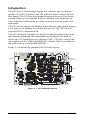
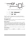
Figure 1-1 illustrates the standard OP7100 board layout.
GND
L2
D3
J11
C58
J4
U20
PRGM PORT
DIGITAL I/O
Figure 1-1. OP7100 Board Layout
12
Overview
OP7100
Features
The OP7100 includes the following features.
•
240 × 320 ¼ VGA LCD (with touchscreen on OP7100 only)
•
jumper-selectable background—positive (blue images on white
background) or negative (white images on blue background)
•
software-controlled cold-cathode fluorescent backlighting
•
software-controlled contrast is enabled/disabled with jumper settting
•
temperature compensation for LCD contrast changes with temperature
•
RS-485 and RS-232 serial communication up to 57,600 bps
•
8 CMOS/TTL-level digital inputs and 8 CMOS/TTL-level digital
outputs
•
18.432 MHz clock with Z180 microprocessor, 9.216 MHz LCD
controller
•
256K flash EPROM for program, 256K flash EPROM for screen bitmaps
•
switching voltage regulator
Appendix B provides detailed specifications for the OP7100.
The OP7100 also includes battery-backed RAM (128K) and a batterybacked real-time clock a watchdog timer, and power-failure interrupt.
Options
The OP7100 series of serial displays has two versions. Table 1-1 lists their
standard features.
Table 1-1. OP7100 Series Features
Model
Features
OP7100
Serial graphic display, touchscreen, blue and white screen,
¼VGA LCD with bezel mount, software contrast control
OP7110
OP7100 with no touchscreen, manual contrast control
Either model may be used in either a portrait or a landscape orientation by
using the corresponding software library.
OP7100
For ordering information, call your Rabbit Semiconuctor
Sales Representative.
Overview 13
Development and Evaluation Tools
The OP7100 is supported by a Tool Kit that include everything you need
to start development with the OP7100.
The Tool Kit includes these items.
•
Serial cable
•
24 V DC power supply capable of delivering 1.1 A
•
User’s manual with schematics
An optional Serial Interface Board (SIB) is available to program the
OP7100 when a second RS-232 serial port is needed by the application
being developed.
For ordering information, call your Rabbit Semiconductor
Sales Representative.
Software
The OP7100 is programmed using Rabbit Semiconductor’s Dynamic C, an
integrated development environment that includes an editor, a C compiler,
and a debugger. Library functions provide an easy and robust interface to
the OP7100.
Rabbit Semiconductor’s Dynamic C reference manuals provide
complete software descriptions and programming instructions.
14
Overview
OP7100
CE Compliance
The OP7100 has been tested and was found to be in
conformity with applicable EN immunity and emission
standards. Note the following requirements for incorporating the OP7100 into your application to comply with CE
requirements.
•
The power supply provided with the Tool Kit is for development
purpose only. It is the customer’s responsibility to provide a CE
compliant power supply for their end-product application.
•
The OP7100 has been tested to meet the following immunity standards.
EN61000-4-2 (ESD)
EN61000-4-3 (Radiated Immunity)
EN61000-4-4 (EFT)
EN61000-4-6 (Conducted Immunity)
Additional shielding or filtering may be required for a heavy industrial
environment.
•
The OP7100 has been tested to meet the EN55022 Class A emissions
standard with ferrite RFI suppressors on the I/O cables. Additional
shielding or filtering may be needed to meet Class B emissions
standards.
Since Rabbit Semiconductor products are connected to other devices, good
EMC prac-tices should be taken to ensure compliance. CE compliance is
eventually the responsibility of the integrator. For more information on tips
and technical assistance, visit our Web site at www.rabbit.com/products/
ce_certification/, or contact your local authorized Rabbit Semiconductor
distributor.
OP7100
Overview
15
16
Overview
OP7100
CHAPTER 2:
GETTING STARTED
Chapter 2 provides instructions for connecting the OP7100 to a host PC
and running a sample program.
OP7100
Getting Started
17
Initial OP7100 Setup
Parts Required
•
24 V unregulated DC power supply capable of delivering up to 1.1 A
•
Serial cable
The necessary parts are supplied with the Tool Kit.
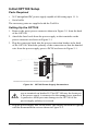
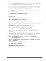
Setting Up the OP7100
1. Remove the green power connector shown in Figure 2-1 from the back
of the OP7100.
2. Attach the bare leads from the power supply to the terminals on the
power connector as shown in Figure 2-1.
3. Plug the connector back into the power connection header at the back
of the OP7100. Watch the polarity of the connection so that the banded
wire from the power supply goes to DCIN as shown in Figure 2-1.
DCIN (1230 VDC)
GND
DCIN
+
485
GND
485
485+
GND
485
5
4
3
2
1
to power
supply
GND
Figure 2-1. OP7100 Power Supply Connections
Be careful to connect the power supply wires to the correct
screw terminals on header J8. The OP7100 may be destroyed
if the power supply is connected to the wrong screw terminal.
A protective diode prevents damage to the OP7100 if the
power supply polarity is reversed.
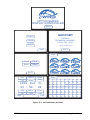
4. Plug the power supply into a wall outlet. The display should now light up
with the demonstration screens shown in Figure 2-2.
18
Getting Started
OP7100
OP7100 SERIES
DISPLAY/CONTROLLER
Menu
SUPPORT
FEATR
Z-WORLD
TECHNICAL SUPPORT
15307573737
DEMO
SUPRT
www.zworld.com
EXIT
EXIT
Clock
Bklit
Exit
Display Bitmaps
Exit
Press Keys Before Tiimeout
Ctrst
Beep
EXIT
+Yr
Yr
1999
+Mon
Mon
Dec
+Day
Day
31
23 : 59 : 59
+Hr
+Min
Hr
Set
Min
+Sec
Sec
Exit
Figure 2-2. OP7100 Demo Screens
OP7100
Getting Started
19
Connecting the OP7100 to a Host PC
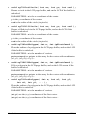
1. Unplug any power supply connected to the OP7100 and remove the
back cover from the OP7100 assembly. The back cover is attached
with the two screws shown in Figure 2-3.
CAUTION: High-Voltage
Transformer. Only qualified
persons may open this case.
CONTRAST
RS232
n.c. 1
TXA 2
RXA 3
n.c. 4
GND 5
6 n.c.
7 232_RX1 / CT
8 232_TX1 / RT
9 PWR_DE9
DCIN (1230 VDC)
GND
485+
485
GND
5
4
3
2
1
S/N:
Figure 2-3. OP7100 Back Cover
2. Establish a serial communication link. A PC “communicates” with the
OP7100 via Serial Port 0 or the Clocked Serial Input/Output port on
the OP7100’s Z180 microprocessor. There are two options for the
serial communication link.
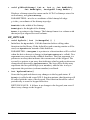
Option 1 (via optional SIB)—Connect an RJ-12 cable between the PC
and the SIB. An RJ-12 to DB9 adapter is included for DB9 PC COM
ports. Remove any jumpers that may be installed on the OP7100’s
header J4 and plug the SIB’s 8-pin connector onto header J4 as shown
in Figure 2-4. Make sure that pin 1 on the ribbon cable connector (on
the striped side) matches up with pin 1 on J4 (indicated by a small
white circle next to the header).
Option 2 (directly)—Place a jumper across pins 1–2 of header J4 on the
OP7100 as shown in Figure 2-5. Connect the PC COM port to the DB9
jack on the OP7100, header J7, using the DB9 to DB9 serial cable
supplied with the Tool Kit.
3. The OP7100 is now ready for programming. The power supply may be
plugged in and turned on.
20
Getting Started
OP7100
Pin 1
J4
PRGM
PORT
Marked
Conductor
to Pin 1
Figure 2-4. SIB Programming Connection
To PC
J4 SIB2
7
5
3
1
8
6
4
2
J4
Figure 2-5. Direct Programming Connection
Option 2 uses an RS-232 serial port to program the OP7100.
If this serial port is needed in your application, use the SIB as
described in Option 1.
See Chapter 3, “Hardware,” for more information on the serial
ports.
OP7100
Getting Started
21
Running Dynamic C
Double-click the Dynamic C icon to start the software. Note that the PC
attempts to communicate with the OP7100 each time Dynamic C is started.
No error messages are displayed once communication is established.
The communication rate, port, and protocol are all selected by choosing
Serial Options from Dynamic C’s OPTIONS menu. The SIB and the
OP7100 both set their baud rate automatically to match the communication
rate set on the host PC using Dynamic C (9600 bps, 19,200 bps, 28,800 bps,
or 57,600 bps). To begin, adjust the communications rate to 19,200 bps.
Make sure that the PC serial port used to connect the serial cable (COM1
or COM2) is the one selected in the Dynamic C OPTIONS menu. Select
the 1-stop-bit protocol.
See Appendix A, “Troubleshooting,” if an error message such
as Target Not Responding or Communication Error appears.
Once the necessary changes have been made to establish
communication between the host PC and the OP7100, use the
Dynamic C shortcut <Ctrl Y> to reset the controller and initiate
communication.
At this point, the LCD should be blank and the backlight should be off.
Once communication is established, load the sample program
DEFDEMOL.C in the Dynamic C SAMPLES\QVGA subdirectory. Compile
and run the program by pressing F9 or by selecting Run from the Run
menu.
The OP7100 should now alternately display the large font (17x × 35h) and
the small font (6w × 8h). The fonts should scroll across the display.
Compiling and running this sample program will overwrite the
demonstration program shown in Figure 2-3.
22
Getting Started
OP7100
CHAPTER 3:
HARDWARE
Chapter 3 describes how to use the OP7100. Sections are included to
describe the following features.
•
Subsystems Overview
•
Power Management
•
Liquid Crystal Display
•
Keyboard Interface
•
Digital I/O
•
Serial Communication
OP7100
Hardware
23
OP7100 Subsystems Overview
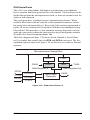
The OP7100 consists of several subsystems, including a computing module,
serial communication channels, lquid crystal display (LCD), a buzzer, and a
keypad interface. Figure 3-1 provides a block diagram of the OP7100.
8
8
Digital
I/O
Z180
SRAM
Batt.
Flash2
RTC
’691
super.
LCD
Control
RS-232
RS-485
Flash1
VRAM1
VRAM2
EPLD
Backlight
Drive
8
Sense
8
LCD
320 x 240
Keypad
Interface
Buzzer
Optional Software
Contrast Adjustment
Touchscreen
Contrast Adjustment
Figure 3-1. OP7100 Block Diagram
Computing Module
The OP7100 computing module consists of a Zilog Z180 microprocessor,
128K of battery-backed static RAM, and 512K of flash EPROM. The
computing module operates in tandem with a real-time clock and a
watchdog timer/microprocessor supervisor.
The Z180 CPU runs at 18.432 MHz, and the LCD controller runs at
9.216 MHz.
The watchdog timer/microprocessor chip provides a watchdog timer
function, power-failure detection, RAM protection, and battery backup.
The real-time clock provides time and date information to applications
running on the OP7100.
The EEPROM is simulated in flash EPROM for consistency
with Rabbit Semiconductor controllers whose software
libraries rely on exchanging information with the EEPROM.
The simulated EEPROM in the OP7100 is unused at the
present time, but addresses 0 and 1 are reserved for furture
use. Do not use these addresses in your application.
24
Hardware
OP7100
Power Management
The OP7100 was designed to operate from a 12 V to 30 V DC source, and
consumes about 4.5 W with the backlight on, 1.5 W with the backlight off.
To allow for a surge current when the OP7100 is first turned on, the power
supply used must be able to handle at least four times this power (for
example, 800 mA at 24 V).
The OP7100 power supply is converted internally to supply three voltages.
1. A switching regulator outputs VCC (+ 5 V).
2. A linear regulator outputs VEE (approximately –20 V).
3. A high-voltage section supplies 300 V rms to drive the cold-cathode
fluorescent backlight. The backlight can be turned on or off under
software control whereby a high on the gate of Q3 enables Q1 and Q2 to
oscillate, and a low turns off Q3, stopping the oscillation of Q1 and Q2.
Figure 3-2 shows these internal power supplies in a block diagram
1230 V DC
VCC
U28
J10:9
2575
Sw Reg
U27
2951
Lin Power
J11:5
1230 V DC
U25
7662
Sw Reg
U23
VEE
7662
Sw Reg
VCC
Backlight
Power
300 V rms, 32.7 kHz,
to CCFL backlight
Q3
from EPLD
Figure 3-2. Block Diagram of OP7100 Internal Power Regulators
The DC input source can also be brought out on pin 9 of header J10, the
DE-9 connector, by installing a 0 Ω resistor at R32. This option allows
power to be supplied to a serial device connected to the OP7100 as long as
the serial device’s RS-232 port can handle the DC input on pin 9.
Be sure to use a power supply with sufficient capacity (for
example, 1.1 A at 24 V) to handle surges when the OP7100
and any devices connected to it are first turned on.
OP7100
Hardware
25
ADM691 Supervisor Chip
A voltage divider consisting of R29 and R30 across the DC input provides
a PFI signal to the ADM691 watchdog supervisor. The ADM691 chip
performs the following services.
•
Watchdog timer resets the microprocessor if software “hangs.”
•
Power-failure shutdown and reset.
•
Generates an “early warning” power-failure interrupt (PFI) that lets the
system know when power is about to fail.
•
Memory protection feature prevents writes to RAM when power is low.
•
Supports battery backup.
Handling Power Fluctuations
During a normal power-down, an interrupt service routine is used in
response to a power-failure interrupt to save vital state information for the
application for when power recovers. The amount of code that the interrupt
service routine can execute depends on how fast the voltage decreases.
Theoretically, a power failure would cause a single power-failure interrupt.
Then, the interrupt service routine would restore data from the previous
state when the voltage recovers.
However, fluctuations in the DC input line could cause the ADM691 to see
multiple crossings of the 1.3 V input power-reset threshold. These multiple
negative-edge transitions would, in turn, cause the Z180 to see multiple
power-failure interrupts.
The ADM691 generates a power-failure interrupt, INT1. After reset, INT1
must be enabled by a write into the ITC register as well as execution of the
EI instruction followed by a RETI instruction. The Z180 will restore saved
state information when it executes the RETI instruction.
Ideally, the Z180 should be able to pop the stack and return to the location
where the program was first interrupted. Also, depending on the number of
fluctuations of the DC input (and hence, the number of stacked powerfailure interrupts), the processor’s stack can overflow, possibly into your
program’s code or data.
The following sample program shows how to handle a power-failure
interrupt.
26
Hardware
OP7100
main(){
...
}
...
char dummy[24];
...
#define INT1_BIT
0
; bit 0
#INT_VEC INT1_VEC power_fail_isr
#asm
power_fail_isr::
ld
sp,dummy+24
;
;
;
;
force stack pointer
to top of dummy vector
to prevent overwriting
code or data
do whatever service, within allowable execution time
loop:
call hitwd
;
;
ld
bc,INT1
;
;
in
a,(c)
;
;
bit INT1_BIT, a ;
jr
nz,loop
;
;
timeout:
;
;
jp
timeout
;
#endasm
make sure no watchdog reset
while low voltage
load the read INT1 register
to bc
read the read INT1 register
for /PFO
check for status of /PFO
wait until the brownout
clears
then...a tight loop to
force a watchdog timeout,
resetting the Z180
Of course, if the DC input voltage continues to decrease, then the OP7100
will just power down.
Call the Dynamic C function hitwd during the power-failure service
routine to make sure that the watchdog timer does not time out and thereby
reset the processor. The controller can continue to run at low voltages, and
so it might not be able to detect the low-voltage condition after the
watchdog timer resets the processor.
Watchdog Timer
To increase reliability, the ADM691’s watchdog timer forces a system reset if
a program does not notify the supervisor nominally at least every second. The
assumption is that if the program fails to “hit” the watchdog, the program
must be stuck in a loop or halted. The Dynamic C function for hitting the
OP7100
Hardware
27
watchdog timer is hitwd. To hold the watchdog timer at bay, make a call to
hitwd in a routine that runs periodically at the lowest software priority level.
A program can read the state of the WDO line with a call to wderror. This
makes it possible to determine whether a watchdog timeout occurred. The
following sample program shows how to do this when a program starts or
restarts.
main(){
if( wderror() ) wd_cleanup();
hitwd();
...
}
Power Shutdown and Reset
When VCC (+5 V) drops below VMIN (between 4.5 V and 4.75 V), the
ADM691 supervisor asserts /RESET and holds it until VCC goes above
VMIN and stays that way for at least 50 ms. This delay allows the system’s
devices to power up and stabilize before the CPU starts.
PFI “Early Warning”
When PFI drops below 1.3 V ± 0.05 V (i.e., DCIN drops below ~10 V),
the supervisor asserts /NMI (nonmaskable interrupt), and allows the
program to clean up and get ready for shutdown. The underlying assumption here is that PFI will cause the interrupt during a power failure before
the ADM691 asserts /RESET.
In order to improve the performance of the power-failure interrupt circuit,
we have added some hysteresis to the power-failure comparator by adding
a resistor, R34, between the comparator input and output pins. R34 can be
found on the 175-0196 and the 175-0211 versions of the OP7100. The
hysteresis prevents the comparator from switching rapidly—and therefore
generating multiple interrupts—when the input voltage is falling slowly.
Once the comparator switches (DC IN falls to approximately 8.5 V), this
feedback holds the input (PFI) low and prevents further interrupts from
being generated. At this point, the 5 V regulator still has sufficient voltage to
keep the processor operating, so that an interrupt service routine can
perform shutdown tasks and “tidying up” before the Vcc line fails. The
comparator will not turn the output (PFO) high until DC IN has risen to
about 9.2 V. The hysteresis will also help prevent any system oscillation in
adverse power supply/loading situations.
The voltage at which the power-failure interrupt occurs may be changed by
adjusting the values of R29 and R30, which are shown in Figure 3-3. To
calculate the values of these components, let VL be the voltage at which
PFO turns off as DC IN falls, and let VH be the voltage at which PFO turns
on as DC IN rises.
28
Hardware
OP7100
U28 Reg.
DCIN
VIN
VCC
VCC
VOUT
U12 Supervisor
VOUT
C44
47 µF
RN2
10 kW
VBAT
R30
29.4 kW
PFI to supervisor
R29
4.99 kW
WDI
WDO
PFI
PFO
RST
RST
INT1
R34
220 kW
Figure 3-3. OP7100 Power-Failure Detection Circuit
⎡ ⎛ R30 ⎞ ⎛ R30(5 V - 1.3 V) ⎞⎤
⎟⎟⎥
VL = 1.3 V ⎢1 + ⎜
⎟ − ⎜⎜
⎢⎣ ⎝ R29 ⎠ ⎝ 1.3 V(R34 + RN2) ⎠⎥⎦
⎡ ⎛ R30 ⎞ ⎛ R30 ⎞⎤
VH = 1.3 V ⎢1 + ⎜
⎟⎥
⎟+⎜
⎣ ⎝ R29 ⎠ ⎝ R34 ⎠⎦
Since R34 >> RN2, the difference between VH and VL, the hysteresis
voltage, would be 5 V × (R30/R34). For a nominal hysteresis voltage of
1.25 V, R30 = 0.25 × R34.
Memory Protection
When /RESET is active, the ADM691 supervisor disables the RAM chipselect line, preventing accidental writes.
Battery Backup
The backup battery protects data in the RAM and the real-time clock (RTC).
VRAM, the voltage supplied to the RAM and RTC, can also protect other
devices attached to the system against power failures. The ADM691 supervisor switches VRAM to VBAT or VCC, whichever is greater. (To prevent
“hunting,” the switchover actually occurs when Vcc is 50 mV higher than
VBAT.)
The circuit draws no current from the battery once regular power is applied.
System Reset
The ADM691 chip drives the /RESET line. The /RESET line is not pulled
up internally.
OP7100
Hardware
29
Liquid Crystal Display (LCD)
The 240 × 320 ¼ VGA LCD supports both graphics and text. Automatic
contrast control is built in so that the contrast, once set, does not drift as
the OP7100 warms up or is moved.
Figure 3-4 provides a block diagram of the LCD control and RAM circuits.
U3
A0
D[0–7]
VA[0–14]
VD[0–7]
U2
FRAME
ON/OFF
/RESET XD[0–3]
/INT0
U1
A[0–14]
D[0–7]
SED1335F
LCD Control
VRAMCS1
VCC
/CS
A[0–14]
D[0–7]
RAM
VCC
VRAMCS2
VCC
/CS
RAM
VCC
FRAME
ON/OFF
VCC
XD[0–3]
R26
10 kΩ
R31
2.5 kΩ
Manual
Software Contrast
Adjustment
VCC
VEE
LCD
+
ADJUST
Figure 3-4. Block Diagram LCD Control and Memory
The LCD is connected to the OP7100
circuit board through header J1 or J3
on the circuit board.
Contrast Adjustment
Figure 3-5 shows the location of the
manual contrast adjustment. This contrast adjustment is the factory default for
the OP7110. The OP7100 is configured
with software contrast control as the factory default. With software contrast control, the contrast level may be set via a
software function call. Since it is hard
to guess the correct level in software,
buttons defined on the OP7100 touchscreen and in software can be used to
adjust the contrast. A user-supplied keypad can facilitate this type of software
control for the OP7110.
30
Hardware
CONTRAST
Figure 3-5. Location of OP7100
Manual Contrast Adjustment
OP7100
Figure 3-6 shows the jumper settings for the contrast control options.
Software
Contrast
Adjustment
Manual
Contrast
Adjustment
3
3
2
2
1
JP2
JP2
1
FD OP7110
FD OP7100
Figure 3-6. Contrast Control Jumper Configurations
Background
The OP7100 comes factory-configured to display blue characters on a
white (positive) background. The jumpers on header JP1 may be rearranged as shown in Figure 3-7 to display white characters on a blue
(negative) background.
2
4
6
8 10 12
FD
JP1
1
3
5
7
9
11
Positive Background
(white with blue graphics)
2
4
6
8 10 12
1
3
5
7
U4
JP1
JP1
9 11
Negative Background
(blue with white graphics)
Figure 3-7. LCD Background Jumper Settings
OP7100
Hardware
31
Coordinate Systems
Figure 3-8 shows the coordinate systems for the touchscreen and the LCD.
LCD
Touchscreen
7,0
7,7
0,0
320,0
landscape
landscape
0,0
0,7
0,7
7,7
portrait
7,0
0,240
320,240
240,0
0,0
portrait
0,0
0,320
240,320
Figure 3-8. Coordinate Systems
(row, column)
LCD Controller Chip
The LCD controller chip provides support for the LCD module. The
controller chip is attached to the data bus on the OP7100, and is mapped to
the I/O address space. This interface is composed of eight data bits, one
address line, and three control lines (RD, WR, and 1335-CS).
The interface from the LCD controller to the LCD module is unidirectional.
Data flow from the controller chip to the LCD module. A number of control
lines are provided for this function, but not all of them are used for a particular LCD module. The controller continually reads the SRAM for data
placed there by the microprocessor, and refreshes the display periodically.
32
Hardware
OP7100
Other functions support the LCD module to adjust its contrast and to turn
the white CCFL backlight on and off. A variable resistor between two of
the LCD module’s terminals sets the contrast, which is set either by software or manually, depending on the jumper setting on header JP2. Once a
contrast value is set, it will be maintained. A single programmed I/O bit is
used to turn the backlight on or off.
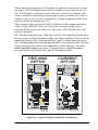
The controller chip used in OP7100’s sold before 2006 supported either
32K or 64K of SRAM. These OP7100s were designed using a dualfootprint SRAM to accept either one 32K or two 32K SRAM. One 32K
part was standard.
OP7100 units sold after June, 2006, have a new LCD controller chip because
the previously used LCD controller chip is no longer available. The new LCD
controller chip has 32K of internal SRAM. Figure 3-9 shows the area of the
OP7100 that changed to accommodate the new LCD controller chip. The new
LCD controller is not 100% code-compatible with the old chip—the New
LCD Controller Chip section on p. 73 explains how to handle programs
developed for an OP7100 for the older LCD controller chip.
PRE-2006
OP7100
CURRENT
OP7100
T1
T1
J2
Q3
RT1
Q2
DANGER! HIGH VOLTAGE
C2
Q2
DANGER! HIGH VOLTAGE
C104
C3
C10
C10
U1
Q3
J2
RT2
R33
C49
R56
R33
C49
R56
RT1
R4
Transformer
C1
C8
Transformer
R4
C1
U2
U2
C106
C103
C12
R51R52
C98
C51
C105
R1
JP8
C100
JP10
U30
U6
C12
U4
R51R52
JP1
C51
C4
U6
U4
JP1
C96
R62
Y1 R61
R2
C7
C4
C5
JP6
JP9
R1
LCD
LCD
C6
Y1
JP7
C97
LCD
Control
J1C101
C7
J1
C95U1
C99
C102
LCD
Control
R2
U3
J3
Figure 3-9. How to Identify Pre-2006 OP7100 Boards
OP7100
Hardware 33
Keypad Interface
The OP7100 has a touchscreen, which is connected to the circuit board at
header J5. Header J6 is available for a customer-supplied keypad for the
OP7110.
Table 3-1 lists the pinouts for headers J5 and J6. The pinout for header J5
is identical to the pinout for header J6.
Table 3-1. OP7100 Keypad Header Pinout
Signal
Header J5/J6 Pin
Signal
Header J5/J6 Pin
ROW0
1
COL0
9
ROW1
2
COL1
10
ROW2
3
COL2
11
ROW3
4
COL3
12
ROW4
5
COL4
13
ROW5
6
COL5
14
ROW6
7
COL6
15
ROW7
8
COL7
16
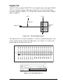
Figure 3-10 shows the location of headers J5 and J6.
J5
J6
Figure 3-10. OP7100 Headers J5 and J6 (Keypad Interface)
Figure 3-11 shows a simplified diagram of the keypad interface.
U8, U9
Q[07]
8
ROW[07]
VCC
U10
D[07]
/COLUMN
8
Y[07] A[07]
74HC244
RN1
47 kΩ
COL[07]
8
C14C21
1 nF
Keypad/Buzzer drive
To J5 (or to J6) keypad
connectors
Keypad sense
Figure 3-11. Block Diagram of OP7100 Keypad Interface
34
Hardware
OP7100
Digital I/O
The OP7100 has eight CMOS/TTL-level digital inputs and eight CMOS/
TTL-level digital outputs. The digital inputs are provided with pullup
resistors, shown in Figure 3-12, to provide a known state before a digital
input is applied..
+5 V
+5 V
10 kΩ
To Z180
Data
Bus
DIN[07]
CMOS
Input
Figure 3-12. OP7100 Digital Inputs
GND
GND
GND
GND
GND
GND
GND
GND
GND
GND
1
3
5
7
9
OUT4
GND
8 10 12 14 16 18 20 22 24 26 28 30 32 34
OUT3
GND
GND
6
OUT2
GND
GND
4
OUT1
GND
GND
2
OUT0
The digital I/O are located on header J7, and are available through a connector on the outside of the OP7100 back cover. Figure 3-13 shows the
pinout and the location of header J7.
J7
VCC
DIN7
DIN6
DIN5
DIN4
DIN3
DIN2
DIN1
DIN0
OUT7
OUT6
OUT5
11 13 15 17 19 21 23 25 27 29 31 33
J7
Figure 3-13. OP7100 Header J7
OP7100
Hardware
35
Serial Communication
Two serial channels support asynchronous communication at baud rates
from 300 bps to 57,600 bps. Serial communication provides a simple and
robust means for networking controllers and other devices.
Figure 3-14 illustrates the configuration of the OP7100 serial channels.
VCC
U24
TXA1
RXA1
EN485
D
A
R
DE
485
RE
to J11
B
U26
TXA0
TX1/RTS
TXA0
RTS0
RXA0
CTS0
RXA0
RX1/CTS
T1IN
T1OUT
T2IN
R1OUT
R2OUT
T2OUT
R1IN
R2IN
to J10 (DE9)
and J8
232A
Figure 3-14. Serial Channels
The factory default configuration for the OP7100 is for one 5-wire RS-232
port (with RTS and CTS) and one half-duplex RS-485 port. An RS-485
channel can provide half-duplex asynchronous communication over
twisted-pair wires for distances up to 3 km. Two other configurations,
shown in Figure 3-14, are one 3-wire RS-232/one RS-485, and two 3-wire
RS-232. The configurations are set with jumpers on header JP3.
JP3
JP3
JP3
1
2
1
2
1
2
3
4
3
4
3
4
5
6
5
6
5
6
7
8
7
8
7
8
9
10
9
10
9
10
11
12
11
12
11
12
5-wire RS-232,
RS-485
3-wire RS-232,
RS-485
two
3-wire RS-232
FD
Figure 3-15. Serial Communication Jumper Configurations
36
Hardware
OP7100
The jumpers on header JP4 may be reconfigured so that header J11 carries
the Z180 Port 1 TX1 and RX1 RS-232 signals on pins 2 and 3 instead of
the factory-default RS-485+ and RS-485– signals.
Figure 3-16 shows the header JP4 jumper configurations and the location
of headers JP3 and JP4.
JP4
JP4
JP5
1
2
1
2
3
4
3
4
5
6
5
6
7
8
7
8
RS-485 on
header J11
RS-232 on
header J11
JP4
JP3
FD
Figure 3-16. Serial Communication Options for
External Plug Connector (Header J11)
OP7100
Hardware
37
RS-232 Communication
2
4
6
RTS/TX1
CTS/RX1
Figure 3-17 shows the RS-232 signals on header J8 and header J10 (the
DE-9 connector).
8 10
9
J8
8
6
7
9
5
4
3
2
1
RX0
TX0
7
GND
5
CTS/RX1
3
RTS/TX1
1
GND
J10
Figure 3-17. RS-232 Signals
Pin 9 on header J10, the DE-9 connector, may be configured to
carry DCIN, the input voltage, by adding a 0 Ω resistor at R32.
Be careful when connecting other devices to header J10 when
R32 is installed since not all devices can handle DCIN. For
example, PCs are limited to 12 V.
The availability of DCIN on pin 9 of header J7 allows a DC
power supply to be made available to the device being
connected to the OP7100.
Rabbit Semiconductor has RS-232 support libraries for Z180 Ports 0 and
1. The following functional support for serial communication is included.
•
Initializing the serial ports.
•
Monitoring and reading a circular receive buffer.
•
Monitoring and writing to a circular transmit buffer.
•
CTS (clear to send) and RTS (request to send) control for Z180 Port 0.
Receive and Transmit Buffers
Serial communication is easier with a background interrupt routine that
updates receive and transmit buffers. Every time a port receives a character, the interrupt routine places it into the receive buffer. A program can
read the data one character at a time or as a string of characters terminated
by a special character.
38
Hardware
OP7100
A program sends data by writing characters into the transmit buffer. If the
serial port is not already transmitting, the write functions will automatically
initiate transmission. Once the last character of the buffer is sent, the
transmit interrupt is turned off. A high-level application can write data one
character at a time or in a string.
CTS/RTS Control
The Z180’s hardware constrains its Port 0 to have the CTS (clear to send)
pulled low by the RS-232 device to which it is talking. The OP7100 does
not support CTS for the Z180’s Port 1.
Modem Communication
Modems and telephone lines facilitate RS-232 communication across great
distances.
The Dynamic C RS-232 library supports communication with a Hayes Smart
Modem or compatible. The CTS, RTS and DTR lines of the modem are not
used. If the modem used is not truly Hayes Smart Modem compatible, tie the
CTS, RTS and DTR lines on the moModem
OP7100
dem side together. The CTS and RTS
Side
Side
lines on the controller also have to
be tied together. A “NULL-modem”
RX
RX
cable is also required for the TX and
TX
TX
RX lines. A commercial NULL-moGND
GND
dem cable would have its CTS and
RTS
RTS
RTS lines tied together already on
CTS
CTS
both sides.
DTR
Figure 3-18 shows the wiring for
connections between a modem and
the OP7100.
OP7100
Figure 3-18. Connections Between
Controller and Modem
Hardware
39
RS-485 Communication
Figure 3-19 shows the RS-485 signals on header J11.
DCIN (1230 V DC)
GND
485+
485
GND
Developing an RS-485
Network
The 2-wire RS-485 serial-communication port and Dynamic C network software are used to develop
an RS-485 network.
5
4
3
2
1
HV11
HV12
PIN12
PIN13
485–
HV10
PIN11
485+
HV09
PIN10
GND
HV08
PIN09
PIN16
HV07
+5V
HV14
HV06
PIN08
HV13
HV05
PIN07
PIN15
HV04
PIN06
PIN14
HV03
PIN05
K
HV02
+DC
GND
HV01
RUN
PIN04
PROGRAM
PIN03
PIN01
GND
PIN02
The OP7100 can be linked together
Figure 3-19. RS-485 Signals
with other Rabbit Semiconductor
controllers over a twisted-pair network for up to 1.2 km. When configuring a
multidrop network, use single twisted-pair wires to connect RS-485+ to RS485+ and RS-485- to RS-485- as shown in Figure 3-20.
CAUTION: High-Voltage
Transformer. Only qualified
persons may open this case.
CONTRAST
RS232
n.c. 1
TXA 2
RXA 3
n.c. 4
GND 5
6 n.c.
7 232_RX1/ CT
8 232_TX1/ RT
9 PWR_DE9
DCIN (1230 VDC)
GND
485+
485
GND
5
4
3
2
1
S/N:
Figure 3-20. RS-485 Network
40
Hardware
OP7100
Any Rabbit Semiconductor controller or the OP7100 can be a master or a
slave. A network can have up to 255 slaves, but only one master.
A multidrop network requires termination/bias resistors to minimize reflections (echoing) and to keep the network line active during an idle state. The
OP7100 termination resistors are already installed, and by default are enabled by having jumpers installed on header J9. Remove the jumpers from
header J9, as shown in Figure 3-21, to disable or remove the termination
resistors. Only the first and last devices on a multidrop RS-485 network should
have the termination resistors enabled.
2
4
FD
J9
1
3
Termination Resistors
Enabled
2
4
1
3
J9
J9
J10
Termination Resistors
Disabled
Figure 3-21. Enabling/Disabling Termination Resistors
Only a single, solid conductor should be placed in a screw clamp terminal.
Bare copper, particularly if exposed to the air for a long period before
installation, can become oxidized. The oxide can cause a high-resistance
(~20 Ω) connection, especially if the clamping pressure is not sufficient.
To avoid oxidation, use tinned wires or clean, shiny copper wire. If you are
using multiple conductors or stranded wire, consider soldering the wire
bundle or using a crimp connector to avoid a later loss of contact pressure
to a spontaneous rearrangement of the wire bundle. Note that soldering a
stranded wire may make the wire subject to fatigue failure at the junction
with the solder if there is flexing or vibration.
OP7100
Hardware
41
Use of the Serial Ports
If you plan to use the serial ports extensively, or if you intend to use synchronous communications, Rabbit Semiconductor recommends that you
obtain copies of the following Zilog technical manuals, available from
Zilog, Inc, in Campbell, California.
Z180 MPU User’s Manual
Z180 SIO Microprocessor Family User’s Manual
Each serial port appears to the CPU as a set of registers. Each port can be
accessed directly with the inport and outport library functions using
the symbolic constants shown in Table 3-2.
Table 3-2. Z180 Serial Port Registers
Address
42
Name
Description
00
CNTLA0
Control Register A, Serial Channel 0
01
CNTLA1
Control Register A, Serial Channel 1
02
CNTLB0
Control Register B, Serial Channel 0
03
CNTLB1
Control Register B, Serial Channel 1
04
STAT0
Status Register, Serial Channel 0
05
STAT1
Status Register, Serial Channel 1
06
TDR0
Transmit Data Register, Serial Channel 0
07
TDR1
Transmit Data Register, Serial Channel 1
08
RDR0
Receive Data Register, Serial Channel 0
09
RDR1
Receive Data Register, Serial Channel 1
Hardware
OP7100
Z180 Serial Ports
The Z180’s two independent, full-duplex asynchronous serial channels
have a separate baud-rate generator for each channel. The baud rate can be
divided down from the microprocessor clock, or from an external clock for
either or both channels.
The serial ports have a multiprocessor communications feature. When
enabled, this feature adds an extra bit to the transmitted character (where
the parity bit would normally go). Receiving Z180s can be programmed to
ignore all received characters except those with the extra multiprocessing
bits enabled. This provides a 1-byte attention message that can be used to
wake up a processor without the processor having to intelligently monitor
all traffic on a shared communications link.
The block diagram in Figure 3-22 shows Serial Channel 0. Serial Channel 1 is similar, but control lines for /RTS and /DCD do not exist. The five
unshaded registers shown in Figure 3-22 are directly accessible as internal
registers.
Microprocessor Internal Bus
RXA0
RDR0
TDR0
RSR0
TSR0
Shift Register In
/RTS0
/CTS0
/DCD0
CNTLA0
CNTLB0
Baud-Rate
Generator
TXA0
Shift Register Out
CKA0
STAT0
Figure 3-22. Z180 Serial Channel 0
OP7100
Hardware
43
The serial ports can be polled or interrupt-driven.
A polling driver tests the ready flags (TDRE and RDRF) until a ready
condition appears (transmitter data register empty or receiver data register
full). If an error condition occurs on receive, the routine must clear the
error flags and take appropriate action, if any. If the /CTS line is used for
flow control, transmission of data is automatically stopped when /CTS
goes high because the TDRE flag is disabled. This prevents the driver from
transmitting more characters because it thinks the transmitter is not ready.
The transmitter will still function with /CTS high, but exercise care
because TDRE is not available to synchronize loading the data register
(TDR) properly.
An interrupt-driven port works as follows. The program enables the
receiver interrupt as long as it wants to receive characters. The transmitter
interrupt is enabled only while characters are waiting in the output buffer.
When an interrupt occurs, the interrupt routine must determine the cause:
receiver data register full, transmitter data register empty, receiver error, or
/DCD0 pin high (channel 0 only). None of these interrupts is edgetriggered. Another interrupt will occur immediately if interrupts are reenabled without disabling the condition causing the interrupt. The signal
/DCD0 is grounded on the OP7100.
Table 3-3 lists the interrupt vectors.
Table 3-3. Serial Port Interrupt Vectors
44
Address
Name
0E
SER0_VEC
Z180 Serial Port 0 (higher priority)
10
SER1_VEC
Z180 Serial Port 1
Hardware
Description
OP7100
Asynchronous Serial Communication Interface
The Z180 incorporates an asynchronous serial communication interface
(ACSI) that supports two independent full-duplex channels.
ASCI Status Registers
A status register for each channel provides information about the state of
each channel and allows interrupts to be enabled and disabled.
STAT0 (04H)
7
6
5
4
3
2
1
0
RDRF
OVRN
PE
FE
RIE
/DCD0
TDRE
TIE
R
R
R
R
R/W
R
R
R/W
STAT1 (05H)
7
6
5
4
3
2
1
0
RDRF
OVRN
PE
FE
RIE
CTS1E
TDRE
TIE
R
R
R
R
R/W
R
R
R/W
/DCD0 (Data Carrier Detect)
This bit echoes the state of the /DCD0 input pin for Channel 0. However,
when the input to the pin switches from high to low, the data bit switches
low only after STAT0 has been read. The receiver is held to reset as long
as the input pin is held high. This function is not generally useful because
an interrupt is requested as long as /DCD0 is a 1. This forces the programmer to disable the receiver interrupts to avoid endless interrupts. A better
design would cause an interrupt only when the state of the pin changes.
This pin is tied to ground in the CM7000.
TIE (Transmitter Interrupt Enable)
This bit masks the transmitter interrupt. If set to 1, an interrupt is requested
whenever TDRE is 1. The interrupt is not edge-triggered. Set this bit to 0
to stop sending. Otherwise, interrupts will be requested continuously as
soon as the transmitter data register is empty.
TDRE (Transmitter Data Register Empty)
A 1 means that the channel is ready to accept another character. A high
level on the /CTS pin forces this bit to 0 even though the transmitter is
ready.
OP7100
Hardware
45
CTS1E (CTS Enable, Channel 1)
The signals RXS and CTS1 are multiplexed on the same pin. A 1 stored in
this bit makes the pin serve the CTS1 function. A 0 selects the RXS
function. (The pin RXS is the CSI/O data receive pin.) When RXS is
selected, the CTS line has no effect.
RIE (Receiver Interrupt Enable)
A 1 enables receiver interrupts and 0 disables them. A receiver interrupt is
requested under any of the following conditions: /DCD0 (Channel 0 only),
RDRF (read data register full), OVRN (overrun), PE (parity error), and FE
(framing error). The condition causing the interrupt must be removed before the interrupts are re-enabled, or another interrupt will occur. Reading
the receiver data register (RDR) clears the RDRF flag. The EFR bit in
CNTLA is used to clear the other error flags.
FE (Framing Error)
A stop bit was missing, indicating scrambled data. This bit is cleared by the
EFR bit in CNTLA.
PE (Parity Error)
Parity is tested only if MOD1 in CNTLA is set. This bit is cleared by the
EFR bit in CNTLA.
OVRN (Overrun Error)
Overrun occurs when bytes arrive faster than they can be read from the
receiver data register. The receiver shift register (RSR) and receiver data
register (RDR) are both full. This bit is cleared by the EFR bit in CNTLA.
RDRF (Receiver Data Register Full)
This bit is set when data is transferred from the receiver shift register to the
receiver data register. It is set even when one of the error flags is set, in
which case defective data is still loaded to RDR. The bit is cleared when
the receiver data register is read, when the /DCD0 input pin is high, and by
RESET and IOSTOP.
46
Hardware
OP7100
ASCI Control Register A
Control Register A affects various aspects of the asynchronous channel
operation.
CNTLA0 (00H)
7
6
5
4
3
2
1
0
MOD2
MOD1
MOD0
MPE
RE
TE
/RTS0
MPBR/
EFR
R/W
R/W
R/W
R/W
R/W
R/W
R/W
R/W
5
4
3
2
1
0
MOD2
MOD1
MOD0
R/W
R/W
R/W
CNTLA1 (01H)
7
6
MPE
RE
TE
R/W
R/W
R/W
MPBR/
CKA1D
EFR
R/W
R/W
MOD0–MOD2 (Data Format Mode Bits)
MOD0 controls stop bits: 0 ⇒ 1 stop bit, 1 ⇒ 2 stop bits. If 2 stop bits are
expected, then 2 stop bits must be supplied.
MOD1 controls parity: 0 ⇒ parity disabled, 1 ⇒ parity enabled. (See PEO
in ASCI Control Register B for even/odd parity control.)
MOD2 controls data bits: 0 ⇒ 7 data bits, 1 ⇒ 8 data bits.
MPBR/EFR (Multiprocessor Bit Receive/Error Flag Reset)
Reads and writes on this bit are unrelated. Storing a byte when this bit is 0
clears all the error flags (OVRN, FE, PE). Reading this bit obtains the
value of the MPB bit for the last read operation when the multiprocessor
mode is enabled.
/RTS0 (Request to Send, Channel 0)
Store a 1 in this bit to set the RTS0 line from the Z180 high. This bit is
essentially a 1-bit output port without other side effects.
CKA1D (CKA1 Disable)
This bit controls the function assigned to the multiplexed pin (CKA1/
~TEND0): 1 ⇒ ~TEND0 (a DMA function) and 0 ⇒ CKA1 (external
clock I/O for Channel 1 serial port).
TE (Transmitter Enable)
This bit controls the transmitter: 1 ⇒ transmitter enabled, 0 ⇒ transmitter
disabled. When this bit is cleared, the processor aborts the operation in
progress, but does not disturb TDR or TDRE.
OP7100
Hardware
47
RE (Receiver Enable)
This bit controls the receiver: 1 ⇒ enabled, 0 ⇒ disabled. When this bit is
cleared, the processor aborts the operation in progress, but does not disturb
RDRF or the error flags.
MPE (Multiprocessor Enable)
This bit (1 ⇒ enabled, 0 ⇒ disabled) controls multiprocessor communication mode which uses an extra bit for selective communication when a
number of processors share a common serial bus. This bit has effect only
when MP in Control Register B is set to 1. When this bit is 1, only bytes
with the MP bit on will be detected. Others are ignored. If this bit is 0, all
bytes received are processed. Ignored bytes do not affect the error flags or
RDRF.
ASCI Control Register B
Control Register B configures the multiprocessor mode, parity, and baud
rate for each channel.
CNTLB0 (02H) and CNTLB1 (03H)
7
6
5
4
3
2
1
0
MPBT
MP
/CTS
PS
PEO
DR
SS2
SS1
SS0
R/W
R/W
R/W
R/W
R/W
R/W
R/W
R/W
SS (Source/Speed Select)
Coupled with the prescaler (PS) and the divide ratio (DR), the SS bits select
the source (internal or external clock) and the baud rate divider, as shown
in Table 3-4.
Table 3-4. Baud Rate Divide Ratios
for Source/Speed Select Bits
*
48
Hardware
SS2
SS1
SS0
Divide Ratio
0
0
0
0
1
1
1
1
0
0
1
1
0
0
1
1
0
1
0
1
0
1
0
1
÷1
÷2
÷4
÷8
÷ 16
÷ 32
÷ 64
external clock*
May not exceed system clock ÷ 40
OP7100
The prescaler (PS), the divide ratio (DR), and the SS bits form a baud-rate
generator, as shown in Figure 3-23.
Processor
Clock
Prescaler
(PS)
÷10
Divider
1
2
or
...
÷30
64
External
Clock
Divide
Ratio
(DR)
16
or
64
Figure 3-23. Z180 Baud-Rate Generator
DR (Divide Ratio)
This bit controls one stage of frequency division in the baud-rate generator.
If 1 then divide by 64. If 0 then divide by 16. This is the only control bit
that affects the external clock frequency.
PEO (Parity Even/Odd)
This bit affects parity: 0 ⇒ even parity, 1 ⇒ odd parity. It is effective only
if MOD1 is set in CNTLA (parity enabled).
/CTS/PS (Clear to Send/Prescaler)
When read, this bit gives the state of external pin /CTS: 0 ⇒ low,
1 ⇒ high. When /CTS is high, RDRF is inhibited so that incoming receive
characters are ignored. When written, this bit has an entirely different
function. If a 0 is written, the baud-rate prescaler is set to divide by 10. If a
1 is written, it is set to divide by 30.
MP (Multiprocessor Mode)
When this bit is set to 1, the multiprocessor mode is enabled. The multiprocessor bit (MPB) is included in transmitted data as shown here.
start bit, data bits, MPB, stop bits
The MPB is 1 when MPBT is 1 and 0 when MPBT is 0.
MPBT (Multiprocessor Bit Transmit)
This bit controls the multiprocessor bit (MPB). When MPB is 1, transmitted bytes will get the attention of other units listening only for bytes with
MPB set.
OP7100
Hardware
49
Table 3-5 relates the Z180’s ASCI Control Register B to the baud rate.
Table 3-5. Baud Rates for ASCI Control Register B
Baud Rate at
9.216 MHz
Baud Rate at
18.432 MHz
(bps)
(bps)
00
57,600
115,200
01
28,800
57,600
02 or 08
14,400
28,800
ASCI
B Value
Baud Rate at
9.216 MHz
Baud Rate at
18.432 MHz
(bps)
(bps)
20
19,200
38,400
21
9600
19,200
22 or 28
4800
9600
ASCI
B Value
03 or 09
7200
14,400
23 or 29
2400
4800
04 or 0A
3600
7200
24 or 2A
1200
2400
05 or 0B
1800
3600
25 or 2B
600
1200
06 or 0C
900
1800
26 or 2C
300
600
0D
450
900
2D
150
300
0E
225
450
2E
75
150
50
Hardware
OP7100
CHAPTER 4:
SOFTWARE
Chapter 4 describes the Dynamic C functions used with the OP7100.
OP7100
Software
51
Supplied Software
Software drivers for controlling the OP7100 are provided with Dynamic C.
Depending on the version of Dynamic C you are using, the OP71L.LIB/
OP71P.LIB or the EZIOOP71.LIB libraries provide drivers specific to the
OP7100. In order to use the OP71L.LIB/OP71P.LIB and other libraries, it
is necessary to include the appropriate Dynamic C libraries in your appplication program. These libraries are listed in Table 4-1.
Table 4-1. OP7100 Software Libraries
Library
Application
AASCZ0.LIB
Serial communication applications Z180 Serial Port 0
AASCZ1.LIB
Serial communication applications Z180 Serial Port 1
BIOS.LIB
BIOS routines
DRIVERS.LIB
General drivers
OP71L.LIB
OP71P.LIB
Select one of these DC 32 libraries to #use first,
corresponding to landscape mode or portrait mode
OP71HW.LIB
DC 32 display hardware functions
EZIOOP71.LIB*
All OP7100 applications
GLCD.LIB*
LCD applications
KP_OP71.LIB
Touchscreen read applications (all DC versions)
LQVGA.LIB*
Landscape image VGA drivers
PQVGA.LIB*
Portrait image VGA drivers
SYS.LIB
General drivers
* Use these libraries with Dynamic C v. 5.xx versions.
Your application can use these libraries by including them in your program. To include these libraries, use the #use directive as shown below.
#use op71l.lib or #use op71p.lib
#use op71hw.lib
Choose the corresponding landscape or portrait libraries from Table 4-1
based on your version of Dynamic C and according to whether you will
use your OP7100 in a landscape or a portrait orientation.
See the Dynamic C Technical Reference manual for more
information on #use and other directives as well as for
information on other libraries.
52
Software
OP7100
Digital I/O
No specific drivers have been written for the OP7100 digital I/O. The
inport and outport functions in the Dynamic C BIOS.LIB library can
be used to read the inputs and write the outputs. The eight digital inputs
(DIN0–DIN7) are bitmapped bits 0 through 7 of the input at 0x4140. Each
digital output (OUT0–OUT7) is controlled by bit 0 at 0x4140 through
0x4147.
For example, OUT2 can be turned on using the following statement.
outport( 0x4142,1 );
Likewise, OUT7 can be turned off using the following statement.
outport( 0x4147,0 );
The inport function reads all eight inputs simultaneously, so the bitwise
AND operator (&) is useful in checking the status of a particular input. For
example, the statement
if( inport(0x4140) & 0x04 )
can be used to check whether DIN2 (whose bit mask is 0x04) is on.
Likewise
if( inport(0x4140) & 0x80 )
can be used to check the status of input DIN7.
The Dynamic C function IBIT can be used to determine the state of one
input bit. For example, to check DIN2 (which is bit 2 of the inputs), use the
statement
if( IBIT(0x4140,2) )
instead of the more complex statement below.
if( inport(0x4140) & 0x04 )
While IBIT works well for the digital inputs, its output equivalents, ISET and IRES, will not work with the digital output
bits because the output register of the OP7100 is write-only.
ISET and IRES will only operate on output registers whose
current state can be read by the processor.
Refer to the Dynamic C Function Reference manual for more
information on the use of these functions.
OP7100
Software
53
The sample program OP71.C below cycles through through the outputs
with one bit high at a time while it displays the state of the digital inputs.
OP71.C
void delay( unsigned wDelay ){
for(;--wDelay;hitwd());
}
void main( void ){
unsigned wAddr;
for (;;)
for(wAddr=0x4140;wAddr<0x4148;++wAddr){
outport( wAddr,0x01 );
printf( "%04x%02x\n",wAddr,inport(0x4140) );
delay( 0x8000 );
outport( wAddr,0x00 );
}
}
Real-Time Clock (RTC)
The OP7100 has an Epson 72423 chip. The chip stores time and date, and
accounts for the number of days in a month, and for leap year. A backup
battery will allow the values in the RTC to be preserved if a power failure
occurs.
The Dynamic C function library DRIVERS.LIB provides the following
RTC functions.
The Dynamic C Function Reference manual describes these
functions and the associated data structure tm.
• tm_rd
Reads time and date values from the RTC.
• tm_wr
Writes time and date values into the RTC.
The following points apply when using the RTC.
1. The AM/PM bit is 0 for AM, 1 for PM. The RTC also has a 24-hour
mode.
2. Set the year to 96 for 1996, 97 for 1997, and so on.
Constantly reading the RTC in a tight loop will result in a loss
of accuracy.
54
Software
OP7100
Display
Flash EPROM
The WriteFlash function in the Dynamic C DRIVERS.LIB library is
used to write data to the program flash EPROM.
• int WriteFlash( unsigned long physical_addr,
char *buf, int count )
Writes count number of bytes pointed to by buf to the program flash
EPROM absolute data location physical_adr. Allocate data location
by declaring the byte arrays as initialized arrays or declare an initialized xdata array. If byte array is declared, conert logical memory to
physical memory with phy_adr(array). For initialized xdata, you
can pass the array name directly.
PARAMETERS: physical_adr is the absolute data location in the
flash EPROM.
*buf is a pointer to the bytes to write.
count is the number of bytes to write.
RETURN VALUES:
0 if WriteFlash is okay.
-1 if the program flash EPROM is not in used.
-2 if physical_addr is inside the BIOS area.
-3 if physical_addr is within the symbol area or the simulated
EEPROM area.
-4 if WriteFlash times out.
The WriteFlash function writes to the program flash
EPROM. See the SYS.LIB section later in this chapter for the
functions associated with the second flash EPROM.
OP7100
Software
55
Dynamic C 32 Libraries
When you are using Dynamic C 32, you must first #use op71l.lib or
#use op71p.lib before the #use op71hw.lib line as shown below.
#use op71l.lib or #use op71p.lib
#use op71hw.lib
Call the #use op71p.lib line to use your OP7100 in a portrait orientation, or call the #use op71l.lib line to use your OP7100 in a landscape
orientation.
OP71HW.LIB
• void op71Init( void );
This call must be used to initialize the OP7100 software and hardware.
It also clears the LCD buffer and screen, sets the contrast to 35, turns
on the LCD power, and turns on the LCD backlight.
• void op71BackLight( int isOn );
Turns the OP7100 backlight on or off.
PARAMETER: isOn turns the OP7100 backlight on or off.
1 to turn backlight on
0 to turn backlight off
• void op71Power( int isOn );
Turns the OP7100 power on or off.
PARAMETER: isOn turns the OP7100 power on or off.
1 to turn power on
0 to turn power off
• void op71SetContrast( unsigned level );
Sets the OP7100 contrast level.
PARAMETER: level is the contrast level (0–63), visibility increases
with a lower level.
• void op71BlankScreen( void );
Blanks (sets to white) the OP7100 screen.
• void op71FillScreen( char pattern );
Fills the OP7100 LCD screen with a pattern. The screen will be set to
all black if the pattern is 0xFF, all white if the pattern is 0x00, and
vertical stripes for any other pattern.
56
Software
OP7100
• void op71BrdOff485( void );
Disables the OP7100's RS-485 driver.
• void op71BrdOn485( void );
Enables the OP7100's RS-485 driver.
• void op71Beep( int onOff );
Controls the OP7100's beeper.
PARAMETER: onOff is non-zero to beep, zero to stop beep.
• void op71BuffLock( void );
Increments the OP7100 LCD screen locking counter. Graphics calls are
recorded in the LCD memory buffer, but are not transferred to the LCD
if the counter is non-zero.
op71BuffLock() and op71BuffUnlock() can be nested up to a
level of 255, but be sure to balance the calls. It is not a requirement to
use these procedures, but a set of op71BuffLock and
op71BuffUnlock bracketing a set of related graphics calls speeds up
the rendering significantly.
• void op71BuffUnlock( void );
Decrements the OP7100 LCD screen locking counter. The contents of
the LCD buffer are transferred to the LCD if the counter goes to zero.
• void op71SetBrushType( int type );
Sets the drawing method (or color) of pixels drawn by subsequent
graphics calls.
PARAMETER: type can be one of the following:
GL_SET or OP71BLACK draws black pixels
GL_CLEAR or OP71WHITE draws white pixels
GL_XOR or OP71XOR draws “oldPixel xor newPixel” pixels
GL_BLOCK or OP71BLACK draws black pixels
• int op71GetBrushType( void );
Gets the current method (or color) of pixels drawn by subsequent
graphics calls.
RETURN: The current brush type.
OP7100
Software
57
• void op71Left1( int left, int top, int cols,
int rows );
Scrolls byte-aligned window left one pixel, right column is filled by
current pixel type (color).
PARAMETERS: left is the left edge of the window, must be evenly
divisible by 8.
top is the top edge of the window.
cols is the number of columns in the window, must be evenly divisible
by 8.
rows is the number of rows in the window.
• void op71Right1( int left, int top, int cols,
int rows );
Scrolls byte-aligned window right one pixel, left column is filled by
current pixel type (color).
PARAMETERS: left is the left edge of the window, must be evenly
divisible by 8.
top is the top edge of the window.
cols is the number of columns in the window, must be evenly divisible
by 8.
rows is the number of rows in the window.
• void op71Up1( int left, int top, int cols,
int rows );
Scrolls byte-aligned window up one pixel, bottom column is filled by
current pixel type (color).
PARAMETERS: left is the left edge of the window, must be evenly
divisible by 8.
top is the top edge of the window.
cols is the number of columns in the window, must be evenly divisible
by 8.
rows is the number of rows in the window.
The op71Left1, op71Right1, op71Up1, and op71Down1
function calls may be called multiple times to provide a smoother
scrolling effect than provided by the scroll function calls. Do
not change the parameters to preserve the window being
scrolled.
58
Software
OP7100
• void op71Down1( int left, int top, int cols,
int rows );
Scrolls byte-aligned window down one pixel, top column is filled by
current pixel type (color).
PARAMETERS: left is the left edge of the window, must be evenly
divisible by 8.
top is the top edge of the window.
cols is the number of columns in the window, must be evenly divisible
by 8.
rows is the number of rows in the window.
• void op71HScroll( int left, int top, int cols,
int rows, int nPix );
Scrolls byte-aligned window right or left, opposite edge is filled by
white pixels.
PARAMETERS: left is the left edge of the window, must be evenly
divisible by 8.
top is the top edge of the window.
cols is the number of columns in the window, must be evenly divisible
by 8.
rows is the number of rows in the window.
nPix is the number of pixels to scroll (negative to scroll left).
• void op71VScroll( int left, int top, int cols,
int rows, int nPix );
Scrolls byte-aligned window up or down, right column is filled by
current pixel type (color).
PARAMETERS: left is the left edge of the window, opposite edge is
filled by white pixels.
top is the top edge of the window.
cols is the number of columns in the window, must be evenly divisible
by 8.
rows is the number of rows in the window.
nPix is the number of pixels to scroll (negative to scroll up).
OP7100
Software
59
• void op71XPutBitmap( int left, int top,
int width, int height, unsigned long bitmap );
Draws bitmap in the specified space. The data for the bitmap are stored
in xmem. Automatically calls op71XPutFastmap if bitmap is bytealigned (left-edge and width each evenly divisible by 8).
PARAMETERS: left is the left edge of the bitmap.
top is the top edge of the bitmap.
width is the width of the bitmap.
height is the height of the bitmap.
bitmap is the address of the bitmap in xmem.
• void op71XPutFastmap( int left, int top,
int width, int height, unsigned long bitmap );
Draws bitmap in the specified space. The data for the bitmap are stored
in xmem.
This function is like op71XPutBitmap, except that it is faster. The
restriction is that the bitmap must be byte-aligned.
PARAMETERS: left is the left edge of the bitmap.
top is the top edge of the bitmap.
width is the width of the bitmap.
height is the height of the bitmap.
bitmap is the address of the bitmap in xmem.
• void op71XGetBitmap( int x, int y, int bmWidth,
int bmHeight, unsigned long xBm );
Gets a bitmap from the LCD page buffer and stores it in xmem RAM.
Automatically calls op71XGetFastmap if the bitmap is byte-aligned
(the left edge and width are each evenly divisible by 8).
PARAMETERS: x is the left edge of the bitmap (in pixels).
y is the top edge of the bitmap (in pixels).
bmWidth is the width of the bitmap (in pixels).
bmHeight is the height of the bitmap (in pixels).
xBm is the xmem RAM storage address.
Figure 3-8 shows the coordinate system for the LCD pixels.
60
Software
OP7100
• void op71XGetFastmap( int x, int y, int bmWidth,
int bmHeight, unsigned long xBm );
Gets a bitmap from the LCD page buffer and stores it in xmem RAM.
This function is like op71XGetBitmap, except that it is faster. The
restriction is that the bitmap must be byte-aligned.
PARAMETERS: x is the left edge of the bitmap (in pixels), and must
be evenly divisible by 8.
y is the top edge of the bitmap (in pixels).
bmWidth is the width of the bitmap (in pixels), and must be evenly
divisible by 8.
bmHeight is the height of the bitmap (in pixels).
xBm is the xmem RAM storage address.
• void op71PlotDot( int x, int y );
Draws a single pixel in the LCD buffer, and on the LCD if the buffer is
unlocked.
PARAMETERS: (x,y) are the coordinates of the dot.
• void op71PlotLine( int x0, int y0,
int x1, int y1 );
Draws a line in the LCD buffer, and on the LCD if the buffer is
unlocked.
PARAMETERS: (x0,y0) are the (x,y) coordinates of one endpoint.
(x1,y1) are the (x,y) coordinates of the other endpoint.
• void op71Block( int x, int y, int bmWidth,
int bmHeight );
Draws a rectangular block in the page buffer, and on the LCD if the
buffer is unlocked.
PARAMETERS: x is the left edge of the pixel.
y is the top edge of the pixel.
bmWidth is the width of the block.
bmHeight is the height of the block.
OP7100
Software
61
• void op71PlotCircle( int xc, int yc, int rad );
Draws a circle in the LCD page buffer, and on the LCD if the buffer is
unlocked.
PARAMETERS: x is the x-coordinate of the center.
y is the y-coordinate of the center.
rad is the radius of the circle (in pixels).
• void op71FillCircle( int xc, int yc, int rad );
Draws a filled circle in the LCD page buffer, and on the LCD if the
buffer is unlocked.
PARAMETERS: x is the x-coordinate of the center.
y is the y-coordinate of the center.
rad is the radius of the circle (in pixels).
• void op71PlotVPolygon( int n, int *pFirstCoord );
Plots the outline of a polygon in the LCD page buffer, and on the LCD
if the buffer is unlocked.
PARAMETERS: n is the number of vertices.
pFirstCoord is a pointer to the array for the vertex with coordinates
(x1,y1), (x2,y2),( x3,y3)...
• void op71FillVPolygon( int n, int *pFirstCoord );
Fills a polygon in the LCD page buffer, and on the LCD screen if the
buffer is unlocked.
PARAMETERS: n is the number of vertices.
pFirstCoord is a pointer to the array for the vertex with coordinates
(x1,y1), (x2,y2),( x3,y3)...
• void op71PlotPolygon( int n, int x1, int y1,
int x2, int y2, ... );
Plots the outline of a polygon in the LCD page buffer, and on the LCD
if the buffer is unlocked.
PARAMETERS: n is the number of vertices.
(x1,y1) are the (x,y) coordinates of the first vertex.
(x2,y2) are the (x,y) coordinates of the first vertex...
62
Software
OP7100
• void op71FillPolygon( int n, int x1, int y1,
int x2, int y2, ... );
Fills a polygon in the LCD page buffer, and on the LCD if the buffer is
unlocked.
PARAMETERS: n is the number of vertices.
(x1,y1) are the (x,y) coordinates of the first vertex.
(x2,y2) are the (x,y) coordinates of the first vertex...
• void op71XFontInit( struct _fontInfo *pInfo,
char pixWidth, char pixHeight,
unsigned startChar, unsigned endChar,
unsigned long xmemBuffer );
Initializes the font descriptor structure, where the font is stored in
xmem. Each font character's bitmap is column major and is bytealigned.
PARAMETERS: pInfo is a pointer to the font descriptor to be
initialized.
pixWidth is the width of each font item (in pixels).
pixHeight is the height of each font item (in pixels).
startChar is the the first printable character in the font (does not
have to be 0).
endChar is the the last printable character in the font.
xmemBuffer is a pointer to a linear array of font bitmaps in xmem.
• unsigned long op71FontChar( unsigned long font,
char letter );
Returns the bitmap address of the character in the font specified.
PARAMETERS: font is the font address in xmem.
letter is the ASCII letter code.
RETURN: xmem bitmap address of the character in the font, column
major and byte-aligned.
OP7100
Software
63
• void op71PutFont( int x, int y,
struct _fontInfo *pInfo, char code );
Puts an entry from the font table to the page buffer, and on the LCD if
the buffer is unlocked. Each font character's bitmap is column major
and byte-aligned.
PARAMETERS: x is the left edge (in pixels).
y is the top edge (in pixels).
pInfo is a pointer to the font descriptor.
code is the code (character) to display.
• int op71GetPfStep( void );
Gets the current op71Printf printing step direction. Each step
direction is independent of the other, and is treated as an 8-bit signed
value. The actual step increments depend on the height and width of the
font being displayed, which are multiplied by the step values.
Use op71SetPfStep to control the x and y printing step direction.
RETURN: The x step is returned in the MSB, and the y step is
returned in the LSB of the integer result.
• void op71SetPfStep( int stepX, int stepY );
Sets the op71Printf printing step direction. The x and y step directions are independent signed values. The actual step increments depend
on the height and width of the font being displayed, which are multiplied by the step values.
Use op71GetPfStep to examine the current x and y printing step
direction.
PARAMETERS: stepX is the op71Printf x step.
stepY is the op71Printf y step.
64
Software
OP7100
• void op71Printf( int x, int y, struct _fontInfo
*pInfo, char *fmt, ... );
Prints a formatted string (much like printf) on the LCD screen. Only
character codes that exist in the font are printed, others are skipped
over. For example, '\b', '\t', '\n', and '\r' (ASCII backspace, tab, new line
and carriage return, respectively) print if they exist in the font, but have
no effect as control characters.
Use op71SetPfStep to control or use op71GetPfStep to examine
the current x and y printing step direction.
PARAMETERS: x is the x-coordinate of the text (left edge).
y is the y-coordinate of the text (top edge).
pInfo is a pointer to the font descriptor.
fmt is a pointer to the format string...
Keypad Programming
The same library used in Dynamic C v. 5.xx, KP_OP71.LIB, is used with
Dynamic C 32. The function calls are described later in this chapter.
OP7100
Software
65
Using Dynamic C v. 5.xx
EZIOOP71.LIB
• void op71BackLight( int onOff )
Turns the backlight of the OP7100 on or off.
PARAMETER: onOff is non-zero to turn the backlight on, zero to
turn the backlight off.
• void op71SetContrast( unsigned contrast )
Controls the contrast of the LCD.
PARAMETER: contrast values range from 0 to 127, 0 for the least
contrast (minimum VEE), 127 for the most contrast (maximum VEE).
• void eioBeep( int onOff )
Turns the buzzer on or off.
PARAMETER: onOff is non-zero to turn the buzzer on, zero to turn
the buzzer off.
GLCD.LIB
• void glFontInit( struct _fontInfo *pInfo,
char pixWidth, char pixHeight,
unsigned startChar, unsigned endChar,
char *bitmapBuffer )
Initializes a font descriptor with the bitmap defined in the root memory.
For fonts with bitmaps defined in xmem, use glXFontInit.
PARAMETERS: pInfo is a pointer to the font descriptor to be
initialized.
pixWidth is the width of each font item (pixWidth must be uniform
for all items).
pixHeight is the height of each font item (pixHeight must be
uniform for all items).
startChar is the offset to the first useable item (useful for fonts for
ASCII or other fonts with an offset).
endChar is the index of the last useable font item.
bitmapBuffer is a pointer to a linear array of the font bitmap. The
bitmap is a column with the major byte aligned.
66
Software
OP7100
• glXFontInit( struct _fontInfo *pInfo,
char pixWidth, char pixHeight,
unsigned startChar, unsigned endChar,
unsigned long xmemBuffer )
Initializes a font descriptor that has the bitmap defined in xmem. For
bitmaps defined in root memory, use glFontInit.
PARAMETERS: pInfo is a pointer to the font descriptor to be
initialized.
pixWidth is the width of each font item (pixWidth must be uniform
for all items).
pixHeight is the height of each font item (pixHeight must be
uniform for all items).
startChar is the offset to the first useable item (useful for fonts for
ASCII or other fonts with an offset).
endChar is the index of the last useable font item.
xmemBuffer is a pointer to a linear array of the font bitmap. The
bitmap is a column with the major byte aligned.
• void glSetBrushType( int type )
Sets the type of brush type and controls how pixels are drawn on the
screen until the next call to glSetBrushType.
PARAMETER: type is the type of the brush. The four macros
described below have been defined for valid values to pass to the
function.
Macro
Description
Effect
GL_SET
Pixels specified by subsequent gl
functions will turn on the LCD
pixels
LCDPix =
LCDPix | newPix
GL_CLEAR
Pixels specified by subsequent gl
functions will turn off the LCD
pixels
LCDPix =
LCDPix & ~newPix
GL_XOR
Pixels specified by subsequent gl
functions will toggle the LCD pixels
LCDPix =
LCDPix ^ newPix
GL_BLOCK
Pixels specified by subsequent gl
functions will be displayed on the
LCD as is
LCDPix = newPix
All four brush types can be used to display text or bitmaps. Do
not use GL_BLOCK for glPlot or glFill graphics primitive
functions.
OP7100
Software
67
• int glInit()
Initializes the LCD module (software and hardware).
RETURN VALUE: the status of the LCD. If the initialization was
successful, this function returns 0. Otherwise, the returned value
indicates the LCD status.
• int glPlotDot( int x, int y )
Plots one pixel on the screen at coordinate (x,y).
PARAMETERS: x is the x coordinate of the pixel to be drawn.
y is the y coordinate of the pixel to be drawn.
RETURN VALUE: Status of the LCD after the operation.
• void glPlotLine( int x1, int y1, int x2, int y2 )
Plots a line on the LCD.
PARAMETERS: x1 is the x coordinate of the first endpoint.
y1 is the y coordinate of the first endpoint.
x2 is the x coordinate of the second endpoint.
y2 is the y coordinate of the second endpoint.
• void glPrintf( int x, int y,
struct _fontInfo *pInfo, char *fmt,... )
Prints a formatted string (much like printf) on the LCD screen.
PARAMETERS: x is the x coordinate of the text (left edge).
y is the y coordinate of the text (top-edge).
*pInfo is the pointer to the font descriptor used for printing on the
LCD screen.
*fmt is the pointer to the format string
• void glPlotCircle( int xc, int yc, int rad )
Draws a circle on the LCD.
PARAMETERS: xc is the x coordinate of the center.
yc is the y coordinate of the center.
rad is the radius of the circle.
• void glFillCircle( int xc, int yc, int rad )
Draws a filled-in circle on the LCD.
PARAMETERS: xc is the x coordinate of the center.
yc is the y coordinate of the center.
rad is the radius of the circle.
68
Software
OP7100
• void glPlotVPolygon( int n, int *pFirstCoord )
Plots a filled-in polygon.
PARAMETERS: n is the number of vertices.
*pFirstCoord is an array of vertex coordinates (x1,y1), (x2,y2), …
• void glPlotPolygon( int n, int x1, int y1,
int x2, int y2,... )
Plots the outline of a polygon.
PARAMETERS: n is the number of vertices.
x1 is the x coordinate of the first vertex.
y1 is the y coordinate of the first vertex.
x2 is the x coordinate of the second vertex.
y2 is the y coordinate of the second vertex.
• void glFillVPolygon( int n, int *pFirstCoord )
Fills in a polygon.
PARAMETERS: n is the number of vertices.
*pFirstCoord is an array of vertex coordinates (x1,y1), (x2,y2), …
• void glFillPolygon( int n, int x1, int y1,
int x2, int y2,... )
Fllls in a polygon.
PARAMETERS: n is the number of vertices.
x1 is the x coordinate of the first vertex.
y1 is the y coordinate of the first vertex.
x2 is the x coordinate of the second vertex.
y2 is the y coordinate of the second vertex.
• void glPutBitmap( int x, int y, int bmWidth,
int bmHeight, char *bm )
Displays a bitmap stored in root memory on the LCD. For bitmaps
defined in xmem memory, use glXPutBitmap.
PARAMETERS: x is the x coordinate of the bitmap left edge.
y is the y coordinate of the bitmap top edge.
bmWidth is the width of the bitmap.
bmHeight is the height of the bitmap.
bm is a pointer to the bitmap. The bitmap format is a column with the
major byte aligned for each column.
OP7100
Software
69
• void glXPutBitmap( int x, int y, int bmWidth,
int bmHeight, unsigned long bmPtr )
Displays a bitmap stored in xmem on the LCD. For bitmaps stored in
root memory, use glPutBitmap.
PARAMETERS: x is the x coordinate of the bitmap left edge.
y is the y coordinate of the bitmap top edge.
bmWidth is the width of the bitmap.
bmHeight is the height of the bitmap.
bmPtr is a pointer to the bitmap. The bitmap format is a column with
the major byte aligned for each column.
KP_OP71.LIB
• void kpInit( int (*changeFn)() )
Initializes the kp module. Call this function before calling other
functions in this library. If the default keypad scanning routine will be
used, use kpDefInit instead of this function.
PARAMETER: changeFn is a pointer to a function that will be called
when the driver detects a change (when kpScanState is called). Two
arguments are passed to the callback function. The first argument is a
pointer to an array that indicates the current state of the keypad. The
second is a pointer to an array that indicates what keypad positions are
changed and detected by kpScanState. The byte offset in the array
represents the line pulled high (row number), and the bits in a byte
represents the positions (column number) read back.
• int kpScanState()
Scans the keypad and detects any changes to the keypad status. If
kpInit is called with a non-NULL function pointer, that function will
be called with the state of the keypad. This function should be called
periodically to scan for keypad activities.
RETURN VALUE: 0 if there is no change to the keypad, non-zero if
there is any change to the keypad.
70
Software
OP7100
• int kpDefStChgFn( char *curState, char *changed )
This is the default state change function for the default get key function
kpDefGetKey. This function is called back by kpScanState when
there is a change in the keypad state. If the current key is not read by
kpDefGetKey, the new key pressed will not be registered.
PARAMETERS: curState points to an array that reflects the current
state of the keypad (bitmapped, 1 indicates key is not currently
pressed).
changed points to an array that reflects the CHANGE of keypad state
from the previous scan. (bitmapped, 1 indicates there was a change).
RETURN VALUE: -1 if no key is pressed. Otherwise kpScanState
returns the normalized key number. The normalized key number is
8*row+col+edge*256. edge is 1 if the key is released, and 0 if the
key is pressed.
• int kpDefGetKey()
This is the default get key function. It returns the key previously
pressed (i.e., from the one-keypress buffer). The key pressed is actually
interpreted by kpDefStChgFn, which is called back by kpScanState.
kpDefInit should be used to initialize the module.
RETURN VALUE: -1 if no key is pressed. Otherwise, kpDefGetKey
returns the normalized key number. The normalized key number is
8*row+col+edge*256. edge is 1 if the key is released, and 0 if the
key is pressed.
• void kpDefInit()
Initializes the library to use the default state change function to interpret key presses when kpScanState is called. Use kpDefGetKey to
get the code of the last key pressed.
OP7100
Software
71
SYS.LIB
• int sysChk2ndFlash( struct _flashInfo *pInfo )
Checks for the existence and configuration of the second flash EPROM
mapped to memory space.
PARAMETER: pInfo is a pointer to struct _flashInfo, which
stores the configuration of the flash.
RETURN VALUE: 0 is returned if the second flash EPROM exists
and the configuration is valid; otherwise, a negative number is returned.
• void sysRoot2FXmem( struct _flashInfo *pInfo,
void *src, unsigned long int dest,
unsigned integer len )
Copies memory content from the root memory space to the second
flash EPROM mapped to memory space.
PARAMETERS: pInfo is a pointer to struct _flashInfo
(initialized by sysChk2ndFlash).
src points to the beginning of the block in root memory to be copied
to the second flash EPROM.
dest (a physical address) points to the beginning of the block in the
second flash EPROM mapped to memory space.
len is the length of the block to be copied.
72
Software
OP7100
Upgrading Dynamic C
Dynamic C patches that focus on bug fixes are available from time to time.
Check the Web site
•
www.rabbit.com/support/downloads/
for the latest patches, workarounds, and bug fixes.
You may need to download upgraded libraries to run an OP7100 purchased
after June, 2006.
When downloading the libraries from the Web site, click on the productspecific links until you reach the links for the OP7100 download you
require. You will be able to either run the download directly from the Web
site, or you may choose to save it to run later.
New LCD Controller Chip
OP7100 units sold after June, 2006, have a new LCD controller chip because
the previously used LCD controller chip is no longer available. The new LCD
controller is not 100% code-compatible with the old chip, and therefore
changes were made to the LCD drivers. The updated drivers for the OP7100
are backward-compatible for use with the old LCD controller chip.
If you are using a program developed for the now-obsolete LCD controller
chip, you will need to replace either the existing Dynamic C OP71L.LIB,
OP71P.LIB, and OP71HW.LIB libraries or the LQVGA.LIB and PQVGA.LIB
libraries in your Dynamic C installation — you only have to replace one of
these two sets of libraries, depending on which set you used when you
created your original application. You may, of course, replace all five libraries,
which will allow you to access the other updated set at a later date.
Unzip the contents of the compressed file you opened or downloaded into
a non-Dynamic C folder to see the updated library files. If you customized
any of these libraries, you should first make backup copies of the libraries
you customized. Then customize the new libraries, if needed. Now copy
and paste the new libraries to replace the old versions in the LIB folder in
your Dynamic C installation. You will have to recompile your program
once you have replaced the libraries.
The changes to the libraries will improve the OP7100 screen update time
for OP7100 units using the new LCD controller chip. Otherwise, the form,
fit, and function of the OP7100 are not affected by the changes.
For applications that are operating in the landscape mode using the new
OP71L.LIB library, there is a macro that can be defined to enhance the LCD
performance for older OP7100s using the original LCD controller chip.
Add the following macro at the start of your program before the graphic
libraries are #used. Using the macro may increase your interrupt latency.
#define LCD_ENHANCED_MODE
OP7100
Software
73
74
Software
OP7100
CHAPTER 5:
GRAPHICS PROGRAMMING
Chapter 5 provides helpful guidelines for drawing graphics on the OP7100.
OP7100
Graphics Programming
75
Initialization
The OP7100, unlike most other Rabbit Semiconductor controllers, uses the
maximum I/O and memory wait states when main() gets control. The wait
states can be reduced to improve performance. The following statement
sets up the proper wait states for the standard OP7100 (using a 90 ns flash
memory).
outport(DCNTL,(inport(DCNTL)&0xf)|0x60);
The graphic LCD can be set up by a simple function call to
op71Init();
This function initializes and starts the LCD controller before supplying
voltage to the LCD screen.
The backlight is controlled by op71BackLight(int isOn). Pass zero to
turn off the backlight (default) or a non-zero value to turn on the backlight.
If you have an OP7100 equipped with software contrast control, call
op71SetContrast(unsigned level) to change contrast. The range
of level is from 0 to 63. A level of 30 usually yields reasonable contrast
at room temperature.
Drawing Primitives
You can draw various objects on the LCD. Before doing any drawing,
specify the type of the "brush" by calling op71SetBrushType(int
type). Four brush macros are supported:
GL_SET sets the pixels as specified by the plot commands, but leaves
other pixels alone;
GL_CLEAR clears the pixels as specified by the plot commands, but
leaves other pixels alone;
GL_XOR toggles the pixels as specified by the plot command, but
leaves other pixels alone;
GL_BLOCK forces the value of pixels in groups of eight vertical
pixels. GL_BLOCK is useful when speed is important, the current
pixels need to be overwritten, and the overwriting pixels are
aligned in eight-pixel rows.
Plot a Pixel
• int op71PlotDot(int x, int y);
x and y are the coordinates, the upper left corner is (0,0).
Figure 3-8 shows the coordinate system for the LCD pixels.
76
Graphics Programming
OP7100
Plot a Line
• void op71PlotLine(int x1, int y1, int x2, int y2);
(x1,y1) and (x2,y2) are the endpoints of the line.
Plot a Circle
• void op71PlotCircle(int xc, int yc, int rad);
(xc,yc) is the center of the circle, rad is the radius.
Plot a Polygon
• void op71PlotPolygon(int n, int x1, int y1,...);
n is the number of vertices, (x1,y1) is the first vertex, followed by the
other vertices in the x-first order.
Fill a Circle
• void op71FillCircle(int xc, int yc, int rad);
Similar to op71PlotCircle, but paints the circle solid.
Fill a Polygon
• void op71FillPolygon(int n, int x1, int y1,...);
Similar to op71PlotPolygon, but paints the polygon solid. Note that
this function works for polygons with concave angles.
Draw a Bitmap
• void op71XPutBitmap( int left, int top,
int width, int height, unsigned long bitmap );
Draws bitmap in the specified space. The data for the bitmap are stored
in xmem. Automatically calls op71XPutFastmap if bitmap is bytealigned (left-edge and width each evenly divisible by 8).
PARAMETERS: left is the left edge of the bitmap.
top is the top edge of the bitmap.
width is the width of the bitmap.
height is the height of the bitmap.
bitmap is the address of the bitmap in xmem.
OP7100
Graphics Programming
77
Font and Bitmap Conversion
Customers are encouraged to design their own fonts and bitmaps. These
restrictions must be followed.
•
Save bitmaps as Windows bitmaps ( .bmp), not OS/2 bitmaps.
•
The bitmap can only have two colors. Color 0 is the background, and
color 1 is the foreground. This is the reverse of most bitmap editors.
•
Fonts must be bitmapped (not true type) and must be of fixed pitch.
•
Save font files as .fnt (version 3).
The OP7100 uses a "vertical stripe" display logic format. The conversion
utility programs fntstrip.exe (landscape image) and fntcvtr.exe
(portrait image) convert the .fnt and .bmp file format to the Rabbit
Semiconductor vertical stripe format.
Follow these instructions to use these utilities.
1. Create the .fnt or .bmp file that conforms to the restrictions listed
above.
2. Start fntstrip or fntcvtr.
3. Specify the file to convert (select the file from the menu List files of
type), and choose either .fnt or .bmp.
Tip
Entering *.fnt or *.bmp in the File name window will not
work. The file must be selected after clicking on Font files or
Bitmap files in the List files of type window.
4. Click the OK button or double-click on the file to convert. At this
point, the software asks the destination of the conversion. Specify a
file to store the result (text file) of the conversion. Click OK when the
file is specified.
5. The title bar displays "[inactive]" when the conversion is done. Close
the window.
Dynamic C may be used to edit the text file that was generated. The
generated file typically looks as follows.
/*Automatic output from Font Converter
font file is U:\TEST\DC5X\SAMPLES\QVGA\6X8.OUT.
dfVersion = 0x300
dfSize = 5148
dfCopyright = (c) Copyright 1997,1998 Rabbit Semiconductor. All rights reserved.
dfType = 0x0
horizontal size is 6 pixels.
vertical size is 8 pixels.
first character is for code 0x20.
78
Graphics Programming
OP7100
last character is for code 0xff.
make call to glFontInit(&fi, 6, 8, 32, 127, fontBitMap)
to initialize table*/
char fontBitMap[] = {
/* char 0x20 of width 6 at 0x5da */
'\x0',
'\x0',
'\x0',
'\x0',
'\x0',
'\x0',
...
'\x0'
};
The first task is to rename the array so that it is unique. Then you can
decide whether the font/bitmap should be stored in root memory or in
extended memory. Because bitmaps can be large and root memory space
is precious, Rabbit Semiconductor recommends you to use xmem to store
the font/bitmap. To store the font/bitmap in xmem, you need to change the
following line.
char fontBitMap[] = {
to
xdata fontBitMap {
Once these changes are made, you can copy and paste the font (as an
initialized character array or as an initialized xdata item) into your
program or library.
Remember to #use either the OP71L.LIB (landscape image)
or the OP71P.LIB (portrait image) library in your program.
Using the Font/Bitmap In Your Program
The array does not store the dimensions of the font or the bitmap. This
information is contained in the comments. The following lines in the
comments indicate the dimensions of the font.
/*horizontal size is 6 pixels.
vertical size is 8 pixels.*/
For fonts, the comments also indicate the starting character and the ending
character code with the following line.
/*make call to op71XFontInit(&fi, 6, 8, 32, 127,
fontBitMap)*/
The fourth argument is the first character code mapped to the font and the
fifth argument is the last character code mapped to the font.
OP7100
Graphics Programming
79
To initialize a font information structure (of type struct _fontInfo),
you can call op71XFontInit for a font stored in xmem.
To display a bitmap, call op71XPutBitmap to display a bitmap stored in
xmem.
Printing Text
Printing text involves setting the font information structures. Call
void op71XFontInit(struct _fontInfo *pInfo,
char pixWidth, char pixHeight,
unsigned startChar, unsigned endChar,
unsigned long xmemBuffer);
to initialize a font information structure if the font is stored in xmem.
pInfo points to a font information structure, pixWidth is the width of
each character (fixed pitch), pixHeight is the height of each character,
startChar is the ASCII code of the first character in the font, endChar is
the ASCII code of the last character in the font, and xmemBuffer is a
physical address pointing to the font table stored in xmem.
Rabbit Semiconductor supplies five font sizes for the OP7100. The
smallest font, engFont6x8, compiles to xmem, and each character is 6
pixels wide by 8 pixels high. The largest font, engFont17x35, also
compiles to xmem, and each character is 17 pixels wide by 35 pixels high.
When you need to print text to the LCD, call
void op71Printf(int x, int y,
struct _fontInfo *pInfo, char *fmt,...);
where (x,y) is the upper left corner of the text, pInfo points to a font
information structure, fmt points to a format string (much like printf),
and the rest of the parameters specify what to print for each field in the
format string (same as printf).
80
Graphics Programming
OP7100
Keypad Programming
The sample program KPDEFLT.C in the Dynamic C SAMPLES\QVGA subdirectory demonstrates how to read the keypad. Add the following directives at
the top of the program to make it possible to use the keypad routines.
#use op71l.lib (landscape orientation) OR
#use op71p.lib (portrait orientation)
#use op71hw.lib
#use kp_op71.lib
Initialization
To initialize the keypad driver, call kpDefInit(). This must be performed before other keypad operations.
Scanning the Keypad
The function kpScanState() must be called periodically to scan the
keypad for changes. In a cooperative multitasking (big-loop style), this
function should be called every 25 ms or so. If you are using a real-time
kernel, you can also attach this function to one of the tasks and have it
invoked approximately every 25 ms. Note that this function scans for
changes, but it does not report what was changed.
Reading Keypad Activities
The function kpDefGetKey() returns the interpretation of the state
change detected by kpScanState() into key activities. The means that
the kpDefGetKey() function must be called no less frequently than
kpScanState() to ensure no key activity is lost. The function
kpDefGetKey() returns an integer. If the integer is –1, no key activity
was detected. Otherwise, bit 0 to bit 3 indicates the index of the sense line
of the key, and bit 4 to bit 7 indicate the index of the drive line of the key.
Bit 8 indicates whether the key has been "pressed"—the key was pressed if
bit 8 is a 1.
Note that if two key activities occur between two calls to kpScanState(),
only one key activity is interpreted by the kpDefGetKey() function even
though both activities may be registered by the kpScanState() function.
The priority of key interpretation is from drive line 0 (highest priority) to
drive line 7. On the same drive line, the priority is from sense line 0
(highest priority) to sense line 7.
Once a key activity is detected by kpScanState(), no further key
activities will be detected by further calls to kpScanState() unless
kpDefGetKey() is called.
OP7100
Graphics Programming
81
82
Graphics Programming
OP7100
CHAPTER 6: INSTALLATION
Chapter 6 provides installation and protective grounding guidelines for the
OP7100.
OP7100
Installation
83
Grounding
Many of the OP7100 ICs are sensitive to static. Use extra
caution when handling units in high-static areas.
To meet electromagnetic compatibility requirements, and in particular to
prevent misoperation or damage from electrostatic discharges, the bezel
must be connected to a protective ground via a low-impedance path.
A protective building ground is recommended once the OP7100 is installed
at the location where it will be used. In addition to providing protection
against an unexpected electric shock, the connection to building ground
also mitigates any problems from external electrostatic discharges and
transients, and dampens any RF emissions.
The metal casing is already connected electrically to the bezel, and so does
not require a separate ground connection. The connection to the building
ground should always be made through the bezel.
The recommended way to connect an OP7100 to a building ground is to
mount the unit in a metal panel that is already grounded. Ensure that the
areas around the securing nuts are clean and free from corrosion or other
contaminants so that a good electrical connection can be realized.
Alternatively, use a wire with a size of at least 20AWG (0.5 mm2), preferably stranded, to establish a connection between one of the bezel mounting
studs and the protective building ground. This wire should be as short as
possible to keep its impedance low.
There is an electrical connection between the OP7100 bezel/casing and the
connection marked GND on the power supply header, J11, via a jumper on
header JP5. This connection is also the return for the DC power supply and
the I/O signals, and should not be relied on for a protective ground
connection.
Remove the jumper across JP5 if you wish to isolate the OP7100 bezel/
casing ground from the power supply ground. Any common-mode voltage
between signal ground and protective ground should be kept below 40 V DC.
84
Installation
OP7100
Figure 6-1 shows the location of header JP5.
FD
JP5
1
0 V/GND
JP5
2
FGND
External
Ground
JP4
Bezel/Casing to Power Supply GND
JP5
1
0 V/GND
2
FGND
JP3
External
Ground
Bezel/Casing to External Ground
Figure 6-1. Location of Header JP5
Installation Guidelines
When possible, following these guidelines when mounting an OP7100.
1. Leave sufficient ventilation space
2. Do not install the OP7100 directly above machinery that radiates a lot
of heat (for example, heaters, transformers, and high-power resistors).
3. Leave at least 8" (20 cm) distance from electric power lines and even
more from high-voltage devices.
4. When installing the OP7100 near devices with strong electrical or
magnetic fields (such as solenoids), allow a least 3" (8 cm), more if
necessary.
The OP7100 has strong environmental resistance and high reliability, but
you can maximize system reliability by avoiding or eliminating the
following conditions at the installation site.
•
Abrupt temperature changes and condensation
•
Ambient temperatures exceeding a range of 0°C to 50°C
•
Relative humidity exceeding a range of 25% to 65%
•
Strong magnetism or high voltage
•
Corrosive gasses
•
Direct vibration or shock
•
Excessive iron dust or salt
•
Spray from harsh chemicals
OP7100
Installation
85
Mounting
A bezel and a gasket are included with the OP7100. When properly mounted in a panel, the bezel of the OP7100 is designed to meet NEMA 4 specifications for water resistance.
Since the OP7100 employs an LCD display, the viewing angle must be
considered when mounting the display. Install the OP7100 at a height and
angle that makes it easy for the operator to see the screen.
Note that the contrast controls, both manual and software, act
as view-angle controls, and should be adjusted to provide
theoptimum display quality at the angle from which the display
will normally be viewed.
Bezel-Mount Installation
This section describes and illustrates how to bezel-mount the OP7100.
Follow these steps for bezel-mount installation.
(89)
3.500
CUTOUT
(117)
4.600
1. Cut mounting holes in the mounting panel in accordance with the
recommended dimensions in Figure 6-2, then use the bezel faceplate to
mount the OP7100 onto the panel.
0.125 D, 8x
(4.5)
1.620
(40)
5.380
(28)
(3.8)
0.180
0.150
1.100
(3)
(137)
7.000
(178)
Figure 6-2. Recommended Cutout Dimensions
2. Remove all eight 4-40 locking hex nuts from their studs on the bezel,
and carefully “drop in” the OP7100 with the bezel and gasket attached.
86
Installation
OP7100
3. Fasten the unit with the eight 4-40 hex nuts that were removed in Step 2.
Carefully tighten the nuts equally until the gasket is compressed to
approximately 75% of its uncompressed thickness of 0.125" (3.2 mm).
Do not tighten each nut fully before moving on to the next nut
since this risks distorting either the panel or the bezel (or
both). Apply only one or two turns to each nut in sequence
until all are tightened to the required amount.
Tip
In order to seal the bezel against the panel, the gasket must be
compressed by the pressure of the mounting nuts. If the panel
is very thin (<0.06" or 1.6 mm), this pressure may distort the
panel, allowing water ingress. In this case, Rabbit Semiconductor recommends using strengthening brackets between the
rear of the panel and the mounting nuts as shown in Figure 6-3.
OP7100 Bezel/Gasket
Bracket
Panel
CAUTION: High-Voltage
Transformer. Only qualified
persons may open this case.
CONTRAST
RS232
n.c. 1
TXA 2
RXA 3
n.c. 4
GND 5
6 n.c.
7 232_RX1/ CT
8 232_TX1/ RT
9 PWR_DE9
DCIN (1230 VDC)
GND
485+
485
GND
5
4
3
2
1
S/ N:
Figure 6-3. Strengthening Bracket
General Mounting Recommendations
If the OP7100 is mounted inside a panel, the enclosure must not be airtight
to ensure that the touchscreen will not distorted by differences in air
pressure. If the OP7100 is mounted in a completely airtight enclosure, a
pressure differential may build up across the window overlay, and could
adversely affect the operation of the touchscreen.
OP7100
Installation
87
88
Installation
OP7100
APPENDIX A:
TROUBLESHOOTING
Appendix A provides procedures for troubleshooting system hardware and
software. The sections include the following topics.
•
Out of the Box
•
Dynamic C Will Not Start
•
Dynamic C Loses Serial Link
•
OP7100 Repeatedly Resets
•
Common Programming Errors
OP7100
Troubleshooting
89
Out of the Box
Check the items mentioned in this section before starting development.
•
Verify that the OP7100 runs in standalone mode before connecting any
devices.
•
Verify that the entire host system has good, low-impedance, separate
grounds for analog and digital signals. The OP7100 might be connected
between the host PC and another device. Any differences in ground
potential from unit to unit can cause serious problems that are hard to
diagnose.
•
Do not connect analog ground to digital ground anywhere.
•
Double-check the connecting ribbon cables to ensure that all wires go
to the correct screw terminals on the OP7100.
•
Verify that the host PC’s COM port works by connecting a good serial
device to the COM port. Remember that COM1/COM3 and COM2/
COM4 share interrupts on a PC. User shells and mouse drivers, in
particular, often interfere with proper COM port operation. For
example, a mouse running on COM1 can preclude running Dynamic C
on COM3.
•
Use the supplied Rabbit Semiconductor power supply. If another power
supply must be used, verify that it has enough capacity and filtering to
support the OP7100.
•
Use the supplied Rabbit Semiconductor cables. The most common fault
of user-made cables is failure to properly assert CTS. Without CTS
being asserted, theOP7100’s RS-232 port will not transmit. Assert CTS
by either connecting the RTS signal of the PC’s COM port or looping
back the OP7100’s RTS.
•
Experiment with each peripheral device connected to the OP7100 to
determine how it appears to the OP7100 when powered up, powered
down, and/or when its connecting wiring is open or shorted.
•
The frame ground and 0 V are connected internally via a jumper on
header JP5. Remove the jumper if this connection causes problems or
is otherwise not required.
90
Troubleshooting
OP7100
Dynamic C Will Not Start
In most situations, when Dynamic C will not start, an error message
announcing a communication failure will be displayed. The following list
describes situations causing an error message and possible resolutions.
•
Wrong Communication Mode — Both sides must be talking RS-232.
•
Wrong COM Port — A PC generally has two serial ports, COM1 and
COM2. Specify the one being used in the Dynamic C “Target Setup”
menu. Use trial and error, if necessary.
•
Wrong Operating Mode — Communication with Dynamic C will be
lost when the OP7100 is configured for standalone operation. Make
sure pins 1–2 on header J4 are connected to reconfigure the board for
programming mode as described in Chapter 2, “Getting Started.”
If all else fails, connect the serial cable to the OP7100 after power up. If
the PC’s RS-232 port supplies a large current (most commonly on portable
and industrial PCs), some RS-232 level converter ICs go into a nondestructive latch-up. Connect the RS-232 cable after power up to eliminate
this problem.
Dynamic C Loses Serial Link
If the application disables interrupts for a period greater than 50 ms,
Dynamic C will lose its serial link with the application. Make sure that
interrupts are not disabled for a period greater than 50 ms.
OP7100 Repeatedly Resets
The OP7100 resets every 1.0 second if the watchdog timer is not “hit.” If a
program does not “hit” the watchdog timer, then the program will have
trouble running in standalone mode. To “hit” the watchdog, make a call to
the Dynamic C library function hitwd.
OP7100
Troubleshooting
91
Common Programming Errors
•
Values for constants or variables out of range. Table A-1 lists acceptable ranges for variables and constants.
Table A-1. Ranges of Dynamic C
Function Types
Type
Range
int
–32,768 (–215) to
+32,767 (215 – 1)
long int
−2,147,483,648 (−231) to
+2147483647 (231 – 1)
float
1.18 × 10-38 to
3.40 × 1038
char
0 to 255
•
Mismatched “types.” For example, the literal constant 3293 is of type
int (16-bit integer). However, the literal constant 3293.0 is of type
float. Although Dynamic C can handle some type mismatches,
avoiding type mismatches is the best practice.
•
Counting up from, or down to, one instead of zero. In software, ordinal
series often begin or terminate with zero, not one.
•
Confusing a function’s definition with an instance of its use in a listing.
•
Not ending statements with semicolons.
•
Not inserting commas as required in functions’ parameter lists.
•
Leaving out ASCII space character between characters forming a
different legal—but unwanted—operator.
•
Confusing similar-looking operators such as && with &,
== with =, and // with /.
•
Inadvertently inserting ASCII nonprinting characters into a source-code
file.
92
Troubleshooting
OP7100
APPENDIX B:
SPECIFICATIONS
Appendix B provides comprehensive physical, electronic, and environmental specifications for the OP7100.
OP7100
Specifications
93
Electrical and Mechanical Specifications
5.551
(101)
(109)
4.291
(92)
(8.5)
(122)
6.579
(167)
(11)
(160)
0.433 max
6.299
(6.5)
(25)
4.803
0.256
(141)
0.984
(4)
3.976
(152)
(4.0)
0.433
(11.0)
0.157 typ
5.984
0.157 typ
0.335
320 x 240 pixel matrix 115.17 mm x 86.37 mm (4.534" x3.400")
3.622
LCD Dimensions
Figure B-1. OP7100 LCD Dimensions
Bezel Dimensions
0.125R typ.
(3.18)
(137)
5.400
(61)
(101)
(124)
4.900
2.400
(91)
3.583
LCD aperture is 122 x 92 mm
Pixel matrix (320 x 240) is 115.17 x 86.37 mm
3.976
4-40-4 screws, 4x
4-40-8 screws, 8x
0.125R, typ
0.320 typ
(8.1)
1.619 typ
(41) 2.120 typ
(54)
1.244
(31.6)
4.763
(121)
8.00
(203)
7.36
(187)
3.76
(96)
1.500 (38.1)
0.909 (23.1)
0.712 (18.1)
0.250 (6.4)
(3.18)
5.984
(152)
0.13 (3.2)
~0.39 (10)
Figure B-2. OP7100 Bezel Dimensions
94
Specifications
OP7100
General Specifications
Table B-1 presents the physical, electronic and environmental specifications.
Table B-1. OP7100 General Specifications
Parameter
Module Size
Bezel Size
Specification
6.63" × 4.40" × 1.36"
(168 mm × 112 mm × 35 mm)
8.00" × 5.4" × 0.156"
(203 mm × 137 mm × 4.0 mm)
with gasket
Package Size
8.0" × 5.4" × 1.6" (203 mm × 137 mm × 41 mm)
Backlight
Replaceable dual cold-cathode fluorescent tube rated
at 20,000 h to 30,000 h with software on/off control
LCD
STN, 320 × 240 pixels, blue on white background.
Pixel matrix is 115.2 mm × 86.4 mm, 0.36 mm
pitch. Viewing area is 121 mm × 91 mm. Adjustable contrast with temperature compensation.
Touchscreen
8 × 8 matrix, 225 touch switches with software interpolation to 15 × 15, rated 106 contacts
Operating Temperature
0°C to 50°C, may be stored at –20°C to 70°C
Humidity
5% to 95%, noncondensing
Power
12 V to 30 V DC, 4.5 W with backlight on,
1.5 W with backlight off
Eight CMOS/TTL-level inputs, –2.0 V to +7.0 V
Digital I/O
Eight CMOS/TTL-level outputs, up to 6 mA per
channel
Processor
Z180 at 18.432 MHz
SRAM
128K standard, up to 512K
VRAM
32K standard, up to 64K
EEPROM
Simulated in flash EPROM
Flash EPROM
Two 256K
Serial Ports
One 5-wire RS-232 and one RS-485, one 3-wire
RS-232 and one RS-485, or two 3-wire RS-232
Serial Rate
600 bps to 57,600 bps
Watchdog
Yes
Time/Date Clock
72423
Keypad
OP7100—touchscreen
OP7110—up to 8 × 8 user-supplied
Backup Battery
Panasonic CR2330, 3 V DC lithium ion, rated life
265 mA⋅h
OP7100
Specifications
95
Header and Jumper Configurations
Figure B-3 shows the locations of the configurable headers on the OP7100.
J5
KEYPAD
J6
JP2
J2
J9
DANGER! HIGH VOLTAGE
JP5
RS485
TERM.
U1
JP4
J10
JP3
J8
J1
LCD
RS232
J3
JP1
J11
J7
LCD
J4
PRGM
PORT
DIGITAL I/O
Figure B-3. OP7100 Headers
Table B-2 lists the headers that carry signals.
Table B-2. OP7100 Signal Headers
Header
96
Description
J1
LCD (hard-wired)
J2
Backlight
J3
LCD (ribbon cable)
J4
Programming port
J5
Touchscreen interface (OP7100 only)
J6
Keypad interface (OP7110 only)
J7
Digital I/O
J8
RS-232 port (header)
J10
RS-232 port (DE9)
J11
DC power supply, RS-485 port
Specifications
OP7100
Table B-3 lists the jumper configurations.
Table B-3. OP7100 Jumper Settings
Pins
Connected
Function
Factory
Default
1–2
5–6
7–8
11–12
Positive LCD background
(blue characters on white
background)
FD
1–3
4–6
7–9
10–12
Negative LCD background
(white characters on blue
background)
1–2
Software contrast adjustment
OP7100
2–3
Manual contrast adjustment
OP7110
1–2
5–6
9–10
11–12
One 5-wire RS-232,
one RS-485
FD
1–2
5–6
One 3-wire RS-232,
one RS-485
3–4
7–8
Two 3-wire RS-232
3–4
5–6
RS-485 on J11: 2–3
1–2
7–8
RS-232 on J11: 2–3
JP5
1–2
Connect to connect frame
ground to power supply
ground
Connected
J4
1–2
Connect to enable program
mode, disconnect for run
mode
Not
connected
J9
1–2
3–4
Connect to enable termination
resistors, disconnect to disable
termination resistors
Connected
Header
JP1
JP2
JP3
FD
JP4
OP7100
Specifications
97
98
Specifications
OP7100
MEMORY,
I/O MAP, AND INTERRUPT VECTORS
APPENDIX C:
Appendix C provides detailed information on memory and an I/O map.
The interrupt vectors are also listed.
OP7100
Memory, I/O Map, and Interrupt Vectors
99
OP7100 Memory
Figure C-1 shows the memory map of the 1M address space.
1024K
Socket U8
RAM
512K
0x80000
Socket U7
EPROM
0x00000
Figure C-1. Memory Map of 1M Address Space
Figure C-2 shows the memory map within the 64K virtual space.
64K
XMEM
XMEM
UNITIALIZED
DATA
UNITIALIZED
DATA
STACK
RAM
STACK
UNUSED
UNUSED
USER CODE
USER CODE
RAM
ROM
LIBRARY
ROM
LIBRARY
0
RAM-Based
ROM-Based
Figure C-2. Memory Map of 64K Virtual Space
The various registers in the input/output (I/O) space can be accessed in
Dynamic C by the symbolic names listed below. These names are treated
as unsigned integer constants. The Dynamic C library functions inport
and outport access the I/O registers directly.
data_value = inport( CNTLA0 );
outport( CNTLA0, data_value );
100
Memory, I/O Map, and Interrupt Vectors
OP7100
Execution Timing
The times reported in Table C-1 were measured using Dynamic C and they
reflect the use of Dynamic C libraries. The time required to fetch the
arguments from memory, but not to store the result, is included in the
timings. The times are for a 9.216 MHz clock with 0 wait states.
Table C-1. CM7000 Execution Times for Dynamic C
Execution Time
(µs)
Operation
DMA copy (per byte)
0.73
Integer assignment (i=j;)
3.4
Integer add (j+k;)
4.4
Integer multiply (j*k;)
18
Integer divide (j/k;)
90
Floating add (p+q;) (typical)
85
Floating multiply (p*q;)
113
Floating divide (p/q;)
320
Long add (l+m;)
28
Long multiply (l*m;)
97
Long divide (l/m;)
415
Floating square root (sqrt(q);)
849
Floating exponent (exp(q);)
2503
Floating cosine (cos(q);)
3049
The execution times can be adjusted proportionally for clock speeds other
than 9.216 MHz. Operations involving one wait state will slow the
execution speed about 25%.
OP7100
Memory, I/O Map, and Interrupt Vectors
101
Memory Map
Input/Output Select Map
The Dynamic C library functions IBIT, ISET, and IRES in the BIOS.LIB
library allow bits in the I/O registers to be tested, set, and cleared. Both
16-bit and 8-bit I/O addresses can be used.
Z180 Internal Input/Output Registers Addresses 00-3F
The internal registers for the I/O devices built into to the Z180 processor
occupy the first 40 (hex) addresses of the I/O space. These addresses are
listed in Table C-2.
Table C-2. Z180 Internal I/O Registers Addresses 0x00–0x3F
Address
Name
Description
0x00
CNTLA0
Serial Channel 0, Control Register A
0x01
CNTLA1
Serial Channel 1, Control Register A
0x02
CNTLB0
Serial Channel 0, Control Register B
0x03
CNTLB1
Serial Channel 1, Control Register B
0x04
STAT0
Serial Channel 0, Status Register
0x05
STAT1
Serial Channel 1, Status Register
0x06
TDR0
Serial Channel 0, Transmit Data Register
0x07
TDR1
Serial Channel 1, Transmit Data Register
0x08
RDR0
Serial Channel 0, Receive Data Register
0x09
RDR1
Serial Channel 1, Receive Data Register
0x0A
CNTR
Clocked Serial Control Register
0x0B
TRDR
Clocked Serial Data Register
0x0C
TMDR0L
Timer Data Register Channel 0, least
0x0D
TMDR0H
Timer Data Register Channel 0, most
0x0E
RLDR0L
Timer Reload Register Channel 0, least
0x0F
RLDR0H
Timer Reload Register Channel 0, most
0x10
TCR
Timer Control Register
0x11–0x13
—
Reserved
0x14
TMDR1L
Timer Data Register Channel 1, least
0x15
TMDR1H
Timer Data Register Channel 1, most
0x16
RLDR1L
Timer Reload Register Channel 1, least
0x17
RLDR1H
Timer Reload Register Channel 1, most
continued…
102
Memory, I/O Map, and Interrupt Vectors
OP7100
Table C-2. Z180 Internal I/O Registers Addresses 0x00–0x3F (concluded)
Address
Name
Description
0x18
FRC
Free-running counter
0x19–0x1F
—
Reserved
0x20
SAR0L
DMA source address Channel 0, least
0x21
SAR0H
DMA source address Channel 0, most
0x22
SAR0B
DMA source address Channel 0, extra bits
0x23
DAR0L
DMA destination address Channel 0, least
0x24
DAR0H
DMA destination address Channel 0, most
0x25
DAR0B
DMA destination address Channel 0, extra bits
0x26
BCR0L
DMA Byte Count Register Channel 0, least
0x27
BCR0H
DMA Byte Count Register Channel 0, most
0x28
MAR1L
DMA Memory Address Register Channel 1, least
0x29
MAR1H
DMA Memory Address Register Channel 1, most
0x2A
MAR1B
DMA Memory Address Register Channel 1, extra
bits
0x2B
IAR1L
DMA I/O Address Register Channel 1, least
0x2C
IAR1H
DMA I/O Address Register Channel 1, most
0x2D
—
Reserved
0x2E
BCR1L
DMA Byte Count Register Channel 1, least
0x2F
BCR1H
DMA Byte Count Register Channel 1, most
0x30
DSTAT
DMA Status Register
0x31
DMODE
DMA Mode Register
0x32
DCNTL
DMA/WAIT Control Register
0x33
IL
Interrupt Vector Low Register
0x34
ITC
Interrupt/Trap Control Register
0x35
—
Reserved
0x36
RCR
Refresh Control Register
0x37
—
Reserved
0x38
CBR
MMU Common Base Register
0x39
BBR
MMU Bank Base Register
0x3A
CBAR
MMU Common/ Bank Area Register
0x3B–0x3D
—
Reserved
0x3E
OMCR
Operation Mode Control Register
0x3F
ICR
I/O Control Register
OP7100
Memory, I/O Map, and Interrupt Vectors
103
Epson 72423 Timer Registers 0x4180–0x418F
Table C-3 lists the Epson 72423 timer registers.
Table C-3. Epson 72423 Timer Registers 0x4180–0x418F
Address
104
Name
Data Bits
Description
0x4180
0x4181
SEC1
SEC10
D7–D0
D7–D0
seconds
10 seconds
0x4182
0x4183
MIN1
MIN10
D7–D0
D7–D0
minutes
10 minutes
0x4184
0x4185
HOUR1
HOUR10
D7–D0
D7–D0
hours
10 hours
0x4186
0x4187
DAY1
DAY10
D7–D0
D7–D0
days
10 days
0x4188
0x4189
MONTH1
MONTH10
D7–D0
D7–D0
months
10 months
0x418A
0x418B
YEAR1
YEAR10
D7–D0
D7–D0
years
10 years
0x418C
WEEK
D7–D0
day of week
0x418D
TREGD
D7–D0
Register D
0x418E
TREGE
D7–D0
Register E
0x418F
TREGF
D7–D0
Register F
Memory, I/O Map, and Interrupt Vectors
OP7100
Other Registers
Table C-4 lists the other registers.
Table C-4. Other I/O Addresses
Address
Name
Data Bits
Description
4000–403F
CS1
Chip Select 1
4040–407F
CS2
Chip Select 2
4080–40BF
CS3
Chip Select 3
40C0–40FF
CS4
Chip Select 4
4100–413F
COLUMN
Chip Select 5
4140–417F
I/O
Chip Select 6
41C0–41FF
WDOG
8000
FSHWE
A000
INT1
C000
WDO
OP7100
D0
Watchdog
Flash EPROM write enable
D0
Bit 0 is the power-failure state.
Watchdog output
Memory, I/O Map, and Interrupt Vectors
105
Interrupt Vectors
Table C-5 presents a suggested interrupt vector map. Most of these
interrupt vectors can be altered under program control. The addresses are
given here in hex, relative to the start of the interrupt vector page, as
determined by the contents of the I-register. These are the default interrupt
vectors set by the boot code in the Dynamic C EPROM.
Table C-5. Interrupt Vectors for Z180 Internal Devices
Address
Name
Description
—
INT0
Available for use.
0x00
INT1_VEC
Used for power-failure detection
0x02
INT2_VEC
Reserved for Development Board (CM7100),
not available for use on CM7200
0x04
PRT0_VEC
PRT Timer Channel 0
0x06
PRT1_VEC
PRT Timer Channel 1
0x08
DMA0_VEC
DMA Channel 0
0x0A
DMA1_VEC
DMA Channel 1
0x0C
CSI/O_VEC
Available for programming (CM7200), not
available for use on CM7100
0x0E
SER0_VEC
Asynchronous Serial Port Channel 0
0x10
SER1_VEC
Asynchronous Serial Port Channel 1
To “vector” an interrupt to a user function in Dynamic C, use a directive
such as the following.
#INT_VEC 0x10 myfunction
The above example causes the interrupt at offset 0x10 (Serial Port 1 of the
Z180) to invoke the function myfunction(). The function must be
declared with the interrupt keyword, as shown below.
interrupt myfunction() {
...
}
Refer to the Dynamic C manuals for further details on interrupt
functions.
106
Memory, I/O Map, and Interrupt Vectors
OP7100
Power-Failure Interrupts
The INT1 line is connected to the power-failure output of the ADM691
supervisor. A power-failure interrupt occurs when PFI falls to 1.25 V ±
0.05 V. This advanced warning allows the program to perform some
emergency processing before an unwanted power-down occurs.
The following example shows how to handle a power-failure interrupt.
#INT_VEC INT1_VEC power_fail_isr
interrupt power_fail_isr(){
IRES(ITC,1); // clear bit 1 of ITC and disable /INT1
body of interrupt routine
}
You also need to add the following line to main().
ISET(ITC,1)
// enables /INT1
Interrupt Priorities
Table C-6 lists the interrupt priorities.
Table C-6. Interrupt Priorities
Interrupt Priorities
(Highest Priority)
Trap (illegal instruction)
NMI (nonmaskable interrupt)
INT 0 (maskable interrupts, Level 0; three modes)
INT 1 (maskable interrupts, Level 1; PLCBus
attention line interrupt)
INT 2 (maskable interrupts, Level 2)
PRT Timer Channel 0
PRT Timer Channel 1
DMA Channel 0
DMA Channel 1
Z180 Serial Port 0
(Lowest Priority)
OP7100
Z180 Serial Port 1
Memory, I/O Map, and Interrupt Vectors 107
108
Memory, I/O Map, and Interrupt Vectors
OP7100
APPENDIX D:
SERIAL INTERFACE BOARD
Appendix D provides technical details and baud rate configuration data for
Rabbit Semiconductor’s Serial Interface Board (SIB).
OP7100
Serial Interface Board 2
109
Introduction
The SIB is an interface adapter used to program the OP7100. The SIB is
contained in an ABS plastic enclosure, making it rugged and reliable. The
SIB enables the OP7100 to communicate with Dynamic C via the Z180’s
clocked serial I/O (CSI/O) port, freeing the OP7100’s serial ports for use
by the application during programming and debugging.
The SIB’s 8-pin cable plugs into the target OP7100’s processor via header
J4 on the OP7100, which is accessed by removing the back cover from the
OP7100, and a 6-conductor RJ-12 phone cable connects the SIB to the
host PC. The SIB automatically selects its baud rate to match the communication rates established by the host PC (9600, 19,200, or 57,600 bps).
However, the SIB determines the host’s communication baud rate only on
the first communication after reset. To change baud rates, change the COM
baud rate, reset the target OP7100 (which also resets the SIB), then select
Reset Target from Dynamic C.
Chapter 2 provides detailed information on connecting the SIB
to the OP7100.
The SIB receives power and resets from the target OP7100 via the 8-pin
connector J1. Therefore, do not unplug the SIB from the target OP7100
while power is applied. To do so could damage both the OP7100 and the
SIB; additionally, the target may reset.
The SIB consumes approximately 60 mA from the +5 V supply. The targetsystem current consumption therefore increases by this amount while the
SIB is connected to the OP7100.
When the OP7100 is powered up or reset with the SIB attached, it is
automatically in the program mode. To operate the OP7100 in the run
mode, remove power, disconnect the SIB, and re-apply power to the
OP7100.
Never connect or disconnect the SIB with power applied to
the OP7100.
110
Serial Interface Board 2
OP7100
External Dimensions
Figure D-1 illustrates the external dimensions for the SIB.
2.25
(57.2)
12.0
(305)
Top View
3.60
(91.4)
0.8
(20)
1.525
(38.7) 1.625
(41.3)
Side View
Figure D-1. SIB External Dimensions
OP7100
Serial Interface Board 2
111
112
Serial Interface Board 2
OP7100
APPENDIX E:
OP7100
BACKUP BATTERY
Backup Battery
113
Battery Life and Storage Conditions
The battery on the OP7100 will provide approximately 9,000 hours of
backup time for the onboard real-time clock and static RAM. However,
backup time longevity is affected by many factors including the amount of
time the OP7100 is unpowered. Most systems are operated on a continuous
basis, with the battery supplying power to the real-time clock and the
SRAM during power outages and/or during routine maintenance. The time
estimate reflects the shelf life of a lithium battery with occasional use
rather than the ability of the battery to power the circuitry full time.
The battery has a capacity of 265 mA·h. At 25°C, the real-time clock
draws 3 µA when idle, and the 128K SRAM draws 4 µA. If the OP7100
were unpowered 100 percent of the time, the battery would last 32, 000
hours (3.6 years).
To maximize the battery life, the OP7100 should be stored at room
temperature in the factory packaging until field installation. Take care that
the OP7100 is not exposed to extreme temperature, humidity, and/or
contaminants such as dust and chemicals.
To ensure maximum battery shelf life, follow proper storage procedures.
Replacement batteries should be kept sealed in the factory packaging at
room temperature until installation. Protection against environmental
extremes will help maximize battery life.
Replacing the Lithium Battery
The battery is user-replaceable, and is fitted in a battery holder. To replace
the battery, lift up on the spring clip and slide out the old battery. Use only
a Panasonic CR2330 or equivalent replacement battery, and insert it into
the battery holder with the + side facing up.
Note that the SRAM contents and the real-time clock settings
will be lost if the battery is replaced with no power applied to
the OP7100. Therefore, if you do replace the battery with
external power applied to the OP7100, exercise caution since
high voltages are present in the vicinity of T1 on the side of the
printed circuit board opposite to the battery holder.
114
Backup Battery
OP7100
Battery Cautions
Caution (English)
There is a danger of explosion if battery is incorrectly replaced.
Replace only with the same or equivalent type recommended by
the manufacturer. Dispose of used batteries according to the
manufacturer’s instructions.
Warnung (German)
Explosionsgefahr durch falsches Einsetzen oder Behandein der
Batterie. Nur durch gleichen Typ oder vom Hersteller
empfohlenen Ersatztyp ersetzen. Entsorgung der gebrauchten
Batterien gemäb den Anweisungen des Herstellers.
Attention (French)
Il y a danger d’explosion si la remplacement de la batterie est
incorrect. Remplacez uniquement avec une batterie du même type
ou d’un type équivalent recommandé par le fabricant. Mettez au
rebut les batteries usagées conformément aux instructions du
fabricant.
Cuidado (Spanish)
Peligro de explosión si la pila es instalada incorrectamente.
Reemplace solamente con una similar o de tipo equivalente a la
que el fabricante recomienda. Deshagase de las pilas usadas de
acuerdo con las instrucciones del fabricante.
Waarschuwing (Dutch)
Explosiegevaar indien de batterij niet goed wordt vervagen.
Vervanging alleen door een zelfde of equivalent type als
aanbevolen door de fabrikant. Gebruikte batterijen afvoeren als
door de fabrikant wordt aangegeven.
Varning (Swedish)
Explosionsfära vid felaktigt batteribyte. Använd samma batterityp
eller en likvärdigt typ som rekommenderas av fabrikanten.
Kassera använt batteri enligt fabrikantens instruktion.
OP7100
Backup Battery
115
116
Backup Battery
OP7100
INDEX
Symbols
use .......................................... 92
691 supervisor ............ 26–29, 107
system reset ............................ 29
backup battery ..................... 26, 29
cautions ................................ 114
replacing .............................. 114
battery-backed RAM ................. 13
baud rates ..................... 36, 49, 50
bezel
dimensions ............................. 94
bitmap conversion ...................... 78
block diagram
internal power regulators ....... 25
keypad interface ..................... 34
LCD ....................................... 30
OP7100 subsystems ............... 24
serial channels ........................ 36
Z180 Serial Channel 0 ........... 43
board layout ............................... 12
buffer
receive ............................. 38, 39
transmit ........................... 38, 39
A
C
ASCI ............................ 47, 48, 50
Control Register A ................. 47
Control Register B ................. 48
status registers ........................ 45
asynchronous channel operation .. 47
CE compliance ........................... 15
CKA1 ......................................... 47
CKA1 disable ............................. 47
CKA1/~TEND0 .......................... 47
CKA1D ....................................... 47
Clear to Send/prescaler .............. 49
clock
real-time ................... 13, 29, 54
clock frequency
system ...................... 48, 49, 50
CNTLA ...................................... 46
CNTLB ...................................... 48
#INT_VEC ................................ 106
#use directive ........................... 52
/CS1–/CS6 ............................... 105
/CTS ............................. 44, 45, 49
/CTS/PS ..................................... 49
/DCD0 .................................. 43–46
line to ground ......................... 44
/NMI ......................................... 107
/RESET ............................... 28, 29
/RTS0 ......................................... 47
/RTS1 ......................................... 43
/TEND0 ...................................... 47
/WDO ......................................... 28
=(assignment)
B
background
negative (blue with white
characters) .......................... 31
positive (white with blue
characters) .......................... 31
backlight .................................... 13
OP7100
Index
117
common problems
programming errors ............... 92
communication
RS-232 ............... 13, 36, 38–40
RS-485 ..................... 13, 36, 40
serial ................. 13, 36, 38–40,
42–45, 47, 48, 50, 102
interrupts ............................ 38
computing module ..................... 24
contrast control ................... 13, 30
CSI/O (clocked serial I/O) ......... 46
CTS .............................. 38, 39, 46
CTS enable ................................ 46
CTS1 .......................................... 46
D
data carrier detect ...................... 45
data format mode bits ................ 47
DATA mode
modem communication .......... 39
DCIN ......................................... 28
digital I/O ............................ 13, 35
dimensions
bezel ................................ 94, 95
LCD ....................................... 94
module ................................... 95
SIB ........................................ 111
divide ratio ................................. 49
DR .............................................. 49
draw a bitmap ............................ 77
drivers ........................................ 52
DTR ............................................ 39
Dynamic C .......................... 14, 22
downloading updates ............. 73
sample programs .................... 22
serial options .......................... 22
E
EEPROM ................................... 24
constants .............................. 106
reserved addresses ................. 24
simulated in flash EPROM .... 24
118
Index
EFR ............................................ 46
EFR bit ....................................... 46
electrostatic precautions ............ 84
Epson 72423 real-time clock ..... 54
execution times ........................ 101
F
FE ....................................... 46, 47
features ....................................... 13
fill a circle .................................. 77
fill a polygon .............................. 77
float
use .......................................... 92
fntcvtr.exe ........................... 78
fntstrip.exe ......................... 78
font and bitmap conversion ....... 78
sample program ..................... 78
using in program .................... 79
framing error .............................. 46
frequency
LCD controller ....................... 24
system clock ............. 48, 49, 50
Z180 ....................................... 24
G
graphics programming
drawing primitives ................. 76
draw a bitmap .................... 77
fill a circle .......................... 77
fill a polygon ...................... 77
plot a circle ........................ 77
plot a line ........................... 77
plot a pixel ......................... 76
plot a polygon .................... 77
font and bitmap conversion ... 78
initialization ........................... 76
keypad programming ............. 81
printing text ............................ 80
grounding ................................... 84
bezel connection .................... 84
GND vs. protective ground .... 84
metal casing ........................... 84
OP7100
H
handshaking
RS-232 ................................... 38
Hayes Smart Modem ................. 39
headers ....................................... 96
J1 ........................................... 96
J10 ......................................... 96
J11 ................................... 40, 96
J2 ........................................... 96
J3 .................................... 30, 96
J4 .................................... 96, 97
J5 .................................... 34, 96
J6 ............................. 21, 34, 96
J7 .................................... 35, 96
J8 ........................................... 96
J9 .................................... 41, 97
JP1 ......................................... 31
JP2 ......................................... 31
JP3 .................................. 36, 37
JP4 ......................................... 37
hitwd .......................... 27, 28, 91
hysteresis circuit
selecting external resistors for
voltage divider ................... 28
I
inputs/outputs
devices ................................. 102
map ...................................... 102
space .................................... 102
installation
compressing gasket ................ 87
guidelines ............................... 85
mounting methods .................. 86
strengthening bracket ............. 87
int
type specifier, use .................. 92
interface
asynchronous serial ports ....... 43
serial communications ........... 50
OP7100
interrupts ..................... 44–46, 106
interrupt vectors ............ 44, 106
default .............................. 106
power-failure .................. 26, 107
priorities ............................... 107
serial communication ............. 38
J
jumper settings ........................... 97
contrast control ............... 31, 97
frame ground ................... 85, 97
J4 .................................... 21, 97
J9 .................................... 41, 97
JP1 .................................. 31, 97
JP2 .................................. 31, 97
JP3 .................................. 36, 97
JP4 .................................. 37, 97
JP5 .................................. 85, 97
LCD background ............ 31, 97
program/run mode .......... 21, 97
programming via Serial Port 0 ... 21
RS-485 termination resistors 40, 97
serial communication 36–37, 97
K
keypad interface ......................... 34
keypad programming ................. 81
reading keypad ....................... 81
scanning keypad ..................... 81
L
LCD .................................... 13, 30
background color ................... 31
contrast adjustment ................ 30
contrast control jumper configurations ................................ 31
dimensions ............................. 94
manual contrast adjustment ... 31
software contrast adjustment . 30
LCD controller .................... 24, 32
handling applications developed
for older chip ..................... 73
identifying new part ............... 33
Index
119
libraries ...................................... 52
literal (C term)
use .......................................... 92
lithium battery .......................... 114
M
memory ............................... 12, 13
application program ............... 12
battery-backed ....................... 30
random access ................. 26, 29
screen bitmaps ....................... 12
memory cycles
execution timing .................. 101
memory map ............................ 100
MOD0 ......................................... 47
MOD1 .................................. 46, 47
MOD2 ......................................... 47
modem commands ..................... 39
modem communication .............. 39
serial link wiring .................... 39
modem option ............................ 39
MP ....................................... 48, 49
MPBR/EFR ................................ 47
MPBT ......................................... 49
MPE ........................................... 48
multiprocessor bit receive/error flag
reset .................................... 47
multiprocessor bit transmit ........ 49
multiprocessor enable ................ 48
multiprocessor mode ........... 47, 49
N
network
RS-485 ................................... 40
NO_CARRIER message ............... 39
null modem ................................ 39
O
OP7100
demonstration ........................ 19
models .................................... 13
setup ....................................... 18
120
Index
output
RS-232 ................................... 38
overrun ....................................... 46
overrun error .............................. 46
OVRN .................................. 46, 47
P
parity .......................................... 49
parity error ................................. 46
parity even/odd .......................... 49
PE ....................................... 46, 47
PEO ............................................ 49
PFI ............................. 26, 28, 107
pinout
digital I/O ............................... 35
plot a circle ................................ 77
plot a line ................................... 77
plot a pixel ................................. 76
plot a polygon ............................ 77
ports
serial ........................ 38, 42, 44
asynchronous ..................... 43
multiprocessor communication
feature ................................ 43
power ................................ 28, 107
SIB ....................................... 110
power failure .............................. 26
interrupts ....................... 13, 107
sample program ..................... 26
power supply
backlight ................................ 25
high voltage ........................... 25
VCC ....................................... 25
VEE ....................................... 25
prescaler ..................................... 49
printing text ................................ 80
programming
directly through Serial Port 0 . 20
R
RAM
battery-backed ....................... 13
static ......................... 26, 29, 30
OP7100
RDR ........................................... 46
RDRF ........................... 44, 46, 48
RE .............................................. 48
read data register full ................. 46
read-only memory ...................... 13
real-time clock (RTC) .. 13, 29, 54
receive buffer ...................... 38, 39
receiver data register .................. 46
receiver data register full ........... 46
receiver enable ........................... 48
receiver interrupt enable ............ 46
receiver interrupts ........ 44, 45, 46
receiver shift register ................. 46
registers
Z180 ..................................... 102
request to send ........................... 47
reset .............................. 26, 28, 29
ROM
programmable ........................ 13
RS-232 serial communication
....................... 13, 36, 38–40
handshaking ........................... 38
serial output ........................... 38
RS-485 serial communication
............................. 13, 36, 40
network .................................. 40
RSR ........................................... 46
RTS ..................................... 38, 39
RTS0 .......................................... 47
RX line ....................................... 39
RXS ............................................ 46
S
sample programs
demonstration ........................ 19
digital I/O ............................... 54
font and bitmap conversion ... 78
Serial Channel 0
block diagram ........................ 43
Serial Channel 1 ......................... 43
serial communication ... 13, 36–40,
42–45, 47, 48, 50, 102
Serial Interface Board. See SIB
OP7100
serial link wiring ........................ 39
serial ports ................... 38, 42, 44
asynchronous ......................... 43
multiprocessor communications
feature ................................ 43
SIB .................................... 21, 110
baud rate .............................. 110
dimensions ............................ 111
PC connections .................... 110
power ................................... 110
program mode ...................... 110
run mode .............................. 110
software .............................. 14, 52
backlight on/off ............... 56, 66
buzzer on/off ................... 57, 66
contrast control ............... 56, 66
digital I/O
IBIT ................................... 53
inport 42, 53, 100, 102, 107
IRES .................................. 53
ISET ................................... 53
outport 42, 53, 76, 100, 102
EZIOOP71.LIB
eioBeep ............................
op71BackLight ...............
op71SetContrast ...........
GLCD.LIB
glFillCircle .................
glFillPolygon ...............
glFillVPolygon .............
glFontInit .....................
glInit ..............................
glPlotCircle .................
glPlotDot ........................
glPlotLine .....................
glPlotPolygon ...............
glPlotVPolygon .............
glPrintf ..........................
glPutBitmap ...................
glSetBrushType .............
glSetBrushType (macros) .
glXFontInit ...................
glXPutBitmap .................
Index
66
66
66
68
69
69
66
68
68
68
68
69
69
68
69
67
67
67
70
121
software (continued)
KP_OP71.LIB
kpDefGetKey ............ 71,
kpDefInit ................. 71,
kpDefStChgFn .................
kpInit ..............................
kpScanState ............ 70,
81
81
71
70
81
LCD ................................ 66, 72
libraries .................................. 52
AASCZ0.LIB ..................... 52
AASCZ1.LIB ..................... 52
BIOS.LIB .......................... 52
DRIVERS.LIB ............ 54, 55
EZIOOP71.LIB .......... 52, 66
GLCD.LIB .......................... 66
KP_OP71.LIB ............ 70, 81
LQVGA.LIB ........................ 52
OP71HW.LIB ....... 52, 56, 81
OP71L.LIB ................. 52, 56
OP71P.LIB ................. 52, 56
PQVGA.LIB ........................ 52
SYS.LIB ..................... 52, 72
OP71HW.LIB
op71BackLight ...............
op71Beep ..........................
op71BlankScreen ...........
op71Block ........................
op71BrdOff485 ...............
op71BrdOn485 .................
op71BuffLock .................
op71BuffUnlock .............
op71Down1 ........................
op71FillCircle ...... 62,
op71FillPolygon .... 63,
op71FillScreen .............
op71FillVPolygon .........
op71FontChar .................
op71GetBrushType .........
op71GetPfStep ...............
op71HScroll ...................
op71Init ..........................
op71Left1 ........................
122
Index
56
57
56
61
57
57
57
57
59
77
77
56
62
63
57
64
59
56
58
op71PlotCircle ...... 62,
op71PlotDot ............ 61,
op71PlotLine .......... 61,
op71PlotPolygon .... 62,
op71PlotVPolygon .........
op71Power ........................
op71Printf .............. 65,
op71PutFont ...................
op71Right1 .....................
op71SetBrushType .. 57,
op71SetBrushType
77
76
77
77
62
56
80
64
58
76
(macros) ........................ 76
56
64
59
80
60
61
77
60
read/write flash EPROM . 55, 72
WriteFlash ..................... 55
real-time clock ....................... 54
op71SetContrast ...........
op71SetPfStep ...............
op71VScroll ...................
op71XFontInit ........ 63,
op71XGetBitmap .............
op71XGetFastmap ...........
op71XPutBitmap ...... 60,
op71XPutFastmap ...........
SYS.LIB
sysChk2ndFlash ............. 72
sysRoot2FXmem ............... 72
time/date clock
tm_rd ................................ 54
tm_wr ................................ 54
touchscreen ............................ 70
source (C term)
use .......................................... 92
source/speed select .................... 48
specifications ............................. 95
SS0 ............................................ 48
SS1 ............................................ 48
SS2 ............................................ 48
STAT0 ........................................ 45
supervisor (691) .......... 26–29, 107
system reset ............................ 29
system clock frequency .. 43, 48–50
system reset ................................ 29
OP7100
T
V
TDR ..................................... 44,
TDRE ........................... 44, 45,
TE ..............................................
TIE .............................................
VBAT ......................................... 29
VEE ........................................... 25
VMIN ........................................ 28
VRAM ....................................... 29
47
47
47
45
time/date clock .................... 13, 54
registers ................................ 104
timer
watchdog ................... 13, 26–28
Tool Kit
contents .................................. 14
touchscreen
initialization ........................... 70
reading ............................ 70, 71
transmit buffer ..................... 38, 39
transmitter data register ............. 45
empty ..................................... 45
transmitter enable ....................... 47
transmitter interrupt ................... 44
transmitter interrupt enable ........ 45
troubleshooting
cables ..................................... 90
COM port ........................ 90, 91
communication mode ............. 91
grounds .................................. 90
operating mode ...................... 91
power supply .......................... 90
repeated resets ....................... 91
TX line ........................................ 39
OP7100
W
watchdog timer ............. 13, 26–28
wderror .................................... 28
Z
Z180
internal I/O registers ............ 102
Serial Port 1 ......................... 106
Index
123
124
Index
OP7100
SCHEMATICS
090-0071 OP7100 Schematic
www.rabbit.com/documentation/schemat/090-0071.pdf
You may use the URL information provided above to access the latest
schematic directly.
OP7100
Schematics
Schematics
XX0000