1
PK2200 Series
C-Programmable Controllers
User’s Manual
019–0015 • 071126–F
PK2200 User’s Manual
Part Number 019-0015 • 071126-F • Printed in U.S.A.
© 1999–2007 Rabbit Semiconductor Inc. • All rights reserved.
Rabbit Semiconductor reserves the right to make changes and
improvements to its products without providing notice.
No part of the contents of this manual may be reproduced or transmitted in any form or by any
means without the express written permission of Rabbit Semiconductor.
Permission is granted to make one or more copies as long as the copyright page contained
therein is included. These copies of the manuals may not be let or sold for any reason without
the express written permission of Rabbit Semiconductor.
Trademarks
• Dynamic
C®
is a registered trademark of Rabbit Semiconductor Inc.
• Windows® is a registered trademark of Microsoft Corporation
• PLCBus™ is a trademark of Rabbit Semiconductor Inc.
The latest revision of this manual is available on the Rabbit Semiconductor Web site,
www.rabbit.com, for free, unregistered download.
Rabbit Semiconductor Inc.
www.rabbit.com
TABLE OF CONTENTS
About This Manual
vii
Chapter 1: Overview
11
Chapter 2: Getting Started
17
Chapter 3: Subsystems
21
Chapter 4: System Development
33
Introduction .......................................................................................... 12
Standard Features ................................................................................. 14
Flexibility and Customization Options ................................................ 15
Development Kit .................................................................................. 15
CE Compliance .................................................................................... 16
Connecting the PK2200 to a PC .......................................................... 18
Establishing Communication with the PK2200 ................................... 19
Running a Sample Program ................................................................. 20
Subsystem Overview ............................................................................ 22
Processor Core ................................................................................ 23
CPU ............................................................................................ 23
Microprocessor Supervisor/Watchdog Timer ............................. 23
Static RAM ................................................................................. 23
EPROM/Flash EPROM ............................................................. 23
EEPROM ................................................................................... 24
Real Time Clock (RTC) ............................................................. 24
Digital Inputs ................................................................................... 24
Digital Outputs ................................................................................ 27
Serial Communication ..................................................................... 29
Serial Channel Configuration ..................................................... 29
Keypad and Display ........................................................................ 31
Changing Modes .................................................................................. 34
Setting the Mode ............................................................................. 34
Development Options .......................................................................... 35
Memory Options ............................................................................. 35
Battery-Backed RAM ..................................................................... 35
EPROM ........................................................................................... 36
Flash EPROM ................................................................................. 36
PK2200
Table of Contents s iii
Digital Inputs ....................................................................................... 36
Using the Digital Inputs .................................................................. 36
Interrupt Inputs ................................................................................ 36
High Speed DMA Counter .............................................................. 36
Digital Outputs ..................................................................................... 37
Using the Digital Outputs ................................................................ 37
Serial Communication .......................................................................... 38
Receive and Transmit Buffers ......................................................... 38
Echo Option .................................................................................... 39
CTS/RTS Control ............................................................................ 39
XMODEM File Transfer ................................................................. 39
Modem Communication .................................................................. 39
Interrupt Handling for Z180 Port 0 ................................................. 41
Remote Downloading ...................................................................... 41
Developing an RS-485 Network ..................................................... 42
Keypad and LCD ................................................................................. 43
Using the Keypad and Display ........................................................ 43
PK2200 Keypads ............................................................................ 43
Keypad Insert Templates ............................................................ 44
Keypad Codes ............................................................................ 45
PK2200 LCDs ................................................................................. 46
Graphic LCD Status ................................................................... 46
Bitmapped Graphics ................................................................... 47
Chapter 5: Software Reference
49
Appendix A: Troubleshooting
65
Software Drivers .................................................................................. 50
Real Time Clock (RTC) .................................................................. 50
EEPROM ........................................................................................ 51
Digital Inputs and Outputs ................................................................... 52
Digital Input Drivers ....................................................................... 52
Digital Output Drivers..................................................................... 54
LCD and Keypad ................................................................................. 55
Sample Programs ................................................................................. 62
Communication Sample Programs .................................................. 63
PK2240 Sample Programs .............................................................. 64
Out of the Box ...................................................................................... 66
Dynamic C Will Not Start .................................................................... 67
Dynamic C Loses Serial Link .............................................................. 67
PK2200 Repeatedly Resets .................................................................. 67
Common Programming Errors ............................................................. 68
iv s Table of Contents
PK2200
Appendix B: Specifications
69
Appendix C: Power Management
79
Appendix D: Interrupt Vectors and I/O Addresses
85
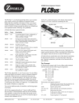
Appendix E: PLCBus
95
General Specifications ......................................................................... 70
Hardware Mechanical Dimensions ...................................................... 71
High Voltage Driver Specifications ..................................................... 75
Environmental Temperature Constraints .............................................. 75
Connectors ........................................................................................... 76
Header Locations and Jumper Settings ................................................ 76
Power Failure Detection Circuitry ....................................................... 80
Power Failure Sequence of Events ...................................................... 80
Recommended Power Fail Routine ...................................................... 82
Interrupt Vectors .................................................................................. 86
Jump Vectors ........................................................................................ 87
EEPROM Addresses ............................................................................ 88
Processor Register Addresses .............................................................. 89
PK2200 Peripheral Addresses ............................................................. 91
PLCBus Overview ............................................................................... 96
Allocation of Devices on the Bus ...................................................... 100
4-Bit Devices ................................................................................ 100
8-Bit Devices ................................................................................ 101
Expansion Bus Software .................................................................... 101
Appendix F: Backup Battery
107
Index
111
PK2200
Table of Contents s v
Battery Life and Storage Conditions .................................................. 108
Replacing Soldered Lithium Battery .................................................. 108
Battery Cautions ................................................................................ 109
Blank
vi s Table of Contents
PK2200
ABOUT THIS MANUAL
This manual provides instructions for installing, testing, configuring, and
interconnecting the Z-World PK2200 controller.
All product references in this manual are made to the PK2200 series. The
term PK2200 is used as a generic term referring to any of the PK2200
series. Where necessary, specific model numbers are used.
®
Instructions are also provided for using Dynamic C functions.
Assumptions
Assumptions are made regarding the user's knowledge and experience in
the following areas.
Ability to design and engineer the target system that a PK2200 will
control.
Understanding of the basics of operating a software program and
editing files under Windows on a PC.
Knowledge of the basics of C programming.
$
For a full treatment of C, refer to the following texts.
The C Programming Language by Kernighan and Ritchie
and/or
C: A Reference Manual by Harbison and Steel
Knowledge of basic Z80 assembly language and architecture.
$
PK2200
For documentation from Zilog, refer to the following texts.
Z180 MPU User's Manual
Z180 Serial Communication Controllers
Z80 Microprocessor Family User's Manual
About This Manual s vii
Acronyms
Table 1 lists and defines the acronyms that may be used in this manual.
Table 1. Acronyms
Acronym
Meaning
EPROM
Erasable Programmable Read-Only Memory
EEPROM
Electronically Erasable Programmable Read-Only Memory
LCD
Liquid Crystal Display
LED
Light-Emitting Diode
NMI
Nonmaskable Interrupt
PIO
Parallel Input/Output Circuit
(Individually Programmable Input/Output)
PRT
Programmable Reload Timer
RAM
Random Access Memory
RTC
Real-Time Clock
SIB
Serial Interface Board
SRAM
Static Random Access Memory
UART
Universal Asynchronous Receiver Transmitter
Icons
Table 2 displays and defines icons that may be used in this manual.
Table 2. Icons
Icon
$
(
Meaning
Meaning
Refer to or see
!
Note
Please contact
7LS
Tip
Caution
FD
Icon
High Voltage
Factory Default
viii s About This Manual
PK2200
Conventions
Table 3 lists and defines the typographic conventions that may be used in
this manual.
Table 3. Typographic Conventions
Example
Description
while
Courier font (bold) indicates a program, a fragment of a
program, or a Dynamic C keyword or phrase.
// IN-01…
Program comments are written in Courier font, plain face.
Italics
Indicates that something should be typed instead of the
italicized words (e.g., in place of filename, type a file’s
name).
Edit
Sans serif font (bold) signifies a menu or menu selection.
...
An ellipsis indicates that (1) irrelevant program text is
omitted for brevity or that (2) preceding program text may
be repeated indefinitely.
[ ]
Brackets in a C function’s definition or program segment
indicate that the enclosed directive is optional.
< >
Angle brackets occasionally enclose classes of terms.
a | b | c
A vertical bar indicates that a choice should be made from
among the items listed.
A black square indicates
pin 1 of all headers.
Pin 1
J1
Pin Number 1
Measurements
All diagram and graphic measurements are in inches followed by millimeters enclosed in parenthesis.
PK2200
About This Manual s ix
Blank
x s About This Manual
PK2200
CHAPTER 1: OVERVIEW
Chapter 1 provides a comprehensive overview and description of the
PK2200.
PK2200
Overview s 11
Introduction
The PK2200 is an inexpensive control computer well suited for a variety
of applications in areas such as packaging, materials handling, and
process control.
Figure 1-1 illustrates the PK2200 with the 2 × 20 character LCD and a
2 × 6 keypad.
PLCBus Expansion
Connector
Screw Connectors
menu
item
field
run
up
down
F3
F4
del
setup
F1
Screw Connectors
F2
LCD
DISPLAY
LED
help
init
add
Keypad
RS-232 Connector
Figure 1-1. PK2200 with Character LCD and Keypad
Figure 1-2 illustrates the PK2240 with the 128 × 64 graphic LCD and a
4 × 3 keypad.
PLCBus Expansion
Connector
Screw Connectors
Screw Connectors
Keypad
LCD
DISPLAY
LED
7
8
9
4
5
6
1
2
3
-
0
.
RS232 Connector
Figure 1-2. PK2240 with Graphic LCD and Keypad
12 s Overview
PK2200
Figure 1-3 illustrates the PK2200 without an enclosure.
U10, U16 are under the EPROM
U8, U11 are under the SRAM
DCIN
J1
LED
JP1
C1
U2
U3
H.C. Driver
JP2
LCD
U1
U5
U6
U4
PLC Bus Connector
JP3
485
L1
U7
U9
PLD
Buffer
RS-232
U12
RS232
Y1
U15
U14
SRAM
Buffer
Inv.
Battery
EPROM
H1
U13
Mux
U18
JP4
H3
Keypad
RTC
J2
Z180
H2
Beeper
RT
U17
Mux
Mux
U20
Phone
Jack
RJ-12
Y2
RS-232
Connector
U19
JP5
Reset
Button
J3
Figure 1-3. PK2200 Without Enclosure
PK2200
Overview s 13
Standard Features
The PK2200 series includes the following standard features:
Compact size: 4" × 5.5" × 1.34"
16 protected digital inputs for detecting contact closures, counting
pulses, or detecting voltage input signals.
14 high-current digital outputs, suitable for driving relays,
solenoids, or lamps.
RS-485 and RS-232 serial ports for external communication and
controller networking using links up to several kilometers
9.216 MHz clock with 18.432 MHz optional
Switching power supply for reduced power consumption. The
PK2200 consumes less than 2 W at 18.432 MHz.
A PLCBus port allows system expansion including relays, A/D
converters, D/A converters, UARTs and more.
EPROM (up to 512K) or flash EPROM (up to 256K) for program
and nonvolatile data storage.
Battery-backed RAM (up to 512K).
Battery-backed real-time clock with time and date functions.
Programmable timers.
EEPROM (512 byte standard) for storing system information.
Watchdog timer and power-fail detection circuitry for improved
system reliability.
Table 1-1 lists PK2200 series models and each models standard features.
Table 1-1. PK2200 Series Standard Features
Model
Features
PK2200
18.432 MHz clock, 2 × 20 character LCD, 2 × 6 keypad,
rugged metal enclosure.
PK2210
9.216 MHz clock, 2 × 20 character LCD, 2 × 6 keypad,
rugged metal enclosure.
PK2220
18.432 MHz clock, 2 × 20 character LCD, 2 × 6 keypad
PK2230
9.216 MHz clock.
PK2240
18.432 MHz clock, 128K flash EPROM, 128 × 64 backlit
graphic LCD, 4 × 3 keypad, rugged metal enclosure.
14 s Overview
PK2200
Flexibility and Customization Options
The PK2200 is available with either quick-release pluggable terminals or
fixed screw terminals.
For added flexibility, special order the PK2200 Series controller with the
following options installed.
Backlit character LCD (for PK2200 and PK2210 only).
128K or 512K battery-backed RAM.
128K flash EPROM for program and nonvolatile data storage.
High-voltage sourcing drivers.
For quantity orders, customization of the PK2200 modified is available to
better suit your application. A wide variety of options are available for I/
O, memory, and packaging.
(
For details on PK2200 customization, contact your
Z-World Sales Representative at (530) 757-3737.
Development Kit
The PK2200 Development Kit contains all the tools required for fast
development. The kit includes the following items:
Programming cable
Power supply
128K flash EPROM
High-current sourcing drivers
Demonstration board that simulates I/O
Users manual with schematics
PK2200
Overview s 15
CE Compliance
The PK2200 has been tested by an approved competent body,
and was found to be in conformity with applicable EN and
equivalent standards. Note the following requirements for
incorporating the PK2200 in your application to comply with
CE requirements.
The power supply provided with the Development Kit is for development purposes only. It is the customers responsibility to provide a
clean DC supply to the controller for all applications in end-products.
Fast transients/burst tests were not performed on this controller. Signal
and process control lines longer than 3 m should be routed in a separate
shielded conduit.
The PK2200, PK2210, PK2220, and PK2230 were tested to Industrial
Immunity Standards. The PK2240 has been tested to Light Industrial
Immunity standards. Additional shielding or filtering may be required
for the PK2240 for an industrial environment.
The PK2200 has been tested to EN55022 Class A emission standards.
Additional shielding or filtering will be required to meet Class B
emission standards.
$
Visit the Technical Reference pages of the Z-World Web site
at http://www.zworld.com for more information on shielding
and filtering.
16 s Overview
PK2200
CHAPTER 2: GETTING STARTED
Chapter 2 provides instructions for connecting the PK2200 to a PC and
running a sample program.
PK2200
Getting Started s 17
Connecting the PK2200 to a PC
The PK2200 is programmed with a PC through an RS-232 port using the
programming cable provided in the Development Kit.
To connect the PK2200 to a PC use the following steps:
1. Install Dynamic C as described in your Dynamic C manuals.
2. Using the supplied adapter, connect the programming cable from the
PK2200s RJ-12 (J2) socket to the appropriate COM port of your
computer.
PK2200 Series Controller
To PC's
COM
Port
Programming
Cable
Adapter
Figure 2-1. Programming Connections
Only use the supplied adapter and programming cable.
!
The supplied 24 V wall power supply is sufficient for all power
requirements. The PK2200 accepts from 9 V to 36 V DC.
3. Connect the supplied 24V DC power supply as follows.
Connect the lead with the red sleeving to the +DC terminal of the
PK2200 (J1 terminal 1).
Connect the other lead to the GND terminal (J1 terminal 3).
18 s Getting Started
PK2200
Figure 2-2 illustrates the power supply connections.
K
+DC
GND
J1
+ Long Lead
Red Shrink Wrap
Short Lead
Power
Supply
Leads
Figure 2-2. Power Supply Connection
4. Plug the power supply into a wall socket.
The PK2200 is now ready to run.
Establishing Communication with the PK2200
To establish communication with the PK2200 use the following steps.
1. Double-click the Dynamic C icon to start the software. Note that each
time you start Dynamic C, communication with the attached PK2200 is
attempted.
2. If the communication attempt is successful, no error messages are
displayed.
$
If an error message such as Target Not Responding or
Communication Error is displayed, see Appendix A,
Troubleshooting.
!
After making necessary changes to establish communication
between a PC and the PK2200, use the Dynamic C shortcut
<Ctrl-Y> to reset the controller and initialize communication.
PK2200
Getting Started s 19
Running a Sample Program
To run a sample program on the PK2200 use the following steps.
1. Open the sample program CDEMO_RT.C located in the SAMPLES\CPLC
Dynamic C subdirectory.
2. Compile the program by pressing F3 or by choosing Compile from the
compile menu. Dynamic C compiles and downloads the program into
the PK2200s memory.
During compilation, Dynamic C rapidly displays several messages in
the compiling window. This condition is normal.
$
If an error message such as Target Not Responding or
Communication Error is displayed, see Appendix A,
Troubleshooting.
3. Run the program by pressing F9 or by choosing Run from the Run
menu.
4. To halt the program, press <Ctrl-Z>.
5. To restart program execution, press F9.
for instructions regarding the use of the Dynamic C
$ Manual
development system.
Refer to Z-Worlds Dynamic C Technical Reference Users
20 s Getting Started
PK2200
CHAPTER 3: SUBSYSTEMS
Chapter 3 describes the various PK2200 subsystems and interfaces,
software drivers and sample programs.
PK2200
Subsystems s 21
Subsystem Overview
The PK2200 is composed of several subsystems. The following list of
subsystem elements is illustrated in Figure 3-1.
Processor core
Protected digital inputs
High-voltage driver outputs
Serial communication channels
Keypad and LCD
Core
HV01
HV02
HV03
HV04
HV05
HV06
HV07
Z180
Real-Time Clock
Protected
Digital
Inputs
PIN01
PIN02
PIN03
PIN04
PIN05
PIN06
PIN07
PIN08
PIN09
PIN10
PIN11
PIN12
PIN13
PIN14
PIN15
PIN16
Battery
HV08
RAM
K
EEPROM
HV09
HV10
HV11
HV12
HV13
HV14
EPROM
OR
Flash EPROM
High
Voltage
Digital
Outputs
Beeper
PLC Expansion
RS485
LCD
and
Keypad
LCD & Keypad
485+
485–
RS232
RS-485
and
RS-232
Serial
Channels
Figure 3-1. PK2200 I/O Systems Block Diagram
22 s Subsystems
PK2200
Processor Core
The PK2200s processor core is composed of the CPU, microprocessor
supervisor/watchdog timer, battery-backed static RAM, EPROM/flash
EPROM, EEPROM, and RTC.
CPU
The PK2200 is available with either 9.216 MHz or 18.432 MHz CPU
clock speeds. The 18.432 MHz clock improves system performance and
allows baud rates up to 11,500 bps. PK2200s with the 9.216 MHz option
are limited to 57,600 bps. The system clock speed is a 16-bit value stored
at location 0x108 in the EEPROM. The clock speed is expressed in
multiples of 1200 Hz. The value read for 9.216 MHz clocks is 7,680 and
for 18.432 MHz clocks the value read is 15,360.
Microprocessor Supervisor/Watchdog Timer
The microprocessor supervisor/watchdog timer provides the following
functions for the PK2200.
Power monitoring for the processor. Protects the system during
brownouts and fluctuating power conditions. The supervisor
provides a power-fail output that can be monitored by the
processor, allowing the processor to save important information
before a complete power-fail and then halt operation until power
is fully restored.
Battery backup for the static RAM. Allows data to remain intact
even when power is removed from the PK2200.
Watchdog timer function. Resets the system in the event of a
software or hardware error that causes the processor to enter an
infinite loop.
Static RAM
Static RAM is normally used to store program data. RAM can also be
used to store program code. This is especially useful during software
development because it allows quick program changes without having to
change EPROMs.
EPROM/Flash EPROM
EPROMs offer a low-cost, permanent medium for storing program code
and constant data. Once the application program is fully functioning and
debugged, an EPROM can be programmed and installed. EPROMs can
be quickly and easily duplicated, and are easy to install.
PK2200
Subsystems s 23
Even though slightly more expensive than standard EPROM, flash
EPROM offers the following benefits.
• In-system programmability.
• Remote downloading of program code and data.
• Easier to reprogram.
• Erases quicker without a special eraser.
EEPROM
EEPROM offers a separate area for storing permanent or semi-permanent
information such as clock speed, network address, calibration coefficients, and installation data. The EEPROM can be write-protected using
a jumper, which prevents data from being accidentally overwritten.
Real Time Clock (RTC)
The RTC provides the application program with the current date and time
of day. The PK2200’s battery keeps the RTC running even when the
power is off. The RTC is accurate to about one second a day and
compensates for leap years and variances in the number of days in each
month.
Digital Inputs
The PK2200’s 16 digital inputs (PN01 through PN16) are flexible and
robust. Configurable pull-up or pull-down resistors and high voltage
protection circuits allow the inputs to detect switch contacts, relay
contacts, outputs from open-collector transistor devices, logic level
outputs, and high voltage outputs. In addition, two inputs may be used for
generating interrupts and another two may be used for high-speed
counting. The protected digital inputs have the follwoing features:
• Nominal input voltage range of –20 V to +24 V.
• Protection against overloads over the range of –48 V to +48 V.
• Logic level detection.
• Configurable pull-ups and pull-downs. Jumper the digital inputs
in groups of eight to pull up to +5 V or down to GND through
4.7 kΩ resistors.
The nominal voltage range for the protected digital inputs is -20 V to
+24 V. The inputs are protected against overvoltages in the range -48 V
to 48 V; however, inputs should not be regularly subjected to voltages
outside the nominal voltage range.
Logic-level signals can also be detected using the digital inputs. The
logic threshold is nominally 2.5 V. The maximum guaranteed low
voltage is 1.25 V. The minimum guaranteed high voltage is 3.75 V.
24 Subsystems
PK2200
The digital inputs can be pulled up to +5 V or down to GND by installing
jumpers on JP2. When jumpered, the digital input line impedance is
4.7 kΩ in the range 05 V for inputs 110 and 1516. The impedance on
inputs 1114 is approximately 1.5 kΩ. Outside this range, the input
impedance is greater than 3.9 kΩ for inputs 110 and 1516. Jumper JP2
connects the inputs to pull-up or pull-down resistors. Table 3-1 lists the
JP2 jumper settings and Figure 3-2 illustrates JP2 jumper settings.
Table 3-1. JP2 Digital Input Jumper Settings
Pins Jumpered
Inputs
Configuration
7–9
1–4 and 9–12
Pulled up
8–10
5–8 and 13–16
Pulled up
9–11
1–4 and 9–12
Pulled down
10–12
5–8 and 13–16
Pulled down
Pull-up configuration
JP2
Pull-down configuration
JP2
1
2
1
2
3
4
3
4
5
6
5
6
7
8
7
8
9
10
9
10
11
12
11
12
Figure 3-2. JP2 Digital Input Jumper Settings
The Figure 3-3 illustrates a typical digital input line.
+5V
JP2
GND
R = 2 kΩ for inputs 11, 12, 13, and 14.
R = 22 kΩ otherwise
4.7 kΩ
Inputs 116
R
0.01 µF
Select
18 or
9 16
D0D7
to Z180 if input 11,
12, 13, or 14
Figure 3-3. Typical Digital Input
PK2200
Subsystems s 25
Inputs 1114, in addition to the protected digital input function, have the
capabilities listed in Table 3-2.
Table 3-2. Digital Input 11-14 Alternate Functions
Input
Z180 Signal
Function
11
/INT0
Interrupt for user programs
12
/INT2
Interrupt for user programs
13
CKA0/DREQ0
DMA channel 0, used for counting
14
/DREQ1
DMA channel 1, used for counting
Inputs 11 and 12 can be used to generate hardware interrupts on the
PK2200 CPU. Input 11 is connected to /INT0 and input 12 is connected
to /INT2. With Dynamic C, you can easily implement service routines for
these interrupts. Table 3-2 lists the alternate functions for digital inputs
11 through 14.
$
Refer to the Dynamic C Technical Reference Users Manual
for more information on writing interrupt service routines.
Inputs 13 and 14 are connected to the CPUs DMA channels. These
inputs may be used for counting high-speed digital signals. For highspeed counting (above 5 kHz), remove capacitor network CN2.
EPROM
CN1
Mux
RAM
Mux
U20
U19
Z180
CN2
JP5
J3
Remove CN2 for
high-speed counting
Figure 3-4. CN2 Capacitor Networks
!
Removing CN2 from the PK2240 disables the filtering on
channels IN5, IN6, IN7, IN8, IN13, IN14, IN15, and IN16
The high-speed counters and can perform a variety of functions including
time stamping, pulse width measurement and duty cycle measurement.
26 s Subsystems
PK2200
Digital Outputs
The PK2200s 14 digital outputs (HV01 through HV14) provide highvoltage, high-current digital outputs for your application. Sinking and
optional sourcing drivers will drive a variety of loads including inductive
loads such as relays, small solenoids, or stepping motors.
Note the following points regarding the digital outputs:
Each output is individually addressable.
Each output includes a protective diode that returns inductive
spikes to the power supply.
Sinking drivers are standard. Sourcing drivers are optional. Both
drivers must be of the same type, either sinking or sourcing.
The total number of outputs that can be on simultaneously is subject to
chip power limits and ambient temperature. There are power limitations
on each channel as well as the entire driver IC. Eight channels, HV1
HV8, are driven by one driver IC. The other six, HV9HV14, are driven
by the other driver IC. Since fewer outputs are being driven by the HV9
HV14 driver IC, the current limit on these channels is higher than on the
HV1HV8 channels.
Figure 3-5 illustrates the configuration for the ULN2803 sinking driver.
inductive
load
external DC
HV01HV14
2
4
JP1
K
Channel (114)
1
3
ULN2803
JP1
Figure 3-5. Sinking Driver Configuration
Note the following points regarding the ULN2803 sinking driver chip.
Outputs pull low (sink current) when turned on.
The chips rating is 48 V and 500 mA maximum per channel,
subject to the chips thermal limits and ambient temperature.
With all channels on, each channel can sink up to 170 mA
continuously (100% duty cycle) as long as the chip temperature is
less or equal to 50°C. At 70°C the current must be reduced to
140 mA or less.
PK2200
Subsystems s 27
Figure 3-6 illustrates the connection for the UDN2985A sourcing driver.
(Note the connections on header JP1.)
K
1 2
external DC
JP1
Channel (114)
HV01HV14
inductive
load
4 3
UDN2985A
JP1
Figure 3-6. Sourcing Driver Configuration
Note the following points regarding the UDN2985A sourcing driver.
Outputs pull high (source current) when turned on.
The chips rating is 30 V and 250 mA maximum per channel,
subject to the chips thermal limits and ambient temperature.
With all channels on, each channel can source up to 170 mA
continuously (100% duty cycle) as long as the chip temperature is
less or equal to 50°C. At 70°C the current must be reduced to
140 mA or less.
Header JP1 configures the outputs for either sourcing or sinking drivers.
Table 3-3 lists the JP1 jumper configurations shown in Figure 3-7.
Table 3-3. JP1 High-Current Output
Jumper Settings
JP1 Setting
Description
1–3, 2–4
Sinking Outputs
1–2, 3–4
Sourcing Outputs
Sinking Drivers
JP1
Sourcing Drivers
JP1
1
2
1
2
3
4
3
4
Figure 3-7. JP1 Digital Output
Jumper Settings
Tip
If incandescent lights are driven, use a series resistor to limit
the incoming current.
$
See Appendix B: Specifications for more detailed information on the sinking and sourcing drivers.
28 s Subsystems
PK2200
Serial Communication
Two serial ports support asynchronous communication at baud rates from
300 bps to 57,600 bps on 9.216 MHz versions up to 115,200 bps with the
18.432 MHz versions. The serial ports can be configured as follows:
Two 3-wire RS-232 ports.
One 5-wire RS-232 port (with RTS and CTS) and
one half-duplex RS-485 port.
The RJ-12 phone jack connector J2 supports full-duplex RS-232 communication with handshake lines. The RS-485 lines (J1 terminals 18 and 19)
provide half-duplex asynchronous communication over twisted pair wires,
up to 3 kilometers. The RS-232 ports on the PK2200 support a subset of
the RS-232 standard that is in common use.
Serial Channel Configuration
Figure 3-8 illustrates the configuration of two 3-wire RS-232 channels.
Z180
TXD0
TXD0
RXD0
RXD0
TXD1
13 11 RS-232CH1TX
RXD1
7 5 RS-232CH1RX
/TX0: J2-3
U12
(RS-232)
/RX0: J2-4
/TX1: J2-1
/RX1: J2-5
JP3
/RTS0
RX485
/CTS0
TXD1
U9
(RS-485)
485+: J1-18
485-: J1-19
R11
4.7k
Figure 3-8. Two RS-232 Channels
Figure 3-9 illustrates the configuration of one 5-wire RS-232 channel and
one half-duplex RS-485 channel.
Z180
TXD0
TXD0
RXD0
RXD0
TXD1
RS-232CH1TX
RXD1
RS-232CH1RX
/RTS0
/CTS0
/TX0
U12
(RS-232)
/RX0
/TX1 = /RTS0
/RX1 = /CTS0
9 11
6 5
JP3
7 8
RXD1 = RX485
TXD1
U9
(RS-485)
485+
485
Figure 3-9. RS-232 and RS-485
PK2200
Subsystems s 29
Table 3-4 lists JP3 jumper settings and Figure 3-10 illustrates jumper
setting configurations for the two serial channels. If only one RS-232
channel is desired, use one of the first two configurations. With these
configurations, the RS-485 port is also active on the second Z180 serial
channel (Z1). Unless the application software explicitly enables Z1, the
RS-485 channel has no effect on the Z180. The RS-485 is connected to
Z1 in the first two configurations in order to keep the Z180 CMOS input
(RXA1) from floating.
Table 3-4. JP3 Serial Communication Jumper Settings
JP3 Jumpered Pins
Serial Communication Configuration
5–6,
7–8,
9–11
One 5-wire RS-232 channel
(Z180 Port 0) with RTS/CTS
One RS-485 channel (port 1)
7–8
One 3-wire RS-232
One RS-485
5–7
11–13
Two 3-wire RS-232
One 5-wire RS-232 and
One RS-485
JP3
One 3-wire RS-232
One RS-485
JP3
FD
Two 3-wire RS-232
JP3
1
2
1
2
1
2
3
4
3
4
3
4
5
6
5
6
5
6
7
8
7
8
7
8
9
10
9
10
9
10
11
12
11
12
11
12
13
14
13
14
13
14
Figure 3-10. JP3 Jumper Settings
30 s Subsystems
PK2200
Keypad and Display
The PK2200 Series supports operator I/O through both keypad and LCD.
The following two standard operator I/O configurations are available on
PK2200 controller models with enclosures:
2-row by 20-column character LCD module plus
a 2-row by 6-column keypad.
128-column by 64-row backlit graphic LCD module plus
a 4-row by 3-column keypad.
The character LCD module is also available with an LED backlighting
option and the graphic LCD has a software controllable electroluminescent backlighting installed as a standard feature. Table 3-5 lists and
describes header connections and functions.
Table 3-5. Header Connections and Function
Header
Function
H1
The LCD connector. Connect a 14-wire ribbon cable
from the LCD to this header. Not used on the PK2240.
H2
The PLCBus expansion connector. This connector
supports the “LCD bus” as well. Use a 26-pin ribbon
cable to attach PLCBus devices to the PK2200.
H3
The keypad connector. Connect a 10-wire flat flexible
cable from the keypad to this header. Not used on the
PK2240.
The PK2200 series also interfaces easily with the Z-World line of
operator interface products. Operator interfaces are available with a
variety of keypad sizes and LCD configurations.
(
PK2200
For more information on Z-World operator interfaces,
contact your Z-World Sales Representative at
(530) 757-3737.
Subsystems s 31
Blank
32 s Subsystems
PK2200
CHAPTER 4: SYSTEM DEVELOPMENT
Chapter 4 describes system development using the PK2200 interfaces and
presents some sample programs to illustrate their use.
PK2200
System Development s 33
Changing Modes
The operating mode of the PK2200 is determined during power-up
initialization. If a valid program is found in EPROM, then it is executed.
Otherwise, the operating mode is determined by the jumper settings on JP4
or by keypress combinations. Following are the possible modes of operation:.
• Run a program stored in RAM or flash EPROM.
• Prepare for Dynamic C programming using the RS-232 port.
The mode can be changed by either of the following two methods:
1. Set jumper JP4 to the desired position. Remove power from the
PK2200. Apply power to the PK2200.
2. With power off, hold down the appropriate keys on the keypad and
apply power. Refer to Figure 4-1 for the appropriate keypress combinations.
You will hear a series of beeps indicating that the mode has been set.
The PK2240 has a sample program loaded at the factory that
will run automatically when the PK2240 is powered. You can
set the PK2240 to program mode using the procedures above.
All other models are preconfigured for program mode.
Setting the Mode
Figures 4-1, 4-2, and 4-3 illustrate keypad and jumper settings for run and
program modes for different PK2200 configurations. The keypress
combination for the 3x4 keypad will work only with the PK2240 model.
The keypress combination for the 2x6 keypad will work with any model
with a 2x6 keypad. If programming at normal 19,200 bps, then press the
“menu setup” and “up pgm” keys. If programming at 28,800 bps, then
press the “menu setup” and the “down pgm” keys. You may instead set the
programming baud rate with jumpers on JP4.
At startup, a PK2200 can also be put into run mode by placing a jumper
across pin 6 and pin 7 of JP4.
Program Mode
Run Mode
28,800 bps
19,200 bps
menu
setup
F1
item
F2
field
down
up
help
menu
run
pgm
pgm
init
setup
F3
F4
del
add
F1
item
F2
field
down
help
run
up
pgm
pgm
init
F3
F4
del
add
Figure 4-1. 2x6 Keypad Mode Settings
34 System Development
PK2200
Program Mode
Run Mode
7
8
9
7
8
9
4
5
6
4
5
6
1
2
3
1
2
3
-
0
-
0
.
.
Figure 4-2. 3x4 Keypad Mode Settings
Program Mode
8
7
6
5
Run Mode
3
4
2
8
1
7
6
JP4
19,200 bps
5
4
3
2
1
JP4
28,800 bps
Figure 4-3. JP4 Mode Settings
Do not jumper more than one pair of pins to configure a mode.
Development Options
Memory Options
Programs for the PK2200 are written and compiled on a PC and then
downloaded to the PK2200 memory and executed. There are three memory
options for program storage on the PK2200:
(1) Battery-backed RAM,
(2) EPROM,
(3) Flash EPROM.
Battery-Backed RAM
Battery-backed RAM is a standard feature on every PK2200. RAM is
available in 32K, 128K, and 512K. During development you can use RAM
to download and execute programs. This speeds development because you
don’t need to program and erase EPROMs. Once a program is fully
debugged and running, you can create a binary file and use an EPROM
burner to store the program in EPROM. Since the RAM is used to store
both data and program, Z-World recommends using a larger RAM during
development. If the PK2200 has flash EPROM installed, the program will
be compiled to flash EPROM instead of RAM.
PK2200
System Development 35
EPROM
EPROMs offer a permanent storage option for programs and data.
The PK2200 BIOS is factory installed in the EPROM. After an application is fully debugged and running, it can be compiled and stored in
EPROM with an EPROM burner. Each time the PK2200 powers up, it
will run the stored application.
Flash EPROM
Flash EPROM offers the benefits of both battery-backed RAM and
standard EPROM. You can quickly change and download a program as if
you were using RAM. Using flash EPROM frees up RAM for data
storage rather than program storage. Flash EPROM does not depend
upon the onboard battery to retain data, so a program is safe in the event
that the battery is drained.
(
For more information on memory options or to place an order,
contact your Z-World Sales Representative at (530) 757-3737.
Digital Inputs
The digital inputs can be used for a variety of applications such as
detecting high-voltage and logic level digital signals, providing interrupts
for time critical events, and high-speed counting.
Using the Digital Inputs
The digital inputs are supported in software by Dynamic C functions and
virtual driver variables. There are several methods for reading the digital
inputs. Some of the digital inputs have additional features listed below.
Interrupt Inputs
Inputs 11 and 12 can be used to generate level sensitive hardware interrupts on the PK2200 CPU. Interrupts can be used to signal events that
need to be serviced in real-time.
High Speed DMA Counter
Two counters connected to digital inputs 13 and 14 are actually the CPUs
DMA channel counters.
The maximum counting speed is ≈1.5 MHz for
9.216 MHz PK2200 series controllers.
The maximum counting speed is 3.0 MHz for
18.432 MHz PK2200 series controllers.
36 s System Development
PK2200
The following points summarize the counters capabilities:
The counter can measure the time at which a negative edge occurs
with a precision of a few microseconds. A minimum time must
occur between successive events to allow for interrupt processing.
The counter can measure the width of a pulse by counting (up to
65,536) at a rate that varies from 300 Hz to 600 kHz, providing
16-bit accuracy.
Count negative-going edges for up to two channels. The maximum count for high-speed counting (5 kHz and up) is 65,536. For
low speeds, the maximum count is unlimited.
Function calls load the count-down value for the DMA channel and
enable the DMA interrupt. Once a counter reaches zero, flags for the
DMA channel are set to 1. DMA flags can be monitored by an application program.
Digital Outputs
Using the Digital Outputs
The digital outputs are supported in software by Dynamic C functions and
virtual driver variables. There are several methods for writing to the
digital outputs.
The digital outputs can be used for a wide variety of applications including the following:
Driving solenoids, relays, motors and other inductive loads
directly.
Driving incandescent lamps, LEDs and resistive loads directly.
Driving FETs, transistors, thyristors or solid state relays to
increase the current or voltage output capability as well as
providing a.c. drive capability.
PK2200
System Development s 37
Serial Communication
Dynamic C has serial communication support libraries. For the Z180 port
z0 and Z180 port z1, use AASC.LIB, Z0232.LIB, and Z1232.LIB. For
RS-232 expansion cards that interfaced through the PLCBus on the
PK2200, use EZIOPLC.LIB.
Functional support for serial communication includes the following:
Initialization of the serial ports
Monitoring, and reading, a circular receive buffer
Monitoring, and writing to, a circular transmit buffer
An echo option
CTS (clear to send) and RTS (request to send) control for
RS-232.
XMODEM protocol for downloading and uploading data
A modem option
!
The PK2200 can be configured for either two RS-232
channels or one RS-232 and one RS-485. Z0 is RS-232
only and Z1 may be configured for RS-232 or RS-485.
See Chapter 3 for information on configuring the serial
communication channels.
FD
Z180 Port Z0 is configured at the factory for RS-232
and Port Z1 is configured for RS-485.
Receive and Transmit Buffers
Serial communication is made easier with a background interrupt routine
that updates receive and transmit buffers. Every time a port receives
another character, the interrupt routine places it into the receive buffer. A
program can read the data one character at a time or as a stream of
characters terminated by a special character.
A program sends data by writing characters into the transmit buffer. If the
serial port is not already transmitting, the write functions automatically
initiate the transmission. Once the last character of the buffer is sent, the
transmit interrupt is turned off. Data can be written one character at a
time or as a stream of characters.
38 s System Development
PK2200
Echo Option
If the echo option is turned on during initialization of the serial port (with
Dinit_z0, Dinit_z1, or Dinit_uart) any character received is
automatically echoed back (transmitted out). This feature is ideal for use
with a dumb terminal and also for checking the characters received.
CTS/RTS Control
Z180 port 0 is constrained by hardware to have the CTS (clear to send)
pulled low by the RS-232 device with which it is communicating. An RS232 expansion card, however, can enable or disable the effect of the CTS
line. Z180 port 1 does not support the CTS / RTS lines.
If you choose the CTS/RTS option, the support software pulls the RTS
(request to send) line high when the receive buffer has reached 80 percent
of capacity. Thus, the transmitting device (if its CTS is enabled) stops
transmitting. The RTS line is pulled low again when the received buffer
has gone below 20 percent of capacity.
If the device with which the PK2200 is communicating does not support
CTS and RTS, the CTS and RTS lines on the PK2200s side can be tied
together to make communication possible.
XMODEM File Transfer
The PK2200 supports the XMODEM protocol for downloading and
uploading data. Currently, the library supports downloading an array of
data whose size is a multiple of 128 bytes.
Uploaded data is written to a specified area in RAM. The targeted area
for writing should not conflict with the current resident program or data.
During XMODEM transfers, character echo is automatically suspended.
Modem Communication
Modems and telephone lines allow serial communication across a great
distance. If you choose the modem option, character streams that are read
from the receive buffer are automatically scanned for modem commands.
When a modem command is found, the software takes appropriate action.
Normally, the communication package functions in COMMAND mode
while waiting for valid modem commands or messages. Once a link is
established, communication functions in DATA mode. However, the
software continues to monitor the modem for a NO_CARRIER message.
The software assumes that modem commands are terminated with CR,
which is carriage return (0x0D). The modem option is easiest to use when
the user protocol also has CR as the terminating character. Otherwise, the
software has to check for two different terminating characters. The users
terminating character cannot be any of the ASCII characters used in
modem commands, nor can it be a line-feed character.
PK2200
System Development s 39
Library functions for the RS-232 port support communication with a
Hayes Smart Modem or compatible. Note the following points:
The CTS, RTS, and DTR lines of the modem are not used.
If the modem used is not truly Hayes Smart Modem compatible,
the user has to tie the CTS, RTS, and DTR lines on the modem
side together. The CTS and RTS lines on the PK2200 side also
have to be tied together.
A NULL connection is required for the TX and RX lines.
A commercial NULL modem will have its CTS and RTS lines tied
together on both sides.
Figure 4-4 shows the correct modem to PK2200 wiring.
Modem
Side
RX
TX
GND
RTS
CTS
DTR
Controller
Side
RX
TX
GND
RTS
CTS
Figure 4-4. Null Modem Cable Connections
Following are descriptions for Z180 port 0 functions. Similar functions
are available for the RS-232 (UART) expansion card. Please note the
following substitutions:
For the RS-232 expansion card, substitute uart for z0 in the function
name.
For Z180 port 1, substitute z1 for z0 in the function name.
For example, the initialization routine for the Z180 port 0 is called
Dinit_z0(). The equivalent function for the RS-232 expansion card is
Dinit_uart() The equivalent function for Z180 port 1 is Dinit_z1().
$
Refer to Appendix F, PLCBus, for details on software
support for the RS-232 expansion card.
40 s System Development
PK2200
Interrupt Handling for Z180 Port 0
Normally, a serial interrupt service routine would be declared with the
compiler directive:
#INT_VEC SER0_VEC routine
However, if you use the same serial port for Dynamic C programming,
your program has to be downloaded first with Dynamic C before the
address of the serial interrupt service routine is loaded into the interrupt
vector table. That is, the service routine must be loaded at run-time.
The following function loads the address of the service function into the
specified location in the interrupt vector table.
reload_vec (int vector, int(*serv_function)())
The #INT_VEC directive should not be used with this function. Once the
service routine has taken over, you cant debug your program in
Dynamic C.
If you communicate with a serial device other than the PCs Dynamic C
programming port, your program has to make sure that the hardware is
properly configured before sending any messages. For example, when
using Z180 port 0 for serial communication with a modem, use the
PK2200s keypad to trigger serial port initialization. Without this trigger,
the modem may not properly communicate with the support software
because the initialization routine also sends initialization commands to the
modem.
When executable programs are generated either for EPROM or for downloading to RAM, there is no need for communication with Dynamic C.
The compile-time directive #INT_VEC can then be used freely.
Remote Downloading
The PK2200 has the capability of remote downloading program code.
This allows units to be reprogrammed in the field, eliminating the need to
recall units for reprogramming or sending field service personnel to install
new software. In order to use the remote download feature, the PK2200
must have a serial link to the remote PC, either a direct RS-232 link or a
modem. The RS-232 connection is limited to several hundred feet.
Modems allow communication over virtually unlimited distances.
If you plan to use the remote download feature, make sure that the
PK2200 has enough memory to store future program revisions and data.
Refer to Dynamic C Technical Reference Manual for a detailed description of the remote downloading procedure.
PK2200
System Development s 41
Developing an RS-485 Network
The two-wire RS-485 serial-communication port and Dynamic-C network
software allow network development. Screw terminal strip J1 provides a
half-duplex RS-485 interface.
The RS-485 signals are on
screw terminals 18 and 19.
485–
+DC
GND
GND
RUN
PROGRAM
K
GND
HV01
HV02
485–
+DC
PIN01
HV03
PROGRAM
K
PIN02
HV04
GND
GND
PIN03
RUN
PIN02
HV01
PIN01
PIN03
HV07
HV06
HV08
HV05
HV09
PIN04
+5V
HV11
HV10
HV02
PIN09
PIN04
PIN10
PIN05
PIN11
HV12
PIN06
HV07
PIN12
HV13
PIN08
HV08
485+
HV14
PIN07
HV09
PIN13
HV03
+5V
HV11
HV10
PIN14
HV04
PIN09
PIN16
PIN15
HV06
PIN10
HV12
HV05
PIN11
HV13
PIN05
PIN12
485+
HV14
PIN06
PIN13
PIN08
PIN14
PIN07
PIN16
In a multidrop network, termination and bias resistors are required
to minimize reflections (echoing)
and to keep the network line active during an idle state. Only the
first and last board on a multidrop
RS-485 cable should have termination resistors. Therefore, when
networking multiple boards via
RS-485, remove termination resistors from all boards in the network, except for the first and last
board of the network.
PIN15
Any Z-World controller can be a
master or a slave. A network can
have up to 255 slave controllers,
but only one controller can be the
master.
GND
The PK2200 and/or other controllers can be linked together over
several kilometers. When configuring a multi-drop network, use
single twisted pair wires on all
controllers to connect RS-485+ to
RS-485+ and RS-485- to RS-485.
A diagram of a two-wire RS-485
network is shown in Figure 4-5.
Figure 4-5. RS-485 Network
Only a single, solid conductor should be placed in a screw clamp terminal. Bare copper, particularly if exposed to the air for a long period
before installation, can become oxidized. The oxide can cause a high
resistance (~20 ohm) connection, especially if the clamping pressure is
not sufficient. To avoid oxidation, use tinned wires or clean, shiny copper
wire. If you are using multiple conductors or stranded wire, consider
soldering the wire bundle or using a crimp connector to avoid a later loss
of contact pressure to a spontaneous rearrangement of the wire bundle.
Soldering may make the wire subject to fatigue failure at the junction with
the solder if there is flexing or vibration.
42 s System Development
PK2200
Keypad and LCD
The PK2200 Series supports operator I/O with a keypad and LCD. Two
standard operator I/O configurations are available on PK2200 series
controllers with enclosures:
2-row by 20-column character LCD module with a 2-row by 6column keypad.
128-column by 64-row backlit graphic LCD module with a 4-row
by 3-column keypad.
The character LCD module is also available with an LED backlighting
option. The graphic LCD has electroluminescent backlighting installed as
a standard feature.
Using the Keypad and Display
The PK2200 keypad and display are supported by a large number of
software drivers. The keypad and display can be used for a variety of user
interface applications including the following:
User code or password entry
System status display
Multiple language/character-set displays
Parameter monitoring and adjustment
PK2200 Keypads
Table 4-1 shows standard keypad configurations.
Table 4-1. Keypad Configurations
Model
PK2200
Keypad
PK2200
2x6
PK2210
2x6
PK2220
None
PK2230
None
PK2240
4x3
System Development s 43
Keypad Insert Templates
The keypads are designed to accept paper inserts. Inserts can be produced on regular paper using a laser printer, thus allowing quick and easy
customization of keypad legends.
menu
item
field
up
F1
F2
F3
F4
down
help
del
add
0.40
0.10
1.13
0.13
0.10
You can use the templates below for creating inserts. All dimensions are
in inches. Inserts can be secured by taping the portion of the insert that
extends beyond the keypad to the supporting bracket
0.30
0.40
0.40
0.13
3.75
0.25 0.25 0.15
2.10
0.40
Figure 4-6. 2x6 Keypad Insert Template
0.05
7
8
9
4
5
6
1
2
3
–
0
.
0.25 0.15
0.05
1.15
Figure 4-7. 3x4 Keypad Insert Template
44 s System Development
PK2200
Keypad Codes
The PK2200 keypads are supported by Dynamic C functions that return
codes corresponding to the key pressed. The figures below show the
codes for the 2x6 and 3x4 keypads used on the PK2200 Series controllers.
1
2
3
4 5
6
7
8
9 10 11 12
Figure 4-8. 2x6 Keypad Codes
24 25 26
16 17 18
8
9
10
0
1
2
Figure 4-9. 3x4 Keypad Codes
PK2200
System Development s 45
PK2200 LCDs
The PK2200 Series LCDs are easy to use with Dynamic C software
libraries. Shown below are the layouts for both the 2x20 character display
and the 64x128 graphic display.
2x20 Character LCD
Row 0
Row 1
Column 0
Column 19
Figure 4-10. 2X20 Character LCD
64x128 Graphic LCD
Row 0
Row 63
Column 127
Column 0
Figure 4-11. 64X128 Graphic LCD
Graphic LCD Status
Several Dynamic C library functions return the operating status of the
LCD. The LCD status bits are shown in the following bitmap.
7
BUSY
6
0
5
ON/OFF
Most significant bit
4
RESET
3
0
2
0
1
0
0
0
Least significant bit
BUSY - Reading a 1 indicates LCD is performing an operation.
Reading a 0 indicates the LCD is ready to accept more data.
46 s System Development
PK2200
ON/OFF - When the ON/OFF bit is set ( 1 ) the display is on, any image
on the screen will be visible. When the bit is reset ( 0 ) any images on the
display will not be visible. The image is still in the display memory.
RESET - Resets the LCD module when low ( 0 ).
Bitmapped Graphics
Many of the Dynamic C functions that operate on the graphic LCD use
bitmaps. These bitmaps represent the images on a section of the display.
An individual dot, or pixel, is represented by one bit in the bitmap. If the
pixel is on, the corresponding bit is set. If the pixel is off, the corresponding pixel is reset.
The image on the display is two-dimensional (width and height). The
bitmap used to store that display information is a one-dimensional array.
Two-dimensional images are stored in column major, byte aligned bitmap
format.
Column major means that bits are stored in the bitmap column by column.
The first pixel of the first column (row 0, column 0) of the image is stored
in the first bit position in the bitmap. The second pixel of the first column is
stored in the second bit position in the bitmap and so on. When the entire first
column is stored in the bitmap, the process begins again with the second
column and repeats until all columns of the image are stored.
Byte aligned means that a column data will end on a byte boundary. If a
column has a number of bits that is not evenly divisible by eight, then the
remaining bits of the last byte representing a column will be left unused.
Image data from the next column will be stored starting in the next byte.
PK2200
System Development s 47
Blank
48 s System Development
PK2200
CHAPTER 5: SOFTWARE REFERENCE
Chapter 5 covers the software drivers used with the PK2200 series
controllers.
PK2200
Software Reference s 49
Software Drivers
Drivers are functions that simplify accessing PK2200 hardware and I/O.
For the following reasons, Z-World drivers make writing software easier:
Provide commonly needed functionality.
Eliminate the need to know all of the details of operation.
Previously tested.
Simplify source code by replacing multiple lines of code with one
function call.
$
Refer to the Dynamic C Technical Reference Manual for
more information on using drivers.
Real Time Clock (RTC)
The RTC keeps the date and the time of day with a resolution of one
second. The worst case error is 50ppm (4.3 seconds) per day. Leap years
and variances in the number of days in a month are automatically tracked.
The following structure holds the time and date:
struct
char
char
char
char
char
char
char
};
tm {
tm_sec;
tm_min;
tm_hour;
tm_mday;
tm_mon;
tm_year;
tm_wday;
//
//
//
//
//
//
//
0-59
0-59
0-23
1-31
1-12
0-150 (1900-2050)
0-6 where 0 means Sunday
The following routines read and write to the real-time clock:
int tm_wr( struct tm *x )
Sets the system time to the values in the structure pointed to by *x.
PARAMETER1: Pointer to the structure holding the system time
information to be written.
RETURN VALUE: 0 if successful; -1 if clock failing or not installed.
int tm _ rd( struct tm *t )
Reads the current system time into the structure t.
PARAMETER1: Pointer to the structure used to store the system time.
RETURN VALUE: 0 if successful; -1 if clock failing or not installed.
50 s Software Reference
PK2200
EEPROM
The following functions provide access to the EEPROM. The EEPROM
is generally used for storing system information, calibration information,
or any data that does not need to change often.
int ee _ rd (int address)
Reads value from EEPROM at specified address.
PARAMETER1: The address to read from.
RETURN VALUE: EEPROM data (0-255) if successful; negative
value if unable to read EEPROM.
int ee_wr (int address, char data)
Writes value to EEPROM at specified address.
PARAMETER1: The address to write to.
RETURN VALUE: Returns 0 if write is successful, negative value if
unsuccessful.
PK2200
Software Reference s 51
Digital Inputs and Outputs
DIGIN1, DIGIN2, ..., DIGING16
The virtual driver variables DIGIN1, DIGIN2, ... DIGIN16 represent
the state of the digital inputs. These variables take the value 1 if the
input is high and 0 if the input is low. The value is changed only if the
new value remains the same for 2 ticks (25 to 50 milliseconds) of the
virtual driver.
void VIOInit();
VIOInit is a dummy function used as a host for the GLOBAL_INIT of
the virtual I/O variables. Virtual inputs are read and virtual outputs are
written out whenever the function VIODrvr() is called. Inputs are
DIGIN1 to DIGIN16. Outputs are OUT1 to OUT16. The DIGIN
values have to be the same for two successive reads to be valid.
RETURN VALUE: None.
void VIODrvr();
Updates the virtual inputs DIGIN1 to DIGIN16. The virtual outputs
OUT1 to OUT14 are send out to corresponding output ports.
RETURN VALUE: None.
Digital Input Drivers
There are several methods for reading digital inputs and setting digital
outputs on the PK2200. Below is a listing of drivers for the digital inputs
and outputs, including the high-speed DMA counters.
int up_digin( int channel )
Read the value at the specified digital input channel (116).
RETURN VALUE: The function returns 1 when the channel is high
and 0 when the channel is low.
unsigned inport( unsigned port )
Reads value from I/O port.
PARAMETER: port is the I/O port to be read.
RETURN VALUE: Value from I/O port.
You can read multiple PK2200 digital inputs simultaneously using the
inport() function.
DIGBANK1 is the address ( 0x180 ) of the first eight digital inputs DIN1
through DIN8. Bit zero represents the state of DIN1, bit one is DIN2,
etc. DIGBANK2 is the address ( 0x181 ) of the second eight digital
inputs DIN9 through DIN16. Bit zero represents the state of DIN9, bit
one is DIN10, etc.
52 s Software Reference
PK2200
The lower eight bits returned by the inport() function represent the
status of the digital inputs. Bits which are set ( 1 ) represent inputs
which are high. Bits which are reset ( 0 ) correspond to inputs which
are low.
Example:
lowDIBank = inport( DIGBANK1 );
highDIBank = inport( DIGBANK2 );
void DMA0Count (unsigned int count)
Loads the DMA channel 0 with the count value and enables the DMA
channel 0 interrupt.
The function sets the flag _DMAFLAG0 to zero. When count negative
edges have been detected, the channel causes an interrupt, and the
interrupt service routine sets the flag _DMAFLAG0 to 1. A program can
monitor _DMAFLAG0 to determine if the number of counts has occurred.
PARAMETER: count is the number of pulses to count.
RETURN VALUE: None
void DMA1Count (unsigned int count)
Loads DMA channel 1 with the count value and enables the DMA
channel 1 interrupt.
The function sets the flag _DMAFLAG1 to zero. When count negative
edges have been detected, the channel causes an interrupt, and the
interrupt service routine sets the flag _DMAFLAG1 to 1. A program can
monitor _DMAFLAG1 to determine if the number of counts has occurred.
PARAMETER: count is the number of pulses to count
RETURN VALUE: None
unsigned int DMASnapShot (byte channel,
unsigned int *count)
Reads the number of pulses that a DMA channel has counted. A DMA
counter is initialized with one of the two preceding functions.
PARAMETERS: channel is the DMA channel (0 or 1)
*count is a pointer to variable holding the pulse count.
RETURN VALUE: 0, if pulse train is too fast to have a snap shot
taken; 1, if a snap shot is obtained and valid data is in *count.
!
PK2200
Even if a program is unable to read the counts, DMA interrupts still occur when the DMA channel counts down from its
loaded value.
Software Reference s 53
Digital Output Drivers
Following are the digital output drivers for the PK2200:
int up_setout( int channel, int value )
Sets the state of digital output.
PARAMETER1: The digital output channel to set.
PARAMETER2: The state to set. 1 (active) or 0 (inactive).
RETURN VALUE: None.
Pass channel (114) and value: 0 for OFF, 1 for ON.
OUT1, OUT2, ..., OUT14
Set the virtual driver variables OUT1, OUT2, OUT3, ... OUT13,
OUT14 to a value of 0 to turn off the output, or 1 to turn on the output.
void outport(unsigned port, unsigned value);
Writes value to I/O port.
PARAMETER1: The output port.
PARAMETER2: The value to be written.
RETURN VALUE: None
The addresses DRV1 - DRV14 are the port addresses for the digital
ouputs. Writing 0 to any of these ports will turn the ouput OFF. To
turn ON digital ouputs 1 through 8 write 0x20 to the corresponding
port. For digital outputs 9 through 14 write 0x40 to turn the ouput ON.
!
The digital outputs are individually addressed and must be set
one at a time.
54 s Software Reference
PK2200
LCD and Keypad
The following functions provide routines for writing to the LCD and
reading the keypad.
Include the following directives in your program if using the PK2240.
#use wintek.lib
#use kp.lib
The following directives provide information to the compiler about the
graphic LCD and keypad on the PK2240.
void lc_init_keypad()
Initializes timer1, keypad driver, and variables, and, if used, the realtime kernel.
RETURN VALUE: None.
int lc_kxget (byte mode)
Fetches the key value from the FIFO keypad buffers. If mode = 0, value
is removed from the buffer; otherwise, value remains in the buffer.
RETURN VALUE: Key value or -1, if no key is available.
$
The Keypad and LCD section in Chapter 4 describes
key values.
void lc_kxinit()
Initialize the keypad driver and accessory variables. If virtual watchdogs are defined the virtual watchdogs are initialized.
RETURN VALUE: None.
void lc_setbeep (int count)
Sounds the beeper for the number of 1280 Hz cycles specified by
count.
RETURN VALUE: None.
up_beep (int milliseconds)
Sets beeper on for specified number of milliseconds. Scaling of the
count passed is dependent on the periodic routines that calls
lc_beepscan. If BeepScale is undefined, it is defaulted to 0.04.
RETURN VALUE: None.
void lc_char (char ch)
Sends a character to the LCD. The function waits for the LCD to
become free before sending the character.
RETURN VALUE: None
PK2200
Software Reference s 55
int lc_cmd (int cmd)
Waits for LCD busy flag to clear, then sends cmd to LCD command
register.
RETURN VALUE: 0, if successful in writing to the LCD; else -1, if
timeout
void lc_ctrl (byte cmd)
Write a control cmd to the LCD.
RETURN VALUE: None.
void lc_init()
Initializes the LCD. The display is turned on, cleared, and the cursor
(now in the top left character position) blinks.
RETURN VALUE: None
void lc_ nl()
Performs a new line function on the LCD.
RETURN VALUE: None
void lc_ pos (int line, int column)
Positions the cursor at the line designated by line and column
designated by column on the LCD.
RETURN VALUE: None
void lc_printf (char* fmt, ...)
Performs a printf to the LCD. The function arguments are specified
as they are for the standard printf.
RETURN VALUE: None
int lc_wait()
Waits for LCD busy flag to clear. Caution, doesnt time out.
RETURN VALUE: 0, when LCD busy flag has cleared; else -1, if
timeout after ten tries.
void glSetBrushType(int type)
Sets the brush type for all following graphics operations in this library.
It controls how pixels are drawn on the screen with respect to existing
pixels.
PARAMETER1: This is the type of the brush. Possible values are
GL_SET for forcing pixels on, GL_CLEAR for forcing pixels off,
GL_XOR for toggling the existing pixels and GL_BLOCK to overwrite the
entire memory location corresponding to the pixel.
RETURN VALUE: None.
56 s Software Reference
PK2200
int glInit()
Initializes the LCD module (software and hardware).
RETURN VALUE: returns the status of the LCD. If the initialization
was successful, this function returns 0. Otherwise, the returned value
indicates the LCD status.
int glBlankScreen()
Blanks the screen of the LCD.
RETURN VALUE: The returned value indicates the status of the LCD
after the operation.
int glPlotDot(int x, int y)
Plots one pixel on the screen at coordinate (x,y).
PARAMETER1: the x coordinate of the pixel to be drawn.
PARAMETER2: the y coordinate of the pixel to be drawn.
RETURN VALUE: Status of the LCD after the operation.
void glPlotLine(int x1, int y1, int x2, int y2)
Plots a line on the LCD.
PARAMETER1: x coordinate of first endpoint.
PARAMETER2: y coordinate of first endpoint.
PARAMETER3: x coordinate of second endpoint.
PARAMETER4: y coordinate of second endpoint.
RETURN VALUE: None.
void glPutBitmap(int x, int y, int bmWidth,
int bmHeight, char *bm)
Displays a bitmap stored in root memory on the LCD. For bitmaps
defined in xmem memory, use glXPutBitmap.
PARAMETER1: x coordinate of the bitmap (left edge).
PARAMETER2: y coordinate of the bitmap (top edge).
PARAMETER3: width of the bitmap.
PARAMETER4: height of the bitmap.
PARAMETER5: pointer to the bitmap.
RETURN VALUE: None.
PK2200
Software Reference s 57
void glXPutBitmap(int x, int y, int bmWidth,
int bmHeight, unsigned long bmPtr)
Displays a bitmap stored in xmem on the LCD. For bitmaps stored in
root memory, use glPutBitmap.
PARAMETER1: x coordinate of the bitmap (left edge).
PARAMETER2: y coordinate of the bitmap (top edge).
PARAMETER3: width of the bitmap.
PARAMETER4: height of the bitmap.
PARAMETER5: pointer to the bitmap.
RETURN VALUE: None.
void glGetBitmap(int x, int y, int bmWidth,
int bmHeight, char *bm)
Gets a bitmap from the LCD.
PARAMETER1: x coordinate of the bitmap (left edge).
PARAMETER2: y coordinate of the bitmap (top edge).
PARAMETER3: width of the bitmap.
PARAMETER4: height of the bitmap.
PARAMETER5: pointer to the bitmap.
RETURN VALUE: None.
void glFontInit(struct _fontInfo *pInfo, char
pixWidth, char pixHeight, unsigned startChar,
unsigned endChar, char bitmapBuffer)
Initializes a font descriptor with the bitmap defined in the root
memory. For fonts with bitmaps defined in xmem, use glXFontInit.
PARAMETER1: pointer to the font descriptor to be initialized.
PARAMETER2: width of each font item (must be uniform for all
items).
PARAMETER3: height of each font item (must be uniform for all
items).
PARAMETER4: offset to the first useable item (useful for fonts for
ASCII or other fonts with an offset).
PARAMETER5: index of the last useable font item.
PARAMETER6: pointer to a linear array of font bitmap.
RETURN VALUE: None.
58 s Software Reference
PK2200
void glXFontInit(struct _fontInfo *pInfo,
char pixWidth, char pixHeight, unsigned
startChar, unsigned endChar, unsigned long
xmemBuffer)
Initializes a font descriptor that has the bitmap defined in xmem. For
bitmaps defined in root memory, use glFontInit.
PARAMETER1: pointer to the font descriptor to be initialized.
PARAMETER2: width of each font item (must be uniform for all
items).
PARAMETER3: height of each font item (must be uniform for all
items).
PARAMETER4: offset to the first useable item (useful for fonts for
ASCII or other fonts with an offset).
PARAMETER5: index of the last useable font item.
PARAMETER6: pointer to a linear array of font bitmap.
RETURN VALUE: None.
void glPutFont(int x, int y, struct fontInfo
*pInfo, unsigned code)
Puts an entry from the font table to the LCD.
PARAMETER1: x-coordinate of the entry (left edge).
PARAMETER2: y-coordinate of the entry (top edge).
PARAMETER3: pointer to the font descriptor that describes the font
table to be indexed.
PARAMETER4: code (offset) in the font table that indexes the bitmap
to display.
RETURN VALUE: None.
void glVPrintf(int x, int y, struct fontInfo
*pInfo, char *fmt, void *firstArg)
Prints a formatted string on the LCD screen, similar to vprintf.
PARAMETER1: x coordinate of the text (left edge).
PARAMETER2: y coordinate of the text (top edge).
PARAMETER3: pointer to font descriptor that describes the font used
for printing the text.
PARAMETER4: pointer to the string that describes the format.
PARAMETER5: pointer to the first argument to instigate the format
string.
RETURN VALUE: None.
PK2200
Software Reference s 59
void glPrintf(int x, int y, struct _fontInfo
*pInfo, char *fmt,...)
Prints a formatted string (much like printf) on the LCD screen.
PARAMETER1: x coordinate of the text (left edge).
PARAMETER2: y coordinate of the text (top edge).
PARAMETER3: pointer to the font descriptor used for printing on the
LCD screen.
PARAMETER4: pointer to the format string
RETURN VALUE: None.
void glPlotCircle(int xc, int yc, int rad)
Draws a circle on the LCD.
PARAMETER1: x coordinate of the center.
PARAMETER2: y coordinate of the center.
PARAMETER3: radius of the circle.
RETURN VALUE: None.
int wtDisplaySw(int onOff)
Switches the display on and off.
PARAMETER1: If this parameter is 1, the display is turned on. If this
parameter is 0, the display is turned off.
RETURN VALUE: Status of the LCD after the operation.
void kdiELSw(int value)
Switchs the EL backlight of the LCD.
PARAMETER1: 1 to turn the backlight on, 0 to turn the backlight off.
RETURN VALUE: None.
void kdiSetContrast(unsigned content)
Sets the contrast control to content.
PARAMETER1: Specifies the contrast (the higher the value, the higher
the contrast).
RETURN VALUE: None
60 s Software Reference
PK2200
void kpInit(int (*changeFn)())
Initializes the kp module. This function should be called before other
functions of this module are called.
PARAMETER1: This is a pointer to a function that will be called when
the driver detects a change (when kpScanState is called). Two
arguments are passed to the call-back function. The first argument is a
pointer to an array that indicates the current state of the keypad. The
second pointer is a pointer to an array that indicates what keypad
positions are changed and detected by kpScanState. The byte offset
in the array represents the line pulled high (row number), and the bits in
a byte represents the positions (column number) read back.
RETURN VALUE: None
int kpScanState()
Scans the keypad and detect any changes to the keypad status. Returns
non-zero if there is any change. If kpInit is called with a non-NULL
function pointer, that function will be called with the state of the
keypad. This function should be called periodically to scan for keypad
activities.
RETURN VALUE: 0 if there is no change to the keypad, non-zero if
there is any change to the keypad.
int kpDefStChgFn(char *curState, char *changed)
This is the default state change function for the default get key function
kpDefGetKey. This function is called back by kpScanState when
there is a change in the keypad state. If the current key is not read by
kpDefGetKey, the new key pressed will not be registered.
PARAMETER1: Points to an array that reflects the current state of the
keypad (bitmapped, 1 indicates key is not currently pressed).
PARAMETER2: Points to an array that reflects the CHANGE of
keypad state from the previous scan. (bitmapped, 1 indicates there was
a change).
RETURN VALUE: -1 if no key is pressed. Otherwise it returns the
normalized key number. The normalized key number is
8*row+col+edge*256. Edge is 1 if the key is released, and 0 if the key
is pressed.
PK2200
Software Reference s 61
int kpDefGetKey()
This is the default get key function. This function returns the key
previously pressed (i.e., from the one-keypress buffer). The key
pressed is actually interpreted by kpDefStChgFn, which is called back
by kpScanState. The function kpDefInit should be used to
initialize the module.
RETURN VALUE: -1 if no key is pressed. Otherwise it returns the
normalized key number. The normalized key number is
8*row+col+edge*256. Edge is 1if the key is released, and 0 if the key
is pressed.
void kpDefInit()
Initializes the module to use the default state change function to
interpret key presses when kpScanState is called. Use
kpDefGetKey to get the code of the last key pressed.
RETURN VALUE: NA.
Sample Programs
The sample programs listed in Table 5-1 are specific to the PK2200.
They can be found in the SAMPLES\CPLC directory.
Table 5-1. PK2200 Sample Programs
Program
Description
5KEYCODE.C
Code-driven sample program for the five-key
system.
5KEYDEMO.C
Uses a code-driven five-key system and the
RT-kbyte for I/O monitor and control.
5KEYLAD.C
Combines 5KEYCODE.C and LADDERC.C.
5KEYLINK.C
Linked-list sample program for the five-key
system.
5KEYSCAN.C
Combines 5KEYCODE.C and SCANBLK.C.
CDEMO_RT.C
Demonstrate the use of the real-time kernel.
DIGDEMO.C
Use the keypad to select which digital input
channel to monitor.
DIGVDVR.C
Similar to DIGDEMO.C. but uses the virtual
driver to monitor the state of the input.
DMACOUNT.C
Demonstrates the use of the high speed
counters.
continued…
62 s Software Reference
PK2200
Table 5-1. PK2200 Sample Programs (concluded)
Program
Description
LADDERC.C
Use ladder C for I/O control.
LCGRAM.C
Illustrates use of the LCD character generator.
OUTDEMO.C
Use keypad to toggle the state of the digital
outputs.
OUTVDVR.C
Similar to OUTDEMO.C, but uses the virtual
driver to change the state of the output.
PRT0DEMO.C
Use TIMER0 for timer interrupt .
READIO.C
Read and toggle the I/Os through STDIN. The
I/Os are driven by function calls.
READKEY.C
Read the keypad and write to the LCD and to
the STDIO window.
SCANBLK.C
Use function blocks for I/O control.
UREADIO.C
Read and toggle the I/Os through STDIN. The
I/Os are driven by the virtual driver.
VWDOG.C
Illustrates the use of the virtual watchdogs and
of KEYREQUEST
Communication Sample Programs
The sample communication programs listed in Table 5-2 are located in the
SAMPLES\NETWORK directory.
Table 5-2. Sample Communication Programs
Program
Description
CSREMOTE.C
Slave version of CZ0REM.C, that includes most
capabilities of CZ0REM.C. Master-to-slave
communication is via opto22 9th-bit binary
protocol.
CUARTREM.C
Same as CZ0REM.C but uses XP8700
expansion card.
continued…
PK2200
Software Reference s 63
Table 5-2. Sample Communication Programs (concluded)
Program
Description
CZ0REM.C
More elaborate sample of serial communication
between board and PC dumb terminal. Includes
modem communication, data monitoring, time
and date setup, memory read and write, data
logging, XMODEM download of the data log,
XMODEM upload of binary file for remote
downloading. Also supports master-to-slave
communication. (Slave has to be running the
program CSREMOTE.C.)
RS232.C
RS-232 communication with a PC dumb
terminal, with or without modem. Also,
master-to-slave communication with another
board running RS-485.C.
RS485.C
Slave program to communicate with the master
running RS-232.C.
UART232.C
RS-232 communication through an RS-232
expansion card with the PK2200.
Z1232.C
An RS-232 program for Z180 port 1.
PK2240 Sample Programs
The sample programs listed in Table 5-3 are specific to the PK2240 and
are located in the SAMPLES\PK224X directory. These programs illustrate
the use of the graphic LCD and keypad.
Table 5-3. PK2240 Sample Programs
Program
Description
GLPRINTF.C
Demonstrates the glprintf function and
shows how to print text on the graphics display.
KPDEFLT.C
Demonstrates key scanning techniques using
functions in the KP library.
64 s Software Reference
PK2200
APPENDIX A: TROUBLESHOOTING
Appendix A provides procedures for troubleshooting system hardware and
software.
PK2200
Troubleshooting s 65
Out of the Box
Check the items mentioned in this section before starting development.
Verify that the PK2200 runs in standalone mode before connecting any
expansion boards or I/O devices.
Verify that the entire host system has good, low-impedance, separate
grounds for analog and digital signals. Often the controller is connected between the host PC and another device. Any differences in
ground potential from unit to unit can cause serious problems that are
hard to diagnose.
Do not connect analog ground to digital ground anywhere.
Double-check the connecting ribbon cables to ensure that all wires go
to the correct headers.
Verify that the host PCs COM port works by connecting a good serial
device to the COM port. Remember that COM1/COM3 and COM2/
COM4 share interrupts on a PC. User shells and mouse drivers, in
particular, often interfere with proper COM port operation. For
example, a mouse running on COM1 can preclude running Dynamic C
on COM3.
Use the supplied Z-World power supply. If another power supply must
be used, verify that it has enough capacity and filtering to support the
PK2200.
Use the supplied Z-World cables. The most common fault of usermade cables is failure to properly assert CTS at the RS-232 port of the
controller Without CTSs being asserted, the controllers RS-232 port
will not transmit. Assert CTS by either connecting the RTS signal of
the PCs COM port or looping back the PK2200s RTS.
Experiment with each peripheral device connected to the controller to
determine how it appears to the controller when powered up, powered
down, and/or when its connecting wiring is open or shorted.
If a DB9 connector or an RJ-12 connector is wired up to a 10-pin
connector, carefully check the connections. These wires do not run
pin-for-pin.
Note: Telephone company wiring does not follow a standardized color
code.
66 s Troubleshooting
PK2200
Dynamic C Will Not Start
In most situations, when Dynamic C will not start, an error message
announcing a communication failure will be displayed. Following is a list
of situations causing an error message and possible resolutions.
Wrong Baud Rate In rare cases, the baud rate has to be changed
when using the Serial Interface Board for development.
Wrong Communication Mode Both sides must be talking RS-232.
Wrong COM Port A PC generally has two serial ports, COM1 and
COM2. Specify the one being used in the Dynamic C Target Setup
menu. Use trial and error, if necessary.
Wrong Operating Mode Communication with Dynamic C will be
lost if the controllers jumper is set for standalone operation. Reconfigure the board for programming mode.
Wrong Memory Size Jumpered pins on JP2 specify the EPROM
size.
If all else fails, connect the serial cable to the controller after power up. If
the PCs RS-232 port supplies a large current (most commonly on
portable and industrial PCs), some RS-232 level converter ICs go into a
nondestructive latch-up. Connect the RS-232 cable after power up to
eliminate this problem.
Dynamic C Loses Serial Link
If the program disables interrupts for a period greater than 50 milliseconds, Dynamic C will lose its serial link with the application program.
Make sure that interrupts are not disabled for a period greater than 50
milliseconds.
PK2200 Repeatedly Resets
The PK2200 resets every 1.0 seconds if the watchdog timer is not hit.
If a program does not hit the watchdog timer, then the program will
have trouble running in standalone mode. To hit the watchdog, make a
call to the Dynamic C library function hitwd.
PK2200
Troubleshooting s 67
Common Programming Errors
Values for constants or variables out of range. Table A-1 lists acceptable ranges for variables and constants.
Table A-1. Constant and Variable Ranges
Type
Range
15
int
–32,768 (–2 ) to
15
+32,767 (2 –1)
long int
−2 , 147,483,648 ( −2 ) to
31
+2147483647 (2 −1 )
float
1.18 × 10 to
38
3.40 × 10
char
0 to 255
31
–38
Mismatched types. For example, the literal constant 3293 is of type
int (16-bit integer). However, the literal constant 3293.0 is of type
float. Although Dynamic C can handle some type mismatches,
avoiding type mismatches is the best practice.
Counting up from, or down to, one instead of zero. In software, ordinal
series often begin or terminate with zero, not one.
Confusing a functions definition with an instance of its use in a listing.
Not ending statements with semicolons.
Not inserting commas as required in functions parameter lists.
Leaving out ASCII space character between characters forming a
different legal, but unwanted operator.
Confusing similar-looking operators such as && with &,
== with =, and // with /.
Inadvertently inserting ASCII nonprinting characters into a source-code
file.
68 s Troubleshooting
PK2200
APPENDIX B: SPECIFICATIONS
Appendix B provides comprehensive PK2200 physical, electronic, and
environmental specifications.
PK2200
Specifications s 69
General Specifications
Table B-1 lists the electrical, mechanical, and environmental specifications for the PK2200.
Table B-1. PK2200 General Specifications
Parameter
Specification
Operating Temp
−40° C to 70° C
Humidity
5% to 95%, noncondensing
Input Voltage
9 V to 24 V DC
Digital Inputs
16 protected, −20 V to +24 V DC
Digital Outputs
14 high-current sinking (500 mA max.) or
sourcing (250 mA max.).
Processor
Z80180
Clock
9.216 MHz or 18.432 MHz.
SRAM
32K standard, 512K maximum
EEPROM
512 bytes
Flash EPROM
Up to 256K
Serial ports
2 RS-232 or 1 RS-232 with RTS/CTS and
1 RS-485
Serial rate
Up to 115,200 bps
Watchdog/supervisor
Yes
Time/date clock
Yes
Backup battery
Yes, internal 3 V DC lithium ion
70 s Specifications
PK2200
Hardware Mechanical Dimensions
Top view for models PK2200 and PK2210.
3.09 (78.5)
2.42 (61.5)
1.85 (47.0)
add
5.5 (140)
del
F3
F1
F4
init
up
run
0.31 typ (7.9)
F2
10-32 clr, 4x
field
menu
item
setup
4.35 (110.5)
1.15 (29.2)
1.11 (28.2)
4.85 (123.2)
4.39 (111.5)
down
help
0.67 (17.0)
0.37 (9.0)
0.2 typ (5)
4.0 (101)
Figure B-1. Top View PK2200 and PK2210
PK2200
Specifications s 71
Top view for model PK2240.
1.105 (28.1)
1.75 (44.5)
0
–
10-32 clr, 4x
4.88 (124.0)
2.719 (69.1)
5.5 (139.7)
2
1
.
5
4
3
8
7
6
1.262 (32.1)
0.37 (9.4)
0.2 typ (5)
4.0 (102)
0.31 typ (7.9)
0.621
(15.8)
3.750 (95.3)
4.85 (123.2)
1.350 (34.3)
9
1.455 (37.0)
Figure B-2. Top View PK2240
72 s Specifications
PK2200
End view for models PK2200, PK2210 and PK2240.
1.71 (43.4)
1.2 (30.5)
0.75 (19.1)
0.22 (5.6)
2.95 (75.0)
0.55 (14.0)
0.2 (5.1)
1.44 (36.6)
Figure B-3. End View PK2200, PK2210, and PK2240
The board dimensions are 4.0"×5.32" overall. The centers of the mounting holes are inset (0.220", 0.770") from the corners of the board. They
are 2.46" and 4.88" on center. Mounting holes are 0.160" in diameter.
PK2200
Specifications s 73
Top view of models PK2220 and PK2230.
0.030 (0.76)
0.220 (5.59)
0 .470 (11.9)
5.100 (129.5)
5.320 (135.1)
R 0.125 X 4
(3.2)
R 0.125 X 4
(3.2)
0.200 (5.1)
0.770 (19.6)
3.230 (82.0)
3.800 (96.5)
4.000 (101.6)
Figure B-4. Top View PK2220 and PK2230
74 s Specifications
PK2200
High Voltage Driver Specifications
Table B-2. Sinking Driver Specifications
Parameter
Output Voltage
Output Current
Power Dissipation (Change)
Power Dissipation (Package)
C-E Saturation Voltage (max.)
Derating Factor
Absolute Maximum Rating
at 25C
50 V DC
500 mA
1.0 W
2.25 W
1.3 V
18.18 mW/C above 25 C
Table B-3. Sourcing Driver Specifications
Parameter
Output Voltage
Output Current
Power Dissipation (Chan)
Power Dissipation
(Package)
C-E Saturation Voltage
(maximum)
Derating Factor
Absolute Maximum Rating
30V DC
250 mA
1.0 W
2.2 W
1.2 V
18 mW/C above 25C
Environmental Temperature Constraints
No special precautions are necessary over the range of 0°C to 50°C
(32°F to 122°F). For operation at temperatures below 0°C, the PK2200
should be equipped with a low temperature LCD that is specified for
operation down to 20°C. The heating effect of the power dissipated by
the unit may be sufficient to keep the temperature above 0°C, depending
on the enclosures insulating capability. The LCD storage temperature is
20°C lower than its operating temperature, which may protect the LCD in
case the power should fail, thus removing the heat source. The LCD unit
is specified for a maximum operating temperature of 50°C. Except for
the LCD, which fades at higher temperatures, the PK2200 operates at
60°C or more without problem.
!
PK2200
External loads and expansion cards can increase power
consumption.
Specifications s 75
Connectors
Only a single, solid conductor should be placed in a screw clamp terminal. Bare copper, particularly if exposed to the air for a long period
before installation, can become oxidized. The oxide can cause a high
resistance (~20 Ω) connection, especially if the clamping pressure is not
sufficient. To avoid this, use tinned wires or clean, shiny copper wire. If
you are using multiple conductors or stranded wire, consider soldering the
wire bundle or using a crimp connector to avoid a loss of contact pressure
to a spontaneous rearrangement of the wire bundle at a latter time.
Soldering may make the wire subject to fatigue failure at the junction with
the solder if there is flexing or vibration.
Header Locations and Jumper Settings
Figure B-5 illustrates the location of the headers on the PK2200.
Table B-4 lists each header and explains possible pin connections.
LED
JP6,1
LCD
Interface
JP2
JP1
1
3
2
4
JP3
H1
PLC Bus
Connector
H2
JP4
JP5
H3 Keypad Conn.
CN1
CN2
Figure B-5 PK2200 Jumpers and Headers
76 s Specifications
PK2200
Table B-4. Headers and Jumper Settings
Header
Pins
Description
1–3, 2–4
1–2, 3–4
Sink/source control. The drivers will be damaged if
the jumpers are set incorrectly.
Connect for the ULN2803 sinking drivers (default).
Connect for the UDN2985A sourcing drivers.
JP1
JP2
1–3, 2–4
3–5, 2–4
3–5, 4–6
3–5, 4–6
3–5, 4–6
7–9
9–11
8–10
10–12
JP3
1–2
3-–4
5–6, 9–11
7–8
5–6, 7–8,
9–11
5–7, 11–13
10–12
12–14
JP4
7–8
6–7
2–3
4–5
EPROM
flash EPROM
32K
64K
128K
128K
256K
256K
512K
Input pullup/pulldown resistors
Inputs 1–4 and 9–12 are pulled up.
Inputs 1–4 and 9–12 are pulled down.
Inputs 5–8 and 13–16 are pulled up.
Inputs 5–8 and 13–16 are pulled down.
Miscellaneous
Enables the watchdog timer (default).
Allows the CTS line to reset the board.
Serial Communication
One 5-wire RS-232 channel (Z180 Port 0) with
RTS/CTS
One 3-wire RS-232
One RS-485 channel (Port 1)
One 5-wire RS-232
FD
One RS-485
Two 3-wire RS-232 channels
SRAM sizing
32K or 128K SRAM (default)
512K SRAM
Readable jumper equivalent to mode-setting keypad
keys. JP4 overrides the keypad if jumper installed.
Places unit in program mode at 19,200 bps.
Runs the program.
Places unit in program mode at 28,800 bps.
indicates to Dynamic C that watchdog timer is
enabled. Connect when JP3:1-2 is installed.
JP5
1–2
2–3
Write protect the EEPROM.
Write-enable the EEPROM.
JP6
1–2
2–3
EPROM
flash EPROM
PK2200
Specifications 77
Blank
78 s Specifications
PK2200
APPENDIX C: POWER MANAGEMENT
Appendix C provides information about power management and hardware
and software specific to power management on the PK2200.
PK2200
Power Management s 79
Power Failure Detection Circuitry
Figure C-1 shows the power failure detection circuitry of the PK2200.
DCIN
R1
+5V
IC691
/PFI
R2
R4
Microprocessor
U15
D6
/NMI D6
/PFO
/RES
U11
3B
/RESET
3Y
74HC257
D6
U18
Figure C-1. PK2200 Power-Fail Circuit
Power Failure Sequence of Events
The following events occur as the input power fails:.
1. The 691 power-management IC first triggers a power-failure /NMI
(non-maskable interrupt) when the unregulated DC input voltage falls
below approximately 7.9 V (as determined by the voltage divider R1/
R2).
2. At some point, the raw input voltage level will not exceed the required
regulated voltage level by the regulators dropout voltage whereupon
the regulated output begins to droop.
3. The 691 next triggers a system reset when the regulated +5 V supply
falls below ∼4.75 V, allowing your power-failure routine the holdup
interval, tH, to store your important state data.
4. The 691 forces the chip enable of the SRAM high (standby mode).
5. The time/date clock and SRAM switches to the lithium backup battery
when the regulated voltage falls below the battery voltage of approximately 3 V.
6. The 691 keeps the reset asserted until the regulated voltage drops
below 1 V.
7. At this point the 691 ceases operating. By this time, the portion of the
circuitry not battery-backed has long since ceased functioning.
80 s Power Management
PK2200
The ratio of your power supplys output capacitors value to your circuits
current draw determines the actual duration of the holdup-time interval, t .
H
Power
Fails
9.0
Unregulated
DC
8.0
Regulated
+5V
7.0
Dropout
Voltage
6.0
5.0
4.0
C
3.0
Slope =
C/-I
2.0
I
VOLTS
1.0
tH
TIME
691
Asserts
PFO
691
Asserts
RESET
691
Ceases
Operation
Figure C-2. Power Fail Sequence of Events
This setup can fail when multiple power fluctuations happen rapidly a
common occurrence in the real world. If the PK2200s Z180 processor
receives multiple /NMIs, it overwrites an internal register, making a
correct return from the first /NMI impossible. Also, depending on the
number of fluctuations of the raw DC input (and hence, the number of
stacked /NMIs), the processors stack could overflow, corrupting your
programs code or data.
When the Z180 senses an NMI, it saves the program counter (PC) on its
processor stack. It copies the maskable interrupt flag, IEF1, to IEF2 and
zeroes IEF1. The Z180 restores IEF2s saved state information when it
executes a RETN (Return from Nonmaskable Interrupt) instruction.
PK2200
Power Management s 81
Recommended Power Fail Routine
Z-World recommends the following routines to handle an NMI. The
routines monitor the state of the /PFO line, via U18 and the data bus, to
determine if the brownout condition is continuing or if the power has
returned to normal levels. If you use one of these routines, you need not
worry about multiple power-failure /NMIs because these routines never
return from the first /NMI unless the power returns.
Program C-1. Suggested Power Fail Routine
main(){
...
}
...
char dummy[24];
// reserve dummy stack
// for /NMI processing
...
#define NMI_BIT 3
#define NMI PIODB2
// routine will test data
// bit 3 to determine
// state of /NMI line
#JUMP_VEC NMI_VEC myint
#asm
myint::
ld
sp,dummy+24 ; force stack pointer
; to top of “dummy”
; array to prevent
; overwriting of code
; or data
;do whatever service, within allowable
;executuin time
loop:
call hitwd
; make sure no
; watchdog reset
; during brownout
ld
bc,NMI
; load the read-NMI
; register to bc
in
a,(c)
; read the read-NMI
; register to /PFO
bit NMI_BIT, a
; check /PFO status
jr
z,loop
; wait until brownout
; condition clears
timeout:
; then... a tight loop
; to force a watchdog
; timeout
jp
timeout
; which will reset the
; Z180
#endasm
82 s Power Management
PK2200
The watchdog timer should be enabled. However, if the watchdog is not
enabled, you can force the processor to restart execution at 0x0000.
Substitute this section for the one labeled timeout above.
Program C-2. Alternate Power Fail Code
restart:
ld
a,0xe2
out0 (CBAR),a
jp
0000h
;
;
;
;
;
;
;
make sure 0x0000
points to start of
EPROM BIOS
set the CBAR
jump to logical
(physical) address
0x0000
#endasm
If the DC input voltage continues to decrease, the controller powers
down. The routine calls hitwd to make sure that watchdog does not
timeout and thereby reset the processor. The controller can continue to
run, after a fashion, at low voltage and might not be able to detect the low
voltage condition, because the Z180s /NMI input needs to see a high-tolow transition edge.
A situation similar to a brownout occurs if the power supply is overloaded. For example, when an LED turns on, the raw voltage supplied to
the PK2200 may dip below 7.9 V. The interrupt routine does a shutdown,
which turns off the LED, clearing the problem. However, if the cause of
the overload persists, the system oscillates, alternately experiencing an
overload and then resetting. To correct this situation, use a power supply
which can provide the needed current and voltage.
A few milliseconds of computing time remain when the regulated +5 V
supply falls below ≈4.75 V, even if power cuts off abruptly. The amount
of time depends on the size of the capacitors in the power supply. The
standard wall power supply provides about 10 ms. If you remove the
power cable abruptly from the PK2200 side, only the capacitors on the
board are available, reducing computing time to a few hundred microseconds. These times can vary considerably depending on systems configuration and loads on the 5 V or 9 V supplies.
The interval between the power failure detection and entry to the powerfailure interrupt routine is approximately 100 µs or less if Dynamic C
NMI communication is not in use.
PK2200
Power Management s 83
Blank
84 s Power Management
PK2200
APPENDIX D: INTERRUPT VECTORS AND
I/O ADDRESSES
Appendix D provides a suggested interrupt vector map and information
on EEPROM address, processor I/O addresses, and peripheral addresses.
PK2200
Interrupts and Addresses s D-85
Most of the following interrupt vectors can be altered under program
control. The addresses are given in hex, relative to the start of the interrupt
vector page, as determined by the contents of the I-register. These are the
default interrupt vectors set by the boot code in the Dynamic C EPROM.
Interrupt Vectors
To vector an interrupt to a user function in Dynamic C, a directive such
as the following is used:
#INT_VEC 0x10 myfunction
The above example causes the interrupt at offset 10H (serial port 1 of the
Z180) to invoke the function myfunction(). The function must be
declared with the interrupt keyword:
interrupt myfunction() {
...
}
Table D-1. Z180 Internal Device Interrupt Vectors
Address
Name
Description
0x00
INT1_VEC
Expansion bus attention /INT1
vector
0x02
INT2_VEC
/INT2 vector
0x04
PRT0_VEC
PRT timer channel 0
0x06
PRT1_VEC
PRT timer channel 1
0x08
DMA0_VEC
DMA channel 0
0x0A
DMA1_VEC
DMA channel 1
0x0C
CSIO_VEC
Clocked Serial I/O
0x0E
SER0_VEC
Asynchronous Serial Port Channel 0
0x10
SER1_VEC
Asynchronous Serial Port Channel 1
Digital input 11 connects to /INT0 and digital input 12 connects to /INT2,
allowing external events to generate interrupts.
D-86 s Interrupts and Adresses
PK2200
Jump Vectors
These special interrupts occur in a different manner: instead of loading
the address of the interrupt routine from the interrupt vector, these
interrupts cause a jump directly to the address of the vector, which
contains a jump instruction to the interrupt routine. For example,
0x66 non-maskable power-failure interrupt
Because nonmaskable interrupts can be used for Dynamic C communication, your interrupt vector for power failure is normally stored just in
front of the Dynamic C program. You can store a vector there by using the
following command:
#JUMP_VEC NMI_VEC name
The Dynamic C communication routines relay to this vector when a
power failure causes the NMI rather than a serial interrupt. Table D-2
lists interrupt priorities from the highest to lowest priority.
Table D-2. Interrupt Priorities
Interrupt Priorities
(Highest Priority)
Trap (Illegal Instruction)
NMI (Nonmaskable Interrupt)
INT 0 (Maskable Interrupt, Level 0,
3 modes, PIO interrupts)
INT 1 (Maskable Interrupt, Level 1,
PLCBus attention line interrupt)
INT 2 (Maskable Interrupt, Level 2)
PRT Timer Channel 0
PRT Timer Channel 1
DMA Channel 0
DMA Channel 1
Clocked Serial I/O
Serial Port 0
(Lowest Priority)
PK2200
Serial Port 1
Interrupts and Addresses s D-87
EEPROM Addresses
These EEPROM constants apply to the standard PK2200.
Table D-3. Z180 I/O Device Register Addresses
Address
Description
0x000
Startup Mode. If 1, enter program mode. If 8,
execute loaded program at startup.
0x001
Baud rate in units of 1200 baud.
0x100
Unit “serial number.” BCD time and date with the
following format: second, minutes, hours, day,
month, year.
0x108
Microprocessor clock speed in units of 1200 Hz (16bits). For 9.216 MHz clock speed, this value is
7680. For 18.432 MHz, this value is 15,360.
0x16C
Long coefficient relating speed of microprocessor
clock relative to speed of real-time clock. Nominal
value is 107,374,182 which is 1/40 of a second
microprocessor clock time on the scale where 232 is 1
second. This value requires 4 bytes of EEPROM,
stored least byte first.
D-88 s Interrupts and Adresses
PK2200
Processor Register Addresses
The Z180s I/O-device registers occupy the first 40 addresses.
H
Table D-4. Z180 Internal I/O Device Registers
Address
Name
Description
0x00
CNTLA0
Serial Channel 0, Control Register A
0x01
CNTLA1
Serial Channel 1, Control Register A
0x02
CNTLB0
Serial Channel 0, Control Register B
0x03
CNTLB1
Serial Channel 1, Control Register B
0x04
STAT0
Status Register, Serial Channel 0
0x05
STAT1
Status Register, Serial Channel 1
0x06
TDR0
Transmit Data Register, Serial Channel 0
0x07
TDR1
Transmit Data Register, Serial Channel 1
0x08
RDR0
Receive Data Register, Serial Channel 0
0x09
RDR1
Receive Data Register, Serial Channel 1
0x0A
CNTR
Clocked Serial Control Register
0x0B
TRDR
Clocked Serial Data Register
0x0C
TMDR0L
Timer Data Register, Channel 0, low
0x0D
TMDR0H
Timer Data Register, Channel 0, high
0x0E
RLDR0L
Timer Reload Register, Channel 0, low
0x0F
RLDR0H
Timer Reload Register, Channel 0, high
0x10
TCR
Timer Control Register
0x11–13
—
Reserved
0x14
TMDR1L
Timer Data Register, Channel 1, low
0x15
TMDR1H
Timer Data Register, Channel 1, high
0x16
RLDR1L
Timer Reload Register, Channel 1, low
0x17
RLDR1H
Timer Reload Register, Channel 1, high
0x18
FRC
Free-Running Counter
0x19–1E
—
Reserved
0x1F
CCR
CPU control register for the 18 MHz chip.
Write 0x80 to get 18.432 MHz. Write 0 to
get 9.216 MHz.
0x20
SAR0L
DMA Source Address, Channel 0, low
continued…
PK2200
Interrupts and Addresses s D-89
Table D-4. Z180 Internal I/O Device Registers (concluded)
Address
Name
Description
0x21
SAR0H
DMA Source Address, Channel 0, high
0x22
SAR0B
DMA Source Address, Channel 0, extra bits
0x23
DAR0L
DMA Destination Address, Channel 0, low
0x24
DAR0H
DMA Destination Address, Channel 0, most
0x25
DAR0B
Destination Address, Channel 0, extra bits
0x26
BCR0L
DMA Byte Count Register, Channel 0, low
0x27
BCR0H
DMA Byte Count Register, Channel 0, high
0x28
MAR1L
DMA Memory Address Register, Channel 1,
low
0x29
MAR1H
DMA Memory Address Register, Channel 1,
high
0x2A
MAR1B
DMA Memory Address Register, Channel 1,
extra bits
0x2B
IAR1L
DMA I/O Address Register, Channel 1, low
0x2C
IAR1H
DMA I/O Address Register, Channel 1, high
0x2D
—
Reserved
0x2E
BCR1L
DMA Byte Count Register, Channel 1, low
0x2F
BCR1H
DMA Byte Count Register, Channel 1, high
0x30
DSTAT
DMA Status Register
0x31
DMODE
DMA Mode Register
0x32
DCNTL
DMA/WAIT Control Register
0x33
IL
Interrupt Vector Low Register
0x34
ITC
Interrupt/Trap Control Register
0x35
—
Reserved
0x36
RCR
Refresh Control Register
0x37
—
Reserved
0x38
CBR
MMU Common Base Register
0x39
BBR
MMU Bank Base Register
0x3A
CBAR
MMU Common/Bank Area Register
0x3B–3D
—
Reserved
0x3E
OMCR
Operation Mode Control Register
0x3F
ICR
I/O Control Register
D-90 s Interrupts and Adresses
PK2200
PK2200 Peripheral Addresses
The following addresses control the I/O devices that are external to the
Z180 processor.
Table D-5. PK2200 External I/O Device Registers
Address
Bit(s)
Symbol
Function
0x40
7
WDOG
Watchdog is “hit” (when
JP3:1-2) by setting bit 7 of
this address.
0x60
7
LED
Turns on LED by setting bit 7
of this address. Turn off by
clearing bit 7.
0x80
7
SCL
EEPROM clock bit. Set the
clock high by setting bit 7 of
this address, and low by
clearing bit 7.
0xA0
7
SDA_W
EEPROM serial data, write.
Send data in bit 7.
0xC0
0–7
BUSRD0
First read, PLC expansion bus
0xC2
0–7
BUSRD1
Second read, PLC expansion
bus
0xC4
0–7
BUSSPARE
Spare read, PLC expansion
bus
0xC6
—
BUSRESET
Read this address to reset all
devices on expansion bus
0xC8
0–7
BUSADR0
PLC expansion bus, first
address byte
0xCA
0–7
BUSADR1
PLC expansion bus, second
address byte
0xCC
0–7
BUSADR2
PLC expansion bus, third
address byte
0xCE
0–7
BUSWR
Expansion bus write to port
0xE0
0–7
LCDRD
LCDWR
LCD read/write register,
control
0xE1
0–7
LCDRD+1
LCDWR+1
LCD read/write register, data
continued…
PK2200
Interrupts and Addresses s D-91
Table D-5. PK2200 External I/O Device Registers (continued)
Address
Bit(s)
Symbol
Function
0x100
0–3
RTALE
Real-time clock, address
register
0x120
0–3
RTRW
Real-time clock, read/write
data register
0x140
7
BUZZER
Self-resonating buzzer. Set bit
7 to turn on. Clear bit 7 to turn
off.
0x160
7
ENB485
Set bit 7 to enable RS-485
channel. Clear bit 7 to disable.
0x180
0–7
DIGBANK1
Digital Input, Bank 1. Bit 0
corresponds to input 1; bit 7
corresponds to input 8.
0x181
0–7
DIGBANK2
Digital Input, Bank 2. Bit 0
corresponds to input 9; bit 7
corresponds to input 16.
0x1A1
4–7
KROW1L
Keypad drive row 1, rightmost
4 keys. Bit 4 is rightmost key.
Bit 5 is key next to that, etc.
Row 1 is the bottom-most row.
0x1A2
4–7
KROW2L
Keypad drive row 2, rightmost
4 keys. Bit 4 is rightmost key.
Bit 5 is key next to that, etc.
0x1A4
4–7
KROW3L
If there were support for a 4×6
keypad, this would be drive
row 3. As of now, it reads
jumper JP4.
0x1A8
4–7
KROW4L
As of now, this address is
reserved.
0x1AF
4–7
KROWAL
Keypad, all rows, rightmost 4
keys. Bit 4 is rightmost key.
Bit 5 is key next to that, etc.
Row 1 is the bottom-most row.
0x1B0
6-7
SDA_R
NMI
Bit 7 represents the EEPROM
SDA line. Bit 6 presents the
power-failure (NMI) state.
continued…
D-92 s Interrupts and Adresses
PK2200
Table D-5. PK2200 External I/O Device Registers (continued)
Address
Bit(s)
Symbol
Function
0x1B1
4–7
KROW1H
Keypad drive row 1, leftmost 2
keys. Bit 5 is leftmost key. Bit 4 is
key next to that. Bit 7 represents
EEPROM SDA line. Bit 6 presents
power-failure (NMI) state. Row 1
is bottom-most row.
0x1B 2
4–7
KROW2H
Keypad drive row 2, leftmost 2
keys. Bit 5 is leftmost key. Bit 4 is
next. Bit 7 represents EEPROM
SDA line. Bit 6 presents powerfailure (NMI) state.
0x1B4
4–7
KROW3H
If there were support for a 4×6
keypad, this would be drive row 3.
As of now, bits 4 and 5 are
reserved. Bit 7 is EEPROM SDA
line. Bit 6 presents power-failure
(NMI) state.
0x1B8
4–7
KROW4H
If there were support for a 4×6
keypad, this would be drive row 4.
As of now, bits 4 and 5 are
reserved. Bit 7 represents
EEPROM SDA line. Bit 6 is
power-failure (NMI) state.
0x1BF
4–7
KROWAH
Keypad, all rows, leftmost 2 keys.
Bit 5 is the leftmost key. Bit 4 is
the key next to that. Bit 7
represents the EEPROM SDA line.
Bit 6 presents the power-failure
(NMI) state. Row 1 is the bottommost row.
0x1C0
5
DRV1
Digital output 1. Writing 0x20
turns on output. Writing 0 turns off
output.
0x1C1
5
DRV2
Digital output 2. Writing 0x20
turns on output. Writing 0 turns off
output.
0x1C2
5
DRV3
Digital output 3. Writing 0x20
turns on output. Writing 0 turns off
output.
continued…
PK2200
continued . . .
Interrupts and Addresses s D-93
Table D-5. PK2200 External I/O Device Registers (concluded)
Address
Bit(s)
Symbol
0x1C3
5
DRV4
Digital output 4. Writing 0x20
turns on output. Writing 0
turns off output.
0x1C4
5
DRV5
Digital output 5. Writing 0x20
turns on output. Writing 0
turns off output.
0x1C5
5
DRV6
Digital output 6. Writing 0x20
turns on output. Writing 0
turns off output.
0x1C6
5
DRV7
Digital output 7. Writing 0x20
turns on output. Writing 0
turns off output.
0x1C7
5
DRV8
Digital output 8. Writing 0x20
turns on output. Writing 0
turns off output.
0x1E0
6
DRV9
Digital output 9. Writing 0x40
turns on Outputs. Writing 0
turns off Outputs.
0x1E1
6
DRV10
Digital Outputs 10. Writing
0x40 turns on output. Writing
0 turns off output.
0x1E2
6
DRV11
Digital output 11. Writing
0x40 turns on output. Writing
0 turns off output.
0x1E3
6
DRV12
Digital output 12. Writing
0x40 turns on output. Writing
0 turns off output.
0x1E4
6
DRV13
Digital output 13. Writing
0x40 turns on output. Writing
0 turns off output.
0x1E5
6
DRV14
Digital output 14. Writing
0x40 turns on output. Writing
0 turns off output.
D-94 s Interrupts and Adresses
Function
PK2200
APPENDIX E: PLCBUS
Appendix E provides the pin assignments for the PLCBus, describes the
registers, and lists the software drivers.
PK2200
PLCBus s 95
PLCBus Overview
The PLCBus is a general-purpose expansion bus for Z-World controllers.
The PLCBus is available on the BL1200, BL1600, BL1700, PK2100,
PK220, and PK2600 controllers. The BL1000, BL1100, BL1300,
BL1400, and BL1500 controllers support the XP8300, XP8400, XP8600,
and XP8900 expansion boards using the controllers parallel input/output
port. The BL1400 and BL1500 also support the XP8200 and XP8500
expansion boards. The ZB4100s PLCBus supports most expansion
boards, except for the XP8700 and the XP8800. The SE1100 adds relay
expansion capability to all controllers through their digital outputs.
Table E-1 lists Z-Worlds expansion devices that are supported on the
PLCBus.
Table E-1. Z-World PLCBus Expansion Devices
Device
Description
EXP-A/D12
Eight channels of 12-bit A/D converters
SE1100
Four SPDT relays for use with all Z-World controllers
XP8100 Series
32 digital inputs/outputs
XP8200
“Universal Input/Output Board”
—16 universal inputs, 6 high-current digital outputs
XP8300
Two high-power SPDT and four high-power SPST relays
XP8400
Eight low-power SPST DIP relays
XP8500
11 channels of 12-bit A/D converters
XP8600
Two channels of 12-bit D/A converters
XP8700
One full-duplex asynchronous RS-232 port
XP8800
One-axis stepper motor control
XP8900
Eight channels of 12-bit D/A converters
Multiple expansion boards may
be linked together and connected
to a Z-World controller to form
an extended system.
Figure E-1 shows the pin layout
for the PLCBus connector.
GND
A0X
LCDX
D1X
D3X
D5X
D7X
GND
GND
GND
GND
+24 V
(+5 V) VCC
26
24
22
20
18
16
14
12
10
8
6
4
2
25
23
21
19
17
15
13
11
9
7
5
3
1
VCC (+5 V)
/RDX
/WRX
D0X
D2X
D4X
D6X
A1X
A2X
A3X
strobe /STBX
attention /AT
GND
Figure E-1. PLCBus Pin Diagram
96 s PLCBus
PK2200
Two independent buses, the LCD bus and the PLCBus, exist on the single
connector.
The LCD bus consists of the following lines.
LCDXpositive-going strobe.
/RDXnegative-going strobe for read.
/WRXnegative-going strobe for write.
A0Xaddress line for LCD register selection.
D0X-D7Xbidirectional data lines (shared with expansion bus).
The LCD bus is used to connect Z-Worlds OP6000 series interfaces or to
drive certain small liquid crystal displays directly. Figure E-2 illustrates
the connection of an OP6000 interface to a controller PLCBus.
Yellow wire
on top
PLCBus Header
Note position of connector
relative to pin 1.
From OP6000
KLB Interface Card
Header J2
Pin 1
Figure E-2. OP6000 Connection to PLCBus Port
The PLCBus consists of the following lines.
/STBXnegative-going strobe.
A1XA3Xthree control lines for selecting bus operation.
D0XD3Xfour bidirectional data lines used for 4-bit operations.
D4XD7Xfour additional data lines for 8-bit operations.
/ATattention line (open drain) that may be pulled low by any device,
causing an interrupt.
The PLCBus may be used as a 4-bit bus (D0XD3X) or as an 8-bit bus
(D0XD7X). Whether it is used as a 4-bit bus or an 8-bit bus depends on
the encoding of the address placed on the bus. Some PLCBus expansion
cards require 4-bit addressing and others (such as the XP8700) require
8-bit addressing. These devices may be mixed on a single bus.
PK2200
PLCBus s 97
There are eight registers corresponding to the modes determined by bus
lines A1X, A2X, and A3X. The registers are listed in Table E-2.
Table E-2. PLCBus Registers
Register
Address
A3
A2
A1
Meaning
BUSRD0
C0
0
0
0
Read data, one way
BUSRD1
C2
0
0
1
Read data, another
way
BUSRD2
C4
0
1
0
Spare, or read data
BUSRESET
C6
0
1
1
Read this register to
reset the PLCBus
BUSADR0
C8
1
0
0
First address nibble
or byte
BUSADR1
CA
1
0
1
Second address
nibble or byte
BUSADR2
CC
1
1
0
Third address nibble
or byte
BUSWR
CE
1
1
1
Write data
Writing or reading one of these registers takes care of all the bus details.
Functions are available in Z-Worlds software libraries to read from or
write to expansion bus devices.
To communicate with a device on the expansion bus, first select a register
associated with the device. Then read or write from/to the register. The
register is selected by placing its address on the bus. Each device
recognizes its own address and latches itself internally.
A typical device has three internal latches corresponding to the three
address bytes. The first is latched when a matching BUSADR0 is
detected. The second is latched when the first is latched and a matching
BUSADR1 is detected. The third is latched if the first two are latched
and a matching BUSADR2 is detected. If 4-bit addressing is used, then
there are three 4-bit address nibbles, giving 12-bit addresses. In addition,
a special register address is reserved for address expansion. This address,
if ever used, would provide an additional four bits of addressing when
using the 4-bit convention.
If eight data lines are used, then the addressing possibilities of the bus
become much greatermore than 256 million addresses according to the
conventions established for the bus.
98 s PLCBus
PK2200
Place an address on the bus by writing (bytes) to BUSADR0, BUSADR1
and BUSADR2 in succession. Since 4-bit and 8-bit addressing modes
must coexist, the lower four bits of the first address byte (written to
BUSADR0) identify addressing categories, and distinguish 4-bit and 8-bit
modes from each other.
There are 16 address categories, as listed in Table E-3. An x indicates
that the address bit may be a 1 or a 0.
Table E-3. First-Level PLCBus Address Coding
First Byte
Mode
Addresses
Full Address Encoding
–
–
–
–
–
–
–
–
–
–
–
–
–
–
–
–
0
0
0
0
0
0
0
0
0
0
1
1
0
1
0
1
4 bits × 3
256
256
256
256
–
–
–
–
–
–
–
–
–
–
–
–
x
x
x
x
0
0
0
0
1
1
1
1
0
0
1
1
0
1
0
1
5 bits × 3
2,048
2,048
2,048
2,048
– – x x 1 0 0 0
– – x x 1 0 0 1
6 bits × 3
16,384
16,384
– – x x 1 0 1 0
6 bits × 1
4
xx1010
– – – – 1 0 1 1
4 bits × 1
1
1011 (expansion register)
x x x x 1 1 0 0
8 bits × 2
4,096
x x x x 1 1 0 1
8 bits × 3
1M
x x x x 1 1 1 0
8 bits × 1
16
xxxx1110
x x x x 1 1 1 1
8 bits × 1
16
xxxx1111
0000
0001
0010
0011
xxxx
xxxx
xxxx
xxxx
x0100
x0101
x0110
x0111
xxxx
xxxx
xxxx
xxxx
xxxxx
xxxxx
xxxxx
xxxxx
xxxxx
xxxxx
xxxxx
xxxxx
xx1000 xxxxxx xxxxxx
xx1001 xxxxxx xxxxxx
xxxx1100 xxxxxxxx
xxxx1101 xxxxxxxx xxxxxxxx
This scheme uses less than the full addressing space. The mode notation
indicates how many bus address cycles must take place and how many
bits are placed on the bus during each cycle. For example, the 5 × 3 mode
means three bus cycles with five address bits each time to yield 15-bit
addresses, not 24-bit addresses, since the bus uses only the lower five bits
of the three address bytes.
PK2200
PLCBus s 99
Z-World provides software drivers that access the PLCBus. To allow
access to bus devices in a multiprocessing environment, the expansion
register and the address registers are shadowed with memory locations
known as shadow registers. The 4-byte shadow registers, which are saved
at predefined memory addresses, are as follows.
SHBUS0
Bus expansion
SHBUS0+1
BUSADR0
SHBUS1
SHBUS0+2
BUSADR1
SHBUS1+1
SHBUS0+3
BUSADR2
Before the new addresses or expansion register values are output to the
bus, their values are stored in the shadow registers. All interrupts that use
the bus save the four shadow registers on the stack. Then, when exiting
the interrupt routine, they restore the shadow registers and output the
three address registers and the expansion registers to the bus. This allows
an interrupt routine to access the bus without disturbing the activity of a
background routine that also accesses the bus.
To work reliably, bus devices must be designed according to the following rules.
1. The device must not rely on critical timing such as a minimum delay
between two successive register accesses.
2. The device must be capable of being selected and deselected without
adversely affecting the internal operation of the controller.
Allocation of Devices on the Bus
4-Bit Devices
Table E-4 provides the address allocations for the registers of 4-bit
devices.
Table E-4. Allocation of Registers
A1
A2
A3
000j
000j
xxxj
digital output registers, 64 registers
64 × 8 = 512 1-bit registers
000j
001j
xxxj
analog output modules, 64 registers
000j
01xj
xxxj
digital input registers, 128 registers
128 × 4 = 512 input bits
000j
10xj
xxxj
analog input modules, 128 registers
000j
11xj
xxxj
128 spare registers (customer)
001j
xxxj
xxxj
512 spare registers (Z-World)
j
x
100 s PLCBus
Meaning
controlled by board jumper
controlled by PAL
PK2200
Digital output devices, such as relay drivers, should be addressed with
three 4-bit addresses followed by a 4-bit data write to the control register.
The control registers are configured as follows
bit 3
A2
bit 2
A1
bit 1
A0
bit 0
D
The three address lines determine which output bit is to be written. The
output is set as either 1 or 0, according to D. If the device exists on the
bus, reading the register drives bit 0 low. Otherwise bit 0 is a 1.
For digital input, each register (BUSRD0) returns four bits. The read
register, BUSRD1, drives bit 0 low if the device exists on the bus.
8-Bit Devices
Z-Worlds XP8700 and XP8800 expansion boards use 8-bit addressing.
Refer to the XP8700 and XP8800 manual.
Expansion Bus Software
The expansion bus provides a convenient way to interface Z-Worlds
controllers with expansion boards or other specially designed boards.
The expansion bus may be accessed by using input functions. Follow the
suggested protocol. The software drivers are easier to use, but are less
efficient in some cases. Table E-5 lists the libraries.
Table E-5. Dynamic C PLCBus Libraries
Library Needed
Controller
DRIVERS.LIB
All controllers
EZIOTGPL.LIB
BL1000
EZIOLGPL.LIB
BL1100
EZIOMGPL.LIB
BL1400, BL1500
EZIOPLC.LIB
BL1200, BL1600, PK2100, PK2200, ZB4100
EZIOPLC2.LIB
BL1700, PK2600
PBUS_TG.LIB
BL1000
PBUS_LG.LIB
BL1100, BL1300
PLC_EXP.LIB
BL1200, BL1600, PK2100, PK2200
PK2200
PLCBus s 101
There are 4-bit and 8-bit drivers. The 4-bit drivers employ the following
calls.
void eioResetPlcBus()
Resets all expansion boards on the PLCBus. When using this call,
make sure there is sufficient delay between this call and the first access
to an expansion board.
LIBRARY: EZIOPLC.LIB, EZIOPLC2.LIB, EZIOMGPL.LIB.
void eioPlcAdr12( unsigned addr )
Specifies the address to be written to the PLCBus using cycles
BUSADR0, BUSADR1, and BUSADR2.
PARAMETER: addr is broken into three nibbles, and one nibble is
written in each BUSADRx cycle.
LIBRARY: EZIOPLC.LIB, EZIOPLC2.LIB, EZIOMGPL.LIB.
void set16adr( int adr )
Sets the current address for the PLCBus. All read and write operations
access this address until a new address is set.
PARAMETER: adr is a 16-bit physical address. The high-order
nibble contains the value for the expansion register, and the remaining
three 4-bit nibbles form a 12-bit address (the first and last nibbles must
be swapped).
LIBRARY: DRIVERS.LIB.
void set12adr( int adr )
Sets the current address for the PLCBus. All read and write operations
access this address until a new address is set.
PARAMETER: adr is a 12-bit physical address (three 4-bit nibbles)
with the first and third nibbles swapped.
LIBRARY: DRIVERS.LIB.
void eioPlcAdr4( unsigned addr )
Specifies the address to be written to the PLCBus using only cycle
BUSADR2.
PARAMETER: addr is the nibble corresponding to BUSADR2.
LIBRARY: EZIOPLC.LIB, EZIOPLC2.LIB, EZIOMGPL.LIB.
102 s PLCBus
PK2200
void set4adr( int adr )
Sets the current address for the PLCBus. All read and write operations
access this address until a new address is set.
A 12-bit address may be passed to this function, but only the last four
bits will be set. Call this function only if the first eight bits of the
address are the same as the address in the previous call to set12adr.
PARAMETER: adr contains the last four bits (bits 811) of the
physical address.
LIBRARY: DRIVERS.LIB.
char _eioReadD0( )
Reads the data on the PLCBus in the BUSADR0 cycle.
RETURN VALUE: the byte read on the PLCBus in the BUSADR0
cycle.
LIBRARY: EZIOPLC.LIB, EZIOPLC2.LIB, EZIOMGPL.LIB.
char _eioReadD1( )
Reads the data on the PLCBus in the BUSADR1 cycle.
RETURN VALUE: the byte read on the PLCBus in the BUSADR1
cycle.
LIBRARY: EZIOPLC.LIB, EZIOPLC2.LIB, EZIOMGPL.LIB.
char _eioReadD2( )
Reads the data on the PLCBus in the BUSADR2 cycle.
RETURN VALUE: the byte read on the PLCBus in the BUSADR2
cycle.
LIBRARY: EZIOPLC.LIB, EZIOPLC2.LIB, EZIOMGPL.LIB.
char read12data( int adr )
Sets the current PLCBus address using the 12-bit adr, then reads four
bits of data from the PLCBus with BUSADR0 cycle.
RETURN VALUE: PLCBus data in the lower four bits; the upper bits
are undefined.
LIBRARY: DRIVERS.LIB.
PK2200
PLCBus s 103
char read4data( int adr )
Sets the last four bits of the current PLCBus address using adr bits 8
11, then reads four bits of data from the bus with BUSADR0 cycle.
PARAMETER: adr bits 811 specifies the address to read.
RETURN VALUE: PLCBus data in the lower four bits; the upper bits
are undefined.
LIBRARY: DRIVERS.LIB.
void _eioWriteWR( char ch)
Writes information to the PLCBus during the BUSWR cycle.
PARAMETER: ch is the character to be written to the PLCBus.
LIBRARY: EZIOPLC.LIB, EZIOPLC2.LIB, EZIOMGPL.LIB.
void write12data( int adr, char dat )
Sets the current PLCBus address, then writes four bits of data to the
PLCBus.
PARAMETER: adr is the 12-bit address to which the PLCBus is set.
dat (bits 03) specifies the data to write to the PLCBus.
LIBRARY: DRIVERS.LIB.
void write4data( int address, char data )
Sets the last four bits of the current PLCBus address, then writes four
bits of data to the PLCBus.
PARAMETER: adr contains the last four bits of the physical address
(bits 811).
dat (bits 03) specifies the data to write to the PLCBus.
LIBRARY: DRIVERS.LIB.
The 8-bit drivers employ the following calls.
void set24adr( long address )
Sets a 24-bit address (three 8-bit nibbles) on the PLCBus. All read and
write operations will access this address until a new address is set.
PARAMETER: address is a 24-bit physical address (for 8-bit bus)
with the first and third bytes swapped (low byte most significant).
LIBRARY: DRIVERS.LIB.
104 s PLCBus
PK2200
void set8adr( long address )
Sets the current address on the PLCBus. All read and write operations
will access this address until a new address is set.
PARAMETER: address contains the last eight bits of the physical
address in bits 1623. A 24-bit address may be passed to this function,
but only the last eight bits will be set. Call this function only if the first
16 bits of the address are the same as the address in the previous call to
set24adr.
LIBRARY: DRIVERS.LIB.
int read24data0( long address )
Sets the current PLCBus address using the 24-bit address, then reads
eight bits of data from the PLCBus with a BUSRD0 cycle.
RETURN VALUE: PLCBus data in lower eight bits (upper bits 0).
LIBRARY: DRIVERS.LIB.
int read8data0( long address )
Sets the last eight bits of the current PLCBus address using address bits
1623, then reads eight bits of data from the PLCBus with a BUSRD0
cycle.
PARAMETER: address bits 1623 are read.
RETURN VALUE: PLCBus data in lower eight bits (upper bits 0).
LIBRARY: DRIVERS.LIB.
void write24data( long address, char data )
Sets the current PLCBus address using the 24-bit address, then writes
eight bits of data to the PLCBus.
PARAMETERS: address is 24-bit address to write to.
data is data to write to the PLCBus.
LIBRARY: DRIVERS.LIB.
void write8data( long address, char data )
Sets the last eight bits of the current PLCBus address using address bits
1623, then writes eight bits of data to the PLCBus.
PARAMETERS: address bits 1623 are the address of the PLCBus
to write.
data is data to write to the PLCBus.
LIBRARY: DRIVERS.LIB.
PK2200
PLCBus s 105
Blank
106 s PLCBus
PK2200
APPENDIX F: BACKUP BATTERY
PK2200
Backup Battery s 107
Battery Life and Storage Conditions
The ten-year estimated life of a battery on the PK2200 is based on typical
use. Most systems are operated on a continuous basis with the battery
only powering the SRAM and real time clock during power outages and/
or routine maintenance. A ten-year life expectancy is an estimate that
reflects the shelf-life of a lithium battery with occasional usage rather than
the ability of the battery to power the circuitry full time.
The battery on the PK2200 has a 165 mA·h capacity. Older versions of
the PK2200 have a Toshiba clock that consumes 8 µA in idle mode.
Newer boards have an Epson clock that consumes 3 µA in idle mode. In
standby mode, SRAM consumes from a low of 1 µA (32K SRAM) to a
high of 8 µA (512K SRAM). If a system were unpowered 100 percent of
the time, the battery life with a Toshiba clock will be approximately
18,300 hours (2.1 years), and with an Epson clock will be approximately
41,250 hours (4.7 years). All life-expectancy ranges are based on normal
operating temperatures of 25°C.
Backup time longevity is affected by many factors, including the amount
of time the controller is not powered, and the SRAM size. To help
achieve a full ten years of backup, a larger capacity cell can replace the
BR2325. Alkaline batteries (mounted external to the board, like in many
PCs) can easily and cheaply give over ten years of backup.
The controller should be stored at room temperature in the factory
packaging until field installation. Take care that the controller is not
exposed to extreme temperature, humidity, and/or contaminants such as
dust and chemicals.
To ensure maximum battery shelf life, follow proper storage procedures.
Replacement batteries should be kept sealed in the factory packaging at
room temperature until installation. Protection against environmental
extremes will help maximize battery life.
Replacing Soldered Lithium Battery
Use the following steps to replace the battery.
1. Locate the three pins on the bottom side of the printed circuit board
that secure the battery to the board.
2. Carefully de-solder the pins and remove the battery. Use a solder
sucker to clean up the holes.
3. Install the new battery and solder it to the board. Use only a Panasonic
BR2325-1GM or equivalent.
108 s Backup Battery
PK2200
Battery Cautions
w
Caution (English)
There is a danger of explosion if battery is incorrectly replaced.
Replace only with the same or equivalent type recommended by
the manufacturer. Dispose of used batteries according to the
manufacturers instructions.
w
Warnung (German)
Explosionsgefahr durch falsches Einsetzen oder Behandein der
Batterie. Nur durch gleichen Typ oder vom Hersteller
empfohlenen Ersatztyp ersetzen. Entsorgung der gebrauchten
Batterien gemäb den Anweisungen des Herstellers.
w
Attention (French)
Il y a danger dexplosion si la remplacement de la batterie est
incorrect. Remplacez uniquement avec une batterie du même
type ou dun type équivalent recommandé par le fabricant.
Mettez au rebut les batteries usagées conformément aux instructions du fabricant.
w
Cuidado (Spanish)
Peligro de explosión si la pila es instalada incorrectamente.
Reemplace solamente con una similar o de tipo equivalente a la
que el fabricante recomienda. Deshagase de las pilas usadas de
acuerdo con las instrucciones del fabricante.
w
Waarschuwing (Dutch)
Explosiegevaar indien de batterij niet goed wordt vervagen.
Vervanging alleen door een zelfde of equivalent type als
aanbevolen door de fabrikant. Gebruikte batterijen afvoeren als
door de fabrikant wordt aangegeven.
w
Varning (Swedish)
Explosionsfära vid felaktigt batteribyte. Använd samma
batterityp eller en likvärdigt typ som rekommenderas av
fabrikanten. Kassera använt batteri enligt fabrikantens
instruktion.
PK2200
Backup Battery s 109
Blank
110 s Backup Battery
PK2200
INDEX
Symbols
#INT_VEC ........................... 41, 86
#JUMP_VEC ................................ 87
/AT ............................................. 97
/DREQ1 ..................................... 26
/INT0 ......................................... 26
/INT2 ......................................... 26
/RDX .......................................... 97
/STBX ........................................ 97
/WRX ......................................... 97
<Ctrl F9> ................................... 20
=(assignment) use ...................... 68
_DMAFLAG0 ................................ 53
_DMAFLAG1 ................................ 53
4-bit bus operations ... 97, 98, 100
5 × 3 addressing mode ............... 99
5KEYCODE.C ............................. 62
5KEYDEMO.C ............................. 62
5KEYLAD.C ................................ 62
8-bit bus operations ... 97, 99, 101
9th-bit binary protocol ............... 63
A
A0X ........................................... 97
A1X, A2X, A3X ................. 97, 98
addresses
digital input ............................ 52
EEPROM ............................... 88
encoding ................................. 99
I/O register ............................. 89
modes ..................................... 99
peripheral I/O ......................... 91
PLCBus ........................... 98, 99
ASCII characters
and modem commands .......... 39
asynchronous serial port
Channel 0 ............................... 86
Channel 1 ............................... 86
PK2200
attention line .............................. 97
attention line interrupt ................ 87
B
background routine .................. 100
battery
backup .................................... 80
replacing .............................. 108
baud rate ............................. 29, 88
BBR ........................................... 89
BCR0H ...................................... 89
BCR0L ....................................... 89
BCR1H ...................................... 89
BCR1L ....................................... 89
beeper
sounding ................................. 55
bidirectional data lines ............... 97
bitmapped graphics .................... 47
bitmaps ....................................... 47
board dimensions ....................... 73
board jumpers ............................ 34
brownout .................................... 83
buffer
receive ............................. 38, 39
transmit .................................. 38
bus
control registers ................... 101
digital inputs ........................ 101
expansion
96, 97, 98, 99, 100, 101
4-bit drivers ..................... 102
8-bit drivers ..................... 104
addresses .......................... 100
devices .................... 100, 101
functions 102, 103, 104, 105
rules for devices ............... 100
software drivers ............... 101
LCD ....................................... 97
Index s 111
bus (continued)
operations
4-bit .................... 97, 98, 100
8-bit ........................... 97, 101
BUSADR0 ................... 91, 98, 99
BUSADR1 ................... 91, 98, 99
BUSADR2 ................... 91, 98, 99
BUSADR3 ...................... 104, 105
BUSRD0 91, 101, 102, 103, 105
BUSRD1 .................. 91, 101, 102
BUSRESET ............................... 91
BUSSPARE ............................... 91
BUSWR ............................ 91, 102
BUZZER .................................... 91
byte aligned ................................ 47
C
calibration constants .................. 88
carriage return (CR)
as modem command terminator .
........................................... 39
CBAR ........................................ 89
CBR ........................................... 89
CCR ........................................... 89
CE compliance ........................... 16
CKA0/DREQ0 ........................... 26
clock
real time ................................. 86
real-time .......................... 88, 91
system ............................. 29, 88
time/date ................................ 50
clock frequency
system .................................... 88
clocked serial control register .... 89
clocked serial data register ........ 89
clocked serial I/O ................ 86, 87
CN2 ............................................ 26
CNTLA0 .................................... 89
CNTLA1 .................................... 89
CNTLB0 .................................... 89
CNTLB1 .................................... 89
CNTR ........................................ 89
column major ............................. 47
112 s Index
COMMAND mode
modem communication .......... 39
common problems
programming errors ............... 68
communication
Dynamic C ............................. 87
error ....................................... 19
initialization routines ............. 40
RS-232 ............................ 29, 63
RS-485 ............................ 29, 63
serial ........................ 29, 38, 63
interrupts ............................ 38
Compile
icon ........................................ 20
program .................................. 20
connect PK2200 to PC .............. 18
connectors ........................... 42, 76
26-pin PLCBus
pin assignments .................. 96
constants
calibration .............................. 88
core ............................................ 23
counters ............................... 26, 36
DMA ...................................... 53
inputs .............................. 36, 53
CPU ........................................... 23
CSIO_VEC .................................. 86
CSREMOTE.C ............................. 63
CTS .............................. 38, 39, 40
CUARTREM.C ............................. 63
customization ............................. 15
CZ0REM.C .................................. 63
D
D0XD7X .................................. 97
DAR0B ...................................... 89
DAR0L ...................................... 89
DATA mode
modem communication .......... 39
date and time ................ 50, 63, 88
DCNTL ...................................... 89
Development Kit ........................ 15
DIGBANK1 ............................... 91
PK2200
DIGBANK2 ............................... 91
digital inputs ......... 24, 26, 36, 62
drivers .................................... 52
reading ................................... 52
multiple inputs ................... 52
virtual driver variables ........... 52
digital outputs ....... 27, 37, 54, 91
drivers .................................... 52
virtual driver variables ........... 54
writing .................................... 54
Dinit_uart ............................. 40
Dinit_z0 .................................. 40
Dinit_z1 .................................. 40
DIP relays .................................. 96
display ................................. 31, 43
liquid crystal. See LCD
dissipation
heat ........................................ 75
DMA .......................................... 89
DMA channels ............. 26, 36, 53
DMA Channel 0 .............. 86, 87
DMA Channel 1 .............. 86, 87
DMA counter ............................. 53
DMA interrupts .......................... 53
DMA/WAIT ............................... 89
DMA0_VEC .................................. 86
DMA1_VEC .................................. 86
DMA0Count ................................ 53
DMA1Count ................................ 53
DMASnapShot ........................... 53
DMODE .................................... 89
downloading data ................ 38, 39
downloading programs .............. 41
drivers
digital input ............................ 52
digital output .......................... 52
expansion bus ...................... 101
4-bit .................................. 102
8-bit .................................. 104
high voltage ........................... 27
relay ..................................... 101
sinking .................................... 27
software ................................. 50
sourcing ................................. 28
PK2200
DRIVERS.LIB ......................... 101
dropout voltage .......................... 80
DRV10 ....................................... 91
DRV11 ....................................... 91
DRV4 ......................................... 91
DRV5 ......................................... 91
DRV6 ......................................... 91
DRV7 ......................................... 91
DRV8 ......................................... 91
DRV9 ......................................... 91
DSTAT ....................................... 89
DTR ........................................... 40
Dynamic C
communication ...................... 87
error messages ....................... 19
programming .......................... 34
E
echo option ......................... 38, 39
edges
counting ................................. 37
ee_rd ........................................ 51
ee_wr ........................................ 51
EEPROM ..................... 24, 51, 91
constants ................................ 86
reading ................................... 51
writing .................................... 51
EEPROM adresses ..................... 88
eioPlcAdr12 ......................... 102
eioReadD0 .............................. 103
eioReadD1 .............................. 103
eioReadD2 .............................. 103
eioResetPlcBus ................... 102
eioWriteWR ........................... 104
electrical and environmental
specifications ..................... 70
ENB485 ..................................... 91
environmental constraints .......... 75
EPROM ..................................... 36
error messages .................... 19, 20
establishing communication ....... 19
Exp-A/D12 ................................. 96
Index s 113
expansion boards
reset ...................................... 102
expansion bus .... 86, 87, 91, 96101
4-bit drivers ......................... 102
8-bit drivers ......................... 104
addresses .............................. 100
devices ........................ 100, 101
digital inputs ........................ 101
functions ...................... 102105
rules for devices ................... 100
software drivers ................... 101
expansion register .................... 100
EZIOLGPL.LIB ....................... 101
EZIOMGPL.LIB ....................... 101
EZIOPL2.LIB ......................... 101
EZIOPLC.LIB ......................... 101
EZIOTGPL.LIB ....................... 101
F
F3 ............................................... 20
F9 ............................................... 20
features ....................................... 12
five-key system
sample program ..................... 62
flash EPROM ............................. 36
float
use .......................................... 68
fonts .................................... 58, 59
format
bitmapped image .................... 47
FRC ............................................ 89
frequency
system clock ........................... 88
function libraries ........................ 98
G
getting started ............................ 17
glBlankScreen ....................... 57
glFontInit ............................. 58
glInit ...................................... 57
glPlotCircle ......................... 60
glPlotDot ................................ 57
114 s Index
glPlotLine .............................
glPrintf ..................................
glPutBitmap ...........................
glPutFont ................................
glSetBrushType .....................
glVPrintf ................................
glXFontInit ...........................
glXPutBitmap .........................
57
60
57
59
56
59
59
58
H
halt program ............................... 20
handshaking
RS-232 ................................... 38
Hayes Smart Modem ................. 40
headers ....................................... 76
heat dissipation .......................... 75
high-current output drivers ........ 22
high-voltage drivers ................... 27
holdup time ................................ 81
hooking up the PK2200 ............. 19
I
I/O addresses ...................... 89, 91
I/O control register ..................... 89
I/O devices ................................. 91
I/O map ............................... 89, 91
I/O register addresses ................ 89
IAR1H ....................................... 89
IAR1L ........................................ 89
ICR ............................................ 89
IL ............................................... 89
illegal instruction interrupt ......... 87
initial PK2200 setup .................. 34
initialization routines
communication ...................... 40
inport ........... 52, 102, 103, 105
inputs
counter ................................... 53
digital ................ 24, 26, 36, 62
inserts
keypad .................................... 44
int
type specifier, use .................. 68
PK2200
INT1 .......................................... 87
INT1_VEC .................................. 86
INT2 .......................................... 87
INT2_VEC .................................. 86
interface
operator .................................. 31
interrupt handling for Z180 Port 0 .. 41
interrupt routines ................. 83, 87
interrupt vector
CSIO_VEC .............................. 86
DMA0_VEC .............................. 86
DMA1_VEC .............................. 86
INT1_VEC .............................. 86
INT2_VEC .............................. 86
PRT0_VEC .............................. 86
PRT1_VEC .............................. 86
SER0_VEC .............................. 86
SER1_VEC .............................. 86
interrupt vector low register ....... 89
interrupt vectors ......................... 87
default .................................... 86
interrupt/trap control register ..... 89
interrupts .... 26, 36, 86, 87, 97, 100
attention line .......................... 87
DMA ...................................... 53
illegal instruction ................... 87
nonmaskable ................... 83, 87
power-fail ................. 80, 83, 87
routines ................................ 100
serial ............................... 41, 87
serial communication ............. 38
T0 output ............................... 87
ITC ............................................. 89
J
jumper settings ............. 34, 77, 86
JP1 (digital outputs) ........ 28, 77
JP2 (digital inputs) .......... 25, 77
JP3 (run/program mode) . 34, 35
JP3 (serial communication) . 30, 77
JP4 (run/program mode) ........ 77
JP5 (EEPROM write-protect) 77
JP6 (EPROM/flash EPROM) 77
PK2200
K
kdiELSw .................................... 60
kdiSetContrast ..................... 60
keypad ................... 31, 34, 55, 91
2 x 6 ....................................... 34
4 x 3 ....................................... 35
initialization ............. 55, 61, 62
mode settings ......................... 34
reading ............................ 61, 62
states ...................................... 61
keypad inserts ............................ 44
KP.LIB ...................................... 55
kpDefGetKey ........................... 62
kpDefInit ................................ 62
kpDefStChgFn ......................... 61
kpInit ...................................... 61
kpScanState ........................... 61
KROW1L .................................. 91
KROW2L .................................. 91
KROW3L .................................. 91
KROW4L .................................. 91
KROWAL .................................. 91
L
lc_char ....................................
lc_cmd ......................................
lc_ctrl ....................................
lc_init ....................................
lc_init_keypad .....................
lc_kxget ..................................
lc_kxinit ................................
lc_nl ........................................
lc_pos ......................................
lc_printf ................................
lc_setbeep .............................
lc_wait ....................................
55
56
56
56
55
55
55
56
56
56
55
56
LCD ...................... 46, 55, 91, 97
backlighting ........................... 43
busy ........................................ 56
character ................................ 43
graphic ................................... 43
backlighting ....................... 60
clear display ....................... 57
Index 115
LCD
graphic (continued)
contrast .............................. 60
drawing ......... 56, 57, 58, 60
font initialization ......... 58, 59
initialization ....................... 57
turning display ON/OFF .... 60
writing ......................... 59, 60
initialization ........................... 56
positioning text ...................... 56
writing ............................. 55, 56
commands .......................... 56
LCD bus ..................................... 97
LCDRD ...................................... 91
LCDWR ..................................... 91
LCDX ........................................ 97
leap year ..................................... 50
LED .................................... 83, 91
libraries
function .................................. 98
liquid crystal display. See LCD
literal (C term)
use .......................................... 68
lithium battery .......................... 108
modes
addressing .............................. 99
operating ................................ 34
M
peripheral I/O addresses ............ 91
pinouts
PLCBus .................................. 96
PK2200
connect to PC ......................... 18
establish communication ........ 19
features ................................... 12
hook-up .................................. 19
subsystems ............................. 21
PLCBus ............. 86, 87, 91, 9698,
100, 101
26-pin connector
pin assignments .................. 96
4-bit operations ............... 97, 99
8-bit operations ............... 97, 99
addresses ......................... 98, 99
memory-mapped I/O register . 98
reading data ........................... 98
MAR1B ..................................... 89
MAR1H ..................................... 89
MAR1L ...................................... 89
master-slave communication ...... 63
mechanical dimensions ........ 7174
MMU bank base register ........... 89
MMU common base register ..... 89
MMU common/bank area register .
........................................... 89
mode
startup .................................... 88
MODEM ............................. 38, 39
modem commands ..................... 39
termination ............................. 39
modem communication ....... 41, 63
serial link wiring .................... 40
116 s Index
N
NMI ...................... 80, 83, 87, 91
NMI_VEC .................................... 87
NO_CARRIER message ............ 39
nonmaskable interrupt. See NMI
NULL modem ............................ 40
O
OMCR ....................................... 89
operating modes ......................... 34
operation mode control register ... 89
operator interface ....................... 31
Opto22 9th-bit binary protocol .... 63
outport ......... 54, 102, 103, 105
outputs
digital ................ 27, 37, 54, 91
overload protection .................... 24
P
PK2200
PLCBus (continued)
relays
DIP ..................................... 96
drivers .............................. 101
writing data ............................ 98
ports
serial ...................................... 38
power failure
detection ................................ 80
interrupts .................. 80, 83, 87
recommended routine ............ 82
power management .................... 79
power supply ....................... 18, 83
overload ................................. 83
program
run .......................................... 20
program development ................ 35
programming
remote .................................... 41
programming cable .................... 18
protected digital inputs .............. 22
protocol
9th-bit binary ......................... 63
Opto22 ................................... 63
XMODEM ...................... 38, 39
PRT timer
Channel 0 ........................ 86, 87
Channel 1 ........................ 86, 87
PRT0_VEC .................................. 86
PRT1_VEC .................................. 86
pulse measurement ..................... 37
R
RAM ................................... 23, 35
RCR ........................................... 89
RDR0 ......................................... 89
RDR1 ......................................... 89
read12data ........................... 103
read24data ........................... 105
read4data .............................. 104
read8data .............................. 105
reading data on the PLCBus ..........
.................................. 98, 103
PK2200
real-time clock .... 24, 50, 86, 88, 91
reading ................................... 50
writing .................................... 50
real-time kernel .......................... 62
receive buffer ...................... 38, 39
receive data register ................... 89
refresh control register ............... 89
regulated input voltage .............. 80
RELOAD_VEC ............................. 41
remote downloading ........... 41, 63
reset
controller ................................ 19
expansion boards ................. 102
system .................................... 80
RLDR0H .................................... 89
RLDR0L .................................... 89
RLDR1H .................................... 89
RLDR1L .................................... 89
RS-232 ................................ 29, 38
communication ...................... 63
expansion card ......... 38, 39, 40
handshaking ........................... 38
jumper settings ....................... 30
RS-485 ....................................... 29
channel ................................... 91
communication ...................... 63
jumper settings ....................... 30
network .................................. 42
RTALE ....................................... 91
RTK ........................................... 62
RTRW ........................................ 91
RTS .............................. 38, 39, 40
RX line ....................................... 40
S
sample program .................. 20, 62
SAR0B ....................................... 89
SAR0H ....................................... 89
SAR0L ....................................... 89
SCL ............................................ 91
screw terminals ................... 42, 76
SDA_R ....................................... 91
SDA_W ..................................... 91
Index s 117
SE1100 ....................................... 96
select PLCBus address ............. 102
SER0_VEC ........................... 41, 86
SER1_VEC .................................. 86
Serial Channel 0
control register B ................... 89
receive data register ............... 89
status register ......................... 89
transmit data register .............. 89
Serial Channel 1
control register A ................... 89
control register B ................... 89
receive data register ............... 89
status register ......................... 89
transmit data register .............. 89
serial channels
configuring ............................. 30
serial communication ... 29, 38, 63
channels ................................. 22
serial interrupts ................... 41, 87
serial link wiring ........................ 40
Serial Port 0 ............................... 87
Serial Port 1 ............................... 87
serial ports ................................. 38
set12adr ................................ 102
set16adr ................................ 102
set24adr ................................ 104
set4adr .................................. 103
set8adr .................................. 105
shadow registers ....................... 100
sinking drivers ........................... 27
software
drivers .................................... 50
libraries ........................... 62, 98
source (C term)
use .......................................... 68
sourcing drivers ......................... 28
specifications ............................. 69
electrical and environmental .. 70
stack overflow ............................ 81
standby mode ............................. 80
startup mode .............................. 88
118 s Index
STAT0 ........................................ 89
STAT1 ........................................ 89
struct tm ................................ 50
supervisor .................................. 23
system clock ............................... 88
frequency ........................ 29, 88
T
T0 output interrupt ..................... 87
target not responding ................. 19
TCR ........................................... 89
TDR0 ......................................... 89
TDR1 ......................................... 89
templates
keypad insert .......................... 44
text
displaying on graphic LCD ........
.................................... 59, 60
time and date ................ 50, 63, 88
time/date clock ........................... 50
timer control register ................. 89
timer data register
Channel 0 ............................... 89
Channel 1 ............................... 89
timer reload register
Channel 0 ............................... 89
Channel 1 ............................... 89
tm ............................................... 50
tm_rd ........................................ 50
tm_wr ........................................ 50
TMDR0H ................................... 89
TMDR0L ................................... 89
TMDR1H ................................... 89
TMDR1L ................................... 89
transmit buffer ............................ 38
transmit data register .................. 89
trap ............................................. 87
TRDR ........................................ 89
troubleshooting
baud rate ................................ 67
cables ..................................... 66
com port .......................... 66, 67
PK2200
troubleshooting (continued)
communication mode ............. 67
expansion boards ................... 66
grounds .................................. 66
memory size ........................... 67
operating mode ...................... 67
repeated resets ....................... 67
TX line ....................................... 40
write12data .........................
write24data .........................
write4data ...........................
write8data ...........................
U
XMODEM .......................... 38, 39
XMODEM download ................ 63
XMODEM upload ..................... 63
XP8100 ...................................... 96
XP8200 ...................................... 96
XP8300 ...................................... 96
XP8400 ...................................... 96
XP8500 ...................................... 96
XP8600 ...................................... 96
XP8700 ...................... 96, 97, 101
XP8800 ............................. 96, 101
XP8900 ...................................... 96
UDN2985A ......................... 27, 28
ULN2803 ................................... 27
unregulated input voltage ........... 80
up_beep .................................... 55
up_digin .................................. 52
up_setout ................................ 54
uploading data .................... 38, 39
V
VIOInit .................................... 52
VIODrvr .................................... 52
W
watchdog .................................... 23
WDOG ....................................... 91
WINTEK.LIB ............................. 55
PK2200
104
105
104
105
writing data on the PLCBus ... 98, 104
wtDisplaySw ........................... 60
X
Z
Z180 Port 0 .......................... 3841
interrupt handling ................... 41
Z180 Port 1 ......................... 38, 86
Index s 119
Blank
SCHEMATICS
PK2200