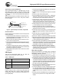
1
ESCUELA TÉCNICA SUPERIOR DE INGENIEROS
INGENIERÍA DE TELECOMUNICACIÓN
Especialidad Electrónica de Comunicaciones
PROYECTO FINAL DE CARRERA
Evaluación del chip EZ-USB SX2 con
implementación de transferencia bulk
USB 2.0
Autor:
Tutor del Proyecto:
Alejandro Raigón Muñoz
Dr. Jonathan N. Tombs
MAYO DE 2007
P ROYECTO F INAL DE C ARRERA :
Evaluación del chip EZ-USB SX2 con
implementación de transferencia bulk
USB 2.0
Autor: Alejandro Raigón Muñoz
Tutor del Proyecto: Dr. Jonathan N. Tombs
Sevilla, Mayo de 2007
Índice general
I Memoria
7
1. Objetivo y alcance
9
1.1. Justificación de la necesidad de este Proyecto . . . . . . . . . . . . . .
9
1.2. Objetivos y alcances . . . . . . . . . . . . . . . . . . . . . . . . . . . . .
10
1.3. Posibles ampliaciones . . . . . . . . . . . . . . . . . . . . . . . . . . . .
10
2. Estructura de la Memoria
13
3. Introducción a la arquitectura USB
15
3.1. Introducción . . . . . . . . . . . . . . . . . . . . . . . . . . . . . . . . .
15
3.2. Definiciones previas . . . . . . . . . . . . . . . . . . . . . . . . . . . .
16
3.3. Características básicas del USB . . . . . . . . . . . . . . . . . . . . . .
17
3.4. Componentes del bus . . . . . . . . . . . . . . . . . . . . . . . . . . . .
20
3.5. División de tareas . . . . . . . . . . . . . . . . . . . . . . . . . . . . . .
20
3.6. Modelo de comunicaciones USB . . . . . . . . . . . . . . . . . . . . .
21
3.7. Transferencias, IRPs, tramas y paquetes . . . . . . . . . . . . . . . . .
22
3.8. Transferencias bulk . . . . . . . . . . . . . . . . . . . . . . . . . . . . .
23
4. Descripción del kit
25
4.1. Introducción al kit de desarrollo CY3682 . . . . . . . . . . . . . . . . .
25
4.2. Descripción del EZ-USB SX2 . . . . . . . . . . . . . . . . . . . . . . . .
26
4.2.1. Conociendo a fondo la EZ-USB SX2 . . . . . . . . . . . . . . .
26
5. Probando el kit de desarrollo paso a paso
29
5.1. Introducción . . . . . . . . . . . . . . . . . . . . . . . . . . . . . . . . .
29
5.2. Requisitos previos . . . . . . . . . . . . . . . . . . . . . . . . . . . . . .
29
5.2.1. Ejercicio 1—Verificando el soporte USB del PC de desarrollo .
30
5.2.2. Ejercicio 2—Verificando la disponibilidad de USB 2.0 . . . . .
30
5.3. Instalación del Panel de Control EZ-USB, Drivers y Documentación .
32
5.4. Teoría de funcionamiento del kit de desarrollo . . . . . . . . . . . . .
32
5.4.1. Ejercicio 3—Comprobando la funcionalidad básica del kit de
desarrollo. Modo 1A o modo de ejemplo . . . . . . . . . . . .
32
4
ÍNDICE GENERAL
5.4.2. Ejercicio 4—Estableciendo el entorno de desarrollo para el SIEMaster. Modo 1B . . . . . . . . . . . . . . . . . . . . . . . . . .
35
5.4.3. Ejercicio 5—Enumeración personalizada . . . . . . . . . . . .
39
5.4.4. Ejercicio 6—Lectura/escritura del registro SETUP . . . . . . .
41
5.4.5. Modo 2–Modo de desarrollo . . . . . . . . . . . . . . . . . . .
45
5.5. Practicando con el kit de desarrollo . . . . . . . . . . . . . . . . . . . .
46
5.5.1. Ejercicio 7—Primera solución al problema de “Dispositivo desconocido”. Descarga de firmware a la EZ-USB FX a través del
SIEMaster . . . . . . . . . . . . . . . . . . . . . . . . . . . . . .
46
5.5.2. Ejercicio 8—Segunda solución al problema de “Dispositivo desconocido”. Descarga del firmware xmaster a la EZ-USB FX
mediante el Panel de Control EZ-USB . . . . . . . . . . . . . .
47
5.5.3. Ejercicio 9—Segunda solución al problema de “Dispositivo desconocido”. Reprogramación de la EEPROM de la EZ-USB FX
con el firmware xmaster . . . . . . . . . . . . . . . . . . . . . .
47
5.5.4. Ejercicio 10—Ejemplo de loopback en modo 1A. Uso de bulkloop 49
5.5.5. Ejercicio 11—Ejemplo de loopback manual en modo 1B . . . . .
6. Marco de trabajo para la programación USB
50
53
6.1. Introducción . . . . . . . . . . . . . . . . . . . . . . . . . . . . . . . . .
53
6.2. Programación del driver . . . . . . . . . . . . . . . . . . . . . . . . . .
53
6.3. Programación del firmware para el procesador principal . . . . . . .
56
6.4. Alternativas para la codificación de la comunicación USB entre la
aplicación host y el dispositivo USB 2.0 . . . . . . . . . . . . . . . . .
57
6.4.1. Comunicación USB a través del API de Windows . . . . . . .
57
6.4.2. Comunicación USB a través del API de Cypress . . . . . . . .
58
6.5. Instalando el estudio de desarrollo USB CY4604 . . . . . . . . . . . .
59
6.6. Usando la API de Cypress—CyAPI . . . . . . . . . . . . . . . . . . . .
59
6.6.1. Ejercicio 12—Adición del identificador del dispositivo al driver 60
6.6.2. Ejercicio 13—Sustitución de las cadenas de texto de fabricante
y suministrador . . . . . . . . . . . . . . . . . . . . . . . . . . .
61
6.6.3. Ejercicio 14—Forzando el uso del driver CyUSB.sys . . . . . .
61
6.6.4. Ejercicio 15—Aplicación host básica para la comunicación USB
2.0 de tipo bulk con el chip EZ-USB SX2 . . . . . . . . . . . . .
62
6.6.5. Ejercicio 16—Aplicación host práctica para la comunicación
USB 2.0 de tipo bulk con el chip EZ-USB SX2 . . . . . . . . . .
65
6.7. Conclusiones . . . . . . . . . . . . . . . . . . . . . . . . . . . . . . . . .
70
7. Contenido del CD-ROM
71
7.1. Manuales de consulta . . . . . . . . . . . . . . . . . . . . . . . . . . . .
71
7.2. Notas de aplicación . . . . . . . . . . . . . . . . . . . . . . . . . . . . .
72
ÍNDICE GENERAL
5
7.3. El estudio de desarrollo USB CY4604 . . . . . . . . . . . . . . . . . . .
7.4. Documentación del WDK de Microsoft . . . . . . . . . . . . . . . . .
73
73
7.5. Herramientas del WDK de Microsoft . . . . . . . . . . . . . . . . . . .
74
II Anexos
75
8. Manuales de referencia
77
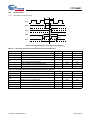
8.1. EZ-USB SX2–Getting Started–Development Kit Manual . . . . . . . . 79
8.2. EZ-USB SX2–SIEMaster User’s Guide . . . . . . . . . . . . . . . . . . 107
8.3. CY7C68001 Datasheet - EZ-USB SX2 High-Speed USB Interface Device 125
8.4. USB Interfacing CY3682 Design Notes . . . . . . . . . . . . . . . . . .
8.5. Errata Document for CY7C68001 EZ-USB SX2 . . . . . . . . . . . . . .
167
179
8.6. User guide for EZ-USB Control Panel . . . . . . . . . . . . . . . . . .
183
9. Notas de aplicación
9.1. SX2 Primer (Life After Enumeration) . . . . . . . . . . . . . . . . . . .
9.2. EZ-USB FX2/AT2/SX2 Reset and Power Considerations . . . . . . .
191
193
197
9.3. USB Error Handling For Electrically Noisy Environments, Rev. 1.0 . .
9.4. High-speed USB PCB Layout Recommendations . . . . . . . . . . . .
201
203
9.5. Bulk Transfers with the EZ-USB SX2 Connected to a Hitachi SH3 DMA
Interface . . . . . . . . . . . . . . . . . . . . . . . . . . . . . . . . . . . 207
9.6. Bulk Transfers with the EZ-USB SX2 Connected to an Intel XScale
DMA Interface . . . . . . . . . . . . . . . . . . . . . . . . . . . . . . . .
223
6
ÍNDICE GENERAL
Parte I
Memoria
Capítulo 1
Objetivo y alcance
1.1. Justificación de la necesidad de este Proyecto
Gran parte de los sistemas electrónicos que un ingeniero pueda desarrollar requerirá algún tipo de intercomunicación con un equipo informático. Hasta hoy, se
han venido utilizando multitud de conectores y protocolos en función del tipo de
transmisión (serie o paralelo), pero la estandarización ha conseguido imponer un
único protocolo y un conjunto limitado de conectores. Nos referimos, sin duda, al
Bus Serie Universal (Universal Serial Bus, USB por sus siglas inglesas), que:
1. Facilita el diseño electrónico,
2. Acelera el desarrollo del software de control (firmware) y de la aplicación final
(fichero ejecutable), y
3. Proporciona una mayor tasa de transferencia que la garantizada por los puertos paralelo (SPP, EPP o ECP) o serie (RS-232).
La proliferación de dispositivos que requieren cada vez una mayor tasa de transferencia (discos duros externos, cámaras web, . . . ), precisa de un protocolo y una
arquitectura que proporcionen el rendimiento suficiente. Es así como, pronto, los
modos 1.0 (low-speed) y 1.1 (full-speed) de USB tuvieron que dar paso al modo
USB 2.0 (high-speed), con una máxima tasa de transferencia teórica de 480 Mbits/s.
No obstante, no se trata de un protocolo sencillo de manejar. En concreto, la codificación manual del capítulo 9 de la Especificación USB es un problema prácticamente inviable en la mayoría de las aplicaciones. Por esto hemos de recurrir a circuitos
integrados que gestionen las peticiones del bus USB, descargando al procesador del
sistema electrónico diseñado de esa tarea, y reduciendo la curva de aprendizaje del
protocolo.
Uno de los kits de desarrollo que se pueden encontrar en el mercado, y que mayor éxito ha tenido entre los desarrolladores, es el EZ-USB FX de Cypress Semiconductor, con modos de funcionamiento low- y full-speed. Para el modo high-speed,
10
CAPÍTULO 1. OBJETIVO Y ALCANCE
en cambio, Cypress proporciona otro kit de desarrollo, que contiene el integrado EZUSB SX2 (C7C68001). Pero, incluso un completo producto como éste, puede desbordar al desarrollador que se enfrente por vez primera a diseños USB, a consecuencia
de documentos mal estructurados, aplicaciones poco actualizadas, y un soporte técnico mejorable.
Sería deseable, pues, un documento que permita adquirir las destrezas necesarias para trabajar con el kit, y comenzar a programar la aplicación final, en cuestión
de horas.
1.2. Objetivos y alcances
El objetivo primordial de este Proyecto Final de Carrera será “Evaluar el kit de
desarrollo CY3682 de Cypress para acelerar el diseño de dispositivos USB 2.0 y su
comunicación con un host PC”.
Con la intención de reducir la curva de aprendizaje, este objetivo principal puede
desglosarse en los siguientes objetivos secundarios:
1. Describir el kit de desarrollo CY3682 de Cypress,
2. Analizar los posibles problemas y soluciones en la configuración y funcionamiento del kit,
3. Determinar el marco de trabajo para la comunicación USB 2.0 entre el equipo
host PC y el dispositivo USB, y
4. Desarrollo de una aplicación práctica de ejemplo: comunicación bulk a velocidad high-speed (480 Mbits/s teóricos).
Adicionalmente, se ha confeccionado una recopilación de los manuales de mayor
relevancia en formato PDF en un CD-ROM adjunto, incluyéndose los más importantes en formato impreso, como anexo al final de este documento. Asimismo, se
ha impreso (y almacenado en dicho CD-ROM) las notas de aplicación que Cypress
ofrece a los desarrolladores, para que puedan proporcionar información de utilidad
en aplicaciones específicas.
1.3. Posibles ampliaciones
No pertenecen al alcance de este Proyecto los siguientes aspectos:
Desarrollo del firmware/aplicaciones software para procesadores específicos
(DSP, ASIC, FPGA, . . . ), ni
Desarrollo de drivers software para aplicaciones concretas, ni
1.3. POSIBLES AMPLIACIONES
Consideraciones de diseño electrónico.
Ambos puntos se dejan para posteriores Proyectos.
11
12
CAPÍTULO 1. OBJETIVO Y ALCANCE
Capítulo 2
Estructura de la Memoria
Con la intención de servir de ayuda al diseñador que desee conseguir, en el menor tiempo posible, que el sistema electrónico que haya diseñado se comunique con
el host PC a través del chip EZ-USB SX2, este documento se estructura de la siguiente forma:
1. La Parte I se dedica enteramente a la Memoria de este Proyecto Final de Carrera. Consta de siete capítulos, de los cuales los dos primeros son introductorios.
a) En el Capítulo 3 proporcionaremos la información mínima y necesaria
para comprender la arquitectura USB: conceptos básicos, componentes,
consideraciones acerca de la topología, flujo de comunicaciones típico;
distinción entre transferencias, transacciones y paquetes; y características
de una transferencia bulk.
b) En el Capítulo 4 veremos de qué partes se compone el kit CY3682, y cuáles son las principales características del chip EZ-USB SX2.
c) El Capítulo 5 pretende ser un tutorial con el que verificar las principales
operaciones a realizar con el kit CY3682. Mediante numerosos ejercicios,
avanzaremos progresivamente en el dominio y comprensión de los componentes hardware y software de dicho kit.
d) El marco de trabajo para la programación USB, de forma enormemente
simplificada, se ofrece en el Capítulo 6. Se proporciona información de
referencia para el programador que desee desarrollar un driver utilizando
el modelo WDK, y se analizan las posibles alternativas para codificar la
comunicación USB entre la aplicación host y el dispositivo USB 2.0. Será
aquí donde expliquemos cómo implementar la comunicación USB 2.0 tipo bulk
con el chip EZ-USB SX2 (vea el apartado 6.6, en la página 59).
e) Por último, en el Capítulo 7 describimos el contenido del CD-ROM compañero, que pretende ser una herramienta más de apoyo.
2. Como anexo, la Parte II recoge los principales manuales de referencia.
14
CAPÍTULO 2. ESTRUCTURA DE LA MEMORIA
3. También como anexo, se adjuntan distintas notas de aplicación en la Parte II.
Capítulo 3
Introducción a la arquitectura y
protocolo del Bus Serie Universal
3.1. Introducción
Comenzaremos en este capítulo proporcionando unas nociones básicas para comprender el cuadro global de la arquitectura USB. No se trata de exponer un análisis
exhaustivo de todos los detalles encontrados en las Especificaciones, sino mas bien
presentar los elementos necesarios para entender cómo iniciarnos en la programación USB.
No obstante, el lector interesado puede ganar el nivel de comprensión que desee
acudiendo a la siguiente bibliografía:
Don Anderson, USB System Architecture. Addison-Wesley, second edition, 2001.
En esta obra se detallan todos los aspectos de la arquitectura USB, de especial
importancia para diseñadores de dispositivos que gestionan las transferencias
USB de más bajo nivel.
Jan Axelson, USB Complete. Lakeview Research, third edition, 2005. Este libro
es para desarrolladores que diseñan y programan dispositivos que utilizan la
interfaz USB. Enseña la programación del firmware que reside en los dispositivos USB y la programación de las aplicaciones que se comunican con éstos.
En lo que sigue, trataremos estos aspectos :
1. Definiciones previas.
2. Características básicas del USB desde el punto de vista del usuario y del desarrollador.
3. Componentes del bus y topología.
4. División de tareas.
16
CAPÍTULO 3. INTRODUCCIÓN A LA ARQUITECTURA USB
5. Modelo de flujo de comunicaciones USB.
6. Transferencias, IRPs, tramas y paquetes.
7. Transferencias bulk.
3.2. Definiciones previas
La arquitectura USB suele manejar un reducido glosario de términos:
Función: La especificación USB define una función como un dispositivo que
proporciona una capacidad al host. Ejemplos de funciones son un ratón, un
conjunto de altavoces, etc. Un único dispositivo físico puede contener más de
una función.
Hub: Un hub tiene un conector upstream para comunicarse con el host y uno o
más conectores downstream o conexiones internas con dispositivos incrustados.
Cada conector downstream o conexión interna representa un puerto USB.
Dispositivo: Un dispositivo es una función o hub, excepto en el caso especial
de un dispositivo compuesto, que contiene un hub y una o más funciones. Cada dispositivo en un hub tiene una dirección única, excepto en el caso de los
dispositivos compuestos, cuyo hub y funciones tienen cada uno direcciones
únicas. Un dispositivo compuesto es un dispositivo multifunción con múltiples e independientes interfaces. Las interfaces se definen por los descriptores
de interfaces almacenados en el dispositivo.
Puerto: En un sentido amplio, un puerto de ordenador es una localización direccionable disponible para conectar circuitos adicionales. El software puede
monitorizar y controlar los circuitos del puerto leyendo y escribiendo en la dirección del puerto. Los puertos USB comparten una única ruta al host y no son
directamente direccionables. Cada conector en un bus representa un puerto
USB, donde todos los dispositivos comparten el ancho de banda del bus. Así
que, incluso aunque un controlador host USB pueda comunicarse con múltiples puertos, cada uno con su propio conector y cable, una ruta de datos sirve
para todos ellos. Sólo un dispositivo o el host puede transmitir cada vez. Un
único ordenador puede tener múltiples controladores host USB, cada uno con
su propio bus.
Endpoint: Puerto al que puede accederse indirectamente a través de los drivers del dispositivo USB.
Low/full/high-speed: Modo de funcionamiento en el que la tasa de transferencia del bus es de 1,5/12/480 Mbps.
3.3. CARACTERÍSTICAS BÁSICAS DEL USB
17
Trama: Intervalo de 1 ms (125 µs en modo high-speed, donde hablaremos de
microtramas).
Transacción: Agrupación de paquetes. Una transacción es de entrada cuando los datos son leídos por el host desde el sistema USB destino, o de salida
cuando se transfieren datos desde el sistema al dispositivo USB destino.
Transferencia: Una o más transacciones.
Además, puede resultar de interés conocer que:
downstream se refiere a una transferencia desde host, y upstream a una transferencia hacia el host;
frame es trama, y
payload equivale a carga útil.
3.3. Características básicas del USB
Desde el punto de vista del usuario el USB presenta las siguientes ventajas:
Facilidad de uso :
• Una única interfaz para multitud de dispositivos.
• Configuración automática. Windows detecta el periférico USB conectado
al PC y carga el driver software apropiado, sin necesidad de reiniciar el
sistema antes de usar el periférico.
• Fácil de conectar. Sin necesidad de abrir la carcasa del ordenador para
añadir una tarjeta de expansión. Pueden conseguirse más puertos USB
añadiendo hubs. La conexión o desconexión puede hacerse “en caliente”,
esto es, sin importar si el sistema y el periférico están alimentados.
• Cables fáciles: no es posible conectarlos de forma incorrecta. Los segmentos de cable pueden tener una longitud máxima de 5 metros. Mediante
hubs, un periférico puede estar hasta 30 metros del PC host. Los conectores son pequeños y compactos en comparación con los conectores RS-232
y paralelo típicos.
• Sin configuraciones del usuario tales como direcciones de puerto o líneas
de petición de interrupción, jumpers o utilidades de configuración. Sólo
existe una línea IRQ dedicada al controlador host USB.
• Sin necesidad de alimentación externa, en caso de que el consumo del
periférico sea inferior a 500 mA.
18
CAPÍTULO 3. INTRODUCCIÓN A LA ARQUITECTURA USB
Transferencias de datos rápidas y fiables. La fiabilidad del USB se debe tanto
al hardware como a los protocolos de transferencias de datos. Las especificaciones hardware de drivers USB, receptores y cables aseguran una interfaz sin
ruidos, que podrían causar errores de datos. El protocolo USB permite detectar
errores en los datos recibidos, y notificar al emisor para que los retransmitan.
La detección, notificación y retransmisión es llevada a cabo por hardware, sin
requerir programación o intervención del usuario.
Flexibilidad. USB permite tres velocidades de bus: high speed a 480 Mb/s, full
speed a 12 Mb/s y low speed a 1,5 Mb/s. Todos los dispositivos comparten el
mismo bus, por lo que la tasa de datos de un periférico individual será menor
que la velocidad del bus.
Bajo coste.
Bajo consumo de potencia, conseguido gracias a circuitos de ahorro de potencia y código que automáticamente apaga los periféricos USB cuando no se
encuentran en uso.
Por desarrolladores entendemos:
Diseñadores hardware, que seleccionan los componentes y diseñan los circuitos de los dispositivos,
Programadores que escriben el software embebido en los dispositivos, y
Programadores que escriben el software PC que se comunican con los dispositivos.
Para todos ellos, la arquitectura USB presenta los siguientes beneficios:
Cables estándares.
Comprobación automática de errores.
Versatilidad: existen cuatro tipos de transferencias y tres velocidades.
Existen clases que especifican los requerimientos y protocolos de ciertos dispositivos (impresoras, teclados, ratones, etc.).
Soporte del USB desde distintos sistemas operativos . Esto es, el sistema operativo detecta los dispositivos que se conectan o desconectan, se comunica con
los dispositivos recién conectados para determinar cómo intercambiar datos
con ellos, y proporciona un mecanismo para permitir que los driver software
se comuniquen con el hardware USB del ordenador y las aplicaciones que deseen acceder a los periféricos USB. A un nivel más alto, el soporte por parte
3.3. CARACTERÍSTICAS BÁSICAS DEL USB
19
del sistema operativo implica la inclusión de drivers de clase que permitan a
los programadores de aplicaciones acceder a los dispositivos.
Las aplicaciones utilizan las funciones de la Interfaz de Programación de Aplicaciones (Application Programming Interface, o API) y otros componentes del
sistema operativo para comunicarse con los drivers de los dispositivos.
Los drivers de dispositivos USB utilizan el Windows Driver Model (WDM), que
define una arquitectura para drivers bajo Windows 98 y ediciones posteriores.
Teniendo en cuenta que Windows incluye drivers de bajo nivel para manejar
las comunicaciones con el hardware USB, escribir un driver de dispositivo USB
es típicamente más fácil que escribir drivers para dispositivos que usan otras
interfaces.
Soporte del USB por los periféricos. El hardware de cada dispositivo USB debe incluir un chip controlador que gestione los detalles de las comunicaciones
USB. El periférico es responsable de responder a peticiones de envío y recepción de datos utilizados al identificar y configurar el dispositivo, y de leer y
escribir otros datos en el bus.
Soporte desde el Foro de Implementadores USB (USB Implementers Forum, o
USB-IF). En su web es posible encontrar los documentos de la especificación,
FAQs, herramientas y foros de desarrolladores que discuten acerca de temas
relacionados con el USB.
Entre las desventajas encontramos las siguientes:
Falta de soporte de comunicaciones peer-to-peer. Cada comunicación USB es
entre un PC host y un periférico. Los host no pueden comunicarse entre sí directamente (se precisa una red que sirva de puente), como tampoco lo pueden
hacer los periféricos con USB.
Imposibilidad de difusión (broadcast).
Falta de soporte en hardware y sistemas operativos antiguos.
Distancia limitada : segmentos de cables de hasta 5 metros, y distancia máxima
entre periférico y host PC de 30 metros.
Desde el punto de vista del desarrollador, los principales retos del USB son la complejidad de la programación y, para desarrolladores a pequeña escala, la obtención
de la identificación de vendedor.
20
CAPÍTULO 3. INTRODUCCIÓN A LA ARQUITECTURA USB
3.4. Componentes del bus
Los componentes físicos del Bus Serie Universal son los circuitos, conectores, y
cables entre un host y uno o más dispositivos. El host es un PC u otro ordenador
que contiene un controlador host USB y un hub raíz, que le permiten al sistema
operativo comunicarse con los dispositivos del bus.
El controlador host formatea los datos para trasmitirlos en el bus y traduce los
datos recibidos a un formato comprensible para los componentes del sistema operativo.
El hub raíz tiene uno o más conectores para la conexión de dispositivos. En conjunción con el controlador host, el hub raíz detecta los dispositivos conectados y
removidos, lleva a cabo peticiones desde el controlador host, y pasa datos entre los
dispositivos y el controlador host.
Los dispositivos son los periféricos y los hubs adicionales conectados bus. Cada
dispositivo debe contener circuitos y códigos que conozcan cómo comunicarse con
el host.
Topología La topología en el bus es en estrella. En el centro de cada estrella se
encontrará un hub, y en cada punta de la estrella hallaremos un dispositivo que se
conecte a un puerto del hub. El número de puntas de cada estrella puede variar,
según el hub, entre dos y siete puertos.
La conexión en estrella describe sólo las conexiones físicas. En programación, lo
que interesa es la conexión lógica. Para la comunicación, el host y el dispositivo no
necesitan conocer cuántos hubs debe atravesar la información. Sólo un dispositivo
puede comunicarse con el controlador host cada vez. Para incrementar el ancho de
banda disponible para dispositivos USB, un PC puede tener múltiples controladores
host.
3.5. División de tareas
De forma simplificada, los deberes del host son:
Detectar los dispositivos conectados al bus y sus capacidades y requerimientos.
Gestionar el flujo de datos. Múltiples periféricos pueden querer transferir datos a la vez. El controlador host divide el tiempo disponible en segmentos denominados tramas o microtramas y reparte cada porción de transmisión de
trama o microtrama.
Comprobar errores.
3.6. MODELO DE COMUNICACIONES USB
21
Proporcionar alimentación.
Intercambiar datos entre periféricos.
El trabajo del host no es trivial. Por suerte, el hardware del controlador host y su
driver en Windows hacen la mayor parte del trabajo de gestión del bus.
Cada dispositivo conectado al host debe tener un driver que permita que las aplicaciones se comuniquen con el dispositivo. Algunos periféricos pueden usar drivers
incluidos con Windows, mientras que otros proporcionarán sus propios drivers.
Varios componentes software a nivel de sistema gestionan la comunicación entre
el driver del dispositivo y el controlador hardware del host y el hub raíz. Las aplicaciones no tienen que preocuparse acerca de los detalles específicos de la comunicación USB con los dispositivos. Todo lo que la aplicación tiene que hacer es enviar
y recibir datos usando funciones estándar del sistema operativo, accesibles desde
cualquier lenguaje de programación.
Por su parte, el periférico deberá realizar las siguientes tareas (que serán manejadas en todo caso por el controlador USB en el periférico):
Detectar comunicaciones dirigidas al chip.
Responder a peticiones estándar.
Comprobar errores.
Gestionar el consumo.
Intercambiar datos con el host.
3.6. Modelo de comunicaciones USB
USB no consume recursos del sistema directamente, es decir, los dispositivos
USB no se mapean en memoria o en el espacio de direcciones e/s, ni tienen líneas
IRQ o canales DMA dedicados. Además, todas las transacciones se originan en el sistema host. Sólo se requieren los siguientes recursos de sistema por un sistema USB:
localizaciones de memoria utilizadas por el software del sistema USB y memoria
y/o espacio de direcciones e/s y líneas IRQ utilizadas por el controlador host.
Flujo de comunicaciones
en el cliente USB:
El flujo de comunicaciones USB típico se inicia siempre
1. El cliente USB inicia una transferencia cuando llama al software del sistema
USB y solicita una transferencia.
22
CAPÍTULO 3. INTRODUCCIÓN A LA ARQUITECTURA USB
2. Los drivers cliente USB proporcionan una memoria buffer utilizada para almacenar datos cuando se transfieran datos a o desde el dispositivo USB. Cada
transferencia entre un registro dado (un endpoint) dentro de un dispositivo
USB y el driver cliente ocurre a través de un conducto de comunicación (pipe)
que el software del sistema USB establece durante la configuración del dispositivo.
3. El software del sistema USB separa la petición del cliente en transacciones individuales consistentes con los requerimientos de ancho de banda del dispositivo y los mecanismos del protocolo USB.
4. Las peticiones se pasan al driver del controlador host, que programa la realización de las transacciones a través del USB en partes.
5. El controlador host realiza la transacción según los contenidos del descriptor
de transferencia que es construido por el driver del controlador host. El descriptor de transferencia define una transacción dada que debe realizarse para
satisfacer la petición de transferencia de un cliente. El controlador host genera
una transacción USB especificada por cada descriptor de transferencia.
6. Cuando finaliza la transferencia, el software del sistema USB lo notifica al driver cliente.
3.7. Transferencias, IRPs, tramas y paquetes
Cada función USB se diseña con una colección de registros, o endpoints, utilizados por el driver cliente cuando accede a su función.
Los tipos de transferencia soportados por USB son: isócronas, de datos (bulk),
interrumpidas o de control. El driver cliente conoce la naturaleza de la transferencia
relacionada con cada endpoint asociado con su función, como lo hace el driver USB.
Esta información se determina leyendo los descriptores del dispositivo.
Cuando un driver cliente desea realizar una transferencia a o desde un endpoint
dado, llama al driver USB para que inicie la transferencia, denominada IRP.
Puesto que el USB es un bus compartido, un único dispositivo no puede realizar la transferencia de un bloque completo sobre USB a la vez. La transferencia
será partida y realizada en segmentos (denominados transacciones) en un periodo
de tiempo superior. Esto asegura que una porción del ancho de banda USB pueda
destinarse a otros dispositivos USB que se encuentren en el bus.
La comunicación USB se basa en transferir datos en intervalos de 1 ms (125 µs
en modo high-speed) denominados tramas. Cada dispositivo USB requiere que una
porción del ancho de banda USB sea reservada durante esas tramas. La reserva de
3.8. TRANSFERENCIAS BULK
23
bancho de banda depende de la latencia requerida por el dispositivo (como es especificada en los descriptores del dispositivo) y del ancho de banda USB disponible.
Cuando un dispositivo USB se conecta y se configura, el software del sistema analiza
los descriptores del dispositivo para determinar la cantidad de ancho de banda del
bus que requiere. El software comprueba el ancho de banda restante y, si los requisitos del dispositivo, pueden ser satisfechos, es configurado. Si el ancho de banda
requerido por el dispositivo no está disponible, debido a ancho de banda del bus
reservado ya para otros dispositivos previamente conectados, el dispositivo no será
configurado y el usuario será notificado.
El driver del controlador host recibe los paquetes de peticiones del driver USB
y las programa para que sean realizadas durante una serie de tramas. La programación es llevada a cabo construyendo una serie de descriptores de transferencia
que definen cada transacción secuencial a ser realizada sobre el USB. El controlador
host lee e interpreta cada descriptor de transferencia y ejecuta la transacción USB
descrita.
El controlador host y el hub raíz generan transacciones sobre USB, que constan
de una serie de paquetes que típicamente incluyen el paquete de testigo, el paquete
de datos, y el paquete de acuse de recibo (ack).
3.8. Transferencias bulk
Las principales características de las transferencias bulk (las que emplearemos
en nuestra aplicación práctica) se listan a continuación:
Son utilizadas por dispositivos que no requieren una tasa de transferencia específica, como las impresoras.
Se programan en función del ancho de banda restante después de haber programado todas las otras transferencias. Si no queda ancho de banda disponible, se retardan hasta que la carga del bus disminuya. Sin embargo, en ausencia de otros tipos de transferencias, se les puede destinar una gran porción del
ancho de banda del bus.
El tamaño máximo del paquete de datos se limita a 8, 16, 32 o 64 bytes.
Cuando tiene lugar una transferencia, todos los tamaños de los paquetes deben tener el tamaño máximo especificado en el campo de tamaño máximo del
paquete, excepto en el último paquete de datos de la transferencia. Un fallo
transmitiendo paquetes sin el tamaño esperado dará lugar a la finalización de
la transferencia.
Sus endpoints siempre se configuran por software, puesto que no existen requisitos de entrega de datos a ninguna tasa específica.
24
CAPÍTULO 3. INTRODUCCIÓN A LA ARQUITECTURA USB
Soportan detección y recuperación ante errores.
Capítulo 4
Descripción del kit
4.1. Introducción al kit de desarrollo CY3682
El kit de desarrollo CY3682 proporciona un entorno de desarrollo para diseñar,
implementar, y depurar un periférico USB utilizando el motor de interfaz serie (SIE)
USB 2.0 Cypress EZ-USB SX2 (CY7C68001), y el chip EZ-USB FX muy popular por
control de firmware para emular un SIE independiente. El CY7C68001 es un dispositivo de lógica fija, que no requiere firmware para operar.
El kit incluye:
Documentación impresa:
• Datasheet del EZ-USB SX2.
• Lista de erratas EZ-USB SX2 CY7C68001 Rev. E, Versión 1.3.
• Notas de diseño del kit de desarrollo CY3682, Rev. August1, 2002.
• Manual de introducción del usuario al kit de desarrollo EZ-USB SX2, Rev.
2.0.
• Manual del usuario del EZ-USB SX2 SIEMaster, v1.0.
• Acuerdo de licencia del software Cypress.
Hardware:
• Placa de desarrollo EZ-USB SX2.
• Placa de desarrollo EZ-USB FX (para controlar la SX2 a través de un microprocesador 8051).
• 2 cables USB A-B de 1 metro de largo.
Software:
• Software de control SIE-Master.
26
CAPÍTULO 4. DESCRIPCIÓN DEL KIT
• Driver del dispositivo de propósito general EZ-USB.
• Código de muestra del firmware 8051.
• Utilidad de panel de control de la familia EZ-USB.
• Ficheros de diseño de la placa.
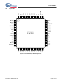
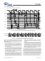
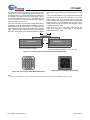
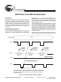
4.2. Descripción del EZ-USB SX2
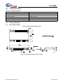
El dispositivo de interfaz Cypress EZ-USB SX2 ha sido diseñado para trabajar
con unidades externas que actúen como master (tales como microprocesadores estándar, ASIC, DSP, FPGA, etc.), habilitando el soporte USB 2.0 para cualquier diseño
de periférico.
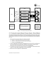
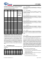
La EZ-USB SX2 proporciona una interfaz esclava con las siguientes características (vea el diagrama de bloques de la figura 4.1):
Transceptor USB 2.0 integrado, permitiendo un funcionamiento a full-speed
(con una tasa de bit de señalización de 12 Mbits/s) o high-speed (con una tasa de bit de señalización de 480 Mbits/s).
Motor de Interfaz Serie (SIE), que se encarga de las peticiones de bajo nivel
desde el host PC sin interrumpir el procesador externo que actúa de master.
Decodificador de comandos.
Endpoint de control con buffer fijo separado y cuatro endpoints configurables
compartiendo un espacio FIFO de 4 KB:
• Endpoint 0 para control de la interfaz USB con un buffer de 64 bytes separado.
• Endpoints 2, 4, 6 y 8 para datos, con posibles configuraciones bulk, interrupt o isochronous.
PLL (Phase-Locked Loop) integrado.
Interfaz de expansión y señales a través de seis conectores de 20 pines.
No requiere firmware.
4.2.1. Conociendo a fondo la EZ-USB SX2
Al final de este documento, se adjuntan los manuales y documentos necesarios
para hallar información sobre:
Características técnicas del CI CY7C68001,
4.2. DESCRIPCIÓN DEL EZ-USB SX2
Figura 4.1: Diagrama de bloques de la placa EZ-USB SX2.
Firmware de ejemplo para el procesador externo,
Esquemas PCB,
Jumpers, conectores, pinouts, indicadores, etc.
Por tanto, no se repetirá dicha información a lo largo de esta Memoria.
27
28
CAPÍTULO 4. DESCRIPCIÓN DEL KIT
Capítulo 5
Probando el kit de desarrollo paso a
paso
5.1. Introducción
En este capítulo analizaremos los siguientes aspectos:
1. Requisitos previos para el funcionamiento del kit de desarrollo,
2. Elementos software disponibles para su instalación,
3. Modos de funcionamiento del kit de desarrollo,
4. Soluciones al problema de “Dispositivo desconocido” al conectar la placa EZUSB SX2, y
5. Demostración funcional: loopback de datos.
De forma desglosada y secuencial, trataremos cada punto con ayuda de abundantes
ejercicios. Se proporcionan, asimismo, numerosas notas para ahondar en la comprensión del comportamiento de la EZ-USB SX2.
5.2. Requisitos previos
Dentro de los productos Microsoft, los sistemas operativos que admiten comunicaciones USB son los siguientes:
Windows XP (recomendado para el desarrollo en USB 2.0),
Windows 2000,
Windows Millenium,
Windows 98 Second Edition.
30
CAPÍTULO 5. PROBANDO EL KIT DE DESARROLLO PASO A PASO
Además del material proporcionado por el kit de desarrollo, se requiere que el PC
sobre el cual se colocará el dispositivo USB disponga de al menos un controlador
host USB 2.0, y tenga instalado los drivers USB 2.0 de Windows. Por otro lado, serán
necesarias herramientas software adicionales para el desarrollo tanto del firmware del procesador principal, como de la aplicación host USB (una IDE como la de
Borland C++Builder 6).
5.2.1. Ejercicio 1—Verificando el soporte USB del PC de desarrollo
Antes de comenzar a trabajar con el kit de desarrollo, aunque sea trivial en un
sistema actual, debemos comprobar que nuestro PC dispone de soporte USB. Esto
es, deberemos disponer de conexiones USB (al menos un conector plano USB disponible en el chasis del PC), y tener instalado el controlador del Bus Serie Universal en
Windows. Esto último puede verse fácilmente siguiendo los pasos siguientes:
1. Abrimos el Administrador de Dispositivos de Windows. Aunque existen varias alternativas para efectuar esta operación, sin duda, la más rápida es ejecutar el fichero devmgmt.msc, lo cual puede hacerse fácilmente tecleando simultáneamente la tecla de Windows y la tecla ’r’, y escribiendo a continuación el
nombre del archivo. De esta forma se abrirá la consola de gestión de Windows
para el administrador de dispositivos.
2. Localizaremos el nodo de “Controladoras de bus serie universal (USB)” y dentro de éste hallaremos el nodo o nodos del “Concentrador raíz USB”.
En el caso de que no aparezcan los iconos mencionados, habrá que comprobar:
Si el USB ha sido desactivado en la BIOS.
Si hay controlador USB en el PC.
Si hay soporte USB por parte del sistema operativo.
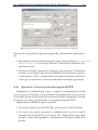
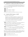
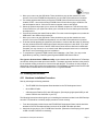
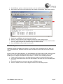
5.2.2. Ejercicio 2—Verificando la disponibilidad de USB 2.0
La siguiente prueba consistirá en determinar si el controlador USB admite el
funcionamiento high-speed (es decir, USB 2.0). Para ello, nos dirigiremos al Administrador de Dispositivos de Windows y dentro del icono de “Controladoras de bus
serie universal (USB)” buscaremos la existencia de un controlador host mejorado (p.e.
“VIA USB 2.0 Enhanced Host Controller”), aparte de un hub raíz 2.0 (“USB 2.0 Root
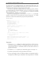
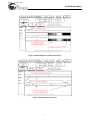
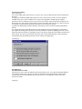
Hub”). Debería encontrar una estructura similar a la mostrada en la figura 5.1.
5.2. REQUISITOS PREVIOS
Figura 5.1: Comprobando la presencia de controlador host USB 2.0.
31
32
CAPÍTULO 5. PROBANDO EL KIT DE DESARROLLO PASO A PASO
5.3. Instalación del Panel de Control EZ-USB, Drivers
y Documentación
El entorno de desarrollo del kit incluye los siguientes elementos:
El Panel de Control EZ-USB: es un programa Windows que permite enviar y
recibir datos a través del USB a cualquier chip de Cypress Semiconductor.
La utilidad SIEMaster: programa que se comunica con el SX2 a través de la
placa de desarrollo FX, mediante la interfaz del procesador principal, permitiendo fácilmente determinar parámetros de configuración de los registros de
la SX2.
En el CD-ROM adjunto se incluye la última versión del entorno de desarrollo hallada en la página web de Cypress. La instalación es relativamente sencilla, sólo hemos
de ejecutar el archivo EZ-USB_devtools_version_261700.exe, seleccionar el
modo de instalación típica, y seguir las instrucciones. Se recomienda la creación de
accesos directos en el escritorio de los programas “EZ-USB Control Panel” y “SX2
SIEMaster”, que pueden encontrarse en Inicio\Programas\Cypress\USB.
5.4. Teoría de funcionamiento del kit de desarrollo
Para demostrar la funcionalidad del SX2, el kit de desarrollo incluye un microprocesador y placa EZ-USB FX con la cual la placa SX2 se conecta. El microprocesador FX basado en un 8051 se utiliza como el procesador principal externo para el
SX2. Hay tres formas de utilizar el kit de desarrollo: dos formas con la placa SX2
conectada a la placa FX (Modo 1A y 1B), y una con el SX2 funcionando independiente (Modo 2)
5.4.1. Ejercicio 3—Comprobando la funcionalidad básica del kit de
desarrollo. Modo 1A o modo de ejemplo
Para comprobar la funcionalidad básica del kit de desarrollo, primero verificaremos la presencia del driver de propósito general EZ-USB (ezusb.sys), que se
instala en el directorio Windows\System durante la instalación del Panel de Control EZ-USB, y después probaremos la comunicación entre el kit de desarrollo y el
Panel de Control.
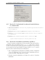
Seguiremos los siguientes pasos:
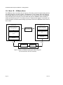
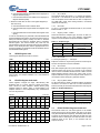
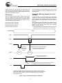
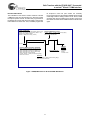
1. Se adoptará el funcionamiento en modo 1A (vea la figura 5.2), para lo cual
tendremos que configurar los jumpers como sigue:
5.4. TEORÍA DE FUNCIONAMIENTO DEL KIT DE DESARROLLO
33
Figura 5.2: Diagrama de bloques del sistema en Modo 1A.
a) En la placa SX2:
JP3 conectado entre los pines 2-3, permitiendo que el reset sea proporcionado por la FX (facilitando la reenumeración mediante firmware).
JP4 no conectado (la EEPROM es de 8 kilobytes, por lo que requiere
un direccionamiento de 2 bytes).
JP7 conectado entre los pines 1-2 (lo cual alimentará a la placa FX
también).
b) y en la placa FX:
JP8 no conectado (la EEPROM es de 8 kilobytes, por lo que requiere
un direccionamiento de 2 bytes).
JP9 conectado entre los pines 1-2 (la RAM contendrá el firmware que
se cargará en la EEPROM al recibir alimentación la placa).
2. Conectamos la placa de desarrollo EZ-USB SX2 a la placa de desarrollo FX.
3. Mediante un cable USB A-B, conectaremos el conector A al controlador host
USB 2.0 del PC y el conector B a la placa SX2, permitiendo que el PC vea la
SX2, que será controlada por el procesador 8051 contenido en la placa FX.
4. El sistema operativo detectará un nuevo dispositivo USB, y notificará que va
a instalar el driver. Como éste ya fue instalado anteriormente, lo localizará
automáticamente y lo cargará.
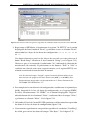
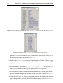
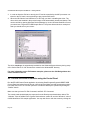
5. Abriremos el Administrador de Dispositivos de Windows y localizaremos debajo de “Controladoras de Bus Serie Universal (USB)”, el icono de “Cypress
EZ-USB Sample Device” (vea la figura 5.3).
Funcionalmente, la detección del kit de desarrollo como dispositivo de prueba se explica teniendo en cuenta que, si no se ha reprogramado la EEPROM
de la FX, ésta tiene almacenado el firmware de ejemplo xmaster.hex, que
34
CAPÍTULO 5. PROBANDO EL KIT DE DESARROLLO PASO A PASO
Figura 5.3: Ventana del Administrador de Dispositivos en modo 1A.
5.4. TEORÍA DE FUNCIONAMIENTO DEL KIT DE DESARROLLO
35
Figura 5.4: El dispositivo de prueba ha sido conectado a un hub raíz USB 2.0.
como se verá luego se encarga de controlar la SX2, provocando la reenumeración del dispositivo tras conectarse al concentrador USB, y cargando el
descriptor por defecto asociado con la etiqueta “Cypress EZ-USB Sample
Device” en el fichero .INF del driver, independientemente del contenido
de la EEPROM de la SX2.
6. Verificaremos que hemos conectado el dispositivo a un puerto del hub raíz
USB 2.0. Esto lo podemos ver seleccionando Ver\Dispositivos por Conexión
en el Administrador de Dispositivos de Windows, y localizando “Bus PCI”,
uno de cuyos nodos hijos será el dispositivo de prueba EZ-USB, con lo cual
deberíamos apreciar un esquema similar al mostrado en la figura 5.4.
7. Ejecutamos el Panel de Control EZ-USB y pulsamos en el botón “Open All”,
provocando la detección (si no se ha producido a continuación de la apertura
de dicha aplicación) del dispositivo USB Cypress conectado y la apertura de
una ventana hija con identificador de dispositivo “Ezusb-0” (texto que aparece
en un control desplegable a la derecha de la etiqueta “Device”).
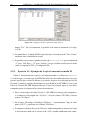
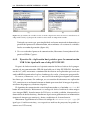
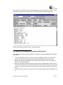
8. Pulsamos sobre el botón “Get Dev” para obtener el descriptor de la placa SX,
y obtendremos una salida similar a la mostrada en la figura 5.5, donde puede
verse que el identificador de vendedor (también conocido como VID), “idVendor”, tiene el valor 0x04b4 (identificación de Cypress Semiconductor), y el
identificador de producto (también conocido como PID), “idProduct”, tiene el
valor 0x1002 (que identifica la aplicación de prueba SX2).
De esta forma, hemos conseguido la comunicación entre el PC y la SX2 a través
del Panel de Control EZ-USB.
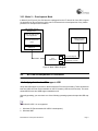
5.4.2. Ejercicio 4—Estableciendo el entorno de desarrollo para el
SIEMaster. Modo 1B
La utilidad SIEMaster descarga un firmware especial a la placa FX, para controlar
la SX2 a través de la FX, facilitando la experimentación con la SX2 sin tener que
36
CAPÍTULO 5. PROBANDO EL KIT DE DESARROLLO PASO A PASO
Figura 5.5: Respuesta de la SX2 al comando de petición de descriptor.
escribir firmware. Así, el usuario puede probar las siguientes funciones básicas que
el SIEMaster realiza sobre la SX2:
Enumeración por defecto,
Enumeración personalizada,
Monitorización de interrupciones,
Lectura/escritura de registros,
Lectura de información de configuración,
Transferencia de datos a través del endpoint 0.
Seguiremos la siguiente lista de pasos:
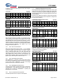
1. Adoptaremos el modo 1B (figura 5.6), para lo cual los jumpers serán configurados como sigue:
a) En la SX2:
JP3 conectado entre los pines 2-3 (el reset será proporcionado por la
FX).
JP4 no conectado (la EEPROM es de 8 kilobytes, por lo que requiere
un direccionamiento de 2 bytes).
JP7 desconectado (la FX obtendrá la alimentación de forma independiente a la SX2).
b) y en la FX:
5.4. TEORÍA DE FUNCIONAMIENTO DEL KIT DE DESARROLLO
37
Figura 5.6: Diagrama de bloques del sistema en modo 1B.
JP8 no conectado (la EEPROM es de 8 kilobytes, por lo que requiere
un direccionamiento de 2 bytes).
JP9 desconectado (el firmware no será leído de la EEPROM, sino que
será proporcionado por el host).
2. Conectamos la placa de desarrollo EZ-USB SX2 a la placa de desarrollo FX.
3. Mediante un cable USB A-B, conectaremos el conector A al controlador host
USB 2.0 del PC y el conector B a la placa SX2. De forma similar, mediante otro
cable USB A-B, conectaremos el conector A al controlador host USB 2.0 del PC
y el conector B a la placa FX. Además, probablemente Windows notifique la
instalación de un nuevo dispositivo y requiera que se autorice la instalación
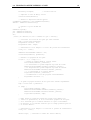
de los drivers.
Si en este momento abrimos el Administrador de Dispositivos de Windows, obtendremos un esquema de dispositivos similar al mostrado en la
figura 5.7. Donde “Dispositivo desconocido”, a menos que la EEPROM de
la SX2 se haya reprogramado, es la propia SX2; y “Cypress EZ-USB (2235)
- EEPROM missing” es la placa FX.
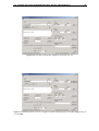
4. Iniciamos a continuación la utilidad SIEMaster, con lo que se descarga un firmware especial en la FX, que conecta esta placa al bus USB como un dispositivo “Cypress EZ-USB Sample Device”, con los siguientes parámetros: identificador de vendedor (VID) igual a 0x0547 e identificador de producto (PID)
igual a 0x1002 (vea la figura 5.8). Puede apreciarse, además, la aparición del
mensaje “Target board ready” en el cuadro de texto debajo del área funcional
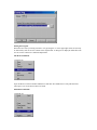
“Setup”.
5. Pulsando en el botón “Read”, leemos que el registro IFCONFIG tiene el valor
C9, lo que indica que la SX2 aún no está conectada. Para ello, pulsamos en el
38
CAPÍTULO 5. PROBANDO EL KIT DE DESARROLLO PASO A PASO
Figura 5.7: Ventana del Administrador de Dispositivos de Windows mostrando los dispositivos USB
conectados en modo 1B antes de ejecutar la aplicación SIEMaster.
5.4. TEORÍA DE FUNCIONAMIENTO DEL KIT DE DESARROLLO
39
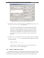
Figura 5.8: Propiedades de “Cypress EZ-USB Sample Device”.
botón “Enumerate”, con lo que obtenemos un esquema de dispositivos USB
similar al recogido en la figura 5.9a. Como puede apreciarse, encontramos dos
dispositivos “Cypress EZ-USB Sample Device”, correspondiente a cada una de
las placas. El dispositivo de muestra nuevo tiene, sin embargo, VID\PID igual
a 0x04b4\0x1002 (vea la figura 5.9b), que coincide con los valores leídos del
descriptor de prueba en el modo 1A. Pulsando ahora sobre el botón “Read”,
vemos que el registro IFCONFIG toma el valor C8, indicando la correcta detección de la SX2 por parte del host; efecto producido por el firmware cargado
que la FX que produce la reenumeración de la SX2, y la carga de un descriptor
de prueba en su RAM.
Consultando en el datasheet, puede comprobarse que el valor 0xC8 (11001000b)
en el registro IFCONFIG indica: que se utilizará el reloj interno de 48 MHz
(bit a uno lógico en los campos booleanos IFCLKSRC y 3048MHZ), con activación por flanco de subida (bit a cero lógico en el campo IFCLKPOL), FIFOs operando asíncronamente (campo ASYNC a 1), modo stand-by desactivado (campo STANDBY a cero lógico), con el pin FLAGD/CS# actuando
como un selector de chip esclavo (campo FLAGD/CS# a 0), y en conexión
con el bus USB (campo DISCON a cero lógico).
5.4.3. Ejercicio 5—Enumeración personalizada
SIEMaster nos permite realizar una enumeración personalizada, en lugar de la
enumeración por defecto con los parámetros VID\PID\DID = 0x04b4\0x1002\0x0000.
40
CAPÍTULO 5. PROBANDO EL KIT DE DESARROLLO PASO A PASO
(a)
(b)
Figura 5.9: (a) Ventana del Administrador de Dispositivos de Windows mostrando los dispositivos
USB conectados en modo 1B después de ejecutar la aplicación SIEMaster. (b) Propiedades del dispositivo de prueba nuevo tras enumerar.
5.4. TEORÍA DE FUNCIONAMIENTO DEL KIT DE DESARROLLO
41
Figura 5.10: Transferencia de un descriptor personalizado mediante el SIEMaster.
Partiendo del estado final del Ejercicio 4 (modo 1B), realizaremos los siguientes pasos:
1. Especificamos un fichero binario con el descriptor, como el hallado en C:\Cypress\USB\Bin\desc.bix, en el campo “Filename” dentro del área funcional “Custom Enumeration”.
2. Pulsamos en el botón “Enumerate” hallado en el área funcional “Custom Enumeration” (vea la figura 5.10), con lo que SIEMaster leerá el fichero y transferirá el descriptor a la FX, y a continuación al descriptor localizado en la RAM de
la SX2, que se reconectará y enumerará utilizando el descriptor especificado.
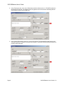
5.4.4. Ejercicio 6—Lectura/escritura del registro SETUP
Seguiremos en el modo 1B (por lo que se requiere la realización previa de los
pasos descritos en el Ejercicio 4), para demostrar el procedimiento a seguir para leer
y/o escribir registros. Practicaremos generando una petición específica de vendedor
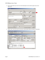
de entrada y de salida, y gestionaremos el contenido del registro SETUP.
Suponiendo que SIEMaster sigue en ejecución:
1. Iniciaremos el Panel de Control EZ-USB, y pulsaremos en “Show Pending”.
2. Generamos una petición específica de vendedor (vendor request) de entrada
(dirección IN) del tipo 0xA2 (vea la figura 5.11). Podrá observar que dicha
petición se marca como pendiente, al no obtener las 16 bytes de datos de la
petición.
42
CAPÍTULO 5. PROBANDO EL KIT DE DESARROLLO PASO A PASO
Figura 5.11: Generación de una petición específica de vendedor desde el Panel de Control EZ-USB.
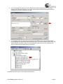
3. Regresemos al SIEMaster, seleccionemos el registro “32: SETUP” en el cuadro
desplegable del área funcional “Read”, y pulsemos 8 veces en el botón “Read”,
obteniendo los 8 bytes de los datos de configuración: 80 C0 A2 00 00 EF
BE 10.
Una forma alternativa para leer los 8 bytes de una sola vez sería pulsar en el
botón “Read Setup” situado en el área funcional “Setup” (vea la figura 5.12).
Obsérvese que se ha marcado el radio-botón “In”, indicando la dirección de
transferencia (de entrada). Si pulsáramos en los botones “Stall” o “Ack” se
escribiría un valor de cero o uno, respectivamente, en el registro SETUP, cancelando o asintiendo la transferencia de control.
Nota: El valor del campo “Length”, según el manual, debería indicar el número de bytes de paquetes de datos menos uno (0x0F, y no 0x10BD). Este
funcionamiento inesperado está documentado en el “Errata Document for
CY7C68001 EZ-USB SX2, Rev. *C”.
4. Para completar la transferencia de configuración, escribiremos el séptimo byte
(0x10), longitud de la fase de datos de configuración, en el registro EP0BC.
Es decir, seleccionaremos “33: EP0BC” en el control desplegable “Register”
ubicado dentro del área funcional “Write”, escribimos 10 en el campo “Value”,
y pulsamos en el botón “Write”. Vea la figura 5.13.
5. Volviendo al Panel de Control EZ-USB, podemos verificar cómo han aparecido
los datos de la fase de datos de configuración (figura 5.14).
6. Generaremos seguidamente una petición específica de vendedor (“VendReq”)
de salida, para enviar los datos del campo “Hex Bytes”. Vea la figura 5.15.
5.4. TEORÍA DE FUNCIONAMIENTO DEL KIT DE DESARROLLO
43
Figura 5.12: Leyendo los datos de configuración de una sola vez.
Figura 5.13: Escritura de un valor en el registro de número de bytes (byte count) del endpoint 0, esto
es, en EP0BC.
44
CAPÍTULO 5. PROBANDO EL KIT DE DESARROLLO PASO A PASO
Figura 5.14: Recepción de los 16 bytes de datos de la fase de configuración.
Figura 5.15: Generación de una petición específica de vendedor de salida.
5.4. TEORÍA DE FUNCIONAMIENTO DEL KIT DE DESARROLLO
45
Figura 5.16: Leyendo la petición específica de vendedor de salida.
7. Pulsando de nuevo en el botón “Read Setup” del SIEMaster, leemos esta vez
80 40 A2 00 00 EF BE 07. Vea la figura 5.16.
Nota: En este caso, se debería haber seleccionado automáticamente el radiobotón “Out”, según indica el manual, y el valor del campo “Lenght” debería ser 0x07, en lugar de 0x07BD. Sin embargo, esta función al igual que
algunas otras de este programa no se comporta como debería, lo que da
a entender que este programa es un tipo de software beta, que no ha sido completamente testeado (lea, por ejemplo, la página 11 del manual del
SIEMaster).
8. Pulsamos 7 veces en el botón “Read” del área funcional “Read”, obteniendo
80 B0 47 05 80 00 01 00, y apareciendo la cadena siguiente en el Panel
de Control EZ-USB:
Vendor Request
0000 B0 47 05 80 00 01 00
Nota: B0 indica que a continuación siguen los parámetros VID\PID con los
nibbles invertidos: VID\PID = 0x0547\0x0080.
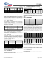
5.4.5. Modo 2–Modo de desarrollo
En el modo 2 (vea la figura 5.17), la placa SX2 se desconecta de la placa FX. Todas
las señales de la SX2 se presentan en dos conectores, que pueden conectarse al kit
de desarrollo de cualquier procesador master para emular un microprocesador.
46
CAPÍTULO 5. PROBANDO EL KIT DE DESARROLLO PASO A PASO
Figura 5.17: Diagrama de bloques del modo 2.
5.5. Practicando con el kit de desarrollo
5.5.1. Ejercicio 7—Primera solución al problema de “Dispositivo
desconocido”. Descarga de firmware a la EZ-USB FX a través
del SIEMaster
Uno de los primeros problemas a los que se tiene que enfrentar el desarrollador
que maneje el kit de desarrollo CY3682 es el del mensaje de “Dispositivo desconocido” que en ciertos casos aparece en el Administrador de Dispositivos de Windows
al conectar el kit en modo 1A; es decir, la SX2 conectada a la FX, y el cable USB entre
el PC y la SX2. Este problema puede surgir por los siguientes motivos:
La configuración de los jumpers no es la adecuada para el modo 1A. Hemos
de revisar principalmente los jumpers JP3 y JP7 en la SX2, y el jumper JP9 en
la FX.
La EEPROM de la FX no contiene el firmware xmaster.iic. Esto puede deberse a que el desarrollador haya efectuado diversas pruebas con la placa, alterando el estado inicial de fábrica de la EEPROM.
La EEPROM de la SX2 no contiene un descriptor válido para el driver de propósito general EZ-USB.
Si después de revisar el primer punto, el problema continua, la primera solución
que se propone es cambiar al modo 1B y utilizar la utilidad SIEMaster.
Entonces, iniciaremos SIEMaster, y pulsaremos en enumerar, con lo que ambos
dispositivos (después de cargarse un firmware especial en la RAM de la EZ-USB FX)
volverán a ser detectados como “Cypress EZ-USB Sample Device”. En este momento, podremos interactuar con la SX2.
5.5. PRACTICANDO CON EL KIT DE DESARROLLO
47
5.5.2. Ejercicio 8—Segunda solución al problema de “Dispositivo
desconocido”. Descarga del firmware xmaster a la EZ-USB
FX mediante el Panel de Control EZ-USB
Alternativamente a la solución anterior, es posible, siguiendo en el modo 1B,
emplear el Panel de Control EZ-USB para descargar el firmware:
1. Iniciamos el Panel de Control EZ-USB, y pulsamos en “Open All”. Debería
abrirse la ventana hija “Ezusb-0” perteneciente a la comunicación establecida
con la FX.
2. Seleccionamos “EZ-USB FX” en el control desplegable junto a “Target”.
3. Pulsamos sobre “Download” y seleccionamos C:\Cypress\USB\Examples\Sx2\xmaster\xmaster.hex, con lo que se carga el firmware en RAM, se
procede a la reenumeración de la SX2, y se consigue que sea detectada como
“Cypress EZ-USB Sample Device”. Sin embargo, la FX quedará como “Cypress
EZ-USB (2235) - EEPROM missing”.
5.5.3. Ejercicio 9—Segunda solución al problema de “Dispositivo
desconocido”. Reprogramación de la EEPROM de la EZ-USB
FX con el firmware xmaster
El problema de las soluciones anteriores es que no nos permiten trabajar en modo
1A, y, además, vuelve a surgir si desconectamos ambas placas y volvemos a conectarlas. Es por ello que una solución más conveniente sea la reprogramación de la
EEPROM de la EZ-USB FX con el firmware xmaster.iic. Para ello la forma de
proceder más directa es la siguiente:
1. Desconectamos todos los dispositivos EZ-USB del PC.
2. Desconectamos el JP9 de la FX y conectamos dicha placa al controlador host
USB del PC. (Deberá ser detectado en el Administrador de Dispositivos de
Windows como “Cypress EZ-USB (2235) - EEPROM missing”). Debemos dejar
el jumper JP1 entre los pines 1-2, y el jumper JP3 entre los pines 2-3.
3. Iniciamos el Panel de Control EZ-USB, y observaremos que se abre inmediatamente una ventana hija con título “Ezusb-0”, lo que nos indica que ha detectado la presencia de la placa EZ-USB FX.
4. Seleccionamos “EZ-USB FX” en el control desplegable junto a “Target”.
5. Conectamos el JP9 de la FX entre los pines 1 y 2.
48
CAPÍTULO 5. PROBANDO EL KIT DE DESARROLLO PASO A PASO
Figura 5.18: Borrado de la EEPROM de 8 kB con la ayuda del firmware vend_ax.hex.
6. Pulsamos en “Show Pending”, y luego en Download” para seleccionar el fichero C:\Cypress\USB\Examples\EzUsb\Vend_Ax\Vend_Ax.hex, con
lo cual se cargará en la RAM de la FX el firmware con el que podremos borrar
la EEPROM por completo. Este firmware, asocia las peticiones específicas de
vendedor (vendreqs) del tipo 0xAx, con x = 0, 2, 3, 4, 5, 6, 8, 9, con operaciones
específicas. Para más información consulte el archivo readme.txt situado en
el mismo directorio que el firmware.
7. Realizaremos una petición específica de vendedor de tipo 0xA9 (carga de EEPROM con direccionamiento de dos bytes), desde la dirección 0x0000, con 4096
bytes (máximo admitido) con el valor FF, y de salida. Vea la figura 5.18. Volveremos a repetir la operación, pero esta vez partiendo de la posición 0x1000,
consiguiendo finalmente el borrado de los 8192 bytes de la EEPROM 24LC64
(de 64 kilobits).
8. Desconectamos y volvemos a conectar la FX.
9. Pulsamos en el botón “EEPROM” y seleccionamos C:\Cypress\USB\Examples\Sx2\eeprom images\xmaster.iic, aguardando un tiempo prudencial (del
orden de 20 segundos) a que se complete esta tarea.
Al finalizar estos pasos, habremos obtenido el estado inicial de la EEPROM de la
EZ-USB FX, esto es, encontraremos el firmware xmaster.iic almacenado en su
EEPROM.
5.5. PRACTICANDO CON EL KIT DE DESARROLLO
49
Figura 5.19: Ruta de datos implementada por el ejemplo xmaster de la SX2.
5.5.4. Ejercicio 10—Ejemplo de loopback en modo 1A. Uso de bulkloop
La EZ-USB SX2 puede utilizarse en un sistema donde una CPU externa inicialice
el chip SX2 y controle las FIFO de la SX2. Los datos host entran en los endpoints SX2
OUT a velocidades USB 2.0, y son inmediatamente movidos a las FIFO de la SX2.
La CPU externa puede controlar la FIFO para recuperar los datos. De forma inversa,
los datos pueden ser movidos desde la CPU externa a las FIFO de la SX2 para una
transferencia inmediata a través de los endpoint IN (de vuelta al PC host).
El firmware de ejemplo “xmaster.hex” (y su carga EEPROM asociada “xmaster.iic”) es un ejemplo de utilizar la EZ-USB FX como CPU master externa. El firmware de la EZ-USB FX consigue que la SX2 devuelva los datos al PC, a través de
la interfaz física con la SX2 (los conectores que conectan la SX2 con la placa EZ-USB
FX). La FX lee los datos de salida de la FIFO de la SX2, y escribe los datos a una FIFO
diferente de la SX2.
La figura 5.19 muestra la ruta de datos.
La línea de actuación para probar este ejemplo se indica a continuación:
1. Como trabajaremos en modo 1A, repetimos los pasos 1–3 del Ejercicio 3.
Si la EEPROM de la placa EZ-USB FX ha sido reprogramada con un firmware distinto
al xmaster.iic, será preciso:
Descargar el firmware xmaster.hex en la RAM de la FX (Ejercicio 8), o bien
Grabar el firmware xmaster.iic en la EEPROM (Ejercicio 9).
2. Ejecutamos C:\CYPRESS\USB\BIN\bulkloop.exe. Esta aplicación de propósito general se encarga de producir el loopback de datos, y su validación a
medida que regresan.
3. Pulsamos en “Get Pipe List”, con lo cual veremos los endpoints 2, 4, 6 y 8.
4. Seleccionamos la opción “Select Pair”, y escribimos “0” para “Out Pipe” (endpoint 2 OUT), y “2” para “In Pipe” (endpoint 6 IN). En “Transfer Size” escri-
50
CAPÍTULO 5. PROBANDO EL KIT DE DESARROLLO PASO A PASO
Figura 5.20: Configuración de los parámetros del bulkloop.
bimos “512”. En este momento, la pantalla será como la mostrada en la figura 5.20.
5. Presionando en el botón START apreciaremos el incremento de “Pass Count”
conforme son verificados los datos.
6. Es posible ejecutar una segunda instancia de bulkloop.exe, pero escribiendo
“1” para “Out Pipe” y “3” para “In Pipe”, lo que establecerá un bucle de datos
entre el endpoint 4 OUT y el endpoint 8 IN.
5.5.5. Ejercicio 11—Ejemplo de loopback manual en modo 1B
Como el funcionamiento loopback está implementado en el firmware xmaster,
es evidente que (a menos que las EEPROM del kit de desarrollo almacenen los programas con los que venían de fábrica) esta prueba requiere la realización previa del
Ejercicio 7, donde se cargaba dicho firmware en la RAM de la EZ-USB FX a través del
Panel de Control EZ-USB. Suponiendo que el Panel de Control sigue en ejecución,
comprobaremos el retorno de los datos manualmente:
1. En la ventana hija con título “Ezusb-1” (EZ-USB SX2, como puede comprobarse al obtener el descriptor con “Get Dev” y leer los valores VID\PID), seleccionamos “Get Pipes”.
2. En la barra “ResetPipe/AbortPipe/FileTrans...” seleccionamos “Pipe: 0: Endpoint 2 OUT” y pulsamos en el botón “FileTrans...”.
3. Escogemos el fichero de test de 512 bytes. Podrá comprobarse cómo tiene lugar
la transferencia bulk de la cuenta de 0 a 255, estando codificado cada núme-
5.5. PRACTICANDO CON EL KIT DE DESARROLLO
51
ro con 2 bytes. Limpiaremos el área de salida de información pulsando en el
botón “Clear”.
4. A continuación, en la barra “Bulk/Int” seleccionamos “PIPE: 2: Endpoint 6
IN”, “Length: 512” y pulsamos en “Bulk/Int” para recuperar los datos.
52
CAPÍTULO 5. PROBANDO EL KIT DE DESARROLLO PASO A PASO
Capítulo 6
Marco de trabajo para la programación
USB
6.1. Introducción
En el capítulo anterior analizamos paso a paso el kit de desarrollo CY3682, siempre al amparo de las aplicaciones de ejemplo (Panel de Control EZ-USB y SIEMaster)
proporcionadas por Cypress Semiconductor. Pero en las aplicaciones reales, el diseñador requerirá poder controlar todos los aspectos de la comunicación USB, adaptando cada parámetro (modo de transferencia, configuración de los endpoints, etc.)
según sus necesidades.
Inicialmente, será primordial limitar el problema; esto es, determinaremos qué
elementos software han de ser desarrollados, y qué medios disponemos para ello.
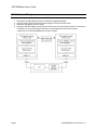
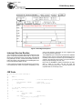
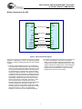
La aplicación USB final, construida con el chip CY7C68001 como elemento esclavo de un procesador externo principal, contendrá (vea la figura 6.1):
Un driver USB de Windows o driver de clase incluido con el sistema operativo.
Los drivers estándares de Windows.
Firmware para la aplicación del procesador host y (opcional) un programa de
aplicación para Windows USB específico.
Trataremos a continuación los principales elementos de este sistema, dejando
para el apartado 6.6 un ejemplo de implementación de una sencilla comunicación
USB 2.0 tipo bulk con el chip EZ-USB SX2.
6.2. Programación del driver
Teniendo en cuenta que el kit incluye el driver de dispositivo de propósito general EZ-USB (GPD, General Purpose Driver), no será necesario la programación de
54
CAPÍTULO 6. MARCO DE TRABAJO PARA LA PROGRAMACIÓN USB
Figura 6.1: Diagrama de bloques del sistema EZ-USB final.
ningún otro driver, a menos que se desee implementar un driver personalizado o
un mini-driver, en cuyo caso el GPD servirá como punto de partida.
La programación de drivers excede las pretensiones de este Proyecto, si bien el
autor tuvo la oportunidad de estudiar las posibilidades para Windows:
WDM (Windows Driver Model) y
WDF (Windows Driver Foundation).
El primer modelo (WDM), y más antiguo, trabaja exclusivamente en modo núcleo,
con lo cual cualquier error de programación puede dar lugar a un “cuelgue” del
sistema. El modelo más actual (WDF), por su parte, permite trabajar en modo núcleo
(utilizando el KMDF, Kernel Mode Device Framework) o en modo usuario (utilizando
el UMDF, User Mode Driver Framework), siendo éste último la forma más segura y
sencilla (relativamente) de generar drivers.
El estudio del modelo WDF puede ser realmente arduo, máxime si se tiene en
cuenta que actualmente sólo se dispone documentación a través de la web de Microsoft, donde es fácil comenzar en un punto de partida, y terminar en otro absolutamente distinto. Por ello, para el lector interesado, se ha estructurado jerárquicamente las principales páginas de interés de la web de Microsoft WDK (Windows
Driver Kit):
1. Driver Fundamentals: Getting Started,
http://www.microsoft.com/whdc/driver/foundation/default.mspx
a) Windows Roadmap for Driver,
http://www.microsoft.com/whdc/driver/foundation/DrvRoadmap.mspx#
b) WHDC (Windows Hardware Developers Central) Technical References for
Driver Development,
http://www.microsoft.com/whdc/resources/respec/TechRef.mspx#
6.2. PROGRAMACIÓN DEL DRIVER
55
c) Russinovich, Mark E., and Solomon, David A. Microsoft Windows Internals,
Fourth Edition, http://www.microsoft.com/MSPress/books/6710.asp
d) Architecture of Microsoft Windows Driver Foundation,
http://www.microsoft.com/whdc/driver/wdf/wdf-arch.mspx#
2. About the Windows Driver Kit (WDK)
a) Windows Driver Foundation (WDF),
http://www.microsoft.com/whdc/driver/wdf/default.mspx
1) Introduction to the Windows Driver Foundation,
http://www.microsoft.com/whdc/driver/wdf/wdf-intro.mspx
2) Windows Driver Foundation Facts,
http://www.microsoft.com/whdc/driver/wdf/WDF_facts.mspx
3) FAQ: Questions from Driver Developers about Windows Driver
Foundation,
http://www.microsoft.com/whdc/driver/wdf/WDF_FAQ.mspx
b) Kernel-Mode Driver Framework (KMDF),
http://www.microsoft.com/whdc/driver/wdf/KMDF.mspx
1) Architecture of the Kernel-Mode Driver Framework,
http://www.microsoft.com/whdc/driver/wdf/kmdf-arch.mspx
2) Sample Drivers for the Kernel-Mode Driver Framework,
http://www.microsoft.com/whdc/driver/wdf/KMDF-samp.mspx
3) How to Build, Install, Test, and Debug a KMDF Driver,
http://www.microsoft.com/whdc/driver/wdf/KMDF-build.mspx
4) Introduction to Plug and Play and Power Management in the Windows
Driver Foundation,
http://www.microsoft.com/whdc/driver/wdf/WDF_pnpPower.mspx
5) DMA Support in Windows Drivers
6) I/O Request Flow in WDF Kernel Mode Drivers
7) How to Enable the Frameworks Verifier
8) How to Use the KMDF Log
9) Is That Handle Still Valid?
10) Troubleshooting KMDF Driver Installation
11) When does EvtCleanupCallback run?
c) User-Mode Driver Framework (UMDF),
http://www.microsoft.com/whdc/driver/wdf/UMDF.mspx
1) Introduction to the WDF User-Mode Driver Framework,
http://www.microsoft.com/whdc/driver/wdf/UMDF_intro.mspx
56
CAPÍTULO 6. MARCO DE TRABAJO PARA LA PROGRAMACIÓN USB
2) Architecture of the User-Mode Driver Framework,
http://www.microsoft.com/whdc/driver/wdf/UMDF-arch.mspx
3) FAQ: User-Mode Driver Framework,
http://www.microsoft.com/whdc/driver/wdf/UMDF_FAQ.mspx
4) Sample Drivers for the User-Mode Driver Framework,
http://www.microsoft.com/whdc/driver/wdf/UMDF-samp.mspx
d) Header file refactoring,
http://www.microsoft.com/whdc/driver/WDK/headers.mspx
e) PREfast,
http://www.microsoft.com/whdc/DevTools/tools/PREfast.mspx
1) PREfast Step-by-Step,
http://www.microsoft.com/whdc/DevTools/tools/PREfast_steps.mspx
f ) Static Driver Verifier,
http://www.microsoft.com/whdc/devtools/tools/SDV.mspx
g) Debugging Tools for Windows,
http://www.microsoft.com/whdc/devtools/debugging/default.mspx
h) Windows Logo Testing,
http://www.microsoft.com/whdc/GetStart/testing.mspx
i) Driver Install Frameworks Tools 2.01,
http://www.microsoft.com/whdc/driver/install/DIFxtls.mspx
j) Static Driver Verifier Facts,
http://www.microsoft.com/whdc/devtools/tools/sdv_facts.mspx
No obstante, es altamente recomendable leer previamente el libro Microsoft Windows
Internal, de Mark E. Russinovich y David A. Solomon, en su cuarta edición, con el
cual el diseñador podrá entender todos los conceptos que se mencionan tanto en
las páginas web anteriores como en los documentos del WDK, descargados desde
dichas páginas y almacenados en el CD-ROM.
Es posible, por otro lado, descargarse numerosas herramientas que pueden servir de ayuda (gran parte de ellas puede encontrarlas en el CD-ROM adjunto).
6.3. Programación del firmware para el procesador principal
Como se puntualizaba en el apartado de “Posibles ampliaciones”, la programación del software de control del procesador específico (microprocesadores estándar,
DSP, ASIC, FPGA, etc.) no pertenece al alcance de este Proyecto. Será el desarrollador quien, en función del tipo de procesador, escoja un lenguaje de programación,
6.4. ALTERNATIVAS PARA LA CODIFICACIÓN DE LA COMUNICACIÓN USB
ENTRE LA APLICACIÓN HOST Y EL DISPOSITIVO USB 2.0
57
que se pueda compilar en un formato comprensible para el microprocesador, y un
entorno de programación apropiado.
6.4. Alternativas para la codificación de la comunicación USB entre la aplicación host y el dispositivo
USB 2.0
Realmente este es el aspecto más importante de los tratados en el Proyecto que
nos ocupa, pues permite demostrar el funcionamiento del CI CY7C68001 (la placa
EZ-USB SX2), comunicándose con una aplicación host. Se entiende por aplicación
host el software situado en un PC que requiere la transferencia de información, a
través del USB, hacia o desde el sistema electrónico diseñado.
De hecho, lo que mostraremos en los próximos párrafos será el marco de trabajo
de la programación entre la aplicación host y el dispositivo USB. En cualquier caso,
no se exige ningún lenguaje de programación determinado, si bien, los ejemplos que
se aportarán estarán codificados en C++.
Grosso modo, podemos encontrar dos posibilidades para comunicarnos con el
dispositivo USB, ambas a través del driver correspondiente:
Mediante funciones Win32 (API de Windows) de bajo nivel, o
Mediante la CyAPI, hallada en el USB Developer’s uStudio (CY4604).
6.4.1. Comunicación USB a través del API de Windows
Comencemos por la primera opción. Como ya se comentó anteriormente, el kit
de desarrollo CY3682 incluye un driver de propósito general EZ-USB (GPD, General
Purpose Driver), que presenta una interfaz en modo usuario a la que puede acceder
a través de las funciones de Win32 CreateFile() y DeviceIoControl(). Las
distintas peticiones al dispositivo USB definidas en el capítulo 9 de la Especificación USB son manejadas mediante códigos de control de entrada/salida, también
denominados, IOCTLs. Serán necesarias además distintas estructuras que servirán
de parámetros de la función DeviceIoControl().
El kit de desarrollo incluye numerosas aplicaciones de ejemplo (como la que
puede encontrar en C:\Cypress\USB\Examples\EzUsb\bulktest\host) que
pueden servir de punto de partida para un diseño que se comunique directamente
con el GPD a través de la API de Windows.
Podrá encontrar todos los detalles de la programación mediante el GPD en el
documento “EZ-USB General Purpose Driver Specification”, impreso en el anexo
de Manuales.
Los principales inconvenientes de este tipo de programación son:
58
CAPÍTULO 6. MARCO DE TRABAJO PARA LA PROGRAMACIÓN USB
1. Se trata de un funcionamiento a bajo nivel, es decir, se requiere un control
absoluto de los parámetros proporcionados (estructuras, tipos de datos, . . . ),
y deben manejarse con soltura los tipos de datos de Windows, junto con su
notación (húngara).
2. Se precisa una programación mediante hilos (threads) para que la transferencia
(transmisión/recepción) de información a través del USB no detenga la ejecución de la aplicación host.
En conclusión, para aplicaciones host sencillas, la programación directa a través del
GPD puede no suponer ningún problema, pero en otros casos puede resultar realmente engorrosa.
6.4.2. Comunicación USB a través del API de Cypress
Precisamente para solventar los inconvenientes mencionados, Cypress desarrolló en 2003 el USB Developer’s uStudio (CY4604) que incluía los siguientes elementos:
Un driver USB genérico, desarrollado siguiendo el WDM (Windows Driver
Model) y compatible con Windows 2000 y Windows XP. Incluye además soporte para Plug and Play (PnP), despertado remoto (remote wake-up), identificador único global (GUID) personalizable, y gestión de potencia de nivel S4.
El driver puede ser usado para aplicaciones de propósito general que usen
transferencias de control, interrupt, bulk o isócronas.
Una versión mejorada del Panel de Control EZ-USB: CyConsole, que incluye
características mejoradas para permitir que los desarrolladores puedan emular
mejor la aplicación host USB, respuestas, y test para ajustar el firmware y la
interfaz con el driver del dispositivo.
Una librería de clase compatible con Visual C++ y Borland C++Builder: CyAPI, que proporciona una interfaz de programación de aplicación (API) con el
driver genérico de dispositivo USB de Cypress.
Este kit de referencia, nos permite una programación más sencilla de la comunicación USB entre la aplicación host y el dispositivo USB, a través de la librería CyAPI.
Nuestro objetivo será, pues, desarrollar una aplicación práctica donde se expongan
las instrucciones necesarias con las que realizar una comunicación bulk.
Antes de proceder, sólo nos queda un comentario más: aunque este kit incluye
un driver USB genérico, con todos los códigos de control IOCTL claramente documentados en el “Cypress CyUsb.sys Programmer’s Reference”, se pretende trabajar
a un nivel superior, dejando a un lado el contacto directo con el API de Windows.
Comenzaremos instalando el estudio de desarrollo.
6.5. INSTALANDO EL ESTUDIO DE DESARROLLO USB CY4604
59
6.5. Instalando el estudio de desarrollo USB CY4604
La instalación no presenta ninguna dificultad. Ejecutaremos el archivo USBDevStudio_1511.exe y seguiremos los pasos hasta completar el proceso. Podremos cerciorarnos del éxito de la instalación comprobando que se han añadido los siguientes
elementos a Inicio\Cypress\USB:
CyConsole,
Programmer’s Reference - CyUSB.sys, y
Programmer’s Reference - CyAPI.lib.
Se recomienda la creación del acceso directo de CyConsole en el escritorio.
6.6. Usando la API de Cypress—CyAPI
Consideremos el siguiente supuesto:
Disponemos de un dispositivo controlado por un procesador externo
principal que requiere la comunicación con una aplicación host a través
del bus serie universal. Se ha conectado adecuadamente el procesador
externo con la placa EZ-USB SX2 (el pinout aparece en el manual de características técnicas), que actuará de interfaz con la aplicación host.
Se requiere el cumplimiento de los siguientes puntos:
El dispositivo USB debe ser reconocido por el sistema operativo (Windows XP,
en nuestro caso), como un “Dispositivo USB de prueba del PFC”.
El fabricante del dispositivo será “Cypress Semiconductor”, y el suministrador, el “Departamento de Ingeniería Electrónica”.
Deberá cargarse el driver CyUSB.sys, ya que posiblemente Windows utilice
el ezusb.sys (instalado y configurado con el kit de desarrollo CY3682).
Deberemos ser capaces de transmitir información en modo bulk y verificar la
correcta recepción de los datos transmitidos.
Resolveremos este problema secuencialmente a lo largo de múltiples ejercicios. Se
considera que, previamente, hemos instalado el estudio de desarrollo USB CY4604,
y que, para facilitar el proceso, partimos del estado final del Ejercicio 3:
La placa EZ-USB SX2 conectada a la FX,
Un único cable USB conectado entre la SX2 y el PC,
60
CAPÍTULO 6. MARCO DE TRABAJO PARA LA PROGRAMACIÓN USB
El firmware xmaster.hex cargado en la RAM de la FX, y
El identificador de dispositivo “Cypress EZ-USB Sample Device” correspondiente a unos valores VID\PID de 0x04B4\0x1002 en el Administrador de Dispositivos de Windows.
6.6.1. Ejercicio 12—Adición del identificador del dispositivo al driver
Para que el driver detecte un dispositivo específico, los identificadores VID y
PID deberán ser añadidos al fichero C:\Archivos de programa\Cypress\USB
DevStudio\Driver\CyUSB.inf.
Siga los siguientes pasos:
1. Localice la sección [Cypress] y duplique la línea
; %VID_VVVV&PID_PPPP.DeviceDesc %=CyUsb, USB\VID_VVVV&PID_PPPP
eliminando el punto y coma de la línea duplicada.
2. Cambie VVVV por “04B4” (correspondiente a 0x04B4), que es el valor hexadecimal del identificador de vendedor (VID) de la SX2 con el descriptor de
prueba cargado por el firmware xmaster, y PPPP por “1002” (correspondiente
a 0x1002), valor hexadecimal del identificador de producto (PID) de la SX2. El
resultado será el siguiente:
%VID_04B4&PID_1002.DeviceDesc %=CyUsb, USB\VID_04B4&PID_1002
3. Localice la sección [Strings] al final del archivo CyUSB.inf, y duplique la
línea
VID_VVVV&PID_PPPP.DeviceDesc="Cypress Generic USB Device"
4. Cambie VVVV por “04B4”, PPPP por “1002” y “Cypress Generic USB Device”
por “Dispositivo USB de prueba del PFC”, con lo que tendría que quedar:
VID_04B4&PID_1002.DeviceDesc="Dispositivo USB de prueba del PFC"
5. Guarde el archivo y ciérrelo.
6.6. USANDO LA API DE CYPRESS—CYAPI
61
Figura 6.2: Cambiando el controlador de la EZ-USB SX2.
6.6.2. Ejercicio 13—Sustitución de las cadenas de texto de fabricante y suministrador
1. Abra de nuevo el archivo C:\Archivos de programa\Cypress\USB DevStudio\Driver\CyUSB.inf.
2. Sustituya MfgName="Cypress" por MfgName="Cypress Semiconductor".
3. Sustituya provider= %CYPRESS % por provider=”Escuela Técnica Superior
de Ingenieros”.
4. Sustituya CyUsb.SvcDesc="Cypress Generic USB Driver" por
CyUsb.SvcDesc="Dispositivo USB de prueba del PFC
6.6.3. Ejercicio 14—Forzando el uso del driver CyUSB.sys
Durante el capítulo 4 configuramos el kit de desarrollo CY3682, que instalaba y
configuraba el driver de propósito general ezusb.sys, y sobre el que se sustentaba toda la funcionalidad que tuvimos oportunidad de comprobar. Lo que haremos
en este ejercicio será forzar que Windows XP cargue el driver CyUSB.sys, pues la
librería CyAPI se comunica únicamente con dicho driver.
1. Abra el Administrador de Dispositivos de Windows, localice el dispositivo
“Cypress EZ-USB Sample Device” dentro del nodo “Controladoras de bus serie universal (USB)” y haga doble clic en su icono.
2. Seleccione la pestaña controlador (vea la figura 6.2) y pulse en “Actualizar
controlador”.
62
CAPÍTULO 6. MARCO DE TRABAJO PARA LA PROGRAMACIÓN USB
3. Seleccione “No por el momento” y pulse en “Siguiente”.
4. Seleccione “Instalar desde una lista o ubicación específica (avanzado)” y pulse
en “Siguiente”.
5. Seleccione “No buscar. Seleccionaré el controlador que se va a instalar” y pulse
en “Siguiente”.
6. Pulse en “Utilizar disco”, luego en “Examinar”, seleccione el archivo C:\Archivos
de programa\Cypress\USB DevStudio\Driver\CyUSB.inf, y pulse en
“Abrir”. Pulse “Aceptar”
7. Pulse en “Siguiente” y autorice la instalación.
8. Pulse en “Finalizar” y luego en “Cerrar”.
Podrá comprobar que, si se siguieron los pasos como se ha indicado, ahora disponemos de un “Dispositivo USB de prueba del PFC” (vea la figura 6.3).
Figura 6.3: Verificando la correcta instalación del driver CyUSB.sys.
6.6.4. Ejercicio 15—Aplicación host básica para la comunicación
USB 2.0 de tipo bulk con el chip EZ-USB SX2
Considerando que el firmware xmaster provoca que los datos que la FX lea del
endpoint tipo bulk de salida (desde el PC) serán reenviados al endpoint tipo bulk
6.6. USANDO LA API DE CYPRESS—CYAPI
63
de entrada (hacia el PC), implementaremos una comunicación USB 2.0 entre una
aplicación host y el chip EZ-USB SX2. Hemos de tener en cuenta que en la tasa de
transferencia media afectará el tiempo de procesado de la FX.
Crearemos una aplicación de consola dummy que establecerá, iniciará y finalizará la comunicación con el chip EZ-USB SX2 a través de CyAPI. Hay que recordar,
que es necesario enlazar CyAPI.lib con el proyecto en el entorno de desarrollo
empleado (Borland C++Builder 6, en nuestro caso).
Seguidamente proporcionamos el contenido de UnidadBasica.cpp (que, lógicamente, se incluye en el CD anexo junto con el archivo de proyecto .bpr). Entre
paréntesis se numeran los comentarios que aparecerán posteriormente.
#include <windows.h>
#include "CyAPI.h"
void main() {
const int packetSize = 512; // (1)
LONG pckSize = packetSize; // (2)
char outBuffer[packetSize]; // (3)
char inBuffer[packetSize];
int devices, vID, pID, d = 0;
CCyUSBDevice *USBDevice = new CCyUSBDevice(); // (4)
devices = USBDevice->DeviceCount();
do { // (5)
USBDevice->Open(d);
vID = USBDevice->VendorID;
pID = USBDevice->ProductID;
d++;
} while ((d < devices) && (vID != 0x04b4) && (pID != 0x1002));
for (int i=0; i<packetSize; i++)
outBuffer[i] = i;
USBDevice->BulkOutEndPt->XferData(outBuffer, pckSize); // (7)
USBDevice->BulkInEndPt->XferData(inBuffer, pckSize);
// (8)
USBDevice->Close(); // (9)
}
Comentarios:
1. El firmware xmaster configura los endpoint tipo bulk para admitir un tamaño máximo de paquete de 512 bytes. Se comprueba que para que el proceso de
transferencia de datos sea satisfactorio, todos los envíos deben realizarse en
paquetes de 512 bytes.
2. La función XferData requiere que el tamaño de paquete sea de tipo LONG.
3. Los datos se almacenarán en arrays de cadenas de 512 bytes.
4. Se hace una llamada al driver CyUSB para obtener un manejador (handle) a
los dispositivos USB de Cypress conectados. Con el depurador de C++Builder
64
CAPÍTULO 6. MARCO DE TRABAJO PARA LA PROGRAMACIÓN USB
Figura 6.4: Valores de las propiedades del objeto USBDevice al obtener el manejador desde el driver.
Figura 6.5: Buffer de salida outBuffer con una secuencia de 512 valores.
podemos ver la ventana de la figura 6.4, donde se aprecian los valores de las
distintas propiedades del objeto USBDevice.
5. En el bucle do-while se busca entre los dispositivos USB de Cypress, el que
tenga vID igual a 0x04b4h y pID igual a 0x1002h, es decir, busca el chip EZUSB SX2.
6. Almacenamos la secuencia 0, 1, 2, 3, . . . , 255, 0, 1, 2, 3, . . . , 255 en el buffer de salida (se trata de una variable signed), como aparece en la figura 6.5.
7. Se transfieren de forma síncrona los datos del buffer de salida de tipo cadena al
primer endpoint de tipo bulk de salida (desde el PC) con la función XferData.
8. Al finalizar el envío, se solicita la recepción síncrona de información del endpoint de tipo bulk de entrada (hacia el PC) de nuevo con la función XferData.
6.6. USANDO LA API DE CYPRESS—CYAPI
(a)
65
(b)
Figura 6.6: (a) Ventana de variables locales en modo depuración antes de iniciar la transferencia al
endpoint de salida y (b) después de recibir los datos desde el endpoint de entrada.
Teniendo en cuenta que, por simplicidad, no hemos mostrado información en
pantalla del proceso de comunicación, nos remitimos a la ventana de variables
locales en modo depuración (figura 6.6).
9. Una vez acabado el proceso de comunicación, liberamos el manejador del dispositivo USB de Cypress.
6.6.5. Ejercicio 16—Aplicación host práctica para la comunicación
USB 2.0 de tipo bulk con el chip EZ-USB SX2
Después de haber trazado en el ejercicio anterior las líneas básicas de la programación de una comunicación USB 2.0 tipo bulk con el chip EZ-USB SX2, haciendo
uso de la CyAPI, trataremos a continuación de diseñar una aplicación que envíe un
archivo BMP determinado a la placa, lo obtenga de vuelta, y lo muestre por pantalla.
De nuevo, el firmware xmaster nos servirá de medio para disponer de retorno
los datos que enviamos. Sin embargo, en esta ocasión diseñaremos una aplicación
VCL, consistente en un formulario con un botón para transferir la imagen de prueba,
una barra de progreso y distintas etiquetas.
El algoritmo de comunicación estará implementado en el método OnClick del
botón de transferencia. Básicamente se encarga de abrir el archivo de datos origen
(una imagen BMP), hacerlo trozos de 512 bytes, enviarlo, recibirlo, almacenarlo en
otro archivo de datos destino, y finalmente representar gráficamente su información
(mostrar la imagen que contiene) y datos estadísticos de la transferencia.
Mostramos seguidamente las líneas de código de UnidadPrincipal.cpp. (Al
igual que el archivo anterior, y sus respectivos archivos de proyecto, los podrá encontrar en el CD anexo.)
66
CAPÍTULO 6. MARCO DE TRABAJO PARA LA PROGRAMACIÓN USB
//--------------------------------------------------------------------------// PROYECTO FINAL DE CARRERA
// Evaluación del chip EZ-USB SX2
//
// Autor: Alejandro Raigón Muñoz
// Tutor: Dr. Jonathan Noel Tombs
//
// Mayo-2007
//--------------------------------------------------------------------------//
DESCRIPCIÓN: Esta aplicación trata de demostrar el proceso de
//
transferencia USB 2.0 tipo bulk utilizando el chip EZ-USB SX2. Para ello
//
tomamos una imagen BMP, la enviamos a la placa EZ-USB SX2, y la
//
recibimos de la misma a través de endpoints bulk. Posteriormente
//
se muestra el resultado obtenido, así como estadísticas de la
//
transferencia.
//
//
Se supone que la EEPROM de la EZ-USB FX tiene almacenado el firmware
//
xmaster, y que la conexión de las placas FX y SX2 es la descrita
//
en el ejercicio 3 de la Memoria. Asimismo, se supone que la SX2 está
//
correctamente conectada al PC, y que ha sido detectada e identificada
//
satisfactoriamente.
//--------------------------------------------------------------------------#include <vcl.h>
#pragma hdrstop
#include "UnidadPrincipal.h"
//--------------------------------------------------------------------------#pragma package(smart_init)
#pragma resource "*.dfm"
#include "CyAPI.h"
#include <time.h>
TForm1 *Form1;
//--------------------------------------------------------------------------__fastcall TForm1::TForm1(TComponent* Owner)
: TForm(Owner)
{
}
//--------------------------------------------------------------------------void __fastcall TForm1::Button1Click(TObject *Sender)
{
// Abrimos la imagen que se enviará por puerto USB a la EZ-USB SX2
TFileStream *source = new TFileStream("source.bmp", fmOpenRead);
// Creamos el fichero destino
TFileStream *target = new TFileStream("target.bmp", fmCreate);
// Los paquetes se enviarán en trozos de 512 bytes
const int packetSize = 512;
// La rutina de transferencia USB (XferData) requiere un tipo LONG
LONG pckSize = packetSize;
// Los buffer de salida y entrada serán de tipo "char"
char outBuffer[packetSize];
char inBuffer[packetSize];
int devices, vID, pID, d = 0;
// En el bitmap cargaremos la imagen recibida
Graphics::TBitmap *bitmap = new Graphics::TBitmap;
// que será pintada con unas dimensiones de 800x600
TRect destArea = TRect((ClientWidth-800)/2,45,
(ClientWidth+800)/2,600+45);
int temp;
double tmp;
// Variable auxiliar
// Variable auxiliar
6.6. USANDO LA API DE CYPRESS—CYAPI
AnsiString stringAux;
// Variable auxiliar
// Limpiamos el área de dibujo inicial
Canvas->FillRect(destArea);
// Abrimos el dispositivo USB de Cypress
CCyUSBDevice *USBDevice = new CCyUSBDevice(Handle);
devices = USBDevice->DeviceCount();
// Buscamos la placa EZ-USB SX2
do {
USBDevice->Open(d);
vID = USBDevice->VendorID;
pID = USBDevice->ProductID;
d++;
} while ((d < devices) && (vID != 0x04b4) && (pID != 0x1002));
// Calculamos los trozos de 512 bytes que serán enviados
temp = source->Size/packetSize;
ProgressBar1->Visible = true;
ProgressBar1->Max = temp+1;
// Almacenamos el valor temporal al inicio del proceso de transferencia
clock_t t1 = clock();
USBDevice->BulkOutEndPt->TimeOut = 500;
source->Read(outBuffer, packetSize);
// Enviamos los paquetes de 512 bytes
for(int i = 0; i < temp; i++) {
// Leemos un paquete desde el archivo fuente
source->Read(outBuffer, packetSize);
// Lo transferimos al primer endpoint tipo bulk de salida
USBDevice->BulkOutEndPt->XferData(outBuffer, pckSize);
// Lo recuperamos del primer endpoint tipo bulk de entrada
USBDevice->BulkInEndPt->XferData(inBuffer, pckSize);
// Y lo almacenamos en el archivo destino
target->Write(inBuffer, packetSize);
// Incrementando la barra de progreso consecuentemente
ProgressBar1->Position = i;
}
// Si queda un paquete de menos de 512 bytes será enviado seguidamente
temp = source->Size % packetSize;
if (temp) {
source->Read(outBuffer, temp);
USBDevice->BulkOutEndPt->XferData(outBuffer, pckSize);
USBDevice->BulkInEndPt->XferData(inBuffer, pckSize);
target->Write(inBuffer, temp);
}
//
//
//
//
//
NOTA: Aunque el tamaño de paquete del último trozo debería ser
inferior a "packetSize", si no se transfieren paquetes de 512 bytes
se ha observado que el firmware "xmaster" no opera correctamente.
No obstante, no se escriben nada más que los "temp" primeros bytes en
el archivo destino.
// Almacenamos el valor temporal al finalizar el proceso de transferencia
clock_t t2 = clock();
delete target;
// Liberamos el handle del archivo destino,
67
68
CAPÍTULO 6. MARCO DE TRABAJO PARA LA PROGRAMACIÓN USB
bitmap->LoadFromFile("target.bmp"); // lo cargamos en el bitmap
Canvas->StretchDraw(destArea, bitmap); // y lo mostramos en pantalla
// A continuación mostraremos cierta información de la transferencia
Canvas->Font->Color = clRed;
Canvas->Font->Size = 12;
Canvas->Font->Style = TFontStyles()<< fsBold;
tmp = (double) 2*source->Size/1024;
stringAux = "Kilobytes transferidos: " + FormatFloat("0.0",tmp) + " kB";
Canvas->TextOut(120,70, stringAux);
tmp = (t2-t1)/CLK_TCK;
stringAux = "Tiempo empleado: " + FormatFloat("0.0",tmp) + " segundos";
Canvas->TextOut(120,90, stringAux);
tmp = (2*source->Size/1024)/tmp;
stringAux = "Throughput: " + FormatFloat("0.0",tmp) + " kB/s";
Canvas->TextOut(120,110, stringAux);
// Téngase en cuenta que en el throughput intervienen distintos
// factores, a saber: tasa de transferencia hacia y desde la
// EZ-USB SX2 y tiempo de procesado de la EZ-USB FX
ProgressBar1->Visible = false;
USBDevice->Close();
// Cerramos el dispositivo,
delete bitmap;
// liberamos el handle del bitmap
delete source;
// y el del archivo fuente
}
6.6. USANDO LA API DE CYPRESS—CYAPI
69
Figura 6.7: Formulario principal de la aplicación práctica de una comunicación USB 2.0 tipo bulk con
el chip EZ-USB SX2.
El formulario principal inicialmente tendrá el aspecto mostrado en la figura 6.7,
y, después de finalizar la transferencia de forma satisfactoria, podremos visualizar
la imagen recogida en la figura 6.8.
Figura 6.8: Resultado satisfactorio de la transferencia de ida y vuelta de la imagen de prueba.
70
CAPÍTULO 6. MARCO DE TRABAJO PARA LA PROGRAMACIÓN USB
6.7. Conclusiones
A pesar de los defectos, mencionados con anterioridad, acerca de la mala calidad
de la documentación disponible, y del servicio de asistencia técnica mejorable, es
posible implementar con éxito una transferencia USB 2.0 utilizando el chip EZ-USB
SX2.
Como hemos visto, la sencillez del CyAPI permite reducir enormemente el tiempo que el desarrollador debe invertir en obtener una aplicación USB final funcional,
pudiendo centrarse, en consecuencia, en el lado del procesador principal (PIC, DSP,
FPGA, etc.).
Capítulo 7
Contenido del CD-ROM
Se proporciona, conjuntamente con esta Memoria, un CD-ROM con información
de utilidad para el desarrollador. En el CD-ROM podrá encontrar el siguiente material:
El entorno de desarrollo del kit CY3682,
Manuales de consulta,
Notas de aplicación,
El estudio de desarrollo USB CY4604 versión 1.5.1.1, y
Documentación y herramientas para trabajar con el WDK de Microsoft.
7.1. Manuales de consulta
Los manuales de consulta recopilados, de los cuales los escritos en cursiva han
sido impresos y adjuntados como anexos, son los siguientes:
1. EZ-USB SX2–Getting Started–Development Kit Manual, Rev. 2.0
[SX2_Getting_Started_Version_2.pdf]
2. EZ-USB SX2–SIEMaster User’s Guide, v1.0
[SX2_SIEMaster_User_Guide_Version_1.pdf]
3. CY7C68001 Datasheet - EZ-USB SX2 High-Speed USB Interface Device, Rev. *H
[CY7C68001.pdf]
4. USB Interfacing CY3682 Design Notes
[SX2_Design_Notes_August_2002.pdf]
5. Errata Document for CY7C68001 EZ-USB SX2, Rev. *C
[CY7C68001errata.pdf]
72
CAPÍTULO 7. CONTENIDO DEL CD-ROM
6. User guide for EZ-USB Control Panel [EzMrUser.pdf]
7. EZ-USB General Purpose Driver Specification [EZ-USB General Purpose
Driver Spec.pdf]
8. EZ-USB Xcelerator Development Kit–Content and Tutorials [EZ-USB
Contents and Tutorial.pdf]
9. EZ-Loader–Creating a Custom USB Device Driver to Perform Firmware
Download [EZLOADER Design Notes.pdf]
10. High-Speed Interface Device EZ-USB SX2 (CY7C68001) [EZ-USB SX2.ppt]
11. EZ-USB FX Manual Technical Reference, v1.3 [EZ-USB FX
TechRefManual.pdf]
7.2. Notas de aplicación
Además, se proporcionan también en formato impreso y electrónico las siguientes notas de aplicación:
1. SX2 Primer (Life After Enumeration) [AN01.pdf]
Suponiendo que la tarjeta destino SX2 se ha enumerado con éxito, en
esta nota se discute la siguiente fase, que comienza transfiriendo la
carga útil (payload) al PC y en el sentido inverso.
2. EZ-USB FX2/AT2/SX2 Reset and Power Considerations [AN02.pdf]
Los dispositivos EZ-USB FX2/AT2/SX2 tienen necesidades de alimentación y reset similares. Esta nota de aplicación se refiere a la
FX2, pero es aplicable a los tres chips high-speed.
3. USB Error Handling For Electrically Noisy Environments, Rev. 1.0 [AN03.pdf]
Para proporcionar un funcionamiento robusto, los drivers de los dispositivos USB deben procesar URBs (USB Request Block) completos
y detectar y manejar errores apropiadamente. Esta nota de aplicación
se centra en el manejo de errores debidos a entornos eléctricamente
ruidosos, que pueden provocar que las peticiones USB sean retiradas
a causa de demasiados errores por tiempo excedido.
4. High-speed USB PCB Layout Recommendations [AN04.pdf]
7.3. EL ESTUDIO DE DESARROLLO USB CY4604
73
Esta nota de aplicación detalla las guías para diseñar una PCB para
USB high-speed con cuatro capas e impedancia controlada, verificando la especificación USB.
5. Bulk Transfers with the EZ-USB SX2 Connected to a Hitachi SH3 DMA Interface
[AN05.pdf] y Bulk Transfers with the EZ-USB SX2 Connected to an Intel XScale
DMA Interface [AN06.pdf]
Estas notas de aplicación muestran un esquema de uso y conexión
con un canal único DMA. El esquema pretende ilustrar un modelo
de conexión de muestra síncrono, seleccionado para mostrar una interfaz esclava rápida. Un único canal DMA SH3 (PXA255) se emplea
en todas las transacciones de datos entre master y esclavo, escritura
de datos y operaciones de estado/comando entre la SX2 y la interfaz
SH3 (PXA255), demostrando la habilidad de cambiar el modo de los
pines de señalización de la SX2 dinámicamente.
7.3. El estudio de desarrollo USB CY4604
En el CD-ROM podrá encontrar, en su correspondiente carpeta, los siguientes
archivos:
El archivo ejecutable para instalar el estudio de desarrollo USB CY4604 [USBDevStudio_1511.exe].
El manual de referencia del driver CyUsb.sys [CyUSB.pdf].
El manual de referencia de la librería estática CyAPI [CyAPI.pdf].
Ambos manuales se encuentran impresos e incluidos en la Parte II (manuales), para
una consulta más rápida.
7.4. Documentación del WDK de Microsoft
Los siguientes documentos, descargados desde la web de Microsoft, se han colocado también en el CD-ROM para que puedan servir al diseñador que intenta desarrollar un driver específico con el modelo WDK:
Windows Driver Kit [WDKintro.doc]
WDK Build Environment Refactoring [WDK_BE-Refactoring.ppt]
The WDK for Engineering Managers and Product Planners: An Introduction
[TWDE05004_WinHEC05.ppt]
74
CAPÍTULO 7. CONTENIDO DEL CD-ROM
Introduction To The Windows Driver Kit: A Comprehensive Driver
Development Solution [DEV041_WH06.ppt]
Architecture of Microsoft’s Windows Driver Foundation [wdf-arch.doc]
Windows Driver Foundation: Introduction [TWDE05002_WinHEC05.ppt]
Introduction to User-Mode Driver Framework [UMDF_Intro.ppt]
User-Mode Driver Framework: Introduction And Overview
[DEV095_WH06.ppt]
User-Mode Driver Framework: Technical Synopsis [DEV096_WH06.ppt]
7.5. Herramientas del WDK de Microsoft
Pueden resultar de utilidad las siguientes herramientas y ficheros hallados dentro de la estructura de páginas web del WDK de Microsoft, y almacenados en el
CD-ROM anejo:
Debugging Tools for Windows 32-bit Version 6.6.7.5
[dbg_x86_6.6.07.5.exe]
DIFx Tools [DriverInstallationTools.msi]
HCT 12.1 for "Designed for Windows" Testing [hct12101.exe] +
[hct121-sp1-x86.exe]
Kernel-Mode Driver Framework [WDFv11.iso]
Kernel-Mode Driver Framework Documentation [KMDF10.exe]
Kernrate Viewer [KrView_100-82.exe]
Microsoft ACPI Source Language Compiler v3.0
[MS_ASL-Compiler_3.0.0.msi]
User-Mode Driver Framework [wdfumdf.msi]
User-Mode Driver Framework Documentation [440 KB zipped .chm
file] + [UMDF.exe]
Remote NDIS USB Driver Kit Download [RNDIS-USB-Kit_05.exe]
Parte II
Anexos
Capítulo 8
Manuales de referencia
A continuación se recogen los siguientes manuales para facilitar la consulta de
información:
1. EZ-USB SX2–Getting Started–Development Kit Manual, Rev. 2.0
2. EZ-USB SX2–SIEMaster User’s Guide, v1.0
3. CY7C68001 Datasheet - EZ-USB SX2 High-Speed USB Interface Device, Rev. *H
4. USB Interfacing CY3682 Design Notes
5. Errata Document for CY7C68001 EZ-USB SX2, Rev. *C
6. EZ-USB General Purpose Driver Specification
EZ-USB SX2
Development Kit Manual
Getting Started
Rev 2.0
• Cypress Semiconductor • Personal Communication Division •
• 3901 North First Street • San Jose, CA 95134 • (408) 943-2600 •
• www.cypress.com •
Cypress Disclaimer Agreement
The information in this document is subject to
change without notice and should not be construed as a commitment by Cypress Semiconductor Corporation Incorporated. While
reasonable precautions have been taken,
Cypress Semiconductor Corporation assumes
no responsibility for any errors that may appear
in this document.
No part of this document may be copied or
reproduced in any form or by any means without the prior written consent of Cypress Semiconductor Corporation.
Cypress Semiconductor products are not
designed, intended, or authorized for use as
components in systems intended for surgical
implant into the body, or other applications
intended to support or sustain life, or for any
other application in which the failure of the
Cypress Semiconductor product could create a
situation where personal injury or death may
occur. Should Buyer purchase or use Cypress
Semiconductor products for any such unintended or unauthorized application, Buyer shall
indemnify and hold Cypress Semiconductor
and its officers, employees, subsidiaries, affiliates and distributors harmless against all
claims, costs, damages, expenses, and reasonable attorney fees arising out of, directly or
indirectly, any claim of personal injury or death
associated with such unintended or unauthorized use, even if such claim alleges that
Cypress Semiconductor was negligent regarding the design or manufacture of the part.
The acceptance of this document will be construed as an acceptance of the foregoing conditions.
SX2 Development Kit Manual Getting Started,
Version 2.0.
Copyright 2002, Cypress Semiconductor Corporation.
All rights reserved.
Table of Contents
1.0 EZ-USB SX2 Development Kit Overview . . . . . . . . . . . . . . . . . . . . . . . . . . . . . . . . . . . . . . . .
1.1 Introduction . . . . . . . . . . . . . . . . . . . . . . . . . . . . . . . . . . . . . . . . . . . . . . . . . . . . . . . . . . . .
1.2 Tools . . . . . . . . . . . . . . . . . . . . . . . . . . . . . . . . . . . . . . . . . . . . . . . . . . . . . . . . . . . . . . . . .
1.2.1 Required Tools Included . . . . . . . . . . . . . . . . . . . . . . . . . . . . . . . . . . . . . . . . . . . . .
1.2.2 Required Tools Not Included. . . . . . . . . . . . . . . . . . . . . . . . . . . . . . . . . . . . . . . . . .
1.2.3 Required Tools for USB 2.0 Not Included . . . . . . . . . . . . . . . . . . . . . . . . . . . . . . . .
1.2.4 Other Suggested Tools . . . . . . . . . . . . . . . . . . . . . . . . . . . . . . . . . . . . . . . . . . . . . .
1
1
2
2
2
2
2
2.0 EZ-USB SX2 Development Kit Contents . . . . . . . . . . . . . . . . . . . . . . . . . . . . . . . . . . . . . . . .
2.1 EZ-USB SX2 Development Kit Contents . . . . . . . . . . . . . . . . . . . . . . . . . . . . . . . . . . . . .
2.1.1 Hardware. . . . . . . . . . . . . . . . . . . . . . . . . . . . . . . . . . . . . . . . . . . . . . . . . . . . . . . . .
2.1.2 Custom Software Utilities & Documentation on Cypress Lab CD . . . . . . . . . . . . . .
3
3
3
3
3.0 EZ-USB SX2 Development Kit Theory of Operation. . . . . . . . . . . . . . . . . . . . . . . . . . . . . . . .
3.1 Final EZ-USB System Block Diagram . . . . . . . . . . . . . . . . . . . . . . . . . . . . . . . . . . . . . . .
3.2 SX2 Development Kit Theory of Operation . . . . . . . . . . . . . . . . . . . . . . . . . . . . . . . . . . .
3.2.1 Mode 1A — Example Mode . . . . . . . . . . . . . . . . . . . . . . . . . . . . . . . . . . . . . . . . . .
3.2.2 Mode 1B — SIEMaster Mode . . . . . . . . . . . . . . . . . . . . . . . . . . . . . . . . . . . . . . . . .
3.2.3 Mode 2 — Development Mode . . . . . . . . . . . . . . . . . . . . . . . . . . . . . . . . . . . . . . . .
4
4
5
5
6
7
4.0 EZ-USB Development Kit Software . . . . . . . . . . . . . . . . . . . . . . . . . . . . . . . . . . . . . . . . . . . . 7
4.1 Verifying that the host PC supports USB . . . . . . . . . . . . . . . . . . . . . . . . . . . . . . . . . . . . . 7
4.2 Installing the EZ-USB Control Panel, Drivers and Documentation . . . . . . . . . . . . . . . . . . 8
4.3 Installing the Hardware . . . . . . . . . . . . . . . . . . . . . . . . . . . . . . . . . . . . . . . . . . . . . . . . . . . 9
4.3.1 Hardware Installation Procedure. . . . . . . . . . . . . . . . . . . . . . . . . . . . . . . . . . . . . . . 9
4.4 Confirm successful installation using the Control Panel . . . . . . . . . . . . . . . . . . . . . . . . . 10
4.5 Setting up the SIEMaster Development Environment . . . . . . . . . . . . . . . . . . . . . . . . . . 11
5.0 EZ-USB SX2 Example Firmware . . . . . . . . . . . . . . . . . . . . . . . . . . . . . . . . . . . . . . . . . . . . .
5.1 Loopback Example . . . . . . . . . . . . . . . . . . . . . . . . . . . . . . . . . . . . . . . . . . . . . . . . . . . . .
5.1.1 Running the Loopback Example Firmware (Xmaster - External Master) . . . . . . .
5.1.2 Further Development with the Xmaster Loopback Example . . . . . . . . . . . . . . . . .
5.2 Other Firmware Examples . . . . . . . . . . . . . . . . . . . . . . . . . . . . . . . . . . . . . . . . . . . . . . .
12
12
13
15
17
6.0 EZ-USB SX2 Development Board . . . . . . . . . . . . . . . . . . . . . . . . . . . . . . . . . . . . . . . . . . . .
6.1 Introduction . . . . . . . . . . . . . . . . . . . . . . . . . . . . . . . . . . . . . . . . . . . . . . . . . . . . . . . . . . .
6.2 Schematic Summary . . . . . . . . . . . . . . . . . . . . . . . . . . . . . . . . . . . . . . . . . . . . . . . . . . .
6.3 Jumpers . . . . . . . . . . . . . . . . . . . . . . . . . . . . . . . . . . . . . . . . . . . . . . . . . . . . . . . . . . . . .
6.4 EEPROM Select-Jumper JP4. . . . . . . . . . . . . . . . . . . . . . . . . . . . . . . . . . . . . . . . . . . . .
6.5 Interface Connectors . . . . . . . . . . . . . . . . . . . . . . . . . . . . . . . . . . . . . . . . . . . . . . . . . . .
6.6 External Master Connectors P8, P9 . . . . . . . . . . . . . . . . . . . . . . . . . . . . . . . . . . . . . . . .
6.7 Indicators—Power and Status . . . . . . . . . . . . . . . . . . . . . . . . . . . . . . . . . . . . . . . . . . . .
17
17
18
18
19
20
20
23
i
ii
Table of Contents
Getting Started
1.0
EZ-USB SX2 Development Kit Overview
1.1 Introduction
The Cypress EZ-USB SX2 interface device is designed to work with any external masters such as
standard microprocessors, ASICs, DSPs, and FPGAs to enable USB 2.0 support for any peripheral design. The Cypress Semiconductor EZ-USB SX2 provides significant improvements over
other USB architectures including a “smart” USB core.
EZ-USB SX2 integrates a USB 2.0 transceiver, a smart SIE, four highly configurable endpoints
sharing a 4-Kilobyte FIFO space, a high-speed PLL, and a very simple local bus interface. The EZUSB SX2 device controller is designed to work “gluelessly” with many standard microprocessors
and digital signal processors. Two key EZ-USB SX2 features are:
•
The EZ-USB SX2 delivers full and high speed USB throughput.
•
The “Smart” SIE of the SX2 is able to take care of the low-level requests from the PC host
without interrupting the master controller so the developer does not have to develop code
to understand the nuances in Chapter 9 of the USB Specifications. This means a much
lower USB learning curve and allows the developer to focus on the peripheral function.
To help reduce the development time and learning curve for making a USB peripheral using the
Cypress Semiconductor EZ-USB device, Cypress provides the EZ-USB Development Kit, which
this manual describes.
In this kit you will find the development tools necessary to set up and view the functionality of the
Cypress SX2 chip. With the use of a Cypress EZ-USB FX™ proto board and sample code, the SX2
development kit can be up and running within minutes. Once the kit has shown that the SX2 is running, the test board may be disconnected from the FX board, and attached to your peripheral
device.
Please note that the FX board and sample code are examples only, used for configuration and to
demonstrate a connection between SX2 and an 8051 board controller. No development should be
done using the FX proto board.
EZ-USB SX2™ Development Kit Manual
Page 1
EZ-USB SX2 Development Kit Manual - Getting Started
1.2 Tools
1.2.1 Required Tools Included
The following list shows the components supplied in the EZ-USB SX2 Development Kit. They represent most of the development tools required to build a USB system.
•
Circuit assembly
•
EZ-USB SX2 Development Board
•
EZ-USB FX Board
•
EZ-USB General-Purpose Device Driver
•
EZ-USB Driver and Firmware Sample Code
•
EZ-USB Control Panel and SIEMaster™ Utilities
•
EZ-USB SX2 Documentation
•
Reference Schematics
1.2.2 Required Tools Not Included
•
Microsoft Visual C++ (all PC sample code is developed under this platform)
•
Microsoft WDM DDK (available free on Microsoft’s website)
•
Development Tools of the external master controller (DSP, FPGA...)
1.2.3 Required Tools for USB 2.0 Not Included
•
Windows USB 2.0 Drivers
•
USB 2.0 Host Controller
1.2.4 Other Suggested Tools
•
Numega Softice for PC driver debugging
•
CATC USB Protocol Analyzer
•
Logic Analyzer with HP compatible Headers (refer to Table 4)
Page 2
Rev 2.0
2.0
EZ-USB SX2 Development Kit Contents
The EZ-USB SX2 Development Kit provides a complete hardware and software solution for accelerating firmware development and an example device driver and application. The development kit
uses the 8051 microcontroller in the EZ-USB FX chip to provide a full demonstration of the USB
transfer methods. Cypress’s software utilities and example firmware allow the user to minimize
time-to-market.
2.1 EZ-USB SX2 Development Kit Contents
2.1.1 Hardware
•
EZ-USB SX2 Development Board
•
EZ-USB FX 8051 Development board (to master the SX2)
•
USB Cables A – B 1-meter long cable (2)
2.1.2 Custom Software Utilities & Documentation on Cypress Lab CD
•
SIEMaster Utilities Software
•
General Purpose Device Driver
•
Driver and Firmware Sample Code
•
EZ-USB Control Panel Utility (supporting SX2)
•
USB Generic Driver Documentation
•
EZ-USB FX Example Firmware
•
Reference Schematics
•
Getting Started Manual
•
Design Notes
•
EZ-USB Control Panel User's Guide
•
SIEMaster User Guide
•
EZ-USB SX2 Datasheet (CY7C68001)
The latest version of these documents is available in the Development Kit section of the Cypress
website: www.cypress.com.
EZ-USB SX2™ Development Kit Manual
Page 3
EZ-USB SX2 Development Kit Manual - Getting Started
3.0
EZ-USB SX2 Development Kit Theory of Operation
3.1 Final EZ-USB System Block Diagram
Your final USB application will contain a few major pieces:
•
A custom Windows USB device driver or a class driver included with the operating system
•
The standard Windows USB drivers
•
Host Processor Application firmware and (optional) custom Windows USB application program.
Figure 1 shows a typical EZ-USB Peripheral application block diagram.
USB-Capable computer
Windows Host
USB Device
Master Processor
(Kit used to develop
firmware)
Application
Program
(Example provided)
Your Custom USB Device
Driver
(Example provided)
EZ-USB SX2
(Described in Datasheet)
USBD.SYS
USB Bus
Figure 1. Final EZ-USB System Block Diagram
Page 4
Rev 2.0
3.2 SX2 Development Kit Theory of Operation
In order to demonstrate the functionality of the SX2, the development kit includes a Cypress EZUSB FX microprocessor and circuit board to which the SX2 board plugs in. The 8051 based FX
microprocessor is used as the external master processor for the SX2. Sample firmware for the FX
can be found in the Design Notes, and its purpose is to illustrate a typical SX2 application. There
are three ways to utilize the development kit: two ways with the SX2 board plugged into the FX
board (Mode 1A and Mode 1B), and one with the SX2 stand-alone (Mode 2).
3.2.1 Mode 1A — Example Mode
In Mode 1A (see in Figure 2), the SX2 board is plugged into the PC via a USB cable and USB 2.0
connector on SX2 PCB powers the FX PCB. Using the example firmware on the FX board which is
loaded into an EEPROM, the firmware initializes the SX2 and loops-back data demonstrating the
functionality of the SX2 chip.
U SB -Capable com puter
W indows H ost
U SB D evic e
C ypress' E Z-U S B Control
P anel A pplication
C ypress FX 8051
C ypress' E Z-U S B Device
D river
E Z-US B SX2
U SB D .SY S
USB Bus
Figure 2. Mode 1a System Block Diagram.
EZ-USB SX2™ Development Kit Manual
Page 5
EZ-USB SX2 Development Kit Manual - Getting Started
3.2.2 Mode 1B — SIEMaster Mode
The SIEMaster utility uses Mode 1B (see Figure 3). This utility is useful for experimenting with the
SX2 without having to write any firmware. The SIEMaster is a PC software utility, and requires a
second USB cable from the FX board to a PC (Note: you can use the same PC). The SIEMaster
utility downloads special firmware to the FX board that gives the SIEMaster utility the ability to
master the SX2 through the FX. This allows the user to read and write registers, enumerate, and
perform Endpoint 0 transfers without writing any firmware. Refer to the SIEMaster User Guide for
more details.
U SB -Capable com puter
W indows H ost
U SB -Capable com puter
W indows H ost
C ypress ' E Z-U S B Control
P anel A pplication
N ote: These can
be the sam e P C
C ypress' S IE M aster
C ontrol P anel Application
C ypress' E Z-U S B Device
D river
C ypress' E Z-U S B Device
D river
U SB D .SY S
U SB D .SY S
U SB B us
U SB B us
S X2
FX &
S IEM aster
Firm ware
Figure 3. Mode 1b SIEMaster utility System Block Diagram.
(FX JP9 removed, SX2 JP7 removed)
Page 6
Rev 2.0
3.2.3 Mode 2 — Development Mode
In Mode 2 (see Figure 4), the SX2 board is unplugged from the FX board. All of the SX2’s signals
are presented on two connectors, which can be connected to the development kit of any master
processor for microprocessor emulation.
USB Device
USB-Capable computer
Windows Host
Cypress' EZ-USB Control
Panel Application
Master Processor
DevelopmentKit
Cypress' EZ-USB Device
Driver
USBD.SYS
P9
USB Bus
SX2
Stand Alone
P8
SX2 Control Signals
SX2 DATA (8 or 16 bit)
Figure 4. Mode 2 Block Diagram.
4.0
EZ-USB Development Kit Software
4.1 Verifying that the host PC supports USB
Verify that USB support is present on the development PC before proceeding. There should be at
least one USB connector socket available on the PC chassis (a flat connector socket). The motherboard BIOS must have USB support enabled as well.
Generally speaking, you must have one of the following operating systems that provide USB support.
Note: Win 95 OSR2.1 is not supported.
1. Windows XP (Recommended for USB 2.0 development)
2. Windows 2000
EZ-USB SX2™ Development Kit Manual
Page 7
EZ-USB SX2 Development Kit Manual - Getting Started
3. Windows Millennium
4. Windows 98 Second Edition
To quickly determine if USB support is present on your PC, do the following:
•
Open Windows Device Manager.
•
You should see a "Universal Serial Bus Controller" icon with a USB Root Hub listed
beneath it. If not, one of the following may be the cause: USB has been disabled in the
BIOS, there is no USB controller in the PC, or there is no USB support in your Operating
System.
•
The PC must support USB for the development to continue.
4.2 Installing the EZ-USB Control Panel, Drivers and Documentation
The Cypress Semiconductor EZ-USB Control Panel is a Windows program that allows sending
and receiving of data over the USB to any Cypress Semiconductor EZ-USB chip. This selection
also installs all of the sample code, examples, drivers, and documentation.
Please read the following instructions for installing the software included in this development kit. If
you have previously installed the EZ-USB Control Panel for an existing Cypress part you must
remove it, then continue on with the installation.
1. After inserting the Cypress Lab CD, the auto run program will begin. If it does not, run the
setup program on the Cypress Lab CD. The Cypress Lab general screen appears - it contains
some bulleted options. It should look like the following:
2. Proceed by selecting the Install Products bullet. From here another screen will appear. It
should contain five bullets, with the second one being USB.
Page 8
Rev 2.0
3. Move your cursor over the USB bullet. There should be a pop-up that contains two more
options. Click on the EZ-USB Development Kit icon and wait for the software to be loaded.
4. If a window appears that informs you that the EZ-USB Control Panel has been previously
installed, STOP - remove the existing EZ-USB Control Panel before trying to install the one
that accompanies this kit. If this screen does not appear continue with Step 8.
5. Select the option that prompts you to remove all installed components. This will remove the
Control Panel from your system and allow you to reinstall the new one that is part of the SX2
development kit.
6. Proceed by selecting the Install Products bullet. From the screen that appears next, select the
USB bullet in the middle of the 3-bullet list.
7. Move your cursor over the USB bullet. There should be a pop-up that contains two more
options. Click on the EZ-USB Development Kit icon and wait for the software to be loaded.
8. A window should appear that contains the information to continue with the setup. By following
the easy instructions the EZ-USB Control Panel should be simple to install. Note: If you have
previously installed a version of the EZ-USB Control Panel and have Keil tools installed with
examples you may choose to run a custom install. When prompted select not to re-install the
Keil tools to avoid overwriting previous installations.
9. To complete the Cypress EZ-USB Control Panel installation, click Finish. You may run the
application by selecting: "Start\Programs\Cypress\USB\EZ-USB Control Panel."
The Cypress Semiconductor SIEMaster utility communicates with the SX2 via the FX Development board, utilizing the master processor interface. The master processor interface is the protocol
for the external master processors to communicate with the SX2. This allows an easy method of
determining custom SX2 register setup parameters. The SIEMaster is installed when the EZ-USB
Control Panel is installed and can be located in the C:\Cypress\USB\Bin.
4.3 Installing the Hardware
4.3.1 Hardware Installation Procedure
Start by collecting the following materials:
•
The EZ-USB SX2 Development Board attached to the FX Development board.
•
One USB A-B Cable.
•
A Development Platform (PC) with USB support. (If developing High-speed USB you will
need a USB 2.0 Host Controller in your PC).
The following instructions should guide you in installing the hardware included in the SX2 Development Kit. This should be a relatively simple procedure if done correctly.
1. From the equipment provided locate the EZ-USB SX2 Development Board, which should be
attached to the FX Development Board, and one of the USB A-B cables provided.
2. Attach the A-type plug to your PC USB Host Controller. (Remember if developing for Hi-speed
a USB 2.0 Host Controller is necessary).
EZ-USB SX2™ Development Kit Manual
Page 9
EZ-USB SX2 Development Kit Manual - Getting Started
3. In order to allow the SX2 to be seen by the PC and be controlled by the 8051 processor contained on the FX board, connect the B-type plug into the SX2 board.
4. When the OS finds the new USB device, it will notify you that it is installing the driver. The
driver which was installed in the previous steps, will be automatically located and loaded. This
can be verified by opening Windows Device Manager by. Under Universal Serial Bus Control
you should see a Cypress EZ-USB Sample Device. The picture below shows an example of
what you should see on your screen:
The driver, ezusb.sys, is automatically installed into the Windows\System directory during setup
of the Control Panel. An .INF file was also created in the Windows\INF directory.
For more information on the FX firmware examples, please see the SX2 Design Notes document included in this kit.
4.4 Confirm successful installation using the Control Panel
Run the EZ-USB Control Panel application by selecting Start\Programs\Cypress\USB\EZ-USB
Control Panel and select from the file tab, open all devices. Make sure that the target drop-down
box reads SX2, not FX or FX2 then perform a "Get Device Descriptor" operation by clicking the
“GetDev” button.
Make sure that you have FX JP9 Connected, and SX2 JP7 Connected.
The control panel should display the response from the Development board shown below. The
“idVendor” value of 0x04b4 is the Cypress Semiconductor vendor ID, and the “idProduct” value of
0x1002 identifies a SX2 sample application. You may wish first to clear the screen by clicking the
Page 10
Rev 2.0
“Clear” button. The “GetDev” button may be clicked anytime, as many times as you wish. The following should appear on your screen if the SX2 is being properly recognized by the PC:
You have a PC talking to the SX2 chip via the Control Panel.
4.5 Setting up the SIEMaster Development Environment
The following list presents the steps needed for setting up and using the SIEMaster development
environment.
1. To use the SIEMaster utility you must first set up the hardware so that it can communicate
properly with the host PC. Begin by disconnecting all USB cables from the SX2 board.
2. Remove two jumpers to select Mode 1b. Remove jumper JP9 from the FX board. Remove
jumper JP7 from the SX2 board.
3. Re-connect the USB cables to the system. Using the two A-B USB cables provided, first connect the SX2 board to your PC Host controller, then connect the FX board to your 2nd PC Host
controller. (If using two computers in the environment be sure to have all software installed on
both).
4. The development environment is now ready to run through examples using the SIEMaster utility.
EZ-USB SX2™ Development Kit Manual
Page 11
EZ-USB SX2 Development Kit Manual - Getting Started
5. Start the SIEMaster utility by selecting Start\Programs\Cypress\USB\SX2 SIEMaster and click
enumerate. You can verify that the Host is recognizing the devices by opening up Windows
Device Manager. If using the same PC, two Cypress sample devices should appear under the
Universal Serial Bus Controllers. If two PCs are being used then one sample device should
show up on each PC. Your system is now ready for development.
6. To ensure that the hardware is properly installed, press the READ button on the SIEMaster
utility with the register value set at IFCONFIG. If a value of C8 or C9, (depending on the state
of the SX2 being connected or not), appears then it is verified that the system is ready for
examples and development. Please see ..\ CYPRESS\USB\Doc\Sx2\SX2 SIEMaster User
Guide.pdf for more information about using SIEMaster.
5.0
EZ-USB SX2 Example Firmware
5.1 Loopback Example
The Cypress Semiconductor EZ-USB SX2 can be used in a system where an external CPU initializes the SX2 chip and masters the SX2 FIFOs. Host data enters the SX2 OUT endpoints at
USB2.0 speeds, and is immediately moved into the SX2 FIFOs. The external CPU may then master the SX2 FIFOs to retrieve data. Conversely, data may be moved from the external master into
the SX2 FIFOs for immediate transfer of SX2 IN endpoints (and back to the host PC).
The firmware example “xmaster.hex” (and the associated “xmaster.iic” EEPROM load) is an example of using the EZ-USB FX as the external CPU master. The EZ-USB FX firmware causes SX2 to
loop bulk data back to the PC.
The EZ-USB FX master processor uses it's GPIF functionality to provide the FIFO interface signals, and it is configured to use burst transfers to simply loop data back to the SX2, thereby illustrating both reads and writes to the SX2 FIFOs.
It does this by looping back SX2 data across the physical interface — the headers which connect
the SX2 daughter card to the EZ-USB FX Development Board. The FX reads data out of an SX2
FIFO, then writes the data into a different SX2 FIFO.
The data path is illustrated in Figure 5.
Page 12
Rev 2.0
SX2
USB Pipe
Endpoint 2 OUT
EP2 FIFO
FX
Logical Data Path
AOUT
FIFO
DMA
PC
USB Pipe
Endpoint 6 IN
EP6 FIFO
USB Pipe
Endpoint 4 OUT
EP4 FIFO
Logical Data Path
Logical Data Path
AIN
FIFO
BOUT
FIFO
DMA
USB Pipe
Endpoint 8 IN
EZ-USB Control Panel is
used to send and request
USB packets through the
various endpoints.
EP8 FIFO
Logical Data Path
SX2 automatically receives USB data and makes it
available to the FX. The SX2 also receives data
from the FX and automatically makes it available to
the PC in the form of USB packets.
BIN
FIFO
FX firmware (xmaster.c)
monitors the FIFO flags
and reads data into a
FIFO. The FX firmware
uses internal DMA to
transfer the data to
another FIFO and then
writes the data back into
the SX2.
Figure 5. SX2 Xmaster Example Data Path
5.1.1 Running the Loopback Example Firmware (Xmaster - External Master)
The Cypress Semiconductor EZ-USB SX2 comes with an EZ-USB FX development board, which
is connected to the SX2 development board. The FX development board is already programmed
with the xmaster.iic firmware, so it loads automatically from the EEPROM when power is applied to
the board.
1. Make sure that your jumper settings are configured as follows:
a. SX2:JP7=1-2 (SX2 USB connector powers both boards)
b. SX2:JP3=2-3 (selects Reset from the FX board, see Table 2)
c.
FX:JP9=1-2 (FX EEPROM Connect)
2. Connect a USB cable from the USB 2.0 “High Speed” port on the host PC to the USB port on
the SX2 development board. Note that the EZ-USB FX board needs no USB connection
because the code is burst-loaded into FX memory then to the EEPROM.
3. The loopback code is part of the xmaster firmware in the EEPROM on the EZ-USB FX board.
There is no need to load it independently. It will run automatically.
4. Make sure the SX2 is plugged into a high-speed port.
EZ-USB SX2™ Development Kit Manual
Page 13
EZ-USB SX2 Development Kit Manual - Getting Started
5. Run C:\CYPRESS\USB\Bin\bulkloop.exe. This is a general-purpose USB data loopback application, which validates the data as it is looped back.
6. The Device Name should remain "EZUSB-0" since the SX2 is the only device connected on
the USB bus.
7. Press "Get Pipe List". Note that you see endpoints 2, 4, 6, and 8.
8. Check the option "Select Pair".
9. Type "0" for "Out Pipe" (Endpoint 2 Out).
10. Type "2" for "In Pipe" (Endpoint 6 In).
11. Type "512" for "Transfer Size".
12. Optionally select "Incrementing Byte" for Data Pattern.
13. Press the START button.
14. Note that the “Pass Count” increments as data are verified.
15. Run a second instance of bulkloop.exe, but this time type “1” for Out Pipe, and “3” for In Pipe.
That will allow you to simultaneously loop back data from Endpoint 4 Out to Endpoint 8 IN.
Page 14
Rev 2.0
5.1.2 Further Development with the Xmaster Loopback Example
The source code for the xmaster firmware example is included with the SX2 Development kit. This
source code may be modified and re-loaded into the EEPROM, or it may be run by downloading
the modified firmware from the EZ-USB Control Panel. It can also be run using the Keil 8051
Development tools.
To load the firmware example using the EZ-USB Control Panel:
1. Make sure that your jumper settings are configured as follows:
a. SX2:JP7=Open (SX2 and FX power separate)
b. SX2:JP3=1-2 (selects onboard RC reset)
c.
FX :JP9=Open (FX EEPROM Not Connected)
d. You can also download and run xmaster.hex with SX2:JP3=2-3 connected, but when you
plug in the SX2, it will not be reset by the FX until you download the FX firmware, so SX2
will fail to enumerate correctly (you get a “yellow bang” in Device Manager).
2. Connect a USB cable from the USB 2.0 “High Speed” port on the host PC to the USB port on
the SX2 development board. Always connect the SX2 first.
3. Connect a USB cable from any USB port on the host PC to the EZ-USB FX board.
4. Run the EZ-USB Control Panel (Start\Programs\Cypress\USB\EZ-USB ControlPanel).
5. You should re-size the Control Panel window by stretching it vertically, and select
“Window\Tile” to arrange the windows nicely.
6. In the Window with “Device: EZ-USB-0” (EZ-USB FX), select “Download”.
7. In the “Anchor Download” dialog, select “xmaster.hex”.
8. After the FX loads the firmware and initialize the SX2 board, select “Open All“ on the Control
Panel tool bar.
9. At this point, you can either use “Bulkloop” to loopback data, or do it manually.
10. To loop back data manually:
a.
In the Window with “Device: EZ-USB-1”(EZ-USB SX2), first select “Get Pipes”.
b. In the “Bulk Trans” toolbar, select “PIPE: 2:Endpoint 6 IN”.
c.
In the “Bulk Trans” toolbar, select “Length: 512”.
d. In the “ResetPipe/AboutPipe/FileTrans” toolbar, select “PIPE: 0:Endpoint 2 OUT”.
e. In the “ResetPipe/AboutPipe/FileTrans” toolbar, press the “FileTrans…” button.
f.
In the “Select Output File for transfer” dialog, select a 512 byte test file to transfer.
g. Note that the data is transferred. Press the “Clear” button.
h. In the “Bulk Trans” toolbar, press the “Bulk Trans” button to read back the data.
Note that if you wish to rebuild xmaster.iic, you should “#define NO_RENUM” in the Keil project
file.
EZ-USB SX2™ Development Kit Manual
Page 15
EZ-USB SX2 Development Kit Manual - Getting Started
If you plan to download xmaster.hex, you should not “#define NO_RENUM” (which is the default
since an xmaster.iic file is already included). You can still download and run the “#define
NO_RENUM” version of xmaster.hex, but since it does not renumerate, you would not be able to
use the included vendor specific commands or define new ones, which is very useful since it
allows dynamic experimentation.
Page 16
Rev 2.0
5.2 Other Firmware Examples
The table below describes three firmware examples that show you how to use an external master
to control the SX2. The external master used in these examples is an EZ-USB FX Development
Board. After exploring these examples using the FX as an external master, you can then use the
firmware code as a template for programming your own, application specific external master.
Each firmware example includes the following basic setup code:
•
InitPorts()-Initializes ports so that you can analyze the examples using a logic analyzer.
•
GpifInit()-Initialize the General Programmable Interface (GPIF). This is the interface
between the external master and the SX2.
•
Load_descriptors(char, char*)-Load the descriptor table into the SX2 descriptor RAM.
•
Int0()-Handle SX2 interrupts.
Table 1. Firmware Examples
Firmware Filename
Firmware Description
SusRes.hex
Shows how to identify and respond to suspend, resume, and reset conditions.
EP0Req.hex
Implements the following SX2 Endpoint Zero vendor requests:
Flag.hex
•
•
•
Request the external master to reset the SX2
Read from an SX2 register
Write to an SX2 register
•
Sets up the programmable, empty, and full flag interrupt conditions. The interrupts will occur when writing data to and reading
data from the Endpoint FIFOs.
Provides visual feedback at run time using LEDs on both the
external master and the SX2 board.
Allows user interaction at run time using pushbuttons on the
external master.
•
•
6.0
EZ-USB SX2 Development Board
6.1 Introduction
The Cypress Semiconductor EZ-USB SX2 Development Board provides a compact evaluation and
design vehicle for the EZ-USB SX2 family. The board provides expansion and interface signals on
six 20-pin headers. A mating prototype board allows quick construction and testing of USB
designs. All ICs on the board operate at 3.3 volts. The board may be powered from the USB con-
EZ-USB SX2™ Development Kit Manual
Page 17
EZ-USB SX2 Development Kit Manual - Getting Started
nector or an external power supply. After code development and debug, the mating prototype may
be removed in order to test and run the SX2 with your own peripherals controller.
6.2 Schematic Summary
This description should be read while referring to the EZ-USB SX2 Development Board Schematic, Document Number CY7C68001-128NC, and the SX2 Development Board PCB silk screen
drawing. Both drawings are included on the Cypress Labs CD.
6.3 Jumpers
Table 2. SX2 Development Board Jumpers
Jumper
Function
Default
Notes
JP1
Connects 3.3 volt
power to the SX2
chip.
IN
(1-2)
JP2
Powers the onboard
3.3 volt regulator
from USB Vbus pin
IN
(1-2)
To operate the board in self-powered mode, remove JP2 and
supply 4-5V to JP2-1, and GND to a ground pin (TP1 is a
convenient GND point).
JP3
Selects the reset signal source into the
SX2.
IN
(1-2)
(1-2) Selects onboard RC reset signal
(2-3) Selects Reset from P9 pin #6.
IN
(1-2)
(1-2) Selects single byte address EEPROMS. Remove for 2
byte address EEPROMS
JP4
JP5
3.3 Volt Power
IN
(1-2)
Supplies 3.3 volt power to the board. It may be removed and
replaced with ammeter probes in series to measure board
current.
JP6
LED Control
IN
(1-2)
This jumper turns on the status LED’s
JP7
5 Volt Power
IN
(1-2)
This jumper connects 5 Volt power between the SX2 and FX
boards.
Page 18
Rev 2.0
6.4 EEPROM Select-Jumper JP4
The SX2 chip contains an I²C-compatible “boot load” controller. The boot load controller operates
when SX2 comes out of reset. The SX2 boot loader accommodates two EEPROM types, in
“Small” and “Large” versions, as shown by Table 3.
Table 3. Typical SX2 external EEPROMs
EEPROM Type
“Small”
“Large”
Size
A2A1A0
Typical P/N
16x8
000
24LC00
128x8
000
24LC01
256x8
000
24LC02
8Kx8
001
24LC64/5
“Small” EEPROMS are typically used to supply custom VID and PID information, allowing the SX2
to enumerate with the default descriptor. The default descriptor is the one built into the SX2.
“Large” EEPROMS are typically used to supply a custom descriptor.
The SX2 loader determines the EEPROM size by first initiating an I²C-compatible transfer to
address 1010000 (1010 is the EEPROM class address, and 000 is the sub-address). If the device
supplies an I²C-compatible acknowledge pulse, the SX2 loader writes a single EEPROM address
byte to initialize the internal EEPROM address pointer to zero.
If the above transfer does not return an ACK pulse, the SX2 loader initiates a second I²C-compatible transfer, this time to address 10100001 (1010=EEPROM, sub-address 001). If an ACK is
returned by the I²C-compatible-device, the SX2 loader writes two EEPROM address bytes to initialize the internal EEPROM address pointer to 0.
If neither transfer returns an ACK pulse, the SX2 loader boots in ‘generic’ mode (explained below).
Three SX2 startup sequences are shown below.
1. Generic:
When no EEPROM is connected to SCL and SDA, the SX2 chip waits for all config and descriptor
information from the external master Processor.
2. C4 Config Load:
A “C4” Config load provides SX2 with interface configuration information so that the SX2 will have
correct polarities, etc.
3. C4 Descriptor load:
A “C4” descriptor load provides a method for loading the SX2 internal RAM with a custom descriptor and allowing the SX2 to enumerate and signal the external Processor when complete.
EZ-USB SX2™ Development Kit Manual
Page 19
EZ-USB SX2 Development Kit Manual - Getting Started
6.5 Interface Connectors
Table 4. Logic Analyzer Pinout
Agilent 01650-63203 Pod Pins
+5V
1
2
CLK2
CLK1
3
4
D15
D14
5
6
D13
D12
7
8
D11
D10
9
10
D9
D8
11
12
D7
D6
13
14
D5
D4
15
16
D3
D2
17
18
D1
D0
19
20
GND
Six 20-pin headers P1-P6 on the SX2 Development Board have pins assigned to be compatible
with HP (Agilent) logic analyzers, as shown in Table 4. The connector is keyed to ensure that the
connector is plugged in correctly.
The six headers P1-P6 serve three purposes.
•
They mate with the prototyping board supplied in the SX2 Development Kit.
•
They allow direct connection of HP (Agilent) Logic Analyzer pods (Agilent P/N 0165063203).
•
They allow general purpose probing by other logic analyzers or oscilloscopes.
6.6 External Master Connectors P8, P9
Table 10 shows pinouts for P8 and P9, two 20-pin connectors that include all of the SX2’s signals.
To facilitate SX2 development with an application specific to your needs, simply unplug the FX and
SX2 boards from each other and connect your master processor development board to P8 and
P9.
Page 20
Rev 2.0
Tables 4 and 5 show the Pinout for P8 and P9.
Table 5. P8 Pinout
P8 Pinout
Pin #
Name
1
TV89
Description
2
+5V
3
IFCLK
Interface Clock is used for synchronously clocking data into or out of the
slave FIFOs. IFCLK also serves as a timing reference for all slave FIFO
control signals. When internal clocking, IFCONFIG.7=1, is used the IFCLK
pin can be configured to output 30/48 MHz by bits IFCONFIG.5 and IFCONFIG.6. IFCLK may be inverted by setting the bit IFCONFIG.4=1.
4
FD[15]
FD[15] is the bidirectional FIFO data bus.
5
FD[14]
FD[14] is the bidirectional FIFO data bus.
6
FD[13]
FD[13] is the bidirectional FIFO data bus.
7
FD[12]
FD[12] is the bidirectional FIFO data bus.
8
FD[11]
FD[11] is the bidirectional FIFO data bus.
9
FD[10]
FD[10] is the bidirectional FIFO data bus.
10
FD[9]
FD[9] is the bi-directional FIFO data bus.
11
FD[8]
FD[8] is the bi-directional FIFO data bus.
12
FD[7]
FD[7] is the bi-directional FIFO data bus.
13
FD[6]
FD[6] is the bi-directional FIFO data bus.
14
FD[5]
FD[5] is the bi-directional FIFO data bus.
15
FD[4]
FD[4] is the bi-directional FIFO data bus.
16
FD[3]
FD[3] is the bi-directional FIFO data bus.
17
FD[2]
FD[2] is the bi-directional FIFO data bus.
18
FD[1]
FD[1] is the bi-directional FIFO data bus.
19
FD[0]
FD[0] is the bi-directional FIFO data bus.
20
GND
Ground.
EZ-USB SX2™ Development Kit Manual
Page 21
EZ-USB SX2 Development Kit Manual - Getting Started
Table 6. Pin 9 Pinout
P9 Pinout
Pin #
Name
Description
1
+5V
2
3.3V
3
SLRD
4
WAKEUP#
5
RDY
6
RESET#
Active LOW Reset. Resets the entire chip. This pin is normally tied to Vcc
through a 100K ohm resistor, and to GND through a 0.1-uF capacitor.
7
PKTEND
PKTEND is an input-only packet end with programmable polarity
(POLAR.5) for the slave FIFOs connected to FD[0..7] or FD[0..15].
8
OE
SLOE is an input-only output enable with programmable polarity
(POLAR.4) for the slave FIFOs connected to FD[0..7] or FD[0..15].
SLRD is the input-only read strobe with programmable polarity (POLAR.3)
for the slave FIFOS connected to FDI[0..7] or FDI[0..15].
USB Wakeup. If the SX2 is in suspend, asserting this pin starts up the oscillator and interrupts the SX2 to allow it to exit the suspend mode. Holding
WAKEUP asserted inhibits the SX2 chip from suspending. This pin has programmable polarity (WAKEUP.4).
RDY is an output-only ready that gates external command reads and
writes.
9
INT
INTERRUPT is an output-only external interrupt signal.
10
SDA
I2C-Compatible Clock. Connect to Vcc with a 10 K ohm resistor, even if no
I2C-Compatible peripheral is attached.
11
SCL
I2C-Compatible Clock. Connect to Vcc with a 10 K ohm resistor, even if no
I2C-Compatible peripheral is attached.
12
SLWR
SLWR is the input-only write strobe with programmable polarity(POLAR.2)
for the slave FIFOs connected to FDI[0..7] or FDI[0..15].
13
FLAGC
FLAGC is a programmable slave-FIFO output status flag signal. Defaults to
EMPTY for the FIFO selected by the FIFOADR[1:0] pins.
14
FLACD/CS#
15
FLAGA
FLAGA is a programmable slave-FIFO output status flag signal. Defaults to
PRGFLAG for the FIFO selected by the FIFOADR[1:0] pins.
16
FLAGB
FLAGB is a programmable slave-FIFO output status flag signal. Defaults to
FULL for the FIFO selected by the FIFOADR[1:0] pins.
17
FADR2
FIFOADR2 is an input-only address select for the slave FIFOs connected to
FD[0..7] or FD[0..15].
18
FADR1
FIFOADR1 is an input-only address select for the slave FIFOs connected to
FD[0..7] or FD[0..15].
19
FADR0
FIFOADR0 is an input-only address select for the slave FIFOs connected to
FD[0..7] or FD[0..15].
20
GND
Page 22
FLAGD is a programmable slave-FIFO output status flag signal. CS# is a
master Chip select (default).
Ground.
Rev 2.0
6.7 Indicators—Power and Status
LED D1 is connected to the PCB 5 volt supply, which is normally supplied from the USB cable
(VBUS pin). Alternatively, JP2 may be removed and external 5 volt power can be applied to JP2
pin 1. In either case, D1 indicates the presence of the 5 volt power.
LED D19 is connected to the 3.3 volt voltage regulator output.
LED’s D3-D18 give a visual status of some of the SX2’s signals. D13-D18 are unused, spare LEDs
and may be used for any purpose. These LEDs can be jumpered using the testpoints on the PCB.
Table 7. Status LEDs and Switches
LED
DEFAULT
D3
Flag A
D4
Flag B
D5
Flag C
D6
Flag D
D7
INT
D8
RDY
D9
SLOE
D10
A0
D11
A1
D12
A2
D13
Spare
D14
Spare
D15
Spare
D16
Spare
D17
Spare
D18
Spare
SWITCHES
S1
Wake Up
S2
Reset
EZ-USB SX2™ Development Kit Manual
Page 23
EZ-USB SX2 Development Kit Manual - Getting Started
Page 24
Rev 2.0
EZ-USB SX2
SIEMaster User’s Guide:
A Programming and
Testing Utility for the
CY768001
Cypress Semiconductor, Personal Communications Division
3901 North First Street
San Jose, CA 95134-1599
www.cypress.com
Cypress Disclaimer Agreement
The information in this document is subject to
change without notice and should not be
construed as a commitment by Cypress
Semiconductor Corporation Incorporated. While
reasonable precautions have been taken,
Cypress Semiconductor Corporation assumes
no responsibility for any errors that may appear
in this document.
No part of this document may be copied or
reproduced in any form or by any means without
the prior written consent of Cypress
Semiconductor Corporation.
Cypress Semiconductor products are not
designed, intended, or authorized for use as
components in systems intended for surgical
implant into the body, or other applications
intended to support or sustain life, or for any
other application in which the failure of the
Cypress Semiconductor product could create a
situation where personal injury or death may
occur. Should Buyer purchase or use Cypress
Semiconductor products
for any such unintended or unauthorized
application, Buyer shall indemnify and hold
Cypress Semiconductor and its officers,
employees, subsidiaries, affiliates and
distributors harmless against all claims, costs,
damages, expenses, and reasonable attorney
fees arising out of, directly or indirectly, any
claim of personal injury or death associated with
such unintended or unauthorized use, even if
such claim alleges that Cypress Semiconductor
was negligent regarding the design or
manufacture of the part.
The acceptance of this document will be
construed as an acceptance of the foregoing
conditions.
The SX2 SIEMaster User’s Guide, Version 1.0.
Copyright 2002, Cypress Semiconductor
Corporation.
All rights reserved.
Table of Contents
1.0 Purpose .....................................................................................................................1
2.0 Hardware Setup.........................................................................................................2
3.0 Using SIEMaster........................................................................................................3
3.1 Development Environment Verification and Default Enumeration ..........................3
3.2 Custom Enumeration ..............................................................................................6
3.3 Monitor Interrupts ...................................................................................................6
3.4 Read Register.........................................................................................................6
3.5 Write Register.........................................................................................................7
3.6 Read Setup.............................................................................................................9
3.7 Transfer Endpoint Zero Data ................................................................................11
4.0 Summary .................................................................................................................12
5.0 Document Revision History .....................................................................................13
i
ii
1.0 Purpose
Cypress designed the SIEMaster Utility so that you can examine the basic functions of the EZ-USB SX2
quickly and without having to write any firmware. SIEMaster accomplishes this by using the EZ-USB FX
as an external master to control the SX2. The basic functions that SIEMaster performs on the SX2 are:
•
•
•
•
•
•
•
Default Enumeration
Custom Enumeration
Monitor Interrupts
Read Register
Write Register
Read Setup Information
Transfer Endpoint Zero Data
This user’s guide explains how to use the SIEMaster GUI interface to explore the basic functions listed
above. SIEMaster’s GUI has seven function areas. The user’s guide focuses on providing procedures for
using the various function areas and buttons. These procedures assume that you have already installed
the EZ-USB Development Kit from the Cypress Lab CD-ROM. Included in the EZ-USB Development Kit
installation are the SIEMaster Utility and the Control Panel Application that you will use in conjunction with
SIEMaster. If you have not already done so, please start Control Panel (Start\Programs\Cypress\USB\EZUSB Control Panel) and run the tutorial by selecting Contents and Tutorial from the Help menu.
SX2 SIEMaster User’s Guide v1.0
Page 1
SX2 SIEMaster User’s Guide
2.0 Hardware Setup
The steps to configure the hardware for use with SIEMaster are:
1.
2.
3.
4.
Page 2
Disconnect all USB cables from the FX and SX2 Development Boards.
Remove jumper JP9 from the FX board and jumper JP7 from the SX2 board.
Attach the SX2 Board to the FX Board.
Using two A-B USB cables, first connect the SX2 to your PC Host Controller and then connect the
FX board to your second PC Host Controller. If the development environment uses two
computers, you must install SIEMaster on both machines.
SX2 SIEMaster User’s Guide v1.0
3.0 Using SIEMaster
SIEMaster’s GUI has seven function areas—Default Enumeration, Custom Enumeration, Interrupts,
Read, Write, Setup and the USB Control Transfer functions for EP0. This section explains how to use
these function areas.
Other notable areas of the GUI are:
•
•
•
Device combo box--indicates the SX2 device recognized by SIEMaster
Revision message--indicates the revision of the SX2 chip and is located in the lower right hand
corner
Quit button--terminates the application
3.1 Development Environment Verification and Default Enumeration
The following procedures walk you through the necessary steps for starting SIEMaster and verifying that
you have correctly installed the hardware and software:
1. Start SIEMaster by selecting Start\Programs\Cypress\USB\SX2 SIEMaster and verify that the
message “Target board ready” appears in the Data edit box directly below the Setup group box.
SX2 SIEMaster User’s Guide v1.0
Page 3
SX2 SIEMaster User’s Guide
2. In the Read group box, click on the Read button with the default value 01: IFCONFIG selected in
the Register combo box. The register value C9 appears in the Value edit box indicating that the
SX2 is disconnected from the USB host.
3. In the Default Enumeration group box, click on Enumerate. The asserted EnumOK button in the
Interrupts group box indicates a successful enumeration. Clear the EnumOK interrupt indicator by
pressing Clear Interrupts.
Page 4
SX2 SIEMaster User’s Guide v1.0
4. In the Read group box, again click on the Read button with the default value 01: IFCONFIG
selected in the Register combo box. The Value edit box should change to the register value C8
indicating that the SX2 connected to the USB.
5. To verify that the PC Host Controller recognizes the EZ-USB Devices, open the MS Windows
Device Manager and expand the USB Controllers branch. Two devices labeled Cypress EZ-USB
Sample Devices should be present. If the development environment uses two computers then
only one sample device should show up on each PC.
Congratulations! The system is now ready for development.
SX2 SIEMaster User’s Guide v1.0
Page 5
SX2 SIEMaster User’s Guide
3.2 Custom Enumeration
SIEMaster allows you to perform a custom enumeration instead of the default enumeration. To do this,
you need to specify a binary descriptor file in the Filename field of the Custom Enumeration group box.
The Browse utility allows you to quickly find and load binary descriptor files like the sample file provided to
you in the ...\Cypress\USB\BIN directory called desc.bix.
After you select a binary descriptor file, click on the Enumerate button in the Custom Enumeration group
box. SIEMaster reads the file and transfers the descriptor to the FX, which writes the descriptor to the
SX2’s descriptor RAM. SX2 then connects and enumerates using the specified descriptor.
3.3 Monitor Interrupts
Some of the SIEMaster functions cause interrupts to occur on the SX2. SIEMaster shows you that the
interrupt occurred by engaging the appropriate interrupt flag in the Interrupts group box. The Clear
Interrupts button resets the interrupt monitoring and allows the FX to detect the next interrupt.
3.4 Read Register
SIEMaster presents the readable SX2 registers in a pull-down menu in the Read group box. When you
click on the Read button, SIEMaster updates the adjacent Value field with the current contents of the
specified register.
For example, if you use Control Panel to generate an IN direction vendor request, you can then use
SIEMaster to read the eight bytes of setup data from Setup Register 0x32. To do this use the following
procedure:
Page 6
SX2 SIEMaster User’s Guide v1.0
1. Start SIEMaster, perform a default enumeration, and clear the EnumOK interrupt.
2. Start Control Panel, click on Show Pending, and generate an IN direction, 0xA2 vendor request.
3. Switch back to SIEMaster and clear the setup interrupt.
4. Select 32: SETUP from the list of the Register combo box in the Read group box.
5. Click on the Read button eight times. Each byte of the setup data appears in the Value field after
each click. After the eighth read, SIEMaster flags the EP0Buf interrupt.
6. Clear the EP0Buf interrupt using Clear Interrupts.
3.5 Write Register
SIEMaster presents the writable SX2 registers in a pull-down menu in the Write group box. When you
click on the Write button, SIEMaster writes the data in the adjacent Value field to the current specified
register.
In the previous section (Read Register), you used SIEMaster and Control Panel to read in the setup data.
Bytes 6 and 7 of the setup data specify the length of the setup data phase. Writing this value to the
EP0BC byte count register completes the setup transfer. To do this, use the following procedure:
1. Follow steps one through four in the Read Register procedure for reading the setup register.
2. Click on the Read button seven times and note the data in the Value field. This is the data phase
byte count.
3. Click the Read button one more time and clear the EP0Buf interrupt.
4. Select 33: EP0BC from the list of the Register combo box in the Write group box.
SX2 SIEMaster User’s Guide v1.0
Page 7
SX2 SIEMaster User’s Guide
5. Enter the data phase byte count in the Value field adjacent to the selected register and click the
Write button.
6. Switch to the Control Panel and notice that the setup data phase data now appears in the window
Page 8
SX2 SIEMaster User’s Guide v1.0
3.6 Read Setup
The Setup group box contains functions for reading USB Control Transfer as well as functions for
acknowledging or stalling the transfer. It also determines the direction of the transfer.
In the Read Register section, you used SIEMaster and Control Panel to read the setup data byte by byte.
Read Setup accomplishes this with one button click. To do this, use the following procedure:
1. Follow steps one through three in the Read Register procedure.
2. Click the Read Setup button in the Setup group box. Notice that the eight bytes of setup data now
appear in the adjacent text field. Furthermore, the length field indicates the number of data packet
bytes minus one and the radio buttons indicate the direction of the transfer (i.e., In).
3. Clear the EP0Buf interrupt using Clear Interrupts.
4. Clicking either the Stall button or the Ack button writes a value of either one or zero to the SETUP
register thus stalling or acknowledging the control transfer.
SX2 SIEMaster User’s Guide v1.0
Page 9
SX2 SIEMaster User’s Guide
5. Switch to the Control Panel, change the VendReq direction indicator Dir to 0 OUT and execute
another vendor request to send the data in the Hex Bytes field.
6. Switch back to SIEMaster and clear the setup interrupt.
7. Click the Read Setup button in the Setup group box. Again, notice that the eight bytes of setup
data appear in the adjacent text field and that the length field indicates the number data packet
bytes minus one. This time, however, the Out direction radio button is selected.
8. Clear the EP0Buf interrupt using Clear Interrupts and click the Stall or Ack button
Page 10
SX2 SIEMaster User’s Guide v1.0
3.7 Transfer Endpoint Zero Data
SIEMaster contains functions for reading from and writing to Endpoint Zero. Currently, the actions
performed with this group of buttons are not fully implemented. You can perform the equivalent actions,
however, using the Write and Read register functions. For instance, you can simulate the ReadBC and
ReadEP0 functions by doing the following:
1. Follow steps one through seven in the Read Setup procedure
2. Set the Read pull-down menu to 33: EP0BC
3. Click on the Read button. The number of bytes in setup data packet appears in the adjacent
Value field.
4. Set the Read pull-down menu to 31: EP0BUF
5. Click on the Read button X number of times where X is the value of the 33: EP0BC register that
you just read. Each byte of the setup data packet appears in the Value field after each click of the
Read button.
SX2 SIEMaster User’s Guide v1.0
Page 11
SX2 SIEMaster User’s Guide
4.0 Summary
The SIEMaster Utility is a development tool that allows you to easily examine some of the basic functions
of the SX2 without having to write or compile any firmware code. Besides directly reading and writing all
of the SX2 registers, SIEMaster gives you the ability to examine endpoint zero operations and perform
both default and custom enumerations. Furthermore, the interrupt monitoring capability of SIEMaster
gives you visual confirmation that the specified tasks are executing correctly. Because it allows you to
perform these functions from an easy to use GUI interface, SIEMaster is a valuable tool that will help you
to quickly familiarize yourself with the SX2, USB operations necessary for your project.
Page 12
SX2 SIEMaster User’s Guide v1.0
5.0 Document Revision History
Description Title:
REV.
1.0
Issue
Date
08/02/02
EZUSB SX2 SIEMaster User’s Guide: A Programming and Testing Utility for
the CY768001
Orig. of
Change
Description of Change
BJN
New User’s Guide
SX2 SIEMaster User’s Guide v1.0
Page 13
CY7C68001
EZ-USB SX2™ High-Speed USB Interface Device
1.0
EZ-USB SX2™ Features
2.0
• USB 2.0-certified compliant
Applications
• DSL modems
— On the USB-IF Integrators List: Test ID Number
40000713
• ATA interface
• Memory card readers
• Operates at high (480 Mbps) or full (12 Mbps) speed
• Legacy conversion devices
• Supports Control Endpoint 0:
• Cameras
— Used for handling USB device requests
• Scanners
• Supports four configurable endpoints that share a 4-KB
FIFO space
• Home PNA
• Wireless LAN
— Endpoints 2, 4, 6, 8 for application-specific control
and data
• MP3 players
• Networking
• Standard 8- or 16-bit external master interface
• Printers
— Glueless interface to most standard microprocessors DSPs, ASICs, and FPGAs
The “Reference Designs” section of the Cypress web site
provides additional tools for typical USB applications. Each
reference design comes complete with firmware source code
and object code, schematics, and documentation. Please see
the Cypress web site at www.cypress.com.
— Synchronous or Asynchronous interface
• Integrated phase-locked loop (PLL)
• 3.3V operation, 5V tolerant I/Os
• 56-pin SSOP and QFN package
• Complies with most device class specifications
SCL
I2C Bus
Controller
(Master Only)
WAKEUP*
Block Diagram
RESET#
2.1
SDA
IFCLK*
24 MHz
XTAL
Read*, Write*, OE*, PKTEND*, CS#
PLL
Interrupt#, Ready
SX2 Internal Logic
Flags (3/4)
Address (3)
Control
VCC
FIFO
Data
Bus
1.5K
DPLUS
DMINUS
CY Smart USB
FS/HS Engine
USB 2.0 XCVR
4 KB
FIFO
8/16-Bit Data
Data
Figure 2-1. Block Diagram
Cypress Semiconductor Corporation
Document #: 38-08013 Rev. *H
•
198 Champion Court
•
San Jose, CA 95134-1709
•
408-943-2600
Revised December 1, 2005
CY7C68001
2.2
Introduction
3.3
The EZ-USB SX2™ USB interface device is designed to work
with any external master, such as standard microprocessors,
DSPs, ASICs, and FPGAs to enable USB 2.0 support for any
peripheral design. SX2 has a built-in USB transceiver and
Serial Interface Engine (SIE), along with a command decoder
for sending and receiving USB data. The controller has four
endpoints that share a 4-KB FIFO space for maximum flexibility and throughput, as well as Control Endpoint 0. SX2 has
three address pins and a selectable 8- or 16- bit data bus for
command and data input or output.
2.3
System Diagram
Boot Methods
During the power-up sequence, internal logic of the SX2
checks for the presence of an I2C EEPROM.[1,2] If it finds an
EEPROM, it will boot off the EEPROM. When the presence of
an EEPROM is detected, the SX2 checks the value of first
byte. If the first byte is found to be a 0xC4, the SX2 loads the
next two bytes into the IFCONFIG and POLAR registers,
respectively. If the fourth byte is also 0xC4, the SX2
enumerates using the descriptor in the EEPROM, then signals
to the external master when enumeration is complete via an
ENUMOK interrupt (Section 3.4). If no EEPROM is detected,
the SX2 relies on the external master for the descriptors. Once
this descriptor information is received from the external
master, the SX2 will connect to the USB and enumerate.
3.3.1
W ind ow s/U S B C ap ab le H o st
U SB
EEPROM Organization
The valid sequence of bytes in the EEPROM are displayed
below
Table 3-1. Descriptor Length Set to 0x06:
Default Enumeration
C a ble
Byte Index
0
0xC4
1
IFCONFIG
2
POLAR
3
0xC4
4
Descriptor Length (LSB):0x06
5
Descriptor Length (MSB): 0x00
6
VID (LSB)
7
VID (MSB)
8
PID (LSB)
9
PID (MSB)
10
DID (LSB)
11
DID (MSB)
U SB C o nn ectio n
C ypre ss
S X2
EE PR O M
R AM /R O M
D evice C P U
A pp licatio n
Figure 2-2. Example USB System Diagram
3.0
3.1
Functional Overview
USB Signaling Speed
SX2 operates at two of the three rates defined in the Universal
Serial Bus Specification Revision 2.0, dated April 27, 2000:
Description
Table 3-2. Descriptor Length Not Set to 0x06
Byte Index
Description
• Full-speed, with a signaling bit rate of 12 Mbits/s
0
0xC4
• High-speed, with a signaling bit rate of 480 Mbits/s.
1
IFCONFIG
2
POLAR
3
0xC4
4
Descriptor Length (LSB)
5
Descriptor Length (MSB
6
Descriptor[0]
7
Descriptor[1]
8
Descriptor[2]
SX2 does not support the low-speed signaling rate of 1.5
Mbits/s.
3.2
Buses
SX2 features:
• A selectable 8- or 16-bit bidirectional data bus
• An address bus for selecting the FIFO or Command Interface.
Notes:
1. Because there is no direct way to detect which EEPROM type (single or double address) is connected, SX2 uses the EEPROM address pins A2, A1, and A0
to determine whether to send out one or two bytes of address. Single-byte address EEPROMs (24LC01, etc.) should be strapped to address 000 and doublebyte EEPROMs (24LC64, etc.) should be strapped to address 001.
2. The SCL and SDA pins must be pulled up for this detection method to work properly, even if an EEPROM is not connected. Typical pull-up values are 2.2K–10K
Ohms.
Document #: 38-08013 Rev. *H
Page 2 of 42
CY7C68001
• 0xC4: This initial byte tells the SX2 that this is a valid EEPROM with configuration information.
3.4
Interrupt System
• IFCONFIG: The IFCONFIG byte contains the settings for
the IFCONFIG register. The IFCONFIG register bits are defined in Section 7.1. If the external master requires an interface configuration different from the default, that interface
can be specified by this byte.
3.4.1
Architecture
• POLAR: The Polar byte contains the polarity of the FIFO
flag pin signals. The POLAR register bits are defined in
Section 7.3. If the external master requires signal polarity
different from the default, the polarity can be specified by
this byte.
• Descriptor: The Descriptor byte determines if the SX2
loads the descriptor from the EEPROM. If this byte = 0xC4,
the SX2 will load the descriptor starting with the next byte.
If this byte does not equal 0xC4, the SX2 will wait for descriptor information from the external master.
• Descriptor Length: The Descriptor length is within the next
two bytes and indicate the length of the descriptor contained
within the EEPROM. The length is loaded least significant
byte (LSB) first, then most significant byte (MSB).
• Byte Index 6 Starts Descriptor Information: The descriptor can be a maximum of 500 bytes.
3.3.2
Default Enumeration
An optional default descriptor can be used to simplify enumeration. Only the Vendor ID (VID), Product ID (PID), and Device
ID (DID) need to be loaded by the SX2 for it to enumerate with
this default set-up. This information is either loaded from an
EEPROM in the case when the presence of an EEPROM
(Table 3-1) is detected, or the external master may simply load
a VID, PID, and DID when no EEPROM is present. In this
default enumeration, the SX2 uses the in-built default
descriptor (refer to Section 12.0).
If the descriptor length loaded from the EEPROM is 6, SX2 will
load a VID, PID, and DID from the EEPROM and enumerate.
The VID, PID, and DID are loaded LSB, then MSB. For
example, if the VID, PID, and DID are 0x0547, 0x1002, and
0x0001, respectively, then the bytes should be stored as:
• 0x47, 0x05, 0x02, 0x10, 0x01, 0x00.
If there is no EEPROM, SX2 will wait for the external master
to provide the descriptor information. To use the default
descriptor, the external master must write to the appropriate
register (0x30) with descriptor length equal to 6 followed by the
VID, PID, and DID. Refer to Section 4.2 for further information
on how the external master may load the values.
The default descriptor enumerates four endpoints as listed in
the following page:
• Endpoint 2: Bulk out, 512 bytes in high-speed mode, 64
bytes in full-speed mode
• Endpoint 4: Bulk out, 512 bytes in high-speed mode, 64
bytes in full-speed mode
• Endpoint 6: Bulk in, 512 bytes in high-speed mode, 64 bytes
in full-speed mode
• Endpoint 8: Bulk in, 512 bytes in high-speed mode, 64 bytes
in full-speed mode.
The entire default descriptor is listed in Section 12.0 of this
data sheet.
Document #: 38-08013 Rev. *H
The SX2 provides an output signal that indicates to the
external master that the SX2 has an interrupt condition, or that
the data from a register read request is available. The SX2 has
six interrupt sources: SETUP, EP0BUF, FLAGS, ENUMOK,
BUSACTIVITY, and READY. Each interrupt can be enabled or
disabled by setting or clearing the corresponding bit in the
INTENABLE register.
When an interrupt occurs, the INT# pin will be asserted, and
the corresponding bit will be set in the Interrupt Status Byte.
The external master reads the Interrupt Status Byte by
strobing SLRD/SLOE. This presents the Interrupt Status Byte
on the lower portion of the data bus (FD[7:0]). Reading the
Interrupt Status Byte automatically clears the interrupt. Only
one interrupt request will occur at a time; the SX2 buffers
multiple pending interrupts.
If the external master has initiated a register read request, the
SX2 will buffer interrupts until the external master has read the
data. This insures that after a read sequence has begun, the
next interrupt that is received from the SX2 will indicate that
the corresponding data is available. Following is a description
of this INTENABLE register.
3.4.2
INTENABLE Register Bit Definition
Bit 7: SETUP
If this interrupt is enabled, and the SX2 receives a set-up
packet from the USB host, the SX2 asserts the INT# pin and
sets bit 7 in the Interrupt Status Byte. This interrupt only occurs
if the set-up request is not one that the SX2 automatically
handles. For complete details on how to handle the SETUP
interrupt, refer to Section 5.0 of this data sheet.
Bit 6: EP0BUF
If this interrupt is enabled, and the Endpoint 0 buffer becomes
available to the external master for read or write operations,
the SX2 asserts the INT# pin and sets bit 6 in the Interrupt
Status Byte. This interrupt is used for handling the data phase
of a set-up request. For complete details on how to handle the
EP0BUF interrupt, refer to Section 5.0 of this data sheet.
Bit 5: FLAGS
If this interrupt is enabled, and any OUT endpoint FIFO’s state
changes from empty to not-empty and from not-empty to
empty, the SX2 asserts the INT# pin and sets bit 5 in the
Interrupt Status Byte. This is an alternate way to monitor the
status of OUT endpoint FIFOs instead of using the FLAGAFLAGD pins, and can be used to indicate when an OUT packet
has been received from the host.
Bit 2: ENUMOK
If this interrupt is enabled and the SX2 receives a
SET_CONFIGURATION request from the USB host, the SX2
asserts the INT# pin and sets bit 2 in the Interrupt Status Byte.
This event signals the completion of the SX2 enumeration
process.
Bit 1: BUSACTIVITY
If this interrupt is enabled, and the SX2 detects either an
absence or resumption of activity on the USB bus, the SX2
asserts the INT# pin and sets bit 1 in the Interrupt Status Byte.
This usually indicates that the USB host is either suspending
Page 3 of 42
CY7C68001
or resuming or that a self-powered device has been plugged
in or unplugged. If the SX2 is bus-powered, the external
master must put the SX2 into a low-power mode after
detecting a USB suspend condition to be USB-compliant.
RESET# signal. The Clock must be in a stable state for at least
200 µs before the RESET is released.
Bit 0: READY
When the SX2 detects a USB Reset condition on the USB bus,
SX2 handles it like any other enumeration sequence. This
means that SX2 will enumerate again and assert the
ENUMOK interrupt to let the external master know that it has
enumerated. The external master will then be responsible for
configuring the SX2 for the application. The external master
should also check whether SX2 enumerated at High or Full
speed in order to adjust the EPxPKTLENH/L register values
accordingly. The last initialization task is for the external
master to flush all of the SX2 FIFOs.
If this interrupt is enabled, bit 0 in the Interrupt Status Byte is
set when the SX2 has powered up and performed a self-test.
The external master should always wait for this interrupt
before trying to read or write to the SX2, unless an external
EEPROM with a valid descriptor is present. If an external
EEPROM with a valid descriptor is present, the ENUMOK
interrupt will occur instead of the READY interrupt after power
up. A READY interrupt will also occur if the SX2 is awakened
from a low-power mode via the WAKEUP pin. This READY
interrupt indicates that the SX2 is ready for commands or data.
3.5.2
3.5.3
3.4.3
Qualify with READY Pin on Register Reads
Although it is true that all interrupts will be buffered once a
command read request has been initiated, in very rare conditions, there might be a situation when there is a pending
interrupt already, when a read request is initiated by the
external master. In this case it is the interrupt status byte that
will be output when the external master asserts the SLRD. So,
a condition exists where the Interrupt Status Data Byte can be
mistaken for the result of a command register read request. In
order to get around this possible race condition, the first thing
that the external master must do on getting an interrupt from
the SX2 is check the status of the READY pin. If the READY
is low at the time the INT# was asserted, the data that will be
output when the external master strobes the SLRD is the
interrupt status byte (not the actual data requested). If the
READY pin is high at the time when the interrupt is asserted,
the data output on strobing the SLRD is the actual data byte
requested by the external master. So it is important that the
state of the READY pin be checked at the time the INT# is
asserted to ascertain the cause of the interrupt.
3.5
Resets and Wakeup
3.5.1
Reset
USB Reset
Wakeup
The SX2 exits its low-power state when one of the following
events occur:
• USB bus signals a resume. The SX2 will assert a BUSACTIVITY interrupt.
• The external master asserts the WAKEUP pin. The SX2 will
assert a READY interrupt[3].
3.6
Endpoint RAM
3.6.1
Size
• Control endpoint: 64 Bytes: 1 × 64 bytes (Endpoint 0).
• FIFO Endpoints: 4096 Bytes: 8 × 512 bytes (Endpoint 2, 4,
6, 8).
3.6.2
Organization
• EP0–Bidirectional Endpoint 0, 64-byte buffer.
• EP2, 4, 6, 8–Eight 512-byte buffers, bulk, interrupt, or isochronous. EP2 and EP6 can be either double-, triple-, or
quad-buffered. EP4 and EP8 can only be double-buffered.
For high-speed endpoint configuration options, see
Figure 3-1.
An input pin (RESET#) resets the chip. The internal PLL stabilizes after V CC has reached 3.3V. Typically, an external RC
network (R = 100 KOhms, C = 0.1 µF) is used to provide the
Note:
3. If the descriptor loaded is set for remote wakeup enabled and the host does a set feature remote wakeup enabled, then the SX2 logic will perform RESUME
signalling after a WAKEUP interrupt.
Document #: 38-08013 Rev. *H
Page 4 of 42
CY7C68001
3.6.3
Endpoint Configurations (High-speed Mode)
E P 0 IN & O U T
64
64
64
64
64
64
1024
1024
1024
1024
G ro u p C
G ro u p A
512
512
512
512
1 024
EP2
EP2
EP2
512
512
512
512
EP4
512
EP2
1 024
512
512
EP2
512
EP2
G ro u p B
512
EP6
512
EP6
512
1024
1 024
512
512
EP6
512
EP6
512
512
EP8
1 024
512
1024
512
EP8
512
512
1024
EP8
512
512
Figure 3-1. Endpoint Configuration
Endpoint 0 is the same for every configuration as it serves as
the CONTROL endpoint. For Endpoints 2, 4, 6, and 8, refer to
Figure 3-1. Endpoints 2, 4, 6, and 8 may be configured by
choosing either:
• One configuration from Group A and one from Group B
• One configuration from Group C.
Some example endpoint configurations are as follows.
• EP2: 1024 bytes double-buffered, EP6: 512 bytes quadbuffered.
• EP2: 512 bytes double-buffered, EP4: 512 bytes doublebuffered, EP6: 512 bytes double-buffered, EP8: 512 bytes
double buffered.
• EP2: 1024 bytes quad-buffered.
3.6.4
Default Endpoint Memory Configuration
At power-on-reset, the endpoint memories are configured as
follows:
are controlled by FIFO control signals (IFCLK, CS#, SLRD,
SLWR, SLOE, PKTEND, and FIFOADR[2:0]).
The SX2 command interface is used to set up the SX2, read
status, load descriptors, and access Endpoint 0. The
command interface has its own READY signal for gating
writes, and an INT# signal to indicate that the SX2 has data to
be read, or that an interrupt event has occurred. The command
interface uses the same control signals (IFCLK, CS#, SLRD,
SLWR, SLOE, and FIFOADR[2:0]) as the FIFO interface,
except for PKTEND.
3.7.2
Control Signals
3.7.2.1 FIFOADDR Lines
The SX2 has three address pins that are used to select either
the FIFOs or the command interface. The addresses correspond to the following table.
Table 3-3. FIFO Address Lines Setting
• EP2: Bulk OUT, 512 bytes/packet, 2x buffered.
Address/Selection
• EP4: Bulk OUT, 512 bytes/packet, 2x buffered.
FIFO2
0
0
0
• EP6: Bulk IN, 512 bytes/packet, 2x buffered.
FIFO4
0
0
1
• EP8: Bulk IN, 512 bytes/packet, 2x buffered.
FIFO6
0
1
0
FIFO8
0
1
1
3.7
External Interface
FIFOADR2 FIFOADR1 FIFOADR0
COMMAND
1
0
0
The SX2 presents two interfaces to the external master.
RESERVED
1
0
1
1. A FIFO interface through which EP2, 4, 6, and 8 data flows.
RESERVED
1
1
0
2. A command interface, which is used to set up the SX2, read
status, load descriptors, and access Endpoint 0.
RESERVED
1
1
1
3.7.1
Architecture
The SX2 slave FIFO architecture has eight 512-byte blocks in
the endpoint RAM that directly serve as FIFO memories and
Document #: 38-08013 Rev. *H
The SX2 accepts either an internally derived clock (30 or 48
MHz) or externally supplied clock (IFCLK, 5–50 MHz), and
SLRD, SLWR, SLOE, PKTEND, CS#, FIFOADR[2:0] signals
from an external master. The interface can be selected for 8-
Page 5 of 42
CY7C68001
or 16- bit operation by an internal configuration bit, and an
Output Enable signal SLOE enables the data bus driver of the
selected width. The external master must ensure that the
output enable signal is inactive when writing data to the SX2.
The interface can operate either asynchronously where the
SLRD and SLWR signals act directly as strobes, or synchronously where the SLRD and SLWR act as clock qualifiers. The
optional CS# signal will tristate the data bus and ignore SLRD,
SLWR, PKTEND.
The external master reads from OUT endpoints and writes to
IN endpoints, and reads from or writes to the command
interface.
• Asynchronous–SLRD, SLWR, and PKTEND pins are
strobes.
• Synchronous–SLRD, SLWR, and PKTEND pins are enables for the IFCLK clock pin.
An external master accesses the FIFOs through the data bus,
FD [15:0]. This bus can be either 8- or 16-bits wide; the width
is selected via the WORDWIDE bit in the EPxPKTLENH/L
registers. The data bus is bidirectional, with its output drivers
controlled by the SLOE pin. The FIFOADR[2:0] pins select
which of the four FIFOs is connected to the FD [15:0] bus, or
if the command interface is selected.
3.7.2.2 Read: SLOE and SLRD
3.7.5
In synchronous mode, the FIFO pointer is incremented on
each rising edge of IFCLK while SLRD is asserted. In
asynchronous mode, the FIFO pointer is incremented on each
asserted-to-deasserted transition of SLRD.
The FIFO flags are FLAGA, FLAGB, FLAGC, and FLAGD.
These FLAGx pins report the status of the FIFO selected by
the FIFOADR[2:0] pins. At reset, these pins are configured to
report the status of the following:
FIFO Flag Pins Configuration
SLOE is a data bus driver enable. When SLOE is asserted, the
data bus is driven by the SX2.
• FLAGA reports the status of the programmable flag.
3.7.2.3 Write: SLWR
• FLAGC reports the status of the empty flag.
• FLAGB reports the status of the full flag.
• FLAGD defaults to the CS# function.
In synchronous mode, data on the FD bus is written to the
FIFO (and the FIFO pointer is incremented) on each rising
edge of IFCLK while SLWR is asserted. In asynchronous
mode, data on the FD bus is written to the FIFO (and the FIFO
pointer is incremented) on each asserted-to-deasserted
transition of SLWR.
The FIFO flags can either be indexed or fixed. Fixed flags
report the status of a particular FIFO regardless of the value
on the FIFOADR [2:0] pins. Indexed flags report the status of
the FIFO selected by the FIFOADR [2:0]pins.[4]
3.7.2.4 PKTEND
3.7.6
PKTEND commits the current buffer to USB. To send a short
IN packet (one which has not been filled to max packet size
determined by the value of PL[X:0] in EPxPKTLENH/L), the
external master strobes the PKTEND pin.
By default, FLAGA is the Programmable Flag (PF) for the
endpoint being pointed to by the FIFOADR[2:0] pins. For EP2
and EP4, the default endpoint configuration is BULK, OUT,
512, 2x, and the PF pin asserts when the entire FIFO has
greater than/equal to 512 bytes. For EP6 and EP8, the default
endpoint configuration is BULK, IN, 512, 2x, and the PF pin
asserts when the entire FIFO has less than/equal to 512 bytes.
In other words, EP6/8 report a half-empty state, and EP2/4
report a half-full state.
All these interface signals have a default polarity of low. In
order to change the polarity of PKTEND pin, the master may
write to the POLAR register anytime. In order to switch the
polarity of the SLWR/SLRD/SLOE, the master must set the
appropriate bits 2, 3 and 4 respectively in the FIFOPINPOLAR
register located at XDATA space 0xE609. Please note that the
SX2 powers up with the polarities set to low. Section 7.3
provides further information on how to access this register
located at XDATA space.
3.7.3
IFCLK
The IFCLK pin can be configured to be either an input (default)
or an output interface clock. Bits IFCONFIG[7:4] define the
behavior of the interface clock. To use the SX2’s internallyderived 30- or 48-MHz clock, set IFCONFIG.7 to 1 and set
IFCONFIG.6 to 0 (30 MHz) or to 1 (48 MHz). To use an externally supplied clock, set IFCONFIG.7=0 and drive the IFCLK
pin (5 MHz – 50 MHz). The input or output IFCLK signal can
be inverted by setting IFCONFIG.4=1.
3.7.4
FIFO Access
An external master can access the slave FIFOs either
asynchronously or synchronously:
3.7.7
Default FIFO Programmable Flag Set-up
FIFO Programmable Flag (PF) Set-up
Each FIFO’s programmable-level flag (PF) asserts when the
FIFO reaches a user-defined fullness threshold. That
threshold is configured as follows:
1. For OUT packets: The threshold is stored in PFC12:0. The
PF is asserted when the number of bytes in the entire FIFO
is less than/equal to (DECIS = 0) or greater than/equal to
(DECIS = 1) the threshold.
2. For IN packets, with PKTSTAT = 1: The threshold is stored
in PFC9:0. The PF is asserted when the number of bytes
written into the current packet in the FIFO is less than/equal
to (DECIS = 0) or greater than/equal to (DECIS = 1) the
threshold.
3. For IN packets, with PKTSTAT = 0: The threshold is stored
in two parts: PKTS2:0 holds the number of committed packets, and PFC9:0 holds the number of bytes in the current
packet. The PF is asserted when the FIFO is at or less full
than (DECIS = 0), or at or more full than (DECIS = 1), the
threshold.
Note:
4. In indexed mode, the value of the FLAGx pins is indeterminate except when addressing a FIFO (FIFOADR[2:0]={000,001,010,011}).
Document #: 38-08013 Rev. *H
Page 6 of 42
CY7C68001
3.7.8
• The first bit signifies an address transfer.
Command Protocol
An address of [1 0 0] on FIFOADR [2:0] will select the
command interface. The command interface is used to write
to and read from the SX2 registers and the Endpoint 0 buffer,
as well as the descriptor RAM. Command read and write transactions occur over FD[7:0] only. Each byte written to the SX2
is either an address or a data byte, as determined by bit7. If
bit7 = 1, then the byte is considered an address byte. If bit7 =
0, then the byte is considered a data byte. If bit7 = 1, then bit6
determines whether the address byte is a read request or a
write request. If bit6 = 1, then the byte is considered a read
request. If bit6 = 0 then the byte is considered a write request.
Bits [5:0] hold the register address of the request. The format
of the command address byte is shown in Table 3-4.
• The second bit signifies that this is a write command.
• The next six bits represent the register address (000001
binary = 0x01 hex).
Once the byte has been received the SX2 pulls the READY
pin low to inform the external master not to send any more
information. When the SX2 is ready to receive the next byte,
the SX2 pulls the READY pin high again. This next byte, the
upper nibble of the data byte, is written to the SX2 as follows.
Table 3-8. Command Data Write Byte One
Address/
Data#
Don’t
Care
Don’t
Care
Don’t
Care
D7
D6
D5
D4
0
X
X
X
1
0
1
1
Table 3-4. Command Address Byte
• The first bit signifies that this is a data transfer.
Address/
Data#
Read/
Write#
A5
A4
A3
A2
A1
A0
Bit 7
Bit 6
Bit 5
Bit 4
Bit 3
Bit 2
Bit 1
Bit 0
Each Write request is followed by two or more data bytes. If
another address byte is received before both data bytes are
received, the SX2 ignores the first address and any incomplete
data transfers. The format for the data bytes is shown in
Table 3-5 and Table 3-6. Some registers take a series of bytes.
Each byte is transferred using the same protocol.
Table 3-5. Command Data Byte One
Bit 7
Bit 6
Bit 5
Bit 4
Bit 3
Bit 2
Bit 1
Bit 0
0
X
X
X
D7
D6
D5
D4
• The next three are don’t care bits.
• The next four bits hold the upper nibble of the transferred
byte.
Once the byte has been received the SX2 pulls the READY
pin low to inform the external master not to send any more
information. When the SX2 is ready to receive the next byte,
the SX2 pulls the READY pin high again. This next byte, the
lower nibble of the data byte is written to the SX2.
Table 3-9. Command Data Write Byte Two
Address/
Data#
Don’t
Care
Don’t
Care
Don’t
Care
D3
D2
D1
D0
0
X
X
X
0
0
0
0
Table 3-6. Command Data Byte Two
Bit 7
Bit 6
Bit 5
Bit 4
Bit 3
Bit 2
Bit 1
Bit 0
0
X
X
X
D3
D2
D1
D0
The first command data byte contains the upper nibble of data,
and the second command byte contains the lower nibble of
data.
3.7.8.1 Write Request Example
Prior to writing to a register, two conditions must be met:
FIFOADR[2:0] must hold [1 0 0], and the Ready line must be
HIGH. The external master should not initiate a command if
the READY pin is not in a HIgh state.
Example: to write the byte <10110000> into the IFCONFIG
register (0x01), first send a command address byte as follows.
Table 3-7. Command Address Write Byte
Address/
Data#
Read/
Write#
A5
A4
A3
A2
A1
A0
1
0
0
0
0
0
0
1
At this point the entire byte <10110000> has been transferred
to register 0x01 and the write sequence is complete.
3.7.8.2 Read Request Example
The Read cycle is simpler than the write cycle. The Read cycle
consists of a read request from the external master to the SX2.
For example, to read the contents of register 0x01, a command
address byte is written to the SX2 as follows.
Table 3-10. Command Address Read Byte
Address/ Read/
Data#
Write#
1
1
A5
A4
A3
A2
A1
A0
0
0
0
0
0
1
When the data is ready to be read, the SX2 asserts the INT#
pin to tell the external master that the data it requested is
waiting on FD[7:0].[5]
Note:
5. An important note: Once the SX2 receives a Read request, the SX2 allocates the interrupt line solely for the read request. If one of the six interrupt sources
described in Section 3.4 is asserted, the SX2 will buffer that interrupt until the read request completes.
Document #: 38-08013 Rev. *H
Page 7 of 42
CY7C68001
4.0
Enumeration
The SX2 has two modes of enumeration. The first mode is
automatic through EEPROM boot load, as described in
Section 3.3. The second method is a manual load of the
descriptor or VID, PID, and DID as described below.
4.1
Standard Enumeration
The SX2 has 500 bytes of descriptor RAM into which the
external master may write its descriptor. The descriptor RAM
is accessed through register 0x30. To load a descriptor, the
external master does the following:
• Initiate a Write Request to register 0x30.
• Write two bytes (four command data transfers) that define
the length of the entire descriptor about to be transferred.
The LSB is written first, followed by the MSB.[6]
• Write the descriptor, one byte at a time until complete.[6]
Note: the register address is only written once.
After the entire descriptor has been transferred, the SX2 will
float the pull-up resistor connected to D+, and parse through
the descriptor to locate the individual descriptors. After the
SX2 has parsed the entire descriptor, the SX2 will connect the
pull-up resistor and enumerate automatically. When enumeration is complete, the SX2 will notify the external master with
an ENUMOK interrupt.
The format and order of the descriptor should be as follows
(see Section 12.0 for an example):
• Device.
• Device qualifier.
• High-speed configuration, high-speed interface, highspeed endpoints.
• Full-speed configuration, full-speed interface, full-speed
endpoints.
• String.
The SX2 can be set to run in full speed only mode. To force full
speed only enumeration write a 0x02 to the unindexed register
CT1 at address 0xE6FB before downloading the descriptors.
This disables the chirp mechanism forcing the SX2 to come up
in full speed only mode after the descriptors are loaded. The
CT1 register can be accessed using the unindexed register
mechanism. Examples of writing to unindexed registers are
shown in Section 5.1. Each write consists of a command write
with the target register followed by the write of the upper nibble
of the value followed by the write of the lower nibble of the
value.
4.2
Default Enumeration
The external master may simply load a VID, PID, and DID and
use the default descriptor built into the SX2. To use the default
descriptor, the descriptor length described above must equal
6. After the external master has written the length, the VID,
PID, and DID must be written LSB, then MSB. For example, if
the VID, PID, and DID are 0x04B4, 0x1002, and 0x0001
respectively, then the external master does the following:
• Initiates a Write Request to register 0x30.
• Writes two bytes (four command data transfers) that define
the length of the entire descriptor about to be transferred.
In this case, the length is always six.
• Writes the VID, PID, and DID bytes: 0xB4, 0x04, 0x02, 0x10,
0x01, 0x00 (in nibble format per the command protocol).
The default descriptor is listed in Section 12.0. The default
descriptor can be used as a starting point for a custom
descriptor.
5.0
Endpoint 0
The SX2 will automatically respond to USB chapter 9 requests
without any external master intervention. If the SX2 receives
a request to which it cannot respond automatically, the SX2
will notify the external master. The external master then has
the choice of responding to the request or stalling.
After the SX2 receives a set-up packet to which it cannot
respond automatically, the SX2 will assert a SETUP interrupt.
After the external master reads the Interrupt Status Byte to
determine that the interrupt source was the SETUP interrupt,
it can initiate a read request to the SETUP register, 0x32.
When the SX2 sees a read request for the SETUP register, it
will present the first byte of set-up data to the external master.
Each additional read request will present the next byte of setup data, until all eight bytes have been read.
The external master can stall this request at this or any other
time. To stall a request, the external master initiates a write
request for the SETUP register, 0x32, and writes any non-zero
value to the register.
If this set-up request has a data phase, the SX2 will then
interrupt the external master with an EP0BUF interrupt when
the buffer becomes available. The SX2 determines the
direction of the set-up request and interrupts when either:
• IN: the Endpoint 0 buffer becomes available to write to, or
• OUT: the Endpoint 0 buffer receives a packet from the USB
host.
For an IN set-up transaction, the external master can write up
to 64 bytes at a time for the data phase. The steps to write a
packet are as follows:
1. Wait for an EP0BUF interrupt, indicating that the buffer is
available.
2. Initiate a write request for register 0x31.
3. Write one data byte.
4. Repeat steps 2 and 3 until either all the data or 64 bytes
have been written, whichever is less.
5. Write the number of bytes in this packet to the byte count
register, 0x33.
To send more than 64 bytes, the process is repeated. The SX2
internally stores the length of the data phase that was specified
in the wLength field (bytes 6,7) of the set-up packet. To send
less than the requested amount of data, the external master
writes a packet that is less than 64 bytes, or if a multiple of 64,
the external master follows the data with a zero-length packet.
When the SX2 sees a short or zero-length packet, it will
complete the set-up transfer by automatically completing the
handshake phase. The SX2 will not allow more data than the
wLength field specified in the set-up packet. Note: the
Note:
6. These and all other data bytes must conform to the command protocol.
Document #: 38-08013 Rev. *H
Page 8 of 42
CY7C68001
PKTEND pin does not apply to Endpoint 0. The only way to
send a short or zero length packet is by writing to the byte
count register with the appropriate value.
For an OUT set-up transaction, the external master can read
each packet received from the USB host during the data
phase. The steps to read a packet are as follows:
1. Wait for an EP0BUF interrupt, indicating that a packet was
received from the USB host into the buffer.
2. Initiate a read request for the byte count register, 0x33. This
indicates the amount of data received from the host.
3. Initiate a read request for register 0x31.
5. Repeat steps 3 and 4 until the number of bytes specified in
the byte count register has been read.
To receive more than 64 bytes, the process is repeated. The
SX2 internally stores the length of the data phase that was
specified in the wLength field of the set-up packet (bytes 6,7).
When the SX2 sees that the specified number of bytes have
been received, it will complete the set-up transfer by automatically completing the handshake phase. If the external master
does not wish to receive the entire transfer, it can stall the
transfer.
If the SX2 receives another set-up packet before the current
transfer has completed, it will interrupt the external master with
another SETUP interrupt. If the SX2 receives a set-up packet
with no data phase, the external master can accept the packet
and complete the handshake phase by writing zero to the byte
count register.
The SX2 automatically responds to all USB standard requests
covered in chapter 9 of the USB 2.0 specification except the
Set/Clear Feature Endpoint requests. When the host issues a
Set Feature or a Clear feature request, the SX2 will trigger a
SETUP interrupt to the external master. The USB spec
requires that the device respond to the Set endpoint feature
request by doing the following:
• Set the STALL condition on that endpoint.
The USB spec requires that the device respond to the Clear
endpoint feature request by doing the following:
• Reset the Data Toggle for that endpoint
• Clear the STALL condition of that endpoint.
The register that is used to reset the data toggle TOGCTL
(located at XDATA location 0xE683) is not an index register
that can be addressed by the command protocol presented in
Section 3.7.8. The following section provides further information on this register bits and how to reset the data toggle
accordingly using a different set of command protocol
sequence.
0xE683
TOGCTL
6
5
Bit Name
Q
S
R
Read/Write
R
W
W
Default
0
0
1
1
Document #: 38-08013 Rev. *H
4
After selecting the desired endpoint by writing the endpoint
select bits (IO and EP3:0), set S=1 to set the data toggle to
DATA1. The endpoint selection bits should not be changed
while this bit is written.
Bit 5: R, Set Data Toggle to DATA0
Bit 4: IO, Select IN or OUT Endpoint
Set this bit to select an endpoint direction prior to setting its R
or S bit. IO=0 selects an OUT endpoint, IO = 1 selects an IN
endpoint.
Bit 3-0: EP3:0, Select Endpoint
Set these bits to select an endpoint prior to setting its R or S
bit. Valid values are 0, 1, 2, , 6, and 8.
A two-step process is employed to clear an endpoint data
toggle bit to 0. First, write to the TOGCTL register with an
endpoint address (EP3:EP0) plus a direction bit (IO). Keeping
the endpoint and direction bits the same, write a “1” to the R
(reset) bit. For example, to clear the data toggle for EP6
configured as an “IN” endpoint, write the following values
sequentially to TOGCTL:
00010110b
00110110b
Following is the sequence of events that the master should
perform to set this register to 0x16:
1. Send Low Byte of the Register (0x83)
a. Command address write of address 0x3A
b. Command data write of upper nibble of the Low Byte of
Register Address (0x08)
c. Command data write of lower nibble of the Low Byte of
Register Address (0x03)
2. Send High Byte of the Register (0xE6)
a. Command address write of address 0x3B
b. Command data write of upper nibble of the High Byte of
Register Address (0x0E)
c. Command data write of lower nibble of the High Byte of
Register Address (0x06)
3. Send the actual value to write to the register Register (in
this case 0x16)
b. Command data write of upper nibble of the register value
(0x01)
Following is the bit definition of the TOGCTL register:
7
Bit 6: S, Set Data Toggle to DATA1
a. Command address write of address0x3C
Resetting Data Toggle
Bit #
Q=0 indicates DATA0 and Q=1 indicates DATA1, for the
endpoint selected by the I/O and EP3:0 bits. Write the endpoint
select bits (IO and EP3:0), before reading this value.
Set R=1 to set the data toggle to DATA0. The endpoint
selection bits should not be changed while this bit is written.
4. Read one byte.
5.1
Bit 7: Q, Data Toggle Value
3
2
1
0
I/O
EP3
EP2
EP1
EP0
R/W
R/W
R/W
R/W
R/W
0
0
1
0
c. Command data write of lower nibble of the register value
(0x06)
The same command sequence needs to be followed to set
TOGCTL register to 0x36. The same command protocol
sequence can be used to reset the data toggle for the other
endpoints.
Page 9 of 42
CY7C68001
In order to read the status of this register, the external master
must do the following sequence of events:
1. Send Low Byte of the Register (0x83)
a. Command address write of address 0x3B
a. Command address write of 0x3A
b. Command data write of upper nibble of the High Byte of
Register Address (0x0E)
b. Command data write of upper nibble of the Low Byte of
Register Address (0x08)
c. Command data write of lower nibble of the High Byte of
Register Address (0x06)
c. Command data write of lower nibble of the Low Byte of
Register Address (0x03)
6.0
6.1
2. Send High Byte of the Register (0xE6)
3. Get the actual value from the TOGCTL register (0x16)
a. Command address READ of 0x3C
Pin Assignments
56-pin SSOP
1
2
3
4
5
6
7
8
9
10
11
12
13
14
15
16
17
18
19
20
21
22
23
24
25
26
27
28
FD13
FD12
FD14
FD11
FD15
FD10
GND
FD9
NC
FD8
VCC
*WAKEUP
GND
VCC
*SLRD
RESET#
*SLWR
GND
AVCC
*FLAGD/CS#
XTALOUT
*PKTEND
XTALIN
FIFOADR1
AGND
FIFOADR0
VCC
FIFOADR2
DPLUS
*SLOE
DMINUS
INT#
GND
READY
VCC
VCC
GND
*FLAGC
*IFCLK
*FLAGB
RESERVED
*FLAGA
SCL
GND
CY7C68001
SDA
56-pin SSOP VCC
VCC
GND
FD0
FD7
FD1
FD6
FD2
FD5
FD3
FD4
56
55
54
53
52
51
50
49
48
47
46
45
44
43
42
41
40
39
38
37
36
35
34
33
32
31
30
29
Figure 6-1. CY7C68001 56-pin SSOP Pin Assignment[7]
Note:
7. A * denotes programmable polarity.
Document #: 38-08013 Rev. *H
Page 10 of 42
CY7C68001
6.2
56-pin QFN
*
GND
VCC
NC
GND
FD15
FD14
FD13
FD12
FD11
FD10
FD9
FD8
W A KEUP
VCC
56
55
54
53
52
51
50
49
48
47
46
45
44
43
* S LRD
1
42
RE SE T#
* S LW R
2
41
GND
A VCC
3
40
* FLAGD/CS#
XTALOUT
4
39
* PK TE ND
XTALIN
5
38
FIFOADR1
AGND
6
37
FIFOADR0
VCC
7
36
FIFOADR2
DPLUS
8
35
* SLOE
DMINUS
9
34
INT#
GND
10
33
RE ADY
VCC
11
32
V CC
GND
12
31
* FLAGC
* IFCLK
13
30
* FLAGB
RE SERV ED
14
29
* FLAGA
CY7C68001
56-pin QFN
15
16
17
18
19
20
21
22
23
24
25
26
27
28
S CL
S DA
V CC
FD0
FD1
FD2
FD3
FD4
FD5
FD6
FD7
GND
V CC
GND
Figure 6-2. CY7C68001 56-pin QFN Assignment[7]
Document #: 38-08013 Rev. *H
Page 11 of 42
CY7C68001
6.3
CY7C68001 Pin Definitions
Table 6-1. SX2 Pin Definitions
QFN SSOP
Pin
Pin
Name
Type
Default
AVCC
Power
N/A
Analog VCC. This signal provides power to the analog section of the chip.
13
AGND
Power
N/A
Analog Ground. Connect to ground with as short a path as possible.
16
DMINUS
I/O/Z
Z
USB D– Signal. Connect to the USB D– signal.
USB D+ Signal. Connect to the USB D+ signal.
3
10
6
9
Description
8
15
DPLUS
I/O/Z
Z
42
49
RESET#
Input
N/A
Active LOW Reset. Resets the entire chip. This pin is normally tied to VCC
through a 100K resistor, and to GND through a 0.1-µF capacitor.
5
12
XTALIN
Input
N/A
Crystal Input. Connect this signal to a 24-MHz parallel-resonant, fundamental
mode crystal and 20-pF capacitor to GND. It is also correct to drive XTALIN with
an external 24-MHz square wave derived from another clock source.
4
11
XTALOUT
Output
N/A
Crystal Output. Connect this signal to a 24-MHz parallel-resonant, fundamental
mode crystal and 20-pF capacitor to GND. If an external clock is used to drive
XTALIN, leave this pin open.
54
5
NC
Output
O
No Connect. This pin must be left unconnected.
33
40
READY
Output
L
READY is an output-only ready that gates external command reads and writes.
Active High.
34
41
INT#
Output
H
INT# is an output-only external interrupt signal. Active Low.
35
42
SLOE
Input
I
SLOE is an input-only output enable with programmable polarity (POLAR.4) for
the slave FIFOs connected to FD[7:0] or FD[15:0].
36
43
FIFOADR2
Input
I
FIFOADR2 is an input-only address select for the slave FIFOs connected to
FD[7:0] or FD[15:0].
37
44
FIFOADR0
Input
I
FIFOADR0 is an input-only address select for the slave FIFOs connected to
FD[7:0] or FD[15:0].
38
45
FIFOADR1
Input
I
FIFOADR1 is an input-only address select for the slave FIFOs connected to
FD[7:0] or FD[15:0].
39
46
PKTEND
Input
I
PKTEND is an input-only packet end with programmable polarity (POLAR.5) for
the slave FIFOs connected to FD[7:0] or FD[15:0].
40
47
FLAGD/C
CS#:I
S#
FLAGD:O
I
FLAGD is a programmable slave-FIFO output status flag signal. CS# is a master
chip select (default).
18
25
FD[0]
I/O/Z
I
FD[0] is the bidirectional FIFO/Command data bus.
19
26
FD[1]
I/O/Z
I
FD[1] is the bidirectional FIFO/Command data bus.
20
27
FD[2]
I/O/Z
I
FD[2] is the bidirectional FIFO/Command data bus.
21
28
FD[3]
I/O/Z
I
FD[3] is the bidirectional FIFO/Command data bus.
22
29
FD[4]
I/O/Z
I
FD[4] is the bidirectional FIFO/Command data bus.
23
30
FD[5]
I/O/Z
I
FD[5] is the bidirectional FIFO/Command data bus.
24
31
FD[6]
I/O/Z
I
FD[6] is the bidirectional FIFO/Command data bus.
25
32
FD[7]
I/O/Z
I
FD[7] is the bidirectional FIFO/Command data bus.
45
52
FD[8]
I/O/Z
I
FD[8] is the bidirectional FIFO data bus.
46
53
FD[9]
I/O/Z
I
FD[9] is the bidirectional FIFO data bus.
47
54
FD[10]
I/O/Z
I
FD[10] is the bidirectional FIFO data bus.
48
55
FD[11]
I/O/Z
I
FD[11] is the bidirectional FIFO data bus.
49
56
FD[12]
I/O/Z
I
FD[12] is the bidirectional FIFO data bus.
50
1
FD[13]
I/O/Z
I
FD[13] is the bidirectional FIFO data bus.
51
2
FD[14]
I/O/Z
I
FD[14] is the bidirectional FIFO data bus.
52
3
FD[15]
I/O/Z
I
FD[15] is the bidirectional FIFO data bus.
Document #: 38-08013 Rev. *H
Page 12 of 42
CY7C68001
Table 6-1. SX2 Pin Definitions (continued)
QFN SSOP
Pin
Pin
Name
Type
Default
Description
1
8
SLRD
Input
N/A
SLRD is the input-only read strobe with programmable polarity (POLAR.3) for the
slave FIFOs connected to FD[7:0] or FD[15:0].
2
9
SLWR
Input
N/A
SLWR is the input-only write strobe with programmable polarity (POLAR.2) for
the slave FIFOs connected to FD[7:0] or FD[15:0].
29
36
FLAGA
Output
H
FLAGA is a programmable slave-FIFO output status flag signal.
Defaults to PF for the FIFO selected by the FIFOADR[2:0] pins.
30
37
FLAGB
Output
H
FLAGB is a programmable slave-FIFO output status flag signal.
Defaults to FULL for the FIFO selected by the FIFOADR[2:0] pins.
31
38
FLAGC
Output
H
FLAGC is a programmable slave-FIFO output status flag signal.
Defaults to EMPTY for the FIFO selected by the FIFOADR[2:0] pins.
13
20
IFCLK
I/O/Z
Z
Interface Clock, used for synchronously clocking data into or out of the slave
FIFOs. IFCLK also serves as a timing reference for all slave FIFO control signals.
When using the internal clock reference (IFCONFIG.7=1) the IFCLK pin can be
configured to output 30/48 MHz by setting bits IFCONFIG.5 and IFCONFIG.6.
IFCLK may be inverted by setting the bit IFCONFIG.4=1. Programmable polarity.
14
21
Reserved
Input
N/A
Reserved. Must be connected to ground.
44
51
WAKEUP
Input
N/A
USB Wakeup. If the SX2 is in suspend, asserting this pin starts up the oscillator
and interrupts the SX2 to allow it to exit the suspend mode. During normal
operation, holding WAKEUP asserted inhibits the SX2 chip from suspending. This
pin has programmable polarity (POLAR.7).
15
22
SCL
OD
Z
I2C Clock. Connect to VCC with a 2.2K-10 KOhms resistor, even if no I2C
EEPROM is attached.
16
23
SDA
OD
Z
I2C Data. Connect to VCC with a 2.2K-10 KOhms resistor, even if no I2C EEPROM
is attached.
55
6
VCC
Power
N/A
VCC. Connect to 3.3V power source.
7
14
VCC
Power
N/A
VCC. Connect to 3.3V power source.
11
18
VCC
Power
N/A
VCC. Connect to 3.3V power source.
17
24
VCC
Power
N/A
VCC. Connect to 3.3V power source.
27
34
VCC
Power
N/A
VCC. Connect to 3.3V power source.
32
39
VCC
Power
N/A
VCC. Connect to 3.3V power source.
43
50
VCC
Power
N/A
VCC. Connect to 3.3V power source.
53
4
GND
Ground
N/A
Connect to ground.
56
7
GND
Ground
N/A
Connect to ground.
10
17
GND
Ground
N/A
Connect to ground.
12
19
GND
Ground
N/A
Connect to ground.
26
33
GND
Ground
N/A
Connect to ground.
28
35
GND
Ground
N/A
Connect to ground.
41
48
GND
Ground
N/A
Connect to ground.
Document #: 38-08013 Rev. *H
Page 13 of 42
CY7C68001
7.0
Register Summary
Table 7-1. SX2 Register Summary
Hex Size Name
Description
General Configuration
01
1 IFCONFIG
Interface Configuration
02
1 FLAGSAB
FIFO FLAGA and FLAGB Assignments
03
1 FLAGSCD
FIFO FLAGC and FLAGD Assignments
04
1 POLAR
FIFO polarities
05
1 REVID
Chip Revision
Endpoint Configuration[8]
06
1 EP2CFG
Endpoint 2 Configuration
07
1 EP4CFG
Endpoint 4 Configuration
08
1 EP6CFG
Endpoint 6 Configuration
09
1 EP8CFG
Endpoint 8 Configuration
0A
1 EP2PKTLENH Endpoint 2 Packet Length H
D7
D6
D4
D3
IFCLKPOL
FLAGB0
ASYNC
FLAGA3
D2
D1
STANDBY FLAGD/CS#
FLAGA2
FLAGA1
D0
DISCON
FLAGA0
Default
Access
11001001 bbbbbbbb
00000000 bbbbbbbb
FLAGD3
FLAGD2
FLAGD1
FLAGD0
FLAGC3
FLAGC2
FLAGC1
FLAGC0
WUPOL
Major
0
Major
PKTEND
Major
SLOE
Major
SLRD
minor
SLWR
minor
EF
minor
FF
minor
00000000
xxxxxxxx
VALID
VALID
VALID
VALID
INFM1
dir
dir
dir
dir
OEP1
TYPE1
TYPE1
TYPE1
TYPE1
ZEROLEN
STALL
STALL
STALL
STALL
PL10
BUF1
0
BUF1
0
PL9
BUF0
0
BUF0
0
PL8
10100010 bbbbbbbb
10100000 bbbbrbrr
11100010 bbbbbbbb
11100000 bbbbrbrr
00110010 bbbbbbbb
PL2
0
PL1
PL9
PL0
PL8
00000000 bbbbbbbb
00110010 bbbbbbbb
PL2
PL10
PL1
PL9
PL0
PL8
00000000 bbbbbbbb
00110010 bbbbbbbb
PL2
0
PL1
PL9
PL0
PL8
00000000 bbbbbbbb
00110010 bbbbbbbb
PL2
0
PL1
PFC9
PL0
PFC8
00000000 bbbbbbbb
10001000 bbbbbbbb
PFC2
0
PFC1
0
PFC0
PFC8
00000000 bbbbbbbb
10001000 bbbbbbbb
PFC2
0
PFC1
PFC9
PFC0
PFC8
00000000 bbbbbbbb
00001000 bbbbbbbb
PFC2
0
PFC1
0
PFC0
PFC8
00000000 bbbbbbbb
00001000 bbbbbbbb
PFC2
0
0
0
0
PFC1
INPPF1
INPPF1
INPPF1
INPPF1
PFC0
INPPF0
INPPF0
INPPF0
INPPF0
00000000
00000001
00000001
00000001
00000001
bbbbbbbb
bbbbbbbb
bbbbbbbb
bbbbbbbb
bbbbbbbb
00100010
01100110
rrrrrrrr
rrrrrrrr
0B
0C
1 EP2PKTLENL
1 EP4PKTLENH
Endpoint 2 Packet Length L (IN only)
Endpoint 4 Packet Length H
PL7
INFM1
PL6
OEP1
0D
0E
1 EP4PKTLENL
1 EP6PKTLENH
Endpoint 4 Packet Length L (IN only)
Endpoint 6 Packet Length H
PL7
INFM1
PL6
OEP1
0F
10
1 EP6PKTLENL
1 EP8PKTLENH
Endpoint 6 Packet Length L (IN only)
Endpoint 8 Packet Length H
PL7
INFM1
PL6
OEP1
11
12
1 EP8PKTLENL
1 EP2PFH
Endpoint 8 Packet Length L (IN only)
EP2 Programmable Flag H
PL7
DECIS
PL6
PKTSTAT
13
14
1 EP2PFL
1 EP4PFH
EP2 Programmable Flag L
EP4 Programmable Flag H
PFC7
DECIS
PFC6
PKTSTAT
15
16
1 EP4PFL
1 EP6PFH
EP4 Programmable Flag L
EP6 Programmable Flag H
PFC7
DECIS
PFC6
PKTSTAT
17
18
1 EP6PFL
1 EP8PFH
EP6 Programmable Flag L
EP8 Programmable Flag H
PFC7
DECIS
PFC6
PKTSTAT
19
1A
1B
1C
1D
1
1
1
1
1
1E
1F
1
1
20
1
2A
2B
2C
2D
1
1
1
1
2E
1
30
500
EP8PFL
EP8 Programmable Flag L
PFC7
PFC6
EP2ISOINPKTS EP2 (if ISO) IN Packets per frame (1-3)
0
0
EP4ISOINPKTS EP4 (if ISO) IN Packets per frame (1-3)
0
0
EP6ISOINPKTS EP6 (if ISO) IN Packets per frame (1-3)
0
0
EP8ISOINPKTS EP8 (if ISO) IN Packets per frame (1-3)
0
0
FLAGS
EP24FLAGS
Endpoints 2,4 FIFO Flags
0
EP4PF
EP68FLAGS
Endpoints 6,8 FIFO Flags
0
EP8PF
INPKTEND/FLUSH[9]
INPKForce Packet End / Flush FIFOs
FIFO8
FIFO6
TEND/FLUSH
USB Configuration
USBFRAMEH USB Frame count H
0
0
USBFRAMEL USB Frame count L
FC7
FC6
MICROFRAME Microframe count, 0-7
0
0
FNADDR
USB Function address
HSGRANT
FA6
Interrupts
INTENABLE
Interrupt Enable
SETUP EP0BUF
Descriptor
DESC
Descriptor RAM
d7
d6
Endpoint 0
31 64 EP0BUF
Endpoint 0 Buffer
32 8/1 SETUP
Endpoint 0 Set-up Data / Stall
33
1 EP0BC
Endpoint 0 Byte Count
Un-Indexed Register control
3A
1
Un-Indexed Register Low Byte pointer
3B
1
Un-Indexed Register High Byte pointer
3C 1
Un-Indexed Register Data
Address Un-Indexed Registers in XDATA Space
0xE609 FIFOPINPOLAR FIFO Interface Pins Polarity
0xE683 TOGCTL
Data Toggle Control
D5
IFCLKSRC 3048MHZ IFCLKOE
FLAGB3 FLAGB2 FLAGB1
TYPE0
SIZE
TYPE0
0
TYPE0
SIZE
TYPE0
0
WORD0
WIDE
PL5
PL4
PL3
ZEROLEN
WORD0
WIDE
PL5
PL4
PL3
ZEROLEN
WORD0
WIDE
PL5
PL4
PL3
ZEROLEN
WORD0
WIDE
PL5
PL4
PL3
IN: PKTS[2] IN: PKTS[1] IN: PKTS[0]
OUT:PFC12 OUT:PFC11 OUT:PFC10
PFC5
PFC4
PFC3
0
IN: PKTS[1] IN: PKTS[0]
OUT:PFC10 OUT:PFC9
PFC5
PFC4
PFC3
IN: PKTS[2] IN: PKTS[1] IN: PKTS[0]
OUT:PFC12 OUT:PFC11 OUT:PFC10
PFC5
PFC4
PFC3
0
IN: PKTS[1] IN: PKTS[0]
OUT:PFC10 OUT:PFC9
PFC5
PFC4
PFC3
0
0
0
0
0
0
0
0
0
0
0
0
00000000 bbbbbbbb
bbbrrrbb
rrrrrrrr
EP4EF
EP8EF
EP4FF
EP8FF
0
0
EP2PF
EP6PF
EP2EF
EP6EF
EP2FF
EP6FF
FIFO4
FIFO2
EP3
EP2
EP1
EP0
00000000 wwwwwwww
0
FC5
0
FA5
0
FC4
0
FA4
0
FC3
0
FA3
FC10
FC2
MF2
FA2
FC9
FC1
MF1
FA1
FC8
FC0
MF0
FA0
xxxxxxxx
xxxxxxxx
xxxxxxxx
00000000
rrrrrrrr
rrrrrrrr
rrrrrrrr
rrrrrrrr
FLAGS
1
1
READY
11111111
bbbbbbbb
d5
d4
d3
d2
d1
d0
xxxxxxxx wwwwwwww
xxxxxxxx
xxxxxxxx
xxxxxxxx
bbbbbbbb
bbbbbbbb
bbbbbbbb
00000000
xxxxxxxx
rrbbbbbb
rbbbbbbb
ENUMOK BUSACTIVITY
d7
d7
d7
d6
d6
d6
d5
d5
d5
d4
d4
d4
d3
d3
d3
d2
d2
d2
d1
d1
d1
d0
d0
d0
a7
a7
a6
a6
a5
a5
a4
a4
a3
a3
a2
a2
a1
a1
a0
a0
d7
d6
d5
d4
d3
d2
d1
d0
0
Q
0
S
PKTEND
R
SLOE
IO
SLRD
EP3
SLWR
EP2
EF
EP1
FF
EP0
Notes:
8. Please note that the SX2 was not designed to support dynamic modification of these endpoint configuration registers. If your applications need the ability to
change endpoint configurations after the device has already enumerated with a specific configuration, please expect some delay in being able to access the
FIFOs after changing the configuration. For example, after writing to EP2PKTLENH, you must wait for at least 35 µs measured from the time the READY signal
is asserted before writing to the FIFO. This delay time varies for different registers and is not characterized, because the SX2 was not designed for this dynamic
change of endpoint configuration registers.
9. Please note that the SX2 was not designed to support dynamic modification of the INPKTEND/FLUSH register. If your applications need the ability to change
endpoint configurations or access the INPKTEND register after the device has already enumerated with a specific configuration, please expect some delay in
being able to access the FIFOs after changing this register. After writing to INPKTEND/FLUSH, you must wait for at least 85 µs measured from the time the
READY signal is asserted before writing to the FIFO. This delay time varies for different registers and is not characterized, because the SX2 was not designed
for this dynamic change of endpoint configuration registers
Document #: 38-08013 Rev. *H
Page 14 of 42
CY7C68001
7.1
IFCONFIG Register 0x01
0x01
IFCONFIG
Bit #
Bit Name
Read/Write
Default
7.1.1
7
6
5
4
3
2
1
0
IFCLKSRC
3048MHZ
IFCLKOE
IFCLKPOL
ASYNC
STANDBY
FLAGD/CS#
DISCON
R/W
R/W
R/W
R/W
R/W
R/W
R/W
R/W
1
1
0
0
1
0
0
1
When ASYNC = 1 (default), the FIFOs operate asynchronously. No clock signal input to IFCLK is required, and the
FIFO control signals function directly as read and write
strobes.
Bit 7: IFCLKSRC
This bit selects the clock source for the FIFOs. If IFCLKSRC =
0, the external clock on the IFCLK pin is selected. If
IFCLKSRC = 1 (default), an internal 30 or 48 MHz clock is
used.
7.1.2
7.1.6
This bit selects the internal FIFO clock frequency. If 3048MHZ
= 0, the internal clock frequency is 30 MHz. If 3048MHZ = 1
(default), the internal clock frequency is 48 MHz.
7.1.3
Bit 5: IFCLKOE
This bit selects if the IFCLK pin is driven. If IFCLKOE = 0
(default), the IFCLK pin is floated. If IFCLKOE = 1, the IFCLK
pin is driven.
7.1.7
7.1.4
Bit 4: IFCLKPOL
Bit 1: FLAGD/CS#
This bit controls the function of the FLAGD/CS# pin. When
FLAGD/CS# = 0 (default), the pin operates as a slave chip
select. If FLAGD/CS# = 1, the pin operates as FLAGD.
This bit controls the polarity of the IFCLK signal.
• When IFCLKPOL=0, the clock has the polarity shown in all
the timing diagrams in this data sheet (rising edge is the
activating edge).
7.1.8
Bit 0: DISCON
This bit controls whether the internal pull-up resistor
connected to D+ is pulled high or floating. When DISCON = 1
(default), the pull-up resistor is floating simulating a USB
unplug. When DISCON=0, the pull-up resistor is pulled high
signaling a USB connection.
• When IFCLKPOL=1, the clock is inverted (in some cases
may help with satisfying data set-up times).
7.1.5
Bit 2: STANDBY
This bit instructs the SX2 to enter a low-power mode. When
STANDBY=1, the SX2 will enter a low-power mode by turning
off its oscillator. The external master should write this bit after
it receives a bus activity interrupt (indicating that the host has
signaled a USB suspend condition). If SX2 is disconnected
from the USB bus, the external master can write this bit at any
time to save power. Once suspended, the SX2 is awakened
either by resumption of USB bus activity or by assertion of its
WAKEUP pin.
Bit 6: 3048MHZ
Bit 3: ASYNC
This bit controls whether the FIFO interface is synchronous or
asynchronous. When ASYNC = 0, the FIFOs operate synchronously. In synchronous mode, a clock is supplied either internally or externally on the IFCLK pin, and the FIFO control
signals function as read and write enable signals for the clock
signal.
7.2
FLAGSAB/FLAGSCD Registers 0x02/0x03
The SX2 has four FIFO flags output pins: FLAGA, FLAGB,
FLAGC, FLAGD.
0x02
FLAGSAB
Bit #
Bit Name
Read/Write
Default
7
6
5
4
3
2
1
0
FLAGB3
FLAGB2
FLAGB1
FLAGB0
FLAGA3
FLAGA2
FLAGA1
FLAGA0
R/W
R/W
R/W
R/W
R/W
R/W
R/W
R/W
0
0
0
0
0
0
0
0
7
6
5
4
3
2
1
0
FLAGD3
FLAGD2
FLAGD1
FLAGD0
FLAGC3
FLAGC2
FLAGC1
FLAGC0
R/W
R/W
R/W
R/W
R/W
R/W
R/W
R/W
0
0
0
0
0
0
0
0
0x03
FLAGSCD
Bit #
Bit Name
Read/Write
Default
Document #: 38-08013 Rev. *H
Page 15 of 42
CY7C68001
These flags can be programmed to represent various FIFO
flags using four select bits for each FIFO. The 4-bit coding for
all four flags is the same, as shown in Table 7-2.
Table 7-2. FIFO Flag 4-bit Coding
.
FLAGx3 FLAGx2 FLAGx1 FLAGx0
0
0
0
0
Pin Function
FLAGA = PF,
FLAGB = FF,
FLAGC = EF,
FLAGD = CS#
(actual FIFO is
selected by
FIFOADR[2:0]
pins)
7.3.1
Bit 7: WUPOL
This flag sets the polarity of the WAKEUP pin. If WUPOL = 0
(default), the polarity is active LOW. If WUPOL=1, the polarity
is active HIGH.
7.3.2
Bit 5: PKTEND
This flag selects the polarity of the PKTEND pin. If PKTEND =
0 (default), the polarity is active LOW. If PKTEND = 1, the
polarity is active HIGH.
7.3.3
Bit 4: SLOE
0
0
0
1
Reserved
0
0
1
0
Reserved
This flag selects the polarity of the SLOE pin. If SLOE = 0
(default), the polarity is active LOW. If SLOE = 1, the polarity
is active HIGH. This bit can only be changed by using the
EEPROM configuration load.
0
0
1
1
Reserved
7.3.4
0
1
0
0
EP2 PF
0
1
0
1
EP4 PF
0
1
1
0
EP6 PF
0
1
1
1
EP8 PF
This flag selects the polarity of the SLRD pin. If SLRD = 0
(default), the polarity is active LOW. If SLRD = 1, the polarity
is active HIGH. This bit can only be changed by using the
EEPROM configuration load.
1
0
0
0
EP2 EF
7.3.5
1
0
0
1
EP4 EF
1
0
1
0
EP6 EF
1
0
1
1
EP8 EF
This flag selects the polarity of the SLWR pin. If SLWR = 0
(default), the polarity is active LOW. If SLWR = 1, the polarity
is active HIGH. This bit can only be changed by using the
EEPROM configuration load.
1
1
0
0
EP2 FF
1
1
0
1
EP4 FF
7.3.6
This flag selects the polarity of the EF pin (FLAGA/B/C/D). If
EF = 0 (default), the EF pin is pulled low when the FIFO is
empty. If EF = 1, the EF pin is pulled HIGH when the FIFO is
empty.
1
1
1
0
EP6 FF
1
1
1
1
EP8 FF
For the default (0000) selection, the four FIFO flags are fixedfunction as shown in the first table entry; the input pins
FIFOADR[2:0] select to which of the four FIFOs the flags
correspond. These pins are decoded as shown in Table 3-3.
The other (non-zero) values of FLAGx[3:0] allow the designer
to independently configure the four flag outputs FLAGAFLAGD to correspond to any flag-Programmable, Full, or
Empty-from any of the four endpoint FIFOs. This allows each
flag to be assigned to any of the four FIFOs, including those
not currently selected by the FIFOADR [2:0] pins. For
example, the external master could be filling the EP2IN FIFO
with data while also checking the empty flag for the EP4OUT
FIFO.
7.3
POLAR Register 0x04
This register controls the polarities of FIFO pin signals and the
WAKEUP pin.
0x04
POLAR
Bit #
7
6
5
4
Bit
Name
WUPOL
0
Read/W
rite
R/W
R/W
R/W
R
R
Default
0
0
0
0
0
PKTEND SLOE
3
2
7.3.7
Bit 3: SLRD
SLWR Bit 2
EF Bit 1
FF Bit 0
This flag selects the polarity of the FF pin (FLAGA/B/C/D). If
FF = 0 (default), the FF pin is pulled low when the FIFO is full.
If FF = 1, the FF pin is pulled HIGH when the FIFO is full.
Note that bits 2(SLWR), 3(SLRD) and 4 (SLOE) are READ
only bits and cannot be set by the external master or the
EEPROM. On power-up, these bits are set to active low
polarity. In order to change the polarity after the device is
powered-up, the external master must access the previously
undocumented (un-indexed) SX2 register located at XDATA
space at 0xE609. This register has exact same bit definition
as the POLAR register except that bits 2, 3 and 4 defined as
SLWR, SLRD and SLOE respectively are Read/Write bits.
Following is the sequence of events that the master should
perform for setting this register to 0x1C (setting bits 4, 3, and
2):
1. Send Low Byte of the Register (0x09)
a. Command address write of address 0x3A
1
0
EF
FF
b. Command data write of upper nibble of the Low Byte of
Register Address (0x00)
R
R/W
R/W
0
0
0
c. Command data write of lower nibble of the Low Byte of
Register Address (0x09)
SLRD SLWR
2. Send High Byte of the Register (0xE6)
a. Command address write of address 0x3B
Document #: 38-08013 Rev. *H
Page 16 of 42
CY7C68001
b. Command data write of upper nibble of the High Byte of
Register Address (0x0E)
c. Command data write of lower nibble of the High Byte of
Register Address (0x06)
3. Send the actual value to write to the register Register (in
this case 0x1C)
7.5.1
Bit 7: VALID
The external master sets VALID = 1 to activate an endpoint,
and VALID = 0 to deactivate it. All SX2 endpoints default to
valid. An endpoint whose VALID bit is 0 does not respond to
any USB traffic. (Note: when setting VALID=0, use default
values for all other bits.)
a. Command address write of address 0x3C
7.5.2
b. Command data write of upper nibble of the register value
(0x01)
0 = OUT, 1 = IN. Defaults for EP2/4 are DIR = 0, OUT, and for
EP6/8 are DIR = 1, IN.
c. Command data write of lower nibble of the register value
(0x0C)
7.5.3
In order to avoid altering any other bits of the FIFOPINPOLAR
register (0xE609) inadvertently, the external master must do a
read (from POLAR register), modify the value to set/clear
appropriate bits and write the modified value to FIFOPINPOLAR register. The external master may read from the
POLAR register using the command read protocol as stated in
Section 3.7.8. Modify the value with the appropriate bit set to
change the polarity as needed and write this modified value to
the FIFOPINPOLAR register.
7.4
Table 7-3. Endpoint Type
TYPE1
TYPE0
Endpoint Type
0
0
Invalid
0
1
Isochronous
1
0
Bulk (Default)
1
1
Interrupt
7.5.4
REVID
Bit [5,4]: TYPE1, TYPE0
These bits define the endpoint type, as shown in Table 7-3.
The TYPE bits apply to all of the endpoint configuration
registers. All SX2 endpoints except EP0 default to BULK.
REVID Register 0x05
These register bits define the silicon revision.
Bit 6: DIR
Bit 3: SIZE
0x05
0 = 512 bytes (default), 1 = 1024 bytes.
Bit #
7
6
5
4
3
2
1
0
Bit
Name
Major
Major
Major
Major
Minor
Minor
Minor
Minor
Endpoints 4 and 8 can only be 512 bytes and is a read only bit.
The size of endpoints 2 and 6 is selectable.
Read/
Write
R/W
R/W
R/W
R/W
R/W
R/W
R/W
R/W
7.5.5
Bit 2: STALL
The upper nibble is the major revision. The lower nibble is the
minor revision. For example: if REVID = 0x11, then the silicon
revision is 1.1.
Each bulk endpoint (IN or OUT) has a STALL bit (bit 2). If the
external master sets this bit, any requests to the endpoint
return a STALL handshake rather than ACK or NAK. The Get
Status-Endpoint Request returns the STALL state for the
endpoint indicated in byte 4 of the request. Note that bit 7 of
the endpoint number EP (byte 4) specifies direction.
7.5
7.5.6
Default
X
X
X
X
X
X
X
X
EPxCFG Register 0x06–0x09
These registers configure the large, data-handling SX2
endpoints, EP2, 4, 6, and 8. Figure 3-1 shows the configuration choices for these endpoints. Shaded blocks group
endpoint buffers for double-, triple-, or quad-buffering. The
endpoint direction is set independently—any shaded block
can have any direction.
Bit #
7
6
Bit
Name
VALID
DIR
Read/
Write
R/W
R/W
R/W
R/W
R/W
R/W
R/W
R/W
1
0
1
0
0
0
1
0
Default
For EP2 and EP6 the depth of endpoint buffering is selected
via BUF1:0, as shown in Table 7-4. For EP4 and EP8 the
buffer is internally set to double buffered and are read only bits.
Table 7-4. Endpoint Buffering
0x06, 0x08
EPxCFG
5
4
TYPE1 TYPE0
3
2
1
0
SIZE
STALL
BUF1
BUF0
.
0x07, 0x09
EPxCFG
Bit #
7
6
5
Bit
Name
VALID
DIR
Read/W
rite
R/W
R/W
R/W
Default
1
0
1
4
3
2
1
0
SIZE
STALL
BUF1
BUF0
R/W
R
R/W
R
R
0
0
0
1
0
TYPE1 TYPE0
Document #: 38-08013 Rev. *H
Bit [1,0]: BUF1, BUF0
BUF1
BUF0
Buffering
0
0
Quad
0
1
Invalid[10]
1
0
Double
1
1
Triple
Note:
10. Setting the endpoint buffering to invalid causes improper buffer allocation
7.6
EPxPKTLENH/L Registers 0x0A–0x11
The external master can use these registers to set smaller
packet sizes than the physical buffer size (refer to the previously described EPxCFG registers). The default packet size is
512 bytes for all endpoints. Note that EP2 and EP6 can have
maximum sizes of 1024 bytes, and EP4 and EP8 can have
maximum sizes of 512 bytes, to be consistent with the
endpoint structure.
Page 17 of 42
CY7C68001
In addition, the EPxPKTLENH register has four other endpoint
configuration bits.
0x0B, 0x0D,
0x0F, 0x11
EPxPKTLENL
7
6
5
4
3
2
1
0
Bit Name
PL7
PL6
PL5
PL4
PL3
PL2
PL1
PL0
Read/Write
R/W
R/W
R/W
R/W
R/W
R/W
R/W
R/W
0
0
0
0
0
0
0
0
Bit #
Default
0x0A, 0x0E
EP2PKTLENH,
EP6PKTLENH
7
Bit #
6
5
4
INFM1 OEP1 ZERO WORD
LEN WIDE
Bit Name
Read/Write
3
2
1
0
0
PL10
PL9
PL8
R/W
R/W
R/W
R/W
R/W
R/W
R/W
R/W
0
0
1
1
0
0
1
0
Default
EP4PKTLENH,
EP8PKTLENH
7
Bit #
Read/Write
Default
6
5
4
INFM1 OEP1 ZERO WORD
LEN WIDE
Bit Name
7.7
EPxPFH/L Registers 0x12–0x19
The Programmable Flag registers control when the PF goes
active for each of the four endpoint FIFOs: EP2, EP4, EP6,
and EP8. The EPxPFH/L fields are interpreted differently for
the high speed operation and full speed operation and for OUT
and IN endpoints.
Following is the register bit definition for high speed operation
and for full speed operation (when endpoint is configured as
an isochronous endpoint).
Bit #
Bit Name
Read/Write
Default
6
5
4
1
0
0
PL9
PL8
R/W
R/W
R/W
R/W
R/W
R/W
R/W
R/W
0
0
1
1
0
0
1
0
Bit Name
Read/Write
2
1
0
PFC1 PFC0
R/W
R/W
R/W
R/W
R/W
R/W
R/W
0
0
0
0
0
0
0
0
Bit #
2
0
3
PFC3 PFC2
R/W
Full Speed ISO and High Speed Mode:
EP4PFH, EP8PFH
Default
7.6.1
7
PFC7 PFC6 PFC5 PFC4
0x0C, 0x10
3
0x13, 0x15,
0x17, 0x19
Full Speed ISO and High Speed Mode: EP2PFL,
EP4PFL, EP6PFL, EP8PFL
7
6
0x14, 0x18
5
DECIS PKTSTAT
4
0
3
IN:
IN:
PKTS[1] PKTS[0]
OUT:
OUT:
PFC10 PFC9
R/W
R/W
R/W
R/W
R/W
0
0
0
0
1
2
1
0
0
0
PFC8
R/W R/W R/W
0
0
0
Bit 7: INFM1 EPxPKTLENH.7
0x12, 0x16
When the external master sets INFM = 1 in an endpoint configuration register, the FIFO flags for that endpoint become valid
one sample earlier than when the full condition occurs. These
bits take effect only when the FIFOs are operating synchronously according to an internally or externally supplied clock.
Having the FIFO flag indications one sample early simplifies
some synchronous interfaces. This applies only to IN
endpoints. Default is INFM1 = 0.
Full Speed ISO and High Speed Mode:
EP2PFH, EP6PFH
7.6.2
Following is the bit definition for the same register when the
device is operating at full speed and the endpoint is not
configured as isochronous endpoint.
Bit 6: OEP1 EPxPKTLENH.6
When the external master sets an OEP = 1 in an endpoint
configuration register, the FIFO flags for that endpoint become
valid one sample earlier than when the empty condition
occurs. These bits take effect only when the FIFOs are
operating synchronously according to an internally or externally supplied clock. Having the FIFO flag indications one
sample early simplifies some synchronous interfaces. This
applies only to OUT endpoints. Default is OEP1 = 0.
7.6.3
Bit 5: ZEROLEN EPxPKTLENH.5
When ZEROLEN = 1 (default), a zero length packet will be
sent when the PKTEND pin is asserted and there are no bytes
in the current packet. If ZEROLEN = 0, then a zero length
packet will not be sent under these conditions.
7.6.4
Bit 4: WORDWIDE EPxPKTLENH.4
This bit controls whether the data interface is 8 or 16 bits wide.
If WORDWIDE = 0, the data interface is eight bits wide, and
FD[15:8] have no function. If WORDWIDE = 1 (default), the
data interface is 16 bits wide.
7.6.5
Bit #
Bit Name
Read/Write
Default
7
6
DECIS PKTSTAT
5
4
3
2
IN:
IN:
IN:
0
PKTS[2] PKTS[1] PKTS[0]
OUT:
OUT:
OUT:
PFC12 PFC11 PFC10
R/W
R/W
R/W
R/W
R/W
1
0
0
0
1
1
R/W R/W R/W
0
0
Bit Name
Read/Write
Default
7
6
5
4
3
2
1
Bit Name
Read/Write
Default
0
IN:
IN:
PFC5 PFC4 PFC3 PFC2 PFC1 PFC0
PKTS[1] PKTS[0]
OUT:
OUT:
PFC7 PFC6
R/W
R/W
R/W
R/W
R/W
R/W
R/W
R/W
0
0
0
0
0
0
0
0
0x12, 0x16
Full Speed Non-ISO Mode:
EP2PFH, EP6PFH
Bit #
0
0x13, 0x15,
0x17, 0x19
Full Speed Non-ISO Mode: EP2PFL,
EP4PFL, EP6PFL, EP8PFL
Bit #
0
PFC9 PFC8
7
6
5
4
3
DECIS PKTSTAT OUT: OUT: OUT:
PFC12 PFC11 PFC10
R/W
R/W
R/W
R/W
R/W
1
0
0
0
1
2
1
0
0
PFC9
IN:
PKTS[2]
OUT:
PFC8
R/W R/W
0
0
R/W
0
Bit [2..0]: PL[X:0] Packet Length Bits
The default packet size is 512 bytes for all endpoints.
Document #: 38-08013 Rev. *H
Page 18 of 42
CY7C68001
0x14, 0x18
7.8
2
1
0
EP2ISOINOKTS, EP4ISOINPKTS,
EP6ISOINPKTS, EP8ISOINPKTS
0
0
PFC8
Full Speed Non-ISO Mode:
EP4PFH, EP8PFH
Bit #
Bit Name
Read/Write
Default
7.7.1
7
6
5
DECIS
PKTSTAT
0
4
3
OUT: OUT:
PFC10 PFC9
R/W
R/W
R/W
R/W
R/W
0
0
0
0
1
R/W R/W
0
0
R/W
0
DECIS: EPxPFH.7
If DECIS = 0, then PF goes high when the byte count i is equal
to or less than what is defined in the PF registers. If DECIS =
1 (default), then PF goes high when the byte count equal to or
greater than what is set in the PF register. For OUT endpoints,
the byte count is the total number of bytes in the FIFO that are
available to the external master. For IN endpoints, the byte
count is determined by the PKSTAT bit.
7.7.2
EPxISOINPKTS Registers 0x1A–0x1D
Bit #
7
6
5
4
3
Bit Name
0
0
0
0
0
R/W
R/W
R/W
R/W
R/W
R/W
R/W
R/W
0
0
0
0
0
0
0
1
Read/Write
Default
PKTSTAT
PF applies to
EPnPFH:L format
0
Number of committed packets PKTS[] and PFC[]
+ current packet bytes
1
Current packet bytes only
7.7.3
PFC[ ]
IN: PKTS(2:0)/OUT: PFC[12:10]: EPxPFH[5:3]
INPPF0
Packets
0
0
Invalid
0
1
1 (default)
1
0
2
1
1
3
7.9
EPxxFLAGS Registers 0x1E–0x1F
The EPxxFLAGS provide an alternate way of checking the
status of the endpoint FIFO flags. If enabled, the SX2 can
interrupt the external master when a flag is asserted, and the
external master can read these two registers to determine the
state of the FIFO flags. If the INFM1 and/or OEP1 bits are set,
then the EPxEF and EPxFF bits are actually empty +1 and full
–1.
Bit #
7
7.7.3.1 IN Endpoints
Bit Name
0
If IN endpoint, the meaning of this EPxPFH[5:3] bits depend
on the PKTSTAT bit setting. When PKTSTAT = 0 (default), the
PF considers when there are PKTS packets plus PFC bytes in
the FIFO. PKTS[2:0] determines how many packets are
considered, according to Table 7-5.
Read/Write
Table 7-5. PKTS Bits
PKTS0
Number of Packets
0
0
0
0
0
0
1
1
0
1
0
2
0
1
1
3
1
0
0
4
When PKTSTAT = 1, the PF considers when there are PFC
bytes in the FIFO, no matter how many packets are in the
FIFO. The PKTS[2:0] bits are ignored.
7.7.3.2 OUT Endpoints
The PF considers when there are PFC bytes in the FIFO
regardless of the PKTSTAT bit setting.
Document #: 38-08013 Rev. *H
0
INPPF1
EP24FLAGS
PKTS1
1
Table 7-6. EPxISOINPKTS
These three bits have a different meaning, depending on
whether this is an IN or OUT endpoint.
PKTS2
2
INPPF2 INPPF1 INPPF0
For ISOCHRONOUS IN endpoints only, these registers
determine the number of packets per frame (only one per
frame for full-speed mode) or microframe (up to three per
microframe for high-speed mode), according to the following
table.
PKSTAT: EPxPFH.6
For IN endpoints, the PF can apply to either the entire FIFO,
comprising multiple packets, or only to the current packet
being filled. If PKTSTAT = 0 (default), the PF refers to the entire
IN endpoint FIFO. If PKTSTAT = 1, the PF refers to the number
of bytes in the current packet.
0x1A, 0x1B,
0x1C, 0x1D
0x1E
6
5
4
EP4PF EP4EF EP4FF
3
0
2
1
0
EP2PF EP2EF EP2FF
R/W
R/W
R/W
R/W
R/W
R/W
R/W
R/W
0
0
1
0
0
0
1
0
Bit #
7
6
5
4
3
2
1
Bit Name
0
Default
0x1F
EP68FLAGS
Read/Write
Default
7.9.1
EP8PF EP8EF EP8FF
0
0
EP6PF EP6EF EP6FF
R/W
R/W
R/W
R/W
R/W
R/W
R/W
R/W
0
0
1
0
0
0
1
0
EPxPF Bit 6, Bit 2
This bit is the current state of endpoint x’s programmable flag.
7.9.2
EPxEF Bit 5, Bit 1
This bit is the current state of endpoint x’s empty flag. EPxEF
= 1 if the endpoint is empty.
7.9.3
EPxFF Bit 4, Bit 0
This bit is the current state of endpoint x’s full flag. EPxFF = 1
if the endpoint is full.
Page 19 of 42
CY7C68001
7.10
INPKTEND/FLUSH Register 0x20
7.13
This register allows the external master to duplicate the
function of the PKTEND pin. The register also allows the
external master to selectively flush endpoint FIFO buffers.
0x20
INPKTEND/FLUSH
7
Bit #
6
5
4
FIFO8 FIFO6 FIFO4 FIFO2
Bit Name
3
2
1
0
EP3
EP2
EP1
EP0
FNADDR Register 0x2D
During the USB enumeration process, the host sends a device
a unique 7-bit address that the SX2 copies into this register.
There is normally no reason for the external master to know its
USB device address because the SX2 automatically responds
only to its assigned address.
0x2D
FNADDR
7
6
5
4
3
2
1
0
HSGRANT
FA6
FA5
FA4
FA3
FA2
FA1
FA0
Read/Write
R
R
R
R
R
R
R
R
Bit [4..7]: FIFOx
Default
0
0
0
0
0
0
0
0
These bits allows the external master to selectively flush any
or all of the endpoint FIFOs. By writing the desired endpoint
FIFO bit, SX2 logic flushes the selected FIFO. For example
setting bit 7 flushes endpoint 8 FIFO.
Bit 7: HSGRANT, Set to 1 if the SX2 enumerated at high
speed. Set to 0 if the SX2 enumerated at full speed.
Bit [3..0]: EPx
7.14
These bits are is used only for IN transfers. By writing the
desired endpoint number (2,4,6 or 8), SX2 logic automatically
commits an IN buffer to the USB host. For example, for
committing a packet through endpoint 6, set the lower nibble
to 6: set bits 1 and 2 high.
This register is used to enable/disable the various interrupt
sources, and by default all interrupts are enabled.
Read/Write
W
W
W
W
W
W
W
W
Default
0
0
0
0
0
0
0
0
Bit #
Bit Name
Bit[6..0]: Address set by the host.
INTENABLE Register 0x2E
7
Bit #
USBFRAMEH/L Registers 0x2A, 0x2B
Every millisecond, the USB host sends an SOF token
indicating “Start Of Frame,” along with an 11-bit incrementing
frame count. The SX2 copies the frame count into these
registers at every SOF.
0x2A
USBFRAMEH
Bit #
7
6
5
4
3
2
1
0
Bit Name
0
0
0
0
0
FC10
FC9
FC8
Read/Write
R
R
R
R
R
R
R
R
Default
X
X
X
X
X
X
X
x
7
6
5
4
3
2
1
0x2B
USBFRAMEL
Bit #
0
FC7
FC6
FC5
FC4
FC3
FC2
FC1
FC0
Read/Write
R
R
R
R
R
R
R
R
Default
X
X
X
X
X
X
X
X
Bit Name
One use of the frame count is to respond to the USB
SYNC_FRAME Request. If the SX2 detects a missing or
garbled SOF, the SX2 generates an internal SOF and increments USBFRAMEL–USBRAMEH.
7.12
7.14.1
5
R/W
R/W
R/W
1
1
1
4
3
1
1
R/W R/W
1
1
2
1
0
ENUM
BUS
READY
OK ACTIVITY
R/W
R/W
R/W
1
1
1
SETUP Bit 7
Setting this bit to a 1 enables an interrupt when a set-up packet
is received from the USB host.
7.14.2
EP0BUF Bit 6
Setting this bit to a 1 enables an interrupt when the Endpoint
0 buffer becomes available.
7.14.3
FLAGS Bit 5
Setting this bit to a 1 enables an interrupt when an OUT
endpoint FIFO’s state transitions from empty to not-empty.
7.14.4
ENUMOK Bit 2
Setting this bit to a 1 enables an interrupt when SX2 enumeration is complete.
7.14.5
BUSACTIVITY Bit 1
Setting this bit to a 1 enables an interrupt when the SX2
detects an absence or presence of bus activity.
MICROFRAME Registers 0x2C
0x2C
MICROFRAME
Bit #
7
6
5
4
3
2
1
0
Bit Name
0
0
0
0
0
MF2
MF1
MF0
Read/Write
R
R
R
R
R
R
R
R
Default
X
X
X
X
X
X
X
x
MICROFRAME contains a count 0–7 that indicates which of
the 125 microsecond microframes last occurred.
This register is active only when SX2 is operating in highspeed mode (480 Mbits/sec).
Document #: 38-08013 Rev. *H
Read/Write
Default
6
SETUP EP0 FLAGS
BUF
Bit Name
7.11
0x2E
INTENABLE
7.14.6
READY Bit 0
Setting this bit to a 1 enables an interrupt when the SX2 has
powered on and performed an internal self-test.
7.15
DESC Register 0x30
This register address is used to write the 500-byte descriptor
RAM. The external master writes two bytes (four command
data transfers) to this address corresponding to the length of
the descriptor or VID/PID/DID data to be written. The external
master then consecutively writes that number of bytes into the
Page 20 of 42
CY7C68001
descriptor RAM in nibble format. For complete details, refer to
Section 4.0.
8.0
7.16
Ambient Temperature with Power Supplied...... 0°C to +70°C
Absolute Maximum Ratings
Storage Temperature ................................. –65°C to +150°C
EP0BUF Register 0x31
This register address is used to access the 64-byte Endpoint
0 buffer. The external master can read or write to this register
to complete Endpoint 0 data transfers. For complete details,
refer to Section 5.0.
Supply Voltage to Ground Potential................–0.5V to +4.0V
7.17
Power Dissipation.................................................... 936 mW
DC Input Voltage to Any Pin ........................................ 5.25V
DC Voltage Applied to
Outputs in High-Z State ........................ –0.5V to VCC + 0.5V
SETUP Register 0x32
This register address is used to access the 8-byte set-up
packet received from the USB host. If the external master
writes to this register, it can stall Endpoint 0. For complete
details, refer to Section 5.0.
Static Discharge Voltage.......................................... > 2000V
7.18
Supply Voltage................................................+3.0V to +3.6V
9.0
TA (Ambient Temperature Under Bias) ............. 0°C to +70°C
EP0BC Register 0x33
Ground Voltage.................................................................. 0V
This register address is used to access the byte count of
Endpoint 0. For Endpoint 0 OUT transfers, the external master
can read this register to get the number of bytes transferred
from the USB host. For Endpoint 0 IN transfers, the external
master writes the number of bytes in the Endpoint 0 buffer to
transfer the bytes to the USB host. For complete details, refer
to Section 5.0.
10.0
Operating Conditions
FOSC (Oscillator or Crystal Frequency) ..................... 24 MHz
± 100-ppm Parallel Resonant
DC Electrical Characteristics
Table 10-1. DC Characteristics
Parameter
Conditions[11]
Description
Min.
Typ.
Max.
Unit
3.0
3.3
3.6
V
5.25
V
VCC
Supply Voltage
VIH
Input High Voltage
VIL
Input Low Voltage
II
Input Leakage Current
VOH
Output Voltage High
0< VIN < VCC
IOUT = 4 mA
VOL
Output Voltage Low
IOUT = –4 mA
IOH
IOL
CIN
Input Pin Capacitance
15
pF
ISUSP
Suspend Current
Includes 1.5k integrated pull-up
250
400
µA
ISUSP
Suspend Current
Excluding 1.5k integrated pull-up
30
180
µA
ICC
Supply Current
Connected to USB at high speed
200
260
mA
90
150
mA
TRESET
RESET Time after valid power
VCC min = 3.0V
2
–0.5
0.8
V
±10
µA
2.4
V
0.4
V
Output Current High
4
mA
Output Current Low
4
mA
10
pF
Except D+/D–
D+/D–
Connected to USB at full speed
1.91
mS
Note:
11. Specific conditions for ICC measurements: HS typical 3.3V, 25°C, 48 MHz; FS typical 3.3V, 25°C, 48 MHz.
11.0
11.1
AC Electrical Characteristics
USB Transceiver
USB 2.0-certified compliant in full and high speed.
Document #: 38-08013 Rev. *H
Page 21 of 42
CY7C68001
11.2
Command Interface
11.2.1
Command Synchronous Read
tIFCLK
IFCLK
tSRD
tRDH
SLRD
tINT
INT#
DATA
N
tOEon
tOEoff
SLOE
Figure 11-1. Command Synchronous Read Timing Diagram[12]
Table 11-1. Command Synchronous Read Parameters with Internally Sourced IFCLK
Parameter
Description
Min.
Max.
Unit
tIFCLK
IFCLK period
20.83
ns
tSRD
SLRD to Clock Set-up Time
18.7
ns
tRDH
Clock to SLRD Hold Time
0
ns
tOEon
SLOE Turn-on to FIFO Data Valid
10.5
ns
tOEoff
SLOE Turn-off to FIFO Data Hold
10.5
ns
tINT
Clock to INT# Output Propagation Delay
9.5
ns
Min.
Max.
Unit
20
200
ns
Table 11-2. Command Synchronous Read with Externally Sourced IFCLK[13]
Parameter
Description
tIFCLK
IFCLK Period
tSRD
SLRD to Clock Set-up Time
12.7
ns
tRDH
Clock to SLRD Hold Time
3.7
ns
tOEon
SLOE Turn-on to FIFO Data Valid
10.5
ns
tOEoff
SLOE Turn-off to FIFO Data Hold
10.5
ns
13.5
ns
Clock to INT# Output Propagation
tINT
Notes:
12. Dashed lines denote signals with programmable polarity.
13. Externally sourced IFCLK must not exceed 50 MHz.
Document #: 38-08013 Rev. *H
Delay
Page 22 of 42
CY7C68001
11.2.2
Command Synchronous Write
tIFCLK
IFCLK
tSWR
SLWR
tWRH
tSFD
tFDH
N
DATA
tNRDY
tNRDY
READY
Figure 11-2. Command Synchronous Write Timing Diagram[12]
Table 11-3. Command Synchronous Write Parameters with Internally Sourced IFCLK
Parameter
Description
Min.
Max.
Unit
tIFCLK
IFCLK Period
20.83
ns
tSWR
SLWR to Clock Set-up Time
18.1
ns
tWRH
Clock to SLWR Hold Time
0
ns
tSFD
Command Data to Clock Set-up Time
9.2
ns
tFDH
Clock to Command Data Hold Time
tNRDY
Clock to READY Output Propagation Time
0
ns
9.5
ns
Min.
Max.
Unit
20
200
ns
Table 11-4. Command Synchronous Write Parameters with Externally Sourced IFCLK[13]
Parameter
Description
tIFCLK
IFCLK Period
tSWR
SLWR to Clock Set-up Time
12.1
ns
tWRH
Clock to SLWR Hold Time
3.6
ns
tSFD
Command Data to Clock Set-up Time
3.2
ns
tFDH
Clock to Command Data Hold Time
4.5
ns
tNRDY
Clock to READY Output Propagation Time
Document #: 38-08013 Rev. *H
13.5
ns
Page 23 of 42
CY7C68001
11.2.3
Command Asynchronous Read
tRDpwh
SLRD
tRDpwl
tXINT
tIRD
INT#
DATA
N
tOEon
tOEoff
SLOE
Figure 11-3. Command Asynchronous Read Timing Diagram[12]
Table 11-5. Command Read Parameters
Parameter
Description
Min.
Max.
Unit
tRDpwl
SLRD Pulse Width LOW
50
ns
tRDpwh
SLRD Pulse Width HIGH
50
ns
tIRD
INTERRUPT to SLRD
0
tXINT
SLRD to INTERRUPT
tOEon
SLOE Turn-on to FIFO Data Valid
10.5
ns
tOEoff
SLOE Turn-off to FIFO Data Hold
10.5
ns
Max.
Unit
11.2.4
ns
70
ns
Command Asynchronous Write
tWRpwl
tWRpwh
SLWR
tSFD
tFDH
DATA
tRDYWR
tRDY
READY
Figure 11-4. Command Asynchronous Write Timing Diagram[12]
Table 11-6. Command Write Parameters
Parameter
Description
Min.
tWRpwl
SLWR Pulse LOW
50
ns
tWRpwh
SLWR Pulse HIGH
70
ns
tSFD
SLWR to Command DATA Set-up Time
10
ns
tFDH
Command DATA to SLWR Hold Time
10
ns
tRDYWR
READY to SLWR Time
0
tRDY
SLWR to READY
Document #: 38-08013 Rev. *H
ns
70
ns
Page 24 of 42
CY7C68001
11.3
FIFO Interface
11.3.1
Slave FIFO Synchronous Read
tIFCLK
IFCLK
tSRD
tRDH
SLRD
tXFLG
FLAGS
DATA
N
tOEon
N+1
tXFD
tOEoff
SLOE
Figure 11-5. Slave FIFO Synchronous Read Timing Diagram[12]
Table 11-7. Slave FIFO Synchronous Read with Internally Sourced IFCLK[13]
Parameter
Description
Min.
Max.
Unit
tIFCLK
IFCLK Period
20.83
ns
tSRD
SLRD to Clock Set-up Time
18.7
ns
tRDH
Clock to SLRD Hold Time
0
ns
tOEon
SLOE Turn-on to FIFO Data Valid
10.5
ns
tOEoff
SLOE Turn-off to FIFO Data Hold
10.5
ns
tXFLG
Clock to FLAGS Output Propagation Delay
9.5
ns
tXFD
Clock to FIFO Data Output Propagation Delay
11
ns
Min.
Max.
Unit
20
200
Table 11-8. Slave FIFO Synchronous Read with Externally Sourced IFCLK[13]
Parameter
Description
tIFCLK
IFCLK Period
tSRD
SLRD to Clock Set-up Time
12.7
tRDH
Clock to SLRD Hold Time
3.7
tOEon
SLOE Turn-on to FIFO Data Valid
10.5
ns
tOEoff
SLOE Turn-off to FIFO Data Hold
10.5
ns
tXFLG
Clock to FLAGS Output Propagation Delay
13.5
ns
tXFD
Clock to FIFO Data Output Propagation Delay
15
ns
Document #: 38-08013 Rev. *H
ns
ns
ns
Page 25 of 42
CY7C68001
11.3.2
Slave FIFO Synchronous Write
tIFCLK
IFCLK
SLWR
tSWR
DATA
tWRH
N
tSFD
tFDH
FLAGS
tXFLG
Figure 11-6. Slave FIFO Synchronous Write Timing Diagram [12]
Table 11-9. Slave FIFO Synchronous Write Parameters with Internally Sourced IFCLK[13]
Parameter
Description
Min.
Max.
Unit
tIFCLK
IFCLK Period
20.83
ns
tSWR
SLWR to Clock Set-up Time
18.1
ns
tWRH
Clock to SLWR Hold Time
0
ns
tSFD
FIFO Data to Clock Set-up Time
9.2
ns
tFDH
Clock to FIFO Data Hold Time
tXFLG
Clock to FLAGS Output Propagation Time
0
ns
9.5
ns
Max.
Unit
Table 11-10. Slave FIFO Synchronous Write Parameters with Externally Sourced IFCLK[13]
Parameter
Description
Min.
tIFCLK
IFCLK Period
20
ns
tSWR
SLWR to Clock Set-up Time
12.1
ns
tWRH
Clock to SLWR Hold Time
3.6
ns
tSFD
FIFO Data to Clock Set-up Time
3.2
ns
tFDH
Clock to FIFO Data Hold Time
4.5
tXFLG
Clock to FLAGS Output Propagation Time
Document #: 38-08013 Rev. *H
ns
13.5
ns
Page 26 of 42
CY7C68001
11.3.3
Slave FIFO Synchronous Packet End Strobe
IFCLK
tPEH
PKTEND
tSPE
FLAGS
tXFLG
Figure 11-7. Slave FIFO Synchronous Packet End Strobe Timing Diagram[12]
Table 11-11. Slave FIFO Synchronous Packet End Strobe Parameters, Internally Sourced IFCLK[13]
Parameter
Description
Min.
Max.
Unit
tIFCLK
IFCLK Period
20.83
ns
tSPE
PKTEND to Clock Set-up Time
14.6
ns
tPEH
Clock to PKTEND Hold Time
tXFLG
Clock to FLAGS Output Propagation Delay
0
ns
9.5
ns
Table 11-12. Slave FIFO Synchronous Packet End Strobe Parameters, Externally Sourced IFCLK[13]
Parameter
Description
Min.
Max.
200
tIFCLK
IFCLK Period
20
tSPE
PKTEND to Clock Set-up Time
8.6
tPEH
Clock to PKTEND Hold Time
2.5
tXFLG
Clock to FLAGS Output Propagation Delay
There is no specific timing requirement that needs to be met
for asserting PKTEND pin with regards to asserting SLWR.
PKTEND can be asserted with the last data value clocked into
the FIFOs or thereafter. The only consideration is the set-up
time tSPE and the hold time tPEH must be met.
Although there are no specific timing requirement for the
PKTEND assertion, there is a specific corner case condition
that needs attention while using the PKTEND to commit a one
byte/word packet. There is an additional timing requirement
that need to be met when the FIFO is configured to operate in
Unit
ns
ns
ns
13.5
ns
auto mode and it is desired to send two packets back to back:
a full packet (full defined as the number of bytes in the FIFO
meeting the level set in AUTOINLEN register) committed
automatically followed by a short one byte/word packet
committed manually using the PKTEND pin. In this particular
scenario, user must make sure to assert PKTEND at least one
clock cycle after the rising edge that caused the last byte/word
to be clocked into the previous auto committed packet.
Figure 11-8 shows this scenario. X is the value the
AUTOINLEN register is set to when the IN endpoint is
configured to be in auto mode.
tIFCLK
IFCLK
tSFA
tFAH
FIFOADR
>= tWRH
>= tSWR
SLWR
tSFD
X-4
DATA
tFDH
tSFD
X-3
tFDH
tSFD
X-2
tFDH
tSFD
X-1
tFDH
tSFD
X
tFDH
tSFD
tFDH
1
At least one IFCLK cycle
tSPE
tPEH
PKTEND
Figure 11-8. Slave FIFO Synchronous Write Sequence and Timing Diagram
Document #: 38-08013 Rev. *H
Page 27 of 42
CY7C68001
Figure 11-8 shows a scenario where two packets are being
committed. The first packet gets committed automatically
when the number of bytes in the FIFO reaches X (value set in
AUTOINLEN register) and the second one byte/word short
packet being committed manually using PKTEND. Note that
11.3.4
there is at least one IFCLK cycle timing between the assertion
of PKTEND and clocking of the last byte of the previous packet
(causing the packet to be committed automatically). Failing to
adhere to this timing, will result in the FX2 failing to send the
one byte/word short packet.
Slave FIFO Synchronous Address
IFCLK
SLCS#/FIFOADR[2:0]
tSFA
tFAH
Figure 11-9. Slave FIFO Synchronous Address Timing Diagram
Table 11-13. Slave FIFO Synchronous Address Parameters[13]
Parameter
Description
Min.
Max.
Unit
200
ns
tIFCLK
Interface Clock Period
20
tSFA
FIFOADR[2:0] to Clock Set-up Time
25
ns
tFAH
Clock to FIFOADR[2:0] Hold Time
10
ns
11.3.5
Slave FIFO Asynchronous Read
tRDpwh
SLRD
tRDpwl
FLAGS
tXFD
tXFLG
DATA
N
N+1
tOEon
tOEoff
SLOE
Figure 11-10. Slave FIFO Asynchronous Read Timing Diagram [12]
Table 11-14. Slave FIFO Asynchronous Read Parameters[14]
Parameter
Description
Min.
Max.
Unit
tRDpwl
SLRD Pulse Width Low
50
tRDpwh
SLRD Pulse Width HIGH
50
tXFLG
SLRD to FLAGS Output Propagation Delay
tXFD
SLRD to FIFO Data Output Propagation Delay
tOEon
SLOE Turn-on to FIFO Data Valid
tOEoff
SLOE Turn-off to FIFO Data Hold
10.5
ns
Document #: 38-08013 Rev. *H
ns
ns
70
ns
15
ns
10.5
ns
Page 28 of 42
CY7C68001
11.3.6
Slave FIFO Asynchronous Write
tWRpwh
SLWR/SLCS#
tWRpwl
tSFD
tFDH
DATA
tXFD
FLAGS
Figure 11-11. Slave FIFO Asynchronous Write Timing Diagram[12]
Table 11-15. Slave FIFO Asynchronous Write Parameters with Internally Sourced IFCLK[14]
Parameter
Description
Min.
Max.
SLWR Pulse LOW
tWRpwh
SLWR Pulse HIGH
70
ns
tSFD
SLWR to FIFO DATA Set-up Time
10
ns
tFDH
FIFO DATA to SLWR Hold Time
10
tXFD
SLWR to FLAGS Output Propagation Delay
11.3.7
50
Unit
tWRpwl
ns
ns
70
ns
Slave FIFO Asynchronous Packet End Strobe
tPEpwh
PKTEND
tPEpwl
FLAGS
tXFLG
Figure 11-12. Slave FIFO Asynchronous Packet End Strobe Timing Diagram
Table 11-16. Slave FIFO Asynchronous Packet End Strobe Parameters[14]
Parameter
Description
Min.
tPEpwl
PKTEND Pulse Width LOW
50
tPWpwh
PKTEND Pulse Width HIGH
50
tXFLG
PKTEND to FLAGS Output Propagation Delay
Max.
Unit
ns
ns
110
ns
Note:
14. Slave FIFO asynchronous parameter values are using internal IFCLK setting at 48 MHz.
Document #: 38-08013 Rev. *H
Page 29 of 42
CY7C68001
11.3.8
Slave FIFO Asynchronous Address
SLCS/FIFOADR[2:0]
tFAH
tSFA
SLRD/SLWR/PKTEND
Figure 11-13. Slave FIFO Asynchronous Address Timing Diagram[12]
Table 11-17. Slave FIFO Asynchronous Address Parameters[14]
Parameter
Description
Min.
Max.
FIFOADR[2:0] to RD/WR/PKTEND Set-up Time
tFAH
SLRD/PKTEND to FIFOADR[2:0] Hold Time
20
ns
tFAH
SLWR to FIFOADR[2:0] Hold Time
70
ns
11.4
10
Unit
tSFA
ns
Slave FIFO Address to Flags/Data
Following timing is applicable
asynchronous interfaces.
to
synchronous
and
FIFOADR [2.0]
tXFLG
FLAGS
tXFD
DATA
N
N+1
Figure 11-14. Slave FIFO Address to Flags/Data Timing Diagram[11]
Table 11-18. Slave FIFO Address to Flags/Data Parameters
Max.
Unit
tXFLG
Parameter
FIFOADR[2:0] to FLAGS Output Propagation Delay
10.7
ns
tXFD
FIFOADR[2:0] to FIFODATA Output Propagation Delay
14.3
ns
11.5
Description
Min.
Slave FIFO Output Enable
Following timings are applicable to synchronous and
asynchronous interfaces.
SLOE
tOEon
DATA
tOEoff
Figure 11-15. Slave FIFO Output Enable Timing Diagram [11]
Table 11-19. Slave FIFO Output Enable Parameters
Max.
Unit
tOEon
Parameter
SLOE assert to FIFO DATA Output
Description
10.5
ns
tOEoff
SLOE deassert to FIFO DATA Hold
10.5
ns
Document #: 38-08013 Rev. *H
Min.
Page 30 of 42
CY7C68001
11.6
Sequence Diagram
11.6.1
Single and Burst Synchronous Read Example
tIFCLK
IFCLK
tSFA
tSFA
tFAH
tFAH
FIFOADR
t=0
tSRD
T=0
tRDH
>= tSRD
>= tRDH
SLRD
t=3
t=2
T=3
T=2
SLCS
tXFLG
FLAGS
tXFD
tXFD
Data Driven: N
DATA
N+1
N+1
N+2
N+3
tOEon
tOEoff
tOEon
tXFD
tXFD
N+4
tOEoff
SLOE
t=4
t=1
T=4
T=1
Figure 11-16. Slave FIFO Synchronous Read Sequence and Timing Diagram
IFCLK
FIFO POINTER
N
IFCLK
IFCLK
N
N+1
FIFO DATA BUS Not Driven
Driven: N
N+1
IFCLK
N+1
SLOE
SLRD
SLRD
SLOE
IFCLK
N+1
SLOE
Not Driven
IFCLK
N+2
IFCLK
N+3
SLRD
N+1
IFCLK
N+4
IFCLK
SLRD
N+2
N+3
N+4
IFCLK
N+4
N+4
SLOE
N+4
Not Driven
Figure 11-17. Slave FIFO Synchronous Sequence of Events Diagram
Figure 11-16 shows the timing relationship of the SLAVE FIFO
signals during a synchronous FIFO read using IFCLK as the
synchronizing clock. The diagram illustrates a single read
followed by a burst read.
• At t = 0 the FIFO address is stable and the signal SLCS is
asserted (SLCS may be tied low in some applications).
Note: tSFA has a minimum of 25 ns. This means when IFCLK
is running at 48 MHz, the FIFO address set-up time is more
than one IFCLK cycle.
• At = 1, SLOE is asserted. SLOE is an output enable only,
whose sole function is to drive the data bus. The data that
is driven on the bus is the data that the internal FIFO pointer
is currently pointing to. In this example it is the first data
value in the FIFO. Note: the data is pre-fetched and is driven
on the bus when SLOE is asserted.
• At t = 2, SLRD is asserted. SLRD must meet the set-up time
of tSRD (time from asserting the SLRD signal to the rising
edge of the IFCLK) and maintain a minimum hold time of
tRDH (time from the IFCLK edge to the deassertion of the
SLRD signal). If the SLCS signal is used, it must be asserted
Document #: 38-08013 Rev. *H
with SLRD, or before SLRD is asserted (i.e., the SLCS and
SLRD signals must both be asserted to start a valid read
condition).
• The FIFO pointer is updated on the rising edge of the IFCLK,
while SLRD is asserted. This starts the propagation of data
from the newly addressed location to the data bus. After a
propagation delay of tXFD (measured from the rising edge
of IFCLK) the new data value is present. N is the first data
value read from the FIFO. In order to have data on the FIFO
data bus, SLOE MUST also be asserted.
The same sequence of events are shown for a burst read and
are marked with the time indicators of T = 0 through 5. Note:
For the burst mode, the SLRD and SLOE are left asserted
during the entire duration of the read. In the burst read mode,
when SLOE is asserted, data indexed by the FIFO pointer is
on the data bus. During the first read cycle, on the rising edge
of the clock the FIFO pointer is updated and increments to
point to address N+1. For each subsequent rising edge of
IFCLK, while the SLRD is asserted, the FIFO pointer is incremented and the next data value is placed on the data bus.
Page 31 of 42
CY7C68001
11.6.2
Single and Burst Synchronous Write
tIFCLK
IFCLK
tSFA
tSFA
tFAH
tFAH
FIFOADR
t=0
tSWR
tWRH
>= tWRH
>= tSWR
T=0
SLWR
t=2
T=2
t=3
T=5
SLCS
tXFLG
tXFLG
FLAGS
tFDH
tSFD
tSFD
N+1
N
DATA
t=1
tFDH
T=1
tSFD
tFDH
tSFD
N+3
N+2
T=3
tFDH
T=4
tSPE
tPEH
PKTEND
Figure 11-18. Slave FIFO Synchronous Write Sequence and Timing Diagram[12]
Figure 11-18 shows the timing relationship of the SLAVE FIFO
signals during a synchronous write using IFCLK as the
synchronizing clock. The diagram illustrates a single write
followed by burst write of 3 bytes and committing all 4 bytes as
a short packet using the PKTEND pin.
• At t = 0 the FIFO address is stable and the signal SLCS is
asserted. (SLCS may be tied low in some applications)
Note: tSFA has a minimum of 25 ns. This means when IFCLK
is running at 48 MHz, the FIFO address set-up time is more
than one IFCLK cycle.
• At t = 1, the external master/peripheral must output the data
value onto the data bus with a minimum set up time of tSFD
before the rising edge of IFCLK.
• At t = 2, SLWR is asserted. The SLWR must meet the setup
time of tSWR (time from asserting the SLWR signal to the
rising edge of IFCLK) and maintain a minimum hold time of
tWRH (time from the IFCLK edge to the de-assertion of the
SLWR signal). If SLCS signal is used, it must be asserted
with SLWR or before SLWR is asserted. (i.e.,the SLCS and
SLWR signals must both be asserted to start a valid write
condition).
• While the SLWR is asserted, data is written to the FIFO and
on the rising edge of the IFCLK, the FIFO pointer is incremented. The FIFO flag will also be updated after a delay of
tXFLG from the rising edge of the clock.
The same sequence of events are also shown for a burst write
and are marked with the time indicators of T = 0 through 5.
Note: For the burst mode, SLWR and SLCS are left asserted
for the entire duration of writing all the required data values. In
this burst write mode, once the SLWR is asserted, the data on
Document #: 38-08013 Rev. *H
the FIFO data bus is written to the FIFO on every rising edge
of IFCLK. The FIFO pointer is updated on each rising edge of
IFCLK. In Figure 11-18, once the four bytes are written to the
FIFO, SLWR is deasserted. The short 4-byte packet can be
committed to the host by asserting the PKTEND signal.
There is no specific timing requirement that needs to be met
for asserting PKTEND signal with regards to asserting the
SLWR signal. PKTEND can be asserted with the last data
value or thereafter. The only consideration is the set-up time
tSPE and the hold time tPEH must be met. In the scenario of
Figure 11-18, the number of data values committed includes
the last value written to the FIFO. In this example, both the
data value and the PKTEND signal are clocked on the same
rising edge of IFCLK. PKTEND can be asserted in subsequent
clock cycles. The FIFOADDR lines should be held constant
during the PKTEND assertion.
Although there are no specific timing requirement for the
PKTEND assertion, there is a specific corner case condition
that needs attention while using the PKTEND to commit a one
byte/word packet. Additional timing requirements exists when
the FIFO is configured to operate in auto mode and it is desired
to send two packets: a full packet (full defined as the number
of bytes in the FIFO meeting the level set in AUTOINLEN
register) committed automatically followed by a short one
byte/word packet committed manually using the PKTEND pin.
In this case, the external master must make sure to assert the
PKTEND pin at least one clock cycle after the rising edge that
caused the last byte/word to be clocked into the previous auto
committed packet (the packet with the number of bytes equal
to what is set in the AUTOINLEN register).
Page 32 of 42
CY7C68001
11.6.3
Sequence Diagram of a Single and Burst Asynchronous Read
tSFA
tFAH
tSFA
tFAH
FIFOADR
t=0
tRDpwl
tRDpwh
tRDpwl
T=0
tRDpwl
tRDpwh
tRDpwl
tRDpwh
tRDpwh
SLRD
t=2
t=3
T=2
T=3
T=5
T=4
T=6
SLCS
tXFLG
tXFLG
FLAGS
tXFD
Data (X)
Driven
DATA
tXFD
tXFD
N
N
N+3
N+2
tOEon
tOEoff
tOEon
tXFD
N+1
tOEoff
SLOE
t=4
t=1
T=1
T=7
Figure 11-19. Slave FIFO Asynchronous Read Sequence and Timing Diagram
SLOE
FIFO POINTER
SLRD
N
FIFO DATA BUS Not Driven
SLRD
SLOE
SLOE
SLRD
SLRD
SLRD
SLRD
SLOE
N
N
N+1
N+1
N+1
N+1
N+2
N+2
N+3
N+3
Driven: X
N
N
Not Driven
N
N+1
N+1
N+2
N+2
Not Driven
Figure 11-20. Slave FIFO Asynchronous Read Sequence of Events Diagram
Figure 11-19 diagrams the timing relationship of the SLAVE
FIFO signals during an asynchronous FIFO read. It shows a
single read followed by a burst read.
• At t = 0 the FIFO address is stable and the SLCS signal is
asserted.
• At t = 1, SLOE is asserted. This results in the data bus being
driven. The data that is driven on to the bus is previous data,
it data that was in the FIFO from a prior read cycle.
• At t = 2, SLRD is asserted. The SLRD must meet the
minimum active pulse of tRDpwl and minimum de-active
pulse width of tRDpwh. If SLCS is used then, SLCS must be
asserted with SLRD or before SLRD is asserted (i.e., the
SLCS and SLRD signals must both be asserted to start a
valid read condition).
Document #: 38-08013 Rev. *H
• The data that will be driven, after asserting SLRD, is the
updated data from the FIFO. This data is valid after a propagation delay of tXFD from the activating edge of SLRD. In
Figure 11-19, data N is the first valid data read from the
FIFO. For data to appear on the data bus during the read
cycle (i.e. SLRD is asserted), SLOE MUST be in an asserted
state. SLRD and SLOE can also be tied together.
The same sequence of events is also shown for a burst read
marked with T = 0 through 5. Note: In burst read mode, during
SLOE is assertion, the data bus is in a driven state and outputs
the previous data. Once SLRD is asserted, the data from the
FIFO is driven on the data bus (SLOE must also be asserted)
and then the FIFO pointer is incremented.
Page 33 of 42
CY7C68001
11.6.4
Sequence Diagram of a Single and Burst Asynchronous Write
tSFA
tFAH
tSFA
tFAH
FIFOADR
t=0
tWRpwl
tWRpwh
T=0
tWRpwl
tWRpwl
tWRpwh
tWRpwl
tWRpwh
tWRpwh
SLWR
t =1
t=3
T=1
T=3
T=4
T=6
T=7
T=9
SLCS
tXFLG
tXFLG
FLAGS
tSFD tFDH
tSFD tFDH
tSFD tFDH
tSFD tFDH
N+1
N+2
N+3
N
DATA
t=2
T=2
T=5
T=8
tPEpwl
tPEpwh
PKTEND
Figure 11-21. Slave FIFO Asynchronous Write Sequence and Timing Diagram [12]
Figure 11-21 diagrams the timing relationship of the SLAVE
FIFO write in an asynchronous mode. The diagram shows a
single write followed by a burst write of 3 bytes and committing
the 4-byte-short packet using PKTEND.
• At t = 0 the FIFO address is applied, insuring that it meets
the set-up time of tSFA. If SLCS is used, it must also be
asserted (SLCS may be tied low in some applications).
• At t = 1 SLWR is asserted. SLWR must meet the minimum
active pulse of tWRpwl and minimum de-active pulse width
of tWRpwh. If the SLCS is used, it must be asserted with
SLWR or before SLWR is asserted.
• At t = 2, data must be present on the bus tSFD before the
deasserting edge of SLWR.
• At t = 3, deasserting SLWR will cause the data to be written
from the data bus to the FIFO and then increments the FIFO
12.0
pointer. The FIFO flag is also updated after tXFLG from the
deasserting edge of SLWR.
The same sequence of events are shown for a burst write and
is indicated by the timing marks of T = 0 through 5. Note: In
the burst write mode, once SLWR is deasserted, the data is
written to the FIFO and then the FIFO pointer is incremented
to the next byte in the FIFO. The FIFO pointer is post incremented.
In Figure 11-21 once the four bytes are written to the FIFO and
SLWR is deasserted, the short 4-byte packet can be
committed to the host using the PKTEND. The external device
should be designed to not assert SLWR and the PKTEND
signal at the same time. It should be designed to assert the
PKTEND after SLWR is deasserted and met the minimum deasserted pulse width. The FIFOADDR lines are to be held
constant during the PKTEND assertion.
Default Descriptor
//Device Descriptor
18,
//Descriptor length
1,
//Descriptor type
00,02,
//Specification Version (BCD)
00,
//Device class
00,
//Device sub-class
00,
//Device sub-sub-class
64,
//Maximum packet size
LSB(VID),MSB(VID),//Vendor ID
LSB(PID),MSB(PID),//Product ID
LSB(DID),MSB(DID),//Device ID
1,
//Manufacturer string index
2,
//Product string index
0,
//Serial number string index
1,
//Number of configurations
//DeviceQualDscr
Document #: 38-08013 Rev. *H
Page 34 of 42
CY7C68001
10,
6,
0x00,0x02,
00,
00,
00,
64,
1,
0,
//Descriptor length
//Descriptor type
//Specification Version (BCD)
//Device class
//Device sub-class
//Device sub-sub-class
//Maximum packet size
//Number of configurations
//Reserved
//HighSpeedConfigDscr
9,
//Descriptor length
2,
//Descriptor type
46,
//Total Length (LSB)
0,
//Total Length (MSB)
1,
//Number of interfaces
1,
//Configuration number
0,
//Configuration string
0xA0,
//Attributes (b7 - buspwr, b6 - selfpwr, b5 - rwu)
50,
//Power requirement (div 2 ma)
//Interface Descriptor
9,
//Descriptor length
4,
//Descriptor type
0,
//Zero-based index of this interface
0,
//Alternate setting
4,
//Number of end points
0xFF,
//Interface class
0x00,
//Interface sub class
0x00,
//Interface sub sub class
0,
//Interface descriptor string index
//Endpoint Descriptor
7,
//Descriptor length
5,
//Descriptor type
0x02,
//Endpoint number, and direction
2,
//Endpoint type
0x00,
//Maximum packet size (LSB)
0x02,
//Max packet size (MSB)
0x00,
//Polling interval
//Endpoint Descriptor
7,
//Descriptor length
5,
//Descriptor type
0x04,
//Endpoint number, and direction
2,
//Endpoint type
0x00,
//Maximum packet size (LSB)
0x02,
//Max packet size (MSB)
0x00,
//Polling interval
//Endpoint Descriptor
7,
//Descriptor length
5,
//Descriptor type
0x86,
//Endpoint number, and direction
2,
//Endpoint type
0x00,
//Maximum packet size (LSB)
0x02,
//Max packet size (MSB)
0x00,
//Polling interval
Document #: 38-08013 Rev. *H
Page 35 of 42
CY7C68001
//Endpoint Descriptor
7,
//Descriptor length
5,
//Descriptor type
0x88,
//Endpoint number, and direction
2,
//Endpoint type
0x00,
//Maximum packet size (LSB)
0x02,
//Max packet size (MSB)
0x00,
//Polling interval
//FullSpeedConfigDscr
9,
//Descriptor length
2,
//Descriptor type
46,
//Total Length (LSB)
0,
//Total Length (MSB)
1,
//Number of interfaces
1,
//Configuration number
0,
//Configuration string
0xA0,
//Attributes (b7 - buspwr, b6 - selfpwr, b5 - rwu)
50,
//Power requirement (div 2 ma)
//Interface Descriptor
9,
//Descriptor length
4,
//Descriptor type
0,
//Zero-based index of this interface
0,
//Alternate setting
4,
//Number of end points
0xFF,
//Interface class
0x00,
//Interface sub class
0x00,
//Interface sub sub class
0,
//Interface descriptor string index
//Endpoint Descriptor
7,
//Descriptor length
5,
//Descriptor type
0x02,
//Endpoint number, and direction
2,
//Endpoint type
0x40,
//Maximum packet size (LSB)
0x00,
//Max packet size (MSB)
0x00,
//Polling interval
//Endpoint Descriptor
7,
//Descriptor length
5,
//Descriptor type
0x04,
//Endpoint number, and direction
2,
//Endpoint type
0x40,
//Maximum packet size (LSB)
0x00,
//Max packet size (MSB)
0x00,
//Polling interval
//Endpoint Descriptor
7,
//Descriptor length
5,
//Descriptor type
0x86,
//Endpoint number, and direction
2,
//Endpoint type
0x40,
//Maximum packet size (LSB)
0x00,
//Max packet size (MSB)
0x00,
//Polling interval
//Endpoint Descriptor
Document #: 38-08013 Rev. *H
Page 36 of 42
CY7C68001
7,
5,
0x88,
2,
0x40,
0x00,
0x00,
//Descriptor length
//Descriptor type
//Endpoint number, and direction
//Endpoint type
//Maximum packet size (LSB)
//Max packet size (MSB)
//Polling interval
//StringDscr
//StringDscr0
4,
3,
0x09,0x04,
//StringDscr1
16,
3,
'C',00,
'y',00,
'p',00,
'r',00,
'e',00,
's',00,
's',00,
//StringDscr2
20,
3,
'C',00,
'Y',00,
'7',00,
'C',00,
'6',00,
'8',00,
'0',00,
'0',00,
'1',00,
13.0
//String descriptor length
//String Descriptor
//US LANGID Code
//String descriptor length
//String Descriptor
//String descriptor length
//String Descriptor
General PCB Layout Guidelines[15]
The following recommendations should be followed to ensure
reliable high-performance operation.
• At least a four-layer impedance controlled boards are required to maintain signal quality.
• Specify impedance targets (ask your board vendor what
they can achieve).
• To control impedance, maintain trace widths and trace spacing.
• Minimize stubs to minimize reflected signals.
• Connections between the USB connector shell and signal
ground must be done near the USB connector.
• Bypass/flyback caps on VBus, near connector, are recommended.
• DPLUS and DMINUS trace lengths should be kept to within
2 mm of each other in length, with preferred length of 20–30
mm.
Document #: 38-08013 Rev. *H
• Maintain a solid ground plane under the DPLUS and DMINUS traces. Do not allow the plane to be split under these
traces.
• It is preferred to have no vias placed on the DPLUS or DMINUS trace routing.
• Isolate the DPLUS and DMINUS traces from all other signal
traces by no less than 10 mm.
14.0
Quad Flat Package No Leads (QFN)
Package Design Notes
Electrical contact of the part to the Printed Circuit Board (PCB)
is made by soldering the leads on the bottom surface of the
package to the PCB. Hence, special attention is required to the
heat transfer area below the package to provide a good
thermal bond to the circuit board. A Copper (Cu) fill is to be
designed into the PCB as a thermal pad under the package.
Heat is transferred from the SX2 through the device’s metal
paddle on the bottom side of the package. Heat from here, is
conducted to the PCB at the thermal pad. It is then conducted
Page 37 of 42
CY7C68001
from the thermal pad to the PCB inner ground plane by a 5 x
5 array of via. A via is a plated through hole in the PCB with a
finished diameter of 13 mil. The QFN’s metal die paddle must
be soldered to the PCB’s thermal pad. Solder mask is placed
on the board top side over each via to resist solder flow into
the via. The mask on the top side also minimizes outgassing
during the solder reflow process.
For further information on this package design please refer to
“Application Notes for Surface Mount Assembly of Amkor’s
MicroLeadFrame® (MLF®) Packages.” This application note
can be downloaded from Amkor’s web site from the following
URL: http://www.amkor.com/products/notes_papers/MLFAppNote.pdf. The application note provides detailed information
on board mounting guidelines, soldering flow, rework process,
etc.
Figure 14-1 below displays a cross-sectional area underneath
the package. The cross section is of only one via. The solder
paste template needs to be designed to allow at least 50%
solder coverage. The thickness of the solder paste template
should be 5 mil. It is recommended that “No Clean” type 3
solder paste is used for mounting the part. Nitrogen purge is
recommended during reflow.
Figure 14-2a is a plot of the solder mask pattern and
Figure 14-2b displays an X-Ray image of the assembly
(darker areas indicate solder.
0.017” dia
Solder Mask
Cu Fill
Cu Fill
PCB Material
0.013” dia
Via hole for thermally connecting the
QFN to the circuit board ground plane.
PCB Material
This figure only shows the top three layers of the
circuit board: Top Solder, PCB Dielectric, and the Ground Plane.
Figure 14-1. Cross section of the Area Underneath the QFN Package
Figure 14-2. (a) Plot of the Solder Mask (White Area)
Figure 0-2. (b) X-ray Image of the Assembly
Note:
15. Source for recommendations: High-Speed USB Platform Design Guidelines, http://www.usb.org/developers/data/hs_usb_pdg_r1_0.pdf.
Document #: 38-08013 Rev. *H
Page 38 of 42
CY7C68001
15.0
Ordering Information
Table 15-1. Ordering Information
Ordering Code
Package Type
CY7C68001-56PVC
56 SSOP
CY7C68001-56LFC
56 QFN
CY7C68001-56PVXC
56 SSOP, Lead-free
CY7C68001-56LFXC
56 QFN, Lead-free
CY3682
EZ-USB SX2 Development Kit
16.0
Package Diagrams
16.1
56-pin SSOP Package
56-pin Shrunk Small Outline Package 056
51-85062-*C
Figure 16-1. 56-lead Shrunk Small Outline Package
Document #: 38-08013 Rev. *H
Page 39 of 42
CY7C68001
16.2
56-pin QFN Package
56-Lead QFN 8 x 8 MM LF56A
TOP VIEW
BOTTOM VIEW
SIDE VIEW
0.08[0.003]
C
1.00[0.039] MAX.
7.90[0.311]
8.10[0.319]
A
0.05[0.002] MAX.
0.80[0.031] MAX.
7.70[0.303]
7.80[0.307]
0.18[0.007]
0.28[0.011]
0.20[0.008] REF.
0.80[0.031]
DIA.
PIN1 ID
0.20[0.008] R.
N
N
1
1
2
2
0.45[0.018]
6.45[0.254]
6.55[0.258]
7.90[0.311]
8.10[0.319]
7.70[0.303]
7.80[0.307]
E-PAD
(PAD SIZE VARY
BY DEVICE TYPE)
0.30[0.012]
0.50[0.020]
0°-12°
0.50[0.020]
C
Dimensions in millimeters
SEATING
PLANE
0.24[0.009]
0.60[0.024]
(4X)
6.45[0.254]
6.55[0.258]
51-85144-*D
Figure 16-2. LF56A 56-pin QFN Package
Purchase of I2C components from Cypress, or one of its sublicensed Associated Companies, conveys a license under the Philips
I2C Patent Rights to use these components in an I2C system, provided that the system conforms to the I2C Standard Specification
as defined by Philips. EZ-USB SX2 is a trademark of Cypress Semiconductor. All product and company names mentioned in this
document are the trademarks of their respective holders.
Document #: 38-08013 Rev. *H
Page 40 of 42
© Cypress Semiconductor Corporation, 2005. The information contained herein is subject to change without notice. Cypress Semiconductor Corporation assumes no responsibility for the use
of any circuitry other than circuitry embodied in a Cypress product. Nor does it convey or imply any license under patent or other rights. Cypress products are not warranted nor intended to be
used for medical, life support, life saving, critical control or safety applications, unless pursuant to an express written agreement with Cypress. Furthermore, Cypress does not authorize its
products for use as critical components in life-support systems where a malfunction or failure may reasonably be expected to result in significant injury to the user. The inclusion of Cypress
products in life-support systems application implies that the manufacturer assumes all risk of such use and in doing so indemnifies Cypress against all charges.
CY7C68001
Document History Page
Description Title: CY7C68001 EZ-USB SX2™ High-Speed USB Interface Device
Document Number: 38-08013
REV.
ECN No. Issue Date
Origin of
Change
Description of Change
**
111807
06/07/02
BHA
New Data Sheet
*A
123155
02/07/03
BHA
Minor clean-up and clarification
Removed references to IRQ Register and replaced them with references to
Interrupt Status Byte
Modified pin-out description for XTALIN and XTALOUT
Added CS# timing to Figure 11-11, Figure 11-9, and Figure 11-13
Changed Command Protocol example to IFCONFIG (0x01)
Edited PCB Layout Recommendations
Added AR#10691
Added USB high-speed logo
*B
126324
07/02/03
MON
Default state of registers specified in section where the register bits are defined
Reorganized timing diagram presentation: First all timing related to synchronous
interface, followed by timing related to asynchronous interface, followed by timing
diagrams common to both interfaces
Provided further information in section 3.3 regarding boot methods
Provided timing diagram that encapsulates ALL relevant signals for a synchronous
and asynchronous slave read and write interface
Added section on (QFN) Package Design Notes
FIFOADR[2:0] Hold Time (tFAH) for Asynchronous FIFO Interface has been updated
as follows: SLRD/PKTEND to FIFOADR[2:0] Hold Time: 20 ns; SLWR to
FIFOADR[2:0] Hold Time:70 ns (recommended)
Added information on the polarity of the programmable flag
Fixed the Command Synchronous Write Timing Diagram
Fixed the Command Asynchronous Write Timing Diagram
Added information on the delay required when endpoint configuration registers are
changed after SX2 has already enumerated
*C
129463
10/07/03
MON
Added Test ID for the USB Compliance Test
Added information on the fact that the SX2 does not automatically respond to
Set/Clear Feature Endpoint (Stall) request, external master intervention required
Added information on accessing undocumented register which are not indexed (for
resetting data toggle)
Added information on requirement of clock stability before releasing reset
Added information on configuration of PF register for full speed
Updated confirmed timing on FIFOADR[2:0] Hold Time (tFAH)for Asynchronous
FIFO Interface has been updated
Corrected the default bit settings of EPxxFLAGS register
Added information on how to change SLWR/SLRD/SLOE polarities
Added further information on buffering interrupt on initiation of a command read
request
Change the default state of the FNADDR to 0x00
Added further labels on the sequence diagram for synchronous and asynchronous
read and write in single and burst mode
Added information on the maximum delay allowed between each descriptor byte
write once a command write request to register 0x30 has been initiated by the
external master
Document #: 38-08013 Rev. *H
Page 41 of 42
CY7C68001
Description Title: CY7C68001 EZ-USB SX2™ High-Speed USB Interface Device
Document Number: 38-08013
*D
130447
12/17/03
KKU
Replaced package diagram in Figure 16-2 spec number 51-85144 with clear image
Fixed last history entry for rev *C
Change reference in section 2.7.2.4 from XXXXXXX to 7.3
Removed the word “compatible” in section 3.3
Change the text in section 5.0, last paragraph from 0xE6FB to 0xE683
Changed label “Reset” to “Default” in sections 5.1 and 7.2 through 7.14
Reformatted Figure 6-2
Added entries 3A, 3B, 3C, 0xE609, and 0xE683 to Figure 7-1
Change access on hex values 07 and 09 from bbbbbbbb to bbbbrbrr
Removed tXFD from Figure 11-1 and Figure 11-3 and tables 11-1,2, and 5
Corrected timing diagrams, figures 11-1,11-2, 11-6
Changed Figure 11-16 through Figure 11-21 for clarity, text which followed had
reference to t3 which should be t2, added reference of t3 for deasserting SLWR and
reworded section 11.6
Updated ICC typical and maximum values
*E
243316
See ECN
KKU
Reformatted data sheet to latest format
Added Lead-free parts numbers
Updated default value for address 0x07 and 0x09
Added Footnote 3.
Removed requirement of less then 360 nsec period between nibble writes in
command
Changed PKTEND to FLAGS output propagation delay in table 11-16 from a max
value of 70 ns to 110 ns
*F
329238
See ECN
KEV
Provided additional timing restrictions and requirement regarding the use of
PKTEND pin to commit a short one byte/word packet subsequent to committing
a packet automatically (when in auto mode)
Miscellaneous grammar corrections.
Added 3.4.3 section header.
Fixed command sequence step 3 to say register value instead of High Byte of
Register Address (upper and lower nibble in two places).
Removed statement that programmable flag polarity is set to active low and cannot
be altered. Programmable flag relies on DECIS bit settings.
Updated Amkor application note URL.
Changed T XINT in Figure 11-3 to be from deassertion edge of SLRD.
Changed T RDY in Figure 11-4 to be from deassertion edge of SLWR.
Changed FLAGS Interrupt from empty to not-empty to both empty to not-empty and
from not-empty to empty conditions for triggering this interrupt.
*G
392570
See ECN
KEV
Modified Figure 3-1 to fit across columns. It was getting cropped in half.
Changed corporate address to 198 Champion Court.
*H
411515
See ECN
BHA
Added information in section 4.1 on Full Speed only enumeration.
Document #: 38-08013 Rev. *H
Page 42 of 42
Revision
August 1, 2002
CY3682 Design Notes
Introduction
Initialization
The SX2 USB interface works with any standard microprocessor or digital signal processor and adds USB 2.0 support
for any peripheral design. The EZ-USB 3682 SX2 Development kit includes a Cypress FX 8051 processor and example
firmware to master the SX2. This document describes the FX
example firmware, fx2sx2. This firmware can be used as a
starting point for development with the SX2 using another
processor as external master.
This example creates four 512-byte double buffered endpoints. The FX uses an asynchronous interface and default
SX2 polarities and it enables all the SX2 interrupts. A list of
the registers and values used in this example is shown in
Table 1. The external master can perform other tasks while
waiting for the SX2 to initialize. For more details, consult the
SX2 datasheet. The description of the initialization process
follows.
This example firmware has the following sections: Initialization, Interrupt Service Routine, Read Register, Write Register,
Write Descriptor, Data Loopback, and Endpoint 0. The firmware is written in the C language and structured so that most
of it can be reused in any application.
After any hardware or FX processor initialization, the FX
brings the SX2 out of reset by sending a signal using an FX
general purpose I/O pin. Then the FX waits until the SX2 is
ready to accept commands; the READY interrupt signals
when the SX2 is ready.
The functions:
Once the SX2 is ready, the FX turns on LED0 and writes all
of the SX2 register values it needs to setup the SX2 for the
application. Next, the FX writes its descriptor string to the
SX2. Note: if the EEPROM initialization is used, then the
READY interrupt is replaced by the ENUM_OK interrupt, and
the host processor can then write the SX2 registers.
• low_level_command_write
• low_level_command_read
• low_level_fifo_write
• low_level_fifo_read
are specific to the FX processor. These functions generate
the proper timing as described in the SX2 Datasheet for asynchronous command and FIFO reads and writes. These functions must be replaced by hardware specific routines for the
particular external master used to control the SX2. It is up to
the system designer to change or replace these functions with their own hardware specific functions which
generate the proper timing as outlined in the SX2
datasheet.
After the SX2 has its descriptor information, it connects and
enumerates. The FX firmware waits for the ENUM_OK interrupt then, after the FX receives the ENUM_OK interrupt, it
turns on LED1 on the FX PCB.
Once the SX2 completes enumeration, the external master
must check and see whether the SX2 enumerated at High or
Full speed. After the FX checks the HSGRANT bit, it adjusts
the IN PACKET LENGTH so that the SX2 knows when to
automatically send packets to the USB host. The FX will turn
on LED2 if the SX2 enumerated at High speed.
The last initialization task is for the FX to flush all of the SX2
FIFOs.
The initialization process is shown in Figure 1 and Figure 2.
Initialization Code
1
2
3
4
5
6
7
8
9
10
11
12
13
14
15
16
OUTA = 0;
EZUSB_Delay(1);
OUTA = 1;
EZUSB_Delay(1);
//Reset the SX2 with a FX GPIO
//Wait a minimum of 200 microseconds
//Bring the SX2 out of reset
//Wait until SX2 is going
//This code is for self powered devices which do not use the EEPROM to enumerate
#ifndef BUSPOWER
while (!sx2_ready);
//Wait until SX2 gives us a ready interrupt
ledX_rdvar = LED0_ON;
//Light LED0 to indicate SX2 is ready
for (i = 0; i < sizeof(regs); i++)
//Setup SX2 with all default values
{
WriteRegister (regs[i], regsvalue[i]);
}
Cypress Semiconductor Corporation
•
3901 North First Street
•
San Jose
•
CA 95134
•
408-943-2600
August 1, 2002
Revision :
August 1, 2002
CY3682 Design Notes
17
18
19
20
21
22
23
24
25
26
27
28
29
30
31
32
33
34
35
36
37
38
39
40
41
42
43
44
WriteDescriptor();
//Load entire descriptor into SX2
#endif
while (!enum_ok);
//Wait until the SX2 has enumerated
ledX_rdvar = LED1_ON;
//Light LED1 to indicate that we're enumerated
if (!(ReadRegister (0x2D) & 0x80))
{
WriteRegister (0x0A, 0x20);
WriteRegister (0x0B, 0x40);
WriteRegister (0x0C, 0x20);
WriteRegister (0x0D, 0x40);
WriteRegister (0x0E, 0x20);
WriteRegister (0x0F, 0x40);
WriteRegister (0x10, 0x20);
WriteRegister (0x11, 0x40);
ledX_rdvar = LED2_OFF;
}
else
{
ledX_rdvar = LED2_ON;
}
//Check if we have not enumerated at Highspeed
WriteRegister (0x20, 0xF0);
//Set IN packet length to 64
//Set IN packet length to 64
//Set IN packet length to 64
//Set IN packet length to 64
//Dim LED2 to indicate full speed
//Light LED2 to indicate high speed
//Flush the FIFOs to start
Number
Register
Value
Number
Register
Value
0x01
IFCONFIG
0xC8
0x11
EP8PKTLENL
0x00
0x02
FLAGSAB
0x00
0x12
EP2PFH
0x81
0x03
FLAGSCD
0x00
0x13
EP2PFL
0x00
0x04
POLAR
0x00
0x14
EP4PFH
0x81
0x06
EP2CFG
0xA2
0x15
EP4PFL
0x00
0x07
EP4CFG
0xA0
0x16
EP6PFH
0x81
0x08
EP6CFG
0xE2
0x17
EP6PFL
0x00
0x09
EP8CFG
0xE0
0x18
EP8PFH
0x81
0x0A
EP2PKTLENH
0x02
0x19
EP8PFL
0x00
0x0B
EP2PKTLENL
0x00
0x1A
EP2ISOINPKTS
0x01
0x0C
EP4PKTLENH
0x02
0x1B
EP4ISOINPKTS
0x01
0x0D
EP4PKTLENL
0x00
0x1C
EP6ISOINPKTS
0x01
0x0E
EP6PKTLENH
0x22
0x1D
EP8ISOINPKTS
0x01
0x0F
EP6PKTLENL
0x00
0x2E
INTENABLE
0xFF
0x10
EP8PKTLENH
0x22
Table 1.Initial Register Values From Header File
2
Revision :
August 1, 2002
CY3682 Design Notes
Figure 1. SX2 Initialization From Reset to Descriptor
Figure 2. SX2 Initialization Continued
3
Revision :
August 1, 2002
CY3682 Design Notes
the next MSB cleared. The next write is the upper nibble of
the data, with the four most significant bits cleared. The last
write is the lower nibble of the data, with the four most significant bits cleared. The complete Write Register Function Sequence is shown in Figure 3.
WriteRegister
The WriteRegister function calls the hardware specific function low_level_command_write. The first byte write is the 6-bit
address of the register, with the most significant bit set and
WriteRegister Code
45 void WriteRegister (BYTE r,
46 {
47
low_level_command_write
48
low_level_command_write
49
low_level_command_write
50 }
BYTE d)
//r = register number, d = data to be written
(0x04, (r | 0x80));
(0x04, (d & 0xF0) >> 4);
(0x04, (d & 0x0F));
//Write request, bit7 = 1, bit6 = 0
//Write data high nibble
//Write data low nibble
Figure 3. Write Register Sequence
two most significant bits set. The FX waits until it receives an
interrupt from the SX2 indicating that the data is ready. The
FX then performs a hardware specific read and returns the
data. The complete Read Register Sequence is shown in Figure 4.
ReadRegister
The ReadRegister function calls the hardware specific function low_level_command_write and low_level_command
_read. The first write is the address of the register, with the
ReadRegister Code
51 BYTE ReadRegister (BYTE r)
52 {
53
BYTE d;
54
read_interrupt = TRUE;
55
low_level_command_write (0x04, (r | 0x80 | 0x40));
56
while (read_interrupt)
57
;
58
d = low_level_command_read (0x04);
59
return (d);
60 }
4
//r = register number
//d holds read data
//Read request, bit7 = 1, bit6 = 1
//Wait until SX2 has data
//Read Data
Revision :
August 1, 2002
CY3682 Design Notes
Figure 4. Read Register Sequence
Interrupt Service Routine
source of the interrupt, some flags are set or toggled to tell
the main loop what is happening.
The Interrupt Service Routine distinguishes between the two
types of interrupts (requested data ready or asynchronous
interrupt) by examining the read_interrupt flag. If the ISR finds
read_interrupt to be true, it clears the interrupt and does no
further processing. This indicates to the ReadRegister function that the data is available to read.
The INTERRUPT pin on the SX2 is connected to a hardware
interrupt source on the FX so that all SX2 interrupts are immediately serviced by the FX. Data may be immediately processed in the interrupt service routine or may be stored for
background processing by the main loop.
Every time the INTERRUPT signal is asserted by the SX2,
data is ready to be read, and the FX calls the
low_level_command_read function . This is true whether it is
requested data or an interrupt source.
If read_interrupt is FALSE, then this interrupt is an asynchronous interrupt that needs to be parsed. Depending on the
ISR Code
61 void int0_isr (void) interrupt 0
62 {
63
BYTE i;
64
65
if (read_interrupt)
//If we are expecting data
66
{
67
read_interrupt = FALSE;
//Clear flag
68
return;
//Don't go any further
69
}
70
71
i = low_level_command_read (0x04);
72
switch (i)
73
{
74
case 0x01:
//Ready
75
sx2_ready = TRUE;
76
break;
77
case 0x02:
//Bus Activity
78
no_activity = !no_activity;
79
break;
5
Revision :
August 1, 2002
CY3682 Design Notes
80
81
82
83
84
85
86
87
88
89
90
91
92
93 }
case 0x04:
enum_ok = TRUE;
break;
case 0x20:
got_out_data = TRUE;
break;
case 0x40:
ep0buf_ready = TRUE;
break;
case 0x80:
got_setup = TRUE;
break;
//Enumeration complete
//Flags
//EP0Buf
//Setup
}
WriteDescriptor
2. Perform four Command Data Transfers representing the
LSB and MSB of the word value that defines the length of
the entire descriptor about to be transferred. These Command Data Transfers and all other data transfers must conform to the Command Protocol–bit seven of each byte set
to zero, bits four through six are don't cares, and bits zero
through three are the lower or upper nibble of the byte
being transferred.
The WriteDescriptor function uses the hardware specific
function low_level_command_write to write the descriptor
data to the SX2's 500 bytes of descriptor RAM. To load the
descriptor, the WriteDescriptor function does the following:
1. Initiate a Command Address Transfer to register 0x30.
This Command Address Transfer must conform to the
Command Protocol specified in the SX2 Data Sheet–bit
seven of the byte set to one, bit six set to zero, and the
remaining bits zero through five indicating the address of
the descriptor register (i.e., 0x30).
3. Write the descriptor one byte at a time (perform two Command Data Transfers at a time), until complete.
Note: the Command Address Transfer is only performed
once.
WriteDescriptor Code
94 void WriteDescriptor (void)
95 {
96
WORD len,i;
97
98
len = sizeof(descriptor);
99
100
low_level_command_write (0x04,
101
low_level_command_write (0x04,
102
low_level_command_write (0x04,
103
low_level_command_write (0x04,
104
low_level_command_write (0x04,
105
for (i = 0; i < len; i++)
106
{
107
low_level_command_write
108
low_level_command_write
109
}
110 }
(0x30 | 0x80));
//Write request, bit7 = 1, bit6 = 0
(len & 0x00F0) >> 4); //Write length high nibble of lsb
(len & 0x000F));
//Write length low nibble of lsb
(len & 0xF000) >> 12);//Write length high nibble of msb
(len & 0x0F00) >> 8); //Write length low nibble of msb
(0x04, (descriptor[i] & 0xF0) >> 4);//Write data high nibble
(0x04, (descriptor[i] & 0x0F));
//Write data low nibble
example acknowledges the vendor request 0xAA if it is a zero-length request. This vendor request could be used by the
host application to indicate application specific status and is
illustrated in Figure 5.
Endpoint 0
This section of code demonstrates how to handle endpoint 0
USB traffic. If the SX2 receives a setup request that it cannot
handle automatically, it fires a SETUP interrupt. The FX ISR
sets the got_setup flag when it sees a setup interrupt. This
flag is checked in the main loop. For more information on
SETUP requests, consult the USB Specification.
The example also responds to the vendor request 0xAB. This
command can have a data stage. If the size is less than 64
bytes, the FX example loops back the data it receives.
The example also uses vendor requests 0xB6 and 0xB8 to
signify a short packet, as described in the Data Loopback
section.
After reading a SETUP interrupt, the FX clears the flag and
reads the eight bytes of setup data. For more information on
the format of the setup data, consult the USB specification.
All other requests are stalled. To stall a request, the external
master initiates a write request for the SETUP register, 0x32,
and writes any non-zero value to the register.
After receiving the setup data, the FX determines the direction, length, and type of request--standard, class, vendor, or
unknown. Not all applications use every request type. This
6
Revision :
August 1, 2002
CY3682 Design Notes
To complete endpoint zero data transfers, the ep0buf_ready
flag is used. If the SX2 receives a setup request with a
non-zero length, it fires the EP0BUF interrupt. For an IN request, this interrupt indicates that the EP0 buffer is available
to be written to. For an OUT request, this interrupt indicates
that a packet was transferred from the host to the SX2.
to the ep0buffer, then writes the byte count to the bytecount
register. If it’s an OUT request, the FX firmware reads the
bytecount register to determine how much data to read, then
reads the ep0buffer. This example only handles a maximum
transfer of 64 bytes, but could be repeated for larger transfers. The SETUP and EP0 interrupts are illustrated in Figure
6.
The FX firmware first clears the ep0buf_ready flag that was
set in the ISR. If it’s an IN request, the FX firmware writes data
Setup Code
111 if (got_setup)
//Received setup interrupt
112 {
113
got_setup = FALSE;
//Clear flag
114
for (i = 0; i < 8; i++)
115
{
116
setup[i] = ReadRegister(0x32);
//Read setup data
117
}
118
setupdirection = setup[0] & 0x80;
//Find direction, In = 1, Out = 0
119
setuplength = setup[6];
//Get length of setup
120
setuplength |= setup[7] << 8;
121
if ((setup[0] & 0x60) == 0)
//This is a standard request
122
{
123
//********TODO: Handle or keep track of any standard requests
124
switch (setup[1])
125
{
126
case 0x01:
// *** Clear Feature
127
switch(setup[0])
128
{
129
case 0x02:
// End Point
130
if(setup[2] == 0)
131
{
132
switch(setup[4] & 0x7F)
133
{
134
case 2:
135
WriteRegister (0x06, 0xA2);
136
//Clear stall bit in EPxCFG
137
WriteRegister (0x33, 0);
138
//Ack this request
139
break;
140
case 4:
141
WriteRegister (0x07, 0xA0);
142
//Clear stall bit in EPxCFG
143
WriteRegister (0x33, 0);
144
//Ack this request
145
break;
146
case 6:
147
WriteRegister (0x08, 0xE2);
148
//Clear stall bit in EPxCFG
149
WriteRegister (0x33, 0);
150
//Ack this request
151
break;
152
case 8:
153
WriteRegister (0x09, 0xE0);
154
//Clear stall bit in EPxCFG
155
WriteRegister (0x33, 0);
156
//Ack this request
157
break;
158
default:
159
WriteRegister (0x32, 0xFF);
160
//Stall the request
161
}
162
}
7
Revision :
August 1, 2002
CY3682 Design Notes
163
164
165
166
167
168
169
170
171
172
173
174
175
176
177
178
179
180
181
182
183
184
185
186
187
188
189
190
191
192
193
194
195
196
197
198
199
200
201
202
203
204
205
206
207
208
209
210
211
212
213
214
215
216
217
218
219
220
221
222
223
224
225
226
else
WriteRegister (0x32, 0xFF);
//Stall the request
break;
}
break;
case 0x03:
// *** Set Feature
switch(setup[0])
{
case 0x02:
// End Point
if(setup[2] == 0)
{
switch(setup[4] & 0x7F)
{
case 2:
WriteRegister (0x06, 0xA6);
//Set stall bit in EPxCFG
WriteRegister (0x33, 0);
//Ack this request
break;
case 4:
WriteRegister (0x07, 0xA4);
//Set stall bit in EPxCFG
WriteRegister (0x33, 0);
//Ack this request
break;
case 6:
WriteRegister (0x08, 0xE6);
//Set stall bit in EPxCFG
WriteRegister (0x33, 0);
//Ack this request
break;
case 8:
WriteRegister (0x09, 0xE4);
//Set stall bit in EPxCFG
WriteRegister (0x33, 0);
//Ack this request
break;
default:
WriteRegister (0x32, 0xFF);
//Stall the request
}
}
else
WriteRegister (0x32, 0xFF);
//Stall the request
break;
}
break;
}
}
else if ((setup[0] & 0x60) == 0x20)
//This is a class request
{
//********TODO: Handle or keep track of any class requests
}
else if ((setup[0] & 0x60) == 0x40)
//This is a vendor request
{
switch (setup[1])
{
//**********TODO: Add specific cases that you handle
case 0xAA:
//We handle this vendor command if zero length
if (!setuplength)
WriteRegister (0x33, 0);
//Ack this request
else
WriteRegister (0x32, 0xFF);
//Stall the request
break;
8
Revision :
August 1, 2002
CY3682 Design Notes
227
228
229
230
231
232
233
234
235
236
237
238
239
240
241
242
243
244
245
246
247
248
249
250
251
252
253
254
255
256
257
258
259
260
261
262
263
264
265
266
267
268
269
270
271
272
273
274 }
case 0xAB:
if (setuplength > 64)
//We want to handle vendor 0xAB
WriteRegister (0x32, 0xFF);
//But only if less than 64
else
{
while (!ep0buf_ready);
//Wait for buffer to become available
ep0buf_ready = FALSE;
//Clear the flag
//This example loops back any data that we receive with a 0xAB vendor request
//Note: this example only handles 64 bytes
if (setupdirection)
//In request
{
for (i = 0; i < setuplength; i++)
{
WriteRegister( 0x31, setupdata[i] );
//Write data to buffer
}
WriteRegister (0x33, len);
//Write bytecount
//Note: This routine can be modified for multiple packets of 64
}
else
//Out request
{
len = ReadRegister (0x33);
//Read the bytecount
for (i = 0; i < len; i++)
{
setupdata[i] = ReadRegister (0x31);
}
//Note: This routine can be modified for multiple packets of 64
}
}
break;
case 0xB6:
ep6shortpacket = TRUE;
//Set a flag so that the main loop commits what data it has
WriteRegister (0x33, 0);
//Ack this request
break;
case 0xB8:
ep8shortpacket = TRUE;
//Set a flag so that the main loop commits what data it has
WriteRegister (0x33, 0);
//Ack this request
break;
default:
//We don't recognize the request
WriteRegister (0x32, 0xFF);
//Stall the request
break;
}
}
else
//Reserved or undefined request
//Stall the request
WriteRegister (0x32, 0xFF);
9
Revision :
August 1, 2002
CY3682 Design Notes
Figure 5. Setup Interrupt and Ack
Figure 6. Setup and EP0 Interrupts and Data
of EP2 and EP4. If one of the endpoints contains data, the FX
firmware reads data out of the endpoint, one byte at a time,
and subsequently writes the bytes into one of the endpoints
used for USB IN data. EP2 data is looped into EP6, and EP4
data is looped into EP8. The FX firmware continues to read
and write data until the endpoint becomes empty.
Data Loopback
If there is bus activity, then the FX firmware checks to see if
the SX2 asserted the FLAGS interrupt. This indicates that the
host sent data to one of the OUT endpoints, EP2 or EP4. If
there is OUT data available, the FX firmware reads the
EP24FLAGS register. This register checks the empty status
10
Revision :
August 1, 2002
CY3682 Design Notes
This is a very simple data loopback example and can be exercised using the EZ-USB Control Panel PC program. Bulk
Transfers of data can be sent OUT on EP2 or EP4 and then
requested IN on EP6 or EP8.
configured IN packet size has not been received. To send the
30 bytes, use the Control Panel to send the vendor request
0xB6 to the SX2. The FX firmware will see this request and
commit the short packet.
The FX firmware also has an example of how to send an IN
data packet which is less than the configured IN packet size.
To do this, use the vendor request 0xB6 or 0xB8 which will
write to the INPKTEND register, thereby committing any data
already in EP6 or EP8 to the USB, regardless of the configured IN packet size.
The FX firmware checks the no_activity flag in its main loop.
This flag is toggled in the ISR. If TRUE, the device has either
been unplugged (self-powered), or suspended (bus-powered). If the device is bus-powered, then the FX firmware
should put the SX2, then the FX into a low-power mode. Another BUSACTIVITY interrupt will wake up the FX. If the device supports remote wakeup, then the FX can wakeup the
SX2 through a general purpose I/O pin instead of waiting for
the host to resume.
This can also be exercised using the EZ-USB Control Panel
program. First, send a small amount of data to EP2 (e.g., 30
bytes). Then, request a larger amount of data from EP6 (e.g.,
64 bytes). The SX2 will not send the 30 bytes because the
Data Loopback Code
275
276
277
278
279
280
281
282
283
284
285
286
287
288
289
290
291
292
293
294
295
296
297
298
299
300
301
302
303
304
305
306
307
308
309
310
311
312
313
314
315
316
317
if (!no_activity)
//If we are not suspended or unplugged
{
ledX_rdvar = LED3_ON;
if (got_out_data)
//The FLAGS int tells us we have out data
{
got_out_data = FALSE;
temp = ReadRegister (0x1E); //Read EP24 Flags Register
if (!(temp & 0x02))
//If EP2 is NOT empty (has data)
{
do
{
if (low_level_data_read (0x00, &dataloopback))
//If there is data to read from FIFO2
while (!low_level_data_write (0x02, dataloopback));
//Loop it back into FIFO6
temp = ReadRegister (0x1E); //Read EP24 Flags Register
}
while (!(temp & 0x02));
//Keep reading data out of EP2 until it is empty
}
if (!(temp & 0x20))
//If EP4 is NOT empty (has data)
{
do
{
if (low_level_data_read (0x01, &dataloopback))
//If there is data to read from FIFO4
while (!low_level_data_write (0x03, dataloopback));
//Loop it back into FIFO8
temp = ReadRegister (0x1E); //Read EP24 Flags Register
}
while (!(temp & 0x20));
//Keep reading data out of EP4 until it is empty
}
}
if (ep6shortpacket)
//Sometimes we need to send an amount of data < the autoinlength
{
ep6shortpacket = FALSE;
WriteRegister (0x20, 0x06);
//Write EP6 packet end bit to INPKTEND register
//Alternatively, the FX hardware could strobe the INPKTEND pin after setting
//the address pins to endpoint 6
}
11
Revision :
August 1, 2002
CY3682 Design Notes
318
319
320
321
322
323
324
325
326
327
328
329
330
331
332
333
334
335
336
337
338
339
if (ep8shortpacket)
//Sometimes we need to send an amount of data < the autoinlength
{
ep8shortpacket = FALSE;
WriteRegister (0x20, 0x08);
//Write EP8 packet end bit to INPKTEND register
//Alternatively, the FX hardware could strobe the INPKTEND pin after setting
// the address pins to endpoint 8
}
}
else
{
//If we are bus powered, then power down the SX2 and ourselves
ledX_rdvar = LED3_OFF;
temp = ReadRegister (0x01);
//Read the IFCONFIG register
WriteRegister (0x01, temp | 0x04);
//Set the SX2 standby bit
while (no_activity)
{
sleep();
//Stay asleep until the host resumes us
}
//*********If the device supports remote wake-up, then it can
//wake up the SX2 instead of waiting for resume
//
//
//
//
//
//
}
Conclusion
The SX2 is a powerful, intelligent peripheral chip that is easy
to use and fits in a number of applications. This example
shows standard initialization and data handling for a typical
SX2 application. Most of the non-hardware-specific C code
can be reused in other SX2 projects, making this example an
excellent starting point for SX2 development.
© Cypress Semiconductor Corporation, 2002. The information contained herein is subject to change without notice. Cypress Semiconductor Corporation assumes no responsibility for the use
of any circuitry other than circuitry embodied in a Cypress Semiconductor product. Nor does it convey or imply any license under patent or other rights. Cypress Semiconductor does not authorize
its products for use as critical components in life-support systems where a malfunction or failure may reasonably be expected to result in significant injury to the user. The inclusion of Cypress
Semiconductor products in life-support systems application implies that the manufacturer assumes all risk of such use and in doing so indemnifies Cypress Semiconductor against all charges.
Errata Revision: *C
August 16, 2005
Errata Document for CY7C68001 EZ-USB SX2™
This document describes the errata for the EZ-USB SX2/CY7C68001. Details include errata trigger conditions, available
workarounds, and silicon revision applicability. This document should be used to compare to the data sheet for this device to fully
describe the device functionality.
Please contact your local Cypress Sales Representative if you have further questions.
Part Numbers Affected
Part Number
Device Characteristics
CY7C68001
All Packages
EZ-USB SX2 Qualification Status
Product status: In Production - Qual report 012406
EZ-USB SX2 Errata Summary
The following table defines the errata applicability to available EZ-USB SX2 family devices. An “X” indicates that the errata
pertains to the selected device.
Note: Errata titles are hyperlinked. Click on table entry to jump to description.
Items
Part Number
Rev E
Fix Status
1. Reset Timing/Unknown Device
CY7C68001
X
Will be fixed in next revision
2. EP4, 6, 8 Packet Length Register, High
Byte, Read back error
CY7C68001
X
Will be fixed in next revision
3. Get Status for a Device Always Reports Bus
Powered
CY7C68001
X
Will be fixed in next revision
1. Reset Timing / Unknown Device
• PROBLEM DEFINITION
If during the power-on sequence, the SX2 is held in Reset for a long period, it may be recognized by the Host Controller as
an Unknown Device and be dropped off of USB.
• PARAMETERS AFFECTED
Reset Timing
• TRIGGER CONDITION(S)
Reset sequence.
• SCOPE OF IMPACT
In normal operation the SX2 will disconnect itself from USB after Reset, awaiting the command from the external master to
enumerate. If, however, the SX2 is held in Reset after power-on it will be halted from performing the actual disconnect. If left
connected by maintaining a reset condition too long, 5–10 seconds, dependant on Host conditions, the Host will identify the
SX2 as an Unknown Device. Note that per the USB 2.0 specification all devices must be capable of enumerating within 100 ms.
Device may appear as an Unknown Device and be dropped off of USB.
• WORKAROUND
Retain standard SX2 power-on Reset timing of 10 ms, either through an RC circuit, or via the external master.
• FIX STATUS
Will be fixed in the next revision of the silicon.
Cypress Semiconductor Corporation
Document #: 38-17011 Rev. *C
•
3901 North First Street
•
San Jose
•
CA 95134 • 408-943-2600
August 16, 2005
ERRATA DOCUMENT
CY7C68001
2. EP4, 6, 8 Packet Length Register, High Byte, Read back Error
• PROBLEM DEFINITION
When reading from the SX2 EPxPKTLENH register for endpoints 4, 6, and 8, the lower nibble is returned with an incorrect
value.
• PARAMETERS AFFECTED
N/A
• TRIGGER CONDITION(S)
EPxPKTLENH register reads.
• SCOPE OF IMPACT
The lower nibbles of 0x0C (EP4PKTLENH), 0x0E (EP6PKTLENH), and 0x10 (EP8PTKTLENH) are incorrect. Note that these
registers are control registers. Read back errors will not negatively affect SX2 operations.
• WORKAROUND
If the external master needs to retain the values as programmed in 0x0C (EP4PKTLENH), 0x0E (EP6PKTLENH), and 0x10
(EP8PKTLENH), it must maintain them in local memory.
• FIX STATUS
Will be fixed in the next revision of the silicon.
3. Get Status for a Device Always Reports Bus Powered
• PROBLEM DEFINITION
When returning the power status, the SX2 always returns bus powered condition.
• PARAMETERS AFFECTED
The self power bit is always false.
• TRIGGER CONDITION(S)
Host sends a Get Status request for the device type.
• SCOPE OF IMPACT
The internal flag selfpwr is set to False at initialization and is not updated during program execution regardless of whether the
device descriptors are programmed for self power. Thus the device always returns false for selfpwr and therefore always
reporting the device as bus powered.
• WORKAROUND
In order to pass the USBV certification test, the device descriptors should be programmed for bus powered and claim a small
amount of bus current (e.g., 2 mA).
• FIX STATUS
Will be fixed in the next revision of the silicon.
References
1. Document # 38-08013, CY7C68001 EZ-USB SX2 High-speed USB Interface Device
EZ-USB SX2 is a trademark of Cypress Semiconductor Corporation. All products and company names mentioned in this document
may be the trademarks of their respective holders.
© Cypress Semiconductor Corporation, 2005. The information contained herein is subject to change without notice. Cypress Semiconductor Corporation assumes no responsibility for the use
of any circuitry other than circuitry embodied in a Cypress product. Nor does it convey or imply any license under patent or other rights. Cypress products are not warranted nor intended to be
used for medical, life support, life saving, critical control or safety applications, unless pursuant to an express written agreement with Cypress. Furthermore, Cypress does not authorize its
products for use as critical components in life-support systems where a malfunction or failure may reasonably be expected to result in significant injury to the user. The inclusion of Cypress
products in life-support systems application implies that the manufacturer assumes all risk of such use and in doing so indemnifies Cypress against all charges.
ERRATA DOCUMENT
CY7C68001
Document History Page
Document Title: CY7C68001 EZ-USB SX2 Rev E Errata
Document Number: 38-17011
REV.
ECN NO.
Issue Date
Orig. of
Change
Description of Change
1.0
June 26,
2001
Initial release for Rev A
1.1
February
22, 2002
Update for Rev E
1.2
June 21,
2002
Rev E: Added Reset Errata, Item 1
1.3
March 20,
2003
Rev E: Added EP4, 6, 8 Packet Length Register, High Byte, Read back
Error, Item 2
Added Flag Interrupt on OUT FIFOs Empty State Change from Not Empty
to Empty, Item 3
1.4
September
19, 2003
Correction made to Item 1.
**
133708
02/26/04
BHA
Document converted to new format, added to Cypress Spec system.
*A
212641
See ECN
BHA
Removed internal markings.
*B
322574
See ECN
KEV
Removed Errata Item 3, which described that the FLAGS interrupt erroneously generates an interrupt for the change in OUT FIFO buffer status from
not-empty to empty. Customers have designs that use this as a feature, so
the data sheet has been updated to describe this as a feature.
*C
392092
See ECN
KEV
Added new Errata item 3: Get Status for a Device Always Reports Bus
Powered.
3
User guide for EZ-USB Control Panel
User guide for EZ-USB Control Panel.
An Overview of the EZ-Usb Control Panel.
The EZ_USB Control Panel allows the user to generate USB requests to the Anchor Chips supplied USB
driver. Standard USB requests are supported as well as EZ-USB specific requests. The standard USB
device requests are documented in Chapter 9 of the USB spec.
The control panel supports the following operations:
•
Get descriptors
•
Download software
•
Send/receive bulk data from the screen or a file
•
Send/receive isochronous data
•
Loop back tests
The USB devices which are found to be available by the Operating System are identified and presented to
the user. Those devices may be selected to operate as the target of some USB operation. A given USB
device may have several USB Pipes and Endpoints available to it. The Anchor Chips EZ-USB device, for
instance loads a default setting with 12 pipes and endpoints associated with it.
When the application is initially started, it checks for available EZ-USB devices on the USB bus. Devices
which are found are each given their own window in the main application into which the users may enter
commands and view output from the device. Available devices may also be identified by selecting the
pulldown menu to the left of the "Clear" button.
To start an operation, select the operation from the box next to the "send" button. This will change the
toolbar so that it can accept information for that command. Fill in the information and press the "send"
button to send the command over the USB bus.
{overview.gif}
The Application Toolbar.
The Application Toolbar has standard buttons such as Cut, Copy, Paste, Save, and Print, as well as an
“About” button to get Version information.
It contains a “Select Target” button to allow the user to specify that an EZ-USB target is being used, or that
an FX2 target is being used. These two targets differ in that Hold/Release is performed differently for each.
In addition, a different default monitor file is used for the two targets.
It contains a “GPIF Tool” button to launch the GPIF Tool application.
{17_tpapp.gif}
The Main Screen.
The Main screen shows a toolbar containing a dropdown menu of standard USB requests and a "Send"
button to initiate transfer of the commands. This "operations" toolbar also contains the Device and Interface
identification strings associated with the USB device. It contains a "Clear" button to clear the contents of
the output buffer, and a "Load Monitor" button to download the monitor code to the USB Device. The
monitor code allows the use of a serial debug monitor while developing target 8051 code.
Note: If your screen doesn't contain a "EZusb-0" window, see the troubleshooting chapter below.
Below the operations toolbar is a text window which contains the output generated to debug USB transfers.
As commands are sent and received, diagnostic text is added to this window. It is a generic text window
with the normal operations such as search, save, and print. The USB commands and their parameters are
printed out as they are sent or received. When the user selects a USB command from the pull down menu,
another ToolBar may be displayed to allow the user to enter parameters for a USB command.
{mainscrn.gif}
Hot Plugging New Devices
When the Control Panel application is started, it checks for USB devices on the bus. If an EZ-USB device
is plugged in after having started the application, it will not be recognized immediately. For the new device
to be recognized by the application, select "File\Open All Devices" to open a new window with the new
device selected and ready to receive commands.
The Properties Dialog.
The General Page.
The Verbose Mode option allows the user to select a more verbose output from the content of transferred
messages.
The Pop Up Command ToolBars option allows the user to select how they want to view the operation
ToolBars. They may view the ToolBars one at a time so the appropriate ToolBar pops up when the
operation is selected. Alternatively, they may clear the selection box so that the operation toolbars are all
displayed at once. This creates a busier display, but may be desirable when the user has a large screen area
or is familiar with the available operations and wants to select them more quickly.
Automatically Hold during download, then Run: automates this chore instead of using the HOLD/RUN
buttons.
Use separate thread for each USB operation: Prevents USB operations from hanging the Control Panel.
Max Operations Pending limit: Specifies the maximum number of operations pending. If the user runs up
against this limit (for instance by repeatedly trying to read from an empty pipe) then further operations will
not be started. The user may increase this limit at any time, thereby allowing them to send an operation
which should clear the pending operations (such as writing to an output pipe).
{general.gif}
The Paths Page.
The Monitor File Location.
This allows the user to select the default location of the monitor code. See Cypress\USB\Target\Monitor
for alternative monitor files. The user can select the default monitor using the browse button, and the
selected monitor will be downloaded when the user presses the "Load Monitor" button on the main
operations ToolBar.
{paths.gif}
Exiting the Program.
When the User exits by selecting "File/Exit" or by pressing the "x" in the upper right corner, the user may
be asked if they wish to save the contents of the output buffer. A dialog box is displayed which allows the
user to save the contents of a modified output buffer.
File Menu Commands.
{menufile.gif}
Open All Devices: Poll for available USB devices and enter all available devices into pull-down lists.
Then open a view for all devices that were found.
Edit Menu Commands.
{menuedit.gif}
View Menu Commands.
{menuview.gif}
Window Menu Commands.
{menuwind.gif}
Options Menu Commands.
{menuopt.gif}
Tools Menu Commands.
{tools.gif}
The tools menu will display whatever Cypress tools are installed on your PC. The menu content is variable.
Help Menu Commands.
{menuhelp.gif}
Unary Operations ToolBar.
{tbuna.gif}
The Unary Operations need no parameters (except the possible selection of a target file).
There are several such operations collected on the Unary Operations toolbar as follows:
Get Device Descriptor: Get Device Descriptor standard call.
Get Configuration Descriptor: Get Configuration Descriptor standard call.
Get Pipes: Uses "Get Pipe Info" IOCTL to get the pipe/endpoint configuration information from the driver.
The driver maintains this information in memory, so no USB traffic is actually generated from this
command.
Get String: gets string descriptors (it is hard coded to get the strings with index 1 and 2). This is normally
the Manufacturer string index and Product string index (which is seen when you plug in the device).
Download: Download a target (*.hex) file.
Re-Load: Re-Load the last target file.
EEPROM: Select EEPROM file to download file contents to EEPROM.
URB Stat: gets the most recent USB Error status reported.
Multiple USB errors (Indicated by the generic “Endpoint Error”) map to a single IOCTL
Error. The IOCTL errors are normally reported directly by the Control Panel, but such a USB error
will now indicate “Endpoint Error” instead.
Pressing URB stat will manually request the last URB (USB Request Block) error.
Please be aware that some types of errors (like a bad parameter in the IOCTL) would fail before
getting to USB, so the error code would be meaningless.
Pressing “URB Stat” (as has been done in the screenshot above) will give you the value of the last
USB error, and will decode the error If possible.
Hold: Put 8051 Reset into Hold state.
Run: Put 8051 Reset into Release state.
Vendor Request ToolBar.
{tbvend.gif}
The Vendor Request parameters are entered here.
NOTE: Please see the EzUsb General Purpose Driver Spec for more detailed information on
Vendor Specific Request parameters.
The Vendor Specific Request parameters are dependant on the program running on the target.
For instance, the C:\Anchor\Examples\Vend_Ax.hex program may be loaded on to the Development
Board. This implements several Vendor Specific Requests (see the readme file in that diretory).
Once the Vend_Ax.hex program is loaded, you can modify the Req Field to send different requests,
such as reading the contents of the EEPROM on the Development Board.
Request: ID representing request type.
Value: Hex value.
Index: Index value.
Length: Length field.
Direction: 0=Out; 1=In.
Hex Bytes: Byte field for data.
Isochronous Transfer ToolBar.
{tbiso.gif}
The Isochronous Transfer parameters are entered here.
The overall size of an Iso transfer is limited to 1MB.
When the Iso Trans button is used for a transfer out, a buffer is filled with incrementing words of ISO data.
If you wish to send a file of specific data for the ISO transfer out, you should use the File Trans button
On the pipe operations bar.
NOTE: See the "EzUsb General Purpose Driver Spec" for more detailed information on Iso Transfers.
Pipe: Select Pipe or Endpoint for operation.
PktCount: Number of Packets.
This is the number of frames of ISO data to read from the device.
ISO transfers occur every USB frame (1ms).
For example, a PacketCount of 3000 would indicate 3 seconds of ISO data.
This parameter must be evenly divisible by the product of the next two parameters that is:
(PacketCount mod (FramesPerBuffer * BufferCount)) must be zero.
PktSize: Size of Packets in bytes.
This is the amount of ISO data to read during each frame.
This value usually corresponds to the max packet size of the ISO endpoint, but can be less.
BuffCount: Number of buffers to use.
This is the number of transfer URBs to use for this
transfer. 2 is a good default value.
FrmPerBuff: Frames per buffer.
This is the number of USB frames of data to transfer in a single URB (USB Request Block).
10 is a good default value.
Bulk Transfer ToolBar.
{tbblk.gif}
The Bulk Transfer (byte mode) parameters are entered here.
Pipe/End: Select Pipe or Endpoint for operation.
Length: Size of transfer.
Blk Loop: Run a loop test by sending data out an OUT endpoint and reading it into an IN endpoint. This
requires the presence of a special program running on the EZ-USB device which ties the endpoints together
in a loop (currently this will work with C:\Anchor\USB_Ctrl\Examples\ep_pair.hex which ties pipesendpoints together). Note that this file must be loaded first.
Hex Bytes: Hex Data Bytes.
Pipe Operations ToolBar.
{tbreset.gif}
The Pipe Operations parameters are entered here.
Pipe/End: Select Pipe or Endpoint for operation.
Op: Allows user to specify Pipe Operation.
File Trans..: The File Transfer button allows you to select ISO or BULK endpoints as targets of a file based
operation. When this button is pressed, You will be prompted for a file name. If you have an OUT pipe
selected, the file will be opened and transferred through the OUT pipe. If an IN pipe is selected, the file will
be created and filled with the data that comes in the pipe (which will have to be generated by the 8051
somehow). There is a sample file: C:\Anchor\EZUSB\TARGET\Test\64_Count.hex that is a typical hex
file, which can be selected to send out an OUT port. It is simple to load the ep_pair, example for instance,
and send the 64_count.hex file out over the USB bus. The hex files used are raw hex values which can be
generated and viewed with any standard hex editor.
Set Interface ToolBar.
{tbint.gif}
The Set Interface parameters are entered here.
Interface: Select Interface Index.
Alternate Setting: Select Alternate Setting index.
Troubleshooting
Why don't I see an EZ-USB0 window??
If the program starts up with a shortened menu and no toolbar, it means that
you don't have a USB device installed.
Since USB is real plug and play, you just have to plug in the device and select
"file/update_all_devices" , then "file/open_all_devices" to see it.
I tried plugging the device in and selecting open All Devices, but I still don't see it.
This indicates that your device isn't loading the driver. Several possible problems are:
Device isn't powered. Make sure the jumper near the USB connector is in the "BUS" position.
Driver wasn't loaded. Go to the Windows Control Panel, select System/usb devices/anchor dev board.
Select "update driver" to re-configure the driver in the registry.
USB connector isn't properly connected to your motherboard.
Device type programmed in the EEPROM (U9) that doesn't match the ezusb.inf file. If you
reprogrammed the EEPROM and can't recover, you can pull the EEPROM off of the board to revert to the
VID/PID of 547/2131.
My software says that it loads, but it doesn't run.
Make sure that your file is in hex format. This is always the preferred format.
If you are using a bix file, you can only download to the lower 8K of memory (0-1fff).
For larger images, always use the hex file format.
The memory map switches are not in the proper position.
Switch 3 should be ON and switch 4 should be OFF to use all of the external RAM (for Series 2100).
You plug in the EZ-USB Development Board and the system responds
with a message saying "unknown device".
Please perform the following procedure (for Win9x only):
1.) Unplug the development board.
2.) Remove (or rename) file
"C:\Windows\System\Inf\Drvidx.bin"
3.) Remove (or rename) file
"C:\Windows\System\Inf\Drvdata.bin"
(These are the 2 largest files in the INF directory).
4.) When you plug the EZ-USB Development Board back
into the PC, it should be recognized and loaded automatically.
Capítulo 9
Notas de aplicación
Seguidamente recogemos algunas de las notas de aplicación de mayor interés
para el chip SX2:
1. SX2 Primer (Life After Enumeration)
2. EZ-USB FX2/AT2/SX2 Reset and Power Considerations
3. USB Error Handling For Electrically Noisy Environments, Rev. 1.0
4. High-speed USB PCB Layout Recommendations
5. Bulk Transfers with the EZ-USB SX2 Connected to a Hitachi SH3 DMA Interface
6. Bulk Transfers with the EZ-USB SX2 Connected to an Intel XScale DMA Interface
SX2 Primer (Life After Enumeration)
Introduction
EPxPKTLENH/L, etc. Make sure you're happy with the
default values. If you're not, set them up appropriately in your
initialization routine by performing as many command writes
as required. Please see the SX2 Design Notes for sample
register initialization values.
This primer assumes that the SX2 target board has
enumerated successfully and discusses the next phase,
which is to start transferring the payload data to the PC and
back. Now is also a good time to install that development kit
software (containing the EZ-USB Control Panel) if you
haven’t done so already. Your PC may also be ready to be set
up for USB 2.0 high speed operation, so now is a good time
to do that too.
The last intialization task is to flush the FIFOs via a command
write to the INPKTEND/FLUSH register. A sequence diagram
below in Figure 1 shows a typical command write operation.
At the end of this particular sequence, the data value of 0xC8
is placed in the IFCONFIG register. Among other things, the
IFCONFIG register settings govern the async/sync mode of
operations for SX2. Ensure that you know which mode you’re
in (default is async).
Writing/Reading Registers
From the external master’s standpoint, the first step is to
perform some more initialization tasks. You should understand how to setup the SX2 registers such as EPxCFG,
FIFOADR[2:0]
It is also essential to include a command read routine so that
register values may be read back by the external master. One
0x04
SLWR
Command
Address Byte
(Address/
Write# bits
set)
FD[7:0]
0x81
Command Data
Byte One
(Upper Nibble,
Data# bit set)
0x0C
Command Data
Byte Two
(Lower Nibble,
Data# bit set)
0x08
The INT# line is inactive
during a command write
INT#
Consecutive write operations need
to be gated by RDY (logic high)
RDY
Typically a few microseconds
This sequence diagram example shows writing a data value of 0xC8 to the IFCONFIG
register (0x01). Note: This sequence diagram does not represent actual timing and scale,
and is meant only as a means to convey the command write protocol in an easy and
understandable manner.
Figure 1. Typical Command Write Sequence Diagram
Cypress Semiconductor Corporation
•
3901 North First Street
•
San Jose, CA 95134
•
408-943-2600
Revised July 13, 2004
SX2 Primer (Life After Enumeration)
The basic algorithm for implementing both async and sync
access is provided in the Sequence Diagrams section of the
SX2 data sheet.
purpose for this is to verify that the correct data value was
written during a command write sequence. Figure 2 shows a
typical command read sequence which reads back the value
0xC8 from the IFCONFIG register.
FIFO Access
Testing the USB bridge datapath (PC to SX2
and back)
After you’re happy with the register settings, you'll need to
write the routines that read and write to the FIFOs.
Throughout this portion of the discussion, remember that the
default descriptor configures the following endpoints (so we
will use this setup as the reference):
To verify the data you wrote into the FIFO from the external
master you can start by using the EZ-USB Control Panel
which is bound to the general purpose driver (ezusb.sys).
Some familiarity with the EZ-USB Control Panel usage is
assumed.
EP2 OUT 512 bytes, 2x buffered
After enumerating SX2 and performing the initialization tasks,
the following is the basic sequence of events that you should
perform to verify that the entire data path of External
Master->SX2->PC is sound:
EP4 OUT 512 bytes, 2x buffered
EP6 IN 512 bytes, 2x buffered
EP8 IN 512 bytes, 2x buffered
1. Open the EZ-USB Control Panel and make sure the device
selected is "SX2" from the drop down box near the top.
FIFOADR[2:0]
0x04
SLOE
SLRD
SLWR
Command
Address Byte
(Address/Read
bits set)
FD[7:0]
0xC1
Data value of 0xC8 is read by the external
master via strobing SLOE/SLRD, after
INT# (low) has been detected
0xC8
Typically a few microseconds in a
command read sequence
INT#
The SX2 sets the INT# line low to alert the external master that data
is available and deasserts the line after data is read
RDY
This sequence diagram example shows reading a value of 0xC8 from the IFCONFIG
register (0x01). Note: This sequence diagram does not represent actual timing and scale,
and is meant only as a means to convey the command read protocol in an easy and
understandable manner.
Figure 2. Typical Command Read Sequence Diagram
2
SX2 Primer (Life After Enumeration)
2. Write 512 bytes into the FIFO (EP6 or EP8) from the
external master.
3. On the "Bulk Trans" bar of the EZ-USB Control Panel,
change to EP6IN (EP8IN), and request 512 bytes of data.
Hit the "Bulk Trans" bar.
4. You should then see the same 512 bytes of data previously
written by the external master.
The following is the basic sequence of events that you should
perform to verify that the entire data path of External
Master<-SX2<-PC is sound:
1. Open the EZ-USB Control Panel and make sure the device
selected is "SX2" from the drop down box near the top.
2. On the "Bulk Trans" bar of the EZ-USB Control Panel,
change to EP2OUT (EP4OUT), and send 512 bytes of
data, for example 512 'A5's. Hit the "Bulk Trans" bar.
3. The external master should then be able to read 512 bytes
of data previously written into the SX2's EP2OUT
(EP4OUT) FIFO and this data can verified on the external
master side.
The next step then is to create your own PC application
software. There are examples you can start with in the development kit software.
Conclusion
This application note aims to give users interested in using
SX2 as a pure data pipe a quick-start guide. This information
should be used in conjunction with the other SX2 collateral
available from the development kit CD to enhance user
experience.
All product and company names mentioned in this document are trademarks of their respective holders.
Approved AN4050 7/13/04 kkv
3
EZ-USB FX2™/AT2™/SX2™
Reset and Power Considerations
Introduction
Reset Circuits
The Cypress EZ-USB FX2™ is a USB 2.0 high-speed device.
It contains an 8051, 8K of program/data memory, 4K of
endpoint buffers and a General Programmable Interface
(GPIF) block. The EZ-USB SX2™ is a USB 2.0 high-speed
intelligent SIE. The EZ-USB AT2™ is a USB 2.0 high-speed
ATA/ATAPI bridge chip. All of these chips have similar power
and reset needs. This application note refers to the FX2, but
is applicable to all three high-speed chips.
The FX2 development kit and reference designs have used
several different reset circuits, including:
Many designers have had difficulty with the reset and power
needs of the FX2. This application note addresses the main
areas where USB and FX2 designs have special needs:
• Reset circuits
• Power limitations
• USB specification special requirements.
• 0.1-µF cap with a 100K resistor to 3.3V
• 0.1-µF cap with a 300K resistor to 3.3V
• 1-µF cap with a 100K resistor to 3.3V
• 1-µF cap with a 100K resistor and diode to 3.3V.
All of these designs use the LT1763-3.3 regulator.
None of these circuits is suitable for reset on
bus-powered USB devices. The key reason is that USB
devices can be hot-plugged and hot unplugged. This means
that VBUS can be removed and reappear with very little delay
when the user power cycles the device by pulling the plug.
Trace 1 shows the RC RESET# line and 3.3V line during an
unplug-replug event (see Figure 1).
VBUS (trace 1, on the bottom) starts to drop as soon as the
device is unplugged. Over 100 ms later, the 3.3V line (trace 4,
red trace on top) begins to drop. The RESET# line (trace 2,
purple on top) tracks the 3.3V line’s drop towards ground. The
FX2 is below minimum operating voltage at 300 ms after the
unplug, but the RESET# line is not below the VIL threshold
until almost two seconds after the unplug.
Figure 1. 3.3V, 5V and RESET#
Cypress Semiconductor Corporation
•
3901 North First Street
•
San Jose, CA 95134
•
408-943-2600
October 14, 2003, rev. 0.B
EZ-USB FX2™/AT2™/SX2™
Reset and Power Considerations
3.3V
C12
3
GND
VDD
MR
WDI
0.01
5
C10
+
2.2 uF
4
C11
0.1
VCC1
VCC2
VCC3
VCC4
VCC5
VCC6
VCC7
2
RST
3.3V
7
11
17
27
32
43
55
U4
1
3.3V
3.3V TPS3820-33
3
RESET#
42
AVCC
RESET#
Figure 2. CY4611 Reset Circuit
Self-powered hubs will create even shorter pulses on VBUS
when they are plugged into a host or when the host resets
them.
to the current usage of the chip. To disable the high-speed
transceiver on startup, set the 0x80 bit in the EEPROM config
byte to 1. This bit is labelled “reserved” in the EEPROM config
byte documentation in Section 3.5 of the FX2 technical
reference manual. This feature is not configurable in the AT2
and SX2.
The solution to these problems is to use an external
Power-On Reset (POR) chip. The CY4611 (FX2) and the
CY4615 (AT2) reference designs contain schematics
showing FX2 configured with an external POR chip. These
schematics are downloadable from www.cypress.com. The
CY4611 circuit (see Figure 2) uses the TI TPS3820-33 reset
chip.
The other major power consumers are the CPU and the GPIF.
If you are not using the GPIF in your design, do not configure
the IFCONFIG register (0xE601). This will reduce your power
requirements by 24 mA, compared to running the GPIF at
48 MHz (like the default fw.c). Configuring the clock speed in
the CPUCS register will save power as well.
RC reset circuits may be safely used in some self powered
designs. You must make sure that your reset properly holds
RESET# below VIL (800 mV) for 100 µs after VCC has risen
to 3.0V, which is VCC(min.) for these chips. Test your reset
circuit in the following conditions:
Suspend
FX2 can be placed in a low-power mode to support USB
suspend. This can be useful for saving power in bus-powered
and self-powered systems. Three wakeup sources are
available: USB traffic, the WAKEUP# pin, and the WU2 pin
(shared with PA3). The wakeup sources are individually
selectable by software.
• Cold power-up, plugged into USB
• Cold power-up, unplugged from USB
• Hibernate/resume, plugged into USB
• Power cycle, plugged into USB
• Power cycle, unplugged from USB
USB Enumeration Spec
• Power cycle, plugged into five tiers of hubs (connect five
hubs together and plug into the furthest one from the host)
The USB spec contains several requirements governing the
behavior of devices at initial plug-in:
• Unplug/replug the five tiers of hubs
• Must pull up D+ within 100 ms of connection.
• Repeat the above two tests with one tier of hub.
• Must be able to respond to a reset 100 ms after D+ is pulled
up (Figure 7-29).
Mixed Power
• Must be able to respond to a SETUP packet with 500 ms
(50 ms if no data stage) (section 9.2.6.4).
Some designs use more than one power supply. If your
design applies power to FX2’s I/O pins before FX2 is powered
up, FX2 will require RESET# be actively pulled LOW after
VBUS is applied to FX2.
• Must NOT drive D+ without VBUS (section 7.1.5, section
7.2.1).
1. D+ Pull-up
Power Conservation with FX2
The USB specification requires devices to pull up D+ within
100 ms of connection (t1 in Figure 7-29 from the USB 2.0
spec). FX2 will pull D+ HIGH soon after reset unless the
DISCON bit is set. If the DISCON bit is set in the config byte
of the EEPROM, the 8051 firmware is responsible for pulling
up D+. This will require careful attention to the amount of time
used by the EEPROM download, even at 400 kHz.
For details on enumerating the FX2 as a bus-powered device,
see the application note entitled Bus-Powered Enumeration
with FX2, available on the cypress.com web site.
The FX2 has several bits that can be used to lower the power
requirements of the part. The largest power consumer is the
high-speed transceiver. The transceiver adds about 100 mA
2
EZ-USB FX2™/AT2™/SX2™
Reset and Power Considerations
4. No D+ without VBUS
The easiest solution is to set the DISCON bit to 0, so your
device will pull up D+ immediately. See chapter 3.5 in the FX2
technical reference manual for more information on the
DISCON and 400-kHz bits.
Specification section 7.1.5 states, “The voltage source on the
pull-up resistor must be derived from or controlled by the
power supplied on the USB cable such that when VBUS is
removed, the pull-up resistor does not supply current on the
data line to which it is attached.” This is not an issue for
bus-powered devices. For self-powered devices, this
requirement means that an I/O pin must be used to sense
VBUS. Don’t forget to pull the pin down, or it will not always
go to 0 when you’re disconnected!
2. Respond to Reset within 100 ms
Typical FX2 designs easily meet this requirement, since the
first USB reset is handled automatically by the FX2 hardware.
3. Set-up Packet within 500 ms
This specification requires that all SETUP packets get replies
in a timely fashion. If the RENUM bit is set, this means that
there cannot be any tasks that delay the TD_Poll() loop. If this
is not practical in your design, SETUP packets can be
processed in an ISR. The CY4611 reference design provides
an example of SETUP processing in an ISR. As the code
fragment in Figure 3 shows, setting up the SUDAV interrupt
takes very little effort:
EZUSB_IRQ_ENABLE();
EZUSB_ENABLE_RSMIRQ();
INTSETUP |= (bmAV2EN);
On FX2, firmware must poll this pin regularly and disable the
pull-up resistor when VBUS is removed. Using the wake-up
line for this purpose allows the design to go to sleep until
VBUS is reapplied.
The AT2 provides a dedicated VBUS sense pin.
On SX2, the host CPU is responsible for disconnecting the
pull-up via the DISCON bit in the IFCONFIG register.
// Enable USB interrupt (INT2)
// Wake-up interrupt
// Enable INT 2 auto vectoring
USBIE |= bmSUDAV | bmSUSP | bmURES | bmHSGRANT;
// Enable selected interrupts
EA = 1;
// Enable 8051 interrupts
// Setup Data Available Interrupt Handler
void ISR_Sudav(void) interrupt 0
{
EZUSB_IRQ_CLEAR();
INT2CLR = bmSUDAV;
// Clear SUDAV IRQ
SetupCommand();
}
Figure 3.
EZ-USB FX2, EZ-USB SX2, and EZ-USB AT2 are trademarks of Cypress Semiconductor
Corporation. All product and company names mentioned in this document are the trademarks
of their respective owners.
Approved AN065 10/14/03 kkv
3
Revision: 1.0 April 2001
USB Error Handling For Electrically Noisy Environments
Introduction
In order to provide robust operation, USB device drivers must
process completed URBs to detect and handle errors appropriately. This application note focuses on handling errors due
to electrically noisy environments that may cause USB requests to be retired due to too many timeout transmission
errors.
Background
As defined in section 10.2.6 in all revisions of the USB specification, a timeout condition occurs “when the addressed
endpoint is unresponsive or the structure of the transmission
is so badly damaged that the targeted endpoint does not recognize it.” When the latter scenario occurs, the correct response for the targeted endpoint is to not return a handshake
response.
The host controller maintains an error count for all transactions of all endpoint types, except isochronous. The host controller increments that error count whenever a transmission
error occurs. When the error count is incremented to three,
the host controller retires the transfer and provides the error
information corresponding to the last transmission error.
When a transaction succeeds, the error count is reset to zero.
A NAK is considered neither a transmission error nor a successful transaction as the transaction is still pending afterwards.
When a device detects a corrupted packet, the correct response is to ignore the transaction. The host controller then
increments the error count and retransmits the transaction. If
this happens three times within a transaction, the transaction
times out and the host retires the transaction. In the current
Windows USB stack, the UHCI/OHCI driver will set the URB
status to USBD_STATUS_DEV_NOT_RESPONDING.
Devices that NAK IN or OUT PIDs for long periods of time are
susceptible to the PID being corrupted by electrically noisy
environments. A real world example that may be particularly
susceptable would be a hub or a hid device. The host controller issues an interrupt IN request every bInterval frames. If the
endpoint does not have data to return, the endpoint must NAK
the IN request. Since such devices will continuously NAK a
single transaction a large number of times, these devices are
particularly susceptible to electrically noisy environment that
may corrupt three IN requests within that transaction and
cause the transaction to be retired.
Therefore, device drivers must monitor the status value when
the URB has completed and take the necessary steps to reestablish data transmissions.
Considerations with USB 2.0
Device drivers of low-speed and full-speed devices need to
be prepared for the characteristics of the USB 2.0 specification. When a full or low-speed bulk or control transaction
times out behind the transaction translator of a high-speed
configured USB 2.0 hub, the transaction translator will issue
Cypress Semiconductor Corporation
•
a STALL response to the complete split transaction from the
EHCI controller. This behavior is defined in section 11.17.1 of
the USB 2.0 specification. For interrupt and isochronous endpoints, an ERR handshake PID is used to indicate a transmission error.
For full-speed bulk and full-speed/low-speed control endpoints whose transactions timeout, the EHCI host controller
driver will most likely set the URB status to
USBD_STATUS_ENDPOINT_HALTED. Therefore, a device
driver cannot distinguish between a timeout and an actual
endpoint HALT without issuing a get endpoint status command.
For full-speed and low-speed interrupt transfers whose transactions timeout, the author speculates that the EHCI host
controller driver will set the URB status to either
USBD_STATUS_ENDPOINT_HALTED
or,
USBD_STATUS_DEV_NOT_RESPONDING. However, it is
possible that some other value may be used. Device drivers
that implement this sort of error handling may need to be updated when Microsoft releases USB 2.0 support in their operating systems.
Solution
Since a device driver is not guaranteed to be able to distinguish between a timeout and a STALL condition for bulk and
control transfers, the driver may issue a get endpoint status
command, and if necessary, a reset pipe request prior to reissuing the failing USB transfer. Since a minimum of one request must be issued, it is recommended to simply issue a
reset pipe request and then reinitialize and resubmit the failed
URB.
If the failed URB was a blocking URB issued at
PASSIVE_LEVEL (i.e., the driver issued the URB when running at PASSIVE_LEVEL and waited until the URB completed), then the device driver simply needs to issue a blocking
ResetPipe URB, reinitialize the failed URB, and resubmit the
URB to the USB stack.
If the failed URB is processed in a completion routine running
at DISPATCH_LEVEL, then the recovery mechanism is more
complicated. The device driver must create a worker thread
to issue the recovery steps (i.e., a system thread or a work
item). The reason for this is due to the fact that ResetPipe
URBs must be issued at PASSIVE_LEVEL. The worker
thread must then issue a blocking ResetPipe URB, reinitialize
the failed URB, and resubmit that URB to the USB stack.
Conclusion
Due to uncontrollable situations, such as electrically noisy environments, USB device drivers must implement error handling to provide robust operation. By implementing the techniques provided in this application note, device drivers will
provide overall better usability to the end consumer.
3901 North First Street
•
San Jose
•
CA 95134
•
408-943-2600
April 6, 2001
High-speed USB PCB Layout Recommendations
Introduction
High-speed USB operates at 480 Mbps with 400-mV signaling. For backwards compatibility, devices that are high-speed
capable must also be able to communicate with existing fullspeed USB products at 12 Mbps with 3.3V signaling. Highspeed USB hubs are also required to talk to low-speed products at 1.5 Mbps. Designing printed circuit boards (PCBs) that
meet these requirements can be challenging.
When two microstrips run parallel to each other cross-coupling occurs. The space between the microstrips (S) as related to their height above a plane (H) affects the amount of
cross-coupling that occurs. The amount of cross-coupling increases as the space between the microstrips is reduced. As
cross-coupling increases the microstrips’ impedances decrease. Differential impedance, Zdiff, is measured by measuring the impedance of both microstrips and summing them.
High-speed USB is defined in the Universal Serial Bus Specification Revision 2.0, located at http://www.usb.org. The organization that oversees the specification is the USB Implementers Forum. The USB-IF requires that all devices receive
testing to show compliance to the specification and to ensure
interoperability with other devices. Cypress recommends that
designers pre-test their products for USB compliance before
attending a USB Compliance Workshop.
This application note details guidelines for designing 4-layer,
controlled-impedance, High-speed USB printed circuit
boards to comply with the USB specification. This note is applicable to all Cypress High-speed USB solutions. Some Cypress High-speed USB chips have separate application notes
that address chip-specific PCB design guidelines.
High-speed USB PCBs are typically 4-layer boards, though
6-layer boards may be helpful if the physical size is extremely
tight and extra space is required for routing. The principles for
both types of boards are the same. Cypress does not recommend using a 2-layer board for High-speed USB PCB design.
W
S
W
T
εr
H
Figure 1. Microstrip Model of Differential Impedance
Figure 1 shows a cross-sectional representation of a PCB
showing (from top to bottom) the differential traces, the substrate, and the GND plane. Figure 2 provides the formulas
necessary for estimating differential impedance using a 2D
parallel microstrip model. Table 1 provides the definition of
the variables. These formulas are valid for 0.1 < W ⁄ H < 2.0
and 0.2 < S ⁄ H < 3.0 . Commercial utilities can obtain more
accurate results using empirical or 3D modeling algorithms.
PCB design influences USB signal quality test results more
than any other factor. This application note address five key
areas of High-speed USB PCB design and layout:
S
Z diff
• Controlled Differential Impedance
• USB Signals
– 0.96 ----
H
= 2Z0 1 – 0.48e
5.98H
87
Z 0 = -------------------------- ln -----------------------ε r + 1.41 0.8W + T
• Power and Ground
• Crystal or Oscillator
Figure 2. Differential Impedance Formula
• Troubleshooting
Table 1. Definition of Differential Impedance Variables
Controlled Differential Impedance
Controlled differential impedance of the D+ and D– traces is
important in High-speed USB PCB design. The impedance of
the D+ and D– traces affect signal eye pattern, end-of-packet
(EOP) width, jitter, and crossover voltage measurements. It is
important to understand the underlying theory of differential
impedance in order to achieve a 90Ω ± 10% impedance.
Variable
Description
Zdiff
Differential impedance of two parallel microstrips over a plane
Z0
Impedance of one microstrip over a plane
W
Width of the traces
H
Distance from the GND plane to the traces
Theory
T
Trace thickness ( 1/2 oz copper ≅ 0.65 mils )
Microstrips are the copper traces on the outer layers of a
PCB. A microstrip has an impedance, Z0, that is determined
by its width (W), height (T), distance to the nearest copper
plane (H), and the relative permittivity (εr) of the material
(commonly FR-4) between the microstrip and the nearest
plane.
S
Space between differential traces (air gap)
εr
Relative permittivity of substrate ( FR-4 ≅ 4.5 )
Cypress Semiconductor Corporation
•
3901 North First Street
•
San Jose, CA 95134
•
408-943-2600
December 10, 2002
High-speed USB PCB Layout Recommendations
Typical 62-mil, 4-layer PCB Example
1. Place the Cypress High-speed USB chip on the signal layer adjacent to the GND plane.
The recommended stackup for a standard 62-mil (1.6-mm)
thick PCB is shown in Figure 3. When this stackup is used
with two parallel traces each with a width, W, of 16 mils and
a spacing, S, of 7 mils the calculated differential impedance,
Zdiff, is 87Ω.
2. Route D+ and D– on the signal layer adjacent to the GND
plane.
3. Route D+ and D– before other signals.
4. Keep the GND plane solid under D+ and D–. Splitting the
GND plane underneath these signals introduces impedance mismatch and increases electrical emissions.
With the same stackup it is possible to achieve a 90Ω ± 10%
differential impedance on D+ and D– using other combinations of variables.
.031 CORE
2 x .012 PREPREG
5. Avoid routing D+ and D– through vias; vias introduce impedance mismatch. Where vias are necessary (e.g., using
mini-B connector) keep them small (25-mil pad, 10-mil
hole) and keep the D+ and D– traces on the same layers.
LAYER1 SIGNAL – ½ oz
6. Keep the length of D+ and D– less than 3 inches (75 mm).
A 1-inch length (25–30 mm) or less is preferred.
LAYER 2 GND PLANE – 1 oz
.062±10%
LAYER 3 VCC PLANE – 1 oz
7. Match the lengths of D+ and D– to be within 50 mils
(1.25 mm) of each other to avoid skewing the signals and
affecting the crossover voltage.
LAYER4 SIGNAL – ½ oz
NOTE: .016 TRACES ARE 90-OHM DIFFERENTIAL IMPEDANCE
Recommendations
8. Keep the D+ and D– trace spacing, S, constant along their
route. Varying trace separation creates impedance mismatch.
Use the following recommendations to achieve the proper differential impedance:
9. Keep a 250-mil (6.5-mm) distance between D+ and D– and
other non-static traces wherever possible.
1. Consult with the PCB manufacturer to obtain the necessary design parameters and stackup to obtain a 90Ω ± 10%
differential impedance on D+ and D–.
10.Use two 45° bends or round corners instead of 90° bends.
Figure 3. Typical Stackup for a 62-mil, 4-layer PCB
11.Keep five trace widths minimum between D+ and D– and
adjacent copper pour. Copper pour when placed too close
to these signals affects their impedance.
2. Set the correct trace widths and trace spacing for the D+
and D– traces in the layout tool.
12.If the Cypress High-speed USB chip requires series termination and pull-up resistors on D+ and D– place their pads
on the traces. Avoid stubs. Locate these resistors as close
as possible to the chip. See Figure 5 for reference.
3. Draw the proper stackup on the PCB Fabrication Drawing
and require the PCB manufacturer to follow the drawing.
See Figure 3.
13.Avoid common-mode chokes on D+ and D– unless required to reduce EMI. Common mode chokes typically provide little benefit for high-speed signals and can adversely
affect full-speed signal waveforms.
4. Annotate the PCB Fabrication Drawing to indicate which
trace widths are differential impedance. Also indicate what
impedance and tolerance is required.
5. Request differential impedance test results from the PCB
manufacturer.
VBUS, GND, and SHIELD
These recommendations for the VBUS, GND, and SHIELD
signals improve inrush current measurements and reduce
susceptibility to EMI, RFI, and ESD.
USB Signals
There are five USB signals: VBUS, D+, D–, GND, and
SHIELD. Their functions are shown in Table 2.
1. Route VBUS on the signal layer adjacent to the VCC plane.
This prevents it from interfering with the D+ and D– signals.
Table 2. USB Signals
Signal
VBUS
D+ and D–
GND
SHIELD
2. Filter VBUS to make it less susceptible to ESD events. This
is especially important if the Cypress High-speed USB chip
uses VBUS to determine whether it is connected or disconnected from the bus. A simple RC filter works well. See
Figure 4 for details. The filter should be placed closer to
the USB connector than the USB chip.
Description
Device power, +5 V, 500 mA (max)
Data signals, mostly differential
3. Use 10 µF or less of capacitance on VBUS to prevent violating the USB inrush current requirements.
Ground return for VBUS
Cable shielding and receptacle housing
4. Connect the SHIELD connection to GND through a resistor. This helps isolate it and reduces EMI and RFI emissions. Keep this resistor close to the USB connector. Some
experimentation may be necessary to obtain the correct
value.
D+ and D–
Properly routing D+ and D– leads to high-quality signal eye
pattern, EOP width, jitter, crossover voltage, and receiver
sensitivity test results. The following recommendations improve signal quality:
5. Provide a plane for the USB shield on the signal layer adjacent to the VCC plane that is no larger than the USB
header.
2
High-speed USB PCB Layout Recommendations
Power and Ground
VBUS
39K
It is important to provide adequate power and ground for
High-speed USB designs. The proper design is as important
as layout technique.
BUS_PWR_VALID
0.1 µF
62K
3.3 V
USB_HDR
VCC and GND Planes
VCC and GND planes are required for High-speed USB PCB
design. They reduce jitter on USB signals and help minimize
susceptibility to EMI and RFI.
0.1 µF
VBUS
D–
D+
GND
SHIELD
1. Use dedicated planes for VCC and GND.
2. Use cutouts on the VCC plane if more than one voltage is
required on the board (e.g., 2.5V, 3.3V, 5.0V).
3. Do not split the GND plane. Do not cut it except as described in ‘USB Peninsula.’ This reduces electrical noise
and decreases jitter on the USB signals.
Power Traces
Figure 4. Schematic Showing the VBUS Filter, USB
SHIELD-to-GND Resistor, and Decoupling Capacitor
For situations where it is not necessary to dedicate a split
plane to a voltage level (e.g., 5V or 12V), but the voltage is
required on the board, route a trace instead. The following
guidelines are recommended for power traces:
USB Peninsula
If the location of a USB connector is near the edge of the PCB,
consider placing it on a ‘USB Peninsula’ as described below.
EMI and RFI are decreased by reducing noise on the VCC and
GND planes, as they are partially isolated from the rest of the
board.
1. Keep the power traces away from high-speed data lines
and active components.
1. Make a cut in the VCC and GND planes around the USB
connector leaving a 200-mil (5-mm) opening for D+ and
D– to preserve their differential impedance.
4. Use larger vias (at least 30-mil pad, 15-mil hole) on power
traces.
2. Use a 0.1-µF capacitor to decouple the VCC and GND
planes on the USB peninsula.
6. Use a chip filter if necessary to reduce noise.
2. Keep trace widths at least 40 mils to reduce inductance.
3. Keep power traces short. Keep routing minimal.
5. Provide adequate capacitance (see below).
Voltage Regulation
3. Place the SHIELD-to-GND resistor on the peninsula. If
necessary, a second set of pads that connects SHIELD to
the GND plane off the peninsula is useful.
The following guidelines are recommended for voltage regulators to reduce electrical emissions and prevent regulation
problems during USB suspend.
1. Select voltage regulators whose quiescent current is appropriate for the board’s minimum current during USB suspend.
2. Select voltage regulators whose minimum load current is
less than the board’s load current during USB suspend. If
the current draw on the regulator is less than the regulator’s minimum load current then the output voltage may
change.
3. Place voltage regulator(s) so they straddle split VCC
planes; this reduces emissions.
Decoupling and Bulk Capacitance
1. Provide 0.1-µF ceramic capacitors to decouple device
power input pins. Place one cap per pin. Keep the distance
from the pad to the power input pin less than 2.0 mm where
possible.
Figure 5. ISD-300A1 Layout Showing D+/D– Traces, Series
Termination Resistors, USB Peninsula, and Crystal
2. Place bulk capacitors near the power input and output
headers and the voltage regulator(s).
4. Place a common-mode choke (if used, though not recommended) at the opening for D+ and D–.
3. Provide 10–20 µF capacitance for the Cypress High-speed
USB chip. Ceramic or tantalum capacitors are recommended. Electrolytic capacitors are not suitable for bulk
capacitance.
3
High-speed USB PCB Layout Recommendations
4. Filter power inputs and outputs near the power headers to
reduce electrical noise.
4. Keep the traces from the crystal or oscillator to the USB
chip short.
5. Follow chip-specific guidelines to properly isolate AVCC
from VCC and AGND from GND.
5. Keep the crystal or oscillator traces away from D+ and D–.
6. Follow chip-specific guidelines to provide enough bulk and
decoupling capacitance for AVCC. Use ceramic or tantalum
capacitors. Electrolytic capacitors are not suitable for bulk
capacitance.
Crystal or Oscillator
A crystal or oscillator provides the reference clock for the
Cypress High-speed USB chip. It is important to provide a
clean signal to the USB chip and to not interfere with other
high-speed signals, like D+ and D–.
1. Use a crystal or oscillator whose accuracy is 100 ppm or
less.
2. Use a crystal whose first harmonic is either 24 or 30 MHz
(depending on the Cypress High-speed USB chip). This
requires less crystal start-up circuitry and is less error
prone.
3. Place the crystal or oscillator near the clock input and output pins of the Cypress High-speed USB chip.
6. Use ceramic capacitors that match the load capacitance
of the crystal.
Troubleshooting
The USB electrical compliance tests often show mistakes in
PCB layouts. The type of failure can point to the cause.
Table 3 shows some common problems and their possible
causes for boards that fail high-speed or full-speed signal integrity or high-speed receiver sensitivity tests.
Conclusion
With the transition from 12 Mbps to 480 Mbps, printed circuit
boards must be designed to meet USB electrical requirements. This is best achieved by using controlled impedance
PCBs, properly laying out D+ and D–, and adequately decoupling the VCC and GND planes to keep them electrically quiet.
Cypress Semiconductor provides a variety of High-speed
USB development and reference design kits. These are helpful to see design examples and contain chip-specific design
guidelines.
Table 3. Troubleshooting High-speed USB PCBs
Common Problem
Possible Causes
The high-speed or full-speed signal integrity tests show exces- There is an impedance mismatch on D+ and D–.
sive jitter.
A noisy trace is located too close to D+ and D–.
A common-mode choke is interfering.
An active component (e.g., voltage regulator, SRAM, etc.) is not
properly decoupled.
AVCC and AGND are not properly isolated or may not have
enough bulk capacitance with a low ESR.
The EOP is not detected or out of spec during high-speed or A common-mode choke is interfering with the EOP.
full-speed signal integrity testing.
The crossover voltage is out of the specified range.
The trace lengths of D+ and D– are not matched.
There is an impedance mismatch on D+ and D–.
The voltage level at the beginning of the high-speed chirp is too The voltage regulator is unable to maintain 3.3V at 100 µA.
high when coming out of suspend.
Receiver sensitivity is below the acceptable limit.
There is a split in the GND plane underneath D+ and D–.
A common-mode choke is interfering.
AVCC and AGND are not properly isolated or may not have
enough bulk capacitance with a low ESR.
Inrush current is above the acceptable limit.
Reduce bulk capacitance on VBUS. If designing a bus-powered
solution employ a soft-start circuit so all of the capacitance isn’t
filled at once.
All product or company names mentioned in this document may be the trademarks of their respective holders.
approved dsg 12/11/02
© Cypress Semiconductor Corporation, 2002. The information contained herein is subject to change without notice. Cypress Semiconductor Corporation assumes no responsibility for the use
of any circuitry other than circuitry embodied in a Cypress Semiconductor product. Nor does it convey or imply any license under patent or other rights. Cypress Semiconductor does not authorize
its products for use as critical components in life-support systems where a malfunction or failure may reasonably be expected to result in significant injury to the user. The inclusion of Cypress
Semiconductor products in life-support systems application implies that the manufacturer assumes all risk of such use and in doing so indemnifies Cypress Semiconductor against all charges.
Bulk Transfers with the EZ-USB SX2™ Connected to a
Hitachi SH3™ DMA Interface
Introduction
The Universal Serial Bus (USB) is an industry-standard serial interface between a host computer and peripheral devices such as
Low-speed mice and keyboards, full-speed solid state mass storage media, and high-speed mass storage and imaging devices.
The EZ-USB SX2™ (CY7C68001) is a high-speed device, which provides a slave interface, buffering, and master processor
programmable endpoints for full- or high-speed USB interface. This application note describes a sample connection scheme
between a slave SX2 and a Hitachi SuperH® RISC (SH7729) master processor. This processor is part of a family of devices,
including the SH7709, which has a DMA interface. This sample interface should work with any of these Hitachi processors that
include this DMA interface.
This application note shows a single DMA channel connection and usage scheme. This scheme is intended to illustrate a sample
synchronous connection model. Synchronous mode has been selected in order to illustrate a fast slave interface. In order to show
the flexibility of the interface, a single SH3™ DMA Channel is used for all Master/Slave transactions—data read, data write, and
command/status operations—between the SX2 and SH3. This highlights the ability to change the mode of SX2 signaling pins
dynamically. Alternative designs can use two SH3 DMA channels with one allocated for read operations and the second allocated
for write operations, which will simplify the flag programming. However, this requires the addition of another pin connection.
This example describes SX2 programming steps for performing a Bulk loopback operation beginning with an OUT transfer from
the PC Host to the SX2, followed by a DMA burst from the SX2, by the SH3 DMA, to a memory storage. This is followed by a
DMA burst from the memory storage, by the SH3 DMA, to the SX2, followed by an IN packet transfer to the PC Host from the
SX2. The method of signaling selected for this example is to use a flag pin (FLAGB) in order to show how to throttle the SH3
DMA activity based on data availability on OUT transfers and buffer availability on IN transfers.
This application note assumes that the reader is familiar with the SH3 DMA dual addressing modes and has reviewed the SX2
data sheet and the SH3 manual (see References). The reader should have both documents at hand, especially the DMA chapter
of the Hitachi SH3 manual.
This application note is based on a concept design that does not include implementation detail and is not supported by a working
example.
Connection Scheme
The example in this application demonstrates a synchronous interface using an externally generated interface clock from the
SH3. The SH3 output clock (CKIO) is connected to the SX2 interface clock (IFCLK) pin for an externally supplied interface clock
to the SX2. The SH3 CKIO frequency can be programmed and the SX2 slave interface IFCLK can accept any frequency in the
range of 5 MHz to 50 MHz. If necessary, the SX2 can be programmed to use the inverse polarity of the SH3-provided interface
clock.
SX2 Interface and Endpoint Configuration Scheme
This connection example uses the following SX2 modes:
• Synchronous slave FIFO interface
• External interface clock (IFCLK)
• Program Flag B for Direction:
— FIFO Empty (EF) for OUT Endpoint Data (Master data reads)
— FIFO Full (FF) for IN Endpoint Data (Master data writes)
• Program Flag D for Chip Select
— Active LOW Chip Select (CS#)
• 16-bit FIFO buffer interface for data (note: Command/Status operations are always 8-bit)
• Endpoint 2 is programmed for:
— OUT direction
— Double buffering
— 512-byte buffer size
— Bulk Type
Cypress Semiconductor Corporation
•
3901 North First Street
•
San Jose, CA 95134
•
408-943-2600
January 7, 2002
Bulk Transfers with the EZ-USB SX2™ connected to an Hitachi SH3™ DMA Interface
• Endpoint 6 is programmed for:
— IN direction
— Double buffering
— 512-byte buffer size
— Bulk Type
SX2 FIFO Flag Configuration Scheme
This loopback example uses the following SX2 endpoint buffer flag settings:
• Set SX2 for inverse polarity for Empty FIFO (EF) and Full FIFO (FF) Flags (active HIGH)
• Read bursts for OUT USB data on Endpoint 2 (see Figure 6 on page 12)
— Set SX2 FLAGB for Endpoint 2 FIFO Empty (FLAGB now high due to inverse EF polarity setting)
— Address SX2 Endpoint 2 FIFO
— Throttle bursts on Data Request (DREQ0#) on SX2 FLAGB
— Wait for FLAGB to go LOW (Host sends a packet)
— On FLAGB LOW (FIFO not empty) throttle DMA on until FLAGB HIGH
— On FLAGB HIGH throttle DMA off until FLAGB LOW again (when Host commits a packet)
— Continue until transfer complete
— FLAGB remains HIGH until new OUT or reprogrammed for IN transfers
• Write bursts for IN USB data on Endpoint 6 (see Figure 7)
— Set SX2 FLAGB for Endpoint 6 FIFO Empty (FLAGB now HIGH due to empty condition and inverse EF polarity setting)
— Address SX2 Endpoint 6 FIFO
— Throttle bursts on Data Request (DREQ0#) on SX2 FLAGB
— Set SX2 FLAGB for Endpoint 2 FIFO Full to force FLAGB to LOW (FLAGB now LOW due to not full condition and inverse
FF polarity setting; DMA burst starts)
— On FLAGB LOW (FIFO not full) throttle DMA on until FLAGB HIGH
— On FLAGB HIGH throttle DMA off until FLAGB LOW again (when Host accepts a packet)
— Continue until transfer complete
— FLAGB remains high until new IN or reprogrammed for OUT transfers
SH3 Configuration Scheme
This loopback example uses the following SH3 modes:
• Generates external interface clock (CKIO)
• Uses CPU Programmed I/O for SX2 Command interface
— Write Control data bytes
(refer to Section 3.7.8.1 in SX2 Data Sheet, Reference item 1)
1.
Write Control register index byte with direction bit set for write
2.
Control register data value bytes
— Read Status data byte
(refer to section 3.7.8.2 in SX2 data sheet, Reference item 1)
1.
Write Control register index (descriptor index) with direction bit set for write
2.
Wait for INT Interrupt signal
3.
Read status register value byte
— Write Descriptor bytes
(refer to section 4.1 in SX2 data sheet, Reference item 1)
1.
Write Control register index (Descriptor index) with direction bit set for write
2.
Write descriptor length bytes
3.
Write descriptor bytes
• DMA Channel 0 is programmed for:
2
Bulk Transfers with the EZ-USB SX2™ connected to an Hitachi SH3™ DMA Interface
— Burst Mode with Level Timing
— Throttle bursts on Data Request (DREQ0#) on SX2 FLAGB
— Dual Address Transfer Mode
1.
On each read during an OUT packet read burst the DMA engine will:
a. Address SX2 Endpoint 2 FIFO using:
•
Four contiguous upper address lines
•
Address line N controls Chip Select
•
Address lines N-1, N-2, N-3 to select SX2 FIFOADR [2:0] lines
b. Read data n
c. Address Memory Store
d. Write data n
2.
On each write during an IN packet write burst the DMA engine will:
a. Address Memory Store
b. Read data n
c. Address SX2 Endpoint 6 FIFO
•
Four contiguous upper address lines
•
Address line N controls Chip Select
— N is allocated memory space for SX2
•
Address lines N-1, N-2, N-3 to select SX2 FIFOADR [2:0] lines
•
Write data n
Important Considerations
In 16-bit mode, the SX2 only transfers even byte packets of data. This can be an issue when a device interfaces to a Host
Application that expects periodic odd byte size packets. An example of this is the Windows USB Mass Storage Class Driver for
Bulk-Only Transport, which expects odd size Command Status Wrapper (CSW) packets. This requires that the Master processor
reprogram the SX2 interface for 8-bit data transfer prior to writing the CSW packet contents to the SX2.
The SX2 is intended for use as a high-speed “data pump” and should be included with care in designs with Control Endpoint data
messaging, such as the USB Communications Class or USB Mass Storage Class (with CBI Transport protocol) where Command
Block Wrapper (CBW) packets are sent via the Control Endpoint. The EZUSB FX2™ (CY7C68013) may be an alternate part
selection for these applications.
The SX2 is best suited for self powered USB applications where Master conditions do not require the SX2 to enter a suspend
state. Therefore, the Master processor should monitor the USB VBus condition, such that when the Host removes VBus, the
Master processor can take appropriate steps to ensure that the SX2 does not attempt to drive the USB Data lines. Failure to
monitor VBus conditions may cause USB Compliance Test failure during back voltage electrical testing.
3
Bulk Transfers with the EZ-USB SX2™ connected to an Hitachi SH3™ DMA Interface
Connection Diagram
Figure 1. SX2 to SH3 Interconnect Diagram
Figure 1 shows the complete set of signal connections between the SX2 and the SH3 devices. For the SX2 READY signaling
pins, the connection to the SH3 can either be to I/O or interrupt pins, however the INT signal should be connected to an interrupting
pin on the SH3 to ensure timely reading of either the interrupt status or the requested register data value.
The SX2 FIFOADR [2:0] pins are connected to upper address bits and the lower address bits are reserved for DMA memory
addressing for sourcing or sinking the SX2 endpoint data. The SX2 chip select (CS function of Flag D) can also be used to localize
addressing of the SX2 on a common address bus.
In this scheme the SX2 Slave Output Enable (SLOE) and Slave Read (SLRD) signals are tied together and driven by the single
SH3 Read (RD#) signal which the SH3 DMA drives during read burst operations.
SX2 write operations require a single Slave Write (SLWR) signal and are driven by the single SH3 Write (WE0#) signal, which
the SH3 DMA drives during write burst operations.
Data is read from or written to the SX2 in either 8-bit or 16-bit operations. When programmed for 8-bit data operations, then of
the 16 total data lines, only the FD [7:0] pins are required for all Command, Status, and Data operations. When programmed for
16-bit operations (as this example shows), the second byte in a 16-bit data word is carried on the upper data pins (FD [15:8]).
The first byte corresponds to the Least Significant Byte (LSB) of a word and the second byte corresponds to the Most Significant
Byte (MSB) of a word. Command and Status operations are always 8-bit.
The SX2 Flag B is connected to the SH3 DMA Request (DREQ0#) signal for the DMA channel. The currently addressed SX2
endpoint FIFO Flag B is used for throttling the DMA request flow.
4
Bulk Transfers with the EZ-USB SX2™ connected to an Hitachi SH3™ DMA Interface
Writing Commands to the SX2
Figure 2. SX2 Command Write Signals
There are two types of Command Write sequences in a typical application: downloading vendor and application specific descriptor
contents and setting indexed SX2 control register contents.
1. The first Command Write sequence is for downloading custom descriptor information into the SX2, which the SX2 will then
use during subsequent USB enumerations. There are two types of descriptor downloads. The first method is for downloading
only Vendor ID (VID), Product ID (PID) and Device ID (DID) information. This sequence consists of loading a six byte only
sequence consisting of VID, PID, and DID. The SX2 will enumerate with its default interface and endpoint configurations. The
second method is for downloading complete descriptor information including interface and endpoint configuration information.
In this case, the SH3 writes a Command Byte, with the Descriptor Register index, followed by the descriptor length, and then
downloads the descriptor contents. The descriptor can be up to 500 bytes in length and includes both high-speed and full-speed
descriptors (see the SX2 data sheet sections 4.1 and 4.2 for downloading descriptors and section 12 for the default descriptors).
2. The second Command Write sequence is for programming the SX2 control registers. This sequence consists of writing a
Command Byte followed by two data bytes. The Command Byte consists of a direction bit (for write or read register contents)
and a register index. The first data byte consists of the most significant 4 bits of the control setting and the second data byte
consists of the least significant 4 bits of the control setting.
5
Bulk Transfers with the EZ-USB SX2™ connected to an Hitachi SH3™ DMA Interface
Reading Status from the SX2
The SX2 INT pin provides the SH3 with two signals depending on mode. When not in a Read SX2 register sequence, the INT
signals the SH3 that a USB event—SX2 internal interrupt (refer to Section 3.4 in the SX2 data sheet, Reference item 1)—has
occurred. When in a Read SX2 register sequence, the INT signals the SH3 that the requested register status byte is available
for reading from the SX2 FD [7:0] data bus.
Figure 3. SX2 Read Status Signals
To Read the SX2 interrupt status register contents:
1. On an INT signal
a. Read the Status byte
To Read an SX2 control register contents:
1. Wait for the SX2 Ready signal
2. Write the SX2 Read register Command sequence for the desired register
3. Wait for the SX2 INT signal
4. Read the Status byte
During a control register read sequence, any USB event interrupts are held off until the read sequence completes, then the INT
line is reasserted for the interrupt event. Multiple interrupt events are queued up and serviced in sequence.
6
Bulk Transfers with the EZ-USB SX2™ connected to an Hitachi SH3™ DMA Interface
Reading OUT Packet Data from SX2 Endpoint Buffer
Figure 4. SX2 16-Bit Data Read Signals
The SH3 allocates the address space at A [n] to the SX2 and relies on CS generation to enable the SX2 for read portions of the
dual-address DMA operation. The SH3 sets the upper address bits A [n-1: n-3] for FIFOADR [2:0] equal to (000b) to read OUT
packet data from the SX2 Endpoint 2 FIFO buffers.
7
Bulk Transfers with the EZ-USB SX2™ connected to an Hitachi SH3™ DMA Interface
Writing IN Packet Data to SX2 Endpoint Buffer
Figure 5. SX2 16-Bit Data Write Signals
The SH3 allocates the address space at A[n] to the SX2 and relies on CS generation to enable the SX2 for write portions of the
dual-address DMA operation. The SH3 sets the upper address bits A [n-1: n-3] for FIFOADR [2:0] equal to (010b) to write IN
packet data to the SX2 Endpoint 6 FIFO buffers.
Note: setting WORDWIDE in either the Endpoint 2 or Endpoint 6 FIFO configuration register enables 16-bit data mode. Setting
either endpoint configuration to WORDWIDE enables the 16-bit interface. 16-bit transfers occur only if the WORDWIDE bit is set
for the currently addressed endpoint buffer, otherwise default 8-bit transfers are performed.
Example SX2 Control Sequence for Bulk Loop Back
The following commands are sent to the SX2 to initialize it and dynamically control it for a loopback set-up and operation on
Endpoints 2 and 6. Endpoint 2 is initialized for OUT packet transactions and Endpoint 6 is initialized for IN packet transactions.
Endpoints 4 and 8 are programmed off and are not used in this example. The sample descriptor at the end of this application
note shows the settings for Endpoints 2 and 6 for both High-Speed and Full (Other) Speed operations. Notice that Endpoints 4
and 8 are not included in the descriptors.
The length of the OUT packet transactions in total bytes is assumed known for the example. In typical operations the method for
communicating total OUT transfer size is communicated through either a control packet or in a wrapper packet. The actual
implementation is application specific.
SX2 Initiation sequence (“Reads” are Command/Status operations and “Programs” are Command/Write operations):
1. The SX2 powers up in async mode, so initial access to configure it to go into sync mode has to be async. Configure SH3 for
async access mode
2. Release reset on SX2
3. Wait for Interrupt Status (INT) assertion
4. Read Interrupt Status Byte and check for READY interrupt
5. Program SX2 interface configuration (IFCONFIG register) for:
8
Bulk Transfers with the EZ-USB SX2™ connected to an Hitachi SH3™ DMA Interface
a. IFCLKSRC = 0 - external clock source
b. 3048MHZ = 0 - ignored for external clock source
c. IFCLKOE = 0 - ignored for external clock source
d. IFCLKPOL = 0 - if normal clock polarity required, else = 1 for inverted polarity
e. ASYNC = 0 - synchronous operation (changes from async to sync)
f. STANDBY = 0 - this bit can be set to put the SX2 into low-powered mode when the BUSACTIVITY bit indicates an absence
of Bus Activity. This is not typically used for self-powered designs unless battery conservation is a requirement.
g. FLAGD/CS# = 1 - use Flag D as chip select
h. DISCON = 0 - to remain disconnected from the USB.
6. Set SH3 to sync mode operation.
7. Download descriptors (see example descriptor at end of this application note):
a. Write Command Byte = address transfer, write request, descriptor register index (30h)
b. Wait for READY
c. Write descriptor size, LSB then MSB (in nibble format)
i.
Write LSB high nibble
ii.
Wait for READY
iii.
Write LSB low nibble
iv.
Wait for READY
v.
Write MSB high nibble
vi.
Wait for READY
vii. Write MSB low nibble
d. For each descriptor byte
i.
Wait for READY
ii.
Write high nibble
iii.
Wait for READY
iv.
Write low nibble
8. Wait for Interrupt Status (INT) assertion.
9. Read Interrupt Status Byte and check for enumeration (ENUMOK interrupt).
10.Read SX2 USB Function (FNADDR) register and test USB Speed (HSGRANT) bit
a. Save speed status for use in programming SX2)
b. If HSGRANT is True then set an SH3 firmware variable MaxPacketSize = 512
c. Otherwise set the SH3 firmware variable MaxPacketSize = 64.
11.Program OUT Endpoint 2 FIFO configuration (EP2PKTLENH, EP2PKTLENL registers) for:
a. INFM1 = 0 - ignored for OUT endpoint
b. OEP1 = 1 - OUT endpoint flags occur 1 sample early to meet SH3 DMA timing (see SH3 Hardware Manual Figure 12.15
in Reference item 2)
c. ZEROLEN = 0 - ignored for OUT endpoint
d. WORDWIDE = 1 - for 16-bit data interface transfers
e. PL[X:0] bits need not be set for OUT transfers, SIE will handle automatically
12.Program IN Endpoint 6 FIFO configuration (EP6PKTLENH, EP6PKTLENL registers) for:
a. INFM1 - IN endpoint flags occur 1 sample early to meet SH3 DMA timing (see SH3 Hardware Manual Figure 12.15 in
Reference item 2)
b. OEP1 = 0 - ignore for IN endpoint
c. ZEROLEN = 1 - SX2 sends a zero length IN packet when no data is in the buffer and INPKTEND is asserted
d. WORDWIDE = 1 - 16-bit data interface transfers
e. If the SH3 firmware variable MaxPacketSize is equal to 512 then
i.
PL [9:8] = 10b - Most significant bits of 512-byte packet size
9
Bulk Transfers with the EZ-USB SX2™ connected to an Hitachi SH3™ DMA Interface
ii.
PL [7:0] = 0000 0000b - Least significant byte of 512-byte packet size. (Note: for WORDWIDE transfers, EP6PKTLENL
must be even)
f. Otherwise
i.
PL [9:8] = 00b - Most significant bits of 64-byte packet size
ii.
PL [7:0] = 0100 0000b - Least significant byte of 64-byte packet size. (Note: for WORDWIDE transfers, EP6PKTLENL
must be even)
13.Program OUT Endpoint 2 configuration (EP2CFG register) for:
a. VALID = 1 - to enable Endpoint 2
b. DIR = 0 - for OUT direction
c. Type = 10b - for BULK type
d. SIZE = 0 - for 512-Byte buffer size
e. STALL = 0 - initial condition is to clear the endpoint stall bit; during runtime, the master processor may set this bit to stall
the endpoint (under error conditions per the USB2.0 specification)
f. BUF = 10b - use double buffering.
14.Program IN Endpoint 6 configuration (EP6CFG register) for:
a. VALID = 1 - to enable Endpoint 6
b. DIR = 1 - for IN direction
c. Type = 10b - for BULK type
d. SIZE = 0 - for 512-Byte buffer size
e. STALL = 0 - initial condition is to clear the endpoint stall bit; during runtime, the master processor may set this bit to stall
the endpoint (under error conditions per the USB2.0 specification)
f. BUF = 10b - use double FIFO buffering.
15.Program unused Endpoint 4 (EP4CFG register) for:
b. VALID = 0 to disable Endpoint 4
c. All other bits ignored.
16.Program unused Endpoint 8 (EP8CFG register) for:
a. VALID = 0 to disable Endpoint 8
b. All other bits ignored.
17.Program SX2 to flush the endpoint FIFO buffers to ensure proper flags and endpoint FIFO buffer operation (INPKTEND/FLUSH
register):
a. FIFO8 = 1 - Flush Endpoint 8 FIFO buffers
b. FIFO6 = 1 - Flush Endpoint 6 FIFO buffers
c. FIFO4 = 1 - Flush Endpoint 4 FIFO buffers
d. FIFO2 = 1 - Flush Endpoint 2 FIFO buffers
e. EP[3:0] = 0 - Do not force packet end on Endpoint 2,4,6,8
18.Program FIFO Empty (EF) Flags (POLAR register) for invert (Low to High assertion):
a. WUPOL = 0 - Wake-up Pin polarity normal (High to Low)
b. PKTEND = 0 - Packet End Pin polarity normal (High to Low)
c. SLOE = 0 - Slave Output Enable Pin polarity normal (High to Low). Configurable via EEPROM bit only
d. SLRD = 0 - Slave Read Pin polarity normal (High to Low). Configurable via EEPROM bit only
e. SLWR = 0 - Slave Write Pin polarity normal (High to Low). Configurable via EEPROM bit only
f. EF = 1 - FIFO Empty Flag Pins (FLAGB in this example) polarity inverted (Low to High)
g. FF = 1 - FIFO Full Flag Pins (FLAGB in this example) polarity inverted (Low to High).
19.Program the SX2 FLAGB (FLAGSAB register, FLAGCD register ignored) for OUT Endpoint 2 Empty:
a. FLAGA [3:0] = 0000b - FLAGA pin ignored
b. FLAGB [3:0] = 1000b - FLAGB pin active on Endpoint 2 FIFO Empty (EF) Flag
i.
At this point the FLAGB pin should be High (OUT Endpoint 2 FIFO is empty - polarity is invert).
10
Bulk Transfers with the EZ-USB SX2™ connected to an Hitachi SH3™ DMA Interface
20.Set SH3 DMA Channel0 for read bursts to SX2:
a. Set transfer count (TC) to 1024-bytes of data
b. Source is SX2 FIFO Endpoint 2 address (SX2 FIFOADR [2:0] = 000b)
c. Destination is memory buffer loop back area.
21.Using EZ-USB Control Panel manually send:
a. If High Speed connection
i.
Two 512-byte OUT packets of Bulk data on Endpoint 2.
b. Otherwise Full Speed connection
i.
Eight 64-byte OUT packets of Bulk data on Endpoint 2.
22.The SH3 DMA should run twice in high-speed operations or eight times in full-speed operations
a. When the Host commits a packet, the FLAGB (OUT Endpoint 2 Empty) goes to not true (LOW) creating a HIGH-to-LOW
transition. The SH3 DMA senses this condition on DREQ0# and bursts data until the Endpoint 2 FIFO is empty. The FLAGB
signals empty is true (HIGH) and the DMA transfer pauses (since the SH3 DMA Transfer Count is not zero).
b. This repeats until all packets have been committed by the Host and the SH3 DMA Transfer Count (TC) = 0
23.Set SH3 DMA Channel0 for write bursts to SX2:
a. Transfer count (TC) to 1024-bytes of data
b. Destination is SX2 Endpoint 6 address (SX2 FIFOADR [2:0] = 010b)
c. Source is memory buffer loop back area.
24.Program the SX2 FLAGB (FLAGSAB register, FLAGCD register ignored) for IN Endpoint 6 Empty:
a. FLAGA [3:0] = 0000b - FLAGA pin ignored
b. FLAGB [3:0] = 1010b - FLAGB pin active on Endpoint 6 FIFO Empty (EF) Flag
i.
At this point the FLAGB pin should be HIGH (IN Endpoint 6 FIFO is empty—polarity is invert).
25.Program the SX2 FLAGB (FLAGSAB register, FLAGCD register ignored) for IN Endpoint 6 Full:
a. FLAGA [3:0] = 0000b - FLAGA pin ignored
b. FLAGB [3:0] = 1110b - FLAGB pin active on Endpoint 6 FIFO Full (FF) Flag
i.
At this point the FLAGB pin should be LOW (IN Endpoint 6 FIFO is not full—polarity is invert).
26.The SH3 DMA should run once in high-speed operations or five times in full-speed operations
a. If high-speed connection
i.
Since Endpoint 6 is double buffered with buffer size of 512 bytes, a single DMA burst fills both buffers with the complete
1024 bytes of loopback data. The SX2 FLAGB goes to HIGH (Endpoint 6 FIFO Full), the DMA TC = 0, and the DMA
transfer terminates.
b. Otherwise full-speed
i.
Since Endpoint 6 is double buffered with buffer size of 64 bytes, a single DMA burst fills both buffers with 128 bytes
of loopback data, the SX2 FLAGB goes to HIGH (Endpoint 6 FIFO Full), and the DMA pauses by throttling off.
27.Using EZ-USB® Control Panel manually get:
a. If high-speed connection
i.
Two 512-byte IN packets of Bulk data on Endpoint 6.
ii.
This completes the loopback for high-speed operations.
b. Otherwise full-speed connection
i.
Eight 64-byte IN packets of Bulk data on Endpoint 6.
ii.
After each of the first six 64-byte packets, the SH3 DMA will throttle back on and burst another 64-bytes of loop back
data.
iii.
After the first six packets are transferred, the SH3 DMA TC = 0 and the DMA operations terminate.
Repeat at step 15 for multiple packet loopback transactions.
11
Bulk Transfers with the EZ-USB SX2™ connected to an Hitachi SH3™ DMA Interface
DREQ0# Waveform Generation with FLAGB
OUT Packet Read Bursts
The FLAGB line is used to create a waveform to throttle a DMA read burst of data from the SX2 to the SH3 when accessing OUT
endpoint packet contents. The FLAGB polarity is programmed for inverse (active HIGH) and the pin is programmed for Endpoint
2 FIFO Empty at the beginning of an OUT packet read, this creates a HIGH-to-LOW transition when the Endpoint 2 FIFO buffer
goes non-empty creating a DMA request (SH3 DREQ0# line). When the buffer goes empty, a LOW-to-HIGH transition occurs,
creating a DMA request termination. This set of conditions throttles the DMA request line and this continues indefinitely, or until
the DMA has transferred a preset amount of data, stops, and notifies the SH3 CPU that the complete transfer is done. Since the
DMA performs one additional data move after the deassertion of the DMA request (FLAGB), the SX2 is programmed to deassert
FLAGB (EF) one read early. At the end of the transfer the master sets FLAGB to EP6EF to handle the IN data burst.
Figure 6. DREQ0# Waveform for OUT Packet DMA Read Bursts
12
Bulk Transfers with the EZ-USB SX2™ connected to an Hitachi SH3™ DMA Interface
IN Packet Write Bursts
The FLAGB line is also used to create a waveform to throttle a DMA burst write from the SH3 to the SX2 when writing IN endpoint
packet contents. FLAGB is first programmed for endpoint 6 FIFO empty with active HIGH polarity. This ensures that FLAGB is
HIGH at the start. Then, FLAGB is programmed for Endpoint 6 FIFO full (this creates the necessary HIGH-to-LOW transition for
the SH3's DREQ0# signal) and will remain LOW until the Full Flag condition occurs. Then, FLAGB will assert and cause the DMA
burst to throttle. Since the SH3 DMA performs one additional data move after the deassertion of the DMA request (FLAGB), the
SX2 is programmed to deassert FLAGB (FF) one write early. At the end of the transfer the master sets FLAGB to EP2EF to handle
OUTs again.
Figure 7. DREQ0# Waveform for IN Packet DMA Write Bursts
13
Bulk Transfers with the EZ-USB SX2™ connected to an Hitachi SH3™ DMA Interface
Bulk Loopback Sample Descriptors
//Device Descriptor
18, // Descriptor Length
1, // Descriptor Type - Device
0x00, 0x02,// Specification Version (BCD)
0, // Device Class
0, // Device Sub-class
0, // Device Sub-sub-class
64, // Control Endpoint Maximum Packet Size
0x00, 0x00// Vendor ID (example 0xB4, 0x04 = Cypress)
0x00, 0x00// Product ID (example 0x02, 0x10 = Sample Device)
0x00, 0x00// Device ID (product version number)
1, // Manufacturer String Index
2, // Product String Index
0, // Serial Number String Index
1, // Number of Configurations
// Device Qualifier Descriptor
10, // Descriptor Length
6, // Descriptor Type - Device Qualifier
0x00, 0x02,// Specification Version (BCD)
0, // Device Class
0, // Device Sub-class
0, // Device Sub-sub-class
64, // Control Endpoint Maximum Packet Size
1, // Number of Configurations
0, // Reserved
// High Speed Configuration Descriptor
9, // Descriptor Length
2, // Descriptor Type - Configuration
34, // Total Length (LSB)
0, // Total Length (MSB)
1, // Number of Interfaces
1, // Configuration Number
0, // Configuration String
0x40,// Attributes (b6 - Self Powered)
50, // Power Requirement (div 2 mA - claiming max unconfigured)
// Interface Descriptor
9, // Descriptor Length
4, // Descriptor Type - Interface
0, // Zero-based Index of this Descriptor
0, // Alternate Setting
2, // Number of Endpoints
0xFF,// Interface Class (Vendor Specific)
0, // Interface Sub-class
0, // Interface Sub-sub-class
0, // Interface Descriptor String Index
// Endpoint Descriptor 1
7, // Descriptor Length
5, // Descriptor Type - Endpoint
0x02,// Endpoint Number and Direction (2 OUT)
2, // Endpoint Type (Bulk)
0x00,// Maximum Packet Size (LSB)
0x02,// Maximum Packet Size (MSB)
0, // Polling Interval
// Endpoint Descriptor 2
7, // Descriptor Length
5, // Descriptor Type - Endpoint
0x86,// Endpoint Number and Direction (6 IN)
2, // Endpoint Type (Bulk)
14
Bulk Transfers with the EZ-USB SX2™ connected to an Hitachi SH3™ DMA Interface
0x00,// Maximum Packet Size (LSB)
0x02,// Maximum Packet Size (MSB)
0, // Polling Interval
// Full Speed Configuration Descriptor
9, // Descriptor Length
2, // Descriptor Type - Configuration
34, // Total Length (LSB)
0, // Total Length (MSB)
1, // Number of Interfaces
1, // Configuration Number
0, // Configuration String
0x40,// Attributes (b6 - Self Powered)
50, // Power Requirement (div 2 mA - claiming max unconfigured)
// Interface Descriptor
9, // Descriptor Length
4, // Descriptor Type - Interface
0, // Zero-based Index of this Descriptor
0, // Alternate Setting
2, // Number of Endpoints
0xFF,// Interface Class (Vendor Specific)
0, // Interface Sub-class
0, // Interface Sub-sub-class
0, // Interface Descriptor String Index
// Endpoint Descriptor 1
7, // Descriptor Length
5, // Descriptor Type - Endpoint
0x02,// Endpoint Number and Direction (2 OUT)
2, // Endpoint Type (Bulk)
0x40,// Maximum Packet Size (LSB)
0x00,// Maximum Packet Size (MSB)
0, // Polling Interval
// Endpoint Descriptor 2
7, // Descriptor Length
5, // Descriptor Type - Endpoint
0x86,// Endpoint Number and Direction (6 IN)
2, // Endpoint Type (Bulk)
0x40,// Maximum Packet Size (LSB)
0x00,// Maximum Packet Size (MSB)
0, // Polling Interval
// String Descriptors
// String Descriptor 0
4, // Descriptor Length
3, // Descriptor Type - String
0x09, 0x04,// US LANG ID
// String Descriptor 1
16, // Descriptor Length
3, // Descriptor Type - String
'C', 0,
'y', 0,
'p', 0,
'r', 0,
'e', 0,
's', 0,
's', 0,
// String Descriptor 2
20, // Descriptor Length
15
Bulk Transfers with the EZ-USB SX2™ connected to an Hitachi SH3™ DMA Interface
3, // Descriptor Type - String
'C', 0,
'Y', 0,
'7', 0,
'C', 0,
'6', 0,
'8', 0,
'0', 0,
'0', 0,
'1', 0,
References
Data Sheets and Manuals
1. EZ-USB SX2™ (CY7C68001) Data Sheet, "38-08013.pdf" www.cypress.com
2. Hitachi SuperH® RISC (SH7729) Hardware Manual, "e602157_sh7729.pdf" - www.hitachisemiconductor.com
3. EZ-USB FX2™ (CY7C68013) Technical Reference Manual, "FX2_TechRefManual.pdf" - www.cypress.com
Specifications
1. USB 2.0 Specification - www.usb.org
2. USB Mass Storage Class Overview - www.usb.org
3. USB Mass Storage Class Bulk-Only Transport (BOT) Protocol - www.usb.org
4. USB Mass Storage Control, Bulk, Interrupt (CBI) Transport Protocol - www.usb.org
5. USB Communication Class - www.usb.org
EZ-USB is a registered trademark and EZ-USB SX2 and EZ-USB FX2 are trademarks of Cypress Semiconductor Corporation.
SuperH is a registered trademark and SH3 is a trademark of Hitachi Semiconductor. All product and company names mentioned
in this document may be the trademarks of their respective holders.
approved dsg 1/7/02
© Cypress Semiconductor Corporation, 2003. The information contained herein is subject to change without notice. Cypress Semiconductor Corporation assumes no responsibility for the use
of any circuitry other than circuitry embodied in a Cypress Semiconductor product. Nor does it convey or imply any license under patent or other rights. Cypress Semiconductor does not authorize
its products for use as critical components in life-support systems where a malfunction or failure may reasonably be expected to result in significant injury to the user. The inclusion of Cypress
Semiconductor products in life-support systems application implies that the manufacturer assumes all risk of such use and in doing so indemnifies Cypress Semiconductor against all charges.
Bulk Transfers with the EZ-USB SX2™ Connected
to an Intel XScale™ DMA Interface
Introduction
Connection Scheme
The Universal Serial Bus (USB) is an industry standard serial
interface between a host computer and peripheral devices
such as low-speed mice and keyboards, full-speed solid state
mass storage media, and high-speed mass storage and
imaging devices. The EZ–USB SX2 (CY7C68001) is a high
speed device, which provides a slave interface, buffering, and
master processor programmable endpoints for a full or high
speed USB interface. This application note describes a
sample connection scheme between a slave SX2 and an
Intel XScale (PXA255) master processor. This sample
interface should work with any Intel XScale processor that
includes a similar memory and DMA interface to that of the
PXA255.
The example in this application demonstrates operation
synchronous to the internal interface clock (IFCLK) of the SX2
running at 30 MHz. The PXA255 should be configured with a
MEMCLK that satisfies the SX2 physical interface timing.
This application note shows a single DMA channel
connection and usage scheme. This scheme is intended to
illustrate a sample connection model. The SX2 synchronous
mode has been selected in order to illustrate a fast slave
interface to an asynchronous connection scheme. In order to
show the flexibility of the interface, a single PXA255 DMA
Channel is used for all Master/Slave transactions — data
read, data write, and command/status operations — between
the SX2 and PXA255. This highlights the ability to change the
mode of SX2 signaling pins dynamically. Alternative designs
can use two PXA255 DMA channels with one allocated for
read operations and the second allocated for write operations, which will simplify the flag programming. However, this
requires the addition of another pin connection.
This example describes SX2 programming steps for
performing a bulk loop–back operation beginning with an
OUT transfer from the PC host to the SX2, followed by a DMA
burst from the SX2, by the PXA255 DMA controller, to a
memory storage. This is followed by a DMA burst from the
memory storage, by the PXA255 DMA controller, to the SX2,
followed by an IN packet transfer to the PC host from the SX2.
The method of signaling selected for this example is to use a
flag pin (FLAGB) in order to show how to throttle the PXA255
DMA activity based on data availability on OUT transfers and
buffer availability on IN transfers.
This application note assumes that the reader is familiar with
the PXA255 DMA controller and has reviewed the SX2 data
sheet and the PXA255 manual (see References). The reader
should have both documents at hand, especially the DMA
chapter of the PXA255 manual.
This application note is based on a concept design that does
not include implementation detail and is not supported by a
working example.
SX2 Interface and Endpoint Configuration Scheme
This connection example uses the following SX2 modes.
• Synchronous slave FIFO internal timing
• Internal interface clock (IFCLK)
• Program Flag B for Direction
— FIFO Empty (EF) for OUT Endpoint Data (Master data
reads)
— FIFO Full (FF) for IN Endpoint Data (Master data writes)
• Program Flag D for Chip Select
— Active Low Chip Select (CS#)
• 16–bit FIFO buffer interface for data (note: Command/Status operations are always 8–bit)
• Endpoint 2 is programmed for
— OUT direction
— Double buffering
— 512–byte buffer size
— Bulk type
• Endpoint 6 is programmed for
— IN direction
— Double buffering
— 512–byte buffer size
— Bulk type
SX2 FIFO Flag Configuration Scheme
This loopback example uses the following SX2 endpoint
buffer flag settings:
• Set SX2 Empty FIFO (EF) and Full FIFO (FF) flags for
active low polarity
• Read bursts for OUT USB data on Endpoint 2 (see Figure 6
on page 10)
— Set SX2 FLAGB for Endpoint 2 FIFO Empty (FLAGB is
low by default)
— Address SX2 Endpoint 2 FIFO
— Throttle bursts on Data Request (DREQ0) on SX2
FLAGB
— Wait for FLAGB to go high (host sends a packet)
Cypress Semiconductor Corporation
•
3901 North First Street
•
San Jose, CA 95134
•
408-943-2600
September 9, 2003, rev. 0.A
Bulk Transfers with the EZ-USB SX2™ Connected
to an Intel XScale™ DMA Interface
• DMA Channel 0 is programmed for:
— On FLAGB high (FIFO not empty) throttle DMA on until
FLAGB low
— Flow through DMA operation
— On FLAGB low throttle DMA off until FLAGB high again
(when Host commits a packet)
— Throttle bursts on Data Request (DREQ0) on SX2
FLAGB
— Continue until transfer complete
• On each read during an OUT packet read burst the
DMA controller will address SX2 Endpoint 2 FIFO using:
— FLAGB remains low until new OUT or re–programmed
for IN transfers
Three contiguous upper address lines
• Write bursts for IN USB data on Endpoint 6 (see Figure 7)
nCS1 of the XScale controls Chip Select
— Set SX2 FLAGB for Endpoint 6 FIFO Empty (FLAGB
now low due to empty condition)
Address lines MA[N], MA[N–1], MA[N–2] to select
SX2 FIFOADR[2:0] lines
— Address SX2 Endpoint 6 FIFO
• Read data n
— Throttle bursts on Data Request (DREQ0) on SX2
FLAGB
• Address Memory Store
— Set SX2 FLAGB for Endpoint 6 FIFO Full to force
FLAGB to high (FLAGB now high due to not full
condition; DMA burst starts)
• Write data n
• On each write during an IN packet write burst the DMA
controller will:
— On FLAGB high (FIFO not full) throttle DMA on until
FLAGB low
— Address Memory Store
— Read data n
— On FLAGB low throttle DMA off until FLAGB high again
(when Host accepts a packet)
— Address SX2 Endpoint 6 FIFO
— Continue until transfer complete
• Three contiguous upper address lines
— FLAGB remains high until new IN or reprogrammed for
OUT transfers
• nCS1 controls Chip Select
• Address lines MA[N], MA[N–1], MA[N–2] to select
SX2 FIFOADR[2:0] lines
XScale Configuration Scheme
— Write data n.
This loop back example uses the following XScale modes:
• Uses Variable Latency I/O for SX2 command interface
Important Considerations
— Write Control data bytes (refer to Section 3.7.8.1 in SX2
data sheet)
In 16-bit mode, the SX2 only transfers even byte packets of
data. This can be an issue when a device interfaces to a Host
Application that expects periodic odd byte size packets. An
example of this is the Windows USB Mass Storage Class
Driver for Bulk-Only Transport, which expects odd size
Command Status Wrapper (CSW) packets. This requires that
the Master processor reprogram the SX2 interface for 8-bit
data transfer prior to writing the CSW packet contents to the
SX2.
• Write Control register index byte with direction bit set
for write
• Write Control register data value bytes
— Read Register data byte (refer to section 3.7.8.2 in SX2
data sheet)
• Write Control register index (descriptor index) with direction bit set for write
The SX2 is intended for use as a high–speed “data pump” and
should be included with care in designs with control endpoint
data messaging such as the USB Communications Class or
USB Mass Storage Class (with CBI transport protocol) where
Command Block Wrapper (CBW) packets are sent via the
control endpoint. The EZ-USB FX2 (CY7C68013) may be an
alternate part selection for these applications.
• Wait for INT Interrupt signal
• Read register data byte
— Write Descriptor bytes (refer to section 4.1 in SX2 data
sheet)
• Write Control register index (Descriptor index) with direction bit set for write
The SX2 is best suited for self-powered USB applications
where master conditions do not require the SX2 to enter a
suspend state. Therefore, the master processor should
monitor the USB VBUS condition such that when the host
removes VBUS, the master processor can take appropriate
steps to ensure that the SX2 does not attempt to drive the
USB data lines. Failure to monitor VBUS conditions will cause
USB compliance test failure during back voltage electrical
testing.
• Write descriptor length bytes
• Write descriptor bytes
2
Bulk Transfers with the EZ-USB SX2™ Connected
to an Intel XScale™ DMA Interface
Connection Diagram
USB VBUS
I/O
USBD+
USB D+/DUSBD-
IFCLK
INT
MEMCLK
Read/Interrupt Status Ready
GPIOx (INT)
READY
Command Select Ready
RDY
FLAG B
OUT Endpoint2 Empty /
IN Endpoint6 Full
DREQ0
CS#
SLOE
SLRD
SLWR
PKTEND
FD[ 7:0]
FD[15:8]
FIFOADR[0]
FIFOADR[1]
FIFOADR[2]
SX2 Chip Select
Read Output Enable
nCS1
Read Access
Write Access
nOE
Pull Up
16-Bit Data Byte1 / 8-Bit Data /
Command/Status Bytes
16-Bit Data Byte2
FIFO 2468 Select1
FIFO 2468 Select2
Command/Status Select
CYPRESS SX2
(CY7C68001)
nPWE
MD[ 7:0]
MD[15:8]
MA[N-2]
MA[N-1]
MA[N]
Intel XScale
PXA255
Figure 1. SX2 to XScale Interconnect Diagram
programmed for 16-bit operations (as this example shows),
the second byte in a 16-bit data word is carried on the upper
data pins (FD [15:8]). The first byte corresponds to the least
significant byte (LSB) of a word and the second byte corresponds to the most significant byte (MSB) of a word.
command and status operations are always 8-bit.
Figure 1 shows the complete set of signal connections
between the SX2 and the XScale device. The SX2 READY
signal can be connected to the XScale RDY signal. This will
allow throttling of consecutive command writes without
firmware having to detect the READY signal returning high.
An alternative method would be to connect the SX2 READY
signal to an XScale GPIO pin (programmed to trigger an
interrupt on the rising edge). The INT signal should be
connected to a GPIO pin (programmed to trigger an interrupt
on the falling edge) on the XScale to ensure timely reading of
either the interrupt status or the requested register data value.
The SX2 Flag B is connected to the XScale DMA Request
(DREQ0) signal for the DMA channel. The currently
programmed SX2 endpoint FIFO Flag B is used for throttling
the DMA request flow.
The SX2 FIFOADR[2:0] pins are connected to address lines
MA[N], MA[N-1], MA[N-2] for DMA memory addressing for
sourcing or sinking the SX2 endpoint data. The SX2 chip
select (CS# function of Flag D) can also be used to localize
addressing of the SX2 on a common address bus.
In this scheme the SX2 slave output enable (SLOE) and slave
read (SLRD) signals are tied together and driven by the single
XScale read (nOE) signal which the XScale DMA drives
during read burst operations.
SX2 write operations require a single slave write (SLWR)
signal and are driven by the single XScale Write (nPWE)
signal, which the XScale DMA drives during write burst operations.
Data is read from or written to the SX2 in either 8-bit or 16-bit
operations. When programmed for 8-bit data operations, then
of the 16 total data lines, only the FD [7:0] pins are required
for all command, status, and data operations. When
3
Bulk Transfers with the EZ-USB SX2™ Connected
to an Intel XScale™ DMA Interface
Writing Commands to the SX2
I/O
USBD+
USBD-
IFCLK
MEMCLK
INT
READY
GPIOx (INT)
Command Select Ready
FLAG B
CS#
RDY
DREQ0
SX2 Chip Select
nCS1
SLOE
SLRD
nOE
Write Access
SLWR
nPWE
PKTEND
FD[ 7:0]
Command Bytes
FD[15:8]
MD[ 7:0]
MD[15:8]
FIFOADR[0]
FIFO 2468 Select1 = 0
MA[N-2]
FIFOADR[1]
FIFO 2468 Select2 = 0
Command/Status Select = 1
MA[N-1]
FIFOADR[2]
CYPRESS SX2
(CY7C68001)
MA[N]
Intel XScale
PXA255
Figure 2. SX2 Command Write Signals
2. The second command write sequence is for programming
the SX2 control registers. This sequence consists of
writing a command byte followed by two data bytes. The
command byte consists of a direction bit (for write or read
register contents) and a register index. The first data byte
consists of the most significant four bits of the control
setting and the second data byte consists of the least
significant four bits of the control setting.
There are two types of command write sequences in a typical
application: downloading vendor and application-specific
descriptor contents and setting indexed SX2 control register
contents.
1. The first Command Write sequence is for downloading
custom descriptor information into the SX2, which the SX2
will then use during subsequent USB enumerations. There
are two types of descriptor downloads. The first method is
for downloading only vendor ID (VID), product ID (PID),
and device ID (DID) information. This sequence consists
of loading a six byte only sequence consisting of VID, PID,
and DID. The SX2 will enumerate with its default interface
and endpoint configurations. The second method is for
downloading complete descriptor information including
interface and endpoint configuration information. In this
case, the XScale writes a command byte, with the
descriptor register index, followed by the descriptor length,
and then downloads the descriptor contents. The
descriptor can be up to 500 bytes in length and includes
both high speed and full speed descriptors (see the SX2
data sheet, sections 4.1 and 4.2 for downloading
descriptors and section 12 for the default descriptors).
4
Bulk Transfers with the EZ-USB SX2™ Connected
to an Intel XScale™ DMA Interface
Reading Status from the SX2
The SX2 INT pin provides the XScale with two signals
depending on mode. When not in a Read SX2 register
sequence, the INT signals the XScale that a USB event – SX2
internal interrupt (refer to section 3.4 in the SX2 data sheet)
has occurred. When in a Read SX2 register sequence, the
INT signals the XScale that the requested register status byte
is available for reading from the SX2 FD[7:0] data bus.
USB VBUS
I/O
IFCLK
USBD+
USB D+/D-
INT
USBD-
MEMCLK
Read/Interrupt Status Ready
GPIOx (INT)
READY
RDY
FLAG B
DREQ0
CS#
SX2 Chip Select
Read Output Enable
nCS1
SLOE
SLRD
Read Access
nOE
SLWR
nPWE
PKTEND
FD[ 7:0]
Status Bytes
FD[15:8]
FIFOADR[0]
FIFOADR[1]
FIFOADR[2]
MD[ 7:0]
MD[15:8]
FIFO 2468 Select1 = 0
FIFO 2468 Select2 = 0
Command/Status Select = 1
MA[N-2]
MA[N-1]
MA[N]
CYPRESS SX2
(CY7C68001)
Intel XScale
PXA255
Figure 3. SX2 Read Status Signals
To Read the SX2 interrupt status register contents.
1. On an INT signal
a. Address command interface
b. Read the status byte
To Read an SX2 control register contents.
1. Wait for the SX2 Ready signal (high)
2. Write the SX2 Read register command sequence for the
desired register
3. Wait for the SX2 INT signal (low)
4. Address command interface
5. Read the status byte
During a control register read sequence, any USB event interrupts are held off until the read sequence completes, then the
INT line is reasserted for the interrupt event. Multiple interrupt
events are queued up and serviced in sequence.
5
Bulk Transfers with the EZ-USB SX2™ Connected
to an Intel XScale™ DMA Interface
Reading OUT Packet Data from SX2 Endpoint
Buffer
I/O
USBD+
USB D+/DUSBD-
IFCLK
MEMCLK
INT
GPIOx (INT)
READY
FLAG B
CS#
RDY
OUT Endpoint2 Empty
DREQ0
SX2 Chip Select
Read Output Enable
nCS1
SLOE
SLRD
Read Access
nOE
SLWR
nPWE
PKTEND
FD[ 7:0]
16-Bit Data Byte1
MD[ 7:0]
FD[15:8]
16-Bit Data Byte2
MD[15:8]
FIFO 2468 Select1 = 0
FIFO 2468 Select2 = 0
Command/Status Select = 0
MA[N-2]
FIFOADR[0]
FIFOADR[1]
FIFOADR[2]
CYPRESS SX2
(CY7C68001)
MA[N-1]
MA[N]
Intel XScale
PXA255
Figure 4. SX2 16–Bit Data Read Signals
The XScale begins allocating the address space at
0x0400_0000 to the SX2 and relies on CS# generation to
enable the SX2 for read portions of the DMA operation. The
XScale sets the address bits MA[N:N-2] for FIFOADR[2:0]
equal to (000b) to read OUT packet data from the SX2
Endpoint 2 FIFO buffers.
6
Bulk Transfers with the EZ-USB SX2™ Connected
to an Intel XScale™ DMA Interface
Writing IN Packet Data to SX2 Endpoint Buffer
I/O
USBD+
USBD+
USBDUSBD-
IFCLK
MEMCLK
INT
GPIOx (INT)
READY
FLAG B
CS#
RDY
IN Endpoint6 Program Full
SX2 Chip Select
DREQ0
nCS1
SLOE
SLRD
SLWR
nOE
Write Access
nPWE
PKTEND
Pull Up
FD[ 7:0]
16-Bit Data Byte1
MD[ 7:0]
FD[15:8]
16-Bit Data Byte2
FIFO 2468 Select1 = 0
MD[15:8]
FIFO 2468 Select2 = 1
Command/Status Select = 0
MA[N-1]
FIFOADR[0]
FIFOADR[1]
FIFOADR[2]
CYPRESS SX2
(CY7C68001)
MA[N-2]
MA[N]
Intel XScale
PXA255
Figure 5. SX2 16-Bit Data Write Signals
The length of the OUT packet transactions in total bytes is
assumed known for the example. In typical operations the
method for communicating total OUT transfer size is communicated through either a control packet or in a wrapper packet.
The actual implementation is application specific.
The XScale begins allocating the address space at
0x0400_0000 to the SX2 and relies on CS# generation to
enable the SX2 for write portions of the DMA operation. The
XScale sets the address bits MA[N:N-2] for FIFOADR[2:0]
equal to (010b) to write IN packet data to the SX2 Endpoint 6
FIFO buffers.
SX2 Initiation sequence (“Reads” are command/status
operations and “Programs” are command/write operations):
Note. Setting WORDWIDE in either the Endpoint 2 or
Endpoint 6 FIFO configuration register enables 16-bit data
mode. Setting either endpoint configuration to WORDWIDE
enables the 16-bit interface. 16-bit transfers occur only if the
WORDWIDE bit is set for the currently addressed endpoint
buffer, otherwise default 8-bit transfers are performed.
Dynamically changing a setting in the EPxPKTLENH register
such as the WORDWIDE bit requires a 35-us delay before
data operations can commence again. See the SX2 data
sheet’s register summary page for more details.
1. The SX2 powers up in internal async mode to allow initial
command sequences.
2. Release reset on SX2
3. Wait for interrupt status (INT) assertion
4. Read interrupt status byte and check for READY interrupt
5. Program SX2 interface configuration (IFCONFIG register)
for:
a. IFCLKSRC = 1 – internal clock source
Example SX2 Control Sequence for Bulk
Loopback
b. 3048MHZ = 0 – IFCLK = 30MHz
c. IFCLKOE = 0 – do not output IFCLK
The following commands are sent to the SX2 to initialize it and
dynamically control it for a loopback set-up and operation on
Endpoints 2 and 6. Endpoint 2 is initialized for OUT packet
transactions and Endpoint 6 is initialized for IN packet transactions. Endpoints 4 and 8 are programmed off and are not
used in this example. The sample descriptor at the end of this
application note shows the settings for Endpoints 2 and 6 for
both high speed and full (other) speed operations. Notice that
Endpoints 4 and 8 are not included in the descriptors.
d. IFCLKPOL = 0 – normal polarity
e. ASYNC = 0 – synchronous internal operation
f. STANDBY = 0 – this bit can be set to put the SX2 into
low powered mode when the BUSACTIVITY bit
indicates an absence of Bus Activity. This is not typically
used for self-powered designs unless battery conservation is a requirement.
7
Bulk Transfers with the EZ-USB SX2™ Connected
to an Intel XScale™ DMA Interface
i. PL [9:8] = 10b – Most significant bits of 512-byte
packet size
g. FLAGD/CS# = 1 – use Flag D as chip select
h. DISCON = 0 – to remain disconnected from the USB.
ii. PL [7:0] = 0000 0000b – Least significant byte of
512–byte packet size. (Note. for WORDWIDE
transfers, EP6PKTLENL must be even.)
6. Download descriptors (see example descriptor at end of
this application note):
a. Write Command Byte = address transfer, write request,
descriptor register index (30h)
f. Otherwise
i. PL [9:8] = 00b – MSBs of 64-byte packet size
b. Wait for READY
ii. PL [7:0] = 0100 0000b – LSB of 64-byte packet size.
(Note. for WORDWIDE transfers, EP6PKTLENL
must be even.)
c. Write descriptor size, LSB then MSB (in nibble format)
i. Write LSB high nibble
ii. Wait for READY
12.Program OUT Endpoint 2 configuration (EP2CFG register)
for:
iii. Write LSB low nibble
iv. Wait for READY
a. VALID = 1 – to enable Endpoint 2
v. Write MSB high nibble
b. DIR = 0 – for OUT direction
vi. Wait for READY
c. Type = 10b – for BULK type
vii.Write MSB low nibble
d. SIZE = 0 – for 512-byte buffer size
e. STALL = 0 – initial condition is to clear the endpoint stall
bit; during runtime, the master processor may set this
bit to stall the endpoint (under error conditions per the
USB2.0 specification
d. For each descriptor byte
i. Wait for READY
ii. Write high nibble
f. BUF = 10b – use double buffering.
iii. Wait for READY
13.Program IN Endpoint 6 configuration (EP6CFG register)
for:
iv. Write low nibble
7. Wait for Interrupt Status (INT) assertion.
8. Read Interrupt Status Byte and check for enumeration
(ENUMOK interrupt).
a. VALID = 1 – to enable Endpoint 6
9. Read SX2 USB Function (FNADDR) register and test USB
Speed (HSGRANT) bit
c. Type = 10b – for BULK type
b. DIR = 1 – for IN direction
d. SIZE = 0 – for 512-byte buffer size
a. Save speed status for use in programming SX2
e. STALL = 0 – initial condition is to clear the endpoint stall
bit; during runtime, the master processor may set this
bit to stall the endpoint (under error conditions per the
USB2.0 specification)
b. If HSGRANT is True then set the XScale firmware
variable MaxPacketSize = 512
c. Otherwise set the XScale firmware variable
MaxPacketSize = 64.
f. BUF = 10b – use double FIFO buffering.
14.Program unused Endpoint 4 (EP4CFG register) for:
10.Program OUT Endpoint 2 FIFO configuration
(EP2PKTLENH, EP2PKTLENL registers) for:
a. VALID = 0 to disable Endpoint 4
a. INFM1 = 0 – ignored for OUT endpoint
b. All other bits ignored.
b. OEP1 = 0 – OUT endpoint flags do not occur 1 sample
early
15.Program unused Endpoint 8 (EP8CFG register) for:
a. VALID = 0 to disable Endpoint 8
c. ZEROLEN = 0 – ignored for OUT endpoint
b. All other bits ignored.
d. WORDWIDE = 1 – for 16-bit data interface transfers
16.Program SX2 to flush the endpoint FIFO buffers to ensure
proper flags and endpoint FIFO buffer operation
(INPKTEND/FLUSH register):
e. PL[X:0] bits need not be set for OUT transfers, SIE will
handle automatically.
11.Program IN Endpoint 6 FIFO configuration
(EP6PKTLENH, EP6PKTLENL registers) for:
a. FIFO8 = 1 – Flush Endpoint 8 FIFO buffers
b. FIFO6 = 1 – Flush Endpoint 6 FIFO buffers
a. INFM1 = 0 – IN endpoint flags do not occur 1 sample
early
c. FIFO4 = 1 – Flush Endpoint 4 FIFO buffers
b. OEP1 = 0 – ignore for IN endpoint
d. FIFO2 = 1 – Flush Endpoint 2 FIFO buffers
c. ZEROLEN = 1 – SX2 sends a zero length IN packet
when no data is in the buffer and INPKTEND is asserted
e. EP[3:0] = 0 – Do not force packet end on Endpoint
2,4,6,8
d. WORDWIDE = 1 – 16-bit data interface transfers
e. If the XScale firmware variable MaxPacketSize is equal
to 512 then
8
Bulk Transfers with the EZ-USB SX2™ Connected
to an Intel XScale™ DMA Interface
23.Program the SX2 FLAGB (FLAGSAB register, FLAGCD
register ignored) for IN Endpoint 6 Empty:
17.Program FIFO Empty (EF) Flags (POLAR register) for
normal polarity (High to Low assertion):
a. WUPOL = 0 – Wakeup Pin polarity normal (High to Low)
a. FLAGA [3:0] = 0000b – FLAGA pin ignored
b. PKTEND = 0 – Packet End Pin polarity normal (High to
Low)
b. FLAGB [3:0] = 1010b – FLAGB pin active on Endpoint 6
FIFO Empty (EF) Flag
i. At this point the FLAGB pin should be Low (IN
Endpoint 6 FIFO is empty – polarity is normal).
c. SLOE = 0 – Slave Output Enable Pin polarity normal
(High to Low). Configurable via EEPROM bit only
24.Program the SX2 FLAGB (FLAGSAB register, FLAGCD
register ignored) for IN Endpoint 6 Full:
d. SLRD = 0 – Slave Read Pin polarity normal (High to
Low). Configurable via EEPROM bit only
a. FLAGA [3:0] = 0000b – FLAGA pin ignored
e. SLWR = 0 – Slave Write Pin polarity normal (High to
Low). Configurable via EEPROM bit only
b. FLAGB [3:0] = 1110b – FLAGB pin active on Endpoint 6
FIFO Full (FF) Flag
f. EF = 0 – FIFO Empty Flag Pins (FLAGB in this
example) assume normal polarity (High to Low)
i. At this point the FLAGB pin should be High (IN
Endpoint 6 FIFO is not full – polarity is normal).
g. FF = 0 – FIFO Full Flag Pins (FLAGB in this example)
assume normal polarity (High to Low).
25.The XScale DMA should run once in high-speed operations or fifteen times in full-speed operations
18.Program the SX2 FLAGB (FLAGSAB register, FLAGCD
register ignored) for OUT Endpoint 2 Empty:
a. If high-speed connection
a. FLAGA [3:0] = 0000b – FLAGA pin ignored
i. Since Endpoint 6 is double buffered with buffer size
of 512 bytes, a single DMA burst fills both buffers with
the complete 1024 bytes of loop back data. The SX2
FLAGB goes to Low (Endpoint 6 FIFO Full), the DMA
transfer length = 0, and the DMA transfer terminates.
b. FLAGB [3:0] = 1000b – FLAGB pin active on Endpoint
2 FIFO Empty (EF) Flag
i. At this point the FLAGB pin should be Low (OUT
Endpoint 2 FIFO is empty – polarity is normal).
b. Otherwise full speed
19.Set XScale DMA Channel0 for read bursts from SX2:
i. Since Endpoint 6 is double buffered with buffer size
of 64 bytes, a single DMA burst fills both buffers with
128 bytes of loopback data, the SX2 FLAGB goes to
Low (Endpoint 6 FIFO Full), and the DMA pauses by
throttling off. An additional DMA burst occurs when
the host requests an IN, and a buffer becomes
available. This causes fourteen additional DMA
bursts to occur to transfer the rest of the 1024 bytes
of data.
a. Set transfer length (DCMD[LENGTH]) to 1024–bytes of
data
b. Source is SX2 FIFO Endpoint 2 address (SX2
FIFOADR[2:0] = 000b)
c. Destination is memory buffer loop back area.
20.Using EZ-USB Control Panel, manually send:
a. If high-speed connection
26.Using EZ-USB Control Panel manually get:
i. Two 512-byte OUT packets of Bulk data on
Endpoint 2.
a. If high speed connection
b. Otherwise Full Speed connection
i. Two 512-byte IN packets of Bulk data on Endpoint 6.
i. Sixteen 64-byte OUT packets of Bulk data on
Endpoint 2.
ii. This completes the loopback for high-speed operations.
21.The XScale DMA should run twice in high-speed operations or sixteen times in full-speed operations
b. Otherwise full-speed connection
i. Sixteen 64-byte IN packets of Bulk data on
Endpoint 6.
a. When the Host commits a packet, the FLAGB (OUT
Endpoint 2 Empty) goes to not true (High) creating a
Low to High transition. The XScale DMA senses this
condition on DREQ0 and bursts data until the
Endpoint 2 FIFO is empty. The FLAGB signals empty
is true (Low) and the DMA transfer pauses (since the
XScale DMA transfer length is not zero).
ii. After the initial 128-byte burst, the XScale DMA will
throttle back on and burst another 64 bytes of loop
back data.
iii. After the sixteen packets are transferred, the XScale
DMA transfer length = 0 and the DMA operations
terminate.
b. This repeats until all packets have been committed by
the Host and the XScale DMA Transfer Length
(DMCD[LENGTH]) = 0.
27.Repeat at step 15 for multiple packet loopback transactions.
22.Set XScale DMA Channel0 for write bursts to SX2:
a. Set transfer length (DCMD[LENGTH]) to 1024 bytes of
data
b. Destination is SX2 Endpoint 6 address (SX2
FIFOADR[2:0] = 010b)
c. Source is memory buffer loop back area.
9
Bulk Transfers with the EZ-USB SX2™ Connected
to an Intel XScale™ DMA Interface
DREQ0 Waveform Generation with FLAGB
OUT Packet Read Bursts
The FLAGB line is used to create a waveform to throttle a
DMA read burst of data from the SX2 to the XScale when
accessing OUT endpoint packet contents. The FLAGB
polarity is programmed for normal polarity (active-low). Since
the pin is programmed for Endpoint 2 FIFO Empty, at the
beginning of an OUT packet read, this creates a low to high
transition when the Endpoint 2 FIFO buffer goes not-empty,
thus creating a DMA request on the XScale DREQ0 line.
When the FIFO goes empty, a high to low transition occurs,
creating a DMA request termination. This set of conditions
throttles the DMA request line and this continues indefinitely,
or until the DMA has transferred a preset amount of data,
stops, and notifies the XScale that the complete transfer is
done. At the end of the transfer the master sets FLAGB to
EP6EF to handle the IN data burst.
INITIAL CONDITIONS:
Master Uses Empty (EF) Flags Polarity (TRUE = Low),
Master Sets FLAGB to EP2EF,
EP2EF = TRUE (EP2 is empty at start)
PACKET COMMITTED BY HOST:
FLAGB = EP2EF = FALSE (Creates Rising Edge)
DMA Transfer Throttles ON
Data burst activity
FLAGB
START OF WRITE (OUT PACKET) TRANSFER:
Master Sets DMA to Hold when FLAGB is Low
Master Sets DMA to Run when FLAGB is High
Host sends packet (Creates Rising Edge)
DMA Transfer Starts
Waveform Repeats:
Until Master DMA done
At End of
Transfer:
Master Sets
FLAGB to EP6EF
to handle INs
EP2 DRAINED:
FLAGB = EP2EF = TRUE (Creates Falling Edge)
DMA Transfer throttles OFF
Figure 6. DREQ0 Waveform for OUT Packet DMA Read Bursts
10
Bulk Transfers with the EZ-USB SX2™ Connected
to an Intel XScale™ DMA Interface
for Endpoint 6 FIFO full (this creates the necessary
low-to-high transition for the XScale’s DREQ0 signal) and will
remain high until the Full Flag condition occurs. Then, FLAGB
will assert and cause the DMA burst to throttle. At the end of
the transfer the master sets FLAGB to EP2EF to handle OUTs
again.
IN Packet Write Bursts
The FLAGB line is also used to create a waveform to throttle
a DMA burst write from the XScale to the SX2 when writing
IN endpoint packet contents. FLAGB is first programmed for
Endpoint 6 FIFO empty with active low polarity. This ensures
that FLAGB is low at the start. Then, FLAGB is programmed
INITIAL CONDITIONS:
Master Uses Empty (EF) Flags Polarity (TRUE = Low),
Master Uses Full (FF) Flags Polarity (TRUE = Low),
Master Sets FLAGB to EP6EF,
EP6EF = TRUE (EP6 is empty at start)
PACKET COMMITTED TO HOST:
FLAGB = EP6FF = FALSE (Creates Rising Edge)
DMA Transfer Throttles ON
Data burst activity
FLAGB
START OF WRITE (IN PACKET) TRANSFER:
Master Prepares Packet Data for DMA Transfer
Master Sets DMA to Hold when FLAGB is Low
Waveform Repeats:
Master Sets DMA to Run when FLAGB is High
Until Master DMA done
Master Sets SX2 FLAGB to EP6FF
FLAGB = EP6FF = FALSE (Creates Rising Edge)
DMA Transfer Starts
EP6 FILLS:
FLAGB = EP6FF = TRUE (Creates Falling Edge)
DMA Transfer throttles OFF
At End of
Transfer:
Master Sets
FLAGB to
EP2EF
to handle OUTs
Figure 7. DREQ0 Waveform for IN Packet DMA Write Bursts
11
Bulk Transfers with the EZ-USB SX2™ Connected
to an Intel XScale™ DMA Interface
Bulk Loopback Sample Descriptors
//Device Descriptor
18, // Descriptor Length
1, // Descriptor Type – Device
0x00, 0x02,// Specification Version (BCD)
0, // Device Class
0, // Device Sub–class
0, // Device Sub–sub–class
64, // Control Endpoint Maximum Packet Size
0xB4, 0x04 // Vendor ID (example 0xB4, 0x04 = Cypress)
0x02, 0x10 // Product ID (example 0x02, 0x10 = Sample Device)
0x00, 0x00 // Device ID (product version number)
1, // Manufacturer String Index
2, // Product String Index
0, // Serial Number String Index
1, // Number of Configurations
// Device Qualifier Descriptor
10, // Descriptor Length
6, // Descriptor Type – Device Qualifier
0x00, 0x02,// Specification Version (BCD)
0, // Device Class
0, // Device Sub–class
0, // Device Sub–sub–class
64, // Control Endpoint Maximum Packet Size
1, // Number of Configurations
0, // Reserved
// High Speed Configuration Descriptor
9, // Descriptor Length
2, // Descriptor Type – Configuration
34, // Total Length (LSB)
0, // Total Length (MSB)
1, // Number of Interfaces
1, // Configuration Number
0, // Configuration String
0x40,// Attributes (b6 – Self Powered)
50, // Power Requirement (div 2 mA – claiming max unconfigured)
// Interface Descriptor
9, // Descriptor Length
4, // Descriptor Type – Interface
0, // Zero–based Index of this Descriptor
0, // Alternate Setting
2, // Number of Endpoints
0xFF,// Interface Class (Vendor Specific)
0, // Interface Sub–class
0, // Interface Sub–sub–class
0, // Interface Descriptor String Index
// Endpoint Descriptor 1
7, // Descriptor Length
5, // Descriptor Type – Endpoint
0x02,// Endpoint Number and Direction (2 OUT)
2, // Endpoint Type (Bulk)
0x00,// Maximum Packet Size (LSB)
0x02,// Maximum Packet Size (MSB)
0, // Polling Interval
// Endpoint Descriptor 2
7, // Descriptor Length
5, // Descriptor Type – Endpoint
0x86,// Endpoint Number and Direction (6 IN)
2, // Endpoint Type (Bulk)
12
Bulk Transfers with the EZ-USB SX2™ Connected
to an Intel XScale™ DMA Interface
0x00,// Maximum Packet Size (LSB)
0x02,// Maximum Packet Size (MSB)
0, // Polling Interval
// Full Speed Configuration Descriptor
9, // Descriptor Length
2, // Descriptor Type – Configuration
34, // Total Length (LSB)
0, // Total Length (MSB)
1, // Number of Interfaces
1, // Configuration Number
0, // Configuration String
0x40,// Attributes (b6 – Self Powered)
50, // Power Requirement (div 2 mA – claiming max unconfigured)
// Interface Descriptor
9, // Descriptor Length
4, // Descriptor Type – Interface
0, // Zero–based Index of this Descriptor
0, // Alternate Setting
2, // Number of Endpoints
0xFF,// Interface Class (Vendor Specific)
0, // Interface Sub–class
0, // Interface Sub–sub–class
0, // Interface Descriptor String Index
// Endpoint Descriptor 1
7, // Descriptor Length
5, // Descriptor Type – Endpoint
0x02,// Endpoint Number and Direction (2 OUT)
2, // Endpoint Type (Bulk)
0x40,// Maximum Packet Size (LSB)
0x00,// Maximum Packet Size (MSB)
0, // Polling Interval
// Endpoint Descriptor 2
7, // Descriptor Length
5, // Descriptor Type – Endpoint
0x86,// Endpoint Number and Direction (6 IN)
2, // Endpoint Type (Bulk)
0x40,// Maximum Packet Size (LSB)
0x00,// Maximum Packet Size (MSB)
0, // Polling Interval
// String Descriptors
// String Descriptor 0
4, // Descriptor Length
3, // Descriptor Type – String
0x09, 0x04,// US LANG ID
// String Descriptor 1
16, // Descriptor Length
3, // Descriptor Type – String
'C', 0,
'y', 0,
'p', 0,
'r', 0,
'e', 0,
's', 0,
's', 0,
// String Descriptor 2
20, // Descriptor Length
13
Bulk Transfers with the EZ-USB SX2™ Connected
to an Intel XScale™ DMA Interface
3, // Descriptor Type – String
'C', 0,
'Y', 0,
'7', 0,
'C', 0,
'6', 0,
'8', 0,
'0', 0,
'0', 0,
'1', 0,
References
Data Sheets and Manuals
EZ–USB SX2™ (CY7C68001) Data Sheet, “38–08013.pdf.”
www.cypress.com.
Intel PXA255 Applications Processors Developer’s Manual,
“27869301.pdf.” www.intel.com.
Intel® PXA255 Processor Design Guide, “27869401.pdf.”
www.intel.com.
Intel® PXA255 Processor Electrical, Mechanical, and
Thermal Specification, “27878001.pdf.” www.intel.com.
EZ–USB FX2 (CY7C68013) Technical Reference Manual,
“FX2_TechRefManual.pdf.” www.cypress.com.
Specifications
USB 2.0 Specification. www.usb.org.
USB Mass Storage Class Overview. www.usb.org.
USB Mass Storage Class Bulk-Only Transport (BOT)
Protocol. www.usb.org.
USB Mass Storage Control, Bulk, Interrupt (CBI) Transport
Protocol. www.usb.org.
USB Communication Class. www.usb.org.
Intel is a registered trademark, and XScale is a trademark, of Intel Corporation. EZ-USB is
a registered trademark, and EZ-USB SX2 and EZ-USB FX2 are trademarks, of Cypress
Semiconductor. All product and company names mentioned in this document are the trademarks of their respective holders.
Approved AN052 9/9/03 kkv
14
Bibliografía
[1] Roger S. Pressman. Ingeniería del Software—Un enfoque práctico. McGraw-Hill,
sexta edición, 2006.
[2] Joseph Schmuller. Sams Teach Yourself UML in 24 Hours. Sams, second edition,
2001.
[3] Craig Larman. UML y Patrones—Una introducción al análisis y diseño orientado a
objetos y al proceso unificado. Prentice-Hall, segunda edición, 2003.
[4] Harvey M. Deitel & Paul J. Deitel. Cómo Programar en C/C++ y Java. Prentice
Hall, cuarta edición, 2004.
[5] Charles Calvert. Charlie Calvert’s Borland C++Builder Unleashed. Sams, 1997.
[6] Jarrod Hollingworth, Paul Gustavson, Bob Swart and Mark Cashman. Borland
C++Builder 6 Developer’s Guide. Sams, second edition, 2002.
[7] Francisco Charte Ojeda. C++Builder 2006. Anaya Multimedia, 2006.
[8] Craig Peacock. USB in a Nutshell. www.beyondlogic.org, third release, 2002.
[9] Jan Axelson, USB Complete. Lakeview Research, third edition, 2005
[10] Don Anderson. Universal Serial Bus System Architecture. Addison-Wesley, 2001.