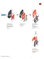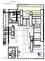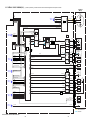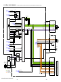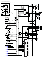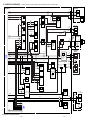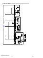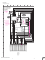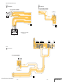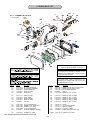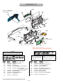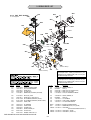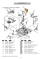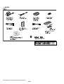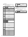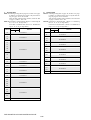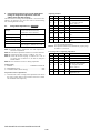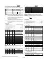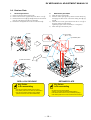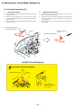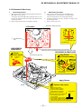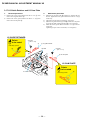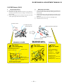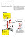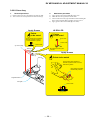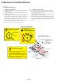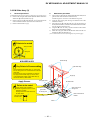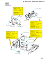
1
DCR-HC39E/HC41/HC42/HC42E/HC43/HC43E
RMT-831
SERVICE MANUAL
DCR-HC42
US Model
Canadian Model
Ver 1.0 2005.01
DCR-HC39E/HC42E
Revision History
AEP Model
UK Model
East European Model
North European Model
DCR-HC42/HC42E/HC43E
How to use
Acrobat Reader
E Model
DCR-HC42E
Australian Model
Hong Kong Model
DCR-HC43
Brazilian Model
DCR-HC43E
Chinese Model
DCR-HC42/HC42E
Tourist Model
DCR-HC42
Korea Model
Z MECHANISM (MDX-Z210)
DCR-HC41
Photo: DCR-HC43E
Japanese Model
Link
SPECIFICATIONS
BLOCK DIAGRAMS
PRINTED WIRING BOARDS
SERVICE NOTE
FRAME SCHEMATIC DIAGRAMS
REPAIR PARTS LIST
DISASSEMBLY
SCHEMATIC DIAGRAMS
• For ADJUSTMENTS (SECTION 6), refer to SERVICE MANUAL, ADJ (9-876-783-51).
• For INSTRUCTION MANUAL, refer to SERVICE MANUAL, LEVEL 1 (9-876-783-41). (EXCEPT J MODEL)
• For MECHANISM ADJUSTMENTS, refer to the “DV MECHANICAL ADJUSTMENT MANUAL VIII
Z (Z200/Z210/Z300/Z310) MECHANISM ” (EXCEPT J: 9-876-724-1[]) (J: 9-876-724-0[]).
• Reference No. search on printed wiring boards is available.
• Table for differences of function of each model.
• TO TAKE OUT A CASSETTE WHEN NOT EJECT (FORCE EJECT)
• HELP: Sheet attachment positions and procedures of processing the flexible boards/harnesses are shown.
On the VC-378 board
This service manual provides the information that is premised
the circuit board replacement service and not intended repair
inside the VC-378 board.
Therefore, schematic diagrams, printed wiring boards, mounted
parts location and electrical parts list of the VC-378 board are
not shown.
The following pages are not shown.
Schematic diagrams ..................... Pages 4-9 to 4-46
Printed wiring boards .................... Pages 4-67 to 4-70
Waveforms ..................................... Pages 4-82 to 4-87
Mounted parts location .................. Pages 4-90 and 4-91
Electrical parts list ......................... Pages 5-15 to 5-22
DIGITAL VIDEO CAMERA RECORDER
DCR-HC39E/HC41/HC42/HC42E/HC43/HC43E
9-876-783-31
Sony EMCS Co.
2005A0500-1
© 2005.1
Published by DI Technical Support Section
ENGLISH
JAPANESE
SPECIFICATIONS
Chrominance signal:
DCR-HC42/HC43: 0.286 Vp-p,
75 Ω (ohms), unbalanced
DCR-HC42E/HC43E: 0.3 Vp-p,
75 Ω (ohms), unbalanced
Audio signal: 327 mV (at output
impedance more than 47 kΩ
(kilohms)), Input impedance more
than 47 kΩ (kilohms), Output
impedance with less than 2.2 kΩ
(kilohms)
System
Video recording
system
2 rotary heads, Helical
scanning system
Still image
Exif Ver. 2.2*1
recording system
Audio recording Rotary heads, PCM system
system
Quantization: 12 bits (Fs 32 kHz,
stereo 1, stereo 2), 16 bits (Fs 48
kHz, stereo)
Video signal
DCR-HC42/HC43:
NTSC color, EIA standards
DCR-HC39E/HC42E/HC43E:
PAL color, CCIR standards
Usable cassette
Mini DV cassette with the
mark printed
Tape speed
SP: Approx. 18.81 mm/s
LP: Approx. 12.56 mm/s
Recording/
playback time
SP: 60 min
LP: 90 min
(using a DVM60 cassette)
Fast forward/
rewind time
Approx. 2 min 40 s
(using a DVM60 cassette)
Viewfinder
Electric viewfinder
DCR-HC39E: black and white
DCR-HC42/HC42E/HC43/HC43E:
color
Image device
Lens
Focal length
DCR-HC39E:
Audio/Video
output
LANC jack
USB jack
mini-B
DV input/output
4-pin connector
DCRA-C123 (DCR-HC39E)
Audio/Video
output
LCD screen
DC 7.2 V (battery pack)
DC 8.4 V (AC Adaptor)
Carl Zeiss Vario-Tessar
Combined power zoom lens
Filter diameter: 25 mm (1 in.)
12 × (Optical), 480 × (Digital)
F=1.8 - 2.5
Average power
consumption
DCR-HC42/HC43:
During camera recording using the
viewfinder 2.6 W
During camera recording using the
LCD 3.0 W
During camera recording using the
viewfinder and the LCD 3.2 W
DCR-HC39E/HC42E/HC43E:
During camera recording using the
viewfinder 2.5 W
During camera recording using the
LCD 2.9 W
During camera recording using the
viewfinder and the LCD 3.1 W
7 lx (lux) (F 1.8)
0 lx (lux) (during NightShot plus
function)*3
10-pin connector
Input/output auto switch
Video signal: 1 Vp-p, 75 Ω (ohms),
unbalanced
Luminance signal: 1 Vp-p, 75 Ω
(ohms), unbalanced
Chrominance signal:
DCR-HC42/HC43: 0.286 Vp-p,
75 Ω (ohms), unbalanced
DCR-HC42E/HC43E: 0.3 Vp-p,
75 Ω (ohms), unbalanced
Audio signal: 327 mV (at output
impedance more than 47 kΩ
(kilohms)), Input impedance more
than 47 kΩ (kilohms), Output
impedance with less than 2.2 kΩ
(kilohms)
Stereo mini-minijack (Ø 2.5 mm)
Power
requirements
*1“Exif” is a file format for still images, established
by the JEITA (Japan Electronics and Information
Technology Industries Association). Files in this
format can have additional information such as your
camcorder’s setting information at the time of
recording.
6.9 cm (2.7 type, aspect ratio 16:9)
Total dot number 123 200 (560 × 220)
General
10-pin connector
Video signal: 1 Vp-p, 75 Ω (ohms),
unbalanced
Luminance signal: 1 Vp-p, 75 Ω
(ohms), unbalanced
Chrominance signal: 0.3 Vp-p,
75 Ω (ohms), unbalanced
Audio signal: 327 mV (at output
impedance more than 47 kΩ
(kilohms)), Output impedance with
less than 2.2 kΩ (kilohms)
USB jack
mini-B
DV output
4-pin connector
AC Adaptor AC-L25A/L25B
Power
requirements
AC 100 - 240 V, 50/60 Hz
Current
consumption
0.35 - 0.18 A
Power
consumption
18 W
Output voltage
DC 8.4 V*
Operating
temperature
0 °C to 40 °C (32 °F to 104 °F)
-20 °C to + 60 °C (-4 °F to + 140
°F)
Storage
temperature
-20 °C to + 60 °C (-4 °F to + 140
°F)
Dimensions
(approx.)
54.7 × 90 × 111.7 mm (2 1/4 ×
3 5/8 × 4 1/2 in.) (w/h/d)
Dimensions
(approx.)
Mass (approx.)
410 g (14 oz) main unit only
470 g (1 lb) including the NP-FP50
rechargeable battery pack and
DVM60 cassette.
56 × 31 × 100 mm (2 1/4 × 1 1/4 ×
4 in.) (w/h/d) excluding the
projecting parts
Mass (approx.)
190 g (6.7 oz) excluding the mains
lead
Operating
temperature
0 °C to 40 °C (32 °F to 104 °F)
Storage
temperature
Supplied
accessories
*2In 16:9 mode, the focal length figures are actual
figures resulting from wide angle pixel readout.
*3Objects unable to be seen due to the dark can be
shot with infrared lighting.
Input/Output connectors
DCR-HC42/HC42E/HC43/HC43E:
Audio/Video
input/output
10-pin connector
Video signal: 1 Vp-p, 75 Ω (ohms),
unbalanced
Luminance signal: 1 Vp-p, 75 Ω
(ohms), unbalanced
Chrominance signal: 0.3 Vp-p,
75 Ω (ohms), unbalanced
Audio signal: 327 mV (at output
impedance more than 47 kΩ
(kilohms)), Output impedance with
less than 2.2 kΩ (kilohms)
Picture
f=3.0 - 36 mm (1/8 - 1 7/16 in.)
When converted to a 35 mm still
camera:
In CAMERA-TAPE:
16:9 mode*2: 46 ~ 628.5 mm
(1 13/16 - 24 3/4 in.)
4:3 mode: 40 ~ 480 mm
(1 5/8 - 19 in.)
In CAMERA-MEMORY:
4:3 mode: 48 ~ 576 mm
(1 15/16 - 22 3/4 in.)
16:9 mode: 43.6 ~ 523.2 mm
(1 3/4 - 20 5/8 in.)
Audio/Video
input/output
Stereo mini-minijack (Ø 2.5 mm)
3.27 mm (1/5.5 type) CCD (Charge
Coupled Device)
Gross: Approx. 1 070 000 pixels
Effective (still): Approx. 1 000 000
pixels
Effective (movie): Approx. 690 000
pixels
Color temperature [AUTO], [ONE PUSH],
[INDOOR] (3 200 K),
[OUTDOOR] (5 800 K)
Minimum
illumination
LANC jack
Handycam Station
DCRA-C121 (DCR-HC42/HC42E/HC43/
HC43E)
10-pin connector
Input/output auto switch
Video signal: 1 Vp-p, 75 Ω (ohms),
unbalanced
Luminance signal: 1 Vp-p, 75 Ω
(ohms), unbalanced
“Memory Stick Duo” 16MB (1)
(DCR-HC43E)
Memory Stick Duo adaptor (1)
(DCR-HC43E)
AC Adaptor (1)
Power cord (1)
Handycam Station (1)
Wireless Remote Commander (1)
A/V connecting cable (1)
USB cable (1)
Shoulder Strap (1)
Rechargeable battery pack (1)
CD-ROM “Picture Package
Ver.1.5” (1)
21-pin adaptor (1) (AEP, UK)
Conversion 2P adaptor (1) (E, JE)
Shoe cover (1)
Operating Guide (1)
See page 5-23.
* See the label on the AC Adaptor for other
specifications.
Rechargeable battery pack
NP-FP50
Maximum output DC 8.4 V
voltage
Output voltage
DC 7.2 V
Capacity
4.9 wh (680 mAh)
Dimensions
(approx.)
31.8 × 18.5 × 45.0 mm
(1 5/16 × 3/4 × 1 13/16 in.) (w/h/d)
Mass (approx.)
40 g (1.5 oz)
Operating
temperature
0 °C to 40 °C (32 °F to 104 °F)
Type
Lithium ion
Design and specifications are subject to change
without notice.
DCR-HC39E/HC41/HC42/HC42E/HC43/HC43E
—2—
ENGLISH
DCR-HC39E/HC41/HC42/HC42E/HC43/HC43E
—3—
JAPANESE
Table for differences of function
Model
DCR-HC39E
DCR-HC41
Destination
AEP, UK, NE, EE
J
Color system
Electrical viewfinder
Digital zoom
A/V jack
DV Interface on the Cradle
(Handycam Station)
PAL
Black and White
480 x
OUT
Model
Destination
Color system
Electrical viewfinder
Digital zoom
A/V jack
DV Interface on the Cradle
(Handycam Station)
DCR-HC42
US, CND, E, KR,
JE
DCR-HC42E
AEP, UK, NE, EE,
E, AUS, HK, JE
NTSC
Color
150 x
IN/OUT
NTSC
Color
480 x
IN/OUT
PAL
Color
480 x
IN/OUT
OUT
IN/OUT
IN/OUT
IN/OUT
DCR-HC43
DCR-HC43E
BR
CH, E
NTSC
Color
480 x
IN/OUT
PAL
Color
480 x
IN/OUT
IN/OUT
IN/OUT
• Abbreviation
AUS : Australian model
BR : Brazilian model
CH : Chinese model
CND : Canadian model
EE : East European model
HK : Hong Kong model
J
: Japanese model
JE : Tourist model
KR : Korea model
NE : North European model
DCR-HC39E/HC41/HC42/HC42E/HC43/HC43E
—4—
ENGLISH
JAPANESE
CAUTION
Danger of explosion if battery is incorrectly replaced.
Replace only with the same or equivalent type.
SAFETY-RELATED COMPONENT WARNING!!
COMPONENTS IDENTIFIED BY MARK 0 OR DOTTED LINE WITH
MARK 0 ON THE SCHEMATIC DIAGRAMS AND IN THE PARTS
LIST ARE CRITICAL TO SAFE OPERATION. REPLACE THESE
COMPONENTS WITH SONY PARTS WHOSE PART NUMBERS
APPEAR AS SHOWN IN THIS MANUAL OR IN SUPPLEMENTS
PUBLISHED BY SONY.
ATTENTION AU COMPOSANT AYANT RAPPORT
À LA SÉCURITÉ!
LES COMPOSANTS IDENTIFÉS PAR UNE MARQUE 0 SUR LES
DIAGRAMMES SCHÉMATIQUES ET LA LISTE DES PIÈCES SONT
CRITIQUES POUR LA SÉCURITÉ DE FONCTIONNEMENT. NE
REMPLACER CES COMPOSANTS QUE PAR DES PIÈSES SONY
DONT LES NUMÉROS SONT DONNÉS DANS CE MANUEL OU
DANS LES SUPPÉMENTS PUBLIÉS PAR SONY.
SAFETY CHECK-OUT
After correcting the original service problem, perform the following
safety checks before releasing the set to the customer.
1.
2.
3.
4.
5.
6.
Check the area of your repair for unsoldered or poorly-soldered
connections. Check the entire board surface for solder splashes
and bridges.
Check the interboard wiring to ensure that no wires are
"pinched" or contact high-wattage resistors.
Look for unauthorized replacement parts, particularly
transistors, that were installed during a previous repair. Point
them out to the customer and recommend their replacement.
Look for parts which, through functioning, show obvious signs
of deterioration. Point them out to the customer and
recommend their replacement.
Check the B+ voltage to see it is at the values specified.
Flexible Circuit Board Repairing
• Keep the temperature of the soldering iron around 270˚C
during repairing.
• Do not touch the soldering iron on the same conductor of the
circuit board (within 3 times).
• Be careful not to apply force on the conductor when soldering
or unsoldering.
Unleaded solder
Boards requiring use of unleaded solder are printed with the leadfree mark (LF) indicating the solder contains no lead.
(Caution: Some printed circuit boards may not come printed with
the lead free mark due to their particular size.)
: LEAD FREE MARK
Unleaded solder has the following characteristics.
• Unleaded solder melts at a temperature about 40°C higher than
ordinary solder.
Ordinary soldering irons can be used but the iron tip has to be
applied to the solder joint for a slightly longer time.
Soldering irons using a temperature regulator should be set to
about 350°C.
Caution: The printed pattern (copper foil) may peel away if the
heated tip is applied for too long, so be careful!
• Strong viscosity
Unleaded solder is more viscous (sticky, less prone to flow) than
ordinary solder so use caution not to let solder bridges occur such
as on IC pins, etc.
• Usable with ordinary solder
It is best to use only unleaded solder but unleaded solder may
also be added to ordinary solder.
DCR-HC39E/HC41/HC42/HC42E/HC43/HC43E
—5—
ENGLISH
DCR-HC39E/HC41/HC42/HC42E/HC43/HC43E
—6—
JAPANESE
TABLE OF CONTENTS
Section
1.
Title
Page
SERVICE NOTE
Section
5.
1-1. Note for Repair ································································ 1-1
1-2. Power Supply During Repairs ········································· 1-1
1-3. To Take Out a Cassette when not Eject (Force Eject) ····· 1-2
1-4. Self-diagnosis Function ··················································· 1-2
1-4-1. Self-diagnosis Function ··················································· 1-2
1-4-2. Self-diagnosis Display ····················································· 1-2
1-4-3. Self-diagnosis Code Table ··············································· 1-3
2.
DISASSEMBLY
2-1.
2-2.
2-3.
2-4.
2-5.
2-6.
Disassembly ····································································· 2-1
Mechanism Deck Service Position ·································· 2-5
LCD Service Position ······················································ 2-7
The Method of Attachment of FP-185 Flexible Board ···· 2-8
Circuit Boards Location ·················································· 2-9
Flexible Boards Location ·············································· 2-10
3.
BLOCK DIAGRAMS
3-1.
3-2.
3-3.
3-4.
3-5.
3-6.
3-7.
3-8.
3-9.
Overall Block Diagram (1/6) ··········································· 3-1
Overall Block Diagram (2/6) ··········································· 3-3
Overall Block Diagram (3/6) ··········································· 3-5
Overall Block Diagram (4/6) ··········································· 3-7
Overall Block Diagram (5/6) ··········································· 3-9
Overall Block Diagram (6/6) ········································· 3-11
Power Block Diagram (1/3) ··········································· 3-13
Power Block Diagram (2/3) ··········································· 3-15
Power Block Diagram (3/3) ··········································· 3-17
4.
PRINTED WIRING BOARDS AND
SCHEMATIC DIAGRAMS
5-1.
5-1-1.
5-1-2.
5-1-3.
5-1-4.
5-1-5.
5-1-6.
5-1-7.
5-1-8.
5-1-9.
5-2.
4-1. Frame Schematic Diagrams ············································· 4-1
4-2. Schematic Diagrams ························································ 4-5
CD-534 (CCD IMAGER) ················································ 4-7
PD-238 (LCD DRIVE, BACKLIGHT DRIVE) ············ 4-47
CR-050 (CRADLE TERMINAL) ································· 4-49
SI-042 (REMOTE COMMANDER RECEIVER,
PITCH/YAW SENSOR) ················································ 4-51
FP-182 FLEXIBLE ······················································· 4-53
JK-278 (JACK) ······························································ 4-53
MS-249 (MS CONNECTOR) ······································· 4-53
LB-109 (EVF, EVF BACKLIGHT) ······························ 4-55
FP-186 FLEXIBLE (PANEL REVERSE DETECT) ···· 4-55
FP-180 FLEXIBLE (DC IN) ········································· 4-56
FP-187 FLEXIBLE (CONTROL SWITCH) ················· 4-56
FP-826, FP-467, FP-228 FLEXIBLE ···························· 4-57
CONTROL KEY BLOCK (SS10300) ·························· 4-59
CONTROL KEY BLOCK (SB10600) ·························· 4-60
4-3. Printed Wiring Boards ··················································· 4-63
CD-534 ·········································································· 4-65
PD-238 ··········································································· 4-71
CR-050 ·········································································· 4-73
SI-042 ············································································ 4-74
LB-109 ··········································································· 4-74
JK-278 ··········································································· 4-75
MS-249 ·········································································· 4-76
FP-180, FP-186, FP-187 FLEXIBLE ···························· 4-77
FP-826, FP-467, FP-228 FLEXIBLE ···························· 4-79
4-4. Waveforms ····································································· 4-81
4-5. Mounted Parts Location ················································ 4-89
DCR-HC39E/HC41/HC42/HC42E/HC43/HC43E
—7—
Title
Page
REPAIR PARTS LIST
Exploded Views ···························································· 5-2
Overall Assembly ·························································· 5-2
F Panel Block ································································ 5-3
Lens Block ···································································· 5-4
Cabinet (R) Block ························································· 5-5
CS Block ······································································· 5-6
Bat EVF Block ······························································ 5-7
Mechanism Deck ·························································· 5-8
LS Chassis Block Assembly ········································· 5-9
Mechanism Chassis Block Assembly ························· 5-10
Electrical Parts List ····················································· 5-11
1. SERVICE NOTE
ENGLISH
JAPANESE
1-1. NOTE FOR REPAIR
Make sure that the flat cable and flexible board are not cracked of
bent at the terminal.
Do not insert the cable insufficiently nor crookedly.
When remove a connector, don’t pull at wire of connector.
It is possible that a wire is snapped.
When installing a connector, don’t press down at wire of connector.
It is possible that a wire is snapped.
Cut and remove the part of gilt
which comes off at the point.
(Be careful or some
pieces of gilt may be left inside)
1-2. POWER SUPPLY DURING REPAIRS
In this unit, about 10 seconds after power is supplied to the battery terminal using the regulated power supply (8.4V), the power is shut off so
that the unit cannot operate.
These following method is available to prevent this.
Method:
Use the AC power adaptor (AC-L25A/L25B).
DCR-HC39E/HC41/HC42/HC42E/HC43/HC43E
1-1
ENGLISH
JAPANESE
1-3. TO TAKE OUT A CASSETTE WHEN NOT EJECT (FORCE EJECT)
1 Refer to “2. DISASSEMBLY” to remove the mechanism deck block.
2 Disconnect the CN6002 of VC-378 board.
3 Supply +4.5V from the DC power supply to the loading motor and unload with a pressing the cassette compartment.
Disconnect the CN6002 of VC-378 board.
Loading motor
DC power supply (+4.5Vdc)
CN6002
VC-378 board
1-4. SELF-DIAGNOSIS FUNCTION
1-4-1. Self-diagnosis Function
1-4-2. Self-diagnosis Display
When problems occur while the unit is operating, the self-diagnosis
function starts working, and displays on the viewfinder or LCD
screen what to do. This function consists of two display; selfdiagnosis display and service mode display.
Details of the self-diagnosis functions are provided in the Instruction
manual.
When problems occur while the unit is operating, the counter of the
viewfinder or LCD screen shows a 4-digit display consisting of an
alphabet and numbers, which blinks at 3.2 Hz. This 5-character
display indicates the “repaired by:”, “block” in which the problem
occurred, and “detailed code” of the problem.
Viewfinder or LCD screen
C:31:11
Blinks at 3.2Hz
C
Repaired by:
C : Corrected by customer
H : Corrected by dealer
E : Corrected by service
engineer
31
11
Block
Detailed Code
Refer to “1-4-3. Self-diagnosis Code Table”.
Indicates the appropriate
step to be taken.
E.g.
31 ....Reload the tape.
32 ....Turn on power again.
DCR-HC39E/HC41/HC42/HC42E/HC43/HC43E
1-2
ENGLISH
JAPANESE
1-4-3. Self-diagnosis Code Table
Repaired by:
Self-diagnosis Code
Block
Function
Detailed
Code
Symptom/State
C
C
C
0
2
2
4
1
2
0
0
0
0
0
0
C
3
1
1
0
C
3
1
1
1
C
C
C
C
C
C
C
C
C
C
C
3
3
3
3
3
3
3
3
3
3
3
1
1
1
1
1
1
1
1
1
1
1
2
2
2
2
3
3
4
4
4
4
4
0
1
2
3
0
1
0
1
2
3
4
C
3
2
1
0
C
3
2
1
1
C
3
2
2
0
C
3
2
2
1
C
3
2
2
2
T reel fault.
C
3
2
2
3
S reel fault.
C
3
2
3
0
FG fault when starting capstan.
C
3
2
3
1
FG fault during normal capstan
operations.
C
3
2
4
0
FG fault when starting drum.
C
3
2
4
1
PG fault when starting drum.
C
3
2
4
2
C
3
2
4
3
C
3
2
4
4
Correction
Non-standard battery is used.
Condensation.
Video head is dirty.
LOAD direction. Loading does not
complete within specified time
UNLOAD direction. Loading does not
complete within specified time
T reel side tape slacking when unloading.
S reel side tape slacking when unloading.
T reel fault.
S reel fault.
FG fault when starting capstan.
FG fault during normal capstan operations.
FG fault when starting drum.
PG fault when starting drum.
FG fault during normal drum operations.
PG fault during normal drum operations.
Phase fault during normal drum operations.
LOAD direction loading motor timeout.
UNLOAD direction loading motor
time-out.
T reel side tape slacking when
unloading.
S reel side tape slacking when
unloading.
FG fault during normal drum
operations.
PG fault during normal drum
operations.
Phase fault during normal drum
operations.
DCR-HC39E/HC41/HC42/HC42E/HC43/HC43E
1-3
Use the InfoLITHIUM battery.
Remove the cassette, and insert it again after one hour.
Clean with the optional cleaning cassette.
Load the tape again, and perform operations from the beginning.
Load the tape again, and perform operations from the beginning.
Load the tape again, and perform operations from the beginning.
Load the tape again, and perform operations from the beginning.
Load the tape again, and perform operations from the beginning.
Load the tape again, and perform operations from the beginning.
Load the tape again, and perform operations from the beginning.
Load the tape again, and perform operations from the beginning.
Load the tape again, and perform operations from the beginning.
Load the tape again, and perform operations from the beginning.
Load the tape again, and perform operations from the beginning.
Load the tape again, and perform operations from the beginning.
Load the tape again, and perform operations from the beginning.
Remove the battery or power cable, connect, and perform
operations from the beginning.
Remove the battery or power cable, connect, and perform
operations from the beginning.
Remove the battery or power cable, connect, and perform
operations from the beginning.
Remove the battery or power cable, connect, and perform
operations from the beginning.
Remove the battery or power cable, connect, and perform
operations from the beginning.
Remove the battery or power cable, connect, and perform
operations from the beginning.
Remove the battery or power cable, connect, and perform
operations from the beginning.
Remove the battery or power cable, connect, and perform
operations from the beginning.
Remove the battery or power cable, connect, and perform
operations from the beginning.
Remove the battery or power cable, connect, and perform
operations from the beginning.
Remove the battery or power cable, connect, and perform
operations from the beginning.
Remove the battery or power cable, connect, and perform
operations from the beginning.
Remove the battery or power cable, connect, and perform
operations from the beginning.
ENGLISH
JAPANESE
Repaired by:
Self-diagnosis Code
Block
Function
Detailed
Code
E
6
1
0
0
E
6
1
1
0
E
6
1
1
1
E
6
2
0
0
E
6
2
0
1
Symptom/State
Correction
Inspect the lens block focus MR sensor (Pin 2, 4 of CN3801 of
VC-378 board) when focusing is performed when the touch panel is
operated in the focus manual mode and the focus motor drive circuit
(IC3803 of VC-378 board) when the focusing is not performed.
Inspect the lens block zoom reset sensor (Pin ws of CN3801 of
VC-378 board) when zooming is performed when the zoom switch
Zoom operations fault
(Cannot initialize zoom lens.)
is operated and the zoom motor drive circuit (IC3803 of VC-378
board) when zooming is not performed.
Focus lens initializing failure and zoom Inspect the flexible board for breakage or loose connection.
lens initializing failure occur simulta- If not faulty, inspect the focus and zoom motor drive circuit (IC3803
neously.
of VC-378 board).
Steadyshot function does not work well.
Inspect pitch angular velocity sensor (SE601 of SI-042 board)
(With pitch angular velocity sensor output
peripheral circuits.
stopped.)
Steadyshot function does not work well.
Inspect yaw angular velocity sensor (SE602 of SI-042 board)
(With yaw angular velocity sensor output
peripheral circuits.
stopped.)
Difficult to adjust focus
(Cannot initialize focus.)
DCR-HC39E/HC41/HC42/HC42E/HC43/HC43E
1-4
1. SERVICE NOTE
DCR-HC39E/HC41/HC42/HC42E/HC43/HC43E
1-5
ENGLISH
JAPANESE
ENGLISH
DCR-HC39E/HC41/HC42/HC42E/HC43/HC43E
1-6
JAPANESE
ENGLISH
DCR-HC39E/HC41/HC42/HC42E/HC43/HC43E
1-7
JAPANESE
ENGLISH
DCR-HC39E/HC41/HC42/HC42E/HC43/HC43E
1-8E
JAPANESE
2. DISASSEMBLY
HELP
The following flow chart shows the disassembly procedure.
7
2-1. DISASSEMBLY
2
1
1
4
6
3
4
0
3
3
6
0
2
9
5
to Page 2-3
8
3
6
8
5
4
4
5
9
2
7
3
1
2
3
4
5
6
7
8
9
0
P2 lock ace screw (M1.7) x1
Cpc lid
Screw (M1.7) x7
Claw x8
Flexible flat cable (FFC-038): CN603
F panel block
FP-190 flexible board: CN1003
FP-185 flexible board: CN1006
FP-187 flexible board: CN1002
Cabinet (R) block
7
7
1
2
3
4
5
6
7
8
9
0
P2 lock ace screw (M1.7) x1
P2 lock ace screw (M1.7) x1
Slide the EVF block.
P2 tappping screw x1
Tape (A) x2 HELP
Open the cabinet (G) block.
FP-180 flexible board: CN2001
FP-181 flexible board: CN7001
FP-184 flexible board: CN1005
BAT EVF block
6
1
1
2
3
4
5
6
7
Cushion (F2)
Tape (W) x1
Flexible board: CN 3801
FP-179 flexible board: CN3201
P2 lock ace screw (M1.7) x1
Boss x2
Lens block
1
8
9
7
1
0
qf
1
5
2
qh
qj
3
4
qa
2
3
2
4
qd qg
6
qs
1
2
3
4
5
6
7
8
9
Tape (A) x1
P2 tapping screw x2
Hinge blind
FP-187 flexible board
Tapping screw x2
P2 tapping screw x2
Claw x6
P cabinet (C (106))
FP-185 flexible board: CN601
0 FP-186 flexible board: CN609
qa Flexible board: CN608
qs Control key block (SB10600):
CN602
qd Flexible board: CN605
qf Tape (W) x1
qg Flexible board: CN603
qh P2 tapping screw x1
qj PD-238 board
1 Slide the CF retainer
in the direction of arrow.
2 D901
3 LCD901
4 Panel cushion (106)
1 Screw (M1.7) x1
2 BT panel block
DCR-HC39E/HC41/HC42/HC42E/HC43/HC43E
2-1
2-2
HELP
5
7
6
6
1
5
1
1
from Page 2-2
3
4
4
3
4
Flexible board: CN1001
Connector x2: CN6002, 6003
P2 lock ace screw (M1.7) x1
Connector x2: CN4301, 6001
FP-182 flexible board: CN1008
Hook x2
VC-378 board
6
1
7
1
2
3
4
5
6
7
2
2
2
1
2
3
4
3
P2 lock ace screw (M1.7) x3
Screw (M1.4x1.5) x4
MD frame block
Mechanism deck
1
2
3
4
5
6
7
Flexible board: CN704
P2 lock ace screw (M1.7) x1
Eject knob
P2 lock ace screw (M1.7) x1
Tapping screw x3
P2 lock ace screw (M1.7) x2
CS block
4
3
6
1
5
2
1
2
3
4
5
6
DCR-HC39E/HC41/HC42/HC42E/HC43/HC43E
2-3
2-4
P2 tapping screw x3
P2 lock ace screw (M1.7) x1
Control key block (SS10300)
P2 lock ace screw (M1.7) x2
CS frame block
JK-278 board
2-2. MECHANISM DECK SERVICE POSITION
Connection to Check the Mechanism deck
To check the mechanism deck, set the Camera or VTR to the "Forced power ON" mode.
(Or, connect the control key block (SS10300) to the CN1001 of VC-378 board and set the power switch
to the "CAMERA" or "PLAY/EDIT" position.)
Operate the VTR function using the adjustment remote commander
(with the HOLD switch set in the OFF position).
4
3
6
2
1
1
4
3
0
Exiting the "Forced Power ON" mode
1) Select page: 0, address: 01, and set data: 01.
2) Select page: A, address: 10, set data: 01
and press the PAUSE button of the
adjustment remote commander.
1) Select page: 0, address: 01, and set data: 01.
2) Select page: A, address: 10, data: 00,
and press the PAUSE button of the
adjustment remote commander.
3) Select page: 0, address: 01, and set data: 00.
Setting the "Forced VTR Power ON" mode
5
1) Select page: 0, address: 01, and set data: 01.
2) Select page: A, address: 10, set data: 02 and
press the PAUSE button of the adjustment remote
commander.
2
3
6
Setting the "Forced Camera Power ON" mode
8
5
4
7
9
7
5
3
1
3
1
3
*: To eject a cassette, connect the cabinet (L) block assembly.
4
0
Control key block
(SS10300)
6
2
Lens block
6
9
8
4
Adjustment
remote commander
(RM95)
5
2
7
1
1
*
Mechanism deck
2
4
I/F unit for LANC control
(J-6082-521-A)
3
1
VC-378 board
2
5
6
6
1
Color monitor
8
7
1
LANC jack
6
4
3
2
2
4
5
7
CPC-15
(J-6082-564-A)
3
JK-278 board
AC adaptor
A/V jack
6
1
BT panel block
DCR-HC39E/HC41/HC42/HC42E/HC43/HC43E
2-5
2-6
AC IN
2-3. LCD SERVICE POSITION
2-4. THE METHOD OF ATTACHMENT OF FP-185 FLEXIBLE BOARD
FP-185 flexible board
2 Set the hinge cover (M) inthe shown below.
Fold
7
7
8
9
Adhesive tape
Adhesive tape
0
Boss
qf
1
2
5
A
1
4
qh
B
qj
3
0
Rib
4
qa
Fold
2
3
3
6
Hinge cover (M)
qd qg
8
6
qs
5
1 The A and A, B and B section are united
4
and an angle is folded.
9
7
3
1
2
3
3 Set the FP-185 flexible board in the direction of arrow A,
and then turn the hinge (103) assembly in the direction of arrow B.
Hinge (103) assembly
Adjustment
remote commander
(RM95)
Hinge cover (M)
Lcd panel
I/F unit for LANC control
(J-6082-521-A)
B
A
8
1
FP-185 flexible board
PD-238 board
CPC-15
(J-6082-564-A)
Lighit guide plate block
AC adaptor
AC IN
DCR-HC39E/HC41/HC42/HC42E/HC43/HC43E
2-7
2-8
2-5. CIRCUIT BOARDS LOCATION
2-6. FLEXIBLE BOARDS LOCATION
FP-184 flexible
LB-109
FP-181 flexible
CD-534
Control key block
(SS10300)
JK-278
FP-182 flexible
MS-249
VC-378
FP-187 flexible
FP-179 flexible
FP-180 flexible
SI-042
FP-185 flexible
PD-238
CR-050
FFC-038 flexible
FP-186 flexible
FP-190 flexible
Board Name
Function
CD-534
CR-050
JK-278
LB-109
MS-249
PD-238
SI-042
VC-378
CCD IMAGER
CRADLE TERMINAL
JACK
EVF, EVF BACKLIGHT
MS CONNECTOR
LCD DRIVE, BACKLIGHT DRIVE
REMOTE COMMANDER RECEIVER, PITCH/YAW SENSOR
A/D CONVERTER, TIMING GENERATOR, LENS DRIVE,
CAMERA SIGNAL PROCESS, VIDEO/AUDIO DSP,
DS/HI CONTROL, FLASH, SDRAM, DV SIGNAL PROCESS, DV INTERFACE,
REC/PB AMP, ASPECT RATIO CONVERTER, VIDEO, AUDIO I/O,
MIC AMP, EVF DRIVE, CAMERA/MECHA CONTROL, SERVO, HI CONTROL,
DC IN, DC/DC CONVERTER, CONNECTOR
DCR-HC39E/HC41/HC42/HC42E/HC43/HC43E
2-9
2-10E
Control key block
(SB10600)
HELP
Sheet attachment positions and procedures of processing the flexible boards/harnesses are shown.
Tape (A)
FP-181 flexible board
FP-180 flexible board
VC-376/VC-377 board
Tape (A)
BT panel assy
Tape (BT)
FP-180 flexible board
DCR-HC39E/HC41/HC42/HC42E/HC43/HC43E
HELP
3. BLOCK DIAGRAMS
Link
OVERALL BLOCK DIAGRAM (1/6)
OVERALL BLOCK DIAGRAM (6/6)
OVERALL BLOCK DIAGRAM (2/6)
POWER BLOCK DIAGRAM (1/3)
OVERALL BLOCK DIAGRAM (3/6)
POWER BLOCK DIAGRAM (2/3)
OVERALL BLOCK DIAGRAM (4/6)
POWER BLOCK DIAGRAM (3/3)
OVERALL BLOCK DIAGRAM (5/6)
DCR-HC39E/HC41/HC42/HC42E/HC43/HC43E
3. BLOCK DIAGRAMS
3-1. OVERALL BLOCK DIAGRAM (1/6)
( ) : Number in parenthesis ( ) indicates the division number of schematic diagram where the component is located.
VC-378 BOARD (1/6)
LINE IC 4401 Y OUT
1
OVERALL (5/6)
(PAGE 3-9)
VCK
2
OVERALL (2/6)
(PAGE 3-3)
LENS BLOCK
CD-534 BOARD
11
IC201
IC203
CCD
IMAGER
S/H
5
4
CLPDM
1
XSHD, XSHP
13
14
4
ı
7
14
16
18
19
V1 – V4, RG, H1, H2, VSUB
CN3201
38
37
LINE
IC 4401 Y OUT
CCD OUT+
CCD OUT-
17
23
62
18
16
22
24
63
64
39
ı
36
13
10
9
35
33
34
59
61
32
28
27
36
1
ı
4
27
31
30
5
1
RCSUB
Q201
34
X3201
IC3803
(2/19)
CN3801
I DRIVE (+), (-)
17
18
H1
J1
I BIAS (+), (-)
12
14
C6 IRIS DRIVE,
A5 HALL AMP
I HALL (+), (-)
13
15
C5
B6
FOCUS ±
8
7
F3
E3
2
4
B1
C4
24
ı
27
K6
L4
F1
G3
K11
J11
H12
J12
L12
H
FOCUS
MOTOR
M
FOCUS MR
SENSOR
ZOOM
MOTOR
M
ZOOM
SENSOR
F MR A, B
ZM A, ZM XA,
ZM B, ZM XB
ZM SENS OUT
SPCK
K12
ZM RST
LENS TEMP AD
NightShot Vcc
S601
(LENS COVER OPEN)
CN603
(1/3)
SE601
PITCH SENSOR
SE602
YAW SENSOR
11
8
2
IC602
5
PITCH/YAW
12 SENSOR 18
AMP
3
19
2
XSHUTTER OPEN
NS LED K
PITCH AD
YAW AD
VST C RESET
6
8
14
16
17
XSHUTTER OPEN
Q1001
LED
DRIVE
VCK
241
MEMCK OUT
VIDEO DSP,
LENS CONTROL
(4/19)
196
174 175
178 – 182
185 – 188
191 – 195
MDQ0 – 15
198 – 205
207 208
210 – 215
144 145
148 – 153
156 – 161
MA0 – 13
170 171
173 174
176 – 185
EXT STROBO
SYS V
SPCK
38 2 4 5 7 8 10 11 13 42
44 45 47 48 50 51 53
20 – 26
29 – 35
IC4002
XSYS RST
EN1, DIR1A, DIR1B
9
8
ZM RST
77
78
75
161
203
XRST VTR
IC 4001CS
186
185
IC5301
(1/2)
181
159
158
156
236
141
248
250
251
238
157
CAMERA
CONTROL
(14/19)
62
74
73
71
183
54
127
187
129
130
40
245
139
154
SYS V
XSYS RST
EXT STROBO
SYS V
ZOOM VR AD
135
118
43
3
OVERALL (6/6)
(PAGE 3-11)
SDC IN
XCS AU1
4
OVERALL (5/6)
(PAGE 3-9)
XRST VTR
SPCK
5
OVERALL (3/6)
(PAGE 3-5)
XRST VTR
SPCK
6
OVERALL (4/6)
(PAGE 3-7)
CAM DD ON
XSHUTTER OPEN
IR ON
7
OVERALL (4/6)
(PAGE 3-7)
100
IR ON
PITCH AD
YAW AD
VST C RESET
05
DCR-HC39E/HC41/HC42/HC42E/HC43/HC43E
3-1
228
ı
230
IFI HD, IFI VD, IF OE
ADCK27
SPCK
XIC 3803 RST
ZM RST
LENS TEMP AD
XNS SW
PITCH AD
YAW AD
VST C RESET
CN1004
(1/3)
13
D601
IR EMITTER/
NIGHTSHOT
11
ı
13
IC4001
(1/4)
64M SDRAM
(4/19)
CH CS, CH SI, CH SO, CH SCK
SI-042 BOARD (1/3)
224
ı
227
102
24
122
90
XNS SW
10
A : VIDEO SIGNAL
20
ı
23
25
TG FLD
IFI C0 – IFI C3
XSYS RST
K9
J9 EN1, DIR1A, DIR1B
L9
M9
6
NIGHTSHOT
PLUS
ADCK27
9
ı
6
167
32
108
109
XSYS RST
216
ı
223
115
XIC 3803 RST
H11
22
TEMP OUT
83
82
84
137
99
IFI Y0 – IFI Y7
CAM SI, CAM SO, CAM SCK, CAM VD
ZM RST
LENS TEMP
SENSOR
VSG1
ZV1
TG ID
CHCK
CSUB
208
ı
202
199
CAM SI, CAM SO, CAM SCK, CAM CS, CAM VD
FOCUS
MOTOR
DRIVE
ZOOM
MOTOR
DRIVE
27MHz
: HC39E/HC42E/HC43E
33MHz
: HC41/HC42/HC43
92
91
IC3901
CAMERA SIGNAL
PROCESS
(3/19)
CAM SI, CAM SO, CAM SCK, CAM CS, CAM VD
M
67
56
ı
59
62
ı
71
TG HD, TG VD
18
A/D CONVERTER, 19
71
TIMING
GENERATOR
70
(1/19)
66
42
55
ı
57
69
252
ı
261
AD0 – AD13
IC3201
6
CAM DD ON
LINE
AD4 – AD13
AD0 – AD13
41
IRIS
METER
LINE
AD4 – AD13
1
ı
7
10
ı
16
47
44
45
CAM SI, CAM SO, CAM SCK, CAM CS, CAM VD
12
Q202
CLAMP
CN201
CCD OUT+
2
CCD OUT3
CH CS, CH SI, CH SO, CH SCK
IRIS
(SHUTTER)
3-2
3-2. OVERALL BLOCK DIAGRAM (2/6)
( ) : Number in parenthesis ( ) indicates the division number of schematic diagram where the component is located.
VC-378 BOARD (2/6)
OVERALL (1/6)
(PAGE 3-2)
2
VCK
20
268
ı
271
279
ı
282
LCKO
119 120
162 163
70 71
121 122
RCO0 – RCO3
HYO, HCO
164
165
ADATAIN0,1
301
302
VIDEO/AUDIO
DSP
(4/19)
143
RYO0 – RYO3
287
288
IC4001
(2/4)
VCK
264
ı
267
272
273
275
276
45
47
48
41
IC4201
DV SIGNAL
PROCESS
(7/19)
13 14
72 73
RCI0 – RCI3
123 – 125
166
RECDT
RECA1,2
RECA1,2
RECCK
149 150
186 187
104
284
285
HYI, HCI
12
75
298
299
ADATAOUT0,1
126
167
DSCK VM
XSYS RST
SFD BCK
SFD LRCK
86
168
169
LBUS0-3
24
IC4101
26
ı DV INTERFACE
28
(8/19)
TRCKO
62
19
62
58
59
111
112
21
78
52
51
48
47
2–4
6 – 9 11
75 – 77
78
TPA±, TPB±
D24A00 – D31A07,
ALE, WRX, RDX
VSP SI, VSP SO, XVSP SCK
13
FRRV, TRRV,
TRRT, DRP
TRRT, FRRV, TRRV
150
ı
152
TPA±, TPB±
D24A00 – D31A07, DXXA08, DXXA09, ALE, WRX, RDX
XCS IC 4101
CS IC 4201 BUS
XCS IC 4201
SWP
CS IC 4201 BUS
XCS IC 4201
SWP
3
114
157
15
Q4005
USB
PULL UP
USB D+
USB D±
USB CLK
USB CLK
24
SFD LRCK
USB 3.1V
OVERALL (6/6)
(PAGE 3-11)
11
2 – 11 33 – 36 15
20 – 27 39 – 46
30 31 55 49 52
SFD BCK
SFD LRCK
20 – 26
29 – 35
13
19
177
124
122
IC5102
(1/3)
DS CONTROL
(5/19)
16 – 18
21 – 24
27 – 35
A1 VM – A21 VM
1 – 4 7 – 11
291 – 298
301 – 304
81
85
78
80
MS XIN
Q5101
LED
DRIVER
19
XCS SDRAM VM
XCS FLASH
71
A : VIDEO SIGNAL
A : AUDIO SIGNAL
A : VIDEO/AUDIO SIGNAL
A : VIDEO/AUDIO/SERVO SIGNAL
69
05
DCR-HC39E/HC41/HC42/HC42E/HC43/HC43E
3-3
XMS LED ON
DSCK VM
287
MS DIO, MS BS, MS SCLK
2 4 5 7 8 10 11 38
13 42 44 45 47
48 50 51 53
IC5201
16M SDRAM
(6/19)
IC5202
32M FLASH
(6/19)
LINEOUT V
XSYS RST
D0 VM – D15 VM
10
A1– A11, A13, A14 VM
OVERALL (5/6)
(PAGE 3-9)
DSCK VM
USB DET
168
185
186
D0 VM – D15 VM
A1 VM – A19 VM
D0 VM – D15 VM
9
98
ı
116
D0 VM – D15 VM
DSCK VM
OVERALL (4/6)
(PAGE 3-7)
121 122
124 – 137
DSCK VM
A1 VM – A21 VM
8
DSCK VM
119
OVERALL (5/6)
(PAGE 3-10)
USB D±
USB D±
USB D±
256
OVERALL (3/6)
(PAGE 3-5)
14
VSP SI, VSP SO, XVSP SCK
VSP SI, VSP SO, XVSP SCK
79
149
80
160
161
164
165
OVERALL (3/6)
(PAGE 3-5)
FRRV, TRRV, TRRT, DRP
28
29
XCS IC 4001
USB XEN
VFI OE
ALIGN VD
LINEOUT V
VREF
OVERALL (3/6)
(PAGE 3-6)
RF IN
54 55 57
107 109 110
152 – 155
189 190 192
188
158
60
12
RECCK
RF IN
139
127
168
RYI0 – RYI3
RECDT
3-4
3-3. OVERALL BLOCK DIAGRAM (3/6)
( ) : Number in parenthesis ( ) indicates the division number of schematic diagram where the component is located.
Z MECHA DECK
(MDX-Z210)
VC-378 BOARD (3/6)
VIDEO HEAD
CN1007
RF MON
SWP
2
XCS EEP
4
7
ı
EEP SI, EEPSO, EEP SCK
5
RECDT
1
CPC
(FOR CHECK)
OVERALL (2/6)
(PAGE 3-4)
46
RECA1,2
12
40
42
44
35
RECCK
RF IN
RF MON
SWP
CONT1, SW PS, ALL PS
VSP SO, XVSP SCK
OVERALL (1/6)
(PAGE 3-2)
VSP SO, XVSP SCK
XRST VTR
SPCK
XRST VTR
SPCK
5
16
172
12
28
IC5302
1
32k EEPROM 2
5
(14/19)
6
XCS EEP
EEP SI, EEPSO, EEP SCK
88
10
87
86
84
89
D24A00 – D31A07, DXXA08, DXXA09, ALE, WRX, RDX
13
XCS IC 4101
CS IC 4201 BUS
XCS IC 4201
SWP
FRRV, TRRV, TRRT, DRP
VSP SI, VSP SO, XVSP SCK
OVERALL (5/6)
(PAGE 3-9)
15
MECHA
CONTROL
45 – 52
(14/19)
32 33
22 24
25
18
26
215
164
XCS EVF
XCS LCD
XCS IC 4701
HI SI, HI SO. XHI SCK. XCS MECHA
(15/19)
IC6001
(1/3)
(15/19)
SERIAL
INTERFACE
45
LPF
43
DRUM
ERROR
CAP
ERROR
7
21
24
8
IC2301
(1/2)
DRUM/
CAPSTAN
PWM DRIVE
(18/19)
15
13
138
189
38
152
XCS IC 4001
USB XEN
VFI OE
ALIGN VD
LINEOUT V
VREF
196
63
ı
66
192
155
195
68
207
201
204
M901
DRUM MOTOR
CN6001
77
78
75
76
Q2306
SWITCHING
SWITCHING
Q2305
DRUM VS
DRUM FG
64
67
DRUM
MOTOR
DRIVE
63
65
68
53
FG AMP
52
50
PG AMP
49
DRUM U, V, W
FG
PG
1
ı
6
M
10
DRUM FG
9
DRUM PG
DRUM FG
75
77
DRUM PG
CAP FWD, CAP ON
CAP FWD, CAP ON
CAP FG
CAP FG
1
80
4
180
CAPSTAN
MOTOR
DRIVE
FG AMP
74
76
78
10
ı
15
7
8
CAP U, V, W 1 11 17
ı ı ı
4 14 20
UHE±,
VHE±,
6
WHE±
ı
10
15
FG1, 2
MODE SW A-C
MODE SW A – C
IC6001
(2/3)
(15/19)
LOAD, UNLOAD
LM LIM DET
LM LIM DET
TAPE END
TAPE END
TAPE TOP
TAPE TOP
TREEL FG
TREEL FG
SREEL FG
SREEL FG
TAPE LED ON
22
25
CN6002
DEW AD
DEW AD
LOAD, UNLOAD
M903
CAPSTAN MOTOR
CN6003
CAP VS
193
8
39
37
45
IC6001
(3/3)
44
41
6
5
2
3
EVEN
37
197
198
106
ı
108
83
82
80
39
XEVEN, YEVEN
1
119
70
69
67
3
4
X5301
20MHz
190
23
179
178
163
REC PROOF
CHIME SDA, SCK
OVERALL (2/6)
(PAGE 3-3)
CAP PWM
XODD, YODD
30
38
VSP SO, XVSP SCK
VD SI, VD SO, VD SCK
16
DRUM PWM
34
35
REC/PB AMP
(9/19)
10
9
3
166
165
VSP SI, VSP SO, XVSP SCK
OVERALL (4/6)
(PAGE 3-7)
XCS IC 6001
38
36
IC4301
DRUM PG
IC5301
(2/2)
OVERALL (2/6)
(PAGE 3-4)
CONT1, SW PS, ALL PS
ODD
CN4301
32
33
31
LOADING
MOTOR
DRIVE
5
7
ı
9
M
HU, HV, HW
CAPSTAN FG
DEW SENSOR
S902
MODE SWITCH
M902
LOADING MOTOR
69
72
LM ±
21
TAPE END
20
DETECT
TAPE END C
19
TAPE TOP
18
DETECT
TAPE TOP C
1
ı
4
M
20
Q901
TAPE END
SENSOR
11
Q902
TAPE TOP
SENSOR
29
T REEL
FG AMP
26
27
T REEL ±
26
25
H902
T REEL
SENSOR
25
S REEL
FG AMP
22
23
S REEL ±
22
23
H901
S REEL
SENSOR
Q6003
LED
DRIVE
TAPE LED K
D901
TAPE LED
18
MIC902
REC PROOF
REC PROOF
CHIME SDA, CHIME SCK
12
14
15
4PIN
CONNECTOR
S903
CC DOWN
OVERALL (6/6)
(PAGE 3-11)
17
XCC DOWN
XCC DOWN
17
A : VIDEO/AUDIO/SERVO SIGNAL
A : SERVO SIGNAL
05
DCR-HC39E/HC41/HC42/HC42E/HC43/HC43E
3-5
3-6
3-4. OVERALL BLOCK DIAGRAM (4/6)
( ) : Number in parenthesis ( ) indicates the division number of schematic diagram where the component is located.
VC-378 BOARD (4/6)
LB-109 BOARD
EXCEPT HC39E
47
EVF R
EVF R
46
EVF G/BW Y
EVF G/BW Y
52
EVF B
EVF B
EVF HD, EVF VD
EVF HD, EVF VD
95
96
CN7001
34
33
EXCEPT HC39E
48
1
42
45
44
XCS EVF
EXTDA
IC7002
OVERALL (1/6)
(PAGE 3-2)
6
OVERALL (2/6)
(PAGE 3-3)
9
OVERALL (5/6)
(PAGE 3-9)
18
5
19
DSCK VM
IC 4401 Y OUT M
IC 4401 C OUT M
42
44
PANEL HD, PANEL VD
92
93
8
18
4
4
ı
13
17
18
ı
9
5
18
VB
16
LCD902
1
+
3 –
EVF DRIVE
(13/19)
COM CS
26
COM, CS
21
19
EVF
UNIT
43
6 – 10
12 14 16
17 28 24
31
18
EVF HST,HCK1, HCK2,
BLK, STB, VCK, PCG,
REF, VST, EN, PSIG
HST,HCK1, HCK2,
BLK, STB, VCK, PCG,
REF, VST, EN, PSIG
5
ı
7
9
ı
15
20
BL ON
D303
(BACKLIGHT)
Q7003
BACKLIGHT
DRIVE
4
LED K
23
B/W : HC39E
COLOR : EXCEPT HC39E
1
7
PANEL R
PANEL G
PANEL B
40
39
45
EVF BACKLIGHT
CONTROL
(13/19)
7
14
17
VG
IC7001
VD SI, VD SO, VD SCK
XRST VTR
SPCK
CN302
VR
6
15
EVF VB
22
CN301
16
EVF VG
21
32
IC4001
(3/4)
D/A
CONVERTER
(4/19)
EVF VR
20
IC4701
ASPECT
RATIO
CONVERTER
(10/19)
IC 4701 Y
IC 4701 C
32
34
Q4701
40
38
36
30
28
26
3
4
22
23
BUFFER
21
OVERALL (5/6)
(PAGE 3-9)
PD-238 BOARD (1/2)
CN1006
(1/2)
PANEL R M
PANEL G M
PANEL B M
PANEL HD M, PANEL VD M
144
148
VD SI, VD SO, VD SCK
XCS LCD
LCD901
CN601
(1/2)
CN605
1
2
3
12
13
PANEL R M
1
PANEL G M
2
PANEL B M
3
12 PANEL HD M, PANEL VD M
13
19
22
21
19
22
21
20
20
XCS IC 4701
48
1
XCS LCD
IC602
EXTDA
BL ON
4
5
3
1
24
23
COM, CS
26
5 – 12
14 16
24 28
43
R
G
B
20
21
22
LCD DRIVE
42
45
44
VD SI, VD SO, VD SCK
10
11
13
VSP SI, VSP SO, XVSP SCK
34
33
32
RGT, PSIG, HCK1, HCK2,
WIDE, REF, HST, PCG,
XSTBY, DWN, EN, VCK, VST
2
6–8
11–14
19–22
2.7 inch
WIDE
COLOR
LCD
UNIT
31
18
12
XCS EVF
VD SI, VD SO, VD SCK
OVERALL (3/6)
(PAGE 3-5)
16
XCS LCD
LXCS
LXWAIT
97
ı
99
237
234
HI SI, HI SO. XHI SCK. XCS MECHA
REC PROOF
CHIME SDA, SCK
OVERALL (6/6)
(PAGE 3-11)
OVERALL (1/6)
(PAGE 3-2)
19
7
74
285
137
138
IC5102
(2/3)
249
HI CONTROL
(5/19)
250
TP X
TP Y
TP X
TP Y
TP SEL1
TP SEL2
TP SEL1
18
16
18
16
17
17
CN603
TP TOP
5
TP L
2
TP X
TP Y
TOUCH
PANEL
I/F
Q601, 602
TP SEL1
Q5108
TP SELECT
SWITCH
246
247
IC601
CAM DD ON
CAM DD ON
XSHUTTER OPEN
IR ON
131
273
254
235 236
103 – 105
CS EEP,
EEP XRDY,
EEP RXD3,
EEP SCK3.
EEP TXD3
OVERALL (5/6)
(PAGE 3-9)
20
MODULATOR
MELODY
MELODY ENV
ZOOM MIC CONT
SHOE STEREO
IC5101
1–3
5 6 64k EEPROM
(5/19)
+
2 –
NS 2.8V
1
A : VIDEO SIGNAL
230
253
154
265
05
DCR-HC39E/HC41/HC42/HC42E/HC43/HC43E
3-7
Q606, 607,
611, 613
BACKLIGHT
CONTROL
3
Q5103, 5104
BEEP
TP R
TP BOT
3-8
1
4
D901
BACKLIGHT
CN608
NS 2.8V
BACK LIGHT
DRIVE
BL REG
BL H
BL FB
TOUCH
PANEL
6
1
4
3
3-5. OVERALL BLOCK DIAGRAM (5/6)
( ) : Number in parenthesis ( ) indicates the division number of schematic diagram where the component is located.
VC-378 BOARD (5/6)
OVERALL (4/6)
(PAGE 3-7)
Q4402
IC 4401 Y OUT M
IC 4401 C OUT M
18
BUFFER
EXCEPT HC39E
Q4403
OVERALL (1/6)
(PAGE 3-2)
IC 4401 Y OUT LINE
1
BUFFER
/CLAMP
EXCEPT HC39E
33
CLPVO
62
OVERALL (4/6)
(PAGE 3-7)
IC4001
(4/4)
21
JK-278 BOARD (1/2)
IC 4701 Y
IC 4701 C
9
6
IC 4001 Y OUT
IC 4001 C OUT
53
60
VIDEO/AUDIO
DSP
(4/19)
LINE
LINE
LINE
12
17
14
19
21
IC 4401 C OUT D LINE
DATA FROM SFD
SFD BCK
SFD LRCK
SFD FCK
89
82
83
85
DATA TO SFD
87
PBIN L
PBIN R
15
16
9
12
10
11
IC4402
A/D, D/A
CONVERTER
(11/19)
8
MULTI JACK IN
IC4401
AUDIO L I/O
AUDIO R I/O
57
61
AUDIO L I/O
AUDIO R I/O
RECOUT L
RECOUT R
3
2
35
34
55
56
OVERALL (4/6)
(PAGE 3-7)
15
10
12
10
12
JACK AD
15
OVERALL (1/6)
(PAGE 3-2)
4
SFD LRCK
SFD BCK
36
37
32
MS XIN
BEEP
ZOOM MIC CONT
SHOE STEREO
65
14
XMS LED ON
OVERALL (2/6)
(PAGE 3-4)
TPA±, TPB±
35
39
CN503
5
6
3
MS INSERT
XACCESS LED
VSP SO, XVSP SCK
XCS AU1
SDC IN
HOT SHOE
(1/2)
INS
4
4
SI-042 BOARD
(2/3)
L
1
R
3
CN601
INT MIC L
INT MIC R
6
D501
(MS ACCESS)
8
SP901
SPEAKER
CN502
23
24
SP±
43
44
SP±
12
13
CN1005
(1/2)
SHOE MIC L
1
2
SHOE MIC R
G5
H3
IC4501
B8 MIC AMP
B7 (12/19)
A1
B2
G6
H2
MIC L
MIC R
42
44
70
74
SP±
CR-050 BOARD (1/2)
CN1003
(1/2)
MIC901
MICROPHONE
UNIT
MEMORY
STICK
DUO
25
27
5
MIC FR
4
2
8
DIO, BS, SCLK
USB D±
VSP SO, XVSP SCK
MIC FL
1
6
MS-249 BOARD (1/2)
USB DET
OVERALL (3/6)
(PAGE 3-5)
A/V
7
AUDIO L
AUDIO R
CN501
(1/2)
EXCEPT HC39E
20
15
20
18
KASYAON
10
CN701
S-Y
10
S-C
5
VIDEO IN/OUT
9
8
6
14
LINE
LINE
MS DIO, MS BS, MS SCLK
OVERALL (2/6)
(PAGE 3-3)
CN704
(1/2)
VIDEO,
AUDIO I/O
(11/19)
ACC CONT
AGC CONT
66
64
91
31
30
S Y I/O
S C I/O
VIDEO I/O
88
3
90
10
7
CN1008
(1/2)
SY
8
SC
6
VIDEO I/O
14
FP-182 FLEXIBLE
BOARD (1/2)
CN603
(2/3)
9
10
7
12
S Y I/O
S C I/O
VIDEO I/O
TPA, NTPA, TPB, NTPB
10
9
7
6
42
43
45
46
TPA, NTPA, TPB, NTPB
31
29
33
35
USB D±
4
3
48
49
USB D±
32
34
2
50
INT MIC R
22
MULTI JACK IN
MULTI JACK IN CRADLE
D1016
USB DET
05
DCR-HC39E/HC41/HC42/HC42E/HC43/HC43E
3-9
9
13
10
8
18
14
34
32
40
39
36
38
MULTI JACK IN
AUDIO L I/O
AUDIO R I/O
OVERALL (6/6)
(PAGE 3-11)
CN002
(1/2)
S Y I/O
S C I/O
VIDEO I/O
18
20
12
13
16
14
CN1004
(2/3)
INT MIC L
A : VIDEO SIGNAL
A : AUDIO SIGNAL
A : VIDEO/AUDIO SIGNAL
CN001
(1/2)
3-10
MULTI JACK IN
AUDIO L I/O
AUDIO R I/O
USB DET
24
26
CRADLE
(1/2)
3-6. OVERALL BLOCK DIAGRAM (6/6)
FP-186 FLEXIBLE BOARD
S101
(PANEL REVERSE)
PD-238 BOARD (2/2)
CN609
3
4
( ) : Number in parenthesis ( ) indicates the division number of schematic diagram where the component is located.
VC-378 BOARD (6/6)
SI-042 BOARD (3/3)
CN1004
(3/3)
XF TALLY LED
PANEL REVERSE
KEY AD0
KEY AD1
KEY AD2
KEY AD3
CONTROL KEY BLOCK
(SB10600)
S004
WIDE/NORMAL
2
T S003
3
(ZOOM)
W S002
4
S001
START/STOP
5
CN602
WIDE/NORMAL SW
139
140
141
142
221
SYS V
19
44
33
2ND ZOOM (T)
2ND ZOOM (W)
CN601
(2/2)
KEY AD1
2ND S/S SW
23
ı
26
CN1006
(2/2)
6
KEY AD1
6
16
41
34
73
FP-187 FLEXIBLE BOARD
S004
PANEL
OPEN/CLOSE
OSD V
XDS RESET
XVM MAD
220
86
274
93
ı
IC 5001 TXD0, IC 5001 RXD0. IC 5001 SCK0. IC 5001 CS
96
SIRCS SIG
S003
BACK LIGHT
X5001
32.768kHz
CN1002
S002
EASY
KEY AD3
S001
DSPL/
BATT INFO
BATT INFO
D001
(EASY)
XEASY LED
D004
CHG
KEY AD3
2
XBATT INFO SW
3
Q5001
LED
DRIVE
4
XCHARGE LED
HI CONTROL
(5/19)
263
245
XCRADLE IN
XF TALLY LED
SIRCS SIG
XLANC JACK IN
XRESET
LI 3V
51
IC5001
52
HI CONTROL
(16/19)
6
54
55
HOTSHOE ID1, 2
17
77
1
10
S001
EJECT
14
ON
8
7
MODE
D001
CAMERA-TAPE
3
D002
CAMERA-MEMORY
5
D003
PLAY/EDIT
6
T
12
Q2005
DOUBLE
INSERTION DETECT
KEY AD2
XPOWER SW
XMODE SW
XCAM LED
XMEM LED
XVTR LED
42
43
Q5002
BATTERY
CHARGE
DETECTOR
OVERALL (2/6)
(PAGE 3-3)
11
OVERALL (3/6)
(PAGE 3-5)
17
OVERALL (5/6)
(PAGE 3-9)
22
OVERALL (4/6)
(PAGE 3-7)
19
10
37
1
2
38
FAST CHARGE
Q2003,
2004 (2/2)
INIT CHARGE ON
ACV UNREG
11
LI 3V
12
ZOOM VR
XRESET
ZOOM VR AD
EXT STROBO
SYS V
XSYS RST
20
21
18
32
XCC DOWN
5
MULTI JACK IN
MULTI JACK IN CRADLE
56
61
Q2001,
2002,
2004 (1/2)
BATT UNREG
10
39
40
7
79
XSYS RST
LINEOUT V
45
31
35
67
LANC IN
LANC OUT
XLANC PWR ON
XLANC ON
HI EVER SO, HI EVER SCK
BATT IN
VTR DD ON
XCS DD
CAM DD ON
IC2301
(2/2)
51 DC CONTROL,
RESET,
57 LANC DRIVE
(18/19)
54
56
55
52
14
15
50
44
13
5
LF2001
30
9
24
ı
29
16
ı
21
1
ı
6
10
ı
15
A 1.2V
D 1.2V
USB 3.1V
A 1.5V
D 1.5V
MT 5V
NS 2.8V
RP 2.8V
A 2.8V
D 2.8V
AU 2.8V
EP 2.8V
D 1.9V
A 4.6V
AU 4.6V
EP 4.6V
RP 4.6V
EP 8.5V
IC 6001 13.5V
BL REG
CAM 15V
CAM -7.5V
EVER 3.0V
VOUT
LANC DC
CAM DD ON
05
DCR-HC39E/HC41/HC42/HC42E/HC43/HC43E
3-11
J701
(LANC)
XLANC JACK IN
LANC SIG
MS-249 BOARD (2/2)
S501
RESET
BT501
LITHIUM
BATTERY
HOT SHOE
(2/2)
CN001
(2/2)
CN002
(2/2)
LANC SIG
XCRADLE IN
28
25
1
ı
10
26
25
19
1
ı
4
21
ACV UNREG
BATT/XEXT
FP-180 FLEXIBLE BOARD
CN2001
ACV UNREG
4
LANC SIG
3
41
JK-278 BOARD (2/2)
CR-050 BOARD (2/2)
(ZOOM)
OVERALL (1/6)
(PAGE 3-2)
11
KEY AD0
XEJECT SW
CN704
(2/2)
3
2
CN1003
(2/2)
LANC SIG
24
XCRADLE IN
27
ACV UNREG 51
ı
42
BATT/XEXT
26
BATT/XEXT
46
RV001
W
FP-182 FLEXIBLE
BOARD (2/2)
CN1001
S002
(PHOTO REC)
OFF
15
42
CN1005
(2/2)
EXT STROBO
15
SHOE CONT
17
HOTSHOE ID1, 2
8
14
LANC SIG
16
S003
(PHOTO FREEZE)
POWER
IC601
REMOTE
4 COMMANDER
RECEIVER
29
CONTROL KEY BLOCK (SS10300)
S004
START/STOP
D602
CAMERA
RECORDING
17
CN501
(2/2)
XRESET
D2006
PHOTO
4
CN1008
(2/2)
XLANC JACK IN
3
LANC SIG
2
SHOE CONT
9
7
2
IC5102
(3/3)
28
X5002
10MHz
CN603
(3/3)
3-12
BATT/XEXT
BATT SIG
ACV UNREG
J001
DC IN
ACV GND
BATT UNREG
BATT GND
+
C
–
BH001
BATTERY
TERMINAL
CRADLE
(2/2)
3-7. POWER BLOCK DIAGRAM (1/3)
( ) : Number in parenthesis ( ) indicates the division number of schematic diagram where the component is located.
VC-378 BOARD (1/3)
F002
F005
CN2001
ACV UNREG
J001
DC IN
LF2001
Q2006, 2007
F003
24
ı
29
16
ı
21
Q2001,
2002,
2004 (1/2)
INIT CHARGE ON
VB 62
61 VCC1
60 VCC3
BATT/XEXT
D2301
1
ı
6
9
10
ı
15
+
C
−
F004
BATT UNREG
BATT SIG
VCCO1 63
VCCO2 67
Q2301, 2308
L2306
OUT1-1
OUT1-2
VS1
IN1
BATT/XEXT
LANC DC
27
J701
(LANC)
51
ı
42
26
1
ı
10
26
30
JK-278 BOARD
22
Q2317, 2318
D2006
ACV UNREG
BATT/XEXT
BATT/XEXT
DC CONTROL,
RESET,
LANC DRIVE,
DRUM/CAPSTAN
PWM DRIVE
(18/19)
LANC DC
4
4
L2307
OUT2 68
VS2 69
IN2 11
Q2302, 2309
L2308
BT501
LITHIUM
BATTERY
MT 5V
L2311
NS 2.8V
L2313
RP 2.8V
L2314
A 2.8V
L2315
D 2.8V
L2316
AU 2.8V
L2317
EP 2.8V
SWITCHING
70
72
71
10
Q2304
CN1008
(1/2)
LANC DC
L2304
L2318
A 4.6V
L2319
AU 4.6V
SWITCHING
58 VOUT4
L2320
EP 4.6V
L2321
RP 4.6V
IC2302
3.1V REG (18/19)
CN501
(1/2)
10
41
LI 3V
1
3
45 VBATT
+
4
USB 3.1V
D2302
46 VOUT3
47 VOUT2
48 VOUT1
EVER 3.0V
IC5001
HI CONTROL
(16/19)
D004
8
CHG
D001
(EASY)
5
CN1002
CHARGE LED VDD
BATT/EXT 77
FAST CHARGE 37
INIT CHARGE 38
EASY LED VDD
IB SO 42
IB SI 43
VOUT
L2301
Q2307
Q2312
L2303
SWITCHING
13.5V REG
Q2310
BATT/XEXT
FAST CHARGE
INIT CHARGE ON
SHOE ON 57
BATT SIG
15V REG
CAM 15V
VCONT5 79
VOUT5 2
VCONT6 3
VOUT6 4
REG6CTL 5
CAM DD ON
D2304
BL REG
BATT SENSE 65
ACV SENSE 66
Q2315, 2316
-7.5V REG
HI EVER SO 20
HI EVER SCK 21
HI EVER SO, HI EVER SCK
BATT IN
VTR DD ON
XCS DD
BATT IN 31
VTR DD ON 35
XCS DD 67
XLANC PWR ON
XLANC ON
XLANC POWER ON 8
XLANC ON 46
MT 5V
CAM -7.5V
41 VR
14 DIN
15 CLK
CAM DD ON
50 OUTC1
44 CTL1
13 LD
55 WAKEUP
52 XCTL2
MT 5V
05
DCR-HC39E/HC41/HC42/HC42E/HC43/HC43E
3-13
EP 8.5V
8.5V REG
IN7 6
Q5002
BATTERY
CHARGE
DETECTOR
IC 6001 13.5V
Q2311
OUT7 79
VTR DD ON
VR
FP-187 FLEXIBLE BOARD
A
POWER (2/3)
(PAGE 3-15)
OUT4 73
VS4 74
IN4 9
MS-249 BOARD
(1/2)
D 1.9V
1.9V REG
SWITCHING
OUT3-1
OUT3-2
VS3
IN3
FP-182
FLEXIBLE
BOARD
(1/2)
CN704
LANC DC
CN1003
D 1.2V
D 1.5V
64
66
65
12
IC2301
CN001
A 1.2V
L2323
A 1.5V
L2310
BATT UNREG
VTR UNREG
CRADLE
L2309
L2322
VTR DD ON
VR
SWITCHING
Q2303
ACV UNREG
1.2V REG
49 VCC2
CR-050 BOARD
1
ı
4
21
Q2313, 2314
D2303
BATT SIG
Q2005
DOUBLE
INSERTION DETECT
CN002
HOT SHOE
VTR UNREG
D2305
BH001
BATTERY
TERMINAL
9
ı
13
MT/15.5/BL UNREG
FAST CHARGE
30
SHOE UNREG
VTR UNREG
F001
Q2003,
2004 (2/2)
CN1005
FB1006
SHOE UNREG
SHOE ON
FP-180
FLEXIBLE
BOARD
Q2305, 2306
CAPSTAN/
DRUM
SWITCHING
C/D UNREG
3-14
3-8. POWER BLOCK DIAGRAM (2/3)
( ) : Number in parenthesis ( ) indicates the division number of schematic diagram where the component is located.
CD-534 BOARD
VC-378 BOARD (2/3)
CN3201
CAM 15V
CAM 15V
CAM 15V
15
14
25
26
L201
CAM -7.5V
CAM -7.5V
A 2.8V
CAM -7.5V
13
12
27
28
FB201
A 2.8V
19
18
21
22
L202
RP 2.8V
RP 4.6V
IC4301
L4302
IC3202
5
REC/PB AMP
(9/19)
3.4V REG
(1/19)
FB3205
4
FB3203
L3201
L4207
IC4501
L4501
IC3203
5
IC4201
MIC AMP
(12/19)
L4205
IC4402
DV SIGNAL
PROCESS
(7/19)
3.1V REG
(1/19)
4
L4101
L4404
ZM SENS Vcc
IC4401
FB5203
VIDEO,
AUDIO I/O
(11/19)
L4405
FB4401
CN1008
(2/2)
MS VCC
IC1001
IC3804
IC5202
5
2.8V REG
(2/19)
IC3803
4
FB3801
L3801
FB5201
FOCUS MR
SENSOR
20
ZOOM
SENSOR
ZM RST LED
32M FLASH
(6/19)
Q4401
3.2V REG
1
DV INTERFACE
(8/19)
L4401
L4402
S/H
Q3801
D 2.8V
L4406
IC203
LENS BLOCK
CN3801
MR VCC
IC4101
POWER (1/3)
(PAGE 3-14)
CCD
IMAGER
A/D CONVERTER,
TIMING
GENERATOR
(1/19)
FB3204
FB4101
AU 4.6V
IC3201
FB4201
A/D, D/A
CONVERTER
(11/19)
AU 2.8V
IC201
L4301
L4202
A
CN201
IC5201
5
FOCUS/ZOOM
MOTOR DRIVE,
IRIS DRIVE,
HALL AMP
(2/19)
2.9V REG
(19/19)
4
FP-182
FLEXIBLE
BOARD
(2/2)
29
MS-249 BOARD
(2/2)
CN501
(2/2)
CN503
VCC
2
9
D501
(MS ACCESS)
1
D 2.8V
40
MEMORY
STICK
DUO
9
16M SDRAM
(6/19)
D 1.9V
A 2.8V
A 4.6V
D 2.8V
MT 5V
VTR UNREG
IC 6001 13.5V
D 1.5V
D 1.2V
USB 3.1V
A 1.5V
D 1.9V
A 2.8V
A 4.6V
D 2.8V
MT 5V
VTR UNREG
IC 6001 13.5V
D 1.5V
D 1.2V
USB 3.1V
A 1.5V
A 4.6V
FB4702
L4701
32k EEPROM
(14/19)
IC4701
ASPECT RATIO
CONVERTER
(10/19)
FB5301
CAMERA
SIGNAL
PROCESS
(3/19)
CN6003
HE VCC
FG VCC
CN6002
TAPE LED A
IC5302
IC3901
A 1.2V
IC6001
VH 17
DRUM/
CAPSTAN/
LOADING
VMR 3
MOTOR DRIVE
(15/19)
D 1.2V
FB3902
L3901
FB6001
D 2.8V
MT 5V
VTR UNREG
IC 6001 13.5V
FB4701
FB3901
Z MECHA DECK
(MDX-Z210)
A 2.8V
16
HU, HV, HW
23
24
CAPSTAN FG
D901
TAPE LED
19
Q6002
HALL VCC
Q5105 - 5107
L6001 CHIME VDD
27
S REEL
SENSOR
H901
13
T REEL
SENSOR
H902
ZM RST LED 55
MIC902
4PIN
CONNECTOR
XREEL HALL ON 153
FB4005
FB4001
IC5101
FB4002
64k EEPROM
(5/19)
L4002
IC4001
IC5301
CAMERA/MECHA
CONTROL
(14/19)
VIDEO/AUDIO
DSP
(4/19)
L4003
FB5103
L4001
IC5102
DS/HI CONTROL
(5/19)
R5127
FB5102
IC4002
64M SDRAM
(4/19)
FB5105
FB5106
CAM DD ON
EVF
BACKLIGHT
CONTROL
(13/19)
EP 8.5V
EP 8.5V
EP 4.6V
EP 4.6V
EP 2.8V
NS 2.8V
BL REG
EP 2.8V
D 2.8V
A 4.6V
A 2.8V
EP 8.5V
EP 4.6V
EP 2.8V
NS 2.8V
BL REG
IC7002
MS VCC ON 286
CHIME PWR CONT 130
131 CAM DD ON
CN7001
EVF VDD
L7003
L7002
EP 4.6V
IC7001
EVF DRIVE
(13/19)
POWER (3/3)
(PAGE 3-17)
05
DCR-HC39E/HC41/HC42/HC42E/HC43/HC43E
3-15
LCD902
CN301 CN302
1
20
22
2
2
VDD
EVF UNIT
L7001
FB7001
C
B/W : HC39E
COLOR : EXCEPT HC39E
LB-109
BOARD
3-16
D303
(BACKLIGHT)
3-9. POWER BLOCK DIAGRAM (3/3)
( ) : Number in parenthesis ( ) indicates the division number of schematic diagram where the component is located.
VC-378 BOARD (3/3)
CONTROL KEY BLOCK
(SS10300)
CN1001
D 2.8V
RV001
T
11
W
(ZOOM)
D001
CAMERA-TAPE
D002
CAMERA-MEMORY
D 2.8V
MODE LED VDD
D003
PLAY/EDIT
4
SI-042 BOARD
CN1004
A 4.6V
A 4.6V
NS LED A
D 2.8V
C
A 2.8V
A 2.8V
IC601
REMOTE
COMMANDER
RECEIVER
CN603
3
16
7
12
1
18
18
1
D601
IR EMITTER
NIGHTSHOT
D602
CAMERA
RECORDING
L601
POWER (2/3)
(PAGE 3-16)
IC602
PITCH/YAW
SENSOR
AMP
SE601
PITCH SENSOR
SE602
YAW SENSOR
PD-238 BOARD
EP 8.5V
CN1006
EP 8.5V
EP 4.6V
EP 4.6V
EP 2.8V
EP 2.8V
CN601
9
9
8
8
Q608, 609
L603
CN605
18
VDD
LCD901
XSTBY
2.7 inch
WIDE
COLOR
LCD UNIT
L602
7
L601
IC602
FB601
LCD DRIVE
7
XSTBY 10
14
CN608
NS 2.8V
BL REG
NS 2.8V
BL REG
11
10
11
10
6
3
IC601
BACKLIGHT
CONTROL
Q606, 607, 611, 613
BACKLIGHT
DRIVE
1
BL 2.8V
BL L
BL H
D901
BACKLIGHT
05
DCR-HC39E/HC41/HC42/HC42E/HC43/HC43E
3-17
3-18E
4. PRINTED WIRING BOARDS AND SCHEMATIC DIAGRAMS
4-1. FRAME SCHEMATIC DIAGRAM
1
2
4
3
6
5
7
10
9
8
11
12
15
14
13
16
18
17
19
21
20
22
24
23
FRAME SCHEMATIC DIAGRAM
A
JK-278 BOARD
(JACK)
CN1008
(CCD IMAGER)
CCD_OUT+
CCD_OUT-
GND
GND
GND
GND
GND
H2
H1
GND
LH
RG
GND
GND
XSHP
CLPDM
XSHD
GND
GND
A_2.8V
A_2.8V
GND
GND
CAM_15V
CAM_15V
CAM_-7.5V
CAM_-7.5V
GND
GND
GND
GND
GND
RCSUB
VSUB
V1
V2
V3
V4
3
4
5
6
7
8
9
10
11
12
13
14
15
16
17
18
19
20
21
22
23
24
25
26
27
28
29
30
31
32
33
34
35
36
37
38
39
FP-826
FLEXIBLE
BOARD
M901
DRUM
MOTOR
VIDEO HEAD
(ODD,EVEN)
FP-467
FLEXIBLE
BOARD
Z MECHANISM DECK (MDX-Z210)
FP-228
FLEXIBLE
BOARD
M902
LOADING
MOTOR
M903
CAPSTAN
MOTOR
26
25
24
23
22
21
20
19
18
17
16
15
14
13
27
FG_GND
FG_GND
FG2
FG_VCC
FG_VCC
FG1
N.C.
CAP_U
CAP_U
CAP_U
CAP_U
HE_VCC
WHE-
CAP_W
CAP_W
9
11
12
CAP_W
CAP_W
8
7
6
5
4
3
2
1
10
WHE+
VHE-
VHE+
UHE-
UHE+
CAP_V
HE_GND
CAP_V
CAP_V
CAP_V
26
25
24
23
22
21
20
19
18
17
16
15
14
13
12
27
27P
HALL_VCC
TREEL+
TREEL-
SREEL-
HALL_GND
SREEL+
TOP/END_GND
TAPE_END
TAPE_LED_A
TAPE_LED_K
XCCDOWN_SW
MIC/REC_SW_GND
CHIME_SCK
CHIME_SDA
CHIME_VDD
XREC_PROOF
9
11
TAPE_TOP
8
7
6
10
SW_COM/SW_GND
XMODE_SW_C
XMODE_SW_B
4
3
2
1
5
DEW-
XMODE_SW_A
DEW+
LM_UNLOAD
LM_LOAD
LM_LOAD
LM_UNLOAD
2
3
4
5
6
7
8
9
1
27P
DRUM_V
DRUM_V
DRUM_W
DRUM_W
DRUM_U
DRUM_U
M_COM
10
FG
PG
FG/PG_COM
2
3
4
5
6
7
8
9
10
1
10P
GND
XEVEN
YEVEN
GND
YODD
XODD
GND
XSDL (N.C.)
10P
GND
YSDL (N.C.)
1
V4
2
V3
3
V2
5
4
V1
VSUB
6
RCSUB
7
GND
8
GND
9
GND
10
GND
11
GND
12
CAM_-7.5V
13
CAM_-7.5V
15
14
CAM_15V
CAM_15V
16
GND
17
GND
18
A_2.8V
19
A_2.8V
20
GND
22
23
21
GND
XSHD
XSHP
CLPDM
24
25
GND
26
GND
27
RG
28
LH
29
GND
30
H1
32
31
H2
GND
33
GND
34
GND
35
37
38
36
GND
GND
CCD_OUT-
39P
REG_GND
VIDEO_I/O
14
14
VIDEO_I/O
MULTI_JACK_IN
15
15
MULTI_JACK_IN
REG_GND
16
16
REG_GND
17
NTPA (N.C.)
AUDIO L
1
18
TPA (N.C.)
N.C(LANC_SIG)
2
19
REG_GND
S_GND
3
20
NTPB (N.C.)
N.C(LANC_DC)
4
21
TPB (N.C.)
S_C
5
22
REG_GND
AUDIO_R
6
23
USB_D- (N.C.)
JACK_AD
7
24
USB_D+ (N.C.)
VIDEO/AUDIO_GND
8
25
USB_DET (N.C.)
VIDEO_IN/OUT
9
26
REG_GND
REG_GND
17
NTPA (N.C.)
18
TPA (N.C.)
19
CN6003
CN6002
CN6001
CN4301
REG_GND
20
NTPB (N.C.)
21
TPB (N.C.)
22
REG_GND
23
USB_D- (N.C.)
24
I_BIAS(+)
I_HALL(+)
I_BIAS(-)
15
I_HALL(-)
16
NC
17
I_DRIVE(+)
18
I_DRIVE(-)
19
LENS_DETE
20
ZM_SENS_Vcc
21
GND
22
ZM_SENS_OUT
23
NC
24
ZM_B
25
ZM_XB
26
ZM_XA
27
ZM_A
MS_VCC
VC-378 BOARD
CONTROL
KEY
BLOCK
(SS10300)
1
REG_GND
GND
10
33
2
MS_VCC
VCC
9
N.C.
34
3
MS_SCLK
SCLK
8
MS_INSERT
35
4
MS_INSERT
N.C.
7
MS_DIO
36
5
MS_DIO
INS
6
REG_GND
3
4
5
6
7
8
9
10
11
12
13
14
15
16
17
18
19
20
21
22
23
24
REG_GND
REG_GND
KEY_AD1
EP_2.8V
EP_4.6V
EP_8.5V
BL_REG
NS_2.8V
PANEL_HD_M
PANEL_VD_M
BL_GND
REG_GND
TP_Y
TP_SEL1
TP_X
VD_SI
XCS_LCD
VD_SCK
VD_SO
REG_GND
REG_GND
1
A_2.8V
PANEL_B_M
2
VST_C_RESET
2
3
YAW_AD
1
4
REG_GND
24P
5
PITCH_AD
PANEL_G_M
6
MIC_GND
CN601
7
PANEL_R_M
MS_BS
37
6
MS_BS
N.C.
5
38
7
REG_GND
DIO
4
XACCESS_LED
39
8
XACCESS_LED
N.C.
3
D_2.8V
40
9
D_2.8V
BS
2
LI_3V
41
10
LI_3V
GND
1
XRESET
42
11
XRESET
SP+
43
12
SP+
SP-
44
13
SP-
REG_GND
45
14
REG_GND
14
XEJECT_SW
HOTSHOE_ID1
8
13
REG_GND
SHOE_UNREG
9
12
ZOOM_VR
11
D_2.8V
10
SHOE_UNREG
10
SHOE_UNREG
11
KEY_AD2(PHOTO)
SHOE_UNREG
12
9
REG_GND
SHOE_UNREG
13
8
XPOWER_SW
HOTSHOE_ID2
14
7
XMODE_SW
EXT_STROBO
15
6
XVTR_LED
LANC_SIG
16
5
XMEM_LED
SHOE_CONT
17
4
MODE_LED_VDD
SHOE_UNREG_GND
18
3
XCAM_LED
SHOE_UNREG_GND
19
2
REG_GND
SHOE_UNREG_GND
20
1
KEY_AD0(SS)
SHOE_UNREG_GND
21
MEMORY
STICK
DUO
2P
SP+
1
SP-
2
SP901
SPEAKER
(EVF, EVF BACKLIGHT)
23P
LED_K
23
CN302
EP_4.6V
22
REG_GND
21
REG_GND
20
1
LED_K
REG_GND
19
2
CN301
20P
21P
COM
21
PSIG
20
EP_4.6V
CS
19
COM_CS
18
3
REG_GND
VG
18
EVF_PSIG
17
4
COM_CS
VR
17
EVF_VR
16
5
EVF_PSIG
VB
16
EVF_VG
15
6
EVF_VR
PCG
15
EVF_VB
14
7
EVF_VG
EN
14
EVF_EN
13
8
EVF_VB
VCK
13
EVF_VST
12
9
EVF_EN
VST
12
10
EVF_VST
STB
11
11
EVF_REF
REF
10
12
EVF_PCG
BLK
9
13
EVF_VCK
RGT
8
EVF_STB
HCK1
7
HCK2
6
HST
5
VSSG
4
EVF_REF
11
EVF_PCG
10
EVF_VCK
9
EVF_STB
8
EVF_BLK
7
14
EVF_HCK2
6
15
EVF_BLK
EVF_HCK1
5
16
EVF_HCK2
EVF_HST
4
17
EVF_HCK1
REG_GND
3
18
EVF_HST
VSS
3
REG_GND
2
19
REG_GND
VDD
2
EVF_VDD
1
20
EVF_VDD
N.C.
1
N.C
BL_FB
BL_L
N.C
BL_H
4
3
2
1
6P
BL_2.8V
TP_TOP
5
CN608
TP_BOT
N.C.
4
6
5
N.C.
3
6
TP_L
COM
24
2
CS
23
TP_R
VST
22
1
VCK
21
6P
EN
20
1
21P
L
CN502
CN609
CN603
DWN
7
19
6
SHOE_MIC_GND
14P
VDD
5
SHOE_MIC_GND
18
MIC_FL
VSS
REG_GND
17
4
1
N.C.
3
MIC_FR
16
2
SHOE_UNREG_GND
KEY_AD3
VSSG
SHOE_UNREG_GND
BATT_INFO
2
15
XEASY_LED
3
XSTBY
4
14
1
PCG
SHOE_UNREG_GND
HST
EASY_LED_VDD
REF
5
CN1005
13
REG_GND
12
XCHARGE_LED
6
10P
CN503
REG_GND
6P
REG_GND
1
N.C.
2
PANEL_REVERSE
3
PANEL_REVERSE
4
N.C.
5
REG_GND
6
CN602
11
CN601 4P
CHARGE_LED_VDD
7
14P
CN501
LCD902
EVF
UNIT
B/W
: HC39E
COLOR
: EXCEPT
HC39E
24
REG_GND
23
VD_SO
22
VD_SCK
21
XCS_LCD
20
VD_SI
19
TP_X
18
TP_SEL1
17
TP_Y
16
REG_GND
15
PANEL_VD_M
PANEL_HD_M
NS_2.8V
BL_GND
14
13
12
11
BATT_UNREG
1
BL_REG
BATT_UNREG
2
10
BATT_UNREG
3
EP_8.5V
BATT_UNREG
4
9
BATT_UNREG
5
EP_4.6V
BATT_UNREG
6
8P
8
CN1001
32
SI-042 BOARD
REMOTE COMMANDER
RECEIVER,
PITCH/YAW SENSOR
TEST1
ACV_UNREG
10
51
N.C.
1
9
ACV_UNREG
HCK2
ACV_UNREG
8
50
HCK1
2
BH001
(BATTERY TERMINAL)
7
ACV_UNREG
J001
DC IN
PSIG
ACV_UNREG
6
49
G
3
5
ACV_UNREG
R
ACV_UNREG
4
48
B
4
3
ACV_UNREG
31
N.C.
LCD DRIVE,
BACKLIGHT DRIVE
24P
ACV_UNREG
CN605
ACV_UNREG
47
RGT
ACV_UNREG
46
5
COM
45
6
30
MS_SCLK
PD-238 BOARD
2
7
ACV_UNREG
(DC IN)
1
ACV_UNREG
ACV_UNREG
FP-180 FLEXIBLE BOARD
8
ACV_UNREG
9
ACV_UNREG
44
MIC_GND
43
8
INT_MIC_L
9
ACV_UNREG
29
N.C.
FP-185 FLEXIBLE
INT_MIC_R
ACV_UNREG
ACV_UNREG
10
N.C
42
REG_GND
N.C
41
10
11
40
11
NS_LED_K
12
N.C.
P
N.C.
FFC-038 FLEXIBLE
ACV_UNREG
(CONTROL SWITCH)
N.C.
N.C.
BATT_SIG
N.C
7
39
8
13
9
N.C
N.C.
BATT_GND
38
10
14
BATT_GND
ACV_GND
N.C.
11
ACV_GND
37
BATT_GND
ACV_GND
36
15
12
35
16
ACV_GND
BATT_GND
17
ACV_GND
13
ACV_GND
BATT_GND
ACV_GND
14
34
BATT_GND
18
15
ACV_GND
ACV_GND
ACV_GND
16
33
ACV_GND
19
17
ACV_GND
ACV_GND
ACV_GND
18
ACV_GND
32
ACV_GND
31
20
19
21
ACV_GND
ACV_GND
ACV_GND
8
ACV_GND
EP_2.8V
30
7
ACV_GND
KEY_AD1
ACV_GND
29
ACV_GND
22
XCRADLE_IN
28
N.C.
ACV_GND
27
20
23
21
24
ACV_GND
22
25
ACV_GND
BATT/XEXT
N.C.
XCRADLE_IN
26
23
26
ACV_UNREG
BATT/XEXT
6
REG_GND
27
REG_GND
25
REG_GND
24
1
ACV_UNREG
3
ACV_UNREG
25
ACV_UNREG
ACV_UNREG
ACV_UNREG
ACV_UNREG
2
26
4
5
LANC_SIG
28
REG_GND
24
LANC_SIG
5
4
1
PANEL_B_M
2
RF_MON
REG_GND
3
SWP
LANC_DC
23
24P
REG_GND
22
29
CN1006
21
30
A/V
EXCEPT HC39E
LB-109 BOARD
PANEL_G_M
3
31
LANC_DC
A/V
OUT
10
N.C.
CN7001
PANEL_R_M
GND
REG_GND
REG_GND
ACV_UNREG
7
27
9
ACV_UNREG
11
S_Y_I/O
28
REG_GND
S_JACK_IN (N.C.)
S_Y
HC39E
(MS CONNECTOR)
2
S_C_I/O
CN701 10P
MS-249 BOARD
1
20
A_2.8V
32
18
S_C_I/O
13
VST_C_RESET
REG_GND
17
4
S_Y_I/O
19
YAW_AD
5
XCS_EEP
18
33
16
EEP_SCK
34
REG_GND
CPC
(FOR CHECK)
S_Y_I/O
REG_GND
ACV_UNREG
15
29
N.C.
15
6
PITCH_AD
EEP_SO
FP-186
FLEXIBLE
BOARD
(PANEL REVERSE DETECT)
6P
REG_GND
6
2ND_S/S_SW
5
2ND_ZOOM(T)
4
2ND_ZOOM(W)
3
WIDE/NORMAL_SW
2
REG_GND
1
CONTROL KEY
BLOCK
(SB10600)
R
MIC901
MICROPHONE UNIT
FP-184
FLEXIBLE
17
BATT/XEXT
N.C.
14
REG_GND
MIC_GND
17
19
13
35
7
INT_MIC_R
REG_GND
EEP_SI
MIC_GND
AUDIO_L_I/O
INT_MIC_L
16
8
12
36
8P
GND
11
AUDIO_L_I/O
CN1007
10
REG_GND
REG_GND
AUDIO_R_I/O
15
9
14
37
NS_LED_K
38
REG_GND
8
AUDIO_R_I/O
NS_LED_A
21
MULTI_JACK_IN
7
23
BATT/XEXT
VIDEO_I/O
13
12
XLANC_JACK_IN (N.C.)
12
39
NS_LED_A
25
40
XSHUTTER_OPEN
LANC_SIG
VIDEO_I/O
MULTI_JACK_IN
6
27
13
LANC_DC
XSHUTTER_OPEN
USB_GND
REG_GND
28
5
REG_GND
14
11
REG_GND
41
SIRCS_SIG
REG_GND
4
TPA
15
10
SIRCS_SIG
42
GND
NTPA
TPA
4
9
A_4.6V
43
3
REG_GND
NTPA
16
8
A_4.6V
44
INT_MIC_R
TPB
REG_GND
3
NTPB
7
XF_TALLY_LED
REG_GND
6
45
2
5
46
TPB
17
47
NTPB
XF_TALLY_LED
REG_GND
GND
USB_D+
2
4
18P
48
CN1004
USB_D+
NS_2.8V
USB_D-
1
USB_DET
3
18
REG_GND
2
49
18P
29
N.C.
1
50
USB_D-
NS_2.8V
31
N.C.
51
USB_DET
(A/D CONVERTER, TIMING GENERATOR)
(LENS DRIVE)
(CAMERA SIGNAL PROCESS)
(VIDEO/AUDIO DSP)
(DS/HI CONTROL)
(FLASH, SDRAM)
(DV SIGNAL PROCESS)
(DV INTERFACE)
(REC/PB AMP)
(ASPECT RATIO CONVERTER)
(VIDEO, AUDIO I/O)
(MIC AMP)
(EVF DRIVE)
(CAMERA/MECHA CONTROL)
(SERVO)
(HI CONTROL)
(DC IN)
(DC/DC CONVERTER)
(CONNECTOR)
CN603
TPA
NTPA
S_C_I/O
REG_GND
51P
33
USB_GND
XCRADLE_IN
CN1003
51P
(1/19)
(2/19)
(3/19)
(4/19)
(5/19)
(6/19)
(7/19)
(8/19)
(9/19)
(10/19)
(11/19)
(12/19)
(13/19)
(14/19)
(15/19)
(16/19)
(17/19)
(18/19)
(19/19)
INT_MIC_L
(MULTI CONNECTOR)
USB_D+
TO CRAGLE UNIT
13
14
FP-187
FLEXIBLE
BOARD
Q
13
13
CN1002
O
AUDIO_R_I/O
REG_GND
12
(CRADLE TERMINAL)
N
12
28
CR-050 BOARD
M
12
27
K
L
REG_GND
AUDIO_R_I/O
26
30
6
AUDIO_L_I/O
11
REG_GND
32
MULTI_JACK_IN
10
11
REG_GND
TPB
VIDEO_I/O
10
REG_GND
USB_DET (N.C.)
USB_D-
REG_GND
REG_GND
AUDIO_L_I/O
GND
35
8
9
NightShot_Vcc
NTPB
10
9
NC
USB_GND
12
S_Y
REG_GND
9
36
AUDIO_R_I/O
8
11
37
14
8
10
39
REG_GND
REG_GND
S_Y
25
41
16
7
USB_D+ (N.C.)
30
J
7
FOCUS-
N.C.
AUDIO_L_I/O
S_C
REG_GND
FOCUS+
ACV_GND
18
6
TEMP_OUT
ACV_GND
REG_GND
6
8
USB_GND
20
REG_GND
S_C
7
ACV_GND
USB_ID (N.C.)
5
6
ACV_GND
USB_DET/VBUS
5
GND
38
22
LANC_DC
REG_GND
5
40
24
XLANC_JACK_IN
4
F_MR_A
42
USB_DET/VBUS
LANC_SIG
3
4
GND
CN002
26
2
3
4
H
I
2
LANC_DC
3
CN001
34
LANC_SIG
XLANC_JACK_IN
F_MR_B
30P
G
REG_GND
2
CN2001
F
1
MR_VCC
FP-190 FLEXIBLE
E
1
1
CN3201
D
27P
GND
CN3801
CCD_OUT+
39
FP-179 FLEXIBLE
26P
REG_GND
FP-181
FLEXIBLE
GND
CN201
C
2
LENS BLOCK
1
39P
B
CN704
45P
FP-182 FLEXIBLE
CD-534 BOARD
2.7 INCH
WIDE COLOR LCD UNIT
TOUCH
PANEL
D901
BACKLIGHT
HOT SHOE
LCD901
05
DCR-HC39E/HC41/HC42/HC42E/HC43/HC43E
4-1
4-2
FRAME
4-2. SCHEMATIC DIAGRAMS
Link
CD-534 BOARD (CCD IMAGER)
LB-109 BOARD (EVF, EVF BACKLIGHT)
PD-238 BOARD
FP-186 FLEXIBLE BOARD
(LCD DRIVE, BACKLIGHT DRIVE)
(PANEL REVERSE DETECT)
CR-050 BOARD (CRADLE TERMINAL)
FP-180 FLEXIBLE BOARD (DC IN)
SI-042 BOARD (REMOTE COMMANDER
FP-187 FLEXIBLE BOARD
RECEIVER, PITCH/YAW SENSOR)
(CONTROL SWITCH)
FP-182 FLEXIBLE BOARD
FP-826, FP-467, FP-228 FLEXIBLE BOARD
JK-278 BOARD (JACK)
CONTROL KEY BLOCK (SS10300)
MS-249 BOARD (MS CONNECTOR)
CONTROL KEY BLOCK (SB10600)
COMMON NOTE FOR SCHEMATIC DIAGRAMS
DCR-HC39E/HC41/HC42/HC42E/HC43/HC43E
WAVEFORMS
ENGLISH
4-2. SCHEMATIC DIAGRAMS
JAPANESE
4-2. SCHEMATIC DIAGRAMS
(ENGLISH)
THIS NOTE IS COMMON FOR SCHEMATIC DIAGRAMS
(In addition to this, the necessary note is printed in each block)
(For schematic diagrams)
• All capacitors are in µF unless otherwise noted. pF : µ
µF. 50 V or less are not indicated except for electrolytics
and tantalums.
• Chip resistors are 1/10 W unless otherwise noted.
kΩ=1000 Ω, MΩ=1000 kΩ.
• Caution when replacing chip parts.
New parts must be attached after removal of chip.
Be careful not to heat the minus side of tantalum
capacitor, Because it is damaged by the heat.
• Some chip part will be indicated as follows.
Example
C541
L452
22U
10UH
TA A
2520
1. Connection
Pattern box
Color bar chart
For PTB-450:
J-6020-250-A
Pattern box PTB-450
J-6082-200-A
or
Small pattern box
PTB-1450
J-6082-557-A
For PTB-1450:
J-6082-559-A
L = About 1m (PTB-450)
L = About 40cm (PTB-1450)
Pattern box
L
Kinds of capacitor
External dimensions (mm)
Case size
• Constants of resistors, capacitors, ICs and etc with XX
indicate that they are not used.
In such cases, the unused circuits may be indicated.
• Parts with ★ differ according to the model/destination.
Refer to the mount table for each function.
• All variable and adjustable resistors have characteristic
curve B, unless otherwise noted.
• Signal name
XEDIT → EDIT
PB/XREC → PB/REC
• 2: non flammable resistor
• 5: fusible resistor
• C: panel designation
• A: B+ Line
• B: B– Line
• J : IN/OUT direction of (+,–) B LINE.
• C: adjustment for repair.
• A: not use circuit
• Circled numbers refer to waveforms.
(Measuring conditions voltage and waveform)
• Voltages and waveforms are measured between the
measurement points and ground when camera shoots
color bar chart of pattern box. They are reference values
and reference waveforms.
(VOM of DC 10 MΩ input impedance is used)
• Voltage values change depending upon input
impedance of VOM used.)
Front of the lens
A B
Red
Blue
White
Magenta
H
Cyan
Green
Yellow
2. Adjust the distance so that the output waveform of
Fig. a and the Fig. b can be obtain.
A=B
B A
Fig. a (Video output terminal output waveform)
Electronic beam
scanning frame
CRT picture frame
Precautions for Replacement of CCD Imager
• The CD-534 board mounted as a repair part is not equipped
with a CCD imager.
When replacing this board, remove the CCD imager from
the old one and mount it onto the new one.
• If the CCD imager has been replaced, carry out all the
adjustments for the camera section.
• As the CCD imager may be damaged by static electricity
from its structure, handle it carefully like for the MOS IC.
In addition, ensure that the receiver is not covered with
dusts nor exposed to strong light.
Fig.b (Picture on monitor TV)
When indicating parts by reference number, please
include the board name.
The components identified by mark 0 or dotted line with
mark 0 are critical for safety.
Replace only with part number specified.
Les composants identifiés par une marque 0 sont
critiques pour la sécurité.
Ne les remplacer que par une pièce portant le numéro
spécifie.
DCR-HC39E/HC41/HC42/HC42E/HC43/HC43E
4-5
4-2. SCHEMATIC DIAGRAMS
(JAPANESE)
DCR-HC39E/HC41/HC42/HC42E/HC43/HC43E
4-6
ENGLISH
JAPANESE
For Schematic Diagram
• Refer to page 4-65 for printed wiring board.
1
2
4
3
7
6
5
8
9
CD-534 BOARD
A
CCD IMAGER
12.2
R210
10k
0
Q201
UNR32A300LS0
SWITCH
10
N.C.
N.C.
V4
V3
V2
V1
VL
N.C.
VDD
R7.2/P0
9
C202
0.1u
C207
0.1u
R0.8/P0.3
R0.8/P0.1
C208
0.1u
R209
XX
C204
0.1u
1
GND
2
SHD
1
CCD_IN
VDD
CCD-
BYP
BYP
BYP
2
2.8
R0.5/P1.7
4
GND
R2.7/P0
3
CLPDM
CCD+
5
1.3
SHP
GND
6
R2/P0
R0.6/P1.8
BYP
C217
0.1u
C209
0.1u
R203
0
C212
XX
VCC
5
OUT
IDRV
4
ISF
6
1
2
GND
3
R213
XX
IN
L202
10uH
1.7
7
10 11 12 13 14
R12.8/P0
R1.9/P0
C205
XX
C201
XX
D
R8/P0
Q202
2SC5096-O/R(TE85L)
CLAMP
R208
XX
R215
0
Note2: Voltage and Waveform of
mounted IC201 on CD-534
board can not be measured,
because this is mounted by
side of the lens.
C218
1u
C219
10u
6.3V
9
N.C.
20 19 18 17 16 15 14 13 12 11
Note1: IC201 is not included in
CD-534 complete board.
C
S/H
IC203
AD80017AJRURL
R212
12k
R207
2700
R211
1k
V_OUT
GND
8
RG
7
N.C.
6
H2
5
N.C.
4
N.C.
CCD IMAGER
IC201 (Note1, 2)
ICX477AKF-13
3
H1
IC201
2
RCSUB
IC203
1
VSUB
B
C206
0.1u
8
XX MARK:NO MOUNT
NO MARK:REC/PB MODE
R:REC MODE
P:PB MODE
R214
XX
R205
XX
IC202
XX
C213
C216
XX
XX
R206
XX
E
F
C221
100p
C220
100p
C210
XX
C211
4.7u
C215
10u
10V
FB201
R202
XX
C214
0.1u
L201
100uH
22
23
24
25
26
27
28
29
30
31
32
33
34
35
36
37
38
39
GND
CAM_15V
CAM_15V
CAM_-7.5V
CAM_-7.5V
GND
GND
GND
GND
GND
RCSUB
VSUB
V1
V2
V3
V4
15
GND
GND
14
GND
21
13
RG
A_2.8V
12
LH
20
11
GND
A_2.8V
10
H1
19
9
H2
GND
8
GND
GND
7
GND
18
6
XSHD
5
GND
17
4
GND
16
3
GND
XSHP
2
CCD_OUT-
CLPDM
1
CCD_OUT+
39P
CN201
G
GND
R201
XX
VC-378 (1/19)
H
CN3201
THROUGH THE
FP-179 FLEXIBLE
PAGE 4-9
of LEVEL3
05
DCR-HC39E/HC41/HC42/HC42E/HC43/HC43E
4-7
4-8
CD-534
Schematic diagrams of the VC-378 board are not shown.
Pages from 4-9 to 4-46 are not shown.
DCR-HC39E/HC41/HC42/HC42E/HC43/HC43E
For Schematic Diagram
• Refer to page 4-71 for printed wiring board.
1
2
3
5
4
6
9
8
10
11
12
14
13
8.5
L603
10uH
LCD DRIVE, BACKLIGHT DRIVE
XX MARK:NO MOUNT
NO MARK:REC/PB MODE
C611
10u C617
6.3V 0.1u
L602
10uH
L601
10uH
R625
0
R636
0
10
11
XCS_LCD
2.8
23
VD_SCK
REG_GND
VD_SO
24
R628
470
2.8
VD_SO
2.7
2.8
CN602 6P
F
5
2ND_ZOOM(W)
4
PANEL_XHD
2ND_ZOOM(T)
2.6
2
REG_GND
1
SI
COMDA
COMOUT
REF
COMREF
BLDET
EXTDA
XLED
VST
VDD
SCAN
VCK
HD
VSS
8
9
R644
2200
CN609 6P
PWM
WIDE
VDD
R626
1200
R627
1500
7
LCD DRIVE
IC602
CXM3006CR-T4
XSCK
VST
21
VCK
20
EN
19
PANEL_XVD
4.6
RB601
10
2.5
2.5
8
6
4
2
2.5
7
5
3
1
VP
XSTBY
CL604
VB
CL605
VG
DWN
18
C626
1u
Q610
2SA2029T2LQ/R
SWITCH
R634
1M
VDD
17
VSS
16
N.C.
15
VSSG
-5.5
14
XSTBY
13
PCG
12
HST
11
REF
10
TEST1
9
N.C
8
HCK2
7
HCK1
6
PSIG
5
G
4
R
3
B
2
RGT
1
COM
PCG
CL606
LCD901
(1/2)
2.7 INCH
WIDE
COLOR
LCD
UNIT
HST
REF
VR
BL_ON
2.8
WIDE
VST
0
R637
120k
0
WIDE
R610
XX
C627
0.1u
With
TOUCH
PANEL
HCK2
HCK1
VP
2.8
VCK
1.4
VG
VR
VB
1
2
3
4
5
6
7
8
9
3
WIDE/NORMAL_SW
BIN
XCS
RGT
2.8
PAGE 4-60
of LEVEL2
6
GND2
IC602
2.7
LND001-LND006
REG_GND
2ND_S/S_SW
SO
VR
13 14 15 16 17 18 19 20 21 22 23 24
22
VD_SO
VB
CL603
2.5
D602
MAZS056008S0
COM
EN
2.7
21
6
FVCC
DWN
VD_SI
VD_SCK
22
10 11 12
2.5
VD_SCK
VCC2
VG
OPIN
XSTBY
20
VP
5
1
OPOUT
2.8
R609
68k
XCS_LCD
3
GND1
PCG
1.4
HST
1.3
0
C610
0.1u
2.8
19
0.1
18
HCK2
17
TP_X
VD_SI
C631
1u
4
2
Filter2
HCK1
TP_SEL1
1.2
1.4
C612
560p
16
RGT
15
1.4
REG_GND
GIN
14
RIN
BL_GND
CS
DWN
VCC1
13
COM
23
VCK
12
PANEL_VD_M
24P
24
EN
VD_SI
CONTROL KEY
BLOCK
(SB10600)
C624
0.1u
36 35 34 33 32 31 30 29 28 27 26 25
PANEL_XVD
REG_GND
CN605
COM
VST
PANEL_XHD
XCS_LCD
COM
2.2
9
BL_REG
C623
10u
R620
10k
2.1
EP_8.5V
NS_2.8V
R618 XX
8
R614
10k
±0.5%
4.1
7
EP_4.6V
R613
91k
±0.5%
1.4
6
EP_2.8V
EXTDA
KEY_AD1
PANEL_HD_M
C630
XX
C622
4.7u
2.8
5
0.4
REG_GND
0.01u
1.5
4
0.01u
C614
1.6
REG_GND
C615
1.6
3
2.8
2
PANEL_B_M
1.2
1
PANEL_G_M
TP_Y
E
C620
XX
D604
XX
Q608
UNR32A300LS0
SWITCH
0.01u
VSS
D
PANEL_R_M
C616
XCLR
PAGE 4-45
of LEVEL3
C619
XX
0
2.8
24P
Filter1
THROUGH THE
FP-185 FLEXIBLE
C618
2.2u
C621
XX
16V
XWRT/CLKIN
CN1006
C605
XX
C606
1u
6.3V
VXD
VC-378
(19/19)
C632
XX
6.3V
48 47 46 45 44 43 42 41 40 39 38 37
C
18
C625
0.01u
0
C609
XX
REF
C604
XX
4V
C603
10u
CN601
17
16
8.5
R624
100k
FB601
0uH
B
15
Q609
NDS356AP
B+ SWITCH
PD-238 BOARD
A
7
EN
N.C
2
PANEL_REVERSE
3
PANEL_REVERSE
4
N.C
5
R645
3900
XSTBY
1
2
3
6
5
N.C.
6
H
2.8
Q601,602
TOUCH PANEL I/F
R608
47k
±0.5%
2.8
2
5
Q601
XP4216-TXE
4.6
A_OUT
A_IN-
2.3
3
0
6
2.8
2.4
4
1
R606
220k
±0.5%
C602
2200p
2
A_IN+
B_IN-
GND
B_IN+
2.3
R616
2200
R643
47k
1.6
2.4
1.6
-4.4
6P
6
BL_2.8V
5
NC
4
BL_FB
3
BL_L
2
NC
1
BL_H
D901
BACKLIGHT
2.4
1.6
-4.4
Q606
2SA1576A-T106-QR
-4.4
R633
XX
Q611
2SA1576A-T106-QR
Q607
2SA1576A-T106-QR
C633
4.7u
2
1
Q606,607,611
BACKLIGHT DRIVE
0.6
6
0.1
3
2.8
4
R603
XX
CH_GND
R604
XX
J
Vcc
B_OUT
R642
47k
R639
0
0
R638
0
2.3
BACKLIGHT CONTROL
IC601
NJM12904V(TE2)
C608
0.1u
R605
47
±0.5%
R623
47
±0.5%
R617
1k
IC601
0
6
Q602
2.8
XP4116-TXE
R619
47
±0.5%
R615
4700
2.8
3
4
1
LND601
CN608
2.8
5
I
BL_ON
TP_TOP
C601
XX
8
4
RGT
D601 XX
7
3
HCK1
C613
XX
R607
XX
6
N.C.
TP_BOT
HST
5
2
PCG
4
1
TP_L
R611
XX
HCK2
2
1
5
D603
XX
CN603 6P
TP_R
Q603
XX
C607
XX
3
REG_GND
LCD901
(2/2)
TOUCH
PANEL
With
LCD UNIT
DWN
4
G
1
EXTDA
FP-186
FLEXIBLE
LND101-LND106
PAGE 4-55
of LEVEL2
REG_GND
1.6
Q613
EMX1T2R
BACKLIGHT DRIVE
5
2.3
05
DCR-HC39E/HC41/HC42/HC42E/HC43/HC43E
4-47
4-48
PD-238
For Schematic Diagram
• Refer to page 4-73 for printed wiring board.
1
5
7
9
11
3
ACV_UNREG
ACV_UNREG
N.C.
S_JACK_IN (N.C.)
S_Y_I/O
43
ACV_UNREG
4
3
4
2
5
4
3
4
3
1
6
5
2
5
2
6
1
6
1
D001
MAZB068H0LS0
D003
MAZB068H0LS0
N.C.
6
ACV_UNREG
MULTI_JACK_IN
8
2
VIDEO_I/O
1
10
2
ACV_UNREG
13
3
ACV_UNREG
REG_GND
4
ACV_UNREG
REG_GND
5
ACV_UNREG
12
6
ACV_UNREG
15
7
ACV_UNREG
S_C_I/O
8
ACV_UNREG
AUDIO_R_I/O
9
ACV_UNREG
TO CRADLE UNIT
14
ACV_UNREG
17
10
N.C.
11
ACV_UNREG
REG_GND
12
N.C.
1
16
13
N.C.
19
14
N.C.
N.C.
15
N.C.
2
6
AUDIO_L_I/O
16
ACV_GND
3
5
18
17
ACV_GND
21
18
ACV_GND
XCRADLE_IN
19
ACV_GND
4
REG_GND
20
ACV_GND
LND001
REG_GND
20
ACV_GND
D007
EDZ TE61 6.8B
23
21
BATT/XEXT
22
ACV_GND
USB_ID (N.C.)
23
ACV_GND
22
24
ACV_GND
25
25
ACV_GND
XLANC_JACK_IN (N.C.)
XCRADLE_IN
USB_DET/VBUS
26
24
BATT/XEXT
27
27
LANC_SIG
28
REG_GND
USB_DET/VBUS
LANC_SIG
D005
MAZB068H0LS0
1
2
26
29
29
REG_GND
LANC_DC
30
USB_GND
LANC_DC
D006
MAZW068H0LS0
3
28
31
31
32
REG_GND
NTPA
33
S_C_I/O
USB_GND
34
30
S_Y_I/O
REG_GND
Note: CN002 (multi connector) is not supplied,
but this is included in CR-050 complete board.
33
35
TPA
36
REG_GND
USB_D+
37
AUDIO_L_I/O
32
38
REG_GND
35
39
AUDIO_R_I/O
TPB
40
MULTI_JACK_IN
USB_D-
41
VIDEO_I/O
34
42
REG_GND
37
43
TPA
NTPB
44
NTPA
39
45
REG_GND
N.C.
46
TPB
USB_GND
G
47
NTPB
36
F
48
REG_GND
USB_GND
E
49
USB_D+
38
PAGE 4-45
of LEVEL3
50
USB_D-
41
THROUGH THE
FP-190 FLEXIBLE
51
USB_DET
ACV_GND
CN1003
10
51P
REG_GND
ACV_GND
VC-378
(19/19)
9
8
ACV_GND
C
7
40
B
6
CN002 (MULTI CONNECTOR)
CRADLE TERMINAL
D
5
CN001
CR-050 BOARD
A
4
44
3
ACV_GND
2
42
1
D002
MAZB068H0LS0
H
05
DCR-HC39E/HC41/HC42/HC42E/HC43/HC43E
4-49
4-50
CR-050
For Schematic Diagram
• Refer to page 4-74 for printed wiring board.
1
2
4
3
6
5
SI-042 BOARD
A
8
7
9
10
4.5
IC601
XX MARK:NO MOUNT
NO MARK:REC/PB MODE
3
4
GND
OUT
GND
VCC
CN603
REMOTE
COMMANDER
RECEIVER
IC601
RS-770
2
R604
47
D601
CL-330IRS-X-TU
IR EMITTER
/NIGHTSHOT
R601
470
D602
SML-512UWT86
(CAMERA RECORDING)
S601
(LENS COVER OPEN)
2
4
3
R607
1k
D605
XX
1
3
2
4
INT_MIC_L
C606
XX
4V
C603
4.7u
1.3
OUT
GND
R605
10k
INT_MIC_R
C621
0.1u
6.3V
OUT
10
REG_GND
9
INT_MIC_L
8
MIC_GND
7
INT_MIC_R
6
MIC_GND
5
PITCH_AD
4
REG_GND
3
YAW_AD
2
VST_C_RESET
1
A_2.8V
VC-378
(19/19)
CN1004
THROUGH THE
FFC-038 FLEXIBLE
PAGE 4-45
of LEVEL3
2
3
4
2
C618
4.7u
PASS
OUT1
1
VCC
CRST
AM1
LND602
REG_GND
3
OUT2
Vref1
4
AM2
Vref2
HO1
HI1
HO2
1.3
1.3
1.3
1.3
1.3
1.3
LO1
LIA1
LIB1
1
2.8
0
1.3
1.3
1.3
11 12 13 14 15 16 17 18 19 20
C613
10u
6.3V
GND Vcc
R602
1M
4
C620
XX
4V
2.8
G
NS_LED_K
C610
0.047u
SE602
YAW SENSOR
3
5
1.3
1.3
2
6
1.4
C608
0.047u
LO2
3
1.4
1
7
HI2
0.7
4
FB604
0.9
2
GND
LIB2
FB603
8
9
0.7
FB602
IC602
PITCH/YAW SENSOR
AMP
IC602
NJM3230V(TE2)
2
4
6
8
1
3
5
7
10
LIA2
RB601
22k
0.9
L601
10uH
Vref
NS_LED_A
11
R606
1M
C616
10u
6.3V
E
1.3
XSHUTTER_OPEN
12
R
GND
C611
0.047u
1
REG_GND
13
L
C615
10u
6.3V
C612
0.047u
F
SIRCS_SIG
14
CN601 4P
FB601
Vcc
A_4.6V
15
MIC901
MICROPHONE UNIT
1.3
2.8
XF_TALLY_LED
16
REG_GND
1
Vref
17
LND601
D603
XX
SE601
PITCH SENSOR
NS_2.8V
4.5
C602
1u
C
18P
18
1
B
GND
12
D604
1SS355TE-17
REMOTE COMMANDER RECEIVER,
PITCH/YAW SENSOR
D
11
C614
10u
6.3V
R603
10k
C619
4.7u
LND603
REG_GND
H
05
DCR-HC39E/HC41/HC42/HC42E/HC43/HC43E
4-51
4-52
SI-042
For Schematic Diagram
• Refer to page 4-75 for printed wiring board.
1
2
3
4
5
6
7
8
9
11
10
12
13
14
15
JK-278 BOARD
A
JACK
XX MARK:NO MOUNT
CN701
HC39E
B
11
10P
AUDIO L
1
N.C(LANC_SIG)
2
S_GND
3
N.C(LANC_DC)
4
S_C
5
AUDIO_R
A/V
13
14
JACK_AD
7
8
S_Y
1
REG_GND
LND046
REG_GND
1
2
2
LANC_SIG
LND047
LANC_SIG
2
LND003
XLANC_JACK_IN
3
3
XLANC_JACK_IN
LND048
XLANC_JACK_IN
3
LND004
LANC_DC
4
4
LANC_DC
LND049
LANC_DC
4
E
F
VC-378
(19/19)
CN1008
PAGE 4-46
of LEVEL3
G
H
I
5
REG_GND
LND050
REG_GND
S_C
LND051
S_C
6
7
7
REG_GND
LND052
REG_GND
7
8
8
S_Y
LND053
S_Y
8
9
9
REG_GND
LND054
REG_GND
9
AUDIO_L_I/O
10
10
AUDIO_L_I/O
LND055
AUDIO_L_I/O
10
REG_GND
11
11
REG_GND
LND056
REG_GND
11
12
12
AUDIO_R_I/O
LND057
AUDIO_R_I/O
12
13
13
REG_GND
LND058
REG_GND
13
14
14
VIDEO_I/O
LND059
VIDEO_I/O
14
MULTI_JACK_IN
15
15
MULTI_JACK_IN
LND060
MULTI_JACK_IN
15
REG_GND
16
16
REG_GND
LND061
REG_GND
16
LND017
REG_GND
17
17
NTPA
LND063
NTPA (N.C.)
17
LND018
NTPA
18
18
TPA
LND064
TPA (N.C.)
18
LND019
TPA
19
19
REG_GND
LND065
REG_GND
19
LND020
REG_GND
20
20
NTPB
LND066
NTPB (N.C.)
20
LND021
NTPB
21
21
TPB
LND067
TPB (N.C.)
21
LND022
TPB
22
22
REG_GND
LND068
REG_GND
22
REG_GND
S_Y
LND009
REG_GND
LND010
LND011
LND012
AUDIO_R_I/O
LND013
REG_GND
LND014
VIDEO_I/O
LND015
LND016
R709
0
VIDEO_I/O
5
F702
XX
6
5
4
6
5
4
6
5
4
1
2
3
1
2
3
1
2
3
TPB
S_Y
NTPA
TPA
FB702
0uH
LANC_SIG
FB703
0uH
LANC_DC
F701
XX
CN703 XX
1
NTPB
2
TPB
3
NTPA
4
TPA
5
6
D706
MAZB068H0LS0
R703
XX
LND701
D707
MAZB068H0LS0
CH_GND
1
D702
XX
D703
XX
2
LANC_SIG
3
R702
XX
CN702 XX
LANC_DC
1
VCC
4
2
D-
3
3
D+
4
ID
5
USB_GND
USB_D-
5
6
LND008
1
S_C
USB_D+
2
1
LF701
XX
S_Y
6
USB
1
LND007
0uH
USB_DET
LANC_SIG
6
FB701
26P
REG_GND
S_C
4
NTPB
D705
MAZB068H0LS0
LND002
LND006
D701
XX
3
CH_GND
LND001
5
AUDIO_R_I/O
LND702
CN704
REG_GND
S_C
0
MULTI_JACK_IN
9
(PRINTED WIRING BOARD is omitted.)
LND005
0
R707
AUDIO_L_I/O
10
FP-182
FLEXIBLE
BOARD
D
R706
6
VIDEO/AUDIO_GND
VIDEO_IN/OUT
C
0
12
A/V
OUT
EXCEPT HC39E
R705
7
AUDIO_L_I/O
AUDIO_R_I/O
232C_TD
SIG
JACK_IN
LANC_DC
GND
VIDEO_I/O
MULTI_JACK_IN
4
1
5
2
3
J701
(LANC)
NTPA
TPA
NTPB
TPB
USB_D-
LND023
REG_GND
23
23
USB_D-
LND069
USB_D- (N.C.)
23
LND024
USB_D-
24
24
USB_D+
LND070
USB_D+ (N.C.)
24
LND025
USB_D+
25
25
USB_DET
LND071
USB_DET (N.C.)
25
LND026
USB_DET
26
26
REG_GND
LND072
REG_GND
26
LND027
REG_GND
27
LND028
REG_GND
28
LND029
MS_VCC
29
LND030
N.C.
30
LND031
N.C.
31
LND032
MS_SCLK
32
1
REG_GND
LND073
REG_GND
1
10
GND
LND033
N.C.
33
2
MS_VCC
LND074
MS_VCC
2
9
VCC
LND034
N.C.
34
3
MS_SCLK
LND075
MS_SCLK
3
8
SCLK
LND035
MS_INSERT
35
4
MS_INSERT
LND076
MS_INSERT
4
7
N.C.
LND036
MS_DIO
36
5
MS_DIO
LND077
MS_DIO
5
6
INS
LND037
MS_BS
37
6
MS_BS
LND078
MS_BS
6
5
N.C.
LND038
REG_GND
38
7
REG_GND
LND079
REG_GND
7
4
DIO
LND039
XACCESS_LED
39
8
XACCESS_LED
LND080
XACCESS_LED
8
3
N.C.
LND040
D_2.8V
40
9
D_2.8V
LND081
D_2.8V
9
2
BS
LND041
LI_3V
41
10
LI_3V
LND082
LI_3V
10
1
GND
LND042
XRESET
42
11
XRESET
LND083
XRESET
11
LND043
SP+
43
12
SP+
LND084
SP+
12
LND044
SP-
44
13
SP-
LND085
SP-
13
LND045
REG_GND
45
14
REG_GND
LND086
REG_GND
14
USB_D+
USB_DET
C501
XX
CN503 10P
CN501 14P
R501
470
BT501
LITHIUM
BATTERY
3
D502
XX
4
1
D501
SML-512UWT86
(MS ACCESS)
12
MEMORY
STICK
DUO
11
VDR502
XX
CHASSIS_GND
VDR503 VDR504 VDR505
XX
XX
XX
LND501
S501
RESET
2
CN502 2P
J
1
SP+
2
SP-
SP901
SPEAKER
3
2
D503
MAZW068H0LS0
1
MS-249 BOARD
K
XX MARK:NO MOUNT
MS CONNECTOR
The components identified by mark 0 or dotted
line with mark 0 are critical for safety.
Replace only with part number specified.
05
Les composants identifiés par une marque 0 sont
critiques pour la sécurité. Ne les remplacer que
par une piéce portant le numéro spécifié.
DCR-HC39E/HC41/HC42/HC42E/HC43/HC43E
4-53
4-54
FP-182, JK-278, MS-249
For Schematic Diagram
• Refer to page 4-74 for printed wiring board.
1
For Schematic Diagram
• Refer to page 4-77 for printed wiring board.
3
2
5
4
6
LB-109 BOARD
A
1
7
4
3
5
FP-180 FLEXIBLE BOARD
A
EVF, EVF BACKLIGHT
2
DC IN
Note: BH001 and J001 are not included in
FP-180 flexible board.
R303
33k
B
CN301
VC-378
(13/19)
C
CN7001
LED_K
1
D
R304
68k
CN302
21P
BATT_UNREG 1
LND002
BATT_UNREG 2
LND003
BATT_UNREG 3
LND004
BATT_UNREG 4
LND005
BATT_UNREG 5
EP_4.6V
2
21
COM
LND006
BATT_UNREG 6
3
20
PSIG
LND007
N.C. 7
COM_CS
4
19
CS
LND008
N.C. 8
EVF_PSIG
5
18
VG
LND009
BATT_SIG 9
EVF_VR
6
17
VR
LND010
BATT_GND 10
EVF_VG
7
16
VB
LND011
BATT_GND 11
LND012
BATT_GND 12
LND013
BATT_GND 13
LND014
BATT_GND 14
LND015
BATT_GND 15
LND016
ACV_GND 16
LND017
ACV_GND 17
EVF_VB
8
15
PCG
EVF_EN
9
14
EN
10
13
VCK
12
11
VST
LCD902
EVF
UNIT
B/W
: HC39E
C
VC-378
(17/19)
COLOR
: EXCEPT
HC39E
CN2001
EVF_PCG
12
11
STB
EVF_VCK
13
10
REF
EVF_STB
14
9
BLK
LND018
ACV_GND 18
LND019
ACV_GND 19
LND020
ACV_GND 20
LND021
ACV_GND 21
N.C. 22
EVF_BLK
15
8
RGT
EVF_HCK2
16
7
HCK1
EVF_HCK1
17
6
HCK2
PAGE 4-41
of LEVEL3
D
EVF_HST
18
5
HST
LND022
REG_GND
19
4
VSSG
LND023
N.C. 23
EVF_VDD
20
3
VSS
LND024
ACV_UNREG 24
2
VDD
LND025
ACV_UNREG 25
1
N.C.
LND026
ACV_UNREG 26
LND027
ACV_UNREG 27
LND028
ACV_UNREG 28
LND029
ACV_UNREG 29
LND030
BATT/XEXT 30
C301
0.1u
C302
1u
R305
1M
C303
2.2u
D302
MAZS056008S0
E
E
BH001 (Note)
(BATTERY TERMINAL)
C
D
J001 (Note)
DC IN
05
05
For Schematic Diagram
• Refer to page 4-78 for printed wiring board.
1
2
For Schematic Diagram
• Refer to page 4-77 for printed wiring board.
3
4
5
FP-186 FLEXIBLE BOARD
A
LND001
REG_GND
EVF_REF
PAGE 4-34
of LEVEL3
B
20P
EVF_VST
THROUGH THE
FP-181 FLEXIBLE
D303
E1S35-AW0C7-01-A2 : HC39E
NSCW100-T39 : EXCEPT HC39E
(BACKLIGHT)
R302
47k
1
4
6
5
FP-187 FLEXIBLE BOARD
A
PANEL REVERSE DETECT
3
2
CONTROL SWITCH
XX MARK:NO MOUNT
NO MARK:REC/PB MODE
S004
PANEL
OPEN/CLOSE
R002
1500
LND009
CHASSIS_GND
B
S101
(PANEL REVERSE)
B
1 REG_GND
LND101
2 N.C.
LND102
3 PANEL_REVERSE
LND103
PD-238
4 PANEL_REVERSE
LND104
5 N.C.
LND105
CN609
PAGE 4-47
of LEVEL2
6 REG_GND
LND106
C
VC-378
(16/19)
CN1002
PAGE 4-39
of LEVEL3
LND001
REG_GND 1
LND002
KEY_AD3 2
LND003
BATT_INFO 3
LND005
XEASY_LED 4
LND004
EASY_LED_VDD 5
LND006
REG_GND 6
LND007
XCHARGE_LED 7
LND008
CHARGE_LED_VDD
2
S003
BACK LIGHT
R001
1200
8
C
R003
470
05
1
3
4
3
2
1
4
2
3
1
4
3
2
D002
VMZ6.8NT2L
D003
VMZ6.8NT2L
1
1
D
S002
EASY
D001
CL-197HB1-D-T
(EASY)
3
2
S001
DSPL/
BATT INFO
R004
47
D004
SML-311YTT86
CHG
05
DCR-HC39E/HC41/HC42/HC42E/HC43/HC43E
4-55
4-56
LB-109, FP-180, FP-186, FP-187
For Schematic Diagram
• Refer to page 4-79 for printed wiring board.
1
2
3
4
5
6
7
A
8
9
VC-378
(15/19)
FP-467
FLEXIBLE
BOARD
C
M902
LOADING
MOTOR
S902
MODE
SWITCH
D
LM_LOAD
1
LM_UNLOAD
2
MODE_SW_COM
3
XMODE_SW_A
4
XMODE_SW_B
5
XMODE_SW_C
6
DEW-
7
DEW+
8
F
HALL_VCC
27
TREEL-
HALL_GND
SREEL-
SREEL+
TOP/END_GND
TREEL+
26
25
24
23
22
D901
(TAPE LED)
S903
(CC DOWN)
DEW
SENSOR
FP-826
FLEXIBLE
BOARD
4 PIN
CONNECTOR
G
+
-
Vcc
H901
S REEL
SENSOR
Q901
TAPE END
SENSOR
Q902
TAPE TOP
SENSOR
E
21
TAPE_END
8P
M
FP-228
FLEXIBLE
BOARD
20
TAPE_LED_K
XCCDOWN_SW
MIC/REC_SW_GND
CHIME_SCK
TAPE_LED_A
19
18
17
16
15
CHIME_SDA
14
XREC_PROOF
TAPE_TOP
CHIME_VDD
13
12
11
XMODE_SW_C
9
10
XMODE_SW_B
8
DEW-
DEW+
LM_UNLOAD
LM_UNLOAD
XMODE_SW_A
7
6
5
4
3
LM_LOAD
2
LM_LOAD
1
27P
B
SW_COM/SW_GND
CN6002
PAGE 4-37
of LEVEL3
G
+
-
Vcc
H902
T REEL
SENSOR
MIC902
(REC PROOF)
05
DCR-HC39E/HC41/HC42/HC42E/HC43/HC43E
4-57
4-58
FP-826, FP-467, FP-228
1
2
3
5
4
CONTROL KEY BLOCK (SS10300)
A
8
7
6
CONTROL KEY BLOCK (SS10300) is replaced as block,
so that PRINTED WIRING BOARD is omitted.
1
(ZOOM)
T
1
2
3
4
B
C
1
2
3
4
D003
PLAY/EDIT
R001
10k
S002
(PHOTO REC)
R002
2700
PHOTO
4
5
CONTROL KEY BLOCK (SB10600) is replaced as block,
so that PRINTED WIRING BOARD is omitted.
RV001
50k
D
3
CONTROL KEY BLOCK (SB10600)
A
S001
EJECT
W
2
14
XEJECT_SW
LND014
13
REG_GND
LND013
12
ZOOM_VR
LND012
11
D_2.8V
LND011
10
KEY_AD2(PHOTO)
LND010
9
REG_GND
LND009
8
XPOWER_SW
LND008
7
XMODE_SW
LND007
6
XVTR_LED
LND006
5
XMEM_LED
LND005
4 MODE_LED_VDD
LND004
3
XCAM_LED
LND003
2
REG_GND
LND002
1
KEY_AD0(SS)
LND001
1
S004
2
WIDE/NORMAL
B
4
3
1
VC-378
(16/19)
T
CN1001
PAGE 4-39
of LEVEL3
(ZOOM)
S003
4
3
1
2
S002
2
1
REG_GND
LND001
2
WIDE/NORMAL_SW
LND002
3
2ND_ZOOM(T)
LND003
4
2ND_ZOOM(W)
LND004
5
2ND_S/S_SW
LND005
6
REG_GND
LND006
W
C
3
4
1
2
3
4
PD-238
CN602
PAGE 4-47
of LEVEL2
S001
START/STOP
D
D002
CAMERA-MEMORY
05
1
3
2
4
E
OFF
POWER
ON
REG_GND
S003
(PHOTO FREEZE)
MODE
D001
CAMERA-TAPE
XPOWER_SW
XMODE_SW
F
1
2
3
4
S004
START/STOP
05
DCR-HC39E/HC41/HC42/HC42E/HC43/HC43E
4-59
4-60
SS10300, SB10600
4-3. PRINTED WIRING BOARDS
Link
CD-534 BOARD
JK-278 BOARD
PD-238 BOARD
MS-249 BOARD
CR-050 BOARD
FP-180, FP-186, FP-187 FLEXIBLE BOARD
SI-042 BOARD
FP-826, FP-467, FP-228 FLEXIBLE BOARD
LB-109 BOARD
COMMON NOTE FOR PRINTED WIRING BOARDS
MOUNTED PARTS LOCATION
CIRCUIT BOARDS LOCATION
WAVEFORMS
FLEXIBLE BOARDS LOCATION
Board Name
Function
CD-534
PD-238
CR-050
SI-042
LB-109
JK-278
MS-249
FP-180
FP-186
FP-187
CCD IMAGER
LCD DRIVE, BACKLIGHT DRIVE
CRADLE TERMINAL
REMOTE COMMANDER RECEIVER, PITCH/YAW SENSOR
EVF, EVF BACKLIGHT
JACK
MS CONNECTOR
DC IN
PANEL REVERSE DETECT
CONTROL SWITCH
DCR-HC39E/HC41/HC42/HC42E/HC43/HC43E
4-3. PRINTED WIRING BOARDS
4-3. PRINTED WIRING BOARDS
(ENGLISH)
THIS NOTE IS COMMON FOR PRINTED WIRING BOARDS
•
•
•
•
•
•
• Chip parts.
Transistor
: Uses unleaded solder.
: Circuit board
: Flexible board
Pattern from the side which enables seeing.
: pattern of the rear side
(The other layers’ patterns are not indicated)
Through hole is omitted.
Circled numbers refer to waveforms.
There are a few cases that the part printed on diagram
isn’t mounted in this model.
C: panel designation
B
Diode
6 5 4 4 5 6 5
C
E
4 4
3
5
3
3
1 23
1 2 3 3 2 1 1 2 3 3 2 1
2
1 2
1 2
1
4
3
3
4 6 5 4 4 5 6
2
1 1 2 3 3 2 1
2 2
1 3
2
5 4 3 3 4 5 4
1
(JAPANESE)
1
2
3
2
4
1
1 6 54
BOARD INFORMATION
Board Name
Waveform
Parts Location
Pattern
(Shown on Page)
(Shown on Page)
Total Number of Layers
Layers Not Indicated
CD-534
4-81
4-89
4 layers
2 to 3 layers
PD-238
4-88
4-92
2 layers
–
CR-050
–
–
2 layers
–
SI-042
–
4-92
2 layers
–
LB-109
–
–
2 layers
–
JK-278
–
4-92
2 layers
–
MS-249
–
–
2 layers
–
FP-180 Flexible
–
–
1 layer
–
FP-186 Flexible
–
–
1 layer
–
FP-187 Flexible
–
–
1 layer
–
FP-826 Flexible
–
–
1 layer
–
FP-467 Flexible
–
–
1 layer
–
FP-228 Flexible
–
–
1 layer
–
DCR-HC39E/HC41/HC42/HC42E/HC43/HC43E
4-63
CD-534
Note for Printed Wiring Board (See page 4-63).
: Uses unleaded solder.
CD-534 BOARD (SIDE A)
CD-534 BOARD (SIDE B)
+
1
2
05
C221
FB201
R211
C206
R212
3
R207
R209
R208
1
14
6
1
IC203
1
C207
C205
C208
C209
38
B
CN201
R215
C201
11
2
Q202
E CB
2
C204
1-864-373-
R210
R205
R203
C202
C212
7
C217
C218
R213
B
R206
L202
20
R201 R202
11
A C219
+
IC201
R214
C213
C
BE
C216
4
Q201
IC202
1
10
A
8
A
05
C214
L201
C211 A
C210
+
C220
C215 A
39
1
1-864-373-
2
11
1
Note: IC201 is not included in CD-534 complete board.
DCR-HC39E/HC41/HC42/HC42E/HC43/HC43E
4-65
4-66
CD-534
Printed wiring boards of the VC-378 board are not shown.
Pages from 4-67 to 4-70 are not shown.
DCR-HC39E/HC41/HC42/HC42E/HC43/HC43E
PD-238
Note for Printed Wiring Board (See page 4-63).
: Uses unleaded solder.
PD-238 BOARD
LND601
CN603
24
1
R637
S
C625
D
R625
1
CN609
6
D602
C631
D604
R634
C
BE
Q610
E B
C
C630
L603
C632
P
+
C606
Q608
6
R610
+
C621
B
C619
C618
4
R609
C610
R613
C616
C615
A C604 +
C614
R614
C603
R620
37
36
R618
C617
25
1
C612
6 IC602
3 2
5
C605
L602
1
6
CN608
C627
R628
C623
C609
FB601
48
2
7
1
RB601
A C611 +
4
R611
1
8
24
3
R636
9
7
C624
CL604
CL606
CL603
CL605
R615
C601
1
R624
R645
E B
C
3
Q603
R644
R627
R626
4
R606
R608
B E
R623
3
C613
12
13
R619
B E
Q611
C
R633
1
C607
8
R605
C
R607
R617
B E
Q607 Q606
C
C
B
1
3
Q613
4
Q602 Q601
C622
1
5
4
6
D601
4
1
C602
1
D603
C633
R616
6
6
5
IC601
R642
R643
8
1
C626
6
CN602
Q609
C608
CN605
G
R604
C620
A
R603
R639
R638
L601
CN601
24
1
1-864-38005
1
2
3
4
5
DCR-HC39E/HC41/HC42/HC42E/HC43/HC43E
4-71
11
4-72
PD-238
Note for Printed Wiring Board (See page 4-63).
CR-050
SI-042
: Uses unleaded solder.
: Uses unleaded solder.
CR-050 BOARD (SIDE A)
SI-042 BOARD (SIDE A)
SI-042 BOARD (SIDE B)
D605
1
9
19
44
29
R607
LND603
3
A
CN002
43
4
S601
(MULTI CONNECTOR)
1
2
Note: CN002 (multi connector) is not supplied,
but this is included in CR-050 complete board.
A
S601
(LENS COVER OPEN)
3941
4
2
2
10
20
30
SE601
(PITCH)
4042
1
4
D601
IR EMITTER/
NIGHTSHOT
FB602
FB601
CN601
C603
1
LND602
4
C616
C
1
FB604
C
C614
R601
18
11
10
C610
D603
51
50
C619
C608
C613
1-864-376-
1-864-376- 11
11
2
2
1
1
3
05
: Uses unleaded solder.
4
6
CN001
LB-109
6
D002 D003
A
1
LB-109 BOARD (SIDE A)
4
LB-109 BOARD (SIDE B)
2
1
21
1
D302
CN302
D007
C301
1
R305
3
D006
2
4
6
1
3
D005
1
C612
K
D602
CAMERA
RECORDING
LND601
3
1
6
4
D001
CR-050 BOARD (SIDE B)
3
A C620 +
D604
C615
C611
05
FB603
IC602
R605
R606
3 1
C621
4 2
1
R603 R602
CN603
11
7
1
RB601
2
8
1-864-36805
20
2
1
3
R604
IC601
SE602
(YAW)
1
L601
2
C602
D601
B
C618
4
A C606 +
3
B
3
R304
R303
1-864-368-
20
11
C302
2
R302
1
C303
05
20
CN301
1-864-37405
11
1-864-374-
11
05
DCR-HC39E/HC41/HC42/HC42E/HC43/HC43E
4-73
D303
(BACKLIGHT)
4-74
CR-050, SI-042, LB-109
Note for Printed Wiring Board (See page 4-63).
JK-278
MS-249
: Uses unleaded solder.
: Uses unleaded solder.
MS-249 BOARD (SIDE A)
JK-278 BOARD (SIDE B)
LND701
JK-278 BOARD (SIDE A)
2
A
D703
26
R703
A
S501
RESET
CN502
D501
(MS ACCESS)
K
1
A
R501
D501
R702
3
S501
2
11
D503
1
D502
4 3
D702
1
CN704
LF701
VDR504
1
5
12
10
C501
4
LND501
F702
F701
3
1
D701
6
VDR505
1
2
3
4
CN702
MEMORY
STICK
DUO
CN503
B
5
B
VDR503
7
21 3
VDR502
2 1
6
C
C
4
3
CN703
1-864-3751
05
2
14
11
1
CN501
R709
R706
R707
R705
5
3
HC39E
FB702
2
6
CN701
7
3
6
4
MS-249 BOARD (SIDE B)
D705
1
3
6
4
EXCEPT HC39E
D
D707
14
CN701
13
5
4
8
A/V
10 9
6
11
1
12
A/V OUT
D
1
D706
4
1
3
FB703
FB701
1
5
J701
J701
4
LANC
2
3
E
LND702
E
1-864-377-
11
1-864-377-
11
BT501
05
1
05
1
1-864-375-
05
BT501
BATTERY,
LITHIUM SECONDARY
CAUTION
Danger of explosion if battery is incorrectly replaced.
Replace only with the same or equivalent type.
DCR-HC39E/HC41/HC42/HC42E/HC43/HC43E
4-75
11
4-76
JK-278, MS-249
Note for Printed Wiring Board (See page 4-63).
FP-180
FP-186
: Uses unleaded solder.
: Uses unleaded solder.
FP-186 FLEXIBLE BOARD
FP-180 FLEXIBLE BOARD
1
FX
1
S101
(PANEL REVERSE)
30
1-864-756FP-180>PI<
J001
DC IN
6
1
Mk 0R
FP-186 >PI<
1
1-864-756-
11
05
1-864-762-
11
05
D C
Note: BH001 and J001 are not included in
FP-180 flexible board.
BH001
D004
CHG
1
3
1
D001
3
K
S002
A
A
S001
K
3
1
2
S003
3
D002
1
3
1
S002, D001
EASY
D003
S001
DISP/BATT INFO
2
S003
BACK LIGHT
FP-187
2
4
2
4
2
R002
4
R003
R004
R001
D004
: Uses unleaded solder.
FP-187 FLEXIBLE BOARD
S004
PANEL
CLOSE/OPEN
> PI <
S004
FP-1871-864-763-
FX
1
1
1-864-763- 11
8
05
DCR-HC39E/HC41/HC42/HC42E/HC43/HC43E
4-77
4-78
FP-180, FP-186, FP-187
FP-826, FP-467, FP-228
Note for Printed Wiring Board (See page 4-63).
: Uses unleaded solder.
Q902
TAPE TOP
SENSOR
FP-826 FLEXIBLE BOARD
H901
S REEL
SENSOR
27
H902
T REEL
SENSOR
1
S903
(CC DOWN)
1
Q901
TAPE END
SENSOR
8
(REC PROOF)
12
1-861-117-
22
4 PIN
CONNECTOR
D901
(TAPE LED)
MIC902
S902
MODE SWITCH
M902
LOADING
MOTOR
M
FP-228
FLEXIBLE
BOARD
DEW
SENSOR
1
1-677-049- 11
8
FP-467 FLEXIBLE BOARD
DCR-HC39E/HC41/HC42/HC42E/HC43/HC43E
4-79
4-80
1-686-798-
11
FP-826, FP-467, FP-228
CD-534 BOARD
4-4. WAVEFORMS
CD-534 BOARD
1
200 mVp-p
H
IC203 qa REC
2
350 mVp-p
H
IC203 5 REC
DCR-HC39E/HC41/HC42/HC42E/HC43/HC43E
4-81
CD-534
Waveforms of the VC-378 board are not shown.
Pages 4-82 to 4-87 are not shown.
DCR-HC39E/HC41/HC42/HC42E/HC43/HC43E
PD-238 BOARD
PD-238 BOARD
6
1
480 mVp-p
3.0 Vp-p
H
2H
IC602 ef REC/PB
2
IC602 wa REC/PB
7
470 mVp-p
3.1 Vp-p
H
2H
IC602 ed REC/PB
3
IC602 w; REC/PB
8
460 mVp-p
2.8 Vp-p
H
V
IC602 es REC/PB
4
IC602 1 REC/PB
9
4.1 Vp-p
2.8 Vp-p
2H
H
IC602 rk REC/PB
IC602 wh REC/PB
5
3.1 Vp-p
2H
IC602 ws REC/PB
DCR-HC39E/HC41/HC42/HC42E/HC43/HC43E
4-88
PD-238
4-3. PRINTED WIRING BOARDS
no mark : side A
* mark : side B
4-5. MOUNTED PARTS LOCATION
CD-534 BOARD
*
*
*
*
*
*
*
*
*
*
*
*
*
*
C202
C204
C206
C207
C208
C209
C211
C214
C215
C217
C218
C219
C220
C221
B-2
B-2
A-1
B-1
B-1
B-1
A-1
A-1
A-1
B-2
B-2
B-2
A-2
A-1
* CN201 B-1
* FB201
A-1
* IC203
B-1
* L201
* L202
A-2
B-2
* Q201
* Q202
A-2
A-1
*
*
*
*
*
*
B-2
A-1
A-1
A-1
A-1
B-2
R203
R207
R210
R211
R212
R215
DCR-HC39E/HC41/HC42/HC42E/HC43/HC43E
4-89
CD-534
Mounted parts location of the VC-378 board are not shown.
Pages 4-90 and 4-91 are not shown.
DCR-HC39E/HC41/HC42/HC42E/HC43/HC43E
4-3. PRINTED WIRING BOARDS
no mark : side A
* mark : side B
PD-238 BOARD
SI-042 BOARD
JK-278 BOARD
* CN701 D-1
* CN704 B-1
C602
C603
C606
C608
C610
C611
C612
C614
C615
C616
C617
C618
C622
C623
C624
C625
C626
C627
C631
C633
A-3
C-3
B-3
A-1
B-3
C-2
C-2
C-3
C-3
C-3
C-2
B-4
C-2
C-2
B-2
B-4
A-4
A-4
A-4
A-1
C602
* C603
C608
C610
C611
C612
C613
C614
C615
C616
* C618
* C619
C621
B-2
B-2
C-2
C-2
C-2
C-2
C-2
C-2
C-2
C-2
B-2
C-1
C-1
D601
D602
* D604
B-2
C-2
C-2
CN601
CN602
CN603
CN605
CN608
CN609
C-5
A-2
A-3
A-4
C-1
B-4
*
*
*
*
FB601
FB602
FB603
FB604
B-2
B-1
C-2
C-1
IC601
IC602
B-2
C-2
D602
A-4
FB601
B-3
IC601
IC602
A-1
B-3
L601
L602
L603
C-3
C-2
B-4
Q601
Q602
Q606
Q607
Q608
Q609
Q610
Q611
Q613
A-3
A-3
B-1
B-1
B-4
B-4
A-4
B-1
B-1
R605
R606
R608
R609
R613
R614
R615
R616
R617
R619
R620
R623
R624
R625
R626
R627
R628
R634
R636
R637
R638
R639
R642
R643
R644
R645
B-1
B-2
B-1
B-3
B-3
C-3
B-2
B-1
B-2
B-2
C-2
B-2
B-4
B-4
A-2
A-2
B-3
A-4
B-4
A-4
A-1
A-2
A-1
A-1
A-2
A-2
* CN601 B-2
* CN603 C-2
* L601
B-2
* R601
R602
R603
R604
R605
R606
* R607
C-2
C-2
C-2
C-2
C-2
C-2
A-1
* D705
* D706
* D707
D-1
D-1
D-1
* FB701
* FB702
* FB703
D-1
D-1
D-1
* J701
E-1
*
*
*
*
C-1
C-1
C-1
C-1
R705
R706
R707
R709
RB601 C-1
S601
A-1
* SE601
* SE602
A-1
B-1
RB601 B-2
DCR-HC39E/HC41/HC42/HC42E/HC43/HC43E
4-92E
PD-238, SI-042, JK-278
NOTE
5. REPAIR PARTS LIST
NOTE: Characters A to Z of the electrical parts list indicate location of exploded views in which the desired part is shown.
EXPLODED VIEWS
Link
A
OVERALL ASSEMBLY
B
F PANEL BLOCK
E
CS BLOCK
C
LENS BLOCK
CABINET (R) BLOCK
G
F
BAT EVF BLOCK
D
H
LS CHASSIS BLOCK
ASSEMBLY
MECHANISM DECK
I
MECHANICAL CHASSIS
BLOCK ASSEMBLY
Link
ELECTRICAL PARTS LIST
ACCESSORIES
CD-534 BOARD
C
FP-187 FLEXIBLE BOARD
D
LB-109 BOARD
F
CR-050 BOARD
D
FP-467 FLEXIBLE BOARD
I
MS-249 BOARD
E
FP-180 FLEXIBLE BOARD
F
FP-826 FLEXIBLE BOARD
H
PD-238 BOARD
D
FP-186 FLEXIBLE BOARD
D
JK-278 BOARD
E
SI-042 BOARD
B
DCR-HC39E/HC41/HC42/HC42E/HC43/HC43E
5. REPAIR PARTS LIST
5. REPAIR PARTS LIST
(ENGLISH)
(ENGLISH)
NOTE:
• -XX, -X mean standardized parts, so they may have some differences from
the original one.
• Items marked “*” are not stocked since they are seldom required for routine
service. Some delay should be anticipated when ordering these items.
• The mechanical parts with no reference number in the exploded views are not
supplied.
• Due to standardization, replacements in the parts list may be different from
the parts specified in the diagrams or the components used on the set.
• CAPACITORS:
uF: µF
• COILS
uH: µH
• RESISTORS
All resistors are in ohms.
METAL: metal-film resistor
METAL OXIDE: Metal Oxide-film resistor
F: nonflammable
• SEMICONDUCTORS
In each case, u: µ, for example:
uA...: µA... , uPA... , µPA... ,
uPB... , µPB... , uPC... , µPC... ,
uPD..., µPD...
When indicating parts by reference number,
please include the board name.
(JAPANESE)
(ENGLISH)
The components identified by mark 0 or
dotted line with mark 0 are critical for safety.
Replace only with part number specified.
Les composants identifiés par une marque
0 sont critiques pour la sécurité.
Ne les remplacer que par une pièce portant
le numéro spécifié.
(JAPANESE)
(JAPANESE)
•
DCR-HC39E/HC41/HC42/HC42E/HC43/HC43E
5-1
Abbreviation
AUS : Australian model
BR : Brazilian model
CH : Chinese model
CND : Canadian model
EE : East European model
HK : Hong Kong model
J
: Japanese model
JE : Tourist model
KR : Korea model
NE : North European model
5. REPAIR PARTS LIST
5-1. EXPLODED VIEWS
5-1-1. OVERALL ASSEMBLY
5
11
ns: not supplied
15
BAT EVF block assembly
(See Page 5-7)
Lens block assembly
(See Page 5-4)
2
2
6
ns
cabinet (R) block assembly
(See Page 5-5)
9
CS block assembly
(See Page 5-6)
ns
3
1
ns
Mechanism deck
(See Page 5-8)
2
ns
1
2
7
8
12
1
4
(9mm X 28mm)
2
F panel block assembly
(See Page 5-3)
ns
13
8
-37
C
V
12
ns
2
10
14
2
CAUTION :
For the part of 4 : TAPE (A) (3-080-272-01), cut
WOVEN (T0.25), FABRIC NON (3-941-343-21) into
the desired length and use it.
Ref. No.
Part No.
Description
1
2
3
4
5
3-078-889-31
3-080-198-11
2-188-477-01
CAUTION
2-188-484-01
SCREW (M1.7)
SCREW (M1.7), LOCK ACE, P2
COVER, JACK
TAPE (A)
COVER (106), SHOE
6
7
2-188-478-01 LID, CPC
A-1101-191-A VC-378 BOARD, COMPLETE (SERVICE)
Ref. No.
7
(HC39E)
7
A-1101-199-A VC-378 BOARD, COMPLETE (SERVICE)
(HC41/HC42/HC43)
DCR-HC39E/HC41/HC42/HC42E/HC43/HC43E
5-2
Part No.
Description
8
9
10
11
A-1101-200-A VC-378 BOARD, COMPLETE (SERVICE)
(HC42E/HC43E)
X-2023-772-1 FRAME ASSY, MD
3-080-204-21 SCREW, TAPPING, P2
3-089-520-01 SCREW
3-080-198-31 SCREW (M1.7), LOCK ACE, P2
12
13
14
15
3-062-214-01
3-081-221-01
1-829-774-11
3-089-544-01
SCREW (M1.4X1.5)
LABEL (Z), LS
CABLE, FLEXIBLE FLAT (FFC-038)
LABEL, VF
5. REPAIR PARTS LIST
5-1-2. F PANEL BLOCK
ns: not supplied
53
54
SI-
04
56
55
2
(9mm X 28mm)
53
52
MIC901
51
CAUTION :
For the part of 55 : TAPE (A) (3-080-272-01), cut
WOVEN (T0.25), FABRIC NON (3-941-343-21) into
the desired length and use it.
Ref. No.
51
51
52
53
Part No.
Description
X-2024-832-1
X-2024-833-1
3-089-771-01
3-078-890-11
PANEL ASSY (480), FRONT (EXCEPT HC41)
PANEL ASSY (150), FRONT (HC41)
CUSHION, MICROPHONE
SCREW, TAPPING
Ref. No.
54
55
56
MIC901
DCR-HC39E/HC41/HC42/HC42E/HC43/HC43E
5-3
Part No.
Description
A-1081-844-A
CAUTION
2-188-425-01
1-542-513-21
SI-042 BOARD, COMPLETE
TAPE (A)
RETAINER, IR
MICROPHONE
5. REPAIR PARTS LIST
5-1-3. LENS BLOCK
ns: not supplied
ns
110
IC201
(Note1, 2)
105
CD
-53
4
103
ns
104
106
108
102
109
101
Ref. No.
Part No.
Description
101
102
103
104
105
8-848-790-01
2-188-472-01
3-080-204-01
1-788-241-11
3-080-204-21
DEVICE, LENS LSV-1080A
FRAME LENS
SCREW, TAPPING, P2
OPTICAL FILTER BLOCK
SCREW, TAPPING, P2
106
A-1081-699-A CD-534 BOARD, COMPLETE
107
Note 1:
IC201 is not included in CD-534 complete board.
Note 2:
Be sure to read “Precuations for Replacement of CCD
Imager” on page 4-5 when changing the CCD imager.
Ref. No.
107
108
109
110
IC201
DCR-HC39E/HC41/HC42/HC42E/HC43/HC43E
5-4
Part No.
Description
1-864-755-11
3-088-645-01
2-349-848-01
2-594-270-01
A-1103-137-A
FP-179 FLEXIBLE BOARD
RUBBER (Z), SEAL
SHEET (CD), RADIATION
SHEET (G), CD COPPER LEAF
CCD BLOCK ASSY (CCD IMAGER) (Note1, 2)
5. REPAIR PARTS LIST
170
ns
5-1-4. CABINET (R) BLOCK
171
ns: not supplied
(Note)
ns
158
161
160
162
(19mm X 19mm)
ns
153
ns
157
153
173
158
168
163
159
(9mm X 28mm)
154
156
166
158
172
155
164
D901
152
151
169
ns
153
167
PD
-23
158
165
8
LCD901
ns
153
Note: Be sure to read “2-4. The Method of Attachment FP-185 Flexible Board” on page 2-8.
CAUTION 1 :
For the part of 160 : TAPE (BT) (2-349-851-01), cut
WOVEN (T0.25), FABRIC NON (3-076-631-01) into
the desired length and use it.
CAUTION 2 :
For the part of 168 : TAPE (A) (3-080-272-01), cut
WOVEN (T0.25), FABRIC NON (3-941-343-21) into
the desired length and use it.
Ref. No.
Part No.
Description
151
152
153
154
155
1-864-764-11
A-1081-704-A
3-080-204-21
2-188-434-01
3-078-889-21
FP-190 FLEXIBLE BOARD
CR-050 BOARD, COMPLETE
SCREW, TAPPING, P2
COVER (C), HINGE
SCREW (M1.7)
156
157
158
159
160
X-2023-771-1
2-188-476-01
3-078-890-11
2-188-433-01
CAUTION 1
161
162
162
163
164
A-1082-203-A
X-2024-695-1
X-2024-696-1
A-1082-042-A
1-478-984-11
165
2-188-437-01 CUSHION (106), PANEL
Ref. No.
Part No.
Description
166
166
167
168
169
X-2024-704-1
X-2024-705-1
A-1081-853-A
CAUTION 2
2-349-514-01
CABINET (M) (106) ASSY, P (EXCEPT HC41)
CABINET (M) (106) ASSY, P (HC41)
PD-238 BOARD, COMPLETE
TAPE (A)
CABINET (C (106)), P (HC42)
HINGE (103) ASSY
BLIND, HINGE
SCREW, TAPPING
COVER (M), HINGE
TAPE (BT)
169
169
169
169
169
2-349-514-11
2-349-514-21
2-349-514-31
2-349-514-41
2-349-514-51
CABINET (C (106)), P (HC42E)
CABINET (C (106)), P (HC43)
CABINET (C (106)), P (HC43E)
CABINET (C (106)), P (HC39E)
CABINET (C (106)), P (HC41)
FP-187 FLEXIBLE BOARD
CABINET R ASSY (EXCEPT HC41)
CABINET R ASSY (HC41)
FP-186 FLEXIBLE BOARD
KEY BLOCK, CONTROL (SB10600)
170
171
172
173
D901
3-085-397-01
1-864-761-11
2-593-937-01
3-089-565-01
1-478-990-11
SCREW
FP-185 FLEXIBLE BOARD
FOOT (RR), RUBBER
CUSHION (R), PANEL
BLOCK, LIGHT GUIDE PLATE (2.7)
LCD901 A-1083-763-A TP BLOCK ASSY 27STGU
DCR-HC39E/HC41/HC42/HC42E/HC43/HC43E
5-5
5. REPAIR PARTS LIST
209
5-1-5. CS BLOCK
ns: not supplied
208
206
204
207
205
ns
203
209
203
209
210
212
211
202
213
ns
209
209
SP901
214
(including BT501)
201
9
-24
217
216
215
MS
!
203
213
BT501
! Board
BT501(BATTERY, LITHIUM SECONDARY)
on the mount position (See page 4-76).
CAUTION
Danger of explosion if battery is incorrectly replaced.
Replace only with the same or equivalent type.
The components identified by
mark 0 or dotted line with
mark 0 are critical for safety.
Replace only with part number specified.
Ref. No.
Part No.
Description
Ref. No.
201
201
202
203
204
X-2024-840-1
X-2024-841-1
2-583-631-01
3-078-890-11
1-478-982-51
CABINET (G) ASSY (EXCEPT HC41)
CABINET (G) ASSY (HC41)
BELT, GRIP
SCREW, TAPPING
KEY BLOCK, CONTROL (SS10300) (HC39E)
204
204
205
206
207
1-478-982-61 KEY BLOCK, CONTROL (SS10300)
(HC42/HC42E/HC43/HC43E)
1-478-982-71 KEY BLOCK, CONTROL (SS10300) (HC41)
3-080-204-01 SCREW, TAPPING, P2
A-1081-841-A JK-278 BOARD, COMPLETE
3-959-978-02 CUSHION, PANEL
208
X-2023-773-1 FRAME ASSY, CS
Les composants identifiés par une
marque 0 sont critiques pour la
sécurité.
Ne les remplacer que par une pièce
portant le numéro spécifié.
Part No.
Description
209
210
211
212
213
3-080-198-11
2-188-450-01
2-188-455-01
1-864-758-11
3-080-204-11
SCREW (M1.7), LOCK ACE, P2
KNOB, EJECT
SHEET METAL (REAR), GRIP BELT
FP-182 FLEXIBLE BOARD
SCREW, TAPPING, P2
214
215
216
217
0 BT501
A-1081-843-A
2-188-453-01
2-188-514-01
2-583-616-01
1-756-075-21
MS-249 BOARD, COMPLETE
SHEET METAL (FRONT), GRIP BELT
FOOT (G), RUBBER
BELT (FRONT), GRIP
BATTERY, LITHIUM (SECONDARY)
SP901
DCR-HC39E/HC41/HC42/HC42E/HC43/HC43E
5-6
1-825-260-23 LOUD SPEAKER (1.6cm)
5. REPAIR PARTS LIST
264
257
5-1-6. BAT EVF BLOCK
ns: not supplied
255
263
253
256
273
265
262
LCD902
260
259
266
274
258
261
263
253
254
268
BH001
253
257
275
252
267
(9mm X 28mm)
267
251
(9mm X 28mm)
271
272
270
(19mm X 19mm)
J001
CAUTION 1 :
For the part of 267 : TAPE (A) (3-080-272-01), cut
WOVEN (T0.25), FABRIC NON (3-941-343-21) into
the desired length and use it.
CAUTION 2 :
For the part of 272 : TAPE (BT) (2-349-851-01), cut
WOVEN (T0.25), FABRIC NON (3-076-631-01) into
the desired length and use it.
Ref. No.
Part No.
Description
Part No.
Description
251
252
253
254
255
2-188-512-01
1-864-757-11
3-078-889-21
X-2023-650-1
1-818-890-11
SHEET, VF FLEXIBLE FIXED
FP-181 FLEXIBLE BOARD
SCREW (M1.7)
VF SLIDE ASSY
CONNECTOR, EXTERNAL (HOT SHOE)
Ref. No.
266
267
268
268
270
2-188-511-01
CAUTION 1
X-2048-505-1
X-2048-506-1
2-188-500-01
CABINET LOWER, VF
TAPE (A)
PANEL ASSY, BT (EXCEPT HC43)
PANEL ASSY, BT (HC43)
PLATE, BT TERMINAL RETAINER
256
257
258
258
259
2-188-483-01
3-080-198-11
A-1081-845-A
A-1081-846-A
3-089-415-01
BASE (106), SHOE
SCREW (M1.7), LOCK ACE, P2
LB-109 BOARD, COMPLETE (HC39E)
LB-109 BOARD, COMPLETE (EXCEPT HC39E)
GUIDE, LAMP
271
272
273
274
275
3-080-204-01
CAUTION 2
1-864-760-11
2-349-849-01
1-864-756-11
SCREW, TAPPING, P2
TAPE (BT)
FP-184 BOARD
SHEET (SHOE), RADIATION
FP-180 FLEXIBLE BOARD
260
261
262
263
264
3-089-417-01
3-089-416-01
3-089-419-01
3-080-204-21
X-2023-648-1
ILLUMINATOR
SHEET, PRISM
CUSHION, LCD
SCREW, TAPPING, P2
EYE CUP ASSY
BH001 1-780-064-21 BATTERY TERMINAL BOARD
J001
1-815-792-11 CONNECTOR, DC-IN (7.2V) (DC IN)
LCD902 8-753-208-78 LCX059AKA-J
(HC41/HC42/HC42E/HC43/HC43E: E)
LCD902 8-753-208-84 LCX059ALA-1 (HC39E)
LCD902 8-753-234-59 LCX059ZKA-1 (HC43E: CH)
265
X-2023-647-1 CABINET UPPER ASSY VF
DCR-HC39E/HC41/HC42/HC42E/HC43/HC43E
5-7
5. REPAIR PARTS LIST
5-1-7. MECHANISM DECK
ns: not supplied
703
704
707
711
705
706
710
707
712
709
708
702
M901
LS chassis block assembly
(See page 5-9)
Mechanical chassis
block assembly
(See page 5-10)
701
716
715
713
714
Ref. No.
Part No.
Description
701
702
703
704
705
X-3952-938-6
3-075-097-11
3-079-206-02
X-2024-802-1
3-079-367-01
GEAR ASSY, GOOSENECK
SCREW (M1.4X1.4), SPECIAL HEAD
SPRING (POP UP S), TXTENSION
COMPARTMENT ASSY, CASSETTE
DAMPER, CASSETTE COMPARTMENT
706
707
708
709
3-079-215-02
3-085-330-01
3-080-545-01
3-079-364-01
SPRING (POP UP T), EXTENSION
SCREW, SPECIAL
COVER, SENSOR S
RETAINER, LS GUIDE
Ref. No.
DCR-HC39E/HC41/HC42/HC42E/HC43/HC43E
5-8
Part No.
Description
710
711
712
713
714
X-3952-937-1
3-079-366-01
X-3953-257-1
A-1082-424-A
3-079-741-02
TABLE ASSY, T REEL
RELEASE, REEL LOCK
PLATE ASSY, RETAINER
MD (Z210) SUB ASSY
SCREW, DRUM FIXING
715
716
M901
3-748-682-01 WASHER, T
3-087-881-01 SHEET, ADHESIVE, FLEXIBLE
A-7048-994-A DRUM (DEH-30B-R) (SERVICE)
5. REPAIR PARTS LIST
5-1-8. LS CHASSIS BLOCK ASSEMBLY
ns: not supplied
765
762
761
766
MIC902
763
Q901
ns
774
760
D901
FP-826
(Note)
769
773
759
H901
Q902
758
768
H902
S903
771
764
757
770
767
772
756
755
754
753
ns
752
751
Ref. No.
Note: FP-826 is included in the LS block assy and is attached
to chassis by hot-press.
Because installation of FP-826 requires a very high
accuracy, FP-826 is not supplied as an independent
service parts.
Part No.
Description
Part No.
Description
751
752
753
754
755
A-7095-402-B
3-079-241-01
3-075-097-11
3-079-246-01
3-079-248-01
BRAKE (T) BLOCK ASSY (S)
PLATE, LS CAM
SCREW (M1.4X1.4), SPECIAL HEAD
SPRING (RELEASE RACK), EXTENSION
POSITIONING (S), CASSETTE
Ref. No.
767
768
769
770
771
3-079-243-02
X-3952-934-1
3-052-062-02
3-079-219-02
3-081-591-01
SPRING (PINCH RETURN), TORSION
ARM ASSY, PINCH
NUT, TG7
TG7
SPRING, COMPRESSION (TG7)
756
757
758
759
760
3-079-244-01
X-3952-932-1
3-079-245-01
3-079-247-01
3-059-090-11
SPRING (ULE), EXTENSION
BRAKE ASSY, ULE
RACK (S), RELEASE
BRAKE (S)
SCREW (M1.4X2.5), SPECIAL HEAD
772
773
774
D901
H901
X-3952-935-3
3-079-237-01
A-7095-403-B
6-500-652-01
8-719-067-74
ARM ASSY, TG7
ADJUSTOR, BAND
TG2 ARM BLOCK ASSY
DIODE GL453SE0000F (TAPE LED)
ELEMENT, HOLE HW-105A-CDE-T (S REEL)
761
762
763
764
765
3-079-242-01
A-7095-951-A
3-079-267-01
3-079-268-01
X-3952-936-2
SPRING, TENSION
LS BLOCK ASSY
HOLDER (S), SENSOR
HOLDER (T), SENSOR
TABLE ASSY, S REEL
H902
MIC902
Q901
Q902
S903
8-719-067-74
1-817-175-12
6-550-672-01
6-550-672-01
1-529-566-51
ELEMENT, HOLE HW-105A-CDE-T (T REEL)
PIN, CONNECTOR (WITH DETECTION SWITCH)
TRANSISTOR PT4850FJE00F (TAPE END)
TRANSISTOR PT4850FJE00F (TAPE TOP)
SWITCH, PUSH (1 KEY) (C.C. DOWN)
766
3-085-330-01 SCREW, SPECIAL
DCR-HC39E/HC41/HC42/HC42E/HC43/HC43E
5-9
5. REPAIR PARTS LIST
827
5-1-9. MECHANICAL CHASSIS BLOCK ASSEMBLY
ns: not supplied
809
813
806
M902
816
S902
822
820
814
811
812
815
829
810
816
821
819
830
825
826
817
807
823
818
808
824
828
805
ns
803
802
804
ns
801
Ref. No.
Part No.
Description
Part No.
Description
801
802
803
804
805
3-079-314-01
3-079-327-01
3-079-323-01
3-079-324-01
X-3952-928-1
SPRING (EJ), EXTENSION
ARM, EJ
GEAR, CONVERSION
ARM, GL DRIVING
GL (S) ASSY
Ref. No.
817
818
819
820
821
3-079-308-01
3-079-309-01
X-3952-942-2
3-079-325-01
3-079-295-02
SHAFT, WORM
GEAR, DECELERATION
ROLLER ASSY, TG3
RAIL, GUIDE
SPRING, TG5
806
807
808
809
810
3-079-315-01
X-3952-925-1
3-079-320-01
3-079-316-01
3-079-319-01
ROLLER (S1), LS GUIDE
ARM ASSY, LS
ROLLER, LS
ROLLER (S2), LS GUIDE
GEAR, CAM
822
823
824
825
826
1-677-049-11
3-079-328-01
3-079-326-02
3-079-301-01
3-079-298-01
FP-228 FLEXIBLE BOARD (DEW SENSOR)
SCREW (M1.4), SPECIAL HEAD
SUPPORT, TG7
SPRING (GLT), TORSION
GEAR (T), GL
811
812
813
814
815
X-3954-274-2
3-079-321-02
X-3954-273-2
3-079-312-01
3-079-307-02
SLIDER ASSY (N), M
SPRING (PINCH), EXTENSION
PLATE ASSY (N), TG2 CAM
SHIELD, MOTOR
HOLDER, MOTOR
827
828
829
830
M902
1-686-798-11
X-3952-927-2
X-3952-930-3
X-3952-929-1
A-7095-396-A
FP-467 FLEXIBLE BOARD
COASTER (S) ASSY
ROLLER ASSY, TG5
COASTER (T) ASSY
MOTOR BLOCK ASSY, L (LOARDING)
816
3-085-330-01 SCREW, SPECIAL
S902
1-477-679-11 ROTARY, ENCODER (SWITCH) (MODE SWITCH)
DCR-HC39E/HC41/HC42/HC42E/HC43/HC43E
5-10
CD-534
CR-050
FP-180
FP-186
FP-187
5-2. ELECTRICAL PARTS LIST
Ref. No.
Part No.
Description
Ref. No.
A-1081-699-A CD-534 BOARD, COMPLETE
***********************
(IC201 is not included in this complete board.)
< CAPACITOR >
C202
C204
C206
C207
C208
1-164-004-11
1-107-826-11
1-125-777-11
1-107-826-11
1-125-777-11
CERAMIC CHIP
CERAMIC CHIP
CERAMIC CHIP
CERAMIC CHIP
CERAMIC CHIP
0.1uF
0.1uF
0.1uF
0.1uF
0.1uF
10%
10%
10%
10%
10%
25V
16V
10V
16V
10V
C209
C211
C214
C215
C217
1-125-777-11
1-127-820-11
1-107-826-11
1-104-851-11
1-125-777-11
CERAMIC CHIP
CERAMIC CHIP
CERAMIC CHIP
TANTAL. CHIP
CERAMIC CHIP
0.1uF
4.7uF
0.1uF
10uF
0.1uF
10%
10%
10%
20%
10%
10V
16V
16V
10V
10V
C218
C219
C220
C221
1-165-908-11
1-135-259-11
1-164-874-11
1-164-874-11
CERAMIC CHIP
TANTAL. CHIP
CERAMIC CHIP
CERAMIC CHIP
1uF
10uF
100PF
100PF
10%
20%
5%
5%
10V
6.3V
50V
50V
Part No.
Description
< DIODE >
D001
D002
D003
D005
D006
6-500-044-01
6-500-044-01
6-500-044-01
6-500-044-01
6-500-776-01
DIODE
DIODE
DIODE
DIODE
DIODE
DF6A6.8FU (TE85R)
DF6A6.8FU (TE85R)
DF6A6.8FU (TE85R)
DF6A6.8FU (TE85R)
MAZW068H0LS0
D007
8-719-083-91 DIODE EDZ TE61 6.8B
1-864-756-11 FP-180 FLEXIBLE BOARD
********************
(BH001 and J001 are not included in this
flexible board.)
< BATTERY TERMINAL >
BH001
1-780-064-21 BATTERY TERMINAL BOARD
< JACK >
J001
1-815-792-11 CONNECTOR, DC-IN (7.2V) (DC IN)
< CONNECTOR >
CN201
1-784-423-21 CONNECTOR, FFC/FPC (ZIF) 39P
A-1082-042-A FP-186 FLEXIBLE BOARD, COMPLETE
*******************************
< FERRITE BEAD >
< SWITCH >
FB201
1-414-760-21 FERRITE, EMI (SMD) (1608)
S101
1-786-179-31 SWITCH, PUSH (1KEY) (PANEL REVERSE)
< IC >
IC201
IC203
A-1103-137-A CCD BLOCK ASSY (CCD IMAGER) (Note)
6-701-755-01 IC AD80017AJRURL
A-1082-203-A FP-187 FLEXIBLE BOARD, COMPLETE
*******************************
< COIL >
L201
L202
< DIODE >
1-469-528-91 INDUCTOR
100uH
1-400-588-11 INDUCTOR, LAMINATE CHIP 10uH
D001
D002
D003
D004
< TRANSISTOR >
Q201
Q202
6-550-234-01 TRANSISTOR
8-729-055-21 TRANSISTOR
UNR32A300LS0
2SC5096-O/R (TE85L)
1-218-990-11
1-218-958-11
1-218-965-11
1-218-953-11
1-218-966-11
SHORT CHIP
RES-CHIP
RES-CHIP
RES-CHIP
RES-CHIP
R215
1-218-990-11 SHORT CHIP
0
2.7K
10K
1K
12K
R001
R002
R003
R004
5%
5%
5%
5%
DIODE
DIODE
DIODE
DIODE
CL-197HB1-D-T (EASY)
MAZW068H0LS0
MAZW068H0LS0
SML-311YTT86 (CHG)
< RESISTOR >
< RESISTOR >
R203
R207
R210
R211
R212
6-501-052-01
6-500-776-01
6-500-776-01
8-719-060-92
1/16W
1/16W
1/16W
1/16W
1-216-822-11
1-216-823-11
1-216-817-11
1-216-805-11
METAL CHIP
METAL CHIP
METAL CHIP
METAL CHIP
1.2K
1.5K
470
47
5%
5%
5%
5%
1/10W
1/10W
1/10W
1/10W
< SWITCH >
S001
S002
S003
S004
0
1-771-138-82
1-771-138-82
1-771-138-82
1-786-180-31
SWITCH, KEY BOARD (DSPL/BATT INFO)
SWITCH, KEY BOARD (EASY)
SWITCH, KEY BOARD (BACK LIGHT)
SWITCH, PUSH (1KEY) (PANEL OPEN/CLOSE)
A-1081-704-A CR-050 BOARD, COMPLETE
***********************
< CONNECTOR >
CN001
CN002
1-817-283-41 CONNECTOR, FPC (ZIF) 51P
(Not supplied) CONNECTOR, MULTIPLE (SOCKET)
Note: Be sure to read “Precautions for Replacement of
CCD Imager” on page 4-5 when changing the CCD
imager.
DCR-HC39E/HC41/HC42/HC42E/HC43/HC43E
5-11
FP-467
Ref. No.
Part No.
FP-826
JK-278
LB-109
MS-249
Description
Ref. No.
1-686-798-11 FP-467 FLEXIBLE BOARD
********************
(S902 is not included in this flexible board.)
R705
R706
R707
R709
1-218-990-11
1-218-990-11
1-218-990-11
1-218-990-11
< CAPACITOR >
C301
C302
C303
6-500-652-01 DIODE GL453SE0000F (TAPE LED)
1-125-777-11 CERAMIC CHIP
1-165-908-11 CERAMIC CHIP
1-164-505-11 CERAMIC CHIP
< HOLL ELEMENT >
8-719-067-74 ELEMENT, HOLE HW-105A-CDE-T (S REEL)
8-719-067-74 ELEMENT, HOLE HW-105A-CDE-T (T REEL)
CN301
CN302
10%
10%
10V
10V
16V
1-818-046-11 FFC/CONNECTOR, FPC (LIF (NON-ZIF)) 20P
1-784-420-11 CONNECTOR, FFC/FPC (ZIF) 21P
< DIODE >
MIC902 1-817-175-12 PIN, CONNECTOR (WITH DELCTION SWITCH)
D302
D303
< TRANSISTOR >
D303
6-550-672-01 TRANSISTOR
6-550-672-01 TRANSISTOR
0.1uF
1uF
2.2uF
< CONNECTOR >
< CONNECTOR >
Q901
Q902
0
0
0
0
A-1081-845-A LB-109 BOARD, COMPLETE (HC39E)
A-1081-846-A LB-109 BOARD, COMPLETE (EXCEPT HC39E)
**********************
< DIODE >
H901
H902
SHORT CHIP
SHORT CHIP
SHORT CHIP
SHORT CHIP
1-477-679-11 ROTARY, ENCODER (SWITCH) (MODE SWITCH)
(Not supplied) FP-826 FLEXIBLE BOARD
********************
(This flexible board is included in LS BLOCK
ASSY (A-7095-951-A).)
D901
Description
< RESISTOR >
< SWITCH >
S902
Part No.
PT4850FJE00F (TAPE END)
PT4850FJE00F (TAPE TOP)
6-500-941-01 DIODE MAZS056008S0
6-500-874-01 DIODE E1S35-AW0C7-01-A2 (BACKLIGHT)
(HC39E)
8-719-082-33 DIODE NSCW100-T38 (BACKLIGHT)
(EXCEPT HC39E)
< RESISTOR >
< SWITCH >
S903
R302
R303
R304
R305
1-529-566-51 SWITCH, PUSH (1 KEY) (C.C. DOWN)
1-216-841-11
1-218-971-11
1-218-975-11
1-218-989-11
METAL CHIP
RES-CHIP
RES-CHIP
RES-CHIP
47K
33K
68K
1M
5%
5%
5%
5%
1/10W
1/16W
1/16W
1/16W
A-1081-841-A JK-278 BOARD, COMPLETE
**********************
A-1081-843-A MS-249 BOARD, COMPLETE
***********************
< CONNECTOR >
CN701
CN704
1-815-794-21 CONNECTOR (MULTIPLE) (AV OUT: HC39E)
(AV: EXCEPT HC39E)
1-818-087-31 CONNECTOR, FFC/FPC (LIF) 26P
< BATTERY >
0 BT501
< DIODE >
D705
D706
D707
6-500-044-01 DIODE DF6A6.8FU (TE85R)
6-500-044-01 DIODE DF6A6.8FU (TE85R)
6-500-044-01 DIODE DF6A6.8FU (TE85R)
< CONNECTOR >
* CN501
CN502
CN503
< FERRITE BEAD >
FB701
FB702
FB703
1-756-075-21 BATTERY, LITHIUM (SECONDARY)
1-691-378-21 CONNECTOR, FFC/FPC 14P
1-778-506-21 PIN, CONNECTOR (PC BOARD) 2P
1-817-913-41 MEMORY STICK DUO CONNECTOR
< DIODE >
1-400-823-11 EMI FERRITE (SMD) (1005)
1-400-823-11 EMI FERRITE (SMD) (1005)
1-400-823-11 EMI FERRITE (SMD) (1005)
D501
D503
6-500-817-01 DIODE SML-512UWT86 (MS ACCESS)
6-500-776-01 DIODE MAZW068H0LS0
< RESISTOR >
< JACK >
R501
J701
1-218-949-11 RES-CHIP
470
5%
1-793-995-11 JACK, SUPER SMALL TYPE (LANC)
< SWITCH >
CAUTION
Danger of explosion if battery is incorrectly replaced.
Replace only with the same or equivalent type.
The components identified by
mark 0 or dotted line with
mark 0 are critical for safety.
Replace only with part number specified.
S501
Les composants identifiés par une
marque 0 sont critiques pour la
sécurité.
Ne les remplacer que par une pièce
portant le numéro spécifié.
DCR-HC39E/HC41/HC42/HC42E/HC43/HC43E
5-12
1-771-138-82 SWITCH, KEY BOARD (RESET)
1/16W
PD-238
Ref. No.
Part No.
Description
Ref. No.
Q613
A-1081-853-A PD-238 BOARD, COMPLETE
**********************
Part No.
SI-042
Description
8-729-053-52 TRANSISTOR
HN1C01FE-Y/GR (TPLR3)
< RESISTOR >
< CAPACITOR >
C602
C603
C606
C608
C610
1-164-939-11
1-137-710-11
1-165-908-11
1-125-777-11
1-125-777-11
CERAMIC CHIP
CERAMIC CHIP
CERAMIC CHIP
CERAMIC CHIP
CERAMIC CHIP
0.0022uF
10uF
1uF
0.1uF
0.1uF
10%
20%
10%
10%
10%
50V
6.3V
10V
10V
10V
C611
C612
C614
C615
C616
1-135-259-11
1-164-739-11
1-164-943-11
1-164-943-11
1-164-943-11
TANTAL. CHIP
CERAMIC CHIP
CERAMIC CHIP
CERAMIC CHIP
CERAMIC CHIP
10uF
560PF
0.01uF
0.01uF
0.01uF
20%
5%
10%
10%
10%
6.3V
50V
16V
16V
16V
C617
C618
C622
C623
C624
1-125-777-11
1-125-889-91
1-127-760-11
1-137-710-11
1-125-777-11
CERAMIC CHIP
CERAMIC CHIP
CERAMIC CHIP
CERAMIC CHIP
CERAMIC CHIP
0.1uF
2.2uF
4.7uF
10uF
0.1uF
10%
10%
10%
20%
10%
10V
10V
6.3V
6.3V
10V
C625
C626
C627
C631
C633
1-164-943-11
1-165-908-11
1-125-777-11
1-165-908-11
1-127-760-11
CERAMIC CHIP
CERAMIC CHIP
CERAMIC CHIP
CERAMIC CHIP
CERAMIC CHIP
0.01uF
1uF
0.1uF
1uF
4.7uF
10%
10%
10%
10%
10%
16V
10V
10V
10V
6.3V
< CONNECTOR >
CN601
CN602
CN603
CN605
CN608
1-815-031-11
1-691-370-11
1-816-176-11
1-815-031-11
1-816-176-11
FFC/CONNECTOR, FPC (ZIF) 24P
CONNECTOR, FFC/FPC 6P
FFC/CONNECTOR, FPC (ZIF) 6P
FFC/CONNECTOR, FPC (ZIF) 24P
FFC/CONNECTOR, FPC (ZIF) 6P
CN609
1-816-176-11 FFC/CONNECTOR, FPC (ZIF) 6P
R605
R606
R608
R609
R613
1-208-855-81
1-208-943-11
1-208-927-11
1-218-975-11
1-208-934-11
METAL CHIP
METAL CHIP
METAL CHIP
RES-CHIP
METAL CHIP
47
220K
47K
68K
91K
0.5%
0.5%
0.5%
5%
0.5%
1/16W
1/16W
1/16W
1/16W
1/16W
R614
R615
R616
R617
R619
1-208-911-11
1-218-961-11
1-218-957-11
1-218-953-11
1-208-855-81
METAL CHIP
RES-CHIP
RES-CHIP
RES-CHIP
METAL CHIP
10K
4.7K
2.2K
1K
47
0.5%
5%
5%
5%
0.5%
1/16W
1/16W
1/16W
1/16W
1/16W
R620
R623
R624
R625
R626
1-218-965-11
1-208-855-81
1-218-977-11
1-218-990-11
1-218-954-11
RES-CHIP
METAL CHIP
RES-CHIP
SHORT CHIP
RES-CHIP
10K
47
100K
0
1.2K
5%
0.5%
5%
1/16W
1/16W
1/16W
5%
1/16W
R627
R628
R634
R636
R637
1-218-955-11
1-218-949-11
1-218-989-11
1-218-990-11
1-218-978-11
RES-CHIP
RES-CHIP
RES-CHIP
SHORT CHIP
RES-CHIP
1.5K
470
1M
0
120K
5%
5%
5%
1/16W
1/16W
1/16W
5%
1/16W
R638
R639
R642
R643
R644
1-216-864-11
1-216-864-11
1-218-973-11
1-218-973-11
1-218-957-11
SHORT CHIP
SHORT CHIP
RES-CHIP
RES-CHIP
RES-CHIP
0
0
47K
47K
2.2K
5%
5%
5%
1/16W
1/16W
1/16W
R645
1-218-960-11 RES-CHIP
3.9K
5%
1/16W
< COMPOSITION CIRCUIT BLOCK >
RB601
1-234-369-21 RES, NETWORK
10 (1005X4)
< DIODE >
D602
6-500-941-01 DIODE MAZS056008S0
A-1081-844-A SI-042 BOARD, COMPLETE
**********************
< FERRITE BEAD >
< CAPACITOR >
FB601
1-400-461-21 FERRITE, EMI (SMD) (1005)
< IC >
IC601
IC602
8-759-693-13 IC NJM12904V (TE2)
8-753-229-98 IC CXM3006CR-T4
< COIL >
L601
L602
L603
1-400-588-11 INDUCTOR, LAMINATE CHIP 10uH
1-400-588-11 INDUCTOR, LAMINATE CHIP 10uH
1-400-588-11 INDUCTOR, LAMINATE CHIP 10uH
< TRANSISTOR >
Q601
Q602
Q606
Q607
Q608
8-729-427-52
8-729-427-23
8-729-026-53
8-729-026-53
6-550-234-01
TRANSISTOR
TRANSISTOR
TRANSISTOR
TRANSISTOR
TRANSISTOR
XP4216
XP4116-TXE
2SA1576A-T106-QR
2SA1576A-T106-QR
UNR32A300LS0
Q609
Q610
Q611
8-729-041-23 TRANSISTOR
6-550-232-01 TRANSISTOR
8-729-026-53 TRANSISTOR
NDS356AP
2SA2029T2LQ/R
2SA1576A-T106-QR
C602
C603
C608
C610
C611
1-125-837-91
1-127-760-11
1-119-923-11
1-119-923-11
1-119-923-11
CERAMIC CHIP
CERAMIC CHIP
CERAMIC CHIP
CERAMIC CHIP
CERAMIC CHIP
1uF
4.7uF
0.047uF
0.047uF
0.047uF
10%
10%
10%
10%
10%
6.3V
6.3V
10V
10V
10V
C612
C613
C614
C615
C616
1-119-923-11
1-137-710-11
1-137-710-11
1-137-710-11
1-137-710-11
CERAMIC CHIP
CERAMIC CHIP
CERAMIC CHIP
CERAMIC CHIP
CERAMIC CHIP
0.047uF
10uF
10uF
10uF
10uF
10%
20%
20%
20%
20%
10V
6.3V
6.3V
6.3V
6.3V
C618
C619
C621
1-127-760-11 CERAMIC CHIP
1-127-760-11 CERAMIC CHIP
1-100-252-11 CERAMIC CHIP
4.7uF
4.7uF
0.1uF
10%
10%
10%
6.3V
6.3V
6.3V
< CONNECTOR >
CN601
CN603
DCR-HC39E/HC41/HC42/HC42E/HC43/HC43E
5-13
1-778-507-21 PIN, CONNECTOR (PC BOARD) 4P
1-766-348-21 CONNECTOR, FFC/FPC 18P
SI-042
Ref. No.
Part No.
Description
Ref. No.
< DIODE >
D601
6-500-512-01 DIODE CL-330IRS-X-TU
(IR EMITTER/NIGHTSHOT)
6-500-817-01 DIODE SML-512UWT86
(CAMERA RECORDING)
8-719-988-61 DIODE 1SS355TE-17
D602
D604
< FERRITE BEAD >
FB601
FB602
FB603
FB604
1-469-179-21
1-469-179-21
1-469-179-21
1-469-179-21
INDUCTOR, FERRITE BEAD
INDUCTOR, FERRITE BEAD
INDUCTOR, FERRITE BEAD
INDUCTOR, FERRITE BEAD
< IC >
IC601
IC602
6-600-163-01 IC RS-770
8-759-489-19 IC uPC6756GR-8JG-E2
< COIL >
L601
1-400-588-11 INDUCTOR, LAMINATE CHIP 10uH
< RESISTOR >
R601
R602
R603
R604
R605
1-218-949-11
1-218-989-11
1-218-965-11
1-218-937-11
1-218-965-11
RES-CHIP
RES-CHIP
RES-CHIP
RES-CHIP
RES-CHIP
R606
R607
1-218-989-11 RES-CHIP
1-216-821-11 METAL CHIP
470
1M
10K
47
10K
5%
5%
5%
5%
5%
1/16W
1/16W
1/16W
1/16W
1/16W
1M
1K
5%
5%
1/16W
1/10W
< COMPOSITION CIRCUIT BLOCK >
RB601
1-234-379-21 RES, NETWORK
22K (1005X4)
< SWITCH >
S601
1-786-148-11 SWITCH, PUSH (1 KEY) (LENS COVER OPEN)
< SENSOR >
SE601
SE602
1-476-807-41 SENSOR, ANGULAR VELOCITY
(PITCH SENSOR)
1-476-807-31 SENSOR, ANGULAR VELOCITY (YAW SENSOR)
Electrical parts list of the VC-378 board is
not shown.
Pages 5-15 to 5-22 are not shown.
DCR-HC39E/HC41/HC42/HC42E/HC43/HC43E
5-14
Part No.
Description
• E MODEL
to J MODEL
Checking supplied accessories.
AC-L AC Adaptor (1)
0 1-477-534-11
Handycam station (1)
DCRA-C121
1-818-729-11 (HC42/HC42E/HC43)
DCRA-C123
1-818-729-31 (HC39E)
Power Cord (1)
0 1-769-608-31 (AEP, E)
0 1-776-985-11 (KR)
0 1-782-476-51 (CH)
0 1-783-374-12 (UK, HK)
0 1-790-107-41 (US, CND)
0 1-790-732-71 (JE)
0 1-827-945-11 (AUS)
USB cable (1)
1-829-868-31
A/V connecting cable (1)
1-823-156-51
Conversion 2P adaptor (1)
0 1-569-008-12 (E)
Shoulder strap (1)
2-176-235-01
Rechargeable battery pack
NP-FP50 (1)
Other accessories
21-pin adaptor (1)
1-770-783-21
(AEP, UK)
2-584-906-11 MANUAL, INSTRUCTION (ENGLISH)
(HC42: US, CND, E, JE)
2-584-906-21 MANUAL, INSTRUCTION (FRENCH) (HC42: CND)
2-584-906-31 MANUAL, INSTRUCTION (SPANISH) (HC42: E, JE)
2-584-906-41 MANUAL, INSTRUCTION (PORTUGUESE) (HC42: E, JE)
2-584-906-51 MANUAL, INSTRUCTION (TRADITIONAL CHINESE)
(HC42: E)
Conversion 2P adaptor (1)
0 1-569-007-12 (JE)
2-584-906-61 MANUAL, INSTRUCTION (KOREAN) (HC42: KR, JE)
2-584-907-11 MANUAL, INSTRUCTION (ENGLISH)
(HC39E: AEP, UK/HC42E: AEP, UK, E, HK, AUS, JE)
2-584-907-21 MANUAL, INSTRUCTION (FRENCH)
(HC39E: AEP/HC42E: AEP, E)
2-584-907-31 MANUAL, INSTRUCTION (SPANISH, PORTUGUESE)
(HC39E: AEP/HC42E: AEP)
2-584-907-41 MANUAL, INSTRUCTION (ITALIAN, GREEK)
(HC39E: AEP/HC42E: AEP)
Battery Holder
3-083-973-01
Wireless Remote Commander
RMT-831 (1)
1-477-898-41
Shoe cover (1)
2-188-484-01
CD-ROM
(SPVD-012 2005 USB Driver)
(Picture Package Ver. 1.5) (1)
2-515-350-01 (EXCEPT CH)
2-586-797-01 (CH)
2-584-907-51 MANUAL, INSTRUCTION (GERMAN, DUTCH)
(HC39E: AEP/HC42E: AEP, JE)
2-584-907-61 MANUAL, INSTRUCTION (SWEDISH, RUSSIAN)
(HC39E: AEP/HC42E: AEP)
2-584-907-71 MANUAL, INSTRUCTION (DANISH, FINNISH)
(HC39E: NE/HC42E: NE)
2-584-907-81 MANUAL, INSTRUCTION (POLISH, CZECH)
(HC39E: EE/HC42E: EE)
2-584-907-91 MANUAL, INSTRUCTION (HUNGARIAN, SLOVAKIAN)
(HC39E: EE/HC42E: EE)
2-586-575-11 MANUAL, INSTRUCTION (ARABIC, PERSIAN) (HC42E: E)
2-586-575-21 MANUAL, INSTRUCTION (TRADITIONAL CHINESE)
(HC42E: HK)
2-586-575-31 MANUAL, INSTRUCTION (SIMPLIFIED CHINESE)
(HC42E: E, JE)
Memory Stick Duo (1)
(not supplied)
(HC43/HC43E)
Memory Stick Duo adaptor (1)
(not supplied)
(HC43/HC43E)
DCR-HC39E/HC41/HC42/HC42E/HC43/HC43E
5-23
The components identified by
mark 0 or dotted line with
mark 0 are critical for safety.
Replace only with part number specified.
Les composants identifiés par une
marque 0 sont critiques pour la
sécurité.
Ne les remplacer que par une pièce
portant le numéro spécifié.
• J MODEL
DCR-HC39E/HC41/HC42/HC42E/HC43/HC43E
5-24E
ENGLISH
JAPANESE
[Description of main button functions on toolbar of the Adobe Acrobat Reader Ver5.0 (for Windows)]
Toolbar
Printing a text
Reversing the screens displayed once
1. Click the Print button
.
2. Specify a printer, print range, number of copies, and other options, and then click [OK].
• To reverse the previous screens (operation) one by one, click
.
the
• To advance the reversed screens (operation) one by one, click
the
.
Application of printing:
To set a range to be printed within a page, select the graphic
and drag on the page to enclose a range to
selection tool
be printed, and then click the Print button.
Application to the Service Manual:
This function allows you to go and back between circuit diagram and printed circuit board diagram, and accordingly it
will be convenient for the voltage check.
Finding a text
1. Click the Find button
.
2. Enter a character string to be found into a text box, and click
the [Find]. (Specify the find options as necessary)
Application to the Service Manual:
To execute “find” from current page toward the previous pages,
select the check box “Find Backward” and then click the
“Find”.
Moving with link
1. Select either palm tool
, zoom tool
, text selection tool
, or graphic selection tool
.
2. Place the pointer in the position in a text where the link exists
(such as a button on cover and the table of contents page, or
blue characters on the removal flowchart page or drawing
page), and the pointer will change to the forefinger form
.
3. Then, click the link. (You will go to the link destination.)
Moving with bookmark:
Click an item (text) on the bookmark pallet, and you can move
can display the
to the link destination. Also, clicking
hidden items.
(To go back to original state, click
)
3. Open the find dialog box again, and click the [Find Again] and
you can find the matched character strings displayed next.
(Character strings entered previously are displayed as they are
in the text box.)
Application to the Service Manual:
The parts on the drawing pages (block diagrams, circuit diagrams, printed circuit boards) and parts list pages in a text
can be found using this find function. For example, find a
Ref. No. of IC on the block diagram, and click the [Find Again]
continuously, so that you can move to the Ref. No. of IC on
the circuit diagram or printed circuit board diagram successively.
Note: The find function may not be applied to the Service
Manual depending on the date of issue.
Zooming or rotating the screen display
“Zoom in/out”
• Click the triangle button in the zoom control box to select the
display magnification. Or, you may click
ing in or out.
or
for zoom-
Switching a page
• To move to the first page, click the
.
• To move to the last page, click the
.
• To move to the previous page, click the
• To move to the next page, click the
.
.
“Rotate”
• Click rotate tool
, and the page then rotates 90 degrees each.
Application to the Service Manual:
The printed circuit board diagram you see now can be changed
to the same direction as the set.
ENGLISH
JAPANESE
Reverse
987678331.pdf
Revision History
Ver.
Date
1.0
2005.01
History
Official Release
DCR-HC39E/HC41/HC42/HC42E/HC43/HC43E
Contents
—
S.M. Rev.
issued
—
DCR-HC39E/HC41/HC42/HC42E/HC43/HC43E
RMT-831
ADJ
SECTION 6
ADJUSTMENTS
Ver 1.0 2005.01
Revision History
Link
VIDEO SECTION ADJUSTMENTS
Before starting adjustments
Adjusting items when replacing main parts and boards
PREPARATIONS BEFORE ADJUSTMENTS
SYSTEM CONTROL SYSTEM ADJUSTMENTS
CAMERA SECTION ADJUSTMENTS
SERVO AND RF SYSTEM ADJUSTMENTS
PREPARATIONS BEFORE ADJUSTMENTS
VIDEO SYSTEM ADJUSTMENTS
INITIALIZATION OF 8, A, B, C, D, E, F, 14, 18,
19, 1A, 1B, 1C, 1E, 1F PAGE DATA
AUDIO SYSTEM ADJUSTMENTS (DCR-HC39E)
AUDIO SYSTEM ADJUSTMENTS
(Except DCR-HC39E)
CAMERA SYSTEM ADJUSTMENTS
ELECTRONIC VIEWFINDER SYSTEM
ADJUSTMENTS
SERVICE MODE
LCD SYSTEM ADJUSTMENTS
ADJUSTMENT REMOTE COMMANDER
MECHANISM SECTION ADJUSTMENTS
HOW TO ENTER RECORD MODE WITHOUT
CASSETE
DATA PROCESS
SERVICE MODE
HOW TO ENTER PLAYBACK MODE WITHOUT
CASSETE
TAPE PATH ADJUSTMENT
Contents of LEVEL 2 and LEVEL 3 Service Manual
CONTENTS
1. SERVICE NOTE
2. DISASSEMBLY
3. BLOCK DIAGRAMS
4. PRINTED WIRING BOARDS AND
SCHEMATIC DIAGRAMS
5. REPAIR PARTS LIST
LEVEL 2
a
a
OVERALL
POWER
CD-534, PD-238, CR-050, SI-042, LB-109, JK-278,
MS-249 BOARD
FP-180, FP-182, FP-186, FP-187, FP-228, FP-467,
FP-826 FLEXIBLE BOARD
CONTROL KEY BLOCK (SS10300), (SB10300)
EXPLODED VIEWS
ELECTRICAL PARTS
DCR-HC39E/HC41/HC42/HC42E/HC43/HC43E
9-876-783-51
Sony EMCS Co.
LEVEL 3
✕
✕
✕
VC-378 BOARD
✕
a
(VC-378 BOARD)
2005A0500-1
©2005.1
Published by DI Technical Support Section
TABLE OF CONTENTS
Section
6.
Title
Page
ADJUSTMENTS
Before Starting Adjustments ····················································· 6-1
1-1. Adjusting Items when Replacing Main Parts and
Boards ·············································································· 6-2
6-1. Camera Section Adjustments ··········································· 6-4
1-1. Preparations before Adjustments (CAMERA Section) ··· 6-4
1-1-1. List of Service Tools ························································ 6-4
1-1-2. Preparations ····································································· 6-5
1-1-3. Precaution ········································································ 6-6
1.
Setting the Switch ···························································· 6-6
2.
Order of Adjustments ······················································ 6-6
3.
Subjects ··········································································· 6-6
4.
Preparing the Flash Adjustment Box ······························· 6-7
1-2. Initialization of 8, A, B, C, D, E, F, 14, 18, 19,
1A, 1B, 1C, 1E, 1F Page Data ········································· 6-8
1-2-1. Initialization of A, B, D, 1A, 1B Page Data ···················· 6-8
1.
Initializing of A, B, D, 1A, 1B Page Data ······················· 6-8
2.
Modification of A, B, D, 1A, 1B Page Data ···················· 6-8
3.
A Page Table ···································································· 6-9
4.
B Page Table ···································································· 6-9
5.
D Page Table ·································································· 6-10
6.
1A Page Table ································································ 6-10
7.
1B Page Table ································································ 6-10
1-2-2. Initialization of 8, C, 18, 1C Page Data ························· 6-11
1.
Initializing of 8, C, 18, 1C Page Data ··························· 6-11
2.
Modification of 8, C, 18, 1C Page Data ························ 6-11
3.
8 Page Table ··································································· 6-12
4.
C Page Table ·································································· 6-13
5.
18 Page Table ································································· 6-15
6.
1C Page Table ································································ 6-15
1-2-3.Initialization of E, F, 14, 19, 1E, 1F Page Data ············· 6-16
1.
Initializing of E, F, 14, 19, 1E, 1F Page Data ················ 6-16
2.
Modification of E, F, 14, 19, 1E, 1F Page Data ············· 6-16
3.
E Page Table ·································································· 6-17
4.
F Page Table ·································································· 6-18
5.
14 Page Table ································································· 6-20
6.
19 Page Table ································································· 6-21
7.
1E Page Table ································································ 6-22
8.
1F Page Table ································································ 6-22
1-3. Camera System Adjustments ········································· 6-23
1.
33MHz/27MHz Origin Oscillation Check ···················· 6-23
2.
Hall Adjustment ····························································· 6-23
3.
MR Adjustment ····························································· 6-24
4.
Flange Back and Zoom Lever Center Adjustment
(Using the minipattern box or
flange back adjustment) ················································· 6-25
5.
Flange Back and Zoom Lever Center Adjustment
(Using the flange back adjustment chart and
subject more than 500 m away) ····································· 6-26
5-1. Flange Back Adjustment (1) ·········································· 6-26
5-2. Flange Back Adjustment (2) ·········································· 6-27
6.
Flange Back Check ························································ 6-27
7.
Picture Frame Setting
(Color reproduction adjustment frame) ························· 6-28
8.
Picture Frame Setting (Center frame) ··························· 6-29
9.
F No. & ND Light Quality Standard Data Input ··········· 6-29
10. MAX GAIN Adjustment ··············································· 6-30
11. Mechanical Shutter Adjustment ···································· 6-30
12. Color Reproduction Adjustment ···································· 6-31
13. Color Reproduction Check ············································ 6-32
14. Picture Frame Setting (All white frame) ······················· 6-33
15. Auto White Balance Standard Data Input ····················· 6-34
16. LV Standard Data Input ················································· 6-34
17. Auto White Balance Adjustment ··································· 6-35
18. Auto White Balance Check ··········································· 6-35
19. Steady Shot Check ························································· 6-36
Section
Title
Page
1-4. Electronic Viewfinder System Adjustments ·················· 6-37
1.
EVF Automatic Adjustment (LB-109 board) ················ 6-37
2.
White Balance Adjustment (LB-109 board)
(Except DCR-HC39E) ··················································· 6-38
1-5. LCD System Adjustments ············································· 6-39
1.
LCD Automatic Adjustment (PD-238 board) ················ 6-39
2.
V-COM Adjustment (PD-238 board) ···························· 6-40
3.
Transmissive Mode White Balance Adjustment
(PD-238 board) ······························································ 6-40
4.
Reflective Mode White Balance Adjustment
(PD-238 board) ······························································ 6-41
6-2. Mechanism Section Adjustments ·································· 6-42
2-1. How To Enter Record Mode Without Cassette ·············· 6-42
2-2. How To Enter Playback Mode Without Cassette ·········· 6-42
2-3. Tape Path Adjustment ···················································· 6-42
1.
Preparation for Adjustment ··········································· 6-42
2.
Procedure after operations ············································· 6-42
6-3. Video Section Adjustments ··········································· 6-43
3-1. Preparations Before Adjustments ·································· 6-43
3-1-1. Equipment Required ······················································ 6-43
3-1-2. Precautions on Adjusting ··············································· 6-43
3-1-3. Adjusting Connectors ···················································· 6-43
3-1-4. Connecting the Equipment ············································ 6-44
3-1-5. Alignment Tapes ···························································· 6-45
3-1-6. Input/Output Level and Impedance ······························· 6-45
3-2. System Control System Adjustments ···························· 6-46
1.
Initialization of 8, A, B, C, D, E, F, 14, 18, 19,
1A, 1B, 1C, 1E, 1F Page Data ······································· 6-46
2.
Touch Panel Adjustment ················································ 6-46
3.
Node Unique ID No. Input ············································ 6-47
3-3. Servo And RF System Adjustments ······························ 6-49
1.
CAP FG Duty Adjustment (VC-378 board) ·················· 6-49
2.
Switching Position Adjustment (VC-378 board) ··········· 6-49
3.
Error Rate Check (VC-378 board) ································ 6-50
3-1. Preparations before Adjustments ··································· 6-50
3-2. Error Rate Check ··························································· 6-50
3-4. Video System Adjustments ············································ 6-51
1.
S VIDEO OUT Y Level Adjustment (1)
(VC-378 board) ····························································· 6-51
2.
S VIDEO OUT Chroma Level Adjustment (1)
(VC-378 board) ····························································· 6-51
3.
S VIDEO OUT Y Level Adjustment (2)
(VC-378 board) ····························································· 6-52
4.
S VIDEO OUT Chroma Level Adjustment (2)
(VC-378 board) ····························································· 6-53
5.
IC4701 Automatic Adjustment (VC-378 board) ··········· 6-54
6.
VIDEO OUT Level Check (VC-378 board) ················· 6-54
3-5. Audio System Adjustments (DCR-HC39E) ·················· 6-55
1.
Playback Level Check ··················································· 6-55
2.
Overall Level Characteristics Check ····························· 6-55
3.
Overall Distortion Check ··············································· 6-56
4.
Overall Noise Level Check ············································ 6-56
5.
Overall Separation Check ·············································· 6-56
3-6. Audio System Adjustments (Except DCR-HC39E) ······ 6-57
1.
Playback Level Check ··················································· 6-57
2.
Overall Level Characteristics Check ····························· 6-57
3.
Overall Distortion Check ··············································· 6-58
4.
Overall Noise Level Check ············································ 6-58
5.
Overall Separation Check ·············································· 6-58
6-4. Service Mode ································································· 6-59
4-1. Adjustment Remote Commander ·································· 6-59
1.
Using the Adjustment Remote Commander ·················· 6-59
2.
Precautions Upon Using the Adjustment
Remote Commander ······················································ 6-59
4-2. Data Process ·································································· 6-60
4-3. Service Mode ································································· 6-61
DCR-HC39E/HC41/HC42/HC42E/HC43/HC43E
—2—
Section
1.
2.
2-1.
2-2.
2-3.
2-4.
2-5.
3.
4.
5.
6.
7.
8.
9.
10.
11.
12.
13.
14.
Title
Page
Setting the Test Mode ···················································· 6-61
Emergence Memory Address ········································ 6-61
Emergency Memory Address (Camera section) ············ 6-61
EMG Code (Emergency Code) ····································· 6-61
Emergence Memory Address (Mechanism section) ······ 6-62
EMG Code (Emergency Code) ····································· 6-62
MSW Code ···································································· 6-63
Bit Value Discrimination ··············································· 6-64
Jack Check (1) (Handycam Station) ······························ 6-64
Jack Check (2) ······························································· 6-64
Switch Check (1) ··························································· 6-64
Switch Check (2) ··························································· 6-65
Switch Check (3) ··························································· 6-65
Switch Check (4) ··························································· 6-65
LED, IR Light Check ···················································· 6-66
Record of Use Check (1) ··············································· 6-66
Record of Use Check (2) ··············································· 6-67
Record of Use Check (3) ··············································· 6-68
Record of Self-diagnosis Check ···································· 6-68
* The color reproduction frame is shown on page 6-69
DCR-HC39E/HC41/HC42/HC42E/HC43/HC43E
—3—
SECTION 6
ADJUSTMENTS
1.
Before starting adjustments
EVR Data Re-writing Procedure When Replacing Board
The data that is stored in the repair board, is not necessarily correct.
Perform either procedure 1 or procedure 2 or procedure 3 when replacing board.
Procedure 1
Save the EVR data of the machine in which a board is going to be replaced. Download the saved data after a
board is replaced.
(Machine before starting repair)
PC
PC
(Machine after a board is replaced)
Download the saved
data to a machine.
Save the EVR data
to a personal computer.
Procedure 2
Remove the EEPROM from the board of the machine that is going to be repaired. Install the removed
EEPROM to the replaced board.
Remove the EEPROM and install it.
(Former board)
(New board)
Procedure 3
When the data cannot be saved due to defective EEPROM, or when the EEPROM cannot be removed or
installed, save the data from the same model of the same destination, and download it.
(Machine to be repaired)
(Machine to be repaired)
PC
Download the data.
Save the data.
(The same model of the same destination)
After the EVR data is saved and downloaded, check the
respective items of the EVR data.
(Refer to page 6-3 for the items to be checked)
DCR-HC39E/HC41/HC42/HC42E/HC43/HC43E
6-1
Initialization of 8,
A, B, C, D, E, F, 14,
18, 19, 1A, 1B, 1C,
1E, 1F page data
Camera
Initialization of A, B, D, 1A, 1B page data
(CCD imager)
(S/H)
(Back light (EVF))
(LCD drive)
(PITCH, YAW sensor)
(A/D converter, Timing generator)
(Camera signal process)
(Video DSP, Lens Control, etc.)
(DV signal process)
(REC/PB AMP)
(Video, Audio IN/OUT)
(Aspect ratio converter)
(HI/DS control)
(EVF drive)
Adjustment
Lens device
LCD block LCD901
LCD block D901
EVF block LCD902
Mechanism deck (Note 1)
Mechanism deck M901
Mechanism deck MD block
CD-534 board IC201
CD-534 board IC203
LB-109 board D303
PD-238 board IC602
SI-042 board SE601, 602
VC-378 board IC3201, X3201
VC-378 board IC3901
VC-378 board IC4001
VC-378 board IC4201
VC-378 board IC4301
VC-378 board IC4401
VC-378 board IC4701
VC-378 board IC5102
VC-378 board IC7001
Adjustment Section
(Drum assembly) (Note 1)
(LCD panel, Touch panel)
(Back light LED)
(LCD panel)
1-1. Adjusting items when replacing main parts and boards
• Adjusting items when replacing main parts
When replacing main parts, adjust the items indicated by z in the following table.
Note 1: When replacing the drum assy or the mechanism deck, reset the data of page: 7, address: A8 to AB to “00”. (Refer to “Record of
Use check” of “6-4. SERVICE MODE”)
Note 2: Except DCR-HC39E model only.
Replaced part
Block replacement
Mounted part replacement
EVF
LCD
Mechanism
System control
Servo, RF
Video
Initialization of 8, C, 18, 1C page data
Initialization of E, F, 14, 19, 1E, 1F page data
33MHz/27MHz origin oscillation check.
HALL adj.
MR adj.
Flange back and zoom lever center adj.
F No. & ND light quality standard data input
MAX GAIN adj.
Mechanical shutter adj.
Color reproduction adj.
Auto white balance standard data input
LV standard data input
Auto white balance adj.
Steadyshot check
EVF automatic adj.
White balance adj. (Note 2)
LCD automatic adj.
V-COM adj.
Transmissive mode white balance adj.
Reflective mode white balance adj.
Tape path adj.
Touch panel adj.
Node uniqe ID No. input
CAP FG duty adj.
Switching position adj.
Error rate check
S VIDEO OUT Y level adj (1).
S VIDEO OUT chroma level adj (1).
S VIDEO OUT Y level adj (2).
S VIDEO OUT chroma level adj (2).
IC4701 automatic adj.
z
z
z
z
z
z
z
z z
z
z
z
z
z
z
z
z
z
z
z
z
z
z
z
z
z
z
z
z
z z
z
z
z
z
z
z
z
z
z
z z
z z
z z
z z z
z
z
z
z z z
z z z
z z
z
z
z
z
Table 6-1-1 (1)
DCR-HC39E/HC41/HC42/HC42E/HC43/HC43E
6-2
z
z
z
z
z
z
z z
z z
z
• Adjusting items when replacing a board or EEPROM
When replacing a board or EEPROM, adjust the items indicated by z in the following table.
Note 3: IC5202 (Flash memory) on
the VC-378 board cannot be
replaced.
Initialization of 8,
A, B, C, D, E, F, 14,
18, 19, 1A, 1B, 1C,
1E, 1F page data
Camera
Initialization of A, B, D, 1A, 1B page data
z
Initialization of 8, C, 18, 1C page data
z z
Initialization of E, F, 14, 19, 1E, 1F page data
33MHz/27MHz origin oscillation check.
HALL adj.
MR adj.
Flange back and zoom lever center adj.
F No. & ND light quality standard data input
MAX GAIN adj.
Mechanical shutter adj.
Color reproduction adj.
Auto white balance standard data input
LV standard data input
Auto white balance adj.
Steadyshot check
EVF automatic adj.
White balance adj. (Note 2)
LCD automatic adj.
V-COM adj.
Transmissive mode white balance adj.
Reflective mode white balance adj.
Tape path adj.
Touch panel adj.
Node uniqe ID No. input
CAP FG duty adj.
Switching position adj.
Error rate check
S VIDEO OUT Y level adj (1).
S VIDEO OUT chroma level adj (1).
S VIDEO OUT Y level adj (2).
S VIDEO OUT chroma level adj (2).
IC4701 automatic adj.
z z
EVF
LCD
Mechanism
System control
Servo, RF
Video
z
z
z
z
z
z
Table 6-1-1 (2)
DCR-HC39E/HC41/HC42/HC42E/HC43/HC43E
6-3
Supporting
Adjustment
CD-534 board
LB-109 board
PD-238 board
SI-042 board
VC-378 board
VC-378 board IC5302
VC-378 board IC5101
Adjustment Section
RadarW
(COMPLETE)
(COMPLETE)
(COMPLETE)
(COMPLETE)
(COMPLETE)
(EEP ROM)
(EEP ROM)
Replaced part
z
z
z
z
z
z
z
z
z
z
z
z
z z
z
z
z
z
z
z
z
z
z
z
z
z
z
z
z
z
z
z
z
z
z
z
z
z
z
z
z
z
z
z
z
z
z
z
z
z
z
z
z
z
z
z
z
z
z
z
z
z
z
z
z
z
z
z
z
z
z
z
z
z
z
z
z
z
z
z
6-1. CAMERA SECTION ADJUSTMENTS
1-1.
PREPARATIONS BEFORE ADJUSTMENTS (CAMERA SECTION)
1-1-1. List of Service Tools
• Oscilloscope
• AC power adapter
• Color monitor
• Frequency counter
• Vectorscope
J-2
J-1
Adjustment remote
commander
J-6082-053-B
J-4
J-3
Color bar chart
Pattern box PTB-450
J-6082-200-A
or
Small pattern box
PTB-1450
J-6082-557-A
J-5
For PTB-450:
J-6020-250-A
For PTB-1450:
J-6082-559-A
J-6
Clear chart
For PTB-450:
J-6080-621-A
Flange back
adjustment jig
J-6082-563-A
Minipattern box
J-6082-353-B
For PTB-1450:
J-6082-560-A
J-7
J-8
ND filter 1.0
J-6080-808-A
ND filter 0.4
J-6080-806-A
ND filter 0.1
J-6080-807-A
Filter for color
temperature correction
(C14)
J-6080-058-A
Siemens star chart
J-6080-875-A
J-10
J-9
J-11
J-12
A
Back ground paper
J-2501-130-A
Camera table
J-6082-384-A
B
Fig. 6-1-1
DCR-HC39E/HC41/HC42/HC42E/HC43/HC43E
6-4
A: CPC-15
J-6082-564-A
B: I/F unit for
LANC control
J-6082-521-A
1-1-2.
Preparations
Pattern box
Note: Before perform the adjustment, check that the data of page:
0, address: 10 is “00”.
If not, select page: 0, address: 10, and set data “00”.
1) Connect the equipment for adjustments according to Fig. 6-1-3.
L
Front of the lens
L=1m (PTB-450)
L=40cm (PTB-1450)
Fig. 6-1-2
LANC jack
A/V jack (Except DCR-HC39E)
A/V OUT jack (DCR-HC39E)
Adjustment remote commander
(RM-95)
S Video
(Black)
AC adaptor
AC IN
Video
(yellow)
Audio L
(White)
To DC IN jack
Audio R
(Red)
Fig. 6-1-3
DCR-HC39E/HC41/HC42/HC42E/HC43/HC43E
6-5
Color monitor Vectorscope
Terminated
75 Ω
1-1-3. Precaution
1. Setting the Switch
Unless otherwise specified, set the switches as follows and perform adjustments without loading cassette.
1.
2.
3.
4.
5.
6.
7.
8.
9.
10.
11.
12.
13.
14.
15.
POWER switch (SS10300 block) .............. CAMERA-TAPE
LENS COVER switch (Lens block) ........................... OPEN
NIGHTSHOT PLUS switch (Lens block) ..................... OFF
BACK LIGHT (FP-187 flexible) ................................... OFF
PROGRAM AE (MENU setting) ................................ AUTO
EXPOSURE (MENU setting) ..................................... AUTO
WHITE BAL. (MENU setting) ................................... AUTO
FOCUS (MENU setting) ...................................... MANUAL
COLOR SLOW S (MENU setting) ................................ OFF
DIGITAL ZOOM (MENU setting) ................................ OFF
WIDE SELECT (Panel block) ....................................... 16: 9
STEADY SHOT (MENU setting) .................................. OFF
D. EFFECT (MENU setting) ......................................... OFF
PICT. EFFECT (MENU setting) .................................... OFF
DEMO MODE (MENU setting) .................................... OFF
2. Order of Adjustments
Basically carry out adjustments in the order given.
Color bar chart (Color reproduction adjustment frame)
Electronic beam scanning frame
C
C=D
D
Yellow
Cyan
Green
White
Magenta
Red
Blue
Blue
Yellow
Cyan
Green
White
Magenta
Red
H
CRT picture frame
V
A B
A=B
B A
Fig. b (monitor TV picture)
Enlargement
Fig. a
(VIDEO terminal of A/V jack
output waveform)
Difference in level
B
Adjust the camera zoom and direction to
obtain the output waveform shown in Fig. a and
the monitor TV display shown in Fig. b.
A
Fig. 6-1-4
3. Subjects
1) Color bar chart (Color reproduction adjustment frame)
When performing adjustments using the color bar chart, adjust
the picture frame as shown in Fig. 6-1-4. (Color reproduction
adjustment frame)
2) Mixed color compensation chart (Color reproduction
adjustment frame)
Remove the color bar chart from the pattern box and insert a
mixed color compensation chart in its place. (Do not perform
zoom operations during this time)
3) Chart for flange back adjustment
Join together a piece of white A0 size paper (1189mm × 841
mm) and a piece of black paper to make the chart shown in
Fig. 6-1-5.
White
841 mm
Black
1189 mm
Note: Use a non-reflecting and non-glazing vellum paper. The
size must be A0 or larger and the joint between the white
and black paper must not have any undulations.
Fig. 6-1-5
DCR-HC39E/HC41/HC42/HC42E/HC43/HC43E
6-6
4. Preparing the Flash Adjustment Box
A dark room is required to provide an accurate flash adjustment.
If it is not available, prepare the flash adjustment box as given
below;
1) Provide woody board A, B and C of 15 mm thickness.
woody board A (2)
woody board B (2)
woody board C (1)
400 mm
370 mm
700 mm
513 mm
730 mm
513 mm
700 mm
700 mm
Fig. 6-1-6
2) Apply black mat paint to one side of woody board A and B.
3) Attach background paper (J-2501-130-A) to woody board C.
4) Assemble so that the black sides and the background paper
side of woody board A, B and C are internal. (Fig. 6-1-7)
woody board A
woody board B
woody board A
woody board B
woody board C
Fig. 6-1-7
DCR-HC39E/HC41/HC42/HC42E/HC43/HC43E
6-7
1-2.
2. Modification of A, B, D, 1A, 1B Page Data
If the A, B, D, 1A, 1B page data has been initialized, change the
data of the “Fixed data-2” address shown in the following table by
manual input.
INITIALIZATION OF 8, A, B, C, D, E, F, 14, 18,
19, 1A, 1B, 1C, 1E, 1F PAGE DATA
Note: If reading/writing data on pages 14, 18, 19, 1A, 1B, 1C,
1E, 1F, set data: 01 to page: 0, address: 10, and then select
pages: 4, 8, 9, A, B, C, E, F.
By this data setting, the pages 14, 18, 19, 1A, 1B, 1C, 1E,
1F, can be selected.
After the data reading/writing finished, return the data on
page: 0, address: 10 to “00”.
Modifying Method:
1) Before changing the data, select page: 0, address: 01, and set
data: 01.
2) If modification of data on pages A, B, D, set data: 00 to page:
0, address: 10, and then select pages A, B, D.
3) If modification of data on pages 1A, 1B, set data: 01 to page:
0, address: 10, and then select pages A, B.
After the modification of data finished, return the data on page:
0, address: 10 to “00”.
4) New data for changing are not shown in the tables because
they are different in destination. When changing the data, copy
the data built in the same model.
Note 1: If copy the data built in the different model, the
camcorder may not operate.
5) When changing the data, press the PAUSE button of the adjustment remote commander each time when setting new data
to write the data in the non-volatile memory.
6) Check that the data of adjustment addresses is the initial value.
If not, change the data to the initial value.
1-2-1. Initialization of A, B, D, 1A, 1B Page Data
Note: Check that the data of page: 0, address: 10 is “00”.
1. Initializing of A, B, D, 1A, 1B Page Data
Note 1: If the A, B, D, 1A, 1B page data has been initialized, the
following adjustments need to be performed again.
1) Modification of A, B, D, 1A, 1B page data
2) Touch panel adjustment
Adjustment Page
A
Adjustment Address
10 to FF
Adjustment Page
B
Adjustment Address
00 to FF
Adjustment Page
D
Adjustment Address
10 to 70
Processing after Completing Modification A, B, D, 1A, 1B
page data:
Adjustment Page
1A
Order Page Address Data
Adjustment Address
00 to FF
1
0
10
00
Adjustment Page
1B
2
2
00
29
Adjustment Address
00 to FF
3
2
01
29
Procedure
1
0
01
01
2
0
10
00
3
7
04
Set the following data
30: NTSC model
31: PAL model
Set the following data
20: Initializing A page
21: Initializing B page
22: Initializing D page
23: Initializing 1A page
24: Initializing 1B page
25: Initializing A and 1A
page
26: Initializing B and 1B
page
28: Initializing A, B, D, 1A
and 1B page
4
7
01
5
7
00
6
7
7
02
01
Press PAUSE button.
Note 2: If following symptoms occur after completing of the
“Modification A, B, D, 1A, 1B page data”, check that
the data of the “Fixed data-2” address of A, B, D, 1A, 1B
page are same as those of same model of same destination.
1) The power is shut off so that unit cannot operate.
Initializing method:
Order Page Address Data
Procedure
Press PAUSE button.
Check the data changes to
“01”.
Perform “Modification of A,
B, D, 1A, 1B Page Data”
Note 2: NTSC model: DCR-HC41/HC42/HC43
PAL model: DCR-HC39E/HC42E/HC43E
DCR-HC39E/HC41/HC42/HC42E/HC43/HC43E
6-8
3. A Page table
Note 1: Check that the data of page: 0, address: 10 is“00”.
Note 2: Fixed data-1: Initialized data. (Refer to“1. Initializing the
A, B, D, 1A, 1B Page Data”)
Fixed data-2: Modified data. (Refer to“2. Modification
of A, B, D, 1A, 1B Page Data”)
Address
10
Initial value
00
11 to 17
Fixed data-2
19
Fixed data-1 (Initialized data)
F4 to FF
Fixed data-2
Address
2F
00 to FF
Fixed data-2
31
32
33 to 60
Fixed data-1 (Initialized data)
61
62
63
Fixed data-2
64
65
66
Fixed data-1 (Initialized data)
67
Fixed data-2
68 to 8F
Fixed data-1 (Initialized data)
90
EA
EA
91
0F
0F
92
C7
C7
93
2A
2A
94 to 97
Touch panel adj
Fixed data-1 (Initialized data)
98
99
9A
9B
Fixed data-2
9C
9D
9E
9F to CF
Fixed data-1 (Initialized data)
D0
D1
Fixed data-2
D2
D3, D4
Fixed data-1 (Initialized data)
D5
Fixed data-2
D6
Fixed data-1 (Initialized data)
D7
Fixed data-2
D8
Fixed data-1 (Initialized data)
D9
Fixed data-2
DA to F0
F1
Fixed data-1 (Initialized data)
4. B Page table
Note 1: Check that the data of page: 0, address: 10 is “00”.
Note 2: Fixed data-1: Initialized data. (Refer to “1. Initializing
the A, B, D, 1A, 1B Page Data”)
Fixed data-2: Modified data. (Refer to “2. Modification
of A, B, D, 1A, 1B Page Data”)
Fixed data-1 (Initialized data)
30
Fixed data-2
F3
Test mode
18
1A
Remark
NTSC PAL
F2
Fixed data-1 (Initialized data)
1B to 2E
Initial value
Remark
NTSC PAL
00
Address
Fixed data-1 (Initialized data)
Fixed data-2
DCR-HC39E/HC41/HC42/HC42E/HC43/HC43E
6-9
Initial value
NTSC PAL
Remark
Fixed data-1 (Initialized data)
6. 1A Page table
Note 1: If reading/writing data on pages 1A, set data: 01 to page:
0, address: 10, and then select pages: A. By this data setting, the pages 1A can be selected.
After the data reading/writing finished, return the data
on page: 0, address: 10 to “00”.
Note 2: Fixed data-1: Initialized data. (Refer to “1. Initializing
the A, B, D, 1A, 1B Page Data”)
Fixed data-2: Modified data. (Refer to “2. Modification
of A, B, D, 1A, 1B Page Data”)
5. D Page table
Note 1: Check that the data of page: 0, address: 10 is “00”.
Note 2: Fixed data-1: Initialized data. (Refer to “1. Initializing
the A, B, D, 1A, 1B Page Data”)
Fixed data-2: Modified data. (Refer to “2. Modification
of A, B, D, 1A, 1B Page Data”)
Address
10 to 13
Initial value
Remark
NTSC PAL
Fixed data-1 (Initialized data)
14
Fixed data-2
15
Fixed data-1 (Initialized data)
16
17
18 to 27
Address
Fixed data-2
2B
2C
Fixed data-1 (Initialized data)
2E
2F
Address
Fixed data-2
30
31, 32
33
34 to 44
45
46, 47
Fixed data-2
Fixed data-1 (Initialized data)
Fixed data-2
Fixed data-1 (Initialized data)
Fixed data-2
49
Fixed data-1 (Initialized data)
4A
4B
Fixed data-2
4C
Fixed data-1 (Initialized data)
4D
Fixed data-2
4E to 56
57
58 to 70
00 to FF
Fixed data-1 (Initialized data)
48
Remark
Fixed data-1 (Initialized data)
7. 1B Page table
Note 1: If reading/writing data on pages 1B, set data: 01 to page:
0, address: 10, and then select pages: B. By this data setting, the pages 1B can be selected.
After the data reading/writing finished, return the data
on page: 0, address: 10 to “00”.
Note 2: Fixed data-1: Initialized data. (Refer to “1. Initializing
the A, B, D, 1A, 1B Page Data”)
Fixed data-2: Modified data. (Refer to “2. Modification
of A, B, D, 1A, 1B Page Data”)
Fixed data-1 (Initialized data)
29
2D
NTSC PAL
00 to FF
Fixed data-2
28
2A
Initial value
Fixed data-1 (Initialized data)
Fixed data-2
Fixed data-1 (Initialized data)
DCR-HC39E/HC41/HC42/HC42E/HC43/HC43E
6-10
Initial value
NTSC PAL
Remark
Fixed data-1 (Initialized data)
1-2-2.
Initialization of 8, C, 18, 1C Page Data
2. Modification of 8, C, 18, 1C Page Data
If the 8, C, 18, 1C page data has been initialized, change the data
of the “Fixed data-2” address shown in the following table by
manual input.
1. Initializing of 8, C, 18, 1C Page Data
Note1: If “Initialization of Pages 8, C, 18, 1C” is executed, all
data on pages 8, C, 18, 1C are initialized. (Only an individual page cannot be initialized)
Note2 : If the 8, C, 18, 1C page data has been initialized, the
following adjustments need to be performed again.
1) Modification of 8, C, 18, 1C page data
2) Electronic viewfinder system adjustments
3) LCD system adjustments
4) Node unique ID No. input
5) Servo, RF system adjustments
6) Video system adjustments
Adjustment Page
8
Adjustment Address
00 to FF
Adjustment Page
C
Adjustment Address
10 to FF
Adjustment Page
18
Adjustment Address
00 to FF
Adjustment Page
1C
Adjustment Address
00 to FF
Modifying Method:
1) Before changing the data, select page: 0, address: 01, and set
data: 01.
2) If modification of data on pages 8, C, set data: 00 to page: 0,
address: 10, and then select pages 8, C.
3) If modification of data on pages 18, 1C, set data: 01 to page:
0, address: 10, and then select pages 8, C.
After the modification of data finished, return the data on page:
0, address: 10 to “00”.
4) New data for changing are not shown in the tables because
they are different in destination. When changing the data, copy
the data built in the same model.
Note: If copy the data built in the different model, the
camcorder may not operate.
5) When changing the data, press the PAUSE button of the adjustment remote commander each time when setting new data
to write the data in the non-volatile memory.
6) If all areas were initialized, check that the data at the addresses
for adjustment are initial values (adjustment initial values)
listed in the table.
If different, change them to the adjustment initial values.
Initializing method:
Order Page Address Data
1
0
01
01
2
0
10
00
3
3
81
4
3
80
5
6
3
80
0C
Processing after Completing Modification 8, C, 18, 1C page
data:
Procedure
Order Page Address Data
1
0
10
00
Check that the data is “00”
2
2
00
29
Press PAUSE button.
3
2
01
29
Check the data changes to
“1C”.
Perform “Modification of 8,
C, 18, 1C Page Data”
DCR-HC39E/HC41/HC42/HC42E/HC43/HC43E
6-11
Procedure
Press PAUSE button.
3. 8 Page table
Note 1: Check that the data of page: 0, address: 10 is“00”.
Note 2: Fixed data-1: Initialized data. (Refer to “1. Initializing
the 8, C, 18, 1C Page Data”)
Fixed data-2: Modified data. (Refer to “2. Modification
of 8, C, 18, 1C Page Data”)
Address
00 to 29
2A
2B to 3F
40
41
42
43
44
45 to 4C
4D
4E to 79
7A
7B
7C to 81
Initial value
Address
C0 to C2
C4
C5
C7
Fixed data-2
CB
Fixed data-1 (Initialized data)
CC
CE to D6
Fixed data-1 (Initialized data)
D7
Fixed data-2
D8 to DF
Fixed data-1 (Initialized data)
Fixed data-2
AC
AD to B2
B3
B4, B5
E8 to EF
Fixed data-2
F0
F1
F2 to F9
Fixed data-1 (Initialized data)
FA
FB
Fixed data-2
FC to FF
Fixed data-1 (Initialized data)
Fixed data-2
Fixed data-1 (Initialized data)
Fixed data-2
Fixed data-1 (Initialized data)
Fixed data-2
Fixed data-1 (Initialized data)
B7
Fixed data-1 (Initialized data)
B8
Fixed data-2
BB
BC, BD
BE
BF
Fixed data-2
E7
Fixed data-2
BA
Fixed data-1 (Initialized data)
E6
B6
B9
Fixed data-2
E1
E5
89
A9
Fixed data-1 (Initialized data)
E0
E4
88
AA, AB
Fixed data-2
E3
85
8F
Fixed data-1 (Initialized data)
E2
Fixed data-1 (Initialized data)
84
90 to A8
Fixed data-2
CD
Fixed data-2
Fixed data-1 (Initialized data)
8E
Fixed data-1 (Initialized data)
C9
CA
Fixed data-2
83
8A to 8D
Fixed data-2
C8
Fixed data-1 (Initialized data)
Fixed data-2
87
Fixed data-1 (Initialized data)
C6
Fixed data-1 (Initialized data)
82
86
Remark
NTSC PAL
C3
Remark
NTSC PAL
Initial value
Fixed data-1 (Initialized data)
Fixed data-2
DCR-HC39E/HC41/HC42/HC42E/HC43/HC43E
6-12
Fixed data-1 (Initialized data)
Fixed data-2
Fixed data-1 (Initialized data)
Fixed data-2
Fixed data-1 (Initialized data)
4. C Page table
Note 1: Check that the data of page: 0, address: 10 is “00”.
Note 2: Fixed data-1: Initialized data. (Refer to “1. Initializing
the 8, C, 18, 1C Page Data”)
Fixed data-2: Modified data. (Refer to “2. Modification
of 8, C, 18, 1C Page Data”)
Address
Initial value
Address
63
67
EE
69, 6A
11
00
00
6B
12
00
00
13
00
00
Switching position adj.
E0
17 to 24
25
80
80
26
54
54
27
3D
3D
28 to 3B
40
B0
B0
Fixed data-1 (Initialized data)
79
Fixed data-1 (Initialized data)
7A
S VIDEO out Y level adj (2).
7B
7D
7D
Reflective mode white balance adj.
S VIDEO out chroma level adj (2).
7C
79
79
(LCD)
Fixed data-2
7D, 7E
Fixed data-1 (Initialized data)
7F
3E
A0
Fixed data-2
76 to 78
Fixed data-2
A0
Fixed data-1 (Initialized data)
CAP FG duty adj.
3C
3F
Fixed data-2
75
Fixed data-1 (Initialized data)
3D
Fixed data-1 (Initialized data)
6C to 74
Fixed data-1 (Initialized data)
E0
Fixed data-2
68
EE
16
Fixed data-2
Fixed data-1 (Initialized data)
66
10
14, 15
EVF automatic adj. (VCO adj.)
Fixed data-2
80
91
91
81
BA
BA
82
85
85
83
00
00
84
00
00
41
Fixed data-1 (Initialized data)
85
00
00
42
Fixed data-2
86
00
00
43
Fixed data-1 (Initialized data)
87
33
33
44
Fixed data-2
88
D2
D2
White balance adj. (EVF)
89
A8
A8
8A
23
23
45
90
90
46
7C
7C
47
28
28
48
EVF automatic adj. (Contrast adj.)
8B to 90
Fixed data-1 (Initialized data)
95
Fixed data-2
4E
96
4F
97, 98
50
A0
A0
51
B0
B0
52
BC
BC
53, 54
55
99
LCD automatic adj. (VCO adj.)
80
9A to A0
A1
1F
1F
A2
1F
1F
Fixed data-2
A3
1F
1F
A4
88
Transmissive mode white balans
57
71
71
adj. (LCD)
58
50
50
LCD automatic adj. (Contrast adj.)
A9
Fixed data-2
AA
Fixed data-1 (Initialized data)
AB
Fixed data-2
AC
A5 to A8
Fixed data-1 (Initialized data)
AD to B1
Fixd data-2
DCR-HC39E/HC41/HC42/HC42E/HC43/HC43E
6-13
IC4701 Automatic adj.
Fixed data-1 (Initialized data)
Fixed data-1 (Initialized data)
88
62
Fixed data-1 (Initialized data)
80
V-COM adj. (LCD)
56
60, 61
Fixed data-2
94
4D
5F
IC4701 Automatic adj.
Fixed data-1 (Initialized data)
93
4C
5A to 5E
S VIDEO out chroma level adj (1).
92
4A, 4B
59
S VIDEO out Y level adj (1).
91
Fixed data-2
49
Remark
NTSC PAL
64, 65
Remark
NTSC PAL
Initial value
IC4701 Automatic adj.
Fixed data-2
Fixed data-1 (Initialized data)
Fixed data-2
Fixed data-1 (Initialized data)
C Page table
Address
Initial value
Remark
NTSC PAL
B2
B3
B4
Fixed data-2
B5
B6
B7
Fixed data-1 (Initialized data)
B8
Fixed data-2
B9
Fixed data-1 (Initialized data)
BA
Fixed data-2
BB to CB
Fixed data-1 (Initialized data)
CC
CD
CE
CF
D0
Fixed data-2
D1
D2
D3
D4
D5 to D7
Fixed data-1 (Initialized data)
D8
D9
Fixed data-2
DA
DB
DC, DD
Fixed data-1 (Initialized data)
DE
Fixed data-2
DF
E0 to E4
E5
Fixed data-1 (Initialized data)
00
00
E6
00
00
E7
00
00
E8 to F3
Node unique ID No. Input
Fixed data-1 (Initialized data)
F4
00
00
F5
00
00
F6
00
00
F7
00
00
F8
00
00
F9
00
00
Emergency memory address
FA
00
00
(Mechanism section)
FB
00
00
FC
00
00
FD
00
00
FE
00
00
FF
00
00
DCR-HC39E/HC41/HC42/HC42E/HC43/HC43E
6-14
5. 18 Page table
Note 1: If reading/writing data on pages 18, set data: 01 to page:
0, address: 10, and then select pages: 8. By this data setting, the pages 18 can be selected.
After the data reading/writing finished, return the data
on page: 0, address: 10 to“00”.
Note 2: Fixed data-1: Initialized data. (Refer to “1. Initializing
the 8, C, 18, 1C Page Data”)
Fixed data-2: Modified data. (Refer to “2. Modification
of 8, C, 18, 1C Page Data”)
Address
00
01
02 to D7
D8
D9 to DC
Initial value
6. 1C Page table
Note 1: If reading/writing data on pages 1C, set data: 01 to page:
0, address: 10, and then select pages: C. By this data setting, the pages 1C can be selected.
After the data reading/writing finished, return the data
on page: 0, address: 10 to“00”.
Note 2: Fixed data-1: Initialized data. (Refer to “1. Initializing
the 8, C, 18, 1C Page Data”)
Fixed data-2: Modified data. (Refer to “2. Modification
of 8, C, 18, 1C Page Data”)
Remark
NTSC PAL
Address
Fixed data-1 (Initialized data)
Initial value
00 to 77
Fixed data-2
Fixed data-1 (Initialized data)
78
Fixed data-1 (Initialized data)
Fixed data-2
79 to B2
Fixed data-1 (Initialized data)
Fixed data-2
B3
00
00
Fixed data-1 (Initialized data)
B4
00
00
DD
Fixed data-2
B5
00
00
DE
Fixed data-1 (Initialized data)
B6
00
00
B7
00
00
DF
E0
E1 to E3
E4
E5 to F1
F2
F3 to F6
F7
F8 to FF
Fixed data-2
B8
80
80
Fixed data-1 (Initialized data)
B9
00
00
Fixed data-2
BA
00
00
Fixed data-1 (Initialized data)
BB
00
00
Fixed data-2
BC
00
00
Fixed data-1 (Initialized data)
BD
00
00
Fixed data-2
BE
00
00
Fixed data-1 (Initialized data)
BF
00
00
C0
00
00
C1
00
00
C2
00
00
C3
80
80
C4
00
00
C5
00
00
C6
00
00
C7
00
00
C8
00
00
C9 to E5
E6
E7 to E9
EA
EB
EC to EE
EF
F0
6-15
SD error rate check (LP)
Fixed data-1 (Initialized data)
Fixed data-2
Fixed data-1 (Initialized data)
Fixed data-2
Fixed data-1 (Initialized data)
Fixed data-2
F1
Fixed data-1 (Initialized data)
F2
Fixed data-2
F3 to FF
DCR-HC39E/HC41/HC42/HC42E/HC43/HC43E
Remark
NTSC PAL
Fixed data-1 (Initialized data)
1-2-3.
Initialization of E, F, 14, 19, 1E, 1F Page Data
2. Modification of E, F, 14, 19, 1E, 1F Page Data
If the E, F, 14, 19, 1E, 1F page data has been initialized, change
the data of the “Fixed data-2” address shown in the following table
by manual input.
1. Initializing of E, F, 14, 19, 1E, 1F Page Data
Note 1: If “Initialization of Pages E, F, 14, 19, 1E, 1F” is executed, all data on pages E, F, 14, 19, 1E, 1F are initialized. (Only an individual page cannot be initialized)
Note 2: If the E, F, 14, 19, 1E, 1F page data has been initialized,
the following adjustments need to be performed again.
1) Modification of E, F, 14, 19, 1E, 1F page data
2) Camera system adjustment (if all areas were initialized)
Adjustment Page
E
Adjustment Address
00 to FF
Adjustment Page
F
Adjustment Address
10 to FF
Adjustment Page
14
Adjustment Address
00 to FF
Adjustment Page
19
Adjustment Address
00 to FF
Adjustment Page
1E
Adjustment Address
00 to FF
Adjustment Page
1F
Adjustment Address
00 to FF
Modifying Method:
1) Before changing the data, select page: 0, address: 01, and set
data: 01.
2) If modification of data on pages E, F, set data: 00 to page: 0,
address: 10, and then select pages E, F.
3) If modification of data on pages 14, 19, 1E, 1F, set data: 01 to
page: 0, address: 10, and then select pages 4, 9, E, F.
After the modification of data finished, return the data on page:
0, address: 10 to “00”.
4) New data for changing are not shown in the tables because
they are different in destination. When changing the data, copy
the data built in the same model.
Note: If copy the data built in the different model, the
camcorder may not operate.
5) When changing the data, press the PAUSE button of the adjustment remote commander each time when setting new data
to write the data in the non-volatile memory.
6) If all areas were initialized, check that the data at the addresses
for adjustment are initial values (adjustment initial values)
listed in the table.
If different, change them to the adjustment initial values.
Processing after Completing Modification E, F, 14, 19, 1E,
1F page data:
Initializing method:
Order Page Address Data
Order Page Address Data Procedure
1
0
01
01
2
0
10
00
3
6
01
4
6
03
5
6
02
6
6
01
7
Set the following data, and
press PAUSE button.
2D: NTSC model
2F: PAL model
01
Press PAUSE button.
Check the data changes to
“01”.
00
Press PAUSE button.
Perform “Modification of E,
F, 14, 19, 1E, 1F Page Data”
Note 3: NTSC model: DCR-HC41/HC42/HC43
PAL model: DCR-HC39E/HC42E/HC43E
DCR-HC39E/HC41/HC42/HC42E/HC43/HC43E
6-16
1
0
10
00
2
2
00
29
3
2
01
29
Procedure
Press PAUSE button.
3. E Page table
Note 1: Check that the data of page: 0, address: 10 is “00”.
Note 2: Fixed data-1: Initialized data. (Refer to“1. Initializing the
E, F, 14, 19, 1E, 1F Page Data”)
Fixed data-2: Modified data. (Refer to“2. Modification
of E, F, 14, 19, 1E, 1F Page Data”)
Address
00 to 04
05
06, 07
Initial value
Address
53
54
0A
56 to 5F
Fixed data-1 (Initialized data)
61
Fixed data-1 (Initialized data)
62
64, 65
Fixed data-2
67
Fixed data-1 (Initialized data)
0F
Fixed data-1 (Initialized data)
13
Fixed data-2
21
22
69
6A to 6E
71
Fixed data-1 (Initialized data)
73
74 to CD
Fixed data-2
CE
Fixed data-1 (Initialized data)
CF to D7
D8
D9 to FF
Fixed data-2
26
27
Fixed data-1 (Initialized data)
3C
3D
3E
Fixed data-2
3F
40 to 43
Fixed data-1 (Initialized data)
44
45
46
47
48
49
4A
4B
Fixed data-2
72
24
28 to 3B
Fixed data-1 (Initialized data)
6F
23
25
Fixed data-2
70
Fixed data-1 (Initialized data)
20
68
Fixed data-2
12
14 to 1F
Fixed data-1 (Initialized data)
66
Fixed data-2
11
Fixed data-2
63
0E
10
Fixed data-1 (Initialized data)
60
Fixed data-2
0B
0C, 0D
Fixed data-2
55
08
09
Remark
NTSC PAL
52
Remark
NTSC PAL
Initial value
Fixed data-2
4C
4D
4E
4F
50
51
DCR-HC39E/HC41/HC42/HC42E/HC43/HC43E
6-17
Fixed data-1 (Initialized data)
Fixed data-2
Fixed data-1 (Initialized data)
Fixed data-2
Fixed data-1 (Initialized data)
4. F Page table
Note 1: Check that the data of page: 0, address: 10 is “00”.
Note 2: Fixed data-1: Initialized data. (Refer to“1. Initializing the
E, F, 14, 19, 1E, 1F Page Data”)
Fixed data-2: Modified data. (Refer to“2. Modification
of E, F, 14, 19, 1E, 1F Page Data”)
Address
Initial value
40
40
11
80
80
12
33MHz/27MHz origin osillation adj.
Flange back and zoom lever center
adj.
Fixed data-1 (Initialized data)
13
28
28
14
70
70
17
19
19
18
28
28
19
D8
D8
15, 16
Hall adj.
Fixed data-1 (Initialized data)
1A, 1B
Hall adj.
Fixed data-1 (Initialized data)
1C
00
00
1D
00
00
1E
00
00
1F
00
00
20
00
00
21
00
00
22
00
00
F No. & ND light quality standard
23
00
00
data input
24
00
00
25
00
00
26
00
00
27
00
00
28
00
00
29
00
00
2A
00
00
2B
30
30
2C
A0
A0
2E
25
25
2F
00
00
Auto white balance
standard data input
2D
07
07
31
00
00
32
15
15
33
00
00
34
0C
0C
35
00
00
36
37
3A to 3F
MAX GAIN adj.
45
48
2E
FC
FE
41
E7
E1
44
2D
2C
45
60
C0
46
59
5B
47
00
80
Auto white balance adj.
48
37
37
49
1D
1D
3B
3B
4B
7A
7A
4C
1C
1C
4D
1F
1F
4E
00
00
4F
00
00
Flange back and zoom lever center
50
00
00
adj.
51
00
00
52
75
75
53
19
19
54
00
00
55
4A
4A
56
00
00
57
00
00
58
00
00
Fixed data-1 (Initialized data)
DCR-HC39E/HC41/HC42/HC42E/HC43/HC43E
6-18
MR adj./Flange back and zoom
lever center adj.
Fixed data-1 (Initialized data)
5A
80
80
5B
80
80
5C
80
80
5D
80
80
5E
40
40
5F
C0
C0
60
40
40
61
C0
C0
62
40
40
63
C0
C0
64
40
40
65
C0
C0
MR adj.
Fixed data-1 (Initialized data)
Fixed data-2
74, 75
Color reproduction adj.
Auto white balance adj.
4A
73
Color reproduction adj.
Color reproduction adj.
Fixed data-1 (Initialized data)
72
Fixed data-1 (Initialized data)
2C
40
66 to 70
Fixed data-1 (Initialized data)
38
39
LV standard data input
Remark
NTSC PAL
59
Fixed data-1 (Initialized data)
30
Initial value
42, 43
Remark
NTSC PAL
10
Address
Fixed data-1 (Initialized data)
76
5C
4D
77
00
00
78
47
3C
79
00
00
7A
3E
34
Mechanical shutter adj.
F Page table
Address
Initial value
7B
00
00
7C
38
2F
7D
00
00
7E
28
20
7F
00
00
80
62
60
81
7A
75
82
81
7B
83
7C
76
84
6A
63
85
1E
1E
86
80
80
87
80
80
88
80
80
89
80
80
8A
80
80
8B
80
80
8C to 93
94
95
96 to 98
99
9A
9B to 9D
9E
9F to AC
AD
AE
AF to BF
C0
C1
C2 to DB
DC
DD
DE to E2
E3
E4
E5 to F4
F5
F6, F7
Remark
NTSC PAL
Mechanical shutter adj.
Fixed data-1 (Initialized data)
Fixed data-2
Fixed data-1 (Initialized data)
Fixed data-2
Fixed data-1 (Initialized data)
Fixed data-2
Fixed data-1 (Initialized data)
Fixed data-2
Fixed data-1 (Initialized data)
Fixed data-2
Fixed data-1 (Initialized data)
Fixed data-2
Fixed data-1 (Initialized data)
Fixed data-2
Fixed data-1 (Initialized data)
Fixed data-2
Fixed data-1 (Initialized data)
F8
F9
FA
Fixed data-2
FB
FC to FF
Fixed data-1 (Initialized data)
DCR-HC39E/HC41/HC42/HC42E/HC43/HC43E
6-19
5. 14 Page table
Note 1: If reading/writing data on pages 14, set data: 01 to page:
0, address: 10, and then select pages: 4. By this data setting, the pages 14 can be selected.
After the data reading/writing finished, return the data
on page: 0, address: 10 to “00”.
Note 2: Fixed data-1: Initialized data. (Refer to“1. Initializing the
E, F, 14, 19, 1E, 1F Page Data”)
Fixed data-2: Modified data. (Refer to“2. Modification
of E, F, 14, 19, 1E, 1F Page Data”)
Address
Initial value
Remark
NTSC PAL
00 to 2C
Address
Fixed data-1 (Initialized data)
2D
Fixed data-2
2E to 31
Fixed data-1 (Initialized data)
32
Fixed data-2
33, 34
Fixed data-1 (Initialized data)
35
Fixed data-2
36 to 3F
Fixed data-1 (Initialized data)
40
41
42
43
Fixed data-2
44
45
46
47
48 to 4E
Fixed data-1 (Initialized data)
4F
Fixed data-2
50 to D5
Fixed data-1 (Initialized data)
D6
Fixed data-2
D7 to DA
Fixed data-1 (Initialized data)
DB
Fixed data-2
DC, DD
Fixed data-1 (Initialized data)
DE
Fixed data-2
DF to E7
Fixed data-1 (Initialized data)
E8
25
25
E9
00
00
EA
07
07
EB
00
00
EC
25
25
ED
00
00
EE
07
07
EF
00
00
F0
25
25
F1
00
00
F2
07
07
F3
00
00
F4
15
15
F5
00
00
F6
0C
0C
Auto white balance
standard data input
Auto white balance adj.
DCR-HC39E/HC41/HC42/HC42E/HC43/HC43E
6-20
Initial value
NTSC PAL
F7
00
00
F8
15
15
F9
00
00
FA
0C
0C
FB
00
00
FC
15
15
FD
00
00
FE
0C
0C
FF
00
00
Remark
Auto white balance adj.
6. 19 Page table
Note 1: If reading/writing data on pages 19, set data: 01 to page:
0, address: 10, and then select pages: 9. By this data setting, the pages 19 can be selected.
After the data reading/writing finished, return the data
on page: 0, address: 10 to “00”.
Note 2: Fixed data-1: Initialized data. (Refer to“1. Initializing the
E, F, 14, 19, 1E, 1F Page Data”)
Fixed data-2: Modified data. (Refer to“2. Modification
of E, F, 14, 19, 1E, 1F Page Data”)
Address
Initial value
30
Fixed data-1 (Initialized data)
54
55
56
57
58
59
5A
5B
5C
5D
5E
5F
Fixed data-2
60
61
62
63
64
65
66
67
68
69
6A
6B
6C to 76
Fixed data-1 (Initialized data)
77
Fixed data-2
78
79, 7A
Fixed data-1 (Initialized data)
7B
Fixed data-2
7C, 7D
Fixed data-1 (Initialized data)
7E
Fixed data-2
7F to 86
Fixed data-1 (Initialized data)
87
00
00
Emergency memory address
88
00
00
(Camera section)
Emergency memory address
(Camera section)
DD
Fixed data-2
37 to 2F
00
00
DE to FF
Fixed data-1 (Initialized data)
36
00
00
A0 to DC
Fixed data-2
31 to 35
DCR-HC39E/HC41/HC42/HC42E/HC43/HC43E
6-21
Remark
NTSC PAL
89
9F
Fixed data-1 (Initialized data)
Initial value
8A
8B to 9E
Remark
NTSC PAL
00 to 2F
Address
Fixed data-1 (Initialized data)
Fixed data-2
Fixed data-1 (Initialized data)
Fixed data-2
Fixed data-1 (Initialized data)
7. 1E Page table
Note 1: If reading/writing data on pages 1E, set data: 01 to page:
0, address: 10, and then select pages: E. By this data setting, the pages 1E can be selected.
After the data reading/writing finished, return the data
on page: 0, address: 10 to “00”.
Note 2: Fixed data-1: Initialized data. (Refer to“1. Initializing the
E, F, 14, 19, 1E, 1F Page Data”)
Fixed data-2: Modified data. (Refer to“2. Modification
of E, F, 14, 19, 1E, 1F Page Data”)
Address
00
01 to 06
07
08
09 to 17
Initial value
8. 1F Page table
Note 1: If reading/writing data on pages 1F, set data: 01 to page:
0, address: 10, and then select pages: F. By this data setting, the pages 1F can be selected.
After the data reading/writing finished, return the data
on page: 0, address: 10 to “00”.
Note 2: Fixed data-1: Initialized data. (“Refer to 1. Initializing
the E, F, 14, 19, 1E, 1F Page Data”)
Fixed data-2: Modified data. (“Refer to 2. Modification
of E, F, 14, 19, 1E, 1F Page Data”)
Remark
NTSC PAL
Address
Fixed data-2
00, 01
Fixed data-1 (Initialized data)
02
03 to 19
Fixed data-2
1A
Fixed data-1 (Initialized data)
1B
18
1C to 70
19
71
1A
72 to AB
1B
1C
AC
Fixed data-2
AD
AE to B1
1D
1E
B2
1F
B3 to B6
20 to 91
92
93 to AC
AD
AE to C4
C5
C6
C7 to C9
CA
CB to D1
B7
Fixed data-1 (Initialized data)
B8 to CB
Fixed data-2
CC
Fixed data-1 (Initialized data)
CD to E6
Fixed data-2
E7
Fixed data-1 (Initialized data)
E8
Fixed data-2
E9 to FF
Fixed data-1 (Initialized data)
Fixed data-2
Fixed data-1 (Initialized data)
D2
D3
D4
Fixed data-2
D5
D6 to D8
Fixed data-1 (Initialized data)
D9
DA
DB
Fixed data-2
DC
DD to FF
Fixed data-1 (Initialized data)
DCR-HC39E/HC41/HC42/HC42E/HC43/HC43E
6-22
Initial value
Remark
NTSC PAL
Fixed data-1 (Initialized data)
Fixed data-2
Fixed data-1 (Initialized data)
Fixed data-2
Fixed data-1 (Initialized data)
Fixed data-2
Fixed data-1 (Initialized data)
Fixed data-2
Fixed data-1 (Initialized data)
Fixed data-2
Fixed data-1 (Initialized data)
Fixed data-2
Fixed data-1 (Initialized data)
Fixed data-2
Fixed data-1 (Initialized data)
Fixed data-2
Fixed data-1 (Initialized data)
2. HALL Adjustment RadarW
For detecting the position of lens iris and ND filter, adjust the hall
AMP gain and offset.
1-3.
CAMERA SYSTEM ADJUSTMENTS
Before perform the camera system adjustments, check that the
specified values of “VIDEO SYSTEM ADJUSTMENTS” are satisfied. (Except “33MHz/27MHz Origin Oscillation Check”)
Check that the data of page: 0, address: 10 is “00”.
If not, select page: 0, address: 10, and set the data “00”.
1.
33MHz/27MHz Origin Oscillation Check
(VC-378 board) (33MHz: NTSC/27MHz: PAL)
Check the frequency of the clock for synchronization.
If deviated, the synchronization will be disrupted and the color
will become inconsistent.
Subject
Not required
Measurement Point
R3209 (Pin rs of IC3201) on VC378 board
Measuring Instrument
Frequency counter
Specified value
f = 33000000 ± 664 Hz (NTSC)
f = 27000000 ± 542 Hz (PAL)
Subject
Not required
Measurement Point
Displayed data of page: 1 (Note 1)
Measuring Instrument
Adjusting remote commander
Adjustment Page
F
Adjustment Address
13, 14, 17 to 19
Specified value
D4 to DC during IRIS CLOSE
24 to 2C during IRIS OPEN
Note: NTSC model: DCR-HC41/HC42/HC43
PAL model: DCR-HC39E/HC42E/HC43E
Note 1: Check that the data of page: 0, address: 10 is “00”
Note 2: Check that the data of page: 6, address: 02 is “00”
If not, select page: 6, address: 01, set data: 00, and press
the PAUSE button.
Note 3: Check that the data of page: 0, address: 02 is “06”
Note 4: The right two digits of the page: 1 displayed data of the
adjusting remote commander.
1 : 00 : XX
Displayed data
Switch setting
1) POWER ............................................. CAMERA-TAPE mode
Switch setting
1) POWER ............................................. CAMERA-TAPE mode
Checking method:
1) Check that the frequency (f) satisfies the specified value.
Adjusting method:
Order Page Address Data
R3209
1
0
01
01
2
6
01
6D
3
6
02
4
6
01
Procedure
Press PAUSE button. (Note 5)
Check the data changes to “01”.
00
Press PAUSE button.
Note 5: The adjustment data will be automatically input to page:
F, address: 13, 14, 17 to 19.
Checking method:
VC-378 board (SIDE A)
Order Page Address Data
IC3201
Procedure
1
0
03
03
2
6
01
01
Press PAUSE button.
3
6
01
03
Press PAUSE button.
4
1
5
6
6
Check that the displayed data
(Note 4) during IRIS CLOSE
satisfied the specified value.
01
01
Press PAUSE button.
Check that the displayed data
(Note 4) during IRIS OPEN
satisfied the specified value.
1
Processing after Completing Adjustment:
Order Page Address Data
Fig. 6-1-8
DCR-HC39E/HC41/HC42/HC42E/HC43/HC43E
6-23
1
6
01
00
2
0
03
00
3
0
01
00
Procedure
Press PAUSE button.
3. MR Adjustment RadarW
The inner focus lens MR adjustment is carried out automatically.
In whichever case, the focus will be deviated during auto focusing/manual focusing.
Subject
Not required
Measurement Point
Adjusting remote commander
Measuring Instrument
Adjustment Page
F
Adjustment Address
58, 5A to 65
Specified value 1
40 to C0
Specified value 2
03 to 78
Specified value 3
88 to FD
Note 1:
Note 2:
Note 3:
Note 4:
Perform the adjustment with the lens in horizontal state.
Perform “Flange Back Adjustment” after this adjustment.
Check that the data of page: 0, address: 10 is “00”.
Check that the data of page: 6, address: 02 is “00”.
If not, select page: 6, address: 01, set data: 00, and press
the PAUSE button.
Switch setting
1) POWER ............................................. CAMERA-TAPE mode
Adjusting method:
Order Page Address Data
Procedure
1
0
01
01
2
6
01
BD
3
6
02
Check the data changes to
“01”.
F
5A
5B
5C
5D
Check that the data of each
address satisfied the specified
value 1.
F
5E
60
62
64
Check that the data of each
address satisfied the specified
value 2.
F
5F
61
63
65
Check that the data of each
address satisfied the specified
value 3.
4
5
6
Press PAUSE button. (Note 5)
Note 5: The adjustment data will be automatically input to page:
F, address: 58, 5A to 65.
Processing after Completing Adjustment:
Order Page Address Data
Procedure
1
6
01
00
Press PAUSE button.
2
6
01
25
Press PAUSE button.
3
6
01
00
Press PAUSE button.
4
0
01
00
DCR-HC39E/HC41/HC42/HC42E/HC43/HC43E
6-24
4.
Flange Back and Zoom Lever Center Adjustment
Preparation (Using the minipattern box)
1) The minipattern box is installed as shown in the following figure.
Note 9: The attachment lenses are not used.
2) Install the minipattern box so that the distance between it and
the front of lens of camera is less than 3 cm.
3) Make the height of minipattern box and the camera equal.
4) Check the output voltage of the regulated power supply is the
specified voltage ± 0.01 Vdc.
5) Check that the center of Siemens star chart meets the center of
shot image screen with the zoom lens at TELE end and WIDE
end respectively.
RadarW (Using the minipattern box or flange
back adjustment jig)
The inner focus lens flange back adjustment is carried out automatically. In whichever case, the focus will be deviated during
auto focusing/manual focusing.
Siemens star chart with ND filter for
minipattern box (Note 1) or flange
back adjustment jig
Subject
Measurement Point
Measuring Instrument
Adjusting remote commander
Adjustment Page
F
Adjustment Address
11, 48 to 58
Specified value
Data of page: F, address: 57 is “00” to “0B”
Data of page: 6, address: 0C is “00”
Specified voltage: The specified voltage varies according to the
minipattern box, so adjustment the power supply output voltage to the specified voltage written on the sheet which is supplied with the minipattern box.
Note 1: Dark Siemens star chart.
Note 2: Perform “HALL Adjustment” and “MR Adjustment”
before this adjustment.
Note 3: Perform the adjustment with the lens in horizontal state.
Note 4: Check that the data of page: 0, address: 10 is “00”.
Note 5: Check that the data of page: 6, address: 02 is “00”. If
not, select page: 6, address: 01, set data: 00, and press
PAUSE button.
Note 6: Don't touch the zoom lever during adjustment.
Below 3 cm
Minipattern box
Camera
Regulated power supply
Output voltage : Specified voltage ± 0.01 Vdc
Output current : more than 3.5 A
Switch setting
1) POWER ............................................. CAMERA-TAPE mode
2) NIGHTSHOT PLUS ........................................................ OFF
3) COLOR SLOW S (Menu setting) ................................... OFF
Red (+)
Adjusting method:
Order Page Address Data
1
0
01
2
E
FD
3
6
01
Black (–)
Procedure
Yellow (SENS +)
01
White (SENS –)
Set the bit value of bit4 is
“1”, and press PAUSE
button. (Note 7)
13
4
Black (GND)
Fig. 6-1-9
Press PAUSE button.
Wait for 2 seconds.
5
6
01
27
6
6
02
7
6
0C
Check the data is “00”.
8
F
57
Check the data is “00” to “0B”.
Preparation (Using the flange back adjustment jig)
(Luminance: about 300 lux)
1) Install the flange back adjustment jig so that the distance between it and the front of lens of camera is less than 3 cm.
2) Make the height of flange back adjustment jig and the camera
equal.
3) Check that the center of chart meets the center of shot image
screen with the zoom lens at TELE end and WIDE end respectively.
Press PAUSE button. (Note 8)
Check the data changes to “01”.
Note 7: For the bit values, refer to “6-4. SERVICE MODE”, “43. 3. Bit value discrimination”.
Note 8: The adjustment data will be automatically input to page:
F, address: 11, 48 to 58.
Processing after Completing Adjustment:
Order Page Address Data
6
01
00
Press PAUSE button.
2
6
01
25
Press PAUSE button.
3
6
01
00
E
FD
5
0
01
6
Flange back adjustment jig
Below 3 cm
Procedure
1
4
Need not connected
Camera
Press PAUSE button.
Set the bit value of bit4 is
“0”, and press PAUSE
button. (Note 7)
Fig. 6-1-10
00
Perform “Flange Back
Check”.
DCR-HC39E/HC41/HC42/HC42E/HC43/HC43E
6-25
5.
Flange Back and Zoom Lever Center Adjustment
(Using the flange back adjustment chart and
subject more than 500 m away)
The inner focus lens flange back adjustment is carried out automatically. In whichever case, the focus will be deviated during
auto focusing/manual focusing.
5-1.
Adjusting method:
Order Page Address Data
Flange Back Adjustment (1) RadarW
Subject
Flange back adjustment chart
(2.0 m from the front of lens)
(Luminance: 300 to 400 lux)
Measurement Point
Adjusting remote commander
F
Adjustment Address
11, 48 to 58
Specified value
Data of page: F, address: 57 is “00” to “0B”
Data of pege: 6, address: 0C is “00”
0
01
2
E
FD
3
6
01
Procedure
01
Set the bit value of bit4 is
“1”, and press PAUSE
button. (Note 6)
13
4
Measuring Instrument
Adjustment Page
1
Press PAUSE button.
Wait for 2 seconds.
5
6
01
6
6
02
7
6
0C
Check the data is “00”.
57
Check the data is “00” to
“0B”.
8
F
15
Press PAUSE button. (Note 7)
Check the data changes to
“01”.
Note 6: For the bit values, refer to “6-4. SERVICE MODE”, “43. 3. Bit value discrimination”.
Note 7: The adjustment data will be automatically input to page:
F, address: 11, 48 to 58.
Note 1: Perform “HALL Adjustment” and “MR Adjustment”
before this adjustment.
Note 2: Perform the adjustment with the lens in horizontal state.
Note 3: Check that the data of page: 0, address: 10 is “00”.
Note 4: Check that the data of page: 6, address: 02 is “00”. If
not, select page: 6, address: 01, set data: 00, and press
PAUSE button.
Note 5: Don't touch the zoom lever during adjustment.
Processing after Completing Adjustment:
Order Page Address Data
Switch setting
1) POWER ............................................. CAMERA-TAPE mode
2) NIGHTSHOT PLUS ........................................................ OFF
3) COLOR SLOW S (Menu setting) ................................... OFF
1
6
01
00
Press PAUSE button.
2
6
01
25
Press PAUSE button.
3
6
01
00
4
E
FD
5
0
01
6
Preparations before adjustments:
1) Check that the center of Flange back adjustment chart meets
the center of shot image screen with the zoom lens at TELE
end and WIDE end respectively.
DCR-HC39E/HC41/HC42/HC42E/HC43/HC43E
6-26
Procedure
Press PAUSE button.
Set the bit value of bit4 is
“0”, and press PAUSE
button. (Note 6)
00
Perform “Flange Back
Adjustment (2)”.
5-2.
Flange Back Adjustment (2) RadarW
Perform this adjustment after performing “Flange Back Adjustment (1)”.
6.
Subject more than 500 m away
(Subject with clear contrast such as
buildings, etc.)
Subject
Measurement Point
Adjusting remote commander
F
Adjustment Address
11, 48 to 58
Specified value
Data of page: F, address: 57 is“00” to “0B”
Data of page: 6, address: 0C is“00”
Subject
Siemens star
(2.0 m from the front of the lens)
(Luminance: approx. 200 lux)
Measurement Point
Check operation on monitor TV
Measuring Instrument
Specified value
Measuring Instrument
Adjustment Page
Flange Back Check
Focused at the TELE end and WIDE
end
Note 1: Check that the data of page: 0, address: 10 is “00”.
Switch setting
1) POWER ............................................. CAMERA-TAPE mode
Note 1: Perform the adjustment with the lens in horizontal state.
Note 2: Check that the data of page: 0, address: 10 is “00”.
Note 3: Check that the data of page: 6, address: 02 is “00”. If
not, select page: 6, address: 01, set data: 00, and press
PAUSE button.
Note 4: Don't touch the zoom lever during adjustment.
Note 2: When the auto focus is ON, the lens can be checked if it
is focused or not by observing the data on the page: 1 of
the adjusting remote commander.
1 : 00 : XX
Odd: Focused
Even: Unfocused
Switch setting
1) POWER ............................................. CAMERA-TAPE mode
2) NIGHTSHOT PLUS ........................................................ OFF
3) COLOR SLOW S (Menu setting) ................................... OFF
Preparations before adjustments:
1) Place the Siemens star 2.0 m from the front of the lens.
2) To open the IRIS, decrease the luminous intensity to the Siemens star up to a point before noise appear on the image.
Preparations before adjustments:
1) Set the zoom lens to the TELE end and expose a subject that is
more than 500 m away.
(subjects with clear contrast such as building, etc.)
(Nearby subjects less than 500 m away should not be in the
screen)
Checking method:
Order Page Address Data
1
6
40
01
2
6
41
01
Shoot the Siemens star with
the zoom TELE end.
3
Adjusting method:
Order Page Address Data
1
0
01
01
2
6
01
13
Press PAUSE button.
3
Wait for 2 seconds.
4
Place ND filter on the lens so
that the optimum image is
obtain.
29
4
Procedure
5
6
01
Press PAUSE button. (Note 5)
6
6
02
7
6
0C
Check the data is “00”.
8
F
57
Check the data is “00” to “0B”.
Check the data changes to “01”.
Turn on the auto focus.
5
0
6
1
7
6
03
0F
Check that the lens is
focused. (Note 2)
21
10
8
Shoot the Siemens star with
the zoom WIDE end.
9
Observe the TV monitor and
check that the lens is
focused.
Processing after Completing Adjustment:
Note 5: The adjustment data will be automatically input to page:
F, address: 11, 48 to 58.
Order Page Address Data
1
6
21
00
Processing after Completing Adjustment:
2
6
40
00
Order Page Address Data
Procedure
3
6
41
00
4
0
03
00
1
6
01
00
Press PAUSE button.
2
6
01
25
Press PAUSE button.
3
6
01
00
Press PAUSE button.
4
0
01
00
5
Procedure
Perform “Flange Back
Check”.
DCR-HC39E/HC41/HC42/HC42E/HC43/HC43E
6-27
Procedure
7.
Picture Frame Setting
(Color reproduction adjustment frame)
Subject
How to release the picture frame setting:
Order Page Address Data
Color bar chart
(Color reproduction adjustment
frame)
(1 m (PTB-450) or 40 cm (PTB1450) from the front of lens)
1
6
01
00
2
6
90
00
3
6
91
00
4
6
92
00
Measurement Point
Video terminal of A/V jack
(75 Ω terminated)
5
6
93
00
Measuring Instrument
Oscilloscope and monitor TV
Specified Value
A=B, C=D, E=F
Procedure
Press PAUSE button.
Check on the oscilloscope
1. Horizontal period
Note 1: Perform “Hall Adjustment” and “Flange Back Adjustment” before this adjustment.
Note 2: Check that the data of page: 0, address: 10 is “00”.
A=B
C=D
B
Switch setting
1) POWER ............................................. CAMERA-TAPE mode
2) NIGHTSHOT PLUS ........................................................ OFF
3) DIGITAL ZOOM (Menu setting) .................................... OFF
4) STEADY SHOT (Menu setting) ..................................... OFF
5) FOCUS (Menu Setting) ......................................... MANUAL
6) WIDE SELECT ................................................................. 4: 3
C
A
D
Setting method:
Order
Procedure
1
Adjust the zoom and the camera direction, and set
the specified position.
2
Mark the position of the picture frame on the monitor
TV, and adjust the picture frame to the this position
in following adjustment using “Color reproduction
adjustment frame”.
Fig. 6-1-11
How to read the XH, XL, YH and YL data:
Order Page Address Data
1
0
2
1
3
0
4
1
03
2. Vertical period
Procedure
E=F
E
18
F
Read XH data and XL data.
(Note 3)
03
22
Read YH data and YL data.
(Note 3)
V
Note 3: The right four digits of the page: 1 displayed data of the
adjusting remote commander.
1:XX : XX
XL or YL data
XH or YH data
Fig. 6-1-12
Check on the monitor TV (Underscanned mode)
How to reset the zoom and focus when they deviated:
If the zoom and focus deviated due to some reason, reset them in
the following method.
Order Page Address Data
1
6
90
XL
2
6
91
XH
3
6
92
YL
4
6
93
YH
5
6
01
79
Procedure
Color bar chart picture frame
Press PAUSE button.
Fig. 6-1-13
DCR-HC39E/HC41/HC42/HC42E/HC43/HC43E
6-28
Monitor TV picture frame
8.
Picture Frame Setting (Center frame)
Subject
Clear chart (Center frame)
(1 m (PTB-450) or 40 cm (PTB1450) from the front of lens)
Measurement Point
Video terminal of A/V jack (75 Ω
terminated)
Measuring Instrument
Monitor TV
Specified Value
A clear chart must be shot in larger
size than nine grids in the center of
frame shown on the screen.
(Fig. 6-1-15)
9. F No. & ND Light Quality Standard Data Input
RadarW
Correct the lens iris and the dispersion of the ND filter light quality.
Switch setting
1) POWER ............................................. CAMERA-TAPE mode
2) NIGHTSHOT PLUS ........................................................ OFF
3) ZOOM .................................................................... WIDE end
4) DIGITAL ZOOM (Menu setting) .................................... OFF
5) STEADY SHOT (Menu setting) ..................................... OFF
6) FOCUS (Menu Setting) ......................................... MANUAL
7) WIDE SELECT ................................................................. 4: 3
0
01
01
3
E
EF
91
5
E
EF
00
6
0
01
00
Adjustment Address
1C to 29
Adjusting method:
Order Page Address Data
Press PAUSE button.
Check that a clear chart is
shot in larger size than nine
grids in the center of frame
shown on the screen.
4
7
Procedure
Shoot a clear chart in the
center of screen with the
zoom at WIDE end.
2
F
Switch setting:
1) POWER ............................................. CAMERA-TAPE mode
2) NIGHTSHOT PLUS ........................................................ OFF
3) ZOOM .................................................................... WIDE end
4) DIGITAL ZOOM (Menu setting) .................................... OFF
5) STEADYSHOT (Menu setting) ...................................... OFF
6) FOCUS (Menu setting) .......................................... MANUAL
7) WIDE SELECT ................................................................. 4: 3
Setting method:
1
Clear chart (Center frame)
Adjustment Page
Note 1: Perform “Mechanical Shutter Adjustment” before this
adjustment.
Note 2: Check that the data of page: 0, address: 10 is “00”.
Note 3: Check that the data of page: 6, address: 02 is “00”.
If not, select page: 6, address: 01, set data: 00, and press
the PAUSE button.
Note 4: If the pattern box (PTB-450) is used, the stability of
brightness is reduced, and thus the adjustment value will
be shifted a little.
The use of small pattern box (PTB-1450) is recommended.
Note: Check that the data of page: 0, address: 10 is “00”.
Order Page Address Data
Subject
Check that the picture frame
is “Center frame”. If not,
perform “8. Picture Frame
Setting (Center Frame)”.
1
Press PAUSE button.
In the following adjustment,
if the “Center frame” is used,
adjust the clear chart to this
position.
Procedure
2
0
01
01
3
6
01
BB
4
6
02
Check the data changes to
“01”.
5
6
0C
Check the data is “00”.
Press PAUSE button. (Note 5)
Note 5: The adjustment data will be automatically input to page:
F, address: 1C to 29.
Processing after completing adjustment:
Order Page Address Data
A clear chart must be shot in larger size than central nine grids.
Fig.6-1-14
DCR-HC39E/HC41/HC42/HC42E/HC43/HC43E
6-29
1
6
01
00
2
0
01
00
Procedure
Press PAUSE button.
11. Mechanical Shutter Adjustment RadarW
10. MAX GAIN Adjustment RadarW
Setting the minimum illumination.
If it is not consistent, the image level required for taking subjects
in low illuminance will not be produced (dark).
Subject
Clear chart (Center frame)
Adjustment Page
F
Adjustment Address
2C
Adjusting method:
Order Page Address Data
Procedure
Check that the picture frame
is “Center Frame”. If not,
perform “8. Picture Frame
Setting (Center Frame)”
1
01
76 to 8B
Adjusting method:
1) Select page: 0, address: 01, and set data: 01.
2) Input the following data to page: F, address: 76 to 8B.
Note: Press the PAUSE button of the adjustment remote commander each time to set data.
Switch setting
1) POWER ............................................. CAMERA-TAPE mode
2) NIGHTSHOT PLUS ........................................................ OFF
3) ZOOM .................................................................... WIDE end
4) DIGITAL ZOOM (Menu setting) .................................... OFF
5) STEADY SHOT (Menu setting) ..................................... OFF
6) FOCUS (Menu setting) .......................................... MANUAL
7) WIDE SELECT ................................................................ 4: 3
0
F
Adjustment Address
Note 1: Check that the data of page: 0, address: 10 is “00”.
Note 1: Perform “Flange Back and Zoom Lever Center Adjustment” before this adjustment.
Note 2: Check that the data of page: 0, address: 10 is “00”.
Note 3: Check that the data of page: 6, address: 02 is “00”. If
not, select page: 6, address: 01, set data: 00, and press
PAUSE button.
Note 4: NTSC model: DCR-HC41/HC42/HC43
PAL model: DCR-HC39E/HC42E/HC43E
Note 5: If the pattern box (PTB-450) is used, the stability of
brightness is reduced, and thus the adjustment value will
be shifted a little.
The use of small pattern box (PTB-1450) is recommended.
2
Adjustment Page
01
Set the following data.
24: NTSC model
21: PAL model
3
6
D0
4
6
D1
00
5
6
01
6F
6
6
02
Note 6: The adjustment data will be automatically input to page:
F, address: 2C.
Processing after Completing Adjustment:
1
6
01
00
2
0
01
00
Data
76
50
77
93
78
3D
79
8D
7A
35
7B
99
7C
31
7D
83
7E
2D
7F
7B
80
60
81
73
82
77
83
72
84
60
85
1C
86
80
87
80
88
80
89
80
8A
80
8B
82
3) Select page: 0, address: 01, and set data: 00.
Press PAUSE button. (Note 6)
Check the data changes to
“01”.
Order Page Address Data
Address
Procedure
Press PAUSE button.
DCR-HC39E/HC41/HC42/HC42E/HC43/HC43E
6-30
12. Color Reproduction Adjustment
Adjust the color separation matrix coefficient so that proper color
reproduction is produced.
Subject
Processing after completing adjustment:
Order Page Address Data
Color bar chart
(Color reproduction adjustment
frame)
Measurement Point
Video terminal of A/V OUT jack or
A/V jack
(75 Ω terminated)
1
6
01
00
2
6
9D
00
3
0
01
00
Procedure
Press PAUSE button.
NTSC model
R-Y
Measuring Instrument
Vectorscope
Adjustment Page
F
Adjustment Address
37, 39, 40, 41
Specified Value
All color luminance points should
settle within each color reproduction
frame.
MG
R
Note 1: Check that the data of page: 0, address: 10 is “00”.
Note 2: Perform “Flange Back Adjustment” before this adjustment.
Note 3: NTSC model: DCR-HC41/HC42/HC43
PAL model: DCR-HC39E/HC42E/HC43E
YE
B-Y
B
Switch setting:
1) POWER ............................................. CAMERA-TAPE mode
2) NIGHTSHOT PLUS ........................................................ OFF
3) DIGITAL ZOOM (Menu setting) .................................... OFF
4) STEADYSHOT (Menu setting) ...................................... OFF
5) FOCUS (Menu setting) .......................................... MANUAL
6) WIDE SELECT ................................................................. 4: 3
G
Burst
CY
Adjusting method:
Order Page Address Data
2
0
01
3
6
9D
4
6
01
F
F0
R-Y
Burst
R
F
37
39
40
41
MG
01
Set the following data.
27: NTSC model
22: PAL model
3D
YE
B-Y
Press PAUSE button.
Set the following data, and
press PAUSE button.
37: NTSC model
B7: PAL model
B
G
CY
Adjust the GAIN and
PHASE of the vectorscope,
and set to the burst luminance point to the burst
position of color reproduction frame.
6
7
PAL model
Check that the picture frame
is “Color Reproduction
Adjustment Frame”. If not,
perform “7. Picture Frame
Setting (Color Reproduction
Adjustment Frame)”
1
5
Procedure
Fig. 6-1-15
Change the data and settle
each color luminance point in
each color reproduction
frame. (Note 4)
Note 4: Be sure to press the PAUSE button of the adjusting remote commander before changing the addresses. If not,
the new data will not be written to the memory.
DCR-HC39E/HC41/HC42/HC42E/HC43/HC43E
6-31
13. Color Reproduction Check RadarW
Subject
Color bar chart (Color reproduction
adjustment frame)
Measurement Point
Video terminal of Displayed data of
A/V OUT jack or page: 1 (Note 4)
A/V jack
(75 Ω terminated)
Measuring Instrument
Specified Value
Vectorscope
All color
luminance
points should
settle within each
color
reproduction
frame.
Adjusting method:
Order Page Address Data
1
Adjusting
remote
commander
bit15 is “1”
Note 1: Perform “Color Reproduction Adjustment” before this
adjustment.
Note 2: Check that the data of page: 0, address: 10 is “00”.
Note 3: Check that the data of page: 6, address: 02 is “00”. If
not, select page: 6, address: 01, set data: 00, and press
PAUSE button.
Note 4: The right four digits of the page: 1 displayed data of the
adjusting remote commander.
1:XX:XX
Displayed data
Procedure
Check that the picture frame
is “Color Reproduction
Adjustment Frame”. If not,
perform “7. Picture Frame
Setting (Color Reproduction
Adjustment Frame)”
2
0
01
01
3
6
9D
4
0
03
33
5
6
01
4D
6
6
02
7
1
Set the following data.
27: NTSC model
22: PAL model
Press PAUSE button.
Check the data changes to
“01”.
Check that bit15 of the
display data (Note 4) is “1”.
(Note 5)
Note 5: When bit15 of the display data is “1”, the display data
is“8000” to “FFFF”.
Processing after Completing Adjustment:
Order Page Address Data
Switch setting
1) POWER ............................................. CAMERA-TAPE mode
2) NIGHTSHOT PLUS ........................................................ OFF
3) DIGITAL ZOOM (Menu setting) .................................... OFF
4) STEADY SHOT (Menu setting) ..................................... OFF
5) FOCUS (Menu setting) .......................................... MANUAL
6) WIDE SELECT ................................................................. 4: 3
DCR-HC39E/HC41/HC42/HC42E/HC43/HC43E
6-32
1
6
01
00
2
6
9D
00
3
0
03
00
4
0
01
00
Procedure
Press PAUSE button.
14. Picture Frame Setting (All white frame)
Subject
Processing after Completing Adjustment:
Reset the data setting after the adjustment finished.
Clear chart (All white frame)
(1 m (PTB-450) or 40 cm (PTB1450) from the front of lens)
Order Page Address Data
1
6
01
00
Video terminal of A/V OUT jack or
A/V jack (75 Ω terminated)
2
6
90
00
3
6
91
00
Measuring Instrument
Monitor TV
4
6
92
00
Specified Value
Only the clear chart must be shot
(entire screen is white).
5
6
93
00
Measurement Point
Note 1: Check that the data of page: 0, address: 10 is “00”.
Note 2: The right four digits of the page: 1 displayed data of the
adjusting remote commander.
1:XX : XX
XL or YL data
XH or YH data
Switch setting
1) POWER ............................................. CAMERA-TAPE mode
2) NIGHTSHOT PLUS ........................................................ OFF
3) DIGITAL ZOOM (Menu setting) .................................... OFF
4) STEADY SHOT (Menu setting) ..................................... OFF
5) FOCUS ................................................................... MANUAL
6) WIDE SELECT .................................................................. 4:3
Setting method:
Order Page Address Data
Procedure
1
While observing the TV
monitor screen, adjust the
zoom to TELE side from
WIDE side, and stop it when
the black frame of the chart
disappears.
2
Check that whole of the
screen is white.
3
0
4
1
5
0
6
1
7
0
03
18
Read XH data and XL data.
(Note 2)
03
22
Read YH data and YL data.
(Note 2)
03
00
In the following adjustment,
if the “All white frame” is
used, adjust the clear chart to
this position.
8
How to release the zoom and focus when they deviated:
If the zoom and focus deviated due to some reason, reset them in
the following method.
Order Page Address Data
1
6
90
XL
2
6
91
XH
3
6
92
YL
4
6
93
YH
5
6
01
79
Procedure
Press PAUSE button
DCR-HC39E/HC41/HC42/HC42E/HC43/HC43E
6-33
Procedure
Press PAUSE button.
16. LV Standard Data Input RadarW
Adjust the normal coefficient of the light value at 3200K.
15. Auto White Balance Standard Data Input RadarW
Adjust the white balance reference at 3200K, and adjust the normal coefficient of the light value.
Subject
Clear chart (All white frame)
Subject
Clear chart (All white frame)
Measurement Point
Displayed data of page: 1 (Note 4)
Adjustment Page
F
14
Measuring Instrument
Adjusting remote commander
Adjustment Address
2E to 31
E8 to F3
Adjustment Page
F
Adjustment Address
2A, 2B
Specified Value
0FE0 to 1020
Note 1: Perform “Color Reproduction Adjustment” before this
adjustment.
Note 2: If reading/writing data on pages 14, set data: 01 to page:
0, address: 10, and then select pages: 4. By this data setting, the pages 14 can be selected.
After the data reading/writing finished, return the data
on page: 0, address: 10 to “00”.
Note 3: Check that the data of page: 6, address: 02 is “00”. If
not, select page: 6, address: 01, set data: 00, and press
PAUSE button.
Note 1: Perform “F No. & ND Light Quality Standard Data Input” and “Auto White Balance Standard Data Input” before this adjustment.
Note 2: Check that the data of page: 0, address: 10 is “00”.
Note 3: Check that the data of page: 6, address: 02 is “00”. If
not, select page: 6, address: 01, set data: 00, and press
PAUSE button.
Note 4: Check that the data of page: 0, address: 02 is “06”.
Note 5: The right four digits of the page: 1 displayed data of the
adjusting remote commander.
1:XX:XX
Displayed data
Switch setting
1) POWER ............................................. CAMERA-TAPE mode
2) NIGHTSHOT PLUS ........................................................ OFF
3) DIGITAL ZOOM (Menu setting) .................................... OFF
4) STEADY SHOT (Menu setting) ..................................... OFF
5) FOCUS (Menu setting) .......................................... MANUAL
6) WIDE SELECT ................................................................. 4: 3
Adjusting method:
Order Page Address Data
1
2
Procedure
Check that the picture frame
is “All White Frame”. If not,
perform “14. Picture Frame
Setting (All White Frame)”
0
01
Adjusting method:
Order Page Address Data
01
3
1
Wait for 2 seconds.
4
6
01
11
Press PAUSE button.
5
6
01
0B
Press PAUSE button. (Note 4)
2
Check the data changes to
“01”.
3
0
01
01
4
6
01
0D
Note 4: The adjustment data will be automatically input to page:
F, address: 2E to 31 and page: 14, address: E8 to F3.
5
6
02
Processing after Completing Adjustment:
6
0
03
7
1
6
6
02
Order Page Address Data
1
6
01
00
2
0
01
00
Procedure
Press PAUSE button.
Procedure
Check that the picture frame
is “All White Frame”. If not,
perform “14. Picture Frame
Setting (All White Frame)”
Wait for 6 seconds.
Press PAUSE button. (Note 6)
Check the data changes to
“01”.
1E
Check that the displayed data
(Note 5) satisfied the
specified value.
Note 6: The adjustment data will be automatically input to page:
F, address: 2A, 2B.
Processing after Completing Adjustment:
Order Page Address Data
DCR-HC39E/HC41/HC42/HC42E/HC43/HC43E
6-34
1
6
01
00
2
0
03
00
3
0
01
00
Procedure
Press PAUSE button.
17. Auto White Balance Adjustment RadarW
Adjust to the proper auto white balance output data.
If it is not correct, auto white balance and color reproducibility
will be poor.
18. Auto White Balance Check RadarW
Subject
Clear chart (All white frame)
Filter
ND filter 1.0, 0.4 and 0.1
Subject
Clear chart (All white frame)
Measurement Point
Displayed data of page: 1 (Note 3)
Filter
Filter C14 for color temperature
correction
Measuring Instrument
Adjusting remote commander
Specified Value
8000 to 8BC0
Adjustment Page
F
14
Adjustment Address
32 to 35, 44 to 47
F4 to FF
Note 1: Perform “Auto White Balance Adjustment” before this
adjustment.
Note 2: Check that the data of page: 0, address: 10 is “00”.
Note 3: The right four digits of the page: 1 displayed data of the
adjusting remote commander.
1:XX:XX
Displayed data
Note 1: Perform “F No. & ND Light Quality Standard Data Input” and “Auto White Balance Standard Data Input” before this adjustment.
Note 2: If reading/writing data on pages 14, set data: 01 to page:
0, address: 10, and then select pages: 4. By this data setting, the pages 14 can be selected.
After the data reading/writing finished, return the data
on page: 0, address: 10 to “00”.
Note 3: Check that the data of page: 6, address: 02 is “00”. If
not, select page: 6, address: 01, set data: 00, and press
PAUSE button.
Switch setting
1) POWER ............................................. CAMERA-TAPE mode
2) NIGHTSHOT PLUS ........................................................ OFF
3) DIGITAL ZOOM (Menu setting) .................................... OFF
4) STEADY SHOT (Menu setting) ..................................... OFF
5) FOCUS (Menu setting) .......................................... MANUAL
6) WIDE SELECT ................................................................. 4: 3
Checking method:
Order Page Address Data
1
Adjusting method:
Order Page Address Data
Procedure
2
Place the C14 filter on the
lens.
3
0
01
01
4
F
44
2C
Press PAUSE button.
5
F
45
E0
Press PAUSE button.
6
F
46
59
Press PAUSE button.
7
F
47
00
Press PAUSE button.
8
6
01
83
Press PAUSE button.
9
6
01
81
Press PAUSE button. (Note 4)
10
OUTDOOR white balance check
Check that the picture frame
is “All White Frame”. If not,
perform “14. Picture Frame
Setting (All White Frame)”
1
6
2
6
01
4F
3
0
03
33
4
1
5
6
Check that bit15 of the
display data (Note 3) is “1”.
(Note 4)
01
00
6
6
7
1
8
6
01
0F
6
01
00
2
0
01
00
3
Press PAUSE button.
Check that bit15 of the
display data (Note 3) is “1”.
(Note 4)
01
00
Press PAUSE button.
Place the ND filter 1.5 (1.0 +
0.4 + 0.1) on the lens.
9
10
0
11
1
03
06
Check that the displayed data
(Note 3) satisfied the
specified value.
Processing after Completing Adjustment:
1
Press PAUSE button.
InOut data check
Note 4: The adjustment data will be automatically input to page:
F, address: 32 to 35, 44 to 47 and page: 14, address: F4
to FF.
Order Page Address Data
Press PAUSE button.
INDOOR white balance check
Check the data changes to
“01”.
02
Procedure
Check that the picture frame
is “All White Frame”. If not,
perform “14. Picture Frame
Setting (All White Frame)”
Procedure
Remove the ND filter 1.5
(1.0 + 0.4 + 0.1) on the lens.
12
Press PAUSE button.
Note 4: When bit15 of the display data is “1”, the display data is
“8000” to “FFFF”.
Remove the C14 filter on the
lens.
Processing after Completing Adjustment:
Order Page Address Data
1
DCR-HC39E/HC41/HC42/HC42E/HC43/HC43E
6-35
0
03
00
Procedure
19. Steady Shot Check RadarW
Precautions on the Parts Replacement
There are two types of repair parts.
Type A ENC03MA
Type B ENC03MB
Replace the broken sensor with a same type sensor. If replace with
other type parts, the image will vibrate up and down or left and
right during hand-shake correction operations.
Precautions on Angular Velocity Sensor
The sensor incorporates a precision oscillator. Handle it with care
as if it dropped, the balance of the oscillator will be disrupted and
operations will not be performed properly.
Subject
Not required
Measurement Point
Displayed data of page: 1 (Note 1)
Measuring Instrument
Adjusting remote commander
Specified value
PITCH data: 2680 to 5080
YAW data: 2680 to 5080
Note 1: The right four digits of the page: 1 displayed data of the
adjusting remote commander.
1 : XX : XX
Displayed data
Note 2: Check that the data of page: 0, address: 10 is “00”.
Switch setting
1) ZOOM ..................................................................... TELE end
2) STEADY SHOT (Menu setting) ....................................... ON
Checking method:
Order Page Address Data
Procedure
PITCH sensor output check (SE601 of SI-042 board)
1
2
0
03
11
With the set in still state,
check that the displayed data
(Note 1) satisfies the PITCH
data specified value.
1
YAW sensor output check (SE602 of SI-042 board)
3
0
4
1
5
0
03
12
With the set in still state,
check that the displayed data
(Note 1) satisfies the YAW
data specified value.
03
00
Steady shot operation check
6
Shake the set vertically and
horizontally to check that the
steady shot function operates
normally.
DCR-HC39E/HC41/HC42/HC42E/HC43/HC43E
6-36
1-4.
ELECTRONIC VIEWFINDER SYSTEM
ADJUSTMENTS
Before perform the electronic viewfinder system adjustments,
check that the data of page: 0, address: 10 is “00”. If not, select
page: 0, address: 10, and set the data “00”.
Adjusting method:
Order Page Address Data
Procedure
1
0
01
01
2
C
71
00 Press PAUSE button.
3
3
01
5A Press PAUSE button. (Note 3)
4
3
02
Check the data changes to “00”.
5
3
03
Check the data is “00”. (Note 4)
Read the data and this data is
6
C
3F
named D3F.
Convert D3F to decimal
notation, and obtain D3F’.
7
(Note 5)
Calculate D40’ using
following equations.
8
(decimal calculation)
D40’ = D3F’ + 10 (NTSC model)
D40’ = D3F’ – 10 (PAL model)
Convert D40’ to a hexadecimal number, and obtain D40.
9
(Note 5)
10
C
40
D40 Press PAUSE button.
11
C
71
41 Press PAUSE button.
12
0
01
00
Note 1: Taken an extreme care not to destroy the liquid crystal
display module by static electricity when replacing it.
Note 2: Perform the following data setting before the viewfinder
system adjustments.
1) Select page: 3, address: C4, and set data: 67.
2) Select page: 3, address: C5, and set data: 01.
Reset the data after completing adjustment.
1) Select page: 3, address: C4, and set data: 00.
2) Select page: 3, address: C5, and set data: 00.
1.
EVF Automatic Adjustment (LB-109 board)
RadarW
This adjustment does the following items automatically.
VCO Adjustment
Contrast Adjustment
Mode
VTR stop (PLAY/EDIT mode)
Signal
No signal
Adjustment Page
C
Adjustment Address
3F, 40 (VCO Adjustment)
47 (Contrast Adjustment)
Note 3: The adjustment data will be automatically input to page:
C, address: 3F and 47.
Note 4: If the data change to “01”, adjustment has error. Contents
of error is written into page: 3, address: C6. See the following table.
Note 5: Refer to table 6-4-1. “Hexadecimal-decimal conversion
table”.
Note 1: Check that the data of page: 0, address: 10 is “00”.
Note 2: NTSC model: DCR-HC41/HC42/HC43
PAL model: DCR-HC39E/HC42E/HC43E
Data of page: 3, address: C6
Switch setting
WIDE SELECT ........................................................................ 4: 3
DCR-HC39E/HC41/HC42/HC42E/HC43/HC43E
6-37
Contents of error
5E
VCO adjustment error
61
Contrast adjustment error
2.
White Balance Adjustment (LB-109 board)
(Except DCR-HC39E)
Correct the white balance.
If deviated, the EVF screen color cannot be reproduced.
Mode
VTR stop (PLAY/EDIT mode)
Signal
No signal
Measurement Point
Check on EVF screen
Measuring Instrument
Adjustment Page
C
Adjustment Address
45, 46
Specified Value
EVF screen must not be colored
Note 1: Check that the data of page: 0, address: 10 is “00”.
Note 2: Check the white balance only when replacing the following parts. If necessary, adjust them.
1. LCD panel
2. Light induction plate
3. IC7001
Adjusting method:
Order Page Address Data
Procedure
1
0
01
01
2
C
45
90
Press PAUSE button.
3
C
46
7C
Press PAUSE button.
Check that the EVF screen is
not colored. If not colored,
proceed to step 6.
4
5
C
45
46
6
0
01
Change the data so that the
EVF screen is not colored.
(Note 3)
00
Note 3: To write in the non-volatile memory (EEPROM), press
the PAUSE button each time to set the data.
DCR-HC39E/HC41/HC42/HC42E/HC43/HC43E
6-38
1-5.
LCD SYSTEM ADJUSTMENTS
Before perform the LCD system adjustments, check that the data
of page: 0, address: 10 is “00”.
If not, select page: 0, address: 10, and set the data “00”.
Adjusting method:
Order Page Address Data
Note 1: Taken an extreme care not to destroy the liquid crystal
display module by static electricity when replacing it.
Note 2: Set the “LCD BRIGHT”, “LCD COLOR” to the center
with the menu settings of the touch panel.
Note 3: Open the LCD panel during the LCD system adjustment.
1.
0
01
01
2
C
70
00
Press PAUSE button.
3
3
01
5A
Press PAUSE button. (Note 4)
4
3
02
Check the data changes to “00”.
5
3
03
Check the data is “00”. (Note 5)
6
C
50
Read the data and this data is
named D50.
LCD Automatic Adjustment (PD-238 board)
RadarW
Convert D50 to decimal
notation, and obtain D50’.
(Note 6)
7
This adjustment does the following items automatically.
VCO Adjustment
Contrast Adjustment
Calculate D51’ using
following equations.
(decimal calculation)
D51’ = D50’ + 10 (NTSC model)
D51’ = D50’ – 10 (PAL model)
8
Mode
VTR stop (PLAY/EDIT mode)
Signal
No signal
Adjustment Page
C
Adjustment Address
50, 51 (VCO Adjustment)
Convert D51’ to a hexadecimal number, and obtain D51.
(Note 6)
9
58 (Contrast Adjustment)
Note 1: Check that the data of page: 0, address: 10 is “00”.
Note 2: Perform “IC4701 Automatic Adjustment” before this adjustment.
Note 3: NTSC model: DCR-HC41/HC42/HC43
PAL model: DCR-HC39E/HC42E/HC43E
Procedure
1
10
C
51
D51
Press PAUSE button.
11
C
70
41
Press PAUSE button.
12
0
01
00
Note 4: The adjustment data will be automatically input to page:
C, address: 50 and 58.
Note 5: If the data change to “01”, adjustment has error. Contents of error is written into page: 3, address: C6. See the
following table.
Note 6: Refer to table 6-4-1. “Hexadecimal-decimal conversion
table”.
Switch setting
WIDE SELECT ...................................................................... 16: 9
Data of page: 3, address: C6 Contents of error
DCR-HC39E/HC41/HC42/HC42E/HC43/HC43E
6-39
58
VCO adjustment error
60
Contrast adjustment error
2. V-COM Adjustment (PD-238 board)
Set the DC bias of the common electrode drive signal of LCD to
the specified value.
If deviated, the LCD display will be move, producing flicker and
conspicuous vertical lines.
3.
Transmissive Mode White Balance Adjustment
(PD-238 board)
Correct the white balance at transmissive mode.
If deviated, the LCD screen color cannot be reproduced.
Mode
VTR stop (PLAY/EDIT mode)
Mode
VTR stop (PLAY/EDIT mode)
Signal
No signal
Signal
No signal
Measurement Point
Check on LCD screen
Measurement Point
Check on LCD screen
Measuring Instrument
Measuring Instrument
Adjustment Page
C
Adjustment Page
C
Adjustment Address
56, 57
Adjustment Address
52
Specified Value
LCD screen must not be colored
Specified Value
The brightness difference between
the section-A and section-B is
minimum
Note 1: Check that the data of page: 0, address: 10 is “00”.
Note 2: Check the white balance only when replacing the following parts. If necessary, adjust them.
1. LCD block
2. Light induction plate
3. IC602
Note 1: Perform “LCD Automatic Adjustment” before this adjustment.
Note 2: Check that the data of page: 0, address: 10 is “00”.
Adjusting method:
Switch setting
LCD BACKLIGHT .................................................................. ON
Order Page Address Data
Adjusting method:
Order Page Address Data
1
0
01
01
2
C
61
CD
3
C
52
4
C
52
5
C
52
6
C
61
C5
7
0
01
00
Procedure
0
01
01
2
C
56
88
Press PAUSE button.
3
C
57
71
Press PAUSE button.
Check that the LCD screen is
not colored. If not colored,
proceed to step 6.
Press PAUSE button.
4
Change the data so that
brightness of the section A
and section B is equal.
5
C
56
57
6
0
01
Subtract 7 from the data.
Press PAUSE button.
A
A
B
B
A
A
B
Change the data so that the
LCD screen is not colored.
(Note 3)
00
Note 3: To write in the non-volatile memory (EEPROM), press
the PAUSE button each time to set the data.
Press PAUSE button.
B
Procedure
1
Fig. 6-1-16
DCR-HC39E/HC41/HC42/HC42E/HC43/HC43E
6-40
Reflective Mode White Balance Adjustment RadarW
(PD-238 board)
Correct the white balance at reflective mode.
If deviated, the LCD screen color cannot be reproduced.
4.
Mode
VTR stop (PLAY/EDIT mode)
Signal
No signal
Adjustment Page
C
Adjustment Address
7B, 7C
Note 1: Check that the data of page: 0, address: 10 is “00”.
Adjusting method:
Order Page Address Data
Procedure
1
0
01
01
2
3
C4
59
3
3
C5
02
4
3
0C
20
Press PAUSE button.
5
3
22
0F
Press PAUSE button.
6
3
01
66
Press PAUSE button. (Note 2)
7
3
02
8
3
03
9
3
01
10
3
02
11
3
03
12
3
C4
00
13
3
C5
00
14
3
0C
00
Press PAUSE button.
15
3
22
00
Press PAUSE button.
16
0
01
00
Check the data changes to
“00”.
Check the data is “00”. (Note 4)
67
Press PAUSE button. (Note 3)
Check the data changes to
“00”.
Check the data is “00”. (Note 4)
Note 2: The adjustment data will be automatically input to page:
C, address: 7B.
Note 3: The adjustment data will be automatically input to page:
C, address: 7C.
Note 4: If the data is “01”, adjustment has error.
DCR-HC39E/HC41/HC42/HC42E/HC43/HC43E
6-41
CN1007 of VC-378 board
6-2. MECHANISM SECTION ADJUSTMENTS
Pin No. Signal Name
On the mechanism section adjustment
For details of mechanism section adjustments, checks, and replacement of mechanism parts, refer to the separate volume “DV MECHANICAL ADJUSTMENT MANUAL VIII Z (Z200) Mechanism ”.
Note: Before performing the adjustments, check the data of page:
0, address: 10 is “00”. If not, set data: 00 to this address.
2-1.
HOW TO ENTER RECORD MODE WITHOUT
CASSETTE
1) Connect the adjustment remote commander to the LANC jack.
2) Turn the HOLD switch of the adjustment remote commander
to the ON position.
3) Close the cassette compartment without the cassette.
4) Select page: 3, address: 01, set data: 0C, and press the PAUSE
button of the adjustment remote commander.
(The mechanism enters the record mode automatically.)
Note: The function buttons become inoperable.
5) To quit the record mode, select page: 3, address: 01, set data:
00, and press the PAUSE button of the adjustment remote commander. (Whenever you want to quit the record mode, be sure
to quit following this procedure.)
2-2.
1
RF MON
2
SWP
3
GND
4
XCS EEP
5
EEP SCK
6
EEP SO
7
EEP SI
8
GND
2. Procedure after operations
1) Connect the adjustment remote commander to the LANC jack
and set the HOLD switch to the ON position.
2) Select page: 3, address: 26, set data: 00, and press the PAUSE
button.
3) Select page: 3, address: 33, and set data: 00.
Entrance side
Check this section
(Normal waveform)
HOW TO ENTER PLAYBACK MODE WITHOUT
CASSETTE
CH1
1) Connect the adjustment remote commander to the LANC jack.
2) Turn the HOLD switch of the adjustment remote commander
to the ON position.
3) Close the cassette compartment without the cassette.
4) Select page: 3, address: 01, set data: 0B, and press the PAUSE
button of the adjustment remote commander.
(The mechanism enters the playback mode automatically.)
Note: The function buttons become inoperable.
5) To quit the playback mode, select page: 3, address: 01, set
data: 00, and press the PAUSE button of the adjustment remote commander. (Whenever you want to quit the playback
mode, be sure to quit following this procedure.)
2-3.
CH2
(Trigger)
3.3msec
Fig. 6-2-1
TAPE PATH ADJUSTMENT
1. Preparation for Adjustment
1) Clean the tape running side (tape guide, drum, capstan shaft,
pinch roller, etc.).
2) Connect the adjustment remote commander to the LANC jack.
3) Turn the HOLD switch of the adjustment remote commander
to the ON position.
4) Connect an oscilloscope to VC-378 board CN1007 via the CPC
Connecting jigs. (J-6082-521-A, J-6082-564-A)
Channel 1: VC-378 board, CN1007 Pin 1 (Note)
External trigger: VC-378 board, CN1007 Pin 2
Note: Connect a 75 Ω resistor between pins 1 of CN1007
and 3 (GND).
75 Ω resistor (Parts code: 1-247-804-11)
5) Playback the alignment tape for tracking. (XH2-1)
6) Select page: 3, address: 33, and set data: 08.
7) Select page: 3, address: 26, set data: 31, and press the PAUSE
button.
8) Check that the oscilloscope RF waveform is normal at the entrance and exit.
If not normal, adjust according to the separate volume
“DV MECHANICAL ADJUSTMENT MANUAL VIII
Z (Z200) Mechanism ” .
DCR-HC39E/HC41/HC42/HC42E/HC43/HC43E
6-42
Exit side
3-1-2. Precautions on Adjusting
Note: Before performing the adjustment, check the data of page:
0, address: 10 is “00”. If not, select page: 0, address: 00,
and set data “00”.
6-3. VIDEO SECTION ADJUSTMENTS
3-1.
PREPARATIONS BEFORE ADJUSTMENTS
Use the following measuring instruments for video section adjustments.
3-1-1.
1) The adjustments of this unit are performed in the VTR mode
(PLAY/EDIT mode) or camera mode (CAMERA-TAPE
mode).
Equipment Required
3-1-3. Adjusting Connectors
The measuring point of the playback RF signal is CN1007 of VC378 board. Connect the measuring instruments via the CPC connecting jigs (J-6082-521-A, J-6082-564-A). Refer to “MECHANISM SECTION ADJUSTMENT” for the measuring method. The
following table lists the pin numbers and signal names of CN1007.
1)
2)
TV monitor
Oscilloscope (dual-phenomenon, band above 30 MHz with
delay mode) (Unless specified otherwise, use a 10 : 1 probe.)
3) Pattern generator with video output terminal.
4) Audio generator
5) Audio level meter
6) Audio distortion meter
7) Audio attenuator
8) AC power adapter
9) Alignment tapes
• Tracking standard (XH2-1)
Parts code: 8-967-997-01
• SW/OL standard (XH2-3)
Parts code: 8-967-997-11
• Audio operation check for NTSC (XH5-3)
Parts code: 8-967-997-51
• System operation check for NTSC (XH5-5)
Parts code: 8-967-997-61
• Audio operation check for PAL (XH5-3P)
Parts code: 8-967-997-55
• System operation check for PAL (XH5-5P)
Parts code: 8-967-997-66
10) Adjustment remote commander (J-6082-053-B)
11) CPC connecting jigs
• CPC-15 (J-6082-564-A)
• I/F unit for LANC control (J-6082-521-A)
Pin No. Signal Name
1
RF_MON
2
SWP
3
GND
4
XCS EEP
5
EEP SCK
6
EEP SO
7
EEP SI
8
GND
Table 6-3-1
DCR-HC39E/HC41/HC42/HC42E/HC43/HC43E
6-43
3-1-4. Connecting the Equipment
Connect the measuring instruments as shown in Fig. 6-3-1, and
perform the adjustments.
For tape path adjustment
CN001
Not used
BATT
LANC
6
4
1
3
7
5
CPC-15
(J-6082-564-A)
3
2
A/V jack (Except DCR-HC39E)
A/V OUT jack (DCR-HC39E)
8
Not used
Not used
*1
1
*1
LANC jack
CN002
1 RF MON
2 SWP
3 GND
4 XSC EEP
I/F unit for LANC control
5 EEP SCK
(J-6082-521-A)
6 EEP SO Not used.
7 EEP SI
*1: Don't connect any cable
to these connectors.
Adjustment remote
commander (RM-95)
S Video
(Black)
CPC lid
Color monitor
Screw (M1.7)
Video
(yellow)
AC adaptor
AC IN
Audio L
(White)
To DC IN jack
Audio R
(Red)
Fig. 6-3-1
DCR-HC39E/HC41/HC42/HC42E/HC43/HC43E
6-44
3-1-5. Alignment Tapes
Use the alignment tapes shown in the following table.
Use tapes specified in the signal column of each adjustment.
Name
Use
Tracking standard (XH2-1)
Tape path adjustment
SW/OL standard (XH2-3)
Switching position adjustment
Audio operation check
Audio system adjustment
(XH5-3 (NTSC), XH5-3P (PAL))
System operation check
Operation check
(XH5-5 (NTSC), XH5-5P (PAL))
Fig. 6-3-2 shows the 75% color bar signals recorded on the alignment tape for Audio Operation Check.
Note: Measure with video terminal (Terminated at 75 Ω)
For NTSC model
Blue
Red
Magenta
Green
(75%)
1V
Cyan
Burst signal
Yellow
0.714 V
White
Cyan
Green
Magenta
Red
Blue
White (75%)
Yellow
White (100%)
0.286 V
0.286 V
Q
Q
I
Black
I
White
(100%)
Horizontal sync signal
Color bar signal waveform
Color bar pattern
Black
Blue
Red
Magenta
Green
Cyan
0.3 V
Yellow
White
0.7 V
1V
Magenta
Red
Blue
White (100%)
Yellow
Cyan
Green
For PAL model
(100%)
0.3 V
Burst signal
Horizontal sync signal
Color bar signal waveform
Color bar pattern
Fig. 6-3-2. Color bar signal of alignment tapes
3-1-6. Input/Output Level and Impedance
Audio input/output
Video input/output
A/V jack
A/V jack
Video signal:
1 Vp-p, 75 Ω unbalanced,
Input level: 327mV
sync negative
Input impedance: More than 47 kΩ
S video input/output
Output level: 327mV (at load impedance 47 kΩ)
A/V jack
Output impedance: Below 2.2 kΩ
Luminance signal: 1 Vp-p, 75 Ω unbalanced,
sync negative
Chrominance signal: 0.286 Vp-p, 75Ω unbalanced (NTSC)
: 0.300 Vp-p, 75Ω unbalanced (PAL)
DCR-HC39E/HC41/HC42/HC42E/HC43/HC43E
6-45
3-2.
SYSTEM CONTROL SYSTEM ADJUSTMENTS
1.
Initialization of 8, A, B, C, D, E, F, 14, 18, 19, 1A, 1B,
1C, 1E, 1F Page Data
If the 8, A, B, C, D, E, F, 14, 18, 19, 1A, 1B, 1C, 1E, 1F page data
is erased due to some reason, perform “1-2. INITIALIZATION
OF 8, A, B, C, D, E, F, 14, 18, 19, 1A, 1B, 1C, 1E, 1F PAGE
DATA” of “CAMERA SYSTEM ADJUSTMENTS”.
Check that the data of page: 0, address: 10 is “00”.
If not, select page: 0, address: 10, and set the data “00”.
2. Touch Panel Adjustment
Adjust the calibration of touch panel.
Mode
VTR stop (PLAY/EDIT mode)
Signal
Arbitrary
Adjustment Page
A
Adjustment Address
90 to 93
Note 1: This adjustment should be carried out upon completetion
of the LCD system adjustments.
Note 2: Check that the data of page: 0, address: 10 is “00”.
Note 3: Check that a Memory Stick Duo is not insteted.
Note 4: Check that the LCD panel is not reverse mode.
Note 5: Adjustment must be performed while observing the LCD
screen from the front.
Preparation:
Order Page Address Data
1
5
01
01
2
5
05
00
3
5
06
C7
4
5
07
00
5
5
08
00
6
5
09
00
7
5
0A
FF
8
5
0B
00
9
5
0C
00
10
5
0D
00
11
5
0E
01
12
5
00
01
Procedure
A
C
B
Fig. 6-3-3
Press PAUSE button.
13
Check that the touch panel
adjustment screen is
displayed.
14
Perform “Adjusting method”.
Adjusting method:
1) Using a ball-point pen etc., push the center of “
in the part A.
2) Using a ball-point pen etc., push the center of “
in the part B.
3) Using a ball-point pen etc., push the center of “
in the part C.
” indicated
” indicated
” indicated
DCR-HC39E/HC41/HC42/HC42E/HC43/HC43E
6-46
3. Node Unique ID No. Input
Write the serial No. and model code to the EEPROM (nonvolatile
memory).
In writing the serial No., a decimal number should be converted
into a hexadecimal number.
Note 1: Check that the data of page: 0, address: 10 is “00”.
Note 2: Perform “Node Unique ID No. Input” if the data on page
C has been cleared and the node unique ID No. is not
found.
Page
C
Address
E5, E6, E7
4) Enter H1 to address: E5 on page: C.
Example: If H1 = FE,
select page: C, address: E5, and set data: FE, then press the
PAUSE button.
5) From Table 6-3-3, obtain the maximum decimal number less
than D2, and it is assumed to be D3.
Example: If D2 = 12345.
D3 = 12288
6) From Table 6-3-3, obtain a hexadecimal number that corresponds to D3, and it is assumed to be H3.
Example: If D3 = 12288,
H3 = 3000
7) Caluculate D 4 using following equations (decimal
caluculation). (0 D4 225)
D4 = D2 – D3
Example: If D2 = 12345 and D3 = 12288,
D4 = 12345 – 12288 = 57
8) Convert D4 into a hexadecimal number to obtain H4. (See Table
6-4-1 “Hexadecimal - decimal conversion table” in 6-4. Service Mode)
Example: If D4 = 57,
H4 = 39
9) Enter higher two digits of H3 to address: E6 on page: C.
Example: If H3 = 3000,
select page: C, address: E6, and set data: 30, then press the
PAUSE button.
10) Enter H4 to address: E7 on page: C.
Example: If H4 = 39,
select page: C, address: E7, and set data: 39, then press the
PAUSE button.
11) Select page: 0, address: 01, and set data: 00.
1) Select page: 0, address: 01, and set data: 01.
2) Read the serial No. from the model name label, and it is assumed to be D1.
Example: If serial No. is “77881”,
D1 = 77881
3) From Table 6-3-2, obtain D2 and H1 that correspond to D1.
Example: If D1 = 77881,
D2 = D1 – 65536 = 12345
H1 = FE
D1 (decimal)
D2 (decimal)
H1 (hexadecimal)
(Service model code)
00001 to 65535
D1
FE
65536 to 131071
D1 – 65536
FE
131072 to196607
D1 – 131072
FE
196608 to 262143 D1 – 196608
FE
262144 to 327679 D1 – 262144
FE
327680 to 393215 D1 – 327680
FE
393216 to 458751 D1 – 393216
FE
458752 to 524287 D1 – 458752
FE
524288 to 589823 D1 – 524288
FE
589824 to 655359 D1 – 589824
FE
655360 to 720895 D1 – 655360
FE
720896 to 786431 D1 – 720896
FE
786432 to 851967 D1 – 786432
FE
851968 to 917503 D1 – 851968
FE
917504 to 983039 D1 – 917504
FE
983040 to 999999 D1 – 983040
FE
Table 6-3-2
DCR-HC39E/HC41/HC42/HC42E/HC43/HC43E
6-47
D3
0
H3
0000
D3
8192
H3
2000
D3
16384
H3
4000
D3
24576
H3
6000
D3
32768
H3
8000
D3
40960
H3
A000
D3
49152
H3
C000
D3
57344
H3
E000
256
512
0100
0200
8448
8704
2100
2200
16640
16896
4100
4200
24832
25088
6100
6200
33024
33280
8100
8200
41216
41472
A100
A200
49408
49664
C100
C200
57600
57856
E100
E200
768
1024
0300
0400
8960
9216
2300
2400
17152
17408
4300
4400
25344
25600
6300
6400
33536
33792
8300
8400
41728
41984
A300
A400
49920
50176
C300
C400
58112
58368
E300
E400
1280
1536
0500
0600
9472
9728
2500
2600
17664
17920
4500
4600
25856
26112
6500
6600
34048
34304
8500
8600
42240
42496
A500
A600
50432
50688
C500
C600
58624
58880
E500
E600
1792
2048
0700
0800
9984
10240
2700
2800
18176
18432
4700
4800
26368
26624
6700
6800
34560
34816
8700
8800
42752
43008
A700
A800
50944
51200
C700
C800
59136
59392
E700
E800
2304
2560
0900
0A00
10496
10752
2900
2A00
18688
18944
4900
4A00
26880
27136
6900
6A00
35072
35328
8900
8A00
43264 A900 51456 C900 59648
43520 AA00 51712 CA00 59904
E900
EA00
2816
3072
0B00
0C00
11008
11264
2B00
2C00
19200
19456
4B00
4C00
27392
27648
6B00
6C00
35584
35840
8B00
8C00
43776 AB00 51968
44032 AC00 52224
60160
60416
EB00
EC00
3328
3584
0D00
0E00
11520
11776
2D00
2E00
19712
19968
4D00
4E00
27904
28160
6D00
6E00
36096
36352
8D00
8E00
44288 AD00 52480 CD00 60672
44544 AE00 52736 CE00 60928
ED00
EE00
3840
4096
0F00
1000
12032
12288
2F00
3000
20224
20480
4F00
5000
28416
28672
6F00
7000
36608
36864
8F00
9000
44800
45056
AF00
B000
52992
53248
CF00
D000
61184
61440
EF00
F000
4352
4608
1100
1200
12544
12800
3100
3200
20736
20992
5100
5200
28928
29184
7100
7200
37120
37376
9100
9200
45312
45568
B100
B200
53504
53760
D100
D200
61696
61952
F100
F200
4864
5120
1300
1400
13056
13312
3300
3400
21248
21504
5300
5400
29440
29696
7300
7400
37632
37888
9300
9400
45824
46080
B300
B400
54016
54272
D300
D400
62208
62464
F300
F400
5376
5632
1500
1600
13568
13824
3500
3600
21760
22016
5500
5600
29952
30208
7500
7600
38144
38400
9500
9600
46336
46592
B500
B600
54528
54784
D500
D600
62720
62976
F500
F600
5888
6144
6400
1700
1800
1900
14080
14336
14592
3700
3800
3900
22272
22528
22784
5700
5800
5900
30464
30720
30976
7700
7800
7900
38656
38912
39168
9700
9800
9900
46848
47104
47360
B700
B800
B900
55040
55296
55552
D700
D800
D900
63232
63488
63744
F700
F800
F900
6656
6912
1A00
1B00
14848
15104
3A00
3B00
23040
23296
5A00
5B00
31232
31488
7A00
7B00
39424
39680
9A00
9B00
47616
47872
BA00
BB00
55808 DA00 64000
56064 DB00 64256
FA00
FB00
7168
7424
1C00
1D00
15360
15616
3C00
3D00
23552
23808
5C00
5D00
31744
32000
7C00
7D00
39936
40192
9C00
9D00
48128 BC00 56320 DC00 64512
48384 BD00 56576 DD00 64768
FC00
FD00
7680
7936
1E00
1F00
15872
16128
3E00
3F00
24064
24320
5E00
5F00
32256
32512
7E00
7F00
40448
40704
9E00
9F00
48640
48896
FE00
FF00
Note: D3: Decimal
H3: Hexadecimal
Table 6-3-3
DCR-HC39E/HC41/HC42/HC42E/HC43/HC43E
6-48
BE00
BF00
56832
57088
CB00
CC00
DE00
DF00
65024
65280
3-3.
2.
SERVO AND RF SYSTEM ADJUSTMENTS
Before perform the servo and RF system adjustments, check that
the specified values of “33MHz/27MHz Origin Oscillation check”
of “1-3. CAMERA SYSTEM ADJUSTMENTS” is satisfied.
Check that the data of page: 0, address: 10 is “00”. If not, select
page: 0, address: 10, and set the data “00”.
RadarW
Adjusting Procedure:
1. CAP FG duty adjustment
2. Switching position adjustment
3. Error rate check
1.
Switching Position Adjustment (VC-378 board)
CAP FG Duty Adjustment (VC-378 board)
Mode
VTR playback (PLAY/EDIT mode)
Signal
SW/OL standard (XH2-3)
Measurement Point
Displayed data of page: 3, address:
03
Measuring Instrument
Adjusting remote commander
Adjustment Page
C
Adjustment Address
10, 11, 12, 13
Specified value
The data of page: 3, address: 03 is
“00”
RadarW
Set the CAP FG signal duty cycle to 50% to establish an appropriate capstan servo. If deviated, the uneven rotation of capstan and
noise can occur in the LP mode.
Note 1:Check that the data of page: 0, address: 10 is “00”.
Adjusting method:
Mode
VTR stop (PLAY/EDIT mode)
Signal
No signal
Measurement Point
Displayed data of page: 3, address:
03
1
Measuring Instrument
Adjusting remote commander
2
0
01
01
Adjustment Page
C
3
C
10
EE
Adjustment Address
16
4
3
21
Specified value
The data of page: 3, address: 03 is
“00”
5
3
01
6
3
02
Check the data changes to “00”.
Note 1: Check that the data of page: 0, address: 10 is “00”.
7
3
03
Check the data is “00”. (Note 3)
8
0
01
Order Page Address Data
Adjusting method:
Order Page Address Data
2
0
01
01
3
3
01
1B
Procedure
Press PAUSE button.
4
3
02
Check the data changes in
the following order
“1B” t “2B” t “00”
5
3
03
Check the data is “00”. (Note 2)
6
0
01
Insert the SW/OL standard
tape and enter the VTR stop
mode.
Press PAUSE button.
Check the data is “02”. (Note 2)
0D
Press PAUSE button.
00
Note 2: If the data is “72”, the tape top being played. After playing the tape for 1 to 2 seconds, stop it, perform step 5 and
higher.
If the data is “62”, the tape end being played. After rewind the tape, perform step 5 and higher.
Note 3: If bit0 of the data is “1”, the EVEN channel is defective.
If bit1 of the data is “1”, the ODD channel is defective.
Contents of the defect is see written into page: C, address: 10 and 12. See following table.
(For the bit values, refer to “6-4. SERVICE MODE”, “43. 3. Bit value discrimination”.)
If bit3 of the data is “1”, the tape end being played, so
rewind the tape and perform the adjustment again.
Close the cassette compartment without inserting
cassette.
1
Procedure
00
When the EVEN channel is defective
Note 2: If the data is “01”, adjustment has errors or the mechanism deck is defective.
Data of page: C,
address: 10
Contents of defect
EE
Writing into EEP ROM (IC5302) is
defective
E8
Adjustment data is out of range
E7
No data is returned from IC4201
When the ODD channel is defective
DCR-HC39E/HC41/HC42/HC42E/HC43/HC43E
6-49
Data of page: C,
address: 12
Contents of defect
EE
Writing into EEP ROM (IC5302) is
defective
E8
Adjustment data is out of range
E7
No data is returned from IC4201
3. Error Rate Check (VC-378 board) RadarW
Note: Check that the data of page: 0, address: 10 is “00”.
3-1.
Adjusting method:
Order Page Address Data
1
Preparations before adjustments
Mode
0
01
2
Check that the data of page:
1C, address: B3 to C8 is the
initial value. (See Table 6-34)
3
Playback the recorded signal
at “Preparations before
adjustments”.
Camera recording (CAMERA-TAPE mode)
Subject
Arbitrary
Adjusting method:
Order Page Address Data
1
0
01
01
2
0
10
01
3
C
0D
C8
4
0
10
00
Press PAUSE button.
Record the camera signal for
2 minutes.
5
3-2.
Procedure
Procedure
01
4
3
01
40
Press PAUSE button.
5
3
02
Check the data changes to
“00”.
6
3
03
Check the data is “00”. (Note 2)
Perform “Processing after
Completing Adjustments”.
7
Note 2: If the data is other than “00”, Error rate is abnormal.
For the contents of the abnormality, see the following
table.
Error Rate Check
Mode
VTR playback (PLAY/EDIT mode)
Subject
Recorded signal at “Preparations
before adjustments”
Data of page: 3,
address: 03
Contents of defect
Measurement Point
Displayed data of page: 3, address:
03
01
EVEN channel is abnormal.
02
ODD channel is abnormal.
03
EVEN channel and ODD channel are
abnormal.
Measuring Instrument
Adjusting remote commander
Adjustment Page
1C
Adjustment Address
B3 to C8
Specified value
The data of page: 3, address: 03 is
“00”
Note 3: If Error rate is abnormal, Check the use tape, clean the
tape running surface. And after inputting initial values to
page 1C: address: B3 to C8, perform re-adjustment. (See
Table 6-3-4)
Note 1: If reading/writing data on pages 1C, set data: 01 to page:
0, address: 10, and then select pages: C. By this data setting, the pages 1C can be selected.
After the data reading/writing finished, return the data
on page: 0, address: 10 to “00”.
Processing after Completing Adjustment:
Order Page Address Data
1
Initial Value of Page 1C: Address: B3 to C8
Address
B3
Initial
value
Address
Initial
value
Address
00
Initial
value
BB
00
C3
80
B4
00
BC
00
C4
00
B5
00
BD
00
C5
00
B6
00
BE
00
C6
00
B7
00
BF
00
C7
00
B8
80
C0
00
C8
00
B9
00
C1
00
BA
00
C2
00
Table 6-3-4
DCR-HC39E/HC41/HC42/HC42E/HC43/HC43E
6-50
0
01
01
2
0
10
01
3
C
0D
00
4
0
10
00
5
0
01
00
Procedure
Press PAUSE button.
3-4.
2.
VIDEO SYSTEM ADJUSTMENTS
Before perform the video system adjustments, check that the specified values of “33MHz/27MHz Origin Oscillation check” of “1-3.
CAMERA SYSTEM ADJUSTMENTS” is satisfied.
Check that the data of page: 0, address: 10 is “00”.
If not, select page: 0, address: 10, and set the data “00”.
Adjusting Procedure:
1. S VIDEO OUT Y level adjustment (1)
2. S VIDEO OUT chroma level adjustment (1)
3. S VIDEO OUT Y lebel adjustment (2)
4. S VIDEO OUT Y chroma adjustment (2)
5. IC4701 Automatic adjustment
6. VIDEO OUT level check
1.
S VIDEO OUT Y Level Adjustment (1) (VC-378 board)
Mode
CAMERA-TAPE
Subject
Arbitrary
Measurement Point
Y signal terminal of S VIDEO plug
of A/V jack (75 Ω terminated)
S VIDEO OUT Chroma Level Adjustment (1)
(VC-378 board)
Mode
CAMERA-TAPE
Subject
Arbitrary
Measurement Point
Chroma signal terminal of S VIDEO
plug of A/V jack (75 Ω terminated)
External trigger: Y signal terminal of
S VIDEO plug of A/V jack (75 Ω
terminated)
Measuring Instrument
Oscilloscope
Adjustment Page
C
Adjustment Address
81, 82
Specified value
Cr level: A = 714 ± 14 mVp-p (NTSC)
A = 715 ± 14 mVp-p (PAL)
Cb level: B = 714 ± 14 mVp-p (NTSC)
B = 715 ± 14 mVp-p (PAL)
Burst level: C = 286 ± 6 mVp-p (NTSC)
C = 300 ± 6 mVp-p (PAL)
Note 1: Check that the data of page: 0, address: 10 is “00”.
Note 2: NTSC model: DCR-HC41/HC42/HC43
PAL model: DCR-HC39E/HC42E/HC43E
Measuring Instrument
Oscilloscope
Adjustment Page
C
Adjustment Address
80
Specified value
Y level: A = 1000 ± 14 mVp-p
Sync level: B = 286 ± 6 mVp-p (NTSC)
B = 300 ± 6 mVp-p (PAL)
Switch setting
1) DEMO MODE (Menu setting) ........................................ OFF
Adjusting method:
Order Page Address Data
Note 1: Check that the data of page: 0, address: 10 is “00”.
Note 2: NTSC model: DCR-HC41/HC42/HC43
PAL model: DCR-HC39E/HC42E/HC43E
Procedure
1
0
01
01
2
3
01
70
Switch setting
1) DEMO MODE (Menu setting) ........................................ OFF
3
C
81
Adjusting method:
4
C
81
Press PAUSE button.
0
01
01
2
3
01
70
5
C
82
Press PAUSE button.
6
C
82
Press PAUSE button.
7
Procedure
3
C
80
Change the data and set the Y
signal level (A) to the
specified value.
4
C
80
Press PAUSE button.
Check the sync signal level
(B) to the specified value.
5
6
3
01
00
7
0
01
00
Change the data and set the
Cr signal level (A) to the
specified value.
Change the data and set the
Cb signal level (B) to the
specified value.
Order Page Address Data
1
Press PAUSE button.
Check the burst signal (C) to
the specified value.
8
3
01
00
9
0
01
00
H
Press PAUSE button.
C
A
B
A
B
0.28 µsec (NTSC)
0.23 µsec (PAL)
0.28 µsec (NTSC)
0.23 µsec (PAL)
H
Fig. 6-3-4
Fig. 6-3-5
DCR-HC39E/HC41/HC42/HC42E/HC43/HC43E
6-51
3.
S VIDEO OUT Y Level Adjustment (2) (VC-378 board)
Mode
CAMERA-TAPE
Subject
Arbitrary
Measurement Point
Y signal terminal of S VIDEO plug
of A/V jack (75 Ω terminated)
Measuring Instrument
Oscilloscope
Adjustment Page
C
Adjustment Address
25
Specified value
A = 1000 ± 14 mVp-p
Note 1: Check that the data of page: 0, address: 10 is “00”.
Switch setting
1) DEMO MODE (Menu setting) ........................................ OFF
Adjusting method:
Order Page Address Data
1
0
01
2
8
4C
3
3
01
Procedure
01
Set the bit value of bit1 is
“0”, and press PAUSE
button. (Note 2)
71
Press PAUSE button.
4
C
25
Change the data and set the Y
signal level (A) to the
specified value.
5
C
25
Press PAUSE button.
6
3
01
7
8
4C
8
0
01
00
Press PAUSE button.
Set the bit value of bit1 is
“1”, and press PAUSE
button. (Note 2)
00
Note 2: For the bit values, refer to “6-4. SERVICE MODE”, “43. 3. Bit value discrimination”.
A
H
Fig. 6-3-6
DCR-HC39E/HC41/HC42/HC42E/HC43/HC43E
6-52
4.
S VIDEO OUT Chroma Level Adjustment (2)
(VC-378 board)
Mode
CAMERA-TAPE
Subject
Arbitrary
Measurement Point
Chroma signal terminal of S VIDEO
plug of A/V jack (75 Ω terminated)
External trigger: Y signal terminal of
S VIDEO plug of A/V jack (75 Ω
terminated)
Measuring Instrument
Oscilloscope
Adjustment Page
C
Adjustment Address
26, 27
Specified value
Cr level: A = 714 ± 14 mVp-p (NTSC)
A = 700 ± 14 mVp-p (PAL)
Cb level: B = 714 ± 14 mVp-p (NTSC)
B = 700 ± 14 mVp-p (PAL)
Burst level:C = 286 ± 6 mVp-p (NTSC)
C = 300 ± 6 mVp-p (PAL)
Adjusting method:
Order Page Address Data
1
0
01
2
8
4C
3
3
01
Set the bit value of bit1 is
“0”, and press PAUSE button.
(Note 4)
71
Press PAUSE button.
4
C
26
Change the data and set the
Cr signal level (A) to the
specified value.
5
C
26
Press PAUSE button.
6
C
27
Change the data and set the
Cb signal level (B) to the
specified value.
7
C
27
Press PAUSE button.
Check the burst signal (C) to
the specified value.
8
Note 1: Perform “S VIDEO OUT Y level adjustment (1)” and “S
VIDEO OUT chroma level adjustment (1)” before this
adjustment.
Note 2: Check that the data of page: 0, address: 10 is “00”.
Note 3: NTSC model: DCR-HC41/HC42/HC43
PAL model: DCR-HC39E/HC42E/HC43E
Procedure
01
9
3
01
10
8
4C
11
0
01
00
Set the bit value of bit1 is
“1”, and press PAUSE button.
(Note 4)
00
Note 4: For the bit values, refer to “6-4. SERVICE MODE”, “43. 3. Bit value discrimination”.
Switch setting
1) DEMO MODE (Menu setting) ........................................ OFF
H
C
A
B
0.28 µsec (NTSC)
0.23 µsec (PAL)
0.28 µsec (NTSC)
0.23 µsec (PAL)
Fig. 6-3-7
DCR-HC39E/HC41/HC42/HC42E/HC43/HC43E
6-53
5.
IC4701 Automatic Adjustment (VC-378 board)
6.
VIDEO OUT Level Check (VC-378 board)
Mode
CAMERA-TAPE
Mode
CAMERA-TAPE
Subject
Arbitrary
Subject
Arbitrary
Measuring Instrument
Adjusting remote commander
Measurement Point
Adjustment Page
C
Video terminal of A/V OUT jack or
A/V jack (75 Ω terminated)
Adjustment Address
83 to 8A, 99, A1 to A3
Measuring Instrument
Oscilloscope
Specified value
Sync level: A = 286 ± 18 mVp-p (NTSC)
A = 300 ± 18 mVp-p (PAL)
Burst level:B = 286 ± 18 mVp-p (NTSC)
B = 300 ± 18 mVp-p (PAL)
Note 1: Perform “S VIDEO OUT Y level adjustment (1)/(2)” and
“S VIDEO OUT chroma level adjustment (1)/(2)” before this adjustment.
Note 2: Check that the data of page: 0, address: 10 is “00”.
Note 3: Connect the multi-cable and make a check with the panel
lighting.
Note: Check that the data of page: 0, address: 10 is “00”.
Switch setting
1) DEMO MODE (Menu setting) ........................................ OFF
Switch setting
LCD panel ........................................................................... OPEN
Checking method:
Adjusting method:
Order Page Address Data
Order Page Address Data
1
0
01
01
2
3
01
78
3
3
04
05
4
3
01
00
5
0
01
00
Procedure
1
3
01
71
Procedure
Press PAUSE button.
2
Check the sync signal level
(A) to the specified value.
Check the data is “78”.
(Note 5)
3
Check the burst signal level
(B) to the specified value.
Press PAUSE button.
4
Press PAUSE button. (Note 4)
3
01
00
Press PAUSE button.
Note 4: The adjustment data will be automatically input to page:
C, address: 83 to 8A, 99, A1 to A3.
Note 5: If the data is other than “78”, adjustment has errors. Contents of error is written into Page: 3, address: 03. See the
following Table.
Data of page:3,
address: 03
Contents fo error
72
S VIDEO OUT Y level adjustment (1)
error
74
IC4701 Panel Clamp level adjustment
error
75
IC4001 Panel Output Gain adjustment
error
76
IC4701 Panel Output Gain adjustment
error
B
A
H
Fig. 6-3-8
DCR-HC39E/HC41/HC42/HC42E/HC43/HC43E
6-54
3-5.
1.
AUDIO SYSTEM ADJUSTMENTS
(DCR-HC39E)
[Connecting the measuring instruments for the audio]
Connect the audio system measuring instruments in addition to
the video system measuring instruments as shown in Fig. 6-3-9.
Playback Level Check
Mode
Playback (PLAY/EDIT mode)
Signal
Alignment tape:
For audio operation check
(XH5-3P)
Measurement Point
Audio left or right terminal of A/V
jack
Measuring Instrument
Audio level meter and frequency
counter
Specified Value
32 kHz mode: 1 kHz, + 3.0 ± 2.0 dBs
48 kHz mode: 1 kHz, + 3.0 ± 2.0 dBs
44.1 kHz mode:
The 7.35 kHz signal level during EMP
OFF is +2.0 ± 2.0 dBs.
The 7.35 kHz signal level during EMP
ON is −6 ± 2 dB from the signal level
during EMP OFF.
In Recording (PLAY/EDIT mode)
Pattern generator
Video output
(75 Ω)
Video
Main unit
L
Audio
oscillator
600 Ω
A/V OUT
jack
R
Attenuator
600 Ω (270 Ω (1-249-410-11) +330 Ω (1-249-411-11))
Checking Method:
1) Check that the playback signal level is the specified value.
In Playback (PLAY/EDIT mode)
Mode
Recording and playback (PLAY/
EDIT mode)
Signal
400 Hz, −7.5 dBs signal:
Audio left and right terminal of A/V
OUT jack
Measurement Point
Audio left or right terminal of A/V
OUT jack
Measuring Instrument
Audio level meter
Specified Value
–7.5 ± 3.0 dBs
Audio level meter or
distortion meter
Main unit
A/V OUT
jack
2. Overall Level Characteristics Check
Audio (L)
Audio (R)
47 k Ω
47 k Ω: 1-249-437-11
TV monitor
Checking Method:
1) Select page: 7, address: 01, and set data: 94.
2) Select page: 7, address: 04, and set data: 0E.
3) Select page: 7, address: 00, set data: 01, and press the PAUSE
button.
4) Select page: 7, address: 02, and check that the changes to “01”.
5) Input the 400 Hz, –7.5 dBs signal in the audio left and right
terminal of A/V OUT jack.
6) Record the signal.
7) Remove the input signal.
8) Playback the recorded section.
9) Check that the 400 Hz signal level is the specified value.
10) Select page: 7, address: 01, and set data: 94.
11) Select page: 7, address: 04, and set data: 0F
12) Select page: 7, address: 00, set data: 01, and press the PAUSE
button.
13) Select page: 7, address: 02, and check that the changes to “01”.
Video
Fig. 6-3-9
DCR-HC39E/HC41/HC42/HC42E/HC43/HC43E
6-55
3. Overall Distortion Check
5.
Overall Separation Check
Mode
Recording and playback (PLAY/
EDIT mode)
Mode
Recording and playback (PLAY/
EDIT mode)
Signal
400 Hz, –7.5 dBs signal:
Audio left and right terminal of A/V
OUT jack
Signal
Measurement Point
Audio left or right terminal of A/V
OUT jack
Measuring Instrument
Audio distortion meter
400 Hz, −7.5 dBs signal:
Audio <right> [left] terminal of A/V
OUT jack
No signal:
Audio <left> [right] terminal of A/V
OUT jack
Specified Value
Below 0.4%
(200 Hz to 6 kHz BPF ON)
Measurement Point
Audio <left> [right] terminal of A/V
OUT jack
Measuring Instrument
Audio level meter
Specified Value
Below −40 dBs
Checking Method:
1) Select page: 7, address: 01, and set data: 94.
2) Select page: 7, address: 04, and set data: 0E.
3) Select page: 7, address: 00, set data: 01, and press the PAUSE
butto.
4) Select page: 7, address: 02, and check that the changes to “01”.
5) Input the 400 Hz, –7.5 dBs signal in the audio left and right
terminal of A/V OUT jack.
6) Record the signal.
7) Remove the input signal.
8) Playback the recorded section.
9) Check that the distortion is the specified value.
10) Select page: 7, address: 01, and set data: 94.
11) Select page: 7, address: 04, and set data: 0F
12) Select page: 7, address: 00, set data: 01, and press the PAUSE
button.
13) Select page: 7, address: 02, and check that the changes to “01”.
4.
< > : Left channel check
[ ] : Right channel check
Checking Method:
1) Select page: 7, address: 01, and set data: 94.
2) Select page: 7, address: 04, and set data: 0E.
3) Select page: 7, address: 00, set data: 01, and press the PAUSE
button.
4) Select page: 7, address: 02, and check that the changes to “01”.
5) Input the 400 Hz, −7.5 dBs signal in the audio <right> [left]
terminal of A/V OUT jack.
Connect the audio <left> [right] terminal of A/V OUT jack to
GND using a jumper wire.
6) Record the signal.
7) Remove the input signal, and remove the jumper wire.
8) Playback the recorded section.
9) Check that the signal level of the audio <left> [right] terminal
is the specified value.
10) Select page: 7, address: 01, and set data: 94.
11) Select page: 7, address: 04, and set data: 0F
12) Select page: 7, address: 00, set data: 01, and press the PAUSE
button.
13) Select page: 7, address: 02, and check that the changes to “01”.
Overall Noise Level Check
Mode
Recording and playback (PLAY/
EDIT mode)
Signal
No signal:
Audio left and right teminal of A/V
OUT jack
Measurement Point
Audio left or right terminal of A/V
OUT jack
Measuring Instrument
Audio level meter
Specified Value
Below −45 dBs
(IHF-A filter ON, 20 kHz LPF ON)
Checking Method:
1) Select page: 7, address: 01, and set data: 94.
2) Select page: 7, address: 04, and set data: 0E.
3) Select page: 7, address: 00, set data: 01, and press the PAUSE
button.
4) Select page: 7, address: 02, and check that the changes to “01”.
5) Connect the audio left terminal of A/V OUT jack to GND using a jumper wire.
Connect the audio right teminal of A/V OUT jack to GND
using a jumper wire.
6) Record the signal.
7) Playback the recorded section.
8) Remove the jumper wires.
9) Check that the noise level is the specified value.
10) Select page: 7, address: 01, and set data: 94.
11) Select page: 7, address: 04, and set data: 0F
12) Select page: 7, address: 00, set data: 01, and press the PAUSE
button.
13) Select page: 7, address: 02, and check that the changes to “01”.
DCR-HC39E/HC41/HC42/HC42E/HC43/HC43E
6-56
3-6.
1.
AUDIO SYSTEM ADJUSTMENTS
(Except DCR-HC39E)
[Connecting the measuring instruments for the audio]
Connect the audio system measuring instruments in addition to
the video system measuring instruments as shown in Fig. 6-3-10.
In Recording (PLAY/EDIT mode)
Main unit
Playback Level Check
Mode
Playback (PLAY/EDIT mode)
Signal
Alignment tape:
For audio operation check
(XH5-3 (NTSC))
(XH5-3P (PAL))
Measurement Point
Audio left or right terminal of A/V
jack
Measuring Instrument
Audio level meter and frequency
counter
L
Audio
oscillator
Specified Value
600 Ω
A/V jack
R
Attenuator
600 Ω (270 Ω (1-249-410-11) +330 Ω (1-249-411-11))
Note: NTSC model: DCR-HC41/HC43
PAL model: DCR-HC42E/HC43E
In Playback (PLAY/EDIT mode)
A/V jack
Checking Method:
1) Check that the playback signal level is the specified value.
Audio level meter or
distortion meter
Main unit
32 kHz mode: 1 kHz, + 3.0 ± 2.0 dBs
48 kHz mode: 1 kHz, + 3.0 ± 2.0 dBs
44.1 kHz mode:
The 7.35 kHz signal level during EMP
OFF is +2.0 ± 2.0 dBs.
The 7.35 kHz signal level during EMP
ON is −6 ± 2 dB from the signal level
during EMP OFF.
2. Overall Level Characteristics Check
Audio (L)
Audio (R)
47 k Ω
47 k Ω: 1-249-437-11
Mode
Recording and playback (PLAY/
EDIT mode)
Signal
400 Hz, −7.5 dBs signal:
Audio left and right terminal of A/V
jack
Measurement Point
Audio left or right terminal of A/V
jack
Measuring Instrument
Audio level meter
Specified Value
–7.5 ± 3.0 dBs
TV monitor
Video
Fig. 6-3-10
Checking Method:
1) Input the 400 Hz, –7.5 dBs signal in the audio left and right
terminal of A/V jack.
2) Record the signal.
3) Remove the input signal.
4) Playback the recorded section.
5) Check that the 400 Hz signal level is the specified value.
DCR-HC39E/HC41/HC42/HC42E/HC43/HC43E
6-57
3. Overall Distortion Check
5.
Overall Separation Check
Mode
Recording and playback (PLAY/
EDIT mode)
Mode
Recording and playback (PLAY/
EDIT mode)
Signal
400 Hz, –7.5 dBs signal:
Audio left and right terminal of A/V
jack
Signal
Measurement Point
Audio left or right terminal of A/V
jack
Measuring Instrument
Audio distortion meter
400 Hz, −7.5 dBs signal:
Audio <right> [left] terminal of A/V
jack
No signal:
Audio <left> [right] terminal of A/V
jack
Specified Value
Below 0.4%
(200 Hz to 6 kHz BPF ON)
Measurement Point
Audio <left> [right] terminal of A/V
jack
Measuring Instrument
Audio level meter
Specified Value
Below −40 dBs
Checking Method:
1) Input the 400 Hz, –7.5 dBs signal in the audio left and right
terminal of A/V jack.
2) Record the signal.
3) Remove the input signal.
4) Playback the recorded section.
5) Check that the distortion is the specified value.
4.
< > : Left channel check
[ ] : Right channel check
Checking Method:
1) Input the 400 Hz, −7.5 dBs signal in the audio <right> [left]
terminal of A/V jack.
Connect the audio <left> [right] terminal of A/V jack to GND
using a jumper wire.
2) Record the signal.
3) Remove the input signal, and remove the jumper wire.
4) Playback the recorded section.
5) Check that the signal level of the audio <left> [right] terminal
is the specified value.
Overall Noise Level Check
Mode
Recording and playback (PLAY/
EDIT mode)
Signal
No signal:
Audio left and right terminal of A/V
jack
Measurement Point
Audio left or right terminal of A/V
jack
Measuring Instrument
Audio level meter
Specified Value
Below −45 dBs
(IHF-A filter ON, 20 kHz LPF ON)
Checking Method:
1) Connect the audio left terminal of A/V jack to GND using a
jumper wire.
Connect the audio right terminal of A/V jack to GND using a
jumper wire.
2) Record the signal.
3) Remove the jumper wires.
4) Playback the recorded section.
5) Check that the noise level is the specified value.
DCR-HC39E/HC41/HC42/HC42E/HC43/HC43E
6-58
2. Precautions Upon Using
the Adjustment Remote Commander
Mishandling of the adjustment remote commander may erase the
correct adjustment data at times. To prevent this, it is recommended
that all adjustment data be noted down before beginning adjustments and new adjustment data after each adjustment.
6-4. SERVICE MODE
4-1.
ADJUSTMENT REMOTE COMMANDER
The adjustment remote commander is used for changing the calculation coefficient in signal processing, EVR data, etc. The adjustment remote commander performs bi-directional
communication with the unit using the remote commander signal
line (LANC). The resultant data of this bi-directional communication is written in the non-volatile memory.
1. Using the Adjustment Remote Commander
1) Connect the adjustment remote commander to the LANC terminal.
2) Set the HOLD switch of the adjustment remote commander to
“HOLD” (SERVICE position). If it has been properly connected, the LCD on the adjustment remote commander will
display as shown in Fig. 6-4-1.
Page
Data
Address
Fig. 6-4-1
3) Operate the adjustment remote commander as follows.
• Changing the page
The page increases when the EDIT SEARCH+ button is
pressed, and decreases when the EDIT SEARCH– button is
pressed. There are altogether 16 pages, from 0 to F.
Hexadecimal
notation
LCD Display
Decimal notation
conversion value
0 1 2 3 4 5 6 7 8 9 A B C D E F
0 1 2 3 4 5 6 7 8 9 A b c d E F
0 1 2 3 4 5 6 7 8 9 10 1112 13 14 15
• Changing the address
The address increases when the FF (M) button is pressed,
and decreases when the REW (m) button is pressed. There
are altogether 256 addresses, from 00 to FF.
• Changing the data (Data setting)
The data increases when the PLAY (N) button is pressed,
and decreases when the STOP (x) button is pressed. There
are altogether 256 data, from 00 to FF.
• Writing the adjustment data
The PAUSE button must be pressed to write the adjustment
data in the nonvolatile memory. (The new adjusting data will
not be recorded in the nonvolatile memory if this step is not
performed)
4) After completing all adjustments, turn off the main power supply (8.4 V) once.
DCR-HC39E/HC41/HC42/HC42E/HC43/HC43E
6-59
4-2.
DATA PROCESS
The calculation of the DDS display and the adjustment remote
commander display data (hexadecimal notation) are required for
obtaining the adjustment data of some adjustment items. In this
case, after converting the hexadecimal notation to decimal notation, calculate and convert the result to hexadecimal notation, and
use it as the adjustment data. Indicates the hexadecimal-decimal
conversion table.
Hexadecimal-decimal Conversion Table
Lower digit of
hexadecimal
2
0
1
2
3
4
5
6
7
8
9
A
(A)
B
(b)
C
(c )
D
(d)
E
(E)
F
(F)
0
0
1
2
3
4
5
6
7
8
9
10
11
12
13
14
15
1
16
17
18
19
20
21
22
23
24
25
26
27
28
29
30
31
2
32
33
34
35
36
37
38
39
40
41
42
43
44
45
46
47
3
48
49
50
51
52
53
54
55
56
57
58
59
60
61
62
63
4
64
65
66
67
68
69
70
71
72
73
74
77
76
77
78
79
5
80
81
82
83
84
85
86
87
88
89
90
91
92
93
94
95
6
96
97
98
99
100
101
102
103
104
105
106
107
108
109
110
111
7
112
113
114
115
116
117
118
119
120
121
122
123
124
125
126
127
8
128
129
130
131
132
133
134
135
136
137
138
139
140
141
142
143
9
144
145
146
147
148
149
150
151
152
153
154
155
156
157
158
159
A ( A)
160
161
162
163
164
165
166
167
168
169
170
171
172
173
174
175
B (b)
176
179
180
181
182
183
184
185
186
187
188
189
190
191
192
177
193
178
C (c)
194
195
196
197
198
199
200
201
202
203
204
205
206
207
D (d)
208
209
210
211
212
213
214
215
216
217
218
219
220
221
222
223
E (E)
224
225
226
227
228
229
230
231
232
233
234
235
236
237
238
239
F (F)
240
241
242
243
244
245
246
247
248
249
250
251
252
253
254
255
Upper digit
of hexadecimal
1
Note: The characters shown in the parenthesis ( ) shown the display on the adjustment remote commander.
(Example) If the DDS display or the adjustment remote commander shows BD (bd);
Because the upper digit of the adjustment number is B (b), and the lower digit is D (d), the meeting point
“189” of 1 and 2 in the above table is the corresponding decimal number.
Table 6-4-1
DCR-HC39E/HC41/HC42/HC42E/HC43/HC43E
6-60
4-3.
2.
SERVICE MODE
Emergence Memory Address
Note: Before performing the adjustment, check the data of page:
0, address: 10 is “00”. If not, select page: 0, address: 00,
and set data “00”.
2-1.
1.
Note: If reading/writing data on pages 19, set data: 01 to page:
0, address: 10, and then select pages: 9. By this data setting, the pages 19 can be selected.
After the data reading/writing finished, return the data on
page: 0, address: 10 to “00”.
Page 19
Setting the Test Mode
Page A
Address 10
Data
Emergency Memory Address (Camera section)
Function
Address 87 to 8A
00
Normal
01
Forced camera power ON (CAMERA-TAPE mode)
87
EMG code when first error occurs
02
Forced VTR power ON (PLAY/EDIT mode)
88
EMG code when second error occurs
Address
Contents
03
Forced camera + VTR power ON
89
EMG code when third error occurs
05
Forced memory power ON
(CAMERA-MEMORY mode)
8A
EMG code when last error occurs
When no error occurs in this unit, data “00” is written in the above
addresses (87 to 8A). when first error occurs in the unit, the data
corresponding to the error is written in the first emergency address (87). In the same way, when the second error occurs, the
data corresponding to the error is written in the second emergency
address (88).
Finally, when the last error occurs, the data corresponding to the
error is written in the last emergency address (8A).
Note: After completing adjustments, be sure to initialize the data
of addresses 87 to 8A to “00”.
• Before setting the data , select page: 0, address: 01, and set data:
01.
• For page A, the data set will be recorded in the non-volatile
memory by pressing the PAUSE button of the adjustment remote commander. In this case, take note that the test mode will
not be exited even when the main power is turned off (8.4 Vdc).
• After completing adjustments/repairs, be sure to return the data
of this address to 00, and press the PAUSE button of the adjustment remote commander. And select page: 0, address: 01, and
set data: 00.
Initializing method:
Order Page Address Data
1
0
01
01
2
6
01
FD
Procedure
Press PAUSE button.
Check the data changes to
“01”.
3
6
02
4
6
01
00
5
0
01
00
Press PAUSE button.
2-2.
EMG Code (Emergency Code)
Codes corresponding to the errors which occur are written in 19
page, addresses 87 to 8A. The type of error indicated by the code
are shown in the following table.
Code
00
DCR-HC39E/HC41/HC42/HC42E/HC43/HC43E
6-61
Emergency Type
No error
2-3.
Emergence Memory Address (Mechanism
section)
Page C
2-4.
EMG Code (Emergency Code)
Codes corresponding to the errors which occur are written in C
page, addresses F4, F8 and FC . The type of error indicated by the
code are shown in the following table.
Address F4 to FF
Address
Code
Contents
Emergency Type
F4
EMG code when first error occurs
00
Upper: MSW code when shift starts when first error
occurs
Lower: MSW code when first error occurs
10
Loading motor emergency during loading
F6
11
Loading motor emergency during unloading
22
T reel emergency during normal rotation
F7
Lower: MSW code to be moved when first error
occurs
23
S reel emergency during normal rotation
F8
EMG code when second error occurs
24
T reel emergency (Short circuit between S reel
terminal and T reel terminal)
FA
Upper: MSW code when shift starts when second
error occurs
Lower: MSW code when second error occurs
30
FG emergency at the start up of the capstan
40
FG emergency at the start up of the drum
FG emergency during normal rotation of the drum
FB
Lower: MSW code to be moved when second error
occurs
42
FC
EMG code when last error occurs
FE
Upper: MSW code when shift starts when last error
occurs
Lower: MSW code when last error occurs
FF
Lower: MSW code to be moved when last error
occurs
When no error occurs in this unit, data “00” is written in the above
addresses (F4 to FF). when first error occurs in the unit, the data
corresponding to the error is written in the first emergency address (F4 to F7). In the same way, when the second error occurs,
the data corresponding to the error is written in the second emergency address (F8 to FB).
Finally, when the last error occurs, the data corresponding to the
error is written in the last emergency address (FC to FF).
Note: After completing adjustments, be sure to initialize the data
of addresses F4 to FF to “00”.
Initializing method:
Order Page Address Data
1
0
01
01
2
3
01
37
3
3
02
4
0
01
Procedure
Press PAUSE button.
Check the data changes to
“00”.
00
DCR-HC39E/HC41/HC42/HC42E/HC43/HC43E
6-62
No error
2-5.
MSW Code
MSW when errors occur:
Information on MSW (mode SW) when errors occur
MSW when movement starts:
Information on MSW when movements starts when the mechanism position is moved (When the L motor is moved)
MSW of target of movement:
Information on target MSW of movement when the mechanism position is moved
Mechanical Position
← UNLOAD
BL
EJ
LOAD →
ULE
BL
SR
BL
HL
BL
STOP
BL
R/P
1 1 0 0 = C
1 1 1 0 = E
1 0 0 0 = 8
1 1 1 0 = E
1 0 1 0 = A
1 1 1 0 = E
0 0 1 0 = 2
1 1 1 0 = E
0 1 1 0 = 6
1 1 1 0 = E
0 1 0 0 = 4
← A (MSB)
←B
←C
← D (LSB) (Fixed at 0 )
LS chassis movement section
Lock released
Cassette compartment
Pinch roller pressing
Position
Code
EJ
4
BL
E
ULE
6
SR
HL
2
A
STOP
8
R/P
C
NULL
0
F
Contents
Position at which the cassette component lock is released, at the farthest unload side mechanically
at which the mechanism can move no further in the UNLOAD direction.
BLANK code, at the boundary between codes.
EJECT completion position. when the cassette is ejected, the mechanism will stop at this position.
Cassette IN standby. The guide will start protruding out as the mechanism moves towards the
LOAD position.
Position at which it is possible to release the S ratchet.
Guide loading are performed here.
Stop position in the loading state. The pinch roller separates, the tension regulator returns, and the
brake is imposed on both reels.
PB, REC, CUE, REVIEW, PAUSE, FF, REW positions. When pinch roller is pressed, and the
tension regulator is ON, the mechanism is operating at this position in modes in which normal
images are shown.
Code not existing in the MD. Default value.
Status before finding any mechanism position.
DCR-HC39E/HC41/HC42/HC42E/HC43/HC43E
6-63
3. Bit Value Discrimination
Bit values must be discriminated using the display data of the adjustment remote commander for the following items. Us the table
below to discriminate if the bit value is “1” or “0”.
Display on the
adjustment
remote
commander
0
1
2
3
4
5
6
7
A
8
9
A (A)
B ( b)
C ( C)
D (d)
E ( E)
B
F ( F)
Display on the adjustment remote commander
Address
Page
bit3 to bit0 discrimination
bit7 to bit4 discrimination
(Example) If the remote commander display is “8E”, bit value from
bit 7 to bit 4 can be discriminated from the column A,
and those from bit 3 to bit 0 from column B.
4.
bit3
or
bit7
0
0
0
0
0
0
0
0
1
1
1
1
1
1
1
1
Bit values
bit2
bit1
or
or
bit6
bit5
0
0
0
0
0
1
0
1
1
0
1
0
1
1
1
1
0
0
0
0
0
1
0
1
1
0
1
0
1
1
1
1
Jack Check (1) (Handycam Station)
Page 7
Address FB
Bit
Function
When bit value = 1
When bit value = 0
0
CRADLE MULTI jack (CR-050 board CN002)
Used
Not used
Using method:
1) Select page: 7, address: FB.
2) By discriminating the bit value of display data, the state of jack can be discriminated.
5.
Jack Check (2)
Page 7
Address F3
Bit
0
Function
When bit value = 1
When bit value = 0
Used
Not used
A/V jack (JK-278 board CN701)
Using method:
1) Select page: 7, address: F3.
2) By discriminating the bit value of display data, the state of jack can be discriminated.
6.
Switch Check (1)
Page 2
Bit
Address 81
Function
When bit value = 1
When bit value = 0
0
POWER (SS10300 block)
ON
OFF
1
MODE CHANGE (SS10300 block)
ON
OFF
3
EJECT (SS10300 block S001)
ON
OFF
4
CC DOWN (Mechanism chassis)
ON (DOWN)
OFF (UP)
5
DISP/BATT INFO (FP-187 flexible S001)
ON
OFF
Using method:
1) Select page: 2, address: 81.
2) By discriminating the bit value of display data, the state of switch can be discriminated.
DCR-HC39E/HC41/HC42/HC42E/HC43/HC43E
6-64
bit0
or
bit4
0
1
0
1
0
1
0
1
0
1
0
1
0
1
0
1
7.
Switch Check (2)
Page 7
Address 0F
Bit
2
Function
Lens cover (SI-042 board S601)
When bit value = 1
When bit value = 0
Close
Open
Using method:
1) Select page: 7, address: 0F.
2) By discriminating the bit value of display data, the state of switch can be discriminated.
8.
Switch Check (3)
Page 7
Address F4
Bit
4
Function
REC PROOF SW (Mechanism chassis)
When bit value = 1
When bit value = 0
SAVE
REC
Using method:
1) Select page: 7, address: F4.
2) By discriminating the bit value of display data, the state of switch can be discriminated.
9. Switch Check (4)
Page 7
Address 65 to 6B
Note: Check that the data of page: 0, address: 10 is “00”.
Using method:
1) Select page: 7, address: 65 to 6B.
2) By discriminating the display data, the pressed key can be discriminated.
Address
Data
00 to 0C
0D to 26
27 to 43
44 to 63
64 to 8A
8B to B6
B7 to E6
E7 to FF
65
(KEY AD0)
(IC5102 <zc. )
START/STOP
(SS10300 block)
(S004)
66
(KEY AD1)
(IC5102 <zv/ )
2nd
PANEL
ZOOM W
ZOOM T
WIDE
START/STOP (SB10600 block)
REVERES
(SB10600 block) (SB10600 block)
(SB10600 block)
(FP-186 flexible)
(S002)
(S003)
(S004)
(S001)
(S001)
PANEL
NORMAL
(FP-186 flexible)
(S001)
67
(KEY AD2)
(IC5102 <zvz )
PHOTO
(REC)
(SS10300 block)
(S002)
PHOTO
(FREEZE)
(SS10300 block)
(S003)
No key input
68
(KEY AD3)
(IC5102 <zvx )
PANEL
EASY
BACK LIGHT
CLOSE
(FP-187 flexible) (FP-187 flexible)
(FP-187 flexible)
(S002)
(S003)
(S004)
No key input
PANEL
OPEN
(FP-187 flexible)
(S004)
69
(KEY AD4)
(IC5102 <zvc )
6A
(KEY AD5)
(IC5102 <zvv )
6B
(KEY AD6)
(IC5102 <zvb )
DCR-HC39E/HC41/HC42/HC42E/HC43/HC43E
6-65
10. LED, IR Light Check
Page 7
Address 00, 01 and 04
Note: Check that the data of page: 0, address: 10 is “00”.
Using method:
Order Page Address Data
Procedure
Set the unit to CAMERATAPE mode.
1
2
7
01
90
3
7
04
01
4
7
00
01
Press PAUSE button.
Check that the all LED are
lit, and that the IR light is lit.
5
6
7
01
90
7
7
04
00
8
7
00
01
9
7
00
00
10
7
01
00
Press PAUSE button.
11. Record of Use Check (1)
Page 7
Address A7 to A9
Note 1: This data will not be erased (reset) when the lithium 3 V
power supply (MS-249 board BT501) is removed.
Note 2: When the drum was replaced, initialize the drum rotation counted time.
Note 3: Check that the data of page: 0, address: 10 is “00”.
Address
Function
Remarks
A4
Power supplying
Hour (H)
100000th place digit and 10000th place digit of counted time (decimal digit)
A5
time
Hour (M)
1000th place digit and 100th place digit of counted time (decimal digit)
Hour (L)
10th place digit and 1st place digit of counted time (decimal digit)
A7
(BCD code)
Minute
A8
Drum rotation
Hour (H)
100000th place digit and 10000th place digit of counted time (decimal digit)
A9
counted time
Hour (M)
1000th place digit and 100th place digit of counted time (decimal digit)
Hour (L)
10th place digit and 1st place digit of counted time (decimal digit)
A6
AA
AB
(BCD code)
Minute
AC
Tape run time
Hour (H)
100000th place digit and 10000th place digit of counted time (decimal digit)
AD
Hour (M)
1000th place digit and 100th place digit of counted time (decimal digit)
AE
Hour (L)
10th place digit and 1st place digit of counted time (decimal digit)
AF
(BCD code)
Minute
Using method:
1) The record of use data is displayed at page: 7, addresses: A4 to
AF.
DCR-HC39E/HC41/HC42/HC42E/HC43/HC43E
6-66
Initializing method:
Order Page Address Data
Procedure
1
7
A4
00
Press PAUSE button.
2
7
A5
00
Press PAUSE button.
3
7
A6
00
Press PAUSE button.
4
7
A7
00
Press PAUSE button.
5
7
A8
00
Press PAUSE button.
6
7
A9
00
Press PAUSE button.
7
7
AA
00
Press PAUSE button.
8
7
AB
00
Press PAUSE button.
9
7
AC
00
Press PAUSE button.
10
7
AD
00
Press PAUSE button.
11
7
AE
00
Press PAUSE button.
12
7
AF
00
Press PAUSE button.
12.
Record of Use Check (2)
Page 7
Address 90 to 95
Note 1: This data will not be erased (reset) when the lithium 3 V
power supply (MS-249 board BT501) is removed.
Note 2: When the drum was replaced, initialize the drum rotation counted time.
Note 3: Check that the data of page: 0, address: 10 is “00”.
Address
90
Function
Remarks
Eject count with tape
Count (H)
100000th place digit and 10000th place digit of Eject count (decimal digit)
Count (M)
1000th place digit and 100th place digit of Eject count (decimal digit)
92
(BCD code)
Count (L)
10th place digit and 1st place digit of Eject count (decimal digit)
93
Eject count without
Count (H)
100000th place digit and 10000th place digit of Eject count (decimal digit)
91
94
tape
Count (M)
1000th place digit and 100th place digit of Eject count (decimal digit)
95
(BCD code)
Count (L)
10th place digit and 1st place digit of Eject count (decimal digit)
Using method:
1) The record of use data is displayed at page: 7, addresses: 90 to
95.
Initializing method:
Order Page Address Data
Procedure
1
7
90
00
Press PAUSE button.
2
7
91
00
Press PAUSE button.
3
7
92
00
Press PAUSE button.
4
7
93
00
Press PAUSE button.
5
7
94
00
Press PAUSE button.
6
7
95
00
Press PAUSE button.
DCR-HC39E/HC41/HC42/HC42E/HC43/HC43E
6-67
13. Record of Use Check (3)
Page 7
Address C8 to CD
Note 1: This data will not be erased (reset) when the lithium 3 V
power supply (MS-249 board BT501) is removed.
Note 2: Check that the data of page: 0, address 10 is “00”.
Address
Function
Remarks
C8
User initial power
Year
C9
on date
Month
CA
(BCD code)
Day
CB
Final condensation
Year
CC
occurrence date
Month
CD
(BCD code)
Day
After setting the clock, set the date of power on next
Using method:
1) The record of use data is displayed at page: 7, addresses: C8 to
CD.
14. Record of Self-diagnosis Check
Page 7
Initializing method:
Address B0 to C6
Order Page Address Data
Note 1: This data will not be erased (reset) when the lithium 3 V
power supply (MS-249 board BT501) is removed.
Note 2: Check that the data of page: 0, address 10 is “00”.
Address
Self-diagnosis code
B0
“Repaired by” code (Occurred 1st time) *1
B1
“Block function” code (Occurred 1st time)
B2
“Detailed” code (Occurred 1st time)
B4
“Repaired by” code (Occurred 2nd time) *1
B5
“Block function” code (Occurred 2nd time)
B6
“Detailed” code (Occurred 2nd time)
B8
“Repaired by” code (Occurred 3rd time) *1
B9
“Block function” code (Occurred 3rd time)
BA
“Detailed” code (Occurred 3rd time)
BC
“Repaired by” code (Occurred 4th time) *1
BD
“Block function” code (Occurred 4th time)
BE
“Detailed” code (Occurred 4th time)
C0
“Repaired by” code (Occurred 5th time) *1
C1
“Block function” code (Occurred 5th time)
C2
“Detailed” code (Occurred 5th time)
C4
“Repaired by” code (Occurred the last time) *1
C5
“Block function” code (Occurred the last time)
C6
“Detailed” code (Occurred the last time)
*1 : “01” t “C”, “03” t “E”
Using method:
1) The past self-diagnosis codes are displayed at page: 7, address: BC to C6. Refer to “1-4. SELF-DIAGNOSIS FUNCTION” of “SERVICE MANUAL, LEVEL 2 (987678331.pdf)”
for detail of the self-diagnosis code.
DCR-HC39E/HC41/HC42/HC42E/HC43/HC43E
6-68
1
7
01
C0
2
7
00
01
3
7
B0 to C6
4
7
00
00
5
7
01
00
Procedure
Press PAUSE button.
Check that the data is “00”.
FOR CAMERA COLOR REPRODUCTION ADJUSTMENT
Take a copy of CAMERA COLOR
REPRODUCTION FRAME with a
clear sheet for use.
R-Y
MG
R
YE
B-Y
B
G
CY
✄
DCR-HC41/HC42/HC43
R-Y
R
MG
YE
B-Y
B
G
✄
CY
DCR-HC39E/HC42E/HC43E
DCR-HC39E/HC41/HC42/HC42E/HC43/HC43E
6-69E
6-69
Reverse
987678351.pdf
Revision History
Ver.
Date
1.0
2005.01
History
Official Release
DCR-HC39E/HC41/HC42/HC42E/HC43/HC43E
Contents
—
S.M. Rev.
issued
—
DV MECHANICAL ADJUSTMENT MANUAL VII
Ver 1.0 2003. 01
Z MECHANISM
Please use this manual with the service manual of the respective models.
The capstan motor and the drum base block assy of this mechanism require very
high precision work to install them in the mechanism. Therefore, the capstan motor
and the drum base block assy are not supplied as the repair part independently.
They are supplied as MD (Z100) SUB block assy.
MECHANISM DECK
1.
TABLE OF CONTENTS
Preparations for Check, Adjustment and
4. Adjustment
4-1. FWD Position Adjustment ················································ 47
Replacement of Mechanism Block
1-1. Cassette Compartment Assy, Damper Assy ······················· 3
2.
Periodic Inspection and Maintenance
2-1. Rotary Drum Cleaning ······················································· 4
2-2. Tape Path System Cleaning (Refer to Fig. 2-1.) ················· 4
2-3. Periodic Inspection List ······················································ 5
2-4. Service Jigs and Tools ························································ 6
2-5. Mode Selector II Operating Procedure ······························· 8
2-5-1. Introduction ········································································ 8
2-5-2. Operation ············································································ 9
2-5-3. Mechanism Status (Position) Transition Table Using
Mode Selector II ······························································· 11
2-5-4. Battery Alarm Indication ·················································· 11
3.
Check, Adjustment and Replacement of
Mechanical Parts
3-1.
3-2.
3-3.
3-4.
3-5.
3-6.
3-7.
3-8.
3-9.
3-10.
3-11.
Flowchart of Replacement of Mechanical Parts ··············· 12
Drum ················································································· 13
Cassette Compartment Assy ············································· 14
TG7 Support ····································································· 15
Motor Holder Block Assy and L Motor Block Assy ········ 16
MIC Terminal (MIC902) ·················································· 17
LED (D901) ······································································ 18
Retainer Plate ··································································· 19
T Reel Table Assy ····························································· 20
Brake (S) and Release Rack (S) ······································· 21
Band Adjuster, S Reel Table Assy and
TG2 Arm Block Assy ······················································· 22
ULE Brake Assy ······························································· 23
Cassette Positioning (S) ···················································· 24
TG7 Arm Block Assy and Pinch Arm Assy ····················· 25
TG7 ··················································································· 26
Gooseneck Gear Assy ······················································· 27
LS Guide Retainer and LS Cam Plate ······························ 28
LS Chassis Block Assy and
Mechanical Chassis Block Assy ······································· 29
Brake (T) Block Assy ······················································· 30
END Sensor (Q901) ························································· 31
TOP Sensor (Q902) ·························································· 32
C-IN Switch (S903), S Reel Sensor (H901) and
T Reel Sensor (H902) ······················································· 33
Guide Rail ········································································· 34
Conversion Gear ······························································· 35
Coaster (S) Block Assy and
Coaster (T) Block Assy ···················································· 36
TG5 Roller Assy and GL Gear (T) ··································· 37
TG2 Cam Plate Assy ························································ 38
LS Arm Assy ···································································· 39
M Slider Assy (1) ····························································· 40
M Slider Assy (2) ····························································· 41
EJ Arm ·············································································· 42
Cam Gear and GL Driving ··············································· 43
Rotary Encoder (S902) ····················································· 44
FP-228 Flexible Board (DEW SENSOR) and
FP-467 Flexible Board ····················································· 45
3-12.
3-13.
3-14.
3-15.
3-16.
3-17.
3-18.
3-19.
3-20.
3-21.
3-22.
3-23.
3-24.
3-25.
3-26.
3-27.
3-28.
3-29.
3-30.
3-31.
3-32.
3-33.
3-34.
4-2. Reel Torque Check ··························································· 47
4-3. LS Cam Plate Position Adjustment ·································· 48
4-4. Tape Path Adjustment ······················································· 49
5.
Exploded Views
5-1. Overall Mechanism Deck Section (Z100) ························ 53
5-2. LS Chassis Block Assembly ············································· 54
5-3. Mechanical Chassis Block Assembly ······························· 55
6.
Schematic Diagrams .............................................. 56
7.
Printed Wiring Boards ........................................... 57
—2—
DV MECHANICAL ADJUSTMENT MANUAL VII
1. Preparations for Check, Adjustment and Replacement of Mechanism Block
•
Refer to the “DISASSEMBLY” section of the SERVICE MANUAL of the respective models for details of removing cabinets and
printed wiring boards.
When making any adjustment to a mechanism or replacing mechanical parts, be sure to use the Mode Selector II and select the appropriate
status of the mechanical deck such that the mechanical status is suitable for the desired work. Refer to section “2-5. Mode Selector II”
for details on how to enter the mode shown in a rectangle [
] mode in subsequent paragraphs of this manual.
•
1-1. Cassette Compartment Assy, Damper Assy
1.
1)
2)
3)
4)
5)
6)
7)
Removal procedure
2.
Set the [EJ] mode.
Press the cassette compartment down halfway. Pull the cassette
compartment damper 1 in the direction of the arrow A. Then
rotate it in the B direction, and remove it in the direction of
C.
Remove the two screws (special head screw M1.4 × 1.4) 2.
Remove the LS chassis block assy 3 in the direction of the
arrow D.
Remove the pin E and groove F of the cassette compartment
assy 4 from the LS chassis groove G and pin H. Then remove
the cassette compartment block assy 4.
Remove the tension spring (POP UP T) (black) 5.
Remove the tension spring (POP UP S) (silver) 6.Then remove
the cassette compartment assy 7.
1)
2)
3)
4)
5)
6)
7)
Cassette compartment
assy
Attachment procedure
Set the [ULE] mode.
Install the tension spring (cassette compartment S) (POP UP
S) (silver) 6 in to the cassette compartment assy 7. (The
spring should be hooked on the front stay with the spring end
facing upward.)
Install the tension spring (cassette compartment T) (POP UP
T) (black) 5 in to the cassette compartment assy 7. (The
spring should be hooked on the front stay with the spring end
facing upward.)
Install the pin E and groove F of the cassette compartment
assy 4 into the LS chassis groove G and pin H.
In the status that the LS block assy 3 is kept open, insert it
into the grooves I and J of the LS chassis block assy.
Close the LS chassis block assy 3 in the direction opposite to
the arrow D, and install it with the two screws (special head
screw M1.4 × 1.4) 2.
Tightening torque: 0.059 ± 0.01N•m (0.6 ± 0.1kgf•cm)
The cassette compartment down halfway. Pass the K portion
of the cassette compartment damper 1 through the groove at
the tip of the cassette compartment. Then pull the L portion
and fix it using tweezers or something.
6 Extension spring
(pop up S) (silver)
Pin E
7 Cassette compartment assy
The spring hook
faces downward
5 Extension spring
(pop up T) (black)
4 Cassette
compartment
block assy
Groove F
2 Two screws
(M1.4 × 1.4)
REMOVING THE CASSETTE
COMPARTMENT DAMPER
The spring
hook faces
downward
Groove G
Groove I
Points
to be noted
D
Pin H
A
3 LS frame
Groove J
Key Points in Re-assembling
1 Cassette
compartment damper
C
B
1 Cassette
compartment damper
K
Fig. 1-1
—3—
Tip groove of cassette
compartment assy
L
DV MECHANICAL ADJUSTMENT MANUAL VII
2. Periodic Inspection and Maintenance
• Be sure to perform the following maintenance and inspection so
that the machine delivers its full performance and functions, and
to protect the machine and tape. Also, perform the following
maintenance items after completing the repair work, regardless
of the number of hours the machine has been operated by the
user.
2-2. Tape Path System Cleaning
(Refer to Fig. 2-1.)
2-1. Rotary Drum Cleaning
1)
Press a wiping cloth (Ref. No. J-2) moistened with cleaning
fluid (Ref. No. J-1) lightly against the rotary drum. Rotate the
upper drum with a super-fine applicator slowly in the counterclockwise direction to clean the rotary drum.
Caution: Never rotate the rotary drum by turning on the main power of
the motor or rotate it in the clockwise direction. Never move the
cloth vertically against the head tip, as this will surely damage
the video head; the video head must not be cleaned by any other
different methods.
1)
Set the EJECT state. Clean the tape running path (TG-1, -2, 3, -4, -5, -6 and -7, pinch roller and capstan shaft) and lower
drum with a super-fine applicator (Ref. J-3) moistened with
cleaning fluid.
Note 1: Be careful not to allow oil or grease of the various link mechanisms
to get on the super-fine applicator (Ref. J-3).
Note 2: Once the super-fine applicator has been moistened with alcohol,
do not use it to clean other mechanical parts such as the tape guide.
However, the pinch roller is cleaned with alcohol.
Note 3: When cleaning the capstan shaft, be carefull not to move the oil
seal. If the oil seal is moved, oil will leak.
Capstan shaft cleaning
Oil seal
TG3
Drum
TG6
TG1
TG5
TG2
TG7
Pinch roller
TG4
Fig. 2-1
—4—
DV MECHANICAL ADJUSTMENT MANUAL VII
2-3. Periodic Inspection List
Performance check Drive
mechanism
Maintenance and inspection item
Tape running surface cleaning
Rotary drum cleaning and
degaussing
Capstan bearing
Loading motor
Abnormal sound
Back-tension measurement
Brake system
Brake system
FWD/RVS torque measurement
500
a
Operating hours (H)
Remarks
1000 1500 2000 2500 3000 3500 4000 4500 5000
a
a
a
a
a
a
a
a
a Be careful not to attach oil
a
a
a
a
a
a
a
a
a
a
—
—
✩
—
—
—
—
✩
✩
✩
✩
✩
✩
✩
—
—
✩
—
—
—
—
✩
✩
✩
✩
✩
✩
✩
—
—
✩
—
—
—
—
✩
✩
✩
✩
✩
✩
✩
—
—
✩
—
—
—
—
✩
✩
✩
✩
✩
✩
✩
—
—
✩
—
—
—
—
✩
✩
✩
✩
✩
✩
✩
a: Cleaning, ✩: Check
Note 1: When the machine is overhauled, replace the parts referring to the
above list.
Note 2: Grease
• Be sure to use the specified grease only. (If grease of different
viscosity is used, it can cause various troubles.)
• The grease must not contain any dust or other matter. (otherwise
it can cause various trouble.)
• Observe the noted amount of grease. (otherwise the oozed grease
can cause troubles.)
• Suncall FG-87HSR
—5—
Be careful not to attach oil
DV MECHANICAL ADJUSTMENT MANUAL VII
2-4. Service Jigs and Tools
Ref. No.
Name
J-1
Cleaning fluid
J-2
Wiping cloth
Super-fine applicator
J-3
(made by Nippon Applicator (P752D))
J-4
Mirror (small oval type)
J-5
Tracking tape (XH2-1) (NTSC, PAL)
J-6
Mini DV torque cassette
J-7
FWD/BACK T adjustment screwdriver
J-8
Torque screwdriver
J-9
Tape path screwdriver
Adjustment remote commander
J-10
(RM-95 upgraded)
J-11 Mode Selector II
J-12 Mode Selector II conversion board (Z)
Mode Selector II ROM (supporting Z mechanism)
J-13
* Note 1
Part code
Y-2031-001-0
7-741-900-53
Jig inscription
Used for
—
J-6080-840-A
8-967-997-01
J-6082-360-A
J-6082-187-A
J-9049-330-A
J-6082-026-A
GD-2038
Tape path
Tape path
For TG2 FWD position adjustment
For tape path adjustment
J-6082-053-B
J-6082-282-B
J-6082-493-A
General adjustment (ROM version 1.8)
J-6082-314-G
ROM for Mode Selector II
Other required equipment: Oscilloscope
Note 1: This is the ROM used for upgrading the version of Mode Selector
II to enable it to be used for the Z mechanism.
—6—
DV MECHANICAL ADJUSTMENT MANUAL VII
J-1
J-2
J-3
J-4
J-5
J-6
J-7
J-8
J-9
J-10
J-11
J-12
J-13
Fig. 2-2
—7—
DV MECHANICAL ADJUSTMENT MANUAL VII
2-5. Mode Selector II Operating Procedure
2-5-1. Introduction
The Mode Selector II is a mechanism drive tool that assists
maintenance work of the various mechanism decks. It has the
following functions.
1. Manual Test
In this mode, the motor of the mechanism deck is powered only
during the period while the switch is turned on manually. Using the
Manual Test, the operator can freely control the motor of the
mechanism deck.
LCD display screen
Selector button
Mode Selector II
(Ref. No. J-14)
RV
S
FF
2. Step Test
In this mode, the motor of the mechanism deck is kept turned on
until the mechanical status is changed from the present mechanical
status that is obtained from the sensor information. The Step Test is
used to confirm a series of movements of the mechanism deck.
3. Auto Test
The Mode Selector II stores the status transition table in its memory
as data indicating the respective modes of the mechanism deck.
The status transition table can be used to confirm whether a
mechanism deck is operating normally or has abnormality from a
series of movements of a mechanism deck. If an abnormal status
transition is detected during operation, the “NG” indication appears
and the mechanism stops moving.
SE
L
External battery is
connected here as
a power supply
Relay board
(already connected)
Alligator clip
Fig. 2-3
Mode Selector II (J-6082-282-B) connection diagram
Alligator clip
(not used in Z mechanism)
Z mechanism
Mode Selector II
Connector (black) 6-pin
(not used in Z mechanism)
Relay board
Mode Selector II
conversion board (Z)
(Ref. No. J-15)
Connector (white) 6-pin
Fig. 2-4
—8—
Battery such as NP-55, NP-77
(power supply)
DV MECHANICAL ADJUSTMENT MANUAL VII
2-5-2. Operation
1. Operation Flow Chart
SEL
Note: The ROM in the Mode Selector II supports the Z mechanism.
POWER ON
MECHA SELECT
RVS, FF
SEL
From any status
MODE SELECT
RVS, FF
Press RVS and FF for
2 sec. simultaneously
SEL
Main power is
turned off
STEP TEST
MANUAL TEST
SEL
RVS
FF
2. Mode Selector II Power On
Turn on the main power of the Mode Selector II as follows.
Press the SEL button.
RVS
FF
SEL
3. Mode Selector II Power Off
Turn off the main power of the Mode Selector II as follows.
Press the RVS and FF buttons at the same time for 2 seconds or
longer while the power is on.
RVS
FF
SEL
—9—
SEL
RVS
AUTO TEST
FF
SEL
RVS, FF
DV MECHANICAL ADJUSTMENT MANUAL VII
4. Mecha Select
When the main power is turned on, the MECHA SELECT display
appears on the LCD screen. Select the desired mechanism name
using the RVS and FF buttons. Selection is complete when the SEL
button is pressed. (Fig. A shows the Z mechanism.)
MECHA SELECT
Z
Pressing the RVS or FF button
changes the mechanism name.
Fig. a
5. Test Type Select
Using the RVS and FF buttons, select a desired test type from the
three types of “MANUAL”, “STEP” and “AUTO”. Selection is
complete when the SEL button is pressed.
TEST TYPE SELECT
MANUAL
Pressing the RVS or FF button cycles
among MANUAL, STEP, AUTO in this order.
Fig. b
6. Manual Test
In this test, the motor of the mechanism deck is turned on only
during the period while the RVS or FF button is pressed manually.
Mechanism name
Present mode
Motor ON/OFF
Z
MANUAL OFF
STATUS
Present status of sensor appears. (example: EJ)
Fig. c
7. Step Test
In this test, the direction of motor movement is determined by the
RVS and FF buttons. The motor of the mechanism deck is kept
turned on until the mechanical status is changed from the present
mechanical status that is obtained from the sensor information.
Mechanism name
Present mode
Motor ON/OFF
Z
STEP
OFF
STATUS
Present status of sensor appears. (example: EJ)
Fig. d
8. Auto Test
In this test, the mechanism deck is tested as to whether it performs
a series of movements correctly in accordance with the operation
sequence that is memorized earlier for each type of deck, by checking
the output signals from sensors with the stored memory. Turning
on the RVS or FF button performs the same operation.
Mechanism name
Present mode
Motor ON/OFF
Z
AUTO
OFF
STATUS
Present status of sensor appears. (example: EJ)
Fig. e
— 10 —
DV MECHANICAL ADJUSTMENT MANUAL VII
2-5-3. Mechanism Status (Position) Transition Table Using Mode Selector II
After selecting a mechanism deck, select either the MANUAL or
STEP test (not AUTO) using the Mode Selector II. The desired
mechanism status (position) can be specified by pressing the RVS
or FF button. (The selected status appears on STATUS.)
EJyULEySRyHLySTOPyR/P
MD name
Code
A
B
C
0
1
0
1
1
0
1
0
0
1
0
1
0
0
1
0
1
1
Z Mechanism
1
2
3
4
5
6
EJ
ULE
SR
HL
STOP
R/P
2-5-4. Battery Alarm Indication
When the level of the battery used to supply power to this system
decreases, this display appears asynchronously. When this happens,
all operations are disabled and the battery must be replaced.
BATT DOWN
CHANGE PLEASE
Fig. f
— 11 —
DV MECHANICAL ADJUSTMENT MANUAL VII
3. Check, Adjustment and Replacement of Mechanical Parts
HELP
3-1. Flowchart of Replacement of Mechanical Parts
MDX-Z100
3-2. Drum
3-3. Cassette Compartment Assy
(page 14)
(page 13)
3-5. Motor Holder Block Assy (Loading),
L Motor Block Assy
3-4. TG7 Support
(page 15)
(page 16)
3-8. Retainer plate
3-6. MIC Terminal (MIC902)
(page 19)
3-16 Gooseneck Gear Assy
3-7. LED (D901)
(page 17)
3-9. T Reel Table Assy
(page 27)
(page 20)
(page 18)
3-10. Brake (S),
Release Rack (S)
3-14. TG7 Arm Block Assy,
Pinch Arm Assy
(page 21)
3-13 Cassette
positioning (S)
3-17. LS Guide Retainer,
LS Cam Plate
(page 28)
(page 24)
3-11. Band Adjustor,
S Reel Table Assy,
TG2 Arm Block Assy
(page 25)
3-15. TG7
(page 26)
(page 22)
3-12. ULE Brake Assy
(page 23)
3-18. LS Chassis Block Assy,
Mechanical Chassis Block Assy
(page 29)
LS Chassis Block Assy
3-19. Brake (T) Block Assy
3-20. END Sensor (Q901)
(page 30)
(page 31)
3-21. TOP Sensor (Q902)
(page 32)
Mechanical Chassis Block Assy
3-23. Guide Rail
3-22. C-IN Switch (S903)
S reel Sensor (H901)
T reel Sensor (H902)
(page 33)
3-24. Conversion Gear
(page 34)
3-25. Coaster (S) Block Assy,
Coaster (T) Block Assy
(page 35)
3-26. TG5 Roller Assy,
GL Gear (T)
(page 36)
(page 37)
3-27. TG2 Cam Plate Assy
(page 38)
3-28. LS Arm Assy
(page 39)
3-29. M Slider Assy (1)
(page 40)
3-30. M Slider Assy (2)
(page 41)
3-31. EJ arm
3-32. Cam Gear, GL Driving Arm
(page 42)
(page 43)
3-33. Rotary Encoder (S902)
(page 44)
3-34. FP-228 Flexible Board (DEW SENSOR),
FP-467 Flexible Board
(page 45)
— 12 —
DV MECHANICAL ADJUSTMENT MANUAL VII
3-2. Drum
1.
1)
2)
Removal procedure
2.
Remove head drum flexible board C from the notch of the
mechanical chassis block assy.
Remove the drum fixing screw (M1.4 × 1.3) 1 and remove
the drum assy 2.
1)
2)
3)
4)
5)
6)
7)
Attachment procedure
Ensure that head drum fixible board is hooked on the tape
supporter block.
Hold the tape-supporter block of the drum 2 and insert the
drum flexible board into the mechanical chassis block assy.
Insert the two reference holes A and B of the drum into the
reference pins A and B of the drum base assy.
Hook the flexible board C portion on the notch.
Install the three drum fixing screws (M1.4 × 1.3) 1 in the
order starting from D, then E, and finally F. Then tighten
the screws.
Tightening torque: 0.059 ± 0.01N•m (0.6 ± 0.1kgf•cm)
Return E 120°, then apply the screw locking paint (Neji lock).
Clean the drum by referring to section2-1.
Perform the tape path adjustment. (Refer to “4-4. Tape Path
Adjustment”.)
Key Points
in Re-assembling
C
Tape supporter block
2 Drum
Long hole
(reference A)
Reference pin A
Notch
Hole
(reference B)
Drum (rear view)
Drum Flexible Board Processing
Key Points
in Re-assembling
E
Reference pin B
F
D
1 Three Drum
fixing screws
— 13 —
DV MECHANICAL ADJUSTMENT MANUAL VII
3-3. Cassette Compartment Assy
1.
1)
2)
3)
4)
5)
6)
7)
Removal procedure
2.
Set the [EJ] mode.
Press the cassette compartment down halfway. Pull the cassette
compartment damper 1 in the direction of the arrow A. Then
rotate it in the B direction, and remove it in the direction of
C.
Remove the two screws (special head screw M1.4 × 1.4) 2.
Remove the LS chassis block assy 3 in the direction of the
arrow D.
Remove the pin E and groove F of the cassette compartment
assy 4 from the LS chassis groove G and pin H. Then remove
the cassette compartment block assy 4.
Remove the tension spring (POP UP T) (black) 5.
Remove the tension spring (POP UP S) (silver) 6.Then remove
the cassette compartment assy 7.
1)
2)
3)
4)
5)
6)
7)
Cassette compartment
assy
Attachment procedure
Set the [ULE] mode.
Install the tension spring (cassette compartment S) (POP UP
S) (silver) 6 in to the cassette compartment assy 7. (The
spring should be hooked on the front stay with the spring end
facing upward.)
Install the tension spring (cassette compartment T) (POP UP
T) (black) 5 in to the cassette compartment assy 7. (The
spring should be hooked on the front stay with the spring end
facing upward.)
Install the pin E and groove F of the cassette compartment
assy 4 into the LS chassis groove G and pin H.
In the status that the LS block assy 3 is kept open, insert it
into the grooves I and J of the LS chassis block assy.
Close the LS chassis block assy 3 in the direction opposite to
the arrow D, and install it with the two screws (special head
screw M1.4 × 1.4) 2.
Tightening torque: 0.059 ± 0.01N•m (0.6 ± 0.1kgf•cm)
The cassette compartment down halfway. Pass the K portion
of the cassette compartment damper 1 through the groove at
the tip of the cassette compartment. Then pull the L portion
and fix it using tweezers or something.
6 Extension spring
(pop up S) (silver)
Pin E
7 Cassette compartment assy
The spring hook
faces downward
5 Extension spring
(pop up T) (black)
4 Cassette
compartment
block assy
Groove F
2 Two screws
(M1.4 × 1.4)
REMOVING THE CASSETTE
COMPARTMENT DAMPER
The spring
hook faces
downward
Groove G
Groove I
Points
to be noted
D
Pin H
A
3 LS frame
Groove J
Key Points in Re-assembling
1 Cassette
compartment damper
C
B
1 Cassette
compartment damper
Tip groove of cassette
compartment assy
K
— 14 —
L
DV MECHANICAL ADJUSTMENT MANUAL VII
3-4. TG7 Support
1.
1)
2)
3)
4)
Removal procedure
2.
Remove the screw (special head screw M1.4 × 6.0) 1.
Remove the FP-468 flexible board 2 from the dowel A of
the TG7 support.
Remove the FP-468 flexible board 2 from the groove B of
the TG7 support.
Remove the TG7 support 3 in the direction of the arrow.
1)
2)
3)
4)
Attachment procedure
Install the FP-468 flexible board 2 into the groove B of TG7
support 3.
Insert the claw C of the TG7 support 3 into the groove D of
the capstan block, and fix it while aligning with the dowel E.
Align the round hole of the FP-468 flexible board 2 with the
dowel A of the TG7 support 3.
Install the screw (special head screw M1.4 × 6.0) 1.
Tightening torque: 0.059 ± 0.01N•m (0.6 ± 0.1kgf•cm)
Points to be noted
• Be careful not to damage the FP-468 flexible board.
1 Screw
(M1.4 × 6.0)
Groove B
3 TG7 support
Claw C
Round hole
2 FP-468 flexible board
Dowel A
Round hole
Capstan block
Dowel E
Groove D
Groove B
Remove in the direction
of the arrow.
— 15 —
DV MECHANICAL ADJUSTMENT MANUAL VII
3-5. Motor Holder Block Assy and L Motor Block Assy
1.
1)
2)
3)
4)
5)
6)
7)
2.
Removal procedure
Remove soldering at the two locations 1, and remove the FP467 flexible board from the motor holder block assy (loading)
3.
Remove the screw (special head screw M1.4 × 2.0) 2.
Remove the motor holder block assy (loading) 3 by pulling it
off from the claw A.
Release the three claws B and remove the motor shield 4.
Remove the deceleration gear 5.
Release the claw C and remove the worm shaft 6.
Release the two claws D and remove the L motor block assy
7 from the motor holder.
1)
2)
3)
4)
5)
6)
7)
Attachment procedure
Confirm the direction of the L motor block assy 7. Align the
dowels E then install into the motor holder. (Insert the motor
worm so that the motor worm does not touch the motor holder,
and fix it with two claws D.
Engage the three claws B and install the motor shield.
Apply 2.0 g of grease (at 2 locations) to the bottom F of the
motor holder.
Install the worm shaft 6 from the worm side and set the claw.
Install the reduction gear 5.
Engage the claw A and align the two dowels G. Then install
the motor holder block assy (loading) 3 in the mechanical
chassis block. Install the screw (special head screw M1.4 ×
2.0) 2.
Tightening torque: 0.059 ± 0.01N•m (0.6 ± 0.1kgf•cm)
Make soldering at the two locations 1. Install the motor holder
block assy (loading) 3 into the FP-467 flexible board 4.
Soldering
Points to be noted
Lead-free solder
Wire type
: ∅0.6
Temperature of the : 320 °C
soldering iron tip
Contacting time of : within 2 sec.
soldering iron tip
7 L motor block assy
• Be careful not to create the
hollow soldering, Br, and there
must be no lacking of parts.
• Be careful not to melt the detent
of the holder.
• Be careful not to melt the END cover.
• Be careful not to break the terminals
due to attaching the soldering iron too
long time.
Dowel E
Two claws D
Motor holder
4 Motor shield
1 Soldering at the
two locations
3 Motor holder block
assy (Loading)
FP-467
flexible board
2 Screw
(M1.4 × 2.0)
Three claws B
Claw C
6 Worm shaft
Claw A
5 Deceleration
gear
WORM SHAFT
Apply Grease
The Points in
Reassembling
The Points
in Reassembling
Attach it while
opening the claw.
Install it from
the worm side.
A
F
G
Amount of grease to be applied
: 2.0 mm dia (at 2 locations)
Claw C
DECELERATION GEAR
The Points
in Reassembling
Motor
holder
— 16 —
Align any one of the
four holes with the
hole of motor holder.
DV MECHANICAL ADJUSTMENT MANUAL VII
3-6. MIC Terminal (MIC902)
1.
1)
2)
Removal procedure
2.
Remove soldering at the five locations A, and remove the FP467 flexible board 1 from the MIC terminal (MIC902) 3.
Remove the screw (special head screw M1.4 × 2.0) 2 and
remove the MIC terminal (MIC902) 3.
1)
2)
Attachment procedure
While pressing the top of the MIC terminal (MIC902) 3,
tighten the two screws (special head screw M1.4 × 2.0) 2 in
the order of B then C.
Tightening torque: 0.059 ± 0.01N•m (0.6 ± 0.1kgf•cm)
Make soldering at the five locations A, and connect the FP468 flexible board 1 into the MIC terminal (MIC902) .
2 Two screws
(M1.4 × 2.0)
3 MIC terminal
(MIC902)
1 FP-468 flexible board
B
C
MIC terminal (MIC902)
Soldering at the five locations A
FP-468 flexible board
Soldering
Points to be noted
Use the rubber finger tip cover
Lead-free solder
: ∅0.6
Wire type
: 941 made by Hakko
Soldering iron
Soldering iron tip : T1-1BC
Temperature of the
: 300 ±10 °C
soldering iron tip
Contacting time of
: within 2 sec
soldering iron tip
— 17 —
DV MECHANICAL ADJUSTMENT MANUAL VII
3-7. LED (D901)
1.
1)
2)
Removal procedure
2.
Remove LED (D901) and the FP-468 flexible board 1 from
the retainer plate.
Remove soldering at the two locations A and remove LED
(D901) 2.
1)
2)
Attachment procedure
Install the LED (D901) 2 to the FP-468 flexible board by
making soldering at the two locations A.
Fold the FP-468 flexible board 1 beneath the LED (D901)
with finger tip so that it is inserted into the B portion of the
retainer plate.
2 LED (D901)
1 LED (D901),
FP-468 flexible board
Soldering at the two locations A
B
Retainer plate
FP-468 flexible board
LED (D901),
FP-468 FLEXIBLE BOARD
Soldering
Points to be noted
Points to be noted
• There must be no solder crack.
• There must be no scars and no
stains.
• The flexible board must have no
breakdown.
• The retainer plate and LED block
must have no deformation.
Rubber finger tip protection cover must be used.
Lead-free solder
Wire type: diameter ∅0.6
Soldering iron: 941 made by Hakko
Soldering iron tip: T1-1BC
Temperature of the soldering iron tip: 300 ±10 °C
Contacting time of soldering iron tip: within 2 sec.
Direction of the terminal
is specified.
LED (D901)
FP-468 flexible board
— 18 —
DV MECHANICAL ADJUSTMENT MANUAL VII
3-8. Retainer Plate
1.
1)
2)
3)
4)
Removal procedure
2.
Remove LED 1 from the retainer plate.
Remove the two screws (special head screw M1.4 × 2.0) 2.
Release the three claws B, C and D, and remove the retainer
plate 3 in the direction of the arrow mark E.
Release the claw A and remove the reel lock release 4.
Attachment procedure
1)
2)
Install the reel lock release 4.
Place the retainer plate 3 on top of the LS chassis block assy
and engage the three claws in the order starting from D, C
and B.
Install the two screws (special head screw M1.4 × 2.0) 2 in
the order starting from F then G.
Tightening torque: 0.059 ± 0.01N•m (0.6 ± 0.1kgf•cm)
Install LED 1 to the retainer plate.
3)
4)
1 LED
2 Two screws
(M1.4 × 2.0)
3 Retainer plate
G
E
F
Claw D
Claw C
Claw B
4 Reel lock release
Claw A
REEL LOCK RELEASE
RETAINER PLATE
Key Points
in Re-assembling
• The reel lock release should not be re-used.
• The retainer plate must not have any deformation.
• The reel lock release should be fully installed.
(Should not be left in the half-installed state.)
Key Points
in Re-assembling
• All claws must be fully engaged.
(Caution : No claws should be left disengaged.)
• The flexible board should not be pinched by anything.
• The retainer plate must not touch with the MIC terminal.
— 19 —
DV MECHANICAL ADJUSTMENT MANUAL VII
3-9. T Reel Table Assy
1.
1)
Removal procedure
2.
Remove the T reel table assy 1, averting three claws A.
1)
Three claws A
— 20 —
Attachment procedure
Confirm that the supplied part is really the T reel table assy 1.
Insert the T reel table assy 1 into the T reel shaft. Install the T
reel table assy 1 and lock it at the position where you can
hear the snapping sound. You can find the locking position by
rotating the T reel table assy 1.
1 T reel table assy
DV MECHANICAL ADJUSTMENT MANUAL VII
3-10.Brake (S) and Release Rack (S)
1.
1)
2)
3)
2.
Removal procedure
Remove the brake (S) 1.
Remove the tension spring (release rack (S)) 2.
Remove the release rack (S) 3.
1)
2)
3)
Round hole C
3 Release rack (S)
Attachment procedure
Remove the release rack (S) 3 by holding it with a ultra
precision tweezers. Install the tension spring (release rack) 2
while being careful of the installation direction of the tension
spring.
Hook the tension spring (release rack) 2 on the hook of the
cassette positioning (S), and then install it in the ULE brake
assy.
Insert the slot B in the dowel A of the release rack (S) 3.
Insert the round hole C into the pivot shaft D and install the
brake (S) 1.
(Installation direction: Claw should be positioned in the reel
table side.)
1 Brake (S)
Slot B
The spring hook
faces downward
2 Extension spring
(Release rack)
Dowel A
Key Points in Re-assembling
Extension spring
(Release rack)
(Be careful not to stretch the spring hook.)
Brake (S)
Claw should be
positioned in the
reel table side.
ULE brake assy
Release rack (S)
Cassette positioning (S)
Cassette positioning (S)
ULE brake assy
Shaft D
— 21 —
DV MECHANICAL ADJUSTMENT MANUAL VII
3-11.Band Adjuster, S Reel Table Assy and TG2 Arm Block Assy
1.
1)
2)
3)
4)
5)
2.
Removal procedure
Remove the screw (special head screw M1.4 × 2.5) 1.
Remove the band A of the TG2 arm block and remove the
band adjuster 2.
Remove the S reel table assy 3.
Remove the tension spring (tension regulator spring) 4.
Remove the TG2 arm block assy 5.
3 S reel table assy
Attachment procedure
1)
2)
Install the S reel table assy 3.
Apply grease in the TG2 arm pivot shaft B.
Amount of grease: a ball of 1.0 mm diameter of grease
Re-application of grease to the point which is greased already
before is not necessary.
3) Hold the TG2 arm block assy 5 with tweezers and insert it in
the TG2 arm pivot shaft B.
4) Hook the tension spring (tension regulator spring) 4 on the
TG2 arm block 5 with tweezers so that the hook faces
downward.
5) Hook the tension spring (tension regulator spring) 4 on the
LS chassis block assy (the second hook from the rear end).
6) Hook the A portion of the band on the claw of the band adjuster
2.
7) Hold the band adjuster with tweezers as shown in C. Insert
the band into groove of the S reel table assy while rotating it,
and insert the adjuster’s dowel into the dowel hole D of the
LS chassis block assy.
8) Install the band adjuster 2 with the screw (special head screw
M1.4 × 2.5) 1.
Tightening torque: 0.059 ± 0.01N•m (0.6 ± 0.1kgf•cm)
9) Perform the TG2 FWD Position Adjustment referring to section
4-1.
10) Perform the FWD Back-tension Adjustment referring to section
4-4.
11) Perform the Reel Torque Check referring to section 4-2.
4 Tension spring
(Tension regulator)
1 Screw
(M1.4 × 2.5)
The spring hook
faces downward.
5 TG2 arm
block assy
2 Band adjustor
A
C
Dowel D
Hole D
Band
Shaft B
Key Points in Re-assembling
Second from
the rear end
The spring hook
faces downward.
Apply Grease
Points to be noted
During installation, apply grease in
the TG2 arm pivot shaft hole.
Amount of grease:
a ball of grease of 1.0 mm diameter
Re-application of grease to the point
which is greased already before is not
necessary.
B
— 22 —
DV MECHANICAL ADJUSTMENT MANUAL VII
3-12.ULE Brake Assy
1.
1)
2)
3)
Removal procedure
2.
Remove the tension spring (ULE brake) 1 from the ULE brake
assy 2.
Slide the LS chassis block assy slightly in the direction of the
arrow F.
Slant the ULE brake assy 2 in the direction of the arrow A
and remove it by sliding it in the direction of B.
1)
2)
Attachment procedure
Confirm the front side and the rear side of the ULE brake assy
2. Hold it correctly with tweezers. Insert the portion C into
the hole D of the LS chassis block assy and install the center
hole in the E of the chassis.
Install the tension spring (ULE brake assy) 1.
F
LS chassis block assy
1 Extension spring
(ULE brake)
LS chassis block assy
ULE brake assy
A
ULE brake assy
2 ULE brake assy
ULE BRAKE ASSY
Key Points in Re-assembling
B
E
ULE brake assy
Hole D
C
— 23 —
DV MECHANICAL ADJUSTMENT MANUAL VII
3-13.Cassette Positioning (S)
1.
1)
2)
3)
Removal procedure
2.
Remove the tention spring (ULE brake) 2 from the hook B
of ULE brake assy.
Slide the cassette positioning (S), then remove the cassette
positioning (S) and tension spring (ULE brake) 1 all together
at the same time.
Remove the tension spring (ULE brake) 2 from the cassette
positioning (S) 3.
1)
2)
3)
Attachment procedure
Hook the tension spring (ULE brake) 2 on the cassette
positioning (S) 3 with tweezers.
Hold the cassette positioning (S) 3 with tweezers and insert
the top tip of the claw into the LS chassis block assy A. Lock
it by sliding it in.
Install the other end of the tension spring (ULE brake) 2 on
the hook B.
1 Cassette positioning (S),
Extension spring (ULE)
2 Extension spring
(ULE)
Claw A
3 Cassette positioning (S)
B
CASSETTE POSITIONING (S)
Key Points in Re-assembling
Cassette positioning (S)
A
Confirm the tip of
cassette positioning (S)
being inserted.
— 24 —
DV MECHANICAL ADJUSTMENT MANUAL VII
3-14.TG7 Arm Block Assy and Pinch Arm Assy
1.
1)
2)
3)
2.
Removal procedure
Remove the TG7 arm block assy 1.
Rotate the pinch arm assy 2 in the direction of the arrow A
and remove it.
Remove the torsion spring (pinch return) 3.
Attachment procedure
1)
Hold the torsion spring (pinch return) 3 with tweezers. Confirm
that the hook faces upward and install it in the bearing.
Hold the pinch arm assy 2 as shown in D and install it in the
pinch arm bearing.
Hold the torsion coil spring (pinch return) 3 with tweezers
and install it as shown in E.
Apply grease on the supporting surface of the TG7 pivot shaft.
Amount of grease: a ball of grease of 0.5 mm diamte
Re-application of grease to the point which is greased already
before is not necessary.
Hold the TG7 arm block assy 1 as shown in B and insert it in
the pivot shaft of the TG7 arm.
Hold the torsion spring (pinch return) 3 with tweezers and
install it on the hook of the TG7 arm block assy 1 as shown in
C.
Confirm that the torsion spring (pinch return) 3 does not
override on the pinch supporting shaft.
2)
3)
4)
5)
6)
7)
1 TG7 arm block assy
3 Torsion spring
(Pinch return)
(The spring hook faces upward.)
Apply Grease
2 Pinch arm assy
A
Points to be noted
TG7 pivot
shaft
Grease application point
Amount of grease:
a ball of grease of 0.5 mm
diameter
Re-application of grease to
the point which is greased
already before is not necessary.
Supporting surface
PINCH ARM ASSY
Key Points
in Re-assembling
D
TG7 ARM BLOCK ASSY
Key Points
in Re-assembling
Pinch arm assy
TG7 arm block assy
TG7 arm
block assy
Pinch arm assy
C
When installing it, do not press
the top of the roller to install it.
B
Pinch arm assy
— 25 —
E
DV MECHANICAL ADJUSTMENT MANUAL VII
3-15.TG7
1.
1)
2)
Removal procedure
2.
Remove the TG7 nut 1 by turning it in the direction of the
arrow.
Remove the TG7 2 and compression coil spring 3 from the
TG7 arm block assy.
1)
2)
Attachment procedure
Install the compression coil spring 3 and TG7 2 in the TG7
shaft of the TG7 arm block assy.
Install the TG7 nut 1 by turning it in the opposite direction of
the arrow.
1 TG7 nut
2 TG7
3 Compression spring (TG7)
TG7 shaft
TG7 arm assy
— 26 —
DV MECHANICAL ADJUSTMENT MANUAL VII
3-16.Gooseneck Gear Assy
1.
1)
2)
Removal procedure
2.
Move the LS chassis block assy 1 in the direction of the arrow
A to make it in YJ position.
YJ position: The position B where gooseneck gear assy can
be removed. (where the center of LS chassis hole matches with
junction gear shaft.)
Remove the gooseneck gear assy, holding it with C.
Attachment procedure
1)
Apply grease to the gooseneck gear shaft D portion.
Amount of grease: a ball of grease of 1.0 mm diameter
Need no re-application to one which applied already.
Install the gooseneck gear assy, holding it with C in the
gooseneck gear shaft.
Move it closer to the S reel.
2)
3)
Mechanism chassis block assy
YJ Position
1 LS chassis block
assy
junction gear shaft
LS chassis hole
GOOSENECK
GEAR ASSY
Points
to be noted
C
A
B The position where gooseneck gear assy can be removed.
(Where the center of LS chassis hole matches with junction gear shaft.)
GOOSENECK GEAR ASSY
2 Gooseneck gear assy
Key Points
in Re-assembling
Hold the C
portion
C
S reel
After installation, move it closer to
the S reel side.
Apply Grease
Points to be noted
Shaft D
Gooseneck gear shaft
Amount of grease: a ball of
grease of 1.0 mm diameter
Apply grease
Re-application of grease to
the point which is greased
already before is not necessary.
• Do not apply grease to the
wrong position.
• Do not forget to apply grease.
• Do not make mistake about amount of grease.
• When applying grease, do not splash or touch
grease to any other parts and components.
— 27 —
DV MECHANICAL ADJUSTMENT MANUAL VII
3-17.LS Guide Retainer and LS Cam Plate
1.
1)
2)
Removal procedure
2.
Remove the screw (special head screw M1.4 × 2.0) 1. and
remove the LS guide retainer 2.
Remove the screw (special head screw M1.4 × 1.4) 3 and
remove the LS cam plate 4.
1)
2)
3)
4)
Attachment procedure
Hold the LS cam plate with A and place it aligning the two
dowels. Tighten the screw (special head screw M1.4 × 1.4) 3
in half way.
Adjust the LS cam plate by referring to section 4-5.
Hold the LS guide retainer 2 with B and hook its key hole
C on the S2 shaft, and align the hole D to S1 screw hole.
Install the screw (special head screw M1.4 × 2.0) 1 in the S1
screw hole.
Tightening torque: 0.059 ± 0.01N•m (0.6 ± 0.1kgf•cm)
LS GUIDE RETAINER
Points
to be noted
1 Screw
(M1.4 × 2.0)
C
2 LS guide retainer
Hold the B portion
S2 shaft
B
D
3 Screw
(M1.4 × 1.4)
4 LS cam plate
LS CAM PLATE
Points
to be noted
S1 screw hole
Hold the A portion
— 28 —
A
DV MECHANICAL ADJUSTMENT MANUAL VII
3-18.LS Chassis Block Assy and Mechanical Chassis Block Assy
1.
1)
2)
3)
4)
2.
Removal procedure
Remove soldering at the eight locations 1.
Release the claw A and remove the FP-468 flexible board 2
from the mechanical chassis block assy in the direction of the
arrow B.
Raise the front portion of the LS chassis block assy 3 so that
the pin C of the LS arm assy is removed. Move the LS chassis
block assy 3 in the direction of the arrow D and release the
three pins of E, F and G, and also groove.
Remove the LS chassis block 4 from the mechanical chassis
block assy.
Soldering
Points
to be noted
Lead-free solder
Wire type: ∅0.6
Temperature of
the soldering iron tip: 350 °C
Contacting time of
soldering iron tip: within 2 sec.
• Be careful not to create the
hollow soldering, Br, and
there must be no lacking
of parts.
• Be careful not to crash the
grip jog to the TG1 guide.
Attachment procedure
1)
Apply grease to the GL drive arm J portion and mechanism
chassis block L.
Amount of grease: a ball of grease of 1.0 mm diameter
2) Rotate the T reel table assy in the counter-clockwise direction
and move the brake T block to the position shown in Fig. 1.
(Fig. 1)
3) Move the TG2 arm block to the inner side. (Fig. 2)
4) Hold the cam groove of the GL driving arm with tweezers
through LS chassis hole K and pick it up.
5) Insert the GL drive shaft into the cam groove of the raised GL
drive arm using the trace mark of caulking on the side of the S
reel of the LS chassis block assy. (Fig. 3)
6) Align the pins E, F and G with the grooves.
7) Align the left side S1 screw hole and S2 shaft with the goove
H of the LS chassis block assy.
8) Move the LS chassis block assy in the direction of the arrow
I so that the YJ position is obtained.
YJ position: The position where gooseneck gear can be
installed. (Ref. 3-16)
9) Align the claw A and install the FL-468 flexible board 2 in
the mechanism chassis block assy.
10) Connect the soldering at the eight locations 1 and install the
FP-467 flexible board and the FP-468 flexible board 2.
2 FP-468
flexible board
B
1 Soldering at the eight locations.
A
Key Points in
Re-assembling
Mechanical chassis
block assy
3 LS chassis block assy
Groove H
Key Points in
Re-assembling
(Fig. 3)
(Fig. 1)
GL driving arm
Align
Brake (T) block assy
(Fig. 2)
G
F
Guideline
Trace mark of GL
driving shaft caulking
TG2 arm
block assy
S2 shaft
Apply Grease
Points
to be noted
E
G
S1 screw
hole
Apply Grease
D
I
Amount of grease:
a ball of grease of 1.0 mm diameter
GL driving arm
Apply
grease
J
Apply grease when installing it.
Amount of grease:
a ball of grease of 1.0 mm
diameter
Apply grease
LS arm assy
C
4 Mechanical chassis
block assy
— 29 —
(Inner side)
DV MECHANICAL ADJUSTMENT MANUAL VII
3-19.Brake (T) Block Assy
1.
1)
Removal procedure
2.
Hold the A portion and remove the brake (T) block assy 1.
1)
2)
Attachment procedure
Hold the A portion of the brake (T) block assy 1. While
inserting the slot portion into the notch of the LS chassis block
assy, install it into the shaft B.
After completing installation of T reel table assy (Refer to 39.), rotate the brake (T) block assy 1 in the clockwise direction
by rotating T reel talbe assy in the counter-clockwise direction.
(Fig. 1)
BRAKE (T) BLOCK ASSY
Points
to be noted
Hold the A portion
A
1 Brake (T) block assy
BRAKE (T) BLOCK ASSY
Key Points
in Re-assembling
T reel table assy
(Fig. 1)
Brake (T) block assy
Shaft B
— 30 —
DV MECHANICAL ADJUSTMENT MANUAL VII
3-20.END Sensor (Q901)
1.
1)
2)
3)
Removal procedure
2.
Peel off the sensor S cover 1.
Release the claw A of the sensor holder (S) 3. Remove it
from the LS chassis block assy by sliding it in the direction of
the arrow B.
Remove soldering at the two locations and remove the END
sensor (Q901) 2 and the sensor holder (S) 1.
1)
2)
3)
4)
Attachment procedure
Connect the END sensor (Q901) 2 and the sensor holder (S)
3 to the FP-468 flexible board by soldering them at the two
locations B.
Slide the END sensor (Q901) 2 and the sensor holder (S) 3
in the direction of the arrow C to install them in the LS chassis
block assy.
Hook the flexible board on the end of the D portion.
Attach the sensor S cover 1.
1 Sensor S cover
LS chassis block assy
Sensor holder (S)
Soldering at the two locations B
Claw A
B
FP-468 flexible board
3 Sensor holder
2 END sensor (Q901)
SENSOR S COVER
END SENSOR (Q901),
SENSOR HOLDER (S)
Key Points
in Re-assembling
Be sure that it does not intrude
into the barrel groove of the
cassette compartment
Key Points
in Re-assembling
Sensor S cover
D
C
Soldering
Points
to be noted
Use the rubber finger tip
cover Lead-free solder
: ∅0.6
Wire type
: 941 made
Soldering iron
by Hakko
Soldering iron tip : T1-1BC
Temperature of the
soldering iron tip : 300 ±10 °C
Contacting time of
soldering iron tip : within 2 sec
Be sure that it
does not go outside
exceeding the Ugroove
Be sure that is does not intrude
into the L-edge of the chassis
— 31 —
DV MECHANICAL ADJUSTMENT MANUAL VII
3-21.TOP Sensor (Q902)
1.
1)
2)
3)
Removal procedure
2.
Peel off the MNO seal 1.
Release the two claws of the sensor holder (T) 2 at the two
locations A. Remove it from the LS chassis block assy by
sliding it in the direction of the arrow B.
Remove the soldering at the two locations B and remove the
TOP sensor (Q902) 3 and the sensor holder (T) 4.
LS chassis block assy
1)
2)
3)
Attachment procedure
Connect the TOP sensor (Q902) 3 and the sensor holder (T)
4 to the FP-468 flexible board by soldering them at the two
locations B.
Engage the two claws A to install the TOP sensor (Q902) 3
and the sensor holder (T) 4 in the LS chassis block assy.
Attach the MNO seal 1.
Two claws A
3 TOP sensor (Q902)
B
Soldering at the
two locations B
2 Sensor holder (T)
1 MNO seal
4 Sensor holder (T)
Soldering
Points to be noted
Use the rubber finger tip cover
Lead-free solder
: ∅0.6
Wire type
: 941 made by Hakko
Soldering iron
Soldering iron tip : T1-1BC
Temperature of the
soldering iron tip : 300 ±10 °C
Contacting time of
soldering iron tip : within 2 sec
— 32 —
DV MECHANICAL ADJUSTMENT MANUAL VII
3-22.C-IN Switch (S903), S Reel Sensor (H901) and T Reel Sensor (H902)
1.
1)
2)
3)
2.
Removal procedure
Remove soldering at the two locations A and remove the CIN switch (S903) 1.
Remove soldering at the four locations B and remove the T
reel sensor (H902) 2.
Remove soldering at the four locations B and remove the S
reel sensor (H901) 3.
1)
2)
3)
Attachment procedure
Connect the S reel sensor (H901) 3 to the FP-468 flexible
board by soldering it at the four locations C.
Connect the T reel sensor (H902) 2 to the FP-468 flexible
board by soldering it at the four locations B.
Align the two dowels D and connect the C-IN switch (S903)
1 to the FP-468 flexible board by soldering it at the two
locations A.
Soldering
2 T reel sensor (H902)
Points to be noted
Soldering it at the
four locations B
3 S reel sensor (H901)
Soldering it at the
four locations C
Two dowels D
Soldering it at the
two locations A
1 C-IN switch (S903)
— 33 —
Use the rubber finger tip cover
Lead-free solder
: ∅0.6
Wire type
: 941 made by Hakko
Soldering iron
Soldering iron tip : T1-1BC
Temperature of the
soldering iron tip : 300 ± 10 °C
Contacting time of
soldering iron tip : within 2 sec
DV MECHANICAL ADJUSTMENT MANUAL VII
3-23.Guide Rail
1.
1)
2)
Removal procedure
2.
Remove the screw (special head screw M1.4 × 2.0) 1.
Remove the guide rail 2 in the direction of the arrow.
1)
2)
3)
2 Guide rail
Attachment procedure
Hold the center of the guide rail 2. While pressing the TG2
cam plate assy, insert the four claws A of the guide rail in a
slant angle from the top into the drum base’s groove B. (Insert
the top tip of the rail at the same time.) Confirm at this time
that the two claws of the TG cam plate assy have entered in the
claw D of the guide rail.
Insert the two claws E of the T side guide rail into the groove
F of the drum base.
Tighten the screw (special head screw M1.4 × 2.0) 1.
Tightening torque: 0.059 ± 0.01N•m (0.6 ± 0.1kgf•cm)
GUIDE RAIL
1 Screw
(M1.4 × 2.0)
Key Points in Re-assembling
Four claws A
Claw D
S side
T side
Two claws E
Groove B
Drum base
Groove F
Claw D
Guide rail
Two claws C
Two claws C
• Confirm that the two claws C of the TG2 cam plate assy have
entered in the claw of the guide rail.
• Detent of the guide rail has not overridden on the groove of the
drum base.
• Guide rail must not have any twist or scars.
— 34 —
DV MECHANICAL ADJUSTMENT MANUAL VII
3-24.Conversion Gear
1.
1)
2)
2.
Removal procedure
Remove the belt 1 from the conversion gear.
Remove the conversion gear 2 from the conversion gear shaft.
1)
2)
3)
Attachment procedure
Apply grease to the conversion gear shaft.
Amount of grease: a ball of grease of 1.0 mm diameter
Install the conversion gear 2 in the conversion gear shaft.
Hook the belt 1 on the conversion gear in a slant angle and
install it by rotating the conversion gear with fingertip.
BELT
Key Points in Re-assembling
2 Conversion gear
Hook the belt 1 on the
conversion gear in a slant angle.
Do not remove the capstan motor assy.
1 Belt
The belt must not be twisted.
Conversion
gear shaft
The belt must not override on
the capstan motor block assy.
Apply Grease
Points to be noted
Apply grease when installing it.
Amount of grease:
a ball of grease of 1.0 mm
diameter
Apply grease
Conversion
gear shaft
• The belt must not override on the capstan motor block assy.
• When installing the belt, the belt must not have any twisting,
dust, scar or grease must not be splashed on belt.
— 35 —
DV MECHANICAL ADJUSTMENT MANUAL VII
3-25. Coaster (S) Block Assy and Coaster (T) Block Assy
1.
1)
2)
3)
2.
Removal procedure
Remove the coaster (T) block assy 1 from the coaster (T)
block shaft. Remove the coaster (T) block assy from the right
groove of the drum base.
Remove the coaster (S) block assy 2 from the coaster (S)
block shaft. Remove the coaster (S) block assy from the left
groove of the drum base.
Remove coaster (S) assy 3 by rotating it through the key hole
of GL (S) assy 4.
1)
2)
3)
Attachment procedure
Install the coaster (S) assy 3 into the key hole of the GL (S)
assy 4 by rotating it.
Insert the coaster (S) block assy 2 into the coaster (S) block
shaft. While aligning it with the left groove of the drum base,
push it in the way that the V-groove comes to the top until it
reaches the pressure-bearing S.
Push in the coaster (T) block assy 1 along with the right groove
of the drum base. Align the phase of the GL gear S, GL gear
T and the GL drive arm at the three phasing locations. Then
install the coaster (T) block assy 1 in the coaster (T) block
assy shaft.
Key Points
in Re-assembling
Phase Adjustment
• When aligning the coaster (S) assy with the left groove
of the drum base, the V-groove must come to the top.
• TG4 and TG5 must not have any stain and their arms
must not be deformed.
2 Coaster (S) block assy
Key Points in Re-assembling
When re-assembling, adjust the gear phase at the three
positions. GL gear (S)
GL gear (T)
4 Keyhole of GL (S) assy
V-groove must
come to the top.
3 Coaster (S) assy
1 Coaster (T)
block assy
Coaster (S)
shaft
Pressurebearing S
GL driving arm
V groove
Drum base groove
GL gear (T)
▲ mark
The second tooth
from the left
GL gear (S)
GL gear (T) shaft
GL driving arm
The second tooth
from the left
GL driving arm
• The second tooth from the left of the GL gear (S) and the V-groove
of the GL gear (T) must be in phase.
• The second tooth from the left of the GL drive arm and the v mark
must be in phase.
— 36 —
DV MECHANICAL ADJUSTMENT MANUAL VII
3-26.TG5 Roller Assy and GL Gear (T)
1.
1)
2)
Removal procedure
2.
Rotate the TG5 roller assy 1 in the direction of the arrow and
remove the TG5 roller assy 1 and the TG5 spring 2 from the
coaster (T) assy.
Release the claw (A) and remove the GL gear (T) 3 and the
torsion coil spring (GLT) 4 from the coaster (T) assy.
1)
2)
3)
Attachment procedure
Install the GL gear (T) 3 and the torsion coil spring (GLT) 4
into the coaster (T) assy.
Install the TG5 spring 2 into the coaster (T) assy.
Install the TG5 roller assy 1 into the coaster (T) assy by rotating
it in the direction opposite to the arrow.
1 TG5 roller assy
2 TG5 spring
Coaster (T) shaft
COASTER (T) ASSY, GL GEAR (T),
TORSION SPRING (GLT)
Coaster (T) assy
Key Points in Re-assembling
(Fig. 1)
4 Torsion
spring (GLT)
A Claw
Coaster (T) assy
Torsion spring (GLT)
3 GL gear (T)
GL gear (T)
— 37 —
DV MECHANICAL ADJUSTMENT MANUAL VII
3-27.TG2 Cam Plate Assy
1.
1)
2)
3)
4)
Removal procedure
2.
Remove the LS guide roller (S1) 1 from the S1 shaft.
Remove the LS guide roller (S2) 2 from the S2 shaft.
Release the claw A of the TG2 cam plate assy 3 from the
right groove B of the mechanical chassis.
Remove the TG2 cam plate assy 3 in the direction of the arrow
C.
1)
2)
3)
4)
5)
6)
7)
8)
Attachment procedure
Move the brake driving arm of the TG2 cam plate assy 3 in
the direction of the arrow D.
Insert the right claw A of the TG2 cam plate assy 3 into the
right groove B of the mechanical chassis first.
Install the two round holes E of the TG2 cam plate assy 3
into the S1 shaft and the S2 shaft.
Apply grease in the F portion of the TG2 cam plate assy.
Amount of grease: a ball of 1.0 mm diameter of grease
Apply grease to both sides of the S1 shaft and the S2 shaft.
Amount of grease: a ball of 1.0 mm diameter of grease
Apply grease to both sides of the LS guide roller S1, S2.
Install the LS guide roller S1 1 in the S1 shaft.
Install the LS guide roller S2 2 in the S2 shaft.
Apply Grease
Points to be noted
Apply grease when installing it.
Amount of grease: a ball of 1.0 mm
diameter of grease
LS guide roller S1, S2
Apply grease
Apply grease
2 LS guide
roller S2
3 TG2 cam
plate assy
C
TG2 CAM PLATE ASSY
1 LS guide roller S1
Claw A
The Points
in Re-assembling
Brake driving arm
Claw A
D
S2 shaft
S2 shaft
S1 shaft
Two round
holes E
S1 shaft
M slider shaft
Apply Grease
TG2 cam
plate assy
Points to be noted
Apply grease when installing it.
Amount of grease: a ball of 1.0 mm
diameter of grease
S1 shaft, S2 shaft
F Apply grease when installing it
Amount of grease: a ball of
1.0 mm diameter of grease
• Confirm that the M slider shaft has entered in the
groove of the brake driving arm surely.
• Confirm that the right and left claws of the TG2
cam plate assy 3 have entered into the
mechanical chassis surely.
Groove B
Apply grease
— 38 —
DV MECHANICAL ADJUSTMENT MANUAL VII
3-28.LS Arm Assy
1.
1)
2)
Removal procedure
2.
Remove the LS arm assy 1 from the LS guide S1 shaft.
Turn over the LS arm assy and remove the LS roller 2.
1)
2)
3)
4)
Apply Grease
Attachment procedure
Apply grease to the LS arm shaft A (on the side).
Install the LS roller 2 into the LS arm shaft.
Turn over the LS arm assy 1 and install it while matching the
phase of the LS guide shaft S1 and the cam gear groove.
Apply grease to the LS arm shaft B (on its side).
LS ROLLER
Points
to be noted
Points
to be noted
Apply grease when installing it
Amount of grease: a ball of
1.0 mm diameter of grease
2 LS roller
LS arm shaft
LS arm shaft
1 LS arm assy
Shaft A
Be careful not to drop the
LS roller
Apply Grease
Shaft B
Points to be noted
Apply grease when installing it
Amount of grease: a ball of 1.0 mm
diameter of grease
Apply grease in parallel
with the side (red line)
LS guide shaft S1
Cam gear
LS arm shaft
Apply grease
— 39 —
DV MECHANICAL ADJUSTMENT MANUAL VII
3-29.M Slider Assy (1)
1.
Removal procedure
2.
1)
Remove an end of the tension spring (pinch) 1 from the round
hole of the M slider.
2) Remove another end of the tension spring (pinch) 1 from the
pinch driving arm 2.
3) Rotate the rotary encoder in the direction of the arrow E, and
align the v mark of ratary encoder with the tooth bottom
between second and third teeth F. Move by hand in the
direction of the arrow A until the cam gear shaft and M slider
shaft match with the shaft hole of the M slider assy 3.
4) Push in the direction of the arrow B until the GL driving arm
4 gets in contact with the conversion gear shaft.
(to be continued to next items 5) through 7) on next page)
Attachment procedure
(continued from the previous items 1) through 5) on next page)
6) Move the conversion gear shaft in the direction opposite tot he
arrow mark B as far as it can go.
7) Rotate the rotary encoder in the direction of the arrow C until
the v mark arrives at the position D.
8) Install an end of the tension coil spring (pinch) 1 on the pinch
driving arm 2 (in the way that spring hook faces upward).
9) Install another end of the tension coil spring (pinch) 1 on the
round hole of the M slider (in the way that spring hook faces
upward).
ROTARY ENCODER
Key Points
in Re-assembling
Points to be noted
D
Rotary encoder
C
3 Move the M slider assy
in the direction of the arrow A.
Cam gear
F
The spring hook faces upward
1 Extension spring
(pinch)
E
Rotary encoder
The spring hook
faces upward
Points to be noted
A
• Confirm that the GL driving arm is in contact
with the conversion gear shaft.
• Confirm that the tension coil spring (pinch) 1
does not have any deformation, elongation and
open.
• Confirm that the spring hook of the tension coil
spring (pinch) 1 is facing upward.
Cam gear
shaft
Round hole
B
Conversion
gear shaft
4 GL driving arm
M slider shaft
— 40 —
2 Pinch driving arm
DV MECHANICAL ADJUSTMENT MANUAL VII
3-30.M Slider Assy (2)
1.
Removal procedure
2.
(continued from the previous items 1) through 5) on previous page)
5) Remove the cam gear shaft and the M slider shaft from the two
shaft holes A of the M slider assy 1.
6) Remove the top tip B of the M slider assy 1 from the notch
of the mechanical chassis in the direction of the arrow.
7) Remove the M slider assy 1.
Attachment procedure
1)
Apply grease to the cam gear shaft and the M slider shaft (neck
groove of the shaft where the M slider slides).
Amount of grease: a ball of 1.0 mm diameter of grease
2) Align the hole of the pinch driving arm and the hole of the
mechanical chassis.
3) Insert the top tip B of the M slider assy 1 into the notch of
the mechanism chassis, and at the same time install the M slider
assy 1 into the GL driving arm.
4) Align the v mark of rotary encoder with the tooth bottom
between second and third teeth F.
5) Install the cam gear shaft and the M slider shaft into the tow
shaft holes A of the M slider assy.
(to be continued to next items 6) through 9) on previous page)
Points to be noted
Rotary encoder
Cam gear
F
Shaft hole A
M SLIDER ASSY
Key Points in Re-assembling
1 M slider assy
• When installing the M slider assy 1, confirm that
the GL driving arm is in contact with the conversion
gear shaft.
• Confirm that you have not forgotten to insert the
top tip B of the M slider assy 1 into the notch
of the mechanical chassis. The M slider assy 1
should not have any deformation.
Apply Grease
Top tip B
Cam gear shaft
M slider shaft
Points to be noted
Apply grease when installing it
Amount of grease: a ball of 1.0 mm
diameter of grease
Neck groove of the shaft where the
M slider slides
Hole of the pinch
driving arm
Conversion
gear shaft
GL driving arm
Hole of mechanical
chassis
Cam gear shaft
M slider shaft
Notch
— 41 —
DV MECHANICAL ADJUSTMENT MANUAL VII
3-31.EJ Arm
1.
1)
2)
3)
Removal procedure
2.
Remove the hook 1 of the tension coil spring (EJ arm) 3 that
is hooked on the round hole A.
Remove the EJ arm and the tension coil spring (EJ arm) 2 all
together in the direction of the arrow.
Remove the tension coil spring (EJ arm) 3 from the EJ arm
4.
1)
2)
3)
Attachment procedure
Install the tension coil spring (EJ arm) 3 into the round hole
of the EJ arm 4 with the hook facing upward.
Insert the top tip (bent) portion B of the EJ arm 4 into the
groove of the mechanical chassis. Insert the dowel C into the
round hole of the EJ arm.
Insert he tension coil spring 1 into the round hole A of the
mechanical chassis with the hook facing upward.
2 EJ arm,
Extension spring (EJ)
1 Remove the hook.
B
The spring hook faces upward
3 Extension
spring (EJ)
The spring hook
faces upward
A
4 EJ arm
Groove of the mechanical chassis
Dowel C
Points to be noted
EJ arm
• When installing the EJ arm, confirm the
front side and rear side so that the correct
side is selected.
• Extension spring (EJ) must not have
elongation and opening of hook.
Extension spring (EJ)
— 42 —
DV MECHANICAL ADJUSTMENT MANUAL VII
3-32.Cam Gear and GL Driving
1.
1)
2)
3)
Removal procedure
2.
Rotate the GL driving arm H block assy in the direction of the
arrow I until it contacts with the conversion gear shaft.
Remove the cam gear 2.
Remove the GL driving arm 3.
1)
2)
3)
Attachment procedure
Insert the GL driving arm 3 into the shaft J of the mechanical
chassis and rotate the GL driving arm H block assy in the
direction of the arrow I until it contacts with the conversion
gear shaft.
Confirm the front side and rear side of the cam gear 2 so that
the correct side is selected. Install the cam gear 2 while
matching phase of the v mark C with the second tooth valley
K and the third tooth valley K of the cam gear.
Apply grease to the specified locations A to G of the cam
gear.
Matching Phase
Points to be noted
Key Points
in Re-assembling
Rotary encoder
• Confirm that the phase of the cam gear and that of the rotary encoder are
matched and in phase.
• Confirm that the cam gear overrides on the GL driving arm.
• Confirm that the GL driving arm is contact with the conversion shaft.
• Do not apply grease to any locations other than the specified location.
Apply grease of the specified amount.
Cam gear
Notes When Applying Grease and During Installation
Key Points in Re-assembling
2 Cam gear
Rotary
encoder
K
Cam gear must have raised
higher than the GL driving arm.
3 GL driving arm
GL driving arm
Cam gear
I
H
G
Rotary
encoder
F
A
B
E
D
C
Conversion gear shaft
Apply grease when installing it
Amount of grease: A a ball of 3.0 mm
diameter of grease
B to G a ball of
3mm
2.0 mm diameter
of grease
Sides of the both grooves
J
— 43 —
C
Conversion gear
shaft
DV MECHANICAL ADJUSTMENT MANUAL VII
3-33.Rotary Encoder (S902)
1.
1)
2)
3)
Removal procedure
2.
Remove the three claws A of the rotary encoder (S902) 1
from the three notches of the mechanical chassis.
Rotate the rotary encoder (S902) 1 in the direction of the arrow
B and remove.
Remove soldering (at the four locations) C to which the rotary
encoder (S902) is attached.
1)
2)
3)
Attachment procedure
Make soldering (at the four locations) C so that the rotary
encoder (S902) 1 is connected to the FP-467 flexible board.
Place the rotary encoder (S902) 1 on top of the notch D of
the mechanical chassis. Lock the three claws A of the rotary
encoder (S902) 1 into the notches D of the mechanical chassis.
Match the phase of the v mark E of the rotary encoder (S902)
1 with the phase of the round hole F of the mechanical
chassis.
Matching Phase
Key Points
in Re-assembling
Points to be noted
• Be careful not to break flexible board when removing
and installing it.
• During installation, the rotary encoder
must have already been locked in the mechanical chasis.
Rotary encoder
E
Three claws A
Round hole F
B
FP-467 flexible board
1 Rotary
encoder (S902)
Rotate
Soldering at the
four locations C
Notch of mechanical chassis D
Rotary encoder
Soldering
Round hole of
mechanical chassis
Points to be noted
Lead-free solder
Wire type: diameter ∅0.6
Soldering iron: 941 made by Hakko
Temperature of the soldering iron tip: 350 ±10 °C
Contacting time of soldering iron tip: within 2 sec.
FP-467 flexible board
— 44 —
DV MECHANICAL ADJUSTMENT MANUAL VII
3-34.FP-228 Flexible Board (DEW SENSOR) and FP-467 Flexible Board
1.
1)
2)
2.
Removal procedure
Remove the soldering at the two locations 1 and remove the
FP-228 flexible board (DEW SENSOR) 2.
Remove the FP-467 flexible board 3 from the mechanical
chassis in the direction of the arrow.
1)
2)
3)
Attachment procedure
Match the phase of the two holes A of the FP-467 flexible
board 3 with the holes of the mechanical chassis, and attach
them each other.
Attach the FP-228 flexible board (DEW SENSOR) 2 to the
FP-467 flexible board 3.
Connect the terminals at the two locations 1 by soldering.
3 FP-467 flexible board
2 FP-228 flexible board
(DEW SENSOR)
Bending the flexible board
at the two locations
FP-467 FLEXIBLE BOARD
Key Points in Re-assembling
FP-467
flexible board
Mechanical chassis
Two holes A
1 Remove the soldering
at the two locations
Soldering
Points to be noted
Points to be noted
• Be careful not to break the flexible board to have
open circuit when installing and removing it.
• Be careful that flexible board must not override
on anything.
• Be careful that the two bending portions of the
FP-467 flexible board must not be bent excessively
that results in open circuit and breakdown of
flexible board.
• Do not rub the DEW sensor with any rubbing bars.
Lead-free solder
Temperature of the soldering iron tip: 350 °C
Contacting time of soldering iron tip: within 2 sec.
• Be careful not to create the hollow soldering, Br,
and there must be no lacking of parts. There must
not be solder ball.
• Be careful not to contact the soldering iron tip too
long time.
— 45 —
DV MECHANICAL ADJUSTMENT MANUAL VII
2003.01.30
HELP
Application of grease, soldering method and precautions, and phase
matching adjustment are compiled and below.
Apply grease (1)
Tension spring
(Tension regulator)
TG2 arm block assy
Note: Re-application of grease to the point which
is greased already before is not necessary.
TG7 arm block assy
During installation, apply grease in the TG2 arm pivot shaft hole.
Amount of grease: a ball of grease of 1.0 mm diameter
(Note)
Apply grease on the supporting surface of the TG7
pivot shaft.
Grease application point:
Amount of grease:
a ball of grease of 0.5 mm
diameter
(Note)
TG7 pivot
shaft
Gooseneck gear shaft
Amount of grease: a ball of
grease of 1.0 mm diameter
(Note)
Supporting surface
Apply grease
Gooseneck
gear assy
• Do not apply grease to the
wrong position.
• Do not forget to apply grease.
• Do not make mistake about amount of grease.
• When applying grease, do not splash or touch
grease to any other parts and components.
Worm shaft
Apply grease
Deceleration gear
Amount of grease to be applied
: 2.0 mm dia (at 2 locations)
Gooseneck gear shaft
HELP
DV MECHANICAL ADJUSTMENT MANUAL VII
Apply grease (2)
Apply Grease
Points to be noted
Apply grease when installing it.
Amount of grease: a ball of 1.0 mm
diameter of grease
LS guide roller S1, S2
Apply
grease
Apply
grease
Conversion gear
LS guide roller (S2)
TG2 cam
plate assy
LS guide roller (S1)
Belt
S2
shaft
S1
shaft
S2 shaft
M slider
shaft
S1 shaft
Conversion
gear shaft
Apply grease when installing it.
Amount of grease:
a ball of grease of 1.0 mm diameter
Apply grease
Conversion
gear shaft
TG2 cam
plate assy
Apply grease when installing it.
Amount of grease: a ball of
1.0 mm diameter of grease
Apply grease when installing it.
Amount of grease: a ball of
1.0 mm diameter of grease
S1 shaft, S2 shaft
Apply
grease
Apply grease when installing it.
Amount of grease: a ball of
1.0 mm diameter of grease
LS arm shaft
LS arm assy
Apply
grease
Apply grease when installing it.
Amount of grease: a ball of 1.0 mm
diameter of grease
Apply grease in parallel
with the side (red line)
LS arm shaft
LS guide shaft S1
Apply grease
Cam gear
HELP
DV MECHANICAL ADJUSTMENT MANUAL VII
Apply grease (3)
Apply grease when installing it.
Amount of grease:
a ball of grease of 1.0 mm diameter
GL driving arm
Apply grease when installing it.
Amount of grease:
a ball of grease of 1.0 mm
diameter
GL driving arm
Apply
grease
Mechanical chassis
block assy
Apply grease
(Inner side)
M slider assy
Shaft hole
Cam gear shaft
Apply grease when installing it.
Amount of grease: a ball of 1.0 mm
diameter of grease
Top tip
Neck groove of the shaft where the
M slider slides
M slider shaft
Cam gear shaft,
M slider shaft
Conversion
gear
GL driving arm
Notch
Rotary encoder
GL driving arm
Cam gear
G
Cam gear
Apply grease when installing it.
Amount of grease:
A a ball of 3.0 mm diameter of grease
B to G a ball of 2.0 mm diameter
of grease
3mm
Sides of the both grooves
F
A
B
E
D
C
Conversion gear
shaft
HELP
DV MECHANICAL ADJUSTMENT MANUAL VII
Soldering (1)
Lead-free solder
Wire type
: ∅0.6
Temperature of the : 320 °C
soldering iron tip
Contacting time of : within 2 sec.
soldering iron tip
• Be careful not to create the
hollow soldering, Br, and there
must be no lacking of parts.
• Be careful not to melt the detent
of the holder.
• Be careful not to melt the END cover.
• Be careful not to break the terminals
due to attaching the soldering iron too
long time.
FP-468
flexible board
FP-467
flexible board
Two solderings
MIC terminal
(MIC902)
Screw
(M1.4 × 2.0)
Motor holder block
assy (Loading)
Five solderings
Use the rubber finger tip cover
Lead-free solder
: ∅0.6
Wire type
: 941 made by Hakko
Soldering iron
Soldering iron tip : T1-1BC
Temperature of the
: 300 ±10 °C
soldering iron tip
Contacting time of
: within 2 sec
soldering iron tip
LED (D901)
Two
solderings
Direction of the terminal
is specified.
LED (D901)
Eight solderings
FP-468 flexible board
Rubber finger tip protection
cover must be used.
Lead-free solder
Wire type: diameter ∅0.6
Soldering iron: 941 made by Hakko
FP-468 flexible board
Soldering iron tip: T1-1BC
Temperature of the soldering iron tip: 300 ±10 °C
Contacting time of soldering iron tip: within 2 sec.
HELP
Lead-free solder
Wire type: diameter 0.6 ∅
Temperature of the soldering iron tip: 350 °C
Contacting time of soldering iron tip: within 2 sec.
• Be careful not to create the
hollow soldering, Br,
and there must be no lacking of parts.
• Be careful not to crash the
grip jog to the TG1 guide.
DV MECHANICAL ADJUSTMENT MANUAL VII
Soldering (2)
Use the rubber finger tip
cover Lead-free solder
: ∅0.6
Wire type
: 941 made
Soldering iron
by Hakko
Soldering iron tip : T1-1BC
TOP sensor (Q902)
Temperature of the
soldering iron tip : 300 ±10 °C
Contacting time of
soldering iron tip : within 2 sec
Two solderings
Two solderings
Sensor holder (T)
Use the rubber finger tip cover
Lead-free solder
: ∅0.6
Wire type
: 941 made by Hakko
Soldering iron
Soldering iron tip : T1-1BC
END sensor (Q901)
Temperature of the
soldering iron tip : 300 ±10 °C
Contacting time of
soldering iron tip : within 2 sec
FP-468 flexible board
Sensor holder (S)
Use the rubber finger tip cover
Lead-free solder
: ∅0.6
Wire type
: 941 made by Hakko
Soldering iron
Soldering iron tip : T1-1BC
T reel sensor (H902)
Use the rubber finger tip cover
Lead-free solder
: ∅0.6
Wire type
: 941 made by Hakko
Soldering iron
Soldering iron tip : T1-1BC
Temperature of the
soldering iron tip : 300 ± 10 °C
Contacting time of
soldering iron tip : within 2 sec
Temperature of the
soldering iron tip : 300 ± 10 °C
Contacting time of
soldering iron tip : within 2 sec
Four solderings
S reel sensor (H901)
Four solderings
Two solderings
Two dowels
C-IN switch (S903)
HELP
DV MECHANICAL ADJUSTMENT MANUAL VII
Soldering (3)
Rotary encoder (S902)
Four solderings
Lead-free solder
Wire type: diameter ∅0.6
Soldering iron: 941 made by Hakko
Temperature of the soldering iron tip: 350 ±10 °C
Contacting time of soldering iron tip: within 2 sec.
FP-467 flexible board
FP-228 flexible board
(DEW SENSOR)
Two solderings
FP-467 flexible board
HELP
Lead-free solder
Temperature of the soldering iron tip: 350 °C
Contacting time of soldering iron tip: within 2 sec.
• Be careful not to create the hollow soldering, Br,
and there must be no lacking of parts. There must
not be solder ball.
• Be careful not to contact the soldering iron tip too
long time.
DV MECHANICAL ADJUSTMENT MANUAL VII
Matching Phase
When re-assembling, adjust the gear phase at the three positions.
GL gear (S)
GL gear (T)
Coaster (S) block assy
Coaster (T) block assy
Drum base
groove
Coaster (S)
shaft
GL driving arm
GL gear (T)
▲ mark
V groove
The second tooth
from the left
GL gear (T) shaft
GL gear (S)
Cam gear
The second tooth
from the left
GL driving arm
• The second tooth from the left of the GL gear (S) and the V-groove
of the GL gear (T) must be in phase.
• The second tooth from the left of the GL drive arm and the v mark
must be in phase.
GL driving arm
Rotary encoder
Cam gear must have raised
higher than the GL driving arm.
GL driving arm
Rotary encoder
Cam gear
Conversion gear
shaft
HELP
DV MECHANICAL ADJUSTMENT MANUAL VII
4. Adjustment
4-1. FWD Position Adjustment
4-2. Reel Torque Check
When the TG2 arm block assy or the band adjuster or the S reel
table assy is replaced or removed, the following adjustment becomes
necessary.
• TG2 FWD Position Adjustment (Refer to section 4-4.)
• FWD Back Tension Adjustment (Refer to section 4-4.)
• Reel Table (RVS) Check (Refer to section 4-2.)
1.
1)
[RVS torque]
1) Set the mini DV torque cassette (Ref. No. J-6).
2) Establish the RVS mode. Confirm that the center value of the S
reel table torque value is in the range of 1.57 to 2.45 (mN•m)
(16.0 to 25.0 g•cm)
2)
Set the R/P mode and check the TG2 guide position as follows.
• Confirm that the distance between the TG2 guide and the L
motor is 1.0 mm. If not, perform adjustment as follows.
Loosen the fixing screw. Use the adjustment screwdriver (Ref
No. J-8) and adjust the band adjuster for the distance of 1.0
mm between the TG2 guide and the L motor. Upon completion
of adjustment, tighten the fixing screw securely as follows.
Tightening torque: 0.059 ± 0.01 N•m (0.6 ± 0.1 kgf•cm)
Note: Upon completion of adjustment, confirm that TG2 can move
with some margin in the direction of the arrow A.
Check Procedure
[FWD torque]
1) Set the mini DV torque cassette (Ref. No. J-6).
2) Establish the FWD mode. Confirm that the center value of the
T reel table torque value is in the range of 0.49 to 0.93 (mN•m)
(5.0 to 9.5 g•cm) within deviation of 0.39 (mN•m) (4.0 g•cm)
If the above specification is not satisfied, check the tension regulator
band for correct operation. If operation of the tension regulator
band has no problem, replace the respective reel tables.
A
L motor
Band adjuster
Fixing screw
Adjustment
screwdriver
Band adjuster
Fig. 4-1
— 47 —
DV MECHANICAL ADJUSTMENT MANUAL VII
4-3. LS Cam Plate Position Adjustment
1.
1)
2)
3)
Adjustment Procedure
Loosen the LS cam plate fixing screw (special head screw
M1.4 × 1.4) by 180 degrees.
Set the STOP mode.
While pressing the center of the LS chassis block with the
force of 1.5 ± 0.5 N (150 gf ± 50 gf), move the LS cam plate
toward the S reel side with the force of 0.147 ± 0.01 N•m (2300
gf ± 200 gf) and tighten the LS cam plate fixing screw (special
head screw M1.4 × 1.4) 1.
Tightening torque: 0.098 ± 0.01 N•m (1.0 ± 0.1 kgf•cm)
Pressing the center of the LS
chassis block with the force of
1.5 ± 0.5 N (150 gf ± 50 gf).
LS cam plate fixing screw
Pin of the LS
arm assy
LS cam plate
Move the LS cam
plate with the force
of 22 ± 2 N
(2300 gf ± 200 gf)
Fig. 4-2
— 48 —
DV MECHANICAL ADJUSTMENT MANUAL VII
4-4. Tape Path Adjustment
4-1.
1)
2)
3)
Envelope must be flat
Adjustment Preparation
CH1
Clean the tape running surface (tape guides, drum, capstan,
pinch roller) referring to section 2-2.
Connect the adjustment remote commander (Ref. No. J-13) to
the LANC terminal of the machine. Set the HOLD switch to
ON.
Connect an oscilloscope to CN1004 of the VC-312 board via
the CPC-7 jig (J-6082-382-A). (In the case of DCR-TRV22K)
Oscilloscope CH1: VC-312 board CN1004 pin2 (Note 1)
EXT. TRIG: VC-312 board CN1004 pin4
CH2
(Trigger)
Note 1: Connect CN1004 pin2 and pin6 (GND) with a 75-ohm
resistor (1-247-804-11).
4)
5)
6)
7)
8)
9)
3.3 msec
Play back the tracking alignment tape (XH 2-1) (Ref. No. J-5).
Select page: 0, address: 10 and set data: 00. (Note 2)
Select page: 3, address: 26 and set data: 31, and press the PAUSE
button. (Note 2)
Select page: 3, address: 33 and set data: 08. (Note 2)
Confirm that the RF waveform on the scope is flat at both of
the entrance side and the exit side. (Refer to Fig. 4-4A.)
If the RF waveform is not flat either at the entrance side or the
exit side (refer to Fig. 4-4 B and C), perform the adjustment of
section 6-2 and later.
When the required conditions of step 8) are satisfied, perform
[Required Work upon Completion of Adjustment] as described
below upon completion of adjustment/check.
Fig. 4-3
Exit side
Entrance side
A Normal
B Entrance side is defective
[Required Work upon Completion of Adjustment]
1) Connect the adjustment remote commander (Ref. No. J-13) to
the LANC terminal of the machine. Set the HOLD switch to
ON.
2) Select page: 0, address: 10 and set data: 00. (Note 2)
3) Select page: 3, address: 26 and set data: 00, and press the PAUSE
button. (Note 2)
4) Select page: 3, address: 33 and set data: 00. (Note 2)
C Exit side is defective
Fig. 4-4
Note 2: Page and address numbers differ depending on each model.
Please to Service Manual of the respective models. Page and
address numbers of DCR-TRV22K are shown in this manual.
S reel table
T reel table
Pinch roller
TG1 guide
Drum
TG3 guide
TG4 guide
Capstan
TG7 guide
TG6 guide TG5 guide
TG2 guide
(tension regulator)
Tape must run while maintaining contact with the
upper flange. There must not exist a large tape curl.
Capstan
FWD
TG1
Tape
TG7
TG6 TG5
TG4 TG3 TG2
Fig. 4-5
— 49 —
DV MECHANICAL ADJUSTMENT MANUAL VII
4-2.
1)
2)
TG3/TG5 Guide Coarse Adjustment
4-4.
Play back the tracking alignment tape (XH 2-1) (Ref. No. J-5).
Adjust the TG3 and TG5 guides until the RF envelope waveform
becomes flat. (Refer to Fig. 4-8.)
Pinch roller
1)
2)
3)
Drum
TG7 guide
TG3 guide,
TG5 guide
Adjustment nut
TG3/TG5 Guide Fine Adjustment
Play back the tracking alignment tape (XH 2-1) (Ref. No. J-5).
Adjust the TG3 so that the RF envelope has the larger amplitude
at the entrance side first, than adjust TG3 guide for flat
amplitude. (Refer to Fig. 4-8.)
Adjust the TG5 so that the RF envelope has the larger amplitude
at the exit side first, than adjust TG5 guide for flat amplitude.
(Refer to Fig. 4-9.)
Entrance side
Exit side
TG6 guide
TG5 guide
TG4 guide
TG3 guide
TG1 guide
TG2 guide
Fig. 4-6
4-3.
1)
2)
FWD Back Tension Adjustment
Set the mini DV torque cassette (Ref. No. J-6) and establish
the FWD mode.
Confirm that the S side torque cassette reading value is in the
range of 0.2 to 0.3 mN•m (2.0 to 3.0 g•cm) including deviation.
If the measurement value does not satisfy the specifications,
perform the following adjustment.
• If the measurement value is higher than the specification:
(Decreases the spring tension)
Move the tension coil spring hook to another spring stay in
the direction of B.
• If the measurement value is lower than the specification:
(Increases the spring tension)
Move the tension coil spring hook to another spring stay in
the direction of A.
Fig. 4-8
Entrance side
Exit side
Tension coil spring (tension regulator)
A
TG2 arm
assy
B
LS chassis assy
Fig. 4-9
Fig. 4-7
— 50 —
DV MECHANICAL ADJUSTMENT MANUAL VII
4-5.
1)
Tape Run Check
4-6.
Play back the tracking alignment tape (XH 2-1) (Ref. No. J-5).
Establish the CUE mode first then the REV mode. Confirm in
the respective modes that there are no large tape curls at the
upper flange of TG3 and TG5. Then confirm in the respective
modes that there are no large tape curls at the upper and lower
flanges of TG1 and TG7.
1.
1)
2)
3)
S reel table
T reel table
Check upon Completion of Adjustment
Tracking Check
Play back the tracking alignment tape (XH 2-1) (Ref. No. J-5).
Establish the CUE (or REV) mode. Take the amplitude (A)
in this mode as the 100% waveform amplitude. (Refer to Fig.
4-11.)
Establish the FWD mode. Confirm that the difference between
the minimum (E min) and the maximum (E max) is less than
30%. (When taking the amplitude (A) in the CUE or REV mode
as 100%)
CUE/REV mode
Pinch roller
A=100%
TG1 guide
Drum
FWD mode
TG3 guide
TG4 guide
Capstan
TG7 guide
TG6 guide TG5 guide
E max
E min
TG2 guide
(tension regulator)
Tape must run while maintaining contact with the
upper flange. There must not exist a large tape curl.
There must not exist
a large tape curl.
There must not exist
a large tape curl.
Capstan
E min: Minimum amplitude
E max: Maximum amplitude
FWD
(E max – E min)
Tape
TG7
TG6 TG5
30% or (
3
A)
10
Fig. 4-11
TG4 TG3 TG2
TG1
4)
Fig. 4-10
Confirm that the RF waveform does not have excessive
fluctuation of amplitude. (Fluctuation of amplitude should be
10% or less at both entrance side (B) and exit side (C), when
taking the amplitude (A) in the CUE or REV mode as 100%)
FWD mode
C 10%
B 10%
Fig. 4-12
— 51 —
DV MECHANICAL ADJUSTMENT MANUAL VII
2.
1)
2)
3)
CUE/REV Check
Play back the tracking alignment tape (XH 2-1) (Ref. No. J-5).
Establish the CUE mode. Confirm that the pitches between the
peaks of the RF waveform are equally spaced. Also confirm
that the RF waveform amplitude at entrance side (B) and exit
side (C) is 50% or more respectively, when taking the amplitude
(A) in the CUE or REV mode as 100%.
Establish the REV mode. Confirm that the pitches between the
peaks of the RF waveform are equally spaced. Also confirm
that the RF waveform amplitude at entrance side (B) and exit
side (C) is 50% or more respectively.
C
B
3.
1)
2)
3)
4)
A=100%
400 µsec
B = 50% or more
C = 50% or more
Fig. 4-13
— 52 —
Rise-up Check
Play back the tracking alignment tape (XH 2-1) (Ref. No. J-5).
Change the modes from CUE mode to FWD. Confirm that the
RF waveform rises up within two seconds when the mode is
changed from CUE mode to FWD.
Change the modes from REV mode (two seconds or more of
REV and to the FWD within five seconds) to FWD. Confirm
that the RF waveform rises up within two seconds when the
mode is changed from REV mode to FWD.
Change the modes from STOP mode to FWD. Confirm that
the RF waveform rises up within two seconds when the mode
is changed from STOP mode to FWD.
DV MECHANICAL ADJUSTMENT MANUAL VII
5. Exploded Views
NOTE:
• -XX, -X mean standardized parts, so they may have some differences
from the original one.
• Items marked “*” are not stocked since they are seldom required for
routine service. Some delay should be anticipated when ordering these
items.
• The mechanical parts with no reference number in the exploded views
are not supplied.
5-1. Overall Mechanism Deck Section (Z100)
703
704
707
711
705
706
710
707
712
709
708
702
LS chassis block assembly
(See page 54)
M901
(Note)
Mechancal chassis
block assembly
(See page 55)
701
715
Note: Type name and part code number of the M901 drum
differ depending on models. Refer to Service Manual
of the respective models.
713
714
Ref. No.
Part No.
Description
701
702
703
704
705
X-3952-938-3
3-075-097-11
3-079-206-02
X-3952-939-3
3-079-367-01
GEAR ASSY, GOOSENECK
SCREW (M1.4X1.4), SPECIAL HEAD
SPRING (POP UP S), EXTENSION
COMPARTMENT ASSY, CASSETTE
DAMPER, CASSETTE COMPARTMENT
706
707
708
3-079-215-02 SPRING (POP UP T), EXTENSION
3-703-816-15 SCREW (M1.4), SPECIAL HEAD
3-080-545-01 COVER, SENSOR S
Ref. No.
Part No.
Description
709
710
711
712
713
3-079-364-01
X-3952-937-1
3-079-366-01
X-3953-257-1
A-7095-393-A
RETAINER, LS GUIDE
TABLE ASSY, T REEL
RELEASE, REEL LOCK
PLATE ASSY, RETAINER
MD (Z100) SUB ASSY
714
715
M901
3-079-741-02 SCREW,DRUM FIXING
3-748-682-01 WASHER,T
– Note –
DRUM (DEH-30A-R)(SERVICE)
— 53 —
DV MECHANICAL ADJUSTMENT MANUAL VII
5-2. LS Chassis Block Assembly
ns : not supplied
765
762
761
766
MIC902
763
Q901
ns
774
760
FP-468
(Note)
D901
769
773
759
H901
Q902
758
768
H902
S903
771
764
757
770
767
772
756
755
754
753
ns
752
751
Ref. No.
Part No.
Description
751
752
753
754
755
A-7095-402-B
3-079-241-01
3-075-097-11
3-079-246-01
3-079-248-01
BRAKE (T) BLOCK ASSY
PLATE, LS CAM
SCREW (M1.4X1.4), SPECIAL HEAD
SPRING (RELEASE RACK),EXTENSION
POSITIONING (S), CASSETTE
756
757
758
759
760
3-079-244-01
X-3952-932-1
3-079-245-01
3-079-247-01
3-059-090-11
761
762
763
764
765
3-079-242-01
A-7095-401-A
3-079-267-01
3-079-268-01
X-3952-936-2
Note: FP-468 is included in the LS block assy and is attached
to chassis by hot-press.
Because installation of FP-468 requires a very high
accuracy, FP-468 is not supplied as an independent
service parts.
Ref. No.
Part No.
Description
766
767
768
769
770
771
3-703-816-15
3-079-243-01
X-3952-934-1
3-052-062-02
3-079-219-02
3-081-591-01
SCREW (M1.4), SPECIAL HEAD
SPRING (PINCH RETURN), TORSION
ARM ASSY, PINCH
NUT, TG7
TG7
SPRING, COMPRESSION (TG7)
SPRING (ULE), EXTENSION
BRAKE ASSY, ULE
RACK (S), RELEASE
BRAKE (S)
SCREW (M1.4X2.5), SPECIAL HEAD
772
773
774
D901
H901
X-3952-935-3
3-079-237-01
A-7095-403-B
6-500-471-01
8-719-067-74
ARM ASSY, TG7
ADJUSTOR, BAND
TG2 ARM BLOCK ASSY
DIODE GL453E00000F (TAPE LED)
ELEMENT, HOLE HW-105A-CDE-T (S REEL)
SPRING, TENSION (TENSION REGULATOR)
LS BLOCK ASSY
HOLDER (S), SENSOR
HOLDER (T), SENSOR
TABLE ASSY, S REEL
H902
MIC902
S903
Q901
Q902
8-719-067-74
1-817-175-12
1-529-566-51
6-550-402-01
6-550-402-01
ELEMENT, HOLE HW-105A-CDE-T (T REEL)
PIN, CONNECTOR (WITH DETECTION SWITCH)
SWITCH, PUSH (1 KEY) (C.C. DOWN)
TRANSISTOR PT4850FE000F (TAPE END)
TRANSISTOR PT4850FE000F (TAPE TOP)
— 54 —
DV MECHANICAL ADJUSTMENT MANUAL VII
6. Schematic Diagrams
5-3. Mechanical Chassis Block Assembly
ns : not supplied
3
4
5
7
M902
LOADING
MOTOR
814
812
M
FLEXIBLE
829
816
810
821
819
S902
MODE
SWITCH
C
FP-228
830
LM_LOAD
1
LM_UNLOAD
2
MODE_SW_COM
3
XMODE_SW_A
4
XMODE_SW_B
5
XMODE_SW_C
6
DEW-
7
DEW+
8
817
19
20
21
22
23
24
25
26
TAPE_LED_A
TAPE_END
END_GND
SREEL+
SREEL-
HALL_VCC
TREEL-
TREEL+
Q902
TAPE TOP
SENSOR
FLEXIBLE
D901
(TAPE LED)
S903
(CC DOWN)
823
818
808
FP-468
824
FLEXIBLE
E
16
828
805
ns
803
802
804
ns
801
Part No.
Description
Ref. No.
801
802
803
804
805
3-079-314-01
3-079-327-01
3-079-323-02
3-079-324-02
X-3952-928-1
SPRING (EJ), EXTENSION
ARM, EJ
GEAR, CONVERSION
ARM, GL DRIVING
GL (S) ASSY
817
818
819
820
821
3-079-308-01
3-079-309-01
X-3952-942-2
3-079-325-01
3-079-295-02
SHAFT, WORM
GEAR, DECELERATION
ROLLER ASSY, TG3
RAIL, GUIDE
SPRING, TG5
806
807
808
809
810
3-079-315-01
X-3952-925-1
3-079-320-01
3-079-316-01
3-079-319-01
ROLLER (S1), LS GUIDE
ARM ASSY, LS
ROLLER, LS
ROLLER (S2), LS GUIDE
GEAR, CAM
822
823
824
825
826
1-677-049-11
3-079-328-01
3-079-326-02
3-079-301-01
3-079-298-01
FP-228 FLEXIBLE BOARD (DEW SENSOR)
SCREW ,SPECIAL (EG GRIP)
SUPPORT, TG7
SPRING (GLT), TORSION
GEAR (T), GL
811
812
813
814
815
X-3952-941-1
3-079-321-02
X-3952-940-2
3-079-312-01
3-079-307-01
SLIDER ASSY, M
SPRING (PINCH), EXTENSION
PLATE ASSY, TG2 CAM
SHIELD, MOTOR
HOLDER, MOTOR
827
828
829
830
M902
1-686-798-11
X-3952-927-2
X-3952-930-3
X-3952-929-3
A-7095-396-A
FP-467 FLEXIBLE BOARD
COASTER (S) ASSY
ROLLER ASSY, TG5
COASTER (T) ASSY
MOTOR BLOCK ASSY, L (LOADING)
816
3-703-816-15 SCREW (M1.4), SPECIAL HEAD
S902
1-477-679-11 ROTARY, ENCODER (SWITCH)
— 55 —
Part No.
Vcc
-
+
G
H901
S REEL
SENSOR
DEW
SENSOR
D
807
27
18
TAPE_LED_K
Q901
TAPE END
SENSOR
825
826
HALL_GND
16
15
17
14
CHIME_SDA
XCCDOWN_SW
13
CHIME_VDD
CHIME_SCK
MIC/REC_SW_GND/
XCCDOWN_SW_GND
12
XREC_PROOF
8
9
7
XMODE_SW_B
11
6
XMODE_SW_A
10
5
DEW-
8P
FP-467
815
TAPE_TOP
4
DEW+
B
MODE_SW_COM/SW_GND
3
LM_UNLOAD
820
XMODE_SW_C
2
LM_UNLOAD
27P
822
1
A
816
LM_LOAD
M902
S902
Ref. No.
8
813
806
811
6
LM_LOAD
809
2
1
827
Description
— 56 —
MIC902
S901
(REC PROOF)
Vcc
-
+
G
H902
T REEL
SENSOR
DV MECHANICAL ADJUSTMENT MANUAL VII
7. Printed Wiring Boards
Q902
TAPE TOP
SENSOR
FP-468 FLEXIBLE BOARD
H901
S REEL
SENSOR
27
H902
T REEL
SENSOR
1
S903
(CC DOWN)
1
Q901
TAPE END
SENSOR
8
12
S901
(REC PROOF)
1-686-799-
MIC902
D901
(TAPE LED)
S902
MODE SWITCH
M902
LOADING
MOTOR
M
FP-228
FLEXIBLE BOARD
DEW
SENSOR
11
1
1-677-049-
8
FP-467 FLEXIBLE BOARD
— 57 —
— 58 —
1-686-798- 11
DV MECHANICAL ADJUSTMENT MANUAL VII
9-876-210-11
Sony EMCS Co.
— 60 —
2003A1600-1
©2003.1
Published by DI Customer Center
Reverse
987621011.pdf
Revision History
Ver.
Date
1.0
2003.01
History
Official Release
Contents
—
S.M. Rev.
issued
—