1
User’s Manual
32
Renesas Peripheral Driver Library
User’s Manual
RX62N, RX621 Group
All information contained in these materials, including products and product specifications,
represents information on the product at the time of publication and is subject to change by
Renesas Electronics Corp. without notice. Please review the latest information published by
Renesas Electronics Corp. through various means, including the Renesas Electronics Corp.
website (http://www.renesas.com).
www.renesas.com
Rev.1.12 July 2014
Notice
1.
Descriptions of circuits, software and other related information in this document are provided only to illustrate the operation of
semiconductor products and application examples. You are fully responsible for the incorporation of these circuits, software,
and information in the design of your equipment. Renesas Electronics assumes no responsibility for any losses incurred by you
or third parties arising from the use of these circuits, software, or information.
2.
Renesas Electronics has used reasonable care in preparing the information included in this document, but Renesas Electronics
does not warrant that such information is error free. Renesas Electronics assumes no liability whatsoever for any damages
incurred by you resulting from errors in or omissions from the information included herein.
3.
Renesas Electronics does not assume any liability for infringement of patents, copyrights, or other intellectual property rights of
third parties by or arising from the use of Renesas Electronics products or technical information described in this document. No
license, express, implied or otherwise, is granted hereby under any patents, copyrights or other intellectual property rights of
Renesas Electronics or others.
4.
You should not alter, modify, copy, or otherwise misappropriate any Renesas Electronics product, whether in whole or in part.
Renesas Electronics assumes no responsibility for any losses incurred by you or third parties arising from such alteration,
modification, copy or otherwise misappropriation of Renesas Electronics product.
5.
Renesas Electronics products are classified according to the following two quality grades: “Standard” and “High Quality”. The
recommended applications for each Renesas Electronics product depends on the product’s quality grade, as indicated below.
“Standard”:
Computers; office equipment; communications equipment; test and measurement equipment; audio and visual
equipment; home electronic appliances; machine tools; personal electronic equipment; and industrial robots etc.
“High Quality”: Transportation equipment (automobiles, trains, ships, etc.); traffic control systems; anti-disaster systems; anticrime systems; and safety equipment etc.
Renesas Electronics products are neither intended nor authorized for use in products or systems that may pose a direct threat to
human life or bodily injury (artificial life support devices or systems, surgical implantations etc.), or may cause serious property
damages (nuclear reactor control systems, military equipment etc.). You must check the quality grade of each Renesas
Electronics product before using it in a particular application. You may not use any Renesas Electronics product for any
application for which it is not intended. Renesas Electronics shall not be in any way liable for any damages or losses incurred
by you or third parties arising from the use of any Renesas Electronics product for which the product is not intended by Renesas
Electronics.
6.
You should use the Renesas Electronics products described in this document within the range specified by Renesas Electronics,
especially with respect to the maximum rating, operating supply voltage range, movement power voltage range, heat radiation
characteristics, installation and other product characteristics. Renesas Electronics shall have no liability for malfunctions or
damages arising out of the use of Renesas Electronics products beyond such specified ranges.
7.
Although Renesas Electronics endeavors to improve the quality and reliability of its products, semiconductor products have
specific characteristics such as the occurrence of failure at a certain rate and malfunctions under certain use conditions. Further,
Renesas Electronics products are not subject to radiation resistance design. Please be sure to implement safety measures to
guard them against the possibility of physical injury, and injury or damage caused by fire in the event of the failure of a Renesas
Electronics product, such as safety design for hardware and software including but not limited to redundancy, fire control and
malfunction prevention, appropriate treatment for aging degradation or any other appropriate measures. Because the evaluation
of microcomputer software alone is very difficult, please evaluate the safety of the final products or systems manufactured by
you.
8.
Please contact a Renesas Electronics sales office for details as to environmental matters such as the environmental compatibility
of each Renesas Electronics product. Please use Renesas Electronics products in compliance with all applicable laws and
regulations that regulate the inclusion or use of controlled substances, including without limitation, the EU RoHS Directive.
Renesas Electronics assumes no liability for damages or losses occurring as a result of your noncompliance with applicable laws
and regulations.
9.
Renesas Electronics products and technology may not be used for or incorporated into any products or systems whose
manufacture, use, or sale is prohibited under any applicable domestic or foreign laws or regulations. You should not use
Renesas Electronics products or technology described in this document for any purpose relating to military applications or use
by the military, including but not limited to the development of weapons of mass destruction. When exporting the Renesas
Electronics products or technology described in this document, you should comply with the applicable export control laws and
regulations and follow the procedures required by such laws and regulations.
10. It is the responsibility of the buyer or distributor of Renesas Electronics products, who distributes, disposes of, or otherwise
places the product with a third party, to notify such third party in advance of the contents and conditions set forth in this
document, Renesas Electronics assumes no responsibility for any losses incurred by you or third parties as a result of
unauthorized use of Renesas Electronics products.
11. This document may not be reproduced or duplicated in any form, in whole or in part, without prior written consent of Renesas
Electronics.
12. Please contact a Renesas Electronics sales office if you have any questions regarding the information contained in this document
or Renesas Electronics products, or if you have any other inquiries.
(Note 1) “Renesas Electronics” as used in this document means Renesas Electronics Corporation and also includes its majorityowned subsidiaries.
(Note 2) “Renesas Electronics product(s)” means any product developed or manufactured by or for Renesas Electronics.
(2012.4)
General Precautions in the Handling of MPU/MCU Products
The following usage notes are applicable to all MPU/MCU products from Renesas. For detailed usage notes on the
products covered by this document, refer to the relevant sections of the document as well as any technical updates that
have been issued for the products.
1. Handling of Unused Pins
Handle unused pins in accordance with the directions given under Handling of Unused Pins in the
manual.
⎯ The input pins of CMOS products are generally in the high-impedance state. In operation with an
unused pin in the open-circuit state, extra electromagnetic noise is induced in the vicinity of LSI, an
associated shoot-through current flows internally, and malfunctions occur due to the false
recognition of the pin state as an input signal become possible. Unused pins should be handled as
described under Handling of Unused Pins in the manual.
2. Processing at Power-on
The state of the product is undefined at the moment when power is supplied.
⎯ The states of internal circuits in the LSI are indeterminate and the states of register settings and
pins are undefined at the moment when power is supplied.
In a finished product where the reset signal is applied to the external reset pin, the states of pins
are not guaranteed from the moment when power is supplied until the reset process is completed.
In a similar way, the states of pins in a product that is reset by an on-chip power-on reset function
are not guaranteed from the moment when power is supplied until the power reaches the level at
which resetting has been specified.
3. Prohibition of Access to Reserved Addresses
Access to reserved addresses is prohibited.
⎯ The reserved addresses are provided for the possible future expansion of functions. Do not access
these addresses; the correct operation of LSI is not guaranteed if they are accessed.
4. Clock Signals
After applying a reset, only release the reset line after the operating clock signal has become stable.
When switching the clock signal during program execution, wait until the target clock signal has
stabilized.
⎯ When the clock signal is generated with an external resonator (or from an external oscillator)
during a reset, ensure that the reset line is only released after full stabilization of the clock signal.
Moreover, when switching to a clock signal produced with an external resonator (or by an external
oscillator) while program execution is in progress, wait until the target clock signal is stable.
5. Differences between Products
Before changing from one product to another, i.e. to a product with a different part number, confirm
that the change will not lead to problems.
⎯ The characteristics of an MPU or MCU in the same group but having a different part number may
differ in terms of the internal memory capacity, layout pattern, and other factors, which can affect
the ranges of electrical characteristics, such as characteristic values, operating margins, immunity
to noise, and amount of radiated noise. When changing to a product with a different part number,
implement a system-evaluation test for the given product.
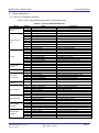
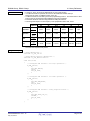
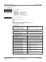
Table of Contents
Table of Contents ............................................................................................................................................ 1-1
1.
Introduction ............................................................................................................................................... 1-1
1.1.
Tool chain requirements .................................................................................................................... 1-2
1.2.
Compiler options when you use this product .................................................................................... 1-2
1.3. Using the library within your project .................................................................................................. 1-3
1.3.1.
Unzip the RPDL files .................................................................................................................. 1-3
1.3.2.
Copy the files into your project area .......................................................................................... 1-3
1.3.3.
Include the new directory ........................................................................................................... 1-6
1.3.4.
Include the new source files ...................................................................................................... 1-7
1)
Peripherals that are not required ................................................................................................. 1-7
2)
Peripherals that are not supported by RPDL ............................................................................... 1-7
1.3.5.
Avoid conflicts with standard project files. ................................................................................. 1-8
1)
Removal ....................................................................................................................................... 1-8
2)
Exclusion...................................................................................................................................... 1-9
1.3.6.
Add the library file path ............................................................................................................ 1-10
1.3.7.
Set the build options. ................................................................................................................1-11
1.3.8.
Add the "L" section................................................................................................................... 1-13
1.3.9.
Build the project ....................................................................................................................... 1-13
1.3.10. Using the library with debug information.................................................................................. 1-14
1.3.11. Header file inclusion................................................................................................................. 1-15
1.3.12. Header file order ...................................................................................................................... 1-15
2.
1.4.
Document structure ......................................................................................................................... 1-16
1.5.
Acronyms and abbreviations ........................................................................................................... 1-17
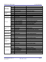
Driver ......................................................................................................................................................... 2-1
2.1.
Overview ............................................................................................................................................ 2-1
2.2.
Control Functions summary .............................................................................................................. 2-1
2.3.
Clock Generation Circuit Driver ......................................................................................................... 2-3
2.4.
Interrupt Control Driver ...................................................................................................................... 2-1
2.5.
I/O Port Driver .................................................................................................................................... 2-2
2.6.
Port Function Control Driver .............................................................................................................. 2-3
2.7.
MCU Operation Driver ....................................................................................................................... 2-4
2.8.
Low Power Consumption Driver ........................................................................................................ 2-5
2.9.
Voltage Detection Circuit Driver ........................................................................................................ 2-6
2.10. Bus Controller Driver ......................................................................................................................... 2-7
2.11. DMA Controller Driver........................................................................................................................ 2-8
2.12. External DMA Controller Driver ......................................................................................................... 2-9
2.13. Data Transfer Controller Driver ....................................................................................................... 2-10
2.14. Multi-Function Timer Pulse Unit Driver .............................................................................................2-11
2.15. Port Output Enable Driver ............................................................................................................... 2-12
2.16. Programmable Pulse Generator Driver ........................................................................................... 2-13
of 361
2.17. 8-bit Timer Driver ............................................................................................................................. 2-14
2.18. Compare Match Timer Driver .......................................................................................................... 2-15
2.19. Real-time Clock Driver..................................................................................................................... 2-16
2.20. Watchdog Timer Driver .................................................................................................................... 2-17
2.21. Independent Watchdog Timer Driver ............................................................................................... 2-18
2.22. Serial Communication Interface Driver............................................................................................ 2-19
2.23. CRC Calculator Driver ..................................................................................................................... 2-20
2.24. I²C Bus Interface Driver ................................................................................................................... 2-21
2.25. Serial Peripheral Interface Driver .................................................................................................... 2-22
2.26. 12-bit Analog to Digital Converter Driver ......................................................................................... 2-23
2.27. 10-bit Analog to Digital Converter Driver ......................................................................................... 2-24
2.28. 10-bit Digital to Analog Converter Driver ......................................................................................... 2-25
3.
Types and definitions ................................................................................................................................ 3-1
3.1.
Data types.......................................................................................................................................... 3-1
3.2. General definitions............................................................................................................................. 3-1
3.2.1.
PDL_NO_FUNC......................................................................................................................... 3-1
3.2.2.
PDL_NO_PTR ........................................................................................................................... 3-1
3.2.3.
PDL_NO_DATA.......................................................................................................................... 3-1
3.2.4.
PDL_MCU_GROUP................................................................................................................... 3-1
3.2.5.
PDL_VERSION .......................................................................................................................... 3-1
3.2.6.
Bit definitions.............................................................................................................................. 3-1
4.
Library Reference...................................................................................................................................... 4-1
4.1.
API List by Peripheral Function ......................................................................................................... 4-1
4.2. Description of Each API ..................................................................................................................... 4-4
4.2.1.
Clock Generation Circuit ............................................................................................................ 4-5
1)
R_CGC_Set ................................................................................................................................. 4-5
2)
R_CGC_Control ........................................................................................................................... 4-7
3)
R_CGC_GetStatus ...................................................................................................................... 4-8
4.2.2.
Interrupt Control Unit.................................................................................................................. 4-9
1)
R_INTC_CreateExtInterrupt ........................................................................................................ 4-9
2)
R_INTC_CreateSoftwareInterrupt ..............................................................................................4-11
3)
R_INTC_CreateFastInterrupt..................................................................................................... 4-12
4)
R_INTC_CreateExceptionHandlers ........................................................................................... 4-16
5)
R_INTC_ControlExtInterrupt...................................................................................................... 4-17
6)
R_INTC_GetExtInterruptStatus ................................................................................................. 4-19
7)
R_INTC_Read ........................................................................................................................... 4-24
8)
R_INTC_Write............................................................................................................................ 4-25
9)
R_INTC_Modify ......................................................................................................................... 4-26
4.2.3.
I/O Port ..................................................................................................................................... 4-27
1)
R_IO_PORT_Set ....................................................................................................................... 4-29
2)
R_IO_PORT_ReadControl ........................................................................................................ 4-30
3)
R_IO_PORT_ModifyControl ...................................................................................................... 4-31
4)
R_IO_PORT_Read .................................................................................................................... 4-33
5)
R_IO_PORT_Write .................................................................................................................... 4-34
6)
R_IO_PORT_Compare .............................................................................................................. 4-35
7)
R_IO_PORT_Modify .................................................................................................................. 4-36
8)
R_IO_PORT_Wait ..................................................................................................................... 4-37
4.2.4.
Port Function Control ............................................................................................................... 4-38
1)
R_PFC_Read ............................................................................................................................ 4-39
2)
R_PFC_Write ............................................................................................................................. 4-40
of 361
3)
4.2.5.
1)
2)
4.2.6.
1)
2)
3)
4)
5)
4.2.7.
1)
4.2.8.
1)
2)
3)
4)
5)
6)
4.2.9.
1)
2)
3)
4)
4.2.10.
1)
2)
3)
4)
4.2.11.
1)
2)
3)
4)
5)
4.2.12.
1)
2)
3)
4)
5)
6)
7)
4.2.13.
1)
2)
3)
4)
4.2.14.
1)
2)
3)
4.2.15.
1)
2)
3)
4)
5)
6)
7)
of 361
R_PFC_Modify .......................................................................................................................... 4-41
MCU operation ......................................................................................................................... 4-42
R_MCU_Control ........................................................................................................................ 4-42
R_MCU_GetStatus .................................................................................................................... 4-43
Low Power Consumption ......................................................................................................... 4-44
R_LPC_Create .......................................................................................................................... 4-44
R_LPC_Control .......................................................................................................................... 4-46
R_LPC_WriteBackup ................................................................................................................. 4-47
R_LPC_ReadBackup................................................................................................................. 4-48
R_LPC_GetStatus ..................................................................................................................... 4-49
Voltage Detection Circuit.......................................................................................................... 4-50
R_LVD_Control .......................................................................................................................... 4-50
Bus Controller .......................................................................................................................... 4-51
R_BSC_Create .......................................................................................................................... 4-51
R_BSC_CreateArea .................................................................................................................. 4-54
R_BSC_SDRAM_CreateArea ................................................................................................... 4-57
R_BSC_Destroy ........................................................................................................................ 4-59
R_BSC_Control ......................................................................................................................... 4-60
R_BSC_GetStatus ..................................................................................................................... 4-62
DMA Controller......................................................................................................................... 4-64
R_DMAC_Create ....................................................................................................................... 4-64
R_DMAC_Destroy ..................................................................................................................... 4-68
R_DMAC_Control ...................................................................................................................... 4-69
R_DMAC_GetStatus .................................................................................................................. 4-71
External DMA Controller .......................................................................................................... 4-73
R_EXDMAC_Create .................................................................................................................. 4-73
R_EXDMAC_Destroy ................................................................................................................ 4-76
R_EXDMAC_Control ................................................................................................................. 4-77
R_EXDMAC_GetStatus ............................................................................................................. 4-79
Data Transfer Controller........................................................................................................... 4-81
R_DTC_Set................................................................................................................................ 4-81
R_DTC_Create .......................................................................................................................... 4-82
R_DTC_Destroy ........................................................................................................................ 4-86
R_DTC_Control ......................................................................................................................... 4-87
R_DTC_GetStatus ..................................................................................................................... 4-89
Multi-Function Timer Pulse Unit ............................................................................................... 4-91
R_MTU2_Set ............................................................................................................................. 4-91
R_MTU2_Create ........................................................................................................................ 4-92
R_MTU2_Destroy .................................................................................................................... 4-101
R_MTU2_ControlChannel ....................................................................................................... 4-102
R_MTU2_ControlUnit .............................................................................................................. 4-105
R_MTU2_ReadChannel ...........................................................................................................4-110
R_MTU2_ReadUnit ..................................................................................................................4-113
Port Output Enable .................................................................................................................4-114
R_POE_Set ..............................................................................................................................4-114
R_POE_Create .........................................................................................................................4-116
R_POE_Control ........................................................................................................................4-118
R_POE_GetStatus ................................................................................................................... 4-120
Programmable Pulse Generator ............................................................................................ 4-121
R_PPG_Create ........................................................................................................................ 4-121
R_PPG_Destroy ...................................................................................................................... 4-123
R_PPG_Control ....................................................................................................................... 4-125
8-bit Timer .............................................................................................................................. 4-126
R_TMR_Set ............................................................................................................................. 4-126
R_TMR_CreateChannel .......................................................................................................... 4-127
R_TMR_CreateUnit ................................................................................................................. 4-130
R_TMR_CreatePeriodic........................................................................................................... 4-133
R_TMR_CreateOneShot ......................................................................................................... 4-136
R_TMR_Destroy ...................................................................................................................... 4-138
R_TMR_ControlChannel ......................................................................................................... 4-139
8)
9)
10)
11)
4.2.16.
1)
2)
3)
4)
5)
4.2.17.
1)
2)
3)
4.2.18.
1)
2)
3)
4.2.19.
1)
2)
3)
4.2.20.
1)
2)
3)
4)
5)
6)
7)
4.2.21.
1)
2)
3)
4)
4.2.22.
1)
2)
3)
4)
5)
6)
7)
8)
9)
4.2.23.
1)
2)
3)
4)
5)
6)
4.2.24.
1)
2)
3)
4)
4.2.25.
1)
2)
of 361
R_TMR_ControlUnit ................................................................................................................ 4-140
R_TMR_ControlPeriodic .......................................................................................................... 4-142
R_TMR_ReadChannel ............................................................................................................ 4-144
R_TMR_ReadUnit ................................................................................................................... 4-145
Compare Match Timer ........................................................................................................... 4-147
R_CMT_Create ........................................................................................................................ 4-147
R_CMT_CreateOneShot ......................................................................................................... 4-149
R_CMT_Destroy ...................................................................................................................... 4-151
R_CMT_Control ....................................................................................................................... 4-152
R_CMT_Read .......................................................................................................................... 4-154
Real-time Clock...................................................................................................................... 4-155
R_RTC_Create ........................................................................................................................ 4-155
R_RTC_Control ....................................................................................................................... 4-158
R_RTC_Read .......................................................................................................................... 4-161
Watchdog Timer ..................................................................................................................... 4-162
R_WDT_Create ....................................................................................................................... 4-162
R_WDT_Control ...................................................................................................................... 4-164
R_WDT_Read ......................................................................................................................... 4-165
Independent Watchdog Timer ................................................................................................ 4-166
R_IWDT_Set ............................................................................................................................ 4-166
R_IWDT_Control ..................................................................................................................... 4-167
R_IWDT_Read ........................................................................................................................ 4-168
Serial Communication Interface............................................................................................. 4-169
R_SCI_Set ............................................................................................................................... 4-169
R_SCI_Create ......................................................................................................................... 4-170
R_SCI_Destroy ........................................................................................................................ 4-174
R_SCI_Send ............................................................................................................................ 4-175
R_SCI_Receive ....................................................................................................................... 4-177
R_SCI_Control ......................................................................................................................... 4-179
R_SCI_GetStatus .................................................................................................................... 4-181
CRC calculator ....................................................................................................................... 4-183
R_CRC_Create ........................................................................................................................ 4-183
R_CRC_Destroy ...................................................................................................................... 4-184
R_CRC_Write .......................................................................................................................... 4-185
R_CRC_Read .......................................................................................................................... 4-186
I²C Bus Interface .................................................................................................................... 4-187
R_IIC_Create ........................................................................................................................... 4-187
R_IIC_Destroy ......................................................................................................................... 4-192
R_IIC_MasterSend .................................................................................................................. 4-193
R_IIC_MasterReceive.............................................................................................................. 4-195
R_IIC_MasterReceiveLast ....................................................................................................... 4-197
R_IIC_SlaveMonitor................................................................................................................. 4-198
R_IIC_SlaveSend .................................................................................................................... 4-200
R_IIC_Control .......................................................................................................................... 4-201
R_IIC_GetStatus ...................................................................................................................... 4-202
Serial Peripheral Interface ..................................................................................................... 4-204
R_SPI_Create .......................................................................................................................... 4-204
R_SPI_Destroy ........................................................................................................................ 4-207
R_SPI_Command .................................................................................................................... 4-208
R_SPI_Transfer ....................................................................................................................... 4-210
R_SPI_Control ......................................................................................................................... 4-212
R_SPI_GetStatus ..................................................................................................................... 4-214
12-bit Analog to Digital Converter .......................................................................................... 4-215
R_ADC_12_Create .................................................................................................................. 4-215
R_ADC_12_Destroy ................................................................................................................ 4-218
R_ADC_12_Control ................................................................................................................. 4-219
R_ADC_12_Read .................................................................................................................... 4-220
10-bit Analog to Digital Converter .......................................................................................... 4-221
R_ADC_10_Create .................................................................................................................. 4-221
R_ADC_10_Destroy ................................................................................................................ 4-225
3)
4)
4.2.26.
1)
2)
3)
5.
R_ADC_10_Control ................................................................................................................. 4-226
R_ADC_10_Read .................................................................................................................... 4-227
10-bit Digital to Analog Converter .......................................................................................... 4-228
R_DAC_10_Create .................................................................................................................. 4-228
R_DAC_10_Destroy ................................................................................................................ 4-229
R_DAC_10_Write .................................................................................................................... 4-230
Usage Examples ....................................................................................................................................... 5-1
5.1.
Interrupt control ................................................................................................................................. 5-1
5.2.
I/O Port .............................................................................................................................................. 5-3
5.3. Low Power Consumption .................................................................................................................. 5-5
5.3.1.
Software Standby Mode ............................................................................................................. 5-5
5.3.2.
Deep Software Standby Mode ................................................................................................... 5-6
5.4.
Voltage Detection Circuit ................................................................................................................... 5-8
5.5. Bus Controller .................................................................................................................................... 5-9
5.5.1.
External bus, CS area ................................................................................................................ 5-9
5.5.2.
External bus, SDRAM area .......................................................................................................5-11
5.6. DMA controller ................................................................................................................................. 5-15
5.6.1.
Software and IRQ triggers ....................................................................................................... 5-15
5.6.2.
SCI transmission trigger........................................................................................................... 5-18
5.6.3.
SCI reception trigger ................................................................................................................ 5-21
5.7. Data Transfer Controller .................................................................................................................. 5-23
5.7.1.
Block transfer mode ................................................................................................................. 5-23
5.7.2.
Chain transfer operation .......................................................................................................... 5-25
5.8. 8-bit Timer ........................................................................................................................................ 5-28
5.8.1.
Periodic operation .................................................................................................................... 5-28
5.9.
Compare Match Timer ..................................................................................................................... 5-30
5.10. Real-time Clock ............................................................................................................................... 5-32
5.11. Independent Watchdog Timer ......................................................................................................... 5-34
5.12. Serial Communication Interface ...................................................................................................... 5-35
5.12.1. SCI Reception .......................................................................................................................... 5-35
5.12.2. SCI Transmission ..................................................................................................................... 5-37
5.12.3. Synchronous Transmission and Reception ............................................................................. 5-39
5.12.4. SCI Reception in Asynchronous Multi-Processor mode .......................................................... 5-41
5.12.5. SCI Transmission in Asynchronous Multi-Processor mode ..................................................... 5-43
5.13. CRC calculator ................................................................................................................................ 5-45
5.14. I²C Bus Interface.............................................................................................................................. 5-46
5.14.1. Master mode ............................................................................................................................ 5-46
1)
Configuration and transmission ................................................................................................. 5-47
2)
Reception ................................................................................................................................... 5-49
3)
Repeated Start ........................................................................................................................... 5-50
5.14.2. Master mode with DMAC ......................................................................................................... 5-51
5.14.3. Master mode with DTC ............................................................................................................ 5-55
5.14.4. Slave mode .............................................................................................................................. 5-59
5.15. Serial Peripheral Interface ............................................................................................................... 5-62
5.15.1. Using one slave (1) .................................................................................................................. 5-62
5.15.2. Using one slave (2) .................................................................................................................. 5-65
5.15.3. Master operation with multiple slaves ...................................................................................... 5-68
5.16. 10-bit Analog to Digital Converter .................................................................................................... 5-71
5.16.1. ADC Conversion ...................................................................................................................... 5-71
5.16.2. ADC Self-Diagnostic function .................................................................................................. 5-73
of 361
6.
RX-specific notes ...................................................................................................................................... 6-1
6.1.
Interrupts and processor mode ......................................................................................................... 6-1
6.2.
Interrupts and DSP instructions ......................................................................................................... 6-1
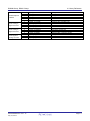
Revision History ................................................................................................................................................ 1
of 361
RX62N Group, RX621 Group
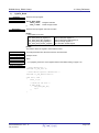
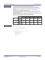
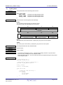
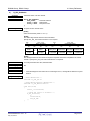
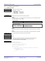
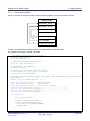
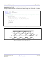
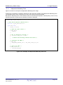
1. Introduction
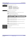
1. Introduction
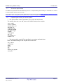
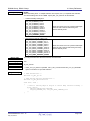
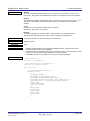
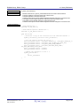
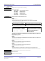
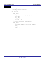
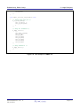
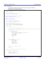
The Renesas Peripheral Driver Library (RPDL) is a unified API for controlling the peripheral modules on the
microcontrollers made by Renesas Electronics.
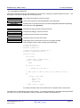
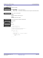
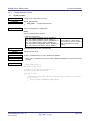
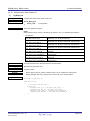
Callback functions
User application
Renesas Peripheral Driver Library
CPU
Peripherals supported by the RPDL
Target MCU
Figure 1-1: System configuration, with all peripherals supported by RPDL
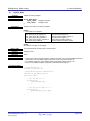
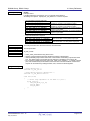
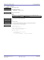
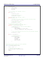
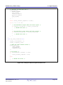
Callback functions
User application
Renesas Peripheral Driver Library
CPU
Peripherals supported by the RPDL
Middleware, including drivers
USB, Ethernet or CAN
Target MCU
Figure 1-2: System configuration, with middleware taking direct control of some peripherals
The library is packaged as:
a) A binary file containing all of the peripheral driver functions,
b) Header files containing the information that the user needs to call any of the functions from their own
application code and
c) Interrupt handlers supplied as source code.
For best use of this library, it is required that the user will have the following documents as a minimum:
i.
The schematic
ii.
The MCU hardware manual
iii.
This RPDL API User’s manual
The binary file is produced using the Renesas RX C compiler. It should be usable by another linker that
conforms to the Renesas Application Binary Interface.
RPDL has not been designed to be compatible for use with an RTOS.
The coding standards and naming conventions are specified by Renesas.
R20UT0084EE0112 Rev.1.12
July. 16, 2014
Page 1-1
RX62N Group, RX621 Group
1.1.
1. Introduction
Tool chain requirements
This RPDL library has been built and tested using the C/C++ Compiler Package for RX Family V.1.02 Release 01. It cannot
be used with older versions of the tool chain.
The latest version of the tool chain can be downloaded from the Renesas Web site (Home / Products / Software and Tools /
Coding Tools / C/C++ Compilers and Assemblers / C/C++ Compiler Package for RX Family /).
1.2.
Compiler options when you use this product
• The options which must be specified in your project are listed below.
The options other than -cpu,-dbl_size are the default setting of the compiler.
-cpu = rx600
-round = nearest
-denormalize = off
-dbl_size = 4
-unsigned_char
-unsigned_bitfield
-bit_order = right
-unpack
-noexception
-rtti = off
-fint_register = 0
-branch = 24
• The options which must NOT be specified in your project are listed below.
Note: The default settings of the compiler do not set these.
-int_to_short
-auto_enum
-base
-patch
-pic
-pid
-nouse_pid_register
-save_acc
R20UT0084EE0112 Rev.1.12
July. 16, 2014
Page 1-2
RX62N Group, RX621 Group
1. Introduction
1.3. Using the library within your project
The driver library can be used:
1. Via the PDG graphical utility
PDG can be downloaded from www.renesas.com/pdg.
The directions for use of the PDG utility are given in the PDG manual.
2. Or added to a project by the user and used stand-alone.
To add the driver library to your project’s build environment, you need to
a)
b)
c)
d)
1.3.1.
Unzip the RPDL distribution.
Copy the required source, header and library files into your project folder.
Include the required source files.
Add the driver library file to the linked files list.
Unzip the RPDL files
Double-click on the file RPDL_RX62N.exe to unpack the files.
The default location is C:\Renesas\RPDL_RX62N.
1.3.2.
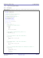
Copy the files into your project area
Navigate to where the RPDL files were unpacked.
Double-click on "Copy_RPDL_RX62N.bat" to start the copy process.
R20UT0084EE0112 Rev.1.12
July. 16, 2014
Page 1-3
RX62N Group, RX621 Group
1. Introduction
Select the device package and endian option by pressing a number, and then press Enter.
Type the full path to the folder where you wish RPDL to be copied to, and then press Enter.
The utility will create a folder in the location that you specified and copy the files into the new folder.
R20UT0084EE0112 Rev.1.12
July. 16, 2014
Page 1-4
RX62N Group, RX621 Group
1. Introduction
Press any key to close the window.
R20UT0084EE0112 Rev.1.12
July. 16, 2014
Page 1-5
RX62N Group, RX621 Group
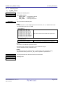
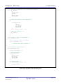
1.3.3.
1. Introduction
Include the new directory
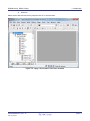
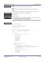
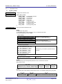
Use the key sequence Alt, B, R to open the "RX Standard Toolchain" window.
Select the C/C++ tab.
Use the key sequence S, I to show the included file directories.
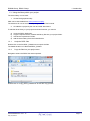
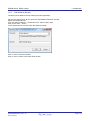
Click on the "Add…" button.
In the "Add include file directory" window, enter the details as shown:
Click on "OK" to close the window.
Click on the "Add…" button.
In the "Add include file directory" window, enter the details as shown:
Click on "OK" to close the window.
Click on "OK" to return to the main HEW window.
R20UT0084EE0112 Rev.1.12
July. 16, 2014
Page 1-6
RX62N Group, RX621 Group
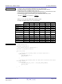
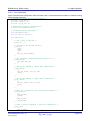
1.3.4.
1. Introduction
Include the new source files
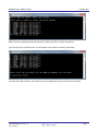
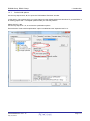
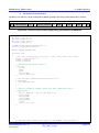
Use the key sequence Alt, P, A to open the "Add files to project ‘<your project>’" window.
Double click on the RPDL folder.
From the "Files of type" drop-down list, select "C source file (*.C)".
Use the key sequence Ctrl-A to select all the Interrupt handler files, as shown below.
Click on "Add".
Click on "OK" to return to the main HEW window.
1)
Peripherals that are not required
If a peripheral module is not required, the interrupt handler file does not need to be included.
If the unused interrupts still require entries in the interrupt vector table, edit the file Interrupt_not_RPDL.c to
uncomment the #define for the unused peripherals.
For example,
//#define RPDL_ADC_10_not_used
Becomes
#define RPDL_ADC_10_not_used
The file Interrupt_INTC.c must be included.
2)
Peripherals that are not supported by RPDL
The file Interrupt_not_RPDL.c also contains handlers for the peripherals that are not supported by RPDL. This
allows the user to add handler code for these peripherals while supporting the Fast Interrupt feature
(see R_INTC_CreateFastInterrupt).
R20UT0084EE0112 Rev.1.12
July. 16, 2014
Page 1-7
RX62N Group, RX621 Group
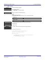
1.3.5.
1. Introduction
Avoid conflicts with standard project files.
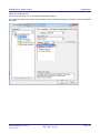
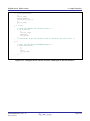
If the files ‘intprg.c’ or ‘vecttbl.c’ are included in the project, remove or exclude them.
1)
Removal
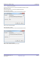
Use the key sequence Alt, P, R to open the "Remove Project Files" window.
Select the files and click on Remove.
R20UT0084EE0112 Rev.1.12
July. 16, 2014
Page 1-8
RX62N Group, RX621 Group
2)
1. Introduction
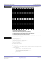
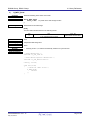
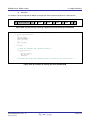
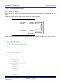
Exclusion
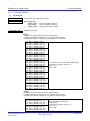
Select the two files and use the key sequence Alt, B, I to exclude them.
Figure 1-3: intprg.c and vecttbl.c have been excluded
R20UT0084EE0112 Rev.1.12
July. 16, 2014
Page 1-9
RX62N Group, RX621 Group
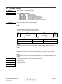
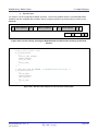
1.3.6.
1. Introduction
Add the library file path
The library file is added to the list used by the linker application.
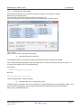
Use the key sequence Alt, B, R to open the "RX Standard Toolchain" window.
Select the Link/Library tab.
From the "Show entries for :" drop-down menu, select "Library files".
Click on the "Add…" button.
In the "Add library file" window, enter the details as shown:
Click on "OK" to close the window.
Click on "OK" to return to the main HEW window.
R20UT0084EE0112 Rev.1.12
July. 16, 2014
Page 1-10
RX62N Group, RX621 Group
1.3.7.
1. Introduction
Set the build options.
Use the key sequence Alt, B, R to open the "RX Standard Toolchain" window.
In this section, only options which you must change from the default settings are described. If you add RPDL in
an existing project see 1.2 Compiler options when you use this product.
Select the C/C++ tab.
Use the key sequence Y, O, O to show the optimisation options.
Ensure that the "Inter-module optimization" option is enabled and set "Optimize level" to 2.
R20UT0084EE0112 Rev.1.12
July. 16, 2014
Page 1-11
RX62N Group, RX621 Group
1. Introduction
Select the Link/Library tab.
Use the key sequence Y, O, O to show the optimisation options.
If the "Eliminate dead code" option is not enabled, from the Optimize drop-down list select Custom and enable
the option.
R20UT0084EE0112 Rev.1.12
July. 16, 2014
Page 1-12
RX62N Group, RX621 Group
1. Introduction
1.3.8. Add the "L" section
Use the key sequence Alt-Y, S to show the section configuration options.
Click the "Edit" button and ensure that an "L" section is included in the list. If it is not, add it below the "C" section
as shown.
Click on "OK" to close the window.
Click on "OK" to return to the main HEW window.
1.3.9.
Build the project
No further configuration should be required.
Simply build the project.
R20UT0084EE0112 Rev.1.12
July. 16, 2014
Page 1-13
RX62N Group, RX621 Group
1. Introduction
1.3.10. Using the library with debug information
RPDL library with debug information should be chosen, in order to step in the RPDL source code for debugging.
Unzip the RPDL source
"c:\my_project_folder").
zip
file
(e.g.
"RPDL_RX62N_CS.x.xx_source.zip")
into
a
folder
(e.g.
Set a breakpoint at the RPDL API to be debugged.
When the program break at the RPDL API, press "F11" key to step in the function.
A pop-up window will appear to request for the location of the corresponding RPDL source file.
Select the folder where you unzip the RPDL source file, and open the source file under respective module folder.
Once the correct source file is selected, user could step in to the file and step through the function.
R20UT0084EE0112 Rev.1.12
July. 16, 2014
Page 1-14
RX62N Group, RX621 Group
1. Introduction
1.3.11. Header file inclusion
The RPDL folder contains a header file, iodefine_RPDL.h.
This file is included by the RPDL source files and will also be included by any user-generated files that call RPDL
functions.
The main HEW project folder may contain the header file iodefine.h.
This file is normally used if access to the I/O registers in the MCU is required.
For any user-generated files that call RPDL functions, there is no need to include this file iodefine.h.
1.3.12. Header file order
The file r_pdl_definitions.h must be included after any peripheral-specific header file.
For example:
/* Peripheral driver function prototypes and definitions */
#include "r_pdl_cgc.h"
#include "r_pdl_cmt.h"
/* PDL device-specific definitions */
#include "r_pdl_definitions.h"
R20UT0084EE0112 Rev.1.12
July. 16, 2014
Page 1-15
RX62N Group, RX621 Group
1. Introduction
1.4. Document structure
The drivers are summarised in section 2 and explained in detail in section 4.
Section 5 provides usage examples.
Section 6 provides details which are specific to the RX CPU.
R20UT0084EE0112 Rev.1.12
July. 16, 2014
Page 1-16
RX62N Group, RX621 Group
1. Introduction
1.5. Acronyms and abbreviations
ADC
API
BCD
Bit
bps
BSC
CAN
CMT
CGC
CPU
CRC
DAC
DC
DMA
DMAC
DSP
DTC
EEPROM
EXDMA
EXDMAC
FIFO
GSM
HEW
I²C
INTC
I/O
kB
LPC
LSB
MCU
MTU
NMI
MSB
PDG
PFC
POE
PPG
PWM
RAM
ROM
RPDL
RSPI
SCI
SDRAM
SMBus
SPI
USB
WDT
Analog to Digital Converter
Application Programming Interface
Binary-Coded Decimal
Binary digit
Bits per second
Bus State Controller
Controller Area Network
Compare Match Timer
Clock Generation Circuit
Central Processing Unit
Cyclic Redundancy Check
Digital to Analog Converter
Direct Current
Direct Memory Access
DMA Controller
Digital Signal Processing
Data Transfer Controller
Electrically Eraseable and Programmable ROM
External DMA
External DMAC
First-In, First-Out
Global System for Mobile communications
High-performance Embedded Workbench
Inter-Integrated Circuit
Interrupt Controller
Input / Output
Kilo Byte (1024 bytes)
Low Power Consumption
Least-Significant Bit
Microcontroller Unit
Multi-function Timer pulse Unit
Non-Maskable Interrupt
Most-Significant Bit
Peripheral Driver Generator
Port Function Control
Port Output Enable
Programmable Pulse Generator
Pulse-Width Modulation
Random-Access Memory
Read-Only Memory
Renesas Peripheral Driver Library
Renesas SPI
Serial Communications Interface
Synchronous Dynamic RAM
System Management Bus
Serial Peripheral Interface
Universal Serial Bus
Watchdog Timer
R20UT0084EE0112 Rev.1.12
July. 16, 2014
Page 1-17
RX62N Group, RX621 Group
2. Driver
2. Driver
2.1. Overview
This library provides a set of peripheral function control programs (peripheral drivers) for Renesas
microcontrollers and allows the peripheral driver to be built into a user program.
2.2. Control Functions summary
This library has the following control functions available as peripheral drivers.
(1) Clock Generation Circuit
These driver functions are used to configure the multiple internal clock signals.
(2) Interrupt
These driver functions are used for configuring the external interrupt pins, handling fixed interrupts and
controlling the interrupt priority.
(3) I/O Port
These driver functions are used to configure the I/O pins and provide data read, write, compare and
modify operations.
(4) Port Function
These driver functions are used for configuring the I/O pin optional functions.
(5) MCU Operation
These driver functions are used for configuring the MCU operation.
(6) Low Power Consumption
These driver functions are used for selecting lower power consumption.
(7) Voltage Detection Circuit
These driver functions are used for configuring the low-voltage detection response.
(8) Bus Controller
These driver functions are used for configuring the external address bus, data bus and chip select pins
and handling any bus errors.
(9) DMA Controller
These driver functions are used for configuring and controlling the transfer of data within the address
space.
(10) External DMA Controller
These driver functions are used for configuring and controlling the transfer of data within the address
space.
(11) Data Transfer Controller
These driver functions are used for configuring and controlling the transfer of data triggered by
peripheral interrupts.
(12) Multi-Function Timer Pulse Unit
These driver functions are used for configuring and controlling the multi-function timers.
(13) Port Output Enable
These driver functions are used for additional configuring and controlling of the timer outputs.
(14) Programmable Pulse Generator
These driver functions are used for configuring and controlling the pulse generator outputs.
(15) 8-bit Timer
R20UT0084EE0112 Rev.1.12
July. 16, 2014
Page 2-1
RX62N Group, RX621 Group
2. Driver
These driver functions are used for configuring and controlling the timers.
(16) Compare Match Timer
These driver functions are used for configuring and controlling the timers.
(17) Real-time Clock
These driver functions are used for configuring and controlling the real-time clock timer.
(18) Watchdog Timer
These driver functions are used for configuring and controlling the timer.
(19) Independent Watchdog Timer
These driver functions are used for configuring and controlling the timer.
(20) Serial Communication Interface
These driver functions are used to configure the serial channels and manage the transmission and / or
reception of data across them.
(21) CRC calculator
These driver functions are used for controlling the calculator.
(22) I²C Bus Interface
These driver functions are used for controlling the I²C bus channels.
(23) Serial Peripheral Interface
These driver functions are used for controlling the SPI channels.
(24) 12-bit Analog to Digital Converter
These driver functions are used for configuring the 12-bit ADC unit, controlling the unit and reading the
conversion results.
(25) 10-bit Analog to Digital Converter
These driver functions are used for configuring the 10-bit ADC units, controlling the units and reading
the conversion results.
(26) 10-bit Digital to Analog converter
These driver functions are used for configuring the DAC module and setting the output voltages.
R20UT0084EE0112 Rev.1.12
July. 16, 2014
Page 2-2
RX62N Group, RX621 Group
2. Driver
2.3. Clock Generation Circuit Driver
The driver functions support the control of the internal clock generator, providing the following
operations.
1. Configuration of the multiple clock outputs for system, peripheral and external bus operation.
2. Controlling the clock generator operation.
3. Reading the Clock generator status flags.
Note: Configuring the Clock Generation Circuit also provides information on clock frequencies that will
be used by the integrated drivers for other peripherals.
R20UT0084EE0112 Rev.1.12
July. 16, 2014
Page 2-3
RX62N Group, RX621 Group
3. Types and definitions
2.4. Interrupt Control Driver
The driver functions support the use of the interrupt controller, providing the following operations.
1. Configuration an external interrupt pin for use.
2. Enabling use of the software interrupt.
3. Assigning an interrupt to be processed using the Fast Interrupt route.
4. Assigning handlers for the fixed exception interrupts.
5. Controlling an external interrupt input.
6. Reading the status of an external interrupt.
7. Reading an interrupt register.
8. Writing to an interrupt register.
9. Modifying an interrupt register.
R20UT0084EE0112 Rev.1.12
July. 16, 2014
Page 2-1
RX62N Group, RX621 Group
3. Types and definitions
2.5. I/O Port Driver
The driver functions support the use of the I/O port pins, providing the following operations.
1. Configuration for use.
2. Reading the pin or port configuration.
3. Modifying the pin or port configuration.
4. Reading a pin or 8-bit port value.
5. Writing to a pin or 8-bit port.
6. Comparing a pin or 8-bit port with a supplied value.
7. Modifying a pin or 8-bit port using a logical operation.
8. Waiting until a pin or 8-bit port matches a supplied value.
R20UT0084EE0112 Rev.1.12
July. 16, 2014
Page 2-2
RX62N Group, RX621 Group
3. Types and definitions
2.6. Port Function Control Driver
The driver functions support access to the Port Function Control (PFC) registers which select the
mode of operation for some I/O pins.
The other driver functions modify the PFC registers automatically. For peripherals that are not
supported by the driver library, these functions support:
1. Reading from a PFC register.
2. Writing to a PFC register.
3. Modifying a PFC register
R20UT0084EE0112 Rev.1.12
July. 16, 2014
Page 2-3
RX62N Group, RX621 Group
3. Types and definitions
2.7. MCU Operation Driver
The driver functions support access to the registers which select the mode of operation for the
microcontroller. These functions support:
1. Controlling the on-chip ROM and RAM.
2. Reading the MCU status flags.
R20UT0084EE0112 Rev.1.12
July. 16, 2014
Page 2-4
RX62N Group, RX621 Group
3. Types and definitions
2.8. Low Power Consumption Driver
The driver functions support access to the registers which select the lower power modes of operation
for the microcontroller. These functions support:
1. Configuring the state while in standby mode, and the activity that can be used to resume
operation.
2. Selecting one of the low-power modes.
3. Writing data to the backup memory area.
4. Reading data from the backup memory area.
5. Determining the cause of the exit from the lowest power mode.
R20UT0084EE0112 Rev.1.12
July. 16, 2014
Page 2-5
RX62N Group, RX621 Group
3. Types and definitions
2.9. Voltage Detection Circuit Driver
The driver function supports access to the registers which control the voltage detection circuit. This
function supports:
1. Configuring the response to the supply voltage dropping below either voltage threshold.
R20UT0084EE0112 Rev.1.12
July. 16, 2014
Page 2-6
RX62N Group, RX621 Group
2.10.
3. Types and definitions
Bus Controller Driver
The driver functions support the control of the external bus, providing the following operations.
1. Configuration of the controller.
2. Configuration of the eight address space areas.
3. Configuration of the SDRAM address space area.
4. Disabling an area that is not required.
5. Controlling the bus controller.
6. Reading the status of the controller.
R20UT0084EE0112 Rev.1.12
July. 16, 2014
Page 2-7
RX62N Group, RX621 Group
2.11.
3. Types and definitions
DMA Controller Driver
The driver functions support the control of the Direct Memory Access (DMA) controller, providing the
following operations.
1. Configuration for use, including
• Access to all control bits.
• Automatic interrupt control
2. Disabling DMA channels that are no longer required and enabling low-power mode.
3. Control of a channel.
4. Reading the status and operation registers of a channel.
R20UT0084EE0112 Rev.1.12
July. 16, 2014
Page 2-8
RX62N Group, RX621 Group
2.12.
3. Types and definitions
External DMA Controller Driver
The driver functions support the control of the external bus Direct Memory Access controller
(EXDMAC), providing the following operations.
1. Configuration for use, including
• Access to all control bits.
• Automatic interrupt control
2. Disabling EXDMAC channels that are no longer required and enabling low-power mode.
3. Control of a channel.
4. Reading the status and operation registers of a channel.
R20UT0084EE0112 Rev.1.12
July. 16, 2014
Page 2-9
RX62N Group, RX621 Group
2.13.
3. Types and definitions
Data Transfer Controller Driver
The driver functions support the control of the Data Transfer Controller, providing the following
operations.
1. Setting the central options.
2. Configuration for use, including support for chain transfers.
3. Disabling the controller.
4. Starting or stopping the controller.
5. Reading the status flags and data transfer registers.
R20UT0084EE0112 Rev.1.12
July. 16, 2014
Page 2-10
RX62N Group, RX621 Group
2.14.
3. Types and definitions
Multi-Function Timer Pulse Unit Driver
The driver functions support the use of the twelve 16-bit timers, providing the following operations.
1. Selection of the MTU pins for use.
2. Configuration for use, including
• Access to all control bits.
• Automatic interrupt control
• Automatic I/O pin configuration
3. Disabling channels that are no longer required and enabling low-power mode.
4. Control of a timer channel.
5. Control of a timer unit.
6. Reading the status flags and registers of a timer channel.
7. Reading the status flags and registers of a timer unit.
Note: The Clock Generation Circuit must be configured before configuring any timer channel.
R20UT0084EE0112 Rev.1.12
July. 16, 2014
Page 2-11
RX62N Group, RX621 Group
2.15.
3. Types and definitions
Port Output Enable Driver
The driver functions support the use of the Port Output module, providing the following operations.
1. Configuring the pins for use.
2. Configuring the interrupts and callback functions.
3. Run-time control of outputs, interrupts and flags.
4. Checking the module status.
R20UT0084EE0112 Rev.1.12
July. 16, 2014
Page 2-12
RX62N Group, RX621 Group
2.16.
3. Types and definitions
Programmable Pulse Generator Driver
The driver functions support the use of the pulse generator, providing the following operations.
1. Configuring the generator for use.
2. Disabling groups of outputs that are no longer required.
3. Control of the generator during run-time.
R20UT0084EE0112 Rev.1.12
July. 16, 2014
Page 2-13
RX62N Group, RX621 Group
2.17.
3. Types and definitions
8-bit Timer Driver
The driver functions support the use of the four 8-bit timers, providing the following operations.
1. Selection of the TMR pins for use.
2. Configuring a channel for use, using register values which have been determined elsewhere.
3. Configuring two channels as a 16-bit pair, using register values which have been determined
elsewhere.
4. Configuration for as a periodic timer, including
•
•
•
•
•
Automatic clock setting using frequency or period as an input.
Automatic pulse width setting, using pulse width or duty cycle as an input.
Automatic interrupt control
I/O pin control
Automatic I/O pin configuration
5. Configuration for as a one-shot timer, including
•
•
•
•
•
•
Automatic clock setting, using pulse width as an input
Automatic interrupt control
CPU sleep option
I/O pin control
Automatic I/O pin configuration
Automatic support for using two channels as a single 16-bit timer.
6. Disabling channels that are no longer required and enabling low-power mode.
7. Control of a single timer channel.
8. Control of two timer channels when configured as one 16-bit channel.
9. Control of channels in periodic mode, enabling pulse-width modulation (PWM) output.
10. Reading the registers of a single timer channel.
11. Reading the registers of a 16-bit timer channel pair.
Note: The Clock Generation Circuit must be configured before configuring any timer channel.
R20UT0084EE0112 Rev.1.12
July. 16, 2014
Page 2-14
RX62N Group, RX621 Group
2.18.
3. Types and definitions
Compare Match Timer Driver
The driver functions support the use of the two 16-bit timers, providing the following operations.
1. Configuration for use, including
•
•
•
Automatic clock setting using frequency or period as an input.
Manual clock setting using register values as inputs.
Automatic interrupt control
2. Configuration for use as a one-shot timer.
3. Disabling channels that are no longer required and enabling low-power mode.
4. Control of a timer, including constant register updates, change of frequency.
5. Reading the counter value and status flag.
Note: The Clock Generation Circuit must be configured before configuring any timer channel.
R20UT0084EE0112 Rev.1.12
July. 16, 2014
Page 2-15
RX62N Group, RX621 Group
2.19.
3. Types and definitions
Real-time Clock Driver
The driver functions support the use of the real-time clock, providing the following operations.
1. Configuring the clock for use, including
•
•
•
Alarm configuration.
Optional day-of-week calculation
Automatic alarm and periodic interrupt control
2. Control of the clock, including
•
•
Changing the alarm settings.
Changing the current date or time.
3. Reading the clock status flags and current time and date.
R20UT0084EE0112 Rev.1.12
July. 16, 2014
Page 2-16
RX62N Group, RX621 Group
2.20.
3. Types and definitions
Watchdog Timer Driver
The driver functions support the use of the watchdog timer, providing the following operations.
1. Configuring the timer for use, including
•
•
•
•
•
Clock divider setting.
Internal timer mode
Watchdog timer mode
MCU reset generation while in watchdog timer mode
Automatic interrupt control
2. Control of the timer, including
•
•
Stopping the timer
Counter refresh to prevent overflow
3. Reading the timer status and counter register.
Note: The Clock Generation Circuit should be configured before configuring this timer.
R20UT0084EE0112 Rev.1.12
July. 16, 2014
Page 2-17
RX62N Group, RX621 Group
2.21.
3. Types and definitions
Independent Watchdog Timer Driver
The driver functions support the use of the independent watchdog timer, providing the following
operations.
1. Configuring the timer for use.
2. Refreshing the timer to prevent the reset operation.
3. Reading the timer status and counter register.
R20UT0084EE0112 Rev.1.12
July. 16, 2014
Page 2-18
RX62N Group, RX621 Group
2.22.
3. Types and definitions
Serial Communication Interface Driver
The driver functions support the use of the six serial communication channels (SCI0~SCI3,
SCI5~SCI6), providing the following operations.
1. Selection of the SCI pins for use.
2. Configuration for use, including
•
•
•
Automatic baud rate clock calculations
Automatic interrupt control
Automatic I/O pin configuration
3. Disabling channels that are no longer required and enabling low-power mode.
4. Transmitting data, with polling or interrupt mode automatically selected.
5. Receiving data, with polling or interrupt mode automatically selected.
6. Control the channel operation.
7. Reading the status flags.
Note: The Clock Generation Circuit must be configured before configuring any serial channel.
R20UT0084EE0112 Rev.1.12
July. 16, 2014
Page 2-19
RX62N Group, RX621 Group
2.23.
3. Types and definitions
CRC Calculator Driver
The driver functions support the CRC calculator, providing the following operations.
1. Configuration for use, including
•
•
•
Polynomial selection.
Bit order selection.
Preparation for a new calculation.
2. Disabling the calculator and enabling low-power mode.
3. Writing data to be used for the calculation.
4. Reading the calculation result.
R20UT0084EE0112 Rev.1.12
July. 16, 2014
Page 2-20
RX62N Group, RX621 Group
2.24.
3. Types and definitions
I²C Bus Interface Driver
The driver functions support the use of the two I²C modules, providing the following operations.
1. Configuration for use, including
•
•
•
Automatic clock setting using transfer rate as an input.
Automatic interrupt control
Automatic I/O pin configuration
2. Disabling modules that are no longer required and enabling low-power mode.
3. Transmitting data in Master mode.
4. Receiving data in Master mode.
5. Completing the reception of data in Master mode.
6. Monitoring the bus and handling the reception of data in Slave mode.
7. Transmitting data in Slave mode.
8. Control of one or more units, including bus lock-up recovery support.
9. Reading the status of a module.
Note: The Clock Generation Circuit must be configured before configuring any I²C module.
R20UT0084EE0112 Rev.1.12
July. 16, 2014
Page 2-21
RX62N Group, RX621 Group
2.25.
3. Types and definitions
Serial Peripheral Interface Driver
The driver functions support the use of the two SPI channels, providing the following operations.
1. Configuration for use, including
•
•
Automatic clock setting using transfer rate as an input.
Automatic I/O pin configuration
2. Disabling channels that are no longer required and enabling low-power mode.
3. Configuration of command sequence settings.
4. Managing the transfer of data on the interface, including
•
•
Automatic interrupt control
Automatic DMAC / DTC control.
5. Control of special modes such as loopback.
6. Reading the status of a module.
Note: The Clock Generation Circuit must be configured before configuring any SPI channel.
R20UT0084EE0112 Rev.1.12
July. 16, 2014
Page 2-22
RX62N Group, RX621 Group
2.26.
3. Types and definitions
12-bit Analog to Digital Converter Driver
The driver functions support the use of the 12-bit ADC unit, providing the following operations.
1. Configuration for use, including
•
•
•
Clock divider setting.
Automatic interrupt control
Automatic I/O pin configuration
2. Disabling the unit when no longer required and enabling low-power mode.
3. Control of one or more units, including
•
CPU sleep option
4. Reading the conversion results, with support for polling or interrupts.
Note: The Clock Generation Circuit must be configured before configuring the ADC unit.
R20UT0084EE0112 Rev.1.12
July. 16, 2014
Page 2-23
RX62N Group, RX621 Group
2.27.
3. Types and definitions
10-bit Analog to Digital Converter Driver
The driver functions support the use of the two ADC units, providing the following operations.
1. Configuration for use, including
•
•
•
Automatic clock setting using sampling time as an input.
Automatic interrupt control
Automatic I/O pin configuration
2. Disabling units that are no longer required and enabling low-power mode.
3. Control of one or more units, including
•
CPU sleep option
4. Reading the conversion results of one or more units, with support for polling or interrupts.
Note: The Clock Generation Circuit must be configured before configuring any ADC unit.
R20UT0084EE0112 Rev.1.12
July. 16, 2014
Page 2-24
RX62N Group, RX621 Group
2.28.
3. Types and definitions
10-bit Digital to Analog Converter Driver
The driver functions support the use of the DAC module, providing the following operations.
1. Configuring a channel for use, including data alignment
2. Disabling channels that are no longer required and enabling low-power mode.
3. Writing data to a channel.
R20UT0084EE0112 Rev.1.12
July. 16, 2014
Page 2-25
RX62N Group, RX621 Group
4. Library Reference
3. Types and definitions
3.1.
Data types
This section describes the data types used in this library. For details about the setting values, refer to the section
"4.2 Description of Each API".
The header files stdint.h and stdbool.h are included with the Renesas RX compiler.
Table 1: Data types
Type
bool
float
uint8_t
uint16_t
int32_t
uint32_t
3.2.
3.2.1.
Defined in
stdbool.h
C
stdint.h
Description
Boolean
Floating point, 32 bits
Unsigned, 8 bits
Unsigned, 16 bits
Signed, 32 bits
Unsigned, 32 bits
Range
0 (false) to 1 (true)
±∞
0 to 255
0 to 215 - 1
-231 to 231 - 1
0 to 232 - 1
General definitions
PDL_NO_FUNC
Used as a parameter when there is no applicable function.
3.2.2.
PDL_NO_PTR
Used as a parameter when there is no applicable data location.
3.2.3.
PDL_NO_DATA
Used as a parameter when there is no applicable data value.
3.2.4.
PDL_MCU_GROUP
The family supported by this build of the driver library. It is defined as RX62N.
A usage example is:
#if PDL_MCU_GROUP != RX62N
#error "Wrong RPDL !"
#endif
3.2.5.
PDL_VERSION
The version number of the RPDL library. The number is stored in BCD format (xx.xx). For example, 0100h is
v1.00.
A usage example is:
const uint16_t rpdl_version_number = PDL_VERSION;
3.2.6.
Bit definitions
The definitions BIT_n and INV_BIT_n, where n = 0 to 31, are available to the user.
R20UT0084EE0112 Rev.1.12
July. 16, 2014
Page 3-1
RX62N Group, RX621 Group
4. Library Reference
4. Library Reference
4.1. API List by Peripheral Function
Table 4.1 lists the Renesas Embedded APIs by peripheral function.
Table 4.1 Renesas Embedded API List
Category
Clock Generation
Circuit
Interrupt control
unit
I/O port
Port Function
Control
MCU operation
Low Power
Consumption
Voltage Detection
Circuit
Bus Controller
DMA Controller
External DMA
Controller
Data Transfer
Controller
Number
1
2
3
1
2
3
4
5
6
7
8
9
1
2
3
4
5
6
7
8
1
2
3
1
2
1
2
3
4
5
Name
R_CGC_Set
R_CGC_Control
R_CGC_GetStatus
R_INTC_CreateExtInterrupt
R_INTC_CreateSoftwareInterrupt
R_INTC_CreateFastInterrupt
R_INTC_CreateExceptionHandlers
R_INTC_ControlExtInterrupt
R_INTC_GetExtInterruptStatus
R_INTC_Read
R_INTC_Write
R_INTC_Modify
R_IO_PORT_Set
R_IO_PORT_ReadControl
R_IO_PORT_ModifyControl
R_IO_PORT_Read
R_IO_PORT_Write
R_IO_PORT_Compare
R_IO_PORT_Modify
R_IO_PORT_Wait
R_PFC_Read
R_PFC_Write
R_PFC_Modify
R_MCU_Control
R_MCU_GetStatus
R_LPC_Create
R_LPC_Control
R_LPC_WriteBackup
R_LPC_ReadBackup
R_LPC_GetStatus
Description
Configure the clock generation circuit.
Modify the clock generation circuit operation.
Read the clock status register.
Configure an external interrupt pin.
Enable use of the software interrupt.
Assign handlers for the fixed-vector interrupts.
Enable faster interrupt processing for one interrupt.
External interrupt control.
Read the external interrupt status.
Read an interrupt register.
Update an interrupt register.
Modify an interrupt register.
Configure an I/O port.
Read an I/O port’s control registers.
Modify an I/O port’s control registers.
Read data from an I/O port.
Write data to an I/O port.
Check the pin states on an I/O port.
Modify the pin states on an I/O port.
Wait for a match on an I/O port.
Read a PFC register.
Write to a PFC register.
Modify a PFC register.
Control the operation of the MCU.
Read the MCU status.
Configure the MCU low power conditions.
Select a low power consumption mode.
Write to the Backup registers.
Read from the Backup registers.
Read the status flags.
1
R_LVD_Control
Configure the voltage detection circuit.
1
2
3
4
5
6
1
2
3
4
1
2
3
4
1
2
3
4
5
R_BSC_Create
R_BSC_CreateArea
R_BSC_SDRAM_CreateArea
R_BSC_Destroy
R_BSC_Control
R_BSC_GetStatus
R_DMAC_Create
R_DMAC_Destroy
R_DMAC_Control
R_DMAC_GetStatus
R_EXDMAC_Create
R_EXDMAC_Destroy
R_EXDMAC_Control
R_EXDMAC_GetStatus
R_DTC_Set
R_DTC_Create
R_DTC_Destroy
R_DTC_Control
R_DTC_GetStatus
Configure the external bus controller.
Configure an external bus area.
Configure the SDRAM area.
Stop the Bus Controller.
Modify the External Bus Controller operation.
Read the External Bus Controller status flags.
Configure the DMA controller.
Disable a DMA channel.
Control the DMA controller.
Check the status of the DMA channel.
Configure the EXDMA controller.
Disable the EXDMA controller.
Control the EXDMA controller.
Check the status of an EXDMAC channel.
Set the Data Transfer Controller options.
Configure the DTC for a transfer.
Shutdown the Data Transfer Controller.
Control the Data Transfer Controller.
Check the status of the Data Transfer Controller.
R20UT0084EE0112 Rev.1.12
July. 16, 2014
Page 4-1
RX62N Group, RX621 Group
Multi-function
Timer pulse unit
Port Output
Enable
Programmable
Pulse Generator
8-bit Timer
Compare Match
Timer
Real-time Clock
Watchdog Timer
Independent
Watchdog Timer
Serial
Communication
Interface
CRC calculator
I²C bus interface
1
2
3
4
5
6
7
1
2
3
4
1
2
3
1
2
3
4
5
6
7
8
9
10
11
1
2
3
4
5
1
2
3
1
2
3
1
2
3
1
2
3
4
5
6
7
1
2
3
4
1
2
3
4
5
6
7
8
9
R20UT0084EE0112 Rev.1.12
July. 16, 2014
4. Library Reference
R_MTU2_Set
R_MTU2_Create
R_MTU2_Destroy
R_MTU2_ControlChannel
R_MTU2_ControlUnit
R_MTU2_ReadChannel
R_MTU2_ReadUnit
R_POE_Set
R_POE_Create
R_POE_Control
R_POE_GetStatus
R_PPG_Create
R_PPG_Destroy
R_PPG_Control
R_TMR_Set
R_TMR_CreateChannel
R_TMR_CreateUnit
R_TMR_CreatePeriodic
R_TMR_CreateOneShot
R_TMR_Destroy
R_TMR_ControlChannel
R_TMR_ControlUnit
R_TMR_ControlPeriodic
R_TMR_ReadChannel
R_TMR_ReadUnit
R_CMT_Create
R_CMT_CreateOneShot
R_CMT_Destroy
R_CMT_Control
R_CMT_Read
R_RTC_Create
R_RTC_Control
R_RTC_Read
R_WDT_Create
R_WDT_Control
R_WDT_Read
R_IWDT_Set
R_IWDT_Control
R_IWDT_Read
R_SCI_Set
R_SCI_Create
R_SCI_Destroy
R_SCI_Send
R_SCI_Receive
R_SCI_Control
R_SCI_GetStatus
R_CRC_Create
R_CRC_Destroy
R_CRC_Write
R_CRC_Read
R_IIC_Create
R_IIC_Destroy
R_IIC_MasterSend
R_IIC_MasterReceive
R_IIC_MasterReceiveLast
R_IIC_SlaveMonitor
R_IIC_SlaveSend
R_IIC_Control
R_IIC_GetStatus
Configure the Multi-function Timer Pulse Units.
Configure a MTU channel.
Disable a Multi-function Timer Pulse Unit.
Control an MTU channel.
Control a Multi-function Timer Pulse Unit.
Read from MTU channel registers.
Read from MTU registers.
Configure the Port Output Enable module.
Configure the Port Output Enable event handling.
Control the Port Output Enable module.
Check the status of the Port Output Enable module.
Configure a PPG group.
Disable a PPG unit.
Control a PPG group.
Configure the optional TMR pins.
Configure a TMR timer channel.
Configure a TMR timer unit.
Select periodic operation.
Configure and use a one-shot timer.
Disable a TMR timer unit.
Write to timer channel registers.
Write to timer unit registers.
Control periodic operation.
Read from timer channel registers.
Read from timer unit registers.
Configure a CMT channel.
Configure a CMT channel as a one-shot event.
Disable a CMT unit.
Control CMT operation.
Read CMT channel status and registers.
Configure the Real-time clock.
Modify the Real-time clock operation.
Read the Real-time clock status flags and counters.
Configure the Watchdog timer.
Control the Watchdog operation.
Read the Watchdog timer status and registers.
Configure the Independent Watchdog operation.
Control the Independent Watchdog operation.
Read the watchdog timer status and counter.
Configure the SCI pin selection.
SCI channel setup.
Shut down a SCI channel.
Send a string of characters.
Receive a string of characters.
Control the SCI channel.
Check the status of a SCI channel.
Configure the CRC calculator.
Shut down the CRC calculator.
Write data into the CRC calculation register.
Read the CRC calculation result.
I²C channel setup.
Disable an I²C channel.
Write data to a slave device.
Read data from a slave device.
Complete a DMAC or DTC-based read process.
Monitor the bus and receive data from a master.
Write data to a master device.
I²C channel control.
Read the status for an I²C channel.
Page 4-2
RX62N Group, RX621 Group
Serial Peripheral
Interface
12-bit Analog to
Digital converter
10-bit Analog to
Digital converter
10-bit Digital to
Analog converter
1
2
3
4
5
6
1
2
3
4
1
2
3
4
1
2
3
R20UT0084EE0112 Rev.1.12
July. 16, 2014
4. Library Reference
R_SPI_Create
R_SPI_Destroy
R_SPI_Command
R_SPI_Transfer
R_SPI_Control
R_SPI_GetStatus
R_ADC_12_Create
R_ADC_12_Destroy
R_ADC_12_Control
R_ADC_12_Read
R_ADC_10_Create
R_ADC_10_Destroy
R_ADC_10_Control
R_ADC_10_Read
R_DAC_10_Create
R_DAC_10_Destroy
R_DAC_10_Write
Configure an SPI channel.
Shutdown an SPI channel.
Configure an SPI command.
Transfer data over an SPI channel.
Control an SPI channel.
Check the status of an SPI channel.
Configure the 12-bit ADC unit.
Shut down the ADC unit.
Start or stop the ADC unit.
Read the ADC conversion results.
Configure a 10-bit ADC unit.
Shut down an ADC unit.
Start or stop an ADC unit.
Read the ADC conversion results.
Configure the 10-bit DAC module.
Disable a DAC channel.
Write data to a DAC channel.
Page 4-3
RX62N Group, RX621 Group
4. Library Reference
4.2. Description of Each API
This section describes each API and explains how to use them, showing a program example for each. The
description of each API is divided into the following items.
Synopsis
Summarises processing by the API function.
Prototype
The function format and a brief explanation of the arguments.
Description
Explains how to use the API function and shows assignable parameters separating
each argument with [argument].
Return value
Describes the returned value of the API function.
Category
Indicates the category of the API function.
Reference
Indicates the API functions to be referred.
Remark
Program example
Describes notes to use the API function.
Represents how to use the API function by a program example.
Two examples of return value checking are shown below.
/* RPDL definitions */
#include "r_pdl_pfc.h"
#include "r_pdl_sci.h"
/* RPDL device-specific definitions */
#include "r_pdl_definitions.h"
void func( void )
{
bool result;
/* Write 0xFF to register PFC1 */
result = (R_PFC_Write(
1,
0xFF
);
if (result == false)
{
/* Handle the error here */
}
/* Keep trying to send a string (if the channel is busy) */
do
{
result = R_SCI_Send(
2,
"Renesas RX",
NULL,
PDL_NO_FUNC
);
} while (result == false);
)
For clarity, the return value is not checked in the examples used in this manual.
The RPDL API is implemented using function macros. To avoid the possibility of parameters being evaluated
more than once do not use operators or function calls within the RPDL API parameter list.
R20UT0084EE0112 Rev.1.12
July. 16, 2014
Page 4-4
RX62N Group, RX621 Group
4.2.1.
1)
4. Library Reference
Clock Generation Circuit
R_CGC_Set
Synopsis
Configure the clock generation circuit.
Prototype
bool R_CGC_Set(
uint32_t data1,
uint32_t data2,
uint32_t data3,
uint32_t data4,
uint16_t data5
);
Description
// Input frequency
// System clock frequency
// Peripheral module clock frequency
// External bus clock frequency
// Configuration options
Set the clock output frequencies and options.
[data1]
The frequency of the main clock oscillator in Hertz.
[data2]
The desired frequency of the System clock (ICLK) in Hertz.
[data3]
The desired frequency of the Peripheral module clock (PCLK) in Hertz.
[data4]
The desired frequency of the External Bus clock (BCLK) in Hertz.
Specify 0 if the value is not important.
[data5]
Configuration options. If multiple selections are required, use "|" to separate each selection.
The default settings are shown in bold.
• BCLK pin output control
PDL_CGC_BCLK_DIV_1 or
PDL_CGC_BCLK_DIV_2 or
PDL_CGC_BCLK_DISABLE or
PDL_CGC_BCLK_HIGH
Output the external bus clock (BCLK),
BCLK ÷ 2,
leave the pin as an input
or fix the pin high.
• SDCLK pin output control
PDL_CGC_SDCLK_ENABLE or
PDL_CGC_SDCLK_DISABLE
Output the SDRAM clock (SDCLK),
or leave the SDCLK pin as a port pin.
• Oscillation Stop Detection control
PDL_CGC_OSC_STOP_ENABLE or
PDL_CGC_OSC_STOP_DISABLE
Enable or disable the oscillation stop detection
function.
• Sub-clock oscillator control
PDL_CGC_SUB_CLOCK_ENABLE or
PDL_CGC_SUB_CLOCK_DISABLE
Return value
Category
References
Enable or disable the sub-clock oscillator.
True if all parameters are valid and exclusive; otherwise false.
For RX62N, the following rules shall be checked:
•
Main clock oscillator frequency: 8 to 14 MHz.
•
f ICLK : 8 to 100 MHz
•
f PCLK : 8 to 50 MHz
•
f BCLK : 8 to 100 MHz
•
f ICLK ≥ f PCLK and f ICLK ≥ f BCLK
•
f ICLK , f PCLK and f BCLK are achievable: (main clock oscillator x 8) ÷ 1, 2, 4 or 8.
Clock generation circuit
None.
R20UT0084EE0112 Rev.1.12
July. 16, 2014
Page 4-5
RX62N Group, RX621 Group
Remarks
•
•
•
4. Library Reference
This function must be called before configuring clock-dependent modules.
This function modifies the BCLK and SDCLK pins for input or output.
The maximum output frequency allowed on the BCLK pin is 25 MHz.
Program example
/* RPDL definitions */
#include "r_pdl_cgc.h"
/* RPDL device-specific definitions */
#include "r_pdl_definitions.h"
void func(void)
{
/* Configure operation using a 12.0 MHz input clock */
/* ICLK = 96 MHz, PCLK = 48 MHz, BCLK = 24 MHz */
R_CGC_Set(
12.0E6,
96E6,
48E6,
24E6,
PDL_CGC_BCLK_DIV_1
);
}
R20UT0084EE0112 Rev.1.12
July. 16, 2014
Page 4-6
RX62N Group, RX621 Group
2)
4. Library Reference
R_CGC_Control
Synopsis
Modify the clock generation circuit operation.
Prototype
bool R_CGC_Control(
uint16_t data
// Control options
);
Description
Modify the clock control registers.
[data]
Control options. If multiple selections are required, use "|" to separate each selection.
• SDCLK pin output control
PDL_CGC_SDCLK_ENABLE or
PDL_CGC_SDCLK_DISABLE
• Sub-clock oscillator control
PDL_CGC_SUB_CLOCK_ENABLE or
PDL_CGC_SUB_CLOCK_DISABLE
Return value
Category
References
Remarks
Enable or disable the SDRAM clock (SDCLK) output.
Enable or disable the sub-clock oscillator.
True if all parameters are valid and exclusive; otherwise false.
Clock generation circuit
None.
•
None.
Program example
/* RPDL definitions */
#include "r_pdl_cgc.h"
/* RPDL device-specific definitions */
#include "r_pdl_definitions.h"
void func(void)
{
/* Stop the sub-clock oscillator */
R_CGC_Control(
PDL_CGC_SUB_CLOCK_DISABLE
);
}
R20UT0084EE0112 Rev.1.12
July. 16, 2014
Page 4-7
RX62N Group, RX621 Group
3)
4. Library Reference
R_CGC_GetStatus
Synopsis
Configure the clock generation circuit.
Prototype
bool R_CGC_GetStatus(
uint8_t * data
// Pointer to the variable where the status value shall be stored.
);
Description
Read the clock status register.
[data]
The status flags shall be stored in the format below.
b7 – b1
-
Return value
Category
References
Remarks
b0
0: The main clock oscillator is operating normally.
1: The main clock oscillator has stopped.
True.
Clock generation circuit
None.
•
None.
Program example
/* RPDL definitions */
#include "r_pdl_cgc.h"
/* RPDL device-specific definitions */
#include "r_pdl_definitions.h"
void func(void)
{
uint8_t Status_flags;
R_CGC_GetStatus(
&Status_flags
);
}
R20UT0084EE0112 Rev.1.12
July. 16, 2014
Page 4-8
RX62N Group, RX621 Group
4.2.2.
1)
4. Library Reference
Interrupt Control Unit
R_INTC_CreateExtInterrupt
Synopsis
Configure an external interrupt pin.
Prototype
bool R_INTC_CreateExtInterrupt(
uint8_t data1,
// Pin selection
uint32_t data2, // Configuration
void * func
// Callback function
uint8_t data3
// Interrupt priority level
);
Description
Sets the specified external interrupt.
[data1]
Choose the interrupt pin to be configured.
PDL_INTC_IRQn (n = 0 to 15) or
IRQn (n = 0 to 15) interrupt pin or
PDL_INTC_NMI
NMI interrupt pin
[data2]
Choose the pin settings. If multiple selections are required, use "|" to separate each selection.
The default settings are shown in bold.
Options which only apply to the IRQ pins
• Input sense selection
PDL_INTC_LOW or
PDL_INTC_FALLING or
PDL_INTC_RISING or
PDL_INTC_BOTH
• Alternate pin selection
PDL_INTC_A or
PDL_INTC_B
Select Low level,
Falling edge,
Rising edge or
Falling and rising edge detection.
Select the IRQn-A or IRQn-B pin to be used (where applicable).
• DMAC / DTC trigger control. Not enabled if low-level detection is selected.
PDL_INTC_DMAC_DTC_TRIGGER_DISABLE or Disable or enable activation of the
PDL_INTC_DMAC_TRIGGER_ENABLE or
DMAC or DTC when a valid edge
PDL_INTC_DTC_TRIGGER_ENABLE
transition is detected on an IRQn pin.
Options which only apply to the NMI
• Input sense selection
PDL_INTC_FALLING or
PDL_INTC_RISING
• Additional detection control
PDL_INTC_LVD_DISABLE or
PDL_INTC_LVD_ENABLE
PDL_INTC_OSD_DISABLE or
PDL_INTC_OSD_ENABLE
Falling or rising edge detection.
Disable or enable the NMI when a low-voltage detection
interrupt occurs.
Disable or enable the NMI when the oscillation stop
detection interrupt occurs.
[func]
The function to be called when a valid condition is detected.
Specify PDL_NO_FUNC if no IRQn interrupt is required.
A function must be specified for the NMI pin.
[data3]
The IRQn interrupt priority level. Select between 1 (lowest priority) and 15 (highest priority).
This parameter will be ignored if PDL_NO_FUNC is specified for parameter func.
This value does not apply to the NMI pin and is ignored.
Return value
True if all parameters are valid and exclusive; otherwise false.
R20UT0084EE0112 Rev.1.12
July. 16, 2014
Page 4-9
RX62N Group, RX621 Group
Category
Interrupt control
Reference
None.
Remarks
4. Library Reference
• The selected interrupt pin is enabled automatically.
• Port Function Control registers PF8IRQ or PF9IRQ are modified to select the A or B IRQn pin.
For smaller device packages, some A or B options are removed.
For the 85-pin package, IRQ5, IRQ6 and IRQ7 are not available.
• The appropriate I/O port ICR and DDR registers are modified.
• Please see the notes on callback function use in §6.
• The NMI callback function should not return. It should stop operation or reset the system.
• If the NMI interrupt fails to initialise, this function will return false.
Program example
/* RPDL definitions */
#include "r_pdl_intc.h"
/* RPDL device-specific definitions */
#include "r_pdl_definitions.h"
/* Declaration of callback function */
void CallBackFunc( void );
void func( void )
{
/* Configure the IRQ13 interrupt on pin IRQ13-A */
R_INTC_CreateExtInterrupt(
PDL_INTC_IRQ13,
PDL_INTC_FALLING | PDL_INTC_A,
CallBackFunc,
7
);
}
R20UT0084EE0112 Rev.1.12
July. 16, 2014
Page 4-10
RX62N Group, RX621 Group
2)
4. Library Reference
R_INTC_CreateSoftwareInterrupt
Synopsis
Enable use of the software interrupt.
Prototype
bool R_INTC_CreateSoftwareInterrupt(
uint8_t data1, // Configuration
void * func,
// Callback function
uint8_t data2 // Interrupt priority level
);
Description
Configure and enable the software interrupt.
[data1]
Choose the pin settings. The default setting is shown in bold.
• DTC trigger control.
PDL_INTC_DTC_SW_TRIGGER_DISABLE or
PDL_INTC_DTC_SW_TRIGGER_ENABLE
Disable or enable activation of the DTC
when a software interrupt is generated.
[func]
The function to be called when a valid condition is detected.
Specify PDL_NO_FUNC if no interrupt is required.
[data2]
The interrupt priority level. Select between 1 (lowest priority) and 15 (highest priority).
This parameter will be ignored if PDL_NO_FUNC is specified for parameter func.
Return value
True if all parameters are valid; otherwise false.
Category
Interrupt control
Reference
R_INTC_Write
Remarks
• Please see the notes on callback function use in §6.
• Specifying PDL_NO_FUNC for the callback function allows the software interrupt to be used
as a DTC trigger.
• R_INTC_Write to generate the software interrupt.
Program example
/* RPDL definitions */
#include "r_pdl_intc.h"
/* RPDL device-specific definitions */
#include "r_pdl_definitions.h"
/* Declaration of callback function */
void CallBackFunc( void );
void func( void )
{
/* Configure the software interrupt handler */
R_INTC_CreateSoftwareInterrupt(
PDL_NO_DATA,
CallBackFunc,
7
);
}
R20UT0084EE0112 Rev.1.12
July. 16, 2014
Page 4-11
RX62N Group, RX621 Group
3)
4. Library Reference
R_INTC_CreateFastInterrupt
Synopsis
Enable faster interrupt processing for one interrupt.
Prototype
bool R_INTC_CreateFastInterrupt(
uint8_t data
// The interrupt to be selected
);
Description (1/3)
[data]
Choose the interrupt vector to be processed using the fast interrupt process.
Name
Module
Interrupt cause
PDL_INTC_VECTOR_BUSERR
External bus
Error (illegal access or timeout)
PDL_INTC_VECTOR_FIFERR
Error
Flash memory
PDL_INTC_VECTOR_FRDYI
Ready
PDL_INTC_VECTOR_SWINT
Interrupt control Software interrupt
PDL_INTC_VECTOR_CMT0
PDL_INTC_VECTOR_CMT1
Compare match
Compare match
timer
PDL_INTC_VECTOR_CMT2
PDL_INTC_VECTOR_CMT3
PDL_INTC_VECTOR_EINT
Ethernet control Event detection
PDL_INTC_VECTOR_D0FIFO0
D0FIFO transfer request
PDL_INTC_VECTOR_D1FIFO0
D1FIFO transfer request
USB port 0
PDL_INTC_VECTOR_USBI0
Event detection
PDL_INTC_VECTOR_USBR0
Resume
PDL_INTC_VECTOR_D0FIFO1
D0FIFO transfer request
PDL_INTC_VECTOR_D1FIFO1
D1FIFO transfer request
USB port 1
PDL_INTC_VECTOR_USBI1
Event detection
PDL_INTC_VECTOR_USBR1
Resume
PDL_INTC_VECTOR_SPEI0
Error
PDL_INTC_VECTOR_SPRI0
Receive buffer full
SPI channel 0
PDL_INTC_VECTOR_SPTI0
Transmit buffer empty
PDL_INTC_VECTOR_SPII0
Idle
PDL_INTC_VECTOR_SPEI1
Error
PDL_INTC_VECTOR_SPRI1
Receive buffer full
SPI channel 1
PDL_INTC_VECTOR_SPTI1
Transmit buffer empty
PDL_INTC_VECTOR_SPII1
Idle
PDL_INTC_VECTOR_ERS0
Error
PDL_INTC_VECTOR_RXF0
Receive FIFO
PDL_INTC_VECTOR_TXF0
CAN channel 0
Transmit FIFO
PDL_INTC_VECTOR_RXM0
Reception complete
PDL_INTC_VECTOR_TXM0
Transmission complete
PDL_INTC_VECTOR_PRD
Periodic
PDL_INTC_VECTOR_CUP
Real-time clock
Carry
PDL_INTC_VECTOR_ALM
Alarm
PDL_INTC_VECTOR_IRQ0
PDL_INTC_VECTOR_IRQ1
PDL_INTC_VECTOR_IRQ2
PDL_INTC_VECTOR_IRQ3
PDL_INTC_VECTOR_IRQ4
PDL_INTC_VECTOR_IRQ5
PDL_INTC_VECTOR_IRQ6
PDL_INTC_VECTOR_IRQ7
External
Valid edge or level detected
interrupt pin
PDL_INTC_VECTOR_IRQ8
PDL_INTC_VECTOR_IRQ9
PDL_INTC_VECTOR_IRQ10
PDL_INTC_VECTOR_IRQ11
PDL_INTC_VECTOR_IRQ12
PDL_INTC_VECTOR_IRQ13
PDL_INTC_VECTOR_IRQ14
PDL_INTC_VECTOR_IRQ15
PDL_INTC_VECTOR_WOVI
Watchdog timer Overflow
PDL_INTC_VECTOR_ADI0
10-bit ADC
Conversion completed
PDL_INTC_VECTOR_ADI1
R20UT0084EE0112 Rev.1.12
July. 16, 2014
Page 4-12
RX62N Group, RX621 Group
Description (2/3)
PDL_INTC_VECTOR_ADI12_0
PDL_INTC_VECTOR_TGIA0
PDL_INTC_VECTOR_TGIB0
PDL_INTC_VECTOR_TGIC0
PDL_INTC_VECTOR_TGID0
PDL_INTC_VECTOR_TCIV0
PDL_INTC_VECTOR_TGIE0
PDL_INTC_VECTOR_TGIF0
PDL_INTC_VECTOR_TGIA1
PDL_INTC_VECTOR_TGIB1
PDL_INTC_VECTOR_TCIV1
PDL_INTC_VECTOR_TCIU1
PDL_INTC_VECTOR_TGIA2
PDL_INTC_VECTOR_TGIB2
PDL_INTC_VECTOR_TCIV2
PDL_INTC_VECTOR_TCIU2
PDL_INTC_VECTOR_TGIA3
PDL_INTC_VECTOR_TGIB3
PDL_INTC_VECTOR_TGIC3
PDL_INTC_VECTOR_TGID3
PDL_INTC_VECTOR_TCIV3
PDL_INTC_VECTOR_TGIA4
PDL_INTC_VECTOR_TGIB4
PDL_INTC_VECTOR_TGIC4
PDL_INTC_VECTOR_TGID4
PDL_INTC_VECTOR_TCIV4
PDL_INTC_VECTOR_TGIU5
PDL_INTC_VECTOR_TGIV5
PDL_INTC_VECTOR_TCIW5
PDL_INTC_VECTOR_TGIA6
PDL_INTC_VECTOR_TGIB6
PDL_INTC_VECTOR_TGIC6
PDL_INTC_VECTOR_TGID6
PDL_INTC_VECTOR_TCIV6
PDL_INTC_VECTOR_TGIE6
PDL_INTC_VECTOR_TGIF6
PDL_INTC_VECTOR_TGIA7
PDL_INTC_VECTOR_TGIB7
PDL_INTC_VECTOR_TCIV7
PDL_INTC_VECTOR_TCIU7
PDL_INTC_VECTOR_TGIA8
PDL_INTC_VECTOR_TGIB8
PDL_INTC_VECTOR_TCIV8
PDL_INTC_VECTOR_TCIU8
PDL_INTC_VECTOR_TGIA9
PDL_INTC_VECTOR_TGIB9
PDL_INTC_VECTOR_TGIC9
PDL_INTC_VECTOR_TGID9
PDL_INTC_VECTOR_TCIV9
PDL_INTC_VECTOR_TGIA10
PDL_INTC_VECTOR_TGIB10
PDL_INTC_VECTOR_TGIC10
PDL_INTC_VECTOR_TGID10
PDL_INTC_VECTOR_TCIV10
PDL_INTC_VECTOR_TGIU11
PDL_INTC_VECTOR_TGIV11
PDL_INTC_VECTOR_TCIW11
PDL_INTC_VECTOR_OEI1
PDL_INTC_VECTOR_OEI2
PDL_INTC_VECTOR_OEI3
PDL_INTC_VECTOR_OEI4
PDL_INTC_VECTOR_CMIA0
PDL_INTC_VECTOR_CMIB0
PDL_INTC_VECTOR_OVI0
R20UT0084EE0112 Rev.1.12
July. 16, 2014
4. Library Reference
12-bit ADC
Multi-function
Timer Pulse Unit
channel 11
Conversion completed
Compare match or Input capture A
Compare match or Input capture B
Compare match or Input capture C
Compare match or Input capture D
Overflow
Compare match E
Compare match F
Compare match or Input capture A
Compare match or Input capture B
Overflow
Underflow
Compare match or Input capture A
Compare match or Input capture B
Overflow
Underflow
Compare match or Input capture A
Compare match or Input capture B
Compare match or Input capture C
Compare match or Input capture D
Overflow
Compare match or Input capture A
Compare match or Input capture B
Compare match or Input capture C
Compare match or Input capture D
Overflow
Compare match or Input capture U
Compare match or Input capture V
Compare match or Input capture W
Compare match or Input capture A
Compare match or Input capture B
Compare match or Input capture C
Compare match or Input capture D
Overflow
Compare match E
Compare match F
Compare match or Input capture A
Compare match or Input capture B
Overflow
Underflow
Compare match or Input capture A
Compare match or Input capture B
Overflow
Underflow
Compare match or Input capture A
Compare match or Input capture B
Compare match or Input capture C
Compare match or Input capture D
Overflow
Compare match or Input capture A
Compare match or Input capture B
Compare match or Input capture C
Compare match or Input capture D
Overflow
Compare match or Input capture U
Compare match or Input capture V
Compare match or Input capture W
Port Output
Enable
Input-level sampling or output-level
comparison detection
8-bit timer TMR
channel 0
Compare match A
Compare match B
Overflow
Multi-function
Timer Pulse Unit
channel 0
Multi-function
Timer Pulse Unit
channel 1
Multi-function
Timer Pulse Unit
channel 2
Multi-function
Timer Pulse Unit
channel 3
Multi-function
Timer Pulse Unit
channel 4
Multi-function
Timer Pulse Unit
channel 5
Multi-function
Timer Pulse Unit
channel 6
Multi-function
Timer Pulse Unit
channel 7
Multi-function
Timer Pulse Unit
channel 8
Multi-function
Timer Pulse Unit
channel 9
Multi-function
Timer Pulse Unit
channel 10
Page 4-13
RX62N Group, RX621 Group
Description (3/3)
Return value
Category
PDL_INTC_VECTOR_CMIA1
PDL_INTC_VECTOR_CMIB1
PDL_INTC_VECTOR_OVI1
PDL_INTC_VECTOR_CMIA2
PDL_INTC_VECTOR_CMIB2
PDL_INTC_VECTOR_OVI2
PDL_INTC_VECTOR_CMIA3
PDL_INTC_VECTOR_CMIB3
PDL_INTC_VECTOR_OVI3
PDL_INTC_VECTOR_DMAC0I
PDL_INTC_VECTOR_DMAC1I
PDL_INTC_VECTOR_DMAC2I
PDL_INTC_VECTOR_DMAC3I
PDL_INTC_VECTOR_EXDMAC0I
PDL_INTC_VECTOR_EXDMAC1I
PDL_INTC_VECTOR_ERI0
PDL_INTC_VECTOR_RXI0
PDL_INTC_VECTOR_TXI0
PDL_INTC_VECTOR_TEI0
PDL_INTC_VECTOR_ERI1
PDL_INTC_VECTOR_RXI1
PDL_INTC_VECTOR_TXI1
PDL_INTC_VECTOR_TEI1
PDL_INTC_VECTOR_ERI2
PDL_INTC_VECTOR_RXI2
PDL_INTC_VECTOR_TXI2
PDL_INTC_VECTOR_TEI2
PDL_INTC_VECTOR_ERI3
PDL_INTC_VECTOR_RXI3
PDL_INTC_VECTOR_TXI3
PDL_INTC_VECTOR_TEI3
PDL_INTC_VECTOR_ERI5
PDL_INTC_VECTOR_RXI5
PDL_INTC_VECTOR_TXI5
PDL_INTC_VECTOR_TEI5
PDL_INTC_VECTOR_ERI6
PDL_INTC_VECTOR_RXI6
PDL_INTC_VECTOR_TXI6
PDL_INTC_VECTOR_TEI6
PDL_INTC_VECTOR_ICEEI0
PDL_INTC_VECTOR_ICRXI0
PDL_INTC_VECTOR_ICTXI0
PDL_INTC_VECTOR_ICTEI0
PDL_INTC_VECTOR_ICEEI1
PDL_INTC_VECTOR_ICRXI1
PDL_INTC_VECTOR_ICTXI1
PDL_INTC_VECTOR_ICTEI1
4. Library Reference
8-bit timer TMR
channel 1
8-bit timer TMR
channel 2
8-bit timer TMR
channel 3
Direct memory
access
controller
External DMAC
SCI channel 0
SCI channel 1
SCI channel 2
SCI channel 3
SCI channel 5
SCI channel 6
I²C bus interface
channel 0
I²C bus interface
channel 1
Compare match A
Compare match B
Overflow
Compare match A
Compare match B
Overflow
Compare match A
Compare match B
Overflow
Transfer complete or Transfer
escape end
Transfer complete or Transfer
escape end
Error in data received
Data received
Start of next data transfer
End of data transfer
Error in data received
Data received
Start of next data transfer
End of data transfer
Error in data received
Data received
Start of next data transfer
End of data transfer
Error in data received
Data received
Start of next data transfer
End of data transfer
Error in data received
Data received
Start of next data transfer
End of data transfer
Error in data received
Data received
Start of next data transfer
End of data transfer
Transfer error or event generation
Data received
Start of next data transfer
End of data transfer
Transfer error or event generation
Data received
Start of next data transfer
End of data transfer
True.
Interrupt control
Reference
Remarks
• The fast interrupt processing is allocated to only one interrupt handler.
• Open the file r_pdl_user_definitions.h and edit the definition FAST_INTC_VECTOR to give it
the same value as the interrupt vector used in parameter data1.
For example:
#define FAST_INTC_VECTOR PDL_INTC_VECTOR_ADI0
This will direct the compiler to generate the instructions required for a fast interrupt vector.
• This function uses an interrupt routine to modify the FINTV register. If the user has disabled
interrupts (cleared the ‘I’ bit in the PSW register) in their own code, this function will lock up.
R20UT0084EE0112 Rev.1.12
July. 16, 2014
Page 4-14
RX62N Group, RX621 Group
4. Library Reference
Program example
/* RPDL definitions */
#include "r_pdl_intc.h"
/* RPDL device-specific definitions */
#include "r_pdl_definitions.h"
void func( void )
{
/* Assign the fast interrupt to the handler for pin IRQ3 */
R_INTC_CreateFastInterrupt(
PDL_INTC_VECTOR_IRQ3
);
}
/* Remember to edit r_pdl_user_definitions.h (see remark 2) */
R20UT0084EE0112 Rev.1.12
July. 16, 2014
Page 4-15
RX62N Group, RX621 Group
4)
4. Library Reference
R_INTC_CreateExceptionHandlers
Synopsis
Assign handlers for the fixed-vector interrupts.
Prototype
bool R_INTC_CreateExceptionHandlers(
void * func1,
// Callback function
void * func2,
// Callback function
void * func3,
// Callback function
void * func4
// Callback function
);
Description
Register the user functions to be called by the fixed-vector and software interrupts.
[func1]
The function to be called when a privileged instruction is detected while in user mode.
Specify PDL_NO_FUNC if no callback function is required.
[func2]
The function to be called when access is made to protected memory while in user mode.
Specify PDL_NO_FUNC if no callback function is required.
[func3]
The function to be called when an undefined instruction is detected.
Specify PDL_NO_FUNC if no callback function is required.
[func4]
The function to be called when a floating point exception is detected.
Specify PDL_NO_FUNC if no callback function is required.
Return value
Category
True.
Interrupt control
Reference
Remarks
• Please see the notes on callback function use in §6.
• A callback function is executed by the interrupt processing function. This means that no other
interrupt can be processed until the callback function has completed.
Program example
/* RPDL definitions */
#include "r_pdl_intc.h"
/* RPDL device-specific definitions */
#include "r_pdl_definitions.h"
/* Declaration of callback function */
void CallBackFunc( void );
void func( void )
{
/* Add a function to manage floating point errors */
R_INTC_CreateExceptionHandlers(
PDL_NO_FUNC,
PDL_NO_FUNC,
PDL_NO_FUNC,
FloatingPointFunc
);
}
R20UT0084EE0112 Rev.1.12
July. 16, 2014
Page 4-16
RX62N Group, RX621 Group
5)
4. Library Reference
R_INTC_ControlExtInterrupt
Synopsis
External interrupt control.
Prototype
bool R_INTC_ControlExtInterrupt(
uint8_t data1,
// Pin selection
uint32_t data2 // Control
);
Description
Modifies the specified external interrupt.
[data1]
Choose the interrupt pin to be controlled.
PDL_INTC_IRQn (n = 0 to 15) or IRQn interrupt pin or
PDL_INTC_NMI
NMI interrupt pin
[data2]
Select the controls. If multiple selections are required, use "|" to separate each selection.
• Enable or disable the interrupt pin (for the IRQ pins)
PDL_INTC_ENABLE or
Enable or disable the IRQn interrupt pin.
PDL_INTC_DISABLE
• Detection sense selection (for the IRQ pins)
PDL_INTC_LOW or
Low level detection
PDL_INTC_FALLING or
Falling edge detection
PDL_INTC_RISING or
Rising edge detection
PDL_INTC_BOTH
Falling and rising edge detection
• Interrupt request clearing
PDL_INTC_CLEAR_IR_FLAG
PDL_INTC_CLEAR_OSD_FLAG
Return value
Clear the Interrupt Request flag.
This is not required if:
• A callback function has been specified.
• The interrupt priority level is higher than 0.
• The processor interrupt priority level is lower than the
interrupt priority level.
This operation should not be applied when low-level
detection is used.
Clear the Oscillation Stop detection flag.
True if all parameters are valid and exclusive; otherwise false.
Category
Interrupt control
Reference
R_INTC_CreateExtInterrupt, R_INTC_GetExtInterruptStatus
Remarks
• The NMI pin was enabled during R_INTC_CreateExtInterrupt and cannot be disabled (an MCU
design feature).
• When disabling an IRQn pin, the Interrupt Request flag will be cleared automatically.
• A callback function may be called once more if a valid event occurs just before the interrupt pin is
disabled.
R20UT0084EE0112 Rev.1.12
July. 16, 2014
Page 4-17
RX62N Group, RX621 Group
4. Library Reference
Program example
/* RPDL definitions */
#include "r_pdl_intc.h"
/* RPDL device-specific definitions */
#include "r_pdl_definitions.h"
void func( void )
{
/* Disable the IRQ1 interrupt pin and clear the flag */
R_INTC_ControlExtInterrupt(
PDL_INTC_IRQ1,
PDL_INTC_DISABLE | PDL_INTC_CLEAR_IR_FLAG
);
}
R20UT0084EE0112 Rev.1.12
July. 16, 2014
Page 4-18
RX62N Group, RX621 Group
6)
4. Library Reference
R_INTC_GetExtInterruptStatus
Synopsis
Read the external interrupt status.
Prototype
bool R_INTC_GetExtInterruptStatus(
uint8_t data1,
// Pin selection
uint8_t * data2 // A pointer to the buffer where the status data shall be stored.
);
Description
Acquire the status for the specified external interrupt.
[data1]
Choose the interrupt pin to be checked.
PDL_INTC_IRQn (n = 0 to 15) or
IRQn (n = 0 to 15) interrupt pin or
PDL_INTC_NMI
NMI interrupt pin
[data2]
The status flags shall be stored in the following format:
For an IRQ pin:
b7 – b4
0
For the NMI pin:
b7 – b4
0
Return value
b3
Oscillation stop
interrupt request
0: Not detected
1: Detected
b2
Low voltage
interrupt request
0: Not detected
1: Detected
b1
Pin level
b0
Input detection status
0: Low
1: High
0: Not detected
1: Detected
b1
Input detection
condition
0: Falling edge
1: Rising edge
b0
Input detection
status
0: Not detected
1: Detected
True if all parameters are valid and exclusive; otherwise false.
Category
Interrupt control
Reference
None.
Remarks
b3 – b2
Input detection condition
00b: Low level
01b: Falling edge
10b: Rising edge
11b: Both edges
• I/O port register PF8IRQ or PF9IRQ is checked to determine which pin is used for IRQn.
• If this function is called from within a callback function, the input detection status will be 0.
Program example
/* RPDL definitions */
#include "r_pdl_intc.h"
/* RPDL device-specific definitions */
#include "r_pdl_definitions.h"
void func( void )
{
uint8_t irq_status;
/* Read the IR flag and pin state for IRQ5 */
R_INTC_GetExtInterruptStatus(
PDL_INTC_IRQ5,
&irq_status
);
}
R20UT0084EE0112 Rev.1.12
July. 16, 2014
Page 4-19
RX62N Group, RX621 Group
4. Library Reference
The INTC Read, Write and Modify functions use one of the following register definitions.
IR register definitions
PDL_INTC_REG_IR_BSC_BUSERR
PDL_INTC_REG_IR_FCU_FIFER
PDL_INTC_REG_IR_FCU_FRDYI
PDL_INTC_REG_IR_ICU_SWINT
PDL_INTC_REG_IR_CMT0_CMI
PDL_INTC_REG_IR_CMT1_CMI
PDL_INTC_REG_IR_CMT2_CMI
PDL_INTC_REG_IR_CMT3_CMI
PDL_INTC_REG_IR_ETHER_EINT
PDL_INTC_REG_IR_USB0_D0FIFO
PDL_INTC_REG_IR_USB0_D1FIFO
PDL_INTC_REG_IR_USB0_USBI
PDL_INTC_REG_IR_USB1_D0FIFO
PDL_INTC_REG_IR_USB1_D1FIFO
PDL_INTC_REG_IR_USB1_USBI
PDL_INTC_REG_IR_SPI0_SPEI
PDL_INTC_REG_IR_SPI0_SPRI
PDL_INTC_REG_IR_SPI0_SPTI
PDL_INTC_REG_IR_SPI0_SPII
PDL_INTC_REG_IR_SPI1_SPEI
PDL_INTC_REG_IR_SPI1_SPRI
PDL_INTC_REG_IR_SPI1_SPTI
PDL_INTC_REG_IR_SPI1_SPII
PDL_INTC_REG_IR_CAN0_ERS
PDL_INTC_REG_IR_CAN0_RXF
PDL_INTC_REG_IR_CAN0_TXF
PDL_INTC_REG_IR_CAN0_RXM
PDL_INTC_REG_IR_CAN0_TXM
PDL_INTC_REG_IR_RTC_PRD
PDL_INTC_REG_IR_RTC_CUP
PDL_INTC_REG_IR_ICU_IRQ0
PDL_INTC_REG_IR_ICU_IRQ1
PDL_INTC_REG_IR_ICU_IRQ2
PDL_INTC_REG_IR_ICU_IRQ3
PDL_INTC_REG_IR_ICU_IRQ4
PDL_INTC_REG_IR_ICU_IRQ5
PDL_INTC_REG_IR_ICU_IRQ6
PDL_INTC_REG_IR_ICU_IRQ7
PDL_INTC_REG_IR_ICU_IRQ8
PDL_INTC_REG_IR_ICU_IRQ9
PDL_INTC_REG_IR_ICU_IRQ10
PDL_INTC_REG_IR_ICU_IRQ11
PDL_INTC_REG_IR_ICU_IRQ12
PDL_INTC_REG_IR_ICU_IRQ13
PDL_INTC_REG_IR_ICU_IRQ14
PDL_INTC_REG_IR_ICU_IRQ15
PDL_INTC_REG_IR_USB_USBR0
PDL_INTC_REG_IR_USB_USBR1
PDL_INTC_REG_IR_RTC_ALM
PDL_INTC_REG_IR_WDT_WOVI
PDL_INTC_REG_IR_AD0_ADI
PDL_INTC_REG_IR_AD1_ADI
PDL_INTC_REG_IR_S12AD_ADI
PDL_INTC_REG_IR_MTU0_TGIA
PDL_INTC_REG_IR_MTU0_TGIB
PDL_INTC_REG_IR_MTU0_TGIC
PDL_INTC_REG_IR_MTU0_TGID
PDL_INTC_REG_IR_MTU0_TCIV
PDL_INTC_REG_IR_MTU0_TGIE
PDL_INTC_REG_IR_MTU0_TGIF
R20UT0084EE0112 Rev.1.12
July. 16, 2014
PDL_INTC_REG_IR_MTU1_TGIA
PDL_INTC_REG_IR_MTU1_TGIB
PDL_INTC_REG_IR_MTU1_TCIV
PDL_INTC_REG_IR_MTU1_TCIU
PDL_INTC_REG_IR_MTU2_TGIA
PDL_INTC_REG_IR_MTU2_TGIB
PDL_INTC_REG_IR_MTU2_TCIV
PDL_INTC_REG_IR_MTU2_TCIU
PDL_INTC_REG_IR_MTU3_TGIA
PDL_INTC_REG_IR_MTU3_TGIB
PDL_INTC_REG_IR_MTU3_TGIC
PDL_INTC_REG_IR_MTU3_TGID
PDL_INTC_REG_IR_MTU3_TCIV
PDL_INTC_REG_IR_MTU4_TGIA
PDL_INTC_REG_IR_MTU4_TGIB
PDL_INTC_REG_IR_MTU4_TGIC
PDL_INTC_REG_IR_MTU4_TGID
PDL_INTC_REG_IR_MTU4_TCIV
PDL_INTC_REG_IR_MTU5_TGIU
PDL_INTC_REG_IR_MTU5_TGIV
PDL_INTC_REG_IR_MTU5_TGIW
PDL_INTC_REG_IR_MTU6_TGIA
PDL_INTC_REG_IR_MTU6_TGIB
PDL_INTC_REG_IR_MTU6_TGIC
PDL_INTC_REG_IR_MTU6_TGID
PDL_INTC_REG_IR_MTU6_TCIV
PDL_INTC_REG_IR_MTU6_TGIE
PDL_INTC_REG_IR_MTU6_TGIF
PDL_INTC_REG_IR_MTU7_TGIA
PDL_INTC_REG_IR_MTU7_TGIB
PDL_INTC_REG_IR_MTU7_TCIV
PDL_INTC_REG_IR_MTU7_TCIU
PDL_INTC_REG_IR_MTU8_TGIA
PDL_INTC_REG_IR_MTU8_TGIB
PDL_INTC_REG_IR_MTU8_TCIV
PDL_INTC_REG_IR_MTU8_TCIU
PDL_INTC_REG_IR_MTU9_TGIA
PDL_INTC_REG_IR_MTU9_TGIB
PDL_INTC_REG_IR_MTU9_TGIC
PDL_INTC_REG_IR_MTU9_TGID
PDL_INTC_REG_IR_MTU9_TCIV
PDL_INTC_REG_IR_MTU10_TGIA
PDL_INTC_REG_IR_MTU10_TGIB
PDL_INTC_REG_IR_MTU10_TGIC
PDL_INTC_REG_IR_MTU10_TGID
PDL_INTC_REG_IR_MTU10_TCIV
PDL_INTC_REG_IR_MTU11_TGIU
PDL_INTC_REG_IR_MTU11_TGIV
PDL_INTC_REG_IR_MTU11_TGIW
PDL_INTC_REG_IR_POE_OEI1
PDL_INTC_REG_IR_POE_OEI2
PDL_INTC_REG_IR_POE_OEI3
PDL_INTC_REG_IR_POE_OEI4
PDL_INTC_REG_IR_TMR0_CMIA
PDL_INTC_REG_IR_TMR0_CMIB
PDL_INTC_REG_IR_TMR0_OVI
PDL_INTC_REG_IR_TMR1_CMIA
PDL_INTC_REG_IR_TMR1_CMIB
PDL_INTC_REG_IR_TMR1_OVI
Page 4-20
RX62N Group, RX621 Group
4. Library Reference
PDL_INTC_REG_IR_TMR2_CMIA
PDL_INTC_REG_IR_TMR2_CMIB
PDL_INTC_REG_IR_TMR2_OVI
PDL_INTC_REG_IR_TMR3_CMIA
PDL_INTC_REG_IR_TMR3_CMIB
PDL_INTC_REG_IR_TMR3_OVI
PDL_INTC_REG_IR_DMAC_DMAC0I
PDL_INTC_REG_IR_DMAC_DMAC1I
PDL_INTC_REG_IR_DMAC_DMAC2I
PDL_INTC_REG_IR_DMAC_DMAC3I
PDL_INTC_REG_IR_EXDMAC_EXDMAC0I
PDL_INTC_REG_IR_EXDMAC_EXDMAC1I
PDL_INTC_REG_IR_SCI0_ERI
PDL_INTC_REG_IR_SCI0_RXI
PDL_INTC_REG_IR_SCI0_TXI
PDL_INTC_REG_IR_SCI0_TEI
PDL_INTC_REG_IR_SCI1_ERI
PDL_INTC_REG_IR_SCI1_RXI
PDL_INTC_REG_IR_SCI1_TXI
PDL_INTC_REG_IR_SCI1_TEI
PDL_INTC_REG_IR_SCI2_ERI
PDL_INTC_REG_IR_SCI2_RXI
PDL_INTC_REG_IR_SCI2_TXI
PDL_INTC_REG_IR_SCI2_TEI
IER register definitions
PDL_INTC_REG_IER02
PDL_INTC_REG_IER03
PDL_INTC_REG_IER04
PDL_INTC_REG_IER05
PDL_INTC_REG_IER06
PDL_INTC_REG_IER07
PDL_INTC_REG_IER08
PDL_INTC_REG_IER09
PDL_INTC_REG_IER0B
PDL_INTC_REG_IER0C
PDL_INTC_REG_IER0E
PDL_INTC_REG_IER0F
PDL_INTC_REG_IER10
PDL_INTC_REG_IER11
PDL_INTC_REG_IER12
PDL_INTC_REG_IER13
PDL_INTC_REG_IER14
PDL_INTC_REG_IER15
PDL_INTC_REG_IER16
PDL_INTC_REG_IER17
PDL_INTC_REG_IER18
PDL_INTC_REG_IER19
PDL_INTC_REG_IER1A
PDL_INTC_REG_IER1B
PDL_INTC_REG_IER1C
PDL_INTC_REG_IER1D
PDL_INTC_REG_IER1E
PDL_INTC_REG_IER1F
IPR register definitions
PDL_INTC_REG_IPR_BSC_BUSERR
PDL_INTC_REG_IPR_FCU_FIFERR
PDL_INTC_REG_IPR_FCU_FRDYI
PDL_INTC_REG_IPR_ICU_SWINT
PDL_INTC_REG_IPR_CMT0_CMI
PDL_INTC_REG_IPR_CMT1_CMI
PDL_INTC_REG_IPR_CMT2_CMI
PDL_INTC_REG_IPR_CMT3_CMI
PDL_INTC_REG_IPR_ETHER_EINT
PDL_INTC_REG_IPR_USB0_D0FIFO
PDL_INTC_REG_IPR_USB0_D1FIFO
PDL_INTC_REG_IPR_USB0_USBI
PDL_INTC_REG_IPR_USB1_D0FIFO
PDL_INTC_REG_IPR_USB1_D1FIFO
PDL_INTC_REG_IPR_USB1_USBI
PDL_INTC_REG_IPR_SPI0_SPEI
PDL_INTC_REG_IPR_SPI0_SPRI
PDL_INTC_REG_IPR_SPI0_SPTI
PDL_INTC_REG_IPR_SPI0_SPII
R20UT0084EE0112 Rev.1.12
July. 16, 2014
PDL_INTC_REG_IR_SCI3_ERI
PDL_INTC_REG_IR_SCI3_RXI
PDL_INTC_REG_IR_SCI3_TXI
PDL_INTC_REG_IR_SCI3_TEI
PDL_INTC_REG_IR_SCI5_ERI
PDL_INTC_REG_IR_SCI5_RXI
PDL_INTC_REG_IR_SCI5_TXI
PDL_INTC_REG_IR_SCI5_TEI
PDL_INTC_REG_IR_SCI6_ERI
PDL_INTC_REG_IR_SCI6_RXI
PDL_INTC_REG_IR_SCI6_TXI
PDL_INTC_REG_IR_SCI6_TEI
PDL_INTC_REG_IR_IIC0_EEI
PDL_INTC_REG_IR_IIC0_RXI
PDL_INTC_REG_IR_IIC0_TXI
PDL_INTC_REG_IR_IIC0_TEI
PDL_INTC_REG_IR_IIC1_EEI
PDL_INTC_REG_IR_IIC1_RXI
PDL_INTC_REG_IR_IIC1_TXI
PDL_INTC_REG_IR_IIC1_TEI
PDL_INTC_REG_IPR_SPI1_SPEI
PDL_INTC_REG_IPR_SPI1_SPRI
PDL_INTC_REG_IPR_SPI1_SPTI
PDL_INTC_REG_IPR_SPI1_SPII
PDL_INTC_REG_IPR_CAN0_ERS
PDL_INTC_REG_IPR_CAN0_RXF
PDL_INTC_REG_IPR_CAN0_TXF
PDL_INTC_REG_IPR_CAN0_RXM
PDL_INTC_REG_IPR_CAN0_TXM
PDL_INTC_REG_IPR_RTC_PRD
PDL_INTC_REG_IPR_RTC_CUP
PDL_INTC_REG_IPR_ICU_IRQ0
PDL_INTC_REG_IPR_ICU_IRQ1
PDL_INTC_REG_IPR_ICU_IRQ2
PDL_INTC_REG_IPR_ICU_IRQ3
PDL_INTC_REG_IPR_ICU_IRQ4
PDL_INTC_REG_IPR_ICU_IRQ5
PDL_INTC_REG_IPR_ICU_IRQ6
PDL_INTC_REG_IPR_ICU_IRQ7
PDL_INTC_REG_IPR_ICU_IRQ8
PDL_INTC_REG_IPR_ICU_IRQ9
PDL_INTC_REG_IPR_ICU_IRQ10
Page 4-21
RX62N Group, RX621 Group
PDL_INTC_REG_IPR_ICU_IRQ11
PDL_INTC_REG_IPR_ICU_IRQ12
PDL_INTC_REG_IPR_ICU_IRQ13
PDL_INTC_REG_IPR_ICU_IRQ14
PDL_INTC_REG_IPR_ICU_IRQ15
PDL_INTC_REG_IPR_USB_USBR0
PDL_INTC_REG_IPR_USB_USBR1
PDL_INTC_REG_IPR_RTC_ALM
PDL_INTC_REG_IPR_WDT_WOVI
PDL_INTC_REG_IPR_AD0_ADI
PDL_INTC_REG_IPR_AD1_ADI
PDL_INTC_REG_IPR_S12AD_ADI
PDL_INTC_REG_IPR_MTU0_TGIA
PDL_INTC_REG_IPR_MTU0_TGIB
PDL_INTC_REG_IPR_MTU0_TGIC
PDL_INTC_REG_IPR_MTU0_TGID
PDL_INTC_REG_IPR_MTU0_TCIV
PDL_INTC_REG_IPR_MTU0_TGIE
PDL_INTC_REG_IPR_MTU0_TGIF
PDL_INTC_REG_IPR_MTU1_TGIA
PDL_INTC_REG_IPR_MTU1_TGIB
PDL_INTC_REG_IPR_MTU1_TCIV
PDL_INTC_REG_IPR_MTU1_TCIU
PDL_INTC_REG_IPR_MTU2_TGIA
PDL_INTC_REG_IPR_MTU2_TGIB
PDL_INTC_REG_IPR_MTU2_TCIV
PDL_INTC_REG_IPR_MTU2_TCIU
PDL_INTC_REG_IPR_MTU3_TGIA
PDL_INTC_REG_IPR_MTU3_TGIB
PDL_INTC_REG_IPR_MTU3_TGIC
PDL_INTC_REG_IPR_MTU3_TGID
PDL_INTC_REG_IPR_MTU3_TCIV
PDL_INTC_REG_IPR_MTU4_TGIA
PDL_INTC_REG_IPR_MTU4_TGIB
PDL_INTC_REG_IPR_MTU4_TGIC
PDL_INTC_REG_IPR_MTU4_TGID
PDL_INTC_REG_IPR_MTU4_TCIV
PDL_INTC_REG_IPR_MTU5_TGIU
PDL_INTC_REG_IPR_MTU5_TGIV
PDL_INTC_REG_IPR_MTU5_TGIW
PDL_INTC_REG_IPR_MTU6_TGIA
PDL_INTC_REG_IPR_MTU6_TGIB
PDL_INTC_REG_IPR_MTU6_TGIC
PDL_INTC_REG_IPR_MTU6_TGID
PDL_INTC_REG_IPR_MTU6_TCIV
PDL_INTC_REG_IPR_MTU6_TGIE
PDL_INTC_REG_IPR_MTU6_TGIF
PDL_INTC_REG_IPR_MTU7_TGIA
PDL_INTC_REG_IPR_MTU7_TGIB
PDL_INTC_REG_IPR_MTU7_TCIV
PDL_INTC_REG_IPR_MTU7_TCIU
PDL_INTC_REG_IPR_MTU8_TGIA
PDL_INTC_REG_IPR_MTU8_TGIB
PDL_INTC_REG_IPR_MTU8_TCIV
PDL_INTC_REG_IPR_MTU8_TCIU
PDL_INTC_REG_IPR_MTU9_TGIA
PDL_INTC_REG_IPR_MTU9_TGIB
PDL_INTC_REG_IPR_MTU9_TGIC
PDL_INTC_REG_IPR_MTU9_TGID
PDL_INTC_REG_IPR_MTU9_TCIV
R20UT0084EE0112 Rev.1.12
July. 16, 2014
4. Library Reference
PDL_INTC_REG_IPR_MTU10_TGIA
PDL_INTC_REG_IPR_MTU10_TGIB
PDL_INTC_REG_IPR_MTU10_TGIC
PDL_INTC_REG_IPR_MTU10_TGID
PDL_INTC_REG_IPR_MTU10_TCIV
PDL_INTC_REG_IPR_MTU11_TGIU
PDL_INTC_REG_IPR_MTU11_TGIV
PDL_INTC_REG_IPR_MTU11_TGIW
PDL_INTC_REG_IPR_POE_OEI1
PDL_INTC_REG_IPR_POE_OEI2
PDL_INTC_REG_IPR_POE_OEI3
PDL_INTC_REG_IPR_POE_OEI4
PDL_INTC_REG_IPR_TMR0_CMIA
PDL_INTC_REG_IPR_TMR0_CMIB
PDL_INTC_REG_IPR_TMR0_OVI
PDL_INTC_REG_IPR_TMR1_CMIA
PDL_INTC_REG_IPR_TMR1_CMIB
PDL_INTC_REG_IPR_TMR1_OVI
PDL_INTC_REG_IPR_TMR2_CMIA
PDL_INTC_REG_IPR_TMR2_CMIB
PDL_INTC_REG_IPR_TMR2_OVI
PDL_INTC_REG_IPR_TMR3_CMIA
PDL_INTC_REG_IPR_TMR3_CMIB
PDL_INTC_REG_IPR_TMR3_OVI
PDL_INTC_REG_IPR_DMAC_DMAC0I
PDL_INTC_REG_IPR_DMAC_DMAC1I
PDL_INTC_REG_IPR_DMAC_DMAC2I
PDL_INTC_REG_IPR_DMAC_DMAC3I
PDL_INTC_REG_IPR_EXDMAC_EXDMAC0I
PDL_INTC_REG_IPR_EXDMAC_EXDMAC1I
PDL_INTC_REG_IPR_SCI0_ERI
PDL_INTC_REG_IPR_SCI0_RXI
PDL_INTC_REG_IPR_SCI0_TXI
PDL_INTC_REG_IPR_SCI0_TEI
PDL_INTC_REG_IPR_SCI1_ERI
PDL_INTC_REG_IPR_SCI1_RXI
PDL_INTC_REG_IPR_SCI1_TXI
PDL_INTC_REG_IPR_SCI1_TEI
PDL_INTC_REG_IPR_SCI2_ERI
PDL_INTC_REG_IPR_SCI2_RXI
PDL_INTC_REG_IPR_SCI2_TXI
PDL_INTC_REG_IPR_SCI2_TEI
PDL_INTC_REG_IPR_SCI3_ERI
PDL_INTC_REG_IPR_SCI3_RXI
PDL_INTC_REG_IPR_SCI3_TXI
PDL_INTC_REG_IPR_SCI3_TEI
PDL_INTC_REG_IPR_SCI5_ERI
PDL_INTC_REG_IPR_SCI5_RXI
PDL_INTC_REG_IPR_SCI5_TXI
PDL_INTC_REG_IPR_SCI5_TEI
PDL_INTC_REG_IPR_SCI6_ERI
PDL_INTC_REG_IPR_SCI6_RXI
PDL_INTC_REG_IPR_SCI6_TXI
PDL_INTC_REG_IPR_SCI6_TEI
PDL_INTC_REG_IPR_IIC0_ICEEI
PDL_INTC_REG_IPR_IIC0_ICRXI
PDL_INTC_REG_IPR_IIC0_ICTXI
PDL_INTC_REG_IPR_IIC0_ICTEI
PDL_INTC_REG_IPR_IIC1_ICEEI
PDL_INTC_REG_IPR_IIC1_ICRXI
PDL_INTC_REG_IPR_IIC1_ICTXI
PDL_INTC_REG_IPR_IIC1_ICTEI
Page 4-22
RX62N Group, RX621 Group
DTCER register definitions
PDL_INTC_REG_DTCER_ICU_SWINT
PDL_INTC_REG_DTCER_CMT0_CMI
PDL_INTC_REG_DTCER_CMT1_CMI
PDL_INTC_REG_DTCER_CMT2_CMI
PDL_INTC_REG_DTCER_CMT3_CMI
PDL_INTC_REG_DTCER_USB0_D0FIFO
PDL_INTC_REG_DTCER_USB0_D1FIFO
PDL_INTC_REG_DTCER_USB1_D0FIFO
PDL_INTC_REG_DTCER_USB1_D1FIFO
PDL_INTC_REG_DTCER_SPI0_SPRI
PDL_INTC_REG_DTCER_SPI0_SPTI
PDL_INTC_REG_DTCER_SPI1_SPRI
PDL_INTC_REG_DTCER_SPI1_SPTI
PDL_INTC_REG_DTCER_ICU_IRQ0
PDL_INTC_REG_DTCER_ICU_IRQ1
PDL_INTC_REG_DTCER_ICU_IRQ2
PDL_INTC_REG_DTCER_ICU_IRQ3
PDL_INTC_REG_DTCER_ICU_IRQ4
PDL_INTC_REG_DTCER_ICU_IRQ5
PDL_INTC_REG_DTCER_ICU_IRQ6
PDL_INTC_REG_DTCER_ICU_IRQ7
PDL_INTC_REG_DTCER_ICU_IRQ8
PDL_INTC_REG_DTCER_ICU_IRQ9
PDL_INTC_REG_DTCER_ICU_IRQ10
PDL_INTC_REG_DTCER_ICU_IRQ11
PDL_INTC_REG_DTCER_ICU_IRQ12
PDL_INTC_REG_DTCER_ICU_IRQ13
PDL_INTC_REG_DTCER_ICU_IRQ14
PDL_INTC_REG_DTCER_ICU_IRQ15
PDL_INTC_REG_DTCER_AD0_ADI
PDL_INTC_REG_DTCER_AD1_ADI
PDL_INTC_REG_DTCER_S12AD_ADI
PDL_INTC_REG_DTCER_MTU0_TGIA
PDL_INTC_REG_DTCER_MTU0_TGIB
PDL_INTC_REG_DTCER_MTU0_TGIC
PDL_INTC_REG_DTCER_MTU0_TGID
PDL_INTC_REG_DTCER_MTU1_TGIA
PDL_INTC_REG_DTCER_MTU1_TGIB
PDL_INTC_REG_DTCER_MTU2_TGIA
PDL_INTC_REG_DTCER_MTU2_TGIB
PDL_INTC_REG_DTCER_MTU3_TGIA
PDL_INTC_REG_DTCER_MTU3_TGIB
PDL_INTC_REG_DTCER_MTU3_TGIC
PDL_INTC_REG_DTCER_MTU3_TGID
PDL_INTC_REG_DTCER_MTU4_TGIA
PDL_INTC_REG_DTCER_MTU4_TGIB
PDL_INTC_REG_DTCER_MTU4_TGIC
PDL_INTC_REG_DTCER_MTU4_TGID
PDL_INTC_REG_DTCER_MTU4_TCIV
PDL_INTC_REG_DTCER_MTU5_TGIU
PDL_INTC_REG_DTCER_MTU5_TGIV
PDL_INTC_REG_DTCER_MTU5_TGIW
R20UT0084EE0112 Rev.1.12
July. 16, 2014
4. Library Reference
PDL_INTC_REG_DTCER_MTU6_TGIA
PDL_INTC_REG_DTCER_MTU6_TGIB
PDL_INTC_REG_DTCER_MTU6_TGIC
PDL_INTC_REG_DTCER_MTU6_TGID
PDL_INTC_REG_DTCER_MTU7_TGIA
PDL_INTC_REG_DTCER_MTU7_TGIB
PDL_INTC_REG_DTCER_MTU8_TGIA
PDL_INTC_REG_DTCER_MTU8_TGIB
PDL_INTC_REG_DTCER_MTU9_TGIA
PDL_INTC_REG_DTCER_MTU9_TGIB
PDL_INTC_REG_DTCER_MTU9_TGIC
PDL_INTC_REG_DTCER_MTU9_TGID
PDL_INTC_REG_DTCER_MTU10_TGIA
PDL_INTC_REG_DTCER_MTU10_TGIB
PDL_INTC_REG_DTCER_MTU10_TGIC
PDL_INTC_REG_DTCER_MTU10_TGID
PDL_INTC_REG_DTCER_MTU10_TCIV
PDL_INTC_REG_DTCER_MTU11_TGIU
PDL_INTC_REG_DTCER_MTU11_TGIV
PDL_INTC_REG_DTCER_MTU11_TGIW
PDL_INTC_REG_DTCER_TMR0_CMIA
PDL_INTC_REG_DTCER_TMR0_CMIB
PDL_INTC_REG_DTCER_TMR1_CMIA
PDL_INTC_REG_DTCER_TMR1_CMIB
PDL_INTC_REG_DTCER_TMR2_CMIA
PDL_INTC_REG_DTCER_TMR2_CMIB
PDL_INTC_REG_DTCER_TMR3_CMIA
PDL_INTC_REG_DTCER_TMR3_CMIB
PDL_INTC_REG_DTCER_DMAC_DMAC0I
PDL_INTC_REG_DTCER_DMAC_DMAC1I
PDL_INTC_REG_DTCER_DMAC_DMAC2I
PDL_INTC_REG_DTCER_DMAC_DMAC3I
PDL_INTC_REG_DTCER_EXDMAC_EXDMAC0I
PDL_INTC_REG_DTCER_EXDMAC_EXDMAC1I
PDL_INTC_REG_DTCER_SCI0_RXI
PDL_INTC_REG_DTCER_SCI0_TXI
PDL_INTC_REG_DTCER_SCI1_RXI
PDL_INTC_REG_DTCER_SCI1_TXI
PDL_INTC_REG_DTCER_SCI2_RXI
PDL_INTC_REG_DTCER_SCI2_TXI
PDL_INTC_REG_DTCER_SCI3_RXI
PDL_INTC_REG_DTCER_SCI3_TXI
PDL_INTC_REG_DTCER_SCI5_RXI
PDL_INTC_REG_DTCER_SCI5_TXI
PDL_INTC_REG_DTCER_SCI6_RXI
PDL_INTC_REG_DTCER_SCI6_TXI
PDL_INTC_REG_DTCER_IIC0_RXI
PDL_INTC_REG_DTCER_IIC0_TXI
PDL_INTC_REG_DTCER_IIC1_RXI
PDL_INTC_REG_DTCER_IIC1_TXI
Page 4-23
RX62N Group, RX621 Group
7)
4. Library Reference
R_INTC_Read
Synopsis
Read an interrupt register.
Prototype
bool R_INTC_Read(
uint16_t data1,
uint8_t * data2
);
Description
// Register selection
// Data storage location
Read an interrupt register and store the value.
[data1]
• The register to be read.
PDL_INTC_REG_IPL or
PDL_INTC_REG_IR_(register) or
PDL_INTC_REG_IER_(register) or
PDL_INTC_REG_IPR_(register) or
PDL_INTC_REG_DTCER_(register)
Select the current CPU interrupt priority level or
Interrupt Request register or
Interrupt Request Enable register or
Interrupt Priority register or
DTC Activation Enable register
[data2]
The location where the register’s value shall be stored.
Return value
True if all parameters are valid and exclusive; otherwise false.
Category
Interrupt control
Reference
None.
Remarks
• For (register), select one of the registers listed in the tables starting on page 4-20.
Program example
/* RPDL definitions */
#include "r_pdl_intc.h"
/* RPDL device-specific definitions */
#include "r_pdl_definitions.h"
void func( void )
{
uint8_t ipl;
/* Read the IPL bits */
R_INTC_Read(
PDL_INTC_REG_IPL,
&ipl
);
}
R20UT0084EE0112 Rev.1.12
July. 16, 2014
Page 4-24
RX62N Group, RX621 Group
8)
4. Library Reference
R_INTC_Write
Synopsis
Update an interrupt register.
Prototype
bool R_INTC_Write(
uint16_t data1,
uint8_t data2
);
Description
// Register selection
// Register value
Write the new value to an interrupt register.
[data1]
• The register to be updated.
PDL_INTC_REG_IPL or
PDL_INTC_REG_IR_(register) or
PDL_INTC_REG_IER_(register) or
PDL_INTC_REG_IPR_(register) or
PDL_INTC_REG_DTCER_(register) or
PDL_INTC_REG_SWINTR
Select the current CPU interrupt priority level or
Interrupt Request register or
Interrupt Request Enable register or
Interrupt Priority register or
DTC Activation Enable register or
Software interrupt activation register
[data2]
The value to be written to the register.
Return value
True if the parameter is within range; otherwise false.
Category
Interrupt control
Reference
None.
Remarks
• This function uses an interrupt routine to modify the IPL bits. If the user has disabled interrupts
(cleared the ‘I’ bit in the PSW register) in their own code, this function will lock up.
• For (register), select one of the registers listed in the tables starting on page 4-20.
• Write 1 to the SWINTR register to generate a software interrupt request.
Program example
/* RPDL definitions */
#include "r_pdl_intc.h"
/* RPDL device-specific definitions */
#include "r_pdl_definitions.h"
void func( void )
{
/* Set the IPL to 6 */
R_INTC_Write(
PDL_INTC_REG_IPL,
6
);
/* Set the IR for IRQ0 to 0 */
R_INTC_Write(
PDL_INTC_REG_IR_ICU_IRQ0,
0
);
}
R20UT0084EE0112 Rev.1.12
July. 16, 2014
Page 4-25
RX62N Group, RX621 Group
9)
4. Library Reference
R_INTC_Modify
Synopsis
Modify an interrupt register.
Prototype
bool R_INTC_Modify(
uint16_t data1, // Register selection
uint8_t data2,
// Logical operation
uint8_t data3
// Modification value
);
Description
Update the value in an interrupt register.
[data1]
• The register to be updated.
PDL_INTC_REG_IR_(register) or
PDL_INTC_REG_IER_(register) or
PDL_INTC_REG_IPR_(register)
Select the Interrupt Request register or
Interrupt Request Enable register or
Interrupt Priority register
[data2]
• The logical operation to be applied to the register contents.
PDL_INTC_AND or
PDL_INTC_OR or
Select between AND (&), OR (|) or Exclusive-OR (^).
PDL_INTC_XOR
[data3]
The value to be used by the logical operation.
Return value
True if the parameter is within range; otherwise false.
Category
Interrupt control
Reference
None.
Remarks
• This function uses an interrupt routine to modify the IPL bits. If the user has disabled interrupts
(cleared the ‘I’ bit in the PSW register) in their own code, this function will lock up.
• For (register), select one of the registers listed in the tables starting on page 4-20.
Program example
/* RPDL definitions */
#include "r_pdl_intc.h"
/* RPDL device-specific definitions */
#include "r_pdl_definitions.h"
void func( void )
{
/* Set bits 6 and 4 in IER09 to 1 */
R_INTC_Modify(
PDL_INTC_REG_IER09,
PDL_INTC_OR,
0x50
);
}
R20UT0084EE0112 Rev.1.12
July. 16, 2014
Page 4-26
RX62N Group, RX621 Group
4.2.3.
4. Library Reference
I/O Port
I/O Port functions may operate on a complete port, or on individual port pins. The available definitions are listed below.
I/O port definitions
PDL_IO_PORT_0
PDL_IO_PORT_2
PDL_IO_PORT_4
PDL_IO_PORT_6
PDL_IO_PORT_8
PDL_IO_PORT_A
PDL_IO_PORT_C
PDL_IO_PORT_E
PDL_IO_PORT_G
Port P0
Port P2
Port P4
Port P6
Port P8
Port PA
Port PC
Port PE
Port PG
PDL_IO_PORT_1
PDL_IO_PORT_3
PDL_IO_PORT_5
PDL_IO_PORT_7
PDL_IO_PORT_9
PDL_IO_PORT_B
PDL_IO_PORT_D
PDL_IO_PORT_F
Port P1
Port P3
Port P5
Port P7
Port P9
Port PB
Port PD
Port PF
Note: Refer to the hardware manual for the ports which are available on the device that you have selected.
I/O port pin definitions
PDL_IO_PORT_0_0
PDL_IO_PORT_0_2
PDL_IO_PORT_0_4
Port pin P0 0
Port pin P0 2
Port pin P0 4
PDL_IO_PORT_0_1
PDL_IO_PORT_0_3
PDL_IO_PORT_0_5
Port pin P0 1
Port pin P0 3
Port pin P0 5
PDL_IO_PORT_1_0
PDL_IO_PORT_1_2
PDL_IO_PORT_1_4
PDL_IO_PORT_1_6
Port pin P1 0
Port pin P1 2
Port pin P1 4
Port pin P1 6
PDL_IO_PORT_1_1
PDL_IO_PORT_1_3
PDL_IO_PORT_1_5
PDL_IO_PORT_1_7
Port pin P1 1
Port pin P1 3
Port pin P1 5
Port pin P1 7
PDL_IO_PORT_2_0
PDL_IO_PORT_2_2
PDL_IO_PORT_2_4
PDL_IO_PORT_2_6
Port pin P2 0
Port pin P2 2
Port pin P2 4
Port pin P2 6
PDL_IO_PORT_2_1
PDL_IO_PORT_2_3
PDL_IO_PORT_2_5
PDL_IO_PORT_2_7
Port pin P2 1
Port pin P2 3
Port pin P2 5
Port pin P2 7
PDL_IO_PORT_3_0
PDL_IO_PORT_3_2
PDL_IO_PORT_3_4
PDL_IO_PORT_3_6
Port pin P3 0
Port pin P3 2
Port pin P3 4
Port pin P3 6
PDL_IO_PORT_3_1
PDL_IO_PORT_3_3
PDL_IO_PORT_3_5
PDL_IO_PORT_3_7
Port pin P3 1
Port pin P3 3
Port pin P3 5
Port pin P3 7
PDL_IO_PORT_4_0
PDL_IO_PORT_4_2
PDL_IO_PORT_4_4
PDL_IO_PORT_4_6
Port pin P4 0
Port pin P4 2
Port pin P4 4
Port pin P4 6
PDL_IO_PORT_4_1
PDL_IO_PORT_4_3
PDL_IO_PORT_4_5
PDL_IO_PORT_4_7
Port pin P4 1
Port pin P4 3
Port pin P4 5
Port pin P4 7
PDL_IO_PORT_5_0
PDL_IO_PORT_5_2
PDL_IO_PORT_5_4
PDL_IO_PORT_5_6
Port pin P5 0
Port pin P5 2
Port pin P5 4
Port pin P5 6
PDL_IO_PORT_5_1
PDL_IO_PORT_5_3
PDL_IO_PORT_5_5
PDL_IO_PORT_5_7
Port pin P5 1
Port pin P5 3
Port pin P5 5
Port pin P5 7
PDL_IO_PORT_6_0
PDL_IO_PORT_6_2
PDL_IO_PORT_6_4
PDL_IO_PORT_6_6
Port pin P6 0
Port pin P6 2
Port pin P6 4
Port pin P6 6
PDL_IO_PORT_6_1
PDL_IO_PORT_6_3
PDL_IO_PORT_6_5
PDL_IO_PORT_6_7
Port pin P6 1
Port pin P6 3
Port pin P6 5
Port pin P6 7
PDL_IO_PORT_7_0
PDL_IO_PORT_7_2
PDL_IO_PORT_7_4
PDL_IO_PORT_7_6
Port pin P7 0
Port pin P7 2
Port pin P7 4
Port pin P7 6
PDL_IO_PORT_7_1
PDL_IO_PORT_7_3
PDL_IO_PORT_7_5
PDL_IO_PORT_7_7
Port pin P7 1
Port pin P7 3
Port pin P7 5
Port pin P7 7
PDL_IO_PORT_8_0
Port pin P8 0
PDL_IO_PORT_8_1
Port pin P8 1
R20UT0084EE0112 Rev.1.12
July. 16, 2014
Page 4-27
RX62N Group, RX621 Group
4. Library Reference
PDL_IO_PORT_8_2
PDL_IO_PORT_8_4
PDL_IO_PORT_8_6
Port pin P8 2
Port pin P8 4
Port pin P8 6
PDL_IO_PORT_8_3
PDL_IO_PORT_8_5
Port pin P8 3
Port pin P8 5
PDL_IO_PORT_9_0
PDL_IO_PORT_9_2
PDL_IO_PORT_9_4
PDL_IO_PORT_9_6
Port pin P9 0
Port pin P9 2
Port pin P9 4
Port pin P9 6
PDL_IO_PORT_9_1
PDL_IO_PORT_9_3
PDL_IO_PORT_9_5
PDL_IO_PORT_9_7
Port pin P9 1
Port pin P9 3
Port pin P9 5
Port pin P9 7
PDL_IO_PORT_A_0
PDL_IO_PORT_A_2
PDL_IO_PORT_A_4
PDL_IO_PORT_A_6
Port pin PA 0
Port pin PA 2
Port pin PA 4
Port pin PA 6
PDL_IO_PORT_A_1
PDL_IO_PORT_A_3
PDL_IO_PORT_A_5
PDL_IO_PORT_A_7
Port pin PA 1
Port pin PA 3
Port pin PA 5
Port pin PA 7
PDL_IO_PORT_B_0
PDL_IO_PORT_B_2
PDL_IO_PORT_B_4
PDL_IO_PORT_B_6
Port pin PB 0
Port pin PB 2
Port pin PB 4
Port pin PB 6
PDL_IO_PORT_B_1
PDL_IO_PORT_B_3
PDL_IO_PORT_B_5
PDL_IO_PORT_B_7
Port pin PB 1
Port pin PB 3
Port pin PB 5
Port pin PB 7
PDL_IO_PORT_C_0
PDL_IO_PORT_C_2
PDL_IO_PORT_C_4
PDL_IO_PORT_C_6
Port pin PC 0
Port pin PC 2
Port pin PC 4
Port pin PC 6
PDL_IO_PORT_C_1
PDL_IO_PORT_C_3
PDL_IO_PORT_C_5
PDL_IO_PORT_C_7
Port pin PC 1
Port pin PC 3
Port pin PC 5
Port pin PC 7
PDL_IO_PORT_D_0
PDL_IO_PORT_D_2
PDL_IO_PORT_D_4
PDL_IO_PORT_D_6
Port pin PD 0
Port pin PD 2
Port pin PD 4
Port pin PD 6
PDL_IO_PORT_D_1
PDL_IO_PORT_D_3
PDL_IO_PORT_D_5
PDL_IO_PORT_D_7
Port pin PD 1
Port pin PD 3
Port pin PD 5
Port pin PD 7
PDL_IO_PORT_E_0
PDL_IO_PORT_E_2
PDL_IO_PORT_E_4
PDL_IO_PORT_E_6
Port pin PE 0
Port pin PE 2
Port pin PE 4
Port pin PE 6
PDL_IO_PORT_E_1
PDL_IO_PORT_E_3
PDL_IO_PORT_E_5
PDL_IO_PORT_E_7
Port pin PE 1
Port pin PE 3
Port pin PE 5
Port pin PE 7
PDL_IO_PORT_F_0
PDL_IO_PORT_F_2
PDL_IO_PORT_F_4
PDL_IO_PORT_F_6
Port pin PF 0
Port pin PF 2
Port pin PF 4
Port pin PF 6
PDL_IO_PORT_F_1
PDL_IO_PORT_F_3
PDL_IO_PORT_F_5
Port pin PF 1
Port pin PF 3
Port pin PF 5
PDL_IO_PORT_G_0
PDL_IO_PORT_G_2
PDL_IO_PORT_G_4
PDL_IO_PORT_G_6
Port pin PG 0
Port pin PG 2
Port pin PG 4
Port pin PG 6
PDL_IO_PORT_G_1
PDL_IO_PORT_G_3
PDL_IO_PORT_G_5
PDL_IO_PORT_G_7
Port pin PG 1
Port pin PG 3
Port pin PG 5
Port pin PG 7
Note: Refer to the hardware manual for the port pins which are available on the device that you have selected.
R20UT0084EE0112 Rev.1.12
July. 16, 2014
Page 4-28
RX62N Group, RX621 Group
1)
4. Library Reference
R_IO_PORT_Set
Synopsis
Configure an I/O port.
Prototype
bool R_IO_PORT_Set(
uint16_t data1, // Port pin selection
uint8_t data2
// Configuration
);
Description
Set the operating conditions for I/O port pins.
[data1]
Select the port pins to be configured (from §4.2.3). Do not use any whole-port definitions.
Multiple pins on the same port may be specified, using "|" to separate each pin.
[data2]
Choose the pin settings. Use "|" to separate each selection.
If no selection is made, the control setting will be left unchanged.
• Direction control
PDL_IO_PORT_INPUT or
PDL_IO_PORT_OUTPUT
• Input buffer control
PDL_IO_PORT_INPUT_BUFFER_ON or
PDL_IO_PORT_INPUT_BUFFER_OFF
• Input pull-up resistor control
PDL_IO_PORT_PULL_UP_ON or
PDL_IO_PORT_PULL_UP_OFF
• Output type control
PDL_IO_PORT_OPEN_DRAIN or
PDL_IO_PORT_CMOS
Return value
Category
References
Remarks
Input or output.
On or off.
On or off. Valid for ports 9 to E and G.
NMOS open-drain or CMOS push-pull output.
Valid for ports 0 to 3 and C.
True if all parameters are valid and exclusive; otherwise false.
I/O port
None.
• Ensure that the specified functions are valid for the selected port pin.
• The data direction and input buffer registers may be modified by other driver Create functions.
Take care to not overwrite existing settings.
Program example
/* RPDL definitions */
#include "r_pdl_io_port.h"
/* RPDL device-specific definitions */
#include "r_pdl_definitions.h"
void func(void)
{
/* Set up port P93 as an input port with the pull-resistor on */
R_IO_PORT_Set(
PDL_IO_PORT_9_3,
PDL_IO_PORT_INPUT | PDL_IO_PORT_INPUT_BUFFER_ON | \
PDL_IO_PORT_PULL_UP_ON
);
}
R20UT0084EE0112 Rev.1.12
July. 16, 2014
Page 4-29
RX62N Group, RX621 Group
2)
4. Library Reference
R_IO_PORT_ReadControl
Synopsis
Read an I/O port’s control registers.
Prototype
bool R_IO_PORT_ReadControl(
uint16_t data1, // Port or port pin selection
uint8_t data2,
// Control register selection
uint8_t * data3 // Data storage location
);
Description
Read an I/O port pin control setting.
[data1]
Use either one of the following definition values (from §4.2.3).
• One port definition or
• One port pin definition.
[data2]
• Select the register to be read.
PDL_IO_PORT_DIRECTION or
PDL_IO_PORT_INPUT_BUFFER or
PDL_IO_PORT_PULL_UP or
PDL_IO_PORT_TYPE
Data direction register.
Input buffer control register.
Pull-up control register. Valid for ports 9 to E and G.
Open-drain control register. Valid for ports 0 to 3 and C.
[data3]
The address to where the register value shall be stored.
The value will be between 0x00 and 0xFF for a port; 0 or 1 for a pin.
Return value
Category
References
Remarks
True if all parameters are valid and exclusive; otherwise false.
I/O port
None.
• Ensure that the specified register is valid for the selected port pin.
Program example
/* RPDL definitions */
#include "r_pdl_io_port.h"
/* RPDL device-specific definitions */
#include "r_pdl_definitions.h"
void func(void)
{
uint8_t direction;
uint8_t output;
/* Read the direction register for port PC */
R_IO_PORT_ReadControl(
PDL_IO_PORT_C,
PDL_IO_PORT_DIRECTION,
&direction
);
/* Read the output type for pin P03 */
R_IO_PORT_ReadControl(
PDL_IO_PORT_0_3,
PDL_IO_PORT_TYPE,
&output
);
}
R20UT0084EE0112 Rev.1.12
July. 16, 2014
Page 4-30
RX62N Group, RX621 Group
3)
4. Library Reference
R_IO_PORT_ModifyControl
Synopsis
Modify an I/O port’s control registers.
Prototype
bool R_IO_PORT_ModifyControl(
uint16_t data1, // Port or port pin selection
uint8_t data2,
// Control register and logical operation selection
uint8_t data3
// Modification value
);
Description
Modifying the operation of an I/O port or I/O port pin.
[data1]
Use either one of the following definition values (from §4.2.3).
• One port definition or
• One port pin definition.
[data2]
Select the register to be modified and the logical operation, using "|" to separate the selections.
• The control register to be modified.
PDL_IO_PORT_DIRECTION or
PDL_IO_PORT_INPUT_BUFFER or
PDL_IO_PORT_PULL_UP or
PDL_IO_PORT_TYPE
Data direction register.
Input buffer control register.
Pull-up MOS control register. Applicable for ports 9 to E
and G.
Open-drain control register. Applicable for ports 0 to 3
and C.
• The logical operation to be applied to the control register.
PDL_IO_PORT_AND or
PDL_IO_PORT_OR or
PDL_IO_PORT_XOR
Select between AND (&), OR (|) or Exclusive-OR (^).
[data3]
The value to be used for the modification; Between 0x00 and 0xFF for a port, 0 or 1 for a pin.
Return value
Category
References
Remarks
True if all parameters are valid and exclusive; otherwise false.
I/O port
None.
• Ensure that the specified functions are valid for the selected port pin.
• The data direction and input buffer registers may be modified by other driver Create functions.
Take care to not overwrite existing settings.
R20UT0084EE0112 Rev.1.12
July. 16, 2014
Page 4-31
RX62N Group, RX621 Group
4. Library Reference
Program example
/* RPDL definitions */
#include "r_pdl_io_port.h"
/* RPDL device-specific definitions */
#include "r_pdl_definitions.h"
void func(void)
{
/* Set the lower 4 bits on port P1 to output */
R_IO_PORT_ModifyControl(
PDL_IO_PORT_1,
PDL_IO_PORT_DIRECTION | PDL_IO_PORT_OR,
0x0F
);
/* Enable the pull-up on pin PA3 */
R_IO_PORT_ModifyControl(
PDL_IO_PORT_A_3,
PDL_IO_PORT_PULL_UP | PDL_IO_PORT_OR,
1
);
}
R20UT0084EE0112 Rev.1.12
July. 16, 2014
Page 4-32
RX62N Group, RX621 Group
4)
4. Library Reference
R_IO_PORT_Read
Synopsis
Read data from an I/O port.
Prototype
bool R_IO_PORT_Read(
uint16_t data1, // Port or port pin selection
uint8_t * data2 // Pointer to the variable in which the value shall be stored.
);
Description
Gets the value of an I/O port or I/O port pin.
[data1]
Use either one of the following definition values (from §4.2.3).
• One port definition or
• One port pin definition.
[data2]
The value will be between 0x00 and 0xFF for a port, 0 or 1 for a pin.
Return value
If the I/O port specification is incorrect, false is returned; otherwise, true is returned.
Category
I/O port
Reference
R_IO_PORT_Set
Remarks
• If an invalid port or pin is specified, the operation of the function cannot be guaranteed.
• The input buffer for the specified port or pin must be switched on (see R_IO_PORT_Set).
Program example
/* RPDL definitions */
#include "r_pdl_io_port.h"
/* RPDL device-specific definitions */
#include "r_pdl_definitions.h"
void func( void )
{
uint8_t data;
/* Get the value of port pin P12 */
R_IO_PORT_Read(
PDL_IO_PORT_1_2,
&data
);
/* Get the value of port 4 */
R_IO_PORT_Read(
PDL_IO_PORT_4,
&data
);
}
R20UT0084EE0112 Rev.1.12
July. 16, 2014
Page 4-33
RX62N Group, RX621 Group
5)
4. Library Reference
R_IO_PORT_Write
Synopsis
Write data to an I/O port.
Prototype
bool R_IO_PORT_Write(
uint16_t data1, // Port or port pin selection
uint8_t data2
// The data to be written to the I/O port or port pin.
);
Description
Write data to an I/O port or I/O port pin.
[data1]
Use either one of the following definition values (from §4.2.3).
• One port definition or
• One port pin definition.
[data2]
The value must be between 0x00 and 0xFF for a port, 0 or 1 for a pin.
Return value
Category
References
Remarks
True if the parameters are valid; otherwise false.
I/O port
None.
• If an invalid port or pin is specified, the operation of the function cannot be guaranteed.
Program example
/* RPDL definitions */
#include "r_pdl_io_port.h"
/* RPDL device-specific definitions */
#include "r_pdl_definitions.h"
void func( void )
{
/* Set the output of port pin P05 */
R_IO_PORT_Write(
PDL_IO_PORT_0_5,
0
);
/* Set the output of port 6 */
R_IO_PORT_Write(
PDL_IO_PORT_6,
0x55
);
}
R20UT0084EE0112 Rev.1.12
July. 16, 2014
Page 4-34
RX62N Group, RX621 Group
6)
4. Library Reference
R_IO_PORT_Compare
Synopsis
Check the pin states on an I/O port.
Prototype
bool R_IO_PORT_Compare(
uint16_t data1, // Input port or port pin selection
uint8_t data2,
// Comparison value
void * func
// Function pointer
);
Description
Read the input state of an I/O port or I/O port pin and call a function if a match occurs.
[data1]
Use either one of the following definition values (from §4.2.3):
• One port definition or
• One port pin definition.
[data2]
The value to be compared with; Between 0x00 and 0xFF for a port, 0 or 1 for a pin.
[func]
The function to be called if a match occurs.
Return value
Category
References
Remarks
True if the parameters are valid; otherwise false.
I/O port
R_IO_PORT_Set
• If an invalid port or pin is specified, the operation of the function cannot be guaranteed.
• The input buffer for the specified port or pin must be switched on (see R_IO_PORT_Set).
Program example
/* RPDL definitions */
#include "r_pdl_io_port.h"
/* RPDL device-specific definitions */
#include "r_pdl_definitions.h"
void IoHandler1{}
void IoHandler2{}
void func( void )
{
/* Call function IoHandler1 if port pin P05 is high */
R_IO_PORT_Compare(
PDL_IO_PORT_0_5,
1,
IoHandler1
);
/* Call function IoHandler2 if port 6 reads as 0x55 */
R_IO_PORT_Compare(
PDL_IO_PORT_6,
0x55,
IoHandler2
);
}
R20UT0084EE0112 Rev.1.12
July. 16, 2014
Page 4-35
RX62N Group, RX621 Group
7)
4. Library Reference
R_IO_PORT_Modify
Synopsis
Modify the pin states on an I/O port.
Prototype
bool R_IO_PORT_Modify(
uint16_t data1, // Output port or port pin selection
uint8_t data2,
// Logical operation
uint8_t data3
// Modification value
);
Description
Read the output state of an I/O port or I/O port pin, modify the result and write it back to the port.
[data1]
Use either one of the following definition values (from §4.2.3).
• One port definition or
• One port pin definition.
[data2]
• The logical operation to be applied to the port or port pin.
PDL_IO_PORT_AND or
PDL_IO_PORT_OR or
Select between AND (&), OR (|) or Exclusive-OR (^).
PDL_IO_PORT_XOR
[data3]
The value to be used for the modification; Between 0x00 and 0xFF for a port, 0 or 1 for a pin.
Return value
Category
References
Remarks
True if the parameters are valid; otherwise false.
I/O port
None.
• If an invalid port or pin is specified, the operation of the function cannot be guaranteed.
Program example
/* RPDL definitions */
#include "r_pdl_io_port.h"
/* RPDL device-specific definitions */
#include "r_pdl_definitions.h"
void func( void )
{
/* Invert port pin P05 */
R_IO_PORT_Modify(
PDL_IO_PORT_0_5,
PDL_IO_PORT_XOR,
1
);
/* And the value port 6 with 0x55 */
R_IO_PORT_Modify(
PDL_IO_PORT_6,
PDL_IO_PORT_AND,
0x55
);
}
R20UT0084EE0112 Rev.1.12
July. 16, 2014
Page 4-36
RX62N Group, RX621 Group
8)
4. Library Reference
R_IO_PORT_Wait
Synopsis
Wait for a match on an I/O port.
Prototype
bool R_IO_PORT_Wait(
uint16_t data1, // Output port or port pin selection
uint8_t data2
// Comparison value
);
Description
Loop until an I/O port or I/O port pin matches the comparison value.
[data1]
Use either one of the following definition values (from §4.2.3).
• One port definition or
• One port pin definition.
[data2]
The value to be compared with; Between 0x00 and 0xFF for a port, 0 or 1 for a pin.
Return value
Category
References
Remarks
True if the parameters are valid; otherwise false.
I/O port
R_IO_PORT_Set
• If an invalid port or pin is specified, the operation of the function cannot be guaranteed.
• This function waits for the I/O port or port pin value to match the comparison data. If the I/O
port’s control registers are directly modified by the user, this function may lock up.
• The input buffer for the specified port or pin must be switched on (see R_IO_PORT_Set).
Program example
/* RPDL definitions */
#include "r_pdl_io_port.h"
/* RPDL device-specific definitions */
#include "r_pdl_definitions.h"
void func( void )
{
/* Wait until pin P05 reads as 0 */
R_IO_PORT_Wait(
PDL_IO_PORT_0_5,
0
);
/* Wait until port 6 reads as 0x55 */
R_IO_PORT_Wait(
PDL_IO_PORT_6,
0x55
);
}
R20UT0084EE0112 Rev.1.12
July. 16, 2014
Page 4-37
RX62N Group, RX621 Group
4.2.4.
4. Library Reference
Port Function Control
Each I/O Port function can operate on a complete port, or on individual port pins. The definitions available to functions are
listed below.
PFC register definitions
PDL_PFC_PF0CSE
PDL_PFC_PF1CSS
PDL_PFC_PF2CSS
PDL_PFC_PF3BUS
PDL_PFC_PF4BUS
PDL_PFC_PF5BUS
PDL_PFC_PF6BUS
PDL_PFC_PF7DMA
PDL_PFC_PF8IRQ
PDL_PFC_PF9IRQ
PDL_PFC_PFAADC
PDL_PFC_PFBTMR
PDL_PFC_PFCMTU
PDL_PFC_PFDMTU
PDL_PFC_PFENET
PDL_PFC_PFFSCI
PDL_PFC_PFGSPI
PDL_PFC_PFHSPI
PDL_PFC_PFJCAN
PDL_PFC_PFKUSB
PDL_PFC_PFLUSB
PDL_PFC_PFMPOE
PDL_PFC_PFNPOE
R20UT0084EE0112 Rev.1.12
July. 16, 2014
Page 4-38
RX62N Group, RX621 Group
1)
4. Library Reference
R_PFC_Read
Synopsis
Read a PFC register.
Prototype
bool R_PFC_Read(
uint8_t data1,
uint8_t * data2
);
Description
// PFC register selection
// Pointer to the variable where the PFC register’s value shall be stored.
Get the value of a PFC register.
[data1]
One of the definition values from §4.2.4.
[data2]
The value read from the register.
Return value
Category
References
Remarks
True if a valid register is specified; otherwise false.
PFC registers
None.
• None.
Program example
/* RPDL definitions */
#include "r_pdl_pfc.h"
/* RPDL device-specific definitions */
#include "r_pdl_definitions.h"
void func( void )
{
uint8_t data;
/* Get the value of register PFBTMR */
R_PFC_Read(
PDL_PFC_PFBTMR,
&data
);
}
R20UT0084EE0112 Rev.1.12
July. 16, 2014
Page 4-39
RX62N Group, RX621 Group
2)
4. Library Reference
R_PFC_Write
Synopsis
Write to a PFC register.
Prototype
bool R_PFC_Write(
uint8_t data1, // PFC register selection
uint8_t data2 // Data to be written to the PFC register
);
Description
Write the value to a PFC register.
[data1]
One of the definition values from §4.2.4.
[data2]
The value to be written to the register.
Return value
Category
References
Remarks
True if a valid register is specified; otherwise false.
PFC registers
None.
• The PFC registers are modified by other driver functions. Take care to not overwrite existing
settings.
Program example
/* RPDL definitions */
#include "r_pdl_pfc.h"
/* RPDL device-specific definitions */
#include "r_pdl_definitions.h"
void func( void )
{
/* Write data to register PF1CSS */
R_PFC_Write(
PDL_PFC_PF1CSS,
0xFF
);
}
R20UT0084EE0112 Rev.1.12
July. 16, 2014
Page 4-40
RX62N Group, RX621 Group
3)
4. Library Reference
R_PFC_Modify
Synopsis
Modify a PFC register.
Prototype
bool R_PFC_Modify(
uint8_t data1, // PFC register selection
uint8_t data2, // Logical operation
uint8_t data3 // Modification value
);
Description
Write the value to a PFC register.
[data1]
One of the definition values from §4.2.4.
[data2]
• The logical operation to be applied to the register contents.
PDL_PFC_AND or
PDL_PFC_OR or
Select between AND (&), OR (|) or Exclusive-OR (^).
PDL_PFC_XOR
[data3]
The value to be used for the modification.
Return value
Category
References
Remarks
True if a valid register is specified; otherwise false.
PFC registers
None.
• The PFC registers are modified by other driver functions. Take care to not overwrite existing
settings.
Program example
/* RPDL definitions */
#include "r_pdl_pfc.h"
/* RPDL device-specific definitions */
#include "r_pdl_definitions.h"
void func( void )
{
/* Set bit 7 in PFDMTU to 1 */
R_PFC_Modify(
PDL_PFC_PFDMTU,
PDL_PFC_OR,
0x80
);
}
R20UT0084EE0112 Rev.1.12
July. 16, 2014
Page 4-41
RX62N Group, RX621 Group
4.2.5.
MCU operation
1)
R_MCU_Control
4. Library Reference
Synopsis
Control the operation of the MCU.
Prototype
bool R_MCU_Control(
uint8_t data // Control options
);
Description
Modify the MCU control registers.
[data]
Select the operation states. If multiple selections are required, use "|" to separate each selection.
Specify PDL_NO_DATA to use the defaults.
• On-chip ROM control
PDL_MCU_ROM_ENABLE or
PDL_MCU_ROM_DISABLE
• On-chip RAM control
PDL_MCU_RAM_ENABLE or
PDL_MCU_RAM_DISABLE
Return value
Category
References
Remarks
Enable or disable the on-chip ROM.
Enable or disable the on-chip RAM.
True if a valid register is specified; otherwise false.
MCU registers
None.
• None.
Program example
/* RPDL definitions */
#include "r_pdl_mcu.h"
/* RPDL device-specific definitions */
#include "r_pdl_definitions.h"
void func( void )
{
/* Modify the MCU operation */
R_MCU_Control(
PDL_MCU_ROM_DISABLE
);
}
R20UT0084EE0112 Rev.1.12
July. 16, 2014
Page 4-42
RX62N Group, RX621 Group
2)
4. Library Reference
R_MCU_GetStatus
Synopsis
Read the MCU status.
Prototype
bool R_MCU_GetStatus(
uint16_t * data // Pointer to the variable where the status value shall be stored.
);
Description
Read the status registers for the MCU.
[data]
The status flags shall be stored in the format below.
b15
b14
b13
0
USB boot
0: Other mode
1: USB Boot mode
0
b7
Endian
0: Little
1: Big
Return value
Category
References
Remarks
b12
b11 – b10
b9
Start-up states
Boot mode
External bus
0: Other mode 00: 16-bit
0: Disabled
1: Boot mode
10: 8-bit
1: Enabled
b6 – b2
0
b8
On-chip ROM
0: Disabled
1: Enabled
b1
b0
Pin states
MD1
MD0
True.
MCU registers
R_MCU_Control
• None.
Program example
/* RPDL definitions */
#include "r_pdl_mcu.h"
/* RPDL device-specific definitions */
#include "r_pdl_definitions.h"
void func( void )
{
uint16_t status;
/* Read the MCU status registers */
R_MCU_GetStatus(
&status
);
}
R20UT0084EE0112 Rev.1.12
July. 16, 2014
Page 4-43
RX62N Group, RX621 Group
4.2.6.
1)
4. Library Reference
Low Power Consumption
R_LPC_Create
Synopsis
Configure the MCU low power conditions.
Prototype
bool R_LPC_Create(
uint32_t data1, // Configuration options
uint32_t data2 // Waiting times
);
Description (1/2)
Load the registers that control module or CPU operation.
[data1]
Select the required settings. If multiple selections are required, use "|" to separate each selection.
The default settings are shown in bold. Specify PDL_NO_DATA to use the defaults.
• Software and Deep Software Standby mode output port control
PDL_LPC_EXT_BUS_ON or
Leave the external bus address and control signals active, or
PDL_LPC_EXT_BUS_HI_Z
set them to the high-impedance state.
• On-chip RAM power / USB resume detection control
PDL_LPC_RAM_USB_DETECT_ON or
Enable or disable power to the RAM (from
PDL_LPC_RAM_USB_DETECT_OFF
00000000h to 0000FFFFh) and USB resume
detection function in deep software standby mode.
• I/O port retention control
PDL_LPC_IO_SAME or
PDL_LPC_IO_DELAY
Select whether I/O port retention is cancelled when deep software
standby mode is ended, or when CPU operation has resumed.
• Deep software standby cancel control
PDL_LPC_CANCEL_IRQ0_DISABLE or
PDL_LPC_CANCEL_IRQ0_FALLING or
PDL_LPC_CANCEL_IRQ0_RISING
PDL_LPC_CANCEL_IRQ1_DISABLE or
PDL_LPC_CANCEL_IRQ1_FALLING or
PDL_LPC_CANCEL_IRQ1_RISING
PDL_LPC_CANCEL_IRQ2_DISABLE or
PDL_LPC_CANCEL_IRQ2_FALLING or
PDL_LPC_CANCEL_IRQ2_RISING
PDL_LPC_CANCEL_IRQ3_DISABLE or
PDL_LPC_CANCEL_IRQ3_FALLING or
PDL_LPC_CANCEL_IRQ3_RISING
PDL_LPC_CANCEL_NMI_DISABLE or
PDL_LPC_CANCEL_NMI_FALLING or
PDL_LPC_CANCEL_NMI_RISING
PDL_LPC_CANCEL_LVD_DISABLE or
PDL_LPC_CANCEL_LVD_ENABLE
PDL_LPC_CANCEL_RTC_DISABLE or
PDL_LPC_CANCEL_RTC_ENABLE
PDL_LPC_CANCEL_USB_DISABLE or
PDL_LPC_CANCEL_USB_ENABLE
R20UT0084EE0112 Rev.1.12
July. 16, 2014
Prevent or allow an edge on the IRQ0-A pin to
cancel deep software standby mode.
Prevent or allow an edge on the IRQ1-A pin to
cancel deep software standby mode.
Prevent or allow an edge on the IRQ2-A pin to
cancel deep software standby mode.
Prevent or allow an edge on the IRQ3-A pin to
cancel deep software standby mode.
Prevent or allow an edge on the NMI pin to cancel
deep software standby mode.
Prevent or allow the Voltage Detection Circuit to
cancel deep software standby mode.
Prevent or allow the Realtime Clock to cancel deep
software standby mode.
Prevent or allow the USB Suspend/Resume to
cancel deep software standby mode.
Page 4-44
RX62N Group, RX621 Group
Description (2/2)
[data2]
Select the waiting times. If multiple selections are required, use "|" to separate each selection.
The default settings are shown in bold. Specify PDL_NO_DATA to use the defaults.
• Software Standby waiting time
PDL_LPC_STANDBY_64 or
PDL_LPC_STANDBY_512 or
PDL_LPC_STANDBY_1024 or
PDL_LPC_STANDBY_2048 or
PDL_LPC_STANDBY_4096 or
PDL_LPC_STANDBY_16384 or
PDL_LPC_STANDBY_32768 or
PDL_LPC_STANDBY_65536 or
PDL_LPC_STANDBY_131072 or
PDL_LPC_STANDBY_262144 or
PDL_LPC_STANDBY_524288
• Deep Software Standby waiting time
PDL_LPC_DEEP_STANDBY_64 or
PDL_LPC_DEEP_STANDBY_512 or
PDL_LPC_DEEP_STANDBY_1024 or
PDL_LPC_DEEP_STANDBY_2048 or
PDL_LPC_DEEP_STANDBY_4096 or
PDL_LPC_DEEP_STANDBY_16384 or
PDL_LPC_DEEP_STANDBY_32768 or
PDL_LPC_DEEP_STANDBY_65536 or
PDL_LPC_DEEP_STANDBY_131072 or
PDL_LPC_DEEP_STANDBY_262144 or
PDL_LPC_DEEP_STANDBY_524288
Return value
Category
References
Remarks
4. Library Reference
Select the number of PCLK cycles that will elapse
before the CPU resumes after exiting from
software standby mode.
Select the number of PCLK cycles that will elapse
before the CPU resumes after exiting from deep
software standby mode.
True if all parameters are valid and exclusive; otherwise false.
LPC
R_LPC_Control
• If PDL_LPC_IO_DELAY is specified, use R_LPC_Control with the PDL_LPC_IO_RELEASE
option to cancel the I/O port state retention.
Program example
/* RPDL definitions */
#include "r_pdl_lpc.h"
/* RPDL device-specific definitions */
#include "r_pdl_definitions.h"
void func( void )
{
/* Allow a falling edge on IRQ0-A to cancel deep software standby */
R_LPC_Create(
PDL_LPC_CANCEL_IRQ0_FALLING,
PDL_LPC_STANDBY_64 | PDL_LPC_DEEP_STANDBY_1024
);
}
R20UT0084EE0112 Rev.1.12
July. 16, 2014
Page 4-45
RX62N Group, RX621 Group
2)
4. Library Reference
R_LPC_Control
Synopsis
Select a low power consumption mode.
Prototype
bool R_LPC_Control(
uint16_t data
// Mode selection
);
Description
Transition to one of the low power modes.
[data]
Control selection. All selections are optional. The default settings are shown in bold.
If multiple selections are required, use "|" to separate each selection.
• Mode selection
PDL_LPC_MODE_SLEEP or
PDL_LPC_MODE_ALL_MODULE_CLOCK_STOP or
PDL_LPC_MODE_SOFTWARE_STANDBY or
PDL_LPC_MODE_DEEP_SOFTWARE_STANDBY
• All-module clock stop cancellation modification
PDL_LPC_TMR_OFF or
PDL_LPC_TMR_UNIT_0 or
PDL_LPC_TMR_UNIT_1 or
PDL_LPC_TMR_BOTH
• I/O port retention cancellation
PDL_LPC_IO_RELEASE
Return value
Category
References
Remarks
Select the mode to be entered.
Select whether the TMR units can be
used to exit from All-module clock stop
mode.
Cancel the retention of I/O port pin states.
True if all parameters are valid and exclusive; otherwise false.
LPC
R_LPC_Create
• Sleep mode is utilised by some peripheral drivers to turn off the CPU when required.
• When entering software standby or deep software standby mode, the oscillation stop detection
function is disabled. The detection is re-enabled if software standby mode is interrupted.
• On exit from deep software standby mode, the MCU is reset.
• The peripheral Create functions bring modules out of the clock-stop state as required.
The peripheral Destroy functions put modules into the clock-stop state as required.
When All Module Clock-Stop mode is cancelled, the peripherals that were active when that
mode was entered will be re-activated.
Program example
/* RPDL definitions */
#include "r_pdl_lpc.h"
/* RPDL device-specific definitions */
#include "r_pdl_definitions.h"
void func( void )
{
/* Enter deep software standby mode */
R_LPC_Control(
PDL_LPC_MODE_DEEP_SOFTWARE_STANDBY
);
/* Clear the I/O port state retention */
R_LPC_Control(
PDL_LPC_IO_RELEASE
);
}
R20UT0084EE0112 Rev.1.12
July. 16, 2014
Page 4-46
RX62N Group, RX621 Group
3)
4. Library Reference
R_LPC_WriteBackup
Synopsis
Write to the Backup registers.
Prototype
bool R_LPC_WriteBackup(
uint8_t * data1,
// Data pointer
uint8_t data2
// Data count
);
Description
Write data into the backup registers.
[data1]
The data to be written to the backup area.
[data2]
The number of bytes to be written to the backup area. Valid from 1 to 32.
Return value
Category
References
Remarks
True if all parameters are valid; otherwise false.
LPC
None.
• The definition R_PDL_LPC_BACKUP_AREA_SIZE specifies the number of bytes that are
available
Program example
/* RPDL definitions */
#include "r_pdl_lpc.h"
/* RPDL device-specific definitions */
#include "r_pdl_definitions.h"
void func( void )
{
uint8_t data_to_save[R_PDL_LPC_BACKUP_AREA_SIZE];
/* Write data into the backup registers */
R_LPC_WriteBackup(
data_to_save,
R_PDL_LPC_BACKUP_AREA_SIZE
);
}
R20UT0084EE0112 Rev.1.12
July. 16, 2014
Page 4-47
RX62N Group, RX621 Group
4)
4. Library Reference
R_LPC_ReadBackup
Synopsis
Read from the Backup registers.
Prototype
bool R_LPC_ReadBackup(
uint8_t * data1, // Data pointer
uint8_t data2
// Data count
);
Description
Read data from the backup registers.
[data1]
The storage area for the data read from the backup area.
[data2]
The number of bytes to be read from the backup area. Valid from 1 to 32.
Return value
Category
References
Remarks
True if all parameters are valid; otherwise false.
LPC
R_LPC_WriteBackup
• The definition R_PDL_LPC_BACKUP_AREA_SIZE specifies the number of bytes that are
available
Program example
/* RPDL definitions */
#include "r_pdl_lpc.h"
/* RPDL device-specific definitions */
#include "r_pdl_definitions.h"
void func( void )
{
uint8_t data_to_restore[R_PDL_LPC_BACKUP_AREA_SIZE];
/* Read data from the backup registers */
R_LPC_ReadBackup(
data_to_restore,
R_PDL_LPC_BACKUP_AREA_SIZE
);
}
R20UT0084EE0112 Rev.1.12
July. 16, 2014
Page 4-48
RX62N Group, RX621 Group
5)
4. Library Reference
R_LPC_GetStatus
Synopsis
Read the status flags.
Prototype
bool R_LPC_GetStatus(
uint16_t * data // Data pointer
);
Description
Read the Deep Standby Interrupt Flag and Reset Status.
[data]
The status flags shall be stored in the format below.
b15
b14 – b11
b10
Event detection flags (0: not detected; 1: detected)
An interrupt has caused an exit from deep software
0
LVD2
standby mode, followed by an internal reset
b9
b8
LVD1
Power-on
reset
b7
b6
b5
b4
b3
b2
b1
b0
Deep Software Standby cancel request detection
0: No activity
1: The exit from deep software standby was caused by one of the following signals.
NMI
USB suspend / resume
RTC
LVD
IRQ3-A IRQ2-A IRQ1-A IRQ0-A
Return value
True.
Category
LPC
References
Remarks
R_LPC_Create, R_LPC_Control
• If a flag is set to 1, it shall be automatically cleared to 0 by this function (apart from the Power-on
reset flag, which can be cleared only by a hardware reset).
Program example
/* RPDL definitions */
#include "r_pdl_lpc.h"
/* RPDL device-specific definitions */
#include "r_pdl_definitions.h"
void func( void )
{
uint16_t status_flags;
/* Find out what caused the exit from deep software standby */
R_LPC_GetStatus(
&status_flags
);
}
R20UT0084EE0112 Rev.1.12
July. 16, 2014
Page 4-49
RX62N Group, RX621 Group
4.2.7.
1)
4. Library Reference
Voltage Detection Circuit
R_LVD_Control
Synopsis
Configure the voltage detection circuit.
Prototype
bool R_LVD_Control(
uint8_t data // Configuration selection
);
Description
Set the voltage detection configuration.
[data]
Set the voltage detection operation.
• Detection configuration
PDL_LVD_VDET2_DISABLE_VDET1_DISABLE or
PDL_LVD_VDET2_DISABLE_VDET1_RESET or
PDL_LVD_VDET2_DISABLE_VDET1_INTERRUPT or
PDL_LVD_VDET2_RESET_VDET1_DISABLE or
PDL_LVD_VDET2_INTERRUPT_VDET1_DISABLE or
PDL_LVD_VDET2_INTERRUPT_VDET1_RESET
Return value
Category
References
Remarks
Select whether the detection of the
supply voltage V CC below levels
V det2 and V det1 is ignored, causes a
reset or generates an interrupt
request.
True if the parameter is valid; otherwise false.
Voltage detection circuit
R_INTC_CreateExtInterrupt, R_INTC_GetExtInterruptStatus
• Use R_INTC_CreateExtInterrupt and R_INTC_GetExtInterruptStatus to monitor LVD interrupt
requests.
Program example
/* RPDL definitions */
#include "r_pdl_lvd.h"
/* RPDL device-specific definitions */
#include "r_pdl_definitions.h"
void func( void )
{
/* Generate an NMI when Vdet2 is reached; reset if Vdet1 is reached */
R_LVD_Control(
PDL_LVD_VDET2_INTERRUPT_VDET1_RESET
);
}
R20UT0084EE0112 Rev.1.12
July. 16, 2014
Page 4-50
RX62N Group, RX621 Group
4.2.8.
Bus Controller
1)
R_BSC_Create
4. Library Reference
Synopsis
Configure the external bus controller.
Prototype
bool R_BSC_Create(
uint32_t data1,
uint32_t data2,
uint8_t data3,
void * func,
uint8_t data4
);
Description (1/2)
// Configuration1 (pin select control)
// Configuration2 (output enable control)
// Configuration3 (error control)
// Callback function
// Interrupt priority level
Configure the I/O pins, error detection and register the callback function
Control the external bus controller.
If multiple selections are required, use "|" to separate each selection.
The default settings are shown in bold. Specify PDL_NO_DATA to use the defaults.
[data1]
• Chip select pin selection (only required for each external memory area that is enabled).
PDL_BSC_CS0_A or
Select pin CS0#-A or CS0#-B.
PDL_BSC_CS0_B
PDL_BSC_CS1_A or
PDL_BSC_CS1_B or
Select pin CS1#-A, CS1#-B or CS1#-C.
PDL_BSC_CS1_C
PDL_BSC_CS2_A or
PDL_BSC_CS2_B or
Select pin CS2#-A, CS2#-B or CS2#-C.
PDL_BSC_CS2_C
PDL_BSC_CS3_A or
PDL_BSC_CS3_B or
Select pin CS3#-A, CS3#-B or CS3#-C.
PDL_BSC_CS3_C
PDL_BSC_CS4_A or
PDL_BSC_CS4_B or
Select pin CS4#-A, CS4#-B or CS4#-C.
PDL_BSC_CS4_C
PDL_BSC_CS5_A or
PDL_BSC_CS5_B or
Select pin CS5#-A, CS5#-B or CS5#-C.
PDL_BSC_CS5_C
PDL_BSC_CS6_A or
PDL_BSC_CS6_B or
Select pin CS6#-A, CS6#-B or CS6#-C.
PDL_BSC_CS6_C
PDL_BSC_CS7_A or
PDL_BSC_CS7_B or
Select pin CS7#-A, CS7#-B or CS7#-C.
PDL_BSC_CS7_C
• Address (A23-A16) pin selection
PDL_BSC_A23_A16_A or
PDL_BSC_A23_A16_B
• WAIT pin selection.
PDL_BSC_WAIT_NOT_USED or
PDL_BSC_WAIT_A or
PDL_BSC_WAIT_B or
PDL_BSC_WAIT_C or
PDL_BSC_WAIT_D
R20UT0084EE0112 Rev.1.12
July. 16, 2014
Select pins A23-A to A16-A, or A23-B to A16-B.
The WAIT signal is not used.
If the WAIT signal is used and the package supports
alternative WAIT pins, select the appropriate pin WAIT#-A,
WAIT#-B, WAIT#-C or WAIT#-D.
Page 4-51
RX62N Group, RX621 Group
Description (2/2)
4. Library Reference
[data2]
• Address output control.
The signals are enabled by default. Specify PDL_NO_DATA for no change.
PDL_BSC_A9_A0_DISABLE
Disable the output of the A9 to A0 signals.
PDL_BSC_A9_A4_DISABLE
Disable the output of the A9 to A4 signals.
PDL_BSC_A9_A8_DISABLE
Disable the output of the A9 to A8 signals.
PDL_BSC_A10_DISABLE
Disable the output of the A10 signal.
PDL_BSC_A11_DISABLE
Disable the output of the A11 signal.
PDL_BSC_A12_DISABLE
Disable the output of the A12 signal.
PDL_BSC_A13_DISABLE
Disable the output of the A13 signal.
PDL_BSC_A14_DISABLE
Disable the output of the A14 signal.
PDL_BSC_A15_DISABLE
Disable the output of the A15 signal.
PDL_BSC_A16_DISABLE
Disable the output of the A16 signal.
PDL_BSC_A17_DISABLE
Disable the output of the A17 signal.
PDL_BSC_A18_DISABLE
Disable the output of the A18 signal.
PDL_BSC_A19_DISABLE
Disable the output of the A19 signal.
PDL_BSC_A20_DISABLE
Disable the output of the A20 signal.
PDL_BSC_A21_DISABLE
Disable the output of the A21 signal.
PDL_BSC_A22_DISABLE
Disable the output of the A22 signal.
PDL_BSC_A23_DISABLE
Disable the output of the A23 signal.
• SDRAM output control
PDL_BSC_SDRAM_PINS_DISABLE or
PDL_BSC_SDRAM_PINS_ENABLE
PDL_BSC_SDRAM_DQM1_DISABLE or
PDL_BSC_SDRAM_DQM1_ENABLE
Enable or disable the SDRAM Pins, except the
DQM1 pin.
Enable or disable the DQM1 pin.
[data3]
• Error monitoring
PDL_BSC_ERROR_ILLEGAL_ADDRESS_ENABLE or
PDL_BSC_ERROR_ILLEGAL_ADDRESS_DISABLE
PDL_BSC_ERROR_TIME_OUT_ENABLE or
PDL_BSC_ERROR_TIME_OUT_DISABLE
Enable or disable illegal address
access detection.
Enable or disable bus time-out
detection.
[func]
The function to be called when a bus error occurs. Specify PDL_NO_FUNC if not required.
[data4]
The interrupt priority level. Select between 1 (lowest priority) and 15 (highest priority).
This parameter will be ignored if PDL_NO_FUNC is specified for parameter func.
Return value
True if all parameters are valid and exclusive; otherwise false.
Category
Bus Controller
Reference
R_BSC_CreateArea, R_CGC_Set
R20UT0084EE0112 Rev.1.12
July. 16, 2014
Page 4-52
RX62N Group, RX621 Group
Remarks
4. Library Reference
• Multiple chip select signals can be output from one I/O pin. The following diagram shows the
CSn pins for 176-pin packages. Please refer hardware manual for other pin packages.
Pin CS0# CS1# CS2# CS3# CS4# CS5# CS6# CS7#
P24
CS4C
P25
CS5C
P26
CS6C
P27
CS7C
P60 CS0A
P61
CS1A
P62
CS2A
P63
CS3A
P64
CS4A
P65
CS5A
P66
CS6A
P67
CS7A
P71
CS1B
P72
CS2B
P73
CS3B
P74
CS4B
P75
CS5B
P76
CS6B
P77
CS7B
PC4
CS3C
PC5
CS2C
PC6
CS1C
PC7 CS0B
•
•
•
•
Port Function Control registers PF1CSS to PF6BUS are modified by this function.
The external bus is enabled by this function.
Call this function before using function R_BSC_CreateArea.
A callback function is executed by the interrupt processing function. This means that no other
interrupt can be processed until the callback function has completed.
• For setting the SDCLK pin output, please use the R_CGC_Set function.
• For the 85-pin package, there are no CS0 to CS3 areas.
• The available parameter options will be different for different pin packages. Please refer to the
hardware manual for more details.
Program example
/* RPDL definitions */
#include "r_pdl_bsc.h"
/* RPDL device-specific definitions */
#include "r_pdl_definitions.h"
/* Bus error handler */
void BusErrorFunc(void){}
void func(void)
{
/* Select CS2-B, all address signals, enable interrupts and register the
callback function */
R_BSC_Create(
PDL_BSC_CS2_B | PDL_BSC_WAIT_NOT_USED,
0,
PDL_BSC_ERROR_ILLEGAL_ADDRESS_ENABLE | \
PDL_BSC_ERROR_TIME_OUT_ENABLE,
BusErrorFunc,
5
);
}
R20UT0084EE0112 Rev.1.12
July. 16, 2014
Page 4-53
RX62N Group, RX621 Group
2)
4. Library Reference
R_BSC_CreateArea
Synopsis
Configure an external bus area.
Prototype
bool R_BSC_CreateArea(
uint8_t data1,
// Area selection
uint16_t data2, // Configuration selection
uint8_t data3,
// RRCV cycles
uint8_t data4,
// WRCV cycles
uint8_t data5,
// CSPRWAIT cycles
uint8_t data6,
// CSPWWAIT cycles
uint8_t data7,
// CSRWAIT cycles
uint8_t data8,
// CSWWAIT cycles
uint8_t data9,
// CSROFF cycles
uint8_t data10, // CSWOFF cycles
uint8_t data11, // WDOFF cycles
uint8_t data12, // RDON cycles
uint8_t data13, // WRON cycles
uint8_t data14, // WDON cycles
uint8_t data15 // CSON cycles
);
Description (1/2)
Set up an external bus area.
[data1]
The address area n (where n = 0 to 7).
[data2]
Configure the operation of area CSn.
If multiple selections are required, use "|" to separate each selection.
The default settings are shown in bold. Specify PDL_NO_DATA to use the defaults.
• External bus width
PDL_BSC_WIDTH_16 or
PDL_BSC_WIDTH_8 or
PDL_BSC_WIDTH_32
Select 16-bit, 8-bit or 32-bit data bus width
• Endian mode
PDL_BSC_ENDIAN_SAME or
PDL_BSC_ENDIAN_OPPOSITE
Set the bus endian mode to be the same or
opposite to that of the CPU.
• Write access mode
PDL_BSC_WRITE_BYTE or
PDL_BSC_WRITE_SINGLE
Select byte strobe or
single write strobe mode.
• External wait control
PDL_BSC_WAIT_DISABLE or
PDL_BSC_WAIT_ENABLE
Disable or enable external wait control (using the
WAIT# pin).
• Page access control
PDL_BSC_PAGE_READ_DISABLE or
PDL_BSC_PAGE_READ_NORMAL or
PDL_BSC_PAGE_READ_CONTINUOUS
PDL_BSC_PAGE_WRITE_DISABLE or
PDL_BSC_PAGE_WRITE_ENABLE
Disable or enable page read accesses using
normal access compatible mode or
continuous assertion mode.
Disable or enable page write accesses.
[data3]
The number of read recovery cycles (RRCV). Valid between 0 and 15.
[data4]
The number of write recovery cycles (WRCV). Valid between 0 and 15.
R20UT0084EE0112 Rev.1.12
July. 16, 2014
Page 4-54
RX62N Group, RX621 Group
Description (2/2)
4. Library Reference
[data5]
The number of wait cycles used for second and subsequent accesses during a page read
sequence (CSPRWAIT). Valid between 0 and 7.
[data6]
The number of wait cycles used for second and subsequent accesses during a page write
sequence (CSPWWAIT). Valid between 0 and 7.
[data7]
The number of wait cycles for the first access during a normal or page read sequence (CSRWAIT).
Valid between 0 and 31.
[data8]
The number of wait cycles for the first access during a normal or page write sequence (CSWWAIT).
Valid between 0 and 31.
[data9]
The number of cycles that the CS signal is left asserted after the read strobe is negated (CSROFF).
Valid between 0 and 7.
[data10]
The number of cycles that the CS signal is left asserted after the write strobe is negated
(CSWOFF). Valid between 0 and 7.
[data11]
The number of cycles that the data output is left asserted after the write strobe is negated
(WDOFF). Valid between 0 and 7.
[data12]
The number of cycles before the read strobe is asserted (RDON). Valid between 0 and 7.
[data13]
The number of cycles before the write strobe is asserted (WRON). Valid between 0 and 7.
[data14]
The number of cycles before the write data is output (WDON). Valid between 1 and 7.
[data15]
The number of cycles before the chip select is asserted (CSON). Valid between 0 and 7.
Return value
True if all parameters are valid and exclusive; otherwise false.
Category
Bus Controller
Reference
R_BSC_Create
Remarks
•
•
•
•
Ensure that function R_BSC_Create is called once before using this function.
The endian mode of the CPU is selected by the MDE pin (low = little endian; high = big endian).
Port Function Control registers PF0CSE and PF5BUS are modified by this function.
The cycle count parameters are not checked for validity. Use the hardware manual to check
these values.
• Setting single write strobe mode is prohibited in the 8-bit bus space.
• The available parameter options will be different for different pin packages. Please refer to the
hardware manual for more details.
R20UT0084EE0112 Rev.1.12
July. 16, 2014
Page 4-55
RX62N Group, RX621 Group
4. Library Reference
Program example
/* RPDL definitions */
#include "r_pdl_bsc.h"
/* RPDL device-specific definitions */
#include "r_pdl_definitions.h"
void func(void)
{
/* Configure CS2: 8-bit width, no wait cycles */
R_BSC_CreateArea(2,
PDL_BSC_WIDTH_8,
0,
0,
0,
0,
0,
0,
0,
0,
1,
0,
0,
1,
0
);
}
R20UT0084EE0112 Rev.1.12
July. 16, 2014
Page 4-56
RX62N Group, RX621 Group
3)
4. Library Reference
R_BSC_SDRAM_CreateArea
Synopsis
Configure the SDRAM area.
Prototype
bool R_BSC_SDRAM_CreateArea(
uint16_t data1,
// Configuration selection
uint16_t data2,
// RFC cycles
uint8_t data3,
// REFW cycles
uint8_t data4,
// ARFI cycles
uint8_t data5,
// ARFC count
uint8_t data6,
// PRC cycles
uint8_t data7,
// CL cycles
uint8_t data8,
// WR cycles
uint8_t data9,
// RP cycles
uint8_t data10,
// RCD cycles
uint8_t data11,
// RAS cycles
uint16_t data12
// SDRAM mode
);
Description (1/2)
Set up the SDRAM area.
[data1]
Configure the operation of SDRAM area.
If multiple selections are required, use "|" to separate each selection.
The default settings are shown in bold. Specify PDL_NO_DATA to use the defaults.
• SDRAM bus width
PDL_BSC_SDRAM_WIDTH_16 or
PDL_BSC_SDRAM_WIDTH_8 or
PDL_BSC_SDRAM_WIDTH_32
• Endian mode
PDL_BSC_SDRAM_ENDIAN_SAME or
PDL_BSC_SDRAM_ENDIAN_OPPOSITE
Select 16-bit, 8-bit or 32-bit data bus width
Set the bus endian mode to be the same or
opposite to that of the CPU.
• Continuous access mode
PDL_BSC_SDRAM_CONT_ACCESS_DISABLE or
PDL_BSC_SDRAM_CONT_ACCESS_ENABLE
• Address multiplex selection
PDL_BSC_SDRAM_8_BIT_SHIFT or
PDL_BSC_SDRAM_9_BIT_SHIFT or
PDL_BSC_SDRAM_10_BIT_SHIFT or
PDL_BSC_SDRAM_11_BIT_SHIFT
Disable or enable Continuous Access.
Select the size of shift in address multiplexing:
8-bit shift, 9-bit shift, 10-bit shift, or 11-bit shift.
[data2]
The value to be set to RFC bits in SDRAM Refresh Control Register (SDRFCR). Valid between
0x0001 and 0x0FFF. Setting of 0x0000 is prohibited.
[data3]
The value to be set to REFW bits in SDRAM Refresh Control Register (SDRFCR). Valid between
0x00 and 0x0F.
[data4]
The value to be set to ARFI bits in SDRAM Initialization Register (SDIR). Valid between 0x00 and
0x0F.
[data5]
The value to be set to ARFC bits in SDRAM Initialization Register (SDIR). Valid between 0x01 and
0x0F. Setting of 0x00 is prohibited.
[data6]
The value to be set to PRC bits in SDRAM Initialization Register (SDIR). Valid between 0x00 and
0x07.
R20UT0084EE0112 Rev.1.12
July. 16, 2014
Page 4-57
RX62N Group, RX621 Group
Description (2/2)
4. Library Reference
[data7]
The value to be set to CL bits in SDRAM Timing Register (SDTR). Valid between 0x01 and 0x03.
Setting of 0x00 or more than 0x03 is prohibited.
[data8]
The value to be set to WR bit in SDRAM Timing Register (SDTR). Valid between 0x00 and 0x01.
[data9]
The value to be set to RP bits in SDRAM Timing Register (SDTR). Valid between 0x00 and 0x07.
[data10]
The value to be set to RCD bits in SDRAM Timing Register (SDTR). Valid between 0x00 and 0x03.
[data11]
The value to be set to RAS bits in SDRAM Timing Register (SDTR). Valid between 0x00 and 0x06.
[data12]
The value to be written to the SDRAM mode register. Only the lower 15 bits are valid. Please refer
to hardware manual for restriction on SDRAM mode setting.
Return value
True if all parameters are valid and exclusive; otherwise false.
Category
Bus Controller
Reference
R_BSC_Create
Remarks
•
•
•
•
Ensure that function R_BSC_Create is called once before using this function.
The endian mode of the CPU is selected by the MDE pin (low = little endian; high = big endian).
Port Function Control register PF5BUS is modified by this function.
The cycle count parameters are not checked for validity. Use the hardware manual to check
these values.
• The exact values in parameters, data2 to data11, are to be set to respective bit-field in SDRAM
registers. For the corresponding cycle / count value, please refer to the hardware manual.
• There is no SDRAM area for the 100-pin and 85-pin packages.
Program example
/* RPDL definitions */
#include "r_pdl_bsc.h"
/* RPDL device-specific definitions */
#include "r_pdl_definitions.h"
void func(void)
{
/* Configure SDRAM: 8-bit width, 10-bit address shift */
R_BSC_SDRAM_CreateArea(
PDL_BSC_SDRAM_WIDTH_32| PDL_BSC_SDRAM_8_BIT_SHIFT,
0x0FFFu,
0x00u,
0x00u,
0x02u,
0x00u,
0x02u,
0x01u,
0x00u,
0x00u,
0x00u,
0x0220u
);
}
R20UT0084EE0112 Rev.1.12
July. 16, 2014
Page 4-58
RX62N Group, RX621 Group
4)
4. Library Reference
R_BSC_Destroy
Synopsis
Stop the External Bus Controller.
Prototype
bool R_BSC_Destroy(
uint8_t data // Area selection
);
Description
Disable an external bus area.
[data]
Select the external bus area CSn (where n = 0 to 7) to be disabled.
Return value
True.
Category
Bus Controller
Reference
R_BSC_CreateArea
Remarks
• The bus error interrupt request will not be disabled by this function.
Use R_BSC_Control to disable it.
• Port Function Control register PF0CSE is modified by this function.
• For the 85-pin package, there are no CS0 to CS3 areas.
Program example
/* RPDL definitions */
#include "r_pdl_bsc.h"
/* RPDL device-specific definitions */
#include "r_pdl_definitions.h"
void func(void)
{
/* Disable the CS4 area */
R_BSC_Destroy(
4
);
}
R20UT0084EE0112 Rev.1.12
July. 16, 2014
Page 4-59
RX62N Group, RX621 Group
5)
4. Library Reference
R_BSC_Control
Synopsis
Modify the External Bus & SDRAM Controller operation.
Prototype
bool R_BSC_Control(
uint16_t data
);
Description
// Control options
Control the BSC & SDRAM operation
[data]
Control the BSC & SDRAM operation. Only one control operation is allowed at one time.
Return value
• Error clearing
PDL_BSC_ERROR_CLEAR
Clear the bus-error status registers.
• Disable bus error interrupt request
PDL_BSC_DISABLE_BUSERR_IRQ
Disable bus error interrupt request.
• SDRAM initialization
PDL_BSC_SDRAM_INITIALIZATION
Perform SDRAM initialization.
• Set Auto-Refresh register
PDL_BSC_SDRAM_AUTO_REFRESH_ENABLE
Set Auto-Refresh register.
• Clear Auto-Refresh register
PDL_BSC_SDRAM_AUTO_REFRESH_DISABLE
Clear Auto-Refresh register.
• Set Self-Refresh register
PDL_BSC_SDRAM_SELF_REFRESH_ENABLE
Set Self-Refresh register.
• Clear Self-Refresh register
PDL_BSC_SDRAM_SELF_REFRESH_DISABLE
Clear Self-Refresh register.
• Enable SDRAM
PDL_BSC_SDRAM_ENABLE
Enable SDRAM operation.
• Disable SDRAM
PDL_BSC_SDRAM_DISABLE
Disable SDRAM operation.
True if success; False if multiple option selection, or condition not right for register modification.
Category
Bus Controller
Reference
R_BSC_Create, R_BSC_SDRAM_CreateArea, R_BSC_Destroy
Remarks
• This function can be called from the error handling function (see R_BSC_Create).
• This function will clear the Interrupt Status Flag indirectly.
• The available parameter options will be different for different pin packages. Please refer to the
hardware manual for more details.
R20UT0084EE0112 Rev.1.12
July. 16, 2014
Page 4-60
RX62N Group, RX621 Group
4. Library Reference
Program example
/* RPDL definitions */
#include "r_pdl_bsc.h"
/* RPDL device-specific definitions */
#include "r_pdl_definitions.h"
void func(void)
{
/* Clear the bus error signals */
R_BSC_Control(
PDL_BSC_ERROR_CLEAR
);
}
R20UT0084EE0112 Rev.1.12
July. 16, 2014
Page 4-61
RX62N Group, RX621 Group
6)
4. Library Reference
R_BSC_GetStatus
Synopsis
Read the status registers of External Bus & SDRAM Controller.
Prototype
bool R_BSC_GetStatus(
uint8_t * data1,
// A pointer to the data1 storage location
uint16_t * data2,
// A pointer to the data2 storage location
uint8_t * data3
// A pointer to the data3 storage location
);
Description
Read the status registers of Bus & SDRAM Controller
[data1]
The status flags shall be stored according to register BERSR1 format as below.
Specify PDL_NO_PTR if this information is not required.
b7
b6 – b4
b3 – b2
b1
b0
0
0 0 0: CPU
0 1 1: DTC/DMACA
1 1 0: EDMAC
1 1 1: EXDMAC
others: Setting prohibited
0
0: Timeout not generated
1: Timeout generated
0: Illegal address access not
made
1: Illegal address access
made
[data2]
The status flags shall be stored according to register BERSR2 format as below.
Specify PDL_NO_PTR if this information is not required.
b15 – b3
The upper 13 bits of an address that was accessed when a bus error
occurred (in units of 512 Kbytes).
b2 – b0
0
[data3]
The status flags shall be stored according to register SDSR format as below.
Specify PDL_NO_PTR if this information is not required.
b7– b5
0
Return value
b4
0: Transition/recovery
not in progress
1: Transition/recovery
in progress
b3
0: Initialization sequence
not in progress
1: Initialization sequence
in progress
b0
0
0: Mode register setting not in
progress
1: Mode register setting in
progress
True.
Category
Bus Controller
Reference
R_BSC_Create, R_BSC_CreateArea, R_BSC_Control
Remarks
b2 – b1
• Call R_BSC_Control to clear the status registers after reading the status.
R20UT0084EE0112 Rev.1.12
July. 16, 2014
Page 4-62
RX62N Group, RX621 Group
4. Library Reference
Program example
/* RPDL definitions */
#include "r_pdl_bsc.h"
/* RPDL device-specific definitions */
#include "r_pdl_definitions.h"
void func(void)
{
uint8_t status1, status3;
uint16_t status2;
/* Read the flags */
R_BSC_GetStatus(
&status1,
&status2,
&status3
);
}
R20UT0084EE0112 Rev.1.12
July. 16, 2014
Page 4-63
RX62N Group, RX621 Group
4.2.9.
DMA Controller
1)
R_DMAC_Create
4. Library Reference
Synopsis
Configure the DMA controller.
Prototype
bool R_DMAC_Create(
uint8_t data1,
uint32_t data2,
uint8_t data3,
void * data4,
void * data5,
uint16_t data6,
uint16_t data7,
int32_t data8,
uint32_t data9,
uint32_t data10,
void * func,
uint8_t data11
);
Description (1/3)
// Channel selection
// Configuration selection
// Trigger selection
// Source start address
// Destination start address
// Transfer count
// Repeat or Block size
// Address offset
// Source address extended repeat area
// Destination address extended repeat area
// Callback function
// Interrupt priority level
Set up a DMA channel.
[data1]
The channel number n (where n = 0 to 3).
[data2]
Configure the operation of channel DMAn.
If multiple selections are required, use "|" to separate each selection.
The default settings are shown in bold.
• Transfer mode selection
PDL_DMAC_NORMAL or
PDL_DMAC_REPEAT or
PDL_DMAC_BLOCK
PDL_DMAC_SOURCE or
PDL_DMAC_DESTINATION
Normal or
Repeat or
Block mode.
If Repeat or Block mode is selected, the source or destination
side can be selected as the Repeat or Block area.
This selection is optional.
• Address direction selection
PDL_DMAC_SOURCE_ADDRESS_FIXED or
PDL_DMAC_SOURCE_ADDRESS_PLUS or
PDL_DMAC_SOURCE_ADDRESS_MINUS or
PDL_DMAC_SOURCE_ADDRESS_OFFSET
Leave the source address unchanged,
increment it, decrement it or modify it by the
value specified in parameter data8.
Address offset is valid only for n = 0.
Leave the destination address
PDL_DMAC_DESTINATION_ADDRESS_FIXED or
unchanged, increment it, decrement it
PDL_DMAC_DESTINATION_ADDRESS_PLUS or
or modify it by the value specified in
PDL_DMAC_DESTINATION_ADDRESS_MINUS or
parameter data8.
PDL_DMAC_DESTINATION_ADDRESS_OFFSET
Address offset is valid only for n = 0.
• Transfer data size
PDL_DMAC_SIZE_8 or
PDL_DMAC_SIZE_16 or
PDL_DMAC_SIZE_32
Select 8, 16 or 32 bits for the data to be transferred.
• Interrupt generation (optional).
PDL_DMAC_IRQ_END
PDL_DMAC_IRQ_ESCAPE_END
PDL_DMAC_IRQ_REPEAT_SIZE_END
PDL_DMAC_IRQ_EXT_SOURCE
PDL_DMAC_IRQ_EXT_DESTINATION
R20UT0084EE0112 Rev.1.12
July. 16, 2014
Transfer completion.
Escape end.
1-repeat size or 1-block data transfer completion.
Extended repeat area overflow on the source.
Extended repeat area overflow on the destination.
Page 4-64
RX62N Group, RX621 Group
Description (2/3)
• Start trigger forwarding
PDL_DMAC_TRIGGER_CLEAR or
PDL_DMAC_TRIGGER_FORWARD
4. Library Reference
When the DMAC transfer is complete, clear the
DMAC activation trigger or pass it on to the CPU.
• DTC trigger control
PDL_DMAC_DTC_TRIGGER_DISABLE or
PDL_DMAC_DTC_TRIGGER_ENABLE
Disable or enable activation of the DTC when
an event specified in the "Interrupt generation"
options occurs.
[data3]
Select one activation source for channel DMAn.
• Trigger selection
Name
PDL_DMAC_TRIGGER_SW or
PDL_DMAC_TRIGGER_CMT0 or
PDL_DMAC_TRIGGER_CMT1 or
PDL_DMAC_TRIGGER_CMT2 or
PDL_DMAC_TRIGGER_CMT3 or
PDL_DMAC_TRIGGER_USB0_D0 or
PDL_DMAC_TRIGGER_USB1_D0 or
PDL_DMAC_TRIGGER_USB0_D1 or
PDL_DMAC_TRIGGER_USB1_D1 or
PDL_DMAC_TRIGGER_SPI0_RX or
PDL_DMAC_TRIGGER_SPI1_RX or
PDL_DMAC_TRIGGER_SPI0_TX or
PDL_DMAC_TRIGGER_SPI1_TX or
PDL_DMAC_TRIGGER_IRQ0 or
PDL_DMAC_TRIGGER_IRQ1 or
PDL_DMAC_TRIGGER_IRQ2 or
PDL_DMAC_TRIGGER_IRQ3 or
PDL_DMAC_TRIGGER_ADC10_0 or
PDL_DMAC_TRIGGER_ADC10_1 or
PDL_DMAC_TRIGGER_ADC12 or
PDL_DMAC_TRIGGER_MTU0 or
PDL_DMAC_TRIGGER_MTU1 or
PDL_DMAC_TRIGGER_MTU2 or
PDL_DMAC_TRIGGER_MTU3 or
PDL_DMAC_TRIGGER_MTU4 or
PDL_DMAC_TRIGGER_MTU6 or
PDL_DMAC_TRIGGER_MTU7 or
PDL_DMAC_TRIGGER_MTU8 or
PDL_DMAC_TRIGGER_MTU9 or
PDL_DMAC_TRIGGER_MTU10 or
PDL_DMAC_TRIGGER_SCI0_RX or
PDL_DMAC_TRIGGER_SCI1_RX or
PDL_DMAC_TRIGGER_SCI2_RX or
PDL_DMAC_TRIGGER_SCI3_RX or
PDL_DMAC_TRIGGER_SCI5_RX or
PDL_DMAC_TRIGGER_SCI6_RX or
PDL_DMAC_TRIGGER_SCI0_TX or
PDL_DMAC_TRIGGER_SCI1_TX or
PDL_DMAC_TRIGGER_SCI2_TX or
PDL_DMAC_TRIGGER_SCI3_TX or
PDL_DMAC_TRIGGER_SCI5_TX or
PDL_DMAC_TRIGGER_SCI6_TX or
PDL_DMAC_TRIGGER_IIC0_RX or
PDL_DMAC_TRIGGER_IIC1_RX or
PDL_DMAC_TRIGGER_IIC0_TX or
PDL_DMAC_TRIGGER_IIC1_TX
Trigger cause
By software.
Compare match on channel CMTn
(n = 0 to 3).
D0FIFO transfer request on USB port n (n = 0 to 1).
D1FIFO transfer request on USB port n (n = 0 to 1).
Receive buffer full on RSPI channel n (n = 0 to 1).
Transmit buffer empty on RSPI channel n
(n = 0 to 1).
Valid edge detected on pin IRQn (n = 0 to 3).
Conversion completed on 10-bit ADC unit n
(n = 0 to 1).
Conversion completed on 12-bit ADC unit.
Input capture or compare match on MTU channel n
(n = 1 to 4 or 6 to 10).
Receive buffer full on SCI channel n
(n = 0 to 3 or 5 to 6).
Transmit buffer empty on SCI channel n
(n = 0 to 3 or 5 to 6).
Receive buffer full on I²C channel n (n = 0 to 1).
Transmit buffer empty on I²C channel n (n = 0 to 1).
[data4]
The source start address.
R20UT0084EE0112 Rev.1.12
July. 16, 2014
Page 4-65
RX62N Group, RX621 Group
Description (3/3)
4. Library Reference
[data5]
The destination start address.
[data6]
The number of transfers to take place.
For normal mode: valid between 0 and 65535 (0 = free running mode).
For repeat and block mode: valid between 0 and 1023 (0 = 1024 transfers).
[data7]
The repeat or block size for each transfer.
For repeat mode: valid between 0 and 1023 (0 = 1024 units).
For block mode: valid between 1 and 1023.
Ignored in normal mode.
[data8]
The address offset value. The range is from +16,777,215 to -16,777,216.
This value is ignored if the offset function is not selected.
[data9]
The source address extended repeat value. The value can be any power of 2, from 21 to 227.
Specify PDL_NO_DATA if the extended repeat function is not required for the source address.
[data10]
The destination address extended repeat value. The value can be any power of 2, from 21 to 227.
Specify PDL_NO_DATA if the extended repeat function is not required for the destination
address.
[func]
The function to be called when a DMA transfer completes.
Specify PDL_NO_FUNC if not required.
[data11]
The interrupt priority level. Select between 1 (lowest priority) and 15 (highest priority).
This parameter will be ignored if PDL_NO_FUNC is specified for parameter func.
Return value
True if all parameters are valid and exclusive; otherwise false.
Category
DMA controller
Reference
None.
Remarks
• If another peripheral will be used to trigger a DMA transfer, call this function before calling the
Create function for the peripheral.
• Some peripheral channels are not available on some device packages. Please check the
hardware manual.
• A callback function is executed by the interrupt processing function. This means that no other
interrupt can be processed until the callback function has completed.
R20UT0084EE0112 Rev.1.12
July. 16, 2014
Page 4-66
RX62N Group, RX621 Group
4. Library Reference
Program example
/* RPDL definitions */
#include "r_pdl_dmac.h"
/* RPDL device-specific definitions */
#include "r_pdl_definitions.h"
void func(void)
{
/* Configure DMA channel 2 */
R_DMAC_Create(
2,
PDL_DMAC_NORMAL | \
PDL_DMAC_SOURCE_ADDRESS_PLUS | \
PDL_DMAC_DESTINATION_ADDRESS_PLUS | \
PDL_DMAC_SIZE_8,
PDL_DMAC_TRIGGER_IRQ0,
(void*)0x0000AA00,
(void*)0x0000BB00,
10,
PDL_NO_DATA,
PDL_NO_DATA,
PDL_NO_DATA,
PDL_NO_DATA,
PDL_NO_FUNC,
0
);
}
R20UT0084EE0112 Rev.1.12
July. 16, 2014
Page 4-67
RX62N Group, RX621 Group
2)
4. Library Reference
R_DMAC_Destroy
Synopsis
Disable the DMA controller.
Prototype
bool R_DMAC_Destroy(
uint8_t data
// Channel number
);
Description
Shutdown the DMAC module.
[data]
The channel number n (where n = 0 to 3).
Return value
True if the shutdown succeeded; otherwise false.
Category
DMA controller
Reference
R_DMAC_Create.
Remarks
• If all channels have been suspended, the DMAC module will be shut down.
• Disabling the DMAC module will also shut down the DTC.
• If another peripheral is being used to trigger a DMA transfer, stop the triggers from that
peripheral (using Control or Destroy for that peripheral) before calling this function.
Program example
/* RPDL definitions */
#include "r_pdl_dmac.h"
/* RPDL device-specific definitions */
#include "r_pdl_definitions.h"
void func(void)
{
/* Shutdown channel 2 */
R_DMAC_Destroy(
2
);
}
R20UT0084EE0112 Rev.1.12
July. 16, 2014
Page 4-68
RX62N Group, RX621 Group
3)
4. Library Reference
R_DMAC_Control
Synopsis
Control the DMA controller.
Prototype
bool R_DMAC_Control (
uint8_t data1,
// Channel number
uint16_t data2,
// Control options
void * data3,
// Source start address
void * data4,
// Destination start address
uint16_t data5,
// Transfer count
uint16_t data6,
// Repeat or Block size
int32_t data7,
// Address offset
uint32_t data8,
// Source address extended repeat area
uint32_t data9
// Destination address extended repeat area
);
Description (1/2)
Change the state of a DMA controller channel.
[data1]
The channel number n (where n = 0 to 3).
[data2]
Control the channel operation.
If multiple selections are required, use "|" to separate each selection.
• Enable / suspend control
PDL_DMAC_ENABLE
PDL_DMAC_SUSPEND
Enable / re-enable DMA transfers.
Suspend DMA transfers.
• Software trigger control
PDL_DMAC_START or
PDL_DMAC_START_RUN or
PDL_DMAC_STOP
Start a DMA transfer.
Start DMA transfers until stopped.
Stop software-triggered transfers.
• Transfer end interrupt flag control
PDL_DMAC_CLEAR_DTIF
Clear the Transfer End flag.
PDL_DMAC_CLEAR_ESIF
Clear the Transfer Escape End flag.
• The values to be modified.
PDL_DMAC_UPDATE_SOURCE
PDL_DMAC_UPDATE_DESTINATION
PDL_DMAC_UPDATE_COUNT
PDL_DMAC_UPDATE_SIZE
PDL_DMAC_UPDATE_OFFSET
PDL_DMAC_UPDATE_REPEAT_SOURCE
PDL_DMAC_UPDATE_REPEAT_DESTINATION
Source address, using parameter data3.
Destination address, using parameter
data4.
Transfer count, using parameter data5.
Repeat or Block size, using parameter
data6.
Address offset, using parameter data7.
Source address extended repeat area,
using parameter data8.
Destination address extended repeat area,
using parameter data9.
[data3]
The new source address. Specify PDL_NO_PTR if not required.
[data4]
The new destination address. Specify PDL_NO_PTR if not required.
[data5]
The transfer count value. Specify PDL_NO_DATA if not required.
[data6]
The repeat or block size for each transfer. Valid between 0 and 1023 (0 = 1024 units).
Ignored in normal mode. Specify PDL_NO_DATA if not required.
R20UT0084EE0112 Rev.1.12
July. 16, 2014
Page 4-69
RX62N Group, RX621 Group
Description (2/2)
4. Library Reference
[data7]
The address offset value. The range is from +16,777,215 to -16,777,216.
This value is ignored if the offset function is not selected. Specify PDL_NO_DATA if not required.
[data8]
The source address extended repeat value. The value can be any power of 2, from 21 to 227.
Specify PDL_NO_DATA if not required.
[data9]
The destination address extended repeat value. The value can be any power of 2, from 21 to 227.
Specify PDL_NO_DATA if not required.
Return value
True if all parameters are valid and exclusive; otherwise false.
Category
DMA controller
Reference
R_DMAC_Create
Remarks
• The Software trigger control is valid only if the Software trigger option has been selected.
• This function must be called in order to start the DMAC.
• The Suspend / Enable and Start control is executed at the end of the function. If a channel has
completed a transfer, parameters may be changed and the channel re-enabled in one function
call.
Program example
/* RPDL definitions */
#include "r_pdl_dmac.h"
/* RPDL device-specific definitions */
#include "r_pdl_definitions.h"
#include <string.h>
const char source_string_1[]="Renesas RX62N";
volatile char destination_string_1[]=".......................";
void func(void)
{
/* Re-enable transfers on channel 2 */
R_DMAC_Control(
2,
PDL_DMAC_ENABLE,
PDL_NO_PTR,
PDL_NO_PTR,
PDL_NO_DATA,
PDL_NO_DATA,
PDL_NO_DATA,
PDL_NO_DATA,
PDL_NO_DATA
);
/* Reload and trigger channel 1 */
R_DMAC_Control(
1,
PDL_DMAC_ENABLE | PDL_DMAC_START | \
PDL_DMAC_UPDATE_SOURCE | PDL_DMAC_UPDATE_DESTINATION | \
PDL_DMAC_UPDATE_COUNT | PDL_DMAC_UPDATE_SIZE,
source_string_1,
destination_string_1,
1,
(uint16_t)strlen(source_string_1),
PDL_NO_DATA,
PDL_NO_DATA,
PDL_NO_DATA
);
}
R20UT0084EE0112 Rev.1.12
July. 16, 2014
Page 4-70
RX62N Group, RX621 Group
4)
4. Library Reference
R_DMAC_GetStatus
Synopsis
Check the status of a DMA channel.
Prototype
bool R_DMAC_GetStatus(
uint8_t data1,
// Channel number
uint8_t * data2,
// Status flags pointer
uint32_t * data3, // Current source address pointer
uint32_t * data4, // Current destination address pointer
uint16_t * data5, // Current transfer count pointer
uint16_t * data6 // Current Repeat or Block size count pointer
);
Description
Return status flags and current channel registers.
[data1]
The channel number n (where n = 0 to 3).
[data2]
The status flags shall be stored in the following format.
Specify PDL_NO_PTR if the flags are not to be read.
b7 – b5
b4
-
Interrupt
request
(IR)
b3
Transfer Escape
End interrupt (ESIF)
0: Idle
1: Generated
b2
Transfer End
interrupt (DTIF)
0: Idle
1: Generated
b1
Status
(ACT)
0: Idle
1: Operating
b0
Transfer
enable (DTE)
0: Disabled
1: Enabled
[data3]
Where the current source address shall be stored. Specify PDL_NO_PTR if it is not required.
[data4]
Where the current destination address shall be stored. Specify PDL_NO_PTR if it is not required.
[data5]
Where the current transfer count shall be stored. Specify PDL_NO_PTR if it is not required.
[data6]
Where the current repeat or block size count shall be stored. Specify PDL_NO_PTR if it is not
required.
Return value
True if all parameters are valid and exclusive; otherwise false.
Category
DMA controller
Reference
R_DMAC_Create
Remarks
• If the Interrupt request flag is set to 1, the flag will be cleared to 0 by this function.
R20UT0084EE0112 Rev.1.12
July. 16, 2014
Page 4-71
RX62N Group, RX621 Group
4. Library Reference
Program example
/* RPDL definitions */
#include "r_pdl_dmac.h"
/* RPDL device-specific definitions */
#include "r_pdl_definitions.h"
void func(void)
{
uint8_t StatusValue;
uint32_t SourceAddr;
/* Read the status and current source address for channel 2 */
R_DMAC_GetStatus(
2,
&StatusValue,
&SourceAddr,
PDL_NO_PTR,
PDL_NO_PTR,
PDL_NO_PTR
);
}
R20UT0084EE0112 Rev.1.12
July. 16, 2014
Page 4-72
RX62N Group, RX621 Group
4. Library Reference
4.2.10. External DMA Controller
1)
R_EXDMAC_Create
Synopsis
Configure the EXDMA controller.
Prototype
bool R_EXDMAC_Create(
uint8_t data1,
// Channel selection
uint32_t data2,
// Configuration selection
uint16_t data3,
// Configuration selection
uint8_t data4,
// Configuration selection
void * data5,
// Source start address
void * data6,
// Destination start address
uint16_t data7,
// Transfer count
uint16_t data8,
// Repeat or Block size
int32_t data9,
// Address offset
uint32_t data10, // Source address extended repeat area
uint32_t data11, // Destination address extended repeat area
void * func,
// Callback function
uint8_t data12
// Interrupt priority level
);
Description (1/3)
Set up an EXDMAC channel.
[data1]
The channel number n (where n = 0 to 1).
[data2]
Configure the operation of channel EXDMACn.
Use "|" to separate each selection.
• Transfer mode selection
PDL_EXDMAC_NORMAL or
PDL_EXDMAC_REPEAT or
PDL_EXDMAC_BLOCK or
PDL_EXDMAC_CLUSTER
PDL_EXDMAC_SOURCE or
PDL_EXDMAC_DESTINATION
Normal or
Repeat or
Block or
Cluster mode.
If Repeat, Block or Cluster mode is selected, the source or
destination side can be selected as the Repeat or Block
area. This selection is optional.
• Address direction selection
PDL_EXDMAC_SOURCE_ADDRESS_FIXED or
PDL_EXDMAC_SOURCE_ADDRESS_PLUS or
PDL_EXDMAC_SOURCE_ADDRESS_MINUS or
PDL_EXDMAC_SOURCE_ADDRESS_OFFSET
Leave the source address unchanged,
increment it, decrement it or modify it by
the value specified in parameter data9.
Address offset is valid only for n = 0.
Leave the destination address
PDL_EXDMAC_DESTINATION_ADDRESS_FIXED or
unchanged, increment it,
PDL_EXDMAC_DESTINATION_ADDRESS_PLUS or
decrement it or modify it by the
PDL_EXDMAC_DESTINATION_ADDRESS_MINUS or
value specified in parameter data9.
PDL_EXDMAC_DESTINATION_ADDRESS_OFFSET
Address offset is valid only for n = 0.
• Address mode selection
PDL_EXDMAC_ADDRESS_MODE_READ or
PDL_EXDMAC_ADDRESS_MODE_WRITE or
PDL_EXDMAC_ADDRESS_MODE_DUAL
• Transfer data size
PDL_EXDMAC_SIZE_8 or
PDL_EXDMAC_SIZE_16 or
PDL_EXDMAC_SIZE_32
R20UT0084EE0112 Rev.1.12
July. 16, 2014
Select single address mode with the source
or destination for address output,
or dual address mode.
Select 8, 16 or 32 bits for the data to be transferred.
Page 4-73
RX62N Group, RX621 Group
Description (2/3)
4. Library Reference
[data3]
Configure the trigger and output options.
Use "|" to separate each selection. The default settings are shown in bold.
• Pin selection
PDL_EXDMAC_PIN_A or
PDL_EXDMAC_PIN_B or
PDL_EXDMAC_PIN_C
Select the -A, -B or -C pins for signals EDREQn
and EDACKn.
• EDACKn pin output control
PDL_EXDMAC_EDACK_DISABLE or
PDL_EXDMAC_EDACK_LOW or
PDL_EXDMAC_EDACK_HIGH
PDL_EXDMAC_EDACK_SYNC or
PDL_EXDMAC_EDACK_WAIT
Disable EDACKn output or select
active low or
active high operation.
If the EDACKn output is enabled, select negate
timing with respect to the RD and WR outputs.
• Trigger selection
PDL_EXDMAC_TRIGGER_SW or
PDL_EXDMAC_TRIGGER_RISING or
PDL_EXDMAC_TRIGGER_FALLING or
PDL_EXDMAC_TRIGGER_LOW or
PDL_EXDMAC_TRIGGER_MTU1
Select activation by software,
a rising edge,
falling edge or
low level on the EDREQn pin or
compare match from MTU1.
[data4]
Select the completion actions.
The default settings are shown in bold. Specify PDL_NO_DATA to use the defaults.
• Interrupt generation. These are all optional.
PDL_EXDMAC_IRQ_END
PDL_EXDMAC_IRQ_REPEAT_SIZE_END
PDL_EXDMAC_IRQ_EXT_SOURCE
PDL_EXDMAC_IRQ_EXT_DESTINATION
Transfer completion.
1-repeat size or 1-block data transfer
completion.
Extended repeat area overflow on the source.
Extended repeat area overflow on the
destination.
• DTC trigger control
PDL_EXDMAC_DTC_TRIGGER_DISABLE or
PDL_EXDMAC_DTC_TRIGGER_ENABLE
Disable or enable activation of the DTC
when an event specified in the "Interrupt
generation" options occurs.
[data5]
The source start address.
[data6]
The destination start address.
[data7]
The number of transfers to take place.
For normal mode: valid between 0 and 65535 (0 = free running mode).
For repeat, block and cluster mode: valid between 0 and 1023 (0 = 1024 transfers).
[data8]
The repeat, block or cluster size for each transfer.
For repeat and block mode: valid between 1 and 1023 units.
For cluster mode: valid between 1 and 7 units.
Ignored in normal mode.
[data9]
The address offset value. The range is from +16,777,215 to -16,777,216.
This value is ignored if the offset function is not selected.
R20UT0084EE0112 Rev.1.12
July. 16, 2014
Page 4-74
RX62N Group, RX621 Group
Description (3/3)
4. Library Reference
[data10]
The source address extended repeat value. The value can be any power of 2, from 21 to 227.
Specify PDL_NO_DATA if the extended repeat function is not required for the source address.
[data11]
The destination address extended repeat value. The value can be any power of 2, from 21 to 227.
Specify PDL_NO_DATA if the extended repeat function is not required for the destination
address.
[func]
The function to be called when a DMA transfer completes.
Specify PDL_NO_FUNC if not required.
[data12]
The interrupt priority level. Select between 1 (lowest priority) and 15 (highest priority).
This parameter will be ignored if PDL_NO_FUNC is specified for parameter func.
Return value
True if all parameters are valid and exclusive; otherwise false.
Category
EXDMA controller
Reference
None.
Remarks
• If another peripheral will be used to trigger an EXDMAC transfer, call this function before
calling the Create function for the peripheral.
• A callback function is executed by the interrupt processing function. This means that no other
interrupt can be processed until the callback function has completed.
• The EXDMA controller is not available on the 100-pin and 85-pin packages.
Program example
/* RPDL definitions */
#include "r_pdl_exdmac.h"
/* RPDL device-specific definitions */
#include "r_pdl_definitions.h"
void func(void)
{
/* Configure EXDMAC channel 0 */
R_EXDMAC_Create(
0,
PDL_EXDMAC_NORMAL | \
PDL_EXDMAC_SOURCE_ADDRESS_PLUS | \
PDL_EXDMAC_DESTINATION_ADDRESS_PLUS | \
PDL_EXDMAC_ADDRESS_MODE_DUAL | PDL_EXDMAC_SIZE_32,
PDL_EXDMAC_PIN_A | PDL_EXDMAC_TRIGGER_FALLING,
PDL_NO_DATA,
(void*)0x0000AA00,
(void*)0x0000BB00,
10,
PDL_NO_DATA,
PDL_NO_DATA,
PDL_NO_DATA,
PDL_NO_DATA,
PDL_NO_FUNC,
0
);
}
R20UT0084EE0112 Rev.1.12
July. 16, 2014
Page 4-75
RX62N Group, RX621 Group
2)
4. Library Reference
R_EXDMAC_Destroy
Synopsis
Disable the EXDMA controller.
Prototype
bool R_EXDMAC_Destroy(
uint8_t data
// Channel number
);
Description
Shutdown the EXDMAC module.
[data]
The channel number n (where n = 0 to 1).
Return value
True if the shutdown succeeded; otherwise false.
Category
EXDMA controller
Reference
R_EXDMAC_Create
Remarks
• If all channels have been suspended, the EXDMAC module will be shut down.
• If the MTU is being used to trigger an EXDMA transfer, stop the triggers from that peripheral
(using Control or Destroy for that peripheral) before calling this function.
Program example
/* RPDL definitions */
#include "r_pdl_exdmac.h"
/* RPDL device-specific definitions */
#include "r_pdl_definitions.h"
void func(void)
{
/* Shutdown channel 1 */
R_EXDMAC_Destroy(
1
);
}
R20UT0084EE0112 Rev.1.12
July. 16, 2014
Page 4-76
RX62N Group, RX621 Group
3)
4. Library Reference
R_EXDMAC_Control
Synopsis
Control the EXDMA controller.
Prototype
bool R_EXDMAC_Control (
uint8_t data1,
// Channel number
uint16_t data2,
// Control options
void * data3,
// Source start address
void * data4,
// Destination start address
uint16_t data5,
// Transfer count
uint16_t data6,
// Repeat or Block size
int32_t data7,
// Address offset
uint32_t data8,
// Source address extended repeat area
uint32_t data9
// Destination address extended repeat area
);
Description (1/2)
Change the state of a DMA controller channel.
[data1]
The channel number n (where n = 0 to 1).
[data2]
Control the channel operation.
If multiple selections are required, use "|" to separate each selection.
• Enable / suspend control
PDL_EXDMAC_ENABLE
PDL_EXDMAC_SUSPEND
Enable / re-enable DMA transfers.
Suspend DMA transfers.
• Software trigger control
PDL_EXDMAC_START or
PDL_EXDMAC_START_RUN or
PDL_EXDMAC_STOP
Start an EXDMA transfer.
Start EXDMA transfers until stopped.
Stop software-triggered transfers
• Transfer end interrupt flag control
PDL_EXDMAC_CLEAR_DTIF
Clear the Transfer End flag.
PDL_EXDMAC_CLEAR_ESIF
Clear the Transfer Escape End flag.
• The values to be modified.
PDL_EXDMAC_UPDATE_SOURCE
PDL_EXDMAC_UPDATE_DESTINATION
PDL_EXDMAC_UPDATE_COUNT
PDL_EXDMAC_UPDATE_SIZE
PDL_EXDMAC_UPDATE_OFFSET
PDL_EXDMAC_UPDATE_REPEAT_SOURCE
PDL_EXDMAC_UPDATE_REPEAT_DESTINATION
Source address, using parameter
data3.
Destination address, using parameter
data4.
Transfer count, using parameter data5.
Repeat, block or cluster size, using
parameter data6.
Address offset, using parameter data7.
Source address extended repeat area,
using parameter data8.
Destination address extended repeat
area, using parameter data9.
[data3]
The new source address. Specify PDL_NO_PTR if not required.
[data4]
The new destination address. Specify PDL_NO_PTR if not required.
[data5]
The transfer count value. Specify PDL_NO_DATA if not required.
[data6]
The repeat, block or cluster size for each transfer. Specify PDL_NO_DATA if not required.
R20UT0084EE0112 Rev.1.12
July. 16, 2014
Page 4-77
RX62N Group, RX621 Group
Description (2/2)
4. Library Reference
[data7]
The address offset value. Specify PDL_NO_DATA if not required.
[data8]
The source address extended repeat value. Specify PDL_NO_DATA if not required.
[data9]
The destination address extended repeat value. Specify PDL_NO_DATA if not required.
Return value
True if all parameters are valid and exclusive; otherwise false.
Category
EXDMA controller
Reference
R_EXDMAC_Create
Remarks
•
•
•
•
The Software trigger control is valid only if the Software trigger option has been selected.
This function must be called in order to start the EXDMAC.
Refer to R_EXDMAC_Create for the valid parameter values.
The Suspend / Enable and Start control is executed at the end of the function. If a channel has
completed a transfer, parameters may be changed and the channel re-enabled in one function
call.
Program example
/* RPDL definitions */
#include "r_pdl_exdmac.h"
/* RPDL device-specific definitions */
#include "r_pdl_definitions.h"
#include <string.h>
const char source_string_1[]="Renesas RX62N";
const char source_string_2[]="DMAC example";
volatile char destination_string_1[]=".......................";
void func(void)
{
/* Re-enable transfers on channel 0 */
R_EXDMAC_Control(
0,
PDL_EXDMAC_ENABLE,
PDL_NO_PTR,
PDL_NO_PTR,
PDL_NO_DATA,
PDL_NO_DATA,
PDL_NO_DATA,
PDL_NO_DATA,
PDL_NO_DATA
);
/* Reload and trigger channel 1 */
R_EXDMAC_Control(
1,
PDL_EXDMAC_ENABLE | PDL_EXDMAC_START | \
PDL_EXDMAC_UPDATE_SOURCE | PDL_EXDMAC_UPDATE_DESTINATION | \
PDL_EXDMAC_UPDATE_COUNT | PDL_EXDMAC_UPDATE_SIZE,
source_string_1,
destination_string_1,
1,
(uint16_t)strlen(source_string_2),
PDL_NO_DATA,
PDL_NO_DATA,
PDL_NO_DATA
);
}
R20UT0084EE0112 Rev.1.12
July. 16, 2014
Page 4-78
RX62N Group, RX621 Group
4)
4. Library Reference
R_EXDMAC_GetStatus
Synopsis
Check the status of an EXDMAC channel.
Prototype
bool R_EXDMAC_GetStatus(
uint8_t data1,
// Channel number
uint8_t * data2,
// Status flags pointer
uint32_t * data3, // Current source address pointer
uint32_t * data4, // Current destination address pointer
uint16_t * data5, // Current transfer count pointer
uint16_t * data6 // Current Repeat or Block size count pointer
);
Description
Return status flags and current channel registers.
[data1]
The channel number n (where n = 0 to 1).
[data2]
The status flags shall be stored in the following format.
Specify PDL_NO_PTR if the flags are not to be read.
b7
0
b6
Peripheral transfer request (PREQ)
0: No request
1: Requested
b3
Transfer Escape End interrupt
(ESIF)
0: Idle
1: Generated
b5
EDREQn transfer request (EREQ)
0: No request
1: Requested
b2
Transfer End interrupt
(DTIF)
0: Idle
1: Generated
b1
Status
(ACT)
0: Idle
1: Operating
b4
Interrupt
request
(IR)
b0
Transfer enable
(DTE)
0: Disabled
1: Enabled
[data3]
Where the current source address shall be stored. Specify PDL_NO_PTR if it is not required.
[data4]
Where the current destination address shall be stored. Specify PDL_NO_PTR if it is not required.
[data5]
Where the current transfer count shall be stored. Specify PDL_NO_PTR if it is not required.
[data6]
Where the current repeat, block or cluster size shall be stored. Specify PDL_NO_PTR if it is not
required.
Return value
True if all parameters are valid and exclusive; otherwise false.
Category
EXDMA controller
Reference
R_EXDMAC_Create
Remarks
• If the Interrupt request flag is set to 1, the flag will be cleared to 0 by this function.
R20UT0084EE0112 Rev.1.12
July. 16, 2014
Page 4-79
RX62N Group, RX621 Group
4. Library Reference
Program example
/* RPDL definitions */
#include "r_pdl_exdmac.h"
/* RPDL device-specific definitions */
#include "r_pdl_definitions.h"
void func(void)
{
uint8_t StatusValue;
uint32_t SourceAddr;
uint32_t DestAddr ;
/* Read the status and current source address for channel 1 */
R_EXDMAC_GetStatus(
1,
&StatusValue,
&SourceAddr,
&DestAddr,
PDL_NO_PTR,
PDL_NO_PTR
);
}
R20UT0084EE0112 Rev.1.12
July. 16, 2014
Page 4-80
RX62N Group, RX621 Group
4. Library Reference
4.2.11. Data Transfer Controller
1)
R_DTC_Set
Synopsis
Set the Data Transfer Controller options.
Prototype
bool R_DTC_Set (
uint8_t data1,
uint32_t * data2
);
Description
// Configuration options
// Vector table base address
Set the global options for the Data Transfer Controller.
[data1]
Configuration selections.
If multiple selections are required, use "|" to separate each selection.
The default settings are shown in bold. Specify PDL_NO_DATA to use the defaults.
• Read skip control
PDL_DTC_READ_SKIP_DISABLE or
PDL_DTC_READ_SKIP_ENABLE
• Address size control
PDL_DTC_ADDRESS_FULL or
PDL_DTC_ADDRESS_SHORT
Disable or enable skipping of transfer data read when
the vector numbers match.
Select 32-bit (full) or 24-bit (short) address mode.
[data2]
The first address of the area of on-chip RAM where the DTC vector table shall be stored.
The address must be on a 4 kB boundary i.e. have the format xxxxx000h.
Return value
True if all parameters are valid and exclusive; otherwise false.
Category
Data Transfer Controller
Reference
R_DTC_Create
Remarks
• Before calling R_DTC_Create, call this function.
Program example
/* RPDL definitions */
#include "r_pdl_dtc.h"
/* RPDL device-specific definitions */
#include "r_pdl_definitions.h"
/* Reserve an area for the DTC vector table */
#pragma address dtc_vector_table = 0x00015000
uint32_t dtc_vector_table [256];
void func(void)
{
/* Configure the controller */
R_DTC_Set(
PDL_DTC_ADDRESS_SHORT,
dtc_vector_table
);
}
R20UT0084EE0112 Rev.1.12
July. 16, 2014
Page 4-81
RX62N Group, RX621 Group
2)
4. Library Reference
R_DTC_Create
Synopsis
Configure the Data Transfer Controller for a transfer.
Prototype
bool R_DTC_Create(
uint32_t data1,
uint32_t * data2,
void * data3,
void * data4,
uint16_t data5,
uint8_t data6
);
Description (1/3)
// Configuration selection
// Transfer data start address
// Source start address
// Destination start address
// Transfer count
// Block size
Configure DTC activation for one trigger source.
[data1]
Configuration selections.
If multiple selections are required, use "|" to separate each selection.
The default settings are shown in bold.
• Transfer mode selection
PDL_DTC_NORMAL or
PDL_DTC_REPEAT or
PDL_DTC_BLOCK
PDL_DTC_SOURCE or
PDL_DTC_DESTINATION
Normal or
Repeat or
Block mode.
If Repeat or Block mode is selected, select the source
or destination side to be the Repeat or Block area.
• Address direction selection
PDL_DTC_SOURCE_ADDRESS_FIXED or
PDL_DTC_SOURCE_ADDRESS_PLUS or
PDL_DTC_SOURCE_ADDRESS_MINUS
PDL_DTC_DESTINATION_ADDRESS_FIXED or
PDL_DTC_DESTINATION_ADDRESS_PLUS or
PDL_DTC_DESTINATION_ADDRESS_MINUS
• Transfer data size
PDL_DTC_SIZE_8 or
PDL_DTC_SIZE_16 or
PDL_DTC_SIZE_32
• Chain transfer control
PDL_DTC_CHAIN_DISABLE or
PDL_DTC_CHAIN_CONTINUOUS or
PDL_DTC_CHAIN_0
• Interrupt generation
PDL_DTC_IRQ_COMPLETE or
PDL_DTC_IRQ_TRANSFER
• Trigger selection
Name
PDL_DTC_TRIGGER_CHAIN or
PDL_DTC_TRIGGER_SW or
PDL_DTC_TRIGGER_CMT0 or
PDL_DTC_TRIGGER_CMT1 or
PDL_DTC_TRIGGER_CMT2 or
PDL_DTC_TRIGGER_CMT3 or
PDL_DTC_TRIGGER_USB0_D0 or
PDL_DTC_TRIGGER_USB1_D0 or
PDL_DTC_TRIGGER_USB0_D1 or
PDL_DTC_TRIGGER_USB1_D1 or
R20UT0084EE0112 Rev.1.12
July. 16, 2014
After a data transfer, leave the source
address unchanged, increment it or
decrement it.
After a data transfer, leave the destination
address unchanged, increment it or
decrement it.
Select 1, 2 or 4 bytes to be transferred in one
operation.
Disable chain transfer operation,
Perform continuous chain transfers or
Perform a chain transfer when the transfer counter is
0.
Select interrupt request generation when the transfer
sequence completes, or for every transfer.
Trigger cause
Chain transfer.
By software.
Compare match on channel CMTn (n = 0 to 3).
D0FIFO transfer request on USB port n (n = 0 to 1).
D1FIFO transfer request on USB port n (n = 0 to 1).
Page 4-82
RX62N Group, RX621 Group
Description (2/3)
PDL_DTC_TRIGGER_SPI0_RX or
PDL_DTC_TRIGGER_SPI1_RX or
PDL_DTC_TRIGGER_SPI0_TX or
PDL_DTC_TRIGGER_SPI1_TX or
PDL_DTC_TRIGGER_IRQ0 or
PDL_DTC_TRIGGER_IRQ1 or
PDL_DTC_TRIGGER_IRQ2 or
PDL_DTC_TRIGGER_IRQ3 or
PDL_DTC_TRIGGER_IRQ4 or
PDL_DTC_TRIGGER_IRQ5 or
PDL_DTC_TRIGGER_IRQ6 or
PDL_DTC_TRIGGER_IRQ7 or
PDL_DTC_TRIGGER_IRQ8 or
PDL_DTC_TRIGGER_IRQ9 or
PDL_DTC_TRIGGER_IRQ10 or
PDL_DTC_TRIGGER_IRQ11 or
PDL_DTC_TRIGGER_IRQ12 or
PDL_DTC_TRIGGER_IRQ13 or
PDL_DTC_TRIGGER_IRQ14 or
PDL_DTC_TRIGGER_IRQ15 or
PDL_DTC_TRIGGER_ADI0 or
PDL_DTC_TRIGGER_ADI1 or
PDL_DTC_TRIGGER_ADC12 or
PDL_DTC_TRIGGER_TGIA0 or
PDL_DTC_TRIGGER_TGIA1 or
PDL_DTC_TRIGGER_TGIA2 or
PDL_DTC_TRIGGER_TGIA3 or
PDL_DTC_TRIGGER_TGIA4 or
PDL_DTC_TRIGGER_TGIA6 or
PDL_DTC_TRIGGER_TGIA7 or
PDL_DTC_TRIGGER_TGIA8 or
PDL_DTC_TRIGGER_TGIA9 or
PDL_DTC_TRIGGER_TGIA10 or
PDL_DTC_TRIGGER_TGIB0 or
PDL_DTC_TRIGGER_TGIB1 or
PDL_DTC_TRIGGER_TGIB2 or
PDL_DTC_TRIGGER_TGIB3 or
PDL_DTC_TRIGGER_TGIB4 or
PDL_DTC_TRIGGER_TGIB6 or
PDL_DTC_TRIGGER_TGIB7 or
PDL_DTC_TRIGGER_TGIB8 or
PDL_DTC_TRIGGER_TGIB9 or
PDL_DTC_TRIGGER_TGIB10 or
PDL_DTC_TRIGGER_TGIC0 or
PDL_DTC_TRIGGER_TGIC3 or
PDL_DTC_TRIGGER_TGIC4 or
PDL_DTC_TRIGGER_TGIC6 or
PDL_DTC_TRIGGER_TGIC9 or
PDL_DTC_TRIGGER_TGIC10 or
PDL_DTC_TRIGGER_TGID0 or
PDL_DTC_TRIGGER_TGID3 or
PDL_DTC_TRIGGER_TGID4 or
PDL_DTC_TRIGGER_TGID6 or
PDL_DTC_TRIGGER_TGID9 or
PDL_DTC_TRIGGER_TGID10 or
PDL_DTC_TRIGGER_TGIU5 or
PDL_DTC_TRIGGER_TGIU11 or
PDL_DTC_TRIGGER_TGIV5 or
PDL_DTC_TRIGGER_TGIV11 or
PDL_DTC_TRIGGER_TGIW5 or
PDL_DTC_TRIGGER_TGIW11 or
PDL_DTC_TRIGGER_TCIV4 or
PDL_DTC_TRIGGER_TCIV10 or
R20UT0084EE0112 Rev.1.12
July. 16, 2014
4. Library Reference
Receive buffer full on SPI channel n (n = 0 to 1).
Transmit buffer empty on SPI channel n (n = 0 to 1).
Valid edge detected on pin IRQn (n = 0 to 15).
Conversion completed on 10-bit ADC unit n (n = 0 to 1).
Conversion completed on 12-bit ADC unit.
Compare match or input capture A on MTU channel n
(n = 0 to 4 or 6 to 10).
Compare match or input capture B on MTU channel n
(n = 0 to 4 or 6 to 10).
Compare match or input capture C on MTU channel n
(n = 0, 3, 4, 6, 9 or 10).
Compare match or input capture D on MTU channel n
(n = 0, 3, 4, 6, 9 or 10).
Compare match or input capture U on MTU channel n
(n = 5 or 11).
Compare match or input capture V on MTU channel n
(n = 5 or 11).
Compare match or input capture W on MTU channel n
(n = 5 or 11).
Counter overflow or underflow on MTU channel n
(n = 4 or 10).
Page 4-83
RX62N Group, RX621 Group
Description (3/3)
PDL_DTC_TRIGGER_CMIA0 or
PDL_DTC_TRIGGER_CMIA1 or
PDL_DTC_TRIGGER_CMIA2 or
PDL_DTC_TRIGGER_CMIA3 or
PDL_DTC_TRIGGER_CMIB0 or
PDL_DTC_TRIGGER_CMIB1 or
PDL_DTC_TRIGGER_CMIB2 or
PDL_DTC_TRIGGER_CMIB3 or
PDL_DTC_TRIGGER_DMACI0 or
PDL_DTC_TRIGGER_DMACI1 or
PDL_DTC_TRIGGER_DMACI2 or
PDL_DTC_TRIGGER_DMACI3 or
PDL_DTC_TRIGGER_EXDMACI0 or
PDL_DTC_TRIGGER_EXDMACI1 or
PDL_DTC_TRIGGER_RXI0 or
PDL_DTC_TRIGGER_RXI1 or
PDL_DTC_TRIGGER_RXI2 or
PDL_DTC_TRIGGER_RXI3 or
PDL_DTC_TRIGGER_RXI5 or
PDL_DTC_TRIGGER_RXI6 or
PDL_DTC_TRIGGER_TXI0 or
PDL_DTC_TRIGGER_TXI1 or
PDL_DTC_TRIGGER_TXI2 or
PDL_DTC_TRIGGER_TXI3 or
PDL_DTC_TRIGGER_TXI5 or
PDL_DTC_TRIGGER_TXI6 or
PDL_DTC_TRIGGER_ICRXI0 or
PDL_DTC_TRIGGER_ICRXI1 or
PDL_DTC_TRIGGER_ICTXI0 or
PDL_DTC_TRIGGER_ICTXI1
4. Library Reference
Compare match A on TMR channel n (n = 0 to 3).
Compare match B on TMR channel n (n = 0 to 3).
Transfer complete on DMAC channel n (n = 0 to 3).
Transfer complete on EXDMAC channel n (n = 0 to 1).
Receive buffer full on SCI channel n
(n = 0 to 3 or 5 to 6).
Transmit buffer empty on SCI channel n
(n = 0 to 3 or 5 to 6).
Receive buffer full on I²C channel n (n = 0 to 1).
Transmit buffer empty on I²C channel n (n = 0 to 1).
[data2]
The start address of the transfer data area. It must be a multiple of 4.
For short address mode, 12 bytes are required to store the transfer data.
For full address mode, 16 bytes are required.
[data3]
The source start address. The valid range depends on the address mode (short or full).
[data4]
The destination start address. The valid range depends on the address mode (short or full).
[data5]
The number of transfers to take place.
For normal or block mode, valid between 0 and 65535 (0 = 65536 transfers).
For repeat mode, valid between 0 and 255 (0 = 256 transfers).
[data6]
The size of each block transfer. Valid between 1 and 255 units.
Ignored in normal or repeat mode.
Return value
True if all parameters are valid and exclusive; otherwise false.
Category
Data Transfer Controller
Reference
R_DTC_Set, R_DTC_Control
R20UT0084EE0112 Rev.1.12
July. 16, 2014
Page 4-84
RX62N Group, RX621 Group
Remarks
4. Library Reference
• If address increment or decrement is selected, the address changes according to the number of
bytes (1, 2 or 4) in each transfer.
• Before calling this function, call R_DTC_Set.
• Call this function before configuring the peripherals that will be involved in the data transfer.
• Call this function once for each peripheral that will trigger a transfer, and for each chained
transfer.
• For chain transfers, each transfer data area in the chain must be contiguous.
• When all calls to this function are complete, call R_DTC_Control to start the DTC.
Program example
/* RPDL definitions */
#include "r_pdl_dtc.h"
/* RPDL device-specific definitions */
#include "r_pdl_definitions.h"
/* Reserve 16 bytes (full address mode) for the CMT0-triggered transfer data
area */
/* Use a 32-bit type to make the address a multiple of 4 */
uint32_t dtc_cmt0_transfer_data[4];
void func(void)
{
/* Configure the DTC for CMT0 */
R_DTC_Create(
PDL_DTC_NORMAL | PDL_DTC_SOURCE_ADDRESS_FIXED | \
PDL_DTC_DESTINATION_ADDRESS_PLUS | PDL_DTC_SIZE_8 | \
PDL_DTC_TRIGGER_CMT0,
dtc_cmt0_transfer_data,
(void*)0x0000AA00,
(void*)0x0000BB00,
100,
0
);
}
R20UT0084EE0112 Rev.1.12
July. 16, 2014
Page 4-85
RX62N Group, RX621 Group
3)
4. Library Reference
R_DTC_Destroy
Synopsis
Disable the Data Transfer Controller.
Prototype
bool R_DTC_Destroy(
void
// No parameter is required
);
Description
Shutdown the Data Transfer Controller.
Return value
True.
Category
Data Transfer Controller
Reference
R_DTC_Control
Remarks
• This function will also shut down the DMAC.
• Before calling this function,
i. If another peripheral is being used to trigger a DTC transfer, stop the triggers from that
peripheral (using Control or Destroy for that peripheral).
ii. Use R_DTC_Control to stop the DTC.
iii. Stop the DMAC.
Program example
/* RPDL definitions */
#include "r_pdl_dtc.h"
/* RPDL device-specific definitions */
#include "r_pdl_definitions.h"
void func(void)
{
/* Shutdown the DTC (& DMAC) */
R_DTC_Destroy(
);
}
R20UT0084EE0112 Rev.1.12
July. 16, 2014
Page 4-86
RX62N Group, RX621 Group
4)
4. Library Reference
R_DTC_Control
Synopsis
Control the Data Transfer Controller.
Prototype
bool R_DTC_Control (
uint32_t data1,
uint32_t * data2,
void * data3,
void * data4,
uint16_t data5,
uint8_t data6
);
Description
// Control options
// Transfer data start address
// Source start address
// Destination start address
// Transfer count
// Block size
Modify the operation of the Data Transfer Controller.
[data1]
Control the operation.
• Stop / Start control
PDL_DTC_STOP or
PDL_DTC_START
Enable / re-enable or suspend DTC transfers.
• The transfer registers to be modified, using the selected parameters.
PDL_DTC_UPDATE_SOURCE
The Source Address register, using parameter data3.
PDL_DTC_UPDATE_DESTINATION The Transfer Address register, using parameter data4.
PDL_DTC_UPDATE_COUNT
The Transfer Count register, using parameter data5.
PDL_DTC_UPDATE_BLOCK_SIZE
The Block Size register, using parameter data6.
• Transfer trigger control
When the transfer count specified in R_DTC_Create is completed, the DTC will ignore further
interrupts from that trigger source.
If you require the interrupt to trigger another transfer, specify the trigger used in the relevant call
of R_DTC_Create.
[data2]
If transfer registers are to be modified, specify the start address of the transfer data area (the same
as that declared in R_DTC_Create).
If no registers are to be modified, specify PDL_NO_PTR.
[data3]
The new source start address. The valid range depends on the address mode (short or full).
Specify PDL_NO_PTR if not required.
[data4]
The new destination start address. The valid range depends on the address mode (short or full).
Specify PDL_NO_PTR if not required.
[data5]
The new number of transfers to take place.
For normal or block mode, valid between 0 and 65535 (0 = 65536 transfers).
For repeat mode, valid between 0 and 255 (0 = 256 transfers).
Specify PDL_NO_DATA if not required.
[data6]
The new size of each block transfer. Valid between 1 and 255.
Ignored in normal or repeat mode.
Specify PDL_NO_DATA if not required.
Return value
True if all parameters are valid and exclusive; otherwise false.
Category
Data Transfer Controller
Reference
R_DTC_Create
R20UT0084EE0112 Rev.1.12
July. 16, 2014
Page 4-87
RX62N Group, RX621 Group
Remarks
4. Library Reference
• This function must be called in order to start the DTC (R_DTC_Create must be called at least
once before starting the DTC).
• Start the DTC before generating a transfer trigger.
Program example
/* RPDL definitions */
#include "r_pdl_dtc.h"
/* RPDL device-specific definitions */
#include "r_pdl_definitions.h"
void func(void)
{
/* Start the controller */
R_DTC_Control(
PDL_DTC_START,
PDL_NO_PTR,
PDL_NO_PTR,
PDL_NO_PTR,
PDL_NO_DATA,
PDL_NO_DATA
);
/* Update the parameters for CMT0-triggered transfers */
R_DTC_Control(
PDL_DTC_UPDATE_DESTINATION | PDL_DTC_UPDATE_COUNT,
dtc_cmt0_transfer_data,
PDL_NO_PTR,
(void*)0x0000BB00,
100,
PDL_NO_DATA
);
}
R20UT0084EE0112 Rev.1.12
July. 16, 2014
Page 4-88
RX62N Group, RX621 Group
5)
4. Library Reference
R_DTC_GetStatus
Synopsis
Check the status of the Data Transfer Controller.
Prototype
bool R_DTC_GetStatus(
uint32_t * data1,
uint16_t * data2,
uint32_t * data3,
uint32_t * data4,
uint16_t * data5,
uint8_t * data6
);
Description
// Transfer data start address
// Status flags pointer
// Current source address pointer
// Current destination address pointer
// Current transfer count pointer
// Current block size count pointer
Return status flags and current channel registers.
[data1]
The start address of the transfer data area.
If all parameters data3, data4, data5 and data6 are not required, specify PDL_NO_PTR.
[data2]
The status flags shall be stored in the following format.
Specify PDL_NO_PTR if the status flags are not required.
b15
0: Idle
1: A transfer is in progress
b14 – b8
b7 - b0
0
The trigger vector (valid only when bit b15 = 1)
[data3]
Where the current source address shall be stored. Ignored if data1 is set to PDL_NO_PTR.
If this value is not required, specify PDL_NO_PTR.
[data4]
Where the current destination address shall be stored. Ignored if data1 is set to PDL_NO_PTR.
If this value is not required, specify PDL_NO_PTR.
[data5]
Where the current transfer count shall be stored. Ignored if data1 is set to PDL_NO_PTR.
If this value is not required, specify PDL_NO_PTR.
[data6]
Where the current block size count shall be stored. Ignored if data1 is set to PDL_NO_PTR.
If this value is not required, specify PDL_NO_PTR.
Return value
True if all parameters are valid and exclusive; otherwise false.
Category
Data Transfer Controller
Reference
R_DTC_Create
Remarks
• The start address of the transfer data area is the same as that declared in R_DTC_Create.
R20UT0084EE0112 Rev.1.12
July. 16, 2014
Page 4-89
RX62N Group, RX621 Group
4. Library Reference
Program example
/* RPDL definitions */
#include "r_pdl_dtc.h"
/* RPDL device-specific definitions */
#include "r_pdl_definitions.h"
/* Declared in the R_DTC_Create example */
extern uint32_t dtc_cmt0_transfer_data[];
void func(void)
{
uint16_t StatusValue;
uint32_t SourceAddr;
/* Read the status and current source address for the CMT0 transfer */
R_DTC_GetStatus(
dtc_cmt0_transfer_data,
&StatusValue,
&SourceAddr,
PDL_NO_PTR,
PDL_NO_PTR,
PDL_NO_PTR
);
}
R20UT0084EE0112 Rev.1.12
July. 16, 2014
Page 4-90
RX62N Group, RX621 Group
4. Library Reference
4.2.12. Multi-Function Timer Pulse Unit
1)
R_MTU2_Set
Synopsis
Configure the Multi-function Timer Pulse Units.
Prototype
bool R_MTU2_Set(
uint16_t data
);
Description
// Configuration
Set up the global MTU options.
[data]
Select the MTU I/O pin options. All settings are optional. Use "|" to separate each selection.
• Pin selection
PDL_MTU2_PIN_3C_A or
PDL_MTU2_PIN_3C_B
PDL_MTU2_PIN_3BD_A or
PDL_MTU2_PIN_3BD_B
PDL_MTU2_PIN_4AC_A or
PDL_MTU2_PIN_4AC_B
PDL_MTU2_PIN_4BD_A or
PDL_MTU2_PIN_4BD_B
PDL_MTU2_PIN_5UVW_A or
PDL_MTU2_PIN_5UVW_B
PDL_MTU2_PIN_CLKABCD_A or
PDL_MTU2_PIN_CLKABCD_B
PDL_MTU2_PIN_11UVW_A or
PDL_MTU2_PIN_11UVW_B
PDL_MTU2_PIN_CLKEFGH_A or
PDL_MTU2_PIN_CLKEFGH_B
Return value
Select the -A or -B pins for MTIOC3B and MTIOC3D.
Select the -A or -B pins for MTIOC4A and MTIOC4C.
Select the -A or -B pins for MTIOC4B and MTIOC4D.
Select the -A or -B pins for MTIC5U, MTIC5V and
MTIC5W.
Select the -A or -B pins for MTCLKA, MTCLKB, MTCLKD
and MTCLKD.
Select the -A or -B pins for MTIC11U, MTIC11V and
MTIC11W.
Select the -A or -B pins for MTCLKE, MTCLKF, MTCLKG
and MTCLKH.
True if all parameters are valid and exclusive; otherwise false.
Category
Multi-function Timer Pulse Unit
Reference
R_MTU2_Create
Remarks
Select the -A or -B pin for MTIOC3C.
•
•
Before calling R_MTU2_Create, call this function once to configure the relevant pins.
Device packages with 145 or fewer pins do not have all of the -A/-B pin options.
Program example
#include "r_pdl_mtu2.h"
void func(void)
{
/* Configure the MTU pins */
R_MTU2_Set(
PDL_MTU2_PIN_3C_A | PDL_MTU2_PIN_3BD_A | \
PDL_MTU2_PIN_4AC_B | PDL_MTU2_PIN_4BD_A | \
PDL_MTU2_PIN_5UVW_B | PDL_MTU2_PIN_CLKABCD_B | \
PDL_MTU2_PIN_11UVW_A | PDL_MTU2_PIN_CLKEFGH_A
);
}
R20UT0084EE0112 Rev.1.12
July. 16, 2014
Page 4-91
RX62N Group, RX621 Group
2)
4. Library Reference
R_MTU2_Create
Synopsis
Configure an MTU channel.
Prototype
bool R_MTU2_Create(
uint8_t data1,
R_MTU2_Create_structure ptr
);
// Channel selection
// A pointer to the structure
R_MTU2_Create_structure members:
uint32_t data2
// Configuration selection
uint32_t data3
// Configuration selection
uint32_t data4
// Configuration selection
uint16_t data5
// Configuration selection
uint32_t data6
// Configuration selection
uint32_t data7
// Configuration selection
uint32_t data8
// Configuration selection
uint16_t data9
// Register value
uint16_t data10
// Register value
uint16_t data11
// Register value
uint16_t data12
// Register value
uint16_t data13
// Register value
uint16_t data14
// Register value
uint16_t data15
// Register value
uint16_t data16
// Register value
uint16_t data17
// Register value
uint16_t data18
// Register value
void * func1
// Callback function
void * func2
// Callback function
void * func3
// Callback function
void * func4
// Callback function
uint8_t data19
// Interrupt priority level
void * func5
// Callback function
void * func6
// Callback function
void * func7
// Callback function
void * func8
// Callback function
uint8_t data20
// Interrupt priority level
Description (1/8)
Set up a 16-bit MTU2 channel.
[data1]
The channel number n (where n = 0 to 11).
[data2]
Configure the channel mode.
If multiple selections are required, use "|" to separate each selection.
The default settings are shown in bold. To use a default value, omit that selection. There is no
default value for operation mode, so this must be selected explicitly.
• Operation mode. Valid for n = 0 to 4 or 6 to 10, unless stated otherwise.
PDL_MTU2_MODE_NORMAL or
Normal operation.
PDL_MTU2_MODE_PWM1 or
Pulse Width Modulation (PWM) mode 1.
Pulse Width Modulation (PWM) mode 2.
PDL_MTU2_MODE_PWM2 or
Valid for n = 0, 1, 2, 6, 7, and 8.
PDL_MTU2_MODE_PHASE1 or
PDL_MTU2_MODE_PHASE2 or
Phase counting mode 1, 2, 3 or 4.
PDL_MTU2_MODE_PHASE3 or
Valid for n = 1, 2, 7, and 8.
PDL_MTU2_MODE_PHASE4 or
PDL_MTU2_MODE_PWM_RS or
Reset-synchronised PWM mode. Valid for n = 3 or 9.
PDL_MTU2_MODE_PWM_COMP1 or Complementary PWM mode 1, 2 or 3.
PDL_MTU2_MODE_PWM_COMP2 or Valid for n = 3 or 9. Select Normal operation when
PDL_MTU2_MODE_PWM_COMP3
configuring channel 4 or 10.
R20UT0084EE0112 Rev.1.12
July. 16, 2014
Page 4-92
RX62N Group, RX621 Group
Description (2/8)
4. Library Reference
• Synchronous mode. Valid for n = 0 to 4 or 6 to 10.
PDL_MTU2_SYNC_DISABLE or
Disable or enable synchronous presetting / clearing.
PDL_MTU2_SYNC_ENABLE
• DMAC / DTC event trigger control. Valid for n = 0 to 4 or 6 to 10 unless stated otherwise.
PDL_MTU2_TGRA_DMAC_DTC_TRIGGER_DISABLE or
TGRA compare match or input
PDL_MTU2_TGRA_DMAC_TRIGGER_ENABLE or
capture.
PDL_MTU2_TGRA_DTC_TRIGGER_ENABLE
PDL_MTU2_TGRB_DTC_TRIGGER_DISABLE or
TGRB compare match or input capture.
PDL_MTU2_TGRB_DTC_TRIGGER_ENABLE
PDL_MTU2_TGRC_DTC_TRIGGER_DISABLE or
TGRC compare match or input capture.
PDL_MTU2_TGRC_DTC_TRIGGER_ENABLE
Valid for n = 0, 3, 4, 6, 9 and 10.
PDL_MTU2_TGRD_DTC_TRIGGER_DISABLE or
TGRD compare match or input capture.
PDL_MTU2_TGRD_DTC_TRIGGER_ENABLE
Valid for n = 0, 3, 4, 6, 9 and 10.
PDL_MTU2_TCIV_DTC_TRIGGER_DISABLE or
Counter overflow or underflow.
PDL_MTU2_TCIV_DTC_TRIGGER_ENABLE
Valid for n = 4 or 10.
• DTC event trigger control. Valid for n = 5 or 11.
PDL_MTU2_TGRU_DTC_TRIGGER_DISABLE or
PDL_MTU2_TGRU_DTC_TRIGGER_ENABLE
PDL_MTU2_TGRV_DTC_TRIGGER_DISABLE or
PDL_MTU2_TGRV_DTC_TRIGGER_ENABLE
PDL_MTU2_TGRW_DTC_TRIGGER_DISABLE or
PDL_MTU2_TGRW_DTC_TRIGGER_ENABLE
TGRU compare match or input capture.
TGRV compare match or input capture.
TGRW compare match or input capture.
[data3]
Configure the counter operation.
If multiple selections are required, use "|" to separate each selection.
The default settings are shown in bold. Specify PDL_NO_DATA to use the defaults.
• TCNT counter clock source selection. Valid for n = 0 to 4 or 6 to 10 unless stated otherwise.
PDL_MTU2_CLK_PCLK_DIV_1 or
PDL_MTU2_CLK_PCLK_DIV_4 or
The internal clock signal PCLK ÷ 1, 4, 16 or 64.
PDL_MTU2_CLK_PCLK_DIV_16 or
PDL_MTU2_CLK_PCLK_DIV_64 or
PDL_MTU2_CLK_PCLK_DIV_256 or
PCLK ÷ 256. Valid for n = 1, 3, 4, 7, 9 and 10.
PDL_MTU2_CLK_PCLK_DIV_1024 or PCLK ÷ 1024. Valid for n = 2, 3, 4, 8, 9 and 10.
PDL_MTU2_CLK_MTCLKA or
MTCLKA pin input. Valid for n = 0 to 4.
PDL_MTU2_CLK_MTCLKB or
MTCLKB pin input. Valid for n = 0 to 4.
PDL_MTU2_CLK_MTCLKC or
MTCLKC pin input. Valid for n = 0 or 2.
PDL_MTU2_CLK_MTCLKD or
MTCLKD pin input. Valid for n = 0.
PDL_MTU2_CLK_MTCLKE or
MTCLKE pin input. Valid for n = 6 to 10.
PDL_MTU2_CLK_MTCLKF or
MTCLKF pin input. Valid for n = 6 to 10.
PDL_MTU2_CLK_MTCLKG or
MTCLKG pin input. Valid for n = 6 or 8.
PDL_MTU2_CLK_MTCLKH or
MTCLKH pin input. Valid for n = 6.
The overflow / underflow signal from channel (n+1).
PDL_MTU2_CLK_CASCADE
Valid for n = 1 or 7.
• TCNT counter clock edge selection. Valid for n = 0 to 4 or 6 to 10.
PDL_MTU2_CLK_RISING or
The TCNT counter clock signal shall be counted on
PDL_MTU2_CLK_FALLING or
rising, falling or both edges.
PDL_MTU2_CLK_BOTH
• TCNT counter clearing. Valid for n = 0 to 4 or 6 to 10 unless stated otherwise.
PDL_MTU2_CLEAR_DISABLE or
Clearing is disabled.
PDL_MTU2_CLEAR_TGRA or
Cleared by TGRA compare match or input capture.
PDL_MTU2_CLEAR_TGRB or
Cleared by TGRB compare match or input capture.
Cleared by counter clearing on another channel
PDL_MTU2_CLEAR_SYNC
configured for synchronous operation.
Cleared by TGRC compare match or input capture.
PDL_MTU2_CLEAR_TGRC or
Valid for n = 0, 3, 4, 6, 9 and 10.
Cleared by TGRD compare match or input capture.
PDL_MTU2_CLEAR_TGRD or
Valid for n = 0, 3, 4, 6, 9 and 10.
R20UT0084EE0112 Rev.1.12
July. 16, 2014
Page 4-93
RX62N Group, RX621 Group
Description (3/8)
4. Library Reference
• Counter clock source selection. Valid for n = 5 or 11.
PDL_MTU2_CLKU_PCLK_DIV_1 or
PDL_MTU2_CLKU_PCLK_DIV_4 or
Counter TCNTU is supplied by the internal clock
PDL_MTU2_CLKU_PCLK_DIV_16 or
signal PCLK ÷ 1, 4, 16 or 64.
PDL_MTU2_CLKU_PCLK_DIV_64 or
PDL_MTU2_CLKV_PCLK_DIV_1 or
PDL_MTU2_CLKV_PCLK_DIV_4 or
Counter TCNTV is supplied by the internal clock
PDL_MTU2_CLKV_PCLK_DIV_16 or
signal PCLK ÷ 1, 4, 16 or 64.
PDL_MTU2_CLKV_PCLK_DIV_64 or
PDL_MTU2_CLKW_PCLK_DIV_1 or
PDL_MTU2_CLKW_PCLK_DIV_4 or
Counter TCNTW is supplied by the internal clock
PDL_MTU2_CLKW_PCLK_DIV_16 or
signal PCLK ÷ 1, 4, 16 or 64.
PDL_MTU2_CLKW_PCLK_DIV_64 or
• Counter clearing (U, V and W counters). Valid for n = 5 or 11.
PDL_MTU2_CLEAR_TGRU_DISABLE or Disable or enable clearing of TCNTU by TGRU
PDL_MTU2_CLEAR_TGRU_ENABLE
compare match or input capture.
PDL_MTU2_CLEAR_TGRV_DISABLE or Disable or enable clearing of TCNTV by TGRV
PDL_MTU2_CLEAR_TGRV_ENABLE
compare match or input capture.
PDL_MTU2_CLEAR_TGRW_DISABLE or Disable or enable clearing of TCNTW by TGRW
PDL_MTU2_CLEAR_TGRW_ENABLE
compare match or input capture.
[data4]
Configure the ADC trigger operation.
If multiple selections are required, use "|" to separate each selection.
The default settings are shown in bold. Specify PDL_NO_DATA to use the defaults.
• ADC conversion trigger control. Valid for n = 0 to 4 or 6 to 10 unless stated otherwise.
PDL_MTU2_ADC_TRIG_TGRA_DISABLE or
Disable or enable ADC start requests on a
PDL_MTU2_ADC_TRIG_TGRA_ENABLE
TGRA compare match or input capture.
Disable or enable ADC start requests on a
PDL_MTU2_ADC_TRIG_TROUGH_DISABLE or
TCNT underflow. Valid for n = 4 or 10 in
PDL_MTU2_ADC_TRIG_TROUGH_ENABLE
complementary PWM mode.
• Control ADC trigger interrupt skipping. Valid for n = 4 or 10 in complementary PWM mode.
Disable or link interrupt
PDL_MTU2_ADC_TRIG_A_TROUGH_INT_SKIP_DISABLE
skipping to ADC trigger
or PDL_MTU2_ADC_TRIG_A_TROUGH_INT_SKIP_ENABLE TRGnAN on a TCNT
underflow.
Disable or link interrupt
PDL_MTU2_ADC_TRIG_B_TROUGH_INT_SKIP_DISABLE
skipping to ADC trigger
or PDL_MTU2_ADC_TRIG_B_TROUGH_INT_SKIP_ENABLE TRGnBN on a TCNT
underflow.
Disable or link interrupt
PDL_MTU2_ADC_TRIG_A_CREST_INT_SKIP_DISABLE or
skipping to ADC trigger
PDL_MTU2_ADC_TRIG_A_CREST_INT_SKIP_ENABLE
TRGnAN on a TGRA
compare match.
Disable or link interrupt
PDL_MTU2_ADC_TRIG_B_CREST_INT_SKIP_DISABLE or
skipping to ADC trigger
TRGnBN on a TGRA
PDL_MTU2_ADC_TRIG_B_CREST_INT_SKIP_ENABLE
compare match.
R20UT0084EE0112 Rev.1.12
July. 16, 2014
Page 4-94
RX62N Group, RX621 Group
Description (4/8)
4. Library Reference
• Control ADC triggers. Valid for n = 4 or 10 in complementary PWM mode unless stated
otherwise
PDL_MTU2_ADC_TRIG_A_DOWN_DISABLE or Disable or enable ADC trigger TRGnAN
PDL_MTU2_ADC_TRIG_A_DOWN_ENABLE
requests during down-count operation.
PDL_MTU2_ADC_TRIG_B_DOWN_DISABLE or Disable or enable ADC trigger TRGnBN
PDL_MTU2_ADC_TRIG_B_DOWN_ENABLE
requests during down-count operation.
Disable or enable ADC trigger TRGnAN
PDL_MTU2_ADC_TRIG_A_UP_DISABLE or
requests during up-count operation.
PDL_MTU2_ADC_TRIG_A_UP_ENABLE
This option can be selected in other
modes.
Disable or enable ADC trigger TRGnBN
PDL_MTU2_ADC_TRIG_B_UP_DISABLE or
requests during up-count operation.
PDL_MTU2_ADC_TRIG_B_UP_ENABLE
This option can be selected in other
modes.
[data5]
Configure the buffer operation.
If multiple selections are required, use "|" to separate each selection.
The default settings are shown in bold. Specify PDL_NO_DATA to use the defaults.
• Control the cycle set buffer transfer timing.
PDL_MTU2_CSB_DISABLE or
PDL_MTU2_CSB_CREST or
PDL_MTU2_CSB_TROUGH or
PDL_MTU2_CSB_BOTH
Valid for n = 4 or 10.
Select no transfer,
transfer on crest detection,
transfer on trough detection or
transfer on crest and trough detection.
PDL_MTU2_CSB_TROUGH and PDL_MTU2_CSB_BOTH are available only in
complementary PWM mode.
• Buffer operation
PDL_MTU2_BUFFER_AC_DISABLE or
PDL_MTU2_BUFFER_AC_ENABLE
PDL_MTU2_BUFFER_BD_DISABLE or
PDL_MTU2_BUFFER_BD_ENABLE
PDL_MTU2_BUFFER_EF_DISABLE or
PDL_MTU2_BUFFER_EF_ENABLE
Disable or enable buffer operation for registers
TGRA and TGRC. Valid for n = 0, 3, 4 ,6 ,9 or 10.
Disable or enable buffer operation for registers
TGRB and TGRD. Valid for n = 0, 3, 4 ,6 ,9 or 10.
Disable or enable buffer operation for registers
TGRE and TGRF. Valid for n = 0 or 6.
• Buffer data transfer
PDL_MTU2_BUFFER_AC_CM_A or
PDL_MTU2_BUFFER_AC_TCNT_CLR
PDL_MTU2_BUFFER_BD_CM_B or
PDL_MTU2_BUFFER_BD_TCNT_CLR
PDL_MTU2_BUFFER_EF_CM_E or
PDL_MTU2_BUFFER_EF_TCNT_CLR
Transfer the data from TGRC to TGRA when a
compare match A occurs or when TCNT is cleared
in each channel. Valid for n = 0, 3, 4, 6, 9 or 10.
Transfer the data from TGRD to TGRB when a
compare match B occurs or when TCNT is cleared
in each channel. Valid for n = 0, 3, 4, 6, 9 or 10.
Transfer the data from TGRF to TGRE when a
compare match E occurs or when TCNT is cleared
in either channel. Valid for n = 0 or 6.
Transfer on TCNT clear is available only in PWM mode 1 or 2.
R20UT0084EE0112 Rev.1.12
July. 16, 2014
Page 4-95
RX62N Group, RX621 Group
Description (5/8)
4. Library Reference
[data6]
Configure the operation for general registers TGRA and TGRB. Valid for n = 0 to 4 or 6 to 10.
If multiple selections are required, use "|" to separate each selection.
The default settings are shown in bold. Specify PDL_NO_DATA to use the defaults.
• Input capture / output compare control for register TGRA
PDL_MTU2_A_OC_DISABLED or
MTIOCnA output disabled.
PDL_MTU2_A_OC_LOW or
MTIOCnA output low.
PDL_MTU2_A_OC_LOW_CM_HIGH or MTIOCnA initial output low; goes high at compare
match.
PDL_MTU2_A_OC_LOW_CM_INV or
MTIOCnA initial output low; toggles at compare
match.
PDL_MTU2_A_OC_HIGH_CM_LOW or MTIOCnA initial output high; goes low at compare
match.
PDL_MTU2_A_OC_HIGH or
MTIOCnA output high.
PDL_MTU2_A_OC_HIGH_CM_INV or
MTIOCnA initial output high; toggles at compare
match.
PDL_MTU2_A_IC_RISING_EDGE or
Input capture at MTIOCnA rising edge.
PDL_MTU2_A_IC_FALLING_EDGE or
Input capture at MTIOCnA falling edge.
PDL_MTU2_A_IC_BOTH_EDGES or
Input capture at MTIOCnA both edges.
Input capture at channel (n+1) up-count or
PDL_MTU2_A_IC_COUNT or
down-count. Valid only for n = 0 or 6.
Input capture at channel (n-1) TGRC compare match
PDL_MTU2_A_IC_CM_IC
or input capture. Valid only for n = 1 or 7.
• Input capture / output compare control for register TGRB.
PDL_MTU2_B_OC_DISABLED or
MTIOCnB output disabled.
PDL_MTU2_B_OC_LOW or
MTIOCnB output low.
PDL_MTU2_B_OC_LOW_CM_HIGH or MTIOCnB initial output low; goes high at compare
match.
PDL_MTU2_B_OC_LOW_CM_INV or
MTIOCnB initial output low; toggles at compare
match.
PDL_MTU2_B_OC_HIGH_CM_LOW or MTIOCnB initial output high; goes low at compare
match.
MTIOCnB output high.
PDL_MTU2_B_OC_HIGH or
MTIOCnB initial output high; toggles at compare
PDL_MTU2_B_OC_HIGH_CM_INV or
match.
PDL_MTU2_B_IC_RISING_EDGE or
Input capture at MTIOCnB rising edge.
PDL_MTU2_B_IC_FALLING_EDGE or
Input capture at MTIOCnB falling edge.
PDL_MTU2_B_IC_BOTH_EDGES or
Input capture at MTIOCnB both edges.
Input capture at channel (n+1) up-count or
PDL_MTU2_B_IC_COUNT or
down-count. Valid only for n = 0 or 6.
Input capture at channel (n-1) TGRC compare match
PDL_MTU2_B_IC_CM_IC
or input capture. Valid only for n = 1 or 7.
• Cascade input capture control. Valid in cascade mode for n = 1 or 7.
Channel n forms the higher 16 bits and channel (n+1) forms the lower 16 bits.
PDL_MTU2_CASCADE_AL_IC_EXC_H or Exclude or include pin MTIOCnA in the TGRA
PDL_MTU2_CASCADE_AL_IC_INC_H
input capture conditions for channel (n+1).
PDL_MTU2_CASCADE_BL_IC_EXC_H or Exclude or include pin MTIOCnB in the TGRB
PDL_MTU2_CASCADE_BL_IC_INC_H
input capture conditions for channel (n+1).
PDL_MTU2_CASCADE_AH_IC_EXC_L or Exclude or include pin MTIOC(n+1)A in the
PDL_MTU2_CASCADE_AH_IC_INC_L
TGRA input capture conditions for channel n.
PDL_MTU2_CASCADE_BH_IC_EXC_L or Exclude or include pin MTIOC(n+1)B in the
PDL_MTU2_CASCADE_BH_IC_INC_L
TGRB input capture conditions for channel n.
R20UT0084EE0112 Rev.1.12
July. 16, 2014
Page 4-96
RX62N Group, RX621 Group
Description (6/8)
4. Library Reference
[data7]
Configure the operation for general registers TGRC and TGRD. Valid for n = 0, 3, 4, 6, 9 and 10.
If multiple selections are required, use "|" to separate each selection.
The default settings are shown in bold. Specify PDL_NO_DATA to use the defaults.
• Input capture / output compare control for register TGRC.
PDL_MTU2_C_OC_DISABLED or
MTIOCnC output disabled.
PDL_MTU2_C_OC_LOW or
MTIOCnC output low.
PDL_MTU2_C_OC_LOW_CM_HIGH or MTIOCnC initial output low; goes high at compare
match.
PDL_MTU2_C_OC_LOW_CM_INV or
MTIOCnC initial output low; toggles at compare
match.
PDL_MTU2_C_OC_HIGH_CM_LOW or MTIOCnC initial output high; goes low at compare
match.
PDL_MTU2_C_OC_HIGH or
MTIOCnC output high.
PDL_MTU2_C_OC_HIGH_CM_INV or
MTIOCnC initial output high; toggles at compare
match.
PDL_MTU2_C_IC_RISING_EDGE or
Input capture at MTIOCnC rising edge.
PDL_MTU2_C_IC_FALLING_EDGE or
Input capture at MTIOCnC falling edge.
PDL_MTU2_C_IC_BOTH_EDGES or
Input capture at MTIOCnC both edges.
Input capture at channel (n+1) up-count or
PDL_MTU2_C_IC_COUNT
down-count. Valid only for n = 0 or 6.
• Input capture / output compare control for register TGRD.
PDL_MTU2_D_OC_DISABLED or
MTIOCnD output disabled.
PDL_MTU2_D_OC_LOW or
MTIOCnD output low.
PDL_MTU2_D_OC_LOW_CM_HIGH or MTIOCnD initial output low; goes high at compare
match.
PDL_MTU2_D_OC_LOW_CM_INV or
MTIOCnD initial output low; toggles at compare
match.
PDL_MTU2_D_OC_HIGH_CM_LOW or MTIOCnD initial output high; goes low at compare
match.
PDL_MTU2_D_OC_HIGH or
MTIOCnD output high.
PDL_MTU2_D_OC_HIGH_CM_INV or
MTIOCnD initial output high; toggles at compare
match.
PDL_MTU2_D_IC_RISING_EDGE or
Input capture at MTIOCnD rising edge.
PDL_MTU2_D_IC_FALLING_EDGE or
Input capture at MTIOCnD falling edge.
PDL_MTU2_D_IC_BOTH_EDGES or
Input capture at MTIOCnD both edges.
Input capture at channel (n+1) up-count or
PDL_MTU2_D_IC_COUNT
down-count. Valid only for n = 0 or 6.
R20UT0084EE0112 Rev.1.12
July. 16, 2014
Page 4-97
RX62N Group, RX621 Group
Description (7/8)
4. Library Reference
[data8]
Configure the input capture / compare match control for general registers TGRU, TRGV and
TGRW. Valid for n = 5 or 11.
The default settings are shown in bold. Specify PDL_NO_DATA to use the defaults.
• Input capture / compare match control for register TGRU.
PDL_MTU2_U_CM or
Compare match.
PDL_MTU2_U_IC_RISING_EDGE or
Input capture at MTICnU rising edge.
PDL_MTU2_U_IC_FALLING_EDGE or
Input capture at MTICnU falling edge.
PDL_MTU2_U_IC_BOTH_EDGES or
Input capture at MTICnU both edges.
PDL_MTU2_U_IC_PWM_LOW_TROUGH or
Input capture at trough,
PDL_MTU2_U_IC_PWM_LOW_CREST or
crest or
PDL_MTU2_U_IC_PWM_LOW_BOTH or
both for low pulse width measurement.
PDL_MTU2_U_IC_PWM_HIGH_TROUGH or
Input capture at trough,
PDL_MTU2_U_IC_PWM_HIGH_CREST or
crest or
PDL_MTU2_U_IC_PWM_HIGH_BOTH
both for high pulse width measurement.
• Input capture / compare match control for register TGRV.
PDL_MTU2_V_CM or
Compare match.
PDL_MTU2_V_IC_RISING_EDGE or
Input capture at MTICnV rising edge.
PDL_MTU2_V_IC_FALLING_EDGE or
Input capture at MTICnV falling edge.
PDL_MTU2_V_IC_BOTH_EDGES or
Input capture at MTICnV both edges.
PDL_MTU2_V_IC_PWM_LOW_TROUGH or
Input capture at trough,
PDL_MTU2_V_IC_PWM_LOW_CREST or
crest or
PDL_MTU2_V_IC_PWM_LOW_BOTH or
both for low pulse width measurement.
PDL_MTU2_V_IC_PWM_HIGH_TROUGH or
Input capture at trough,
PDL_MTU2_V_IC_PWM_HIGH_CREST or
crest or
PDL_MTU2_V_IC_PWM_HIGH_BOTH
both for high pulse width measurement.
• Input capture / compare match control for register TGRW.
PDL_MTU2_W_CM or
Compare match.
PDL_MTU2_W_IC_RISING_EDGE or
Input capture at MTICnW rising edge.
PDL_MTU2_W_IC_FALLING_EDGE or
Input capture at MTICnW falling edge.
PDL_MTU2_W_IC_BOTH_EDGES or
Input capture at MTICnW both edges.
PDL_MTU2_W_IC_PWM_LOW_TROUGH or
Input capture at trough,
PDL_MTU2_W_IC_PWM_LOW_CREST or
crest or
PDL_MTU2_W_IC_PWM_LOW_BOTH or
both for low pulse width measurement.
PDL_MTU2_W_IC_PWM_HIGH_TROUGH or
Input capture at trough,
PDL_MTU2_W_IC_PWM_HIGH_CREST or
crest or
PDL_MTU2_W_IC_PWM_HIGH_BOTH
both for high pulse width measurement.
[data9]
For n = 0 to 4 or 6 to 10: The timer counter TCNT value.
For n = 5 or 11: The timer counter TCNTU value.
[data10]
For n = 0 to 4 or 6 to 10: The register TGRA value.
For n = 5 or 11: The timer counter TCNTV value.
[data11]
For n = 0 to 4 or 6 to 10: The register TGRB value.
For n = 5 or 11: The timer counter TCNTW value.
[data12]
For n = 0, 3, 4, 6, 9 or 10: The register TGRC value.
For n = 5 or 11: The register TGRU value.
Ignored for n = 1, 2, 7 or 8.
[data13]
For n = 0, 3, 4, 6, 9 or 10: The register TGRD value.
For n = 5 or 11: The register TGRV value.
Ignored for n = 1, 2, 7 or 8.
R20UT0084EE0112 Rev.1.12
July. 16, 2014
Page 4-98
RX62N Group, RX621 Group
Description (8/8)
4. Library Reference
[data14]
For n = 0 or 6: The register TGRE value.
For n = 5 or 11: The register TGRW value.
Ignored for n = 1, 2, 3, 4, 7, 8, 9 or 10.
[data15]
For n = 0 or 6: The register TGRF value.
For n = 4 or 10: The register TADCORA value.
Ignored for n = 1, 2, 3, 5, 7, 8, 9 or 11.
[data16]
The register TADCORB value (ignored for n ≠ 4 or 10).
[data17]
The register TADCOBRA value (ignored for n ≠ 4 or 10).
[data18]
The register TADCOBRB value (ignored for n ≠ 4 or 10).
[func1]
For n = 0 to 4 or 6 to 10: The function to be called when a TGRA event occurs.
For n = 5 or 11: The function to be called when a TGRU event occurs.
Specify PDL_NO_FUNC if not required.
[func2]
For n = 0 to 4 or 6 to 10: The function to be called when a TGRB event occurs.
For n = 5 or 11: The function to be called when a TGRV event occurs.
Specify PDL_NO_FUNC if not required.
[func3]
For n = 0, 3, 4, 6, 9 or 10: The function to be called when a TGRC event occurs.
For n = 5 or 11: The function to be called when a TGRW event occurs.
Specify PDL_NO_FUNC if not required.
[func4]
For n = 0, 3, 4, 6, 9 or 10: The function to be called when a TGRD event occurs.
Specify PDL_NO_FUNC if not required.
[data19]
The interrupt priority level for TGR(A to D or U to W) events.
Select between 1 (lowest priority) and 15 (highest priority).
This parameter will be ignored if PDL_NO_FUNC is specified for all parameters func(1 to 4).
[func5]
For n = 0 or 6: The function to be called when a TGRE event occurs.
Specify PDL_NO_FUNC if not required.
[func6]
For n = 0 or 6: The function to be called when a TGRF event occurs.
Specify PDL_NO_FUNC if not required.
[func7]
For n = 0 to 3 or 6 to 9: The function to be called when an overflow occurs.
For n = 4 or 10: The function to be called when an overflow or underflow occurs.
Specify PDL_NO_FUNC if not required.
[func8]
For n = 1, 2, 7 or 8: The function to be called when an underflow occurs.
Specify PDL_NO_FUNC if not required.
[data20]
The interrupt priority level for TGRE, TGRF, overflow or underflow events.
Select between 1 (lowest priority) and 15 (highest priority).
This parameter will be ignored if PDL_NO_FUNC is specified for all parameters func(5 to 8).
R20UT0084EE0112 Rev.1.12
July. 16, 2014
Page 4-99
RX62N Group, RX621 Group
Return value
True if all parameters are valid and exclusive; otherwise false.
Category
Multi-function Timer Pulse Unit
Reference
R_MTU2_Set, R_MTU2_ControlChannel, R_MTU2_ControlUnit
Remarks
4. Library Reference
• If an external clock input pin (MTCLKx) or I/O pin (MTIOCnx) is made active, this function will
configure that pin for input or output and disable other functions on that pin.
• The alternative pins are assigned using function R_MTU2_Set.
• Either R_MTU2_ControlChannel or R_MTU2_ControlUnit must be used to start the timers.
• If a callback function is specified, this function will enable the relevant CPU interrupt.
Please see the notes on callback function usage in §6.
• A callback function is executed by the interrupt processing function. This means that no other
interrupt can be processed until the callback function has completed.
• If the channel is configured for phase counting mode, the counter clock source setting is ignored.
• If buffer operation is selected for registers TGRA and TGRC, input capture / output compare is
not valid for register TGRC.
• If buffer operation is selected for registers TGRB and TGRD, input capture / output compare is
not valid for register TGRD.
• If synchronous mode is required, at least two channels must be enabled for synchronous
operation.
• A companion function, R_MTU2_Create_load_defaults, can be used to load the default values
into the structure.
• If the channel operation mode will be changed, ensure that the timer is stopped (use
R_MTU2_ControlChannel or R_MTU2_ControlUnit).
Program example
/* RPDL definitions */
#include "r_pdl_mtu2.h"
/* RPDL device-specific definitions */
#include "r_pdl_definitions.h"
void func(void)
{
/* Allocate a copy of the structure for the selected channel */
R_MTU2_Create_structure ch4_parameters;
/* Load the defaults */
R_MTU2_Create_load_defaults(&ch4_parameters);
/* Set the non-default options for channel 4 */
ch4_parameters.data2 = PDL_MTU2_MODE_NORMAL | PDL_MTU2_SYNC_ENABLE |
PDL_MTU2_TGRA_DTC_TRIGGER_ENABLE;
ch4_parameters.data3 = PDL_MTU2_CLK_PCLK_DIV_4;
ch4_parameters.data5 = PDL_MTU2_BUFFER_AC_CM_A;
ch4_parameters.data7 = PDL_MTU2_C_OC_HIGH_CM_LOW;
ch4_parameters.data9 = 0;
ch4_parameters.data10 = 199;
ch4_parameters.data11 = 99;
ch4_parameters.data12 = 50;
ch4_parameters.data13 = 100;
ch4_parameters.data14 = 0;
ch4_parameters.data15 = 0;
R_MTU2_Create(
4,
&ch4_parameters
);
}
R20UT0084EE0112 Rev.1.12
July. 16, 2014
Page 4-100
RX62N Group, RX621 Group
3)
4. Library Reference
R_MTU2_Destroy
Synopsis
Disable a Multi-function Timer Pulse Unit.
Prototype
bool R_MTU2_Destroy(
uint8_t data // Unit selection
);
Description
Shut down a timer pulse unit
[data]
The muti-function timer pulse unit n (where n = 0 or 1).
Unit 0 comprises channels 0 to 5.
Unit 1 comprises channels 6 to 11.
Return value
True if the unit selection is valid; otherwise false.
Category
Multi-function Timer Pulse Unit
Reference
None.
Remarks
•
The unit is put into the stop state to reduce power consumption.
Program example
#include "r_pdl_mtu2.h"
void func(void)
{
/* Shutdown MTU2 channels 0 to 5 */
R_MTU2_Destroy(
0
);
}
R20UT0084EE0112 Rev.1.12
July. 16, 2014
Page 4-101
RX62N Group, RX621 Group
4)
4. Library Reference
R_MTU2_ControlChannel
Synopsis
Control an MTU channel.
Prototype
bool R_MTU2_ControlChannel(
uint8_t data1,
R_MTU2_ControlChannel_structure ptr
);
// Channel selection
// A pointer to the structure
R_MTU2_ControlChannel_structure members:
uint8_t data2
// Control settings
uint16_t data3
// Register selection
uint16_t data4
// Register value
uint16_t data5
// Register value
uint16_t data6
// Register value
uint16_t data7
// Register value
uint16_t data8
// Register value
uint16_t data9
// Register value
uint16_t data10
// Register value
uint16_t data11
// Register value
uint16_t data12
// Register value
Description (1/2)
Modify a timer channel’s registers.
[data1]
The channel number n (where n = 0 to 11).
[data2]
The channel settings to be modified.
If multiple selections are required, use "|" to separate each selection.
Specify PDL_NO_DATA if no change is required.
• Counter stop / start. Valid for n = 0 to 4 or 6 to 10.
PDL_MTU2_STOP
Stop the count operation.
PDL_MTU2_START
Start the count operation.
• Counter stop / Start. Valid for n = 5 or 11.
PDL_MTU2_STOP_U
PDL_MTU2_STOP_V
Stop the count operation.
PDL_MTU2_STOP_W
PDL_MTU2_START_U
PDL_MTU2_START_V
Start the count operation.
PDL_MTU2_START_W
[data3]
The channel registers to be modified.
If multiple selections are required, use "|" to separate each selection.
Specify PDL_NO_DATA if no register change is required.
• The registers to be modified.
For n = 0 to 4 or 6 to 10.
PDL_MTU2_REGISTER_COUNTER
PDL_MTU2_REGISTER_TGRA
PDL_MTU2_REGISTER_TGRB
PDL_MTU2_REGISTER_TGRC
PDL_MTU2_REGISTER_TGRD
PDL_MTU2_REGISTER_TGRE
PDL_MTU2_REGISTER_TGRF
PDL_MTU2_REGISTER_TADCOBRA
PDL_MTU2_REGISTER_TADCOBRB
R20UT0084EE0112 Rev.1.12
July. 16, 2014
Timer counter register (TCNT).
General register A.
General register B.
General register C. Valid for n = 0, 3, 4, 6, 9 or 10.
General register D. Valid for n = 0, 3, 4, 6, 9 or 10.
General register E. Valid for n = 0 or 6.
General register F. Valid for n = 0 or 6.
ADC start request cycle set buffer A.
Valid for n = 4 or 10.
ADC start request cycle set buffer B.
Valid for n = 4 or 10.
Page 4-102
RX62N Group, RX621 Group
Description (2/2)
For n = 5 or 11.
PDL_MTU2_REGISTER_COUNTER_U
PDL_MTU2_REGISTER_COUNTER_V
PDL_MTU2_REGISTER_COUNTER_W
PDL_MTU2_REGISTER_TGRU
PDL_MTU2_REGISTER_TGRV
PDL_MTU2_REGISTER_TGRW
4. Library Reference
Timer counter U register (TCNTU).
Timer counter V register (TCNTV).
Timer counter W register (TCNTW).
General register U.
General register V.
General register W.
[data4]
For n = 0 to 4 or 6 to 10: The timer counter TCNT value.
For n = 5 or 11: The timer counter TCNTU value.
This will be ignored if the register is not selected.
[data5]
For n = 0 to 4 or 6 to 10: The register TGRA value.
For n = 5 or 11: The timer counter TCNTV value.
This will be ignored if the register is not selected.
[data6]
For n = 0 to 4 or 6 to 10: The register TGRB value.
For n = 5 or 11: The timer counter TCNTW value.
This will be ignored if the register is not selected.
[data7]
For n = 0, 3, 4, 6, 9 or 10: The register TGRC value.
For n = 5 or 11: The register TGRU value.
This will be ignored if the register is not selected.
[data8]
For n = 0, 3, 4, 6, 9 or 10: The register TGRD value.
For n = 5 or 11: The register TGRV value.
This will be ignored if the register is not selected.
[data9]
For n = 0 or 6: The register TGRE value.
For n = 5 or 11: The register TGRW value.
This will be ignored if the register is not selected.
[data10]
For n = 0 or 6: The general register TGRF value.
This will be ignored if the register is not selected.
[data11]
For n = 4 or 10: ADC start request cycle set buffer A.
This will be ignored if the register is not selected.
[data12]
For n = 4 or 10: ADC start request cycle set buffer B.
This will be ignored if the register is not selected.
Return value
True if the channel number is valid; otherwise false.
Category
Multi-function Timer Pulse Unit
Reference
R_MTU2_Create, R_MTU2_ControlUnit
R20UT0084EE0112 Rev.1.12
July. 16, 2014
Page 4-103
RX62N Group, RX621 Group
Remarks
4. Library Reference
• Before calling this function, use R_MTU2_Create to configure the channel operation.
• Either this function or R_MTU2_ControlUnit must be used to start the timers.
• The Stop operation is executed at the start of this function.
The Start operation is executed at the end.
Therefore, both options can be selected together with other changes in one function call.
• When generating PWM waveforms in complementary PWM mode 1 to complementary PWM
mode 3, set the timer cycle data registers (TCDR) and timer dead time data registers (TDDR) to
values that satisfy the following condition:
Timer cycle data register value > Timer dead time data register value × 2 + 2
Program example
/* RPDL definitions */
#include "r_pdl_mtu2.h"
/* RPDL device-specific definitions */
#include "r_pdl_definitions.h"
void func(void)
{
/* Allocate a copy of the structure for the selected channel */
R_MTU2_ControlChannel_structure ch3_parameters;
/* Set the control options for channel 3 */
ch3_parameters.data2 = PDL_MTU2_START;
ch3_parameters.data3 = PDL_MTU2_REGISTER_COUNTER |
PDL_MTU2_REGISTER_TGRB;
ch3_parameters.data4 = 0xFFDD;
ch3_parameters.data6 = 0x0020;
/* Modify the operation of channel 3 */
R_MTU2_ControlChannel(
3,
&ch3_parameters
);
}
R20UT0084EE0112 Rev.1.12
July. 16, 2014
Page 4-104
RX62N Group, RX621 Group
5)
4. Library Reference
R_MTU2_ControlUnit
Synopsis
Control a Multi-function Timer Pulse Unit.
Prototype
bool R_MTU2_ControlUnit(
uint8_t data1,
R_MTU2_ControlUnit_structure ptr
);
// Unit selection
// A pointer to the structure
R_MTU2_ControlUnit_structure members:
uint16_t data2
// Control selection
uint32_t data3
// Control selection
uint32_t data4
// Control selection
uint16_t data5
// Control selection
uint32_t data6
// Control selection
uint8_t data7
// Register selection
uint16_t data8
// Register value
uint16_t data9
// Register value
uint16_t data10
// Register value
Description (1/4)
Modify a timer unit’s registers.
[data1]
The unit number n (where n = 0 to 1).
[data2]
Simultaneous stop / start control. All selections are optional.
If multiple selections are required, use "|" to separate each selection.
Specify PDL_NO_DATA if no change is required.
• Counter stop control
PDL_MTU2_STOP_CH_0
PDL_MTU2_STOP_CH_1
PDL_MTU2_STOP_CH_2
PDL_MTU2_STOP_CH_3
PDL_MTU2_STOP_CH_4
PDL_MTU2_STOP_CH_6
PDL_MTU2_STOP_CH_7
PDL_MTU2_STOP_CH_8
PDL_MTU2_STOP_CH_9
PDL_MTU2_STOP_CH_10
• Counter start control
PDL_MTU2_START_CH_0
PDL_MTU2_START_CH_1
PDL_MTU2_START_CH_2
PDL_MTU2_START_CH_3
PDL_MTU2_START_CH_4
PDL_MTU2_START_CH_6
PDL_MTU2_START_CH_7
PDL_MTU2_START_CH_8
PDL_MTU2_START_CH_9
PDL_MTU2_START_CH_10
R20UT0084EE0112 Rev.1.12
July. 16, 2014
Stop the count operation for the selected channels.
Valid for n = 0.
Stop the count operation for the selected channels.
Valid for n = 1.
Start the count operation for the selected channels.
Valid for n = 0.
Start the count operation for the selected channels.
Valid for n = 1.
Page 4-105
RX62N Group, RX621 Group
Description (2/4)
4. Library Reference
[data3]
The output control settings to be modified. All settings are optional.
If multiple selections are required, use "|" to separate each selection.
• Output control.
Select one option for each output.
PDL_MTU2_OUT_P_PHASE_1_ENABLE or
PDL_MTU2_OUT_P_PHASE_1_DISABLE
PDL_MTU2_OUT_N_PHASE_1_ENABLE or
PDL_MTU2_OUT_N_PHASE_1_DISABLE
PDL_MTU2_OUT_P_PHASE_2_ENABLE or
PDL_MTU2_OUT_P_PHASE_2_DISABLE
PDL_MTU2_OUT_N_PHASE_2_ENABLE or
PDL_MTU2_OUT_N_PHASE_2_DISABLE
PDL_MTU2_OUT_P_PHASE_3_ENABLE or
PDL_MTU2_OUT_P_PHASE_3_DISABLE
PDL_MTU2_OUT_N_PHASE_3_ENABLE or
PDL_MTU2_OUT_N_PHASE_3_DISABLE
For n = 0: MTIOC3B.
For n = 1: MTIOC9B.
For n = 0: MTIOC3D.
For n = 1: MTIOC9D.
For n = 0: MTIOC4A.
For n = 1: MTIOC10A.
For n = 0: MTIOC4C.
For n = 1: MTIOC10C.
For n = 0: MTIOC4B.
For n = 1: MTIOC10B.
For n = 0: MTIOC4D.
For n = 1: MTIOC10D.
Or all six phase outputs can be controlled together by selecting one of each:
PDL_MTU2_OUT_P_PHASE_ALL_ENABLE or
All P phase outputs.
PDL_MTU2_OUT_P_PHASE_ALL_DISABLE
PDL_MTU2_OUT_N_PHASE_ALL_ENABLE or
All N phase outputs.
PDL_MTU2_OUT_N_PHASE_ALL_DISABLE
• Output inversion control (applies only to reset-synchronised or complementary PWM modes).
Each phase output can be configured for
a) initial high level, active low level or
b) initial low level, active high level.
If dead time is not generated, the options for negative phases will be ignored as their outputs will
always be the inversion of the positive phases.
All six phase outputs can be controlled together by selecting one of each:
PDL_MTU2_OUT_P_PHASE_ALL_HIGH_LOW or
Positive-phase outputs.
PDL_MTU2_OUT_P_PHASE_ALL_LOW_HIGH
PDL_MTU2_OUT_N_PHASE_ALL_HIGH_LOW or
Negative-phase outputs.
PDL_MTU2_OUT_N_PHASE_ALL_LOW_HIGH
Or independently by selecting one option for each required output.
PDL_MTU2_OUT_P_PHASE_1_HIGH_LOW or
For n = 0: MTIOC3B.
PDL_MTU2_OUT_P_PHASE_1_LOW_HIGH
For n = 1: MTIOC9B.
PDL_MTU2_OUT_N_PHASE_1_HIGH_LOW or
For n = 0: MTIOC3D.
PDL_MTU2_OUT_N_PHASE_1_LOW_HIGH
For n = 1: MTIOC9D.
PDL_MTU2_OUT_P_PHASE_2_HIGH_LOW or
For n = 0: MTIOC4A.
PDL_MTU2_OUT_P_PHASE_2_LOW_HIGH
For n = 1: MTIOC10A.
PDL_MTU2_OUT_N_PHASE_2_HIGH_LOW or
For n = 0: MTIOC4C.
PDL_MTU2_OUT_N_PHASE_2_LOW_HIGH
For n = 1: MTIOC10C.
PDL_MTU2_OUT_P_PHASE_3_HIGH_LOW or
For n = 0: MTIOC4B.
PDL_MTU2_OUT_P_PHASE_3_LOW_HIGH
For n = 1: MTIOC10B.
PDL_MTU2_OUT_N_PHASE_3_HIGH_LOW or
For n = 0: MTIOC4D.
PDL_MTU2_OUT_N_PHASE_3_LOW_HIGH
For n = 1: MTIOC10D.
• Write access control (applies only to reset-synchronised or complementary PWM modes).
Prevent further changes to the phase
PDL_MTU2_OUT_LOCK_ENABLE
output control.
• Toggle output control (applies only to reset-synchronised or complementary PWM modes).
PDL_MTU2_OUT_TOGGLE_ENABLE or
Enable or disable toggle output
PDL_MTU2_OUT_TOGGLE_DISABLE
synchronised with the PWM cycle.
R20UT0084EE0112 Rev.1.12
July. 16, 2014
Page 4-106
RX62N Group, RX621 Group
Description (3/4)
4. Library Reference
[data4]
The buffer control settings to be modified. All settings are optional.
If multiple selections are required, use "|" to separate each selection.
• Output level buffer control (applies only to reset-synchronised or complementary PWM modes).
Set the output control to be transferred to the output:
PDL_MTU2_OUT_BUFFER_P_PHASE_1_LOW or
For n = 0: MTIOC3B.
PDL_MTU2_OUT_BUFFER_P_PHASE_1_HIGH
For n = 1: MTIOC9B.
PDL_MTU2_OUT_BUFFER_N_PHASE_1_LOW or
For n = 0: MTIOC3D.
PDL_MTU2_OUT_BUFFER_N_PHASE_1_HIGH
For n = 1: MTIOC9D.
PDL_MTU2_OUT_BUFFER_P_PHASE_2_LOW or
For n = 0: MTIOC4A.
PDL_MTU2_OUT_BUFFER_P_PHASE_2_HIGH
For n = 1: MTIOC10A.
PDL_MTU2_OUT_BUFFER_N_PHASE_2_LOW or
For n = 0: MTIOC4C.
PDL_MTU2_OUT_BUFFER_N_PHASE_2_HIGH
For n = 1: MTIOC10C.
PDL_MTU2_OUT_BUFFER_P_PHASE_3_LOW or
For n = 0: MTIOC4B.
PDL_MTU2_OUT_BUFFER_P_PHASE_3_HIGH
For n = 1: MTIOC10B.
PDL_MTU2_OUT_BUFFER_N_PHASE_3_LOW or
For n = 0: MTIOC4D.
PDL_MTU2_OUT_BUFFER_N_PHASE_3_HIGH
For n = 1: MTIOC10D.
• Set the transfer timing
In complementary PWM modes:
PDL_MTU2_OUT_BUFFER_TRANSFER_DISABLE or
PDL_MTU2_OUT_BUFFER_TRANSFER_CREST or
PDL_MTU2_OUT_BUFFER_TRANSFER_TROUGH or
PDL_MTU2_OUT_BUFFER_TRANSFER_BOTH
In Reset-synchronised PWM mode:
PDL_MTU2_OUT_BUFFER_TRANSFER_DISABLE or
PDL_MTU2_OUT_BUFFER_TRANSFER_CLEAR
Disable or enable on detection of
crest,
trough or
both
Disable or enable on counter clear.
• Buffer transfer to temporary transfer control. Applicable for complementary PWM modes.
PDL_MTU2_BUFFER_TRANSFER_DISABLE or Disable transfers,
PDL_MTU2_BUFFER_TRANSFER_ENABLE or
enable without linking to interrupt skipping
PDL_MTU2_BUFFER_TRANSFER_LINK
or enable and link to interrupt skipping.
[data5]
Brushless DC motor control settings. All settings are optional.
If multiple selections are required, use "|" to separate each selection.
Applies only to reset-synchronised or complementary PWM modes
• Brushless DC motor waveform control
PDL_MTU2_BDCM_ENABLE or
PDL_MTU2_BDCM_DISABLE
PDL_MTU2_BDCM_P_PHASE_ENABLE or
PDL_MTU2_BDCM_P_PHASE_DISABLE
PDL_MTU2_BDCM_N_PHASE_ENABLE or
PDL_MTU2_BDCM_N_PHASE_DISABLE
PDL_MTU2_BDCM_OPS_FB or
PDL_MTU2_BDCM_OPS_000 or
PDL_MTU2_BDCM_OPS_001 or
PDL_MTU2_BDCM_OPS_010 or
PDL_MTU2_BDCM_OPS_011 or
PDL_MTU2_BDCM_OPS_100 or
PDL_MTU2_BDCM_OPS_101 or
PDL_MTU2_BDCM_OPS_110 or
PDL_MTU2_BDCM_OPS_111
R20UT0084EE0112 Rev.1.12
July. 16, 2014
Enable or disable brushless DC motor control
Enable or disable PWM outputs on the
positive-phase output pins.
Enable or disable PWM outputs on the
negative-phase output pins.
Use input capture signals for output switch
control, or
Set the outputs according to table 17.41 in the
hardware manual.
Page 4-107
RX62N Group, RX621 Group
Description (4/4)
4. Library Reference
[data6]
General control settings. All settings are optional.
If multiple selections are required, use "|" to separate each selection.
• Interrupt skipping control
PDL_MTU2_INT_SKIP_TROUGH_DISABLE or
PDL_MTU2_INT_SKIP_TROUGH_1 or
PDL_MTU2_INT_SKIP_TROUGH_2 or
PDL_MTU2_INT_SKIP_TROUGH_3 or
PDL_MTU2_INT_SKIP_TROUGH_4 or
PDL_MTU2_INT_SKIP_TROUGH_5 or
PDL_MTU2_INT_SKIP_TROUGH_6 or
PDL_MTU2_INT_SKIP_TROUGH_7
PDL_MTU2_INT_SKIP_CREST_DISABLE or
PDL_MTU2_INT_SKIP_CREST_1 or
PDL_MTU2_INT_SKIP_CREST_2 or
PDL_MTU2_INT_SKIP_CREST_3 or
PDL_MTU2_INT_SKIP_CREST_4 or
PDL_MTU2_INT_SKIP_CREST_5 or
PDL_MTU2_INT_SKIP_CREST_6 or
PDL_MTU2_INT_SKIP_CREST_7
Disable TCNT underflow (TCIV) interrupt
skipping, or set the skip count between 1
and 7.
Disable TGRA compare match (TGIA)
interrupt skipping, or set the skip count
between 1 and 7.
• Dead time generation control (applies only to complementary PWM modes).
Disable or enable dead time generation. If
PDL_MTU2_DEAD_TIME_DISABLE or
enabling, the dead time data register value
PDL_MTU2_DEAD_TIME_ENABLE
must not be 0.
• Waveform retention control (applies only to complementary PWM modes).
PDL_MTU2_WAVEFORM_RETAIN_DISABLE or Disable or enable waveform output
PDL_MTU2_WAVEFORM_RETAIN_ENABLE
retention.
• Compare match clearing control (applies only to complementary PWM mode 1).
PDL_MTU2_CNT_CLEAR_CM_A_DISABLE or
Disable or enable counter clearing on
PDL_MTU2_CNT_CLEAR_CM_A_ENABLE
TGRA compare match.
• Reset-synchronised or complementary PWM control
PDL_MTU2_PWM_RS_COMP_ENABLE
• Register protection
PDL_MTU2_ACCESS_DISABLE
PDL_MTU2_ACCESS_ENABLE
Enable reset-synchronised or
complementary PWM mode.
Control access to the registers and counters in
channels 3 and 4 (n = 0) or 9 and 10 (n = 1).
[data7]
The unit registers to be modified.
If multiple selections are required, use "|" to separate each selection.
• The registers to be modified. These apply only to complementary PWM mode.
PDL_MTU2_REGISTER_DEAD_TIME
Update the dead time data register (TDDR).
PDL_MTU2_REGISTER_CYCLE_DATA
Update the cycle data register (TCDR).
PDL_MTU2_REGISTER_CYCLE_BUFFER
Update the cycle buffer register (TCBR).
[data8]
The dead time data register value. This will be ignored if the register is not selected.
[data9]
The cycle data register value. This will be ignored if the register is not selected.
[data10]
The cycle buffer register value. This will be ignored if the register is not selected.
Return value
Category
True if all parameters are valid and exclusive; otherwise false.
Multi-function Timer Pulse Unit
R20UT0084EE0112 Rev.1.12
July. 16, 2014
Page 4-108
RX62N Group, RX621 Group
Reference
Remarks
4. Library Reference
R_MTU2_ControlChannel
• Either this function or R_MTU2_ControlChannel must be used to start the timers.
• The Stop operation is executed at the start of this function.
The Start operation is executed at the end.
Therefore, both options can be selected together with other changes in one function call.
• The register access enable operation is executed at the start of this function.
The register access disable operation is executed at the end.
Therefore, both options can be selected together with other changes in one function call.
Program example
/* RPDL definitions */
#include "r_pdl_mtu2.h"
/* RPDL device-specific definitions */
#include "r_pdl_definitions.h"
void func(void)
{
/* Allocate a copy of the structure for the selected channel */
R_MTU2_ControlUnit_structure unit0_parameters;
/* Set the control options for unit 0 */
unit0_parameters.data2 = PDL_MTU2_START_CH_0 | PDL_MTU2_START_CH_1;
unit0_parameters.data3 = PDL_MTU2_OUT_P_PHASE_ALL_HIGH_LOW;
unit0_parameters.data6 = PDL_MTU2_DEAD_TIME_ENABLE;
unit0_parameters.data7 = PDL_MTU2_REGISTER_DEAD_TIME |
PDL_MTU2_REGISTER_CYCLE_DATA;
unit0_parameters.data8 = 0xFFDD;
unit0_parameters.data9 = 0x0100;
/* Modify the operation of unit 0 */
R_MTU2_ControlUnit(
0,
&unit0_parameters
);
}
R20UT0084EE0112 Rev.1.12
July. 16, 2014
Page 4-109
RX62N Group, RX621 Group
6)
4. Library Reference
R_MTU2_ReadChannel
Synopsis
Read from MTU channel registers.
Prototype
bool R_MTU2_ReadChannel(
uint8_t data1,
// Channel selection
uint8_t * data2,
// A pointer to the data storage location
uint16_t * data3, // A pointer to the data storage location
uint16_t * data4, // A pointer to the data storage location
uint16_t * data5, // A pointer to the data storage location
uint16_t * data6, // A pointer to the data storage location
uint16_t * data7, // A pointer to the data storage location
uint16_t * data8, // A pointer to the data storage location
uint16_t * data9 // A pointer to the data storage location
);
Description (1/2)
Read any of the timer’s counter, compare or status flag registers.
[data1]
The channel number n (where n = 0 to 11).
[data2]
The status flags shall be stored in the format below.
The input capture / compare match flags will be set to 1 if the condition has been detected.
Specify PDL_NO_PTR if the flags are not to be read.
For n = 0 or 6
b7
b6
b5
F
E
Overflow
V
For n = 1, 2, 7 or 8
b7
b6
Underflow
Overflow
U
V
For n = 3 or 9
b7
b4
b3
b2
Detection
Input capture / compare match
D
C
B
A
b5 – b3
Detection
-
b2
b1
b5
b4
Overflow
-
0
V
0
D
For n = 4 or 10
b7
b6
b5
b4
-
Overflow or
underflow
-
0
V
0
B
A
b3
b2
b1
Detection
Input capture / compare match
C
b3
Detection
B
A
b2
b1
C
B
b0
Count
direction
0: down
1: up
b0
Count
direction
0: down
1: up
b0
Count
direction
Input capture / compare match
D
b0
Count
direction
0: down
1: up
Input capture / compare match
0
b6
-
b1
A
0: down
1: up
For n = 5 or 11
b7 – b3
0
R20UT0084EE0112 Rev.1.12
July. 16, 2014
b2
b1
b0
Detection
Input capture / compare match
W
V
U
Page 4-110
RX62N Group, RX621 Group
Description (2/2)
4. Library Reference
[data3]
For n = 0 to 4 or 6 to 10: A pointer to where the TCNT register value shall be stored.
For n = 5 or 11: A pointer to where the TCNTU register value shall be stored.
Specify PDL_NO_PTR if it is not required.
[data4]
For n = 0 to 4 or 6 to 10: A pointer to where the TGRA register value shall be stored.
For n = 5 or 11: A pointer to where the TCNTV register value shall be stored.
Specify PDL_NO_PTR if it is not required.
[data5]
For n = 0 to 4 or 6 to 10: A pointer to where the TGRB register value shall be stored.
For n = 5 or 11: A pointer to where the TCNTW register value shall be stored.
Specify PDL_NO_PTR if it is not required.
[data6]
For n = 0, 3, 4, 6, 9 or 10: A pointer to where the TGRC register value shall be stored.
For n = 5 or 11: A pointer to where the TGRU register value shall be stored.
Specify PDL_NO_PTR if it is not required.
[data7]
For n = 0, 3, 4, 6, 9 or 10: A pointer to where the TGRD register value shall be stored.
For n = 5 or 11: A pointer to where the TGRV register value shall be stored.
Specify PDL_NO_PTR if it is not required.
[data8]
For n = 0 or 6: A pointer to where the TGRE register value shall be stored.
For n = 5 or 11: A pointer to where the TGRW register value shall be stored.
Specify PDL_NO_PTR if it is not required.
[data9]
For n = 0 or 6: A pointer to where the TGRF register value shall be stored.
Specify PDL_NO_PTR if it is not required.
Return value
True if all parameters are valid and exclusive; otherwise false.
Category
Multi-function Timer Pulse Unit
Reference
None.
Remarks
• If the flags are read, any detection flag that has been set to 1 shall be automatically cleared to 0
by this function.
R20UT0084EE0112 Rev.1.12
July. 16, 2014
Page 4-111
RX62N Group, RX621 Group
4. Library Reference
Program example
/* RPDL definitions */
#include "r_pdl_mtu2.h"
/* RPDL device-specific definitions */
#include "r_pdl_definitions.h"
uint8_t Flags;
uint16_t General_A;
uint16_t General_D;
void func(void)
{
/* Read the status flags and registers of channel 3 */
R_MTU2_ReadChannel(
3,
&Flags,
PDL_NO_PTR,
&General_A,
PDL_NO_PTR,
PDL_NO_PTR,
&General_D,
PDL_NO_PTR,
PDL_NO_PTR
);
}
R20UT0084EE0112 Rev.1.12
July. 16, 2014
Page 4-112
RX62N Group, RX621 Group
7)
4. Library Reference
R_MTU2_ReadUnit
Synopsis
Read from MTU registers.
Prototype
bool R_MTU2_ReadUnit(
uint8_t data1,
// Unit selection
uint16_t * data2, // A pointer to the data storage location
uint8_t * data3
// A pointer to the data storage location
);
Description
Read any of the timer units’s counter registers
[data1]
The unit number n (where n = 0 to 1).
[data2]
A pointer to where the Timer Subcounter register (TCNTS) value shall be stored.
Specify PDL_NO_PTR if it is not required.
[data3]
Where the Timer Interrupt Skipping Counter register (TITCNT) value shall be stored.
Specify PDL_NO_PTR if it is not required.
Return value
True if all parameters are valid and exclusive; otherwise false.
Category
Multi-function Timer Pulse Unit
Reference
None.
Remarks
• None.
Program example
/* RPDL definitions */
#include "r_pdl_mtu2.h"
/* RPDL device-specific definitions */
#include "r_pdl_definitions.h"
uint16_t Sub_count;
uint8_t Skip_count;
void func(void)
{
/* Read the counter registers for unit 0 */
R_MTU2_ReadUnit(
0,
&Sub_count,
&Skip_count
);
}
R20UT0084EE0112 Rev.1.12
July. 16, 2014
Page 4-113
RX62N Group, RX621 Group
4. Library Reference
4.2.13. Port Output Enable
1)
R_POE_Set
Synopsis
Configure the Port Output Enable module.
Prototype
bool R_POE_Set(
uint32_t data1,
uint8_t data2,
uint32_t data3
);
Description (1/2)
// Input configuration selection
// Input configuration selection
// Output configuration selection
Initialise the POE pins.
[data1]
Configure the input pin detection for pins POE0 to POE7.
If multiple selections are required, use "|" to separate each selection.
All settings are optional. Specify PDL_NO_DATA if none are required.
PDL_POE_0_MODE_EDGE or
PDL_POE_0_MODE_LOW_8 or
PDL_POE_0_MODE_LOW_16 or
PDL_POE_0_MODE_LOW_128
PDL_POE_1_MODE_EDGE or
PDL_POE_1_MODE_LOW_8 or
PDL_POE_1_MODE_LOW_16 or
PDL_POE_1_MODE_LOW_128
PDL_POE_2_MODE_EDGE or
PDL_POE_2_MODE_LOW_8 or
PDL_POE_2_MODE_LOW_16 or
PDL_POE_2_MODE_LOW_128
PDL_POE_3_MODE_EDGE or
PDL_POE_3_MODE_LOW_8 or
PDL_POE_3_MODE_LOW_16 or
PDL_POE_3_MODE_LOW_128
PDL_POE_4_MODE_EDGE or
PDL_POE_4_MODE_LOW_8 or
PDL_POE_4_MODE_LOW_16 or
PDL_POE_4_MODE_LOW_128
PDL_POE_5_MODE_EDGE or
PDL_POE_5_MODE_LOW_8 or
PDL_POE_5_MODE_LOW_16 or
PDL_POE_5_MODE_LOW_128
PDL_POE_6_MODE_EDGE or
PDL_POE_6_MODE_LOW_8 or
PDL_POE_6_MODE_LOW_16 or
PDL_POE_6_MODE_LOW_128
PDL_POE_7_MODE_EDGE or
PDL_POE_7_MODE_LOW_8 or
PDL_POE_7_MODE_LOW_16 or
PDL_POE_7_MODE_LOW_12
For each pin POE0 to POE7, select falling edge or
low level for 16 samples at PCLK ÷ 8,
PCLK ÷ 16 or
PCLK ÷ 128.
[data2]
Configure the input pin detection for pins POE8 to POE9.
If multiple selections are required, use "|" to separate each selection.
All settings are optional. Specify PDL_NO_DATA if none are required.
PDL_POE_8_MODE_EDGE or
PDL_POE_8_MODE_LOW_8 or
PDL_POE_8_MODE_LOW_16 or
PDL_POE_8_MODE_LOW_128
PDL_POE_9_MODE_EDGE or
PDL_POE_9_MODE_LOW_8 or
PDL_POE_9_MODE_LOW_16 or
PDL_POE_9_MODE_LOW_128
R20UT0084EE0112 Rev.1.12
July. 16, 2014
For pins POE8 and POE9 select
falling edge or
low level for 16 samples at PCLK ÷ 8,
PCLK ÷ 16 or
PCLK ÷ 128.
Page 4-114
RX62N Group, RX621 Group
Description (2/2)
4. Library Reference
[data3]
Configure pin output control.
If multiple selections are required, use "|" to separate each selection.
All settings are optional. Specify PDL_NO_DATA if none are required.
• High impedance request detection
PDL_POE_HI_Z_REQ_8_ENABLE
If a request is detected on pin POE8, place the MTU
channel 0 I/O pins in the high impedance state.
PDL_POE_HI_Z_REQ_MTIOC0A
PDL_POE_HI_Z_REQ_MTIOC0B
PDL_POE_HI_Z_REQ_MTIOC0C
PDL_POE_HI_Z_REQ_MTIOC0D
Select the MTU channel 0 I/O pins that shall be
controlled by the high impedance request, software
control or the oscillation stop detection flag.
PDL_POE_HI_Z_REQ_9_ENABLE
If a request is detected on pin POE9, place the MTU
channel 6 I/O pins in the high impedance state.
PDL_POE_HI_Z_REQ_MTIOC6A
PDL_POE_HI_Z_REQ_MTIOC6B
PDL_POE_HI_Z_REQ_MTIOC6C
PDL_POE_HI_Z_REQ_MTIOC6D
Select the MTU channel 6 I/O pins that shall be
controlled by the high impedance request, software
control or the oscillation stop detection flag.
• Output short detection
PDL_POE_SHORT_3_4_HI_Z
If a short is detected, place the all the selected MTU
channel 3 and 4 pins in the high impedance state.
PDL_POE_SHORT_MTIOC4BD_B
PDL_POE_SHORT_MTIOC4AC_B
PDL_POE_SHORT_MTIOC3BD_B
PDL_POE_SHORT_MTIOC4BD_A
PDL_POE_SHORT_MTIOC4AC_A
PDL_POE_SHORT_MTIOC3BD_A
Select the MTU channel I/O pin pairs that shall be
controlled by the short detection response, software
control or the oscillation stop detection flag.
PDL_POE_SHORT_9_10_HI_Z
PDL_POE_SHORT_MTIOC10BD
PDL_POE_SHORT_MTIOC10AC
PDL_POE_SHORT_MTIOC9BD
Return value
If a short is detected, place the all the selected MTU
channel 9 and 10 pins in the high impedance state.
Select the MTU channel I/O pins that shall be
controlled by the short detection response, software
control or the oscillation stop detection flag.
True if all parameters are valid and exclusive; otherwise false.
Category
Port Output Enable
Reference
R_POE_Control, R_MTU2_Set, R_INTC_GetExtInterruptStatus
Remarks
• The POE module is not available on the 85-pin package.
• Do not select MTU pins that are not used.
• The oscillation stop detection flag may be read using R_INTC_GetExtInterruptStatus.
Program example
/* RPDL definitions */
#include "r_pdl_poe.h"
/* RPDL device-specific definitions */
#include "r_pdl_definitions.h"
void func(void)
{
/* Configure POE pins 0 and 3 */
R_POE_Set(
PDL_POE_0_MODE_EDGE | PDL_POE_3_MODE_LOW_128,
PDL_NO_DATA,
PDL_NO_DATA
);
}
R20UT0084EE0112 Rev.1.12
July. 16, 2014
Page 4-115
RX62N Group, RX621 Group
2)
4. Library Reference
R_POE_Create
Synopsis
Configure the Port Output Enable event handling.
Prototype
bool R_POE_Create(
uint16_t data1,
void * func1,
void * func2,
void * func3,
void * func4,
uint8_t data2
);
Description
// Input configuration selection
// Callback function
// Callback function
// Callback function
// Callback function
// Interrupt priority level
Enable interrupts and register callback functions.
[data1]
Interrupt selection.
If multiple selections are required, use "|" to separate each selection.
The default settings are shown in bold. Specify PDL_NO_DATA to use the defaults.
• High impedance request response
PDL_POE_IRQ_HI_Z_0_3_DISABLE or
PDL_POE_IRQ_HI_Z_0_3_ENABLE
PDL_POE_IRQ_HI_Z_4_7_DISABLE or
PDL_POE_IRQ_HI_Z_4_7_ENABLE
Disable or enable an interrupt on detection of any
high impedance request on pins POE0 to POE3.
Disable or enable an interrupt on detection of any
high impedance request on pins POE4 to POE7.
• Output short detection response
PDL_POE_IRQ_SHORT_3_4_DISABLE or
PDL_POE_IRQ_SHORT_3_4_ENABLE
PDL_POE_IRQ_SHORT_9_10_DISABLE or
PDL_POE_IRQ_SHORT_9_10_ENABLE
Disable or enable an interrupt on detection of
a short on any MTU channel 3 or 4 two-phase
output pair.
Disable or enable an interrupt on detection of
a short on any MTU channel 9 or 10
two-phase output pair.
[func1]
The function to be called when an enabled request on pins POE0 to POE3 or an output short on
MTU channels 3 or 4 occurs.
Specify PDL_NO_FUNC if not required.
[func2]
The function to be called when an enabled request on pins POE4 to POE7 or an output short on
MTU channels 9 or 10 occurs.
Specify PDL_NO_FUNC if not required.
[func3]
The function to be called when a request on pin POE8 occurs.
Specify PDL_NO_FUNC if not required.
[func4]
The function to be called when a request on pin POE9 occurs.
Specify PDL_NO_FUNC if not required.
[data2]
The interrupt priority level. Select between 1 (lowest priority) and 15 (highest priority).
This parameter will be ignored if PDL_NO_FUNC is specified for all parameters func1 to func4.
Return value
True if all parameters are valid and exclusive; otherwise false.
Category
Port Output Enable
Reference
R_POE_Set, R_POE_GetStatus
R20UT0084EE0112 Rev.1.12
July. 16, 2014
Page 4-116
RX62N Group, RX621 Group
Remarks
4. Library Reference
• A callback function is executed by the interrupt processing function. This means that no other
interrupt can be processed until the callback function has completed.
• Use R_POE_GetStatus to determine the interrupt cause.
Program example
/* RPDL definitions */
#include "r_pdl_poe.h"
/* RPDL device-specific definitions */
#include "r_pdl_definitions.h"
void POE0_handler(void){}
void func(void)
{
/* Assign the callback function for pin POE0 */
R_POE_Create(
PDL_POE_IRQ_HI_Z_0_3_ENABLE,
POE0_handler,
PDL_NO_FUNC,
PDL_NO_FUNC,
PDL_NO_FUNC,
15
);
}
R20UT0084EE0112 Rev.1.12
July. 16, 2014
Page 4-117
RX62N Group, RX621 Group
3)
4. Library Reference
R_POE_Control
Synopsis
Control the Port Output Enable module.
Prototype
bool R_POE_Control (
uint8_t data1,
// Control options
uint16_t data2, // Control options
uint16_t data3
// Control options
);
Description (1/2)
Change the state of output pins, status flags and interrupt control.
[data1]
Manual high impedance control.
If multiple selections are required, use "|" to separate each selection.
All settings are optional. Specify PDL_NO_DATA if no control is required.
• MTU channel high impedance control
PDL_POE_MTU3_MTU4_HI_Z_ON or
PDL_POE_MTU3_MTU4_HI_Z_OFF
PDL_POE_MTU0_HI_Z_ON or
PDL_POE_MTU0_HI_Z_OFF
PDL_POE_MTU9_MTU10_HI_Z_ON or
PDL_POE_MTU9_MTU10_HI_Z_OFF
PDL_POE_MTU6_HI_Z_ON or
PDL_POE_MTU6_HI_Z_OFF
Control the high impedance state of the MTU3 and
MTU4 outputs.
Control the high impedance state of the MTU0
outputs.
Control the high impedance state of the MTU9 and
MTU10 outputs.
Control the high impedance state of the MTU6
outputs.
[data2]
Event flag control.
If multiple selections are required, use "|" to separate each selection.
All settings are optional. Specify PDL_NO_DATA if no control is required.
PDL_POE_FLAG_POE0_CLEAR
PDL_POE_FLAG_POE1_CLEAR
PDL_POE_FLAG_POE2_CLEAR
PDL_POE_FLAG_POE3_CLEAR
PDL_POE_FLAG_POE4_CLEAR
PDL_POE_FLAG_POE5_CLEAR
PDL_POE_FLAG_POE6_CLEAR
PDL_POE_FLAG_POE7_CLEAR
PDL_POE_FLAG_POE8_CLEAR
PDL_POE_FLAG_POE9_CLEAR
PDL_POE_FLAG_SHORT_3_4_CLEAR
PDL_POE_FLAG_SHORT_9_10_CLEAR
R20UT0084EE0112 Rev.1.12
July. 16, 2014
Select the flags to be cleared.
Page 4-118
RX62N Group, RX621 Group
Description (2/2)
4. Library Reference
[data3]
Interrupt control.
If multiple selections are required, use "|" to separate each selection.
All settings are optional. Specify PDL_NO_DATA if no control is required.
•
High impedance request response
PDL_POE_IRQ_HI_Z_0_3_DISABLE
PDL_POE_IRQ_HI_Z_0_3_ENABLE
PDL_POE_IRQ_HI_Z_4_7_DISABLE
PDL_POE_IRQ_HI_Z_4_7_ENABLE
PDL_POE_IRQ_HI_Z_8_DISABLE
PDL_POE_IRQ_HI_Z_8_ENABLE
PDL_POE_IRQ_HI_Z_9_DISABLE
PDL_POE_IRQ_HI_Z_9_ENABLE
Control interrupts on detection of any high
impedance request on pins POE0 to POE3.
Control interrupts on detection of any high
impedance request on pins POE4 to POE7.
Control interrupts on detection of a high impedance
request on pin POE8.
Control interrupts on detection of a high impedance
request on pin POE9.
• Output short detection response
PDL_POE_IRQ_SHORT_3_4_DISABLE
PDL_POE_IRQ_SHORT_3_4_ENABLE
PDL_POE_IRQ_SHORT_9_10_DISABLE
PDL_POE_IRQ_SHORT_9_10_ENABLE
Return value
True if all parameters are valid and exclusive; otherwise false.
Category
Port Output Enable
Reference
R_POE_Create
Remarks
Control interrupts on detection of a short on any
MTU channel 3 or 4 two-phase output pair.
Control interrupts on detection of a short on any
MTU channel 9 or 10 two-phase output pair.
• Call R_POE_Create before using this function.
• Clearing a level-triggered event flag will fail if the trigger is still asserted.
• Interrupt disabling is processed at the start of the function and enabling is processed at the
end. This allows a flag to be cleared and the interrupt re-enabled in one function call.
• Do not clear an Output Short Flag ( using PDL_POE_FLAG_SHORT_x_x_CLEAR ) until the
pins, that simultaneously became active, have been set to the inactive level. Inactive-level
outputs can be achieved by setting the MTU, GPT, and ALR1 internal registers.
Program example
/* RPDL definitions */
#include "r_pdl_poe.h"
/* RPDL device-specific definitions */
#include "r_pdl_definitions.h"
void func(void)
{
/* Select high impedance on the MTU6 I/O pins */
R_POE_Control(
PDL_POE_MTU6_HI_Z_ON,
PDL_NO_DATA,
PDL_NO_DATA
);
}
R20UT0084EE0112 Rev.1.12
July. 16, 2014
Page 4-119
RX62N Group, RX621 Group
4)
4. Library Reference
R_POE_GetStatus
Synopsis
Check the status of the Port Output Enable module.
Prototype
bool R_POE_GetStatus(
uint16_t * data // Status flags pointer
);
Description
Return the status flags.
[data]
The status flags shall be stored in the following format.
b15
b14
Output short detection
MTU9 or MTU10 MTU3 or MTU4
0: Not detected
1: Detected
Return value
b7
b6
POE7
POE6
0
b9
b8
High impedance request detection (more)
POE9
POE8
0: No request
1: Requested
b5
b4
b3
b2
High impedance request detection on pin POEn
POE5
POE4
POE3
POE2
0: No request
1: Requested
b1
b0
POE1
POE0
True.
Category
Port Output Enable
Reference
R_POE_Control
Remarks
b13 – b10
• Use R_POE_Control to clear the flags.
Program example
/* RPDL definitions */
#include "r_pdl_poe.h"
/* RPDL device-specific definitions */
#include "r_pdl_definitions.h"
void func(void)
{
uint16_t StatusFlags;
/* Read the POE status */
R_POE_GetStatus(
& StatusFlags
);
}
R20UT0084EE0112 Rev.1.12
July. 16, 2014
Page 4-120
RX62N Group, RX621 Group
4. Library Reference
4.2.14. Programmable Pulse Generator
1)
R_PPG_Create
Synopsis
Configure a PPG group.
Prototype
bool R_PPG_Create(
uint32_t data1, // Output pin selection
uint16_t data2, // Configuration selection
uint8_t data3
// Output values
);
Description (1/2)
Set up a 4-bit PPG group.
[data1]
Select the outputs to be enabled.
If multiple selections are required, use "|" to separate each selection.
Select only outputs within one group.
• Output pin selection. Outputs are disabled by default.
PDL_PPG_PO0
PDL_PPG_PO1
Group 0.
PDL_PPG_PO2
PDL_PPG_PO3
PDL_PPG_PO4
PDL_PPG_PO5
Group 1.
PDL_PPG_PO6
PDL_PPG_PO7
PDL_PPG_PO8
PDL_PPG_PO9
Group 2.
PDL_PPG_PO10
PDL_PPG_PO11
PDL_PPG_PO12
PDL_PPG_PO13
Group 3.
PDL_PPG_PO14
PDL_PPG_PO15
PDL_PPG_PO16
PDL_PPG_PO17
Group 4.
PDL_PPG_PO18
PDL_PPG_PO19
PDL_PPG_PO20
PDL_PPG_PO21
Group 5.
PDL_PPG_PO22
PDL_PPG_PO23
PDL_PPG_PO24
PDL_PPG_PO25
Group 6.
PDL_PPG_PO26
PDL_PPG_PO27
PDL_PPG_PO28
PDL_PPG_PO29
Group 7.
PDL_PPG_PO30
PDL_PPG_PO31
R20UT0084EE0112 Rev.1.12
July. 16, 2014
Unit 0.
Unit 1.
Page 4-121
RX62N Group, RX621 Group
Description (2/2)
4. Library Reference
[data2]
Operation control
If multiple selections are required, use "|" to separate each selection.
• Output trigger selection
PDL_PPG_TRIGGER_MTU0 or
PDL_PPG_TRIGGER_MTU1 or
PDL_PPG_TRIGGER_MTU2 or
PDL_PPG_TRIGGER_MTU3 or
PDL_PPG_TRIGGER_MTU6 or
PDL_PPG_TRIGGER_MTU7 or
PDL_PPG_TRIGGER_MTU8 or
PDL_PPG_TRIGGER_MTU9
• Non-overlap control
PDL_PPG_NORMAL or
PDL_PPG_NON_OVERLAP
• Invert control
PDL_PPG_DIRECT or
PDL_PPG_INVERT
Select Compare Match on MTU channel 0 to 3 as the output
trigger.
Select Compare Match on MTU channel 6 to 9 as the output
trigger (valid only for groups 4 to 7).
Select overlapping (Compare Match A) or
non-overlapping (Compare Match A or B) operation.
Select direct or inverted output.
[data3]
The initial and next output values for the enabled pins, using the following format.
b7
Group
0
1
2
3
4
5
6
7
Return value
b6
b5
b4
Next pulse output values
PO3
PO2
PO1
PO0
PO7
PO6
PO5
PO4
PO11
PO10
PO9
PO8
PO15
PO14
PO13
PO12
PO19
PO18
PO17
PO16
PO23
PO22
PO21
PO20
PO27
PO26
PO25
PO24
PO31
PO30
PO29
PO28
PO3
PO7
PO11
PO15
PO19
PO23
PO27
PO31
b2
b1
Initial output values
PO2
PO1
PO6
PO5
PO10
PO9
PO14
PO13
PO18
PO17
PO22
PO21
PO26
PO25
PO30
PO29
b0
PO0
PO4
PO8
PO12
PO16
PO20
PO24
PO28
True if all parameters are valid and exclusive; otherwise false.
Category
Programmable Pulse Generator
Reference
None.
Remarks
b3
• If more than one group must be configured, use multiple calls of this function.
• The applicable PPG unit 0 or 1 is brought out of the stop state.
• If both Group 0 and Group 1, Group 2 and Group 3, Group 4 and Group 5, or Group 6 and
Group 7 need to be configured, odd group must be configured before even group.
• This function configures each PO pin that is required for operation. User needs to ensure no
higher priority modules using the same pins as required by PPG.
Program example
#include "r_pdl_ppg.h"
/* RPDL device-specific definitions */
#include "r_pdl_definitions.h"
void func(void)
{
/* Configure PPG outputs PO4 and PO6 (group 1) */
R_PPG_Create(
PDL_PPG_PO4 | PDL_PPG_PO6,
PDL_PPG_TRIGGER_MTU2,
0x15
);
}
R20UT0084EE0112 Rev.1.12
July. 16, 2014
Page 4-122
RX62N Group, RX621 Group
2)
4. Library Reference
R_PPG_Destroy
Synopsis
Disable PPG outputs.
Prototype
bool R_PPG_Destroy(
uint32_t data // Output pin selection
);
Description
Disable the pulse output on the selected pins.
[data]
Select the outputs to be disabled.
If multiple selections are required, use "|" to separate each selection.
Select only outputs within one group.
• Output pin selection.
PDL_PPG_PO0
PDL_PPG_PO1
Group 0.
PDL_PPG_PO2
PDL_PPG_PO3
PDL_PPG_PO4
PDL_PPG_PO5
Group 1.
PDL_PPG_PO6
PDL_PPG_PO7
PDL_PPG_PO8
PDL_PPG_PO9
Group 2.
PDL_PPG_PO10
PDL_PPG_PO11
PDL_PPG_PO12
PDL_PPG_PO13
Group 3.
PDL_PPG_PO14
PDL_PPG_PO15
PDL_PPG_PO16
PDL_PPG_PO17
Group 4.
PDL_PPG_PO18
PDL_PPG_PO19
PDL_PPG_PO20
PDL_PPG_PO21
Group 5.
PDL_PPG_PO22
PDL_PPG_PO23
PDL_PPG_PO24
PDL_PPG_PO25
Group 6.
PDL_PPG_PO26
PDL_PPG_PO27
PDL_PPG_PO28
PDL_PPG_PO29
Group 7.
PDL_PPG_PO30
PDL_PPG_PO31
Return value
Unit 1.
True if the unit selection is valid; otherwise false.
Category
Programmable Pulse Generator
Reference
R_PPG_Create
Remarks
Unit 0.
• If all the outputs in a unit become disabled, that unit will be put into the stop state to reduce
power consumption.
R20UT0084EE0112 Rev.1.12
July. 16, 2014
Page 4-123
RX62N Group, RX621 Group
4. Library Reference
Program example
#include "r_pdl_ppg.h"
/* RPDL device-specific definitions */
#include "r_pdl_definitions.h"
void func(void)
{
/* Disable outputs PO24 and PO26 */
R_PPG_Destroy(
PDL_PPG_PO24 | PDL_PPG_PO26
);
}
R20UT0084EE0112 Rev.1.12
July. 16, 2014
Page 4-124
RX62N Group, RX621 Group
3)
4. Library Reference
R_PPG_Control
Synopsis
Control a PPG group.
Prototype
bool R_PPG_Control(
uint32_t data1, // Group selection
uint8_t data2
// Next output values
);
Description
Set the next output for a PPG group.
[data1]
Select the group(s) to be modified.
If multiple selections are required, use "|" to separate each selection.
• Group selection
PDL_PPG_GROUP_0 or
PDL_PPG_GROUP_1 or
PDL_PPG_GROUP_2 or
PDL_PPG_GROUP_3 or
PDL_PPG_GROUP_4 or
PDL_PPG_GROUP_5 or
PDL_PPG_GROUP_6 or
PDL_PPG_GROUP_7
If a pair of groups (0-1, 2-3, 4-5 or 6-7) is using the same output
trigger, both groups may be selected.
[data2]
The next output values (either for a single group, or a pair of groups), using the format:
Group pair
1&0
3&2
5&4
7&6
Return value
b7
PO7
PO15
PO23
PO31
Group 1, 3, 5 or 7
b6
b5
PO6
PO5
PO14
PO13
PO22
PO21
PO30
PO29
b3
PO3
PO11
PO19
PO27
Group 0, 2, 4 or 6
b2
b1
PO2
PO1
PO10
PO9
PO18
PO17
PO26
PO25
b0
PO0
PO8
PO16
PO24
True if all parameters are valid and exclusive; otherwise false.
Category
Programmable Pulse Generator
Reference
R_PPG_Create
Remarks
b4
PO4
PO12
PO20
PO28
• None.
Program example
/* RPDL definitions */
#include "r_pdl_ppg.h"
/* RPDL device-specific definitions */
#include "r_pdl_definitions.h"
void func(void)
{
/* Load the next output values on group 6 */
R_PPG_Control(
PDL_PPG_GROUP_6,
0x07
);
}
R20UT0084EE0112 Rev.1.12
July. 16, 2014
Page 4-125
RX62N Group, RX621 Group
4. Library Reference
4.2.15. 8-bit Timer
1)
R_TMR_Set
Synopsis
Configure the optional TMR pins.
Prototype
bool R_TMR_Set(
uint8_t data
);
Description
// Configuration
Set up the global TMR options.
[data]
Configure the global options. Use "|" to separate each selection.
• Pin selection (required only if the pin is used for the timer function).
PDL_TMR_PIN_TMR0_A or
Select the -A or -B pins for TMCI0 and TMRI0.
PDL_TMR_PIN_TMR0_B
PDL_TMR_PIN_TMR1_A or
Select the -A or -B pin for TMCI1.
PDL_TMR_PIN_TMR1_B
PDL_TMR_PIN_TMR2_A or
Select the -A or -B pin for TMCI2.
PDL_TMR_PIN_TMR2_B
PDL_TMR_PIN_TMR3_A or
Select the -A or -B pins for TMCI3 and TMRI3.
PDL_TMR_PIN_TMR3_B
Return value
True if all parameters are valid and exclusive; otherwise false.
Category
Timer TMR
Reference
R_TMR_CreateChannel, R_TMR_CreateUnit
Remarks
•
•
Before calling any R_TMR_Create function, if the selected device package offers -A or -B pins
for TMR signals then call this function to configure the relevant pins.
Pins which are not used for the TMR functions may be omitted.
Program example
#include "r_pdl_tmr.h"
/* RPDL device-specific definitions */
#include "r_pdl_definitions.h"
void func(void)
{
/* Configure the applicable TMR pins */
R_TMR_Set(
PDL_TMR_PIN_TMR0_A | PDL_TMR_PIN_TMR1_B | PDL_TMR_PIN_TMR2_B
);
}
R20UT0084EE0112 Rev.1.12
July. 16, 2014
Page 4-126
RX62N Group, RX621 Group
2)
4. Library Reference
R_TMR_CreateChannel
Synopsis
Configure a timer TMR channel.
Prototype
bool R_TMR_CreateChannel(
uint8_t data1,
// Channel selection
uint32_t data2, // Configuration selection
uint8_t data3,
// Configuration selection
uint8_t data4,
// Register value
uint8_t data5,
// Register value
uint8_t data6,
// Register value
void * func1,
// Callback function
void * func2,
// Callback function
void * func3,
// Callback function
uint8_t data7
// Interrupt priority level
);
Description (1/2)
Set up an 8-bit timer TMR channel.
[data1]
The channel number n (where n = 0, 1, 2 or 3).
[data2]
Configure the channel. If multiple selections are required, use "|" to separate each selection.
The default settings are shown in bold. Specify PDL_NO_DATA to use the defaults.
• Counter clock source selection
PDL_TMR_CLK_OFF or
PDL_TMR_CLK_EXT_RISING or
PDL_TMR_CLK_EXT_FALLING or
PDL_TMR_CLK_EXT_BOTH or
PDL_TMR_CLK_PCLK_DIV_1 or
PDL_TMR_CLK_PCLK_DIV_2 or
PDL_TMR_CLK_PCLK_DIV_8 or
PDL_TMR_CLK_PCLK_DIV_32 or
PDL_TMR_CLK_PCLK_DIV_64 or
PDL_TMR_CLK_PCLK_DIV_1024 or
PDL_TMR_CLK_PCLK_DIV_8192 or
PDL_TMR_CLK_TMR1_OVERFLOW or
PDL_TMR_CLK_TMR3_OVERFLOW or
PDL_TMR_CLK_TMR0_CM_A or
PDL_TMR_CLK_TMR2_CM_A
• Counter clearing
PDL_TMR_CLEAR_DISABLE or
PDL_TMR_CLEAR_CM_A or
PDL_TMR_CLEAR_CM_B or
PDL_TMR_CLEAR_RESET_RISING or
PDL_TMR_CLEAR_RESET_HIGH
The clock input is disabled.
The external clock signal TMCIn is used.
Select rising, falling or both edges detected.
The internal clock signal PCLK ÷ 1, 2, 8, 32, 64,
1024 or 8192.
The overflow signal from TMR(n+1).
Valid for n = 0 or 2.
The compare match A signal from TMR(n-1).
Valid for n = 1 or 3.
Clearing is disabled.
Cleared after a compare match A occurs.
Cleared after a compare match B occurs.
Cleared by a rising edge on the external reset pin
TMRIn.
Cleared when the external reset pin TMRIn is high.
• ADC trigger control
PDL_TMR_ADC_TRIGGER_DISABLE or
PDL_TMR_ADC_TRIGGER_ENABLE
Disable or enable ADC conversion start requests
on a compare match A signal.
Only applicable for channels TMR0 or TMR2.
• Compare Match A DTC trigger control
PDL_TMR_CM_A_DTC_TRIGGER_DISABLE or
PDL_TMR_CM_A_DTC_TRIGGER_ENABLE
Disable or enable activation of the DTC
when a Compare Match A occurs.
• Compare Match B DTC trigger control
PDL_TMR_CM_B_DTC_TRIGGER_DISABLE or
PDL_TMR_CM_B_DTC_TRIGGER_ENABLE
Disable or enable activation of the DTC
when a Compare Match B occurs.
R20UT0084EE0112 Rev.1.12
July. 16, 2014
Page 4-127
RX62N Group, RX621 Group
Description (2/2)
4. Library Reference
[data3]
Configure the output control. If multiple selections are required, use "|" to separate each selection.
The default settings are shown in bold. Specify PDL_NO_DATA to use the defaults.
• Output control for pin TMOn
PDL_TMR_OUTPUT_IGNORE_CM_A or
PDL_TMR_OUTPUT_LOW_CM_A or
PDL_TMR_OUTPUT_HIGH_CM_A or
PDL_TMR_OUTPUT_INV_CM_A
PDL_TMR_OUTPUT_IGNORE_CM_B or
PDL_TMR_OUTPUT_LOW_CM_B or
PDL_TMR_OUTPUT_HIGH_CM_B or
PDL_TMR_OUTPUT_INV_CM_B
No change if a compare match A occurs.
0 is output if a compare match A occurs.
1 is output if a compare match A occurs.
The output toggles if a compare match A occurs.
No change if a compare match B occurs.
0 is output if a compare match B occurs.
1 is output if a compare match B occurs.
The output toggles if a compare match B occurs.
[data4]
The counter value.
[data5]
The compare match A value.
[data6]
The compare match B value.
[func1]
The function to be called when an overflow occurs. Use PDL_NO_FUNC if not required.
[func2]
The function to be called when a Compare match A occurs. Use PDL_NO_FUNC if not required.
[func3]
The function to be called when a Compare match B occurs. Use PDL_NO_FUNC if not required.
[data7]
The interrupt priority level. Select between 1 (lowest priority) and 15 (highest priority).
This parameter will be ignored if PDL_NO_FUNC is specified for all parameters func1, func2 and
func3.
Return value
True if all parameters are valid and exclusive; otherwise false.
Category
Timer TMR
Reference
R_TMR_Set
Remarks
• If an input pin (TMCIn or TMRIn) is selected, this function will configure the direction and input
buffer control for that pin. Please use R_TMR_Set to select source (A/B) of the input signals if
needed. The default source selection is based on value after MCU reset.
• User needs to ensure no higher priority modules using the same pins as required by this
function.
• A closed clock loop will be created if:
The overflow signal from TMR1 is selected for TMR0 and the compare match A signal from
TMR0 is selected for TMR1, or
The overflow signal from TMR3 is selected for TMR2 and the compare match A signal from
TMR2 is selected for TMR3.
Either case should be avoided.
• If a callback function is specified, this function will enable the relevant interrupt.
Please see the notes on callback function usage in §6.
• A callback function is executed by the interrupt processing function. This means that no other
interrupt can be processed until the callback function has completed.
R20UT0084EE0112 Rev.1.12
July. 16, 2014
Page 4-128
RX62N Group, RX621 Group
4. Library Reference
Program example
/* RPDL definitions */
#include "r_pdl_tmr.h"
/* RPDL device-specific definitions */
#include "r_pdl_definitions.h"
void func(void)
{
/* Configure TMR0: PCLK, clear after a compare match A */
R_TMR_CreateChannel(
0,
PDL_TMR_CLK_PCLK_DIV_1 | PDL_TMR_CLEAR_CM_A,
PDL_NO_DATA,
0,
199,
99,
PDL_NO_FUNC,
PDL_NO_FUNC,
PDL_NO_FUNC,
0
);
}
R20UT0084EE0112 Rev.1.12
July. 16, 2014
Page 4-129
RX62N Group, RX621 Group
3)
4. Library Reference
R_TMR_CreateUnit
Synopsis
Configure a timer TMR unit.
Prototype
bool R_TMR_CreateUnit(
uint8_t data1,
// Unit selection
uint32_t data2, // Configuration selection
uint8_t data3,
// Output control
uint16_t data4, // Register value
uint16_t data5, // Register value
uint16_t data6, // Register value
void * func1,
// Callback function
void * func2,
// Callback function
void * func3,
// Callback function
uint8_t data7
// Interrupt priority level
);
Description (1/2)
Set up a timer TMR unit in 16-bit count mode.
[data1]
The unit number n (where n = 0 or 1).
[data2]
Configure the unit. If multiple selections are required, use "|" to separate each selection.
The default settings are shown in bold. Specify PDL_NO_DATA to use the defaults.
• Counter clock source selection
PDL_TMR_CLK_OFF or
PDL_TMR_CLK_EXT_RISING or
PDL_TMR_CLK_EXT_FALLING or
PDL_TMR_CLK_EXT_BOTH or
PDL_TMR_CLK_PCLK_DIV_1 or
PDL_TMR_CLK_PCLK_DIV_2 or
PDL_TMR_CLK_PCLK_DIV_8 or
PDL_TMR_CLK_PCLK_DIV_32 or
PDL_TMR_CLK_PCLK_DIV_64 or
PDL_TMR_CLK_PCLK_DIV_1024 or
PDL_TMR_CLK_PCLK_DIV_8192
• Counter clearing
PDL_TMR_CLEAR_DISABLE or
PDL_TMR_CLEAR_CM_A or
PDL_TMR_CLEAR_CM_B or
PDL_TMR_CLEAR_RESET_RISING or
PDL_TMR_CLEAR_RESET_HIGH
• ADC trigger control
PDL_TMR_ADC_TRIGGER_DISABLE or
PDL_TMR_ADC_TRIGGER_ENABLE
The clock input is disabled.
The external clock signal TMCIx (x = 1 or 3 for n =
0 or 1) is used, with rising, falling or both edges
detected.
The internal clock signal PCLK ÷ 1, 2, 8, 32, 64,
1024 or 8192.
Clearing is disabled.
Cleared after a compare match A occurs.
Cleared after a compare match B occurs.
Cleared by a rising edge on the external reset pin
TMRIn.
Cleared when the external reset pin TMRIx (x = 0
or 2 for n = 0 or 1) is high.
Disable or enable ADC conversion start requests
on a compare match A signal.
• Compare Match A DTC trigger control
PDL_TMR_CM_A_DTC_TRIGGER_DISABLE or
PDL_TMR_CM_A_DTC_TRIGGER_ENABLE
Disable or enable activation of the DTC
when a Compare Match A occurs.
• Compare Match B DTC trigger control
PDL_TMR_CM_B_DTC_TRIGGER_DISABLE or
PDL_TMR_CM_B_DTC_TRIGGER_ENABLE
Disable or enable activation of the DTC
when a Compare Match B occurs.
R20UT0084EE0112 Rev.1.12
July. 16, 2014
Page 4-130
RX62N Group, RX621 Group
Description (2/2)
4. Library Reference
[data3]
Configure the output control. If multiple selections are required, use "|" to separate each selection.
The default settings are shown in bold.
• Output control for pin TMOy (y = 0 or 2 for n = 0 or 1)
PDL_TMR_OUTPUT_IGNORE_CM_A or No change if a compare match A occurs.
PDL_TMR_OUTPUT_LOW_CM_A or
0 is output if a compare match A occurs.
PDL_TMR_OUTPUT_HIGH_CM_A or
1 is output if a compare match A occurs.
PDL_TMR_OUTPUT_INV_CM_A
The output toggles if a compare match A occurs.
PDL_TMR_OUTPUT_IGNORE_CM_B or No change if a compare match B occurs.
PDL_TMR_OUTPUT_LOW_CM_B or
0 is output if a compare match B occurs.
PDL_TMR_OUTPUT_HIGH_CM_B or
1 is output if a compare match B occurs.
PDL_TMR_OUTPUT_INV_CM_B
The output toggles if a compare match B occurs.
[data4]
The 16-bit counter value.
[data5]
The 16-bit compare match A value.
[data6]
The 16-bit compare match B value.
[func1]
The function to be called when an overflow occurs. Use PDL_NO_FUNC if not required.
[func2]
The function to be called when a Compare match A occurs. Use PDL_NO_FUNC if not required.
[func3]
The function to be called when a Compare match B occurs. Use PDL_NO_FUNC if not required.
[data7]
The interrupt priority level. Select between 1 (lowest priority) and 15 (highest priority).
This parameter will be ignored if PDL_NO_FUNC is specified for all parameters func1, func2 and
func3.
Return value
True if all parameters are valid and exclusive; otherwise false.
Category
Timer TMR
Reference
R_TMR_Set
Remarks
• If an input pin (TMCIx or TMRIy) is selected, this function will configure the direction and input
buffer control for that pin. Please use R_TMR_Set to select source (A/B) of the input signals if
needed. The default source selection is based on value after MCU reset.
• User needs to ensure no higher priority modules using the same pins as required by this
function.
• If a callback function is specified, this function will enable the relevant interrupt.
Please see the notes on callback function usage in §6.
• A callback function is executed by the interrupt processing function. This means that no other
interrupt can be processed until the callback function has completed.
R20UT0084EE0112 Rev.1.12
July. 16, 2014
Page 4-131
RX62N Group, RX621 Group
4. Library Reference
Program example
#include "r_pdl_tmr.h"
/* RPDL device-specific definitions */
#include "r_pdl_definitions.h"
void func(void)
{
/* Configure TMR unit 0: PCLK, clear after a compare match A */
R_TMR_CreateUnit(
0,
PDL_TMR_CLK_PCLK_DIV_1 | PDL_TMR_CLEAR_CM_A,
0,
0,
199,
99,
PDL_NO_FUNC,
PDL_NO_FUNC,
PDL_NO_FUNC,
0
);
}
R20UT0084EE0112 Rev.1.12
July. 16, 2014
Page 4-132
RX62N Group, RX621 Group
4)
4. Library Reference
R_TMR_CreatePeriodic
Synopsis
Select periodic operation.
Prototype
bool R_TMR_CreatePeriodic(
uint8_t data1,
// 8-bit (channel) or 16-bit (unit) selection
uint32_t data2, // Configuration selection
float data3,
// Period or frequency
float data4,
// Pulse width or duty cycle
void * func1,
// Callback function
void * func2,
// Callback function
uint8_t data5
// Interrupt priority level
);
Description (1/2)
Set up a TMR timer channel or unit for periodic operation and start the timer.
[data1]
PDL_TMR_TMR0 or
PDL_TMR_TMR1 or
PDL_TMR_TMR2 or
PDL_TMR_TMR3 or
PDL_TMR_UNIT0 or
PDL_TMR_UNIT1
The channel n (n = 0, 1, 2 or 3) or unit (n = 0 or 1) to be
configured.
[data2]
Configure the timer. If multiple selections are required, use "|" to separate each selection.
The default settings are shown in bold.
• Period or frequency calculation
PDL_TMR_PERIOD or
PDL_TMR_FREQUENCY
• Output pin control
PDL_TMR_OUTPUT_HIGH or
PDL_TMR_OUTPUT_LOW or
PDL_TMR_OUTPUT_OFF
The parameters data3 and data4 will contain either
period and pulse width or frequency and duty cycle.
Start with a high-level or
low-level output, or
no output on pin TMOn.
For 16-bit operation the pin shall be TMO2 when n = 1.
• ADC trigger control
PDL_TMR_ADC_TRIGGER_OFF or
PDL_TMR_ADC_TRIGGER_ON
Disable or enable TMR-triggered ADC conversion start
requests.
Applicable only for channels TMR0 or TMR2, or either
TMR unit.
• Pulse DTC trigger control
PDL_TMR_PULSE_DTC_TRIGGER_DISABLE or
PDL_TMR_PULSE_DTC_TRIGGER_ENABLE
Disable or enable activation of the DTC
at the pulse width interval.
• Period DTC trigger control
PDL_TMR_PERIOD_DTC_TRIGGER_DISABLE or
PDL_TMR_PERIOD_DTC_TRIGGER_ENABLE
Disable or enable activation of the DTC
at the periodic interval.
[data3]
The period (in seconds) or frequency (in Hz).
[data4]
The pulse width (in seconds) or duty cycle (%).
[func1]
The function to be called at the pulse width interval. Use PDL_NO_FUNC if not required.
[func2]
The function to be called at the periodic interval. Use PDL_NO_FUNC if not required.
R20UT0084EE0112 Rev.1.12
July. 16, 2014
Page 4-133
RX62N Group, RX621 Group
Description (2/2)
Return value
4. Library Reference
[data5]
The interrupt priority level. Select between 1 (lowest priority) and 15 (highest priority).
This parameter will be ignored if PDL_NO_FUNC is specified for both parameters func1and func2.
True if all parameters are valid and exclusive; otherwise false.
Category
Timer TMR
Reference
R_CGC_Set, R_TMR_CreateChannel, R_TMR_CreateUnit
Remarks
• Function R_CGC_Set must be called before any use of this function.
• This function is an alternative to R_TMR_CreateChannel and R_TMR_CreateUnit.
• User needs to ensure no higher priority modules using the same pins as required by this
function.
• If a callback function is specified, this function will enable the relevant interrupt. Please see the
notes on callback function use in §6.
• The timing limits depend on the peripheral module clock, PCLK.
Equation
Timer resolution
Period MIN
Period MAX_CHANNE
L
Period MAX_UNIT
1
f PCLK
2
f PCLK
2 21
f PCLK
2 29
f PCLK
50
48
f PCLK (MHz)
12.5
12
8
20ns
20.8ns
80ns
83.3ns
125ns
40ns
41.7ns
160ns
166.7ns
250ns
41.9ms
43.7ms
167.7ms
174.8ms
262ms
10.7s
11.2s
42.9s
44.7s
67.1s
Width MIN
Width MAX_CHANNEL
Width MAX_UNIT
f MAX
f MIN_CHANNEL
Period MIN
Period MAX_CHANNEL
Period MAX_UNIT
f PCLK
2
f PCLK
2 21
f PCLK
2 29
25 MHz
24 MHz
6.25 MHz
6 MHz
4 MHz
23.8 Hz
22.9 Hz
5.96 Hz
5.7 Hz
3.81 Hz
0.0931
0.0894
0.0232
0.0224
0.0149
Hz
Hz
Hz
Hz
Hz
• If the requested period is not a multiple of the timer resolution, the actual time period will be more
than the requested time period.
• The actual duty cycle will be less than the requested duty cycle if the resulting pulse width is not
a multiple of the timer resolution.
• A callback function is executed by the interrupt processing function. This means that no other
interrupt can be processed until the callback function has completed.
f MIN_UNIT
R20UT0084EE0112 Rev.1.12
July. 16, 2014
Page 4-134
RX62N Group, RX621 Group
4. Library Reference
Program example
/* RPDL definitions */
#include "r_pdl_tmr.h"
/* RPDL device-specific definitions */
#include "r_pdl_definitions.h"
void func(void)
{
/* Configure pin TMO1 for 500ns period, 200ns pulse width */
R_TMR_CreatePeriodic(
PDL_TMR_TMR1,
PDL_TMR_PERIOD | PDL_TMR_OUTPUT_HIGH,
500E-9,
200E-9,
PDL_NO_FUNC,
PDL_NO_FUNC,
0
);
/* Configure pin TMO1 for 5MHz frequency, 60% duty cycle */
R_TMR_CreatePeriodic(
PDL_TMR_TMR1,
PDL_TMR_FREQUENCY | PDL_TMR_OUTPUT_HIGH,
5E6,
60,
PDL_NO_FUNC,
PDL_NO_FUNC,
0
);
}
R20UT0084EE0112 Rev.1.12
July. 16, 2014
Page 4-135
RX62N Group, RX621 Group
5)
4. Library Reference
R_TMR_CreateOneShot
Synopsis
Configure and use a one-shot timer.
Prototype
bool R_TMR_CreateOneShot(
uint8_t data1,
// 8-bit (channel) or 16-bit (unit) timer selection
uint32_t data2, // Configuration selection
float data3,
// Period
void * func,
// Callback function
uint8_t data4
// Interrupt priority level
);
Description
Set up a TMR timer channel or unit for one-shot operation and start the timer.
[data1]
PDL_TMR_TMR0 or
PDL_TMR_TMR1 or
PDL_TMR_TMR2 or
PDL_TMR_TMR3 or
PDL_TMR_UNIT0 or
PDL_TMR_UNIT1
The channel n (n = 0, 1, 2 or 3) or unit n (n = 0 or 1) to be
configured.
[data2]
Configure the timer. Use "|" to separate each selection. The default settings are shown in bold.
Specify PDL_NO_DATA to use the defaults.
• Output pin control
PDL_TMR_OUTPUT_HIGH or
PDL_TMR_OUTPUT_LOW or
PDL_TMR_OUTPUT_OFF
For the duration of the one-shot period, generate a high-level
output,
low-level output or
no output on pin TMOn.
For 16-bit operation the pin shall be TMO2 when n = 1.
• DTC trigger control
PDL_TMR_PULSE_DTC_TRIGGER_DISABLE or
PDL_TMR_PULSE_DTC_TRIGGER_ENABLE
Disable or enable activation of the DTC
when the one-shot period ends.
• Control the CPU during the one-shot operation.
PDL_TMR_CPU_ON or
Allow the CPU to run normally while the one-shot operates.
Stop the CPU when the one-shot timer starts.
PDL_TMR_CPU_OFF
The CPU will re-start when any valid interrupt occurs.
[data3]
The one-shot time period (in seconds).
[func]
The function to be called when the one-shot period ends.
Specify PDL_NO_FUNC for this function to wait for the timer to complete before returning.
You should always specify a function if PDL_TMR_CPU_OFF is selected, to ensure that an
interrupt will re-start the CPU.
[data4]
The interrupt priority level. Select between 1 (lowest priority) and 15 (highest priority).
This parameter will be ignored if PDL_NO_FUNC is specified for parameter func.
Return value
True if all parameters are valid and exclusive; otherwise false.
Category
Timer TMR
Reference
R_CGC_Set, R_TMR_CreateChannel, R_TMR_CreateUnit
R20UT0084EE0112 Rev.1.12
July. 16, 2014
Page 4-136
RX62N Group, RX621 Group
Remarks
•
•
•
•
•
•
•
•
4. Library Reference
Function R_CGC_Set must be called before any use of this function.
This function is an alternative to R_TMR_CreateChannel and R_TMR_CreateUnit.
This function stops the timer on completion, so no other TMR function calls are required.
User needs to ensure no higher priority modules using the same pins as required by this
function.
If a callback function is specified, this function will enable the relevant interrupt.
Please see the notes on callback function usage in §6.
If no callback function is specified, this function waits for the CMIB flag to indicate that the
one-shot time delay is complete. If the timer’s control registers are directly modified by the user,
this function may lock up.
A callback function is executed by the interrupt processing function. This means that no other
interrupt can be processed until the callback function has completed.
The timer period limits depend on the peripheral module clock, PCLK.
Equation
T MIN
T MAX_CHANNEL
T MAX_UNIT
1
f PCLK
2 21
f PCLK
2 29
f PCLK
50
48
f PCLK (MHz)
12.5
12
8
20ns
20.83ns
80ns
83.3ns
125ns
41.9ms
43.7ms
167.7ms
174.8ms
262ms
10.7s
11.2s
42.9s
44.7s
67.1s
Program example
#include "r_pdl_tmr.h"
/* RPDL device-specific definitions */
#include "r_pdl_definitions.h"
void func(void)
{
/* Output a pulse and wait for 40ms */
R_TMR_CreateOneShot(
PDL_TMR_TMR0,
PDL_TMR_OUTPUT_HIGH,
40E-3,
PDL_NO_FUNC,
0
);
}
R20UT0084EE0112 Rev.1.12
July. 16, 2014
Page 4-137
RX62N Group, RX621 Group
6)
4. Library Reference
R_TMR_Destroy
Synopsis
Disable a TMR timer unit.
Prototype
bool R_TMR_Destroy(
uint8_t data // Unit selection
);
Description
Shut down a TMR timer unit.
[data]
The timer unit n (where n = 0 or 1).
Unit 0 comprises channels TMR0 and TMR1.
Unit 1 comprises channels TMR2 and TMR3.
Return value
True if the unit selection is valid; otherwise false.
Category
Timer TMR
Reference
None.
Remarks
• The timer unit is put into the stop state to reduce power consumption.
Program example
/* RPDL definitions */
#include "r_pdl_tmr.h"
/* RPDL device-specific definitions */
#include "r_pdl_definitions.h"
void func(void)
{
/* Shutdown channels 0 and 1 */
R_TMR_Destroy(
0
);
}
R20UT0084EE0112 Rev.1.12
July. 16, 2014
Page 4-138
RX62N Group, RX621 Group
7)
4. Library Reference
R_TMR_ControlChannel
Synopsis
Write to timer channel registers.
Prototype
bool R_TMR_ControlChannel(
uint8_t data1,
// Channel selection
uint32_t data2, // Configuration selection
uint8_t data3,
// Register value
uint8_t data4,
// Register value
uint8_t data5
// Register value
);
Description
Modify a timer channel’s operation, counter and compare registers.
[data1]
The channel number n (where n = 0, 1, 2 or 3).
[data2]
The channel settings to be modified.
If multiple selections are required, use "|" to separate each selection.
• Counter stop / re-start
PDL_TMR_STOP or
PDL_TMR_START
Disable or re-enable the counter clock source.
• The counter or compare registers to be modified.
PDL_TMR_COUNTER
Update the timer counter register (TCNT).
PDL_TMR_TIME_CONSTANT_A
Update the timer compare match A register (TCORA).
PDL_TMR_TIME_CONSTANT_B
Update the timer compare match B register (TCORB).
[data3]
The counter value. This will be ignored if the register is not selected.
[data4]
The compare match A value. This will be ignored if the register is not selected.
[data5]
The compare match B value. This will be ignored if the register is not selected.
Return value
True if all parameters are valid and exclusive; otherwise false.
Category
Timer TMR
Reference
R_TMR_CreateChannel
Remarks
• None.
Program example
/* RPDL definitions */
#include "r_pdl_tmr.h"
/* RPDL device-specific definitions */
#include "r_pdl_definitions.h"
void func(void)
{
/* Load the counter on channel TMR0 */
R_TMR_ControlChannel(
0,
PDL_TMR_COUNTER,
0xFF,
PDL_NO_DATA,
PDL_NO_DATA
);
}
R20UT0084EE0112 Rev.1.12
July. 16, 2014
Page 4-139
RX62N Group, RX621 Group
8)
4. Library Reference
R_TMR_ControlUnit
Synopsis
Write to timer unit registers.
Prototype
bool R_TMR_ControlUnit(
uint8_t data1,
// Unit selection
uint32_t data2, // Configuration selection
uint16_t data3, // Register value
uint16_t data4, // Register value
uint16_t data5 // Register value
);
Description
Modify a timer unit’s counter and compare registers.
[data1]
The unit number n (where n = 0 or 1).
[data2]
The channel settings to be modified.
If multiple selections are required, use "|" to separate each selection.
• Counter stop / re-start
PDL_TMR_STOP or
PDL_TMR_START
Disable or re-enable the counter clock source.
• The counter or compare registers to be modified.
PDL_TMR_COUNTER
Update the timer counter register (TCNT).
PDL_TMR_TIME_CONSTANT_A
Update the timer compare match A register (TCORA).
PDL_TMR_TIME_CONSTANT_B
Update the timer compare match B register (TCORB).
[data3]
The 16-bit counter value. This will be ignored if the register is not selected.
[data4]
The 16-bit compare match A value. This will be ignored if the register is not selected.
[data5]
The 16-bit compare match B value. This will be ignored if the register is not selected.
Return value
True if all parameters are valid and exclusive; otherwise false.
Category
Timer TMR
Reference
R_TMR_CreateUnit
Remarks
• For unit 0, the upper byte is the value for TMR0 and the lower byte is the value for TMR1.
For unit 1, the upper byte is the value for TMR2 and the lower byte is the value for TMR3.
R20UT0084EE0112 Rev.1.12
July. 16, 2014
Page 4-140
RX62N Group, RX621 Group
4. Library Reference
Program example
/* RPDL definitions */
#include "r_pdl_tmr.h"
/* RPDL device-specific definitions */
#include "r_pdl_definitions.h"
void func(void)
{
/* Load the unit 1 counter and constants */
R_TMR_ControlUnit(
1,
PDL_TMR_COUNTER | PDL_TMR_TIME_CONSTANT_A | \
PDL_TMR_TIME_CONSTANT_B,
0xAAFF,
0x100,
0x5600
);
}
R20UT0084EE0112 Rev.1.12
July. 16, 2014
Page 4-141
RX62N Group, RX621 Group
9)
4. Library Reference
R_TMR_ControlPeriodic
Synopsis
Control periodic operation.
Prototype
bool R_TMR_ControlPeriodic(
uint8_t data1,
// 8-bit (channel) or 16-bit (unit) selection
uint32_t data2, // Configuration selection
float data3,
// The new period or frequency
float data4
// The new pulse width or duty cycle
);
Description
Modify a periodic timer operation.
[data1]
PDL_TMR_TMR0 or
PDL_TMR_TMR1 or
PDL_TMR_TMR2 or
PDL_TMR_TMR3 or
PDL_TMR_UNIT0 or
PDL_TMR_UNIT 1
The channel n (n = 0, 1, 2 or 3) or unit (n = 0 or 1) to be
configured.
[data2]
Select the options to be modified. Use "|" to separate each selection.
• Period or frequency calculation
PDL_TMR_PERIOD or
PDL_TMR_FREQUENCY
The parameters data3 and data4 will contain either
period and pulse width or frequency and duty cycle.
• Output pin control
PDL_TMR_OUTPUT_ENABLE or
PDL_TMR_OUTPUT_DISABLE
Enable or disable the periodic output on pin TMOn.
For 16-bit operation the pin shall be TMO2 when n = 1.
• ADC trigger control
PDL_TMR_ADC_TRIGGER_OFF or
PDL_TMR_ADC_TRIGGER_ON
• Counter stop / start
PDL_TMR_STOP or
PDL_TMR_START
Disable or enable periodic ADC conversion start
requests.
Applicable only for channels TMR0 or TMR2, or units 0
or 1.
Disable or re-enable the counter clock source.
[data3]
The new period or frequency. This will be ignored if a timing change is not requested.
[data4]
The new pulse width or duty cycle (%). This will be ignored if a timing change is not requested.
Return value
True if all parameters are valid and exclusive; otherwise false.
Category
Timer TMR
Reference
R_TMR_CreatePeriodic
Remarks
•
R20UT0084EE0112 Rev.1.12
July. 16, 2014
See the remarks for R_TMR_CreatePeriodic.
Page 4-142
RX62N Group, RX621 Group
4. Library Reference
Program example
/* RPDL definitions */
#include "r_pdl_tmr.h"
/* RPDL device-specific definitions */
#include "r_pdl_definitions.h"
void func(void)
{
/* Change timer TMR1 to 600ns period, 100ns pulse width */
R_TMR_ControlPeriodic(
PDL_TMR_TMR1,
PDL_TMR_PERIOD,
600E-9,
100E-9
);
}
R20UT0084EE0112 Rev.1.12
July. 16, 2014
Page 4-143
RX62N Group, RX621 Group
10)
4. Library Reference
R_TMR_ReadChannel
Synopsis
Read from timer channel registers.
Prototype
bool R_TMR_ReadChannel(
uint8_t data1,
// Channel selection
uint8_t * data2, // A pointer to the data storage location
uint8_t * data3, // A pointer to the data storage location
uint8_t * data4, // A pointer to the data storage location
uint8_t * data5 // A pointer to the data storage location
);
Description
Read any of the timer’s counter, compare or status flag registers.
[data1]
The channel number n (where n = 0, 1, 2 or 3).
[data2]
The status flags shall be stored in the format below.
The flag will be set to 1 if the condition has been detected.
Specify PDL_NO_PTR if the flags are not to be read.
b7 – b3
b2
b1
Overflow
Compare match B
b0
Compare match A
[data3]
A pointer to where the counter value shall be stored. Specify PDL_NO_PTR if it is not required.
[data4]
Where the compare match A value shall be stored. Specify PDL_NO_PTR if it is not required.
[data5]
Where the compare match B value shall be stored. Specify PDL_NO_PTR if it is not required.
Return value
True if all parameters are valid and exclusive; otherwise false.
Category
Timer TMR
Reference
R_TMR_CreateChannel
Remarks
• If the status flags are read, any flag that has been set to 1 shall be automatically cleared to 0 by
this function.
Program example
#include "r_pdl_tmr.h"
/* RPDL device-specific definitions */
#include "r_pdl_definitions.h"
uint8_t
uint8_t
uint8_t
uint8_t
Flags;
Counter;
CompareMatchA;
CompareMatchB;
void func(void)
{
/* Read the status flags and registers for TMR0 */
R_TMR_ReadChannel(
0,
&Flags,
&Counter,
&CompareMatchA,
&CompareMatchB
);
}
R20UT0084EE0112 Rev.1.12
July. 16, 2014
Page 4-144
RX62N Group, RX621 Group
11)
4. Library Reference
R_TMR_ReadUnit
Synopsis
Read from timer unit registers.
Prototype
bool R_TMR_ReadUnit(
uint8_t data1,
// Unit selection
uint8_t * data2,
// A pointer to the data storage location
uint16_t * data3, // A pointer to the data storage location
uint16_t * data4, // A pointer to the data storage location
uint16_t * data5 // A pointer to the data storage location
);
Description
Read any of the timer’s counter, compare or status flag registers.
[data1]
The unit number n (where n = 0 or 1).
[data2]
The status flags shall be stored in the format below.
A flag will be set to 1 if the condition has been detected.
Specify PDL_NO_PTR if the flags are not to be read.
The unit 0 status flags shall be stored in the format:
b7
b6
b5
b4
b3
TMR0
0
0
Compare
Compare
Overflow
match B
match A
The unit 1 status flags shall be stored in the format:
b7
b6
b5
b4
b3
TMR2
0
0
Compare
Compare
Overflow
match B
match A
b2
Overflow
b2
Overflow
b1
TMR1
Compare
match B
b1
TMR3
Compare
match B
b0
Compare
match A
b0
Compare
match A
[data3]
Where the counter value shall be stored. Specify PDL_NO_PTR if it is not required.
[data4]
Where the compare match A value shall be stored. Specify PDL_NO_PTR if it is not required.
[data5]
Where the compare match B value shall be stored. Specify PDL_NO_PTR if it is not required.
Return value
True if all parameters are valid and exclusive; otherwise false.
Category
Timer TMR
Reference
R_TMR_CreateUnit
Remarks
• If the status flags are read, any flag that has been set to 1 shall be automatically cleared to 0 by
this function.
R20UT0084EE0112 Rev.1.12
July. 16, 2014
Page 4-145
RX62N Group, RX621 Group
4. Library Reference
Program example
/* RPDL definitions */
#include "r_pdl_tmr.h"
/* RPDL device-specific definitions */
#include "r_pdl_definitions.h"
uint8_t Flags;
uint16_t Counter;
uint16_t CompareMatchA;
uint16_t CompareMatchB;
void func(void)
{
/* Read the status flags and registers for TMR unit 0 */
R_TMR_ReadUnit(
0,
&Flags,
&Counter,
&CompareMatchA,
&CompareMatchB
);
}
R20UT0084EE0112 Rev.1.12
July. 16, 2014
Page 4-146
RX62N Group, RX621 Group
4. Library Reference
4.2.16. Compare Match Timer
1)
R_CMT_Create
Synopsis
Configure a CMT channel.
Prototype
bool R_CMT_Create(
uint8_t data1,
uint16_t data2,
float data3,
void * func,
uint8_t data4
);
Description
// Timer channel selection
// Configuration selection
// Period, frequency or register data
// Callback function
// Interrupt priority level
Set up a Compare Match Timer channel and start the timer.
[data1]
The channel number n (where n = 0, 1, 2 or 3).
[data2]
Configure the timer. To set multiple options at the same time, use "|" to separate each value.
The default settings are shown in bold.
• Clock calculation
PDL_CMT_PERIOD or
PDL_CMT_FREQUENCY or
PDL_CMT_PCLK_DIV_8 or
PDL_CMT_PCLK_DIV_32 or
PDL_CMT_PCLK_DIV_128 or
PDL_CMT_PCLK_DIV_512
The parameter data3 will specify the timer period.
The counter clock source and compare match value will be
calculated by this function.
The parameter data3 will specify the timer frequency.
The counter clock source and compare match value will be
calculated by this function.
Select the internal clock signal PCLK ÷ 8, 32, 128 or 512 as the
counter clock source.
The parameter data3 will be the register CMCOR value.
• DMAC / DTC trigger control
PDL_CMT_DMAC_DTC_TRIGGER_DISABLE or
PDL_CMT_DMAC_TRIGGER_ENABLE or
PDL_CMT_DTC_TRIGGER_ENABLE
Disable or enable activation of the DMAC
or DTC when a compare match occurs.
[data3]
The data to be used for the register value calculations.
Data use
Parameter type
The timer period in seconds or
float
The timer frequency in Hz or
float
The value to be put in register CMCOR
uint16_t
[func]
The function to be called at the periodic interval. Specify PDL_NO_FUNC if not required.
[data4]
The interrupt priority level. Select between 1 (lowest priority) and 15 (highest priority).
This parameter will be ignored if PDL_NO_FUNC is specified for parameter func.
Return value
True if all parameters are valid and exclusive; otherwise false.
Category
Compare Match Timer
Reference
R_CGC_Set
R20UT0084EE0112 Rev.1.12
July. 16, 2014
Page 4-147
RX62N Group, RX621 Group
Remarks
4. Library Reference
• Function R_CGC_Set must be called before any use of this function.
• If a callback function is specified, this function will enable the relevant interrupt.
Please see the notes on callback function use in §6.
• A callback function is executed by the interrupt processing function. This means that no other
interrupt can be processed until the callback function has completed.
• Ensure that the timer channel is stopped before calling this function.
• The timing limits depend on the frequency of the peripheral module clock, PCLK.
Equation
Period MIN
Period MA
8
f PCLK
2 25
f PCLK
X
f MAX
f MIN
f PCLK
8
f PCLK
2 25
f PCLK (MHz)
12.5
12
50
48
32
8
160ns
167ns
640ns
667ns
250ns
1.0µs
671ms
699ms
2.68s
2.79s
1.05s
4.19s
6.25 MHz
6.0 MHz
1.56 MHz
1.5 MHz
4.0 MHz
1.0 MHz
1.49 Hz
1.43 Hz
0.37 Hz
0.357 Hz
0.95 Hz
0.24 Hz
• If the requested period is not a multiple of the minimum period, the actual time period will be
more than the requested time period.
Program example
/* RPDL definitions */
#include "r_pdl_cmt.h"
/* RPDL device-specific definitions */
#include "r_pdl_definitions.h"
void func(void)
{
/* Configure CMT channel 0 for 10µs operation */
R_CMT_Create(
0,
PDL_CMT_PERIOD,
10E-6,
PDL_NO_FUNC,
0
);
/* Configure CMT channel 1 for 1kHz operation */
R_CMT_Create(
1,
PDL_CMT_FREQUENCY,
1E3,
PDL_NO_FUNC,
0
);
/* Configure CMT channel 2 using register values */
R_CMT_Create(
2,
PDL_CMT_PCLK_DIV_32,
0x55AA,
PDL_NO_FUNC,
0
);
}
R20UT0084EE0112 Rev.1.12
July. 16, 2014
Page 4-148
RX62N Group, RX621 Group
2)
4. Library Reference
R_CMT_CreateOneShot
Synopsis
Configure a CMT channel as a one-shot event.
Prototype
bool R_CMT_CreateOneShot(
uint8_t data1,
// Timer channel selection
uint16_t data2, // Configuration selection
float data3,
// Period
void * func,
// Callback function
uint8_t data4
// Interrupt priority level
);
Description
Set up a Compare Match Timer channel and start the timer.
[data1]
The channel number n (where n = 0, 1, 2 or 3).
[data2]
Configure the timer.
The default settings are shown in bold. Specify PDL_NO_DATA to use the defaults.
• Control the CPU during the one-shot operation.
PDL_CMT_CPU_ON or
Allow the CPU to run normally while the one-shot operates.
Stop the CPU when the one-shot timer starts.
PDL_CMT_CPU_OFF
The CPU will re-start when any valid interrupt occurs.
• DMAC / DTC trigger control
PDL_CMT_DMAC_DTC_TRIGGER_DISABLE or
PDL_CMT_DMAC_TRIGGER_ENABLE or
PDL_CMT_DTC_TRIGGER_ENABLE
Disable or enable activation of the DMAC
or DTC when a compare match occurs.
[data3]
The one-shot time period (in seconds).
[func]
The function to be called when the one-shot period ends.
If you specify PDL_NO_FUNC, this function will wait for the timer to complete before returning.
You should always specify a function if PDL_CMT_CPU_OFF is selected to ensure that an interrupt
will re-start the CPU.
[data4]
The interrupt priority level. Select between 1 (lowest priority) and 15 (highest priority).
This parameter will be ignored if PDL_NO_FUNC is specified for parameter func.
Return value
True if all parameters are valid and exclusive; otherwise false.
Category
Compare Match Timer
Reference
R_CGC_Set
R20UT0084EE0112 Rev.1.12
July. 16, 2014
Page 4-149
RX62N Group, RX621 Group
Remarks
4. Library Reference
• Function R_CGC_Set must be called before any use of this function.
• Function R_CMT_Create is not required.
• Ensure that the timer channel is stopped before calling this function. Note that the timer is
stopped automatically when the one-shot period is reached.
• If a callback function is specified, this function will enable the relevant interrupt. Please see the
notes on callback function use in §6.
• A callback function is executed by the interrupt processing function. This means that no other
interrupt can be processed until the callback function has completed.
• The timing limits depend on the peripheral module clock, PCLK.
Equation
T MIN
T MA
X
8
f PCLK
2 25
f PCLK
f PCLK (MHz)
12.5
12
50
48
160ns
166.67ns
640ns
671ms
699ms
2.68s
32
8
666.67ns
250ns
1µs
2.79s
1.05s
4.19s
• If the requested period is not a multiple of the minimum period, the actual time period will be
more than the requested time period.
Program example
/* RPDL definitions */
#include "r_pdl_cmt.h"
/* RPDL device-specific definitions */
#include "r_pdl_definitions.h"
void func(void)
{
/* Use CMT channel 0 for a 1ms pause */
R_CMT_CreateOneShot(
0,
0,
1E-3,
PDL_NO_FUNC,
0
);
}
R20UT0084EE0112 Rev.1.12
July. 16, 2014
Page 4-150
RX62N Group, RX621 Group
3)
4. Library Reference
R_CMT_Destroy
Synopsis
Disable a CMT unit.
Prototype
bool R_CMT_Destroy(
uint8_t data // Unit selection
);
Description
Shut down a CMT unit.
[data]
The timer unit n (where n = 0 or 1).
Unit 0 comprises channels CMT0 and CMT1.
Unit 1 comprises channels CMT2 and CMT3.
Return value
True if the unit selection is valid; otherwise false.
Category
Compare Match Timer
Reference
R_CMT_Create
Remarks
• The timer unit is put into the stop state to reduce power consumption.
Program example
/* RPDL definitions */
#include "r_pdl_cmt.h"
/* RPDL device-specific definitions */
#include "r_pdl_definitions.h"
void func(void)
{
/* Shutdown channels 0 and 1 */
R_CMT_Destroy(
0
);
}
R20UT0084EE0112 Rev.1.12
July. 16, 2014
Page 4-151
RX62N Group, RX621 Group
4)
4. Library Reference
R_CMT_Control
Synopsis
Control CMT operation.
Prototype
bool R_CMT_Control(
uint8_t data1,
// Channel selection
uint16_t data2, // Configuration selection
float data3
// Period, frequency or register data
);
Description
Modify the operation of a CMT channel.
[data1]
The channel number n (where n = 0, 1, 2 or 3).
[data2]
Configure the timer channel. To set multiple options at the same time, use "|" to separate each
value.
• Counter stop / re-start
PDL_CMT_STOP
PDL_CMT_START
Disable the counter clock source.
Enable the counter clock source.
• Value change request
PDL_CMT_PERIOD or
PDL_CMT_FREQUENCY or
PDL_CMT_CONSTANT or
PDL_CMT_COUNTER
The parameter data3 will contain the new period,
frequency,
constant register (CMCOR) or
counter register (CMCNT) value.
[data3]
The new period, frequency or register value.
Data use
The timer period in seconds or
The timer frequency in Hz or
The value to be put in the selected register
Return value
True if all parameters are valid and exclusive; otherwise false.
Category
Compare Match Timer
Reference
R_CMT_Create
Remarks
This will be ignored if a value change is not requested.
Parameter type
float
float
uint16_t
• R_CMT_Create must be used first to configure the channel.
• The Stop operation is executed at the start of this function.
The Start operation is executed at the end.
Therefore, both options can be selected together with a value change in one function call.
To avoid register access conflicts or invalid calls to the callback function, use this method when
changing any value.
• If the CMCNT register value is changed to the same value as the CMCOR register, the CMCNT
register will be set to 0.
R20UT0084EE0112 Rev.1.12
July. 16, 2014
Page 4-152
RX62N Group, RX621 Group
4. Library Reference
Program example
/* RPDL definitions */
#include "r_pdl_cmt.h"
/* RPDL device-specific definitions */
#include "r_pdl_definitions.h"
void func(void)
{
/* Change channel 2 to 1ms period */
R_CMT_Control(
2,
PDL_CMT_STOP | PDL_CMT_PERIOD | PDL_CMT_START,
1E-3
);
}
R20UT0084EE0112 Rev.1.12
July. 16, 2014
Page 4-153
RX62N Group, RX621 Group
5)
4. Library Reference
R_CMT_Read
Synopsis
Read CMT channel status and registers.
Prototype
bool R_CMT_Read(
uint8_t data1,
uint8_t * data2,
uint16_t * data3
);
Description
// Channel selection
// A pointer to the data storage location
// A pointer to the data storage location
Read and store the counter value and status flag.
[data1]
The channel number n (where n = 0, 1, 2 or 3).
[data2]
The compare match status flag shall be stored in the following format.
Specify PDL_NO_PTR if the flag is not to be read.
b7 – b1
0
b0
0: Idle
1: Compare match condition detected
[data3]
A pointer to where the counter value shall be stored. Specify PDL_NO_PTR if it is not required.
Return value
True if all parameters are valid; otherwise false.
Category
Compare Match Timer
Reference
R_CMT_Create
Remarks
• If the flag is read and is set to 1, it shall be automatically cleared to 0 by this function.
Program example
/* RPDL definitions */
#include "r_pdl_cmt.h"
/* RPDL device-specific definitions */
#include "r_pdl_definitions.h"
uint8_t Flags;
uint16_t Counter;
void func(void)
{
/* Read the channel 2 values */
R_CMT_Read(
2,
&Flags,
&Counter
);
}
R20UT0084EE0112 Rev.1.12
July. 16, 2014
Page 4-154
RX62N Group, RX621 Group
4. Library Reference
4.2.17. Real-time Clock
1)
R_RTC_Create
Synopsis
Configure the Real-time clock.
Prototype
bool R_RTC_Create(
uint32_t data1,
uint32_t data2,
uint32_t data3,
uint32_t data4,
uint32_t data5,
void * func1,
uint8_t data6,
void * func2,
uint8_t data7
);
Description (1/2)
// Configuration selection
// Current time
// Current date
// Alarm time
// Alarm date
// Callback function
// Interrupt priority level
// Callback function
// Interrupt priority level
Set up and start the Real-time clock.
[data1]
Configure the clock options.
To set multiple options at the same time, use "|" to separate each value.
The default settings are shown in bold.
• Alarm enabling
PDL_RTC_ALARM_HOUR_ENABLE
PDL_RTC_ALARM_MINUTE_ENABLE
PDL_RTC_ALARM_SECOND_ENABLE
PDL_RTC_ALARM_YEAR_ENABLE
PDL_RTC_ALARM_MONTH_ENABLE
PDL_RTC_ALARM_DAY_ENABLE
PDL_RTC_ALARM_DOW_ENABLE
• Periodic interrupt selection
PDL_RTC_PERIODIC_DISABLE or
PDL_RTC_PERIODIC_256_HZ or
PDL_RTC_PERIODIC_64_HZ or
PDL_RTC_PERIODIC_16_HZ or
PDL_RTC_PERIODIC_4_HZ or
PDL_RTC_PERIODIC_2_HZ or
PDL_RTC_PERIODIC_1_HZ or
PDL_RTC_PERIODIC_2S
• Clock output control
PDL_RTC_OUTPUT_DISABLE or
PDL_RTC_OUTPUT_ENABLE
All three can be enabled using:
PDL_RTC_ALARM_TIME_ENABLE
All four can be enabled using:
PDL_RTC_ALARM_DATE_ENABLE
The frequency or interval for periodic interrupt
requests.
Disable or enable the 1 Hz clock output on the
RTCOUT pin.
[data2]
The current day of the week (DOW) and time in hours, minutes and seconds.
BCD format is used.
b31 – b24
Day of week
Valid from 0 to 6. 0 = Sunday. Specify 0xFF for
automatic calculation using the values in data3.
b23 – b16
Hours
Valid from 0
to 23.
b15 – b8
Minutes
Valid from 0
to 59.
b7 – b0
Seconds
Valid from 0
to 59.
[data3]
The current year, month and day. BCD format is used. If not required, specify PDL_NO_DATA.
b31 – b16
Year
Valid from 0 to 9999.
R20UT0084EE0112 Rev.1.12
July. 16, 2014
b15 – b8
Month
Valid from 1 to 12.
b7 – b0
Day
Valid from 1 to the number of days in the month.
Page 4-155
RX62N Group, RX621 Group
Description (2/2)
4. Library Reference
[data4]
The alarm day of the week and time in hours, minutes and seconds. BCD format is used.
If not required, specify PDL_NO_DATA.
b31 – b24
Day of week
Valid from 0 to 6. 0 = Sunday. Specify 0xFF for
automatic calculation using the values in data5.
b23 – b16
Hours
Valid from 0
to 23.
b15 – b8
Minutes
Valid from 0
to 59.
b7 – b0
Seconds
Valid from 0
to 59.
[data5]
The alarm year, month and day. BCD format is used. If not required, specify PDL_NO_DATA.
b31 – b16
Year
Valid from 0 to 9999.
b15 – b8
Month
Valid from 1 to 12.
b7 – b0
Day
Valid from 1 to the number of days in the month.
[func1]
The function to be called when an alarm occurs. Specify PDL_NO_FUNC if not required.
[data6]
The alarm interrupt priority level. Select between 1 (lowest priority) and 15 (highest priority).
This parameter will be ignored if PDL_NO_FUNC is specified for parameter func1.
[func2]
The function to be called at the periodic interval. Specify PDL_NO_FUNC if not required.
[data7]
The periodic interrupt priority level. Select between 1 (lowest priority) and 15 (highest priority).
This parameter will be ignored if PDL_NO_FUNC is specified for parameter func2.
Return value
True if all parameters are valid and exclusive; otherwise false.
Category
Real-time clock
Reference
R_CGC_Set, R_CGC_Control
Remarks
•
•
•
•
Before use, use function R_CGC_Set or R_CGC_Control to enable the sub-clock oscillator.
The sub-clock oscillator should be allowed to settle before starting the real-time clock.
Please refer to section 40.3.1 of the hardware manual for the settling time.
If the sub-clock oscillator is not running, this function will lock up.
The check for days in the month allows for leap years.
R20UT0084EE0112 Rev.1.12
July. 16, 2014
Page 4-156
RX62N Group, RX621 Group
4. Library Reference
Program example
/* RPDL definitions */
#include "r_pdl_rtc.h"
/* RPDL device-specific definitions */
#include "r_pdl_definitions.h"
void alarm_function(void){}
void func(void)
{
/* Configure the clock for an alarm at 12 noon every day */
R_RTC_Create(
PDL_RTC_ALARM_HOUR_ENABLE | PDL_RTC_ALARM_MINUTE_ENABLE |
PDL_RTC_ALARM_SECOND_ENABLE,
0xFF114200,
// Automatic day of week; 11:42:00
0x20100916,
// 16-Sep-2010
0x00120000,
// Alarm at 12 noon
PDL_NO_DATA,
alarm_function,
15,
PDL_NO_FUNC,
PDL_NO_DATA
);
}
R20UT0084EE0112 Rev.1.12
July. 16, 2014
Page 4-157
RX62N Group, RX621 Group
2)
4. Library Reference
R_RTC_Control
Synopsis
Modify the Real-time clock operation.
Prototype
bool R_RTC_Control(
uint32_t data1, // Control selection
uint16_t data2, // Update selection
uint32_t data3, // Current time
uint32_t data4, // Current date
uint32_t data5, // Alarm time
uint32_t data6 // Alarm date
);
Description (1/2)
Change clock settings and update the time or date.
[data1]
Change the clock operation.
To set multiple options at the same time, use "|" to separate each value.
If no change is required, specify PDL_NO_DATA.
• Alarm control
PDL_RTC_ALARM_HOUR_DISABLE or
PDL_RTC_ALARM_HOUR_ENABLE
PDL_RTC_ALARM_MINUTE_DISABLE or
PDL_RTC_ALARM_MINUTE_ENABLE
PDL_RTC_ALARM_SECOND_DISABLE or
PDL_RTC_ALARM_SECOND_ENABLE
PDL_RTC_ALARM_YEAR_DISABLE or
PDL_RTC_ALARM_YEAR_ENABLE
PDL_RTC_ALARM_MONTH_DISABLE or
PDL_RTC_ALARM_MONTH_ENABLE
PDL_RTC_ALARM_DAY_DISABLE or
PDL_RTC_ALARM_DAY_ENABLE
PDL_RTC_ALARM_DOW_DISABLE or
PDL_RTC_ALARM_DOW_ENABLE
• Periodic interrupt selection
PDL_RTC_PERIODIC_DISABLE or
PDL_RTC_PERIODIC_256_HZ or
PDL_RTC_PERIODIC_64_HZ or
PDL_RTC_PERIODIC_16_HZ or
PDL_RTC_PERIODIC_4_HZ or
PDL_RTC_PERIODIC_2_HZ or
PDL_RTC_PERIODIC_1_HZ or
PDL_RTC_PERIODIC_2S
• Clock output control
PDL_RTC_OUTPUT_DISABLE or
PDL_RTC_OUTPUT_ENABLE
• Clock control
PDL_RTC_CLOCK_STOP or
PDL_RTC_CLOCK_START
All three can be controlled using:
PDL_RTC_ALARM_TIME_DISABLE or
PDL_RTC_ALARM_TIME_ENABLE
All four can be controlled using:
PDL_RTC_ALARM_DATE_DISABLE or
PDL_RTC_ALARM_DATE_ENABLE
The frequency or interval for periodic interrupt
requests.
Disable or enable the 1 Hz clock output on the
RTCOUT pin.
Stop or re-start the clock.
• 30-second adjustment control
PDL_RTC_ADJUST_START
Start the 30-second adjustment process.
• Reset control
PDL_RTC_RESET_START
Start the reset process.
R20UT0084EE0112 Rev.1.12
July. 16, 2014
Page 4-158
RX62N Group, RX621 Group
Description (2/2)
4. Library Reference
[data2]
Select the values to be changed.
To set multiple options at the same time, use "|" to separate each value.
If no change is required, specify PDL_NO_DATA.
• Select the time counters to be updated, using values supplied in parameter data3.
PDL_RTC_UPDATE_CURRENT_HOUR
All three can be selected using:
PDL_RTC_UPDATE_CURRENT_MINUTE
PDL_RTC_UPDATE_CURRENT_TIME
PDL_RTC_UPDATE_CURRENT_SECOND
• Select the date counters to be updated, using values supplied in parameters data3 and data4.
PDL_RTC_UPDATE_CURRENT_YEAR
All four can be selected using:
PDL_RTC_UPDATE_CURRENT_MONTH
PDL_RTC_UPDATE_CURRENT_DATE.
Parameter data3 is used for the day of the
PDL_RTC_UPDATE_CURRENT_DAY
week.
PDL_RTC_UPDATE_CURRENT_DOW
• Select the alarm time counters to be updated, using values supplied in parameter data5.
PDL_RTC_UPDATE_ALARM_HOUR
All three can be selected using
PDL_RTC_UPDATE_ALARM_MINUTE
PDL_RTC_UPDATE_ALARM_TIME.
PDL_RTC_UPDATE_ALARM_SECOND
• Select the alarm date counters to be updated, using values supplied in parameters data5 and
data6.
PDL_RTC_UPDATE_ALARM_YEAR
All four can be selected using
PDL_RTC_UPDATE_ALARM_MONTH
PDL_RTC_UPDATE_ALARM_DATE.
Parameter data5 is used for the day of the
PDL_RTC_UPDATE_ALARM_DAY
week.
PDL_RTC_UPDATE_ALARM_DOW
[data3]
The new day of the week and time. Ignored if not selected above.
[data4]
The new year, month and day. Ignored if not selected above.
[data5]
The new alarm day of the week and time. Ignored if not selected above.
[data6]
The new alarm year, month and day. Ignored if not selected above.
Return value
True if all parameters are valid and exclusive; otherwise false.
Category
Real-time clock
Reference
R_RTC_Create
Remarks
•
•
•
•
Refer to R_RTC_Create for the time and date formats.
If the current time or date values are updated, the clock is stopped during the update.
If the day of week is updated using automatic calculation, the most recent year, month and
date will be used.
The range checking for either day value uses the most recent year and month values.
R20UT0084EE0112 Rev.1.12
July. 16, 2014
Page 4-159
RX62N Group, RX621 Group
4. Library Reference
Program example
/* RPDL definitions */
#include "r_pdl_rtc.h"
/* RPDL device-specific definitions */
#include "r_pdl_definitions.h"
void func(void)
{
/* Disable the alarm calendar, and update the alarm time */
R_RTC_Control(
PDL_RTC_ALARM_DATE_DISABLE,
PDL_RTC_UPDATE_ALARM_TIME,
PDL_NO_DATA,
PDL_NO_DATA,
0x00105300,
// Alarm at 10:53.
PDL_NO_DATA
);
/* Change the day to the 23rd */
R_RTC_Control(
PDL_NO_DATA,
PDL_RTC_UPDATE_CURRENT_DOW | PDL_RTC_UPDATE_CURRENT_DAY,
0xFF000000,
0x00000023,
PDL_NO_DATA,
PDL_NO_DATA
);
}
R20UT0084EE0112 Rev.1.12
July. 16, 2014
Page 4-160
RX62N Group, RX621 Group
3)
4. Library Reference
R_RTC_Read
Synopsis
Read the Real-time clock status flags and counters.
Prototype
bool R_RTC_Read(
uint8_t * data1,
uint32_t * data2,
uint32_t * data3
);
Description
// A pointer to the flags storage location
// A pointer to the data storage location
// A pointer to the data storage location
Read the Clock counters registers and status flags.
[data1]
The clock status shall be stored in the following format.
Specify PDL_NO_PTR if the flags are not to be read.
b7
b6
Carry
0
b3
b5
Interrupt requests
Periodic
0: Idle
1: Occurred
b2
b4
Alarm
b1
b0
Reset
0: Normal operation
1: Reset in progress
Clock
0: Stopped
1: Running
Status
0
30-second adjustment
0: Normal operation
1: Adjustment in progress
[data2]
The current day of the week and time. Specify PDL_NO_PTR if it is not required.
[data3]
The current year, month and day. Specify PDL_NO_PTR if it is not required.
Return value
True if all parameters are valid; otherwise false.
Category
Real-time clock
Reference
R_RTC_Create
Remarks
• If an interrupt request flag is set to 1, it shall be automatically cleared to 0 by this function.
• Refer to R_RTC_Create for the time and date formats.
• If the Carry flag is read as 1, the current time and date were updated during the read process
and should be re-read.
Program example
/* RPDL definitions */
#include "r_pdl_rtc.h"
/* RPDL device-specific definitions */
#include "r_pdl_definitions.h"
uint8_t Flags;
uint32_t CurrentTime;
void func(void)
{
/* Read the time and flags */
R_RTC_Read(
&Flags,
&CurrentTime,
PDL_NO_PTR
);
}
R20UT0084EE0112 Rev.1.12
July. 16, 2014
Page 4-161
RX62N Group, RX621 Group
4. Library Reference
4.2.18. Watchdog Timer
1)
R_WDT_Create
Synopsis
Configure the Watchdog timer.
Prototype
bool R_WDT_Create(
uint16_t data1, // Configuration selection
void * func,
// Callback function
uint8_t data2
// Interrupt priority level
);
Description
Set up and start the Watchdog timer.
[data1]
Configure the timer. To set multiple options at the same time, use "|" to separate each value.
The default settings are shown in bold.
• Clock selection
PDL_WDT_PCLK_DIV_4 or
PDL_WDT_PCLK_DIV_64 or
PDL_WDT_PCLK_DIV_128 or
PDL_WDT_PCLK_DIV_512 or
PDL_WDT_PCLK_DIV_2048 or
PDL_WDT_PCLK_DIV_8192 or
PDL_WDT_PCLK_DIV_32768 or
PDL_WDT_PCLK_DIV_131072
• MCU reset control
PDL_WDT_RESET_DISABLE or
PDL_WDT_RESET_ENABLE
The division ratio for the internal clock signal PCLK.
Disable or enable reset of the MCU when the watchdog
timer overflows with no callback function specified.
[func]
The function to be called at the periodic interval.
Specify PDL_NO_FUNC to have the timer output a WDTOVF# signal.
The MCU will also be reset (if selected above).
[data2]
The interrupt priority level. Select between 1 (lowest priority) and 15 (highest priority).
This parameter will be ignored if PDL_NO_FUNC is specified for parameter func.
Return value
Category
True if all parameters are valid and exclusive; otherwise false.
Watchdog Timer
Reference
R20UT0084EE0112 Rev.1.12
July. 16, 2014
Page 4-162
RX62N Group, RX621 Group
Remarks
4. Library Reference
• Function R_CGC_Set should be called before any use of this function.
• If a callback function is specified, this function will enable the relevant interrupt.
Please see the notes on callback function use in §6.
• A callback function is executed by the interrupt processing function. This means that no other
interrupt can be processed until the callback function has completed.
• The timing limits depend on the frequency of the peripheral module clock, PCLK.
Period =
f PCLK
n × 256
or Frequency =
f PCLK
n × 256
Where n = 4, 64, 128, 512, 2048, 8192, 32768 or 131072.
Examples for different values of f PCLK are given below.
Period PCLK÷4
Period PCLK÷64
Period PCLK÷128
Period PCLK÷512
Period PCLK÷2048
Period PCLK÷8192
Period PCLK÷32768
Period PCLK÷13107
2
f PCLK÷4
f PCLK÷64
f PCLK÷128
f PCLK÷512
f PCLK÷2048
f PCLK÷8192
f PCLK÷32768
f PCLK÷131072
50
20.5 µs
328 µs
655 µs
2.62 ms
10.5 ms
41.9 ms
168 ms
12.5
81.9 µs
1.31 ms
2.62 ms
10.5 ms
41.9 ms
168 ms
671 ms
671 ms
2.68 s
48.8 kHz
3.05 kHz
1.53 kHz
381 Hz
95.4 Hz
23.8 Hz
5.96 Hz
1.49 Hz
12.2 kHz
763 Hz
381 Hz
95.4 Hz
23.8 Hz
5.96 Hz
1.49 Hz
0.373 Hz
f PCLK (MHz)
48
12
21.3 µs
85.3 µs
341µs
1.37 ms
683 µs
2.73 ms
2.73 ms
10.9 ms
10.9 ms
43.7 ms
43.7 ms
175 ms
175 ms
699 ms
2.8 s
699 ms
32
32.0 µs
512.0 µs
1.02 ms
4.10 ms
16.4 ms
65.5 ms
262 ms
8
128 µs
2.05 ms
4.10 ms
16.4 ms
65.5 ms
262 ms
1.05 s
1.05 s
4.19 s
46.9 kHz
2.93 kHz
1.46 kHz
366 Hz
91.6 Hz
22.9 Hz
5.72 Hz
1.43 Hz
31.3 kHz
1.95 kHz
977 Hz
244 Hz
61.0 Hz
15.3 Hz
3.81 Hz
0.954 Hz
7.81 kHz
488 Hz
244 Hz
61.0 Hz
15.3 Hz
3.81 Hz
0.954 Hz
0.238 Hz
11.7 kHz
732 Hz
366 Hz
91.6 Hz
22.9 Hz
5.72 Hz
1.43 Hz
0.358 Hz
Program example
/* RPDL definitions */
#include "r_pdl_wdt.h"
/* RPDL device-specific definitions */
#include "r_pdl_definitions.h"
void func(void)
{
/* Configure the watchdog timer for PCLK/4 operation */
R_WDT_Create(
PDL_WDT_PCLK_DIV_4,
WDT_handler,
7
);
/* Configure the watchdog timer for PCLK/131072 operation with output
and reset enable */
R_WDT_Create(
PDL_WDT_PCLK_DIV_131072 | PDL_WDT_RESET_ENABLE,
PDL_NO_FUNC,
0
);
}
R20UT0084EE0112 Rev.1.12
July. 16, 2014
Page 4-163
RX62N Group, RX621 Group
2)
4. Library Reference
R_WDT_Control
Synopsis
Control the Watchdog operation.
Prototype
bool R_WDT_Control(
uint8_t data // Control selection
);
Description
Modify the operation of the Watchdog timer.
[data]
Configure the timer channel.
To set multiple options at the same time, use "|" to separate each value.
Return value
• Counter stop
PDL_WDT_STOP
Disable the counter clock source.
• Counter update
PDL_WDT_RESET_COUNTER
Reset the counter.
True if all parameters are valid and exclusive; otherwise false.
Category
Watchdog Timer
Reference
R_WDT_Create
Remarks
• R_WDT_Create must be first be used to configure the timer.
Program example
/* RPDL definitions */
#include "r_pdl_wdt.h"
/* RPDL device-specific definitions */
#include "r_pdl_definitions.h"
void func(void)
{
/* Prevent the watchdog timer from overflowing */
R_WDT_Control(
PDL_WDT_RESET_COUNTER
);
}
R20UT0084EE0112 Rev.1.12
July. 16, 2014
Page 4-164
RX62N Group, RX621 Group
3)
4. Library Reference
R_WDT_Read
Synopsis
Read the Watchdog timer status and registers.
Prototype
bool R_WDT_Read(
uint8_t * data
);
Description
// A pointer to the data storage location
Read and store the status flags.
[data]
The timer status shall be stored in the following format.
b7 – b1
0
Return value
True.
Category
Watchdog Timer
Reference
R_WDT_Create
Remarks
b0
0: Not overflowed
1: Overflow has occurred
• If the flag is set to 1, it shall be automatically cleared to 0 by this function.
Program example
/* RPDL definitions */
#include "r_pdl_wdt.h"
/* RPDL device-specific definitions */
#include "r_pdl_definitions.h"
uint8_t Flags;
void func(void)
{
/* Read the timer values */
R_WDT_Read(
&Flags
);
}
R20UT0084EE0112 Rev.1.12
July. 16, 2014
Page 4-165
RX62N Group, RX621 Group
4. Library Reference
4.2.19. Independent Watchdog Timer
1)
R_IWDT_Set
Synopsis
Configure the Independent Watchdog operation.
Prototype
bool R_IWDT_Set(
uint16_t data
);
Description
// Configuration selection
Select the operation of the Independent Watchdog timer.
[data]
Configure the timer options. Use "|" to separate each value.
• Counter selection
PDL_IWDT_TIMEOUT_1024 or
PDL_IWDT_TIMEOUT_4096 or
PDL_IWDT_TIMEOUT_8192 or
PDL_IWDT_TIMEOUT_16384
PDL_IWDT_CLOCK_OCO_1 or
PDL_IWDT_CLOCK_OCO_16 or
PDL_IWDT_CLOCK_OCO_32 or
PDL_IWDT_CLOCK_OCO_64 or
PDL_IWDT_CLOCK_OCO_128 or
PDL_IWDT_CLOCK_OCO_256
Return value
The selected clock.
The on-chip oscillator clock ÷ 1, 16, 32, 64, 128 or 256.
True if all parameters are valid and exclusive; otherwise false.
Category
Independent Watchdog Timer
Reference
R_IWDT_Control
Remarks
The number of cycles of the selected clock before the
reset occurs.
• R_IWDT_Control must be used to start the timer.
Program example
/* RPDL definitions */
#include "r_pdl_iwdt.h"
/* RPDL device-specific definitions */
#include "r_pdl_definitions.h"
void func(void)
{
/* Configure the IWDT */
R_IWDT_Set(
PDL_IWDT_TIMEOUT_16384 | PDL_IWDT_CLOCK_OCO_256
);
}
R20UT0084EE0112 Rev.1.12
July. 16, 2014
Page 4-166
RX62N Group, RX621 Group
2)
4. Library Reference
R_IWDT_Control
Synopsis
Control the Independent Watchdog operation.
Prototype
bool R_IWDT_Control(
uint8_t data // Control selection
);
Description
Modify the operation of the Independent Watchdog timer.
[data]
Control the timer.
• Counter start / refresh
PDL_IWDT_REFRESH
Return value
True if the parameter is valid; otherwise false.
Category
Independent Watchdog Timer
Reference
R_IWDT_Set
Remarks
Start or refresh the counter by re-loading the timeout value.
• R_IWDT_Set must be first be used to configure the timer.
Program example
/* RPDL definitions */
#include "r_pdl_iwdt.h"
/* RPDL device-specific definitions */
#include "r_pdl_definitions.h"
void func(void)
{
/* Refresh the IWDT */
R_IWDT_Control(
PDL_IWDT_REFRESH
);
}
R20UT0084EE0112 Rev.1.12
July. 16, 2014
Page 4-167
RX62N Group, RX621 Group
3)
4. Library Reference
R_IWDT_Read
Synopsis
Read the watchdog timer status and counter.
Prototype
bool R_IWDT_Read(
uint16_t * data // A pointer to the data storage location
);
Description
Read and store the status flags.
[data]
The timer status shall be stored in the following format.
b15
0
Return value
b14
0: Not underflowed
1: An underflow has occurred
The current counter value
True.
Category
Independent Watchdog Timer
Reference
None.
Remarks
b13 - b0
•
If the flag is set to 1, it shall be automatically cleared to 0 by this function.
Program example
/* RPDL definitions */
#include "r_pdl_iwdt.h"
/* RPDL device-specific definitions */
#include "r_pdl_definitions.h"
uint16_t Status;
void func(void)
{
/* Read the timer status */
R_IWDT_Read(
&Status
);
}
R20UT0084EE0112 Rev.1.12
July. 16, 2014
Page 4-168
RX62N Group, RX621 Group
4. Library Reference
4.2.20. Serial Communication Interface
1)
R_SCI_Set
Synopsis
Configure the SCI pin selection.
Prototype
bool R_SCI_Set(
uint8_t data
);
Description
// Configuration
Set up the global SCI options.
[data]
Configure the global options. Use "|" to separate each selection.
• Pin selection (required only if the pins are used for the SCI function).
PDL_SCI_PIN_SCI1_A or
Select the -A or -B pins for RxD1, SCK1, TxD1.
PDL_SCI_PIN_SCI1_B
PDL_SCI_PIN_SCI2_A or
Select the -A or -B pins for RxD2, SCK2, TxD2.
PDL_SCI_PIN_SCI2_B
PDL_SCI_PIN_SCI3_A or
Select the -A or -B pins for RxD3, SCK3, TxD3.
PDL_SCI_PIN_SCI3_B
PDL_SCI_PIN_SCI6_A or
Select the -A or -B pins for RxD6, SCK6, TxD6.
PDL_SCI_PIN_SCI6_B
Return value
True if all parameters are valid and exclusive; otherwise false.
Category
SCI
Reference
R_SCI_Create
Remarks
•
•
•
Before calling R_SCI_Create, if the selected device package offers A or B pins for SCI signals
call this function to configure the relevant pins.
Pins which are not used for the SCI functions may be omitted.
Please refer to the "Port Function Control Register F (PFFSCI)" section in the RX62N Hardware
Manual for details of SCI pin selection.
Program example
#include "r_pdl_sci.h"
/* RPDL device-specific definitions */
#include "r_pdl_definitions.h"
void func(void)
{
/* Configure the applicable SCI pins */
R_SCI_Set(
PDL_SCI_PIN_SCI2_A | PDL_SCI_PIN_SCI6_B
);
}
R20UT0084EE0112 Rev.1.12
July. 16, 2014
Page 4-169
RX62N Group, RX621 Group
2)
4. Library Reference
R_SCI_Create
Synopsis
SCI channel setup.
Prototype
bool R_SCI_Create(
uint8_t data1,
uint32_t data2,
uint32_t data3,
uint8_t data4
);
Description (1/3)
// Channel selection
// Channel configuration
// Bit rate or register value
// Interrupt priority level
Set up the selected SCI channel.
[data1]
Select channel SCIn (where n = 0 to 6, but not 4).
[data2]
Configure the channel. If multiple selections are required, use "|" to separate each selection.
The default settings are shown in bold.
• Operation mode
PDL_SCI_ASYNC or
PDL_SCI_SYNC or
PDL_SCI_SMART or
PDL_SCI_ASYNC_MP
Choose between Asynchronous,
Clock synchronous,
Smart Card Interface or
Multi-Processor Asynchronous operation.
• Transmit / Receive connections
PDL_SCI_TX_CONNECTED or
PDL_SCI_TX_DISCONNECTED or
PDL_SCI_RX_CONNECTED or
PDL_SCI_RX_DISCONNECTED
• Data transfer format
PDL_SCI_LSB_FIRST or
PDL_SCI_MSB_FIRST
The TXDn output is required / not required.
The RXDn input is required / not required.
Select least- or most-significant bit first.
Options which are available in Asynchronous mode or Multi-Processor Asynchronous mode
• Data clock source selection
PDL_SCI_CLK_INT_IO or
PDL_SCI_CLK_INT_OUT or
PDL_SCI_CLK_EXT or
PDL_SCI_CLK_TMR
The SCKn pin functions as an I/O pin.
Select the on-chip
baud rate generator. The SCKn pin outputs the bit clock.
Input a clock of 8 or 16 times the desired bit rate to the SCKn
pin. See parameter data3 for the multiplier selection.
For SCI5, select Timer output TMO0.
For SCI6, select Timer output TMO2.
The SCKn pin is set to high-impedance.
• Data length
PDL_SCI_8_BIT_LENGTH or
PDL_SCI_7_BIT_LENGTH
8- or 7-bit data length.
• Parity mode
PDL_SCI_PARITY_NONE or
PDL_SCI_PARITY_EVEN or
PDL_SCI_PARITY_ODD
No parity bit, even parity bit or odd parity bit.
Note: Do not set parity bit for Multi-Processor
Asynchronous mode.
• Stop bit length
PDL_SCI_STOP_1 or
PDL_SCI_STOP_2
One or two stop bits.
The option "PDL_SCI_8N1" can be used to select 8-bit data length, no parity and one stop bit.
R20UT0084EE0112 Rev.1.12
July. 16, 2014
Page 4-170
RX62N Group, RX621 Group
Description (2/3)
4. Library Reference
Options which are available in Clock Synchronous mode
• Data clock source selection
PDL_SCI_CLK_INT_OUT or
PDL_SCI_CLK_EXT
Select the On-chip baud rate generator.
The SCKn pin outputs the bit clock.
Input the clock to the SCKn pin.
Options which are available in Smart Card Interface mode
• Data inversion
PDL_SCI_INVERSION_OFF or
PDL_SCI_INVERSION_ON
• Base clock pulse cycle count
PDL_SCI_BCP_32 or
PDL_SCI_BCP_64 or
PDL_SCI_BCP_93 or
PDL_SCI_BCP_128 or
PDL_SCI_BCP_186 or
PDL_SCI_BCP_256 or
PDL_SCI_BCP_372 or
PDL_SCI_BCP_512
Control data inversion (transmission and reception).
The number of base clock cycles in a 1-bit data transfer
period.
• Parity selection
PDL_SCI_PARITY_EVEN or
PDL_SCI_PARITY_ODD
Select even or odd parity bit.
• Block transfer mode selection
PDL_SCI_BLOCK_MODE_OFF or
PDL_SCI_BLOCK_MODE_ON
Control Block transfer mode.
• GSM mode selection
PDL_SCI_GSM_MODE_OFF or
PDL_SCI_GSM_MODE_ON
Control GSM mode.
• SCKn pin output control
PDL_SCI_SCK_OUTPUT_OFF or
PDL_SCI_SCK_OUTPUT_LOW or
PDL_SCI_SCK_OUTPUT_ON or
PDL_SCI_SCK_OUTPUT_HIGH
R20UT0084EE0112 Rev.1.12
July. 16, 2014
Normal mode
GSM mode
I/O pin
Not applicable
Not applicable.
Fixed low.
Outputs the bit clock.
Not applicable
Fixed high.
Page 4-171
RX62N Group, RX621 Group
Description (3/3)
4. Library Reference
[data3]
Select the SCI transfer rate.
See the Remarks section for the maximum rate that the device can support.
The format may be either:
• The transfer bit rate in bits per second (bps).
The clock division values will be calculated using this value.
This format is valid only when the on-chip baud rate generator is selected as the data clock
source (in parameter data2).
Or the following, using "|" to separate each selection.
•
b31
b30 – b24
1
0
b23 – b0
A value between 256 (0x100) and 16,776,960 (0xFFFF00) that is nearest
to the transfer bit rate.
• ABCS selection (required for asynchronous mode)
PDL_SCI_CYCLE_BIT_16 or
Select 16 or 8 base clock cycles for one bit period.
PDL_SCI_CYCLE_BIT_8
• CKS selection (required if the on-chip baud rate generator is selected as the data clock source)
PDL_SCI_PCLK_DIV_1 or
PDL_SCI_PCLK_DIV_4 or
Select the internal clock signal PCLK ÷ 1, 4, 16 or 64 as the
PDL_SCI_PCLK_DIV_16 or
baud rate generator clock source.
PDL_SCI_PCLK_DIV_64
• BRR setting (required if the on-chip baud rate generator is selected as the data clock source)
The BRR register value, between 0 and 255.
[data4]
The interrupt priority level. Select between 1 (lowest priority) and 15 (highest priority).
This parameter will be ignored if PDL_NO_FUNC is specified for parameter func in functions
R_SCI_Send or R_SCI_Receive.
Return value
True if all parameters are valid, exclusive and achievable; otherwise false.
Category
SCI
Reference
R_CGC_Set, R_SCI_Set, R_SCI_Send, R_SCI_Receive
Remarks
Mode
Asynchronous
Synchronous
Smart card
• Function R_CGC_Set must be called before any use of this function.
• This function configures each SCI pin that is required for operation. User needs to ensure no
higher priority modules using the same pins as required by SCI.
• The wait time of 1 data bit period that is required during configuration is handled within this
function.
• The range of achievable bit rates is listed below.
Data
clock
source
Internal
External
Internal
External
Internal
f PCLK
Limit
Minimum
Maximum
Minimum
Maximum
Minimum
Maximum
R20UT0084EE0112 Rev.1.12
July. 16, 2014
50 MHz
48 MHz
32 MHz
12.5 MHz
12 MHz
8 MHz
96
3,125,000
1,562,500
763
6,250,000
8,333,333
3
781,250
92
3,000,000
1,500,000
733
6,000,000
8,000,000
3
750,000
62
2,000,000
1,000,000
489
4,000,000
5,333,333
2
500,000
24
781,250
390,625
191
1,562,500
2,083,333
1
195,312
23
750,000
375,000
184
1,500,000
2,000,000
1
187,500
16
500,000
250,000
123
1,000,000
1,333,333
1
125,000
Page 4-172
RX62N Group, RX621 Group
4. Library Reference
Program example
/* RPDL definitions */
#include "r_pdl_sci.h"
/* RPDL device-specific definitions */
#include "r_pdl_definitions.h"
void func(void)
{
/* Configure SCI0 for asynchronous, 8N1, 38400 baud */
R_SCI_Create(
0,
PDL_SCI_ASYNC | PDL_SCI_8N1,
38400,
1
);
/* Configure SCI1 for asynchronous, 8N1, register values supplied */
R_SCI_Create(
1,
PDL_SCI_ASYNC | PDL_SCI_8N1,
BIT_31 | PDL_SCI_PCLK_DIV_1 | PDL_SCI_CYCLE_BIT_16 | \
(115200 & 0x00FFFF00) | 0x50,
1
);
}
R20UT0084EE0112 Rev.1.12
July. 16, 2014
Page 4-173
RX62N Group, RX621 Group
3)
4. Library Reference
R_SCI_Destroy
Synopsis
Shut down a SCI channel.
Prototype
bool R_SCI_Destroy(
uint8_t data
// Channel selection
);
Description
Stop data flow and shutdown the selected SCI channel.
[data]
Select channel SCIn (where n = 0 to 6, but not 4).
Return value
True if all parameters are valid; otherwise false.
Category
SCI
Reference
None.
Remarks
• The SCI channel is put into the power-down state.
Program example
/* RPDL definitions */
#include "r_pdl_sci.h"
/* RPDL device-specific definitions */
#include "r_pdl_definitions.h"
void func(void)
{
/* Shutdown SCI channel 1 */
R_SCI_Destroy(
1
);
}
R20UT0084EE0112 Rev.1.12
July. 16, 2014
Page 4-174
RX62N Group, RX621 Group
4)
4. Library Reference
R_SCI_Send
Synopsis
Transmit data on a SCI channel.
Prototype
bool R_SCI_Send(
uint8_t data1,
uint16_t data2,
uint8_t * data3,
uint16_t data4,
void * func
);
Description
// Channel selection
// Channel configuration (and Target Station ID)
// Data start address
// Data count
// Callback function
Transmit data on the specified serial channel.
[data1]
Select channel SCIn (where n = 0 to 6, but not 4).
[data2]
Control options.
The default options are shown in bold. Specify PDL_NO_DATA to use the defaults.
• DMAC / DTC trigger control.
PDL_SCI_DMAC_DTC_TRIGGER_DISABLE or
PDL_SCI_DMAC_TRIGGER_ENABLE or
PDL_SCI_DTC_TRIGGER_ENABLE
Disable or enable activation of the DMAC
or DTC when a data byte is transmitted.
• ID transmission control (valid only in Multi-processor mode).
Transmit the upper byte as the ID byte.
PDL_SCI_MP_ID_CYCLE
The valid ID range is 0 to 255.
[data3]
The start address of the data to be sent.
Specify PDL_NO_PTR for the ID cycle in Multi-processor mode.
If the DMAC or DTC shall be used to transfer the data, specify PDL_NO_PTR.
[data4]
For sending binary data, set this to the number of bytes to be sent. The valid range is 1 to 65535.
Set this to 0 for transmission of a null-terminated character string.
For the ID cycle in Multi-processor mode, specify 0.
If the DMAC or DTC shall be used to transfer the data, specify PDL_NO_DATA.
[func]
Specify PDL_NO_FUNC or a callback function name, depending on the required transfer method.
Use R_SCI_Control to terminate this operation early.
R_SCI_GetStatus can be used to find out how many characters have been transmitted.
Transfer method
Polling
Interrupts
DMAC
DTC
Return value
Parameter
PDL_NO_FUNC. This function will continue until the required number of
bytes has been sent.
The function to be called when the last byte has been sent.
Either the function to be called when each byte is sent, or PDL_NO_FUNC if
the callback function specified in R_DMAC_Create will be used.
The function to be called at the interval specified in R_DTC_Create.
True if all parameters are valid and the operation completed without errors;
False if a parameter was out of range or if the channel was already transmitting or if an error
occurred during transmission.
Category
SCI
Reference
R_SCI_Create, R_SCI_Control, R_SCI_GetStatus
R20UT0084EE0112 Rev.1.12
July. 16, 2014
Page 4-175
RX62N Group, RX621 Group
Remarks
4. Library Reference
• The compiler adds a null character to the end of string constants.
• If a callback function is specified, transmission interrupts are used.
Please see the notes on callback function usage in §6.
• If polling mode is used, the TXI and TEND flags will be used to manage the data transmission.
If the SCI channel’s control registers are directly modified by the user, this function may lock up.
• The maximum number of characters to be transmitted is 65535.
• A callback function is executed by the interrupt processing function. This means that no other
interrupt can be processed until the callback function has completed.
• If reception is enabled and receive errors occur, transmission will be blocked until the errors are
cleared.
• In Multi-processor mode, R_SCI_Send is to be called in pair: the first one is to send ID (ID cycle);
the second one is to send data (Data cycle). For ID transmission, it will be sent by internal
polling operation. For Data transmission, it will be the same as normal Asynchronous mode.
For a usage example of Multi-processor mode, please refer to section 5.12.5.
• For ID cycle, the DMAC / DTC trigger control and the callback function will be ignored.
Program example
/* RPDL definitions */
#include "r_pdl_sci.h"
/* RPDL device-specific definitions */
#include "r_pdl_definitions.h"
void func( void )
{
uint8_t data_store[100];
/* Send a string on channel 2 */
R_SCI_Send(
2,
PDL_NO_DATA,
"Renesas RX",
0,
PDL_NO_FUNC
);
/* Send 50 bytes of binary data on channel 1 */
R_SCI_Send(
2,
PDL_NO_DATA,
data_store,
50,
PDL_NO_FUNC
);
/* Send the ID byte (0x0A, shifted into the upper byte) */
R_SCI_Send(
2,
PDL_SCI_MP_ID_CYCLE | 0x0A00,
PDL_NO_PTR,
0,
PDL_NO_FUNC
);
}
R20UT0084EE0112 Rev.1.12
July. 16, 2014
Page 4-176
RX62N Group, RX621 Group
5)
4. Library Reference
R_SCI_Receive
Synopsis
Receive data on a SCI channel.
Prototype
bool R_SCI_Receive(
uint8_t data1,
uint16_t data2,
uint8_t * data3,
uint16_t data4,
void * func1,
void * func2
);
Description
// Channel selection
// Channel configuration (and Station ID of receiving device)
// Data start address
// Receive threshold
// Callback function
// Callback function
Enable SCI reception and acquire any incoming data.
[data1]
Select channel SCIn (where n = 0 to 6, but not 4).
[data2]
Control options.
The default options are shown in bold. Specify PDL_NO_DATA to use the defaults.
• DMAC / DTC trigger control
The default setting is shown in bold. May also specify PDL_NO_DATA to use the defaults.
PDL_SCI_DMAC_DTC_TRIGGER_DISABLE or
Disable or enable activation of the DMAC
PDL_SCI_DMAC_TRIGGER_ENABLE or
or DTC when a data byte is received.
PDL_SCI_DTC_TRIGGER_ENABLE
• Continuous receive mode (valid only in asynchronous mode)
PDL_SCI_RX_CONTINUOUS_DISABLE or
Disable or enable continuous receive mode
PDL_SCI_RX_CONTINUOUS_ENABLE
when interrupt is used to receive.
• ID reception control (valid only in Multi-processor mode).
Use the upper byte as the station ID.
PDL_SCI_MP_ID_CYCLE
The valid ID range is 0 to 255.
[data3]
The start address of the storage area for the expected data.
Specify PDL_NO_PTR if no data shall be processed by this function e.g. if the DMAC or DTC shall
be used to process the received data, or for ID cycle in Multi-processor mode.
[data4]
The number of bytes that must be received before the function completes or the callback function is
called.
Specify 0 for the ID cycle in Multi-processor mode.
If the DMAC or DTC shall be used to handle the received data, specify PDL_NO_DATA.
[func1]
Specify PDL_NO_FUNC or a callback function name, depending on the required transfer method.
Transfer method
Polling
Interrupts
DMAC
DTC
Parameter
PDL_NO_FUNC. This function will continue until the required number of
bytes has been received.
The function to be called when the number of received bytes reaches the
threshold number.
Either the function to be called when each byte is received, or
PDL_NO_FUNC if the callback function specified in R_DMAC_Create will be
used.
The function to be called at the interval specified in R_DTC_Create.
[func2]
The function to be called if a receive error occurs. Specify PDL_NO_FUNC to ignore errors.
Return value
True if all parameters are valid and the operation completed; false if a parameter was out of range.
R20UT0084EE0112 Rev.1.12
July. 16, 2014
Page 4-177
RX62N Group, RX621 Group
4. Library Reference
Category
SCI
Reference
Remarks
R_SCI_Create, R_SCI_Control, R_SCI_GetStatus
• The maximum number of characters to be received is 65535.
• Wait until a transmission on the same channel is complete before calling this function.
• If callback function func1 is specified, reception interrupts are used.
Please see the notes on callback function usage in §6.
• If polling mode is used, the RXI flag will be used to manage the data reception.
If the SCI channel’s control registers are directly modified by the user, this function may lock up.
• If no error callback function func2 is specified, the error flags are cleared automatically to allow
the reception process to complete.
• Callback functions are executed by the interrupt processing function. This means that no other
interrupt can be processed until a callback function has completed.
• In Multi-processor mode, R_SCI_Receive is to be called in a pair: the first one is to receive ID (ID
cycle); the second one is to receive data (Data cycle). For ID reception, it could be done by
reception interrupt (by specifying func1), or by internal polling operation (without specifying
func1). For Data reception, it will be the same as normal Asynchronous mode.
For a usage example of Multi-processor mode, please refer to section 5.12.4.
• For the ID cycle, the DMAC / DTC trigger control will be ignored.
• If synchronous reception and transmission are required, a transmission must be started at the
same time as reception. Please refer to the usage example in section 5.12.3.
• If PDL_SCI_RX_CONTINUOUS_ENABLE is selected, reception will not be terminated once the
callback function is activated. Instead, new data arriving will be stored at the start of the buffer
and the callback function activated again as required.
Program example
/* PDL functions */
#include "r_pdl_sci.h"
/* RPDL device-specific definitions */
#include "r_pdl_definitions.h"
volatile uint8_t SCI1ReceiveBuffer[10];
/* SCI channel 1 receive data handler */
void SCI1RxFunc(void){}
/* SCI channel 1 error handler */
void SCI1ErrFunc(void){}
void func( void )
{
uint8_t temp;
/* Wait for 1 character to be received on channel 0 */
R_SCI_Receive(
0,
PDL_NO_DATA,
&temp,
1,
PDL_NO_FUNC,
PDL_NO_FUNC
);
/* Start the reception of 9 characters on channel 1 */
R_SCI_Receive(
1,
PDL_NO_DATA,
SCI1ReceiveBuffer,
9,
SCI1RxFunc,
SCI1ErrFunc
);
}
R20UT0084EE0112 Rev.1.12
July. 16, 2014
Page 4-178
RX62N Group, RX621 Group
6)
4. Library Reference
R_SCI_Control
Synopsis
Control the SCI channel.
Prototype
bool R_SCI_Control(
uint8_t data1, // Channel selection
uint8_t data2 // Channel control
);
Description
Stops SCI transmission or reception.
[data1]
Select channel SCIn (where n = 0 to 6, but not 4).
[data2]
Control the channel. If multiple selections are required, use "|" to separate each selection.
• Select the process to be stopped.
Stop the transmission process.
PDL_SCI_STOP_TX
If a reception process is active, the transmit output will not become idle
until the reception process has stopped.
Stop the reception process.
If a transmission process is active, the receive error flags may be set
PDL_SCI_STOP_RX
erroneously. These can be ignored and will be cleared when a new
reception process is started.
The option "PDL_SCI_STOP_TX_AND_RX" can be used to select both processes.
If both processes are selected, transmission and reception will stop immediately.
• Generate a Space or Mark signal when idle.
Set the idle output to Space (logic 0).
PDL_SCI_OUTPUT_SPACE
This can be used to generate a Break condition.
PDL_SCI_OUTPUT_MARK
Set the idle output to Mark (logic 1).
• Error flag control
PDL_SCI_CLEAR_RECEIVE_ERROR_FLAGS
• Manual SCK control
PDL_SCI_GSM_SCK_STOP or
PDL_SCI_GSM_SCK_START
Return value
Disable or enable the clock output (can be used while GSM
mode is enabled).
True if all parameters are valid; otherwise false.
Category
SCI
Reference
R_SCI_Create, R_SCI_Send, R_SCI_Receive
Remarks
Try to clear the receive error flags.
• None.
R20UT0084EE0112 Rev.1.12
July. 16, 2014
Page 4-179
RX62N Group, RX621 Group
4. Library Reference
Program example
/* RPDL definitions */
#include "r_pdl_sci.h"
/* RPDL device-specific definitions */
#include "r_pdl_definitions.h"
void func(void)
{
/* Terminate SCI reception on channel 0 */
R_SCI_Control(
0,
PDL_SCI_STOP_RX
);
}
R20UT0084EE0112 Rev.1.12
July. 16, 2014
Page 4-180
RX62N Group, RX621 Group
7)
4. Library Reference
R_SCI_GetStatus
Synopsis
Check the status of an SCI channel.
Prototype
bool R_SCI_GetStatus(
uint8_t data1,
uint8_t * data2,
uint8_t * data3,
uint16_t * data4,
uint16_t * data5
);
Description
// Channel selection
// Status flags
// Last byte received
// Bytes transmitted
// Bytes received
Acquires the channel status and the byte counts
[data1]
Select channel SCIn (where n = 0 to 6, but not 4).
[data2]
The status flags shall be stored in the format:
Asynchronous or Synchronous mode:
b7
b6
b5
b4
b3
Buffer status
Reception error detection
Transmit Receive
Overrun
Framing
Parity
0: Full
0: Empty
0: No error
0: No error
0: No error
1: Empty
1: Full
1: Detected 1: Detected 1: Detected
b2
Transmit
status
0: Active
1: Idle
b1
Smart card mode:
b7
b6
Buffer status
Transmit
Receive
0: Full
0: Empty
1: Empty
1: Full
b2
Transmit
status
0: Active
1: Idle
b1
b5
b4
b3
Error detection
Overrun
Error signal
Parity
0: No error
0: No error
0: No error
1: Detected 1: Detected 1: Detected
0
0
b0
RxD pin
level
0: Low
1: High
b0
RxD pin
level
0: Low
1: High
[data3]
The storage location for the last byte that was received. Specify PDL_NO_PTR if this information is
not required.
[data4]
The storage location for the number of characters that are have been transmitted in the current
transmission. Specify PDL_NO_PTR if this information is not required.
[data5]
The storage location for the number of characters that are have been received in the current
reception process. Specify PDL_NO_PTR if this information is not required.
Return value
True if all parameters are valid and the operation completed; false if a parameter was out of range.
Category
SCI
Reference
R_SCI_Send, R_SCI_Receive
Remarks
• The error flags are not modified by this function. They are cleared when a new reception
process is started.
R20UT0084EE0112 Rev.1.12
July. 16, 2014
Page 4-181
RX62N Group, RX621 Group
4. Library Reference
Program example
/* RPDL definitions */
#include "r_pdl_sci.h"
/* RPDL device-specific definitions */
#include "r_pdl_definitions.h"
uint8_t StatusValue;
uint16_t TxChars;
uint16_t RxChars;
void func(void)
{
/* Read the status of SCI channel 0 */
R_SCI_GetStatus(
0,
&StatusValue,
PDL_NO_PTR,
&TxChars,
&RxChars
);
}
R20UT0084EE0112 Rev.1.12
July. 16, 2014
Page 4-182
RX62N Group, RX621 Group
4. Library Reference
4.2.21. CRC calculator
1)
R_CRC_Create
Synopsis
Configure the CRC calculator.
Prototype
bool R_CRC_Create(
uint8_t data
// Configuration
);
Description
Enable the CRC and set the operating conditions.
[data]
Calculation options. To set multiple options at the same time, use "|" to separate each value.
• Polynomial selection
PDL_CRC_POLY_CRC_8 or
PDL_CRC_POLY_CRC_16 or
PDL_CRC_POLY_CRC_CCITT
• Bit order
PDL_CRC_LSB_FIRST or
PDL_CRC_MSB_FIRST
Return value
Select LSB or MSB-first operation.
True if all parameters are valid and exclusive; otherwise false.
Category
CRC
References
None.
Remarks
X8 + X2 + X + 1
X16 + X15 + X2 + 1
X16 + X12 + X5 + 1
• None.
Program example
/* RPDL definitions */
#include "r_pdl_crc.h"
/* RPDL device-specific definitions */
#include "r_pdl_definitions.h"
void func(void)
{
/* Set up the CRC in 8-bit mode with LSB first */
R_CRC_Create(
PDL_CRC_POLY_CRC_8 | PDL_CRC_LSB_FIRST
);
}
R20UT0084EE0112 Rev.1.12
July. 16, 2014
Page 4-183
RX62N Group, RX621 Group
2)
4. Library Reference
R_CRC_Destroy
Synopsis
Shut down the CRC calculator.
Prototype
bool R_CRC_Destroy(
void
// No parameter is required
);
Description
Put the CRC calculator into the Power-down state, with minimal power consumption.
Return value
True.
Category
CRC
Reference
R_CRC_Create
Remarks
• None.
Program example
/* RPDL definitions */
#include "r_pdl_crc.h"
/* RPDL device-specific definitions */
#include "r_pdl_definitions.h"
void func( void )
{
/* Shut down the CRC */
R_CRC_Destroy(
);
}
R20UT0084EE0112 Rev.1.12
July. 16, 2014
Page 4-184
RX62N Group, RX621 Group
3)
4. Library Reference
R_CRC_Write
Synopsis
Write data into the CRC calculation register.
Prototype
bool R_CRC_Write(
uint8_t data
// The data to be used for the calculation
);
Description
Write the data into the data input register.
[data]
The data to be written into the register.
Return value
True.
Category
CRC
Reference
R_CRC_Create
Remarks
• None.
Program example
/* RPDL definitions */
#include "r_pdl_crc.h"
/* RPDL device-specific definitions */
#include "r_pdl_definitions.h"
void func(void)
{
/* Write F0h into the CRC calculation register */
R_CRC_Write(
0xF0
);
}
R20UT0084EE0112 Rev.1.12
July. 16, 2014
Page 4-185
RX62N Group, RX621 Group
4)
4. Library Reference
R_CRC_Read
Synopsis
Read the CRC calculation result.
Prototype
bool R_CRC_Read(
uint8_t data1,
uint16_t * data2
);
Description
// Control
// Data storage location
Reads and stores the CRC calculation result.
[data1]
Control the behaviour of the CRC unit.
The default setting is shown in bold. Specify PDL_NO_DATA to use the default.
• Result register clearing
PDL_CRC_CLEAR_RESULT or
PDL_CRC_RETAIN_RESULT
Clear or retain the value in the result register.
[data2]
The address of the location where the result shall be stored.
For the 8-bit polynomial, the results are stored in the lower-order byte.
Return value
True.
Category
CRC
Reference
R_CRC_Create, R_CRC_Write
Remarks
• None.
Program example
/* RPDL definitions */
#include "r_pdl_crc.h"
/* RPDL device-specific definitions */
#include "r_pdl_definitions.h"
void func(void)
{
uint16_t CRCresult;
/* Read the CRC result and clear it */
R_CRC_Read(
PDL_CRC_RETAIN_RESULT,
&CRCresult
);
}
R20UT0084EE0112 Rev.1.12
July. 16, 2014
Page 4-186
RX62N Group, RX621 Group
4. Library Reference
4.2.22. I²C Bus Interface
1)
R_IIC_Create
Synopsis
I²C channel setup.
Prototype
bool R_IIC_Create(
uint8_t data1,
uint32_t data2,
uint32_t data3,
uint16_t data4,
uint16_t data5,
uint16_t data6,
uint32_t data7,
uint32_t data8
);
Description (1/3)
// Channel selection
// Channel configuration
// Detection configuration
// Slave address
// Slave address
// Slave address
// Transfer rate control
// Rise and fall time correction
Set up the selected I²C channel.
[data1]
Select channel IICn (where n = 0 or 1).
[data2]
Configure the channel. If multiple selections are required, use "|" to separate each selection.
The default settings are shown in bold.
• Bus mode selection
PDL_IIC_MODE_IIC or
PDL_IIC_MODE_IIC_FMP or
PDL_IIC_MODE_SMBUS
• Internal reference clock
PDL_IIC_INT_PCLK_DIV_1 or
PDL_IIC_INT_PCLK_DIV_2 or
PDL_IIC_INT_PCLK_DIV_4 or
PDL_IIC_INT_PCLK_DIV_8 or
PDL_IIC_INT_PCLK_DIV_16 or
PDL_IIC_INT_PCLK_DIV_32 or
PDL_IIC_INT_PCLK_DIV_64 or
PDL_IIC_INT_PCLK_DIV_128
Choose between I²C Bus,
I²C Bus with Fast-mode Plus (for data rate > 400 kbps) or
SMBus mode.
The reference clock source, used inside the I²C module.
• Timeout detection control
PDL_IIC_TIMEOUT_DISABLE or
PDL_IIC_TIMEOUT_LOW or
PDL_IIC_TIMEOUT_HIGH or
PDL_IIC_TIMEOUT_BOTH
Disable timeout detection, or enable for SCL stuck at a
low level
high level or
both low and high level.
• Timeout mode
PDL_IIC_TIMEOUT_LONG or
PDL_IIC_TIMEOUT_SHORT
Select 16-bit (long) or
14-bit (short) mode.
• SDA output delay count
PDL_IIC_SDA_DELAY_0 or
PDL_IIC_SDA_DELAY_1 or
PDL_IIC_SDA_DELAY_2 or
PDL_IIC_SDA_DELAY_3 or
PDL_IIC_SDA_DELAY_4 or
PDL_IIC_SDA_DELAY_5 or
PDL_IIC_SDA_DELAY_6 or
PDL_IIC_SDA_DELAY_7
• SDA output delay clock source
PDL_IIC_SDA_DELAY_DIV_1 or
PDL_IIC_SDA_DELAY_DIV_2
R20UT0084EE0112 Rev.1.12
July. 16, 2014
Select the number of cycles for the SDA output delay
counter.
Select the clock source (internal reference clock ÷ 1 or ÷ 2)
for the SDA output delay counter.
Page 4-187
RX62N Group, RX621 Group
Description (2/3)
• Noise filter control
PDL_IIC_NF_DISABLE or
PDL_IIC_NF_1 or
PDL_IIC_NF_2 or
PDL_IIC_NF_3 or
PDL_IIC_NF_4
4. Library Reference
Select the number of stages in the noise filter.
[data3]
Detection settings. Specify PDL_NO_DATA to use the defaults.
• NACK Transmission Arbitration Lost Detection control
PDL_IIC_NTALD_DISABLE or
Disable or enable arbitration to be lost when an ACK is
PDL_IIC_NTALD_ENABLE
detection during transmission of a NACK in receive mode.
• Slave Arbitration Lost Detection control
PDL_IIC_SALD_DISABLE or
Disable or enable arbitration to be lost when a mismatch
PDL_IIC_SALD_ENABLE
occurs during slave data transmission.
• Slave address detection control
PDL_IIC_SLAVE_0_DISABLE or
PDL_IIC_SLAVE_0_ENABLE_7 or
PDL_IIC_SLAVE_0_ENABLE_10
PDL_IIC_SLAVE_1_DISABLE or
PDL_IIC_SLAVE_1_ENABLE_7 or
PDL_IIC_SLAVE_1_ENABLE_10
PDL_IIC_SLAVE_2_DISABLE or
PDL_IIC_SLAVE_2_ENABLE_7 or
PDL_IIC_SLAVE_2_ENABLE_10
PDL_IIC_SLAVE_GCA_DISABLE or
PDL_IIC_SLAVE_GCA_ENABLE
Disable or enable detection of slave address 0 in
7-bit or
10-bit format.
Disable or enable detection of slave address 1 in
7-bit or
10-bit format.
Disable or enable detection of slave address 2 in
7-bit or
10-bit format.
Disable or enable detection of the General Call
address.
• Device-ID detection control
PDL_IIC_DEVICE_ID_DISABLE or
PDL_IIC_DEVICE_ID_ENABLE
Disable or enable detection of the Device-ID address
(1111 100b).
• Host Address detection control
PDL_IIC_HOST_ADDRESS_DISABLE or
PDL_IIC_HOST_ADDRESS_ENABLE
Disable or enable detection of the SMBus host
address.
[data4]
Slave address 0. Ignored if slave address 0 detection is disabled.
[data5]
Slave address 1. Ignored if slave address 1 detection is disabled.
[data6]
Slave address 2. Ignored if slave address 2 detection is disabled.
[data7]
Transfer rate control.
Either:
The maximum bit rate in bits per second.
For Master mode, the clock division values will be calculated using a 50% duty cycle.
For Slave mode, the rate will be used to calculate the clock stretching period.
Or:
b31 b30 - b13
b12 - b8
b7 - b5
b4 - b0
Bit rate high-level register
Bit rate low-level register
1
(ICBRH) value.
(ICBRL) value.
R20UT0084EE0112 Rev.1.12
July. 16, 2014
Page 4-188
RX62N Group, RX621 Group
Description (3/3)
4. Library Reference
[data8]
Rise and fall time compensation.
If the transfer rate is specified in bits per second, the high-level and low-level durations can be
adjusted to allow for application-dependent rise and fall times. If unsure, use 0.
b31 - b16
The SCL rise time in nanoseconds.
Valid from 0 to 65535.
Return value
b15 - b0
The SCL fall time in nanoseconds.
Valid from 0 to 65535.
True if all parameters are valid, exclusive and achievable; otherwise false.
Category
I²C
Reference
R_CGC_Set
R20UT0084EE0112 Rev.1.12
July. 16, 2014
Page 4-189
RX62N Group, RX621 Group
Remarks
4. Library Reference
• Function R_CGC_Set must be called before any use of this function.
• This function configures each I²C pin that is required for operation. User needs to ensure no
higher priority modules using the same pins as required by I²C.
• The 7 or 10-bit slave addresses should use the format:
b15 - b8
b7 - b1
b0
7-bit address
b15 - b11
-
b10 - b1
10-bit address
b0
-
• The timing limits depend on the frequency of the internal reference clock (IRC).
Transfer _ rate =
t rise + t fall
1
+ ( ICBRH + 1)t IRC + ( ICBRL + 1)t IRC
The maximum transfer rate is given when ICBRH = ICBRL = 0; the minimum when ICBRH =
ICBRL = 31.
The absolute limits (with zero rise and fall times) are:
f IRC
f PCLK ÷ 1
f PCLK ÷ 2
f PCLK ÷ 4
f PCLK ÷ 8
f PCLK ÷ 16
f PCLK ÷ 32
f PCLK ÷ 64
f PCLK ÷ 128
f PCLK (MHz)
50
48
12.5
12
32
8
781 kbps to
750 kbps to
195 kbps to
187.5 kpbs to
500 kbps to
125 kbps to
25.0 Mbps
24.0 Mbps
6.25 Mbps
6.0 Mbps
16.0 Mbps
4.00 Mbps
391 kbps to
375 kbps to
97.7 kbps to
93.75 kbps to
250 kbps to
62.5 kbps to
12.5 Mbps
12.0 Mbps
3.13 Mbps
3.0 Mbps
8.00 Mbps
2.00 Mbps
195 kbps to
187.5 kbps to
48.8 kbps to
46.875 kbps to
125 kbps to
31.3 kbps to
6.25 Mbps
6.0 Mbps
1.56 Mbps
1.5 Mbps
4.00 Mbps
1.00 Mbps
97.7 kbps to
93.75 kbps to
24.4 kbps to
23.4 kbps to
62.5 kbps to
15.6 kbps to
3.13 Mbps
3.0 Mbps
781 kbps
750 kbps
2.00 Mbps
500 kbps
48.8 kbps to
46.875 kbps to
12.2 kbps to
11.71 kbps to
31.3 kbps to
7.81 kbps to
1.56 Mbps
1.5 Mbps
391 kbps
375 kbps
1.00 Mbps
250 kbps
24.4 kbps to
23.4 kbps to
6.10 kbps to
5.86 kbps to
15.6 kbps to
3.91 kbps to
781 kbps
750 kbps
195 kbps
187.5 kbps
500 kbps
125 kbps
12.2 kbps to
11.71 kbps to
3.05 kbps to
2.93 kbps to
7.81 kbps to
1.95 kbps to
391 kbps
375 kbps
97.7 kbps
93.75 kbps
250 kbps
62.5 kbps
6.10 kbps to
5.86 kbps to
1.53 kbps to
1.46 kbps to
3.91 kbps to
977 bps to
195 kbps
187.5 kbps
48.8 kbps
46.875 kbps
125 kbps
31.3 kbps
The actual rise and fall times will not be zero.
Using the limits from the I²C specification:
Rise time: (rate ≤ 100 kbps): 1000 ns; (100 kbps < rate ≤ 400 kbps): 300 ns; (400 kbps < rate ≤ 1
Mbps): 120 ns
Fall time: (rate ≤ 400 kbps): 300 ns; (400 kbps < rate ≤ 1 Mbps): 120 ns
Maximum rate: 1 Mbps
The achievable transfer rates are:
IRC
PCLK ÷ 1
PCLK ÷ 2
PCLK ÷ 4
PCLK ÷ 8
PCLK ÷ 16
PCLK ÷ 32
PCLK ÷ 64
PCLK ÷ 128
50
658 bps to 1
Mbps
316 kbp to 1
Mbps
175 kbps to 1
Mbps
86.7 kbps to 1
Mbps
45.9 kbps to 1
Mbps
23.7 kbps to
658 kbps
12.0 kbps to
316 kbps
6.06 kbps to
175 kbps
R20UT0084EE0112 Rev.1.12
July. 16, 2014
48
635.6 kbps to
1 Mbps
306 kbps to 1
Mbps
168.5 kbps to
1 Mbps
83.6 kbps to 1
Mbps
44.2 kbps to 1
Mbps
22.7 kbps to
635.6 kbps
11.5 kbps to
306.1 kbps
5.82 kbps to
168.5 kbps
f PCLK (MHz)
12.5
12
175 kbps to 1
168.5 kbps to
Mbps
1 Mbps
86.7 kbps to 1
83.6 kbps to 1
Mbps
Mbps
45.9 kbps to 1
44.2 kbps to 1
Mbps
Mbps
23.7 kbps to
22.7 kbps to
658 kbps
635.6 kbps
12.0 kbps to
11.5 kbps to
316 kbps
306.1 kbps
6.06 kbps to
5.8 kbps to
175 kbps
168.5 kbps
3.04 kbps to
2.9 kbps to
86.7 kbps
83.6 kbps
1.52 kbps to
1.5 kpbs to
45.9 kbps
44.2 kbps
32
446 kbps to 1
Mbps
217 kbps to 1
Mbps
116 kbps to 1
Mbps
57.8 kbps to 1
Mbps
30.0 kbps to
806 kbps
15.3 kbps to
446 kbps
7.73 kbps to
217 kbps
3.89 kbps to
116 kbps
8
116 kbps to 1
Mbps
57.8 kbps to 1
Mbps
30.0 kbps to
806 kbps
15.3 kbps to
446 kbps
7.73 kbps to
217 kbps
3.89 kbps to
116 kbps
1.95 kbps to
57.8 kbps
975 bps to
30.0 kbps
Page 4-190
RX62N Group, RX621 Group
4. Library Reference
Program example
/* RPDL definitions */
#include "r_pdl_iic.h"
/* RPDL device-specific definitions */
#include "r_pdl_definitions.h"
void func(void)
{
/* Select I²C mode at 100kHz, 100ns rise and fall times */
R_IIC_Create(
0,
PDL_IIC_MODE_IIC | PDL_IIC_INT_PCLK_DIV_8,
PDL_NO_DATA,
PDL_NO_DATA,
PDL_NO_DATA,
PDL_NO_DATA,
100E3,
(100 << 16) | 100
);
/* Select I²C mode with two slave addresses */
R_IIC_Create(
1,
PDL_IIC_MODE_IIC,
PDL_IIC_SLAVE_0_ENABLE_7 | PDL_IIC_SLAVE_1_ENABLE_7,
0x0020,
0x0056,
PDL_NO_DATA,
100E3,
(300 << 16) | 200
);
}
R20UT0084EE0112 Rev.1.12
July. 16, 2014
Page 4-191
RX62N Group, RX621 Group
2)
4. Library Reference
R_IIC_Destroy
Synopsis
Disable an I²C channel.
Prototype
bool R_IIC_Destroy(
uint8_t data // Channel selection
);
Description
Shut down the selected I²C module.
[data]
Select channel IICn (where n = 0 or 1).
Return value
True if the parameter is valid; otherwise false.
Category
I²C
Reference
R_IIC_Create
Remarks
• The I²C module is put into the power-down state.
Program example
/* RPDL definitions */
#include "r_pdl_iic.h"
/* RPDL device-specific definitions */
#include "r_pdl_definitions.h"
void func(void)
{
/* Shutdown IIC channel 1 */
R_IIC_Destroy(
1
);
}
R20UT0084EE0112 Rev.1.12
July. 16, 2014
Page 4-192
RX62N Group, RX621 Group
3)
4. Library Reference
R_IIC_MasterSend
Synopsis
Write data to a slave device.
Prototype
bool R_IIC_MasterSend(
uint8_t data1,
// Channel selection
uint16_t data2, // Channel configuration
uint16_t data3, // Slave address
uint8_t * data4, // Data start address
uint16_t data5, // Data count
void * func,
// Callback function
uint8_t data6
// Interrupt priority level
);
Description
Transmit data on the specified channel.
[data1]
Select channel IICn (where n = 0 or 1).
[data2]
Configure the channel. If multiple selections are required, use "|" to separate each selection.
The default settings are shown in bold. Specify PDL_NO_DATA to use the defaults.
• Start / Repeated Start condition control
PDL_IIC_START_ENABLE or Choose whether or not to issue a Start or Repeated Start
PDL_IIC_START_DISABLE
condition at the beginning of the transfer.
• Stop condition control
PDL_IIC_STOP_ENABLE or
PDL_IIC_STOP_DISABLE
Choose whether or not to issue a Stop condition at the end of
the transfer.
• Slave address size override
PDL_IIC_10_BIT_SLAVE_ADDRESS
Specify this option if 10-bit address mode is to be
used instead of 7-bit mode when the slave address is
≤ FFh.
• DMAC / DTC trigger control
PDL_IIC_DMAC_DTC_TRIGGER_DISABLE or
PDL_IIC_DMAC_TRIGGER_ENABLE or
PDL_IIC_DTC_TRIGGER_ENABLE
Disable or enable activation of the DMAC or
DTC when a data byte is transmitted.
[data3]
The address of the slave device. Ignored if the Start condition is disabled.
[data4]
The start address of the data to be sent.
If the DMAC or DTC shall be used to transfer the data, specify PDL_NO_PTR.
[data5]
The number of bytes to be sent.
If the DMAC or DTC shall be used to transfer the data, specify PDL_NO_DATA.
[func]
Specify PDL_NO_FUNC or a callback function name, depending on the required transfer method.
Transfer method
Polling
Interrupts
DMAC
DTC
R20UT0084EE0112 Rev.1.12
July. 16, 2014
Parameter
PDL_NO_FUNC. This function will continue until the required number of
bytes has been sent (or another event occurs).
The function to be called when bus activity has stopped.
Either the function to be called when each byte is sent, or PDL_NO_FUNC if
the callback function specified in R_DMAC_Create will be used.
The function to be called at the interval specified in R_DTC_Create.
Page 4-193
RX62N Group, RX621 Group
4. Library Reference
[data6]
The interrupt priority level. Select between 1 (lowest priority) and 15 (highest priority).
This parameter will be ignored if PDL_NO_FUNC is specified for parameter func.
Return value
Category
True if all parameters are valid, exclusive and achievable and a normal transfer completed;
otherwise false.
I²C
Reference
R_IIC_Create, R_IIC_GetStatus
Remarks
• If a callback function is specified, transmission interrupts are used.
Please see the notes on callback function usage in §6.
• If the Start condition is enabled and the previous transfer did not issue a Stop condition, a
Repeated Start condition shall be generated.
• If the Start condition is disabled, the slave address will not be transmitted.
• If no callback function is specified for transmission completion, this function will monitor the
status flags to manage the data transmission. If the I²C channel’s registers are modified directly
by the user, this function may lock up.
• If false is returned, use R_IIC_GetStatus to check if an unexpected event on I²C bus was the
cause of the failure. If the transfer has ended prematurely, use R_IIC_Control to issue a Stop
condition.
• False will be returned if the DMAC channel has not been allocated using R_DMAC_Create.
Program example
/* RPDL definitions */
#include "r_pdl_iic.h"
/* RPDL device-specific definitions */
#include "r_pdl_definitions.h"
const uint8_t data_array[5] = {0x23, 0x48, 0x59, 0x60, 0xFE};
void func(void)
{
/* Send 5 bytes to device 0x0A0 on channel 1, using polling */
R_IIC_MasterSend(
1,
PDL_NO_DATA,
0x0A0,
data_array,
5,
PDL_NO_FUNC,
0
);
}
R20UT0084EE0112 Rev.1.12
July. 16, 2014
Page 4-194
RX62N Group, RX621 Group
4)
4. Library Reference
R_IIC_MasterReceive
Synopsis
Read data from a slave device.
Prototype
bool R_IIC_MasterReceive(
uint8_t data1,
// Channel selection
uint16_t data2, // Channel configuration
uint16_t data3, // Slave address
uint8_t * data4, // Data start address
uint16_t data5, // Receive threshold
void * func,
// Callback function
uint8_t data6
// Interrupt priority level
);
Description
Read data over an I²C channel and store it.
[data1]
Select channel IICn (where n = 0 or 1).
[data2]
Configure the channel.
The default setting is shown in bold. Specify PDL_NO_DATA to use the defaults.
• Slave address size override
PDL_IIC_10_BIT_SLAVE_ADDRESS
Specify this option if 10-bit address mode is to be
used instead of 7-bit mode when the slave address is
≤ FFh.
• DMAC / DTC trigger control
PDL_IIC_DMAC_DTC_TRIGGER_DISABLE or
PDL_IIC_DMAC_TRIGGER_ENABLE or
PDL_IIC_DTC_TRIGGER_ENABLE
Disable or enable activation of the DMAC or
DTC when a data byte is received.
[data3]
The address of the slave device.
[data4]
The start address of the storage area for the expected data.
Specify PDL_NO_PTR if no data shall be processed by this function e.g. if the DMAC or DTC shall
be used to process the received data.
[data5]
The number of bytes that must be received before the function completes or the callback function is
called.
If the DMAC or DTC shall be used to handle the received data, specify PDL_NO_DATA.
[func]
Specify PDL_NO_FUNC or a callback function name, depending on the required transfer method.
Transfer method
Polling
Interrupts
DMAC
DTC
Parameter
PDL_NO_FUNC. This function will continue until the required number of
bytes has been received (or another event occurs).
The function to be called when bus activity has stopped.
Either the function to be called when each byte is received, or
PDL_NO_FUNC if the callback function specified in R_DMAC_Create will be
used.
The function to be called at the interval specified in R_DTC_Create.
[data6]
The interrupt priority level. Select between 1 (lowest priority) and 15 (highest priority).
This parameter will be ignored if PDL_NO_FUNC is specified for parameter func.
Return value
True if all parameters are valid, exclusive and achievable; otherwise false.
R20UT0084EE0112 Rev.1.12
July. 16, 2014
Page 4-195
RX62N Group, RX621 Group
Category
I²C
Reference
R_IIC_Create, R_IIC_GetStatus, R_IIC_MasterReceiveLast
Remarks
4. Library Reference
• If a callback function is specified, reception interrupts are used.
Please see the notes on callback function usage in §6.
• If the previous transfer did not issue a Stop condition, a Repeated Start condition shall be
generated.
• The last byte to be read shall be completed with a NACK signal.
• If no callback function is specified, this function will operate in polling mode.
The status flags will be used to manage the data reception.
If the I²C channel’s control registers are directly modified by the user, this function may lock up.
If an error occurs during this polling process, the function will terminate.
• If the DMAC or DTC is used, use R_IIC_MasterReceiveLast to complete the transfer.
• Use R_IIC_GetStatus to determine if the transfer was successful.
• False will be returned if the DMAC channel has not been allocated using R_DMAC_Create.
• Using PDL_IIC_10_BIT_SLAVE_ADDRESS in Polling mode.
Program example
/* RPDL definitions */
#include "r_pdl_iic.h"
/* RPDL device-specific definitions */
#include "r_pdl_definitions.h"
volatile uint8_t data_array[5];
void func(void)
{
/* Read 5 bytes from device 0xAA on channel 1, using polling */
R_IIC_MasterReceive(
1,
PDL_NO_DATA,
0xAA,
data_array,
5,
PDL_NO_FUNC,
0
);
}
R20UT0084EE0112 Rev.1.12
July. 16, 2014
Page 4-196
RX62N Group, RX621 Group
5)
4. Library Reference
R_IIC_MasterReceiveLast
Synopsis
Complete a DMAC or DTC-based read process.
Prototype
bool R_IIC_MasterReceiveLast(
uint8_t data1,
// Channel selection
uint8_t * data2 // Data storage address
);
Description
Read one data byte with NACK and stop.
[data1]
Select channel IICn (where n = 0 or 1).
[data2]
The storage location for the data byte.
Return value
True if all parameters are valid and the function completed; otherwise false.
Category
I²C
Reference
R_IIC_GetStatus
Remarks
• This function must only be used to terminate a Read process that has used the DMAC or DTC.
• Use R_IIC_GetStatus to determine if the transfer was successful.
• Please specify one byte less in the Transfer Count when using with the DMAC or DTC.
Program example
/* RPDL definitions */
#include "r_pdl_iic.h"
/* RPDL device-specific definitions */
#include "r_pdl_definitions.h"
volatile uint8_t data_array[5];
void func(void)
{
/* Read 1 byte on channel 1 and stop */
R_IIC_MasterReceiveLast(
1,
&data_array[4]
);
}
R20UT0084EE0112 Rev.1.12
July. 16, 2014
Page 4-197
RX62N Group, RX621 Group
6)
4. Library Reference
R_IIC_SlaveMonitor
Synopsis
Monitor the bus.
Prototype
bool R_IIC_SlaveMonitor(
uint8_t data1,
// Channel selection
uint16_t data2, // Channel configuration
uint8_t * data3, // Receive data start address
uint16_t data4, // Receive threshold
void * func,
// Callback function
uint8_t data5
// Interrupt priority level
);
Description
Monitor the bus until an address match occurs and store any data received.
Register the storage area and transfer method for data received on the selected I²C channel.
[data1]
Select channel IICn (where n = 0 or 1).
[data2]
Select the operation options.
The default setting is shown in bold. Specify PDL_NO_DATA to use the default.
• DMAC / DTC trigger control
PDL_IIC_RX_DMAC_DTC_TRIGGER_DISABLE or
PDL_IIC_RX_DMAC_TRIGGER_ENABLE or
PDL_IIC_RX_DTC_TRIGGER_ENABLE
PDL_IIC_TX_DMAC_DTC_TRIGGER_DISABLE or
PDL_IIC_TX_DMAC_TRIGGER_ENABLE or
PDL_IIC_TX_DTC_TRIGGER_ENABLE
Disable or enable activation of the
DMAC or DTC when a byte is received.
Disable or enable activation of the
DMAC or DTC for data transmission.
[data3]
The start address of the storage area for any received data.
If the DMAC or DTC shall be used to handle the received data, specify PDL_NO_PTR.
[data4]
The number of bytes in the storage area.
If the DMAC or DTC shall be used to handle the received data, specify PDL_NO_DATA.
[func]
Specify PDL_NO_FUNC or a callback function name, depending on the required transfer method.
Transfer method
Polling
Interrupts
DMAC or DTC
Parameter
PDL_NO_FUNC. This function will continue until a Stop condition is detected
or the master tries to read data from this slave.
The function to be called when a Stop condition is detected or the master tries
to read data from this slave.
The function to be called when a Stop or error condition is detected.
[data5]
The interrupt priority level. Select between 1 (lowest priority) and 15 (highest priority).
This parameter will be ignored if PDL_NO_FUNC is specified for parameter func.
Return value
True if all parameters are valid, exclusive and achievable; otherwise false.
Category
I²C
Reference
R_IIC_Create, R_IIC_GetStatus, R_IIC_SlaveSend
R20UT0084EE0112 Rev.1.12
July. 16, 2014
Page 4-198
RX62N Group, RX621 Group
Remarks
4. Library Reference
• If a callback function is specified, interrupts are used.
Use R_IIC_GetStatus in the callback function to identify the activity that has occurred.
Please see the notes on callback function usage in §6.
• If no callback function is specified, this function will read the status flags to monitor the bus
activity. Use R_IIC_GetStatus to identify the activity that has occurred.
If the I²C channel’s control registers are directly modified by the user, this function may lock up.
• If the master sends more data than is expected and the DMAC / DTC trigger is disabled, this
function will issue a NACK to the master.
• When a Stop condition is detected, if the DMAC or DTC is used for transferring data, use
R_DMAC_Control or R_DTC_Control to re-set the address and count before the next transfer
begins.
• False will be returned if the DMAC channel has not been allocated using R_DMAC_Create.
Program example
/* RPDL definitions */
#include "r_pdl_iic.h"
/* RPDL device-specific definitions */
#include "r_pdl_definitions.h"
volatile uint8_t data_array[5];
void func(void)
{
/* Monitor channel 0, using polling */
R_IIC_SlaveMonitor(
0,
PDL_NO_DATA,
data_array,
5,
PDL_NO_FUNC,
0
);
}
R20UT0084EE0112 Rev.1.12
July. 16, 2014
Page 4-199
RX62N Group, RX621 Group
7)
4. Library Reference
R_IIC_SlaveSend
Synopsis
Write data to a master device.
Prototype
bool R_IIC_SlaveSend(
uint8_t data1,
// Channel selection
uint8_t * data2, // Data start address
uint16_t data3 // Data count
);
Description
Transmit data on the specified channel.
[data1]
Select channel IICn (where n = 0 or 1).
[data2]
The start address of the data to be sent.
[data3]
The number of bytes available to be sent.
Return value
True if all parameters are valid, exclusive and achievable; otherwise false.
If this function is not called from the R_IIC_SlaveMonitor callback function, it will complete when a
stop condition is detected.
Category
I²C
Reference
R_IIC_SlaveMonitor
Remarks
• Use this function in conjunction with R_IIC_SlaveMonitor.
• If the master requires more data than is supplied, and polling or interrupt-based transfers are
used, this function shall loop back to the start of the data. The transmitted byte count will also be
reset to 0.
Program example
/* RPDL definitions */
#include "r_pdl_iic.h"
/* RPDL device-specific definitions */
#include "r_pdl_definitions.h"
const uint8_t data_array[5] = {0x23, 0x48, 0x59, 0x60, 0xFE};
void func(void)
{
/* Assign 5 bytes to be read by a master on channel 0 */
R_IIC_SlaveSend(
0,
data_array,
5
);
}
R20UT0084EE0112 Rev.1.12
July. 16, 2014
Page 4-200
RX62N Group, RX621 Group
8)
4. Library Reference
R_IIC_Control
Synopsis
I²C channel control.
Prototype
bool R_IIC_Control(
uint8_t data1, // Channel selection
uint8_t data2 // Control options
);
Description
Modify the operation of the selected I²C channel.
[data1]
Select channel IICn (where n = 0 or 1).
[data2]
Control the channel. If multiple selections are required, use "|" to separate each selection.
• Stop generation
PDL_IIC_STOP
Issue a Stop condition.
• NACK generation
PDL_IIC_NACK
Set the Acknowledge bit to the NACK state.
• Pin control
PDL_IIC_SDA_LOW or
PDL_IIC_SDA_HI_Z
PDL_IIC_SCL_LOW or
PDL_IIC_SCL_HI_Z
Set the SDA pin to low level or high-impedance.
Set the SCL pin to low level or high-impedance.
• Extra clock cycle generation
Generate an extra clock cycle on the SCL pin. This can be used in
PDL_IIC_CYCLE_SCL
Master mode to try and unlock a slave device that is holding the SDA
signal low.
• Reset control
PDL_IIC_RESET
Return value
True if all parameters are valid, exclusive and achievable; otherwise false.
Category
I²C
Reference
R_IIC_Create
Remarks
Carry out an internal reset of the I²C module (the settings are
preserved).
• None.
Program example
/* RPDL definitions */
#include "r_pdl_iic.h"
/* RPDL device-specific definitions */
#include "r_pdl_definitions.h"
void func(void)
{
/* Issue a Stop condition on channel 0 */
R_IIC_Control(
0,
PDL_IIC_STOP
);
}
R20UT0084EE0112 Rev.1.12
July. 16, 2014
Page 4-201
RX62N Group, RX621 Group
9)
4. Library Reference
R_IIC_GetStatus
Synopsis
Read the status for an I²C channel.
Prototype
bool R_IIC_GetStatus(
uint8_t data1,
uint32_t * data2,
uint16_t * data3,
uint16_t * data4
);
Description
// Channel selection
// Status flags
// Transmitted bytes
// Received bytes
Read the status registers for the selected I²C channel.
[data1]
Select channel IICn (where n = 0 or 1).
[data2]
The status flags shall be stored in the format below.
Specify PDL_NO_PTR if this information is not required.
b31 – b18
0
b15
Bus state
0: Idle
1: Busy
b14
b13
Pin level
SCL
b7
Transmission
0: Active
1: Idle
SDA
b6
Mode
0: Receive
1: Transmit
b17
b16
Buffer status
Transmit Receive
0: Full
0: Empty
1: Empty
1: Full
b12
b11
b10
b9
b8
Event detection (0 = Not detected, 1 = detected)
Stop
Start
NACK
Arbitration lost
Timeout
condition
condition
b5
b4
b3
b2 b1 b0
Address detection (0 = Not detected, 1= detected)
Slave
SMBus host
Device-ID
General call
2
1
0
[data3]
The address for storing the number of bytes that are have been transmitted in the current transfer.
Specify PDL_NO_PTR if this information is not required.
[data4]
The address for storing for the number of bytes that are have been received in the current transfer.
Specify PDL_NO_PTR if this information is not required.
Return value
True if all parameters are valid; otherwise false.
Category
I²C
Reference
R_IIC_Create
Remarks
• The flags are not modified by this function. The event detection flags are cleared when a new
transfer is started.
R20UT0084EE0112 Rev.1.12
July. 16, 2014
Page 4-202
RX62N Group, RX621 Group
4. Library Reference
Program example
/* RPDL definitions */
#include "r_pdl_iic.h"
/* RPDL device-specific definitions */
#include "r_pdl_definitions.h"
void func(void)
{
uint32_t status_flags;
uint16_t tx_count;
/* Read the status of channel 0 */
R_IIC_GetStatus(
0,
&status_flags,
&tx_count,
PDL_NO_PTR
);
}
R20UT0084EE0112 Rev.1.12
July. 16, 2014
Page 4-203
RX62N Group, RX621 Group
4. Library Reference
4.2.23. Serial Peripheral Interface
1)
R_SPI_Create
Synopsis
Configure an SPI channel.
Prototype
bool R_SPI_Create(
uint8_t data1,
uint32_t data2,
uint32_t data3,
uint32_t data4,
uint32_t data5
);
Description (1/3)
// Channel selection
// Channel configuration
// Data format
// Extended timing control
// Bit rate or register value
Set up the selected SPI channel.
[data1]
Select channel SPIn (where n = 0 to 1).
[data2]
Configure the channel mode and connection settings.
If multiple selections are required, use "|" to separate each selection.
The default settings are shown in bold.
• Connection mode
PDL_SPI_MODE_SPI_MASTER or
PDL_SPI_MODE_SPI_MULTI_MASTER or
PDL_SPI_MODE_SPI_SLAVE or
PDL_SPI_MODE_SYNC_MASTER or
PDL_SPI_MODE_SYNC_SLAVE
• Reception control
PDL_SPI_FULL_DUPLEX or
PDL_SPI_TRANSMIT_ONLY
• Pin selection and control
PDL_SPI_PIN_CMOS or
PDL_SPI_PIN_OPEN_DRAIN
PDL_SPI_PIN_A or
PDL_SPI_PIN_B
PDL_SPI_PIN_RSPCK_ENABLE or
PDL_SPI_PIN_RSPCK_DISABLE
PDL_SPI_PIN_MOSI_ENABLE or
PDL_SPI_PIN_MOSI_DISABLE
PDL_SPI_PIN_MISO_ENABLE or
PDL_SPI_PIN_MISO_DISABLE
PDL_SPI_PIN_SSL0_LOW or
PDL_SPI_PIN_SSL0_HIGH or
PDL_SPI_PIN_SSL0_DISABLE
PDL_SPI_PIN_SSL1_LOW or
PDL_SPI_PIN_SSL1_HIGH or
PDL_SPI_PIN_SSL1_DISABLE
PDL_SPI_PIN_SSL2_LOW or
PDL_SPI_PIN_SSL2_HIGH or
PDL_SPI_PIN_SSL2_DISABLE
PDL_SPI_PIN_SSL3_LOW or
PDL_SPI_PIN_SSL3_HIGH or
PDL_SPI_PIN_SSL3_DISABLE
PDL_SPI_PIN_MOSI_IDLE_LAST or
PDL_SPI_PIN_MOSI_IDLE_LOW or
PDL_SPI_PIN_MOSI_IDLE_HIGH
R20UT0084EE0112 Rev.1.12
July. 16, 2014
The required SPI (four-wire) or Clock
synchronous (three-wire operation) connection
type.
Enable or disable reception operations.
Select CMOS or Open-drain output type.
Select the -A or -B pins for signals MISO, MOSI,
RSPCK, SSL0, SSL1, SSL2 and SSL3.
Enable or disable signal RSPCK.
Enable or disable output signal MOSI.
Enable or disable input signal MISO.
Select active-low,
active-high or
disabled for output signal SSL0.
Select active-low,
active-high or
disabled for output signal SSL1.
Select active-low,
active-high or
disabled for output signal SSL2.
Select active-low,
active-high or
disabled for output signal SSL3.
The MOSI output state when no SSLn pin is
active.
Page 4-204
RX62N Group, RX621 Group
Description (2/3)
4. Library Reference
[data3]
Configure the data format. If multiple selections are required, use "|" to separate each selection.
The default settings are shown in bold.
• Buffer size
PDL_SPI_BUFFER_64 or
PDL_SPI_BUFFER_128
Select a buffer size of 64 bits (up to four 16-bit frames) or
128 bits (up to four 32-bit frames).
• Frame configuration selection (refer to figure 32.2 in the hardware manual).
Number of
Number of frames in
Selection
command
each command transfer
transfers
PDL_SPI_FRAME_1_1 or
1
1
PDL_SPI_FRAME_1_2 or
1
2
PDL_SPI_FRAME_1_3 or
1
3
PDL_SPI_FRAME_1_4 or
1
4
PDL_SPI_FRAME_2_1 or
2
1
PDL_SPI_FRAME_2_2 or
2
2
PDL_SPI_FRAME_3 or
3
1
PDL_SPI_FRAME_4 or
4
1
PDL_SPI_FRAME_5 or
5
1
PDL_SPI_FRAME_6 or
6
1
7
1
PDL_SPI_FRAME_7 or
PDL_SPI_FRAME_8
8
1
• Parity bit control
PDL_SPI_PARITY_NONE or
PDL_SPI_PARITY_EVEN or
PDL_SPI_PARITY_ODD
Total number of
transfer frames
1
2
3
4
2
4
3
4
5
6
7
8
Disable or enable the addition of the parity bit.
[data4]
Extended timing control (optional).
All items apply only to Master mode.
If multiple selections are required, use "|" to separate each selection.
The default settings are shown in bold. Specify PDL_NO_DATA if not required.
• Extended clock delay
PDL_SPI_CLOCK_DELAY_1 or
PDL_SPI_CLOCK_DELAY_2 or
PDL_SPI_CLOCK_DELAY_3 or
PDL_SPI_CLOCK_DELAY_4 or
PDL_SPI_CLOCK_DELAY_5 or
PDL_SPI_CLOCK_DELAY_6 or
PDL_SPI_CLOCK_DELAY_7 or
PDL_SPI_CLOCK_DELAY_8
• Extended SSL negation delay
PDL_SPI_SSL_DELAY_1 or
PDL_SPI_SSL_DELAY_2 or
PDL_SPI_SSL_DELAY_3 or
PDL_SPI_SSL_DELAY_4 or
PDL_SPI_SSL_DELAY_5 or
PDL_SPI_SSL_DELAY_6 or
PDL_SPI_SSL_DELAY_7 or
PDL_SPI_SSL_DELAY_8
• Extended next-access delay
PDL_SPI_NEXT_DELAY_1 or
PDL_SPI_NEXT_DELAY_2 or
PDL_SPI_NEXT_DELAY_3 or
PDL_SPI_NEXT_DELAY_4 or
PDL_SPI_NEXT_DELAY_5 or
PDL_SPI_NEXT_DELAY_6 or
PDL_SPI_NEXT_DELAY_7 or
PDL_SPI_NEXT_DELAY_8
R20UT0084EE0112 Rev.1.12
July. 16, 2014
The number of bit clock periods between the assertion of
the SSL pin and the start of RSPCK oscillation.
Ignored in Slave mode.
The number of bit clock periods between the end of RSPCK
oscillation and the negation of the active SSL pin.
Ignored in Slave mode.
The number of bit clock periods (plus two cycles of the
peripheral clock) between the end of one frame and the
start of the next frame.
Ignored in Slave mode.
Page 4-205
RX62N Group, RX621 Group
Description (3/3)
4. Library Reference
[data5]
The format must be either:
•
The maximum required bit rate.
Or:
•
b31
1
b30 to b8
0
b7 – b0
The SPBR register value.
If only Slave mode will be used, specify PDL_NO_DATA.
Return value
True if all parameters are valid; otherwise false.
Category
SPI
Reference
R_CGC_Set, R_SPI_Command
Remarks
• Function R_CGC_Set must be called before any use of this function.
• -A or –B pin selection is not available on the 85-pin package.
• The actual bit rate will be reduced if division > 1 is specified in R_SPI_Command.
Program example
/* RPDL definitions */
#include "r_pdl_spi.h"
/* RPDL device-specific definitions */
#include "r_pdl_definitions.h"
void func(void)
{
/* Configure SPI channel 0 */
R_SPI_Create(
0,
PDL_SPI_MODE_SPI_MASTER | PDL_SPI_PIN_SSL0_LOW | PDL_SPI_PIN_A,
PDL_SPI_FRAME_1_1,
PDL_NO_DATA,
2E6
);
}
R20UT0084EE0112 Rev.1.12
July. 16, 2014
Page 4-206
RX62N Group, RX621 Group
2)
4. Library Reference
R_SPI_Destroy
Synopsis
Shutdown an SPI channel.
Prototype
bool R_SPI_Destroy(
uint8_t data // Channel selection
);
Description
Shutdown the selected SPI channel.
[data]
Select channel SPIn (where n = 0 to 1).
Return value
True if all parameters are valid; otherwise false.
Category
SPI
Reference
R_SPI_Create
Remarks
•
The SPI channel is put into the power-down state.
Program example
/* RPDL definitions */
#include "r_pdl_spi.h"
/* RPDL device-specific definitions */
#include "r_pdl_definitions.h"
void func(void)
{
/* Shutdown SPI channel 1 */
R_SPI_Destroy(
1
);
}
R20UT0084EE0112 Rev.1.12
July. 16, 2014
Page 4-207
RX62N Group, RX621 Group
3)
4. Library Reference
R_SPI_Command
Synopsis
Configure an SPI command.
Prototype
bool R_SPI_Command(
uint8_t data1,
// Channel selection
uint8_t data2,
// Command selection
uint32_t data3, // Command options
uint8_t data4
// Extended timing control
);
Description (1/2)
Select the options for a command.
[data1]
Select channel SPIn (where n = 0 to 1).
[data2]
Select command n (where n = 0 to 7).
[data3]
Select the command options. If multiple selections are required, use "|" to separate each selection.
The default settings are shown in bold.
• Clock phase and polarity
PDL_SPI_CLOCK_MODE_0 or
PDL_SPI_CLOCK_MODE_1 or
PDL_SPI_CLOCK_MODE_2 or
PDL_SPI_CLOCK_MODE_3
• Clock division
PDL_SPI_DIV_1 or
PDL_SPI_DIV_2 or
PDL_SPI_DIV_4 or
PDL_SPI_DIV_8
• SSL assertion
PDL_SPI_ASSERT_SSL0 or
PDL_SPI_ASSERT_SSL1 or
PDL_SPI_ASSERT_SSL2 or
PDL_SPI_ASSERT_SSL3
• SSL negation
PDL_SPI_SSL_NEGATE or
PDL_SPI_SSL_KEEP
• Frame data length
PDL_SPI_LENGTH_8 or
PDL_SPI_LENGTH_9 or
PDL_SPI_LENGTH_10 or
PDL_SPI_LENGTH_11 or
PDL_SPI_LENGTH_12 or
PDL_SPI_LENGTH_13 or
PDL_SPI_LENGTH_14 or
PDL_SPI_LENGTH_15 or
PDL_SPI_LENGTH_16 or
PDL_SPI_LENGTH_20 or
PDL_SPI_LENGTH_24 or
PDL_SPI_LENGTH_32
• Data transfer format
PDL_SPI_MSB_FIRST or
PDL_SPI_LSB_FIRST
R20UT0084EE0112 Rev.1.12
July. 16, 2014
Clock is low when idle; data is sampled on the rising edge.
Clock is low when idle; data is sampled on the falling edge.
Clock is high when idle; data is sampled on the falling edge.
Clock is high when idle; data is sampled on the rising edge.
Use the bit rate (specified for R_SPI_Create) ÷ 1, 2, 4 or 8.
Ignored in Slave mode.
The SSL pin to be asserted during the frame transfer.
Ignored in Slave mode.
Negate or retain the SSL signal after the frame transfer.
Ignored in Slave mode.
The number of bits in the frame transfer.
If a buffer size of 64 bits was selected when R_SPI_Create
was called, the number of bits must not exceed 16.
Select least- or most-significant bit first.
Page 4-208
RX62N Group, RX621 Group
Description (2/2)
4. Library Reference
[data4]
Extended timing control. If multiple selections are required, use "|" to separate each selection.
The default settings are shown in bold. For Slave mode, select PDL_NO_DATA.
• Extended timing selection
PDL_SPI_CLOCK_DELAY_MINIMUM or
PDL_SPI_CLOCK_DELAY_EXTENDED
Select the minimum or extended delay between
the assertion of the SSL pin and the start of
RSPCK oscillation.
• SSL negation delay
PDL_SPI_SSL_DELAY_MINIMUM or
PDL_SPI_SSL_DELAY_EXTENDED
Select the minimum or extended delay between
the end of RSPCK oscillation and the negation of
the active SSL pin.
• Next-access delay
PDL_SPI_NEXT_DELAY_MINIMUM or
PDL_SPI_NEXT_DELAY_EXTENDED
Return value
True if all parameters are valid; otherwise false.
Category
SPI
Reference
R_SPI_Create
Remarks
Select the minimum or extended delay between
the end of one frame and the start of the next
frame.
•
•
•
For Slave mode operation, configure command 0.
When Clock-synchronous Slave mode is used, avoid selecting mode 0 or mode 2.
If parity is enabled while in Master mode, both the frame data length and data transfer format
should be the same for each command.
Program example
/* RPDL definitions */
#include "r_pdl_spi.h"
/* RPDL device-specific definitions */
#include "r_pdl_definitions.h"
void func(void)
{
/* Configure SPI channel 0 commands 0 and 1 */
R_SPI_Command(
0,
0,
PDL_SPI_CLOCK_MODE_0 | PDL_SPI_ASSERT_SSL0 | \
PDL_SPI_LENGTH_8 | PDL_SPI_MSB_FIRST,
PDL_NO_DATA
);
R_SPI_Command(
0,
1,
PDL_SPI_CLOCK_MODE_1 | PDL_SPI_ASSERT_SSL1 | \
PDL_SPI_LENGTH_8 | PDL_SPI_LSB_FIRST,
PDL_NO_DATA
);
}
R20UT0084EE0112 Rev.1.12
July. 16, 2014
Page 4-209
RX62N Group, RX621 Group
4)
4. Library Reference
R_SPI_Transfer
Synopsis
Transfer data over an SPI channel.
Prototype
bool R_SPI_Transfer(
uint8_t data1,
uint8_t data2,
uint32_t * data3,
uint32_t * data4,
uint16_t data5,
void * func,
uint8_t data6
);
Description
// Channel selection
// DMAC / DTC control
// Transmit data start address
// Receive data start address
// Sequence loop count
// Callback function
// Interrupt priority level
In Master mode, transfer the data to and/or from the Slave device.
In Slave mode, transfer the data under control of the Master device.
[data1]
Select channel SPIn (where n = 0 to 1).
[data2]
Select the automatic data transfer options.
The default setting is shown in bold. Specify PDL_NO_DATA to use the default.
• DMAC / DTC trigger control
PDL_SPI_DMAC_DTC_TRIGGER_DISABLE or
PDL_SPI_DMAC_TRIGGER_ENABLE or
PDL_SPI_DTC_TRIGGER_ENABLE
Disable or enable activation of the DMAC
or DTC for data transmission and
reception.
[data3]
The start address of the data to be transmitted. The data must be stored as 32-bit values.
Specify PDL_NO_PTR if no data is to be transmitted (or if the data content is not important), or if the
DMAC or DTC shall be used to handle the data transfer.
[data4]
The start address of the data to be received. The data will be stored as 32-bit values.
Specify PDL_NO_PTR if no data is to be received, or if the DMAC or DTC shall be used to handle
the data transfer.
[data5]
The number of times that the command sequence will be executed.
If the DMAC or DTC shall be used to handle the transfer, specify PDL_NO_DATA.
[func]
Specify PDL_NO_FUNC or a callback function name, depending on the required transfer method.
Transfer method
Polling
Interrupts
DMAC or DTC
Parameter
PDL_NO_FUNC. This function will handle the data transfer until completion
or an error occurs.
The function to be called when the transfer has completed or an error has
occurred.
The function to be called if an error has occurred or when the DMAC or DTC
passes on the transfer interrupt.
If PDL_NO_FUNC is specified, this function will exit without checking the
transfer result. Use R_DMAC_GetStatus or R_DTC_GetStatus to monitor
the transfer status, R_SPI_GetStatus to check for errors and R_SPI_Control
to stop the SPI transfer.
[data6]
The interrupt priority level. Select between 1 (lowest priority) and 15 (highest priority).
This parameter will be ignored if PDL_NO_FUNC is specified for parameter func.
Return value
True if all parameters are valid; otherwise false.
R20UT0084EE0112 Rev.1.12
July. 16, 2014
Page 4-210
RX62N Group, RX621 Group
4. Library Reference
Category
SPI
Reference
R_SPI_Create, R_DMAC_GetStatus, R_DTC_GetStatus, R_SPI_GetStatus
Remarks
•
•
•
•
The amount of data for must match the total number of transfer frames (refer to parameter data3
in R_SPI_Create).
If a callback function is specified and DMAC / DTC control is not used, interrupts are used to
handle the data transfer.
Please see the notes on callback function usage in §6.
When using transmit only in slave mode, return of the function by using polling or trigger of
interrupt by using interrupt or DTC / DMAC does not ensure the end of transmission.
After using this function, use R_SPI_GetStatus to check for and clear any error flags.
Program example
/* RPDL definitions */
#include "r_pdl_spi.h"
/* RPDL device-specific definitions */
#include "r_pdl_definitions.h"
void func(void)
{
uint32_t transmit_data[8];
uint32_t receive_data[8];
/* Transmit and receive all enabled frames once */
R_SPI_Transfer(
0,
PDL_NO_DATA,
transmit_data,
receive_data,
1,
PDL_NO_FUNC,
0
);
}
R20UT0084EE0112 Rev.1.12
July. 16, 2014
Page 4-211
RX62N Group, RX621 Group
5)
4. Library Reference
R_SPI_Control
Synopsis
Control an SPI channel.
Prototype
bool R_SPI_Control(
uint8_t data1,
// Channel selection
uint8_t data2,
// Control options
uint32_t data3 // Extended timing control
);
Description
Modify the operation of the selected SPI channel.
[data1]
Select channel SPIn (where n = 0 to 1).
[data2]
Control the channel. If multiple selections are required, use "|" to separate each selection.
All items are optional. Specify PDL_NO_DATA if not required.
•
Channel control
PDL_SPI_DISABLE
Disable and partially initialise the SPI channel.
• Loopback control
PDL_SPI_LOOPBACK_DISABLE or
PDL_SPI_LOOPBACK_DIRECT or
PDL_SPI_LOOPBACK_REVERSED
Disable or enable loopback in direct or reversed mode.
[data3]
Extended timing control (optional).
All items apply only to Master mode. Specify PDL_NO_DATA if not required.
If multiple selections are required, use "|" to separate each selection.
• Extended clock delay
PDL_SPI_CLOCK_DELAY_1 or
PDL_SPI_CLOCK_DELAY_2 or
PDL_SPI_CLOCK_DELAY_3 or
PDL_SPI_CLOCK_DELAY_4 or
PDL_SPI_CLOCK_DELAY_5 or
PDL_SPI_CLOCK_DELAY_6 or
PDL_SPI_CLOCK_DELAY_7 or
PDL_SPI_CLOCK_DELAY_8
• Extended SSL negation delay
PDL_SPI_SSL_DELAY_1 or
PDL_SPI_SSL_DELAY_2 or
PDL_SPI_SSL_DELAY_3 or
PDL_SPI_SSL_DELAY_4 or
PDL_SPI_SSL_DELAY_5 or
PDL_SPI_SSL_DELAY_6 or
PDL_SPI_SSL_DELAY_7 or
PDL_SPI_SSL_DELAY_8
• Extended next-access delay
PDL_SPI_NEXT_DELAY_1 or
PDL_SPI_NEXT_DELAY_2 or
PDL_SPI_NEXT_DELAY_3 or
PDL_SPI_NEXT_DELAY_4 or
PDL_SPI_NEXT_DELAY_5 or
PDL_SPI_NEXT_DELAY_6 or
PDL_SPI_NEXT_DELAY_7 or
PDL_SPI_NEXT_DELAY_8
Return value
The number of bit clock periods between the assertion of
the SSL pin and the start of RSPCK oscillation.
Ignored in Slave mode.
The number of bit clock periods between the end of RSPCK
oscillation and the negation of the active SSL pin.
Ignored in Slave mode.
The number of bit clock periods (plus two cycles of the
peripheral clock) between the end of one frame and the
start of the next frame.
Ignored in Slave mode.
True if all parameters are valid; otherwise false.
R20UT0084EE0112 Rev.1.12
July. 16, 2014
Page 4-212
RX62N Group, RX621 Group
Category
SPI
Reference
R_SPI_Create
Remarks
•
4. Library Reference
If a channel is disabled using PDL_SPI_DISABLE, call R_SPI_Create to resume channel
operations.
Program example
/* RPDL definitions */
#include "r_pdl_spi.h"
/* RPDL device-specific definitions */
#include "r_pdl_definitions.h"
void func(void)
{
/* Enable direct loopback mode */
R_SPI_Control(
0,
PDL_SPI_LOOPBACK_DIRECT,
PDL_NO_DATA
);
/* Change the extended timings */
R_SPI_Control(
0,
PDL_NO_DATA,
PDL_SPI_CLOCK_DELAY_8 | PDL_SPI_SSL_DELAY_5
);
}
R20UT0084EE0112 Rev.1.12
July. 16, 2014
Page 4-213
RX62N Group, RX621 Group
6)
4. Library Reference
R_SPI_GetStatus
Synopsis
Check the status of an SPI channel.
Prototype
bool R_SPI_GetStatus(
uint8_t data1,
// Channel selection
uint16_t * data2, // Status flags
uint16_t * data3 // Sequence count
);
Description
Acquires the SPI channel status.
[data1]
Select channel SPIn (where n = 0 to 1).
[data2]
The status flags shall be stored in the format below.
Specify PDL_NO_PTR if this information is not required
b15
0
b7
Receive
buffer
0: Empty
1: Full
b14 – b12
Error command
b6
0
b5
Transmit
buffer
0: Full
1: Empty
b11
0
b4
0
b10 – b8
Command pointer
b3
b2
b1
b0
Parity error
Mode fault
Bus state
Overrun error
0: No error
1: Detected
0: No fault
1: Detected
0: Idle
1: Active
0: No error
1: Detected
[data3]
The storage location for the number of sequence loops that have been completed in the current
transfer. Specify PDL_NO_PTR if this information is not required.
Return value
Category
True if all parameters are valid; otherwise false.
SPI
Reference
Remarks
•
If the status flags are read and an error or fault flag is set to 1, the flag will be cleared to 0 by this
function.
Program example
/* RPDL definitions */
#include "r_pdl_spi.h"
/* RPDL device-specific definitions */
#include "r_pdl_definitions.h"
void func(void)
{
uint16_t StatusValue;
/* Read the status of channel 0 */
R_SPI_GetStatus(
0,
&StatusValue,
PDL_NO_PTR
);
}
R20UT0084EE0112 Rev.1.12
July. 16, 2014
Page 4-214
RX62N Group, RX621 Group
4. Library Reference
4.2.24. 12-bit Analog to Digital Converter
1)
R_ADC_12_Create
Synopsis
Configure the 12-bit ADC unit.
Prototype
bool R_ADC_12_Create(
uint8_t data1,
// Unit selection
uint32_t data2, // Conversion options
uint16_t data3, // Trigger selection
uint16_t data4, // Value addition mode options
void * func,
// Callback function
uint8_t data5
// Interrupt priority level
);
Description (1/2)
Set the ADC mode and operating condition.
[data1]
Select the ADC unit to be configured. This must always be 0.
[data2]
Conversion options. To set multiple options at the same time, use "|" to separate each value.
The default settings are shown in bold.
• Scan mode
PDL_ADC_12_SCAN_SINGLE or
PDL_ADC_12_SCAN_CONTINUOUS
• Input channel selection
PDL_ADC_12_CHANNEL_0
PDL_ADC_12_CHANNEL_1
PDL_ADC_12_CHANNEL_2
PDL_ADC_12_CHANNEL_3
PDL_ADC_12_CHANNEL_4
PDL_ADC_12_CHANNEL_5
PDL_ADC_12_CHANNEL_6
PDL_ADC_12_CHANNEL_7
• Clock division
PDL_ADC_12_DIV_1 or
PDL_ADC_12_DIV_2 or
PDL_ADC_12_DIV_4 or
PDL_ADC_12_DIV_8
Select Single scan or
Continuous scan mode.
Carry out a conversion on each of the selected
channels AN0 to AN7.
Use the peripheral clock, PCLK ÷ 1, 2, 4 or 8.
• Data alignment
PDL_ADC_12_DATA_ALIGNMENT_LEFT or
PDL_ADC_12_DATA_ALIGNMENT_RIGHT
• Result register clearing
PDL_ADC_12_RETAIN_RESULT or
PDL_ADC_12_CLEAR_RESULT
The alignment of the 12-bit ADC conversion
result within the 16-bit register.
Ignored for channels using value addition
mode (the 14-bit result is always left-aligned).
Retain or clear the value in each result register after it
has been read.
• DMAC / DTC trigger control
PDL_ADC_12_DMAC_DTC_TRIGGER_DISABLE or
PDL_ADC_12_DMAC_TRIGGER_ENABLE or
PDL_ADC_12_DTC_TRIGGER_ENABLE
R20UT0084EE0112 Rev.1.12
July. 16, 2014
Disable or enable activation of the
DMAC or DTC when a scan cycle
completes.
Page 4-215
RX62N Group, RX621 Group
Description (2/2)
4. Library Reference
[data3]
Trigger control selection. To set multiple options at the same time, use "|" to separate each value.
The default settings are shown in bold.
• Trigger selection
PDL_ADC_12_TRIGGER_SOFTWARE or
PDL_ADC_12_TRIGGER_ADTRG0 or
PDL_ADC_12_TRIGGER_MTU0_ICCM_A or
PDL_ADC_12_TRIGGER_MTU0_ICCM_B or
PDL_ADC_12_TRIGGER_MTU0_MTU4_ICCM or
PDL_ADC_12_TRIGGER_MTU6_MTU10_ICCM or
PDL_ADC_12_TRIGGER_MTU0_CM_E or
PDL_ADC_12_TRIGGER_MTU0_CM_F or
PDL_ADC_12_TRIGGER_MTU4_CM or
PDL_ADC_12_TRIGGER_MTU10_CM or
PDL_ADC_12_TRIGGER_TMR0 or
PDL_ADC_12_TRIGGER_TMR2
• Pin selection (required only if the pin is used).
PDL_ADC_12_PIN_ADTRG0_A or
PDL_ADC_12_PIN_ADTRG0_B
Software trigger.
A pulse input on the ADTRG0# pin.
Input capture / compare match A from
MTU0.
Input capture / compare match B from
MTU0.
Input capture / compare match from
MTU0 to MTU4.
Input capture / compare match from
MTU6 to MTU10.
Compare match E from MTU0.
Compare match F from MTU0.
Compare match from MTU4.
Compare match from MTU10.
Compare match from TMR0.
Compare match from TMR2.
Select the -A or -B pin for ADTRG0#.
[data4]
Value addition mode control. If multiple selections are required, use "|" to separate each selection.
Specify PDL_NO_DATA if not required.
• Value addition mode selection
PDL_ADC_12_VALUE_ADD_CHANNEL_0
PDL_ADC_12_VALUE_ADD_CHANNEL_1
PDL_ADC_12_VALUE_ADD_CHANNEL_2
PDL_ADC_12_VALUE_ADD_CHANNEL_3
PDL_ADC_12_VALUE_ADD_CHANNEL_4
PDL_ADC_12_VALUE_ADD_CHANNEL_5
PDL_ADC_12_VALUE_ADD_CHANNEL_6
PDL_ADC_12_VALUE_ADD_CHANNEL_7
• Value addition count selection
PDL_ADC_12_VALUE_ADD_TIME_1 or
PDL_ADC_12_VALUE_ADD_TIME_2 or
PDL_ADC_12_VALUE_ADD_TIME_3 or
PDL_ADC_12_VALUE_ADD_TIME_4
Enable value addition mode on each of the
selected channels AN0 to AN7.
Only enabled channels may be selected.
The number of conversions applied to each
channel selected for value addition mode.
[func]
The function to be called when the ADC conversion scan cycle is complete.
Specify PDL_NO_FUNC if no callback function is required.
[data5]
The interrupt priority level. Select between 1 (lowest priority) and 15 (highest priority).
This parameter will be ignored if PDL_NO_FUNC is specified for parameter func.
Return value
Category
True if all parameters are valid and exclusive; otherwise false.
12-bit ADC
References
R20UT0084EE0112 Rev.1.12
July. 16, 2014
Page 4-216
RX62N Group, RX621 Group
Remarks
4. Library Reference
• Interrupts are enabled automatically if a callback function is specified.
Please see the notes on callback function usage in §6.
• If an external trigger is used, the low-level pulse width must be at least 1.5 PCLK cycles.
• This function brings the converter unit out of the power-down state.
• A callback function is executed by the interrupt processing function. This means that no other
interrupt can be processed until the callback function has completed.
• -A or –B pin selection is not available on the 85-pin package.
• Function R_CGC_Set must be called before any use of this function.
• Allow 10ms to elapse from the completion of this function to the start of the first conversion.
• For more details of the MTU or TMR trigger options, please refer to the RX62N hardware
manual.
Program example
/* RPDL definitions */
#include "r_pdl_adc_12.h"
/* RPDL device-specific definitions */
#include "r_pdl_definitions.h"
/* ADC callback function */
void ADCIntFunc(void){}
void func(void)
{
/* Set up the ADC in single mode using AN0 and AN2 */
R_ADC_12_Create(
0,
PDL_ADC_12_SCAN_SINGLE | PDL_ADC_12_CHANNEL_0 |
PDL_ADC_12_CHANNEL_2 | PDL_ADC_12_DIV_1,
PDL_ADC_12_TRIGGER_SOFTWARE,
PDL_NO_DATA,
ADCIntFunc,
2
);
}
R20UT0084EE0112 Rev.1.12
July. 16, 2014
Page 4-217
RX62N Group, RX621 Group
2)
4. Library Reference
R_ADC_12_Destroy
Synopsis
Shut down the ADC unit.
Prototype
bool R_ADC_12_Destroy(
uint8_t data // ADC unit selection
);
Description
Put the ADC into the Power-down state, with minimal power consumption.
[data]
Select the ADC unit to be shut down. This must always be 0.
Return value
True if a valid unit is selected; otherwise false.
Category
12-bit ADC
Reference
R_ADC_12_Create
Remarks
• This function includes a 1ms delay to allow the ADC to stop any current scan cycle.
Program example
/* RPDL definitions */
#include "r_pdl_adc_12.h"
/* RPDL device-specific definitions */
#include "r_pdl_definitions.h"
void func( void )
{
/* Shut down the ADC unit */
R_ADC_12_Destroy(
0
);
}
R20UT0084EE0112 Rev.1.12
July. 16, 2014
Page 4-218
RX62N Group, RX621 Group
3)
4. Library Reference
R_ADC_12_Control
Synopsis
Start or stop an ADC unit.
Prototype
bool R_ADC_10_Control(
uint8_t data
// Conversion unit control
);
Description
Controls start / stop operation of the specified ADC.
[data]
To select multiple options at the same time, use "|" to separate each value.
• On / off control
PDL_ADC_12_0_ON or
PDL_ADC_12_0_OFF
Start a software-triggered conversion or re-enable the trigger.
Stop the conversion (and disable all triggers).
• Control the CPU during the ADC conversion.
Stop the CPU when the scan conversion process starts.
PDL_ADC_12_CPU_OFF
The CPU will re-start when any valid interrupt occurs.
Return value
True if all parameters are valid and exclusive; otherwise false.
Category
12-bit ADC
Reference
R_ADC_12_Create
Remarks
• For single scan mode, the ADC will stop automatically when the conversion is complete.
• Do not select CPU Off when stopping the ADC conversion, unless there is another interrupt to
wake up the CPU.
Program example
/* RPDL definitions */
#include "r_pdl_adc_12.h"
/* RPDL device-specific definitions */
#include "r_pdl_definitions.h"
void func(void)
{
/* Start the ADC conversion process */
R_ADC_12_Control(
PDL_ADC_12_0_ON
);
}
R20UT0084EE0112 Rev.1.12
July. 16, 2014
Page 4-219
RX62N Group, RX621 Group
4)
4. Library Reference
R_ADC_12_Read
Synopsis
Read the ADC conversion results.
Prototype
bool R_ADC_12_Read(
uint8_t data1,
// ADC unit selection
uint16_t * data2 // Pointer to the buffer where the converted values are to be stored
);
Description
Reads the conversion values for an ADC unit.
[data1]
Select the ADC unit to be used. This must always be 0.
[data2]
Specify a pointer to an array where the results shall be stored.
Return value
True if a valid unit is selected; otherwise false.
Category
12-bit ADC
Reference
R_ADC_12_Create
Remarks
• Ensure that the storage area has room for all 8 channels. Only active channels will be read and
the value stored in the appropriate array location.
• The data alignment is controlled using the R_ADC_12_Createfunction.
• If no callback function is used, this function waits for the ADI12_0 flag to indicate that conversion
is complete before reading the results. If the ADC unit’s control registers are directly modified by
the user, this function may lock up.
Program example
/* RPDL definitions */
#include "r_pdl_adc_12.h"
/* RPDL device-specific definitions */
#include "r_pdl_definitions.h"
void func(void)
{
uint16_t ADCresult[8];
/* Read the ADC */
R_ADC_12_Read(
0,
ADCresult
);
}
R20UT0084EE0112 Rev.1.12
July. 16, 2014
Page 4-220
RX62N Group, RX621 Group
4. Library Reference
4.2.25. 10-bit Analog to Digital Converter
1)
R_ADC_10_Create
Synopsis
Configure a 10-bit ADC unit.
Prototype
bool R_ADC_10_Create(
uint8_t data1,
// ADC unit selection
uint32_t data2, // ADC configuration
uint32_t data3, // ADC conversion clock frequency
float data4,
// ADC input sampling time
void * func,
// Callback function
uint8_t data5
// Interrupt priority level
);
Description (1/2)
Set the ADC’s mode and operating condition.
[data1]
Select the ADC unit (0 or 1) to be configured.
[data2]
Conversion options. To set multiple options at the same time, use "|" to separate each value.
The default settings are shown in bold. Specify PDL_NO_DATA to use the defaults.
• Scan mode
PDL_ADC_10_MODE_SINGLE or
PDL_ADC_10_MODE_CONTINUOUS_SCAN or
PDL_ADC_10_MODE_ONE_CYCLE_SCAN
Select Single mode,
Continuous scan mode or
One-cycle scan mode.
• Input channel selection
PDL_ADC_10_CHANNELS_OPTION_1 or
Any mode:
For unit 0, channel AN0.
For unit 1, channel AN4.
Single mode:
For unit 0, channel AN1.
For unit 1, channel AN5.
PDL_ADC_10_CHANNELS_OPTION_2 or
Scan mode:
For unit 0, channels AN0 and AN1.
For unit 1, channels AN4 and AN5.
Single mode:
For unit 0, channel AN2.
For unit 1, channel AN6.
PDL_ADC_10_CHANNELS_OPTION_3 or
Scan mode:
For unit 0, channels AN0, AN1 and AN2.
For unit 1, channels AN4, AN5 and AN6.
Single mode:
For unit 0, channel AN3.
For unit 1, channel AN7.
PDL_ADC_10_CHANNELS_OPTION_4
Scan mode:
For unit 0, channels AN0, AN1, AN2 and AN3.
For unit 1, channels AN4, AN5, AN6 and AN7.
R20UT0084EE0112 Rev.1.12
July. 16, 2014
Page 4-221
RX62N Group, RX621 Group
Description (2/2)
4. Library Reference
• Trigger selection
PDL_ADC_10_TRIGGER_SOFTWARE or
PDL_ADC_10_TRIGGER_MTU0_MTU4_CMIC_A or
PDL_ADC_10_TRIGGER_TMR0_CM_A or
PDL_ADC_10_TRIGGER_ADTRG0 or
PDL_ADC_10_TRIGGER_ADTRG1 or
PDL_ADC_10_TRIGGER_MTU0_CMIC or
PDL_ADC_10_TRIGGER_MTU6_MTU10_CMIC_A or
PDL_ADC_10_TRIGGER_MTU4_CM or
PDL_ADC_10_TRIGGER_MTU10_CM
Software trigger.
Compare-match / input-capture A
signal from MTU0 to MTU4.
Compare-match A signal from TMR
channel 0.
ADTRG0# pin (valid for unit 0 only).
ADTRG1# pin (valid for unit 1 only).
A signal from MTU channel 0:
For unit 0: compare match / input
capture A.
For unit 1: compare match / input
capture B.
Compare-match / input-capture A
signal from MTU6 to MTU10.
Compare-match signal from MTU
channel 4.
Compare-match signal from MTU
channel 10.
• Data alignment selection
PDL_ADC_10_DATA_ALIGNMENT_LEFT or
PDL_ADC_10_DATA_ALIGNMENT_RIGHT
The alignment of the 10-bit ADC conversion
result within the 16-bit register.
Left: padded at the MSB end.
Right: padded at the LSB end.
• DMAC / DTC trigger control
PDL_ADC_10_DMAC_DTC_TRIGGER_DISABLE or
PDL_ADC_10_DMAC_TRIGGER_ENABLE or
PDL_ADC_10_DTC_TRIGGER_ENABLE
Disable or enable activation of the
DMAC or DTC when a conversion or
scan cycle completes.
• Sampling time calculation
PDL_ADC_10_ADSSTR_CALCULATE or
PDL_ADC_10_ADSSTR_SPECIFY
• Pin selection (required only if the pin is used).
PDL_ADC_10_PIN_ADTRG0_A or
PDL_ADC_10_PIN_ADTRG0_B
Select whether parameter data4 is used to
calculate the ADSSTR register value, or
contains the value to be stored in ADSSTR.
Select the -A or -B pin for ADTRG0#.
• Self-Diagnostic
PDL_ADC_10_SELF_DIAGNOSTIC_DISABLE or
PDL_ADC_10_SELF_DIAGNOSTIC_VREF_0 or
PDL_ADC_10_SELF_DIAGNOSTIC_VREF_0_5 or
PDL_ADC_10_SELF_DIAGNOSTIC_VREF_1
Disable or enable Self-diagnostic
function of Vref x 0 voltage value, or
Vref x ½ voltage value, or
Vref x 1 voltage value.
[data3]
The desired frequency of the conversion clock (ADCLK) in Hertz.
Up to four frequencies are available, as a division of the peripheral clock. Please see the Remarks.
[data4]
The data to be used for the sampling state register value calculations.
Data use
Parameter type
The timer period in seconds or
float
The value to be put in register ADSSTR
uint8_t
[func]
The function to be called when the ADC conversion or scan cycle is complete.
Specify PDL_NO_FUNC if no callback function is required.
Return value
[data5]
The interrupt priority level. Select between 1 (lowest priority) and 15 (highest priority).
This parameter will be ignored if PDL_NO_FUNC is specified for parameter func.
True if all parameters are valid and exclusive; otherwise false.
R20UT0084EE0112 Rev.1.12
July. 16, 2014
Page 4-222
RX62N Group, RX621 Group
Category
References
Remarks
4. Library Reference
ADC
R_CGC_Set, R_ADC_10_Control, R_ADC_10_Read
• This function configures the selected pin(s) for ADC operation by setting the direction to input
and turning off the input buffer.
The port control settings for any ADC pins that subsequently become inactive are not modified.
• This function brings the selected converter unit out of the power-down state.
• Interrupts are enabled automatically if a callback function is specified.
Please see the notes on callback function usage in §6.
• A callback function is executed by the interrupt processing function. This means that no other
interrupt can be processed until the callback function has completed.
• Function R_CGC_Set must be called before any use of this function.
• The available values for the conversion clock are PCLK ÷ 8, 4, 2 or 1. If the desired frequency is
not an exact match, the actual frequency will be the next highest frequency.
The timing limits depend on the peripheral module clock, PCLK. Use the table below with the
appropriate frequency for f PCLK .
Parameter
Conversion clock
(ADCLK) / MHz
Conversion time / µs
Sampling time
Total conversion time
/ µs
Limit
Equation
Minimum
Maximum
Maximum
Minimum
Minimum
Maximum
(f PCLK ÷ 8, 4, 2, 1) ≥ 4.0
f PCLK
Minimum
25 ÷ ADCLK
255 ÷ ADCLK
Conversion time +
sampling time
f PCLK (MHz)
48
12
32
6.0
6.0
4.0
48.00 12.00 32.00
4.17
4.17
6.25
0.52
2.08
0.781
0.5µs
e.g. 5.1µs at 50 MHz
50
6.25
50.00
4.0
0.5
12.5
6.25
12.50
4.0
2.0
1.0
2.5
1.02
2.58
1.28
8
4.0
8.00
6.25
3.13
3.63
• The 12-bit ADC and 10-bit ADC must be used exclusively. If 12-bit ADC is already in use, this
function will return false.
• If any of Self-Diagnostic-enabled options is selected, please do not select the Scan mode, Input
channel selection and Trigger selection. Their default settings will be used.
The user is expected to call R_ADC_10_Control and R_ADC_10_Read to get the conversion
result. Please refer to Section 5.11 for a usage example.
• Simultaneous use of the ADC and DAC peripherals may affect ADC conversion accuracy.
Please refer to the Hardware Manual for countermeasures.
R20UT0084EE0112 Rev.1.12
July. 16, 2014
Page 4-223
RX62N Group, RX621 Group
4. Library Reference
Program example
/* RPDL definitions */
#include "r_pdl_adc_10.h"
/* RPDL device-specific definitions */
#include "r_pdl_definitions.h"
/* ADC unit 1 callback function */
void ADC1IntFunc(void){}
void func(void)
{
/* Set up ADC 1 at 48 MHz in single mode using AN1 with 0.6 µs sampling
time */
R_ADC_10_Create(
1,
PDL_ADC_10_CHANNELS_OPTION_2,
48E6,
0.6E-6,
ADC1IntFunc,
2
);
/* Set up ADC 1 at 48 MHz in single mode using AN1 */
R_ADC_10_Create(
1,
PDL_ADC_10_CHANNELS_OPTION_2 | PDL_ADC_10_ADSSTR_SPECIFY,
48E6,
0x40,
ADC1IntFunc,
2
);
}
R20UT0084EE0112 Rev.1.12
July. 16, 2014
Page 4-224
RX62N Group, RX621 Group
2)
4. Library Reference
R_ADC_10_Destroy
Synopsis
Shut down an ADC unit.
Prototype
bool R_ADC_10_Destroy(
uint8_t data // ADC unit selection
);
Description
Put the ADC into the Power-down state, with minimal power consumption.
[data]
Select the ADC unit (0 or 1) to be shut down.
Return value
True if a valid unit is selected; otherwise false.
Category
ADC
Reference
R_ADC_10_Create
Remarks
• This function waits for the ADST flag to indicate that the converter has stopped. If the ADC unit’s
control registers are directly modified by the user, this function may lock up.
Program example
/* RPDL definitions */
#include "r_pdl_adc_10.h"
/* RPDL device-specific definitions */
#include "r_pdl_definitions.h"
void func( void )
{
/* Shut down ADC unit 1 */
R_ADC_10_Destroy(
1
);
}
R20UT0084EE0112 Rev.1.12
July. 16, 2014
Page 4-225
RX62N Group, RX621 Group
3)
4. Library Reference
R_ADC_10_Control
Synopsis
Start or stop an ADC unit.
Prototype
bool R_ADC_10_Control(
uint16_t data // Conversion unit control
);
Description
Controls start / stop operation of the specified ADC.
[data]
To select multiple units at the same time, use "|" to separate each value.
• On / off control
PDL_ADC_10_0_ON or
PDL_ADC_10_0_OFF
PDL_ADC_10_1_ON or
PDL_ADC_10_1_OFF
Start or stop ADC unit 0 conversion.
Start or stop ADC unit 1 conversion.
• Control the CPU during the ADC conversion. The default setting is shown in bold.
PDL_ADC_10_CPU_ON or Allow the CPU to run normally during the conversion.
Stop the CPU when the conversion starts.
PDL_ADC_10_CPU_OFF
The CPU will re-start when any valid interrupt occurs.
Return value
True if all parameters are valid and exclusive; otherwise false.
Category
ADC
Reference
R_ADC_10_Create
Remarks
• Use this API function only when the software trigger option is selected.
• For single or one-cycle scan modes, the ADC will stop automatically when the conversion is
complete.
• The time delay between starting conversions on multiple units is minimised, but has to use
separate instructions. This function minimises the delay between starts by using an interrupt to
prevent other interrupts from occurring during the start sequence. If the user has disabled
interrupts (cleared the ‘I’ bit in the PSW register) in their own code, this function will lock up.
For true simultaneous starting of ADC units, select an appropriate hardware trigger e.g. timer
TMR.
• Do not select CPU Off when stopping the ADC conversion, unless there is another interrupt to
wake up the CPU.
Program example
/* RPDL definitions */
#include "r_pdl_adc_10.h"
/* RPDL device-specific definitions */
#include "r_pdl_definitions.h"
void func(void)
{
/* Stop ADC unit 0 and start ADC unit 1 */
R_ADC_10_Control(
PDL_ADC_10_0_OFF | PDL_ADC_10_1_ON
);
}
R20UT0084EE0112 Rev.1.12
July. 16, 2014
Page 4-226
RX62N Group, RX621 Group
4)
4. Library Reference
R_ADC_10_Read
Synopsis
Read the ADC conversion results.
Prototype
bool R_ADC_10_Read(
uint8_t data1,
// ADC unit selection
uint16_t * data2 // Pointer to the buffer where the converted values are to be stored
);
Description
Reads the conversion values for an ADC unit.
[data1]
Select the ADC unit (0 or 1) to be read.
[data2]
Specify a pointer to a variable or array where the results shall be stored.
Return value
True if a valid unit is selected; otherwise false.
Category
ADC
Reference
R_ADC_10_Create, R_ADC_10_Control
Remarks
• Between 1 and 4 conversion results will be read and stored. The number depends on the
settings for "Input channel selection" and "Scan mode" when R_ADC_10_Create is used to
configure the ADC unit.
• The 10-bit data alignment is controlled using the R_ADC_10_Create function.
• Ensure that the buffer is big enough for the requested number of values.
• If no callback function is used, this function waits for the ADI flag to indicate that conversion is
complete before reading the results. If the ADC unit’s control registers are directly modified by
the user, this function may lock up.
Program example
/* RPDL definitions */
#include "r_pdl_adc_10.h"
/* RPDL device-specific definitions */
#include "r_pdl_definitions.h"
void func(void)
{
uint16_t ADCresult[2];
/* Read the ADC values for unit 2 */
R_ADC_10_Read(
2,
ADCresult
);
}
R20UT0084EE0112 Rev.1.12
July. 16, 2014
Page 4-227
RX62N Group, RX621 Group
4. Library Reference
4.2.26. 10-bit Digital to Analog Converter
1)
R_DAC_10_Create
Synopsis
Configure the 10-bit DAC module.
Prototype
bool R_DAC_10_Create(
uint8_t data1,
// Configuration
uint16_t data2, // Output value
uint16_t data3 // Output value
);
Description
Enable the DAC module and set the operating conditions.
[data1]
Configuration options. To set multiple options at the same time, use "|" to separate each value.
The default settings are shown in bold.
• Channel enable
PDL_DAC_10_CHANNEL_0
PDL_DAC_10_CHANNEL_1
Enable channel 0
Enable channel 1
• Data alignment selection
PDL_DAC_10_ALIGN_LEFT or
PDL_DAC_10_ALIGN_RIGHT
The alignment of the 10-bit output data within the 16-bit
parameters data2 and data3.
Left: padded at the MSB end.
Right: padded at the LSB end.
[data2]
The value to be written to the channel 0 output register. Ignored if the channel is not enabled.
[data3]
The value to be written to the channel 1 output register. Ignored if the channel is not enabled.
Return value
True if all parameters are valid and exclusive; otherwise false.
Category
DAC
References
None.
Remarks
• This function configures the relevant pin of selected channel for DAC operation.
• This function brings the converter module out of the power-down state.
• Do not select channel 0 for 100-pin package.
Program example
/* RPDL definitions */
#include "r_pdl_dac_10.h"
/* RPDL device-specific definitions */
#include "r_pdl_definitions.h"
void func(void)
{
/* Set up DAC channel 0 with default operation, mid voltage */
R_DAC_10_Create(
PDL_DAC_10_CHANNEL_0,
1024 / 2,
0
);
}
R20UT0084EE0112 Rev.1.12
July. 16, 2014
Page 4-228
RX62N Group, RX621 Group
2)
4. Library Reference
R_DAC_10_Destroy
Synopsis
Disable a DAC channel.
Prototype
bool R_DAC_10_Destroy(
uint8_t data // Channel selection
);
Description
Disable the channel output.
[data1]
Disable selection. To set multiple options at the same time, use "|" to separate each value.
PDL_DAC_10_CHANNEL_0
Disable channel 0
PDL_DAC_10_CHANNEL_1
Disable channel 1
Return value
True if the parameter is valid; otherwise false.
Category
DAC
Reference
R_DAC_10_Create
Remarks
• Once both channels are disabled, the module is put into the power-down state.
• Do not select channel 0 for 100-pin package.
Program example
/* RPDL definitions */
#include "r_pdl_dac_10.h"
/* RPDL device-specific definitions */
#include "r_pdl_definitions.h"
void func( void )
{
/* Shut down both DAC channels */
R_DAC_10_Destroy(
PDL_DAC_10_CHANNEL_0 | PDL_DAC_10_CHANNEL_1
);
}
R20UT0084EE0112 Rev.1.12
July. 16, 2014
Page 4-229
RX62N Group, RX621 Group
3)
4. Library Reference
R_DAC_10_Write
Synopsis
Write data to a DAC channel.
Prototype
bool R_DAC_10_Write(
uint8_t data1,
// Channel selection
uint16_t data2, // Output value
uint16_t data3
// Output value
);
Description
Write data to the selected DAC channel(s).
[data1]
Select the DAC channel output to be modified.
PDL_DAC_10_CHANNEL_0 Select channel 0
PDL_DAC_10_CHANNEL_1 Select channel 1
[data2]
The value to be written to the channel 0 output register. Ignored if the channel is not selected.
[data3]
The value to be written to the channel 1 output register. Ignored if the channel is not selected.
Return value
True if all parameters are valid; otherwise false.
Category
DAC
Reference
R_DAC_10_Create
Remarks
• Refer to the data alignment that was selected when R_DAC_10_Create was called.
• Do not select channel 0 for 100-pin package.
Program example
/* RPDL definitions */
#include "r_pdl_dac_10.h"
/* RPDL device-specific definitions */
#include "r_pdl_definitions.h"
void func(void)
{
/* Write new data to DAC channel 0 */
R_DAC_10_Write(
PDL_DAC_10_CHANNEL_0,
100,
0
);
}
R20UT0084EE0112 Rev.1.12
July. 16, 2014
Page 4-230
RX62N Group, RX621 Group
5. Usage Examples
5. Usage Examples
This chapter shows programming examples for each driver in this library.
5.1. Interrupt control
Figure 5-1 shows an example of external interrupt use.
Pin IRQ0-A is used to detect a falling edge and generates an interrupt.
Pin IRQ1-B is used to detect a falling edge and is polled.
Pin IRQ2-A is used to detect a low-level signal and generates an interrupt. Further interrupts are prevented until
the signal has returned to the high level.
/* Peripheral driver function prototypes */
#include "r_pdl_intc.h"
#include "r_pdl_io_port.h"
/* RPDL device-specific definitions */
#include "r_pdl_definitions.h"
volatile uint8_t switch_sw1_pressed;
volatile uint8_t irq2_low;
/* Callback function prototypes */
void IRQ0Handler(void);
void IRQ0Handler(void);
static void ReEnableIRQ2(void);
void main(void)
{
uint8_t irq_status;
/* Set the CPU’s Interrupt Priority Level to 0 */
R_INTC_Write(
PDL_INTC_REG_IPL,
0
);
/* Configure the IRQ0 interrupt on pin IRQ0-A */
R_INTC_CreateExtInterrupt(
PDL_INTC_IRQ0,
PDL_INTC_FALLING | PDL_INTC_A,
IRQ0Handler,
7
);
/* Configure the IRQ1 interrupt on pin IRQ1-B */
R_INTC_CreateExtInterrupt(
PDL_INTC_IRQ1,
PDL_INTC_FALLING | PDL_INTC_B,
PDL_NO_FUNC,
0
);
/* Configure the IRQ2 interrupt on pin IRQ2-A */
R_INTC_CreateExtInterrupt(
PDL_INTC_IRQ2,
PDL_INTC_LOW | PDL_INTC_A,
IRQ2Handler,
7
);
irq2_low = false;
while(1)
{
R20UT0084EE0112 Rev.1.12
July. 16, 2014
Page 5-1
RX62N Group, RX621 Group
5. Usage Examples
/* Poll the IRQ1 flag */
R_INTC_GetExtInterruptStatus(
PDL_INTC_IRQ1,
&irq_status
);
if ((irq_status & 0x01) == 0)
{
/* Disable IRQ1 */
R_INTC_ControlExtInterrupt(
PDL_INTC_IRQ1,
PDL_INTC_DISABLE
);
}
/* Has IRQ2 triggered? */
if (irq2_low == true)
{
/* Re-enable the interrupt if the signal has returned to the high level */
R_IO_PORT_Compare(
PDL_IO_PORT_3_2,
1,
ReEnableIRQ2
);
}
}
}
void IRQ0Handler(void)
{
/* Process the IRQ0 event here (the flag is cleared automatically */
switch_sw1_pressed = true;
}
void IRQ2Handler(void)
{
/* Disable the level-triggered interrupt */
R_INTC_ControlExtInterrupt(
PDL_INTC_IRQ2,
PDL_INTC_DISABLE
);
irq2_low = true;
}
static void ReEnableIRQ2(void)
{
/* Re-enable the interrupt (and try to clear it) */
R_INTC_ControlExtInterrupt(
PDL_INTC_IRQ2,
PDL_INTC_ENABLE | PDL_INTC_CLEAR_IR_FLAG
);
}
Figure 5-1: Example of External Interrupt
R20UT0084EE0112 Rev.1.12
July. 16, 2014
Page 5-2
RX62N Group, RX621 Group
5. Usage Examples
5.2. I/O Port
Figure 5-2 shows examples of I/O port configuration, reading and writing.
/* Peripheral driver function prototypes */
#include "r_pdl_io_port.h"
#include "r_pdl_pfc.h"
/* RPDL device-specific definitions */
#include "r_pdl_definitions.h"
void main(void)
{
uint8_t result;
uint8_t direction;
uint8_t output;
/* Configure port 4 as an input */
R_IO_PORT_Set(
PDL_IO_PORT_4,
PDL_IO_PORT_INPUT | PDL_IO_PORT_INPUT_BUFFER_ON
);
/* Configure port pin P21 as an open-drain output */
R_IO_PORT_Set(
PDL_IO_PORT_2_1,
PDL_IO_PORT_OUTPUT | PDL_IO_PORT_OPEN_DRAIN
);
/* Write 0x44 to register PFC2 */
R_PFC_Write(
2,
0x44
);
/* Read the value of all the pins on port 4 */
R_IO_PORT_Read(
PDL_IO_PORT_4,
&result
);
/* Set pin P21 to output high */
R_IO_PORT_Write(
PDL_IO_PORT_2_1,
1
);
/* Invert pin P21 */
R_IO_PORT_Modify(
PDL_IO_PORT_2_1,
PDL_IO_PORT_XOR,
1
);
/* And the value on port 4 with 55h */
R_IO_PORT_Modify(
PDL_IO_PORT_4,
PDL_IO_PORT_AND,
0x55
);
/* Read the output type for port PC */
R_IO_PORT_ReadControl(
PDL_IO_PORT_1,
PDL_IO_PORT_TYPE,
&output
);
R20UT0084EE0112 Rev.1.12
July. 16, 2014
Page 5-3
RX62N Group, RX621 Group
5. Usage Examples
/* Read the direction for pin P03 */
R_IO_PORT_ReadControl(
PDL_IO_PORT_0_3,
PDL_IO_PORT_DIRECTION,
&direction
);
/* Set the lower 4 bits on port P1 to output */
R_IO_PORT_ModifyControl(
PDL_IO_PORT_1,
PDL_IO_PORT_DIRECTION | PDL_IO_PORT_OR,
0x0F
);
/* Enable the pull-up on pin PA3 */
R_IO_PORT_ModifyControl(
PDL_IO_PORT_A_3,
PDL_IO_PORT_PULL_UP | PDL_IO_PORT_OR,
1
);
}
Figure 5-2: Example of I/O Port Operations
R20UT0084EE0112 Rev.1.12
July. 16, 2014
Page 5-4
RX62N Group, RX621 Group
5. Usage Examples
5.3. Low Power Consumption
5.3.1.
Software Standby Mode
Figure 5-3 shows an example of entering Software Standby mode through Low Power Consumption control.
/* Peripheral driver function prototypes */
#include "r_pdl_lpc.h"
#include "r_pdl_intc.h"
/* RPDL device-specific definitions */
#include "r_pdl_definitions.h"
void SW2_handler(void);
void main(void)
{
/* Enable the switch SW2 interrupt */
R_INTC_CreateExtInterrupt(
PDL_INTC_IRQ9,
PDL_INTC_FALLING | PDL_INTC_A,
SW2_handler,
7
);
/* Select the default options */
R_LPC_Create(
PDL_NO_DATA,
PDL_NO_DATA
);
/* Enter software standby mode */
R_LPC_Control(
PDL_LPC_MODE_SOFTWARE_STANDBY
);
/* Normal execution will resume after switch SW2 is pressed */
}
void SW2_handler(void)
{
nop();
}
Figure 5-3: Example of Software Standby Mode
R20UT0084EE0112 Rev.1.12
July. 16, 2014
Page 5-5
RX62N Group, RX621 Group
5.3.2.
5. Usage Examples
Deep Software Standby Mode
Figure 5-4 shows an example of entering Deep Software Standby mode through Low Power Consumption
control.
R20UT0084EE0112 Rev.1.12
July. 16, 2014
Page 5-6
RX62N Group, RX621 Group
5. Usage Examples
/* PDL functions */
#include "r_pdl_lpc.h"
#include "r_pdl_intc.h"
/* PDL device-specific definitions */
#include "r_pdl_definitions.h"
void NMI_handler_lpc(void);
void main(void)
{
const uint8_t data_to_save[] = "Hello_World_1234567890_abcdefghi";
uint8_t data_to_restore[R_PDL_LPC_BACKUP_AREA_SIZE];
uint16_t status_flags;
/* Check if recover from deep software standby & what caused the exit */
R_LPC_GetStatus(
&status_flags
);
/* restore data if recover from deep software standby */
if( (status_flags & 0x8000) != 0)
{
/* Read data from the backup registers */
R_LPC_ReadBackup(
data_to_restore,
R_PDL_LPC_BACKUP_AREA_SIZE
);
}
/* Configure the NMI pin (P35) */
R_INTC_CreateExtInterrupt(
PDL_INTC_NMI, PDL_INTC_FALLING,
NMI_handler_lpc,
7
);
/* Allow a falling edge on NMI to cancel deep software standby */
R_LPC_Create(
PDL_LPC_CANCEL_NMI_FALLING,
PDL_NO_DATA
);
/* Write data into the backup registers */
R_LPC_WriteBackup(
data_to_save,
R_PDL_LPC_BACKUP_AREA_SIZE
);
/* Enter deep software standby mode */
R_LPC_Control(
PDL_LPC_MODE_DEEP_SOFTWARE_STANDBY
);
/* An internal reset will occur when exit from deep software standby */
/* Program Counter will not return to here */
while(1);
}
void NMI_handler_lpc(void)
{
nop();
}
Figure 5-4: Example of Deep Software Standby Mode
R20UT0084EE0112 Rev.1.12
July. 16, 2014
Page 5-7
RX62N Group, RX621 Group
5. Usage Examples
5.4. Voltage Detection Circuit
Figure 5-5 shows an example of Voltage detection circuit usage.
If the supply voltage drops below 3.15V (Vdet2), the callback function is called.
If the supply voltage drops below 2.85V (Vdet1), the MCU is reset.
/* Peripheral driver function prototypes */
#include "r_pdl_lvd.h"
#include "r_pdl_intc.h"
/* PDL device-specific definitions */
#include "r_pdl_definitions.h"
void NMICallBackFunc(void);
void main(void)
{
/* Generate an NMI when Vdet2 is reached; reset if Vdet1 is reached */
R_LVD_Control(
PDL_LVD_VDET2_INTERRUPT_VDET1_RESET
);
/* Configure the NMI */
R_INTC_CreateExtInterrupt(
PDL_INTC_NMI,
PDL_INTC_FALLING | PDL_INTC_LVD_ENABLE,
NMICallBackFunc,
15
);
}
void NMICallBackFunc(void)
{
/* Handle the low voltage detection response here */
}
Figure 5-5: Example of Independent Watchdog Timer use
R20UT0084EE0112 Rev.1.12
July. 16, 2014
Page 5-8
RX62N Group, RX621 Group
5. Usage Examples
5.5. Bus Controller
5.5.1.
External bus, CS area
Figure 5-6 shows an example of external bus controller usage.
/* Peripheral driver function prototypes */
#include "r_pdl_bsc.h"
#include "r_pdl_cgc.h"
#include "r_pdl_intc.h"
/* RPDL device-specific definitions */
#include "r_pdl_definitions.h"
void BSC_error_handler(void)
{
/* Clear the error signals */
R_BSC_Control(
PDL_BSC_ERROR_CLEAR
);
}
void main(void)
{
uint8_t * cs1_location_8;
uint16_t * cs7_location_16;
cs1_location_8 = ( uint8_t *)0x07000000ul;
cs7_location_16 = (uint16_t *)0x01000000ul;
/* Initialise the system clocks and enable the BCLK output */
R_CGC_Set(
12.5E6,
100E6,
50E6,
25E6,
PDL_CGC_BCLK_DIV_1
);
/* Set the CPU’s Interrupt Priority Level to 0 */
R_INTC_Write(
PDL_INTC_REG_IPL,
0
);
/* Configure the bus controller */
R_BSC_Create(
PDL_BSC_CS2_B | PDL_BSC_WAIT_NOT_USED,
0,
PDL_BSC_ERROR_ILLEGAL_ADDRESS_ENABLE | PDL_BSC_ERROR_TIME_OUT_ENABLE,
BSC_error_handler,
5
);
/* Configure area CS7 */
R_BSC_CreateArea(
7,
PDL_BSC_WRITE_SINGLE | PDL_BSC_WIDTH_16,
0,
0,
0,
0,
0,
0,
0,
0,
1,
R20UT0084EE0112 Rev.1.12
July. 16, 2014
Page 5-9
RX62N Group, RX621 Group
5. Usage Examples
0,
0,
1,
0
);
/* Configure area CS1 */
R_BSC_CreateArea(
1,
PDL_BSC_WIDTH_8 | PDL_BSC_WRITE_SINGLE,
0,
0,
0,
0,
0,
0,
0,
0,
1,
0,
0,
1,
0
);
/* Write to external areas */
*cs7_location_16 = 0xAA55;
*cs1_location_8 = 0xAA;
/* Disable area CS1 */
R_BSC_Destroy(
1
);
}
Figure 5-6: Example of Bus Controller use
R20UT0084EE0112 Rev.1.12
July. 16, 2014
Page 5-10
RX62N Group, RX621 Group
5.5.2.
5. Usage Examples
External bus, SDRAM area
Figure 5-7 shows an example of SDRAM bus controller usage, and the procedure for transition to and recovery
from self-refresh mode in deep software standby mode.
/* PDL functions */
#include "r_pdl_bsc.h"
#include "r_pdl_io_port.h"
#include "r_pdl_cgc.h"
#include "r_pdl_lpc.h"
#include "r_pdl_intc.h"
/* PDL device-specific definitions */
#include "r_pdl_definitions.h"
#define SELF_REFRESH_SELECT 1
void BSC_error_handler(void);
void NMI_handler_lpc(void);
void main(void)
{
uint32_t * sdram_location_32;
uint8_t status1, sdram_status;
uint16_t status2;
volatile uint32_t temp;
uint32_t i;
bool rtn;
uint16_t status_flags;
/* Point to respective external memory areas */
sdram_location_32 = (uint32_t *)0x08000000ul;
/* Configure the clocks and enable the BLCK output */
/* ICLK=96MHz, PCLK=48MHz, BCLK=12MHz, SDCLK=12MHz */
R_CGC_Set(
12E6,
96E6,
48E6,
12E6, PDL_CGC_BCLK_DIV_1 | PDL_CGC_SDCLK_ENABLE
);
/* Enable control of LED1 */
R_IO_PORT_Set(
PDL_IO_PORT_0_3,
PDL_IO_PORT_OUTPUT
);
/* Turn OFF LED1 */
R_IO_PORT_Write(
PDL_IO_PORT_0_3,
1
);
/* Configure the bus controller */
/* Select pin-B for CS1#~CS7#; enable SDRAM pins; enable error monitoring */
R_BSC_Create( \
PDL_BSC_CS1_B|PDL_BSC_CS2_B|PDL_BSC_CS3_B|PDL_BSC_CS4_B| \
PDL_BSC_CS5_B|PDL_BSC_CS6_B|PDL_BSC_CS7_B | PDL_BSC_WAIT_NOT_USED, \
PDL_BSC_SDRAM_PINS_ENABLE | PDL_BSC_SDRAM_DQM1_ENABLE, \
PDL_BSC_ERROR_ILLEGAL_ADDRESS_ENABLE | PDL_BSC_ERROR_TIME_OUT_ENABLE,
BSC_error_handler,
5
);
/* Configure SDRAM area */
R_BSC_SDRAM_CreateArea(
PDL_BSC_SDRAM_WIDTH_32| PDL_BSC_SDRAM_8_BIT_SHIFT,
R20UT0084EE0112 Rev.1.12
July. 16, 2014
Page 5-11
RX62N Group, RX621 Group
0x0FFFu,
0x00u,
0x00u,
0x02u,
0x00u,
0x02u,
0x01u,
0x00u,
0x00u,
0x00u,
0x0220u
5. Usage Examples
// RFC = 4096 cycles
// REFW = 1 cycle
// ARFI = 3 cycles
// ARFC = 2 times
// PRC = 3 cycles
// CL = 2 cycles
// WR = 2 cycles
// RP = 1 cycle
// RCD = 1 cycle
// RAS = 1 cycle
// SDMOD = 0x220u
);
/* Perform SDRAM initialization */
R_BSC_Control(PDL_BSC_SDRAM_INITIALIZATION);
/* Start Auto-Refresh */
R_BSC_Control(PDL_BSC_SDRAM_AUTO_REFRESH_ENABLE);
/* Enable SDRAM operation */
R_BSC_Control(PDL_BSC_SDRAM_ENABLE);
/* write SDRAM */
for (i = 0; i < (16 * 1024 * 1024 / 4); i += 2)
{
*(sdram_location_32 + i) = 0xAAAAAAAAu;
*(sdram_location_32 + i + 1) = 0x55555555u;
}
#if SELF_REFRESH_SELECT
/**************** Entering Self-Refresh *********************/
/* Disable SDRAM operation */
R_BSC_Control(PDL_BSC_SDRAM_DISABLE);
/* Check the status flags */
do{
R_BSC_GetStatus(&status1, &status2, &sdram_status);
} while(sdram_status != 0);
/* Start Self-Refresh */
R_BSC_Control(PDL_BSC_SDRAM_SELF_REFRESH_ENABLE);
/**************** In Self-Refresh mode **********************/
#endif
/*********** Entering Deep Software-Standby mode ************/
/* Find out what caused the exit from deep software standby */
R_LPC_GetStatus(
&status_flags
);
/* Configure the NMI pin P35, ensure NMIER.BIT.NMIEN = 1*/
R_INTC_CreateExtInterrupt(
PDL_INTC_NMI,
PDL_INTC_FALLING,
NMI_handler_lpc,
7
);
/* Allow a falling edge on NMI to cancel deep software standby */
/* to ensure uninitialized data (e.g. B section) are retained */
/* SBYCR.OPE = 1, DPSBYCR.IOKEEP = 1 */
R_LPC_Create(\
PDL_LPC_CANCEL_NMI_FALLING | \
PDL_LPC_RAM_USB_DETECT_ON | PDL_LPC_EXT_BUS_ON | \
PDL_LPC_IO_DELAY,
PDL_LPC_STANDBY_64 | PDL_LPC_DEEP_STANDBY_1024
);
R20UT0084EE0112 Rev.1.12
July. 16, 2014
Page 5-12
RX62N Group, RX621 Group
5. Usage Examples
/* Enter deep software standby mode. An internal reset will occur. */
R_LPC_Control(PDL_LPC_MODE_DEEP_SOFTWARE_STANDBY);
/**************
/*********
In Deep Software-Standby mode ***************/
/***********
Exiting Deep Software-Standby mode By NMI ********/
Out of Deep Software-Standby mode **************/
/* Find out what caused the exit from deep software standby */
R_LPC_GetStatus(
&status_flags
);
#if SELF_REFRESH_SELECT
/* Enable SDCLK */
R_CGC_Control(PDL_CGC_SDCLK_ENABLE);
/* Configure the bus controller */
/* Select pin-B for CS1#~CS7#; enable SDRAM pins; enable error monitoring */
R_BSC_Create(
PDL_BSC_CS1_B|PDL_BSC_CS2_B|PDL_BSC_CS3_B|PDL_BSC_CS4_B | \
PDL_BSC_CS5_B|PDL_BSC_CS6_B|PDL_BSC_CS7_B,
PDL_BSC_SDRAM_PINS_ENABLE | PDL_BSC_SDRAM_DQM1_ENABLE,
(PDL_BSC_ERROR_ILLEGAL_ADDRESS_ENABLE | PDL_BSC_ERROR_TIME_OUT_ENABLE),
BSC_error_handler,
5
);
/* Configure SDRAM area */
R_BSC_SDRAM_CreateArea(
PDL_BSC_SDRAM_WIDTH_32| PDL_BSC_SDRAM_8_BIT_SHIFT,
0x0FFFu,
// RFC = 4096 cycles
0x00u,
// REFW = 1 cycle
0x00u,
// ARFI = 3 cycles
0x02u,
// ARFC = 2 times
0x00u,
// PRC = 3 cycles
0x02u,
// CL = 2 cycles
0x01u,
// WR = 2 cycles
0x00u,
// RP = 1 cycle
0x00u,
// RCD = 1 cycle
0x00u,
// RAS = 1 cycle
0x0220u
// SDMOD = 0x220u
);
/* Start Auto-Refresh */
R_BSC_Control(PDL_BSC_SDRAM_AUTO_REFRESH_ENABLE);
/* Check the status flags */
do{
R_BSC_GetStatus(&status1, &status2, &sdram_status);
} while(sdram_status != 0);
/* Start Self-Refresh */
R_BSC_Control(PDL_BSC_SDRAM_SELF_REFRESH_ENABLE);
/* to release IO ports */
R_LPC_Control(
PDL_LPC_IO_RELEASE
);
/****************
In Self-Refresh mode **********************/
/* read SDRAM, should fail */
temp = *sdram_location_32;
/****************
R20UT0084EE0112 Rev.1.12
July. 16, 2014
Exiting Self-Refresh *********************/
Page 5-13
RX62N Group, RX621 Group
5. Usage Examples
/* Check the status flags */
do{
R_BSC_GetStatus(&status1, &status2, &sdram_status);
} while(sdram_status != 0);
/* Stop Self-Refresh */
do {
rtn = R_BSC_Control(PDL_BSC_SDRAM_SELF_REFRESH_DISABLE);
} while (rtn == false);
/* Check the status flags */
do{
R_BSC_GetStatus(&status1, &status2, &sdram_status);
} while(sdram_status != 0);
/* Enable SDRAM operation */
R_BSC_Control(PDL_BSC_SDRAM_ENABLE);
/****************
#endif
Out of Self-Refresh mode ******************/
/* read SDRAM */
for (i=0; i<(16*1024*1024/4); i+=2)
{
if(*(sdram_location_32+i) != 0xAAAAAAAAu)
{
/* An error has occurred */
while(1);
}
if(*(sdram_location_32+i+1) != 0x55555555u)
{
/* An error has occurred */
while(1);
}
/* Read the status flags */
R_BSC_GetStatus(&status1, &status2, &sdram_status);
R_BSC_Control(PDL_BSC_ERROR_CLEAR);
while(1);
}
}
void BSC_error_handler(void)
{
/* Invert the port pin */
R_IO_PORT_Modify(PDL_IO_PORT_0_3, PDL_IO_PORT_XOR, 1);
/* Clear the error signals */
R_BSC_Control(PDL_BSC_ERROR_CLEAR);
}
void NMI_handler_lpc(void)
{
nop();
}
Figure 5-7: Example of SDRAM Bus Controller use
R20UT0084EE0112 Rev.1.12
July. 16, 2014
Page 5-14
RX62N Group, RX621 Group
5. Usage Examples
5.6. DMA controller
The following examples show the use of triggers by software, IRQ pin edge detection and SCI transmission.
5.6.1.
Software and IRQ triggers
Channel 0 will copy the string "Renesas RX62N" into the destination area when a falling edge occurs on pin
IRQ3-B.
Channel 1 will copy the string "Hello, World" into the destination area as soon as it is enabled.
/* PDL functions and definitions */
#include "r_pdl_dmac.h"
#include "r_pdl_cgc.h"
#include "r_pdl_intc.h"
#include "r_pdl_io_port.h"
/* RPDL device-specific definitions */
#include "r_pdl_definitions.h"
/* Required for this example */
#include <string.h>
/* Callback function prototype */
void DMAC0_transfer_end_handler(void);
/* Data source and destination declarations */
const char source_string_1[]="Renesas RX62N";
const char source_string_2[]="Hello, World";
volatile uint8_t destination_string_1[]=".......................";
volatile uint8_t destination_string_2[]=".......................";
void main(void)
{
uint8_t StatusValue;
uint32_t SourceAddr;
uint32_t DestAddr;
uint16_t TransferCount;
uint16_t SizeCount;
/* Initialise the system clocks */
R_CGC_Set(
12.5E6,
100E6,
50E6,
PDL_NO_DATA,
PDL_CGC_BCLK_DISABLE
);
/* Set the CPU’s Interrupt Priority Level to 0 */
R_INTC_Write(
PDL_INTC_REG_IPL,
0
);
/* Enable control of LED0 */
R_IO_PORT_Set(
PDL_IO_PORT_0_2,
PDL_IO_PORT_OUTPUT | PDL_IO_PORT_OPEN_DRAIN
);
/* Configure channel 0 */
R_DMAC_Create(
0,
PDL_DMAC_BLOCK | PDL_DMAC_SOURCE_ADDRESS_PLUS | \
PDL_DMAC_DESTINATION_ADDRESS_PLUS | PDL_DMAC_SIZE_8 | PDL_DMAC_IRQ_END,
PDL_DMAC_TRIGGER_IRQ3,
R20UT0084EE0112 Rev.1.12
July. 16, 2014
Page 5-15
RX62N Group, RX621 Group
5. Usage Examples
source_string_1,
destination_string_1,
1,
(uint16_t)strlen(source_string_1),
PDL_NO_DATA,
PDL_NO_DATA,
PDL_NO_DATA,
DMAC0_transfer_end_handler,
7
);
/* Configure channel 1 */
R_DMAC_Create(
1,
PDL_DMAC_BLOCK | PDL_DMAC_SOURCE_ADDRESS_PLUS | \
PDL_DMAC_DESTINATION_ADDRESS_PLUS | PDL_DMAC_SIZE_8,
PDL_DMAC_TRIGGER_SW,
source_string_2,
destination_string_2,
1,
(uint16_t)strlen(source_string_2),
PDL_NO_DATA,
PDL_NO_DATA,
PDL_NO_DATA,
PDL_NO_FUNC,
0
);
/* Enable the IRQ3 interrupt (RSK+RX62N J6 pin 2) */
R_INTC_CreateExtInterruptAll(
PDL_INTC_IRQ3,
PDL_INTC_FALLING | PDL_INTC_B | PDL_INTC_DMAC_TRIGGER_ENABLE,
PDL_NO_FUNC,
0
);
/* Enable channel 0 */
R_DMAC_Control(
0,
PDL_DMAC_ENABLE,
PDL_NO_PTR,
PDL_NO_PTR,
PDL_NO_DATA,
PDL_NO_DATA,
PDL_NO_DATA,
PDL_NO_DATA,
PDL_NO_DATA
);
/* Enable and start channel 1 */
R_DMAC_Control(
1,
PDL_DMAC_ENABLE | PDL_DMAC_START,
PDL_NO_PTR,
PDL_NO_PTR,
PDL_NO_DATA,
PDL_NO_DATA,
PDL_NO_DATA,
PDL_NO_DATA,
PDL_NO_DATA
);
/* Read the status for channel 0 */
R_DMAC_GetStatus(
0,
&StatusValue,
&SourceAddr,
&DestAddr,
R20UT0084EE0112 Rev.1.12
July. 16, 2014
Page 5-16
RX62N Group, RX621 Group
5. Usage Examples
&TransferCount,
&SizeCount
);
}
void DMAC0_transfer_end_handler(void)
{
/* Invert the port pin */
R_IO_PORT_Modify(
PDL_IO_PORT_0_2,
PDL_IO_PORT_XOR,
1
);
/* Stop all channels */
R_DMAC_Control(
0,
PDL_DMAC_SUSPEND,
PDL_NO_PTR,
PDL_NO_PTR,
PDL_NO_DATA,
PDL_NO_DATA,
PDL_NO_DATA,
PDL_NO_DATA,
PDL_NO_DATA
);
/* Stop channel 0 */
R_DMAC_Destroy(
0
);
}
Figure 5-8: Two examples of DMAC use
R20UT0084EE0112 Rev.1.12
July. 16, 2014
Page 5-17
RX62N Group, RX621 Group
5.6.2.
5. Usage Examples
SCI transmission trigger
DMAC Channel 3 will be used to transmit the string "Renesas RX62N".
Then the string "Hello, World" will be transmitted by polling.
/* PDL functions and definitions */
#include "r_pdl_dmac.h"
#include "r_pdl_cgc.h"
#include "r_pdl_intc.h"
#include "r_pdl_sci.h"
/* RPDL device-specific definitions */
#include "r_pdl_definitions.h"
/* Required for this example */
#include <string.h>
/* Callback function prototype */
void DMAC3_transfer_end_handler(void);
/* Data source and destination declarations */
const uint8_t source_string_1[]="Renesas RX62N";
const uint8_t source_string_2[]="Hello, World";
/* Global flags */
volatile uint8_t sci_dma_transfer_complete;
volatile uint8_t break_required;
void main(void)
{
/* Initialise the system clocks */
R_CGC_Set(
12.5E6,
100E6,
50E6,
PDL_NO_DATA,
PDL_CGC_BCLK_DISABLE
);
/* Set the CPU’s Interrupt Priority Level to 0 */
R_INTC_Write(
PDL_INTC_REG_IPL,
0
);
/* Configure the RS232 port */
R_SCI_Create(
2,
PDL_SCI_ASYNC | PDL_SCI_RX_DISCONNECTED | PDL_SCI_8N1,
115200,
0
);
/* Configure channel 3 */
R_DMAC_Create(
3,
PDL_DMAC_BLOCK | PDL_DMAC_SOURCE_ADDRESS_PLUS | \
PDL_DMAC_DESTINATION_ADDRESS_FIXED | PDL_DMAC_SIZE_8 | PDL_DMAC_IRQ_END,
PDL_DMAC_TRIGGER_SCI2_TX,
source_string_1,
(uint8_t *)&SCI1.TDR,
1,
(uint16_t)strlen((char *)source_string_1),
PDL_NO_DATA,
PDL_NO_DATA,
PDL_NO_DATA,
DMAC3_transfer_end_handler,
R20UT0084EE0112 Rev.1.12
July. 16, 2014
Page 5-18
RX62N Group, RX621 Group
5. Usage Examples
7
);
/* Enable channel 3 */
R_DMAC_Control(
3,
PDL_DMAC_ENABLE,
PDL_NO_PTR,
PDL_NO_PTR,
PDL_NO_DATA,
PDL_NO_DATA,
PDL_NO_DATA,
PDL_NO_DATA,
PDL_NO_DATA
);
/* Initialise the flags */
sci_dma_transfer_complete = false;
break_required = false;
/* Enable the transmission using the DMAC */
R_SCI_Send(
2,
PDL_SCI_DMAC_TRIGGER_ENABLE,
PDL_NO_PTR,
PDL_NO_DATA,
PDL_NO_FUNC
);
/* Wait for the DMAC to complete the transfer */
while (sci_dma_transfer_complete == false);
/* Send the next string using polling mode */
R_SCI_Send(
2,
PDL_NO_DATA,
source_string_2,
0,
PDL_NO_FUNC
);
}
void DMAC3_transfer_end_handler(void)
{
uint8_t SCI_status = 0;
/* Wait for the SCI transmission to end */
do
{
R_SCI_GetStatus(
2,
&SCI_status,
PDL_NO_PTR,
PDL_NO_PTR,
PDL_NO_PTR
);
} while ((SCI_status & 0x04) == 0);
if (break_required == true)
{
/* Stop the SCI to allow the break signal to be output */
R_SCI_Control(
2,
PDL_SCI_STOP_TX | PDL_SCI_OUTPUT_SPACE
);
}
else
{
R20UT0084EE0112 Rev.1.12
July. 16, 2014
Page 5-19
RX62N Group, RX621 Group
5. Usage Examples
/* Stop the SCI */
R_SCI_Control(
2,
PDL_SCI_STOP_TX | PDL_SCI_OUTPUT_MARK
);
}
sci_dma_transfer_complete = true;
}
Figure 5-9: An example of using the DMAC for serial port transmission
R20UT0084EE0112 Rev.1.12
July. 16, 2014
Page 5-20
RX62N Group, RX621 Group
5.6.3.
5. Usage Examples
SCI reception trigger
DMAC channel 2 will transfer 5 received characters into the assigned storage area and then call the callback
function.
/* PDL functions and definitions */
#include "r_pdl_dmac.h"
#include "r_pdl_cgc.h"
#include "r_pdl_intc.h"
#include "r_pdl_sci.h"
/* RPDL device-specific definitions */
#include "r_pdl_definitions.h"
/* Callback function prototype */
void DMAC2_transfer_end_handler(void);
/* Data destination area */
volatile uint8_t destination_string_1[]=".......................";
void main(void)
{
/* Initialise the system clocks */
R_CGC_Set(
12.5E6,
100E6,
50E6,
PDL_NO_DATA,
PDL_CGC_BCLK_DISABLE
);
/* Set the CPU’s Interrupt Priority Level to 0 */
R_INTC_Write(
PDL_INTC_REG_IPL,
0
);
/* Configure the RS232 port */
R_SCI_Create(
2,
PDL_SCI_ASYNC | PDL_SCI_TX_DISCONNECTED | PDL_SCI_8N1,
115200,
0
);
/* Configure channel 2 */
R_DMAC_Create(
2,
PDL_DMAC_REPEAT | PDL_DMAC_SOURCE_ADDRESS_FIXED| \
PDL_DMAC_DESTINATION_ADDRESS_PLUS| PDL_DMAC_SIZE_8 | PDL_DMAC_IRQ_END,
PDL_DMAC_TRIGGER_SCI2_RX,
(uint8_t *)&SCI2.RDR,
destination_string_1,
1,
20,
PDL_NO_DATA,
PDL_NO_DATA,
PDL_NO_DATA,
DMAC2_transfer_end_handler,
7
);
/* Enable channel 2 */
R_DMAC_Control(
2,
PDL_DMAC_ENABLE,
PDL_NO_PTR,
R20UT0084EE0112 Rev.1.12
July. 16, 2014
Page 5-21
RX62N Group, RX621 Group
5. Usage Examples
PDL_NO_PTR,
PDL_NO_DATA,
PDL_NO_DATA,
PDL_NO_DATA,
PDL_NO_DATA,
PDL_NO_DATA
);
/* Initiate reception, triggering the DMAC when data is received */
R_SCI_Receive(
2,
PDL_SCI_DMAC_TRIGGER_ENABLE,
PDL_NO_PTR,
PDL_NO_DATA,
PDL_NO_FUNC,
PDL_NO_FUNC
);
}
void DMAC2_transfer_end_handler(void)
{
/* Disable channel 2 */
R_DMAC_Control(
2,
PDL_DMAC_SUSPEND,
PDL_NO_PTR,
PDL_NO_PTR,
PDL_NO_DATA,
PDL_NO_DATA,
PDL_NO_DATA,
PDL_NO_DATA,
PDL_NO_DATA
);
}
Figure 5-10: An example of using the DMAC for serial port reception
R20UT0084EE0112 Rev.1.12
July. 16, 2014
Page 5-22
RX62N Group, RX621 Group
5. Usage Examples
5.7. Data Transfer Controller
5.7.1.
Block transfer mode
Figure 5-11 shows an example of Data Transfer Controller usage with a single block transfer.
/* Peripheral driver function prototypes */
#include "r_pdl_dtc.h"
#include "r_pdl_io_port.h"
#include "r_pdl_intc.h"
/* RPDL device-specific definitions */
#include "r_pdl_definitions.h"
/* Required for this example */
#include <string.h>
/* Reserve an area for the DTC vector table */
#pragma address dtc_vector_table = 0x00015000
uint32_t dtc_vector_table[256];
/* Reserve 16 bytes for the IRQ15-triggered transfer data area */
uint32_t dtc_irq15_transfer_data[4];
const char source_string_1[] = "Renesas RX62N";
const char source_string_2[] = "Second trigger";
volatile char destination_string_1[] = ".......................";
volatile char destination_string_2[] = ".......................";
void IRQ15_handler(void);
void main(void)
{
/* Enable control of LED0 */
R_IO_PORT_Set(
PDL_IO_PORT_0_2,
PDL_IO_PORT_OUTPUT
);
/* Set the DTC options */
R_DTC_Set(
PDL_NO_DATA,
dtc_vector_table
);
/* Configure the DTC for IRQ15 (push switch SW3) */
R_DTC_Create(
PDL_DTC_BLOCK | PDL_DTC_DESTINATION | \
PDL_DTC_SOURCE_ADDRESS_PLUS | PDL_DTC_DESTINATION_ADDRESS_PLUS | \
PDL_DTC_SIZE_8 | \
PDL_DTC_IRQ_COMPLETE | \
PDL_DTC_TRIGGER_IRQ15,
dtc_irq15_transfer_data,
source_string_1,
destination_string_1,
1,
(uint8_t)(strlen((char *)source_string_1))
);
/* Enable the SW3 interrupt */
R_INTC_CreateExtInterruptAll(
PDL_INTC_IRQ15,
PDL_INTC_FALLING | PDL_INTC_A | PDL_INTC_DTC_TRIGGER_ENABLE,
IRQ15_handler,
7
);
R20UT0084EE0112 Rev.1.12
July. 16, 2014
Page 5-23
RX62N Group, RX621 Group
5. Usage Examples
/* Start the DTC */
R_DTC_Control(
PDL_DTC_START,
PDL_NO_PTR,
PDL_NO_PTR,
PDL_NO_PTR,
PDL_NO_DATA,
PDL_NO_DATA
);
}
void IRQ15_handler(void)
{
uint16_t StatusValue;
uint32_t SourceAddr;
uint32_t DestAddr;
uint16_t TransferCount;
/* Read the status and current source address for the IRQ15 transfer */
R_DTC_GetStatus(
dtc_irq15_transfer_data,
&StatusValue,
&SourceAddr,
&DestAddr,
&TransferCount,
PDL_NO_PTR
);
/* Invert the port pin */
R_IO_PORT_Modify(
PDL_IO_PORT_0_2,
PDL_IO_PORT_XOR,
1
);
/* Re-enable IRQ15 as a DTC trigger */
R_DTC_Control(
PDL_DTC_UPDATE_SOURCE | PDL_DTC_UPDATE_DESTINATION | \
PDL_DTC_UPDATE_BLOCK_SIZE | PDL_DTC_UPDATE_COUNT | \
PDL_DTC_TRIGGER_IRQ15,
dtc_irq15_transfer_data,
source_string_2,
destination_string_2,
1,
(uint8_t)(strlen((char *)source_string_2))
);
}
Figure 5-11: Example of DTC use
R20UT0084EE0112 Rev.1.12
July. 16, 2014
Page 5-24
RX62N Group, RX621 Group
5.7.2.
5. Usage Examples
Chain transfer operation
Figure 5-12 shows an example of Data Transfer Controller operation, using chain transfer of blocks.
Address space
destination_string_3
destination_string_2
destination_string_1
1
2
3
Renesas RX62N
DTC example
Using chain transfer
Transfer 1 is triggered by a software interrupt and copies data from ROM into RAM.
On completion of transfer 1, transfer 2 is started.
On completion of transfer 2, transfer 3 is started.
/* Peripheral driver function prototypes */
#include "r_pdl_dtc.h"
#include "r_pdl_intc.h"
/* RPDL device-specific definitions */
#include "r_pdl_definitions.h"
/* Required for this example */
#include <string.h>
/* Reserve an area for the DTC vector table */
#pragma address dtc_vector_table = 0x00015000
uint32_t dtc_vector_table[256];
/* Reserve three contiguous groups of 16 bytes (full address mode) for the transfer
data areas */
uint32_t dtc_sw_transfer_data[4 * 3];
const char source_string_1[] = "Renesas RX62N";
const char source_string_2[] = "DTC example";
const char source_string_3[] = "using chain transfer";
volatile char destination_string_1[] = ".......................";
volatile char destination_string_2[] = ".......................";
volatile char destination_string_3[] = ".......................";
volatile uint8_t transfer_complete;
void main(void)
{
uint16_t TransferCount;
/* Enable software interrupts */
R_INTC_CreateSoftwareInterrupt(
PDL_INTC_DTC_SW_TRIGGER_ENABLE,
PDL_NO_FUNC,
0
);
R20UT0084EE0112 Rev.1.12
July. 16, 2014
Page 5-25
RX62N Group, RX621 Group
5. Usage Examples
/* Configure the controller */
R_DTC_Set(
PDL_DTC_ADDRESS_FULL,
dtc_vector_table
);
/* Configure the DTC for Software trigger */
R_DTC_Create(
PDL_DTC_BLOCK | PDL_DTC_SOURCE | \
PDL_DTC_SOURCE_ADDRESS_PLUS | PDL_DTC_DESTINATION_ADDRESS_PLUS | \
PDL_DTC_SIZE_8 | PDL_DTC_CHAIN_0 | PDL_DTC_TRIGGER_SW,
dtc_sw_transfer_data,
source_string_1,
destination_string_1,
1,
(uint8_t)strlen(source_string_1)
);
/* Configure the DTC for chain transfer */
R_DTC_Create(
PDL_DTC_BLOCK | PDL_DTC_SOURCE | \
PDL_DTC_SOURCE_ADDRESS_PLUS | PDL_DTC_DESTINATION_ADDRESS_PLUS | \
PDL_DTC_SIZE_8 | PDL_DTC_CHAIN_0 | PDL_DTC_TRIGGER_CHAIN,
dtc_sw_transfer_data + 4,
source_string_2,
destination_string_2,
1,
(uint8_t)strlen(source_string_2)
);
/* Configure the DTC for chain transfer */
R_DTC_Create(
PDL_DTC_BLOCK | PDL_DTC_SOURCE | \
PDL_DTC_SOURCE_ADDRESS_PLUS | PDL_DTC_DESTINATION_ADDRESS_PLUS | \
PDL_DTC_SIZE_8 | PDL_DTC_TRIGGER_CHAIN,
dtc_sw_transfer_data + 8,
source_string_3,
destination_string_3,
1,
(uint8_t)strlen(source_string_3)
);
/* Start the controller */
R_DTC_Control(
PDL_DTC_START,
PDL_NO_PTR,
PDL_NO_PTR,
PDL_NO_PTR,
PDL_NO_DATA,
PDL_NO_DATA
);
/* Generate a software interrupt request */
R_INTC_Write(
PDL_INTC_REG_SWINTR,
1
);
R20UT0084EE0112 Rev.1.12
July. 16, 2014
Page 5-26
RX62N Group, RX621 Group
5. Usage Examples
/* Wait for the last transfer to complete */
do
{
/* Read the count for the last transfer in the chain */
R_DTC_GetStatus(
dtc_sw_transfer_data + 8,
PDL_NO_PTR,
PDL_NO_PTR,
PDL_NO_PTR,
&TransferCount,
PDL_NO_PTR
);
} while (TransferCount != 0);
/* Clear the software interrupt flag */
R_INTC_Write(
PDL_INTC_REG_IR_ICU_SWINT,
0
);
/* Stop the controller */
R_DTC_Control(
PDL_DTC_STOP,
PDL_NO_PTR,
PDL_NO_PTR,
PDL_NO_PTR,
PDL_NO_DATA,
PDL_NO_DATA
);
}
Figure 5-12: Example of DTC chain transfer
R20UT0084EE0112 Rev.1.12
July. 16, 2014
Page 5-27
RX62N Group, RX621 Group
5. Usage Examples
5.8. 8-bit Timer
5.8.1.
Periodic operation
Timer channel 0 is configured to provide pulses on pin TMO0, with a pulse width of 500µs and an on-time of
200µs.
/* Peripheral driver function prototypes */
#include "r_pdl_tmr.h"
#include "r_pdl_cgc.h"
#include "r_pdl_intc.h"
/* RPDL device-specific definitions */
#include "r_pdl_definitions.h"
void main(void)
{
/* Initialise the system clocks */
R_CGC_Set(
12.0E6,
96E6,
48E6,
24E6,
PDL_CGC_BCLK_HIGH
);
/* Set the CPU’s Interrupt Priority Level to 0 */
R_INTC_Write(
PDL_INTC_REG_IPL,
0
);
/* Configure TMR0 for 500µs period, 200µs pulsewidth */
R_TMR_CreatePeriodic(
PDL_TMR_TMR0,
PDL_TMR_PERIOD | PDL_TMR_OUTPUT_HIGH,
500E-6,
200E-6,
PDL_NO_FUNC,
PDL_NO_FUNC,
0
);
/* Re-configure, using frequency (2MHz) and duty cycle (40%) */
R_TMR_CreatePeriodic(
PDL_TMR_TMR0,
PDL_TMR_FREQUENCY | PDL_TMR_OUTPUT_HIGH,
2E6,
40,
PDL_NO_FUNC,
PDL_NO_FUNC,
0
);
}
Figure 5-13: Example of Pulse Output code
R20UT0084EE0112 Rev.1.12
July. 16, 2014
Page 5-28
RX62N Group, RX621 Group
5. Usage Examples
For full flexibility, the R_TMR_CreateChannel() function can be used.
In this example, Timer channel 0 is configured to provide pulses on pin TMO0, with a pulse width of 200 ticks of
PCLK and a duty cycle of 50%.
Note that the output transitions and counter clearing occur after the compare match has occurred. So the values
for compare match A and compare match B should be 1 less than the required count.
/* Peripheral driver function prototypes */
#include "r_pdl_tmr.h"
#include "r_pdl_definitions.h"
void main(void)
{
/* Configure TMR0 to clear on a compare match A, output 1 at a compare match A and output
0 at a compare match B */
R_TMR_CreateChannel(
0,
PDL_TMR_CLK_PCLK_DIV_1 | PDL_TMR_CLEAR_CM_A,
PDL_TMR_OUTPUT_HIGH_CM_A | PDL_TMR_OUTPUT_LOW_CM_B,
0,
(200 – 1),
(200 / 2) – 1,
PDL_NO_FUNC,
PDL_NO_FUNC,
PDL_NO_FUNC,
0
);
}
Figure 5-14: Example of Pulse Output code
255
199
99
Counter
value
00
TMO0
Figure 5-15: Example of pulse output operation
R20UT0084EE0112 Rev.1.12
July. 16, 2014
Page 5-29
RX62N Group, RX621 Group
5. Usage Examples
5.9. Compare Match Timer
Figure 5-16 shows an example of Compare Match Timer usage. One channel is used to generate interrupts at
regular intervals.
R20UT0084EE0112 Rev.1.12
July. 16, 2014
Page 5-30
RX62N Group, RX621 Group
5. Usage Examples
/* Peripheral driver function prototypes */
#include "r_pdl_cmt.h"
#include "r_pdl_cgc.h"
#include "r_pdl_io_port.h"
#include "r_pdl_intc.h"
/* RPDL device-specific definitions */
#include "r_pdl_definitions.h"
/* Callback function prototype */
void CMT0_handler(void);
void main(void)
{
/* Initialise the system clocks */
R_CGC_Set(
12.0E6,
96E6,
48E6,
24E6,
PDL_CGC_BCLK_DISABLE
);
/* Set the CPU’s Interrupt Priority Level to 0 */
R_INTC_Write(
PDL_INTC_REG_IPL,
0
);
/* Configure a port pin for output */
R_IO_PORT_Set(
PDL_IO_PORT_3_4,
PDL_IO_PORT_OUTPUT
);
/* Configure CMT channel 0 for 1 kHz operation */
R_CMT_Create(
0,
PDL_CMT_FREQUENCY,
1E3,
CMT0_handler,
7
);
/* Change the frequency to 10kHz */
R_CMT_Control(
0,
PDL_CMT_STOP | PDL_CMT_FREQUENCY | PDL_CMT_START,
10E3
);
}
void CMT0_handler(void)
{
/* Invert the port pin */
R_IO_PORT_Modify(
PDL_IO_PORT_3_4,
PDL_IO_PORT_XOR,
1
);
}
Figure 5-16: Example of Compare Match Timer use
R20UT0084EE0112 Rev.1.12
July. 16, 2014
Page 5-31
RX62N Group, RX621 Group
5.10.
5. Usage Examples
Real-time Clock
Figure 5-17 shows an example of Real-time Clock usage.
The sub-clock oscillator is enabled and allowed to settle.
The two-second settling time is generated using one CMT call with the peripheral clock (PCLK) set to 12MHz.
Other methods can be used, such as multiple calls of the one-shot function.
The current time and date are set, with the day of week being calculated by the function.
The alarm is set for 10 seconds in the future.
After 10 seconds have elapsed, the callback function is called and moves the alarm time to 10 seconds in the
future.
/* Peripheral driver function prototypes */
#include "r_pdl_cgc.h"
#include "r_pdl_cmt.h"
#include "r_pdl_rtc.h"
/* PDL device-specific definitions */
#include "r_pdl_definitions.h"
void Alarm_handler(void);
void main(void)
{
uint8_t Flags;
uint32_t CurrentTime;
/* Set PCLK to 12MHz and enable the sub clock oscillator */
R_CGC_Set(
12E6,
96E6,
12E6,
24E6,
PDL_CGC_SUB_CLOCK_ENABLE
);
/* Allow 2s for the sub-clock oscillator to settle */
R_CMT_CreateOneShot(
0,
PDL_NO_DATA,
2.0,
PDL_NO_FUNC,
0
);
/* Set the current time and enable the alarm */
R_RTC_Create(
PDL_RTC_ALARM_TIME_ENABLE,
0xFF114250,
// Automatic day of week, 11:42:50
0x20100921,
// 21-Sep-2010
0x00114300,
// Alarm in 10 seconds time
PDL_NO_DATA,
Alarm_handler,
15,
PDL_NO_FUNC,
PDL_NO_DATA
);
/* Read the timer values */
R_RTC_Read(
R20UT0084EE0112 Rev.1.12
July. 16, 2014
Page 5-32
RX62N Group, RX621 Group
5. Usage Examples
&Flags,
&CurrentTime,
PDL_NO_PTR
);
}
void Alarm_handler(void)
{
/* Change the alarm */
R_RTC_Control(
PDL_NO_DATA,
PDL_RTC_UPDATE_ALARM_TIME,
PDL_NO_DATA,
PDL_NO_DATA,
0x00114310,
PDL_NO_DATA
);
}
Figure 5-17: Example of Real-Time Clock use
R20UT0084EE0112 Rev.1.12
July. 16, 2014
Page 5-33
RX62N Group, RX621 Group
5.11.
5. Usage Examples
Independent Watchdog Timer
Figure 5-18 shows an example of Independent Watchdog timer usage.
At start-up the underflow is checked to identify if the the reset was caused by the Independent Watchdog timer.
The watchdog timer is then configured for a 1024-count timeout period and started.
Because the watchdog timer is not refreshed, after two seconds (this depends on the frequency of the on-chip
oscillator) the MCU is reset and the underflow condition is detected.
/* Peripheral driver function prototypes */
#include "r_pdl_iwdt.h"
/* PDL device-specific definitions */
#include "r_pdl_definitions.h"
void main(void)
{
uint16_t Status;
/* Read the timer status */
R_IWDT_Read(
&Status
);
/* Has an underflow occurred? */
if ((Status & BIT_14) != 0x0u)
{
/* Handle the watchdog-induced reset here */
}
/* Configure the IWDT */
R_IWDT_Set(
PDL_IWDT_TIMEOUT_1024 | PDL_IWDT_CLOCK_OCO_256
);
/* Start the IWDT */
R_IWDT_Control(
PDL_IWDT_REFRESH
);
}
Figure 5-18: Example of Independent Watchdog Timer use
R20UT0084EE0112 Rev.1.12
July. 16, 2014
Page 5-34
RX62N Group, RX621 Group
5.12.
5. Usage Examples
Serial Communication Interface
5.12.1. SCI Reception
Figure 5-19 shows the setting of SCI channels 0 and 1 and the reception of data using interrupts (channel 0) and
polling (channel 1).
/* Peripheral driver function prototypes */
#include "r_pdl_sci.h"
#include "r_pdl_cgc.h"
#include "r_pdl_intc.h"
/* RPDL device-specific definitions */
#include "r_pdl_definitions.h"
/* Callback function prototypes */
void System_failed(void);
void System_reset(void);
void SCI0RxFunc(void);
void SCI0ErrFunc(void);
void System_failed(void);
volatile char rx_string[10];
void main(void)
{
uint8_t result = 0;
/* Initialise the system clocks */
R_CGC_Set(
12E6,
96E6,
48E6,
0,
PDL_CGC_BCLK_DISABLE
);
/* Set the CPU’s Interrupt Priority Level to 0 */
R_INTC_Write(
PDL_INTC_REG_IPL,
0
);
/* Set up SCI channel 0: Async, 8N1, 38400 baud */
R_SCI_Create(
0,
PDL_SCI_ASYNC | PDL_SCI_8N1,
38400,
1
);
/* Set up SCI channel 1: Async, 8N1, 19200 baud */
R_SCI_Create(
1,
PDL_SCI_ASYNC | PDL_SCI_8N1,
19200,
0
);
/* Start the interrupt-based reception of 9 characters on channel 0 */
R_SCI_Receive(
0,
PDL_NO_DATA,
(uint8_t *)rx_string,
9,
SCI0RxFunc,
SCI0ErrFunc
);
R20UT0084EE0112 Rev.1.12
July. 16, 2014
Page 5-35
RX62N Group, RX621 Group
5. Usage Examples
/* Wait for 1 character to be received on channel 1 */
R_SCI_Receive(
1,
PDL_NO_DATA,
&result,
1,
PDL_NO_FUNC,
PDL_NO_FUNC
);
/* Check that channel 0 has completed */
do
{
R_SCI_GetStatus(
0,
&result,
PDL_NO_PTR,
PDL_NO_PTR,
PDL_NO_PTR
);
} while ((result & 0x10) != 0);
/* Shut down channel 0 */
R_SCI_Destroy(
0
);
}
/* SCI channel 0 receive data handler */
void SCI0RxFunc(void)
{
char * str_ptr = (char *)rx_string;
while (*str_ptr-- != 0)
{
/* Process the string contents */
}
}
/* SCI channel 0 error handler */
void SCI0ErrFunc(void)
{
uint8_t error_flags = 0;
/* Read the status */
R_SCI_GetStatus(
0,
&error_flags,
PDL_NO_PTR,
PDL_NO_PTR,
PDL_NO_PTR
);
/* Overrun error? */
if ((error_flags & 0x20) != 0)
{
System_failed();
}
}
Figure 5-19: Example of SCI Reception code
R20UT0084EE0112 Rev.1.12
July. 16, 2014
Page 5-36
RX62N Group, RX621 Group
5. Usage Examples
5.12.2. SCI Transmission
Figure 5-20 shows the configuration of SCI channels 0 and 1 and the transmission of data (on channel 0) using
polling and then interrupts.
/* Peripheral driver function prototypes */
#include "r_pdl_sci.h"
#include "r_pdl_cgc.h"
#include "r_pdl_intc.h"
/* RPDL device-specific definitions */
#include "r_pdl_definitions.h"
/* Callback function prototype */
void SCI0TxFunc(void);
volatile uint8_t result[2];
void main(void)
{
/* Put a null at the end */
result[1] = 0;
/* Initialise the system clocks */
R_CGC_Set(
12E6,
96E6,
48E6,
0,
PDL_CGC_BCLK_DISABLE
);
/* Set the CPU’s Interrupt Priority Level to 0 */
R_INTC_Write(
PDL_INTC_REG_IPL,
0
);
/* Set up SCI channel 0: Async, 8N1, 38400 baud */
R_SCI_Create(
0,
PDL_SCI_ASYNC | PDL_SCI_8N1,
38400,
7
);
/* Set up SCI channel 1: Async, 8N1, 19200 baud */
R_SCI_Create(
1,
PDL_SCI_ASYNC | PDL_SCI_8N1,
19200,
0
);
/* Wait for 1 character to be received on channel 1 */
R_SCI_Receive(
1,
PDL_NO_DATA,
result,
1,
PDL_NO_FUNC,
PDL_NO_FUNC
);
/* Send a string on channel 0 (wait for completion) */
R_SCI_Send(
0,
PDL_NO_DATA,
R20UT0084EE0112 Rev.1.12
July. 16, 2014
Page 5-37
RX62N Group, RX621 Group
5. Usage Examples
"Renesas RX",
0,
PDL_NO_FUNC
);
/* Send another string on channel 0 */
R_SCI_Send(
0,
PDL_NO_DATA,
"www.renesas.com",
0,
SCI0TxFunc
);
/* Echo the character on channel 1 */
R_SCI_Send(
1,
PDL_NO_DATA,
result,
0,
PDL_NO_FUNC
);
}
/* SCI channel 0 transmit complete handler */
void SCI0TxFunc(void)
{
/* Shut down channel 0 */
R_SCI_Destroy(
0
);
}
Figure 5-20: Example of SCI Transmission code
R20UT0084EE0112 Rev.1.12
July. 16, 2014
Page 5-38
RX62N Group, RX621 Group
5. Usage Examples
5.12.3. Synchronous Transmission and Reception
Figure 5-21 shows the configuration of SCI channel 3 as the clock master followed by the simultaneous
transmission and reception of data.
The Receive function call uses interrupts while the Transmit function uses polling.
/* Peripheral driver function prototypes */
#include "r_pdl_sci.h"
#include "r_pdl_cgc.h"
#include "r_pdl_intc.h"
/* RPDL device-specific definitions */
#include "r_pdl_definitions.h"
/* Callback function prototype */
void SCI3RxFunc(void);
volatile uint8_t data_received;
#define BUFFER_SIZE 10
void main(void)
{
uint8_t Tx_Data[BUFFER_SIZE];
uint8_t Rx_Data[BUFFER_SIZE];
uint16_t transfer_size = 8;
uint8_t i;
/* Configure the system clocks */
R_CGC_Set(
12E6,
96E6,
48E6,
0,
PDL_CGC_BCLK_DISABLE
);
/* Set the CPU’s Interrupt Priority Level to 0 */
R_INTC_Write(
PDL_INTC_REG_IPL,
0
);
/* Set up SCI channel 3: Sync, MSb first, 2 Mbps */
R_SCI_Create(
3,
PDL_SCI_SYNC | PDL_SCI_MSB_FIRST,
2E6,
1
);
/* Load the required data into the transmit buffer */
for (i = 0; i < BUFFER_SIZE; i++)
{
Tx_Data[i] = (uint8_t)(i + 1);
}
data_received = false;
/* Set up the receive process (no bus activity will occur) */
R_SCI_Receive(
3,
PDL_NO_DATA,
Rx_Data,
transfer_size,
SCI3RxFunc,
PDL_NO_FUNC
R20UT0084EE0112 Rev.1.12
July. 16, 2014
Page 5-39
RX62N Group, RX621 Group
5. Usage Examples
);
/* Send data (which will also receive data at the same time) */
R_SCI_Send(
3,
PDL_NO_DATA,
Tx_Data,
transfer_size,
PDL_NO_FUNC
);
/* Ensure the receive interrupt has processed the last byte */
while (data_received == false);
/* Process the received data here */
}
/* SCI channel 3 receive complete handler */
void SCI3RxFunc (void)
{
data_received = true;
}
Figure 5-21: Example of Synchronous Transmission and Reception code
R20UT0084EE0112 Rev.1.12
July. 16, 2014
Page 5-40
RX62N Group, RX621 Group
5. Usage Examples
5.12.4. SCI Reception in Asynchronous Multi-Processor mode
Figure 5-22 shows the setting of SCI channel 2 and the Multi-Processor mode reception of data using interrupts
and polling.
/* PDL functions */
#include "r_pdl_sci.h"
#include "r_pdl_cgc.h"
#include "r_pdl_io_port.h"
/* PDL device-specific definitions */
#include "r_pdl_definitions.h"
void SCI1rx(void);
void SCI1Er(void);
#define NUM_DATA
volatile uint8_t
volatile uint8_t
volatile uint8_t
50
data_received;
error_happen;
receive_data[NUM_DATA];
void main(void)
{
uint8_t i;
bool id_received;
for (i=0; i<NUM_DATA; i++)
{
receive_data[i] = 0;
}
/* Configure the clocks */
R_CGC_Set(
12E6,
96E6,
48E6,
0,
PDL_CGC_BCLK_HIGH
);
/* Configure the pin selection of SCI */
R_SCI_Set(PDL_SCI_PIN_SCI2_A);
/* Configure the RS232 port, specify Async MP mode */
R_SCI_Create(
2,
PDL_SCI_8N1 | PDL_SCI_ASYNC_MP,
100E3,
15
);
/* -------------------------------------------- */
/*
Async MP mode, data Reception, by CPU ISR */
/* -------------------------------------------- */
data_received = false;
error_happen = false;
/* Wait by CPU ISR, until receive matching Station ID (0x0A) */
R_SCI_Receive(
2,
0x0A00 | PDL_SCI_MP_ID_CYCLE,
PDL_NO_PTR,
0,
SCI1rx,
SCI1Er
);
R20UT0084EE0112 Rev.1.12
July. 16, 2014
Page 5-41
RX62N Group, RX621 Group
5. Usage Examples
while (data_received == false);
data_received = false;
// Receive data (ID = 0x0A) by CPU ISR
R_SCI_Receive(
2,
PDL_NO_DATA,
receive_data,
10,
SCI1rx,
SCI1Er
);
while (data_received == false);
/* -------------------------------------------- */
/*
Async MP mode, data Reception, by polling
*/
/* -------------------------------------------- */
id_received = false;
// Wait by polling, until receive matching Station ID (0x01)
id_received = R_SCI_Receive(
2,
0x0100 | PDL_SCI_MP_ID_CYCLE,
PDL_NO_PTR,
0,
PDL_NO_FUNC,
SCI1Er
);
if (id_received == true)
{
// Receive data (ID = 0x01) by polling
R_SCI_Receive(
2,
PDL_NO_DATA,
receive_data,
10,
PDL_NO_FUNC,
SCI1Er
);
}
}
void SCI1rx(void)
{
data_received = true;
}
void SCI1Er(void)
{
error_happen = true;
}
Figure 5-22: Example of SCI Reception code in Asynchronous Multi-Processor mode
R20UT0084EE0112 Rev.1.12
July. 16, 2014
Page 5-42
RX62N Group, RX621 Group
5. Usage Examples
5.12.5. SCI Transmission in Asynchronous Multi-Processor mode
Figure 5-23 shows the setting of SCI channel 2 and the Multi-Processor mode transmission of data using
interrupts and polling.
/* PDL functions */
#include "r_pdl_sci.h"
#include "r_pdl_cgc.h"
/* PDL device-specific definitions */
#include "r_pdl_definitions.h"
void SCI1tx(void);
uint8_t* send_data0 = "\n\rWelcome to the Renesas RX62N.\n\r";
uint8_t* send_data = "testing ASYNC MP mode";
bool tx_end;
void main(void)
{
/* Configure the clocks */
R_CGC_Set(
12E6,
96E6,
48E6,
0,
PDL_CGC_BCLK_HIGH
);
/* Configure the pin selection of SCI */
R_SCI_Set(PDL_SCI_PIN_SCI2_A);
/* Configure the RS232 port, specify Async MP mode */
R_SCI_Create(
2,
PDL_SCI_8N1 | PDL_SCI_ASYNC_MP,
100E3,
15
);
/* -------------------------------------------- */
/* Async MP mode, data Transmission, by CPU ISR */
/* -------------------------------------------- */
/* Send Target Station ID (0x0A), by internal polling */
R_SCI_Send(
2,
0x0A00 | PDL_SCI_MP_ID_CYCLE,
PDL_NO_PTR,
0,
PDL_NO_FUNC
);
tx_end = false;
/* Send data to Target Station (ID = 0x0A), using interrupts */
R_SCI_Send(
2,
PDL_NO_DATA,
send_data0,
0,
SCI1tx
);
while(tx_end == false);
/* -------------------------------------------- */
/* Async MP mode, data Transmission, by polling */
/* -------------------------------------------- */
R20UT0084EE0112 Rev.1.12
July. 16, 2014
Page 5-43
RX62N Group, RX621 Group
5. Usage Examples
/* Send Target Station ID (0x01) by internal polling */
R_SCI_Send(
2,
0x0100 | PDL_SCI_MP_ID_CYCLE,
PDL_NO_PTR,
0,
PDL_NO_FUNC
);
/* Send data to Target Station (ID = 0x01), by polling */
R_SCI_Send(
2,
PDL_NO_DATA,
send_data,
0,
PDL_NO_FUNC
);
}
void SCI1tx(void)
{
tx_end = true;
}
Figure 5-23: Example of SCI Transmission code in Asynchronous Multi-Processor mode
R20UT0084EE0112 Rev.1.12
July. 16, 2014
Page 5-44
RX62N Group, RX621 Group
5.13.
5. Usage Examples
CRC calculator
Figure 5-24 shows an example of CRC usage.
The payload and CRC checksum have been received from a remote unit.
The CRC calculator is used to check that the payload is correct.
/* Peripheral driver function prototypes */
#include "r_pdl_crc.h"
/* RPDL device-specific definitions */
#include "r_pdl_definitions.h"
void main(void)
{
uint16_t crc_result;
/* Configure the CRC to use the CCITT polynomial; LSB first */
R_CRC_Create(
PDL_CRC_POLY_CRC_CCITT | PDL_CRC_LSB_FIRST
);
/* Write the payload data */
R_CRC_Write(
0xF0
);
/* Write the first half of the CRC checksum */
R_CRC_Write(
0x8F
);
/* Write the second half of the CRC checksum */
R_CRC_Write(
0xF7
);
/* Read the CRC calculation result */
R_CRC_Read(
PDL_NO_DATA,
&crc_esult
);
/* Shutdown the CRC unit */
R_CRC_Destroy(
);
}
Figure 5-24: Example of CRC calculation
R20UT0084EE0112 Rev.1.12
July. 16, 2014
Page 5-45
RX62N Group, RX621 Group
5.14.
5. Usage Examples
I²C Bus Interface
In the following examples, the bus activity will be illustrated using the following format.
S
Slave address
R/W
A
Data
From the master
A
Data
A
Data
A
Data
A
P
A = Acknowledge (SDA held low)
A = Not Acknowledge (SDA released high)
From the slave
S = Start condition
P = Stop condition
Sr = Repeated Start condition
R = Read (SDA released high)
W = Write (SDA held low)
Figure 5-25: I²C bus activity notation
5.14.1. Master mode
In this example an EEPROM device has been connected to channel 0.
The EEPROM responds to the 7-bit slave address 1010xxxb.
During a read process the bits "xxx" can be any value.
During a write process:
i)
The bits "xxx" represent the EEPROM memory address bits a10, a9 and a8.
ii)
The first byte after the slave address is the EEPROM memory address bits a7 to a0.
The EEPROM has a write cycle time of 5 ms.
The following examples illustrate the use of Master mode.
R20UT0084EE0112 Rev.1.12
July. 16, 2014
Page 5-46
RX62N Group, RX621 Group
1)
5. Usage Examples
Configuration and transmission
The MCU’s I²C channel 1 will be configured for Master operation and used to send three bytes to a slave.
S
Slave address
W
A
Memory address
A
Data
A
Data
A
Data
A
P
Figure 5-26: The bus activity, showing 4 bytes being transmitted to the EEPROM
/* Peripheral driver function prototypes */
#include "r_pdl_iic.h"
#include "r_pdl_cgc.h"
#include "r_pdl_intc.h"
#include "r_pdl_cmt.h"
/* RPDL device-specific definitions */
#include "r_pdl_definitions.h"
#define EEPROM_ADDRESS 0xA0
void main(void)
{
const uint8_t eeprom_data_array_1[5] = {0x00, 0x01, 0x02, 0x03, 0x04};
uint32_t status_flags = 0;
uint16_t TxChars;
uint16_t RxChars;
/* Initialise the system clocks */
R_CGC_Set(
12.0E6,
96E6,
48E6,
PDL_NO_DATA,
PDL_CGC_BCLK_HIGH
);
/* Set the CPU’s Interrupt Priority Level to 0 */
R_INTC_Write(
PDL_INTC_REG_IPL,
0
);
/* Select I²C mode at 100kHz, 300ns rise time, 200ns fall time */
R_IIC_Create(
0,
PDL_IIC_MODE_IIC | PDL_IIC_INT_PCLK_DIV_8,
PDL_NO_DATA,
PDL_NO_DATA,
PDL_NO_DATA,
PDL_NO_DATA,
100E3,
(300 << 16) | 200
);
/* Send the lower address and 3 bytes to the EEPROM, using polling */
R20UT0084EE0112 Rev.1.12
July. 16, 2014
Page 5-47
RX62N Group, RX621 Group
5. Usage Examples
if (R_IIC_MasterSend(
0,
PDL_NO_DATA,
EEPROM_ADDRESS,
eeprom_data_array_1,
4,
PDL_NO_FUNC,
0
) == false)
{
/* Read the channel and transfer status */
R_IIC_GetStatus(
0,
&status_flags,
&TxChars,
PDL_NO_PTR
);
/* Review the flags and transmit count to decide on the next action */
}
else
{
/* Wait for 5ms while the EEPROM updates */
R_CMT_CreateOneShot(
0,
0,
5E-3,
PDL_NO_FUNC,
0
);
}
}
Figure 5-27: Configure the I²C channel and write 3 data bytes to the first locations
R20UT0084EE0112 Rev.1.12
July. 16, 2014
Page 5-48
RX62N Group, RX621 Group
2)
5. Usage Examples
Reception
I²C channel 1 will be configured for Master operation and used to read four bytes from a slave device.
S
Slave address
R
A
Data
A
Data
A
Data
A
Data
A
P
Figure 5-28: The bus activity, showing 4 bytes being transmitted by the EEPROM
/* Read data from the EEPROM, using polling */
if (R_IIC_MasterReceive(
0,
PDL_NO_DATA,
EEPROM_ADDRESS,
data_storage,
4,
PDL_NO_FUNC,
0
) == false)
{
/* Read the channel and transfer status */
R_IIC_GetStatus(
0,
&status_flags,
PDL_NO_PTR,
&RxChars
);
/* Review the flags and transmit count to decide on the next action */
}
Figure 5-29: An example of reading data from the EEPROM
R20UT0084EE0112 Rev.1.12
July. 16, 2014
Page 5-49
RX62N Group, RX621 Group
3)
5. Usage Examples
Repeated Start
I²C channel 1 will be configured for Master operation. The memory address pointer of an EEPROM will be
modified, and then a Repeat Start condition used to change to read the byte at that memory location in the
EEPROM.
S
Slave address
W
A
Memory address
A
Sr
Slave address
R
Data
Data
A
A
A
P
Figure 5-30: The bus activity, showing the Repeated Start condition when switching to the Read
process
/* Send 1 byte to the EEPROM to update the lower address bits and do not stop */
uint8_t byte_to_send = 0x37;
R_IIC_MasterSend(
0,
PDL_IIC_STOP_DISABLE,
EEPROM_ADDRESS,
&byte_to_send,
1,
PDL_NO_FUNC,
0
);
/* Read data from the EEPROM.
R_IIC_MasterReceive(
0,
PDL_NO_DATA,
EEPROM_ADDRESS,
data_storage,
2,
PDL_NO_FUNC,
0
);
A repeated start will occur. */
Figure 5-31: Set the lower address to 37h and then read 2 bytes.
R20UT0084EE0112 Rev.1.12
July. 16, 2014
Page 5-50
RX62N Group, RX621 Group
5. Usage Examples
5.14.2. Master mode with DMAC
In the following example, data is written to an EEPROM in two bursts. DMAC channel 3 is used to handle the
data transfer.
The same EEPROM address locations are then read out in two bursts. DMAC channel 2 is used to handle the
data transfer.
/* Peripheral driver function prototypes */
#include "r_pdl_iic.h"
#include "r_pdl_cgc.h"
#include "r_pdl_cmt.h"
#include "r_pdl_dmac.h"
/* RPDL device-specific definitions */
#include "r_pdl_definitions.h"
static void write_eeprom_data(void);
static void read_eeprom_data(void);
void iic_tx_dmac_end_handler(void);
void iic_rx_dmac_end_handler(void);
#define EEPROM_MEMORY_ADDRESS_UPPER 0x00
#define EEPROM_MEMORY_ADDRESS_LOWER 0x00
#define EEPROM_ADDRESS (0x00A0 | EEPROM_MEMORY_ADDRESS_UPPER)
volatile uint8_t bus_busy;
volatile uint8_t data_storage[20];
void main(void)
{
const uint8_t eeprom_data_array_1[] = {EEPROM_MEMORY_ADDRESS_LOWER, 0x01, 0x02, 0x03,
0x04, 0x05};
const uint8_t eeprom_data_array_2[] = {EEPROM_MEMORY_ADDRESS_LOWER + 5, 0x06, 0x07,
0x08, 0x09, 0x0A, 0x0B, 0x0C, 0x0D, 0x0E, 0x0F};
uint8_t i;
/* Configure the clocks */
R_CGC_Set(
12.0E6,
96E6,
48E6,
PDL_NO_DATA,
PDL_CGC_BCLK_DISABLE
);
/* Set up a DMAC channel for IIC transmission */
R_DMAC_Create(
3,
PDL_DMAC_NORMAL | PDL_DMAC_SIZE_8 |
PDL_DMAC_SOURCE_ADDRESS_PLUS |
PDL_DMAC_DESTINATION_ADDRESS_FIXED |
PDL_DMAC_IRQ_END,
PDL_DMAC_TRIGGER_IIC0_TX,
eeprom_data_array_1,
(uint8_t *)&RIIC0.ICDRT,
6,
PDL_NO_DATA,
PDL_NO_DATA,
PDL_NO_DATA,
PDL_NO_DATA,
iic_tx_dmac_end_handler,
7
);
R20UT0084EE0112 Rev.1.12
July. 16, 2014
Page 5-51
RX62N Group, RX621 Group
5. Usage Examples
/* Set up a DMAC channel for IIC reception */
R_DMAC_Create(
2,
PDL_DMAC_NORMAL | PDL_DMAC_SIZE_8 |
PDL_DMAC_SOURCE_ADDRESS_FIXED |
PDL_DMAC_DESTINATION_ADDRESS_PLUS |
PDL_DMAC_IRQ_END,
PDL_DMAC_TRIGGER_IIC0_RX,
(uint8_t *)&RIIC0.ICDRR,
data_storage,
5-1,
PDL_NO_DATA,
PDL_NO_DATA,
PDL_NO_DATA,
PDL_NO_DATA,
iic_rx_dmac_end_handler,
7
);
/* Select I²C mode at 100kHz, 300ns rise time, 200ns fall time */
R_IIC_Create(
0,
PDL_IIC_MODE_IIC | PDL_IIC_INT_PCLK_DIV_8,
0,
0,
0,
0,
100E3,
(300 << 16) | 200
);
/* Write the data into the EEPROM */
write_eeprom_data();
/* Prepare the next data for the EEPROM */
R_DMAC_Control(
3,
PDL_DMAC_SUSPEND | PDL_DMAC_ENABLE | \
PDL_DMAC_UPDATE_SOURCE | PDL_DMAC_UPDATE_COUNT | PDL_DMAC_CLEAR_DTIF,
eeprom_data_array_2,
PDL_NO_PTR,
8,
PDL_NO_DATA,
PDL_NO_DATA,
PDL_NO_DATA,
PDL_NO_DATA
);
/* Write the data into the EEPROM */
write_eeprom_data();
/* Clear the data storage area */
for (i = 0; i < 20; i++) data_storage[i] = 0x00;
/* Reset the EEPROM sub-address to 0, using polling */
R_IIC_MasterSend(
0,
PDL_IIC_STOP_DISABLE,
EEPROM_ADDRESS,
eeprom_data_array_1,
1,
PDL_NO_FUNC,
0
);
/* Read data from the EEPROM on channel 1, using the DMAC */
read_eeprom_data();
R20UT0084EE0112 Rev.1.12
July. 16, 2014
Page 5-52
RX62N Group, RX621 Group
5. Usage Examples
/* Prepare the next data */
R_DMAC_Control(
2,
PDL_DMAC_SUSPEND | PDL_DMAC_ENABLE | \
PDL_DMAC_UPDATE_DESTINATION | PDL_DMAC_UPDATE_COUNT,
PDL_NO_PTR,
&data_storage[5],
5,
PDL_NO_DATA,
PDL_NO_DATA,
PDL_NO_DATA,
PDL_NO_DATA
);
/* Read data from the EEPROM on channel 1, using the DMAC */
read_eeprom_data();
}
static void write_eeprom_data(void)
{
bus_busy = true;
/* Send data to the EEPROM on channel 1, using the DMAC */
R_IIC_MasterSend(
0,
PDL_IIC_DMAC_TRIGGER_ENABLE,
EEPROM_ADDRESS,
PDL_NO_PTR,
0,
PDL_NO_FUNC,
0
);
while (bus_busy == true);
/* Wait for 5ms while the EEPROM updates */
R_CMT_CreateOneShot(
0,
0,
5E-3,
PDL_NO_FUNC,
0
);
}
static void read_eeprom_data(void)
{
bus_busy = true;
/* Read data from the EEPROM on channel 1, using the DMAC */
R_IIC_MasterReceive(
0,
PDL_IIC_DMAC_TRIGGER_ENABLE,
EEPROM_ADDRESS,
PDL_NO_PTR,
0,
PDL_NO_FUNC,
0
);
while (bus_busy == true);
}
R20UT0084EE0112 Rev.1.12
July. 16, 2014
Page 5-53
RX62N Group, RX621 Group
5. Usage Examples
void iic_tx_dmac_end_handler(void)
{
uint32_t status_flags = 0;
/* Wait for the transmission to complete */
do
{
R_IIC_GetStatus(
0,
&status_flags,
PDL_NO_PTR,
PDL_NO_PTR
);
} while((status_flags & 0x00000080ul) == 0x0u);
/* Issue a Stop condition on channel 1 */
R_IIC_Control(
0,
PDL_IIC_STOP
);
bus_busy = false;
}
void iic_rx_dmac_end_handler(void)
{
uint32_t DestAddr = 0;
/* Read the next destination address for the current transfer */
R_DMAC_GetStatus(
2,
PDL_NO_PTR,
PDL_NO_PTR,
&DestAddr,
PDL_NO_PTR,
PDL_NO_PTR
);
/* Read one more byte with NACK condition on channel 1 and stop */
R_IIC_MasterReceiveLast(
0,
(uint8_t *)DestAddr
);
bus_busy = false;
}
Figure 5-32: An example of write data to and reading data from an EEPROM, using two DMAC channels
R20UT0084EE0112 Rev.1.12
July. 16, 2014
Page 5-54
RX62N Group, RX621 Group
5. Usage Examples
5.14.3. Master mode with DTC
In the following example, data is written to an EEPROM in two bursts. The DTC is used to handle the data
transfer.
The same EEPROM address locations are then read out in two bursts. The DTC is used to handle the data
transfer.
/* Peripheral driver function prototypes */
#include "r_pdl_iic.h"
#include "r_pdl_cgc.h"
#include "r_pdl_cmt.h"
#include "r_pdl_dtc.h"
/* RPDL device-specific definitions */
#include "r_pdl_definitions.h"
static void write_eeprom_data(void);
static void read_eeprom_data(void);
void iic_tx_dtc_end_handler(void);
void iic_rx_dtc_end_handler(void);
#define EEPROM_MEMORY_ADDRESS_UPPER 0x00
#define EEPROM_MEMORY_ADDRESS_LOWER 0x00
#define EEPROM_ADDRESS (0x00A0 | EEPROM_MEMORY_ADDRESS_UPPER)
volatile uint8_t bus_busy;
volatile uint8_t data_storage[20];
/* Reserve an area for the DTC vector table */
#pragma address dtc_vector_table = 0x00001000
uint32_t dtc_vector_table[256];
/* Reserve 16 bytes (full address mode) for the transfer data areas */
uint32_t dtc_iic0_tx_transfer_data[4];
uint32_t dtc_iic0_rx_transfer_data[4];
void main(void)
{
const uint8_t eeprom_data_array_1[] = {EEPROM_MEMORY_ADDRESS_LOWER, 0x01, 0x02, 0x03,
0x04, 0x05};
const uint8_t eeprom_data_array_2[] = {EEPROM_MEMORY_ADDRESS_LOWER + 5, 0x06, 0x07,
0x08, 0x09, 0x0A, 0x0B, 0x0C, 0x0D, 0x0E, 0x0F};
uint8_t i;
/* Configure the clocks */
R_CGC_Set(
12.0E6,
96E6,
48E6,
PDL_NO_DATA,
PDL_CGC_BCLK_DISABLE
);
/* Configure the DTC controller */
R_DTC_Set(
PDL_DTC_ADDRESS_FULL,
dtc_vector_table
);
/* Set up a DTC channel for IIC transmission */
R_DTC_Create(
PDL_DTC_NORMAL | \
PDL_DTC_SOURCE_ADDRESS_PLUS | PDL_DTC_DESTINATION_ADDRESS_FIXED | \
PDL_DTC_SIZE_8 | \
PDL_DTC_IRQ_COMPLETE | \
PDL_DTC_TRIGGER_ICTXI0,
dtc_iic0_tx_transfer_data,
R20UT0084EE0112 Rev.1.12
July. 16, 2014
Page 5-55
RX62N Group, RX621 Group
5. Usage Examples
eeprom_data_array_1,
(uint8_t *)&RIIC0.ICDRT,
6,
PDL_NO_DATA
);
/* Set up a DTC channel for IIC reception */
R_DTC_Create(
PDL_DTC_NORMAL | \
PDL_DTC_SOURCE_ADDRESS_FIXED | PDL_DTC_DESTINATION_ADDRESS_PLUS | \
PDL_DTC_SIZE_8 | \
PDL_DTC_IRQ_COMPLETE | \
PDL_DTC_TRIGGER_ICRXI0,
dtc_iic0_rx_transfer_data,
(uint8_t *)&RIIC0.ICDRR,
data_storage,
4,
PDL_NO_DATA
);
/* Select I²C mode at 100kHz, 300ns rise time, 200ns fall time */
R_IIC_Create(
0,
PDL_IIC_MODE_IIC | PDL_IIC_INT_PCLK_DIV_8,
0,
0,
0,
0,
100E3,
(300 << 16) | 200
);
/* Enable the DTC */
R_DTC_Control(
PDL_DTC_START,
PDL_NO_PTR,
PDL_NO_PTR,
PDL_NO_PTR,
PDL_NO_DATA,
PDL_NO_DATA
);
/* Write the data into the EEPROM */
write_eeprom_data();
/* Prepare the next data for the EEPROM */
R_DTC_Control(
PDL_DTC_UPDATE_SOURCE | PDL_DTC_UPDATE_COUNT,
dtc_iic0_tx_transfer_data,
eeprom_data_array_2,
PDL_NO_PTR,
8,
PDL_NO_DATA
);
/* Write the data into the EEPROM */
write_eeprom_data();
/* Clear the data storage area */
for (i = 0; i < 20; i++) data_storage[i] = 0x00;
/* Reset the EEPROM sub-address to 0, using polling */
R_IIC_MasterSend(
0,
PDL_IIC_STOP_DISABLE,
EEPROM_ADDRESS,
eeprom_data_array_1,
1,
R20UT0084EE0112 Rev.1.12
July. 16, 2014
Page 5-56
RX62N Group, RX621 Group
5. Usage Examples
PDL_NO_FUNC,
0
);
/* Read data from the EEPROM on channel 1, using the DTC */
read_eeprom_data();
/* Prepare the next data */
R_DTC_Control(
PDL_DTC_UPDATE_DESTINATION | PDL_DTC_UPDATE_COUNT,
dtc_iic0_rx_transfer_data,
PDL_NO_PTR,
&data_storage[5],
5,
PDL_NO_DATA
);
/* Read data from the EEPROM on channel 1, using the DTC */
read_eeprom_data();
}
static void write_eeprom_data(void)
{
bus_busy = true;
/* Send data to the EEPROM on channel 1, using the DTC */
R_IIC_MasterSend(
0,
PDL_IIC_DTC_TRIGGER_ENABLE,
EEPROM_ADDRESS,
PDL_NO_PTR,
0,
iic_tx_dtc_end_handler,
15
);
while (bus_busy == true);
/* Wait for 5ms while the EEPROM updates */
R_CMT_CreateOneShot(
0,
0,
5E-3,
PDL_NO_FUNC,
0
);
}
static void read_eeprom_data(void)
{
bus_busy = true;
/* Read data from the EEPROM on channel 1, using the DTC */
R_IIC_MasterReceive(
0,
PDL_IIC_DTC_TRIGGER_ENABLE,
EEPROM_ADDRESS,
PDL_NO_PTR,
0,
iic_rx_dtc_end_handler,
15
);
while (bus_busy == true);
}
void iic_tx_dtc_end_handler(void)
{
uint32_t status_flags = 0;
/* Wait for the transmission to complete */
do
R20UT0084EE0112 Rev.1.12
July. 16, 2014
Page 5-57
RX62N Group, RX621 Group
5. Usage Examples
{
R_IIC_GetStatus(
0,
&status_flags,
PDL_NO_PTR,
PDL_NO_PTR
);
} while((status_flags & 0x00000080ul) == 0x0u);
/* Issue a Stop condition on channel 1 */
R_IIC_Control(
0,
PDL_IIC_STOP
);
bus_busy = false;
}
void iic_rx_dtc_end_handler(void)
{
uint32_t DestAddr = 0;
/* Read the next destination address for the current transfer */
R_DTC_GetStatus(
dtc_iic0_rx_transfer_data,
PDL_NO_PTR,
PDL_NO_PTR,
&DestAddr,
PDL_NO_PTR,
PDL_NO_PTR
);
/* Read one more byte with NACK condition on channel 1 and stop */
R_IIC_MasterReceiveLast(
0,
(uint8_t *)DestAddr
);
bus_busy = false;
}
Figure 5-33: An example of write data to and reading data from an EEPROM, using two DMAC channels
R20UT0084EE0112 Rev.1.12
July. 16, 2014
Page 5-58
RX62N Group, RX621 Group
5. Usage Examples
5.14.4. Slave mode
In this example the MCU behaves as a virtual slave memory device on channel 0.
It will respond to 7-bit address 0001001b.
The sample is interrupt driven after the initial setup.
/* Peripheral driver function prototypes */
#include "r_pdl_iic.h"
#include "r_pdl_cgc.h"
/* RPDL device-specific definitions */
#include "r_pdl_definitions.h"
/* Define the size of the virtual memory */
#define STORAGE_SIZE 0x100
#define RX_BUFFER_SIZE (STORAGE_SIZE + 1)
#define SLAVE_CHANNEL 0
#define SLAVE_ADDRESS 0xB0
static void slave_callback(void);
static void StoreData(uint16_t count);
/* Current memory address */
volatile uint8_t data_storage_index = 0;
volatile uint8_t data_storage[STORAGE_SIZE];
volatile uint8_t Rx_Buffer[RX_BUFFER_SIZE];
void main(void)
{
/* Initialise the system clocks */
NOTE: The code to initialise the system clock using R_CGC_Set is omitted here.
/* Select IIC mode at 100kHz */
R_IIC_Create(
SLAVE_CHANNEL,
PDL_IIC_MODE_IIC | PDL_IIC_INT_PCLK_DIV_8,
PDL_IIC_SLAVE_0_ENABLE_7,
SLAVE_ADDRESS,
PDL_NO_DATA,
PDL_NO_DATA,
100E3,
0
);
/* Start monitor the channel */
R_IIC_SlaveMonitor(
SLAVE_CHANNEL,
PDL_NO_DATA,
Rx_Buffer,
RX_BUFFER_SIZE,
slave_callback,
7
);
/* The rest is interrupt driven */
while(1);
}
/* R_IIC_SlaveMonitor or R_IIC_SlaveSend callback */
static void slave_callback(void)
{
uint32_t status_flags = 0;
uint16_t tx_count = 0;
uint16_t rx_count = 0;
bool bStartMonitor = true;
R20UT0084EE0112 Rev.1.12
July. 16, 2014
Page 5-59
RX62N Group, RX621 Group
5. Usage Examples
/* Read the status */
R_IIC_GetStatus(
SLAVE_CHANNEL,
&status_flags,
&tx_count,
&rx_count
);
/* Has the master just completed a write? */
if(rx_count != 0)
{
StoreData(rx_count);
/*Start monitoring again.*/
bStartMonitor = true;
}
/* Has the master just completed a read? */
else if(tx_count != 0)
{
/*Increment the current index by the amount the master read*/
data_storage_index += tx_count;
/*Start monitoring again.*/
bStartMonitor = true;
}
/* Is the master starting a read?
Check this by seeing if in transmit mode. */
else if(0 != (status_flags & BIT_6))
{
/* Send data to master based on current address */
R_IIC_SlaveSend(
SLAVE_CHANNEL,
&data_storage[data_storage_index],
(uint16_t)(STORAGE_SIZE - data_storage_index)
);
/* Don't start monitoring again until the R_IIC_SlaveSend completes. */
bStartMonitor = false;
}
if(true == bStartMonitor)
{
/* Continue monitoring */
R_IIC_SlaveMonitor(
SLAVE_CHANNEL,
PDL_NO_DATA,
Rx_Buffer,
RX_BUFFER_SIZE,
slave_callback,
7
);
}
}
/* The master has sent us data (now in the Rx_Buffer),
store it in the data_storage array. */
static void StoreData(uint16_t count)
{
uint16_t index = 0;
/* Update data_storage_index */
data_storage_index = Rx_Buffer[index];
count--;
index++;
R20UT0084EE0112 Rev.1.12
July. 16, 2014
Page 5-60
RX62N Group, RX621 Group
5. Usage Examples
/* Store any data */
while(count != 0)
{
data_storage[data_storage_index] = Rx_Buffer[index];
count--;
index++;
data_storage_index++;
if(data_storage_index == STORAGE_SIZE)
{
/* Wrap around */
data_storage_index = 0;
}
}
}
Figure 5-34: Virtual IIC Slave memory
R20UT0084EE0112 Rev.1.12
July. 16, 2014
Page 5-61
RX62N Group, RX621 Group
5.15.
5. Usage Examples
Serial Peripheral Interface
5.15.1. Using one slave (1)
This is an example of Serial Peripheral Interface usage where one SPI master communicates with one SPI
slave.
The RSK evaluation board is used to connect the two SPI channels together.
SPI channel 1
(master)
RSPCKB-A
MOSIB-A
MISOB-A
SSLB1-A
RX62N MCU
SPI channel 0
(slave)
SSLA0-A
MISOA-A
MOSIA-A
RSPCKA-A
Figure 5-35 shows how four 32-bit words are transmitted and received simultaneously by the master and slave.
The received data is then checked to confirm that the transfer was successful.
/* Peripheral driver function prototypes */
#include "r_pdl_cgc.h"
#include "r_pdl_spi.h"
/* PDL device-specific definitions */
#include "r_pdl_definitions.h"
void spi_slave_callback(void);
volatile bool slave_transfer_complete;
#define SLAVE_CHANNEL 0
#define MASTER_CHANNEL 1
void main(void)
{
const uint32_t master_0_tx_data[4] = \
{
0x00000001,
0x98765432,
0xABCDEF34,
0x12345678
};
uint32_t master_0_rx_data[4] = \
{
0x00000000,
0x00000000,
0x00000000,
0x00000000
};
const uint32_t slave_0_tx_data[4] = \
{
0x32323232,
0x3456789A,
0xDEADBEEF,
R20UT0084EE0112 Rev.1.12
July. 16, 2014
Page 5-62
RX62N Group, RX621 Group
5. Usage Examples
0xFEEDCEDE
};
uint32_t slave_0_rx_data[4] = \
{
0x00000000,
0x00000000,
0x00000000,
0x00000000
};
uint8_t i;
/* Configure the clocks */
R_CGC_Set(
12E6,
96E6,
48E6,
PDL_NO_DATA,
PDL_CGC_BCLK_DISABLE
);
/* Configure the master SPI channel using -A pins */
R_SPI_Create(
MASTER_CHANNEL,
PDL_SPI_MODE_SPI_MASTER | PDL_SPI_PIN_SSL1_LOW | PDL_SPI_PIN_A,
PDL_SPI_FRAME_1_4,
PDL_NO_DATA,
2E6
);
/* Configure the slave SPI channel using -A pins */
R_SPI_Create(
SLAVE_CHANNEL,
PDL_SPI_MODE_SPI_SLAVE | PDL_SPI_PIN_A,
PDL_SPI_FRAME_1_4,
PDL_NO_DATA,
PDL_NO_DATA
);
/* Configure the Master */
R_SPI_Command(
MASTER_CHANNEL,
0,
PDL_SPI_CLOCK_MODE_0 | PDL_SPI_LENGTH_32 | PDL_SPI_LSB_FIRST |
PDL_SPI_ASSERT_SSL1,
PDL_NO_DATA
);
/* Configure the slave */
R_SPI_Command(
SLAVE_CHANNEL,
0,
PDL_SPI_CLOCK_MODE_0 | PDL_SPI_LENGTH_32 | PDL_SPI_LSB_FIRST,
PDL_NO_DATA
);
/* Prepare the Slave for data transfer */
R_SPI_Transfer(
SLAVE_CHANNEL,
PDL_NO_DATA,
slave_0_tx_data,
slave_0_rx_data,
1,
spi_slave_callback,
15
);
slave_transfer_complete = false;
R20UT0084EE0112 Rev.1.12
July. 16, 2014
Page 5-63
RX62N Group, RX621 Group
5. Usage Examples
/* Transfer all the data once */
R_SPI_Transfer(
MASTER_CHANNEL,
PDL_NO_DATA,
master_0_tx_data,
master_0_rx_data,
1,
PDL_NO_FUNC,
0
);
while (slave_transfer_complete == false);
for (i = 0; i < 4; i++)
{
/* Did the Master output match the Slave input? */
if (master_0_tx_data[i] != slave_0_rx_data[i])
{
/* Handle the error */
}
/* Did the Master input match the Slave output? */
if (master_0_rx_data[i] != slave_0_tx_data[i])
{
/* Handle the error */
}
}
}
void spi_slave_callback(void)
{
uint16_t StatusValue = 0;
uint16_t Sequence_count;
/* Read the slave channel status */
R_SPI_GetStatus(
SLAVE_CHANNEL,
&StatusValue,
&Sequence_count
);
/* No errors? */
if ((StatusValue & 0x000Du) == 0x0u)
{
slave_transfer_complete = true;
}
else
{
/* Handle the error */
}
}
Figure 5-35: Example of Serial Peripheral Interface use
R20UT0084EE0112 Rev.1.12
July. 16, 2014
Page 5-64
RX62N Group, RX621 Group
5. Usage Examples
5.15.2. Using one slave (2)
Figure 5-36 shows how strings of 8-bit data are copied into 32-bit buffers, then transmitted and received
simultaneously by the master and slave.
The received data is then checked to confirm that the transfer was successful.
/* Peripheral driver function prototypes */
#include "r_pdl_cgc.h"
#include "r_pdl_spi.h"
/* PDL device-specific definitions */
#include "r_pdl_definitions.h"
/* Required for this example */
#include <string.h>
void spi_slave_callback(void);
volatile bool slave_transfer_complete;
#define SLAVE_CHANNEL 0
#define MASTER_CHANNEL 1
#define BUFFER_LENGTH 25
const char master_data_to_be_sent[] = "SPI data to slave";
const char slave_data_to_be_sent[] = "SPI slave output ";
void main(void)
{
uint32_t master_tx_data[BUFFER_LENGTH];
uint32_t master_rx_data[BUFFER_LENGTH];
uint32_t slave_tx_data[BUFFER_LENGTH];
uint32_t slave_rx_data[BUFFER_LENGTH];
uint8_t i;
/* Configure the clocks */
R_CGC_Set(
12E6,
96E6,
48E6,
PDL_NO_DATA,
PDL_CGC_BCLK_DISABLE
);
/* Configure the master SPI channel using -A pins */
R_SPI_Create(
MASTER_CHANNEL,
PDL_SPI_MODE_SPI_MASTER | PDL_SPI_PIN_SSL1_LOW | PDL_SPI_PIN_A,
PDL_SPI_FRAME_1_1,
PDL_NO_DATA,
2E6
);
/* Configure the slave SPI channel using -A pins */
R_SPI_Create(
SLAVE_CHANNEL,
PDL_SPI_MODE_SPI_SLAVE | PDL_SPI_PIN_A,
PDL_SPI_FRAME_1_1,
PDL_NO_DATA,
PDL_NO_DATA
);
/* Configure the Master */
R_SPI_Command(
MASTER_CHANNEL,
R20UT0084EE0112 Rev.1.12
July. 16, 2014
Page 5-65
RX62N Group, RX621 Group
5. Usage Examples
0,
PDL_SPI_CLOCK_MODE_0 | PDL_SPI_LENGTH_8 | PDL_SPI_LSB_FIRST |
PDL_SPI_ASSERT_SSL1,
PDL_NO_DATA
);
/* Configure the slave */
R_SPI_Command(
SLAVE_CHANNEL,
0,
PDL_SPI_CLOCK_MODE_0 | PDL_SPI_LENGTH_8 | PDL_SPI_LSB_FIRST,
PDL_NO_DATA
);
/* Clear the receive buffers */
for (i = 0; i < BUFFER_LENGTH; i++)
{
master_rx_data[i] = 0x00000000;
slave_rx_data[i] = 0x00000000;
}
/* Copy the source data into the transmit buffers */
for (i = 0; i < strlen(master_data_to_be_sent); i++)
{
master_tx_data[i] = (uint32_t)master_data_to_be_sent[i];
slave_tx_data[i] = (uint32_t)slave_data_to_be_sent[i];
}
/* Prepare the Slave for data transfer */
R_SPI_Transfer(
SLAVE_CHANNEL,
PDL_NO_DATA,
slave_tx_data,
slave_rx_data,
(uint16_t)strlen(slave_data_to_be_sent),
spi_slave_callback,
15
);
slave_transfer_complete = false;
/* Transfer all the data once */
R_SPI_Transfer(
MASTER_CHANNEL,
PDL_NO_DATA,
master_tx_data,
master_rx_data,
(uint16_t)strlen(master_data_to_be_sent),
PDL_NO_FUNC,
0
);
while (slave_transfer_complete == false);
for (i = 0; i < strlen(master_data_to_be_sent); i++)
{
/* Did the Master output match the Slave input? */
if (master_data_to_be_sent[i] != (uint8_t)slave_rx_data[i])
{
while(1);
}
/* Did the Master input match the Slave output? */
if ( (uint8_t)master_rx_data[i] != slave_data_to_be_sent[i])
{
while(1);
}
}
}
R20UT0084EE0112 Rev.1.12
July. 16, 2014
Page 5-66
RX62N Group, RX621 Group
5. Usage Examples
void spi_slave_callback(void)
{
uint16_t StatusValue = 0;
uint16_t Sequence_count;
/* Read the slave channel status */
R_SPI_GetStatus(
SLAVE_CHANNEL,
&StatusValue,
&Sequence_count
);
/* No errors? */
if ((StatusValue & 0x000Du) == 0x0u)
{
slave_transfer_complete = true;
}
else
{
while(1);
}
}
Figure 5-36: Example of Serial Peripheral Interface use
R20UT0084EE0112 Rev.1.12
July. 16, 2014
Page 5-67
RX62N Group, RX621 Group
5. Usage Examples
5.15.3. Master operation with multiple slaves
This is an example of Serial Peripheral Interface usage where one SPI master communicates with four SPI
slaves. Each slave requires different data bit lengths.
SPI channel 1
Master
RSPCKB-A
MOSIB-A
MISOB-A
SSLB0-A
SSLB1-A
SSLB2-A
SSLB3-A
RSPCK
MOSI
MISO
SSL
RSPCK
MOSI
MISO
SSL
Slave 0
(8-bit data words)
Slave 1
(9-bit data words)
RSPCK
MOSI
Slave 2
MISO
(15-bit data words)
SSL
RSPCK
MOSI
Slave 3
MISO
(24-bit data words)
SSL
Figure 5-37 shows how data of appropriate bit lengths is transferred to each SPI slave.
Commands 0 to 3 are executed in sequence, with each command asserting the appropriate SSL pin.
/* Peripheral driver function prototypes */
#include "r_pdl_cgc.h"
#include "r_pdl_spi.h"
/* PDL device-specific definitions */
#include "r_pdl_definitions.h"
#define MASTER_CHANNEL 1
void main(void)
{
const uint32_t master_tx_data[4] = \
{
0x000000A4, /* 8-bit data */
0x00000132, /* 9-bit data */
0x00007F34, /* 15-bit data */
0x00345678
/* 24-bit data */
};
uint32_t master_rx_data[4] = \
{
0x00000000,
0x00000000,
R20UT0084EE0112 Rev.1.12
July. 16, 2014
Page 5-68
RX62N Group, RX621 Group
5. Usage Examples
0x00000000,
0x00000000
};
/* Configure the clocks */
R_CGC_Set(
12E6,
96E6,
48E6,
PDL_NO_DATA,
PDL_CGC_BCLK_DISABLE
);
/* Configure the master SPI channel using -A pins */
R_SPI_Create(
MASTER_CHANNEL,
PDL_SPI_MODE_SPI_MASTER | PDL_SPI_PIN_A | \
PDL_SPI_PIN_SSL0_LOW | PDL_SPI_PIN_SSL1_LOW | \
PDL_SPI_PIN_SSL2_LOW | PDL_SPI_PIN_SSL3_LOW,
PDL_SPI_FRAME_4,
PDL_NO_DATA,
2E6
);
/* Prepare the transfer with slave 0 */
R_SPI_Command(
MASTER_CHANNEL,
0,
PDL_SPI_CLOCK_MODE_0 | PDL_SPI_LSB_FIRST | \
PDL_SPI_ASSERT_SSL0 | PDL_SPI_LENGTH_8,
PDL_NO_DATA
);
/* Prepare the transfer with slave 1 */
R_SPI_Command(
MASTER_CHANNEL,
1,
PDL_SPI_CLOCK_MODE_0 | PDL_SPI_LSB_FIRST | \
PDL_SPI_ASSERT_SSL1 | PDL_SPI_LENGTH_9,
PDL_NO_DATA
);
/* Prepare the transfer with slave 2 */
R_SPI_Command(
MASTER_CHANNEL,
2,
PDL_SPI_CLOCK_MODE_0 | PDL_SPI_LSB_FIRST | \
PDL_SPI_ASSERT_SSL2 | PDL_SPI_LENGTH_15,
PDL_NO_DATA
);
/* Prepare the transfer with slave 3 */
R_SPI_Command(
MASTER_CHANNEL,
3,
PDL_SPI_CLOCK_MODE_0 | PDL_SPI_LSB_FIRST | \
PDL_SPI_ASSERT_SSL3 | PDL_SPI_LENGTH_24,
PDL_NO_DATA
);
/* Transfer all the data once */
R_SPI_Transfer(
MASTER_CHANNEL,
PDL_NO_DATA,
master_tx_data,
master_rx_data,
1,
PDL_NO_FUNC,
R20UT0084EE0112 Rev.1.12
July. 16, 2014
Page 5-69
RX62N Group, RX621 Group
5. Usage Examples
0
);
}
Figure 5-37: Example of multiple slave Serial Peripheral Interface use
R20UT0084EE0112 Rev.1.12
July. 16, 2014
Page 5-70
RX62N Group, RX621 Group
5.16.
5. Usage Examples
10-bit Analog to Digital Converter
5.16.1. ADC Conversion
Figure 5-38 shows an example of ADC usage. ADC unit 0 is polled until the conversion is complete. Interrupts
are enabled for ADC unit 1, which operates in the one-cycle scan mode.
/* Peripheral driver function prototypes */
#include "r_pdl_adc_10.h"
#include "r_pdl_cgc.h"
#include "r_pdl_intc.h"
/* RPDL device-specific definitions */
#include "r_pdl_definitions.h"
volatile uint16_t adc0_result;
volatile uint16_t adc1_result[4];
void ADC1Handler(void);
void main(void)
{
/* Initialise the system clocks */
R_CGC_Set(
12E6,
96E6,
48E6,
0,
PDL_CGC_BCLK_DISABLE
);
/* Set the CPU’s Interrupt Priority Level to 0 */
R_INTC_Write(
PDL_INTC_REG_IPL,
0
);
/* Configure ADC unit 0 for single scan on pin AN1, polled */
R_ADC_10_Create(
0,
PDL_ADC_10_MODE_SINGLE | PDL_ADC_10_CHANNELS_OPTION_1,
48E6,
0.5E-6,
PDL_NO_FUNC,
0
);
/* Configure ADC unit 1 for one cycle scan on pins AN4 to AN7, interrupts */
R_ADC_10_Create(
1,
PDL_ADC_10_MODE_ONE_CYCLE_SCAN | PDL_ADC_10_CHANNELS_OPTION_4,
48E6,
0.5E-6,
ADC1Handler,
6
);
/* Start conversions on ADC units 0 and 1 */
R_ADC_10_Control(
PDL_ADC_10_0_ON | PDL_ADC_10_1_ON
);
/* Read the level on AN1 */
R_ADC_10_Read(
0,
&adc0_result
);
R20UT0084EE0112 Rev.1.12
July. 16, 2014
Page 5-71
RX62N Group, RX621 Group
5. Usage Examples
/* Shutdown unit 2 */
R_ADC_10_Destroy(
0
);
}
void ADC1Handler(void)
{
R_ADC_10_Read(
1,
adc1_result
);
}
Figure 5-38: Example of ADC Conversion
R20UT0084EE0112 Rev.1.12
July. 16, 2014
Page 5-72
RX62N Group, RX621 Group
5. Usage Examples
5.16.2. ADC Self-Diagnostic function
Figure 5-39 shows a usage example of ADC Self-Diagnostic function.
ADC unit 0 is set to get the A/D conversion of Vref x 1 voltage value.
ADC unit 1 is set to get the A/D conversion of Vref x 0 voltage value.
/* PDL functions */
#include "r_pdl_adc_10.h"
#include "r_pdl_cgc.h"
#include "r_pdl_intc.h"
/* PDL device-specific definitions */
#include "r_pdl_definitions.h"
void ADC0_callback(void);
volatile uint8_t adc0_complete;
uint16_t result_adc0;
uint16_t result_adc1;
void main(void)
{
/* Configure the clocks */
R_CGC_Set(
12E6,
96E6,
48E6,
0,
PDL_CGC_BCLK_HIGH
);
/* Configure ADC unit 0 */
R_ADC_10_Create(
0,
PDL_ADC_10_SELF_DIAGNOSTIC_VREF_1,
12E6,
20E-6,
ADC0_callback,
7
);
/* Configure ADC unit 1 */
R_ADC_10_Create(
1,
PDL_ADC_10_SELF_DIAGNOSTIC_VREF_0,
48E6,
0.5E-6,
PDL_NO_FUNC,
0
);
adc0_complete = false;
/* Start ADC0 */
R_ADC_10_Control(PDL_ADC_10_0_ON | PDL_ADC_10_CPU_ON);
/* Start ADC1 and wait for it to complete */
R_ADC_10_Control(PDL_ADC_10_1_ON);
/* Fetch the result */
R_ADC_10_Read(
1,
&result_adc1
);
/* Wait for ADC0 to complete */
while (adc0_complete == false);
R20UT0084EE0112 Rev.1.12
July. 16, 2014
Page 5-73
RX62N Group, RX621 Group
5. Usage Examples
/* Fetch the result */
R_ADC_10_Read(
0,
&result_adc0
);
/* Shutdown ADC unit 0 */
R_ADC_10_Destroy(0);
}
void ADC0_callback(void)
{
adc0_complete = true;
}
Figure 5-39: Example of ADC Self-Diagnostic function
R20UT0084EE0112 Rev.1.12
July. 16, 2014
Page 5-74
RX62N Group, RX621 Group
6. RX-specific notes
6. RX-specific notes
6.1.
Interrupts and processor mode
The RX CPU has two processor modes; supervisor and user.
The API driver functions will be executed by the CPU in user mode.
However, any callback functions which are called by the API interrupt handlers will be executed by the CPU in
supervisor mode.
This means that the privileged CPU instructions (RTFI, RTE and WAIT) can be executed by the callback function
and any function that is called by the callback function.
The user must:
1. Avoid using the RTFI and RTE instructions.
These instructions are issued by the API interrupt handlers, so there should be no need for the user’s code to
use these instructions.
2. Use the wait() intrinsic function with caution.
This instruction is used by some API functions as part of power management, so there should be no need for the
user’s code to use this instruction.
More information on the processor modes can be found in §1.4 of the RX Family software manual.
6.2.
Interrupts and DSP instructions
The accumulator (ACC) register is modified by the following instructions:
i. DSP (MACHI, MACLO, MULHI, MULLO, MVTACHI, MVTACLO and RACW).
ii. Multiply and multiply-and-accumulate (EMUL, EMULU, FMUL, MUL, and RMPA)
The accumulator (ACC) register is not pushed onto the stack by the API interrupt handlers.
If DSP instructions are being utilised in the users’ code, callback functions which are called by the API interrupt
handlers should either
a) Avoid using instructions which modify the ACC register.
b) Take a copy of the ACC register and restore it before exiting the callback function.
R20UT0084EE0112 Rev.1.12
July. 16, 2014
Page 6-1
RX62N Group, RX621 Group
Revision History
Revision History
RX62N Group User’s Manual
Description
Rev.
Date
Page
Summary
0.01
May 27, 2010
First draft.
0.02
Jun 22, 2010
Re-designed the I/O parameters; Modified DMAC, DTC, PPG, SCI and CRC functions.
0.03
Jul. 23, 2010
Modified CGC, IO_PORT, DTC, MTU, TMR and CMT. Improved ADC and DAC comments.
Modified INTC, BSC, DTC, MTU, SCI and IIC. Created SPI.
0.04
Aug. 25, 2010
Added an SDRAM bus control example.
0.05
0.06
Sep. 14, 2010
Modified INTC, BSC, DMAC, MTU, SCI, IIC and SPI. Created EXDMAC, POE and ADC_12.
1-8
Added an explanation of iodefine_RPDL.h. Added an explanation of header file order.
2-18
Corrected the description.
2-27
Correction of number of ADC_10 units.
4-45
Added a remark on clearing I/O port state retention.
4-46
Added and updated remarks to R_LPC_Control.
4-49
Updated the flag-clearing description.
4-50
Created the LVD function.
4-55
Updated the WDOFF range. Added remarks.
4-58
Update the valid range of RAS bits.
4-64
Removed the default comment. Added the optional comment.
4-81
Updated the usage remark.
4-84
Updated the block size range.
4-87
Clarified the usage and descriptions for the transfer register parameters.
4-89
Modified the processing of parameters data3 to data6.
4-100
Corrected the R_MTU2_Create program example.
4-105
Added MTU simultaneous stop / start control.
4-108
Modified the register access control (and added a remark on 4-100). Updated interrupt
skipping descrption.
Dec. 22, 2010.
4-110
Changed the R_MTU2_ReadChannel parameters from structure to list format.
4-113
Corrected parameter data3.
4-116
Swapped parameters func2 and func3 to align with RX62T and RX630.
4-120
Re-assigned the PPG_GetStatus bits to allow for expansion. Removed OEI1 to OEI4.
4-126
Updated the usage remark.
4-152
Updated the remarks.
4-155
Created the RTC functions.
4-166
Create the IWDT functions.
4-167
Corrected the return value.
4-169
Updated the usage remark.
4-174
Updated the R_SCI_Send description and remarks.
4-176
Updated the R_SCI_Receive description and remarks.
4-204
Added the DELAY_1 options.
4-205
Added a remark about the bit rate.
4-208
Renamed the extended timing default parameters.
4-210
Redesigned the SPI transmit and receive parameters.
4-211
Moved R_SPI_Control to after R_SPI_Transfer. Added delay options.
R20UT0084EE0112 Rev.1.12
July. 16, 2014
Revision History-1
RX62N Group, RX621 Group
Revision History
Description
Rev.
1.00
Date
Jan. 12, 2011.
Page
Summary
4-212
Added a remark.
4-220
Added more detail to ADC_10_Create parameter data3.
4-221
Added columns for 48 and 12 MHz; Added a remark for simultaneous ADC and DAC use.
5-4
Updated the R_IO_PORT_Set examples.
5-6
Added an LVD usage example.
5-29
Added an RTC usage example.
5-31
Added an IWDT usage example.
5-63
Added SPI usage examples.
5-72
Correction of ADC_10 sample code.
4-9
Updated the description for A/B pin selection.
4-10
Added more details for A/B pin selection.
4-46
Set TMR Off as the default.
4-73
Added Cluster mode to the Source or Destination option.
4-204
Set default options for parameter data3.
4-207
Set a default SSL pin option.
4-209
Updated the data3 description (for Don’t care data content).
3-1
Added a section for bit definitions.
4-51
Removed the WAIT pin default option. Added the Not Used option.
4-54
Removed the bus width default option.
4-51 to
Updated package dependency remarks for BSC.
4-61
1.01
1.02
1.03
1.04
Jan. 21, 2011.
Feb. 09, 2011.
Feb. 18, 2011.
4-170
Removed one external clock option.
4-171
Updated the description for parameter data3.
4-172
Added columns for 48 and 12 MHz.
5-6
Added a section for Low Power consumption.
5-6
Updated the example for Software Standby mode.
5-7
Updated the example for Deep Software Standby mode.
4-6
Corrected the maximum BCLK output frequency.
4-64
Corrected the parameter description of R_DMAC_Create.
4-73
Corrected the parameter description of R_EXDMAC_Create.
4-69
Added a software-triggered Stop option.
4-77
Added a software-triggered Stop option.
4-82
Updated the trigger text.
4-108
Added reset-synchronised / complementary PWM control.
4-130
Corrected the TMCIx text.
4-229
Corrected the R_DAC_Write prototype and data3 description.
4-227 to
Updated pin-package support for DAC_10.
Apr. 08, 2011.
4-229
1.10
Oct. 25, 2013
5-18
Corrected one R_DMAC_Control parameter
1-1
Added "Not designed for RTOS" note.
1-2
Added compiler settings required.
1-3 to
Updated example dialog boxes.
1-13
1-7
R20UT0084EE0112 Rev.1.12
July. 16, 2014
Added details on not including interrupt files, and for peripherals that are not supported.
Revision History-2
RX62N Group, RX621 Group
Revision History
Description
Rev.
Date
Page
Summary
1-11
Added the section on build options.
2-16
Removed watchdog references from RTC description.
2-25
Removed linked operation configuration from DAC description.
4-4
Added a comment regarding function macros.
4-8
Corrected name of R_CGC_GetStatus in example.
4-12
Text changes in the Module column.
4-16
Added support for access exceptions.
4-67
Added type casts to parameters in example.
4-74
Interrupt option PDL_EXDMAC_IRQ_ESCAPE_END removed. This is now set automatically
when required.
4-75
Added type casts to parameters in example.
4-78
Changed name and added definition of 2 source string.
4-80
Corrected size of StatusValue. Added &DestAddr parameter.
4-85
R_DTC_Create: Added a remark for chain-transfer transfer data area.
nd
Added type casts to parameters in example.
4-88
R_DTC_Control: Added a remark.
Added type casts to parameters in example.
4-91
R_MTU2_Set: Changed the description for parameter data. Updated the first remark.
4-92
R_MTU2_Create: Removed option to use PDL_NO_DATA.
4-94
R_MTU2_Create: Updated the description for cycle set buffer transfer timing. Removed the
references to pins MTIOCxE and MTIOCxF. Updated the description for buffer data transfer.
Added note that PDL_MTU2_ADC_TRIG_B_UP_DISABLE/ENABLE can be selected in other
modes.
R_MTU2_Create: Revised restriction for buffer operation.
4-96
Corrected the description for PDL_MTU2_A_IC_CM_IC. Added a remark for changing the
mode.
4-104
R_MTU_ControlChannel: Added remark about TCDR and TDDR. Technical Update 64.
4-106 to
R_MTU_ControlUnit: Noted where selections apply only to reset-synchronised and / or
4-108
complementary PWM control.
4-109
Corrected typo. PDL_MTU2_START_0/1 changed to PDL_MTU2_START_CH_0/1
4-111
R_MTU2_ReadChannel: Corrected typo TNCTx to TCNTx #489
4-115
Corrected names of defines in example
4-117
Added an interrupt priority, which is required since a callback is defined.
4-119
R_POE_Control: Added remark to clear pin levels before clearing flag. Technical Update 18.
4-122
R_PPG_Create: Updated remarks.
4-128
R_TMR_CreateChannel: Updated remarks.
4-130
Updated R_TMR_CreateUnit data1 comment.
4-131
R_TMR_CreateUnit: Updated remarks.
4-134
R_TMR_CreatePeriodic: Updated remarks.
4-137
R_TMR_CreateOneShot: Updated remarks.
4-137
Corrected name of define in example.
4-149
Updated the comment in DMAC / DTC trigger control: add words "or DTC "
4-154
Update the Return value for issue mis-describe function return value.
R20UT0084EE0112 Rev.1.12
July. 16, 2014
Revision History-3
RX62N Group, RX621 Group
Revision History
Description
Rev.
Date
Page
Summary
4-170 to
Moved "Data transfer format" options out of the smart-card-only section.
4-171
This option is now available to all modes.
4-172
R_SCI_Create: Modified the description for data3. Updated the remarks.
4-177 to
Added continuous receive mode parameters and remark.
4-178
4-190
R_IIC_Create: Updated remarks.
4-193
R_IIC_MasterSend : Corrected the maximum interrupt priority level. Added
PDL_IIC_10_BIT_SLAVE_ADDRESS
4-195
R_IIC_MasterReceive: Corrected the maximum interrupt priority level. Added
PDL_IIC_10_BIT_SLAVE_ADDRESS.
4-198
Corrected the maximum interrupt priority level from 7 to 15.
4-204
R_SPI_Create: Corrected two mode definitions.
4-208
R_SPI_Command: Corrected three mode definitions.
4-210
R_SPI_Transfer: Modified the description for func when the DMAC or DTC is used. Added a
remark for slave transfer completion.
1.11
4-219
R_ADC_12_Control: Added remark about turning CPU off.
4-220
R_ADC_12_Read: Updated the data2 description and one remark.
4-226
R_ADC_10_Control: Added remark about turning CPU off.
4-228
R_DAC_10_Create: Corrected the remarks.
5-2
Minor corrections to usage example.
5-4
Updated R_IO_PORT_ReadControl calls in usage example.
5-11
Updated R_BSC_Create call in usage example.
5-16
Updated and corrected DMAC SW+IRQ usage example.
5-18
Updated DMAC SCI TX usage example.
5-21
Updated DMAC SCI RX usage example.
5-23
Updated the DTC block usage example.
5-25
Updated the DTC chain usage example.
5-28
Updated the TMR usage example.
5-51
Updated the IIC master DMAC example.
5-59
Updated the IIC slave example
4-122
R_PPG_Create: Add remark for limitation.
4-177
Correct option name of PDL_SCI_RX_CONTINUOUS_DISABLE.
4-196
R_IIC_MasterReceive: Add remark” Using PDL_IIC_10_BIT_SLAVE_ADDRESS in Polling
Nov. 20, 2013
mode.”
4-108
1.12
July. 16, 2014
R_MTU2_ControlUnit: Revised from "Compare match clearing control (applies only to
complementary PWM modes)." to "Compare match clearing control (applies only to
complementary PWM mode 1)."
R20UT0084EE0112 Rev.1.12
July. 16, 2014
Revision History-4
Renesas Peripheral Driver Library
User’s Manual
RX62N, RX621 Group
Publication Date:
Rev.1.00
Rev.1.01
Rev.1.02
Rev.1.03
Rev.1.04
Rev.1.10
Rev.1.11
Rev.1.12
January 12, 2011
January 21, 2011
February 09, 2011
February 18, 2011
April 08, 2011
October 25, 2013
November 20, 2013
July 16, 2014
Published by:
Renesas Electronics Corporation
http://www.renesas.com
SALES OFFICES
Refer to "http://www.renesas.com/" for the latest and detailed information.
Renesas Electronics America Inc.
2801 Scott Boulevard Santa Clara, CA 95050-2549, U.S.A.
Tel: +1-408-588-6000, Fax: +1-408-588-6130
Renesas Electronics Canada Limited
1101 Nicholson Road, Newmarket, Ontario L3Y 9C3, Canada
Tel: +1-905-898-5441, Fax: +1-905-898-3220
Renesas Electronics Europe Limited
Dukes Meadow, Millboard Road, Bourne End, Buckinghamshire, SL8 5FH, U.K
Tel: +44-1628-585-100, Fax: +44-1628-585-900
Renesas Electronics Europe GmbH
Arcadiastrasse 10, 40472 Düsseldorf, Germany
Tel: +49-211-6503-0, Fax: +49-211-6503-1327
Renesas Electronics (China) Co., Ltd.
Room 1709, Quantum Plaza, No.27 ZhiChunLu Haidian District, Beijing 100191, P.R.China
Tel: +86-10-8235-1155, Fax: +86-10-8235-7679
Renesas Electronics (Shanghai) Co., Ltd.
Unit 301, Tower A, Central Towers, 555 Langao Road, Putuo District, Shanghai, P. R. China 200333
Tel: +86-21-2226-0888, Fax: +86-21-2226-0999
Renesas Electronics Hong Kong Limited
Unit 1601-1613, 16/F., Tower 2, Grand Century Place, 193 Prince Edward Road West, Mongkok, Kowloon, Hong Kong
Tel: +852-2265-6688, Fax: +852 2886-9022/9044
Renesas Electronics Taiwan Co., Ltd.
13F, No. 363, Fu Shing North Road, Taipei 10543, Taiwan
Tel: +886-2-8175-9600, Fax: +886 2-8175-9670
Renesas Electronics Singapore Pte. Ltd.
80 Bendemeer Road, Unit #06-02 Hyflux Innovation Centre, Singapore 339949
Tel: +65-6213-0200, Fax: +65-6213-0300
Renesas Electronics Malaysia Sdn.Bhd.
Unit 906, Block B, Menara Amcorp, Amcorp Trade Centre, No. 18, Jln Persiaran Barat, 46050 Petaling Jaya, Selangor Darul Ehsan, Malaysia
Tel: +60-3-7955-9390, Fax: +60-3-7955-9510
Renesas Electronics Korea Co., Ltd.
12F., 234 Teheran-ro, Gangnam-Ku, Seoul, 135-920, Korea
Tel: +82-2-558-3737, Fax: +82-2-558-5141
© 2014 Renesas Electronics Corporation. All rights reserved.
Colophon 3.0
RX62N, RX621 Group
R20UT0084EE0112