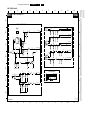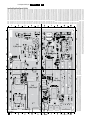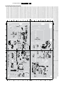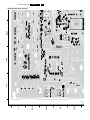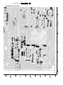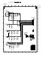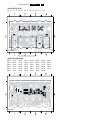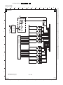
1
Colour Television
Chassis
LC7.2E
LA
ME7
G_16860_000.eps
200207
Contents
Page
1. Technical Specifications, Connections, and Chassis
Overview
2
2. Safety Instructions, Warnings, and Notes
6
3. Directions for Use
7
4. Mechanical Instructions
8
5. Service Modes, Error Codes, and Fault Finding 16
6. Block Diagrams, Test Point Overviews, and
Waveforms
Wiring Diagram 26” & 32”
29
Wiring Diagram 37” & 42”
30
Wiring Diagram 37” & 42” (ME7 Promo Set)
31
Wiring Diagram 42” 1080p
32
Wiring Diagram 47” (ME7)
33
Wiring Diagram 47” 1080p (ME7)
34
Block Diagram Video
35
Block Diagram Audio
36
Block Diagram Control & Clock Signals
37
Test Point Overview SSB (Bottom Side)
38
I2C IC’s Overview
39
Supply Lines Overview
40
7. Circuit Diagrams and PWB Layouts
Diagram
SSB: DC/DC
(B02) 41
SSB: Tuner & Demodulator
(B03A) 42
SSB: DVB - Demodulator
(B03B) 43
SSB: DVB - Common Interface
(B03C) 44
SSB: DVB - Mojo
(B03D) 45
SSB: DVB - Mojo Memory
(B03E) 46
SSB: DVB - Mojo Analog Back End
(B03F) 47
SSB: Micro Processor
(B04A) 48
SSB: Video Processor
(B04B) 49
SSB: PNX2015: Audio Processor
(B04C) 50
SSB: YPBPR & Rear IO
(B06A) 51
SSB: I/O Scart 1 & 2
(B06B) 52
SSB: HDMI
(B06C) 53
Contents
8.
9.
10.
11.
Page
SSB: Headphone Amp & Muting
(B06D) 54
SSB: Audio
(B07) 55
SSB: SRP List
56
Side A/V Panel
(D) 67
Keyboard Control Panel
(E) 69
1080P Panel: On Chip uController
(F1) 71
1080P Panel: Flash & NVM
(F2) 72
1080P Panel: LVDS In
(F3) 73
1080P Panel: LVDS Out
(F4) 74
1080P Panel: Supply In
(F5) 75
1080P Panel: DDR SDRAM
(F6) 76
1080P Panel: DC Power Supply
(F7) 77
Front IR / LED Panel
(J) 79
Alignments
81
Circuit Descriptions, Abbreviation List, and IC Data
Sheets
86
Abbreviation List
93
IC Data Sheets
95
Spare Parts List
103
Revision List
111
57-66
57-66
57-66
68
70
78
78
78
78
78
78
78
80
PWB
57-66
57-66
57-66
57-66
57-66
57-66
57-66
57-66
57-66
57-66
57-66
57-66
57-66
©
Copyright 2007 Philips Consumer Electronics B.V. Eindhoven, The Netherlands.
All rights reserved. No part of this publication may be reproduced, stored in a
retrieval system or transmitted, in any form or by any means, electronic,
mechanical, photocopying, or otherwise without the prior permission of Philips.
Published by TY 0769 BU CD Customer Service
Printed in the Netherlands
Subject to modification
EN 3122 785 16863
EN 2
1.
Technical Specifications, Connections, and Chassis Overview
LC7.2E LA
1. Technical Specifications, Connections, and Chassis Overview
1.1.3
Index of this chapter:
1.1 Technical Specifications
1.2 Connection Overview
1.3 Chassis Overview
Notes:
• Figures can deviate due to the different set executions.
• Specifications are indicative (subject to change).
1.1
Technical Specifications
1.1.1
Vision
Display type
Screen size
Resolution (HxV pixels)
Dyn. contrast ratio
Min. light output (cd/m2)
Typ. response time (ms)
Viewing angle (HxV degrees)
Tuning system
Presets/channels
Tuner bands
TV Colour systems
Video playback
Supported computer formats
Supported video formats
1.1.2
:
:
:
:
:
:
:
:
:
:
:
:
:
:
:
:
:
:
:
:
:
:
:
:
:
:
:
:
:
:
:
:
:
:
:
:
LCD
26” (66 cm), 16:9
32” (82 cm), 16:9
37” (94 cm), 16:9
42” (107 cm), 16:9
1366x768
1920x1080 (42PFL7662)
3500:1 (26”)
4000:1 (32”)
5000:1 (37”)
5000:1 (42”)
500
8 (26”, 32”)
6 (37”)
5 (42”)
160x150 (26”)
176x176 (> 26”)
PLL
100 presets
VHF, UHF, S, H
PAL B/G, D/K, I
SECAM B/G, D/K, L/L’
DVB-T COFDM
NTSC
PAL
SECAM
640x480
800x600
1024x768
640x480i - 1fH
720x576i - 1fH
640x480p - 2fH
720x576p - 2fH
1920x1080i - 2fH
1280x720p - 3fH
1920x1080p(42PFL7662)
:
:
:
:
2CS B/G, D/K
NICAM B/G, D/K, I, L
2 x 5 (26”)
2 x 10 (> 26”)
Sound
Sound systems
Maximum power (WRMS)
Miscellaneous
Power supply:
- Mains voltage (VAC)
- Mains frequency (Hz)
: 220 - 240
: 50 / 60
Ambient conditions:
- Temperature range (°C)
- Maximum humidity
: +5 to +40
: 90% R.H.
Power consumption (values are indicative)
- Normal operation (W)
: ≈ 120 (26”)
: ≈ 140 (32”)
: ≈ 175 (37”)
: ≈ 240 (42”)
- Stand-by (W)
: <1
Dimensions (WxHxD cm)
:
:
:
:
69.1x47.4x11.1 (26”)
81.6x55.2x11.6 (32”)
94.4x62.8x11.3 (37”)
105.8x69.2x11.6 (42”)
Weight (kg)
:
:
:
:
12.4 (26”)
16.3 (32”)
21.6 (37”)
27.9 (42”)
Technical Specifications, Connections, and Chassis Overview
1.2
LC7.2E LA
1.
EN 3
Connection Overview
G_16860_046.eps
310107
Figure 1-1 Side and rear I/O connections
Note: The following connector colour abbreviations are used
(acc. to DIN/IEC 757): Bk= Black, Bu= Blue, Gn= Green, Gy=
Grey, Rd= Red, Wh= White, and Ye= Yellow.
1.2.1
Side Connections
EXT3: Head phone - Out
Bk - Head phone
32 - 600 ohm / 10 mW
rt
EXT3: Cinch: Video CVBS - In, Audio - In
Rd - Audio R
0.5 VRMS / 10 kohm
Wh - Audio L
0.5 VRMS / 10 kohm
Ye - Video CVBS
1 VPP / 75 ohm
jq
jq
jq
EXT3: S-Video (Hosiden): Video Y/C - In
1 - Ground Y
Gnd
2 - Ground C
Gnd
3 - Video Y
1 VPP / 75 ohm
4 - Video C
0.3 VPPP / 75 ohm
1.2.2
H
H
j
j
Rear Connections
EXT1: Video RGB - In, CVBS - In/Out, Audio - In/Out
20
21
2
1
E_06532_001.eps
050404
Figure 1-2 SCART connector
1
2
3
4
5
6
7
- Audio R
- Audio R
- Audio L
- Ground Audio
- Ground Blue
- Audio L
- Video Blue
0.5 VRMS / 1 kohm
0.5 VRMS / 10 kohm
0.5 VRMS / 1 kohm
Gnd
Gnd
0.5 VRMS / 10 kohm
0.7 VPP / 75 ohm
k
j
k
H
H
j
j
8
- Function Select
9
10
11
12
13
14
15
16
- Ground Green
- Easylink P50
- Video Green
- n.c.
- Ground Red
- Ground P50
- Video Red
- Status/FBL
17
18
19
20
21
- Ground Video
- Ground FBL
- Video CVBS
- Video CVBS
- Shield
0 - 2 V: INT
4.5 - 7 V: EXT 16:9
9.5 - 12 V: EXT 4:3
Gnd
0 - 5 V / 4.7 kohm
0.7 VPP / 75 ohm
Gnd
Gnd
0.7 VPP / 75 ohm
0 - 0.4 V: INT
1 - 3 V: EXT / 75 ohm
Gnd
Gnd
1 VPP / 75 ohm
1 VPP / 75 ohm
Gnd
j
H
jk
j
H
H
j
j
H
H
k
j
H
EXT2: Video YC - In, CVBS - In/Out, Audio - In/Out
1
2
3
4
5
6
7
8
- Audio R
- Audio R
- Audio L
- Ground Audio
- n.c.
- Audio L
- C-out
- Function Select
9
10
11
12
13
14
15
16
- n.c.
- Easylink P50
- n.c.
- n.c.
- n.c.
- Ground P50
-C
- Status/FBL
17
18
19
20
21
- Ground Video
- Ground FBL
- Video CVBS
- Video CVBS/Y
- Shield
0.5 VRMS / 1 kohm
0.5 VRMS / 10 kohm
0.5 VRMS / 1 kohm
Gnd
k
j
k
H
0.5 VRMS / 10 kohm
0.7 VPP / 75 ohm
0 - 2 V: INT
4.5 - 7 V: EXT 16:9
9.5 - 12 V: EXT 4:3
j
k
0 - 5 V / 4.7 kohm
Gnd
0.7 VPP / 75 ohm
0 - 0.4 V: INT
1 - 3 V: EXT / 75 ohm
Gnd
Gnd
1 VPP / 75 ohm
1 VPP / 75 ohm
Gnd
j
jk
H
j
j
H
H
k
j
H
EN 4
1.
Technical Specifications, Connections, and Chassis Overview
LC7.2E LA
Common Interface
68p - See diagram B03C
jk
Service Connector (UART)
1 - UART_TX
Transmit
2 - Ground
Gnd
3 - UART_RX
Receive
k
H
j
Aerial - In
- - IEC-type (EU)
D
Coax, 75 ohm
Service Connector (ComPair)
1 - SDA-S
I2C Data (0 - 5 V)
2 - SCL-S
I2C Clock (0 - 5 V)
3 - Ground
Gnd
jk
j
H
HDMI 1 & 2: Digital Video, Digital Audio - In
19
18
1
2
E_06532_017.eps
250505
Figure 1-3 HDMI (type A) connector
1
2
1.3
- D2+
- Shield
Data channel
Gnd
j
H
3
4
5
6
7
8
9
10
11
12
13
14
15
16
17
18
19
20
- D2- D1+
- Shield
- D1- D0+
- Shield
- D0- CLK+
- Shield
- CLK- n.c.
- n.c.
- DDC_SCL
- DDC_SDA
- Ground
- +5V
- HPD
- Ground
j
j
H
j
j
H
j
j
H
j
Data channel
Data channel
Gnd
Data channel
Data channel
Gnd
Data channel
Data channel
Gnd
Data channel
j
jk
H
j
j
H
DDC clock
DDC data
Gnd
Hot Plug Detect
Gnd
EXT4: Cinch: Video YPbPr - In, Audio - In
Gn - Video Y
1 VPP / 75 ohm
Bu - Video Pb
0.7 VPP / 75 ohm
Rd - Video Pr
0.7 VPP / 75 ohm
Wh - Audio L
0.5 VRMS / 10 kohm
Rd - Audio R
0.5 VRMS / 10 kohm
jq
jq
jq
jq
jq
Chassis Overview
SIDE I/O PANEL
D
CONTROL BOARD
E
LED PANEL
J
POWER SUPPLY UNIT
B
SMALL SIGNAL
BOARD
G_16860_047.eps
310107
Figure 1-4 PWB/CBA locations (26” and 32” models)
Technical Specifications, Connections, and Chassis Overview
LC7.2E LA
1.
EN 5
SIDE I/O PANEL
D
CONTROL PANEL
E
LED PANEL
J
POWER SUPPLY UNIT
B
SMALL SIGNAL
BOARD
H_16940_008.eps
050307
Figure 1-5 PWB/CBA locations (37” and 42” models without 1080p module)
F
SIDE I/O PANEL
D
CONTROL PANEL
E
LED PANEL
J
1080p PANEL
POWER SUPPLY UNIT
B
SMALL SIGNAL
BOARD
G_16860_092.eps
150307
Figure 1-6 PWB/CBA locations (42” models with 1080p module)
EN 6
2.
LC7.2E LA
Safety Instructions, Warnings, and Notes
2. Safety Instructions, Warnings, and Notes
Index of this chapter:
2.1 Safety Instructions
2.2 Warnings
2.3 Notes
•
2.1
Safety Instructions
Safety regulations require the following during a repair:
• Connect the set to the Mains/AC Power via an isolation
transformer (> 800 VA).
• Replace safety components, indicated by the symbol h,
only by components identical to the original ones. Any
other component substitution (other than original type) may
increase risk of fire or electrical shock hazard.
Safety regulations require that after a repair, the set must be
returned in its original condition. Pay in particular attention to
the following points:
• Route the wire trees correctly and fix them with the
mounted cable clamps.
• Check the insulation of the Mains/AC Power lead for
external damage.
• Check the strain relief of the Mains/AC Power cord for
proper function.
• Check the electrical DC resistance between the Mains/AC
Power plug and the secondary side (only for sets that have
a Mains/AC Power isolated power supply):
1. Unplug the Mains/AC Power cord and connect a wire
between the two pins of the Mains/AC Power plug.
2. Set the Mains/AC Power switch to the "on" position
(keep the Mains/AC Power cord unplugged!).
3. Measure the resistance value between the pins of the
Mains/AC Power plug and the metal shielding of the
tuner or the aerial connection on the set. The reading
should be between 4.5 Mohm and 12 Mohm.
4. Switch "off" the set, and remove the wire between the
two pins of the Mains/AC Power plug.
• Check the cabinet for defects, to prevent touching of any
inner parts by the customer.
2.2
•
2.3.2
•
•
•
•
•
•
•
•
All ICs and many other semiconductors are susceptible to
electrostatic discharges (ESD w). Careless handling
during repair can reduce life drastically. Make sure that,
during repair, you are connected with the same potential as
the mass of the set by a wristband with resistance. Keep
components and tools also at this same potential. Available
ESD protection equipment:
– Complete kit ESD3 (small tablemat, wristband,
connection box, extension cable and earth cable) 4822
310 10671.
– Wristband tester 4822 344 13999.
Be careful during measurements in the high voltage
section.
Never replace modules or other components while the unit
is switched "on".
When you align the set, use plastic rather than metal tools.
This will prevent any short circuits and the danger of a
circuit becoming unstable.
2.3
Notes
2.3.1
General
•
Measure the voltages and waveforms with regard to the
chassis (= tuner) ground (H), or hot ground (I), depending
on the tested area of circuitry. The voltages and waveforms
shown in the diagrams are indicative. Measure them in the
All resistor values are in ohms, and the value multiplier is
often used to indicate the decimal point location (e.g. 2K2
indicates 2.2 kohm).
Resistor values with no multiplier may be indicated with
either an "E" or an "R" (e.g. 220E or 220R indicates 220
ohm).
All capacitor values are given in micro-farads (μ= x10-6),
nano-farads (n= x10-9), or pico-farads (p= x10-12).
Capacitor values may also use the value multiplier as the
decimal point indication (e.g. 2p2 indicates 2.2 pF).
An "asterisk" (*) indicates component usage varies. Refer
to the diversity tables for the correct values.
The correct component values are listed in the Spare Parts
List. Therefore, always check this list when there is any
doubt.
BGA (Ball Grid Array) ICs
Introduction
For more information on how to handle BGA devices, visit this
URL: www.atyourservice.ce.philips.com (needs subscription,
not available for all regions). After login, select “Magazine”,
then go to “Repair downloads”. Here you will find Information
on how to deal with BGA-ICs.
BGA Temperature Profiles
For BGA-ICs, you must use the correct temperature-profile,
which is coupled to the 12NC. For an overview of these profiles,
visit the website www.atyourservice.ce.philips.com (needs
subscription, but is not available for all regions)
You will find this and more technical information within the
"Magazine", chapter "Repair downloads".
For additional questions please contact your local repair help
desk.
Warnings
•
Schematic Notes
•
2.3.3
Service Default Mode (see chapter 5) with a colour bar
signal and stereo sound (L: 3 kHz, R: 1 kHz unless stated
otherwise) and picture carrier at 475.25 MHz for PAL, or
61.25 MHz for NTSC (channel 3).
Where necessary, measure the waveforms and voltages
with (D) and without (E) aerial signal. Measure the
voltages in the power supply section both in normal
operation (G) and in stand-by (F). These values are
indicated by means of the appropriate symbols.
Manufactured under license from Dolby Laboratories.
“Dolby”, “Pro Logic” and the “double-D symbol”, are
trademarks of Dolby Laboratories.
2.3.4
Lead-free Soldering
Due to lead-free technology some rules have to be respected
by the workshop during a repair:
• Use only lead-free soldering tin Philips SAC305 with order
code 0622 149 00106. If lead-free solder paste is required,
please contact the manufacturer of your soldering
equipment. In general, use of solder paste within
workshops should be avoided because paste is not easy to
store and to handle.
• Use only adequate solder tools applicable for lead-free
soldering tin. The solder tool must be able:
– To reach a solder-tip temperature of at least 400°C.
– To stabilize the adjusted temperature at the solder-tip.
– To exchange solder-tips for different applications.
• Adjust your solder tool so that a temperature of around
360°C - 380°C is reached and stabilized at the solder joint.
Heating time of the solder-joint should not exceed ~ 4 sec.
Avoid temperatures above 400°C, otherwise wear-out of
tips will increase drastically and flux-fluid will be destroyed.
Directions for Use
•
2.3.5
To avoid wear-out of tips, switch “off” unused equipment or
reduce heat.
Mix of lead-free soldering tin/parts with leaded soldering
tin/parts is possible but PHILIPS recommends strongly to
avoid mixed regimes. If this cannot be avoided, carefully
clear the solder-joint from old tin and re-solder with new tin.
MODEL
LC7.2E LA
: 32PF9968/10
PROD.NO: AG 1A0617 000001
3.
MADE IN BELGIUM
220-240V ~ 50/60Hz
128W
VHF+S+H+UHF
S
Figure 2-1 Serial number (example)
2.3.6
3. Directions for Use
You can download this information from the following websites:
http://www.philips.com/support
http://www.p4c.philips.com
Board Level Repair (BLR) or Component Level Repair
(CLR)
If a board is defective, consult your repair procedure to decide
if the board has to be exchanged or if it should be repaired on
component level.
If your repair procedure says the board should be exchanged
completely, do not solder on the defective board. Otherwise, it
cannot be returned to the O.E.M. supplier for back charging!
2.3.7
NVM content
If the processor NVM IC is replaced or initialised, the Model
Number, Serial Number, and SSB Code number must be rewritten to the NVM. ComPair will foresee in a possibility to do
this.
2.3.8
Identification: The bottom line of a type plate gives a 14-digit
serial number. Digits 1 and 2 refer to the production centre (e.g.
AG is Bruges), digit 3 refers to the B.O.M. code, digit 4 refers
to the Service version change code, digits 5 and 6 refer to the
production year, and digits 7 and 8 refer to production week (in
example below it is 2006 week 17). The 6 last digits contain the
serial number.
BJ3.0E LA
E_06532_024.eps
130606
Alternative BOM identification
The third digit in the serial number (example:
AG2B0335000001) indicates the number of the alternative
B.O.M. (Bill Of Materials) that has been used for producing the
specific TV set. In general, it is possible that the same TV
model on the market is produced with e.g. two different types
of displays, coming from two different suppliers. This will then
result in sets which have the same CTN (Commercial Type
Number; e.g. 28PW9515/12) but which have a different B.O.M.
number.
By looking at the third digit of the serial number, one can
identify which B.O.M. is used for the TV set he is working with.
If the third digit of the serial number contains the number “1”
(example: AG1B033500001), then the TV set has been
manufactured according to B.O.M. number 1. If the third digit is
a “2” (example: AG2B0335000001), then the set has been
produced according to B.O.M. no. 2. This is important for
ordering the correct spare parts!
For the third digit, the numbers 1...9 and the characters A...Z
can be used, so in total: 9 plus 26= 35 different B.O.M.s can be
indicated by the third digit of the serial number.
EN 7
Practical Service Precautions
•
•
It makes sense to avoid exposure to electrical shock.
While some sources are expected to have a possible
dangerous impact, others of quite high potential are of
limited current and are sometimes held in less regard.
Always respect voltages. While some may not be
dangerous in themselves, they can cause unexpected
reactions that are best avoided. Before reaching into a
powered TV set, it is best to test the high voltage insulation.
It is easy to do, and is a good service precaution.
EN 8
4.
LC7.2E LA
Mechanical Instructions
4. Mechanical Instructions
Notes:
• Figures below can deviate slightly from the actual situation,
due to the different set executions.
• Follow the disassemble instructions in described order.
Index of this chapter:
4.1 Cable Dressing
4.2 Service Positions
4.3 Assy/Panel Removal
4.4 Set Re-assembly
4.1
Cable Dressing
LC07: 26” (BASIC SET)
G_16860_084.eps
150307
Figure 4-1 Cable dressing (26” models)
Mechanical Instructions
LC7.2E LA
4.
EN 9
G_16860_064.eps
310107
Figure 4-2 Cable dressing (32-inch models)
G_16860_085.eps
150307
Figure 4-3 Cable dressing (37” models)
EN 10
4.
LC7.2E LA
Mechanical Instructions
H_16940_009.eps
050307
Figure 4-4 Cable dressing (42” models without 1080p module)
G_16860_091.eps
150307
Figure 4-5 Cable dressing (42” models with 1080p module)
Mechanical Instructions
4.2
Service Positions
4.3
Assy/Panel Removal
For easy servicing of this set, there are a few possibilities
created:
• The buffers from the packaging.
• Foam bars (created for Service).
• Aluminium service stands (created for Service).
4.3.1
Rear Cover
Foam Bars
EN 11
1. Place the TV set upside down on a table top, using the
foam bars (see part "Service Position").
2. Remove rear cover screws and the stand (if mounted).
3. Remove rear cover.
4.3.2
Keyboard Control Panel
1. Refer to next figure (is taken from the 32” model, but the
method is comparable for the other screen sizes).
2. Remove the T10 parker screws [1].
3. Unplug connector [2].
4. Remove the unit.
5. Release clips [3] and remove the board.
When defective, replace the whole unit.
1
1
4.
Warning: Disconnect the mains power cord before you remove
the rear cover.
Note: the aluminium service stands can only be used when the
set is equipped with so-called “mushrooms”. Otherwise use the
original stand that comes with the set.
4.2.1
LC7.2E LA
Required for sets
42"
1
E_06532_018.eps
171106
Figure 4-6 Foam bars
3
The foam bars (order code 3122 785 90580 for two pieces) can
be used for all types and sizes of Flat TVs. See figure “Foam
bars” for details.
Sets with a display of 42” and larger, require four foam bars [1].
Ensure that the foam bars are always supporting the cabinet
and never only the display.
Caution: Failure to follow these guidelines can seriously
damage the display!
By laying the TV face down on the (ESD protective) foam bars,
a stable situation is created to perform measurements and
alignments. By placing a mirror under the TV, you can monitor
the screen.
4.2.2
2
1
G_16850_007.eps
310707
Aluminium Stands
Figure 4-8 Keyboard control panel
4.3.3
E_06532_019.eps
170504
Figure 4-7 Aluminium stands (drawing of MkI)
The new MkII aluminium stands (not on drawing) with order
code 3122 785 90690, can also be used to do measurements,
alignments, and duration tests. The stands can be
(dis)mounted quick and easy by means of sliding them in/out
the "mushrooms". The new stands are backwards compatible
with the earlier models.
Important: For (older) FTV sets without these "mushrooms", it
is obligatory to use the provided screws, otherwise it is possible
to damage the monitor inside!
Side I/O Panel
1. Refer to next figure (is taken from the 32” model, but the
method is comparable for the other screen sizes).
2. Unplug connector [a].
3. Remove screws [b] and remove the complete module. One
of the screws is T10 tapping, the other one is T10 parker.
4. Remove T10 parker screw [c]. Refer to next figure.
5. Push catch [d] (located at the underside of the bracket) and
slide the unit to the right from its bracket [e]. See fig. “Side
I/O panel 2”.
6. To remove the PWB from its bracket, you have to lift the
catch [f] located on top of the head phone connector. At the
same time, slide the PWB out of its bracket [g]. See fig.
“Side I/O panel 3”.
When defective, replace the whole unit.
EN 12
4.
LC7.2E LA
Mechanical Instructions
b (1x)
a
b (1x)
f
g
2
G_16860_066.eps
010207
Figure 4-9 Side I/O module
G_16860_077.eps
010207
Figure 4-12 Side I/O panel [3/3]
4.3.4
IR/LED Panel
c
1. Refer to next figure (is taken from the 32” model, but the
method is comparable for the other screen sizes).
2. Unplug connector(s) [1].
3. Release clip [2] and remove the board.
When defective, replace the whole unit.
1
2
G_16860_075.eps
010207
Figure 4-10 Side I/O panel [1/3] top side
G_16850_009.eps
110107
Figure 4-13 IR/LED panel
d
2
e
2
G_16860_076.eps
010207
Figure 4-11 Side I/O panel [2/3] bottom side
Mechanical Instructions
4.3.5
4.3.6
Speakers
This depends on the model/screen size: for the 26” and 32”
models, the bare speakers are accessible, while for the larger
models they are encased, and therefore must be replaced as
assembly when defective.
Full- or Mid-range Speakers (for 26” and 32” models)
1. Refer to next figure.
2. Unplug connectors [1].
3. Remove screws [2].
LC7.2E LA
4.
EN 13
1080p Panel
1. Refer to next figure(s).
2. Unplug cables [a]. Be careful with the LVDS connectors as
they are very fragile.
3. Remove the fixation screws [b].
4. Take the board out (it hinges at the lower side).
5. Remove the screws [c] that fixate the top and bottom
shieldings, and remove the shieldings.
Note: Pay special attention not to damage the EMC foams.
Ensure that EMC foams are mounted correctly, especially
notice the large EMC foam “block” [d] at the bottom shielding.
c
2
1
2
G_16850_010.eps
110107
b
c
Figure 4-14 Mid-range speakers
a
Tweeters (only for 32” models)
1. Refer to next figure.
2. Unplug connectors [1].
3. Remove screws [2].
c
b
c
G_16860_089.eps
150307
Figure 4-17 1080p panel
2
1
G_16850_011.eps
110107
Figure 4-15 Tweeters
Speaker box (for 37” and 42” models)
1. Refer to next figure.
2. Unplug connectors [1].
3. Remove screws [2].
When defective, replace the whole unit.
d
1
2
2
H_16851_011.eps
080307
Figure 4-16 Tweeters
G_16860_088.eps
150307
Figure 4-18 Bottom shielding 1080p panel
EN 14
4.3.7
4.
LC7.2E LA
Mechanical Instructions
Main Supply Panel
Some models (37 and 42PFL3512D) come with a so-called IPB
(Integrated Power Board) power supply with integrated
backlight inverters. Disassembly is equal as described below.
1. Refer to next figure (is taken from the 32” model, but the
method is comparable for the other screen sizes).
2. Unplug cables [a].
3. Remove the fixation screws [b].
4. Take the board out (it hinges at the left side).
b (3×)
a
a
a
G_16860_065.eps
010207
Figure 4-19 Main supply panel (32” model)
4.3.8
Small Signal Board (SSB)
1. Refer to next figure (is taken from the 32” model, but the
method is comparable for the other screen sizes).
2. Disconnect all cables [a] on the SSB.
3. Remove the T10 tapping screws [b] that hold the SSB. See
Figure “SSB removal”.
4. Remove the screws that hold the CINCH and HDMI
connectors at the connector panel.
5. Lift the SSB from the set.
b (3x)
a
b (3x)
a
b (2x)
b (2x)
G_16860_074.eps
010207
Figure 4-20 SSB removal
Mechanical Instructions
4.3.9
LC7.2E LA
4.
EN 15
4. Do NOT forget to unplug the LVDS connector [e] from the
SSB. Important: Be careful, as this is a fragile connector!
5. Remove T10 parker screw [b] that holds the Side I/O
module bracket.
6. Remove T10 parker screws [f] of the central sub-frame.
7. Remove LCD panel fixation screws [g] and lift the complete
central sub-frame from the set (incl. the PSU, SSB, and
Side I/O boards and wiring).
8. Lift the LCD panel [7] from the front cabinet.
LCD Panel
The disassembly method for the LCD panel differs per model
or screen size. The following description applies to the 32”
model, but for the other screen sizes, the method is similar.
1. Refer to next figure(s).
2. Unplug the connectors on the Main Supply Panel [a] and
the LED & IR board [c].
3. Unplug the connectors [d] from the loudspeakers.
f (1x)
g (2x)
e
a
g (2x)
b
f (3x)
d
f (2x)
d
c (1x)
G_16860_067.eps
310107
Figure 4-21 LCD panel 32” [1/2]
4.4
Set Re-assembly
To re-assemble the whole set, execute all processes in reverse
order.
Notes:
• While re-assembling, make sure that all cables are placed
and connected in their original position. See figure "Cable
dressing".
• Pay special attention not to damage the EMC foams.
Ensure that EMC foams are mounted correctly (one is
located above the LVDS connector on the display, between
the LCD display and the metal sub-frame).
7
G_16850_015.eps
110107
Figure 4-22 LCD panel 32” [2/2]
EN 16
5.
LC7.2E LA
Service Modes, Error Codes, and Fault Finding
5. Service Modes, Error Codes, and Fault Finding
5.1
Test Points
In the chassis schematics and layout overviews, the test points
(Fxxx) are mentioned. In the schematics, test points are
indicated with a rectangular box around “Fxxx” or “Ixxx”, in the
layout overviews with a “half-moon” sign.
As most signals are digital, it will be difficult to measure
waveforms with a standard oscilloscope. Several key ICs are
capable of generating test patterns, which can be controlled via
ComPair. In this way it is possible to determine which part is
defective.
Perform measurements under the following conditions:
• Service Default Mode.
• Video: Colour bar signal.
• Audio: 3 kHz left, 1 kHz right.
5.2
Service Modes
The Service Mode feature is split into four parts:
• Service Default Mode (SDM).
• Service Alignment Mode (SAM).
• Customer Service Mode (CSM) and Digital Customer
Service Mode (DCSM).
• Computer Aided Repair Mode (ComPair).
SDM and SAM offer features, which can be used by the Service
engineer to repair/align a TV set. Some features are:
• A pre-defined situation to ensure measurements can be
made under uniform conditions (SDM).
• Activates the blinking LED procedure for error identification
when no picture is available (SDM).
• The possibility to overrule software protections when SDM
was entered via the Service pins.
• Make alignments (e.g. white tone), (de)select options,
enter options codes, reset the error buffer (SAM).
• Display information (“SDM” or “SAM” indication in upper
right corner of screen, error buffer, software version,
operating hours, options and option codes, sub menus).
The (D)CSM is a Service Mode that can be enabled by the
consumer. The CSM displays diagnosis information, which the
customer can forward to the dealer or call centre. In CSM
mode, “CSM”, is displayed in the top right corner of the screen.
The information provided in CSM and the purpose of CSM is to:
• Increase the home repair hit rate.
• Decrease the number of nuisance calls.
• Solved customers' problem without home visit.
5.2.1
General
Some items are applicable to all Service Modes or are general.
These are listed below.
Life Timer
During the life time cycle of the TV set, a timer is kept. It counts
the normal operation hours (not the Stand-by hours). The
actual value of the timer is displayed in SDM and CSM in a
decimal value. Every two soft-resets increase the hour by +1.
Software Identification, Version, and Cluster
The software ID, version, and cluster will be shown in the main
menu display of SDM, SAM, and CSM.
The screen will show: “AAAABCD X.YY”, where:
• AAAA is the chassis name: LC71 for analogue range (nonDVB), LC72 for digital range (DVB).
• B is the region indication: E= Europe, A= AP/China, U=
NAFTA, L= LATAM.
• C is the display indication: L= LCD, P= Plasma.
• D is the language/feature indication: 1= standard, H=
1080p full HD.
• X is the main version number: this is updated with a major
change of specification (incompatible with the previous
software version). Numbering will go from 1 - 9 and A - Z.
– If the main version number changes, the new version
number is written in the NVM.
– If the main version number changes, the default
settings are loaded.
• YY is the sub version number: this is updated with a minor
change (backwards compatible with the previous versions)
Numbering will go from 00 - 99.
– If the sub version number changes, the new version
number is written in the NVM.
– If the NVM is fresh, the software identification, version,
and cluster will be written to NVM.
Display Option Code Selection
When after an SSB or display exchange, the display option
code is not set properly, it will result in a TV with “no display”.
Therefore, it is required to set this display option code after
such a repair.
To do so, press the following key sequence on a standard RC
transmitter: “062598” directly followed by MENU and “xxx”,
where “xxx” is a 3 digit decimal value of the panel type: see
column “Panel Code” in table “Option Codes OP1...OP7” (ch.
8), or see sticker on the side/bottom of the cabinet. When the
value is accepted and stored in NVM, the set will switch to
Stand-by, to indicate that the process has been completed.
Display Option
Code
39mm
PHILIPS
27mm
Index of this chapter:
5.1 Test Points
5.2 Service Modes
5.3 Service Tools
5.4 Error Codes
5.5 The Blinking LED Procedure
5.6 Software Upgrading
5.7 Fault Finding and Repair Tips
040
MODEL:
32PF9968/10
PROD.SERIAL NO:
AG 1A0620 000001
(CTN Sticker)
ComPair Mode is used for communication between a computer
and a TV on I2C /UART level and can be used by a Service
engineer to quickly diagnose the TV set by reading out error
codes, read and write in NVMs, communicate with ICs and the
uP (PWM, registers, etc.), and by making use of a fault finding
database. It will also be possible to up and download the
software of the TV set via I2C with help of ComPair. To do this,
ComPair has to be connected to the TV set via the ComPair
connector, which will be accessible through the rear of the set
(without removing the rear cover).
E_06532_038.eps
290107
Figure 5-1 Location of Display Option Code sticker
During this algorithm, the NVM-content must be filtered,
because several items in the NVM are TV-related and not SSBrelated (e.g. Model and Prod. S/N). Therefore, “Model” and
“Prod. S/N” data is changed into “See Type Plate”.
In case a call centre or consumer reads “See Type Plate” in
CSM mode, he needs to look to the side/bottom sticker to
identify the set, for further actions.
Service Modes, Error Codes, and Fault Finding
5.2.2
Service Default Mode (SDM)
Purpose
Set the TV in SDM mode in order to be able to:
• Create a pre-defined setting for measurements to be
made.
• Override software protections.
• Start the blinking LED procedure.
• Read the error buffer.
• Check the life timer.
LC7.2E LA
5.
EN 17
On Screen Menu
After activating SDM, the following screen is visible, with SDM
in the upper right corner of the screen to indicate that the
television is in Service Default Mode.
S D M
HHHHH
A A A A B C D - X . Y Y
E R R
X X
X X
X X
X X
X X
O P
X X X
X X X
X X X
X X X
X X X
X X X
Specifications
Table 5-1 SDM default settings
Region
Freq. (MHz)
Default syst.
Europe (except France),
AP-PAL/-Multi
475.25
PAL B/G
France
SECAM L
NAFTA, AP-NTSC
61.25 (channel 3) NTSC M
LATAM
•
•
PAL M
Set linear video and audio settings to 50%, but volume to
25%. Stored user settings are not affected.
All service-unfriendly modes (if present) are disabled, since
they interfere with diagnosing/repairing a set. These
service unfriendly modes are:
– (Sleep) timer.
– Blue mute/Wall paper.
– Auto switch “off” (when there is no “ident” signal).
– Hotel or hospital mode.
– Child lock or parental lock (manual or via V-chip).
– Skipping, blanking of “Not favourite”, “Skipped” or
“Locked” presets/channels.
– Automatic storing of Personal Preset or Last Status
settings.
– Automatic user menu time-out (menu switches back/
OFF automatically.
– Auto Volume levelling (AVL).
How to Activate
To activate SDM, use one of the following methods:
• Press the following key sequence on the remote control
transmitter: “062596” directly followed by the MENU button
(do not allow the display to time out between entries while
keying the sequence).
• Short one of the “Service” jumpers on the TV board during
cold start (see Figures “Service jumper”). Then press the
mains button (remove the short after start-up).
Caution: Activating SDM by shorting “Service” jumpers will
override the DC speaker protection (error 1), the General
I2C error (error 4), and the Trident video processor error
(error 5). When doing this, the service-technician must
know exactly what he is doing, as it could damage the
television set.
G_16860_030.eps
260107
Figure 5-3 SDM menu
Menu explanation:
• HHHHH: Are the operating hours (in decimal).
• AAAABCD-X.YY: See paragraph “Service Modes” ->
“General” -> “Software Identification, Version, and Cluster”
for the SW name definition.
• SDM: The character “SDM” to indicate that the TV set is in
Service mode.
• ERR: Shows all errors detected since the last time the
buffer was erased. Five errors possible.
• OP: Used to read-out the option bytes. See “Options” in the
Alignments section for a detailed description. Seven codes
are possible.
How to Navigate
As this mode is read only, there is not much to navigate. To
switch to other modes, use one of the following methods:
• Command MENU from the user remote will enter the
normal user menu (brightness, contrast, colour, etc...) with
“SDM” OSD remaining, and pressing MENU key again will
return to the last status of SDM again.
• To prevent the OSD from interfering with measurements in
SDM, command “OSD” (“STATUS” for NAFTA and
LATAM) from the user remote will toggle the OSD “on/off”
with “SDM” OSD remaining always “on”.
• Press the following key sequence on the remote control
transmitter: “062596” directly followed by the OSD/i+
button to switch to SAM (do not allow the display to time out
between entries while keying the sequence).
How to Exit
Switch the set to STANDBY by pressing the mains button on
the remote control transmitter or on the television set.
If you switch the television set “off” by removing the mains (i.e.,
unplugging the television), the television set will remain in SDM
when mains is re-applied, and the error buffer is not cleared.
The error buffer will only be cleared when the “clear” command
is used in the SAM menu.
Note:
• If the TV is switched “off” by a power interrupt while in SDM,
the TV will show up in the last status of SDM menu as soon
as the power is supplied again. The error buffer will not be
cleared.
• In case the set is in Factory mode by accident (with “F”
displayed on screen), by pressing and hold “VOL-“ and
“CH-” together should leave Factory mode.
SDM
G_16860_027.eps
260107
Figure 5-2 Service jumper (SSB component side)
EN 18
5.2.3
5.
LC7.2E LA
Service Modes, Error Codes, and Fault Finding
uploading via ComPair. Read paragraph “Service Tools” > “ComPair”. Caution: When this mode is selected without
ComPair connected, the TV will be blocked. Remove the
AC power to reset the TV.
12. SW Events. Only to be used by development to monitor
SW behaviour during stress test.
Service Alignment Mode (SAM)
Purpose
• To change option settings.
• To display / clear the error code buffer.
• To perform alignments.
Specifications
• Operation hours counter (maximum five digits displayed).
• Software version, error codes, and option settings display.
• Error buffer clearing.
• Option settings.
• Software alignments (Tuner, White Tone, and Audio).
• NVM Editor.
• ComPair Mode switching.
• Set the screen mode to full screen (all contents on screen
are viewable).
How to Activate
To activate SAM, use one of the following methods:
• Press the following key sequence on the remote control
transmitter: “062596" directly followed by the OSD/
STATUS/INFO/i+ button (it depends on region which
button is present on the RC). Do not allow the display to
time out between entries while keying the sequence.
• Or via ComPair.
After entering SAM, the following screen is visible, with SAM in
the upper right corner of the screen to indicate that the
television is in Service Alignment Mode.
S A M
L L L L L
E R R
X X
O P
X X X
C
O
T
R
N
C
S
l
p
u
G
V
o
W
e
t
n
B
M
m
a r
i o n
e r
A l
E d
p a i
E V E
A A A A B C D - X . Y Y
X X
X X
X X
X X
X X X
X X X
X X X
X X X
s
i g n
i t o r
r
N T S
>
>
>
>
>
>
>
X X X
Y e s
G_16860_031.eps
260107
Figure 5-4 SAM menu
Menu explanation:
1. LLLLL. This represents the run timer. The run timer counts
normal operation hours, but does not count Stand-by
hours.
2. AAAABCD-X.YY. See paragraph “Service Modes” ->
“General” -> “Software Identification, Version, and Cluster”
for the SW name definition.
3. SAM. Indication of the Service Alignment Mode.
4. ERR (ERRor buffer). Shows all errors detected since the
last time the buffer was erased. Five errors possible.
5. OP (Option Bytes). Used to read-out the option bytes. See
“Options” in the Alignments section for a detailed
description. Seven codes are possible.
6. Clear. Erases the contents of the error buffer. Select the
CLEAR menu item and press the MENU RIGHT key. The
content of the error buffer is cleared.
7. Options. Used to set the option bits. See “Options” in the
“Alignments” chapter for a detailed description.
8. Tuner. Used to align the tuner. See “Tuner” in the
“Alignments” chapter for a detailed description.
9. RGB Align. Used to align the White Tone. See “White
Tone” in the “Alignments” chapter for a detailed
description.
10. NVM Editor. Can be used to change the NVM data in the
television set. See also paragraph “Fault Finding and
Repair Tips” further on.
11. ComPaIr. Can be used to switch the television to “In
Application Programming” mode (IAP), for software
How to Navigate
• In the SAM menu, select menu items with the MENU UP/
DOWN keys on the remote control transmitter. The
selected item will be indicated. When not all menu items fit
on the screen, use the MENU UP/DOWN keys to display
the next / previous menu items.
• With the MENU LEFT/RIGHT keys, it is possible to:
– Activate the selected menu item.
– Change the value of the selected menu item.
– Activate the selected sub menu.
• When you press the MENU button twice while in top level
SAM, the set will switch to the normal user menu (with the
SAM mode still active in the background). To return to the
SAM menu press the MENU button.
• Command “OSD/i+” key from the user remote will toggle
the OSD “on/off” with “SAM” OSD remaining always “on”.
• Press the following key sequence on the remote control
transmitter: “062596” directly followed by the MENU button
to switch to SDM (do not allow the display to time out
between entries while keying the sequence).
How to Store SAM Settings
To store the settings changed in SAM mode (except the
OPTIONS settings), leave the top level SAM menu by using the
POWER button on the remote control transmitter or the
television set.
How to Exit
Switch the set to STANDBY by pressing the mains button on
the remote control transmitter or the television set.
Note:
• When the TV is switched “off” by a power interrupt while in
SAM, the TV will show up in "normal operation mode" as
soon as the power is supplied again. The error buffer will
not be cleared.
• In case the set is in Factory mode by accident (with “F”
displayed on screen), by pressing and hold “VOL-“ and
“CH-” together should leave Factory mode.
Service Modes, Error Codes, and Fault Finding
5.2.4
Customer Service Mode (CSM)
Purpose
The Customer Service Mode shows error codes and
information on the TV’s operation settings. A call centre can
instruct the customer (by telephone) to enter CSM in order to
identify the status of the set. This helps them to diagnose
problems and failures in the TV before making a service call.
The CSM is a read-only mode; therefore, modifications are not
possible in this mode.
Specifications
• Ignore “Service unfriendly modes”.
• Line number for every line (to make CSM language
independent).
• Set the screen mode to full screen (all contents on screen
are viewable).
• After leaving the Customer Service Mode, the original
settings are restored.
• Possibility to use “CH+” or “CH-” for channel surfing, or
enter the specific channel number on the RC.
How to Activate
To activate CSM, press the following key sequence on the
remote control transmitter: “123654” (do not allow the display
to time out between entries while keying the sequence).
Upon entering the Customer Service Mode, the following
screen will appear:
CS M
1
2
3
4
5
6
7
8
9
1
1
1
1
1
0
1
2
3
4
M
P
S
O
C
S
N
F
L
T
S
S
H
F
O
R
W
P
O
S
V
l
I
U
Y
O
D
O
D E L :
O D
S /
I D :
:
D E S :
B
:
M
:
a s h D
F E
TI
N E R :
S T E M:
U N D :
A U
:
R M A T:
3 2
N:
L C
XX
XX
3 1
XX
a t
ME
WE
P A
MO
Y E
XX
P F L 5 5 2
A G1 A 0 7
7 1 EL 1 X XXX
XX XX
3 9 1 2 7
XXXXXX
a : XX. X
R: L L L L
A K/ GOO
L / NT S C
NO/ S T E
S / NO
XXXXXX
2
1
1
X
X
L
D
/
R
D
2
.
X
X
1
/
1
x
X
X
2
1 0
2 3 4 5 6
x
XXX XXX
XX
3 4 1
XXX
5.
EN 19
Menu Explanation
1. MODEL. Type number, e.g. 42PFL7662/12. (*)
2. PROD S/N. Product serial no., e.g. SV1A0701000008. (*)
3. SW ID. Software cluster and version is displayed.
4. OP. Option code information.
5. CODES. Error buffer contents.
6. SSB. Indication of the SSB factory ID (= 12nc). (*)
7. NVM. The NVM software version no.
8. Flash Data. PQ (picture quality) and AQ (audio quality)
data version. This is a sub set of the main SW.
9. LIFE TIMER. Operating hours indication.
10. TUNER. Indicates the tuner signal condition: “Weak” when
signal falls below threshold value, “Medium” when signal is
at mid-range, and “Strong” when signal falls above
threshold value.
11. SYSTEM. Gives information about the video system of the
selected transmitter (PAL/SECAM/NTSC).
12. SOUND. Gives information about the audio system of the
selected transmitter (MONO/STEREO/NICAM).
13. HDAU. HDMI audio stream detection. “YES” means audio
stream detected. “NO” means no audio stream present.
Only displayed when HDMI source is selected.
14. FORMAT. Gives information about the video format of the
selected transmitter (480i/480p/720p/1080i).
15. HD SW ID. Software version of the 1080p full HD module
(when present).
16. Reserved.
17. Reserved.
18. Reserved.
(*) If an NVM IC is replaced or initialised, the Model Number,
Serial Number, and SSB Code Number must be re-written to
the NVM. ComPair will foresee in a possibility to do this.
XXX
How to Exit
To exit CSM, use one of the following methods:
• Press the MENU button twice, or POWER button on the
remote control transmitter.
• Press the POWER button on the television set.
. XX. XX
/ S T R ONG
S ECA M
E O/ NI C A M
G_16860_032.eps
210207
Figure 5-5 CSM menu (example)
LC7.2E LA
EN 20
5.2.5
5.
LC7.2E LA
Service Modes, Error Codes, and Fault Finding
Digital Customer Service Mode (DCSM)
Purpose
The Digital Customer Service Mode shows error codes and
information on the IBO Zapper module (DVB reception part)
operation settings. The call centre can instruct the customer to
activate DCSM by telephone and read off the information
displayed. This helps the call centre to diagnose problems and
failures in the IBO Zapper module before making a service
call.The DCSM is a read-only mode; therefore, modifications
are not possible in this mode.
How to Activate
To activate the DCSM, put the television in its digital mode (via
the “A/D” button on the remote control).
1. Press the “Digital Menu” button on the remote control to
activate the digital user menu (called “Setup”).
2. Activate the “Information” sub menu (via the “down” and
“right” cursor buttons).
3. In the “Information” sub menu, press the following key
sequence on the remote control to activate the DCSM:
“GREEN RED YELLOW 9 7 5 9” (do not allow the display
to time out between entries while keying this sequence).
Then, the “Service menu” will appear (see figures below).
Alternative method to activate DCSM: press key sequence
“123654” on the remote control transmitter while in digital mode
(do not allow the display to time out between entries while
keying the sequence). Then, the “Service menu” will appear
(see figures below).
Menu explanation
E_14970_040.eps
090904
Figure 5-6 DCSM menu - 1
E_14970_041.eps
100904
Figure 5-7 DCSM menu - 2
E_14970_042.eps
090904
Figure 5-8 DCSM menu - 3
1. Hardware version: This indicates the version of the IBO
Zapper module hardware.
2. Application SW: The application software version.
3. NOR Version: The NOR Flash image software version
4. Digital Frequency: The digital frequency that the set is
tuned to.
5. Bit Error Rate: The error rate measured before the error
correction algorithm circuitry. (this value gives an
impression of the received signal)
6. Tuner AGC: Tuner AGC value.
7. COFDM Lock: Indication if COFDM decoder is locked.
8. AFD Status: Status of the Active Picture Format
Descriptor.
9. Terrestrial Delivery System Parameters:
– Bandwidth: Bandwidth of the received signal.
– Constellation Pattern: Displays the signal
constellation.
– Alpha Value: Displays the Alpha Value.
– FEC Scheme: Displays the Forward Error Correcting
Scheme
– Guard Interval: Displays the value for the Guard
Interval.
– Transmission Mode: Displays the Transmission
Mode.
10. Audio Comp Type: Type of detected audio stream.
11. MHEG Present: Indicates if MHEG is present or not.
12. CIM Card Present: Indicates if CIM card is present or not.
How to exit
Press the BLUE button on the Remote Control to exit DCSM.
Service Modes, Error Codes, and Fault Finding
5.3
Service Tools
5.3.1
ComPair
5.3.2
Introduction
ComPair (Computer Aided Repair) is a Service tool for Philips
Consumer Electronics products. and offers the following:
1. ComPair helps you to quickly get an understanding on how
to repair the chassis in a short and effective way.
2. ComPair allows very detailed diagnostics and is therefore
capable of accurately indicating problem areas. You do not
have to know anything about I2C or UART commands
yourself, because ComPair takes care of this.
3. ComPair speeds up the repair time since it can
automatically communicate with the chassis (when the uP
is working) and all repair information is directly available.
4. ComPair features TV software upgrade possibilities.
Specifications
ComPair consists of a Windows based fault finding program
and an interface box between PC and the (defective) product.
The (new) ComPair II interface box is connected to the PC via
an USB cable. For the TV chassis, the ComPair interface box
and the TV communicate via a bi-directional cable via the
service connector(s).
The ComPair fault finding program is able to determine the
problem of the defective television, by a combination of
automatic diagnostics and an interactive question/answer
procedure.
How to Connect
This is described in the chassis fault finding database in
ComPair.
TO TV
TO
UART SERVICE
CONNECTOR
ComPair II
RC in
RC out
TO
I2C SERVICE
CONNECTOR
5.
EN 21
LVDS Tool
Introduction
This Service tool (also called “ComPair Assistant 1“) may help
you to identify, in case the TV does not show any picture,
whether the Small Signal Board (SSB) or the display of a Flat
TV is defective. Thus to determine if LVDS, RGB, and sync
signals are okay.
When operating, the tool will show a small (scaled) picture on
a VGA monitor. Due to a limited memory capacity, it is not
possible to increase the size when processing high-resolution
LVDS signals (> 1280x960). Below this resolution, or when a
DVI monitor is used, the displayed picture will be full size.
How to Connect
Connections are explained in the user manual, which is packed
with the tool. The LVDS cables included in the package cover
most chassis. For some chassis, a separate cable must be
ordered.
Note: To use the LVDS tool, you must have ComPair release
2004-1 (or later) on your PC (engine version >= 2.2.05).
For every TV type number and screen size, one must choose
the proper settings via ComPair. The ComPair file will be
updated regularly with new introduced chassis information.
How to Order
• LVDS tool (incl. two LVDS cables: 31p and 20p, covering
chassis BJx, EJx, FJx and LC4.1): 3122 785 90671.
• LVDS tool Service Manual: 3122 785 00810.
• LVDS cable 20p/DF -> 20p/DF (standard with tool):
3122 785 90731.
• LVDS cable 31p/FI -> 31p/FI (standard with tool):
3122 785 90662.
TO
UART SERVICE
CONNECTOR
For other chassis, a separate LVDS cable must be ordered.
Refer to table “LVDS cable order number” for an overview of all
available cables.
Multi
function
Table 5-2 LVDS cable order number
Optional Power Link/ Mode
Switch
Activity
I2C
RS232 /UART
PC
ComPair II Developed by Philips Brugge
HDMI
I2C only
LC7.2E LA
Optional power
5V DC
G_06532_036.eps
240807
Figure 5-9 ComPair II interface connection
Caution: It is compulsory to connect the TV to the PC as
shown in the picture above (with the ComPair interface in
between), as the ComPair interface acts as a level shifter. If
one connects the TV directly to the PC (via UART), ICs will be
blown!
How to Order
ComPair II order codes:
• ComPair II interface: 3122 785 91020.
• ComPair32 CD (update): 3122 785 60160.
• ComPair interface cable: 3122 785 90004.
• ComPair interface extension cable: 3139 131 03791.
• ComPair UART interface cable: 3122 785 90630.
Note: If you encounter any problems, contact your local
support desk
Chassis
LVDS cable order number
BJ2.4
3122 785 90662 1
BJ2.5
3122 785 90662 1
BJ3.0
3122 785 90662 1
BJ3.1
3122 785 90662 1
EJ2.0
3122 785 90662 1
EJ3.0
3122 785 90662 1
EL1.1
3122 785 90662 1 / 3122 785 90821
FJ3.0
3122 785 90662 1
FTL2.4
3122 785 90662 1, 2
LC4.1
3122 785 90731 1 / 3122 785 90851
LC4.3
3122 785 90821
LC4.31
3122 785 90821
LC4.41
3122 785 90662 1, 2 / 3122 785 90851
LC4.8
3122 785 90662 1, 2 / 3122 785 90851
LC4.9
3122 785 90662 1, 2 / 3122 785 90851
LC7.x
t.b.d.
JL2.1
3122 785 90861
Remarks
Only for 26 & 32” sets.
MFD variant only.
Notes:
1. Included in LVDS tool package.
2. Pins “27” and “28” must be grounded or not connected.
EN 22
5.
5.4
Error Codes
5.4.1
Introduction
LC7.2E LA
Service Modes, Error Codes, and Fault Finding
Table 5-3 Error code overview
Error codes are required to indicate failures in the TV set. In
principle a unique error code is available for every:
• Activated protection.
• Failing I2C device.
• General I2C error.
• SDRAM failure.
The last five errors, stored in the NVM, are shown in the
Service menu’s. This is called the error buffer.
The error code buffer contains all errors detected since the last
time the buffer was erased. The buffer is written from left to
right. When an error occurs that is not yet in the error code
buffer, it is displayed at the left side and all other errors shift one
position to the right.
An error will be added to the buffer if this error differs from any
error in the buffer. The last found error is displayed on the left.
An error with a designated error code may never lead to a
deadlock situation. This means that it must always be
diagnosable (e.g. error buffer via OSD or blinking LED
procedure, ComPair to read from the NVM).
In case a failure identified by an error code automatically
results in other error codes (cause and effect), only the error
code of the MAIN failure is displayed.
Example: In case of a failure of the I2C bus (CAUSE), the error
code for a “General I2C failure” and “Protection errors” is
displayed. The error codes for the single devices (EFFECT) is
not displayed. All error codes are stored in the same error
buffer (TV’s NVM) except when the NVM itself is defective.
5.4.2
How to Read the Error Buffer
You can read the error buffer in 3 ways:
• On screen via the SAM/SDM/CSM (if you have a picture).
Example:
– ERROR: 0 0 0 0 0 : No errors detected
– ERROR: 6 0 0 0 0 : Error code 6 is the last and only
detected error
– ERROR: 9 6 0 0 0 : Error code 6 was detected first and
error code 9 is the last detected (newest) error
• Via the blinking LED procedure (when you have no
picture). See “The Blinking LED Procedure”.
• Via ComPair.
5.4.3
Error Codes
In case of non-intermittent faults, write down the errors present
in the error buffer and clear the error buffer before you begin
the repair. This ensures that old error codes are no longer
present.
If possible, check the entire contents of the error buffer. In
some situations, an error code is only the result of another error
and not the actual cause of the problem (for example, a fault in
the protection detection circuitry can also lead to a protection).
Error
code1)
Description
0
No error.
1
DC Protection of speakers.
2
+12V protection error.
3
Reserved.
Item nr. Remarks
12V missing or "low".
4
General I2C error.
5
Trident Video Processor
communication error.
7202
note 2
When Trident IC is
defective, error 10 and 14
might also be reported.
Trident communicates via
parallel bus, not via the I2C
bus. The I2C bus of Trident
is only used in ComPair
mode.
6
I2C error while communicating 7315
with the NVM.
The TV will not start-up due
to critical data not available
from the NVM, but the LED
will blink the error code.
7
I2C error while communicating 1101
with the Tuner.
8
I2C error while communicating 7113
with the IF Demodulator.
9
I2C error communicating with 7411
the Sound Processor.
10
SDRAM defective.
11
I2C error while communicating 7817
with the HDMI IC.
7204
12
I2C error while communicating 7G00
with the MOJO PNX8314.
if applicable
13
DVB HW communication
error.
7F01,
7K00,
7G00
if applicable
14
SDRAM defective.
7205
15
Reserved.
16
Reserved.
17
Reserved.
18
I2C error while communicating
with the iBoard processor.
if applicable
19
I2C error while communication
with 1080p bolt-on module.
if applicable
Notes
1. Some of the error codes reported are depending on the
option code configurations.
2. This error means: no I2C device is responding to the
particular I2C bus. Possible causes: SCL/SDA shorted to
GND, SCL shorted to SDA, or SCL/SDA open (at uP pin).
The internal bus of the Trident platform should not cause
the entire system to halt as such an error can be reported.
5.4.4
How to Clear the Error Buffer
The error code buffer is cleared in the following cases:
• By using the CLEAR command in the SAM menu:
– To enter SAM, press the following key sequence on the
remote control transmitter: “062596” directly followed
by the OSD/i+ button (do not allow the display to time
out between entries while keying the sequence).
– Make sure the menu item CLEAR is selected. Use the
MENU UP/DOWN buttons, if necessary.
– Press the MENU RIGHT button to clear the error
buffer. The text on the right side of the “CLEAR” line will
change from “CLEAR?” to “CLEARED”
• If the contents of the error buffer have not changed for 50
hours, the error buffer resets automatically.
Note: If you exit SAM by disconnecting the mains from the
television set, the error buffer is not reset.
Service Modes, Error Codes, and Fault Finding
5.5
The Blinking LED Procedure
5.5.1
Introduction
The software is capable of identifying different kinds of errors.
Because it is possible that more than one error can occur over
time, an error buffer is available, which is capable of storing the
last five errors that occurred. This is useful if the OSD is not
working properly.
Errors can also be displayed by the blinking LED procedure.
The method is to repeatedly let the front LED pulse with as
many pulses as the error code number, followed by a period of
1.5 seconds in which the LED is “off”. Then this sequence is
repeated.
Example (1): error code 4 will result in four times the sequence
LED “on” for 0.25 seconds / LED “off” for 0.25 seconds. After
this sequence, the LED will be “off” for 1.5 seconds. Any RC5
command terminates the sequence. Error code LED blinking is
in red colour.
Example (2): the content of the error buffer is “12 9 6 0 0”
After entering SDM, the following occurs:
• 1 long blink of 5 seconds to start the sequence,
• 12 short blinks followed by a pause of 1.5 seconds,
• 9 short blinks followed by a pause of 1.5 seconds,
• 6 short blinks followed by a pause of 1.5 seconds,
• 1 long blink of 1.5 seconds to finish the sequence,
• The sequence starts again with 12 short blinks.
5.5.2
Displaying the Entire Error Buffer
Additionally, the entire error buffer is displayed when Service
Mode “SDM” is entered. In case the TV set is in protection or
Stand-by: The blinking LED procedure sequence (as in SDMmode in normal operation) must be triggered by the following
RC sequence: “MUTE” “062500” “OK”.
In order to avoid confusion with RC5 signal reception blinking,
this blinking procedure is terminated when a RC5 command is
received.
To erase the error buffer, the RC command “MUTE” “062599
“OK” can be used.
5.6
LC7.2E LA
5.
EN 23
Software Upgrading
In this chassis, three SW “stacks” are used:
• TV mains SW (processor and processor NVM).
• Digital TV SW (IBO Zapper).
• 1080p Panel SW (if present, depends on execution).
5.6.1
TV Main SW Upgrade
For instructions on how to upgrade the TV Main software, refer
to ComPair.
5.6.2
“Digital TV” Software Upgrade
How to Upgrade Philips “Digital TV” Software (IBO Zapper):
Preparation of the Memory Device for Software Upgrade
For the procedure you will require:
1. A personal computer with web browsing capability.
2. An archive utility that supports the ZIP-format (e.g. Winzip
for Windows).
3. A CompactFlash PC Card Adapter (Type II).
4. A CompactFlash (Type I) portable memory card for
insertion into the PC Card Adapter. Philips recommends
using Compact Flash (CF) portable memory cards with
their respective PC Card Adapters (Sandisk or Kingston)
with memory sizes of up to 256MB. Philips does not
guarantee that other types of portable memory cards and
their respective PC Card Adapters, including multi-card PC
Card Adapters work on Philips Digital TV.
Note: Only FAT16-formatted portable memory is
supported. NTFS & FAT32 are not supported.
Copying of Software Image Files to the Flash Device
Copy the appropriate “FCL.img” and “IBOZ.img” to the root
directory of the flash device.
Verifying the Current Version of the TV Software
Before you start the software upgrade procedure, it is advised
to check what the current TV software is. The current TV
software version can be seen in the “System software” menu.
1. First press the “A/D” key and then the “DIGITAL MENU”
key on the remote controller to access the “Setup” menu.
2. Access the “Information” menu.
3. Access the “Current software version” menu.
Example:
The menu shows “IdtvZapper_HW260.256_SW2.0.24”. This
means that the hardware version is “260.256” and the software
version is “2.0.24”.
G_16221_001.eps
241006
Figure 5-10 Current software version
EN 24
5.
LC7.2E LA
Service Modes, Error Codes, and Fault Finding
Software Upgrade Procedure
1. Power ON your TV with the power switch at the side of the
TV. Put your TV ON by using the remote controller if the TV
is in Stand-by.
2. Make sure that it is in “Digital” mode (via “A/D” button).
3. Make sure that your TV is not in Stand-by. Power OFF your
TV with the power switch of the TV.
4. Remove the Conditional Access Module (if any) from the
CI-slot.
5. Insert the PC Card Adapter with the portable memory card
containing the software upgrade files.
6. Switch ON your TV with the power switch at the side of the
TV.
7. At start-up, the TV will scan the CI slot until it finds the
update content. The TV will automatically go to the
upgrade mode. After a few seconds it will display the status
of the upgrade procedure.
G_16221_005.eps
241006
Figure 5-14 Upgrade ready
When the software upgrade has been successful, switch OFF
the TV, remove the PC Card Adapter, and restart the TV with
the Power switch at the side of the TV.
The TV will now start up with the new software.
Warnings:
Do NOT remove the memory card or the PC card adapter
during the software upgrade procedure.
In case of a power drop during the upgrade procedure, don’t
remove the portable memory from the TV. The TV will continue
the upgrade as soon as the power comes back.
Verifying that the Software Has Been Upgraded
Successfully
Verify that the software is upgraded to the new version by
following the procedure outlined in the section “Verifying the
current version of the TV software”.
Example: At start-up of the TV, the current software is erased.
5.6.3
1080p Panel SW Upgrade
To upgrade the SW on the 1080p panel:
1. Remove the back cover of the TV.
2. Connect the ComPair UART cable to the UART connector
on the 1080p panel (refer to next figure).
3. Follow the instructions in ComPair.
G_16221_002.eps
241006
Figure 5-11 Erasure of the software
DUAL LVDS
12V
If the erasure is successful, the programming will start.
FLASH MEMORY
G_16221_003.eps
241006
Figure 5-12 Programming of the software
Example: The programming is completed when the progress
bar reaches the 100% mark.
SINGLE LVDS + I2C
UART
G_16860_090.eps
150307
Figure 5-15 1080p connection overview
G_16221_004.eps
241006
Figure 5-13 Programming complete
The TV will reset and the screen will go blank, after a few
seconds a dialogue box will occur to inform you that the current
module inserted in the CI slot is not recognized. This is normal
as the slot only recognizes a Conditional Access Module during
normal operation.
Example: The following dialogue box will appear after the TV is
upgraded successfully:
Service Modes, Error Codes, and Fault Finding
5.7
Fault Finding and Repair Tips
NVM Editor
Table 5-4 NVM editor overview
Hex
Dec
Description
0x000A
10
Existing value
.VAL
0x0000
0
New value
.Store
Store?
.ADR
5.7.2
Load Default NVM Values
It is possible to download default values automatically into the
NVM in case a blank NVM is placed or when the NVM first 20
address contents are "FF". After the default values are
downloaded, it is possible to start-up and to start aligning the
TV set. To initiate a forced default download the following
action has to be performed:
1. Switch “off” the TV set with the mains cord disconnected
from the wall outlet (it does not matter if this is from "Standby" or "Off" situation).
2. Short-circuit the SDM jumpers on the SSB (keep short
circuited).
3. Press “P+” or “CH+” on the local keyboard (and keep it
pressed).
4. Reconnect the mains supply to the wall outlet.
5. Release the “P+” or “CH+” when the set is “on” or blue LED
is blinking.
When the downloading has completed successfully, the set
should be into Stand-by, i.e. red LED on.
EN 25
Alternative method (2):
It is also possible to upload the default values to the NVM with
ComPair in case the SW is changed, the NVM is replaced with
a new (empty) one, or when the NVM content is corrupted.
After replacing an EEPROM (or with a defective/no EEPROM),
default settings should be used to enable the set to start-up and
allow the Service Default Mode and Service Alignment Mode to
be accessed.
In some cases, it can be convenient if one directly can change
the NVM contents. This can be done with the “NVM Editor” in
SAM mode. With this option, single bytes can be changed.
Caution:
• Do not change the NVM settings without
understanding the function of each setting, because
incorrect NVM settings may seriously hamper the
correct functioning of the TV set!
• Always write down the existing NVM settings, before
changing the settings. This will enable you to return to the
original settings, if the new settings turn out to be incorrect.
5.
Alternative method (1):
1. Go to SAM.
2. Select NVM Editor.
3. Select ADR (address) to 1 (dec).
4. Change the VAL (value) to 170 (dec).
5. Store the value.
6. Do a hard reset to make sure new default values took
place.
Notes:
• It is assumed that the components are mounted correctly
with correct values and no bad solder joints.
• Before any fault finding actions, check if the correct options
are set.
5.7.1
LC7.2E LA
5.7.3
Start-up/Shut-down Flowcharts
Important note for DVB sets:
• When you put a DVB set into Stand-by mode with an RC,
the set will go to “Semi Stand-by” mode for 5 minutes. This,
to facilitate “Off the Air download” (OAD). If there is no
activity within these 5 minutes, the set will switch to Standby mode. In “Semi Stand-by” mode, the LCD backlight and
Audio Amplifier are turned “off” but other circuits still work
as normal. The customer might think the set is in Stand-by.
However, in real Stand-by mode, only the uP and the NVM
are alive and all other circuits are switched “off”.
• If you press the mains switch at the local key board in a
DVB set, the set will switch to Stand-by mode.
On the next pages you will find start-up and shut-down
flowcharts, which might be helpful during fault finding.
Please note that some events are only related to PDP sets,
and therefore not applicable to this LCD chassis.
EN 26
5.
Service Modes, Error Codes, and Fault Finding
LC7.2E LA
AC ON
Start Up
+5VSTBY & +3V3STBY Available (1)
RENEAS POR by +3VSTBY (2)
STANDBYn = LOW
160ms
(1) +5VSTBY to be measured
at PDTC114ET (item 7322)
(2) to be measured at pin 4
of BD45275G (item 7312)
InitCold Component:
1. Check SDM port.
- If SDM pin = LOW and NVM first 20Byte =
0xFF, reload Software default NVM value.
2. Check Panel port.
- If Panel Pin = LOW and check slave address
0x65 = 0xA5, Enter Panel Mode.
Error 6 - NVM
[Protection]
No
Last status is ON?
User wake up the sets
in DVB recording mode
Yes
Read NVM completed.
STOP I²C activities.
Standby Normal Mode
(RED LED)
LED = BLUE for Normal mode
LED = RED for Recording mode
Port Assignment in STANDBY
BLOCK RC Key
Wait for RC key or
Wake up event
M16C RST_H = HIGH
RST_HDMI = LOW
RST_AUD = LOW
RESET_n = LOW
LCD_PWR_ON = LOW
SDI PDP => CTRL_DISP1 = LOW
LCD_PWR_ON = HIGH
(Same function as CTRL-DISP2)
SDI PDP => CTRL_DISP1 = LOW
Wait for 20 ms
20ms
Switch ON LVDS Signal
1000ms to
1500ms
STANDBYn = HIGH
(Same function as CTRL-DISP3)
Init. Warm Component
(For software)
For LCD:
BL_ON_OFF = HIGH
* BL_ADJ keep 100% for 3000ms
before dimming.
For PDP:
3000ms delay
Wait for 500ms
500ms
Blank Picture
Picture Mode Setup & Detection
Error 2
[Protection]
Wait for 100ms
Time out = 2000ms
No
Is Power Down =
HIGH?
unBlank Picture &
UnMute Audio
Yes
Notes:
--------1. LC07 TV software only start communication with IBOZ once
receive the INT message from IBOZ.
100ms
Wait for 100ms
End
M16C RST_H to LOW
RST_HDMI = HIGH
RST_AUD = HIGH
RESET_n = HIGH
No
Enable Power Down INT
Enable DC_PROT INT
For DVB Sets only (Semistandby)
Recording mode
Error 7
Initialise Tuner
Error 8
Initialise IF Demodulator, Afric
TDA9886T
Error 9
Initialise Micronas
Mute Audio
Error 11
Initialise HDMI, Sil9023
SDI PDP => CTRL_DISP1 = HIGH
Error 5 - Trident
[Protection]
Recording Mode finished
Software Shutdown:
1700ms
WP for NVM
Yes
Port Assignment in STANDBY
Error 3
[Protection]
Initialise Trident CX
BL_ADJ = HIGH (100% Duty Cycle)
DPTVInit( )
Error 10 – SDRAM 7204
[Protection]
Error 14 – SDRAM 7205
[Protection]
Initialise FHP Panel
* For FHP PDP Sets only
Error 17 – AmbiLight
Initialise Bolt-ON
* For iTV, 1080P, Ambi Light
Error 18 – iTV iFace
Enable RC Key
Error 19 – 1080P
STANDBYn = LOW
Standby
Normal Mode
DVB recording mode
Figure 5-16 Start-up flowchart
G_16860_070.eps
220207
Service Modes, Error Codes, and Fault Finding
LC7.2E LA
5.
EN 27
Start
SEMISTANDBY/ STANDBY
Mute Audio
BL_ADJ stop dimming
(PWM duty cycle 100%)
BL_ON_OFF = LOW
Wait 300ms
300ms
Switch OFF LVDS
Wait 20ms
20ms
LCD_PWR_ON = LOW
Software Shutdown:
LED = RED
No
Standby using
“power key”
For DVB Sets only (Semistandby)
Yes
Wait for 3000ms
Except power tact switch
LED = NO LED
for Standby soft mode
SDI PDP => CTRL_DISP1 = HIGH
Disable Power Down INT &
DC_PROT_INT
Off Air Downloading/ Recording Mode
BL_ADJ = LOW
(PWM duty cycle 0%)
IBOZ send shut down command
WriteProtect for NVM
Port Assignment in STANDBY
40ms
STANDBYn = LOW
Sets go to standby here
Blocking for the next start up to ensure
power supply discard properly.
Total = 360ms
Wait for 3000ms
End
Figure 5-17 Semi Stand-by/Stand-by flowchart
G_16860_071.eps
220207
EN 28
5.
LC7.2E LA
Service Modes, Error Codes, and Fault Finding
Power Down INT:
AC OFF or Transient INT
Start
Avoid false trigger
No
Poll the Power Down
INT for 5 times
Yes
End
Notes:
1. Power Down INT will be based on fall edge triggering
2. +3V3STBY will stay for 15ms, software must perform
WriteProtect for NVM within 15ms.
Mute Audio & VIdeo
WriteProtect for NVM
STANDBYn = LOW
Wait 5000 ms
Re-start: Start up
End
DC_PROT INT
Start
Avoid false trigger
No
is DC_PROT = LOW
for 3 sec?
Yes
End
Error 1
[Protection]
Mute Audio & VIdeo
Log Error Code
WriteProtect for NVM
STANDBYn = LOW
End
Figure 5-18 Power Down & DC_PROT flowchart
G_16860_072.eps
220207
Block Diagrams, Test Point Overviews, and Waveforms
LC7.2E LA
6.
29
6. Block Diagrams, Test Point Overviews, and Waveforms
Wiring Diagram 26” & 32”
WIRING 26”- 32” LCD (STYLING ME7)
CN6
CONTROL:
1. BL-DIM
2. PG
3. BL-ON
4. GND
5. N.C.
6. PSON
7. N.C.
8. 12V
LCD DISPLAY
(1004)
CN6
9P
LVDS
30P
14P
CN2
8C01
CN7
8P
8G51
8P11
12P
CN3
8735
MAIN SUPPLY
9P
1C01
(1005)
ONLY USED
FOR LPL PANEL
8P
1P11
30P
1G51
7P
1M20
11P
1304
4P
1735
12P
CN3
8521
8520
B SSB
INVERTER
CONTROL
E KEYBOARD
(1114)
INVERTER
TUNER
8735
3P
1M01
8002
8304
SIDE I/O
(1116)
11P
1304
D
CN1
2P3
8M01
INLET
RIGHT SPEAKER
(5200)
8191
8192(UK)
CN3
DISPLAY SUPPLY
1. +24V
2. +24V
3. +24V
4. +24V
5. +24V
6. GND
7. GND
8. GND
9. GND
10. GND
11. N.C.
12. N.C.
CN7
CONTROL:
1. -12VA
2. +12VA
3. GND
4. 5.2VS
5. 5.2VS
6. 5.2VS
7. GND
8. GND.
9. GND
CN2
14P
CN2
DISPLAY SUPPLY
1. +24V
2. +24V
3. +24V
4. +24V
5. +24V
6. GND
7. GND
8. GND
9. GND
10. GND
11. DIM
12. BL-ON
13. PWM
14. N.C.
8M20
LEFT SPEAKER
(5200)
7P
1M20
J
3P
1M01
IR/LED/LIGHT
SENSOR
(1112)
G_16860_034.eps
180707
Block Diagrams, Test Point Overviews, and Waveforms
LC7.2E LA
6.
30
Wiring Diagram 37” & 42”
WIRING 37”- 42” LCD (STYLING ME7)
LCD DISPLAY
(1004)
LVDS
30P
8520
8G51
8521
8C01
8P11
9P
X412
8P
X406
14P
X404
12P
X403
MAIN SUPPLY
CN2
14P
(1005)
12P
CN3
8735
9P
1C01
INVERTER
8P
1P11
30P
1G51
7P
1M20
11P
1304
4P
1735
INVERTER
SIDE I/O
(1116)
3P
1M01
8002
D
CONTROL
E KEYBOARD
(1114)
X101
2P3
B SSB
8191
8192(UK)
8M01
8304
11P
1304
INLET
RIGHT SPEAKER
8M20
7P
1M20
LEFT SPEAKER
J
3P
1M01
IR/LED/LIGHT
SENSOR
(1112)
G_16860_094.eps
180707
Block Diagrams, Test Point Overviews, and Waveforms
LC7.2E LA
6.
31
Wiring Diagram 37” & 42” (ME7 Promo Set)
WIRING 37”- 42” LCD (STYLING ME7 PROMO SET)
LCD DISPLAY
(1004)
LVDS
30P
2P
2P
CN207
CN206
High Voltage (HV) Cable to panel (2x) is
provided by supplier on PSU for
Delta’s Integrated power Board (IPB)
INTEGRATED POWER BOARD
(1005)
8C01
8P11
PANEL HV
CONNECTOR
PANEL HV
CONNECTOR
8735
CN201
CN202
1.
2.
3.
4.
5.
6.
7.
8.
9.
1.
2.
3.
4.
5.
6.
7.
8.
-12Va
+12Va
GND
5.2Vs
5.2Vs
5.2Vs
SGND
SGND
SGND
9P
1C01
BL-DIM
PG
BL-ON
SGND
BOOT
PSON
5.2Vs
12V
8P
1P11
30P
1G51
7P
1M20
11P
1304
4P
1735
B SSB
CN1
2P3
D
CONTROL
E KEYBOARD
(1114)
MAIN SUPPLY
CN202
8P
CN201
9P
8G51
SIDE I/O
(1116)
3P
1M01
8002
8191
8192(UK)
8M01
8304
11P
1304
INLET
RIGHT SPEAKER
8M20
7P
1M20
LEFT SPEAKER
J
3P
1M01
IR/LED/LIGHT
SENSOR
(1112)
H_16940_017.eps
020807
Block Diagrams, Test Point Overviews, and Waveforms
LC7.2E LA
6.
32
Wiring Diagram 42” 1080p
WIRING 37”- 42” LCD 1080p (STYLING ME7)
LCD DISPLAY
(1004)
8710
LVDS
51P
8520
41P
8G52
8521
4P
1710
1G52
8C01
8P11
F 1080p BOLT-ON
4P
X405
9P
X412
8P
X406
14P
X404
12P
X403
1G51
40P
8G51
MAIN SUPPLY
CN2
14P
(1005)
12P
CN3
8735
ONLY USED
FOR LPL PANEL
9P
1C01
INVERTER
8P
1P11
30P
1G51
7P
1M20
11P
1304
4P
1735
INVERTER
CONTROL
E KEYBOARD
(1114)
B SSB
X101
2P3
TUNER
SIDE I/O
(1116)
3P
1M01
8002
D
8191
8192(UK)
8M01
8304
11P
1304
INLET
RIGHT SPEAKER
(5201)
8M20
LEFT SPEAKER
(5201)
7P
1M20
J
3P
1M01
IR/LED/LIGHT
SENSOR
(1112)
G_16860_095.eps
190707
Block Diagrams, Test Point Overviews, and Waveforms
LC7.2E LA
6.
33
Wiring Diagram 47” (ME7)
WIRING 47” LCD (STYLING ME7)
CN3
1. 24Vinv
2. 24Vinv
3. 24Vinv
4. 24Vinv
5. 24Vinv
6. GND3
7. GND3
8. GND3
9. GND3
10. GND3
11. N.C.
12. N.C.
CN6
1. -12V( Audio)
2. +12V (Audio)
3. GND2 (Audio)
4. 5V2stby
5. 5V2stby
6. 5V2stby
7. GND1
8. GND1
9. GND1
CN7
1. BL_ADJUST
2. Power OK
3. BL_ON_OFF
4. GND1
5. Boost
6. STANDBY
7. N.C.
8. +12Vssb
LCD DISPLAY
(1004)
LVDS
30P
8G51
8C01
8520
8P11
8521
14P
CN2
12P
CN3
9P
CN6
8P
CN7
MAIN SUPPLY
(1005)
CN2
14P
12P
CN3
8735
9P
1C01
INVERTER
8P
1P11
30P
1G51
7P
1M20
11P
1304
4P
1735
INVERTER
CONTROL
E KEYBOARD
(1114)
B SSB
TUNER
X101
2P3
D
SIDE I/O
(1116)
3P
1M01
8002
8M01
8304
11P
1304
INLET
8191
8192(UK)
CN2
1. 24Vinv
2. 24Vinv
3. 24Vinv
4. 24Vinv
5. 24Vinv
6. GND3
7. GND3
8. GND3
9. GND3
10. GND3
11. Vbri
12. ON/PFF
13. PWM
14. GND
RIGHT SPEAKER
8M20
7P
1M20
LEFT SPEAKER
J
3P
1M01
IR/LED/LIGHT
SENSOR
(1112)
H_16862_001.eps
260907
Block Diagrams, Test Point Overviews, and Waveforms
LC7.2E LA
6.
34
Wiring Diagram 47” 1080p (ME7)
WIRING 47” LCD 1080p (STYLING ME7)
CN3
1. 24Vinv
2. 24Vinv
3. 24Vinv
4. 24Vinv
5. 24Vinv
6. GND3
7. GND3
8. GND3
9. GND3
10. GND3
11. N.C.
12. N.C.
CN5
1. 12Va
2. 12Va
3. GND1
4. GND1
CN6
1. -12V( Audio)
2. +12V (Audio)
3. GND2 (Audio)
4. 5V2stby
5. 5V2stby
6. 5V2stby
7. GND1
8. GND1
9. GND1
CN7
1. BL_ADJUST
2. Power OK
3. BL_ON_OFF
4. GND1
5. Boost
6. STANDBY
7. N.C.
8. +12Vssb
LCD DISPLAY
(1004)
LVDS
30P
8G52
8710
8C01
8520
8P11
8521
41P
4P
1710
1G52
14P
CN2
12P
CN3
4P
CN5
9P
CN6
8P
CN7
F 1080p BOLT-ON
1G51
40P
MAIN SUPPLY
(1005)
12P
CN3
8953
CN2
14P
8735
9P
1C01
INVERTER
8P
1P11
30P
1G51
7P
1M20
11P
1304
4P
1735
INVERTER
CONTROL
E KEYBOARD
(1114)
B SSB
TUNER
X101
2P3
D
SIDE I/O
(1116)
3P
1M01
8002
8M01
8304
11P
1304
INLET
8191
8192(UK)
CN2
1. 24Vinv
2. 24Vinv
3. 24Vinv
4. 24Vinv
5. 24Vinv
6. GND3
7. GND3
8. GND3
9. GND3
10. GND3
11. Vbri
12. ON/PFF
13. PWM
14. GND
RIGHT SPEAKER
8M20
7P
1M20
LEFT SPEAKER
J
3P
1M01
IR/LED/LIGHT
SENSOR
(1112)
H_16862_002.eps
260907
Block Diagrams, Test Point Overviews, and Waveforms
LC7.2E LA
6.
35
Block Diagram Video
VIDEO
B03A TUNER IF & DEMODULATOR
MAIN
IF_OUT1
TUNER
(HYBRID)
RF_AGC
IF_ATV
8
2
1103
RF_AGC_IBO
13
RF_AGC
1 VIF1
4
VIF2
2 VIF2
5
SIF1
23 SIF1
4
SIF2
24 SIF2
SUPPLY
I2C-BUS TRANSCEIVER
B03C DVB-COMMON INTERFACE
B03D DVB-MOJO
B03F DVB-MOJO
ANALOG BACK END
B04B VIDEO PROCESSOR
7G00
PNX8314HS/C102
MOJO
PCMCIA
CONTROLLER
ADC
TDA_DAT(0-7)
35 TDA_SYNC
1
TS_DATA(0-7)
49
62
TS_SYNC
CVBS_RF
172
C
163
B
(AV)
165
G
167
R
(TS)
30
F3
C_CVBS
5J52
B|Pb
5J54
IBO_B_IN
G|Y
5J53
IBO_G_IN
R|Pr
5J55
IBO_R_IN
IBO_CVBS_IN
169
CVBS1
71 FS1
199
PC_B
183 PC_G
VIDEO
PROCESSOR
VDISP
B06B IO - SCART 1 & 2
RF_AGC_IBO
1G51
1
3
5
7
191 PC_R
TS
INTERFACE
7F04
B03A
1504
3535
19
15
1K00
1
3537
SC1_RF_OUT_CVBS
163
SC1_R_IN
3523
SC1_G_IN
SC1_B_IN
3545
20
3528
16
3518
8
68P
7503
EF
3516
7
A_MDO(0-7)
ANALOG
MUX
3528
11
LVDS IN
7202
SVP CX32-LF
62
61
2
SCL
7114
EF
B04A
7K00
STV0700L
MPEG-TS
(PARALLEL)
MAD
14 TAGC
DVB_SW
CVBS 17
SINGLE REFERENCE QSS MIXER
INTERCARRIER MIXER AND
AM-DEMODULATOR
1
B03B
SOUND TRAPS
4.5 to 6.5 Mhz
VIF-PLL
SIF AGC
11
7F01
TDA10046AHT
PCMCIA
VIF1
TUNER AGC VIF AGC
B03B DVB-DEMODULATOR
COMP_OUT
12
14
VIM_IBO
VIP_IBO
IF_AGC_IBO
10
11
9
7111
21
DEMODULATOR
5
1
SDA
1102
COFDM
CHANNEL
DECODER
ADC
+5VS
7113
TDA9886T/V4
1101
TD1316AF/IHP-2
SC1_STATUS
189
CVBS_OUT1
PR_R2
181 Y_G2
197 PB_B2
SC1_CVBS_IN
198
SC1_FBL_IN
173
PB_B3
FB1
B04A
51
TA1 50
TXAn
49
TB1 48
TXBn
8-BIT
45
SINGLE
TC1 44
LVDS TX
2
30
RA-
4
28
RA+
TXBn1
TXBp1
6
8
26
24
RB+
TXCn1
12
TXCp1
14
TXCLKn1
18
16
RCLK-
TXCLKp1
20
14
RCLK+
TXDn1
24
12
RD-
TXDp1
26
10
RD+
BOLT_ON_SCL
BOLT_ON_SDA
27
29
2
4
1211
1212
TXCp
TXCLKn
41
TD1 40
TXDn
7301
THC63LVDF84B
TXAp1
TXBp
43
TCLK1 42
+VDISP
TXAn1
1210
TXAp
TXCn
1G51
40
38
36
34
1213
TXCLKp
LVDS
CONNECTOR
TO DISPLAY
FOR NON
1080P SETS
LCD PANEL
INTERFACE
RECEIVER
RB-
22
RC-
20
RC+
EXT1
7500
EF
1506
A_MDI(0-7)
19
3522
21
15
3521
SC2_CVBS_MON_OUT
3529
20
2x SCART
3552
3550
8
SC2_STATUS
162 CVBS_OUT2
SC2_Y_CVBS_IN
190
SC2_C_IN
70
1214
TXDp
PR_R3
MAIN_SCL
MAIN_SDA
FS2
B04A
F2
FLASH & NVM
EXT2
7101
GM1601-LF
B06A YPBPR & REAR IO
1615
3617
HD_Pr_IN
Pr
3618
Y
3619
188
HD_Y_IN
180
HD_Pb_IN
196
Pb
7201
M29W400DT
PR_R1
F1
OCM
EPROM
OCMDATA
512Kx8
256Kx16
OCMADDR
F3
VIDEO
VRED(0-7)
Y_G1
VGRN(0-7)
PB_B3
VBLU(0-7)
D
B04A MICROPROCESSOR
SIDE FACING SIDE AV
FRONT_Y_CVBS_IN
FRONT_C_IN
VIDEO
1301
1
1304
2
4
F6
1304
2
FRONT_Y_CVBS_IN_T
182
FRONT_C_IN_T
192
4
1Mx32x4
4
XTALI
B06C HDMI
7817
SII9025CTU
1
2
RX2+A
3
RX2-A
RX1+A
4
6
7
19
18
52 +
51 - R0X2
ADC
48 +
ODCK
47 - R0X1
HDMI
44 +
(MAIN)
DE
43 - R0X0
HSYNC
40 +
VSYNC
39 - R0XC
RX1-A
RX0+A
9
10
RX0-A
RXC+A
12
19
RXC-A
XTALO
121
HDMI_VCLK
1
HDMI_DE
2
HDMI_H
3
HDMI_V
B04A
1
2
RX2+B
3
DP_DE_FLD
4 DP_HS
5 DP_VS
HDMI_Cb(0-7)
RX2-B
RX1+B
71 +
70 - R1X2
67 +
66 - R1X1
63 +
62 - R1X0
59 +
58 - R1XC
RX1-B
RX0+B
9
10
RXC+B
12
RXC-B
RX0-B
HDMI_Y(0-7)
(0-11)
DRAM
1Mx16x4
(0-15)
MEMORY
7205
IS42S16400D-6TL
DIN_PORTD
(24BIT)
CX_MA
HDMI_Cr(0-7)
(ONLY FOR 1080P)
ADDR
F6
SYSTEM
F4 AF23
LVDS AE23
TXA0n
AF22
TXA1n
AE22
TXA1p
AF21
TXA2n
1411
AE21
TXA2p
AF20
TXACn
AE20
TXACp
AF19
TXA3n
AE19
TXA3p
32
31
TXA0p
1412
30
1413
28
29
27
1414
25
24
1415
22
21
7204
IS42S16400D-6TL
DQ(0-31)
1
19
204
1201
14M31
6
1811
4
6
7
205
23 DP-CLK
7814
HDMI_HOTPLUG_RESET
2x HDMI
CONNECTOR
DATA
3
1
LVDS OUT
1G52
7601
K4D263238I
C
SDRAM
1810
(ONLY FOR 1080P)
F4
DDR SDRAM
Y_G3
S VIDEO 5
2
SCALER
(ONLY FOR 1080P)
1302
19
18
CONDITIONAL
ACCESS
(0-11)
DRAM
1Mx16x4
(16-31)
AE16
TXB0n
AF16
TXB0p
AE15
TXB1n
AF15
TXB1p
AE14
TXB2n
AF14
TXB2p
AF13
TXBCn
AE12
TXBCp
AF12
TXB3n
AF11
TXB3p
1416
17
LVDS
CONNECTOR
TO FULL HD
DISPLAY
16
1417
15
14
1818
13
12
1419
10
1420
7
9
6
7860
HDMI_HOTPLUG_RESET
B04A
(ONLY FOR 1080P)
G_16860_036.eps
190707
Block Diagrams, Test Point Overviews, and Waveforms
LC7.2E LA
6.
36
Block Diagram Audio
AUDIO
B03A TUNER IF & DEMODULATOR
1101
TD1316AF/IHP
8
MAIN
IF_OUT1
TUNER
(HYBRID)
2
RF_AGC
B03B DVB-DEMODULATOR
13
RF_AGC
B03B
1 VIF1
4
VIF2
2 VIF2
5
SIF1
23 SIF1
4
SIF2
24 SIF2
DVB_SW
B03D DVB-MOJO
7K00
STV0700L
62
TUNER AGC
12
MAD
VIF AGC
B04C AUDIO PROCESSOR
7411
MSP4450P-VK-E8 000 Y
7G00
PNX8314HS/C102
MOJO
PCMCIA
CONTROLLER
SIF
TS_DATA(0-7)
(TS)
63
7A01
TDA8932T/N1
ANA-IN1+
DACM-L
MOJO_I2S_OUT_SD
202
TDA_DAT(0-7)
SIOMAD 12
I2C-BUS TRANSCEIVER
SAW_SW
B04A
B03C DVB-COMMON INTERFACE
61
2
SINGLE REFERENCE QSS MIXER
INTERCARRIER MIXER AND
AM-DEMODULATOR
SIF AGC
11
CVBS
SOUND TRAPS
4.5 to 6.5 Mhz
VIF-PLL
SCL
B04A
SUPPLY
14 TAGC
7109
7F01
TDA10046AHT
COFDM
ADC
CHANNEL
DECODER
1103
6103
11
9
1
14
VIM_IBO
VIP_IBO
IF_AGC_IBO
10
7111
RF_AGC_IBO
VIF1
1
IF-ATV
12
DEMODULATOR
5
SDA
1102
B07 AUDIO
+5VS
7113
TDA9886T/V4
7
(AV) 203
MOJO_I2S_OUT_SCK
4
204
MOJO_I2S_OUT_WS
5
TS
INTERFACE
67
DA1
CL
WS
DACM-R
SC1_AUDIO _MUTE_R
1504
PCMCIA
SC1_AUDIO _OUT_L
SC1_AUDIO_IN_L
SC1_AUDIO _MUTE_L
EXT1
9
26
AUDIO-LS_R
3A11
1
B04A
XTALIN
55
54
XTALOUT
SUPPLY
13
SC2_AUDIO _MUTE_R
1506
1
SC2_AUDIO_IN_L
SC2_AUDIO _MUTE_L
EXT2
+8V
SC1-OUT-R
38
SC1-IN-R
+5V_AUD
40
3
22 5A04
4
RIGHT
SPEAKER
5
1302
L_FRONT_IN
1304
6
1304
6
8
R_FRONT_IN
8
DC_PROT
DC-DETECTION
SC1-OUT-L
SC1-IN-L
52
SC2-OUT-L
SIDE_AUDIO_IN_R_CON
7901
SC2-IN-L
DACA-L
DACA-R
48
49
D
SIDE FACING SIDE AV
SC2-IN-R
B06D
SIDE_AUDIO_IN_L_CON
B04A MICRO
PROCESSOR
SC2-OUT-R
B04A MICROPROCESSOR
SIDE FACING SIDE AV
EXT3
53
34
SC2_AUDIO _OUT_L
AUDIO
L/R IN
LEFT
SPEAKER
7A05÷7A07
B06D HEADPHONE AMP & MUTING
33
6
D
ENGAGE
3A26
6
B04A
B06D
SC2_AUDIO_IN_R
3
3A19
2
CLASS D
POWER
AMPLIFIER
B06D
SC2_AUDIO _OUT_R
2
21
STANDBYn
1735
1
27 5A03
+5V_D
39
A_MDO(0-7)
24
HP_AUDIO_OUT_L
HP_LOUT
1304
10
23
HP_AUDIO_OUT_R
HP_ROUT
11
B04A
MUTING
SC4-IN-R
B04A
B04A
B04A
POWER_DOWN
STANDBY
MUTEn
1304
HEAD_PH_L
10
11
HEAD_PH_R
1303
2
3
5
HEADPHONE
EXT3
SC1_AUDIO _MUTE_R
ANTI_PLOP
SC4-IN-L
B06A YPBPR & REAR IO
SC1_AUDIO _MUTE_L
SC2_AUDIO _MUTE_R
SC2_AUDIO _MUTE_L
B06B
CONTROL
1615
EXT4
AUDIO
L/R IN
COMP_AUDIO_IN_L
COMP_AUDIO_IN_L
50
COMP_AUDIO_IN_R
COMP_AUDIO_IN_R
51
14
HDMI_AUDIO_IN_L
57
16
HDMI_AUDIO_IN_R
58
SC3-IN-L
SC3-IN-R
B06C HDMI
7810
UDA1334ATS/N2
7817
SII9025CTU
1
2
+
RXxxA
+
1
2
19
18
+
RXxxB
19
18
CONDITIONAL
ACCESS
68
37
6
68P
1411
18M432
36
SC1_AUDIO_IN_R
3
1
B06D
SC1_AUDIO _OUT_R
2
2x SCART
3A03
12
1K00
1
AUDIO-LS_L
SOUND
PROCESSOR
B06B I0 - SCART 1 & 2
A_MDO(0-7)
27
2x HDMI
CONNECTOR
+
-
AUDIO
DAC
RX2
HDMI
RX1
SCK
WS
RX0
SD0
RXC
MUTE
86
HDMI_I2S_SCK
1
85
HDNI_I2S_WS
2
84
77
HDMI_I2S_SD
3
8
BCK
VOUTL
WS
DATAI
VOUTR
SC5-IN-L
SC5-IN-R
MUTE
G_16860_037.eps
200907
Block Diagrams, Test Point Overviews, and Waveforms
LC7.2E LA
6.
37
Block Diagram Control & Clock Signals
CONTROL & CLOCK SIGNALS
B03B DVB-DEMODULATOR
B03C DVB-COMMON INTERFACE B03A TUNER IF & DEMODULATOR
B03D DVB-MOJO
B04B VIDEO PROCESSOR
1101
TD1316AF/IHP-2
7F01
TDA10046AHT/C1
MAIN
TUNER
(HYBRID)
1
7F04
CONFDM
CHANNEL
DECODER
COMP_OUT
12
RF_AGC_IBO
2
14
7F03
1
11
158
TDA_DAT(0-7)
RF_AGC
50
48
35
TDA_SYNC
FE_LOCK
34
14
37
CX_CLKE
112
38
CX_MCLK
111
AD(0-7)
7311
M30300SAGP
B06C HDMI
DEMODULATOR
RESET_STV
32
(GPIO)
7310
M29W800DT
+
23
EPROM
1
2
-
HDMI_Cb(0-7)
R1
63
62
TS_CLK
TS_SYNC
29
30
61
TS_VALID
28
26
CE
48
12
CPU_RST
10
LCD_PWR_ON
B04B
STANDBYn
B04B B07
STANDBY
B02 B06D
MICRO
PROCESSOR
1301
10M
11
+3V3_STBY
1312
7312
BD45275G
HDMI_Cr(0-7)
5
VOUT
4
9
ITV_SPI_CLK
6
8
ITV_SPI_DATA_IN
5
(3V3)
110
MIU_RDY
15
118
7K04
2,3
109
MIU_ADDR(15-24)
35
102
27M
7K03
PCMCIA
99
B04B
B04B
13
11 28
HDMI_Y(0-7)
2x HDMI
CONNECTOR
CTRL_DISP1_up
CTRL_DISP4_up
7322
A(0-19)
R0
19
18
RXxxB
77
76
3
AD(0-7)
1Mx8
512Kx16
19
18
-
+
(TS)
TS_DATA(0-7)
A_MOCLK
B02
B04A MICROPROCESSOR
49
A_MICLK
BL_ADJUST
CONTROL
VIDEO
PROCESSOR
121 HDMI_CCLK
A_MDO(0-7)
TO DISPLAY
(LVDS)
A(0-7)
PCMCIA
CONTROLLER
A_MDI(0-7)
57
20
7203
7206
CX_MA(0-11)
RXxxA
20
TXCLKP1
7817
SII9025CTU
34
1K00
1
35
TXCLKP
7113
TDA9886T/V4
7K00
STV0700L
TDA_CLK
42
55
DRAM
1Mx16x4
31
TDA_VALID
18
ONLY FOR LCD
MOJO
4MHZ_MOJO
RESET_FE_n
36
TXCLKn1
38
7F02
37
TXCLKn
37
7205
IS42S16400D-6TL
4MHZ_CLK
25
9
7G00
PNX8314HS/C102
6
DVB_SW B04A
1
43
DQ(0-31)
7111
13
54
1G51
DRAM
1Mx16x4
1
2
21
7202
SVP CX32-LF
7204
IS42S16400D-6TL
ITV_CONNECTOR A
61
CS
62
WR
44
63
84
86
RD
ALE_EMU
RST_H
42
38
4
INT
56
45
(MIU)
MIU_DATA(0-7)
PCMCIA_D(0-7)
RST
CONDITIONAL
ACCESS
3L11
RESET_n
4
B03E
7K01
36
IBO_RESET
ANTI_PLOP
75
BL_ON_OFF
72
POWER_DOWN
B06D
B02
B6D
18
68P
BUFFERING
74
78
MUTEn
89
HDMI_HOTPLUG_RESET
88
RST_AUD
B06D
B06C
B04C
2
FOR DVB ONLY
IB0_IRQ
180
16
BUFFERING
PCMCIA_A(0-7)
MIU_ADDR(0-7)
MIU_ADDR(0-24)
E
B06B
KEYBOARD CONTROL
B06B
7K01
CHANNEL +
CHANNEL MENU
VOLUME VOLUME +
BUFFERING
PCMCIA_D(8-14)
MIU_ADDR(8-14)
B07
1011
1012
1013
1014
1015
1016
ON / OFF
B06C
SC1_STATUS
91
SC2_STATUS
90
DC_PROT
71
HDMI_INT
104
7315
M24C64-WMN6P
100
E_PAGE
7
EEPROM
1M01
8Kx8
2
KEYBOARD
34
68
J
IR/LED/LIGHT-SENSOR
1M01
7H00
M29W320ET70N6F
2
1M20
EPROM
SDRAM
MIU_ADDR(0-20)
7
6010
+5V2-STBY
4MX8/2Mx16
2/4/8MB
NOR
FLASH
RESET_n
B04A
6011
+5V2-STBY
7H02
K4S281632I-UC60
6
LED1
3013
LED2
RED
7
KEYB
93
6
LED1
95
7011
LED1
BLEU
MIU_DATA(0-15)
38
3012
1M20
19
DCC_RESET
23
SAW_SW
21
DVB_SW
38
136
LED2
4
4
LED2
87
3361
4301
SDM
7010
SYNC
SDRAM
3010
RC
+5V2_STBY
SDRAM_DATA(0-15)
B03A
+3V3_STBY
25
SDRAM_CLK
B06C
B03A
7012
3366
B03E DVB-MOJO MEMORY
(SDRAM)
3
3
REMOTE
18
1
1
LIGHT_SENSOR
2
IR
SENSOR
4x2Mx16
N.C.
SDRAM_ADDR(0-14)
G_16860_038.eps
190707
Block Diagrams, Test Point Overviews, and Waveforms
LC7.2E LA
6.
38
Test Point Overview SSB (Bottom Side)
A110
A115
A116
A124
A125
F111
F112
F114
F115
F116
F117
F118
F119
F120
F121
F122
F123
E5
E5
E5
E5
E5
E5
E7
E7
F6
F6
F6
E6
E6
E6
E6
E6
D6
F126
F127
F128
F129
F130
F131
F132
F133
F134
F140
F210
F211
F212
F213
F214
F215
F217
E7
E7
D5
D5
D5
E6
E7
E6
F7
D5
A5
C4
A4
A4
A4
A4
A4
F218
F219
F220
F221
F222
F223
F224
F225
F226
F227
F228
F229
F230
F231
F232
F302
F303
A4
A5
A5
A5
A4
A4
A4
A4
A4
A4
A4
A4
A4
C4
B4
B3
C4
3139 123 6261.1
F304
F305
F309
F310
F311
F312
F313
F314
F315
F316
F317
F318
F319
F320
F321
F322
F323
A3
B4
B4
A4
B4
A3
B4
A3
B3
A3
B4
A3
B3
A3
B3
A3
A3
F324
F325
F326
F327
F328
F329
F330
F331
F332
F333
F334
F335
F336
F337
F338
F339
F340
B4
A3
B3
A3
B3
B3
A5
B3
B3
B3
B3
B3
A3
A3
B4
B4
B3
F341
F342
F343
F344
F345
F346
F347
F348
F349
F350
F351
F352
F353
F354
F356
F357
F360
B3
F7
F7
F6
C7
B5
B5
B5
B5
B5
A3
A4
B5
B5
A5
A3
A3
F361
F362
F363
F364
F365
F366
F367
F368
F369
F370
F379
F380
F381
F382
F383
F384
F385
B4
A4
B5
B5
B5
B3
A4
A3
B4
F7
A4
A4
B4
A3
A3
A3
A4
F386
F387
F401
F402
F403
F510
F511
F512
F513
F514
F515
F516
F517
F518
F519
F520
F521
A5
A3
B3
C3
C4
E2
E3
E1
E2
E1
E3
D2
D2
D1
E2
D2
D2
F522
F523
F524
F525
F526
F527
F528
F529
F530
F531
F532
F534
F535
F536
F537
F538
F539
D2
D2
D2
C3
C3
C2
C2
C1
C2
D3
D2
E3
E3
E2
E2
D3
D2
F540
F541
F542
F543
F544
F601
F602
F603
F604
F605
F606
F607
F608
F609
F610
F611
F612
D3
D3
D2
E1
D1
F5
F5
E5
F5
F1
F2
F2
F2
F2
F6
F5
F1
F613
F614
F615
F616
F801
F802
F805
F806
F832
F840
F841
F842
F843
F850
F851
F861
F869
E1
F2
F5
F3
E3
E3
D3
E3
F4
F4
F4
F4
F4
F4
E4
F3
F3
F870
F871
F872
F873
F874
F875
F876
F877
F901
F902
F903
F904
F905
F908
F910
FA01
FA02
F3
F4
F4
F3
F4
E3
D3
E4
B2
B2
B1
C2
B1
B2
B2
A3
A2
FA04
FA05
FA06
FA07
FA08
FA09
FA10
FA11
FA12
FA32
FB10
FB11
FB13
FB14
FB15
FB16
FB17
A2
A3
A3
A1
A1
B3
A1
A1
A3
A2
B8
C4
C6
E6
A8
C8
D6
FB19
FB20
FB21
FB22
FB23
FB24
FB25
FB26
FB27
FB28
FB29
FB30
FB31
FB32
FB33
FB34
FC25
D7
C8
A8
A8
A8
A8
A8
A8
B6
A9
A7
A8
A7
A6
A6
A6
A7
FC26
FC27
FC28
FC29
FF10
FF11
FF12
FF13
FF14
FF16
FF17
FF18
FF19
FF20
FF21
FF22
FF23
A6
A6
A6
A6
C8
E8
F8
F7
F8
E7
E8
E7
E8
E7
F7
E8
E7
FF24
FF25
FF26
FF27
FF28
FF29
FF30
FG10
FG11
FG12
FG13
FG14
FG15
FG16
FG17
FG18
FG19
C10
F8
E7
F8
E7
E7
E7
B10
B10
B10
D10
C10
B10
B10
C10
B10
C10
FG20
FG21
FG24
FG25
FG26
FG27
FG28
FG29
FG30
FG31
FG32
FG33
FG34
FG35
FG36
FG37
FG39
C10
C10
C9
C9
C10
C9
C9
C8
B9
B10
C10
B10
C10
C10
C10
B9
C9
FG40
FG41
FG42
FH00
FH01
FH02
FH03
FH04
FH05
FH06
FH07
FH08
FJ01
FJ02
FJ22
FJ23
FJ24
C9
C9
C10
B9
D9
B10
B10
B10
D10
D9
C8
D10
D9
F9
C9
C9
F9
FJ25
FJ26
FJ27
FK01
FK02
FK05
FK06
FK10
FK11
FK12
FK13
FK14
FK15
FK16
FK17
FK18
FK19
F9
C8
C9
F9
F10
D8
E9
E9
E9
D9
E9
E9
E9
D9
E9
E9
E9
FK20
FK21
FK22
FK23
FK24
FK25
FK26
FK27
FK28
FK29
FK30
FK31
FK32
FK33
FK34
FK35
FK36
D9
E9
E9
E9
D9
E9
E9
E9
D9
E9
E9
E9
E9
E9
D9
E9
E9
FK37
FK38
FK39
FK40
FK41
FK42
FK43
FK44
FK45
FK46
FK47
FK48
FK49
FK50
FK51
FK52
FK53
E9
D9
E9
E9
E8
D9
E9
E8
E8
D8
E8
E8
E8
D8
E8
E8
E8
FK54
FK55
FK56
FK57
FK58
FK59
FK60
FK61
FK62
FK63
FK67
FK68
FK69
FK70
FK71
FK72
FK73
D8
E8
E8
E8
D8
E8
E8
E8
E10
E8
E10
E10
E10
D10
E10
E10
E9
FK74
FK75
FK80
FK81
FK82
FK83
FK84
FL20
FL21
FL22
FL23
FL24
FL25
FL26
I110
I111
I112
D9
E9
D10
F10
F9
D9
F9
A2
A2
A2
A2
A2
A2
A2
E5
E7
E5
I114
I118
I120
I121
I122
I123
I124
I125
I126
I127
I128
I129
I130
I131
I133
I135
I136
E5
E5
E5
E7
F6
E6
D5
D5
D5
D5
D5
D5
D5
D5
D5
D5
D4
I137
I138
I139
I141
I142
I143
I144
I145
I146
I147
I210
I211
I213
I214
I215
I216
I217
E6
D5
D5
D6
D5
D5
D5
E6
D6
E6
B5
A5
D6
C4
A5
A5
D5
I218
I220
I224
I225
I230
I231
I232
I233
I236
I238
I239
I240
I241
I242
I243
I244
I245
D5
A5
A5
A5
C4
B5
C4
C4
A3
C4
C5
C4
B5
D5
D4
C4
D5
I246
I247
I248
I249
I250
I251
I252
I253
I254
I255
I256
I257
I258
I259
I260
I261
I262
C4
C4
D4
C4
D5
C4
D4
D4
C4
B4
B4
D4
D4
C4
D4
C4
C4
I263
I264
I265
I266
I267
I268
I269
I270
I271
I311
I312
I313
I314
I315
I317
I318
I320
C4
D5
D3
D3
D3
D4
D4
D4
D4
A4
A4
A4
A4
A4
A4
A5
A4
I321
I322
I323
I326
I328
I329
I330
I331
I332
I333
I334
I335
I336
I337
I338
I339
I341
G_16860_018.eps
240107
B3
B3
A3
A5
A3
A3
A4
A4
A3
A4
A4
B4
A4
A4
A4
D3
B5
I342
I344
I345
I347
I349
I351
I352
I353
I354
I357
I359
I362
I363
I364
I365
I366
I367
I368
I369
I370
I373
I374
I376
I380
I382
I383
I384
I387
I388
I389
I390
I391
I392
I393
I394
I395
I396
I397
I398
I399
I412
I413
I414
I415
I416
I417
I418
I419
I420
I421
I422
I423
I424
I425
I426
I427
I428
I429
I430
I431
I432
I510
I512
I517
I520
I528
I530
I533
I540
I541
I543
I544
I545
I548
I549
I550
I551
I552
I553
I554
I556
I557
I610
I611
I615
I623
I627
I631
I632
I633
I635
I636
I801
I802
I803
I804
I805
I806
I813
I814
I820
I821
I822
I823
I828
B4
B4
C8
B4
B4
B5
A4
A4
B5
A5
B5
A4
B4
A4
B4
B4
B4
B4
B4
B4
A3
A3
A3
A4
B4
B4
B4
B5
F7
A5
A5
B5
B5
A4
A4
A4
B5
A5
B4
D3
C3
C3
B3
B3
B3
B3
B3
B3
C3
C3
C3
C3
C3
C3
B3
D4
D4
D4
D3
D4
D3
E2
E2
E1
D1
C2
C2
C1
E2
E2
C2
C1
D2
C3
C3
C3
C2
C2
D3
C3
C2
C2
E2
E2
E5
E2
E2
E5
F5
F5
F5
E5
E3
E2
E2
E2
E3
E2
E3
E4
E4
E4
E4
E4
F3
I831
I833
I840
I841
I842
I843
I844
I845
I846
I847
I848
I850
I851
I852
I853
I854
I855
I856
I857
I858
I861
I862
I863
I864
I865
I866
I901
I902
I903
I904
I905
I911
I912
I913
I914
I915
I916
I917
I918
I919
I920
I921
I922
I923
I924
IA01
IA02
IA03
IA04
IA05
IA06
IA07
IA09
IA10
IA11
IA12
IA13
IA14
IA15
IA16
IA17
IA18
IA19
IA20
IA21
IA22
IA23
IA24
IA25
IA26
IA27
IA29
IA30
IA31
IA33
IA34
IA35
IA36
IA37
IA38
IA39
IA40
IA41
IB10
IB11
IB12
IB13
IB14
IB15
IB17
IB18
IB19
IB20
IF10
IF11
IF12
IF13
IF14
IF15
IF16
IF17
IF18
IF19
IF20
IF21
F4
F3
E3
E3
E3
E3
E4
E4
E3
E3
E3
F3
E3
F4
E4
E4
F3
E3
E3
E4
F3
E3
F2
E3
E3
E3
B2
B2
B2
B2
B2
B1
E1
C1
B1
C1
B1
B1
C1
E2
E1
E2
E1
C1
B2
A2
A2
A2
A2
A3
A3
A2
B2
B3
B3
B3
B2
A2
A2
B2
A1
A2
B2
B2
A2
B2
A2
A2
A2
A2
A2
A2
A2
A2
A3
A2
A2
A2
A1
B2
B2
A2
A3
A8
B8
A8
A8
B6
B6
A8
A6
A8
B8
F7
C9
F7
F8
E7
E7
E8
E7
E8
F8
F9
F8
IF22
IF23
IF24
IF25
IF26
IF27
IF28
IF29
IF30
IF31
IF32
IG13
IG14
IG15
IG16
IG17
IG18
IG19
IG20
IG21
IH04
IH06
IH07
IJ01
IJ02
IJ11
IJ63
IJ64
IJ65
IJ66
IJ67
IJ68
IK68
IK69
IK70
IK72
IK73
IK75
IK76
IK84
IK85
IL20
IL21
IL22
IL23
F8
F9
F8
F8
F8
F9
F8
F8
F8
E8
E7
C9
C9
C10
C10
C10
B10
C10
B10
B10
C10
D10
D9
D8
D8
B9
C9
C9
C9
C9
F9
F9
E9
F9
F9
E9
E9
C9
F9
F8
F9
A2
A3
A2
A2
Block Diagrams, Test Point Overviews, and Waveforms
LC7.2E LA
6.
39
I2C IC’s Overview
I²C
MICROPROCESSOR
DOC_SDAB
15
DOC_SCLB
5
6
7811
M24C02
EEPROM
EEPROM
3833
7113
TDA9886T/V4
VIDEO
PROCESSOR
DEMODULATOR
ERR
05
ERR
08
ERR
14
DVB-MOJO MEMORY
+5V_SW
DVB-COMMON INTERFACE
B03C
B03B
DVB-DEMODULATOR
1
1
3
MOJO_TDI
user_EEPROM_WP
185
15
TXD0
DVB-MOJO ANALOG
BACK END
1J14
4J14
1
14
RXD0
4J15
5
7
B03F
208
207
STV_TDI
JTAG_TCK
30
6
31
7H03
M24C64
7K00
STV0700L
EEPROM
8Kx8
PCMCIA
CONTROLLER
3F44
3
8
4
6
7F01
TDA10046AHT 4
STV_TDO
STV_TDI
JTAG_TCK
JTAG_TRST
JTAG_TMS
COFDM
CHANNEL
DECODER
3
JTAG_TRST
JTAG_TMS
10046_TDO
2
I2C_TDA_SCL
5
5
11
B04A
DVB_SW
4
1101
TD1316AF/IHP
TUNER
ERR
07
B03D
2
I2C_TDA_SDA
10046_TDO
JTAG_TCK
3
JTAG_TRST
JTAG_TMS
15
+5V_SW
3F42
2
MOJO_TMS
MOJO_TCK
+5V_SW
3F41
MOJO_TRST
7
9
7111
74HCT4053D
3F40
I2C_LOCAL_SCL
3128
3129
3212
3410
3411
3896
3897
3215
7205
IS42S16400D
11
7202
SVP CX32-LF
DRAM
1Mx16x4
3K00
3G43
3H11
1G01
1
4G01
ERR
09
ERR
10
10
57
3H13
I2C_LOCAL_SDA
PROT
13
4G02
ERR
11
29
3K01
6
3G44
(NOT STUFFED)
4G03
SOUND
PROCESSOR
58
DRAM
1Mx16x4
3
7
B04B
7411
MSP4450P
7204
IS42S16400D
+3V3_SW
B03E
UART
CONNECTOR
(FOR DEVELOPMENT ONLY)
ONLY FOR
DEVELOPMENT
2
HDMI
CONTROL
30
5
6
7850
M24C02
1311
1
2
2
5
3834
3802
7812-7813
3H12
3L08
30
7817
SII9025CTU
3H10
3L09
TXD1
3
32
3H09
3L06
3L07
2x HDMI
CONNECTOR
31
28
3121
COMPAIR
SERVICE
CONNECTOR
1811
16
19
18
ERR
12
DOC_SCLA
+3V3_STBY
RXD1
TUNER IF & DEMODULATOR
3120
3
ERR
06
DOC_SDAA
15
7851-7852
27
3828
MOJO
2
1810
16
+3V3_SW
+5V_SW
3846
19
18
3345
7G00
PNX8314HS
1314
1
1
2
3343
3832
8
3831
+5V_SW
3801
3G46
9
EEPROM
(NVM)
29
B03A
VIDEOPROCESSOR
IIC_SCL
6
7315
M24C64
MICRO
PROCESSOR
B04B
IIC_SDA
1
2
5
AUDIO PROCESSOR
B04C
HDMI
7320
ERR
04
7311
M30300SAGP
B06C
3305
IIC_SCL_up
7321
3308
27
3377
IIC_SDA_up
3379
3382
3378
3G47
SCL2
28
3355
SDA2
DVB-MOJO
B03D
+3V3_SW
+3V3_STBY
3357
B03D
B03D
UART CON FOR
COMPAIR ONLY
VIDEO PROCESSOR
F3
LVDS IN
F5
SUPPLY IN
F1
OCM ON CHIP MICROCONTROLLER
3356 BOLT_ON_SCL
1G51
29
3246
27
1G51
4
MAIN_SDA
MAIN_SCL
2
(LVDS CONNECTOR)
(ONLY FOR 1080P)
F6
DDR SDRAM
N1
7101
GM1601-LF
DISPLAY
PERFECTION
7601
K4D263238I
SDRAM
+3V3_STBY
N2
M2
3112
UART_RX
M1
3113
UART_TX
3110
34
3247
3111
3354 BOLT_ON_SDA
3542
RXD0
33
3543
TXD0
3352
+3V3_STBY
3351
B04A
1101
3
1
2
DATA
GPROBE UART
1Mx32x4
(ONLY FOR 1080P)
ADDR
(ONLY FOR 1080P)
(ONLY FOR 1080P)
(ONLY FOR 1080P)
G_16860_039.eps
140907
Block Diagrams, Test Point Overviews, and Waveforms
LC7.2E LA
6.
40
Supply Lines Overview
SUPPLY LINES OVERVIEW
B02
*CN6
**X406
CN02
7
8
B03A
DC-DC
1P11
7
+3V3_SW
+3V3_SW
B02
+5V_SW
+5V_SW
B02
B02
+12V_DISP
B04a,b,c
*CN7
**X412
CN01
3133
5114
+5VS
3134
5115
+5V_IF
MICROPROCESSOR
B06B
+12V_DISP
+12V_DISP
+3V3_STBY
+3V3_STBY
+3V3_SW
B02
1
-AUDIO_POWER
2
2
+AUDIO_POWER
+VTUN
B07
+3V3_SW
+5V_STANDBY
+5V_STANDBY
4
4C57÷4C60
5
5
6
6
7B02
7
7
IN OUT
COM
8
8
9
9
+5V_SW
B07
B04a
B03B
B02
B03a,b,c,e,
B03f
B04c,
B06a,b,c,d
+3V3
CX_PAVDD1
3248
CX_PAVDD2
5224
CX_PDVDD
+5V_SW
5226
CX_PAVDD
5220
CX_AVDD_ADC1
+3V3_SW
IN OUT
COM
5222
B03a,f,B04a,b,
B06c
+3V3_MOJO
IN OUT
COM
B03f
B03C
+3V3
+3V3
5K03
5K04
+1V2_MOJO
5B01
1811
HDMI
18
CONNECTOR-2
+5VHDMI_B
+3V3_PLL
+3V3_PLL
F7
+3V3_LVDSA
+3V3_LVDSA
+3V3_LVDSD
+3V3_LVDSD
+3V3_LBADC
+3V3_LBADC
F7
F7
HEADPHONE AMP & MUTING
+3V3_STBY
+3V3_DVI
+3V3_DVI
(ONLY FOR 1080P)
+3V3_STBY
+5V_SW
F6
+5V_SW
5225
CX_AVDD_ADC3
5227
CX_AVDD_ADC4
LVDS IN
+1V8_CORE
B03a
VDDA
CX_AVDD3_OUTBUF
5A05
VDD
5218
CX_AVDD3_ADC1
5A07
5221
CX_AVDD3_ADC2
CX_AVDD3_BG_ASS
5223
+5V_SW
5B03
+12V_DISP
+12V_DISP
5215
VDISP
1G51
1
5217
7
LCD_PWR_ON
CONTROL
+1V2_MOJO
B04A
+3V3
F7
+3V3
B04C
1
5G04
TO 1710
F7
2
1080P
+12V_DISP
+12V_DISP
+3V3clean
DVB-MOJO MEMORY
+5V_SW
B02
+3V3
+3V3
5H02
F7
5A07
+5V_D
7
+3V3_SW
YPBPR & REAR IO
F7
+5V_SW
B02
7J04
+3V3
+5V_SW
1G51
B04B
SSB
B02
+3V3_IO
+3V3_SW
+3V3_SW
5717
+3V3_LVDSA
5718
+3V3_LVDSD
5719
+3V3_LBADC
5720
+3V3_ADC
5721
+3V3_SW
5722
+3V3_DVI
5723
+3V3_PLL
5724
+3V3_LVDSVCC
F2,F5
F3,F5
F3,F5
F5
F5
F1,F2,
F5,F6
F5
F5
F3
7713
IN OUT
COM
LVDS IN
+2V5
5715 +2V5_DDR_MAL
7714
+1V8
+5V_AUD
DVB-MOJO ANALOF BACK END
+3V3clean
+3V3_IO
IN OUT
COM
F7
+3V3_MOJO
FLASH & NVM
+3V3_IO
F3
F7
5JO1
5716
F6
5401
5402
B06A
+3V3_MOJO
+3V3
7701-2
(ONLY FOR 1080P)
B02
CONTROL
OCM ON CHIP MICROCONTROLLER
+3V3_SW
F2
F7
+5V_SW
IJ01
11
STEP
DOWN
REG.
14
F1
+5V_SW
3402
+3V3_NOR48
+5V_SW
+1V8S_SW
+12V
7701-1
+AUDIO_POWER_+12V_DISP
7410
+8V
B03F
VSS
5A07
(ONLY FOR 1080P)
IN OUT
COM
B03f
5A06
AUDIO PROCESSOR
4401
+3V3clean
B03E
VSSA
TO
SUPPLY
+3V3_VDDP
B02
B03f
1710
1
-AUDIO_POWER
3A02
ONLY FOR LCD
B02
B03f
1G51
F3
1080P
7208
DVB-MOJO
+1V2_MOJO
DC POWER SUPPLY
7710
PCMCIA_VPP
7210
B03D
-AUDIO_POWER
PCMCIA_AVCC
B02
5K02
F7
+AUDIO_POWER_+12V_DISP
B02
5B02 +1V8S_SW
B03b,B04b
4A01
RES
PCMCIA_5V
IN OUT
COM
5K01
+3V3_SW
F7
(ONLY FOR 1080P)
7K05
3B13
F7
+3V3_SW
3A01
5219
+2V5_DDR_MAL
+2V5_DDR_MAL
+AUDIO_POWER
B02
+3V3_BUF
+5V_SW
F7
AUDIO
+AUDIO_POWER
+3V3_SW
+VTUN
(34V)
B07
+3V3_CORE
5K05
6B03
B02
* 26” - 47” SETS
** 42” SETS
+3V3_SW
F7
CX_AVDD_ADC2
+3V3_SW
B03d
5B06
7B03
*CN5
**X405
+3V3_ADC
F7
+5VHDMI_A
B06D
+3V3_STV
B02
7B08
1
+5V_SW
1810
18
B02
DVB-COMMON INTERFACE
B03f
IN OUT
COM
STEP
DOWN
REG.
+3V3_ADC
+3V3_SW
F7
+1V8_CORE
7B06
3
+3V3_SW
B02
7B04
7B01
+3V3_SW
+5V_SW
B02
+3V3_IO
F7
+3V3FE
ONLY FOR LCD
+1V8_ADC
+3V3_IO
+3V3
5F10
+1V8_ADC
F7
HDMI
CONNECTOR-1
+1V8S_SW
3244
+1V8_DVI
F7
HDMI
+5V_SW
+1V8S_SW
STANDBY
SUPPLY
1M20
J
IR/LED
B06C
B02
+1V8S_SW
DVB-DEMODULATOR
+1V8S_SW
+5V_SW
5304
VIDEO PROCESSOR
B04a,B06d
7B05
B04A
B04B
B02
+3V3_STBY
1M20
5
B02
+12V_DISP
+1V8_CORE
+1V8_DVI
F7
ONLY FOR ANALOG TV
+12V_DISP
SUPPLY IN
F7
+5V_SW
+5V_STANDBY
3L10
B02
RES
+5V_SW
B02
+VTUN
B02
F5
IO - SCART 1 & 2
+1V8_CORE
B02
1CO1
1
4
B04A
B02
+5V_STANDBY
8
TUNER IF & DEMODULATOR
+3V3_LVDSA
+3V3_LVDSA
5713 +1V8_ADC
+3V3_LVDSVCC
+3V3_LVDSD
+3V3_LVDSVCC
5714
F5
F5
+3V3_LVDSD
1G51
40
+VDISP
F4
(ONLY FOR 1080P)
F4
F3
+1V8_DVI
F5,F6
(ONLY FOR 1080P)
B03d
B03b,c,d
5712 +1V8_CORE
+VDISP
1M20
B04A
SSB
LVDS OUT
+VDISP
1G52
41
J
1M20
5
IR/LED/LIGHT-SENSOR
+5V_STANDBY
+5V_STANDBY
TO
DISPLAY
(ONLY FOR 1080P)
G_16860_040.eps
190707
Circuit Diagrams and PWB Layouts
LC7.2E LA
7.
41
7. Circuit Diagrams and PWB Layouts
SSB: DC/DC
1
2
4
5
6
8
1n0
2C61
2B23
ELCAP SM 16V 10U PM20 COL R
2B26
ELCAP SM 16V 10U PM20 COL R
3B17
RST SM 0603 6K8 PM5 COL
3B18
RST SM 0603 6K8 PM5 COL
4C55
RST SM 0603 JUMP. 0R05 COL
4C56
RST SM 0603 JUMP. 0R05 COL
4C57
RST SM 0603 JUMP. 0R05 COL
4C58
RST SM 0603 JUMP. 0R05 COL
4C59
RST SM 0603 JUMP. 0R05 COL
4C60
RST SM 0603 JUMP. 0R05 COL
4C61
RST SM 0603 JUMP. 0R05 COL
4C62
RST SM 0603 JUMP. 0R05 COL
7B05
(VISH)R
IC SM LD1117DT33C (ST00) R
IC SM LD1117DT (ST00) R
10n
2B10
6B02
BZX384-C33
22u 35V
2B19
BAV99
100p
2B20
7B06
LD1117DT33C
3
+5V_SW
IN
OUT
E
FB19
2
+3V3_MOJO
COM
7B08
LD1117DT
3
+5V_SW
IN
OUT
FB20
2
+1V2_MOJO
COM
F
100n
+5V_SW
2B25
47u 16V
2B24
(---V) MEASURED IN STANDBY
7B06
7B08
10u 16V
ELCAP SM 35V 4U7 PM20 COL R
2B21
Description
2B22
1
2
3
4
6K8
7B05
SI4423DY
+3V3_SW
COM
10u 16V
4u7 35V
2B22
IB17
5
6
7
8
F
0V(5V)
3B18
6K8
3B17
FB15
FB17
2
10u 16V
+5V_STANDBY
OUT
2B23
ONLY FOR LCD
IN
2B26
B3B-PH-SM4-TBT(LF)
3
1
Item
5
FB16
+5V_SW
1
4
7B04
LD1085D2T33
1
1
2
3
GNDTUN
EU iTV - LCD
2B18
1
100n
2B17
1B11
G_16860_001.eps
250107
3139 123 6261.1
1
2
3
4
C
D
+3V3_STBY
COM
ITV Connector
+VTUN
FB13
2
EU-LCD
OUT
EU-PDP
IN
10u 16V
3
+5V_STANDBY
34V
1K0
3B15
7B02
LD1117DT33C
STANDBY
6B03
IB15
IB14
7B03
2N7002
E
100u 16V
SS24
3B19
10K
3B14
1K0 1%
1n0
2C58
RES
B8B-PH-K-S
FB14
68u
FB34
GNDDC
100u
1V6
0V(5V)
5B06
FB32
FB33
RES
5B04
1
2
3
4
5
6
7
8
3B13
IB18
FC27
FC29
B
470R
220R
RES 4C01
3B11
1P11
2V9
2V8
FC26
BACKLIGHT_BOOST
STANDBY
FC28
+5V_STANDBY
+12V_DISP
2B11
3B12
TO / FROM PSU
BL_ADJUST
POWER_DOWN
BL_ON_OFF
IB20
470u 16V
7
IB19
LCD 4C55 / 4C56 / 4C61 / 4C62
PDP 4C57 / 4C58 / 4C59 / 4C60
10u
2B13
GND GND_HS
9
B9B-PH-K
IB12
4
FB11
+1V8S_SW
33u
RES
3B10
COMP
5
5B02
5B03
RES
2B16
SYNC
IB13
6B01
FB
IB11
1
22n
OUT
INH
2B15
2
Φ VREF
RES
4B01
IB10
33u
220p
3
8
VCC
6
7B01
L5973D
2B14
FB31
10u
22u
1
2
3
4
5
6
7
8
9
RES
5B05
2B12
100n
2C59
GNDSND
FB22
FB24
FB26
FB28
FB29
FB30
FC25
TO / FROM PSU
2C56
2C60
10n
FB21
FB23
FB25
FB27
A
FB10
4K7
*
**
**
**
*
*
-12V2
+12V2
RES
4C57
4C58
4C59
4C60
GNDSND
GNDSND
5V2
4C55
4C56
4C61
4C62
RES
1n0
10n
RES
2C55
+5V_SW
22u
22u
1n0
+5V_STANDBY
5B10
5B11
5B01
+5V_SW
1C01
2C57
-AUDIO_POWER
+AUDIO_POWER
D
9
B02
A
C
7
DC - DC
B02
B
3
5
6
7
8
9
1B11 D2
1C01 A3
1P11 C3
2B10 B8
2B11 B9
2B12 B4
2B13 B8
2B14 B6
2B15 B6
2B16 B7
2B17 D1
2B18 D3
2B19 C8
2B20 D7
2B21 E7
2B22 F2
2B23 E7
2B24 F3
2B25 F3
2B26 F7
2C55 A2
2C56 A2
2C57 B2
2C58 C2
2C59 B2
2C60 A2
2C61 A2
3B10 B7
3B11 C6
3B12 B7
3B13 C6
3B14 C7
3B15 D6
3B17 F2
3B18 F2
3B19 C7
4B01 A8
4C01 C2
4C55 B1
4C56 B1
4C57 B1
4C58 B1
4C59 B1
4C60 B1
4C61 B1
4C62 B1
5B01 A4
5B02 A8
5B03 A8
5B04 C7
5B05 A8
5B06 C7
5B10 A1
5B11 A1
6B01 B7
6B02 C9
6B03 C8
7B01 A5
7B02 D3
7B03 D7
7B04 D6
7B05 F3
7B06 E6
7B08 F6
FB10 A5
FB11 A9
FB13 D4
FB14 C9
FB15 E2
FB16 D6
FB17 D7
FB19 E7
FB20 F7
FB21 A3
FB22 A3
FB23 A3
FB24 A3
FB25 A3
FB26 A3
FB27 A3
FB28 A3
FB29 B3
FB30 B3
FB31 B3
FB32 C2
FB33 C2
FB34 C2
FC25 B3
FC26 C1
FC27 C1
FC28 C1
FC29 C1
IB10 A8
IB11 A7
IB12 B6
IB13 B7
IB14 C6
IB15 C7
IB17 F2
IB18 C2
IB19 B6
IB20 B8
Circuit Diagrams and PWB Layouts
LC7.2E LA
7.
42
SSB: Tuner & Demodulator
1
2
3
4
5
6
7
10
*
RESERVED
I
ISWI
I118
A124
5
4
O1
O2
SIF2
SIF1
A125
3
330n
2147
* ***
COM
6110
DVB ONLY
+5V_IF
7111
74HCT4053D
+VTUN
3130
1K0
B
*
4113
I137
2119
100n
2142
10u 50V
*
RES
2151
10u 50V
4V3
2120 2118
22u
6
G4
14
13
12
11
1
2
4X1
4X2
RF_AGC_IBO
WAGC_SW
DVB_SW
IIC_SDA
* 4125
15
1
2
10
I2C_TDA_SDA
4
3
5
9
I2C_TDA_SCL
10n
IIC_SCL
I122
VIP_IBO
IF_ATV
4MHZ_CLK
* 4120
7109
BC847B
22K
5120
4123
2122
15p
RES 3120
2121
15p
RES 3121
I121
120R
RES
3131
4K7
5121
E
24
SIF2
SIF1
2V
23
SINGLE REFERENCE QSS MIXER
INTERCARRIER MIXER AND
AM-DEMODULATOR
17
AUD
AUDIO PROCESSING
DEEM
AND SWITCHES
8
5
F130
2V1
7114
BC847B
1V5
I138
I128 2133
10n
1n0
4 FMPLL
2V3
7 DGND
12 SIOMAD
I131
390p
2140
100R
RES
3129
100R
2141
RES
Y
Y
Y
Y
Y
Y
Y
Y
Y
Y
Y
Y
Y
G
Y
Y
Y
Y
Y
Y
Y
CVBS_RF
3126
5u6
F114 3133
5114
1R0
10u
F129
+5VS
2130
10n
H
2137 I130 3127
10n
2139
3128
470n
DIGITAL
2129
22u
10n
2145
I144
IIC_SCL
IIC_SDA
2V1
I143
10n
AFD
ANALOG
+5V_SW
2144
2138
I129 2136
6
F140
5116
RES
11 SCL
3 OP1
+5VS
NARROW-BAND FM-PLL
DEMODULATOR
I2C-BUS TRANSCEIVER
22 OP2
13 NC
18 AGND
20 Vp
H
OUTPUT
PORTS
* 4124
I139
10 SDA
SIF
AGC
*
10n
2128
CVBS
MAD
SUPPLY
15R
3135
1n0
2143
21
470n
22p
AFC
16 I126
VAGC
2127
SOUND TRAPS
4.5 to 6.5 Mhz
VIF-PLL
SIF1
E
+3V3_SW
15p
2V
RES
7132
BSH111
4110
4111
4112
4113
4114
4115
4116
4117
4118
4119
4120
4121
4122
4123
4124
AFC DETECTOR
2135
SIF2
DIGITAL VCO CONTROL
15p
VIF1
RC VCO
2134
VIF2
1
RES
3132
4K7
F
3125
2
2V
VIF AGC
4122
*+5V_IF
10R
150R
2V
VIF1
I142
180R
VIF2
1n5
15
0V
14
TAGC
TUNER AGC
19I127 2126
220n
9
TOP
7113
TDA9886T/V4
+3V3_SW
+5VS
4M0
I125
VPLL
F128
22n
2125
100R
RES 2124
RES
7131
BSH111
1104
3123
330R
2123
REF
I124
3124
RF_AGC
I123
120R
D
4121
*+5V_IF
10R
*
DEMODULATOR
C
VIM_IBO
IF_AGC_IBO
1V3
1V3
I141 3119 I120
5K6
3134
5115
1R0
10u
F131
+5V_SW
2131
22u
I133
+5V_IF
2132
22u
I135
I
I136
SIF
3139 123 6261.1
1
10n
MDX
RES
3122
18K
I
3115
39K
VSS VEE
3118
2K2
F
I111
BAS316
2149
2u2
VDD
5112
220R
F133
5113
OFWK9656M
38M9
2112
10u
2113
ONLY FOR ANALOG TV
GND
+5V_IF
A
3110
8K2
4V9
2
DC_PWR
RF_AGC
CS
SCL
SDA
XTAL_OUT
+5V
IF_OUT1
IF_AGC
IF_OUT2
IF_OUT3
**
B03A
7
1103
1
I145
3
8
1SS356
2K2
6103
3117
3113/4110 & 2110/4111
at same position
RF_AGC
5K6
47R
F126
F127
3
2
1
10n
OUT
13
+5V_IF
12
F120
F121
F122
F123
RES
I114
2117
40.4MHz
Trap
F134
4117
4118
4119
OFWK3953M
38M9
4116
5117
3116
6K8
7
C
GND
+5V_IF
8
15
VIF1
VIF2
A116
F117
F118
F119
2114
3p3
4
5111
390n
6
5110
3
A115
5
4
O1
O2
13
IN
MT
1
2
3
4
5
6
7
8
9
10
11
68p
TUNER
TD1316AF/IHP-2
1u0
F116
F115
220p
14
4114
4115
2110
47R
I
IGND
1u0
RES
2116
3113
2111 I112
F132
7133
L78M05CDT
1
MT
1102
5
IF_ATV
4112
F111
* 4111
1
B
*
F112
I110
4110
1u0
RES
2115
*
TUNER
1101
2146
A110
12
3137
16
47R
220R
SAW FILTERS
I147
3136
100n
I146
2148
A
G
11
3111
5118
+12V_DISP
+12V_DISP
SAW_SW
9
TUNER IF & DEMODULATOR
B03A
D
8
G_16860_002.eps
240107
2
3
4
5
6
7
8
9
10
11
12
13
1101 A6
1102 B4
1103 C4
1104 E4
2110 B2
2111 B2
2112 B11
2113 B10
2114 B2
2115 B6
2116 B6
2117 C3
2118 C10
2119 C8
2120 C9
2121 E7
2122 D7
2123 F3
2124 F2
2125 F3
2126 F3
2127 F5
2128 F7
2129 H11
2130 H11
2131 I11
2132 I11
2133 G6
2134 H7
2135 H8
2136 H6
2137 H5
2138 H2
2139 H5
2140 I3
2141 I3
2142 C9
2143 F5
2144 I3
2145 I3
2146 B6
2147 A8
2148 A9
2149 B11
2151 C9
3110 A12
3111 A11
3113 B2
3115 B12
3116 B3
3117 C3
3118 D2
3119 D1
3120 D8
3121 E8
3122 D2
3123 E3
3124 E2
3125 G7
3126 H7
3127 H6
3128 I4
3129 I3
3130 B8
3131 D10
3132 E10
3133 H10
3134 H10
3135 F7
3136 A8
3137 A9
4110 B2
4111 B2
4112 B6
4113 B8
4114 C7
4115 C7
4116 C7
4117 C7
4118 C7
4119 C7
4120 D8
4121 D10
4122 E10
4123 D7
4124 G8
4125 B11
5110 B2
5111 B1
5112 B9
5113 C5
5114 H11
5115 H11
5116 G8
5117 B5
5118 A8
5120 D8
5121 E8
6103 C3
6110 A11
7109 D2
7111 B10
7113 F2
7114 G7
7131 D11
7132 E11
7133 A8
A110 B1
A115 B5
A116 B5
A124 C5
A125 C5
F111 B3
F112 B6
F114 H10
F115 B7
F116 B7
F117 B7
F118 B7
F119 B7
F120 B7
F121 B7
F122 B7
F123 B7
F126 C7
F127 C7
F128 F2
F129 H11
F130 G6
F131 H11
F132 B6
F133 B9
F134 A8
F140 G8
I110 B2
I111 A12
I112 B3
I114 C4
I118 C4
I120 D2
I121 D10
I122 D7
I123 E10
I124 E3
I125 F4
I126 F3
I127 F3
I128 G6
I129 G6
I130 H6
I131 H5
I133 I4
I135 I4
I136 I4
I137 B8
I138 G7
I139 G7
I141 D1
I142 F5
I143 H3
I144 H4
I145 A9
I146 A8
I147 A8
Circuit Diagrams and PWB Layouts
SSB: DVB - Demodulator
1
2
B03B
3
LC7.2E LA
4
7.
43
5
6
7
8
9
10
11
DVB - DEMODULATOR
B03B
A
A
5F10
+3V3
4MHz_MOJO
+1V8S_SW
IF11
3F12
330R
220K
2F23
100n
2F26
100n
2F32
100n
1V5
62
1V5
61
0V7
54
0V6
55
2V3
21
FF19
+5V_SW
FF21
8
5
7F04-2
3F28
100K
2F33
10p
LM393D
3F29
100K
FF22
7
+5V_SW
6
FF23
COMP_OUT
4
23
E
FF24
FE_LOCK
3F30
33R
IF19
26
11
+5V_SW
10
3F42
2K7
I2C_LOCAL_SDA
3F40
100R
I2C_LOCAL_SCL
3F44
100R
FF26
I2C_TDA_SDA
FF28
I2C_TDA_SCL
3F46
3F48
100R
100R
FF25
FF27
FF29
VIP
VIM
XOUT
GPIO0
GPIO1
4V6
8
4V6
6
5V
5V
4
3
GPIO3
SADDR0
SADDR1
SDA
SCL
SDA_TUN
TEST
63
58
56
52
45
40
29
24
15
30
S_DEN
28
S_PSYNC
27
S_UNCOR
SACLK
D
JTAG_TRST
31
S_OCLK
UNCOR
JTAG_TCK
2V4
32
S_DO
DEN
STV_TDO
JTAG_TMS
13
ENSERI
OCLK
10046_TDO
33R
18 0V
14
TRST
DO0
DO1
DO2
DO3
DO4
DO5
DO6
DO7
3F21
16 2V4
TCK
SCL_TUN
VSSA_ADC
12
17 0V
TMS
PSYNC
FF30
20 0V
TDI
COFDM
CHANNEL DECODER
XIN
VDDE33_1
VDDE33_2
VDDE33_3
VDDI18_1
VDDI18_2
VDDI18_3
VDDI18_4
VDDA18_PLL
AGC_IF
2F24
100n
2F25
100n
C
GPIO2
10K
3F41
2K7
B
19
TDO
25
3V2
3F33
+3V3FE
+5V_SW
AGC_TUN
1K0
FF17
34
MPEG-TS (SERIAL)
JTAG
100n
2
47
MPEG-TS (SERIAL)
2F31
1V3
5
MPEG-TS (PARALLEL)
FF20
VIP_IBO
2F21
47u 16V
TDA_DAT(0:7)
3F31-4
3F31-3
3F31-2
3F31-1
3F32-4
3F32-3
3F32-2
3F32-1
4
3
2
1
4
3
2
1
5
6
7
8
5
6
7
8
33R
33R
33R
33R
33R
33R
33R
33R
IF20
IF21
IF22
IF23
IF24
IF25
IF26
IF27
37 1V7 3F34-1
38
39
41
43
44
46
48
49
2V2
2V2
2V2
2V2
2V2
2V2
2V2
2V2
E
TDA_DAT(0)
TDA_DAT(1)
TDA_DAT(2)
TDA_DAT(3)
TDA_DAT(4)
TDA_DAT(5)
TDA_DAT(6)
TDA_DAT(7)
1
8 33R
IF28
TDA_CLK
36 1V3 3F34-2
2
7 33R
IF29
TDA_VALID
35 0V 3F34-3
3
6 33R
IF30
TDA_SYNC
F
33 0V
51
IF31
VSS1
FF18
IF17
3F26
100n
22
VSS2
2F29
1
42
VSS3
100K
FF16
2F28
100n
VIM_IBO
2V8
CLR_
50
VSS4
3F22
680K
IF_AGC_IBO
4
IF16
3F25
4F12
RES
10K
53
VSS5
100K
IF15
IF13
3V2 9
3F18
3F20
4K7
57
VSSA_OSC
100n
2F30
IF18
IF14
4F11
3F27
2
3V3
3F24
3F19
4K7
59
VSS_PLL_ADC
3V3
3
1
2V2
D
100n
100K
4K7
3F23
7F04-1
60
VDDA18_OSC
RESET_FE_n
+5V_SW
2F27
8
VDD33_ADC
+5V_SW
64
VDDA33_ADC
220K
+5V_SW
COMP_OUT
100n
2F22
3F16
390R
RES
LM393D
2F20
100n
FF14
7F01
TDA10046AHT
+5V_SW
2F17
100n
330R
C
+5V_SW
2F19
100n
60R
2F18
100n
+3V3FE
IF12
3F14
VDD18_PLL_ADC
3F17
2F13
100n
2F16
100n
2F15
100n
I2C
1
IF32
RF_AGC_IBO
3
5
7F03
3V2
74AHC1GU04GW
FF13
2
4
1
1V6
NC
1V3
3F15
680K
5F11
+1V8S_SW
2F14
100n
4MHZ_CLK
FF12
+3V3FE
+3V3
F
FF11
VSS6
B
+3V3
60R
2F11
47u 16V
2F10
100n
VSS7
3F13
3F10
330R
3
1
3F11
680K
4
1V6
1
NC
100n
FF10
2F12
1V3
+3V3FE
+3V3FE
3V2
5
7F02
74AHC1GU04GW
IF10
2
7
G
G
G_16860_003.eps
240107
3139 123 6261.1
1
2
3
4
5
6
7
8
9
10
11
2F10 B10
2F11 B10
2F12 B7
2F13 B9
2F14 B8
2F15 B8
2F16 B8
2F17 B9
2F18 B10
2F19 B9
2F20 B9
2F21 B10
2F22 C7
2F23 C9
2F24 C10
2F25 C10
2F26 C6
2F27 C2
2F28 D3
2F29 D5
2F30 D1
2F31 D5
2F32 D5
2F33 D4
3F10 B5
3F11 B4
3F12 B6
3F13 B5
3F14 C5
3F15 C4
3F16 C6
3F17 C5
3F18 C6
3F19 C5
3F20 C6
3F21 C10
3F22 D3
3F23 D1
3F24 D2
3F25 D5
3F26 D5
3F27 D3
3F28 D4
3F29 D5
3F30 E6
3F31-1 E9
3F31-2 E9
3F31-3 E9
3F31-4 E9
3F32-1 F9
3F32-2 F9
3F32-3 F9
3F32-4 E9
3F33 E6
3F34-1 F9
3F34-2 F9
3F34-3 F9
3F40 F6
3F41 F3
3F42 F3
3F44 F6
3F46 F6
3F48 F6
4F11 D3
4F12 D3
5F10 A10
5F11 B10
7F01 C7
7F02 B4
7F03 B4
7F04-1 C2
7F04-2 D2
FF10 B5
FF11 B8
FF12 B9
FF13 C5
FF14 C9
FF16 D4
FF17 D6
FF18 D4
FF19 D6
FF20 D4
FF21 D6
FF22 E6
FF23 E6
FF24 E6
FF25 F6
FF26 F6
FF27 F6
FF28 F6
FF29 F6
FF30 F6
IF10 B4
IF11 B6
IF12 C5
IF13 C7
IF14 D3
IF15 D4
IF16 D6
IF17 D6
IF18 D2
IF19 E6
IF20 E10
IF21 E10
IF22 E10
IF23 E10
IF24 E10
IF25 E10
IF26 F10
IF27 F10
IF28 F10
IF29 F10
IF30 F10
IF31 F9
IF32 C1
Circuit Diagrams and PWB Layouts
LC7.2E LA
7.
44
SSB: DVB - Common Interface
2
4
5
6
7
8
9
11
12
13
14
ADLE
|ADOE
DATDIR
VCCEN
|DATOE
A_|CE2
A_|CE1
PCMCIA_|OE
PCMCIA_|IOWR
PCMCIA_|WE
PCMCIA_|IORD
PCMCIA_|REG
A_|WAIT
A_RESET
A_|CD2
A_|CD1
0V
C
ADLE 66
GND-CORE
VCC-PROC
TCK
3V2
7K05
ST890C
FK84
MIU_ADDR(24)
FK06
7
5V
PCMCIA_5V
6
5
0V
OUT1
IN1
OUT2
IN2
SET FAULT_
2K0 1%
2K07
IK70
STV_A25
MIU_RDY
E
SWITCH
MIU_ADDR(0:24)
STV_CS
CURRENT
+3V3_STV
ON_
5V
1
2
3K11
29 A25
+3V3_CORE
GND
28 A24
0V
0V
36
3K10
27 A23
+3V3_STV
64
51
13 EXTCS
26 A22
0V
0V
MIU_ADDR(23)
MIU_ADDR(22)
25 A21
3V2
MIU_ADDR(21)
24 A20
3V2
MIU_ADDR(20)
23 A19
3V2 22 A18
3V2
MIU_ADDR(19)
MIU_ADDR(18)
20 A16
0V
3V2 21 A17
MIU_ADDR(17)
19 A15
0V
MIU_ADDR(16)
MIU_ADDR(15)
3V2 15 WAIT|ACK
IK75
3V2 18 CS
3V2 16 WR|STR
14 INT
3V2
0V 34 RESET
FK02
3V2 12 EXTINT
10K
3K09
3V2 17 RD|DIR
MIU_WEN
TS_DATA(7)
MIU_OEN
3K05-4 33R
TS_DATA(6)
FK05
IK84
STV_INT
3K05-3 33R
TS_DATA(5)
RESET_STV
3K05-2 33R
TS_DATA(4)
1n0
3K05-1 33R
TS_DATA(3)
2K14
3K03-4 33R
TS_DATA(2)
10K
3
GND
2
47n
3K03-3 33R
TS_DATA(1)
+3V3_STV 3K12
D
109
8
3
0V
+5V_SW
IK72
VCCEN
J
D0
D1 1D
D2
D3
D4
D5
D6
GND
D7
10
Q0 19
Q1 18
Q2 17
Q3 16
Q4 15
Q5 14
Q6 13
Q7 12
0V
3V2
0V
0V
3V2
0V
3V2
PCMCIA_A(8)
PCMCIA_A(9)
PCMCIA_A(10)
PCMCIA_A(11)
PCMCIA_A(12)
PCMCIA_A(13)
PCMCIA_A(14)
PCMCIA_A(12)
PCMCIA_A(7)
PCMCIA_A(6)
PCMCIA_A(5)
PCMCIA_A(4)
PCMCIA_A(3)
PCMCIA_A(2)
PCMCIA_A(1)
PCMCIA_A(0)
PCMCIA_D(0)
PCMCIA_D(1)
PCMCIA_D(2)
BUS TRANSCEIVER +3V3_BUF
2K04
100n
MIU_DATA(0:15)
K
FK63
3V2
7K03
74LVC245A
MIU_DATA(7)
0V 18
MIU_DATA(6)
MIU_DATA(5)
MIU_DATA(4)
MIU_DATA(3)
MIU_DATA(2)
MIU_DATA(1)
MIU_DATA(0)
0V
0V
0V
0V
0V
0V
0V
17
16
15
14
13
12
11
A_|IOIS16
20
VCC 3EN1
3EN2
G3
1
2
GND
1
0V
19
0V
3K25
33R
2
3K26
2K15
0V 3K23-4 4
33R
100p
5 33R
3
4
5
6
7
8
9
0V
0V
0V
0V
0V
0V
0V
6
7
8
5
6
7
8
3K23-3
3K23-2
3K23-1
3K24-4
3K24-3
3K24-2
3K24-1
3
2
1
4
3
2
1
33R
33R
33R
33R
33R
33R
33R
DATDIR
|DATOE
7069
57
58
59
60
61
62
63
64
65
66
67
68
100n
2K05
100n
PCMCIA_VPP
100n
2K03
A_|VS1
PCMCIA_|IORD
PCMCIA_|IOWR
A_MISTRT
PCMCIA_AVCC
PCMCIA_VPP
FK33
FK35
FK37
FK39
FK41
FK43
FK45
FK47 A_|INPACK
FK49
FK51
FK53
FK55
FK57
FK59
FK61
FK82
+3V3_CORE
100n
A_MDI(0:7)
10u 16V
2K12
60R
FK83
5K05
+3V3
60R
A_MDI(4)
A_MDI(5)
A_MDI(6)
A_MDI(7)
100n
2K10
100n
2K09
+3V3_STV
5K04
+3V3
2K11
A_MDI(0)
A_MDI(1)
A_MDI(2)
A_MDI(3)
10u 16V
2K08
A_|CE2
2K06
60R
H
FK81
5K03
+3V3
100n
60R
A_|CD1
FK67
FK69
FK71
FK73
FK75
FK11
FK13
FK15
FK17
FK19
FK21
FK23
FK25
FK27
FK29
2K02
A_MDO(0)
A_MDO(1)
A_MDO(2)
10K
3K04
5K02
+3V3_BUF
10u 16V
2
3
4
5
6
7
8
9
35
36
37
38
39
40
41
42
43
44
45
46
47
48
49
50
51
52
53
54
55
56
PCMCIA_5V
PCMCIA_AVCC
2K13
0V
3V2
0V
0V
3V2
0V
3V2
100n
1
2
3
4
5
6
7
8
9
10
11
12
13
14
15
16
17
18
19
20
21
22
23
24
25
26
27
28
29
30
31
32
33
34
GND3
CD1
D11
D12
D13
D14
D15
CE2
VS1
IORD
IOWR
A17
A18
A19
A20
A21
VCC2
VPP2
A22
A23
A24
A25
VS2
RESET
WAIT
INPACK
REG
BVD2|SPKR
BVD1|STSCHG
D8
D9
D10
CD2
FK62
GND4
A_MOCLK
A_RESET
A_|WAIT
PCMCIA_|REG
A_MOVAL
A_MOSTRT
J
A_|CD2
PCMCIA_D(7)
PCMCIA_D(6)
PCMCIA_D(5)
PCMCIA_D(4)
PCMCIA_D(3)
PCMCIA_D(2)
PCMCIA_D(1)
PCMCIA_D(0)
K
10
G_16860_004.eps
240107
3139 123 6261.1
1
2
3
4
I
7172
10K
MIU_ADDR(8)
MIU_ADDR(9)
MIU_ADDR(10)
MIU_ADDR(11)
MIU_ADDR(12)
MIU_ADDR(13)
MIU_ADDR(14)
PCMCIA_|WE
A_|RDY|IRQ
PCMCIA_AVCC
PCMCIA_VPP
A_MIVAL
A_MICLK
2K01
7K02
74LVC573ADB
1 OE_
0V
20
EN
11
C1VCC
FK80
FK68
FK70
FK72
FK74
FK10
FK12
FK14
FK16
FK18
FK20
FK22
FK24
FK26
FK28
FK30
FK31
FK32
FK34
FK36
FK38
FK40
FK42
FK44
FK46
FK48
FK50
FK52
FK54
FK56
FK58
FK60
PCMCIA_A(10)
PCMCIA_A(11)
PCMCIA_A(9)
PCMCIA_A(8)
PCMCIA_A(13)
PCMCIA_A(14)
LATCH+3V3_BUF
I
PCMCIA_A(7)
PCMCIA_A(6)
PCMCIA_A(5)
PCMCIA_A(4)
PCMCIA_A(3)
PCMCIA_A(2)
PCMCIA_A(1)
PCMCIA_A(0)
1K00-B
ROW_B
60R
3K06
10K
0V
3V2
3V2
3V2
3V2
0V
3V2
3V2
GND1
D3
D4
D5
D6
D7
CE1
A10
OE
A11
A9
A8
A13
A14
WE|P
RDY|BSY
VCC1
VPP1
A16
A15
A12
A7
A6
A5
A4
A3
A2
A1
A0
D0
D1
D2
WP|IOIS16
GND2
+3V3_STV
+3V3_STV
Q0 19
Q1 18
Q2 17
Q3 16
Q4 15
Q5 14
Q6 13
Q7 12
D0
D1 1D
D2
D3
D4
D5
D6
D7
GND10
PCMCIA_D(3)
PCMCIA_D(4)
PCMCIA_D(5)
PCMCIA_D(6)
PCMCIA_D(7)
A_|CE1
PCMCIA_|OE
3K07
2
3
4
5
6
7
8
9
PCMCIA_D(0:7)
+3V3_STV
0V
3V2
3V2
3V2
3V2
0V
3V2
3V2
1K00-A
ROW_A
PCMCIA_A(0:14)
100n
4K7
33R
3K51
3K50
7K01
74LVC573ADB
1 OE_
20
0V
EN
3V2
11
C1VCC
10K
33R
PCMCIA_5V
+3V3_STV
MIU_ADDR(0:24)
MIU_ADDR(7)
MIU_ADDR(6)
MIU_ADDR(5)
MIU_ADDR(4)
MIU_ADDR(3)
MIU_ADDR(2)
MIU_ADDR(1)
MIU_ADDR(0)
3K49
68p PCMCIA
CONNECTOR
2K00
3K08
|ADOE
ADLE
G
5K01
A_MDO(0:7)
A_MDO(3)
A_MDO(4)
A_MDO(5)
A_MDO(6)
A_MDO(7)
LATCH +3V3_BUF
F
4
47n
3K03-2 33R
TS_DATA(0)
EMC
2K16
3K03-1 33R
4
VDD
1
EMC
2K17
3K02-1 33R
TS_VALID
3K02-2 33R
TS_SYNC
TS_CLK
2V5
FK0135 CLK
60 MDO7
2V2
59 MDO6
2V2
58 MDO5
2V2
57 MDO4
2V2
56 MDO3
2V2
54 MDO1
55 MDO2
2V2
2V2
61 MOVAL
62 MOSTRT
53 MDO0
2V2
1V3
1V5
3K02-3 33R
TDA_DAT(7)
TDA_VALID
TDA_SYNC
TDA_CLK
I2C_LOCAL_SDA
+3V3_STV
39
37
TS_DATA(0:7)
G
H
+5V_SW
7K04
OC
27M
TDA_DAT(0:7)
I2C_LOCAL_SCL
0V
63 MOCLK
47 MDI7
2V2
46 MDI6
TDA_DAT(6)
1V3
45 MDI5
TDA_DAT(5)
2V2
44 MDI4
2V2
TDA_DAT(4)
TDA_DAT(3)
2V2
43 MDI3
42 MDI2
41 MDI1
2V2
2V2
TDA_DAT(2)
TDA_DAT(1)
40 MDI0
48 MIVAL
2V2
2V2
50 MICLK
49 MISTRT
0V
1V6
30 SDA
4V6
100R
TDA_DAT(0)
F
3K01
31 SCL
33 SA1
3K00
100R
4V6
E
32 SA0
7K00
STV0700L
VCC-TSI
VCC-CORE
9
52
3K13
10
VCC-TSO
86
10u
TMS
GND-TSI
UCSG
TDI
INTERRUPTS
TRST_
GND-TSO
MANAGEMENT
TS INTERFACE
JTAG_TCK
TDO
2
IC
INTERFACE
JTAG_TMS
11 65 38 8
JTAG_TRST
STV_TDI
GND-PROC
10K
0V
ADOE_ 67
DATDIR 68
0V
0V
0V
DATOE_ 69
VCCEN 70
CE2B_ 85
CE2A_ 87
CE1B_ 81
3V2
3V2
CE1A_ 82
3V2
3V2
OE_ 88
IOW_R 90
3V2
IORD_ 89
3V2
WE_ 97
REG_ 123 3V2
5V
WAITB_ 121
IK76
5V
WAITA_ 122
0V
RSTB 119
CD1A_ 72
MDOB7 83
MDOB6 79
MDOB5 77
MDOB3 73
MDOB2 4
MDOB1 2
124
MDOB0 128
MOVALB
MOCLKB 117
MOSTRTB 126
MDIB6 113
MDIB7 115
MDIB5 111
MDIB4 106
MDIB3 102
MDIB2 98
MDIB1 95
MDIB0 93
MIVALB 104
MISTRTB 91
MICLKB 108
MDOA7 84
RSTA 120
10K
A_|RDY|IRQ
10K
3K22
IK73
RDY|IRQB_ 100 5V
3K17
B
RDY|IRQA_ 101 5V
10K
IK68
3V2
IK69
3V2
10K
3K16
CD2B_ 6
10K
3K15
CD1B_ 71
3K48
0V
3K18
3V2
3K47
0V
10K
3V2
3K46
0V
MDOA6 80
3K45
0V
10K
3K20
CD2A_ 7
A_MDO(7)
A_MDO(6)
A_MDO(5)
A_MDO(4)
3K44
0V
MDOA5 78
3K43
0V
MDOA4 76
3K42
0V
MDOA2 5
MDOA3 74
3K41
0V
MDOA1 3
3K40
0V
MDOA0 1
MOVALA 125
2V8 IK85 3K38
3K52
0V
3K39
MOCLKA 118
3K34-4
0V
MDIA7 116
10K
3K21
GND-DVB2
D
16
A
3K19
47R
47R
47R
A_MDO(3)
47R
A_MDO(1)
A_MDO(0)
A_MDO(2)
47R
47R
47R
+3V3_STV
PCMCIA_5V
A_MOVAL
47R
47R
A_MOCLK
A_MDO(0:7)
4
47R
4K7
47R
A_MOSTRT
A_MDI(7)
A_MDI(6)
47R
A_MDI(5)
47R
3
5
3K34-3
0V
MDIA6 114
3K34-2
0V
6
A_MDI(3)
A_MDI(4)
2 47R
1 47R
MDIA5 112
7
0V
MDIA4 107
3K33
0V
MDIA3 103
3K34-1 8
A_MDI(2)
47R
A_MDI(1)
47R
3K32
0V
47R
3K31
0V
3K30
MDIA2 99
MDIA1 96
MOSTRTA 127
A_MIVAL
3K29
0V
MIVALA 105
0V
47R
47R
A_MDI(0)
A_MDI(0:7)
MDIA0 94
A_MICLK
A_MISTRT
47R
3K28
0V
47R
3K27
0V
MICLKA 110
PCMCIA
CONTROLLER
MISTRTA 92
B
STV_TDO
15
B03C
A
C
10
DVB-COMMON INTERFACE
MDOB4 75
B03C
3
10K
1
5
6
7
8
9
10
11
12
13
14
15
16
1K00-A H7
1K00-B H8
2K00 H4
2K01 I4
2K02 H15
2K03 H15
2K04 J2
2K05 G15
2K06 H15
2K07 F14
2K08 H15
2K09 H15
2K10 H15
2K11 I15
2K12 I15
2K13 I15
2K14 F9
2K15 K4
2K16 F8
2K17 G8
3K00 F2
3K01 F2
3K02-1 F4
3K02-2 F4
3K02-3 F4
3K03-1 F5
3K03-2 F5
3K03-3 F5
3K03-4 F5
3K04 H9
3K05-1 F5
3K05-2 F5
3K05-3 F5
3K05-4 F6
3K06 J9
3K07 J9
3K08 J6
3K09 F9
3K10 E14
3K11 F16
3K12 F10
3K13 F14
3K15 B9
3K16 B9
3K17 B9
3K18 B9
3K19 B9
3K20 B9
3K21 B9
3K22 B9
3K23-1 K4
3K23-2 K4
3K23-3 K4
3K23-4 K4
3K24-1 K4
3K24-2 K4
3K24-3 K4
3K24-4 K4
3K25 J4
3K26 K4
3K27 B2
3K28 B2
3K29 B3
3K30 B3
3K31 B3
3K32 B3
3K33 B3
3K34-1 B3
3K34-2 C3
3K34-3 C4
3K34-4 C4
3K38 B4
3K39 B4
3K40 B4
3K41 B5
3K42 B5
3K43 B5
3K44 B5
3K45 B5
3K46 B5
3K47 B5
3K48 B6
3K49 H2
3K50 H2
3K51 J6
3K52 B4
5K01 G14
5K02 H14
5K03 H14
5K04 I14
5K05 I14
7K00 E1
7K01 H3
7K02 I3
7K03 J3
7K04 F8
7K05 E15
FK01 E9
FK02 E10
FK05 F9
FK06 F14
FK10 H7
FK11 H8
FK12 H7
FK13 H8
FK14 H7
FK15 H8
FK16 H7
FK17 H8
FK18 I7
FK19 I8
FK20 I7
FK21 I8
FK22 I7
FK23 I8
FK24 I7
FK25 I8
FK26 I7
FK27 I8
FK28 I7
FK29 I8
FK30 I7
FK31 I7
FK32 I7
FK33 I8
FK34 I7
FK35 I8
FK36 I7
FK37 I8
FK38 I7
FK39 I8
FK40 I7
FK41 I8
FK42 I7
FK43 I8
FK44 J7
FK45 J8
FK46 J7
FK47 J8
FK48 J7
FK49 J8
FK50 J7
FK51 J8
FK52 J7
FK53 J8
FK54 J7
FK55 J8
FK56 J7
FK57 J8
FK58 J7
FK59 J8
FK60 J7
FK61 J8
FK62 J8
FK63 J7
FK67 H8
FK68 H7
FK69 H8
FK70 H7
FK71 H8
FK72 H7
FK73 H8
FK74 H7
FK75 H8
FK80 H7
FK81 H15
FK82 I15
FK83 I15
FK84 E15
IK68 C10
IK69 C10
IK70 F15
IK72 F16
IK73 C10
IK75 F11
IK76 C11
IK84 F8
IK85 C4
Circuit Diagrams and PWB Layouts
LC7.2E LA
7.
45
SSB: DVB - Mojo
1
2
3
4
B03D
A
10K
MOJO_TRST
3G19
10K
MOJO_TDI
RES 3G15
10K
10046_TDO
3G16
10K
MOJO_TMS
3G17
10K
MOJO_TCK
3G20
10K
RESET_n
9
10
ROW_1
1G01-1
FG11
ROW_2
1G01-2
1
3
5
7
9
11
13
15
17
19
FG12
FG14
FG15
FG16
FG13
2
4
6
8
10
12
14
16
18
20
FTSH
4G01
TS_SYNC
TS_STROBE
TS_VAL
30 0V
33R
3V2
3V2
28 1V3
SDRAM_DATA(1)
2V6 114
SDRAM_DATA(2)
2V6 115
SDRAM_DATA(3)
2V6 116
SDRAM_DATA(4)
2V6 117
SDRAM_DATA(5)
2V6 118
SDRAM_DATA(6)
0V 121
SDRAM_DATA(7)
2V3 122
SDRAM_DATA(8)
2V9 132
SDRAM_DATA(9)
2V5 129
SDRAM_DATA(10)
0V 128
SDRAM_DATA(11)
2V5 127
SDRAM_DATA(12)
2V3 126
SDRAM_DATA(13)
2V3 125
SDRAM_DATA(14)
0V 124
SDRAM_DATA(15)
2V3 123
STV_TDI
4G05
10046_TDO
PNX8314HS
7G00-8
207
TDO
SYS_RESETN
31
RESET_STV
0V
32
user_EEPROM_WP
4V6
185
G
205
Y
CVBS
WS_OUT
SPDIF
B
FSCLK
G
Y
C_CVBS
100MHz
170
163 0V
B|Pb
165 0V
G|Y
0V
R|Pr
167
I2C_LOCAL_SCL
FG31
I2C_LOCAL_SDA
FG33
IIC_SCL
FG17 3G46
IIC_SDA
FG19 3G47
1G04
1
2
3
4
5
5
3V3
34
NOR_RYBY
0V
35
NOR_WP
0V
45
STV_INT
0V
46
STV_A25
0V
47
3V3
48
DSW_n
3G44
6
SCL0 (I2C-USB-SCO)
4V6
SC0_CMDVCC
100R FG34 7
SDA0
4V6
USB_PWR
FG35
100R
8
SCL1
3V3
USB_DP
100R FG36 9
SDA1
3V3
USB_DM
36
198
39
SC0_CCK
USB_OVRCUR
SC0_RST
7G00-1
PNX8314HS
1V2
10K
IG17 0V
TXD0
2G12
100n
41
8
2G13
100n
78
2G14
100n
119
2G15
100n
134
135
2G16
100n
191
192
2G03
100n 3V3 10
VDDC
VSSC
10
11
11
12
12
13
13
14
14
15
43
44
100n
60
61
2G06
100n
76
2G07
100n
94
2G08
100n
111
112
VSSP
130
131
161
162
199
2G11 100n
190
0
10u 16V
2G23
AVDD 1
2
10u 16V
2G24
1
10u 16V
IDUMP
2
5G04
BM05B-SRSS-TBT
60R
0V
SDRAM_ADDR(1)
155
0V
SDRAM_ADDR(2)
156
0V
SDRAM_ADDR(3)
149
0V
SDRAM_ADDR(4)
148
0V
SDRAM_ADDR(5)
147
0V
SDRAM_ADDR(6)
146
0V
SDRAM_ADDR(7)
145
0V
SDRAM_ADDR(8)
144
0V
SDRAM_ADDR(9)
152
0V
SDRAM_ADDR(10)
143
0V
SDRAM_ADDR(11)
142
0V
SDRAM_ADDR(12)
150
0V
SDRAM_ADDR(13)
151
0V
SDRAM_ADDR(14)
138
2V1
SDRAM_DQM0
133
3V1
SDRAM_DQM1
140
3V
SDRAM_CAS
141
2V9
SDRAM_RAS
139
3V
SDRAM_WE
137
3V3
SDRAM_CKE
136
1V5
SDRAM_CLK
IR_IN
B03D
A
B
C
D
(GPIO)
IR_OUT
PWM
DTR0
0V
15
+3V3_VDDP
VPP
RX1
TX1
C4
C8
BOOT <0:3>
SC1_DA
0
SC1_CMDVCC
1
SC1_RST
2
SC1_OFF
3
ITU_OUT
SC1_CCK
4
CTS0
5
RTS0
6
RX0
7
ITU_CLOCK
TX0
DCD0
FG22 FG21 3G41
18
0V RX_ZAP
19
3V3 TX_ZAP FG23 FG20
10K
FG24 3G30
PIO19|ITU_OUT0|BOOT0
FG25 3G28
177 3V3 PIO20|ITU_OUT1|BOOT1
3G31
178 3V3 PIO21|ITU_OUT2|BOOT2
FG27 3G36
FG28
179
PIO22|ITU_OUT3|BOOT3
3G29
180
3G37
181
3V2
176
0V
182
FG30
183
0V
184
FG29
3
4
5
6
7
MIU_DATA(0:15)
MIU_DATA(0)
MIU_DATA(1)
MIU_DATA(2)
MIU_DATA(3)
MIU_DATA(4)
MIU_DATA(5)
MIU_DATA(6)
MIU_DATA(7)
MIU_DATA(8)
MIU_DATA(9)
MIU_DATA(10)
MIU_DATA(11)
MIU_DATA(12)
MIU_DATA(13)
MIU_DATA(14)
MIU_DATA(15)
+3V3clean
3G57-1
3G57-3
3G58-1
3G58-3
3G56-1
3G56-3
3G59-1
3G59-3
3G57-2
3G57-4
3G58-2
3G58-4
3G56-2
3G56-4
3G59-2
3G59-4
100n
169
2G20
100n
NOR_CS
100n
STV_CS
164
2G21
8
6
8
6
8
6
8
6
7
5
7
5
7
5
7
5
1
3
1
3
1
3
1
3
2
4
2
4
2
4
2
4
MIU_RDY
2G19
33R
33R
33R
33R
33R
33R
33R
33R
33R
33R
33R
33R
33R
33R
33R
33R
69 0V
67 0V
65 0V
63 0V
59 0V
57 0V
55 0V
53 0V
68 0V
66 0V
64 0V
62 0V
58 0V
56 0V
54 0V
52 0V
3V3 109
3V3 74
3G60
3V3 73
33R
171
72
71
166
8
+3V3
10K
+3V3
10K RES
10K
10K
RES
+3V3
IBO_IRQ
F
3G51
10K
DSW_I2C_enable
IG13
1V2
10K
3G55
+3V3
RES10K
G
MIU_OEN
MIU_WEN
3G61 3V3
33R
3V3
3G62
33R
70
108
106
MIU_ADDR(0:24)
0
(MIU)
1
2
3
4
5
6
7
MIU_DATA
8
9
10
11
MIU_ADDR
12
13
14
15
MIU_RDY
MIU_CS_N0
MIU_CS_N1
MIU_CS_N2
0
1
2
3
4
5
6
7
8
9
10
11
12
13
14
15
16
17
18
19
20
21
22
23
24
MIU_CS_N3
MIU_MASK1
MIU_OE_N
MIU_LBA
MIU_WEN
MIU_BAA
MIU_MASK0
75
80
81
82
83
84
85
86
87
88
89
90
91
92
93
96
97
98
99
100
101
102
103
104
105
0V
3V3
0V
3V3
3V3
3V3
3V3
0V
0V
3V3
0V
0V
3V3
0V
3V3
0V
0V
3V3
3V3
3V3
3V3
3V3
0V
0V
0V
MIU_ADDR(0)
MIU_ADDR(1)
MIU_ADDR(2)
MIU_ADDR(3)
MIU_ADDR(4)
MIU_ADDR(5)
MIU_ADDR(6)
MIU_ADDR(7)
MIU_ADDR(8)
MIU_ADDR(9)
MIU_ADDR(10)
MIU_ADDR(11)
MIU_ADDR(12)
MIU_ADDR(13)
MIU_ADDR(14)
MIU_ADDR(15)
MIU_ADDR(16)
MIU_ADDR(17)
MIU_ADDR(18)
MIU_ADDR(19)
MIU_ADDR(20)
MIU_ADDR(21)
MIU_ADDR(22)
MIU_ADDR(23)
MIU_ADDR(24)
107
110
50
51
G_16860_005.eps
240107
3139 123 6261.1
2
10K
RES
PIO <16:27>
MIU_CLK
1
E
10K
7G00-5
PNX8314HS
175
173
17 0V
VCXO_CLOCK
3G54
174
+3V3
PRO. FOR USB
154
PIO <0:15>
193
2G22
SC0_OFF
SDRAM_ADDR(0)
+3V3
95
2G10 100n
7
DQM0
0V
PLL_OUTX0
77
VDDP
2G09 100n
38
14
16
11
100n
40
8
10
120
2G05
201
SDRAM_DATA
9
79
(PWR)
2G04
200
7
9
12
0V
42
37
100R FG32
SC0_DA
USB_OVRCUR
USB_PWR
USB_DM
USB_DP
6
3G43
10u 16V
FG39 1V2_CORE
100MHz
5G02
7G00-6
PNX8314HS
RES
I
5G01
172 0V
10u 16V
SCK_OUT
R
C
H
7
33
FE_LOCK
RXD0
168
6
SDRAM_ADDR
153
7G00-7
PNX8314HS
3V3
RESET_FE_n
3G40
3G33
(AV)
C
CVBS
5
6
HSCKB
+1V2_MOJO
10u 16V
3G34
SD_OUT
4
5
CKE
1K2 1%
IG16
202
1V
IG19
22R
203
0V
IG20
22R
204
1V6
206
4
13
CVBS
Y
IG18
22R
3
49
2G18
MOJO_I2S_OUT_WS
IG15
3G35
2
3
WE
TS_VALID
2G17
MOJO_I2S_OUT_SCK
IG14
2
4G05 FOR DEVELOPMENT ONLY
4G01, 4G02, 4G03,4G04 FOR PRODUCTION
+3V3_VDDP
2G02
MOJO_I2S_OUT_SD
1
RAS
TS_CLK
7G00-3
PNX8314HS
0
1
CAS
3G63
F
0
CONFIGURABLE
208
3V3
1
DSU_TPC0
2
TMS
TRST
2
1 PCST0
0
188
189
194
3
0V
3V3
3V3
158
4
TCK
RESETN
XTAL_IN
TS_SYNC
29 1V6
14
SDRAM_ADDR(0:14)
(SDRAM)
DQM1
10K
0
1
2
3 TS_DATA
4
5
6
7
4G04
+3V3_VDDP
(TS)
20
21
22
23
24
25
26
27
JTAG_TMS
FG26 3G12
2V2
2V2
2V2
2V2
2V2
2V2
2V2
2V2
TS_DATA(0)
TS_DATA(1)
TS_DATA(2)
TS_DATA(3)
TS_DATA(4)
TS_DATA(5)
TS_DATA(6)
TS_DATA(7)
JTAG_TRST
4G03
10K
TS_DATA(0:7)
4G02
IG21
7G00-2
PNX8314HS
0V 113
VS
3G11
E
2
1 PCST1
0
DSU_CLK
186
FOR DEV. ONLY
195
196
197
2
1
RES 1G03
SKQTLB
3
33n
RES
2G34
4
4
3
D
16V
160
10u
157
CDNC GND
0V
100n
2G33
RESET_n
159
3V3
1V2
2G32
1
XTAL_OUT
OUTP
DSU_TPC1
INP
FG18
FG37
187
2
FG42 5
1V2clean
(JTAG-ETAG-SYS) TDI
5G03
100MHz
AVSS_PLL
3V3
+3V3
13
7G00-4
PNX8314HS
SDRAM_DATA(0)
JTAG_TCK
3G48
4G31
+1V2_MOJO
RES 1K0
7G06
NCP303LSN30
AVDD_PLL
C
POWER ON RESET
100n
MOJO_TMS
MOJO_TCK
RESET_n
RES
3G65
MOJO_TRST
B
RES
2G31
12
FTSH
FOR DVE. ONLY
4MHZ_MOJO
11
SDRAM_DATA(0:15)
FG10
FG41
4G10
RES
8
FG40
4G09
RES
NOR_RYBY
7
RES 3G18
+3V3
MIU_WEN
6
10K
3G38
DVB-MOJO
5
9
10
11
12
13
14
H
I
1G01-1 A8
1G01-2 A9
1G03 D2
1G04 I1
2G02 G5
2G03 G6
2G04 G6
2G05 G6
2G06 H6
2G07 H6
2G08 H6
2G09 H6
2G10 H6
2G11 H6
2G12 F6
2G13 G6
2G14 G6
2G15 G6
2G16 G6
2G17 G6
2G18 G6
2G19 H9
2G20 I9
2G21 I9
2G22 H6
2G23 I6
2G24 I6
2G31 B4
2G32 C5
2G33 C5
2G34 D1
3G11 E6
3G12 E9
3G15 A4
3G16 A4
3G17 A4
3G18 A4
3G19 A4
3G20 A4
3G28 E14
3G29 F14
3G30 E14
3G31 E14
3G33 G2
3G34 G2
3G35 F2
3G36 F14
3G37 F14
3G38 A4
3G40 I8
3G41 E14
3G43 H2
3G44 H2
3G46 H2
3G47 I2
3G48 C6
3G51 G13
3G54 G13
3G55 G13
3G56-1 H10
3G56-2 H10
3G56-3 H10
3G56-4 H10
3G57-1 G10
3G57-2 H10
3G57-3 G10
3G57-4 H10
3G58-1 G10
3G58-2 H10
3G58-3 G10
3G58-4 H10
3G59-1 H10
3G59-2 H10
3G59-3 H10
3G59-4 H10
3G60 I11
3G61 I11
3G62 I11
3G63 F10
3G65 C2
4G01 B9
4G02 B9
4G03 B9
4G04 C8
4G05 C8
4G09 A2
4G10 A2
4G31 C4
5G01 F5
5G02 G5
5G03 C4
5G04 I6
7G00-1 F7
7G00-2 E3
7G00-3 F3
7G00-4 A12
7G00-5 G12
7G00-6 H4
7G00-7 D12
7G00-8 D7
7G06 C1
FG10 A7
FG11 A7
FG12 A7
FG13 A9
FG14 A7
FG15 A7
FG16 A7
FG17 H2
FG18 C6
FG19 H2
FG20 E13
FG21 E13
FG22 E13
FG23 E13
FG24 E14
FG25 E14
FG26 E9
FG27 F14
FG28 F13
FG29 F13
FG30 F13
FG31 H2
FG32 H3
FG33 H2
FG34 H3
FG35 H3
FG36 I3
FG37 C5
FG39 F6
FG40 A7
FG41 A7
FG42 C1
IG13 I8
IG14 F1
IG15 G1
IG16 G1
IG17 F11
IG18 F2
IG19 G2
IG20 G2
IG21 E6
Circuit Diagrams and PWB Layouts
LC7.2E LA
7.
46
SSB: DVB - Mojo Memory
1
B03E
2
3
4
5
6
7
8
DVB-MOJO MEMORY
B03E
MIU_ADDR(0:24)
FH08
7H00
M29W320ET70N
A
100n
+3V3_NOR48
2H07
100MHz
10u 16V
2H04
5H02
+3V3
A
37
MIU_DATA(0:15)
MIU_ADDR(1)
MIU_ADDR(2)
MIU_ADDR(3)
MIU_ADDR(4)
MIU_ADDR(5)
MIU_ADDR(6)
MIU_ADDR(7)
MIU_ADDR(8)
MIU_ADDR(9)
MIU_ADDR(10)
MIU_ADDR(11)
MIU_ADDR(12)
MIU_ADDR(13)
MIU_ADDR(14)
MIU_ADDR(15)
MIU_ADDR(16)
MIU_ADDR(17)
MIU_ADDR(18)
MIU_ADDR(19)
MIU_ADDR(20)
+3V3
100n
SDRAM_ADDR(0:14)
MIU_ADDR(20)
SDRAM_ADDR(12)
E
23
24
25
26
29
30
31
32
33
34
22
35
SDRAM_ADDR(13)
SDRAM_ADDR(14)
0V
0V
20
21
SDRAM_CLK
SDRAM_CKE
1V5
3V3
SDRAM_RAS
SDRAM_CAS
SDRAM_WE
3V
3V
3V
38
37
19
18
17
16
IH04
4H01
RES
14
27
3
9
VDD
0
1
2
3
4
5 A
6
7
8
9
10
11
43
NC
0
1
2
3
4
5
6
7
8
9
10
11
12
13
14
15
Φ
SYNC
SDRAM
4x2Mx16
D
0
BA
1
CLK
CKE
CS
RAS
CAS
WE
L
DQM
U
41
36 0V
40
2/4/8MB
NOR
FLASH
NC
SDRAM_DATA(0)
SDRAM_DATA(1)
SDRAM_DATA(2)
SDRAM_DATA(3)
SDRAM_DATA(4)
SDRAM_DATA(5)
SDRAM_DATA(6)
SDRAM_DATA(7)
SDRAM_DATA(8)
SDRAM_DATA(9)
SDRAM_DATA(10)
SDRAM_DATA(11)
SDRAM_DATA(12)
SDRAM_DATA(13)
SDRAM_DATA(14)
SDRAM_DATA(15)
15 3V3
39 2V2
13
0V
0V
0V
0V
0V
0V
0V
0V
0V
0V
0V
0V
0V
0V
IH07
0V
MIU_DATA(0)
MIU_DATA(1)
MIU_DATA(2)
MIU_DATA(3)
MIU_DATA(4)
MIU_DATA(5)
MIU_DATA(6)
MIU_DATA(7)
MIU_DATA(8)
MIU_DATA(9)
MIU_DATA(10)
MIU_DATA(11)
MIU_DATA(12)
MIU_DATA(13)
MIU_DATA(14)
MIU_DATA(15)
4H05
IH06
RB
RP
WE
OE
CE
BYTE
VPP/WP_
+3V3_NOR48
C
10K
4H15
NOR_WP
RES
46
FH01
MIU_WEN
MIU_OEN
FH05
FH06
NOR_CS
D
+3V3_NOR48
3H14
5H03
FH03
+5V_SW
2H14
2H15
220n
220n
+5V_SW
100MHz
7H03
M24C64-WMN6
1R0
I2C ADDRESS:A0
5V
Φ
(8Kx8)
1
2
3
+5V_SW
SDRAM_DQM0
SDRAM_DQM1
B
MIU_ADDR(22)
3H05
14
3V2
27
SDRAM_DATA(0:15)
2 1V3
4 1V3
5 1V
7 1V3
8 1V3
10 1V2
11 0V
13 1V4
42 1V3
44 1V3
45 1V
47 1V4
48 1V4
50 1V3
51 0V7
53 1V2
0
32M-1
0V
0V
29
31
33
35
38
40
42
44
30
32
34
36
39
41
43
45
7
WC
EEPROM
0
1
2
6
SCL
ADR
5
SDA
5V
4V6
FH00
4V6
4H12
FH04
4V6
100R
FH02
3H09
100R
4
user_EEPROM_WP
3H10
I2C_LOCAL_SCL
I2C_LOCAL_SDA
VSSQ
VSS
28
15
12
11
28
26
47
A
RESET_n
49
VDDQ
8
D
0V
0V
0V
0V
0V
0V
0V
0V
0V
0V
0V
0V
3V2
3V2
3V2
3V2
3V2
3V2
4H04
4H00
3K3
NOR_RYBY
7H02
EDS1216AGTA 1
SDRAM_ADDR(0)
SDRAM_ADDR(1)
SDRAM_ADDR(2)
SDRAM_ADDR(3)
SDRAM_ADDR(4)
SDRAM_ADDR(5)
SDRAM_ADDR(6)
SDRAM_ADDR(7)
SDRAM_ADDR(8)
SDRAM_ADDR(9)
SDRAM_ADDR(10)
SDRAM_ADDR(11)
4H03
RES
4Mx8/2Mx16
0
1
2
3
4
5
6
7
D
8
9
10
11
12
13
14
15
A-1
3K3
3K3
2H11
100n
2H03
2H12
100n
100n
2H08
100n
100n
2H13
MIU_ADDR(22)
MIU_ADDR(21)
3H00
+3V3_NOR48
4H02
EPROM
10K
C
2H10
2H09
100n
FH07
0
1
2
3
4
5
6
7
8
9
10
11
12
13
14
15
16
17
18
19
20
3H11
B
10u 16V
2H06
100MHz
25
24
23
22
21
20
19
18
8
7
6
5
4
3
2
1
48
17
16
9
10
3H12
3H13
5H01
3V2
0V
3V2
3V2
3V2
3V2
0V
0V
3V2
0V
0V
3V2
0V
3V2
0V
0V
3V2
0V
3V2
3V2
3V2
54
6
12
46
52
G_16860_006.eps
240107
3139 123 6261.1
1
2
3
4
5
6
7
8
E
2H03 C2
2H04 A7
2H06 B1
2H07 A6
2H08 C2
2H09 C2
2H10 C2
2H11 C2
2H12 C2
2H13 C2
2H14 D6
2H15 D6
3H00 C4
3H05 C7
3H09 E7
3H10 E7
3H11 E7
3H12 E7
3H13 E7
3H14 D5
4H00 C5
4H01 C5
4H02 C5
4H03 C5
4H04 C5
4H05 C7
4H12 E7
4H15 C7
5H01 B1
5H02 A6
5H03 D5
7H00 A6
7H02 C1
7H03 D5
FH00 E7
FH01 D5
FH02 E7
FH03 D6
FH04 E7
FH05 D5
FH06 D5
FH07 B2
FH08 A6
IH04 C5
IH06 C7
IH07 C7
Circuit Diagrams and PWB Layouts
LC7.2E LA
7.
47
SSB: DVB - Mojo Analog Back End
1
B03F
2
3
4
5
6
7
8
9
DVB-MOJO ANALOG BACK END
B03F
A
A
RES
2J60
IJ11
5J01
100n
10u 16V
2J02
IJ01
3J03
100R
1V2
IJ02
12K
7J05
PDTC114ET
1V8
+1V8S_SW
FJ01
+3V3
RES
6J63
47R
3J66
68p
2J73
180p
2J72
3J65
180R
100R
RES
100R
IJ67
TXD0
IJ68
RXD0
RES
4J15
D
BZX384-C6V8
6J14
BZX384-C6V8
2J15
330p
RES
2J14
330p
RES
RES
E
IBO_R_IN
PESD5V0S1BA
FJ27
3J15
5
ESD Protection
PESD5V0S1BA
47R
RES
6J62
3J64
68p
2J70
180p
2J69
180R
3J63
22p
5J55
3u3
4
IBO_B_IN
RES
2J71
E
FJ25
FJ02
FJ26
3J14
1002
22p
5J54
FJ24
1001
1
2
3
RES
2J68
3u3
4J14
UART CON FOR COMPAIR ONLY
1J14
S3B-PH-SM4-TB
D
C
IBO_G_IN
6J15
47R
RES
6J61
68p
3J62
180p
IJ66
2J66
R|Pr
180R
IJ65
3J61
B|Pb
FJ23
3u3
PESD5V0S1BA
IJ64
2J67
G|Y
5J53
100n
2J05
22p
C
EMC
2J06
6J03
2J64
100u 16V
IJ63
B
7J04
SI2301BDS
BAS316
C_CVBS
3J02
22K
2J04
B
22u 16V
+3V3_MOJO
3J01
PESD5V0S1BA
47R
RES
6J60
68p
3J60
2J62
180p
2J63
180R
60R
IBO_CVBS_IN
2J01
FJ22
3u3
3J59
+3V3clean
+3V3_MOJO
22p
5J52
G_16860_007.eps
240107
3139 123 6261.1
1
2
3
4
5
6
7
8
9
1001 D7
1002 D7
1J14 D6
2J01 B7
2J02 B7
2J04 B8
2J05 C8
2J06 C9
2J14 D8
2J15 D8
2J60 A2
2J62 B3
2J63 B2
2J64 C2
2J66 C2
2J67 C3
2J68 D2
2J69 D2
2J70 D3
2J71 E2
2J72 E2
2J73 E2
3J01 B8
3J02 B8
3J03 B6
3J14 D8
3J15 D8
3J59 B2
3J60 B3
3J61 C2
3J62 C3
3J63 D2
3J64 D3
3J65 E2
3J66 E3
4J14 D8
4J15 D8
5J01 A6
5J52 A2
5J53 C2
5J54 D2
5J55 E2
6J03 C7
6J14 D7
6J15 D8
6J60 B3
6J61 C3
6J62 D3
6J63 E3
7J04 B9
7J05 B7
FJ01 B9
FJ02 D6
FJ22 A4
FJ23 C4
FJ24 D8
FJ25 D8
FJ26 D4
FJ27 E4
IJ01 B7
IJ02 B8
IJ11 A8
IJ63 B1
IJ64 C1
IJ65 C1
IJ66 C1
IJ67 D8
IJ68 D8
Circuit Diagrams and PWB Layouts
LC7.2E LA
7.
48
SSB: Micro Processor
RES
*2L23
RES
*2L22
10p
10p
* *
10p
1n0
1n0
RES
*2L33
RES
*2L32
1n0
22n
2L29
*
100p
2L28 22n
10p
RES
*2L21
RES
* * *2L20
1n0
RES
10u
2311
37
0
A
8M-1
RB
RP
WE
OE
CE
BYTE
NC
29
31
33
35
38
40
42
44
30
32
34
36
39
41
43
45
F312
F314
F316
F318
F320
F322
F325
F327
AD(0)
AD(1)
AD(2)
AD(3)
AD(4)
AD(5)
AD(6)
AD(7)
F337
A(0)
C
D
9
10
13
14
46
100R
100n
1N4148
6304
0
1
2
3
4
5
6
7
D
8
9
10
11
12
13
14
15
A-1
E
5
I391
I392
4
3
2
1
F346
F347
F349
+5V_STANDBY
5
6
7
ADR
5
SDA
F364
F365
10K
100R
3357
100R
3
1
8
3
7321
BSH111
3389
5304
3390
3391
RES
3392
F382
I373
F383
F384
F387
10
3K3
G
+3V3_SW
IIC_SDA
IIC_SCL
3V2
+5V_STANDBY +3V3_STBY
9
2
RES 4314
RES 4315
EMC
2327
10n
F360
IIC_SCL
IIC_SDA
RES
4307
2
7320
BSH111
F357
3308
RES
4306
F345
BOLT_ON_SDA
BOLT_ON_SCL
3K3
3305
3355
RES 3374
6
SCL
4
F363 3V3
7
WC
EEPROM
0
1
2
1
1
2
3
RES 3309
+3V3_STBY
+3V3_SW BOLT_ON_SDA
1M20
ITV_SPI_DATA_IN
ITV_SPI_CLK
REMOTE
CPU_RST
STANDBY
SC1_CVBS_RF_OUT
I318
100p
7
6
5
4
3
2
1
B7B-PH-K
BOLT_ON_SCL
BOLT_ON_SDA
Φ
(8Kx8)
+3V3_SW
47R
220R
47R
47R
LED1
I374
I376
47R
11
H
KEYB
RES
4303
1311
3K3
3K3
BACKLIGHT_BOOST
DVB_SW
RST
+3V3_STBY
+3V3_SW
BOLT_ON_SCL
E_PAGE
7315
8 M24C64-WMN6
+3V3_STBY
LED2
REMOTE
LIGHT_SENSOR
2332 1n0
RES
4313
PANEL
+3V3_SW
+5V_SW
22u
F
+3V3_STBY
3353
4K7
4K7
RES FOR BDS 3L12
3K3
3352
3K3
3356
100R
RES 2322 100p
ITV_Connector A:
F348
F353
F351
F352
F354
+3V3_STBY
TO / FROM IR/ LED & KEYBOARD
4
AD(0:7)
I
4309
1312
3358
3359
RES 2324
RES 3307
RES FOR BDS 3L13
3351
I347
3354
100R
RES 2321
+3V3_STBY
+3V3_STBY
4K7
I383
4308
BOOT LOADER
I369 3L08
100R
I370 3L09
100R
RES
2325
100p
1n0
I349
12
11
3
0
1
2
3
4
5
6
7
8
9
10
11
12
13
14
15
16
17
18
60R
IIC_SCL_up
F370
F303
10K
100R
100R
F309
RES
RES
3
2
RES
I382 3L02
100R
2337
+3V3_STBY
RES 3371
I363
3373
100R
10K
100R
3K3
3378
3139 123 6261.1
2
15
12
11
28
26
47
1n0
30
29
*2L31
RES
*2L30
100p
RES
CPU_RST
WR
RD
CE
100p
SAW_SW
RES
7314
BC847BW
1
3L01
31
*2L27
RES
* 2L26
IIC_SDA_up
RES
2326
F340
F341
F366
F367
F369
1R0
I359
RES 3360
RES 3369
3370
3377
B10B-PH-SM4-TBT(LF)
1
F356
1
25
24
23
22
21
20
19
18
8
7
6
5
4
3
2
1
48
17
16
27
3K3
+3V3_STBY
5302
EPROM
1Mx8/512Kx16
3336
RES
2319
3379
10K +3V3_STBY
34
33
32
FOR EMC
RES
2339
S3B-PH-SM4-TB
100R
RES
4302
3L10
35
B
F310
F311
F313
F315
F317
F319
F321
F324
F326
F328
F329
F331
F332
F333
F334
F335
F336
F338
F339
RES
2334 1n0
EMC
2335 1n0
EMC
2336 1n0
22
1
2
3
4
5
6
7
8
9
10
1
2
3
4
3382
F350
4301
F305
SDM
100R 3366
RES FOR PSU_STBY
+3V3_SW
24
10K
I354 RES 3367
100R
3365
23
94
12
62
F344
5
NC
25I351 3361
36
HP_LOUT
HP_ROUT
I366
AVSS
1314
100R I329
ITV_SPI_CLK
ITV_SPI_DATA_IN
I367
2
4310
I384
WRL
WR
WRH
BHE
RD
BCLK
HLDA
HOLD
ALE
RDY
CLKOUT
ISP
6
1n0
47K
100R
4K7
Other region
+3V3_STBY
+3V3_STBY
3337
6303
10K
47K
100R
100R
7313-1
BC847BPN
IBO_IRQ
1n0 2333
3385
3386
3375
42
41
40
39
38
37
with Side AV
INT
+3V3_STBY
RES
2340
CTS0
RTS0
CLK0
SCL1
RXD0
TXD0
SDA0
CTS0
CTS1
RTS1
CLKS1
CLK1
SCL1
RXD1
TXD1
SDA1
P6<0:7>
1N4148
DDC_RESET
REMOTE
+3V3_STBY
21
I322
I328
BZX384-C12
I396
I397
I398
+3V3_STBY
27
P7<0:7>
3
TO / FROM SIDE IO
+3V3_STBY
1K0
3350
3397
3387
3388
1K5
3328
47K
6302
1n0
I368
1303
I344
I345
10K
47R
10K
3330
10K
WAGC_SW
BL_ADJUST
1n0
TA3IN
I321
1n0
16
17
ADDR
18
19
0
1
CS
2
I323
1n0
44
3
LCD_PWR_ON
2320
ADDR
4
5
RES
2328
EMC
2329
EMC
2330
EMC
2331
3V3
I365
22R
4K7
F343
6307
BZX384-C6V8
3347
3348
3349
A
2L25
A(1)
A(2)
A(3)
A(4)
A(5)
A(8:19) A(6)
A(7)
A(8)
A(9)
A(10)
A(11)
A(12)
A(13)
A(14)
A(15)
A(16)
A(17)
A(18)
A(19)
RES
100R
3326
E_PAGE
28
26
33R
100n 16V
8
9
10
11
12
13
14
15
7313-2
BC847BPN
RESET_n
+3V3_SW
B04A
SIDE_AUDIO_IN_L_CON
220n
IL21
220n
IL23
SIDE_AUDIO_IN_R_CON
2L24
IL22
33R
33R
+12V_DISP
RES
10K
TA0OUT
TXD2
SDA2
TB5IN
TA0IN
RXD2
SCL2
TA1OUT
V
CLK2
TA1IN
V
V
CTS2
RTS2
TA2OUT
W
TA2IN
W
TA3OUT
STANDBY
STANDBYn
100R
I388
RES 3304
IL20
33R
3L22
ISP
100R
100R
FRONT_C_IN_T
A(1:7)
6313
RES
BZX384-C6V8
52
51
50
49
48
47
46
45
3384
3372
F342
1302
6306
BZX384-C6V8
10K
+3V3_STBY
COMPAIR
I
15
9
8
7322
PDTC114ET
P8<0:7>
VSS
100R
100R
18
17
16
+5V_STANDBY
FOR DVB ONLY
100R
FRONT_Y_CVBS_IN_T
3L23
RST_H
1K0
3L11
RES 3376
I362
100R
F368
RES
3L14
ADDR
19
3396
100R F304
I390
100R
HEAD_PH_L
4316
TA4OUT
U
TA4IN
U
0
INT 1
2
ZP
NMI
XCOUT
XCIN
P5<0:7>
3343
3345
20
RES 3L26
RES
I341
3344
I342
3346
3380
B11B-PH-K
6312
RES
BZX384-C6V8
1305
22R
H
IIC_SDA_up
IIC_SCL_up
I336
FL23 R_FRONT_IN
FL24
FL25
FL26
13
100R
4L24
RES 3L24
4L25
RES 3L25
FL22 L_FRONT_IN
RES
6305
BZX384-B5V1
A(16)
A(17)
A(18)
A(19)
4
+3V3_STBY
I364
98
FL20
FL21 FRONT_C_IN
1310
61
59
58
57
56
55
54
53
43
+3V3_STBY
99
P9<0:7>
P4<0:7>
ALE_EMU
+5V_STANDBY
RES
3362
10K
F386
I326
3368
I357
IBO_RESET
I389
1
2
3
4
5
6
7
8
9
10
11
12
7310
M29W800DT-70N6
+3V3_STBY
6311
RES
BZX384-C6V8
10K
47K
8
A(8)
A(9)
A(10)
A(11)
A(12)
A(13)
A(14)
A(15)
CS
+3V3_STBY
F302
BZX384-C6V8
DATA
5
4
3
2
1
100
4L20
RES 3L20
4L21
RES 3L21
1304
LED1
KEYB
LIGHT_SENSOR
SC1_STATUS
SC2_STATUS
HDMI_HOTPLUG_RESET
RST_AUD
LED2
ESD_RST
1309
CLK3
SIN3
SOUT3
DA0
DA1
CLK4
ANEX0
SOUT4
ANEX1
SIN4
ADTRG
P2<0:7>
2
RD
10K
100R
F323
TBIN<0:4>
4
8
100n
2323
1
7
3381
RES 3327
3329
KI<0:3>
DATA
330R
100R
330R
100R
100R
100R
100R
330R
11
HEAD_PH_R
RES
BZX384-C6V8
A(8:19)
3V2
WR
I311
3313
3315
RES 3317
3320
3322
3303
3L05
3324
I313
I314
I315
I317
I395
F362
I320
P10<0:7>
P3<0:7>
7323-1
NL27WZ08USG
RES
3312
RES
3311
VREF
95
93
92
91
90
89
88
87
3310
2313
CNVSS
A<0:7>
6
330R
G
10K
RST SM 0603 JUMP. 0R05 COL
AN2<0:7>
7316
BC847BW
5
3L15 3
3399
100K
+3V3_STBY
7323-2
NL27WZ08USG
CE
+3V3_STBY
+3V3_STBY
4L09
0
1
2
3
AN
4
5
6
7
D<0:7>
3383
RES
4323
F
100n
RST SM 0603 10K PM5 COL
D<0:7>
3398 I394
DC_PROT
RST SM 0603 100R PM5 COL
3L13
RESET
+3V3_STBY
RST SM 0603 100R PM5 COL
RES
6308
PDZ6.2-B
3356
1308
1K5
RST SM 0603 100R PM5 COL
6310
6318
RST SM 0603 3K3 PM5 COL
3354
1306
3L04
1K5
2338
7308
BC847BW
I393
220n
3395
0V8
RST SM 0603 3K3 PM5 COL
3352
RST SM 0603 10K PM5 COL
OUT
0
1
2
3
4
5
6
7
3351
1307
I380
7317
BC847BW
70
69
68
67
66
65
64
63
RST SM 0603 100R PM5 COL
RST SM 0603 100R PM5 COL
3L12
INT<3:5>
A(0)
A(1)
A(2)
A(3)
A(4)
A(5)
A(6)
A(7)
+12V_DISP
3320
3322
RES 6309
BZX384-C6V8
3393
22K
CER1 0603 NP0 50V 22P COL
1K0
A(0:7)
2322
RST SM 0603 100R PM5 COL
P1<0:7>
+3V3_STBY
15K
3394
CON V 7P M 2.00 PH B
CER1 0603 NP0 50V 22P COL
RST SM FUSE 1206 1R PM5 R
BYTE
8
9
10
11
12
13
14
15
1M20
2321
UART CON
For Development only
POWER_DOWN
I352 78
I331 77
I333 76
I335 75
I338 74
F385 73
72
F361 71
CON V 6P M 2.00 PH B
RES
3306
2318
RES 4324
RES 4325
F379
100R
100R
100R
100R
100R
100R
CON V 10P M 2.00 SM PH R
1315
3L10
AN0<0:7>
3364
3338
3339
3340
3341
3342
1312
AVCC
XTAL
0
1
2
3
4
5
6
7
CON V 11P M 2.00 PH B
RST SM 0603 100R PM5 COL
10K
I353
I330
I332
I334
I337
I339
I399
MUTEn
CTRL_DISP1_up
CTRL_DISP4_up
BL_ON_OFF
ANTI_PLOP
HDMI_INT
ESD_INT
RES
3363
RES
3332
1K2
86
85
84
83
82
81
80
79
1304
3L09
P0<0:7>
RES
3334
RES
3335
RES
3331
3300
AD(0:7)
10K
10K
10K
10K
10K
+3V3_STBY
RES
3333
10K
C
AD(0)
AD(1)
AD(2)
AD(3)
AD(4)
AD(5)
AD(6)
AD(7)
Φ
10
FRONT_Y_CVBS_IN
3L08
IN
9
Description
97
1301
10M
F381
2317
100n +3V3_STBY
VCC
8
3370
10K
RES
3L07
3
SUB GND
+3V3_SW
RES 6317
BZX384-C3V3
Item
14
60
+3V3_STBY
10K
10K
6
100R I387 7
1K0
10
100R
96
3318
3321
RES
3323
CNVSS
F380
11
7
RES
3L06
10K
3325
2
3316
4
3V3
VOUT
ER
15p 1V5
10K I312
2316
3314
100n
Φ
F330 1
E
6
10K
VDD
7311
M30300SAGP
15p 1V5
13
2314
3319
100n
BAS316
6301
5
7312
BD45275G
2315
+3V3_STBY
B
5301
+3V3_STBY
CPU_RST
100n
2312
A
D
+3V3_STBY
MICROPROCESSOR
B04A
5
iTV
4
2310
3
100n
2
60R
1
G_16860_008.eps
250107
12
13
1301 B3
1302 I2
1303 I2
1304 A9
1305 I9
1306 H8
1307 I8
1308 I8
1309 I8
1310 I9
1311 H7
1312 H5
1314 I3
1M20 H8
2310 A4
2311 C13
2312 A4
2313 A4
2314 B3
2315 B1
2316 B3
2317 B2
2318 C3
2319 E11
2320 F9
2321 G7
2322 G7
2323 G1
2324 F7
2325 F8
2326 E8
2327 H9
2328 I10
2329 I10
2330 I10
2331 I10
2332 I12
2333 I10
2334 I11
2335 I11
2336 I11
2337 I12
2338 E2
2339 I12
2340 I10
2L20 A10
2L21 A10
2L22 A11
2L23 A11
2L24 A12
2L25 A12
2L26 B10
2L27 B10
2L28 B11
2L29 B11
2L30 B10
2L31 B10
2L32 B11
2L33 B11
3300 C1
3303 B5
3304 D6
3305 G12
3306 F7
3307 G7
3308 G12
3309 G12
3310 B6
3311 B5
3312 B5
3313 B5
3314 B3
3315 B5
3316 B2
3317 B5
3318 B3
3319 B2
3320 B5
3321 B3
3322 B5
3323 B3
3324 C5
3325 C1
3326 D11
3327 C5
3328 D10
3329 C5
3330 D10
3331 C2
3332 D2
3333 C1
3334 C2
3335 C2
3336 E11
3337 E9
3338 D3
3339 D3
3340 D3
3341 D3
3342 D3
3343 I1
3344 D5
3345 I1
3346 D5
3347 D5
3348 D5
3349 E5
3350 E5
3351 G7
3352 G7
3353 F11
3354 G7
3355 G11
3356 G7
3357 G11
3358 F7
3359 F7
3360 G5
3361 F5
3362 C6
3363 D2
3364 D3
3365 F5
3366 F5
3367 F5
3368 C5
3369 G5
3370 G5
3371 G5
3372 H2
3373 G5
3374 G13
3375 H2
3376 D6
3377 E7
3378 F7
3379 E7
3380 D5
3381 G2
3382 E7
3383 F2
3384 H2
3385 H2
3386 H2
3387 E5
3388 E5
3389 I11
3390 I11
3391 I11
3392 I11
3393 E1
3394 D1
3395 E2
3396 C7
3397 E5
3398 E2
3399 E2
3L01 G6
3L02 H5
3L04 E2
3L05 B5
3L06 H6
3L07 H7
3L08 H5
3L09 H5
3L10 H11
3L11 C7
3L12 G7
3L13 G7
3L14 G9
3L15 F1
3L20 A11
3L21 A11
3L22 B11
3L23 B11
3L24 A11
3L25 A11
3L26 D5
4301 F6
4302 H11
4303 H12
4306 G12
4307 G12
4308 H5
4309 I12
4310 I11
4313 H6
4314 H11
4315 H11
4316 G9
4323 F1
4324 D2
4325 D2
4L20 A11
4L21 A11
4L24 A11
4L25 A11
5301 A4
5302 C13
5304 I11
6301 B2
6302 D10
6303 E10
6304 E10
6305 F9
6306 I2
6307 I2
6308 H8
6309 I8
6310 I8
6311 I9
6312 I9
6313 I9
6317 D1
6318 E2
7308 E1
7310 C12
7311 B3
7312 B1
7313-1 D9
7313-2 C10
7314 F6
7315 F10
7316 F2
7317 E1
7320 H11
7321 H12
7322 C7
7323-1 G1
7323-2 F1
F302 C6
F303 G6
F304 C6
F305 F5
F309 H5
F310 C11
F311 C11
F312 C13
F313 C11
F314 C13
F315 C11
F316 C13
F317 C11
F318 C13
F319 C11
F320 C13
F321 C11
F322 C13
F323 B6
F324 D11
F325 D13
F326 D11
F327 D13
F328 D11
F329 D11
F330 B1
F331 D11
F332 D11
F333 D11
F334 D11
F335 D11
F336 D11
F337 D13
F338 D11
F339 D11
F340 D11
F341 E11
F342 I2
F343 I2
F344 I3
F345 G10
F346 H5
F347 I5
F348 I5
F349 I5
F350 F8
F351 I5
F352 I5
F353 I5
F354 I5
F356 E8
F357 H8
F360 I9
F361 D3
F362 C5
F363 G11
F364 G11
F365 G11
F366 E11
F367 E11
F368 C13
F369 E11
F370 G6
F379 D2
F380 B3
F381 B3
F382 I10
F383 I10
F384 I10
F385 D3
F386 C5
F387 I10
FL20 A9
FL21 A9
FL22 A9
FL23 A9
FL24 A9
FL25 A9
FL26 A9
I311 B5
I312 B3
I313 B5
I314 B5
I315 B5
I317 B5
I318 G9
I320 C5
I321 D10
I322 D10
I323 D10
I326 C5
I328 D10
I329 E9
I330 D1
I331 D3
I332 D1
I333 D3
I334 D1
I335 D3
I336 D5
I337 D1
I338 D3
I339 D1
I341 D5
I342 D5
I344 D5
I345 E5
I347 G6
I349 G6
I351 F5
I352 D3
I353 D1
I354 F5
I357 C5
I359 G5
I362 D6
I363 G5
I364 D5
I365 G3
I366 E6
I367 E6
I368 G3
I369 H5
I370 H5
I373 I10
I374 I11
I376 I12
I380 E1
I382 G5
I383 H5
I384 H3
I387 B3
I388 D6
I389 C5
I390 C6
I391 H6
I392 H6
I393 E2
I394 E2
I395 B5
I396 E5
I397 E5
I398 E5
I399 D1
IL20 A11
IL21 A12
IL22 A11
IL23 A12
Circuit Diagrams and PWB Layouts
LC7.2E LA
7.
49
SSB: Video Processor
5
15
16
3253
38 3266
37
19 3268-2
18 3268-4
17 3271-1
16 3271-3
2
2
4
1
3
7
5
8
6
3253
RST SM 0603 22R PM5 COL
3254
RST SM 0603 22R PM5 COL
3256
RST SM 0603 22R PM5 COL
3257
RST SM 0603 10K PM5 COL
3258
RST SM 0603 10K PM5 COL
4204
RST SM 0603 JUMP. 0R05 COL
4205
RST SM 0603 JUMP. 0R05 COL
4206
RST SM 0603 JUMP. 0R05 COL
4208
RST SM 0603 JUMP. 0R05 COL
4209
0
1
2
3
A_D
4
5
6
7
ALE
AIN_HS
AIN_VS
M
P
M
P
M
TC1
P
M
TD1
P
TA1
TB1
TCLK1
FB
IND FXD 0805 EMI 100MHZ 220R R
5217
IND FXD 0805 EMI 100MHZ 220R R
6202
DIO REG SM BZX384-C5V6 COL R
7203
TRA SIG SM BC847BW (COL) R
7206
TRA SIG SM BC847BW (COL) R
7208
TRA SIG SM PDTC114ET (COL) R
7210
E3(VISH)R
7211
M
P
1
2
1
FS
2
RST SM 0603 JUMP. 0R05 COL
5215
DQM
N_1
P_1
VREF
N_2
P_2
BA
0
1
IC SM 74LCX14T (COL) R
CS0_
RAS_
CAS_
WE_
MCK
CLKE
PWM0
CVBS1
PLF2
MLF1
C
TESTMODE
VSSH
VSSM
AVSS_ADC
PAVSS
1 2
TXCLKn
TXCLKp
SC1_FBL_IN
PC_VGA_V
I268
RES
2206
100n
100n
DLW21S
CX_BA0
CX_BA1
CX_CS0#
CX_RAS#
CX_CAS#
CX_WE#
CX_MCLK
CX_CLKE
7
7
I244
+12V_DISP
2271
100n
2274
2266
100n
2270
8
6
7
5
100u 16V 100u 16V
RES
4214
2209
RES
4215
4K7 RES
4K7 RES
4K7 RES
4K7 RES
3223
3224
CX_MCLK
CX_CLKE
CX_CS0#
CX_RAS#
CX_CAS#
CX_WE#
LGE
3225
3226
100p RES
100R
100p RES
F215 CTRL_DISP4
CTRL_DISP4_up
2265
F214 CTRL_DISP3
2264
100R
3238
100R
3235
I236
STANDBYn
100p RES
LCD_PWR_ON
F213 CTRL_DISP2
100p RES
3227
100R
3233
2263
22u
6.3V
2297
22R
22R
22R
22R
SDI
TXCLKp
DISPEN
On time : H
Off time : Don’t care
CPU-GO
On time : H
Off time : Don’t care
PDWIN
On time : H
Off time : Don’t care
CTRL-DISP4
PDP-GO
On time : H
Semi standby : L
Off time : Don’t care
TXAp1
CTRL_DISP1
CTRL_DISP2
CTRL_DISP3
CTRL_DISP4
TXCp1
TXDp
TXCLKp1
TXDn1
BOLT_ON_SCL
BOLT_ON_SDA
TXDp1
3246
3247
36
34
32
31
VDISP
30
29
28
27
26
25
24
23
22
F21821
20
F219
19
F220
18
17
F221
16
F222
15
14
F223
13
F224
12
11
F225
10
F226
9
8
F227
7
F228
6
5
4
3
2
100R
1
F230
100R
37
35
33
DISPLAY CONTROL
LVDS
CONNECTOR
1G51
1
2
3
4
5
6
7
8
F217
9
10
11
12
13
14
15
16
17
18
19
20
21
22
23
24
25
26
27
28
29
30
32 31
FOR LCD ONLY
FOR LCD ONLY
4
5
6
J
RES
2278
22u
RES
2281
10u
8
I
I241
RES
4207
L
CX_PDVDD
7
H
K
BL_ADJUST
3243
100R
G_16860_009.eps
250107
3
G
0-1453230-3
3139 123 6261.1
2
F
FHP
CTRL-DISP3(Rev_Standby)
TXCLKn1
TXDn
100n
PDP
E
RESET
Semi standby : H
Normal and off : L
RES
1G50
TXBp1
F212 CTRL_DISP1
CTRL_DISP1_up
2262
100n
2296
22R
TXCn1
TXCLKn
100n
2208
60R
+5V_STANDBY
4204
4205
4206
RES 4203
100n
2223
2229
100n
100n
100n
2226
100n
100n
100n
2225
2228
100n
2224
1
14
27
3
9
43
49
2295
CX_MA(0)
CX_MA(1)
CX_MA(2)
CX_MA(3)
CX_MA(4)
CX_MA(5)
CX_MA(6)
CX_MA(7)
CX_MA(8)
CX_MA(9)
CX_MA(10)
CX_MA(11)
22R
22R
22R
22R
22R
22R
22R
22R
22R
22R
22R
22R
D
7203
BC847BW
10K
DLW21S
CX_PAVDD
8
7
6
5
8
7
6
5
8
7
5
6
+3V3_SW
TXBn1
TXCn
I259
I260
I271
1216
RES
4212
12
RES
4211
13
RES
4210
14
7211-6
74LCX14T
10
TXBp
I261
I262
3245
11
LCD
IBO_CVBS_IN
SC2_C_IN
175
174
185
184
I240
I263
I225
0V
7208
PDTC114ET
TXAn1
TXBn
TXCp
+3V3_SW
VDISP-SWITCH
60R
5228
43
42
3242
3241
4K7
220R
7206
BC847BW
RES
2205
TXAp
C
3217
47K
CTRL-DISP1
TXAn
173
172
171
170
129
130
131
132
111
112
55
1u0 I224
CTRL-DISP2(LCD_PWR_on)
TXAn
TXAp
TXBn
TXBp
TXCn
TXCp
TXDn
TXDp
128
127
47R
CX_DQM(0:3)
51
50
49
48
45
44
41
40
2267
2268
1K0 I215 SML-310
RES
RES
F229
RST SM 0603 22R PM5 COL
6201
3210
100p
RST SM 0603 100R PM5 COL
3250
B
3216 I220 2248
22R CX_MCLK
CX_CLKE
22R CX_CS0#
22R CX_RAS#
22R CX_CAS#
22R CX_WE#
CX_MA(0:11)
CX_DQM(0)
CX_DQM(1)
CX_DQM(3)
CX_DQM(2)
156
133
109
87
47K
6202
BZX384-C5V6
100p
3247
0
1
2
3
RES
7207
SI3441BDV
3213
CX_BA0
CX_BA1
DLW21S
RST SM 0603 100R PM5 COL
1
2
3
4
1
2
3
4
1
2
4
3
38
3267
37
19 3268-1 1
18 3268-3 3
17 3271-2 2
16 3271-4 4
DLW21S
RST SM 0603 10K PM5 COL
3246
22u
6.3V
5212
1
20
21
DLW21S
RST SM 0603 100R PM5 COL
3245
23 3263-1
24 3263-2
25 3263-3
26 3263-4
29 3264-1
30 3264-2
31 3264-3
32 3264-4
33 3265-1
34 3265-2
22 3265-4
35 3265-3
DLW21S
3243
MA
I216
28
RST SM 0603 4K7 PM5 COL
220R
CX_BA0
CX_BA1
28
41
54
6
52
20
21
VSS
VSSQ
1210
RST SM 0603 220R PM5 COL
3242
H
DQM
L
1211
RST SM 0603 100R PM5 COL
3241
0
1
CLK
CKE
CS
RAS
CAS
WE
1212
RST SM 0603 100R PM5 COL
3238
0
1
2
3
4
0
5
A
1M-1
6
7
8
9
10
11
1213
3235
CX_MA(0)
CX_MA(1)
CX_MA(2)
CX_MA(3)
CX_MA(4)
CX_MA(5)
CX_MA(6)
CX_MA(7)
CX_MA(8)
CX_MA(9)
CX_MA(10)
CX_MA(11)
VDISP
12V1
+3V3_SW
VDD
41
RST SM 0603 100R PM5 COL
124
123
122
121
118
117
116
115
114
113
125
126
F210
3V2
BA
54
3233
0
1
2
3
4
5
6
7
8
9
10
11
100n
2221
CX_MA(0)
CX_MA(1)
CX_MA(2)
CX_MA(3)
CX_MA(4)
CX_MA(5)
CX_MA(6)
CX_MA(7)
CX_MA(8)
CX_MA(9)
CX_MA(10)
CX_MA(11)
22R
22R
22R
22R
22R
22R
22R
22R
22R
22R
22R
22R
D
6
RST SM 0603 100R PM5 COL
39
15
0
1
2
3
4
5
6
7
8
9
10
11
12
13
14
15
12
RST SM 0603 47K PM5 COL
3227
CX_DQM(3)
CX_DQM(2)
NC
46
RST SM 0603 47R PM5 COL
3217
DQ(0:31)
Φ
DRAM
1M X 16 X 4
52
RST SM 0603 47K PM5 COL
3216
2
4
5
7
8
10
11
13
42
44
45
47
48
50
51
53
DQ(24)
DQ(25)
DQ(26)
DQ(27)
DQ(28)
DQ(29)
DQ(30)
DQ(31)
DQ(16)
DQ(17)
DQ(18)
DQ(19)
DQ(20)
DQ(21)
DQ(22)
DQ(23)
100n
39
CER2 0603 X7R 16V 100N COL
3213
2222
100n
100n
2220
100n
2219
100n
2218
1
14
27
3
9
43
49
2217
8
7
6
5
8
7
6
5
8
7
5
6
220R
5215
220R
5217
VSS
12
10u
VSSQ
VDDQ
36
40
2269
CER2 0603 X7R 16V 100N COL
VSSC
14
14 7
0
1
CLK
CKE
CS
RAS
CAS
WE
H
DQM
L
7205
IS42S16400D-6TL
100n
CER2 0805 X7R 16V 1U PM10 R
2267
DQ(15)
DQ(14)
DQ(13)
DQ(12)
DQ(11)
DQ(10)
DQ(9)
DQ(8)
DQ(7)
DQ(6)
DQ(5)
DQ(4)
DQ(3)
DQ(2)
DQ(1)
DQ(0)
DQ(23)
DQ(22)
DQ(21)
DQ(20)
DQ(19)
DQ(18)
DQ(17)
DQ(16)
DQ(31)
DQ(30)
DQ(29)
DQ(28)
DQ(27)
DQ(26)
DQ(25)
DQ(24)
2272
CER2 0603 X7R 16V 100N COL
2248
2294
0
1
2
3
ADDR
4
5
6
7
100R
7211-5
74LCX14T
7
2216
100n
100n
2235
100n
2233
1K0
3211
2210
1215
3256
BA
SC1_RF_OUT_CVBS
SC2_CVBS_MON_OUT
155
154
153
152
151
150
149
148
145
144
143
142
141
140
139
138
107
106
105
104
103
102
101
100
95
94
93
92
91
90
89
88
150R
0
1
2
3
4
5
6
7
8
9
10
11
DP
12
13
14
15
16
17
18
19
20
21
22
23
DP_HS
DP_VS
DP_CLK
DP_DE_FLD
3239
3255
I264
39
15
1
2
3
4
1
2
3
4
1
2
4
3
5211 RES
I211
7210
SI4835BDY
D
85
V5SF
PDVDD
PLL_VCC
46
LVDSVCC
52
LVDSVDDP
200
202
208
3
166
AVDD3_BG_ASS
165
AVDD3_OUTBUF
168
AVDD3_ADC 195
ELCAP SM 16V 100U PM20 COL R
22R
RES
FOR ITV ONLY
2234
CX_PAVDD1
CX_PAVDD2
CX_AVDD3_ADC1
CX_AVDD3_ADC2
CX_AVDD3_BG_ASS
CX_AVDD3_OUTBUF
CX_AVDD_ADC1
CX_AVDD_ADC2
CX_AVDD_ADC3
CX_AVDD_ADC4
177
186
AVDD_ADC 193
178
AP/CH/LT PDP
98
108
134
146
ELCAP SM SEV 25V 100U PM20 R
100n
8
CX_DQM(1)
CX_DQM(0)
23 3260-1
24 3260-2
25 3260-3
26 3260-4
29 3261-1
30 3261-2
31 3261-3
32 3261-4
33 3262-1
34 3262-2
22 3262-4
35 3262-3
DLW21S
192
157
MD
ELCAP SM 16V 100U PM20 COL R
2209
22R
9
0
1
2
3
4
0
5
A
1M-1
6
7
8
9
10
11
1214
I239
0
1
2
3
4
5
6
7
8
9
10
11
12
13
14
15
16
17
18
19
20
21
22
23
24
25
26
27
28
29
30
31
I217
I218
163
162
2294
6
+3V3_SW
0
1
2
3
4
5
6
7
8
9
10
11
12
13
14
15
VDD
60R
RES 3272
100n
2
207
ELCAP SM SEV 25V 100U PM20 R
LVDSGND
2277
169
I257
I258
2208
1
2
PC_VGA_H
22R
7211-4
74LCX14T
100n
CVBS_OUT
RES
4213
5
2n7
2n7
CER2 0603 X7R 16V 100N COL
I270
3254
100n
FIL CM SM 50V 100MHZ 67R R
2207
I269
7211-3
74LCX14T
14 7
4K7
22R
100n
B04B
RES
2285
RES
2283
4
3
RES
3240
14 7
7211-2
74LCX14T
2298
FIL CM SM 50V 100MHZ 67R R
1218
PLL_GND
83
82
81
80
79
78
77
76
84
158
159
19
72
1217
13
28
54
75
97
120
137
161
14
22R
22R
2273
2275
2276
150R
4K7
2
1
3251
2245
Description
PDVSS
5 220R
6 220R
7 220R
8 220R
5 220R
6 220R
7 220R
8 220R
I238
+3V3_SW
+5V_SW
1
17
A
47
64
65
66
67
68
69
70
71
AP/CH/LT LCD
Item
1
2 Y_G
3
PC_G
1
2 PR_R
3
PC_R
1
2 PB_B
3
PC_B
EU/US LCD-iTV
0
GPIO
1
EU PDP
CS
WR_
RD_
SCL
SDA
INTN
RESET
38
ALE_EMU
CVBS_RF
3250
2215
2214
2213
100n
2232
12
27
53
74
96
119
136
160
VIDEO PROCESSOR
O
1 2
PAVDD
201
8 100R
7 100R
6 100R
5 100R
8 100R
7 100R
6 100R
5 100R
AD(0) 3203-4 4
AD(1) 3203-3 3
AD(2) 3203-2 2
AD(3) 3203-1 1
AD(4) 3204-4 4
AD(5) 3204-3 3
AD(6) 3204-2 2
AD(7) 3204-1 1
FRONT_C_IN_T
2293
10u
F211 5213
203
206
1
1
2
3
4
1
2
3
4
VDDM
167
AVSS_BG_ASS
164
AVSS_OUTBUF
3201-1
3201-2
3201-3
3201-4
3202-1
3202-2
3202-3
3202-4
A(0)
A(1)
A(2)
A(3)
A(4)
A(5)
A(6)
A(7)
VDDH
XTAL
176
187
194
179
37
36
35
34
33
32
31
30
29
26
25
24
22
21
18
17
16
15
14
11
10
9
8
7
4
5
23
6
VDDC
I
EU LCD
180
181
182
183
188
189
190
191
196
197
198
199
HDMI_Y(0)
HDMI_Y(1)
HDMI_Y(2)
HDMI_Y(3)
HDMI_Y(4)
HDMI_Y(5)
HDMI_Y(6)
HDMI_Y(7)
HDMI_Cb(0)
HDMI_Cb(1)
HDMI_Cb(2)
HDMI_Cb(3)
HDMI_Cb(4)
HDMI_Cb(5)
HDMI_Cb(6)
HDMI_Cb(7)
HDMI_Cr(0)
HDMI_Cr(1)
HDMI_Cr(2)
HDMI_Cr(3)
HDMI_Cr(4)
HDMI_Cr(5)
HDMI_Cr(6)
HDMI_Cr(7)
FOR NON SIDE IO
RES
4209
I253 CX_AVDD_ADC4
60R
+5V_STANDBY
2
4
5
7
8
10
11
13
42
44
45
47
48
50
51
53
DQ(8)
DQ(9)
DQ(10)
DQ(11)
DQ(12)
DQ(13)
DQ(14)
DQ(15)
DQ(0)
DQ(1)
DQ(2)
DQ(3)
DQ(4)
DQ(5)
DQ(6)
DQ(7)
2291
10u
60R
99
110
135
147
AD(0:7)
DQ(0:31)
5227
CX_PAVDD
I254
Φ
DRAM
1M X 16 X 4
NC
I252 CX_AVDD_ADC3
2290
10u
I214
A(0:7)
VGA_H
100n
100n
100n
10u
100n
2211
2212
10u
2230
100n
60
59
100n
100n
100n
100n
100n
100n
100n
100n
100n
100n
100n
100n
HDMI_H
HDMI_V
HDMI_VCLK
HDMI_DE
I
VDDQ
36
40
60R
5226
20
73
150R
2244
61
62
63
57
58
56
86
I232
I233
RES
3229
RES
3231
RES
3230
RES
3228
RES
3232
100n
100n
204
2250
2251
2252
2253
2254
2255
2256
2257
2258
2259
2260
2261
150R
150R
150R
150R
FOR NON
SIDE IO
RES
FRONT_Y_CVBS
4208
HD_Y_IN
SC1_G_IN
FRONT_Y_CVBS_IN_T
IBO_G_IN
HD_PR_IN
SC1_R_IN
SC2_Y_CVBS_IN
IBO_R_IN
HD_PB_IN
SC1_B_IN
SC1_CVBS_IN
IBO_B_IN
H
100n
2241
205
I230
I231
HDMI_Cr(0:7)
2243
100n
2240
20p
7202
SVP CX32
F232
HDMI_Cb(0:7)
2287
10u
5225
CX_PDVDD
I251
F231
100n
60R
2242
100n
100n
2239
10u
100n
2236
2238
14M31818
RES
3220
2247
7211-1
74LCX14T
2286
10u
5224
20p
1201
2246
G
7204
IS42S16400D-6TL
60R
60R
30R
4K7
3222
RES
3219
4K7
3221
5214
+3V3_SW
5216
HDMI_Y(0:7)
I249 CX_AVDD_ADC2
2292
10u
+3V3_SW
+5V_SW
I213
5222
CX_PAVDD2
I247
22R
I210
12
100R
3215 I256
FRONT_C
3248
10
2237
100R
3257
14
CX_AVDD_ADC1
2282
10u
ESD_INT
8
CS
WR
RD
IIC_SDA
INT
RST_H
I248 CX_AVDD3_ADC2
2288
10u
14 7
+1V8S_SW
3258
13
60R
2279
10u
60R
60R
7
RES
3212 I255
I243
46
5210
+3V3_SW
13
L
12
7
14
6
14 7
7213-6
74LVC04APW
VGA_V
11
+3V3_SW
5220 I246
CX_PAVDD1
22R
5221
2289
10u
11
IIC_SCL
CX_AVDD3_ADC1
2280
10u
CX_AVDD3_OUTBUF
I250
14 7
7
14
10K
3274
7213-4
74LVC04APW
7213-5
74LVC04APW
K
10
+1V8S_SW
3244
60R
60R
4
3
7213-2
74LVC04APW
7213-3
74LVC04APW
3276
5
560R I267
9
C
CX_AVDD3_BG_ASS
2284
10u
5223
B
5218 I242
60R
560R
2
10K
J
9
2227
1
7214
BC847BW
3273 I266
ESD_RST
3275
14
7213-1
74LVC04APW
I265
2231
A
F
8
+1V8S_SW
+3V3_SW
+3V3_SW
5219 I245
E
7
VIDEO PROCESSOR
B04B
D
6
100n
4
2210
3
100n
2
2207
1
9
10
11
12
13
14
15
16
17
1201 D4
1210 H12
1211 I12
1212 I12
1213 J12
1214 J12
1215 L7
1216 L7
1G50 H15
1G51 H17
2205 K7
2206 K7
2207 B17
2208 B16
2209 B16
2210 B17
2211 C5
2212 C5
2213 C5
2214 C5
2215 C5
2216 D9
2217 B13
2218 B13
2219 B13
2220 B13
2221 B13
2222 B13
2223 B14
2224 E12
2225 E12
2226 E13
2227 E13
2228 E13
2229 B14
2230 C5
2231 C5
2232 C5
2233 D8
2234 D8
2235 D8
2236 D3
2237 D4
2238 D4
2239 D4
2240 D4
2241 D4
2242 D4
2243 D5
2244 D5
2245 D8
2246 D3
2247 E3
2248 C15
2250 F4
2251 F4
2252 F4
2253 F4
2254 F4
2255 F4
2256 F4
2257 F4
2258 F4
2259 F4
2260 F4
2261 F4
2262 F16
2263 F16
2264 F16
2265 F16
2266 J11
2267 I8
2268 I8
2269 J11
2270 J11
2271 J10
2272 J10
2273 J3
2274 J10
2275 J3
2276 J3
2277 J3
2278 K9
2279 A7
2280 A6
2281 L8
2282 A9
2283 K15
2284 A4
2285 K15
2286 B7
2287 B9
2288 B6
2289 B4
2290 B7
2291 B9
2292 C7
2293 C9
2294 K3
2295 E13
2296 E13
2297 E13
2298 D8
3201-1 I4
3201-2 I4
3201-3 I4
3201-4 I4
3202-1 I4
3202-2 I4
3202-3 I4
3202-4 I4
3203-1 I4
3203-2 I4
3203-3 I4
3203-4 I4
3204-1 J4
3204-2 J4
3204-3 J4
3204-4 J4
3210 C16
3211 D8
3212 D2
3213 C15
3215 D2
3216 C15
3217 C16
3219 E1
3220 E2
3221 E1
3222 E2
3223 E16
3224 E16
3225 E16
3226 E16
3227 E16
3228 G2
3229 G2
3230 G2
3231 G2
3232 G3
3233 E16
3235 E16
3238 E16
3239 K4
3240 K3
3241 K9
3242 K9
3243 K9
3244 A7
3245 K8
3246 J14
3247 J14
3248 B7
3250 J2
3251 J3
3253 K3
3254 K2
3255 K3
3256 L3
3257 J1
3258 K1
3260-1 B12
3260-2 B12
3260-3 B12
3260-4 B12
3261-1 B12
3261-2 B12
3261-3 B12
3261-4 B12
3262-1 B12
3262-2 B12
3262-3 C12
3262-4 C12
3263-1 E12
3263-2 E12
3263-3 E12
3263-4 E12
3264-1 E12
3264-2 E12
3264-3 E12
3264-4 E12
3265-1 E12
3265-2 E12
3265-3 F12
3265-4 F12
3266 C12
3267 F13
3268-1 F12
3268-2 C12
3268-3 F12
3268-4 C12
3271-1 C12
3271-2 F12
3271-3 C12
3271-4 F12
3272 J9
3273 A2
3274 B2
3275 A3
3276 B3
4203 B14
4204 B15
4205 B15
4206 B15
4207 L9
4208 E2
4209 I2
4210 L6
4211 L7
4212 L7
4213 L8
4214 B16
4215 B16
5210 B4
5211 A16
5212 A14
5213 C9
5214 C4
5215 A16
5216 C3
5217 B16
5218 A6
5219 A4
5220 A8
5221 B6
5222 B8
5223 B4
5224 B7
5225 B8
5226 C7
5227 C8
5228 D13
6201 C17
6202 C15
7202 D4
7203 L9
7204 B11
7205 E11
7206 K9
7207 B16
7208 C15
7210 A15
7211-1 J2
7211-2 K2
7211-3 K2
7211-4 L2
7211-5 L4
7211-6 L5
7213-1 A3
7213-2 B3
7213-3 B3
7213-4 B3
7213-5 C3
7213-6 C3
7214 A2
F210 A17
F211 C9
F212 E16
F213 E16
F214 E16
F215 E16
F217 I17
F218 I15
F219 I15
F220 I15
F221 I15
F222 I15
F223 I15
F224 I15
F225 J15
F226 J15
F227 J15
F228 J15
F229 J15
F230 J15
F231 C5
F232 E4
I210 B5
I211 A16
I213 A13
I214 C5
I215 C16
I216 B15
I217 D8
I218 E8
I220 C15
I224 C15
I225 C16
I230 E4
I231 E4
I232 E4
I233 E4
I236 E15
I238 J4
I239 K4
I240 K8
I241 K9
I242 A6
I243 A7
I244 L8
I245 A4
I246 A9
I247 B7
I248 A6
I249 B9
I250 B4
I251 B7
I252 B9
I253 C9
I254 C7
I255 D2
I256 D2
I257 J4
I258 J4
I259 J10
I260 J10
I261 J10
I262 J10
I263 K8
I264 L3
I265 A3
I266 A2
I267 B3
I268 K6
I269 K7
I270 K7
I271 K8
Circuit Diagrams and PWB Layouts
LC7.2E LA
7.
50
SSB: PNX2015: Audio Processor
2
3
4
AUDIO PROCESSOR
9
1n5
470p
2410
A
F403
470p
1n5
2444
220p
2443
2413
5402
470p
+5V_AUD
2412
1R0
8
+5V_D
F402
470n
2411
10u
2440
120R
3402
I426
1n5
2442
+5V_D
2408
COM
5401
+5V_SW
7
+8V
F401
1
OUT
220p
2441
A
IN
2
4402
6
B04C
2409
+AUDIO_POWER_+12V_DISP
3
470n
4401
+12V_DISP
5
7410
L78L08ACU
2439
B04C
10u 16V
1
4411
RES
4412
I431
E
2432
RES 3416
5403
56p
470R
22u
I420
DACA
R
L
M
CAPL
2436
10u
I424 2V6 56
2445
100n
SC1_AUDIO_IN_R
SC1_AUDIO_IN_L
55
54
SC2_AUDIO_IN_R
SC2_AUDIO_IN_L
53
52
COMP_AUDIO_IN_R
COMP_AUDIO_IN_L
SIDE_AUDIO_IN_R_CON
SIDE_AUDIO_IN_R
SIDE_AUDIO_IN_L
SIDE_AUDIO_IN_L_CON
HDMI_AUDIO_IN_R
HDMI_AUDIO_IN_L
51
50
IN
OUT
DEL I2S
CL
WS
DCTR_IO
0
1
SPDIF_OUT
1
2
DA
3
4
SC1_OUT
IN1+
IN- ANA
IN2+
R
L
SC2_OUT
R
L
SC3_OUT
R
L
VREFTOP
R
SC1_IN
L
NC
R
SC2_IN
L
R
SC3_IN
L
4403
49
48
AUDIO_LS_R
AUDIO_LS_L
28
2418
330p
29
58
57
23
24
0V2
0V2
HP_AUDIO_OUT_R
HP_AUDIO_OUT_L
+8V
40
6V7
2420
10u 16V
38
6V3
I414
2423
10u 16V
2422
330p
76
36
37
3V8
3V8
I416
I417
2424
2425
10u
10u
3417
3418
100R
100R
SC1_AUDIO_OUT_R
SC1_AUDIO_OUT_L
33
34
3V8
3V8
I418
I419
2426
2427
10u
10u
3419
3420
100R
100R
SC2_AUDIO_OUT_R
SC2_AUDIO_OUT_L
41
42
2428
100p
2429
100p
1
22
32
46
47
71
72
73
74
75
AH
D
43
44
14
15
1 2
100n
45
2438
Item
VREF
A
59
60
VSS
AGNDC
2437
10u
2421
330p
2430
100p
E
Description
4403
RST SM 0603 JUMP. 0R05 COL
4406
RST SM 0603 JUMP. 0R05 COL
4407
RST SM 0603 JUMP. 0R05 COL
4408
RST SM 0603 JUMP. 0R05 COL
4411
RST SM 0603 JUMP. 0R05 COL
F
G_16860_010.eps
250107
2
3
4
5
6
D
2431
100p
3139 123 6261.1
1
C
78
77
R
SC5_IN
L
I425
2417
330p
30
31
R
SC4_IN
L
4406
F
0V6
0V6
I415
DA_OUT
I421 1V5 63
I422
64
I423
65
26
27
CL3
WS3
7
16
20
21
330p
330p
330p
2433
2434
2435
SR
SL
A
6
SIF
SUB
CL
WS
8
9
10
11
I432
DACM
CL
DA
I2C
ADR_SEL
17
18
MOJO_I2S_OUT_SD
HDMI_SD
C
RESETQ
STNDBYQ
TESTEN
TP
I427 4
I428 5
I429
I430
R
L
B
70
AP/CH/LT with Side AV
4408
4407
MULTISTANDARD
SOUND PROCESSOR
OUT
2
3
79
RES 4409
RES 4410
D
68
AUD_CL_OUT
EU- with Side AV
I412
I413
100R
100R
100p
100p
1V4
1V6
HDMI_SCK
HDMI_WS
XTAL
19
80
66
69
2419
3410
3411
RES 2446
RES 2447
IN
Φ
iTV
100n
67
3
2V4
XTALOUT 2V4
MOJO_I2S_OUT_SCK
MOJO_I2S_OUT_WS
RES
XTALIN
3p3
IIC_SCL
IIC_SDA
C
2
2416
+5V_AUD
DVSUP
SUP
1
1411
18M432
RST_AUD
AH
A
4
3p3
35
25
B
61
62
7411
MSP4450P-VK-E8 000
2415
12
13
2414
10u
39
+5V_AUD
120R
7
8
9
1411 B3
2408 A4
2409 A4
2410 A4
2411 A2
2412 A4
2413 A6
2414 B2
2415 B3
2416 B3
2417 B7
2418 B7
2419 C3
2420 C6
2421 C7
2422 C7
2423 C6
2424 D7
2425 D7
2426 D7
2427 D7
2428 D6
2429 D7
2430 D7
2431 D7
2432 D2
2433 D3
2434 E3
2435 E3
2436 E3
2437 F4
2438 F4
2439 A3
2440 A3
2441 A4
2442 A4
2443 A6
2444 A6
2445 E3
2446 C3
2447 C3
3402 A1
3410 C3
3411 C3
3416 E2
3417 D8
3418 D8
3419 D8
3420 D8
4401 A2
4402 A2
4403 E3
4406 F3
4407 C3
4408 C3
4409 D3
4410 D3
4411 D3
4412 D3
5401 A1
5402 B1
5403 E2
7410 A4
7411 B4
F401 A4
F402 A4
F403 A5
I412 C3
I413 C3
I414 C6
I415 C6
I416 D6
I417 D6
I418 D6
I419 D6
I420 D3
I421 D4
I422 D4
I423 E4
I424 E4
I425 F4
I426 A3
I427 C4
I428 C4
I429 C2
I430 C2
I431 D4
I432 D2
Circuit Diagrams and PWB Layouts
SSB: YPBPR & Rear IO
1
2
B06A
3
LC7.2E LA
4
7.
5
51
6
7
8
9
10
11
YPBPR & REAR IO
B06A
A
A
FOR NON SIDE IO / ITV
MSD-246V1-145 NIDIP
FRONT_C
GND
9
10R
RES
2600
3617
RES
6610
3604
75R
PESD5V0S1BA
I615
3600
1606
F601
HD_PR_IN_ITV
F605
3
RES
2602
PESD5V0S1BA
PR
1601-3
B
YPbPr
1615-1 2
SVHS
RES
2603
3601
75R
3618
F602
4
1615-2 5
1609
C
F615
RES
6604
PESD5V0S1BA
PB
3609
3602
75R
10R
HD_PB_IN_ITV
1601-2 8
RES
4602
RES
6613
1615-3 8
3623
100K
I632
3605
75R
HD_PB_IN
R
9
150R
2607
I623
3608
33K
2608
3n3
I610
COMP_AUDIO_IN_L
220n
D
F609
2610
3611
RES
6614
C
100R
150R
I627
3612
33K
2612
3n3
I611
COMP_AUDIO_IN_R
220n
56K
RES
2601
7
BC857BW
7601
100R
1u0
L
MSD-246V1-145 NIDIP
3625
3624
6615
PESD5V0S1BA
3613
75R
1610
F608
+5V_SW
2617
RES
2606
3607
+5V_SW
F603
F604
RES
6612
FRONT_Y_CVBS
3622
1612
D
F607
RES
2609
1K0
1608
RES
6606
PESD5V0S1BA
I631
HD_Y_IN
100R
3619
6
MSD-246V1-145 NIDIP
4601
3603
75R
4
Y
PESD5V0S1BA
2
RES
6611
F614
PESD5V0S1BA
6
F606
PESD5V0S1BA
3
1613
5
1611
I633
1607
1
7
B
HD_Y_IN_ITV
1601-1
CVBS
HD_PR_IN
100R
E
E
F611
F616
2
1
3
220n
SIDE_AUDIO_IN_L
4603
1619
150R
L
1618
1603
MSD-242V-01 NIDIP (765A) LF
ITV Connector D
I635 2615
3621
RES
6607
PESD5V0S1BA
3616
33K
1
2
3
4
5
6
2616
3n3
R
F
HD_PR_IN_ITV
HD_Y_IN_ITV
HD_PB_IN_ITV
F612
7
8
VGA_H
VGA_V
F
F613
BM06B-SRSS-TBT
F610
I636 2614
3620
220n
4604
SIDE_AUDIO_IN_R
1614
150R
RES
6605
PESD5V0S1BA
3615
33K
2613
3n3
G
G
G_16860_011.eps
240107
3139 123 6261.1
1
2
3
4
5
6
7
8
9
10
11
1601-1 B2
1601-2 D1
1601-3 B2
1603 E2
1606 B7
1607 C7
1608 D3
1609 C3
1610 C7
1611 D7
1612 D2
1613 D7
1614 F2
1615-1 B7
1615-2 C7
1615-3 D7
1618 F2
1619 E7
2600 B3
2601 E2
2602 B8
2603 B8
2606 C8
2607 C9
2608 D9
2609 D4
2610 D9
2612 D9
2613 F4
2614 F4
2615 E4
2616 F4
2617 D2
3600 B4
3601 B8
3602 C4
3603 B8
3604 B4
3605 C8
3607 D8
3608 D9
3609 C2
3611 D8
3612 D9
3613 E1
3615 F3
3616 F3
3617 B9
3618 B9
3619 C9
3620 F3
3621 E3
3622 D4
3623 D4
3624 E4
3625 D4
4601 C2
4602 D2
4603 E5
4604 F5
6604 C3
6605 G3
6606 D3
6607 F3
6610 B8
6611 C8
6612 C8
6613 D8
6614 D8
6615 E2
7601 D4
F601 B3
F602 C3
F603 D2
F604 D1
F605 B7
F606 B7
F607 C7
F608 D7
F609 D7
F610 F3
F611 E3
F612 F7
F613 F7
F614 C7
F615 C2
F616 F1
I610 C10
I611 D10
I615 B4
I623 D9
I627 D9
I631 C4
I632 D3
I633 B1
I635 E4
I636 F4
Circuit Diagrams and PWB Layouts
LC7.2E LA
7.
52
SSB: I/O Scart 1 & 2
6
7
Item
ITV-Connector C
ITV-Connector B
1526
1
2
3
4
5
6
7
8
9
5
IO - SCART 1 & 2
B06B
A
4
SC1_B_IN
SC1_G_IN
SC1_R_IN
SC1_FBL_IN
1
2
3
4
5
SC1_AUDIO_OUT_L
SC1_AUDIO_OUT_R
SC2_AUDIO_IN_R
SC2_AUDIO_IN_L
SC2_Y_CVBS_IN_ITV
SC2_C_IN_ITV
6 7
10
11
12
13
B06B
Description
1504
SOC EURO V 21P F BK R-GRND B
1506
SOC EURO V 21P F BK R-GRND B
1525
CON V 5P M 1.00 SM SR R
1526
CON V 8P M 1.00 SM SR R
3516
A
RST SM 0603 100R PM5 COL
RST SM 0603 680R PM5 COL
10
3523
RST SM 0603 100R PM5 COL
B
RST SM 0603 680R PM5 COL
1524
6511
H
SC1_G_IN
16
17
18
SC1_R_IN
F541
CVBS_out
19
F527
Video/YC-Y_in
20
F529
100R
1K0
I550
68R
330p
PESD5V0S1BA
2502
RES 6523
PESD5V0S1BA PESD5V0S1BA
RES 6501
330p
2506
33K
3508
3n3
2512
33K
3513
3n3
2520
SC2_C_IN_ITV
I557
RES
2538
3546
75R
SC2_C_IN
100R
RES
2524
3553
75R
F
3519
15R
3538
4K7
2536 I551 2525
I543
220n
SC1_FBL_IN
220n
3522
68R
RES
2526
5V2
I530 3V
3525
1K0
I552
RES
4502
3V7
7500
BC847B
I544
3521
I528
SC2_CVBS_MON_OUT
I556
SC2_CVBS_MON_OUT_ITV
SC1_CVBS_IN
3529
100R
RES
2530
7502
BC857BW
SC2_Y_CVBS_IN_ITV
I533
100R
3531
75R
G
1K0
3555
F530
E
6K8
SC2_STATUS
68R
3545
SC2_AUDIO_IN_L
I545
21
F542
I520
+5V_SW
PPTV/55
3532
2518
3552
RES 6509
F540
SC2_AUDIO_IN_R
220n
F523
15
RGB-R_out/YC-C_in
100R
3528
3535
RES
2535
RES 6522
14
3523
RES
2531
RES 6524
13
PESD5V0S1BA
12
I517
220n
F544
27K
PESD5V0S1BA
SC1_STATUS
1513
C
D
3550
1514
F539
RES
2529
PESD5V0S1BA
1501
1503
1508
1510
11
RES
2527
RES 6505
1500
330p
2508
330p
2514
75R
3517
10
2509
F543
3506
SC2_Y_CVBS_IN
H
+5V_SW
3540
4K7
15R
1523
1522
G
F532
9
SC2_AUDIO_OUT_L
SC2_AUDIO_MUTE_L
3524
1520
PPTV/55
8
Function_Sw
1515
1519
21
F
SC1_B_IN
PESD5V0S1BA
F528
F538
PESD5V0S1BA
Video_in
20
3516
100R
SC2_AUDIO_OUT_R
I512
3502
3512
1518
19
150R
F518
RES 6525
Terr_CVBS_out
F526
6
7
3518
27K
150R
I510
150R
5
1521
F525
18
4F516
RES 6510
17
F514
Audio-L_in
6512
F524
F512
3
1N4148
RGB-BL_in
16
F531
2
SC1_AUDIO_IN_L
3515
33K
6513
15
Audio-R_in
Audio-L_out
1N4148
RGB-R_in
1
I541
220n
2523
3n3
RES
2528
150R
F510
Audio-R_out
6K8
14
E
SC1_AUDIO_IN_R
1506
2521
F537
150R
3520
1516
13
I540
220n
75R
12
1517
RGB-G_in
F522
1512
SCART 2
2515
3511
33K
2517
3n3
3526
11
SC2_AUDIO_MUTE_R
3500
SC1_AUDIO_OUT_L
F536
3510
3514
1511
1509
10
RST SM 0603 100R PM5 COL
1K0
F521
9
3528
SC1_AUDIO_MUTE_L
75R
8
F535
3530
Function_Sw
SC1_AUDIO_OUT_R
RST SM 0603 680R PM5 COL
75R
F520
3507
150R
3533
7
F534
3536
RGB-B_in
PESD5V0S1BA PESD5V0S1BA PESD5V0S1BA
F519
150R
PESD5V0S1BA PESD5V0S1BA PESD5V0S1BA PESD5V0S1BA PESD5V0S1BA
6
PESD5V0S1BA PESD5V0S1BA
1505
Audio-L_in
1507
5
RES 6504
F517
RES 6507
F515
4
RES 6514
3
RES 6520
Audio-L_out
RES 6515
F513
RES 6516
Audio-R_in
2
RES 6521
F511
6517
Audio-R_out
1
RES 6519
1504
PESD5V0S1BA
1502
SCART 1
RES 6518
3503
150R
3551
SC1_AUDIO_MUTE_R
D
9
1525
B
C
8
iTV-Digital
3
iTV Analog
2
non-iTV
1
2534 I553 2533
I548
220n
I
220n
I549
7503
BC847B
7504
BC857BW
RES
4504
3537
SC1_RF_OUT_CVBS
1K0
3554
I554
SC1_CVBS_RF_OUT
68R
G_16860_012.eps
250107
3139 123 6261.1
1
2
3
4
5
6
7
8
9
10
11
12
13
I
1500 C9
1501 C9
1502 C3
1503 D9
1504 C2
1505 C3
1506 D8
1507 D3
1508 E9
1509 D2
1510 E9
1511 D3
1512 E2
1513 E9
1514 E9
1515 F9
1516 E3
1517 E3
1518 G9
1519 F3
1520 G3
1521 H9
1522 G3
1523 H3
1524 H3
1525 A2
1526 A1
2502 C10
2506 C10
2508 B4
2509 D12
2512 D10
2514 C4
2515 C5
2517 D4
2518 D12
2520 E10
2521 D5
2523 D4
2524 F10
2525 G10
2526 G10
2527 F4
2528 E4
2529 F4
2530 H10
2531 G4
2533 I11
2534 I10
2535 H3
2536 G10
2538 H3
3500 B10
3502 C10
3503 B4
3506 D10
3507 C4
3508 D11
3510 C4
3511 D4
3512 D10
3513 E11
3514 D4
3515 D4
3516 E4
3517 E4
3518 E3
3519 G10
3520 E4
3521 G12
3522 G10
3523 F4
3524 I11
3525 G10
3526 F4
3528 F4
3529 H10
3530 G4
3531 H10
3532 G4
3533 G4
3535 H3
3536 H4
3537 I12
3538 G11
3540 I12
3545 H4
3546 H4
3550 E10
3551 E10
3552 F11
3553 F11
3554 I12
3555 H12
4502 G11
4504 I12
6501 D10
6504 D3
6505 E10
6507 D3
6509 F10
6510 H9
6511 H3
6512 G5
6513 G5
6514 E3
6515 F3
6516 G3
6517 H3
6518 C3
6519 C3
6520 E3
6521 G3
6522 C10
6523 C10
6524 E10
6525 G9
7500 G10
7502 G11
7503 I11
7504 I11
F510 D9
F511 C2
F512 D9
F513 C2
F514 D9
F515 C2
F516 D9
F517 C2
F518 D9
F519 D2
F520 D2
F521 D2
F522 D2
F523 F9
F524 E2
F525 E2
F526 F2
F527 F9
F528 F2
F529 F9
F530 H5
F531 E2
F532 E9
F534 B4
F535 C4
F536 C4
F537 D4
F538 E5
F539 E4
F540 F4
F541 F5
F542 G4
F543 D11
F544 D11
I510 B11
I512 C11
I517 D12
I520 D12
I528 G12
I530 G10
I533 H12
I540 C5
I541 D5
I543 G10
I544 G12
I545 E11
I548 I11
I549 I11
I550 G4
I551 G10
I552 G11
I553 I11
I554 I12
I556 H12
I557 F12
Circuit Diagrams and PWB Layouts
LC7.2E LA
7.
53
SSB: HDMI
5
6
8
9
10
6
RX1-A
RX0+A
7851
BSN20
2K2
44
43
RX1+A
RX1-A
48
47
RX2+A
RX2-A
52
51
RXC+A
RXC-A
40
39
HDMI_HOTPLUG_RESET
RX0+B
RX0-B
63
62
I842 3883
RX1+B
RX1-B
67
66
RX2+B
RX2-B
71
70
RXC+B
RXC-B
59
58
100R
3882
DDC_RESET
2K2
7861
BC847BW
F876
HDMI_INT
104
F877
RST
AUDIO DAC
102
32
31
+3V3_SW +3V3_SW
G
30
29
3804
1R0
2805
16
3806
220R
9
VOUTL
DATAI
PLL0
VOUTR
SFOR
DEEM
CLKOUT
0
1
VSSD
HDMI_AUDIO_IN_L
I805
I806
2814
10n
7810
UDA1334ATS
2815
10n
MUTE
3
+3V3_SW
10
2
3811
3850
3
RES
4802
+3V3_SW
3807-1 1
8 33R
3807-4 4
5 33R
2
3807-3 3
8
3807-2 2
11
7
+5VHDMI_B
1
10K
2
1
7824
BSN20
2810
10n
4803
+3V3_SW
2809 2813 I846
10n
18p
2828
18p
I828
3815
1M0
I848
4K7
56
NC 101
I862
103
3819
97
I847
33R
96
88
I864
HDMI_I2S_SCK
86
6 33R
I865
HDMI_I2S_WS
85
7 33R
I866
HDMI_I2S_SD
84
NC 78
15
HDMI_AUDIO_IN_R
5
I
VSSA
WS
F802
10K
13
VDDA
SYSCLK
PLL1
1
6
F851
1823
I80314
10u
VREF_DAC
BCK
7825
BSN20
28M322
10u
I804 2812
Φ
DAC
+5VHDMI_A
9
34
33
RES
33R
HDMI_WS 3885
I802 2811
NC
F850
100n
3809
12
NC 107
3
I801
3805
220R
I863
VDDD
H
2808
6.3V 47u
I845
6.3V 47u
2806
4
100n
28
27
33R
F801
100R
100R
33R
HDMI_SD 3886
2801
6.3V 47u
2802
3896
3897
IIC_SCL
IIC_SDA
I844
HDMI_SCK 3884
3803
1R0
2807
100n
+3V3_SW
+3V3_SW
+3V3_SW
+3V3_SW
+3V3_SW
+1V8S_SW
+1V8S_SW
120R
5818
5815
5814
120R
5813
120R
120R
5811
120R
5812
120R
1n0
1n0
1n0
1n0
2858
2859
2860
2861
2845 100n
1n0
2857
2844 100n
2843 100n
1n0
2856
2840 100n
1n0
2855
2839 100n
2838 100n
1n0
2854
2836 100n
1n0
2853
2835 100n
1n0
2851 1n0
2852
1n0
1n0
1n0
2876
98
2873
2875
1n0
1n0
1n0
2871
2872
1n0
2870
CGND
TMDS
PGND
IOGND
4
15
25
75
90
108
120
135
AUDPGND
REGVCC
D
F875
77
MAIN
+
R0X0
+
R0X1
+
R0X2
NC
+
R0XC
+
R1X0
+
R1X1
+
R1X2
+
R1XC
INT
RESET
DSCL0
DSDA0
DSCL1
DSDA1
CSCL
CSDA
CLK48B
EVNODD
R0
PWR5V
R1
RSVD_A
RSVDL
Q
0
1
2
3
4
5
6
7
8
9
10
11
12
13
14
15
16
17
18
19
20
21
22
23
DE
HSYNC
SCDT
VSYNC
XTALIN
ODCK
6
7
8
10
11
12
13
14
17
18
19
20
81
82
83
87
93
100
HDMI_Cb(0:7)
3835
33R
HDMI_Cb(0)
3851-1 1
8 33R
HDMI_Cb(1)
3851-2 2
7 33R
HDMI_Cb(2)
3851-3 3
6 33R
HDMI_Cb(3)
3851-4 4
5 33R
HDMI_Cb(4)
3852-1 1
8 33R
HDMI_Cb(5)
3852-2 2
7 33R
HDMI_Cb(6)
3852-3 3
6 33R
HDMI_Cb(7)
3852-4 4
5 33R
HDMI_Y(0)
3853-1 1
8 33R
HDMI_Y(1)
3853-2 2
7 33R
HDMI_Y(2)
3853-3 3
6 33R
HDMI_Y(3)
3853-4 4
5 33R
HDMI_Y(4)
3854-1 1
8 33R
HDMI_Y(5)
3854-2 2
7 33R
HDMI_Y(6)
3854-3 3
6 33R
HDMI_Y(7)
3854-4 4
5 33R
HDMI_Cr(0)
3855-1 1
8 33R
HDMI_Cr(1)
3855-2 2
7 33R
HDMI_Cr(2)
3855-3 3
6 33R
HDMI_Cr(3)
1
3855-4 4
5 33R
HDMI_Cr(4)
2
3856-1 1
8 33R
HDMI_Cr(5)
3
3856-2 2
7 33R
HDMI_Cr(6)
121
3856-3 3
6 33R
HDMI_Cr(7)
3856-4 4
5 33R
3857
33R
I813
3858
33R
F805
HDMI_H
3859
33R
F806
HDMI_V
3860
33R
I814
144
143
142
141
140
137
136
133
132
131
130
129
126
125
124
123
119
118
117
116
113
112
111
110
XTALOUT
E
HDMI_Y(0:7)
3
4
5
6
7
8
F
G
HDMI_Cr(0:7)
H
MCLKOUT
SCK
WS
SD0
SPDIF
MUTEOUT
HDMI_DE
HDMI_VCLK
G_16860_013.eps
240107
2
B
GND_HS
145
PVCC
54
22
35
74
79
92
105
114
128
139
23
5
16
26
76
89
109
122
134
0 1
IOVCC
3139 123 6261.1
1
I856
7817-1
SII9025CTU
RX0+A
RX0-A
I843
2833 100n
41
45
49
53
60
64
68
72
7813 3846
BSN20 4K7
I821
I861
F
2830 100n
AGND
+5VHDMI_B
3881
CVCC18
21
24
36
73
80
91
106
115
127
138
+3V3_SW +3V3_SW
DOC_SCLB
DOC_SDAB
7860
BC847BW
AUDPVCC18
POWER
B
F869
F870
94
153
154
155
156
157
158
AVCC
RXC-B
2120
2322
7817-2
SII9025CTU
3828
4K7
I820
NC
HDMI CONNECTOR-2
7812
BSN20
RX0-B
RXC+B
1K0
I857
VIA
RX2-B
RX1+B
RX1-B
RX0+B
2874
+3V3_SW
99
+3V3_SW
5
SDA
DOC_SDAB
DOC_SCLB
RX2+B
3880
I855
37
55
6
SCL
ADR
VIA
2869 1n0
7
WC
159
160
161
162
VIA
163
164
165
95
1811
F871
F872
I854
C
VIA
2818 100n
146
147
148
149 VIA
150
151
152
2868 1n0
7817-3
SII9025CTU
2865 1n0
Φ
(256x8)
EEPROM
0
1
2
2803
100n
4
1
2
3
3802
47K
RES
4805
7811
M24C02-WMN6
7816
BC847BW
3801
47K
F873
8
3864
3810
4K7
DDC_RESET
2K2
I841
F861
I853
I858
166
167
168
169
170
I840 3877
100R
7814
BC847BW
C
2850 1n0
I823
2848 1n0
6802
BAT54 COL
2867 1n0
+5VHDMI_B
I831
2866 1n0
HDMI_HOTPLUG_RESET
2847 1n0
7852 3834
BSN20 4K7
6801
BAT54 COL
2849 1n0
2829 100n
+5V_SW
+5VHDMI_A
1K0
38
42
46
50
57
61
65
69
DOC_SCLA
DOC_SDAA
I833
+1V8S_SW
3833
4K7
+3V3_SW +3V3_SW
2K2
I852
I822
RXC-A
3863
I851
+3V3_SW
+3V3_SW
DOC_SDAA
DOC_SCLA
RX0-A
RXC+A
3862
5810
I850
5
SDA
A
2819 100n
ADR
120R
5817
7
WC
SCL
2816 1n0
A
0
1
2
4
HDMI CONNECTOR-1
RX2-A
RX1+A
F874
Φ
(256x8)
EEPROM
1
2
3
2804
100n
2817 100n
RX2+A
3832
47K
RES
4804
7850
M24C02-WMN6
1810
DC1R019JBAR190
1
F832
2
3
4
5
6
7
8
9
10
11
12
13
14
F840
15
F841
16
17
F842
18
F843
19
2120
2322
3831
47K
3830
4K7
+3V3_SW
6830
BAT54 COL
6831
8
A
E
13
B06C
BAT54 COL
1
2
3
4
5
6
7
8
9
10
11
12
13
14
15
16
17
18
19
12
+5V_SW
+5VHDMI_A
D
11
HDMI
B06C
B
7
5816
4
120R
3
120R
2
XTALVCC
1
9
10
11
12
13
I
1810 A1
1811 D1
1823 H8
2801 G3
2802 H3
2803 C7
2804 A7
2805 G3
2806 H3
2807 H2
2808 H2
2809 H8
2810 H6
2811 H2
2812 I2
2813 H8
2814 I2
2815 I2
2816 B11
2817 B11
2818 C11
2819 B11
2828 H8
2829 B10
2830 B10
2833 B11
2835 B12
2836 B12
2838 B12
2839 B12
2840 B12
2843 B13
2844 B13
2845 B13
2847 C10
2848 C10
2849 C11
2850 C11
2851 C11
2852 C11
2853 C12
2854 C12
2855 C12
2856 C12
2857 C12
2858 C13
2859 C13
2860 C13
2861 C13
2865 C10
2866 C10
2867 C11
2868 C11
2869 C11
2870 C12
2871 C12
2872 C12
2873 C12
2874 C12
2875 C13
2876 C13
3801 C6
3802 C7
3803 G3
3804 G3
3805 I2
3806 I2
3807-1 I5
3807-2 I5
3807-3 I5
3807-4 I5
3809 H5
3810 C6
3811 H8
3815 H8
3819 I8
3828 D7
3830 A6
3831 A6
3832 A7
3833 B7
3834 B7
3835 E11
3846 E7
3850 H7
3851-1 E11
3851-2 E11
3851-3 E11
3851-4 F11
3852-1 F11
3852-2 F11
3852-3 F11
3852-4 F11
3853-1 F11
3853-2 F11
3853-3 G11
3853-4 G11
3854-1 G11
3854-2 G11
3854-3 G11
3854-4 G11
3855-1 H11
3855-2 H11
3855-3 H11
3855-4 H11
3856-1 H11
3856-2 H11
3856-3 H11
3856-4 I11
3857 I11
3858 I11
3859 I11
3860 I11
3862 B2
3863 C2
3864 C2
3877 C3
3880 E2
3881 F2
3882 F2
3883 F3
3884 I6
3885 I7
3886 I7
3896 G5
3897 G5
4802 H6
4803 H6
4804 A6
4805 C6
5810 A11
5811 A11
5812 A11
5813 A12
5814 A12
5815 A13
5816 A13
5817 A10
5818 A13
6801 C5
6802 C5
6830 A5
6831 A5
7810 I3
7811 C5
7812 D7
7813 E7
7814 C2
7816 C3
7817-1 E9
7817-2 D10
7817-3 C9
7824 H5
7825 H7
7850 A5
7851 B7
7852 B7
7860 F2
7861 F3
F801 G3
F802 H4
F805 I12
F806 I12
F832 A1
F840 B1
F841 B1
F842 B1
F843 B1
F850 H6
F851 H7
F861 D1
F869 E1
F870 E1
F871 E1
F872 E1
F873 C6
F874 A6
F875 D13
F876 F6
F877 G6
I801 H2
I802 H2
I803 H3
I804 I2
I805 I2
I806 I2
I813 I12
I814 I12
I820 D7
I821 E7
I822 B7
I823 C7
I828 I6
I831 C2
I833 C2
I840 C3
I841 C3
I842 F3
I843 F3
I844 G6
I845 G6
I846 H8
I847 H9
I848 I8
I850 A10
I851 A11
I852 A11
I853 A12
I854 A12
I855 A13
I856 A13
I857 A13
I858 A11
I861 F2
I862 H9
I863 H3
I864 I7
I865 I7
I866 I7
Circuit Diagrams and PWB Layouts
LC7.2E LA
7.
54
SSB: Headphone Amp & Muting
4
5
6
7
B06D HEADPHONE AMP & MUTING
B06D
2901
A
3902
33p
HPIC_LIN
3901
I901
47K
470n
2V6
2
2V6
3
F901
ITV Connector E
2V6 1
SC2_CVBS_MON_OUT_ITV
6 5
1
2
3
4
F902
3908
33p
10n
2908
220n
I924
120K
3905
F904
2V6
6
2V6
5
47K
2907
470n
4
HPIC_RIN
3
2913
220n
7901-2
TS482IDT
I903
2V6 7
2906
33R
3910
I905
F903
33R
100u 16V
EMC 2910
10n
EMC 2912
5V3
10n
C
HP_ROUT
4903
MUTING CIRCUIT
3917
1
7911
BC847BW
2
1K0
I911
ANTI_PLOP
3911
10K
F905
3
3V3
I912
3918
0V
D
7902
BC857BW
1
7912
BC847BW
2
D
10K
3912
1K0
I919
4901
3
+3V3_STBY
3913
1
I920
3934
4K7
I913
I914
I915
6914
BAT54 COL
3937
STANDBY
3914
4K7
2940
47u 6.3V
I916
0V
3
3V3 3935
I917
7917
BC857BW
10K
E
3
0V
3915
1
I922
3
+3V3_STBY
3916
1
7916
BC847BW
2
6919
BAS316
0V
MUTEn
10K
RES
3940
1K0
F
SC2_AUDIO_MUTE_R
7915
BC847BW
2
1K0
7919
BC847BW
SC1_AUDIO_MUTE_L
7914
BC847BW
2
I921
10K
3938
1
1K0
6916
BAS316 I918
SC1_AUDIO_MUTE_R
7913
BC847BW
2
1K0
POWER_DOWN
3942
SC2_AUDIO_MUTE_L
ENGAGE
F
I923
7922
BC847BW
1K0
3943
10K
G_16860_014.eps
250107
3139 123 6261.1
1
C
3
+3V3_STBY
E
1
RES
3909
HPIC_ROUT
3907
100K
B
1900
YKB21-5157N
2
8
F910
10n
EMC 2909
33R
2905
470n
2904
33R
3904
2903
100u 16V I904
+5V_SW
3906
100K
HP_AUDIO_OUT_R
I902
HPIC_LOUT
5V3
1901
B
7901-1
TS482IDT
4
F908
8
2902
A
FOR NON SIDE IO
EMC 2911
RES
3903
HP_AUDIO_OUT_L
HP_LOUT
4902
120K
2
3
4
5
6
7
1900 B7 I915 E2
1901 B2 I916 E2
2901 A4 I917 E3
2902 A2 I918 E4
2903 B5 I919 D6
2904 C2 I920 E6
2905 B4 I921 E6
2906 C5 I922 F6
2907 C3 I923 F6
2908 B5 I924 B5
2909 A7
2910 C7
2911 A7
2912 C7
2913 B5
2940 E2
3901 A3
3902 A4
3903 A6
3904 B6 Item
1901
3905 C3
2901
3906 B3
2902
3907 C3 2903
3908 B4 2904
3909 B6 2905
3910 C6 2906
3911 D2 2907
3912 D4 2909
3913 D4 2910
3914 E4 2911
3915 E4 2912
3916 F4 3901
3917 C4 3902
3918 D4 3904
3934 E3 3905
3935 E2 3906
3937 E1 3907
3938 E2 3908
3940 F3 3910
3942 F5 3917
3943 F6 3918
4901 D3 4902
4902 A7 4903
4903 C7 7901
6914 E2 7911
6916 E3 7912
6919 F4
7901-1 A4
7901-2 B4
7902 D3
7911 C5
7912 D5
7913 D5
7914 E5
7915 E5
7916 F5
7917 E3
7919 E2
7922 F6
F901 B3
F902 B6
F903 C6
F904 C3
F905 D2
F908 A2
F910 B2
I901 A3
I902 B5
I903 C5
I904 B6
I905 C5
I911 D2
I912 D3
I913 E2
I914 E1
US iTV
3
non-iTV
2
EU iTV
1
Description
CON V 4P M 1.00 SM SR R
CER1 0603 NP0 50V 33P COL
CER2 0603 Y5V 10V 470N COL
ELCAP SM 16V 100U PM20 COL R
CER2 0603 Y5V 10V 470N COL
CER1 0603 NP0 50V 33P COL
ELCAP SM 16V 100U PM20 COL R
CER2 0603 Y5V 10V 470N COL
CER2 0603 X7R 50V 10N COL
CER2 0603 X7R 50V 10N COL
CER2 0603 X7R 50V 10N COL
CER2 0603 X7R 50V 10N COL
RST SM 0603 47K PM5 COL
RST SM 0603 RC21 120K PM5 R
RST SM 0603 33R PM5 COL
RST SM 0603 47K PM5 COL
RST SM 0603 100K PM5 COL
RST SM 0603 100K PM5 COL
RST SM 0603 RC21 120K PM5 R
RST SM 0603 33R PM5 COL
RST SM 0603 1K PM5 COL
RST SM 0603 1K PM5 COL
RST SM 0603 JUMP. 0R05 COL
RST SM 0603 JUMP. 0R05 COL
IC SM TS482ID (ST00) R
TRA SIG SM BC847BW (COL) R
TRA SIG SM BC847BW (COL) R
Circuit Diagrams and PWB Layouts
SSB: Audio
1
2
3
LC7.2E LA
7.
4
55
5
6
7
8
9
10
11
AUDIO
B07
B07
5A07
47n
2A46
60R
IA40
RES 4A01
+AUDIO_POWER
A
+AUDIO_POWER_+12V_DISP
A
RES 4A02
47n
2A47
IA41
3A02
10R
IA25
GNDSND
3A01
10R
IA24
B
11V9
VDDA
GNDSND
FA02
+AUDIO_POWER
GNDSND
IA26
30R
FA01
VSSA
B
2A01
100n
5A05
-12V2
2A02
100n
-AUDIO_POWER
12V2
5A06
30R
IA27
+12V2
VSS
2A08
220u 25V
VDD
2A04
220u 25V
GNDSND
GNDSND
C
1u0
2A22
2A24
3A13
FA12
NC
GNDSND
VSSA
2A29
100n
3A26
22K
3A19
STANDBYn
2A40
10K
31
11
-8V2
IA19
18
IA33 4V7
5
3V2
IA21
6
-2V6
IA22
13
EMC
2A32
1n0
2A10
OUT2
IN2P
DIAG
IN2N
HVP1
INREF
HVP2
OSCREF
BOOT1
OSCIO
BOOT2
HVPREF
STAB1
DREF
STAB2
IA07
22
4 2V6
30
19
EMC
FA04
2A18
1n0
NC
NC
28 8V9
21 3V9
25
IA18
IA36
GNDSND
3A12
2A25
IA14
2A27
IA16
3A15
GNDSND
2A35
1n0
2A45
1n0
1M0
15n
15n
1M0
GNDSND 5A04
22u
IA20
220n
IA37
2A38
220n
IA17
3A14
22R
GNDSND
E
7A05
BC857BW
IA30
DC_PROT
24 -1V3
IA38
2A30
100n
POWERUP
D
LEFT +
GND
GND
RIGHT -
2A23
1n0
2A26
3A17
10R
1
2
3
4
VDD
2A28
470n
ENGAGE
IA31
7A06
BC847BW
2A31
1n0
3A27
FA32
IA29
TEST
CGND VSSA VSSP
VSS
VSSD|HW
F
220K
3A28
IA39
2A36
1n0
VSSA
GNDSND
FA07
FA08
FA10
FA11
10K
E
2A20
IN1N
OUT1
1735
B4B-PH-K
2A21
1n0
IA03
27
TO SPEAKERS
3A31
VSSA
ENGAGE
*
3A08
VDDP
CLASS D
POWER
AMPLIFIER
IN1P
IA35
47K
IA11
1u0
1u0
GNDSND
2A17
1n0
47K
*
3A11
2A15
2A16
IA10
Φ
22R
3A29
FA09
IA05
2
-2V8
IA06
3
IA09
-2V8
15
2A19 -2V8
220p
14
IA12
-2V8
IA13 12
100n
100n
-7V6
IA15 10
39K
3A05
220K
VSS
GNDSND
2A33
2A34
VSSA
100n
100n
GNDSND
GNDSND
GNDSND
7A07
BC847BW
F
1u0
AUDIO_LS_R
** 3A06
3A07
2A12
220p
IA04
220n
2A41
*
2A37
3A30
VDDA
3A04
FA06
100n
100n
2A09
1u0
IA34
220n
2A14
470n
29
20
IA02
2A11
2A13
3A09
10R
1
16
17
32
IA01
26
23
*
3A03
5A03
22u
IA23
GNDSND GNDSND
8
FA05
7A01
TDA8932T
9
AUDIO_LS_L
PDP
6K8
22K
6K8
6K8
22K
6K8
470n
D
LCD
10K
12K
10K
10K
12K
10K
7
*
3A03
3A04
3A06
3A07
3A08
3A11
C
VDD
VDDA
DC-DETECTION
GNDSND
GNDSND GNDSND
GNDSND
G
G
G_16860_015.eps
240107
3139 123 6261.1
1
2
3
4
5
6
7
8
9
10
11
1735 D11
2A01 B7
2A02 B9
2A04 C7
2A08 B9
2A09 D5
2A10 D5
2A11 D3
2A12 D4
2A13 D8
2A14 D8
2A15 D3
2A16 D3
2A17 D8
2A18 D6
2A19 D4
2A20 E3
2A21 D7
2A22 E3
2A23 E8
2A24 E3
2A25 E6
2A26 E8
2A27 E6
2A28 E8
2A29 E3
2A30 F6
2A31 F7
2A32 F4
2A33 F5
2A34 F5
2A35 E7
2A36 F7
2A37 D8
2A38 E8
2A40 F3
2A41 F9
2A45 E7
2A46 A6
2A47 B6
3A01 B6
3A02 B8
3A03 D2
3A04 D3
3A05 D9
3A06 D2
3A07 D2
3A08 D3
3A09 D7
3A11 E2
3A12 E6
3A13 E3
3A14 E9
3A15 E6
3A17 E7
3A19 F3
3A26 E3
3A27 F9
3A28 F9
3A29 E10
3A30 E10
3A31 F11
4A01 A6
4A02 A6
5A03 C7
5A04 E7
5A05 B6
5A06 B8
5A07 A6
7A01 D4
7A05 E11
7A06 F10
7A07 F10
FA01 C6
FA02 B8
FA04 D6
FA05 D2
FA06 D2
FA07 D11
FA08 D11
FA09 E2
FA10 D11
FA11 D11
FA12 E2
FA32 E11
IA01 D3
IA02 D3
IA03 D6
IA04 D9
IA05 D3
IA06 D4
IA07 D6
IA09 D4
IA10 D3
IA11 E3
IA12 E3
IA13 E4
IA14 E6
IA15 E4
IA16 E6
IA17 E9
IA18 E5
IA19 E4
IA20 E6
IA21 F4
IA22 F4
IA23 D6
IA24 B7
IA25 B9
IA26 B7
IA27 B9
IA29 F10
IA30 E10
IA31 E10
IA33 E4
IA34 C8
IA35 D7
IA36 D7
IA37 E8
IA38 E7
IA39 F7
IA40 A7
IA41 A6
Circuit Diagrams and PWB Layouts
LC7.2E LA
7.
56
SSB: SRP List
1.1.
Netname
Introduction
SRP (Service Reference Protocol) is a software tool that creates a list with all references to signal lines. The list contains
references to the signals within all schematics of a PWB. It replaces the text references currently printed next to the signal
names in the schematics. These printed references are created manually and are therefore not guaranteed to be 100%
correct. In addition, in the current crowded schematics there is often none or very little place for these references.
Some of the PWB schematics will use SRP while others will still use the manual references. Either there will be an SRP
reference list for a schematic, or there will be printed references in the schematic.
1.2.
Non-SRP Schematics
There are several different signals available in a schematic:
1.2.1.
Power Supply Lines
All power supply lines are available in the supply line overview (see chapter 6). In the schematics (see chapter 7) is not
indicated where supplies are coming from or going to.
It is however indicated if a supply is incoming (created elsewhere), or outgoing (created or adapted in the current schematic).
+5V
Outgoing
1.2.2.
+5V
Incoming
Normal Signals
For normal signals, a schematic reference (e.g. B14b) is placed next to the signals.
B14b
1.2.3.
signal_name
Grounds
For normal and special grounds (e.g. GNDHOT or GND3V3 etc.), nothing is indicated.
1.3.
SRP Schematics
SRP is a tool, which automatically creates a list with signal references, indicating on which schematic the signals are used.
A reference is created for all signals indicated with an SRP symbol, these symbols are:
+5V
name
name
+5V
Power supply line.
name
Stand alone signal or switching line (used as less as possible).
name
Signal line into a wire tree.
name
name
Switching line into a wire tree.
name
Bi-directional line (e.g. SDA) into a wire tree.
name
Signal line into a wire tree, its direction depends on the circuit (e.g. ingoing for PDP, outgoing for LCD sets).
Remarks:
•
When there is a black dot on the "signal direction arrow" it is an SRP symbol, so there will be a reference to the signal
name in the SRP list.
•
All references to normal grounds (Ground symbols without additional text) are not listed in the reference list, this to keep
it concise.
•
Signals that are not used in multiple schematics, but only once or several times in the same schematic, are included
in the SRP reference list, but only with one reference.
Additional Tip:
When using the PDF service manual file, you can very easily search for signal names and follow the signal over all the
schematics. In Adobe PDF reader:
•
Select the signal name you want to search for, with the "Select text" tool.
•
Copy and paste the signal name in the "Search PDF" tool.
•
Search for all occurrences of the signal name.
•
Now you can quickly jump between the different occurrences and follow the signal over all schematics. It is advised to
"zoom in" to e.g. 150% to see clearly, which text is selected. Then you can zoom out, to get an overview of the complete
schematic.
PS. It is recommended to use at least Adobe PDF (reader) version 6.x, due to better search possibilities in this version.
3104 313 6261.1
+12V_DISP
+12V_DISP
+12V_DISP
+1V2_MOJO
+1V2_MOJO
+1V8S_SW
+1V8S_SW
+1V8S_SW
+1V8S_SW
+1V8S_SW
+3V3
+3V3
+3V3
+3V3
+3V3
+3V3_BUF
+3V3_CORE
+3V3_MOJO
+3V3_MOJO
+3V3_NOR48
+3V3_STBY
+3V3_STBY
+3V3_STBY
+3V3_STV
+3V3_SW
+3V3_SW
+3V3_SW
+3V3_SW
+3V3_VDDP
+3V3clean
+3V3clean
+3V3FE
+5V_AUD
+5V_D
+5V_IF
+5V_STANDBY
+5V_STANDBY
+5V_STANDBY
+5V_SW
+5V_SW
+5V_SW
+5V_SW
+5V_SW
+5V_SW
+5V_SW
+5V_SW
+5V_SW
+5V_SW
+5V_SW
+5VHDMI_A
+5VHDMI_B
+5VS
+8V
+AUDIO_POWER
+AUDIO_POWER
+AUDIO_POWER
+AUDIO_POWER
+IO_POWER
+IO_POWER
+VTUN
+VTUN
+VTUN
10046_TDO
10046_TDO
4MHZ_CLK
4MHZ_CLK
4MHz_MOJO
4MHz_MOJO
A(0)
A(0)
A(0:7)
A(0:7)
A(1)
A(1)
A(1:7)
A(10)
A(11)
A(12)
A(13)
A(14)
A(15)
A(16)
A(17)
A(18)
A(19)
A(2)
A(2)
A(3)
A(3)
A(4)
A(4)
A(5)
A(5)
A(6)
A(6)
A(7)
A(7)
A(8)
A(8:19)
A(9)
A_MICLK
A_MISTRT
A_MIVAL
A_MOCLK
A_MOSTRT
A_MOVAL
AD(0)
AD(0)
AD(0:7)
AD(0:7)
AD(1)
AD(1)
AD(2)
AD(2)
AD(3)
AD(3)
AD(4)
AD(4)
AD(5)
AD(5)
AD(6)
AD(6)
AD(7)
AD(7)
Schematic
B02 (1x)
B04A (1x)
B04B (1x)
B02 (1x)
B03D (2x)
B02 (1x)
B03B (2x)
B03F (1x)
B04B (3x)
B06C (3x)
B03B (3x)
B03C (3x)
B03D (8x)
B03E (2x)
B03F (1x)
B03C (4x)
B03C (2x)
B02 (1x)
B03F (2x)
B03E (4x)
B02 (1x)
B04A (30x)
B06D (3x)
B03C (10x)
B02 (1x)
B04A (8x)
B04B (13x)
B06C (19x)
B03D (3x)
B03D (1x)
B03F (1x)
B03B (5x)
B04C (3x)
B04C (2x)
B03A (4x)
B02 (4x)
B04A (4x)
B04B (2x)
B02 (6x)
B03A (4x)
B03B (9x)
B03C (2x)
B03E (3x)
B04A (1x)
B04B (2x)
B04C (2x)
B06A (2x)
B06B (2x)
B06D (1x)
B06C (3x)
B06C (3x)
B03A (3x)
B04C (2x)
B02 (1x)
B04C (1x)
B06A (1x)
B07 (1x)
B06A (10x)
B06B (7x)
B02 (1x)
B03A (1x)
B04A (1x)
B03B (1x)
B03D (1x)
B03A (1x)
B03B (1x)
B03B (1x)
B03D (1x)
B04A (1x)
B04B (1x)
B04A (1x)
B04B (1x)
B04A (2x)
B04B (1x)
B04A (1x)
B04A (2x)
B04A (2x)
B04A (2x)
B04A (2x)
B04A (2x)
B04A (2x)
B04A (2x)
B04A (2x)
B04A (2x)
B04A (2x)
B04A (2x)
B04B (1x)
B04A (2x)
B04B (1x)
B04A (2x)
B04B (1x)
B04A (2x)
B04B (1x)
B04A (2x)
B04B (1x)
B04A (2x)
B04B (1x)
B04A (2x)
B04A (2x)
B04A (2x)
B03C (1x)
B03C (1x)
B03C (1x)
B03C (1x)
B03C (1x)
B03C (1x)
B04A (2x)
B04B (1x)
B04A (2x)
B04B (1x)
B04A (2x)
B04B (1x)
B04A (2x)
B04B (1x)
B04A (2x)
B04B (1x)
B04A (2x)
B04B (1x)
B04A (2x)
B04B (1x)
B04A (2x)
B04B (1x)
B04A (2x)
B04B (1x)
ALE_EMU
ALE_EMU
ANTI_PLOP
ANTI_PLOP
AUDIO_LS_L
AUDIO_LS_L
AUDIO_LS_R
AUDIO_LS_R
-AUDIO_POWER
-AUDIO_POWER
BACKLIGHT_BOOST
BACKLIGHT_BOOST
BL_ADJUST
BL_ADJUST
BL_ADJUST
BL_ON_OFF
BL_ON_OFF
BOLT_ON_SCL
BOLT_ON_SDA
CE
COMP_AUDIO_IN_L
COMP_AUDIO_IN_L
COMP_AUDIO_IN_R
COMP_AUDIO_IN_R
CPU_RST
CS
CS
CTRL_DISP1
CTRL_DISP1_up
CTRL_DISP1_up
CTRL_DISP2
CTRL_DISP3
CTRL_DISP4
CTRL_DISP4_up
CTRL_DISP4_up
CVBS_RF
CVBS_RF
CX_AVDD_ADC1
CX_AVDD_ADC2
CX_AVDD_ADC3
CX_AVDD_ADC4
CX_AVDD3_ADC1
CX_AVDD3_ADC2
CX_AVDD3_BG_ASS
CX_AVDD3_OUTBUF
CX_PAVDD
CX_PAVDD1
CX_PAVDD2
CX_PDVDD
DC_PROT
DC_PROT
DDC_RESET
DDC_RESET
DVB_SW
DVB_SW
E_PAGE
ENGAGE
ENGAGE
FE_LOCK
FE_LOCK
FRONT_C_IN
FRONT_C_IN
FRONT_Y_CVBS_IN
FRONT_Y_CVBS_IN
GNDDC
GNDSND
GNDSND
GNDTUN
HD_PB_IN
HD_PB_IN
HD_PR_IN
HD_PR_IN
HD_Y_IN
HD_Y_IN
HDMI_AUDIO_IN_L
HDMI_AUDIO_IN_L
HDMI_AUDIO_IN_R
HDMI_AUDIO_IN_R
HDMI_Cb(0)
HDMI_Cb(0)
HDMI_Cb(0:7)
HDMI_Cb(0:7)
HDMI_Cb(1)
HDMI_Cb(1)
HDMI_Cb(2)
HDMI_Cb(2)
HDMI_Cb(3)
HDMI_Cb(3)
HDMI_Cb(4)
HDMI_Cb(4)
HDMI_Cb(5)
HDMI_Cb(5)
HDMI_Cb(6)
HDMI_Cb(6)
HDMI_Cb(7)
HDMI_Cb(7)
HDMI_Cr(0)
HDMI_Cr(0)
HDMI_Cr(0:7)
HDMI_Cr(0:7)
HDMI_Cr(1)
HDMI_Cr(1)
HDMI_Cr(2)
HDMI_Cr(2)
HDMI_Cr(3)
HDMI_Cr(3)
HDMI_Cr(4)
HDMI_Cr(4)
HDMI_Cr(5)
HDMI_Cr(5)
HDMI_Cr(6)
HDMI_Cr(6)
HDMI_Cr(7)
HDMI_Cr(7)
HDMI_DE
HDMI_DE
HDMI_H
HDMI_H
HDMI_HOTPLUG_RESET
HDMI_HOTPLUG_RESET
HDMI_INT
HDMI_INT
HDMI_V
HDMI_V
HDMI_VCLK
HDMI_VCLK
B04A (1x)
B04B (1x)
B04A (1x)
B06D (1x)
B04C (1x)
B07 (1x)
B04C (1x)
B07 (1x)
B02 (1x)
B07 (1x)
B02 (1x)
B04A (1x)
B02 (1x)
B04A (1x)
B04B (1x)
B02 (1x)
B04A (1x)
B04A (2x)
B04A (2x)
B04A (1x)
B04C (1x)
B06A (1x)
B04C (1x)
B06A (1x)
B04A (1x)
B04A (1x)
B04B (1x)
B04B (2x)
B04A (1x)
B04B (1x)
B04B (2x)
B04B (2x)
B04B (2x)
B04A (1x)
B04B (1x)
B03A (1x)
B04B (1x)
B04B (2x)
B04B (2x)
B04B (2x)
B04B (2x)
B04B (2x)
B04B (2x)
B04B (2x)
B04B (2x)
B04B (2x)
B04B (2x)
B04B (2x)
B04B (2x)
B04A (1x)
B07 (1x)
B04A (1x)
B06C (2x)
B03A (1x)
B04A (1x)
B04A (1x)
B06D (1x)
B07 (1x)
B03B (1x)
B03D (1x)
B04B (1x)
B06A (1x)
B04B (1x)
B06A (1x)
B02 (1x)
B02 (3x)
B07 (21x)
B02 (1x)
B04B (1x)
B06A (2x)
B04B (1x)
B06A (2x)
B04B (1x)
B06A (2x)
B04C (1x)
B06C (1x)
B04C (1x)
B06C (1x)
B04B (1x)
B06C (1x)
B04B (1x)
B06C (1x)
B04B (1x)
B06C (1x)
B04B (1x)
B06C (1x)
B04B (1x)
B06C (1x)
B04B (1x)
B06C (1x)
B04B (1x)
B06C (1x)
B04B (1x)
B06C (1x)
B04B (1x)
B06C (1x)
B04B (1x)
B06C (1x)
B04B (1x)
B06C (1x)
B04B (1x)
B06C (1x)
B04B (1x)
B06C (1x)
B04B (1x)
B06C (1x)
B04B (1x)
B06C (1x)
B04B (1x)
B06C (1x)
B04B (1x)
B06C (1x)
B04B (1x)
B06C (1x)
B04B (1x)
B06C (1x)
B04B (1x)
B06C (1x)
B04A (1x)
B06C (2x)
B04A (1x)
B06C (1x)
B04B (1x)
B06C (1x)
B04B (1x)
B06C (1x)
HDMI_Y(0)
HDMI_Y(0)
HDMI_Y(0:7)
HDMI_Y(0:7)
HDMI_Y(1)
HDMI_Y(1)
HDMI_Y(2)
HDMI_Y(2)
HDMI_Y(3)
HDMI_Y(3)
HDMI_Y(4)
HDMI_Y(4)
HDMI_Y(5)
HDMI_Y(5)
HDMI_Y(6)
HDMI_Y(6)
HDMI_Y(7)
HDMI_Y(7)
HP_AUDIO_OUT_L
HP_AUDIO_OUT_L
HP_AUDIO_OUT_R
HP_AUDIO_OUT_R
I2C_LOCAL_SCL
I2C_LOCAL_SCL
I2C_LOCAL_SCL
I2C_LOCAL_SCL
I2C_LOCAL_SDA
I2C_LOCAL_SDA
I2C_LOCAL_SDA
I2C_LOCAL_SDA
I2C_TDA_SCL
I2C_TDA_SCL
I2C_TDA_SDA
I2C_TDA_SDA
IBO_B_IN
IBO_B_IN
IBO_CVBS_IN
IBO_CVBS_IN
IBO_G_IN
IBO_G_IN
IBO_IRQ
IBO_IRQ
IBO_R_IN
IBO_R_IN
IF_AGC_IBO
IF_AGC_IBO
IF_ATV
IIC_SCL
IIC_SCL
IIC_SCL
IIC_SCL
IIC_SCL
IIC_SCL
IIC_SCL_up
IIC_SDA
IIC_SDA
IIC_SDA
IIC_SDA
IIC_SDA
IIC_SDA
IIC_SDA_up
INT
INT
ISP
ITV_SPI_CLK
ITV_SPI_DATA_IN
JTAG_TCK
JTAG_TCK
JTAG_TCK
JTAG_TMS
JTAG_TMS
JTAG_TMS
JTAG_TRST
JTAG_TRST
JTAG_TRST
KEYB
LCD_PWR_ON
LCD_PWR_ON
LED1
LED2
LIGHT_SENSOR
MIU_ADDR(0)
MIU_ADDR(0)
MIU_ADDR(0:24)
MIU_ADDR(1)
MIU_ADDR(1)
MIU_ADDR(1)
MIU_ADDR(10)
MIU_ADDR(10)
MIU_ADDR(10)
MIU_ADDR(11)
MIU_ADDR(11)
MIU_ADDR(11)
MIU_ADDR(12)
MIU_ADDR(12)
MIU_ADDR(12)
MIU_ADDR(13)
MIU_ADDR(13)
MIU_ADDR(13)
MIU_ADDR(14)
MIU_ADDR(14)
MIU_ADDR(14)
MIU_ADDR(15)
MIU_ADDR(15)
MIU_ADDR(15)
MIU_ADDR(16)
MIU_ADDR(16)
MIU_ADDR(16)
MIU_ADDR(17)
MIU_ADDR(17)
MIU_ADDR(17)
MIU_ADDR(18)
MIU_ADDR(18)
MIU_ADDR(18)
MIU_ADDR(19)
MIU_ADDR(19)
MIU_ADDR(19)
MIU_ADDR(2)
MIU_ADDR(2)
MIU_ADDR(2)
MIU_ADDR(20)
MIU_ADDR(20)
MIU_ADDR(20)
MIU_ADDR(21)
MIU_ADDR(21)
MIU_ADDR(21)
B04B (1x)
B06C (1x)
B04B (1x)
B06C (1x)
B04B (1x)
B06C (1x)
B04B (1x)
B06C (1x)
B04B (1x)
B06C (1x)
B04B (1x)
B06C (1x)
B04B (1x)
B06C (1x)
B04B (1x)
B06C (1x)
B04B (1x)
B06C (1x)
B04C (1x)
B06D (1x)
B04C (1x)
B06D (1x)
B03B (1x)
B03C (1x)
B03D (1x)
B03E (1x)
B03B (1x)
B03C (1x)
B03D (1x)
B03E (1x)
B03A (1x)
B03B (1x)
B03A (1x)
B03B (1x)
B03F (1x)
B04B (1x)
B03F (1x)
B04B (1x)
B03F (1x)
B04B (1x)
B03D (1x)
B04A (1x)
B03F (1x)
B04B (1x)
B03A (1x)
B03B (1x)
B03A (2x)
B03A (2x)
B03D (1x)
B04A (1x)
B04B (2x)
B04C (1x)
B06C (1x)
B04A (2x)
B03A (2x)
B03D (1x)
B04A (1x)
B04B (2x)
B04C (1x)
B06C (1x)
B04A (2x)
B04A (1x)
B04B (1x)
B04A (1x)
B04A (2x)
B04A (2x)
B03B (1x)
B03C (1x)
B03D (1x)
B03B (1x)
B03C (1x)
B03D (1x)
B03B (1x)
B03C (1x)
B03D (1x)
B04A (2x)
B04A (1x)
B04B (1x)
B04A (2x)
B04A (2x)
B04A (2x)
B03C (1x)
B03D (1x)
B03D (1x)
B03C (1x)
B03D (1x)
B03E (1x)
B03C (1x)
B03D (1x)
B03E (1x)
B03C (1x)
B03D (1x)
B03E (1x)
B03C (1x)
B03D (1x)
B03E (1x)
B03C (1x)
B03D (1x)
B03E (1x)
B03C (1x)
B03D (1x)
B03E (1x)
B03C (1x)
B03D (1x)
B03E (1x)
B03C (1x)
B03D (1x)
B03E (1x)
B03C (1x)
B03D (1x)
B03E (1x)
B03C (1x)
B03D (1x)
B03E (1x)
B03C (1x)
B03D (1x)
B03E (1x)
B03C (1x)
B03D (1x)
B03E (1x)
B03C (1x)
B03D (1x)
B03E (1x)
B03C (1x)
B03D (1x)
B03E (1x)
MIU_ADDR(22)
MIU_ADDR(22)
MIU_ADDR(22)
MIU_ADDR(23)
MIU_ADDR(23)
MIU_ADDR(24)
MIU_ADDR(24)
MIU_ADDR(3)
MIU_ADDR(3)
MIU_ADDR(3)
MIU_ADDR(4)
MIU_ADDR(4)
MIU_ADDR(4)
MIU_ADDR(5)
MIU_ADDR(5)
MIU_ADDR(5)
MIU_ADDR(6)
MIU_ADDR(6)
MIU_ADDR(6)
MIU_ADDR(7)
MIU_ADDR(7)
MIU_ADDR(7)
MIU_ADDR(8)
MIU_ADDR(8)
MIU_ADDR(8)
MIU_ADDR(9)
MIU_ADDR(9)
MIU_ADDR(9)
MIU_DATA(0)
MIU_DATA(0)
MIU_DATA(0)
MIU_DATA(0:15)
MIU_DATA(0:15)
MIU_DATA(1)
MIU_DATA(1)
MIU_DATA(1)
MIU_DATA(10)
MIU_DATA(10)
MIU_DATA(11)
MIU_DATA(11)
MIU_DATA(12)
MIU_DATA(12)
MIU_DATA(13)
MIU_DATA(13)
MIU_DATA(14)
MIU_DATA(14)
MIU_DATA(15)
MIU_DATA(15)
MIU_DATA(2)
MIU_DATA(2)
MIU_DATA(2)
MIU_DATA(3)
MIU_DATA(3)
MIU_DATA(3)
MIU_DATA(4)
MIU_DATA(4)
MIU_DATA(4)
MIU_DATA(5)
MIU_DATA(5)
MIU_DATA(5)
MIU_DATA(6)
MIU_DATA(6)
MIU_DATA(6)
MIU_DATA(7)
MIU_DATA(7)
MIU_DATA(7)
MIU_DATA(8)
MIU_DATA(8)
MIU_DATA(9)
MIU_DATA(9)
MIU_OEN
MIU_OEN
MIU_OEN
MIU_RDY
MIU_RDY
MIU_WEN
MIU_WEN
MIU_WEN
MOJO_I2S_OUT_SCK
MOJO_I2S_OUT_SCK
MOJO_I2S_OUT_SD
MOJO_I2S_OUT_SD
MOJO_I2S_OUT_WS
MOJO_I2S_OUT_WS
MUTEn
MUTEn
NOR_CS
NOR_CS
NOR_RYBY
NOR_RYBY
NOR_WP
NOR_WP
PCMCIA_5V
PCMCIA_AVCC
PCMCIA_VPP
POWER_DOWN
POWER_DOWN
POWER_DOWN
RD
RD
REMOTE
RESET_FE_n
RESET_FE_n
RESET_n
RESET_n
RESET_STV
RESET_STV
RF_AGC
RF_AGC_IBO
RF_AGC_IBO
RST
RST
RST_AUD
RST_AUD
RST_H
RST_H
RXD0
RXD0
SAW_SW
SAW_SW
SC1_AUDIO_IN_L
SC1_AUDIO_IN_L
SC1_AUDIO_IN_R
SC1_AUDIO_IN_R
SC1_AUDIO_MUTE_L
SC1_AUDIO_MUTE_L
B03C (1x)
B03D (1x)
B03E (1x)
B03C (1x)
B03D (1x)
B03C (1x)
B03D (1x)
B03C (1x)
B03D (1x)
B03E (1x)
B03C (1x)
B03D (1x)
B03E (1x)
B03C (1x)
B03D (1x)
B03E (1x)
B03C (1x)
B03D (1x)
B03E (1x)
B03C (1x)
B03D (1x)
B03E (1x)
B03C (1x)
B03D (1x)
B03E (1x)
B03C (1x)
B03D (1x)
B03E (1x)
B03C (1x)
B03D (1x)
B03E (1x)
B03D (1x)
B03E (1x)
B03C (1x)
B03D (1x)
B03E (1x)
B03D (1x)
B03E (1x)
B03D (1x)
B03E (1x)
B03D (1x)
B03E (1x)
B03D (1x)
B03E (1x)
B03D (1x)
B03E (1x)
B03D (1x)
B03E (1x)
B03C (1x)
B03D (1x)
B03E (1x)
B03C (1x)
B03D (1x)
B03E (1x)
B03C (1x)
B03D (1x)
B03E (1x)
B03C (1x)
B03D (1x)
B03E (1x)
B03C (1x)
B03D (1x)
B03E (1x)
B03C (1x)
B03D (1x)
B03E (1x)
B03D (1x)
B03E (1x)
B03D (1x)
B03E (1x)
B03C (1x)
B03D (1x)
B03E (1x)
B03C (1x)
B03D (1x)
B03C (1x)
B03D (1x)
B03E (1x)
B03D (1x)
B04C (1x)
B03D (1x)
B04C (1x)
B03D (1x)
B04C (1x)
B04A (1x)
B06D (1x)
B03D (1x)
B03E (1x)
B03D (1x)
B03E (1x)
B03D (1x)
B03E (1x)
B03C (4x)
B03C (3x)
B03C (3x)
B02 (1x)
B04A (1x)
B06D (1x)
B04A (1x)
B04B (1x)
B04A (3x)
B03B (1x)
B03D (1x)
B03D (1x)
B03E (1x)
B03C (1x)
B03D (1x)
B03A (2x)
B03A (1x)
B03B (1x)
B04A (1x)
B06C (1x)
B04A (1x)
B04C (1x)
B04A (1x)
B04B (1x)
B03D (1x)
B03F (1x)
B03A (1x)
B04A (1x)
B04C (1x)
B06B (1x)
B04C (1x)
B06B (1x)
B06B (1x)
B06D (1x)
SC1_AUDIO_MUTE_R
SC1_AUDIO_MUTE_R
SC1_AUDIO_OUT_L
SC1_AUDIO_OUT_L
SC1_AUDIO_OUT_R
SC1_AUDIO_OUT_R
SC1_B_IN
SC1_B_IN
SC1_CVBS_IN
SC1_CVBS_IN
SC1_CVBS_RF_OUT
SC1_CVBS_RF_OUT
SC1_FBL_IN
SC1_FBL_IN
SC1_G_IN
SC1_G_IN
SC1_R_IN
SC1_R_IN
SC1_RF_OUT_CVBS
SC1_RF_OUT_CVBS
SC1_STATUS
SC1_STATUS
SC2_AUDIO_IN_L
SC2_AUDIO_IN_L
SC2_AUDIO_IN_R
SC2_AUDIO_IN_R
SC2_AUDIO_MUTE_L
SC2_AUDIO_MUTE_L
SC2_AUDIO_MUTE_R
SC2_AUDIO_MUTE_R
SC2_AUDIO_OUT_L
SC2_AUDIO_OUT_L
SC2_AUDIO_OUT_R
SC2_AUDIO_OUT_R
SC2_C_IN
SC2_C_IN
SC2_CVBS_MON_OUT
SC2_CVBS_MON_OUT
SC2_CVBS_MON_OUT
SC2_STATUS
SC2_STATUS
SC2_Y_CVBS_IN
SC2_Y_CVBS_IN
SDRAM_ADDR(0)
SDRAM_ADDR(0)
SDRAM_ADDR(0:14)
SDRAM_ADDR(1)
SDRAM_ADDR(1)
SDRAM_ADDR(10)
SDRAM_ADDR(10)
SDRAM_ADDR(11)
SDRAM_ADDR(11)
SDRAM_ADDR(12)
SDRAM_ADDR(12)
SDRAM_ADDR(13)
SDRAM_ADDR(13)
SDRAM_ADDR(14)
SDRAM_ADDR(14)
SDRAM_ADDR(2)
SDRAM_ADDR(2)
SDRAM_ADDR(3)
SDRAM_ADDR(3)
SDRAM_ADDR(4)
SDRAM_ADDR(4)
SDRAM_ADDR(5)
SDRAM_ADDR(5)
SDRAM_ADDR(6)
SDRAM_ADDR(6)
SDRAM_ADDR(7)
SDRAM_ADDR(7)
SDRAM_ADDR(8)
SDRAM_ADDR(8)
SDRAM_ADDR(9)
SDRAM_ADDR(9)
SDRAM_CAS
SDRAM_CAS
SDRAM_CKE
SDRAM_CKE
SDRAM_CLK
SDRAM_CLK
SDRAM_DATA(0)
SDRAM_DATA(0)
SDRAM_DATA(0:15)
SDRAM_DATA(1)
SDRAM_DATA(1)
SDRAM_DATA(10)
SDRAM_DATA(10)
SDRAM_DATA(11)
SDRAM_DATA(11)
SDRAM_DATA(12)
SDRAM_DATA(12)
SDRAM_DATA(13)
SDRAM_DATA(13)
SDRAM_DATA(14)
SDRAM_DATA(14)
SDRAM_DATA(15)
SDRAM_DATA(15)
SDRAM_DATA(2)
SDRAM_DATA(2)
SDRAM_DATA(3)
SDRAM_DATA(3)
SDRAM_DATA(4)
SDRAM_DATA(4)
SDRAM_DATA(5)
SDRAM_DATA(5)
SDRAM_DATA(6)
SDRAM_DATA(6)
SDRAM_DATA(7)
SDRAM_DATA(7)
SDRAM_DATA(8)
SDRAM_DATA(8)
SDRAM_DATA(9)
SDRAM_DATA(9)
SDRAM_DQM0
SDRAM_DQM0
SDRAM_DQM1
SDRAM_DQM1
SDRAM_RAS
SDRAM_RAS
SDRAM_WE
SDRAM_WE
SIDE_AUDIO_IN_L
SIDE_AUDIO_IN_L
SIDE_AUDIO_IN_R
SIDE_AUDIO_IN_R
SIF
B06B (1x)
B06D (1x)
B04C (1x)
B06B (2x)
B04C (1x)
B06B (2x)
B04B (1x)
B06B (2x)
B04B (1x)
B06B (1x)
B04A (1x)
B06B (1x)
B04B (1x)
B06B (2x)
B04B (1x)
B06B (2x)
B04B (1x)
B06B (2x)
B04B (1x)
B06B (1x)
B04A (1x)
B06B (1x)
B04C (1x)
B06B (2x)
B04C (1x)
B06B (2x)
B06B (1x)
B06D (1x)
B06B (1x)
B06D (1x)
B04C (1x)
B06B (1x)
B04C (1x)
B06B (1x)
B04B (1x)
B06B (2x)
B04B (1x)
B06B (1x)
B06D (1x)
B04A (1x)
B06B (1x)
B04B (1x)
B06B (2x)
B03D (1x)
B03E (1x)
B03D (1x)
B03D (1x)
B03E (1x)
B03D (1x)
B03E (1x)
B03D (1x)
B03E (1x)
B03D (1x)
B03E (1x)
B03D (1x)
B03E (1x)
B03D (1x)
B03E (1x)
B03D (1x)
B03E (1x)
B03D (1x)
B03E (1x)
B03D (1x)
B03E (1x)
B03D (1x)
B03E (1x)
B03D (1x)
B03E (1x)
B03D (1x)
B03E (1x)
B03D (1x)
B03E (1x)
B03D (1x)
B03E (1x)
B03D (1x)
B03E (1x)
B03D (1x)
B03E (1x)
B03D (1x)
B03E (1x)
B03D (1x)
B03E (1x)
B03D (1x)
B03D (1x)
B03E (1x)
B03D (1x)
B03E (1x)
B03D (1x)
B03E (1x)
B03D (1x)
B03E (1x)
B03D (1x)
B03E (1x)
B03D (1x)
B03E (1x)
B03D (1x)
B03E (1x)
B03D (1x)
B03E (1x)
B03D (1x)
B03E (1x)
B03D (1x)
B03E (1x)
B03D (1x)
B03E (1x)
B03D (1x)
B03E (1x)
B03D (1x)
B03E (1x)
B03D (1x)
B03E (1x)
B03D (1x)
B03E (1x)
B03D (1x)
B03E (1x)
B03D (1x)
B03E (1x)
B03D (1x)
B03E (1x)
B03D (1x)
B03E (1x)
B04C (1x)
B06A (1x)
B04C (1x)
B06A (1x)
B03A (1x)
SIF
SIF1
SIF2
STANDBY
STANDBY
STANDBY
STANDBYn
STANDBYn
STANDBYn
STV_A25
STV_A25
STV_CS
STV_CS
STV_INT
STV_INT
STV_TDO
STV_TDO
TDA_CLK
TDA_CLK
TDA_DAT(0)
TDA_DAT(0)
TDA_DAT(0:7)
TDA_DAT(1)
TDA_DAT(1)
TDA_DAT(2)
TDA_DAT(2)
TDA_DAT(3)
TDA_DAT(3)
TDA_DAT(4)
TDA_DAT(4)
TDA_DAT(5)
TDA_DAT(5)
TDA_DAT(6)
TDA_DAT(6)
TDA_DAT(7)
TDA_DAT(7)
TDA_SYNC
TDA_SYNC
TDA_VALID
TDA_VALID
TS_CLK
TS_CLK
TS_DATA(0)
TS_DATA(0)
TS_DATA(0:7)
TS_DATA(1)
TS_DATA(1)
TS_DATA(2)
TS_DATA(2)
TS_DATA(3)
TS_DATA(3)
TS_DATA(4)
TS_DATA(4)
TS_DATA(5)
TS_DATA(5)
TS_DATA(6)
TS_DATA(6)
TS_DATA(7)
TS_DATA(7)
TS_SYNC
TS_SYNC
TS_VALID
TS_VALID
TXAn
TXAp
TXBn
TXBp
TXCLKn
TXCLKp
TXCn
TXCp
TXD0
TXD0
TXDn
TXDp
user_EEPROM_WP
user_EEPROM_WP
VCCEN
VDD
VDDA
VDISP
VGA_H
VGA_H
VGA_V
VGA_V
VIF1
VIF2
VIM_IBO
VIM_IBO
VIP_IBO
VIP_IBO
VSS
VSSA
WR
WR
B04C (1x)
B03A (2x)
B03A (2x)
B02 (2x)
B04A (2x)
B06D (1x)
B04A (1x)
B04B (1x)
B07 (1x)
B03C (1x)
B03D (1x)
B03C (1x)
B03D (1x)
B03C (1x)
B03D (1x)
B03B (1x)
B03C (1x)
B03B (1x)
B03C (1x)
B03B (1x)
B03C (1x)
B03B (1x)
B03B (1x)
B03C (1x)
B03B (1x)
B03C (1x)
B03B (1x)
B03C (1x)
B03B (1x)
B03C (1x)
B03B (1x)
B03C (1x)
B03B (1x)
B03C (1x)
B03B (1x)
B03C (1x)
B03B (1x)
B03C (1x)
B03B (1x)
B03C (1x)
B03C (1x)
B03D (1x)
B03C (1x)
B03D (1x)
B03D (1x)
B03C (1x)
B03D (1x)
B03C (1x)
B03D (1x)
B03C (1x)
B03D (1x)
B03C (1x)
B03D (1x)
B03C (1x)
B03D (1x)
B03C (1x)
B03D (1x)
B03C (1x)
B03D (1x)
B03C (1x)
B03D (1x)
B03C (1x)
B03D (1x)
B04B (2x)
B04B (2x)
B04B (2x)
B04B (2x)
B04B (2x)
B04B (2x)
B04B (2x)
B04B (2x)
B03D (1x)
B03F (1x)
B04B (2x)
B04B (2x)
B03D (1x)
B03E (1x)
B03C (1x)
B07 (3x)
B07 (2x)
B04B (2x)
B04B (1x)
B06A (1x)
B04B (1x)
B06A (1x)
B03A (2x)
B03A (2x)
B03A (1x)
B03B (1x)
B03A (1x)
B03B (1x)
B07 (3x)
B07 (5x)
B04A (1x)
B04B (1x)
G_16860_026.eps
250107
Circuit Diagrams and PWB Layouts
LC7.2E LA
7.
57
Layout Small Signal Board (Overview Top Side)
1101
1102
1103
1104
1201
1210
1211
1212
1213
1214
1301
1304
1305
1306
E3
E6
E6
D6
D7
A7
A7
A7
A7
A7
B6
A9
A8
A8
1307
1308
1309
1310
1311
1312
1500
1501
1502
1503
1504
1505
1506
1507
A8
A8
A8
A8
A5
B5
E10
E10
E9
E10
D9
E9
D10
E9
1508
1509
1510
1511
1512
1513
1514
1515
1516
1517
1518
1519
1520
1521
D10
D9
D10
D9
D9
D10
D10
D10
D9
D9
C10
D9
D9
C10
1522
1523
1524
1525
1526
1601
1603
1606
1607
1608
1609
1610
1611
1612
D9
C9
C9
B10
F10
F6
F6
F10
F10
F6
F6
F9
F9
F6
1613
1614
1615
1618
1619
1735
1810
1811
1823
1900
1901
1B11
1C01
1G03
F9
F6
F9
F6
F10
A10
F7
F8
E8
B9
B10
A2
A3
B1
1G04
1G50
1G51
1K00
1M20
1P11
2110
2111
2114
2117
2127
2128
2129
2130
B2
A7
A7
E5
A8
A5
E6
E6
E6
E6
D6
D6
D6
D6
2134
2135
2138
2142
2143
2144
2151
2208
2209
2211
2212
2214
2215
2242
D6
D6
D6
E5
D6
D6
D5
A6
A6
C6
C6
C6
C6
C6
2243
2246
2247
2250
2251
2252
2253
2254
2255
2256
2257
2259
2260
2261
C6
D7
D7
D7
D7
D7
D7
D7
D7
D7
D7
D7
D7
D7
2262
2263
2264
2265
2267
2268
2273
2277
2283
2285
2311
2314
2315
2316
A7
A7
A7
A7
D7
D6
D6
D7
A7
A7
A8
B6
A6
B6
2317
2319
2327
2328
2329
2330
2331
2332
2333
2334
2335
2336
2337
2339
B6
B8
A8
A8
A8
A8
A8
A8
A8
A8
A8
A8
A8
A8
2340
2408
2409
2410
2411
2412
2413
2414
2417
2418
2419
2420
2421
2422
A8
B8
B8
B8
C8
C8
C8
C8
C8
C8
C8
B8
C8
C8
2423
2432
2433
2434
2435
2436
2437
2438
2439
2440
2441
2442
2443
2444
B8
C8
C8
C8
C8
C8
C8
C8
B8
B8
C8
C8
C8
C7
2445
2446
2447
2600
2601
2609
2613
2614
2615
2616
2617
2801
2802
2805
C8
C8
C8
F6
F6
F6
E6
E6
F6
F6
F6
F8
F8
F9
2806
2807
2808
2809
2810
2811
2812
2813
2814
2815
2828
2901
2902
2903
E9
F9
F9
F7
F7
E9
E9
E8
E9
E9
E8
B9
B9
B9
2906
2907
2909
2910
2911
2912
2940
2A01
2A02
2A04
2A08
2A09
2A10
2A11
B9
B9
B10
B10
B10
B10
B10
A9
A9
B9
A9
A9
B9
A9
2A12
2A13
2A14
2A15
2A16
2A17
2A18
2A19
2A20
2A22
2A23
2A24
2A26
2A28
A9
A10
A10
A8
B8
A10
A9
B9
B8
B9
A10
B9
A10
A10
2A29
2A30
2A32
2A33
2A34
2A37
2A38
2A40
2A41
2B10
2B11
2B12
2B13
2B14
B9
A9
B9
A9
A9
A10
A10
A9
A9
B4
B4
B3
B4
A3
2B15
2B16
2B18
2B19
2B20
2B21
2B22
2B23
2B24
2B26
2C55
2C56
2C57
2C58
A3
B3
C5
B5
B5
D5
A3
D3
A2
C3
A3
A3
A3
A5
2C59
2C60
2C61
2F10
2F11
2F12
2F13
2F20
2F21
2F22
2G02
2G17
2G18
2G22
A4
A3
A3
D3
D3
F3
F3
D3
D3
E3
C3
B1
C1
D3
2G23
2G24
2G33
2G34
2H06
2H07
2H08
2J01
2J04
2J05
2J06
2K06
2K07
2K11
D1
B1
B2
C1
C3
D1
D3
B1
D3
D3
D3
F1
E1
D3
2K13
2K14
2K16
2K17
2L20
2L21
2L22
2L23
2L24
2L25
2L26
2L27
2L28
2L29
D3
F2
F3
F3
A9
A8
A8
A8
A9
A9
A9
A9
A9
A9
2L30
2L31
2L32
2L33
3113
3116
3117
3118
3119
3122
3125
3126
3130
3133
A9
A9
A9
A9
E6
E6
E6
E6
E6
E6
D6
D6
D5
D6
3135
3201
3202
3203
3204
3212
3213
3215
3216
3223
3224
3225
3226
3227
D6
B7
B7
B7
B7
B7
A6
B7
A6
A7
A7
A7
A7
A7
3229
3231
3232
3233
3235
3238
3239
3240
3246
3247
3266
3268
3271
3272
D7
D7
D7
A8
A8
A8
D6
D7
A7
A7
C6
C6
C6
D6
3304
3319
3325
3327
3328
3329
3330
3336
3337
3344
3350
3351
3352
3354
B6
A6
A6
A6
B8
A6
A8
B8
A8
B6
B6
B6
B6
B7
3356
3361
3365
3366
3367
3369
3370
3371
3373
3381
3383
3384
3386
3387
B7
B6
B6
B6
B6
B6
B6
B7
B7
B7
A7
B7
B6
B6
3388
3389
3390
3391
3392
3398
3399
3402
3410
3411
3416
3600
3602
3604
B6
A8
A8
A8
A8
A7
A7
C8
C8
C8
C8
F6
F6
F6
3609
3613
3615
3616
3620
3621
3622
3623
3624
3625
3803
3804
3805
3806
F6
F6
E6
F6
F6
F6
F6
E6
F6
E6
F8
E9
E9
E9
3807
3809
3811
3815
3819
3828
3833
3834
3835
3846
3850
3851
3852
3853
Part 1
G_16860_016a.eps
Part 2
G_16860_016b.eps
Part 4
G_16860_016d.eps
Part 3
G_16860_016c.eps
3139 123 6261.1
G_16860_016.eps
240107
E8
F7
E8
E8
E8
E7
E7
E7
E7
E7
F7
E7
E7
E7
3854
3855
3856
3857
3858
3859
3860
3862
3863
3880
3881
3896
3897
3901
3902
3903
3904
3907
3909
3910
3942
3943
3A01
3A02
3A03
3A04
3A05
3A06
3A07
3A08
3A11
3A13
3A14
3A19
3A26
3A27
3A28
3A29
3A30
3A31
3B10
3B11
3B12
3B13
3B14
3B15
3B17
3B18
3B19
3G15
3G19
3G48
3G56
3G57
3G58
3G59
3G60
3G61
3G65
3J01
3J02
3J03
3K00
3K01
3K02
3K03
3K05
3K09
3K12
3K15
3K16
3K18
3K21
3K25
3K26
3K27
3K28
3K29
3K30
3K31
3K32
3K33
3K34
3K49
3K50
3K51
3K52
3L06
3L07
3L08
3L09
3L10
3L12
3L13
3L20
3L21
3L22
3L23
3L24
3L25
E8
E8
E8
E8
E8
E8
E7
F7
F7
F8
F8
E7
E7
B9
B9
B9
B9
B9
B10
B10
B10
B10
A9
A9
A8
A9
A9
A8
B8
B9
B8
B9
A10
A9
A8
A9
A9
A9
A9
A9
B3
A3
A3
B5
A3
B5
A3
A3
A3
B1
B1
B1
D1
D1
D1
D1
D2
D2
B1
D3
D3
D3
F2
F2
E3
F3
E3
F2
F2
E1
E2
F2
F2
E2
E2
F1
E2
E1
E2
E2
E2
E1
F1
E2
E2
E1
F1
B6
B6
A6
B6
A8
B6
B6
A8
A9
A9
A9
A9
A9
3L26
4110
4111
4117
4120
4124
4203
4204
4205
4206
4208
4209
4214
4215
4301
4302
4303
4308
4309
4310
4314
4315
4401
4402
4403
4406
4601
4602
4603
4604
4802
4803
4902
4903
4B01
4C01
4C55
4C56
4C57
4C58
4C59
4C60
4C61
4C62
4H01
4H02
4H03
4H04
4H05
4L20
4L21
4L24
4L25
5110
5111
5113
5114
5116
5210
5302
5304
5401
5402
5403
5A03
5A04
5A05
5A06
5B01
5B02
5B03
5B04
5B05
5B06
5B10
5B11
5F10
5F11
5G01
5G02
5G04
5H01
5H02
5K03
5K04
5K05
6103
6301
6302
6303
6304
6308
6309
6310
6311
6312
6313
6604
6605
6606
B6
E6
E6
E5
E5
D6
A6
A6
A6
A6
D7
D7
A6
A6
B6
A8
A8
B7
A8
A8
B6
B6
A8
A8
B8
C8
F6
F6
C8
C8
E8
F8
B9
B9
B4
A5
A3
A3
A4
A4
A4
A4
A3
A3
D2
D2
D3
D2
D2
A8
A9
A9
A9
E6
E6
E6
D6
D6
C6
A8
A8
C8
C8
C8
A10
B10
A9
A9
B3
B4
B3
B5
B4
A5
A4
A5
D3
D3
C3
C3
D3
D3
D1
F1
D2
D3
E6
A6
B8
B8
B8
A8
A8
A8
A8
A8
A8
F6
F6
F6
6607
6615
6B01
6B02
6B03
6J03
7109
7113
7114
7202
7207
7311
7312
7313
7316
7410
7601
7810
7812
7813
7814
7817
7824
7825
7851
7852
7860
7922
7A01
7A05
7A06
7A07
7B01
7B03
7B04
7B05
7G00
7G06
7H00
7H02
7J04
7J05
7K00
7K04
F6
E6
B3
B5
B5
D3
E6
D6
D6
C7
A6
B7
A6
A8
B7
B8
F6
E8
E7
E7
F7
E7
F7
F7
E7
E7
F8
B10
A9
A9
A9
A9
B3
B5
C4
A3
C2
C1
D2
C3
D3
D3
F2
F3
Circuit Diagrams and PWB Layouts
LC7.2E LA
7.
58
Layout Small Signal Board (Part 1 Top Side)
Part 1
G_16860_016a.eps
240107
Circuit Diagrams and PWB Layouts
LC7.2E LA
7.
59
Layout Small Signal Board (Part 2 Top Side)
Part 2
G_16860_016b.eps
240107
Circuit Diagrams and PWB Layouts
LC7.2E LA
7.
60
Layout Small Signal Board (Part 3 Top Side)
Part 3
G_16860_016c.eps
240107
Circuit Diagrams and PWB Layouts
LC7.2E LA
7.
61
Layout Small Signal Board (Part 4 Top Side)
Part 4
G_16860_016d.eps
240107
Circuit Diagrams and PWB Layouts
LC7.2E LA
7.
62
Layout Small Signal Board (Overview Bottom Side)
1001
1002
1215
1216
1302
1303
1314
1411
1G01
1J14
2112
2113
2115
2116
2118
2119
2120
F9
F9
D4
C4
F7
F7
F7
C3
C10
F9
F7
E7
F6
F6
E6
E6
E6
2121
2122
2123
2124
2125
2126
2131
2132
2133
2136
2137
2139
2140
2141
2145
2146
2147
F6
E6
D5
D5
D5
D5
E7
E7
D5
D5
D5
D5
D5
D5
D5
F6
E6
2148
2149
2205
2206
2207
2210
2213
2216
2217
2218
2219
2220
2221
2222
2223
2224
2225
E7
F7
D4
D4
A5
A5
B5
C4
D6
C5
D5
C5
D5
D5
D5
C5
C5
2226
2227
2228
2229
2230
2231
2232
2233
2234
2235
2236
2237
2238
2239
2240
2241
2244
C5
C5
C5
D5
C4
C4
C4
C4
C4
C4
C4
C4
C4
B4
C4
B5
D5
2245
2248
2258
2266
2269
2270
2271
2272
2274
2275
2276
2278
2279
2280
2281
2282
2284
B4
A5
D4
C4
D4
C4
C4
D4
C4
D4
D4
C4
D4
D4
C4
D4
D5
2286
2287
2288
2289
2290
2291
2292
2293
2294
2295
2296
2297
2298
2310
2312
2313
2318
C4
D4
D4
D5
C4
D4
C4
D4
D4
C5
C5
C4
B4
A4
B4
B4
A4
2320
2321
2322
2323
2324
2325
2326
2338
2415
2416
2424
2425
2426
2427
2428
2429
2430
B5
B4
B4
B4
B5
B4
B4
A4
D3
D3
B3
B3
B3
B3
B3
B3
B3
2431
2502
2506
2508
2509
2512
2514
2515
2517
2518
2520
2521
2523
2524
2525
2526
2527
B3
E2
E2
E3
E1
E1
E3
E2
E2
D1
D1
E2
E2
D2
C2
C2
D3
2528
2529
2530
2531
2533
2534
2535
2536
2538
2602
2603
2606
2607
2608
2610
2612
2803
D3
D3
C1
D2
D3
D3
C3
C2
C2
F1
F2
F2
F2
F2
F2
F2
F3
2804
2816
2817
2818
2819
2829
2830
2833
2835
2836
2838
2839
2840
2843
2844
2845
2847
F4
E3
E3
E4
E4
F3
F3
F3
F4
E4
E4
E3
E3
F3
F3
E3
F3
2848
2849
2850
2851
2852
2853
2854
2855
2856
2857
2858
2859
2860
2861
2865
2866
2867
F3
F3
F4
F3
E4
E3
E3
E3
E4
E4
E3
F4
F4
E3
F4
F4
F4
2868
2869
2870
2871
2872
2873
2874
2875
2876
2904
2905
2908
2913
2A21
2A25
2A27
2A31
F4
F4
E4
E4
E3
E3
E3
F3
E4
C2
C2
B2
B2
A2
A2
B2
B2
2A35
2A36
2A45
2A46
2A47
2B17
2B25
2F14
2F15
2F16
2F17
2F18
2F19
2F23
2F24
2F25
2F26
A2
B2
A1
A2
A2
C7
C7
E8
E8
E8
E8
E7
F8
F8
E8
E8
F7
2F27
2F28
2F29
2F30
2F31
2F32
2F33
2G03
2G04
2G05
2G06
2G07
2G08
2G09
2G10
2G11
2G12
E7
E7
E7
E7
E7
E7
E7
C9
D9
D10
C9
C9
C9
C10
C10
D9
C9
2G13
2G14
2G15
2G16
2G19
2G20
2G21
2G31
2G32
2H03
2H04
2H09
2H10
2H11
2H12
2H13
2H14
D9
C9
C9
C10
B9
B9
C9
C9
C9
C8
D9
C8
C8
C8
C8
C8
B9
2H15
2J02
2J14
2J15
2J60
2J62
2J63
2J64
2J66
2J67
2J68
2J69
2J70
2J71
2J72
2J73
2K00
B9
B9
F9
F9
C9
C9
C9
C9
C9
C9
C8
C8
C8
C9
C9
C9
D10
2K01
2K02
2K03
2K04
2K05
2K08
2K09
2K10
2K12
2K15
3110
3111
3115
3120
3121
3123
3124
D9
E9
E9
D9
E9
F9
F9
E9
F9
D10
E7
E7
E7
E6
F6
D5
D5
3127
3128
3129
3131
3132
3134
3136
3137
3210
3211
3217
3219
3220
3221
3222
3228
3230
D5
D5
D5
E6
F6
E7
E6
E7
A5
B5
A5
C4
C4
C4
C4
D4
D4
3241
3242
3243
3244
3245
3248
3250
3251
3253
3254
3255
3256
3257
3258
3260
3261
3262
C4
C4
C4
D4
C4
D4
D4
D4
D4
D4
D5
D5
D4
D4
D6
C6
D6
3263
3264
3265
3267
3273
3274
3275
3276
3300
3303
3305
3306
3307
3308
3309
3310
3311
C5
C5
C5
C5
D3
D3
D3
D3
B4
A4
A5
B5
B5
A5
A5
A4
A4
3312
3313
3314
3315
3316
3317
3318
3320
3321
3322
3323
3324
3326
3331
3332
3333
3334
A4
A4
A4
A4
B4
A4
B4
A4
B4
A4
B4
A4
B3
A4
A4
A4
A4
3335
3338
3339
3340
3341
3342
3343
3345
3346
3347
3348
3349
3353
3355
3357
3358
3359
A4
A4
A4
A4
A4
A4
F7
F7
B4
B4
B4
B4
B5
B5
B5
B5
B5
3360
3362
3363
3364
3368
3372
3374
3375
3376
3377
3378
3379
3380
3382
3385
3393
3394
B4
A5
A4
A4
A4
B4
A5
B4
A4
B4
B4
B4
A4
B4
B4
A4
A4
3395
3396
3397
3417
3418
3419
3420
3500
3502
3503
3506
3507
3508
3510
3511
3512
3513
A4
A5
B4
B3
B3
B3
B3
E2
E2
E3
E1
E3
E1
E2
E2
D1
D1
3514
3515
3516
3517
3518
3519
3520
3521
3522
3523
3524
3525
3526
3528
3529
3530
3531
E2
E2
D3
D3
D2
C2
D2
C2
C2
D3
C3
C2
D3
D3
C1
D3
C1
3532
3533
3535
3536
3537
3538
3540
3545
3546
3550
3551
3552
3553
3554
3555
3601
3603
D2
D2
C3
C3
C3
C2
C3
C2
C2
D2
D2
D2
D2
C3
C2
F1
F2
3605
3607
3608
3611
3612
3617
3618
3619
3801
3802
3810
3830
3831
3832
3864
3877
3882
F2
F2
F2
F2
F2
F1
F2
F2
F3
F3
F3
F4
F4
F4
E3
E3
E3
3883
3884
3885
3886
3905
3906
3908
3911
3912
3913
3914
3915
3916
3917
3918
3934
3935
Part 1
G_16860_017a.eps
Part 2
G_16860_017b.eps
Part 4
G_16860_017d.eps
Part 3
G_16860_017c.eps
3139 123 6261.1
G_16860_017.eps
240107
E3
E3
E3
E3
C2
B2
C2
B1
B1
E1
B1
E1
C1
B1
B1
B1
C1
3937
3938
3940
3A09
3A12
3A15
3A17
3F10
3F11
3F12
3F13
3F14
3F15
3F16
3F17
3F18
3F19
3F20
3F21
3F22
3F23
3F24
3F25
3F26
3F27
3F28
3F29
3F30
3F31
3F32
3F33
3F34
3F40
3F41
3F42
3F44
3F46
3F48
3G11
3G12
3G16
3G17
3G18
3G20
3G28
3G29
3G30
3G31
3G33
3G34
3G35
3G36
3G37
3G38
3G40
3G41
3G43
3G44
3G46
3G47
3G51
3G54
3G55
3G62
3G63
3H00
3H05
3H09
3H10
3H11
3H12
3H13
3H14
3J14
3J15
3J59
3J60
3J61
3J62
3J63
3J64
3J65
3J66
3K04
3K06
3K07
3K08
3K10
3K11
3K13
3K17
3K19
3K20
3K22
3K23
3K24
3K38
3K39
3K40
3K41
3K42
3K43
3K44
3K45
B1
B1
B1
A2
A2
B2
B2
C9
C8
C9
C9
F7
F7
F7
F7
F7
E7
E7
F8
E7
E7
E7
E7
E7
E7
E7
E7
F8
F8
F8
F8
F8
F7
E7
E7
F7
E7
E7
B10
D10
C10
C10
C10
D9
C9
C9
C9
C9
B10
B10
C10
C9
C9
B10
C9
C10
C10
C10
C10
C10
C9
B9
B9
D9
C10
D9
D10
B9
B9
B9
B9
B9
C9
F9
F9
C9
C9
C9
C8
C8
C8
C9
C9
E9
E9
E8
D8
E9
F9
F9
E8
E9
E9
F9
D10
D10
E9
E8
E8
E8
E8
E8
E10
E10
3K46
3K47
3K48
3L01
3L02
3L04
3L05
3L11
3L14
3L15
4112
4113
4114
4115
4116
4118
4119
4121
4122
4123
4125
4207
4210
4211
4212
4213
4306
4307
4313
4316
4323
4324
4325
4407
4408
4409
4410
4411
4412
4502
4504
4804
4805
4901
4A01
4A02
4F11
4F12
4G01
4G02
4G03
4G04
4G05
4G09
4G10
4G31
4H00
4H12
4H15
4J14
4J15
5112
5115
5117
5118
5120
5121
5211
5212
5213
5214
5215
5216
5217
5218
5219
5220
5221
5222
5223
5224
5225
5226
5227
5228
5301
5810
5811
5812
5813
5814
5815
5816
5817
5818
5A07
5G03
5H03
5J01
5J52
5J53
5J54
5J55
5K01
E9
E9
E9
B4
B4
A4
A4
A5
B5
B4
E7
E6
F6
F6
E6
E6
E6
E6
F6
F6
F7
C4
C4
D4
D4
C4
A5
A5
B4
B5
B4
D3
D3
D4
D4
D3
D3
D3
D3
C2
C3
F4
F3
B1
A2
A2
E7
E7
C10
C10
C10
C10
C10
D9
C10
C9
D9
B9
D10
F9
F9
E6
E7
D5
D6
E6
F6
A5
D5
C4
C4
A5
C4
A5
D4
D4
C4
C4
C4
D5
C4
C4
C4
C4
C4
B4
E3
F4
E4
E4
E3
F3
E3
E3
E3
A2
B9
C9
B9
C9
C9
C8
C9
E9
5K02
6110
6201
6202
6305
6306
6307
6317
6318
6501
6504
6505
6507
6509
6510
6511
6512
6513
6514
6515
6516
6517
6518
6519
6520
6521
6522
6523
6524
6525
6610
6611
6612
6613
6614
6801
6802
6830
6831
6914
6916
6919
6J14
6J15
6J60
6J61
6J62
6J63
7111
7131
7132
7133
7203
7204
7205
7206
7208
7210
7211
7213
7214
7308
7310
7314
7315
7317
7320
7321
7322
7323
7411
7500
7502
7503
7504
7811
7816
7850
7861
7901
7902
7911
7912
7913
7914
7915
7916
7917
7919
7B02
7B06
7B08
7F01
7F02
7F03
7F04
7H03
7K01
7K02
7K03
7K05
E9
E7
A5
A5
B5
F7
F6
A4
A4
E1
E2
D1
E2
D2
C1
C2
D2
D2
D3
D3
D3
D3
E3
D3
D2
D2
E1
E2
D2
C2
F1
F2
F2
F2
F2
F4
F3
F4
F4
C1
B1
B1
F9
F9
C9
C8
C8
C9
F7
E6
F6
D6
C4
D5
C5
C4
A5
A5
D4
D3
D3
A4
B3
B5
B5
A4
A5
A5
A5
B4
C3
C2
C2
C3
C3
F3
E3
F4
E3
B2
B1
B1
B1
E2
B1
E1
C1
B1
B1
C6
D7
C7
F8
C8
F7
E7
B10
D9
D9
D10
F9
Circuit Diagrams and PWB Layouts
LC7.2E LA
7.
63
Layout Small Signal Board (Part 1 Bottom Side)
Part 1
G_16860_017a.eps
050307
Circuit Diagrams and PWB Layouts
LC7.2E LA
7.
64
Layout Small Signal Board (Part 2 Bottom Side)
Part 2
G_16860_017b.eps
050307
Circuit Diagrams and PWB Layouts
LC7.2E LA
7.
65
Layout Small Signal Board (Part 3 Bottom Side)
Part 3
G_16860_017c.eps
050307
Circuit Diagrams and PWB Layouts
LC7.2E LA
7.
66
Layout Small Signal Board (Part 4 Bottom Side)
Part 4
G_16860_017d.eps
050307
Circuit Diagrams and PWB Layouts
LC7.2E LA
7.
67
Side A/V Panel
1
D
2
3
4
5
6
7
8
9
SIDE FACING SIDE AV
D
1301
YKF51-5564
SVHS
4
C
S301
3303
3304
10R
100R
3302
75R
3
6302
DF3A6.8
1
3
6301
DF3A6.8
2303
22p
1
S302
2
I303
2
Y_CVBS
5
2
A
1
3
2301
47p
2302
47p
A
4304
TO 1M36 OF BJ/EBJ SSB
B
I321
3301
3305
75R
10R
3306
100R
2304
47p
2
S303
100R
1302-1 1
C
3307
2
FRONT_Y_CVBS_IN
I315
FRONT_C_IN
I316
I317
I318
L_FRONT_IN
FRONT_DETECT
R_FRONT_IN
I319
I320
HEAD_PH_L
HEAD_PH_R
4306
I306
YELLOW
CVBS
I314
2311
22p
B
1304
1
2
3
4
5
6
7
8
9
10
11
4307
C
6303
DF3A6.8
1
3
1310
I308
1
2
3
2313
3314
**
**
**
3309
2305
**
**
B3B-PH-K
1
2
3
4
5
2
3310
**
**
**
3311
2306
**
**
100u
16V
1308
I325
I326
I327
I328
220R
5
6
1
2
3
4
USB
B5B-PH-K
292303-4
E
1
6305
DF3A6.8
3
4303
3315
5300
4310
4311
S312
E
2314
I330
I331
I332
S310
8
9
1302-3 7
S305
R
2312
1309
I309
RED
D
TO 1H01 OF BJ SSB /
TO 1M60 OF EBJ SSB
6304
DF3A6.8
1
3
S311
D
S304
5
6
1302-2 4
4301
4302
L
3308
2
WHITE
5
4
2
I311
4308
I312
4309
2307
22n
2309
10n
2308
22n
2310
10n
3312
10K
3313
10K
2305
2306
2313
2314
3314
3315
3308
3310
3309
3311
S308
YKB21-5101A
3
1
6306
DF3A6.8
1
3
6307
DF3A6.8
S307
**
2
2
3
7
8
1
S306
F
HEADPHONE
1303
DIVERSITY TABLE
EBJ 2K7
100p
100p
NA
NA
NA
NA
100R
100R
100K
100K
LC07
1n
1n
1n
1n
NA
NA
150R
150R
33K
33K
BJ 2K7
100p
100p
680p
680p
33K
33K
1K
1K
NA
NA
G_16850_023.eps
110107
3139 123 6229.1
1
F
2
3
4
5
6
7
8
9
1301 A1
1302-1 C1
1302-2 D1
1302-3 E1
1303 E1
1304 B9
1308 D9
1309 D7
1310 D9
2301 A4
2302 A4
2303 A2
2304 B4
2305 D4
2306 E4
2307 F4
2308 F4
2309 F4
2310 F4
2311 C2
2312 D8
2313 D3
2314 E3
3301 B2
3302 A4
3303 A4
3304 A5
3305 B4
3306 B5
3307 C5
3308 D4
3309 D4
3310 E4
3311 E4
3312 F5
3313 F5
3314 D4
3315 E4
4301 D2
4302 D2
4303 E8
4304 A5
4306 B5
4307 C5
4308 F4
4309 F4
4310 E7
4311 E7
5300 D7
6301 B3
6302 B3
6303 C3
6304 D3
6305 E3
6306 F3
6307 F3
I303 A3
I306 C2
I308 D2
I309 E2
I311 F2
I312 F2
I314 B7
I315 B7
I316 B7
I317 B7
I318 C7
I319 C7
I320 C7
I321 B9
I325 D8
I326 D8
I327 E8
I328 E8
I330 D7
I331 D7
I332 E7
S301 A2
S302 A2
S303 C2
S304 D2
S305 E2
S306 F2
S307 F2
S308 F2
S310 E8
S311 E8
S312 E8
Circuit Diagrams and PWB Layouts
LC7.2E LA
7.
68
A3
1310
Layout Side A/V Panel (Top Side)
1301
A1
1302
A2
1303
A3
1304
A2
1308
A4
1309
A3
G_16850_026.eps
120107
3139 123 6229.1
Layout Side A/V Panel (Bottom Side)
2301 A4
2307 A2
2313 A3
2302 A4
2308 A2
2314 A3
2303 A4
2309 A2
3301 A4
2304 A3
2310 A2
3302 A4
2305 A3
2311 A4
3303 A4
2306 A3
2312 A1
3304 A4
3139 123 6229.1
3305
3306
3307
3308
3309
3310
A3
A3
A3
A3
A3
A3
3311
3312
3313
3314
3315
4301
A3
A2
A2
A3
A3
A3
4302
4303
4304
4306
4307
4308
A3
A1
A4
A3
A3
A2
4309
4310
4311
5300
6301
6302
A2
A1
A1
A2
A4
A4
6303
6304
6305
6306
6307
A4
A3
A2
A2
A2
G_16850_027.eps
020207
Circuit Diagrams and PWB Layouts
LC7.2E LA
7.
69
Keyboard Control Panel
1
2
3
4
Personal Notes:
KEYBOARD CONTROL
E
E
A
A
1M01
4001
270R
470p
RES
5001
2001
6012
B
F001
C
SKQNAB
ON / OFF 1016
1015
SKQNAB
VOLUME+
1005
BZX384-C3V9
0R
BZX384-C5V6
1014
SKQNAB
VOLUME-
1004
6018
3017
0R
I118
BZX384-C5V6
6017
3016
1013
SKQNAB
MENU
6016
BZX384-C5V6
I117
1003
3015
0R
SKQNAB
CHANNEL-
1012
BZX384-C5V6
6015
1002
SKQNAB
CHANNEL+
1011
BZX384-C5V6
6014
1001
C
I116
I110
BZX384-C3V9
6013
I115
BZX384-C3V9
I114
S3B-PH-K
1K8
3012
820R
3014
I113
1
2
3
F002
6011
I112
560R
3011
3010
I111
390R
3013
B
150R
KEYBOARD
D
*
LC06
Jaguar
3010
390R
390R
3011
560R
560R
3012
1K8
1K8
3013
150R
150R
3014
820R
820R
6011
YES
NO
6012
YES
NO
6013
NO
YES
1001 C1
1002 C1
1003 C1
1004 C2
1005 C2
1011 C1
1012 C1
1013 C2
1014 C2
1015 C2
1016 C3
1M01 A4
2001 B3
3010 B1
3011 B2
3012 B2
3013 B1
3014 B2
3015 B1
3016 B2
3017 B2
3099 D1
4001 B4
5001 B4
6011 B3
6012 C3
6013 B3
6014 C1
6015 C1
6016 C1
6017 C2
6018 C2
F001 B4
F002 B3
F310 D1
F311 D1
I110 B3
I111 B1
I112 B1
I113 B2
I114 B2
I115 B2
I116 C1
I117 C2
I118 C2
D
Diversity Resistor
F310
3099
F311
RES
G_16850_024.eps
110107
3139 123 6219.1
1
2
3
4
E_06532_012.eps
131004
Circuit Diagrams and PWB Layouts
LC7.2E LA
7.
70
Layout Keyboard Control Panel (Top Side)
1011 A5
1012 A6
1013 A3
1014 A2
1015 A1
1016 A7
1M01 A8
G_16850_028.eps
120107
3139 123 6219.1
Layout Keyboard Control Panel (Bottom Side)
2001 A1
3010 A4
3011 A6
3012 A8
3139 123 6219.1
3013 A5
3014 A7
3015 A3
3016 A6
3017 A7
3099 A8
4001 A1
5001 A1
6011 A2
6012 A3
6013 A1
6014 A4
6015 A3
6016 A5
6017 A6
6018 A8
G_16850_029.eps
020207
Circuit Diagrams and PWB Layouts
LC7.2E LA
7.
71
1080P Panel: On Chip uController
1
F1
2
3
4
5
6
7
8
OCM ON CHIP MICROCONTROLLER
F1
F2
A
A
7101-4
GM1601
OCM-ADR
AA1
AA2
AA3
Y1
Y2
Y3
W1
W2
W3
V1
OCMADDR(0)
OCMADDR(1)
OCMADDR(2)
OCMADDR(3)
OCMADDR(4)
OCMADDR(5)
OCMADDR(6)
OCMADDR(7)
OCMADDR(8)
OCMADDR(9)
B
OCMADDR0
OCMADDR10|GPIO_G11_B2
OCMADDR1
OCMADDR11|GPIO_G11_B3
OCMADDR2
OCMADDR12|GPIO_G11_B4
OCMADDR3
OCMADDR13|GPIO_G11_B5
OCMADDR4
OCMADDR14|GPIO_G11_B6
OCMADDR5
OCMADDR15|GPIO_G11_B7
OCMADDR16|GPIO_19
OCMADDR6
OCMADDR17|GPIO_20
OCMADDR7|GPIO_18
OCMADDR8|GPIO_G11_B0 OCMADDR18|GPIO_21
OCMADDR9|GPIO_G11_B1 OCMADDR19|GPIO_22
V2
V3
V4
U1
U2
U3
U4
T1
T2
T3
OCMADDR(10)
OCMADDR(11)
OCMADDR(12)
OCMADDR(13)
OCMADDR(14)
OCMADDR(15)
OCMADDR(16)
OCMADDR(17)
OCMADDR(18)
OCMADDR(19)
B
+3V3_SW
C
C
F2
3111
10K
3110
10K
7101-5
GM1601
GPROBE UART
OCM_DATA
D
OCMDATA0
OCM_TIMER1|PWM3|GPIO_13
OCMDATA1
OCMDATA2
OCM_UDI|GPIO_27
OCMDATA3
OCMDATA4
OCM_UDO|GPIO_26
OCMDATA5
OCMDATA6
OCM_INT1|GPIO_30
OCMDATA7
OCM_INT2|GPI_10
OCMDATA8|GPIO_G10_B0
OCMDATA9|GPIO_G10_B1
OCMDATA10|GPIO_G10_B2
OCM_WE_
OCMDATA11|GPIO_G10_B3
OCMDATA12|GPIO_G10_B4
OCM_RE_
OCMDATA13|GPIO_G10_B5
OCMDATA14|GPIO_G10_B6
OCM_CS0_|GPIO_23
OCMDATA15|GPIO_G10_B7
OCM_CS1_|GPIO_24
OCM_CS2_|GPIO_25
E
ROM_CS_|GPI_9
3119
I117
M2
I110
M1
I111
L2
I112
1101
10K
3114
3112
100R
UART_RX
3113
100R
UART_TX
10K
+3V3_SW
L1
I113
3115
R3
#OCM_WE
R2
#OCM_RE
T4
P1
P2
R1
I114
I115
I116
6101
10K
3116
3117
3118
6102
5
4
3
2
1
D
B3B-PH-SM4-TBT(LF)
F2
10K
10K
10K
#ROM_CS
F110
F111
F112
BZX384-C6V8
OCMDATA(0)
OCMDATA(1)
OCMDATA(2)
OCMDATA(3)
OCMDATA(4)
OCMDATA(5)
OCMDATA(6)
OCMDATA(7)
OCMDATA(8)
OCMDATA(9)
OCMDATA(10)
OCMDATA(11)
OCMDATA(12)
OCMDATA(13)
OCMDATA(14)
OCMDATA(15)
D25
BZX384-C6V8
AD4
AF3
AE3
AD3
AF2
AE2
AD2
AF1
AE1
AD1
AC1
AC2
AC3
AB1
AB2
AB3
+3V3_SW
E
F2
G_16860_019.eps
240107
3139 123 6225.1
1
2
3
4
5
6
7
8
1101 D8
3110 C7
3111 C7
3112 D6
3113 D6
3114 D5
3115 D5
3116 E5
3117 E5
3118 E5
3119 D5
6101 D7
6102 D7
7101-4 A3
7101-5 C3
F110 D7
F111 D7
F112 D7
I110 D5
I111 D5
I112 D5
I113 D5
I114 E5
I115 E5
I116 E5
I117 D5
Circuit Diagrams and PWB Layouts
LC7.2E LA
7.
72
1080P Panel: Flash & NVM
1
F2
2
3
4
5
6
7
8
9
10
11
12
FLASH & NVM
F2
A
A
10K
10K
10K
10K
+3V3_IO
+3V3_IO
2210
F1
F1
100n
2211
10u 16V
37
7201
M29W400DT-55N6
D
3232
3217
1K0
220K
F238
F239
F242
F245
F247
15
12
11
28
26
47
0
4M-1
RB
RP
WE
OE
CE
BYTE
2212
10n
OCMADDR(0)
OCMADDR(0)
OCMADDR(1)
OCMADDR(2)
OCMADDR(3)
F211
F213
F215
F217
OCMADDR(4)
OCMADDR(5)
OCMADDR(6)
OCMADDR(7)
F221
F223
F225
F226
3205-1
3205-2
3205-3
3205-4
1
2
3
4
8
7
6
5
10K
10K
10K
10K
OCMADDR(8)
OCMADDR(9)
OCMADDR(10)
OCMADDR(11)
F227
F229
F231
F232
3204-1
3204-2
3204-3
3204-4
1
2
3
4
8
7
6
5
10K
10K
10K
10K
OCMADDR(12)
OCMADDR(19)
OCMADDR(17)
OCMADDR(18)
F234
F235
F236
F237
OCMADDR(16)
OCMADDR(14)
OCMADDR(13)
OCMADDR(15)
F240
F243
F246
F248
+3V3_IO
3230
3231
3226
3227
10K
10K
C
F230
F233
10K
10K
10K
10K
1
3
4
2
3202-1
3202-3
3202-4
3202-2
3216
OCMDATA(0)
OCMDATA(1)
OCMDATA(2)
OCMDATA(3)
OCMDATA(4)
OCMDATA(5)
OCMDATA(6)
OCMDATA(7)
3215
F212
F214
F216
F218
F219
F220
F222
F224
9
10
13
14
16
NC
27
+3V3_IO
#OCM_WE
#OCM_RE
#ROM_CS
A
29
31
33
35
38
40
42
44
30
32
34
36
39
41
43
45
0
1
2
3
4
5
6
7
D
8
9
10
11
12
13
14
15
A-1
3214
C
0
1
2
3
4
5
6
7
8
9
10
11
12
13
14
15
16
17
8
6
5
7
10K
10K
10K
10K
D
F241
46
25
24
23
22
21
20
19
18
8
7
6
5
4
3
2
1
48
17
10K
EPROM
512Kx8/256Kx16
OCMADDR(1)
OCMADDR(2)
OCMADDR(3)
OCMADDR(4)
OCMADDR(5)
OCMADDR(6)
OCMADDR(7)
OCMADDR(8)
OCMADDR(9)
OCMADDR(10)
OCMADDR(11)
OCMADDR(12)
OCMADDR(13)
OCMADDR(14)
OCMADDR(15)
OCMADDR(16)
OCMADDR(17)
OCMADDR(18)
B
3210
3211
3212
3213
B
RES
RES RES
3218
3219
3228
2213
10n
E
E
+3V3_SW
+3V3_SW
+3V3_SW
SCL
ADR
SDA
0
1
2
1201
SKQR
1
2
3
2
4
1
3
4
For Software
Development
only - (RES)
F253
1
0V
MR
7203
PST596J
VOUT
4
F252
#RESET
F6
MAIN_RESET
F3
3V2
3223
10K
1SS356
RES
6210
I215
3224
330R
3225
F
10K
5
5
F254
(4Kx8)
EEPROM
VCC
SDA_IO
WC
SUB
6
GND
7
F251
2
F250
SCL_IO
3222
1K0
3
NVM_WP_SCALER
RES
2214
1u0
8 M24C32-WMN6
Φ
2215
100n
6211
F
100n
BZX384-C6V8
F5
F6
F6
7202
RES
3229
10K
2216
3V2
RES
RES
G
G
H
H
PCB MB 1080 BOLT-ON 12NC : 3139_123_62241_02
PCB SB 1080 BOLT-ON 12NC : 3139_123_62251_02
G_16860_020.eps
240107
3139 123 6225.1
1
2
3
4
5
6
7
8
9
10
11
12
1201 F8
2210 B6
2211 B6
2212 D4
2213 D5
2214 F7
2215 F8
2216 F10
3202-1 D9
3202-2 D9
3202-3 D9
3202-4 D9
3204-1 C9
3204-2 C9
3204-3 C9
3204-4 D9
3205-1 C9
3205-2 C9
3205-3 C9
3205-4 C9
3210 B9
3211 B9
3212 B9
3213 B10
3214 C10
3215 C10
3216 C10
3217 D4
3218 D10
3219 D10
3222 F9
3223 F9
3224 F10
3225 G10
3226 D9
3227 D9
3228 D10
3229 F5
3230 D9
3231 D9
3232 D4
6210 F10
6211 F8
7201 B6
7202 E6
7203 F9
F211 C8
F212 C7
F213 C8
F214 C7
F215 C8
F216 C7
F217 C8
F218 C7
F219 C7
F220 C7
F221 C8
F222 C7
F223 C8
F224 C7
F225 C8
F226 C8
F227 C8
F229 C8
F230 C10
F231 C8
F232 D8
F233 D10
F234 D8
F235 D8
F236 D8
F237 D8
F238 D5
F239 D5
F240 D8
F241 D10
F242 D5
F243 D8
F245 D5
F246 D8
F247 D5
F248 D8
F250 F5
F251 F5
F252 F9
F253 F8
F254 F5
I215 F10
Circuit Diagrams and PWB Layouts
LC7.2E LA
7.
73
1080P Panel: LVDS In
1
F3
2
3
4
5
6
7
8
9
10
11
12
LVDS IN
F3
A
A
B4B-PH-SM4-TBT(LF)
6
RES
VBLU0|GPIO_G03_B0
VBLU1|GPIO_G03_B1
VBLU2|GPIO_G03_B2
VBLU3|GPIO_G03_B3
VBLU4|GPIO_G03_B4
VBLU5|GPIO_G03_B5
VBLU6|GPIO_G03_B6
VBLU7|GPIO_G03_B7
E
C19
B19
A19
D18
C18
B18
A18
C17
VGRN(0)
VGRN(1)
VGRN(2)
VGRN(3)
VGRN(4)
VGRN(5)
VGRN(6)
VGRN(7)
F329
F330
F332
F334
F335
F336
F338
F339
VRED(0)
VRED(1)
VRED(2)
VRED(3)
VRED(4)
VRED(5)
VRED(6)
VRED(7)
B25
A25
D24
C24
B24
A24
C23
B23
F341
F342
F343
F345
F346
F348
F349
F351
27
29
30
32
33
35
37
4314
4312
4313
2310
2311
100n
2312
100n
2313
100n
100n
2314
100n
1u0
VGRN(3)
VGRN(4)
VGRN(5)
VGRN(6)
VGRN(7)
VBLU(2)
VBLU(3)
38
39
43
45
46
47
51
VBLU(4)
VBLU(5)
VBLU(6)
VBLU(7)
VHS_CSYNC
VVS
VDV
53
54
55
1
3
5
6
VRED(0)
VRED(1)
VGRN(0)
VGRN(1)
VBLU(0)
VBLU(1)
VFF
270R
270R
270R
270R
270R
270R
270R
270R
7
34
41
42
49
50
2
0
1
2
3 RA
4
5
6
RA+
LCD PANEL
INTERFACE
RECEIVER
RA-
10
9
F2
RB+
RB+
RB-
0
1
2
3 RB
4
5
6
RC+
RC-
0
1
2
3 RC
4
5
6
RD+
RD-
RCLK+
0
1
2
3 RD
4
5
6
RCLKPDWN
CLKOUT
F315
4315
MAIN_SDA
F317
4316
MAIN_RESET
F320
4317
RAF323
RD+
12
11
F326
RDRB-
RCLK+
F328
RC+
RCLK-
F331
RC-
RC+
F337
RD+
RC-
F340
RB+
F344
16
15
20
19
RDRCLK+
18
17
RB-
F354
RA+
F350
F352
RARCLK-
25
26
I324
VCLK
+3V3_LVDSD
3332
4K7
+VDISP
PLLGND
GND
LVDSGND
F314
F353
100n
3349
3350
3351
3352
3353
3354
3355
3356
3341
3342
3343
3344
3345
3346
3347
3348
3333
3334
3335
3336
3337
3338
3339
3340
RA+
Φ
24
22
270R
270R
270R
270R
270R
270R
270R
270R
270R
270R
270R
270R
270R
270R
270R
270R
RES
VBLU(0)
VBLU(1)
VBLU(2)
VBLU(3)
VBLU(4)
VBLU(5)
VBLU(6)
VBLU(7)
VRED(2)
VRED(3)
VRED(4)
VRED(5)
VRED(6)
VRED(7)
VGRN(2)
3313
F316
F318
F319
F321
F322
F324
F325
F327
F5
2317
VRED0|GPIO_G01_B0
VRED1|GPIO_G01_B1
VRED2|GPIO_G01_B2
VRED3|GPIO_G01_B3
VRED4|GPIO_G01_B4
VRED5|GPIO_G01_B5
VRED6|GPIO_G01_B6
VRED7|GPIO_G01_B7
A23
C22
B22
A22
D21
C21
B21
A21
MAIN_SCL
VCC
100R
VGRN0|GPIO_G02_B0
VGRN1|GPIO_G02_B1
VGRN2|GPIO_G02_B2
VGRN3|GPIO_G02_B3
VGRN4|GPIO_G02_B4
VGRN5|GPIO_G02_B5
VGRN6|GPIO_G02_B6
VGRN7|GPIO_G02_B7
LVDSVCC
100R
VCLK|GPI_01
PLLVCC
100R
3331
RES
SVDV|VCOAST|GPIO_03
SVDATA7|GPIO_G00_B7
SVDATA6|GPIO_G00_B6
SVDATA5|GPIO_G00_B5
SVDATA4|GPIO_G00_B4
SVDATA3|GPIO_G00_B3
SVDATA2|GPIO_G00_B2
SVDATA1|GPIO_G00_B1
SVDATA0|GPIO_G00_B0
270R
F333 A20
SVODD|GPIO_00
VFF
7301
THC63LVDF84B
100R
A17
D14
A15
B15
C15
D15
A16
B16
C16
4311
SVVSYNC|GPIO_01
CON_STND_MAL_N40_M2
1G51
VVS
VHS_CSYNC
I313
100R
A14
I315
I316
I317
I318
I319
I320
I321
I322
I323
F313
3317
I314
10K
10K
10K
10K
10K
10K
10K
10K
10K
D19
RES
3322
10K
3319
3320
3321
3323
3324
3325
3326
3327
3329
VHS_CSYNC|GPIO_04
B
RES
4310
3328
3318
VCLK
D
B14
VVS|GPIO_05
SVHSYNC|GPIO_02
F311
F312
3330
I312
10K
C14
B20
C20
56
48
40
31
3316
C
I311
10K
SVCLK|GPI_0
1302
21
14
8
3315
D16
+3V3_LVDSD
VDV
13
10K
10K
52
44
36
28
4
3314
VODD|HSOUT|GPIO_06
F310
23
VDV|VSOG|GPIO07
I310
3357
B17
D20
2315
VCLAMP|GPIO_31
+3V3_LVDSVCC
4
3
2
1
270R
270R
270R
2316
VIDEO
B
+3V3_LVDSA
3310
3311
3312
100n
7101-6
GM1601
5
42
1
2
3
4
5
6
7
8
9
10
11
12
13
14
15
16
17
18
19
20
21
22
23
24
25
26
27
28
29
30
31
32
33
34
35
36
37
38
39
40
41
C
D
E
DF13-40DP-1.25V
F
F
G
G
H
H
PCB MB 1080 BOLT-ON 12NC : 3139_123_62241_02
PCB SB 1080 BOLT-ON 12NC : 3139_123_62251_02
"300" ~ "399"
G_16860_021.eps
240107
3139 123 6225.1
1
2
3
4
5
6
7
8
9
10
11
12
1302 B12
1G51 C12
2310 B10
2311 B10
2312 B9
2313 B9
2314 B8
2315 B8
2316 B7
2317 F10
3310 B6
3311 B6
3312 B6
3313 C10
3314 B2
3315 C2
3316 C2
3317 C9
3318 C2
3319 C2
3320 C2
3321 C2
3322 D9
3323 C2
3324 C2
3325 C2
3326 C2
3327 D2
3328 D9
3329 D2
3330 E9
3331 D2
3332 E10
3333 F4
3334 F5
3335 F5
3336 F5
3337 F5
3338 F5
3339 F5
3340 F5
3341 F5
3342 F5
3343 F5
3344 F5
3345 F5
3346 F5
3347 F6
3348 F6
3349 F6
3350 F6
3351 F6
3352 F6
3353 F6
3354 F6
3355 F6
3356 F6
3357 B5
4310 B5
4311 C5
4312 B11
4313 B11
4314 B11
4315 C12
4316 C12
4317 C12
7101-6 B3
7301 C9
F310 B5
F311 B5
F312 B5
F313 C5
F314 E10
F315 C11
F316 C6
F317 C11
F318 C6
F319 C6
F320 C11
F321 C6
F322 C6
F323 C11
F324 C6
F325 C6
F326 C11
F327 C6
F328 D11
F329 C6
F330 D6
F331 D11
F332 D6
F333 D2
F334 D6
F335 D6
F336 D6
F337 D11
F338 D6
F339 D6
F340 D11
F341 D6
F342 D6
F343 D6
F344 D11
F345 D6
F346 D6
F348 D6
F349 E6
F350 E11
F351 E6
F352 E11
F353 F11
F354 D11
I310 B2
I311 C2
I312 C2
I313 C6
I314 C2
I315 C2
I316 C2
I317 C2
I318 C2
I319 C2
I320 C2
I321 C2
I322 C2
I323 D2
I324 E9
Circuit Diagrams and PWB Layouts
LC7.2E LA
7.
74
1080P Panel: LVDS Out
1
F4
2
3
4
5
6
7
8
9
10
11
12
LDVS OUT
F4
+VDISP
A
F3
4401
RES
I411
I410
2
D26
TXA1p
TXA2n
TXA2p
TXA2n
A1+|GPIO_G05_B4
AE22
A1-|GPIO_G05_B5
AF22
TXA1p
TXA1n
A0+|GPIO_G05_B6
AE23
A0-|GPIO_G05_B7
AF23
TXA0p
TXA0n
F
TXACp
TXA3n
TXA3p
10p
10p
2417
2418
10p
10p
2419
2420
10p
10p
2421
2422
+VPANEL
41
40
39
38
37
36
35
34
33
32
31
30
29
28
27
26
25
24
23
22
21
20
19
18
17
16
15
14
13
12
11
10
9
8
7
6
5
4
3
2
1
F412
F413
F414
F415
F416
F417
F418
F419
F420
F421
10p
10p
F422
F423
F424
F425
F426
F427
F428
F429
SHIELD5
AD14
SHIELD4
AE13
SHIELD3
AE11
SHIELD2
AD11
SHIELD1
AC11
SHIELD0
AF10
1416
TXB0n
BC+
AE12
BCAF13
TXBCp
TXBCn
B3+
AF11
B3AF12
TXB3p
TXB3n
B2+
AF14
B2AE14
TXB2p
TXB2n
B1+
AF15
B1AE15
TXB1p
TXB1n
B0+
AF16
B0AE16
TXB0p
TXB0n
TXB0p
TXB1n
1417
E
1414
A2+|GPIO_G05_B1
AE21
A2-|GPIO_G05_B2
AF21
1415
A3+|GPIO_G06_B4
AE19
A3-|GPIO_G06_B5
AF19
TXA3p
TXA3n
TXA2p
TXACn
TXB1p
TXB2n
1418
D
TXACp
TXACn
2415
2416
TXB2p
TXBCn
1419
LVDS
GM1601
7101-8
1420
TXBCp
TXB3n
TXB3p
2423
2424
2425
2426
2427
2428
2429
2430
10p
10p
2431
2432
10p
10p
F430
F431
10p
10p
F432
10p
10p
10p
10p
B
1G52
50 51
48 49
46 47
44 45
42 43
F411
AC7
AC+|GPIO_G06_B6
AE20
AC-|GPIO_G06_B7
AF20
DLW21S
DCLK|GPIO_17
PWM2|GPIO_12
TXA0p
TXA1n
10p
10p
DLW21S
DVS|GPIO_15
DEN|GPIO_16
B26
2414
1u0
16V
2412
2413
DLW21S
PBIAS|GPIO_09
F410
1413
C
DHS|GPIO_14
PPWR|GPIO_08
7412
PDTC114ET
DLW21S
AD7
PWM1|GPIO_11
A26
2411
47u 16V
TXA0n
I414
DLW21S
AD16
I413
DLW21S
3K3
3413
AF17
CTRL
PWM0|GPIO_10
DLW21S
C25
OEXTR
3412
100R
DLW21S
C26
SI2301BDS-T1-E3
1412
I415
1
I412
3411
15K
7101-7
GM1601
AC16
2410
4u7
1411
B
RES
5411
120R
DLW21S
3410
10K
3
100n
7411
2434
5410
DLW21S
A
C
D
E
FI-RE41S-HF
F
G
G
H
H
PCB MB 1080 BOLT-ON 12NC : 3139_123_62241_02
PCB SB 1080 BOLT-ON 12NC : 3139_123_62251_02
"400" ~ "499"
G_16860_022.eps
240107
3139 123 6225.1
1
2
3
4
5
6
7
8
9
10
11
12
1411 B8
1412 C8
1413 C8
1414 D8
1415 D8
1416 E8
1417 E8
1418 F8
1419 F8
1420 G8
1G52 B11
2410 B4
2411 B10
2412 B9
2413 B9
2414 C4
2415 C9
2416 C9
2417 C9
2418 C9
2419 D9
2420 D9
2421 D9
2422 D9
2423 E9
2424 E9
2425 E9
2426 E9
2427 F9
2428 F9
2429 F9
2430 F9
2431 G9
2432 G9
2434 B10
3410 B4
3411 B4
3412 B4
3413 C1
4401 A6
5410 A4
5411 A5
7101-7 B2
7101-8 F4
7411 B4
7412 C4
F410 C3
F411 C10
F412 C10
F413 C10
F414 C10
F415 C10
F416 C10
F417 C10
F418 D10
F419 D10
F420 D10
F421 D10
F422 D10
F423 D10
F424 D10
F425 D10
F426 D10
F427 E10
F428 E10
F429 E10
F430 E10
F431 E10
F432 E11
I410 B5
I411 B4
I412 B4
I413 B4
I414 B4
I415 B1
Circuit Diagrams and PWB Layouts
LC7.2E LA
7.
75
1080P Panel: Supply In
1
4
3
5
6
7
8
9
10
11
12
SUPPLY IN
F5
7101-9
GM1601
+1V8_CORE
F2
AC13
AC14
AC15
AD17
LVDSA_3.3_3
LVDSA_GND_3
LVDSA_3.3_2
LVDSB_GND_1
LVDSA_3.3_1
LVDSB_GND_2
LVDSB_3.3_3
LVDSB_GND_3
LVDSB_3.3_2
VSSD33_LVDS
LVDSB_3.3_1
AC21
2549
100n
+3V3_LVDSD
AD20
10K
C12
3537
10K
B12
3538
10K
3539
10K
2578
AD12
2551
100n
2550
100n
2552
100n
2553
100n
2554
100n
LBADC_IN1
2577
100n
3536
10K
10K
3520
3521
10K
10K
I517
I518
C2
C1
3522
3523
10K
10K
I519
I520
B2
B1
D2
D1
A12
D12
N4
N3
3527
3528
10K
10K
I523
I524
A6
B6
3529
3530
10K
10K
I525
A8
B8
3531
3532
10K
10K
3533
3534
10K
10K
3535
10K
A9
B9
I526
2570
7101-2
GM1601
100n
100n
2561
2562
ADC_DGND
E
A5
B4
100n
2571
+3V3_DVI
DVI
100n
BLUE+
BLUE-
100n
I522
100n
GREEN+
GREEN-
C11
C10
C9
C8
C6
D6
D8
D9
D10
10K
10K
2560
2558 22u 6.3V
RED+
RED-
100n
100n
2569
2568
100n
3524
3525
2559
D
SOG
DVI_3.3
100n
3518
3519
AHSYNC
VGA_SCL
VGA_SDA
2574
C3
I515
I516
ADC_3.3
100n
10K
ANA-IN
100n
3517
N2
N1
B3
E3
D3
A2
A4
A3
100n
100R
100R
DVI_1.8
DVI_SCL
DVI_SDA
F
RXC+
RXCRX0+
RX0RX1+
RX1-
A10
RX2+
B10
RX2B11
REXT
DVI_GND
LBADC_IN2
I527
I528
AC12
AD13
C13
7101-3
GM1601
ADC
2548
100u
16V
AC22
3542
3543
ADC_1.8
AVSYNC
7101-1
GM1601
G
A7
A11
B5
B7
C7
D7
D11
AC20
F513
LBADC_33
G
LVDSA_GND_2
RES
2567
2575 22u 6.3V
3K3
3526
K2
F514
AE17
L4
C
LBADC_IN3
LBADC_RETURN
LBADC_GND
2555
100n
D13
AC19
VDDD33_LVDS
L3
I514
22p
2546
I521
ACS_RSET_HD
14M31818
LVDSA_GND_1
I513
10K
+1V8_DVI
G4
+3V3_LVDSA
22u 6.3V
AD19
10K 3541
10K 3540
1n0
F2
VDDD33_PLL
J1
VDDD33_SDDS
VSSD33_PLL
XTAL
1510
7101-10
GM1601
DISPLAY PWR
+3V3_ADC
ADC_AGND
+3V3_LBADC
F512
10K
3516
+3V3_PLL
G2
VSSD33_SDDS
VSSD33_DDDS
K4
J4
VDDD33_DDDS
H1
G1
CLK-SYN
VSSA33_FPLL
VSSA33_RPLL
VDDA33_FPLL
VDDA33_RPLL
J3
H2
F
7101-11
GM1601
H4
F1
D5
F3
K3
VSSA33_DDDS
NC NC
TCLK
F4
H3
VDDA33_SDDS
AC17
J2
C5
G3
NC
VSSA33_SDDS
A1
22p
2547
E
7101-14
GM1601
VDDA33_DDDS
+3V3_PLL
B
2572
RES
2539
100n
2538
100n
4
1502
C4
D4
E1
E2
E4
2537
100n
2544
100n
100n
2543
100n
2542
100n
2566
2541
100n
2556
D
MAIN_SCL
MAIN_SDA
2557
F3
3515
RES
1n0
+3V3_PLL
100n
2564
2565 22u 6.3V
A13
B13
K12
K13
K14
K15
L10
L12
L13
L14
L15
L17
M10
M11
M12
M13
M14
M15
M16
M17
N10
N11
N12
N13
N14
N15
N16
N17
P10
P11
P12
P13
P14
P15
P16
P17
R10
R11
R12
R13
R14
R15
R16
R17
T10
T12
T13
T14
T15
U12
U13
U14
U15
AD15
RES
5
1
2
3
B3B-PH-SM4-TBT(LF)
D_GND
+3V3_SW
2540
22u 16V
JTAG_CLK_SDA
+1V8_ADC
2563
D_GND
D_GND
C
F510
F511
10K
10K
10K
AE8
GPIO_G07_B0
AF8
GPIO_G07_B1
AC9
GPIO_G07_B2
AD9
GPIO_G07_B3
AE9
GPIO_G07_B4
AF9
GPIO_G07_B5
AD10
GPIO_G07_B6
AE10
GPIO_G07_B7
A
RES
2576 22u 6.3V
CORE_1.8
JTAG_CLK_SCL
I510
I511
I512
2533
2534
2532
2536
100u
16V
100n
100n
100n
2531
2530
100n
100n
2529
2528
100n
AD6
AD23
GPIO_G08_B0|ICD_JTAG_CLK
GPIO_G04_B0
AD24
AE6
GPIO_G04_B1 GPIO_G08_B1|ICD_JTAG_MODE
AF6
AE24
GPIO_G08_B2|ICD_JTAG_TDI
GPIO_G04_B2
AF24
AE7
GPIO_G08_B3|DVS
GPIO_G04_B3
AF25
AF7
GPIO_G08_B4|ICD_JTAG_TDO
GPIO_G04_B4
AD8
AF26
GPIO_G04_B5 GPIO_G08_B5|ICD_JTAG_RESET
AE25
GPIO_G04_B6
AE4
AE26
GPIO_G09_B0
GPIO_G04_B7
AF4
GPIO_G09_B1
AC5
AD21
GPIO_G09_B2
GPIO_G05_B0
AD5
AD22
GPIO_G09_B3
GPIO_G05_B3
AE5 NVM_WP_SCALER
GPIO_G09_B4
AC18
AF5
GPIO_G09_B5
GPIO_G06_B0
AD18
GPIO_G06_B1
AE18
GPIO_G06_B2
AF18
GPIO_G06_B3
U17
U16
U11
U10
T17
T16
T11
L16
L11
K17
K16
K11
K10
7101-13
GM1601
SUPPLY
IO_3.3
100n
2526
2527
100n
2525
100n
100n
100n
2523
2524
2522
100n
AC10
AC8
AC6
AC4
AB4
AA4
Y4
W4
D23
D22
D17
B
100n
2520
2521
100n
100n
2518
2517
2519
100n
100n
100n
2515
2514
2516
100n
100n
2513
100n
100n
2512
100n
100n
2535
100u
16V
2511
A
3511
10K
3510
10K
GPIO
3512
3513
3514
+3V3_IO
2573
F5
2
H
H
"500" ~ "599"
G_16860_023.eps
240107
3139 123 6225.1
1
2
3
4
5
6
7
8
9
10
11
12
1502 B12
1510 F5
2511 A2
2512 A2
2513 A2
2514 A2
2515 A3
2516 A3
2517 A3
2518 A3
2519 A3
2520 A3
2521 A3
2522 A5
2523 A5
2524 A5
2525 A5
2526 A5
2527 A6
2528 A7
2529 A7
2530 A7
2531 A7
2532 A7
2533 A8
2534 A8
2535 A2
2536 A8
2537 D6
2538 D6
2539 D6
2540 D3
2541 D3
2542 D3
2543 D4
2544 D4
2546 E6
2547 E3
2548 G4
2549 G4
2550 G4
2551 G4
2552 G4
2553 G5
2554 G5
2555 G5
2556 D9
2557 D9
2558 C11
2559 C12
2560 C12
2561 C12
2562 C12
2563 C10
2564 C10
2565 C10
2566 F9
2567 F9
2568 F9
2569 F9
2570 F11
2571 F11
2572 F11
2573 F11
2574 F11
2575 F9
2576 F12
2577 G7
2578 H3
3510 A11
3511 A11
3512 B11
3513 B11
3514 B11
3515 D9
3516 D9
3517 D9
3518 D9
3519 D9
3520 D9
3521 E9
3522 E9
3523 E9
3524 F9
3525 F9
3526 F6
3527 F9
3528 F9
3529 F9
3530 F9
3531 F9
3532 G9
3533 G9
3534 G9
3535 G9
3536 G5
3537 G5
3538 G5
3539 G5
3540 D9
3541 D9
3542 D9
3543 D9
7101-1 C11
7101-10 F2
7101-11 E5
7101-13 B5
7101-14 E2
7101-2 F10
7101-3 G7
7101-9 A9
F510 A12
F511 A12
F512 F4
F513 F6
F514 G4
I510 B11
I511 B11
I512 B11
I513 D10
I514 D10
I515 D10
I516 D10
I517 D10
I518 D10
I519 E10
I520 E10
I521 E6
I522 F9
I523 F9
I524 F9
I525 F9
I526 G9
I527 G6
I528 G6
Circuit Diagrams and PWB Layouts
LC7.2E LA
7.
76
1080P Panel: DDR SDRAM
1
F6
2
3
4
5
7
6
8
9
10
11
12
DDR SDRAM
F6
+2V5_DDR_MAL
A
FSADDR(0)
FSADDR(1)
FSADDR(2)
FSADDR(3)
FSADDR(4)
FSADDR(5)
FSADDR(6)
FSADDR(7)
FSADDR(8)
FSADDR(9)
FSADDR(10)
FSADDR(11)
31
32
33
34
47
48
49
50
51
45
36
37
38
39
40
41
42
43
E
93
52
0
1
2
3
4
5 A
6
7
8
9
10
11
D
NC
RFU
MCL
VSSQ
DQS
97
98
100
1
3
4
6
7
60
61
63
64
68
69
71
72
9
10
12
13
17
18
20
21
74
75
77
78
80
81
83
84
3615
FSDATA(8)
FSDATA(9)
100n 2640
100n 2639
100n 2638
100n 2637
100n 2635
100n 2636
100n 2634
100n 2633
100n 2631
100n 2632
100n 2630
100n 2629
M3
M4
I614
R4
10K
FSVREF
FSDATA(13)
FSDATA(15)
FSDATA(16)
FSDATA(17)
FSDATA(20) 3636-4
FSDATA(21) 3636-3
FSDATA(22) 3636-2
FSDATA(23) 3636-1
22R
22R
22R
22R
DATA(20)
DATA(21)
DATA(22)
FSDATA(16) 3635-4
FSDATA(17) 3635-3
FSDATA(18) 3635-2
FSDATA(19) 3635-1
22R
22R
22R
22R
DATA(16)
DATA(17)
DATA(18)
FSDATA(4) 3632-4
FSDATA(5) 3632-3
FSDATA(6) 3632-2
FSDATA(7) 3632-1
22R
22R
22R
22R
DATA(4)
DATA(5)
DATA(6)
DATA(23)
DATA(19)
DATA(7)
FSDATA(18)
FSDATA(19)
FSDATA(0) 3631-4
FSDATA(1) 3631-3
FSDATA(2) 3631-2
FSDATA(3) 3631-1
DATA(0)
DATA(1)
DATA(2)
DATA(3)
DATA(7)
DATA(8)
DATA(9)
DATA(10)
DATA(11)
DATA(12)
DATA(13)
DATA(14)
DATA(15)
DATA(16)
DATA(17)
DATA(18)
FSDATA(21)
DATA(20)
DATA(21)
DATA(22)
FSDATA(28)
FSDATA(30)
FSDATA(31)
3625
3626
3627
3628
22R DATA(28)
22R DATA(29)
22R DATA(30)
22R DATA(31)
FSDATA(23)
FSDATA(25) 22R
FSDATA(24) 22R
3637-4 DATA(27)
3637-3 DATA(26)
3637-2 DATA(25)
3637-1 DATA(24)
FSDATA(12) 22R
FSDATA(13) 22R
FSDATA(14) 22R
FSDATA(15) 22R
3634-1
3634-2
3634-3
3634-4
FSDATA(8) 22R
FSDATA(9) 22R
FSDATA(10) 22R
FSDATA(11) 22R
3633-1 DATA(8)
3633-2 DATA(9)
3633-3 DATA(10)
3633-4 DATA(11)
FSDATA(27) 22R
FSDATA(26) 22R
FSDATA(24)
FSDATA(25)
FSDATA(26)
F
DATA(3)
DATA(4)
DATA(5)
DATA(6)
FSDATA(20)
FSDATA(29)
94
22R
22R
22R
22R
DATA(0)
DATA(1)
DATA(2)
DATA(19)
FSDATA(22)
FSDATA(27)
FSDATA(28)
FSDATA(29)
P23
M23
L23
J23
H23
F23
E23
W25
FSVREF2
W24
FSVREFVSS2
FSVREF
FSDATA(14)
EXTCLK|GPI_02
J24
FSVREF1
K26
FSVREFVSS1
FSDATA(10)
FSDATA(12)
IR0|GPIO_28
IR1|GPIO_29
DATA(12)
DATA(13)
DATA(14)
DATA(23)
DATA(24)
DATA(25)
DATA(26)
DATA(27)
DATA(28)
DATA(29)
DATA(30)
DATA(31)
E24
E25
E26
G26
G24
H26
H24
J25
T26
R25
P24
P26
N24
N26
M25
L24
L25
M26
M24
N25
N23
P25
R26
R24
K24
J26
H25
G23
G25
F24
F25
F26
FSDATA0
FSDATA1
FSDATA2
FSDATA3
FSDATA4
FSDATA5
FSDATA6
FSDATA7
FSDATA8
FSDATA9
FSDATA10
FSDATA11
FSDATA12
FSDATA13
FSDATA14
FSDATA15
FSDATA16
FSDATA17
FSDATA18
FSDATA19
FSDATA20
FSDATA21
FSDATA22
FSDATA23
FSDATA24
FSDATA25
FSDATA26
FSDATA27
FSDATA28
FSDATA29
FSDATA30
FSDATA31
VDDA18_DLL K23
I610
I611
FSDATA(11)
5
11
19
62
70
76
82
92
99
16
46
66
85
VSS
AC23
AB23
AA23
Y23
W23
V23
T23
R23
2
8
14
22
59
67
73
79
86
95
D
0
BA
1
FSDATA(7)
10K
10K
FS_2.5
RESET_
AD25
FSADDR0
AD26
FSADDR1
AC24
FSADDR2
AC25
FSADDR3
AB26
FSADDR4
AA24
FSADDR5
AA25
FSADDR6
AA26
FSADDR7
Y24
FSADDR8
AB25
FSADDR9
AC26
FSADDR10
AB24
FSADDR11
ADDR(0)
ADDR(1)
ADDR(2)
ADDR(3)
ADDR(4)
ADDR(5)
ADDR(6)
ADDR(7)
ADDR(8)
ADDR(9)
ADDR(10)
ADDR(11)
Y25
FSBKSEL0
Y26
FSBKSEL1
BKSEL(0)
BKSEL(1)
T25
FSDQM0
U25
FSDQM1
U26
FSDQM2
T24
FSDQM3
DQM(0)
DQM(1)
DQM(2)
DQM(3)
W26
CKE
V26
WE
FSCKE
FSWE
FSCAS
FSRAS
FSCLKn
FSCLKp
FSDQS
MSTR_SCL|GPI_03
MSTR_SDA|GPI_04
V25
CAS
V24
RAS
U23
CLK-
U24
CLK+
L26
DQS
ADDR(0)
ADDR(1)
ADDR(2)
ADDR(3)
3639-1
3639-2
3639-3
3639-4
22R
22R
22R
22R
FSADDR(0)
FSADDR(1)
FSADDR(2)
FSADDR(3)
ADDR(4)
ADDR(5)
ADDR(6)
ADDR(7)
3640-1
3640-2
3640-3
3640-4
22R
22R
22R
22R
FSADDR(4)
FSADDR(5)
FSADDR(6)
FSADDR(7)
ADDR(11)
ADDR(10)
ADDR(9)
ADDR(8)
3641-2
3641-1
3641-3
3641-4
22R FSADDR(11)
22R FSADDR(10)
22R FSADDR(9)
22R FSADDR(8)
3643-4
3643-3
3643-2
3643-1
CKE
RAS
CAS
WE
DQM(0)
DQM(1)
DQM(2)
DQM(3)
BKSEL(0)
BKSEL(1)
F617
F618
RES
RES
P4
P3
22R
22R
22R
22R
3645
3646
22R
22R
22R
22R
3642-1
3642-3
3642-4
3642-2
DATA(15)
C
FSCKE
FSRAS
FSCAS
FSWE
D
FSDQM(0)
FSDQM(1)
FSDQM(2)
FSDQM(3)
+3V3_SW
22R FSBKSEL(0)
22R FSBKSEL(1)
3618
22R
FSCLK-
3619
22R
FSCLK+
3620
22R
FSDQS
3621
3622
100R
100R
3617
29
30
3612
3613
K1
E
RES
FSBKSEL(0)
FSBKSEL(1)
0
1 DM
2
3
FSDATA(6)
#RESET
SCL_IO
SDA_IO
RES
23
56
24
57
0
1
2
3
4
5
6
7
8
9
10
11
12
13
14
15
16
17
18
19
20
21
22
23
24
25
26
27
28
29
30
31
F2
RES 3616
FSDQM(0)
FSDQM(1)
FSDQM(2)
FSDQM(3)
CK
CK
CKE
FSDATA(5)
10K
10K
55
54
53
NC
44
87
88
89
90
91
2645
2646
D
150R 1%
VDDQ
7101-12
GM1601
SYSTEM
RES
C
27
26
25
Φ
SDRAM
1M X 32 X 4
FS_2.5
1n0
1n0
FSCLK+
FSCLKFSCKE
F611
F612
F613
3614
F614
F615
F616
VDD
FSDATA(4)
VSSA18_DLL
FSRAS
FSCAS
FSWE
VREF
CS
RAS
CAS
WE
B
F2
F
K25
28
+1V8_CORE
FSDATA(3)
3611
10K
1%
58
15
35
65
96
100n
2644
2643
7601
K4D263238I-UC50
100n 2628
47u
6.3V
FSDATA(2)
100n 2627
F610
FSVREF
22u 16V
B
100n 2625
FSDATA(0)
FSDATA(1)
100n 2626
+2V5_DDR_MAL
2642
1u0
2610
100n 2623
100n 2624
100n 2621
2641
47u
6.3V
100n 2622
100n 2619
100n 2620
100n 2618
100n 2616
100n 2617
100n 2614
100n 2615
100n 2613
100n 2612
3610
10K
1%
100n 2611
A
FSDATA(30)
FSDATA(31)
FSDQS
G
G
H
H
"600" ~ "699"
G_16860_024.eps
240107
3139 123 6225.1
1
2
3
4
5
6
7
8
9
10
11
12
2610 A4 7101-12 B8
2611 A2 7601 B3
2612 A2 F610 B2
2613 A2 F611 C2
2614 A2 F612 C2
2615 A2 F613 C2
2616 A3 F614 C2
2617 A3 F615 C2
2618 A3 F616 C2
2619 A3 F617 E10
2620 A3 F618 E10
2621 A4 I610 C7
2622 A4 I611 C7
2623 A4 I614 C7
2624 A4
2625 B7
2626 B7
2627 B7
2628 B7
2629 B7
2630 B8
2631 B8
2632 B8
2633 B8
2634 B8
2635 B8
2636 B9
2637 B9
2638 B9
2639 B9
2640 B10
2641 A4
2642 B6
2643 B2
2644 B2
2645 F11
2646 F12
3610 A2
3611 B2
3612 C7
3613 C7
3614 C2
3615 C7
3616 E11
3617 E12
3618 E11
3619 E11
3620 E11
3621 E11
3622 F11
3625 E6
3626 E6
3627 E6
3628 E6
3631-1 E6
3631-2 E6
3631-3 E6
3631-4 E6
3632-1 E6
3632-2 D6
3632-3 D6
3632-4 D6
3633-1 F6
3633-2 F6
3633-3 F6
3633-4 F6
3634-1 F6
3634-2 F6
3634-3 F6
3634-4 F6
3635-1 D6
3635-2 D6
3635-3 D6
3635-4 D6
3636-1 D6
3636-2 D6
3636-3 D6
3636-4 D6
3637-1 F6
3637-2 F6
3637-3 F6
3637-4 E6
3639-1 C11
3639-2 C11
3639-3 C11
3639-4 C11
3640-1 C11
3640-2 C11
3640-3 C11
3640-4 C11
3641-1 D11
3641-2 C11
3641-3 D11
3641-4 D11
3642-1 D11
3642-2 D11
3642-3 D11
3642-4 D11
3643-1 D11
3643-2 D11
3643-3 D11
3643-4 D11
3645 E11
3646 E11
Circuit Diagrams and PWB Layouts
LC7.2E LA
7.
77
1080P Panel: DC Power Supply
1
F7
2
3
4
5
6
7
8
9
11
10
12
DC POWER SUPPLY
F7
A
A
7714
LD1117DT18
B
2
OUT
IN
+1V8
F710
5712 30R
F711
5713 30R
F712
F5, F6
1
100n
2727
10u
2728
100n
F715
5710
F717
F718
10u
C
7713
LD1117DT25
B4B-PH-SM4-TBT(LF)
+12V
3710
510R
2710
100n
2711
1n0
2712
100u
16V
SS
3
Monitor
+12V
BOOT
12
HGATE
11
2714
100n
7701-1
SI4936ADY
I716
Protection & Ref
PHASE
OSC
E
2
5711
10u
10
14
PGND
13
+3V3
5716
4
30R
F722
+3V3_IO
100n
100n
100K
EAREF
GND
5717 30R
F723
+3V3_LVDSA
100n
3713
22u
F3, F5
F724
5719 30R
F725
5720 30R
F726
+3V3_LVDSD
+12V
F3, F5
10R
6
5718 30R
+3V3_LBADC
4u7
NC
F5
+3V3_ADC
16
5
F
2718
2719
COMP
2717
2713
3712
VFB
7
2716
E
F2, F5
3
LGATE
F721
7701-2
SI4936ADY
I719
8
+2V5_DDR_MAL
F6
D
I718
OSC
2724
100n
F720
BAS316
I717
2
5715 30R
7
8
VREF
4
+2V5
F719
I711
1
1
I715
2
OUT
IN
COM
2723
330u
16V
I713
6701
OCSET
I714
VCC
PGOOD
7710
L6910
15
9
I712
3
5
6
10K
I710
+12V
1
+12V
D
100n
+1V8_DVI
F5
+12V
1
2
3
4
2715
F713
F716
3711
SUPPLY
CONNECTOR (PSU)
C
F714
+1V8_ADC
F5
5714 30R
1710
B
+1V8_CORE
COM
2729
2730
330u 16V
3
F5
5721 30R
F
F727
+3V3_SW
I723
2720
I721
15n
3714
I720
F1, F2, F5, F6
3715 4K7
5722 30R
F728
5723 30R
F729
5724 30R
F730
+3V3_DVI
2K7
3716 1K0 I722
2721 1n5
2722
F5
47n
3717
1K8
+3V3_PLL
F5
+3V3_LVDSVCC
F3
G
G
H
H
"700" ~ "799"
G_16860_025.eps
240107
3139 123 6225.1
1
2
3
4
5
6
7
8
9
10
11
12
1710 C2
2710 D5
2711 D4
2712 D5
2713 F2
2714 E5
2715 F2
2716 E6
2717 F3
2718 F5
2719 F5
2720 F4
2721 F4
2722 F6
2723 D8
2724 D8
2727 B9
2728 B9
2729 B8
2730 B8
3710 D4
3711 D4
3712 F2
3713 E6
3714 F5
3715 F5
3716 F5
3717 G5
5710 C3
5711 E6
5712 B10
5713 B10
5714 C10
5715 C10
5716 E8
5717 E8
5718 E8
5719 F8
5720 F8
5721 F8
5722 F8
5723 F8
5724 G8
6701 D5
7701-1 E6
7701-2 E6
7710 D3
7713 C8
7714 B8
F710 B9
F711 B10
F712 B10
F713 C10
F714 C3
F715 C3
F716 C4
F717 C3
F718 C3
F719 C9
F720 C10
F721 E7
F722 E8
F723 E8
F724 E8
F725 F8
F726 F8
F727 F8
F728 F8
F729 F8
F730 G8
I710 D4
I711 D6
I712 D4
I713 D5
I714 E3
I715 E3
I716 E5
I717 E3
I718 E5
I719 E5
I720 F5
I721 F4
I722 F5
I723 F4
Circuit Diagrams and PWB Layouts
LC7.2E LA
7.
78
Layout 1080P Panel (Top Side)
1101
1201
1302
1411
1412
1413
1414
1415
1416
F6
E5
F5
A3
A3
A3
A3
A3
A3
1417
1418
1419
1420
1510
1710
1G51
2210
2211
A4
A4
A4
A4
D4
A6
F3
B5
B5
2214
2215
2216
2317
2410
2411
2412
2414
2434
B4
E5
E5
E3
D2
A2
A3
E2
A3
3139 123 6225.1
2535
2536
2540
2548
2558
2565
2575
2576
2578
B5
D5
D5
A2
E5
E4
E4
E4
A2
2610
2612
2613
2614
2615
2620
2621
2622
2623
D2
B2
C1
D2
D1
C1
C1
C1
D2
2624
2641
2642
2643
2644
2710
2712
2716
2723
Layout 1080P Panel (Bottom Side)
C1
D1
B2
C1
B1
B6
B6
B6
E6
2730
3110
3111
3112
3113
3204
3205
3210
3211
D6
E6
E5
E5
E6
C5
C5
B5
B5
3212
3213
3215
3216
3219
3222
3223
3224
3225
C5
C5
C5
C5
C5
E5
E5
E5
E5
3228
3229
3313
3317
3322
3328
3330
3410
3411
C5
B4
F3
F3
F3
F3
F3
D2
D2
3412
3610
3611
3627
3628
3631
3632
3635
3636
E2
B2
C1
D2
D2
D2
C2
C2
C2
3639
3640
3641
3645
3646
4312
4313
4314
4315
B2
B1
B2
B2
B3
E5
E5
E5
E4
4316
4317
4401
5410
5411
5710
5711
5715
5716
E4
E4
E2
E2
D2
A6
B6
D2
B6
5721
5723
6101
6102
6210
6211
7101
7201
7202
E5
D5
E6
E5
E5
E5
C4
C5
B4
7203
7301
7411
7412
7601
E5
E3
D2
D2
C2
G_16860_082.eps
120307
2212
2213
2310
2311
2312
2313
2314
2315
2316
2413
2415
2416
2417
2418
2419
2420
2421
C2
C2
E3
E4
E4
E4
E4
E4
E4
A4
A4
A4
A4
A4
A4
A4
A4
2422
2423
2424
2425
2426
2427
2428
2429
2430
2431
2432
2511
2512
2513
2514
2515
2516
A4
A4
A4
A4
A3
A3
A3
A3
A3
A3
A3
B3
B3
B3
B3
B3
C3
2517
2518
2519
2520
2521
2522
2523
2524
2525
2526
2527
2528
2529
2530
2531
2532
2533
C3
C3
D4
D4
D4
C4
C4
C3
C3
C4
C4
C3
C4
C3
C4
C4
C3
3139 123 6225.1
2534
2537
2538
2539
2541
2542
2543
2544
2546
2547
2549
2550
2551
2552
2553
2554
2555
C3
C2
C2
D3
C3
C3
C3
C2
D3
D3
B4
B4
B4
B4
B3
B3
B3
2556
2557
2559
2560
2561
2562
2563
2564
2566
2567
2568
2569
2570
2571
2572
2573
2574
C2
C2
D3
C3
D3
D3
D3
D3
D3
C3
D3
D3
D3
D3
D3
D3
D3
2577
2611
2616
2617
2618
2619
2625
2626
2627
2628
2629
2630
2631
2632
2633
2634
2635
D3
C5
C5
C5
C5
C5
B4
C4
C4
C4
C4
C4
C4
C4
C4
C4
C4
2636
2637
2638
2639
2640
2645
2646
2711
2713
2714
2715
2717
2718
2719
2720
2721
2722
C4
C4
C4
D4
C4
C3
C3
B1
B1
A1
B1
B2
A1
A1
B1
B1
B1
2724
2727
2728
2729
3114
3115
3116
3117
3118
3119
3202
3214
3217
3218
3226
3227
3230
D1
D1
D1
C1
C2
C2
C3
C2
C3
D4
C2
C2
C2
C2
B2
C2
C3
3231
3232
3310
3311
3312
3314
3315
3316
3318
3319
3320
3321
3323
3324
3325
3326
3327
C3
C2
E4
D4
D4
C4
D3
D3
D3
D3
C3
D3
D3
D3
C3
D3
D4
3329
3331
3332
3333
3334
3335
3336
3337
3338
3339
3340
3341
3342
3343
3344
3345
3346
C4
D4
E3
D4
E4
E4
E4
E4
E4
D4
D4
E4
D4
D4
D4
D3
D4
3347
3348
3349
3350
3351
3352
3353
3354
3355
3356
3357
3413
3510
3511
3512
3513
3514
D4
D3
D4
D4
D4
D4
D4
D4
D4
D4
D4
B3
A2
A2
B3
B3
B3
3515
3516
3517
3518
3519
3520
3521
3522
3523
3524
3525
3526
3527
3528
3529
3530
3531
C3
C3
D3
D3
D2
D2
D2
D3
D2
C3
C3
C2
D3
D3
D3
D3
D3
3532
3533
3534
3535
3536
3537
3538
3539
3540
3541
3542
3543
3612
3613
3614
3615
3616
D3
D3
D3
D3
D3
D3
D3
C3
C2
C2
C2
C2
C3
C3
C6
C3
C3
3617
3618
3619
3620
3621
3622
3625
3626
3633
3634
3637
3642
3643
3710
3711
3712
3713
C3
C6
C6
C5
C3
C3
C6
D6
C6
C5
C6
C5
C5
B1
A2
B1
A1
3714
3715
3716
3717
4310
4311
5712
5713
5714
5717
5718
5719
5720
5722
5724
6701
7701
B1 7710 A1
B1 7713 D1
B1 7714 C1
B2
E4
E4
D1
E2
E3
E3
E3
D3
D2
D3
E3
A1
B1
G_16860_083.eps
120307
Circuit Diagrams and PWB Layouts
LC7.2E LA
7.
79
Front IR / LED Panel
1
2
3
4
5
IR/LED/LIGHT-SENSOR
J
J
+5V_STANDBY
+5V_STANDBY
A
+5V_STANDBY
A
ITV
RES
4011
4019
MFD
3013
B
820R
4018
ITV
MFD
4017
6K8
3
7012
BC847B
+5V_STANDBY
7011
BC847B
2
RES
3022
10K
LS
7013
BPW34
4012
0R
MFD
3015
RES
3021
1
10K
+5V_STANDBY
C
RED
6011
L-174A2IT
2
1
ITV
6002
L-174A2F3BT
2
1
BLUE
2
3012
3014
3
5
4
GND
6012
B
1
RC
1
BZX384-C4V7
OUT
2
10K
VS
ITV
7010
GP1UE260RKVF
6010
L-174A2PBC-A
IR Tx
RES
6013
L-934F3BT
22u
6K8
2001
3011
4010
MFD
3010
330R
C
3016
2M2
RES
S7B-PH-K
1M01
1
2
3
6016
6015
BZX384-C4V7
S6B-PH-K
3019
150R
3020
150R
BZX384-C4V7
RC
LED2
+5V_STANDBY
LED1
RES
1 F010
F011
2
F012
3
F013
4
F014
5
F015
6
F016
7
1
2
3
4
5
6
KEYBOARD
S3B-PH-K
F
4015
ITV
MFD
D
E
REF
MFD
ITV
3012
3013
4010
4011
4012
4013
4014
4015
4017
4018
4019
6001
6002
6010
6011
3K3
820R
Y
N
Y
N
N
Y
Y
N
Y
N
N
BLUE LED
RED LED
82R
180R
N
Y
N
Y
Y
N
N
Y
N
Bi-GR/RD
IR ED
N
N
F
G_16850_025.eps
110107
3139 123 6210.1
1
SPR-325MVW
RES
4014
Bi- LED
ITV
RES
Personal Notes:
1M20
1M21
E
6001-1
2
6001-2
2
RESERVED
FOR LIGHT SENSOR ONLY
RED
1
ITV
GREEN
3
3018
4M7
2002
1u0
BZX384-C5V6
6014
D
3017
10K
SPR-325MVW
LIGHT_SENSOR
4016
RES
4013
7014
BC847B
1M01 E1
1M20 E1
1M21 E1
2001 A2
2002 D2
3010 A2
3011 A2
3012 B4
3013 B4
3014 B2
3015 C2
3016 C3
3017 D2
3018 D3
3019 E3
3020 E3
3021 C3
3022 C5
4010 A4
4011 B5
4012 D3
4013 D4
4014 D5
4015 D5
4016 D2
4017 B4
4018 B4
4019 B5
6001-1 D5
6001-2 D4
6002 B4
6010 B3
6011 B4
6012 B2
6013 B3
6014 D2
6015 E2
6016 E2
7010 B1
7011 C4
7012 B5
7013 C2
7014 C2
F010 E2
F011 E2
F012 E2
F013 E2
F014 E2
F015 E2
F016 E2
2
3
4
5
E_06532_012.eps
131004
Circuit Diagrams and PWB Layouts
LC7.2E LA
7.
Layout Front IR / LED Panel (Top Side)
1M01 D4
1M20 D2
1M21 D2
3139 123 6210.1
6001 B2
6002 B1
6010 B2
6011 B1
6013 A1
7010 A3
80
Layout Front IR / LED Panel (Bottom Side)
2001 C2
3014 B2
3020 C3
4005
2002 B1
3015 B1
3021 C3
4010
3010 C2
3016 A2
3022 C3
4011
3011 C3
3017 C1
4001 D3
4012
3012 B4
3018 B1
4002 C3
4013
3013 B4
3019 C3
4004 C2
4014
7013 B4
G_16850_030.eps
020207
3139 123 6210.1
C2
A3
B4
B3
B3
B4
4015
4016
4017
4018
4019
6012
C4
C1
A4
A3
B4
D3
6014
6015
6016
7011
7012
7014
D4
C3
C2
B3
C4
C1
G_16850_031.eps
020207
Alignments
LC7.2E LA
8.
EN 81
8. Alignments
8.3.1
Index of this chapter:
8.1 General Alignment Conditions
8.2 Hardware Alignments
8.3 Software Alignments
8.4 Option Settings
8.1
Purpose: To keep the tuner output signal constant as the input
signal amplitude varies.
Note: Figures below can deviate slightly from the actual
situation, due to the different set executions.
The LC7.xx chassis comes with two tuner types: the UV1318S
for the analogue sets (LC7.1x) and the TD1316AF for the
hybrid sets (LC7.2x).
General: The Service Default Mode (SDM) and Service
Alignment Mode (SAM) are described in chapter 5. Menu
navigation is done with the CURSOR UP, DOWN, LEFT or
RIGHT keys of the remote control transmitter.
For the digital tuner TD1316AF, no alignment is necessary, as
the AGC alignment is done automatically (standard value:
“15”), even during analogue reception.
Hardware Alignments
There are no hardware alignments foreseen for this chassis,
but below find an overview of the most important DC voltages
on the SSB. These can be used for checking proper functioning
of the DC/DC converters.
Description
8.3
The analogue tuner UV1318S can also use the default value of
“15”, however in case of problems use the following method
(use multimeter and RF generator):
• Apply a vision IF carrier of 38.9 MHz (105 dBuV = 178
mVrms) to test point F111 (input via 50 ohm coaxial cable
terminated with an RC network of series 10nF with 120
ohm to ground).
• Measure voltage on pin 1 of the tuner.
• Adjust AGC (via SAM menu: TUNER -> AGC), until voltage
on pin 1 is 3.3 +0.5/-1.0 V.
• Store settings and exit SAM.
General Alignment Conditions
Perform all electrical adjustments under the following
conditions:
• Power supply voltage (depends on region):
– AP-NTSC: 120 VAC or 230 VAC / 50 Hz (± 10%).
– AP-PAL-multi: 120 - 230 VAC / 50 Hz (± 10%).
– EU: 230 VAC / 50 Hz (± 10%).
– LATAM-NTSC: 120 - 230 VAC / 50 Hz (± 10%).
– US: 120 VAC / 60 Hz (± 10%).
• Connect the set to the mains via an isolation transformer
with low internal resistance.
• Allow the set to warm up for approximately 15 minutes.
• Measure voltages and waveforms in relation to correct
ground (e.g. measure audio signals in relation to
AUDIO_GND).
Caution: It is not allowed to use heatsinks as ground.
• Test probe: Ri > 10 Mohm, Ci < 20 pF.
• Use an isolated trimmer/screwdriver to perform
alignments.
8.2
Tuner Adjustment (RF AGC Take Over Point)
Test Point Specifications (V)
Diagram
Min.
Typ.
Max.
+AUDIO_POWER FB21
11.40
12.00
12.60
-AUDIO_POWER
-11.40 -12.00 -12.60 B02_DC-DC
FB23
B02_DC-DC
B02_DC-DC
8.3.2
RGB Alignment
Before alignment, choose “TV MENU” -> “Picture” and set:
• “Brightness” to “50”.
• “Colour” to “50”.
• “Contrast” to “100”.
White Tone Alignment:
• Activate SAM.
• Select “RGB Align.” -> “White Tone” and choose a colour
temperature.
• Use a 100% white screen as input signal and set the
following values:
– All “White point” values initial to “256”.
– All “BlackL Offset” values to “0”.
In case you have a colour analyser:
• Measure with a calibrated (phosphor- independent) colour
analyser (e.g. Minolta CA-210) in the centre of the screen.
Consequently, the measurement needs to be done in a
dark environment.
• Adjust the correct x,y coordinates (while holding one of the
White point registers R, G or B on “256”) by means of
decreasing the value of one or two other white points to the
correct x,y coordinates (see table “White D alignment
values”). Tolerance: dx: ± 0.004, dy: ± 0.004.
• Repeat this step for the other colour Temperatures that
need to be aligned.
• When finished return to the SAM root menu and press
STANDBY on the RC to store the aligned values to the
NVM.
+12V_DISP
FB34
11.40
12.00
12.60
+8V
F401
7.60
8.00
8.40
B04C_Audio Proc.
+5V_STANDBY
FB27
4.94
5.20
5.46
B02_DC-DC
+5V_SW
FB16
4.93
5.19
5.45
B02_DC-DC
+5V_D
I411
4.75
5.00
5.25
B04C_Audio Proc.
+5V_AUD
I410
4.75
5.00
5.25
B04C_Audio Proc.
+5V_TUN
I115
4.75
5.00
5.25
B03_Tuner IF
+3V3_STBY
FB13
3.10
3.30
3.50
B02_DC-DC
+3V3_SW
FB17
3.1
3.3
3.5
B02_DC-DC
+3V3_MOJO
FB19
3.1
3.3
3.5
B02_DC-DC
+3V3
FJ01
3.2
3.27
3.4
B03F_DVB-MOJO
+3V3FE
FF14
3.2
3.27
3.4
B03B_DVB-Demod
+1V8S_SW
FB11
1.70
1.80
1.90
B02_DC-DC
+1V2_MOJO
FB20
1.18
1.25
1.31
B02_DC-DC
Value
Cool (11000 K)
Normal (9000 K)
Warm (6500 K)
+1V2_CORE
FG39
1.14
1.24
1.34
B03D_DVB-MOJO
x
0.278
0.289
0.314
VDISP
F210
11.40
12.00
12.60
B04B_Video proc.
y
0.278
0.291
0.319
Software Alignments
With the software alignments of the Service Alignment Mode
(SAM) the Tuner and RGB settings can be aligned.
To store the data: Use the RC button “Menu” to switch to the
main menu and next, switch to “Stand-by” mode.
Table 8-1 White D alignment values
If you do not have a colour analyser, you can use the default
values. This is the next best solution. The default values are
average values coming from production (statistics).
• Set the RED, GREEN and BLUE default values per
temperature according to the values in the “Tint settings”
table.
EN 82
•
8.
Alignments
LC7.2E LA
When finished return to the SAM root menu and press
STANDBY on the RC to store the aligned values to the
NVM.
8.4
Option Settings
8.4.1
Introduction
Table 8-2 Tint settings
Colour Temp.
R
G
B
Cool
243
256
249
Normal
251
256
220
Warm
256
241
189
Black Level Offset Alignment
• Activate SAM.
• Select “RGB Align.” -> “BlackL Offset” and choose a colour.
• Set all “BlackL Offset” values to “0”.
• When finished return to the SAM root menu and press
STANDBY on the RC to store the aligned values to the
NVM.
Note: For models with “Pixel Plus”, the “Black Offset” (black
level offset) should NOT be changed in SAM. These offset
values of RGB should be set to “0”, and should NOT be
adjusted. Any adjustment of these values will affect the low
light white balance.
ADC YPbPr Gray Scale Alignment
When the grey scale is not correct, use this alignment:
• Activate SAM.
• Select “NVM Editor”.
• Enter address “26(dec)” (ADR).
• Set value (VAL) to “197(dec) ± 25”.
• Store (STORE) the value.
The microprocessor communicates with a large number of I2C
ICs in the set. To ensure good communication and to make
digital diagnosis possible, the microprocessor has to know
which ICs to address. The presence/absence of these specific
ICs (or functions) is made known by the option codes.
Notes:
• After changing the option(s), save them with the STORE
command.
• The new option setting becomes active after the TV is
switched "off" and "on" again with the mains switch (the
EAROM is then read again).
8.4.2
How To Set Option Codes
When the NVM is replaced, all options will require resetting. To
be certain that the factory settings are reproduced exactly, you
must set all option numbers. You can find the correct option
numbers in table “Option Codes OP1...OP7“ below.
How to Change Options Codes
An option code (or “option byte”) represents eight different
options (bits). When you change these numbers directly, you
can set all options very quickly. All options are controlled via
seven option bytes (OP1... OP7).
Activate SAM and select “Options”. Now you can select the
option byte (OP1.. OP7) with the CURSOR UP/ DOWN keys,
and enter the new 3 digit (decimal) value. For the correct
factory default settings, see the next table “Option codes
OP1...OP7“. For more detailed information, see the second
table “Option codes at bit level“. If an option is set (value “1”), it
represents a certain decimal value.
When all the correct options (bits) are set, the sum of the
decimal values of each Option Byte (OP) will give the option
code.
Alignments
Sets 12NC
Sets Type
Panel Type
Panel
Code
(Dec)
Group 1
1
LPL : LC260WX2-SLB2
867000025134
867000025148
CMO : V260B1-L03
068
067
32PFL5522D/05
AUO : T260XW03 V1
LPL : LC320W01-SL06
LPL : LC320W01-SLB1
AUO : T315XW02 VD
CMO : V315B1-L05
LPL : LC370WX1-SLB1
LPL : LC370WX4-SLB1
AUO : T370XW02 V5
069
867000025147
42PFL5522D/05
867000025293
47PFL5522D/05
2
3
Group 2
4
5
6
7
045
26PFL5522D/05
37PFL5522D/05
8.
Option Byte
LC07_EU_DTV_LCD_UK (/05)
867000025135
LC7.2E LA
000
046
001
091
071
019
023
010
223
009
002
072
LPL : LC420WX3-SLA1
073
AUO : T420XW01 V8
LPL : LC420WX5-SLD1
LPL : LC420WX7-SLB1
LPL : LC470WX1-SLA2
076
109
LPL : LC260WX2-SLB2
045
002
107
LC07_EU_DTV Pan Europe (/12)
867000026844
867000026848
26PFL5522D/12
32PFL5522D/12
CMO : V260B1-L03
068
AUO : T260XW03 V1
067
LPL : LC320W01-SL06
LPL : LC320W01-SLB1
AUO : T315XW02 VD
CMO : V315B1-L05
867000026866
37PFL5522D/12
867000026966
42PFL5522D/12
867000026884
47PFL5522D/12
LPL : LC370WX1-SLB1
LPL : LC370WX4-SLB1
AUO : T370XW02 V5
000
046
001
091
069
019
023
010
223
009
002
071
072
LPL : LC420WX3-SLA1
073
AUO : T420XW01 V8
LPL : LC420WX5-SLD1
LPL : LC420WX7-SLB1
LPL : LC470WX1-SLA2
076
109
LPL : LC260WX2-SLB2
045
CMO : V260B1-L03
068
AUO : T260XW02 V4
049
AUO : T370HW02 V1
108
LPL : LC420WU2-SLA1
093
LPL : LC470WU4-SLA2
081
002
107
LC07_EU_DTV_LCD_Entry +_UK (/05)
867000025145
26PFL7532D/05
867000030842
37PFL7662D/05
867000030844
42PFL7662D/05
867000032178
42PFL7682D/05
867000030855
47PFL7642D/05
019
010
223
009
002
023
000
151
002
LC07_EU_DTV_LCD_Entry +_Pan Europe (/12)
867000026846
LPL : LC260WX2-SLB2
045
CMO : V260B1-L03
068
AUO : T260XW02 V4
049
AUO : T370HW02 V1
108
LPL : LC420WU2-SLA1
093
LPL : LC470WU4-SLA2
081
26PFL7532D/12
867000030843
37PFL7662D/12
867000030841
42PFL7662D/12
867000032177
42PFL7682D/12
867000030854
47PFL7642D/12
019
023
010
223
009
002
000
002
151
LC07_EU_DTV_LCD_Promo_UK (/05)
867000032495
26PFL3512D/05
CMO : V260B1-L03
068
000
867000032379
32PFL3512D/05
CMO : V315B1-L05
LPL : LC370WX1-SLB1
LPL : LC370WX4-SLB1
AUO : T370XW02 V9
LPL : LC420WX5-SLD1
LPL : LC420WX7-SLB1
AUO : T420XW01 V9
069
001
867000032377
867000032375
37PFL3512D/05
42PFL3512D/05
071
112
019
023
010
223
009
002
002
107
113
LC07_EU_DTV_LCD_Promo_Pan Europe (/12)
867000032492
26PFL3512D/12
CMO : V260B1-L03
068
000
867000032374
32PFL3512D/12
CMO : V315B1-L05
LPL : LC370WX1-SLB1
LPL : LC370WX4-SLB1
AUO : T370XW02 V9
LPL : LC420WX5-SLD1
LPL : LC420WX7-SLB1
AUO : T420XW01 V9
069
001
867000032376
867000032375
37PFL3512D/12
42PFL3512D/12
071
112
019
023
010
223
009
002
002
107
113
G_16860_079.eps
030807
Figure 8-1 Option codes OP1...OP7 (for all LC7.2E models)
EN 83
EN 84
8.
LC7.2E LA
Alignments
Option Bit Overview
Below find an overview of the Option Codes on bit level.
Table 8-3 Option codes at bit level (OP1-OP4)
Option Byte & Bit
Dec. Value
Option Name
Description
Byte OP1
Bit 7 (MSB)
128
Reserved
Not Used (Reserved)
Bit 6
64
CHINA
ON = SW is for CHINA only
OFF = SW is for Non-China AP cluster
Bit 5
32
DTV_CHINA
ON = DTV_CHINA will be available (Reserved)
OFF = DTV_CHINA will not be available
Bit 4
16
DTV_EU
ON = DTV will be available
OFF = DTV will not be available
Bit 3
8
UK_PNP
ON = UK PNP is available
OFF = UK PNP is not available
Bit 2
4
VIRGIN_MODE
ON = Virgin Mode (PNP) is available
OFF = Virgin Mode (PNP) is not available
Bit 1
2
ACI
ON = ACI is available
OFF = ACI is not available
Bit 0 (LSB)
1
ATS
ON = ATS is available
OFF = ATS is not available
Total DEC Value
Byte OP2
Bit 7 (MSB)
128
1080P
ON = 1080p is available
OFF = 1080p is not available
Bit 6
64
LIGHT_SENSOR
ON = Light Sensor is available
OFF = Light Sensor is not available
Bit 5
32
AMBILIGHT
ON = Ambilight Feature will be available
OFF = Ambilight Feature will not be available
Bit 4
16
BACKLIGHT_DIMMING
ON = Backlight Dimming is available
OFF = Backlight Dimming is not available
Bit 3
8
HUE
ON = Hue is available
OFF = Hue is not available
Bit 2
4
2D3DCF
ON = 3D Comb Filter is available
OFF = 2D Comb Filter is available
Bit 1
2
WSSB
ON = WSS is available
OFF = WSS is not available
Bit 0 (LSB)
1
WIDE_SCREEN
ON = TV is 16x9 set
OFF = TV is 4x3 set
Total DEC Value
Byte OP3
Bit 7 (MSB)
128
CVI2
ON=CVI1 (YPbPr)
(For ROW)
Bit 6
64
Reserved
Not Used (Reserved)
Bit 5
32
Reserved
Not Used (Reserved)
Bit 4
16
VCHIP
ON = VChip is available
OFF = VChip is not available
Bit 3
8
VIDEO_TEXT
ON = Video-TXT is available
OFF = Video-TXT is not available
Bit 2
4
STEREO_DBX
ON = Stereo DBX detection is available (LATAM)
OFF = Stereo DBX detection is not available
Bit 1
2
STEREO_NICAM_2CS
ON = Stereo NICAM 2CS detection is available (EU/AP/China)
OFF = Stereo NICAM 2CS detection is not available
Bit 0 (LSB)
1
LIP_SYNC
ON = Lip Sync is available
OFF = Lip Sync is not available
Total DEC Value
Byte OP4
Bit 7 (MSB)
128
HDMI2
ON = HDMI2 is available
OFF = HDMI2 is not available
Bit 6
64
HDMI1
ON = HDMI1 is available
OFF = HDMI1 is not available
Bit 5
32
VGA
ON = VGA is available
OFF = VGA is not available
Bit 4
16
SVHS3
ON = SVHS3 is available
OFF = SVHS3 is not available
Bit 3
8
AV3
ON = AV3 is available
OFF = AV3 is not available
Bit 2
4
CVI
ON = CVI is available
OFF = CVI is not available
Bit 1
2
SVHS2
ON = SVHS2 is available
OFF = SVHS2 is not available
Bit 0 (LSB)
1
AV2
ON = AV2 is available
OFF = AV2 is not available
Total DEC Value
Alignments
LC7.2E LA
Table 8-4 Option codes at bit level (OP5-OP7)
Option Byte & Bit
Dec. Value
Option Name
Description
Bit 7 (MSB)
128
NVM_CHECK
ON = NVM (range) checking is available
OFF = NVM (range) checking is not available
Bit 6
64
Reserved
Not Used (Reserved)
Bit 5
32
Reserved
Not Used (Reserved)
Bit 4
16
MP_ALIGN
ON = Using multi-point alignment for Gamma & White Point
OFF = Using old way for Gamma (pre-defined) & WP alignment
Bit 3
8
SYS_RECVRY
ON = System Recovery is available
OFF = System Recovery is not available
Bit 2
4
SL_WIRED
ON = BDS Smart Loader Wired is available
OFF = BDS Smart Loader Wired is not available
Bit 1
2
HOTEL
ON = Hotel/BDS is available
OFF = Hotel/BDS is not available
Bit 0 (LSB)
1
SS_DEMO
ON = Split Screen Demo is available
OFF = Split Screen is not available
Byte OP5
Total DEC Value
Byte OP6
Bit 7 (MSB)
128
Reserved
Not Used (Reserved)
Bit 6
64
Reserved
Not Used (Reserved)
Bit 5
32
Reserved
Not Used (Reserved)
Bit 4
16
Reserved
Not Used (Reserved)
Bit 3
8
TUNER PROFILE
Bit 2
4
Bit 1
2
Bit 0 (LSB)
1
0 = ATV_EU_PHILIPS UV1318S/AIH-3
1 = ATV_EU_Panasonic EN57K28G3F
2 = DTV_EU_PHILIPS TD1316AF/IHP-2
4 = ATV_AP_PHILIPS UV1316E/AIH-4
5 = ATV_AP_Tuner2 (Reserved)
6 = ATV_CHINA_ALPS TEDE9-286B
7 = ATV_CHINA_Tuner2 (Reserved)
8 = ATV_LATAM_PHILIPS UV1338/AIH-4
9 = ATV_LATAM_Tuner2 (Reserved)
10 = DTV_CHINA_Tuner1 (Reserved)
11 = DTV_CHINA_Tuner2 (Reserved)
12 = Not Used (Reserved)
13 = Not Used (Reserved)
14 = Not Used (Reserved)
15 = Not Used (Reserved)
Total DEC Value
Byte OP7
Bit 7 (MSB)
128
Reserved
Not Used (Reserved)
Bit 6
64
Reserved
Not Used (Reserved)
Bit 5
32
Reserved
Not Used (Reserved)
Bit 4
16
CABINET PROFILE
Bit 3
8
Bit 2
4
Bit 1
2
Bit 0 (LSB)
1
0 = Cabinet_Profile_26_LCD_ME7
1 = Cabinet_Profile_32_LCD_ME7
2 = Cabinet_Profile_37_42_47_LCD_ME7
3 = Cabinet_Profile_42_50_PDP_ME7
4 = Cabinet_Profile_26_LCD_ME5P
5 - 32 = Reserved
Total DEC Value
8.
EN 85
EN 86
9.
Circuit Descriptions, Abbreviation List, and IC Data Sheets
LC7.2E LA
9. Circuit Descriptions, Abbreviation List, and IC Data Sheets
9.1
Index of this chapter:
9.1 Introduction
9.2 LCD Power Supply
9.3 DC/DC converters
9.4 Front-End
9.5 DVB-T Signal Processing
9.6 Video Processing
9.7 Memory addressing
9.9 Audio Processing
9.10 HDMI
9.11 Abbreviation List
9.12 IC Data Sheets
The LC7.x (development name “LC07”) is a new global chassis
for the year 2007 (LC7.1 is the analogue range, LC7.2 is the
digital range). It is the successor of the LC4.x chassis, and
covers a screen size of 26 to 47 inch for LCD and 42 to 50 inch
for Plasma sets with a new styling called “ME7”. Some key
components are:
• Audio: Sound processing is performed by a multi-standard
sound processor MSP4450 (item 7411)
• Video: Video processing is performed by the Trident video
processor SVP CV32-LF (item 7202).
Notes:
• Only new circuits (circuits that are not published recently)
are described.
• Figures can deviate slightly from the actual situation, due
to different set executions.
• For a good understanding of the following circuit
descriptions, please use the Wiring, Block (chapter 6) and
Circuit Diagrams (chapter 7). Where necessary, you will
find a separate drawing for clarification.
9.1.1
Introduction
For analogue reception, a standard IF demodulator is used,
whereas digital input signals (DVB-T) are processed through a
COFDM channel decoder together with an MPEG decoder
(integrated on the SSB). A so-called “Reneas” microprocessor
performs the control functionality.
Important features of this chassis are:
• AmbiLight: LED AmbiLight (where applicable) is
introduced as the successor of glass-tube AmbiLight
• 1080p Full HD (where applicable).
SSB Cell Layout
Description of the functional blocks (top side):
• In the middle, there is the Trident video processor.
• Above it, there is the Reneas micro processor.
• At the right hand top, there is the audio class D amplifier.
• The left part of the SSB contains the digital reception
circuit. In the LC4.x, this was a separate module, here it is
integrated on the SSB (same MOJO chip set).
• Between the digital reception part and the Trident part,
there is the DC/DC conversion circuit.
AUDIO CLASS D
DC-DC CONVERSION
RENEAS
uP
MOJO
FLASH
MEM
COMMON INTERFACE
TRIDENT
VIDEO
PROC.
SDRAM
HYBRID TUNER
IF DEM
VIF SAW
SIF SAW
HDMI
PCMCIA
CONTROLLER
G_16860_048.eps
310107
Figure 9-1 SSB top view
Circuit Descriptions, Abbreviation List, and IC Data Sheets
LC7.2E LA
9.
EN 87
Description of the functional blocks (bottom side):
• The “Flash Mem” chip contains the software of the TV.
• The “Micronas” is the audio demodulator/processor.
• The two SDRAM’s are used for the video processing.
• The right part of the SSB contains the digital reception
circuit. This side contains the channel decoder.
• There are two connectors for ComPair:
– One on the other side of the tuner for I2C
communication with the Reneas micro processor.
– The other one at the digital reception part, for UART
communication with the MOJO.
FLASH
MEM
AUDIO CLASS D
MICRONAS
AUDIO PROC.
SDRAM
DC-DC CONVERSION
SDRAM
COMMON INTERFACE
CHANNEL
DECODER
G_16860_049.eps
310107
Figure 9-2 SSB bottom view
9.2
LCD Power Supply
The Power Supply Unit (PSU) in this chassis is a buy-in and is
a black-box for Service. When defective, a new panel must be
ordered and the defective panel must be returned for repair,
unless the main fuse of the unit is broken. Always replace the
fuse with one of the correct specifications! This part is
commonly available in the regular market.
Some models (37 and 42PFL3312) come with a so-called IPB
(Integrated Power Board) power supply. This power supply
also incorporates the backlight inverters.
Three different PSU can be used in this chassis:
• 26 and 32 inch sets use a “Delta” PSU
• 37 and 42 inch sets use a “PPS” (Philips Power Solutions)
PSU, except IPB PSUs; they come from “Delta”.
• 47 inch sets use a “Delta” PSU.
Figure “Overview of PSU connectivity” shows the connectivity
of the Power Supply Unit with the other panels in the set.
G_16860_051.eps
310107
Figure 9-3 Overview of PSU connectivity (for non-IPB sets)
All Power Supply Units deliver the following voltages to the
chassis:
• +24 V to the inverters
• +12 V to SSB
• +12 V and -12 V to Audio Supply
• 12 V to Bolt-on Supply (where applicable)
• +5.2 V Standby voltage.
EN 88
9.3
9.
LC7.2E LA
Circuit Descriptions, Abbreviation List, and IC Data Sheets
DC/DC converters
Video
SAW filter
CVBS
IF Demodulator
A switch generates the +5.2 V (+5V_SW) from the +5.2 V
(+5V_STANDBY) supply voltage. For LCD sets, this switch is
mounted on-board the SSB. For PDP sets, this switch is
mounted on the Power Supply Panel. This results in the
+5V_STANDBY (and +5V_SW for PDP sets) voltage(s),
coming from the Power Supply Unit, is (are) used as input for
the on-board DC/DC converters.
They deliver the following voltages to the board:
• +3.3 V (+3V3_STBY)
• +5.2 V (+5V_SW) (only for LCD sets)
• +1.8 V (+1V8S_SW)
• +34 V (+VTUN)
• +3.3 V (+3V3_SW)
• +3.3 V (+3V3_MOJO)
• +1.2 V (+1V2_MOJO)
2nd SIF
Audio
SAW filter
Tuner
RF AGC_analogue
RFAGC
RF AGC_digital
Supply
I2C
+5V/+33V
4MHz
I2C_analogue
Switch IC
Digital IF
36.16MHz
I2C_digital
G_16860_054.eps
020207
IF AGC
Figure 9-5 Tuner IF diagram
While receiving analogue signals, the signal coming from the
tuner is fed to the IF demodulator (through the SAW filters) and
then passed to the Trident Video Processor.
While receiving digital signals, the signal coming from the tuner
is fed to the channel decoder, to the MPEG decoder and then
to the Trident Video Processor.
An overview can be found in figure “DC-DC converter block
diagram”.
9.4.1
Video IF Amplifier
The IF-filter is integrated in a SAW (Surface Acoustic Wave)
filter. One for filtering IF-video (item 1102) and one for IF-audio
(item 1103). The type of these filters depends on the standard
to be received (region-dependency). Some filters can be
switched to another standard, what makes them suitable for
applications in multi-standard platforms. An overview of the
SAW filter diversity can be found in table “SAW filter diversity”.
Table 9-2 SAW filter diversity
(n.a. for LC7.xH)
(n.a. for LC7.xH)
(n.a. for LC7.xH)
G_16860_063.eps
270707
Figure 9-4 DC-DC converter block diagram
The +5 V switch, needed for the switch voltages, is for LCD
sets physically mounted on the SSB, whereas for the PDP sets
it is physically mounted on the PSU board.
9.4
Front-End
This chassis uses different tuners depending on the region. An
overview of region-dependency can be found in table “Tuner
diversity”.
SAW filter
Switching Y/N
Region
Video/Audio
OFWK3953M
No
Europe
Video
OFWK9656M
Yes
Europe
Audio
OFWK7265L
Yes
AP
Video
OFWK9361L
No
AP
Sound
OFWK3956L
No
China
Video
OFWK3955L
No
China
Video
OFWK9352L
No
China
Audio
OFWM1967L
No
LATAM
Video/Audio
Switching is done by the microcontroller via SAW_SW. In table
“SAW filter switching” is explained how to address the different
system standards.
Table 9-3 SAW filter switching
Region
SAW_SW
System
Europe
1
L’
0
other systems
AP
1
B/G, D/K, I
0
M/N
China
Table 9-1 Tuner diversity
LATAM
Region
Tuner
Europe
TD1316AF
Hybrid
UV1318S
analogue
1
B/G, D/K, I
0
M/N
n.a.
M/N
Type
AP
UV1316E
analogue
China
TEDE9
analogue
Latam
UV1338
analogue
The hybrid tuner TDA1316AF, used in Europe sets, needs to
be switched between digital and analogue mode. This is done
by the microcontroller via DVB_SW. Refer to table “Hybrid
tuner digital/analogue switching” for details.
Table 9-4 Hybrid tuner digital/analogue switching
The TD1316AF hybrid tuner used, is capable of receiving both
analogue and digital (DVB-T) signals. For the application in this
chassis see figure “Tuner IF diagram”.
Region
DVB_SW
Mode
Europe
1
analogue reception
0
Digital reception
Circuit Descriptions, Abbreviation List, and IC Data Sheets
The pin assignment of all analogue tuners is equal and can be
found in table “Pin assignment analogue tuners”.
9.5
DC voltage (V)
1
RF AGC voltage
3.3 - 4.5 (weak or no signal)
< 3.3 (strong signal)
2
n.c.
3
I2C-bus address select
0
4
SCL
0 to 3.3
5
SDA
0 to 3.3
6
n.c.
7
supply voltage
8
n.c.
9
tuning supply voltage
10
n.c.
11
TV IF output
9.
EN 89
DVB-T Signal Processing
The DVB-T cell on the SSB is built around the “MOJO” MPEG
decoder PNX8314HS (item 7G00) and receives the signal from
the COFDM Channel Decoder TDA10046 (item 7F01). The
(hybrid) tuner TD1316AF (item 1101) supports digital (DVB-T)
reception and transports the signal via the VIM_IBO and
VIP_IBO lines. The digital data stream exits the DVB-T cell
when it is fed to the Trident SVP CX32 Video Processor (item
7202). A Common Interface (CI) slot allows reception of
encoded signals when used with a Conditional Access Module
(CAM) in combination with a smart card. See figure “Block
diagram DVB-T reception” for details.
Table 9-5 Pin assignment analogue tuners
Pin number Description
LC7.2E LA
5 ±0.25
1V2_MOJO
1V8S_SW
3V3_MOJO
33
4MHz CLK
DVB_SW
RF_AGC_IBO
IF_AGC_IBO
The pin assignment of the hybrid tuner can be found in table
“Pin assignment hybrid tuner”.
TDA10046
Channel
Decoder
CI SLOT
(STV0700)
I2C_SDA
SDA
HYBRID
TUNER
SCL
MUX
I2C_SCL
VIP_IBO
VIM_IBO
1
n.c.
2
RF AGC voltage
DC voltage (V)
RESET_STV
I2C_LOCAL SCL
Pin number Description
RESET_FE_n
Table 9-6 Pin assignment hybrid tuner
I2C_LOCAL SDA
TDA_SDA
TDA_SCL
IBO_R,G,B
LPF
IBO_CVBS
3.3 - 4.5 (weak or no signal)
< 3.3 (strong signal)
3
I2C-bus address select
0
4
SCL
0 to 3.3
5
SDA
0 to 3.3
6
4 MHz reference output
7
supply voltage
8
broadband IF output
IBO_I2 C_SD
IBO_I2 C_SCL
IBO_IRQ
TRIDENT/uP
9
IF AGC voltage
10
narrowband IF output
11
9.4.2
UART
RESET_n
TXD0
RXD0
MOJO
FLASH
5 ±0.25
SDRAM
0 to 3
I2 S (SD, WS, SCLK)
narrowband IF output
SCART 2
G_16860_057.eps
310107
Figure 9-6 Block diagram DVB-T reception
Automatic Gain Control
During analogue reception, the hybrid tuner receives an
external AGC voltage, coming from the demodulator to perform
automatic gain control. During digital reception, no external
AGC voltage is used but the tuners internal AGC loop is used.
Multi
Sound
Processor
LC07 EU DVB Cell
9.5.1
Common Interface (CI)
Introduction
The digital sets of this chassis are provided with a special slot
called Common Interface (CI). Together with a Conditional
Access Module (CAM) and a smart card, it is possible to
receive scrambled TV programs. This means that it is not
necessary to have a separate Set Top Box to receive digital
cable SDTV and HDTV programs (however this still is
possible).
The removable smart card, distributed by cable companies,
allows you to tune digital and high definition scrambled or
encrypted cable channels through the cable antenna. The
smart card is also required to receive premium digital TV
channels and services (where available) through the cable. A
smart card functionality includes conditional access and copy
protection.
Implementation
1. The receiver receives the digital data stream.
2. The data flows into the Conditional Access Module, which
contains the content provider's unscrambling algorithms.
3. This module verifies the existence of a smart card that
contains the subscriber's authorization code.
4. If the authorization code is accepted, the CAM
unscrambles the data and returns the data to the receiver
(if the code is not accepted, the data remains scrambled,
restricting access).
5. The receiver then decodes the data and outputs it for
viewing.
EN 90
9.5.2
9.
Circuit Descriptions, Abbreviation List, and IC Data Sheets
LC7.2E LA
“Block diagram video processing” shows the input and output
signals to and from the Trident Video Processor in EU
applications.
Supply
The internal voltages that are used are:
• 5 V (+5V_SW)
• 3.3 V (+3V3_MOJO)
• 1.2 V (+1V2_MOJO)
• 1.8 V (+1V8S_SW).
During analogue reception, a CVBS signal coming from the
analogue front-end is fed to the video processor via pin
CVBS1. During digital reception, the video signal coming from
the MPEG decoder (MOJO) is fed to the video processor via
pins FS1, PC_B, PC_G and PC_R.
During start-up, it is important that the +1V8S_SW line comes
up earlier than the +3V3_MOJO line. In order to implement this,
a delay circuit is added which is shown in figure “Delay
circuitry”.
The video processor also interfaces the SCART1 & 2 input,
side AV, EXT4 (HD where applicable) and HDMI1 & 2 input.
Through the SCART1 & 2 connectors, a monitor output is
foreseen.
9.7
Memory addressing
Figure “Memory block diagram” shows the interconnection
between the microprocessor, the FLASH memory, the Trident
Video Processor and the SDRAM.
G_16860_058.eps
310107
7310
7311
CPU_RST/WR/RD/CE
Reneas
microprocessor
Figure 9-7 Delay circuitry
A[0:19]
1MB
Flash Memory
D[0:7]
Item 7J05 switches the MOSFET “on” and “off” (item 7J04).
The diode (item 6J03) performs a short-circuit protection for the
+3V3 output stage.
CS/WR/RD
7202
9.6
Video Processing
A[0:7]
The video processing is completely handled by the Trident SVP
CX32 video processor which features:
• CVBS-input for analogue signals.
• RGB-input for digital (DVB-T) signals.
• Motion and “edge-adaptive” de-interlacing.
• Integrated ADC.
• Built-in 8-bit LVDS transmitter.
• Colour stretch.
• Skin colour enhancement.
• 3D Digital Comb Video Decoder.
• Interlaced and Progressive Scan refresh.
• TeleText decoding.
• OSD and VBI/Closed Caption.
9.6.1
Video Application
A n a lo g u e C V B S _ R F
F ro n t E n d
CVBS1
SCART1
S C 1 _ R _ IN
S C 1 _ G _ IN
S C 1 _ B _ IN
S C 1 _ C V B S _ IN
S C 1 _ F B L _ IN
PR _R 2
Y_G 2
PB_B2
PB_B3
FB1
SCART2
S C 2 _ Y _ C V B S _ IN
S C 2 _ C _ IN
PR _R 3
FS2
F R O N T _ Y _ C V B S _ IN _ T
F R O N T _ C _ IN _ T
S ID E A V
H D _ Y _ IN
H D _ P B _ IN
H D _ P R _ IN
IB O _ R _ IN
D i g DŽ F r o n t E n d IB O _ G _ IN
( D V B-T
IB O _ B _ IN
d e m o d u la to r
a n d d e c o d e r) IB O _ C V B S _ IN
H D M I2
CVBS
SCART 1 Mon. out
Y_G 3
C
T r id e n t
Video Processor
SVP CX32
O n b o a rd E X T 3
EXT4
C VBS_O U T1
Y_G 1
PB_B1
PR _R 1
C VBS_O U T2
CVBS
PC_R
PC_G
PC _B
FS1
H D M I_ Y (0 :7 )
H D M I_ C b (0 :7 )
H D M I H D M I_ C r (0 :7 )
Decoder
H D M I1
G_16860_060.eps
150307
Figure 9-8 Block diagram video processing
SCART 2 Mon. out
D[0:7]
7204
CX_BA0/BA1/MCLK/
CLKE/CS0/RAS/CAS/WE
8MB
SDRAM
CX_MA[0:11]
Trident CX
DQ[0:15]
CX_BA0/BA1/MCLK/
CLKE/CS0/RAS/CAS/WE
CX_MA[0:11]
DQ[16:31]
7205
8MB
SDRAM
G_16860_062
220207
Figure 9-9 Memory block diagram
Control signals CPU_RST, WR, RD and CE, address lines
A[0:19] and data lines D[0:7] are used for transferring data
between the microprocessor (item 7311) and the flash memory
(item 7310). Control signals CS, WR and RD, address lines
A[0:7] and data lines D[0:7] are used for transferring data
between the Trident Video Processor (item 7202) and the
microprocessor (item 7311). Control signals CX_BA0,
CX_BA1, CX_MCLK, CX_CLKE, CX_CS0, CX_RAS, CX_CAS
and CX_WE, address lines CX_MA[0:11] and data lines
DQ[0:15] are used for transferring data between the Trident
Video Processor and the SDRAM ICs (items 7204 and 7205).
Circuit Descriptions, Abbreviation List, and IC Data Sheets
9.8
9.9
1080p Panel (if present)
In the LC7.x chassis with 1080p full-HD LCD panel (e.g. the
42PFL7662D), an extra module called “1080p panel” is
needed, because the main video processor supports only
“single LVDS”, while the full HD LCD panel requires “dual
LVDS”.
On this panel, a “Genesis” scaler IC performs the processing.
The input is a “single LVDS” signal from the Trident video
processor, while the output is a “dual LVDS” signal for the HD
display.
Communication is done via I2C, and controlled by the Reneas
microprocessor on the SSB.
DC -DC
REGU
LATOR
TRIDENT
CX32
SINGLE LVDS
8
2
RENESIS
M16C
IC
THINE
LVDS RX
4x32Mb
DDR
9.
EN 91
Audio Processing
The audio decoding is done entirely via the Multistandard
Sound Processor (MSP) 4450P (item 7411).
This processor covers the processing of both analogue and
(NICAM) digital input signals by processing the (analogue) IF
signal-in to processed (analogue) AF-out (baseband audio). An
internal 40 ms (stereo) audio delay line (LIP SYNC) is foreseen
and therefore no external delay line is necessary.
All internal clock signals are derived from an external
18.432 MHz oscillator, which, in NICAM or I2S-mode, on its
turn is locked to the corresponding source.
The following functionality is included:
• Automatic Standard Detection (ASD) automatically detects
the actual broadcasted TV standard
• Automatic Sound Select (ASS) automatically switches
(without any I2C-bus action) between mono/stereo/
bilingual mode when the broadcast mode changes.
12V BOLT-ON
PSU
LC7.2E LA
512kB
FLASH
RBG 24BIT
32kb
NVM
DUAL LVDS
GENESIS
GM1601
1080p
LCD PANEL
9.9.1
Audio Application
RESET
MSP 4450P
ANALOGUE
FRONT END
LCD_PWR
_ON; BL ON/OFF
2 nd SIF
ANA_IN1+
BL DIMMING (PWM)
I2S1
G_16860_093.eps
160307
DVB / MOJO
(if present)
DACM
LOUDSPEAKER
CLASS D
AMPLIFIER
I2S_DA_IN1
I2S_WS
I2S_CL
DACA
Figure 9-10 1080p block diagram
SCART 1 IN
Some features of the board are:
• Single LBVDS input, dual LVDS output.
• LVDS output enable/disable.
• Hue, saturation, and flesh tone adjustment (= skin tone).
• Brightness and contrast adjustment.
• Motion adaptive de-interlacer (in 1080i).
• Supported SD formats:
– HDMI and YPbPr: 480i&p, 576i&p (50 and 60 Hz).
• Supported HD 720p formats:
– HDMI and YPbPr: 720p (50 and 60 Hz).
• Supported HD 1080i formats:
– HDMI: 1080i (50 and 60 Hz).
– YPbPr: 1080i (50, 59.94, and 60 Hz).
• Supported HD 1080p formats:
– HDMI and YPbPr: 1080p (25 and 30 Hz).
• Upgradable software (via UART). Please refer to chapter 5
and/or ComPair.
COMP IN
SIDE IN
HDMI IN HDMI
IC
HP AMPLIFIER
SC1-IN
SCART 2 IN
SC2-IN
SC1-OUT
SCART 1 OUT
SC3-IN
SC2-OUT
SCART 2 OUT
SC4-IN
AUDIO
DAC
SC5-IN
G_16860_055.eps
090307
Figure 9-11 Block diagram audio processing - EU application
In EU applications, the MSP features:
• Sound IF input for signals coming from the analogue
front-end
• Three I2S-inputs for signals (“DATA”, “CLK” and “WS”)
coming from the MOJO in case of digital reception
• Five analogue inputs: for EXT1 to EXT4 and HDMI
• Loudspeaker output path
• Headphone output path
• SCART-1 output path (RF)
• SCART-2 output path (WYSIWYG = monitor).
Digital audio signals coming from HDMI sources are fed to a
digital-to-analogue converter and then fed to the MSP.
In case of reception of digital TV signals, digital audio signals
coming from the MOJO are directly fed to the MSP via the
I2S_DA_IN1, I2S_WS1 and I2S_CL1 lines. This ensures a
“true digital path”.
The microprocessor (item 7311) controls the audio part with the
following control lines:
• MUTEn: used to mute the Class D amplifiers
• ANTI_PLOP: used to detect any DC failure in the Class D
amplifiers
• DC_PROT: used to detect any DC failure in the Class D
amplifiers.
9.9.2
Audio Amplifier
The audio amplifier is an integrated class-D amplifier
(TDA8932T, item 7A01). It combines a good performance with
a high efficiency, resulting in a big reduction in heat generation.
EN 92
9.
LC7.2E LA
Circuit Descriptions, Abbreviation List, and IC Data Sheets
9.10 HDMI
Principle
+V
9.10.1 Introduction
Note: Text below is an excerpt from the ”HDMI Specification”
that is issued by the HDMI founders (see http://www.hdmi.org).
-V
G_16860_080.eps
020207
Figure 9-12 Principle Class-D Amplifier
The Class D amplifier works by varying the duty cycle of a
Pulse Width Modulated (PWM) signal.
By comparing the input voltage to a triangle wave, the amplifier
increases duty cycle to increase output voltage, and decreases
duty cycle to decrease output voltage.
The output transistors of a Class D amplifier switch from 'full off'
to 'full on' (saturated) and then back again, spending very little
time in the linear region in between. Therefore, very little power
is lost to heat. If the transistors have a low 'on' resistance
(RDS(ON)), little voltage is dropped across them, further
reducing losses.
A Low Pass Filter at the output passes only the average of the
output wave, which is an amplified version of the input signal.
In order to keep the distortion low, negative feedback is
applied.
The advantage of Class D is increased efficiency (= less heat
dissipation). Class D amplifiers can drive the same output
power as a Class AB amplifier using less supply current.
The disadvantage is the large output filter. The main reason
for this filter is that the switching waveform results in maximum
current flow. This causes more loss in the load, which causes
lower efficiency. An LC filter with a cut-off frequency less than
the Class D switching frequency, allows the switching current
to flow through the filter instead of the load, thus reducing the
overall loss and increasing the efficiency.
DC-protection
A DC-detection circuit is foreseen to protect the speakers. It is
built around three transistors (items 7A05 to 7A07) and
generates a protection signal (DC_PROT) to the
microprocessor in case of a DC failure in the Class D
amplifiers.
The High-Definition Multimedia Interface is developed for
transmitting digital signals from audiovisual sources to
television sets, projectors and other video displays.
HDMI can carry high quality multi-channel audio data and can
carry all standard and high-definition consumer electronics
video formats. Content protection technology is available.
HDMI can also carry control and status information in both
directions.
HDMI is backward compatible with DVI (1.0). Compared with
DVI, HDMI offers extra:
• YUV 4:4:4 (3 x 8-bit) or 4:2:2 (up to 2 x 12-bit), where DVI
offers only RGB 4:4:4 (3 x 8 bit).
• Digital audio in CD quality (16-bit, 32/44.1/48 kHz), higher
quality available (8 channels, 192 kHz).
• Remote control via CEC bus (Consumer Electronics
Control): allows user to control all HDMI devices with the
TV's remote control and menus.
• Smaller connector (SCART successor).
• Less cables: e.g. from 10 audio/9 video cables to 3 HDMI
cables.
9.10.2 Implementation
The IC used is the Sil 9025 (Silicon Image) third generation
HDMI receiver (item 7817 on the SSB) with following features:
• Dual HDMI input connector.
• Two EEPROMS to support EDID.
• HDMI audio.
• I2S output to DACs which operating freq. of 32 to 192 kHz.
• Integrated HDCP decryption engine.
• Built-in pre-programmed HDCP keys for copy protection.
• Colour space conversion RGB to YCbCr.
• “Hot Plug Reset” signal.
Hot plug
Reset
HDMI 1
DDC Reset
HDMI_HOTPLUG_RESET
DDC_RESET
Microprocessor
RST
I2C
(Port 1)
EDID
HDMI
Receiver
Sil9025
Data Enable
(Port 2)
24 bits YCbCr 4:4:4
HDMI CLK
Trident
CX32
HDMI 2
H and V Sync
EDID
I2S
HDMI_Audio LR
I2S DAC
COMP_AUDIO LR
for DVI audio input
only
Audio Processor
Micronas MSP4450P
G_16860_078.eps
010207
Figure 9-13 HDMI implementation
HDMI connectors 1 and 2 are connected to resp. ports 1 and 2
of the HDMI receiver. The ports cannot be activated at the
same moment. Switching is controlled by software.
“Hot Plug Reset” and “DDC Reset” are controlled by the
microprocessor.
The HDMI receiver will convert all RGB or YCbCr 4:2:2 signals
to 24-bit YCbCr 4:4:4. When it receives a YCbCr 4:4:4 signal it
will just pass the signal directly to the Trident Video Processor.
Circuit Descriptions, Abbreviation List, and IC Data Sheets
9.11 Abbreviation List
1080i
1080p
2CS
2DNR
3DNR
480i
480p
AARA
ACI
ADC
AFC
AGC
AM
AUO
AP
AR
ASD
AV
B/G
BTSC
CAM
CBA
CEC
CI
CL
CLUT
ComPair
COFDM
CSM
CVBS
CVBS-MON
CVBS-TER-OUT
CVI
DAC
DBE
DDC
DFU
DNR
DRAM
DSP
DST
DTS
DVB(T)
DVD
DVI
DW
ED
EDID
1080 visible lines, interlaced
1080 visible lines, progressive scan
2 Carrier Sound
Spatial (2D) Noise Reduction
Temporal (3D) Noise Reduction
480 visible lines, interlaced
480 visible lines, progressive scan
Automatic Aspect Ratio Adaptation:
algorithm that adapts aspect ratio to
remove horizontal black bars; keeping
up the original aspect ratio
Automatic Channel Installation:
algorithm that installs TV channels
directly from a cable network by
means of a predefined TXT page
analogue to Digital Converter
Automatic Frequency Control: control
signal used to tune to the correct
frequency
Automatic Gain Control: algorithm that
controls the video input of the feature
box
Amplitude Modulation
Acer Unipack Optronics
Asia Pacific
Aspect Ratio: 4 by 3 or 16 by 9
Automatic Standard Detection
Audio Video
Monochrome TV system. Sound
carrier distance is 5.5 MHz
Broadcast Television System
Committee
Conditional Access Module
Circuit Board Assembly (or PWB)
Consumer Electronics Control bus;
remote control bus on HDMI
connections
Common Interface; E.g PCMCIA slot
for a CAM in a set top box
Constant Level: audio output to
connect with an external amplifier
Colour Look Up Table
Computer aided rePair
Coded Orthogonal Frequency Division
Multiplexing; A multiplexing technique
that distributes the data to be
transmitted over many carriers
Customer Service Mode
Composite Video Blanking and
Synchronisation
CVBS monitor signal
CVBS terrestrial out
Component Video Input
Digital to analogue Converter
Dynamic Bass Enhancement: extra
low frequency amplification
Display Data Channel; is a part of the
"Plug and Play" feature
Directions For Use: owner's manual
Dynamic Noise Reduction
Dynamic RAM
Digital Signal Processing
Dealer Service Tool: special
(European) remote control designed
for service technicians
Digital Theatre Sound
Digital Video Broadcast; An MPEG2
based standard for transmitting digital
audio and video. T= Terrestrial
Digital Versatile Disc
Digital Visual Interface
Double Window
EEPROM
EU
EXT
FBL
FBL-TXT
FLASH
FM
FMR
FRC
FTV
H
HD
HDCP
HDMI
HP
I
I2C
I2S
IBO(Z)
IC
IF
IR
IRQ
Last Status
LATAM
LC07
LCD
LED
L/L'
LPL
LS
LVDS
M/N
MOSFET
MPEG
MSP
MUTE
NAFTA
NC
LC7.2E LA
9.
EN 93
Enhanced Definition: 480p, 576p
Extended Display Identification Data
(VESA standard)
Electrically Erasable and
Programmable Read Only Memory
EUrope
EXTernal (source), entering the set by
SCART or by cinches (jacks)
Fast Blanking: DC signal
accompanying RGB signals
Fast Blanking Teletext
FLASH memory
Field Memory / Frequency Modulation
FM Radio
Frame Rate Converter
Flat TeleVision
H_sync to the module
High Definition: 720p, 1080i, 1080p
High-bandwidth Digital Content
Protection; A "key" encoded into the
HDMI/DVI signal that prevents video
data piracy. If a source is HDCP coded
and connected via HDMI/DVI without
the proper HDCP decoding, the
picture is put into a "snow vision"
mode or changed to a low resolution.
For normal content distribution, the
source and the display device must be
enabled for HDCP "software key"
decoding
High Definition Multimedia Interface,
digital audio and video interface
Head Phone
Monochrome TV system. Sound
carrier distance is 6.0 MHz
Integrated IC bus
Integrated IC Sound bus
Intelligent Bolt On module. Z= Zapper;
module for DVB reception.
Integrated Circuit
Intermediate Frequency
Infra Red
Interrupt ReQuest
The settings last chosen by the
customer and read and stored in RAM
or in the NVM. They are called at startup of the set to configure it according
the customers wishes
LATin AMerica
Philips chassis name for LCD TV 2007
project
Liquid Crystal Display
Light Emitting Diode
Monochrome TV system. Sound
carrier distance is 6.5 MHz. L' is Band
I, L is all bands except for Band I
LG Philips LCD
Loud Speaker
Low Voltage Differential Signalling,
data transmission system for high
speed and low EMI communication.
Monochrome TV system. Sound
carrier distance is 4.5 MHz
Metal Oxide Semiconductor Field
Effect Transistor
Motion Pictures Experts Group
Multi-standard Sound Processor: ITT
sound decoder
MUTE Line
North American Free Trade
Association: Trade agreement
between Canada, USA and Mexico
Not Connected
EN 94
9.
NICAM
NTSC
NVM
O/C
ON/OFF LED
OAD
OSD
PAL
PC
PCB
PDP
PIG
PIP
PLL
PSU
PWB
RAM
RC
RC5 (6)
RF
RGB
RGBHV
ROM
SAM
SC
SC1-OUT
SC2-OUT
S/C
SCL
SD
SDA
SDI
SDM
SDRAM
SECAM
SIF
SMPS
SND
SOPS
S/PDIF
SRAM
SSB
STBY
SVHS
SW
THD
TXT
uP
LC7.2E LA
Circuit Descriptions, Abbreviation List, and IC Data Sheets
Near Instantaneous Compounded
Audio Multiplexing. This is a digital
sound system, used mainly in Europe.
National Television Standard
Committee. Colour system used
mainly in North America and Japan.
Colour carrier NTSC M/N = 3.579545
MHz, NTSC 4.43 = 4.433619 MHz
(this is a VCR norm, it is not
transmitted off-air)
Non Volatile Memory: IC containing
TV related data (for example, options)
Open Circuit
On/Off control signal for the LED
Over the Air Download
On Screen Display
Phase Alternating Line. Colour system
used mainly in Western Europe
(colour carrier = 4.433619 MHz) and
South America (colour carrier PAL M =
3.575612 MHz and PAL N = 3.582056
MHz)
Personal Computer
Printed Circuit Board (or PWB)
Plasma Display Panel
Picture In Graphic
Picture In Picture
Phase Locked Loop. Used, for
example, in FST tuning systems. The
customer can directly provide the
desired frequency
Power Supply Unit
Printed Wiring Board (or PCB)
Random Access Memory
Remote Control transmitter
Remote Control system 5 (6), the
signal from the remote control receiver
Radio Frequency
Red, Green, and Blue. The primary
colour signals for TV. By mixing levels
of R, G, and B, all colours (Y/C) are
reproduced.
Red, Green, Blue, Horizontal sync,
and Vertical sync
Read Only Memory
Service Alignment Mode
SandCastle: two-level pulse derived
from sync signals
SCART output of the MSP audio IC
SCART output of the MSP audio IC
Short Circuit
Clock signal on I2C bus
Standard Definition: 480i, 576i
Data signal on I2C bus
Samsung Display Industry
Service Default Mode
Synchronous DRAM
SEequence Couleur Avec Memoire.
Colour system used mainly in France
and Eastern Europe. Colour carriers =
4.406250 MHz and 4.250000 MHz
Sound Intermediate Frequency
Switch Mode Power Supply
SouND
Self Oscillating Power Supply
Sony Philips Digital InterFace
Static RAM
Small Signal Board
Stand-by
Super Video Home System
Sub Woofer / SoftWare / Switch
Total Harmonic Distortion
TeleteXT
Microprocessor
VL
VCR
VGA
WD
WYSIWYR
XTAL
YPbPr
Y/C
Y-OUT
YUV
Variable Level out: processed audio
output toward external amplifier
Video Cassette Recorder
Video Graphics Array
Watch Dog
What You See Is What You Record:
record selection that follows main
picture and sound
Quartz crystal
Component video (Y= Luminance, Pb/
Pr= Colour difference signals B-Y and
R-Y, other amplitudes w.r.t. to YUV)
Video related signals: Y consists of
luminance signal, blanking level and
sync; C consists of colour signal.
Luminance-signal
Baseband component video (Y=
Luminance, U/V= Colour difference
signals)
Circuit Descriptions, Abbreviation List, and IC Data Sheets
LC7.2E LA
9.
9.12 IC Data Sheets
This section shows the internal block diagrams and pin layouts
of ICs that are drawn as "black boxes" in the electrical diagrams
(with the exception of "memory" and "logic" ICs).
9.12.1 Diagram B03B, Type TDA10046AHT(IC7F01), COFDM Channel Decoder
AGC_TUN
Block Diagram
AGC_IF
ANALOG
DIGITAL FRONT-END
AND OFDM
DEMODULATION
ΔΣ
Dual AGC
VIM
ΔΣ
A
D
C
VIP
10
OFDM Spectrum
Fsamp
SACLK
CHANNEL ESTIMATION
AND CORRECTION
Carrier
Recovery
Time
Recovery
ACI
Filtering
Digital
AGC
FFT
2K/8K
Dynamic
TimeShift
Coarse
Time
Estimator
XIN
XOUT
Partial
Channel
Estimation
CPE
calculation
PLL
O
S
C
Time
Interpolation
SCL_TUN
SDA_TUN
SCL
SDA
SADDR(1:0)
I2C
spare inputs
Interface
Frequency
Interpolation
DSP CORE
SYNCHRONISATION
ΔΣ
GPIO(3:0)
ΔΣ
Frequency, Time, Frame Recovery
FFT Window positioning
TPS decoding
ΔΣ
ΔΣ
Confidence
Calculation
Channel
Correction
(I,Q)
Confidence
MPEG-TS
(parallel)
MPEG-TS
(serial)
MPEG2
Output
Interface
Descrambler
Outer
Forney
Deinterleaver
RS decoder
CPT_UNCOR
Bit
Deinterleaver
Viterbi
Decoder
Demapper
Inner
Frequency
Deinterleaver
CBER
VBER
59
57
55
VDDI18
51
DO[7]
VSS
53
SACLK
VDDA18_OSC
XIN
XOUT
VSSA_OSC
VSS_PLL_ADC
VDD18_PLL_ADC
VDDA33_ADC
61
49
1
48
64
AGC_TUN
VIM
VSSA_ADC
VDD33_ADC
VIP
Pin Configuration
VDDA18_PLL
CHANNEL DECODER
3
45
DO[5]
SDA_TUN
5
43
TDA10046
TQFP 64
9
CLR#
SADDR[1]
11
13
VDD 1.8 V
VSS
VDD 3.3 V
UNCOR
S_DO
S_OCLK
32
S_DEN
VSS
GPIO[2]
29
S_PSYNC
27
GPIO[3]
25
S_UNCOR
VSS
GPIO[1]
TDO
23
VDDI18
21
GPIO[0]
TDI
TCK
VDDE33
19
PSYNC
VDDE33
16
17
OCLK
DEN
VSS 0 V
TRST
TMS
DO[1]
DO[0]
TEST
ENSERI
DO[2]
VSS
37
SADDR[0]
DO[3]
VDDI18
41
SDA
39
7
VSS
VSS
DO[4]
SCL
35
VDDI18
33
SCL_TUN
DO[6]
VDDE33
AGC_IF
G_16860_044.eps
300107
Figure 9-14 Internal block diagram and pin configuration
EN 95
EN 96
9.
Circuit Descriptions, Abbreviation List, and IC Data Sheets
LC7.2E LA
9.12.2 Diagram B03C, Type STV0700 (IC7K00), PCMCIA Controller
Block Diagram
Pin Configuration
H_16861_001.eps
060307
Figure 9-15 Internal block diagram and pin configuration
Circuit Descriptions, Abbreviation List, and IC Data Sheets
LC7.2E LA
9.12.3 Diagram B03D, Type PNX8314HS (IC7G00), DVB-MOJO
Block Diagram
MIU
CPU PR1910
SDRAM interface
DVP L3
Bus
EJTAG, DSU
16 bit@133 MHz
Fast PI-Bus@120 MHz
Priority int ctrl
PI Bridge
DMA
Central Data Unit
Slow PI-Bus (60 MHz)
Clock, Reset
Power down
MPEG system processor
I2C-unit2
Video decoder
GPIO
Audio decoder
Infrared
DVP L2Bus
I2C-unit1
Background color
Boot
Display
USB host
Graphics (OSD)
RS232-UART0
RS232-UART1
ISO7816-UART
Cursor
Mixer unit
DENC
Analog video
RGB, Y,C,CVBS
CCIR
CCIR-656
G_16860_043b.eps
300107
RGB, Y,C,CVBS
AVDD_PLL
XTAL_IN
XTAL_OUT
AVSS_PLL
VDDP
VSSP
B
AVDD_2
G/Y
IDUMP_2
R/C
CVBS / Y
AVDD_1
Y / CVBS
IDUMP_1
C / CVBS
VREF
RSET
AVDD_0
PIO19 / ITU_OUT[0] / BOOT[0]
PIO20 / ITU_OUT[1] / BOOT[1]
PIO21 / ITU_OUT[2] / BOOT[2]
PIO22 / ITU_OUT[3] / BOOT[3]
PIO23 / ITU_OUT[4]
PIO24 / ITU_OUT[5]
PIO25 / ITU_OUT[6]
PIO26 / ITU_OUT[7]
PIO27 / ITU_CLOCK
PIO2 / PWM / VS
DSU_CLK
DSU_TPC1
PCST0[2]
PCST0[1]
VDDP
VDDC
VSSC
VSSP
PCST0[0]
PCST1[2]
PCST1[1]
PCST1[0]
USB_OVRCUR
USB_PWR
USB_DP
USB_DM
SD_OUT
SCK_OUT
WS_OUT
FSCLK
SPDIF
TDO / DSU_TPC0
TDI
Pin Configuration
157
158
159
160
161
162
163
164
165
166
167
168
169
170
171
172
173
174
175
176
177
178
179
180
181
182
183
184
185
186
187
188
189
190
191
192
193
194
195
196
197
198
199
200
201
202
203
204
205
206
207
208
TMS
TRST
TCK
RESETN
SYS_RESETN
SCL0
SDA0
SCL1
SDA1
VDDP
VSSP
PIO11 / CTS0
PIO12 / RTS0
PIO13 / RX0
PIO14 / TX0
PIO15 / DCD0 / PLL_OUT
PIO16 / DTR0 / VCXO_CLOCK
PIO17 / RX1
PIO18 / TX1
TS_DATA[0]
TS_DATA[1]
TS_DATA[2]
TS_DATA[3]
TS_DATA[4]
TS_DATA[5]
TS_DATA[6]
TS_DATA[7]
TS_VAL
TS_STROBE
TS_SYNC
PIO0 / IR_IN
PIO1 / IR_OUT
PIO3 / VPP
PIO4 / C4
PIO5 / C8
SC0_DA
SC0_CMDVCC
SC0_RST
SC0_OFF
SC0_CCK
VDDC
VSSC
VDDP
VSSP
PIO6 / SC1_DA
PIO7 / SC1_CMDVCC
PIO8 / SC1_RST
PIO9 / SC1_OFF
PIO10 / SC1_CCK
MIU_BAA
MIU_CLK
MIU_DATA[15]
1
2
3
4
5
6
7
8
9
10
11
12
13
14
15
16
17
18
19
20
21
22
23
24
25
26
27
28
29
30
31
32
33
34
35
36
37
38
39
40
41
42
43
44
45
46
47
48
49
50
51
52
156
155
154
153
152
151
150
149
148
147
146
145
144
143
142
141
140
139
138
137
136
135
134
133
132
131
130
129
128
127
126
125
124
123
122
121
120
119
118
117
116
115
114
113
112
111
110
109
108
107
106
105
pnx831x
(SQFP208 top view)
SDRAM_ADDR[3]
SDRAM_ADDR[2]
SDRAM_ADDR[1]
SDRAM_ADDR[0]
SDRAM_ADDR[10]
SDRAM_ADDR[14]
SDRAM_ADDR[13]
SDRAM_ADDR[4]
SDRAM_ADDR[5]
SDRAM_ADDR[6]
SDRAM_ADDR[7]
SDRAM_ADDR[8]
SDRAM_ADDR[9]
SDRAM_ADDR[11]
SDRAM_ADDR[12]
RAS
CAS
WE
DQM[0]
CKE
HSCKB
VSSC
VDDC
DQM[1]
SDRAM_DATA[8]
VSSP
VDDP
SDRAM_DATA[9]
SDRAM_DATA[10]
SDRAM_DATA[11]
SDRAM_DATA[12]
SDRAM_DATA[13]
SDRAM_DATA[14]
SDRAM_DATA[15]
SDRAM_DATA[7]
SDRAM_DATA[6]
VSSC
VDDC
SDRAM_DATA[5]
SDRAM_DATA[4]
SDRAM_DATA[3]
SDRAM_DATA[2]
SDRAM_DATA[1]
SDRAM_DATA[0]
VSSP
VDDP
MIU_LBA
MIU_RDY
MIU_WEN
MIU_MASK[1]
MIU_MASK[0]
MIU_ADDR[24]
104
103
102
101
100
99
98
97
96
95
94
93
92
91
90
89
88
87
86
85
84
83
82
81
80
79
78
77
76
75
74
73
72
71
70
69
68
67
66
65
64
63
62
61
60
59
58
57
56
55
54
53
MIU_ADDR[23]
MIU_ADDR[22]
MIU_ADDR[21]
MIU_ADDR[20]
MIU_ADDR[19]
MIU_ADDR[18]
MIU_ADDR[17]
MIU_ADDR[16]
MIU_ADDR[15]
VSSP
VDDP
MIU_ADDR[14]
MIU_ADDR[13]
MIU_ADDR[12]
MIU_ADDR[11]
MIU_ADDR[10]
MIU_ADDR[9]
MIU_ADDR[8]
MIU_ADDR[7]
MIU_ADDR[6]
MIU_ADDR[5]
MIU_ADDR[4]
MIU_ADDR[3]
MIU_ADDR[2]
MIU_ADDR[1]
VSSC
VDDC
VSSP
VDDP
MIU_ADDR[0]
MIU_CS_N[0]
MIU_CS_N[1]
MIU_CS_N[2]
MIU_CS_N[3]
MIU_OE_N
MIU_DATA[0]
MIU_DATA[8]
MIU_DATA[1]
MIU_DATA[9]
MIU_DATA[2]
MIU_DATA[10]
MIU_DATA[3]
MIU_DATA[11]
VSSP
VDDP
MIU_DATA[4]
MIU_DATA[12]
MIU_DATA[5]
MIU_DATA[13]
MIU_DATA[6]
MIU_DATA[14]
MIU_DATA[7]
G_16860_043p.eps
300107
Figure 9-16 Internal block diagram and pin configuration
9.
EN 97
EN 98
9.
Circuit Descriptions, Abbreviation List, and IC Data Sheets
LC7.2E LA
9.12.4 Diagram B04B, Type SVP CX32 (IC7202), Trident Video processor
Block Diagram
SDR
16/32
5 CVBS
UMAC
Memory Control
2 Chroma
Noise
Reduction
CRTC
Analog Mux
PC RGB x 1
(up to SXGA 60Hz)
Ypbpr x 2 (up to 1080i)
24bit Digital or 8/10 bit
CCIR656/601
ADC
Din_portD
(24bit)
3D Video
Decoder
3D motion
Deinterlacer
ASS/DSS
Dynamic
Contrast
VBI
Slicer
6th
Generation
Scaler
Sharpness
Control
LVDS Out
LCD Over
Drive
8bit Single
LVDS Tx
CSC
Color
Management
OSD
Engine
ICSC
10bit Gama
CVBS Out
MCU
Interface
8/16 bit
CPU bus
GPIO
I2C
GPIO
PWM
I2C
CVBS_OUT
PWM
External
MCU
156
155
154
153
152
151
150
149
148
147
146
145
144
143
142
141
140
139
138
137
136
135
134
133
132
131
130
129
128
127
126
125
124
123
122
121
120
119
118
117
116
115
114
113
112
111
110
109
108
107
106
105
DQM0
MD0
MD1
MD2
MD3
MD4
MD5
MD6
MD7
VSSM
VDDM
MD8
MD9
MD10
MD11
MD12
MD13
MD14
MD15
VSSC
VDDC
VSSM
VDDM
DQM1
WE#
CAS#
RAS#
CS0#
BA0
BA1
MA11
MA10
MA0
MA1
MA2
MA3
VSSC
VDDC
MA4
MA5
MA6
MA7
MA8
MA9
CLKE
MCK
VSSM
DQM2
VDDM
MD16
MD17
MD18
Pin Configuration
SVPTMCX32
.
104
103
102
101
100
99
98
97
96
95
94
93
92
91
90
89
88
87
86
85
84
83
82
81
80
79
78
77
76
75
74
73
72
71
70
69
68
67
66
65
64
63
62
61
60
59
58
57
56
55
54
53
1
2
3
4
5
6
7
8
9
10
11
12
13
14
15
16
17
18
19
20
21
22
23
24
25
26
27
28
29
30
31
32
33
34
35
36
37
38
39
40
41
42
43
44
45
46
47
48
49
50
51
52
157
158
159
160
161
162
163
164
165
166
167
168
169
170
171
172
173
174
175
176
177
178
179
180
181
182
183
184
185
186
187
188
189
190
191
192
193
194
195
196
197
198
199
200
201
202
203
204
205
206
207
208
MD19
MD20
MD21
MS22
MD23
VSSM
VDDM
VSSC
VDDC
MD24
MD25
MD26
MD27
MD28
MD29
MD30
MD31
DQM3
RESET
V5SF
ALE
A_D0
A_D1
A_D2
A_D3
A_D4
A_D5
A_D6
A_D7
VSSC
VDDC
VSSH
VDDH
ADDR7
ADDR6
ADDR5
ADDR4
ADDR3
ADDR2
ADDR1
ADDR0
RD#
WR#
CS
GPIO0
GPIO1
SDA
SCL
INTN
PWM0
VSSC
VDDC
PAVSS2
PLF2
PAVDD2
ADVDD33
AVSS33_1
AVSS33_2
VM
R
G
B
IRSET
AVDD33
AVSS33_3
HSG
VSG
HSD
HFLB
FBLANK
DP_HS
DP_VS
DP_DE_FLD
VDDC
VSSC
DP23
DP22
DP21
DP20
DP19
VDDH
VSSH
DP18
DP17
DP16
DP15
DP14
DP13
DP12
DP_CLK
DP11
DP10
DP9
VDDC
VSSC
DP8
DP7
DP6
DP5
DP4
DP3
DP2
DP1
DP0
r
TESTMODE
AIN_HS
AIN_VS
VDDC
VSSC
CVBS_OUT2
CVBS_OUT1
AVSS_OUTBUF
AVDD3_OUTBUF
AVDD3_BG_ASS
AVSS_BG_ASS
AVDD3_ADC1
CVBS1
FS2
FS1
FB2
FB1
VREFP_1
VREFN_1
AVSS_ADC1
AVDD_ADC1
AVDD_ADC4
AVSS_ADC4
Y_G1
Y_G2
Y_G3
PC_G
VREFP_2
VREFN_2
AVDD_ADC2
AVSS_ADC2
PR_R1
PR_R2
PR_R3
PC_R
C
AVDD_ADC3
AVSS_ADC3
AVDD3_AD2
PB_B1
PB_B2
PB_B3
PC_B
PDVDD
PDVSS
PAVDD
PAVSS
XTALO
XTALI
PAVSS1
MLF1
PAVDD1
G_16860_042.eps
220207
Figure 9-17 Internal block diagram and pin configuration
Circuit Descriptions, Abbreviation List, and IC Data Sheets
LC7.2E LA
9.
9.12.5 Diagram B04C, Type MSP4450P (IC7411), Micronas Sound Processor
Demodulator
ADC
Sound IF1
Loudspeaker
Sound
Processing
Preprocessing
internal /
external
Audio Delay
I2S5
12
/
16
/
2
Source Select
Sound IF2
I S1
I2S2
I2 S
I2S3
I2S4
I2 S
(2..8-channel)
L
R
SL
SR
Center
Subwoofer
Headphone
Sound
Processing
I2
DAC/
HighResolution
PWM
DAC
Headphone
S
S/PDIF
Prescale
I2S
Surround
Processing
SCART1
SCART4
Prescale
SCART3
DAC
SCART
DSP
Input
Select
ADC
SCART2
Loudspeaker
Block Diagram
SCART1
DAC
SCART
Output
Select
SCART2
SCART5
SCART3
G_16860_041.eps
300107
Figure 9-18 Internal block diagram
EN 99
EN 100
9.
Circuit Descriptions, Abbreviation List, and IC Data Sheets
LC7.2E LA
9.12.6 Diagram B06C, Type SIL9025CTU(IC7817), HDMI Receiver
Block Diagram
Pin Configuration
G_16860_073.eps
300107
Figure 9-19 Internal block diagram and pin configuration
Circuit Descriptions, Abbreviation List, and IC Data Sheets
LC7.2E LA
9.
9.12.7 Diagram B06C, Type UDA1334ATS (IC7810), Audio DAC
Block Diagram
VSSD
VDDD
4
BCK
WS
DATAI
5
1
2
3
DIGITAL INTERFACE
MUTE
DEEM/CLKOUT
10
PLL
DE-EMPHASIS
UDA1334ATS
SYSCLK/PLL1
PLL0
6
7
8
11
INTERPOLATION FILTER
9
SFOR1
SFOR0
NOISE SHAPER
VOUTL
DAC
14
DAC
13
15
VDDA
VSSA
16
VOUTR
12
Vref(DAC)
Pin Configuration
BCK 1
16 VOUTR
WS 2
15 VSSA
DATAI 3
VDDD 4
VSSD 5
SYSCLK/PLL1 6
SFOR1 7
MUTE 8
14 VOUTL
UDA1334ATS
13 VDDA
12 Vref(DAC)
11 SFOR0
10 PLL0
9
DEEM/CLKOUT
G_16860_081.eps
220207
Figure 9-20 Internal block diagram and pin configuration
EN 101
EN 102
9.
Circuit Descriptions, Abbreviation List, and IC Data Sheets
LC7.2E LA
9.12.8 Diagram B07, Type TDA8932T (IC7A01), Audio Amplifier
Block Diagram
OSCREF
OSCIO
10
VDDA
31
8
28
IN1P
2
OSCILLATOR
29
DRIVER
HIGH
PWM
MODULATOR
VSSD
IN1N
INREF
IN2P
CTRL
26
DRIVER
LOW
3
12
21
MANAGER
20
15
DRIVER
HIGH
PWM
MODULATOR
IN2N
27
22
CTRL
23
DRIVER
LOW
14
PROTECTIONS:
OVP, OCP, OTP,
UVP, TF, WP
VDDP1
OUT1
VSSP1
BOOT2
VDDP2
OUT2
VSSP2
VDDA
STABILIZER 11 V
DIAG
BOOT1
4
25
STAB1
VSSP1
VDDA
STABILIZER 11 V
CGND
POWERUP
7
6
REGULATOR 5 V
18
DREF
5
VDDA
11
30
TEST
STAB2
VSSD
MODE
ENGAGE
24
VSSP2
VSSA
TDA8932
13
19
HVPREF
HVP1
HVP2
HALF SUPPLY VOLTAGE
9
VSSA
1, 16, 17, 32
VSSD(HW)
Pin Configuration
VSSD(HW)
1
32 VSSD(HW)
IN1P
2
31 OSCIO
IN1N
3
30 HVP1
DIAG
4
29 VDDP1
ENGAGE
5
28 BOOT1
POWERUP
6
27 OUT1
CGND
7
VDDA
8
VSSA
9
26 VSSP1
TDA8932T
25 STAB1
24 STAB2
OSCREF 10
23 VSSP2
HVPREF 11
22 OUT2
INREF 12
21 BOOT2
TEST 13
20 VDDP2
IN2N 14
19 HVP2
IN2P 15
18 DREF
VSSD(HW) 16
17 VSSD(HW)
G_16860_045.eps
300107
Figure 9-21 Internal block diagram and pin configuration
Spare Parts List
LC7.2E LA
10.
EN 103
10. Spare Parts List
Set Level per Model Number (CTN)
26PFL3512D/12
0815
0816
0821
0822
0851
0852
1004h
1005h
1112
1114
1116
8002
8304
8520
8521
8735
8C01
8G51
8M01
8M20
8P11
Proc. main SW
Proc. NVM SW
HDMI-1 SW
HDMI-2 SW
IBOZ main SW
IBOZ NVM SW
9322 249 37682
3139 128 78521
3139 268 05931
3139 268 05921
3139 268 08891
3104 311 06951
3139 131 09451
3104 311 10701
3104 311 12441
3139 131 08511
3139 131 08551
3139 131 08281
3104 311 09961
3104 311 03811
3139 131 08581
Download from website
Download from website
Download from website
Download from website
Download from website
Download from website
V260B1-L03 (CMO)
Power Supply Unit
IR/LED Assy [J]
Keyboard Assy [E]
Side IO Assy [D]
Cable 2p3/180/Inlet
Cable 11p/340/11p
Cable 12p/680/12p
Cable 14p/220/14p
Cable 4p/400+820/2ft
Cable 9p/180/9p Bk
Cable 30p/180/30p Fi-x
Cable 3p/140/3p Bk
Cable 7p/480/7p Bk
Cable 8p/220/8p Bk
5213
0815
0816
0821
0822
0851
0852
1004h
1005h
1112
1114
1116
8002
8304
8521
8735
8C01
8G51
8M01
8M20
8P11
Proc. main SW
Proc. NVM SW
HDMI-1 SW
HDMI-2 SW
IBOZ main SW
IBOZ NVM SW
9322 248 65682
3139 128 78521
3139 268 05931
3139 268 05921
3139 268 08851
3104 311 07121
3139 131 09411
3104 311 12441
3139 131 08671
3139 131 08541
3139 131 08281
3104 311 09961
3104 311 04341
3139 131 08581
Download from website
Download from website
Download from website
Download from website
Download from website
Download from website
V315B1-L05 (CMO)
Power Supply Unit
IR/LED Assy [J]
Keyboard Assy [E]
Side IO Assy [D]
Cable 2p3/220/Inlet
Cable 11p/480/11p
Cable 14p/220/14p
Cable 4p/480 1000/2ft
Cable 9p/220/9p Bk
Cable 30p/180/30p Fi-x
Cable 3p/140/3p Bk
Cable 7p/560/7p Bk
Cable 8p/220/8p Bk
b
5213
5215
b
b
32PFL3512D/12
2422 264 00605 Loudsp. 6Ω 15W FR
2422 264 00607 Loudsp. 6Ω 15W Tw
2422 264 00605 Loudsp. 6Ω 15W FR
32PFL5522D/05 (ME7)
26PFL5522D/05 (ME7)
0815
0816
0821
0822
0851
0852
1004h
1005h
1112
1114
1116
8002
8304
8520
8521
8735
8C01
8G51
8M01
8M20
8P11
Proc. main SW
Proc. NVM SW
HDMI-1 SW
HDMI-2 SW
IBOZ main SW
IBOZ NVM SW
9322 234 13682
3139 128 78521
3139 268 05931
3139 268 05921
3139 268 08891
3104 311 06951
3139 131 09451
3104 311 10701
3104 311 12441
3139 131 08511
3139 131 08551
3139 131 08281
3139 131 08601
3104 311 03601
3139 131 08581
Download from website
Download from website
Download from website
Download from website
Download from website
Download from website
LC260WX2-SLB2
Power Supply Unit
IR/LED Assy [J]
Keyboard Assy [E]
Side IO Assy [D] 26”
Cable 2p3/180/2p
Cable 11p/340/11p
Cable 12p/680/12p
Cable 14p/220/14p
Cable 04p/400 820/2ft
Cable 9p/180/9p Bk
Cable 30p/180/30p Fi-x
Cable 3p/80/3p Bk
Cable 7p/400/7p
Cable 8p/220/8p Bk
b
5213
2422 264 00605 Loudsp. 6Ω 15W FR
Proc. main SW
Proc. NVM SW
HDMI-1 SW
HDMI-2 SW
IBOZ main SW
IBOZ NVM SW
9322 234 13682
3139 128 78521
3139 268 05931
3139 268 05921
3139 268 08891
3104 311 06951
3139 131 09451
3104 311 10701
3104 311 12441
3139 131 08511
3139 131 08551
3139 131 08281
3139 131 08601
3104 311 03601
3139 131 08581
Download from website
Download from website
Download from website
Download from website
Download from website
Download from website
LC260WX2-SLB2
Power Supply Unit
IR/LED Assy [J]
Keyboard Assy [E]
Side IO Assy [D] 26”
Cable 2p3/180/2p
Cable 11p/340/11p
Cable 12p/680/12p
Cable 14p/220/14p
Cable 04p/400 820/2ft
Cable 9p/180/9p Bk
Cable 30p/180/30p Fi-x
Cable 3p/80/3p Bk
Cable 7p/400/7p
Cable 8p/220/8p Bk
b
5213
Proc. main SW
Proc. NVM SW
HDMI-1 SW
HDMI-2 SW
IBOZ main SW
IBOZ NVM SW
9322 230 03682
3139 128 78521
3139 268 05931
3139 268 05921
3139 268 08851
3104 311 07121
3104 311 08031
3104 311 10701
3104 311 12431
3139 131 08671
3139 131 08541
3139 131 08281
3139 131 08601
3139 131 08691
3139 131 08581
Download from website
Download from website
Download from website
Download from website
Download from website
Download from website
LC320W01-SL06
Power Supply Unit
IR/LED Assy [J]
Keyboard Assy [E]
Side IO Assy [D] 32"
Cable 2p3/220/Inlet
Cable 11p/480/11p
Cable 12p/680/12p
Cable 14p/180/14p
Cable 4p/480 1000/2ft
Cable 9p/220/9p Bk
Cable 30p/180/30p Fi-x
Cable 3p/80/3p Bk
Cable 7p/560/7p Bk
Cable 8p/220/8p Bk
b
5213
5215
2422 264 00605 Loudsp. 6Ω 15W FR
2422 264 00607 Loudsp. 6Ω 15W Tw
32PFL5522D/12 (ME7)
26PFL5522D/12 (ME7)
0815
0816
0821
0822
0851
0852
1004h
1005h
1112
1114
1116
8002
8304
8520
8521
8735
8C01
8G51
8M01
8M20
8P11
0815
0816
0821
0822
0851
0852
1004h
1005h
1112
1114
1116
8002
8304
8520
8521
8735
8C01
8G51
8M01
8M20
8P11
2422 264 00605 Loudsp. 6Ω 15W FR
0815
0816
0821
0822
0851
0852
0821
0822
1004h
1005h
1112
1114
1116
8002
8304
8520
8521
8735
8C01
8G51
8M01
8M20
8P11
Proc. main SW
Proc. NVM SW
HDMI-1 SW
HDMI-2 SW
IBOZ main SW
IBOZ NVM SW
3139 127 09103
3139 127 09113
9322 230 03682
3139 128 78521
3139 268 05931
3139 268 05921
3139 268 08851
3104 311 07121
3104 311 08031
3104 311 10701
3104 311 12431
3139 131 08671
3139 131 08541
3139 131 08281
3139 131 08601
3139 131 08691
3139 131 08581
Download from website
Download from website
Download from website
Download from website
Download from website
Download from website
HDMI-1 Software
HDMI-2 Software
LC320W01-SL06
Power Supply Unit
IR/LED Assy [J]
Keyboard Assy [E]
Side IO Assy [D] 32"
Cable 2p3/220/Inlet
Cable 11p/480/11p
Cable 12p/680/12p
Cable 14p/180/14p
Cable 4p/480 1000/2ft
Cable 9p/220/9p Bk
Cable 30p/180/30p Fi-x
Cable 3p/80/3p Bk
Cable 7p/560/7p Bk
Cable 8p/220/8p Bk
5213
5215
2422 264 00605 Loudsp. 6Ω 15W FR
2422 264 00607 Loudsp. 6Ω 15W Tw
37PFL3512D/12 (with alt. BOM’s 1 and 2)
0815
0816
0821
0822
0851
0852
1004h
1004h
1005h
1005h
1112
1114
1116
8002
8002
8304
8520
8521
8735
8C01
8C01
8G51
8G51
8M01
8M20
8P11
8P11
Proc. main SW
Proc. NVM SW
HDMI-1 SW
HDMI-2 SW
IBOZ main SW
IBOZ NVM SW
9322 253 29682
9322 246 96682
3139 128 79011
3122 427 24573
3139 268 05931
3139 268 05921
3139 268 08971
3104 311 07121
3139 131 08501
3139 131 09411
3104 311 08191
3104 311 12481
3139 131 08031
3139 131 08551
3139 131 08531
3139 131 08271
3139 131 08281
3104 311 09961
3104 311 13091
3139 131 08581
3139 131 08571
Download from website
Download from website
Download from website
Download from website
Download from website
Download from website
T370XW02V9 (AUO) (1)
LC370WX1-SLB1 (2)
IPB Pwr. Supply Unit (1)
Power Supply Unit (2)
IR/LED Assy [J]
Keyboard Assy [E]
Side IO Assy [D]
Cable 2p3/220/Inlet (1)
Cable 2p3/100/Inlet (2)
Cable 11p/480/11p
Cable 12p/1k2/12p (2)
Cable 14p/400/14p (2)
Cable 4p/560+1000/2ft
Cable 9p/180/9p Bk (1)
Cable 9p/340/9p Bk (2)
Cable 30p/220/30p (1)
Cable 30p/180/30p (2)
Cable 3p/140/3p Bk
Cable 7p/560/7p Bk
Cable 8p/220/8p Bk (1)
Cable 8p/340/8p Bk (2)
b
5213
5215
2422 264 00605 Loudsp. 6Ω 15W FR
2422 264 00607 Loudsp. 6Ω 15W Tw
37PFL5522D/05 (ME7)
0815
0816
0821
0822
0851
0852
1004
1005h
1112
1114
1116
8002
8304
8520
8521
8735
8C01
8G51
8M01
8M20
8P11
Proc. main SW
Proc. NVM SW
HDMI-1 SW
HDMI-2 SW
IBOZ main SW
IBOZ NVM SW
9322 246 96682
3122 427 24571
3139 268 05931
3139 268 05921
3139 268 08971
3139 131 08501
3104 311 07951
3104 311 08191
3104 311 12481
3139 131 08041
3139 131 08531
3139 131 08281
3139 131 08601
3104 311 10101
3139 131 08571
Download from website
Download from website
Download from website
Download from website
Download from website
Download from website
LC370WX1-SLB1
Power Supply Unit
IR/LED Assy [J]
Keyboard Assy [E]
Side IO Assy [D] 37”
Cable 2p3/100/inlet
Cable 11p/680/11p
Cable 12p/1200/12p
Cable 14p/400/14p Wh
Cable 4p/560 820/2ft
Cable 9p/340/9p Bk
Cable 30p/180/30p Fi-x
Cable 3p/80/3p Bk
Cable 7p/680/7p Wh
Cable 8p/340/8p Bk
b
5211
5212
2422 264 00618 Loudsp. 6Ω 15W R
2422 264 00617 Loudsp. 6W 15W L
37PFL5522D/12 (ME7)
0815
0816
0821
0822
0851
0852
1004h
1005h
1112
1114
1116
8002
8304
8520
Proc. main SW
Proc. NVM SW
HDMI-1 SW
HDMI-2 SW
IBOZ main SW
IBOZ NVM SW
9322 246 96682
3122 427 24571
3139 268 05931
3139 268 05921
3139 268 08971
3139 131 08501
3104 311 07951
3104 311 08191
Download from website
Download from website
Download from website
Download from website
Download from website
Download from website
LC370WX1-SLB1
Power Supply Unit
IR/LED Assy [J]
Keyboard Assy [E]
Side IO Assy [D] 37”
Cable 2p3/100/inlet
Cable 11p/680/11p
Cable 12p/1200/12p
EN 104
8521
8735
8C01
8G51
8M01
8M20
8P11
10.
LC7.2E LA
3104 311 12481
3139 131 08041
3139 131 08531
3139 131 08281
3139 131 08601
3104 311 10101
3139 131 08571
Cable 14p/400/14p Wh
Cable 4p/560 820/2ft
Cable 9p/340/9p Bk
Cable 30p/180/30p Fi-x
Cable 3p/80/3p Bk
Cable 7p/680/7p Wh
Cable 8p/340/8p Bk
b
5211
5212
2422 264 00618 Loudsp. 6Ω 15W R
2422 264 00617 Loudsp. 6W 15W L
42PFL3512D/12 (with alt. BOM’s 1, 2, and 3)
0815
0816
0821
0822
0851
0852
1004h
1004h
1004h
1005h
1005h
1112
1114
1116
8002
8002
8304
8520
8521
8735
8C01
8C01
8G51
8G51
8M01
8M20
8P11
8P11
Proc. main SW
Proc. NVM SW
HDMI-1 SW
HDMI-2 SW
IBOZ main SW
IBOZ NVM SW
9322 253 30682
9322 249 09682
9322 253 95682
3139 128 79001
3122 427 24573
3139 268 05931
3139 268 05921
3139 268 08961
3104 311 07691
3104 311 08071
3139 131 09441
3104 311 08191
3104 311 12481
3139 131 08031
3139 131 08551
3139 131 08521
3139 131 08291
3139 131 09481
3104 311 09961
3104 311 10101
3139 131 08581
3139 131 08561
Download from website
Download from website
Download from website
Download from website
Download from website
Download from website
T420XW01V9 (AUO) (1)
LC420WX5-SLD1 (2)
LC420WX7-SLB1 (3)
IPB Pwr. Supply Unit (1)
Power Supply Unit (2+3)
IR/LED Assy [J]
Keyboard Assy [E]
Side IO Assy [D]
Cable 2p3/280/Inlet (1)
Cable 2p3/140/Inlet (2+3)
Cable 11p/480/11p
Cable 12p/1k2/12p (2+3)
Cable 14p/400/14p (2+3)
Cable 4p/560+1000/2ft
Cable 9p/180/9p Bk (1)
Cable 9p/400/9p Bk (2+3)
Cable 30p/280/30p (1+2)
Cable 30p/280/30p (3)
Cable 3p/140/3p Bk
Cable 7p/680/7p Bk
Cable 8p/220/8p Bk (1)
Cable 8p/400/8p Bk (2+3)
b
5213
5215
2422 264 00605 Loudsp. 6Ω 15W FR
2422 264 00607 Loudsp. 6Ω 15W Tw
Spare Parts List
1116
8002
8304
8520
8521
8735
8C01
8G51
8M01
8M20
8P11
3139 268 08961
3104 311 08071
3104 311 07951
3104 311 08191
3104 311 12481
3139 131 08041
3139 131 08521
3139 131 08291
3139 131 08601
3139 131 08611
3139 131 08561
Side IO Assy [D] 42
Cable 2P3/140
Cable 11p/680/11p
Cable 12p/1200/12p
Cable 14p/400/14p Wh
Cable 4p/560 820/2ft
Cable 9p/400/9p Bk
Cable 30p/280/30p Fi-x
Cable 3p/80/3p Bk
Cable 7p/680/7p Bk
Cable 8p/400/8p Bk
b
5211
5212
2422 264 00618 Loudsp. 6Ω 15W R
2422 264 00617 Loudsp. 6W 15W L
42PFL7662D/05 (ME7)
0815
0816
0821
0822
0823
0851
0852
1004h
1005h
1112
1114
1116
1121
8002
8304
8520
8521
8710
8735
8C01
8G52
8G53
8M01
8M20
8P11
Proc. main SW
Proc. NVM SW
HDMI-1 SW
HDMI-2 SW
Scal. 1080p SW
IBOZ main SW
IBOZ NVM SW
9322 246 84682
3122 427 24571
3139 268 05931
3139 268 05921
3139 268 08961
3139 268 06131
3104 311 08071
3104 311 08161
3104 311 08191
3104 311 12481
3139 131 09231
3139 131 08041
3139 131 08521
3139 131 09001
3139 131 09351
3139 131 08601
3139 131 08611
3139 131 08561
Download from website
Download from website
Download from website
Download from website
Download from website
Download from website
Download from website
LCD LC420WU2-SLA1
Power Supply Unit
IR/LED Assy [J]
Keyboard Assy [E]
Side IO Assy [D] 42
1080P Bolt-on Assy [F]
Cable 2P3/140
Cable 11p/480/11p
Cable 12p/1200/12p
Cable 14p/400/14p Wh
Cable 4p/560/4p
Cable 4p/560 820/2ft
Cable 9p/400/9p Bk
Cable 41p/280/51p
Cable 30p/120/40p
Cable 3p/80/3p Bk
Cable 7p/680/7p Bk
Cable 8p/400/8p Bk
b
5211
5212
2422 264 00618 Loudsp. 6Ω 15W R
2422 264 00617 Loudsp. 6W 15W L
42PFL5522D/05 (ME7)
42PFL7662D/12 (ME7)
0815
0816
0821
0822
0851
0852
1004h
1005h
1112
1114
1116
8002
8304
8520
8521
8735
8C01
8G51
8M01
8M20
8P11
Proc. main SW
Proc. NVM SW
HDMI-1 SW
HDMI-2 SW
IBOZ main SW
IBOZ NVM SW
9322 246 97682
3122 427 24571
3139 268 05931
3139 268 05921
3139 268 08961
3104 311 08071
3104 311 07951
3104 311 08191
3104 311 12481
3139 131 08041
3139 131 08521
3139 131 08291
3139 131 08601
3139 131 08611
3139 131 08561
Download from website
Download from website
Download from website
Download from website
Download from website
Download from website
LC420WX3-SLA1
Power Supply Unit
IR/LED Assy [J]
Keyboard Assy [E]
Side IO Assy [D] 42”
Cable 2P3/140
Cable 11p/680/11p
Cable 12p/1200/12p
Cable 14p/400/14p Wh
Cable 4p/560 820/2ft
Cable 9p/400/9p Bk
Cable 30p/280/30p Fi-x
Cable 3p/80/3p Bk
Cable 7p/680/7p Bk
Cable 8p/400/8p Bk
b
5211
5212
2422 264 00618 Loudsp. 6Ω 15W R
2422 264 00617 Loudsp. 6W 15W L
Proc. main SW
Proc. NVM SW
HDMI-1 SW
HDMI-2 SW
IBOZ main SW
IBOZ NVM SW
9322 246 97682
3122 427 24571
3139 268 05931
3139 268 05921
Proc. main SW Download from website
Proc. NVM SW Download from website
HDMI-1 SW
Download from website
HDMI-2 SW
Download from website
Scaler 1080p SW Download from website
IBOZ main SW Download from website
IBOZ NVM SW Download from website
9322 246 84682 LCD LC420WU2-SLA1
3122 427 24571 Power Supply Unit
3139 268 05931 IR/LED Assy [J]
3139 268 05921 Keyboard Assy [E]
3139 268 08961 Side IO Assy [D] 42
3139 268 06131 1080P Bolt-on Assy [F]
3104 311 08071 Cable 2P3/140
3104 311 08161 Cable 11p/480/11p
3104 311 08191 Cable 12p/1200/12p
3104 311 12481 Cable 14p/400/14p Wh
3139 131 09231 Cable 4p/560/4p
3139 131 08041 Cable 4p/560 820/2ft
3139 131 08521 Cable 9p/400/9p Bk
3139 131 09001 Cable 41p/280/51p
3139 131 09351 Cable 30p/120/40p
3139 131 08601 Cable 3p/80/3p Bk
3139 131 08611 Cable 7p/680/7p Bk
3139 131 08561 Cable 8p/400/8p Bk
b
42PFL5522D/12 (ME7)
0815
0816
0821
0822
0851
0852
1004h
1005h
1112
1114
0815
0816
0821
0822
0823
0851
0852
1004h
1005h
1112
1114
1116
1121
8002
8304
8520
8521
8710
8735
8C01
8G52
8G53
8M01
8M20
8P11
Download from website
Download from website
Download from website
Download from website
Download from website
Download from website
LC420WX3-SLA1
Power Supply Unit
IR/LED Assy [J]
Keyboard Assy [E]
5211
5212
2422 264 00618 Loudsp. 6Ω 15W R
2422 264 00617 Loudsp. 6W 15W L
Small Signal Board [B]
Various
1101
1102
3112 297 14001 Tuner TD1316AF/IHP-2
9322 042 72682 SAW 38.9MHz K3953M
1103
1104
1201
1210
1211
1212
1213
1214
1215
1216
1301
1304
1311
1314
1411
1504
1506
1615
1735
1810
1811
1823
1C01
1G51
1J14
1K00
1M20
1P11
2422 549 44341
2422 543 01386
2422 543 01133
2422 549 45325
2422 549 45325
2422 549 45325
2422 549 45325
2422 549 45325
2422 549 45325
2422 549 45325
2422 543 01526
2422 025 10655
2422 025 18738
2422 025 18749
2422 543 01461
4822 265 11338
4822 265 11338
2422 026 05894
2422 025 09406
2422 033 00617
2422 033 00617
2422 543 01517
2422 025 10769
2422 025 18772
2422 025 18749
2422 025 20061
4822 267 10618
4822 265 11352
SAW 38.9MHz K9656M
Xtal 4MHz 20p
Xtal 14.32MHz 20pF
Bead 67Ω at 100MHz
Bead 67Ω at 100MHz
Bead 67Ω at 100MHz
Bead 67Ω at 100MHz
Bead 67Ω at 100MHz
Bead 67Ω at 100MHz
Bead 67Ω at 100MHz
Xtal 10MHz 12p NX8045
Connector 11p m
Connector 3p m
Connector 3p m
Xtal 18.432MHz 12p
21p (SCART)
21p (SCART)
Socket CINCH
Connector 4p m
Socket HDMI
Socket HDMI
Xtal 28M322 18p NX5032
Connector 9p m
Connector 30p m
Connector 3p m
Socket PCMCIA H
Connector 7p
Connector 8p
2020 552 00343
5322 126 11583
5322 126 11583
5322 126 11583
2020 552 00343
3198 016 31590
3198 016 31590
4822 126 14247
3198 017 44740
3198 017 42240
4822 122 33761
5322 126 11583
2020 552 00343
5322 126 11583
2020 552 00343
2020 552 00343
5322 126 11583
3198 017 44740
5322 126 11583
5322 126 11583
4822 126 14315
5322 126 11578
5322 126 11583
5322 126 11578
3198 017 41050
2238 786 19856
2238 586 59812
2020 552 00132
2238 586 59812
4822 124 12095
4822 124 12095
2238 586 59812
2020 552 00291
2020 552 00415
2238 586 59812
2238 586 59812
2238 586 59812
2238 586 59812
2020 552 00291
2020 552 00415
2238 586 59812
2238 586 59812
2238 586 59812
2238 586 59812
2238 586 59812
2238 586 59812
2238 586 59812
2238 586 59812
2238 586 59812
2238 586 59812
2238 586 59812
2238 586 59812
2020 552 00134
2020 552 00291
2020 552 00415
2238 586 59812
2238 586 59812
2238 586 59812
2238 586 59812
2238 586 59812
2020 552 00291
2020 552 00415
22μF 10% 16V
10nF 10% 50V 0603
10nF 10% 50V 0603
10nF 10% 50V 0603
22μF 10% 16V
15pF 10% 50V 0603
15pF 10% 50V 0603
1.5nF 50V 0603
470nF 10V 0603
220nF 16V Y5V 0603
22pF 5% 50V
10nF 10% 50V 0603
22μF 10% 16V
10nF 10% 50V 0603
22μF 10% 16V
22μF 10% 16V
10nF 10% 50V 0603
470nF 10V 0603
10nF 10% 50V 0603
10nF 10% 50V 0603
390pF 5% 50V 0603
1nF 10% 50V 0603
10nF 10% 50V 0603
1nF 10% 50V 0603
1μF 10V 0603
330nF 20% 160V 0603
100nF 20% 50V 0603
2.2μF 10% 10V
100nF 20% 50V 0603
100μF 20% 16V
100μF 20% 16V
100nF 20% 50V 0603
10μF 20% 6V3 0603
10μF 20% 6.3V 0603
100nF 20% 50V 0603
100nF 20% 50V 0603
100nF 20% 50V 0603
100nF 20% 50V 0603
10μF 20% 6V3 0603
10μF 20% 6.3V 0603
100nF 20% 50V 0603
100nF 20% 50V 0603
100nF 20% 50V 0603
100nF 20% 50V 0603
100nF 20% 50V 0603
100nF 20% 50V 0603
100nF 20% 50V 0603
100nF 20% 50V 0603
100nF 20% 50V 0603
100nF 20% 50V 0603
100nF 20% 50V 0603
100nF 20% 50V 0603
22μF 20% 6.3V 0805
10μF 20% 6V3 0603
10μF 20% 6.3V 0603
100nF 20% 50V 0603
100nF 20% 50V 0603
100nF 20% 50V 0603
100nF 20% 50V 0603
100nF 20% 50V 0603
10μF 20% 6V3 0603
10μF 20% 6.3V 0603
g
2112
2113
2117
2118
2120
2121
2122
2123
2125
2126
2127
2128
2129
2130
2131
2132
2133
2136
2137
2138
2139
2143
2144
2145
2146
2147
2148
2149
2207
2208
2209
2210
2211
2211
2212
2213
2214
2215
2216
2216
2217
2218
2219
2220
2221
2222
2223
2224
2225
2226
2227
2228
2229
2230
2230
2231
2232
2233
2234
2235
2236
2236
Spare Parts List
2237
2238
2239
2240
2241
2242
2243
2244
2245
2246
2247
2248
2250
2251
2252
2253
2254
2255
2256
2257
2258
2259
2260
2261
2266
2267
2268
2269
2270
2271
2272
2273
2274
2275
2276
2277
2279
2279
2280
2280
2282
2282
2284
2284
2286
2286
2287
2287
2288
2288
2289
2289
2290
2290
2291
2291
2292
2292
2293
2293
2295
2296
2297
2298
2310
2311
2311
2312
2313
2314
2315
2316
2317
2318
2320
2323
2327
2329
2330
2331
2332
2333
2335
2336
2337
2338
2408
2409
2410
2411
2411
2412
2413
2414
2238 586 59812
2238 586 59812
2238 586 59812
2238 586 59812
2238 586 59812
2238 586 59812
2238 586 59812
2238 586 59812
2238 586 59812
2020 552 96749
2020 552 96749
2022 552 05679
2238 586 59812
2238 586 59812
2238 586 59812
2238 586 59812
2238 586 59812
2238 586 59812
2238 586 59812
2238 586 59812
2238 586 59812
2238 586 59812
2238 586 59812
2238 586 59812
2238 586 59812
2238 586 59812
2238 586 59812
2238 586 59812
2238 586 59812
2238 586 59812
2238 586 59812
2238 586 59812
2238 586 59812
2238 586 15628
2238 586 15628
2238 586 59812
2020 552 00291
2020 552 00415
2020 552 00291
2020 552 00415
2020 552 00291
2020 552 00415
2020 552 00291
2020 552 00415
2020 552 00291
2020 552 00415
2020 552 00291
2020 552 00415
2020 552 00291
2020 552 00415
2020 552 00291
2020 552 00415
2020 552 00291
2020 552 00415
2020 552 00291
2020 552 00415
2020 552 00291
2020 552 00415
2020 552 00291
2020 552 00415
2238 586 59812
2238 586 59812
2020 552 00134
2238 586 59812
2238 586 59812
2020 552 00291
2020 552 00415
2238 586 59812
2238 586 59812
3198 016 31590
2238 586 59812
3198 016 31590
2238 586 59812
2238 586 59812
2238 586 59812
2238 586 59812
5322 126 11583
5322 126 11578
5322 126 11578
5322 126 11578
5322 126 11578
5322 126 11578
5322 126 11578
5322 126 11578
5322 126 11578
4822 126 13879
4822 126 13881
4822 126 14247
4822 124 23002
2020 552 00291
2020 552 00415
4822 126 13883
4822 126 13883
2020 552 00291
100nF 20% 50V 0603
100nF 20% 50V 0603
100nF 20% 50V 0603
100nF 20% 50V 0603
100nF 20% 50V 0603
100nF 20% 50V 0603
100nF 20% 50V 0603
100nF 20% 50V 0603
100nF 20% 50V 0603
20pF 5% 50V 0603
20pF 5% 50V 0603
1μF 10% 16V 0805
100nF 20% 50V 0603
100nF 20% 50V 0603
100nF 20% 50V 0603
100nF 20% 50V 0603
100nF 20% 50V 0603
100nF 20% 50V 0603
100nF 20% 50V 0603
100nF 20% 50V 0603
100nF 20% 50V 0603
100nF 20% 50V 0603
100nF 20% 50V 0603
100nF 20% 50V 0603
100nF 20% 50V 0603
100nF 20% 50V 0603
100nF 20% 50V 0603
100nF 20% 50V 0603
100nF 20% 50V 0603
100nF 20% 50V 0603
100nF 20% 50V 0603
100nF 20% 50V 0603
100nF 20% 50V 0603
2.7nF 10% 50V 0603
2.7nF 10% 50V 0603
100nF 20% 50V 0603
10μF 20% 6V3 0603
10μF 20% 6.3V 0603
10μF 20% 6V3 0603
10μF 20% 6.3V 0603
10μF 20% 6V3 0603
10μF 20% 6.3V 0603
10μF 20% 6V3 0603
10μF 20% 6.3V 0603
10μF 20% 6V3 0603
10μF 20% 6.3V 0603
10μF 20% 6V3 0603
10μF 20% 6.3V 0603
10μF 20% 6V3 0603
10μF 20% 6.3V 0603
10μF 20% 6V3 0603
10μF 20% 6.3V 0603
10μF 20% 6V3 0603
10μF 20% 6.3V 0603
10μF 20% 6V3 0603
10μF 20% 6.3V 0603
10μF 20% 6V3 0603
10μF 20% 6.3V 0603
10μF 20% 6V3 0603
10μF 20% 6.3V 0603
100nF 20% 50V 0603
100nF 20% 50V 0603
22μF 20% 6.3V 0805
100nF 20% 50V 0603
100nF 20% 50V 0603
10μF 20% 6V3 0603
10μF 20% 6.3V 0603
100nF 20% 50V 0603
100nF 20% 50V 0603
15pF 10% 50V 0603
100nF 20% 50V 0603
15pF 10% 50V 0603
100nF 20% 50V 0603
100nF 20% 50V 0603
100nF 20% 50V 0603
100nF 20% 50V 0603
10nF 10% 50V 0603
1nF 10% 50V 0603
1nF 10% 50V 0603
1nF 10% 50V 0603
1nF 10% 50V 0603
1nF 10% 50V 0603
1nF 10% 50V 0603
1nF 10% 50V 0603
1nF 10% 50V 0603
220nF +80-20% 16V
470pF 5% 50V
1.5nF 50V 0603
10μF 16V
10μF 20% 6V3 0603
10μF 20% 6.3V 0603
220pF 5% 50V
220pF 5% 50V
10μF 20% 6V3 0603
2414
2415
2416
2417
2418
2419
2420
2421
2422
2423
2424
2424
2425
2425
2426
2426
2427
2427
2428
2429
2430
2431
2432
2433
2434
2435
2436
2436
2437
2437
2438
2439
2440
2441
2442
2443
2444
2445
2502
2506
2508
2509
2512
2514
2515
2517
2518
2520
2521
2523
2525
2533
2534
2536
2607
2608
2610
2612
2801
2802
2803
2804
2805
2806
2807
2808
2809
2810
2811
2811
2812
2812
2813
2814
2815
2816
2817
2818
2819
2828
2829
2830
2833
2835
2836
2838
2839
2840
2843
2844
2845
2847
2848
2849
2020 552 00415
3198 016 33380
3198 016 33380
4822 126 14241
4822 126 14241
2238 586 59812
4822 124 23002
4822 126 14241
4822 126 14241
4822 124 23002
2020 552 00291
2020 552 00415
2020 552 00291
2020 552 00415
2020 552 00291
2020 552 00415
2020 552 00291
2020 552 00415
2020 552 94427
2020 552 94427
2020 552 94427
2020 552 94427
4822 126 14225
4822 126 14241
4822 126 14241
4822 126 14241
2020 552 00291
2020 552 00415
2020 552 00291
2020 552 00415
2238 586 59812
2020 552 00247
2020 552 00247
4822 126 14247
4822 126 13881
4822 126 14247
4822 126 13881
2238 586 59812
4822 126 14241
4822 126 14241
4822 126 14241
4822 126 13879
5322 126 11579
4822 126 14241
4822 126 13879
5322 126 11579
4822 126 13879
5322 126 11579
4822 126 13879
5322 126 11579
4822 126 13879
4822 126 13879
4822 126 13879
4822 126 13879
4822 126 13879
5322 126 11579
4822 126 13879
5322 126 11579
4822 124 11131
2238 586 59812
2238 586 59812
2238 586 59812
4822 124 11131
2238 586 59812
2238 586 59812
4822 124 11131
5322 126 11583
5322 126 11583
2020 552 00291
2020 552 00415
2020 552 00291
2020 552 00415
4822 126 14507
5322 126 11583
5322 126 11583
5322 126 11578
2238 586 59812
2238 586 59812
2238 586 59812
4822 126 14507
2238 586 59812
2238 586 59812
2238 586 59812
2238 586 59812
2238 586 59812
2238 586 59812
2238 586 59812
2238 586 59812
2238 586 59812
2238 586 59812
2238 586 59812
5322 126 11578
5322 126 11578
5322 126 11578
10μF 20% 6.3V 0603
3.3pF 50V 0603
3.3pF 50V 0603
330pF 0603 50V
330pF 0603 50V
100nF 20% 50V 0603
10μF 16V
330pF 0603 50V
330pF 0603 50V
10μF 16V
10μF 20% 6V3 0603
10μF 20% 6.3V 0603
10μF 20% 6V3 0603
10μF 20% 6.3V 0603
10μF 20% 6V3 0603
10μF 20% 6.3V 0603
10μF 20% 6V3 0603
10μF 20% 6.3V 0603
100pF 5% 50V
100pF 5% 50V
100pF 5% 50V
100pF 5% 50V
56pF 5% 50V 0603
330pF 0603 50V
330pF 0603 50V
330pF 0603 50V
10μF 20% 6V3 0603
10μF 20% 6.3V 0603
10μF 20% 6V3 0603
10μF 20% 6.3V 0603
100nF 20% 50V 0603
470nF 10% 25V
470nF 10% 25V
1.5nF 50V 0603
470pF 5% 50V
1.5nF 50V 0603
470pF 5% 50V
100nF 20% 50V 0603
330pF 0603 50V
330pF 0603 50V
330pF 0603 50V
220nF +80-20% 16V
3.3nF 10% 63V
330pF 0603 50V
220nF +80-20% 16V
3.3nF 10% 63V
220nF +80-20% 16V
3.3nF 10% 63V
220nF +80-20% 16V
3.3nF 10% 63V
220nF +80-20% 16V
220nF +80-20% 16V
220nF +80-20% 16V
220nF +80-20% 16V
220nF +80-20% 16V
3.3nF 10% 63V
220nF +80-20% 16V
3.3nF 10% 63V
47μF 6.3V
100nF 20% 50V 0603
100nF 20% 50V 0603
100nF 20% 50V 0603
47μF 6.3V
100nF 20% 50V 0603
100nF 20% 50V 0603
47μF 6.3V
10nF 10% 50V 0603
10nF 10% 50V 0603
10μF 20% 6V3 0603
10μF 20% 6.3V 0603
10μF 20% 6V3 0603
10μF 20% 6.3V 0603
18pF 5% 50V 0603
10nF 10% 50V 0603
10nF 10% 50V 0603
1nF 10% 50V 0603
100nF 20% 50V 0603
100nF 20% 50V 0603
100nF 20% 50V 0603
18pF 5% 50V 0603
100nF 20% 50V 0603
100nF 20% 50V 0603
100nF 20% 50V 0603
100nF 20% 50V 0603
100nF 20% 50V 0603
100nF 20% 50V 0603
100nF 20% 50V 0603
100nF 20% 50V 0603
100nF 20% 50V 0603
100nF 20% 50V 0603
100nF 20% 50V 0603
1nF 10% 50V 0603
1nF 10% 50V 0603
1nF 10% 50V 0603
LC7.2E LA
2850
2851
2852
2853
2854
2855
2856
2857
2858
2859
2860
2861
2865
2866
2867
2868
2869
2870
2871
2872
2873
2874
2875
2876
2901
2902
2903
2904
2905
2906
2907
2908
2913
2940
2A01
2A02
2A04
2A08
2A09
2A10
2A11
2A12
2A13
2A14
2A15
2A16
2A17
2A18
2A19
2A20
2A21
2A22
2A23
2A24
2A25
2A26
2A27
2A28
2A29
2A30
2A31
2A32
2A33
2A34
2A35
2A36
2A37
2A38
2A40
2A41
2A45
2A46
2A47
2B10
2B11
2B12
2B13
2B14
2B15
2B17
2B18
2B19
2B20
2B21
2B22
2B23
2B24
2B25
2B26
2C55
2C56
2C57
2F10
2F11
5322 126 11578
5322 126 11578
5322 126 11578
5322 126 11578
5322 126 11578
3198 016 31020
5322 126 11578
5322 126 11578
5322 126 11578
5322 126 11578
5322 126 11578
5322 126 11578
3198 016 31020
5322 126 11578
5322 126 11578
5322 126 11578
5322 126 11578
5322 126 11578
5322 126 11578
5322 126 11578
5322 126 11578
3198 016 31020
5322 126 11578
5322 126 11578
2020 552 96664
3198 017 44740
4822 124 12095
3198 017 44740
2020 552 96664
4822 124 12095
3198 017 44740
4822 126 13879
4822 126 13879
4822 124 11131
2238 586 59812
2238 586 59812
2020 021 00215
2020 021 00215
2238 586 59812
2238 586 59812
2020 552 96807
4822 126 13883
3198 017 42240
2020 552 00247
2020 552 96807
2020 552 96807
3198 016 31020
3198 016 31020
4822 126 13883
2020 552 96807
3198 016 31020
2238 586 59812
3198 016 31020
2238 586 59812
3198 017 31530
3198 017 42240
3198 017 31530
2020 552 00247
2238 586 59812
2238 586 59812
3198 016 31020
3198 016 31020
2238 586 59812
2238 586 59812
3198 016 31020
3198 016 31020
3198 017 42240
3198 017 42240
2020 552 00247
2020 552 96807
3198 016 31020
3198 024 44730
3198 024 44730
4822 124 12095
5322 126 11583
2020 552 00343
2022 031 00373
4822 126 13883
2238 916 15641
2238 586 59812
4822 124 23002
2022 031 00308
2020 552 94427
4822 124 23002
3198 030 74780
4822 124 23002
2020 012 93822
2238 586 59812
4822 124 23002
5322 126 11578
5322 126 11578
5322 126 11578
2238 586 59812
2020 012 93822
10.
EN 105
1nF 10% 50V 0603
1nF 10% 50V 0603
1nF 10% 50V 0603
1nF 10% 50V 0603
1nF 10% 50V 0603
1nF 25V 0603
1nF 10% 50V 0603
1nF 10% 50V 0603
1nF 10% 50V 0603
1nF 10% 50V 0603
1nF 10% 50V 0603
1nF 10% 50V 0603
1nF 25V 0603
1nF 10% 50V 0603
1nF 10% 50V 0603
1nF 10% 50V 0603
1nF 10% 50V 0603
1nF 10% 50V 0603
1nF 10% 50V 0603
1nF 10% 50V 0603
1nF 10% 50V 0603
1nF 25V 0603
1nF 10% 50V 0603
1nF 10% 50V 0603
33pF 50V 0603
470nF 10V 0603
100μF 20% 16V
470nF 10V 0603
33pF 50V 0603
100μF 20% 16V
470nF 10V 0603
220nF +80-20% 16V
220nF +80-20% 16V
47μF 6.3V
100nF 20% 50V 0603
100nF 20% 50V 0603
220μF 20% 25V
220μF 20% 25V
100nF 20% 50V 0603
100nF 20% 50V 0603
1μF 10% 10V 0603
220pF 5% 50V
220nF 16V Y5V 0603
470nF 10% 25V
1μF 10% 10V 0603
1μF 10% 10V 0603
1nF 25V 0603
1nF 25V 0603
220pF 5% 50V
1μF 10% 10V 0603
1nF 25V 0603
100nF 20% 50V 0603
1nF 25V 0603
100nF 20% 50V 0603
15nF 20% 50V 0603
220nF 16V Y5V 0603
15nF 20% 50V 0603
470nF 10% 25V
100nF 20% 50V 0603
100nF 20% 50V 0603
1nF 25V 0603
1nF 25V 0603
100nF 20% 50V 0603
100nF 20% 50V 0603
1nF 25V 0603
1nF 25V 0603
220nF 16V Y5V 0603
220nF 16V Y5V 0603
470nF 10% 25V
1μF 10% 10V 0603
1nF 25V 0603
47nF 50V 0603
47nF 50V 0603
100μF 20% 16V
10nF 10% 50V 0603
22μF 10% 16V
470μF 20% 16V
220pF 5% 50V
22nF 10% 25V 0603
100nF 20% 50V 0603
10μF 16V
22μF 20% 35V
100pF 5% 50V
10μF 16V
4u7 20% 35V
10μF 16V
47μF 20% 16V
100nF 20% 50V 0603
10μF 16V
1nF 10% 50V 0603
1nF 10% 50V 0603
1nF 10% 50V 0603
100nF 20% 50V 0603
47μF 20% 16V
EN 106
2F12
2F13
2F14
2F15
2F16
2F17
2F18
2F19
2F20
2F21
2F22
2F23
2F24
2F25
2F26
2F27
2F28
2F29
2F30
2F31
2F32
2F33
2G02
2G03
2G04
2G05
2G06
2G07
2G08
2G09
2G10
2G11
2G12
2G13
2G14
2G15
2G16
2G17
2G18
2G19
2G20
2G21
2G22
2G23
2G24
2G32
2G33
2H03
2H04
2H06
2H07
2H08
2H09
2H10
2H11
2H12
2H13
2H14
2H15
2J01
2J02
2J04
2J05
2J06
2J62
2J63
2J66
2J67
2J69
2J70
2J72
2J73
2K00
2K01
2K02
2K03
2K04
2K05
2K06
2K07
2K08
2K09
2K10
2K11
2K12
2K13
2K14
2K15
2K16
2K17
2L24
2L25
10.
2238 586 59812
2238 586 59812
2238 586 59812
2238 586 59812
2238 586 59812
2238 586 59812
2238 586 59812
2238 586 59812
2238 586 59812
2020 012 93822
2238 586 59812
2238 586 59812
2238 586 59812
2238 586 59812
2238 586 59812
2238 586 59812
2238 586 59812
2238 586 59812
2238 586 59812
2238 586 59812
2238 586 59812
4822 122 33741
4822 124 23002
2238 586 59812
2238 586 59812
2238 586 59812
2238 586 59812
2238 586 59812
2238 586 59812
2238 586 59812
2238 586 59812
2238 586 59812
2238 586 59812
2238 586 59812
2238 586 59812
2238 586 59812
2238 586 59812
4822 124 23002
4822 124 23002
2238 586 59812
2238 586 59812
2238 586 59812
4822 124 23002
4822 124 23002
4822 124 23002
2238 586 59812
4822 124 23002
2238 586 59812
2238 586 59812
4822 124 23002
4822 124 23002
2238 586 59812
2238 586 59812
2238 586 59812
2238 586 59812
2238 586 59812
2238 586 59812
4822 126 13879
4822 126 13879
4822 124 23002
2238 586 59812
5322 124 41945
4822 124 12095
2238 586 59812
3198 016 36890
4822 126 14508
4822 126 14508
3198 016 36890
4822 126 14508
3198 016 36890
4822 126 14508
3198 016 36890
2238 586 59812
2238 586 59812
2238 586 59812
2238 586 59812
2238 586 59812
2238 586 59812
4822 124 23002
4822 124 23002
2238 586 59812
2238 586 59812
2238 586 59812
4822 124 23002
2238 586 59812
4822 124 23002
5322 126 11578
2020 552 94427
3198 017 34730
3198 017 34730
4822 126 13879
4822 126 13879
LC7.2E LA
100nF 20% 50V 0603
100nF 20% 50V 0603
100nF 20% 50V 0603
100nF 20% 50V 0603
100nF 20% 50V 0603
100nF 20% 50V 0603
100nF 20% 50V 0603
100nF 20% 50V 0603
100nF 20% 50V 0603
47μF 20% 16V
100nF 20% 50V 0603
100nF 20% 50V 0603
100nF 20% 50V 0603
100nF 20% 50V 0603
100nF 20% 50V 0603
100nF 20% 50V 0603
100nF 20% 50V 0603
100nF 20% 50V 0603
100nF 20% 50V 0603
100nF 20% 50V 0603
100nF 20% 50V 0603
10pF 10% 50V
10μF 16V
100nF 20% 50V 0603
100nF 20% 50V 0603
100nF 20% 50V 0603
100nF 20% 50V 0603
100nF 20% 50V 0603
100nF 20% 50V 0603
100nF 20% 50V 0603
100nF 20% 50V 0603
100nF 20% 50V 0603
100nF 20% 50V 0603
100nF 20% 50V 0603
100nF 20% 50V 0603
100nF 20% 50V 0603
100nF 20% 50V 0603
10μF 16V
10μF 16V
100nF 20% 50V 0603
100nF 20% 50V 0603
100nF 20% 50V 0603
10μF 16V
10μF 16V
10μF 16V
100nF 20% 50V 0603
10μF 16V
100nF 20% 50V 0603
100nF 20% 50V 0603
10μF 16V
10μF 16V
100nF 20% 50V 0603
100nF 20% 50V 0603
100nF 20% 50V 0603
100nF 20% 50V 0603
100nF 20% 50V 0603
100nF 20% 50V 0603
220nF +80-20% 16V
220nF +80-20% 16V
10μF 16V
100nF 20% 50V 0603
22μF 20% 35V
100μF 20% 16V
100nF 20% 50V 0603
68pF 50V 0603
180pF 5% 50V 0603
180pF 5% 50V 0603
68pF 50V 0603
180pF 5% 50V 0603
68pF 50V 0603
180pF 5% 50V 0603
68pF 50V 0603
100nF 20% 50V 0603
100nF 20% 50V 0603
100nF 20% 50V 0603
100nF 20% 50V 0603
100nF 20% 50V 0603
100nF 20% 50V 0603
10μF 16V
10μF 16V
100nF 20% 50V 0603
100nF 20% 50V 0603
100nF 20% 50V 0603
10μF 16V
100nF 20% 50V 0603
10μF 16V
1nF 10% 50V 0603
100pF 5% 50V
47nF 16V 0603
47nF 16V 0603
220nF +80-20% 16V
220nF +80-20% 16V
Spare Parts List
f
3110
3111
3115
3116
3117
3118
3119
3120
3121
3122
3123
3123
3124
3125
3126
3127
3128
3129
3133h
3134h
3135
3136
3137
3201
3202
3203
3204
3211
3212
3213
3215
3216
3217
3221
3222
3239
3241
3242
3243
3244
3245
3246
3247
3248
3260
3261
3262
3263
3264
3265
3266
3267
3268
3271
3300
3303
3305
3308
3310
3313
3314
3315
3316
3318
3319
3320
3322
3323
3324
3325
3329
3336
3338
3339
3340
3341
3342
3343
3345
3346
3347
3348
3349
3350
3351
3352
3353
3354
3355
3356
3198 021 38220
4822 051 30562
4822 051 30393
4822 051 30682
4822 051 30222
4822 051 30222
4822 051 30223
2422 549 42896
2422 549 42896
4822 051 30183
4822 051 30151
4822 051 30331
4822 051 30101
4822 051 30151
4822 051 30181
4822 051 30562
4822 051 30101
4822 051 30101
4822 117 11151
4822 117 11151
4822 117 12971
2322 762 60479
2322 762 60479
3198 031 11010
3198 031 11010
4822 117 13523
4822 117 13523
4822 051 30102
4822 051 30101
4822 117 12925
4822 051 30101
4822 051 30479
4822 117 12925
4822 051 30472
4822 051 30472
4822 051 30101
4822 051 30221
4822 051 30472
4822 051 30101
3198 021 32290
4822 051 30103
4822 051 30101
4822 051 30101
3198 021 32290
2350 035 10229
2350 035 10229
2350 035 10229
2350 035 10229
2350 035 10229
2350 035 10229
3198 021 32290
3198 021 32290
2350 035 10229
2350 035 10229
4822 117 11817
4822 051 30101
4822 051 30332
4822 051 30332
4822 051 30102
4822 051 30331
4822 051 30103
4822 051 30101
4822 051 30103
4822 051 30101
4822 051 30103
4822 051 30101
4822 051 30101
4822 051 30101
4822 051 30331
4822 051 30103
4822 051 30101
4822 051 30101
4822 051 30101
4822 051 30101
4822 051 30101
4822 051 30101
4822 051 30101
4822 051 30101
4822 051 30101
4822 051 30101
4822 051 30103
4822 051 30479
4822 051 30103
4822 051 30103
4822 051 30332
4822 051 30332
4822 051 30103
4822 051 30101
4822 051 30101
4822 051 30101
8.2kΩ 5% 0.062W 0603
5.6kΩ 5% 0.063W 0603
39kΩ 5% 0.062W
6.8Ω 5% 0.062W
2.2kΩ 5% 0.062W
2.2kΩ 5% 0.062W
22kΩ 5% 0.062W
Bead 120Ω 100MHz
Bead 120Ω 100MHz
18kΩ 5% 0.062W
150Ω 5% 0.062W
330Ω 5% 0.062W
100Ω 5% 0.062W
150Ω 5% 0.062W
180Ω 5% 0.062W
5.6kΩ 5% 0.063W 0603
100Ω 5% 0.062W
100Ω 5% 0.062W
1Ω 5%
1Ω 5%
15Ω 5% 0603 0.62W
47Ω 5% 2512
47Ω 5% 2512
4 x 100Ω 5% 1206
4 x 100Ω 5% 1206
220Ω 5% 0.63W
220Ω 5% 0.63W
1kΩ 5% 0.062W
100Ω 5% 0.062W
47kΩ 1% 0.063W 0603
100Ω 5% 0.062W
47Ω 5% 0.062W
47kΩ 1% 0.063W 0603
4.7Ω 5% 0.062W
4.7Ω 5% 0.062W
100Ω 5% 0.062W
220Ω 5% 0.062W
4.7Ω 5% 0.062W
100Ω 5% 0.062W
22Ω 5% 0603
10kΩ 5% 0.062W
100Ω 5% 0.062W
100Ω 5% 0.062W
22Ω 5% 0603
4 x 22Ω 5% 1206
4 x 22Ω 5% 1206
4 x 22Ω 5% 1206
4 x 22Ω 5% 1206
4 x 22Ω 5% 1206
4 x 22Ω 5% 1206
22Ω 5% 0603
22Ω 5% 0603
4 x 22Ω 5% 1206
4 x 22Ω 5% 1206
1.2kΩ 1% 0.0625W
100Ω 5% 0.062W
3.3Ω 5% 0.062W
3.3Ω 5% 0.062W
1kΩ 5% 0.062W
330Ω 5% 0.062W
10kΩ 5% 0.062W
100Ω 5% 0.062W
10kΩ 5% 0.062W
100Ω 5% 0.062W
10kΩ 5% 0.062W
100Ω 5% 0.062W
100Ω 5% 0.062W
100Ω 5% 0.062W
330Ω 5% 0.062W
10kΩ 5% 0.062W
100Ω 5% 0.062W
100Ω 5% 0.062W
100Ω 5% 0.062W
100Ω 5% 0.062W
100Ω 5% 0.062W
100Ω 5% 0.062W
100Ω 5% 0.062W
100Ω 5% 0.062W
100Ω 5% 0.062W
100Ω 5% 0.062W
10kΩ 5% 0.062W
47Ω 5% 0.062W
10kΩ 5% 0.062W
10kΩ 5% 0.062W
3.3Ω 5% 0.062W
3.3Ω 5% 0.062W
10kΩ 5% 0.062W
100Ω 5% 0.062W
100Ω 5% 0.062W
100Ω 5% 0.062W
3357
3361
3364
3365
3366
3368
3370
3372
3373
3375
3377
3378
3379
3380
3381
3382
3383
3384
3385
3386
3387
3388
3389
3390
3391
3393
3394
3395
3396
3397
3398
3399
3402h
3410
3411
3417
3418
3419
3420
3500
3502
3503
3506
3507
3508
3510
3511
3512
3513
3514
3515
3516
3517
3518
3519
3520
3521
3522
3523
3524
3525
3526
3528
3529
3530
3531
3532
3533
3535
3536
3537
3538
3540
3545
3546
3550
3551
3552
3553
3554
3555
3601
3603
3605
3607
3608
3611
3612
3617
3618
3619
3801
3802
3803
4822 051 30101
4822 051 30101
4822 051 30101
4822 051 30101
4822 051 30103
4822 051 30101
4822 051 30101
4822 051 30472
4822 051 30101
4822 051 30472
4822 051 30332
4822 051 30101
4822 051 30332
4822 051 30101
3198 021 32290
4822 051 30101
4822 117 12925
3198 021 32290
4822 117 12925
4822 051 30101
4822 051 30101
4822 051 30101
4822 051 30479
4822 051 30479
4822 051 30479
4822 051 30153
4822 051 30223
4822 051 30152
4822 051 30102
4822 117 12925
4822 117 13632
4822 051 30103
4822 117 11151
4822 051 30101
4822 051 30101
4822 051 30101
4822 051 30101
4822 051 30101
4822 051 30101
4822 051 30151
4822 051 30151
4822 051 30151
4822 051 30151
4822 051 30151
4822 051 30333
4822 051 30151
4822 051 30333
4822 051 30151
4822 051 30333
4822 051 30151
4822 051 30333
4822 051 30101
4822 051 30759
4822 051 30273
4822 117 12971
4822 051 30682
4822 051 30102
4822 051 30689
4822 051 30101
4822 117 12971
4822 051 30102
4822 051 30759
4822 051 30101
4822 051 30101
4822 051 30759
4822 051 30759
4822 051 30102
4822 051 30759
4822 051 30689
4822 051 30102
4822 051 30102
4822 051 30472
4822 051 30472
4822 051 30101
4822 051 30759
4822 051 30273
4822 051 30682
4822 051 30101
4822 051 30759
4822 051 30689
4822 051 30689
4822 051 30759
4822 051 30759
4822 051 30759
4822 051 30151
4822 051 30333
4822 051 30151
4822 051 30333
4822 051 30101
4822 051 30101
4822 051 30101
4822 117 12925
4822 117 12925
3198 021 31080
100Ω 5% 0.062W
100Ω 5% 0.062W
100Ω 5% 0.062W
100Ω 5% 0.062W
10kΩ 5% 0.062W
100Ω 5% 0.062W
100Ω 5% 0.062W
4.7Ω 5% 0.062W
100Ω 5% 0.062W
4.7Ω 5% 0.062W
3.3Ω 5% 0.062W
100Ω 5% 0.062W
3.3Ω 5% 0.062W
100Ω 5% 0.062W
22Ω 5% 0603
100Ω 5% 0.062W
47kΩ 1% 0.063W 0603
22Ω 5% 0603
47kΩ 1% 0.063W 0603
100Ω 5% 0.062W
100Ω 5% 0.062W
100Ω 5% 0.062W
47Ω 5% 0.062W
47Ω 5% 0.062W
47Ω 5% 0.062W
15kΩ 5% 0.062W
22kΩ 5% 0.062W
1.5Ω 5% 0.062W
1kΩ 5% 0.062W
47kΩ 1% 0.063W 0603
100kΩ 1% 0603 0.62W
10kΩ 5% 0.062W
1Ω 5%
100Ω 5% 0.062W
100Ω 5% 0.062W
100Ω 5% 0.062W
100Ω 5% 0.062W
100Ω 5% 0.062W
100Ω 5% 0.062W
150Ω 5% 0.062W
150Ω 5% 0.062W
150Ω 5% 0.062W
150Ω 5% 0.062W
150Ω 5% 0.062W
33kΩ 5% 0.062W
150Ω 5% 0.062W
33kΩ 5% 0.062W
150Ω 5% 0.062W
33kΩ 5% 0.062W
150Ω 5% 0.062W
33kΩ 5% 0.062W
100Ω 5% 0.062W
75Ω 5% 0.062W
27kΩ 5% 0.062W
15Ω 5% 0603 0.62W
6.8Ω 5% 0.062W
1kΩ 5% 0.062W
68Ω 5% 0.063W 0603
100Ω 5% 0.062W
15Ω 5% 0603 0.62W
1kΩ 5% 0.062W
75Ω 5% 0.062W
100Ω 5% 0.062W
100Ω 5% 0.062W
75Ω 5% 0.062W
75Ω 5% 0.062W
1kΩ 5% 0.062W
75Ω 5% 0.062W
68Ω 5% 0.063W 0603
1kΩ 5% 0.062W
1kΩ 5% 0.062W
4.7Ω 5% 0.062W
4.7Ω 5% 0.062W
100Ω 5% 0.062W
75Ω 5% 0.062W
27kΩ 5% 0.062W
6.8Ω 5% 0.062W
100Ω 5% 0.062W
75Ω 5% 0.062W
68Ω 5% 0.063W 0603
68Ω 5% 0.063W 0603
75Ω 5% 0.062W
75Ω 5% 0.062W
75Ω 5% 0.062W
150Ω 5% 0.062W
33kΩ 5% 0.062W
150Ω 5% 0.062W
33kΩ 5% 0.062W
100Ω 5% 0.062W
100Ω 5% 0.062W
100Ω 5% 0.062W
47kΩ 1% 0.063W 0603
47kΩ 1% 0.063W 0603
1Ω 5% 0603
Spare Parts List
3804
3805
3806
3807
3809
3810
3811
3815
3819
3828
3830
3831
3832
3833
3834
3835
3846
3850
3851
3852
3853
3854
3855
3856
3857
3858
3859
3860
3862
3863
3864
3877
3880
3881
3882
3883
3896
3897
3901
3902
3904
3905
3906
3907
3908
3910
3911
3912
3913
3914
3915
3916
3917
3918
3934
3935
3937
3938
3942
3943
3A01
3A02
3A03
3A04
3A05
3A06
3A07
3A08
3A09
3A11
3A12
3A13
3A14
3A15
3A17
3A19
3A26
3A27
3A28
3A29
3A30
3A31
3B11
3B12
3B13
3B14
3B15
3B17
3B18
3B19
3F10
3F11
3F12
3F13
3198 021 31080
4822 051 30221
4822 051 30221
3198 031 13390
4822 051 30103
4822 051 30472
4822 051 30472
4822 051 30105
4822 051 30339
4822 051 30472
4822 051 30472
4822 117 12925
4822 117 12925
4822 051 30472
4822 051 30472
4822 051 30339
4822 051 30472
4822 051 30103
3198 031 13390
3198 031 13390
3198 031 13390
3198 031 13390
3198 031 13390
3198 031 13390
4822 051 30339
4822 051 30339
4822 051 30339
4822 051 30339
4822 051 30102
4822 051 30222
4822 051 30101
4822 051 30222
4822 051 30102
4822 051 30222
4822 051 30101
4822 051 30222
4822 051 30101
4822 051 30101
4822 117 12925
4822 051 30124
4822 051 30339
4822 117 12925
4822 117 13632
4822 117 13632
4822 051 30124
4822 051 30339
4822 051 30103
4822 051 30103
4822 051 30102
4822 051 30102
4822 051 30102
4822 051 30102
4822 051 30102
4822 051 30102
4822 051 30472
4822 051 30472
4822 051 30103
4822 051 30103
4822 051 30102
4822 051 30103
5322 117 11726
5322 117 11726
4822 051 30103
4822 051 30123
2322 762 60229
4822 051 30103
4822 051 30103
4822 051 30123
4822 051 30109
4822 051 30103
4822 051 30105
4822 051 30393
2322 762 60229
4822 051 30105
4822 051 30109
4822 051 30103
4822 051 30223
4822 117 12891
4822 117 12891
4822 117 12925
4822 117 12925
4822 051 30103
4822 051 30472
5322 117 13049
4822 051 30221
2322 704 61002
4822 051 30102
4822 051 30682
4822 051 30682
4822 051 30103
4822 051 30331
4822 051 30684
4822 051 30331
4822 117 12891
1Ω 5% 0603
220Ω 5% 0.062W
220Ω 5% 0.062W
4 x 33Ω 5% 1206
10kΩ 5% 0.062W
4.7Ω 5% 0.062W
4.7Ω 5% 0.062W
1MΩ 5% 0.062W
33Ω 5% 0.062W
4.7Ω 5% 0.062W
4.7Ω 5% 0.062W
47kΩ 1% 0.063W 0603
47kΩ 1% 0.063W 0603
4.7Ω 5% 0.062W
4.7Ω 5% 0.062W
33Ω 5% 0.062W
4.7Ω 5% 0.062W
10kΩ 5% 0.062W
4 x 33Ω 5% 1206
4 x 33Ω 5% 1206
4 x 33Ω 5% 1206
4 x 33Ω 5% 1206
4 x 33Ω 5% 1206
4 x 33Ω 5% 1206
33Ω 5% 0.062W
33Ω 5% 0.062W
33Ω 5% 0.062W
33Ω 5% 0.062W
1kΩ 5% 0.062W
2.2kΩ 5% 0.062W
100Ω 5% 0.062W
2.2kΩ 5% 0.062W
1kΩ 5% 0.062W
2.2kΩ 5% 0.062W
100Ω 5% 0.062W
2.2kΩ 5% 0.062W
100Ω 5% 0.062W
100Ω 5% 0.062W
47kΩ 1% 0.063W 0603
120kΩ 5% 0.062W
33Ω 5% 0.062W
47kΩ 1% 0.063W 0603
100kΩ 1% 0603 0.62W
100kΩ 1% 0603 0.62W
120kΩ 5% 0.062W
33Ω 5% 0.062W
10kΩ 5% 0.062W
10kΩ 5% 0.062W
1kΩ 5% 0.062W
1kΩ 5% 0.062W
1kΩ 5% 0.062W
1kΩ 5% 0.062W
1kΩ 5% 0.062W
1kΩ 5% 0.062W
4.7Ω 5% 0.062W
4.7Ω 5% 0.062W
10kΩ 5% 0.062W
10kΩ 5% 0.062W
1kΩ 5% 0.062W
10kΩ 5% 0.062W
10Ω 5%
10Ω 5%
10kΩ 5% 0.062W
12kΩ 5% 0.1W
22Ω 5% 1005
10kΩ 5% 0.062W
10kΩ 5% 0.062W
12kΩ 5% 0.1W
10Ω 5% 0.062W
10kΩ 5% 0.062W
1MΩ 5% 0.062W
39kΩ 5% 0.062W
22Ω 5% 1005
1MΩ 5% 0.062W
10Ω 5% 0.062W
10kΩ 5% 0.062W
22kΩ 5% 0.062W
220kΩ 1%
220kΩ 1%
47kΩ 1% 0.063W 0603
47kΩ 1% 0.063W 0603
10kΩ 5% 0.062W
4.7Ω 5% 0.062W
470Ω 1% 0.063W 0603
220Ω 5% 0.062W
1kΩ 1%
1kΩ 5% 0.062W
6.8Ω 5% 0.062W
6.8Ω 5% 0.062W
10kΩ 5% 0.062W
330Ω 5% 0.062W
680kΩ 5% 0.062W
330Ω 5% 0.062W
220kΩ 1%
3F14
3F15
3F16
3F17
3F18
3F19
3F20
3F21
3F23
3F24
3F25
3F26
3F28
3F29
3F30
3F31
3F32
3F33
3F34
3F40
3F41
3F42
3F44
3F46
3F48
3G11
3G12
3G16
3G17
3G19
3G20
3G28
3G30
3G31
3G33
3G34
3G35
3G37
3G38
3G40
3G41
3G43
3G44
3G46
3G47
3G48
3G54
3G56
3G57
3G58
3G59
3G60
3G61
3G62
3G63
3H00
3H05
3H09
3H10
3H11
3H12
3H13
3H14h
3J01
3J02
3J03
3J59
3J60
3J61
3J62
3J63
3J64
3J65
3J66
3K00
3K01
3K02
3K03
3K04
3K05
3K06
3K07
3K08
3K09
3K10
3K11
3K12
3K13
3K15
3K16
3K17
3K18
3K19
3K20
4822 051 30331
4822 051 30684
4822 051 30391
4822 117 12891
4822 051 30103
4822 051 30472
4822 051 30472
4822 051 30339
4822 051 30472
4822 117 13632
4822 117 13632
4822 051 30102
4822 117 13632
4822 117 13632
4822 051 30339
3198 031 13390
3198 031 13390
4822 051 30103
3198 031 13390
4822 051 30101
4822 051 30272
4822 051 30272
4822 051 30101
4822 051 30101
4822 051 30101
4822 051 30103
4822 051 30103
4822 051 30103
4822 051 30103
4822 051 30103
4822 051 30103
4822 051 30103
4822 051 30103
4822 051 30103
3198 021 32290
3198 021 32290
3198 021 32290
4822 051 30103
4822 051 30103
5322 117 13036
4822 051 30103
4822 051 30101
4822 051 30101
4822 051 30101
4822 051 30101
4822 051 30339
4822 051 30103
3198 031 13390
3198 031 13390
3198 031 13390
3198 031 13390
4822 051 30339
4822 051 30339
4822 051 30339
4822 051 30103
4822 051 30332
4822 051 30103
4822 051 30101
4822 051 30101
4822 051 30103
4822 051 30332
4822 051 30332
4822 117 11151
4822 051 30223
4822 051 30123
4822 051 30101
4822 051 30181
4822 051 30479
4822 051 30181
4822 051 30479
4822 051 30181
4822 051 30479
4822 051 30181
4822 051 30479
4822 051 30101
4822 051 30101
3198 031 13390
3198 031 13390
4822 051 30103
3198 031 13390
4822 051 30103
4822 051 30103
4822 051 30103
4822 051 30103
4822 051 30103
4822 051 30103
4822 051 30103
2322 704 62002
4822 051 30103
4822 051 30103
4822 051 30103
4822 051 30103
4822 051 30103
4822 051 30103
330Ω 5% 0.062W
680kΩ 5% 0.062W
390Ω 5% 0.062W
220kΩ 1%
10kΩ 5% 0.062W
4.7Ω 5% 0.062W
4.7Ω 5% 0.062W
33Ω 5% 0.062W
4.7Ω 5% 0.062W
100kΩ 1% 0603 0.62W
100kΩ 1% 0603 0.62W
1kΩ 5% 0.062W
100kΩ 1% 0603 0.62W
100kΩ 1% 0603 0.62W
33Ω 5% 0.062W
4 x 33Ω 5% 1206
4 x 33Ω 5% 1206
10kΩ 5% 0.062W
4 x 33Ω 5% 1206
100Ω 5% 0.062W
2.7kΩ 5% 0.062W
2.7kΩ 5% 0.062W
100Ω 5% 0.062W
100Ω 5% 0.062W
100Ω 5% 0.062W
10kΩ 5% 0.062W
10kΩ 5% 0.062W
10kΩ 5% 0.062W
10kΩ 5% 0.062W
10kΩ 5% 0.062W
10kΩ 5% 0.062W
10kΩ 5% 0.062W
10kΩ 5% 0.062W
10kΩ 5% 0.062W
22Ω 5% 0603
22Ω 5% 0603
22Ω 5% 0603
10kΩ 5% 0.062W
10kΩ 5% 0.062W
1.2kΩ 1% 0.063W 0603
10kΩ 5% 0.062W
100Ω 5% 0.062W
100Ω 5% 0.062W
100Ω 5% 0.062W
100Ω 5% 0.062W
33Ω 5% 0.062W
10kΩ 5% 0.062W
4 x 33Ω 5% 1206
4 x 33Ω 5% 1206
4 x 33Ω 5% 1206
4 x 33Ω 5% 1206
33Ω 5% 0.062W
33Ω 5% 0.062W
33Ω 5% 0.062W
10kΩ 5% 0.062W
3.3Ω 5% 0.062W
10kΩ 5% 0.062W
100Ω 5% 0.062W
100Ω 5% 0.062W
10kΩ 5% 0.062W
3.3Ω 5% 0.062W
3.3Ω 5% 0.062W
1Ω 5%
22kΩ 5% 0.062W
12kΩ 5% 0.1W
100Ω 5% 0.062W
180Ω 5% 0.062W
47Ω 5% 0.062W
180Ω 5% 0.062W
47Ω 5% 0.062W
180Ω 5% 0.062W
47Ω 5% 0.062W
180Ω 5% 0.062W
47Ω 5% 0.062W
100Ω 5% 0.062W
100Ω 5% 0.062W
4 x 33Ω 5% 1206
4 x 33Ω 5% 1206
10kΩ 5% 0.062W
4 x 33Ω 5% 1206
10kΩ 5% 0.062W
10kΩ 5% 0.062W
10kΩ 5% 0.062W
10kΩ 5% 0.062W
10kΩ 5% 0.062W
10kΩ 5% 0.062W
10kΩ 5% 0.062W
2kΩ 1%
10kΩ 5% 0.062W
10kΩ 5% 0.062W
10kΩ 5% 0.062W
10kΩ 5% 0.062W
10kΩ 5% 0.062W
10kΩ 5% 0.062W
LC7.2E LA
3K21
3K22
3K23
3K24
3K25
3K26
3K27
3K28
3K29
3K30
3K31
3K32
3K33
3K34
3K38
3K39
3K40
3K41
3K42
3K43
3K44
3K45
3K46
3K47
3K48
3K49
3K50
3K51
3K52
3L01
3L02
3L04
3L05
3L08
3L09
3L10h
3L11
3L15
3L22
3L23
4110
4111
4112
4115
4116
4117
4118
4119
4123
4124
4125
4204
4205
4206
4309
4310
4316
4401
4402
4403
4406
4407
4408
4411
4803
4901
4902
4903
4C55
4C56
4C61
4C62
4F12
4G01
4G02
4G03
4G04
4G31
4H00
4H02
4H04
4H05
4H12
4J14
4J15
4L20
4L21
4L24
4L25
4822 051 30103
4822 051 30103
3198 031 13390
3198 031 13390
4822 051 30339
4822 051 30339
4822 051 30479
4822 051 30479
4822 051 30479
4822 051 30479
4822 051 30479
4822 051 30479
4822 051 30479
4822 117 13573
4822 051 30479
4822 051 30479
4822 051 30479
4822 051 30479
4822 051 30479
4822 051 30479
4822 051 30479
4822 051 30479
4822 051 30479
4822 051 30479
4822 051 30479
4822 051 30339
4822 051 30339
4822 051 30472
4822 051 30472
4822 051 30472
4822 051 30101
4822 051 30152
4822 051 30101
4822 051 30101
4822 051 30101
4822 117 11151
4822 051 30101
4822 051 30331
4822 051 30008
4822 051 30008
4822 051 30008
4822 051 30008
4822 051 30008
4822 051 30008
4822 051 30008
4822 051 30008
4822 051 30008
4822 051 30008
4822 051 30008
4822 051 30008
4822 051 30008
4822 051 30008
4822 051 30008
4822 051 30008
4822 051 30008
4822 051 30008
4822 051 30008
4822 051 30008
4822 051 30008
4822 051 30008
4822 051 30008
4822 051 30008
4822 051 30008
4822 051 30008
4822 051 30008
4822 051 30008
4822 051 30008
4822 051 30008
4822 051 30008
4822 051 30008
4822 051 30008
4822 051 30008
4822 051 30008
4822 051 30008
4822 051 30008
4822 051 30008
4822 051 30008
4822 051 30008
4822 051 30008
4822 051 30008
4822 051 30008
4822 051 30008
4822 051 30008
4822 051 30008
4822 051 30008
4822 051 30008
4822 051 30008
4822 051 30008
4822 051 30008
10.
EN 107
10kΩ 5% 0.062W
10kΩ 5% 0.062W
4 x 33Ω 5% 1206
4 x 33Ω 5% 1206
33Ω 5% 0.062W
33Ω 5% 0.062W
47Ω 5% 0.062W
47Ω 5% 0.062W
47Ω 5% 0.062W
47Ω 5% 0.062W
47Ω 5% 0.062W
47Ω 5% 0.062W
47Ω 5% 0.062W
4 x 47Ω 5%
47Ω 5% 0.062W
47Ω 5% 0.062W
47Ω 5% 0.062W
47Ω 5% 0.062W
47Ω 5% 0.062W
47Ω 5% 0.062W
47Ω 5% 0.062W
47Ω 5% 0.062W
47Ω 5% 0.062W
47Ω 5% 0.062W
47Ω 5% 0.062W
33Ω 5% 0.062W
33Ω 5% 0.062W
4.7Ω 5% 0.062W
4.7Ω 5% 0.062W
4.7Ω 5% 0.062W
100Ω 5% 0.062W
1.5Ω 5% 0.062W
100Ω 5% 0.062W
100Ω 5% 0.062W
100Ω 5% 0.062W
1Ω 5%
100Ω 5% 0.062W
330Ω 5% 0.062W
Jumper 0603
Jumper 0603
Jumper 0603
Jumper 0603
Jumper 0603
Jumper 0603
Jumper 0603
Jumper 0603
Jumper 0603
Jumper 0603
Jumper 0603
Jumper 0603
Jumper 0603
Jumper 0603
Jumper 0603
Jumper 0603
Jumper 0603
Jumper 0603
Jumper 0603
Jumper 0603
Jumper 0603
Jumper 0603
Jumper 0603
Jumper 0603
Jumper 0603
Jumper 0603
Jumper 0603
Jumper 0603
Jumper 0603
Jumper 0603
Jumper 0603
Jumper 0603
Jumper 0603
Jumper 0603
Jumper 0603
Jumper 0603
Jumper 0603
Jumper 0603
Jumper 0603
Jumper 0603
Jumper 0603
Jumper 0603
Jumper 0603
Jumper 0603
Jumper 0603
Jumper 0603
Jumper 0603
Jumper 0603
Jumper 0603
Jumper 0603
Jumper 0603
b
5111
2422 536 01057 0.39μH 5% 0603
EN 108
5112
5114
5115
5118
5210
5212
5213
5214
5215
5216
5217
5218
5219
5220
5221
5222
5223
5224
5225
5226
5227
5228
5301
5302
5304
5401
5402
5403
5810
5811
5812
5813
5814
5815
5816
5817
5818
5A03
5A04
5A05
5A06
5A07
5B01
5B02
5B03
5B06
5B10
5B11
5F10
5F11
5G01
5G02
5G03
5G04
5H01
5H02
5H03
5J01
5J52
5J53
5J54
5J55
5K01
5K02
5K03
5K04
5K05
10.
LC7.2E LA
2422 549 44197
2422 536 01521
2422 536 01521
2422 549 44197
4822 157 11499
4822 157 11499
4822 157 11499
4822 157 11499
2422 549 44197
2422 549 43769
2422 549 44197
4822 157 11499
4822 157 11499
4822 157 11499
4822 157 11499
4822 157 11499
4822 157 11499
4822 157 11499
4822 157 11499
4822 157 11499
4822 157 11499
4822 157 11499
4822 157 11499
4822 157 11499
2422 549 01397
2422 549 42896
2422 549 42896
3198 018 62290
2422 549 42896
2422 549 42896
2422 549 42896
2422 549 42896
2422 549 42896
2422 549 42896
2422 549 42896
2422 549 42896
2422 549 42896
2422 536 01564
2422 536 01564
4822 157 11716
4822 157 11716
2422 549 45186
2422 535 94134
2422 536 00779
2422 536 00707
2422 536 01516
2422 536 01495
2422 536 01495
4822 157 11499
4822 157 11499
4822 157 11717
4822 157 11717
4822 157 11717
4822 157 11499
4822 157 11499
4822 157 11499
4822 157 11499
4822 157 11499
3198 018 53380
3198 018 53380
3198 018 53380
3198 018 53380
4822 157 11499
4822 157 11499
4822 157 11499
4822 157 11499
4822 157 11499
Bead 220Ω at 100MHz
10μH 10% 1207
10μH 10% 1207
Bead 220Ω at 100MHz
Bead 60Ω at 100MHz
Bead 60Ω at 100MHz
Bead 60Ω at 100MHz
Bead 60Ω at 100MHz
Bead 220Ω at 100MHz
Bead 30Ω at 100MHz
Bead 220Ω at 100MHz
Bead 60Ω at 100MHz
Bead 60Ω at 100MHz
Bead 60Ω at 100MHz
Bead 60Ω at 100MHz
Bead 60Ω at 100MHz
Bead 60Ω at 100MHz
Bead 60Ω at 100MHz
Bead 60Ω at 100MHz
Bead 60Ω at 100MHz
Bead 60Ω at 100MHz
Bead 60Ω at 100MHz
Bead 60Ω at 100MHz
Bead 60Ω at 100MHz
Bead 220Ω at 100MHz
Bead 120Ω 100MHz
Bead 120Ω 100MHz
22μH 5% 1008
Bead 120Ω 100MHz
Bead 120Ω 100MHz
Bead 120Ω 100MHz
Bead 120Ω 100MHz
Bead 120Ω 100MHz
Bead 120Ω 100MHz
Bead 120Ω 100MHz
Bead 120Ω 100MHz
Bead 120Ω 100MHz
22μH 20%
22μH 20%
Bead 30Ω at 100MHz
Bead 30Ω at 100MHz
Bead 100MHz 0805
10μH 20% 0805
10μH 20%
33μH 20%
68μF 20%
22μH 10%
22μH 10%
Bead 60Ω at 100MHz
Bead 60Ω at 100MHz
Bead 50Ω at 100MHz
Bead 50Ω at 100MHz
Bead 50Ω at 100MHz
Bead 60Ω at 100MHz
Bead 60Ω at 100MHz
Bead 60Ω at 100MHz
Bead 60Ω at 100MHz
Bead 60Ω at 100MHz
3.3μH 10% 0603
3.3μH 10% 0603
3.3μH 10% 0603
3.3μH 10% 0603
Bead 60Ω at 100MHz
Bead 60Ω at 100MHz
Bead 60Ω at 100MHz
Bead 60Ω at 100MHz
Bead 60Ω at 100MHz
d
6103
6110
6202
6301
6306
6307
6318
6511
6512
6513
6517
6801
6802
6830
6831
6914
6916
6919
6B01
6B02
6B03
6J03
4822 130 11525
4822 130 11397
3198 020 55680
4822 130 11397
4822 130 11416
4822 130 11416
9340 548 54115
9340 580 04115
9965 000 20150
9965 000 20150
9340 580 04115
4822 130 80622
4822 130 80622
4822 130 80622
4822 130 80622
4822 130 80622
4822 130 11397
4822 130 11397
3198 010 10720
9340 548 71115
5322 130 34337
4822 130 11397
1SS356
BAS316
BZX384-C5V6
BAS316
PDZ6.8B
PDZ6.8B
PDZ6.2B
PESD5V0S1BA
1N4148WS SOD-323
1N4148WS SOD-323
PESD5V0S1BA
BAT54
BAT54
BAT54
BAT54
BAT54
BAS316
BAS316
SS24
PDZ33B
BAV99
BAS316
Spare Parts List
1304
2422 025 10655 Connector 11p m
ce
7109
7111
7113
7114
7133
7202
7203
7204
7205
7206
7208
7210
7308
7310
7311
7312
7315
7316
7317
7320
7321
7322
7323
7410
7411
7500
7502
7503
7504
7810
7811
7812
7813
7814
7816
7817
7824
7825
7850
7851
7852
7860
7861
7901
7902
7911
7912
7913
7914
7915
7916
7917
7919
7922
7A01
7A05
7A06
7A07
7B01
7B02
7B03
7B04
7B05
7B06
7B08
7F01
7F02
7F03
7F04
7G00
7H00
7H02
7H03
7J04
7J05
7K00
7K01
7K02
7K03
7K04
7K05
5322 130 60159
3198 010 70350
9352 723 71118
5322 130 60159
9322 104 47668
9322 240 94671
3198 010 42310
9322 245 45668
9322 245 45668
3198 010 42310
4822 130 11155
9322 204 71668
3198 010 42310
9322 245 53671
9322 229 46685
3198 010 42310
3198 010 42310
9340 560 36235
9340 560 36235
4822 130 11155
9322 246 85685
9322 198 11685
9322 243 36671
5322 130 60159
3198 010 42320
5322 130 60159
3198 010 42320
9352 668 39118
9965 000 04199
9965 000 04199
3198 010 42310
3198 010 42310
9322 245 55671
9965 000 04199
9965 000 04199
9965 000 04199
9965 000 04199
3198 010 42310
3198 010 42310
9322 183 05668
3198 010 42320
3198 010 42310
3198 010 42310
3198 010 42310
3198 010 42310
3198 010 42310
3198 010 42310
3198 010 42320
3198 010 42310
3198 010 42310
9352 796 42518
3198 010 42320
3198 010 42310
3198 010 42310
9322 202 34668
4822 209 17398
4822 130 11057
9322 175 62687
9322 212 14668
4822 209 17398
9322 144 97668
9352 732 45557
9352 630 16165
9352 630 16165
5322 209 70225
9352 773 55557
9322 241 27668
9322 214 00668
4822 130 11155
9322 227 91671
9352 190 10118
9352 190 10118
9352 115 40118
2722 171 08821
9322 175 13668
BC846B
74HCT4053D
TDA9886T/V4
BC846B
L78M05CDT
SVP CX32-LF
BC847BW
SVP CX32-LF
SVP CX32-LF
BC847BW
PDTC114ET
SI4835BDY
BC847BW
For SW see item 0815
M30300SAGP
BD45275G
For SW see item 0816
BC847BW
BC847BW
BSH111
BSH111
PDTC114ET
NL27WZ08USG
L78L08ACU
MSP4450P-VK-E8
BC846B
BC857BW
BC846B
BC857BW
UDA1334ATS/N2
For SW see item 0822
BSN20
BSN20
BC847BW
BC847BW
SII9025CTU
BSN20
BSN20
For SW see item 0821
BSN20
BSN20
BC847BW
BC847BW
TS482ID
BC857BW
BC847BW
BC847BW
BC847BW
BC847BW
BC847BW
BC847BW
BC857BW
BC847BW
BC847BW
TDA8932T/N1
BC857BW
BC847BW
BC847BW
L5973D
LD1117DT33
2N7002
LD1085D2T33
SI4423DY
LD1117DT33
LD1117DT
TDA10046AHT/C1
74AHC1GU04GW
74AHC1GU04GW
LM393D
PNX8314HS/C102
For SW see item 0851
K4S281632I-UC60
For SW see item 0852
SI2301BDS-E3
PDTC114ET
STV0700L
74LVC573ADB
74LVC573ADB
74LVC245APW
XTL 27MHz 50pF
ST890CD
Side I/O Panel [D]
Various
1301
1302
1303
2422 026 05133 Connector SVHS 4p f
2422 026 05807 Soc. Cinch 3p f YeWhRd
4822 267 31014 Socket Headphone
g
2301
2302
2303
2304
2305
2306
2307
2308
2309
2310
2311
2313
2314
4822 126 11785
4822 126 11785
4822 122 33761
4822 126 11785
3198 016 31020
3198 016 31020
2238 916 15641
2238 916 15641
5322 126 11583
5322 126 11583
3198 016 36890
3198 016 31020
3198 016 31020
47pF 5% 50V 0603
47pF 5% 50V 0603
22pF 5% 50V
47pF 5% 50V 0603
1nF 25V 0603
1nF 25V 0603
22nF 10% 25V 0603
22nF 10% 25V 0603
10nF 10% 50V 0603
10nF 10% 50V 0603
68pF 50V 0603
1nF 25V 0603
1nF 25V 0603
4822 051 30759
4822 051 30759
4822 051 30109
4822 051 30101
4822 051 30109
4822 051 30101
4822 051 30151
4822 051 30333
4822 051 30151
4822 051 30333
4822 051 30103
4822 051 30103
2422 549 42896
2422 549 42896
75Ω 5% 0.062W
75Ω 5% 0.062W
10Ω 5% 0.062W
100Ω 5% 0.062W
10Ω 5% 0.062W
100Ω 5% 0.062W
150Ω 5% 0.062W
33kΩ 5% 0.062W
150Ω 5% 0.062W
33kΩ 5% 0.062W
10kΩ 5% 0.062W
10kΩ 5% 0.062W
Bead 120Ω 100MHz
Bead 120Ω 100MHz
9322 146 61685
9322 146 61685
9322 146 61685
9322 146 61685
9322 146 61685
9322 146 61685
9322 146 61685
DF3A6.8FU
DF3A6.8FU
DF3A6.8FU
DF3A6.8FU
DF3A6.8FU
DF3A6.8FU
DF3A6.8FU
f
3301
3302
3303
3304
3305
3306
3308
3309
3310
3311
3312
3313
4308
4309
d
6301
6302
6303
6304
6305
6306
6307
Keyboard Control Panel [E]
Various
1011
1012
1013
1014
1015
1016
1M01
4822 276 13775
4822 276 13775
4822 276 13775
4822 276 13775
4822 276 13775
4822 276 13775
2422 025 10775
Switch 1p 0.1A 12V
Switch 1p 0.1A 12V
Switch 1p 0.1A 12V
Switch 1p 0.1A 12V
Switch 1p 0.1A 12V
Switch 1p 0.1A 12V
Connector 3p m
g
2001
4822 126 13881 470pF 5% 50V
f
3010
3011
3012
3013
3014
3015
3016
3017
4001
4822 051 30391
4822 051 30561
3198 021 31820
4822 051 30151
4822 117 12968
4822 051 30008
4822 051 30008
4822 051 30008
4822 051 30008
390Ω 5% 0.062W
560Ω 5% 0.062W
1.8kΩ 5% 0.062W 0603
150Ω 5% 0.062W
820Ω 5% 0.62W
Jumper 0603
Jumper 0603
Jumper 0603
Jumper 0603
4822 130 11564
4822 130 11564
3198 020 55680
3198 020 55680
3198 020 55680
3198 020 55680
3198 020 55680
UDZ3.9B
UDZ3.9B
BZX384-C5V6
BZX384-C5V6
BZX384-C5V6
BZX384-C5V6
BZX384-C5V6
d
6011
6012
6014
6015
6016
6017
6018
Spare Parts List
1080P Panel (F)
Various
1101
1411
1412
1413
1414
1415
1416
1417
1418
1419
1420
1510
1710
1G51
1G52
2422 025 18738
2422 549 45325
2422 549 45325
2422 549 45325
2422 549 45325
2422 549 45325
2422 549 45325
2422 549 45325
2422 549 45325
2422 549 45325
2422 549 45325
2422 543 01374
2422 025 18779
2422 025 19829
2422 025 18973
Connector 3p m
Bead 67Ω at 100MHz
Bead 67Ω at 100MHz
Bead 67Ω at 100MHz
Bead 67Ω at 100MHz
Bead 67Ω at 100MHz
Bead 67Ω at 100MHz
Bead 67Ω at 100MHz
Bead 67Ω at 100MHz
Bead 67Ω at 100MHz
Bead 67Ω at 100MHz
Xtal 14.318MHz
Connector 4p m
Connector 40p m
Conn. 41p f 0.5 smd
3198 035 71040
4822 124 23002
3198 035 71030
3198 035 71030
3198 035 71040
2020 552 96834
3198 035 71040
3198 035 71040
3198 035 71040
3198 035 71040
3198 035 71040
3198 035 71040
2020 552 96834
3198 035 71040
2238 869 15109
2238 869 15109
2238 869 15109
2238 869 15109
2238 869 15109
2238 869 15109
2238 869 15109
2238 869 15109
2238 869 15109
2238 869 15109
2238 869 15109
2238 869 15109
2238 869 15109
2238 869 15109
2238 869 15109
2238 869 15109
2238 869 15109
2238 869 15109
2238 869 15109
2238 869 15109
3198 035 71040
3198 035 71040
3198 035 71040
3198 035 71040
3198 035 71040
3198 035 71040
3198 035 71040
3198 035 71040
3198 035 71040
3198 035 71040
3198 035 71040
3198 035 71040
3198 035 71040
3198 035 71040
3198 035 71040
3198 035 71040
3198 035 71040
3198 035 71040
3198 035 71040
3198 035 71040
3198 035 71040
3198 035 71040
3198 035 71040
2020 021 91557
2020 021 91557
3198 035 71040
3198 035 71040
3198 035 71040
5322 124 41945
3198 035 71040
3198 035 71040
3198 035 71040
3198 035 71040
4822 126 14519
4822 126 14519
100nF 10% 16V 0402
10μF 16V
10nF 16V 0402
10nF 16V 0402
100nF 10% 16V 0402
1μF 20% 6.3V 0402
100nF 10% 16V 0402
100nF 10% 16V 0402
100nF 10% 16V 0402
100nF 10% 16V 0402
100nF 10% 16V 0402
100nF 10% 16V 0402
1μF 20% 6.3V 0402
100nF 10% 16V 0402
10pF 5% 50V 0402
10pF 5% 50V 0402
10pF 5% 50V 0402
10pF 5% 50V 0402
10pF 5% 50V 0402
10pF 5% 50V 0402
10pF 5% 50V 0402
10pF 5% 50V 0402
10pF 5% 50V 0402
10pF 5% 50V 0402
10pF 5% 50V 0402
10pF 5% 50V 0402
10pF 5% 50V 0402
10pF 5% 50V 0402
10pF 5% 50V 0402
10pF 5% 50V 0402
10pF 5% 50V 0402
10pF 5% 50V 0402
10pF 5% 50V 0402
10pF 5% 50V 0402
100nF 10% 16V 0402
100nF 10% 16V 0402
100nF 10% 16V 0402
100nF 10% 16V 0402
100nF 10% 16V 0402
100nF 10% 16V 0402
100nF 10% 16V 0402
100nF 10% 16V 0402
100nF 10% 16V 0402
100nF 10% 16V 0402
100nF 10% 16V 0402
100nF 10% 16V 0402
100nF 10% 16V 0402
100nF 10% 16V 0402
100nF 10% 16V 0402
100nF 10% 16V 0402
100nF 10% 16V 0402
100nF 10% 16V 0402
100nF 10% 16V 0402
100nF 10% 16V 0402
100nF 10% 16V 0402
100nF 10% 16V 0402
100nF 10% 16V 0402
100μF 20% 16V
100μF 20% 16V
100nF 10% 16V 0402
100nF 10% 16V 0402
100nF 10% 16V 0402
22μF 20% 35V
100nF 10% 16V 0402
100nF 10% 16V 0402
100nF 10% 16V 0402
100nF 10% 16V 0402
22pF 5% 50V 0402
22pF 5% 50V 0402
g
2210
2211
2212
2213
2215
2216
2310
2311
2312
2313
2314
2315
2316
2317
2412
2413
2415
2416
2417
2418
2419
2420
2421
2422
2423
2424
2425
2426
2427
2428
2429
2430
2431
2432
2512
2513
2514
2515
2516
2517
2518
2519
2520
2521
2522
2523
2524
2525
2526
2527
2528
2529
2530
2531
2532
2533
2534
2535
2536
2537
2538
2539
2540
2541
2542
2543
2544
2546
2547
2548
2549
2550
2551
2552
2553
2554
2555
2558
2559
2560
2561
2562
2563
2564
2565
2566
2567
2568
2569
2570
2571
2572
2573
2574
2575
2576
2577
2578
2610
2611
2612
2613
2614
2615
2616
2617
2618
2619
2620
2621
2622
2623
2624
2625
2626
2627
2628
2629
2630
2631
2632
2633
2634
2635
2636
2637
2638
2639
2640
2641
2642
2643
2644
2710
2711
2712
2713
2714
2715
2716
2717
2718
2719
2720
2721
2722
2723
2724
2727
2728
2729
2730
2020 021 91557
3198 035 71040
3198 035 71040
3198 035 71040
3198 035 71040
3198 035 71040
3198 035 71040
3198 035 71040
4822 124 23237
3198 035 71040
3198 035 71040
3198 035 71040
3198 035 71040
3198 035 71040
3198 035 71040
4822 124 23237
3198 035 71040
3198 035 71040
3198 035 71040
3198 035 71040
3198 035 71040
3198 035 71040
3198 035 71040
3198 035 71040
3198 035 71040
4822 124 23237
4822 124 23237
3198 035 71040
4822 124 23237
2020 552 96834
3198 035 71040
3198 035 71040
3198 035 71040
3198 035 71040
3198 035 71040
3198 035 71040
3198 035 71040
3198 035 71040
3198 035 71040
3198 035 71040
3198 035 71040
3198 035 71040
3198 035 71040
3198 035 71040
3198 035 71040
3198 035 71040
3198 035 71040
3198 035 71040
3198 035 71040
3198 035 71040
3198 035 71040
3198 035 71040
3198 035 71040
3198 035 71040
3198 035 71040
3198 035 71040
3198 035 71040
3198 035 71040
3198 035 71040
3198 035 71040
4822 124 11131
4822 124 11131
3198 035 71040
5322 124 41945
3198 035 71040
2020 552 96618
4822 124 12095
3198 035 71040
3198 035 71040
3198 035 71040
2020 552 00134
3198 035 71040
3198 035 71040
2020 552 00027
2020 552 96631
2020 552 96621
3198 035 74730
2020 012 00004
3198 035 71040
2020 552 96637
3198 035 71040
3198 035 71040
2020 012 00004
100μF 20% 16V
100nF 10% 16V 0402
100nF 10% 16V 0402
100nF 10% 16V 0402
100nF 10% 16V 0402
100nF 10% 16V 0402
100nF 10% 16V 0402
100nF 10% 16V 0402
22μF 6.3V
100nF 10% 16V 0402
100nF 10% 16V 0402
100nF 10% 16V 0402
100nF 10% 16V 0402
100nF 10% 16V 0402
100nF 10% 16V 0402
22μF 6.3V
100nF 10% 16V 0402
100nF 10% 16V 0402
100nF 10% 16V 0402
100nF 10% 16V 0402
100nF 10% 16V 0402
100nF 10% 16V 0402
100nF 10% 16V 0402
100nF 10% 16V 0402
100nF 10% 16V 0402
22μF 6.3V
22μF 6.3V
100nF 10% 16V 0402
22μF 6.3V
1μF 20% 6.3V 0402
100nF 10% 16V 0402
100nF 10% 16V 0402
100nF 10% 16V 0402
100nF 10% 16V 0402
100nF 10% 16V 0402
100nF 10% 16V 0402
100nF 10% 16V 0402
100nF 10% 16V 0402
100nF 10% 16V 0402
100nF 10% 16V 0402
100nF 10% 16V 0402
100nF 10% 16V 0402
100nF 10% 16V 0402
100nF 10% 16V 0402
100nF 10% 16V 0402
100nF 10% 16V 0402
100nF 10% 16V 0402
100nF 10% 16V 0402
100nF 10% 16V 0402
100nF 10% 16V 0402
100nF 10% 16V 0402
100nF 10% 16V 0402
100nF 10% 16V 0402
100nF 10% 16V 0402
100nF 10% 16V 0402
100nF 10% 16V 0402
100nF 10% 16V 0402
100nF 10% 16V 0402
100nF 10% 16V 0402
100nF 10% 16V 0402
47μF 6.3V
47μF 6.3V
100nF 10% 16V 0402
22μF 20% 35V
100nF 10% 16V 0402
1nF 10% 50V 0402
100μF 20% 16V
100nF 10% 16V 0402
100nF 10% 16V 0402
100nF 10% 16V 0402
22μF 20% 6.3V 0805
100nF 10% 16V 0402
100nF 10% 16V 0402
4.7μF 2% 6.3V 0603
15nF 10% 16V 0402
1.5nF 10% 50V 0402
47nF 5% 16V 0402
330µF 20% 16V
100nF 10% 16V 0402
10μF 10% 6.3V 0805
100nF 10% 16V 0402
100nF 10% 16V 0402
330µF 20% 16V
4822 117 13606
4822 117 13606
4822 117 13545
4822 117 13545
4822 117 13606
4822 117 13606
4822 117 13606
10kΩ 5% 0.01W 0402
10kΩ 5% 0.01W 0402
100Ω 1% 0402
100Ω 1% 0402
10kΩ 5% 0.01W 0402
10kΩ 5% 0.01W 0402
10kΩ 5% 0.01W 0402
f
3110
3111
3112
3113
3114
3115
3116
LC7.2E LA
3117
3118
3119
3202
3204
3205
3210
3211
3212
3213
3214
3215
3216
3217
3222
3224
3226
3227
3230
3231
3232
3313
3314
3315
3316
3317
3318
3319
3320
3321
3322
3323
3324
3325
3326
3327
3328
3329
3330
3332
3357
3413
3510
3511
3512
3513
3514
3515
3516
3517
3518
3519
3520
3521
3522
3523
3524
3525
3526
3527
3528
3529
3530
3531
3532
3533
3534
3535
3536
3537
3538
3539
3542
3543
3610
3611
3612
3613
3614
3615
3618
3619
3620
3625
3626
3627
3628
3631
3632
3633
3634
3635
3636
3637
4822 117 13606
4822 117 13606
4822 117 13606
3198 031 11030
3198 031 11030
3198 031 11030
4822 117 13606
4822 117 13606
4822 117 13606
4822 117 13606
4822 117 13606
4822 117 13606
4822 117 13606
3198 031 02240
4822 117 13548
4822 117 13597
4822 117 13606
4822 117 13606
4822 117 13606
4822 117 13606
4822 117 13548
4822 117 13545
4822 117 13606
4822 117 13606
4822 117 13606
4822 117 13545
4822 117 13606
4822 117 13606
4822 117 13606
4822 117 13606
4822 117 13545
4822 117 13606
4822 117 13606
4822 117 13606
4822 117 13606
4822 117 13606
4822 117 13545
4822 117 13606
4822 117 13545
3198 031 04720
4822 117 13606
3198 031 03320
4822 117 13606
4822 117 13606
4822 117 13606
4822 117 13606
4822 117 13606
4822 117 13606
4822 117 13606
4822 117 13606
4822 117 13606
4822 117 13606
4822 117 13606
4822 117 13606
4822 117 13606
4822 117 13606
4822 117 13606
4822 117 13606
3198 031 03320
4822 117 13606
4822 117 13606
4822 117 13606
4822 117 13606
4822 117 13606
4822 117 13606
4822 117 13606
4822 117 13606
4822 117 13606
4822 117 13606
4822 117 13606
4822 117 13606
4822 117 13606
4822 117 13545
4822 117 13545
2322 704 61003
2322 704 61003
4822 117 13606
4822 117 13606
2322 704 61501
4822 117 13606
4822 117 13546
4822 117 13546
4822 117 13546
4822 117 13546
4822 117 13546
4822 117 13546
4822 117 13546
4822 117 13573
4822 117 13573
4822 117 13573
4822 117 13573
4822 117 13573
4822 117 13573
4822 117 13573
10.
EN 109
10kΩ 5% 0.01W 0402
10kΩ 5% 0.01W 0402
10kΩ 5% 0.01W 0402
4 x 10kΩ 5% 1206
4 x 10kΩ 5% 1206
4 x 10kΩ 5% 1206
10kΩ 5% 0.01W 0402
10kΩ 5% 0.01W 0402
10kΩ 5% 0.01W 0402
10kΩ 5% 0.01W 0402
10kΩ 5% 0.01W 0402
10kΩ 5% 0.01W 0402
10kΩ 5% 0.01W 0402
220kΩ 5% 0.1W 0402
1kΩ 5% 0402
330Ω 5% 0.01W 0402
10kΩ 5% 0.01W 0402
10kΩ 5% 0.01W 0402
10kΩ 5% 0.01W 0402
10kΩ 5% 0.01W 0402
1kΩ 5% 0402
100Ω 1% 0402
10kΩ 5% 0.01W 0402
10kΩ 5% 0.01W 0402
10kΩ 5% 0.01W 0402
100Ω 1% 0402
10kΩ 5% 0.01W 0402
10kΩ 5% 0.01W 0402
10kΩ 5% 0.01W 0402
10kΩ 5% 0.01W 0402
100Ω 1% 0402
10kΩ 5% 0.01W 0402
10kΩ 5% 0.01W 0402
10kΩ 5% 0.01W 0402
10kΩ 5% 0.01W 0402
10kΩ 5% 0.01W 0402
100Ω 1% 0402
10kΩ 5% 0.01W 0402
100Ω 1% 0402
4.7kΩ 5% 0402
10kΩ 5% 0.01W 0402
3.3kΩ 5% 0402
10kΩ 5% 0.01W 0402
10kΩ 5% 0.01W 0402
10kΩ 5% 0.01W 0402
10kΩ 5% 0.01W 0402
10kΩ 5% 0.01W 0402
10kΩ 5% 0.01W 0402
10kΩ 5% 0.01W 0402
10kΩ 5% 0.01W 0402
10kΩ 5% 0.01W 0402
10kΩ 5% 0.01W 0402
10kΩ 5% 0.01W 0402
10kΩ 5% 0.01W 0402
10kΩ 5% 0.01W 0402
10kΩ 5% 0.01W 0402
10kΩ 5% 0.01W 0402
10kΩ 5% 0.01W 0402
3.3kΩ 5% 0402
10kΩ 5% 0.01W 0402
10kΩ 5% 0.01W 0402
10kΩ 5% 0.01W 0402
10kΩ 5% 0.01W 0402
10kΩ 5% 0.01W 0402
10kΩ 5% 0.01W 0402
10kΩ 5% 0.01W 0402
10kΩ 5% 0.01W 0402
10kΩ 5% 0.01W 0402
10kΩ 5% 0.01W 0402
10kΩ 5% 0.01W 0402
10kΩ 5% 0.01W 0402
10kΩ 5% 0.01W 0402
100Ω 1% 0402
100Ω 1% 0402
10kW 1% 0603
10kW 1% 0603
10kΩ 5% 0.01W 0402
10kΩ 5% 0.01W 0402
150Ω 1% 0603
10kΩ 5% 0.01W 0402
47Ω 5% 0402
47Ω 5% 0402
47Ω 5% 0402
47Ω 5% 0402
47Ω 5% 0402
47Ω 5% 0402
47Ω 5% 0402
4 x 47Ω 5%
4 x 47Ω 5%
4 x 47Ω 5%
4 x 47Ω 5%
4 x 47Ω 5%
4 x 47Ω 5%
4 x 47Ω 5%
EN 110
3639
3640
3641
3642
3643
3645
3646
3710
3711
3712
3713
3714
3715
3716
3717
4311
4315
4316
4317
4401
10.
LC7.2E LA
4822 117 13573
4822 117 13573
4822 117 13573
4822 117 13573
4822 117 13573
4822 117 13546
4822 117 13546
2322 702 60511
4822 117 13606
4822 117 11297
3198 031 01090
3198 031 02720
3198 031 04720
4822 117 13548
3198 031 01820
4822 117 13605
4822 117 13605
4822 117 13605
4822 117 13605
4822 117 13605
4 x 47Ω 5%
4 x 47Ω 5%
4 x 47Ω 5%
4 x 47Ω 5%
4 x 47Ω 5%
47Ω 5% 0402
47Ω 5% 0402
510Ω 5% 0603
10kΩ 5% 0.01W 0402
100kΩ 5% 0.1W
10Ω 5% 0.01W 0402
2.7kΩ 5% 0.01W 0402
4.7kΩ 5% 0402
1kΩ 5% 0402
1.8kΩ 5% 0.01W 0402
Jumper 0402
Jumper 0402
Jumper 0402
Jumper 0402
Jumper 0402
2422 535 94134
2422 536 00671
2422 549 43769
2422 549 43769
2422 549 43769
2422 549 43769
2422 549 43769
2422 549 43769
2422 549 43769
2422 549 43769
2422 549 43769
2422 549 43769
2422 549 43769
2422 549 43769
2422 549 43769
10μH 20% 0805
10μH 20%
Bead 30Ω at 100MHz
Bead 30Ω at 100MHz
Bead 30Ω at 100MHz
Bead 30Ω at 100MHz
Bead 30Ω at 100MHz
Bead 30Ω at 100MHz
Bead 30Ω at 100MHz
Bead 30Ω at 100MHz
Bead 30Ω at 100MHz
Bead 30Ω at 100MHz
Bead 30Ω at 100MHz
Bead 30Ω at 100MHz
Bead 30Ω at 100MHz
4822 130 11416
4822 130 11416
4822 130 11525
4822 130 11416
4822 130 11397
PDZ6.8B
PDZ6.8B
1SS356
PDZ6.8B
BAS316
b
5710
5711
5712
5713
5714
5715
5716
5717
5718
5719
5720
5721
5722
5723
5724
d
6101
6102
6210
6211
6701
ce
7101
7201
7203
7301
7601
7701
7710
7713
7714
9322 246 49671 GM1601-LF-CF
For SW see item 0823
9322 215 39685 PST596JN
9322 210 59668 THC63LVDF84B
9322 235 50668 K4D263238I-UC50
9322 160 70668 SI4936ADY
9322 182 77668 L6910
9322 160 50668 LD1117DT25
9322 217 28668 LD1117DT18
IR LED Panel [J]
Various
1M01
1M01
1M20
1M20
2422 025 10775
2422 025 18146
2422 025 18151
4822 265 41343
Connector 3p m
Connector 3p m Wh
Connector 7p m Wh
Connector 7p m
g
2001
2020 552 00134 22μF 20% 6.3V 0805
f
3010
3011
3012
3013
3014
3019
3020
4001
4002
4004
4005
4010
4012
4015
4017
4822 051 30331
4822 051 30682
4822 051 30682
4822 117 12968
4822 051 30103
4822 051 30151
4822 051 30151
4822 051 30008
4822 051 30008
4822 051 30008
4822 051 30008
4822 051 30008
4822 051 30008
4822 051 30008
4822 051 30008
330Ω 5% 0.062W
6.8Ω 5% 0.062W
6.8Ω 5% 0.062W
820Ω 5% 0.62W
10kΩ 5% 0.062W
150Ω 5% 0.062W
150Ω 5% 0.062W
Jumper 0603
Jumper 0603
Jumper 0603
Jumper 0603
Jumper 0603
Jumper 0603
Jumper 0603
Jumper 0603
Spare Parts List
4019
4822 051 30008 Jumper 0603
d
6010
6011
6012
9322 243 77676 LED L-174A2PBC
9322 244 07676 LED L-174A2IT-TNB5-19
4822 130 11148 UDZ4.7B
ce
7010
7011
7012
9322 243 06671 IR Receiver
5322 130 60159 BC846B
5322 130 60159 BC846B
Revision List
11. Revision List
Manual xxxx xxx xxxx.0
• First release.
Manual xxxx xxx xxxx.1
• All chapters: 1080p panel info and new model numbers
added.
• Per chapter the following changes:
1. Updated with new model numbers.
2. Minor textual changes.
3. No changes.
4. Updated with new model numbers. Minor textual
changes.
5. Display code table moved to chapter 8. Minor textual
changes. Error code table slightly adapted. Added SW
upgrade description for 1080p panel. Fault finding flow
charts updated.
6. Block diagrams updated with new model numbers.
7. Diagrams of the 1080p panel added.
8. Updated with new model numbers. Minor textual
changes.
9. Description of 1080p panel added. Minor textual
changes. Some redundant info removed. Missing IC
data sheets added.
10. Spare parts of new model numbers added.
Manual xxxx xxx xxxx.2
• All chapters: minor textual changes.
• All chapters updated with **PFL3512/12 models (so-called
“Promo” sets).
Manual xxxx xxx xxxx.3
• Chapter 6: Block diagrams updated.
LC7.2E LA
11.
EN 111