1
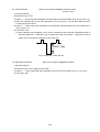
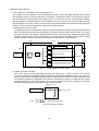
PART NO. 599910501
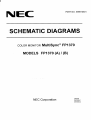
SERVICE MANUAL
COLOR MONITOR
MultiSync! FP1370
MODELS FP1370 (A) / (B)
NEC Corporation
200002
08109341
08109342
WARNING
The SERVICE PERSONNEL should have the appropriate technical training, knowledge and experience
necessary to:
・ Be familiar with specialized test equipment, and
・ Be careful to follow all safety procedures associated with high voltage CRT circuit designs to minimize
danger to themselves and their coworkers.
To avoid electrical shocks, this equipment should be used with an appropriate power code and be
connected only to a properly grounded AC outlet.
This equipment utilized a micro-gap power switch. Turn off the set by first pushing the front panel
power switch. Next, remove the power cord from the AC outlet.
To prevent fire or shock hazards, do not expose this unit to rain or moisture.
This symbol warns the personnel that un-insulated voltage within the unit may have sufficient
magnitude to cause electric shock.
This symbol alerts the personnel that important literature concerning the operation and
maintenance of this unit has been included.
Therefore, it should be read carefully in order to avoid any problems.
PRODUCT SAFETY CAUTION
1. When parts replacement is required for servicing, always use the manufacturer's specified replacement.
2. Comply with all caution and safety-related notes on the product display chassis and picture tube.
3. When replacing the component, always be certain that all the components are put back in the place.
4. When servicing display monitor unit, it is required that the provided lead dress is used in the high voltage
circuit area.
5. It is also recommended that shatter proof goggles are worn, when removing installing and handling the
picture tube.
People not equipped with the proper precautionary measures mentioned should keep the
picture tube away from body while handling.
6. As for a connector, pick and extract housing with fingers properly since a disconnection and improper
contacts may occur, when wires of the connector are led.
7. Use a proper screwdriver. If you use screwdriver that does not fit, you may damage the screws.
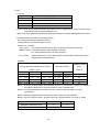
8. X-radiation precaution
This product contains critical electrical and mechanical parts essential for X-ray protection.
Normal anode voltage is 27.0 kV at zero beam picture tube current under AC 100-120V/220-240V input,
and anode voltage must not exceed the voltages shown below under any operation condition.
To measure anode voltage set brightness for very dim picture, and use a high impedance volt meter
between chassis and anode lead and measure high voltage.
If high voltage exceeds the specifications on the chassis schematic diagram, take the necessary
corrective action.
Table MAXIMUM ANODE VOLTAGE
beam current
at 0 mA
at 0.8 mA
at 1.4 mA
A/B
34.5 kV
32.5 kV
32.3 kV
9. When you degauss the set with an external degaussing coil, you must keep strictly item “ ※Notes
about degaussing method ” of ADJUSTMENT PROCEDURES.
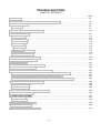
CONTENTS
Page No.
SPECIFICATIONS
1-1
CONTROLS
2-1
SERIAL NUMBER INFORMATION
3-1
ASSEMBLY
4-1
ADJUSTMENT PROCEDURES
5-1
INSPECTION
6-1
TROUBLE SHOOTING
7-1
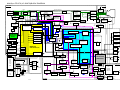
CIRCUIT DESCRIPTION
8-1
REPLACEMENT PARTS LIST
9-1
PRINTED WIRING BOARDS
10-1
BLOCK DIAGRAM
11-1
SPECIFICATIONS
Monitor Specifications
Picture Tube
Diagonal:
Viewable Image Size:
Radius:
MultiSync ® FP1370 ™ Monitor
55.3 cm / 22 inch
50.8 cm / 20 inch
57800 mm
Input Signal
Notes
90°deflection, 0.24 mm grille pitch,
Medium-Short persistence phosphor,
aperture grille CRT, multi-layered, antistatic screen coating, semi-dark-tint
screen, and OptiClear screen surface.
Video: ANALOG 0.7 Vp-p/75 Ohms
Sync: Separate sync. TTL Level
Horizontal sync. Positive/Negative
Vertical sync. Positive/Negative
Composite sync. (Positive/Negative) (TTL Level)
Sync on Green video (Positive) 0.7 Vp-p and sync.
(Negative) 0.3 Vp-p
Display Colors Analog input: Unlimited number of Colors
Depends on display card used.
Synchronization
Horizontal: 31 kHz to 130 kHz
Automatically
Automatically
Range
Vertical: 55 Hz to 160 Hz
Resolutions Supported
640 x 480 @ 60 to 160 Hz
Some systems may not support
Resolution based on horizontal 800 x 600 @ 55 to 160 Hz
all modes listed.
and vertical frequencies only
832 x 624 @ 55 to 160 Hz
1024 x 768 @ 55 to 154 Hz
1152 x 870 @ 55 to 137 Hz
1280 x 1024 @ 55 to 118 Hz
1600 x 1200 @ 55 to 102Hz …....
NEC cites recommended resolution
1792 x 1344 @ 55 to 91 Hz
at 85 Hz for optimal display
1800 x 1440 @ 55 to 85 Hz
performance
1856 x 1392 @ 55 to 88 Hz
1920 x 1440 @ 55 to 85 Hz
2048 x 1536 @ 55 to 80 Hz
Active Display Area Horizontal: 396 mm/15.6 inches
Dependent upon signal timing used,
and does not include border area.
(Factory Setting)
Vertical: 297 mm/11.7 inches
Active Display Area
406 mm/16.0 inches
Dependent upon signal timing used,
305 mm/12.0 inches
and does not include border area.
(Full Scan)
Power Supply
AC 100 - 120 V / 220 - 240 V, 50/60 Hz
Current Rating
2.4A @ 100 - 120 V / 1.1A@ 220-240 V
Dimensions
483 mm (W) x 501 mm (H) x 472 mm (D)
19.0 inches (W) x 19.7 inches (H) x 18.6 inches (D)
Weight
32.4 kg
71.4 lbs
Environmental Considerations
Operating Temperature: 10゚C to + 35゚C / + 50゚F to + 90゚F
Humidity: 30% to 80%
Altitude: 3,000 m / 10,000 Feet
Torage Temperature: -20゚C to + 60゚C / + 4゚F to + 140゚F
Humidity: 10% to 90%
Altitude: 13,700 m / 45,000 Feet
NOTE: Technical specifications are subject to change without notice.
1-1
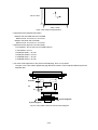
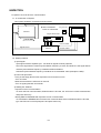
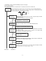
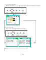
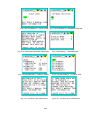
CONTROLS
TM
OSM
(ON-Screen Manager) control buttons on the front of the monitor function as follows:
EXIT
▲/▼
▼
-/+
+
PROCEED
Main Menu
Sub-Menu
Exits the OSM menu.
Moves the highlighted area up/down to
select one of the controls.
Moves the highlighted area left/right to
select one of the controls.
Has no function.
Exits to the OSM controls main menu.
Moves the highlighted area up/down to select
one of the controls.
Moves the bar in the - or + direction to
decrease or increase the adjustment.
Only executes control or enters sub, submenu.
Resets the highlighted control to the factory
setting.
Resets all the controls within the
highlighted menu to the factory setting.
RESET
NOTE : When RESET is pressed in the main and sub-menu, a warning window will appear allowing you to
cancel the reset function.
When OSM controls are activated, icons are displayed at the top of the menu.
If an arrow (
) is displayed in a sub-menu, it indicates further choices are available.
To enter a sub, sub-menu, press PROCEED.
Brightness/Contrast Controls
Brightness : Adjusts the overall image and background screen brightness.
Contrast : Adjusts the image brightness in relation to the background.
Degauss : Eliminates the buildup of stray magnetic fields which alter the correct scan of the electron
beams and affect the purity of the screen colors, focus, and convergence. When activated, your screen
image will jump and waver a bit as the screen is demagnetized.
Caution : Please allow a minimum of 20 minutes to elapse between uses of the Degauss Control.
Size and Position Controls
Auto Adjust : Automatically adjusts the horizontal and vertical size and position settings for applicable
signal timings.
Left/Right : Moves the image horizontally (left or right).
Down/Up : Moves the image vertically (up or down).
Narrow/Wide : Decreases or increases the horizontal size of the image.
Short/Tall : Decreases or increases the vertical size of the image.
RGB
R
Color Control / AccuColor Control System
Color Presets 1 through 5 selects the desired color setting. The bar is replaced by the color setting
choice from 1 to 5. Each color setting is adjusted at the factory to the stated Kelvin. If a setting is
adjusted, the name of the setting will change from Kelvin to Custom.
Red, Green, Blue : NEC’s AccuColor Control System decreases or increases the monitor’s red, green,
or blue color guns depending upon which is selected. The change in color will appear on screen and
the direction (decrease or increase) will be shown by the bars.
2-1
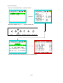
Geometry Controls
Geometry Controls Menu
The Geometry controls allow you to adjust the curvature or angle of the sides of your display.
Sides In/Out (pincushion): Decreases or increases the curvature of the sides either inward or outward.
Sides Left/Right (pincushion balance): Decreases or increases the curvature of the sides either to
the left or right.
Sides Tilt (parallelogram) : Decreases or increases the tilt of the sides either to the left or right.
Sides Align (trapezoidal) : Decreases or increases the bottom of the screen to be the same as the top.
Rotate (raster rotation) : Rotates the entire display clockwise or counterclockwise.
Tools 1
Moiré Canceler: Moiré is a wavy pattern which can sometimes appear on the screen. The pattern is
repetitive and superimposed as rippled images. When running certain applications, the wavy pattern is
more evident than in others. To reduce moiré, adjust the ON/Level by using the –/+ CONTROL buttons.
Basic Convergence: Aligns all three colors(R,G,B) to form a single color(white). The purpose of this
control is to ensure that a white line drawn on the screen is as crisp and clear as possible.
Use the Horizontal control to adjust the alignment of the white lines in the up/down direction.
Use the Vertical control to adjust the alignment of the white lines in the left/right direction.
Area Convergence: A small window will appear to indicate the area of adjustment - Top Horizontal,
Top Vertical, Bottom Horizontal or Bottom Vertical.
Corner Correction: Allows you to adjust the geometry of the corners of your display - Top, Top
Balance, Bottom or Bottom Balance.
Linearity: This selection allows you to adjust the spacing of the area on the screen. The purpose of
this control is to ensure that a one-inch circle is a true one-inch circle wherever it is on the screen.
The best way to determine the vertical linearity is as follows:
Draw equally spaced horizontal lines using a drawing application that has a ruler.
Use the Vertical Balance control to adjust the lines near the top and bottom of your screen.
Use the Vertical control to adjust the spacing between the lines near the center and top of your screen.
GlobalSync® Control: Eliminates picture impurities that may result from the earth’s magnetic field.
While in the sub-menus(GlobalSync, Top Left, Top Right, Bottom Left or Bottom Right), use the -/+
control buttons to fine tune the GlobalSync corrections.
Note: NEC recommends that you perform GlobalSync correction while running a typical application
such as a spreadsheet or text document.
Sharpness: Allows you to adjust the clarity of the image, based on the quality of the signal received
from the computer.
Use a full text document to make this adjustment.
Cycle through the four sharpness settings and select the one that provides the sharpness focus and
contrast of the text.
Factory Preset: Selecting Factory Preset allows you a reset most OSM™ control settings back to the
factory settings. A warning statement will appear to confirm that you do want to reset ALL settings.
Individual settings can be reset by highlighting the control to be reset and pressing the RESET button.
2-2
Tools 2
Language: OSM control menus are available in seven languages.
OSM Position: You can choose where you would like the OSM controls menu to appear on your
screen. Selecting OSM Position allows you to manually adjust the OSM controls menu left, right, up or
down.
OSM Turn Off: The OSM controls menu will stay on as long as it is in use. In the OSM Turn Off submenu, you can select how long the monitor waits after the last touch of a button for the OSM controls
menu to disappear. The preset choices are 10, 20, 30, 60 and 120 seconds.
OSM Lock Out: This control completely locks out access to all OSM controls functions except
Brightness and Contrast. When attempting to activate OSM controls while in the lock out mode, a
screen will appear indicating that OSM controls are locked out. To activate the OSM Lock Out function,
press PROCEED, then press ▲ and hold down simultaneously. To deactivate the OSM Lock Out,
press PROCEED, then press ▲ and hold down simultaneously.
IPM™ System Off Mode: Enable: The IPM System works normally and all stages of energy savings
are utilized.
Disable: The Off Mode of the IPM System is not used.
NOTE: For standard systems and graphics boards, keep the factory setting at ENABLE.
TM
EdgeLock Control: Operating your monitor at a non-standard timing may cause images to appear
darker than normal or have color distortion. Use of the EdgeLock control will adjust images to their
normal state.
Refresh Notifier: A message will advise you if the refresh rate of the signal being applied to the
monitor by the computer is too low. For further information, please refer to your display card or system
manual.
Information
Display Mode: Indicates the current mode and frequency setting of the monitor.
Fitness Tips: The fitness Tips provide you with helpful reminders to periodically rest your eyes. You
may select how frequently the remainders are displayed based upon your individual needs. Select an
interval from 15,30,45,60,90 or 120 minutes for the tips to appear. When the tips appear, follow the
advice of the tips and press EXIT to clear.
Monitor Info: Indicates the model and serial numbers of your monitor.
2-3
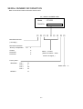
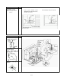
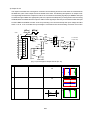
SERIAL NUMBER INFORMATION
Refer to the serial number information shown below.
EX.) SERIAL NUMBER LABEL
Model
: FP1370
Serial No. :
□ □ □ □ □ □ □ □ □
Manufactured Year :
( Last digit )
Manufactured Month :
January to September
1 to
9
October
X
November
Y
December
Z
00001 ~ on ward
( Start from 00001 ~ when
month is changed. )
Factory mark :
GEORGIA
MEXICO
Line 1
“K”
Line 2
“L”
Line 3
“M”
Line 4
“N”
Model mark … A
“A”
3-1
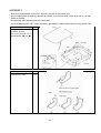
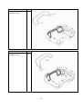
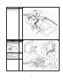
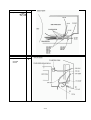
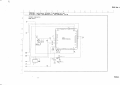
ASSEMBLY
・Before you disassemble the set, turn off power and pull out the power plug.
・Use the appropriate screwdrivers that fits the screws. If you use screwdriver that does not fit, you may
break the screws.
・Disassembly is the opposite process of assembly.
・Carefully discharge the CRT anode potential by grounding to coating dag before removing Anode Cap.
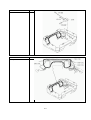
REMARK
SYMBOL
Clamp the EMF COIL with
CLAMPER. (4 point)
132
The thick of the EMF COIL is
placed between A and B .
REMARK
Forming(Corner Coil)
SYMBOL
133
4-1
REMARK
SYMBOL
Clamp the EMC COIL with
CLAMPER, WIRE.
133
REMARK
SYMBOL
Clamp the EMC COIL with
CLAMPER, WIRE.
133
4-2
REMARK
SYMBOL
Clamp the DEG COIL with
CLAMPER, WIRE.
134
REMARK
SYMBOL
Clamp the DEG COIL with
CLAMPER, WIRE.
(134)
4-3
REMARK
Mount the EMF PWB.
REMARK
SYMBOL
121E
SYMBOL
Clamp the connector.
4-4
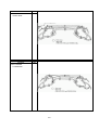
REMARK
SYMBOL
COIL FORMING
-UPPER SIDE-
REMARK
SYMBOL
COIL FORMING
-LOWER SIDE-
4-5
REMARK
SYMBOL
Mount LEAF SPRING(CRT)
and LEAF SPRING to the
PLATE, SHEILDING.
135
136
Mount CN-CE and COIL
SPRING to the PLATE,
SHEILDING.
137
138
EMC COIL’s wire
through under the
SPRING.(both sides)
pass
LEAF
Don’t change the form the
LEAF, SPRING.
REMARK
SYMBOL
4-6
REMARK
SYMBOL
Insert CN-DY and CN-CA to
CRT’s DY.
143
179
183
Note:
Don’t pull out CN-DY if you
insert it once.
SAFETY
Tie CN-DY, DY’s wires and
CN-ZDY with BAND(L=100)
as per sketch.
SAFETY
176
REMARK
SYMBOL
BUTTON
CABINET
139
140
Peel off the sheet of CNTROL
PANEL and attach PUSH
BUTTON(CONTROL)
to
CABINET FRONT ASSY.
141
Mount
PUSH
(CONTROL) to
FRONT ASSY.
Pass through the CN-ZDY
between
DY and
DY’s
connectors.
4-7
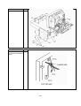
Screw CRT on CABINET, FRONT (4 point).
No.
The use of WASHER at setting CRT
1. Necessary to make sure the screw condition of each Lot.
Make sure the CABINET FRONT, it should not be whitish by stress
of securing screws. And make sure the gap between CABINET
FRONT and CRT. It must keep in tolerance.
2. In case of gap or changing color caused by stress, arrange the
thickness of washers.
REMARK
SYMBOL
Screw VIDEO PWB ASSY to
the
PLATE
SHEILDING
(BOTTOM).
121A
101
145
Screw PLATE SHEILDING
(VIDEO) to the VIDEO PWB
ASSY.
101
102
146
Insert
BUSH,INSULATOR,
CLAMPER, WIRE and EDGE,
SADDLE to the PLATE,
SHEILDING(BOTTOM).
114
147
148
Insert CN-SG and CN-HT to
the VIDEO PWB ASSY
149
150
4-8
DESCRIPTION
PART No.
Q’ty
142
WASHER (D20,D6.5,T2)
04
142
WASHER (D20,D6.5,T1)
or
142
WASHER (D20,D6.5,T1.2)
or
142
WASHER (D20,D6.5,T1.6)
or
142
WASHER (T0.5,P20)
or
142
WASHER, SPECIAL
or
REMARK
SYMBOL
Attach the CUSHION SHEET
on the SW/HV PWB ASSY.
175
REMARK
SYMBOL
Clamp CN-P with the EDGE
SADDLE.
(*1)
Screw the safety earth
terminal to the BRACKET
(VIDEO,A).
SAFETY
104
After the VIDEO PWB ASSY
mount the PWB FRAME,
connect the CN-SW1.
4-9
REMARK
SYMBOL
Clamp the wires with the
CLAMPER,WIRE as follows.
REMARK
Clamp the CN-CC.
Don’t touch copper wire of
IC4H1.
SYMBOL
155
122C
(Because copper wire is
easy to break.)
4-10
REMARK
SYMBOL
Clamp CN-CU with the
CLAMPER,WIRE as follows.
REMARK
SYMBOL
Clamp CN-CL and CN-LEB
with the CLAMPER,WIRE
(bottom side of the OUTER
SHIELDING).
After mounting the CABINET
FRONT ASSY to the FRAME
ASSY,SCREW
the
CASE,SHIELDING(CRT,F)
(To avoid broken CRT neck)
156
Dress CN-CL lead
to the right side of
the PWB FRAME
Don’t damage
PU PWB when
screwing
4-11
REMARK
SYMBOL
Tie CN-CL and CN-LEB
with BAND (L=100).
144
Insert a pencil between PLATE
SHIELDING CRT ASSY and CN-CL,
CN-LEB as per sketch.
Note:Use a pencil as a
spacer.
REMARK
SYMBOL
Clamp the leads of FBT
with the EDGE SADDLE.
Insert the Focus Lead to
the CRT Socket.
Push in Focus lead so
that the Line is all in the
CRT Socket.
Mount the Anode cap as
follows.
4-12
After tie BAND(L=100), pull out a pencil.
REMARK
SYMBOL
Mount the REVOLVING
STAND ASSY to the
CHASSIS BASE.
Degauss both the outside
and inside surfaces of
the CHASSIS BASE.
160
184
REMARK
SYMBOL
4-13
REMARK
SYMBOL
REMARK
SYMBOL
Clamp CN-CA, CN-CC
and CN-D with CLAMPER
WIRE.
4-14
REMARK
SYMBOL
Mount
the
ANODE
CLAMPER to ANODE
LEAD.
(True up the upper
ANODE CLAMPER and
above WHITE MARK.)
167
SAFETY
REMARK
SYMBOL
Screw the terminal from
HEAT SINK with DEF
PWB ASSY.
4-15
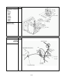
REMARK
SYMBOL
Before
screw
the
BRACKET(L), connect the
wires.)
CN-HDY
CN-VDY
CN-CR
CN-K
CN-DF
CN-SD
CN-ASD
CN-EMF
CN-ZDY
CN-CC
CN-CL
CN-PM
Clamp the wires.
(Detail next page.)
REMARK
SYMBOL
Clamp the wires.
SAFETY
4-16
REMARK
SYMBOL
Clamp the wires.
SAFETY
REMARK
SYMBOL
Clamp the wires.
21
▽
CN-ASD
CN-AF
4-17
REMARK
SYMBOL
Clamp the ANODE LEAD
with
the
CLAMPER
WIRE(H19.5)
119
SAFETY
Don’t change the form
the LEAF,SPRING.
169
REMARK
SYMBOL
4-18
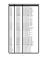
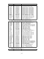
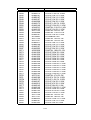
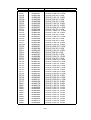
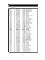
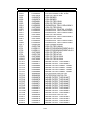
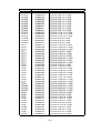
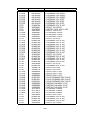
SYMBOL
PARTS No.
DESCRIPTION
Qty
101
102
103
104
2E853031
2E853031
24851731
24852341
CHEXIBS(CUP)*3*8*15CF
CHEXIBS(CUP)*3*8*15CF
SCREW,FT*4*16*15BF(S)
SCREW,WM*4*10*15CF(S)
54
05
06
01
114
115
119
25283461
25284061
25283111
EDGE SADDLE
CLAMPER,WIRE
CRAMPER WIRE (H19.5)
01
04
01
121
121
122
123
124
843E6C03
843E7C01
843E6B01
843E6D02
843E6A01
VIDEO PWB ASSY
VIDEO PWB ASSY
SUB PWB ASSY
DEF PWB ASSY
SW/HV PWB ASSY
01
01
01
01
01
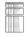
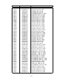
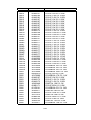
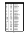
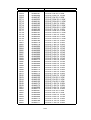
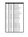
132
133
134
135
136
137
138
139
61322304
61322303
61322101
741X9741
741E9881
73891347
25534632
2E323932
COIL(50T,40H)
CORNER COIL(190T,50H)
DEGAUSSIING COIL(85T,10H)
LEAF SPRING(CRT)
LEAF SPRING
WIRE CONNECTOR CN-CE
COIL SPRING
CABINET FRONT ASSY
01
02
01
08
02
01
02
01
140
141
142
143
145
146
147
148
149
2E457751
25430551
24N00301
33022503
2E548181
744E0351
24282111
25282131
73891360
PUSH BUTTON(CONTROL)
CONTROL PANEL
WASHER(D20,D6.5,T2)
CRT M51LRY22X61
BRACKET(VIDEO.A)
PLATE,SHIELDING(VIDEO)
BUSHING,INSULATOR
EDGE SADDLE
WIRE CONNECTOR CN-SG
01
01
04
01
01
01
03
03
01
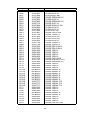
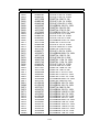
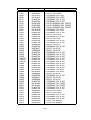
150
155
156
73891333
73891362
744E0311
WIRE CONNECTOR CN-HT
WIRE CONNECTOR CN-CC
CASE,SHIELDING(CRT,F)
01
01
01
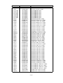
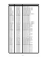
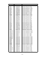
160
162
163
164
165
166
167
168
169
2E548061
744E0441
2E548141
2E548131
25280851
25281421
25282111
744E0431
741X4311
CHASSIS BASE
PLATE.SHIELDING(BOTTOM)
BRACKET(R.B)
BRACKET(L.B)
BUSHING,INSULATOR
PWB HOLDER
ANODE CLAMPER
PLATE.SHIELDING(BACK)
LEAF SPRING(CRT.B)
01
01
01
01
02
04
01
01
01
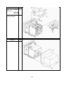
4-19
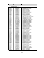
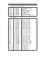
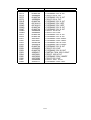
REMARKS
EMF
EMC
DEG
CN-CE
CRT
CN-SG
CN-HT
CN-CC
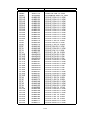
SYMBOL
PARTS No.
DESCRIPTION
170
172
173
174
175
176
179
744E0421
2E322123
843E6P01
25282992
25618341
24280701
73891431
PLATE.SHIELDING(TOP)
CABINET BACK
CONV PWB ASSY
CLAMPER WIRE (H29.5)
CUSHION SHEET
BAND (L=100)
WIRE CONNECTORE CN-DY
01
01
01
02
01
01
01
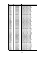
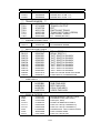
183
184
73891450
2E430782
WIRE CONNECTORE CN-CA
REVOLVING STAND ASSY
01
4-20
Qty
REMARKS
CN-DY
CN-CA
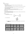
ADJUSTMENT PROCEDURES
Application
These specifications outline the adjustment procedures for Model FP1370 (A)/(B) 22-inch color monitor.
Model Name:
FP1370 (A)/(B)
Destination:
North America, Europe Standard Adjustment Conditions
Standard Adjustment Conditions
1. Power Supply Voltage
A / B Version:
AC 100V±5% 50/60Hz or AC 120V±5% 60Hz or
AC 220V±5% 50Hz
2. Warm Up
Adjust this monitor after a minimum of 90 minutes to allow unit to reach ambient operating temperature.
(Use the Self Test screen. Refer item 7-5-3. about Self Test. )
※ Adjust the monitor according to item “Rough Adjustment before warm up” before warm up.
※ When aging, cover with back cabinet or aging jig.
3. Signals
Unless otherwise specified, adjustment should be Mini D-SUB 15 pins.
Video:
Analog 0.7±0.01 Vp-p Positive polarity (terminated at 75 ohms±1%)
or
Analog sync. on green
Video 0.7±0.01 Vp-p positive polarity
Sync 0.3±0.01 Vp-p negative polarity
(terminated at 75 ohms ±1%)
Sync.:
TTL level (High level : more than 2.4V / Low level : less than 0.8V)
H/V separate, positive / negative polarity
or H/V composite, positive / negative polarity
or Sync. on green, 0.3±0.01 Vp-p negative polarity
(terminated at 75 ohms ±1%)
5-1
4. Magnetic Fields
Vertical Magnetic Fields: 40±1uT
Horizontal Magnetic Fields: 30±1uT
* Unless instructed otherwise, the CRT face should be facing to the east.
* Degauss the entire unit with an external degaussing coil for the adjustment.
※Notes about degaussing method
Follow the degaussing procedure below. (To prevent intertwinement of aperture grille)
1) Use cylinder-shaped degaussing coil.
Do not use ring degaussing coil. But ring degaussing coil can be
used at degaussing chassis.
2) In order to remove a magnetization from top sides, base shield and chassis, degauss each side.
Do not switch off the degaussing coil abruptly. Move the degaussing coil slowly when degaussing.
Note: If the degaussing coil is switched off near the set, the set will be magnetized.
3) To degauss panel surface
Switch on the degaussing coil, keep a distance between panel surface and degaussing coil to more than 50
cm. Move the degaussing coil vertically near the panel surface.
Keep distance of panel surface and degaussing coil to more than 15 mm.
Horizontal
Vertical
4) Degaussing method of CRT surface
Starting from edge of CRT, move the degaussing coil toward CRT center in circular motion, spending 6 to 7
seconds. (about 4 or 5 round )
When LED is orange in factory mode (“AUTO EMF ON” appear on OSM or TAG 3, TAG 4, TAG 5, TAG B,
TAG C is selected), Do not degauss.
In user mode, do not degauss except when “DEGAUSS OK” appear on OSM.
Service Factory MODE: Auto EMF function is off. (LED is yellow)
Auto EMF function off -> on (LED is orange.)
a. TAG 3, TAG 4, TAG5, TAG B, TAG C is selected.
b. When OSM MENU disappear, Push “+” and “!” switch at once.
Then “AUTO EMF ON” appear on OSM, and AUTO EMF function
is on state.
Push any switch and power on/off, AUTO EMF function become off state.
But when receive frequency change, AUTO EMF function stay on state.
5-2
User MODE: Auto EMF function is on.(LED is green)
Auto EMF function on -> off
a. Open the MENU (U),TAG7)-”DISPLAY MODE”, and Press “+” and
“▲” switch at once.
b. Then “DEGAUSS OK” appear on OSM, and AUTO EMF function is
on state.
When push any switch and power on/off, AUTO EMF function become
off state.
But when receive frequency change, AUTO EMF function stay on state.
5) After sufficiently degaussing the CRT, move degaussing coil slowly away from the panel surface while
rotating from corner to center, taking more than 3 seconds.
Turn off SW more than 1 m away from the CRT. Degauss again if the unit is gassed.
Over 1m
SW OFF
Magnetized Pattern Example
6) When aperture grille get entangled while degaussing, receive the signal of 1dot alternate pattern and
degauss again. If aperture grille remain entangled, Put vibrate from side.
5. Signal Generator
LVG-1603 is recommended for signal generator.
Use calibrated signal generators. However, use VG-819 in focus regulation.
Note) Adjustment timings are timing tables and are not programmed timing.
6. Color Analyzer, Convergence Meter, Landing Mater
The color analyzer should be CA-100 (made by MINOLTA) or compatible.
The convergence meter should be CC-100 (made by MINOLTA) or compatible.
The Landing meter should be KLD-01 (made by KAMAYA) or compatible.
5-3
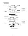
7. OSM Menu Operation
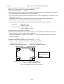
7-1. Front Panel
MultiSync
EXIT
!
+
"
PROCEED RESET BNC/D-SUB
(POWER SW)
7-2. OSM Menu
This unit is adjusted in on screen menu by front panel key operation.
There are 2 types of On Screen menu.
1) Menu (user): This Menu can be operated by a customer.
2) Menu (service): This Menu is hidden from a customer.
Here after, they will be called MENU (U) and MENU (S).
The menu can be displayed when the signal is input to the display unit.
7-3. FACTORY MODE
This model has function that is named "FACTORY MODE"
When the FACTORY MODE is
ON: LED indicator light is yellow usual. But when TAG 3, TAG 4, TAG 5, TAG B or TAG C is selected,
LED indicator light is orange.
Power management function does not work.
It is possible to enter MENU (S) by shortcut key.
OFF: LED indicator is GREEN when Horizontal and Vertical Sync Pulse are ON.
Power management function works when the Horizontal or (and) Vertical sync are OFF.
It is not possible to enter MENU (S) by shortcut key.
Always turn on “FACTORY MODE”, when adjust the monitor.
If the adjustment finish, should be “FACTORY MODE” OFF.
7-4. FACTORY MODE SETTING
7-4-1 FACTORY MODE: OFF ! ON
1)Open the MENU(U),TAG7-"DISPLAY MODE"(As below)
2)Press "RESET" and "!",""" switch at once.
3)A "WARNING" will be displayed, then press "PROCEED" switch once.
4)LED indicator light turn to Yellow from Green.
7-4-2 FACTORY MODE ON → OFF
1) When OSM MENU is displayed, press "EXIT" switch twice. Otherwise, press "EXIT" switch once.
2) A "WARNING" will be displayed, then press "EXIT" switch once.
3) LED indicator light turns to Green from Yellow.
5-4
7-5. Displaying the OSM.
7-5-1 FACTORY MODE: OFF
MENU(U):Press "EXIT" or "+" , "-" , "!" , """ , "PROCEED" once .
MENU(S):Open MENU, TAG7 "INFORMATION" - "DISPLAY MODE”, and press "RESET" and
"!" , """ switch at once.
A warning message will be displayed, then press "PROCEED" switch.
7-5-2 FACTORY MODE: ON
MENU(U):Press "+" , "-" or "!",""" switch.
MENU(S):Press "PROCEED" switch once.
7-5-3 Self Test
When FACTORY MODE is ON, Self test is on by no signal.
When FACTORY MODE is OFF, Self test in on by power on with pushing “RESET” switch.
7-6. How to turn off OSM MENU
* To close the Menu
Press "EXIT" switch while MENU (U) or MENU (S) is displayed
TAG is highlighted
: 1 time.
ITEM is highlighted
: 2 times.
Entering SUB MENU
: 3 times
* To close MENU temporarily.
Press "PROCEED" once, while MENU (S) is being displayed.
Press "PROCEED" once more, MENU (S) is displayed again.
5-5
7-7. TAG, Item, Sub Menu Change
TAG to TAG
: Push "-" SW or "+" SW.
TAG to item
: Push "!" SW or """ SW
: Push "PROCEED" SW once.
Item to sub Menu
Sub Menu to item
: Push "!" SW or """ SW.
: Push "EXIT" SW once.
Item to TAG
: When top item is selected, push "!" SW.
Item to item
When bottom item is selected, push """ SW.
Push "EXIT" all items.
TAG
ITEM
7-8. To change Data values
Data values are changed by pressing "-" or "+" switch.
7-9. To save Data Value.
Data values are saved for EEPROM, while highlighted ITEM is changed.
5-6
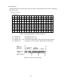
OSD MENU (S)
TAG1
H.SIZE MAX.1
H.SIZE MAX.2
H.D.FOCUS
V.D.FOCUS
H.LINEARITY1
H. LINEARITY2
SLFTST SYNC BAND
TAG2
V.LINEARITY
V.LIN.BALANCE
V.SIZE MAX
V.RASTER CENTER
H.POSITION
V.POSITION
H.SIZE
V.SIZE
TAG3
SIDE PIN
SIDE PIN BAL.
ALIGN
TILT
S-WAVE
SIDE WING
ROTATE
TAG4
CORNER TOP
CORNER TOP BAL.
CORNER BOTTOM
CORNER BOTTOM BAL.
TAG5
GLOBALSYNC
EMF TOP RIGHT
EMF TOP LEFT
EMF BOTTOM RIGHT
EMF BOTTOM LEFT
TAG6
MOIRE OFFSET
MOIRE PARABOLA T
MOIRE PARABOLA B
MOIRE SAW TOP
MOIRE SAW BOTTOM
5-7
TAG7
GAIN
R GAIN
G GAIN
B GAIN
OSM COLOR GAIN
TAG8
SUB BIAS
R BIAS
G BIAS
B BIAS
CONTRAST MAX/MIN
TAG9
G SUB BRIGHT
B SUB BRIGHT
R SUB BRIGHT
TAGA
1 2 3 4 5 (COLOR PRESET)
R COLOR GAIN
G COLOR GAIN
B COLOR GAIN
CONT.MAX.ADJ.
TAGB
H.S.CONVER
V.S.CONVER
ROW
COLUMN
4H
4V
TAGC
H.CONVER SAW T
H.CONVER PARA T
H.CONVER SAW B
H.CONVER PARA B
V.CONVER SAW T
V.CONVER PARA T
V.CONVER SAW B
V.CONVER PARA B
TAGD
AUTO ADJUST H
AUTO ADJUST L
DESTINATION
CONTRAST PRESET
HOURS READ
5-8
TAGE
HOURS RUNNING:ON
:STANDBY
:SUSPEND
ROM:
CPU VERSION
OSD MENU (U)
TAG1 (BRT&CONT)
BRIGHTNESS
CONTRAST
DEGAUSS
TAG2 (SIZE&POSITION)
AUTO ADJUST
LEFT/RIGHT
DOWN/UP
NARROW/WIDE
SHORT/TALL
TAG3 (COLOR CONTROL)
1 2 3 4 5 (COLOR PRESET)
RED
GREEN
BLUE
TAG4 (GEOMETRY)
IN/OUT
LEFT/RIGHT
TILT
ALIGN
ROTATE
5-9
TAG5 (TOOL1)
MOIRE CANCELER
---- OFF
ON / LEVEL
BASIC CONVERGENCE---HORIZONTAL
VERTICAL
AREA CONVERGENCE ---TOP HORIZONTAL
TOP VERTICAL
BOTTOM HORIZONTAL
BOTTOM VERTICAL
CORNER
CORRECTION ---- TOP
TOP BALANCE
BOTTOM
BTM BALANCE
LINEARITY
---VERTICAL
VERTICAL BALANCE
GLOBALSYNC
---- GLOBALSYNC
TOP LEFT
TOP RIGHT
BOTTOM LEFT
BOTTOM RIGHT
SHARPNESS
---- 1 / 2 / 3 / 4
FACTORY PRESET
TAG6 (TOOL2)
LANGUAGE
OSM POSITION
---- ENGLISH / DEUTSCH / FRANCAIS / ESPANOL /
ITALIANO / SVENSKA / JAPANESE
---- LEFT/RIGHT
DOWN/UP
---- 10 / 20 / 30 / 60 / 120 SECONDS
OSM TURN OFF
OSM LOCK OUT
IPM
---ENABLE / DISABLE
EDGE LOCK
---- 1 / 2
REFRESH NOTIFIER ---- ON / OFF
TAG7 (INFOMATION)
DISPLAY MODE
FITNESS TIPS
---MONITOR INFO
OFF / 15 / 30 / 45 / 60 / 90 / 120 MINUTES
5-10
ADJUSTMENT ITEMS
[A] Pre-Adjustment
1. High-Voltage Adjustment
SAFTY
(When circuit board energizing is examined.)
[B] Initial Settings
1. Control Setting
[C] Main Adjustment
1. Raster Position
1-1. Horizontal Raster Position
1-2. Vertical Raster Position
2. Linearity Adjustment
2-1. Horizontal Linearity Adjustment
2-2. Vertical Linearity Adjustment
3. Horizontal / Vertical Maximum Size Adjustment
3-1. Horizontal Maximum Size Adjustment
3-2. Vertical Maximum Size Adjustment
4. Deflection Distortion Adjustment
4-1. Horizontal / Vertical Size Rough Adjustment
4-2. Picture Tilt Adjustment
4-3. Side Pincushion Balance Adjustment
4-4. Side Pincushion Adjustment
4-5. Trapezoid distortion Adjustment
4-6. Parallelogram Distortion Adjustment
4-7. Horizontal W-wave Distortion Adjustment
4-8. Vertical S-wave Distortion Adjustment
4-9. Corner Distortion Adjustment
4-10. Overall Distortion Adjustment
5. Preset Picture Size and Position Adjustment
6. Video Amplitude Adjustment
6-1. Settings
6-2. Video Amplitude
6-3. OSM Gain Adjustment
SAFTY
6-4. Cut Off Adjustment
6-5. Contrast Tracking Adjustment
6-6. Brightness Tracking Adjustment
6-7. Color Preset Adjustment
6-8. Maximum Brightness Adjustment
6-9.Contrast preset adjustment
7. Focus Adjustment
8. Purity
9. Convergence Adjustment
10. Auto adjustment
[D] Reference
1. Adjustment Signal
2. Adjustment Signal timing
3. Connector , test pins
SAFTY : This MARK is important adjustment item for products safety.
5-11
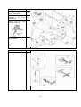
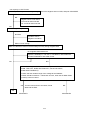
[A] Pre-Adjustment
1. High-Voltage Adjustment
Initial Setting
Signal 3 (VGA480) All Black
SAFTY
SCREEN VR: Fully counterclockwise (MIN)
VR5T1: Fully counterclockwise (MIN)
This adjustment is made when circuit board energizing is examined.
1) Receive signal 3.
2) Adjust VR5T1 slowly so that high voltage is 27kV±0.2kV.
After adjusting, seal VR5T1 with a silicon adhesive and cap (Part No. 74106841).
[B] Initial Settings
1. Control Setting
Before adjusting, set the position of control as follows.
FBT
SCREEN VR
: Fully counterclockwise (MIN)
FOCUS F1
: Mechanical center
FOCUS F2
VR581
SW581
: Mechanical center
: Fully clockwise (MAX)
: CRT side
[C] Main Adjustment
Use this manual for aligning the monitor.
1) Push "RESET" SW to reset a highlighted item.
2) Close OSM menu and turn the power off.
3) Turn the monitor back on and confirm that the adjustment values / contrast / white balance / distortion
values are the same before the Menu was closed.
When "PROCEED" SW is pushed by the condition which Menu (S) is displayed, OSM Menu will
disappear. If "PROCEED" SW is pushed once more, OSM displays)
4) A highlight displays items of TAG 3, TAG 4, TAG 5, TAG B and TAG C, AUTO EMF function becomes
ON, and Landing Rotation Convergence alters.
When it is moved from this items to the tag after the adjusted, AUTO EMF function is turned off,
and Landing Rotation Convergence alters.
Previous setting
Signal: No. 3 (VGA480) All White
1) Screen VR setting
Open Menu (U), TAG 1 "BRIGHTNESS & CONTRAST" and push "RESET" SW.
Adjust SCREEN VR so that the back-raster is just disappeared.
2) FOCUS VR setting
Display OSM menu and adjust FOCUS F1 VR and F2 VR to be able to recognize characters.
3) Rough Adjustment before warm up
Signal: No. 7 (VESA350@85) All White
Signal: No. 13 (MAC832*624) All White
Signal: No. 36 (H.HOLD2(130k) All Black
Signal: No. 29 (V.RASTER) All White
5-12
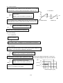
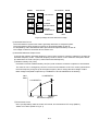
a. Rough adjustment of horizontal raster position
1) Receive signal 36.
2) Adjust SCREEN VR on the FBT so that the back raster just appears.
3) Make sure to set the position of control as follows :
VR581 (on the DEF PWB)
: Fully clockwise (MAX)
SW581 (on the DEF PWB)
: CRT side
4) Open Menu (S), TAG2 “H.SIZE” and adjust the horizontal size to inside the bezel.
5) If raster has approached on the left of displayed area, switch SW581 position to the CRT side.
If raster has approached on the right of displayed area, switch SW581 position to VR581 side.
6) Adjust VR581 so that the raster edge is centered in the bezel.
b. Rough adjustment of vertical horizontal raster position
1) Receive signal 29. All White
2) Menu (S), TAG2 data on ”V.LINEARITY" are 90, and it confirms that data on "V.LIN.BALANCE" are 128.
* When data are not 90 and 128, Open TAG2 ”V.LINEARITY" and TAG2 "V.LIN.BALANCE",
and set up data.
3) Open Menu (S), TAG2 "V.SIZE", adjust "+", "-" SW so that the vertical raster size is 297±3.0 mm.
4) Open Menu (S), TAG 2 "V.RASTER CENTER" and push "RESET" SW.
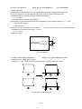
5) Adjust the vertical raster and the space of the edge as listed below by switch. (Fig 1-2 reference)
| Ytop - Ybottom | " 1.0mm
6) Push "EXIT" SW.
c. Rough adjustment of self test screen
1) Receive signal 7.
2) Open Menu (S), TAG1”. Make sure that data on " SLFTST SYNC BAND " is “1”.
3) Open Menu (S), TAG2 "V.POSITION" and adjust "+", "-" SW so that the picture is centered with in
the screen.
4) Open Menu (S), TAG2 "V.SIZE" and adjust it so that top and bottom picture size may be 3-5mm
from the bezel. When picture doesn't spread out, open Menu (S), TAG2 "V.SIZE MAX".
If not able to set picture size, open Menu (S), TAG2 "V.SIZE MAX", adjust so that screen may
become full with the bezel. And open Menu (S), TAG2 "V.SIZE" and adjust it so that top and bottom
picture size may be 3-5mm from the bezel.
5) Receive signal 13.
6) Open Menu (S), TAG2 “H.SIZE” and adjust the picture size is just the bezel.
7) Display the self test screen.
Note) Make sure that the screen is one image.
If there is not stable, Open Menu (S),TAG1” SLFTST SYNC BAND” and adjust “-“ SW so that
the data is “0”
8) Make sure that the picture size is just the bezel.
d. Screen VR Adjustment
1) Display the self test screen.
2) Adjusted with the screen VR so that the voltage of the video PWB TP-ABL may become
4.64 (V) <ABL<8.14 (V).
5-13
1. Raster Position
1-1. Horizontal Raster Position
Signal: No.36 (H.HOLD 2(130k)) All Black
1) Receive signal 36.
2) Adjust SCREEN-VR on the FBT so that the back raster just appears.
3) Make sure to set the position of control as follows.
VR581: Fully clockwise (MAX).
SW581: Set position to the CRT side.
4) Open Menu (S), TAG2 "H.SIZE", Horizontal Size and adjust "+", "-" SW so that the horizontal size is
396±2.0 mm.
5) If raster has approached on the left of displayed area, change the SW581 position to the CRT side If
raster has approached on the right of displayed area, change the SW581 position to the VR581 side.
6) Adjust VR581 so that the distance between the bezel and raster edge is as follows.
| XLeft-XRight | " 1.0 mm
Bezel
Raster
XLeft
XRight
396±2.0mm
Fig 1-1 Horizontal Raster Centering
5-14
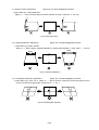
1-2. Vertical Raster Position
Signal: No. 29 (V.RASTER) All White
1) Receive signal 29.
2) Menu (S), TAG2 data on "V.LINEARITY" are 90, and it confirms that data on "V.LIN.BALANCE" are 128.
* When data are not 90 and 128, Open TAG2 "V.LINEARITY" and TAG2 "V.LIN.BALANCE", and set up data.
Open Menu (S), TAG2 "H.SIZE" and adjust "+" SW so that the vertical raster size is 297±3.0 mm.
3) Open Menu (S), TAG 2 "V.RASTER CENTER" and push "RESET" SW.
4) Adjust the vertical raster and the space of the edge as listed below by switch. (Fig 1-2 reference)
|Ytop - Ybottom | " 1.0mm
5) Push "RESET" SW.
Bezel
Y top
Raster
297#3.0mm
Y bottom
Fig 1-2 Vertical Raster Centering
5-15
2. Linearity Adjustment
2-1. Horizontal Linearity Adjustment
Signal: No. 17 (1024*768@75Hz)
Cross hatch pattern
Signal: No. 23 (1600*1200@85Hz)
Cross hatch pattern
* Hereunder integrate is done when value of control former "H.LINEARITY 1:60" and "H.LINEARITY 2:180"
come off the value of standardized.
1) Receive signal 23.
2) Open Menu (S), TAG2 "H.POSITION" and adjust "+", "-" SW so that the picture is centered with in the screen.
3) Open Menu (S), TAG2 "H.SIZE" and adjust "+" SW so that the horizontal size is 396±3 mm. If not able
to set horizontal size, open Menu (S), TAG1 "H.SIZE MAX 2", adjust the horizontal size is 396 mm.
After, Data on "H.SIZE" adjusted to the maximum (255).
4) Open Menu (S), TAG1 "H.LINEARITY 2" and adjusted so that the horizontal direction width of the
second square may become the same from both ends of the screen.
Note: When a OSM Menu is hidden temporarily for picture adjustment, push "PROCEED " SW once to
display OSM Menu.
5) Receive signal 17.
6) Open Menu (S), TAG2 "H.POSITION" and adjust "+", "-" SW so that the picture is centered with in the screen.
7) Open Menu (S), TAG2 "H.SIZE" and adjust "+" SW so that the horizontal size is 396±3 mm. If not able
to set horizontal size, open Menu (S), TAG1 "H.SIZE MAX 2", adjust the horizontal size is 396 mm. After,
Data on "H.SIZE" adjusted to the maximum (255).
8) Open Menu (S), TAG1 "H.LINEARITY 1" and adjusted so that the horizontal direction width of the
second square may become the same from both ends of the screen.
Note: When a OSM Menu is hidden temporarily for picture adjustment, push "PROCEED " SW once to
display OSM Menu.
9) Push "EXIT" SW.
2-2. Vertical Linearity Adjustment
Signal: No. 22 (1600*1200@75Hz)
Cross hatch pattern
1) Receive signal 22.
2) Open Menu (S), TAG2 "V.POSITION" and adjust "+", "-" SW so that the picture is centered with in the screen.
3) Open Menu (S), TAG2 "V.SIZE" and adjust "+" SW so that the vertical size is 297±3 mm. If not able to
set vertical size, open Menu (S), TAG2 "V.SIZE MAX", adjust the vertical size is 297±3 mm. After open
Menu (S), TAG2 "V.SIZE" so that the data is max (255).
4) Open Menu (S), TAG2 "V.LINEARITY" and adjust "+", "-" SW to make size of top square and bottom
square on the screen equal vertically.
Note: When a OSM Menu is hidden temporarily for picture adjustment, push "PROCEED " SW once to
display OSM Menu.
5) Open Menu (S) TAG2 "V.LIN.BALANCE" and adjust "+", "-" SW to make size of top square and bottom
square on the screen equal vertically.
6) Open Menu (S) TAG2 "V.LINEARITY" again and adjust "+", "-" SW to make size of top square and
center square on the screen equal vertically.
7) Make sure that the linearity of top, center, and bottom on the screen are under ±3%.
8) Push "EXIT" SW.
5-16
3. Horizontal / Vertical Maximum Size Adjustment
3-1. Horizontal Maximum Size Adjustment
Signal: No. 13 (MAC832*624) All white
Signal: No. 35 (H.SIZE) All white
1) Receive signal 13.
2) Open Menu (S), TAG2 "V.SIZE" and adjust "+", "-" SW so that the vertical size is 297±5 mm.
If not able to set vertical size, open Menu (S), TAG2 "V.SIZE MAX", adjust the vertical size.
And open Menu (S), TAG2 "V.SIZE" and adjust vertical size.
3) Open Menu (S), TAG3 "IN / OUT" and adjust "+", "-" SW to correct side pincushion distortion.
4) Open Menu (S), TAG1 "H.SIZE MAX.1", push “RESET”SW and make sure that "H.SIZE MAX.1" is set to 1.
5) Open Menu (S), TAG1 "H.SIZE MAX.1", and adjust "+", "-" SW so that video horizontal size may become
full with the bezel.
6) Receive signal 35.
7) Open Menu (S), TAG2 "H.POSITION", rough adjust so that video area may become in the center of the screen.
8) Open Menu (S), TAG1 "H.SIZE MAX. 2", and push "EXIT" SW. It confirms that data on "H.SIZE MAX.1"
are 0.
9) Open Menu (S), TAG1 "H.SIZE MAX. 2", and adjust "+", "-" SW so that video horizontal size may become
full with the bezel.
10) Push "EXIT" SW.
3-2. Vertical Maximum Size Adjustment
1) Receive signal 28.
Signal: No. 28 (V.MAX) All white
2) Open Menu (S), TAG2 "V.POSITION" and adjust "+", "-" SW so that the picture is centered in the screen.
3) Open Menu (S), TAG3 "V.SIZE MAX", push “RESET”SW and adjust "+", "-" SW so that the vertical size is
297±3 mm.
4) Push "EXIT" SW.
5-17
4. Deflection Distortion Adjustment
Environment: Adjustment Magnetic Field by three dimension magnetic field system.
Turn the CRT face to east and degauss the monitor using an external degaussing coil.
*When distortion amount is confirmed in the hereunder adjusted, It is made the condition that items of the
menu tag 3 or 4 is select, or PROCEED is used in the condition that items is select, and turn off condition
the OSM.
*After 4-1 section and 4-2 section are adjusted, Redo adjusts 4-3 sections to 4-8 sections in the case of the
manual adjustment. When distortion left at the top-bottom corner, the adjusted of 4-9 section is done by
this adjustment. 4-10 section is confirmed at the end.
4-1. Horizontal / Vertical Size Rough Adjustment
Signal: No. 33 (788*1200@75Hz) All white
1) Open Menu (S), TAG2 "H.POSITION", "V.POSITION", "H.SIZE", "V.SIZE" and adjust the screen size to
the following values.
Horizontal Size: 396 mm±3 mm
Vertical Size: 297 mm±3 mm
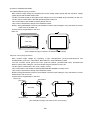
Horizontal Picture Position: | Xleft - XRight | " 3.0 mm
Vertical Picture Position: | XTop - XBottom | " 2.0 mm
Xleft
XRight
XTop
XBottom
Fig 4-1 Screen Size Rough Adjustment
5-18
4-2. Picture Tilt Adjustment
Signal: No. 33 (788*1200@75Hz)
Cross Hatch Pattern
1) Receive signal 33.
2) Open Menu (S) TAG3 "ROTATE" and make sure that initial value of adjustment data is "128".
3) Turn the CRT face to east and degauss the monitor using an external degaussing coil.
4) Make sure that the picture tilt meets the following specification.
X " ± 2.0 mm
If out of specification, correct CRT assembly.
5) Open Menu (S) TAG3 "ROTATE" and make sure that the picture is tilted as follows by "+", "-" SW.
"-" SW: counterclockwise
"+" SW: clockwise
6) Open Menu (S) TAG3 "ROTATE" and adjust "+", "-" SW so that the picture tilt meets the following
standards. The maximum correction is ±1.0mm.
X " ± 1.0 mm
7) Push "EXIT" SW.
+X
-X
Fig 4-2 Picture Tilt
4-3. Side Pincushion Balance Adjustment
Signal: No. 33 (788*1200@75Hz) All white
1) Open Menu (S), TAG3 "SIDE PIN BAL".
Adjust "+", "-" SW so that the difference of XSl and XSr is equal ( maximum 1.0 mm).
×
Xsl
Xsr
×
Xsl
Xsr
Fig 4-3 Side Pincushion Balance
5-19
4-4. Side Pincushion Adjustment
Signal: No. 33 (788*1200@75Hz) All white
1) Open Menu (S), TAG3 "SIDE PIN".
Adjust "+", "-" SW so that the side pincushion distortion is small ( maximum ± 0.5 mm).
A
A
B
C
B
C
Fig 4-4 Side Pincushion
4-5. Trapezoid Distortion Adjustment
Signal: No. 33 (788*1200@75Hz) All white
1) Open Menu (S), TAG3 "ALIGN".
Adjust "+", "-" SW so that the Trapezoid Distortion is equal to Xtop and Xbtm. (|Xtop - Xbtm| " 1.0 mm)
Xtop
Xtop
Xbtm
Xbtm
Fig 4-5 Trapezoid Distortion
4-6. Parallelogram Distortion Adjustment
Signal: No. 33 (788*1200@75Hz) All white
1) Open Menu (S), TAG3 "TILT". Adjust "+", "-" SW so that the vertical line and horizontal line at the
screen's center fall at right angles. (maximum 90゚ ± 0.5゚)
Fig 4-6 Parallelogram Distortion
5-20
4-7. Horizontal W-wave Distortion Adjustment
Signal: No. 33 (788*1200@75Hz) All white
1) Open Menu (S), TAG3 " SIDE WING ".
Adjust "+", "-" SW so that the side vertical line is about straight. (maximum ± 0.5 mm)
Center line
Fig 4-7 Horizontal W-wave Distortion
4-8. Vertical S-wave Distortion Adjustment Signal No. 33 (788*1200@75Hz) All white
1) Open Menu (S), TAG3 "S.WAVE".
Adjust "+", "-" SW so that the side vertical line is about straight. (maximum ± 0.5 mm)
Center line
Fig 4-8 Vertical S-wave Distortion
If Trapezoid Distortion is out of specification, repeat adjustment step 4-5.
It implements this adjustment in case of the following Undulation distortion.
Undulation is a directional difference of tilt at AB and DE.
Following figures (I) and (II) are example.
A
B
C
D
E
( || )
(|)
(
Fig 4-9 Vertical S-wave Distortion Definition
5-21
4-9. Corner Distortion Adjustment
Signal: No. 33 (788*1200@75Hz) All white
Do this integrate when distortion is adjust in the top or the bottom after the integrate to 4-8 sections.
4-9-1. Top Corner Distortion Adjustment
1) Open Menu (S), TAG4 "CORNER TOP".
Adjust "+", "-" SW so that the top corner forms a right angle. (maximum ±1.0 mm)
Fig 4-10 Top Corner Distortion
4-9-2. Bottom Corner Distortion Adjustment
1) Open Menu(S), TAG4 "CORNER BOTTOM".
Adjust "+", "-" SW so that the bottom corner forms a right angle. (maximum ±1.0 mm)
Fig 4-11 Bottom Corner Distortion
4-9-3. Top Corner Balance Adjustment
1) Open Menu(S), TAG4 "CORNER TOP BAL"
.Adjust "+", "-" SW so that the top corner forms a right angle. (maximum ±1.0mm)
Fig 4-12 Top Corner Balance
4-9-4 Bottom Corner Balance Adjustment
1) Open Menu (S), TAG4 "CORNER BOTTOM BAL".
Adjust "+", "-" SW so that the bottom corner forms a right angle. (maximum ±1.0 mm)
Fig 4-13 Bottom Corner Balance
5-22
4-10. Overall Distortion Adjustment
Signal: No. 33 (788*1200@75Hz) All white
1) Confirm that adjustment on steps 4-2 to 4-9 meets the specifications.
2) If undulating, re-adjustment each distortion adjustment.
Undulation is a directional difference of tilt at either AC and CE or both.
Following figures (I) and (II) are example. AB and BC, CD and DE are the direction of tilt.
Undulated correction is the same direction of tilt at AB and BC, CD and DE.
Following figures (III) and (IV) are example. In this state, each adjustment standard must be met.
A
B
C
D
E
(|)
( || )
( ||| )
( |V )
Fig 4-14 Undulated Definition
5. Preset Picture Size and Position Adjustment
Signal: No. 3 (VGA480)
No. 6 (MAC 640*480)
No.12 (VESA 640*480@85Hz)
No.13 (MAC 832*624)
No.14 (800*600@85Hz)
Video:
No.17 (1024*768@75Hz)
No.21 (1280*1024@75Hz)
No.22 (1600*1200@75Hz)
No.23 (1600*1200@85Hz)
No.32 (1280*1024@85Hz)
All White
1) Receive signal 3.
2) Open Menu (S), TAG2 "H.POSITION", "V.POSITION", "H.SIZE", "V.SIZE".
3) Adjust the picture size and position as listed below by "+", "-" SW.
Picture size
H: 396 ± 1.0 mm
V: 297 ± 1.0 mm
Picture Position
H: | XLeft – XRight | " 1.0 mm
V: | XTop – XBottom | " 1.0 mm
4) Push "EXIT" SW.
5) Receive the next signal and repeat steps 2) - 4).
Note: Before receiving the next signal, always push "EXIT" SW to store adjustments.
XTop
Bezel
VIDEO
XLeft
XRight
XBottom
Fig 5-1 Picture Position
5-23
6) For the signals below, picture size and position are calculated from above adjustment data and data are written
into EEPROM.
Preset Signal:
No. 1 (VGA350)
No.10 (XGA)
No. 2 (VGA400)
No.11 (VESA800*600@75Hz)
No. 4 (640*400@70Hz)
No.15 (1024*768@70Hz)
No. 5 (800*600@60Hz)
No.16 (1280*1024@60Hz)
No. 7 (VESA350@85Hz)
No.18 (Mac1152*870)
No. 8 (VESA400@85Hz)
No.19 (1024*768@85Hz)
No. 9 (VESA640*480@75Hz)
USER Signal:
USER1 (PC98 1120*750(I))
USER15 (800*600@120Hz)
USER2 (VESA 800*600@56Hz)
USER16 (640*480@160Hz)
USER3 (VESA 1024*768@60Hz)
USER17 (VESA 1920*1440@60Hz)
USER4 (VESA 800*600@72Hz)
USER18 (1600*1200@70Hz)
USER5 (1120*750@60Hz)
USER19 (800*600@140Hz)
USER6 (640*480@100Hz)
USER20 (VESA 1792*1344@75Hz)
USER7 (XGA-2 1024*768@75Hz)
USER21 (VESA 1600*1200@80Hz)
USER8 (800*600@100Hz)
USER22 (1024*768@120Hz)
USER9 (640*480@120Hz)
USER23 (800*600@160Hz)
USER10 (640*480@140Hz)
USER24 (VESA 1920*1440@75Hz)
USER11 (VESA 1600*1200@60Hz)
USER25(VESA 1792*1344@85)
USER12 (1280*1024@70Hz)
USER26 (VESA 2048*1536@80Hz)
USER13 (1152*864@85Hz)
USER27 (VESA 1920*1440@85Hz)
USER14 (1024*768@100Hz)
5-24
6. Video Amplitude Adjustment
6-1. Settings
Signal: No. 23 (1600*1200@85Hz)
All White
NOTE: Degauss the monitor using an external degaussing coil.
1) Confirm that the video signal of generator is as follows.
Video: Analog 0.7Vp-p ± 0.01V p-p (terminated 75 ohms ± 1 %)
2) Receive signal No.23 (All White), confirms that there is screen size of hereunder span.
It is adjust in menu TAG 2 (S),"H.SIZE", "V.SIZE", "H.POSITION", "V.POSITION" in the case
as the outside of the span.
Horizontal Size
Vertical Size
: 396±3mm
: 297±3mm
Horizontal picture position: |XLeft - Xright | " 3.0mm
Vertical picture position : |Xtop - Xbottom | " 3.0mm
3) Open Menu (S), TAG 7,TAG 8,TAG 9,TAG A, TAG D and make sure that the following values.
Menu (S), TAG 7
Menu (S), TAG 8
GAIN
: 200
SUB BIAS
: 255
R GAIN
: 200
R BIAS
:0
G GAIN
: 200
G BIAS
:0
B GAIN
: 200
B BIAS
:0
OSM COLOR GAIN:5
Menu (S), TAG 9
G SUB BRIGHT : 150
Menu (S), TAG A
COLOR PRESET : 1(9300K)
B SUB BRIGHT : 150
R COLOR GAIN : 255
R SUB BRIGHT : 150
G COLOR GAIN : 255
B COLOR GAIN : 255
CONT.MAX.ADJ. : 150
Menu (S), TAG D
CONTRAST PRESET: 150
5-25
6-2. Video Amplitude
Signal: No.23 (1600*1200@85Hz) Window Pattern
(H:33% V:33%)
1) Receive signal 23.
2) Open Menu (S), TAG7.
3) Adjust "+", "-" SW so that video amplitude at TP-R (R GAIN) on the CRT PWB is set to 45 Vp-p (+0V/ -1V).
4) When the indicated value of the video amplitude is not 45 Vp-p(+0V/ -1V) with Gain data maximum,
increase the R Gain values.
5) Adjust "+", "-" SW so that video amplitude at TP-G (G GAIN) ,TP-B (B GAIN) on the CRT PWB is set to
45 Vp-p(+0V/ -1V)
6) Push "EXIT" SW
※ When adjusting video amplitude, move cursor to desired function and push PROCEED button to
hide the OSM menu. Adjustment can be made with OSM menu hidden. OSM menu must be
hidden since its amplitude will appear on the wave form.
45 +0/-1 Vp-p
Fig 6-1 Wave form of RK, GK, BK
6-3. OSM Gain Adjustment
Signal: No.23 (1600*1200@85Hz) All black
1) Receive signal 23.
2) Open Menu (S), TAG7 “OSM COLOR GAIN”.
3) Adjust “+”, “-“ SW so that OSM video amplitude at TP-G on the CRT PWB is set to 31 (±4) Vp-p.
4) Push "EXIT" SW.
5-26
6-4. Cut off Adjustment
Signal: No.23 (1600*1200@85Hz) All black
1) Receive signal 23 All black
2) Open Menu (S), TAG8 "SUB BIAS" and push “RESET” SW.
Note: Do not touch a front panel key and do not come out from “SUB BIAS” since a picture can not be seen.
3) SAFTY Connect the DVM with a high voltage probe at TP-G2 on the CRT PWB and adjust SCREEN
VR to obtain 700 Vdc ± 5 Vdc. (Use a high voltmeter whose maximum voltage is more than 1.5kV and
input resistance is more than 1000 MΩ.)
4) Set 00 channel x, y, Y modes of color analyzer CA-100 and make sure that the following values are preset.
x = 0.273
y = 0.300
Y = 0.2 cd/㎡
5) Set analyzer mode at color analyzer.
6) Open Menu (S), TAG8 " SUB BIAS " and adjust until raster appears with “+” and “-“ SW.
The color that appears first is the reference color.
Adjust “+”,”-“SW so that its color analyzer indicated value is 20-80.
If color analyzer does not indicate 20-80, adjust “SUB BIAS” 255 and go to (7).
Then reference color is anything OK.
7) Open Menu (S), TAG8 and adjust the reference color bias so that its analyzer indicated value is 90-110.
8) Open Menu (S), TAG8 and adjust the other color biases so that its analyzer indicated value is 90-110.
9) When the indicated value of the reference color is over 110, repeat steps (7) to (8) so that it is 90-110.
10) Close menu.
6-5. Contrast Tracking Adjustment
Signal: No.23 (1600*1200@85Hz)
Window Pattern (H: 33% V:33%)
1) Receive Signal 23.
2) Open Menu (S), TAG8 “CONT MAX/MIN”. Adjust "+" SW so that the contrast is max.
3) Setting modes x, y, Y at the color analyzer, measures the window color temperature. This
measurement determines x=x1, y=y1.
4) Open Menu (S), TAG8 “CONT MAX/MIN”. Adjust "-" SW so that the contrast is min.
5) Measure the window color temperature. This measurement determines x=x2, y=y2.
6) Open Menu(S), TAG8 “G BIAS”, ”R BIAS”, ”B BIAS” and make sure that the window color
temperature are the following values :
x2 = x1 ± 0.003
y2 = y1 ± 0.003
7) Open Menu (S), TAG8 “CONT MAX/MIN”. Adjust "+" SW so that the contrast is max.
8) Measure the window color and confirm that the readings are the following values :
x1 = x2 ± 0.003
y1 = y2 ± 0.003.
If not, repeat items 3) to 8).
9) Push "EXIT" SW twice.
5-27
6-6. Brightness Tracking Adjustment
Signal: No.23 (1600*1200@85Hz) All black
1) Receive Signal 23.
2) Set modes x, y, Y at color analyzer.
3) Open Menu (S), TAG9 “G SUB BRIGHT”, “B SUB BRIGHT”, “R SUB BRIGHT” and push "RESET"
SW. (Each figure becomes 0.)
4) Adjust "+", "-" SW so that the “G SUB BRIGHT” is 5 ± 0.5 cd/㎡.
5) Adjust “R SUB BRIGHT", "B SUB BRIGHT" and adjust "+", "-" SW so that the each color temperature
measured in step 6-5.
x = x1 ± 0.002
y = y1 ± 0.002
6)
Push "EXIT" SW.
6-7. Color Preset Adjustment
Signal: No.23 (1600*1200@85Hz)
Window Pattern (H:33% V:33%)
1) Receive Signal 23.
2) Open Menu (S), TAG A and push "RESET" SW. (R/G/B COLOR GAIN value is made the early stages.)
3) Open Menu (S), TAG A, "Color Preset No.1 9300k ".
4) Open Menu (S), TAG A, and adjust "R COLOR GAIN", "G COLOR GAIN", "B COLOR GAIN" so that
the color temperature is the following value. (RGB either value make become 255 at this time.)
x = 0.283 ± 0.003
y = 0.297 ± 0.003
5) Push "EXIT" SW.
6) Open Menu(S), TAG A, and adjust Color Presets No.2 to 5 (8200K ~ 5000K) to the following values :
COLOR PRESET No.
2(8200K)
0.290
3(7500K)
0.300
4(6500K)
0.315
5(5000K)
0.345
x
±
±
±
±
6-8. Maximun Brightness adjustment
0.003
0.003
0.003
0.003
0.313
0.315
0.325
0.350
y
±
±
±
±
0.003
0.003
0.003
0.003
Signal: No.23 (1600*1200@85Hz)
Window Pattern (H:33% V:33%)
1) Receive Signal 23.
2) Open Menu (S), TAG A "Color Preset No.1 9300K ".
3) Open Menu (S), TAG A “CONT.MAX.ADJ”. Adjust to 140(+0, -5) cd/㎡ if the “window brightness” is
over 140cd/㎡.
4) Open Menu (S), TAG D “CONTRAST PRESET” and push "RESET" SW.
6-9.Contrast preset adjustment (B version only)
Signal: No.23 (1600*1200@85Hz) Window Pattern
(H:33% V:33%)
1) Receive Signal 23.
2) Open Menu (S), TAG D “CONTRAST PRESET”.
3) Adjust "+", "-" SW so that the “window brightness” is 80 to 95 cd/㎡.
5-28
7. Focus Adjustment
Signal:
No.23 (1600*1200@85Hz) Window Pattern (H:33% V:33%)
No.31(1600*1200@60Hz)Cross Hatch Pattern “ ヨ “ Character
No.33(788*1200@75Hz) Cross Hatch Pattern
PC Excel Focus Check Pattern *(1600*1200@85Hz)
*PC Focus Check Pattern
Video Board: Millennium ||
Application: Excel (Microsoft)
Font: Arial
Font Size: 8
Character: ##&&%%$$##
※ After maximum horizontal amplitude adjustment, maximum vertical amplitude adjustment, and video
adjustment are completed, perform this focus adjustment.
For steps of
8) , 9), 14), 15), adjust it with signal input through BNC using signal generator VG-819 or
alternate.
※ "CONTRAST" of the user menu and "BRIGHTNESS" are set up.
BNC input
:CONTRAST - PRESET BRIGHTNESS - PRESET
D-SUB input
:CONTRAST - MAX.
BRIGHTNESS - PRESET
As for 1)-3), it applies to A version only.
1) Receive Signal 23.
2) Open Menu (S), TAG D “CONTRAST PRESET”.
3) Adjust "+", "-" SW so that the “window brightness” is 90(+0, -1) cd/㎡.
4) Receive Signal 31.
Open Menu (S), TAG2 "H.SIZE", "V.SIZE","H.POSITION", "V.POSITION".
Adjust the picture size and position as listed below by "+", "-" SW.
Picture size
H: 396±1 mm
V: 297±1 mm
Picture Position
H: | XLeft – XRight | " 1.0 mm
V: | XTop – XBottom | " 1.0 mm
5) Open Menu (S), TAG1 "V.D.FOCUS".
Adjust the voltage at TP-DF on the SW/HV PWB to obtain the following values.
The waveform of the TP-DF on the SW/HV PWB is observed, and the amplitude of parabolic-wave of
the vertical period is adjusted to 185±5Vp-p with "V.D.FOCUS".
Note: When measuring Vp-p, use a 100:1 probe with capacitance of approx. 2pF.
6) Open Menu (S), TAG1 "H.D.FOCUS", and confirms that data are "210".
* When data are different, a " H.D.FOCUS " will be displayed, adjusted to "210".
7) "EXIT" Switch is pushed, and data is saved in the memory.
8) Receive Signal 31 (1600*1200 (60Hz) cross-hatch pattern (green monochrome)) by BNC input, Menu
(U), TAG1 of "CONTRAST" and "BRIGHTNESS" are set up in " PRESET ".
9) The halo level is down with FOCUS VR F2 of FBT, and adjust so that vertical line may become thin in
the center of the screen.
10) Receive Excel of PC (Focus check pattern (1280*1024@85Hz) by D-SUB input, Hereunder setting is
done in the user menu.
CONRAST:MAX.
BRIGHTNESS:PRESET (Menu (U), TAG1)
H.SIZE
:396mm±1mm V.SIZE
:297mm±1mm (Menu (U), TAG2)
5-29
11) It pays attention to the horizontal line of EXCEL.
A Focus is made to get fat with VR, and some double horizontal lines are displayed.
Adjust within the limits of value of VDF(±10STEP) so that the horizontal line double pallet width of 4
square of center and top and bottom may become the same.
Adjust within the limits of value of HDF(between 210±20 STEP) so that the horizontal line width of 4
cell of center and left and right may become the same.
Note: Double horizontal lines is done as the one for the center is a little opened because both
differences become ambiguous when it is displayed too much. And because it becomes overrevision, it is faced a little inside at the edge of the screen.
12) Adjust Focus VR F2 so that character vertical wire of EXCEL may get clear thicker.
13) Adjust Focus VR F1 so that horizontal is not double line and characters are fine on all area.
14) Receive signal 31("ヨ" character) by BNC input, and "CONTRAST" and "BRIGHTNESS" are adjusted
to PRESET in the user menu.
15) Make sure that the horizontal lines of "ヨ" character white and green colors are crisp as possible in the
whole screen. (It is confirmed by using a magnifying glass of 10 times.)
a)
The space between horizontal lines is crisp.
b)
The horizontal lines are not bold, and do not form halo
When it isn't missing, it is adjusted again about 12), the 13) clause.
16) Receive signal 33. (Cross-hatch,Red/Green/Blue each color) Make sure halo is
within the specification.
Vertical line halo: halo and core of red and blue color <= 9
halo and core of green color <= 8
Horizontal line halo: judged to be level (core / halo: 1/1)
17) Open Menu (S), TAG D “CONTRAST PRESET” and push “RESET” SW.(it applies to A/R/AS version only)
V ertical C ycle
185 # 5V
Fig 7-1 Dynamic Focus Wave Form
5-30
8. Purity
Signal: No. 22 (1600*1200@75Hz) All green
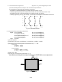
Adjustment Magnetic Field by three dimension magnetic field system.
Setting of the Landing meter (KLD-01 made by KAMAYA)
Volt: 2.0V Time: 50ms
GAIN: 7
※ Adjust this monitor after a minimum of 90 minutes to allow unit to reach ambient operating temperature.
(Use the Self Test screen. Refer item 7-5-3. About Self Test.)
1) Turn the CRT face to east, and the outside degauss is done, and demagnetization is done again in the
Degauss power source.
The degauss of the outside is conducted in the front face, both sides, the base, the top panel.
But, degauss is unnecessary for the chassis of the part of aluminum.
2) Receive signal 22(all green) and make sure that the following specifications are satisfied.
Picture Size
H: 396mm±1.0mm
V: 297mm±1.0mm
Picture Position H: | XLeft - Xright | " 1.0mm
V: | Xtop - Xbottom | " 1.0mm
3) Open Menu (S), TAG 5 “EMF TOP RIGHT”.
4) The four corners (Within 3*3cm) of the screen (Fig 8-1) are measured by the Landing meter, and the
value of X when the value of Y was made 0 is measured.
When measured value is more than ±3%, Adjust "+","-" SW so that items of each four corners the
following standards.
-3% " $ " +3%
5) Measure that the items of each four corners are -3% " $ " +3%
When it is not in the adjustment standard, 4), 5) clause are repeated.
Top Right: EMF TOP RIGHT
Bottom Right: EMF BOTTOM RIGHT
EMF TOP LEFT
Top Left: EMF TOP LEFT
Bottom Left: EMF BOTTOM LEFT
EMF TOP RIGHT
The one within 3*3cm
from each corner is
adjusted.
EMF BOTTOM LEFT
EMF BOTTOM RIGHT
Fig 8-1 Landing measurement point
Don't use "GLOBAL SYNC" when you adjust it.
5-31
9. Convergence Adjustment
Signal: No.33(788*1200@75Hz)
Cross Hatch Pattern and frame Pattern
9-1. Settings
1) Receive Signal 33 (Cross Hatch Pattern and frame Pattern).
Adjust the H / V an interval of Cross Hatch Pattern to the following values, and Cross Hatch Pattern
consist of the 15 vertical lines and the 11 horizontal lines is displayed.
H interval: 54 dot
V interval: 112 line
2) It confirms that screen amplitude and screen positions are following values.
Screen amplitude
Screen position
H : 396mm±1.0mm
V : 297mm±1.0mm
H : | Xleft - Xright | ≦ 1.0mm
V : | Xtop - Xbottom | ≦ 1.0mm
3) Open Menu (S), TAG C, and make sure the data for each Item.
H. CONVER SAW T
: 127
H. CONVER PARA T
: 128
H. CONVER SAW B
: 128
H. CONVER PARA B
: 128
V. CONVER SAW T
: 127
V. CONVER PARA T
: 128
V. CONVER SAW B
: 128
V. CONVER PARA B
: 128
If not, Select item and then press RESET SW.
4) Open Menu (S), TAG B, and highlight TAG B.
Push and hold “RESET” SW and push “▲” SW at the same time.
(4H, 4V data on every COLUMN / ROW will be reset.)
5) Set a Convergence Meter.
REFERENCE COLOR
:G
S.P. (STRIPE PITCH)
: 0.25±0.02mm
9-2. Static Convergence Adjustment
Auto EMF function must be ON.
When each Convergence item is selected, Auto EMF will be worked and LED will be changed to orange.
While measuring convergence, hide OSM with “PROCEED” SW.
1) Receive Signal 33 White (Cross Hatch Pattern).
Measure the static convergence at center.
Spec : x , y ≦ 0.05mm
2) Receive Signal 33 Red and Blue (Cross Hatch Pattern).
If misconvergence at center is 0.21mm or greater, adjust 4-pole magnet on CPM to get 0.21mm or less.
If misconvergence at center is 0.20mm or less, adjust Menu (S), TAG B “H.S.CONVER” ,
“V.S.CONVER” to get the spec.
3) Receive Signal 33 White (Cross Hatch Pattern).
Adjust 6-pole magnet on CPM to get spec.
4) Receive Signal 33 Red and Blue again (Cross Hatch Pattern).
Adjust Menu (S), TAG B “H.S.CONVER” , “V.S.CONVER” to get the spec.
Adjustment limits
H.S.CONVER: 65 - 191
V.S.CONVER: 82 - 174
5-32
9-3. Dynamic Convergence Adjustment
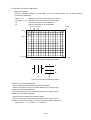
1) Adjustment function
There are 165 blocks (ROW: 1-11,COLUMN: 1-15) on the picture where you can adjust dynamic
convergence individually.
ROW (1-11)
: Adjusting cross can be selected (Top to bottom).
COLUMN (1 -15) : Adjusting cross can be selected (Left to right).
4H
: R-B (X) convergence can be adjusted.
4V
: R-B (Y) convergence can be adjusted.
(1,1) (1.2) (1,3)
(1,15)
(2,1)
(2.2)
(11,1)
(ROW, COLUMN)
Fig 10-1 Convergence Adjustment Points
+
B G
B +
B
G
B
4H
4V
Fig 10-2 Convergence Adjustment Items
2) Menu (S), TAG B 4V Adjustment
Receive Signal 33 Red and Blue (Cross Hatch Pattern).
Adjust convergence at every COLUMN / ROW by 4V to get the spec.
3) Menu (S), TAG B 4H Adjustment
Adjust convergence at every COLUMN / ROW by 4H to get the spec.
4) Menu (S), TAG B 6H Adjustment
Receive Signal 33 White (Cross Hatch Pattern).
Adjust convergence at every COLUMN / ROW by 6H to get the spec.
5) Make sure the misconvergence at every COLUMN / ROW is within spec.
Specification : x ≦ 0.25mm , y ≦ 0.25mm
5-33
(11,15)
Y
297±1.0mm
X
396±1.0mm
Fig 9-3 Convergence Specification
* Adjustment limits (Adjusted point data)
Between the COLUMN and next COLUMN
Difference 4H: 45 or less, 4V: 40 or less
Between the ROW and next ROW
Difference 4H: 45 or less, 4V: 40 or less
* Adjustment limits (Dynamic correction data)
H.S CONVER : 65-191 (the count of OSM number)
V.S CONVER : 82-174
H.CONVER SAW T : 95-159
H.CONVER SAW B : 95-159
V.CONVER SAW T : 95-159
V.CONVER SAW B : 95-159
* The noise will be appeared on the picture while adjusting, but it is no problem.
The jitter or the noise will be appeared by big difference between current adjusted data and previous
adjusted data.
XV-COIL
Yv
Yh
4-pole magnets
6-pole magnets
Fig 9-4 The location of the VR. and Coil and magnets
5-34
10. Auto Adjustment
Signal: No. 3 (VGA480) All White
Signal: No. 23 (1600*1200@85Hz) All White
When this adjustment is done, picture size, linearity, picture position, picture deformation, video adjustment
are to be finished.
1) Receive signal 3 (VGA480) All White, and confirm that the picture size and picture position is as follows.
Open Menu (S), TAG D "AUTO ADJUT L", and push "Proceed" SW (Adjustment data is written in the
Monitor at this time).
2) Receive signal 23 (1600*1200@85Hz) All White, and confirm that the picture size and picture position is
as follows.
Open Menu (S), TAG D "AUTO ADJUT H", and push "Proceed" SW (Adjustment data is written in the
Monitor at this time).
Picture size
H: 396±1mm
V: 297±1mm
Picture position
H: | Xleft - Xright | " 1.0mm
V: | Xtop - Xbottom | " 1.0mm
5-35
[D] Reference
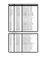
1. Adjustment Signal
NO. Signal Name
SYNC Type
SYNC Polarity(H/V)
--------------------------------------------------------------------------------------------------------1
VGA 350
Separate
Pos/Neg
2
VGA 400
Separate
Neg/Pos
3
VGA 480
Separate
Neg/Neg
4
640*400@70Hz
Separate
Neg/Neg
5
800*600@60Hz
Separate
Pos/Pos
6
MAC 640*480
Composite + Sync on G
Neg/Neg
7
VESA 350@85Hz
Separate
Pos/Neg
8
VESA 400@85Hz
Separate
Neg/Pos
9
VESA 640*480@75Hz
Separate
Neg/Neg
10 XGA
Separate
Pos/Pos
11 VESA 800*600@75Hz
Separate
Pos/Pos
12 VESA 640*480@85Hz
Separate
Neg/Neg
13 MAC 832*624
Composite + Sync on G
Neg/Neg
14 800*600@85Hz
Separate
Pos/Pos
15 1024*768@70Hz
Separate
Neg/Neg
16 1280*1024@60Hz
Separate
Pos/Pos
17 1024*768@75Hz
Separate
Pos/Pos
18 MAC 1152*870
Composite + Sync on G
Neg/Neg
19 1024*768@85Hz
Separate
Pos/Pos
20 1280*1024@70Hz
Sync on G
21 1280*1024@75Hz
Separate
Pos/Pos
22 1600*1200@75Hz
Separate
Pos/Pos
23 1600*1200@85Hz
Separate
Pos/Pos
25 H.HOLD 1
Composite
Pos/Pos *1
28 V.MAX
Separate
Neg/Neg
29 V.RASTER
Separate
Pos/Pos
30 EDID
Separate
Neg/Neg
31 1600*1200@60Hz
Separate
Pos/Pos
32 1280*1024@85Hz
Separate
Pos/Pos
33 788*1200@75Hz
Separate
Pos/Pos
36 H.HOLD 2(130K)
Separate
Pos/Pos *1
5-36
NO.
Signal Name
SYNC Type
SYNC Polarity(H/V)
---------------------------------------------------------------------------USER1
PC98 1120*750(I)
Separate
Pos/Pos
USER2
VESA 800*600@56Hz
Separate
Pos/Pos
USER3
VESA 1024*768@60Hz
Separate
Neg/Neg
USER4
VESA 800*600@72Hz
Separate
Pos/Pos
USER5
1120*750@60Hz
Separate
Neg/Neg
USER6
640*480@100Hz
Separate
Neg/Neg
USER7
XGA-2 1024*768@72Hz
Separate
Neg/Neg
USER8
800*600@100Hz
Separate
Pos/Pos
USER9
640*480@120Hz
Separate
Pos/Pos
USER10
640*480@140Hz
Separate
Neg/Neg
USER11
VESA 1600*1200@60Hz
Separate
Neg/Neg
USER12
1280*1024@70Hz
Separate
Pos/Pos
USER13
VESA 1152*864@85Hz
Separate
Pos/Pos
USER14
1024*768@100Hz
Separate
Pos/Pos
USER15
800*600@120Hz
Separate
Pos/Pos
USER16
640*480@160Hz
Separate
Neg/Neg
USER17
VESA1920*1440@60Hz
Separate
Neg/Pos
USER18
1600*1200@70Hz
Separate
Pos/Pos
USER19
800*600@140Hz
Separate
Pos/Pos
USER20
VESA1792*1344@75Hz
Separate
Pos/Pos
USER21
VESA 1600*1200@80Hz
Separate
Neg/Pos
USER22
1024*768@120Hz
Separate
Pos/Pos
USER23
800*600@160Hz
Separate
Pos/Pos
USER24
VESA1920*1440@75Hz
Separate
Pos/Pos
USER25
VESA1792*1344@85Hz
Separate
Neg/Pos
USER26
VESA2048*1536@80Hz
Separate
Neg/Pos
USER27
VESA1920*1440@85Hz
Separate
Neg/Pos
*1
*2
*3
When an approximate value is utilized because it is impossible to output the exact fH from the
signal generator
On the 31kHz side, utilize the highest frequency signal that satisfies
fH ≦ 31.0kHz.
On the 130kHz side, utilize the lowest frequency signal that satisfies
fH ≧ 130kHz. (Tolerance must be within 50Hz.) being used:
Supply the sync signals output from the signal generator as follows:
H/V Composite
: Supply to the set undergoing adjustment
V. SYNC only
: Supply to the CA-100 color analyzer.
The crosshatch pattern shall have 17 vertical lines and 13 horizontal lines.
5-37
2. Adjustment Signal timing
Signal Timing Charts
SEPARATE SYNC
VIDEO
HORIZONTAL
C
D
E
A: H.Total Time
B: H.Sync Time
C: H.Back Porch
D: H.Addr Time
E: H.Front Porch
B
A
VIDEO
VERTICAL
Q
R
S
P
O
Sync Polarity: Positive/Negative
COMPOSITE SYNC
VIDEO
HORIZONTAL
C
D
E
B
A
VIDEO
VERTICAL
Q
R
P
O
Sync Polarity: Positive/Negative
5-38
S
O: V.Total Time
P: V.Sync Time
Q: V.Back Porch
R: V.Addr Time
S: V.Front Porch
5-39
TIMING NAME
Pixel Clock
H.Frequency
V.Frequency
H.Tortal Time
H.Addr Time
H.Blank Time
H.Front Porch
H.Sync Time
H.Back Porch
V.Tortal Time
V.Addr Time
V.Blank Time
V.Front Porch
V.Sync Time
V.Back Porch
Scan Type
H.Sync Polarity
V.Sync Polarity
1
900
720
180
18
108
54
449
350
99
37
2
60
6
864
640
224
64
64
96
525
480
45
3
3
39
VGA350
28.322 [MHz]
31.469 [kHz]
70.086 [Hz]
[dots] 31.778 [us]
[dots] 25.422 [us]
[dots]
6.356 [us]
[dots]
0.636 [us]
[dots]
3.813 [us]
[dots]
1.907 [us]
[lines] 14.268 [ms]
[lines] 11.122 [ms]
[lines]
3.146 [ms]
[lines]
1.176 [ms]
[lines]
0.064 [ms]
[lines]
1.907 [ms]
Non-interlaced
Positive
Negative
Separate
MAC640*480
30.240 [MHz]
35.000 [kHz]
66.667 [Hz]
[dots] 28.571 [us]
[dots] 21.164 [us]
[dots]
7.407 [us]
[dots]
2.116 [us]
[dots]
2.116 [us]
[dots]
3.175 [us]
[lines] 15.000 [ms]
[lines] 13.714 [ms]
[lines]
1.286 [ms]
[lines]
0.086 [ms]
[lines]
0.086 [ms]
[lines]
1.114 [ms]
Non-interlaced
Negative
Negative
Composit + Sync On G
2
900
720
180
18
108
54
449
400
49
12
2
35
7
832
640
192
32
64
96
445
350
95
32
3
60
VGA400
28.322 [MHz]
31.469 [kHz]
70.087 [Hz]
[dots] 31.777 [us]
[dots] 25.422 [us]
[dots]
6.355 [us]
[dots]
0.636 [us]
[dots]
3.813 [us]
[dots]
1.907 [us]
[lines] 14.268 [ms]
[lines] 12.711 [ms]
[lines]
1.557 [ms]
[lines]
0.381 [ms]
[lines]
0.064 [ms]
[lines]
1.112 [ms]
Non-interlaced
Negative
Positive
Separate
VESA640*350@85Hz
31.500 [MHz]
37.861 [kHz]
85.080 [Hz]
[dots] 26.413 [us]
[dots] 20.317 [us]
[dots]
6.095 [us]
[dots]
1.016 [us]
[dots]
2.032 [us]
[dots]
3.048 [us]
[lines] 11.754 [ms]
[lines]
9.244 [ms]
[lines]
2.509 [ms]
[lines]
0.845 [ms]
[lines]
0.079 [ms]
[lines]
1.585 [ms]
Non-interlaced
Positive
Negative
Separate
3
800
640
160
16
96
48
525
480
45
10
2
33
8
832
640
192
32
64
96
445
400
45
1
3
41
VGA480
25.175 [MHz]
31.469 [kHz]
59.940 [Hz]
[dots] 31.778 [us]
[dots] 25.422 [us]
[dots]
6.356 [us]
[dots]
0.636 [us]
[dots]
3.813 [us]
[dots]
1.907 [us]
[lines] 16.683 [ms]
[lines] 15.253 [ms]
[lines] 1.430 [ms]
[lines] 0.318 [ms]
[lines] 0.064 [ms]
[lines] 1.049 [ms]
Non-interlaced
Negative
Negative
Separate
VESA640*400@85Hz
31.500 [MHz]
37.861 [kHz]
85.080 [Hz]
[dots] 26.413 [us]
[dots] 20.317 [us]
[dots]
6.095 [us]
[dots]
1.016 [us]
[dots]
2.032 [us]
[dots]
3.048 [us]
[lines] 11.754 [ms]
[lines] 10.565 [ms]
[lines] 1.189 [ms]
[lines] 0.026 [ms]
[lines] 0.079 [ms]
[lines] 1.083 [ms]
Non-interlaced
Negative
Positive
Separate
4
800
640
160
17
64
79
449
400
49
13
2
34
9
840
640
200
16
64
120
500
480
20
1
3
16
640*400@70 Hz
5 800*600@60
40.000 [MHz]
25.175 [MHz]
37.879 [kHz]
31.469 [kHz]
60.317 [Hz]
70.086 [Hz]
1056 [dots]
26.400 [us]
[dots]
31.778 [us]
800 [dots]
20.000 [us]
[dots]
25.422 [us]
256 [dots]
6.400 [us]
[dots]
6.356 [us]
40 [dots]
1.000 [us]
[dots]
0.675 [us]
128 [dots]
3.200 [us]
[dots]
2.542 [us]
88 [dots]
2.200 [us]
[dots]
3.138 [us]
628 [lines] 16.579 [ms]
[lines] 14.268 [ms]
600 [lines] 15.840 [ms]
[lines] 12.711 [ms]
28 [lines]
0.739 [ms]
[lines]
1.557 [ms]
1 [lines]
0.026 [ms]
[lines]
0.413 [ms]
4 [lines]
0.106 [ms]
[lines]
0.064 [ms]
23 [lines]
0.607 [ms]
[lines]
1.080 [ms]
Non-interlaced
Non-interlaced
Positive
Negative
Positive
Negative
Separate
Separate
VESA640*480@75Hz 10 XGA
31.500 [MHz]
44.900 [MHz]
37.500 [kHz]
35.522 [kHz]
75.000 [Hz]
87.064 [Hz]
[dots]
26.667 [us]
1264 [dots]
29.577 [us]
[dots]
20.317 [us]
1024 [dots]
22.806 [us]
[dots]
6.349 [us]
240 [dots]
6.771 [us]
[dots]
0.508 [us]
8 [dots]
0.535 [us]
[dots]
2.032 [us]
176 [dots]
3.029 [us]
[dots]
3.810 [us]
56 [dots]
3.207 [us]
[lines] 13.333 [ms]
408 [lines] 23.839 [ms]
[lines] 12.800 [ms]
384 [lines] 22.715 [ms]
[lines]
0.533 [ms]
24 [lines]
1.124 [ms]
[lines]
0.027 [ms]
0 [lines]
0.089 [ms]
[lines]
0.080 [ms]
4 [lines]
0.177 [ms]
[lines]
0.427 [ms]
20 [lines]
0.858 [ms]
Non-interlaced
Interlaced
Negative
Positive
Negative
Positive
Separate
Separate
Adjustment Signal (1)
TIMING NAME
Pixel Clock
H.Frequency
V.Frequency
H.Tortal Time
H.Addr Time
H.Blank Time
H.Front Porch
H.Sync Time
H.Back Porch
V.Tortal Time
V.Addr Time
V.Blank Time
V.Front Porch
V.Sync Time
V.Back Porch
Scan Type
H.Sync Polarity
V.Sync Polarity
5-40
TIMING NAME
Pixel Clock
H.Frequency
V.Frequency
H.Tortal Time
H.Addr Time
H.Blank Time
H.Front Porch
H.Sync Time
H.Back Porch
V.Tortal Time
V.Addr Time
V.Blank Time
V.Front Porch
V.Sync Time
V.Back Porch
Scan Type
H.Sync Polarity
V.Sync Polarity
16
1688
1280
408
48
112
248
1066
1024
42
1
3
38
12
832
640
192
56
56
80
509
480
29
1
3
25
VESA 1280*1024@60Hz 17
[dots]
[dots]
[dots]
[dots]
[dots]
[dots]
[lines]
[lines]
[lines]
[lines]
[lines]
[lines]
VESA640*480@85Hz
[dots]
[dots]
[dots]
[dots]
[dots]
[dots]
[lines]
[lines]
[lines]
[lines]
[lines]
[lines]
13
MAC832*624
14
36.000 [MHz]
57.283 [MHz]
43.296 [kHz]
49.725 [kHz]
85.008 [Hz]
74.550 [Hz]
23.111 [us]
1152 [dots] 20.111 [us]
1048
17.778 [us]
832 [dots] 14.524 [us]
800
5.333 [us]
320 [dots]
5.586 [us]
248
1.556 [us]
32 [dots]
0.559 [us]
32
1.556 [us]
64 [dots]
1.117 [us]
64
2.222 [us]
224 [dots]
3.910 [us]
152
11.764 [ms]
667 [lines] 13.414 [ms]
631
11.093 [ms]
624 [lines] 12.549 [ms]
600
0.670 [ms]
43 [lines]
0.865 [ms]
31
0.023 [ms]
1 [lines]
0.020 [ms]
1
0.069 [ms]
3 [lines]
0.060 [ms]
3
0.578 [ms]
39 [lines]
0.784 [ms]
27
Non-interlaced
Non-interlaced
Negative
Negative
Negative
Negative
Separate
Composit + Sync On G
VESA 1024*768@75Hz
18
MAC1152*870
19
108.000 [MHz]
78.750 [MHz]
100.000 [MHz]
63.981 [kHz]
60.023 [kHz]
68.681 [kHz]
60.020 [Hz]
75.029 [Hz]
75.062 [Hz]
15.630 [us]
1312 [dots] 16.660 [us]
1456 [dots] 14.560 [us]
1376
11.582 [us]
1024 [dots] 13.003 [us]
1152 [dots] 11.520 [us]
1024
3.778 [us]
288 [dots]
3.657 [us]
304 [dots]
3.040 [us]
352
0.444 [us]
16 [dots]
0.203 [us]
32 [dots]
0.320 [us]
48
1.037 [us]
96 [dots]
1.219 [us]
128 [dots]
1.280 [us]
96
2.296 [us]
176 [dots]
2.235 [us]
144 [dots]
1.440 [us]
208
16.661 [ms]
800 [lines] 13.328 [ms]
915 [lines] 13.322 [ms]
808
16.005 [ms]
768 [lines] 12.795 [ms]
870 [lines] 12.667 [ms]
768
0.656 [ms]
32 [lines]
0.533 [ms]
45 [lines]
0.655 [ms]
40
0.016 [ms]
1 [lines]
0.017 [ms]
3 [lines]
0.044 [ms]
1
0.047 [ms]
3 [lines]
0.050 [ms]
3 [lines]
0.044 [ms]
3
0.594 [ms]
28 [lines]
0.466 [ms]
39 [lines]
0.568 [ms]
36
Non-interlaced
Non-interlaced
Non-interlaced
Positive
Positive
Negative
Positive
Positive
Negative
Separate
Separate
Composit + Sync On G
VESA 800*600@85Hz
[dots]
[dots]
[dots]
[dots]
[dots]
[dots]
[lines]
[lines]
[lines]
[lines]
[lines]
[lines]
VESA 1024*768@85Hz
[dots]
[dots]
[dots]
[dots]
[dots]
[dots]
[lines]
[lines]
[lines]
[lines]
[lines]
[lines]
15
VESA 1024*768@70Hz
56.250 [MHz]
75.000 [MHz]
53.674 [kHz]
56.476 [kHz]
85.061 [Hz]
70.069 [Hz]
18.631 [us]
1328 [dots]
17.707 [us]
14.222 [us]
1024 [dots]
13.653 [us]
4.409 [us]
304 [dots]
4.053 [us]
0.569 [us]
24 [dots]
0.320 [us]
1.138 [us]
136 [dots]
1.813 [us]
2.702 [us]
144 [dots]
1.920 [us]
11.756 [ms]
806 [lines] 14.272 [ms]
11.179 [ms]
768 [lines] 13.599 [ms]
0.578 [ms]
38 [lines]
0.673 [ms]
0.019 [ms]
3 [lines]
0.053 [ms]
0.056 [ms]
6 [lines]
0.106 [ms]
0.503 [ms]
29 [lines]
0.513 [ms]
Non-interlaced
Non-interlaced
Positive
Negative
Positive
Negative
Separate
Separate
94.500 [MHz]
68.677 [kHz]
84.997 [Hz]
14.561 [us]
10.836 [us]
3.725 [us]
0.508 [us]
1.016 [us]
2.201 [us]
11.765 [ms]
11.183 [ms]
0.582 [ms]
0.015 [ms]
0.044 [ms]
0.524 [ms]
Non-interlaced
Positive
Positive
Separate
20
1694
1280
414
30
160
224
1073
1024
48
3
4
42
1280*1024@70Hz
[dots]
[dots]
[dots]
[dots]
[dots]
[dots]
[lines]
[lines]
[lines]
[lines]
[lines]
[lines]
127.000 [MHz]
74.970 [kHz]
69.870 [Hz]
13.339 [us]
10.079 [us]
3.260 [us]
0.236 [us]
1.260 [us]
1.764 [us]
14.312 [ms]
13.659 [ms]
0.654 [ms]
0.040 [ms]
0.053 [ms]
0.560 [ms]
Non-interlaced
Negative
Negative
Sync on G
Adjustment Signal (2)
11 VESA800*600@75Hz
TIMING NAME
Pixel Clock
49.500 [MHz]
H.Frequency
46.875 [kHz]
V.Frequency
75.000 [Hz]
H.Tortal Time
1056 [dots] 21.333 [us]
H.Addr Time
800 [dots] 16.162 [us]
H.Blank Time
256 [dots]
5.172 [us]
H.Front Porch
16 [dots]
0.323 [us]
H.Sync Time
80 [dots]
1.616 [us]
H.Back Porch
160 [dots]
3.232 [us]
V.Tortal Time
625 [lines] 13.333 [ms]
V.Addr Time
600 [lines] 12.800 [ms]
V.Blank Time
25 [lines]
0.533 [ms]
V.Front Porch
1 [lines]
0.021 [ms]
V.Sync Time
3 [lines]
0.064 [ms]
V.Back Porch
21 [lines]
0.448 [ms]
Scan Type
Non-interlaced
H.Sync Polarity
Positive
V.Sync Polarity
Positive
Separate
21
1688
1280
408
16
144
248
1066
1024
42
1
3
38
VESA 1280*1024@75Hz
[dots]
[dots]
[dots]
[dots]
[dots]
[dots]
[lines]
[lines]
[lines]
[lines]
[lines]
[lines]
135.000 [MHz]
79.976 [kHz]
75.025 [Hz]
12.504 [us]
9.481 [us]
3.022 [us]
0.119 [us]
1.067 [us]
1.837 [us]
13.329 [ms]
12.804 [ms]
0.525 [ms]
0.013 [ms]
0.038 [ms]
0.475 [ms]
Non-interlaced
Positive
Positive
Separate
5-41
2160
1600
560
64
192
304
1250
1200
50
1
3
46
27
1236
900
336
68
100
168
718
690
28
1
4
23
5-40
TIMING NAME 26 H.HOLD2 (110K)
Pixel Clock
237.600 [MHz]
H.Frequency
110.000 [kHz]
V.Frequency
160.000 [Hz]
H.Tortal Time
2160 [dots]
9.091 [us]
H.Addr Time
1600 [dots]
6.734 [us]
H.Blank Time
560 [dots]
2.357 [us]
H.Front Porch
64 [dots]
0.269 [us]
H.Sync Time
192 [dots]
0.808 [us]
H.Back Porch
309 [dots]
1.280 [us]
V.Tortal Time
687 [lines]
6.250 [ms]
V.Addr Time
660 [lines]
6.000 [ms]
V.Blank Time
27 [lines]
0.250 [ms]
V.Front Porch
1 [lines]
0.013 [ms]
V.Sync Time
4 [lines]
0.038 [ms]
V.Back Porch
22 [lines]
0.200 [ms]
Scan Type
Non-interlaced
H.Sync Polarity
Positive
V.Sync Polarity
Positive
Separate
22
VESA 1600*1200@75Hz
[dots]
[dots]
[dots]
[dots]
[dots]
[dots]
[lines]
[lines]
[lines]
[lines]
[lines]
[lines]
202.500 [MHz]
93.750 [kHz]
75.000 [Hz]
10.667 [us]
7.901 [us]
2.765 [us]
0.316 [us]
0.948 [us]
1.501 [us]
13.333 [ms]
12.800 [ms]
0.533 [ms]
0.011 [ms]
0.032 [ms]
0.491 [ms]
Non-Interlaced
Positive
Positive
Separate
H.HOLD2 (115K)
[dots]
[dots]
[dots]
[dots]
[dots]
[dots]
[lines]
[lines]
[lines]
[lines]
[lines]
[lines]
142.140 [MHz]
115.000 [kHz]
160.000 [Hz]
8.695 [us]
6.332 [us]
2.364 [us]
0.478 [us]
0.704 [us]
1.182 [us]
6.250 [ms]
6.000 [ms]
0.250 [ms]
0.013 [ms]
0.038 [ms]
0.200 [ms]
Non-interlaced
Positive
Positive
Separate
23
VESA 1600*1200@85Hz
2160
1600
560
64
192
304
1250
1200
50
1
3
46
[dots]
[dots]
[dots]
[dots]
[dots]
[dots]
[lines]
[lines]
[lines]
[lines]
[lines]
[lines]
28
V.MAX
1300
1024
276
24
92
160
806
596
210
89
6
115
[dots]
[dots]
[dots]
[dots]
[dots]
[dots]
[lines]
[lines]
[lines]
[lines]
[lines]
[lines]
229.500 [MHz]
106.250 [kHz]
85.000 [Hz]
9.412 [us]
6.972 [us]
2.440 [us]
0.279 [us]
0.837 [us]
1.325 [us]
11.765 [ms]
11.294 [ms]
0.471 [ms]
0.009 [ms]
0.028 [ms]
0.433 [ms]
Non-interlaced
Positive
Positive
Separate
24
2640
1920
720
144
224
352
1500
1440
60
1
3
56
29
84.500 [MHz]
65.000 [kHz]
80.65 [Hz]
15.38 [us]
12.12 [us]
3.26 [us]
0.28 [us]
1.09 [us]
1.89 [us]
12.4 [ms]
9.169 [ms]
3.231 [ms]
1.343 [ms]
0.092 [ms]
1.796 [ms]
Non-interlaced
Negative
Negative
Separate
1328
1024
288
16
96
176
800
788
13
0
3
9
VESA 1920*1440@75Hz
[dots]
[dots]
[dots]
[dots]
[dots]
[dots]
[lines]
[lines]
[lines]
[lines]
[lines]
[lines]
297.000 [MHz]
112.500 [kHz]
75.000 [Hz]
8.889 [us]
6.465 [us]
2.424 [us]
0.485 [us]
0.754 [us]
1.185 [us]
13.333 [ms]
12.800 [ms]
0.533 [ms]
0.009 [ms]
0.027 [ms]
0.498 [ms]
Non-Interlaced
Negative
Positive
Separate
V.RASTER
[dots]
[dots]
[dots]
[dots]
[dots]
[dots]
[lines]
[lines]
[lines]
[lines]
[lines]
[lines]
78.750 [MHz]
60.023 [kHz]
75.029 [Hz]
16.66 [us]
13.003 [us]
3.657 [us]
0.203 [us]
1.219 [us]
2.235 [us]
13.328 [ms]
13.128 [ms]
0.217 [ms]
0 [ms]
0.05 [ms]
0.150 [ms]
Non-interlaced
Positive
Positive
Separate
25
H.HOLD1
900
720
180
18
108
54
564
428
136
52
2
82
[dots]
[dots]
[dots]
[dots]
[dots]
[dots]
[lines]
[lines]
[lines]
[lines]
[lines]
[lines]
30
EDID
900
720
180
18
108
54
749
685
64
14
3
47
[dots]
[dots]
[dots]
[dots]
[dots]
[dots]
[lines]
[lines]
[lines]
[lines]
[lines]
[lines]
27.900 [MHz]
31.000 [kHz]
54.963 [Hz]
32.260 [us]
25.810 [us]
6.450 [us]
0.640 [us]
3.870 [us]
1.940 [us]
18.194 [ms]
13.807 [ms]
4.387 [ms]
1.677 [ms]
0.065 [ms]
2.645 [ms]
Non-interlaced
Positive
Positive
Composit
28.322 [MHz]
31.463 [kHz]
42.01 [Hz]
31.777 [us]
25.422 [us]
6.36 [us]
0.636 [us]
3.813 [us]
1.907 [us]
23.8 [ms]
21.767 [ms]
2.034 [ms]
0.445 [ms]
0.095 [ms]
1.494 [ms]
Non-interlaced
Negative
Negative
Separate
Adjustment Signal (3)
TIMING NAME
Pixel Clock
H.Frequency
V.Frequency
H.Tortal Time
H.Addr Time
H.Blank Time
H.Front Porch
H.Sync Time
H.Back Porch
V.Tortal Time
V.Addr Time
V.Blank Time
V.Front Porch
V.Sync Time
V.Back Porch
Scan Type
H.Sync Polarity
V.Sync Polarity
31
2160
1600
560
64
192
304
1250
1200
50
1
3
46
VESA 1600*1200@60Hz
[dots]
[dots]
[dots]
[dots]
[dots]
[dots]
[lines]
[lines]
[lines]
[lines]
[lines]
[lines]
5-42
162.000 [MHz]
75.000 [kHz]
60.000 [Hz]
13.333 [us]
9.877 [us]
3.457 [us]
0.395 [us]
1.185 [us]
1.877 [us]
16.667 [ms]
16.000 [ms]
0.667 [ms]
0.013 [ms]
0.040 [ms]
0.613 [ms]
Non-interlaced
Positive
Positive
Separate
TIMING NAME 36 H.HOLD2 (130K)
Pixel Clock
163.280 [MHz]
H.Frequency
130.000 [kHz]
V.Frequency
160.000 [Hz]
H.Tortal Time 1256 [dots]
7.692 [us]
H.Addr Time
900 [dots]
5.512 [us]
H.Blank Time
356 [dots]
2.180 [us]
H.Front Porch
74 [dots]
0.453 [us]
H.Sync Time
104 [dots]
0.637 [us]
H.Back Porch
178 [dots]
1.090 [us]
V.Tortal Time
813 [lines]
6.250 [ms]
V.Addr Time
740 [lines]
5.692 [ms]
V.Blank Time
73 [lines]
0.558 [ms]
V.Front Porch
1 [lines]
0.008 [ms]
V.Sync Time
3 [lines]
0.023 [ms]
V.Back Porch
69 [lines]
0.527 [ms]
Scan Type
Non-Interlaced
H.Sync Polarity
Positive
V.Sync Polarity
Positive
Separate
32
1728
1280
448
64
160
224
1072
1024
48
1
3
44
37
2640
1920
720
149
211
360
1514
1440
74
1
3
70
VESA 1280*1024@85Hz
[dots]
[dots]
[dots]
[dots]
[dots]
[dots]
[lines]
[lines]
[lines]
[lines]
[lines]
[lines]
157.500 [MHz]
91.146 [kHz]
85.024 [Hz]
10.971 [us]
8.127 [us]
2.844 [us]
0.406 [us]
1.016 [us]
1.422 [us]
11.761 [ms]
11.235 [ms]
0.527 [ms]
0.011 [ms]
0.033 [ms]
0.483 [ms]
Non-Interlaced
Positive
Positive
Separate
1920*1440@85
[dots]
[dots]
[dots]
[dots]
[dots]
[dots]
[lines]
[lines]
[lines]
[lines]
[lines]
[lines]
339.750 [MHz]
128.693 [kHz]
85.002 [Hz]
7.77 [us]
5.651 [us]
2.119 [us]
0.439 [us]
0.621 [us]
1.06 [us]
11.764 [ms]
11.189 [ms]
0.575 [ms]
0.008 [ms]
0.023 [ms]
0.544 [ms]
Non-Interlaced
Positive
Positive
Separate
33
1066
788
278
34
94
150
1250
1200
50
1
3
46
788*1200@75
[dots]
[dots]
[dots]
[dots]
[dots]
[dots]
[lines]
[lines]
[lines]
[lines]
[lines]
[lines]
34
812*1024@85
35
99.900 [MHz]
99.900 [MHz]
93.720 [kHz]
91.160 [kHz]
74.980 [Hz]
85.040 [Hz]
10.670 [us]
1096 [dots] 10.970 [us]
7.890 [us]
812 [dots]
8.120 [us]
2.780 [us]
284 [dots]
2.850 [us]
0.340 [us]
40 [dots]
0.410 [us]
0.940 [us]
102 [dots]
1.020 [us]
1.500 [us]
142 [dots]
1.420 [us]
13.337 [ms] 1072 [lines] 11.760 [ms]
12.804 [ms] 1024 [lines] 11.233 [ms]
0.533 [ms]
48 [lines]
0.527 [ms]
0.010 [ms]
1 [lines]
0.011 [ms]
0.032 [ms]
3 [lines]
0.033 [ms]
0.491 [ms]
44 [lines]
0.483 [ms]
Non-interlaced
Non-interlaced
Positive
Positive
Positive
Positive
Separate
Separate
38
39
[dots]
[dots]
[dots]
[dots]
[dots]
[dots]
[lines]
[lines]
[lines]
[lines]
[lines]
[lines]
[MHz]
[kHz]
[Hz]
[us]
[us]
[us]
[us]
[us]
[us]
[ms]
[ms]
[ms]
[ms]
[ms]
[ms]
2160
1520
640
104
192
344
1250
1200
50
1
3
46
H.SIZE
[dots]
[dots]
[dots]
[dots]
[dots]
[dots]
[lines]
[lines]
[lines]
[lines]
[lines]
[lines]
229.500 [MHz]
106.250 [kHz]
85.000 [Hz]
9.412 [us]
6.623 [us]
2.789 [us]
0.454 [us]
0.837 [us]
1.500 [us]
11.765 [ms]
11.294 [ms]
0.471 [ms]
0.009 [ms]
0.028 [ms]
0.433 [ms]
Non-interlaced
Positive
Positive
Separate
40
[dots]
[dots]
[dots]
[dots]
[dots]
[dots]
[lines]
[lines]
[lines]
[lines]
[lines]
[lines]
[MHz]
[kHz]
[Hz]
[us]
[us]
[us]
[us]
[us]
[us]
[ms]
[ms]
[ms]
[ms]
[ms]
[ms]
[dots]
[dots]
[dots]
[dots]
[dots]
[dots]
[lines]
[lines]
[lines]
[lines]
[lines]
[lines]
[MHz]
[kHz]
[Hz]
[us]
[us]
[us]
[us]
[us]
[us]
[ms]
[ms]
[ms]
[ms]
[ms]
[ms]
Adjustment Signal (4)
TIMING NAME
Pixel Clock
H.Frequency
V.Frequency
H.Tortal Time
H.Addr Time
H.Blank Time
H.Front Porch
H.Sync Time
H.Back Porch
V.Tortal Time
V.Addr Time
V.Blank Time
V.Front Porch
V.Sync Time
V.Back Porch
Scan Type
H.Sync Polarity
V.Sync Polarity
Adjustment Signal (5)
5-43
USER2 VESA 800*600@56Hz USER3 VESA 1024*768@60Hz USER4 VESA 800*600@72Hz USER5 1120*750@60Hz
TIMING NAME USER1 PC98 1120*750(I)
Pixel Clock
47.846 [MHz]
36.000 [MHz]
65.000 [MHz]
50.000 [MHz]
78.431 [MHz]
H.Frequency
32.861 [kHz]
35.156 [kHz]
48.363 [kHz]
48.077 [kHz]
50.020 [kHz]
V.Frequency
78.993 [Hz]
56.250 [Hz]
60.004 [Hz]
72.188 [Hz]
60.048 [Hz]
H.Tortal Time
1456 [dots] 30.431 [us]
1024 [dots] 28.444 [us]
1344 [dots] 20.677 [us]
1040 [dots] 20.800 [us]
1568 [dots] 19.992 [us]
H.Addr Time
1120 [dots] 23.408 [us]
800 [dots] 22.222 [us]
1024 [dots] 15.754 [us]
800 [dots] 16.000 [us]
1120 [dots] 14.280 [us]
H.Blank Time
336 [dots]
7.023 [us]
224 [dots]
6.222 [us]
320 [dots]
4.923 [us]
240 [dots]
4.800 [us]
448 [dots]
5.712 [us]
H.Front Porch
112 [dots]
2.341 [us]
24 [dots]
0.667 [us]
24 [dots]
0.369 [us]
56 [dots]
1.120 [us]
168 [dots]
2.142 [us]
H.Sync Time
84 [dots]
1.756 [us]
72 [dots]
2.000 [us]
136 [dots]
2.092 [us]
120 [dots]
2.400 [us]
112 [dots]
1.428 [us]
H.Back Porch
140 [dots]
2.926 [us]
128 [dots]
3.556 [us]
160 [dots]
2.462 [us]
64 [dots]
1.280 [us]
168 [dots]
2.142 [us]
V.Tortal Time
416 [lines] 12.659 [ms]
625 [lines] 17.778 [ms]
806 [lines] 16.666 [ms]
666 [lines] 13.853 [ms]
833 [lines] 16.653 [ms]
V.Addr Time
375.5 [lines] 11.427 [ms]
600 [lines] 17.067 [ms]
768 [lines]
15.88 [ms]
600 [lines] 12.480 [ms]
750 [lines] 14.994 [ms]
V.Blank Time
40.5 [lines] 1.232 [ms]
25 [lines]
0.711 [ms]
38 [lines]
0.786 [ms]
66 [lines]
1.373 [ms]
83 [lines]
1.659 [ms]
V.Front Porch
9 [lines] 0.274 [ms]
1 [lines]
0.028 [ms]
3 [lines]
0.062 [ms]
37 [lines]
0.770 [ms]
27 [lines]
0.540 [ms]
V.Sync Time
5 [lines] 0.152 [ms]
2 [lines]
0.057 [ms]
6 [lines]
0.124 [ms]
6 [lines]
0.125 [ms]
10 [lines]
0.200 [ms]
V.Back Porch
26.5 [lines] 0.806 [ms]
22 [lines]
0.626 [ms]
29 [lines]
0.600 [ms]
23 [lines]
0.478 [ms]
46 [lines]
0.920 [ms]
Scan Type
Interlaced
Non-interlaced
Non-interlaced
Non-interlaced
Non-interlaced
H.Sync Polarity
Positive
Positive
Negative
Positive
Negative
V.Sync Polarity
Positive
Positive
Negative
Positive
Negative
Separate
Separate
Separate
Separate
Separate
USER10 640*480@140Hz
USER7 XGA-2 1024*768@72Hz USER8 800*600@100Hz
USER9 640*480@120Hz
TIMING NAME USER6 640*480@100Hz
Pixel Clock
42.000 [MHz]
79.000 [MHz]
68.179 [MHz]
50.400 [MHz]
58.800 [MHz]
H.Frequency
50.000 [kHz]
58.088 [kHz]
63.600 [kHz]
59.990 [kHz]
70.000 [kHz]
V.Frequency
100.000 [Hz]
71.980 [Hz]
100.000 [Hz]
119.980 [Hz]
140.000 [Hz]
H.Tortal Time
840 [dots] 20.000 [us]
1360 [dots] 17.215 [us]
1072 [dots] 15.723 [us]
840 [dots] 16.669 [us]
840 [dots] 14.286 [us]
H.Addr Time
640 [dots] 15.240 [us]
1024 [dots] 12.962 [us]
800 [dots] 11.734 [us]
640 [dots] 12.701 [us]
640 [dots] 10.884 [us]
H.Blank Time
200 [dots]
4.760 [us]
336 [dots]
4.253 [us]
272 [dots]
3.989 [us]
200 [dots]
3.969 [us]
200 [dots]
3.401 [us]
H.Front Porch
16 [dots]
0.380 [us]
8 [dots]
0.101 [us]
48 [dots]
0.704 [us]
16 [dots]
0.318 [us]
16 [dots]
0.272 [us]
H.Sync Time
64 [dots]
1.520 [us]
288 [dots]
3.646 [us]
88 [dots]
1.291 [us]
64 [dots]
1.270 [us]
64 [dots]
1.088 [us]
H.Back Porch
120 [dots]
2.860 [us]
40 [dots]
0.506 [us]
136 [dots]
1.995 [us]
120 [dots]
2.381 [us]
120 [dots]
2.041 [us]
V.Tortal Time
500 [lines] 10.000 [ms]
807 [lines] 13.893 [ms]
636 [lines] 10.000 [ms]
500 [lines]
8.335 [ms]
500 [lines]
7.143 [ms]
V.Addr Time
480 [lines] 9.600 [ms]
768 [lines] 13.221 [ms]
600 [lines]
9.434 [ms]
480 [lines]
8.001 [ms]
480 [lines]
6.857 [ms]
V.Blank Time
20 [lines] 0.400 [ms]
39 [lines]
0.671 [ms]
36 [lines]
0.566 [ms]
20 [lines]
0.334 [ms]
20 [lines]
0.286 [ms]
V.Front Porch
1 [lines] 0.020 [ms]
0 [lines]
0.000 [ms]
1 [lines]
0.016 [ms]
1 [lines]
0.017 [ms]
1 [lines]
0.014 [ms]
V.Sync Time
3 [lines] 0.060 [ms]
8 [lines]
0.138 [ms]
3 [lines]
0.047 [ms]
3 [lines]
0.050 [ms]
3 [lines]
0.043 [ms]
V.Back Porch
16 [lines] 0.320 [ms]
31 [lines]
0.534 [ms]
32 [lines]
0.503 [ms]
16 [lines]
0.267 [ms]
16 [lines]
0.229 [ms]
Scan Type
Non-interlaced
Non-interlaced
Non-interlaced
Non-interlaced
Non-interlaced
H.Sync Polarity
Negative
Negative
Positive
Negative
Negative
V.Sync Polarity
Negative
Negative
Positive
Negative
Negative
Separate
Separate
Separate
Separate
Separate
USER17 VESA 1920*1440@60Hz USER18 VESA 1600*1200@70Hz USER19 800*600@140Hz
USER20 VESA 1792*1344@75Hz
TIMING NAME USER16 640*480@160Hz
Pixel Clock
67.200 [MHz]
234.000 [MHz]
189.000 [MHz]
92.300 [MHz]
261.000 [MHz]
H.Frequency
80.000 [kHz]
90.000 [kHz]
87.500 [kHz]
87.488 [kHz]
106.270 [kHz]
V.Frequency
160.000 [Hz]
60.000 [Hz]
70.000 [Hz]
139.981 [Hz]
74.997 [Hz]
H.Tortal Time
840 [dots] 12.500 [us]
2600 [dots] 11.111 [us]
2160 [dots] 11.429 [us]
1055 [dots]
11.430 [us]
2456 [dots]
9.410 [us]
H.Addr Time
640 [dots]
9.524 [us]
1920 [dots]
8.205 [us]
1600 [dots]
8.466 [us]
799 [dots]
8.657 [us]
1792 [dots]
6.866 [us]
H.Blank Time
200 [dots]
2.976 [us]
680 [dots]
2.906 [us]
560 [dots]
2.963 [us]
256 [dots]
2.774 [us]
664 [dots]
2.544 [us]
H.Front Porch
16 [dots]
0.238 [us]
128 [dots]
0.547 [us]
64 [dots]
0.339 [us]
16 [dots]
0.173 [us]
96 [dots]
0.368 [us]
H.Sync Time
64 [dots]
0.952 [us]
208 [dots]
0.889 [us]
192 [dots]
1.016 [us]
80 [dots]
0.867 [us]
216 [dots]
0.828 [us]
H.Back Porch
120 [dots]
1.786 [us]
344 [dots]
1.470 [us]
304 [dots]
1.608 [us]
160 [dots]
1.733 [us]
352 [dots]
1.349 [us]
V.Tortal Time
500 [lines] 6.250 [ms]
1500 [lines] 16.667 [ms]
1250 [lines] 14.286 [ms]
625 [lines]
7.144 [ms]
1417 [lines] 13.334 [ms]
V.Addr Time
480 [lines] 6.000 [ms]
1440 [lines] 16.000 [ms]
1200 [lines] 13.714 [ms]
600 [lines]
6.858 [ms]
1344 [lines] 12.647 [ms]
V.Blank Time
20 [lines] 0.250 [ms]
60 [lines] 0.667 [ms]
50 [lines] 0.571 [ms]
25 [lines]
0.286 [ms]
73 [lines]
0.687 [ms]
V.Front Porch
1 [lines] 0.013 [ms]
1 [lines] 0.011 [ms]
1 [lines] 0.011 [ms]
1 [lines]
0.011 [ms]
1 [lines]
0.009 [ms]
V.Sync Time
3 [lines] 0.038 [ms]
3 [lines] 0.033 [ms]
3 [lines] 0.034 [ms]
3 [lines]
0.034 [ms]
3 [lines]
0.028 [ms]
V.Back Porch
16 [lines] 0.200 [ms]
56 [lines] 0.622 [ms]
46 [lines] 0.526 [ms]
21 [lines]
0.240 [ms]
69 [lines]
0.649 [ms]
Scan Type
Non-Interlaced
Non-interlaced
Non-Interlaced
Non-interlaced
Non-Interlaced
H.Sync Polarity
Negative
Negative
Positive
Positive
Negative
V.Sync Polarity
Negative
Positive
Positive
Positive
Positive
Separate
Separate
Separate
Separate
Separate
Adjustment Signal (6)
5-44
USER13 VESA1152*864@85Hz
USER14 1024*768@100Hz
USER15 800*600@120Hz
TIMING NAME USER11 VESA 1600*1200@60Hz USER12 1280*1024@70Hz
Pixel Clock
162.000 [MHz]
127.000 [MHz]
121.500 [MHz]
108.390 [MHz]
83.250 [MHz]
H.Frequency
75.000 [kHz]
74.970 [kHz]
77.094 [kHz]
80.647 [kHz]
78.835 [kHz]
V.Frequency
60.000 [Hz]
69.870 [Hz]
84.999 [Hz]
100.059 [Hz]
121.659 [Hz]
H.Tortal Time
2160 [dots] 13.333 [us]
1694 [dots] 13.339 [us]
1576 [dots] 12.971 [us]
1344 [dots]
12.400 [us]
1056 [dots]
12.685 [us]
H.Addr Time
1600 [dots]
9.877 [us]
1280 [dots] 10.079 [us]
1152 [dots]
9.481 [us]
1024 [dots]
9.447 [us]
800 [dots]
9.610 [us]
H.Blank Time
560 [dots]
3.457 [us]
414 [dots]
3.260 [us]
424 [dots]
3.490 [us]
320 [dots]
2.952 [us]
256 [dots]
3.075 [us]
H.Front Porch
64 [dots]
0.395 [us]
30 [dots]
0.236 [us]
64 [dots]
0.527 [us]
24 [dots]
0.221 [us]
32 [dots]
0.384 [us]
H.Sync Time
192 [dots]
1.185 [us]
160 [dots]
1.260 [us]
128 [dots]
1.053 [us]
136 [dots]
1.255 [us]
80 [dots]
0.961 [us]
H.Back Porch
304 [dots]
1.877 [us]
224 [dots]
1.764 [us]
232 [dots]
1.909 [us]
160 [dots]
1.476 [us]
144 [dots]
1.730 [us]
V.Tortal Time
1250 [lines] 16.667 [ms]
1073 [lines] 14.312 [ms]
907 [lines] 11.765 [ms]
806 [lines]
9.994 [ms]
648 [lines]
8.220 [ms]
V.Addr Time
1200 [lines] 16.000 [ms]
1024 [lines] 13.659 [ms]
864 [lines] 11.207 [ms]
768 [lines]
9.523 [ms]
600 [lines]
7.611 [ms]
V.Blank Time
50 [lines] 0.667 [ms]
49 [lines] 0.654 [ms]
43 [lines] 0.558 [ms]
38 [lines]
0.471 [ms]
48 [lines]
0.609 [ms]
V.Front Porch
1 [lines] 0.013 [ms]
3 [lines] 0.040 [ms]
1 [lines] 0.013 [ms]
3 [lines]
0.037 [ms]
2 [lines]
0.025 [ms]
V.Sync Time
3 [lines] 0.040 [ms]
4 [lines] 0.053 [ms]
3 [lines] 0.039 [ms]
6 [lines]
0.074 [ms]
4 [lines]
0.051 [ms]
V.Back Porch
46 [lines] 0.613 [ms]
42 [lines] 0.560 [ms]
39 [lines] 0.506 [ms]
29 [lines]
0.360 [ms]
42 [lines]
0.533 [ms]
Scan Type
Non-Interlaced
Non-interlaced
Non-Interlaced
Non-Interlaced
Non-interlaced
H.Sync Polarity
Positive
Negative
Positive
Positive
Positive
V.Sync Polarity
Positive
Negative
Positive
Positive
Positive
Separate
Sync on G
Separate
Separate
Separate
Adjustment Signal (7)
5-45
USER23 800*600@160Hz
USER24 VESA1920*1440@75
USER25 1792*1344@85Hz
TIMING NAME USER21 VESA 1600*1200@80Hz USER22 1024*768@120Hz
Pixel Clock
216.000 [MHz]
139.054 [MHz]
116.406 [MHz]
297.000 [MHz]
297.000 [MHz]
H.Frequency
100.000 [kHz]
98.760 [kHz]
105.440 [kHz]
112.500 [kHz]
120.536 [kHz]
V.Frequency
80.000 [Hz]
120.000 [Hz]
160.000 [Hz]
75.000 [Hz]
85.004 [Hz]
H.Tortal Time
2160 [dots] 10.000 [us]
1408 [dots] 10.126 [us]
1104 [dots] 9.484 [us]
2640 [dots]
8.889 [us]
2464 [dots]
8.296 [us]
H.Addr Time
1600 [dots] 7.407 [us]
1024 [dots] 7.364 [us]
800 [dots] 6.873 [us]
1920 [dots]
6.465 [us]
1792 [dots]
6.034 [us]
H.Blank Time
560 [dots] 2.593 [us]
384 [dots] 2.762 [us]
304 [dots] 2.612 [us]
720 [dots]
2.424 [us]
672 [dots]
2.262 [us]
H.Front Porch
64 [dots] 0.296 [us]
80 [dots] 0.575 [us]
64 [dots] 0.550 [us]
144 [dots]
0.485 [us]
136 [dots]
0.458 [us]
H.Sync Time
192 [dots] 0.889 [us]
112 [dots] 0.805 [us]
88 [dots] 0.765 [us]
224 [dots]
0.754 [us]
200 [dots]
0.673 [us]
H.Back Porch
304 [dots] 1.407 [us]
192 [dots] 1.381 [us]
152 [dots] 1.306 [us]
352 [dots]
1.185 [us]
336 [dots]
1.131 [us]
V.Tortal Time
1250 [lines] 12.500 [ms]
823 [lines] 8.333 [ms]
659 [lines] 6.250 [ms]
1500 [lines] 13.333 [ms]
1418 [lines] 11.764 [ms]
V.Addr Time
1200 [lines] 12.000 [ms]
768 [lines] 7.776 [ms]
600 [lines] 5.690 [ms]
1440 [lines] 12.800 [ms]
1344 [lines] 11.150 [ms]
V.Blank Time
50 [lines] 0.500 [ms]
55 [lines] 0.557 [ms]
59 [lines] 0.560 [ms]
60 [lines]
0.533 [ms]
74 [lines]
0.614 [ms]
V.Front Porch
1 [lines] 0.010 [ms]
1 [lines] 0.010 [ms]
1 [lines] 0.009 [ms]
1 [lines]
0.009 [ms]
1 [lines]
0.008 [ms]
V.Sync Time
3 [lines] 0.030 [ms]
3 [lines] 0.030 [ms]
3 [lines] 0.028 [ms]
3 [lines]
0.027 [ms]
3 [lines]
0.025 [ms]
V.Back Porch
46 [lines] 0.460 [ms]
51 [lines] 0.516 [ms]
55 [lines] 0.522 [ms]
56 [lines]
0.498 [ms]
70 [lines]
0.581 [ms]
Scan Type
Non-Interlaced
Non-Interlaced
Non-Interlaced
Non-Interlaced
Non-Interlaced
H.Sync Polarity
Positive
Positive
Positive
Positive
Positive
V.Sync Polarity
Positive
Positive
Positive
Positive
Positive
Separate
Separate
Separate
Separate
Separate
USER27 1920*1440@85
TIMING NAME USER26 2048*1536@80
Pixel Clock
364.308 [MHz]
339.750 [MHz]
[MHz]
[MHz]
[MHz]
H.Frequency
128.640 [kHz]
128.693 [kHz]
[kHz]
[kHz]
[kHz]
V.Frequency
80.000 [Hz]
85.002 [Hz]
[Hz]
[Hz]
[Hz]
H.Tortal Time
2832 [dots] 7.774 [us]
2640 [dots] 7.770 [us]
[dots]
[us]
[dots]
[us]
[dots]
[us]
H.Addr Time
2048 [dots] 5.622 [us]
1920 [dots] 5.651 [us]
[dots]
[us]
[dots]
[us]
[dots]
[us]
H.Blank Time
784 [dots] 2.152 [us]
720 [dots] 2.119 [us]
[dots]
[us]
[dots]
[us]
[dots]
[us]
H.Front Porch
168 [dots] 0.461 [us]
149 [dots] 0.439 [us]
[dots]
[us]
[dots]
[us]
[dots]
[us]
H.Sync Time
224 [dots] 0.615 [us]
211 [dots] 0.621 [us]
[dots]
[us]
[dots]
[us]
[dots]
[us]
H.Back Porch
392 [dots] 1.076 [us]
360 [dots] 1.060 [us]
[dots]
[us]
[dots]
[us]
[dots]
[us]
V.Tortal Time
1608 [lines] 12.500 [ms]
1514 [lines] 11.764 [ms]
[lines]
[ms]
[lines]
[ms]
[lines]
[ms]
V.Addr Time
1536 [lines] 11.940 [ms]
1440 [lines] 11.189 [ms]
[lines]
[ms]
[lines]
[ms]
[lines]
[ms]
V.Blank Time
72 [lines] 0.560 [ms]
74 [lines] 0.575 [ms]
[lines]
[ms]
[lines]
[ms]
[lines]
[ms]
V.Front Porch
1 [lines] 0.008 [ms]
1 [lines] 0.008 [ms]
[lines]
[ms]
[lines]
[ms]
[lines]
[ms]
V.Sync Time
3 [lines] 0.023 [ms]
3 [lines] 0.023 [ms]
[lines]
[ms]
[lines]
[ms]
[lines]
[ms]
V.Back Porch
68 [lines] 0.529 [ms]
70 [lines] 0.544 [ms]
[lines]
[ms]
[lines]
[ms]
[lines]
[ms]
Scan Type
Non-Interlaced
Non-Interlaced
H.Sync Polarity
Positive
Positive
V.Sync Polarity
Positive
Positive
Separate
Separate
Program No.
Original
16
Special
16
Original
18
Special
18
Signal Name VESA1280*
-
MAC1152*
870
-
VESA1280*
1024@75
Resolution
1280*1024
Dot Clock
108.000
fh
63.981
fv
60.020
Cell Size
8
Total
1688
(CHR)
211
(uS)
15.630
Disp
1280
(CHR)
160
(uS)
11.852
Front
48
(uS)
0.444
Sync
112
(uS)
1.037
Back
248
(uS)
2.296
Program No.
Original
26
Signal Name H.HOLD2
-
-
1280*1024
135.000
79.976
75.025
8
1688
211
12.504
1280
160
9.481
16
0.119
144
1.067
248
1.837
Original
32
1024@60
Horizontal
5-46
(110K)
Horizontal
Resolution
Dot Clock
fh
fv
Cell Size
Total
(CHR)
(uS)
Disp
(CHR)
(uS)
Front
(uS)
Sync
(uS)
Back
(uS)
237.600
110.000
160.000
8
2160
270
9.091
1600
200
6.734
64
0.269
192
0.808
309
1.280
81
63.981
60.020
8
1266
158
15.63
960
120
11.852
36
0.444
84
1.037
186
2.296
Special
26
-
59.400
110.000
160.000
8
540
68
9.091
400
50
6.734
16
0.269
48
0.808
77
1.280
1152*870
100.000
68.681
75.062
8
1456
182
14.560
1152
144
11.520
32
0.320
128
1.280
144
1.440
Original
27
H.HOLD2
(115K)
142.140
115.000
160.000
8
1236
155
8.695
900
113
6.332
68
0.478
100
0.704
168
1.182
75
68.681
75.062
8
1092
137
14.560
864
108
11.520
24
0.320
96
1.280
108
1.440
Special
27
-
71.070
115.000
160.000
8
618
77
8.695
450
56
6.332
34
0.478
50
0.704
84
1.182
Original
21
VESA1280*
1024@85
1280*1024
157.500
91.146
85.024
8
1728
216
10.971
1280
160
8.127
64
0.406
160
1.016
224
1.422
Special
21
-
Original
22
VESA1600*
1200@75
1600*1200
67.5
202.500
79.976
93.750
75.025
75.000
8
8
844
2160
106
270
12.504
10.667
640
1600
80
200
9.481
7.901
8
64
0.119
0.316
72
192
1.067
0.948
124
304
1.837
1.501
Special
Original
32
33
-
78.750
91.146
85.024
8
864
108
10.971
640
80
8.127
32
0.406
80
1.016
112
1.422
788*1200
@75
788*1200
99.900
93.720
74.980
8
1066
133
10.670
788
99
7.890
34
0.340
94
0.940
150
1.500
Special
22
Original
23
Special
23
-
VESA1600*
1200@85
-
1600*120
50.625
229.500
93.750
106.250
75.000
85.000
8
8
540
2160
68
270
10..667
9.412
400
1600
50
200
7.901
6.972
16
64
0.316
0.279
48
192
0.948
0.837
76
304
1.501
1.325
Special
Original
33
34
-
74.925
93.720
74.980
8
800
100
10.670
591
74
7.890
26
0.340
71
0.940
113
1.500
812*1024
@85
812*1024
99.900
91.160
85.040
8
1096
137
10.970
812
102
8.120
40
0.410
102
1.020
142
1.420
Original
24
VESA1920*
1440@75
1920*1440
57.375
297.000
106.250
112.500
85.000
75.000
8
8
540
2640
68
330
9.412
8.889
400
1920
50
240
6.972
6.465
16
144
0.279
0.485
48
224
0.837
0.754
76
352
1.325
1.185
Special
Original
34
35
-
74.925
91.160
85.040
8
822
103
10.970
609
76
8.120
30
0.410
77
1.020
107
1.420
H.SIZE
229.500
106.250
85.000
8
2160
270
9.412
1520
190
6.623
104
0.454
192
0.837
344
1.500
Special
24
74.250
112.500
75.000
8
660
83
8.889
480
60
6.465
36
0485
56
0.754
88
1.185
Special
35
-
57.375
106.250
85.000
8
540
68
9.412
380
48
6.623
26
0.454
48
0.837
86
1.500
Adjustment / Inspection Signal (SPECIAL)
NOTE) Use special signals when original signals can not be made by equipped signal generator. Don't use these signal timing for Focus Adjustment. (The resolution is different.)
3. Connector, test pins
SW.REG/HV PWB
CN-R
CN-PM
CN-P
CN-K
CN-PS
CN-CR
HEAT SINK
T981
TP-HV
TP-DF
CN-DF
HEAT SINK
CNTP
F.B.T.
C5R1
VR5T1
high voltage adj.
(WITH SEALING CAP)
Fig.3-1 SW/HV PWB
LED111 LED112 LED113
CN-LEB
CN-CLB
SW104
SW101 SW102
SW105 SW106 SW107 SW108
SW103
Fig.3-2 CONT PWB
CN-LEA
SW601
Fig.3-3 SW PWB
5-47
CN-SW
CN-CLA
CN-AC
IN6T1
CNZ
CNSW2
CNPS
CNR
Fig.3-4 INLET PWB
F1
FOCUS
F2
SCREEN
Fig.3-5
F.B.T
VR
TP-B
TP-R
TP-G
CNSGA
TP-G2
CN-G2
CN-HT CN-GND
Fig.3-6
CRT PWB
5-48
CNSG
CNP
CNPU
CNHT
CNASD
TP-TMP
CNCL
TP-ABL
CNPM
BNC
R
Fig.3-7
G
B
VIDEO PWB
IC4H1
CNPU
Fig.3-8
PU PWB
5-49
H
V Mini D-SUB USB
CN-AF
HEAT SINK
CNDF
CNHSC
CNVSC
CNK
CNHDY
CNEMF
CNVDY
CNCR
CNZDY
VR581
SW581
Fig.3-9
DEF PWB
CN-SD
CN-DSB
CN-DSA
Fig.3-10
OSC PWB
5-50
HS8N1
CN-D
CN-CA
CN-CCB
Fig.3-11
CONV
PWB
CN-LL
CN-RR
CN-EMF
CNEM
Fig.3-12
EMF PWB
5-51
INSPECTION
1. Inspection of PLUG & PLAY communication
1-1. A construction of System
This system should be connected as shown below.
* TEST PROG RAM
P ro g ra m D is k
P AR T No. 599910408
M o n ito r
S ig n a l G e n e ra to r
PC
R G B H V
P o w e r C a b le
S ig n a l C a b le
F ix tu re
P rin te r C a b le
1-2. Starting method
1) Input Signal
Input signal must be separate sync. Two kinds of signals must be prepared.
One is the signal whose vertical synchronization frequency is 42Hz, and another is the signal whose
vertical synchronization frequency is between 55Hz and 25kHz.
Horizontal synchronization frequency should be set to reasonable value (example 31.5kHz).
2) Power ON procedure
- First, put the floppy disk for PnP Inspection into PC and turn on PC.
- Turn on Fixture.
- Make sure that fixture’s LED turns on and off.
- Turn on signal generator and monitor.
3) Starting PC Software
- Inspection of PnP communication
To check the PnP communication, EDID file name is FP1370, set “P FP1370” to DOS command line
and press return key.
- Writing EDID to EEPROM and inspection of PnP communication
To write EDID to EEPROM and check the PnP communication which its EDID file name is FP1370,
type “WP FP1370” on DOS prompt line and press return key.
6-1
1-3. Operation
- The operation should be performed according to the screen message.
- When the message of “Please set Vsync to 42Hz.” is displayed, set the signal generator to the signal
with vertical synchronization frequency of 42Hz. When the message of “Please set Vsync to over 55Hz.”
is displayed, set the signal generator to the signal whose vertical synchronization frequency is between
55Hz and 25kHz.
- The message of “Normally Complete” means that writing of EDID data or PnP inspection completed normally.
The message of “Error” means that writing of EDID data or PnP inspection finished incorrectly.
- When the PnP inspection is completed, read EDID data would be displayed. And if the read EDID data
differed from the original EDID data, the different bytes would be displayed in red.
- For the details of error, see the messages displayed at the bottom right of the screen. The meaning of
the messages is shown on section 4.
- After writing of EDID data or inspection of DDC2B, monitor can not be communicated by DDC1. In that
case, turn off and on the monitor again, which will make the DDC1 communication test possible.
- Make sure that fixture’s LED flashes on and off before writing EDID data, inspecting DDC1 and DDC2B.
If the fixture’s LED does not flash on and off, turn off and turn on the monitor and the fixture.
1-4. Error Messages
- Start Bit Error
This message is displayed when the start bit is not “H” while sending data from PC to MPU on the
fixture. This error will be caused by noise etc. on the line.
- Command Error
This message is displayed when the different command is sent from PC to MPU on the fixture.
- Hardware Error
This message means that the PC does not recognize ACK command sent from the MPU on the fixture.
- File Open Error
This message means that the input EDID file name was wrong.
- Command line Switch Error
This message means that the input communication command is incorrect.
- Parity Error
This message is displayed when the MPU on the fixture recognized the parity bit is incorrect. This error
can be caused by noise etc. on the line.
- EDID Data Error
This message is displayed when the null bit is not detected in EDID data read by DDC1 communication.
- EDID Data Sort Error
This message is displayed when the header code is not detected in EDID data read by DDC1 communication.
- Time Out Error
This message is displayed when the PC does not recognize ACK commands sent from MPU within
10m sec after the PC had sent communication command or EDID data. If this error occurs, check the
connection on PC, fixture and monitor.
6-2
1-5. EDID data file
The EDID data file text is shown below. When you write or inspect EDID for this monitor, the following
table can be used.
File name : FP1370
EDID-151
0
1
2
3
4
5
6
7
8
9
A
B
C
D
E
F
00
00
FF
FF
FF
FF
FF
FF
00
38
A3
A8
61
01
01
01
01
10
2D
09
01
02
0E
29
1E
78
EA
A0
B8
A2
54
4C
9B
26
20
10
48
4C
FF
FF
80
31
59
45
59
61
59
71
4F
81
99
30
A9
59
D1
4F
E1
54
A6
59
40
30
62
B0
32
40
40
C0
40
13
00
8C
29
11
00
00
1E
00
00
00
FD
00
37
A0
1F
50
82
24
00
0A
20
20
20
20
20
20
00
00
00
FC
00
4E
60
45
43
20
46
50
31
33
37
30
0A
20
20
00
00
00
FF
70
00
38
36
30
30
30
30
31
52
41
0A
20
20
20
00
59
Table 1-5. Data list (Management number : EDID-151)
※1 : address 10h
Manufactured month x 4
※2 : address 11h
Manufactured year - 1990
※3 : address 71h ~ 7Dh Input serial number (ASCII code). Add 20th remaining address.
※4 : address 7Fh
Checksum. The sum of entire 128byte shall be equal to 00h.
BUS
ACTIVITY
MASTER
S
T
A CONTROL WORD
R BYTE
ADDRESS
T
SDA(DATA)
12pin
S
BUS ACTIVITY
DATA
S
T
O
P
P
A
C
K
A
C
K
Diagram 1-5 Timing chart of DDC2B
6-3
A
C
K
2. Serial No./Model name writing procedures
2-1. Outline description
This is a program intended to write the contents of the “MODEL NUMBER” and the “SERIAL NUMBER”
indicated in the OSM menu [Menu (U), Tag 7], “MONITOR INFO”.
2-2. Jigs and tools required
AUTO ADJ I/F JIG (PART No. : 599910401(120V) / 599910402(240V))
Serial No./Model name writing program (PART No. 599910512)
In this case, however, the program of serial No./ model name writing program is used in place of the
automatic adjustment program.
2-3. Connection method
The connection method is the same as the one specified in the connection diagram for the automatic
adjustment of size, position, and distortion.
In this case, however, the program of serial No./ model name writing program is used in place of the
automatic adjustment program.
2-4. Writing order
(1) Turn on all equipment units other than the PC.
(2) Enter a signal input in the monitor.
(3) Confirm that there is a display of “Please change the monitor into factory mode state.” in the monitor
screen. When this display is seen, set the monitor at the factory mode.
(4) Turn on the power supply for the personal computer and start this computer with the floppy disk for serial
No./ model name writing.
(5) When you see a display of “Please input id product code,” enter 2 characters of EDID data address
0A(H) and 2 more characters of address 0B(H), an input of 4 characters in all.
At that time, you should enter the 2 characters of address 0B(H) at first, then the EDID data address 0A(H).
Example) When the EDID data are as follows:
Address 0A(H) : A8(H) data
Address 0B(H) : 61(H) data
For the command line of the writing software, enter “61A8” and press the ENTER key.
(6) Since the confirmation message is displayed, press the “Y” key if this message is found correct.
Note) At that time, characters of “UMA” and the like may be displayed as “XXX.” Even in such a If
“-0” is displayed at the end, nothing is displayed on actual OSM screen.
(7) Processing for model name writing is executed.
If any message other than “Factory Communication OK” is displayed, the above steps should be
repeated from the beginning again.
(8) When you see a display of“Please input serial no.”enter the nine digits of the serial number and press
the ENTER key.
(9) Since the confirmation message is displayed, press the “Y” key if this message is found correct.
(10) Processing for serial number writing is executed.
(11) If any message other than “Factory Communication OK” is displayed, the above steps should be
repeated from the beginning again.
(12) At this step, the writing work has been finished. Confirm that the “MODEL NUMBER” and the “SERIAL
NUMBER” are correctly displayed on the OSM screen.
6-4
3. CRT
[A] CRT face plate defect
1. Inspection condition
1) In the operating condition, observe the defect on the screen under following condition :
9,300K (Δx=0.281, Δy=0.311)
white raster or the element monochrome raster which its brightness is 34cd/m2 (10ft・L) on the screen
center surrounding light is about 10 Lux
2) In the non-operating condition, observe the defect of the screen under light of about 200 Lux,
measured at the faceplate.
3) Inspection shall be made more than 45 cm away from the screen.
4) Observe the screen on white raster and each monochrome color of red, green, and blue.
2. Division of zone
A screen is divided into following 2 zones.
Zone A: Area inside the rectangle that its size measures H: 395 mm, V: 295 mm in the center of screen.
Zone B: Area outside the above rectangle
3. Limits
3-1. CRT face defect
3-1-1. Distance (minimum distance)
a
3-1-2. Average diagram
b
Turn of
a !b
a
! 2b small value into an on the average diameter. (a: length, b: width)
or
2
20
3-1-3. Limit
- Dark spot, Blocked aparture
Average diameter(mm)
A
B
A+B
minimum distance
0.51 ~
0
0
0
-
0.31 ~ 0.50
0
0
0
-
0.15 ~ 0.30
6 (note 1)
6 (note 1)
10 (note 1)
10 mm
- Discoloration, stain, Missing phospher, etc.
Average diameter(mm)
A
B
A+B
minimum distance
0.51 ~ 0.75
0
1
-
20 mm
0.15 ~ 0.50
2
3
-
20 mm
Note 1: No missing spot larger than specified are allowed in Zone A.
Note 2: The spec. applies to each color.
6-5
3-2. Face plate defect
3-2-1. Blisters, opaque spots and elongated closed blisters
Average diameter
Allowable number(pcs)
Minimum Separation
(mm) #1
Zone A
Zone B
Total
0.76 ~
0
0
0
0.51 ~ 0.75
0
1
1
0.26 ~ 0.50
2
3
5
0.11 ~ 0.25
-
-
-
(mm)
30
#1: More than 5 detects shall not gather in a Φ10 circle.
3-2-2. Scratch
Width(mm)
Allowable Length(mm)
0.16 ~
Rejected
0.11 ~ 0.15
3
0.06 ~ 0.10
26
~ 0.05
Unlimited
3-2-3. Other glass defects
Flaw, crack and lack cannot be distinguish easily by naked eye.
Iron rust conforms to limited sample.
[B] AR-film's surface defect
1. Inspection condition
1) Put a valve on an inspective stand and Illuminate it from the top with white fluorescent light.
2) Valve surface illuminance is less than 1500Lux and more than 1000Lux.
3) Observe from distance of 40cm from surface, disregard flaws which can not be distinguished from
this distance.
2. Division of zone
A screen is divided into following 3 zones.
Zone A: Area inside the rectangle that measures H: 395 mm, V: 295 mm at the center of screen.
Zone B: Area outside zone A and inside the fluorescent surface edge.
Zone C: Area outside the fluorescent surface edge.
fluorescent surface edge
zone B
295mm
zone A
zone C
395mm
6-6
3. Limits
3-1. Scratch
Width(mm)
Allowable Length(mm)(Zone A + Zone B)
0.16 ~
reject
0.11 ~ 0.15
13
0.06 ~ 0.10
26
~ 0.05
unlimited
NOTE 1: Even though width of scratch is more than 0.16mm, regard scratch whose contrast is weak
extremely as stain and apply standard of 3.2.
NOTE 2: Do not recognize flaws which injures goods prices though it is not especially stipulated as for zone C.
3-2. Opaque flaws ( ex. Stain ) and coating peeling
Do not apply the following standard to zone C.
Classify flaws by contrast and judge it by size.
Definition of a contrast
High contrast
:The foreign substance which shuts off light from fluorescence surface
Middle contrast :A semitransparent foreign substance and stain
(Ex. coating material which has been changed )
Low contrast
:stain and dust which do not reflect light from fluorescence surface and can be
distinguished by its appearance
Standard
Allowable Length
Average diameter classified by a contrast
Allowable number
NOTE 4 (mm)
NOTE 3
High contrast Middle contrast Low contrast
~ 0.10
(mm)
~ 0.20
~ 0.50
zone A
zone B
Rejected
Rejected
-
0.11 ~ 0.25
0.21 ~ 0.50
0.51 ~ 1.25
2[4]
4[5]
20
0.26 ~ 0.50
0.51 ~ 1.00
1.26 ~ 2.50
1[4]
2[4]
40
0.51 ~ 0.75
1.01 ~ 1.50
2.51 ~ 3.75
0[4]
1[4]
80
NOTE 1: A number inside brackets show allowable number of Low contrast. However, it is based on
the following tables as for the total number of a low contrastive fault.
NOTE 2: If a defect has different contrast’s one in it, shall be judged by higher contrast’s
specification.
NOTE 3: Allowable length between the different class is applied on size standard.
NOTE 4: Convert (a+b)/2 or a/20 + 2b small value into average diameter. (a: length, b: width)
total number of a low contrast flaws
zone A
zone B
Standard classified by zones
6
8
Total ( zone A + zone B )
10
6-7
3-3. Reflectance
Less than 0.7% (at the screen center)
3-4. Reflected color unevenness
The reflected color unevenness which can be confirmed easily in visual check must not exist.
3-5. Strength
Wear and abrasion resistance: Coating should withstand 30 - minute scrubbing with a #50 eraser.
(load; 500g)
Pencil resistance : Coating should withstand 3H pencil. (according to conformed item of Coating
Strength JIS - 5400)
[Supplementary explanation]
Definition of striped coating (tear) and flaw (rubbed coating). (according to JIS)
Striped coating (tear) : Tear that reaches to the glass surface.
Flaw (rubbed coating) : Scratches that slightly dig into the surface of the coating
3-6. Stain, blur, unevenness, and other faults
The flaws must not be to be distinguishable in white raster or green raster.
4. Notice for cleaning up the surface of faceplate filmed over by the AR - film.
4-1. Do not rub CRT surface with hard objects or hit CRT surface.
4-2. Wipe off the dust softly with a dry soft cloth.
Do not use acid cleaner, alkaline cleaner, and solvent thinner.
Use water, alcohol, neutral glass cleaner or detergent when stain cannot be removed with drying
cloth.
If the stain sticks to CRT surface, be quick to take out the stain from CRT.
4-3. Be careful not to damage or scratch CRT surface with a hard foreign object, etc. while cleaning.
6-8
TROUBLE SHOOTING
TABLE OF CONTENTS
Page
1. NO RASTER………………………………………………………………………………………………………… 7-2
2. ABNORMAL VIDEO ON CRT SCREEN (too dark or too bright) ………………………………………….. 7-4
3. UNSTABLE PICTURE…………………………………………………………………………………………….. 7-8
3-1.Horizontal……………………………………………………………………………………………………….. 7-8
3-2.Vertical ………………………………………………………………………………………………………….. 7-9
4. ON SCREEN MANAGER (OSM) FAILURE…………………………………………………………………….. 7-10
5. ABNORMAL PICTURE……………………………………………………………………………………………. 7-11
5-1.Horizontal Size………………………………………………………………………………………………….. 7-11
5-2.Vertical Size…………………………………………………………………………………………………….. 7-13
5-3.Horizontal Position……………………………………………………………………………………………... 7-13
5-4.Vertical Position………………………………………………………………………………………………… 7-14
5-5.Poor Linearity…………………………………………………………………………………………………… 7-14
5-5-1.Horizontal………………………………………………………………………………………………….. 7-14
5-5-2.Vertical……………………………………………………………………………………………………... 7-14
5-6.Distortion Correction Circuit…………………………………………………………………………………... 7-15
5-7.Poor Focus……………………………………………………………………………………………………... 7-16
5-8.Impurity On CRT Screen…………………………………………………………………………………….... 7-17
6. H OSC / DEF / HV CIRCUIT FAILURE………………………………………………………………………...... 7-20
7. V OSC / DEF CIRCUIT FAILURE………………………………………………………………………………... 7-23
8. SELF TEST ERROR……………………………………………………………………………………………….. 7-24
9. RASTER CENTERING CIRCUIT FAILURE…………………………………………………………………….. 7-25
10. RASTER ROTATION ERROR…………………………………………………………………………………... 7-25
11. POWER MANAGEMENT SYSTEM (PMS) FAILURE………………………………………………………...
11-1. PMS FAILURE 1(When a monitor receives Horizontal and Vertical Sync.)……………………………
11-2. PMS FAILURE 2(When a monitor receives no Horizontal Sync)……………………………………….
11-3. PMS FAILURE 3(When a monitor receives no Vertical Sync) ………………………………………….
11-4. PMS FAILURE 4(When monitor receives neither Horizontal nor Vertical Sync)………………………
7-26
7-26
7-27
7-27
7-27
12. DIGITAL CONTROL CIRCUIT FAILURE……………………………………………………………………… 7-28
12-1. Digital control error…………………………………………………………………………………………... 7-28
12-2. User control error…………………………………………………………………………………………….. 7-29
12-3. DAC output error……………………………………………………………………………………………… 7-29
13. SWITCHING REGULATOR CIRCUIT FAILURE……………………………………………………………… 7-30
14. MOIRE CANCEL FAILURE....................................................................................................................... 7-33
15. PLUG & PLAY FAILURE………………………………………………………………………………………… 7-34
15-1. DDC 1 failure…………………………………………………………………………………………………. 7-34
15-2. DDC 2B failure……………………………………………………………………………………………….. 7-34
16. OUT OF Cg-SPECIFICATION................................................................................................................... 7-35
17. USB CIRCUIT FAILURE............................................................................................................................7-36
18. AUTO ADJUST CIRCUIT FAILURE……………………………………………………………………………. 7-37
7-1
1. NO RASTER
Check 230V line
Check 80.2V line
Remove the CN-K, measure the voltages at K1(230V), K2(14.5V), K4(-15.6V) and
CN-P P3(80.2V),P6(8.5V) on the SW/HV PWB (PWE-571)
Check 14.5V line
Check -15.6V line
Check 8.5V line
NG
Check SW REG. (see item 13 )
OK
Is LED power
Check H and V sync input.
indicator green ?
NG
Check PMS (see item 11)
OK
Check HV operation
NG
Judge peculiar noise of HV generated at power SW or static electricity.
Check H OSC/DEF/HV circuit (see item 6)
OK
Check 6.2V line
NG
Measure the voltage at IC7F1 3 pin on the CRT PWB (PWE-567C).
R7F5,IC7F1 and their ambient circuit failure
OK
Check the screen voltage
Measure the voltage at TP-G2 on the CRT PWB (PWE-567C). Normally,
screen voltage is 700!5V.
CONTINUE
7-2
CONTINUE
NG
T5R1 (FBT), R905, C903, C904, CNCRT and screen wire failure
Check H OSC/DEF/HV circuit (see item 6)
OK
Turn the screen control clockwise
Back raster appear?
NG
Horizontal bar appear?
NG
CRT failure
OK
Check V OSC/DEF circuit (see item 7)
OK
Video amp. circuit failure (see item 2)
7-3
2. ABNORMAL VIDEO ON CRT SCREEN (too dark or too bright)
* Input 1/4 window pattern.
Set up BRIGHTNESS:preset, CONTRAST:max. and R/G/B control:all max. at OSM menu.
Check R/G/B
Measure R/G/B video outputs at TP-R, TP-G and TP-B on the CRT PWB (PWE-567C).
video output
Normally, R/G/B video output voltages are approx. 45Vp-p with 1/4 window pattern input
when the contrast control of the OSM menu is MAX.
45 Vp-p
NG
Check IC721
output (VIDEO)
Measure the video output at IC721 pins 6(R), 14(G) and 4(B) on VIDEO
PWB (PWE-567A).
Normally, the wave form is same as upon figure.
OK
C729R/G/B failure, or CN-SG Failure.
NG
Check 80V line
Measure the voltage at CNP 3 on the VIDEO PWB(PWE-567A).
NG
CN-P failure, or check SW-REG (see item 13)
OK
Check Vbb line
and 12V line
NG
1) Check the voltage at C726 on the VIDEO PWB(PWE-567A). The voltage
is approx. 9.1VDC.
2) Check the voltage at R728 (reverse of ZD721) on the VIDEO PWB
(PWE-567A). The voltage is approx. 12VDC.
1) ZD721, C726, R728 failure.
2) CN-AF failure.
OK
Check IC721
input (VIDEO)
Measure the video input at IC721 pins 8(R), 12(G) and 2(B) on VIDEO PWB
(PWE-567A). The voltage is approx. 5Vp-p.
OK
IC721 failure.
NG
Check IC711
output (VIDEO)
CONTINUE 1
Measure the video output at IC711 pins 32(R), 29(G) and 35(B) on VIDEO
PWB (PWE-567A). The voltage is approx. 3Vp-p.
CONTINUE 2
7-4
CONTINUE 1
CONTINUE 2
OK
Q711 R/G/B failure.
NG
Check IC711 input
1) Measure the video input at IC711 pins 6(R), 11(G) and 2(B) on VIDEO
PWB (PWE-567A). The voltage is approx. 0.78Vp-p.
2) Measure the clamp pulse input at IC711 pin 19 on VIDEO PWB
(PWE-567A). The voltage is approx. 4.2Vp-p.
3) Measure the voltage at IC711 pin 15 on VIDEO PWB (PWE-567A).
The voltage is approx. 3.9VDC.
4) Measure the voltage at IC711 pin 30 on VIDEO PWB (PWE-567A).
The voltage is approx. 2.3VDC.
5) Measure the voltage at IC711 pin 17 on VIDEO PWB (PWE-567A).
The voltage is approx. 5.0VDC.
1)-5) OK
IC711 failure.
2) NG
3) NG
4) NG
IC7A1 failure.
C773 or Q772 failure.
D713 failure.
5) NG
LC768 failure.
1) NG
Check IC731
output (VIDEO)
OK
Measure the video output at IC731 pins 35(R), 30(G) and 27(B) on VIDEO
PWB (PWE-567A). The voltage is approx. 0.78Vp-p.
C711 R/G/B or C712R/G/B failure.
NG
Check IC731
input (VIDEO)
CONTINUE 1
Measure the video input at IC731 pins 2(R), 5(G) and 7(B) [BNC] or pins
11(R), 13(G) and 16(B) [D-SUB] on VIDEO PWB (PWE-567A). The voltage
is approx. 0.7Vp-p.
CONTINUE 2
7-5
CONTINUE 1
CONTINUE 2
OK
IC731 failure.
NG
BNC:
LC761R/G/B, C701R/G/B, C702R/G/B or MD701R/G/B failure.
D-SUB: LC762R/G/B, C703R/G/B, C704R/G/B or MD702R/G/B failure.
Check R/G/B cathode
Measure R/G/B cathode voltages at TP-R, TP-G and TP-B on the CRT PWB
(PWE-567C). Normally, the DC voltage is between approx. 80VDC and 150VDC at
voltage video output
point A when BRIGHTNESS is preset. The DC voltage moves 15V or 20V when
BRIGHTNESS changes from min. to max..
A
NG
GND
Check the power
supply voltage of
clamp circuit
NG
Measure the voltage at C747 on the VIDEO PWB (PWB-567A). The
voltage is approx. 230V.
LC76A, LC76N or CNP failure.
OK
D741 R/G/B, Q741R/G/B, IC742 or IC751 failure.
OK
Check the screen voltage
Measure the voltage at TP-G2 on the CRT PWB (PWB-567C). Normally, the
screen voltage is 700!15VDC. Adjust 700!5VDC if it is different.
NG
・R905, C903, C904 or CNCRT on the CRT PWB (PWB-567C),
T5R1 (FBT) on the SW/HV PWB (PWB-571) or screen wire failure.
・Check H OSC/DEF/HV circuit (see item 6)
OK
Check the heater voltage
Measure the voltage at IC7F1 pin 3 on the CRT PWB (PWE-567C). The voltage
is approx. 6.2V.
CONTINUE
7-6
CONTINUE
NG
Check IC7F1 input voltage
NG
Measure the voltage at IC7F1 pin 5 on the CRT PWB (PWE567C). The voltage is approx. 8.5V.
LC901, LC903, R7F5, C764 or CN-HT failure.
OK
Check the heater controlled voltage
OK
Measure the voltage at IC7F1 pin 2 on the CRT PWB
(PWE-567C). The voltage is 0V.
IC7F1 failure.
NG
IC801 on the VIDEO PWB (PWB-567A) failure.
OK
Check the G1 voltage
Measure the voltage at CN-HT pin 1 on the CRT PWB (PWE-567C).
Normally, the G1 voltage’s high level is OV.
NG
D7K1, R7K2, Q7K1, Q7K3 or Q7K2 on the VIDEO PWB (PWB-567A) failure.
OK
CRT failure.
CN-HT failure.
7-7
3. UNSTABLE PICTURE
3-1.Horizontal
Check H sync
NG
Measure at CN-AF 5 pin (HD) on the VIDEO PWB (PWE-567A)
Check the input H sync
NG
Check the sync pulse at Mini D-SUB 13pin on the VIDEO
PWB (PWE-567A).
Signal cable failure
OK
Check the output pulse
NG
Check the pulse (HD) at IC731 22 pin on the VIDEO PWB
(PWE-567A).
Q7Y1, Q7Y2, Q7Y5, Q7Y6, Q734, Q735, IC731 and their ambient
circuit failure on the VIDEO PWB (PEW-567A).
OK
IC7A1 and their ambient circuit failure on the VIDEO PWB (PWE-567A).
OK
・ H OSC/DEF/HV circuit failure (see item 6).
・ Digital control circuit failure (see item 12).
7-8
3-2.Vertical
Measure at CN-AF 7 pin (VD) on the VIDEO PWB (PWE-567A)
Check V sync
NG
Check the input V sync
Check the sync pulse at Mini D-SUB 14pin on the VIDEO
PWB (PWE-567A).
NG
Signal cable failure
OK
Check the output pulse
Check the pulse (VD) at IC731 21 pin on the VIDEO PWB
(PWE-567A).
NG
Q7Y3, Q7Y4, Q7Y7, Q7Y8, Q734, Q735, IC731 and their ambient
circuit failure on the VIDEO PWB (PEW-567A).
OK
IC7A1 and their ambient circuit failure on the VIDEO PWB (PWE-567A).
OK
・ V OSC/DEF circuit failure (see item 7).
・ Digital control circuit failure (see item 12).
7-9
4. ON SCREEN MANAGER (OSM) FAILURE
Check the OSM signals output
Check the pulses 5Vp-p at IC791 pins 13(R), 15(G), 17(B) and
12(blanking) on the VIDEO PWB (PWE-567A). when EXIT, CONTROL
or PROCEED SW is pressed.
OK
・IC711 failure
NG
Check the H sync input
NG
Check the pulse 5Vp-p at IC791 pin 18 on the VIDEO PWB (PWE-567A).
・Q791 or its ambient circuit failure
・CN-AF failure
・Q5E1 or its ambient circuit failure
(on the DEF PWB(PWE-624))
OK
Check the V sync input
NG
Check the pulse 5Vp-p at IC791 pin 19 on the VIDEO PWB (PWE-567A).
IC7A1, Q793, Q794, Q795, Q7A2 or their ambient circuit failure.
OK
・IC791 and its ambient circuit failure
・Digital control circuit failure (see item 12)
7-10
5. ABNORMAL PICTURE
5-1. Horizontal Size
Measure the voltage at CRT anode.
Check HV voltage
Normally, the voltage is approx. 27kV.
NG
HV circuit failure (see item 6)
OK
Check 8.5V line
NG
Check the voltage at CNP pin 6 on the VIDEO PWB (PWE-567A).
SW REG. failure (see item 13)
OK
Check the voltage which is supplied to CPU
NG
IC801, IC802, IC8G1, IC7A1or their ambient circuit failure
OK
Check the horizontal frequency mode output (IC571 pins 4~7、10~12) See Fig. 5.1.1
fH 1
fH 2
fH 3
fH 4
fH 5
fH 6
fH 7
6 5 .5 k H z
3 3 .6 k H z
3 0 .8 k H z
4 1 .5 k H z
3 6 .6 k H z
49kH z
4 5 .8 k H z
57kH z
5 2 .7 k H z
Fig 5.1.1
CONTINUE
7-11
8 2 .6 k H z
6 9 .5 k H z
110kH z
101kH z
130kH z
121kH z
CONTINUE
NG
IC571 failure
OK
Check S-correction capacitor
Check the operation of MQ571, Q572, Q573.
Switching circuit
NG
MQ571, Q572, Q573 failure
OK
Check whether IC592 pin 1 on DEF PWB
and IC531 pin 5 vary by horizontal
size control in OSD menu or not
NG
Measure the voltage at IC592 pin 1 and IC531 pin 12.
Normally, pin 1 voltage varies from approx. 3.5V to 5V
and pin 5 voltage varies from approx. 0.9V to 5V.
Digital control circuit or IC592 failure
OK
Check Q561 FBP
Measure the voltage at Q561 Collector.
Normally, this voltage varies from 850 to 1200V by H-SIZE control for user.
See Fig 5.1.2
approx.
850~1200 Vp-p
approx.
2.0 usec
NG
Fig 5.1.2
Q561, D561, D562, C561, H-DY or their ambient circuit failure
OK
Check the distortion correction circuit (see item 5-6)
OK
H OSC/DEF/HV circuit failure (see item 6)
7-12
5-2. Vertical Size
Check whether the amplitude (approx. 6Vp-p~10Vp-p) at CN-DSB pin 12
on the DEF PWB (PWE-624) varies by OSD vertical size control or not ?
v. saw wave
NG
・IC501 or IC511 failure.
・Digital control circuit failure. (see item 12)
OK
Check whether the amplitude (approx. 6Vp-p~10Vp-p) at IC421 8 pin
on the DEF PWB (PWE-624) varies by OSD vertical size control or not ?
NG
・IC421 or its ambient circuit failure.
OK
V OSC/DEF circuit failure. (see item 7)
5-3. Horizontal Position
Check the raster position.
NG
Raster centering circuit failure.
OK
・IC501 failure.
・Q504, Q505 or their ambient circuit failure.
・Digital control circuit failure. (see item 12)
7-13
v. size min.
v. size max.
Approx. 6Vp-p
Approx.10Vp-p
5-4. Vertical Position
Check whether the DC voltages level at CN-DSB pin 12 on the DEF
PWB (PWE-624) varies by OSD vertical position control or not?
NG
V. saw wave
・IC501 failure.
0V
・Digital control circuit failure. (see item 12)
OK
Check whether the DC voltages level at IC421 pin 8 on the DEF
Position down
Position up
PWB (PWE-624) varies by OSD vertical position control or not?
NG
・IC421 or its ambient circuit failure.
OK
・IC401, VDY or their ambient circuit failure.
5-5. Poor Linearity
5-5-1. Horizontal
Check an item 5-1.
OK
T571, Q571, IC591、IC532(pin 17) or their ambient circuit failure.
5-5-2. Vertical
Check if the vertical linearity on the screen varies by OSD ‘VERTICAL
LINEARITY’ and ‘VERTICAL LINEARITY BALANCE’.
NG
・IC501 failure.
・Digital control circuit failure. (see item 12)
OK
Check the D/A converter output. (IC532 pin 4,18,19)
NG ・IC532 or its ambient circuit failure.
OK
・Digital control circuit failure. (see item 12)
・Q421, Q422, Q423 or their ambient circuit failure.
・IC421 or its ambient circuit failure.
Check the voltage at IC532 pin 4,18 and 19.
The output voltages of each pin are as follows.
5V
pin 4
0V
5V
pin 18
0V
5V
pin 19
0V
105 130 160
55 70 90
Vertical frequency (Hz)
7-14
5-6. Distortion Correction Circuit
Check whether the distortion on the screen varies by OSD
distortion correction control (SIDEPIN) or not ?
Sidepin -
NG
Check the waveform at CN-DSB pin 11 is present.
Sidepin +
vertical period
Approx.0.5Vp-p.
NG
Check the waveform at IC511 pin 5.
vertical period
Approx.0.5Vp-p.
NG
・IC501, R544 or C524 failure.
・Digital control circuit failure (see item 12)
OK
IC511 or its ambient circuit failure.
OK
Check the waveform at IC5GA pin 3.
NG
IC5GA or its ambient circuit failure.
OK
IC5A1, Q5A1 or their ambient circuit failure.
OK
Check whether the distortion on the screen varies by OSD
distortion correction control (TILT) or not ?
vertical period TILT min.
NG
TILT max.
Check the waveform at C519.
Approx. 0.5Vp-p when TILT
control is min. condition.
NG
IC501, R526 or C519 failure.
OK
IC511 or its ambient circuit failure.
OK
H OSC/DEF/HV circuit failure. (see item 6 )
7-15
5-7. Poor Focus
Adjust Focus VR on FBT. (F1 and F2)
Focus is poor all over the screen.
FBT, focus lead, CRT socket or CRT failure.
Focus performance is different at center and other parts of the screen.
Check the dynamic focus voltage at TP-DF.
H. Dynamic focus voltage is approx. 580Vp-p.
V. Dynamic focus voltage is approx. 170Vp-p.
V is NG.
H is NG.
Check the waveform at CN-DSB pin 1.
Check the waveform at CN-DSB pin 2.
.
NG
NG
Check the waveform at IC513 pin 5.
OK
Check the waveform at IC510 pin 10.
OK
IC510 or its ambient circuit failure.
IC513 or its ambient circuit failure.
NG
NG
・IC501,R501 or C501 failure.
・IC501,R527 or C520 failure.
・Digital control circuit failure. (See item 12)
・Digital control circuit failure. (See item 12)
OK
OK
Check the waveform at CN-DF pin 3.
Check the waveform at CN-DF pin 4.
NG
NG
Q951 or its ambient circuit failure.
OK
DEF PWB pattern failure.
OK
Q981~Q985, T981 or their ambient
Check the Q5X1 Emitter voltage and
circuit failure.
confirm the voltage approx. -80V.
NG
Q5X1, Q5X2 or their ambient
circuit failure.
OK
Q987, T981 or their ambient circuit failure.
7-16
5-8. Impurity on CRT Screen
Does the picture sway when the degaussing
Select the degauss item on OSD, and push ‘PROCEED’
NG
/Digital control circuit failure
/Z connector disconnected
/CL connector disconnected
OK
Confirm degaussing effect
No effect
/SW REG. failure
/Degauss coil failure
Effect, but not enough
Make sure that the monitor is removed away from any strong magnetic field
No magnetic field interference
Adjust the GlobalSync, TOP LEFT, TOP RIGHT, BOTTOM LEFT
and BOTTOM RIGHT with OSD control.
OK
NG
Check the voltage at the feedback resister (R4J6: GLOBALSYNC,
R4N6: TOP LEFT, R4R6: BOTTOM LEFT, R4L6:TOP RIGHT,
R4M6: BOTTOM RIGHT).
Confirm that the variable range of the voltage at the feedback
resister should be between –5.6volt and +5.6volt , when the GLOBALSYNC
(5 Items) control is varied.
OK
Turn the monitor face to the North, South
NG
West and the East.
OK
CONTINUE1
CONTINUE2
7-17
CONTINUE1
CONTINUE2
OK
NG
Check the voltage at the CNPU (pin3 and pin4)on the VIDEO PWB.
Confirm that the voltage varies at each direction of the monitor and
its variable range should be between +1.5volt and +3.5volt.
/IC4J1,IC4L1,Q4J1,Q4J2 Q4N1,Q4N2
Q4R1 Q4R2,Q4L1, Q4L2, Q4M1,Q4M2
OK
NG
failure
/or its associated circuit failure
/IC4H1 failure
/IC4H3 failure or its associated circuit failure
Check the voltage at the CNCL pin14 or TP-TMP on the VIDEO PWB.
Confirm the output voltage from approx. 100mV to 500mV
(ex:250mV at 25℃)
OK
NG
/LC151 (on VIDEO PWB) failure
/IC151 (on CONTROL PWB) failure
/or its associated circuit failure
* When power switch on, Check the voltage of C4P1’s both ends increase
After a few seconds, the voltage continue to increase without saturation.
(See Graph 5-8-1)
* Be sure to use voltage meter which has input impedance more than 10MΩ
OK
NG
CONTINUE1
CONTINUE2
7-18
CONTINUE1
CONTINUE2
OK
NG
/Q4P1, Q4P3, MD4P1
/or its associated circuit failure
* When power switch on too, Check the voltage of IC801 pin 51 increase
at approx. C4P1 voltage (See Graph 5-8-1) + 0.5V
* Be sure to use voltage meter which has input impedance more than 10MΩ
OK
NG
/Q4P4, D4P1, MD4P2, R4P7
CRT, DY failure
/or its associated circuit failure
C4P1 Time vs Voltage
C4P1 Time vs Voltage
1
4
0.9
3.5
3
0.7
Voltage(V)
Voltage(V)
0.8
0.6
0.5
0.4
2.5
2
1.5
0.3
1
0.2
0.5
0.1
0
0
0
1
2
3
4
5
6
7
8
9
0
10
60
Time(minute)
Graph 5-8-1: C4P1 Voltage
7-19
120
180
Time(minute)
240
300
6. H OSC / DEF / HV CIRCUIT FAILURE
Check the horizontal drive pulse.
.
Check the drive pulse at CN-DSB pin 10 on the DEF PWB(PWE-624)
outputs a rectangle waveform which amplitude is 4.3Vp-p.
OK
Normally, it is sawtooth wave which amplitude is
approx. 5Vp-p.
Check the waveform of IC592 pin 3.
.
NG
IC592 or its ambient circuit failure.
OK
Be sure to get the L5G2 off the DEF PWB, and
Check the waveform of gate at Q5G1.
output as following.
approx. 220V
Horizontal period
NG
Q5G1, ZD5G1, D5G2 or their ambient circuit failure.
Note: Q561, Q5G1 and Q5A1 will short out at the same time.
OK
Check the voltage for horizontal drive circuit.
Measure the voltage at Q553 collector.
Normally, it is approx. 15V.
NG
R557 failure
OK
Check the AFC pulse at R5E1.
Normally, its amplitude is approx. 50Vp-p~60Vp-p.
NG
Q555, Q561, T551, T561 or their ambient circuit failure.
OK
Check high voltage.
NG
CONTINUE1
CONTINUE2
Measure the CRT anode voltage.
Normally, high voltage is approx. 27kV.
Check 80V line.
Measure the voltage at CN-P pin 3 on the SW/HV PWB
(PWE-571).
CONTINUE3
7-20
CONTINUE1
CONTINUE2
CONTINUE3
NG
Remove L5R1 and check 80V line again.
NG
・Video amplifier IC721 on the VIDEO
PWB (PWE-567A) failure.
・Check SW REG circuit. (see item 13)
OK
Q5R1 and its ambient circuit failure.
Check 15V line.
Measure the voltage at C5P1 on the SW/HV PWB(PWE-571).
NG
Check SW REG circuit. (see item 13)
OK
Check the pulse at Q5R1 gate on the SW/HV PWB
Check HV drive pulse.
(PWE-571).
OK
・Q5R1 and ambient circuit failure.
・T5R1 (FBT) failure.
NG
Check the horizontal trigger pulse.
NG
OK
Check the pulse at pin 14 of IC5W1
on the HVCT PWB (PWE-623).
・CN-DF Failure.
・CNPCS or R5W7 Failure.
approx.15V
Check waveform at pin1 of CNPCS.
Horizontal period
OK
CONTINUE1
CONTINUE2
NG
・R5P1,R5P2 failure.
7-21
CONTINUE3
CONTINUE1
CONTINUE2
CONTINUE3
OK
NG
・Q5F1 and its ambient circuit failure.
NG
・Q5F2 and its ambient circuit failure.
・IC2001 and its ambient circuit failure.
・T5R1 (FBT) failure.
・VR5T1 and its ambient circuit failure.
・IC5W1 and its ambient circuit
Check the abnormal picture. (see item 5)
Check the horizontal input trigger.
Check the horizontal sync pulse (HD) at CN-DSB pin 4 on the DEF
PWB (PWE-624)
Check the unstable picture. (see item 3-1)
NG
Check the Q502 gate pulse.
OK
NG
Its amplitude is approx.3Vp-p at Q502 gate on the OSC PWB (PWE-567B).
・IC501 failure.
・Q504, Q505 or its ambient circuit failure.
・R503, R504, R507, R508 or C509 failure.
・Digital control circuit failure. (see item 12)
OK
Q501, Q502 or their ambient circuit failure.
7-22
7. V OSC / DEF CIRCUIT FAILURE
Check +15V/-15V line.
Measure the voltage at CN-K pins K2 and K4 on the DEF PWB (PWE-624)
Pin K2 voltage is approx. 14.5V. Pin K4 voltage is approx. -15.6V.
NG
・CN-K wire failure.
・Check SW REG. (see item 13)
OK
Check the sawtooth wave at IC421 pin 8 on the DEF PWB (PWE-624).
NG
Check the sawtooth wave at CN-DSB pin 11 on the DEF PWB (PWE-624).
OK
IC421 or its ambient circuit failure.
NG
Check the vertical input trigger.
Check sync pulse (VD) at CN-DSB pin 6 on the DEF PWB
(PWE-624)
NG
Check the unstable picture (see item 3-2)
OK
Check the sawtooth wave at IC511 pin 12.
NG
IC511 or its ambient circuit failure.
OK
・IC501 failure.
・Digital control circuit failure (see item 12)
OK
・IC401 or its ambient circuit failure .
・V DY failure.
7-23
8. SELF TEST ERROR
Check the self-test mode
Measure the voltage at IC801 pin 14 on the VIDEO PWB (PWE-567A).
The voltage is approx. 0V when self-test.
NG
IC801 or its ambient circuit failure
OK
Check the self-test H sync output
NG
Measure the pulse at the collector of Q797 on the VIDEO PWB (PWE-567A).
Normally, the frequency of the pulse is approx. 60kHz.
・Q797 or its ambient circuit failure
・H OSC/DEF circuit failure (see item 6 )
・Digital control circuit failure (see item 12)
OK
Check the clamp pulse output
Check the pulse at IC7A1 pin 17 on the VIDEO PWB (PWE-567A).
Normally, the voltage is approx. 5.0Vp-p.
NG
・IC7A1 or its ambient circuit failure
・IC731, Q734, Q735, Q796 or their ambient circuit failure
・IC791 and their ambient circuit failure
OK
Check the self-test V sync output
Measure the pulse at IC8M1 pin 15 on the VIDEO PWB(PWE-549A).
Normally, the frequency of the pulse is approx. 120Hz.
NG
・Q793, Q794 or their ambient circuit failure
・V OSC / DEF circuit failure (see item 6 )
・IC8M1, Q831~3 and their ambient circuit on the VIDEO PWB (PWE-567A) failure
OK
Check the self-test video output
NG
Check the pulses 5Vp-p at IC791 pins 13(R), 15(G), 17(B) and
12(Blanking) on the VIDEO PWB (PWE-567A).
OSM circuit failure (see item 4)
OK
IC711 or its ambient circuit failure
7-24
9. RASTER CENTERING CIRCUIT FAILURE
Check the raster control operation
NG
Make certain that the image position is adjusted when the horizontal
centering control(VR581) on the DEF PWB (PWE-624) is used.
Check the raster control
The voltage of CN-CR pin1-2 on the DEF PWB (PWE-624)
should be approx. 5.5V.
operation voltage.
OK
Q581 or C581 may have failed.
NG
Q581, C581 or VR581 on the DEF PWB (PWE-624), C6K1, C6K2 or
D6K1 on the SW/HV PWB (PWE-571) may have failed.
Adjust the raster centering again.
10. RASTER ROTATION ERROR
Check +15 / -15V line
NG
Check the voltage at IC4J1 pin 10 (+14.5V) and pin 5 (-15.6V) on the DEF
PWB (PWE-624).
・Check SW REG circuit. (see item 13)
OK
Check +5V line
NG
Check the voltage at CN-DSA pin 7.
・LC76K on the VIDEO PWB (PWE-567A) failure.
・CN-ASO,CN-DSA failure.
Check if Z-DY voltage varies by
Measure the voltage at IC532 pin 15 on the DEF PWB (PWE-624).
OSM rotate control
Normally, the voltage varies from approx. 0V to 5V.
NG
Digital control circuit failure (see item 12)
OK
IC4J1,Q4K1and Q4K2 on the DEF PWB (PWE-624)
or its ambient circuit failure.
7-25
11. POWER MANAGEMENT SYSTEM (PMS) FAILURE
11-1. PMS FAILURE 1(When a monitor receives Horizontal and Vertical Sync.)
At the first, push the “EXIT” switch 2 times or over.
Check the color of power LED.
Green
Check the picture
OK
NG: See “No Raster” (item 1)
Yellow
Check the signal.
IC801 pin 36(V.Sync) on the VIDEO PWB (PWE-567A).
OK
Check the voltage.
CN-PM pin 2 should be approx. 5V.
OK: Q101-104, LED111-113 may have failed.
NG: IC801 or IC802 may have failed.
NG
Q7Y1-7Y8, Q734, Q735, Q798 or IC7A1 may have failed.
Orange
Push the "BNC/D-SUB" SW
Green
OK
Orange
Check the voltage.
Check the voltage of pin 1 and 2 of IC801 on the VIDEO PWB (PWE-567A).
It should be one or the other approx. 5V.
NG
OK
Q7G1-7G6, MD7GE, MD7GG, D7GA, D7GFor IC7G1 may have failed.
Q101-104, LED111-113, IC801 or IC802 may have failed.
7-26
11-2. PMS FAILURE 2(When a monitor receives no Horizontal Sync)
Check the PMS control voltage.
Check the voltage of pin 22 of IC801.
The voltage should be approx. 5V.
NG
IC801 or IC7A1 may have failed.
OK
SW/HV may have failed. (see item 13)
11-3. PMS FAILURE 3(When a monitor receives no Vertical Sync)
Check the PMS control voltage.
Check the voltage of pin 22 of IC801.
The voltage should be approx. 0V.
NG
IC801 or IC7A1 may have failed
OK
SW/HV may have failed. (see item 13)
11-4. PMS FAILURE 4(When monitor receives neither Horizontal nor Vertical Sync)
Check the PMS control voltage.
Check the voltage of pin 8 and 22 of IC801.
The both voltages should be approx. 0V.
NG
IC801 or IC7A1 may have failed.
OK
IC8G1、IC8G2 may have failed.
7-27
12. DIGITAL CONTROL CIRCUIT FAILURE
12-1. Digital control error
Check +8.5V line
Check the voltage at CN-P pin 6 on the VIDEO PWB(PWE-567A).
NG
Check SW REG (see item 13)
OK
Check +5V line
Check the voltage at IC8G1 pin 2 on the VIDEO PWB(PWE-567A).
NG
IC8G1 failure.
OK
Check Reset circuit
When +5V is supplied to the circuit, IC801 pin 35 should vary from LOW level
(approx. 0V ) to HIGH level ( approx. 5V ).
NG
IC8G1, C814, IC801 failure
OK
Check the waveform at IC801 pins 41 and 42
2Vpp 10MHz sine wave
NG
X801, IC801 failure
OK
Check Sync signals
Check the pulse 5Vpp at IC801 pin 4 (H sync), IC801 pin 36 (VD), IC801 pin 59
(H polarity) and IC801 pin 58 (V polarity) on the VIDEO PWB (PWE-567A).
NG
Sync interface circuit failure (see item 3)
OK
IC801 failure
7-28
12-2. User control error
Check the control switches
Check the voltage at CN-CL pin 4 to 11 on the VIDEO PWB(PWE-567A),
when push the user control switches.
NG
CONTROL PWB failure
OK
Digital control error
12-3. DAC output error
Check upper and lower ref. voltage
Check the voltage at each DAC upper and lower.
NG
IC751
: Upper.....pin9,11,
Lower.....pin 8
IC532
: Upper.....pin11,13,
Lower.....pin10
IC571
: VDD.........pin13,
GND.......pin8
Each DAC, IC802 and their ambient circuit failure
OK
Check serial communications (I2C-Bus method)
Check some pulse are presented at IC801 pin 62 (SDA) pin 64 (SCL) on VIDEO PWB
Normally, these pulses can be seen.
No pulse
Digital control error
Pulse
Each DAC, IC802 and their ambient circuit failure
7-29
13. SWITCHING REGULATOR CIRCUIT FAILURE
Check the output voltages
1. Make sure that the voltage of between K 1 pin
and 3 pin (GND) is approx. 230V.
2. Make sure that the voltage of between P 3 pin
and 5 pin (GND) is approx. 80.2V.
3. Make sure that the voltage of between K 2 pin
and 3 pin (GND) is approx. +14.5V.
4. Make sure that the voltage of between P 6 pin
and 5 pin (GND) is approx. 8.5V.
5. Make sure that the voltage of between K 4 pin
and 3 pin (GND) is approx. -15.6V.
6. Make sure that the voltage of between CR 1 pin
and 2 pin (floating GND) is approx. 5.5V.
7. Make sure that the voltage of between D 1 pin
and 2 pin (GND) is approx. 20.0V.
8. Make sure that the voltage of between D 3 pin
and 2 pin (GND) is approx. -20.0V.
Check other circuits
Failed
Passed
1. Turn off the power switch and wait 1 minute.
2. Disconnect CN-K & P & PM & CR & PS from SW/HV PWB(PWE-571).
Disconnect CN-D from SW/HV PWB(PWE-571).
3. Short Q673 emitter and Q673 corrector on the SW/HV PWB(PWE-571)
4. Add dummy resistor (2.2KΩ,±10%,40W) in parallel with R6A1.
5. Add dummy resistor (82Ω,±10%,2W) in parallel with C6G2.
6. Turn on the power switch and check the output voltages again.
CONTINUE
7-30
CONTINUE
Passed
Check other circuits
Failed
Check the following parts
Either (1) +230V, (2) +14.5V, (3) -15.6V,
(4) +8.5V, (5)+5.5V, (6)+20V,(7)-20V
Yes
(1) D6A1, L6A1
(2) D6F1, L6F1, R6F1
output is 0V.
(3) D6H1, L6H1, F6H1, ZD6H1
(4) D6G2, R6G1, ZD6G1
(5) D6K1, L6K1, R6K1
(6) D6L1, L6L1
(7) D6M1, L6M1
No
Check the following parts
When the power switch turns on,
the voltage of both ends of C623
Yes
C611, C624, C671, C672, C674,
C6A1, C6A2, C6E1, C6E2, D624,
repeats from 5V to 8V.
D671, D6A1, D6E1, IC621, IC671,
R623, R624, R625, R638, Q623,
Q624, Q625, Q672, ZD622, ZD672,
T601
No
Check the following parts
When the power switch turns on,
the voltage of both ends of C653
Yes
C651, C653, C654, C655, C656,
C658,C660,C6L1, C6L2, C6L4,
repeats from 4.7V to 5.7V.
C6M1,C6M2,C6M4,L6L1,L6M1,
D651,D653,D6L1,D6M1,R651,
R657,R662,R664,Q652,Q653,
No
PC651, IC652,T651
CONTINUE
7-31
CONTINUE
Check the following parts
All outputs are 0V. And when the
power switch turn on, the voltage
ZD6G1, C6G1, C6G2, F671,
Yes
of both ends of C623 increase
Q671, R6G1, D6G2, C623,
until approx 10V, and become 0V
Q623, D623, D625, D673,
momentarily.
D6E1, IC621, IC671, L6E1,
PC621, ZD622, T601
No
Check the following parts
+20V and -20V output is 0V.
And when the power switch turn on,
C652,C653,C654,D6L1,
Yes
the voltage of both ends of C651
D6M1,R655,R663,ZD651,
increase until approx 13V, and become
Q651,Q652,Q653,IC651,
0V momentarily.
IC652,T651
No
All outputs are 0V. And when the
power switch turn on, the voltage
Check the following parts
D602, R634, R635, IC621
Yes
IC651
of both ends of C623 is within the
range of 0V to 10V.
No
Yes
Fuse F6T1 is broken.
Check the following parts
IC621,C622,C609,C610,
C621,R625,IC651
7-32
14. MOIRE CANCEL FAILURE
Operate the moire cancel control, and check the moire cancel control signal.
When the moire cancel control is max. condition, IC501 pin 22 waveform is as follows.
0V
horizontal period
Only horizontal signal is NG.
vertical period
・IC501 failure.
・Digital control circuit failure. (see item 12)
NG
Check the vertical moire cancel control signal.
When the moire cancel control is max. condition, C513 waveform is as follows.
0V
vertical period
NG
・R512 or C513 failure.
・IC501 failure.
・Digital control circuit failure. (see item 12)
OK
・R513 failure.
・IC501 failure.
・Digital control circuit failure. (see item 12)
OK
・C512, R511 or R508 failure.
・IC501 failure.
7-33
15. PLUG & PLAY FAILURE
15-1. DDC 1 failure
Retry
OK
Check the DDC Function alter Power OFF/ON.
OK
NG
Check the Write Protect function
Check the voltage of IC8A1 pin 3. It should be approx. 0 (V)
NG
Check the vertical frequency
41±1Hz
Your PC system may have failed
others
OK
CPU (IC801) failure
Check the V Sync
Check the IC8A1 pin 7
OK
IC8A1 may have failed
NG
Q8A1, Q8A2, Q8A3 may have failed
15-2. DDC 2B failure
Check the DDC 1
NG
Check the DDC 1 failure
OK
Mini D-sub 12, 15 pin, Signal cable, ZD8A1, ZD8A2 may have failed.
7-34
16. OUT OF Cg-SPECIFICATION
Adjust the static and the dynamic convergence with OSD control.
OK
NG
Check +20V / -20V line
After pull out CN-D from CONV PWB, check the voltage at CN-D pin 1(+20V) and pin 3(-20V).
NG
OK
Check +20V / -20V REG. circuit (see item 13)
Check +20V / -20V line again
After put CN-D on CONV PWB, check the voltage at CN-D pin 1(+20V) and pin 3(-20V).
NG
The convergence coil in the CRT failure.
IC8P1, Q8R1 or its associated circuit failure.
IC8T1, IC8T2 failure.
OK
Check the input voltage at XSC,YSC
Measure the voltage at CNCCB pin 9(YSC) and pin 10(XSC).
The voltage of pin 9 varies from +1.2V to +2.1V by adjusting V.S.CONVER.
The voltage of pin 10 varies from +1.2V to +2.1V by adjusting H.S.CONVER.
NG
IC501, IC510 or its associated circuit on the OSC PWB failure.
OK
Check the output voltage of IC8U1 (digital convergence IC)
Measure the voltage at pin3 of and pin5 of IC8W2.
Normally, those voltages are approx. 2.5V.
NG
IC8U1, IC8U2 or its associated circuit failure.
OK
Check the output voltage of IC8P2
Measure the voltage of pin 1 and pin 7 at IC8P2.
The voltage of pin 1 at IC8P2 varies from -0.8V to +0.8V by adjusting V.S.CONVER.
The voltage of pin 7 at IC8P2 varies from -0.7V to +0.7V by adjusting H.S.CONVER.
NG
IC8P2 or its associated circuit failure.
OK
IC8P1 or its associated circuit failure.
7-35
17. USB CIRCUIT FAILURE
USB function don’t operate.
Check the voltage of IC851 pin27 outputs 5V.
NG
Check the following parts
Q851, Q852, ZD854, R855, R857, R85N, R85P
OK
IC851 failure
7-36
18. AUTO ADJUST CIRCUIT FAILURE
Set signal all white characters, and perform AUTO ADJUST on OSD control.
When check the following contents, perform AUTO ADJUST at the each time.
Check +5.0V and +3.3V
Make sure that the voltage of C8M7 is approx. +5.0V and C8MF is approx.+3.3V.
NG
+5.0V line, IC8M2 or IC8G2 failure on the VIDEO PWB.
OK
Check the waveform at IC8M1 pin 27,pin 28 and pin 29.
Check R.G.B video input signals
(Approx. +3.2Vp-p)
NG
Q8M1R, Q8M1G and Q8M1B failure separately
or VIDEO CIRCUIT FAILURE. (See item 2)
V. frequency
OK
Check the waveform at IC8M1 pin 14.
Check AFC_TTL input signal
(Approx.+5.0Vp-p)
NG
H. frequency
CNASD pin 4 or AFC_TTL line failure.
OK
Check the waveform at IC8M1 pin 13.
Check V.PUMP input signal
(Approx. +5.0Vp-p)
V. frequency
NG
CNASD pin8 or V_PUMP line or its ambient circuit failure.
OK
Re-adjust Auto Adjust adjustment (Set again AUTO ADJUST L and AUTO ADJUST H)
NG
Failure IC8M1or it's ambient circuit failure.
OK
The video signal was not possible for working correctly of Auto Adjust function.
7-37
CIRCUIT DESCRIPTION
TABLE OF CONTENTS
Page
1. VIDEO CIRCUIT …………………………………………………………………………………………………… 8-3
1) Selection of BNC/D-SUB Input…………………………………………………………………………………. 8-3
2) Video Signal Amplification Section…………………………………………………………………………….. 8-4
3) Video Bias Circuit………………………………………………………………………………………………... 8-5
4) ABL Circuit……………………………………………………………………………………………………….. 8-5
5) On Screen Manager (OSM)……………………………………………………………………………………. 8-6
6) Self Test…………………………………………………………………………………………………………... 8-6
2. DEFLECTION CIRCUIT…………………………………………………………………………………………… 8-7
2-1. The oscillation and deflection control integrated circuit…………………………………………………… 8-7
1) Digital Signal Processor (DSP).............................................................................................................8-7
2) 1bit D/A converter ( 1bit DAC )………………………………………………………………………………. 8-7
2-2. HORIZONTAL DEFLECTION CIRCUIT…………………………………………………………………….. 8-8
1) Horizontal oscillation circuit and Horizontal position control circuit……………………………………… 8-8
2) Distortion correction circuit…………………………………………………………………………………… 8-9
3) Horizontal Drive Circuit………………………………………………………………………………………. 8-11
4) Horizontal Deflection Output Circuit………………………………………………………………………… 8-11
5) Horizontal Size Control Circuit………………………………………………………………………………. 8-12
6) Rotation Correction Circuit…………………………………………………………………………………… 8-12
7) H Centering Circuit……………………………………………………………………………………………. 8-14
2-3. VERTICAL DEFRECTION CIRCUIT.....................................................................................................8-15
1) Sawtooth wave generating, vertical size and position control and linearity control circuits..................8-15
2) Vertical filter circuit............................................................................................................................... 8-15
3) Vertical output amplifier circuit..............................................................................................................8-16
3. HIGH VOLTAGE CIRCUIT………………………………………………………………………………………… 8-17
1) High Voltage Control Circuit……………………………………………………………………………………. 8-17
2) High Voltage Output Circuit…………………………………………………………………………………….. 8-17
3) High Voltage Protector Circuit…………………………………………………………………………………. 8-17
4 .BLANKING CIRCUIT……………………………………………………………………………………………… 8-19
1) Blanking Circuit………………………………………………………………………………………………….. 8-19
2) Spot Killer Circuit………………………………………………………………………………………………… 8-19
3) Auto Adjust Blanking Circuit……………………………………………………………………………………. 8-19
5. DYNAMIC FOCUS CIRCUIT…………………………………………………………………………………..….
1) The horizontal parabolic wave generation and gain control circuit…………………………………………
2) The vertical parabolic wave generation and gain control circuit……………………………………………
3) The output amplifier circuit and the coupling circuit………………………………………………………….
8-1
8-20
8-20
8-20
8-21
6. CPU CIRCUIT……………………………………………………………………………………………………… 8-22
1) CPU………………………………………………………………………………………………………………. 8-22
2) DC Control Circuit………………………………………………………………………………………………. 8-24
3) Power Management System (PMS) Circuit………………………………………………………………….. 8-25
4) Plug and Play (DDC 1 / 2)……………………………………………………………………………………… 8-26
5) User Control Operation…………………………………………………………………………………………. 8-27
・OSM MENU Structure…………………………………………………………………………………………….. 8-33
7. MOIRE CANCELLER……………………………………………………………………………………………… 8-41
8. SWITCHING REGULATOR CIRCUIT…………………………………………………………………………… 8-42
8-1. Rectifying and Smoothing Circuit……………………………………………………………………………. 8-42
8-2. Auxiliary Power Supply Circuit……………………………………………………………………………….. 8-42
8-3. Converter Circuit………………………………………………………………………………………………. 8-43
8-4. Output Rectifying and Smoothing Circuit…………………………………………………………………… 8-44
8-5. Error Detection Amplifier Circuit……………………………………………………………………………... 8-45
8-6. Over Voltage Protection………………………………………………………………………………………. 8-45
8-7. Degaussing Circuit……………………………………………………………………………………………. 8-46
8-8. Posistor’s Automatic Selective Circuit………………………………………………………………………. 8-47
8-9. Over Current Protection………………………………………………………………………………………. 8-48
8-10. Power Management System Circuit……………………………………………………………………….. 8-49
8-11. Power Factor Controller Circuit……………………………………………………………………………...8-50
8-12. Second Auxiliary Power Supply Circuit……………………………………………………………………. 8-51
8-13. Second Converter Circuit…………………………………………………………………………………… 8-51
8-14. Second Output Rectifying and Smoothing Circuit……………………………………………………….. 8-52
8-15. Second Error Detection Amplifier Circuit………………………………………………………………….. 8-52
8-16. Second Over Voltage Protection…………………………………………………………………………… 8-53
8-17. Second Over Current Protection…………………………………………………………………………… 8-53
8-18. Second Power Management System Circuit……………………………………………………………… 8-54
9. DYNAMIC CONVERGENCE CORRECTION CIRCUIT……………………………………………………….. 8-56
1) Digital Convergence Circuit…………………………………………………………………………………….. 8-56
2) DSP Convergence Correction Circuit…………………………………………………………………………. 8-56
3) Output Circuit…………………………………………………………………………………………………….. 8-57
10. AUTO and MANUAL PURITY CORRECTION (GLOBALSYNC) CIRCUIT……………………………….. 8-59
1) SENSOR PART....................................................................................................................................... 8-59
2) PURITY CORRECTION PART................................................................................................................ 8-61
11. USB CIRCUIT............................................................................................................................................8-62
12. AUTO ADJUST CIRCUIT..........................................................................................................................8-63
8-2
1. VIDEO CIRCIT
1) Selection of BNC/D-SUB Input
The input selection circuit selects the BNC input or D-SUB input according to the voltage of IC731 pin19 (0V
or 5V). IC731 pin19 voltage changes whenever SW108 (momentary switch) is pressed.
CPU detects BNC input or D-SUB input by input signal of Sync On Green and H/C sync. JC-22W70’s user
can know by OSM information whether input is BNC or D-SUB. Sync sensor outputs high level when fH is
1kHz or more, and low level when fH is less than 1kHz.
CPU detects BNC/D-SUB inputs and memories CONTRAST, SHARPNESS and EDGELOCK condition at
each input.
C702G
BNC
LC761G
R73WG
G
R736G
IC731
30
M52755SP
WIDE BAND
13 ANALOG
SWITCH 19
4
C701G
R73XG
SYNC
SENSOR
R701G R701G
To
Amplification
R73A
LC763
H/C
R709 C705
C73E
C704G
D-SUB
LC762G
G
②
IC801
C703G
H/C
⑬
SYNC
SENSOR
R703G R704G
SW108
7
+5V
1
2
CPU
27
LC765
MRC802
R70E C707
(Fig 1.1.1) Input Selection Circuit (Green channel)
C7G3
R7G2
+5V
R7GP
C7GH
R7GT
Q7G4
R7GX
MD7GG
R7GY
15
2
G
14
IC7G1
HD74HC123AFP
R7G7
R7GR
R7GW
C7GG Q7G5
+5V
R7G6
R7G8
R7G9
H/C
Q7G6
C7GJ
D7GF
(Fig 1.1.2) Sync Sensor (D-SUB part)
8-3
R7G4
13
C7G6
To
CPU
2) Video Signal Amplification Section
The video signal amplification section basically consists of the input section circuit and the amplification circuit.
Each Red(R), Green(G) and Blue(B) video signal circuit is identical to each other, the G circuit being described
below.
The video signal through the input selection circuit is input the amplification circuit. The amplification circuit
is constructed with IC711(Pre-amp), Q711G(buffer), IC721(Output amp).
IC711 controls CONTRAST and R/G/B GAIN with I2C BUS by CPU. Only ABL function is controlled by
external DC voltage. IC711 is possible to change gain, it is approx.4.3 after the video adjustment.
The output of IC711 is buffered by Q711G and fed to IC721(Output amp).IC721’s gain is fixed approx.15.
Rs and Cs connected IC721 pin 13 form emitter peaking. On American version, emitter peaking effect
changes 4 levels by Q721G, Q722G and Q723G. On European version, that changes 2 levels by Q721G.
+12V
CLAMP PULSE
C712G
R717G
R736G
11
C711G
I2C BUS
IC711
26
23
R719G
12
R716G
IC721
C729G
14
To
VPS16
R718G
M52742ASP 25
15
CRTCathode
13
24
C72AG
C723G
C722G
R724G
R725G
R722G
Q721G
SHARPNESS1
R723G
R727G
ABL
IC801
CPU
Q711G
29
GAIN ADJUST
From
Input
Selection
Circuit
R72HG
SHARPNESS2
R726G
C72EG
Q722G
Q723G
SHARPNESS3
R72KG
Only American version
(Fig 1.2) Video Amplification Circuit
8-4
3) Video Bias Circuit
The video signal is amplified maximum 45Vpp in IC721 output, then the signal is done DC bias by video bias
circuit through C729G. This DC voltage varies when cut off adjustment and brightness adjustment.
The video bias circuit consists of fixed voltage circuit construction with op-amp. Q741G is used high-voltage
transistor due to get approx.80V to 170V at cathode black level voltage.
The voltage from DAC IC751 input
TP-G
Cathod
R901G
IC721
R902G
CRT
14
L901G
C729G
+220V
R745G
IC801
CPU
D741G
R742G
G1
SG901G
R74GG
SG902
R74AG
I2C BUS
14
+12V
C741G
R747G
G_BIAS
R74FG
SUB_BIAS
R74EG
C7E4
Q741G
R749G
G_BRT
M62393FP
5
R744G R743G
C744G
15
IC751
R741G
C743G
R904
R903
R748G
+
BLANKING
C902
C901
Auto Adjust
R746G
+12V
(Fig 1.3) Brightness and Cut-off Control
4) ABL Circuit
The ABL circuit consists of the part (Q771,Q772 and peripherals) which detects and amplifies the current
flowing to the CRT anode, and the other parts (IC711) which control the gain of the video signal (R,G and B).
The ABL circuit limits the amplitude of the video signal and serves to keep the maximum average current
flowing to the CRT up to 750μA. When the anode current is less than 750μA, Q772 does not operate. And
the anode current attempts to exceed 750μA, Q772 operates and the voltage of IC711 pin 15 drops, the
gain of IC711 drops. After saturation of IC711 pin 15, D713 becomes ON, then IC711 pin 30 drops. This is
the voltage that decides the black level of IC711 video output. Therefore back raster becomes dark.
+12V
VIDEO PWB
SW/HV PWB
R713
+80V
15
C771
ABL IN
D771
GAIN
R5U1
+12V
R772
R775
23
IC711
M52742ASP
VIDEO
PRE AMP
HIGH VOLTAGE
8
R5U3
BRIGHT
-NESS
30
R714
D711
D712
R5U2
T5R1
F.B.T
MAIN
R771
Q771
R773
Q5F2
ZD5F1
+15V
C5F2
(Fig 1.4) ABL Circuit
8-5
Q772
R774
D713
5) On Screen Manager (OSM)
The OSM circuit consists of IC791 (OSM controller) and IC711 (Pre-amp) which matrix the video signal and
the OSM signal. IC791 receives the display data from IC801 (CPU), and the signal outputs R, G, B and
Blanking are fed out of pins 13, 15, 17 and 12 respectively. The OSM signals are mixed with video signals in
IC711 (Pre-amp). The OSM screen brightness is controlled by I2C BUS from CPU.
IC711
M52742ASP
PRE-AMP
13
9
R
G
15
13
IC801
CPU
4
B
17
1
BLK
12
18
H.Sync (AFC_T)
IC791
M35070-050FP
19
OSM CONTROLLER
I2C
V.Sync (VD_B)
(Fig 1.5) On Screen Manager
6) Self Test
There are two ways to activate the self test function,.
User mode: power on the monitor while holding down the RESET switch
Factory mode: no H/C sync and SOG of selected input mode
When the self test mode is activated, IC801(CPU) controls IC501 to oscillate at approx.61.6KHz. Thus the
horizontal deflection circuit and the high voltage circuit operate at this frequency. When Q797 is turned off by
S_BIAS signal from IC801(CPU). The pseudo vertical sync signal count down from the horizontal sync signal
with IC8M1 is effective, and the shape AFC pulse are fed to IC791 and IC7A1, the clamp pulse for IC711 is
generated by IC7A1. The video signal is generated by IC791, and fed to IC721(Output amp) via IC711(PRE-AMP).
IC7A1
M52347FP
I/F
CLAMP
PULSE
IC711
M52742ASP
PRE-AMP
R/G/B
IC721
VPS16
OUTPUT-AMP
R/G/B/BLK
IC791
M35070-050FP
OSM
IC801
CPU
S_BIAS
AFC(TTL)
V(PUMP)
I2CBUS
IC501
HE6-0092
DSP(OSC IC)
VD_SELF
IC8M1
BU6483K
AUTO SIZE
(Fig1.6) Self Test
8-6
DEFLECTION
CIRCUIT
2. DEFLECTION CIRCUIT
2-1. The oscillation and deflection control integrated circuit
The oscillation and the deflection circuit is generated by IC501. IC501 has digital signal processor (DSP)
and generates variety of correction signals by calculations. The feature of IC501 are low tolerance and low
drift of temperature compared with current analog circuit. The functions of IC501 are Horizontal oscillation,
Vertical oscillation, Horizontal position control, Distortion correction, Dynamic focus control, Moire canceler,
and Convergence correction. These correction signals generated by DSP are converted to analog signal by
the D/A converter, and these signals are output from IC output terminal.
1) Digital Signal Processor (DSP)
The digital signal processor generates variety of correction signals by calculations based on MPU (IC801)
data. The DSP generate saw wave by MPU data. The signal, after the AGC in this saw wave, is moved to
the reference signal. This reference signal generates various correction signals. All the signal wave shape
formation inside DSP are done by the operation. The output signals from DSP are converted to analog
signal by the D/A converter, and then these signals are output from IC output terminal.
IC501
V.sync
DSP
Vertical saw wave
DATA
Distortion correction wave
MPU
AGC
Moire cancel wave
Reference
signal
D/A
converter
Dynamic focus wave
Convergence correction wave
(Fig. 2.1) Digital Signal Processor (DSP)
2) 1bit D/A converter (1bit DAC)
Most of the signals which are generated by DSP are output from 1 bit D/A converter. The 1bit D/A
converter is pulse width modulation (PWM) circuit which is operated with 25MHz internal clock signal. The
3.3Vp-p signal which is modulated by pulse width is output from the 1bit D/A converter output terminal.
This signal is integrated by integration circuit which is composed of resistor and capacitor and creates
vertical periodic wave. The vertical dynamic focus control, distortion correction, convergence correction
and moire canceler signals are output from the 1bit D/A converter.
Integration circuit
1bit D/A OUTPUT
3.3Vp-p
Operated by 25MHz clock.
(Fig. 2.2) 1bit D/A converter
8-7
2-2.HORIZONTAL DEFLECTION CIRCUIT
1) Horizontal oscillation circuit and Horizontal position control circuit
The horizontal oscillation circuit and the horizontal position control circuit are constructed by IC501. The
horizontal oscillation circuit in IC501 is composed of two PLL ( Phase Locked Loop) circuit (PLL1 circuit
and PLL2 circuit).
①PLL1 circuit
MPU (IC801) measures the horizontal frequency of input signal and set the data to the frequency divider
of PLL circuit ( PLL1 and PLL2 ) in IC501. Then IC501 oscillates and controls horizontal position by PLL1
circuit based on MPU data.
The peripheral circuit of pin 13 is filter circuit and decides response characteristic of horizontal frequency.
The voltage at pin 13 is approximately 1 volt DC. The resistors connected to pin 14 and pin 16 (R503 and
R504 ) decide pull-in range of horizontal frequency. Pin 18 is reference voltage terminal of PLL (PLL1 and
PLL ) circuit and outputs 0.92 volt.
H. Position/Phase
IC501
1/N Divider
To PLL2
1/N Divider
H. sync
Phase Comparator
VCO
13
Reference Voltage
16
14
18
Q505
Approx. 1Vdc
R502
Filter Circuit
0.92Vdc
R504
R50J
C506
C509
R503
C507
Approx. 1Vdc
(Fig. 2.3) PLL1 circuit
②PLL2 circuit
The PLL2 circuit operates phase locking of fly-back pulse at IC501 pin 27 and duty cycle control of
horizontal drive pulse at IC501 pin 25. The composition of PLL2 circuit is similar to PLL1 circuit. The
peripheral circuit of pin 20 is filter circuit and decides response characteristic of horizontal frequency. The
voltage at pin 20 is approximately 1 volt DC. The resistors connected to pin 17 and pin 19 (R507 and
R508) of horizontal frequency.
IC501 operates phase locking by comparing internal PLL1 circuit output signal with fly-back pulse. The
duty ratio of horizontal drive pulse at IC501 pin 25 is set to approximately 50% by MPU data and this duty
ratio does not depend on horizontal frequency.
8-8
1/N Divider
IC501
Phase Comparator
From PLL1
Duty cycle
control
VCO
H. drive
pulse
Approx.1Vdc
19
20
17
Q504
0.92Vdc
R507
R509
R510
R508
C510
Filter Circuit
C511
Approx.1Vdc
(Fig. 2.4) PLL2 circuit
2) Distortion correction circuit
①Size distortion correction circuit
This model has 6 size distortion correction items. (SIDE PIN, ALIGN, CORNER TOP, CORNER BOTTOM,
S-WAVE, SIDE WING). MPU controls these distortion correction data of IC501. DSP in IC501 generates
these correction signals and outputs distortion correction signal which is combined each of the correction
signals. The distortion correction signal is output from 1bit D/A converter at pin 64, and is integrated by
integration circuit which is composed of R544 and C524. This integrated signal is inverted by IC510, and
IC510 output signal is input into the distortion correction output circuit.
The figure 2.6. shows the screen image and voltage waveform at C524, when the size distortion
correction are operated by OSM.
3.3V
Approx.0.5Vp-p
R548
R549
IC510
R544
E/W. output
(1bitDAC)
64
R545
C524
Approx.0.5Vp-p
IC510
R546
Integration circuit
Inverting circuit
(Fig. 2.5) size distortion correction signal output
8-9
IMAGE
C524 WAVE
C524 WAVE
IMAGE
IN/OUT
ALIGN
CORNER
TOP
CORNER
BOTTOM
S-WAVE
SIDE WING
MIN.
OSM MENU
MAX.
(Fig. 2.6) Voltage at C524 and screen image
②Phase distortion correction circuit
This model has 4 phase distortion correction items. (SIDE PIN BALANCE, TILT, CORNER TOP
BALANCE, CORNER BOTTOM BALANCE). The distortion correction signal is output from 1bit D/A
converter at pin 57, and is integrated by integration circuit which is composed of R525 and C519. This
integrated signal is added to filter terminal at pin 20 (PLL2 filter circuit) via C508 and R505.
The figure 2.8. shows the screen image and voltage waveform at C519, when the phase distortion
correction are operated by OSM.
1bit DAC
Approx.1Vdc
57
20
C508
Q504
R506
R526
R509
R510
C519
C510
C511
Integration Circuit
(Fig. 2.7) phase distortion correction circuit
8-10
IMAGE
C519 WAVE
C519 WAVE IMAGE
LEFT/RIGHT
TILT
CORNER
TOP BALANCE
CORNER
BTM BALANCE
MIN.
OSM MENU
MAX.
(Fig.2.8) Voltage at C519 and screen image
3) Horizontal Drive Circuit
The horizontal drive system uses what is generally referred to as a flyback system.
The horizontal drive pulse output from IC501 pin 25 switches Q555 on and off.
It is amplified by T551 and switches Q561 (the horizontal output transistor) on and off.
The voltage of C552 for horizontal drive is fixed at 15V.
4) Horizontal Deflection Output Circuit
It corrects the optimum horizontal linearity by using Linear-coil and S correction capacitor to change the
horizontal frequency mode. Horizontal frequency mode is shown in CPU CIRCUIT description section.
The Inductance of Linear-coil (T571) varies with horizontal frequency.
①Variable Linearity Coil (T571)
Horizontal circuit has variable linearity coil (T571) and control the character to optimum in all resolution.
The value of T571 is changed by current of control coil and ambient circuit. The current goes down at
the lower frequency and goes up at the higher frequency due to change the base voltage of Q571.
Base voltage is adjusted to optimum by H.LINEARITY1 and H.LINEARITY2 as following.
Q571
Base
H.LINEARITY2
H.LINEARITY1
31KHz
60KHz
106KHz
Horizontal Frequency
②S-Correction Circuit
IC571 (I/O Expander) make the matrix of FH band, and it switches a FET array (MQ571).
*Matrix of FH band (Refer to Fig. 6-1)
8-11
5) Horizontal Size Control Circuit
Horizontal size is controlled by power-supply voltage for a horizontal deflection made using PWM method.
The horizontal size is controlled by two methods. One is H-SIZE which can be adjusted with a user menu,
and the other is H-SIZE MAX which can be adjusted only with a service menu. The horizontal size control
circuit consists of the circuit shown in the following.
! Saw-tooth-wave form generator
! Switching pulse generator
! PWM Chopper
! +B modulation circuit
A saw-tooth wave form is generated inside IC592 . Its frequency is depend on horizontal drive pulse signal
input at pin 8 and its slope is decided by the time constant of R59J and C598. The waveform can be monitored
at pin 3.
Horizontal size control voltage is compared with reference voltage from pin 6 of IC592, output is fed into
pin1 of IC592. On the other hand, horizontal maximum size control voltage is compared with AFC feedback
voltage and then output is fed to a buffer circuit inside IC592 at pin5 and output at pin4 of IC592.
These 2 comparing voltages that are inputted at pin 1 and 13 shall be compared within IC592 as well as
feedback from output voltage of PWM chopper circuit. Output of comparison is the voltage that controls the
duty cycle of square wave that generated from saw-tooth waveform. Square wave is buffered and output at
pin 9 of IC592 to the gate of Q5G1,PWM modulation.
Source voltage (230V) of Q5G1 is converted into horizontal deflection voltage by the duty cycle of the square
wave. This voltage is supplied to a horizontal size modulation circuit consists of Q5A1, R5AC, R5AE, C5A5,
C5A8, and ZD5A1. Transistor Q5A1 modulates chopper DC output voltage from L5G2, C5G3. Self bias voltage
by R5AC and R5AE , and a modulation wave form( E/W parabolic wave form) is applied to a base through C5A6.
A modulation wave form is made in the distortion correction circuit described in below section
8-12
E/W from IC501
(V)
Amplifier
IC5GA
220V
PWM Chopper
Q5G1
+B Modulator
Q5A1
C598
R59J
(H)
(H)
3
2
+B
(V)
9
(H)
PWM Amp
H_Drive
Pulse
8
SAW GEN
H.Out Trans
Error Amp
6
Ref.
Voltage
1
H.SIZE MAX
13
Bufferr Amp
4
5
+
IC591
+
IC592
H.Def Out
FB
H.SIZE
AFC_Feedback
(Fig. 2.9) HORIZONTAL SIZE CONTROL CIRCUIT
①Horizontal size modulation circuit
The transistor Q5A1modulates the Chopper output voltage that location is C5G3. This transistor is biased
by R5AC and R5AE and the modulation wave is added to the base through C5A6. The modulation wave
is made by Horizontal size correction circuit which is described section 2).
②User H SIZE control
OSM control for users vary from 0 to 255. At this time, the voltage of IC532 pin 5 (HS control line) vary
from 5V to 0.9V.
The horizontal video size reduces as much as approximately 78% irrespective of the horizontal frequency
when the maximum size is taken to 100%.
③H SIZE MAX control
The H SIZE MAX control is accessible in service mode only, and this control sets the maximum horizontal size.
The H SIZE for user control vary from the horizontal maximum size which is adjusted at this stage to less than
the H SIZE MAX. H SIZE MAX control vary from 0 to 255 on OSM menu, and the voltage of IC532 pin 6
output voltage vary from approximately 0.9V to 5V. The horizontal maximum size control voltage (HSM)is
output to IC591 pin 10 and is compared to the HS voltage (IC591 pin 9) . The HSM output voltage is
converted to slice voltage at the comparator for PWM control which is input to error amplifier IC592 pin 1.
8-13
The H SIZE MAX has two area of memory (H SIZE MAX 1 and 2) which is selected by the below table.
H Frequency Range[kHz]
Selected Memory
121.0 – 130.0
H SIZE MAX 2
111.0 – 121.0
H SIZE MAX 2
101.0 - 111.0
H SIZE MAX 2
82.6 - 101.0
H SIZE MAX 2
69.5 - 82.6
H SIZE MAX 2
52.7 - 69.5
H SIZE MAX 2
49.0 - 52.7
H SIZE MAX 1
41.5 - 49.0
H SIZE MAX 1
36.6 - 41.5
H SIZE MAX 1
33.6 - 36.6
H SIZE MAX 1
30.8 - 33.6
H SIZE MAX 2
6) Rotation Correction Circuit
Raster rotation is corrected by moving the electron beam in the magnetic field produced by current applied
to the Z-coil. The amount of correction is proportional to the current applied to the Z-coil and the correction
can be adjusted with the control voltage (DC) of the D/A converter. The DC voltage output from IC532(D/A
converter) pin 15 generates current to flow in the Z coil, and amount of rotation is determined. User can
adjust the level of rotation by operating OSM menu (Rotate). The level of rotation is controlled by detective
amplifier (IC4J1), and output the current to Z coil by push-pull buffer. (Q4K1, Q4K2)
+5V
IC532
15pin
(Fig. 2.10) Rotation Correction Circuit
7) H Centering Circuit
Switching regulator generates the floating 5.5 volts which is compared to the deflection circuit power
supply voltage ( high B+ voltage). This voltage is divided by VR581 (H centering) and is supplied to the
base of Q581. The voltage differences of Q581's base and emitters is supplied to L562.
Horizontal centering is manipulated by the current supplied by L562 to the horizontal deflection circuit.
8-14
2-3. VERTICAL DEFRECTION CIRCUIT
The vertical deflection circuit is constructed by following three blocks.
1) Sawtooth wave generating, vertical size and position control and linearity control circuits
2) Vertical filter circuit
3) Vertical output amplifier circuit
1) Sawtooth wave generating, vertical size and position control and linearity control circuits
The vertical sync signal from IC7A1 on VIDEO PWB is fed to IC501 pin 42 on OSC PWB. DSP in IC501
generates saw wave by calculations. The signal, after the AGC in this saw wave, is moved to vertical
deflection control signal. This vertical deflection control signal is output from IC501 pin 1. After IC501
receives vertical size data, vertical position data, vertical max. size data, vertical raster position data,
vertical linearity data and vertical linearity balance data from MPU, IC501 pin 1 outputs vertical saw wave
which is controlled by these correction items.
The vertical max. size control is standard adjustment item for vertical size. The vertical raster position
control is standard adjustment item for vertical position. These control items do not have the function of
tracking operation for distortion correction.
2) Vertical filter circuit
IC501 pin 1 output of vertical saw wave is converted 1.7V DC to 0V DC and amplified 14.5 times by IC511.
The output signal of IC501 includes digital noise because it is generated by digital circuit. After this digital
noise is eliminated by filter circuit which are composed of IC421 and its peripheral circuit, the vertical saw
wave is sent to the vertical output amplifier circuit.
The vertical saw wave is input to IC421 pin 3. After this vertical saw wave is combined with output signal
at IC421 pin 7, this combined signal passes the low pass filter composed of R529 and C423. The low
pass filter eliminates the digital noise and the vertical saw wave output from IC421 pin 8. Q421, Q422 and
Q423 are correction circuit for vertical linearity. These FET are controlled by IC532 based on vertical
frequency. Figure 2.12 shows IC532 output voltage.
R421
R422
6
C429
IC421
7
5
R424
R50C
1.7Vdc out
13
R428
R427
2
R50P
Vertical output
10bitDAC
R50E
R423
R50A
2
R425
1
12
14
IC421
9
8
1
IC511
IC511
3
C424~C426
R426
R50M
R429
10
C423
0Vdc
Approx.0.55Vp-p
1.7Vdc
Q421 Q422 Q423
(Fig. 2.11) vertical saw wave output and filter circuits
8-15
Approx.8Vp-p
5V
pin4 (Q421 Gate)
0V
5V
pin18 (Q422 Gate)
0V
5V
pin19 (Q422 Gate)
0V
55 70
90
105
130
160
Vertical frequency (Hz)
(Fig. 2.12) IC532 output voltage
3) Vertical output amplifier circuit
The current proportional to the input voltage to IC401 is supplied to the vertical deflection coil (V-DY).
The vertical deflection current is taken as voltage wave form on R406 and fed back to IC401.
R404
R403
⑥
-
③
V SAW Input
⑤
V-DY
IC401
+
R406
R401
Pump Up 2
② ⑦
④
⑩ ⑨
Pump Up 1
-15.6V
⑧
+14.5V
(Fig. 2.13) Vertical output amplifier circuit
8-16
3. HIGH VOLTAGE CIRCUIT
The high voltage circuit consists of the high voltage control circuit, and Q5R1 and its peripheral circuits made
up for the high voltage output circuit and the high voltage protection circuit for instance of high voltages circuit
irregular operation.
1) High Voltage Control Circuit
HVCT PWB assy is high voltage control circuit. It is located on the SW-HV connected board type connector.
The high voltage detection voltage is output to TP-HV from the FBT’s internal bleeder resistor.
The AFC pulse output from the horizontal output transformer (T561) is input to 14pin of IC5W1, and the
sawtooth wave is generated in IC5W1. R5W6, C5W6 are parts to adjust a slope of sawtooth. This sawtooth
wave is compared with the high voltage detection voltage and the drive pulse applied to the gate of Q5R1 is
generated. This pulse width becomes narrower when the high voltage rises, and becomes wider when high
voltage drops.
2) High Voltage Output Circuit
The output circuit operates depending on the drive pulse applied to the gate of Q5R1, and the fly-back pulse
is produced at pin 1 of T5R1 (FBT). The drive pulse width changes with respect to the high voltage
fluctuation resulting from changes in the CRT beam current and operation frequency, the peak value of the
corrector pulse changes, and high voltage stabilization is performed.
3) High Voltage Protector Circuit
This circuit consists of the X-ray protector which stops the operation of the control circuit when the high
voltage rises abnormally, and the overcurrent protector which operates when the current flowing into FBT
(T5R1) has increased. Once the X-ray protector and the over current protector have started operation, their
operation is not canceled unless the power supply is switched off, and then on again.
*X-ray protector
When the high voltage rises, the voltage of T5R1 (FBT) pin 10 rises. This voltage is compared with the
reference voltage in IC2001, and when the reference voltage is exceeded, the comparator operates and
output voltage of IC2001 (5pin) is high level, then the operation of the high voltage control circuit is stopped.
*Overcurrent Protector
When the current flowing into T5R1 (FBT) pin 2 increases, Q5F1 operates and Q5F3 is switched on.
Also when the current flowing into T5R1 (FBT) pin 8 increases, Q5F2 operates and Q5F3 is switched on.
When Q5F3 is switched on, Q5F4 is switched on and the voltage of ICD5P1 10pin rises.
Then latch circuit of Q5W1, Q5W2, and ambient parts operates and the high voltage control circuit is
stopped.
8-17
+15V
+80V
AFC
D.FOCUS
(Fig.3.1) HIGH VOLTAGE CIRCUIT AND PROTECTOR CIRCUIT
8-18
4. BLANKING CIRCUIT
The blanking circuit consists of Q7E1 through Q7E3 which amplify the blanking pulse, the spot killer circuit and
the auto adjust blanking circuit.
1) Blanking Circuit
The IC501(DSP) on OSC PWB generates the blanking pulse which are mixed the horizontal blanking pulse
and the vertical blanking pulse and outputs the blanking pulse(VH_BLK) from pin40.The blanking pulse is
amplified by Q7E1 through Q7E3 and are applied to G1.Therefore during the horizontal and vertical retrace
periods, the voltage of G1 becomes low and then the raster is disappeared.
2) Spot Killer Circuit
The spot killer circuit operates when the display is turned off ,the suspend and the off modes. When the
power is on, Q781 is turned off by 8.8V of C781 and the collector voltage of Q781 becomes 137V. When the
display is turn off, the Q781 is activated by the voltage of 8.8V power supply drop. Then the collector voltage
of Q781 becomes 0V from 137V.Therefore G1 voltage is changed to -137V by the change of C783 charge. It
is the same with the suspend and the off modes. Then the raster is cut off.
3) Auto Adjust Blanking Circuit
The auto adjust blanking circuit operates one second when the user proceeds the auto adjust on OSM.
Then Q7K2 is activated by the change of the AS_BLK voltage. Then Q7K3 and Q7K1 are turned off.
Therefore G1 voltage is change to -80V and the raster is cut off.
R785
CRT G1
R786
+220V
R784
SPOT KILLER CIRCUIT
R787
C781
D781
C783
D783
Q781
R783
D784
AUTO ADJUST BLANKING CIRCUIT
D782
R781
R782
+12V
+8.8V
+12V
R7K1
R7K3
Q7K1
R7K4
R7E5
R7E4
R7E6
D7K1
R7K5
Q7E2
C7E1
R7E2
Q7E1
C7E4
VH_BLK
D7E1
C7K1
AS_BLK
R7K2 Q7K3
Q7E3
R7E3
R7E7
Q7K2
-15V
-80V
G1 BLANKING CIRCUIT
(Fig.4.1) Blanking Circuit
8-19
5. DYNAMIC FOCUS CIRCUIT
The dynamic focus circuit section is made up of following three blocks:
1) The horizontal parabolic wave generation and gain control circuit
2) The vertical parabolic wave generation and gain control circuit
3) The output amplifier circuit and the coupling circuit
1) The horizontal parabolic wave generation and gain control circuit
IC501 generates horizontal dynamic focus signal controlled by MPU data based on horizontal frequency
and horizontal screen size. The horizontal dynamic focus signal which is generated by internal logic circuit
is multiplied with vertical period signal which is created by DSP. The multiplier inside IC501 outputs the
horizontal dynamic focus signal modulated with the vertical signal. This signal is output from 8bit D/A
converter at pin 10 after it is converted to analog signal. The output signal at pin 10 is smoothed by noise
filter composed of R501 and C501. After this signal is inverted and amplified approximately 14 times by
IC513, it is sent to the horizontal dynamic focus output circuit.
1H
3.3V
R50G
Aprox. 0.5Vp-p
R50H
IC513
H.DF. Output
10
(8bit DAC)
R501
R50K
C501
Noise filter
IC513
Aprox. 7Vp-p
R50L
Inverting amplifier
(Aprox.14times )
(Fig. 5.1) The horizontal parabolic wave generation and gain control circuit
2) The vertical parabolic wave generation and gain control circuit
The vertical parabolic wave is generated by DSP. IC501 generates vertical parabolic wave by calculation
based on MPU data and outputs vertical dynamic focus correction signal at IC501 pin 58. This signal is
integrated by integration circuit composed of R527 and C520. After this signal is inverted and amplified
approximately 3 times by IC510, it is sent to the vertical dynamic focus output circuit.
8-20
1V
3.3V
Aprox. 1Vp-p
R528
R529
IC510
V.DF. output
(1bitDAC)
R527
58
R541
C520
IC510
Aprox. 3Vp-p
R540
Inverting amplifier
(3times amplifier)
Integration circuit
(Fig. 5.2) The vertical parabolic wave generation and gain control circuit
3) The output amplifier circuit and the coupling circuit
The horizontal and vertical parabola waveforms output from IC501 are clamped before each output circuit
for wide dynamic range of the output circuit. The clamp voltage is determined by the voltages of ZD951 (for
the horizontal parabolic wave) and ZD981 (for the vertical parabolic wave).
After the clamp circuit, the horizontal parabola waveform is amplified approximately 12 times by Q981. The
output signal at Q981 collector is input to T981 via the buffer circuit which is composed of Q982, Q983, Q984
and Q985. The gain of T981 is approximately 9. The vertical parabola waveform is amplified approximately 80
times by Q987. The output signal at Q987 collector modulates the secondary winding of T981 as the vertical
parabola waveform. Therefore, T981 outputs the horizontal parabola waveform which is modulated by the
vertical waveform. This modulated waveform is input to the CRT focus grid via the built-in capacitor of T5R1
(FBT).
+80V
Q982
R983
Q984
C989
R985
+15V
R951
Q951
R952
C983
To FBT(T5R1)
D981 R986
R953
From IC513
R989
+12V
C958
Q985
D982
Q981
Q983
T981
D951
+220V
R984
ZD951
R991
C959
R993
R990
C985
From IC510
C984
D984
R992
ZD981
C986
-80V
(Fig. 5.3) The dynamic focus output circuit
8-21
6. CPU CIRCUIT
1) CPU
IC801: 8 bit CPU / CMOS IC
IC802: EEPROM / CMOS IC
IC571: I/O Expander
This system has the following functions.
Frequency Counter
I2C BUS control
fH band
Degaussing Control
DAC control (see 2. DC Control Circuit)
PMS control (see 3. Power Management system (PMS) Circuit )
OSD control (see 5. User Control Operation)
a. Frequency Counter
IC801 counts Horizontal frequency by event counter, Vertical frequency by interval timer. Horizontal sync
is negative input to IC801 pin 4. Vertical sync is positive input to IC801 pin 36.
Sync range
Horizontal
31.0 - 130.0 kHz
Vertical
55.0 - 160 Hz
If Horizontal frequency is less than 1 kHz or Vertical frequency is less than 10 Hz, IC801 judges “NO
PULSE”. And IC801 enters to “PMS MODE”.
b. I2C BUS control
CPU (IC801) controls the following ICs through I2C BUS.
DAC
IC751(M62393FP)、IC532(M62392FP)
PREAMP
IC711(M52742ASP)
E PROM
IC802(24LC08,M24C08) 、IC8A1(24LCS21A)
I/O EXPANDER
IC571(M62320FP)
OSC IC(DSP)
IC501(HE6-0092)
OSD IC
IC791(M35070-050FP)
SUB CPU
IC851(MC68HC705BD32FU)
AUTO SIZE IC
IC8M1(BU6483K)
CONVERGENCE IC
IC8U1(uPD93299GD)
2
8-22
c. Fh Band
fHV
fH1
fH2
fH3
fH4
fH5
fH6
fH7
65.5KH
111kHz
82.6kH
57kHz
121kHz 130kHz
36.6kHz 45.8kHz 52.7kHz 69.5kH
101kHz
33.6kHz 41.5kHz
30.8kHz
49kHz
(Fig. 6.1) Output fh Band status (IC571)
Attention: fH1 to 7 Band signals are output for horizontal output circuit control to keep the horizontal
linearity constant.
d. Degaussing Control
Manual degaussing signal. IC801 pin 53 becomes High for 3 seconds when user presses the
“PROCEED” switch while “DEGAUSS” (MENU(u) - “BRIGHTNESS & CONTRAST”) or “GLOBALSYNC”
(MENU(u) - “TOOL2”) is highlighted, the monitor is powered on.
DAC - ”ROTATE”,”GLOBALSYNC” , and “CONVERGENCE” data value is set to center, while
degaussing. This pin will be LOW in normal condition.
8-23
2) DC Control Circuit
CPU (IC801) controls three DAC ICs (IC532, IC751, IC711) through I2C BUS. Its analog outputs control DAC
output so that the analog voltage corresponds to the DC control data from CPU. IC802 is an EEPROM which
stores the DC control data for preset graphics standard timings.
Table 1 Summary of DAC control (IC532 on DEF PWB: CS0=CS1=CS2=0)
PORT
A01
A02
A03
A04
A05
A06
A07
A08
A09
A10
A11
A12
NAME
COR_LT
ROT
EMF
H_LIN
FV_L2
FV_L3
FV_L1
HS
HSM
COR_RB
COR_RT
COR_LB
Summary
Corner Landing Adjustment (LEFT TOP)
Raster Rotation Adjustment
Earth Magnetic Field Correction
Horizontal Linearity Adjustment
Vertical Filter Switch 2
Vertical Filter Switch 3
Vertical Filter Switch 1
Horizontal Size Adjustment
Horizontal Maximum Size Adjustment
Corner Landing Adjustment (RIGHT BOTTOM)
Corner Landing Adjustment (RIGHT TOP)
Corner Landing Adjustment (LEFT BOTTOM)
Table 2 Summary of DAC control (IC751 on VIDEO PWB: CS0=1 CS1=CS2=0)
PORT
A01
A02
A03
A04
A05
A06
A07
A08
NAME
SUB_BIAS
G_BIAS
G_BRT
B_BRT
B_BIAS
R_BIAS
R_BRT
Summary
Not in use
CRT Cut off adjustment
CRT Cut off adjustment (Green)
Brightness tracking adjustment (Green)
Brightness tracking adjustment (Blue)
CRT Cut off adjustment (Blue)
CRT Cut off adjustment (Red)
Brightness tracking adjustment (Red)
Table 3 Summary of DAC control (IC711 on VIDEO PWB)
PORT
D/A OUT1
D/A OUT2
D/A OUT3
D/A OUT4
NAME
SHARP1
SHARP2
SHARP3
GAIN_ADJ
Summary
Picture sharpness control 1
Picture sharpness control 2 (Only Aver.)
Picture sharpness control 3 (Only Aver.)
Video gain adjustment
8-24
3) Power Management System (PMS) Circuit
PMS circuits reduce power consumption. They have 3 modes of stand-by, suspend and off.
Table 4 PMS Mode (IC801)
Mode
On
Stand-by
Suspend
Off
Pin 22 PMS_SUS#
High
High
Low
Low
Pin 8 PMS_OFF#
High
High
High
Low
Pin 54 POWER LED
Low
Low
Pulse(1KHz)
High
a. Stand-by Mode
When the horizontal sync is not input, this monitor enters stand-by mode in a few seconds. The video signal
of IC711 pin 29, 32, 35 are stopped by the video blank signal from IC801 pin 10. Then CPU (IC801) controls
the DAC outputs of the I/O Expander(IC571) to high. (fH1~fH3 and fH5~fH7 becomes high.)
When the horizontal sync is input, this monitor returns to normal operation mode with the shortest recovery
time.
b. Suspend Mode
When the vertical sync is not input, this monitor enters suspend mode in a few seconds. IC801 outputs
pulse(1kHz) from pin 54. Because Q101 and Q102 toggle on-off alternately, LED111,LED112 and
LED113 turn yellow. IC801 pin 22 outputs low to operate each power saving circuit. When the vertical
sync is input to this monitor, it becomes normal operation mode with longer recovery time than stand-by
Mode.
c. OFF mode
When the horizontal sync and vertical sync are not input, this monitor enters off mode in a few seconds.
IC801 pin 8 becomes low, then IC8G2 (5V regulator) turns off.
8-25
4) Plug and Play (DDC 1 / 2)
VESA Display Data Channels (DDC)
a. DDC1
When the monitor is turned on, the operation mode starts in DDC1 mode. When the VCLK (SYNC) is
provided to IC8A1 pin 7, serial data stream is generated from the IC8A1 pin 5 by synchronizing with the
rising edge of the VCLK. The contents of the serial data (SDA) is called EDID, and it contains the
information of monitor’s specification and supported signals. The EDID is composed of 8 bits, 128 bytes,
but the individual data is composed of 9 bits. The 9th bit is always low and is ignored. If 128 bytes are
finished to generate, then the 24LCS21A starts to generate the first byte.
This operation lasts
continuously until the operation mode changes to DDC2B.
SDA
VCLK
1
2
3
4
5
6
7
8
9
1
2
b. DDC2B
When the SCL (IC8A1 pin 6) input is changed from high to low, the operation mode changes from DDC1
to DDC2B. The output data is the same as DDC1 (EDID), but the communication protocol is different. In
DDC2B mode, the serial data is communicated by I2C-bus protocol. The operation mode never go back
from DDC2B to DDC1 except by turning off the monitor.
SDA
SCL
VCLK
DDC1 mode
DDC2B mode
8-26
5) User Control Operation
User Control Interface (IC801)
Table 5 Input (IC801)
Pushed SW
pin 33
pin 32
pin 34
pin 31
pin 30
pin 29
pin 28
pin27
EXIT
Low
High
High
High
High
High
High
High
-
High
Low
High
High
High
High
High
High
▼
High
High
Low
High
High
High
High
High
▲
High
High
High
Low
High
High
High
High
+
High
High
High
High
Low
High
High
High
PROCEED
High
High
High
High
High
Low
High
High
RESET
High
High
High
High
High
High
Low
High
BNC/D-SUB
High
High
High
High
High
High
High
Low
① OSD
This model is adjusted through OSD ( On Screen Display ; it is called OSMTM in the USA), by operating
Control Panel. It is located on the lower center of front panel.
▲
+
▼
EXIT
PROCEED
RESET
(Fig. 6.2) Control Panel
8-27
BNC/D-SUB
② OSM MENU structure is as below. (It is structured “TAB”, “SUB MENU”)
TAB
ITEM
press “PROCEED”
▲
-
+
▼
PROCEED
(Fig. 6.3) SUB MENU
KEY
Table 6 USER CONTROL SWITCH FUNCTION
“EXIT”
“-”
“+”
“▲”
“▼”
“PROCEED”
MENU
TAB
TAB
TAB
ITEM
ITEM
SUBMENU
ITEM
ITEM
SUBMENU
ITEM
ITEM
TAB
ALLITEM
TAB
○
○
○
○
○
○
○
* : Valid only if highlighted bar is on top ITEM
** : Valid only if highlighted bar is on bottom ITEM
8-28
○
○
○*
○**
③ How to display OSM MENU
MENU(u) : Press “EXIT” or “-”, “+”, “▲”, “▼”, “PROCEED” once when OSM MENU is not displayed.
▲
+
▼
EXIT
CONTROL
PROCEED RESET
BNC/D-SUB
④ How to change TAB
press “-” OR “+” switch while highlighted bar is on TAB
▲
+
▼
EXIT
CONTROL
PROCEED RESET
BNC/D-SUB
“-”
“+”
8-29
⑤ Select ITEM
▲
+
▼
EXIT
CONTROL
PROCEED RESET
BNC/D-SUB
Press “▲” or “▼” switch
“▼”
6) Change DATA Value
Press “-” or “+” switch while highlighted BAR is on ITEM
▲
+
▼
EXIT
CONTROL
PROCEED RESET
BNC/D-SUB
“+”
“-”
8-30
7) Save DATA Value To Memory
Move highlighted BAR to other “ITEM” or “TAB” (press “EXIT” or “▼”, “▲”)
▲
+
▼
EXIT
PROCEED RESET
CONTROL
BNC/D-SUB
8) Open SUB MENU
Press “PROCEED” switch when the highlighted “ITEM” contains “..→”
▲
+
▼
EXIT
CONTROL
9) Turn off OSM MENU
Press “EXIT” switch
PROCEED RESET
BNC/D-SUB
once
: when highlighted BAR is on “TAB”
twice
: when highlighted BAR is on “TAB”
three times : when entering “SUB MENU”
Turn off OSM MENU
8-31
10) Open MENU(S)
Open menu “INFORMATION” - “DISPLAY MODE”
then press “RESET” and “+”, “-” switch at same time
▲
+
▼
EXIT
CONTROL
PROCEED RESET
BNC/D-SUB
A warning message will be displayed, then press “PROCEED”
8-32
・ OSM MENU Structure
1. MENU (u)
(Fig. 6.4) MENU(u) - “BRIGHTNESS&CONTRAST” (Fig. 6.5) MENU(u) - “SIZE & POSITION”
(Fig. 6.6) MENU (u) - “RGB”
(Fig. 6.8) MENU(u) - “TOOL1”
(Fig. 6.7) MENU(u) “GEOMETRY”
(Fig. 6.9) SUB MENU(u) - “MOIRE CANCELER”
(Fig. 6.10) SUB MENU(u) - “BASIC CONVERGENCE”
8-33
(Fig. 6.11) SUB MENU(u) - “AREA CONVERGENCE”
(Fig. 6.12) SUB MENU(u) - “CORNER CORRECTION”
(Fig. 6.13) SUB MENU(u) - “LINEARITY”
(Fig. 6.15) SUB MENU(u) - “GLOBALSYNC 2”
(Fig. 6.14) SUB MENU(u) - “GLOBALSYNC 1”
(Fig. 6.16) SUB MENU(u) -“SHARPNESS”
*Ex; American Version
8-34
(Fig. 6.17) MENU(u) - “FACTORY PRESET” (Fig. 6.18) SUB MENU(u) - “TOOL2”
(Fig. 6.19) MENU(u) - “LANGUAGE”
(Fig. 6.20) SUB MENU(u) - “OSM POSITION”
(Fig. 6.21) SUB MENU(u) - “OSM TURN OFF” (Fig. 6.22) SUB MENU(u) - “OSM LOCK OUT1”
(Fig. 6.23) SUB MENU(u) - “OSM LOCK OUT2” (Fig. 6.24) SUB MENU(u) - “IPM OFF MODE”
8-35
(Fig. 6.25) SUB MENU (u) - “EDGE LOCK” (Fig. 6.26) SUB MENU(u)- “REFRESH NOTIFIER”
(Fig. 6.27) “REFRESH NOTIFIRE” MESSAGE“
(Fig. 6.29) SUB MENU(u) - “DISPLAY MODE”
(Fig. 6.31) “FITNESS TIPS” MESSAGE-1
8-36
(Fig. 6.28) MENU(u) - “INFORMATION”
(Fig. 6.30) SUB MENU(u) - “FITNESS TIPS”
(Fig. 6.32) “FITNESS TIPS” MESSAGE-2
(Fig. 6.33) “FITNESS TIPS” MESSAGE-3
(Fig. 6.34) SUB MENU(u) - “MONITOR INFO.”
2. MENU(s)
(Fig. 6.35) MENU(s) - TAG1
(Fig. 6.36) MENU(s) - TAG2
(Fig. 6.37) MENU(s) - TAG3
(Fig. 6.39) MENU(s) - TAG5
(Fig. 6.38) MENU(s) - TAG4
(Fig. 6.40) MENU(s) - TAG6
8-37
(Fig. 6.41) MENU(s) - TAG7
(Fig. 6.42) MENU(s) - TAG8
(Fig. 6.43) MENU(s) - TAG9
(Fig. 6.44) MENU(s) - TAG A
(Fig. 6.45) MENU(s) - TAG B
(Fig. 6.46) MENU(s) - TAG C
(Fig. 6.47) MENU(s) - TAG D
(Fig. 6.48) MENU(s) - TAG D
8-38
Factory Preset
Open Menu (u) - “TOOL1”, then move highlighted BAR to “FACTORY PRESET”
“Warning message” will be displayed, when “RESET” switch is pressed.
All user setting are set to “FACTORY PRESET” value when “PROCEED” switch is pressed.
Table 11 FACTORY PRESET
TAB
BRIGHTNESS
& CONTRAST
SIZE & POSITION
RGB
GEOMETRY
TOOL1
TOOL2
INFORMATION
ITEM
preset value
BRIGHTNESS
CONTRAST
DEGAUSS
ALL ITEMS
12345
RED, GREEN, BLUE
ALL ITEMS
MOIRE CANCELER
BASIC CONVERGENCE
AREA CONVERGENCE
CORNER CORRECTION
LINEARITY
GLOBALSYNC
SHARPNESS
LANGUAGE
OSM POSITION
OSM TURN OFF
OSM LOCK OUT
IPM
EDGE LOCK
REFRESH NOTIFIER
FITNESS TIPS
SET TO FACTORY PRESET
A/R/AS ver.:MAXIMUM B ver.:90cd
--SET TO FACTORY PRESET
NO. 1 (9300K)
SET TO FACTORY PRESET
SET TO FACTORY PRESET
MODE : OFF
LEVEL : MINIMUM
SET TO FACTORY PRESET
SET TO FACTORY PRESET
SET TO FACTORY PRESET
SET TO FACTORY PRESET
SET TO FACTORY PRESET
MODE 2
NO CHANGE
SET TO FACTORY PRESET
30 SECONDS
--NO CHANGE
NO CHANGE
MODE:OFF
OFF
8-39
FITNESS TIPS
How to confirm “FITNESS TIPS” message.
1) Open SUB MENU (u) - “INFORMATION” - “FITNESS TIPS”
2) Press “+” and “-” switch together, then message will be displayed.
3) Press “+” switch, then message will change.
4) Press “+” switch, then message will change.
5) Press “+” switch, the SUB MENU(u) - “INFORMATION” - “FITNESS TIPS” will be displayed.
OSM LOCK OUT
1) Open MENU (u) - “TOOL2”
2) Move highlighted BAR to “OSM LOCK OUT”
3) Press “PROCEED” switch while “OSM LOCK OUT” is highlighted, then message will be displayed as below.
4) Press “▲” and “PROCEED” switch together, then message will be displayed as below, and OSM is locked out.
5) Any control switch does not work while OSM is locked out.
6) To unlock “OSM LOCK OUT”, press “▲” and “PROCEED” switch together when the above message is
displayed.
8-40
7. MOIRE CANCELLER
MOIRE canceler circuit is constructed by IC501 and its peripheral circuits. IC501 generates moire canceling
signal which the period is double the horizontal and vertical wave signals controlled by MPU data. The moire
canceling signal which is modulated by vertical period is output from 1bit D/A converter at pin 23. The output
signal at pin 23 is integrated by integrated circuit which is composed of R512 and C513.
The waveform at C513 is vertical periodic signal shown on the diagram (a). The function of this signal is to
cancel moire in all screen area with changing vertical modulation value. When the moire cancel function is
activated, pin 22 outputs the square wave signal shown on the diagram (b). This square wave signal is
combined with C513 signal by R513, and the combined signal is added to pin 19 via C512 and R511. Pin 22
output signal is shown on this diagram (c). When moire canceler control is operated, the signal at pin 22 is
shown on the Fig. 7.2.
Moire cancel vertical modulation items in OSM menu such as “MOIRE SAW TOP” and “MOIRE PARABOLA
T” are set to fixed value. These control items do not have to be adjusted.
Moire out
1bit DAC
22
23
19
R511
C512
R512
R513
Integration
circuit
C513
R508
1V
2H
1V
(b)
(c)
(a)
(Fig. 7.1) MOIRE canceler circuit
22pin voltage
GND
MOIRE CONTROL BAR
MIN.
CENTER
MAX.
(Fig.7.2) 22 pin voltage when moire canceler is operated.
8-41
8. SWITCHING REGULATOR CIRCUIT
8-1. Rectifying and Smoothing Circuit
AC input is rectified by D601. Then, it is smoothed by C610 and C609.
The resulting DC voltage is supplied to the converter circuit.
AC
D601
C610
AC
C609
+
+
CONVERTER
-
-
CIRCUIT
(Fig. 8-1) Rectifying and Smoothing Circuit
8-2. Auxiliary Power Supply Circuit
The auxiliary power supply circuit need to activate IC621. When the power switch is turn on, the current
flows into the capacitor C623 through R634, R635 and D602. Oscillation starts when the voltage of IC621
pin 9 reaches 8V by this action.
After the start of oscillation, the fly-back voltage of the auxiliary winding of T601 is rectified and smoothed
by D625,D623 and C623.
The resulting DC voltage is supplied to IC621 pin 9.
AC
SW601
D602
Q623
R634
R636
R638
R635
D623 D625
IC621
VIN
9
GND
2
C623
+
-
ZD622
R625
D601
(Fig.8-2) Auxiliary Power Supply Circuit
8-42
D624 L621
+
C624
-
T601
8-3. Converter Circuit
The converter circuit consists of the primary winding of T601, a switching device TR1(internal IC621) and
surge absorbers (C611, R605 and D603) which are connected to the primary winding of T601.
The oscillating signal through IC621 pin 5,Q624,R622 and C621 applied to IC621 pin 3(the base of TR1) so
that the collector-emitter is turned ON and OFF. In result, the oscillating voltage is applied to the primary
winding of T601.
T601
D601
C623
R605
C611
IC621
DRIVE
DRIVE CIRCUIT
Q624
5
D603
R641
Q625
SINK
4
R623
+
-
3
TR1
C
R622
C621
B
1
B
C
E
2
GND
R625
D601
(Fig.8-3) Converter Circuit
8-43
L601
8-4. Output Rectifying and Smoothing Circuit
The fly-back voltages which are generated at the secondary windings of T601 are rectified by D6A1, D6E1,
D6F1, D6G2, D6H1 and D6K1. Then, these voltages are smoothed by C6A1, C6A2, C6E1, C6E2, C6F1,
C6F2, C6F3, C6G2, C6H1, C6H2, C6K1 and C6K2 so that DC voltages are obtained.
The DC voltages are maintained constantly by controlling the ON period duty cycle of TR1 (internal IC621)
in the converter circuit.
T601
D6A1
+
-
C6A1
+230V
L6A1 +
-
C6A2
D6E1
+
-
C6E3
+
+
-
-
L6F1 +
C6F2
C6F1
D6G2 +
+
D6H1 -
+80.2V
L6E1 +
C6E1 +
D6F1
-
C6E2
+14.5V
C6F3
+8.5V
C6G2
C6H1
+
L6H1 -
GND
C6H2
-15.6V
D6K1 +
-
C6K1
L6K1 +
-
F5.5V
C6K2
FG
(Fig.8-4) Output Rectifying and smoothing Circuit
8-44
8-5. Error Detection Amplifier Circuit
The output voltage +80.2V is compared with the reference voltage at the error amplifier IC671.
An error signal is applied to the control circuit via the photocupler PC621.
+80.2V
R674
PC621
CONTROL
R675
CIRCUIT
2
IC671
1
C673
3
GND
(Fig.8-5) Error Detection Amplifier Circuit
8-6. Over Voltage Protection
If some failure occurs and the output voltage of the secondary windings of T601 increase, the voltage of the
auxiliary winding of T601 also increase proportionally. When the voltage of C623 and IC621 pin 9 increase.
This action will stop the oscillator with in IC.
D623
IC621
VIN
9
GND
2
C623
+
-
(Fig.8-6) Over Voltage Protection
8-45
D625
T601
8-7. Degaussing Circuit
When the power switch turns on, or when user accesses the OSM degauss control, the current flows from
CN-PM pin 3 to the base of Q682. Then Q682 and RL6V1 turn on for 3 seconds.
SW601
AC
R6V1
AC
+14.5V
D6V1
Posistor’s
CN-PM
R696
RL6V1
Automatic
3
Selective
Circuit
Q682
R697
GND
TH6V2
DEGAUSSING COIL
TH6V1
(Fig.8-7) Degaussing Circuit
8-46
8-8. Posistor’s Automatic Selective Circuit
When the power switch is turn on, the voltage of C610 is detected by IC6V1.
If AC input voltage is less than AC 150V, IC6V1 output is high.
This will cause Q6V1 and RL6V2 to turn on.
Then the posistor TH6V2 is connected in parallel with TH6V1.
If AC input voltage is more than AC 150V, IC6V1 output is low. This will cause Q6V1 to turn off, and the
posistor TH6V2 is not connected.
To Auxiliary Winding
To Degaussing Coil
L622
D622
R6V2
TH6V2
To C610
TH6V1
R6W3
R695
R6V5
R6V6
R6V9
D6V4
R6W1
RL6V2
R6V7
R694
R6W0
D6V3
Q6V1
R6V4
IC6V1
R6V8
AC
IC6V1
C6V3
R6W2
ZD6V1 C6V4
C6V2 R6V3
(Fig.8-8) Posistor’s Automatic Selective Circuit
8-47
8-9. Over Current Protection
If some failure occurs and the total power of secondary outputs increase, the peak voltage of IC621 pin6
increases proportionally.
And when the peak voltage of IC621 pin 6 reaches -1V, IC621 decreases ON period duty cycle of TR1
(internal IC621).
And also the voltage of secondary outputs and the voltage of auxiliary winding of T601 decrease.
When the auxiliary winding T601 decreases below 5V, IC621 operation stop.
But the charging current flows into the capacitor C623 through R634, R635 and IC621 operation start when
the voltage of IC621 pin 9 reaches 8V by this action.
So IC621 repeats the intermittent oscillation.
T601
AC
D601
SW601
D602
C623
IC621
9
Q624
DRIVE CIRCUIT
R641
5
4 R623
TR1
C
R638
+ R622
D625
B
C
E
R635
1
B
C623
+
-
2
GND
-1V
R625
R624
6
OCP
D624 L621
R634
- C621
3
Q623 R636
L601
DRIVE
Q625
R626
D601
(Fig.8-9) Over Current Protection
8-48
ZD622
+
C624
-
8-10. Power Management System Circuit
When the horizontal and vertical Sync. are missing, the voltage of CN-PM pin 2 becomes low level and
Q673 turn off and Q672 turn on.
As current flows via R673, R675 and D673 into a PC621 when Q672 turns on, each output
voltage
starts lowering and becomes stable. When the voltage of C671 “+” terminal (about +80V at normal output
voltage), reduced to about +11V in this event.
The stable power source for IC801 can be established by supplying C671 “+” terminal through R671 and
Q671 while Q672 in on.
This is “SUSPEND STATE” and “OFF STATE” condition.
When the horizontal and vertical Sync applies again, the voltage of CN-PM pin 2 becomes high and Q673
turns on and Q672 turns off.
At this time, each output voltage rise and becomes stable at the normal output voltage.
And “ON STATE” is achieved.
PRIMARY
SECONDARY
D6E1
To +80.2V
L6E1
+80.2V
secondary winding
R671
D671
ZD671
R672
C623
Q671
+8.5V
D672
R621
9
R674
R673
R675
R676
+
R677
-
IC621
D673
PC621
7
C674
C672
-
IC671
2
ZD672
1
C673
+
Q672
CN-PM
3
R678
2
Q673
(Fig.8-10) Power Management System Circuit
8-49
C671
8-11. Power Factor Controller Circuit
This circuit is composed of Low pass filter block and Power feedback block. AC input is rectified by D601,
then it charge C6Y2, C610 and C609.
C610 is not charged during period α and period γ from input voltage directly, because the voltage of
C6Y2 is smaller than the voltage of C610. Then, C610 is charged during period α and periodγby Power
feedback block. When TR1 (internal IC621) turn on, the N1 winding of T6Y1 is charged with energy. When
TR1(internal IC621) turn off, the N2 winding of T6Y1 discharge energy. So, the voltage of point A is the
part of slant line(Fig.8-12 : VC610-VC6Y2).And C610 is charged with feedback energy during period α
and period γ, because the voltage of point A is bigger than the voltage of C610.
C610 is charged during period β(Fig.8-12) from input voltage directly.(Power supply which doesn't have
“Power Factor Controller Circuit” is only charged during this period.)
Finally, the voltage of C610 and input current become Wave of Fig.8-12.The harmonic current is decrease,
and Power Factor is improved. Because C610 is charged not only period βbut also many parts of 1 cycle.
POWER FEEDBACK BLOCK
POINT A
LOW PASS FILTER BLOCK
L6Y1
N2
AC
T601
T6Y1
N1
D601
C6Y2
D6Y1
AC
D6Y2
D6Y3
C6Y1
+
+
-
-
C611
C610 C609
IC621
L601
TR1
C
B
1
C
B
VOLTAGE
D603
3
(Fig.8-11) POWER FOCTER CONTROLLER CIRCUIT
VC6Y2>VC610
VC6Y2<VC610
E
VC610
VC6Y2
VC6Y2min
INPUT CURRENT
Period α
VC6Y2<VC610
IN2
GND
β
2
GND
GND
VC6Y2>VC610
+
IN2+ID6Y2
γ
(Fig.8-12) VOLTAGE・INPUT CURRENT
8-50
R605
8-12. Second Auxiliary Power Supply Circuit
The second auxiliary power supply circuit need to activate IC651. When the power switch is turn on, the
current flows into IC651 pin3.
And the current which flowed out from IC651 pin1 charges C653.
Oscillation starts when the voltage of IC651 pin 1 reaches about 6V by this action.
After start of oscillation, the fly-back voltage of the auxiliary winding of T651 is rectified and smoothed by
D651,R651 and C651.
The resulting DC voltage is supplied to IC651 pin 1.(Then current frows in into IC651 pin 1.)
T651
D601(+)
C610
+
+
- C609
R651
PC651
3
DRAIN
CONTROL
D651
1
IC651
C651
SOURCE
2
R658
R657
C654
C653
+
-
+
-
(Fig.8-13) Second Auxiliary Power Supply Circuit
8-13. Second Converter Circuit
The second converter circuit consists of the primary winding of T651,
a switching device MOSFET(internal IC651) and surge absorbers (C656,C660,R659,R660 and D653)
which are connected to the primary winding of T651.The feedback current to control “ON Duty” flows in
into IC651 pin 1. so that the collector-emitter is turned ON and OFF.
IC651 pin 1 is also used as the connection to provide internal bias current.
R660
T651
D601(+)
+
+
C660
- C609
C610
D653
IC651
Feedback Current
C
1
D
3
PWM
Control
Circuit
R659
R657
+
C653
C656
2
S
-
(Fig.8-14) Second Conveter Circuit
8-51
8-14. Second Output Rectifying and Smoothing Circuit
The fly-back voltages which are generated at the secondary windings of T651 are rectified by D6L1 and D6M1.
Then, these voltages are smoothed by C6L1, C6L2, C6M1 and C6M2 so that DC voltages are obtained.
The DC voltages are maintained constantly by controlling the ON period duty cycle of MOSFET(internal
IC651) in the second converter circuit.
D6L1
+
L6L1
C6L1
-
-
C6L2
GND
+
+
-
+20.0V
+
C6M1
-
C6M2
-20.0V
L6M1
D6M1
(Fig.8-15) Second Output Rectifying and smoothing Circuit
8-15. Second Error Detection Amplifier Circuit
The output voltage +20.0V is compared with the reference voltage at the error amplifier IC652.
An error signal is applied to the control circuit via the photocupler PC651.
+20.0V
R662
PC651
CONTROL
R663
CIRCUIT
C659
3
IC652
R665
1
R664
2
GND
(Fig.8-16) Second Error Detection Amplifier Circuit
8-52
8-16. Second Over Voltage Protection
If some failure occurs and the output voltage of the secondary windings of T651 increase, the voltage of
the auxiliary winding of T651 also increase proportionally. When the voltage of C651 increase about +13V.
This action will stop the oscillator with in IC651.
T651
PC651
ZD651
CONTROL
1
IC651
+
R652
SOURCE
-
Q651
2
C651
Q652
R653
(Fig.8-17) Second Over Voltage Protection
8-17. Second Over Current Protection
If some failure occurs and the total power of secondary outputs increase, the peak current of IC651 pin3
increases.
And when the peak current of IC651 pin3 reaches about 1.5A,the voltage of IC651 pin 1 decrease.
When the the voltage of IC651 pin 1 decreases below 4.7V, IC651 operation stop.
Next,the charging current flows into C653 and the voltage of IC651 pin 1 increase about 5.7V.
IC651 continues the movement of decreasing and increasing voltages 8 times.
After IC651 repeats the intermittent oscillation.
R660
D601(+)
C610
+
+
- C609
-
T651
C660
D653
IC651
C
1
D
3
PWM
Control
Circuit
R659
R657
+
C653
C656
2
S
-
(Fig.8-18) Second Over Current Protection
8-53
8-18. Second Power Management System Circuit
When the horizontal and vertical Sync. are missing, power supply circuit to operate with IC621 becomes
“SUSPEND STATE” or “OFF STATE” condition.(Refer to item 8-10.)
Then,the voltage of “SINK” becomes low level and Q653 turn on.
The voltage of IC651 pin1 decreases low level and IC651 operation stop.
(Output +20V and -20V fall.)
When the horizontal and vertical Sync applies again, power supply circuit to operate with IC621 becomes
“ON STATE”. And the voltage of “SINK” becomes high level and Q653 turn off.
At this time, IC651 operation start and output +20V and -20V rise.
T651
D6L1
PC651
DRAIN
CONTROL
R655
R657
D6M1
+
Q653
SOURCE
2
R656
+
C651
C653
(Fig.8-19) Power Management System Circuit
8-54
GND
C6M1
-20.0V
D651
1
C6L1
+
R651
3
IC651
+20.0V
+
SINK
INLET PWB PWE-566A
SW/HV PWB PWE-571
POWER
SWITCH
AC
AC
T601
INLET
AND
FILTER
DEGAUSSING
COIL
DEGAUSSING
CONTROL
POSISTOR’S
AUTOMATIC
RECTIFY
AND
SMOOTH
POWER
FACTOER
CONTROLLER
+230V
+80.2V
OUTPUT
RECTIFY
AND
SMOOTH
AUXILIARY
POWER
SUPPLY
+14.5V
-15.6V
+8.5V
GND
F5.5V
FG
CONVERTER
ERROR
DETECTION
AMPLIFIER
OVER
VOLTAGE
PROTECTION
POWER
SELECTIVE
PMS_SUS
MANAGEMENT
OVER
CURRENT
PROTECTION
SYSTEM
T651
+20V
SECOND
OUTPUT
RECTIFY
AND
SMOOTH
SECOND
AUXILIARY
POWER
SUPPLY
SECOND
CONVERTER
OVER
VOLTAGE
PROTECTION
OVER
CURRENT
PROTECTION
8-55
SECOND
ERROR
DETECTION
AMPLIFIER
SECOND
POWER
MANAGEMENT
SYSTEM
-20V
GND
9. DYNAMIC CONVERGENCE CORRECTION CIRCUIT
The dynamic convergence correction circuit consists of the digital convergence circuit(IC8U1 and IC8U2) and
the DSP convergence correction circuit(IC501) and the output circuit(IC8P2, and IC8P1).
1) Digital Convergence Circuit
The digital convergence circuit make three correction signals(4H and 4V).
4H :R-B(X) convergence can be adjusted.
4V :R-B(Y) convergence can be adjusted.
These signals can change individually at 165 blocks(ROW:1-11,COLUMN:1-15) on the picture.
When the power turn on, the convergence correction data which is held at IC802 is sent to IC8U2 through
IC801 and IC8U1, then the data is output from IC8U1. The timing of the output data corresponds with AFC
and V_PUMP timing. The output data is converted to analog signals by R-2R ladder resistance (MR8U1 and
MR8U2). The MUTE signal which stop convergence correction current is output from IC8U1 at pin 95. This
signal work during the degauss is proceeded.
2) DSP Convergence Correction Circuit
The DSP convergence circuit make two correction signals (XSC and YSC).
These signals are composed of DC, vertical saw wave and vertical parabolic wave. The fig.9.3 show the
relationship between the waveform and picture image.
CONV PWB
IC8U2(SRAM)
AFC
MUTE
6H
V_PUMP
IC8U1
N.C
uPD93299GD
4H correction
IC8P1(STK391-110)
(Digital
IC802
2
(E PROM
)
Convergence
coil (on CRT)
4H
correction IC)
4V correction
IC8P1(STK391-110)
2
I C-bus
coil (on CRT)
4V
IC801
(CPU)
IC501
VIDEO PWB
XSC
OSC PWB
HE6-0092 (DSP) YSC
(Fig. 9.1) Dynamic Convergence Correction Circuit
8-56
3) Output Circuit
The output circuit make two convergence correction currents flowing 4H and 4V coils which are constructed on
the deflection yoke. These output circuits are similar to the other. The following description is 4V output circuit.
The digital signals which are output from IC8U1 are converted to the analog signal(4V) at MR8U2 and input
to IC8P2 through IC8W2.The signal(YSC) which is output from DSP(IC501) is changed DC level and swing
at R8N2,R8N3 and R8N4 and then input to IC8P2.These signal(4V and YSC) are mixed at IC8P2 and input
to IC8P1.R8R7 and D8R3 are slice circuit for preventing over current and keep the input voltage at IC8P1
within -0.7V to +0.7V. At IC8N1 the input voltage is converted to the current flowing correction coil on CRT.
(v)
(H)
IC8U1
4V
R8PH
R8PG
-
-
+
4V Correction
Coil (on CRT)
+
-
+
+15V
IC8W2
IC8P1
R8R7
D8R3
IC8P2
C8PC
R8PN
R8N3
R8PP
R8N2
R8PM
R8PR
C8P2
R8NT
R8N4
-15V
(V)
MR8U2
YSC
(Fig. 9.2) Convergence Output Circuit (Ex. 4V)
1
SERVICE MENU
H.S.CONVER
USER MENU
HORIZONTAL
WAVE FORM
DC
2
V.S.CONVER
VERICAL
DC
3
H.CONVER SAW T
PICTURE IMAGE
BGR
TOP HORIZONTAL
1V
8-57
4
H.CONVER PARA T
-
1V
5
H.CONVER SAW B BOTTOM HORIZONTAL
1V
6
H.CONVER PARA B
-
1V
7
V.CONVER SAW T
TOP VERTICAL
1V
8
V.CONVER PARA T
-
1V
9
V.CONVER SAW B
BOTTOM VERTICAL
1V
10
V.CONVER PARA B
-
1V
(Fig. 9.3) Convergence Waveform And picture image
8-58
10. AUTO and MANUAL PURITY CORRECTION (GLOBALSYNC) CIRCUIT
1) SENSOR PART
FP1370 has three sensors to correct poor purity.
A) SENSOR OF EARTH MAGNETIC FIELD CIRCUIT
B) SENSOR OF TEMPERATURE CIRCUIT
C) SENSOR OF CRT BEAM CURRENT CIRCUIT
1-A) SENSOR OF EARTH MAGNETIC FIELD CIRCUIT
EARTH MAGNETIC FIELD CORRECTION CIRCUIT compensates automatically for purity problem of the
EAST,WEST,NORTH and SOUTH magnetic field.
Magnetic sensor (IC4H1) is used in this circuit.
When the magnetic field change, the voltage of IC4H1 pin5 (CNPU pin3), IC4H1 pin6(CNPU pin2) varies.
CNPU pin3 voltage is fed to the A/D converter in IC801 (pin48).
CNPU pin2 voltage is fed to the A/D converter in IC801 (pin47).
And the reference voltage (2.5V) of Magnetic sensor (IC4H1 pin7) is fed IC801 (pin49) too.
CRT face Direction
(Horizontal magnetic field
BH:30uT)
EAST
WEST
SOUTH
NORTH
IC4H1 pin5 Voltage-IC4H1
pin7 Voltage
IC4H1 pin6 Voltage-IC4H1
pin7 Voltage
0V
0V
-0.5V
0.5V
-0.5V
0.5V
0
0
(Fig.10.1) The example of Magnetic sensor (IC4H1) voltage
IC4H1
+
BH
CRT face (SOUTH)
8-59
1-B) SENSOR OF TEMPERATURE CIRCUIT
Temperature Sensor (IC151) is used in this circuit.(on CONTROL PWB)
When the surrounding temperature of the unit change, the voltage of IC151 out put pin (CNCL 16pin on
VIDEO PWB) varies.
This voltage is fed to the A/D converter in IC801 (pin50)
pin16 Voltage (mV)
400
CNCL
1000
200
800
600
0
40
20
60
80
100
Temperature (℃)
(Fig.10.2) The example of Temperature sensor (IC4H1) voltage
1-C) SENSOR OF CRT BEAM CURRENT CIRCUIT
Change of purity is caused by warm up after power on and changing of CRT beam current.
Correction voltage is generated by charging C4P1. This voltage can detect both warm up and changing of
CRT beam current. Warm up is detected by C4P1 charging time, changing of CRT beam current is detected
by changing of ABL voltage. Correction voltage is input to IC801 pin 51. IC801 calculates four corner purity
correction. Q4P2 is switch in PMS and power off. Q4P4 is buffer of correction voltage.
R4P9
+12V
R4P8
ABL Voltage
R4PF
R4P1
Q4P1
Q4P3
R4PA
R4PH
+12V
S5V
D4P1
R4PE
MD4P2
Q4P4
MD4P1
51
Q4P2
C4P1
IC801
CPU
R4P7
R4P5
R4P4
+12V
(Fig.10.3) Sensor of CRT beam current circuit
8-60
2) PURITY CORRECTION PART
2-A) NORTH/SOUTH purity correction
MPU controls output voltage by comparing the sensor voltage (IC801 pin48) with the reference voltage
(IC801 pin49) and GLOBALSYNC OSD.
The D/A converter (IC532 pin16) output center voltage is 2.5V and variable range is between 0V and +5V.
The DC output current flows in the EMF (Earth Magnetic Field) coil.
This current flows to the feedback resistor (R4J6) of IC4J1.
This current is detected as voltage at the feedback resistor.
NOTE) : During DEGAUSS, becomes Low level(D/A converter output voltage is 2.5V), therefore the current
doesn’t flow in the EMF coil.
And it prevents magnetization in the CRT.
EMF coil
CRT face
(The example of image: Correction of NORTH/SOUTH purity)
2-B) Four corner purity correction.
MPU controls output voltage by comparing 4 input voltages(IC801 pin47,pin49,pin50,pin51) and
GLOBALSYNC (TOP LEFT, TOP RIGHT, BOTTOM LEFT, BOTTOM RIGHT) OSD.
The D/A converter IC532 (pin14:TOP LEFT, pin8:TOP RIGHT, pin9:BOTTOM LEFT, pin7:BOTTOM
RIGHT) output center voltage is 2.5V and variable range is between 0V and +5V.
The DC output current flows in the corner coil(four corner).
This current flows to the feedback resistor(R4N6,R4R6,R4L6,R4M6) of output circuit.
This current is detected as voltage at the feedback resistor.
NOTE) :During DEGAUSS, becomes Low level(D/A converter output voltage is 2.5V), therefore the current
doesn’t flow in the corner coil.
And it prevents magnetization in the CRT.
Corner coil
TOP RIGHT
TOP LEFT
CRT face
BOTTOM LEFT
BOTTOM RIGHT
(The example of image: Correction of four corner purity)
8-61
11. USB CIRCUIT
IC801 (MAIN MPU) uses as the I2 C-Bus master, and IC851 (USB MPU) uses as the I2 C-Bus slave.
At the time of power on of the monitor, IC801 forwards the present value and the necessary early period data
to IC851 through I2C-Bus (SCL, SDA).
In the case that CN-USB and PC (USB HOST) are connecting with USB cable, the 5V from PC is input to
IC851 pin27 through Q851, Q852.
Then according to IC851 forwards these data to PC through D+/D-, the monitor is recognized as the human
interface device.
And, in the case that CN-USB and PC are connected with USB cable in the condition of power off of the monitor,
the monitor is not recognized as a/the human interface device, because IC851 pin27 becomes low by Q851,
Q852.
In the case that the monitor is adjusted with USB ,the WINDOWS application called APPLET is used.
For example, when we do the adjustment of H.SIZE by using APPLET, the command that makes H. SIZE a
certain value is forwarded from PC to IC851 through D+/D-.
At this time, IC851 forwards 1 pulse to the INT line, because it needs to forward the command to IC801.
By this IC801 reads out the command from IC851 through I2 C-Bus, because it recognizes that the command
from PC is forwarded to IC851.
IC801 controls DAC by the command as OSM control.
IC851
IC801
3
INT
37
25
SDA
52
27
SCL
54
33
34
5V
D-
60
D+
CN-USB
61
4
64
3
2
5V
1
Q851
R85P
ZD854
R855
R857
Q852
R85N
(Fig.11.1) USB Circuit
8-62
12. AUTO ADJUST CIRCUIT
By detecting video signal, AutoAdjust function adjusts size and position. MPU has several standards of
frequency, active ratio and so on. MPU compares measurement data and with their standards, and calculates
adaptive size and position data and sets them.
IC8M1 is video detecting IC. It measures following data.
H.trace.time, H.disp.time, H.front.porch, H.back.porch
V.total.time, V.disp.time, V.front.porch, V, back.porch
That means AutoAdjust function can't work correctly in the cases as follows.
a. No signal (ex. All black)
b. Too narrow active ratio (ex. 1/3 window)
c. Animation (ex. movie, game)
d. Too dark
If Animation, sometimes AutoAdjust function can detect video signal and sometimes can't. As a result
AutoAdjust function can't work stably.
A blinking picture is worst case.
Horizontal
Deflection
Circuit
AFC_TTL
Video
Auto Adjust
Pre-Amp
Video Signal
Circuit
MPU
(IC8M1 QFP32)
(IC801)
V_PUMP
Vertical
Deflection
Circuit
(Fig.12.1) Auto Adjust Circuit Block Diagram
8-63
REPLACEMENT PARTS LIST
The components specified for Model FP1370(A)
SYMBOL
PART NO
DESCRIPTION
*** CRT & TUNER ***
CRT
33022503
CRT M51LRY22X61
*** ICS ***
IC151
IC401
IC421
IC471
IC481
IC4H3
IC4J1
IC4L1
IC501
IC510
IC511
IC513
IC532
IC571
IC591
IC592
IC5A1
IC5GA
IC5W1
IC621
IC651
IC652
IC671
IC6V1
IC711
IC721
IC731
IC742
IC751
IC791
IC7A1
IC7F1
IC7G1
IC801
IC802
IC851
IC854
IC8A1
IC LM45CIM3X
IC LA7876N
IC BA14741F-E2
IC UPC7812AHF (REG)
IC BA033FP-E2
IC BA10358
IC BA4558F-E2(OP-AMP)
IC BA10324AF-E2 (OP-AMP)
MOS HE6-0092(JANGLE61882)
IC BA14741F-E2
IC BA14741F-E2
IC UPC814G2-E2(OP-AMP)
MOS M62392FP-D
MOS M62320FP-D-T2
IC BA10324AF-E2 (OP-AMP)
IC BA9757
IC BA4558F-E2(OP-AMP)
IC CA0007AM-T
IC BA9762F
IC STR-S6729A(LF953)
IC MIP0224SY
IC UPC1093J-T (REG)
IC SE080N(LF12)
IC KIA393P (COMP)
IC M52742ASP
IC VPS16
IC M52755FP-D
IC BA10324AF-E2 (OP-AMP)
MOS M62393FP-D
MOS M35070-050FP
IC M52347FP
IC SI-3062FA
MOS HD74HC123AFP-EL
MOS UPD78018FYGC-R23-AB8
MOS M24C16-MN6 T
MOS LSC528223FU
IC UPC1093J-T (REG)
MOS 24LCS21AT/SN
370EF040
37006027
370E6178
37005256
370KE062
37056616
370AA092
370AA067
37R56288
370E6178
370E6178
370EB067
370EF032
37REH024
370AA067
37076409
370AA092
370EF021
370KJ003
37076406
37005345
370A1009
37076357
37011351
37011401
37011380
37RAA021
370AA067
370EF031
37R56305
370EF025
37076408
370EC058
37R56377
370EE004
37R56326
370A1009
370ED003
9-1
SYMBOL
PART NO
IC8G1
IC8G2
IC8M1
IC8M2
IC8P1
IC8P2
IC8T1
IC8T2
IC8U1
IC8U2
IC8W2
37005277
37005349
37076420
370KE062
37011403
370EB067
370K5005
370K5006
37R56294
370E3438
370EB067
*** TRANSISTORS ***
CR601
35599006
MQ571
35135002
Q101
35AB0313
Q102
35AB0313
Q103
35EB0238
Q104
35EB0238
Q411
35KB2498
Q421
35KB2498
Q422
35KB2498
Q423
35KB2498
Q4J1
350J5602
Q4J2
350C2022
Q4K1
350J5602
Q4K2
350C2022
Q4L1
350J5602
Q4L2
350C2022
Q4M1
350J5602
Q4M2
350C2022
Q4N1
350J5602
Q4N2
350C2022
Q4P1
35AB0313
Q4P2
35KB2498
Q4P3
35AB0313
Q4P4
35KB2505
Q4R1
350J5602
Q4R2
350C2022
Q501
35CB1113
Q502
35KB2498
Q503
35AB0313
Q504
35CB1113
Q505
35CB1113
Q553
35CB1113
Q554
35AB0313
Q555
35128023
Q561
35095411
DESCRIPTION
IC PQ05RR13 (REG)
IC PQ05RD08(REG)
MOS BU6483K(V_DETECT)
IC BA033FP-E2
IC STK391-110
IC UPC814G2-E2(OP-AMP)
IC UPC78L15J-T
IC UPC79L15J-T
MOS UPD93299GD(D-CONV)
MOS CY7C199-15VCT
IC UPC814G2-E2(OP-AMP)
TRIAC TM1061S-L
TR SLA5070(FET ARRAY)
TR 2SA1037AK-T146 R
TR 2SA1037AK-T146 R
TR DTC114YKA-T146
TR DTC114YKA-T146
TR 2SK3018-T106
TR 2SK3018-T106
TR 2SK3018-T106
TR 2SK3018-T106
TR 2SD1994A(TA)
TR 2SB1322A(TA)
TR 2SD1994A(TA)
TR 2SB1322A(TA)
TR 2SD1994A(TA)
TR 2SB1322A(TA)
TR 2SD1994A(TA)
TR 2SB1322A(TA)
TR 2SD1994A(TA)
TR 2SB1322A(TA)
TR 2SA1037AK-T146 R
TR 2SK3018-T106
TR 2SA1037AK-T146 R
TR 2SK1103-Q(TX)
TR 2SD1994A(TA)
TR 2SB1322A(TA)
TR 2SC2412K-T146 R
TR 2SK3018-T106
TR 2SA1037AK-T146 R
TR 2SC2412K-T146 R
TR 2SC2412K-T146 R
TR 2SC2412K-T146 R
TR 2SA1037AK-T146 R
TR IRLS530A
TR 2SC5453
9-2
SYMBOL
PART NO
Q571
Q572
Q581
Q5A1
Q5E1
Q5F1
Q5F2
Q5F3
Q5F4
Q5G1
Q5R1
Q5W1
Q5W2
Q5X1
Q5X2
Q621
Q622
Q623
Q624
Q625
Q651
Q652
Q653
Q671
Q672
Q673
Q682
Q6P1
Q6V1
Q711B
Q711G
Q711R
Q721B
Q721G
Q721R
Q722B
Q722G
Q722R
Q723B
Q723G
Q723R
Q732
Q734
Q735
Q741B
Q741G
Q741R
Q771
35072612
35128000
35072612
35072720
35CB1113
35AB1596
35EB0212
35CB1113
35EB0212
35128034
35128009
35CB1113
35AB0313
350K4112
350K4112
350E3218
350J4817
35095270
35092400
35092400
35AB0011
35CB0012
35AB0011
35030000
350J5382
35EB0230
35CB0012
350E3218
350E3218
350H0200
350H0200
350H0200
35KB2498
35KB2498
35KB2498
35KB2498
35KB2498
35KB2498
35KB2498
35KB2498
35KB2498
35AB0313
35EB0230
35EB0230
350J5205
350J5205
350J5205
35AB0313
DESCRIPTION
TR 2SD2396 J
TR 2SK2522-01M
TR 2SD2396 J
TR 2SD1889
TR 2SC2412K-T146 R
TR 2SA1514K S-T
TR DTA114WKA-T146
TR 2SC2412K-T146 R
TR DTA114WKA-T146
TR 2SJ569LS
TR 2SK2645-01MR(F111)
TR 2SC2412K-T146 R
TR 2SA1037AK-T146 R
TR 2SA916-T L
TR 2SA916-T L
TR 2SC1740S-T R
TR 2SC1473A-TA Q
TR 2SC2317
TR 2SC3852A
TR 2SC3852A
TR 2SA812-T1B M5
TR 2SC1623-T1B L6
TR 2SA812-T1B M5
TR 2SB1626
TR 2SC3478A-T K
TR DTC114EKA-T146
TR 2SC1623-T1B L6
TR 2SC1740S-T R
TR 2SC1740S-T R
TR 2SC2407A-T
TR 2SC2407A-T
TR 2SC2407A-T
TR 2SK3018-T106
TR 2SK3018-T106
TR 2SK3018-T106
TR 2SK3018-T106
TR 2SK3018-T106
TR 2SK3018-T106
TR 2SK3018-T106
TR 2SK3018-T106
TR 2SK3018-T106
TR 2SA1037AK-T146 R
TR DTC114EKA-T146
TR DTC114EKA-T146
TR 2SC3415S-TP
TR 2SC3415S-TP
TR 2SC3415S-TP
TR 2SA1037AK-T146 R
9-3
SYMBOL
PART NO
DESCRIPTION
Q772
Q781
Q791
Q792
Q793
Q794
Q795
Q796
Q797
Q798
Q7A1
Q7A2
Q7E1
Q7E2
Q7E3
Q7G1
Q7G2
Q7G3
Q7G4
Q7G5
Q7G6
Q7K1
Q7K2
Q7K3
Q7Y1
Q7Y2
Q7Y3
Q7Y4
Q7Y5
Q7Y6
Q7Y7
Q7Y8
Q831
Q832
Q833
Q834
Q851
Q852
Q8A1
Q8A2
Q8A3
Q8A4
Q8A5
Q8A6
Q8M1B
Q8M1G
Q8M1R
Q8R1
35CB1113
350J5205
35CB2385
35CB2385
35CB1113
35EB0232
35CB1113
35CB2385
35EB0230
35EB0230
35EB0232
35CB1113
35CB2393
35CB1113
35AB0313
35CB1113
35CB1113
35CB1113
35CB1113
35CB1113
35CB1113
350K4112
35EB0232
35CB1113
35AB1592
35CB2468
35AB1592
35CB2468
35AB1592
35CB2468
35AB1592
35CB2468
35EB0230
35EB0230
35EB0230
35EB0230
35AB0313
35EB0232
35CB1113
35EB0232
35CB1113
35AB0313
35KB2498
35KB2498
35CB2453
35CB2453
35CB2453
35CB0011
TR 2SC2412K-T146 R
TR 2SC3415S-TP
TR 2SC3735-T1B B34
TR 2SC3735-T1B B34
TR 2SC2412K-T146 R
TR DTC144EKA-T146(0°)
TR 2SC2412K-T146 R
TR 2SC3735-T1B B34
TR DTC114EKA-T146
TR DTC114EKA-T146
TR DTC144EKA-T146(0°)
TR 2SC2412K-T146 R
TR 2SC3757 R-TX
TR 2SC2412K-T146 R
TR 2SA1037AK-T146 R
TR 2SC2412K-T146 R
TR 2SC2412K-T146 R
TR 2SC2412K-T146 R
TR 2SC2412K-T146 R
TR 2SC2412K-T146 R
TR 2SC2412K-T146 R
TR 2SA916-T L
TR DTC144EKA-T146(0°)
TR 2SC2412K-T146 R
TR 2SA1434-TB
TR 2SC3624-T1B-L18
TR 2SA1434-TB
TR 2SC3624-T1B-L18
TR 2SA1434-TB
TR 2SC3624-T1B-L18
TR 2SA1434-TB
TR 2SC3624-T1B-L18
TR DTC114EKA-T146
TR DTC114EKA-T146
TR DTC114EKA-T146
TR DTC114EKA-T146
TR 2SA1037AK-T146 R
TR DTC144EKA-T146(0°)
TR 2SC2412K-T146 R
TR DTC144EKA-T146(0°)
TR 2SC2412K-T146 R
TR 2SA1037AK-T146 R
TR 2SK3018-T106
TR 2SK3018-T106
TR 2SC3772-3-TB
TR 2SC3772-3-TB
TR 2SC3772-3-TB
TR 2SC1623-T1B L5
9-4
SYMBOL
PART NO
DESCRIPTION
Q951
Q981
Q982
Q983
Q984
Q985
Q987
35CB1113
35CB2491
350J5241
350A2001
35072752
35030012
350J5262
TR 2SC2412K-T146 R
TR 2SC3906K-E2
TR 2SC2389S-TP R
TR 2SA1038S-TP R
TR 2SD1763A E
TR 2SB1186A E
TR 2SC4620 P-TV2
*** DIODES
D2001
D2002
D401
D402
D421
D4H1
D4H2
D4P1
D541
D542
D551
D553
D561
D562
D591
D592
D593
D5A1
D5A2
D5E1
D5E2
D5E3
D5G1
D5G2
D5G3
D5G4
D5R1
D5R2
D5R3
D5R4
D5W1
D5X1
D601
D602
D603
D604
D622
D623
D624
***
361K7822
36CB0213
361K7778
361K7778
360K1025
360K1025
360K1025
36CB0213
360K1025
360K1025
36107771
36107775
36107846
36108250
361K7778
361K7778
360K1025
361K8252
361K8252
361K7777
361K7777
360K1025
360K1025
36107792
361K8252
361K8252
36107308
361K7606
361K7822
361K7822
36CB0072
361K7822
36108116
361K7523
361K7174
361K7823
361K7823
361K7823
361K7505
DIODE D1NL20,AT52
DIODE DAN212K-T146
DIODE PR1004G,AT52
DIODE PR1004G,AT52
DIODE 1SS133
DIODE 1SS133
DIODE 1SS133
DIODE DAN212K-T146
DIODE 1SS133
DIODE 1SS133
DIODE FE5DL-6596
DIODE RX3Z(LF014-102)
DIODE FMC-28UA
DIODE FMQ-G5FS
DIODE PR1004G,AT52
DIODE PR1004G,AT52
DIODE 1SS133
DI RB721Q-40T72
DI RB721Q-40T72
DIODE 1SS244-T72
DIODE 1SS244-T72
DIODE 1SS133
DIODE 1SS133
DIODE YG911S3R
DI RB721Q-40T72
DI RB721Q-40T72
DIODE ERC20M-08
DIODE ERB44-08 V1
DIODE D1NL20,AT52
DIODE D1NL20,AT52
DIODE HSM83-TL
DIODE D1NL20,AT52
DIODE KBU605G-FA1
DIODE ERA15-04V1
DIODE RU1P V1
DI ERA18-02-V1
DI ERA18-02-V1
DI ERA18-02-V1
DIODE ERB44-06V1
9-5
SYMBOL
PART NO
D625
D626
D627
D628
D629
D651
D653
D671
D672
D673
D6A1
D6E1
D6F1
D6G2
D6H1
D6K1
D6L1
D6M1
D6P1
D6P2
D6V1
D6V2
D6V3
D6V4
D6Y1
D6Y2
D6Y3
D711
D712
D713
D721B
D721G
D721R
D722B
D722G
D722R
D741B
D741G
D741R
D771
D781
D782
D783
D784
D7E1
D7GA
D7GF
D7K1
361K7823
361K7823
36107858
361K7842
361K7823
361K7842
361K7174
36107844
361K7823
361K7823
36107835
36107841
36107729
36107832
36107832
361K7823
36107729
36107729
361K7523
361K7523
360K1025
360K1025
360K1025
360K1025
36107320
36107701
361K7842
360K1025
360K1025
360K1025
36CB0072
36CB0072
36CB0072
36CB0072
36CB0072
36CB0072
361K7777
361K7777
361K7777
360K1025
360K1025
360K1025
36CB0072
36CB0072
360K1025
360K1025
360K1025
361K7562
DESCRIPTION
DI ERA18-02-V1
DI ERA18-02-V1
DI RG2A2(LF-B4)
DIODE ERB38-06(V1)
DI ERA18-02-V1
DIODE ERB38-06(V1)
DIODE RU1P V1
DIODE RU3A(LF-C4)
DI ERA18-02-V1
DI ERA18-02-V1
DI RU3C(LF-C4)
DIODE FMU-G16S
DIODE YG901C2
DI ERC30-01(L3)
DI ERC30-01(L3)
DI ERA18-02-V1
DIODE YG901C2
DIODE YG901C2
DIODE ERA15-04V1
DIODE ERA15-04V1
DIODE 1SS133
DIODE 1SS133
DIODE 1SS133
DIODE 1SS133
DIODE FMG-G26S
DIODE RU4AM(LF-K2)
DIODE ERB38-06(V1)
DIODE 1SS133
DIODE 1SS133
DIODE 1SS133
DIODE HSM83-TL
DIODE HSM83-TL
DIODE HSM83-TL
DIODE HSM83-TL
DIODE HSM83-TL
DIODE HSM83-TL
DIODE 1SS244-T72
DIODE 1SS244-T72
DIODE 1SS244-T72
DIODE 1SS133
DIODE 1SS133
DIODE 1SS133
DIODE HSM83-TL
DIODE HSM83-TL
DIODE 1SS133
DIODE 1SS133
DIODE 1SS133
DIODE EGP10G G23
9-6
SYMBOL
PART NO
D8A1
D8M2B
D8M2G
D8M2R
D8R2
D8R3
D8U1
D951
D981
D982
D984
LED111
LED112
LED113
MD4P1
MD4P2
MD701B
MD701G
MD701R
MD702B
MD702G
MD702R
MD711
MD7GE
MD7GG
ZD592
ZD5A1
ZD5E1
ZD5F1
ZD5G1
ZD5GA
ZD5GC
ZD5X1
ZD621
ZD622
ZD623
ZD651
ZD653
ZD671
ZD672
ZD6G1
ZD6H1
ZD6P1
ZD6V1
ZD6V2
ZD701
ZD702
ZD703
36CB0233
360K1025
360K1025
360K1025
36CB0054
36CB0054
36CB0233
360K1025
36CB0213
36CB0213
36CB0213
36801424
36801424
36801424
36CB0079
36CB0054
36CB0054
36CB0054
36CB0054
36CB0054
36CB0054
36CB0054
36CB0079
36CB0079
36CB0079
360A0055
360A0119
360A0039
360A0091
360A0059
360A0035
360A0035
360A0043
360A0072
360A0051
360K3116
360A0075
360K3120
360A0021
360K3486
360K3120
360K3120
360A0072
360A0038
360A0064
360A0039
360A0039
360A0039
DESCRIPTION
DIODE RB411D-T146
DIODE 1SS133
DIODE 1SS133
DIODE 1SS133
DIODE DA204K-T
DIODE DA204K-T
DIODE RB411D-T146
DIODE 1SS133
DIODE DAN212K-T146
DIODE DAN212K-T146
DIODE DAN212K-T146
LED SMLS79723C
LED SMLS79723C
LED SMLS79723C
DIODE DAN202K-T146(0°)
DIODE DA204K-T
DIODE DA204K-T
DIODE DA204K-T
DIODE DA204K-T
DIODE DA204K-T
DIODE DA204K-T
DIODE DA204K-T
DIODE DAN202K-T146(0°)
DIODE DAN202K-T146(0°)
DIODE DAN202K-T146(0°)
DIODE MTZJ8.2B T-72
DIODE MTZJ33D-T72
DIODE MTZJ5.6B T-72
DIODE MTZJ20A
DIODE MTZJ9.1B T-72
DIODE MTZJ5.1B T-72
DIODE MTZJ5.1B T-72
DIODE MTZJ6.2B T-72
DIODE MTZJ12B
DIODE MTZJ7.5B T-72
DIODE RD4.7EB(3)-T4
DIODE MTZJ13A
DIODE RD24EB(3)-T4
DIODE MTZJ3.6B T-72
DI RD6.8JS AB(2)-T4
DIODE RD24EB(3)-T4
DIODE RD24EB(3)-T4
DIODE MTZJ12B
DIODE MTZJ5.6A T-72
DIODE MTZJ10C
DIODE MTZJ5.6B T-72
DIODE MTZJ5.6B T-72
DIODE MTZJ5.6B T-72
9-7
SYMBOL
PART NO
ZD704
ZD721
ZD852
ZD853
ZD854
ZD8A1
ZD8A2
ZD951
ZD981
360A0039
360A0060
360A0039
360A0039
360A0018
360A0039
360A0039
360A0039
360A0026
*** TRANSFORMERS ***
T551
45804033
T561
47710028
T5R1
47105736
T601
46311124
T651
46305106
T6Y1
46316102
T981
45950005
DESCRIPTION
DIODE MTZJ5.6B T-72
DIODE MTZJ9.1C T-72
DIODE MTZJ5.6B T-72
DIODE MTZJ5.6B T-72
DIODE MTZJ3.3B T-72
DIODE MTZJ5.6B T-72
DIODE MTZJ5.6B T-72
DIODE MTZJ5.6B T-72
DIODE MTZJ4.3A T-72
TRANS,H.DRAIVE
TRANS,H.OUTPUT
FBT
SWITCHING TRANS
TRANS,SWITCHING (EER28)
SWITCHING TRANS
D.F.TRANS(W515K)
*** VARIABLE RESISTORS ***
VR581
410G1157
R,VARIABLE B1.0K
VR5T1
415K5163
R,VARIABLE B200K
*** RELAYS & SWITCHES ***
RL6V1
65660047
RELAY RPEF-12
RL6V2
65660047
RELAY RPEF-12
SW101
65360051
TACT SWITCH SKHHQV
SW102
65360051
TACT SWITCH SKHHQV
SW103
65360051
TACT SWITCH SKHHQV
SW104
65360051
TACT SWITCH SKHHQV
SW105
65360051
TACT SWITCH SKHHQV
SW106
65360051
TACT SWITCH SKHHQV
SW107
65360051
TACT SWITCH SKHHQV
SW108
65360051
TACT SWITCH SKHHQV
SW581
65161075
SWITCH SLIDE SSSF022-S09N
SW601
65360071
PUSH SWITCH ESB92S21B
*** PWB ASSYS ***
843E6A02
843E6B01
843E6C03
843E6D02
843E6P01
SW/HV PWB ASSY
SUB PWB ASSY
VIDEO PWB ASSY
DEF PWB ASSY
CONV PWB ASSY
*** COILS & FILTERS ***
DEG
61322101
EMC
61322303
EMF
61322304
DEGAUSSIING COIL(85T,10H)
CORNER COIL(190T,50H)
COIL(50T,40H)
9-8
SYMBOL
PART NO
DESCRIPTION
FL561
FL6T1
FL6T2
L561
L562
L5G1
L5G2
L5R1
L5R2
L601
L602
L621
L622
L6A1
L6E1
L6E2
L6F1
L6F2
L6H1
L6H2
L6K1
L6L1
L6M1
L6Y1
L711
L731
L732
L763
L791
L901B
L901G
L901R
LC151
LC4H1
LC763
LC764
LC765
LC766
LC767
LC768
LC769
LC76A
LC76E
LC76F
LC76G
LC76H
LC76K
LC76M
616J9019
61062235
61062234
610G0342
46204008
610F3025
46205005
610G0233
610F3014
616K5076
616K5076
610E4001
610E4001
610G0335
610F3023
610G0322
610G0333
610G0333
610F3023
610G0335
610F3023
610G0333
610G0333
61099166
610E1729
610G0111
610G0111
610F3025
610E1725
610F6505
610F6505
610F6505
616K6971
616K6971
616K6942
616K6942
616K6942
616K6942
390J9028
390J9028
616K6970
616K6970
616K6971
616K6971
616K6971
616K6971
616K6971
616K6971
FERAITE BEADS HF55BTL
COIL,FILTER (LFZ2805V10)
COIL,FILTER (LFZ2404V11)
CHOKECOIL TSL1112RA-331KR
COIL,CHOKE 4MH
COIL,FILTER 47UH
COIL,CHOKE 4MH (EI25)
FILTER CHOKE PJ8T-470K
COIL,FILTER 3.3UH
COIL,BEADS
COIL,BEADS
COIL,FILTER 10UH
COIL,FILTER 10UH
CHOKECOIL TSL1112RA-680K1
COIL,FILTER 33UH
CHOKECOIL TSL0709-101KR66
CHOKECOIL TSL1112RA-330K2
CHOKECOIL TSL1112RA-330K2
COIL,FILTER 33UH
CHOKECOIL TSL1112RA-680K1
COIL,FILTER 33UH
CHOKECOIL TSL1112RA-330K2
CHOKECOIL TSL1112RA-330K2
COIL,CHOKE 400UH
COIL,FILTER 100UH
INDUCTOR,BEADS(FBR07HA121
INDUCTOR,BEADS(FBR07HA121
COIL,FILTER 47UH
COIL,FILTER 47UH
COIL,FILTER 0.22UH
COIL,FILTER 0.22UH
COIL,FILTER 0.22UH
NOISE FILTER TY2E103MCT
NOISE FILTER TY2E103MCT
NOISE FILTER FILMAC TU20M
NOISE FILTER FILMAC TU20M
NOISE FILTER FILMAC TU20M
NOISE FILTER FILMAC TU20M
FILTER ZJSC-R47-391TA
FILTER ZJSC-R47-391TA
NOISE FILTER TY2E101MCT
NOISE FILTER TY2E101MCT
NOISE FILTER TY2E103MCT
NOISE FILTER TY2E103MCT
NOISE FILTER TY2E103MCT
NOISE FILTER TY2E103MCT
NOISE FILTER TY2E103MCT
NOISE FILTER TY2E103MCT
9-9
SYMBOL
PART NO
LC76N
LC76R
LC851
LC852
LC853
LC854
LC901
LC902
LC903
MR8U1
MR8U2
MRC801
MRC802
R5R3
T571
616K6971
390J9028
616K6970
616K6970
616K6970
616K6971
616K6971
616K6971
616K6970
39032303
39032303
39040002
39040002
616J9019
60918114
DESCRIPTION
NOISE FILTER TY2E103MCT
FILTER ZJSC-R47-391TA
NOISE FILTER TY2E101MCT
NOISE FILTER TY2E101MCT
NOISE FILTER TY2E101MCT
NOISE FILTER TY2E103MCT
NOISE FILTER TY2E103MCT
NOISE FILTER TY2E103MCT
NOISE FILTER TY2E101MCT
R,NETWORK 8L 10K 1/50W
R,NETWORK 8L 10K 1/50W
RC,NETWORK 10K 1K 0.01UF
RC,NETWORK 10K 1K 0.01UF
FERAITE BEADS HF55BTL
COIL,VARIABLE LIN.
*** ELECTRICAL PARTS & MISCELLANEOUS PARTS ***
ADAPTE
70599171
ADAPTER(MAC),SXGA
CABLE
73893283
SIGNAL CABLE MD15P J-H
CNBNC
32990281
PANEL,MD-SUB/BNC
CNCRT
70032275
CRT SOCKET HPS0720-015005
CORD
70810778
POWER CORD U-3 L1.8 GRY,S
F671
666J9242
FUSE 25101.6,AT52
F6H1
666J9141
FUSE 25102.5,AT52
F6T1
66671040
FUSE 250V 5A(215)
IC2001
79645922
HV PROTECTOR UNIT
IC4H1
79610572
UNIT,SENSOR TMC3000NF(7)
IN6T1
70521069
INLET SK-1019(DELTA)
PC621
38200354
PHOTOCOUPLER PC123FY2
PC651
38200354
PHOTOCOUPLER PC123FY2
PC6P1
38200354
PHOTOCOUPLER PC123FY2
SG901B
329J0047
ARRESTER (300V),AT52
SG901G
329J0047
ARRESTER (300V),AT52
SG901R
329J0047
ARRESTER (300V),AT52
SG902
329J0047
ARRESTER (300V),AT52
SG903
667K6007
SPARK GAP 1.5KV
SG951
667K6007
SPARK GAP 1.5KV
TH6V1
38112071
POSISTOR (PTH451A180M270A
TH6V2
38112072
POSISTOR (PTH451ABG3R0Q14
USBCAB
73893284
USB CABLE (COA1) J-PC99
X801
64098039
X'TAL(10.000MHZ)
X851
64098070
X'TAL HC-49U/S(6MHZ)CIT
X8M1
64098075
X'TAL 20MHZ(CSA-309)
X8U1
64098072
X'TAL 25MHZ(CSA-309)
*** KNOBS & PUSH BUTTONS ***
A4501
2E457751
PUSH BUTTON(CONTROL)
9-10
SYMBOL
PART NO
DESCRIPTION
*** APPEARANCE PARTS ***
A3001
2E323932
CABINET FRONT ASSY
A3002
2E322123
CABINET BACK
A4001
25430552
CONTROL PANEL
A4003
2E430783
REVOLVING STAND ASSY
A5004
2E548061
CHASSIS BASE
*** PRINTED & PACKING MATERIALS ***
A7001
2E790461
NAME PLATE,INSTRUCTION
A7501
2E790481
LABEL(CRA)(720MX)
A8001
2E837641
CARTON BOX(CN921A)
A8003
2E835891
FILLER(T).CARTON
A8004
2E835901
FILLER(B).CARTON
A8005
2E836001
PLATE,PULL
A8007
2E833831
SHEET PROTECTION
GPNAME
2E785131
LABEL(PTB)
GPNAME
2E788571
LABEL(CE)
CDROM
68830763
FP950/1350 CD-ROM VER1.1
MANUAL
78135163
MANUAL CN871/756/921A USA
*** RESISTORS ***
J413
40AA1000
J414
40AA1000
J415
40AA1000
J416
40AA1000
J419
40AA1000
J420
40AA1000
J421
40AA1000
J422
40AA1000
J423
40AA1000
J424
40AA1000
J5W1
40AAD100
J5W2
40AA1000
J5W3
40AA1000
J5W4
40AA1000
J5W5
40AA1000
J5W7
40AAD100
J5W8
40AA1000
J5W9
40AA1000
J5Y1
40AA1000
J5Y2
40AA1000
J5Y3
40AA1000
J5Y4
40AA1000
J5Y5
40AA1000
J733
40AA3000
J8N1
40AA3000
J8N2
40AA3000
J8N3
40AA3000
R,CHIP 0H 5% 1/8W
R,CHIP 0H 5% 1/8W
R,CHIP 0H 5% 1/8W
R,CHIP 0H 5% 1/8W
R,CHIP 0H 5% 1/8W
R,CHIP 0H 5% 1/8W
R,CHIP 0H 5% 1/8W
R,CHIP 0H 5% 1/8W
R,CHIP 0H 5% 1/8W
R,CHIP 0H 5% 1/8W
R,CHIP 0.0H 5% 1/2W
R,CHIP 0H 5% 1/8W
R,CHIP 0H 5% 1/8W
R,CHIP 0H 5% 1/8W
R,CHIP 0H 5% 1/8W
R,CHIP 0.0H 5% 1/2W
R,CHIP 0H 5% 1/8W
R,CHIP 0H 5% 1/8W
R,CHIP 0H 5% 1/8W
R,CHIP 0H 5% 1/8W
R,CHIP 0H 5% 1/8W
R,CHIP 0H 5% 1/8W
R,CHIP 0H 5% 1/8W
R,CHIP 0.0H 5% 1/10W
R,CHIP 0.0H 5% 1/10W
R,CHIP 0.0H 5% 1/10W
R,CHIP 0.0H 5% 1/10W
9-11
SYMBOL
PART NO
J8N4
J952
LC761B
LC761G
LC761R
LC762B
LC762G
LC762R
R101
R102
R103
R104
R105
R106
R111
R112
R113
R151
R2001
R2002
R401
R402
R403
R404
R405
R406
R411
R412
R413
R414
R421
R422
R423
R424
R425
R426
R427
R428
R429
R42A
R42D
R42E
R4H1
R4H2
R4H5
R4H6
R4H7
R4H8
40AA3000
40AA1000
401J9820
401J9820
401J9820
401J9820
401J9820
401J9820
40AAD129
40AB3161
40AB3173
40AB3169
40AB3170
40AB3155
40AA3125
40AA3125
40AA3125
40AA3146
404K5109
40AB3224
40AA3181
40AC7301
40AB3199
40AB3183
40AAD189
40499440
40AB3211
40AA3159
40AB3208
40AA2165
40AA3197
40AA3197
40AA3197
40AA3197
40AB3197
40AB3197
40AB3197
40AB3197
40AA3215
40AA3149
40AA3149
40AA3149
401K5721
401K5697
401K5721
401K5697
404C1680
404C1673
DESCRIPTION
R,CHIP 0.0H 5% 1/10W
R,CHIP 0H 5% 1/8W
R,CARBON 0.0H
R,CARBON 0.0H
R,CARBON 0.0H
R,CARBON 0.0H
R,CARBON 0.0H
R,CARBON 0.0H
R,CHIP 15H 5% 1/2W
R,CHIP 330H 1% 1/10W
R,CHIP 1.0K 1% 1/10W
R,CHIP 680H 1% 1/10W
R,CHIP 750H 1% 1/10W
R,CHIP 180H 1% 1/10W
R,CHIP 10H 5% 1/10W
R,CHIP 10H 5% 1/10W
R,CHIP 10H 5% 1/10W
R,CHIP 75H 5% 1/10W
R,METAL 2.2H 5% 1/4W
R,CHIP 130K 1% 1/10W
R,CHIP 2.2K 5% 1/10W
R,CHIP 1.0H 5% 1/2W
R,CHIP 12K 1% 1/10W
R,CHIP 2.7K 1% 1/10W
R,CHIP 4.7K 5% 1/2W
R,METAL 1.0H 1% 1W
R,CHIP 39K 1% 1/10W
R,CHIP 270H 5% 1/10W
R,CHIP 30K 1% 1/10W
R,CHIP 470H 5% 1/4W
R,CHIP 10K 5% 1/10W
R,CHIP 10K 5% 1/10W
R,CHIP 10K 5% 1/10W
R,CHIP 10K 5% 1/10W
R,CHIP 10K 1% 1/10W
R,CHIP 10K 1% 1/10W
R,CHIP 10K 1% 1/10W
R,CHIP 10K 1% 1/10W
R,CHIP 56K 5% 1/10W
R,CHIP 100H 5% 1/10W
R,CHIP 100H 5% 1/10W
R,CHIP 100H 5% 1/10W
R,CARBON 100K 5% 1/6W
R,CARBON 10K 5% 1/6W
R,CARBON 100K 5% 1/6W
R,CARBON 10K 5% 1/6W
R,METAL 2.0K 1% 1/6W
R,METAL 1.0K 1% 1/6W
9-12
SYMBOL
PART NO
DESCRIPTION
R4H9
R4J1
R4J2
R4J6
R4J7
R4K1
R4K2
R4K6
R4K7
R4K8
R4K9
R4KE
R4L1
R4L2
R4L6
R4L7
R4M1
R4M2
R4M6
R4M7
R4N1
R4N2
R4N6
R4N7
R4P1
R4P4
R4P5
R4P6
R4P7
R4P8
R4P9
R4PA
R4PE
R4PF
R4PH
R4R1
R4R2
R4R6
R4R7
R501
R502
R503
R504
R506
R507
R508
R509
R50A
404K5125
40AA3199
40AA3149
40372137
40AA3207
40AA3199
40AA3149
40371145
40AA3207
40AA3217
40AA3210
40AA2155
40AA3199
40AA3149
40372139
40AA3207
40AA3199
40AA3149
40372139
40AA3207
40AA3199
40AA3149
40372139
40AA3207
40AB3219
404C1740
40AA3149
40AA3000
40AA3197
404J9476
404C1745
40AB3225
40AB3203
40AB3212
40AB3219
40AA3199
40AA3149
40372139
40AA3207
40AA3173
40AA1155
40AB3177
40AB3168
40AA3169
40AA3169
40AB3176
40AA3199
40AB3183
R,METAL 10H 5% 1/4W
R,CHIP 12K 5% 1/10W
R,CHIP 100H 5% 1/10W
R,METAL 33H 5% 2W
R,CHIP 27K 5% 1/10W
R,CHIP 12K 5% 1/10W
R,CHIP 100H 5% 1/10W
R,METAL 68H 5% 1W
R,CHIP 27K 5% 1/10W
R,CHIP 68K 5% 1/10W
R,CHIP 36K 5% 1/10W
R,CHIP 180H 5% 1/4W
R,CHIP 12K 5% 1/10W
R,CHIP 100H 5% 1/10W
R,METAL 39H 5% 2W
R,CHIP 27K 5% 1/10W
R,CHIP 12K 5% 1/10W
R,CHIP 100H 5% 1/10W
R,METAL 39H 5% 2W
R,CHIP 27K 5% 1/10W
R,CHIP 12K 5% 1/10W
R,CHIP 100H 5% 1/10W
R,METAL 39H 5% 2W
R,CHIP 27K 5% 1/10W
R,CHIP 82K 1% 1/10W
R,METAL 620K 1% 1/6W
R,CHIP 100H 5% 1/10W
R,CHIP 0.0H 5% 1/10W
R,CHIP 10K 5% 1/10W
R,METAL 2.2M 1% 1/4W
R,METAL 1.0M 1% 1/6W
R,CHIP 150K 1% 1/10W
R,CHIP 18K 1% 1/10W
R,CHIP 43K 1% 1/10W
R,CHIP 82K 1% 1/10W
R,CHIP 12K 5% 1/10W
R,CHIP 100H 5% 1/10W
R,METAL 39H 5% 2W
R,CHIP 27K 5% 1/10W
R,CHIP 1.0K 5% 1/10W
R,CHIP 180H 5% 1/8W
R,CHIP 1.5K 1% 1/10W
R,CHIP 620H 1% 1/10W
R,CHIP 680H 5% 1/10W
R,CHIP 680H 5% 1/10W
R,CHIP 1.3K 1% 1/10W
R,CHIP 12K 5% 1/10W
R,CHIP 2.7K 1% 1/10W
9-13
SYMBOL
PART NO
R50C
R50E
R50G
R50H
R50J
R50K
R50L
R50M
R50P
R510
R511
R512
R513
R514
R515
R516
R517
R518
R519
R51A
R51F
R51G
R51P
R51R
R51W
R520
R521
R522
R523
R524
R525
R526
R527
R528
R529
R52A
R52C
R52E
R52F
R52H
R531
R532
R533
R53E
R53F
R540
R541
R542
40AB3182
40AB3210
40AB3197
40AB3199
40AA3221
40AB3187
40AB3215
40AB3215
40AA3197
40AA1151
40AA3245
40AA3173
40AA3189
40AA3221
40AA2165
40AA3173
40AA3173
40AA3190
40AA3193
40AA3149
40AA3190
40AA3169
404K5125
404K5133
40AA3189
40AA3190
40AA3197
40AA3149
40AA3149
40AA3149
40AA3197
40AA3173
40AA3173
40AA3197
40AA3208
40AA3165
40AA3161
40AA3173
40AA3173
40AA3173
40AA3173
40AA1149
40AA3149
40AA3149
40AA3149
40AA3209
40AA3197
40AA3173
DESCRIPTION
R,CHIP 2.4K 1% 1/10W
R,CHIP 36K 1% 1/10W
R,CHIP 10K 1% 1/10W
R,CHIP 12K 1% 1/10W
R,CHIP 100K 5% 1/10W
R,CHIP 3.9K 1% 1/10W
R,CHIP 56K 1% 1/10W
R,CHIP 56K 1% 1/10W
R,CHIP 10K 5% 1/10W
R,CHIP 120H 5% 1/8W
R,CHIP 1.0M 5% 1/10W
R,CHIP 1.0K 5% 1/10W
R,CHIP 4.7K 5% 1/10W
R,CHIP 100K 5% 1/10W
R,CHIP 470H 5% 1/4W
R,CHIP 1.0K 5% 1/10W
R,CHIP 1.0K 5% 1/10W
R,CHIP 5.1K 5% 1/10W
R,CHIP 6.8K 5% 1/10W
R,CHIP 100H 5% 1/10W
R,CHIP 5.1K 5% 1/10W
R,CHIP 680H 5% 1/10W
R,METAL 10H 5% 1/4W
R,METAL 22H 5% 1/4W
R,CHIP 4.7K 5% 1/10W
R,CHIP 5.1K 5% 1/10W
R,CHIP 10K 5% 1/10W
R,CHIP 100H 5% 1/10W
R,CHIP 100H 5% 1/10W
R,CHIP 100H 5% 1/10W
R,CHIP 10K 5% 1/10W
R,CHIP 1.0K 5% 1/10W
R,CHIP 1.0K 5% 1/10W
R,CHIP 10K 5% 1/10W
R,CHIP 30K 5% 1/10W
R,CHIP 470H 5% 1/10W
R,CHIP 330H 5% 1/10W
R,CHIP 1.0K 5% 1/10W
R,CHIP 1.0K 5% 1/10W
R,CHIP 1.0K 5% 1/10W
R,CHIP 1.0K 5% 1/10W
R,CHIP 100H 5% 1/8W
R,CHIP 100H 5% 1/10W
R,CHIP 100H 5% 1/10W
R,CHIP 100H 5% 1/10W
R,CHIP 33K 5% 1/10W
R,CHIP 10K 5% 1/10W
R,CHIP 1.0K 5% 1/10W
9-14
SYMBOL
PART NO
DESCRIPTION
R543
R544
R545
R546
R548
R549
R54A
R556
R557
R558
R559
R55A
R55E
R55K
R561
R562
R56A
R56C
R56E
R56F
R571
R573
R574
R575
R576
R577
R578
R579
R57A
R57C
R57E
R57F
R57J
R57K
R57L
R57M
R57N
R57P
R57T
R57X
R57Y
R581
R582
R583
R584
R592
R593
R595
40AA3173
40AA3173
40AB3197
40AB3197
40AA3197
40AA3208
40AA3173
40AA3149
404J9510
40AA3125
40371133
40399098
40AA3197
401J9820
40371125
40373127
40AB3211
40AB3199
40AA3197
40AA3205
40383028
40AA1239
40AA1239
40AA1239
40AA1239
40AA1239
40AA1239
40AA3149
40AA3149
40AA3149
40AA3149
40AA3149
40AA3149
40373141
40AA3189
40AA3173
40AA3197
40AA3213
40AA5145
40AA3149
40AA1239
40AA1165
40AA3125
40371129
40371131
40AB3223
40AB3197
40AA1205
R,CHIP 1.0K 5% 1/10W
R,CHIP 1.0K 5% 1/10W
R,CHIP 10K 1% 1/10W
R,CHIP 10K 1% 1/10W
R,CHIP 10K 5% 1/10W
R,CHIP 30K 5% 1/10W
R,CHIP 1.0K 5% 1/10W
R,CHIP 100H 5% 1/10W
R,METAL 2.2H 5% 1/4W
R,CHIP 10H 5% 1/10W
R,METAL 22H 5% 1W
R,METAL 1.0H 5% 5W
R,CHIP 10K 5% 1/10W
R,CARBON 0.0H
R,METAL 10H 5% 1W
R,METAL 12H 5% 3W
R,CHIP 39K 1% 1/10W
R,CHIP 12K 1% 1/10W
R,CHIP 10K 5% 1/10W
R,CHIP 22K 5% 1/10W
R,METAL 180H 5% 3W
R,CHIP 560K 5% 1/8W
R,CHIP 560K 5% 1/8W
R,CHIP 560K 5% 1/8W
R,CHIP 560K 5% 1/8W
R,CHIP 560K 5% 1/8W
R,CHIP 560K 5% 1/8W
R,CHIP 100H 5% 1/10W
R,CHIP 100H 5% 1/10W
R,CHIP 100H 5% 1/10W
R,CHIP 100H 5% 1/10W
R,CHIP 100H 5% 1/10W
R,CHIP 100H 5% 1/10W
R,METAL 47H 5% 3W
R,CHIP 4.7K 5% 1/10W
R,CHIP 1.0K 5% 1/10W
R,CHIP 10K 5% 1/10W
R,CHIP 47K 5% 1/10W
R,CHIP 68H 5% 1/4W
R,CHIP 100H 5% 1/10W
R,CHIP 560K 5% 1/8W
R,CHIP 470H 5% 1/8W
R,CHIP 10H 5% 1/10W
R,METAL 15H 5% 1W
R,METAL 18H 5% 1W
R,CHIP 120K 1% 1/10W
R,CHIP 10K 1% 1/10W
R,CHIP 22K 5% 1/8W
9-15
SYMBOL
PART NO
R596
R597
R598
R599
R59A
R59C
R59E
R59F
R59G
R59J
R59K
R59L
R59M
R59N
R59P
R59R
R59T
R59W
R5A1
R5A3
R5A4
R5A5
R5A6
R5A7
R5A8
R5A9
R5AC
R5AE
R5E1
R5E2
R5E3
R5E4
R5E5
R5F1
R5F2
R5F3
R5F4
R5F5
R5F6
R5F7
R5F8
R5G1
R5G2
R5G3
R5GA
R5GC
R5GE
R5GF
40AA1213
40AA1197
40AA3209
40AB3233
40AB3224
40AB3206
40AB3205
40AA3199
40AB3185
40AA3218
40AA3191
40AA3197
40AB3200
404K5133
40AB3201
40AB5223
40AB3175
40AA3197
404K5125
40AA3201
40AB3229
40AA3197
40AA3197
40AA3191
40AA3239
404J9509
40AA3191
40371221
404J9510
40AA3179
40371187
40AA3000
40AA3155
40371339
401G6191
40AA3235
40AA3221
40AA3197
40AA1207
40AA3205
40AB3197
40AA5141
40AA3195
40AC5309
40AAD163
40AAD163
40AB3201
40AB3197
DESCRIPTION
R,CHIP 47K 5% 1/8W
R,CHIP 10K 5% 1/8W
R,CHIP 33K 5% 1/10W
R,CHIP 330K 1% 1/10W
R,CHIP 130K 1% 1/10W
R,CHIP 24K 1% 1/10W
R,CHIP 22K 1% 1/10W
R,CHIP 12K 5% 1/10W
R,CHIP 3.3K 1% 1/10W
R,CHIP 75K 5% 1/10W
R,CHIP 5.6K 5% 1/10W
R,CHIP 10K 5% 1/10W
R,CHIP 13K 1% 1/10W
R,METAL 22H 5% 1/4W
R,CHIP 15K 1% 1/10W
R,CHIP 120K 1% 1/2W
R,CHIP 1.2K 1% 1/10W
R,CHIP 10K 5% 1/10W
R,METAL 10H 5% 1/4W
R,CHIP 15K 5% 1/10W
R,CHIP 220K 1% 1/10W
R,CHIP 10K 5% 1/10W
R,CHIP 10K 5% 1/10W
R,CHIP 5.6K 5% 1/10W
R,CHIP 560K 5% 1/10W
R,METAL 470H 1% 1/4W
R,CHIP 5.6K 5% 1/10W
R,METAL 100K 5% 1W
R,METAL 2.2H 5% 1/4W
R,CHIP 1.8K 5% 1/10W
R,METAL 3.9K 5% 1W
R,CHIP 0.0H 5% 1/10W
R,CHIP 180H 5% 1/10W
R,METAL 0.56H 5% 1W
R,CARBON 5.6K 5% 1/4W
R,CHIP 390K 5% 1/10W
R,CHIP 100K 5% 1/10W
R,CHIP 10K 5% 1/10W
R,CHIP 27K 5% 1/8W
R,CHIP 22K 5% 1/10W
R,CHIP 10K 1% 1/10W
R,CHIP 47H 5% 1/4W
R,CHIP 8.2K 5% 1/10W
R,CHIP 2.2H 5% 1/8W
R,CHIP 390H 5% 1/2W
R,CHIP 390H 5% 1/2W
R,CHIP 15K 1% 1/10W
R,CHIP 10K 1% 1/10W
9-16
SYMBOL
PART NO
R5P1
R5P2
R5R1
R5R2
R5T1
R5T2
R5U1
R5U2
R5U3
R5W1
R5W2
R5W3
R5W6
R5W7
R5W8
R5W9
R5X1
R5X2
R5X3
R5X4
R5X5
R5Y1
R602
R603
R604
R605
R606
R621
R622
R623
R624
R625
R626
R627
R628
R629
R630
R631
R632
R633
R634
R635
R636
R638
R639
R640
R641
R642
40AA2139
40AA2141
40224137
40224137
401K5717
404C1718
40AB3183
40AB3219
40AB1231
40AA3211
40AA3201
40AA3197
40AA3214
40AA3213
40AB3180
40AA3197
404K5125
40AA2199
40AA3221
40AB3226
40AB3201
40AA3197
40299104
40AA3197
40372143
40299181
40299104
40AA3169
40371103
40371337
40AB3149
40499462
404C1689
404C1745
404C1745
40AB3217
40AB3217
401K5739
401K5739
40AA3205
40372217
40372221
401G6109
40372197
40AA3179
40AA3169
40AA3171
40AA3221
DESCRIPTION
R,CHIP 39H 5% 1/4W
R,CHIP 47H 5% 1/4W
R,WIRE 33H 5% 5W
R,WIRE 33H 5% 5W
R,CARBON 68K 5% 1/6W
R,METAL 75K 1% 1/6W
R,CHIP 2.7K 1% 1/10W
R,CHIP 82K 1% 1/10W
R,CHIP 270K 1% 1/8W
R,CHIP 39K 5% 1/10W
R,CHIP 15K 5% 1/10W
R,CHIP 10K 5% 1/10W
R,CHIP 51K 5% 1/10W
R,CHIP 47K 5% 1/10W
R,CHIP 2.0K 1% 1/10W
R,CHIP 10K 5% 1/10W
R,METAL 10H 5% 1/4W
R,CHIP 12K 5% 1/4W
R,CHIP 100K 5% 1/10W
R,CHIP 160K 1% 1/10W
R,CHIP 15K 1% 1/10W
R,CHIP 10K 5% 1/10W
R,WIRE 10H 5% 5W
R,CHIP 10K 5% 1/10W
R,METAL 56H 5% 2W
R,WIRE 56K 5% 5W
R,WIRE 10H 5% 5W
R,CHIP 680H 5% 1/10W
R,METAL 1.2H 5% 1W
R,METAL 0.47H 5% 1W
R,CHIP 100H 1% 1/10W
R,METAL 0.12H 5% 3W
R,METAL 4.7K 1% 1/6W
R,METAL 1.0M 1% 1/6W
R,METAL 1.0M 1% 1/6W
R,CHIP 68K 1% 1/10W
R,CHIP 68K 1% 1/10W
R,CARBON 560K 5% 1/6W
R,CARBON 560K 5% 1/6W
R,CHIP 22K 5% 1/10W
R,METAL 68K 5% 2W
R,METAL 100K 5% 2W
R,CARBON 2.2H 5% 1/4W
R,METAL 10K 5% 2W
R,CHIP 1.8K 5% 1/10W
R,CHIP 680H 5% 1/10W
R,CHIP 820H 5% 1/10W
R,CHIP 100K 5% 1/10W
9-17
SYMBOL
PART NO
R651
R652
R653
R655
R656
R657
R658
R659
R660
R662
R663
R664
R665
R666
R671
R672
R673
R674
R675
R676
R677
R678
R694
R695
R696
R697
R6A1
R6E1
R6F1
R6G1
R6K1
R6K2
R6L1
R6L2
R6M2
R6P1
R6P2
R6T1
R6V1
R6V2
R6V3
R6V4
R6V5
R6V6
R6V7
R6V8
R6V9
R6W0
401K5643
40AA3181
40AA3181
40371209
40AB3185
40AA3149
401K5697
40372139
40372207
401C6665
40AB3213
40AB3193
40AA3201
401C6665
40373109
40AA3189
40AA3169
40373187
40AA3177
401K5671
40371199
40AA3219
404C1745
404C1745
40AA3187
40AA3219
40371221
40372199
40499508
40499507
404E1329
401K5669
40372167
401G6125
401G6125
40372217
401K5701
401H6757
401C6631
401G6109
401K5697
401K5669
401K5691
401K5721
401K5745
401K5721
401K5689
401K5673
DESCRIPTION
R,CARBON 56H 5% 1/6W
R,CHIP 2.2K 5% 1/10W
R,CHIP 2.2K 5% 1/10W
R,METAL 33K 5% 1W
R,CHIP 3.3K 1% 1/10W
R,CHIP 100H 5% 1/10W
R,CARBON 10K 5% 1/6W
R,METAL 39H 5% 2W
R,METAL 27K 5% 2W
R,CARBON 470H 5% 1/4W
R,CHIP 47K 1% 1/10W
R,CHIP 6.8K 1% 1/10W
R,CHIP 15K 5% 1/10W
R,CARBON 470H 5% 1/4W
R,METAL 2.2H 5% 3W
R,CHIP 4.7K 5% 1/10W
R,CHIP 680H 5% 1/10W
R,METAL 3.9K 5% 3W
R,CHIP 1.5K 5% 1/10W
R,CARBON 820H 5% 1/6W
R,METAL 12K 5% 1W
R,CHIP 82K 5% 1/10W
R,METAL 1.0M 1% 1/6W
R,METAL 1.0M 1% 1/6W
R,CHIP 3.9K 5% 1/10W
R,CHIP 82K 5% 1/10W
R,METAL 100K 5% 1W
R,METAL 12K 5% 2W
R,METAL 0.1H 5% 1/2W
R,METAL 0.22H 5% 1/2W
R,METAL 0.22H 5% 1/4W
R,CARBON 680H 5% 1/6W
R,METAL 560H 5% 2W
R,CARBON 10H 5% 1/4W
R,CARBON 10H 5% 1/4W
R,METAL 68K 5% 2W
R,CARBON 15K 5% 1/6W
R,CARBON 3.3M 5% 1/2W
R,CARBON 18H 5% 1/4W
R,CARBON 2.2H 5% 1/4W
R,CARBON 10K 5% 1/6W
R,CARBON 680H 5% 1/6W
R,CARBON 5.6K 5% 1/6W
R,CARBON 100K 5% 1/6W
R,CARBON 1.0M 5% 1/6W
R,CARBON 100K 5% 1/6W
R,CARBON 4.7K 5% 1/6W
R,CARBON 1.0K 5% 1/6W
9-18
SYMBOL
PART NO
R6W1
R6W2
R6W3
R701B
R701G
R701R
R702B
R702G
R702R
R703B
R703G
R703R
R704B
R704G
R704R
R709
R70A
R70E
R70F
R712
R713
R714
R716B
R716G
R716R
R717B
R717G
R717R
R718B
R718G
R718R
R719B
R719G
R719R
R71A
R71E
R71F
R71G
R71H
R71K
R721B
R721G
R721R
R722B
R722G
R722R
R723B
R723G
401K5689
404C1715
401K5663
40AB3153
40AB3153
40AB3153
40AB3153
40AB3153
40AB3153
40AB3153
40AB3153
40AB3153
40AB3153
40AB3153
40AB3153
40AA3175
40AA3143
40AA3175
40AA3143
40AA3149
40AB3199
40AB3177
40AAD165
40AAD165
40AAD165
40AA3151
40AA3151
40AA3151
40AAD159
40AAD159
40AAD159
40AA3151
40AA3151
40AA3151
40AA3177
40AA3173
40AA3149
40AA3149
40AA3155
40AA3000
40AA3149
40AA3149
40AA3149
40AB3185
40AB3185
40AB3185
40AB3171
40AB3171
DESCRIPTION
R,CARBON 4.7K 5% 1/6W
R,METAL 56K 1% 1/6W
R,CARBON 390H 5% 1/6W
R,CHIP 150H 1% 1/10W
R,CHIP 150H 1% 1/10W
R,CHIP 150H 1% 1/10W
R,CHIP 150H 1% 1/10W
R,CHIP 150H 1% 1/10W
R,CHIP 150H 1% 1/10W
R,CHIP 150H 1% 1/10W
R,CHIP 150H 1% 1/10W
R,CHIP 150H 1% 1/10W
R,CHIP 150H 1% 1/10W
R,CHIP 150H 1% 1/10W
R,CHIP 150H 1% 1/10W
R,CHIP 1.2K 5% 1/10W
R,CHIP 56H 5% 1/10W
R,CHIP 1.2K 5% 1/10W
R,CHIP 56H 5% 1/10W
R,CHIP 100H 5% 1/10W
R,CHIP 12K 1% 1/10W
R,CHIP 1.5K 1% 1/10W
R,CHIP 470H 5% 1/2W
R,CHIP 470H 5% 1/2W
R,CHIP 470H 5% 1/2W
R,CHIP 120H 5% 1/10W
R,CHIP 120H 5% 1/10W
R,CHIP 120H 5% 1/10W
R,CHIP 270H 5% 1/2W
R,CHIP 270H 5% 1/2W
R,CHIP 270H 5% 1/2W
R,CHIP 120H 5% 1/10W
R,CHIP 120H 5% 1/10W
R,CHIP 120H 5% 1/10W
R,CHIP 1.5K 5% 1/10W
R,CHIP 1.0K 5% 1/10W
R,CHIP 100H 5% 1/10W
R,CHIP 100H 5% 1/10W
R,CHIP 180H 5% 1/10W
R,CHIP 0.0H 5% 1/10W
R,CHIP 100H 5% 1/10W
R,CHIP 100H 5% 1/10W
R,CHIP 100H 5% 1/10W
R,CHIP 3.3K 1% 1/10W
R,CHIP 3.3K 1% 1/10W
R,CHIP 3.3K 1% 1/10W
R,CHIP 820H 1% 1/10W
R,CHIP 820H 1% 1/10W
9-19
SYMBOL
PART NO
R723R
R724B
R724G
R724R
R725B
R725G
R725R
R726B
R726G
R726R
R727B
R727G
R727R
R728
R72E
R72F
R72G
R72HB
R72HG
R72HR
R72KB
R72KG
R72KR
R731
R732
R733
R734
R736B
R736G
R736R
R738
R739
R73A
R73E
R73F
R73G
R73H
R73J
R73K
R73WB
R73WG
R73WR
R73XB
R73XG
R73XR
R741B
R741G
R741R
40AB3171
40AB3151
40AB3151
40AB3151
40AB3159
40AB3159
40AB3159
40AA3149
40AA3149
40AA3149
40AA3149
40AA3149
40AA3149
40AAD163
40AA3173
40AA3173
40AA3173
40AB3159
40AB3159
40AB3159
40AA3149
40AA3149
40AA3149
40AA3149
40AA3149
40AA3149
40AA3149
40AA3143
40AA3141
40AA3143
40AA3169
40AA3181
40AA3173
40AB3191
40AB3183
40AB3205
40AA3173
40AB3191
40AB3183
40AA3137
40AA3137
40AA3137
40AA3137
40AA3137
40AA3137
401K5737
401K5737
401K5737
DESCRIPTION
R,CHIP 820H 1% 1/10W
R,CHIP 120H 1% 1/10W
R,CHIP 120H 1% 1/10W
R,CHIP 120H 1% 1/10W
R,CHIP 270H 1% 1/10W
R,CHIP 270H 1% 1/10W
R,CHIP 270H 1% 1/10W
R,CHIP 100H 5% 1/10W
R,CHIP 100H 5% 1/10W
R,CHIP 100H 5% 1/10W
R,CHIP 100H 5% 1/10W
R,CHIP 100H 5% 1/10W
R,CHIP 100H 5% 1/10W
R,CHIP 390H 5% 1/2W
R,CHIP 1.0K 5% 1/10W
R,CHIP 1.0K 5% 1/10W
R,CHIP 1.0K 5% 1/10W
R,CHIP 270H 1% 1/10W
R,CHIP 270H 1% 1/10W
R,CHIP 270H 1% 1/10W
R,CHIP 100H 5% 1/10W
R,CHIP 100H 5% 1/10W
R,CHIP 100H 5% 1/10W
R,CHIP 100H 5% 1/10W
R,CHIP 100H 5% 1/10W
R,CHIP 100H 5% 1/10W
R,CHIP 100H 5% 1/10W
R,CHIP 56H 5% 1/10W
R,CHIP 47H 5% 1/10W
R,CHIP 56H 5% 1/10W
R,CHIP 680H 5% 1/10W
R,CHIP 2.2K 5% 1/10W
R,CHIP 1.0K 5% 1/10W
R,CHIP 5.6K 1% 1/10W
R,CHIP 2.7K 1% 1/10W
R,CHIP 22K 1% 1/10W
R,CHIP 1.0K 5% 1/10W
R,CHIP 5.6K 1% 1/10W
R,CHIP 2.7K 1% 1/10W
R,CHIP 33H 5% 1/10W
R,CHIP 33H 5% 1/10W
R,CHIP 33H 5% 1/10W
R,CHIP 33H 5% 1/10W
R,CHIP 33H 5% 1/10W
R,CHIP 33H 5% 1/10W
R,CARBON 470K 5% 1/6W
R,CARBON 470K 5% 1/6W
R,CARBON 470K 5% 1/6W
9-20
SYMBOL
PART NO
R742B
R742G
R742R
R743B
R743G
R743R
R744B
R744G
R744R
R745B
R745G
R745R
R746B
R746G
R746R
R747B
R747G
R747R
R748B
R748G
R748R
R749B
R749G
R749R
R74AB
R74AG
R74AR
R74EB
R74EG
R74ER
R74FB
R74FG
R74FR
R74GB
R74GG
R74GR
R751
R752
R753
R771
R772
R773
R774
R775
R781
R782
R783
R784
40AAD213
40AAD213
40AAD213
40AB3233
40AB3233
40AB3233
40AB3227
40AB3227
40AB3227
40AA3157
40AA3157
40AA3157
40AB3221
40AB3221
40AB3221
40AA3197
40AA3197
40AA3197
40AA3185
40AA3185
40AA3185
40AB3219
40AB3219
40AB3219
40AB3205
40AB3205
40AB3205
40AB3211
40AB3211
40AB3211
40AB3222
40AB3222
40AB3222
40AAD213
40AAD213
40AAD213
40AA3173
40AA3149
40AA3149
40AA3197
40AA3193
40AA3173
40AA3169
40AA3195
40AA3167
40AA3209
40AA1245
40AA3231
DESCRIPTION
R,CHIP 47K 5% 1/2W
R,CHIP 47K 5% 1/2W
R,CHIP 47K 5% 1/2W
R,CHIP 330K 1% 1/10W
R,CHIP 330K 1% 1/10W
R,CHIP 330K 1% 1/10W
R,CHIP 180K 1% 1/10W
R,CHIP 180K 1% 1/10W
R,CHIP 180K 1% 1/10W
R,CHIP 220H 5% 1/10W
R,CHIP 220H 5% 1/10W
R,CHIP 220H 5% 1/10W
R,CHIP 100K 1% 1/10W
R,CHIP 100K 1% 1/10W
R,CHIP 100K 1% 1/10W
R,CHIP 10K 5% 1/10W
R,CHIP 10K 5% 1/10W
R,CHIP 10K 5% 1/10W
R,CHIP 3.3K 5% 1/10W
R,CHIP 3.3K 5% 1/10W
R,CHIP 3.3K 5% 1/10W
R,CHIP 82K 1% 1/10W
R,CHIP 82K 1% 1/10W
R,CHIP 82K 1% 1/10W
R,CHIP 22K 1% 1/10W
R,CHIP 22K 1% 1/10W
R,CHIP 22K 1% 1/10W
R,CHIP 39K 1% 1/10W
R,CHIP 39K 1% 1/10W
R,CHIP 39K 1% 1/10W
R,CHIP 110K 1% 1/10W
R,CHIP 110K 1% 1/10W
R,CHIP 110K 1% 1/10W
R,CHIP 47K 5% 1/2W
R,CHIP 47K 5% 1/2W
R,CHIP 47K 5% 1/2W
R,CHIP 1.0K 5% 1/10W
R,CHIP 100H 5% 1/10W
R,CHIP 100H 5% 1/10W
R,CHIP 10K 5% 1/10W
R,CHIP 6.8K 5% 1/10W
R,CHIP 1.0K 5% 1/10W
R,CHIP 680H 5% 1/10W
R,CHIP 8.2K 5% 1/10W
R,CHIP 560H 5% 1/10W
R,CHIP 33K 5% 1/10W
R,CHIP 1.0M 5% 1/8W
R,CHIP 270K 5% 1/10W
9-21
SYMBOL
PART NO
R785
R786
R787
R791
R792
R793
R794
R795B
R795G
R795R
R79A
R79E
R79F
R79G
R79H
R79K
R79L
R79M
R79N
R79P
R79R
R79T
R79U
R79W
R7A1
R7A2
R7A3
R7A7
R7A8
R7A9
R7AG
R7AH
R7AK
R7AL
R7AM
R7E2
R7E3
R7E4
R7E5
R7E6
R7E7
R7F1
R7F2
R7F5
R7G1
R7G2
R7G3
R7G4
40AA3242
40AA3242
40AA3233
40AB3173
40AA3149
40AA3149
40AA3157
40AA3157
40AA3157
40AA3157
40AA3181
40AA3197
40AA3187
40AA3173
40AA3197
40AA3213
40AA3189
40AA3197
40AA3205
40AA3213
40AA3213
40AA3197
40AA3197
40AA3181
40AA3173
40AB3187
40AB3181
40AA3173
40AA3169
40AA3212
40AB3214
40AA3169
40AA3169
40AA3159
40AA3159
40AA2167
40AA3181
40372169
404K5125
40AA2189
40AA2195
40AA3000
40AA3177
40371103
40AA3185
40AA3185
40AA3209
40AA3209
DESCRIPTION
R,CHIP 750K 5% 1/10W
R,CHIP 750K 5% 1/10W
R,CHIP 330K 5% 1/10W
R,CHIP 1.0K 1% 1/10W
R,CHIP 100H 5% 1/10W
R,CHIP 100H 5% 1/10W
R,CHIP 220H 5% 1/10W
R,CHIP 220H 5% 1/10W
R,CHIP 220H 5% 1/10W
R,CHIP 220H 5% 1/10W
R,CHIP 2.2K 5% 1/10W
R,CHIP 10K 5% 1/10W
R,CHIP 3.9K 5% 1/10W
R,CHIP 1.0K 5% 1/10W
R,CHIP 10K 5% 1/10W
R,CHIP 47K 5% 1/10W
R,CHIP 4.7K 5% 1/10W
R,CHIP 10K 5% 1/10W
R,CHIP 22K 5% 1/10W
R,CHIP 47K 5% 1/10W
R,CHIP 47K 5% 1/10W
R,CHIP 10K 5% 1/10W
R,CHIP 10K 5% 1/10W
R,CHIP 2.2K 5% 1/10W
R,CHIP 1.0K 5% 1/10W
R,CHIP 3.9K 1% 1/10W
R,CHIP 2.2K 1% 1/10W
R,CHIP 1.0K 5% 1/10W
R,CHIP 680H 5% 1/10W
R,CHIP 43K 5% 1/10W
R,CHIP 51K 1% 1/10W
R,CHIP 680H 5% 1/10W
R,CHIP 680H 5% 1/10W
R,CHIP 270H 5% 1/10W
R,CHIP 270H 5% 1/10W
R,CHIP 560H 5% 1/4W
R,CHIP 2.2K 5% 1/10W
R,METAL 680H 5% 2W
R,METAL 10H 5% 1/4W
R,CHIP 4.7K 5% 1/4W
R,CHIP 8.2K 5% 1/4W
R,CHIP 0.0H 5% 1/10W
R,CHIP 1.5K 5% 1/10W
R,METAL 1.2H 5% 1W
R,CHIP 3.3K 5% 1/10W
R,CHIP 3.3K 5% 1/10W
R,CHIP 33K 5% 1/10W
R,CHIP 33K 5% 1/10W
9-22
SYMBOL
PART NO
DESCRIPTION
R7G6
R7G7
R7G8
R7G9
R7GA
R7GE
R7GF
R7GG
R7GH
R7GJ
R7GK
R7GL
R7GM
R7GN
R7GP
R7GR
R7GT
R7GW
R7GX
R7GY
R7K1
R7K2
R7K3
R7K4
R7K5
R7Y1
R7Y2
R7Y3
R7Y4
R7Y5
R7Y6
R7Y7
R7Y8
R7Y9
R7YA
R7YE
R7YF
R801
R802
R803
R804
R805
R806
R807
R808
R809
R80A
R80E
40AB3229
40AA3221
40AA3199
40AB3185
40AA3209
40AA3209
40AA3185
40AA3181
40AA3227
40AA3199
40AB3229
40AB3185
40AA3199
40AA3221
40AA3209
40AA3209
40AA3185
40AA3181
40AA3227
40AA3199
40AA3192
40AAD211
40AA3197
40AA3000
40AA3197
40AA3233
40AA3161
40AA3185
40AA3233
40AA3161
40AA3185
40AA3233
40AA3161
40AA3185
40AA3233
40AA3161
40AA3185
40AA3179
40AA3179
40AA3000
40AA3000
40AA3000
40AA3000
40AA3000
40AA3000
40AA3000
40AA3173
40AA3000
R,CHIP 220K 1% 1/10W
R,CHIP 100K 5% 1/10W
R,CHIP 12K 5% 1/10W
R,CHIP 3.3K 1% 1/10W
R,CHIP 33K 5% 1/10W
R,CHIP 33K 5% 1/10W
R,CHIP 3.3K 5% 1/10W
R,CHIP 2.2K 5% 1/10W
R,CHIP 180K 5% 1/10W
R,CHIP 12K 5% 1/10W
R,CHIP 220K 1% 1/10W
R,CHIP 3.3K 1% 1/10W
R,CHIP 12K 5% 1/10W
R,CHIP 100K 5% 1/10W
R,CHIP 33K 5% 1/10W
R,CHIP 33K 5% 1/10W
R,CHIP 3.3K 5% 1/10W
R,CHIP 2.2K 5% 1/10W
R,CHIP 180K 5% 1/10W
R,CHIP 12K 5% 1/10W
R,CHIP 6.2K 5% 1/10W
R,CHIP 39K 5% 1/2W
R,CHIP 10K 5% 1/10W
R,CHIP 0.0H 5% 1/10W
R,CHIP 10K 5% 1/10W
R,CHIP 330K 5% 1/10W
R,CHIP 330H 5% 1/10W
R,CHIP 3.3K 5% 1/10W
R,CHIP 330K 5% 1/10W
R,CHIP 330H 5% 1/10W
R,CHIP 3.3K 5% 1/10W
R,CHIP 330K 5% 1/10W
R,CHIP 330H 5% 1/10W
R,CHIP 3.3K 5% 1/10W
R,CHIP 330K 5% 1/10W
R,CHIP 330H 5% 1/10W
R,CHIP 3.3K 5% 1/10W
R,CHIP 1.8K 5% 1/10W
R,CHIP 1.8K 5% 1/10W
R,CHIP 0.0H 5% 1/10W
R,CHIP 0.0H 5% 1/10W
R,CHIP 0.0H 5% 1/10W
R,CHIP 0.0H 5% 1/10W
R,CHIP 0.0H 5% 1/10W
R,CHIP 0.0H 5% 1/10W
R,CHIP 0.0H 5% 1/10W
R,CHIP 1.0K 5% 1/10W
R,CHIP 0.0H 5% 1/10W
9-23
SYMBOL
PART NO
R80F
R80H
R80J
R80K
R810
R811
R812
R813
R814
R815
R818
R819
R821
R822
R823
R826
R827
R82A
R831
R832
R852
R855
R857
R859
R85A
R85E
R85F
R85H
R85K
R85L
R85M
R85N
R8A1
R8A2
R8A3
R8A4
R8A5
R8A6
R8A7
R8A8
R8A9
R8AA
R8AE
R8AF
R8AH
R8AJ
R8GE
R8M1B
40AA3000
40AA3000
40AA3173
40AA3173
40AA3173
40AA3173
40AA3000
40AA3125
40AA3125
40AA3125
40AA3173
40AA3173
40AA3000
40AA3173
40AA3207
40AA3205
40AA3000
40AA3000
40AA3173
40AA3189
40AA3177
40AA3209
40AA3209
40AA3221
40AA3167
40AA3000
40AA3000
40AAD149
40AB3203
40AB3215
40AA3000
40AA3173
40AA3207
40AAD146
40AA3213
40AAD146
40AA3197
40AA3197
40AA3197
40AA3213
40AAD151
40AA3209
40AA3173
40AA3173
40AA3209
40AA3179
40372113
40AA3161
DESCRIPTION
R,CHIP 0.0H 5% 1/10W
R,CHIP 0.0H 5% 1/10W
R,CHIP 1.0K 5% 1/10W
R,CHIP 1.0K 5% 1/10W
R,CHIP 1.0K 5% 1/10W
R,CHIP 1.0K 5% 1/10W
R,CHIP 0.0H 5% 1/10W
R,CHIP 10H 5% 1/10W
R,CHIP 10H 5% 1/10W
R,CHIP 10H 5% 1/10W
R,CHIP 1.0K 5% 1/10W
R,CHIP 1.0K 5% 1/10W
R,CHIP 0.0H 5% 1/10W
R,CHIP 1.0K 5% 1/10W
R,CHIP 27K 5% 1/10W
R,CHIP 22K 5% 1/10W
R,CHIP 0.0H 5% 1/10W
R,CHIP 0.0H 5% 1/10W
R,CHIP 1.0K 5% 1/10W
R,CHIP 4.7K 5% 1/10W
R,CHIP 1.5K 5% 1/10W
R,CHIP 33K 5% 1/10W
R,CHIP 33K 5% 1/10W
R,CHIP 100K 5% 1/10W
R,CHIP 560H 5% 1/10W
R,CHIP 0.0H 5% 1/10W
R,CHIP 0.0H 5% 1/10W
R,CHIP 100H 5% 1/2W
R,CHIP 18K 1% 1/10W
R,CHIP 56K 1% 1/10W
R,CHIP 0.0H 5% 1/10W
R,CHIP 1.0K 5% 1/10W
R,CHIP 27K 5% 1/10W
R,CHIP 75H 5% 1/2W
R,CHIP 47K 5% 1/10W
R,CHIP 75H 5% 1/2W
R,CHIP 10K 5% 1/10W
R,CHIP 10K 5% 1/10W
R,CHIP 10K 5% 1/10W
R,CHIP 47K 5% 1/10W
R,CHIP 120H 5% 1/2W
R,CHIP 33K 5% 1/10W
R,CHIP 1.0K 5% 1/10W
R,CHIP 1.0K 5% 1/10W
R,CHIP 33K 5% 1/10W
R,CHIP 1.8K 5% 1/10W
R,METAL 3.3H 5% 2W
R,CHIP 330H 5% 1/10W
9-24
SYMBOL
PART NO
R8M1G
R8M1R
R8M2B
R8M2G
R8M2R
R8M4B
R8M4G
R8M4R
R8M5
R8M6
R8M7
R8M8
R8M9
R8MA
R8MC
R8ME
R8MFB
R8MFG
R8MFR
R8MH
R8N2
R8N3
R8N4
R8NT
R8NW
R8NX
R8P2
R8P3
R8P4
R8P5
R8P6
R8P8
R8P9
R8PA
R8PE
R8PG
R8PH
R8PM
R8PN
R8PP
R8PR
R8PT
R8R1
R8R2
R8R5
R8R6
R8R7
R8R8
40AA3161
40AA3161
40AA2177
40AA2177
40AA2177
40AA3153
40AA3153
40AA3153
40AA3149
40AA3149
40AA3149
40AA3149
40AA3149
40AA3245
40AB3179
40AB3200
40AA2161
40AA2161
40AA2161
40AA3173
40AB3164
40AB3212
40AB3189
40AA3173
40AA3000
40AA3000
40AB3163
40AB3215
40AB3189
40AB3169
40AB3154
40AA3185
40AA3185
40371105
40371157
40AB3171
40AB3154
40AA3185
40AA3185
40371157
40371105
40AA3173
40AA3207
40AA3197
40AA3147
40AA3000
40AA3147
40AA3000
DESCRIPTION
R,CHIP 330H 5% 1/10W
R,CHIP 330H 5% 1/10W
R,CHIP 1.5K 5% 1/4W
R,CHIP 1.5K 5% 1/4W
R,CHIP 1.5K 5% 1/4W
R,CHIP 150H 5% 1/10W
R,CHIP 150H 5% 1/10W
R,CHIP 150H 5% 1/10W
R,CHIP 100H 5% 1/10W
R,CHIP 100H 5% 1/10W
R,CHIP 100H 5% 1/10W
R,CHIP 100H 5% 1/10W
R,CHIP 100H 5% 1/10W
R,CHIP 1.0M 5% 1/10W
R,CHIP 1.8K 1% 1/10W
R,CHIP 13K 1% 1/10W
R,CHIP 330H 5% 1/4W
R,CHIP 330H 5% 1/4W
R,CHIP 330H 5% 1/4W
R,CHIP 1.0K 5% 1/10W
R,CHIP 430H 1% 1/10W
R,CHIP 43K 1% 1/10W
R,CHIP 4.7K 1% 1/10W
R,CHIP 1.0K 5% 1/10W
R,CHIP 0.0H 5% 1/10W
R,CHIP 0.0H 5% 1/10W
R,CHIP 390H 1% 1/10W
R,CHIP 56K 1% 1/10W
R,CHIP 4.7K 1% 1/10W
R,CHIP 680H 1% 1/10W
R,CHIP 160H 1% 1/10W
R,CHIP 3.3K 5% 1/10W
R,CHIP 3.3K 5% 1/10W
R,METAL 1.5H 5% 1W
R,METAL 220H 5% 1W
R,CHIP 820H 1% 1/10W
R,CHIP 160H 1% 1/10W
R,CHIP 3.3K 5% 1/10W
R,CHIP 3.3K 5% 1/10W
R,METAL 220H 5% 1W
R,METAL 1.5H 5% 1W
R,CHIP 1.0K 5% 1/10W
R,CHIP 27K 5% 1/10W
R,CHIP 10K 5% 1/10W
R,CHIP 82H 5% 1/10W
R,CHIP 0.0H 5% 1/10W
R,CHIP 82H 5% 1/10W
R,CHIP 0.0H 5% 1/10W
9-25
SYMBOL
PART NO
R8U1
R8U2
R8U3
R8U4
R8U5
R8U6
R8U7
R8U8
R8U9
R8UA
R8UF
R8UG
R8UH
R8W3
R8W4
R8W5
R8W6
R8W7
R8W8
R8W9
R8WA
R8WE
R8WF
R8X3
R8X4
R901B
R901G
R901R
R902B
R902G
R902R
R903
R904
R905
R951
R952
R953
R983
R984
R985
R986
R989
R990
R991
R992
R993
R994
R995
40AA3137
40AA3137
40AA3185
40AA3181
40AA3197
40AA3197
40AA3197
40AA3197
40AA3197
40AA3197
40AA3173
40AA3149
40AA3149
40AA3137
40AA3137
40AA3177
40AA3177
40AA3177
40AA3177
40AA3177
40AA3177
40AA3177
40AA3177
40AA3000
40AA3000
40AA3149
40AA3149
40AA3149
401C6629
401C6629
401C6629
401C6649
40AAD133
401C6689
40AA3197
40AA3173
40AA3173
40499449
40AB1171
401G6141
401G6141
404J9477
40AA3233
40372215
40AB3169
40AA5193
404K5125
401H5677
DESCRIPTION
R,CHIP 33H 5% 1/10W
R,CHIP 33H 5% 1/10W
R,CHIP 3.3K 5% 1/10W
R,CHIP 2.2K 5% 1/10W
R,CHIP 10K 5% 1/10W
R,CHIP 10K 5% 1/10W
R,CHIP 10K 5% 1/10W
R,CHIP 10K 5% 1/10W
R,CHIP 10K 5% 1/10W
R,CHIP 10K 5% 1/10W
R,CHIP 1.0K 5% 1/10W
R,CHIP 100H 5% 1/10W
R,CHIP 100H 5% 1/10W
R,CHIP 33H 5% 1/10W
R,CHIP 33H 5% 1/10W
R,CHIP 1.5K 5% 1/10W
R,CHIP 1.5K 5% 1/10W
R,CHIP 1.5K 5% 1/10W
R,CHIP 1.5K 5% 1/10W
R,CHIP 1.5K 5% 1/10W
R,CHIP 1.5K 5% 1/10W
R,CHIP 1.5K 5% 1/10W
R,CHIP 1.5K 5% 1/10W
R,CHIP 0.0H 5% 1/10W
R,CHIP 0.0H 5% 1/10W
R,CHIP 100H 5% 1/10W
R,CHIP 100H 5% 1/10W
R,CHIP 100H 5% 1/10W
R,CARBON 15H 5% 1/4W
R,CARBON 15H 5% 1/4W
R,CARBON 15H 5% 1/4W
R,CARBON 100H 5% 1/4W
R,CHIP 22H 5% 1/2W
R,CARBON 4.7K 5% 1/4W
R,CHIP 10K 5% 1/10W
R,CHIP 1.0K 5% 1/10W
R,CHIP 1.0K 5% 1/10W
R,METAL 10K 2% 1W
R,CHIP 820H 1% 1/8W
R,CARBON 47H 5% 1/4W
R,CARBON 47H 5% 1/4W
R,METAL 68H 5% 2W
R,CHIP 330K 5% 1/10W
R,METAL 56K 5% 2W
R,CHIP 680H 1% 1/10W
R,CHIP 6.8K 5% 1/4W
R,METAL 10H 5% 1/4W
R,CARBON 1.5K 5% 1/2W
9-26
SYMBOL
PART NO
*** CAPACITORS ***
C151
42AA2744
C153
42AA2744
C2001
430C8715
C2002
430C8519
C401
430C8722
C402
42AA2744
C403
430C8721
C404
430C8721
C405
430C8722
C406
42AA2744
C407
428D4417
C421
42AA2744
C422
42AA2744
C423
427A7066
C424
42CA1458
C425
42CA1446
C426
42CA1450
C427
430C8522
C428
430C8522
C429
42CA1424
C471
42AA2726
C472
430C8711
C473
430C8711
C481
430B9041
C482
42AA2744
C483
430C8423
C4H1
430B9041
C4H2
421D6009
C4H3
430C8711
C4H7
430C8711
C4J4
42AA2744
C4J6
42AA2744
C4J8
42AA2744
C4K1
42AA2744
C4K2
430B9044
C4K3
430B9044
C4K4
42AA2744
C4K5
42AA2744
C4P1
4309J248
C502
430B9039
C503
42AA2744
C504
430B9039
C505
42AA2744
C506
42CA1472
C507
430C8423
C508
433A7014
DESCRIPTION
C,CERAMIC 25V 0.1UF
C,CERAMIC 25V 0.1UF
C,ELEC 50V 22UF
C,ELEC 25V 100UF
C,ELEC 50V 330UF
C,CERAMIC 25V 0.1UF
C,ELEC 50V 220UF
C,ELEC 50V 220UF
C,ELEC 50V 330UF
C,CERAMIC 25V 0.1UF
C,METAL FILM 250V 0.22UF
C,CERAMIC 25V 0.1UF
C,CERAMIC 25V 0.1UF
C,FILM 100V 0.018UF 5%
C,CERAMIC 50V 560PF
C,CERAMIC 50V 180PF
C,CERAMIC 50V 270PF
C,ELEC 25V 330UF
C,ELEC 25V 330UF
C,CERAMIC 50V 22PF
C,CERAMIC 50V 0.01UF
C,ELEC 50V 4.7UF
C,ELEC 50V 4.7UF
C,ELEC 25V 47UF
C,CERAMIC 25V 0.1UF
C,ELEC 16V 470UF
C,ELEC 25V 47UF
C,CERAMIC 25V 0.1UF
C,ELEC 50V 4.7UF
C,ELEC 50V 4.7UF
C,CERAMIC 25V 0.1UF
C,CERAMIC 25V 0.1UF
C,CERAMIC 25V 0.1UF
C,CERAMIC 25V 0.1UF
C,ELEC 25V 330UF
C,ELEC 25V 330UF
C,CERAMIC 25V 0.1UF
C,CERAMIC 25V 0.1UF
C,ELEC 10V 3300UF
C,ELEC 25V 22UF
C,CERAMIC 25V 0.1UF
C,ELEC 25V 22UF
C,CERAMIC 25V 0.1UF
C,CERAMIC 50V 2200PF
C,ELEC 16V 470UF
C,ELEC 16V 100UF
9-27
SYMBOL
PART NO
C509
C510
C511
C512
C513
C514
C515
C516
C517
C518
C519
C51A
C520
C522
C523
C524
C52A
C52C
C52E
C52G
C52J
C52K
C52L
C52M
C52N
C52P
C52T
C532
C533
C54A
C552
C554
C561
C562
C56A
C56C
C56E
C571
C573
C574
C575
C576
C577
C578
C579
C57A
C57C
C57E
430B9041
427F4669
430C8423
42AA2744
42AA1521
42AA2744
430C8419
42AA2744
430C8419
42AA2744
42AA2744
42AA2744
42AA1521
42AA1521
42AA1521
42AA2744
42AA2744
430B9041
42AA2744
42AA2744
430B9041
42AA2744
42AA2744
430B9041
42AA2744
430B9041
42AA2744
42AA2744
430C8417
42AA1535
4303H527
420C9571
42818327
433A7014
430C6582
430C6582
42AA2744
42AA2744
42816384
42816381
42816376
42816357
42816367
42816364
42816351
42816351
420C9066
42AA1538
DESCRIPTION
C,ELEC 25V 47UF
C,FILM 50V 0.033UF
C,ELEC 16V 470UF
C,CERAMIC 25V 0.1UF
C,CHIP CERAMIC 50V 0.01UF
C,CERAMIC 25V 0.1UF
C,ELEC 16V 100UF
C,CERAMIC 25V 0.1UF
C,ELEC 16V 100UF
C,CERAMIC 25V 0.1UF
C,CERAMIC 25V 0.1UF
C,CERAMIC 25V 0.1UF
C,CHIP CERAMIC 50V 0.01UF
C,CHIP CERAMIC 50V 0.01UF
C,CHIP CERAMIC 50V 0.01UF
C,CERAMIC 25V 0.1UF
C,CERAMIC 25V 0.1UF
C,ELEC 25V 47UF
C,CERAMIC 25V 0.1UF
C,CERAMIC 25V 0.1UF
C,ELEC 25V 47UF
C,CERAMIC 25V 0.1UF
C,CERAMIC 25V 0.1UF
C,ELEC 25V 47UF
C,CERAMIC 25V 0.1UF
C,ELEC 25V 47UF
C,CERAMIC 25V 0.1UF
C,CERAMIC 25V 0.1UF
C,ELEC 16V 47UF
C,CERAMIC 25V 0.047UF
C,ELEC 25V 2200UF
C,CERAMIC 500V 4700PF
C,METAL 2.0KV 4600PF 3%
C,ELEC 16V 100UF
C,ELEC 50V 10UF
C,ELEC 50V 10UF
C,CERAMIC 25V 0.1UF
C,CERAMIC 25V 0.1UF
C,FILM 250V 0.62UF 5%
C,FILM 250V 0.36UF 5%
C,FILM 250V 0.11UF 5%
C,FILM 250V 0.27UF 5%
C,FILM 250V 1.5UF 5%
C,FILM 250V 0.82UF 5%
C,FILM 250V 0.10UF 5%
C,FILM 250V 0.10UF 5%
C,CERAMIC 500V 1800PF
C,CERAMIC 25V 0.1UF
9-28
SYMBOL
PART NO
C57F
C57H
C57J
C57K
C57M
C57N
C57P
C57R
C57T
C57W
C57X
C581
C582
C591
C592
C593
C595
C596
C597
C598
C59C
C59E
C59F
C59H
C59L
C5A1
C5A2
C5A3
C5A4
C5A5
C5A6
C5A7
C5A8
C5A9
C5AC
C5E1
C5E2
C5E3
C5F1
C5F2
C5F3
C5F4
C5F5
C5G1
C5G2
C5G3
C5G5
C5GA
42AA1538
42AA1538
42AA1538
42AA1538
42AA1538
430C6537
430C6582
42816349
430B6041
430F1113
42AA1538
430C6520
433A4026
42AA2744
430B9553
420C9567
427F4617
430C6582
430B6041
42CA1454
42AA2744
42AA2744
430B6041
430C6551
430C6582
42AA2744
42AA2744
433A7046
427F4687
427F4621
4302J556
428D0097
427F4625
430C6552
430C6552
430B9096
428D0053
42CA1464
430B9016
433A7002
430B9016
42AA2744
42AA2744
4309J236
428D5093
4302J558
428D5093
430C6584
DESCRIPTION
C,CERAMIC 25V 0.1UF
C,CERAMIC 25V 0.1UF
C,CERAMIC 25V 0.1UF
C,CERAMIC 25V 0.1UF
C,CERAMIC 25V 0.1UF
C,ELEC 16V 330UF
C,ELEC 50V 10UF
C,FILM 250V 0.068UF 5%
C,ELEC 25V 47UF
C,ELEC 16V 100UF
C,CERAMIC 25V 0.1UF
C,ELEC 10V 220UF
C,ELEC 16V 100UF
C,CERAMIC 25V 0.1UF
C,ELEC 250V 2.2UF
C,CERAMIC 500V 2200PF
C,FILM 50V 0.022UF
C,ELEC 50V 10UF
C,ELEC 25V 47UF
C,CERAMIC 50V 390PF
C,CERAMIC 25V 0.1UF
C,CERAMIC 25V 0.1UF
C,ELEC 25V 47UF
C,ELEC 25V 100UF
C,ELEC 50V 10UF
C,CERAMIC 25V 0.1UF
C,CERAMIC 25V 0.1UF
C,ELEC 50V 10UF
CQ93M1H151J,BT
C,FILM 50V 0.047UF
C,ELEC 250V 10UF
C,FILM 250V 0.22UF
C,FILM 50V 0.1UF
C,ELEC 25V 220UF
C,ELEC 25V 220UF
C,ELEC 100V 3.3UF
C,METAL 100V 0.1UF
C,CERAMIC 50V 1000PF
C,ELEC 10V 100UF
C,ELEC 10V 47UF
C,ELEC 10V 100UF
C,CERAMIC 25V 0.1UF
C,CERAMIC 25V 0.1UF
C,ELEC 350V 33UF
C,METAL 250V 0.1UF
C,ELEC 250V 33UF
C,METAL 250V 0.1UF
C,ELEC 50V 33UF
9-29
SYMBOL
PART NO
C5GE
C5GF
C5GH
C5GK
C5P1
C5P2
C5R1
C5R2
C5R3
C5R4
C5T2
C5U1
C5W2
C5W4
C5W5
C5W6
C5W7
C5W8
C5X1
C5X2
C5X3
C607
C608
C609
C610
C611
C621
C622
C623
C624
C625
C651
C652
C653
C654
C655
C656
C658
C659
C660
C671
C672
C673
C674
C6A1
C6A2
C6E1
C6E2
42AA2726
430B6028
430C6581
42AA2744
430B9041
42AA2744
4309J196
42898011
42826301
42703464
427F4625
427F4625
42AA1538
430B6062
427F4617
42CA1452
430B6028
42AA2744
430C8152
430C6631
42AA2726
42AA2721
42060330
43109896
43109896
428D0225
430C9502
42899196
430C9502
430C8152
42CA1456
430B9066
42AA2721
430B9041
42AA2721
420J8061
420J8052
430B6068
427F4625
428D0081
430C9503
428D6011
428D6009
430C6614
43099262
43036674
4302J104
4302F102
DESCRIPTION
C,CERAMIC 50V 0.01UF
C,ELEC 16V 47UF
C,ELEC 50V 4.7UF
C,CERAMIC 25V 0.1UF
C,ELEC 25V 47UF
C,CERAMIC 25V 0.1UF
C,ELEC 100V 120UF
C,FILM 100V 2.2UF
C,FILM 800V 1000PF
C,FILM 630V 0.012UF
C,FILM 50V 0.1UF
C,FILM 50V 0.1UF
C,CERAMIC 25V 0.1UF
C,ELEC 50V 2.2UF
C,FILM 50V 0.022UF
C,CHIP 50V 330PF
C,ELEC 16V 47UF
C,CERAMIC 25V 0.1UF
C,ELEC 160V 10UF
C,ELEC 160V 3.3UF
C,CERAMIC 50V 0.01UF
C,CERAMIC 50V 0.1UF
C,CERAMIC 400V 2200PF
C,ELEC 400V 330UF
C,ELEC 400V 330UF
C,METAL 630V 0.022UF
C,ELEC 35V 220UF
C,METAL 1.25KV 1000PF 3%
C,ELEC 35V 220UF
C,ELEC 160V 10UF
C,CERAMIC 50V 470PF
C,ELEC 50V 22UF
C,CERAMIC 50V 0.1UF
C,ELEC 25V 47UF
C,CERAMIC 50V 0.1UF
C,CERAMIC 560PF 1KV10%-AT
C,CERAMIC 100PF1KV10%,AT
C,ELEC 50V 47UF
C,FILM 50V 0.1UF
C,METAL 250V 0.01UF
C,ELEC 100V 47UF
C,METAL 100V 0.15UF
C,METAL 100V 0.1UF
C,ELEC 100V 1UF
C,ELEC 300V 220UF
C,ELEC 315V 22UF
C,ELEC 100V 330UF
C,ELEC 100V 100UF
9-30
SYMBOL
PART NO
C6E3
C6F1
C6F2
C6F3
C6G2
C6H1
C6H2
C6K1
C6K2
C6L1
C6L2
C6L4
C6M1
C6M2
C6M4
C6P1
C6P2
C6T1
C6T2
C6T3
C6T4
C6V1
C6V2
C6V3
C6V4
C6Y1
C6Y2
C701B
C701G
C701R
C702B
C702G
C702R
C703B
C703G
C703R
C704B
C704G
C704R
C705
C706
C707
C708
C709
C711B
C711G
C711R
C712B
4302J104
4302J047
4302J047
430C6554
4302J047
4302J047
430C6554
430B9020
430C6535
430CH627
430B6056
420J8061
430CH627
430B6056
420J8061
430C6601
421C3479
42826201
420EJ013
420EJ013
42826201
430C8523
421C3479
421C3479
421C3479
42845181
42839865
433A6148
433A6148
433A6148
42AA2726
42AA2726
42AA2726
433A6148
433A6148
433A6148
42AA2726
42AA2726
42AA2726
428B3513
433A6143
428B3513
433A6143
430B8144
433A6180
433A6180
433A6180
42AA2726
DESCRIPTION
C,ELEC 100V 330UF
C,ELEC 25V 2200UF
C,ELEC 25V 2200UF
C,ELEC 25V 470UF
C,ELEC 25V 2200UF
C,ELEC 25V 2200UF
C,ELEC 25V 470UF
C,ELEC 10V 1000UF
C,ELEC 16V 100UF
C,ELEC 35V 2200UF
C,ELEC 35V 330UF
C,CERAMIC 560PF 1KV10%-AT
C,ELEC 35V 2200UF
C,ELEC 35V 330UF
C,CERAMIC 560PF 1KV10%-AT
C,ELEC 63V 10UF
C,CERAMIC 50V 0.1UF
C,FILM 250V 0.1UF
C,CERAMIC 400V 1000PF
C,CERAMIC 400V 1000PF
C,FILM 250V 0.1UF
C,ELEC 25V 470UF
C,CERAMIC 50V 0.1UF
C,CERAMIC 50V 0.1UF
C,CERAMIC 50V 0.1UF
C,FILM 400V 0.47UF
C,METAL FILM 400V 0.47UF
C,ELEC 16V 100UF
C,ELEC 16V 100UF
C,ELEC 16V 100UF
C,CERAMIC 50V 0.01UF
C,CERAMIC 50V 0.01UF
C,CERAMIC 50V 0.01UF
C,ELEC 16V 100UF
C,ELEC 16V 100UF
C,ELEC 16V 100UF
C,CERAMIC 50V 0.01UF
C,CERAMIC 50V 0.01UF
C,CERAMIC 50V 0.01UF
C,METAL FILM 50V 0.1UF
C,ELEC 16V 10UF
C,METAL FILM 50V 0.1UF
C,ELEC 16V 10UF
C,ELEC 16V 47UF
C,ELEC 50V 3.3UF
C,ELEC 50V 3.3UF
C,ELEC 50V 3.3UF
C,CERAMIC 50V 0.01UF
9-31
SYMBOL
PART NO
C712G
C712R
C713B
C713G
C713R
C714B
C714G
C714R
C715
C716
C717
C718
C71AB
C71AG
C71AR
C71E
C71FB
C71FG
C71FR
C721B
C721G
C721R
C722B
C722G
C722R
C723B
C723G
C723R
C724
C725
C726
C727
C728
C729B
C729G
C729R
C72AB
C72AG
C72AR
C72EB
C72EG
C72ER
C72F
C731
C731A
C732B
C732G
C732R
42AA2726
42AA2726
430J9184
430J9184
430J9184
42AA2744
42AA2744
42AA2744
430C6537
42AA2744
430C0244
42AA2744
42AA2744
42AA2744
42AA2744
42AA2744
430C8417
430C8417
430C8417
42AA1538
42AA1538
42AA1538
42CA1448
42CA1448
42CA1448
42CA1426
42CA1426
42CA1426
42AA2744
42AA2744
430C8421
428C9002
430C6621
428D0097
428D0097
428D0097
42CA1430
42CA1430
42CA1430
42CA1438
42CA1438
42CA1438
42AA2744
430C0244
42AA2744
42AA2744
42AA2744
42AA2744
DESCRIPTION
C,CERAMIC 50V 0.01UF
C,CERAMIC 50V 0.01UF
C,ELEC 16V 100UF
C,ELEC 16V 100UF
C,ELEC 16V 100UF
C,CERAMIC 25V 0.1UF
C,CERAMIC 25V 0.1UF
C,CERAMIC 25V 0.1UF
C,ELEC 16V 330UF
C,CERAMIC 25V 0.1UF
C,ELEC 16V 47UF
C,CERAMIC 25V 0.1UF
C,CERAMIC 25V 0.1UF
C,CERAMIC 25V 0.1UF
C,CERAMIC 25V 0.1UF
C,CERAMIC 25V 0.1UF
C,ELEC 16V 47UF
C,ELEC 16V 47UF
C,ELEC 16V 47UF
C,CERAMIC 25V 0.1UF
C,CERAMIC 25V 0.1UF
C,CERAMIC 25V 0.1UF
C,CERAMIC 50V 220PF
C,CERAMIC 50V 220PF
C,CERAMIC 50V 220PF
C,CERAMIC 50V 27PF
C,CERAMIC 50V 27PF
C,CERAMIC 50V 27PF
C,CERAMIC 25V 0.1UF
C,CERAMIC 25V 0.1UF
C,ELEC 16V 220UF
C,METAL FILM 100V 0.1UF
C,ELEC 100V 47UF
C,FILM 250V 0.22UF
C,FILM 250V 0.22UF
C,FILM 250V 0.22UF
C,CERAMIC 50V 39PF
C,CERAMIC 50V 39PF
C,CERAMIC 50V 39PF
C,CERAMIC 50V 82PF
C,CERAMIC 50V 82PF
C,CERAMIC 50V 82PF
C,CERAMIC 25V 0.1UF
C,ELEC 16V 47UF
C,CERAMIC 25V 0.1UF
C,CERAMIC 25V 0.1UF
C,CERAMIC 25V 0.1UF
C,CERAMIC 25V 0.1UF
9-32
SYMBOL
PART NO
C733B
C733G
C733R
C735
C735A
C735E
C738
C739
C73A
C73E
C73F
C73H
C741B
C741G
C741R
C742B
C742G
C742R
C743B
C743G
C743R
C744B
C744G
C744R
C747
C748
C751
C752
C764
C765
C766
C771
C772
C773
C781
C783
C791
C792
C793
C794
C795
C796
C797
C79A
C79E
C79G
C79H
C7A1
42AA2744
42AA2744
42AA2744
430J9184
42AA2744
42AA2744
42AA2744
42AA2744
430C0244
42AA2744
430B8179
430B8179
430B9552
430B9552
430B9552
42AA1521
42AA1521
42AA1521
428D0093
428D0093
428D0093
427F4673
427F4673
427F4673
430C8355
42AA2744
42AA2744
42AA2744
430C8419
430C6536
430C6535
427F4675
430C6534
430C8417
430B6028
430B9552
42AA1505
42AA1538
430C0275
42AA2744
430J9184
430C6535
42AA2744
42CA1444
42CA1438
42AA1515
42AA1509
42AA2744
DESCRIPTION
C,CERAMIC 25V 0.1UF
C,CERAMIC 25V 0.1UF
C,CERAMIC 25V 0.1UF
C,ELEC 16V 100UF
C,CERAMIC 25V 0.1UF
C,CERAMIC 25V 0.1UF
C,CERAMIC 25V 0.1UF
C,CERAMIC 25V 0.1UF
C,ELEC 16V 47UF
C,CERAMIC 25V 0.1UF
C,ELEC 50V 10UF
C,ELEC 50V 10UF
C,ELEC 250V 1.0UF
C,ELEC 250V 1.0UF
C,ELEC 250V 1.0UF
C,CHIP CERAMIC 50V 0.01UF
C,CHIP CERAMIC 50V 0.01UF
C,CHIP CERAMIC 50V 0.01UF
C,METALFILM 250V 0.1UF
C,METALFILM 250V 0.1UF
C,METALFILM 250V 0.1UF
C,FILM 50V 0.068UF
C,FILM 50V 0.068UF
C,FILM 50V 0.068UF
C,ELEC 250V 10UF
C,CERAMIC 25V 0.1UF
C,CERAMIC 25V 0.1UF
C,CERAMIC 25V 0.1UF
C,ELEC 16V 100UF
C,ELEC 16V 220UF
C,ELEC 16V 100UF
C,FILM 50V 0.1UF
C,ELEC 16V 47UF
C,ELEC 16V 47UF
C,ELEC 16V 47UF
C,ELEC 250V 1.0UF
C,CHIP CERAMIC 50V 470PF
C,CERAMIC 25V 0.1UF
C,ELEC 50V 1.0UF
C,CERAMIC 25V 0.1UF
C,ELEC 16V 100UF
C,ELEC 16V 100UF
C,CERAMIC 25V 0.1UF
C,CERAMIC 50V 150PF
C,CERAMIC 50V 82PF
C,CHIP CERAMIC 50V 3300PF
C,CHIP CERAMIC 50V 1000PF
C,CERAMIC 25V 0.1UF
9-33
SYMBOL
PART NO
C7A2
C7A3
C7A4
C7A5
C7A8
C7A9
C7AA
C7AE
C7AG
C7E1
C7E3
C7E4
C7E7
C7F1
C7F2
C7F3
C7G1
C7G2
C7G3
C7G5
C7G6
C7GA
C7GE
C7GF
C7GG
C7GH
C7GJ
C7GK
C7K1
C801
C802
C808
C809
C811
C814
C816
C817
C818
C852
C853
C854
C855
C857
C85A
C85E
C8A1
C8A2
C8G3
430C0278
428B3511
430C0278
430C0275
42CA1448
42AA2744
430J9184
42CA1440
433A6520
430C6586
430C8417
428D0097
430C6551
430C8417
42AA2744
42AA2744
42AA2744
42AA1538
42AA1538
42AA2744
42AA2744
42CA1464
42AA2726
42CA1436
42CA1464
42AA2726
42CA1436
42AA2744
428D0081
42AA2744
430C6535
42CA1416
42CA1416
42AA2744
42AA2744
42AA1509
42AA1509
42AA1509
42CA1428
42CA1428
42AA2744
430B8145
42AA2744
430B8179
42AA2744
42AA2744
430B8144
42AA2744
DESCRIPTION
C,ELEC 50V 4.7UF
C,METAL 50V 0.068UF
C,ELEC 50V 4.7UF
C,ELEC 50V 1.0UF
C,CERAMIC 50V 220PF
C,CERAMIC 25V 0.1UF
C,ELEC 16V 100UF
C,CERAMIC 50V 100PF
C,ELEC 50V 1.0UF
C,ELEC 50V 100UF
C,ELEC 16V 47UF
C,FILM 250V 0.22UF
C,ELEC 25V 100UF
C,ELEC 16V 47UF
C,CERAMIC 25V 0.1UF
C,CERAMIC 25V 0.1UF
C,CERAMIC 25V 0.1UF
C,CERAMIC 25V 0.1UF
C,CERAMIC 25V 0.1UF
C,CERAMIC 25V 0.1UF
C,CERAMIC 25V 0.1UF
C,CERAMIC 50V 1000PF
C,CERAMIC 50V 0.01UF
C,CERAMIC 50V 68PF
C,CERAMIC 50V 1000PF
C,CERAMIC 50V 0.01UF
C,CERAMIC 50V 68PF
C,CERAMIC 25V 0.1UF
C,METAL 250V 0.01UF
C,CERAMIC 25V 0.1UF
C,ELEC 16V 100UF
C,CERAMIC 50V 10PF
C,CERAMIC 50V 10PF
C,CERAMIC 25V 0.1UF
C,CERAMIC 25V 0.1UF
C,CHIP CERAMIC 50V 1000PF
C,CHIP CERAMIC 50V 1000PF
C,CHIP CERAMIC 50V 1000PF
C,CERAMIC 50V 33PF
C,CERAMIC 50V 33PF
C,CERAMIC 25V 0.1UF
C,ELEC 16V 100UF
C,CERAMIC 25V 0.1UF
C,ELEC 50V 10UF
C,CERAMIC 25V 0.1UF
C,CERAMIC 25V 0.1UF
C,ELEC 16V 47UF
C,CERAMIC 25V 0.1UF
9-34
SYMBOL
PART NO
DESCRIPTION
C8G4
C8G6
C8G7
C8G8
C8G9
C8M1B
C8M1G
C8M1R
C8M2
C8M3
C8M4
C8M5
C8M6
C8M7
C8M9
C8MA
C8MF
C8N9
C8P1
C8P2
C8P3
C8P4
C8P5
C8P6
C8P7
C8P8
C8P9
C8PA
C8PC
C8R1
C8T3
C8T4
C8T5
C8T6
C8UE
C8W1
C8W2
C8W6
C8W7
C8W9
C8WA
C8X1
C8X2
C901
C902
C903
C904
C905
430C8417
430B6028
42AA2744
42AA2744
42AA2744
42AA2744
42AA2744
42AA2744
42AA2744
42AA2744
42AA2744
42CA1424
42CA1424
430B6028
42AA2744
430C8417
430B6028
42AA2744
42CA1444
42CA1444
42AA2744
42AA2744
430B6042
430B6042
42AA2744
42AA2744
42AA2744
42AG0520
42AG0520
430B9062
42AA2744
430B9064
42AA2744
430B9064
42AA2744
42CA1416
42CA1416
42AA2744
42AA2744
430B9028
430B9065
42AA2744
42AA2744
420C9557
420C9551
4204K108
420D0019
42AA2744
C,ELEC 16V 47UF
C,ELEC 16V 47UF
C,CERAMIC 25V 0.1UF
C,CERAMIC 25V 0.1UF
C,CERAMIC 25V 0.1UF
C,CERAMIC 25V 0.1UF
C,CERAMIC 25V 0.1UF
C,CERAMIC 25V 0.1UF
C,CERAMIC 25V 0.1UF
C,CERAMIC 25V 0.1UF
C,CERAMIC 25V 0.1UF
C,CERAMIC 50V 22PF
C,CERAMIC 50V 22PF
C,ELEC 16V 47UF
C,CERAMIC 25V 0.1UF
C,ELEC 16V 47UF
C,ELEC 16V 47UF
C,CERAMIC 25V 0.1UF
C,CERAMIC 50V 150PF
C,CERAMIC 50V 150PF
C,CERAMIC 25V 0.1UF
C,CERAMIC 25V 0.1UF
C,ELEC 25V 100UF
C,ELEC 25V 100UF
C,CERAMIC 25V 0.1UF
C,CERAMIC 25V 0.1UF
C,CERAMIC 25V 0.1UF
C,CHIP 50V 8200PF
C,CHIP 50V 8200PF
C,ELEC 50V 2.2UF
C,CERAMIC 25V 0.1UF
C,ELEC 50V 4.7UF
C,CERAMIC 25V 0.1UF
C,ELEC 50V 4.7UF
C,CERAMIC 25V 0.1UF
C,CERAMIC 50V 10PF
C,CERAMIC 50V 10PF
C,CERAMIC 25V 0.1UF
C,CERAMIC 25V 0.1UF
C,ELEC 16V 47UF
C,ELEC 50V 10UF
C,CERAMIC 25V 0.1UF
C,CERAMIC 25V 0.1UF
C,CERAMIC 500V 330PF
C,CERAMIC 500V 100PF
C,CERAMIC 2KV 0.01UF
C,CERAMIC 2KV 1000PF
C,CERAMIC 25V 0.1UF
9-35
SYMBOL
PART NO
C958
C959
C983
C984
C985
C986
C987
C989
433A4033
42AA2726
428D4317
430C6621
420C9563
430C6582
430B9098
423E2111
DESCRIPTION
C,ELEC 25V 10UF
C,CERAMIC 50V 0.01UF
C,METAL FILM 100V 0.22UF
C,ELEC 100V 47UF
C,CERAMIC 500V 1000PF
C,ELEC 50V 10UF
C,ELEC 100V 10 UF
C,CERAMIC 500V 10PF
9-36
REPLACEMENT PARTS LIST
The components specified for Model FP1370(B)
SYMBOL
PART NO
DESCRIPTION
*** CRT & TUNER ***
CRT
33022503
CRT M51LRY22X61
*** ICS ***
IC151
IC401
IC421
IC471
IC481
IC4H3
IC4J1
IC4L1
IC501
IC510
IC511
IC513
IC532
IC571
IC591
IC592
IC5A1
IC5GA
IC5W1
IC621
IC651
IC652
IC671
IC6V1
IC711
IC721
IC731
IC742
IC751
IC791
IC7A1
IC7F1
IC7G1
IC801
IC802
IC851
IC854
IC8A1
IC LM45CIM3X
IC LA7876N
IC BA14741F-E2
IC UPC7812AHF (REG)
IC BA033FP-E2
IC BA10358
IC BA4558F-E2(OP-AMP)
IC BA10324AF-E2 (OP-AMP)
MOS HE6-0092(JANGLE61882)
IC BA14741F-E2
IC BA14741F-E2
IC UPC814G2-E2(OP-AMP)
MOS M62392FP-D
MOS M62320FP-D-T2
IC BA10324AF-E2 (OP-AMP)
IC BA9757
IC BA4558F-E2(OP-AMP)
IC CA0007AM-T
IC BA9762F
IC STR-S6729A(LF953)
IC MIP0224SY
IC UPC1093J-T (REG)
IC SE080N(LF12)
IC KIA393P (COMP)
IC M52742ASP
IC VPS16
IC M52755FP-D
IC BA10324AF-E2 (OP-AMP)
MOS M62393FP-D
MOS M35070-050FP
IC M52347FP
IC SI-3062FA
MOS HD74HC123AFP-EL
MOS UPD78018FYGC-R23-AB8
MOS M24C16-MN6 T
MOS LSC528223FU
IC UPC1093J-T (REG)
MOS 24LCS21AT/SN
370EF040
37006027
370E6178
37005256
370KE062
37056616
370AA092
370AA067
37R56288
370E6178
370E6178
370EB067
370EF032
37REH024
370AA067
37076409
370AA092
370EF021
370KJ003
37076406
37005345
370A1009
37076357
37011351
37011401
37011380
37RAA021
370AA067
370EF031
37R56305
370EF025
37076408
370EC058
37R56377
370EE004
37R56326
370A1009
370ED003
9-37
SYMBOL
PART NO
IC8G1
IC8G2
IC8M1
IC8M2
IC8P1
IC8P2
IC8T1
IC8T2
IC8U1
IC8U2
IC8W2
37005277
37005349
37076420
370KE062
37011403
370EB067
370K5005
370K5006
37R56294
370E3438
370EB067
*** TRANSISTORS ***
CR601
35599006
MQ571
35135002
Q101
35AB0313
Q102
35AB0313
Q103
35EB0238
Q104
35EB0238
Q411
35KB2498
Q421
35KB2498
Q422
35KB2498
Q423
35KB2498
Q4J1
350J5602
Q4J2
350C2022
Q4K1
350J5602
Q4K2
350C2022
Q4L1
350J5602
Q4L2
350C2022
Q4M1
350J5602
Q4M2
350C2022
Q4N1
350J5602
Q4N2
350C2022
Q4P1
35AB0313
Q4P2
35KB2498
Q4P3
35AB0313
Q4P4
35KB2505
Q4R1
350J5602
Q4R2
350C2022
Q501
35CB1113
Q502
35KB2498
Q503
35AB0313
Q504
35CB1113
Q505
35CB1113
Q553
35CB1113
Q554
35AB0313
Q555
35128023
Q561
35095411
DESCRIPTION
IC PQ05RR13 (REG)
IC PQ05RD08(REG)
MOS BU6483K(V_DETECT)
IC BA033FP-E2
IC STK391-110
IC UPC814G2-E2(OP-AMP)
IC UPC78L15J-T
IC UPC79L15J-T
MOS UPD93299GD(D-CONV)
MOS CY7C199-15VCT
IC UPC814G2-E2(OP-AMP)
TRIAC TM1061S-L
TR SLA5070(FET ARRAY)
TR 2SA1037AK-T146 R
TR 2SA1037AK-T146 R
TR DTC114YKA-T146
TR DTC114YKA-T146
TR 2SK3018-T106
TR 2SK3018-T106
TR 2SK3018-T106
TR 2SK3018-T106
TR 2SD1994A(TA)
TR 2SB1322A(TA)
TR 2SD1994A(TA)
TR 2SB1322A(TA)
TR 2SD1994A(TA)
TR 2SB1322A(TA)
TR 2SD1994A(TA)
TR 2SB1322A(TA)
TR 2SD1994A(TA)
TR 2SB1322A(TA)
TR 2SA1037AK-T146 R
TR 2SK3018-T106
TR 2SA1037AK-T146 R
TR 2SK1103-Q(TX)
TR 2SD1994A(TA)
TR 2SB1322A(TA)
TR 2SC2412K-T146 R
TR 2SK3018-T106
TR 2SA1037AK-T146 R
TR 2SC2412K-T146 R
TR 2SC2412K-T146 R
TR 2SC2412K-T146 R
TR 2SA1037AK-T146 R
TR IRLS530A
TR 2SC5453
9-38
SYMBOL
PART NO
Q571
Q572
Q581
Q5A1
Q5E1
Q5F1
Q5F2
Q5F3
Q5F4
Q5G1
Q5R1
Q5W1
Q5W2
Q5X1
Q5X2
Q621
Q622
Q623
Q624
Q625
Q651
Q652
Q653
Q671
Q672
Q673
Q682
Q6P1
Q6V1
Q711B
Q711G
Q711R
Q722B
Q722G
Q722R
Q732
Q734
Q735
Q741B
Q741G
Q741R
Q771
Q772
Q781
Q791
Q792
Q793
Q794
35072612
35128000
35072612
35072720
35CB1113
35AB1596
35EB0212
35CB1113
35EB0212
35128034
35128009
35CB1113
35AB0313
350K4112
350K4112
350E3218
350J4817
35095270
35092400
35092400
35AB0011
35CB0012
35AB0011
35030000
350J5382
35EB0230
35CB0012
350E3218
350E3218
350H0200
350H0200
350H0200
35KB2498
35KB2498
35KB2498
35AB0313
35EB0230
35EB0230
350J5205
350J5205
350J5205
35AB0313
35CB1113
350J5205
35CB2385
35CB2385
35CB1113
35EB0232
DESCRIPTION
TR 2SD2396 J
TR 2SK2522-01M
TR 2SD2396 J
TR 2SD1889
TR 2SC2412K-T146 R
TR 2SA1514K S-T
TR DTA114WKA-T146
TR 2SC2412K-T146 R
TR DTA114WKA-T146
TR 2SJ569LS
TR 2SK2645-01MR(F111)
TR 2SC2412K-T146 R
TR 2SA1037AK-T146 R
TR 2SA916-T L
TR 2SA916-T L
TR 2SC1740S-T R
TR 2SC1473A-TA Q
TR 2SC2317
TR 2SC3852A
TR 2SC3852A
TR 2SA812-T1B M5
TR 2SC1623-T1B L6
TR 2SA812-T1B M5
TR 2SB1626
TR 2SC3478A-T K
TR DTC114EKA-T146
TR 2SC1623-T1B L6
TR 2SC1740S-T R
TR 2SC1740S-T R
TR 2SC2407A-T
TR 2SC2407A-T
TR 2SC2407A-T
TR 2SK3018-T106
TR 2SK3018-T106
TR 2SK3018-T106
TR 2SA1037AK-T146 R
TR DTC114EKA-T146
TR DTC114EKA-T146
TR 2SC3415S-TP
TR 2SC3415S-TP
TR 2SC3415S-TP
TR 2SA1037AK-T146 R
TR 2SC2412K-T146 R
TR 2SC3415S-TP
TR 2SC3735-T1B B34
TR 2SC3735-T1B B34
TR 2SC2412K-T146 R
TR DTC144EKA-T146(0°)
9-39
SYMBOL
PART NO
Q795
Q796
Q797
Q798
Q7A1
Q7A2
Q7E1
Q7E2
Q7E3
Q7G1
Q7G2
Q7G3
Q7G4
Q7G5
Q7G6
Q7K1
Q7K2
Q7K3
Q7Y1
Q7Y2
Q7Y3
Q7Y4
Q7Y5
Q7Y6
Q7Y7
Q7Y8
Q831
Q832
Q833
Q834
Q851
Q852
Q8A1
Q8A2
Q8A3
Q8A4
Q8A5
Q8A6
Q8M1B
Q8M1G
Q8M1R
Q8R1
Q951
Q981
Q982
Q983
Q984
Q985
35CB1113
35CB2385
35EB0230
35EB0230
35EB0232
35CB1113
35CB2393
35CB1113
35AB0313
35CB1113
35CB1113
35CB1113
35CB1113
35CB1113
35CB1113
350K4112
35EB0232
35CB1113
35AB1592
35CB2468
35AB1592
35CB2468
35AB1592
35CB2468
35AB1592
35CB2468
35EB0230
35EB0230
35EB0230
35EB0230
35AB0313
35EB0232
35CB1113
35EB0232
35CB1113
35AB0313
35KB2498
35KB2498
35CB2453
35CB2453
35CB2453
35CB0011
35CB1113
35CB2491
350J5241
350A2001
35072752
35030012
DESCRIPTION
TR 2SC2412K-T146 R
TR 2SC3735-T1B B34
TR DTC114EKA-T146
TR DTC114EKA-T146
TR DTC144EKA-T146(0°)
TR 2SC2412K-T146 R
TR 2SC3757 R-TX
TR 2SC2412K-T146 R
TR 2SA1037AK-T146 R
TR 2SC2412K-T146 R
TR 2SC2412K-T146 R
TR 2SC2412K-T146 R
TR 2SC2412K-T146 R
TR 2SC2412K-T146 R
TR 2SC2412K-T146 R
TR 2SA916-T L
TR DTC144EKA-T146(0°)
TR 2SC2412K-T146 R
TR 2SA1434-TB
TR 2SC3624-T1B-L18
TR 2SA1434-TB
TR 2SC3624-T1B-L18
TR 2SA1434-TB
TR 2SC3624-T1B-L18
TR 2SA1434-TB
TR 2SC3624-T1B-L18
TR DTC114EKA-T146
TR DTC114EKA-T146
TR DTC114EKA-T146
TR DTC114EKA-T146
TR 2SA1037AK-T146 R
TR DTC144EKA-T146(0°)
TR 2SC2412K-T146 R
TR DTC144EKA-T146(0°+D256)
TR 2SC2412K-T146 R
TR 2SA1037AK-T146 R
TR 2SK3018-T106
TR 2SK3018-T106
TR 2SC3772-3-TB
TR 2SC3772-3-TB
TR 2SC3772-3-TB
TR 2SC1623-T1B L5
TR 2SC2412K-T146 R
TR 2SC3906K-E2
TR 2SC2389S-TP R
TR 2SA1038S-TP R
TR 2SD1763A E
TR 2SB1186A E
9-40
SYMBOL
PART NO
DESCRIPTION
Q987
350J5262
TR 2SC4620 P-TV2
*** DIODES
D2001
D2002
D401
D402
D421
D4H1
D4H2
D4P1
D541
D542
D551
D553
D561
D562
D591
D592
D593
D5A1
D5A2
D5E1
D5E2
D5E3
D5G1
D5G2
D5G3
D5G4
D5R1
D5R2
D5R3
D5R4
D5W1
D5X1
D601
D602
D603
D604
D622
D623
D624
D625
D626
D627
D628
D629
D651
***
361K7822
36CB0213
361K7778
361K7778
360K1025
360K1025
360K1025
36CB0213
360K1025
360K1025
36107771
36107775
36107846
36108250
361K7778
361K7778
360K1025
361K8252
361K8252
361K7777
361K7777
360K1025
360K1025
36107792
361K8252
361K8252
36107308
361K7606
361K7822
361K7822
36CB0072
361K7822
36108116
361K7523
361K7174
361K7823
361K7823
361K7823
361K7505
361K7823
361K7823
36107858
361K7842
361K7823
361K7842
DIODE D1NL20,AT52
DIODE DAN212K-T146
DIODE PR1004G,AT52
DIODE PR1004G,AT52
DIODE 1SS133
DIODE 1SS133
DIODE 1SS133
DIODE DAN212K-T146
DIODE 1SS133
DIODE 1SS133
DIODE FE5DL-6596
DIODE RX3Z(LF014-102)
DIODE FMC-28UA
DIODE FMQ-G5FS
DIODE PR1004G,AT52
DIODE PR1004G,AT52
DIODE 1SS133
DI RB721Q-40T72
DI RB721Q-40T72
DIODE 1SS244-T72
DIODE 1SS244-T72
DIODE 1SS133
DIODE 1SS133
DIODE YG911S3R
DI RB721Q-40T72
DI RB721Q-40T72
DIODE ERC20M-08
DIODE ERB44-08 V1
DIODE D1NL20,AT52
DIODE D1NL20,AT52
DIODE HSM83-TL
DIODE D1NL20,AT52
DIODE KBU605G-FA1
DIODE ERA15-04V1
DIODE RU1P V1
DI ERA18-02-V1
DI ERA18-02-V1
DI ERA18-02-V1
DIODE ERB44-06V1
DI ERA18-02-V1
DI ERA18-02-V1
DI RG2A2(LF-B4)
DIODE ERB38-06(V1)
DI ERA18-02-V1
DIODE ERB38-06(V1)
9-41
SYMBOL
PART NO
D653
D671
D672
D673
D6A1
D6E1
D6F1
D6G2
D6H1
D6K1
D6L1
D6M1
D6P1
D6P2
D6V1
D6V2
D6V3
D6V4
D6Y1
D6Y2
D6Y3
D711
D712
D713
D721B
D721G
D721R
D722B
D722G
D722R
D741B
D741G
D741R
D771
D781
D782
D783
D784
D7E1
D7GA
D7GF
D7K1
D8A1
D8M2B
D8M2G
D8M2R
D8R2
D8R3
361K7174
36107844
361K7823
361K7823
36107835
36107841
36107729
36107832
36107832
361K7823
36107729
36107729
361K7523
361K7523
360K1025
360K1025
360K1025
360K1025
36107320
36107701
361K7842
360K1025
360K1025
360K1025
36CB0072
36CB0072
36CB0072
36CB0072
36CB0072
36CB0072
361K7777
361K7777
361K7777
360K1025
360K1025
360K1025
36CB0072
36CB0072
360K1025
360K1025
360K1025
361K7562
36CB0233
360K1025
360K1025
360K1025
36CB0054
36CB0054
DESCRIPTION
DIODE RU1P V1
DIODE RU3A(LF-C4)
DI ERA18-02-V1
DI ERA18-02-V1
DI RU3C(LF-C4)
DIODE FMU-G16S
DIODE YG901C2
DI ERC30-01(L3)
DI ERC30-01(L3)
DI ERA18-02-V1
DIODE YG901C2
DIODE YG901C2
DIODE ERA15-04V1
DIODE ERA15-04V1
DIODE 1SS133
DIODE 1SS133
DIODE 1SS133
DIODE 1SS133
DIODE FMG-G26S
DIODE RU4AM(LF-K2)
DIODE ERB38-06(V1)
DIODE 1SS133
DIODE 1SS133
DIODE 1SS133
DIODE HSM83-TL
DIODE HSM83-TL
DIODE HSM83-TL
DIODE HSM83-TL
DIODE HSM83-TL
DIODE HSM83-TL
DIODE 1SS244-T72
DIODE 1SS244-T72
DIODE 1SS244-T72
DIODE 1SS133
DIODE 1SS133
DIODE 1SS133
DIODE HSM83-TL
DIODE HSM83-TL
DIODE 1SS133
DIODE 1SS133
DIODE 1SS133
DIODE EGP10G G23
DIODE RB411D-T146
DIODE 1SS133
DIODE 1SS133
DIODE 1SS133
DIODE DA204K-T
DIODE DA204K-T
9-42
SYMBOL
PART NO
D8U1
D951
D981
D982
D984
LED111
LED112
LED113
MD4P1
MD4P2
MD701B
MD701G
MD701R
MD702B
MD702G
MD702R
MD711
MD7GE
MD7GG
ZD592
ZD5A1
ZD5E1
ZD5F1
ZD5G1
ZD5GA
ZD5GC
ZD5X1
ZD621
ZD622
ZD623
ZD651
ZD653
ZD671
ZD672
ZD6G1
ZD6H1
ZD6P1
ZD6V1
ZD6V2
ZD701
ZD702
ZD703
ZD704
ZD721
ZD852
ZD853
ZD854
ZD8A1
36CB0233
360K1025
36CB0213
36CB0213
36CB0213
36801424
36801424
36801424
36CB0079
36CB0054
36CB0054
36CB0054
36CB0054
36CB0054
36CB0054
36CB0054
36CB0079
36CB0079
36CB0079
360A0055
360A0119
360A0039
360A0091
360A0059
360A0035
360A0035
360A0043
360A0072
360A0051
360K3116
360A0075
360K3120
360A0021
360K3486
360K3120
360K3120
360A0072
360A0038
360A0064
360A0039
360A0039
360A0039
360A0039
360A0060
360A0039
360A0039
360A0018
360A0039
DESCRIPTION
DIODE RB411D-T146
DIODE 1SS133
DIODE DAN212K-T146
DIODE DAN212K-T146
DIODE DAN212K-T146
LED SMLS79723C
LED SMLS79723C
LED SMLS79723C
DIODE DAN202K-T146(0°)
DIODE DA204K-T
DIODE DA204K-T
DIODE DA204K-T
DIODE DA204K-T
DIODE DA204K-T
DIODE DA204K-T
DIODE DA204K-T
DIODE DAN202K-T146(0°)
DIODE DAN202K-T146(0°)
DIODE DAN202K-T146(0°)
DIODE MTZJ8.2B T-72
DIODE MTZJ33D-T72
DIODE MTZJ5.6B T-72
DIODE MTZJ20A
DIODE MTZJ9.1B T-72
DIODE MTZJ5.1B T-72
DIODE MTZJ5.1B T-72
DIODE MTZJ6.2B T-72
DIODE MTZJ12B
DIODE MTZJ7.5B T-72
DIODE RD4.7EB(3)-T4
DIODE MTZJ13A
DIODE RD24EB(3)-T4
DIODE MTZJ3.6B T-72
DI RD6.8JS AB(2)-T4
DIODE RD24EB(3)-T4
DIODE RD24EB(3)-T4
DIODE MTZJ12B
DIODE MTZJ5.6A T-72
DIODE MTZJ10C
DIODE MTZJ5.6B T-72
DIODE MTZJ5.6B T-72
DIODE MTZJ5.6B T-72
DIODE MTZJ5.6B T-72
DIODE MTZJ9.1C T-72
DIODE MTZJ5.6B T-72
DIODE MTZJ5.6B T-72
DIODE MTZJ3.3B T-72
DIODE MTZJ5.6B T-72
9-43
SYMBOL
PART NO
ZD8A2
ZD951
ZD981
360A0039
360A0039
360A0026
*** TRANSFORMERS ***
T551
45804033
T561
47710028
T5R1
47105736
T601
46311124
T651
46305106
T6Y1
46316102
T981
45950005
DESCRIPTION
DIODE MTZJ5.6B T-72
DIODE MTZJ5.6B T-72
DIODE MTZJ4.3A T-72
TRANS,H.DRAIVE
TRANS,H.OUTPUT
FBT
SWITCHING TRANS
TRANS,SWITCHING (EER28)
SWITCHING TRANS
D.F.TRANS(W515K)
*** VARIABLE RESISTORS ***
VR581
410G1157
R,VARIABLE B1.0K
VR5T1
415K5163
R,VARIABLE B200K
*** RELAYS & SWITCHES ***
RL6V1
65660047
RELAY RPEF-12
RL6V2
65660047
RELAY RPEF-12
SW101
65360051
TACT SWITCH SKHHQV
SW102
65360051
TACT SWITCH SKHHQV
SW103
65360051
TACT SWITCH SKHHQV
SW104
65360051
TACT SWITCH SKHHQV
SW105
65360051
TACT SWITCH SKHHQV
SW106
65360051
TACT SWITCH SKHHQV
SW107
65360051
TACT SWITCH SKHHQV
SW108
65360051
TACT SWITCH SKHHQV
SW581
65161075
SWITCH SLIDE SSSF022-S09N
SW601
65360071
PUSH SWITCH ESB92S21B
*** PWB ASSYS ***
843E6A02
843E6B01
843E6D02
843E6P01
843E7C01
SW/HV PWB ASSY
SUB PWB ASSY
DEF PWB ASSY
CONV PWB ASSY
VIDEO PWB ASSY
*** COILS & FILTERS ***
DEG
61322101
EMC
61322303
EMF
61322304
FL561
616J9019
FL6T1
61062235
FL6T2
61062234
L561
610G0342
L562
46204008
L5G1
610F3025
DEGAUSSIING COIL(85T,10H)
CORNER COIL(190T,50H)
COIL(50T,40H)
FERAITE BEADS HF55BTL
COIL,FILTER (LFZ2805V10)
COIL,FILTER (LFZ2404V11)
CHOKECOIL TSL1112RA-331KR
COIL,CHOKE 4MH
COIL,FILTER 47UH
9-44
SYMBOL
PART NO
DESCRIPTION
L5G2
L5R1
L5R2
L601
L602
L621
L622
L6A1
L6E1
L6E2
L6F1
L6F2
L6H1
L6H2
L6K1
L6L1
L6M1
L6Y1
L711
L731
L732
L763
L791
L901B
L901G
L901R
LC151
LC4H1
LC763
LC764
LC765
LC766
LC767
LC768
LC769
LC76A
LC76E
LC76F
LC76G
LC76H
LC76K
LC76M
LC76N
LC76R
LC851
LC852
LC853
LC854
46205005
610G0233
610F3014
616K5076
616K5076
610E4001
610E4001
610G0335
610F3023
610G0322
610G0333
610G0333
610F3023
610G0335
610F3023
610G0333
610G0333
61099166
610E1729
610G0111
610G0111
610F3025
610E1725
610F6505
610F6505
610F6505
616K6971
616K6971
616K6942
616K6942
616K6942
616K6942
390J9028
390J9028
616K6970
616K6970
616K6971
616K6971
616K6971
616K6971
616K6971
616K6971
616K6971
390J9028
616K6970
616K6970
616K6970
616K6971
COIL,CHOKE 4MH (EI25)
FILTER CHOKE PJ8T-470K
COIL,FILTER 3.3UH
COIL,BEADS
COIL,BEADS
COIL,FILTER 10UH
COIL,FILTER 10UH
CHOKECOIL TSL1112RA-680K1
COIL,FILTER 33UH
CHOKECOIL TSL0709-101KR66
CHOKECOIL TSL1112RA-330K2
CHOKECOIL TSL1112RA-330K2
COIL,FILTER 33UH
CHOKECOIL TSL1112RA-680K1
COIL,FILTER 33UH
CHOKECOIL TSL1112RA-330K2
CHOKECOIL TSL1112RA-330K2
COIL,CHOKE 400UH
COIL,FILTER 100UH
INDUCTOR,BEADS(FBR07HA121
INDUCTOR,BEADS(FBR07HA121
COIL,FILTER 47UH
COIL,FILTER 47UH
COIL,FILTER 0.22UH
COIL,FILTER 0.22UH
COIL,FILTER 0.22UH
NOISE FILTER TY2E103MCT
NOISE FILTER TY2E103MCT
NOISE FILTER FILMAC TU20M
NOISE FILTER FILMAC TU20M
NOISE FILTER FILMAC TU20M
NOISE FILTER FILMAC TU20M
FILTER ZJSC-R47-391TA
FILTER ZJSC-R47-391TA
NOISE FILTER TY2E101MCT
NOISE FILTER TY2E101MCT
NOISE FILTER TY2E103MCT
NOISE FILTER TY2E103MCT
NOISE FILTER TY2E103MCT
NOISE FILTER TY2E103MCT
NOISE FILTER TY2E103MCT
NOISE FILTER TY2E103MCT
NOISE FILTER TY2E103MCT
FILTER ZJSC-R47-391TA
NOISE FILTER TY2E101MCT
NOISE FILTER TY2E101MCT
NOISE FILTER TY2E101MCT
NOISE FILTER TY2E103MCT
9-45
SYMBOL
PART NO
LC901
LC902
LC903
MR8U1
MR8U2
MRC801
MRC802
R5R3
T571
616K6971
616K6971
616K6970
39032303
39032303
39040002
39040002
616J9019
60918114
DESCRIPTION
NOISE FILTER TY2E103MCT
NOISE FILTER TY2E103MCT
NOISE FILTER TY2E101MCT
R,NETWORK 8L 10K 1/50W
R,NETWORK 8L 10K 1/50W
RC,NETWORK 10K 1K 0.01UF
RC,NETWORK 10K 1K 0.01UF
FERAITE BEADS HF55BTL
COIL,VARIABLE LIN.
*** ELECTRICAL PARTS & MISCELLANEOUS PARTS ***
CABLE
73893283
SIGNAL CABLE MD15P J-H
CNBNC
32990281
PANEL,MD-SUB/BNC
CNCRT
70032275
CRT SOCKET HPS0720-015005
CORD
70800087
POWER CORD E-2 L1.8 GRY
F671
666J9242
FUSE 25101.6,AT52
F6H1
666J9141
FUSE 25102.5,AT52
F6T1
66671040
FUSE 250V 5A(215)
HD562
31709503
SHEET,INSULATOR
IC2001
79645922
HV PROTECTOR UNIT
IC4H1
79610572
UNIT,SENSOR TMC3000NF(7)
IN6T1
70521069
INLET SK-1019(DELTA)
PC621
38200354
PHOTOCOUPLER PC123FY2
PC651
38200354
PHOTOCOUPLER PC123FY2
PC6P1
38200354
PHOTOCOUPLER PC123FY2
SG901B
329J0047
ARRESTER (300V),AT52
SG901G
329J0047
ARRESTER (300V),AT52
SG901R
329J0047
ARRESTER (300V),AT52
SG902
329J0047
ARRESTER (300V),AT52
SG903
667K6007
SPARK GAP 1.5KV
SG951
667K6007
SPARK GAP 1.5KV
TH6V1
38112071
POSISTOR (PTH451A180M270A
TH6V2
38112072
POSISTOR (PTH451ABG3R0Q14
USBCAB
73893284
USB CABLE (COA1) J-PC99
X801
64098039
X'TAL(10.000MHZ)
X851
64098070
X'TAL HC-49U/S(6MHZ)CIT
X8M1
64098075
X'TAL 20MHZ(CSA-309)
X8U1
64098072
X'TAL 25MHZ(CSA-309)
*** KNOBS & PUSH BUTTONS ***
A4501
2E457751
PUSH BUTTON(CONTROL)
*** APPEARANCE PARTS ***
A3001
2E323932
CABINET FRONT ASSY
A3002
2E322123
CABINET BACK
A4001
25430552
CONTROL PANEL
A4003
2E430783
REVOLVING STAND ASSY
A5004
2E548061
CHASSIS BASE
9-46
SYMBOL
PART NO
DESCRIPTION
*** PRINTED & PACKING MATERIALS ***
A7001
2E790471
NAME PLATE,INSTRUCTION
A7002
2E790821
LABEL(ESCUTCHEON)
A7503
2E785131
LABEL(PTB)
A8001
2E837651
CARTON BOX(CN921B/R)
A8003
2E835891
FILLER(T).CARTON
A8004
2E835901
FILLER(B).CARTON
A8005
2E836001
PLATE,PULL
A8007
2E833831
SHEET PROTECTION
CDROM
68830763
FP950/1350 CD-ROM VER1.1
MANUAL
78134182
MANUAL CN756/CN921 B USA
*** RESISTORS ***
J413
40AA1000
J414
40AA1000
J415
40AA1000
J416
40AA1000
J419
40AA1000
J420
40AA1000
J421
40AA1000
J422
40AA1000
J423
40AA1000
J424
40AA1000
J5W1
40AAD100
J5W2
40AA1000
J5W3
40AA1000
J5W4
40AA1000
J5W5
40AA1000
J5W7
40AAD100
J5W8
40AA1000
J5W9
40AA1000
J5Y1
40AA1000
J5Y2
40AA1000
J5Y3
40AA1000
J5Y4
40AA1000
J5Y5
40AA1000
J733
40AA3000
J8N1
40AA3000
J8N2
40AA3000
J8N3
40AA3000
J8N4
40AA3000
J952
40AA1000
LC761B
401J9820
LC761G
401J9820
LC761R
401J9820
LC762B
401J9820
LC762G
401J9820
R,CHIP 0H 5% 1/8W
R,CHIP 0H 5% 1/8W
R,CHIP 0H 5% 1/8W
R,CHIP 0H 5% 1/8W
R,CHIP 0H 5% 1/8W
R,CHIP 0H 5% 1/8W
R,CHIP 0H 5% 1/8W
R,CHIP 0H 5% 1/8W
R,CHIP 0H 5% 1/8W
R,CHIP 0H 5% 1/8W
R,CHIP 0.0H 5% 1/2W
R,CHIP 0H 5% 1/8W
R,CHIP 0H 5% 1/8W
R,CHIP 0H 5% 1/8W
R,CHIP 0H 5% 1/8W
R,CHIP 0.0H 5% 1/2W
R,CHIP 0H 5% 1/8W
R,CHIP 0H 5% 1/8W
R,CHIP 0H 5% 1/8W
R,CHIP 0H 5% 1/8W
R,CHIP 0H 5% 1/8W
R,CHIP 0H 5% 1/8W
R,CHIP 0H 5% 1/8W
R,CHIP 0.0H 5% 1/10W
R,CHIP 0.0H 5% 1/10W
R,CHIP 0.0H 5% 1/10W
R,CHIP 0.0H 5% 1/10W
R,CHIP 0.0H 5% 1/10W
R,CHIP 0H 5% 1/8W
R,CARBON 0.0H
R,CARBON 0.0H
R,CARBON 0.0H
R,CARBON 0.0H
R,CARBON 0.0H
9-47
SYMBOL
PART NO
LC762R
R101
R102
R103
R104
R105
R106
R111
R112
R113
R151
R2001
R2002
R401
R402
R403
R404
R405
R406
R411
R412
R413
R414
R421
R422
R423
R424
R425
R426
R427
R428
R429
R42A
R42D
R42E
R4H1
R4H2
R4H5
R4H6
R4H7
R4H8
R4H9
R4J1
R4J2
R4J6
R4J7
R4K1
R4K2
401J9820
40AAD129
40AB3161
40AB3173
40AB3169
40AB3170
40AB3155
40AA3125
40AA3125
40AA3125
40AA3146
404K5109
40AB3224
40AA3181
40AC7301
40AB3199
40AB3183
40AAD189
40499440
40AB3211
40AA3159
40AB3208
40AA2165
40AA3197
40AA3197
40AA3197
40AA3197
40AB3197
40AB3197
40AB3197
40AB3197
40AA3215
40AA3149
40AA3149
40AA3149
401K5721
401K5697
401K5721
401K5697
404C1680
404C1673
404K5125
40AA3199
40AA3149
40372137
40AA3207
40AA3199
40AA3149
DESCRIPTION
R,CARBON 0.0H
R,CHIP 15H 5% 1/2W
R,CHIP 330H 1% 1/10W
R,CHIP 1.0K 1% 1/10W
R,CHIP 680H 1% 1/10W
R,CHIP 750H 1% 1/10W
R,CHIP 180H 1% 1/10W
R,CHIP 10H 5% 1/10W
R,CHIP 10H 5% 1/10W
R,CHIP 10H 5% 1/10W
R,CHIP 75H 5% 1/10W
R,METAL 2.2H 5% 1/4W
R,CHIP 130K 1% 1/10W
R,CHIP 2.2K 5% 1/10W
R,CHIP 1.0H 5% 1/2W
R,CHIP 12K 1% 1/10W
R,CHIP 2.7K 1% 1/10W
R,CHIP 4.7K 5% 1/2W
R,METAL 1.0H 1% 1W
R,CHIP 39K 1% 1/10W
R,CHIP 270H 5% 1/10W
R,CHIP 30K 1% 1/10W
R,CHIP 470H 5% 1/4W
R,CHIP 10K 5% 1/10W
R,CHIP 10K 5% 1/10W
R,CHIP 10K 5% 1/10W
R,CHIP 10K 5% 1/10W
R,CHIP 10K 1% 1/10W
R,CHIP 10K 1% 1/10W
R,CHIP 10K 1% 1/10W
R,CHIP 10K 1% 1/10W
R,CHIP 56K 5% 1/10W
R,CHIP 100H 5% 1/10W
R,CHIP 100H 5% 1/10W
R,CHIP 100H 5% 1/10W
R,CARBON 100K 5% 1/6W
R,CARBON 10K 5% 1/6W
R,CARBON 100K 5% 1/6W
R,CARBON 10K 5% 1/6W
R,METAL 2.0K 1% 1/6W
R,METAL 1.0K 1% 1/6W
R,METAL 10H 5% 1/4W
R,CHIP 12K 5% 1/10W
R,CHIP 100H 5% 1/10W
R,METAL 33H 5% 2W
R,CHIP 27K 5% 1/10W
R,CHIP 12K 5% 1/10W
R,CHIP 100H 5% 1/10W
9-48
SYMBOL
PART NO
DESCRIPTION
R4K6
R4K7
R4K8
R4K9
R4KE
R4L1
R4L2
R4L6
R4L7
R4M1
R4M2
R4M6
R4M7
R4N1
R4N2
R4N6
R4N7
R4P1
R4P4
R4P5
R4P6
R4P7
R4P8
R4P9
R4PA
R4PE
R4PF
R4PH
R4R1
R4R2
R4R6
R4R7
R501
R502
R503
R504
R506
R507
R508
R509
R50A
R50C
R50E
R50G
R50H
R50J
R50K
R50L
40371145
40AA3207
40AA3217
40AA3210
40AA2155
40AA3199
40AA3149
40372139
40AA3207
40AA3199
40AA3149
40372139
40AA3207
40AA3199
40AA3149
40372139
40AA3207
40AB3219
404C1740
40AA3149
40AA3000
40AA3197
404J9476
404C1745
40AB3225
40AB3203
40AB3212
40AB3219
40AA3199
40AA3149
40372139
40AA3207
40AA3173
40AA1155
40AB3177
40AB3168
40AA3169
40AA3169
40AB3176
40AA3199
40AB3183
40AB3182
40AB3210
40AB3197
40AB3199
40AA3221
40AB3187
40AB3215
R,METAL 68H 5% 1W
R,CHIP 27K 5% 1/10W
R,CHIP 68K 5% 1/10W
R,CHIP 36K 5% 1/10W
R,CHIP 180H 5% 1/4W
R,CHIP 12K 5% 1/10W
R,CHIP 100H 5% 1/10W
R,METAL 39H 5% 2W
R,CHIP 27K 5% 1/10W
R,CHIP 12K 5% 1/10W
R,CHIP 100H 5% 1/10W
R,METAL 39H 5% 2W
R,CHIP 27K 5% 1/10W
R,CHIP 12K 5% 1/10W
R,CHIP 100H 5% 1/10W
R,METAL 39H 5% 2W
R,CHIP 27K 5% 1/10W
R,CHIP 82K 1% 1/10W
R,METAL 620K 1% 1/6W
R,CHIP 100H 5% 1/10W
R,CHIP 0.0H 5% 1/10W
R,CHIP 10K 5% 1/10W
R,METAL 2.2M 1% 1/4W
R,METAL 1.0M 1% 1/6W
R,CHIP 150K 1% 1/10W
R,CHIP 18K 1% 1/10W
R,CHIP 43K 1% 1/10W
R,CHIP 82K 1% 1/10W
R,CHIP 12K 5% 1/10W
R,CHIP 100H 5% 1/10W
R,METAL 39H 5% 2W
R,CHIP 27K 5% 1/10W
R,CHIP 1.0K 5% 1/10W
R,CHIP 180H 5% 1/8W
R,CHIP 1.5K 1% 1/10W
R,CHIP 620H 1% 1/10W
R,CHIP 680H 5% 1/10W
R,CHIP 680H 5% 1/10W
R,CHIP 1.3K 1% 1/10W
R,CHIP 12K 5% 1/10W
R,CHIP 2.7K 1% 1/10W
R,CHIP 2.4K 1% 1/10W
R,CHIP 36K 1% 1/10W
R,CHIP 10K 1% 1/10W
R,CHIP 12K 1% 1/10W
R,CHIP 100K 5% 1/10W
R,CHIP 3.9K 1% 1/10W
R,CHIP 56K 1% 1/10W
9-49
SYMBOL
PART NO
R50M
R50P
R510
R511
R512
R513
R514
R515
R516
R517
R518
R519
R51A
R51F
R51G
R51P
R51R
R51W
R520
R521
R522
R523
R524
R525
R526
R527
R528
R529
R52A
R52C
R52E
R52F
R52H
R531
R532
R533
R53E
R53F
R540
R541
R542
R543
R544
R545
R546
R548
R549
R54A
40AB3215
40AA3197
40AA1151
40AA3245
40AA3173
40AA3189
40AA3221
40AA2165
40AA3173
40AA3173
40AA3190
40AA3193
40AA3149
40AA3190
40AA3169
404K5125
404K5133
40AA3189
40AA3190
40AA3197
40AA3149
40AA3149
40AA3149
40AA3197
40AA3173
40AA3173
40AA3197
40AA3208
40AA3165
40AA3161
40AA3173
40AA3173
40AA3173
40AA3173
40AA1149
40AA3149
40AA3149
40AA3149
40AA3209
40AA3197
40AA3173
40AA3173
40AA3173
40AB3197
40AB3197
40AA3197
40AA3208
40AA3173
DESCRIPTION
R,CHIP 56K 1% 1/10W
R,CHIP 10K 5% 1/10W
R,CHIP 120H 5% 1/8W
R,CHIP 1.0M 5% 1/10W
R,CHIP 1.0K 5% 1/10W
R,CHIP 4.7K 5% 1/10W
R,CHIP 100K 5% 1/10W
R,CHIP 470H 5% 1/4W
R,CHIP 1.0K 5% 1/10W
R,CHIP 1.0K 5% 1/10W
R,CHIP 5.1K 5% 1/10W
R,CHIP 6.8K 5% 1/10W
R,CHIP 100H 5% 1/10W
R,CHIP 5.1K 5% 1/10W
R,CHIP 680H 5% 1/10W
R,METAL 10H 5% 1/4W
R,METAL 22H 5% 1/4W
R,CHIP 4.7K 5% 1/10W
R,CHIP 5.1K 5% 1/10W
R,CHIP 10K 5% 1/10W
R,CHIP 100H 5% 1/10W
R,CHIP 100H 5% 1/10W
R,CHIP 100H 5% 1/10W
R,CHIP 10K 5% 1/10W
R,CHIP 1.0K 5% 1/10W
R,CHIP 1.0K 5% 1/10W
R,CHIP 10K 5% 1/10W
R,CHIP 30K 5% 1/10W
R,CHIP 470H 5% 1/10W
R,CHIP 330H 5% 1/10W
R,CHIP 1.0K 5% 1/10W
R,CHIP 1.0K 5% 1/10W
R,CHIP 1.0K 5% 1/10W
R,CHIP 1.0K 5% 1/10W
R,CHIP 100H 5% 1/8W
R,CHIP 100H 5% 1/10W
R,CHIP 100H 5% 1/10W
R,CHIP 100H 5% 1/10W
R,CHIP 33K 5% 1/10W
R,CHIP 10K 5% 1/10W
R,CHIP 1.0K 5% 1/10W
R,CHIP 1.0K 5% 1/10W
R,CHIP 1.0K 5% 1/10W
R,CHIP 10K 1% 1/10W
R,CHIP 10K 1% 1/10W
R,CHIP 10K 5% 1/10W
R,CHIP 30K 5% 1/10W
R,CHIP 1.0K 5% 1/10W
9-50
SYMBOL
PART NO
DESCRIPTION
R556
R557
R558
R559
R55A
R55E
R55K
R561
R562
R56A
R56C
R56E
R56F
R571
R573
R574
R575
R576
R577
R578
R579
R57A
R57C
R57E
R57F
R57J
R57K
R57L
R57M
R57N
R57P
R57T
R57X
R57Y
R581
R582
R583
R584
R592
R593
R595
R596
R597
R598
R599
R59A
R59C
R59E
40AA3149
404J9510
40AA3125
40371133
40399098
40AA3197
401J9820
40371125
40373127
40AB3211
40AB3199
40AA3197
40AA3205
40383028
40AA1239
40AA1239
40AA1239
40AA1239
40AA1239
40AA1239
40AA3149
40AA3149
40AA3149
40AA3149
40AA3149
40AA3149
40373141
40AA3189
40AA3173
40AA3197
40AA3213
40AA5145
40AA3149
40AA1239
40AA1165
40AA3125
40371129
40371131
40AB3223
40AB3197
40AA1205
40AA1213
40AA1197
40AA3209
40AB3233
40AB3224
40AB3206
40AB3205
R,CHIP 100H 5% 1/10W
R,METAL 2.2H 5% 1/4W
R,CHIP 10H 5% 1/10W
R,METAL 22H 5% 1W
R,METAL 1.0H 5% 5W
R,CHIP 10K 5% 1/10W
R,CARBON 0.0H
R,METAL 10H 5% 1W
R,METAL 12H 5% 3W
R,CHIP 39K 1% 1/10W
R,CHIP 12K 1% 1/10W
R,CHIP 10K 5% 1/10W
R,CHIP 22K 5% 1/10W
R,METAL 180H 5% 3W
R,CHIP 560K 5% 1/8W
R,CHIP 560K 5% 1/8W
R,CHIP 560K 5% 1/8W
R,CHIP 560K 5% 1/8W
R,CHIP 560K 5% 1/8W
R,CHIP 560K 5% 1/8W
R,CHIP 100H 5% 1/10W
R,CHIP 100H 5% 1/10W
R,CHIP 100H 5% 1/10W
R,CHIP 100H 5% 1/10W
R,CHIP 100H 5% 1/10W
R,CHIP 100H 5% 1/10W
R,METAL 47H 5% 3W
R,CHIP 4.7K 5% 1/10W
R,CHIP 1.0K 5% 1/10W
R,CHIP 10K 5% 1/10W
R,CHIP 47K 5% 1/10W
R,CHIP 68H 5% 1/4W
R,CHIP 100H 5% 1/10W
R,CHIP 560K 5% 1/8W
R,CHIP 470H 5% 1/8W
R,CHIP 10H 5% 1/10W
R,METAL 15H 5% 1W
R,METAL 18H 5% 1W
R,CHIP 120K 1% 1/10W
R,CHIP 10K 1% 1/10W
R,CHIP 22K 5% 1/8W
R,CHIP 47K 5% 1/8W
R,CHIP 10K 5% 1/8W
R,CHIP 33K 5% 1/10W
R,CHIP 330K 1% 1/10W
R,CHIP 130K 1% 1/10W
R,CHIP 24K 1% 1/10W
R,CHIP 22K 1% 1/10W
9-51
SYMBOL
PART NO
R59F
R59G
R59J
R59K
R59L
R59M
R59N
R59P
R59R
R59T
R59W
R5A1
R5A3
R5A4
R5A5
R5A6
R5A7
R5A8
R5A9
R5AC
R5AE
R5E1
R5E2
R5E3
R5E4
R5E5
R5F1
R5F2
R5F3
R5F4
R5F5
R5F6
R5F7
R5F8
R5G1
R5G2
R5G3
R5GA
R5GC
R5GE
R5GF
R5P1
R5P2
R5R1
R5R2
R5T1
R5T2
R5U1
40AA3199
40AB3185
40AA3218
40AA3191
40AA3197
40AB3200
404K5133
40AB3201
40AB5223
40AB3175
40AA3197
404K5125
40AA3201
40AB3229
40AA3197
40AA3197
40AA3191
40AA3239
404J9509
40AA3191
40371221
404J9510
40AA3179
40371187
40AA3000
40AA3155
40371339
401G6191
40AA3235
40AA3221
40AA3197
40AA1207
40AA3205
40AB3197
40AA5141
40AA3195
40AC5309
40AAD163
40AAD163
40AB3201
40AB3197
40AA2139
40AA2141
40224137
40224137
401K5717
404C1718
40AB3183
DESCRIPTION
R,CHIP 12K 5% 1/10W
R,CHIP 3.3K 1% 1/10W
R,CHIP 75K 5% 1/10W
R,CHIP 5.6K 5% 1/10W
R,CHIP 10K 5% 1/10W
R,CHIP 13K 1% 1/10W
R,METAL 22H 5% 1/4W
R,CHIP 15K 1% 1/10W
R,CHIP 120K 1% 1/2W
R,CHIP 1.2K 1% 1/10W
R,CHIP 10K 5% 1/10W
R,METAL 10H 5% 1/4W
R,CHIP 15K 5% 1/10W
R,CHIP 220K 1% 1/10W
R,CHIP 10K 5% 1/10W
R,CHIP 10K 5% 1/10W
R,CHIP 5.6K 5% 1/10W
R,CHIP 560K 5% 1/10W
R,METAL 470H 1% 1/4W
R,CHIP 5.6K 5% 1/10W
R,METAL 100K 5% 1W
R,METAL 2.2H 5% 1/4W
R,CHIP 1.8K 5% 1/10W
R,METAL 3.9K 5% 1W
R,CHIP 0.0H 5% 1/10W
R,CHIP 180H 5% 1/10W
R,METAL 0.56H 5% 1W
R,CARBON 5.6K 5% 1/4W
R,CHIP 390K 5% 1/10W
R,CHIP 100K 5% 1/10W
R,CHIP 10K 5% 1/10W
R,CHIP 27K 5% 1/8W
R,CHIP 22K 5% 1/10W
R,CHIP 10K 1% 1/10W
R,CHIP 47H 5% 1/4W
R,CHIP 8.2K 5% 1/10W
R,CHIP 2.2H 5% 1/8W
R,CHIP 390H 5% 1/2W
R,CHIP 390H 5% 1/2W
R,CHIP 15K 1% 1/10W
R,CHIP 10K 1% 1/10W
R,CHIP 39H 5% 1/4W
R,CHIP 47H 5% 1/4W
R,WIRE 33H 5% 5W
R,WIRE 33H 5% 5W
R,CARBON 68K 5% 1/6W
R,METAL 75K 1% 1/6W
R,CHIP 2.7K 1% 1/10W
9-52
SYMBOL
PART NO
R5U2
R5U3
R5W1
R5W2
R5W3
R5W6
R5W7
R5W8
R5W9
R5X1
R5X2
R5X3
R5X4
R5X5
R5Y1
R602
R603
R604
R605
R606
R621
R622
R623
R624
R625
R626
R627
R628
R629
R630
R631
R632
R633
R634
R635
R636
R638
R639
R640
R641
R642
R651
R652
R653
R655
R656
R657
R658
40AB3219
40AB1231
40AA3211
40AA3201
40AA3197
40AA3214
40AA3213
40AB3180
40AA3197
404K5125
40AA2199
40AA3221
40AB3226
40AB3201
40AA3197
40299104
40AA3197
40372143
40299181
40299104
40AA3169
40371103
40371337
40AB3149
40499462
404C1689
404C1745
404C1745
40AB3217
40AB3217
401K5739
401K5739
40AA3205
40372217
40372221
401G6109
40372197
40AA3179
40AA3169
40AA3171
40AA3221
401K5643
40AA3181
40AA3181
40371209
40AB3185
40AA3149
401K5697
DESCRIPTION
R,CHIP 82K 1% 1/10W
R,CHIP 270K 1% 1/8W
R,CHIP 39K 5% 1/10W
R,CHIP 15K 5% 1/10W
R,CHIP 10K 5% 1/10W
R,CHIP 51K 5% 1/10W
R,CHIP 47K 5% 1/10W
R,CHIP 2.0K 1% 1/10W
R,CHIP 10K 5% 1/10W
R,METAL 10H 5% 1/4W
R,CHIP 12K 5% 1/4W
R,CHIP 100K 5% 1/10W
R,CHIP 160K 1% 1/10W
R,CHIP 15K 1% 1/10W
R,CHIP 10K 5% 1/10W
R,WIRE 10H 5% 5W
R,CHIP 10K 5% 1/10W
R,METAL 56H 5% 2W
R,WIRE 56K 5% 5W
R,WIRE 10H 5% 5W
R,CHIP 680H 5% 1/10W
R,METAL 1.2H 5% 1W
R,METAL 0.47H 5% 1W
R,CHIP 100H 1% 1/10W
R,METAL 0.12H 5% 3W
R,METAL 4.7K 1% 1/6W
R,METAL 1.0M 1% 1/6W
R,METAL 1.0M 1% 1/6W
R,CHIP 68K 1% 1/10W
R,CHIP 68K 1% 1/10W
R,CARBON 560K 5% 1/6W
R,CARBON 560K 5% 1/6W
R,CHIP 22K 5% 1/10W
R,METAL 68K 5% 2W
R,METAL 100K 5% 2W
R,CARBON 2.2H 5% 1/4W
R,METAL 10K 5% 2W
R,CHIP 1.8K 5% 1/10W
R,CHIP 680H 5% 1/10W
R,CHIP 820H 5% 1/10W
R,CHIP 100K 5% 1/10W
R,CARBON 56H 5% 1/6W
R,CHIP 2.2K 5% 1/10W
R,CHIP 2.2K 5% 1/10W
R,METAL 33K 5% 1W
R,CHIP 3.3K 1% 1/10W
R,CHIP 100H 5% 1/10W
R,CARBON 10K 5% 1/6W
9-53
SYMBOL
PART NO
R659
R660
R662
R663
R664
R665
R666
R671
R672
R673
R674
R675
R676
R677
R678
R694
R695
R696
R697
R6A1
R6E1
R6F1
R6G1
R6K1
R6K2
R6L1
R6L2
R6M2
R6P1
R6P2
R6T1
R6V1
R6V2
R6V3
R6V4
R6V5
R6V6
R6V7
R6V8
R6V9
R6W0
R6W1
R6W2
R6W3
R701B
R701G
R701R
R702B
40372139
40372207
401C6665
40AB3213
40AB3193
40AA3201
401C6665
40373109
40AA3189
40AA3169
40373187
40AA3177
401K5671
40371199
40AA3219
404C1745
404C1745
40AA3187
40AA3219
40371221
40372199
40499508
40499507
404E1329
401K5669
40372167
401G6125
401G6125
40372217
401K5701
401H6757
401C6631
401G6109
401K5697
401K5669
401K5691
401K5721
401K5745
401K5721
401K5689
401K5673
401K5689
404C1715
401K5663
40AB3153
40AB3153
40AB3153
40AB3153
DESCRIPTION
R,METAL 39H 5% 2W
R,METAL 27K 5% 2W
R,CARBON 470H 5% 1/4W
R,CHIP 47K 1% 1/10W
R,CHIP 6.8K 1% 1/10W
R,CHIP 15K 5% 1/10W
R,CARBON 470H 5% 1/4W
R,METAL 2.2H 5% 3W
R,CHIP 4.7K 5% 1/10W
R,CHIP 680H 5% 1/10W
R,METAL 3.9K 5% 3W
R,CHIP 1.5K 5% 1/10W
R,CARBON 820H 5% 1/6W
R,METAL 12K 5% 1W
R,CHIP 82K 5% 1/10W
R,METAL 1.0M 1% 1/6W
R,METAL 1.0M 1% 1/6W
R,CHIP 3.9K 5% 1/10W
R,CHIP 82K 5% 1/10W
R,METAL 100K 5% 1W
R,METAL 12K 5% 2W
R,METAL 0.1H 5% 1/2W
R,METAL 0.22H 5% 1/2W
R,METAL 0.22H 5% 1/4W
R,CARBON 680H 5% 1/6W
R,METAL 560H 5% 2W
R,CARBON 10H 5% 1/4W
R,CARBON 10H 5% 1/4W
R,METAL 68K 5% 2W
R,CARBON 15K 5% 1/6W
R,CARBON 3.3M 5% 1/2W
R,CARBON 18H 5% 1/4W
R,CARBON 2.2H 5% 1/4W
R,CARBON 10K 5% 1/6W
R,CARBON 680H 5% 1/6W
R,CARBON 5.6K 5% 1/6W
R,CARBON 100K 5% 1/6W
R,CARBON 1.0M 5% 1/6W
R,CARBON 100K 5% 1/6W
R,CARBON 4.7K 5% 1/6W
R,CARBON 1.0K 5% 1/6W
R,CARBON 4.7K 5% 1/6W
R,METAL 56K 1% 1/6W
R,CARBON 390H 5% 1/6W
R,CHIP 150H 1% 1/10W
R,CHIP 150H 1% 1/10W
R,CHIP 150H 1% 1/10W
R,CHIP 150H 1% 1/10W
9-54
SYMBOL
PART NO
R702G
R702R
R703B
R703G
R703R
R704B
R704G
R704R
R709
R70A
R70E
R70F
R712
R713
R714
R716B
R716G
R716R
R717B
R717G
R717R
R718B
R718G
R718R
R719B
R719G
R719R
R71A
R71E
R71F
R71G
R71H
R71K
R721B
R721G
R721R
R722B
R722G
R722R
R723B
R723G
R723R
R724B
R724G
R724R
R726B
R726G
R726R
40AB3153
40AB3153
40AB3153
40AB3153
40AB3153
40AB3153
40AB3153
40AB3153
40AA3175
40AA3143
40AA3175
40AA3143
40AA3149
40AB3199
40AB3177
40AAD165
40AAD165
40AAD165
40AA3151
40AA3151
40AA3151
40AAD159
40AAD159
40AAD159
40AA3151
40AA3151
40AA3151
40AA3177
40AA3173
40AA3149
40AA3149
40AA3155
40AA3000
40AA3149
40AA3149
40AA3149
40AB3185
40AB3185
40AB3185
40AB3171
40AB3171
40AB3171
40AB3151
40AB3151
40AB3151
40AA3149
40AA3149
40AA3149
DESCRIPTION
R,CHIP 150H 1% 1/10W
R,CHIP 150H 1% 1/10W
R,CHIP 150H 1% 1/10W
R,CHIP 150H 1% 1/10W
R,CHIP 150H 1% 1/10W
R,CHIP 150H 1% 1/10W
R,CHIP 150H 1% 1/10W
R,CHIP 150H 1% 1/10W
R,CHIP 1.2K 5% 1/10W
R,CHIP 56H 5% 1/10W
R,CHIP 1.2K 5% 1/10W
R,CHIP 56H 5% 1/10W
R,CHIP 100H 5% 1/10W
R,CHIP 12K 1% 1/10W
R,CHIP 1.5K 1% 1/10W
R,CHIP 470H 5% 1/2W
R,CHIP 470H 5% 1/2W
R,CHIP 470H 5% 1/2W
R,CHIP 120H 5% 1/10W
R,CHIP 120H 5% 1/10W
R,CHIP 120H 5% 1/10W
R,CHIP 270H 5% 1/2W
R,CHIP 270H 5% 1/2W
R,CHIP 270H 5% 1/2W
R,CHIP 120H 5% 1/10W
R,CHIP 120H 5% 1/10W
R,CHIP 120H 5% 1/10W
R,CHIP 1.5K 5% 1/10W
R,CHIP 1.0K 5% 1/10W
R,CHIP 100H 5% 1/10W
R,CHIP 100H 5% 1/10W
R,CHIP 180H 5% 1/10W
R,CHIP 0.0H 5% 1/10W
R,CHIP 100H 5% 1/10W
R,CHIP 100H 5% 1/10W
R,CHIP 100H 5% 1/10W
R,CHIP 3.3K 1% 1/10W
R,CHIP 3.3K 1% 1/10W
R,CHIP 3.3K 1% 1/10W
R,CHIP 820H 1% 1/10W
R,CHIP 820H 1% 1/10W
R,CHIP 820H 1% 1/10W
R,CHIP 120H 1% 1/10W
R,CHIP 120H 1% 1/10W
R,CHIP 120H 1% 1/10W
R,CHIP 100H 5% 1/10W
R,CHIP 100H 5% 1/10W
R,CHIP 100H 5% 1/10W
9-55
SYMBOL
PART NO
R728
R72F
R731
R732
R733
R734
R736B
R736G
R736R
R738
R739
R73A
R73E
R73F
R73G
R73H
R73J
R73K
R73WB
R73WG
R73WR
R73XB
R73XG
R73XR
R741B
R741G
R741R
R742B
R742G
R742R
R743B
R743G
R743R
R744B
R744G
R744R
R745B
R745G
R745R
R746B
R746G
R746R
R747B
R747G
R747R
R748B
R748G
R748R
40AAD163
40AA3173
40AA3149
40AA3149
40AA3149
40AA3149
40AA3143
40AA3141
40AA3143
40AA3169
40AA3181
40AA3173
40AB3191
40AB3183
40AB3205
40AA3173
40AB3191
40AB3183
40AA3137
40AA3137
40AA3137
40AA3137
40AA3137
40AA3137
401K5737
401K5737
401K5737
40AAD213
40AAD213
40AAD213
40AB3233
40AB3233
40AB3233
40AB3227
40AB3227
40AB3227
40AA3157
40AA3157
40AA3157
40AB3221
40AB3221
40AB3221
40AA3197
40AA3197
40AA3197
40AA3185
40AA3185
40AA3185
DESCRIPTION
R,CHIP 390H 5% 1/2W
R,CHIP 1.0K 5% 1/10W
R,CHIP 100H 5% 1/10W
R,CHIP 100H 5% 1/10W
R,CHIP 100H 5% 1/10W
R,CHIP 100H 5% 1/10W
R,CHIP 56H 5% 1/10W
R,CHIP 47H 5% 1/10W
R,CHIP 56H 5% 1/10W
R,CHIP 680H 5% 1/10W
R,CHIP 2.2K 5% 1/10W
R,CHIP 1.0K 5% 1/10W
R,CHIP 5.6K 1% 1/10W
R,CHIP 2.7K 1% 1/10W
R,CHIP 22K 1% 1/10W
R,CHIP 1.0K 5% 1/10W
R,CHIP 5.6K 1% 1/10W
R,CHIP 2.7K 1% 1/10W
R,CHIP 33H 5% 1/10W
R,CHIP 33H 5% 1/10W
R,CHIP 33H 5% 1/10W
R,CHIP 33H 5% 1/10W
R,CHIP 33H 5% 1/10W
R,CHIP 33H 5% 1/10W
R,CARBON 470K 5% 1/6W
R,CARBON 470K 5% 1/6W
R,CARBON 470K 5% 1/6W
R,CHIP 47K 5% 1/2W
R,CHIP 47K 5% 1/2W
R,CHIP 47K 5% 1/2W
R,CHIP 330K 1% 1/10W
R,CHIP 330K 1% 1/10W
R,CHIP 330K 1% 1/10W
R,CHIP 180K 1% 1/10W
R,CHIP 180K 1% 1/10W
R,CHIP 180K 1% 1/10W
R,CHIP 220H 5% 1/10W
R,CHIP 220H 5% 1/10W
R,CHIP 220H 5% 1/10W
R,CHIP 100K 1% 1/10W
R,CHIP 100K 1% 1/10W
R,CHIP 100K 1% 1/10W
R,CHIP 10K 5% 1/10W
R,CHIP 10K 5% 1/10W
R,CHIP 10K 5% 1/10W
R,CHIP 3.3K 5% 1/10W
R,CHIP 3.3K 5% 1/10W
R,CHIP 3.3K 5% 1/10W
9-56
SYMBOL
PART NO
R749B
R749G
R749R
R74AB
R74AG
R74AR
R74EB
R74EG
R74ER
R74FB
R74FG
R74FR
R74GB
R74GG
R74GR
R751
R752
R753
R771
R772
R773
R774
R775
R781
R782
R783
R784
R785
R786
R787
R791
R792
R793
R794
R795B
R795G
R795R
R79A
R79E
R79F
R79G
R79H
R79K
R79L
R79M
R79N
R79P
R79R
40AB3219
40AB3219
40AB3219
40AB3205
40AB3205
40AB3205
40AB3211
40AB3211
40AB3211
40AB3222
40AB3222
40AB3222
40AAD213
40AAD213
40AAD213
40AA3173
40AA3149
40AA3149
40AA3197
40AA3193
40AA3173
40AA3169
40AA3195
40AA3167
40AA3209
40AA1245
40AA3231
40AA3242
40AA3242
40AA3233
40AB3173
40AA3149
40AA3149
40AA3157
40AA3157
40AA3157
40AA3157
40AA3181
40AA3197
40AA3187
40AA3173
40AA3197
40AA3213
40AA3189
40AA3197
40AA3205
40AA3213
40AA3213
DESCRIPTION
R,CHIP 82K 1% 1/10W
R,CHIP 82K 1% 1/10W
R,CHIP 82K 1% 1/10W
R,CHIP 22K 1% 1/10W
R,CHIP 22K 1% 1/10W
R,CHIP 22K 1% 1/10W
R,CHIP 39K 1% 1/10W
R,CHIP 39K 1% 1/10W
R,CHIP 39K 1% 1/10W
R,CHIP 110K 1% 1/10W
R,CHIP 110K 1% 1/10W
R,CHIP 110K 1% 1/10W
R,CHIP 47K 5% 1/2W
R,CHIP 47K 5% 1/2W
R,CHIP 47K 5% 1/2W
R,CHIP 1.0K 5% 1/10W
R,CHIP 100H 5% 1/10W
R,CHIP 100H 5% 1/10W
R,CHIP 10K 5% 1/10W
R,CHIP 6.8K 5% 1/10W
R,CHIP 1.0K 5% 1/10W
R,CHIP 680H 5% 1/10W
R,CHIP 8.2K 5% 1/10W
R,CHIP 560H 5% 1/10W
R,CHIP 33K 5% 1/10W
R,CHIP 1.0M 5% 1/8W
R,CHIP 270K 5% 1/10W
R,CHIP 750K 5% 1/10W
R,CHIP 750K 5% 1/10W
R,CHIP 330K 5% 1/10W
R,CHIP 1.0K 1% 1/10W
R,CHIP 100H 5% 1/10W
R,CHIP 100H 5% 1/10W
R,CHIP 220H 5% 1/10W
R,CHIP 220H 5% 1/10W
R,CHIP 220H 5% 1/10W
R,CHIP 220H 5% 1/10W
R,CHIP 2.2K 5% 1/10W
R,CHIP 10K 5% 1/10W
R,CHIP 3.9K 5% 1/10W
R,CHIP 1.0K 5% 1/10W
R,CHIP 10K 5% 1/10W
R,CHIP 47K 5% 1/10W
R,CHIP 4.7K 5% 1/10W
R,CHIP 10K 5% 1/10W
R,CHIP 22K 5% 1/10W
R,CHIP 47K 5% 1/10W
R,CHIP 47K 5% 1/10W
9-57
SYMBOL
PART NO
DESCRIPTION
R79T
R79U
R79W
R7A1
R7A2
R7A3
R7A7
R7A8
R7A9
R7AG
R7AH
R7AK
R7AL
R7AM
R7E2
R7E3
R7E4
R7E5
R7E6
R7E7
R7F1
R7F2
R7F5
R7G1
R7G2
R7G3
R7G4
R7G6
R7G7
R7G8
R7G9
R7GA
R7GE
R7GF
R7GG
R7GH
R7GJ
R7GK
R7GL
R7GM
R7GN
R7GP
R7GR
R7GT
R7GW
R7GX
R7GY
R7K1
40AA3197
40AA3197
40AA3181
40AA3173
40AB3187
40AB3181
40AA3173
40AA3169
40AA3212
40AB3214
40AA3169
40AA3169
40AA3159
40AA3159
40AA2167
40AA3181
40372169
404K5125
40AA2189
40AA2195
40AA3000
40AA3177
40371103
40AA3185
40AA3185
40AA3209
40AA3209
40AB3229
40AA3221
40AA3199
40AB3185
40AA3209
40AA3209
40AA3185
40AA3181
40AA3227
40AA3199
40AB3229
40AB3185
40AA3199
40AA3221
40AA3209
40AA3209
40AA3185
40AA3181
40AA3227
40AA3199
40AA3192
R,CHIP 10K 5% 1/10W
R,CHIP 10K 5% 1/10W
R,CHIP 2.2K 5% 1/10W
R,CHIP 1.0K 5% 1/10W
R,CHIP 3.9K 1% 1/10W
R,CHIP 2.2K 1% 1/10W
R,CHIP 1.0K 5% 1/10W
R,CHIP 680H 5% 1/10W
R,CHIP 43K 5% 1/10W
R,CHIP 51K 1% 1/10W
R,CHIP 680H 5% 1/10W
R,CHIP 680H 5% 1/10W
R,CHIP 270H 5% 1/10W
R,CHIP 270H 5% 1/10W
R,CHIP 560H 5% 1/4W
R,CHIP 2.2K 5% 1/10W
R,METAL 680H 5% 2W
R,METAL 10H 5% 1/4W
R,CHIP 4.7K 5% 1/4W
R,CHIP 8.2K 5% 1/4W
R,CHIP 0.0H 5% 1/10W
R,CHIP 1.5K 5% 1/10W
R,METAL 1.2H 5% 1W
R,CHIP 3.3K 5% 1/10W
R,CHIP 3.3K 5% 1/10W
R,CHIP 33K 5% 1/10W
R,CHIP 33K 5% 1/10W
R,CHIP 220K 1% 1/10W
R,CHIP 100K 5% 1/10W
R,CHIP 12K 5% 1/10W
R,CHIP 3.3K 1% 1/10W
R,CHIP 33K 5% 1/10W
R,CHIP 33K 5% 1/10W
R,CHIP 3.3K 5% 1/10W
R,CHIP 2.2K 5% 1/10W
R,CHIP 180K 5% 1/10W
R,CHIP 12K 5% 1/10W
R,CHIP 220K 1% 1/10W
R,CHIP 3.3K 1% 1/10W
R,CHIP 12K 5% 1/10W
R,CHIP 100K 5% 1/10W
R,CHIP 33K 5% 1/10W
R,CHIP 33K 5% 1/10W
R,CHIP 3.3K 5% 1/10W
R,CHIP 2.2K 5% 1/10W
R,CHIP 180K 5% 1/10W
R,CHIP 12K 5% 1/10W
R,CHIP 6.2K 5% 1/10W
9-58
SYMBOL
PART NO
R7K2
R7K3
R7K4
R7K5
R7Y1
R7Y2
R7Y3
R7Y4
R7Y5
R7Y6
R7Y7
R7Y8
R7Y9
R7YA
R7YE
R7YF
R801
R802
R803
R804
R805
R806
R807
R808
R809
R80A
R80E
R80F
R80H
R80J
R80K
R810
R811
R812
R813
R814
R815
R818
R819
R821
R822
R823
R826
R827
R82A
R831
R832
R852
40AAD211
40AA3197
40AA3000
40AA3197
40AA3233
40AA3161
40AA3185
40AA3233
40AA3161
40AA3185
40AA3233
40AA3161
40AA3185
40AA3233
40AA3161
40AA3185
40AA3179
40AA3179
40AA3000
40AA3000
40AA3000
40AA3000
40AA3000
40AA3000
40AA3000
40AA3173
40AA3000
40AA3000
40AA3000
40AA3173
40AA3173
40AA3173
40AA3173
40AA3000
40AA3125
40AA3125
40AA3125
40AA3173
40AA3173
40AA3000
40AA3173
40AA3207
40AA3205
40AA3000
40AA3000
40AA3173
40AA3189
40AA3177
DESCRIPTION
R,CHIP 39K 5% 1/2W
R,CHIP 10K 5% 1/10W
R,CHIP 0.0H 5% 1/10W
R,CHIP 10K 5% 1/10W
R,CHIP 330K 5% 1/10W
R,CHIP 330H 5% 1/10W
R,CHIP 3.3K 5% 1/10W
R,CHIP 330K 5% 1/10W
R,CHIP 330H 5% 1/10W
R,CHIP 3.3K 5% 1/10W
R,CHIP 330K 5% 1/10W
R,CHIP 330H 5% 1/10W
R,CHIP 3.3K 5% 1/10W
R,CHIP 330K 5% 1/10W
R,CHIP 330H 5% 1/10W
R,CHIP 3.3K 5% 1/10W
R,CHIP 1.8K 5% 1/10W
R,CHIP 1.8K 5% 1/10W
R,CHIP 0.0H 5% 1/10W
R,CHIP 0.0H 5% 1/10W
R,CHIP 0.0H 5% 1/10W
R,CHIP 0.0H 5% 1/10W
R,CHIP 0.0H 5% 1/10W
R,CHIP 0.0H 5% 1/10W
R,CHIP 0.0H 5% 1/10W
R,CHIP 1.0K 5% 1/10W
R,CHIP 0.0H 5% 1/10W
R,CHIP 0.0H 5% 1/10W
R,CHIP 0.0H 5% 1/10W
R,CHIP 1.0K 5% 1/10W
R,CHIP 1.0K 5% 1/10W
R,CHIP 1.0K 5% 1/10W
R,CHIP 1.0K 5% 1/10W
R,CHIP 0.0H 5% 1/10W
R,CHIP 10H 5% 1/10W
R,CHIP 10H 5% 1/10W
R,CHIP 10H 5% 1/10W
R,CHIP 1.0K 5% 1/10W
R,CHIP 1.0K 5% 1/10W
R,CHIP 0.0H 5% 1/10W
R,CHIP 1.0K 5% 1/10W
R,CHIP 27K 5% 1/10W
R,CHIP 22K 5% 1/10W
R,CHIP 0.0H 5% 1/10W
R,CHIP 0.0H 5% 1/10W
R,CHIP 1.0K 5% 1/10W
R,CHIP 4.7K 5% 1/10W
R,CHIP 1.5K 5% 1/10W
9-59
SYMBOL
PART NO
R855
R857
R859
R85A
R85E
R85F
R85H
R85K
R85L
R85M
R85N
R8A1
R8A2
R8A3
R8A4
R8A5
R8A6
R8A7
R8A8
R8A9
R8AA
R8AE
R8AF
R8AH
R8AJ
R8GE
R8M1B
R8M1G
R8M1R
R8M2B
R8M2G
R8M2R
R8M4B
R8M4G
R8M4R
R8M5
R8M6
R8M7
R8M8
R8M9
R8MA
R8MC
R8ME
R8MFB
R8MFG
R8MFR
R8MH
R8N2
40AA3209
40AA3209
40AA3221
40AA3167
40AA3000
40AA3000
40AAD149
40AB3203
40AB3215
40AA3000
40AA3173
40AA3207
40AAD146
40AA3213
40AAD146
40AA3197
40AA3197
40AA3197
40AA3213
40AAD151
40AA3209
40AA3173
40AA3173
40AA3209
40AA3179
40372113
40AA3161
40AA3161
40AA3161
40AA2177
40AA2177
40AA2177
40AA3153
40AA3153
40AA3153
40AA3149
40AA3149
40AA3149
40AA3149
40AA3149
40AA3245
40AB3179
40AB3200
40AA2161
40AA2161
40AA2161
40AA3173
40AB3164
DESCRIPTION
R,CHIP 33K 5% 1/10W
R,CHIP 33K 5% 1/10W
R,CHIP 100K 5% 1/10W
R,CHIP 560H 5% 1/10W
R,CHIP 0.0H 5% 1/10W
R,CHIP 0.0H 5% 1/10W
R,CHIP 100H 5% 1/2W
R,CHIP 18K 1% 1/10W
R,CHIP 56K 1% 1/10W
R,CHIP 0.0H 5% 1/10W
R,CHIP 1.0K 5% 1/10W
R,CHIP 27K 5% 1/10W
R,CHIP 75H 5% 1/2W
R,CHIP 47K 5% 1/10W
R,CHIP 75H 5% 1/2W
R,CHIP 10K 5% 1/10W
R,CHIP 10K 5% 1/10W
R,CHIP 10K 5% 1/10W
R,CHIP 47K 5% 1/10W
R,CHIP 120H 5% 1/2W
R,CHIP 33K 5% 1/10W
R,CHIP 1.0K 5% 1/10W
R,CHIP 1.0K 5% 1/10W
R,CHIP 33K 5% 1/10W
R,CHIP 1.8K 5% 1/10W
R,METAL 3.3H 5% 2W
R,CHIP 330H 5% 1/10W
R,CHIP 330H 5% 1/10W
R,CHIP 330H 5% 1/10W
R,CHIP 1.5K 5% 1/4W
R,CHIP 1.5K 5% 1/4W
R,CHIP 1.5K 5% 1/4W
R,CHIP 150H 5% 1/10W
R,CHIP 150H 5% 1/10W
R,CHIP 150H 5% 1/10W
R,CHIP 100H 5% 1/10W
R,CHIP 100H 5% 1/10W
R,CHIP 100H 5% 1/10W
R,CHIP 100H 5% 1/10W
R,CHIP 100H 5% 1/10W
R,CHIP 1.0M 5% 1/10W
R,CHIP 1.8K 1% 1/10W
R,CHIP 13K 1% 1/10W
R,CHIP 330H 5% 1/4W
R,CHIP 330H 5% 1/4W
R,CHIP 330H 5% 1/4W
R,CHIP 1.0K 5% 1/10W
R,CHIP 430H 1% 1/10W
9-60
SYMBOL
PART NO
R8N3
R8N4
R8NT
R8NW
R8NX
R8P2
R8P3
R8P4
R8P5
R8P6
R8P8
R8P9
R8PA
R8PE
R8PG
R8PH
R8PM
R8PN
R8PP
R8PR
R8PT
R8R1
R8R2
R8R5
R8R6
R8R7
R8R8
R8U1
R8U2
R8U3
R8U4
R8U5
R8U6
R8U7
R8U8
R8U9
R8UA
R8UF
R8UG
R8UH
R8W3
R8W4
R8W5
R8W6
R8W7
R8W8
R8W9
R8WA
40AB3212
40AB3189
40AA3173
40AA3000
40AA3000
40AB3163
40AB3215
40AB3189
40AB3169
40AB3154
40AA3185
40AA3185
40371105
40371157
40AB3171
40AB3154
40AA3185
40AA3185
40371157
40371105
40AA3173
40AA3207
40AA3197
40AA3147
40AA3000
40AA3147
40AA3000
40AA3137
40AA3137
40AA3185
40AA3181
40AA3197
40AA3197
40AA3197
40AA3197
40AA3197
40AA3197
40AA3173
40AA3149
40AA3149
40AA3137
40AA3137
40AA3177
40AA3177
40AA3177
40AA3177
40AA3177
40AA3177
DESCRIPTION
R,CHIP 43K 1% 1/10W
R,CHIP 4.7K 1% 1/10W
R,CHIP 1.0K 5% 1/10W
R,CHIP 0.0H 5% 1/10W
R,CHIP 0.0H 5% 1/10W
R,CHIP 390H 1% 1/10W
R,CHIP 56K 1% 1/10W
R,CHIP 4.7K 1% 1/10W
R,CHIP 680H 1% 1/10W
R,CHIP 160H 1% 1/10W
R,CHIP 3.3K 5% 1/10W
R,CHIP 3.3K 5% 1/10W
R,METAL 1.5H 5% 1W
R,METAL 220H 5% 1W
R,CHIP 820H 1% 1/10W
R,CHIP 160H 1% 1/10W
R,CHIP 3.3K 5% 1/10W
R,CHIP 3.3K 5% 1/10W
R,METAL 220H 5% 1W
R,METAL 1.5H 5% 1W
R,CHIP 1.0K 5% 1/10W
R,CHIP 27K 5% 1/10W
R,CHIP 10K 5% 1/10W
R,CHIP 82H 5% 1/10W
R,CHIP 0.0H 5% 1/10W
R,CHIP 82H 5% 1/10W
R,CHIP 0.0H 5% 1/10W
R,CHIP 33H 5% 1/10W
R,CHIP 33H 5% 1/10W
R,CHIP 3.3K 5% 1/10W
R,CHIP 2.2K 5% 1/10W
R,CHIP 10K 5% 1/10W
R,CHIP 10K 5% 1/10W
R,CHIP 10K 5% 1/10W
R,CHIP 10K 5% 1/10W
R,CHIP 10K 5% 1/10W
R,CHIP 10K 5% 1/10W
R,CHIP 1.0K 5% 1/10W
R,CHIP 100H 5% 1/10W
R,CHIP 100H 5% 1/10W
R,CHIP 33H 5% 1/10W
R,CHIP 33H 5% 1/10W
R,CHIP 1.5K 5% 1/10W
R,CHIP 1.5K 5% 1/10W
R,CHIP 1.5K 5% 1/10W
R,CHIP 1.5K 5% 1/10W
R,CHIP 1.5K 5% 1/10W
R,CHIP 1.5K 5% 1/10W
9-61
SYMBOL
PART NO
R8WE
R8WF
R8X3
R8X4
R901B
R901G
R901R
R902B
R902G
R902R
R903
R904
R905
R951
R952
R953
R983
R984
R985
R986
R989
R990
R991
R992
R993
R994
R995
40AA3177
40AA3177
40AA3000
40AA3000
40AA3139
40AA3139
40AA3139
401C6629
401C6629
401C6629
401C6649
40AAD133
401C6689
40AA3197
40AA3173
40AA3173
40499449
40AB1171
401G6141
401G6141
404J9477
40AA3233
40372215
40AB3169
40AA5193
404K5125
401H5677
*** CAPACITORS ***
C151
42AA2744
C153
42AA2744
C2001
430C8715
C2002
430C8519
C401
430C8722
C402
42AA2744
C403
430C8721
C404
430C8721
C405
430C8722
C406
42AA2744
C407
428D4417
C421
42AA2744
C422
42AA2744
C423
427A7066
C424
42CA1458
C425
42CA1446
C426
42CA1450
C427
430C8522
C428
430C8522
DESCRIPTION
R,CHIP 1.5K 5% 1/10W
R,CHIP 1.5K 5% 1/10W
R,CHIP 0.0H 5% 1/10W
R,CHIP 0.0H 5% 1/10W
R,CHIP 39H 5% 1/10W
R,CHIP 39H 5% 1/10W
R,CHIP 39H 5% 1/10W
R,CARBON 15H 5% 1/4W
R,CARBON 15H 5% 1/4W
R,CARBON 15H 5% 1/4W
R,CARBON 100H 5% 1/4W
R,CHIP 22H 5% 1/2W
R,CARBON 4.7K 5% 1/4W
R,CHIP 10K 5% 1/10W
R,CHIP 1.0K 5% 1/10W
R,CHIP 1.0K 5% 1/10W
R,METAL 10K 2% 1W
R,CHIP 820H 1% 1/8W
R,CARBON 47H 5% 1/4W
R,CARBON 47H 5% 1/4W
R,METAL 68H 5% 2W
R,CHIP 330K 5% 1/10W
R,METAL 56K 5% 2W
R,CHIP 680H 1% 1/10W
R,CHIP 6.8K 5% 1/4W
R,METAL 10H 5% 1/4W
R,CARBON 1.5K 5% 1/2W
C,CERAMIC 25V 0.1UF
C,CERAMIC 25V 0.1UF
C,ELEC 50V 22UF
C,ELEC 25V 100UF
C,ELEC 50V 330UF
C,CERAMIC 25V 0.1UF
C,ELEC 50V 220UF
C,ELEC 50V 220UF
C,ELEC 50V 330UF
C,CERAMIC 25V 0.1UF
C,METAL FILM 250V 0.22UF
C,CERAMIC 25V 0.1UF
C,CERAMIC 25V 0.1UF
C,FILM 100V 0.018UF 5%
C,CERAMIC 50V 560PF
C,CERAMIC 50V 180PF
C,CERAMIC 50V 270PF
C,ELEC 25V 330UF
C,ELEC 25V 330UF
9-62
SYMBOL
PART NO
C429
C471
C472
C473
C481
C482
C483
C4H1
C4H2
C4H3
C4H7
C4J4
C4J6
C4J8
C4K1
C4K2
C4K3
C4K4
C4K5
C4P1
C502
C503
C504
C505
C506
C507
C508
C509
C510
C511
C512
C513
C514
C515
C516
C517
C518
C519
C51A
C520
C522
C523
C524
C52A
C52C
C52E
C52G
C52J
42CA1424
42AA2726
430C8711
430C8711
430B9041
42AA2744
430C8423
430B9041
421D6009
430C8711
430C8711
42AA2744
42AA2744
42AA2744
42AA2744
430B9044
430B9044
42AA2744
42AA2744
4309J248
430B9039
42AA2744
430B9039
42AA2744
42CA1472
430C8423
433A7014
430B9041
427F4669
430C8423
42AA2744
42AA1521
42AA2744
430C8419
42AA2744
430C8419
42AA2744
42AA2744
42AA2744
42AA1521
42AA1521
42AA1521
42AA2744
42AA2744
430B9041
42AA2744
42AA2744
430B9041
DESCRIPTION
C,CERAMIC 50V 22PF
C,CERAMIC 50V 0.01UF
C,ELEC 50V 4.7UF
C,ELEC 50V 4.7UF
C,ELEC 25V 47UF
C,CERAMIC 25V 0.1UF
C,ELEC 16V 470UF
C,ELEC 25V 47UF
C,CERAMIC 25V 0.1UF
C,ELEC 50V 4.7UF
C,ELEC 50V 4.7UF
C,CERAMIC 25V 0.1UF
C,CERAMIC 25V 0.1UF
C,CERAMIC 25V 0.1UF
C,CERAMIC 25V 0.1UF
C,ELEC 25V 330UF
C,ELEC 25V 330UF
C,CERAMIC 25V 0.1UF
C,CERAMIC 25V 0.1UF
C,ELEC 10V 3300UF
C,ELEC 25V 22UF
C,CERAMIC 25V 0.1UF
C,ELEC 25V 22UF
C,CERAMIC 25V 0.1UF
C,CERAMIC 50V 2200PF
C,ELEC 16V 470UF
C,ELEC 16V 100UF
C,ELEC 25V 47UF
C,FILM 50V 0.033UF
C,ELEC 16V 470UF
C,CERAMIC 25V 0.1UF
C,CHIP CERAMIC 50V 0.01UF
C,CERAMIC 25V 0.1UF
C,ELEC 16V 100UF
C,CERAMIC 25V 0.1UF
C,ELEC 16V 100UF
C,CERAMIC 25V 0.1UF
C,CERAMIC 25V 0.1UF
C,CERAMIC 25V 0.1UF
C,CHIP CERAMIC 50V 0.01UF
C,CHIP CERAMIC 50V 0.01UF
C,CHIP CERAMIC 50V 0.01UF
C,CERAMIC 25V 0.1UF
C,CERAMIC 25V 0.1UF
C,ELEC 25V 47UF
C,CERAMIC 25V 0.1UF
C,CERAMIC 25V 0.1UF
C,ELEC 25V 47UF
9-63
SYMBOL
PART NO
C52K
C52L
C52M
C52N
C52P
C52T
C532
C533
C54A
C552
C554
C561
C562
C56A
C56C
C56E
C571
C573
C574
C575
C576
C577
C578
C579
C57A
C57C
C57E
C57F
C57H
C57J
C57K
C57M
C57N
C57P
C57R
C57T
C57W
C57X
C581
C582
C591
C592
C593
C595
C596
C597
C598
C59C
42AA2744
42AA2744
430B9041
42AA2744
430B9041
42AA2744
42AA2744
430C8417
42AA1535
4303H527
420C9571
42818327
433A7014
430C6582
430C6582
42AA2744
42AA2744
42816384
42816381
42816376
42816357
42816367
42816364
42816351
42816351
420C9066
42AA1538
42AA1538
42AA1538
42AA1538
42AA1538
42AA1538
430C6537
430C6582
42816349
430B6041
430F1113
42AA1538
430C6520
433A4026
42AA2744
430B9553
420C9567
427F4617
430C6582
430B6041
42CA1454
42AA2744
DESCRIPTION
C,CERAMIC 25V 0.1UF
C,CERAMIC 25V 0.1UF
C,ELEC 25V 47UF
C,CERAMIC 25V 0.1UF
C,ELEC 25V 47UF
C,CERAMIC 25V 0.1UF
C,CERAMIC 25V 0.1UF
C,ELEC 16V 47UF
C,CERAMIC 25V 0.047UF
C,ELEC 25V 2200UF
C,CERAMIC 500V 4700PF
C,METAL 2.0KV 4600PF 3%
C,ELEC 16V 100UF
C,ELEC 50V 10UF
C,ELEC 50V 10UF
C,CERAMIC 25V 0.1UF
C,CERAMIC 25V 0.1UF
C,FILM 250V 0.62UF 5%
C,FILM 250V 0.36UF 5%
C,FILM 250V 0.11UF 5%
C,FILM 250V 0.27UF 5%
C,FILM 250V 1.5UF 5%
C,FILM 250V 0.82UF 5%
C,FILM 250V 0.10UF 5%
C,FILM 250V 0.10UF 5%
C,CERAMIC 500V 1800PF
C,CERAMIC 25V 0.1UF
C,CERAMIC 25V 0.1UF
C,CERAMIC 25V 0.1UF
C,CERAMIC 25V 0.1UF
C,CERAMIC 25V 0.1UF
C,CERAMIC 25V 0.1UF
C,ELEC 16V 330UF
C,ELEC 50V 10UF
C,FILM 250V 0.068UF 5%
C,ELEC 25V 47UF
C,ELEC 16V 100UF
C,CERAMIC 25V 0.1UF
C,ELEC 10V 220UF
C,ELEC 16V 100UF
C,CERAMIC 25V 0.1UF
C,ELEC 250V 2.2UF
C,CERAMIC 500V 2200PF
C,FILM 50V 0.022UF
C,ELEC 50V 10UF
C,ELEC 25V 47UF
C,CERAMIC 50V 390PF
C,CERAMIC 25V 0.1UF
9-64
SYMBOL
PART NO
DESCRIPTION
C59E
C59F
C59H
C59L
C5A1
C5A2
C5A3
C5A4
C5A5
C5A6
C5A7
C5A8
C5A9
C5AC
C5E1
C5E2
C5E3
C5F1
C5F2
C5F3
C5F4
C5F5
C5G1
C5G2
C5G3
C5G5
C5GA
C5GE
C5GF
C5GH
C5GK
C5P1
C5P2
C5R1
C5R2
C5R3
C5R4
C5T2
C5U1
C5W2
C5W4
C5W5
C5W6
C5W7
C5W8
C5X1
C5X2
C5X3
42AA2744
430B6041
430C6551
430C6582
42AA2744
42AA2744
433A7046
427F4687
427F4621
4302J556
428D0097
427F4625
430C6552
430C6552
430B9096
428D0053
42CA1464
430B9016
433A7002
430B9016
42AA2744
42AA2744
4309J236
428D5093
4302J558
428D5093
430C6584
42AA2726
430B6028
430C6581
42AA2744
430B9041
42AA2744
4309J196
42898011
42826301
42703464
427F4625
427F4625
42AA1538
430B6062
427F4617
42CA1452
430B6028
42AA2744
430C8152
430C6631
42AA2726
C,CERAMIC 25V 0.1UF
C,ELEC 25V 47UF
C,ELEC 25V 100UF
C,ELEC 50V 10UF
C,CERAMIC 25V 0.1UF
C,CERAMIC 25V 0.1UF
C,ELEC 50V 10UF
CQ93M1H151J,BT
C,FILM 50V 0.047UF
C,ELEC 250V 10UF
C,FILM 250V 0.22UF
C,FILM 50V 0.1UF
C,ELEC 25V 220UF
C,ELEC 25V 220UF
C,ELEC 100V 3.3UF
C,METAL 100V 0.1UF
C,CERAMIC 50V 1000PF
C,ELEC 10V 100UF
C,ELEC 10V 47UF
C,ELEC 10V 100UF
C,CERAMIC 25V 0.1UF
C,CERAMIC 25V 0.1UF
C,ELEC 350V 33UF
C,METAL 250V 0.1UF
C,ELEC 250V 33UF
C,METAL 250V 0.1UF
C,ELEC 50V 33UF
C,CERAMIC 50V 0.01UF
C,ELEC 16V 47UF
C,ELEC 50V 4.7UF
C,CERAMIC 25V 0.1UF
C,ELEC 25V 47UF
C,CERAMIC 25V 0.1UF
C,ELEC 100V 120UF
C,FILM 100V 2.2UF
C,FILM 800V 1000PF
C,FILM 630V 0.012UF
C,FILM 50V 0.1UF
C,FILM 50V 0.1UF
C,CERAMIC 25V 0.1UF
C,ELEC 50V 2.2UF
C,FILM 50V 0.022UF
C,CHIP 50V 330PF
C,ELEC 16V 47UF
C,CERAMIC 25V 0.1UF
C,ELEC 160V 10UF
C,ELEC 160V 3.3UF
C,CERAMIC 50V 0.01UF
9-65
SYMBOL
PART NO
C607
C608
C609
C610
C611
C621
C622
C623
C624
C625
C651
C652
C653
C654
C655
C656
C658
C659
C660
C671
C672
C673
C674
C6A1
C6A2
C6E1
C6E2
C6E3
C6F1
C6F2
C6F3
C6G2
C6H1
C6H2
C6K1
C6K2
C6L1
C6L2
C6L4
C6M1
C6M2
C6M4
C6P1
C6P2
C6T1
C6T2
C6T3
C6T4
42AA2721
42060330
43109896
43109896
428D0225
430C9502
42899196
430C9502
430C8152
42CA1456
430B9066
42AA2721
430B9041
42AA2721
420J8061
420J8052
430B6068
427F4625
428D0081
430C9503
428D6011
428D6009
430C6614
43099262
43036674
4302J104
4302F102
4302J104
4302J047
4302J047
430C6554
4302J047
4302J047
430C6554
430B9020
430C6535
430CH627
430B6056
420J8061
430CH627
430B6056
420J8061
430C6601
421C3479
42826201
420EJ013
420EJ013
42826201
DESCRIPTION
C,CERAMIC 50V 0.1UF
C,CERAMIC 400V 2200PF
C,ELEC 400V 330UF
C,ELEC 400V 330UF
C,METAL 630V 0.022UF
C,ELEC 35V 220UF
C,METAL 1.25KV 1000PF 3%
C,ELEC 35V 220UF
C,ELEC 160V 10UF
C,CERAMIC 50V 470PF
C,ELEC 50V 22UF
C,CERAMIC 50V 0.1UF
C,ELEC 25V 47UF
C,CERAMIC 50V 0.1UF
C,CERAMIC 560PF 1KV10%-AT
C,CERAMIC 100PF1KV10%,AT
C,ELEC 50V 47UF
C,FILM 50V 0.1UF
C,METAL 250V 0.01UF
C,ELEC 100V 47UF
C,METAL 100V 0.15UF
C,METAL 100V 0.1UF
C,ELEC 100V 1UF
C,ELEC 300V 220UF
C,ELEC 315V 22UF
C,ELEC 100V 330UF
C,ELEC 100V 100UF
C,ELEC 100V 330UF
C,ELEC 25V 2200UF
C,ELEC 25V 2200UF
C,ELEC 25V 470UF
C,ELEC 25V 2200UF
C,ELEC 25V 2200UF
C,ELEC 25V 470UF
C,ELEC 10V 1000UF
C,ELEC 16V 100UF
C,ELEC 35V 2200UF
C,ELEC 35V 330UF
C,CERAMIC 560PF 1KV10%-AT
C,ELEC 35V 2200UF
C,ELEC 35V 330UF
C,CERAMIC 560PF 1KV10%-AT
C,ELEC 63V 10UF
C,CERAMIC 50V 0.1UF
C,FILM 250V 0.1UF
C,CERAMIC 400V 1000PF
C,CERAMIC 400V 1000PF
C,FILM 250V 0.1UF
9-66
SYMBOL
PART NO
C6V1
C6V2
C6V3
C6V4
C6Y1
C6Y2
C701B
C701G
C701R
C702B
C702G
C702R
C703B
C703G
C703R
C704B
C704G
C704R
C705
C706
C707
C708
C709
C711B
C711G
C711R
C712B
C712G
C712R
C713B
C713G
C713R
C714B
C714G
C714R
C715
C716
C717
C718
C71AB
C71AG
C71AR
C71E
C71FB
C71FG
C71FR
C721B
C721G
430C8523
421C3479
421C3479
421C3479
42845181
42839865
433A6148
433A6148
433A6148
42AA2726
42AA2726
42AA2726
433A6148
433A6148
433A6148
42AA2726
42AA2726
42AA2726
428B3513
433A6143
428B3513
433A6143
430B8144
433A6180
433A6180
433A6180
42AA2726
42AA2726
42AA2726
430J9184
430J9184
430J9184
42AA2744
42AA2744
42AA2744
430C6537
42AA2744
430C0244
42AA2744
42AA2744
42AA2744
42AA2744
42AA2744
430C8417
430C8417
430C8417
42AA1538
42AA1538
DESCRIPTION
C,ELEC 25V 470UF
C,CERAMIC 50V 0.1UF
C,CERAMIC 50V 0.1UF
C,CERAMIC 50V 0.1UF
C,FILM 400V 0.47UF
C,METAL FILM 400V 0.47UF
C,ELEC 16V 100UF
C,ELEC 16V 100UF
C,ELEC 16V 100UF
C,CERAMIC 50V 0.01UF
C,CERAMIC 50V 0.01UF
C,CERAMIC 50V 0.01UF
C,ELEC 16V 100UF
C,ELEC 16V 100UF
C,ELEC 16V 100UF
C,CERAMIC 50V 0.01UF
C,CERAMIC 50V 0.01UF
C,CERAMIC 50V 0.01UF
C,METAL FILM 50V 0.1UF
C,ELEC 16V 10UF
C,METAL FILM 50V 0.1UF
C,ELEC 16V 10UF
C,ELEC 16V 47UF
C,ELEC 50V 3.3UF
C,ELEC 50V 3.3UF
C,ELEC 50V 3.3UF
C,CERAMIC 50V 0.01UF
C,CERAMIC 50V 0.01UF
C,CERAMIC 50V 0.01UF
C,ELEC 16V 100UF
C,ELEC 16V 100UF
C,ELEC 16V 100UF
C,CERAMIC 25V 0.1UF
C,CERAMIC 25V 0.1UF
C,CERAMIC 25V 0.1UF
C,ELEC 16V 330UF
C,CERAMIC 25V 0.1UF
C,ELEC 16V 47UF
C,CERAMIC 25V 0.1UF
C,CERAMIC 25V 0.1UF
C,CERAMIC 25V 0.1UF
C,CERAMIC 25V 0.1UF
C,CERAMIC 25V 0.1UF
C,ELEC 16V 47UF
C,ELEC 16V 47UF
C,ELEC 16V 47UF
C,CERAMIC 25V 0.1UF
C,CERAMIC 25V 0.1UF
9-67
SYMBOL
PART NO
C721R
C722B
C722G
C722R
C723B
C723G
C723R
C725
C726
C727
C728
C729B
C729G
C729R
C731
C731A
C732B
C732G
C732R
C733B
C733G
C733R
C735
C735A
C735E
C738
C739
C73A
C73E
C73F
C73H
C741B
C741G
C741R
C742B
C742G
C742R
C743B
C743G
C743R
C744B
C744G
C744R
C747
C748
C751
C752
C764
42AA1538
42CA1448
42CA1448
42CA1448
42CA1426
42CA1426
42CA1426
42AA2744
430C8421
428C9002
430C6621
428D0097
428D0097
428D0097
430C0244
42AA2744
42AA2744
42AA2744
42AA2744
42AA2744
42AA2744
42AA2744
430J9184
42AA2744
42AA2744
42AA2744
42AA2744
430C0244
42AA2744
430B8179
430B8179
430B9552
430B9552
430B9552
42AA1521
42AA1521
42AA1521
428D0093
428D0093
428D0093
427F4673
427F4673
427F4673
430C8355
42AA2744
42AA2744
42AA2744
430C8419
DESCRIPTION
C,CERAMIC 25V 0.1UF
C,CERAMIC 50V 220PF
C,CERAMIC 50V 220PF
C,CERAMIC 50V 220PF
C,CERAMIC 50V 27PF
C,CERAMIC 50V 27PF
C,CERAMIC 50V 27PF
C,CERAMIC 25V 0.1UF
C,ELEC 16V 220UF
C,METAL FILM 100V 0.1UF
C,ELEC 100V 47UF
C,FILM 250V 0.22UF
C,FILM 250V 0.22UF
C,FILM 250V 0.22UF
C,ELEC 16V 47UF
C,CERAMIC 25V 0.1UF
C,CERAMIC 25V 0.1UF
C,CERAMIC 25V 0.1UF
C,CERAMIC 25V 0.1UF
C,CERAMIC 25V 0.1UF
C,CERAMIC 25V 0.1UF
C,CERAMIC 25V 0.1UF
C,ELEC 16V 100UF
C,CERAMIC 25V 0.1UF
C,CERAMIC 25V 0.1UF
C,CERAMIC 25V 0.1UF
C,CERAMIC 25V 0.1UF
C,ELEC 16V 47UF
C,CERAMIC 25V 0.1UF
C,ELEC 50V 10UF
C,ELEC 50V 10UF
C,ELEC 250V 1.0UF
C,ELEC 250V 1.0UF
C,ELEC 250V 1.0UF
C,CHIP CERAMIC 50V 0.01UF
C,CHIP CERAMIC 50V 0.01UF
C,CHIP CERAMIC 50V 0.01UF
C,METALFILM 250V 0.1UF
C,METALFILM 250V 0.1UF
C,METALFILM 250V 0.1UF
C,FILM 50V 0.068UF
C,FILM 50V 0.068UF
C,FILM 50V 0.068UF
C,ELEC 250V 10UF
C,CERAMIC 25V 0.1UF
C,CERAMIC 25V 0.1UF
C,CERAMIC 25V 0.1UF
C,ELEC 16V 100UF
9-68
SYMBOL
PART NO
C765
C766
C771
C772
C773
C781
C783
C791
C792
C793
C794
C795
C796
C797
C79A
C79E
C79G
C79H
C7A1
C7A2
C7A3
C7A4
C7A5
C7A8
C7A9
C7AA
C7AE
C7AG
C7E1
C7E3
C7E4
C7E7
C7F1
C7F2
C7F3
C7G1
C7G2
C7G3
C7G5
C7G6
C7GA
C7GE
C7GF
C7GG
C7GH
C7GJ
C7GK
C7K1
430C6536
430C6535
427F4675
430C6534
430C8417
430B6028
430B9552
42AA1505
42AA1538
430C0275
42AA2744
430J9184
430C6535
42AA2744
42CA1444
42CA1438
42AA1515
42AA1509
42AA2744
430C0278
428B3511
430C0278
430C0275
42CA1448
42AA2744
430J9184
42CA1440
433A6520
430C6586
430C8417
428D0097
430C6551
430C8417
42AA2744
42AA2744
42AA2744
42AA1538
42AA1538
42AA2744
42AA2744
42CA1464
42AA2726
42CA1436
42CA1464
42AA2726
42CA1436
42AA2744
428D0081
DESCRIPTION
C,ELEC 16V 220UF
C,ELEC 16V 100UF
C,FILM 50V 0.1UF
C,ELEC 16V 47UF
C,ELEC 16V 47UF
C,ELEC 16V 47UF
C,ELEC 250V 1.0UF
C,CHIP CERAMIC 50V 470PF
C,CERAMIC 25V 0.1UF
C,ELEC 50V 1.0UF
C,CERAMIC 25V 0.1UF
C,ELEC 16V 100UF
C,ELEC 16V 100UF
C,CERAMIC 25V 0.1UF
C,CERAMIC 50V 150PF
C,CERAMIC 50V 82PF
C,CHIP CERAMIC 50V 3300PF
C,CHIP CERAMIC 50V 1000PF
C,CERAMIC 25V 0.1UF
C,ELEC 50V 4.7UF
C,METAL 50V 0.068UF
C,ELEC 50V 4.7UF
C,ELEC 50V 1.0UF
C,CERAMIC 50V 220PF
C,CERAMIC 25V 0.1UF
C,ELEC 16V 100UF
C,CERAMIC 50V 100PF
C,ELEC 50V 1.0UF
C,ELEC 50V 100UF
C,ELEC 16V 47UF
C,FILM 250V 0.22UF
C,ELEC 25V 100UF
C,ELEC 16V 47UF
C,CERAMIC 25V 0.1UF
C,CERAMIC 25V 0.1UF
C,CERAMIC 25V 0.1UF
C,CERAMIC 25V 0.1UF
C,CERAMIC 25V 0.1UF
C,CERAMIC 25V 0.1UF
C,CERAMIC 25V 0.1UF
C,CERAMIC 50V 1000PF
C,CERAMIC 50V 0.01UF
C,CERAMIC 50V 68PF
C,CERAMIC 50V 1000PF
C,CERAMIC 50V 0.01UF
C,CERAMIC 50V 68PF
C,CERAMIC 25V 0.1UF
C,METAL 250V 0.01UF
9-69
SYMBOL
PART NO
C801
C802
C808
C809
C811
C814
C816
C817
C818
C852
C853
C854
C855
C857
C85A
C85E
C8A1
C8A2
C8G3
C8G4
C8G6
C8G7
C8G8
C8G9
C8M1B
C8M1G
C8M1R
C8M2
C8M3
C8M4
C8M5
C8M6
C8M7
C8M9
C8MA
C8MF
C8N9
C8P1
C8P2
C8P3
C8P4
C8P5
C8P6
C8P7
C8P8
C8P9
C8PA
C8PC
42AA2744
430C6535
42CA1416
42CA1416
42AA2744
42AA2744
42AA1509
42AA1509
42AA1509
42CA1428
42CA1428
42AA2744
430B8145
42AA2744
430B8179
42AA2744
42AA2744
430B8144
42AA2744
430C8417
430B6028
42AA2744
42AA2744
42AA2744
42AA2744
42AA2744
42AA2744
42AA2744
42AA2744
42AA2744
42CA1424
42CA1424
430B6028
42AA2744
430C8417
430B6028
42AA2744
42CA1444
42CA1444
42AA2744
42AA2744
430B6042
430B6042
42AA2744
42AA2744
42AA2744
42AG0520
42AG0520
DESCRIPTION
C,CERAMIC 25V 0.1UF
C,ELEC 16V 100UF
C,CERAMIC 50V 10PF
C,CERAMIC 50V 10PF
C,CERAMIC 25V 0.1UF
C,CERAMIC 25V 0.1UF
C,CHIP CERAMIC 50V 1000PF
C,CHIP CERAMIC 50V 1000PF
C,CHIP CERAMIC 50V 1000PF
C,CERAMIC 50V 33PF
C,CERAMIC 50V 33PF
C,CERAMIC 25V 0.1UF
C,ELEC 16V 100UF
C,CERAMIC 25V 0.1UF
C,ELEC 50V 10UF
C,CERAMIC 25V 0.1UF
C,CERAMIC 25V 0.1UF
C,ELEC 16V 47UF
C,CERAMIC 25V 0.1UF
C,ELEC 16V 47UF
C,ELEC 16V 47UF
C,CERAMIC 25V 0.1UF
C,CERAMIC 25V 0.1UF
C,CERAMIC 25V 0.1UF
C,CERAMIC 25V 0.1UF
C,CERAMIC 25V 0.1UF
C,CERAMIC 25V 0.1UF
C,CERAMIC 25V 0.1UF
C,CERAMIC 25V 0.1UF
C,CERAMIC 25V 0.1UF
C,CERAMIC 50V 22PF
C,CERAMIC 50V 22PF
C,ELEC 16V 47UF
C,CERAMIC 25V 0.1UF
C,ELEC 16V 47UF
C,ELEC 16V 47UF
C,CERAMIC 25V 0.1UF
C,CERAMIC 50V 150PF
C,CERAMIC 50V 150PF
C,CERAMIC 25V 0.1UF
C,CERAMIC 25V 0.1UF
C,ELEC 25V 100UF
C,ELEC 25V 100UF
C,CERAMIC 25V 0.1UF
C,CERAMIC 25V 0.1UF
C,CERAMIC 25V 0.1UF
C,CHIP 50V 8200PF
C,CHIP 50V 8200PF
9-70
SYMBOL
PART NO
C8R1
C8T3
C8T4
C8T5
C8T6
C8UE
C8W1
C8W2
C8W6
C8W7
C8W9
C8WA
C8X1
C8X2
C901
C902
C903
C904
C905
C958
C959
C983
C984
C985
C986
C987
C989
430B9062
42AA2744
430B9064
42AA2744
430B9064
42AA2744
42CA1416
42CA1416
42AA2744
42AA2744
430B9028
430B9065
42AA2744
42AA2744
420C9557
420C9551
4204K108
420D0019
42AA2744
433A4033
42AA2726
428D4317
430C6621
420C9563
430C6582
430B9098
423E2111
DESCRIPTION
C,ELEC 50V 2.2UF
C,CERAMIC 25V 0.1UF
C,ELEC 50V 4.7UF
C,CERAMIC 25V 0.1UF
C,ELEC 50V 4.7UF
C,CERAMIC 25V 0.1UF
C,CERAMIC 50V 10PF
C,CERAMIC 50V 10PF
C,CERAMIC 25V 0.1UF
C,CERAMIC 25V 0.1UF
C,ELEC 16V 47UF
C,ELEC 50V 10UF
C,CERAMIC 25V 0.1UF
C,CERAMIC 25V 0.1UF
C,CERAMIC 500V 330PF
C,CERAMIC 500V 100PF
C,CERAMIC 2KV 0.01UF
C,CERAMIC 2KV 1000PF
C,CERAMIC 25V 0.1UF
C,ELEC 25V 10UF
C,CERAMIC 50V 0.01UF
C,METAL FILM 100V 0.22UF
C,ELEC 100V 47UF
C,CERAMIC 500V 1000PF
C,ELEC 50V 10UF
C,ELEC 100V 10 UF
C,CERAMIC 500V 10PF
9-71
10-1
10-2
10-3
10-4
10-5
MultiSync FP1370 (JC-22W70)BLOCK DAIGRAM
CRT PWB
VIDEO PWB
8.5V
SYNC
CLAMP
FILTER
MINI D-SUB
15 pin
SYNC
ANALOG SW
SYNC
M52755FP
VIDEO
BNC
D-SUB IN
V Sync
H Sync
DDC
24LCS21A
BLK IN
V_BLK
BNC/D
SYNC
SENSOR
S BIAS
Only SOG
VIDEO
PRE-AMP
OSD MIX
M52742ASP
BUFFER
SHARPNESS 1/2/3
VIDEO 80.2V
VIDEO OUTPUT
DRIVER
VPS16
+
R VIDEO
R VIDEO
CLAMP/BIAS
R BRT
G VIDEO R BIAS
PEAKING
OSD R/G/B BLK IN
OSD
CHARACTER
GENERATOR
M35070-050FP
G VIDEO
CLAMP/BIAS
B VIDEO G BIAS
B BRT
B BIAS
B VIDEO
CLAMP/BIAS
220V
CLP
3.3V
FREQUENCY
DETECT
X’tal
NO SYNC#
+
HD
DEF. CORRECTION
CONTROLLER
+
VD
PICTURE
ADJUST
DRIVER
MAIN CPU
uPD78018FYGC
H PULSE VCO/PLL
3.3V
REG.
14.5V
3.3V
12V
REG.
12V
Corner RB
DRIVER
DISTORTION CORRECTION
WAVE GENERATOR
CONV PWB
EMF COIL
Z
DRIVER
Z COIL
D-Cg
4H/4V
STK
391-110
D-Cg COIL
INLET PWB
5V
REG.
RESET
5V
H PULSE
DRIVE
230V
+B CHOPPER
S5V
ANALOG
MULTIPLIER
CA0007AM
+B MODULATOR
uPD93299GD
D-FOCUS HDF
WAVE
GENERATOR VDF
V_SAW
SW PWB
5V
REG.
ON/OFF
H SIZE
CONTROLLER
BA9757
CONTROLLER
EW
RESET
8.5V
D-Cg
DAC
M62392FP
EXP
M62320FP
PMS_SUSPEND
X’tal
V DISTORTION
CONTROL
/FILTER SW
SW/HV PWB
FBT
H DF OUT
D.F.T.
V DF OUT
RELAY
AFC
V DEF
OUTPUT
LA7876N
H DEF
OUTPUT
RELAY
INLET
EMF
DRIVER
S5V
8.5V
20V
-20V
EMF
Corner
COIL
Corner RT
DRIVER
CONVERGENCE
CONTROLLER
PMS
CONTROLLER
A/D④
SUB
SWITCHING
REGULATOR
Corner LT
DRIVER
Corner LB
DRIVER
B2_SDP
F5.5V
XSC/YSC
I2CBUS
PMS_OFF
230V
80.2V
14.5V
-15.6V
8.5V
SYNC
SEPARATOR HDM52347FP
OSC PWB
SW/HV PWB
SWITCHING
REGULATOR
VH_BLK
SYNC.PROCESSOR
A/D①②
SW ON TIME DETECT
G1 BLANKING
CONTROLLER
V SAW GENERATOR
EW O
EW,NS
-15.6V
V_PUMP
H_DRIVE
FIELD MAG. SENSOR
TMC-3000NF
PU PWB
AFC_T
BLANKING
DRIVE
X’tal
5V
A/D③
HV
VD_B
CONTROL CONTROL
SWITCH
PWB
THERMAL SENSOR
LM45CIM3X
From CPU
-80V
HE6-0092
PRE-AMP
CONTROLLER
USB CONNECTOR
AS_BLK
ABL
12V
SELFTEST
SW
OSD
CONTROLLER
MC68HC705
BD32FU
5V
VD-
PnP IC
CONTROLLER
SUB CPU
LED
VD _SELF
X’tal
AUTO
ADJUST
BLANKING
8.5V
AUTO ADJUST
CONTROLLER
BU6483K
POLARITY DETECT
MODE DISTINGUISH
/PROCESSING
12V
230V
SPOT
KILLER
DAC
M62393FP
MEMORY
24LC16
R OUT
G OUT
B OUT
G BRT
SHARPNESS
CONTROLLER
3.3V
REG.
6.2V
FOCUS/SCREEN
VIDEO
Only SOG
FILTER
G VIDEO
BNC
HEATER
REG.
HEATER CONTOROL
VIDEO
LINEAR COIL
/CONTROLLER
HDY
DEGAUSSING
COIL
S CAPACITOR
CORRECTION
H CENTERING
F5.5V
BUFFER
DEF PWB
-80V
REG.
VDY
AFC
11-1
HV
PROTECTER
H8D2967
FOCUS/
SCREEN
CONTROL
HV
CONTROLLER
HVCT PWB
HV
OUTPUT
80.2V
-80V
for Human Potential