1
Programmer’s Manual
AIC-6915
Ethernet LAN Controller
R
Document Title: ABA-1030 DVB Satellite Receiver
Stock Number: 512130-00, Rev. A
Print Spec Number: 497767-00, Rev. AA
Current Date: 10/10/98
Cover-1
Adaptec, Inc.
691 South Milpitas Boulevard
Milpitas, CA 95035
© 1998, Adaptec, Inc.
All rights reserved. Adaptec and the Adaptec logo
are registered trademarks of Adaptec, Inc.
Printed in Singapore
STOCK NO: 512130-00, Rev. A
SG 9/98
Document Title: ABA-1030 DVB Satellite Receiver
Stock Number: 512130-00, Rev. A
Print Spec Number: 497767-00, Rev. AA
Current Date: 10/10/98
Cover-2
▼ ▼ ▼ ▼ ▼
AIC-6915
Ethernet LAN Controller
Programmer’s Manual
R
Document Title: Document Title
Stock Number: xxxxxx-xx Rev. x
Print Spec Number: xxxxxx-xx Rev. x
Current Date: 10/10/98
Page: Front Matter-i
ECN Date: xx/xx/xx
Copyright
© 1998 Adaptec, Inc. All rights reserved. No part of this publication may be reproduced, stored in a retrieval
system, or transmitted in any form or by any means, electronic, mechanical, photocopying, recording or
otherwise, without the prior written consent of Adaptec, Inc., 691 South Milpitas Blvd., Milpitas, CA 95035.
Trademarks
Adaptec and the Adaptec logo are trademarks of Adaptec, Inc. which may be registered in some jurisdictions.
All other trademarks are owned by their respective owners.
Changes
The material in this document is for information only and is subject to change without notice. While reasonable
efforts have been made in the preparation of this document to assure its accuracy, Adaptec, Inc. assumes no
liability resulting from errors or omissions in this document, or from the use of the information contained herein.
Adaptec reserves the right to make changes in the product design without reservation and without notification
to its users.
Adaptec Technical Support and Services
If you have questions about installing or using your Adaptec product, check this programmer’s manual first—
you will find answers to most of your questions here. If you need further assistance, please contact us. We offer
the following support and information services:
Electronic Support
Technical information, including product literature, answers to commonly asked questions, information on
software upgrades and other topics is available electronically through the following:
■
Adaptec World Wide Web (WWW) site at http://www.adaptec.com.
■
File Transfer Protocol (FTP) server at ftp.adaptec.com.
■
Adaptec USA Bulletin Board Service (BBS) at 408-945-7727; supports up to 28,800 bps (bits per second), 8
data bits, 1 stop bit, no parity. No product literature is available on the Adaptec BBS.
■
Interactive Fax System at 408-957-7150; available 24 hours a day, 7 days a week.
Technical and Product Support
■
For technical support and information about many of Adaptec’s electronic support services, call
800-959-7274 or 408-945-2550, 24 hours a day, 7 days a week.
■
To use the Adaptec Interactive Support System, call 800-959-7274 or 408-945-2550, 24 hours a day, 7 days a
week. The system prompts you with questions regarding your problem and then provides step-by-step
troubleshooting instructions.
■
To speak with a product support representative, call 408-934-7274, M–F, 6:00 A.M. to 5:00 P.M., Pacific Time.
After hours, on weekends, and on holidays, product support is also available for a fee at 800-416-8066.
Sales and Ordering Information
ii
■
For sales information, call 800-959-7274 or 408-945-2550, M–F, 6:00 A.M. to 5:00 P.M., Pacific Time.
■
To order Adaptec software and SCSI cables, call 800-442-7274 or 408-957-7274, M–F, 6:00 A.M. to 5:00 P.M.,
Pacific Time.
■
To request additional documentation for Adaptec products, call 800-934-2766 or 510-732-3829, M–F, 6:00
A.M. to 5:00 P.M., Pacific Time.
Document Title: Document Title
Stock Number: xxxxxx-xx Rev. x
Print Spec Number: xxxxxx-xx Rev. x
Current Date: 10/10/98
Page: Front Matter-ii
ECN Date: xx/xx/xx
▼ ▼ ▼ ▼
1
Contents
Introduction
Features 1-2
General 1-2
Ethernet 1-2
DMA 1-2
Internal Buffer Management 1-3
32/64-bit PCI 1-3
Block Diagram 1-5
Modules 1-6
2
Receive Architecture
Features 2-1
Host Data Structures 2-2
Producer and Consumer Indices 2-2
Receive DMA Descriptor Queues 2-2
Normal Mode 2-3
Polling Mode 2-3
32-bit Addressing Mode 2-4
64-bit Addressing Mode 2-4
Completion/Status Descriptor Queue 2-4
Accepting frames 2-5
Completion Descriptor 2-5
3
Transmit Architecture
Features 3-1
Transmit Data Structure 3-4
Transmit Register Set 3-5
Transmit DMA Buffer Descriptor Queues 3-5
Type 0, 32-bit Addressing Mode (Frame Descriptor) 3-5
Type 1 (Generic), 32-bit Addressing Mode (Buffer Descriptor) 3-8
Type 2 (Generic), 64-bit Addressing Mode (Buffer Descriptor) 3-8
Type 3, 32-bit Addressing Mode (Frame Descriptor) 3-9
Type 4, 32-bit Addressing Mode (Frame Descriptor) 3-9
Transmit Completion Queue Entry 3-10
Document Title: AIC-6915 Ethernet LAN Controller Programmer’s
Manual
Stock Number: xxxxxx-xx Rev. x
Page: Front Matter-iii
Print Spec Number: xxxxxx-xx Rev. x
Current Date: 10/10/98
ECN Date: xx/xx/xx
iii
AIC-6915 Ethernet LAN Controller Programmer’s Manual
4
PCI Module Architecture
Features 4-1
PCI Block Diagram 4-3
PCI Master Module 4-4
64-bit PCI Bus Master 4-5
Arbitration 4-6
PCI Target Module 4-6
Power Management 4-8
CardBus 4-9
Retry Function 4-9
Response to PCI Commands 4-9
Configuration Address Space 4-11
I/O Address Space (Direct Access) 4-11
I/O Address Space (Indirect Access) 4-11
Expansion ROM Address Space 4-12
Memory Address Space 4-12
Parity 4-12
SERR_ 4-12
PERR_ 4-13
The Command And Byte Enable Bits CBE[3:0]_ 4-13
Illegal Behavior 4-14
5
Frame Processor Architecture
Features 5-1
General Architecture & Operation 5-1
Wake-up Mode 5-2
Transmit Checksum Accelerator 5-2
GFP Address Space 5-3
Internal Registers 5-3
External Registers 5-4
Block Diagram 5-5
Instruction Formats 5-6
6
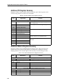
AIC-6915 Internal Registers Summary
PCI Configuration Header Registers Summary 6-1
AIC-6915 Functional Registers Summary 6-2
Additional PCI Registers Summary 6-4
Additional Ethernet Registers Summary 6-4
iv
Contents
7
Register Descriptions
Overview 7-1
AIC-6915 Address Space 7-2
AIC-6915 PCI Address Map 7-2
Terminology 7-4
AIC-6915 Internal Registers 7-4
PCI Registers 7-5
PCI Configuration Header Registers 7-5
PCI Functional Registers Definition 7-17
Ethernet Registers 7-27
General Ethernet Functional Registers 7-27
Transmit Registers 7-37
Completion Queue Registers 7-43
Receive Registers 7-48
PCI Diagnostic Registers 7-59
PCI CardBus Registers 7-66
Additional Ethernet Registers 7-69
Ethernet Physical Device Registers 7-69
MAC Control Registers 7-71
Address Filtering Registers 7-82
MAC Statistic Registers 7-84
8
Sample Driver
Code Conventions 8-1
Producer-Consumer Model for the AIC-6915 8-2
Basic Register Initialization and Reset Sequence 8-3
Receive Process 8-7
Receive Completion Descriptor Queue 8-7
Receive Completion Descriptor Types 8-7
Receive Buffer Descriptor Queue 8-8
Receive Buffer Descriptor Types 8-8
Two Receive Queues 8-9
Receive Producer/Consumer Model 8-9
Receive Polling Model 8-9
Receive Initialization 8-9
Receive Interrupt Handling 8-15
Transmit Process 8-16
Transmit Completion Descriptor Queue 8-16
Transmit Completion Descriptor Types 8-17
Transmit Buffer Descriptor Queue 8-17
Document Title: AIC-6915 Ethernet LAN Controller Programmer’s
Manual
Stock Number: xxxxxx-xx Rev. x
Page: Front Matter-v
Print Spec Number: xxxxxx-xx Rev. x
Current Date: 10/10/98
ECN Date: xx/xx/xx
v
AIC-6915 Ethernet LAN Controller Programmer’s Manual
Transmit Buffer Descriptor Types 8-18
Two Transmit Queues 8-20
Transmit Producer-Consumer Model 8-20
Transmit Initialization 8-21
Transmit Handling 8-25
Transmit Completion Interrupt Handling 8-27
AIC-6915 DDK Features 8-29
DDK Development Environment 8-30
vi
▼ ▼ ▼ ▼
Figures
Figure
1-1
AIC-6915 Block Diagram 1-5
2-1
The AIC-6915 Receive Data Structures 2-2
3-1
4-1
4-2
Transmit Host Communication Data Structure 3-4
PCI Block Diagram 4-3
64-bit PCI Reset Timing 4-5
5-1
Data Processing Unit 5-5
7-1
AIC-6915 PCI Address Map 7-3
Document Title: Document Title
Stock Number: xxxxxx-xx Rev. x
Print Spec Number: xxxxxx-xx Rev. x
Current Date: 10/10/98
Page: Front Matter-vii
ECN Date: xx/xx/xx
vii
Document Title: Document Title
Stock Number: xxxxxx-xx Rev. x
Print Spec Number: xxxxxx-xx Rev. x
Current Date: 10/10/98
Page: Front Matter-viii
ECN Date: xx/xx/xx
▼ ▼ ▼ ▼
Tables
Table
2-1
2-2
2-3
2-4
2-5
2-6
2-7
2-8
2-9
2-10
Receive Buffer Descriptor (One-size, 32-bit Addressing) 2-4
Receive Buffer Descriptor (One-size Buffer, 64-bit Addressing) 2-4
Short (Type 0) Completion Entry 2-6
Basic (Type 1) Completion Descriptor 2-6
Checksum (Type 2) Completion Descriptor 2-6
Full (Type 3) Completion Descriptor 2-6
Receive Completion Descriptor (Word 0) 2-7
Receive Completion Descriptor (Word 1) 2-8
Receive Completion Descriptor (Word 2) 2-9
Receive Completion Descriptor (Word 3) 2-9
3-1
3-2
3-3
3-4
3-5
3-6
3-7
3-8
Type 0 Transmit DMA Descriptor (32-bit Addressing Only) 3-6
End Bit Functionality 3-7
Intr Bit Functionality 3-7
Type 1 Transmit DMA Descriptor (32-bit Addressing) 3-8
Type 2 Transmit DMA Descriptor (64-bit Addressing) 3-9
Type 4 Transmit DMA Descriptor (32-bit Addressing only) 3-10
Transmit Completion Queue Entry Type = DMA Complete Entry 3-10
Transmit Completion Queue Entry Type = Transmit Complete Entry 3-11
4-1
4-2
4-3
Power Management States 4-8
Target Response to PCI Commands 4-10
Address Phase CBE[3:0] Values 4-13
5-1
5-2
Status/Control Register 5-3
Instruction Formats 5-6
6-1
6-2
6-3
6-4
PCI Configuration Header Registers Summary 6-1
AIC-6915 Functional Registers Summary 6-2
AIC-6915 Additional PCI Registers Summary 6-4
AIC-6915 Additional Ethernet Registers Summary 6-4
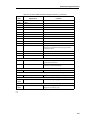
7-1
7-2
7-3
7-4
7-5
7-6
7-7
7-8
7-9
Shade Legends 7-1
AIC-6915 PCI Address Space 7-2
PCI Vendor ID Register 7-5
PCI Device ID Register 7-5
PCI Command Register 7-6
PCI Status Register 7-7
Device Revision ID Register 7-9
Program Interface Register 7-9
Subclass Register 7-9
Document Title: AIC-6915 Ethernet LAN Controller Programmer’s
Manual
Stock Number: xxxxxx-xx Rev. x
Page: Front Matter-ix
Print Spec Number: xxxxxx-xx Rev. x
Current Date: 10/10/98
ECN Date: xx/xx/xx
ix
AIC-6915 Ethernet LAN Controller Programmer’s Manual
Table
7-10
7-11
7-12
7-13
7-14
7-15
7-16
7-17
7-18
7-19
7-20
7-21
7-22
7-23
7-24
7-25
7-26
7-27
7-28
7-29
7-30
7-31
7-32
7-33
7-34
7-35
7-36
7-37
7-38
7-39
7-40
7-41
7-42
7-43
7-44
7-45
7-46
7-47
7-48
7-49
7-50
7-51
7-52
x
BaseClass Register 7-10
Cache Line Size Register 7-10
Latency Timer Register 7-10
Header Type Register 7-11
BIST Register 7-11
Base Address 0 Register 7-11
High Base Address 0 Register 7-12
Base Address 1 Register 7-12
Configuration Card Information Structure Register 7-12
SubSystemVendor ID Register 7-13
SubSystem ID Register 7-13
Expansion ROM Control Register 7-14
Capabilities List Pointer Register 7-14
Interrupt Line Select Register 7-14
Interrupt Pin Select Register 7-15
Minimum Grant Register 7-15
Maximum Latency Register 7-16
PCIDeviceConfig Register 7-17
BacControl Register 7-20
PCI Monitor1 Register 7-21
PCI Monitor2 Register 7-22
Power Management Register 7-22
Power Management Control Status Register 7-23
PME Event Register 7-24
EEPROMControlStatus Register 7-24
EEPROM Memory Definition 7-25
PCIComplianceTesting Register 7-26
IndirectIoAddress Register 7-26
IndirectIoDataPort Register 7-26
GeneralEthernetCtrl Register 7-27
TimersControl Register 7-28
CurrentTime Register 7-30
InterruptStatus Register 7-31
ShadowInterruptStatus Register 7-34
InterruptEn Register 7-35
GPIO Register 7-36
TxDescQueueCtrl Register 7-37
HiPrTxDescQueueBaseAddress Register 7-39
LoPrTxDescQueueBaseAddress Register 7-39
TxDescQueueHighAddr Register 7-40
TxDescQueueProducerIndex Register 7-40
TxDescQueueConsumerIndex Register 7-41
TxDmaStatus1 Register 7-41
Document Title: AIC-6915 Ethernet LAN Controller Programmer’s
Manual
Stock Number: xxxxxx-xx Rev. x
Page: Front Matter-x
Print Spec Number: xxxxxx-xx Rev. x
Current Date: 10/10/98
ECN Date: xx/xx/xx
Tables
Table
7-53
7-54
7-55
7-56
7-57
7-58
7-59
7-60
7-61
7-62
7-63
7-64
7-65
7-66
7-67
7-68
7-69
7-70
7-71
7-72
7-73
7-74
7-75
7-76
7-78
7-79
7-80
7-81
7-82
7-83
7-84
7-85
7-86
7-87
7-88
7-89
7-90
7-91
7-92
7-93
7-94
7-95
7-96
TxDmaStatus2 Register 7-42
TransmitFrameControlStatus Register 7-42
CompQueueHighAddress Register 7-43
TxCompletionQueueCtrl Register 7-43
RxCompletionQueue1Ctrl Register 7-44
RxCompletionQueue2Ctrl Register 7-45
CompletionQueueConsumerIndex Register 7-46
CompletionQueueProducerIndex Register 7-47
RxHiPrCompletionPtrs Register 7-47
RxDmaCtrl Register 7-48
RxDescQueue1Ctrl Register 7-50
RxDescQueue2Ctrl Register 7-52
RxDescQueueHighAddress Register 7-52
RxDescQueue1LowAddress Register 7-52
RxDescQueue2LowAddress Register 7-53
RxDescQueue1Ptrs Register 7-53
RxDescQueue2Ptrs Register 7-54
RxDmaStatus Register 7-54
RxAddressFilteringCtrl Register 7-56
RxFrameTestOut Register 7-58
PCITargetStatus Register 7-59
PCIMasterStatus1 Register 7-60
PCIMasterStatus2 Register 7-61
PCI DMALowHostAddress Register 7-61
BacDmaDiagnostic1 Register 7-62
BacDmaDiagnostic2 Register 7-63
BACDMADiagnostic3 Register 7-64
MacAddr1 Register 7-65
MacAddr2 Register 7-65
FunctionEvent Register 7-66
FunctionEventMask Register 7-67
FunctionPresentState Register 7-67
ForceFunction Register 7-68
MIIRegistersAccessPort Register 7-69
TestMode Register 7-70
Rx General Frame Processor Control Register 7-70
TxFrameProcessorCtrl Register 7-70
MacConfig1 Register 7-71
MacConfig2 Register 7-73
BkToBkIPG Register 7-74
NonBkToBkIPG Register 7-75
ColRetry Register 7-75
MaxLength Register 7-76
Document Title: AIC-6915 Ethernet LAN Controller Programmer’s
Manual
Stock Number: xxxxxx-xx Rev. x
Page: Front Matter-xi
Print Spec Number: xxxxxx-xx Rev. x
Current Date: 10/10/98
ECN Date: xx/xx/xx
xi
AIC-6915 Ethernet LAN Controller Programmer’s Manual
Table
xii
7-97
7-98
7-99
7-100
7-101
7-102
7-103
7-104
7-105
7-106
7-107
7-108
7-109
7-110
7-111
7-112
TxNibbleCnt Register 7-76
TxByteCnt Register 7-76
ReTxCnt Register 7-77
RandomNumGen Register 7-77
MskRandomNum Register 7-78
TotalTxCnt Register 7-78
RxByteCnt Register 7-79
TxPauseTimer Register 7-79
VLANType Register 7-79
MIIStatus Register 7-80
External PHY Address Examples 7-81
Address Filtering Memory 7-82
MAC Statistic Register 7-84
Transmit Frame Processor Register 7-87
Receive Frame Processor Register 7-87
FifoAccess Register 7-87
8-1
AIC-6915 DDK Features 8-29
Document Title: AIC-6915 Ethernet LAN Controller Programmer’s
Manual
Stock Number: xxxxxx-xx Rev. x
Page: Front Matter-xii
Print Spec Number: xxxxxx-xx Rev. x
Current Date: 10/10/98
ECN Date: xx/xx/xx
▼ ▼ ▼ ▼
1
Introduction
The Adaptec AIC-6915, PCI 10/100 Ethernet LAN Controller provides advanced Ethernet
adapter features in a single chip optimized for high-performance and cost effective
Ethernet NICs (Network Interface Cards).
The AIC-6915 integrates all the functions necessary for an Ethernet PCI adapter to directly
connect (via a Medium Independent Interface (MII) -based PHY and line transformer) to
Category 5 unshielded twisted pair (UTP) or shielded twisted pair (STP). The AIC-6915
integrates the following main blocks:
■
Full-featured 2.1 PCI compliant, 32/64-bit master and 32-bit slave bus interface
■
Powerful DMA engine
■
802.3 compliant 10/100 MAC (Medium Access Control) module
■
MII Module
■
100BASE-TX compliant PCS (Physical Signaling) and PMA (Physical Medium
Attachment) modules
The PCI Master uses enhanced data transfer commands to transfer data in zero wait state
bursts. It supports 32- or 64-bit addressing for host buffers and transfers data at up to the
maximum burst rate of 133/266 MBytes/sec with a maximum burst size of up to 2
KBytes. The AIC-6915 provides an External Interface port for access to a ROM/EEPROM
(for add-in card local BIOS support, or boot ROM) and general purpose registers. A
separate 4-wire Serial EEPROM port allows for downloading configuration information
such as the Device ID, Vendor ID, Subsystem ID, Subsystem Device ID and Interrupt line.
The AIC-6915 supports VLAN tagging, IEEE 802.1q and Flow Control as defined by the
IEEE 802.3x specification. The AIC-6915 also provides an MII.
Throughout this document data sizes are defined as follows:
■
Byte = 8-bits
■
Halfword = 16-bits
■
Word = 32-bits
■
Doubleword = 64-bits
1-1
AIC-6915 Ethernet LAN Controller Programmer’s Manual
Features
General
■
Supports four general purpose I/Os that can be programmed separately as inputs,
outputs, open-drain outputs or, interrupt inputs
■
Interface to an external, 8-bit Boot ROM with a maximum size of 256-KByte
■
Supports dynamic system bus (PCI) clock where the network can continue to
operate at any clock frequency
■
Internal loopback on all network ports for testing purposes
■
IEEE 1149.1 compliant JTAG Boundary Scan Test Access port
Ethernet
■
IEEE 802.3 compliant 10/100 MII that supports Category 3 UTP, Category 5 UTP,
Type 1 STP and Fiber cables
■
IEEE 802.3.x compliant Flow Control mechanism
■
Supports Cisco proprietary VLAN ISL frame format
■
Supports IEEE 802.1q (VLAN) frame format
■
Supports PCI and OnNow power management
■
Supports OnNow wakeup function
■
Calculates TCP/IP checksum in transmit mode
■
Checks TCP/IP checksum in receive mode
■
Supports full-duplex operation on all ports (MII, 10/100 Twisted Pair)
■
Provides a variety of address filtering modes:
– Promiscuous
– 16 full 48-bit addresses
– 512-bit hash table for multicast address filtering
■
Time stamp information of every frame received
DMA
■
Two transmit DMA queues to prioritize network traffic
■
Enhanced interrupt mechanism increases performance and reduces CPU utilization:
– Transmit DMA Complete (Early Transmit)
– Early receive
– Transmit/Receive buffer under/over flow error handling. No software
intervention required
■
1-2
DMA channel arbitration eliminates overrun/underrun of First-In-First-Out (FIFO)
buffers
Introduction
■
Supports 32- and 64-bit addressing of Host DMA buffers and DMA descriptor
queues
■
Big/Little endian support for data and descriptors
■
Special output pin to indicate high-priority PCI request
Internal Buffer Management
■
Large, 8 KByte DMA FIFO (default - 4KByte for transmit, 4-KByte for receive)
■
Programmable hardware-controlled transmit FIFO thresholds to prevent underrun
of transmit FIFO and enhance overall system performance
■
Unlimited (limited only by the FIFO size) Receive/Transmit frame queueing in the
FIFO to handle long PCI bus latencies
■
Hardware support for handling transmit collisions and FIFO underruns without
software intervention
32/64-bit PCI
■
Compliant with PCI Local Bus Specification revision 2.1
■
Compliant with Intel PCI Bus Power Management Interface Specification Rev 1.00
and Microsoft Device Class Power Management Reference Specification (OnNow)
■
PC 97 ready. Implements all hardware features required by Microsoft’s PC 98 design
specification
■
Supports 3.3V and 5.0V PCI signaling
■
Direct pin out connection to PCI 32/64-bit bus interface
■
PCI bus master with zero wait state 32/64-bit memory data transfers at 133/266
MBytes/sec, capable to support leading and trailing byte offset for DMA read and
write (32-bit) for DMA write
■
Supports 64-bit addressing in master and target modes
■
PCI bus master/slave timing referenced to PCI signal PCLK (33.3 MHz max)
■
PCI bus master programmable Latency Timer, Cache Size, And Interrupt Line Select
registers
■
Automatically senses if the adapter is plugged into a 32-bit or a 64-bit PCI slot.
■
Supports cache line sizes of 16, 32, 64, 128, and 256 bytes
■
Supports any combination of active byte enables for all PCI slave accesses
■
Supports medium PCI target device-select response time
■
Supports, as a bus master, enhanced PCI System memory data read and write
commands:
– Memory Read
– Memory Read Line
– Memory Read Multiple
– Memory Write
1-3
AIC-6915 Ethernet LAN Controller Programmer’s Manual
– Memory Write And Invalidate
1-4
■
Supports PCI bus address and data parity generation and checking
■
Supports PCI PERR and SERR requirements
■
Supports 8-bit, 256-KByte, external Memory port for interface with external Boot
ROM or devices/registers
■
Supports external Boot ROM access from memory or Expansion ROM address space
■
Supports an external serial EEPROM for downloading chip configurations and MAC
address
■
INTA_ interrupt generation from hardware, firmware, and software controlled
sources
■
Supports PCI slave accesses to PCI Configuration Header from configuration
(read/write), I/O (indirect, read only) and memory address spaces (read only)
■
Supports PCI slave access to AIC-6915 functional registers from configuration, I/O
and memory address spaces
■
Supports PCI slave access to AIC-6915 debug/buffer/FIFO Ethernet registers
(implemented in the Ethernet control module) and external Memory port from
indirect I/O and memory address spaces
■
PCI target latency of 16 clocks maximum for the first target access cycle. The
AIC-6915 initiates a cycle retry when an access requires more than 16 clocks to
complete
Introduction
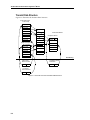
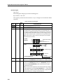
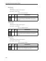
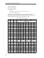
Block Diagram
Figure 1-1 is a block diagram of the AIC-6915.
Status
(Receive)
(Transmit)
MAC
Data (8)
Status
Station
Address
TCP
Checksum
Wakeup
Data (8)
Statistics
TxFrame
Receive Clock
Status
Sync.
FIFO Bus (32-bits)
RxFrame
Arbiter
TCP
Checksum
TxDMA
8 KByte SRAM
Control
Combined
Tx/Rx FIFO
Serial
EPROM
RxDMA
EPROM
Port
DMA Bus (64-bits)
Comp.
BusAccessControl
(64 bits)
(Master)
SlaveAccess, system registers
PCI Clock
PCI
(32 bits)
(Slave)
Status
Receive Clock Domain
PCI Bus (64-bits)
PCI Clock Domain
Transmit Clock Domain
Figure 1-1. AIC-6915 Block Diagram
1-5
AIC-6915 Ethernet LAN Controller Programmer’s Manual
Modules
The AIC-6915 contains the following major modules:
❒
1-6
■
PCI - Controls access to the PCI bus and contains PCI-specific registers.
■
BusAccessControl - Arbitrates master accesses to the PCI bus from internal
modules, and accesses the FIFO from the PCI side.
■
SlaveAccess - Drives the REGBUS to access the internal modules when AIC-6915 is
accessed from the PCI bus.
■
General Registers - Contains general control and status registers, timers, and
interrupt control. These registers are located throughout the AIC-6915.
■
Memory Port - Controls accesses to external EEPROM, FLASH, or other devices.
■
Serial EPROM - Controls interface to the serial EPROM.
■
TxDMA - Manages reading of the current frame being DMA-transferred for
transmit, as well as transmit descriptor lists.
■
TxFrame - Manages the current frame being transmitted, reading the frame from the
FIFO.
■
RxDMA - Manages writing of the current frame being DMA-transferred for receive,
as well as the receive descriptor lists.
■
RxFrame - Manages the current frame being received, writing the frame to the FIFO.
■
Station Address - Compares the address of incoming frames with the stored
addresses and/or hash table bits, and signals the RxFrame module if the addresses
do not match.
■
TCP Checksum - Two TCP checksum modules are implemented, one for receive and
one for transmit. The Receive TCP checksum module sums all relevant fields and
compares them with the checksum value in the frame. The Transmit TCP checksum
computes the checksum and places it in the FIFO.
■
Wakeup - Looks for frames matching a predefined pattern and asserts the PME_
signal to wake up the system if one is found.
■
Completion - Records the current address for writing completion descriptors and
stores the upper 32-bits of the descriptor’s address.
■
Statistics - Counts various events from MAC, receive, and transmit.
■
Synchronizer - Synchronizes receive data and control to the transmit clock.
■
MAC - The MAC layer defined in the Ethernet specification manages many of the
details in transmitting and receiving frames.
■
8 KByte SRAM - Dual-port SRAM used for storing transmit and receive data.
▼ ▼ ▼ ▼
2
Receive Architecture
Features
The host-related Receive Architecture features are
■
Interrupts may be delayed so that only one interrupt is generated when a group of
frames is received
■
Choice of shared or separate completion lists for receive and transmit. An optional
second completion list can be used for high-priority traffic
■
Two programmable 256-entry or 2048-entry buffer descriptor lists, with optional
smaller lists as defined by an “end” bit
■
All receive buffers can be either the same size, or have individual sizes
■
Early receive interrupt is generated when the DMA-transfer of a programmable
number of bytes is complete. Status is not available until the end of the packet is
DMA-transferred
■
Optional 64-bit addressing for buffers and descriptor lists. All descriptor lists must
be in the same 32-bit region in 64-bit space. Buffers can be located anywhere within
the space, but an individual buffer must not cross a 4-GByte boundary
The internal Receive Architecture features are
■
4K Byte receive FIFO (The actual 8KByte on-chip SRAM is shared with Transmit)
■
The FIFO does not have an arbitrary limit on the number of frames, but can continue
receiving frames until it is full, regardless of the frame sizes
■
Each frame requires only 8 bytes of overhead in the FIFO
■
IEEE 802.3x based flow control
■
Cisco’s ISL frame support (Implemented in the MAC)
Additional value-added features
■
Power management.
■
Wakeup frames compliant to Microsoft’s OnNow specification
■
TCP and UDP checksum support
2-1
AIC-6915 Ethernet LAN Controller Programmer’s Manual
■
VLAN support:
– Address filtering based on VLAN
– Ability to delete VLAN tag and number from frame returned to the host
■
Optional second buffer list for allocating two different buffer sizes
Host Data Structures
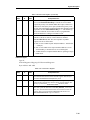
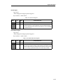
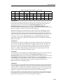
Figure 2-1 illustrates the AIC-6915 receive data structures.
Receive Buffers
Receive Buffer Descriptor Queue (256/2KByte)
Adrs
Receive Completion Queue (2KByte entries)
Start
End Len Stat
Adrs
Adrs
Adrs
Adrs
1 per Frame
Host Memory
On-chip
Adrs ListLen
Adrs
Write Read
Write Read
BufferLength
(2 Queues are available for 2 different sizes of buffers)
(2 completion Queues allow for 2 priorities)
Figure 2-1. The AIC-6915 Receive Data Structures
Producer and Consumer Indices
The transmit, receive, and completion descriptors are stored in circular queues. With the
descriptor queue, the host writes entries into the queue. The AIC-6915 reads from the
descriptor queue and writes to the completion queue, which is in turn read by the host.
The AIC-6915 maintains onchip Producer and Consumer indexes to each queue. The first
element of any queue has an index of 0.
The Producer Index indicates the next entry of the queue to be written, while the
Consumer Index indicates the next entry in the queue to be read.
If Producer and Consumer indices are equal, the queue is empty. If (Producer+1) mod
QueueSize is equal to Consumer then the queue is full. The maximum number of entries
placed in a queue at one time is the queue size minus one.
Receive DMA Descriptor Queues
The AIC-6915 contains two Producer/Consumer type DMA Receive Descriptor Queues
that contain a maximum of either 256 or 2048 entries. A variable option permits the use of
a smaller queue. Host Buffer addresses must be aligned to a word (4-byte) boundary. For
best performance, addresses should also be aligned to cacheline boundary.
2-2
Receive Architecture
A programmable number of words can be skipped between buffer descriptors. This
allows the driver to store data related to a buffer. When using 64-bit addressing, all
descriptor and completion queues must be contained in the same 32-bit address space.
Descriptor queues must be aligned to a 256-byte boundary.
When using 64-bit addressing, each receive buffer must fit within one 32-bit address space
and must not cross a 4-GByte boundary.
There are two modes available for the host to inform the AIC-6915 that it has placed new
buffer on the Buffer Descriptor Queue, Normal And Polling mode.
Normal Mode
In normal mode, after adding buffers to the buffer queue, the host writes to the onchip
producer index. Some normal mode features are
■
Fixed size 256- or 2048-entry queue.
■
The AIC-6915 tracks the number of receive buffers available and can interrupt the
host using the RxQ1LowBuffersInt and RxQ2LowBuffersInt interrupts if the number
falls below a programmable threshold. The software driver may use this interrupt
status bit to indicate the time it should update the producer index of the receive
descriptor queue. This may save some ‘expensive’ slave cycles used for updating the
producer index.
■
If the AIC-6915 runs out of descriptors, it generates a RxQ1LowBuffers or
RxQ2LowBuffers interrupt.
Polling Mode
In polling mode (RxPrefetchDescriptorMode = 1’b1), the host writes the descriptor to its
local memory. When the AIC-6915 needs a descriptor, it always reads the next one
regardless of the value in the producer pointer. If the valid bit is set, the AIC-6915 uses the
descriptor. If not, it waits for the host to place more descriptors in the queue and to write
any values to the producer. Some of the features of prefetch mode are
■
Variable sized descriptor list with a maximum of 256 or 2048 entries. The host can set
an “End” bit in the last descriptor in the list, causing the AIC-6915 to automatically
wrap to the start of the list when fetching the next entry. The AIC-6915 automatically
wraps after 256 or 2048 entries even if the “End” bit is not set.
■
The AIC-6915 cannot track the number of receive buffers available and only
interrupts the host requesting more buffers when it is completely out by generating a
RxQ1LowBuffersInt or RxQ2LowBuffersInt interrupt. If the host does not respond to
this interrupt fast enough, the onchip buffer may overflow and frames may be lost.
■
Whenever the number of buffers is zero and the host has posted more buffers to the
receive list, it must also write to the producer pointer to inform the AIC-6915 that
more buffers have been added. The host can write any value. This causes the
AIC-6915 to refetch the descriptor and look at the Valid bit again.
■
The AIC-6915 does not reset the ‘Valid’ bit in the descriptor queue. It is the software
driver’s responsibility to manage the queue. The software driver can do this by
maintaining at least one invalid descriptor right after the group of valid ones.
■
In Polling mode, software driver must write to Producer Index (with RxDmaEn) to
wake-up the AIC-6915 after reset.
2-3
AIC-6915 Ethernet LAN Controller Programmer’s Manual
32-bit Addressing Mode
Table 2-1. Receive Buffer Descriptor (One-size, 32-bit Addressing)
31
24
23
16
15
8
7
Address
0
E V
64-bit Addressing Mode
Table 2-2. Receive Buffer Descriptor (One-size Buffer, 64-bit Addressing)
31
24
23
16
15
8
7
LowAddress
0
E V
HighAddress
Descriptor Fields:
■
Address - The address of the buffer.
■
LowAddress - Least-significant 32-bits of address.
■
HighAddress - Most-significant 32-bits of address.
■
E / End - This bit is set to indicate the last descriptor. The next descriptor should be
taken from the beginning of the list. This bit should only be set when the receive
descriptors are in prefetch mode. It must be cleared otherwise.
■
V / Valid - In prefetch mode, this bit should be set if the descriptor is valid.
Completion/Status Descriptor Queue
There are two receive completion descriptor queues, one for high-priority frames and one
for low-priority frames. The completion queues include the following features:
2-4
■
Producer/Consumer type completion queue.
■
Programmable queue contains a separate list for receive, or the queue can be shared
between transmit and receive.
■
A second list is available for high-priority frames. This cannot be shared with
transmit.
■
Software can zero the word being read and check for a nonzero value to confirm that
new status was written. No valid descriptors will be all zero’s.
■
Two and four word completion descriptors include full status.
■
Completion descriptor queues must be aligned on a 256-byte boundary.
■
Completion descriptors may be 1, 2, or 4 words, depending on the amount of
information required by the driver. Only 1 or 2 word completion descriptors may be
used if the receive and transmit completion queues are shared.
Receive Architecture
Accepting frames
The AIC-6915 uses two criteria when deciding whether to accept a frame: Frame address
and frame quality. When receiving a frame, the Station Address block evaluates a frame’s
address to determine if this station should receive the frame. Address filtering is
accomplished by the time 64bytes are received. During this time, the General Frame
Processor (GFP) also determines some characteristics about a frame, such as whether it is
a TCP frame, whether it should override the descriptor or completion queues used, and
the length of the header.
The MAC also determines some characteristics about the frame, such as its length, and
whether any errors have occurred. This evaluation completes by the end of the frame, and
the frame is assigned a “quality” based on this information. Normally, frames are only
accepted if there are no CRC errors, no extra nibbles or bits, and the length is legal (less
than or equal to a programmable value, normally 1536, and at least 64 bytes). However,
the following control bits can allow additional frames to be accepted:
■
RxDmaCrcErrorFrames - if set, accept frames with a CRC errors
■
RxDmaLongFrames - if set, frames longer than a programmable value (normally
1536) are accepted. Otherwise, they are rejected
■
RxDmaBadFrames - if set, accept frames with a CRC error, nibble or code violation
■
RxDmaShortFrames - if set, the AIC-6915 accepts frames shorter than 64 bytes.
■
RxReportBadFrames - if set, the AIC-6915 reports the status for long and bad frames
to the host, although it reuses the buffers for the next frame. Otherwise, the AIC-6915
does not report any status when it receives a bad frame, but only updates internal
statistics.
Once 64 bytes of a frame have been received successfully, the AIC-6915 can start DMAtransferring the frame to the host. In some operating modes, such as header splitting, it
must also wait for the frame processor to process the frame’s IP header. If the frame is bad,
the AIC-6915 does not inform the host of the buffers it used for that frame. Rather, it backs
up its internal pointers and reuses those buffers on the next frame. The receive DMA
engine transfers the receive data in amounts equal to the RxBurstSize field specified in
RxDmaCtrl register. The DMA operation starts when a number of bytes equal to or greater
than RxBurstSize is stored in the FIFO. When the number of bytes in the FIFO exceeds a
programmable threshold (RxHighPriorityThreshold), the receive DMA engine is granted
priority over the transmit engine for DMA services.
Completion Descriptor
A completion descriptor is normally DMA-transferred to the host when a good frame is
received. The frame is DMA-transferred to the host and indicates the frame status, frame
length, and the number of buffers used.
Various formats of completion descriptors are available, with RxCompletionQ1Type
selecting the type to use the main completion queue, and RxCompletionQ2Type selecting
the type to use in the high-priority queue.
If RxCompletionSize is set, the completion descriptor includes only the first word shown.
If the bit is cleared, the first two words are shown. The RxCompletionType field controls
whether the second word contains the TimeStamp, data from the Frame Processor, or some
frame processor data and the VLAN ID.
A valid completion descriptor will never have a length field with a value of 0.
2-5
AIC-6915 Ethernet LAN Controller Programmer’s Manual
Table 2-3. Short (Type 0) Completion Entry
31
24
0 1 Status1
23
16
15
8
EndIndex
7
0
Length
Table 2-4. Basic (Type 1) Completion Descriptor
31
24
0 1 Status1
23
16
15
8
EndIndex
7
0
Length
Status2
VLAN ID
Table 2-5. Checksum (Type 2) Completion Descriptor
31
24
0 1 Status1
23
16
15
8
EndIndex
7
0
Length
Status2
Partial TCP/UDP Checksum
Table 2-6. Full (Type 3) Completion Descriptor
31
24
0 1 Status1
23
16
15
EndIndex
7
Length
Status2
Status3
Partial TCP/UDP Checksum
Start Index
VLAN ID + Priority
Timestamp
2-6
8
0
Receive Architecture
Table 2-7. Receive Completion Descriptor (Word 0)
Bit(s)
Description/Function
Status1 field
29
OK - The frame is good. There were no CRC errors, dribble nibble, illegal lengths, or
receive code violations. In ISL mode, the ISL and Ethernet checksums must both be
valid. This does not include the TCP/UDP checksum.
28
FifoFull - If set, the frame is incomplete due to FIFO full - no other status bits, except
OK, are valid.
27
BufferQueue - If set, the buffer queue 2 was used for the packet. If cleared, buffer
queue 1 was used.
EndIndex field
26:16
EndIndex - Index of the last buffer used in the buffer queue.
Length field
15:0
Length - Total length of data transferred in bytes for good packet.
This value is generally equal to the length of the packet (including destination and
source addresses, type fields, etc.) minus 4 bytes, since the CRC isn’t transferred by
default. Setting RxDmaCrc to transfer the CRC can increase the length transferred here
and reported by 4 bytes. Setting VlanMode=01, which causes the VLAN tag and ID to
be stripped will reduce the length transferred and reported by 4 bytes.
In header-splitting mode (RxDmaQueueMode=100), two buffer descriptors are
transferred for TCP packets. A single receive completion queue is used for this mode.
The Length field of the first completion descriptor contains the length of the header in
bytes. The Length field of the second completion descriptor contains the total bytes
transferred, including the header, even through the header data is transferred to the
first queue, while the rest of the data is transferred to the second queue. This field may
not be valid for bad packets.
2-7
AIC-6915 Ethernet LAN Controller Programmer’s Manual
Table 2-8. Receive Completion Descriptor (Word 1)
Bit(s)
Description/Function
Status2 field
31
Perfect - destination address matches one of the 16 predefined “perfect” addresses.
30
Hash - hashed destination address matches a bit set in the hash table
29
CRC Error - TRUE if the packet had a CRC error. [PE-15 CRC error]
28
ISL CRC error - TBD
27
Dribble - TRUE if the packet contains a noninteger number of bytes (i.e. extra bits or an
extra nibble).
26
Receive Code Violation - An illegal 4B/5B code was received in the packet.
25
Vlan Frame - TRUE if the packet’s tag matched the tag programmed in the MAC
VlanType register.
24
ChecksumOk - If set, the packet is a TCP or UDP packet, the checksum was checked
and is good.
23
ChecksumBad - If set, the packet is a TCP or UDP packet, the checksum was checked
and is bad
22
PartialChecksumValid - If set, the partial checksum is valid
21
Fragmented - If set, the frame was fragmented
20
TcpFrame - If set, the frame was a TCP frame
19
UdpFrame - If set, the frame was a UDP frame
18:16
FrameType - 0=Unknown, 1=IPv4, 2=IPv6, 3=IPX, 4=Icmp, 5=Unsupported
Status3 field
15
IslFrame - If set, the frame is an ISL frame, meaning that the first 5 bytes of its
destination are 01:00:0C:00:00.
14
PauseFrame - If set, the frame is a Pause MAC Control frame as defined in the IEEE
802.3x specification.
13
ControlFrame - If set, the frame is a MAC control frame other than a pause frame as
defined in the IEEE 802.3 specification.
12
Header - If set, the completion descriptor is for a frame header.
11
Trailer - If set, the completion descriptor is for the remaining data in a frame whose
header was transferred.
StartIndex field
10:0
2-8
StartIndex - Index of the first buffer used in the buffer queue. This field is only
important when both receive descriptor queues are being used.
Receive Architecture
Table 2-9. Receive Completion Descriptor (Word 2)
Bit(s)
Description/Function
Partial TCP/UDP checksum field
31:16
Partial TCP/UDP Checksum - When fragmented TCP/UDP frames are received, the
partial TCP/UDP checksum of the first frame is calculated by the TCP/UDP header
and data. The partial TCP/UDP checksum for subsequent frames is calculated by the
TCP/UDP data only
VLan + Priority field
15:0
VLanID + Priority - This field contains bytes 13 and 14 of the IEEE 802.1Q compliant
frame.
Table 2-10. Receive Completion Descriptor (Word 3)
Bit(s)
Description/Function
Timestamp field
31:0
TimeStamp - Time stamp value at the completion of the received frame.
The AIC-6915 provides address filters that have an effect on which receive frames are
accepted and how they are processed. For more information on address filtering, refer to
Address Filtering Registers on page 7-82.
❒
2-9
▼ ▼ ▼ ▼
3
Transmit Architecture
Features
The main features of Transmit Architecture are
■
Two Buffer Descriptor Queues in the Host Memory. One for high-priority packets
and one for low-priority packets.
■
Driver notifies the transmit block to start transmitting packets by writing the
“Producer Index” of descriptor queues to its internal register. Producer and
consumer indices are 11-bit pointers to an 8-byte descriptor in the queue. The
transmit block does not poll host memory for new packets.
■
Five descriptor types are supported. Descriptors can be categorized as “frame
descriptors”, which contain multiple buffer pointers in one descriptor format, and as
“buffer descriptors”, which contain one buffer pointer in one descriptor format. The
driver must program the descriptor type at initialization time.
■
Buffer descriptors (type 1 and 2) are multiples of either 8- or 16-bytes depending on
whether the address is 32-bit or 64-bit. Frame descriptors (types 0, 3, and 4) can be
either fixed size or variable size. In fixed-size mode, the frame size is defined in the
“MinFrameDescSpacing” register, regardless of the number of buffer segments in
the frame. In variable size mode, frame descriptors’ size is the sum of total buffer
segments. There is a “Skip field” defined in front of each descriptor to reserve space
for the driver to store information. The “Skip field” size varies from 0 bytes to 128
bytes and is programmed by the driver at initialization time. The AIC-6915 does not
read or write to the “Skip field”.
■
The descriptor queue size has a maximum size of 16KBytes. The actual length is
variable with the end of queue defined by the “End” bit. The definition of the “End”
bit is described in the Descriptor Queue section. Both high-priority and low-priority
queues have base addresses aligned on a 256-byte boundary.
■
The transmit DMA module returns buffers to the host by DMA-transferring the
“Completion Descriptors” to the completion queue in the host memory. As soon as
the DMA transfer completes, the packet is considered “done” and returned to the
host.
3-1
AIC-6915 Ethernet LAN Controller Programmer’s Manual
3-2
■
There are three kinds of interrupts generated by the transmit DMA engine. A
“TxDmaDoneInt” is generated when the entire packet is DMA-transferred. A
“TxFrameCompleteInterrupt” is generated when an entire packet is transmitted.
There are two control bits, DisableTxDmaCompletion and
DmaCompletionAfterTransmitComplete defined in the TxDescQueueCtrl and
TxFrameControl registers to enable and disable each one of them. Setting these
interrupt status bits is also conditioned with the INTR control bit in the transmit
descriptor. A third interrupt, “TxQueueDoneInterrupt”, is generated only when the
descriptor queue is empty.
■
Completion queue address control is centralized in the Completion Module for both
receive and transmit. There are separate Completion Queues for receive and
transmit. However, extra logic is built in the Completion Module to handle one
Completion Queue for both receive and transmit. The Completion Queue size is
1024 entries. Each entry is either one word or two words, defined by driver at
initialization time. The Completion Queue is aligned at 256-byte boundary. There is a
Completion Queue Threshold defined in the register. When the free entries in the
Completion Queue fall below this threshold, an interrupt is generated. The software
driver should update the consumer index of the completion queue when it detects
that the interrupt status bit is set.
■
A Transmit DMA operation is triggered when there are frames in the descriptor
queues and when the FIFO has room for “DMA Burst Size”, a register defined by the
software driver during initialization. The transmit DMA module dynamically
adjusts DMA burst size so that DMA operations end on cache line boundaries. This
can improve bus utilization on DMA data transfers.
■
The “Frame Processor (FP) FIFO Engine” in the transmit DMA block works with FP
to calculate TCP/UDP checksum for transmit packets. The checksum calculation
starts when the DMA engine fetches the first burst of transmit data from Bus Access
Control (BAC) and works in parallel during the DMA-transfer of the packet. Actual
transmission to the MAC is not enabled until the checksum calculation is finished.
For non-TCP/UDP packets, the driver can set the CALTCP bit to zero in the
descriptor to disable checksum calculation and the transmission to the MAC can
start without waiting for the end of packet. After the Transmit DMA fetches the first
burst of transmit data, it signals the FP FIFO engine to begin reading packet data
from the FIFO bus and passes that data to FP 16-bits at a time. The FP FIFO Engine
decodes the write pointer of the FIFO to make sure that it does not read past the
valid data of transfer. At the end of the packet, the DMA-transfer terminates and the
FP FIFO Engine waits for the checksum and address of checksum returned by the FP.
The FP FIFO engine writes the checksum to the FIFO, signals the transmit frame to
start transmitting the packet, and signals the transmit DMA engine to start reading
the next packet.
■
Internal 4 KByte dedicated transmit FIFO. The FIFO is implemented by a dual-port
SRAM. Once the port is written by the BAC, the other port is shared by the transmit
and receive blocks.
■
Packets in the internal FIFO are handled by link-lists. Transmit DMA block can DMA
as many packets as possible into the FIFO as long as there is enough space.
Transmit Architecture
■
When the amount of packet data in the FIFO exceeds the “Transmit Threshold,” or
when the end of packet is already in the FIFO, the “Transmit Frame” state machine
signals the MAC to start transmitting the packet. The transmit frame block handles
reading packets from the FIFO, MAC interface and FIFO link list management. It
also handles “retries” in case collision occurs and handles “aborts” when MAC
signals errors.
■
Built-in decode logic in the transmit frame block dynamically adjusts the priority of
BAC arbitration. When the valid data in the FIFO drops below the “High-Priority
Transmit FIFO Threshold” during transmission, the priority of transmit DMA is
asserted and subsequent Transmit DMA operations are allotted a higher priority in
BAC arbitration. Note that this only happens when the Transmit DMA engine and
Transmit Frame are working on the same packet. This algorithm is designed to help
prevent FIFO underrun.
■
When the MAC is transmitting a packet, it may encounter network errors such as
late collision, excessive deferral, excess collisions, or long packets. The MAC signals
the transmit frame, which in turn aborts the current transmission. For normal
collisions during the collision window, the MAC signals a “retry” to the Transmit
Frame, which in turn retries transmission of these packets.
■
Error handling routines are implemented in the Transmit Frame to retransmit a
packet when transmit FIFO underrun error occurs. The Transmit Frame attempts to
retransmit the packet if the start_of_packet data has not been overwritten by a
subsequent DMA operation. If the Transmit Frame block cannot re-transmit the
packet after three tries, the packet is aborted. The start_of_packet “Producer Index”
of the error packet is DMA-transferred back to the host through the “Completion
Queue”.
■
As the MAC completes each packet transmission, it advertises the transmit status of
this packet. The Statistic Block collects both transmit and receive status and stores
them in a local register file. When the mode of “Transmit Complete Interrupt” is on,
the transmit status is DMA-transferred to the host.
■
64-bit addressing support on all data buffers. The “Descriptor Queue” and the
“Completion Queue” are also 64-bit addressing, but they share the same high-order
32-bit addresses (same 4-GByte page).
■
Power Management Mode defined by PCI Bus Power Management Interface
Specification. When the transmit block is put to the “Sleep” mode, all the state
machines are reset to “Idle” and then the clock is removed.
3-3
AIC-6915 Ethernet LAN Controller Programmer’s Manual
Transmit Data Structure
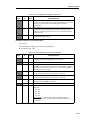
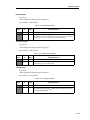
Figure 3-1 illustrates the Transmit Data Structure
Buffer Descriptors
for Hi-Priority
Skip Field
Frame Header
Pkt 1 Buf1
Pkt 1 Buf2
Pkt 1 Buf3
Skip Field
Frame Header
Pkt 2 Buf1
Pkt 2 Buf2
Pkt 2 Buf3
Packet Data Buffers
Completion Queue
Status
CI
Buffer Descriptors
for Lo-Priority
Skip Field
Frame Header
Pkt 3 Buf1
Pkt 3 Buf2
Pkt 3 Buf3
Host Memory
High-Priority
Queue Pointers
CI
Completion Queue
Pointers
CI
PI
PI
Low-Priority
Queue Pointers
CI
PI
Figure 3-1. Transmit Host Communication Data Structure
3-4
the AIC-6915
Transmit Architecture
Transmit Register Set
The following is a list of transmit parameters programmed by the driver during
initialization.
■
Transmit descriptor queue size and base address.
■
Completion queue size and base address.
■
Descriptor type, minimum spacing, and skip field size.
■
FIFO size (4KBytes).
■
PCI cache line size.
■
DMA burst size.
■
Transmit start threshold.
■
DMA priority threshold.
The following is a list of transmit registers used during a host to AIC-6915
communication.
■
High-priority queue consumer index. (Written by the AIC-6915, read by driver).
■
High-priority queue producer index. (Written by the driver, read by the AIC-6915).
■
Low-priority queue consumer index. (Written by the AIC-6915, read by the driver).
■
Low-priority queue producer index. (Written by the driver, read by the AIC-6915).
■
Completion queue consumer index. (Written by the driver, read by the AIC-6915).
■
Completion queue producer index. (Written by the AIC-6915, read by the driver).
Transmit DMA Buffer Descriptor Queues
There are two Buffer Descriptor Queues for transmission. One for high-priority traffic and
one for low-priority traffic. Each Descriptor Queue size has a maximum size of 16-KBytes.
The actual length is variable with the end-of-queue defined by the “END” bit. The
definition of the “END” bit is described in the following sections. Both high-priority and
low-priority queues have base addresses aligned on a 256-byte boundary.
Five descriptor types are supported. The driver must program the descriptor type during
initialization. Descriptors are in multiples of 8-bytes. The Descriptor Queue is aligned on a
256-byte boundary. There is a “Skip field” defined in front of each packet to reserve space
for the driver to store information. The “Skip field” size varies from 0 bytes to 128 bytes
and is programmed by the driver during initialization. The AIC-6915 does not read or
write to the “Skip field”.
Type 0, 32-bit Addressing Mode (Frame Descriptor)
Type 0 enables the driver to execute a simple and fast copy of a TCB data structure (given
by the upper layer software as a frame descriptor) to the Descriptor Queue area.
3-5
AIC-6915 Ethernet LAN Controller Programmer’s Manual
Table 3-1. Type 0 Transmit DMA Descriptor (32-bit Addressing Only)
31
24
32
16
15
8
7
0
Skip Field (multiple of 8 bytes)
One Skip Field per Packet
ID =
4’b1011
I E C C
N N A R
T D L C
R
T E
C N
P
Reserved
Reserved
Reserved
Number Of Tx Buffers
First Buffer Address
Total Packet Length
First Buffer Length
Last Buffer Address
Reserved
3-6
Last Buffer Length
■
ID: 4 bits. This field is used by the software/debugger to identify the start of a
descriptor. If a transmit DMA operation does not see a matched ID in this field, it
aborts the DMA operation and sets an interrupt status bit.
■
Number of Fragments: 8 bits. Defines the number of follow-on segments. This field
must be “nonzero”.
■
END: Indicates that the current descriptor is at the end of the queue. The ‘End” has
different functionality for the following conditions:
Transmit Architecture
Table 3-2. End Bit Functionality
Desc. Type
■
Conditions
Functionality
Frame (0,3,4) MinFrameDescSpacing
!=0
The number of bytes between two
consecutive frame descriptions is fixed. The
queue wraps around at the end of the fixed
address. No wrap in the middle of a frame
descriptor.
Frame (0,3,4) MinFrameDescSpacing
=0
The number of bytes between two
consecutive frame descriptions is variable.
For type 0/4, the queue wraps after reading
16 bytes of descriptor data. For type 1/3, the
queue wraps after reading 8 bytes of
descriptors.
Buffer (1,2)
For type 1, the queue wraps after reading 8
bytes of descriptors data.
For type 2, the queue wraps after reading 16
bytes of descriptor data.
MinFrameDescSpacing
must be 0.
‘End’ bit is valid only
for the first descriptor
of a frame.
INTR: Causes setting of the interrupt status bits (TxDmaDoneInt and/or
TxFrameCompleteInt) after complete transmission of the entire packet. The
appropriate interrupt status bit is set based on two control bits that the software
programs at the initialization phase. Given ‘INTR’ is set the following table specifies
the functionality:
Table 3-3. Intr Bit Functionality
DisableTxDmaCo TxCompletionDescAft
mpletion
erTxComplete
Functionality
0
0
TxDmaDoneInt is set after complete DMA the
whole packet.
0
1
TxDmaDoneInt is set after complete DMA the
whole packet, and TxFrameCompleteInt is set
after complete transmitting the whole frame.
1
0
None of the two interrupt status bits is set.
1
1
TxFrameCompleteInt is set after complete
transmitting the whole frame. ‘INTR’
Note: The software driver may choose to work with another interrupt status bit,
TxQueueDoneInt, that is not controlled by ‘INTR’. The AIC-6915 sets this bit after
the DMA-transfer of a completion descriptor for the last frame queued for
transmit. The last frame is detected when the consumer and producer indices of
the queue are equal.
■
CRCEN: Setting this bit enables the MAC to calculate and append the CRC value for
the current packet. Clearing the bit disables the MACs ability to calculate the CRC
value.
■
CALTCP: Setting this bit enables the F P to calculate TCP/UDP checksum for this
packet. Clearing the bit disables the FPs ability to calculate the checksum.
3-7
AIC-6915 Ethernet LAN Controller Programmer’s Manual
■
Total Packet Length: This 16-bit field defines the total packet length. If this field is
zero, it is ignored and the total packet length is equal to the sum of all the buffers. If
this field is nonzero, it is defined as the total packet length.
Note: In Novell TCB/ECB blocks, the total packet length is not always equal to the
sum of the buffer length. Transmit DMA pads extra bytes to the FIFO if the total
packet length is greater than the sum of the buffer length.
■
Buffer Length: The length of the host buffer in bytes.
■
Buffer Address: The byte address of the host buffer.
Type 1 (Generic), 32-bit Addressing Mode (Buffer Descriptor)
In Type 1 and 2 buffer descriptors, the INTR, END, CALTCP, CRCEN, and Number of Tx
Buffers fields are valid for the first buffer of a frame only. The ID, Length, and Address are
valid for all buffers of the frame. The software driver must use the ‘End’ bit only in the
first buffer descriptor of a frame. The queue wraps around after reading 8 bytes of
descriptor data for Type 1 and 16 bytes of data for Type 2.
Table 3-4. Type 1 Transmit DMA Descriptor (32-bit Addressing)
31
24
23
16
15
8
7
0
Skip Field (multiple of 8 bytes)
One Skip Field per Buffer
ID =
4’b1011
I E C C Number Of Tx Buffers
N N A R
(valid only if first
T D L C
fragment)
R
T E
C N
P
Length (bytes)
Address
Type 2 (Generic), 64-bit Addressing Mode (Buffer Descriptor)
In Type 1 and 2 buffer descriptors, the INTR, END, CALTCP, CRCEN, and Number of Tx
Buffers fields are valid for the first buffer of a frame only. The ID, Length, and Address are
valid for all buffers of the frame. The software driver must use the ‘END’ bit only in the
first buffer descriptor of a frame. The queue wraps around after reading 8 bytes of
descriptor data for Type 1 and 16 bytes of data for Type 2.
3-8
Transmit Architecture
Table 3-5. Type 2 Transmit DMA Descriptor (64-bit Addressing)
31
24
23
16
15
8
7
0
Skip Field (multiple of 8 bytes)
One Skip Field per Buffer
ID =
4’b1011
I E C C Number Of Tx Buffers
N N A R
(valid only if first
T D L C
fragment)
R
T E
C N
P
Length (bytes)
Reserved
Low Address
High Address
Type 3, 32-bit Addressing Mode (Frame Descriptor)
This mode is currently not supported in the AIC-6915.
Type 4, 32-bit Addressing Mode (Frame Descriptor)
Type 4 enables the driver to execute a simple and fast copy of DOS and OS2 data structure
(given by the upper layer software as a frame descriptor) to the descriptor queue area. The
only difference is the location of ‘Buffer Length’ and ‘Buffer Address’.
3-9
AIC-6915 Ethernet LAN Controller Programmer’s Manual
Table 3-6. Type 4 Transmit DMA Descriptor (32-bit Addressing only)
31
24
23
16
15
8
7
0
Skip Field (multiple of 8 bytes)
One Skip Field per Packet
ID =
4’b1011
I E C C
N N A R
T D L C
R
T E
C N
P
Reserved
Reserved
Reserved
Number Of Tx Buffers
First Buffer Length
Total Packet Length
First Buffer Address
Last Buffer Length
Reserved
Last Buffer Address
Transmit Completion Queue Entry
Transmit Completion Queue entries consist of two types: DMA Complete Entry and
Transmit Complete Entry, differentiated by the MSB of the entry. Three bits are defined in
the “Type” field because the AIC-6915 always returns a nonzero value in the DMA
Complete Entry. Each Transmit Completion Queue Entry can be programmed as either
4 bytes or 8 bytes.
Table 3-7. Transmit Completion Queue Entry Type = DMA Complete Entry
31
29 28
Type
3-10
16 15 14
Time Stamp
Pr
i
0
Index
■
Type - 3 bit. Always 3’b100 for DMA Complete Entry.
■
Time Stamp - 13 bits. These are the 13 least significant bits of the 32-bit timer. These
bits are sampled when the completion descriptor is formed after the complete DMAtransfer of the whole frame from host memory.
■
Pri - 1 bit. Indicates a high- or low-priority queue.
■
Index - 15 bits. Descriptor Queue Consumer Index points to the beginning of a
packet in the Descriptor Queue. Its an 8 byte index, incremented by 1 every 8 bytes.
If the buffer/frame descriptor has a Skip field, the index points to the beginning of
the Skip field.
Transmit Architecture
If the AIC-6915 is programmed to transmit two words (8 bytes), the second word (bit 6332) is the InterruptStatus register content.
Table 3-8. Transmit Completion Queue Entry Type = Transmit Complete Entry
31
29 28
Type
16 15 14
Transmit Status
Pr
i
■
Type -3 bit. Always 3’b101 for Transmit Complete Entry.
■
Transmit Status - 13 bits. The bits are defined as
0
Index
Bit 12: Transmit previously paused.
Bit 11: Pause control frame transmitted.
Bit 10: Control frame transmitted.
Bit 9: Transmit abort due to FIFO underrun.
Bit 8: Transmit abort due to long frame.
Bit 7: Transmit abort due to late collision.
Bit 6: Transmit abort due to excessive collision.
Bit 5: Transmit abort due to excessive deferral.
Bit 4: Transmit packet deferred.
Bit 3: Packet transmitted successfully.
Bit 2: Transmit field length out of range error.
Bit 1: Transmit field length check error.
Bit 0: Transmit CRC error.
■
Pri - 1 bit. Indicates a high- or low-priority queue.
■
Index - 15 bits. Descriptor Queue Consumer Index points to the beginning of a
packet in the Descriptor Queue. It is an 8-byte index, incremented by 1 every 8 bytes.
If the buffer/frame descriptor has a Skip field, the index points to the beginning of
the Skip field.
If the AIC-6915 is programmed to transmit two words (8 bytes), the second word (bit 6332) is the InterruptStatus register content.
❒
3-11
▼ ▼ ▼ ▼
4
PCI Module Architecture
Features
■
Compliant with PCI Local Bus Specification, Revision 2.1
■
Compliant with Intel PCI Bus Power Management Interface Specification Rev 1.00
and Microsoft Device Class Power Management Reference Specification (OnNow)
■
PC 97 ready. Implements all hardware features required by Microsoft’s PC 97 design
specification
■
Supports 3.3V and 5.0V PCI signaling
■
Direct pin out connection to PCI 32/64-bit bus interface
■
PCI bus master with zero wait state 32/64-bit memory data transfers at 133/266
MBytes/sec, capable of supporting leading and trailing byte offset for DMA read
and write (32-bit) for DMA write.
■
Supports PCI Single/Dual address cycles in target mode and Single/Dual address
cycles in master mode.
■
PCI bus master/slave timing referenced to PCI signal PCLK (33.3 MHz max)
■
PCI bus master programmable Latency Timer, Cache Size, and Interrupt Line Select
registers
■
Supports cache line sizes of 4, 8, 16, 32, and 64 words
■
Supports any combination of active byte enables for all PCI slave accesses
■
Supports medium PCI target device-select response time
■
Supports, as a bus master, enhanced PCI System memory data read and write
commands:
– Memory Read
– Memory Read Line
– Memory Read Multiple
– Memory Write
– Memory Write And Invalidate
■
Supports PCI bus address and data parity generation and checking.
4-1
AIC-6915 Ethernet LAN Controller Programmer’s Manual
■
Supports PCI PERR and SERR requirements.
■
Supports 8-bit, 256-KByte, external Memory port for interface with external Boot
ROM or devices/registers.
■
Supports external Boot ROM access from memory or Expansion ROM address space.
■
Supports an external I2C serial EEPROM for downloading chip configurations and
MAC address.
■
Optional external serial EEPROM support for downloading PCI Configuration
information and CardBus (Card Information Structure, CIS) pointer when a PCI
hard reset is applied.
■
INTA_ interrupt generation from hardware, firmware, and software controlled
sources.
4-2
■
Supports PCI slave accesses to PCI Configuration Header from configuration
(read/write), I/O (indirect, read only) and memory address spaces (read only).
■
Supports PCI slave access to AIC-6915 functional registers from configuration, I/O
and memory address spaces.
■
Supports PCI slave access to AIC-6915 debug/buffer/FIFO Ethernet registers
(implemented in the Ethernet control module) and external Memory port from I/O
(indirect) and memory address space.
■
PCI target latency of 16 clocks maximum for the first target access cycle (revision 2.1
support). The AIC-6915 initiates a cycle retry when an access requires more than 16
clocks to complete.
PCI Module Architecture
PCI Block Diagram
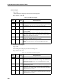
Figure 4-1 is a PCI block diagram.
PCI_PADS
PCI Module
PCI_TOP
BUFOUTFLOPS/OUTFLOPS
PCITGT
PCIMST
EEPROMCNTL
TGTDPU
Pcimaster Logic
Serial
EPROM
Datapath Logic
TGTCTL
control logic
BOOTROMCTL
DECODER
BAC
RX
DMA
Memory Port
Interface
Address Decoder
Bus Access
Control
Data
Fifo
TX
DMA
SAC
Slave Access Ctl
Ethernet
Control
Module
Figure 4-1. PCI Block Diagram
4-3
AIC-6915 Ethernet LAN Controller Programmer’s Manual
PCI Master Module
The PCI master transfers data to/from system memory. Therefore, the AIC-6915 never
generates PCI transactions for Interrupt Acknowledge, Special Cycle, I/O space, or
Configuration space. The PCI master generates all Memory space commands, and uses
the optional ones as appropriate to make efficient use of cache-oriented memory
hardware.
The module transfers a minimum 32-bits of data per Data phase, even if it has to fetch
(DMA read) less than that. The selection of the right bytes and the byte alignment
operation is done internally in the BAC module.
Note: In case of a DMA write the data must always be aligned on a 32-bit
boundary.
The PCI master has a programmable option to assert only the byte enables corresponding
to data it has to fetch. This option can be used in systems where reading extra bytes might
cause a problem.
The PCI master module samples DEVSEL_ when initiating a transaction to a selected
target in order to determine if the target is capable of proceeding with the current
transaction. In the case when DEVSEL_ is not asserted by the selected target for five
PCLKs (SAC - single address cycle) or six PCLKS (DAC - dual address cycle) after FRAME_
is asserted, the AIC-6915 performs a master-abort.
The PCI master does not retry transactions that resulted in a master-abort (no response
from target) and generates an interrupt to the driver with the RMA (Received Master
Abort in the PCI Configuration Status register) status active. Intervention by the software
driver is required for the AIC-6915 to continue with bus master transactions.
The PCI master does not retry transactions that resulted in a target-abort and generates an
interrupt to the driver with RTA (Received Target Abort in the PCI Configuration Status
register) status active. Intervention by the software driver is required for the AIC-6915 to
continue with bus master transactions.
The PCI master detects and reports parity errors. In normal operation mode, the AIC-6915
continues the DMA transfer even if a parity error is detected. The software driver can
request the AIC-6915 to stop the DMA transfer when a parity error is detected and
suspend any other DMA operations until the error is serviced.
The PCI master is designed to burst data as much as possible. Whenever it starts a burst
transfer, it continues until one of the following conditions occurs:
4-4
■
The target disconnects or aborts.
■
A Parity error is detected and the StopOnParErr bit is set.
■
The DMA counter expires (all requested data has been transferred).
■
The GNT_ signal is deasserted and the Latency timer expires.
■
The AIC-6915 never asserts wait states (‘irdy_’ is always ‘1’) and completes the
transfer even if it detects that there is no data or room in the FIFO.
PCI Module Architecture
64-bit PCI Bus Master
The AIC-6915 supports a 64-bit PCI bus master and performs 64-bit data transfers with a
64-bit target. If the responding target is a 32-bit device, the lower 32-bit of address bus is
used.
The REQ64_ signal is used to determine whether the system supports a 64-bit data path. A
pull-up resistor on the motherboard places the PCI bus in 32-bit mode by default. For PCI
expansion cards that do not support 64-bit PCI data path, the REQ64_ must be pulled-up
with a separate pull-up resistor. The central resource must assert REQ64_ during the time
that RST_ is asserted, according to the timing specification.
Pci Clk
RST_
REQ64_
//
//
REQ64_ to RST_ s
setup min
102 cycle time
//
RST_ to REQ64_0 ns to 50 ns
hold time
Figure 4-2. 64-bit PCI Reset Timing
Sixty-four bit data transfer capability is only supported for memory commands. When the
PCI bus master starts a transfer and REQ64_ is asserted, the starting address is
doubleword aligned. This means that AD[2:0] must be set to zero. The AIC-6915 issues a
64-bit data transfer instead of a 32-bit data transfer by the number of bytes transferred and
the starting address: hcnt >= 16 bytes and DmaAddr[2:0] = 0, for simplicity of
modifications. The 64-bit address alignment (DmaAddr[2:0] = 0) requirement is removed
and the AIC-6915 issues a 64-bit transfer for any starting address.
Upon request from the Ethernet control module for a PCI transfer, the PCI master
determines whether to use a 64-bit or a 32-bit transfer according to the above conditions.
For a 64-bit data transfer, the PCI master asserts FRAME_ and REQ64_ to indicate the start
of a 64-bit data transfer, then waits for the target device to assert DEVSEL_ to claim the
transaction and check whether ACK64_ is asserted. If ACK64_ is asserted, the PCI master
starts a 64-bit data transfer. If not, a 32-bit data transfer is performed.
If a multiple data transaction cycle is being disconnected after the first 32-bit transfer, the
AIC-6915 restarts the transaction with a 32-bit transfer. Under this situation, it is very
possible that the target is a 32-bit device and does not support multiple-data transfer
cycles. If the master continues with the 64-bit data transfer cycle, the lower 32-bit data
byte enables are deasserted and no data is transferred before the target initiates a
disconnect again. Therefore, the upper 32-bits of data can never be transferred.
4-5
AIC-6915 Ethernet LAN Controller Programmer’s Manual
Arbitration
The AIC-6915 drives AD[31:00] during 32-bit transfers and AD[63:0] during 64-bit transfers.
CBE[3:0]_ are asserted on the first PCLK when GNT_ is sampled asserted and the PCI bus
idle. PAR and PAR64 are asserted one PCLK later. The AIC-6915 also asserts FRAME_ and
REQ64_ for 64-bit transfers if PREQ_ is asserted to start a DMA transfer. The assertion of
PREQ_ indicates to the PCI System board arbiter that a master desires use of the bus. When
a transaction is terminated by a target, the master must deassert its PREQ_ signal for a
minimum of 2 PCLK periods (one period must include the bus idle period). This allows
another agent to use the bus while the previous target (that requested the STOP) prepares
to continue.
Note: This is not required where the master deasserted FRAME_, indicating the
last data phase of a transaction is in process. In this case, provided GNT_ is still
asserted, the master could start another transaction without deasserting PREQ_.
PCI Target Module
The AIC-6915 uses Base Address 0 to request that the system allocate 512 K Bytes of
memory space. Base Address 1 is used to request that the system allocate 256 bytes of I/O
space. The AIC-6915 uses the expansion ROM base address to request from the system to
allocate 256 KBytes of memory space to access an External ROM.
When the AIC-6915 detects a PCI cycle which is addressed to it, it checks the command to
verify that it can respond, then asserts DEVSEL_ with medium speed. As a target device,
the AIC-6915 distinguishes between cycles targeted to registers implemented in the PCI
clock domain, and other registers implemented in the Ethernet clock domain which can be
also implemented externally. When the cycle is targeted to a register in the Ethernet clock
domain, the PCI target asserts a request to the module to complete the cycle, then waits
for it to acknowledge before terminating the transaction on the PCI bus.
The AIC-6915 issues a target retry if more than 16 PCI clocks are required to terminate the
cycle. Retry is an operation on the PCI bus that occurs when an external bus master
accesses the AIC-6915 (AIC-6915 is the target). If the target is not ready, it responds with a
cycle retry indication on the PCI bus. PCI module asserts the signal RETRY to indicate that
the cycle cannot be completed within 16 PCI clock cycles. When the target samples the
RETRY signal and is asserted, it terminates the PCI cycle. Target retry can happen only if
the cycle is targeted to a register implemented in the Ethernet clock domain, or to the
serial EPROM at boot time (after hard reset), if selecting nondefault values for the PCI
configuration header registers.
The posted write function is used when the AIC-6915 is being targeted to access any
Ethernet clock domain registers. The PCI module captures the target address and byte
enables to its internal registers and completes the slave access. However, it will not accept
any slave accesses until the current write is being completed by the Ethernet CLOCK
DOMAIN register.
4-6
PCI Module Architecture
The value of BR_A1 pin is sampled when PCI reset is active to determine if the serial
EPROM data (BR_A1=1) or the default values (BR_A1=0) should be used for
■
Vendor ID [7:0]
■
Vendor ID [15:8]
■
Device ID [7:0]
■
Device ID [15:8]
■
Sub Class [7:0]
■
Base Class [7:0]
■
SubSystem Vendor ID [7:0]
■
SubSystem Vendor ID [15:8]
■
SubSystem Device ID [7:0]
■
SubSystem Device ID [15:8]
■
Interrupt Pin [7:0]
The target does not support data bursts. Rather it disconnects after the first Data phase. In
addition, the AIC-6915 does not support 64-bit target mode data transfers. Two locations
in I/O space are used as Data (IndirectIoDataPort) and Address (IndirectIoAddress)
registers. The Address register points to a word location within the 512K Byte memory
address space. When the target decodes and checks the legality of an access to its Data
register it selects the address stored in IndirectIoAddress as an input to its address
decoder and performs a read/write cycle using the address stored in IndirectIoAddress.
The target responds to such a cycle with the exact same behavior (checks legality of the
cycle) as if the master had initiated the transaction, executing a memory access with the
address stored in IndirectIoAddress. The target increments IndirectIoAddress if the cycle
completed successfully. BE_[3] and EnIncrement (Enable Increment in PciDeviceConfig
register) are asserted. All 256 bytes are accessible directly in I/O space.
When the target detects a cycle to its I/O space, it checks that CBE_[3:0] matches the
address. If the address does not match the cycle is aborted. The target receives and
executes a NOP cycle if none of the CBE_ bits are asserted.
4-7
AIC-6915 Ethernet LAN Controller Programmer’s Manual
Power Management
The PCI bus power management defined four power states. D0 indicates the “On” state,
D3 indicates the “Off” state, and D1 and D2 represent power managed states. In the
AIC-6915, three states are supported. D0 and D3 are required states and D2 is an optional
state. Table 4-1 shows the states supported by the AIC-6915.
Table 4-1. Power Management States
Device
States
Supported
Action to
Function
Supported
Actions from
Function
Implementation in
PCI Module
Function Context
Power
D0
All context is
retained
Full power
Any PCI
transaction
D2
All PCI
configuration
registers and
Receive module
are retained
Lower power
than D0
PCI
Configuration
Access
Wakeup
event
All clocks stop
other than target
module and
Receive module.
Target abort if not
config cycle
D3
All PCI
configuration
registers are
retained
Lower power
than any other
state
PCI
Configuration
Access
No action
All clocks stop
other than target
module. target
abort if not config
cycle
Any PCI
Regular power and
transaction or
clocks
interrupt
The assertion of RST_ on the PCI bus always returns the PCI function to the D0
uninitialized power-on default state. Removing Vcc always transitions the function to the
D3 state. All other function power state changes are made by software through the PMCSR
register.
When a function is not in the D0 state, the value of the Bus Master, Memory Space and
I/O Space bits in the PCI Command register are ignored, along with all Memory and I/O
accesses on the PCI bus. In the D1, D2, and D3 states, only PCI configuration space can be
accessed. All the other functional blocks are stopped, including the PCI master submodule and the BAC module.
For the device to start another transaction other than a configuration access, software
must return that device to the D0 state. This is accomplished by setting the Powerstate bits
in the PMCSR register to the D0 state, or by a wakeup event that is initiated by the Receive
module. When the PCI module receives any transfer request from the Receive module, it
generates a PME_ (Power Management Event) interrupt. Software then checks the power
management status registers and sets the PowerState to D0 and activates the full power
PCI bus access. PME_ can be enabled by setting PME_Support field in the PMC (Power
Management Capabilities) register.
When the POWERSTATE bits in PMCSR are being changed, the PCI module sends a state
change request to all other modules to make sure there are no current of pending
transfers. The power state can be changed only after acknowledgment is received from all
modules.
4-8
PCI Module Architecture
CardBus
CardBus is the interface between a PC card and a portable device which has 32-bit bus
mastering capability. The CardBus interface is based on the PCI interface with lower power
consumption, additional signals and registers supported. There are four 32-bit CardBus
registers. The following events must be implemented:
■
Function Event
■
Function Event Mask
■
Function Present State
■
Function Force Event
An additional signal, CLKRUN_ is used to maintain or start the PCI clock any time a card
wishes to start a PCI transaction. It is asserted low for two cycles after being sampled high
(not asserted) for two cycles. In the AIC-6915, CLKRUN_ is asserted if any DMA request or
interrupt request is asserted, and CLKRUN_ has been sampled high for at least two cycles.
When CLKRUN_ is not asserted, the system is free to slow down or stop the PCI bus.
Retry Function
When a master is trying to access the EEPROM, Memory port interface and Ethernet clock
domain in the AIC-6915, the retry functional block determines whether the transaction
can be completed within 16 clock cycles. If the access cannot be completed within 16 clock
cycles, the target address and byte enables are stored in the PCI module while a retry is
issued by the master. Once a retry is signalled, no other PCI slave access can be accepted
until the current slave access is completed by the same master (for read) or the current
data has been completed (for write). The PCI module keeps signalling to the originating
master every time it requests until it has completed the access or until the timer expires
after 32768 PCI clock cycles.
Response to PCI Commands
The AIC-6915 does not contain cache memory, and the Memory Interface bus gains no
special efficiency from cacheline-size bursts, so the AIC-6915’s PCI target responds to the
cache-oriented memory space commands (Memory Read Multiple, Memory Read Line,
Memory Write and Invalidate) as if they were simple Memory Read or Memory Write
commands.
Any device on the External Memory Interface bus is accessible in PCI memory space or
I/O space using an indirect address which is stored in IndirectIoAddress register.
The PCI configuration header registers are accessible in configuration space and, as read
only, in memory, or I/O space (indirect).
The PCI Device registers are accessible in configuration, memory and I/O space (indirect).
The Ethernet control module registers (in the Ethernet clock domain) are accessible in PCI
memory and I/O space (indirect).
The IndirectIoDataPort and IndirectIoAddress are accessed only in I/O space (direct).
As a target, the AIC-6915 ignores Interrupt Acknowledge, Special Cycle, Dual Address
Cycle and Reserved commands. However, even for these commands, the address/CBE_
parity-checking hardware remains active.
4-9
AIC-6915 Ethernet LAN Controller Programmer’s Manual
Table 4-2 lists all 16 PCI commands and the corresponding AIC-6915 response.
Table 4-2. Target Response to PCI Commands
CBE[3:0]_
4-10
Command
Abbrev.
AIC-6915 Response to Command
0000
Interrupt
Acknowledge
Ignored
0001
Special Cycle
0010
I/O Read
IORD
Supports IORD from the IndirectIoDataPort and
IndirectIoAddress registers. When reading the Data
Port, the AIC-6915 responds (after verifying that the
address matches the assertion of CBE_) in the same
manner as if it has received MRDC with an address
equal to the one stored in IndirectIoAddress.
0011
I/O Write
IOWR
Supports IOWR to the IndirectIoDataPort and
IndirectIoAddress registers. When writing to the
Data port, the AIC-6915 responds (after verifying that
the address matches the assertion of CBE_) in the
same manner as if it has received MWRC with an
address equal to the one stored in IndirectIoAddress.
0100
Reserved
Ignored
0101
Reserved
Ignored
0110
Memory Read
MRDC
Supports MRDC for different combinations of CBE_.
Any unsupported CBE[3:0]_ values result in a target
abort. When no CBE[3:0]_ signal is asserted the data
cycle is treated as a NOP. DEVSEL_ is asserted using
medium speed target response timing. TRDY_ is
asserted as soon as the Target has valid read data. The
period before TRDY_ is asserted will vary depending
on whether the address is internal or external.
0111
Memory Write MWRC
Supports MWRC for different combinations of CBE_.
Any unsupported CBE[3:0]_ values result in a target
abort. When no CBE[3:0]_ signal is asserted the data
cycle is treated as a NOP. DEVSEL_ is asserted using
medium speed target response timing. TRDY_ is
asserted as soon as the target is able to complete (data
is actually written) the cycle and IRDY_ is asserted.
The period before TRDY_ is asserted varies
depending on whether the address is internal or
external.
1000
Reserved
RSVD
Ignored
1001
Reserved
RSVD
Ignored
1010
Configuration
Read
CRDC
Supports CRDC accesses for all registers in single
function Configuration register space. All 32-bits are
always provided without regard for the CBE[3:0]_
value. When no CBE[3:0]_ signals are asserted the
data cycle is treated as a NOP. DEVSEL_ is asserted
using medium speed target response timing.
Ignored
PCI Module Architecture
Table 4-2. Target Response to PCI Commands (Continued)
CBE[3:0]_
Command
Abbrev.
AIC-6915 Response to Command
1011
Configuration
Write
CWRC
Supports CWRC accesses for all registers in single
function Configuration register space. Any
combination of CBE[3:0]_ values is acceptable for
writing bytes. When no signal is asserted the data
cycle is treated as a NOP. DEVSEL_ is asserted using
medium speed target response timing.
1100
Memory Read
Multiple
MRDMC
Defaults to MRDC
1101
Dual Address
Cycle
DAC
Ignored.
1110
Memory Read
Line
MRDLC
Defaults to MRDC
1111
Memory Write MWRIC
and Invalidate
Defaults to MWRC
Configuration Address Space
The AIC-6915, as a single function target, supports type 0 address space accesses with a
single configuration space. As a target, the AIC-6915 uses positive address decoding over
AD[07:02] along with CBE[3:0]_ (command is CRDC or CWRC), IDSEL, AD[01:00] = 0H and
FRAME_ to validate the Configuration register address decode. The AIC-6915 then asserts
DEVSEL_ to claim the transaction.
The AIC-6915 supports a read/write operation to its configuration space with any
combination of CBE[3:0]_ as defined in the PCI specification. For a read, the AIC-6915
always sources all bytes of the addressed register. Reading reserved configuration space
register bytes/bits always return a zero value. Data written to reserved configuration
space register bits or bytes is discarded. No error indication is made for reading or writing
to reserved registers. When more than one Data phase is indicated (burst operation) the
AIC-6915 indicates a disconnect and only accepts the first Data phase.
I/O Address Space (Direct Access)
The AIC-6915 uses Base Address 1 to request an allocation of a 256-byte I/O space block
and supports only read/write operation to the 256-byte registers, including the
IndirectIoDataPort and IndirectIoAddress registers for indirect I/O accesses. When more
than one data phase is indicated (burst operation) the AIC-6915 indicates a disconnect and
only accepts the first data phase.
I/O Address Space (Indirect Access)
Two locations (IndirectIoDataPort, IndirectIoAddress) in I/O space are used as Data and
Address registers. The Address register points to a word location within the 512-K Byte
address space of the AIC-6915. When the AIC-6915 decodes a legal access to its Data
register it selects the address stored in IndirectIoAddress as an input to its address
decoder and performs a read/write cycle using the address in IndirectIoAddress. The
AIC-6915 responds to such a cycle with the exact same behavior as if the master which
initiated the transaction was executing a memory access with the address that is stored in
the IndirectIoAddress register.
4-11
AIC-6915 Ethernet LAN Controller Programmer’s Manual
Expansion ROM Address Space
When in target mode, the AIC-6915 allows access to an 8-bit ROM/EEPROM (connected
to the External Memory Interface port) through the expansion ROM address space. The
AIC-6915 uses positive address decoding over EXROMCTL register (stored value),
AD[31:02], CBE[3:0]_ (command) and FRAME_ to obtain the doubleword access decode and
claim the transaction by asserting (DEVSEL_ = medium speed).
For memory read from the expansion ROM space, the memory interface module of the
AIC-6915 performs a burst of four consecutive read accesses from the ROM, incrementing
automatically the address with values of 0, 1, 2, and 3 to assemble a 32-bit value. Usually
this kind of transfer takes longer than 16 PCI clocks, so the memory interface requests the
PCI target to retry the cycle. The transfer is completed only when all the data is available
and ready in the memory interface module. The AIC-6915 does not support writes to
expansion ROM space.
Memory Address Space
The AIC-6915 uses Base Address 0 to request an allocation of a 512-KBytes memory space
block.
AD[01:00] are excluded from the address decode and defaults to a word-aligned address.
The value on AD[01:00] are used in the memory address space to indicate different
memory address transfer modes. A value of 0h indicates linear address increment mode,
while a value of 1h indicates address cache line toggle mode. Values 2h and 3h are
reserved. The AIC-6915 only supports the linear address increment mode.
As a target device, the AIC-6915 allows accesses to it's 512-KByte allocated memory space.
The AIC-6915 uses positive address decoding over BASEADR0 register (stored value),
AD[31:02], CBE[3:0]_ (command) and FRAME_ to obtain the doubleword access decode,
then claims the transaction by asserting (DEVSEL_ = medium speed). The AIC-6915 uses
the CBE[3:0]_ (data) value to complete the decode.
Parity
The AIC-6915 implements even parity that protects both the AD[31:00] and CBE[3:0]_
busses. PAR is generated by the agent that is sourcing the 32-bit address of the transaction
and/or the data of the transaction and includes the CBE[3:0] values even if not sourcing
them. The state of PAR is valid for the value on AD[31:00] and CBE[3:0] during the previous
PCLK period, excluding turn-around cycles of AD[31:00] (for which the PAR is invalid).
SERR_
The AIC-6915 asserts SERR_ when it detects an address parity error only if the
PERRESPEN (Parity Error Response Enable, COMMAND register in PCI Configuration
header) and SERRESPEN (System Error Response Enable, COMMAND register in PCI
Configuration header) bits are set. SERR_ is restored only by a weak pull-up on the system
board, and may take several PCLK periods to recover to a deasserted state. SERR_ is
asserted for one PCLK period on an address errors. SERR_ is asserted two PCLK periods
after the Address phase that contained the error. The AIC-6915 as a master does not
monitor or assert SERR.
4-12
PCI Module Architecture
PERR_
The AIC-6915 asserts PERR_ for detected data parity errors only if PERRESPEN is asserted.
As a target device, the AIC-6915 asserts PERR_ and sets the DPE bit active (STATUS
register in PCI Configuration header) for write cycles in which it detects a data parity
error, only if it claims the access and asserts DEVSEL_. PERR_ is asserted for one PCLK
period for each detected error two PCLK periods after the Data phase that contained the
error.
As a master, the AIC-6915 asserts PERR_, and sets DPE (PCI header) for read cycles in
which it detects a data parity error. The AIC-6915 asserts PERR_ only for cycles that it
initiates.
The Command And Byte Enable Bits CBE[3:0]_
The Bus Command and Byte Enable bits are multiplexed on the same PCI pins. During the
address phase of a transaction, CBE[3:0]_ contain a Bus command that defines the function
to be performed during the transaction. Table 4-3 describes how the AIC-6915 responds to
different commands.
Table 4-3. Address Phase CBE[3:0] Values
CBE [3:0]_
Target
Master
0000
IAC
Interrupt Acknowledge
No
No
0001
SSC
Special Cycle
No
No
0010
IORDC
I/O Read
Yes
No
I/O Write
0011
IOWRC
Yes
No
RSVD
No
No
0101
RSVD
No
No
0110
MRDC
Memory Read
Yes
Yes
Memory Write
0111
MWRC
Yes
Yes
1000
RSVD
No
No
1001
RSVD
No
No
1010
CRDC
Configuration Read
Yes
No
1011
CWRC
Configuration Write
Yes
No
1100
MRDMC
Memory Read Multiple
1
Yes
1101
DAC
Dual Address Cycle
No
Yes
Memory Read Line
1
Yes
Memory Write and
Invalidate
2
Yes
1111
2
Type
0100
1110
1
AIC-6915 Support
Command
Abbrev.
MRDLC
MWRIC
Defaults to Memory Read
Defaults to Memory Write
The CBE[3:0]_ values accepted during a Data phase indicate the valid data bytes. The PCI
target supports any combination of byte enables.
4-13
AIC-6915 Ethernet LAN Controller Programmer’s Manual
Illegal Behavior
As a target, when the AIC-6915 accepts a cycle (I/O, memory, configuration) which is
addressed to it and drives DEVSEL_, it checks the legality of the transaction and aborts
under any of the following conditions:
❒
4-14
■
The combination of CBE[3:0]_ in an I/O cycle does not match the address. The
AIC-6915 aborts the cycle and sets the ILLEGALBE bit in PCIDEVICESTS register.
■
During a memory cycle to the expansion ROM, if the address range defined in
expansion ROM space overlaps the address defined in Base Address 0 overlaps, the
AIC-6915 aborts the cycle and sets the ILLEGALOVERLAP bit.
■
Memory or indirect I/O access to the memory gap are defined as: 21'h6_0000 21'h7_FFFF.
■
Memory or indirect I/O access to the indirect I/O registers.
▼ ▼ ▼ ▼
5
Frame Processor Architecture
Features
■
Calculate the TCP and UDP checksum
■
Decode frame type (TCP, UDP, ARP, RARP, IPX, Wake-up, VLAN 802.1q, Ipv4, Ipv6,
ICMP, Ethernet 2, IEEE 802/803)
■
Process Ethernet 2, 802, IPv4, IPv6, TCP and UDP headers
■
Process receive data on-the-fly. The maximum receive buffer requirement is 8-bytes
■
Same architecture for both transmit and receive
■
Ease of implementation, simple decoding logic, no pipeline, fixed instruction format,
simple commands
■
Maximum clock frequency is 25 Mhz. Cycle time of 40 nS is enough to read the
instruction RAM and execute the command without any critical pass.
■
16 bit data interface. Frame data halfword is sampled when DataValid is asserted
■
Provides indication when User Data field starts after UDP or TCP headers
■
Provides partial checksum result for fragmented TCP frame
General Architecture & Operation
When DATAVALID is asserted, a new 16-bit halfword is read by the processor on the rising
edge of clock. The processor has an option to throttle down the data rate by deasserting
the signal REQNEXTDATA. New data can be presented to the processor only when
REQNEXTDATA is sampled asserted. The interface between the processor and the receive
block does not take advantage of that option (REQNEXTDATA is asserted all the time) and
assumes that there are at list three instructions the processor can execute between two
consecutive assertions of DATAVALID. In the interface with the transmit DMA engine, a
64-bit doubleword is read from the transmit FIFO and 16-bits are presented when
ReqNextData is sampled asserted.
The processor reads and executes instructions from the instruction memory in 1 clock
cycle. The processor executes the instruction and jumps to the next address at the same
clock edge if
■
Loop Counter (LC) is: ‘0’ ‘1’ or ‘2’, and DATAVALID is set, or
5-1
AIC-6915 Ethernet LAN Controller Programmer’s Manual
■
LC= 0, 1 or 2, and EXCONCLOCK is set, or
■
Read/Write instruction is executed and the Input IOREADY is sampled asserted.
Note: EXCONCLOCK is a bit in the instruction.
The loop counter is decremented by 2 every clock cycle if EXCONCLOCK=1, or if
DATAVALID is asserted. The loop counter stops when reaching its terminal count of zero.
Decrementing the counter by 2 each time assures that incoming data is on a byte
boundary.
The processor writes 16-bit data (ALU output) to a 16-bit address space defined in the
instruction. It can also read a location pointed by an address defined in the instruction,
and load the data to any of its working registers. The data read is passing through the
ALU and can also be processed if specified by the instruction.
Wake-up Mode
When the chip is functioning in power down mode, the GFP is loaded with a program
designed for decoding wake-up frames. When the GFP decodes a wake-up frame it
asserts the status bits WAKEUPFRAME and GFPDONE. External logic is responsible to
execute all the processes required by Microsoft On-Now specification, including assertion
of the PME_ signal.
When working in wake-up mode, the GFP should not be reset between frames. Instead
the input STARTOFFRAME is asserted to signal the beginning of a new incoming Ethernet
frame. This feature enables the GFP to try and decode multiple frame types in a serial
manner.
Transmit Checksum Accelerator
To accelerate the checksum calculation the 25 MHz clock must be connected to the GFP at
all times. When the GFP is ready to process the frame in a loop, it asserts the
STARTUSERDATA status bit. At this point the transmit DMA engine presents (instead of
the regular frame data) a sum of two or more (up to four) 16-bit halfwords that are
computed in parallel (at one clock cycle), with an indication (GFPBYTECNT[3:0]) of how
many bytes of frame data are included in the sum. The GFP then decrements the LC by
the number given by the transmit DMA engine. The maximum number is 8 = 2*4 and the
minimum number is three. The GFP implements a 16-bit frame counter,
GfpFrameCnt[15:0], which counts the number of GFPDATAVALID from the beginning of
the Ethernet frame. The Transmit DMA engine monitors the counters 3 least significant
bits and activates the accelerator only when they are ‘0’. This guarantees that the
accelerator is activated only when 8 bytes of data is read from the transmit FIFO.
The transmit DMA engine must monitor LC[15:0] to detect when the number of bytes still
requiring processing is below 3, at which time the accelerator hardware is disconnected
from the data path. When the transmit DMA engine presents a sum of 2 or more
halfwords instead of the regular frame data, it must also provide 2 bits of carry
information (GFPDATAIN[17:16]).
The transmit DMA engine can monitor the status register bits all the time since these are
available as outputs also. If it can be guaranteed that the TCP/UDP Checksum field is
presented as 0 x 0 to the GFP, then a few instructions can be saved.
5-2
Frame Processor Architecture
GFP Address Space
A total of 256 address locations can be accessed by the GFP executing Read/Write
instructions. The target address is presented in the BRANCHADD[7:0] field of the
instruction. When executing a read or write instruction, the GFP asserts GIFPRD/GFPWR,
and drives GFPADD[7:0], then waits for GFPIOREADY signal to complete the execution.
The total address space is divided in two. The first half, 7Fh-00h, is used for accessing
external registers. The second half, FFh-80h, is used for accessing internal registers.
Internal Registers
The GFP implements two status registers and two 16-bit general registers. These registers
are accessed using the regular Read/Write instructions and are mapped to the following
addresses:
GENERALREG1 - 80h
GENERALREG2 - 81h
STATUS[15:0] - 82h
STATUS[31:16] - 83h
The general registers are used to assist in executing the special branch instructions, but
can also be used as a general storage area. The Status register is used for status and control
information storage. Both register types can be accessed by the host during a read-only
operation.
All the bits of the Status/Control register are available as outputs. The GFP is also capable
of executing a write instruction, using the status data as the write data. The 32-bit status
registers are defined in Table 5-1.
Table 5-1. Status/Control Register
Bit
Description
0
TcpFrame - If set, indicates a TCP frame
1
UdpFrame - If set, indicates a UDP frame
2
ArpFrame - If set, indicates a ARP request/reply frame
3
RarpFrame - If set, indicates a RARP request/reply frame
4
Rfc1042Frame - If set, indicates IEEE 802.2/802.3 Encapsulation (RFC 1042)
5
Rfc894Frame - If set, indicates Ethernet encapsulation (RFC 894)
6
IpxFrame - If set, indicates IPX/SPX frame
7
WakeupFrame - If set, indicates a wake-up frame.
8
FragmentedFrame - If set, indicates a fragmented frame
9
IpFrame - If set, indicates an IPv4 or Ipv6 frame
10
Ipv6Frame - If set, indicates an IPv6 frame
11
ChecksumOk - If set, indicates TCP/UDP checksum is OK
12
IpChecksumOk - If set, indicates IP header checksum is OK. This bit is not
implemented in the current firmware version.
13
ChecksumBad - If set, indicates TCP/UDP checksum was checked and is bad
14
FrameTypeNotSupported - If set, indicates frame type not supported. GFP is not able to
calculate the checksum, or its not a TCP/UDP frame.
15
GfpDone - If set, indicates GFP completed successfully executing the frame processing.
5-3
AIC-6915 Ethernet LAN Controller Programmer’s Manual
Table 5-1. Status/Control Register (Continued)
Bit
Description
16
StopTxDma - If set, indicates the transmit DMA engine must freeze its operation and
wait for software intervention
17
VlanFrame - If set, indicates a VLAN 802.1q frame
18
DiscardFrame - If set, indicates the frame being processed must be discarded (transmit
or receive)
19
PartialChecksumValid - If set, indicates that Wreg1 stores a valid partial checksum for a
fragmented frame.
20
BypassMaskingIntTimer - If set, indicates the receive DMA is requested to interrupt the
host immediately after a completion descriptor for current frame is DMA-transferred to
host memory.
21
DmaHeaderOnly - If set, indicates the receive DMA is requested to the DMA only the
header of the frame being processed. The header size equals 2*(1+GfpFrameCnt[15:0])
bytes at the moment DmaHeaderOnly changes to ‘1’.
22
StartUserData - When set, this bit indicates that GFPFRAMECNT[15:0] stores the offset to
the beginning of user data from the start of the Ethernet frame, in 16-bit halfword units.
23
IcmpFrame - If set, indicates an ICMP frame.
24
SelDescQueue0 - If set, indicates the receive DMA engine is requested to DMA the
frame to buffers specified in Descriptor Queue 0.
25
SelDescQueue1 - If set, indicates the receive DMA engine is requested to DMA the
frame to buffers specified in Descriptor Queue 1.
26
SelCompQueue0 - If set, indicates the receive DMA engine is requested to DMA the
completion descriptor for this frame to queue 0.
27
SelCompQueue1 - If set, indicates the receive DMA engine is requested to DMA the
completion descriptor for this frame to queue 0.
28
Reserved
29
Reserved
30
Reserved
31
Reserved
External Registers
The external registers are used as a standard way to communicate with other modules. All
defined external registers are write-only (from the GFPs point of view). They are used for
providing information to external devices. The following external addresses are defined:
‘0x00’ - GFPSTATUS[15:0].
‘0x01’ - GFPSTATUS[31:16].
‘0x02’ - TCP/UDP checksum location
‘0x03’ - TCP/UDP checksum value
‘0x04’ - IP checksum location register
‘0x05’ - IP checksum value register
‘0x06’ - TCP/UDP frame size
‘0x0D - 0x07’ - Reserved
‘0x0E’ - GFP Receive Interrupt.
‘0x0F’ - GFP Transmit Interrupt
5-4
Frame Processor Architecture
Block Diagram
DataValid
Frame Data Counter
Instruction
Memory
Data
8 Input Mux
Barrel Shifter
Mask Control
IP
8 Input Mux
Mask Control
Instruction
LC
Data
WR1 WR2 WR3 WR4
Frame Data
Figure 5-1 is a block diagram of the Data Processing Unit.
ALU-Out[31:0]
Simple ALU:
Adder,
Comparator
WR1[31:0]
WR2[15:0]
WR3[15:0]
Flag
Loop Counter
(LC[15:0])
Instruction Ptr
Register
Input2
Immediate
BranchAdd
Branch Logic
Input1
WR4[15:0]
Figure 5-1. Data Processing Unit
5-5
AIC-6915 Ethernet LAN Controller Programmer’s Manual
Instruction Formats
Table 5-2 describes the Instruction Formats.
Table 5-2. Instruction Formats
Name
5-6
Bit Number
Description
Opcode 0
3:0
Execute - Execute instruction as specified by control fields
Opcode 1
3:0
BrToImmIfTrue - Branch to immediate address specified in
BRANCHADD field if ALU flag is true
Opcode 2
3:0
BrToImmIfFalse - Branch to immediate address specified in
BRANCHADD field if ALU flag is false
Opcode 3
3:0
BrToWreg3IfTrue - Branch to the location pointed to by WR3 if
ALU flag is True
Opcode 4
3:0
BrToWreg3IfFalse - Branch to immediate address specified in
BRANCHADD field if ALU flag is False
Opcode 5
3:0
Write - Write ALU output to 8-bit address defined in
BRANCHADD[7:0]. If BRANCHADD[7] is set the write operation is
targeted to a register implemented in the GFP module. If the bit is
reset the target register is implemented externally.
Opcode 6
3:0
Read - Read location pointed to by the address defined in
BRANCHADD[7:0], pass the data through the ALU and store it in
the working registers.
Opcode 7
3:0
Halt - Halt the processor. Wait for the assertion of ResetProcessor
input, then reset and start execution at address 0.
Opcode 8
3:0
CheckIpv4ProtocolId - Special instruction for checking Ipv4
Protocol ID field, then branch to one of three possible addresses.
The GFP recognizes 3 Protocol IDs:
TCPFRAMEID = 8'h06, Branch address = BRANCHADD[7:0]
UDPFRAMEID = 8'h11, Branch address = DATA[7:0]
ICMPFRAMEID = 8'h00, Branch address = DATA[15:8]
Opcode 9
3:0
ReadIpv6ExtHeader - Special instruction for reading the Next
Header and Length fields of an Ipv6 extension header. After the
instruction is executed, WR2 stores the size of the extension header
in 16-bit halfword units minus 1 (for the first 16-bit already read).
WR3 stores the total size of the frame in bytes. WR4 stores the Next
Header field.
Frame Processor Architecture
Table 5-2. Instruction Formats (Continued)
Name
Bit Number
Description
Opcode A
3:0
CheckIpv6NextHeader - Special instruction for checking the Next
Header field. The GFP recognizes 8 types of extension headers
implemented in hardware, identified by the following Next
Header identification number:
TcpProtocolId
= 8'd6;
UdpProtocolId
= 8'd17;
HopByHopProtocolId
= 8'd0;
DestinationProtocolId = 8'd60;
RoutingProtocolId
= 8'd43;
FragmentProtocolId
= 8'd44;
AuthentinationProtocolId = 8'd51;
EncapsulationProtocolId = 8'd50;
When this instruction is executed the GFP compares data at input
2 of the ALU (Next Header) with the hard coded protocol IDs, then
branches to an address defined as follows:
Every protocol ID has a 2bit ‘Type’ specified in an internal register
implemented in the GFP.
Type 0 protocol - Branch Address specified by Instruction[31:24].
Type 1 protocol - Branch Address specified by Instruction[39:32].
Type 2 protocol - Branch Address specified by Instruction[47:40].
Type 3 protocol - Branch Address specified by GeneralReg2[7:0].
GFP implements two 16-bit internal registers, GeneralReg1 and
GeneralReg2. It can access the registers by executing a ‘Write’
instruction to address x80 and x81. The first register stores the 2bit
‘Type’ assigned to each protocol, and the second stores the branch
address for Type 3 protocol.
Opcode B
3:0
CheckEthernetType - Special instruction for checking the Ethernet
‘Type’ field, then branch to one of seven possible addresses. The
GFP recognizes 7 types:
IPFRAMEID = 16'h0800, Branch Address = BRANCHADD[7:0]
ARPFRAMEID = 16'h0806, Branch Address = GENERALREG1[15:8]
RARPFRAMEID = 16'h8035; Branch Address = GENERALREG2[7:0]
IPXFRAMEID = 16'h8137; Branch Address = GENERALREG2[15:8]
FRAME802MAXLENGTH = 16'h05DC (IEEE 802.3 encapsulation),
Branch address = DATA[7:0]
VLANFRAMEID = Programmable number comes as an input to
GFP, Branch address = DATA[15:8]
ISLFRAMEID = One bit input, provided by external decoding logic,
Branch address = GENERALREG1[7:0]
Opcode C
3:0
WAITFORSTARTOFFRAME - Stop the processor. Wait for assertion
of STARTOFFRAME input, then branch to the address defined by
BRANCHADD[7:0].
Opcode D
3:0
CHECKIPV4FRAGMENTFIELD - Special command for processing the
16-bit halfword in the Ipv4 header that provides information about
the frame fragmentation. This is a branch command to
BranchAdd[7:0] if the frame is fragmented.
5-7
AIC-6915 Ethernet LAN Controller Programmer’s Manual
Table 5-2. Instruction Formats (Continued)
Name
Bit Number
Description
Opcode E
3:0
Return - Return to main program. When branching from the main
program, the next instruction pointer value of the main program is
saved in a special register. When executing this command, the
information stored in the special register is used as the next
instruction address.
Opcode F
3:0
BRONINPUT - When this instruction is executed, the signal
InputBranch is checked. If the signal is asserted, the branch
address is BRANCHADD[7:0], otherwise its DATA[7:0]. This
instruction is specifically used to facilitate having a common
program for receive and transmit. On the receive side,
INPUTBRANCH is tied to ‘1’. On the receive side, it is tied to ‘0’.
ExcOnClock
4
Instruction is executed or rising edge of clock, otherwise when
DATAVALID is asserted.
ReqNextData
5
Enables the processor to throttle down the incoming data rate.
When asserted, the processor is ready to process the next frame
data.
LoadWR1
6
ALU output is loaded to WR1
LoadWR2
7
ALU output is loaded to WR2
LoadWR3
8
ALU output is loaded to WR3
LoadWR4
9
ALU output is loaded to WR4
LoadLC
10
Loading Loop Counter. The exact data loaded and the counters
operation is defined in Data (INST[47:32]).
BarrelShifterCtrl
11
‘0’ - Not active (No shift)
‘1’ - Active, shift as specified in Data
MaskCtrl
12
‘0’ - Masking is disabled
‘1’ - AND mask is defined by MaskSel
MaskSel
13
‘0’ - Data[3:1] specifies which nibble of the data is being masked.
DATA[15:4] specifies the mask.
‘1’ - DATA[14:12] specifies which nibble of the data is being
masked. DATA[11:0] specifies the mask.
MuxSelInput2
5-8
[16:14]
Controls the 8 input mux operation at ALU input 2.
‘0’ - Data
‘1’ - DataIn (Frame Data)
‘2’ - WR1[15:0]
‘3’ - WR2
‘4’ - WR3
‘5’ - WR4
‘6’ - LC
‘7’ - ReadData
Frame Processor Architecture
Table 5-2. Instruction Formats (Continued)
Name
Bit Number
Description
MuxSelInput1
[29:17]
Controls the 8 input mux operation at ALU input 1
‘0’ - Data
‘1’ - WR1[15:0]
‘2’ - WR2
‘3’ - WR3
‘4’ - Status[31:16]
‘5’ - Status[15:0]
‘6’ - FrameCnt
‘7’ - WR1[31:15]
AluCtrl
[23:20]
‘0’ - NOP (Output=Input2, Flag=False)
‘1’ - ADD (Input1+Input2)
‘2’ - Check for Equality (Input1=Input2)
‘3’ - Check for greater than (Input1>Input2)
‘4’ - Check for greater than or equal (Input1>=Input2)
‘5’ - OR (Input1 | Input2)
‘6’ - AND (Input1 & Input2)
‘7’ - XOR (Input1 ^ Input2)
‘8’ - Invert (~Input2)
‘9’ - AddLong ({Wreg1[31:16],Input1} + Input2)
‘A’ - Decrement2 (Input1 - Input2)
‘B’ - Decrement1 (Input2 - Input1)
‘15’-’12’ - Reserved
BranchAdd
[31:24]
When the Opcode is a Branch to immediate command, then
BranchAdd points to the next instruction memory location. If the
command is Read/Write it indicates the target address.
Data
[47:32]
General data 1 field. Data is also a control field for the barrel shifter
and the Loop Counter.
If BarrelShifterCtrl=1 then:
Data[15] - If ‘0’ shift right, else shift Left.
Data[14:11] - Shift size.
if LoadLC=1 then:
Data[10] - Defines the operation mode of LC. If it’s set, LC is
loaded with a specified number, else LC is loaded with double the
specified number.
Note, LC is decremented by 2 every time an instruction is
executed.
Data[9] - If ‘0’ decrement LC every DataValid, else every clock.
Data[8] - When the bit is set and executing an instruction in a loop
and ReqNextData is asserted, then ReqNextData is cleared when
executing the last instruction in the loop.
Data[7] - Load Immediate data to LC.
Data[6] - Load ALU out to LC.
Data[5] - Load WR1 to LC.
Data[4] - Load WR2 to LC.
Data[3] - Load WR3 to LC.
Data[2] - Load WR4 to LC.
❒
5-9
▼ ▼ ▼ ▼
6
AIC-6915 Internal Registers
Summary
For the following registers, the ‘Byte Address’ indicates each registers location in memory
space given as a byte offset address from the start of the memory space dedicated for
internal registers - 0x50000h.
PCI Configuration Header Registers Summary
The PCI configuration registers are mapped to Memory Base Address+0x50000 in
memory space, 0x00 in configuration spaces and address 0x00 in I/O space. Each register
can be accessed on a read using Memory, I/O and configuration commands. Write
operations are limited to configuration commands only.
Table 6-1. PCI Configuration Header Registers Summary
Byte Addr
Data Byte 3
Data Byte 2
Data Byte 1
0000h
Device ID
Vendor ID
0004h
Status
Command
Data byte 0
0008h
Base Class
Sub Class
Program IF
Revision ID
000Ch
Built-In Self Test
Header Type
Latency Timer
Cache Line Size
0010h
LowBaseAdr0 (512-KByte Memory Space, low address bits)
0014h
HighBaseAdr0 (high address bits)
0018h
BaseAdr1 (256 byte I/O Space)
001Ch:0024h
Reserved
0028h
Card Bus CIS Pointer
002Ch
SubSystem ID
SubSystem Vendor ID
0030h
Expansion ROM Control
0034h
Reserved
0038h
Reserved
003Ch
Max Latency
Cap_Ptr
Min Gnt
Interrupt Pin
Interrupt Line
6-1
AIC-6915 Ethernet LAN Controller Programmer’s Manual
AIC-6915 Functional Registers Summary
Mapped to address range 0x50040-0x500FF in memory space, address 0x40-0xFF in
configuration space and address 0x40-0xFF in I/O space. These registers are read/write
and can be accessed using Memory, I/O, and Configuration commands.
Table 6-2. AIC-6915 Functional Registers Summary
Byte Offset
(Hex)
Register Name
Comments
PCI functional registers, starts @offset byte address 0x50040 in memory space
0040
PciDeviceConfig
Configuration of PCI master and Target modules
0044
BacControl
Configuration and control of the BAC module
0048
PciMonitor1
004C
PciMonitor2
0050
PMC (Power Management
Capability)
0054
PMCSR (Power Management
Control Status)
0058
PMEvent register
For Wakeup and LinkFail register
0060
SerialEpromControl
For reading external serial EPROM
0064
PciComplianceTesting
For testing PCI Compliance checklist - R/W
0068
IndirectIoAddress
006C
IndirectIoDataPort
For Accessing indirectly the entire memory address
space using PCI I/O commands
Ethernet functional registers, starts @offset byte address 0x50070 in memory space
6-2
0070
GeneralEthernetCtrl
Used for enable/disable different blocks
0074
TimersControl
Controls interrupt masking timer and the general
purpose timer
0078
CurrentTime
Provides a free running counter
0080
InterruptStatus
0084
ShadowInterruptStatus
0088
InterruptEn
Provides interrupt status information and control
over the status bits which are set in response to an
external interrupt event
008C
GPIO
Controls the general purpose I/O port
0090
TxDescQueueCtrl
0094
HiPrTxDescQueueBaseAddr
Transmit DMA control, configuration and status
registers
0098
LoPrTxDescQueueBaseAddr
009C
TxDescQueueHighAddr
00A0
TxDescQueueProducerIndex
00A4
TxDescQueueConsumerIndex
00A8
TxDmaStatus1
00AC
TxDmaStatus2
00B0
TransmitFrameCtrl/Status
Transmit Frame control, configuration and status
registers
AIC-6915 Internal Registers Summary
Table 6-2. AIC-6915 Functional Registers Summary (Continued)
Byte Offset
(Hex)
Register Name
00B4
CompletionQueueHighAddr
00B8
TxCompletionQueueCtrl
00BC
RxCompletionQueue1Ctrl
00C0
RxCompletionQueue2Ctrl
00C4
CompletionQueueConsumerIndex
00C8
CompletionQueueProducerIndex
00CC
RxHiPrCompletionPtrs
00D0
RxDmaCtrl
00D4
RxDescQueue1Ctrl
00D8
RxDescQueue2Ctrl
00DC
RxDescQueueHighAddress
00E0
RxDescQueue1LowAddress
00E4
RxDescQueue2LowAddress
00E8
RxDescQueue1Ptrs
00EC
RxDescQueue2Ptrs
00F0
RxDmaStatus
00F4
RxAddressFilteringCtrl
00F8
RxFrameTestOut
Comments
Completion queue control and configuration
registers
Receive DMA control, configuration and status
registers
Receive Frame and addressing control,
configuration and status registers
6-3
AIC-6915 Ethernet LAN Controller Programmer’s Manual
Additional PCI Registers Summary
Mapped to address range 0x50FFF-0x50100 in Memory space. These registers can be
accessed using memory or indirect I/O commands.
Table 6-3. AIC-6915 Additional PCI Registers Summary
Byte Offset
(Hex)
Register Name
Comments
PCI diagnostic/CardBus registers
0100
PciTargetStatus
Read only, For PCI target diagnostic purpose in
case of target abort
0104
PciMasterStatus1
Read only, For PCI master diagnostic purpose only
0108
PciMasterStatus2
010C
PciDmaLowHostAddr
0110
BacDmaDiagnostic0
0114
BacDmaDiagnostic1
0118
BacDmaDiagnostic2
011C
BacDmaDiagnostic3
0120
MacAddr1
0124
MacAddr2
0130
FunctionEvent
0134
FunctionEventMask
0138
FunctionPresentState
013C
ForceFunction
Read only, For BAC diagnostic purpose only.
Data read from the serial EPROM at init time is
latched. Software can override the value.
Interrupt bit of registers required by the CardBus
standard.
Additional Ethernet Registers Summary
Mapped to address range 0x52000-0x54FFF in memory space. These are read/write
registers that can be accessed using Memory or indirect I/O commands. Used for
mapping Ethernet clock domain registers that are rarely accessed during run time.
Table 6-4. AIC-6915 Additional Ethernet Registers Summary
Byte Offset
(Hex)
Register Name
Comments
Physical (32 devices, 128 bytes each), starts @offset byte address 0x52000 in memory space
2000-3FFF External Physical devices
MII Register Access port
General Ethernet registers, starts @offset byte address 0x54000 in memory space
4000
TestMode
4004
RxFrameProcessorCtrl
4008
TxFrameProcessorCtrl
4010-4FFF Reserved
MAC registers, starts @offset byte address 0x55000 in memory space
6-4
5000
MacConfig1
5004
MacConfig2
5008
BkToBkIPG
AIC-6915 Internal Registers Summary
Table 6-4. AIC-6915 Additional Ethernet Registers Summary (Continued)
Byte Offset
(Hex)
Register Name
500C
NonBkToBkIPG
5010
ColRetry
5014
MaxLength
5018
TxNibbleCnt
501C
TxByteCnt
5020
ReTxCnt
5024
RandomNumGen
5028
MskRandomNum
502C-5033
5034
Comments
Reserved
TotalTxCnt
5040
RxByteCnt
5060
TxPauseTimer
5064
VLANType
5070
MiiStatus
Writing to this register will cause a flow-control
frame to be transmitted with the programmed
pause time value.
5074-5FFF Reserved
Address Filtering, starts @offset byte address 0x56000 in memory space
6000-60FF Perfect address memory
The AIC-6915 compares the destination address
against these addresses
6100-617F Hash bitmap
The AIC-6915 uses a hash of the destination
addresses to index this bitmap
Statistic, starts @offset byte address 0x57000 in memory space
7000-7FFF Ethernet Statistic
TX Frame Processor, starts @offset byte address 0x58000 in memory space
8000-9FFF TxGfpMem
Used for loading the program for the transmit GFP.
RX Frame Processor, starts @offset byte address 0x5A000 in memory space
A000BFFF
RxGfpMem
Used for loading the program for the receive GFP.
Fifo Port, starts @offset byte address 0x60000 in memory space
C000DFFF
EthernetFifo
Used for accessing the internal FIFO. Used for
diagnostic and testing only.
❒
6-5
▼ ▼ ▼ ▼
7
Register Descriptions
Overview
This section includes all the registers required for controlling, programming, and
operating the AIC-6915. All registers throughout this section subscribe to the following
format.
Table 7-1. Shade Legends
These bits or fields are under software control. They
may be programmed by software to initialize the
controller or to optimize performance.
1248
These bits or fields are used solely by the hardware.
They are reserved fields and should not be modified by
the software.
7-1
AIC-6915 Ethernet LAN Controller Programmer’s Manual
AIC-6915 Address Space
A device on a PCI bus can be accessed using different PCI command types. The AIC-6915
can be accessed using Memory, I/O and Configuration commands. The 512-KByte
address space is mapped to a base address defined by the operating system at boot time.
The first 256-KBytes are also mapped to the expansion ROM space. In addition, the first
256-bytes of the second 256-KBytes are mapped to Configuration and I/O space and are
directly accessed using one of the three PCI command types: Memory, I/O, and
Configuration. Indirect I/O commands can be used for accessing the rest of the space. The
AIC-6915 address space is divided to a number of major subspaces with different
characteristics. Table 7-2 describes these subspaces.
Table 7-2. AIC-6915 PCI Address Space
Byte Address
Range
Size
(bytes)
Reserved
0x70084 0x7FFFF
64K
Status Registers
0x70000 0x70083
Ethernet Fifo
0x60000 0x6FFFF
General_Registers
0x50100 0x5FFFF
Internal_Functional_
Registers
0x50000 0x500FF
64K
Used for accessing the PCI configuration
header and AIC-6915 internal functional
registers that are mostly accessed by the
software driver during normal chip
operation.
Ext_General_Purpose_
Registers
0x40000 0x4FFFF
64K
Used for connecting an external device to
the AIC-6915.
[[E]EP]ROM
0x00000 0x3FFFF
256K
Read/Write external [E]EPROM. This
sub-space is mapped also to the PCI
Expansion ROM space.
Name
Description
Reserved for future use
Contains status registers.
64K
Used for accessing the internal
receive/transmit data FIFO
Used for accessing physical chip registers,
Serial EPROM, MAC registers and
additional status/debug registers.
AIC-6915 PCI Address Map
Figure 7-1 illustrates the AIC-6915 PCI address map.
7-2
Register Descriptions
64K Internal Registers Address Map
0xFFFF
Reserved
0xE000
Ethernet FIFO
Access
0xC000
512K PCI Address Map
Rx Frame Processor
Instruction memory
0x7FFFF
Reserved
Tx Frame Processor
Instruction memory
0x8000
Statistic register file
0x60000
0x7000
Address filtering
(includes external
PHY MII registers)
0x6000
(~16K words (~64KBytes))
MAC registers
0x50000
External registers
0x5000
Ethernet extra registers
(16K words (64KBytes))
(PCI clock domain)
0x4000
0x40000
Physical (MII) registers
up to 32 devices,
256-byte each
(64KByte words (256KBytes))
(PCI clock domain)
0x2000
Serial EPROM
0x1000
PCI extra registers
0x0100
0x0070
0x0040
0x00000
Functional registers
Ethernet
0x0000
PCI
PCI Configuration
header registers
Memory/Config/
I/O direct access
(E)EPROM R/W
Expansion ROM space
Memory Mapped and Indirect I/O Mapped
Internal registers
Memory and Indirect I/O access
0xA000
Figure 7-1. AIC-6915 PCI Address Map
7-3
AIC-6915 Ethernet LAN Controller Programmer’s Manual
Terminology
Throughout this chapter, data values are defined as follows:
■
Byte = 8 bits
■
Halfword = 16 bits
■
Word = 32 bits
■
Doubleword = 64 bits
AIC-6915 Internal Registers
These registers are used by the software driver for configuration, control, and retrieval of
status information. All registers which are ‘cleared on read’ are reset when the most
significant bit is read. Reading any other byte in a byte or halfword operation does not
affect the register. When the AIC-6915 activates a function as a result of writing to a
register, the activation takes place (usually) when writing the most-significant-byte of the
register.
All registers ‘Byte Address’ is defined as the offset byte address from the start of the
memory space dedicated for internal registers - 0x50000h.
Reserved fields are always read as zero. Values written to reserved fields are ignored.
However, the host should always write a zero to reserved fields to ensure compatibility
with future versions of the AIC-6915 that might use these fields.
Regions in the memory map that do not contain registers may be read as any value.
Writing to them has no effect.
Certain bits of certain registers in the AIC-6915 are not directly accessible by software and
are cleared by writing a logic one to the bit. These bits are originally set (written as a 1) by
the AIC-6915 based on an event or condition. Software can read the status of these
registers to determine the appropriate course of action. Software clears the bit by writing a
logical one to the logic block that manages the register. The logic block is in turn
responsible for setting the actual bit to zero.
The Reset Value column of each register is the value of the bit after a power-up or reset
cycle.
7-4
Register Descriptions
PCI Registers
PCI Configuration Header Registers
At the deassertion edge of the PCI reset, the AIC-6915 starts reading the serial EPROM. At
the same time, the BR_A1 input is sampled. If the board has a pull-up on this pin, the
AIC-6915 replaces the default value of the following PCI configuration header registers:
Vendor ID, Device ID, SubClass, Base Class, SubSystem Vendor ID, SubSystem Device ID,
MinGnt (MinimumGrant), MaxLat (MaximumLatency) and Interrupt Pin, with the value
read from the serial EEPROM. The CCIS (Configuration Card Information Structure) and
MAC address are always read and stored in the appropriate registers. There are no default
values for these registers.
PCI VendorID Register
Type: R
Internal Registers Subgroup: PCI Configuration Header
Byte Address: 00h - 01h
Table 7-3. PCI Vendor ID Register
Bit(s)
rw
15:0
r
Reset
Value
9004h
Description/Function
VendorID[15:0]: The PCI Vendor Identifier register contains
product information used by the HOST. The Adaptec Vendor ID
default value is 9004h. This value can be changed to a value read
from an external serial EEPROM if BR_A1’ pin is ‘1’ when
PCIRST_ is deasserted.
PCI DeviceID Register
Type: R
Internal Registers Subgroup: PCI Configuration Header
Byte Address: 02h-03h
Table 7-4. PCI Device ID Register
Bit(s)
rw
Reset
Value
15:0
r
6915h
Description/Function
DeviceID[15:0]: The PCI Device Identifier registers contain
product information for use by the HOST during system
initialization and configuration. The two Device ID bytes contain
an Adaptec product code. The default product code for the
AIC-6915 is 6915h. This value can be changed to a value read from
an external serial EEPROM if BR_A1’ pin is ‘1’ when
PCI_PCIRST_ is deasserted.
7-5
AIC-6915 Ethernet LAN Controller Programmer’s Manual
PCI Command Register
Type: R/W
Internal Registers Subgroup: PCI Configuration Header
Byte Address: 04h - 05h
Table 7-5. PCI Command Register
7-6
Bit(s)
rw
Reset
Value
15:10
r
0
Always read as 0.
9
r
0
MFBTBEN: Master Fast Back-To-Back Enable. When active (=1)
indicates a master can perform Fast Back-To Back transactions to
different PCI targets. The AIC-6915 does not support this feature
and MFBTBEN always reads zero.
8
r/w
0
SERRESPEN: System Error Response Enable. When both
SERRESPEN and PERRESPEN are set, the output PCI_SERR_
can be asserted. As a target, the AIC-6915 only asserts PCI_SERR_
for detected address parity errors. SERRESPEN is cleared during
and after assertion of PCI_PCIRST_.
7
r
0
WAITCTLEN: Always reads zero. The AIC-6915 does not support
Address/Data stepping.
6
r/w
0
PERRESPEN: Parity Error Response Enable. Setting this bit
enables PCI_PERR_ to be asserted when a PCI 36-bit even parity
error is detected during the data phase of a transaction. The
AIC-6915 asserts PCI_PERR_ when PERRESPEN is active and a
data parity error is detected as a target for write accesses or as a
master for read commands. PERRESPEN is set inactive during
and after assertion of PCI_PCIRST_.
5
r
0
VSNOOPEN: VGA Snoop Enable, Always reads 0. The AIC-6915
does not support VSNOOPEN.
4
r/w
0
MWRICEN: Memory Write and Invalidate Enable. Setting this bit
enables a PCI master to issue Memory Write and Invalidate
commands to more optimally transfer data to System memory.
When inactive the Memory Write and Invalidate command is
replaced with a Memory Write command. MWRICEN is set
inactive during and after assertion of PCI_PCIRST_
3
r
0
SPCYCEN: Always reads as 0. Setting this bit allows a target to
monitor special cycle transactions broadcast on the PCI bus. The
AIC-6915 does not support special cycles as a target or master.
2
r/w
0
MASTEREN: Master Enable. Setting this bit enables the AIC-6915
to perform bus master transactions on the PCI bus. Note,
additional transactions to the AIC-6915's Device registers must be
performed before the AIC-6915 may request to be a bus master.
When inactive the AIC-6915 bus master transactions are inhibited.
MASTEREN is set inactive during and after assertion of
PCI_PCIRST_
1
r/w
0
MSPACEEN: Memory Space Enable. Setting this bit enables the
AIC-6915 to respond to PCI memory space transactions. When
MSPACEEN is inactive the AIC-6915 does not respond to PCI
memory space transactions. MSPACEEN is set inactive during
and after assertion of PCI_PCIRST_
Description/Function
Register Descriptions
Table 7-5. PCI Command Register (Continued)
Bit(s)
rw
Reset
Value
0
r/w
0
Description/Function
ISPACEEN: I/O Space Enable. Setting this bit enables the
AIC-6915 to respond to PCI I/O transactions. When ISPACEEN is
inactive the AIC-6915 does not respond to I/O cycles.
PCI Status Register
Type: R/W
Internal Registers Subgroup: PCI Configuration Header
Byte Address: 06h - 07h
The STATUS register is used to record status information for PCI bus related events.
Read transactions of the STATUS register access the currently stored status
information. Write transactions to the STATUS register are not used to store data but
rather to clear those bits that are set. The STATUS register is forced to be inactive
when PCI_PCIRST_ is asserted. The STATUS register may be read at any time in
Configuration, I/O, or memory Space.
If at least one of the status bits: DPE, SSE, RMA, RTA, STA or DPR is asserted and
the corresponding enable bit, implemented in PCIDeviceConfig register, is also
asserted, then PCIInt is asserted. PCIInt is an internal interrupt status bit
implemented in GeneralInterruptStatus register.
Table 7-6. PCI Status Register
Bit(s)
rw
Reset
Value
15
r/w
0
DPE: The Detected Parity Error bit is set when a 36-bit even-parity
error is detected by the AIC-6915 (as a target) during an Address
phase or a Write Data phase, and by the transaction master during
a Read Data phase. DPE is set inactive during and after assertion of
PCI_PCIRST_ or by a write to the STATUS register with bit 15
(=1).
14
r/w
0
SSE: Signal System Error. The AIC-6915 sets the SSE bit only when
PERRESPEN and SERRESPEN are set for detected address parity
errors.
13
r/w
0
RMA: Received Master Abort is set when the AIC-6915-generated
transaction is terminated by the AIC-6915 due to no response from
the intended target by the sixth (for SAC) or seventh (for DAC )
PCLK after the AIC-6915 asserted FRAME_. The AIC-6915 releases
the bus on the next PCLK and does not retry the transaction.
Software/firmware intervention is required for the AIC-6915 to
continue master transactions. RMA is set inactive during and after
assertion of PCI_PCIRST_ or by a write to the STATUS register with
bit 13 (=1).
12
r/w
0
RTA: Received Target Abort is set when the AIC-6915, as a PCI bus
master, generates a transaction terminated with Target-Abort
indication. RTA is set inactive during and after assertion of
PCI_PCIRST_ or by a write to the STATUS register with bit 28
(=1). When an Target-Abort indication is received, the AIC-6915
does not retry the transaction and software/firmware intervention
is required for the AIC-6915 to continue master transactions.
Description/Function
7-7
AIC-6915 Ethernet LAN Controller Programmer’s Manual
Table 7-6. PCI Status Register (Continued)
Bit(s)
rw
Reset
Value
11
r/w
0
Description/Function
STA: Signal Target Abort is set by the target of a PCI bus
transaction if it is unable to respond due to a fatal error condition.
STA is set inactive during and after assertion of PCI_PCIRST_ or
by a write to the STATUS register with bit 11 (=1). The AIC-6915
indicates target-abort for the following conditions:
Illegal Overlap.
Illegal Write.
Illegal Byte Enables.
Decoding a non-configuration cycle when in power down mode.
Note: For the exact conditions under which a Target Abort is
indicated by the AIC-6915, refer to PCITargetStatus register.
Software must clear both the STA bit and the PCITARGETSTATUS
register separately.
7-8
10:9
r
1h
DST[1:0]: Device Select Timing[1:0] value indicates the longest
response time of a PCI device for assertion of PCI_DEVSEL_. Valid
values are: 0h for “fast” (1 PCLK), 1h for “medium” (2 PCLKs), 2h
for “slow” (3 PCLKs) with value 3h “reserved”. Response time for
the AIC-6915 is “medium”, DST[1:0] = 1h.
8
r/w
0
DPR: Data Parity Reported. Setting this bit indicates that the
master of a transaction, with it's PERRESPEN bit set, has either
detected PCI_PERR_ asserted or asserted PCI_PERR_. DPR is
cleared during and after assertion of PCI_PCIRST_ or by a write to
the STATUS register with bit 8 (=1).
7
r
1
TFBTBC: Target Fast-Back-To-Back Capable. Setting this bit
indicates that the target is capable of accepting fast PCI back-toback transactions even when the transactions are not to the same
agent. The AIC-6915 as a target supports Fast Back-To-Back
transactions. TFBTBC is a read only bit.
6:5
r
0
Reserved: Always read as 0
4
r
1
NewCapabilities: This bit indicates whether the device
implements a list of new capabilities. The AIC-6915 implements
PCI power management. If this bit is set, the register at address 34h
provides an offset into the PCI configuration space pointing to the
location of the first item in the capabilities list. A value of reset
means that the device does not implement the capability list.
NewCapabilities is a read only bit.
3:0
r
0
Reserved: Always read as 0
Register Descriptions
PCI DEVREVID (Device Revision ID) Register
Type: R
Internal Registers Subgroup: PCI Configuration Header
Byte Address: 08h
Table 7-7. Device Revision ID Register
Bit(s)
Reset
Value
rw
7:0
r
03h
Description/Function
DEVREVID[7:0]: Always read as 3h or higher. The Device Revision
ID identifies the revision level of a PCI device. Device Revision
values change in metal only.
PCI Proginfc (Program Interface) Register
Type: R
Internal Registers Subgroup: PCI Configuration Header
Byte Address:09h
Table 7-8. Program Interface Register
Bit(s)
rw
Reset
Value
7:0
r
00h
Description/Function
PROGINFC[7:0]: The Program Interface register value identifies the
specific register-level programming interface the agent supports. The
PROGINFC for the first version of the AIC-6915 is identified as 00h.
PCI Subclass Register
Type: R
Internal Registers Subgroup: PCI Configuration Header
Byte Address: 0Ah
Table 7-9. Subclass Register
Bit(s)
rw
Reset
value
7:0
r
00h
Description/Function
SUBCLASS[7:0]: The SubClass register identifies which SubClass
the PCI device is assigned to. The SUBCLASS for the first version of
the AIC-6915 is identified as 00h (Ethernet controller). This value
can be changed to a value read from an external serial EEPROM if
the BR_A1 pin is ‘1’ when PCI_PCIRST_ is deasserted.
7-9
AIC-6915 Ethernet LAN Controller Programmer’s Manual
PCI Baseclass Register
Type: R
Internal Registers Subgroup: PCI Configuration Header
Byte Address: 0Bh
Table 7-10. BaseClass Register
Bit(s)
rw
Reset
value
7:0
r
02h
Description/Function
BASECLASS[7:0]: The BaseClass register identifies which base class
the PCI device has been assigned to. The BASECLASS for the first
version of the AIC-6915 is identified as 02h (Network controller). This
value can be changed to a value read from an external serial EEPROM
if the BR_A1 pin is ‘1’ when PCI_PCIRST_ is deasserted.
PCI Cachesize (Cache Line Size) Register
Type: R/W
Internal Registers Subgroup: PCI Configuration Header
Byte Address: 0Ch
The Cache Size register specifies the system cache line size in units of 32-bit words.
The value stored in the register defines the minimum data transfer size and
associated cache starting boundary (and multiples there of) that may be performed
with cache line referenced PCI MWRIC, MRDLC or MRDMC commands.
CACHESIZE[7:0] are reset to 0h during assertion of PCI_PCIRST_.
Table 7-11. Cache Line Size Register
Bit(s)
rw
Reset
Value
7:0
r/w
0
Description/Function
CACHESIZE[7:0]: Cache Size [7:0] defines the cache line size (in 32bit words). Those word values supported are: 0, 4, 8, 16, 32 and 64.
Any other value is treated as CACHESIZE = 0. When CACHESIZE =
0, MWRIC is disabled.
PCI Lattime (Latency Timer) Register
Type: R/W
Internal Registers Subgroup: PCI Configuration Header
Byte Address: 0Dh
Table 7-12. Latency Timer Register
7-10
Bit(s)
rw
Reset
Value
7:2
r/w
10
LATTIME[7:2]: These bits determine the bus master latency timer
period (in PCLK periods) of the AIC-6915.
1:0
r
0
LATTIME[1:0]: Always read 0 (sets granularity at four CLKs).
Description/Function
Register Descriptions
PCI Hdrtype (Header Type) Register
Type: R
Internal Registers Subgroup: PCI Configuration Header
Byte Address: 0Eh
Table 7-13. Header Type Register
Bit(s)
rw
Reset
Value
7
r
0
HDRTYPE[7]: The AIC-6915 is a single function device
6:0
r
0
HDRTYPE[6:0]: Always read 0.
Description/Function
BIST (Built-in Self Test) Register
Type: R
Internal Registers Subgroup: PCI Configuration Header
Byte Address: 0Fh
Table 7-14. BIST Register
Bit(s)
rw
Reset
Value
7:0
r
0
Description/Function
BIST[7:0]: Always read as 0.
PCI LowBASEADR0 (Base Address 0) Register
Type: R/W
Internal Registers Subgroup: PCI Configuration Header
Byte Address: 10h - 13h
Note: When an access is made to an address that is mapped and enabled in both the
BASEADR0 and EXROMCTL registers, The PCI responds with a target abort.
Table 7-15. Base Address 0 Register
Bit(s)
rw
Reset
Value
31:19
r/w
0
BASEADR0[31:19]: This field indicates the mapping capability of
512-KBytes of system memory space within the low 32-bit address
segment of the 64-bit address space.
18:4
r
0
BASEADR0[18:4]: Indicates address space requirement, Always
read as 0.
3
r
0
Prefetchable: Always reads 0. Not supported.
2:1
r
10
MemorySpaceAccessType[1:0]: Always read as 10. The AIC-6915 as
a target may be located anywhere in a 64-bit address space.
0
r
0
Memory Space Indicator: Always reads 0.
Note: bit0 =0 indicates that BASEADR0 register is used for mapping
into system memory address space.
Description/Function
7-11
AIC-6915 Ethernet LAN Controller Programmer’s Manual
PCI HighBASEADR0 (Base Address 0) Register
Type: R/W
Internal Registers Subgroup: PCI Configuration Header
Byte Address: 14h - 17h
Note: When an access is made to an address that is mapped and enabled in both the
BASEADR0 and EXROMCTL registers, the PCI responds with a target abort.
Table 7-16. High Base Address 0 Register
Bit(s)
rw
Reset
Value
31:0
r/w
0
Description/Function
BASEADR0[63:32]: Contains the upper 32-bits of memory address
where the AIC-6915 is mapped.
PCI BASEADR1 (Base Address 1) Register
Type: R/W
Internal Registers Subgroup: PCI Configuration Header
Byte Address: 18h - 1Ch
Table 7-17. Base Address 1 Register
Bit(s)
rw
Reset
Value
31:8
r/w
0
BASEADR1[31:8]: Indicates the mapping capability of the 256byte system I/O space.
7:2
r
0
BASEADR1[7:3]: Indicates address space requirement. Always
read as 0.
1
r
0
Reserved: Always read as 0.
0
r
1
I/O Space Indicator: Always reads 1.
Description/Function
PCI CCIS (Configuration Card Information Structure) Register
Type: R
Internal Registers Subgroup: PCI Configuration Header
Byte Address: 28h - 2Bh
The CCIS register points to one of the possible address spaces where the card
information structure begins. The pointer is used in a CardBus PC card environment.
The value of this register is loaded from the external serial EPROM after a PCI hard
reset.
Table 7-18. Configuration Card Information Structure Register
7-12
Bit(s)
rw
Reset
Value
31:28
r
0
ROM Image
27:3
r
0
AddressSpaceOffset
2:0
r
0
AddressSpaceIndicator
Description/Function
Register Descriptions
PCI SubSystemVendor ID Register
Type: R
Internal Registers Subgroup: PCI Configuration Header
Byte Address: 2Ch - 2Dh
Table 7-19. SubSystemVendor ID Register
Bit(s)
rw
Reset
Value
15:0
r
9004h
Description/Function
SubSystemVendorID[15:0]: The PCI SubSystem Vendor Identifier
register helps to identify the vendor of the add-in board even
though the PCI controller has been designed by another vendor
and has another Vendors ID. The default value is the Adaptec
Vendor ID number, 9004h. This value can be changed to a value
read from an external serial EEPROM if BR_A1 pin is ‘1’ when
PCI_PCIRST_ is deasserted.
PCI SubSystem ID Register
Type: R
Internal Registers Subgroup: PCI Configuration Header
Byte Address: 2Eh - 2Fh
Table 7-20. SubSystem ID Register
Bit(s)
rw
Reset
Value
15
r
0
14:0
r
xxxxh
Description/Function
64-bit Address Space: For Base Address 0 register bit 2. Setting
this bit indicates 64-bit address space. Clearing the bit indicates
32-bit address space.
SubSystemID: The PCI SubSystem Identifier register provides the
vendors of add-in cards a mechanism to distinguish their cards
from one another even though the cards may have the same PCI
device ID. This value can be changed to a value read from an
external serial EEPROM if BR_A1 pin is ‘1’ when PCI_PCIRST_ is
deasserted. Refer to Table 7-35 for the possible default values for
the SubSystem ID.
PCI EXPROMCTL (Expansion ROM Control) Register
Type: R/W
Internal Registers Subgroup: PCI Configuration Header
Byte Address: 30h - 33h
The Expansion ROM Base Address register is used to define the base address,
maximum size and access enable control of an external ROM which may be used
with a PCI device. The PCI supports an external ROM/EEPROM of 256-KBytes.
When an access is made with both BASEADR0 and EXROMCTL address defined
region overlaps and EXROMEN is active, the PCI responds with a target-abort.
7-13
AIC-6915 Ethernet LAN Controller Programmer’s Manual
Table 7-21. Expansion ROM Control Register
Bit(s)
rw
Reset
Value
31:18
r/w
0
EXPROMCTL[31:18]: Indicates the mapping increment capability
of 256-KBytes.
17:11
r
0
EXPROMCTL[17:11]: Always read as 0. Set the maximum ROM
size to 256-KBytes.
10:1
r
0
EXPROMCTL[10:1]: Reserved: Always read as 0.
0
r/w
0
EXPROMCTL[0]: External ROM Enable. When this bit is set along
with the MSPACEEN bit in the Configuration Command register,
this bit enables the device to accept accesses to expansion ROM.
Unless both EXROMEN and MSPACEEN are active, accesses to
External ROM addresses do not return PCI_DEVSEL_ and are
ignored.
Description/Function
PCI CapPtr (Capabilities List Pointer) Register
Type: R/W
Internal Registers Subgroup: PCI Configuration Header
Byte Address: 34h
Table 7-22. Capabilities List Pointer Register
Bit(s)
rw
Reset
Value
7:0
r
50’h
Description/Function
CapPtr[7:0]: A pointer to the location of the first item in the New
Capabilities Linked List.
PCI INTLINSEL (Interrupt Line Select) Register
Type: R/W
Byte Address: 3Ch
Table 7-23. Interrupt Line Select Register
7-14
Bit(s)
rw
Reset
Value
7:0
r/w
0
Description/Function
INTLS[7:0]: Interrupt Line Select [7:0] is read-write register in
which the HOST can store information about the interrupt line
connected to the device. The PCI bus supports four interrupt lines
(INTA[D:A]).
Register Descriptions
PCI INTPINSEL (Interrupt Pin Select) Register
Type: R
Internal Registers Subgroup: PCI Configuration Header
Byte Address: 3Dh
Table 7-24. Interrupt Pin Select Register
Bit(s)
rw
Reset
Value
7:0
r
1h
Description/Function
INTPS[7:0]: The Interrupt Pin register specifies which PCI
interrupt pin the device (or device function) uses. The AIC-6915,
as a single function PCI device, must use INTA_ and have a
default value of 1h. The default value can be changed to a value
read from an external serial EEPROM if BR_A1 pin is asserted
when PCI_PCIRST_ is deasserted. This feature enables the
integration of multiple AIC-6915 devices on the same PCI card (as
a multiport Ethernet NIC) and treats the card as one PCI device
with multiple functions having different interrupt lines.
PCI MINGNT (Minimum Grant) Register
Type: R
Internal Registers Subgroup: PCI Configuration Header
Byte Address: 3Eh
Table 7-25. Minimum Grant Register
Bit(s)
rw
Reset
Value
7:0
r
08h
Description/Function
MINGNT[7:0]: The Minimum Grant register indicates the desired
PCI_GNT_ asserted period needed to complete burst transfer of
the device data buffer, assuming that the intended target does not
extend the transfer time by use of PCI_TRDY_. The value read
from the register specifies a period of time in units of 0.25
microseconds. The AIC-6915’s MINGNT register value is 8h
which is the minimum time to burst out 256-byte buffer.
The default value can be changed to a value read from an external
serial EEPROM if the BR_A1 signal pin is asserted when
PCIRST_ is deasserted.
7-15
AIC-6915 Ethernet LAN Controller Programmer’s Manual
PCI MAXLAT (Maximum Latency) Register
Type: R
Internal Registers Subgroup: PCI Configuration Header
Byte Address: 3Fh
Table 7-26. Maximum Latency Register
7-16
Bit(s)
rw
Reset
Value
7:0
r
06h
Description/Function
MAXLAT[7:0]: Always read as 06h. The Maximum Latency
register indicates how often the device needs to gain access to the
PCI bus. The value read from the register specifies a period of time
in units of 0.25 microseconds.
Assuming an average required transfer rate of 30MByte/Sec (25M
+ 5M overhead), and an average burst size of 64 bytes (which
takes 0.48usec based on clock of 33MHz and 4 bytes per Data
phase) the maximum latency would be:
30MByte/Sec = 64 / (0.48usec+MaxLat)
MaxLat = (64 / 30) - 0.48 = 1.65333usec =~ 1.50 usec
The AIC-6915's MAXLAT register value is 6h, which is
1.5usec/0.25usec.
Note: For smaller burst sizes or higher required data transfer rates
this number has to change.
The default value can be changed to a value read from an external
serial EEPROM if the BR_A1 signal pin is asserted when PCIRST_
is deasserted.
Register Descriptions
PCI Functional Registers Definition
The following registers are accessible from PCI configuration, memory and direct I/O
space.
PCIDeviceConfig Register
Type: R/W
Internal Registers Subgroup: PCI Functional Registers
Byte Address: 40h - 43h
Table 7-27. PCIDeviceConfig Register
Bit(s)
rw
Reset
Value
31
r/w
0
EnDpeInt: Enables assertion of DPE (in PCI Configuration Header
Status register) to set PCIInt. PCIInt is an internal interrupt status
bit implemented in InterruptStatus register.
30
r/w
0
EnSseInt: Enables assertion SSE (in PCI Configuration Header
Status register) to set PCIInt.
29
r/w
0
EnRmaInt: Enables assertion RMA (in PCI Configuration Header
Status register) to set PCIInt.
28
r/w
0
EnRtaInt: Enables assertion RTA (in PCI Configuration Header
Status register) to set PCIInt.
27
r/w
0
EnStaInt: Enables assertion STA (in PCI Configuration Header
Status register) to set PCIInt.
26:25
r
0
Reserved: Always read as 0.
24
r/w
0
EnDprInt: Enables assertion DPR (in PCI Configuration Header
Status register) to set PCIInt.
23
r/w
0
IntEnable: Setting this bit enables the device to assert a PCI
interrupt (PCI_INTA_), else PCI interrupt is disabled. This bit must
be set if the software driver wishes to receive any type of interrupts.
22:20
r/w
0
ExternalRegCsWidth: Indicates the width of the chip-select when
an access to an external register is performed.
‘000’ - 8 PCI clocks
‘111’ - 7 PCI clocks
‘110’ - 6 PCI clocks
‘101’ - 5 PCI clocks
‘100’ - 4 PCI clocks
‘011’ - 3 PCI clocks
All other combinations are reserved.
19
r/w
0
StopMWrOnCacheLineDis: When this bit is cleared, the AIC-6915
stops any memory write on a cacheline boundary if the remaining
number of data transfers is more than the cacheline size. A memory
write and invalidate cycle follows. When the bit is set this function is
disabled.
Description/Function
7-17
AIC-6915 Ethernet LAN Controller Programmer’s Manual
Table 7-27. PCIDeviceConfig Register (Continued)
7-18
Bit(s)
rw
Reset
Value
18:16
r/w
000
15
r/w
0
EnBeLogic: When this bit is set and a DMA read is active, the PCI
master asserts leading and trailing data byte enables as a function of
DMA address and transfer size. When the bit is reset, the PCI master
always asserts all 4-byte enables for reading data from HOST
memory.
14
r/w
0
LatencyStopOnCacheLine: When the latency timer expires and the
PCI grant is deasserted, the PCI master must stop the DMA transfer.
If the bit is set and a cache reference DMA Read command is
executed, the PCI master stops the DMA on the next cacheline
boundary, otherwise its stops immediately.
13
r/w
1
PCIMstDmaEn: Enables the PCI master operation. The bit is cleared
when a DMA error, such as when StopOnPerr is asserted, or when a
master abort or target abort is detected during an active DMA
transfer.
To enable the PCI master operation the software must make sure
that;
PCIMSTDMAEN is set.
MASTEREN is set (PCI Command register).
ISPACEEN or MSPACEEN is set (PCI Command register).
12
r/w
0
StopOnCachelineEn: When set, the AIC-6915 stops any memory
write or memory write and invalidate on a cacheline. Otherwise it
allows the target to control cycle termination.
11:8
r/w
1h
FifoThreshold[3:0]: Specifies a value in a resolution of 16 bytes. This
value is used as a threshold to determine when the PCI master
should request the PCI bus. During an active DMA read operation,
the threshold is the number of data bytes stored in the FIFO. During
an active DMA write operation, the threshold specifies the amount
of room in the FIFO. FIFOTHRESHOLD = 0 specifies a threshold of 256
bytes. The software driver should always use the default.
7
r/w
0
MemRdCmdEn: Controls when the PCI master uses the simple
Memory Read command. If MEMRDCMDEN is asserted, the
memory read command is used for all DMA read operations,
otherwise, memory read is used only when reading a number of
bytes that is less than or equal to four. A memory read line is used
for reading data up to the next cacheline, and a memory read
multiple is used if the read operation crosses a cache line boundary.
Description/Function
EpromCsWidth: Indicates the width of the EPROM chip-select.
‘000’ - 8 PCI clocks
‘111’ - 7 PCI clocks
‘110’ - 6 PCI clocks
‘101’ - 5 PCI clocks
‘100’ - 4 PCI clocks
‘011’ - 3 PCI clocks
All other combinations are reserved.
Register Descriptions
Table 7-27. PCIDeviceConfig Register (Continued)
Bit(s)
rw
Reset
Value
6
r/w
0
StopOnPerr: Specifies the behavior of the PCI master when a data
parity error is encountered during an active DMA operation. If the
bit is asserted, the PCI master stops the transfer as soon as it
detects/receives a data parity error. The PCIMstDmaEn, TxDmaEn
and RxDmaEn bits are reset, and driver software intervention is
required to resume operation.
5
r/w
0
AbortOnAddrParityErr: This bit controls the behavior of the PCI
target state machine in response to a bad parity during an address
phase. If reset, (default) the target state machine claims the
transaction despite the bad parity. If set to ‘1’, the target state
machine does not claim the cycle, and thereby cause a master-abort
condition for the other agent.
4
r/w
0
EnIncrement: when the bit is asserted and completing a successful
read/write to I/O Data Port register with PCI_CBE_[3] asserted, the
address stored in DATAADD register is incremented by 1,
otherwise the address is not changed.
Note: The address is incremented only if the PCI cycle is completed
successfully.
3
r/w
0
Reserved: Always read as 0.
2
r
0
System64: This bit indicates the system bus size. Setting the bit
indicates a 64-bit system. Clearing the bit indicates a 32-bit system.
1
r/w
0
Force64: Setting this bit forces master mode to be 64-bit transfers if
SYSTEM64 = 0. Clearing the bit indicates that the size of master mode
transfers depends on the SYSTEM64 bit.
0
r/w
0
SoftReset: When set, this bit produces a reset pulse which performs
in the same way as if PCI_PCIRST_ (except for the Configuration
Header register space which remains unchanged). The reset pulse is
transferred to the other clock domain and remains asserted until the
entire AIC-6915 is initialized. As long as the initialization process
takes place (no more than 1 other clock period + 4 PCLK periods)
the PCI Target does not respond to any PCI cycles. SoftReset is a self
clearing bit that always read as ‘0’. Note, when soft reset is
performed the serial EPROM is not read again. The PHYRESET pin is
not affected by the SOFTRESET bit.
Description/Function
7-19
AIC-6915 Ethernet LAN Controller Programmer’s Manual
BacControl Register
Type: R/W
Internal Registers Subgroup: PCI Functional Registers
Byte Address: 44h - 47h
This register provides the software driver a way to configure and control BAC DMA
operation.
Table 7-28. BacControl Register
rw
Reset
Value
31:22
r
0
Reserved: Always read as 0.
7:6
r/w
0
DescSwapMode[1:0]: Must always be 0.
5:4
r/w
0
DataSwapMode: Controls the way transmit/receive DMA data is
read and written to and from host memory. In the default state (‘0)
the swapper is disabled, and the data on the PCI bus is assumed to
be in little endian format. When the bit is set the swapper is active
and the data on the PCI bus is assumed to be in big endian format.
Note: This bit has no affect on the way descriptors are read from
and written to host memory.
Bit(s)
Description/Function
System
Memory
W1 7
W0 3
6
5
4
2
1
0
3
2
1
0
Chip
63
7
W1
6 5
63
7
W1
6 5
DataSwapMode=0
4
4
3
W0
2 1
3
W0
2 1
LSB (Little Endian)
Byte Address[2:0]=0
Bit 0
32 bit PCI Bus
0
Assembly Register
0
0
0
Internal Fifo
First Byte
Received/transmitted
3
r/w
0
SingleDmaMode: Is used for debugging only. In this mode the
BAC resets its BacDmaEn bit after completion of a DMA transfer.
2
r/w
0
PreferTxDmaReq: Controls the BAC’s arbitration algorithm. If
the bit is set, TxDmaReq has priority over RxDmaReq. If the bit is
cleared and PreferRxDmaReq is also cleared, they have equal
(round-robin) priority.
Note: The AIC-6915 implements an internal dynamically changing
control signal that can force PreferTxDmaReq to ‘1’. This control
signal is active when the transmit data falls bellow a programmable
threshold and there is a danger of FIFO underrun.
7-20
Register Descriptions
Table 7-28. BacControl Register (Continued)
Bit(s)
rw
Reset
Value
1
r/w
0
PREFERRXDMAREQ: Controls BAC’s arbitration algorithm. If the
bit is set and PREFERTXDMAREQ is cleared, the receive DMA
request has priority over transmit DMA data request, otherwise if
both bits are cleared, they have equal (round-robin) priority. Note,
the AIC-6915 implements an internal dynamically changing control
signal that can force PREFERRXDMAREQ to ‘1’. This control signal is active when the receive FIFO is above a programmable
threshold and there is a danger of a FIFO overrun.
0
r/w
1
BacDmaEn: This bit controls the way the BAC responds to DMA
transfers. If the bit is cleared, or if PCI master is disabled
(GLOBALDMAEN=0), BAC does not respond to any DMA
requests. The bit is cleared after:
Description/Function
1. BAC receives a DMA request and (HostAddress + TransferSize
> 4 GByte).
2. BAC receives DMA write request and Host address is not on
word boundary, or Transfer Size is not 4 word aligned.
3. A DMA transfer is completed and the BAC is operating in single
DMA mode.
PCIMonitor1 Register
Type: R
Internal Registers Subgroup: PCI Functional Registers
Byte Address: 48h - 4Bh
Table 7-29. PCI Monitor1 Register
Bit(s)
rw
Reset
Value
31:24
r/w
0
PCIBusMaxLatency: Provides the peak PCI bus latency measured
from the time the software driver reset the register. The latency is
presented in PCICLKCYCLE*16 (480nSec) units.
23:16
r/w
0
PCIIntMaxLatency: Provides the peak PCI interrupt latency
measured from the time the software driver reset the register. The
latency is presented in PCICLKCYCLE*1K (30.72usec) units.
15:0
r
0
PCISlaveBusUtilization: Provides a count of the total number of
PCI clock cycles the AIC-6915 asserts PCI_DEVSEL_ as an active
PCI slave, measured from the time the software driver resets the
register. The count is presented in PCICLKCYCLE. Reset to 0 if
ACTIVETRANSFERCOUNT wraps around to 0.
Description/Function
7-21
AIC-6915 Ethernet LAN Controller Programmer’s Manual
PCIMonitor2 Register
Type: R
Internal Registers Subgroup: PCI Functional Registers
Byte Address: 4Ch - 4Fh
Table 7-30. PCI Monitor2 Register
Bit(s)
rw
Reset
Value
31:16
r
0
PCIMasterBusUtilization: Provides a count of the total number of
PCI clock cycles that the AIC-6915 asserts PCI_FRAME_ as an active
PCI master, measured from the time the software driver resets the
register. The count is presented in; 1 unit=64PCIClkCycles. The
calculated PCI bus utilization is:
ActiveTransferCount / (PCISlaveBusUtilization/64 +
PCIMasterBusUtilization)
This field is reset to zero if ACTIVETRANSFERCOUNT wraps around
to 0.
15:0
r
0
ActiveTransferCount: Provides a count of the total number of PCI
DMA data transfers (PCI_IRDY_ & PCI_TRDY_ are asserted). The
count is presented in 1unit = 64cycles. This field is reset to zero if
PCIMASTERBUSUTILIZATION wraps around to 0.
Description/Function
PMC (Power Management Capabilities) Register
Type: R/W
Internal Registers Subgroup: PCI Functional Registers
Byte Address: 50h - 53h
Table 7-31. Power Management Register
7-22
Bit(s)
rw
Reset
Value
31:27
r
00100b
26
r
1
D2Support: The AIC-6915 supports the D2 power management
state.
25
r
0
D1Support: The AIC-6915 does not support the D1 power
management state.
24:22
r
0
Reserved: Always read as 0.
21
r
0
DSI: This bit indicates whether special initialization of the function
is required before the generic class device driver is able to use it. The
AIC-6915 does not require special initialization.
20
r
0
Auxiliary Power Source: This bit is only meaningful when PME_ is
supported in D3 (cold) state. The AIC-6915 does not support this
function.
19
r
0
PME Clock, Setting this bit indicates that the function relies on the
presence of the PCI clock for PME_ operation. The AIC-6915
generates PME_ without PCI clock.
Description/Function
PmeSupport: Indicates the power state that the device supports
when asserting PME_. The AIC-6915 is capable of asserting PME_
from the D0, D1 and D2 power states. PME is asserted when
detecting a ‘wake-up’ frame or Link Fail.
Register Descriptions
Table 7-31. Power Management Register (Continued)
Bit(s)
rw
Reset
Value
18:16
r
1h
PMVersion: This field indicates that there are 4 bytes of General
Purpose Power Management registers implemented as described in
revision 1.0 of the ‘PCI Bus Power Management Interface
Specification’.
15:8
r
00h
NextItemPtr: This field provides an offset into the function’s PCI
configuration space pointing to the location of next item in the
function’s capability list. The AIC-6915 does not implement more
items in the list.
7:0
r
01h
PowerManagementId: This ID indicates the start of the Power
Management Register Block
Description/Function
PMCSR (Power Management Control/Status) Register
Type: R/W
Internal Registers Subgroup: PCI Functional Registers
Byte Address: 54h - 57h
Table 7-32. Power Management Control Status Register
Bit(s)
rw
Reset
Value
31:29
r
0
PMData: This function is not implemented. The AIC-6915 does not
provide information about the power it consumes.
23:16
r
0
Reserved: Always read as 0.
15
r/w
0
PmeStatus: This bit is set when the function would normally assert
the PME_ signal independent of the state of the PMEEN bit. Setting
this bit clears it and causes the function to stop asserting a PME_.
Clearing the bit has no effect.
14:13
r
0
DataScale: This function is not implemented. The AIC-6915 does
not provide information about the power it consumes.
12:9
r
0
DataSelect: This function is not implemented. The AIC-6915 does
not provide information about the power it consumes.
8
r/w
0
PmeEn: This bit enables the function to assert PME_. If this bit is
cleared assertion of PME_ is disabled.
7:2
r
0
Reserved: Always read as 0.
1:0
r/w
Description/Function
PowerState: This 2-bit field determines the power state of the
AIC-6915
‘00’ - D0
‘01’ - D1
‘10’ - D2
‘11’ - D3
Reset Value: In CardBus mode, (when the EPROM A0 pin is
sampled low at reset), the PowerState starts at D3. Otherwise, it
starts at D0.
7-23
AIC-6915 Ethernet LAN Controller Programmer’s Manual
PME Event Register
Type: R/W
Internal Registers Subgroup: Ethernet Functional Registers
Byte Address: 58h- 5Bh
Table 7-33. PME Event Register
Bit(s)
rw
Reset
Value
31:6
r
0
Reserved: Always read 0.
5
r/w
0
ExtPhyReset: This bit controls the PHYRESET pin directly. Setting
EXTPHYRESET is the only way to assert the external pin.
4
r
0
LinkFailStatus: Indicates there is a link fail. This bit is connected
directly to the LINKFAIL pin in GPIO bit 0.
3
r/w
0
LinkFailEn: Setting this bit indicates that GPIO bit 0 input mode is
used for a Link Fail event. Clearing the bit disables Link Fail from
generating PME_.
2
r/w
0
LinkFailLowActive: Clearing this bit indicates that GPIO bit 0 is
active high at input mode as a Link Fail indicator. Setting the bit
indicates the GPIO bit 0 is active low.
1
r
0
LinkFailEvt: Indicates a link fail event. PME_ is asserted. This bit is
cleared when the PME_STATUS bit is cleared.
0
r
0
WakeupEvt: Indicates a wake-up event from the receive module.
PME_ is asserted. This bit is cleared when PME_STATUS bit is
cleared.
Description/Function
Serial EEPROMControlStatus Register
Type: R/W
Internal Registers Subgroup: PCI Functional Registers
Byte Address: 60h - 63h
Table 7-34. EEPROMControlStatus Register
7-24
Bit(s)
rw
Reset
Value
31:4
r
0
Reserved: Always read as 0.
3
r
0
InitDone: If the board is set up to read the EEPROM after a hardreset, this bit indicates when the initial reading of the EEPROM is
finished. If the board is set up not to read EEPROM after a hardreset, this bit is cleared.
2
r
0
Idle: This is the idle STATUS bit indicating the serial EEPROM state
machine is busy or idle.
1
r/w
0
WriteEnable: When this bit is set, it triggers the serial EEPROM
interface to issue a ‘Write Enable’ command. When the command is
completed the bit is cleared.
0
r/w
0
WriteDisable: When this bit is set, it triggers the serial EEPROM
interface to issue a ‘Write Disable’ command. When the command is
completed the bit is cleared.
Description/Function
Register Descriptions
EEPROM Memory Definition
Table 7-35. EEPROM Memory Definition
Byte
Address
Description/Function
Value
0
Vendor ID [7:0]
04
1
Vendor ID [15:8]
90
2
Device ID [7:0]
15
3
Device ID [15:8]
69
4
SubClass [7:0]
00
5
Base Class [7:0]
02
6
SubSystem Vendor ID [7:0]
04
7
SubSystem Vendor ID [15:8]
8
SubSystem Device ID [7:0]
9
SubSystem Device ID [15:8]
00
10
Interrupt Pin [7:0]
01
11
Card Bus [7:0]
00
12
Card Bus [15:8]
00
13
Card Bus [23:16]
00
14
Card Bus [31:24]
00
15
MAC address [7:0] --> MAC Addr Byte 5
(LSB)
16
MAC address [7:0] --> MAC Addr Byte 4
17
MAC address [7:0] --> MAC Addr Byte 3
18
MAC address [7:0] --> MAC Addr Byte 2
19
MAC address [7:0] --> MAC Addr Byte 1
20
MAC address [7:0] --> MAC Addr Byte 0
(MSB)
21
Minimum Grant [7:0]
22
90
08 = 62011/TX Rev. 0
09 = 62011/TX Rev. 1
10 = 62022
28 = 62044
20 = 62020/FX
28 = 69011/TX
09
Maximum Latency [7:0]
05
Reserved
FF
125
Adaptec Standard Format
00
126
Checksum [7:0]
LSB
127
Checksum [15:8]
MSB
23-124
7-25
AIC-6915 Ethernet LAN Controller Programmer’s Manual
PCIComplianceTesting Register
Type: R/W
Internal Registers Subgroup: PCI Functional Registers
Byte Address: 64h - 67h
This register is used for PCI compliance checker testing purposes only and has no
meaning to the AIC-6915..
Table 7-36. PCIComplianceTesting Register
Bit(s)
rw
Reset
Value
31:0
r/w
0
Description/Function
PCI compliance data word.
IndirectIoAddress Register
Type: R/W
Internal Registers Subgroup: PCI Functional Registers
Byte Address: 68h - 6Bh
This register stores the target address for an indirect I/O slave cycle. It can be
accessed only in I/O or configuration space, using I/O configuration Read or Write
commands.
Table 7-37. IndirectIoAddress Register
Bit(s)
rw
Reset
Value
31:19
r
0
Reserved
18:2
r/w
0
IndirectIoAddress: Points to a word (4-byte) location in the
AIC-6915 512-KByte address space. When an external PCI Master
starts a legal access to the Indirect I/O Data Port register
(IndirectIoDataPort), the PCI target uses the IndirectIoAddress for
addressing the requested register.
1:0
r
0
Reserved
Description/Function
IndirectIoDataPort Register
Type: R/W
Internal Registers Subgroup: PCI Functional Registers
Byte Address: 6Ch - 6Fh
Table 7-38. IndirectIoDataPort Register
7-26
Bit(s)
rw
31:0
r/w
Reset
value
Description/Function
IndirectIoDataPort: This is a visual register/data port used by the
software to access any location within the 512-KByte address space.
It can only be accessed in I/O or configuration space, using I/O or
configuration Read or Write commands. When the PCI Target
decodes a legal access to this register, it uses the address stored in
INDIRECTIOADDRESS to execute the requested read/write
operation. A legal I/O access occurs when the least-significant two
address bits match the asserted byte enables.
Register Descriptions
Ethernet Registers
The following registers are accessible from PCI configuration, memory, and direct I/O
space. They are all synchronized to the Ethernet Transmit clock.
General Ethernet Functional Registers
GeneralEthernetCtrl Register
Type: R/W
Internal Registers Subgroup: Ethernet Functional Registers
Byte Address: 70h - 73h
Table 7-39. GeneralEthernetCtrl Register
Bit(s)
rw
Reset
value
31:10
r
0
Reserved: Always reads 0.
9
r/w
0
Reserved: Always reads 0.
8
r/w
0
SetSoftInt: When set, the SOFTINT status bit in the
INTERRUPTSTATUS register is set. This bit is always read as ‘0’.
7
r/w
0
Reserved: Always reads 0.
6
r/w
0
Reserved: Always reads 0.
5
r/w
0
TxGfpEn: When set, the transmit general frame processor is
enabled, otherwise it remains in the reset state.
4
r/w
0
RxGfpEn: When set, the receive general frame processor is enabled,
otherwise it remains in the reset state.
3
r/w
0
TxDmaEn: Controls the transmit DMA operation. When the bit is
cleared the transmit module (data, buffer descriptors, completion
descriptors) does not issue any DMA requests. The bit is cleared by
the software driver, or when the PCI master encounters a PCI error
which should disable the DMA operation. Note that only when the
TXDMAEN bit is cleared can the software driver access and write the
transmit DMA buffer queue consumer index and the transmit DMA
completion queue producer index.
2
r/w
0
RxDmaEn: Controls the receive DMA operation. When the bit is
cleared, the receive DMA module (data, buffer descriptors,
completion descriptors) does not issue any DMA requests. The bit is
cleared when the PCI master encounters a PCI error which should
disable the DMA operation. Note that only when the RXDMAEN bit
is cleared can the software driver access and write the receive DMA
buffer queue consumer index and the receive DMA completion
queue producer index.
1
r/w
0
TransmitEn: Controls the transmit engine operation. When the bit is
cleared, no data is transmitted. This bit has no effect on the transmit
DMA operation.
0
r/w
0
ReceiveEn: Controls the receive engine operation. When the bit is
cleared, all newly received frames are discarded. This bit has no
effect on the receive DMA operation.
Description/Function
7-27
AIC-6915 Ethernet LAN Controller Programmer’s Manual
TimersControl Register
Type: R/W
Internal Registers Subgroup: Ethernet Functional Registers
Byte Address: 74h - 77h
Table 7-40. TimersControl Register
7-28
Bit(s)
rw
Reset
value
31
r/w
0
EarlyRxQ1IntDelayDisable: When set, the interrupt masking timer
has no effect on EarlyRxQ1Int.
30
r/w
0
RxQ1DoneIntDelayDisable: When set, the interrupt masking timer
has no effect on RxQ1DoneInt.
29
r/w
0
EarlyRxQ2IntDelayDisable: When set, the interrupt masking timer
has no effect on EarlyRxQ2Int.
28
r/w
0
RxQ2DoneIntDelayDisable: When set, the interrupt masking timer
has no effect on RxQ2DoneInt.
27
r
0
Reserved: Always reads 0.
26
r/w
0
TimeStampResolution: Specifies the resolution of the time stamp
recorded in the long format transmit completion descriptor. The
recorded time stamp is a 13-bit number equal to CurrentTime[12:0]
if TimeStampResolution is reset (0), otherwise it is equal to
CurrentTime[20:8]. The long-format receive completion descriptors
always include the full 32-bit CurrentTime.
25
r/w
0
GeneralTimerResolution: Specifies the resolution of GeneralTimer,
that controls the spacing of GeneralTimerInt. When the bit is
cleared the timer has a resolution of 24 TimerClock periods (12.8 µs).
When the bit is set the resolution is 29 TimerClock periods (0.4096
ms).
24
r/w
0
OneShotMode: Specifies the GeneralTimer operation mode. If the
bit is set, only one interrupt is produced when the timer reaches its
terminal count, else the GeneralTimer continuously produces
interrupts every period as defined by GeneralTimerResolution and
GeneralTimerInterval bits.
23:16
r/w
0
GeneralTimerInterval: Specifies the spacing between two
consecutive assertions of the interrupt status bit, GeneralTimerInt.
A default value ‘0’ does not delay the assertion of the interrupt
status bit. If the TimerClock period is ~0.8 µS and the GeneralTimer
is running at high resolution mode (GeneralTimerResolution=1),
the interrupt spacing range is: 12.8 µs - 3.264 ms. For the low
resolution mode the range is: 0.4096 mS - 104.8 ms. The general
timer starts when this field is not 0.
15
r/w
0
TxFrameCompleteIntDelayDisable: When set, the interrupt
masking timer has no effect on TxFrameCompleteInt.
14
r/w
0
TxQueueDoneIntDelayDisable: When set, the interrupt masking
timer has no effect on TxQueueDoneInt.
13
r/w
0
TxDmaDoneIntDelayDisable: When set, the interrupt masking
timer has no effect on TxDmaDoneInt.
Description/Function
Register Descriptions
Table 7-40. TimersControl Register (Continued)
Bit(s)
rw
Reset
value
12
r/w
0
RxHiPrBypass: If this bit is set, bypass the interrupt masking timer
when generating RxDoneInt after DMA-transferring the
completion descriptor of a high-priority frame.
11
r/w
0
Timer10X: Enables the software to easily scale the TimerClock
period by a factor of 10 to match a 10 Mbits/sec or 100 Mbits/sec
environment. When this bit is set, TXCLK is divided by 20 to create
TIMERCLOCK, otherwise it is divided by 2. The division by 20 is used
when the AIC-6915 operates at line speed of 100 Mbits/Sec.
10:9
r/w
0
SmallRxFrame: Defines the size of a received Ethernet frame that is
considered ‘small’. The AIC-6915 interrupts ‘small’ frames earlier
than normal frames if SmallFrameBypass bit is set.
‘00’ - ‘Small’ frame when less or equal to 64 bytes
‘01’ - ‘Small’ frame when less or equal to 128 bytes
‘10’ -‘Small’ frame when less or equal to 256 bytes
‘11’ - ‘Small’ frame when less or equal to 512 bytes
8
r/w
0
SmallFrameBypass: When this bit is set, AND the receive interrupt
masking timer is active, and the interrupt status bit RXDONEINT is
set as a result of receiving and completing the DMA transfer of a
‘small’ frame, then RXDONEINT by-passes the masking timer and
asserts the external PCI interrupt line. When SMALLFRAMEBYPASS is
reset, the AIC-6915 treats all received frames the same. It does not
assert the external interrupt line if the interrupt masking timer is
active.
7
r
0
Reserved: Always read as ‘0’.
6:5
r/w
0
IntMaskMode: Controls the operation of the interrupt masking
timer.
‘00’ - The timer is not loaded.
‘01’ - When this value is written, the timer is loaded with the
number defined by IntMaskPeriod. The timer is decremented
by one every rising edge of TIMERCLOCK. During a maskingperiod, active (asserted) Transmit and Receive Interrupts are
masked and do not cause an assertion of an interrupt on the
PCI bus. When the timer reaches its terminal count (0) the
interrupts are enabled.
‘10’ - Same as ‘01’, except that new masking period starts
automatically when the software driver clears both
TXDONEINT and RXDONEINT.
‘11’ - Same as ‘01’, except that new masking period starts
automatically when first asserting a new interrupt. In this case
the masking period is extended by the time interval from the
last time the software cleared the interrupt until a new one is
asserted.
Description/Function
7-29
AIC-6915 Ethernet LAN Controller Programmer’s Manual
Table 7-40. TimersControl Register (Continued)
Bit(s)
rw
Reset
value
4:0
r/w
0
Description/Function
IntMaskPeriod: Specifies a minimum amount of time between two
consecutive assertions of external PCI interrupt (PCI_INTA_) as a
result of the interrupt status bits TXDONEINT and RXDONEINT, if
the corresponding bits TXDELAYDISABLE and RXDELAYDISABLE are
at their reset state, ‘0’. When the software driver writes a ‘01’ or ‘11’
to INTMASKMODE, the AIC-6915 loads the interrupt masking timer
and prevents the interrupt status bits TXDONEINT and RXDONEINT
from causing a PCI interrupt for a period defined by
IntMaskPeriod. The number loaded to the timer is
IntMaskPeriod*128. The following samples of masking periods are
calculated based on TimerClockPeriod=0.8usec:
‘00000’ - Timer in terminal count state - no masking.
‘00001’ - 128 TimerClock periods, 0.1024mSec
‘10000’ - 2048 TimerClock periods, 1.6384mSec
‘11111’ - 4095 TimerClock periods, 3.2760mSec
Note: Interrupts resulting from irregular operations, such as error
reporting, are not affected by the interrupt mask timer operation.
The following interrupts are affected by the masking time:
■
RxQ1DoneInt
■
EarlyRxQ1Int
■
RxQ2DoneInt
■
EarlyRxQ2Int
■
TxDmaDoneInt
■
TxQueueDoneInt
■
TxFrameCompleteInt
CurrentTime Register
Type: R/W
Internal Registers Subgroup: Ethernet Functional Registers
Byte Address: 78h - 7Bh
Table 7-41. CurrentTime Register
7-30
Bit(s)
rw
Reset
value
31:0
r/w
0
Description/Function
CurrentTime: This field is a 32-bit counter clocked by TimerClock.
If TimerClock period is 0.8 µs, then the range of CurrentTime is ~60
Min. The driver can load the register anytime in order to
synchronize the current time of two adapter cards. This counter is
used for time stamp purposes.
Register Descriptions
InterruptStatus Register
Type: R/W
Internal Registers Subgroup: Ethernet Functional Registers
Byte Address: 80h - 83h
This register stores the interrupt vector which indicates the interrupt source. Some of
the bits in the register are cleared on a read, while others must be cleared at the
source. All ‘cleared by read bits’ are also cleared when writing a ‘1’ to the bit. When a
bit in the register is set and the corresponding bit in the INTERRUPTEN register is set,
an interrupt is asserted on the PCI bus, assuming that PCI interrupts are enabled in
the PCIDeviceConfig register. Seven interrupt status bits, RXQ1DONEINT,
EARLYRXQ1INT, RXQ2DONEINT, EARLYRXQ2INT, TXDMADONEINT,
TXQUEUEDONEINT and TXFRAMECOMPLETEINT have a second level of masking
using a programmable timer. For more details about the second level masking refer
to TIMERSCONTROL register.
Table 7-42. InterruptStatus Register
Bit(s)
rw
Reset
Value
31:28
r/w
0
GPIOInt[3:0]: This bit is set if the corresponding GPIO bit is
configured to be an input and causes an interrupt. Any GPIO pin
can be configured to be an input and set an interrupt when its high,
or low, or on a change. This bit must be cleared at the source, except
the case where the corresponding GPIO pin is programmed to cause
an interrupt on change. GPIOINT[0] is also connected to the power
management function and may serve as a wake-up event input.
27
r/w
0
StatisticWrapInt: Provides an indication of when one of the
statistical counters are going to wrap (change from 7FFFFFFF to
80000000). This bit is cleared on a read, or by writing a ‘1’.
26
r
0
Reserved: Always reads 0.
25
r
0
AbnormalInterrupt: Is the logical ‘OR’ of bits [24:16], [7:1].
24
r/w
0
GeneralTimerInt: Indicates that the GENERALTIMER count reached
its terminal Count of zero. This bit is cleared on a read, or by writing
a ‘1’.
23
r/w
0
SoftInt: This bit is set when the software driver writes a ‘1’ to the Set
Soft Interrupt bit in the GENERALCONTROL register. This bit is
cleared by read, or by writing a ‘1’.
22
r/w
0
RxCompletionQueue1Int: This bit is set if the number of available
entries in Receive Completion Descriptor Queue 1 is below a
programmable threshold. This bit is cleared on a read, or by writing
a ‘1’.
21
r/w
0
TxCompletionQueueInt: This bit is set if the number of available
entries in the Transmit Completion Descriptor Queue is below a
programmable threshold. This bit is cleared on a read, or by writing
a ‘1’.
20
r
0
PCIInt: This bit is set when a one of the interrupt status bits in
PCIStatus register is set and the corresponding enable bit in
PCIConfig register is also set. This bit must be cleared at the source.
Description/Function
7-31
AIC-6915 Ethernet LAN Controller Programmer’s Manual
Table 7-42. InterruptStatus Register (Continued)
7-32
Bit(s)
rw
Reset
Value
19
r/w
0
DmaErrInt: This bit is set on a DMA error. The DMA errors are:
Target abort, Master abort, Data parity error (with STOPONPARERR
bit set), and bad descriptor. This bit is cleared on a read, or by
writing a ‘1’.
18
r/w
0
TxDataLowInt: This bit is set when transmitting data from a frame
that is currently being DMA-transferred, and the number of data
bytes stored in the FIFO falls below a programmable threshold as
defined by TXFIFOTHRESHOLD. This bit is cleared on a read, or by
writing a ‘1’.
Note: When the software receives this interrupt it must tune (raise)
the TRANSMITTHRESHOLD.
17
r/w
0
RxCompletionQueue2Int: This bit is set if the number of available
entries in Receive Completion Descriptor Queue 2 falls below a
programmable threshold. This bit is cleared on a read, or by writing
a ‘1’.
16
r/w
0
RxQ1LowBuffersInt: Indicates a shortage of receive buffers in
receive buffer descriptor queue 1. The bit is set when the AIC-6915
tries to fetch a buffer descriptor and the number of buffers available
in the queue is less than a programmable threshold as defined in the
RXDMACTRL register. The bit is cleared on a read, or by writing a ‘1’.
The number of buffers in the queue is determined by the producer
and consumer indexes of the queue.
15
r
0
NormalInterrupt: Is the logical ‘OR’ of bits 8, 9, 10, 11, 12, 13, & 14.
14
r/w
0
TxFrameCompleteInt: Indicates that at least one complete Ethernet
frame has been transmitted (out of the AIC-6915). The AIC-6915 sets
the bit after DMA of a Transmit completion descriptor to host
memory. This bit is cleared on a read, or by writing a ‘1’.
13
r/w
0
TxDmaDoneInt: Indicates that at least one complete Ethernet frame
has been DMA-transferred from the host buffer to the AIC-6915. The
AIC-6915 sets the bit after the DMA-transfer of a transmit
completion descriptor to host memory. This bit is cleared on a read,
or by writing a ‘1’.
12
r/w
0
TxQueueDoneInt: Indicates that all frames scheduled for transmit
by the software driver were fetched from host buffer and transferred
into the internal FIFO. The AIC-6915 sets the bit after the DMA
transfer of the transmit completion descriptor of the last frame
queued for transmit in either the low priority or high priority
transmit DMA queue. This bit is cleared on a read, or by writing a
‘1’.
11
r/w
0
EarlyRxQ2Int: This bit is set after the DMA transfer of a
programmable number of bytes of a received frame. The
programmable number is defined by RxEarlyIntThreshold. No
status is DMA-transferred at this time. The RxQ2DoneInt interrupt
is generated when the whole frame is DMA-transferred. At this time
EarlyRxQ2Int is cleared. This bit is cleared on a read, or by writing a
‘1’.
Description/Function
Register Descriptions
Table 7-42. InterruptStatus Register (Continued)
Bit(s)
rw
Reset
Value
10
r/w
0
EarlyRxQ1Int: This bit is set after the DMA transfer of a
programmable number of bytes of a received frame. The
programmable number is defined by RxEarlyIntThreshold. No
status is DMA-transferred at this time. The RxQ1DoneInt interrupt
is generated when the whole frame is DMA-transferred. At this time
EarlyRxQ1Int is cleared. This bit is cleared on a read, or by writing a
‘1’.
9
r/w
0
RxQ2DoneInt: Indicates that at least one complete Ethernet frame
has been DMA-transferred to host memory. The AIC-6915 sets the
bit after the DMA transfer of a receive completion descriptor to the
receive completion descriptor queue 2. This bit is cleared on a read,
or by writing a ‘1’.
8
r/w
0
RxQ1DoneInt: Indicates that at least one complete Ethernet frame
has been DMA-transferred to host memory. The AIC-6915 sets the
bit after the DMA transfer of a receive completion descriptor to the
receive completion descriptor queue 1. This bit is cleared on a read,
or by writing a ‘1’.
7
r/w
0
RxGfpNoResponseInt: Indicates that the receive DMA engine was
expecting the GFP to check the checksum for the frame being
received, but the GFP does not respond for at least 16 transmit
clocks.
6
r/w
0
RxQ2LowBuffersInt: Indicates a shortage of receive buffers in the
receive buffer descriptors queue 2. The bit is set when the AIC-6915
tries to fetch a buffer descriptor and the number of buffers available
in the queue is less than a programmable threshold as defined in the
RxDmaCtrl register. This bit is cleared on a read, or by writing a ‘1’.
The number of buffers in the queue is determined by the producer
and consumer indices of the queue.
5
r/w
0
NoTxChecksumInt: Indicates that the transmit DMA engine was
expecting the GFP to provide the checksum for the frame being
transmitted, but the GFP either reported not being able to calculate
the checksum, or did not respond for at least 16 transmit clocks.
If the GFP terminates the program execution because it is not able to
compute the checksum, but does not request termination of the
DMA operation, the frame is transmitted normally.
4
r/w
0
TxLowPrMismatchInt: Indicates that the transmit DMA engine
detected a bad ID in a low priority transmit buffer descriptor. The
expected ID is 1011b.
3
r/w
0
TxHiPrMismatchInt: Indicates that the transmit DMA engine
detected a bad ID in a high priority transmit buffer descriptor. The
expected ID is 1011b.
2
r/w
0
GfpRxInt: Indicates that the receive GFP has asserted the interrupt
status bit. The GFP asserts the interrupt by executing a write
instruction to address ‘0x0E’.
1
r/w
0
GfpTxInt: Indicates that the transmit GFP asserts the interrupt
status bit. The GFP asserts the interrupt by executing a write
instruction to address ‘0x0F’.
0
r/w
0
PCIPadInt: This bit is set if the AIC-6915 asserts the PCI bus
interrupt line.
Description/Function
7-33
AIC-6915 Ethernet LAN Controller Programmer’s Manual
ShadowInterruptStatus Register
Type: R
Internal Registers Subgroup: Ethernet Functional Registers
Byte Address: 84h - 87h
This register is used for reading the Interrupt Status register in read-only mode. In
this mode the interrupt status bits that are defined as ‘cleared by read’ are not
affected.
Table 7-43. ShadowInterruptStatus Register
Bit(s)
7-34
rw
Reset
Value
Description/Function
31:28
r
0
GPIOInt
27
r
0
StatisticWrapInt
26
r
0
Reserved
25
r
0
AbNormalInterrupt
24
r
0
GeneralTimerInt
23
r
0
SoftInt
22
r
0
RxCompletionQueue1Int
21
r
0
TxCompletionQueueInt
20
r
0
PCIInt
19
r
0
DmaErrInt
18
r
0
TxDataLowInt
17
r
0
RxCompletionQueue2Int
16
r
0
RxQ1LowBuffersInt
15
r
0
NormalInterrupt
14
r
0
TxFrameCompleteInt
13
r
0
TxDmaDoneInt
12
r
0
TxQueueDoneInt
11
r
0
EarlyRxQ2Int
10
r
0
EarlyRcQ1Int
9
r
0
RxQ2DoneInt
8
r
0
RxQ1DoneInt
7
r
0
RxGfpNoResponseInt
6
r
0
RxQ2LowBuffersInt
5
r
0
NoTxChecksumInt
4
r
0
TxLowPrMismatchInt
3
r
0
TxHiPrMismatchInt
2
r
0
GfpRxInt
1
r
0
GfpTxInt
0
r
0
PCIPadInt
Register Descriptions
InterruptEn Register
Type: R/W
Internal Registers Subgroup: Ethernet Functional Registers
Byte Address: 88h - 8Bh
Specifies if the corresponding bit in INTERRUPTSTATUS register is enabled, causing
an external PCI interrupt. The PCI interrupt bit must be enabled in the
PCIDEVICECONFIG register.
Table 7-44. InterruptEn Register
Bit(s)
rw
Reset
Value
Description/Function
31:28
r/w
0
GPIOIntEn[3:0]
27
r/w
0
StatisticWrapIntEn
26
r/w
0
Reserved
25
r/w
0
AbNormalInterruptEn
24
r/w
0
GeneralTimerIntEn
23
r/w
0
SoftIntEn
22
r/w
0
RxCompletionQueue1IntEn
21
r/w
0
TxCompletionQueueIntEn
20
r/w
0
PCIIntEn
19
r/w
0
DmaErrIntEn
18
r/w
0
TxDataLowIntEn
17
r/w
0
RxOverunIntEn
16
r/w
0
RxQ1LowBuffersInt
15
r/w
0
NormalInterruptEn
14
r/w
0
TxFrameCompleteIntEn
13
r/w
0
TxDmaDoneIntEn
12
r/w
0
TxQueueDoneIntEn
11
r/w
0
EarlyRxQ2IntEn
10
r/w
0
EarlyRxQ1Int
9
r/w
0
RxQ2DoneInt
8
r
0
RxQ1DoneInt
7
r/w
0
RxGfpNoResponseIntEn
6
r/w
0
RxQ2LowBuffersInt
5
r/w
0
NoTxChecksumIntEn
4
r/w
0
TxLowPrMismatchIntEn
3
r/w
0
TxHiPrMismatchIntEn
2
r/w
0
GfpRxIntEn
1
r/w
0
GfpTxIntEn
0
r/w
0
PCIPadIntEn
7-35
AIC-6915 Ethernet LAN Controller Programmer’s Manual
GPIO Register
Type: R/W
Internal Registers Subgroup: Ethernet Functional Registers
Byte Address: 8C - 8Fh
The GPIO register provides for host software control of the GPIO[3:0] pins.
Table 7-45. GPIO Register
Bit(s)
7-36
rw
Reset
Value
Description/Function
31:28
r
0
27:24
r/w
1111
Reserved: Always written as ‘0’.
23:20
r
0
Reserved: Always written as ‘0’.
19:16
r/w
0
GPIOOutMode[3:0]: Active only when the corresponding GPIO
pin is configured as an output. Bit 0 controls GPIO[0], bit 1
controls GPIO[1], etc.
‘0’ - Regular output.
‘1’ - Open Drain output.
15:8
r/w
0
GPIOInpMode[7:0]: Active only when the corresponding GPIO
pin is configured as an input. Bits [1:0] control GPIO[0], Bits[3:2]
control GPIO[1] etc.
‘00’ - Regular input.
‘01’ - Corresponding interrupt status bit is set when the
GPIO input is high.
‘10’ - Corresponding interrupt status bit is set when the
GPIO input is low.
‘11’ - Corresponding interrupt status bit is set when the GPIO
input is changing.
7:4
r
0
Reserved: Always reads 0.
3:0
r/w
depends
on input
value
GPIOCtrl[3:0]: If any of these bits are set, the corresponding
GPIO bit is configured as an input. Otherwise it is an output.
GPIOData[3:0]: Reading the port gives the value on the
GPIO[3:0] pins. Writing the port is effective only for those GPIO
pins configured as outputs. In this case the written value is driven
to the output.
Register Descriptions
Transmit Registers
TxDescQueueCtrl Register
Type: R/W
Internal Registers Subgroup: Ethernet Functional Registers
Byte Address: 90h - 93h
Table 7-46. TxDescQueueCtrl Register
Bit(s)
rw
Reset
Value
31:24
r/w
2
TxHighPriorityFifoThreshold: Specifies a programmable
threshold. When the transmit engine is transmitting data from a
frame that is currently being DMA-transferred (End-Of-Frame not
yet been fetched from host memory, and the number of transmit
data bytes stored in the FIFO drops below the threshold), the
transmit DMA engine asserts a high priority DMA request instead
of the normal priority one.
The internal BAC module arbitrates the receive and transmit DMA
requests, detects the request priority, and gives the transmit priority
over the receive.
The programmable threshold is defined in bytes as:
16*TXHIGHPRIORITYFIFOTHRESHOLD.
Note: The TXHIGHPRIORITYFIFOTHRESHOLD register must have
values less than or equal to the TXTHRESHOLD register defined in
TRANSMITFRAMECTRL register.
23:21
r
0
Reserved: Always written as 0.
20:16
r/w
0
SkipLength: At the front of every frame/buffer transmit DMA
descriptor there is a field reserved for software driver usage. The
skip length field specifies that field size. The skip length is
(SkipLength*8) bytes. If the field is 0, the skip length is 0.
15:14
r
0
Reserved: Always reads 0.
13:8
r/w
4
TxDmaBurstSize: Specifies the number of bytes that the transmit
DMA engine requests from the PCI master during its host memory
access. Before issuing a new request, the transmit DMA engine
checks to see if there is enough room in the FIFO to store
(TXDMABURSTSIZE*32) bytes of data.
Note: The transmit DMA engine can request the PCI master to fetch
more data than TXDMABURSTSIZE*32 in order to align the DMA
address to next cacheline boundary if the number of bytes that
remains in the buffer is less than a cacheline. In addition, the
transmit DMA can request the PCI Master to fetch less data than the
burst size if the host buffer is smaller than the burst size.
7
r/w
0
TxDescQueue64bitAddr: If set to a ‘1’, the transmit buffer
descriptor queue contains a 64-bit address. The AIC-6915 PCI
master must then use the 64-bit addressing mode to access the
queue. The high address is defined in the TXDESCQUEUEHIGHADDR
register.
Description/Function
7-37
AIC-6915 Ethernet LAN Controller Programmer’s Manual
Table 7-46. TxDescQueueCtrl Register (Continued)
Bit(s)
rw
Reset
Value
6:4
r/w
0
MinFrameDescSpacing: Defines the minimum number of bytes
between two consecutive frame/buffer descriptors. This feature is
particularly useful for operating systems that have a variable
number of fragments per frame (Netware).
‘000’ - not restricted
‘001’ - 32 byte
‘010’ - 64 byte
‘011’ - 128 byte
‘100’ - 256 byte
all other combinations are reserved.
Note: When the software driver restricts the frame descriptor size, it
must be aware that the maximum number of possible fragments per
frame is limited.
3
r/w
0
DisableTxDmaCompletion: If this bit is set, the AIC-6915 does not
transfer completion descriptors and does not set the interrupt status
bit TXDMADONEINT. If the bit is cleared (default state), the
AIC-6915 transfers a completion descriptor after DMA-transferring
the entire frame, then sets the interrupt status bit if the bit ‘INTR’ is
set in the first buffer/frame descriptor of the frame.
2:0
r/w
0
TxDescType: Indicates the transmit descriptor type:
‘000’ - Basic frame descriptor, 32-bit addressing.
‘001’ - Basic buffer descriptor, 32-bit addressing.
‘010’ - Basic buffer descriptor, 64-bit addressing.
‘011’ - Special netware frame descriptor with 32-bit addressing.
The AIC-6915 builds the Ethernet media header. This type has 4
subtypes associated with it.
‘100’ - Special DOS/OS2 Frame descriptor with 32-bit
addressing. Same as type 0, but the Length field is bytes 4:3
instead of 1:0 in type 0.
All other combinations are reserved.
Description/Function
Note: Maximum transmit descriptor queue length 16-KBytes for the high-priority
queue and 16-KBytes for the low-priority queue. Priorities cannot be mixed
within the same queue. Overall queue size is programmable by setting the “END”
bit in the appropriate descriptor field.
7-38
Register Descriptions
HiPrTxDescQueueBaseAddr Register
Type: R/W
Internal Registers Subgroup: Ethernet Functional Registers
Byte Address: 94h - 97h
Table 7-47. HiPrTxDescQueueBaseAddress Register
Bit(s)
rw
Reset
Value
31:8
r/w
0
HighPriorityTxDescQueueBaseAddress[31:8]: When written with
a nonzero value, this field indicates the starting address of the queue
in host memory. It is written by the software driver during device
initialization. The address must be aligned to a 256-byte boundary.
The producer and consumer indices are pointing to a doubleword
(8-byte address) in the queue.
7:0
r/w
0
HighPriorityTxDescQueueBaseAddress[7:0]: Must be 0.
Description/Function
LoPrTxDescQueueBaseAddr Register
Type: R/W
Internal Registers Subgroup: Ethernet Functional Registers
Byte Address: 98h - 9Bh
Table 7-48. LoPrTxDescQueueBaseAddress Register
Bit(s)
rw
Reset
Value
31:8
r/w
0
LowPriorityTxDescQueueBaseAddress[31:8]: When written with a
nonzero value, this field indicates the starting address of the queue
in host memory. It is written by the software driver during device
initialization. The address must be aligned to a 256-byte boundary.
The producer and consumer indices are pointing to a doubleword
(8-byte address) in the queue.
7:0
r/w
0
LowPriorityTxDescQueueBaseAddress[31:8]: Must be 0.
Description/Function
7-39
AIC-6915 Ethernet LAN Controller Programmer’s Manual
TxDescQueueHighAddr Register
Type: R/W
Internal Registers Subgroup: Ethernet Functional Registers
Byte Address: 9Ch - 9Fh
Table 7-49. TxDescQueueHighAddr Register
Bit(s)
rw
Reset
Value
31:0
r/w
0
Description/Function
TxDescQueueHighAddr[31:0]: Contains the upper 32-bits of
address of the transmit descriptor queues when using 64-bit
addressing.
TxDescQueueProducerIndex Register
Type: R/W
Internal Registers Subgroup: Ethernet Functional Registers
Byte Address: A0h- A3h
Table 7-50. TxDescQueueProducerIndex Register
7-40
Bit(s)
rw
Reset
Value
31:27
r
0
Reserved: Always read as 0.
26:16
r/w
0
HiPrTxProducerIndex Written by the software driver and read by
the AIC-6915. When the software driver wants to transmit a frame, it
adds the frame buffer descriptor to the low-priority queue, then
updates the Producer Index to point to the next empty location in
the queue.
15:11
r
0
Reserved: Always read as 0.
10:0
r/w
0
LoPrTxProducerIndex: Written by the software driver and read by
the AIC-6915. When the software driver wants to transmit a frame, it
adds the frame buffer descriptor to the low-priority queue, then
updates the Producer Index to point to the next empty location in
the queue.
Description/Function
Register Descriptions
TxDescQueueConsumerIndex Register
Type: R/W
Internal Registers Subgroup: Ethernet Functional Registers
Byte Address: A4h- A7h
Table 7-51. TxDescQueueConsumerIndex Register
Bit(s)
rw
Reset
Value
31:27
r
0
Reserved: Always read as ‘0’.
26:16
r
0
HiPrTxConsumerIndex: Written by the AIC-6915 and read by the
software driver. This field points to an 8-byte entry in the
low-priority DMA descriptor queue. The AIC-6915 increments
HIPRTXCONSUMERINDEX after it completes the fetching of the
descriptors from host memory. The software driver can write this
field only if TXDMAEN is reset to ‘0’. In this case, the queue is
disabled and the AIC-6915 cannot continue on to fetch the next
descriptor. The producer and consumer indices point to a
doubleword (8-byte) address in the queue.
Description/Function
15:11
r
0
Reserved: Always reads 0.
10:0
r
0
LoPrTxConsumerIndex: Written by the AIC-6915 and read by the
software driver. This field points to an 8-byte entry in the
low-priority DMA descriptor queue. The AIC-6915 increments
LOPRTXCONSUMERINDEX after it completes fetching the descriptors
from host memory. The software driver can write this field only if
TXDMAEN is reset to ‘0’. In this case the queue is disabled and the
AIC-6915 cannot continue on to fetch the next descriptor. The
producer and consumer indices point to a doubleword (8-byte
address) in the queue.
TxDmaStatus1
Type: R
Internal Registers Subgroup: Ethernet Functional Registers
Byte Address: A8h - ABh
Table 7-52. TxDmaStatus1 Register
Bit(s)
rw
Reset
Value
31:24
r
0
TxFifoEngineState: Indicates the state of the internal transmit DMA
FP FIFO engine state machine.
23:11
r
0
EndOfFrameBufferPtr: This is the current end of frame FIFO
Pointer.
10:2
r
0
TxDmaState: Indicates the state of the internal transmit DMA state
machine.
1
r
0
Reserved.
0
r
0
Reserved.
Description/Function
7-41
AIC-6915 Ethernet LAN Controller Programmer’s Manual
TxDmaStatus2
Type: R
Internal Registers Subgroup: Ethernet Functional Registers
Byte Address: ACh- AFh
Table 7-53. TxDmaStatus2 Register
Bit(s)
rw
Reset
Value
31:29
r
0
FragmentCount: Specifies the number of buffer fragments that still
have to be DMA-transferred in order to complete fetching of the
entire frame.
28:16
r
0
FifoWritePointer: Current FIFO write pointer from transmit DMA.
15:3
r
0
FifoReadPointer: Current FIFO read pointer from transmit Frame.
2
r
0
TxLockDma: Indicates that the transmit frame is updating the link
list and locking the transmit DMA.
1
r
0
TxLockFrame: Indicates that the transmit DMA engine is updating
the link list and is locking the transmit frame.
0
r
0
TxEndValid: This bit indicates if the current transmit frame has
completely been DMA-transferred to the FIFO.
Description/Function
TransmitFrameCtrl/Status Register
Type: R/W
Internal Registers Subgroup: Ethernet Functional Registers
Byte Address: B0h - B3h
Table 7-54. TransmitFrameControlStatus Register
7-42
Bit(s)
rw
Reset
Value
31:25
r
0
Mac/TX Interface: Interface signals between the MAC and TX
blocks. These bits are: Start of Frame, UnderRun, Retry, Abort, and
Pause. This field is used during debug only.
24:16
r
0
Tx Frame States: Indicates the state of the internal transmit frame
state machine.
15:9
r/w
0
Tx Debug Config Bits: These bits configure the transmit DMA and
transmit frame state machines to perform certain functions or make
changes to certain states during debug. These bits are reserved for
debugging purposes, software should always write “0” to these bits.
8
r/w
0
DmaCompletion After Transmit Complete: If this bit is cleared the
AIC-6915 does not set the interrupt status bit
TXFRAMECOMPLETEINT. If the bit is set, the AIC-6915 DMAtransfers a completion descriptor after completely transferring the
entire frame.
7:0
r/w
4
TransmitThreshold: Specifies the programmable threshold used by
the transmit engine to start transmitting data from a frame that is
currently being DMA-transferred (end-of-frame not yet been
fetched from host memory). The threshold (in bytes) is defined as:
16*TRANSMITTHRESHOLD.
Description/Function
Register Descriptions
Completion Queue Registers
Note: All completion queues have a fixed size of 1KByte entries.
CompletionQueueHighAddr Register
Type: R/W
Internal Registers Subgroup: Ethernet Functional Registers
Byte Address: B4h - B7h
Table 7-55. CompQueueHighAddress Register
Bit(s)
rw
Reset
Value
31:0
r/w
x
Description/Function
CompQueueHighAddr[31:0]: Upper 32-bits of address of all the
completion queues.
TxCompletionQueueCtrl
Type: R/W
Internal Registers Subgroup: Ethernet Functional Registers
Byte Address: B8 - BBh
Table 7-56. TxCompletionQueueCtrl Register
Bit(s)
rw
Reset
Value
31:8
r/w
x
TxCompletionBaseAddress[31:8]: This field contains the starting
address of the queue in host memory. It is written by the host driver
during initialization and read by the AIC-6915. The amount of host
memory allocated for the completion queue is either 4-KBytes, 8KBytes, or 16-KBytes (programmable by bits 5:4,
RXCOMPLETIONQ1TYPE). The start address must be aligned to a 256byte boundary. The total number of completion descriptor entries in
the queue is fixed at 1024.
7
r/w
0
TxCompletion64bitAddress: This bit indicates if the transmit
Completion Queue is located in 64-bit address space, If so, the
AIC-6915 PCI Master must use 64-bit addressing mode to access the
queue.
6
r/w
0
TxCompletionProducerWe: When this bit is set, the software driver
is able to write the transmit completion queue producer index.
Otherwise, writes to the index are disabled. When the bit is cleared
the queue is disabled and the AIC-6915 cannot add entries to the
queue.
5
r/w
0
TxCompletionSize: When this bit is set, each transmit completion
descriptor size is 8-bytes, which makes the entire completion queue
8-KBytes. When cleared, each transmit completion descriptor size is
4-bytes, which makes the entire completion queue 4-KBytes.
Description/Function
7-43
AIC-6915 Ethernet LAN Controller Programmer’s Manual
Table 7-56. TxCompletionQueueCtrl Register (Continued)
Bit(s)
rw
Reset
Value
4
r/w
0
CommonQueueMode: When this bit is set, the receive completion
queues are disabled and all completion descriptors and general chip
status are DMA-transferred to the Transmit Completion Queue. This
bit overrides any values specified for the receive completion queues.
In this mode the maximum receive completion size is 8-bytes.
3:0
r/w
0
TxCompletionQueueThreshold specifies a threshold equals to
4*TXCOMPLETIONQUEUETHRESHOLD.
If TXCOMPLETIONTHRESHOLDMODE is ‘0’ and the number of empty
entries in transmit queue is less or equal to the threshold, an
interrupt status bit is set.
If TXCOMPLETIONTHRESHOLDMODE is ‘1’ and the number of valid
completion entries in transmit queue is greater than or equal to the
threshold, an interrupt status bit is set.
Description/Function
RxCompletionQueue1Ctrl
Type: R/W
Internal Registers Subgroup: Ethernet Functional Registers
Byte Address: BCh - BFh
Table 7-57. RxCompletionQueue1Ctrl Register
7-44
Bit(s)
rw
Reset
Value
31:8
r/w
x
RxCompletionQ1BaseAddress[31:8]: This field contains the
starting address of the queue in host memory. It is written by the
host driver during initialization and read by the AIC-6915. The
amount of host memory allocated for the completion queue is either
4-KBytes, 8-KBytes, or 16-KBytes (programmable by bits 5:4,
RXCOMPLETIONQ2TYPE). The starting address must be aligned to a
256-byte boundary.
7
r/w
0
RxCompletionQ1_64bitAddress: The bit indicates if Receive
Completion Queue 1 is located in 64-bit address space. If so, the
AIC-6915 PCI master must use 64-bit addressing mode to access the
queue.
6
r/w
0
RxCompletionQ1ProducerWe: When this bit is set, the software
driver is able to write the receive completion queue producer index.
Otherwise, writes to the index are disabled.
5:4
r/w
0
RxCompletionQ1Type[1:0]: Controls the type of the completion
descriptor.
‘00’ - One word completion entry.
‘01’ - Two word completion entry. The second word contains
extended status and the VLAN ID and priority.
‘10’ - Two word completion entry. The second word contains a
partial checksum and 16 status bits.
‘11’ - Four word completion entry. The entry contains a
timestamp, full status, VLAN ID and priority, and the partial
checksum.
Description/Function
Register Descriptions
Table 7-57. RxCompletionQueue1Ctrl Register (Continued)
Bit(s)
rw
Reset
Value
3:0
r/w
0
Description/Function
RxCompletionQ1Threshold specifies a threshold equal to
4*RxCompletionQ1Threshold.
If RxCompletionQ1ThresholdMode is ‘0’ and the number of empty
entries in receive queue 1 is less or equal to the threshold, an
interrupt status bit is set.
If RxCompletionQ1ThresholdMode is ‘1’ and the number of valid
completion entries in receive queue 1 is greater than or equal to the
threshold, an interrupt status bit is set.
RxCompletionQueue2Ctrl
Type: R/W
Internal Registers Subgroup: Ethernet Functional Registers
Byte Address: C0h - C3h
Table 7-58. RxCompletionQueue2Ctrl Register
Bit(s)
rw
Reset
Value
31:8
r/w
x
RxCompletionQ2BaseAddress[31:8]: This field contains the
starting address of the queue in host memory. It is written by the
host driver during initialization and read by the AIC-6915. The
amount of host memory allocated for the completion queue is either
4-KBytes or 8-KBytes (programmable by bit 5, receive completion
size). The starting address must be aligned to a 256-byte boundary.
7
r/w
0
RxCompletionQ2_64bitAddress: This bit indicates if Receive
Completion queue 1 is located in 64-bit address space. If so, the
AIC-6915 PCI Master must use 64-bit addressing mode to access the
queue.
6
r/w
0
RxCompletionQ2ProducerWe: When this bit is set, the software
driver is able to write the receive completion queue producer index.
Otherwise, writes to the index are disabled.
5:4
r/w
0
RxCompletionQ2Type[1:0]: Controls the type of the completion
descriptor.
‘00’ - One word completion entry.
‘01’ - Two word completion entry. The second word contains
extended status and the VLAN ID and priority.
‘10’ - Two word completion entry. The second word contains a
partial checksum and 4 status bits.
‘11’ - Four word completion entry. The entry contains a timestamp,
full status, VLAN ID and priority, and the partial checksum.
3:0
r/w
0
RxCompletionQ2Threshold specifies a threshold equals to
4*RxCompletionQ2Threshold.
If RxCompletionQ2ThresholdMode is ‘0’ and the number of empty
entries in receive queue 1 is less or equal to the threshold, an
interrupt status bit is set.
If RxCompletionQ2ThresholdMode is ‘1’ and the number of valid
completion entries in receive queue 1 is equal to or more than the
threshold, an interrupt status bit is set.
Description/Function
7-45
AIC-6915 Ethernet LAN Controller Programmer’s Manual
CompletionQueueConsumerIndex
Type: R/W
Internal Registers Subgroup: Ethernet Functional Registers
Byte Address: C4h - C7h
Note: A queue is considered empty if both QUEUEPRODUCERINDEX and
QUEUECONSUMERINDEX are equal. The queue is considered full if the value of
QUEUEPRODUCERINDEX + 1 is equal to the value of QUEUECONSUMERINDEX.
If the corresponding COMPLETIONSIZE bit is cleared, the index points to a 4-byte
address. If the bit is set, it points to an 8-byte address..
Table 7-59. CompletionQueueConsumerIndex Register
7-46
Bit(s)
rw
Reset
Value
31
r/w
0
TxCompletionThresholdMode: This bit indicates when
TxCompletionInt is asserted. In the default state (‘0’) the interrupt
is asserted if the number of empty entries in the queue is less than or
equal to a programmable threshold. When the bit is set, the
interrupt status bit is asserted if the number of valid completion
descriptors in the queue is greater than or equal to the
programmable threshold.
30:26
r
0
Reserved: Always read and write 0.
25:16
r/w
0
TxCompletionConsumerIndex: Written by the software driver and
read by the AIC-6915. The software driver increments or writes a
new index to free space in the queue.
15
r/w
0
RxCompletionQ1ThresholdMode: This bit indicates when
RxCompletionQueue1Int is asserted. In the default state (‘0’) the
interrupt is asserted if the number of empty entries in the queue is
less than or equal to a programmable threshold. When the bit is set,
the interrupt status bit is asserted if the number of valid completion
descriptors in the queue is greater than or equal to the
programmable threshold.
14:10
r
0
Reserved: Always read and write 0.
9:0
r/w
0
RxCompletionQ1ConsumerIndex: Written by software driver and
read by the AIC-6915. The software driver increments or writes a
new index to free space in the queue.
Description/Function
Register Descriptions
CompletionQueueProducerIndex
Type: R/W
Internal Registers Subgroup: Ethernet Functional Registers
Byte Address: C8h - CBh
Table 7-60. CompletionQueueProducerIndex Register
Bit(s)
rw
Reset
Value
31:26
r
0
Reserved: Always read and written as zero.
25:16
r/w
0
TxCompletionProducerIndex: Written by the AIC-6915 and read by
the host driver. The AIC-6915 increments the index by 1 whenever a
completion descriptor is successfully DMA-transferred to the
transmit (or shared) completion list in host memory. The software
driver writes this field only if TxCompletionProducerWe is set,
which also disables the completion list.
15:10
r
0
Reserved: Always read and write 0.
9:0
r/w
0
RxCompletionQ1ProducerIndex: Written by the AIC-6915 and read
by the host driver. The AIC-6915 increments the index by 1
whenever a completion descriptor is successfully DMA-transferred
to the receive completion list in host memory. The software driver
can write this field only if RxCompletionProducerWe is set, which
also disables the completion list.
Description/Function
RxHiPrCompletionPtrs
Type: R/W
Internal Registers Subgroup: Ethernet Functional Registers
Byte Address: CCh - CFh
Table 7-61. RxHiPrCompletionPtrs Register
rw
Reset
Value
31:26
r
0
Reserved: Always read and write 0.
25:16
r/w
0
RxCompletionQ2ProducerIndex: Written by the AIC-6915 and read
by host driver. The AIC-6915 increments the index by 1 whenever a
completion descriptor is successfully DMA-transferred to
completion list 2 in host memory. The software driver can write this
field only if RxCompletionQueue2ProducerWe is set, which also
disables the completion list.
15
r/w
0
RxCompletionQ2ThresholdMode: This bit indicates when
RxCompletionQueue2Int is asserted. In the default state (‘0’) the
interrupt is asserted if the number of empty entries in the queue is
less than or equal to a programmable threshold. When the bit is set,
the interrupt status bit is asserted if the number of valid completion
descriptors in the queue is greater than or equal to a programmable
threshold.
14:10
r
0
Reserved: Always read and write 0.
Bit(s)
Description/Function
7-47
AIC-6915 Ethernet LAN Controller Programmer’s Manual
Table 7-61. RxHiPrCompletionPtrs Register (Continued)
Bit(s)
rw
Reset
Value
9:0
r/w
0
Description/Function
RxCompletionQ2ConsumerIndex: Written by software driver and
read by the AIC-6915. The software driver increments or writes a
new index to free space in the queue.
Receive Registers
RxDmaCtrl
Type: R/W
Internal Registers Subgroup: Ethernet Functional Registers
Byte Address: D0h - D3h
Table 7-62. RxDmaCtrl Register
7-48
Bit(s)
rw
Reset
Value
31
r/w
0
RxReportBadFrames: If set, the AIC-6915 reports the status for
rejected frames to the host, although it reuses the buffers for the next
frame. Otherwise, the AIC-6915 does not report any status when it
receives a bad frame, but only updates internal statistics. This bit
can be set only if long-completion descriptor mode is selected.
30
r/w
0
RxDmaShortFrames: If set, the receive DMA module accepts frames
shorter than 64 bytes. Otherwise, they are rejected.
Note: Although this register is implemented in the receive DMA
module, it actually affects the operation of receive frames.
29
r/w
0
RxDmaBadFrames: If set, accept frames with dribble nibble, code
violation, or cut off due to FIFO overflow. Otherwise, they are
rejected.
28
r/w
0
RxDmaCrcErrorFrames: If set, frames with CRC errors are accepted.
If the bit is cleared they are rejected.
27
r/w
0
RxDmaControlFrame: If this bit is set the AIC-6915 transfers MAC
control frames other than pause frames to the host.
26
r/w
0
RxDmaPauseFrame: If this bit is set the AIC-6915 transfers MAC
control pause frames to the host.
25:24
r/w
0
RxChecksumMode: This field determines whether to use the
checksum to accept frames. The encoding is as follows:
‘00’ - Ignore the checksum.
‘01’ - Reject TCP frames with a bad checksum.
‘10’ - Reject both TCP and UDP frames with bad checksums.
‘11’ - reserved.
23
r/w
0
RxCompletionQ2Enable: If this bit is set, the second completion
queue is enabled. The results of high-priority frames are DMAtransferred to the high-priority completion queue. When the second
queue is enabled, the FP can override which queue to use.
Description/Function
Register Descriptions
Table 7-62. RxDmaCtrl Register (Continued)
Bit(s)
rw
Reset
Value
22:20
r/w
0
RxDmaQueueMode[2:0]: This field determines how to select the
DMA buffer descriptor queue. The encoding is as follows:
‘000’ - Disable buffer descriptor queue 2. DMA all (good) packets
to buffers taken from queue 1.
‘001’ - DMA all (good) packets to buffers taken from queue 1.
Queue 2 is only used if chosen by the frame processor.
‘010’ - DMA packets whose size is less than or equal to
RxQ2BufferLength to queue 2. DMA larger packets to queue 1.
The DMA transfer cannot start until at least the number of bytes
equal to RxQ2BufferLength (or the entire packet) are received, or
if the frame processor determines the length of the queue,
whichever occurs sooner.
‘011’ - DMA high-priority packets to queue 2 and standard
priority packets to queue 1.
‘100’ - For IP frames the header frame (Ethernet, IP, TCP/UDP) is
DMA-transferred to DMA queue 1, and the rest of the frame to
DMA queue 2. The frame processor determines where the cutoff
is in the frame. For non-IP frames DMA the frame to queue 2.
Notes:
1. In all cases, except for ‘000’ mode, the frame processor can
override the selection.
2. If the header-splitting option (RxDmaQueueMode=100b) is
selected, only one receive completion queue can be implemented.
The second queue must remain disabled.
3. If this mode is selected, only one receive completion queue can
be implemented. The second completion queue must remain
disabled.
19
r/w
0
RxUseBackupQueue: If this bit is set and the DMA queue that
would normally be used to DMA-transfer a packet is out of buffers,
the packet is DMA-transferred to the other queue. This bit is ignored
if RXDMAQUEUEMODE is 0.
18
r/w
0
RxDmaCrc: If this bit is cleared, the last 4 bytes of the frame (which
contain the CRC) are not transferred to the host. If the bit is set, the
entire frame transferred. This only affects the final 4 bytes regardless
of ISL mode, so in ISL mode, if the bit is 1, the Ethernet CRC is still
DMA-transferred.
This bit should normally be changed only after a reset (or soft reset)
before the RXDMA module is enabled. To change it without a reset,
the driver must first disable RXDMA (by writing to the
GENERALCTRL register), then wait until it reads a 1 from
NOBURSTSTATE. The driver can then write RXDMACRC and reenable RXDMA.
Description/Function
17
r
0
Reserved: Always written as zero.
16:12
r/w
0
RxEarlyIntThreshold[4:0]: This field specifies the number of bytes
from the same frame, times 64, DMA-transferred to host memory,
before the EARLYRECEIVE interrupt is generated.
7-49
AIC-6915 Ethernet LAN Controller Programmer’s Manual
Table 7-62. RxDmaCtrl Register (Continued)
Bit(s)
rw
Reset
Value
11:8
r/w
6h
RxHighPriorityThreshold[3:0]: If more than
RxHighPriorityThreshold * 256 ± 128 bytes are in the FIFO,
increase the priority of receive DMA requests. The high-priority
indication is used by the internal arbiter (BAC) to determine which
module (transmit or receive) to service next. The programmable
threshold in bytes is 16 * RXHIGHPRIORITYFIFOTHRESHOLD.
7
r
0
RxFpTestMode: If this bit is set the FP is not set between frames.
Used for diagnostic purposes only.
6:0
r/w
4h
RxBurstSize[6:0]: Specifies the amount of data to write at one time,
times 32 bytes. The receive DMA engine starts a transfer only if
RxBurstSize of data or the end-of-frame is stored in the FIFO.
If a burst is greater than or equal to a cacheline, and it does not end
on a cache line boundary, the burst size for that burst is rounded
down to end of the previous cacheline. This causes the next burst to
be cache-line aligned.
Description/Function
RxDescQueue1Ctrl
Type: R/W
Internal Registers Subgroup: Ethernet Functional Registers
Byte Address: D4h - D7h
Note: Many of the bits in RXDESCQUEUE1CTRL affect descriptor queue 2 as well.
Table 7-63. RxDescQueue1Ctrl Register
7-50
Bit(s)
rw
Reset
Value
31:16
r/w
x
RxQ1BufferLength[15:0]: Indicates the length of buffer (in bytes) in
descriptor queue 1. This value must be an integral number of 4-byte
words.
15
r/w
0
RxPrefetchDescriptorsMode: Setting this bit places the AIC-6915 in
Prefetch mode. The AIC-6915 does not wait for the producer to be
updated before fetching a buffer descriptor. When it needs a
descriptor, it always reads the next one. If the Valid bit in the
descriptor is set, the AIC-6915 uses the descriptor. If not, it generates
an RXQ1LOWBUFFERS or RXQ2LOWBUFFERS interrupt, then waits
for the host to place more descriptors in the queue and to write any
value to the producer.
This control bit is used for both descriptor queues.
14
r/w
0
RxDescQ1Entries - If 0, the receive descriptor queue 1 is 256 entries
maximum. If set, it is 2048 entries maximum.
Description/Function
Register Descriptions
Table 7-63. RxDescQueue1Ctrl Register (Continued)
Bit(s)
rw
Reset
Value
13
r/w
0
RxVariableSizeQueues: Indicates the Rx descriptor mode:
‘0’ - Fixed size queue is used.
‘1’ - Variable size queue is used.
If the descriptor queue is variable size, it still has a maximum of 256
or 2048 entries depending on RXDESCQUEUESIZE. The host can set
an END bit in the last descriptor of the queue, causing the AIC-6915
to automatically wrap to the start of the queue when fetching the
next entry. The AIC-6915 still wraps after 256 or 2048 entries even if
the END bit is not set.
This control bit is used for both descriptor queues.
12
r/w
0
Rx64bitBufferAddresses: Indicates the Rx descriptor type:
‘0’ - 32-bit buffer addressing - 4-byte descriptor.
‘1’ - 64-bit buffer addressing - 8-byte descriptor.
This Control bit is used for both descriptor queues.
11
r/w
0
Rx64bitDescQueueAddress: Setting this bit indicates that the
Receive Descriptor Queue is located in 64-bit address space. If this
bit is set, the AIC-6915 PCI Master must use 64-bit addressing mode
to access the queue.
This control bit is used for both descriptor queues.
10:8
r/w
0
RxDescSpacing[2:0]: Specifies the minimum offset between
descriptors. If the size of the descriptor is larger than the
DescriptorSpacing, the spacing between descriptors is the size of the
descriptor. The first descriptor always starts at the very beginning of
the descriptor list. The spacing is used to calculate the location of
subsequent descriptors.
‘000’ - 4-bytes (no space between descriptors)
‘001’ - 8-bytes
‘010’ - 16-bytes
‘011’ - 32-bytes
‘100’ - 64-bytes
‘101’ - 128-bytes
All other combinations are reserved.
These control bits are used for both descriptor queues.
7
r/w
0
RxQ1ConsumerWe: When this bit is set, the software driver is able
to write and update the buffer descriptor queue 1 consumer index.
When the bit is cleared, the Consumer Index is write-protected. The
Consumer Index is implemented in the RXDESCQUEUE1PTRS
register.
6:0
r/w
0
RxQ1MinDescriptorsThreshold[6:0]: If the number of receive
buffers available (producer - consumer) is less than
RxQ1MinDescriptorsThreshold, the AIC-6915 generates a
RxQ1LowDescriptors interrupt. This function is active only when a
fixed queue size is used.
Description/Function
7-51
AIC-6915 Ethernet LAN Controller Programmer’s Manual
RxDescQueue2Ctrl
Type: R/W
Internal Registers Subgroup: Ethernet Functional Registers
Byte Address: D8h - DBh
Table 7-64. RxDescQueue2Ctrl Register
Bit(s)
rw
31:16
r/w
Reset
Value
Description/Function
RxQ2BufferLength[15:0]: Indicates the length of buffer in
bytes. This value must be an integral number of 4-byte words.
15
r
0
Reserved: Always written with zero.
14
r/w
0
RxDescQ2Entries - If this bit is cleared, the Receive Descriptor
Queue 2 is 256 entries maximum. If set, it is 2048 entries.
13:8
r
0
Reserved: Always written with zero.
7:0
r/w
0
RxQ2MinDescriptorsThreshold[7:0]: If the number of receive
buffers available (producer - consumer) is less than
RxQ2MinDescriptorsThreshold, then the AIC-6915 generates
a RxQ2LowDescriptors interrupt. This function is active only
when a fixed queue size is used.
RxDescQueueHighAddress
Type: R/W
Internal Registers Subgroup: Ethernet Functional Registers
Byte Address: DCh - DFh
Table 7-65. RxDescQueueHighAddress Register
Bit(s)
rw
31:0
r/w
Reset
value
Description/Function
RxDescQueueHighAddress[31:0]: Indicates the upper 32 bits of the
Receive Descriptor Queues in 64-bit addressing mode
(RxDescQueue64bitAddress=1).
RxDescQueue1LowAddress
Type: R/W
Internal Registers Subgroup: Ethernet Functional Registers
Byte Address: E0h - E3h
Table 7-66. RxDescQueue1LowAddress Register
7-52
Bit(s)
rw
31:8
r/w
Reset
value
Description/Function
RxDescQ1LowAddress[31:8]: This field indicates the 24 high-order
bits of the 32-bit address of the first Receive Buffer Descriptor
Queue. The lower 8 bits of address must be 0. This register is written
by host driver during initialization and read by the AIC-6915 during
a receive DMA operation.
Note: The address must be aligned to a 256-byte boundary.
Register Descriptions
Table 7-66. RxDescQueue1LowAddress Register (Continued)
Bit(s)
rw
Reset
value
7:0
r
0
Description/Function
Reserved: Always write 0
RxDescQueue2LowAddress
Type: R/W
Internal Registers Subgroup: Ethernet Functional Registers
Byte Address: E4h - E7h
Table 7-67. RxDescQueue2LowAddress Register
Bit(s)
rw
31:8
r/w
7:0
r
Reset
Value
Description/Function
RxDescQ2LowAddress[31:8]: This field indicates the 24 high-order
bits of a 32-bit address of the first Receive Buffer Descriptor Queue.
The lower 8 bits of the address must be 0. This field is written by
host driver during initialization and read by the AIC-6915 during a
receive DMA operation.
Note: The address must be aligned to 256-byte boundary.
0
Reserved: Always write 0
RxDescQueue1Ptrs
Type: R/W
Internal Registers Subgroup: Ethernet Functional Registers
Byte Address: E8h - EBh
Table 7-68. RxDescQueue1Ptrs Register
Bit(s)
rw
Reset
Value
31:27
r/w
0
26:16
r/w
15:11
r/w
10:0
r/w
Description/Function
Reserved: Always write zero.
RxDescQ1Consumer: Written by the AIC-6915 and read by host.
This field indicates the address of the last descriptor read by the
AIC-6915. The software driver should use the ENDINDEX value in
the receive completion descriptor rather that this value to determine
which buffer the AIC-6915 has used because if the AIC-6915 receives
a bad frame, it reverts the consumer back to the beginning of the
frame to reuse the buffers. Software can write this field only after
setting the RXQ1CONSUMERWE bit in the RXDESCQUEUE1CTRL
register.
0
Reserved: Always write 0.
RxDescQ1Producer: Written by host driver and read by the
AIC-6915. This field indicates the index value after the last
descriptor.
7-53
AIC-6915 Ethernet LAN Controller Programmer’s Manual
RxDescQueue2Ptrs
Type: R/W
Internal Registers Subgroup: Ethernet Functional Registers
Byte Address: ECh - EFh
Table 7-69. RxDescQueue2Ptrs Register
Bit(s)
rw
Reset
Value
31:27
r/w
0
Reserved: Always write 0.
26:16
r/w
0
RxDescQ2Consumer: Written by the AIC-6915 and read by host.
This field indicates the address of the last descriptor read by the
AIC-6915. The software driver should use the ENDINDEX value in
the receive completion descriptor rather that this value to determine
which buffer the AIC-6915 has used because if the AIC-6915 receives
a bad frame, it reverts the consumer back to the beginning of the
frame to reuse the buffers. Software can write this field only after
setting the RXQ2CONSUMERWE bit in the RXDESCQUEUE2CTRL
register.
Description/Function
15:11
r/w
0
Reserved: Always write 0.
10:0
r/w
0
RxDescQ2Producer: Written by the host driver and read by the
AIC-6915. This field indicates the index value after the last
descriptor.
RxDmaStatus Register
Type: R/W
Internal Registers Subgroup: Ethernet Functional Registers
Byte Address:
F0h- F3h
Table 7-70. RxDmaStatus Register
7-54
Bit(s)
rw
Reset
Value
31:17
r
0
InternalStatus: For diagnostic use only - may change without
notice.
16
r
0
NonBurstState: If set, this bit indicates that the RXDMA internal
state machine is not in a state where it can start a receive data burst.
If RXDMA is disabled, and NONBURSTSTATE is set, the AIC-6915 is
guaranteed not to start a new receive data burst until RXDMA is
enabled. This bit should be read if the driver wishes to write to
RXDMACRC without resetting the AIC-6915.
15:0
r/w
0
RxFramesLostCount: This field indicates the number of frames
dropped due to the FIFO being full when no descriptors were
available to DMA the data into.
Description/Function
Register Descriptions
RxAddressFilteringCtrl Register
Address filtering, which is controlled by the RXADDRESSFILTERINGCTRL register and
various address filtering memories, determines which frames are accepted by the
AIC-6915 and passed to the driver. The frame’s destination address is compared against
the following three criteria. If the address matches any of these criteria, the frame is
accepted.
1
Perfect Address Match: The destination address is compared against 16 preprogrammed addresses in the Perfect Address Table. In standard perfect filtering
mode (PERFECTFILTERINGMODE = 01), the frame is accepted if the destination
address matches any of the pre-programmed addresses. If a Network Interface Card
(NIC) has only one destination address, all of the addresses can be programmed the
same. Other options include accepting all frames except those with a matching
programmed address. Refer to the PERFECTFILTERINGMODE field for more
information.
2
Hash Address Match: The internal CRC computation logic in the AIC-6915 is
executed on each byte of the destination address in sequence, producing a 32-bit
CRC. The upper 9-bits of that CRC are used as an index into the hash table. If
HashFilteringMode is enabled, and the bit in the Hash Address Bit Table at the given
index is a ‘1’, the frame is accepted. Refer to the HASHFILTERINGMODE field for more
information.
3
Multicast and Broadcast frames Explicitly Accepted: The destination address is
either a broadcast or multicast address. The PASSMULTICAST bit causes the
AIC-6915 to accept all multicast frames including broadcast frames. The
PassBroadcast bit causes the AIC-6915 to accept all broadcast frames. The
PASSMULTICASTEXCEPTBROADCAST bit causes the AIC-6915 to pass all multicast
frames except broadcast frames.
Type: R/W
Internal Registers Subgroup: Ethernet Functional Registers
Byte Address:
F4h - F7h
Note: Writing to the status bits has no effect.
7-55
AIC-6915 Ethernet LAN Controller Programmer’s Manual
Table 7-71. RxAddressFilteringCtrl Register
7-56
Bit(s)
rw
Reset
Value
31:16
r/w
0
PerfectAddressPriority[15:0]: Each bit in this field corresponds to
one “perfect” address, bit 0 corresponding to the first address. In
PERFECTFILTERINGMODE (01), if the bit is set and the destination
address of the incoming frame matches the corresponding address
in the Address Filtering Memory, the frame is considered
high-priority and a completion descriptor for this frame is DMAtransferred to completion queue 2. If PERFECTFILTERINGMODE does
not equal 01 these bits have no meaning.
15:13
r/w
7
MinVlanPriority: In VLAN mode, if the VLAN priority (VLAN bits
14:12) is greater than the value in this field, and the frame is
accepted, the frame is a high-priority frame.
12
r/w
0
PassMulticastExceptBroadcast: When set, all incoming packets
with a multicast address (except broadcast packets) are received and
DMA-transferred regardless of the destination address. If
VLANMODE is set and the frame is a VLAN frame, the VLAN tag
must still match one of the pre-programmed VLAN tags in order for
the frame to be accepted.
11:10
r/w
0
WakeupMode[1:0]:
‘00’ - Wakeup mode disabled.
‘01’ - Wakeup on frames that pass address filtering.
‘10’ - Wakeup on frames that pass the frame processor.
‘11’ - Wakeup on any frame that address filtering would consider
high-priority, or any frame that passes address filtering and also
passes the frame processor.
Note: Any wake-up mode other than 00 disables normal receive
operation.
9:8
r/w
0
VlanMode[1:0]:
‘00’ - VLAN mode disabled.
‘01’ - VLAN mode enabled. The AIC-6915 does not strip the
VLAN tag from the frame.
‘10’ - VLAN mode enabled. The AIC-6915 strips the VLAN tag
and identifier from the frame.
‘11’ - Reserved
Note: The VLAN tag can be provided to the driver in the
completion descriptor if the appropriate
RXCOMPLETIONQUEUE2TYPE is selected.
Description/Function
Register Descriptions
Table 7-71. RxAddressFilteringCtrl Register (Continued)
Bit(s)
rw
Reset
Value
7:6
r/w
0
PerfectFilteringMode[1:0]
‘00’ - Perfect filtering disabled.
‘01’ - 16 perfect addresses filtering. The AIC-6915 compares the
incoming frame destination address with 16 addresses stored in
an internal SRAM, then DMA transfers the frame if there is a
match.
‘10’ - 16 perfect addresses inverse filtering. The AIC-6915
compares the incoming frame destination address with 16
addresses stored in an internal SRAM, then DMA transfers the
frame if there is not a match.
‘11’ - In VLAN mode, The AIC-6915 accepts frames that match
the first perfect address, or whose VLAN ID matches one of the
preprogrammed VLAN IDs and whose address matches one of
the other 15 perfect addresses. When not in VLAN mode, this
mode is reserved.
5:4
r/w
0
HashFilteringMode[1:0]:
‘00’ - Hash filtering disabled.
‘01’ - Hash only multicast destination addresses. In VLAN mode,
only accept matching frames if the VLAN ID also matches.
‘10’ - Hash only multicast destination addresses. In VLAN mode,
accept matching frames regardless of VLAN ID.
‘11’ - Hash all. Accept any frames that matches regardless of
VLAN.
3
r/w
0
HashPriorityEnable: If this bit is set, the hash priority table is used
to determine the priority of frames that are accepted because of their
hash address matching.
Note: If a frame is defined as high priority, the completion
descriptor for this frame is DMA-transferred to completion queue 2.
2
r/w
0
PassBroadcast: When this bit is set the AIC-6915 accepts broadcast
frames. In VLAN mode, if the frame is a VLAN frame, its VLAN ID
must match one of the preprogrammed IDs.
An alternative way to accept all broadcast frames is to program the
broadcast address as one of the perfect addresses. In this case,
VLAN tag is ignored.
1
r/w
0
PassMulticast: When set, incoming packets with multicast
addresses are received and DMA-transferred regardless of the
destination address. If VlanMode is set and the frame is a VLAN
frame, then the VLAN tag must still match one of the
preprogrammed VLAN tags for the frame to be accepted.
0
r/w
0
PromiscuousMode: When set, all incoming packets are received
and DMA-transferred regardless of the destination address. The
address match is checked and reported in the completion descriptor.
This overrides all other bits.
Description/Function
7-57
AIC-6915 Ethernet LAN Controller Programmer’s Manual
RxFrameTestOut Register
Type: R
Internal Registers Subgroup: Ethernet Functional Registers
Byte Address:
F8h- FBh
Table 7-72. RxFrameTestOut Register
7-58
Bit(s)
rw
Reset
Value
31:24
r
0
Reserved: Always read as 0.
23:16
r
0
TestRxFrame:
If TestSel[2:0] = 0: TestRxFrame = status0; (default)
else If TestSel[2:0] = 1: TestRxFrame = status1;
else If TestSel[2:0] = 2: TestRxFrame = status2;
else If TestSel[2:0] = 3: TestRxFrame = status3;
where;
status0 = {main_ready, Main-End, bypass_fp, receive_byte,
hword_next, byte_state}:
status1 = {2’b0, frame_done, force_early_status, fp_valid,
adrs_valid, status_written, write_early_status}:
status2 = {frame_done, bypass_fp, new_adrsmatch, got_fp_status,
mac_status_state}:
status3 = {main_ready, main_end, match, state}:
15:12
r
0
Reserved: Always read as 0.
11:8
r
0
Mac_Status_state: MAC status
7:5
r
0
Byte_state: RxFrame_Byte state machine state.
4:0
r
0
State: RxFrame state machine state.
Description/Function
Register Descriptions
PCI Diagnostic Registers
The following registers are accessible from PCI configuration, memory, and indirect I/O
space. They are used for diagnostic purposes only.
PCITargetStatus Register
Type: R/W
Internal Registers Subgroup: PCI Extra Registers
Byte Address: 0100h - 0103h
This register is for diagnostic purposes only. When the AIC-6915 responds with a
target abort, the software driver can determine the reason by reading this register.
Table 7-73. PCITargetStatus Register
Bit(s)
rw
Reset
value
31
r
0
Reserved: Always read as 0.
30:16
r/w
0
RetryDiscardTimer: Programmable PCI clock cycle count for retry
timeout. Default is 0 and times out after 32768 pclk’s.
15:4
r
0
Reserved: Always read as 0.
3
r/w
0
IllegalOverlap: This bit is set by hardware when the PCI target
detects a memory access to an address that is mapped to both the
Expansion ROM space and the memory space. The bit is cleared by
writing a ‘1’.
2
r/w
0
IllegalWrite: This bit is set by hardware when the PCI target detects
an illegal write cycle to a read-only area, such as a write to the
configuration header registers through memory space. The bit is
cleared by writing a ‘1’.
1
r/w
0
IllegalBe: This bit is set when the PCI target detects a cycle with an
illegal byte enable. This feature is not implemented in the AIC-6915.
The bit is cleared by writing a ‘1’.
0
r
*
PCIVoltageSense: Voltage Sense, provides the capability to
determine which PCI bus voltage level (0 for 3.3V and 1 for 5V) the
AIC-6915 has been connected to. The state of PCIVOLTAGESENSE
adjusts the operation of the AIC-6915's PCI interface pin cells to
account for the difference in voltage. (*) The reset state is determined
by the external voltage present on the power pins.
Description/Function
7-59
AIC-6915 Ethernet LAN Controller Programmer’s Manual
PCIMasterStatus1 Register
Type: R
Internal Registers Subgroup: PCI Extra Registers
Byte Address: 0104h - 0107h
This register is used for diagnostic purposes to read the internal status of a DMA
operation.
Table 7-74. PCIMasterStatus1 Register
7-60
Bit(s)
rw
Reset
Value
31:25
r
1
PCIRequestState: Provides the current state of the PCI master
request state machine. The total number of states is 7 each state is
represented by 1 bit.
24:18
r
1
PCIFrameState: Provides the current state of the PCI master frame
state machine. The total number of states is 7 each state is
represented by 1 bit.
17
r
0
GlobalDmaEn: Provides the status of the PCI Master’s Global
DMA Enable bit. The bit is a logical ‘and’ of the following:
PCIMstDmaEn, RMA, RTA, (MEMSPACEN + IOSPACEN)
16
r
0
PCIDualAddrCycle: When set, this bit indicates that the last DMA
operation was to 64-bit address space.
15
r
0
DmaRead: When set, this bit indicates that the DMA operation is
DMA read, otherwise it is a DMA write.
14
r
1
PCIMstDmaDone: When set, this bit indicates that the PCI master
has no pending DMA request. The transfer was completed normally,
HCNT has expired (count=0), or abnormally, an unrecoverable error
was encountered and the PCI master waits for software
intervention. The bit is cleared when the PCI Master receives a
request for a new DMA transfer.
13
r
0
PCIMstDmaReq: Provides the status of an internal signal that
triggers the PCI master to start a new DMA transfer when changing
to a ‘1’. When the signal changes to ‘0’ while PCI Master is active, it
terminates the DMA operation when the FIFO is full/empty
(PCIFIFOSPACE=0) rather then when HOSTCOUNT=0. The Receive
DMA uses this mode of operation since it does not know how long
the transfer is when it issues a DMA request.
12:0
r
x
PCIFifoSpace: The FIFO current status. This bit provides the
number of data bytes stored in the FIFO during a DMA write
operation and the number of empty bytes in DMA read operation.
Description/Function
Register Descriptions
PCIMasterStatus2 Register
Type: R
Internal Registers Subgroup: PCI Extra Registers
Byte Address: 0108h-010Bh
Table 7-75. PCIMasterStatus2 Register
Bit(s)
rw
Reset
Value
31:26
r
0
Reserved: Always read as 0.
25
r
x
System64: Provides the information of the system: Setting the bit
indicates a 64-bit system, while clearing the bit indicates a 32-bit
system.
24:10
r
1
PCIMainState: Provides the current state of the PCI master main
state machine. The total number of states is 15. Each state is
represented by 1 bit.
9:0
r
0
HCNT[9:0]: The Host Count register contains a count of the number
of words to be transferred between system memory and the PCI bus
when the PCI is an active bus master. HCNT decrements by one
each time a word is transferred between system memory and the
internal buffer. Transfers are inhibited when the count value of
HCNT is zero.
Description/Function
PCIDmaLowHostAddr Register
Type: R
Internal Registers Subgroup: PCI Extra Registers
Byte Address: 010Ch - 010Fh
Table 7-76. PCI DMALowHostAddress Register
Bit(s)
rw
Reset
Value
31:0
r
0
Description/Function
LowHostAddr[31:0]: The Low Host address register contains the
low (32-bit) word of the system memory byte address of the data
being transferred to or from the AIC-6915 as an active bus master.
This register is implemented as a counter that counts up by one for
each byte transferred between the device and system memory. The
value in this register is driven on the PCI AD[31:00] bus during the
first Address phase in single address cycles or the second Address
phase in dual address cycles.
7-61
AIC-6915 Ethernet LAN Controller Programmer’s Manual
BacDmaDiagnostic0 Register
Type: R
Internal Registers Subgroup: PCI Extra Registers
Byte Address: 0110h - 0113h
Table 7-77. BACDMADiagnostic0 Register
Bit(s)
rw
Reset
Value
31:29
r
0
Reserved: Always read as 0.
28:16
r
X
StartFifoPtr[12:0]: This is a tri-state bus that contains the start value
of the FIFO pointer of the current DMA transfer. This value is driven
by the DMA requester and is stable until another DMA requester is
granted. This value is synchronized to the Ethernet clock.
15:12
r
0
Reserved: Always read as 0.
11:0
r
0
PCITransferCount[11:0]: This field is implemented in the BAC
module and contains the number of bytes transferred between
system memory and the transmit or receive FIFOs when the
AIC-6915 is an active bus master. The PCITransferCount field
functions as a counter that decrements by one each time a byte is
transferred between the PCI master and the FIFOs. Transfers are
inhibited when the count value of TransferCount is zero. This register
is used for diagnostic purposes only.
Description/Function
BacDmaDiagnostic1 Register
Type: R
Internal Registers Subgroup: PCI Extra Registers
Byte Address: 0114h -0117h
This register provides information about the current DMA transfer, used for
diagnostic purpose only.
Table 7-78. BacDmaDiagnostic1 Register
7-62
Bit(s)
rw
Reset
Value
31:28
r
0
BacPCIState[3:0]: Is the current state of BAC PCI state machine.
27
r
0
Reserved: Always read as 0.
26
r
0
PCIDmaRead: When set, the Data Path Direction bit indicates that
the data transfer is from the PCI bus (system memory) to one of the
FIFOs. Clearing the bit indicates that the data transfer is from the
FIFO to the PCI bus (system memory).
25:13
r
0
PCIFifoPtr[12:0]: A byte address of the FIFO location currently being
read or written. The BAC module control the address which is synchronized to the PCI clock.
12:0
r
X
PCIFifoSpace[12:0]: Represents the actual number of data bytes in the
FIFO during a DMA write operation, or the number of empty bytes in the
FIFO during a DMA read operation. This information is provided by the
BAC to the PCI master module during an active DMA transfer.
Description/Function
Register Descriptions
BacDmaDiagnostic2 Register
Type: R
Internal Registers Subgroup: PCI Extra Registers
Byte Address: 0118h - 011Bh
This register provides information about the current DMA transfer and is used for
diagnostic purposes only. All values in the register are synchronized to the Ethernet
clock.
Table 7-79. BacDmaDiagnostic2 Register
Reset
Value
Bit(s)
rw
Description/Function
31:29
r
0
28:16
r
1X
15:13
r
0
Reserved: Always read as 0.
12:0
r
X
EtherFifoSpace[12:0]: Indicates the actual number of data bytes in
the FIFO during a DMA read operation, or the number of empty
bytes in the FIFO during a DMA write operation. This information
is provided by the BAC to the DMA requester module during an
active DMA transfer.
Reserved: Always read as 0.
EtherFifoPtr[12:0]: Indicates the byte address of the current DMA
requester FIFO pointer.
7-63
AIC-6915 Ethernet LAN Controller Programmer’s Manual
BacDmaDiagnostic3 Register
Type: R
Internal Registers Subgroup: PCI Functional Registers
Byte Address: 011Ch - 011Fh
Table 7-80. BACDMADiagnostic3 Register
7-64
Bit(s)
rw
Reset
Value
31:25
r
0
Reserved: Always read as 0.
24
r
0
IllegalDmaReq: This bit is set during a receive DMA request when
the host address is not aligned on a (32-bit) word boundary.
23
r
0
TxDmaReq: Is the fifth highest priority DMA request line. By
default, it has the same priority as RxDmaReq. If PreferTxDmaReq
in the BacControlStatus register is set, TxDmaReq gets higher
priority then RxDmaReq.
22
r
0
RxDmaReq: Is the fifth highest priority DMA request line. By
default, it has the same priority as TxDmaReq. If PreferRxDmaReq
in the BacControlStatus register is set, RxDmaReq gets higher
priority than TxDmaReq.
21
r
0
RxStatusReq: Is the fourth highest priority DMA request line and is
connected to the receive completion descriptor request line.
20
r
0
TxStatusReq: Is the third highest priority DMA request line and is
connected to the transmit completion descriptor request line.
19
r
0
RxDescReq: Is the second highest priority DMA request line and is
connected to the receive DMA descriptor request line.
18
r
0
TxDescReq: Is the first and highest priority DMA request line and is
connected to the transmit DMA descriptor request line.
17
r
0
TxDmaGnt: Specifies that the current (or last if no other transfers
since then) DMA grant was given to the transmit DMA requester.
16
r
0
RxDmaGnt: Specifies that the current (or last if no other transfers
since then) DMA grant was given to the receive DMA requester.
15
r
0
TxStatusGnt: Specifies that the current (or last if no other transfers
since then) DMA grant was given to the transmit status.
14
r
0
RxStatusGnt: Specifies that the current (or last if no other transfers
since then) DMA grant was given to the receive status.
13
r
0
TxDescGnt: Specifies that the current (or last if no other transfers
since then) DMA grant was given to the transmit descriptors.
12
r
0
RxDescGnt: Specifies that the current (or last if no other transfers
since then) DMA grant was given to the receive descriptor.
11:0
r
0
Reserved: Always reads 0.
Description/Function
Register Descriptions
MacAddr1 Register
Type: R/W
Internal Registers Subgroup: PCI Functional Registers
Byte Address: 0120h - 0123h
Table 7-81. MacAddr1 Register
Bit(s)
rw
Reset
Value
31:0
r/w
0
Description/Function
MacAddr[31:0]: The MAC address of the AIC-6915 is read from the
external serial EPROM and loaded in to the MACADDR register. The
software driver can overwrite the value by writing to this register.
NIC’s MAC Addr Byte 5 --> MacAddr[7:0] (LSB)
NIC’s MAC Addr Byte 4 --> MacAddr[15:8]
NIC’s MAC Addr Byte 3 --> MacAddr[23:16]
NIC’s MAC Addr Byte 2 --> MacAddr[31:24]
MacAddr2 Register
Type: R/W
Internal Registers Subgroup: PCI Functional Registers
Byte Address: 0124h - 0127h
Table 7-82. MacAddr2 Register
Bit(s)
rw
Reset
Value
31:16
r
0
Reserved: Always reads 0.
15:0
r/w
0
MacAddr[47:32]: The MAC address of the AIC-6915 is read from the
external serial EPROM and loaded to the MACADDR register. The
software driver can overwrite the value by writing to this register.
The transmit engine uses the address to create the media header
when selecting an ECB descriptor format.
Description/Function
NIC’s MAC Addr Byte 1 --> MacAddr[7:0]
NIC’s MAC Addr Byte 0 --> MacAddr[15:8] (MSB)
7-65
AIC-6915 Ethernet LAN Controller Programmer’s Manual
PCI CardBus Registers
The following registers are defined in the CardBus PC Card Electrical Specification. Their
implementation in the AIC-6915 is described here. For more detailed information on the
meaning of these bits see the PC Card specification.
The registers are accessible from PCI memory and indirect I/O space. They are all
synchronized to the PCI clock. They are usually not accessed during normal operation.
FunctionEvent Register
Type: R/W
Internal Registers Subgroup: PCI Functional Registers
Byte Address: 0130h - 0133h
The CardBus specification indicates that all bits, except bit 15, should be set when
the corresponding bit in the Function Present State register changes state. Since none
of those bits can change state, the bits in the Function Event register are always 0 and
are not actually implemented. Only bit 15 is implemented.
Table 7-83. FunctionEvent Register
7-66
Bit(s)
rw
Reset
Value
31:16
r
0
Reserved: Always reads 0.
15
r/w*
0
Intr: This bit is set if bit 15 (INTR) of the FORCEFUNCTION register is
set. When this bit is set, and bit 15 (Intr) of the
FUNCTIONEVENTMASK register is set, an interrupt is asserted. This
bit is cleared by writing a 1 to the bit. Writing a 0 has no effect.
14:5
r
0
Reserved: Always reads 0.
4
r
0
GWake: Always reads 0.
3:2
r
0
BVD[2:1]: Always reads 0.
1
r
0
Ready: Always reads 0.
0
r
0
WP: Always reads 0.
Description/Function
Register Descriptions
FunctionEventMask Register
Type: R/W
Internal Registers Subgroup: PCI Functional Registers
Byte Address: 0134h - 0137h
Controls which events cause a status change interrupt. Only bit 15 is implemented,
all other bits are zero.
Table 7-84. FunctionEventMask Register
Bit(s)
rw
Reset
Value
Description/Function
31:16
r
0
Reserved: Always reads 0.
15
r/w*
0
Intr: Interrupt Mask. If set, and bit 15 (INTR) of the FUNCTIONEVENT
register is set, an interrupt is generated.
14:5
r
0
Reserved: Always reads 0.
4
r
0
GWake: Always reads 0.
3:2
r
0
BVD[2:1]: Always reads 0.
1
r
0
Ready: Always reads 0.
0
r
0
WP: Always reads 0.
FunctionPresentState Register
Type: R
Internal Registers Subgroup: PCI Functional Registers
Byte Address: 0138h - 013Bh
Reports the present state of various functions only the interrupt function (bit 15) can
change state. Bit 15 is the only bit implemented.
Table 7-85. FunctionPresentState Register
Bit(s)
rw
Reset
Value
31:16
r
0
Reserved: Always reads 0.
15
r
0
Intr: Set to 1 if an interrupt is generated from somewhere in the chip
other than the FORCEFUNCTION register.
14:5
r
0
Reserved: Always reads 0.
4
r
0
GWake: Always 0. The AIC-6915 does not support wakeup on
CardBus as it requires an external power source.
2:3
r
3
BVD[2:1]: Always 0 x 3 (11b). The card containing the AIC-6915 is
not expected to have batteries, so the battery is considered
“operational”.
1
r
1
Ready: Always set. The AIC-6915 always indicates it is ready.
0
r
0
WP: Always cleared. Write protect is not supported.
Description/Function
7-67
AIC-6915 Ethernet LAN Controller Programmer’s Manual
ForceFunction Register
Type: R/W
Internal Registers Subgroup: PCI Functional Registers
Byte Address: 013Ch - 013Fh
Setting a bit here also sets a bit in the FunctionPresentState register. Since only the
interrupt function is supported, only bit 15 is implemented.
Table 7-86. ForceFunction Register
Bit(s)
7-68
rw
Reset
Value
Description/Function
31:16
r
0
Reserved: Always reads 0
15
r/w*
0
Intr: Setting this bit also sets bit 15 in the FUNCTIONEVENT register,
which causes an interrupt if bit 15 in the FUNCTIONINTERRUPTMASK
register is set. Writing a 0 has no effect. To clear the interrupt, write a
1 to bit 15 of the FUNCTIONEVENT register.
14:0
r
0
Reserved: Always reads 0.
Register Descriptions
Additional Ethernet Registers
The following group of registers control access to the MAC, physical device (MII),
transmit FP, receive FP, and Ethernet FIFO. The registers are accessible from PCI memory
and indirect I/O space. They are all synchronized to the Ethernet transmit clock and are
usually not accessed during normal operation.
Ethernet Physical Device Registers
MIIRegistersAccessPort
Type: R/W
Internal Registers Subgroup: MII Registers
Byte Address: 2000h - 3FFFh
Table 7-87. MIIRegistersAccessPort Register
Bit(s)
rw
Reset
Value
31
r
1
MiiDataValid: Same bit as in MIISTATUS register.
Description/Function
30
r
1
MiiBusy: Same bit as in MIISTATUS register.
29:16
r
0
Reserved: Always read as 0.
15:0
r/w
0
MiiRegDataPort: The Data port is used for accessing MII registers
implemented in external physical device[s]. The Data port resides in
a 4-KBytes of address space. Up to 32 external physical devices can
be mapped to this space. Each physical device has 32 x 16-bit
registers that are mapped to 32 x 32-bits of address space in such a
way that the two high bytes are reserved. When the software driver
reads any address within the range, the reserved bits are all ‘0’
except bit ‘31’ which provides the ‘MiiBusy’ status. When the
software driver accesses the port and the Serial MII Management
port is idle, the AIC-6915 sets the MiiBusy bit and starts an access to
the appropriate external physical device. When the access is
completed, the AIC-6915 resets the Status bit.
Note: accesses to the port while it is ‘busy’ are ignored.
7-69
AIC-6915 Ethernet LAN Controller Programmer’s Manual
TestMode Register (TBD)
Type: R/W
Internal Registers Subgroup: Ethernet Extra Registers
Byte Address: 4000h - 4003h
This register controls test mode of the chip.
Table 7-88. TestMode Register
rw
Reset
Value
31:9
r
0
Reserved. Always reads 0.
8
r/w
0
Boot EPROM Test Select - This bit is used by the Boot EPROM
control block to multiplex out test output bits instead of using
regular functional output bits. This bit must be set for the test mode
to be active.
7:4
r/w
0
TestBlockSelect - This field selects a block whose test information is
to be driven onto the GPIODATA[3:0] pins.
3:0
r/w
0
TestSel - The test select bus is used by those blocks specified by bits
7:4. The bus is used to perform internal multiplexing of the test
information and drive the result to its Test Output port.
Bit(s)
Description/Function
RxFrameProcessorCtrl Register
Type: R/W
Internal Registers Subgroup: Ethernet Extra Registers
Byte Address:
4004h - 4007h
Table 7-89. Rx General Frame Processor Control Register
Bit(s)
rw
Reset
Value
31:0
r
0
Description/Function
Reserved: Always read as 0.
TxFrameProcessorCtrl Register
Type: R/W
Internal Registers Subgroup: Ethernet Extra Registers
Byte Address:
4008h- 400Bh
Table 7-90. TxFrameProcessorCtrl Register
7-70
Bit(s)
rw
Reset
Value
31:0
r
0
Description/Function
Reserved: Always read as 0.
Register Descriptions
MAC Control Registers
MacConfig1 Register
Type: R/W
Internal Registers Subgroup: MAC Registers
Byte Address: 5000h - 5003h
Table 7-91. MacConfig1 Register
Bit(s)
rw
Reset
Value
31:16
r/w
0
Reserved: Always read as 0.
15
r/w
0
SoftRst: Software reset to internal MAC logic. This bit has no effect
on any configuration register state.
14
r/w
0
MIILoopBack: All transmit MII signals, including data and control,
are connected to receive side so that same transmitted data are
received at the same time.
13:12
r/w
0
TestMode: For simulation and manufacturing test purposes. This
field should not be used during normal operation. It is encoded as
follows:
0 x --- normal operation
1 0 --- transmit module test mode
1 1 --- receive module test mode
11
r/w
0
TxFlowEn: Transmit flow control enable. Setting this bit enables
transmitting flow control (pause) frames by setting the
TXCTLFRAME in MACCONFIG2 register. The value in the flow
control frame is taken from TXPAUSETIMER register.
10
r/w
0
RxFlowEn: Receive flow control enable. When this bit is cleared,
pause frames are treated as other control frames. When the bit is
set, ‘pause’ frames (one type of a control frame) are passed to the
transmit side and may stop or start the transmit operation.
9
r/w
0
Preamble Detect Count: Setting this bit causes the MAC to detect
up to 11 bytes of preamble before discarding the frame. Clearing the
bit causes the MAC to detect up to 32 bytes of preamble before
discarding the frame.
8
r/w
0
PassAllRxPackets: When this bit is cleared, control frames are
discarded and not DMA-transferred to host memory. When the bit
is set, all control frames are treated as regular frames and are DMAtransferred to host memory.
7
r/w
0
PurePreamble: When this bit is set, the MAC module checks the
preamble of received frames and discards frames with a bad
preamble. If this is cleared, the MAC ignores the preamble field.
6
r/w
0
LengthCheck: Frame length checking. When this bit is set, transmit
and receive module parse the Length field of an Ethernet packet
and compares it with the actual packet length.
Description/Function
7-71
AIC-6915 Ethernet LAN Controller Programmer’s Manual
Table 7-91. MacConfig1 Register (Continued)
Bit(s)
rw
Reset
Value
5
r/w
0
NoBackoff: Controls the backoff algorithm after a collision. When
the bit is reset the backoff algorithm is invoked every time a
collision occurs during a transmit operation. The retransmission is
determined by a controlled randomization process called
‘truncated binary exponential backoff’. The number of slot times of
delay before the nth retransmission attempt is chosen as a
uniformly distributed random integer (r) in the following range:
0 <= r < 2k where k = min(n,10)
When NOBACKOFF is set, the above algorithm is disabled.
Retransmission is started after appropriate inter packet gap.
4
r/w
0
DelayCRC: Delayed CRC. When the bit is set, it causes CRC
calculation to begin 4 bytes after the start of a frame delimiter
(SFD). This is different from normal operation where the
calculation begins immediately after SFD.
3
r/w
0
TxHalfDuplexJam: If software sets this bit when the AIC-6915 is in
half-duplex mode, and the receive is active (Carrier Sense active),
the AIC-6915 starts transmitting to create a JAM condition.
2
r/w
0
PadEn: When this bit is set and the packet is less than 60 bytes,
additional bytes are inserted in order to pad the packet to 60 bytes.
For each packet the software driver may request the AIC-6915 to
calculate and add the 4-bytes CRC to the Ethernet frame. This is
done by setting the bit CRCEN in the first buffer descriptor. When
the bit is cleared software is responsible for providing a minimum
frame size of 60 bytes and request the AIC-6915 to add the 4-bytes
CRC, or provide a complete minimum frame CRC.
1
r/w
0
FullDuplex: When this bit is cleared (half-duplex mode), any
collision causes the transmission to be truncated and extended with
jam bytes of zeroes. When this bit is set, carrier sense and collision
functions are disabled. Data transmission and reception can
happen at the same time. In half-duplex mode, the value of IPGT
must be modified (See Table 7-92).
0
r/w
0
HugeFrame: If HUGEFRAME is not set and the transmit packet
length is over 1536 bytes, the packet is aborted. The received packet
truncates packets greater than 1536 bytes. There is no limit to
packet length if HUGEFRAME is set.
Description/Function
For proper operation, the internal MAC must be reset after enabling any of the
configuration bits in this register by setting bit 15 (MACSOFTRST). For example, after
setting the TXFLOWEN and RXFLOWEN bits to enable flow control, set bit 15 to reset the
internal MAC. Setting bit 15 only resets the internal MAC and has no effect on any of the
bits in this register.
7-72
Register Descriptions
MacConfig2 Register
Type: R/W
Internal Registers Subgroup: MAC Registers
Byte Address: 5004h- 5007h
Table 7-92. MacConfig2 Register
Bit(s)
rw
Reset
Value
31:16
r/w
0
Reserved: Always read as 0.
15
r
0
TxCRCerr: Transmit Ethernet CRC error status.
14
r
0
TxIslCRCerr: Transmit ISL (Interswitch Link) CRC error status.
13
r
0
RxCRCerr: Receive Ethernet CRC error status.
12
r
0
RxIslCRCerr: Receive ISL CRC error status.
11
r
0
TXCF: Transmit Control Frame.
10
r/w
0
CtlSoftRst: Flow control module soft reset. This bit has no effect on
any configuration register state.
9
r/w
0
RxSoftRst: Receive module soft reset. This bit has no effect on any
configuration register state.
8
r/w
0
TxSoftRst: Transmit module soft reset. This bit has no effect on any
configuration register state.
7
r/w
0
RxISLEn: This bit enables the Rx ISL function. When this bit is
cleared, regular Ethernet frames are received. The Address Filtering
block qualifies this bit with the first 40-bits of the ISL frame header.
6
r/w
0
BackPressureNoBackOff: When this bit is reset, the Transmit Half
Duplex Flow Control bit in the configuration register is ignored.
When this bit is set, the transmit engine optionally asserts back
pressure with or without the back off delay algorithm dependent on
Transmit Half Duplex Flow Control bit.
5
r/w
0
AutoVlanPad: This bit may be set only when PADEN is also set in
the MACCONFIG1 register. When AUTOVLANPAD and PADEN are
set, the padding is to 60 for a non-VLAN frame and to 64 for VLAN
type frames. A VLAN frame is detected when the VLAN type
matches the value contained in the VLAN Type register.
Note: If the AIC-6915 is required to calculate and add the CRC, then
the minimum frame size is 64 for non-VLAN frames, and 68 for a
VLAN type frames.
4
r/w
0
MandatoryVLANPad: Mandatory VLAN pad. When this bit is set,
padding out to 64-bytes always occurs.
3
r/w
0
TxISLAppen/TxISLCrcEn: Enables ISL hardware CRC generation
function. When the bit is reset, the hardware does not append the 4byte CRC at the end of the frame. Instead, it checks the correctness
of the user supplied CRC bytes and flags error accordingly. When
this bit is set, hardware a appends 4-byte ISL CRC in addition to
normal Ethernet CRC bytes. This bit does not affect the receive
operation.
Description/Function
7-73
AIC-6915 Ethernet LAN Controller Programmer’s Manual
Table 7-92. MacConfig2 Register (Continued)
Bit(s)
rw
Reset
Value
2
r/w
0
TxISLEn: Enables ISL function. When this bit is cleared, regular
Ethernet frames are transmitted and received. When this bit is set
the ISL frame, including the encapsulated Ethernet frame, are
transmitted and received.
1
r/w
0
SimuRst: This Simulation Reset bit is used for control over internal
random events during simulation, such as placing the random
number generator in a predictable state.
0
r/w
0
TstXmtEn: This bit is used as internal Early MTXEN signal in
receive module stand-alone test (TestMode bits in MacConfig
register = 2’b11)
Description/Function
For proper operation, the internal MAC must be reset after enabling any of the
configuration bits in this register by setting bit 15 (MACSOFTRST). For example, after
setting the TXFLOWEN and RXFLOWEN bits to enable flow control, set bit 15 to reset the
internal MAC. Setting bit 15 only resets the internal MAC and has no effect on any of the
bits in this register.
BkToBkIPG Register
Type: R/W
Internal Registers Subgroup: MAC Registers
Byte Address: 5008h- 500Bh
Table 7-93. BkToBkIPG Register
7-74
Bit(s)
rw
Reset
Value
31:7
r/w
0
6:0
r/w
15h
Description/Function
Reserved: Always read as 0.
IPGT: When doing back-to-back transmit, the inter-packet-gap
(IPG) is enforced by this nibble counter. 0 x 15 is the recommended
value to program into this register in Full duplex operation to meet
minimum IPG requirement. 0 x 11 is the recommended value for
Half duplex operation.
Register Descriptions
NonBkToBkIPG Register
Type: R/W
Internal Registers Subgroup: MAC Registers
Byte Address: 500Ch- 500Fh
Table 7-94. NonBkToBkIPG Register
Bit(s)
rw
Reset
Value
31:15
r/w
0
14:8
r/w
0Ch
7
r/w
0
Reserved: Always reads 0.
6:0
r/w
6h
IPGR2: If a carrier is sensed after IPGR1 and before IPGR2 expires,
the transmit engine continues to count time even though a carrier
has been sensed. When IPGR2 expires, the transmit engine transmits
the data and thus forces a collision on the network. If some stations
on the network have a smaller IPG programmed, this prevents other
stations from losing the contention all the time.
Description/Function
Reserved: Always reads 0.
IPGR1: For a non back-to-back transmit operation, a two-part
deferral algorithm is implemented. IPGR1 is part 1 and IPGR2 is
part 2. If a carrier is sensed on the network before the nibble counter
expires, the transmit engine defers and waits until the line is idle,
then restarts the IPGR1 timer.
ColRetry Register
Type: R/W
Internal Registers Subgroup: MAC Registers
Byte Address: 5010h- 5013h
Table 7-95. ColRetry Register
Bit(s)
rw
Reset
Value
31:14
r/w
0
13:8
r/w
37h
7:4
r/w
0
3:0
r/w
Fh
Description/Function
Reserved: Always read as 0.
LateColWin: This collision value is used to compare with the
number of bytes transmitted on the network. If a collision is
detected within this window, transmit is retried automatically.
Usually the slot time is defined as 64-bytes. However, this counter
does not include 8-byte preambles and SFD.
Reserved: Always read as 0.
MaxRetry: This value specifies the number of retries allowed after a
collision before reporting the transmit operation aborted due to
excess collisions.
7-75
AIC-6915 Ethernet LAN Controller Programmer’s Manual
MaxLength Register
Type: R/W
Internal Registers Subgroup: MAC Registers
Byte Address: 5014h - 5017h
Table 7-96. MaxLength Register
Bit(s)
rw
Reset
Value
31:16
r/w
0
15:0
r/w
1536
(600h)
Description/Function
Reserved: Always read as 0.
MaxPacketLength: Frames longer than the specified number of
bytes are truncated unless the HUGEENABLE control bit in the
configuration is asserted, in which case no transmit frame length is
enforced.
TxNibbleCnt Register
Type: R/W
Internal Registers Subgroup: MAC Registers
Byte Address: 5018h- 501Bh
Table 7-97. TxNibbleCnt Register
Bit(s)
rw
Reset
Value
31:16
r/w
0
Reserved: Always read as 0.
15:0
r/w
0
TxNibbleCnt: This is a multiple purpose counter used internally to
count the number of nibbles at different times. It should only be
written for test purposes, such as testing the excess deferral
function.
Description/Function
TxByteCnt Register
Type: R/W
Internal Registers Subgroup: MAC Registers
Byte Address: 501Ch - 501Fh
Table 7-98. TxByteCnt Register
Bit(s)
7-76
rw
Reset
Value
Description/Function
31:16
r/w
0
Reserved: Always read as 0.
15:0
r/w
0
TxByteCnt: This is a multipurpose counter used internally to count
the number of bytes at different times. It should only be written for
test purposes, such as testing frame functionality.
Register Descriptions
ReTxCnt Register
Type: R/W
Internal Registers Subgroup: MAC Registers
Byte Address: 5020h- 5023h
Table 7-99. ReTxCnt Register
Bit(s)
rw
Reset
Value
31:4
r/w
0
Reserved: Always read as 0.
3:0
r/w
0
ReTxCnt: This counter keeps track of the number of times a
retransmission has occurred. The final count is loaded in statistics
vectors. It should only be written for test purposes, such as speeding
up simulation time.
Description/Function
RandomNumGen Register
Type: R/W
Internal Registers Subgroup: MAC Registers
Byte Address: 5024h - 5027h
Table 7-100. RandomNumGen Register
Bit(s)
rw
Reset
Value
31:10
r/w
0
Reserved: Always read as 0.
9:0
r/w
0
RandomNumGen: This is a Linear Feedback Shift Register (LFSR)
that generates random numbers which influence the number of slot
times in collision backoff. It should only be written for test purposes,
such as loading a predictable number to it rather than random.
Description/Function
7-77
AIC-6915 Ethernet LAN Controller Programmer’s Manual
MskRandomNum Register
Type: R/W
Internal Registers Subgroup: MAC Registers
Byte Address: 5028h - 502Bh
Table 7-101. MskRandomNum Register
Bit(s)
rw
Reset
Value
31:10
r/w
0
Reserved: Always read as 0.
9:0
r/w
0
MskRandomNum: This is the sliding window mask result on
RANDOMNUMGEN register. This mask is used to implement the
truncated binary exponential backoff algorithm. For example, only
the LSB of RandomNumGen is evaluated to determine the number
of slot times of delay before the first retransmission. It may be either
0 or 1. Only the 2 least-significant-bits of RANDOMNUMGEN are
evaluated before the second retransmission. It may be 0, 1, 2, or 3
slot times, etc. This field should only be written for test purposes,
such as for loading a predictable number rather than a random
number.
Description/Function
TotalTxCnt Register
Type: R/W
Internal Registers Subgroup: MAC Registers
Byte Address: 5034h- 5037h
Table 7-102. TotalTxCnt Register
7-78
Bit(s)
rw
Reset
Value
31:16
r/w
0
Reserved: Always read as 0.
15:0
r/w
0
TotalTxByteCnt: This field is used for counting the total number of
bytes transmitted on the wire for the current packet, including all
bytes from collided attempts. It should only be written for test
purposes.
Description/Function
Register Descriptions
RxByteCnt Register
Type: R/W
Internal Registers Subgroup: MAC Registers
Byte Address: 5040h- 5043h
Table 7-103. RxByteCnt Register
Bit(s)
rw
Reset
Value
31:16
r/w
0
Reserved: Always reads 0.
15:0
r/w
0
RxByteCnt: This is a multipurpose counter used internally to count
the number of bytes at different times. It should only be written for
test purposes, such as testing huge frame functionality.
Description/Function
TxPauseTimer Register
Type: R/W
Internal Registers Subgroup: MAC Registers
Byte Address: 5060h- 5063h
Table 7-104. TxPauseTimer Register
Bit(s)
rw
Reset
Value
31:16
r/w
0
Reserved: Always reads 0.
15:0
r/w
0
TxPauseTimer: This is the pause timer value used when
transmitting a pause control frame.
Description/Function
VLANType Register
Type: R/W
Internal Registers Subgroup: MAC Registers
Byte Address: 5064h- 5067h
Table 7-105. VLANType Register
Bit(s)
rw
Reset
Value
31:16
r/w
0
Reserved: Always read as 0.
15:0
r/w
0
VLAN type: A frame is considered a VLAN frame if the 13th byte in
the frame matchesVLANTYPE[15:8] and the 14th byte in the frame
matchesVLANTYPE[7:0].
Description/Function
7-79
AIC-6915 Ethernet LAN Controller Programmer’s Manual
MIIStatus Register
Type: R/W
Internal Registers Subgroup: MAC Registers
Byte Address: 5070h - 5073h
Table 7-106. MIIStatus Register
7-80
Bit(s)
rw
Reset
value
31:5
r
0
Reserved: Always read as 0.
4
r
0
MIILink Fail: MII Link Fail indicator. Setting this bit indicates to the
current PHY that the AIC-6915 is continuously scanning for link
status. The external PHY’s Status register’s (Register 1) bit 2, has
failed. This bit is cleared during normal operation.
Note: This bit is only valid when the SCAN bit is set. Otherwise, the
bit has no meaning.
3
r
0
NotValid: Indicates the period of time at the beginning of a scan
operation when the external PHY link fail indicator (MIILF) is not
valid.
2
r/w
0
Scan: MII management scan. When this bit is set, the host
continuously reads the same external MII PHY register specified by
MIIPHYAD and MIIREGAD in the MIIAdr register. The MIIADR
register must be appropriately set before turning on this bit. The
intention use of this bit is to continuously monitor the ‘Link Status’
bit in MII register 1 (bit 2).
1
r
0
MiiDataValid: MII management data valid. When the serial MII
management interface completes a read transaction from an external
physical device, the read data and the address of the device (as its
mapped in the AIC-6915) are latched, and the MIIDATAVALID bit is
set, indicating to the software driver that valid data is ready. Any
read or write to the MIIREGISTERSACCESSPORT resets the bit, unless
it is a read access, and the target address equals the latched address
of the read data. In this case MIIDATAVALID resets only after the
data is passed to the host, otherwise it resets immediately.
0
r
0
MiiBusy: MII management busy. The host should poll this bit before
reading data from MIIACCESSPORT register or issuing next write
command. It is high when MII serial interface is transferring data.
Description/Function
Register Descriptions
Since each external PHY takes up 128 bytes (32 x 32 bits), the actual address offset to
access each of them through the AIC-6915 is:
Table 7-107. External PHY Address Examples
External PHY
Byte Address
PHY # 0
2000h
PHY # 1
2080h
PHY # 2
2100h
PHY # 3
2180h
PHY # 4
2200h
PHY # 5
2280h
PHY # 6
2300h
PHY # 7
2380h
PHY # 8
2400h
PHY # 9
2480h
PHY # 10
2500h
PHY # 11
2580h
PHY # 12
2600h
PHY # 13
2680h
PHY # 14
2700h
PHY # 15
2780h
PHY # 16
2800h
PHY # 17
2880h
PHY # 18
2900h
PHY # 19
2980h
PHY # 20
2A00h
PHY # 21
2A80h
PHY # 22
2B00h
PHY # 23
2B80h
PHY # 24
2C00h
PHY # 25
2C80h
PHY # 26
2D00h
PHY # 27
2D80h
PHY # 28
2E00h
PHY # 29
2E80h
PHY # 30
2F00h
PHY # 31
2F80h
7-81
AIC-6915 Ethernet LAN Controller Programmer’s Manual
Address Filtering Registers
Perfect Address Memory Register
Type: R/W
Internal Registers Subgroup: Address Filtering Memory Access
Byte Address: 6000h - 6FFFh
Table 7-108 starts at byte address 6000h from the internal registers base address, offset
56000h from the AIC-6915’s base address. No bits have reset values, so all bits
corresponding to enabled functions must be written. Note that word 3 is not used, and
that data is transferred only on the lower 16-bits of words 2, 1, and 0.
Table 7-108. Address Filtering Memory
byte (h)
word (h)
word ->
3
2
Perfect
Address
1
Perfect Address Table
0
0
1
Bytes0-1
Bytes2-3
Bytes4-5
10
4
2
Bytes0-1
Bytes2-3
Bytes4-5
20
8
3
Bytes0-1
Bytes2-3
Bytes4-5
30
C
4
Bytes0-1
Bytes2-3
Bytes4-5
40
10
5
Bytes0-1
Bytes2-3
Bytes4-5
50
14
6
Bytes0-1
Bytes2-3
Bytes4-5
60
18
7
Bytes0-1
Bytes2-3
Bytes4-5
70
1C
8
Bytes0-1
Bytes2-3
Bytes4-5
80
20
9
Bytes0-1
Bytes2-3
Bytes4-5
90
24
10
Bytes0-1
Bytes2-3
Bytes4-5
A0
28
11
Bytes0-1
Bytes2-3
Bytes4-5
B0
2C
12
Bytes0-1
Bytes2-3
Bytes4-5
C0
30
13
Bytes0-1
Bytes2-3
Bytes4-5
D0
34
14
Bytes0-1
Bytes2-3
Bytes4-5
E0
38
15
Bytes0-1
Bytes2-3
Bytes4-5
F0
3C
16
Bytes0-1
VLAN Table
7-82
0
100
40
VLAN1
Bytes2-3
Hash Address
Priority
Bits15-0
Bytes4-5
Hash Address Bit
Table
Bits15-0
110
44
VLAN2
31-16
31-16
120
48
VLAN3
47-32
47-32
130
4C
VLAN4
63-48
63-48
...
...
...
...
...
1E0
78
VLAN15
239-224
239-224
1F0
7C
VLAN16
255-240
255-240
200
80
Internal
271-256
271-256
210
84
Internal
287-272
287-272
...
...
...
...
...
Register Descriptions
Table 7-108. Address Filtering Memory (Continued)
byte (h)
word (h)
word ->
3
2
1
0
2C0
B0
Internal
463-448
463-448
2D0
B4
Internal
479-464
479-464
2E0
B8
Internal
495-480
495-480
2F0
BC
Internal
511-496
511-496
Perfect Addresses
The AIC-6915 compares the destination address of the incoming frame against all of the
perfect addresses stored in memory. The comparison is used as one of the criteria for
accepting a frame. This is indicated by the PerfectFilteringMode field of the
RXADDRESSFILTERINGCTRL register. For example, if PerfectFilteringMode = 0, the
destination address is compared against all of the perfect addresses stored in memory. The
frame is accepted if it matches any of these perfect addresses.
The perfect addresses are stored 16-bits to a 32-bit word. The 1st and 2nd bytes of the
network are compared to the lower 16-bits stored in word 2. The 3rd and 4th bytes are
compared to the lower 16-bits of word 1. The 5th and 6th network bytes are compared to
word 0. The high-order bits within each 16-bits are compared against the first byte (1, 3, 5).
In addition, if the bit in the AddressPriority field in the RXADDRESSFILTERINGCTRL
register that corresponds to the index of the perfect match is 1, the frame is considered a
high-priority frame.
Hash Addresses
The Ethernet CRC function is applied to the destination address in the incoming frame.
This is used as an index into the hash table. The upper 9 bits of the CRC are used as an
index into a hash table. If hash addressing is enabled and the bit in the hash table is a 1,
the frame is accepted. Hash addresses can optionally be used to hash only multicast
frames or any frames. When hashing multicast frames, the VLAN address of VLAN
frames can also be verified before accepting a frame.
Hash Priorities
An additional bit corresponding to each HASH bit indicates the priority of any frames that
are accepted because of a hash address. If the HASHPRIORITYENABLE bit in the
RXADDRESSCTRL register is set, hash priority determination is enabled. In this case, if the
HASH PRIORITY bit corresponding to the hash address, as well as the HASH bit
corresponding to the hash address, are both 1, the frame is considered high-priority. If the
queue is enabled, the completion entry for the frame is DMA-transferred to the
high-priority Receive Completion Queue.
VLAN Numbers
In VLAN mode, VLAN tagged broadcast and multicast frames have their VLAN identifier
compared against entries in the VLAN table. If the VLAN number matches, the frame is
accepted. When in VLAN mode, the adapter can belong to up to 32 VLANs. The AIC-6915
compares the VLAN number against all of the entries in the table. So, for example, if the
adapter is a member of only one VLAN, all of the entries should be the same.
The VLAN numbers are programmed into the lower 12-bits of the VLAN table words. If
the 13th bit (bit_12) is set, VLAN frames with a matching VLAN number are considered
high priority. The upper 3 bits of the VLAN identifier are ignored.
7-83
AIC-6915 Ethernet LAN Controller Programmer’s Manual
MAC Statistic Registers
Type: R/W
Internal Registers Subgroup: MAC Statistic
Byte Address: 7000h - 7FFFh
The following are a list of statistics counters tracked by the MAC block. The “Source” field
indicates the internal logic block that generates the statistics. The “Priority” field indicates
802.3 priority; “M” as mandatory, “R” as recommendation, “O” as optional. All the “M”
and “R” fields are supported. All the “O” fields are listed in descending priority order of
support.
Table 7-109. MAC Statistic Register
7-84
Byte
Addr
Statistics
Source
Priority
0h
Transmit OK Frames.
MAC
(TX)
M
32
Count the number of
successfully transmitted
frames.
4h
Single Collision
Frames.
MAC
(TX)
M
32
Count frames with one
collision during transmission.
8h
Multiple Collision
Frames.
MAC
(TX)
M
32
Count frames with multiple
collisions during transmission.
Ch
Transmit CRC Errors.
MAC
(TX)
M
32
Transmit frame with error in
CRC field.
10h
Transmit OK Octets.
MAC
(TX)
R
32
Count the number of octets of
successfully transmitted
frames.
14h
Transmit Deferred
Frames.
MAC
(TX)
R
32
Count frames which have to be
deferred when it transmits.
18h
Transmit Late
Collision Count.
MAC
(TX)
R
32
Count late collisions during
transmissions.
1Ch
Transmit Pause
Control Frames.
MAC
(TX)
R
32
Count the number of frames
transmitted which are control
frames with valid pause
opcode.
20h
Transmit Control
Frames.
MAC
(TX)
R
32
Count the number of frames
transmitted which are control
frames.
24h
Transmit Abort Due
to Excessive
Collisions.
MAC
(TX)
R
32
Count the number of frames
which were aborted due to
excessive collisions.
28h
Transmit Abort Due
to Excessive Deferral.
MAC
(TX)
R
32
Count the number of frames
which are aborted due to
excessive deferral.
2Ch
Multicast Frames
Transmitted OK.
MAC
(TX)
O
32
Count the number of multicast
frames successfully
transmitted.
30h
Broadcast Frames
Transmitted OK.
MAC
(TX)
O
32
Count the number of broadcast
frames successfully
transmitted.
Bits
Descriptions
Register Descriptions
Table 7-109. MAC Statistic Register (Continued)
Byte
Addr
Source
Priority
34h
Frames Lost due to
Internal Transmit
Errors. (Cannot
recover from FIFO
underrun)
Statistics
TX
R
32
Bits
Count the number of frames
which are lost in transmit
engine because it cannot retransmit after encountering
FIFO underflow errors.
Descriptions
38h
Receive OK Frames
MAC
(RX)
M
32
Count the number of frames
successfully received.
3Ch
Receive CRC Errors
MAC
(RX)
M
32
Count the number of frames
received with CRC errors.
40h
Alignment Errors
MAC
(RX)
M
32
Count the number of frames
received with dribble nibbles
or dribble bits.
44h
Receive OK Octets.
MAC
(RX)
R
32
Count the number of octets of
frames successfully received.
48h
Pause Frames
Received OK.
MAC
(RX)
R
32
Count the number of Control
frames containing a valid
Pause frame Opcode and a
valid address.
4Ch
Control Frames
Received OK.
MAC
(RX)
R
32
Count the number of Control
frames successfully received.
50h
Control Frames
Received with
unsupported opcode.
MAC
(RX)
R
32
Count the number of Control
frames successfully received
but with unsupported opcode.
54h
Receive Frames Too
Long.
MAC
(RX)
RMON
32
Count the number of received
frames whose length exceeds
maximum allowed length
(1518).
58h
Receive Frames Too
Short.
MAC
(RX)
RMON
32
Count the number of received
frames whose length is less
than 64 bytes.
5Ch
Receive Frames
Jabbers Error.
MAC
(RX)
RMON
32
Count the number of received
frames whose length exceeds
maximum allowed length
(1518) and had either a CRC
error or alignment error.
60h
Receive Frames
Fragments.
MAC
(RX)
RMON
32
Count the number of received
frames whose length is less
than 64 bytes and had a CRC
error or alignment error.
64h
Receive Packets 64
Bytes
MAC
(RX)
RMON
32
Count the number of receive
frames whose length is 64
bytes.
68h
Receive Packets 65 to
127 Bytes
MAC
(RX)
RMON
32
Count the number of receive
frames whose length is
between 65 and 127 bytes.
7-85
AIC-6915 Ethernet LAN Controller Programmer’s Manual
Table 7-109. MAC Statistic Register (Continued)
Byte
Addr
Source
Priority
6Ch
Receive Packets 128
to 255 Bytes
Statistics
MAC
(RX)
RMON
32
Bits
Count the number of receive
frames whose length is
between 128 and 255 bytes.
Descriptions
70h
Receive Packets 256
to 511 Bytes
MAC
(RX)
RMON
32
Count the number of receive
frames whose length is
between 256 and 511 bytes.
74h
Receive Packets 512
to 1023 Bytes
MAC
(RX)
RMON
32
Count the number of receive
frames whose length is
between 512 and 1023 bytes.
78h
Receive Packets 1024
to 1518 Bytes
MAC
(RX)
RMON
32
Count the number of receive
frames whose length is
between 1024 and 1518 bytes.
7Ch
Frames Lost Due to
Internal Receive
Errors. (Fifo
Overflow Or No
Descriptor.)
RX
R
32
Count the number of frame
discarded by receive engine
due to FIFO overflow or no
descriptor.
80h
Transmit Fifo
Underflow Counts.
TX
O
16
Count the number of frames
which encounter a FIFO
underflow during
transmission.
Note: This counter is used for
internal debugging purposes
only and is not a real counter
for Network Management.
Note: Due to the limitation of the SRAM size, Receive Multicast, Broadcast, and
VLAN packets are counted by software for RMON usage.
7-86
Register Descriptions
Transmit Frame Processor - TxGfpMem
Type: R/W
Internal Registers Subgroup: Transmit Frame Processor Register
Byte Address: 8000h-9FFFh
Table 7-110. Transmit Frame Processor Register
Bit(s)
rw
Reset
Value
31:0
r/w
x
Description/Function
TxGfpMem: This field defines a 256-byte address space that the
software driver can use to access the transmit General Frame
Processor program memory.
Receive Frame Processor - RxGfpMem
Type: R/W
Internal Registers Subgroup: Receive Frame Processor Register
Byte Address: A000h-BFFFh
Table 7-111. Receive Frame Processor Register
Bit(s)
rw
Reset
Value
31:0
r/w
x
Description/Function
RxGfpMem: This field defines a 256-byte address space that the
software driver can use to access the receive GFP program memory.
Ethernet FIFO
Type: R/W
Internal Registers Subgroup: Ethernet FIFO
Byte Address: C000h-DFFFh
The DMA FIFO is mapped to an 8Kbyte address space.
Table 7-112. FifoAccess Register
Bit(s)
rw
Reset
Value
31:0
r/w
x
Description/Function
EthernetFifo: This field defines an 8-KByte address space that the
software driver can use to access the Ethernet port of the DMA
FIFO.
❒
7-87
▼ ▼ ▼ ▼
8
Sample Driver
The following sample driver documentation is intended as a guide for the software
developer writing a device driver for the Adaptec AIC-6915 Ethernet Network Controller.
It is designed to complement the driver source code in the DDK and to serve as a basic
checklist for driver development. Initialization of the controller, receive and transmit
queues, and interrupt handling are covered in this document. All register fields discussed
here must be initialized by the driver to provide basic functionality.
Although the examples contained in this section are based on the Windows NT
environment, the concepts may be ported to any operating system. These examples have
been simplified here for clarity and do not necessarily represent code which can be
compiled. Refer to the source code in the DDK for complete source code.
Code Conventions
The code examples shown in this documentation utilize several C macros to demonstrate
driver initialization of the AIC-6915. The actual implementation of these macros is
operating system-specific. These macros include the following:
■
AIC6915_READ_REG (AIC-6915 Register, & LocalVariable)
■
This macro reads from the register located at address AIC-6915REGISTER, and
returns the value in LOCALVARIABLE. In the NT environment, this macro is defined
as a call to NDISREADREGISTERULONG.
■
AIC6915_WRITE_REG (AIC-6915 Register, LocalVariable)
■
This macro writes the value LOCALVARIABLE to address AIC-6915REGISTER. In the
NT environment, this macro is defined as a call to NDISWRITEREGISTERULONG.
■
AIC6915_ALLOC_MEMORY (Status, & Address, Length)
■
This macro translates to an operating system-specific call to allocate memory for
buffer or completion descriptors. A block of memory of size LENGTH is returned in
variable ADDRESS.
■
Adapter structure
This structure contains device-specific information that must be maintained globally. The
element REGISTERBASEVA points to the beginning of the AIC-6915 register address space,
and is a structure that contains all AIC-6915 registers.
8-1
AIC-6915 Ethernet LAN Controller Programmer’s Manual
Producer-Consumer Model for the AIC-6915
The AIC-6915 uses the Producer-Consumer model for its operation and interaction with
the driver. One of the entities (AIC-6915 or the driver) "Produces" work items by placing
them in a shared queue, the other entity "Consumes" the work items by dequeueing them
from the queue.
For example, when the driver wants to transmit a packet, it Produces the work item by
queueing descriptors containing the addresses of the packet buffers in the Transmit DMA
Buffer Descriptors Queue. The AIC-6915 Consumes the packet buffers by dequeueing
them from the Transmit DMA buffer descriptors queue. After transmitting the packet, the
AIC-6915 Produces a transmit completion descriptor by queueing such a descriptor into
the Transmit Completion Queue. The driver then Consumes the transmit completion
descriptor by dequeueing and reading it from the Transmit Completion Queue.
Similarly, on the receive side, the driver Produces receive buffers by queueing descriptors
containing the buffer addresses in the Receive DMA Descriptors Queue. After an Ethernet
packet has been received from the network, the AIC-6915 Consumes a receive buffer by
dequeueing it from the Receive DMA Descriptors Queue and Produces a Receive
Completion Descriptor by writing it to the receive completion queue. The driver
Consumes the receive completion descriptor by reading and dequeueing it from the
Receive Completion Queue.
An easy way to remember who is the Producer and who is the Consumer for a particular
queue, is to consider who writes entries into the queue and who reads entries from the
queue. The entity (driver or AIC-6915) doing the writing is the Producer and the entity
doing the reading is the Consumer.
In order to keep track of how many entries have been written into a queue and how many
have been read, each queue has a Producer Index and a Consumer Index. The Producer
Index points to (using an offset from the base address of the queue) the next entry that will
be written to by the Producer. In other words, the last entry already written by the
Producer is the one pointed to by (Producer Index - 1). Similarly the Consumer Index
points to the next entry to be read by the Consumer. The last entry already read by the
Consumer is the one pointed to by (Consumer Index - 1).
8-2
Sample Driver
Basic Register Initialization and Reset Sequence
The first step in the initialization process is NIC recognition. The most straightforward
method of finding the card is through PCI configuration space. Operating system-specific
calls may be used to locate the device with the AIC-6915 Device ID (6915) and Vendor ID
(9004).
Example:
// Windows NT driver example
// Find the AIC-6915 card in PCI space
// This assumes that the card has been installed and the slot number is stored
// in the registry
// Read the Device and Vendor ID
NdisImmediateReadPciSlotInformation(
ConfigurationHandle,
Adapter->SlotNumber,
// obtained from the registry
PCI_CONF_VENDOR_ID,
// offset 0 in PCI
(PVOID)&Cfid,
// returned device/vendor ID
sizeof (ULONG)
// return 4 bytes
// configuration space
);
if ( (Cfid != AIC6915_CFID) )
// 0x69159004
{
DbgPrint("CFID doesn't match expected\n");
return (NDIS_STATUS_FAILURE);
}
Part of the initialization process is the allocation and initialization of memory structures,
such as transmit and receive descriptors. These structures all reside in host memory.
Memory allocation is unique to each operating system and will not be covered here in
detail. For an example under Windows NT, refer to the DDK AllocateAdapterMemory
function.
During driver operation, some atypical events may occur which will require that the
controller be reset. For example the operating system may force a reset of the AIC-6915.
The reset sequence is slightly different from the initialization sequence listed below.
During a reset operation, the first two steps outlined below are not required. All other
steps should be followed as described here.
There are several general registers that must be initialized before the chip functionality is
available. These are summarized in the sections below. With the exception of the first
seven steps, these registers may be set in any order. PCI registers located in the PCI
configuration header (offsets 0-3fh) must be accessed through PCI configuration cycles.
All other register access in the driver contained in the DDK is memory-mapped. The
AIC-6915 does offer the ability to perform an I/O register access, but this is not shown in
these examples.
8-3
AIC-6915 Ethernet LAN Controller Programmer’s Manual
1
PCI COMMAND Register (offset 04h): The PCI Command register must be initialized
to enable memory and/or I/O register access, to enable bus master mode, to enable
Memory Write and Invalidate, and to enable system error response. The Command
register does not have to be reinitialized for a reset operation.
2
PCI HIGHBASEADR0 Register (offset 14h): For 32-bit addressing, the upper 32 bits
of the memory address should be initialized to zero. This step does not have to be
repeated for a reset operation.
3
PHY Reset: PHY initialization in the sample driver is based on the Seeq Technology
Incorporated 80220/80221 100BASE-TX/10BASE-T Ethernet Media Interface
Adapter. The developer is referred to the Seeq data sheet for more information on
PHY operation. Following reset of the PHY, a delay of three seconds must be
observed in order to allow completion of the autonegotiation process and transmit
timing synchronization.
4
GENERALETHERNETCTRL Register (offset 70h): The driver must ensure that the chip
is not already enabled before beginning the initialization process. Writing a value of
0 to this register will disable receive and transmit DMA and the receive and transmit
engines.
5
PCI Device Configuration Register (offset 40h): Use this register to perform a
software reset and then to specify PCI interrupts. At a minimum the INTENABLE bit
must be set. A two microsecond delay is required after this register is set.
6
PCI Status Register (offset 06h): The PCI Status register must be cleared at reset time,
to reset any error indications which may have been set. The Status register is cleared
by writing all 1’s to it.
7
MACCONFIG1 Register (offset 5000h): This register controls certain MAC
characteristics. The register must first be programmed to the desired settings. The
internal MAC must then be reset by setting the MACSOFTRST bit. The MACSOFTRST
bit must then be cleared, and the register written again. Refer to the code sample
below for specific details.
Required Fields:
– FullDuplex: The driver should initialize the duplex mode after determining the
appropriate setting, either from an operating system configuration such as the NT
registry, or from a setting determined from autonegotiation. The BkToBk IPG
register setting may also need to be adjusted.
– MacSoftRst: This bit is set and then cleared in two separate write operations. This
is required to reset the internal MAC state after any control bits in this register
have been enabled.
After all other registers have been initialized, this register is written again to begin
the transmit and receive processes. The receive and transmit DMA operations must
be enabled, as well as the receive and transmit engines.
Required Fields:
– ReceiveEn = 1: Enable the receive engine.
– TransmitEn = 1: Enable the transmit engine.
– RxDmaEn = 1: Enable receive DMA.
– TxDmaEn = 1: Enable transmit DMA.
8-4
Sample Driver
8
InterruptStatus (offset 80h): The InterruptStatus register should be set to zero during
initialization. There are two types of status bits - those that are cleared on read or
write, and others that must be cleared at the source.
9
InterruptEnable (offset 88h): This register indicates which events should trigger an
interrupt. It is application-specific, but at a minimum the following interrupts must
be enabled.
Required Fields:
– RxQ1(2)DoneIntEn = 1: This is the normal receive interrupt. Either it or
EarlyRxQ1(2)Int must be set to generate receive interrupts.
– TxDmaDoneIntEn = 1: This enables transmit interrupts upon DMA completion.
Either this interrupt or TxFrameCompleteInt or TxQueueDoneInt must be set to
generate transmit interrupts.
Example:
// Windows NT driver example of driver reset.
// The board has already been discovered.
// Reset the PHY
InitAutonegotiate();
// Initialize GeneralEthernetCtrl register to stop any DMA activity
AIC6915_WRITE_REG(Adapter->RegisterBaseVa->GeneralEthernetCtrl, 0);
// Perform a software reset on the chip
AIC6915_READ_REG(PCIDeviceConfig, &PCIValue);
Delay(2);
AIC6915_WRITE_REG(PCIDeviceConfig, 0);
Delay(2);
AIC6915_WRITE_REG(PCIDeviceConfig, SOFTWARE_RESET);
Delay(2);
AIC6915_WRITE_REG(PCIDeviceConfig, PCIValue);
Delay(2);
// Clear the PCI Status register to clear any previous error conditions.
// Write all 1's to clear all bits.
PCIValue = 0xffff;
NdisWritePciSlotInformation(
Adapter->MiniportAdapterHandle,
Adapter->SlotNumber,
PCI_CONF_STATUS,
&PCIValue,
sizeof(USHORT));
// Initialize MacConfig1 register
// Read current value
AIC6915_READ_REG(Adapter->RegisterBaseVa->MacConfig1, &MacConfig1Value);
// Set duplex mode and any other control bits as needed.
MacConfig1Value.FullDuplex = DuplexMode;
// determined from registry or MII
8-5
AIC-6915 Ethernet LAN Controller Programmer’s Manual
// Other fields in MacConfig1 may remain at the default value
AIC6915_WRITE_REG(Adapter->RegisterBaseVa->MacConfig1, MacConfig1Value);
// Read MacConfig1 again
AIC6915_READ_REG(MacConfig1, MacConfig1Value);
// Now do a soft reset to the MAC, separately from the programming step
MacConfig1Value.MacSoftRst = 1;
AIC6915_WRITE_REG(MacConfig1, MacConfig1Value);
// Read it again
AIC6915_READ_REG(MacConfig1, &MacConfig1Value);
// Clear MAC reset bit
MacConfig1Value.MacSoftRst = 0;
AIC6915_WRITE_REG(MacConfig1, MacConfig1Value);
// Initialize Bus Access Control
// Read current value
AIC6915_READ_REG(Adapter->RegisterBaseVa->BacControl, &BacControlValue);
BacControlValue.PreferRxDmaReq = 1;
// RX DMA has priority
// All other fields may remain at the default value.
AIC6915_WRITE_REG(Adapter->RegisterBaseVa->BacControl, BacControlValue);
// Clear all interrupts that are cleared on read.
Other interrupts must be
// cleared at the source.
AIC6915_READ_REG(Adapter->RegisterBaseVa->InterruptStatus,
&InterruptStatusValue);
// Receive Initialization (see example below)
:
// Transmit Initialization (see example below)
// After all other pertinent AIC-6915 registers have been initialized, the
// controller must be enabled. The Receive and Transmit DMA operations must
// be enabled, as well as the Receive and Transmit engines. These bits are all
// contained in the GeneralEthernetCtrl register.
GeneralEthernetCtrlValue = 0;
GeneralEthernetCtrlValue.RxDmaEn = 1;
// enable RX DMA
GeneralEthernetCtrlValue.RxEn = 1;
// enable receiver
GeneralEthernetCtrlValue.TxDmaEn = 1;
// enable TX DMA
GeneralEthernetCtrlValue.TxEn = 1;
// enable transmitter
AIC6915_WRITE_REG(Adapter->RegisterBaseVa->GeneralEthernetCtrl,
GeneralEthernetCtrlValue);
// Enable the interrupts now
AIC6915_WRITE_REG(Adapter->RegisterBaseVa->InterruptEn, InterruptEnValue);
8-6
Sample Driver
// Specify which interrupts we want
InterruptEnValue.RxQ1DoneIntEn = 1;
// interrupt on receive DMA
InterruptEnValue.TxDmaDoneIntEn = 1;
// interrupt on transmit DMA
// The hardware is now ready to transmit and receive packets!
Receive Process
The receive process in the AIC-6915 is based on the use of a receive completion queue and
receive buffers. Their relationship is discussed below.
Receive Completion Descriptor Queue
When a packet has been received and DMA-transferred to host memory, the AIC-6915
adds a new entry to the Receive Completion Descriptor Queue. The memory for this
queue is allocated by the driver and is passed to AIC-6915 via the
RXCOMPLETIONQUEUE1CTRL register (offset BCh). The size of this queue is fixed at 1024
entries. There are four different descriptor format types available: the 4-byte short
descriptor (Type 0), the 8-byte basic descriptor (Type 1), the 8-byte checksum descriptor
(Type 2), and the 16-byte full descriptor (Type 3). Therefore, depending upon the
descriptor type, 4KByte, 8KByte, or 16KByte of memory is required to accommodate the
Receive Completion Descriptor Queue. These descriptors are discussed in more detail
below. The completion descriptor type is programmed using the RXCOMPLETIONQ1TYPE
field in the RXCOMPLETIONQUEUE1CTRL register. There is a corresponding field in
RXCOMPLETIONQUEUE2CTRL if two Receive Completion Queues are used. The developer
may choose to implement two receive completion queues if the protocol environment can
utilize packet sorting based on priority or size. The AIC-6915 controller offers the choices
of sorting based on address filtering priority, VLAN priority, or packet size. This option is
programmed in the RXDMAQUEUEMODE field in register RXDMACTRL. For address
filtering and AIC-6915 ID sorting, refer to the description of register
RXADDRESSFILTERINGCTRL.
Each entry in the Receive Completion Descriptor Queue points to one or more entries in
the Receive Buffer Descriptor Queue, depending upon the size of the received frame.
There is one Receive Completion Descriptor Queue entry for each received frame.
Receive Completion Descriptor Types
Type 0 Completion Descriptor
The Type 0 descriptor is known as the short completion descriptor. This descriptor
consists of a four byte entry (one word). It contains a descriptor ID, a status field, an end
index which points to the associated Receive Buffer Descriptor Queue entry, and a length
field indicating the length of the received packet. To program the AIC-6915 to use a Type
0 descriptor, the developer must set RXCOMPLETIONQ1TYPE in register
RXCOMPLETIONQUEUE1CTRL to 00b.
Type 1 Completion Descriptor
The Type 1 descriptor is also known as the basic completion descriptor. It consists of two
word entries. The first word is identical to the Type 0 descriptor. The second word
contains extended status information and a VLAN ID and priority. To program the
AIC-6915 to use a Type 1 descriptor, the developer must set RXCOMPLETIONQ1TYPE in
register RXCOMPLETIONQUEUE1CTRL to 01b.
8-7
AIC-6915 Ethernet LAN Controller Programmer’s Manual
Type 2 Completion Descriptor
The Type 2 descriptor is also known as the checksum completion descriptor. It consists of
two word entries. The first word is identical to the Type 0 descriptor. The second word
contains extended status information and a partial TCP/UDP checksum. To program the
AIC-6915 to use a Type 2 descriptor, the developer must set RXCOMPLETIONQ1TYPE in
register RXCOMPLETIONQUEUE1CTRL to 10b.
Type 3 Completion Descriptor
The Type 3 descriptor is also known as the full completion descriptor. It consists of four
word entries. The first word is identical to the Type 0 descriptor. The second word
contains additional status information and an index pointing to the first buffer used in the
buffer queue. The third word contains a partial TCP/UDP checksum and a VLAN ID and
priority. The fourth word is a packet timestamp. To program the AIC-6915 to use a Type 3
descriptor, the developer must set RXCOMPLETIONQ1TYPE in register
RXCOMPLETIONQUEUE1CTRL to 11b.
Receive Buffer Descriptor Queue
There are two types of receive buffer descriptors, a 32-bit descriptor and a 64-bit
descriptor. The receive buffer descriptor type is programmed using the
RX64BITBUFFERADDRESSES bit in the RXDESCQUEUE1CTRL register. The number of
entries in the Receive Buffer Descriptor Queue is fixed at either 256 or 2048. This number
of entries is programmed using the RXDESCQ1ENTRIES bit in the RXDESCQUEUE1CTRL
register.
The receive buffer descriptor contains the physical address of the buffer which contains
the actual data for the packet just received. It also contains an END bit, which is used by
the driver to indicate the end of the buffer queue when the receive polling model is
implemented. The END bit is not set when the receive producer-consumer model is
selected. The Receive Buffer Descriptor also contains a VALID bit, which is also used only
in the polling model. The VALID bit is set by the driver upon initialization and whenever
a receive buffer resource has been freed by the driver following processing such that it is
available again for use by the hardware.
Receive Buffer Descriptor Types
32-bit buffer descriptor
This descriptor type is used in most operating systems. The 32-bit Receive Buffer
Descriptor consists of a receive buffer address field, an END bit, and a VALID bit. This
descriptor type is selected by setting the RX64BITBUFFERADDRESSES bit to zero in register
RXDESCQUEUE1CTRL.
64-bit buffer descriptor
This buffer descriptor is useful when the operating system supports 64-bit addressing.
The 64-bit Receive Buffer Descriptor consists of a 64-bit receive buffer address field which
is split into the high and low addresses, an END bit, and a VALID bit. This descriptor type
is selected by setting the RX64BITBUFFERADDRESSES bit to one in register
RXDESCQUEUE1CTRL.
8-8
Sample Driver
Two Receive Queues
The AIC-6915 offers the ability to use two Receive Completion Descriptors Queues and
two Receive Buffer Descriptor Queues. Two Receive Buffer Descriptor Queues are
selected through the RXDESCQUEUE2CTRL register. There is a corresponding register,
RXCOMPLETIONQUEUE2CTRL, if two receive completion queues are used. Use of two
completion queues does not dictate the use of two receive descriptor queues, and vice
versa.
If a single completion queue is used with two buffer queues, the completion queue points
to the buffer queue for each received packet through the BUFFERQUEUE bit in the STATUS1
field in the Receive Completion Descriptor.
There are several options available for the use of two receive descriptor queues. Incoming
frames are sorted based on the criteria selected in the driver, and are placed in the
appropriate receive queue. The developer may choose among the criteria of sorting based
on size, VLAN priority, or on priority as defined in the Perfect Addressing table.
Receive Producer/Consumer Model
There are two different receive models available in the AIC-6915. One option is to use a
producer-consumer model to manage receive resources. In this case, the software is the
producer of Receive Buffer Descriptors, since it makes the receive buffer resource
available at initialization time and also again after processing each receive interrupt. The
driver writes an updated value to the RXDESCQ1PRODUCER field in the
RXDESCQUEUE1PTRS register following receive processing. The AIC-6915 is then the
consumer of Receive Buffer Descriptors, as it uses the buffer resources provided by the
driver. The AIC-6915 writes entries to the Receive Completion Descriptor Queue, and is
therefore the producer of Receive Completion Descriptors. The software is the consumer
in this case. It is responsible for writing the RXCOMPLETIONQ1CONSUMERINDEX field in
register COMPLETIONQUEUE1CONSUMERINDEX.
Receive Polling Model
The software developer may choose to implement the polling model instead of the
producer-consumer model for receive buffers. In this model, the AIC-6915 does not rely
on the producer index to determine that a buffer descriptor is available. Instead, the
VALID bit in the next Receive Buffer Descriptor is examined. If the VALID bit is set,
AIC-6915 uses the descriptor. The software manages the setting of the VALID bit after
processing receive complete interrupts. The END bit in the Receive Buffer Descriptor
indicates the last descriptor in the list, and must be set by the driver when using the
polling model. Receive Completion Descriptors are handled in a manner identical to that
used in the producer-consumer model.
Receive Initialization
There are several registers which must be defined before the AIC-6915 can begin to receive
packets. These registers and the fields which must be initialized in the driver are
summarized below for the case of 32-bit addressing. Control bit fields which require
initialization are described. Register bits which are not explicitly described here may be
left at the default reset value. The developer must determine if these default values need
to be modified for the driver under development. These registers may be initialized in
any order. Refer to Chapter 7 for more detailed information on these registers.
8-9
AIC-6915 Ethernet LAN Controller Programmer’s Manual
1
RXCOMPLETIONQUEUE1CTRL (offset BCh): This register is used to define the
location and type of the first Receive Completion Descriptor Queue.
Required Fields:
– RxCompletionQ1BaseAddress: Assign the base address of Receive Completion
Descriptor Queue 1 in hardware.
– RxCompletionQ1Type: Select the type of the Receive Completion Descriptor.
Four completion descriptor types are available.
2
RXCOMPLETIONQUEUE2CTRL (offset C0h): This register is used to define the
location and type of the second Receive Completion Descriptor Queue. It is required
only if two Receive Completion Descriptor queues are used.
Required Fields:
– RxCompletionQ2BaseAddress: Assign the base address of Receive Completion
Descriptor Queue 2 in hardware.
– RxCompletionQ2Type: Select the type of the Receive Completion Descriptor.
Four completion descriptor types are available.
3
COMPLETIONQUEUE1CONSUMERINDEX (offset C4h): This register contains both the
Receive and Transmit Completion Descriptor Queue consumer indices.
Required Fields:
– RxCompletionQ1ConsumerIndex = 0: Initialize the Receive Completion
Descriptor Queue 1 consumer index to zero.
– TxCompletionConsumerIndex = 0: Initialize the Transmit Completion Descriptor
Queue consumer index to zero.
Note: This entry is also covered in the Transmit Initialization section.
4
COMPLETIONQUEUE1PRODUCERINDEX (offset C8h): This register contains both the
Receive and Transmit Completion Descriptor Queue producer indices.
Required Fields:
– RxCompletionQ1ProducerIndex = 0: Initialize the Receive Completion Descriptor
Queue 1 producer index to zero.
– TxCompletionProducerIndex = 0: Initialize the Transmit Completion Descriptor
Queue producer index to zero. Note: this entry is also covered in the Transmit
Initialization section.
5
RXCOMPLETIONQ2PTRS (offset CCh): This register contains the producer and
consumer indices for the second Receive Completion Descriptor Queue. It is
required only if two Receive Completion Descriptor Queues are used.
Required Fields:
– RxCompletionQ2ProducerIndex = 0: Initialize the second Receive Completion
Descriptor Queue producer index to zero.
– RxCompletionQ2ConsumerIndex = 0: Initialize the second Receive Completion
Descriptor Queue consumer index to zero.
8-10
Sample Driver
6
RXDMACTRL (offset D0h): This register controls receive DMA operation and frame
acceptance criteria.
Required Fields:
– RxCompletionQ2Enable: Enable the second Receive Completion Descriptor
Queue if needed.
– RxDmaQueueMode: Select the queue sorting criteria, if a second queue is needed.
Sorting may be based on packet size or priority.
7
RXDESCQUEUE1CTRL (offset D4h): This register defines Receive Buffer Descriptor
Queue 1.
Required Fields:
– RxQ1BufferLength: Select the size of each receive buffer in Queue 1.
– RxPrefetchDescriptorsMode: Select normal or polling receive model. This value
also applies to a second Receive Buffer Descriptor Queue, if used.
– RxDescQ1Entries: Select the size of Receive Buffer Descriptor Queue 1 - either 256
or 2048 entries. This entry must be selected even if variable size queues are used.
In this case, this size is the maximum size of the variable size queue.
– RxVariableSizeQueues: Select the variable or fixed size Receive Buffer Descriptor
Queue.
8
RXDESCQUEUE2CTRL (offset D8h): This register defines Receive Buffer Descriptor
Queue 2. It is required only if two Receive Buffer Descriptor Queues are used.
Required Fields:
– RxQ2BufferLength: Specify the size of each receive buffer in Queue 2. If two
Receive Buffer Descriptor Queues are implemented, and sorting is based on
packet size, this length is used as the sorting criteria. Packets larger than this
length are DMA-transferred to Queue 1, while larger packets are placed in Queue
2.
– RxDescQ2Entries: Select the size of Receive Buffer Descriptor Queue 2 - either
256 or 2048 entries. This entry must be selected even if variable size queues are
used.
9
RXDESCQUEUE1LOWADDRESS (offset E0h): This register defines the location of
Receive Buffer Descriptor Queue 1.
Required Fields:
– RxDescQ1LowAddress: Assign the base address of the first Receive Buffer
Descriptor Queue in hardware.
10
RXDESCQUEUE2LOWADDRESS (offset E4h): This register defines the location of
Receive Buffer Descriptor Queue 2. It is required only if two queues are used.
Required Fields:
– RxDescQ2Address: Assign the base address of the second Receive Buffer
Descriptor Queue in hardware.
8-11
AIC-6915 Ethernet LAN Controller Programmer’s Manual
11
RXDESCQUEUE1PTRS (offset E8h): This register contains the consumer and producer
indices for the first Receive Buffer Descriptor Queue. Initialization of this register
depends on the choice of the receive model - producer-consumer versus polling.
Required Fields:
– RxDescQ1Consumer = 0: Initialize the consumer index to zero.
– RxDescQ1Producer = 0: In the producer-consumer model, initialize the producer
index to zero to indicate that the queue is empty. For the polling model, initialize
the producer index to any value. The Valid bit in the Receive Buffer descriptor is
used to determine buffer availability.
12
RXDESCQUEUE2PTRS (offset ECh): This register contains the consumer and
producer indices for the second Receive Buffer Descriptor Queue. It is required only
if two queues have been implemented. Initialization of this register depends on the
choice of the receive model - producer-consumer versus polling.
Required Fields:
– RxDescQ2Consumer = 0: Initialize the consumer index to zero.
– RxDescQ2Producer = 0: In the producer-consumer model, initialize the producer
index to zero to indicate that the queue is empty. For the polling model, initialize
the producer index to any value. The Valid bit in the Receive Buffer descriptor is
used to determine buffer availability.
13
RXADDRESSFILTERINGCTRL (offset F4h): This register sets frame acceptance criteria.
The exact settings depend on the address filtering appropriate for the driver
environment.
Example:
// Receive initialization example
// 4 byte Receive Completion Descriptors (type 0)
// Single Receive Completion Descriptor Queue
// Single Receive Buffer Descriptor Queue
// 2048 entries in Receive Buffer Descriptor Queue
// Use receive polling model
// Perfect address filtering
// Allocate memory for RxCompletionQueue1
AIC6915_ALLOC_MEMORY(&Status, &RxCompletionQ, 4 * 1024);
// 4 byte descriptor,
// 1K fixed size queue
// Initialize RxCompletionQueue1Ctrl
// set the threshold based on a registry entry
RxCompletionQueue1CtrlValue.RxCompletionQ1Threshold =
Adapter->RxCompletionQ1Threshold;
// use a Type 0 descriptor (one word)
RxCompletionQueue1CtrlValue.RxCompletionQ1Type = 0;
// software does not write the producer index
RxCompletionQueue1CtrlValue.RxCompletionQ1ProducerWe = 0;
// use 32-bit addressing for the completion queue
RxCompletionQueue1CtrlValue.RxCompletionQ1_64bitAddress = 0;
8-12
Sample Driver
// assign the base address of the completion queue (high 24 bits)
RxCompletionQueue1CtrlValue.RxCompletionQ1BaseAddress =
NdisGetPhysicalAddressLow(RxCompletionQ) >> 8;
// Write the value to the AIC-6915
AIC6915_WRITE_REG(Adapter->RegisterBaseVa->RxCompletionQueue1Ctrl,
RxCompletionQueue1CtrlValue);
// Single completion queue - use default value for RxCompletionQueue2Ctrl
// Initialize Tx and Rx Completion Queue consumer and producer indices to zero
AIC6915_WRITE_REG(Adapter->RegisterBaseVa->CompletionQueue1ConsumerIndex,
0);
AIC6915_WRITE_REG(Adapter->RegisterBaseVa->CompletionQueue1ProducerIndex, 0);
// Use default value for RxCompletionQ2Ptrs
// Use default value for RxDmaCtrl
// Initialize RxDescQueue1Ctrl
// set the threshold based on a registry entry
// NOTE: The following threshold need not be set for polling model.
// It's important only in producer-consumer model.
RxDescQueue1CtrlValue.RxQ1MinDescThreshold = Adapter->RxQ1MinDescThreshold;
// do not allow software to write consumer index
RxDescQueue1CtrlValue.RxQ1ConsumerWe = 0;
// no spacing between descriptors
RxDescQueue1CtrlValue.RxDescSpacing = 0;
// use 32-bit addressing
RxDescQueue1CtrlValue.Rx64bitDescQAddr = 0;
// use a 4 byte descriptor
RxDescQueue1CtrlValue.Rx64bitBufferAddress = 0;
// use a variable size queue
RxDescQueue1CtrlValue.RxVariableSizeQueues = 1;
// use 2K receive buffer descriptors.
// variable size queues are used.
// of the variable-size queue.
This entry must be selected even if
In this case, this size is the maximum size
RxDescQueue1CtrlValue.RxDescQ1Entries = 1;
// use polling model
RxDescQueue1CtrlValue.RxPrefetchDescriptors = 1;
// set the size of each receive buffer
RxDescQueue1CtrlValue.RxQ1BufferLength = AIC6915_SIZE_OF_RX_BUFFERS;
// Write the value to AIC-6915
AIC6915_WRITE_REG(Adapter->RegisterBaseVa->RxDescQueue1Ctrl,
RxDescQueue1CtrlValue.reg);
// Single buffer queue - use default value for RxDescQueue2Ctrl
// Set up the Receive Buffer Descriptor Queue
8-13
AIC-6915 Ethernet LAN Controller Programmer’s Manual
// If single queue, use the first queue only
// Initialize RxDescQueue1LowAddress
// Allocate memory for RxDescQueue1
AIC6915_ALLOC_MEMORY(&Status, &RxDescQ, 4 * 2048);
// 4 byte descriptor,
//2K fixed size queue
RxDescQueue1LowAddressvalue.Reserved = 0;
// assign the buffer address
RxDescQueue1LowAddrValue.RxDescQ1LowAddress =
NdisGetPhysicalAddressLow(RxDescQ);
// Write the value to AIC-6915
AIC6915_WRITE_REG(RxDescQueue1LowAddress, RxDescQLowAddrValue);
// Use default value for RxDescQueue2LowAddress
// Initialize RxDescQueueHighAddr
// set up the high 32 bits of address - it's 0 since we're not using
// 64 bit addresses
AIC6915_WRITE_REG(RxDescQueueHighAddr, 0);
// Initialize RxDescQueue1Ptrs. This initializes the Receive Buffer Descriptor
// Producer and Consumer indices to 0.
// NOTE: we're using polling model on the receive side.
AIC6915_WRITE_REG(RxDescQueue1Ptrs, 0);
// Use default value for RxDescQueue2Ptrs
// Initialize RxAddressFilteringCtrl
// read current value
AIC6915_READ_REG(Adapter->RegisterBaseVa->RxAddressFilteringCtrl,
&RxAddressFilteringCtrlValue);
// we’re using Perfect Address Mode
RxAddressFilteringCtrlValue.PerfectFilteringMode = 1;
AIC6915_WRITE_REG(Adapter->RegisterbaseVa->RxAddressFilteringCtrl,
RxAddressFilteringCtrlValue);
// Program the Current Network Address into the first Receive Address filter
// register
Address = CurrentNetworkAddress[4]<<8 | CurrentNetworkAddress[5];
AIC6915_WRITE_REG(PerfectAddressTable[0][0], Address);
Address = CurrentNetworkAddress[2]<<8 | CurrentNetworkAddress[3];
AIC6915_WRITE_REG(PerfectAddressTable[0][1], Address);
Address = CurrentNetworkAddress[0]<<8 | CurrentNetworkAddress[1];
AIC6915_WRITE_REG(PerfectAddressTable[0][2], Address);
AIC6915_WRITE_REG(PerfectAddressTable[0][3], 0);
// Receive is now initialized!
8-14
Sample Driver
Receive Interrupt Handling
When a packet is received, the AIC-6915 adds a new entry to the Receive Completion
Descriptor Queue and generates either an EARLYRXQ1INT (or EARLYRXQ2INT) or an
RXQ1DONEINT (or RXQ2DONEINT), depending on which receive interrupts have been
enabled. When the driver processes this interrupt, it must first read the Receive
Completion Queue consumer and producer indices. For a single completion queue
implementation, these indices are contained in registers
COMPLETIONQUEUE1CONSUMERINDEX and COMPLETIONQUEUE1PRODUCERINDEX. The
consumer index points to the next Receive Completion Descriptor which has not yet been
processed by the driver. In this Receive Completion Descriptor, the ENDINDEX field is an
index to the Receive Buffer Descriptor which contains the packet just received. The driver
uses this index to extract the Receive Buffer containing the packet just received. The
packet length and receive status are also contained in the Completion Descriptor.
Example:
// Windows NT example
// Receive Interrupt Handling Pseudocode
// This example is for the polling model
// Illustrates the use of a single Receive Completion Queue and Receive Buffer
// Queue
// Process the receive interrupt
// Read the Completion Queue pointer registers
AIC6915_READ_REG(Adapter->RegisterBaseVa->CompletionQueue1ProducerIndex,
&CompletionQueue1ProducerValue);
AIC6915_READ_REG(Adapter->RegisterBaseVa->CompletionQueue1ConsumerIndex,
&CompletionQueue1ConsumerValue);
// Get the Receive Completion Queue producer and consumer index fields
RxComQProducerIndex =
CompletionQueue1ProducerValue.RxCompletionQ1ProducerIndex;
RxComQConsumerIndex =
CompletionQueue1ConsumerValue.RxCompletionQ1ConsumerIndex;
// We got a receive interrupt.
Process all Completion Queue entries until
// we’re caught up.
while (RxComQConsumerIndex != RxComQProducerIndex )
{
// Get the completion descriptor pointed to by the current consumer index
RxCompletionDesc = Adapter->RxCompletionDesc[RxComQConsumerIndex];
// Get the buffer descriptor index
RxDescIndex = RxCompletionDesc->EndIndex;
// Get the receive status and packet length
RxStatus
= (USHORT)RxCompletionDesc->Status1;
Length
= (USHORT)RxCompletionDesc->Length;
// Using the EndIndex in the completion descriptor, get the current
// receive buffer
8-15
AIC-6915 Ethernet LAN Controller Programmer’s Manual
// RxBufferRing structure contains pointers to physical and virtual
// buffer addresses, and flush buffer address
CurrentRxBuffer = Adapter->RxBufferRing[RxDescIndex];
// Indicate the packet to the protocol (operating system specific).
NdisMEthIndicateReceive(…CurrentRxBuffer…);
// For Windows NT
// We’ve finished with that receive buffer, increment the consumer index
RxComQConsumerIndex++;
// Roll over if necessary
RxComQConsumerIndex %= NUMBER_OF_RX_COMPLETION_DESC;
}
// while ( RxComQConsumerIndex != RxComQProducerIndex
// We have processed all current entries in the Receive Completion Descriptor
// Queue
// Give the processed Rx completion descriptors back to the AIC-6915
AIC6915_WRITE_REG(Adapter->RegisterBaseVa->CompletionQueue1ConsumerIndex,
CompletionQueue1ConsumerValue);
// Clear the valid bit for the last descriptor we just indicated up (polling
// model)
Adapter->RxDesc[RxDescIndex]->Valid = 0;
// We need to keep track of the receive descriptors and update the end of the
// queue with the Valid bit
// Set the previous last descriptor to valid
Adapter->RxDesc[Adapter->RxDescQProducerIndex]->Valid = 1;
Adapter->RxDescQProducerIndex = RxDescIndex;
// We’re done with receives!
Transmit Process
The transmit process in the AIC-6915 utilizes the producer-consumer model. It is based
on a transmit completion queue and transmit buffers. The relationship between
Completion and Buffer Descriptors is discussed below.
Transmit Completion Descriptor Queue
When the AIC-6915 has finished a transmit operation, it places information about that
transmitted Buffer Descriptor in the Transmit Completion Descriptor Queue and
generates either a TXDMADONE interrupt, a TXFRAMECOMPLETE interrupt, or a
TXQUEUEDONE interrupt, depending on which interrupt has been enabled in the driver.
If dual transmit queues are implemented, a single Transmit Completion Descriptor Queue
is used by both queues.
The number of Transmit Completion Descriptors is fixed at 1024. There are two types of
Completion Descriptors. Both types may either be 4 bytes or 8 bytes in size. The
TXCOMPLETIONSIZE field in register TXCOMPLETIONQUEUECTRL is used to select the
descriptor size. The first descriptor type is a DMA complete entry, while the other type is
a transmit complete entry. The type which is implemented depends upon the type of
8-16
Sample Driver
transmit completion interrupt which is enabled. The Transmit Completion Descriptors
are described in more detail below.
Transmit Completion Descriptor Types
DMA Complete Transmit Completion Descriptor
This four byte descriptor contains an identifier of 100b, which denotes a DMA complete
entry. It also includes a time stamp field, representing the 13 least significant bits of the
32-bit timer. A 1-bit priority field indicates the high or low priority queue into which the
corresponding transmit descriptor was placed. This field is useful only if two Transmit
Buffer Descriptor Queues are implemented. The last field in the descriptor is an index to
the Transmit Buffer Descriptor which contains the packet just transmitted. This index,
which is an address index, must be converted to a software index before the driver uses it
to retrieve the Transmit Buffer Descriptor. The address index is incremented by the size of
the Transmit Buffer Descriptor. Therefore, the driver must divide the address index by the
size of the Transmit Buffer Descriptor before using it as an index into software arrays. For
clarification on this concept, refer to both the code segment below, and the Receive
Architecture section of this manual.
Transmit Complete Transmit Completion Descriptor
This four byte descriptor contains an identifier of 101b, which denotes a Transmit
Complete entry. It also includes the transmit status. A 1-bit priority field indicates the
high or low priority queue into which the corresponding transmit descriptor was placed.
This field is useful only if two Transmit Buffer Descriptor Queues are implemented. The
last field in the descriptor is an index to the Transmit Buffer Descriptor which contains the
packet just transmitted. This index, which is an address index, must be converted to a
software index before the driver uses it to retrieve the Transmit Buffer Descriptor. The
address index is incremented by the size of the Transmit Buffer Descriptor. Therefore, the
driver must divide the address index by the size of the Transmit Buffer Descriptor before
using it as an index into software arrays. For clarification on this concept, refer to both the
code segment below, and the Receive Architecture section of this manual.
Transmit Buffer Descriptor Queue
Four different Transmit Buffer Descriptor types are available in the AIC-6915. The
developer should choose the type best optimized for the operating system environment.
The maximum size of the Transmit Buffer Descriptor Queue is 16 KByte. The queue is
variable size and the end is defined by the setting of the END bit in the Buffer Descriptor.
The END bit is set only for the first buffer in the last packet in the queue. For example,
suppose that the operating system passes a packet containing 3 buffers to the driver. If the
driver has determined that this packet will not completely fit into the descriptor queue,
this packet will be the last packet in the queue. The driver must set the END bit for the
first Transmit Buffer Descriptor used to transmit this packet. If a Type 0 descriptor is used,
and all three buffers are placed in a single descriptor, the END bit is set in that descriptor.
If a Type 1 descriptor is used, and the three buffers are each placed in a separate Transmit
Buffer Descriptor, the END bit would be set in only the first descriptor. The next descriptor
following the descriptor with the END bit set must always be at a Transmit Producer Index
of zero.
The Transmit Buffer Descriptor contains the data to be transmitted by the AIC-6915. Since
the driver is the producer of Transmit Buffer Descriptors, it is responsible for defining the
fragment counts and addresses in the buffer. The exact format is dependent upon the type
8-17
AIC-6915 Ethernet LAN Controller Programmer’s Manual
of descriptor. These descriptors are outlined below. For a complete description, refer to
the Transmit Architecture section.
All hardware indices which reference a Transmit Buffer Descriptor are incremented by a
value which is dependent upon the size of the descriptor. The size of the descriptor will
vary, depending upon the descriptor type, skip field option, and number of buffers in the
descriptor for Type 0 and Type 4 descriptors. Transmit Buffer Descriptors are referenced
in two places in hardware - in the Transmit Completion Descriptor, and in the Transmit
Producer and Consumer indices (TXDESCQUEUEPRODUCERINDEX). However, in software,
typically the buffer descriptors are referenced by an index which changes by a value of
one for each new descriptor. Therefore, the driver must translate the hardware index to an
index suitable for use by the software.
To convert the hardware address index in the Transmit Completion Descriptor to a
software array index, divide the address index by the size of the Transmit Buffer
Descriptor. To convert the hardware Transmit Producer or Consumer index to a software
array index, multiply the hardware index by 8, and then divide by the size of the Transmit
Buffer Descriptor in bytes. The Producer and Consumer indices are essentially a count of
the number of 8-byte blocks in a Transmit Buffer Descriptor.
Transmit Buffer Descriptor Types
Type 0 descriptor
This descriptor is a frame descriptor for 32-bit transmit descriptors. It is programmed by
setting the TXDESCTYPE field in register TXDESCQUEUECTRL to 000b. An optional skip
field is available for use by the driver for storage of pertinent information. The skip field
size must be a multiple of 8 bytes. Since this descriptor type is a frame descriptor, it can
contain all of the buffers in a given packet. The driver must determine the size of each
descriptor to convert the Transmit Producer or Consumer index to a software array index.
When calculating the size of this descriptor, include each buffer and its length. The size of
a Type 0 descriptor in bytes is calculated using the formula:
((NUMBEROFFRAGMENTS * 8) + 8 + SKIPFIELDBYTES).
For example, assume that a Type 0 descriptor is in use, with an 8-byte skip field. If a
packet which contains two fragments is transmitted, the size of the descriptor is
(NUMBEROFFRAGMENTS*8) + 16 bytes, which is 32 bytes. This includes 8 bytes for the
skip field, 4 bytes for the ID header information, 4 bytes for the count of the number of
fragments and reserved field, and (NUMBEROFFRAGMENTS * 8) or 16 bytes for the buffer
addresses and length fields.
To convert the hardware Transmit Producer or Consumer index to a software index,
multiply the hardware index by 8, and then divide by the calculated size of the descriptor.
Refer to the Transmit DMA Buffer Descriptor Queue section in the Transmit Architecture
chapter for a description of all fields in this descriptor type.
Type 1 descriptor
This descriptor is a buffer descriptor for use with 32-bit transmit descriptors. It is
programmed by setting the TXDESCTYPE field in register TXDESCQUEUECTRL to 001b.
Each descriptor contains a single 4-byte buffer address. An optional skip field is available
for use by the driver for storage of pertinent information. The skip field size must be a
multiple of 8 bytes. The driver must determine the size of each descriptor to convert the
8-18
Sample Driver
Transmit Producer or Consumer index to a software array index. The size of a Type 1
descriptor in bytes is calculated using the formula:
(8 + SKIPFIELDBYTES).
For example, assume that a Type 1 descriptor is in use, with a 16-byte skip field. The size
of the descriptor is then 24 bytes. This includes 16 bytes for the skip field, 4 bytes for the
ID header and 4 bytes for the buffer address.
To convert the hardware Transmit Producer or Consumer index to a software index,
multiply the hardware index by 8, and then divide by the calculated size of the descriptor.
Refer to the Transmit DMA Buffer Descriptor Queue section in the Transmit Architecture
chapter for a description of all fields in this descriptor type.
Type 2 descriptor
The Type 2 descriptor is a buffer descriptor for use with 64-bit descriptors. It is
programmed by setting the TXDESCTYPE field in register TXDESCQUEUECTRL to 010b. It is
equivalent to the Type 1 descriptor, but with an 8-byte buffer address field instead of a 4byte address. In order to preserve the descriptor size in multiples of 8 bytes, there is a 4byte reserved field. The size of this descriptor in bytes is calculated by:
(16 + SKIPFIELDBYTES).
The ID header consumes 4 bytes, the reserved field is 4 bytes, and the buffer address is 8
bytes.
To convert the hardware Transmit Producer or Consumer index to a software index,
multiply the hardware index by 8, and then divide by the calculated size of the descriptor.
Refer to the Transmit DMA Buffer Descriptor Queue section in the Transmit Architecture
chapter for a description of all fields in this descriptor type.
Type 3 descriptor
This descriptor type is reserved and is currently not available for use. The developer must
not select this descriptor type.
Type 4 descriptor
This descriptor is a frame descriptor for use with 32-bit Transmit Buffer Descriptors. It is
programmed by setting the TXDESCTYPE field in register TXDESCQUEUECTRL to 100b. It is
similar to the Type 0 descriptor. However, the buffer length and buffer address fields are
reversed. This buffer descriptor is for use with DOS or OS/2 drivers, to take advantage of
the frame descriptor format for these operating systems. An optional skip field is
available for use by the driver for storage of pertinent information. The skip field size
must be a multiple of 8 bytes. Since this descriptor type is a frame descriptor, it can
contain all of the buffers in a given packet. The driver must determine the size of each
descriptor to convert the Transmit Producer or Consumer index to a software array index.
When calculating the size of this descriptor, include each buffer and its length. The size of
a Type 0 descriptor in bytes is calculated using the formula:
((NUMBEROFFRAGMENTS * 8) + 8 + SKIPFIELDBYTES).
For example, assume that a Type 0 descriptor is in use, with an 8-byte skip field. If a
packet which contains three fragments is transmitted, the size of the descriptor is
(NUMBEROFFRAGMENTS*8) + 16 bytes, which is 40 bytes. This includes 8 bytes for the
skip field, 8 bytes for the ID header and the count of the number of fragments, and
(NUMBEROFFRAGMENTS * 8) or 24 bytes for the buffer addresses and length fields.
8-19
AIC-6915 Ethernet LAN Controller Programmer’s Manual
To convert the hardware Transmit Producer or Consumer index to a software index,
multiply the hardware index by 8, and then divide by the calculated size of the descriptor.
Refer to the Transmit DMA Buffer Descriptor Queue section in the Transmit Architecture
chapter for a description of all fields in this descriptor type.
Two Transmit Queues
Only one Transmit Completion Descriptor Queue is available. Two Transmit Buffer
Descriptor Queues are available, and are referred to as the low and high priority queues.
Since the software is the producer of Transmit Buffer Descriptors, it is the responsibility of
the driver to determine the priority of a given Transmit Buffer and to place it in the
appropriate queue.
If only one Transmit Buffer Descriptor Queue is needed, either the low or high priority
queue may be used, as defined in the driver. When the transmit resource is returned to the
driver, the queue is indicated in the Priority bit in the Completion Descriptor.
Transmit Producer-Consumer Model
The AIC-6915 uses a producer-consumer model to manage transmit resources. The driver
is the producer of transmit packets, so the Transmit Buffer Descriptor producer index
must be maintained by software. The hardware is the consumer of transmit buffers, and is
responsible for maintaining the Transmit Buffer Descriptor consumer index. The
AIC-6915 generates a Transmit Done or Transmit DMA interrupt and provides
information in the Transmit Completion Descriptor Queue about the packet just
transmitted. Therefore, the AIC-6915 is the producer of Transmit Completion Descriptors,
and software is the consumer.
When a descriptor has been filled with the transmit data, a new Transmit Producer Index
(TxDescQueueProducerIndex, offset A0h) is written to inform the AIC-6915 to initiate the
transmit process. The value written to this register is in multiples of the number of 8-byte
blocks in the Transmit Buffer Descriptor. Therefore, the value of the Producer Index
depends upon the size of the Transmit Buffer Descriptor. For example, if a Type 1
descriptor is specified with no skip field, each new transmit would cause the Transmit
Producer Index to be incremented by 1 since the total descriptor size is 8 bytes. For a Type
0 descriptor with no skip field, the Transmit Producer Index is incremented by
(NumberOfFragments + 1) for each packet. This is because each fragment uses eight bytes
in the descriptor, and 8 additional bytes at the start of the descriptor contain the number of
fragments and other information. A macro is the simplest way to implement this index
calculation in the driver. Refer to the Transmit Buffer Descriptor Queue section above,
and to the DDK for an example.
The polling model is not available for transmit operation.
8-20
Sample Driver
Transmit Initialization
The AIC-6915 provides a set of registers which must be initialized in preparation for
transmitting packets. These registers and the fields which must be initialized in the driver
are summarized below. Register bits which are not explicitly described here may be left at
the default reset value. The developer must determine if these default values need to be
modified for the driver under development. These registers may be initialized in any
order. Refer to Chapter 7 for more detailed information on these registers.
1
TXDESCQUEUECTRL (offset 90h): This register provides information about the
Transmit Buffer Descriptor Queue. This includes the descriptor type.
Required Fields:
– SkipLength: The driver may specify a field for software usage at the beginning of
each Transmit Buffer. This length must be a multiple of 8 bytes. The driver may
store any information in this field. It is most useful for storing data provided
when the operating system first initiated the transmit, so that this information
may be referenced when the transmit resources are returned to the operating
system. This field is optional and may be set to zero.
– TxDescQueue64bitAddr = 0: This should be set to 0 for all 32-bit driver
environments.
– TxDescType: This field designates the Transmit Buffer Descriptor Type. Four
choices are available. The operating system environment usually dictates the
choice of descriptor.
2
HIPRTXDESCQUEUEBASEADDR (offset 94h): This register initializes the address of
the high priority Transmit Buffer Descriptor Queue. If only one queue is
implemented, it may be either the low or high priority queue. In this case, there is
no difference between the queues. Note that there is only one Transmit Completion
Descriptor Queue.
Required Fields:
– HighPriorityTxDescQueueBaseAddress: This field contains the high 24 bits of the
buffer address, as allocated from the operating system. If the only queue used is
the low priority queue, this register need not be initialized.
3
LOPRTXDESCQUEUEBASEADDR (offset 98h): This register initializes the address of
the low priority Transmit Buffer Descriptor Queue. In this case, there is no
difference between the queues.
Required Fields:
– LowPriorityTxDescQueuebaseAddress: This field contains the high 24 bits of the
buffer address, as allocated from the operating system. If the only queue used is
the high priority queue, this register need not be initialized.
4
TXDESCQUEUEHIGHADDR (offset 9Ch): This register contains the high 32 bits of the
Transmit Buffer Descriptor Queue when using 64-bit addressing. It applies to both
the low and high priority queues.
Required Fields:
– TXDESCQUEUEHIGHADDR = 0: In most operating system environments, this
value is set to zero.
8-21
AIC-6915 Ethernet LAN Controller Programmer’s Manual
5
TXDESCQUEUEPRODUCERINDEX (offset A0h): This register contains the producer
index for both the high and low priority Transmit Buffer Descriptor Queues. These
fields are incremented in software whenever the driver has prepared a packet for
transmission. The producer index is more appropriately referred to as an offset. It is
an offset to the next packet in the Transmit Buffer Descriptor Queue, in units of 8
bytes, and therefore is dependent upon the type of descriptor.
Required Fields:
– HiPrTxProducerIndex = 0: The producer index should be initialized to zero,
which is the reset value.
– LoPrTxProducerIndex = 0: The producer index should be initialized to zero,
which is the reset value.
6
TXDESCQUEUECONSUMERINDEX (offset A4h): This register contains the consumer
index for both the high and low priority Transmit Buffer Descriptor Queues. These
fields are incremented whenever the AIC-6915 transmits a packet. The consumer
index, just as the producer index, is more appropriately referred to as an offset. It is
an offset to the next packet in the Transmit Buffer Descriptor Queue, in units of 8
bytes, and therefore is dependent upon the type of descriptor.
Required Fields:
– HiPrTxConsumerIndex = 0: The consumer index should be initialized to zero,
which is the reset value.
– LoPrTxConsumerIndex = 0: The consumer index should be initialized to zero,
which is the reset value.
7
TXFRAMECTRL (offset B0h): This register is normally not changed by the driver.
Required Fields:
– TransmitThreshold: If significant transmit underruns occur, it may be necessary
to increase the value of the transmit threshold.
8
COMPLETIONQUEUEHIGHADDR (offset B4h): This value is used to initialize the high
32 bits of the address of all the completion queues. It is set only if 64-bit addressing
is used.
Required Fields:
– CompQueueHighAddr = 0: Set the high 32 bits of the completion queue
addresses to zero for 32-bit addressing.
9
TXCOMPLETIONQUEUECTRL (offset B8h): This register is used to initialize the
Transmit Completion Descriptor Queue.
Required Fields:
– TxCompletionSize: Either a 4 byte or an 8 bytes Transmit Completion Descriptor
is available.
– TxCompletion64bitAddress = 0: This is set to zero for 32-bit environments.
– TxCompletionBaseAddress: Initialize the high 24 bits of the low 32 bits of the
Transmit Completion Descriptor Queue base address.
10
8-22
COMPLETIONQUEUE1CONSUMERINDEX (offset C4h): This register contains both the
Receive and Transmit Completion Descriptor Queue consumer indices.
Sample Driver
Required Fields:
– RxCompletionQ1ConsumerIndex = 0: Initialize the Receive Completion
Descriptor Queue 1 consumer index to zero. Note: this entry is also covered in the
Receive Initialization section.
– TxCompletionConsumerIndex = 0: Initialize the Transmit Completion Descriptor
Queue consumer index to zero.
11
COMPLETIONQUEUE1PRODUCERINDEX (offset C8h): This register contains both the
Receive and Transmit Completion Descriptor Queue producer indices.
Required Fields:
– RxCompletionQ1ProducerIndex = 0: Initialize the Receive Completion Descriptor
Queue 1 producer index to zero. Note: this entry is also covered in the Receive
Initialization section.
– TxCompletionProducerIndex = 0: Initialize the Transmit Completion Descriptor
Queue producer index to zero.
12
RXCOMPLETIONQ2PTRS (offset CCh): This register is used only if two receive
completion queues are implemented. In this case, RxCompletionQ2ConsumerIndex
should be initialized to zero.
Example:
// Windows NT driver example
// Single Transmit Completion and Buffer Descriptor Queues
// Type 1 32 bit buffer descriptors with an 8-byte skip field
// First, setup all fields in the descriptor control register
// This includes the descriptor type, minimum spacing, and skip length
TxDescQCtrlValue.TxDescType = 1;
// basic 32 bit buffer descriptor
TxDescQCtrlValue.DisableTxCompletion = 0;
// do not disable TX interrupts
TxDescQCtrlValue.MinFrameDescSpacing = 0;
// no restrictions
TxDescQCtrlValue.TxDescQ64bitAddr = 0;
// using 32 bit descriptors
TxDescQCtrlValue.TxDmaBurstSize =
Adapter->TxDmaBurstSize;
// from registry
TxDescQCtrlValue.SkipLength = 1;
// 8 byte skip field length
TxDescQCtrlValue.TxHighPriorityFifoThreshold =
Adapter->TxHighPriorityFifoThreshold;
// from registry
AIC6915_WRITE_REG(TxDescQCtrl, TxDescQCtrlValue);
// We're using a single buffer descriptor queue
// Use the low priority queue (could use either one)
8-23
AIC-6915 Ethernet LAN Controller Programmer’s Manual
// Set up the low 32 bits of the low priority transmit descriptor queue
// base address
LoPrTxDescQBaseAddrValue =
NdisGetPhysicalAddressLow(Adapter->TxDescRing.AlignedPa);
AIC6915_WRITE_REG(LoPrTxDescQBaseAddr, LoPrTxDescQBaseAddrValue);
// Set up the high 32 bits of address - it's 0 since we're not using
// 64 bit addresses
AIC6915_WRITE_REG(TxDescQHighAddr, 0);
// Set the upper 32 bits of address of all the completion queues
AIC6915_WRITE_REG(CompletionQHighAddr, 0);
// Initialize the Producer and Consumer indices
AIC6915_WRITE_REG(TxDescQueueProducerIndex, 0);
AIC6915_WRITE_REG(TxDescQueueConsumerIndex, 0);
// Get interrupt on transmit complete, not DMA complete.
TxFrameCtrlValue = 0;
TxFrameCtrlValue.TxCompletionDescAfterTxComplete = 0;
TxFrameCtrlValue.TransmitThreshold = Adapter->TransmitThreshold;
// from registry
AIC6915_WRITE_REG(TxFrameCtrl, TxFrameCtrlValue);
// Set up the TxCompletionQueueCtrl register
TxCompletionQCtrlValue.TxCompletionQThreshold =
Adapter->TxCompletionQThreshold;
// from registry
TxCompletionQCtrlValue.CommonQMode = 0;
// do not use common TX and RX
// completion queue
TxCompletionQCtrlValue.TxCompletionSize = 0;
// 4 byte completion descriptor
TxCompletionQCtrlValue.TxCompletionProducerWe = 0;
// Software can’t write TX
// producer index
TxCompletionQCtrlValue.TxCompletion64bitAddress = 0;
// do not use 64 bit addressing
// Set up the low 32 bits of the Transmit completion queue base address
TxCompletionQCtrlValue.b.TxCompletionBaseAddress =
NdisGetPhysicalAddressLow(Adapter->TxCompletionQ.AlignedPa) >> 8;
AIC6915_WRITE_REG(TxCompletionQCtrl, TxCompletionQCtrlValue.reg);
// Initialize TX and RX Completion Queue Producer and Consumer indices
AIC6915_WRITE_REG(CompletionQ1ConsumerIndex, 0);
AIC6915_WRITE_REG(CompletionQ1ProducerIndex, 0);
AIC6915_WRITE_REG(RxCompletionQ2Ptrs, 0);
// Transmit Initialization is complete!
8-24
Sample Driver
Transmit Handling
In the code fragment below, the operating system has called the transmit routine with a
packet to be transmitted. The driver must set up the Transmit Buffer Descriptor(s) for all
buffers in this packet, and then instruct the AIC-6915 controller to transmit the packet.
Example:
// Windows NT driver example
// Type 1 Transmit Buffer Descriptor
// Single Transmit Buffer Descriptor Queue (low priority)
// 8 byte skip field
// Assume the operating system has notified us that we are to transmit
// “Packet”
// Read in the current producer index register
AIC6915_READ_REG(Adapter->RegisterBaseVa->TxDescQProducerIndex,
&TxDescQProducerIndexValue);
// Pull the current descriptor index out of the producer index. The producer
// index points to the next entry in the descriptor queue in units of 8
// bytes.In this example, we are using
// Type 1 descriptors with an 8 byte skip field.
// therefore 16 bytes.
// units of
The descriptor size is
In
8 bytes, each descriptor is indexed by 2.
CurrentTxDescIndex = (TxDescQProducerIndexValue.LoPrTxProducerIndex * 8) /
sizeof(TransmitBufferDescriptor);
// Get the first buffer in this packet
// This is an operating system-specific call
NdisQueryPacket(
Packet,
&PhysicalSegmentCount,
&NdisBufferCount,
&CurrentBuffer,
&TotalDataLength);
FirstBuffer = TRUE;
// Figure out if we will need to roll the queue for this packet
if (CurrentTxDescIndex+PhysicalSegmentCount >=AIC6915_NUMBER_0F_TxDESC-1)
Rollover = TRUE;
// Loop over all buffers in this packet.
Use one Transmit Buffer per packet
// buffer.
// while (CurrentBuffer)
{
// This example utilizes map registers to translate the logical address
// into a physical buffer address
// Get the physical address segments for the current buffer
NdisMStartBufferPhysicalMapping(
Adapter->MiniportAdapterHandle,
CurrentBuffer,
8-25
AIC-6915 Ethernet LAN Controller Programmer’s Manual
Adapter->MapRegisterIndex,
TRUE,
PhysicalSegmentArray,
&BufferPhysicalSegments);
// Put each physical segment for this buffer into a Transmit Buffer
// Descriptor
for (ii = 0 ; ii < BufferPhysicalSegments; ii++)
{
PhysicalAddressUnit = PhysicalSegmentArray[ii] ;
// Get a local copy of this Transmit Buffer Descriptor
TxDesc = Adapter->TxDesc[CurrentTxDescIndex];
// We only fill in the NumberOfFragments field and the owning packet
// for the descriptor pointing to the first fragment of the first
// buffer for a Type 1 descriptor
TxDesc->DWORD0.NumFrags = 0;
if ( (ii == 0) && FirstBuffer )
{
// In the Skip Field portion of the Transmit Buffer (the Reserved
// field),save the address of the originating packet.
This will be
// used later
// when we process the Transmit Complete interrupt.
TxDesc->Reserved.OwningPacket = Packet;
FirstBuffer = FALSE;
// Remember where this packet started
PacketStartIndex = CurrentTxDescIndex;
PacketStartTxDesc = Adapter->TxDesc[PacketStartIndex];
}
TxDesc->BufferAddress =
NdisGetPhysicalAddressLow(PhysicalAddressUnit.PhysicalAddress);
TxDesc->DWORD0.Length = PhysicalAddressUnit.Length;
TxDesc->DWORD0.End = 0;
// Keep track of the number of fragments in the first descriptor
PacketStartTxDesc->DWORD0.NumFrags++;
CurrentTxDescIndex++;
// If we're approaching the end of the descriptor queue, roll
// over.
if (Rollover)
{
// Set the end bit - in the first descriptor for this packet
PacketStartTxDesc->DWORD0.End = 1;
CurrentTxDescIndex = 0;
Rollover = False;
}
// Get the next buffer in this packet
NdisGetNextBuffer(CurrentBuffer,
8-26
Sample Driver
&CurrentBuffer);
} // while (CurrentBuffer)
// We’ve placed all the buffers in this packet into Transmit Buffer
// Descriptors.
// We’re ready to tell the chip to transmit the packet.
// Advance the Tx Producer Index causing the chip to transmit the packet out.
// The Producer index is incremented by units of 8 bytes.
For this example,
// we are using a Type 1 descriptor (8 bytes) with an 8 byte skip field.
// Therefore, we must increment the producer index by 2 for each buffer
// transmitted
TxDescQProducerIndexValue.LoPrTxProducerIndex =
(CurrentTxDescIndex * sizeof(TransmitBufferDescriptor) / 8;
// and write the updated register value back to the chip
AIC6915_WRITE_REG(Adapter->RegisterbaseVa->TxDescQueueProducerIndex,
TxDescQProducerIndexValue);
// Our transmit is complete!
Transmit Completion Interrupt Handling
After the AIC-6915 has transmitted a packet, it places that packet in the Transmit
Completion Descriptor Queue and initiates a TXFRAMECOMPLETE interrupt or a
TXDMADONE interrupt. The driver must process this interrupt and return the transmitted
packet resource to the operating system. In the code fragment below, we have received a
transmit complete interrupt.
Example:
// Windows NT example
// Single Transmit Completion and Buffer Descriptor Queue
// 32-bit addressing, 8-byte skip field
// Read the Completion QueueProducer and Consumer indices
AIC6915_READ_REG(CompletionQueue1ProducerIndex,
&CompletionQueue1ProducerReg);
AIC6915_READ_REG(CompletionQueue1ConsumerIndex,
&CompletionQueue1ConsumerReg);
TxComQProducerIndex =
CompletionQueue1ProducerReg.b.TxCompletionProducerIndex;
TxComQConsumerIndex =
CompletionQueue1ConsumerReg.b.TxCompletionConsumerIndex;
// Repeat until we’ve processed all transmit complete entries
while ( TxComQConsumerIndex != TxComQProducerIndex )
{
// Get the TX Complete entry
TxCompletionDesc = Adapter->TxCompletionDesc[TxComQConsumerIndex];
// Get the TX buffer descriptor index from the completion descriptor.
8-27
AIC-6915 Ethernet LAN Controller Programmer’s Manual
// The index is a multiple of the size of the Transmit Buffer Descriptor.
IndexToDescriptor = TxCompletionDesc->ConsumerIndex/
sizeof(AIC6915_TX_DESC);
TxDesc = Adapter->TxDesc[IndexToDescriptor];
// Return the packet to the operating system.
// This is the packet given to us by the operating system when the
// transmit was first initiated.
The packet was stored in the skip field
// at that time.
NdisMSendComplete( Adapter->MiniportAdapterHandle,
TxDesc->Reserved.OwningPacket,
NDIS_STATUS_SUCCESS
);
TxComQConsumerIndex++;
TxComQConsumerIndex %= AIC6915_NUMBER_OF_TX_COMPLETION_DESC;
} // while (TxComQConsumerIndex != TxComQProducerIndex)
// Give the Tx completion descriptors we've processed back to the AIC-6915.
AIC6915_READ_REG(CompletionQ1ConsumerIndex, &CompletionQ1ConsumerReg);
CompletionQ1ConsumerReg.TxCompletionConsumerIndex =
TxComQConsumerIndex;
AIC6915_WRITE_REG(CompletionQ1ConsumerIndex, CompletionQ1ConsumerReg);
// We’re finished with all Transmit Complete processing!
8-28
Sample Driver
AIC-6915 DDK Features
Table 8-1 is a list of the major features available in the AIC-6915 and demonstrated in the
DDK.
Table 8-1. AIC-6915 DDK Features
Feature
Status
Comments
Low/Hi priority Tx Buffer
Descriptor Queues
Option to implement one or two
queues
Set through #define in
A6915HRD.H
Low/Hi priority Rx Buffer
Descriptor Queues
Option to implement one or two
queues
Set through #define in
A6915HRD.H
Low/Hi priority Rx
Option to implement one or two
Completion Descriptor Queues queues
Set through #define in
A6915HRD.H
Size of Rx Buffer Descriptor
Queue
Option to 256 or 2048 entry
receive buffer
Set through #define in
A6915HRD.H
Skip Field
Implemented in transmit buffer
descriptors
8-byte skip field
Shared Completion Queue for
Tx and Rx
Not Implemented
Producer/Consumer Model
Implemented
Polling Receive Model
Implemented
Power Management
Not implemented
Wakeup Mode
Not implemented
Demonstrated in Tx code
VLAN Mode
Not implemented
Additional Interrupts
Not implemented
Perfect Address Filtering
Implemented
Hash Filtering
Implemented
In NDIS 5.0 driver
TCP Checksum For
Transmitted Packets
Implemented
In NDIS 5.0 driver
Transmit Buffer Descriptor
Type
Type 1 implemented
Specific to operating system
Transmit Completion
Descriptor Type
32-bit descriptor is implemented
Receive Buffer Descriptor Type 32-bit descriptor is implemented
Receive Completion Descriptor Type 0 is implemented
Type
Statistics
Implemented
Transmit and Receive Flow
Control
Not implemented
Specific to operating system
*Additional interrupts not enabled in DDK driver:
GpioInt, StatisticWrapInt, PhyInt, AbNormalInterrupt, GeneralTimerInt, SoftInt,
RxCompletionQueue1Int, TxCompletionQueueInt, PciInt, DmaErrInt, TxDataLowInt,
RxOverrunInt, RxQ1LowBuffersInt, TxDmaDoneInt, TxQueueDoneInt, EarlyRxQ2Int,
EarlyRxQ1Int, RxQ2DoneInt, RxGfpNoResponseInt, RxQ2LowBuffersInt,
NoTxChecksumInt, TxLowPrMismatchInt, TxHiPrMismatchInt, GfpRxInt, GfpTxInt,
PciPadInt
8-29
AIC-6915 Ethernet LAN Controller Programmer’s Manual
DDK Development Environment
The drivers contained in the DDK were written for the Windows NT environment. There
is an NDIS 3.0/4.0 driver and an NDIS 5.0 driver in the DDK. They were developed using
Version 5.0 of the Microsoft Visual C++ compiler. When using this compiler version, the
/Ox optimization cannot be used in a free build. Using the default optimization of /Oxs
results in some incorrect code generation. The drivers have been built and tested using
both the NT 3.51, NT 4.0, and NT 5.0 versions of the SDK and DDK.
❒
8-30