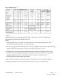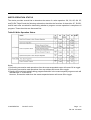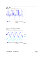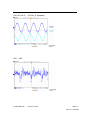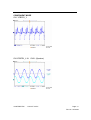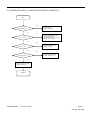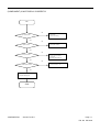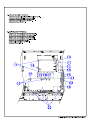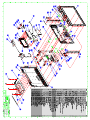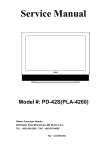
1
Service Manual Model #: VIZIO VX32L HDTV V, Inc 320A Kalmus Drive Costa Mesa, CA 92626 TEL : +714-668-0588 FAX :+714-668-9099 Top Confidential Table of Contents CONTENTS PAGE Sections 1. Features 1-1 2. Specifications 2-1 3. On Screen Display 3-1 4. Factory Preset Timings 4-1 5. Pin Assignment 5-1 6. Main Board I/O Connections 6-1 7. Theory of Circuit Operation 7-1 8. Waveforms 8-1 9. Trouble Shooting 9-1 10. Block Diagram 10-1 11. Spare parts list 11-1 12. Complete Parts List 12-1 Appendix 1. Main Board Circuit Diagram 2. Main Board PCB Layout 3. Assembly Explosion Drawing Block Diagram VIZIO VX32L HDTV Service Manual VINC Service Manual VIZIO VX32L HDTV COPYRIGHT © 2000 V, INC. ALL RIGHTS RESERVED. IBM and IBM products are registered trademarks of International Business Machines Corporation. Macintosh and Power Macintosh are registered trademarks of Apple Computer, Inc. VINC and VINC products are registered trademarks of V, Inc. VESA, EDID, DPMS and DDC are registered trademarks of Video Electronics Standards Association (VESA). Energy Star is a registered trademark of the US Environmental Protection Agency (EPA). No part of this document may be copied, reproduced or transmitted by any means for any purpose without prior written permission from VINC. FCC INFORMATION This equipment has been tested and found to comply with the limits of a Class B digital device, pursuant to part 15 of the FCC Rules. These limits are designed to provide reasonable protection against harmful interference in a residential installation. This equipment generates, uses and can radiate radio frequency energy, and if not installed and used in accordance with the instructions, may cause harmful interference to radio communications. However, there is no guarantee that the interference will not occur in a particular installation. If this equipment does cause unacceptable interference to radio or television reception, which can be determined by turning the equipment off and on, the user is encouraged to try to correct the interference by one or more of the following measures -- reorient or relocate the receiving antenna; increase the separation between equipment and receiver; or connect the into an outlet on a circuit different from that to which the receiver is connected. FCC WARNING To assure continued FCC compliance, the user must use a grounded power supply cord and the provided shielded video interface cable with bonded ferrite cores. Also, any unauthorized changes or modifications to Amtrak products will void the user’s authority to operate this device. Thus VINC Will not be held responsible for the product and its safety. CE CERTIFICATION This device complies with the requirements of the EEC directive 89/336/EEC with regard to “Electromagnetic compatibility.” SAFETY CAUTION Use a power cable that is properly grounded. Always use the AC cords as follows – USA (UL); Canada (CSA); Germany (VDE); Switzerland (SEV); Britain (BASEC/BS); Japan (Electric Appliance Control Act); or an AC cord that meets the local safety standards. VIZIO VX32L HDTV Service Manual Chapter 1 Features 1. Built in TV channel selector for TV viewing 2. Simulatnueous display of PC and TV images 3. Connectable to PC’s analog RGB port 4. Built in S-video, HDTV, composite video, HDMI and TV out 5. Built in auto adjust function for automatic adjument of screen display 6. Smoothing function enables display of smooth texts and graphics even if image withresolution lower than 1366x768 is magnified 7. Picture In Picture (PIP) funtion to show TV or VCR/DVD images 8. Power saving to reduce consumption power too less than 3W 9. On Screen Display: user can define display mode (i.e. color, brightness, contrast, sharpness, backlight), sound setting, PIP, TV channel program, aspect and gamma or reset all setting. CONFIDENTIAL – DO NOT COPY Page 1-1 File No. SG-0204 Chapter 2 Specification 1. LCD CHARACTERISTICS LC320W01 Item Specification Active Screen Size 31.51(800.4mm) inch diagonal Outline Dimension 760.0mm(H) x 450.0mm(V) x 48.0mm(D) (Typ.) Pixel Pitch 0.17025mm x 0.51075mm xRGB Pixel Format 1366 (R,G,Bx3) x 768 Display Color 16.7 M (8-bit + FRC for R,G,B) Luminance, White 500 cd/m2 (Typ) Viewing Angle(L/R/U/D) 89/89/89/89 Power Consumption 84 Watt (Typ.) (Vdd line +CCFL line)(at 3.5A) Weight 6900g (Typ) Display Mode Transmissive mode, normally black Surface Treatment Hard coating(3H), AG 2. OPTICAL CHARACTERISTICS Viewing Angle (CR>10) Left: 89°typ. Right: 89°typ. Top: 89°typ. Bottom: 89°typ. 3. SIGNAL (Refer to the Timing Chart) Sync Signal 1) Type: TMDS 2) Input Voltage Level: 100~240 Vac, 50/ 60 Hz 4.Input Connectors RJ11, D-SUB15PIN (MINI, 3rows), HDMIX2, RCAX2 (component), RCAX2 (AUDIO in), RCAX2 (composite), RCAX2 (AUDIO in), S-Video, Tuner Output Connectors Analog audio out (Stereo RCA Jack) , Digital audio out (Optical) CONFIDENTIAL – DO NOT COPY Page 2-1 File No. SG-0204 5. POWER SUPPLY Power Consumption: 180W MAX Power OFF: to less than 3W MAX 6.Speaker Output 10W (max) X2 7. ENVIRONMENT 7-1. Operating Temperature: 5c~35c (Ambient) 7-2. Operating Humidity: Ta= 35 °C, 90%RH (Non-condensing) 7-3. Operating Altitude: 0 - 14,000 feet (Non-Operating) 8. DIMENSIONS (Physical dimension) Width: 797.00 mm. Depth: 593.00mm Height: 263.7mm 9. WEIGHT (Physical weight) a. Net: 15.0+/-0.5kgs b. Gross: 20+/-0.5kgs Please pay attention to the followings when you use this TFT LCD module. 9-1. MOUNTING PRECAUTIONS (1) You must mount a module using holes arranged in four corners or four sides. (2) You should consider the mounting structure so that uneven force (ex. Twisted stress) is not applied to the module. And the case on which a module is mounted should have sufficient strength so that external force is not transmitted directly to the module. (3) Please attach the surface transparent protective plate to the surface in order to protect the polarizer. Transparent protective plate should have sufficient strength in order to the resist external force. (4) You should adopt radiation structure to satisfy the temperature specification. CONFIDENTIAL – DO NOT COPY Page 2-2 File No. SG-0204 (5) Acetic acid type and chlorine type materials for the cover case are not desirable because the former generates corrosive gas of attacking the polarizer at high temperature and the latter causes circuit break by electro-chemical reaction. (6) Do not touch, push or rub the exposed polarizes with glass, tweezers or anything harder than HB pencil lead. And please do not rub with dust clothes with chemical treatment. Do not touch the surface of polarizer for bare hand or greasy cloth.(Some cosmetics are detrimental to the polarizer.) (7) When the surface becomes dusty, please wipe gently with absorbent cotton or other soft materials like chamois soaks with petroleum benzene. Normal-hexane is recommended for cleaning the adhesives used to attach front / rear polarizers. Do not use acetone, toluene and alcohol because they cause chemical damage to the polarizer. (8) Wipe off saliva or water drops as soon as possible. Their long time contact with polarizer causes deformations and color fading. (9) Do not open the case because inside circuits do not have sufficient strength. 9-2. OPERATING PRECAUTIONS (1) The spike noise causes the mis-operation of circuits. It should be lower than following voltage : V=±200mV(Over and under shoot voltage) (2) Response time depends on the temperature. (In lower temperature, it becomes longer.) (3) Brightness depends on the temperature. (In lower temperature, it becomes lower.)And in lower temperature, response time (required time that brightness is stable after turned on) becomes longer. (4) Be careful for condensation at sudden temperature change. Condensation makes damage to polarizer or electrical contacted parts. And after fading condensation, smear or spot will occur. (5) When fixed patterns are displayed for a long time, remnant image is likely to occur. (6) Module has high frequency circuits. System manufacturers shall do sufficient suppression to the electromagnetic interference. Grounding and shielding methods may be important to minimize the interference. CONFIDENTIAL – DO NOT COPY Page 2-3 File No. SG-0204 9-3. HANDLING PRECAUTIONS FOR PROTECTION (1) The protection film is attached to the bezel with a small masking tape. When the protection film is peeled off, static electricity is generated between the film and polarizer. This should be peeled off slowly and carefully by people who are electrically grounded and with well ion-blown equipment or in such a condition, etc. (2) When the module with protection film attached is stored for a long time, sometimes there remains a very small amount of glue still on the bezel after the protection film is peeled off. (3) You can remove the glue easily. When the glue remains on the bezel surface or its vestige is recognized, please wipe them off with absorbent cotton waste or other soft material like chamois soaked with normal-hexane. CONFIDENTIAL – DO NOT COPY Page 2-4 File No. SG-0204 Chapter 3 On Screen Display Main unit button Power MENU CH ▲ CH ▼ VOL + VOL Input TV Source A. PICTURE: a. PICTURE MODE (CUSTOM/ STANDARD / MOVIE / GAME) b. BACKLIGHT (0~100) c. BRIGHTNESS (0~100) d. CONTRAST (0~100) e. COLOR (0~100) f. TINT (-32~32) g. SHARPNESS (0~100) h. COLOR TEMPERATURE (CUSTOM/COOL/NORMAL/WARM) i. ADVANCED VIDEO i-1. DNR(OFF/LOW/MEDIUM/STRONG) i-2. BLACK LEVEL EXTENDER (ON/OFF) i-3. WHITE PEAK LIMITATOR (ON/OFF) i-4 CTI(OFF/LOW/MEDIUM/STRONG) i-5 FLESH TONE (ON/OFF) i-6 ADAPTIVE LUMA (ON/OFF) CONFIDENTIAL – DO NOT COPY Page 3-1 File No. SG-0204 B. AUDIO: a. VOLUME (0~100) b. BASS (0~100) c. TREBLE (0~100) d. BALANCE (-50~50) e. SURROUND (ON/OFF) f. SPEAKERS (ON/OFF) C. TV: a. TUNER MODE (ANTENNA/CABLE) b. AUTO SEARCH (RUN) c. SKIP CHANNEL (TABLE) d. TIME ZONE (HAWALL/EASTTERN/INDIANA/CENTRAL/MOUNTAIN/ARIZONA/PACIFIC/ALA SKA) e. Daylight Saving(ON/OFF) D. SETUP: a. LANGUAGE (ENGLISH/FRENCH/SPANISH) b. SLEEP TIMER (OFF/30/60/90/120) c. ANALOG CC (OFF/CC1/CC2/CC3/CC4) d. DIGITAL CC(OFF/SERVICE1/ SERVICE2/ SERVICE3/ SERVICE4/ SERVICE5/ SERVICE6) e. DIGITAL CC STYLE e-1. CAPTION STYLE (AS BROADCASTER/CUSTOM) e-2. FONT SIZE(SMALL/MEDIUM/LARGE) e-3. FONT COLOR (GREEN/BLUE//RED/CYAN/YELLOW/MAGENTA/BLACK/WHITE) e-4. FONT OPACITY (SOLID/TRANSLUCENT/TRANSPARENT) e-5. BACKGROUND COLOR (GREEN/BLUE//RED/CYAN/YELLOW/MAGENTA/BLACK/WHITE) e-6. BACKGROUND OPACITY (SOLID/TRANSLUCENT/TRANSPARENT) CONFIDENTIAL – DO NOT COPY Page 3-2 File No. SG-0204 e-7. WINDOW COLOR (GREEN/BLUE//RED/CYAN/YELLOW/MAGENTA/BLACK/WHITE) e-8. WINDOW OPATITY (SOLID/TRANSLUCENT/TRANSPARENT) f. RESET ALL SETTING E. PARENTAL: a. PASSWORD a-1. CHANNEL BLOCK a-2. TV RATING a-3. MOVIE RATING a-4. BLOCK TV UNRATED a-5. ACCESS CODE EDIT RGB Mode A. PICTURE ADJUST: a. AUTO PICTURE (Run) b. BACKLIGHT (0~100) c. BRIGHTNESS (0~100) d. CONTRAST (0~100) e. COLOR TEMPERATURE(CUSTOM, 6500K, 9300K) f. H-SIZE (0~255) g. H-POSITION (0~100) h. V-POSITION (0~100) i. FINE TUNE (0~31) B. AUDIO: a. VOLUME (0~100) b. BASS (0~100) c. TREBLE (0~100) d. BALANCE (-50~50) e. SURROUND (ON/OFF) f. SPEAKERS (ON/OFF) CONFIDENTIAL – DO NOT COPY Page 3-3 File No. SG-0204 C. SETUP: a. LANGUAGE (ENGLISH/FRENCH/SPANISH) b. SLEEP TIMER (OFF/30/60/90/120) RESET ALL SETTING AV COMPONENT MODE AV-C、AV-S、COMPONENT A. PICTURE: a. PICTURE MODE (CUSTOM/ STANDARD / MOVIE / GAME) b. BACKLIGHT (0~100) c. BRIGHTNESS (0~100) d. CONTRAST (0~100) e. COLOR (0~100) f. TINT (-32~32) g. SHARPNESS (0~100) h. COLOR TEMPERATURE (CUSTOM/COOL/NORMAL/WARM) i. ADVANCED VIDEO i-1. DNR(OFF/LOW/MEDIUM/STRONG) i-2. BLACK LEVEL EXTENDER (ON/OFF) i-3. WHITE PEAK LIMITATOR (ON/OFF) i-4 CTI(OFF/LOW/MEDIUM/STRONG) i-5 FLESH TONE (ON/OFF) i-6 ADAPTIVE LUMA (ON/OFF) CONFIDENTIAL – DO NOT COPY Page 3-4 File No. SG-0204 B. AUDIO: a. VOLUME (0~100) b. BASS (0~100) c. TREBLE (0~100) d. BALANCE (-50~50) e. SURROUND (ON/OFF) f. SPEAKERS (ON/OFF) D. SETUP: a. LANGUAGE (ENGLISH/FRENCH/SPANISH) b. SLEEP TIMER (OFF/30/60/90/120) c. RESET ALL SETTING E. PARENTAL: a. PASSWORD a-1. CHANNEL BLOCK a-2. TV RATING a-3. MOVIE RATING a-4. BLOCK TV UNRATED a-5. ACCESS CODE EDIT CONFIDENTIAL – DO NOT COPY Page 3-5 File No. SG-0204 HDMI MODE: A. PICTURE: a. PICTURE MODE (CUSTOM/ STANDARD / MOVIE / GAME) b. BACKLIGHT (0~100) c. BRIGHTNESS (0~100) d. CONTRAST (0~100) e. COLOR (0~100) f. TINT (-32~32) g. SHARPNESS (0~100) h. COLOR TEMPERATURE (CUSTOM/COOL/NORMAL/WARM) i. ADVANCED VIDEO i-1. DNR(OFF/LOW/MEDIUM/STRONG) i-2. BLACK LEVEL EXTENDER (ON/OFF) i-3. WHITE PEAK LIMITATOR (ON/OFF) i-4 CTI(OFF/LOW/MEDIUM/STRONG) i-5 FLESH TONE (ON/OFF) i-6 ADAPTIVE LUMA (ON/OFF) B. AUDIO: a. VOLUME (0~100) b. BASS (0~100) c. TREBLE (0~100) d. BALANCE (-50~50) e. SURROUND (ON/OFF) f. SPEAKERS (ON/OFF) CONFIDENTIAL – DO NOT COPY Page 3-6 File No. SG-0204 C. SETUP: a. LANGUAGE (ENGLISH/FRENCH/SPANISH) b. SLEEP TIMER (OFF/30/60/90/120) RESET ALL SETTING CONFIDENTIAL – DO NOT COPY Page 3-7 File No. SG-0204 Chapter4 Factory preset timings This timing chart is already preset for the TFT LCD analog & digital display monitors. Refresh Horizontal Vertical Horizontal Vertical Pixel rate Frequency Frequency Polarity Polarity Rate 640x480 60Hz 31.5kHz 59.94Hz N N 25.175 640x480 75Hz 37.5kHz 75.00Hz N N 31.500 800X600 60Hz 37.9kHz 60.317Hz P P 40.000 800x600 75Hz 46.9kHz 75.00Hz P P 49.500 800X600 85Hz 53.7kHz 85.06Hz P P 56.250 1024x768 60Hz 48.4kHz 60.01Hz N N 65.000 1024X768 75Hz 60.0kHz 75.03Hz P P 78.750 720x400 70Hz 31.46kHz 70.08Hz N P 28.320 1366X768 60 47.7KHZ 60.00HZ P N 85.500 Resolution Remark: P: positive N: negative CONFIDENTIAL – DO NOT COPY Page 4-1 File No. SG-0204 Chapter5 Pin Assignment The TFT LCD analog display monitors use a 15 Pin Mini D-Sub connector as video input source. Pin Description 1 Red 2 Green 3 Blue 4 Ground 5 Ground 6 R-Ground 7 G-Ground 8 B-Ground 9 +5V for DDC 10 Ground 11 No Connection 12 (SDA) 13 H-Sync (Composite Sync) 14 V-Sync 15 (SCL) 1 5 6 11 CONFIDENTIAL – DO NOT COPY 10 15 Page 5-1 File No. SG-0204 HDMI CONNECT PIN ASSIGNMENT PIN SIGNAL ASSIGNMENT 1 TMDS Data2+ 2 TMDS Data2 Shield 3 TMDS Data2- 4 TMDS Data1+ 5 TMDS Data1 Shield 6 TMDS Data1- 7 TMDS Data0+ 8 TMDS Data0 Shield 9 TMDS Data0- 10 TMDS Clock+ 11 TMDS Clock Shield 12 TMDS Clock- 13 CEC 14 Reserved (N.C on device) 15 SCL 16 SDA 17 DDC/CEC Ground 18 +5V Power 19 Hot Plug Detect CONFIDENTIAL – DO NOT COPY Page 5-2 File No. SG-0095 Four-Pin mini DIN S-Video Connector a. Pin Assignment b. Signal Level Video (Y): Analog 0.1Vp-p/75Ω Video (C): Analog 0.286p-p/75 Sync (H+V): 0.3V below Video (Y) c. Frequency H: 15.734KHz V: 60Hz (NTSC) Signal Level Video (Y) : Analog 0.1Vp-p/75Ω Video (C) : Analog 0.286p-p/75Ω Sync (H+V): 0.3V below Video (Y) Frequency H: 15.734Khz V: 60HZ (NTSC) F-Type TV RF connector a. Signal Level 60dBµV typical b. System NTSC c. Frequency 55~801MHz (NTSC) PC connector 15 pin male D-sub connector a. Pin Assignment Refer to Section 2.3.10 b. Signal Level Video (R, G, B): Analog 0.7Vp-p/75Ω Sync (H, V): TTL level RGB Signal: a. Sync Type TTL (Separate / Composite) or Sync. On Green b. Sync polarity Positive or Negative c. Video Amplitude RGB: 0.7Vp-p d. Frequency H: support to 30K~70KHz V: support to 50~85Hz Pixel Clock: support to 110MHz CONFIDENTIAL – DO NOT COPY Page 5-3 File No. SG-0095 HDMI Signal (HDMI): a. Pin Assignment Refer to HDNI Pin Assignment b. Type A c. Polarity Positive or Negative d. Frequency H: 15.734KHz V: 60Hz (NTSC-480i) H: 31KHz V: 60Hz (NTSC-480p) H: 45KHz V: 60Hz (NTSC-720p) H: 33KHz V: 60Hz (NTSC-1080i) Component signal Component a. Frequency H: 15.734KHz V: 60Hz (NTSC-480i) H: 31KHz V: 60Hz (NTSC-480p) H: 45KHz V: 60Hz (NTSC-720p) H: 33KHz V: 60Hz (NTSC-1080i) b. Signal level Y: 1Vp-p Pb: ±0.350Vp-p Pr: ±0.350Vp-p c. Impedance 75Ω CONFIDENTIAL – DO NOT COPY Page 5-4 File No. SG-0095 Chapter 6 Main Board I/o Connections J2 CONNECTION (TOP→BOTTOM) Pin Description 1 “LED WHITE” 2 “LED AMBER” 3 “+5V” 4 “+5V” 5 “IR” 6 “GND” 7 “GND” 8 “ADIN1” 9 “ADIN2” 10 “+3.3V” J1 CONNECTION (TOP→BOTTOM) Pin Description 1 “POWRSW” 2 “+12V” 3 “+12V” 4 “+12V” 5 “+12V” 6 “GND” 7 “GND” 8 “GND” 9 “+5V” 10 “+5V” 11 “+5V” 12 “PWM” 13 “BL ON/OFF” CONFIDENTIAL – DO NOT COPY Page 6-1 File No. SG-0204 Chapter 7 Theory of Circuit Operation The operation of D-SUB 15pin route The D-SUB 15pin is input analog signal to the MT5372 transfer A/D converter then generates the vertical and horizontal timing signals for display device. The operation of HDMII CON route .Then transfer to the MT5372, the MT5372 generates the vertical and horizontal timing signals for display device. The operation of HDTV & Component route HDTV & Component signal is input to the MT5372 then MT5372 generates the vertical and horizontal timing signals for display device. The operation of Video & S-Video route The Video and S-Video signal is transmission signal to the MT5372 then MT5372 generates the vertical and horizontal timing signals for display device. The operation of TV route TV signal is processes to the tuner and output to MT5372 then MT5372 generates the vertical and horizontal timing signals for display device. Audio is processes to the tuner output to SIF circuit and output to MT5372.Then MT5372 process to wm8776 and output to TDA8946AJ transfer to speaker The operation of DTV route DTV signal is processes to the tuner and transmission to MT5112 and output signal to MT5372 generates the vertical and horizontal timing signals for display device. The operation of keypad There are 7 keys to control and select the function of VX32L and also has one LED to indicate the status of operation. They are “Power, ▼▲, + CONFIDENTIAL – DO NOT COPY -, Input, OSD”. Page 7-1 File No. SG-0204 MT5372 Application MT5372 is a highly integrated video and audio single chip processor for emerging HDTV-Ready LCD TV. It includes one 3D/2D TV Decoder recovering the best image from CVBS, and in addition, its analog input also support popular S-Video, Component, VGA video source. On-chip advanced motion adaptive de-interlacer (MDDitm) converts accordingly the interlace video into smooth non-flicking progressive motion pictures. With on-chip advanced 2D Graphic processor,MT5372 provides customers with high quality UI adding significant end product value. Flexible scalar provides wide adoption to various LCD panel for different video sources. Its on-chip audio processor decodes whole world standard audio signals from tuner with lip sync control, delivering high quality post-processed sound effect to customers. On-chip microprocessor and reference FW reduces the system BOM and shortens the schedule of UI design by high-level C program. With truly SOC design, MT5372 offers our customers the real cost-effective high performance HDTV-ready solution. CONFIDENTIAL – DO NOT COPY Page 7-2 File No. SG-0204 CONFIDENTIAL – DO NOT COPY Page 7-3 File No. SG-0204 1. Video input a. Input Multiplexing 1.component X2 2.composite X2 3.s-videoX1 4.HDMI X1 5.VGA X1 6.RF&DTV X1 b. Input formats: 1.support HDTV 480i/480p/720p/1080p 2.support Y/C signal 1VP-P/75Ω 3.support Y/C signal 1VP-P/75Ω 4.support 480i/408p/720p/1080i/1080p 5.support VGA input up to 1366x168@60HZ 6.support RF NTSC system Frequency 55~801MHZ;DTV 480i/480p/720p/1080p 2. Decoder TVD 1.Single 2nd generation TV decoder 2.Automatic TV standard detection supporting NTSC, NTSC-4.43, 3.Enhanced 2nd generation NTSC Motion Adaptive 3D comb filter 4.Motion Adaptive 3D Noise Reduction 5.Embedded VBI decoder for Closed-Caption/XDS/ Teletext/WSS/VPS 6.Supporting Macro vision detection YPbPr 1.Supporting HDTV 480i/480p/576i/576p/720p/1080i input 2.Smart detection on Scart function for European region VGA 1.Supporting various VGA input timings up to SXGA (1280x1024@75Hz). 2.Supporting Separate/Composite/SOG sync types CONFIDENTIAL – DO NOT COPY Page 7-4 File No. SG-0204 Digital port 1.1 digital port supporting DVI 24-bit RGB or CCIR-656/601 digital video input format 2.1 additional 8 bit digital port for ITU656 video format VBI 1.Dual VBI decoders for the application of V-Chip/Closed-Caption/XDS/ Teletext/WSS/VPS 2.Supporting external VBI decoder by YPrPb input 3.VBI decoder up to 1000 pages Teletext. 3. Support Formats: Support NTSC, NTSC-4.43 Automatic Luma / Chroma gain control Automatic TV standard detection NTSC Motion Adaptive 3D comb filter Motion adaptive 3D Noise Reduction VBI decoder for closed-caption/XDS/Teletext/WSS/VPS Macro vision detection 4. 2D-Graphic/OSD processor Embedded two backend RGB domain OSD planes and one YUV domain OSD plane. to support Main/PIP Teletext/Close-caption functions together with setup menu 1.Supporting alpha blending among these two planes and video 2.Supporting Text/Bitmap decoder 3.Supporting line/rectangle/gradient fill 4.Supporting bitblt 5.Supporting color Key function 6.Supporting Clip Mask 7.65535/256/16/4/2-color bitmap format OSD, 8.Automatic vertical scrolling of OSD image 9.Supporting OSD mirror and upside down CONFIDENTIAL – DO NOT COPY Page 7-5 File No. SG-0204 5. Microprocessor interface When power is supplied and power key is pressed then the rest circuit lets Reset to low state that will reset the MT5372 to initial state. After that the Reset will transits to high state and the MT5372 start to work that microprocessor executes the programs and configures the internal registers. The execution speed of CPU is 162 MHz. PIP/POP HARDWARE LIMITION: AV1(S) ATV YPbPr RGB HDMI1 DTV AV1/2 v v v v ATV v v v YPbPr v v v v RGB v v v v HDMI1 v v DTV v v v v v v v 6. Video processor 1.Color Management Fully 10-bit processing to enhance the video quality Advanced flesh tone and multiple-color enhancement. (For skin, sky, and grass…) Gamma/anti-Gamma correction Advanced Color Transient Improvement (CTI) Saturation/hue adjustment 2.Contrast/Brightness/Sharpness Management Sharpness and DLTI/DCTI Brightness and contrast adjustment Black level extender White peak level limiter Adaptive Luma/Chroma management 3.De-interlacing 2nd generation advanced Motion adaptive de-interlacing Automatic detect film or video source 3:2/2:2 pull down source detection Main/PIP 2 independent de-interlacing processor CONFIDENTIAL – DO NOT COPY Page 7-6 File No. SG-0204 4.Scaling 2nd generation high resolution arbitrary ratio vertical/horizontal scaling of video, from 1/32X to 32X Advanced linear and non-linear Panorama scaling Programmable Zoom viewer Picture-in-Picture (PIP) Picture-Out-Picture (POP) 5.Display Advanced dithering processing for LCD display with 6/8/10 bit output 10bit gamma correction Supporting alpha blending for Video and two OSD planes Frame rate conversion 6.Seamless performance comparing demonstration function Support Left/Right video processing comparing function without additional resources (DRAM…) for customers’ demonstration All the video functions (De-interlace/3D comb/NR/Flesh tone/CTI) can be included 7. DRAM Usage 1.For features of 5372, Dual for enhance features support, and single 8x16 DDR for simple function support Lists are the comparison chart between function support lists of (2xDDR) and (1xDDR) 2.For single DDR,5372only support 1080i bob mode de-interlacing. (Non-3D de interlace) 3.With single DDR, it is suggested not to support PIP/POP features. Due to DDR Bandwidth limitation on PIP when single DDR. CONFIDENTIAL – DO NOT COPY Page 7-7 File No. SG-0204 WM8776 Application The WM8776 is a high performance, stereo audio codec with five channel input selector. The WM8776 is ideal for surround sound processing applications for home hi-fi, DVD-RW and other audiovisual equipment. Etch ADC channel has programmable gain control with automatic level control. Digital audio output word lengths from 16-32 bits and sampling rates from 32kHZ to 96KHZ are supported. The DAC has an input mixer allowing an external analogue signal to be mixed with the DAC signal. There are also Headphone and line outputs, with control for the headphone The WM8776 supports fully independent sample rates for the ADC and DAC. The audio data interface supports I2S, left justified, right justified and DSP formats. BLOCK DIAGRAM 1. Audio sample rate The master clock forWM8776 supports DAC and ADC audio sampling rates 256fs to 768fs, where fs is the audio sample frequency (DACLRC or ADCLRC) typically 32KHZ, 44.1KHZ, 48KHZ or 96KHZ (the DAC also supports operation at 128fs and 192fs and 192KHZ sample rate). The master clock is used to operate the digital filters and the noise shaping circuits. In slave mode the WM8776 has a master detection circuit that automatically determines the relationship between the master clock frequency and the sampling rate (to within +/- 32 system clocks) If there is a greater than 32 clocks error the interface is disabled and ADCLRC/DACLRC for optical performance, although the WM8776 is tolerant of phase variations or jitter on this clock. Table shows the typical master clock frequency inputs for the WM8776 CONFIDENTIAL – DO NOT COPY Page 7-8 File No. SG-0204 2. DIGITAL AUDIO INTERFACE 1. Slave mode The audio interfaces operations in either slave mode selectable using the MS control bit. In slave mode DIN is always an input to the WM8776 and DOUT is always an output. The default is Slave mode. In slave mode (ms=0) ADCLRC, DACLRC, ADCBCLK, DACBCLK are input to the WM8776 DIN and DACLRC are sampled by the WM8776 on the rising edge of DACBCLK; ADCLRC is sampled on the rising edge of ADCBCLK. ADC data is output on DOUT and changes on the falling edge of ADCBCLK. By setting control bit BCLKINV the polarity of ADCBCLK and DACBCLK may be reversed so that DIN and DACLRC are sample on the falling edge of DACBCLK, ADCLRC is sampled on the falling edge of ADCBCLK and DOUT changes on the rising of ADCBCLK Slave mode as shown in the following figure. 2. 2 Wire serial control mode The wm8776 supports software control via a 2-wire serial bus. Many devices can be controlled by the same bus, and each device has a unique 7-bit address (this is not the same as the 7-bit address of each register in the wm8776). The wm8776 operates as a slave device only. 2-wire serial interface as shown in the following figure. CONFIDENTIAL – DO NOT COPY Page 7-9 File No. SG-0204 The wm8776 has two possible device addresses, which can be selected using the CE pin In the VX32L LCD TV CE pin is High (device address is 36h) In the VX32L wm8776 has 2-wire interface 3. HDCP Decryption HDCP decryption contains all necessary logic to decrypt the incoming audio and video data. The decryption process is entirely controlled by the host microprocessor through a set sequence of register reads and wires through the DDC channel. Pre-programmed HDCP keys and key Selection Vector are used in the decryption process. A resulting calculated to an XOR mask during each clock cycle to decrypt the audio/video data in sync with the host. CONFIDENTIAL – DO NOT COPY Page 7-10 File No. SG-0204 TDA8946 Application In VX32L TV the TDA8946AJ is a dual-channel audio power amplifier with DC gain control. It has an output power of 2 10 W at an 8 load and a 12 V supply. Block diagram 1. Input configuration The TDA8946AJ inputs can be driven symmetrical (floating) as well as asymmetrical. In the asymmetrical mode one input pin is connected via a capacitor to the signal source and the other input is connected to the signal ground. The signal ground should be as close as possible to the SVR (electrolytic) capacitor ground. Note that the DC level of the input pins is half of the supply voltage VCC, so coupling capacitors for both pins are necessary CONFIDENTIAL – DO NOT COPY Page 7-11 File No. SG-0204 2. Output power measurement The output power as a function of the supply voltage is measured on the output pins at THD = 10%,in the VX32L LCD TV Vcc=12V so we can see as shown in the following figure output about 7W. CONFIDENTIAL – DO NOT COPY Page 7-12 File No. SG-0204 3. Mode selection In the VX32L LCD TV TDA8946AJ has two functional modes, which can be selected by applying the proper DC voltage to pin MODE. 1. Mute — In this mode the amplifier is DC-biased but not operational (no audio output). This allows the input coupling capacitors to be charged to avoid pop-noise. The device is in mute mode when 3.5 V < VMODE < (VCC 1.5 V). 2. Operating — In this mode the amplifier is operating normally. The operating mode is activated at VMODE<1.0V. General Feature List : 1 . Host CPU: 1. ARM 926EJ 2.16K I-Cache and 16K D-Cache 3. 8K Data TCM and 8K instruction 4. JTAG ICE interface 5. Watch Dog timers CONFIDENTIAL – DO NOT COPY Page 7-13 File No. SG-0204 2 . Transport Demuxer : 1. Support 3 independent transport stream inputs 2. Support serial/parallel interface for each transport stream input 3. Support ATSC , DVB , and MPEG2 transport stream inputs. 4. Programmable sync detection. 5. Support DES/3-DES De-scramble. 6. 96 PID filter and 128 section filters. 7. Support TS recording via IEEE1394 interface. 3 . MPEG2 Decoder : 1. Support dual MPEG-2 HD decoder or up to 8 SD decoder. 2. Complaint to MP@ML , MP@HL and MPEG-1 video standards. 4 . JPEG Decoder : 1. Decode Base-line or progressive JPEG file. 5 . 2D Graphics : 1. Support multiple color modes. 2. Point , horizontal/vertical line primitive drawing. 3. Rectangle fill and gradient fill functions. 4. Bitblt with transparent , alpha blending , alpha composition and stretch. 5. Font rendering by color expansion. 6. Support clip masks. 7. YCrCb to RGB color space transfer. 6 . OSD Display : 1. 3 linking list OSDs with multiple color mode. 2. OSD scaling with arbitary ratio from 1/2x to 2x. 3. Square size , 32x32 or 64x64 pixel , hardware cursor. 7 . Video Processing : 1. Advanced Motion adaptive de-interlace on SDTV resolution. 2. Support clip 3. 3:2/2:2 pull down source detection. 4. Arbitrary ratio vertical/horizontal scaling of video , from 1/15X to 16X. 5. Support Edge preserve. 6. Support horizontal edge enhancement. 7. Support Quad-Picture. CONFIDENTIAL – DO NOT COPY Page 7-14 File No. SG-0204 8 . Main Display : 1. Mixing two video and three OSD and hardware cursor. 2. Contrast/Brightness adjustment. 3. Gamma correction. 4. Picture-in-Picture( PIP ). 5. Picture-Out-Picture( POP ). 6. 480i/576i/480p/576p/720p/1080i output 9 . Auxiliary Display : 1. Mixing one video and one OSD. 2. 480i/576i output. 10 . TV Encoder : 1. Support NTSC M/N , PAL M/N/B/D/G/H/I 2. Macrovision Rev 7.1.L1 3. CGMS/WSS. 4. Closed Captioning. 5. Six 12-bit video DACs for CVBS , S-video or RGB/YPbPr output. 11 . Digital Video Interface : 1. Support SAV/EAV. 2. Support 8/16 for SD/HD digital video input. 3. Support 8/16/24 bits digital output for main display. 4. Support 8 bits digital output for aux display. 12 . DRAM Controller : 1. Support 64Mb to 1Gb DDR DRAM devices. 2. Configurable 32/64 bit data bus interface. 3. Support DDR266 , DDR333 , DDR400 , JEDEC specification compliant SDRAM. 13 . Peripheral Bus Interface : 1. Support NOR/NAND flash. 2. Support CableCard host control bus. CONFIDENTIAL – DO NOT COPY Page 7-15 File No. SG-0204 14 . Audio : 1. Support Dolby Digital AC-3 decoding. 2. MPEG-1 layer I/II , MP3 decoding. 3. Dolby prologic II. 4. Main audio output : 5.1ch + 2ch ( down mix ) 5. Auxiliary audio output : 2ch. 6. Pink noise and white noise generator. 7. Equalizer. 8. Bass management. 9. 3D surround processing include virtual surround. 10. Audio and video lip synchronization. 11. Support reverberation. 12. SPDIF out. 13. I2S I/F. 15 . Peripherals : 1. Three UARTs with Tx and Rx FIFO , two of them have hardware flow control. 2. Two serial interfaces , one is master only the other can be set to master mode or slave mode. 3. Two PWMs. 4. IR blaster and receiver. 5. IEEE1394 link controller. 6. IDE bus : ATA/ATAPI7 UDMA mode 5 , 100MB/s. 7. Real-time clock and watchdog controller. 8. Memory card I/F : MS/MS-pro ,SD ,CF ,and MMC 9. PCMCIA/POD/CI interface 16 . IC Outline : 1. 471 Pin BGA Package. 2. 3.3V/1.2V dual Voltage. CONFIDENTIAL – DO NOT COPY Page 7-16 File No. SG-0204 MX29LV320BTTC (Flash) Application : The MX29LV320AT/B is a 32-mega bit Flash memory organized as 4M bytes of 8 bits and 2M words of 16 bits. MXIC's Flash memories offer the most cost-effective and reliable read/write non-volatile random access memory. The MX29LV320AT/B is packaged in 48-pin TSOP and 48-ball CSP. It is designed to be reprogrammed and erased in system or in standard EPROM programmers. The standard MX29LV320AT/B offers access time as fast as 70ns, allowing operation of high-speed microprocessors without wait states. To eliminate bus contention, the MX29LV320AT/B has separate chip enable (CE) and output enable (OE) controls. MXIC's Flash memories augment EPROM functionality with in-circuit electrical erasure and programming. The MX29LV320AT/B uses a command register to manage this functionality. MXIC Flash technology reliably stores memory contents even after 100,000 erase and program cycles. The MXIC cell is designed to optimize the erase and program mechanisms. In addition, the combination of advanced tunnel oxide processing and low internal electric fields for erase and programming operations produces reliable cycling. The MX29LV320AT/B uses a 2.7V to 3.6V VCC supply to perform the High Reliability Erase and auto Program/Erase algorithms. The highest degree of latch-up protection is achieved with MXIC's proprietary non-epi process. Latch-up protection is proved for stresses up to 100 milliamperes on address and data pin from -1V to VCC + 1V. CONFIDENTIAL – DO NOT COPY Page 7-17 File No. SG-0204 BLOCK DIAGRAM CONFIDENTIAL – DO NOT COPY Page 7-18 File No. SG-0204 BUS OPERATION--1 Legend: L=Logic LOW=VIL, H=Logic High=VIH, VID=12.0 0.5V, VHH=11.5-12.5V, X=Don't Care, AIN=Address IN, DIN=Data IN,DOUT=Data OUT Notes: 1. When the WP/ACC pin is at VHH, the device enters the accelerated program mode. See "Accelerated Program Operations" for more information. 2.The sector group protect and chip unprotect functions may also be implemented via programming equipment. See the "Sector Group Protection and Chip Unprotection" section. 3.If WP/ACC=VIL, the two outermost boot sectors remain protected. If WP/ACC=VIH, the two outermost boot sector protection depends on whether they were last protected or unprotected using the method described in "Sector/Sector Block Protection and Unprotection". If WP/ACC=VHH, all sectors will be unprotected. 4.DIN or Dout as required by command sequence, data polling, or sector protection algorithm. 5.Address are A20:A0 in word mode (BYTE=VIH), A20:A-1 in byte mode (BYTE=VIL). CONFIDENTIAL – DO NOT COPY Page 7-19 File No. SG-0204 BUS OPERATION--2 Notes: 1.Code=00h means unprotected, or code=01h protected. 2.Code=99 means factory locked, or code=19h not factory locked. WRITE COMMANDS/COMMAND SEQUENCES To program data to the device or erase sectors of memory , the system must drive WE and CE to VIL, and OE to VIH.An erase operation can erase one sector, multiple sectors , or the entire device. A "sector address" consists of the address bits required to uniquely select a sector. Writing specific address and data commands or sequences into the command register initiates device operations. Table A defines the valid register command sequences. Writing incorrect address and data values or writing them in the improper sequence resets the device to reading array data. Section has details on erasing a sector or the entire chip, or suspending/resuming the erase operation. After the system writes the Automatic Select command sequence, the device enters the Automatic Select mode. The system can then read Automatic Select codes from the internal register (which is separate from the memory array) on Q7-Q0. Standard read cycle timings apply in this mode. Refer to the Automatic Select Mode and Automatic Select Command Sequence section for more information.ICC2 in the DC Characteristics table represents the active current specification for the write mode. The "AC Characteristics" section contains timing specification table and timing diagrams for write operations. CONFIDENTIAL – DO NOT COPY Page 7-20 File No. SG-0204 TABLE A. MX29LV320AT/B COMMAND DEFINITIONS Legend: X=Don't care RA=Address of the memory location to be read. RD=Data read from location RA during read operation. PA=Address of the memory location to be programmed. Addresses are latched on the falling edge of the WE or CE pulse. PD=Data to be programmed at location PA. Data is latched on the rising edge of WE or CE pulse. SA=Address of the sector to be erased or verified. Address bits A20-A12 uniquely select any sector. ID=22A7h(Top), 22A8h(Bottom) Notes: 1.All values are in hexadecimal. 2.Except when reading array or Automatic Select data, all bus cycles are write operation. 3.The Reset command is required to return to the read mode when the device is in the Automatic Select mode or if Q5 goes high. 4.The fourth cycle of the Automatic Select command sequence is a read cycle. 5.The data is 99h for factory locked and 19h for not factory locked. 6.The data is 00h for an unprotected sector/sector block and 01h for a protected sector/sector block. In the third cycle of the command sequence, address bit A20=0 to verify sectors 0~31, A20=1 to verify sectors 32~70 for Top Boot device. 7.Command is valid when device is ready to read array data or when device is in Automatic Select mode. 8.The system may read and program functions in non-erasing sectors, or enter the Automatic Select mode, when in the erase Suspend mode. The Erase Suspend command is valid only during a sector erase operation. 9.The Erase Resume command is valid only during the Erase Suspend mode. CONFIDENTIAL – DO NOT COPY Page 7-21 File No. SG-0204 STANDBY MODE MX29LV320AT/B can be set into Standby mode with two different approaches. One is using both CE and RESET pins and the other one is using RESET pin only. When using both pins of CE and RESET, a CMOS Standby mode is achieved with both pins held at Vcc ±0.3V. Under this condition, the current consumed is less than 0.2uA (typ.). If both of the CE and RESET are held at VIH, but not within the range of VCC ± 0.3V, the device will still be in the standby mode, but the standby current will be larger. During Auto Algorithm operation, Vcc active current (ICC2) is required even CE = "H" until the operation is completed. The device can be read with standard access time (tCE) from either of these standby modes. When using only RESET, a CMOS standby mode is achieved with RESET input held at Vss 0.3V, Under this condition the current is consumed less than 1uA (typ.). Once the RESET pin is taken high, the device is back to active without recovery delay.In the standby mode the outputs are in the high impedance state, independent of the OE input.MX29LV320AT/B is capable to provide the Automatic Standby Mode to restrain power consumption during readout of data. This mode can be used effectively with an application requested low power consumption such as handy terminals. To active this mode, MX29LV320AT/B automatically switch themselves to low power mode when MX29LV320AT/B addresses remain stable during access time of tACC+30ns. It is not necessary to control CE, WE, and OE on the mode. Under the mode, the current consumed is typically 0.2uA (CMOS level). RESET OPERATION 01The RESET pin provides a hardware method of resetting the device to reading array data. When the RESET pin is driven low for at least a period of tRP, the device immediately terminates any operation in progress, tristates all output pins, and ignores all read/write commands for the duration of the RESET pulse. The device also resets the internal state machine to reading array data. The operation that was interrupted should be reinitiated once the device is ready to accept another command sequence, to ensure data integrity. Current is reduced for the duration of the RESET pulse. When RESET is held at VSS 0.3V, the device draws CMOS standby current (ICC4). If RESET is held at VIL but not within VSS 0.3V, the standby current will be greater.The RESET pin may be tied to system reset circuitry. A system reset would that also reset the Flash memory, enabling the system to read the boot-up firm-ware from the Flash memory. CONFIDENTIAL – DO NOT COPY Page 7-22 File No. SG-0204 If RESET is asserted during a program or erase operation, the RY/BY pin remains a "0" (busy) until the internal reset operation is complete, which requires a time of tREADY (during Embedded Algorithms). The system can thus monitor RY/BY to determine whether the reset operation is complete. If RESET is asserted when a program or erase operation is not executing (RY/BY pin is "1"), the reset operation is completed within a time of tREADY (not during Embedded Algorithms). The system can read data tRH after the RESET pin returns to VIH. Refer to the AC Characteristics tables for RESET parameters and to Figure 14 for the timing diagram. WRITE PROTECT (WP) The write protect function provides a hardware method to protect boot sectors without using VID. If the system asserts VIL on the WP/ACC pin, the device disables program and erase functions in the two "outermost" 8 Kbyte boot sectors independently of whether those sectors were protected or unprotected using the method described in Sector/Sector Group Protection and Chip Unprotection". The two outermost 8 Kbyte boot sectors are the two sectors containing the lowest addresses in a bottom-boot-configured device, or the two sectors containing the highest addresses in a top-boot-configured device. If the system asserts VIH on the WP/ACC pin, the device reverts to whether the two outermost 8K Byte boot sectors were last set to be protected or unprotected. That is, sector protection or unprotection for these two sectors depends on whether they were last protected or unprotected using the method described in "Sector/Sector Group Protection and Chip Unprotection". Note that the WP/ACC pin must not be left floating or unconnected; inconsistent behavior of the device may result. SOFTWARE COMMAND DEFINITIONS : Device operations are selected by writing specific address and data sequences into the command register. Writing incorrect address and data values or writing them in the improper sequence will reset the device to the read mode. Table 3 defines the valid register command sequences. Note that the Erase Suspend (B0H) and Erase Resume (30H) commands are valid only while the Sector Erase operation is in progress. Either of the two reset command sequences will reset the device (whenapplicable). All addresses are latched on the falling edge of WE or CE, whichever happens later. All data are latched on rising edge of WE or CE, whichever happens first. CONFIDENTIAL – DO NOT COPY Page 7-23 File No. SG-0204 WRITE OPERATION STATUS The device provides several bits to determine the status of a write operation: Q2, Q3, Q5, Q6, Q7, and RY/BY.Table B and the following subsections describe the functions of these bits. Q7, RY/BY, and Q6 each offer a method for determining whether a program or erase operation is complete or in progress. These three bits are discussed first. Table B. Write Operation Status Notes: 1.Performing successive read operations from the erase-suspended sector will cause Q2 to toggle. 2.Performing successive read operations from any address will cause Q6 to toggle. 3.Reading the byte/word address being programmed while in the erase-suspend program mode will indicate logic "1" at the Q2 bit. However, successive reads from the erase-suspended sector will cause Q2 to toggle. CONFIDENTIAL – DO NOT COPY Page 7-24 File No. SG-0204 Fig C. COMMAND WRITE OPERATION Fig D. READ TIMING WAVEFORMS CONFIDENTIAL – DO NOT COPY Page 7-25 File No. SG-0204 Fig E. RESET TIMING WAVEFORM CONFIDENTIAL – DO NOT COPY Page 7-26 File No. SG-0204 DDR SDRAM (NT5DS16M16CS-5T) Application: Functional Description The 256Mb DDR SDRAM is a high-speed CMOS, dynamic random-access memory containing 268, 435, 456 bits. The 256Mb DDR SDRAM is internally configured as a quad-bank DRAM. The 256Mb DDR SDRAM uses a double-data-rate architecture to achieve high-speed operation. The double-data-rate architecture is essentially a 2n prefetch architecture, with an interface designed to transfer two data words per clock cycle at the I/O pins. A single read or write access for the 256Mb DDR SDRAM consists of a single 2n-bit wide, one clock cycle data transfer at the internal DRAM core and two corresponding n-bit wide, one-half clock cycle data transfers at the I/O pins. Read and write accesses to the DDR SDRAM are burst oriented; accesses start at a selected location and continue for a programmed number of locations in a programmed sequence. Accesses begin with the registration of an Active command, which is then followed by a Read or Write command. The address bits registered coincident with the Active command are used to select the bank and row to be accessed (BA0, BA1 select the bank; A0-A12 select the row). The address bits registered coincident with the Read or Write command are used to select the starting column location for the burst access.Prior to normal operation, the DDR SDRAM must be initialized. The following sections provide detailed information covering device initialization, register definition, command descriptions and device operation. Block Diagram (16Mb x 16) Note: This Functional Block Diagram is intended to facilitate user understanding of the operation of the device; it does not represent an actual circuit implementation. Note: DM is a unidirectional signal (input only), but is internally loaded to match the load of the bidirectional DQ and DQS signals. CONFIDENTIAL – DO NOT COPY Page 7-27 File No. SG-0204 Pin Configuration - 400mil TSOP II (x4 / x8 / x16) CONFIDENTIAL – DO NOT COPY Page 7-28 File No. SG-0204 Mode Register Operation Operating Mode The normal operating mode is selected by issuing a Mode Register Set Command with bits A7-A12 to zero, and bits A0-A6 set to the desired values. A DLL reset is initiated by issuing a Mode Register Set command with bits A7 and A9-A12 each set to zero, bit A8 set to one, and bits A0-A6 set to the desired values. A Mode Register Set command issued to reset the DLL should always be followed by a Mode Register Set command to select normal operating mode. All other combinations of values for A7-A12 are reserved for future use and/or test modes. Test modes and reserved states should not be used as unknown operation or incompatibility with future versions may result. CONFIDENTIAL – DO NOT COPY Page 7-29 File No. SG-0204 Extended Mode Register The Extended Mode Register controls functions beyond those controlled by the Mode Register; these additional functions include DLL enable/disable, bit A0; output drive strength selection, bit A1; and QFC output enable/disable, bit A2 (NTC optional). These functions are controlled via the bit settings shown in the Extended Mode Register Definition. The Extended Mode Register is programmed via the Mode Register Set command (with BA0 = 1 and BA1 = 0) and retains the stored information until it is programmed again or the device loses power. The Extended Mode Register must be loaded when all banks are idle, and the controller must wait the specified time before initiating any subsequent operation. Violating either of these requirements result in unspecified operation. Extended Mode Register Definition CONFIDENTIAL – DO NOT COPY Page 7-30 File No. SG-0204 Truth Table a: Commands 1. CKE is high for all commands shown except Self Refresh. 2. BA0, BA1 select either the Base or the Extended Mode Register (BA0 = 0, BA1 = 0 selects Mode Register; BA0 = 1, BA1 = 0 selects ,Extended Mode Register; other combinations of BA0-BA1 are reserved; A0-A12 provide the op-code to be written to the selected Mode Register.) 3. BA0-BA1 provide bank address and A0-A12 provide row address. 4. BA0, BA1 provide bank address; A0-Ai provide column address (where i = 9 for x8 and 9, 11 for x4); A10 high enables the Auto Precharge feature (non-persistent), A10 low disables the Auto Precharge feature. 5. A10 LOW: BA0, BA1 determine which bank is precharged.A10 HIGH: all banks are precharged and BA0, BA1 are “Don’t Care.” 6. This command is auto refresh if CKE is high; Self Refresh if CKE is low. 7. Internal refresh counter controls row and bank addressing; all inputs and I/Os are “Don’t Care” except for CKE. 8. Applies only to read bursts with Auto Precharge disabled; this command is undefined (and should not be used) for read bursts with Auto Precharge enabled or for write bursts 9. Deselect and NOP are functionally interchangeable. Active The Active command is used to open (or activate) a row in a particular bank for a subsequent access. The value on the BA0,BA1 inputs selects the bank, and the address provided on inputs A0-A12 selects the row. This row remains active (or open) for accesses until a Precharge (or Read or Write with Auto Precharge) is issued to that bank. A Precharge (or Read or Write with Auto Precharge) command must be issued and completed before opening a different row in the same bank. Read The Read command is used to initiate a burst read access to an active (open) row. The value on the BA0, BA1 inputs selects the bank, and the address provided on inputs A0-Ai, Aj (where [i = 9, j = don’t care] for x8; where [i = 9, j = 11] for x4) selects the starting column location. The value on input A10 determines whether or not Auto Precharge is used. If Auto Precharge is selected, the row being accessed is precharged at the end of the Read burst; if Auto Precharge is not selected, the row remains open for subsequent accesses. CONFIDENTIAL – DO NOT COPY Page 7-31 File No. SG-0204 Write The Write command is used to initiate a burst write access to an active (open) row. The value on the BA0, BA1 inputs selects the bank, and the address provided on inputs A0-Ai, Aj (where [i = 9, j = don’t care] for x8; where [i = 9, j = 11] for x4) selects the starting column location. The value on input A10 determines whether or not Auto Precharge is used. If Auto Precharge is selected, the row being accessed is precharged at the end of the Write burst; if Auto Precharge is not selected, the row remains open for subsequent accesses. Input data appearing on the DQs is written to the memory array subject to the DM input logic level appearing coincident with the data. If a given DM signal is registered low, the corresponding data is written to memory; if the DM signal is registered high, the corresponding data inputs are ignored, and a Write is not executed to that byte/column location. Auto Refresh Auto Refresh is used during normal operation of the DDR SDRAM and is analogous to CAS Before RAS (CBR) Refresh in previous DRAM types. This command is nonpersistent, so it must be issued each time a refresh is required.The refresh addressing is generated by the internal refresh controller. This makes the address bits “Don’t Care” during an Auto Refresh command. The 256Mb DDR SDRAM requires Auto Refresh cycles at an average periodic interval of 7.8µs (maximum). Self Refresh The Self Refresh command can be used to retain data in the DDR SDRAM, even if the rest of the system is powered down.When in the self refresh mode, the DDR SDRAM retains data without external clocking. The Self Refresh command is initiated as an Auto Refresh command coincident with CKE transitioning low. The DLL is automatically disabled upon entering Self Refresh, and is automatically enabled upon exiting Self Refresh (200 clock cycles must then occur before a Read command can be issued). Input signals except CKE (low) are “Don’t Care” during Self Refresh operation. The procedure for exiting self refresh requires a sequence of commands. CK (and CK) must be stable prior to CKE returning high. Once CKE is high, the SDRAM must have NOP commands issued for tXSNR because time is required for the completion of any internal refresh in progress. A simple algorithm for meeting both refresh and DLL requirements is to apply NOPs for 200 clock cycles before applying any other command. CONFIDENTIAL – DO NOT COPY Page 7-32 File No. SG-0204 Operations: Reads Subsequent to programming the mode register with CAS latency, burst type, and burst length, Read bursts are initiated with a Read command. The starting column and bank addresses are provided with the Read command and Auto Precharge is either enabled or disabled for that burst access. If Auto Precharge is enabled, the row that is accessed starts precharge at the completion of the burst, provided tRAS has been satisfied. For the generic Read commands used in the following illustrations, Auto Precharge is disabled. During Read bursts, the valid data-out element from the starting column address is available following the CAS latency after the Read command. Each subsequent data-out element is valid nominally at the next positive or negative clock edge (i.e. at the next crossing of CK and CK). The following timing figure entitled “Read Burst: CAS Latencies (Burst Length=4)” illustrates the general timing for each supported CAS latency setting. DQS is driven by the DDR SDRAM along with output data. The initial low state on DQS is known as the read preamble; the low state coincident with the last data-out element is known as the read postamble . Upon completion of a burst, assuming no other commands have been initiated, the DQs and DQS goes High-Z. Data from any Read burst may be concatenated with or truncated with data from a subsequent Read command. In either case, a continuous flow of data can be maintained. The first data element from the new burst follows either the last element of a completed burst or the last desired data element of a longer burst which is being truncated. The new Read command should be issued x cycles after the first Read command, where x equals the number of desired data element pairs (pairs are required by the 2n prefetch architecture). This is shown in timing figure entitled “Consecutive Read Bursts: CAS Latencies (Burst Length =4 or 8)”.A Read command can be initiated on any positive clock cycle following a previous Read command. Nonconsecutive Read data is shown in timing figure entitled “Non-Consecutive Read Bursts: CAS Latencies (Burst Length = 4)”. Full-speed Random Read Accesses: CAS Latencies (Burst Length = 2, 4 or 8) within a page (or pages) can be performed as shown on following: CONFIDENTIAL – DO NOT COPY Page 7-33 File No. SG-0204 Random Read Accesses: CAS Latencies (Burst Length = 2, 4 or 8) CONFIDENTIAL – DO NOT COPY Page 7-34 File No. SG-0204 Read Command Writes Write bursts are initiated with a Write command, as shown in timing figure Write Command on following: The starting column and bank addresses are provided with the Write command, and Auto Precharge is either enabled or disabled for that access. If Auto Precharge is enabled, the row being accessed is precharged at the completion of the burst. For the generic Write commands used in the following illustrations, Auto Precharge is disabled. During Write bursts, the first valid data-in element is registered on the first rising edge of DQS following the write command, and subsequent data elements are registered on successive edges of DQS. The Low state on DQS between the Write command and the first rising edge is known as the write preamble; the Low state on DQS following the last data-in element is known as the write postamble. The time between the Write command and the first corresponding rising edge of DQS (tDQSS) is specified with a relatively wide range (from 75% to 125% of one clock cycle), so most of the Write diagrams that follow are drawn for the two extreme cases (i.e. tDQSS(min) and tDQSS(max)). Timing figure Write Burst (Burst Length = 4) on page 33 shows the two extremes of tDQSS for a burst of four. Upon completion of a burst, assuming no other commands have been initiated, the DQs and DQS enters High-Z and any additional input data is ignored.Data for any Write burst may be concatenated with or truncated with a subsequent Write command. In either case, a continuous flow of input data can be maintained. CONFIDENTIAL – DO NOT COPY Page 7-35 File No. SG-0204 The new Write command can be issued on any positive edge of clock following the previous Write command. The first data element from the new burst is applied after either the last element of a completed burst or the last desired data element of a longer burst which is being truncated. The new Write command should be issued x cycles after the first Write command, where x equals the number of desired data element pairs (pairs are required by the 2n prefetch architecture). Write Command Data Input (Write) CONFIDENTIAL – DO NOT COPY Page 7-36 File No. SG-0204 Data Output (Read) CONFIDENTIAL – DO NOT COPY Page 7-37 File No. SG-0204 Chapter8 Waveforms PC MODE(1366X768 60HZ) CH1 H-sync (R209); CH2 H-sync (L52) CH1 V-sync (R213); CH2 V-sync (L53) CONFIDENTIAL – DO NOT COPY Page 8-1 File No. SG-0204 CH1 R (R203) CH1 R (C95) CH1 B (R199) CH1 B (C92) CONFIDENTIAL – DO NOT COPY Page 8-2 File No. SG-0204 CH1 G (R195) CH1 G (C89) CH1 VGAL (R207); CH2 VOL CONFIDENTIAL – DO NOT COPY Page 8-3 File No. SG-0204 CH1 VGAR (R208) ; CH2 VOL AV&TV MODE (AV1/AV2/TV) VIDEO CH1 TV CONFIDENTIAL – DO NOT COPY Page 8-4 File No. SG-0204 CH1 AV1 CH1 AV1L IN ; CH2 AV L (Speaker) CONFIDENTIAL – DO NOT COPY Page 8-5 File No. SG-0204 CH1 AV1 IN R CH1 ; CH2 AV_R (Speaker) AV2 CONFIDENTIAL – DO NOT COPY Page 8-6 File No. SG-0204 CH1 AV2L IN ; CH2 AV L (Speaker) CH1 AV2 IN R ; CH2 AV_R (Speaker) CONFIDENTIAL – DO NOT COPY Page 8-7 File No. SG-0204 COMPONENT MODE CH1 YPBPR1_Y CH1YPBPR1_L IN CH2 L (Speaker) CONFIDENTIAL – DO NOT COPY Page 8-8 File No. SG-0204 CH1 YPBPR1_R IN CH2 R (Speaker) CH1 YPBPR2_Y CONFIDENTIAL – DO NOT COPY Page 8-9 File No. SG-0204 CH1YPBPR2_L IN CH1 YPBPR2_R IN CH2 L (Speaker) CH2 R (Speaker) CONFIDENTIAL – DO NOT COPY Page 8-10 File No. SG-0204 HDMI 1 CH1 RX1; CH2 RX1-B HDMI 2 CH1 RX1; CH2 RX1-B CONFIDENTIAL – DO NOT COPY Page 8-11 File No. SG-0204 Chapter 9 Trouble shooting MONITOR DISPLAY NOTHING (PC MODE) Start N0 LED is lighted 1. 2. 3. 4. Is Power board output +5VSB &DV12? Is J1 connector good? Is DC-DC OK? Is U1 (+5V) working ok? Yes N0 LED is lighting? It is in power saving 1. Check video cable 2. Is the timing supported? 3. Check sync input 4. Check VGASOG rout if analog (SOG) Yes N0 Is backlight on? 1.Check J1 PIN 1 2.Is inverter ok? 3.Is Power Board ok? Yes Yes N0 U14 no data out? It means data to LVDS 1.Is J7 connecting OK? 2.Check J1 +5V&+12V 3.Is panel ok? 4. Check P3 D-sub Input correct 5. Check analog input route Yes END CONFIDENTIAL – DO NOT COPY Page 9-1 File No. SG-0204 (TV, COMPOSITE VIDEO1,, S-VIDEO) IS NOT DISPLAY CORRECTLY Start N0 1.Check video 2.Check DVD player Input signal good? Yes N0 U14 input correct? 1.Check P11(VIDEO&S) signal 2.Check signal between P1 and U14 (IF IN AV mode) 3.Check Tuner &U13 (IF TV mode) 4.Check P1 (IF S-Video) Yes N0 1. Check U14 DV33&DV12&AV15&AV12 2.Check X1 is OK? U14 output correct? Yes N0 LVDS output correct? 1.Check LVDS LINE 2.Check U14 clock (27MHz) 3.Check LVDS 5V or 12V Yes 1.Chcak J7 Connect is good? 2.Is panel working ok? END CONFIDENTIAL – DO NOT COPY Page 9-2 File No. SG-0204 (COMPONENT) IS NOT DISPLAY CORRECTLY Start N0 1.Check video 2.Check host’s setting Input signal good? Yes N0 1.Check signal between P1 2.Check power 12V& 5v P1 input correct? Yes N0 1.Check signal between U14&P1 2.Check U14 Clock (27MHZ) 3. Check U14 DV33&DV12&AV15&AV12 U14 input correct? Yes N0 LVDS output correct ? 1.Check U14 2. Check LVDS 5V or 12V Yes 1.Is J7 connected good? 2.Is panel working ok? END CONFIDENTIAL – DO NOT COPY Page 9-3 File No. SG-0204 (HDMI) IS NOT DISPLAY CORRECTLY Start N0 1.Check video 2.Check host’s setting Input signal good? N0 U31 input correct? 1.Check p10&p11 connect 2.Check signal between U31 and U19 Yes N0 U11 no data out ? 1.Check U11 power 2.Check between signal U19 and U11 3.Check U19 clock 27MHZ Yes Yes 1.Is J6 connected good? 2.Is panel working ok? END CONFIDENTIAL – DO NOT COPY Page 9-4 File No. SG-0204 TROUBLE OF DC-DC CONVERTER Start N0 J7 PIN10,11,12 The voltage is about + 5V 1.Check power board 2.Check power cable connection J7 Yes N0 The voltage is about + 12V while power switch on 1.J7 connection good 2.Check J7 Pin1 is up to 3V? 3.Check power board J7 PIN 2,3,4 Yes N0 U1 pin 5 6 7 8 The voltage is about +5V while power switch on 1.J1 connection good 2. Check U11 GPIO_7 Pin Yes N0 U4 pin2 The voltage is about +3.3V 1.J1 to connection good? 2.Check U4 Yes N0 U6 pin 2 Yes The voltage is about +3.3V 1.J1 to connection good? 2.Check U6 N0 The voltage is about +1.8V while power switch on 1.Check U5 U5 pin2 Yes N0 U8 pin2 The voltage is about +3.3V while power switch on 1.Check J1 Connect 2.Check U8 U7&U8&U10 pin2 The voltage is about +1.8V while power switch on 1.Check J1 Connect 2.Check U7&U8&U10 END CONFIDENTIAL – DO NOT COPY Page 9-5 File No. SG-0204 TROUBLE OF DDC READING Start N0 Support DDC1/2B 1.Analog cable ok? 2.Check signal (U20 to P3) 3.Check U20 Voltage 4.Is compliant protocol? Analog DDC OK? Yes N0 HDMIDDC OK? Support DDC1/2B 1.Analog cable ok? 2.Check signal (U32 to P10) 3. Check signal (U34 to P11) 4.Is compliant protocol? Yes END CONFIDENTIAL – DO NOT COPY Page 9-6 File No. SG-0204 Chapter 10 Block Diagram System Block Diagram 32” WXGA panel Digital Video bus AC IN Power Board Speakers J2 J7 J1 J6 Main Board J4 □□□□□ P6 P7 P8 P3 P4 P1 P2 P11 U12 P1 P9 Keypad/IR Board RJ11 HDMIX2 RCA RGB earphone YPBPRX2RCAX2 AV1 Tuner SPDIF AudioRCA OUT The TV system block diagram is powered by power board that transforms AC source of 100V~240V AC +/- 10% @ 50/60 HZ into DC 5V & 12V& 24Vsource. The main board receives different types of video signal into the MT5372 Ic. Afterward, the MT5372 Ic process the signals control the various functions of the monitor and outputs control signal, video signal and power to the 32” WXGA panel to be displayed. The power send to the panel is first processed by the inverter. The function of the inverter is to step up the voltage supplied by the main board to the power that is needed to light up the lamps in the panel. Simultaneously, the digital video signals are processed in the panel and the outcome determines the brightness, pixel on/off and the color displayed on the panel. The analog video signals of S-video, YPbPr, TV, PC and A/V all video signals are translated from analog signals into MT5372 generates the vertical and horizontal timing signals for display device. The analog audio of s-video, YpbPr, TV, PC and A/V is transmitting to the WM8776 processed. The purpose is process the input audio signal to control volume, bass, treble, surround, and balance. All functions are controllable by the main board. Plus, all functions in the IC boards are programmable using I2C Bus. CONFIDENTIAL – DO NOT COPY Page 10-1 File No. SG-0204 Main Board Block Diagram P5 service P6 HDMI1 Video Signal Audio Signal U22 Communicate Signal PI3HDMI412FT Control Pin P7 HDMI2 U24 U23 HDMI1 EDID EEPROM P8 P3 P4 U25 HDMI2 EDID EEPROM PI5C3257 DVI AUDIO U28 U21 VGA EDID EEPROM DSUB RL+ L- DSUB AUDIO U27 CD4052 Pb1 L1 R1 L2 R2 U18 U19 16M x 16 DDR 16M x 16 DDR P2 U17 Y2 I2C 24C16 SYS EEPROM I2C Pb2 U14 Pr2 Panel MT5372 AV1 J4 TDA8946AJ AUDIO AMP. WM8776 Pr1 P1 R+ U31 Audio Processor Y1 P1 I2C L1 R1 IR J4 P11 S-Video U11 AV2 74HC00 POWER ON Detect Key Board L2 R2 P10 SPDIF AUDIO OUT I2C U12 Tuner U30 WM8521 NTSC_CVBS SIF FAT_INFAT_IN+ IF_AGC CONFIDENTIAL – DO NOT COPY U13 MT5112 I2C P9 ANALOGY AUDIO OUT U16 FLASH MX29LV320 Page 10-2 File No. SG-0204 Chapter 11 Spare Parts List PART NO DESCRIPTION LOC FUSE 125V/3A SMD (R451003) 0320-4000-0142 POWER CORD 110V UL/CSA 1800mm BLK N.M. (VINC) 1 0321-0000-0411 AV CABLE RCA(Y/W/R) 1800mm BLK (VINC) 1 0360-1000-0420 POWER INDUCTOR L:10uH 1.44A L26 1 0390-6005-2103 SCHOTTKY DIODE 0.5A/40V MBR0540T1G SOD-123 LF D5 1 TRANSISTOR MMBT3904LT1G SOT-23 L-F Q1, Q10, Q11, Q13, Q15, Q16, Q17, Q18, Q19, Q2 , Q21, Q22, Q24, Q26, Q3, Q4, Q5, Q8, Q9 19 Q12, Q14, Q23, 4 0410-5000-5610 LF QTY 0185-1302-0073 F1, F2 5.8x5.2mm SMD LF 0410-5000-5611 TRANSISTOR PMBS3904 SMD T LF 0410-5000-5710 TRANSISTOR MMBT3906LT1G SOT-23 L-F 0410-5000-5711 TRANSISTOR PMBS3906 SMD LF 0420-1005-4601 POWER MOS IRF7316TRPBF SMD 8PIN LF U1, U32 2 0420-2005-8635 MOSFET 3.6A 30V AM2343P-T1-PF SOT-23 3PIN LF QF3 1 Q25 0430-4013-3109 IC TDA8946AJ 17PIN DIP LF U31 1 0430-6006-1079 IC LDO AP1084KLA ADJ TO-263-3L LF U10 1 0430-6009-1051 IC AMC1117SKF-ADJ SMD 3PIN SOT-223 LF U2, U33, U4, U7, U8, U9 6 0430-6011-3204 IC LM7805CT TO-220 3PIN LF 0430-6011-3210 IC MC7805CTG 3PIN U3 1 0430-6015-6099 IC RESET STL8110GCL438 4.38V SOT-23 3PIN U15 1 0430-6015-8079 IC DC/DC CONVERTER AP1522WA SOT23-5 5PIN LF U34 1 0430-7043-1999 IC DEMODULATOR MT5112BD LQFP 100PIN LF U13 1 0430-7043-5092 IC SWITCH PI5C3257QE QSOP 16PIN LF U24 1 0430-7043-6999 IC SCALER MT5372AJ-L BGA 588PIN LF U14 1 0430-7044-1092 IC SWITCH PI3HDMI412FTZHE TQFN 42PIN LF U22 1 0980-0103-3060 MODULE TUNER DTVS205CH201A L-F U12 1 1801-0124-3011 FRONT BEZEL (VX32L)(ABS, Piano Black) ASS'Y 1 1801-0214-9010 REAR COVER (VX32L)(ABS,SONY White) ASS'Y 1 1801-0524-3010 BASE (VX37L HDTV)(ABS) ASS'Y 1 1925-1000-3500 EPS FOAM_TL (VX32L) 1 1925-1000-3510 EPS FOAM_TR (VX32L) 1 1925-1000-3520 EPS FOAM_BL (VX32L) 1 1925-1000-3530 EPS FOAM_BR (VX32L) 1 1925-1100-0230 PE BAG 320*230*0.04T 2 1925-1100-0280 PE BAG (180W*290L*0.04t)(PE-LD)(ACC.-1) 1 1925-1100-2320 PE BAG (VX32L HDTV) 1 1925-1200-7080 ACCESSARY BOX (330W*230D*50H) 1 1925-1200-9060 CARTON TRAY (VX32L) 1 1925-1200-9190 CARTON VIZIO VX32L HDTV 1 1925-1300-7080 Brochure VIZIO Series 1 1925-1300-7980 Quick Setup Guide VIZIO VX32L HDTV 1 1925-1300-7990 MANUAL VIZIO VX32L HDTV 1 1925-1400-2710 Register 1 TO-220 LF CARD/VIZIO L15 CONFIDENTIAL – DO NOT COPY LF REMARK 2 Page 11-1 File No. SG-0204 PART NO 1925-1900-0610 DESCRIPTION LOC QTY CARTON JOINT (TM-32V) 4 1925-2000-0030 Polishing Cloth VIZIO P42 HDTV10A 1 1936-1100-8780 B/C LBL VIZIO VX32L HDTV 1 1936-1300-1550 SERIAL NO.LBL byd:sign 1 1936-1600-1180 TECHNOLOGY LOGO LBL VIZIO VX20L/32/37 HDTV 1 1947-1200-0310 ACETATE CLOTH TAPE ( 醋酸布膠帶 ) 27*75mm 1 1947-1200-0400 ACETATE CLOTH TAPE ( 醋酸布膠帶 ) 20*45mm 21 1947-1200-0820 ACETATE CLOTH TAPE ( 醋酸布膠帶 ) 60*45mm 1947-1200-1560 FILAMENT TAPE (TIBON 25wide) 1947-1200-3680 ACETATE CLOTH TAPE ( 醋酸布膠帶 ) 40*80mm 1 1947-1200-3870 MYLAR (18.0*28.0*0.6t)(VX32L) 1 1947-1200-3900 SPONGE (22.0L*55.0W*0.6t) 6 1947-1700-0130 SHIELDING AL.TAPE (70.0*50.0) 1 1947-1700-0550 SHIELDING AL. TAPE (100.L*45.0W*0.15T) 1 1947-1800-0030 GASKET BLOCK (10W*17H*60L) 6 1947-1800-0080 GASKET BLOCK (17*34*25mm) (773GT) 2 1947-1800-0460 GASKET BLOCK (3.0H*10.0W*100.0L mm) 2 1947-1900-0030 HEATPATH (25x14mm) 1 3632-0012-0156 DISPLAY BD ASS'Y VX32L HDTV 1 3632-0022-0146 CONNECTOR BD ASS'Y VX32L HDT 1 3632-0062-0150 MAIN BD ASS'Y VX32L HDTV_LG 1 3642-0022-0189 IR BD ASS'Y GV42L HDTV 1 CONFIDENTIAL – DO NOT COPY REMARK 1 0.7 Page 11-2 File No. SG-0204 Chapter 12 Complete Parts List 9632-8500-3053 ITEM M/S LCD TV MONITOR 32'' VX32L HDTV (LG)(ABS,433C) LOCATION PART NO. DESCRPTION QTY 1 3632-0022-0312 PACKING ASS'Y VX32L HDTV 1 2 3632-0052-0331 PANEL ASS'Y VX32L HDTV (LG)(ABS,433C) 1 CONFIDENTIAL – DO NOT COPY Page 12-1 File No. SG-0204 3632-0022-0312 PACKING ASS'Y VX32L HDTV ITEM M/S LOCATION PART NO. DESCRPTION QTY 1 1701-0800-2150 REAR PLATE VIZIO VX32L HDTV 1 2 1925-1000-3500 EPS FOAM_TL (VX32L) 1 3 1925-1000-3510 EPS FOAM_TR (VX32L) 1 4 1925-1000-3520 EPS FOAM_BL (VX32L) 1 5 1925-1000-3530 EPS FOAM_BR (VX32L) 1 6 1925-1100-2320 PE BAG (VX32L HDTV) 1 7 1925-1200-9060 CARTON TRAY (VX32L) 1 8 1925-1200-9190 CARTON VIZIO VX32L HDTV 1 9 1925-1900-0610 CARTON JOINT (TM-32V) 4 10 1936-1100-8780 B/C LBL VIZIO VX32L HDTV 1 11 1936-1300-1550 SERIAL NO.LBL byd:sign 1 12 1936-1600-1180 TECHNOLOGY LOGO LBL VIZIO VX20L/32/37 HDTV 13 1947-1200-1560 FILAMENT TAPE (TIBON 25wide) 0.7 14 3632-0022-0393 ACCESSARY ASS'Y VX32L HDTV 1 CONFIDENTIAL – DO NOT COPY 1 Page 12-2 File No. SG-0204 3632-0052-0331 PANEL ASS'Y VX32L HDTV (LG)(ABS,433C) ITEM M/S 1 2 SS 3 LOCATION PART NO. DESCRPTION QTY 0211-0320-1261 LCD MODULE 32.0'' LC320W01-SL01 (LG.PHILIPS)(China) 0211-0320-1361 LCD MODULE 32.0'' LC320W01-SL01 (LG.PHILIPS)(Korea) 1 0260-0000-0221 AC INLET +VHR5P 1617#22 500mm 1015#18 100mm 1 4 0335-1008-0160 SPEAKER 10W 8ohm(126*56*55) +Wire 870/570mm (L,R) 1 5 0460-1004-0330 WH PH4P-PH4P 1061#26 130mm LF 1 6 0460-1012-0260 WH A2001H02-12P/A2001H02-12P 1061#26 150mm 1 7 0460-3010-0180 WH A1251H02-10P/A1251H02-10P 1571#28 350mm 1 8 0460-3430-0991 WH P240430/FI-X30H 20276#30 220mm+ 吸波材 *2 1 9 0460-4012-0020 WH A2543H12P-PH12P 1007#24 300mm 1 10 0460-4012-0170 WH A2543H00-12P/A2001H02-12P 1007#24 600mm 1 11 0460-4013-0070 WH A2543H13P-PH13P 1007#24 350mm CORE 1 1 12 13 14 SS 0500-0502-0180 POWER BD ASS'Y 0601D03200 0500-0507-0240 POWER BD ASS'Y DPS-199AP L-F 0950-0000-0010 License: Dolbly-AC3 Two-Channel Dolby Digital Deco 1 15 0950-0000-0020 License: MPEG-LA Consumer Products 1 16 0950-0000-0030 License: HDMI 1 17 0960-0000-0100 SOFTWARE MTK HDCP KEY w/mask CODE (China) 1 18 0980-0700-0071 LED BACKLIGHT 18*50 LYSB-4916W/SY-E 400mm 1 19 1701-1000-0430 BASE FOOT (TM-32V) 6 20 1701-1500-0690 WIRE SADDLE (CH-14) 2 21 1701-1500-1660 SPACER SUPPORT (DCB-6.5) 1 22 1701-1500-2500 CABLE CLIP(VX37L) 1 23 1701-1933-2010 SIDE JACK COVER (VX32L_LG)(ABS, SONY White) 1 24 1712-0100-4590 HEAT SINK FIX MTEAL (TM-30A) 1 25 1712-0101-0560 MAIN SHIELD (VX32L) 1 26 1712-0101-0590 WALL MOUNT SUPPORT (VX32L) 4 27 1712-0101-0620 BRACKET FOR AC SOCKET (VX32L HDTV) 1 28 1712-0101-1150 BKT FOR SUPPORT (VX32L) 2 29 1712-0101-1160 CHASSIS (VX32L_LG) 1 30 1712-0101-1170 PANEL HOLDER_L (VX32L_LG) 1 31 1712-0101-1180 PANEL HOLDER_R (VX32L_LG) 1 32 1712-0400-1920 HEAT SINK (VX37L HDTV) 1 33 1720-0003-0620 MAC. SCREW-MB M3.0*6.0L,Ni 20 34 1720-0004-1020 MAC. SCREW-MB M4.0*10.0L Ni 11 35 1720-1204-0820 MAC. SCREW-MPGW M4.0*8.0L,Ni 1 36 1720-1503-0620 MAC.SCREW-MPSWF M3.0*6.0L Ni 18 37 1720-1504-0820 MAC. SCREW-MPSWF M4.0*8.0L,NI 16 38 1720-3003-0820 MAC.SCREW-MF M3.0*8.0L,NI 2 39 1720-7344-0820 MAC. SCREW-MHSW #4-40*8.0L,Ni 2 40 1721-0003-0820 TAP. SCREW-TB #3.0*8.0L,NI 11 41 1721-0004-0820 TAP. SCREW-TP #4.0*8.0L,NI 15 42 1721-0004-1050 TAP. SCREW-TP #4.0*10.0L, BLK-Ni 6 43 1721-0004-1650 TAP. SCREW-TP #4.0*16.0L, BLK-Ni 8 CONFIDENTIAL – DO NOT COPY Page 12-3 File No. SG-0204 ITEM M/S LOCATION PART NO. DESCRPTION QTY 44 1721-0045-1020 TAP. SCREW-TP #4.5*10.0L, Ni 2 45 1721-3003-0920 TAP. SCREW-MF M3.0*9.0L, Ni 2 46 1721-4104-1220 TAP. SCREW-TRF #4.0*12.0L,Ni 6 47 1801-0124-3011 FRONT BEZEL (VX32L)(ABS, Piano Black) ASS'Y 1 48 1801-0214-9010 REAR COVER (VX32L)(ABS,SONY White) ASS'Y 1 49 1801-0524-3010 BASE (VX37L HDTV)(ABS) ASS'Y 1 50 1947-1200-0310 ACETATE CLOTH TAPE ( 醋酸布膠帶 ) 27*75mm 1 51 1947-1200-0400 ACETATE CLOTH TAPE ( 醋酸布膠帶 ) 20*45mm 21 52 1947-1200-0820 ACETATE CLOTH TAPE ( 醋酸布膠帶 ) 60*45mm 1 53 1947-1200-3680 ACETATE CLOTH TAPE ( 醋酸布膠帶 ) 40*80mm 1 54 1947-1200-3870 MYLAR (18.0*28.0*0.6t)(VX32L) 1 55 1947-1200-3900 SPONGE (22.0L*55.0W*0.6t) 6 56 1947-1700-0130 SHIELDING AL.TAPE (70.0*50.0) 1 57 1947-1700-0550 SHIELDING AL. TAPE (100.L*45.0W*0.15T) 1 58 1947-1800-0030 GASKET BLOCK (10W*17H*60L) 6 59 1947-1800-0080 GASKET BLOCK (17*34*25mm) (773GT) 2 60 1947-1800-0460 GASKET BLOCK (3.0H*10.0W*100.0L mm) 2 61 1947-1900-0030 HEATPATH (25x14mm) 1 62 3632-0012-0156 DISPLAY BD ASS'Y VX32L HDTV 1 63 3632-0022-0146 CONNECTOR BD ASS'Y VX32L HDTV 1 64 3632-0062-0150 MAIN BD ASS'Y VX32L HDTV_LG (HDCP) 1 65 3642-0022-0189 IR BD ASS'Y GV42L HDTV 1 CONFIDENTIAL – DO NOT COPY Page 12-4 File No. SG-0204 3632-0012-0156 ITEM M/S DISPLAY BD ASS'Y VX32L HDTV LOCATION PART NO. DESCRPTION QTY 1 363200120156M DISPLAY BD ASS'Y VX32L HDTV MI 1 2 363200120156S DISPLAY BD ASS'Y VX32L HDTV SMD 1 CONFIDENTIAL – DO NOT COPY Page 12-5 File No. SG-0204 3632-0022-0146 ITEM M/S CONNECTOR BD ASS'Y VX32L HDTV LOCATION 1 PART NO. DESCRPTION QTY 0171-3871-0171 PCB CONN. BD FR4 80*22*1.6t D (VX32L HDTV)(1:10) 1 2 JC1 0451-2000-1266 WAFER 2.0mm 12P 90' DIP KINK (M242612R) L-F 1 3 JC2 0300-3041-0090 S-VIDEO 4PIN 90' (2MJ-0602-005) L-F 1 4 JC3 0302-9030-0114 RCA JACK 1ROW 3I/O (Y-W-R) L-F 1 5 LC1 0370-0001-4773 CHIP BEAD CORE 80ohm (MCB1608H800GA) LF 1 CONFIDENTIAL – DO NOT COPY Page 12-6 File No. SG-0204 3632-0022-0393 ACCESSARY ASS'Y VX32L HDTV ITEM M/S LOCATION PART NO. DESCRPTION QTY 1 0320-4000-0142 POWER CORD 110V UL/CSA 1800mm BLK N.M. (VINC) 1 2 0321-0000-0411 AV CABLE RCA(Y/W/R) 1800mm BLK (VINC) 1 3 0602-3000-0020 Battery Zn-Carbon 1.5V AA 2 4 0980-0303-5020 REMOTE CONTROL 66700BA0-010-R LF 1 5 1925-1100-0230 PE BAG 320*230*0.04T 2 6 1925-1100-0280 PE BAG (180W*290L*0.04t)(PE-LD)(ACC.-1) 1 7 1925-1200-7080 ACCESSARY BOX (330W*230D*50H) 1 8 1925-1300-7080 Brochure VIZIO Series 1 9 1925-1300-7980 Quick Setup Guide VIZIO VX32L HDTV 1 10 1925-1300-7990 MANUAL VIZIO VX32L HDTV 1 11 1925-1400-2710 Register 1 12 1925-2000-0030 Polishing Cloth VIZIO P42 HDTV10A CONFIDENTIAL – DO NOT COPY CARD/VIZIO L15 1 Page 12-7 File No. SG-0204 3632-0062-0150 MAIN BD ASS'Y VX32L HDTV_LG (HDCP) ITEM M/S LOCATION PART NO. DESCRPTION QTY 1 363200620150A MAIN BD ASS'Y VX32L HDTV LG AI 1 2 363200620150M MAIN BD ASS'Y VX32L HDTV_LG MI 1 3 363200620150S MAIN BD ASS'Y VX32L HDTV_LG SMD 1 CONFIDENTIAL – DO NOT COPY Page 12-8 File No. SG-0204 3642-0022-0189 IR BD ASS'Y GV42L HDTV ITEM M/S LOCATION PART NO. DESCRPTION QTY 1 364200220189M IR BD ASS'Y GV42L HDTV MI 1 2 364200220189S IR BD ASS'Y GV42L HDTV SMD 1 CONFIDENTIAL – DO NOT COPY Page 12-9 File No. SG-0204 363200120156M DISPLAY BD ASS'Y VX32L HDTV MI ITEM M/S 1 LOCATION PART NO. DESCRPTION QTY 0451-1250-1066 WAFER 1.25mm 10P 90' DIP KINK (M240110R) L-F 0451-1250-1063 WAFER 1.25mm 10P 90' KINK (A1251WR0-10P) L-F CON3 0451-1250-0366 WAFER 1.25mm 3P 90' DIP KINK (M24013R) L-F 0451-1250-0363 WAFER 1.25mm 3P 90' KINK (A1251WR0-3P) L-F J2 0451-2000-0466 WAFER 2.0mm 4P 90' DIP KINK (M24264R) L-F 0451-2003-0463 WAFER 2.00mm 4P 90' KINK (A2001WR2-4P) L-F 7 SW1 0220-7020-0130 SW TACT 6*6mm 180' 160g SFKHHAM2525 L-F 1 8 SW2 0220-7020-0130 SW TACT 6*6mm 180' 160g SFKHHAM2525 L-F 1 9 SW3 0220-7020-0130 SW TACT 6*6mm 180' 160g SFKHHAM2525 L-F 1 2 CON1 SS 3 4 SS 5 6 SS 1 1 1 10 SW4 0220-7020-0130 SW TACT 6*6mm 180' 160g SFKHHAM2525 L-F 1 11 SW5 0220-7020-0130 SW TACT 6*6mm 180' 160g SFKHHAM2525 L-F 1 12 SW6 0220-7020-0130 SW TACT 6*6mm 180' 160g SFKHHAM2525 L-F 1 13 SW7 0220-7020-0130 SW TACT 6*6mm 180' 160g SFKHHAM2525 L-F 1 CONFIDENTIAL – DO NOT COPY Page 12-10 File No. SG-0204 363200120156S DISPLAY BD ASS'Y VX32L HDTV SMD ITEM M/S LOCATION 1 2 3 CD1 SS 4 5 CD2 SS 6 7 CD3 SS 8 9 CD4 SS PART NO. DESCRPTION QTY 0174-1770-1791 PCB DISPLAY BD K1 150*25*1.6t (VX32L HDTV)(1:10) 1 0111-3104-1617 C/M Multi. 0.1uF 16V X7R 0402 1 0112-3104-1617 C/M Multi. 0.1uF 16V X7R 0402 0111-3104-1617 C/M Multi. 0.1uF 16V X7R 0402 0112-3104-1617 C/M Multi. 0.1uF 16V X7R 0402 0111-3104-1617 C/M Multi. 0.1uF 16V X7R 0402 0112-3104-1617 C/M Multi. 0.1uF 16V X7R 0402 0111-3104-1617 C/M Multi. 0.1uF 16V X7R 0402 0112-3104-1617 C/M Multi. 0.1uF 16V X7R 0402 1 1 1 10 RD1 0130-0000-1859 RES. CF 0.0ohm 1/8W J 1206 1 11 RD10 0130-0000-1859 RES. CF 0.0ohm 1/8W J 1206 1 12 RD11 0130-2001-1654 RES CF 2Kohm 1/16W J 0402 1 13 RD12 0130-2001-1654 RES CF 2Kohm 1/16W J 0402 1 14 RD13 0130-2001-1654 RES CF 2Kohm 1/16W J 0402 1 15 RD14 0130-1001-1654 RES. CF 1Kohm 1/16W J 0402 1 16 RD15 0130-0000-1654 RES. CF 0ohm 1/16W J 0402 1 17 RD16 0130-0000-1654 RES. CF 0ohm 1/16W J 0402 1 18 RD17 0130-0000-1654 RES. CF 0ohm 1/16W J 0402 1 19 RD2 0130-2401-1654 RES. CF 2.4 Kohm 1/16W J 0402 1 20 RD3 0130-2001-1654 RES CF 2Kohm 1/16W J 0402 1 21 RD4 0130-2001-1654 RES CF 2Kohm 1/16W J 0402 1 22 RD5 0130-2001-1654 RES CF 2Kohm 1/16W J 0402 1 23 RD6 0130-1001-1654 RES. CF 1Kohm 1/16W J 0402 1 24 RD7 0130-0000-1654 RES. CF 0ohm 1/16W J 0402 1 25 RD8 0130-0000-1654 RES. CF 0ohm 1/16W J 0402 1 CONFIDENTIAL – DO NOT COPY Page 12-11 File No. SG-0204 363200620150A MAIN BD ASS'Y VX32L HDTV_LG AI ITEM M/S LOCATION PART NO. DESCRPTION QTY 1 CE1 0103-1221-1311 E/C VT 220uF 25V 105'C F-T (8*11.5mm) 1 2 CE10 0103-1221-1311 E/C VT 220uF 25V 105'C F-T (8*11.5mm) 1 3 CE11 0103-1221-1311 E/C VT 220uF 25V 105'C F-T (8*11.5mm) 1 4 CE12 0103-6471-1312 E/C HF 470uF 25V 105'C (10*16mm) 1 5 CE13 0103-1100-1511 E/C VT 10uF 50V 105'C F-T (5*11mm) 1 6 CE14 0103-1221-1311 E/C VT 220uF 25V 105'C F-T (8*11.5mm) 1 7 CE15 0103-6471-1312 E/C HF 470uF 25V 105'C (10*16mm) 1 8 CE16 0103-1221-1311 E/C VT 220uF 25V 105'C F-T (8*11.5mm) 1 9 CE17 0103-1101-1211 E/C VZ 100uF 16V 105'C F-T (5*11mm) 1 10 CE18 0103-1221-1311 E/C VT 220uF 25V 105'C F-T (8*11.5mm) 1 11 CE19 0103-1101-1211 E/C VZ 100uF 16V 105'C F-T (5*11mm) 1 12 CE2 0103-1221-1311 E/C VT 220uF 25V 105'C F-T (8*11.5mm) 1 13 CE20 0103-1101-1211 E/C VZ 100uF 16V 105'C F-T (5*11mm) 1 14 CE21 0103-1221-1311 E/C VT 220uF 25V 105'C F-T (8*11.5mm) 1 15 CE22 0103-1221-1311 E/C VT 220uF 25V 105'C F-T (8*11.5mm) 1 16 CE23 0103-1221-1311 E/C VT 220uF 25V 105'C F-T (8*11.5mm) 1 17 CE24 0103-1101-1211 E/C VZ 100uF 16V 105'C F-T (5*11mm) 1 18 CE25 0103-1221-1311 E/C VT 220uF 25V 105'C F-T (8*11.5mm) 1 19 CE26 0103-1101-1211 E/C VZ 100uF 16V 105'C F-T (5*11mm) 1 20 CE27 0103-1221-1311 E/C VT 220uF 25V 105'C F-T (8*11.5mm) 1 21 CE3 0103-1220-1511 E/C VT 22uF 50V 105'C F-T (5*11mm) 1 22 CE31 0103-1101-1211 E/C VZ 100uF 16V 105'C F-T (5*11mm) 1 23 CE32 0103-1221-1311 E/C VT 220uF 25V 105'C F-T (8*11.5mm) 1 24 CE33 0103-1100-1511 E/C VT 10uF 50V 105'C F-T (5*11mm) 1 25 CE34 0103-1100-1511 E/C VT 10uF 50V 105'C F-T (5*11mm) 1 26 CE35 0103-1100-1511 E/C VT 10uF 50V 105'C F-T (5*11mm) 1 27 CE36 0103-1100-1511 E/C VT 10uF 50V 105'C F-T (5*11mm) 1 28 CE37 0103-1471-1211 E/C VZ 470uF 16V 105'C F-T (8*11.5mm) 1 29 CE38 0103-1101-1211 E/C VZ 100uF 16V 105'C F-T (5*11mm) 1 30 CE4 0103-1220-1511 E/C VT 22uF 50V 105'C F-T (5*11mm) 1 31 CE40 0103-1100-1511 E/C VT 10uF 50V 105'C F-T (5*11mm) 1 32 CE41 0103-1221-1311 E/C VT 220uF 25V 105'C F-T (8*11.5mm) 1 33 CE42 0103-1101-1211 E/C VZ 100uF 16V 105'C F-T (5*11mm) 1 34 CE43 0103-1221-1311 E/C VT 220uF 25V 105'C F-T (8*11.5mm) 1 35 CE44 0103-1101-1211 E/C VZ 100uF 16V 105'C F-T (5*11mm) 1 36 CE45 0103-1220-1511 E/C VT 22uF 50V 105'C F-T (5*11mm) 1 37 CE46 0103-1220-1511 E/C VT 22uF 50V 105'C F-T (5*11mm) 1 38 CE47 0103-1220-1511 E/C VT 22uF 50V 105'C F-T (5*11mm) 1 39 CE48 0103-1220-1511 E/C VT 22uF 50V 105'C F-T (5*11mm) 1 40 CE49 0103-1220-1511 E/C VT 22uF 50V 105'C F-T (5*11mm) 1 41 CE5 0103-1221-1311 E/C VT 220uF 25V 105'C F-T (8*11.5mm) 1 42 CE50 0103-1471-1211 E/C VZ 470uF 16V 105'C F-T (8*11.5mm) 1 43 CE51 0103-1220-1511 E/C VT 22uF 50V 105'C F-T (5*11mm) 1 CONFIDENTIAL – DO NOT COPY Page 12-12 File No. SG-0204 ITEM M/S LOCATION PART NO. DESCRPTION QTY 44 CE52 0103-1100-1511 E/C VT 10uF 50V 105'C F-T (5*11mm) 1 45 CE53 0103-1100-1511 E/C VT 10uF 50V 105'C F-T (5*11mm) 1 46 CE54 0103-1100-1511 E/C VT 10uF 50V 105'C F-T (5*11mm) 1 47 CE55 0103-1100-1511 E/C VT 10uF 50V 105'C F-T (5*11mm) 1 48 CE56 0103-1100-1511 E/C VT 10uF 50V 105'C F-T (5*11mm) 1 49 CE57 0103-1100-1511 E/C VT 10uF 50V 105'C F-T (5*11mm) 1 50 CE58 0103-1100-1511 E/C VT 10uF 50V 105'C F-T (5*11mm) 1 51 CE59 0103-1100-1511 E/C VT 10uF 50V 105'C F-T (5*11mm) 1 52 CE6 0103-1221-1311 E/C VT 220uF 25V 105'C F-T (8*11.5mm) 1 53 CE60 0103-1100-1511 E/C VT 10uF 50V 105'C F-T (5*11mm) 1 54 CE62 0103-1100-1511 E/C VT 10uF 50V 105'C F-T (5*11mm) 1 55 CE64 0103-1100-1511 E/C VT 10uF 50V 105'C F-T (5*11mm) 1 56 CE65 0103-1100-1511 E/C VT 10uF 50V 105'C F-T (5*11mm) 1 57 CE66 0103-1100-1511 E/C VT 10uF 50V 105'C F-T (5*11mm) 1 58 CE67 0103-1100-1511 E/C VT 10uF 50V 105'C F-T (5*11mm) 1 59 CE7 0103-1221-1311 E/C VT 220uF 25V 105'C F-T (8*11.5mm) 1 60 CE72 0103-1100-1511 E/C VT 10uF 50V 105'C F-T (5*11mm) 1 61 CE75 0103-1221-1311 E/C VT 220uF 25V 105'C F-T (8*11.5mm) 1 62 CE78 0230-5008-0000 JUMPER WIRE 5.0*0.6MM 1 63 CE79 0230-5008-0000 JUMPER WIRE 5.0*0.6MM 1 64 CE8 0103-1221-1311 E/C VT 220uF 25V 105'C F-T (8*11.5mm) 1 65 CE81 0103-1100-1511 E/C VT 10uF 50V 105'C F-T (5*11mm) 1 66 CE82 0103-1100-1511 E/C VT 10uF 50V 105'C F-T (5*11mm) 1 67 CE83 0103-1100-1511 E/C VT 10uF 50V 105'C F-T (5*11mm) 1 68 CE84 0103-1100-1511 E/C VT 10uF 50V 105'C F-T (5*11mm) 1 69 CE87 0103-6102-1212 E/C HF 1000uF 16V 105'C F (10*20) 1 0103-6102-1210 E/C HF 1000uF 16V 105'C N-F (10*20) 70 SS 71 CE88 0103-1220-1511 E/C VT 22uF 50V 105'C F-T (5*11mm) 1 72 CE89 0103-1100-1511 E/C VT 10uF 50V 105'C F-T (5*11mm) 1 73 CE9 0103-1221-1311 E/C VT 220uF 25V 105'C F-T (8*11.5mm) 1 74 CE90 0103-1220-1511 E/C VT 22uF 50V 105'C F-T (5*11mm) 1 75 CE91 0103-1221-1311 E/C VT 220uF 25V 105'C F-T (8*11.5mm) 1 76 C159 0103-1100-1511 E/C VT 10uF 50V 105'C F-T (5*11mm) 1 77 C160 0103-1100-1511 E/C VT 10uF 50V 105'C F-T (5*11mm) 1 78 C161 0103-1100-1511 E/C VT 10uF 50V 105'C F-T (5*11mm) 1 79 C33 0103-1101-1211 E/C VZ 100uF 16V 105'C F-T (5*11mm) 1 80 C34 0103-1101-1211 E/C VZ 100uF 16V 105'C F-T (5*11mm) 1 81 C38 0103-1100-1511 E/C VT 10uF 50V 105'C F-T (5*11mm) 1 CONFIDENTIAL – DO NOT COPY Page 12-13 File No. SG-0204 363200620150M MAIN BD ASS'Y VX32L HDTV_LG MI ITEM M/S 1 2 SS 3 4 J2 SS 5 6 J4 SS 7 8 LOCATION J1 J6 SS PART NO. DESCRPTION QTY 0451-2000-1366 WAFER 2.0mm 13P 90' DIP KINK (M242613R) L-F 0451-2003-1363 WAFER 2.00mm 13P 90' KINK (A2001WR2-13P) L-F 0451-1250-1066 WAFER 1.25mm 10P 90' DIP KINK (M240110R) L-F 0451-1250-1063 WAFER 1.25mm 10P 90' KINK (A1251WR0-10P) L-F 0451-2000-1266 WAFER 2.0mm 12P 90' DIP KINK (M242612R) L-F 0451-2003-1263 WAFER 2.00mm 12P 90' KINK (A2001WR2-12P) L-F 0451-2500-0446 WAFER 2.5mm 4P 90' DIP KINK (M241854R) L-F 0451-2500-0443 WAFER 2.50mm 4P 90' KINK (A2501WR2-4P) L-F 9 L11 0361-2022-0030 COIL CHOKE 22UH 2.9A 11*12 DIP 10 L68 0370-0000-1011 FERRITE CORE RH 3.5X6X1.0(W)X2 11 L8 0361-2022-0030 COIL CHOKE 22UH 2.9A 11*12 DIP 1 1 1 1 1 L-F 1 1 12 P1 0302-9060-0020 RCA JACK 2ROW 6I/O (G-B-R) 1 13 P10 0300-6400-0031 OPTO CONN. Transmitter (134-0029-399A) L-F 1 14 P11 0302-9030-0114 RCA JACK 1ROW 3I/O (Y-W-R) L-F 1 15 P2 0302-9040-0010 RCA JACK 2ROW 4I/O 90' (W-R) L-F 1 16 P3 0300-1205-3151 D-SUB FEMALE 90' 15P 3ROW (DV11201-H5R6-4F) L-F 1 17 P4 0302-0350-0012 PHONE JACK 3.5 φ 18 P5 0202-6000-0003 RJ11 6P6C Gray UNDER CONTACT L-F 1 19 P8 0302-9020-0114 RCA JACK 2ROW 2I/O (W-R) L-F 1 20 P9 0302-9020-0114 RCA JACK 2ROW 2I/O (W-R) L-F 1 21 SW1 0220-7020-0130 SW TACT 6*6mm 180' 160g SFKHHAM2525 L-F 1 22 U12 0980-0103-3060 MODULE TUNER DTVS205CH201A L-F 1 23 U3 0430-6011-3210 IC MC7805CTG 3PIN 1 24 SS 5P 90' +SHIELD L-F TO-220 LF 1 0430-6011-3204 IC LM7805CT TO-220 3PIN LF 25 U31 0430-4013-3109 IC TDA8946AJ 17PIN DIP LF 1 26 Y1 0280-2500-0012 X'TAL 25MHZ 49/US 30PPM 20PF LF 1 CONFIDENTIAL – DO NOT COPY Page 12-14 File No. SG-0204 363200620150S MAIN BD ASS'Y VX32L HDTV_LG SMD ITEM M/S LOCATION PART NO. DESCRPTION QTY 1 363200620150B MAIN BD ASS'Y VX32L HDTV LG SMD BOT 1 2 363200620150T MAIN BD ASS'Y VX32L HDTV_LG SMD TOP 1 CONFIDENTIAL – DO NOT COPY Page 12-15 File No. SG-0204 364200220189M IR BD ASS'Y GV42L HDTV MI ITEM M/S 1 2 LOCATION JR1 SS PART NO. DESCRPTION 0451-2000-0466 WAFER 2.0mm 4P 90' DIP KINK (M24264R) L-F 0451-2003-0463 WAFER 2.00mm 4P 90' KINK (A2001WR2-4P) L-F QTY 1 3 UR1 0980-0200-2130 MODULE. IR RECEIVER (FM-6038LM-5AN) 1 4 UR1S 1701-1500-0360 IR HOLDER (TM-15A) 1 CONFIDENTIAL – DO NOT COPY Page 12-16 File No. SG-0204 364200220189S IR BD ASS'Y GV42L HDTV SMD ITEM M/S LOCATION 1 2 CR2 PART NO. DESCRPTION PCB IR BD FR4 66.5*12*1.6t D (GV42L HDTV)(1:20) 1 0111-3106-1614 C/M Multi. 10uF 16V X7R K 1206 1 3 SS 0111-3106-1114 C/M MULTI 10uF 10V X7R K 1206 4 SS 0112-3106-1614 C/M MULTI 10uF 16V X7R 1206 5 SS 0115-7106-1614 C/M MULTI 10uF 16V X7R 1206 6 7 CR3 SS QTY 0171-1671-0501 0111-3104-1617 C/M Multi. 0.1uF 16V X7R 0402 0112-3104-1617 C/M Multi. 0.1uF 16V X7R 0402 1 8 LR1 0370-0000-6452 CHIP BEAD CORE 80ohm (MLB-201209-0080A-N2) 1 9 RR1 0130-4709-1654 RES. CF 47ohm 1/16W J 0402 1 10 RR2 0130-4709-1654 RES. CF 47ohm 1/16W J 0402 1 CONFIDENTIAL – DO NOT COPY Page 12-17 File No. SG-0204 363200620150B MAIN BD ASS'Y VX32L HDTV_LG SMD BOT ITEM M/S 1 2 SS 3 4 CB101 SS 5 6 CB102 SS 7 8 CB103 SS 9 10 CB104 SS 11 12 CB105 SS 13 14 CB106 SS 15 16 CB107 SS 17 18 CB108 SS 19 20 CB109 SS 21 22 CB111 SS 23 24 CB112 SS 25 26 CB113 SS 27 28 CB114 SS 29 30 CB115 SS 31 32 CB116 SS 33 34 CB117 SS 35 36 CB118 SS 37 38 CB119 SS 39 40 CB12 SS 41 42 43 LOCATION CB100 CB126 SS CB13 PART NO. DESCRPTION 0111-3104-1617 C/M Multi. 0.1uF 16V X7R 0402 0112-3104-1617 C/M Multi. 0.1uF 16V X7R 0402 0111-3104-1617 C/M Multi. 0.1uF 16V X7R 0402 0112-3104-1617 C/M Multi. 0.1uF 16V X7R 0402 0111-3104-1617 C/M Multi. 0.1uF 16V X7R 0402 0112-3104-1617 C/M Multi. 0.1uF 16V X7R 0402 0111-3104-1617 C/M Multi. 0.1uF 16V X7R 0402 0112-3104-1617 C/M Multi. 0.1uF 16V X7R 0402 0111-3104-1617 C/M Multi. 0.1uF 16V X7R 0402 0112-3104-1617 C/M Multi. 0.1uF 16V X7R 0402 0111-3104-1617 C/M Multi. 0.1uF 16V X7R 0402 0112-3104-1617 C/M Multi. 0.1uF 16V X7R 0402 0111-3104-1617 C/M Multi. 0.1uF 16V X7R 0402 0112-3104-1617 C/M Multi. 0.1uF 16V X7R 0402 0111-3104-1617 C/M Multi. 0.1uF 16V X7R 0402 0112-3104-1617 C/M Multi. 0.1uF 16V X7R 0402 0111-3104-1617 C/M Multi. 0.1uF 16V X7R 0402 0112-3104-1617 C/M Multi. 0.1uF 16V X7R 0402 0111-3104-1617 C/M Multi. 0.1uF 16V X7R 0402 0112-3104-1617 C/M Multi. 0.1uF 16V X7R 0402 0111-3104-1617 C/M Multi. 0.1uF 16V X7R 0402 0112-3104-1617 C/M Multi. 0.1uF 16V X7R 0402 0111-3104-1617 C/M Multi. 0.1uF 16V X7R 0402 0112-3104-1617 C/M Multi. 0.1uF 16V X7R 0402 0111-3104-1617 C/M Multi. 0.1uF 16V X7R 0402 0112-3104-1617 C/M Multi. 0.1uF 16V X7R 0402 0111-3104-1617 C/M Multi. 0.1uF 16V X7R 0402 0112-3104-1617 C/M Multi. 0.1uF 16V X7R 0402 0111-3104-1617 C/M Multi. 0.1uF 16V X7R 0402 0112-3104-1617 C/M Multi. 0.1uF 16V X7R 0402 0111-3104-1617 C/M Multi. 0.1uF 16V X7R 0402 0112-3104-1617 C/M Multi. 0.1uF 16V X7R 0402 0111-3104-1617 C/M Multi. 0.1uF 16V X7R 0402 0112-3104-1617 C/M Multi. 0.1uF 16V X7R 0402 0111-3104-1617 C/M Multi. 0.1uF 16V X7R 0402 0112-3104-1617 C/M Multi. 0.1uF 16V X7R 0402 0111-3104-1617 C/M Multi. 0.1uF 16V X7R 0402 0112-3104-1617 C/M Multi. 0.1uF 16V X7R 0402 0111-3104-1617 C/M Multi. 0.1uF 16V X7R 0402 0112-3104-1617 C/M Multi. 0.1uF 16V X7R 0402 0111-3104-1617 C/M Multi. 0.1uF 16V X7R 0402 0112-3104-1617 C/M Multi. 0.1uF 16V X7R 0402 0111-3104-1617 C/M Multi. 0.1uF 16V X7R 0402 CONFIDENTIAL – DO NOT COPY QTY 1 1 1 1 1 1 1 1 1 1 1 1 1 1 1 1 1 1 1 1 1 1 Page 12-18 File No. SG-0204 ITEM 44 M/S 45 46 CB130 SS 47 48 CB136 SS 49 50 CB137 SS 51 52 CB138 SS 53 54 CB139 SS 55 56 CB14 SS 57 58 CB140 SS 59 60 CB141 SS 61 62 CB142 SS 63 64 CB144 SS 65 66 CB145 SS 67 68 CB146 SS 69 70 CB147 SS 71 72 CB148 SS 73 74 CB149 SS 75 76 CB150 SS 77 78 CB151 SS 79 80 CB152 SS 81 82 CB153 SS 83 84 CB154 SS 85 86 CB156 SS 87 88 CB157 SS 89 90 LOCATION SS CB158 SS PART NO. DESCRPTION 0112-3104-1617 C/M Multi. 0.1uF 16V X7R 0402 0111-3104-1617 C/M Multi. 0.1uF 16V X7R 0402 0112-3104-1617 C/M Multi. 0.1uF 16V X7R 0402 0111-3104-1617 C/M Multi. 0.1uF 16V X7R 0402 0112-3104-1617 C/M Multi. 0.1uF 16V X7R 0402 0111-3104-1617 C/M Multi. 0.1uF 16V X7R 0402 0112-3104-1617 C/M Multi. 0.1uF 16V X7R 0402 0111-3104-1617 C/M Multi. 0.1uF 16V X7R 0402 0112-3104-1617 C/M Multi. 0.1uF 16V X7R 0402 0111-3104-1617 C/M Multi. 0.1uF 16V X7R 0402 0112-3104-1617 C/M Multi. 0.1uF 16V X7R 0402 0111-3104-1617 C/M Multi. 0.1uF 16V X7R 0402 0112-3104-1617 C/M Multi. 0.1uF 16V X7R 0402 0111-3104-1617 C/M Multi. 0.1uF 16V X7R 0402 0112-3104-1617 C/M Multi. 0.1uF 16V X7R 0402 0111-3104-1617 C/M Multi. 0.1uF 16V X7R 0402 0112-3104-1617 C/M Multi. 0.1uF 16V X7R 0402 0111-3104-1617 C/M Multi. 0.1uF 16V X7R 0402 0112-3104-1617 C/M Multi. 0.1uF 16V X7R 0402 0111-3104-1617 C/M Multi. 0.1uF 16V X7R 0402 0112-3104-1617 C/M Multi. 0.1uF 16V X7R 0402 0111-3104-1617 C/M Multi. 0.1uF 16V X7R 0402 0112-3104-1617 C/M Multi. 0.1uF 16V X7R 0402 0111-3104-1617 C/M Multi. 0.1uF 16V X7R 0402 0112-3104-1617 C/M Multi. 0.1uF 16V X7R 0402 0111-3104-1617 C/M Multi. 0.1uF 16V X7R 0402 0112-3104-1617 C/M Multi. 0.1uF 16V X7R 0402 0111-3104-1617 C/M Multi. 0.1uF 16V X7R 0402 0112-3104-1617 C/M Multi. 0.1uF 16V X7R 0402 0111-3104-1617 C/M Multi. 0.1uF 16V X7R 0402 0112-3104-1617 C/M Multi. 0.1uF 16V X7R 0402 0111-3104-1617 C/M Multi. 0.1uF 16V X7R 0402 0112-3104-1617 C/M Multi. 0.1uF 16V X7R 0402 0111-3104-1617 C/M Multi. 0.1uF 16V X7R 0402 0112-3104-1617 C/M Multi. 0.1uF 16V X7R 0402 0111-3104-1617 C/M Multi. 0.1uF 16V X7R 0402 0112-3104-1617 C/M Multi. 0.1uF 16V X7R 0402 0111-3104-1617 C/M Multi. 0.1uF 16V X7R 0402 0112-3104-1617 C/M Multi. 0.1uF 16V X7R 0402 0111-3104-1617 C/M Multi. 0.1uF 16V X7R 0402 0112-3104-1617 C/M Multi. 0.1uF 16V X7R 0402 0111-3104-1617 C/M Multi. 0.1uF 16V X7R 0402 0112-3104-1617 C/M Multi. 0.1uF 16V X7R 0402 0111-3104-1617 C/M Multi. 0.1uF 16V X7R 0402 0112-3104-1617 C/M Multi. 0.1uF 16V X7R 0402 0111-3104-1617 C/M Multi. 0.1uF 16V X7R 0402 0112-3104-1617 C/M Multi. 0.1uF 16V X7R 0402 CONFIDENTIAL – DO NOT COPY QTY 1 1 1 1 1 1 1 1 1 1 1 1 1 1 1 1 1 1 1 1 1 1 1 Page 12-19 File No. SG-0204 ITEM M/S 91 92 SS 93 94 CB160 SS 95 96 CB161 SS 97 98 CB162 SS 99 100 CB163 SS 101 102 CB164 SS 103 104 CB165 SS 105 106 CB166 SS 107 108 CB167 SS 109 110 CB168 SS 111 112 CB170 SS 113 114 CB175 SS 115 116 CB212 SS 117 118 CB213 SS 119 120 CB214 SS 121 122 CB215 SS 123 124 CB216 SS 125 126 CB217 SS 127 128 CB218 SS 129 130 CB219 SS 131 132 CB220 SS 133 134 CB221 SS 135 136 137 LOCATION CB159 CB222 SS CB223 PART NO. DESCRPTION 0111-3104-1617 C/M Multi. 0.1uF 16V X7R 0402 0112-3104-1617 C/M Multi. 0.1uF 16V X7R 0402 0111-3104-1617 C/M Multi. 0.1uF 16V X7R 0402 0112-3104-1617 C/M Multi. 0.1uF 16V X7R 0402 0111-3104-1617 C/M Multi. 0.1uF 16V X7R 0402 0112-3104-1617 C/M Multi. 0.1uF 16V X7R 0402 0111-3104-1617 C/M Multi. 0.1uF 16V X7R 0402 0112-3104-1617 C/M Multi. 0.1uF 16V X7R 0402 0111-3104-1617 C/M Multi. 0.1uF 16V X7R 0402 0112-3104-1617 C/M Multi. 0.1uF 16V X7R 0402 0111-3104-1617 C/M Multi. 0.1uF 16V X7R 0402 0112-3104-1617 C/M Multi. 0.1uF 16V X7R 0402 0111-3104-1617 C/M Multi. 0.1uF 16V X7R 0402 0112-3104-1617 C/M Multi. 0.1uF 16V X7R 0402 0111-3104-1617 C/M Multi. 0.1uF 16V X7R 0402 0112-3104-1617 C/M Multi. 0.1uF 16V X7R 0402 0111-3104-1617 C/M Multi. 0.1uF 16V X7R 0402 0112-3104-1617 C/M Multi. 0.1uF 16V X7R 0402 0111-3104-1617 C/M Multi. 0.1uF 16V X7R 0402 0112-3104-1617 C/M Multi. 0.1uF 16V X7R 0402 0111-3104-1617 C/M Multi. 0.1uF 16V X7R 0402 0112-3104-1617 C/M Multi. 0.1uF 16V X7R 0402 0111-3104-1617 C/M Multi. 0.1uF 16V X7R 0402 0112-3104-1617 C/M Multi. 0.1uF 16V X7R 0402 0111-3104-1617 C/M Multi. 0.1uF 16V X7R 0402 0112-3104-1617 C/M Multi. 0.1uF 16V X7R 0402 0111-3104-1617 C/M Multi. 0.1uF 16V X7R 0402 0112-3104-1617 C/M Multi. 0.1uF 16V X7R 0402 0111-3104-1617 C/M Multi. 0.1uF 16V X7R 0402 0112-3104-1617 C/M Multi. 0.1uF 16V X7R 0402 0111-3104-1617 C/M Multi. 0.1uF 16V X7R 0402 0112-3104-1617 C/M Multi. 0.1uF 16V X7R 0402 0111-3104-1617 C/M Multi. 0.1uF 16V X7R 0402 0112-3104-1617 C/M Multi. 0.1uF 16V X7R 0402 0111-3104-1617 C/M Multi. 0.1uF 16V X7R 0402 0112-3104-1617 C/M Multi. 0.1uF 16V X7R 0402 0111-3104-1617 C/M Multi. 0.1uF 16V X7R 0402 0112-3104-1617 C/M Multi. 0.1uF 16V X7R 0402 0111-3104-1617 C/M Multi. 0.1uF 16V X7R 0402 0112-3104-1617 C/M Multi. 0.1uF 16V X7R 0402 0111-3104-1617 C/M Multi. 0.1uF 16V X7R 0402 0112-3104-1617 C/M Multi. 0.1uF 16V X7R 0402 0111-3104-1617 C/M Multi. 0.1uF 16V X7R 0402 0112-3104-1617 C/M Multi. 0.1uF 16V X7R 0402 0111-3104-1617 C/M Multi. 0.1uF 16V X7R 0402 0112-3104-1617 C/M Multi. 0.1uF 16V X7R 0402 0111-3104-1617 C/M Multi. 0.1uF 16V X7R 0402 CONFIDENTIAL – DO NOT COPY QTY 1 1 1 1 1 1 1 1 1 1 1 1 1 1 1 1 1 1 1 1 1 1 1 1 Page 12-20 File No. SG-0204 ITEM 138 M/S 139 140 CB232 SS 141 142 CB233 SS 143 144 CB234 SS 145 146 CB235 SS 147 148 CB240 SS 149 150 CB241 SS 151 152 CB242 SS 153 154 CB243 SS 155 156 CB244 SS 157 158 CB245 SS 159 160 CB246 SS 161 162 CB39 SS 163 164 CB40 SS 165 166 CB46 SS 167 168 CB47 SS 169 170 CB48 SS 171 172 CB49 SS 173 174 CB50 SS 175 176 CB51 SS 177 178 CB52 SS 179 180 CB53 SS 181 182 CB54 SS 183 184 LOCATION SS CB57 SS PART NO. DESCRPTION 0112-3104-1617 C/M Multi. 0.1uF 16V X7R 0402 0111-3104-1617 C/M Multi. 0.1uF 16V X7R 0402 0112-3104-1617 C/M Multi. 0.1uF 16V X7R 0402 0111-3104-1617 C/M Multi. 0.1uF 16V X7R 0402 0112-3104-1617 C/M Multi. 0.1uF 16V X7R 0402 0111-3104-1617 C/M Multi. 0.1uF 16V X7R 0402 0112-3104-1617 C/M Multi. 0.1uF 16V X7R 0402 0111-3104-1617 C/M Multi. 0.1uF 16V X7R 0402 0112-3104-1617 C/M Multi. 0.1uF 16V X7R 0402 0111-3104-1617 C/M Multi. 0.1uF 16V X7R 0402 0112-3104-1617 C/M Multi. 0.1uF 16V X7R 0402 0111-3104-1617 C/M Multi. 0.1uF 16V X7R 0402 0112-3104-1617 C/M Multi. 0.1uF 16V X7R 0402 0111-3104-1617 C/M Multi. 0.1uF 16V X7R 0402 0112-3104-1617 C/M Multi. 0.1uF 16V X7R 0402 0111-3104-1617 C/M Multi. 0.1uF 16V X7R 0402 0112-3104-1617 C/M Multi. 0.1uF 16V X7R 0402 0111-3104-1617 C/M Multi. 0.1uF 16V X7R 0402 0112-3104-1617 C/M Multi. 0.1uF 16V X7R 0402 0111-3104-1617 C/M Multi. 0.1uF 16V X7R 0402 0112-3104-1617 C/M Multi. 0.1uF 16V X7R 0402 0111-3104-1617 C/M Multi. 0.1uF 16V X7R 0402 0112-3104-1617 C/M Multi. 0.1uF 16V X7R 0402 0111-3104-1617 C/M Multi. 0.1uF 16V X7R 0402 0112-3104-1617 C/M Multi. 0.1uF 16V X7R 0402 0111-3104-1617 C/M Multi. 0.1uF 16V X7R 0402 0112-3104-1617 C/M Multi. 0.1uF 16V X7R 0402 0111-3104-1617 C/M Multi. 0.1uF 16V X7R 0402 0112-3104-1617 C/M Multi. 0.1uF 16V X7R 0402 0111-3104-1617 C/M Multi. 0.1uF 16V X7R 0402 0112-3104-1617 C/M Multi. 0.1uF 16V X7R 0402 0111-3104-1617 C/M Multi. 0.1uF 16V X7R 0402 0112-3104-1617 C/M Multi. 0.1uF 16V X7R 0402 0111-3104-1617 C/M Multi. 0.1uF 16V X7R 0402 0112-3104-1617 C/M Multi. 0.1uF 16V X7R 0402 0111-3104-1617 C/M Multi. 0.1uF 16V X7R 0402 0112-3104-1617 C/M Multi. 0.1uF 16V X7R 0402 0111-3104-1617 C/M Multi. 0.1uF 16V X7R 0402 0112-3104-1617 C/M Multi. 0.1uF 16V X7R 0402 0111-3104-1617 C/M Multi. 0.1uF 16V X7R 0402 0112-3104-1617 C/M Multi. 0.1uF 16V X7R 0402 0111-3104-1617 C/M Multi. 0.1uF 16V X7R 0402 0112-3104-1617 C/M Multi. 0.1uF 16V X7R 0402 0111-3104-1617 C/M Multi. 0.1uF 16V X7R 0402 0112-3104-1617 C/M Multi. 0.1uF 16V X7R 0402 0111-3104-1617 C/M Multi. 0.1uF 16V X7R 0402 0112-3104-1617 C/M Multi. 0.1uF 16V X7R 0402 CONFIDENTIAL – DO NOT COPY QTY 1 1 1 1 1 1 1 1 1 1 1 1 1 1 1 1 1 1 1 1 1 1 1 Page 12-21 File No. SG-0204 ITEM M/S 185 186 SS 187 188 CB59 SS 189 190 CB60 SS 191 192 CB61 SS 193 194 CB62 SS 195 196 CB63 SS 197 198 CB64 SS 199 200 CB65 SS 201 202 CB66 SS 203 204 CB67 SS 205 206 CB68 SS 207 208 CB70 SS 209 210 CB71 SS 211 212 CB72 SS 213 214 CB73 SS 215 216 CB75 SS 217 218 CB77 SS 219 220 CB78 SS 221 222 CB79 SS 223 224 CB82 SS 225 226 CB83 SS 227 228 CB84 SS 229 230 231 LOCATION CB58 CB85 SS CB86 PART NO. DESCRPTION 0111-3104-1617 C/M Multi. 0.1uF 16V X7R 0402 0112-3104-1617 C/M Multi. 0.1uF 16V X7R 0402 0111-3104-1617 C/M Multi. 0.1uF 16V X7R 0402 0112-3104-1617 C/M Multi. 0.1uF 16V X7R 0402 0111-3104-1617 C/M Multi. 0.1uF 16V X7R 0402 0112-3104-1617 C/M Multi. 0.1uF 16V X7R 0402 0111-3104-1617 C/M Multi. 0.1uF 16V X7R 0402 0112-3104-1617 C/M Multi. 0.1uF 16V X7R 0402 0111-3104-1617 C/M Multi. 0.1uF 16V X7R 0402 0112-3104-1617 C/M Multi. 0.1uF 16V X7R 0402 0111-3104-1617 C/M Multi. 0.1uF 16V X7R 0402 0112-3104-1617 C/M Multi. 0.1uF 16V X7R 0402 0111-3104-1617 C/M Multi. 0.1uF 16V X7R 0402 0112-3104-1617 C/M Multi. 0.1uF 16V X7R 0402 0111-3104-1617 C/M Multi. 0.1uF 16V X7R 0402 0112-3104-1617 C/M Multi. 0.1uF 16V X7R 0402 0111-3104-1617 C/M Multi. 0.1uF 16V X7R 0402 0112-3104-1617 C/M Multi. 0.1uF 16V X7R 0402 0111-3104-1617 C/M Multi. 0.1uF 16V X7R 0402 0112-3104-1617 C/M Multi. 0.1uF 16V X7R 0402 0111-3104-1617 C/M Multi. 0.1uF 16V X7R 0402 0112-3104-1617 C/M Multi. 0.1uF 16V X7R 0402 0111-3104-1617 C/M Multi. 0.1uF 16V X7R 0402 0112-3104-1617 C/M Multi. 0.1uF 16V X7R 0402 0111-3104-1617 C/M Multi. 0.1uF 16V X7R 0402 0112-3104-1617 C/M Multi. 0.1uF 16V X7R 0402 0111-3104-1617 C/M Multi. 0.1uF 16V X7R 0402 0112-3104-1617 C/M Multi. 0.1uF 16V X7R 0402 0111-3104-1617 C/M Multi. 0.1uF 16V X7R 0402 0112-3104-1617 C/M Multi. 0.1uF 16V X7R 0402 0111-3104-1617 C/M Multi. 0.1uF 16V X7R 0402 0112-3104-1617 C/M Multi. 0.1uF 16V X7R 0402 0111-3104-1617 C/M Multi. 0.1uF 16V X7R 0402 0112-3104-1617 C/M Multi. 0.1uF 16V X7R 0402 0111-3104-1617 C/M Multi. 0.1uF 16V X7R 0402 0112-3104-1617 C/M Multi. 0.1uF 16V X7R 0402 0111-3104-1617 C/M Multi. 0.1uF 16V X7R 0402 0112-3104-1617 C/M Multi. 0.1uF 16V X7R 0402 0111-3104-1617 C/M Multi. 0.1uF 16V X7R 0402 0112-3104-1617 C/M Multi. 0.1uF 16V X7R 0402 0111-3104-1617 C/M Multi. 0.1uF 16V X7R 0402 0112-3104-1617 C/M Multi. 0.1uF 16V X7R 0402 0111-3104-1617 C/M Multi. 0.1uF 16V X7R 0402 0112-3104-1617 C/M Multi. 0.1uF 16V X7R 0402 0111-3104-1617 C/M Multi. 0.1uF 16V X7R 0402 0112-3104-1617 C/M Multi. 0.1uF 16V X7R 0402 0111-3104-1617 C/M Multi. 0.1uF 16V X7R 0402 CONFIDENTIAL – DO NOT COPY QTY 1 1 1 1 1 1 1 1 1 1 1 1 1 1 1 1 1 1 1 1 1 1 1 1 Page 12-22 File No. SG-0204 ITEM 232 M/S 233 234 CB87 SS 235 236 CB90 SS 237 238 CB93 SS 239 240 CB94 SS 241 242 CB95 SS 243 244 CB97 SS 245 246 CB98 SS 247 248 C132 SS 249 250 C20 SS 251 252 C23 SS 253 254 C26 SS 255 256 C27 SS 257 258 C28 SS 259 260 LOCATION SS C31 SS 261 D10 262 SS 263 SS PART NO. DESCRPTION 0112-3104-1617 C/M Multi. 0.1uF 16V X7R 0402 0111-3104-1617 C/M Multi. 0.1uF 16V X7R 0402 0112-3104-1617 C/M Multi. 0.1uF 16V X7R 0402 0111-3104-1617 C/M Multi. 0.1uF 16V X7R 0402 0112-3104-1617 C/M Multi. 0.1uF 16V X7R 0402 0111-3104-1617 C/M Multi. 0.1uF 16V X7R 0402 0112-3104-1617 C/M Multi. 0.1uF 16V X7R 0402 0111-3104-1617 C/M Multi. 0.1uF 16V X7R 0402 0112-3104-1617 C/M Multi. 0.1uF 16V X7R 0402 0111-3104-1617 C/M Multi. 0.1uF 16V X7R 0402 0112-3104-1617 C/M Multi. 0.1uF 16V X7R 0402 0111-3104-1617 C/M Multi. 0.1uF 16V X7R 0402 0112-3104-1617 C/M Multi. 0.1uF 16V X7R 0402 0111-3104-1617 C/M Multi. 0.1uF 16V X7R 0402 0112-3104-1617 C/M Multi. 0.1uF 16V X7R 0402 0111-3106-1114 C/M MULTI 10uF 10V X7R K 1206 0112-3106-1114 C/M Multi. 10UF 10V X7R 1206 0111-3104-5166 C/M MULTI 0.1UF 50V X7R J 0603 0112-3104-5166 C/M Muitl. 0.1uF 50V X7R J 0603 0111-3104-5166 C/M MULTI 0.1UF 50V X7R J 0603 0112-3104-5166 C/M Muitl. 0.1uF 50V X7R J 0603 0111-3475-1135 C/M MULTI 4.7uF 10V Y5V 0805 0112-3475-1135 C/M MULTI 4.7uF 10V Y5V 0805 0111-3475-1135 C/M MULTI 4.7uF 10V Y5V 0805 0112-3475-1135 C/M MULTI 4.7uF 10V Y5V 0805 0111-3106-1114 C/M MULTI 10uF 10V X7R K 1206 0112-3106-1114 C/M Multi. 10UF 10V X7R 1206 0111-3475-1135 C/M MULTI 4.7uF 10V Y5V 0805 0112-3475-1135 C/M MULTI 4.7uF 10V Y5V 0805 0390-5004-2343 GEN. DIODE LL4148WP SMD 1206 L-F 0390-3006-7353 DIODE FAST 0.3A 100V LL4148 LL-34 LF QTY 1 1 1 1 1 1 1 1 1 1 1 1 1 1 1 0390-5004-2223 GEN. DIODE RLS4148NTE-11 SMD L-F 264 L13 0370-0000-6452 CHIP BEAD CORE 80ohm (MLB-201209-0080A-N2) 1 265 L30 0370-0000-6452 CHIP BEAD CORE 80ohm (MLB-201209-0080A-N2) 1 266 L33 0370-0000-6452 CHIP BEAD CORE 80ohm (MLB-201209-0080A-N2) 1 267 L38 0370-0000-6452 CHIP BEAD CORE 80ohm (MLB-201209-0080A-N2) 1 268 L42 0370-0000-6452 CHIP BEAD CORE 80ohm (MLB-201209-0080A-N2) 1 269 L43 0370-0000-6452 CHIP BEAD CORE 80ohm (MLB-201209-0080A-N2) 1 270 L49 0370-0000-6452 CHIP BEAD CORE 80ohm (MLB-201209-0080A-N2) 1 271 R100 0130-4701-1654 RES. CF 4.7Kohm 1/16W J 0402 1 272 R101 0130-4701-1654 RES. CF 4.7Kohm 1/16W J 0402 1 273 R102 0130-4701-1654 RES. CF 4.7Kohm 1/16W J 0402 1 274 R226 0130-2000-1654 RES. CF 200ohm 1/16W J 0402 1 275 R227 0130-2000-1654 RES. CF 200ohm 1/16W J 0402 1 276 R228 0130-2000-1654 RES. CF 200ohm 1/16W J 0402 1 277 R229 0130-2000-1654 RES. CF 200ohm 1/16W J 0402 1 278 R230 0130-2000-1654 RES. CF 200ohm 1/16W J 0402 1 CONFIDENTIAL – DO NOT COPY Page 12-23 File No. SG-0204 ITEM M/S LOCATION PART NO. DESCRPTION QTY 279 R231 0130-2000-1654 RES. CF 200ohm 1/16W J 0402 1 280 R232 0130-2000-1654 RES. CF 200ohm 1/16W J 0402 1 281 R233 0130-2000-1654 RES. CF 200ohm 1/16W J 0402 1 282 R390 0130-1001-1654 RES. CF 1Kohm 1/16W J 0402 1 283 R391 0130-1001-1654 RES. CF 1Kohm 1/16W J 0402 1 284 R397 0130-2000-1654 RES. CF 200ohm 1/16W J 0402 1 285 R398 0130-2000-1654 RES. CF 200ohm 1/16W J 0402 1 286 R399 0130-2000-1654 RES. CF 200ohm 1/16W J 0402 1 287 R400 0130-2000-1654 RES. CF 200ohm 1/16W J 0402 1 288 R401 0130-2000-1654 RES. CF 200ohm 1/16W J 0402 1 289 R402 0130-2000-1654 RES. CF 200ohm 1/16W J 0402 1 290 R403 0130-2000-1654 RES. CF 200ohm 1/16W J 0402 1 291 R404 0130-2000-1654 RES. CF 200ohm 1/16W J 0402 1 292 R407 0130-0000-1654 RES. CF 0ohm 1/16W J 0402 1 CONFIDENTIAL – DO NOT COPY Page 12-24 File No. SG-0204 363200620150T MAIN BD ASS'Y VX32L HDTV_LG SMD TOP ITEM M/S LOCATION 1 2 3 CB1 SS 4 5 CB110 SS 6 7 CB120 SS 8 9 CB121 SS 10 11 CB122 SS 12 13 CB123 SS 14 15 CB124 SS 16 17 CB125 SS 18 19 CB127 SS 20 21 CB128 SS 22 23 CB129 SS 24 25 CB131 SS 26 27 CB132 SS 28 29 CB133 SS 30 31 CB134 SS 32 33 CB135 SS 34 35 CB143 SS 36 37 CB15 SS 38 39 CB155 SS 40 41 CB16 SS 42 43 CB169 SS PART NO. DESCRPTION QTY 0171-2272-2173 PCB MAIN BD FR4 340*140*1.6t 4M (VX32L HDTV)(1:1) 1 0111-3104-1617 C/M Multi. 0.1uF 16V X7R 0402 1 0112-3104-1617 C/M Multi. 0.1uF 16V X7R 0402 0111-3104-1617 C/M Multi. 0.1uF 16V X7R 0402 0112-3104-1617 C/M Multi. 0.1uF 16V X7R 0402 0111-3104-1617 C/M Multi. 0.1uF 16V X7R 0402 0112-3104-1617 C/M Multi. 0.1uF 16V X7R 0402 0111-3104-1617 C/M Multi. 0.1uF 16V X7R 0402 0112-3104-1617 C/M Multi. 0.1uF 16V X7R 0402 0111-3104-1617 C/M Multi. 0.1uF 16V X7R 0402 0112-3104-1617 C/M Multi. 0.1uF 16V X7R 0402 0111-3104-1617 C/M Multi. 0.1uF 16V X7R 0402 0112-3104-1617 C/M Multi. 0.1uF 16V X7R 0402 0111-3104-1617 C/M Multi. 0.1uF 16V X7R 0402 0112-3104-1617 C/M Multi. 0.1uF 16V X7R 0402 0111-3104-1617 C/M Multi. 0.1uF 16V X7R 0402 0112-3104-1617 C/M Multi. 0.1uF 16V X7R 0402 0111-3104-1617 C/M Multi. 0.1uF 16V X7R 0402 0112-3104-1617 C/M Multi. 0.1uF 16V X7R 0402 0111-3103-1617 C/M Multi. 0.01uF 16V X7R K 0402 0112-3103-1617 C/M Multi. 0.01uF 16V X7R K 0402 0111-3104-1617 C/M Multi. 0.1uF 16V X7R 0402 0112-3104-1617 C/M Multi. 0.1uF 16V X7R 0402 0111-3104-1617 C/M Multi. 0.1uF 16V X7R 0402 0112-3104-1617 C/M Multi. 0.1uF 16V X7R 0402 0111-3104-1617 C/M Multi. 0.1uF 16V X7R 0402 0112-3104-1617 C/M Multi. 0.1uF 16V X7R 0402 0111-3104-1617 C/M Multi. 0.1uF 16V X7R 0402 0112-3104-1617 C/M Multi. 0.1uF 16V X7R 0402 0111-3104-1617 C/M Multi. 0.1uF 16V X7R 0402 0112-3104-1617 C/M Multi. 0.1uF 16V X7R 0402 0111-3104-1617 C/M Multi. 0.1uF 16V X7R 0402 0112-3104-1617 C/M Multi. 0.1uF 16V X7R 0402 0111-3104-1617 C/M Multi. 0.1uF 16V X7R 0402 0112-3104-1617 C/M Multi. 0.1uF 16V X7R 0402 0111-3104-1617 C/M Multi. 0.1uF 16V X7R 0402 0112-3104-1617 C/M Multi. 0.1uF 16V X7R 0402 0111-3104-1617 C/M Multi. 0.1uF 16V X7R 0402 0112-3104-1617 C/M Multi. 0.1uF 16V X7R 0402 0111-3104-1617 C/M Multi. 0.1uF 16V X7R 0402 0112-3104-1617 C/M Multi. 0.1uF 16V X7R 0402 0111-3104-1617 C/M Multi. 0.1uF 16V X7R 0402 0112-3104-1617 C/M Multi. 0.1uF 16V X7R 0402 CONFIDENTIAL – DO NOT COPY 1 1 1 1 1 1 1 1 1 1 1 1 1 1 1 1 1 1 1 1 Page 12-25 File No. SG-0204 ITEM M/S 44 45 SS 46 47 CB171 SS 48 49 CB172 SS 50 51 CB173 SS 52 53 CB174 SS 54 55 CB176 SS 56 57 CB177 SS 58 59 CB178 SS 60 61 CB179 SS 62 63 CB18 SS 64 65 CB180 SS 66 67 CB181 SS 68 69 CB183 SS 70 71 CB184 SS 72 73 CB185 SS 74 75 CB186 SS 76 77 CB187 SS 78 79 CB188 SS 80 81 CB189 SS 82 83 CB19 SS 84 85 CB190 SS 86 87 CB191 SS 88 89 90 LOCATION CB17 CB192 SS CB193 PART NO. DESCRPTION 0111-3104-1617 C/M Multi. 0.1uF 16V X7R 0402 0112-3104-1617 C/M Multi. 0.1uF 16V X7R 0402 0111-3104-1617 C/M Multi. 0.1uF 16V X7R 0402 0112-3104-1617 C/M Multi. 0.1uF 16V X7R 0402 0111-3104-1617 C/M Multi. 0.1uF 16V X7R 0402 0112-3104-1617 C/M Multi. 0.1uF 16V X7R 0402 0111-3104-1617 C/M Multi. 0.1uF 16V X7R 0402 0112-3104-1617 C/M Multi. 0.1uF 16V X7R 0402 0111-3104-1617 C/M Multi. 0.1uF 16V X7R 0402 0112-3104-1617 C/M Multi. 0.1uF 16V X7R 0402 0111-3104-1617 C/M Multi. 0.1uF 16V X7R 0402 0112-3104-1617 C/M Multi. 0.1uF 16V X7R 0402 0111-3104-1617 C/M Multi. 0.1uF 16V X7R 0402 0112-3104-1617 C/M Multi. 0.1uF 16V X7R 0402 0111-3104-1617 C/M Multi. 0.1uF 16V X7R 0402 0112-3104-1617 C/M Multi. 0.1uF 16V X7R 0402 0111-3104-1617 C/M Multi. 0.1uF 16V X7R 0402 0112-3104-1617 C/M Multi. 0.1uF 16V X7R 0402 0111-3104-1617 C/M Multi. 0.1uF 16V X7R 0402 0112-3104-1617 C/M Multi. 0.1uF 16V X7R 0402 0111-3104-1617 C/M Multi. 0.1uF 16V X7R 0402 0112-3104-1617 C/M Multi. 0.1uF 16V X7R 0402 0111-3104-1617 C/M Multi. 0.1uF 16V X7R 0402 0112-3104-1617 C/M Multi. 0.1uF 16V X7R 0402 0111-3104-1617 C/M Multi. 0.1uF 16V X7R 0402 0112-3104-1617 C/M Multi. 0.1uF 16V X7R 0402 0111-3104-1617 C/M Multi. 0.1uF 16V X7R 0402 0112-3104-1617 C/M Multi. 0.1uF 16V X7R 0402 0111-3104-1617 C/M Multi. 0.1uF 16V X7R 0402 0112-3104-1617 C/M Multi. 0.1uF 16V X7R 0402 0111-3104-1617 C/M Multi. 0.1uF 16V X7R 0402 0112-3104-1617 C/M Multi. 0.1uF 16V X7R 0402 0111-3104-1617 C/M Multi. 0.1uF 16V X7R 0402 0112-3104-1617 C/M Multi. 0.1uF 16V X7R 0402 0111-3104-1617 C/M Multi. 0.1uF 16V X7R 0402 0112-3104-1617 C/M Multi. 0.1uF 16V X7R 0402 0111-3104-1617 C/M Multi. 0.1uF 16V X7R 0402 0112-3104-1617 C/M Multi. 0.1uF 16V X7R 0402 0111-3104-1617 C/M Multi. 0.1uF 16V X7R 0402 0112-3104-1617 C/M Multi. 0.1uF 16V X7R 0402 0111-3104-1617 C/M Multi. 0.1uF 16V X7R 0402 0112-3104-1617 C/M Multi. 0.1uF 16V X7R 0402 0111-3104-1617 C/M Multi. 0.1uF 16V X7R 0402 0112-3104-1617 C/M Multi. 0.1uF 16V X7R 0402 0111-3104-1617 C/M Multi. 0.1uF 16V X7R 0402 0112-3104-1617 C/M Multi. 0.1uF 16V X7R 0402 0111-3104-1617 C/M Multi. 0.1uF 16V X7R 0402 CONFIDENTIAL – DO NOT COPY QTY 1 1 1 1 1 1 1 1 1 1 1 1 1 1 1 1 1 1 1 1 1 1 1 1 Page 12-26 File No. SG-0204 ITEM 91 M/S 92 93 CB194 SS 94 95 CB195 SS 96 97 CB196 SS 98 99 CB197 SS 100 101 CB198 SS 102 103 CB199 SS 104 105 CB2 SS 106 107 CB20 SS 108 109 CB200 SS 110 111 CB201 SS 112 113 CB202 SS 114 115 CB203 SS 116 117 CB204 SS 118 119 CB205 SS 120 121 CB206 SS 122 123 CB207 SS 124 125 CB208 SS 126 127 CB209 SS 128 129 CB21 SS 130 131 CB210 SS 132 133 CB211 SS 134 135 CB22 SS 136 137 LOCATION SS CB224 SS PART NO. DESCRPTION 0112-3104-1617 C/M Multi. 0.1uF 16V X7R 0402 0111-3104-1617 C/M Multi. 0.1uF 16V X7R 0402 0112-3104-1617 C/M Multi. 0.1uF 16V X7R 0402 0111-3104-1617 C/M Multi. 0.1uF 16V X7R 0402 0112-3104-1617 C/M Multi. 0.1uF 16V X7R 0402 0111-3104-1617 C/M Multi. 0.1uF 16V X7R 0402 0112-3104-1617 C/M Multi. 0.1uF 16V X7R 0402 0111-3104-1617 C/M Multi. 0.1uF 16V X7R 0402 0112-3104-1617 C/M Multi. 0.1uF 16V X7R 0402 0111-3104-1617 C/M Multi. 0.1uF 16V X7R 0402 0112-3104-1617 C/M Multi. 0.1uF 16V X7R 0402 0111-3104-1617 C/M Multi. 0.1uF 16V X7R 0402 0112-3104-1617 C/M Multi. 0.1uF 16V X7R 0402 0111-3104-1617 C/M Multi. 0.1uF 16V X7R 0402 0112-3104-1617 C/M Multi. 0.1uF 16V X7R 0402 0111-3104-1617 C/M Multi. 0.1uF 16V X7R 0402 0112-3104-1617 C/M Multi. 0.1uF 16V X7R 0402 0111-3103-1617 C/M Multi. 0.01uF 16V X7R K 0402 0112-3103-1617 C/M Multi. 0.01uF 16V X7R K 0402 0111-3104-1617 C/M Multi. 0.1uF 16V X7R 0402 0112-3104-1617 C/M Multi. 0.1uF 16V X7R 0402 0111-3104-1617 C/M Multi. 0.1uF 16V X7R 0402 0112-3104-1617 C/M Multi. 0.1uF 16V X7R 0402 0111-3104-1617 C/M Multi. 0.1uF 16V X7R 0402 0112-3104-1617 C/M Multi. 0.1uF 16V X7R 0402 0111-3104-1617 C/M Multi. 0.1uF 16V X7R 0402 0112-3104-1617 C/M Multi. 0.1uF 16V X7R 0402 0111-3104-1617 C/M Multi. 0.1uF 16V X7R 0402 0112-3104-1617 C/M Multi. 0.1uF 16V X7R 0402 0111-3104-1617 C/M Multi. 0.1uF 16V X7R 0402 0112-3104-1617 C/M Multi. 0.1uF 16V X7R 0402 0111-3104-1617 C/M Multi. 0.1uF 16V X7R 0402 0112-3104-1617 C/M Multi. 0.1uF 16V X7R 0402 0111-3104-1617 C/M Multi. 0.1uF 16V X7R 0402 0112-3104-1617 C/M Multi. 0.1uF 16V X7R 0402 0111-3104-1617 C/M Multi. 0.1uF 16V X7R 0402 0112-3104-1617 C/M Multi. 0.1uF 16V X7R 0402 0111-3104-1617 C/M Multi. 0.1uF 16V X7R 0402 0112-3104-1617 C/M Multi. 0.1uF 16V X7R 0402 0111-3104-1617 C/M Multi. 0.1uF 16V X7R 0402 0112-3104-1617 C/M Multi. 0.1uF 16V X7R 0402 0111-3104-1617 C/M Multi. 0.1uF 16V X7R 0402 0112-3104-1617 C/M Multi. 0.1uF 16V X7R 0402 0111-3104-1617 C/M Multi. 0.1uF 16V X7R 0402 0112-3104-1617 C/M Multi. 0.1uF 16V X7R 0402 0111-3104-1617 C/M Multi. 0.1uF 16V X7R 0402 0112-3104-1617 C/M Multi. 0.1uF 16V X7R 0402 CONFIDENTIAL – DO NOT COPY QTY 1 1 1 1 1 1 1 1 1 1 1 1 1 1 1 1 1 1 1 1 1 1 1 Page 12-27 File No. SG-0204 ITEM M/S 138 139 SS 140 141 CB226 SS 142 143 CB227 SS 144 145 CB228 SS 146 147 CB229 SS 148 149 CB23 SS 150 151 CB230 SS 152 153 CB231 SS 154 155 CB236 SS 156 157 CB237 SS 158 159 CB238 SS 160 161 CB239 SS 162 163 CB24 SS 164 165 CB247 SS 166 167 CB248 SS 168 169 CB25 SS 170 171 CB26 SS 172 173 CB27 SS 174 175 CB28 SS 176 177 CB29 SS 178 179 CB3 SS 180 181 CB30 SS 182 183 184 LOCATION CB225 CB31 SS CB32 PART NO. DESCRPTION 0111-3104-1617 C/M Multi. 0.1uF 16V X7R 0402 0112-3104-1617 C/M Multi. 0.1uF 16V X7R 0402 0111-3104-1617 C/M Multi. 0.1uF 16V X7R 0402 0112-3104-1617 C/M Multi. 0.1uF 16V X7R 0402 0111-3104-1617 C/M Multi. 0.1uF 16V X7R 0402 0112-3104-1617 C/M Multi. 0.1uF 16V X7R 0402 0111-3104-1617 C/M Multi. 0.1uF 16V X7R 0402 0112-3104-1617 C/M Multi. 0.1uF 16V X7R 0402 0111-3104-1617 C/M Multi. 0.1uF 16V X7R 0402 0112-3104-1617 C/M Multi. 0.1uF 16V X7R 0402 0111-3104-1617 C/M Multi. 0.1uF 16V X7R 0402 0112-3104-1617 C/M Multi. 0.1uF 16V X7R 0402 0111-3104-1617 C/M Multi. 0.1uF 16V X7R 0402 0112-3104-1617 C/M Multi. 0.1uF 16V X7R 0402 0111-3104-1617 C/M Multi. 0.1uF 16V X7R 0402 0112-3104-1617 C/M Multi. 0.1uF 16V X7R 0402 0111-3104-1617 C/M Multi. 0.1uF 16V X7R 0402 0112-3104-1617 C/M Multi. 0.1uF 16V X7R 0402 0111-3104-1617 C/M Multi. 0.1uF 16V X7R 0402 0112-3104-1617 C/M Multi. 0.1uF 16V X7R 0402 0111-3104-1617 C/M Multi. 0.1uF 16V X7R 0402 0112-3104-1617 C/M Multi. 0.1uF 16V X7R 0402 0111-3104-1617 C/M Multi. 0.1uF 16V X7R 0402 0112-3104-1617 C/M Multi. 0.1uF 16V X7R 0402 0111-3104-1617 C/M Multi. 0.1uF 16V X7R 0402 0112-3104-1617 C/M Multi. 0.1uF 16V X7R 0402 0111-3104-1617 C/M Multi. 0.1uF 16V X7R 0402 0112-3104-1617 C/M Multi. 0.1uF 16V X7R 0402 0111-3104-1617 C/M Multi. 0.1uF 16V X7R 0402 0112-3104-1617 C/M Multi. 0.1uF 16V X7R 0402 0111-3104-1617 C/M Multi. 0.1uF 16V X7R 0402 0112-3104-1617 C/M Multi. 0.1uF 16V X7R 0402 0111-3104-1617 C/M Multi. 0.1uF 16V X7R 0402 0112-3104-1617 C/M Multi. 0.1uF 16V X7R 0402 0111-3104-1617 C/M Multi. 0.1uF 16V X7R 0402 0112-3104-1617 C/M Multi. 0.1uF 16V X7R 0402 0111-3104-1617 C/M Multi. 0.1uF 16V X7R 0402 0112-3104-1617 C/M Multi. 0.1uF 16V X7R 0402 0111-3104-1617 C/M Multi. 0.1uF 16V X7R 0402 0112-3104-1617 C/M Multi. 0.1uF 16V X7R 0402 0111-3104-1617 C/M Multi. 0.1uF 16V X7R 0402 0112-3104-1617 C/M Multi. 0.1uF 16V X7R 0402 0111-3104-1617 C/M Multi. 0.1uF 16V X7R 0402 0112-3104-1617 C/M Multi. 0.1uF 16V X7R 0402 0111-3104-1617 C/M Multi. 0.1uF 16V X7R 0402 0112-3104-1617 C/M Multi. 0.1uF 16V X7R 0402 0111-3104-1617 C/M Multi. 0.1uF 16V X7R 0402 CONFIDENTIAL – DO NOT COPY QTY 1 1 1 1 1 1 1 1 1 1 1 1 1 1 1 1 1 1 1 1 1 1 1 1 Page 12-28 File No. SG-0204 ITEM 185 M/S 186 187 CB33 SS 188 189 CB34 SS 190 191 CB35 SS 192 193 CB36 SS 194 195 CB37 SS 196 197 CB38 SS 198 199 CB4 SS 200 201 CB41 SS 202 203 CB42 SS 204 205 CB43 SS 206 207 CB44 SS 208 209 CB45 SS 210 211 CB5 SS 212 213 CB55 SS 214 215 CB56 SS 216 217 CB69 SS 218 219 CB74 SS 220 221 CB76 SS 222 223 CB80 SS 224 225 CB81 SS 226 227 CB88 SS 228 229 CB89 SS 230 231 LOCATION SS CB96 SS PART NO. DESCRPTION 0112-3104-1617 C/M Multi. 0.1uF 16V X7R 0402 0111-3104-1617 C/M Multi. 0.1uF 16V X7R 0402 0112-3104-1617 C/M Multi. 0.1uF 16V X7R 0402 0111-3104-1617 C/M Multi. 0.1uF 16V X7R 0402 0112-3104-1617 C/M Multi. 0.1uF 16V X7R 0402 0111-3104-1617 C/M Multi. 0.1uF 16V X7R 0402 0112-3104-1617 C/M Multi. 0.1uF 16V X7R 0402 0111-3104-1617 C/M Multi. 0.1uF 16V X7R 0402 0112-3104-1617 C/M Multi. 0.1uF 16V X7R 0402 0111-3104-1617 C/M Multi. 0.1uF 16V X7R 0402 0112-3104-1617 C/M Multi. 0.1uF 16V X7R 0402 0111-3104-1617 C/M Multi. 0.1uF 16V X7R 0402 0112-3104-1617 C/M Multi. 0.1uF 16V X7R 0402 0111-3104-1617 C/M Multi. 0.1uF 16V X7R 0402 0112-3104-1617 C/M Multi. 0.1uF 16V X7R 0402 0111-3104-5166 C/M MULTI 0.1UF 50V X7R J 0603 0112-3104-5166 C/M Muitl. 0.1uF 50V X7R J 0603 0111-3104-1617 C/M Multi. 0.1uF 16V X7R 0402 0112-3104-1617 C/M Multi. 0.1uF 16V X7R 0402 0111-3104-1617 C/M Multi. 0.1uF 16V X7R 0402 0112-3104-1617 C/M Multi. 0.1uF 16V X7R 0402 0111-3104-5166 C/M MULTI 0.1UF 50V X7R J 0603 0112-3104-5166 C/M Muitl. 0.1uF 50V X7R J 0603 0111-3104-5166 C/M MULTI 0.1UF 50V X7R J 0603 0112-3104-5166 C/M Muitl. 0.1uF 50V X7R J 0603 0111-3104-1617 C/M Multi. 0.1uF 16V X7R 0402 0112-3104-1617 C/M Multi. 0.1uF 16V X7R 0402 0111-3104-1617 C/M Multi. 0.1uF 16V X7R 0402 0112-3104-1617 C/M Multi. 0.1uF 16V X7R 0402 0111-3104-1617 C/M Multi. 0.1uF 16V X7R 0402 0112-3104-1617 C/M Multi. 0.1uF 16V X7R 0402 0111-3104-1617 C/M Multi. 0.1uF 16V X7R 0402 0112-3104-1617 C/M Multi. 0.1uF 16V X7R 0402 0111-3104-1617 C/M Multi. 0.1uF 16V X7R 0402 0112-3104-1617 C/M Multi. 0.1uF 16V X7R 0402 0111-3104-1617 C/M Multi. 0.1uF 16V X7R 0402 0112-3104-1617 C/M Multi. 0.1uF 16V X7R 0402 0111-3104-1617 C/M Multi. 0.1uF 16V X7R 0402 0112-3104-1617 C/M Multi. 0.1uF 16V X7R 0402 0111-3104-1617 C/M Multi. 0.1uF 16V X7R 0402 0112-3104-1617 C/M Multi. 0.1uF 16V X7R 0402 0111-3104-1617 C/M Multi. 0.1uF 16V X7R 0402 0112-3104-1617 C/M Multi. 0.1uF 16V X7R 0402 0111-3104-1617 C/M Multi. 0.1uF 16V X7R 0402 0112-3104-1617 C/M Multi. 0.1uF 16V X7R 0402 0111-3104-1617 C/M Multi. 0.1uF 16V X7R 0402 0112-3104-1617 C/M Multi. 0.1uF 16V X7R 0402 CONFIDENTIAL – DO NOT COPY QTY 1 1 1 1 1 1 1 1 1 1 1 1 1 1 1 1 1 1 1 1 1 1 1 Page 12-29 File No. SG-0204 ITEM M/S 232 233 SS 234 235 C1 SS 236 237 C10 SS 238 239 C100 SS 240 241 C101 SS 242 243 C104 SS 244 245 C105 SS 246 247 C106 SS 248 249 C107 SS 250 251 C111 SS 252 253 C116 SS 254 255 C117 SS 256 257 C118 SS 258 259 C119 SS 260 261 C121 SS 262 263 C122 SS 264 265 C123 SS 266 267 C124 SS 268 269 C126 SS 270 271 C127 SS 272 273 C128 SS 274 275 C129 SS 276 277 278 LOCATION CB99 C13 SS C130 PART NO. DESCRPTION 0111-3104-1617 C/M Multi. 0.1uF 16V X7R 0402 0112-3104-1617 C/M Multi. 0.1uF 16V X7R 0402 0111-3105-1615 C/M MULTI. 1.0uF 16V X7R 0805 0112-3105-1615 C/M MULTI 1.0uF 16V X7R 0805 0111-3470-5107 C/M Multi. 47pF 50V NPO 0402 0112-3470-5107 C/M Multi. 47PF 50V NPO J 0402 0111-3220-5107 C/M Multi. 22PF 50V NPO J 0402 0112-3220-5107 C/M Multi. 22PF 50V NPO J 0402 0111-3220-5107 C/M Multi. 22PF 50V NPO J 0402 0112-3220-5107 C/M Multi. 22PF 50V NPO J 0402 0111-3102-5117 C/M MULTI 1000PF 50V X7R 0402 0112-3102-5117 C/M Multi. 1000PF 50V X7R 0402 0111-3475-1135 C/M MULTI 4.7uF 10V Y5V 0805 0112-3475-1135 C/M MULTI 4.7uF 10V Y5V 0805 0111-3102-5117 C/M MULTI 1000PF 50V X7R 0402 0112-3102-5117 C/M Multi. 1000PF 50V X7R 0402 0111-3102-5117 C/M MULTI 1000PF 50V X7R 0402 0112-3102-5117 C/M Multi. 1000PF 50V X7R 0402 0111-3104-1617 C/M Multi. 0.1uF 16V X7R 0402 0112-3104-1617 C/M Multi. 0.1uF 16V X7R 0402 0111-3472-5117 C/M Multi. 4700PF 50V X7R K 0402 0112-3472-5117 C/M Multi. 4700PF 50V X7R K 0402 L-F 0111-3472-5117 C/M Multi. 4700PF 50V X7R K 0402 0112-3472-5117 C/M Multi. 4700PF 50V X7R K 0402 L-F 0111-3474-1636 C/M Multi. 0.47uF 16V Y5V 0603 0112-3474-1636 C/M Multi. 0.47uF 16V Y5V 0603 L-F 0111-3102-5117 C/M MULTI 1000PF 50V X7R 0402 0112-3102-5117 C/M Multi. 1000PF 50V X7R 0402 0111-3224-2516 C/M Multi. 0.22uF 25V X7R 0603 0112-3224-2516 C/M Multi. 0.22uF 25V X7R 0603 0111-3474-1636 C/M Multi. 0.47uF 16V Y5V 0603 0112-3474-1636 C/M Multi. 0.47uF 16V Y5V 0603 L-F 0111-3474-1636 C/M Multi. 0.47uF 16V Y5V 0603 0112-3474-1636 C/M Multi. 0.47uF 16V Y5V 0603 L-F 0111-3102-5117 C/M MULTI 1000PF 50V X7R 0402 0112-3102-5117 C/M Multi. 1000PF 50V X7R 0402 0111-3474-1636 C/M Multi. 0.47uF 16V Y5V 0603 0112-3474-1636 C/M Multi. 0.47uF 16V Y5V 0603 L-F 0111-3224-2516 C/M Multi. 0.22uF 25V X7R 0603 0112-3224-2516 C/M Multi. 0.22uF 25V X7R 0603 0111-3224-2516 C/M Multi. 0.22uF 25V X7R 0603 0112-3224-2516 C/M Multi. 0.22uF 25V X7R 0603 0111-3224-2516 C/M Multi. 0.22uF 25V X7R 0603 0112-3224-2516 C/M Multi. 0.22uF 25V X7R 0603 0111-3103-1617 C/M Multi. 0.01uF 16V X7R K 0402 0112-3103-1617 C/M Multi. 0.01uF 16V X7R K 0402 0111-3104-1617 C/M Multi. 0.1uF 16V X7R 0402 CONFIDENTIAL – DO NOT COPY QTY 1 1 1 1 1 1 1 1 1 1 1 1 1 1 1 1 1 1 1 1 1 1 1 1 Page 12-30 File No. SG-0204 ITEM 279 M/S 280 281 C131 SS 282 283 C14 SS 284 285 C15 SS 286 287 C157 SS 288 289 C158 SS 290 291 C16 SS 292 293 C164 SS 294 295 C17 SS 296 297 C19 SS 298 299 C2 SS 300 301 C21 SS 302 303 C22 SS 304 305 C24 SS 306 307 C25 SS 308 309 C29 SS 310 311 C30 SS 312 313 C32 SS 314 315 C37 SS 316 317 C40 SS 318 319 C41 SS 320 321 C42 SS 322 323 C44 SS 324 325 LOCATION SS C46 SS PART NO. DESCRPTION 0112-3104-1617 C/M Multi. 0.1uF 16V X7R 0402 0111-3104-1617 C/M Multi. 0.1uF 16V X7R 0402 0112-3104-1617 C/M Multi. 0.1uF 16V X7R 0402 0111-3569-5107 C/M Multi. 5.6pF 50V NPO 0112-3569-5107 C/M Multi. 5.6pF 50V NPO 0402 0111-3150-5107 C/M Multi. 15PF 50V NPO 0402 0112-3150-5107 C/M Multi. 15PF 50V NPO 0402 0402 0111-3475-1135 C/M MULTI 4.7uF 10V Y5V 0805 0112-3475-1135 C/M MULTI 4.7uF 10V Y5V 0805 0111-3106-1114 C/M MULTI 10uF 10V X7R K 1206 0112-3106-1114 C/M Multi. 10UF 10V X7R 1206 0111-3473-2517 C/M Multi. 0.047uF 25V X7R 0402 0112-3473-2517 C/M Multi. 0.047uF 25V X7R 1 1 1 1 1 1 0402 0111-3104-1617 C/M Multi. 0.1uF 16V X7R 0402 0112-3104-1617 C/M Multi. 0.1uF 16V X7R 0402 0111-3103-1617 C/M Multi. 0.01uF 16V X7R K 0402 0112-3103-1617 C/M Multi. 0.01uF 16V X7R K 0402 0111-3103-1617 C/M Multi. 0.01uF 16V X7R K 0402 0112-3103-1617 C/M Multi. 0.01uF 16V X7R K 0402 0111-3104-1617 C/M Multi. 0.1uF 16V X7R 0402 0112-3104-1617 C/M Multi. 0.1uF 16V X7R 0402 0111-3104-5166 C/M MULTI 0.1UF 50V X7R J 0603 0112-3104-5166 C/M Muitl. 0.1uF 50V X7R J 0603 0111-3106-1114 C/M MULTI 10uF 10V X7R K 1206 0112-3106-1114 C/M Multi. 10UF 10V X7R 1206 0111-3180-5107 C/M Multi. 18PF 50V NPO 0402 0112-3180-5107 C/M Multi. 18PF 50V NPO 0402 0111-3180-5107 C/M Multi. 18PF 50V NPO 0402 0112-3180-5107 C/M Multi. 18PF 50V NPO 0402 0111-3106-1114 C/M MULTI 10uF 10V X7R K 1206 0112-3106-1114 C/M Multi. 10UF 10V X7R 1206 0111-3475-1135 C/M MULTI 4.7uF 10V Y5V 0805 0112-3475-1135 C/M MULTI 4.7uF 10V Y5V 0805 0111-3475-1135 C/M MULTI 4.7uF 10V Y5V 0805 0112-3475-1135 C/M MULTI 4.7uF 10V Y5V 0805 0111-3470-5107 C/M Multi. 47pF 50V NPO 0402 0112-3470-5107 C/M Multi. 47PF 50V NPO J 0402 0111-3103-1617 C/M Multi. 0.01uF 16V X7R K 0402 0112-3103-1617 C/M Multi. 0.01uF 16V X7R K 0402 0111-3102-5117 C/M MULTI 1000PF 50V X7R 0402 0112-3102-5117 C/M Multi. 1000PF 50V X7R 0402 0111-3470-5107 C/M Multi. 47pF 50V NPO 0402 0112-3470-5107 C/M Multi. 47PF 50V NPO J 0402 0111-3220-5107 C/M Multi. 22PF 50V NPO J 0402 0112-3220-5107 C/M Multi. 22PF 50V NPO J 0402 0111-3220-5107 C/M Multi. 22PF 50V NPO J 0402 0112-3220-5107 C/M Multi. 22PF 50V NPO J 0402 CONFIDENTIAL – DO NOT COPY QTY 1 1 1 1 1 1 1 1 1 1 1 1 1 1 1 1 1 Page 12-31 File No. SG-0204 ITEM M/S 326 327 SS 328 329 C48 SS 330 331 C49 SS 332 333 C50 SS 334 335 C51 SS 336 337 C52 SS 338 339 C53 SS 340 341 C56 SS 342 343 C57 SS 344 345 C58 SS 346 347 C59 SS 348 349 C6 SS 350 351 C60 SS 352 353 C61 SS 354 355 C62 SS 356 357 C63 SS 358 359 C64 SS 360 361 C65 SS 362 363 C66 SS 364 365 C67 SS 366 367 C68 SS 368 369 C69 SS 370 371 372 LOCATION C47 C70 SS C71 PART NO. DESCRPTION 0111-3220-5107 C/M Multi. 22PF 50V NPO J 0402 0112-3220-5107 C/M Multi. 22PF 50V NPO J 0402 0111-3473-2517 C/M Multi. 0.047uF 25V X7R 0402 0112-3473-2517 C/M Multi. 0.047uF 25V X7R 1 1 0402 0111-3470-5107 C/M Multi. 47pF 50V NPO 0402 0112-3470-5107 C/M Multi. 47PF 50V NPO J 0402 0111-3102-5117 C/M MULTI 1000PF 50V X7R 0402 0112-3102-5117 C/M Multi. 1000PF 50V X7R 0402 0111-3102-5117 C/M MULTI 1000PF 50V X7R 0402 0112-3102-5117 C/M Multi. 1000PF 50V X7R 0402 0111-3473-2517 C/M Multi. 0.047uF 25V X7R 0402 0112-3473-2517 C/M Multi. 0.047uF 25V X7R 0111-3470-5107 C/M Multi. 47pF 50V NPO 0402 0112-3470-5107 C/M Multi. 47PF 50V NPO J 0402 0111-3473-2517 C/M Multi. 0.047uF 25V X7R 0402 0112-3473-2517 C/M Multi. 0.047uF 25V X7R 0111-3470-5107 C/M Multi. 47pF 50V NPO 0402 0112-3470-5107 C/M Multi. 47PF 50V NPO J 0402 1 1 1 1 0402 1 1 0402 0111-3102-5117 C/M MULTI 1000PF 50V X7R 0402 0112-3102-5117 C/M Multi. 1000PF 50V X7R 0402 0111-3473-2517 C/M Multi. 0.047uF 25V X7R 0402 0112-3473-2517 C/M Multi. 0.047uF 25V X7R 1 1 1 0402 0111-3103-1617 C/M Multi. 0.01uF 16V X7R K 0402 0112-3103-1617 C/M Multi. 0.01uF 16V X7R K 0402 0111-3470-5107 C/M Multi. 47pF 50V NPO 0402 0112-3470-5107 C/M Multi. 47PF 50V NPO J 0402 0111-3102-5117 C/M MULTI 1000PF 50V X7R 0402 0112-3102-5117 C/M Multi. 1000PF 50V X7R 0402 0111-3473-2517 C/M Multi. 0.047uF 25V X7R 0402 0112-3473-2517 C/M Multi. 0.047uF 25V X7R 0111-3470-5107 C/M Multi. 47pF 50V NPO 0402 1 1 1 1 0402 0112-3470-5107 C/M Multi. 47PF 50V NPO J 0402 0111-3102-5117 C/M MULTI 1000PF 50V X7R 0402 0112-3102-5117 C/M Multi. 1000PF 50V X7R 0402 0111-3103-1617 C/M Multi. 0.01uF 16V X7R K 0402 0112-3103-1617 C/M Multi. 0.01uF 16V X7R K 0402 0111-3102-5117 C/M MULTI 1000PF 50V X7R 0402 0112-3102-5117 C/M Multi. 1000PF 50V X7R 0402 0111-3150-5107 C/M Multi. 15PF 50V NPO 0402 0112-3150-5107 C/M Multi. 15PF 50V NPO 0402 0111-3103-1617 C/M Multi. 0.01uF 16V X7R K 0402 0112-3103-1617 C/M Multi. 0.01uF 16V X7R K 0402 0111-3103-1617 C/M Multi. 0.01uF 16V X7R K 0402 0112-3103-1617 C/M Multi. 0.01uF 16V X7R K 0402 0111-3102-5117 C/M MULTI 1000PF 50V X7R 0402 0112-3102-5117 C/M Multi. 1000PF 50V X7R 0402 0111-3150-5107 C/M Multi. 15PF 50V NPO 0402 CONFIDENTIAL – DO NOT COPY QTY 1 1 1 1 1 1 1 1 1 Page 12-32 File No. SG-0204 ITEM 373 M/S 374 375 C72 SS 376 377 C73 SS 378 379 C74 SS 380 381 C75 SS 382 383 C76 SS 384 385 C77 SS 386 387 C78 SS 388 389 C79 SS 390 391 C80 SS 392 393 C81 SS 394 395 C82 SS 396 397 C83 SS 398 399 C84 SS 400 401 C85 SS 402 403 C86 SS 404 405 C87 SS 406 407 C88 SS 408 409 C89 SS 410 411 C9 SS 412 413 C90 SS 414 415 C91 SS 416 417 C92 SS 418 419 LOCATION SS C93 SS PART NO. DESCRPTION 0112-3150-5107 C/M Multi. 15PF 50V NPO 0402 0111-3103-1617 C/M Multi. 0.01uF 16V X7R K 0402 0112-3103-1617 C/M Multi. 0.01uF 16V X7R K 0402 0111-3103-1617 C/M Multi. 0.01uF 16V X7R K 0402 0112-3103-1617 C/M Multi. 0.01uF 16V X7R K 0402 0111-3150-5107 C/M Multi. 15PF 50V NPO 0402 0112-3150-5107 C/M Multi. 15PF 50V NPO 0402 0111-3103-1617 C/M Multi. 0.01uF 16V X7R K 0402 0112-3103-1617 C/M Multi. 0.01uF 16V X7R K 0402 0111-3102-5117 C/M MULTI 1000PF 50V X7R 0402 0112-3102-5117 C/M Multi. 1000PF 50V X7R 0402 0111-3103-1617 C/M Multi. 0.01uF 16V X7R K 0402 0112-3103-1617 C/M Multi. 0.01uF 16V X7R K 0402 0111-3102-5117 C/M MULTI 1000PF 50V X7R 0402 0112-3102-5117 C/M Multi. 1000PF 50V X7R 0402 0111-3150-5107 C/M Multi. 15PF 50V NPO 0402 0112-3150-5107 C/M Multi. 15PF 50V NPO 0402 0111-3103-1617 C/M Multi. 0.01uF 16V X7R K 0402 0112-3103-1617 C/M Multi. 0.01uF 16V X7R K 0402 0111-3103-1617 C/M Multi. 0.01uF 16V X7R K 0402 0112-3103-1617 C/M Multi. 0.01uF 16V X7R K 0402 0111-3150-5107 C/M Multi. 15PF 50V NPO 0402 0112-3150-5107 C/M Multi. 15PF 50V NPO 0402 0111-3102-5117 C/M MULTI 1000PF 50V X7R 0402 0112-3102-5117 C/M Multi. 1000PF 50V X7R 0402 0111-3103-1617 C/M Multi. 0.01uF 16V X7R K 0402 0112-3103-1617 C/M Multi. 0.01uF 16V X7R K 0402 0111-3103-1617 C/M Multi. 0.01uF 16V X7R K 0402 0112-3103-1617 C/M Multi. 0.01uF 16V X7R K 0402 0111-3150-5107 C/M Multi. 15PF 50V NPO 0402 0112-3150-5107 C/M Multi. 15PF 50V NPO 0402 0111-3103-1617 C/M Multi. 0.01uF 16V X7R K 0402 0112-3103-1617 C/M Multi. 0.01uF 16V X7R K 0402 0111-3102-5117 C/M MULTI 1000PF 50V X7R 0402 0112-3102-5117 C/M Multi. 1000PF 50V X7R 0402 0111-3103-1617 C/M Multi. 0.01uF 16V X7R K 0402 0112-3103-1617 C/M Multi. 0.01uF 16V X7R K 0402 0111-3473-2517 C/M Multi. 0.047uF 25V X7R 0402 0112-3473-2517 C/M Multi. 0.047uF 25V X7R 0111-3509-5107 C/M Multi. 5PF 50V NPO 0402 0112-3509-5107 C/M Multi. 5PF 50V COG 0402 L-F 0111-3103-1617 C/M Multi. 0.01uF 16V X7R K 0402 0112-3103-1617 C/M Multi. 0.01uF 16V X7R K 0402 0111-3103-1617 C/M Multi. 0.01uF 16V X7R K 0402 1 1 1 1 1 1 1 1 1 1 1 1 1 1 1 1 1 1 1 0402 0112-3103-1617 C/M Multi. 0.01uF 16V X7R K 0402 0111-3509-5107 C/M Multi. 5PF 50V NPO 0402 0112-3509-5107 C/M Multi. 5PF 50V COG 0402 L-F CONFIDENTIAL – DO NOT COPY QTY 1 1 1 1 Page 12-33 File No. SG-0204 ITEM M/S 420 421 SS 422 423 C95 SS 424 425 C96 SS 426 427 C97 SS 428 429 C98 SS 430 431 LOCATION C94 C99 SS 432 D1 PART NO. DESCRPTION 0111-3103-1617 C/M Multi. 0.01uF 16V X7R K 0402 0112-3103-1617 C/M Multi. 0.01uF 16V X7R K 0402 0111-3103-1617 C/M Multi. 0.01uF 16V X7R K 0402 0112-3103-1617 C/M Multi. 0.01uF 16V X7R K 0402 0111-3509-5107 C/M Multi. 5PF 50V NPO 0402 0112-3509-5107 C/M Multi. 5PF 50V COG 0402 L-F 0111-3103-1617 C/M Multi. 0.01uF 16V X7R K 0402 0112-3103-1617 C/M Multi. 0.01uF 16V X7R K 0402 0111-3102-5117 C/M MULTI 1000PF 50V X7R 0402 0112-3102-5117 C/M Multi. 1000PF 50V X7R 0402 0111-3102-5117 C/M MULTI 1000PF 50V X7R 0402 0112-3102-5117 C/M Multi. 1000PF 50V X7R 0402 0390-5004-2343 GEN. DIODE LL4148WP SMD 1206 L-F SS 0390-3006-7353 DIODE FAST 0.3A 100V LL4148 LL-34 LF 434 SS 0390-5004-2223 GEN. DIODE RLS4148NTE-11 SMD L-F 0390-5004-2343 GEN. DIODE LL4148WP SMD 1206 L-F D13 436 SS 0390-3006-7353 DIODE FAST 0.3A 100V LL4148 LL-34 LF 437 SS 0390-5004-2223 GEN. DIODE RLS4148NTE-11 SMD L-F 438 D14 439 SS 440 SS 441 D30 0390-5004-2343 GEN. DIODE LL4148WP SMD 1206 L-F 0390-3006-7353 DIODE FAST 0.3A 100V LL4148 LL-34 LF 0390-5004-2223 GEN. DIODE RLS4148NTE-11 SMD L-F 0390-5004-2343 GEN. DIODE LL4148WP SMD 1206 L-F 442 SS 0390-3006-7353 DIODE FAST 0.3A 100V LL4148 LL-34 LF 443 SS 0390-5004-2223 GEN. DIODE RLS4148NTE-11 SMD L-F 444 D32 1 1 1 433 435 QTY 0390-5004-2343 GEN. DIODE LL4148WP SMD 1206 L-F 445 SS 0390-3006-7353 DIODE FAST 0.3A 100V LL4148 LL-34 LF 446 SS 0390-5004-2223 GEN. DIODE RLS4148NTE-11 SMD L-F 1 1 1 1 1 1 1 1 447 D4 0390-6005-5293 SCHOTTKY DIODE 3A 40V B340A-13-F SMA L-F 1 448 D42 0390-6005-5293 SCHOTTKY DIODE 3A 40V B340A-13-F SMA L-F 1 449 D45 0390-6005-5293 SCHOTTKY DIODE 3A 40V B340A-13-F SMA L-F 1 450 D5 0390-6005-2103 SCHOTTKY DIODE 0.5A/40V MBR0540T1G SOD-123 LF 1 1 451 D51 452 SS 453 SS 0390-5004-2343 GEN. DIODE LL4148WP SMD 1206 L-F 0390-3006-7353 DIODE FAST 0.3A 100V LL4148 LL-34 LF 0390-5004-2223 GEN. DIODE RLS4148NTE-11 SMD L-F 454 D52 0390-6005-5293 SCHOTTKY DIODE 3A 40V B340A-13-F SMA L-F 1 455 D9 0390-5004-2343 GEN. DIODE LL4148WP SMD 1206 L-F 1 456 SS 0390-3006-7353 DIODE FAST 0.3A 100V LL4148 LL-34 LF 457 SS 0390-5004-2223 GEN. DIODE RLS4148NTE-11 SMD L-F 458 F1 0185-1302-0073 FUSE 125V/3A SMD (R451003) LF 1 459 F2 0185-1302-0073 FUSE 125V/3A SMD (R451003) LF 1 J7 0302-2000-1301 CONN MALE R/A 30P SMD DF14-30P-1.25H(26) L-F 0302-2000-1306 CONN MALE R/A 30P SMD (MS240430) L-F 460 461 SS 462 L10 0370-0001-4282 CHIP BEAD 80ohm 6A 0805 (GB201212K800TM) 463 L12 0370-0000-6452 CHIP BEAD CORE 80ohm (MLB-201209-0080A-N2) 1 464 L14 0370-0000-6452 CHIP BEAD CORE 80ohm (MLB-201209-0080A-N2) 1 465 L16 0370-0001-4282 CHIP BEAD 80ohm 6A 0805 (GB201212K800TM) 1 466 L21 0370-0000-6452 CHIP BEAD CORE 80ohm (MLB-201209-0080A-N2) CONFIDENTIAL – DO NOT COPY LF 1 LF 1 1 Page 12-34 File No. SG-0204 ITEM M/S LOCATION PART NO. DESCRPTION QTY 467 L22 0370-0000-6452 CHIP BEAD CORE 80ohm (MLB-201209-0080A-N2) 1 468 L26 0360-1000-0420 POWER INDUCTOR L:10uH 1.44A 5.8x5.2mm SMD LF 1 469 L28 0370-0000-6452 CHIP BEAD CORE 80ohm (MLB-201209-0080A-N2) 1 470 L29 0370-0000-6452 CHIP BEAD CORE 80ohm (MLB-201209-0080A-N2) 1 471 L31 0370-0000-6452 CHIP BEAD CORE 80ohm (MLB-201209-0080A-N2) 1 472 L32 0370-0000-6452 CHIP BEAD CORE 80ohm (MLB-201209-0080A-N2) 1 473 L34 0370-0000-6452 CHIP BEAD CORE 80ohm (MLB-201209-0080A-N2) 1 474 L35 0370-0000-6452 CHIP BEAD CORE 80ohm (MLB-201209-0080A-N2) 1 475 L36 0370-0000-6452 CHIP BEAD CORE 80ohm (MLB-201209-0080A-N2) 1 476 L37 0370-0000-6452 CHIP BEAD CORE 80ohm (MLB-201209-0080A-N2) 1 477 L39 0360-1000-0430 POWER INDUCTOR L:150uH 400mA 5.8x5.2mm SMD LF 1 478 L4 0370-0000-6452 CHIP BEAD CORE 80ohm (MLB-201209-0080A-N2) 1 479 L40 0370-0000-6452 CHIP BEAD CORE 80ohm (MLB-201209-0080A-N2) 1 480 L41 0360-1000-0430 POWER INDUCTOR L:150uH 400mA 5.8x5.2mm SMD LF 1 481 L44 0370-0000-6452 CHIP BEAD CORE 80ohm (MLB-201209-0080A-N2) 1 482 L5 0370-0000-6452 CHIP BEAD CORE 80ohm (MLB-201209-0080A-N2) 1 483 L50 0370-0000-6452 CHIP BEAD CORE 80ohm (MLB-201209-0080A-N2) 1 484 L51 0370-0000-6452 CHIP BEAD CORE 80ohm (MLB-201209-0080A-N2) 1 485 L52 0370-2022-9620 CHIP COIL 2.2uH 15mA 0603 LF (MLF1608A2R2KT) 1 486 L53 0370-2022-9620 CHIP COIL 2.2uH 15mA 0603 LF (MLF1608A2R2KT) 1 487 L54 0370-0000-6452 CHIP BEAD CORE 80ohm (MLB-201209-0080A-N2) 1 488 L55 0130-2709-1858 RES. CF 27ohm 1 489 L56 0370-0000-6452 CHIP BEAD CORE 80ohm (MLB-201209-0080A-N2) 1 490 L58 0370-0000-6452 CHIP BEAD CORE 80ohm (MLB-201209-0080A-N2) 1 491 L6 0370-0000-6452 CHIP BEAD CORE 80ohm (MLB-201209-0080A-N2) 1 492 L60 0370-0000-6452 CHIP BEAD CORE 80ohm (MLB-201209-0080A-N2) 1 493 L61 0370-0000-6452 CHIP BEAD CORE 80ohm (MLB-201209-0080A-N2) 1 494 L63 0370-0000-6452 CHIP BEAD CORE 80ohm (MLB-201209-0080A-N2) 1 495 L64 0370-0001-4282 CHIP BEAD 80ohm 6A 0805 (GB201212K800TM) 1 496 L67 0370-0000-6452 CHIP BEAD CORE 80ohm (MLB-201209-0080A-N2) 1 497 L7 0370-0001-4282 CHIP BEAD 80ohm 6A 0805 (GB201212K800TM) LF 1 498 L74 0130-0000-1858 RES. CF 0.0ohm 1/8W J 0805 499 L9 0370-0001-4282 CHIP BEAD 80ohm 6A 0805 (GB201212K800TM) LF 1 500 P6 0304-1000-0113 CONN HDMI 19P 90' SMD With Flange (392M19-H58) L-F 1 501 P7 0304-1000-0113 CONN HDMI 19P 90' SMD With Flange (392M19-H58) L-F 1 502 QF3 0420-2005-8635 MOSFET 3.6A 30V AM2343P-T1-PF SOT-23 3PIN LF 1 1 503 504 Q1 SS 505 506 Q10 SS 507 508 Q11 SS 509 510 Q12 SS 511 512 513 Q13 SS Q14 1/8W J 0805 0410-5000-5610 TRANSISTOR MMBT3904LT1G SOT-23 L-F 0410-5000-5611 TRANSISTOR PMBS3904 SMD T LF 0410-5000-5610 TRANSISTOR MMBT3904LT1G SOT-23 L-F 0410-5000-5611 TRANSISTOR PMBS3904 SMD T LF 0410-5000-5610 TRANSISTOR MMBT3904LT1G SOT-23 L-F 0410-5000-5611 TRANSISTOR PMBS3904 SMD T LF 0410-5000-5710 TRANSISTOR MMBT3906LT1G SOT-23 L-F 0410-5000-5711 TRANSISTOR PMBS3906 SMD LF 0410-5000-5610 TRANSISTOR MMBT3904LT1G SOT-23 L-F 0410-5000-5611 TRANSISTOR PMBS3904 SMD T LF 0410-5000-5710 TRANSISTOR MMBT3906LT1G SOT-23 L-F CONFIDENTIAL – DO NOT COPY LF 1 1 1 1 1 1 Page 12-35 File No. SG-0204 ITEM 514 M/S 515 516 Q15 SS 517 518 Q16 SS 519 520 Q17 SS 521 522 Q18 SS 523 524 Q19 SS 525 526 Q2 SS 527 528 Q21 SS 529 530 Q22 SS 531 532 Q23 SS 533 534 Q24 SS 535 536 Q25 SS 537 538 Q26 SS 539 540 Q3 SS 541 542 Q4 SS 543 544 Q5 SS 545 546 Q8 SS 547 548 LOCATION SS Q9 SS PART NO. DESCRPTION 0410-5000-5711 TRANSISTOR PMBS3906 SMD LF 0410-5000-5610 TRANSISTOR MMBT3904LT1G SOT-23 L-F 0410-5000-5611 TRANSISTOR PMBS3904 SMD T LF 0410-5000-5610 TRANSISTOR MMBT3904LT1G SOT-23 L-F 0410-5000-5611 TRANSISTOR PMBS3904 SMD T LF 0410-5000-5610 TRANSISTOR MMBT3904LT1G SOT-23 L-F 0410-5000-5611 TRANSISTOR PMBS3904 SMD T LF 0410-5000-5610 TRANSISTOR MMBT3904LT1G SOT-23 L-F 0410-5000-5611 TRANSISTOR PMBS3904 SMD T LF 0410-5000-5610 TRANSISTOR MMBT3904LT1G SOT-23 L-F 0410-5000-5611 TRANSISTOR PMBS3904 SMD T LF 0410-5000-5610 TRANSISTOR MMBT3904LT1G SOT-23 L-F 0410-5000-5611 TRANSISTOR PMBS3904 SMD T LF 0410-5000-5610 TRANSISTOR MMBT3904LT1G SOT-23 L-F 0410-5000-5611 TRANSISTOR PMBS3904 SMD T LF 0410-5000-5610 TRANSISTOR MMBT3904LT1G SOT-23 L-F 0410-5000-5611 TRANSISTOR PMBS3904 SMD T LF 0410-5000-5710 TRANSISTOR MMBT3906LT1G SOT-23 L-F 0410-5000-5711 TRANSISTOR PMBS3906 SMD LF 0410-5000-5610 TRANSISTOR MMBT3904LT1G SOT-23 L-F 0410-5000-5611 TRANSISTOR PMBS3904 SMD T LF 0410-5000-5710 TRANSISTOR MMBT3906LT1G SOT-23 L-F 0410-5000-5711 TRANSISTOR PMBS3906 SMD LF 0410-5000-5610 TRANSISTOR MMBT3904LT1G SOT-23 L-F 0410-5000-5611 TRANSISTOR PMBS3904 SMD T LF 0410-5000-5610 TRANSISTOR MMBT3904LT1G SOT-23 L-F 0410-5000-5611 TRANSISTOR PMBS3904 SMD T LF 0410-5000-5610 TRANSISTOR MMBT3904LT1G SOT-23 L-F 0410-5000-5611 TRANSISTOR PMBS3904 SMD T LF 0410-5000-5610 TRANSISTOR MMBT3904LT1G SOT-23 L-F 0410-5000-5611 TRANSISTOR PMBS3904 SMD T LF 0410-5000-5610 TRANSISTOR MMBT3904LT1G SOT-23 L-F 0410-5000-5611 TRANSISTOR PMBS3904 SMD T LF 0410-5000-5610 TRANSISTOR MMBT3904LT1G SOT-23 L-F 0410-5000-5611 TRANSISTOR PMBS3904 SMD T LF QTY 1 1 1 1 1 1 1 1 1 1 1 1 1 1 1 1 1 549 RN10 0141-2209-3851 ARRAY RES. A(X) 22ohm 4R J 8P 1 550 RN11 0141-7509-3851 ARRAY RES. A(X) 75ohm 4R J 8P 1 551 RN12 0141-7509-3851 ARRAY RES. A(X) 75ohm 4R J 8P 1 552 RN13 0141-7509-3851 ARRAY RES. A(X) 75ohm 4R J 8P 1 553 RN14 0141-7509-3851 ARRAY RES. A(X) 75ohm 4R J 8P 1 554 RN15 0141-7509-3851 ARRAY RES. A(X) 75ohm 4R J 8P 1 555 RN16 0141-4709-3851 ARRAY RES. A(X) 47ohm 4R J 8P 1 556 RN17 0141-7509-3851 ARRAY RES. A(X) 75ohm 4R J 8P 1 557 RN18 0141-4709-3851 ARRAY RES. A(X) 47ohm 4R J 8P 1 558 RN19 0141-7509-3851 ARRAY RES. A(X) 75ohm 4R J 8P 1 559 RN20 0141-4709-3851 ARRAY RES. A(X) 47ohm 4R J 8P 1 560 RN21 0141-4709-3851 ARRAY RES. A(X) 47ohm 4R J 8P 1 CONFIDENTIAL – DO NOT COPY Page 12-36 File No. SG-0204 ITEM M/S LOCATION PART NO. DESCRPTION QTY 561 RN22 0141-7509-3851 ARRAY RES. A(X) 75ohm 4R J 8P 1 562 RN23 0141-7509-3851 ARRAY RES. A(X) 75ohm 4R J 8P 1 563 RN24 0141-4709-3851 ARRAY RES. A(X) 47ohm 4R J 8P 1 564 RN25 0141-7509-3851 ARRAY RES. A(X) 75ohm 4R J 8P 1 565 RN26 0141-4709-3851 ARRAY RES. A(X) 47ohm 4R J 8P 1 566 RN27 0141-7509-3851 ARRAY RES. A(X) 75ohm 4R J 8P 1 567 RN28 0141-4709-3851 ARRAY RES. A(X) 47ohm 4R J 8P 1 568 RN29 0141-7509-3851 ARRAY RES. A(X) 75ohm 4R J 8P 1 569 RN30 0141-4709-3851 ARRAY RES. A(X) 47ohm 4R J 8P 1 570 RN31 0141-7509-3851 ARRAY RES. A(X) 75ohm 4R J 8P 1 571 RN6 0141-2209-3851 ARRAY RES. A(X) 22ohm 4R J 8P 1 572 RN7 0141-2209-3851 ARRAY RES. A(X) 22ohm 4R J 8P 1 573 RN8 0141-2209-3851 ARRAY RES. A(X) 22ohm 4R J 8P 1 574 RN9 0141-2209-3851 ARRAY RES. A(X) 22ohm 4R J 8P 1 575 RP23 0141-3309-3851 ARRAY RES. A(X) 33ohm 4R J 8P 1 576 RP24 0141-3309-3851 ARRAY RES. A(X) 33ohm 4R J 8P 1 577 RP3 0141-3309-3851 ARRAY RES. A(X) 33ohm 4R J 8P 1 578 RP4 0141-3309-3851 ARRAY RES. A(X) 33ohm 4R J 8P 1 579 RP5 0141-3309-3851 ARRAY RES. A(X) 33ohm 4R J 8P 1 580 R1 0130-4701-1654 RES. CF 4.7Kohm 1/16W J 0402 1 581 R10 0130-4702-1654 RES. CF 47Kohm 1/16W J 0402 1 582 R103 0130-5109-1654 RES. CF 51ohm 1/16W J 0402 1 583 R104 0130-3309-1654 RES. CF 33ohm 1/16W J 0402 1 584 R106 0130-1002-1654 RES. CF 10Kohm 1/16W J 0402 1 585 R109 0130-4701-1654 RES. CF 4.7Kohm 1/16W J 0402 1 586 R11 0130-3302-1654 RES. CF 33Kohm 1/16W J 0402 1 587 R110 0130-4701-1654 RES. CF 4.7Kohm 1/16W J 0402 1 588 R112 0130-1000-1654 RES. CF 100ohm 1/16W J 0402 1 589 R113 0130-1000-1654 RES. CF 100ohm 1/16W J 0402 1 590 R114 0130-4709-1654 RES. CF 47ohm 1/16W J 0402 1 591 R115 0130-4709-1654 RES. CF 47ohm 1/16W J 0402 1 592 R116 0130-4709-1654 RES. CF 47ohm 1/16W J 0402 1 593 R117 0130-4709-1654 RES. CF 47ohm 1/16W J 0402 1 594 R118 0130-4709-1654 RES. CF 47ohm 1/16W J 0402 1 595 R119 0130-4709-1654 RES. CF 47ohm 1/16W J 0402 1 596 R12 0130-1001-1654 RES. CF 1Kohm 1/16W J 0402 1 597 R120 0130-4709-1654 RES. CF 47ohm 1/16W J 0402 1 598 R121 0130-4709-1654 RES. CF 47ohm 1/16W J 0402 1 599 R122 0130-7509-1654 RES. CF 75ohm 1/16W J 0402 1 600 R123 0130-0000-1654 RES. CF 0ohm 1/16W J 0402 1 601 R124 0130-1002-1654 RES. CF 10Kohm 1/16W J 0402 1 602 R125 0130-2209-1654 RES. CF 22ohm 1/16W J 0402 1 603 R126 0130-7509-1654 RES. CF 75ohm 1/16W J 0402 1 604 R127 0130-7509-1654 RES. CF 75ohm 1/16W J 0402 1 605 R128 0130-7509-1654 RES. CF 75ohm 1/16W J 0402 1 606 R129 0130-7509-1654 RES. CF 75ohm 1/16W J 0402 1 607 R13 0130-1800-1654 RES. CF 180ohm 1/16W J 0402 1 CONFIDENTIAL – DO NOT COPY Page 12-37 File No. SG-0204 ITEM M/S LOCATION PART NO. DESCRPTION QTY 608 R130 0130-7509-1654 RES. CF 75ohm 1/16W J 0402 1 609 R131 0130-7509-1654 RES. CF 75ohm 1/16W J 0402 1 610 R133 0130-1002-1654 RES. CF 10Kohm 1/16W J 0402 1 611 R134 0130-2209-1654 RES. CF 22ohm 1/16W J 0402 1 612 R135 0130-1000-1654 RES. CF 100ohm 1/16W J 0402 1 613 R136 0130-2209-1654 RES. CF 22ohm 1/16W J 0402 1 614 R137 0130-2209-1654 RES. CF 22ohm 1/16W J 0402 1 615 R138 0130-1000-1654 RES. CF 100ohm 1/16W J 0402 1 616 R139 0130-2209-1654 RES. CF 22ohm 1/16W J 0402 1 617 R14 0130-1000-1654 RES. CF 100ohm 1/16W J 0402 1 618 R140 0130-4701-1654 RES. CF 4.7Kohm 1/16W J 0402 1 619 R141 0130-0000-1654 RES. CF 0ohm 1/16W J 0402 1 620 R142 0130-1000-1654 RES. CF 100ohm 1/16W J 0402 1 621 R143 0130-7509-1654 RES. CF 75ohm 1/16W J 0402 1 622 R144 0130-4702-1654 RES. CF 47Kohm 1/16W J 0402 1 623 R145 0130-4702-1654 RES. CF 47Kohm 1/16W J 0402 1 624 R146 0130-0000-1654 RES. CF 0ohm 1/16W J 0402 1 625 R147 0130-1000-1654 RES. CF 100ohm 1/16W J 0402 1 626 R148 0130-7509-1654 RES. CF 75ohm 1/16W J 0402 1 627 R15 0130-1002-1654 RES. CF 10Kohm 1/16W J 0402 1 628 R151 0130-0000-1654 RES. CF 0ohm 1/16W J 0402 1 629 R152 0130-1000-1654 RES. CF 100ohm 1/16W J 0402 1 630 R153 0130-7509-1654 RES. CF 75ohm 1/16W J 0402 1 631 R154 0130-4702-1654 RES. CF 47Kohm 1/16W J 0402 1 632 R155 0130-0000-1654 RES. CF 0ohm 1/16W J 0402 1 633 R156 0130-1000-1654 RES. CF 100ohm 1/16W J 0402 1 634 R157 0130-7509-1654 RES. CF 75ohm 1/16W J 0402 1 635 R158 0130-4702-1654 RES. CF 47Kohm 1/16W J 0402 1 636 R159 0130-0000-1654 RES. CF 0ohm 1/16W J 0402 1 637 R16 0130-1002-1654 RES. CF 10Kohm 1/16W J 0402 1 638 R160 0130-1000-1654 RES. CF 100ohm 1/16W J 0402 1 639 R161 0130-7509-1654 RES. CF 75ohm 1/16W J 0402 1 640 R162 0130-4702-1654 RES. CF 47Kohm 1/16W J 0402 1 641 R163 0130-1001-1654 RES. CF 1Kohm 1/16W J 0402 1 642 R164 0130-0000-1654 RES. CF 0ohm 1/16W J 0402 1 643 R165 0370-0001-4773 CHIP BEAD CORE 80ohm (MCB1608H800GA) LF 1 644 R166 0130-6809-1654 RES. CF 68 ohm 1/16W J 0402 1 645 R167 0130-4702-1654 RES. CF 47Kohm 1/16W J 0402 1 646 R168 0130-7509-1654 RES. CF 75ohm 1/16W J 0402 1 647 R169 0130-1000-1654 RES. CF 100ohm 1/16W J 0402 1 648 R17 0130-4703-1654 RES. CF 470Kohm 1/16W J 0402 1 649 R170 0370-0001-4773 CHIP BEAD CORE 80ohm (MCB1608H800GA) LF 1 650 R171 0130-6809-1654 RES. CF 68 ohm 1/16W J 0402 1 651 R172 0130-4702-1654 RES. CF 47Kohm 1/16W J 0402 1 652 R173 0130-7509-1654 RES. CF 75ohm 1/16W J 0402 1 653 R174 0130-1000-1654 RES. CF 100ohm 1/16W J 0402 1 654 R175 0370-0001-4773 CHIP BEAD CORE 80ohm (MCB1608H800GA) LF 1 CONFIDENTIAL – DO NOT COPY Page 12-38 File No. SG-0204 ITEM M/S LOCATION PART NO. DESCRPTION QTY 655 R176 0130-6809-1654 RES. CF 68 ohm 1/16W J 0402 1 656 R177 0130-7509-1654 RES. CF 75ohm 1/16W J 0402 1 657 R178 0130-1000-1654 RES. CF 100ohm 1/16W J 0402 1 658 R179 0130-0000-1654 RES. CF 0ohm 1/16W J 0402 1 659 R180 0370-0001-4773 CHIP BEAD CORE 80ohm (MCB1608H800GA) LF 1 660 R181 0130-6809-1654 RES. CF 68 ohm 1/16W J 0402 1 661 R182 0130-4702-1654 RES. CF 47Kohm 1/16W J 0402 1 662 R183 0130-7509-1654 RES. CF 75ohm 1/16W J 0402 1 663 R184 0130-1000-1654 RES. CF 100ohm 1/16W J 0402 1 664 R185 0370-0001-4773 CHIP BEAD CORE 80ohm (MCB1608H800GA) LF 1 665 R186 0130-6809-1654 RES. CF 68 ohm 1/16W J 0402 1 666 R187 0130-7509-1654 RES. CF 75ohm 1/16W J 0402 1 667 R188 0130-4702-1654 RES. CF 47Kohm 1/16W J 0402 1 668 R189 0130-1000-1654 RES. CF 100ohm 1/16W J 0402 1 669 R190 0370-0001-4773 CHIP BEAD CORE 80ohm (MCB1608H800GA) LF 1 670 R191 0130-6809-1654 RES. CF 68 ohm 1/16W J 0402 1 671 R192 0130-7509-1654 RES. CF 75ohm 1/16W J 0402 1 672 R193 0130-1000-1654 RES. CF 100ohm 1/16W J 0402 1 673 R194 0130-0000-1654 RES. CF 0ohm 1/16W J 0402 1 674 R195 0370-0001-4773 CHIP BEAD CORE 80ohm (MCB1608H800GA) LF 1 675 R196 0130-6809-1654 RES. CF 68 ohm 1/16W J 0402 1 676 R197 0130-7509-1654 RES. CF 75ohm 1/16W J 0402 1 677 R198 0130-1000-1654 RES. CF 100ohm 1/16W J 0402 1 678 R199 0370-0001-4773 CHIP BEAD CORE 80ohm (MCB1608H800GA) LF 1 679 R2 0130-5600-1654 RES. CF 560ohm 1/16W J 0402 1 680 R20 0130-1002-1654 RES. CF 10Kohm 1/16W J 0402 1 681 R200 0130-6809-1654 RES. CF 68 ohm 1/16W J 0402 1 682 R201 0130-7509-1654 RES. CF 75ohm 1/16W J 0402 1 683 R202 0130-1000-1654 RES. CF 100ohm 1/16W J 0402 1 684 R203 0370-0001-4773 CHIP BEAD CORE 80ohm (MCB1608H800GA) LF 1 685 R204 0130-6809-1654 RES. CF 68 ohm 1/16W J 0402 1 686 R205 0130-7509-1654 RES. CF 75ohm 1/16W J 0402 1 687 R206 0130-1000-1654 RES. CF 100ohm 1/16W J 0402 1 688 R207 0130-4702-1654 RES. CF 47Kohm 1/16W J 0402 1 689 R208 0130-4702-1654 RES. CF 47Kohm 1/16W J 0402 1 690 R209 0131-5110-1614 RES. MF 511 ohm 1/16W F 0402 1 691 R21 0130-1002-1654 RES. CF 10Kohm 1/16W J 0402 1 692 R210 0130-2001-1654 RES CF 2Kohm 1/16W J 0402 1 693 R211 0130-1002-1654 RES. CF 10Kohm 1/16W J 0402 1 694 R212 0130-1002-1654 RES. CF 10Kohm 1/16W J 0402 1 695 R213 0131-5110-1614 RES. MF 511 ohm 1/16W F 0402 1 696 R214 0130-1000-1654 RES. CF 100ohm 1/16W J 0402 1 697 R215 0130-1000-1654 RES. CF 100ohm 1/16W J 0402 1 698 R216 0130-2001-1654 RES CF 2Kohm 1/16W J 0402 1 699 R217 0130-2002-1654 RES. CF 20Kohm 1/16W J 0402 1 700 R218 0130-3309-1654 RES. CF 33ohm 1/16W J 0402 1 701 R220 0130-4701-1654 RES. CF 4.7Kohm 1/16W J 0402 1 CONFIDENTIAL – DO NOT COPY Page 12-39 File No. SG-0204 ITEM M/S LOCATION PART NO. DESCRPTION QTY 702 R221 0130-4701-1654 RES. CF 4.7Kohm 1/16W J 0402 1 703 R222 0130-0000-1654 RES. CF 0ohm 1/16W J 0402 1 704 R223 0130-0000-1654 RES. CF 0ohm 1/16W J 0402 1 705 R224 0130-3300-1654 RES. CF 330ohm 1/16W J 0402 1 706 R225 0130-3300-1654 RES. CF 330ohm 1/16W J 0402 1 707 R23 0130-5600-1654 RES. CF 560ohm 1/16W J 0402 1 708 R235 0130-1000-1654 RES. CF 100ohm 1/16W J 0402 1 709 R236 0130-1000-1654 RES. CF 100ohm 1/16W J 0402 1 710 R237 0130-2002-1654 RES. CF 20Kohm 1/16W J 0402 1 711 R238 0130-3309-1654 RES. CF 33ohm 1/16W J 0402 1 712 R239 0130-1001-1654 RES. CF 1Kohm 1/16W J 0402 1 713 R24 0130-1002-1654 RES. CF 10Kohm 1/16W J 0402 1 714 R241 0130-1002-1654 RES. CF 10Kohm 1/16W J 0402 1 715 R242 0130-1501-1654 RES. CF 1.5Kohm 1/16W J 0402 1 716 R243 0130-1801-1654 RES. CF 1.8Kohm 1/16W J 0402 1 717 R245 0130-1000-1654 RES. CF 100ohm 1/16W J 0402 1 718 R246 0130-1000-1654 RES. CF 100ohm 1/16W J 0402 1 719 R247 0130-2002-1654 RES. CF 20Kohm 1/16W J 0402 1 720 R248 0130-3309-1654 RES. CF 33ohm 1/16W J 0402 1 721 R249 0130-1001-1654 RES. CF 1Kohm 1/16W J 0402 1 722 R251 0130-1002-1654 RES. CF 10Kohm 1/16W J 0402 1 723 R254 0130-1002-1654 RES. CF 10Kohm 1/16W J 0402 1 724 R255 0130-1002-1654 RES. CF 10Kohm 1/16W J 0402 1 725 R256 0130-4701-1654 RES. CF 4.7Kohm 1/16W J 0402 1 726 R257 0130-1002-1654 RES. CF 10Kohm 1/16W J 0402 1 727 R259 0130-4702-1654 RES. CF 47Kohm 1/16W J 0402 1 728 R26 0130-4701-1654 RES. CF 4.7Kohm 1/16W J 0402 1 729 R260 0130-4702-1654 RES. CF 47Kohm 1/16W J 0402 1 730 R261 0130-2002-1654 RES. CF 20Kohm 1/16W J 0402 1 731 R262 0130-2002-1654 RES. CF 20Kohm 1/16W J 0402 1 732 R263 0130-4702-1654 RES. CF 47Kohm 1/16W J 0402 1 733 R264 0130-4702-1654 RES. CF 47Kohm 1/16W J 0402 1 734 R265 0130-4702-1654 RES. CF 47Kohm 1/16W J 0402 1 735 R266 0130-4702-1654 RES. CF 47Kohm 1/16W J 0402 1 736 R267 0130-4702-1654 RES. CF 47Kohm 1/16W J 0402 1 737 R268 0130-1002-1654 RES. CF 10Kohm 1/16W J 0402 1 738 R269 0130-4702-1654 RES. CF 47Kohm 1/16W J 0402 1 739 R27 0130-1001-1654 RES. CF 1Kohm 1/16W J 0402 1 740 R270 0130-4702-1654 RES. CF 47Kohm 1/16W J 0402 1 741 R271 0130-4702-1654 RES. CF 47Kohm 1/16W J 0402 1 742 R272 0130-4702-1654 RES. CF 47Kohm 1/16W J 0402 1 743 R273 0130-4702-1654 RES. CF 47Kohm 1/16W J 0402 1 744 R274 0130-4702-1654 RES. CF 47Kohm 1/16W J 0402 1 745 R275 0130-4702-1654 RES. CF 47Kohm 1/16W J 0402 1 746 R276 0130-1002-1654 RES. CF 10Kohm 1/16W J 0402 1 747 R277 0130-4702-1654 RES. CF 47Kohm 1/16W J 0402 1 748 R278 0130-4702-1654 RES. CF 47Kohm 1/16W J 0402 1 CONFIDENTIAL – DO NOT COPY Page 12-40 File No. SG-0204 ITEM M/S LOCATION PART NO. DESCRPTION QTY 749 R279 0130-1002-1654 RES. CF 10Kohm 1/16W J 0402 1 750 R28 0130-1002-1654 RES. CF 10Kohm 1/16W J 0402 1 751 R280 0130-1002-1654 RES. CF 10Kohm 1/16W J 0402 1 752 R281 0130-1002-1654 RES. CF 10Kohm 1/16W J 0402 1 753 R282 0130-4701-1654 RES. CF 4.7Kohm 1/16W J 0402 1 754 R283 0130-4701-1654 RES. CF 4.7Kohm 1/16W J 0402 1 755 R284 0130-1002-1654 RES. CF 10Kohm 1/16W J 0402 1 756 R285 0130-1002-1654 RES. CF 10Kohm 1/16W J 0402 1 757 R286 0130-1002-1654 RES. CF 10Kohm 1/16W J 0402 1 758 R287 0130-1002-1654 RES. CF 10Kohm 1/16W J 0402 1 759 R288 0130-1002-1654 RES. CF 10Kohm 1/16W J 0402 1 760 R289 0130-1002-1654 RES. CF 10Kohm 1/16W J 0402 1 761 R290 0130-1002-1654 RES. CF 10Kohm 1/16W J 0402 1 762 R293 0130-4701-1654 RES. CF 4.7Kohm 1/16W J 0402 1 763 R294 0130-6802-1654 RES. CF 68Kohm 1/16W J 0402 1 764 R295 0130-1000-1654 RES. CF 100ohm 1/16W J 0402 1 765 R296 0130-1000-1654 RES. CF 100ohm 1/16W J 0402 1 766 R298 0130-2702-1654 RES. CF 27Kohm 1/16W J 0402 1 767 R299 0130-4702-1654 RES. CF 47Kohm 1/16W J 0402 1 768 R3 0130-1002-1654 RES. CF 10Kohm 1/16W J 0402 1 769 R30 0130-1800-1654 RES. CF 180ohm 1/16W J 0402 1 770 R304 0130-1001-1654 RES. CF 1Kohm 1/16W J 0402 1 771 R307 0130-1002-1654 RES. CF 10Kohm 1/16W J 0402 1 772 R308 0130-1002-1654 RES. CF 10Kohm 1/16W J 0402 1 773 R309 0130-3001-1654 RES. CF 3 Kohm 1/16W J 0402 1 774 R31 0130-1100-1654 RES. CF 110ohm 1/16W J 0402 1 775 R310 0130-1001-1654 RES. CF 1Kohm 1/16W J 0402 1 776 R315 0130-1002-1654 RES. CF 10Kohm 1/16W J 0402 1 777 R317 0130-1002-1654 RES. CF 10Kohm 1/16W J 0402 1 778 R319 0130-1002-1654 RES. CF 10Kohm 1/16W J 0402 1 779 R32 0130-1100-1654 RES. CF 110ohm 1/16W J 0402 1 780 R320 0130-1002-1654 RES. CF 10Kohm 1/16W J 0402 1 781 R321 0130-4701-1654 RES. CF 4.7Kohm 1/16W J 0402 1 782 R322 0130-3309-1654 RES. CF 33ohm 1/16W J 0402 1 783 R325 0130-1000-1654 RES. CF 100ohm 1/16W J 0402 1 784 R326 0130-0000-1654 RES. CF 0ohm 1/16W J 0402 1 785 R327 0130-1002-1654 RES. CF 10Kohm 1/16W J 0402 1 786 R329 0130-1000-1654 RES. CF 100ohm 1/16W J 0402 1 787 R33 0130-1800-1654 RES. CF 180ohm 1/16W J 0402 1 788 R330 0130-0000-1654 RES. CF 0ohm 1/16W J 0402 1 789 R331 0130-1002-1654 RES. CF 10Kohm 1/16W J 0402 1 790 R333 0130-4701-1654 RES. CF 4.7Kohm 1/16W J 0402 1 791 R334 0130-3908-1858 RES. CF 3.9ohm 792 R335 0130-4701-1654 RES. CF 4.7Kohm 1/16W J 0402 1 793 R336 0130-1002-1654 RES. CF 10Kohm 1/16W J 0402 1 794 R337 0130-4701-1654 RES. CF 4.7Kohm 1/16W J 0402 1 795 R338 0130-3908-1858 RES. CF 3.9ohm 1 CONFIDENTIAL – DO NOT COPY 1/8W J 0805 1/8W J 0805 1 Page 12-41 File No. SG-0204 ITEM M/S LOCATION PART NO. DESCRPTION QTY 796 R34 0130-1100-1654 RES. CF 110ohm 1/16W J 0402 1 797 R340 0130-3908-1858 RES. CF 3.9ohm 1/8W J 0805 1 798 R341 0130-3908-1858 RES. CF 3.9ohm 1/8W J 0805 1 799 R342 0130-1002-1654 RES. CF 10Kohm 1/16W J 0402 1 800 R343 0130-4701-1654 RES. CF 4.7Kohm 1/16W J 0402 1 801 R344 0130-1002-1654 RES. CF 10Kohm 1/16W J 0402 1 802 R345 0130-1002-1654 RES. CF 10Kohm 1/16W J 0402 1 803 R346 0130-7509-1654 RES. CF 75ohm 1/16W J 0402 1 804 R347 0130-3309-1654 RES. CF 33ohm 1/16W J 0402 1 805 R35 0130-1201-1654 RES. CF 1.2Kohm 1/16W J 0402 1 806 R352 0130-0000-1858 RES. CF 0.0ohm 1/8W J 0805 1 807 R353 0130-0000-1654 RES. CF 0ohm 1/16W J 0402 1 808 R354 0130-1002-1654 RES. CF 10Kohm 1/16W J 0402 1 809 R358 0130-4703-1654 RES. CF 470Kohm 1/16W J 0402 1 810 R359 0130-1002-1654 RES. CF 10Kohm 1/16W J 0402 1 811 R36 0130-1800-1654 RES. CF 180ohm 1/16W J 0402 1 812 R360 0130-1002-1654 RES. CF 10Kohm 1/16W J 0402 1 813 R361 0130-1002-1654 RES. CF 10Kohm 1/16W J 0402 1 814 R362 0130-1002-1654 RES. CF 10Kohm 1/16W J 0402 1 815 R364 0130-7509-1654 RES. CF 75ohm 1/16W J 0402 1 816 R366 0130-0000-1654 RES. CF 0ohm 1/16W J 0402 1 817 R367 0130-0000-1654 RES. CF 0ohm 1/16W J 0402 1 818 R369 0130-1002-1654 RES. CF 10Kohm 1/16W J 0402 1 819 R37 0130-2001-1654 RES CF 2Kohm 1/16W J 0402 1 820 R370 0130-1002-1654 RES. CF 10Kohm 1/16W J 0402 1 821 R371 0130-1002-1654 RES. CF 10Kohm 1/16W J 0402 1 822 R372 0130-4701-1654 RES. CF 4.7Kohm 1/16W J 0402 1 823 R373 0130-2002-1654 RES. CF 20Kohm 1/16W J 0402 1 824 R375 0130-0000-1654 RES. CF 0ohm 1/16W J 0402 1 825 R377 0130-3309-1654 RES. CF 33ohm 1/16W J 0402 1 826 R378 0130-3309-1654 RES. CF 33ohm 1/16W J 0402 1 827 R379 0130-3309-1654 RES. CF 33ohm 1/16W J 0402 1 828 R38 0130-3001-1654 RES. CF 3 Kohm 1/16W J 0402 1 829 R380 0130-3309-1654 RES. CF 33ohm 1/16W J 0402 1 830 R382 0112-3105-1157 C/M Multi. 1.0uF 10V X5R 0402 1 831 R383 0112-3105-1157 C/M Multi. 1.0uF 10V X5R 0402 1 832 R384 0130-1002-1654 RES. CF 10Kohm 1/16W J 0402 1 833 R385 0130-4703-1654 RES. CF 470Kohm 1/16W J 0402 1 834 R386 0130-4703-1654 RES. CF 470Kohm 1/16W J 0402 1 835 R387 0130-1002-1654 RES. CF 10Kohm 1/16W J 0402 1 836 R39 0130-1001-1654 RES. CF 1Kohm 1/16W J 0402 1 837 R393 0130-1002-1654 RES. CF 10Kohm 1/16W J 0402 1 838 R394 0130-1002-1654 RES. CF 10Kohm 1/16W J 0402 1 839 R395 0130-1002-1654 RES. CF 10Kohm 1/16W J 0402 1 840 R396 0130-1002-1654 RES. CF 10Kohm 1/16W J 0402 1 841 R4 0130-1002-1654 RES. CF 10Kohm 1/16W J 0402 1 842 R40 0130-1100-1654 RES. CF 110ohm 1/16W J 0402 1 CONFIDENTIAL – DO NOT COPY Page 12-42 File No. SG-0204 ITEM M/S LOCATION PART NO. DESCRPTION QTY 843 R406 0130-1002-1654 RES. CF 10Kohm 1/16W J 0402 1 844 R408 0130-1002-1654 RES. CF 10Kohm 1/16W J 0402 1 845 R41 0130-1003-1654 RES. CF 100Kohm 1/16W J 0402 1 846 R42 0130-1001-1654 RES. CF 1Kohm 1/16W J 0402 1 847 R43 0130-1200-1654 RES. CF 120ohm 1/16W J 0402 1 848 R44 0130-1100-1654 RES. CF 110ohm 1/16W J 0402 1 849 R45 0130-1800-1654 RES. CF 180ohm 1/16W J 0402 1 850 R46 0130-1100-1654 RES. CF 110ohm 1/16W J 0402 1 851 R47 0130-1003-1654 RES. CF 100Kohm 1/16W J 0402 1 852 R48 0130-2209-1654 RES. CF 22ohm 1/16W J 0402 1 853 R49 0130-3001-1654 RES. CF 3 Kohm 1/16W J 0402 1 854 R5 0130-1000-1654 RES. CF 100ohm 1/16W J 0402 1 855 R50 0130-1000-1654 RES. CF 100ohm 1/16W J 0402 1 856 R51 0130-0000-1654 RES. CF 0ohm 1/16W J 0402 1 857 R52 0130-0000-1654 RES. CF 0ohm 1/16W J 0402 1 858 R53 0130-0000-1654 RES. CF 0ohm 1/16W J 0402 1 859 R54 0130-4701-1654 RES. CF 4.7Kohm 1/16W J 0402 1 860 R55 0130-1000-1654 RES. CF 100ohm 1/16W J 0402 1 861 R56 0130-1000-1654 RES. CF 100ohm 1/16W J 0402 1 862 R57 0130-1003-1654 RES. CF 100Kohm 1/16W J 0402 1 863 R58 0130-1000-1654 RES. CF 100ohm 1/16W J 0402 1 864 R59 0130-1000-1654 RES. CF 100ohm 1/16W J 0402 1 865 R60 0130-2203-1654 RES. CF 220Kohm 1/16W J 0402 1 866 R62 0130-1000-1654 RES. CF 100ohm 1/16W J 0402 1 867 R63 0130-0000-1654 RES. CF 0ohm 1/16W J 0402 1 868 R64 0130-4701-1654 RES. CF 4.7Kohm 1/16W J 0402 1 869 R65 0130-1003-1654 RES. CF 100Kohm 1/16W J 0402 1 870 R66 0130-4702-1654 RES. CF 47Kohm 1/16W J 0402 1 871 R68 0131-6341-1614 RES. MF 6.34 Kohm 1/16W F 0402 1 872 R69 0130-4701-1654 RES. CF 4.7Kohm 1/16W J 0402 1 873 R7 0130-1002-1654 RES. CF 10Kohm 1/16W J 0402 1 874 R70 0130-4701-1654 RES. CF 4.7Kohm 1/16W J 0402 1 875 R71 0130-1001-1654 RES. CF 1Kohm 1/16W J 0402 1 876 R72 0130-1004-1654 RES. CF 1Mohm 1/16W J 0402 1 877 R73 0130-4701-1654 RES. CF 4.7Kohm 1/16W J 0402 1 878 R74 0130-4701-1654 RES. CF 4.7Kohm 1/16W J 0402 1 879 R75 0130-1001-1654 RES. CF 1Kohm 1/16W J 0402 1 880 R78 0130-5600-1654 RES. CF 560ohm 1/16W J 0402 1 881 R8 0130-4702-1654 RES. CF 47Kohm 1/16W J 0402 1 882 R83 0130-4709-1654 RES. CF 47ohm 1/16W J 0402 1 883 R85 0130-4701-1654 RES. CF 4.7Kohm 1/16W J 0402 1 884 R86 0130-1002-1654 RES. CF 10Kohm 1/16W J 0402 1 885 R88 0130-1002-1654 RES. CF 10Kohm 1/16W J 0402 1 886 R9 0130-4701-1654 RES. CF 4.7Kohm 1/16W J 0402 1 887 R91 0130-1002-1654 RES. CF 10Kohm 1/16W J 0402 1 888 R92 0130-3309-1654 RES. CF 33ohm 1/16W J 0402 1 889 R93 0130-3309-1654 RES. CF 33ohm 1/16W J 0402 1 CONFIDENTIAL – DO NOT COPY Page 12-43 File No. SG-0204 ITEM M/S LOCATION PART NO. DESCRPTION QTY 890 R94 0130-1002-1654 RES. CF 10Kohm 1/16W J 0402 1 891 R95 0130-1002-1654 RES. CF 10Kohm 1/16W J 0402 1 892 R96 0130-4701-1654 RES. CF 4.7Kohm 1/16W J 0402 1 893 R97 0130-4701-1654 RES. CF 4.7Kohm 1/16W J 0402 1 894 R98 0130-8201-1654 RES. CF 8.2Kohm 1/16W J 0402 1 895 R99 0130-0000-1654 RES. CF 0ohm 1/16W J 0402 1 896 U1 0420-1005-4601 POWER MOS IRF7316TRPBF SMD 8PIN LF 1 897 U10 0430-6006-1079 IC LDO AP1084KLA ADJ TO-263-3L LF 1 898 U11 0430-1002-0015 IC CMOS SN74HC00DR SOIC 14PIN LF 1 899 0430-1002-0009 IC CMOS 74HC00D SO14 LF 900 SS U13 0430-7043-1999 IC DEMODULATOR MT5112BD LQFP 100PIN LF 901 U14 0430-7043-6999 IC SCALER MT5372AJ-L BGA 588PIN LF 902 U15 0430-6015-6099 IC RESET STL8110GCL438 4.38V SOT-23 3PIN 1 1 LF 1 903 U16 0430-3039-4645 IC MX29LV320CTTC-70G 48PIN TSOP LF 1 904 U17 0430-3004-3011 IC AT24C16AN-10SU-2.7 SO-8 L-F 1 905 U18 0430-7031-9603 IC DDR 16Mx16 NT5DS16M16CS-5T 66PIN TSOPII LF 1 906 U19 0430-7031-9603 IC DDR 16Mx16 NT5DS16M16CS-5T 66PIN TSOPII LF 1 907 U2 0430-6009-1051 IC AMC1117SKF-ADJ SMD 3PIN SOT-223 LF 1 908 U20 0430-6010-9028 IC G2996F1Uf 909 U21 0430-3039-6011 IC AT24C02BN-10SU-1.8 8Pin SOIC L-F 910 U22 0430-7044-1092 IC SWITCH PI3HDMI412FTZHE TQFN 42PIN LF 1 911 U23 0430-3039-6011 IC AT24C02BN-10SU-1.8 8Pin SOIC L-F 1 912 U24 0430-7043-5092 IC SWITCH PI5C3257QE QSOP 16PIN LF 1 913 U25 0430-3039-6011 IC AT24C02BN-10SU-1.8 8Pin SOIC L-F 1 1 914 915 U27 SS 8PIN SOP-8(FD) LF 0430-0001-8015 IC CD4052BNSR 16PIN SOP16 L-F 0430-0002-9086 IC CMOS 4052L-S16-R SOP 16PIN LF 1 1 916 U28 0430-7027-3699 IC WM8776SEFT 48PIN TQFP L-F 1 917 U30 0430-7043-7099 IC AUDIO DAC WM8521HCGED SOIC 14PIN LF 1 918 U32 0420-1005-4601 POWER MOS IRF7316TRPBF SMD 8PIN LF 1 919 U33 0430-6009-1051 IC AMC1117SKF-ADJ SMD 3PIN SOT-223 LF 1 920 U34 0430-6015-8079 IC DC/DC CONVERTER AP1522WA SOT23-5 5PIN LF 1 921 U4 0430-6009-1051 IC AMC1117SKF-ADJ SMD 3PIN SOT-223 LF 1 922 U5 0430-6015-5079 IC STEP DOWN CONVERTER AP1513SA SOP 8PIN LF 1 923 U6 0430-6015-5079 IC STEP DOWN CONVERTER AP1513SA SOP 8PIN LF 1 924 U7 0430-6009-1051 IC AMC1117SKF-ADJ SMD 3PIN SOT-223 LF 1 925 U8 0430-6009-1051 IC AMC1117SKF-ADJ SMD 3PIN SOT-223 LF 1 926 U9 0430-6009-1051 IC AMC1117SKF-ADJ SMD 3PIN SOT-223 LF 1 927 X1 0286-2700-0024 OSC 27MHz 25ppm 3.3V SMD VCXO 1 CONFIDENTIAL – DO NOT COPY Page 12-44 File No. SG-0204 CAM Products 2000(TM): top.art