1
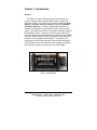
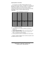
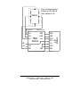
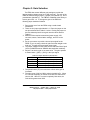
Not Recommended for New Installations. Please contact Technical Support for more information. Strain Gauge/Load Cell Bridge Amplifier Model FBDA Documentation Number FBDA0797 This product Designed and Manufactured In Ottawa, Illinois USA of domestic and imported parts by B&B Electronics Mfg. Co. Inc. 707 Dayton Road -- P.O. Box 1040 -- Ottawa, IL 61350 PH (815) 433-5100 -- FAX (815) 433-5105 Internet: http://www.bb-elec.com [email protected] [email protected] 1997 B&B Electronics Documentation Number FBDA0797 Manual Cover Page B&B Electronics -- PO Box 1040 -- Ottawa, IL 61350 PH (815) 433-5100 -- FAX (815) 433-5105 TABLE OF CONTENTS CHAPTER 1: INTRODUCTION.................................................................1 FEATURES ...............................................................................................1 PACKING LIST ..........................................................................................2 SOFTWARE ..............................................................................................2 CALIBRATION ...........................................................................................2 FBDA SPECIFICATIONS ............................................................................2 CHAPTER 2: CONNECTIONS..................................................................3 POWER SUPPLY CONNECTIONS ................................................................3 SENSOR CONNECTIONS ............................................................................3 DATA ACQUISITION CONNECTIONS ............................................................4 CHAPTER 3: GAIN SELECTION..............................................................7 CHAPTER 4: EXCITATION VOLTAGE ....................................................9 Documentation Number FBDA0797 Manual Table of Contents B&B Electronics -- PO Box 1040 -- Ottawa, IL 61350 PH (815) 433-5100 -- FAX (815) 433-5105 i Chapter 1: Introduction Features The FBDA is a signal conditioning module that allows you to measure voltages produced by full-bridge sensors using a data acquisition module. This module can condition signals from Strain Gauges, Load Cells, Pressure Sensors, and other Full-Bridge Transducer Sensors. A number of different gain settings are available on the FBDA to accommodate a wide variety of voltage ranges. The FBDA also provides an adjustable excitation voltage for the full-bridge circuitry. The sensor connections are made using terminal blocks, and the A/D connections are made through a DB-25 connector. B&B Electronics’ SDAXX, and ADIO12 data acquisition modules are pin compatible with the FBDA. This allows you to simply plug one of the data acquisition modules mentioned above into the FBDA, and the A/D connections are complete. The SPDA data acquisition modules can also be used with the FBDA. Figure 1.1: FBDA Module Documentation Number FBDA0797 Manual B&B Electronics -- PO Box 1040 -- Ottawa, IL 61350 PH (815) 433-5100 -- FAX (815) 433-5105 1 Packing List Examine the shipping carton and the contents for physical damage. The following items should be in the shipping carton: 1. FBDA module 2. This instruction manual If any of these items are damaged or missing, contact B&B Electronics immediately. Software Software is not included with the FBDA module. This device is used in conjunction with a data acquisition device. All of B&B Electronics’ data acquisition modules come complete with software that you can modify to meet your exact needs. Calibration The FBDA is calibrated at the factory. The excitation voltage is set to 5VDC ± 0.05VDC and the gain is calibrated at 80 ± 2. The process of calibrating the FBDA and your sensor will vary depending on the type of sensor being used. An example calibration procedure is covered in Chapter 3. FBDA Specifications Size: Maximum Input Voltage from Sensor: Output Voltage Range: Gain: Maximum Gain Error: Input Offset Voltage: Input Offset Voltage Drift: Excitation Voltage: Operating Temperature Range: Power Requirements: 2 4.8 x 2.2 x 0.9 in 440mV (using Gain = 25) 0.003V to 11VDC 25, 40, 80, 220-1000 5% of gain setting max. 150µV max. o 1.5µV/ C 0.5VDC to +11VDC o 0 to 70 C 13-18VDC @10mA (does not include current draw from excitation voltage.) Documentation Number FBDA0797 Manual B&B Electronics -- PO Box 1040 -- Ottawa, IL 61350 PH (815) 433-5100 -- FAX (815) 433-5105 Chapter 2: Connections Power Supply Connections The FBDA module requires 13 to 18VDC @ 10mA. Model 232PS2 available from B&B Electronics is recommended. Although the 232PS2 is a 12VDC power supply, it outputs a voltage above 13VDC when less than 10mA are being drawn from it. The power supply is connected to the terminal blocks marked +13V and GND. Make sure the polarity of the power supply is correct (the white striped wire on the 232PS2 is the positive lead). Sensor Connections Most full-bridge sensor circuits require four connections for the sensor to operate properly. These connections will be made using the terminal blocks. First, an excitation voltage is required to excite the bridge circuitry. This can be done using the adjustable excitation voltage (marked EXV) available on the FBDA, or another voltage source can be furnished by the user. This excitation voltage is referenced with respect to ground, which is the second connection (marked GND). The remaining two leads from the sensor carry the differential signal voltage that is to be conditioned and read by the data acquisition module. These two leads are connected to SIG+ and SIG-. Consult your sensor manual to determine the signal lead polarity. Table 2.1 shows the terminal block assignments. Table 2.1: Terminal Block Assignments Terminal Function I/O Block Name SIG+ Positive Signal Lead Input SIGNegative Signal Lead Input EXV Excitation Voltage Output A/D 1 A/D Converter channel Input +13V Power Supply Connection Input GND Power Supply Connection Input Note: A/D 1 is connected straight through from the terminal blocks to DB-25 pin # 9. This allows access to A/D channel 1 on B&B Electronic’s SDAXX line of A/D converters. This channel can read voltages between 0 and 5VDC (useful for calibrating the excitation voltage). This channel has no signal conditioning circuitry. It is simply connected to A/D 1 on the data acquisition module. Documentation Number FBDA0797 Manual B&B Electronics -- PO Box 1040 -- Ottawa, IL 61350 PH (815) 433-5100 -- FAX (815) 433-5105 3 Data Acquisition Connections The connections to the Data Acquisition Module are made through a DB-25 (male) connector. The FBDA is pin compatible with B&B Electronics’ SDAXX, and ADIO12 modules. This allows you to simply plug the FBDA into one of the above data acquisition modules, and the data acquisition module connections to the FBDA are complete. Table 2.2 contains the DB-25 (male) pin assignments. Table 2.2: DB-25 (Male) Pin Assignments DB-25 Pin # 1 2 3 4 5 6 7 8 9 10 11 12 13 Function GND ------------------------------GND Vout A/D 1 ------------------------- DB-25 Pin # 14 15 16 17 18 19 20 21 22 23 24 25 Function ------------------looped to 18 looped to 17 GND ------------------------------------- 1. ------- denotes no connection. 2. The conditioned sensor signal is available on pin #8 and is labeled Vout. 3. Pin #9 is connected straight through to terminal block A/D 1 (no signal conditioning circuitry). 4. Pins #17 and #18 are looped to each other to provide +5V to REF+ in the SDAXX line of A/D modules. 5. Pin #19 provides 0V to REF- in the SDAXX line of A/D modules. Figure 2.1 contains a diagram of the connections required to read the signal produced by a sensor. 4 Documentation Number FBDA0797 Manual B&B Electronics -- PO Box 1040 -- Ottawa, IL 61350 PH (815) 433-5100 -- FAX (815) 433-5105 Sensor 1 2 3 A/D 1 +13V SIGSIG+ EXV 4 5 6 +13V GND DB-25P Connector FBDA Module GND GND Vout GND 1 1 7 7 8 8 9 9 17 17 18 18 19 19 GND GND A/D 0 A/D 1 +5V REF+ REF- A/D Module Terminal Blocks Note: Conditioned signal is available on DB-25 pin #8 and is labeled as Vout. Figure 2.1: Block Diagram of FBDA Connections Documentation Number FBDA0797 Manual B&B Electronics -- PO Box 1040 -- Ottawa, IL 61350 PH (815) 433-5100 -- FAX (815) 433-5105 5 Chapter 3: Gain Selection The FBDA has several different gain settings to provide the largest possible voltage range for an A/D converter. The gain of the FBDA is selected using a jumper, 6 jumper pins (labeled 1-6), and a potentiometer (labeled P1). The FBDA is calibrated at the factory to have a gain of 80 ± 2. To change the gain of the FBDA the following steps should be followed: 1. Remove the cover from the FBDA using a small slotted screwdriver. 2. There are six jumper pins labeled 1-6. Place the jumper on the two pins selected from Table 3.1 below. Placing the jumper on the two selected pins will set a gain near the values listed in Table 3.1. 3. Make all of the required connections (power supply, A/D converter, sensor, and excitation voltage), and turn on the power. 4. Set up your sensor to provide a known input signal for the FBDA. If you are using a load cell, place a known weight on the load cell. This will produce a known input signal. 5. The output voltage from the FBDA can be read from DB-25 pin 8 (A/D 0 on B&B Electronics’ SDAXX data acquisition modules). 6. Adjust P1 to trim the gain to an exact value. The gain equation is shown below. ((SIG+) - (SIG-)) is the input signal. Table 3.1: Jumper Selection to Choose Gain Gain 25 40 80 220-1000 Jumper Selection Jumper pin 5 to pin 6 Jumper pin 4 to pin 5 Jumper pin 2 to pin 3 Jumper pin 1 to pin 2 1. The potentiometer (P1) becomes more critical as the gain is increased. 2. The gain range of 220 to 1000 is entirely decided by P1. When P1 is turned completely in counter-clock-wise, the Gain will be close to 220. When P1 is turned completely clock-wise, the Gain will be greater than 1000. Documentation Number FBDA0797 Manual B&B Electronics -- PO Box 1040 -- Ottawa, IL 61350 PH (815) 433-5100 -- FAX (815) 433-5105 7 Gain Equation GAIN = Vout / ((SIG+) - (SIG-)) Sensors that incorporate bridge circuitry usually have noticeable zero offsets. This should be considered when taking measurements and determining gain. The easiest way to solve this problem is to calibrate the system while avoiding zero inputs, and correct for the zero offset in software. Example: If a 10lb. load cell needs to be calibrated, the suggested method is the following: 1. Make all of the required connections. 2. Place a 1lb. mass on the load cell. Record the voltage on DB25 pin 8 as Vouta. Pin 8 is A/D 0 on the SDAXX modules. 3. Add a second 1lb. mass onto the load cell. Record the voltage on DB-25 pin 8 as Voutb. 4. Subtract Vouta form Voutb. The difference is the voltage, Vout, which corresponds to 1lb. 5. Calculate what ((SIG+) - (SIG-)) is for 1lb. This is the voltage produced by the sensor. 6. Use the Gain Equation to calculate the exact gain of the amplifier. 7. Adjust P1, and repeat process until the desired gain is achieved. 8. Subtract Vouta from Vout. The difference is the zero offset error. The zero offset error should be included in any equation conversion equation used in your software. 8 Documentation Number FBDA0797 Manual B&B Electronics -- PO Box 1040 -- Ottawa, IL 61350 PH (815) 433-5100 -- FAX (815) 433-5105 Chapter 4: Excitation Voltage Sensors that are based on a Wheatstone bridge need an excitation voltage to excite the bridge. The FBDA provides an adjustable excitation voltage. This excitation voltage is available on the terminal block labeled EXV. The excitation voltage is set to 5VDC ± 0.05VDC at the factory. This voltage is referenced with respect to GND. To adjust the excitation voltage, the following steps should be followed: 1. Remove the cover from the FBDA module using a small slotted screwdriver. 2. Make all of the required connections except the sensor connections and turn on the power. 3. Using a voltmeter, measure the voltage on the terminal block labeled EXV with respect to the GND terminal block. Adjust P2 to change the excitation voltage. The terminal block labeled A/D 1 can be used to measure the excitation voltage. Sensors that are comprised of Wheatstone bridges usually state the amount of output per volt of excitation voltage. An example is: 10mV output / 1V of excitation. If a 5V excitation voltage is used, The full scale output of the sensor will be 50mV. The gain of the FBDA should then be chosen, so that Vout does not exceed 5V (the maximum voltage that the SDAXX line of data acquisition modules can measure). If for some reason the excitation voltage source in the FBDA does not meet your needs, you can use an external excitation voltage. If this is the case, then nothing should be connected to the EXV terminal block, and the GND lead of the external excitation voltage source should be connected to the GND terminal block on the FBDA module. Documentation Number FBDA0797 Manual B&B Electronics -- PO Box 1040 -- Ottawa, IL 61350 PH (815) 433-5100 -- FAX (815) 433-5105 9