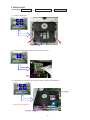
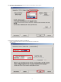
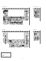
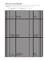
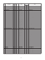
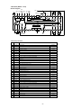
1
Service Manual CD5004 /N1B/N1SG U1B/K1SG/K1B CD Player CD PLAYER CD5004 MP3/WMA STANDBY DISPLAY OFF PHONES CD5004 ON/STANDBY LEVEL - + •For purposes of improvement, specifications and design are subject to change without notice. •Please use this service manual with referring to the operating instructions without fail. •Some illustrations using in this service manual are slightly different from the actual set. CD5004 S0055V01DM/DG1006 Copyright 2010 D&M Holdings Inc. All rights reserved. WARNING: Violators will be prosecuted to the maximum extent possible. Ver. 1 MARANTZ DESIGN AND SERVICE Using superior design and selected high grade components, MARANTZ company has created the ultimate in stereo sound. Only original MARANTZ parts can insure that your MARANTZ product will continue to perform to the specifications for which it is famous. Parts for your MARANTZ equipment are generally available to our National Marantz Subsidiary or Agent. ORDERING PARTS : Parts can be ordered either by mail or by Fax.. In both cases, the correct part number has to be specified. The following information must be supplied to eliminate delays in processing your order : 1. Complete address 2. Complete part numbers and quantities required 3. Description of parts 4. Model number for which part is required 5. Way of shipment 6. Signature : any order form or Fax. must be signed, otherwise such part order will be considered as null and void. USA EUROPE / TRADING D&M EUROPE B. V. P. O. BOX 8744, BUILDING SILVERPOINT BEEMDSTRAAT 11, 5653 MA EINDHOVEN THE NETHERLANDS PHONE : +31 - 40 - 2507844 FAX : +31 - 40 - 2507860 MARANTZ AMERICA, INC 100 CORPORATE DRIVE MAHWAH, NEW JERSEY 07430 USA CANADA D&M Canada Inc. 5-505 APPLE CREEK BLVD. MARKHAM, ONTARIO L3R 5B1 CANADA PHONE : 905 - 415 - 9292 FAX : 905 - 475 - 4159 KOREA JAPAN D&M SALES AND MARKETING KOREA LTD. 2F,YEON BLDG., 88-5, BANPO-DONG, SEOCHO-GU, SEOUL KOREA PHONE : +82 - 2 - 715 - 9041 FAX : +82 - 2 - 715 - 9040 D&M Holdings Inc. D&M BUILDING, 2-1 NISSHIN-CHO, KAWASAKI-KU, KAWASAKI-SHI, KANAGAWA, 210-8569 JAPAN CHINA D&M SALES AND MARKETING SHANGHAI LTD. ROOM.808 SHANGHAI AIRPORT CITY TERMINAL NO.1600 NANJING (WEST) ROAD, SHANGHAI, CHINA. 200040 TEL : 021 - 6248 - 5151 FAX : 021 - 6248 - 4434 NOTE ON SAFETY : Symbol z Fire or electrical shock hazard. Only original parts should be used to replaced any part marked with symbol z . Any other component substitution (other than original type), may increase risk of fire or electrical shock hazard. 安全上の注意: zがついている部品は、安全上重要な部品です。必ず指定されている部品番号のものを使用して下さい。 SHOCK, FIRE HAZARD SERVICE TEST : CAUTION : After servicing this appliance and prior to returning to customer, measure the resistance between either primary AC cord connector pins (with unit NOT connected to AC mains and its Power switch ON), and the face or Front Panel of product and controls and chassis bottom. Any resistance measurement less than 1 Megohms should cause unit to be repaired or corrected before AC power is applied, and verified before it is return to the user/customer. Ref. UL Standard No. 60065. In case of difficulties, do not hesitate to contact the Technical Department at above mentioned address. 091105DM/DG 2 SAFETY PRECAUTIONS The following check should be performed for the continued protection of the customer and service technician. LEAKAGE CURRENT CHECK Before returning the unit to the customer, make sure you make either (1) a leakage current check or (2) a line to chassis resistance check. if the leakage current exceeds 0.5 milliamps, or if the resistance from chassis to either side of the power cord is less than 460 kohms, the unit is defective. Be sure to test for leakage current with the AC plug in both polarities, in addition, in each power ON, OFF and STANDBY mode, if applicable. CAUTION Please heed the points listed below during servicing and inspection. ◎◎ Heed the cautions! ◎◎ Inspect for safety after servicing! Spots requiring particular attention when servicing, such as the cabinet, parts, chassis,etc., have cautions indicated on labels. be sure to heed these causions and the cautions indicated in the handling instructions. Check that all screws, parts and wires removed or disconnected for servicing have been put back in their original positions, inspect that no parts around the area that has been serviced have been negatively affected, conduct an inslation check on the external metal connectors and between the blades of the power plug, and otherwise check that safety is ensured. ◎◎ Caution concerning electric shock! (1)An AC voltage is impressed on this set, so touching internal metal parts when the set is energized could cause electric shock. Take care to avoid electric shock, by for example using an isolating transformer and gloves when servicing while the set is energized, unplugging the power cord when replacing parts, etc. (Insulation check procedure) Unplug the power cord from the power outlet, disconnect the antenna, plugs, etc., and turn the power switch on. Using a 500V insulation resistance tester, check that the inplug and the externally exposed metal parts (antenna terminal, headphones terminal, input terminal, etc.) is 1MΩ or greater. If it is less, the set must be inspected and repaired. (2)Tere are high voltage parts inside. Handle with extra care when the set is energized. ◎◎ Caution concerning disassembly and assembly! Through great care is taken when manufacturing parts from sheet metal, there may in some rare cases be burrs on the edges of parts which could cause injury if fingers are moved across them. Use gloves to protect your hands. CAUTION Concerning important safety parts Many of the electric and structural parts used in the set have special safety properties. In most cases these properties are difficult to distinguish by sight, and using replacement parts with higher ratings (rated power and withstand voltage) does not necessarily guarantee that safety performance will be poreserved. Parts with safety properties are indicated as shown below on the wiring diagrams and parts lists is this service manual. Be sure to replace them with parts with the designated part number. ◎◎ Only use designated parts! The set's parts have specific safety properties (fire resistance, voltage resistance, etc.). For replacement parts, be sure to use parts which have the same poroperties. In particular, for the important safety parts that are marked z on wiring diagrams and parts lists, be sure to use the designated parts. ◎◎ Be sure to mount parts and arrange the wires as they were originally! (1)Schematic diagrams.......Indicated by the z mark. (2).Parts lists.......Indicated by the z mark. Using parts other than the designated parts could result in electric shock, fires or other dangerous situations. For safety seasons, some parts use tape, tubes or other insulating materials, and some parts are mounted away from the surface of printed circuit boards. Care is also taken with the positions of the wores omsode amd clamps are used to keep wires away from heating and high voltage parts, so be sure to set everything back as it was originally. 3 NOTE FOR SCHEMATIC DIAGRAM WARNING: Parts marked with this symbol z have critical characteristics. Use ONLY replacement parts recommended by the manufacturer. CAUTION: Before returning the unit to the customer, make sure you make either (1) a leakage current check or (2) a line to chassis resistance check. If the leakage current exceeds 0.5 milliamps, or if the resistance from chassis to either side of the power cord is less than 460 kohms, the unit is defective. WARNING: DO NOT return the unit to the customer until the problem is located and corrected. NOTICE: ALL RESISTANCE VALUES IN OHM. k=1,000 OHM / M=1,000,000 OHM ALL CAPACITANCE VALUES IN MICRO FARAD. P=MICRO-MICRO FARAD EACH VOLTAGE AND CURRENT ARE MEASURED AT NO SIGNAL INPUT CONDITION. CIRCUIT AND PARTS ARE SUBJECT TO CHANGE WITHOUT PRIOR NOTICE. NOTE FOR PARTS LIST NOTE ON SAFETY FOR FUSIBLE RESISTOR : PARTS INFORMATION The suppliers and their type numbers of fusible resistors are as follows; 1. KOA Corporation Part No. (MJI) Type No. (KOA) Description 00MNH05 × × × 140 RF25S × × × × ΩJ (±5% 1/4W) 00MNH05 × × × 120 RF50S × × × × ΩJ (±5% 1/2W) 00MNH85 × × × 110 RF73B2A × × × × ΩJ (±5% 1/10W) 00MNH95 × × × 140 RF73B2E × × × × ΩJ (±5% 1/4W) Resistance value Resistance value (0.1 − 10kΩ) RESISTORS } 1) 00MGD05 × × × 140, Carbon film fixed resistor, ±5% 1/4W 2) 00MGD05 × × × 160, Carbon film fixed resistor, ±5% 1/6W ▲ ▲ Resistance value Examples ; Resistance value 0.1Ω......001 10Ω......100 1kΩ...... 102 100kΩ...... 104 0.5Ω......005 18Ω......180 2.7kΩ...... 272 680kΩ...... 684 1Ω......010 100Ω......101 10kΩ...... 103 1MΩ...... 105 6.8Ω......068 390Ω......391 22kΩ...... 223 4.7MΩ...... 475 Note : Please distinguish 1/4W from 1/6W by the shape of parts used actually. } ▲ CAPACITORS ▲ CERAMIC CAP. 3) 00MDD1 × × × × 370, Ceramic capacitor Disc type Temp.coeff.P350 ~ N1000, 50V Capacity value Tolerance Examples ; Tolerance (Capacity deviation) ±0.25pF...... 0 ±0.5pF...... 1 ±5%...... 5 Tolerance of COMMON PARTS handled here are as follows : 0.5pF ~ 5pF......±0.25pF 6pF ~ 10pF......±0.5pF 12pF ~ 560pF......±5% Capacity value 0.5pF......005 3pF......030 100pF...... 101 1pF......010 10pF......100 220pF...... 221 1.5pF......015 47pF......470 560pF...... 561 } } } Resistance value Examples ; * Resistance value 0.1Ω......001 10Ω......100 0.5Ω......005 18Ω......180 1Ω......010 100Ω......101 6.8Ω......068 390Ω......391 Description (±5% 1/4W) (±2% 1/4W) Resistance value 1kΩ...... 102 2.7kΩ...... 272 10kΩ...... 103 22kΩ...... 223 100kΩ..... 104 680kΩ..... 684 1MΩ..... 105 4.7MΩ..... 475 ABBREVIATION AND MARKS CERAMIC CAP. } 4) 00MDK16 × × × 300, High dielectric constant ceramic capacitor Disc type Temp.chara. 2B4, 50V Capacity value Examples ; Capacity value 100pF......101 1000pF...... 102 10000pF......103 470pF......471 2200pF...... 222 ELECTROLY CAP. ( ) 5) 00MEA × × × × × × 10, Electrolytic capacitor One-way lead type, Tolerance ±20% Working voltage Capacity value Examples ; Capacity value 0.1µF...... 104 4.7µF......475 100µF.... 107 0.33µF...... 334 10µF......106 330µF.... 337 1µF...... 105 22µF......226 1100µF.... 118 2200µF.... 228 Working voltage 6.3V...... 006 25V......025 10V...... 010 35V......035 16V...... 016 50V......050 ANT. CAP. CONN. HP µ-PRO RES. SW TRIM. VAR. : ANTENNA : CAPACITOR : CONNECTING : HEADPHONE : MICROPROCESSOR : RESISTOR : SWITCH : TRIMMING : VARIABLE BATT. : BATTERY CER. : CERAMIC DIG. : DIGITAL MIC. : MICROPHONE REC. : RECORDING SPK : SPEAKER TRANSF.: TRANSFORMER TRS. : TRAMSISTOR X’TAL : CRYSTAL NOTE ON FUSE : } } Regarding to all parts of parts code 00MFS20xxx2xx, replace only with Wickmann-Werke GmbH, Type 372 non glass type fuse. NOTE ON SAFETY : Symbol z Fire or electrical shock hazard. Only original parts should be used to replaced any part marked with symbol z. Any other component substitution (other than original type), may increase risk of fire or electrical shock hazard. Plastic film capacitor One-way type, Mylar ±5% 50V Plastic film capacitor One-way type, Mylar ±10% 50V Capacity value ▲ ▲ } FILM CAP. ( ) 6) 00MDF15 × × × 350 00MDF15 × × × 310 00MDF16 × × × 310 ▲ ▲ } 2. Matsushita Electronic Components Co., Ltd Part No. (MJI) Type No. (MEC) 00MNF05 × × × 140 ERD-2FCJ × × × 00MRF05 × × × 140 00MNF02 × × × 140 ERD-2FCG × × × 00MRF02 × × × 140 Examples ; Capacity value 0.001µF.(1000pF)............102 0.0018µF............................182 0.01µF............................103 0.015µF............................153 安全上の注意 : z がついている部品は、安全上重要な部品です。必ず指定 されている部品番号の部品を使用して下さい。 0.1µF..... 104 0.56µF..... 564 1µF..... 105 060522 MZ 4 WARNING AND LASER SAFETY INSTRUCTIONS GB WARNING NL All ICs and many other semi-conductors are susceptible to electrostatic discharges (ESD). Careless handling during repair can reduce life drastically. When repairing, make sure that you are connected with the same potential as the mass of the set via a wrist wrap with resistance. Keep components and tools also at this potential. F WAARSCHUWING Alle IC’s en vele andere halfgeleiders zijn gevoelig voor elektrostatische ontladingen (ESD). Onzorgvuldig behandelen tijdens reparatie kan de levensduur drastisch doen verminderen. Zorg ervoor dat u tijdens reparatie via een polsband met weerstand verbonden bent met hetzelfde potentiaal als de massa van het apparaat. Houd componenten en hulpmiddelen ook op ditzelfde potentiaal. D ATTENTION Tous les IC et beaucoup d’autres semiconducteurs sont sensibles aux décharges statiques (ESD). Leur longévité pourrait être considérablement écourtée par le fait qu’aucune précaution n’est prise a leur manipulation. Lors de réparations, s’assurer de bien être relié au même potentiel que la masse de l’appareil et enfiler le bracelet serti d’une résistance de sécurité. Veiller a ce que les composants ainsi que les outils que l’on utilise soient également a ce potentiel. WARNUNG I Alle IC und viele andere Halbleiter sind empfindlich gegen elektrostatische Entladungen (ESD). Unsorgfältige Behandlung bei der Reparatur kann die Lebensdauer drastisch vermindern. Sorgen sie dafür, das Sie im Reparaturfall über ein Pulsarmband mit Widerstand mit dem Massepotential des Gerätes verbunden sind. Halten Sie Bauteile und Hilfsmittel ebenfalls auf diesem Potential. AVVERTIMENTO Tutti IC e parecchi semi-conduttori sono sensibili alle scariche statiche (ESD). La loro longevita potrebbe essere fortemente ridatta in caso di non osservazione della piu grande cauzione alla loro manipolazione. Durante le riparazioni occorre quindi essere collegato allo stesso potenziale che quello della massa dell’apparecchio tramite un braccialetto a resistenza. Assicurarsi che i componenti e anche gli utensili con quali si lavora siano anche a questo potenziale. D GB Bei jeder Reparatur sind die geltenden Sicherheitsvorschriften zu beachten. Der Originalzustand des Gerats darf nicht verandert werden. Fur Reparaturen sind Original-Ersatzteile zu verwenden. Safety regulations require that the set be restored to its original condition and that parts which are identical with those specified be used. NL I Veiligheidsbepalingen vereisen, dat het apparaat in zijn oorspronkelijke toestand wordt terug gebracht en dat onderdelen, identiek aan de gespecifieerde worden toegepast. Le norme di sicurezza esigono che l’apparecchio venga rimesso nelle condizioni originali e che siano utilizzati pezzi di ricambiago idetici a quelli specificati. F “Pour votre sécurité, ces documents doivent être utilisés par des spécialistes agrées, seuls habilités à réparer votre appareil en panne.” Les normes de sécurité exigent que l’appareil soit remis a l’état d’origine et que soient utilisées les pièces de rechange identiques à celles spécifiées. LASER SAFETY This unit employs a laser. Only a qualified service person should remove the cover or attempt to service this device, due to possible eye injury. USE OF CONTROLS OR ADJUSTMENTS OR PERFORMANCE OF PROCEDURE OTHER THAN THOSE SPECIFIED HEREIN MAY RESULT IN HAZARDOUS RADIATION EXPOSURE. AVOID DIRECT EXPOSURE TO BEAM WARNING The use of optical instruments with this product will increase eye hazard. Repair handling should take place as much as possible with a disc loaded inside the player WARNING LOCATION: INSIDE ON LASER COVERSHIELD CAUTION VISIBLE AND INVISIBLE LASER RADIATION WHEN OPEN AVOID EXPOSURE TO BEAM ADVARSEL SYNLIG OG USYNLIG LASERSTRÅLING VED ÅBNING UNDGÅ UDSÆTTELSE FOR STRÅLING ADVARSEL SYNLIG OG USYNLIG LASERSTRÅLING NÅR DEKSEL Å PNES UNNGÅ EKSPONERING FOR STRÅLEN VARNING SYNLIG OCH OSYNLIG LASERSTRÅLNING NÄR DENNA DEL ÄR ÖPPNAD BETRAKTA EJ STRÅLEN VARO! AVATT AESSA OLET ALTTIINA NÄKYVÄLLE JA NÄKYMÄTTÖMÄLLE LASER SÄTEILYLLE. ÄLÄ KATSO SÄTEESEEN VORSICHT SICHTBARE UND UNSICHTBARE LASERSTRAHLUNG WENN ABDECKUNG GEÖFFNET NICHT DEM STRAHL AUSSETSEN DANGER VISIBLE AND INVISIBLE LASER RADIATION WHEN OPEN AVOID DIRECT EXPOSURE TO BEAM ATTENTION RAYONNEMENT LASER VISIBLE ET INVISIBLE EN CAS D'OUVERTURE EXPOSITION DANGEREUSE AU FAISCEAU 5 030804ecm TECHNICAL SPECIFICATIONS nn Audio characteristics • • • • • • • • • Channels: Frequency response: Dynamic range: Signal-to-noise ratio: Channel separation: Harmonic distortion: Wow & flutter: Audio output: Headphone output: • Digital output Coaxial output (pin jack): Optical output (square optical connector): nn Power supply • • • • • 2 channels 2 Hz to 20 kHz 100 dB 110 dB 110 dB (1 kHz) 0.002% (1 kHz) Precision of quartz 2.25 V rms, stereo 18 mW/32 ohms (variable maximum) nn Cabinet, etc. • Accessories Remote controller: AAA batteries: AC power cord: Audio connecting cord: Remote control connecting cord: • Maximum outer dimensions Width: Height: Depth: • Weight: • Allowable operating temperature: • Allowable operating humidity: 0.5 Vp-p, 75 ohms –19 dBm nn Optical readout system • Laser: • Wavelength: AlGaAs semiconductor 780 nm nn Signal system • Sampling frequency: • Quantization: AC 230 V 50 Hz AC 120 V 60 Hz AC 220 V 50 Hz 14 W 0.4 W N version: U version: K version: Power consumption: Standby power consumption: 44.1 kHz 16-bit linear PCM DIMENSION 4 328.5 339.5 7 14 6 104.5 90.5 440 1 2 1 1 1 440mm 104.5mm 339.5mm 5.1kg +5 to +35°C 5 to 90% (no condensation) DISASSEMBLY • Disassemble in order of the arrow of the figure of following flow. • In the case of the re-assembling, assemble it in order of the reverse of the following flow. • In the case of the re-assembling, observe "attention of assembling" it. • If wire bundles are untied or moved to perform adjustment or parts replacement etc., be sure to rearrange them neatly as they were originally bundled or placed afterward. Otherwise, incorrect arrangement can be a cause of noise generation. CABINET TOP FRONT PANEL ASSY Refer to "DISASSEMBLY 1. FRONT PANEL ASSY" and "EXPLODED VIEW" FRONT PWB (Ref. No. of EXPLODED VIEW : 14) HEADPHONE PWB (Ref. No. of EXPLODED VIEW : 16) TACT SW PWB (Ref. No. of EXPLODED VIEW : 15) MAIN PWB Refer to "DISASSEMBLY 2. MAIN PWB" and "EXPLODED VIEW" MAIN PWB (Ref. No. of EXPLODED VIEW : 30) POWER PWB Refer to "DISASSEMBLY 3. POWER PWB" and "EXPLODED VIEW" POWER PWB (Ref. No. of EXPLODED VIEW : 31) AUDIO PWB Refer to "DISASSEMBLY 4. AUDIO PWB" and "EXPLODED VIEW" AUDIO PWB (Ref. No. of EXPLODED VIEW : 29) MECHA ASSY Refer to "DISASSEMBLY 5. MECHA ASSY" and "EXPLODED VIEW" 7 About the photos used for descriptions in the DISASSEMBLY" section. •The direction from which the photographs used herein were photographed is indicated at "Direction of photograph: ***" at the left of the respective photographs. • Refer to the table below for a description of the direction in which the photos were taken. • Photographs for which no direction is indicated were taken from above the product. • The photograph is CD5004 K1SG. The viewpoint of each photograph (Photografy direction) Direction of photograph: B Front side [View from above] Direction of photograph: C Direction of photograph: D Direction of photograph: A 8 1.FRONT PANEL ASSY Proceeding : TOP COVER → FRONT PANEL ASSY (1) Remove the Loadr Panel. Direction of photograph: B (2) Remove the screws. View from bottom (3) Disconnect the connector wire and FFC Cable. Remove the screws. Cut the wire clamp bands. cut CN81 FFC Cable Please refer to "EXPLODED VIEW" for the disassembly method of each P.W.B included in FRONT PANEL ASSY. 9 2.MAIN PWB Proceeding : TOP COVER → MAIN PWB (1) Remove the screws. Direction of photograph: A (2) Remove the screws. Disconnect the connectors wire and FFC Cable. MAIN PWB CN43 CN45 CN42 CN44 Direction of photograph: B FFC Cable 10 CN31 3.POWER PWB Proceeding : TOP COVER → POWER PWB (1) Remove the screws. Direction of photograph: A (2) Remove the screws. Disconnect the connector wires. Cut the wire clamp band. CN94 CN93 CN92 CN91 cut CN44 CN45 11 MAIN PWB 4.AUDIO PWB Proceeding : TOP COVER → AUDIO PWB (1) Remove the screws. Direction of photograph: A (2) Remove the screws. Disconnect the connector wires. CN81 AUDIO PWB CN43 CN42 12 5.MECHA ASSY Proceeding : TOP COVER → FRONT PANEL ASSY → MECHA ASSY (1) Remove the screws. MECHA ASSY (2) Solder the short-circuit before disconnect the FFC Cable. Short (3) Disconnect the connectors wire and FFC Cable. Cut the wire clamp bands. FFC Cable cut Direction of photograph: C Connector wire 13 REMOVING DISCS (1) Remove the Top Cover. (2) Remove the screws. (3) Remove the disc clamper. 14 SERVICE MODE AND TAKING THE DISC OUT OF EMERGENCY [A] SERVICE MODE (1)Insert mains cable plug in the outlet. (The Unit is standby mode.) (2)Press the <ON / STANDBY> button While pressing 7/9 and 2 Button. Model name is displayed. CD5004 (3)Press 7/9 button. Version of microprocessor is displayed. 2008-05-16-1 (4)Press 7/9 button. Light up all FL segment. DISC TTL RNDM TRK PROG A– B TEXT 1 2 3 4 5 6 7 8 9 10 11 12 13 14 15 16 17 18 19 20 RPT 1 PITCH EDIT PEAK (5)Press 7/9 button. Serial number is displayed. MZ_000000000 (6)Press 7/9 button. Playback time is displayed. PTime : 00021h To return to a previous display at anytime, press 8/6 button. Press the <ON / STANDBY> button to quit Service Mode. 15 TTL TIME HOW TO THE RESET OF PLAYBACK TIME When replacing CD MECHANISM (TRAVERSE), please reset Playback time (total) in the following procedure. (1)Procedure 6 of SERVICE MODE, Playback time (total) is displayed. PTime : 00051h The display is a time unit. (Example: "10050 hours, 0 minute, 1 second " is 10051h) The maximum Playback time is 65536h. (2)Press 2 Button 3 seconds and more. PTime Clear? is displayed. PTime Clear? (3)Press 1 Button. Done is displayed after PTime:00000h is displayed. Play back time (total) was reset. Done PTime : 00000h Press the <ON / STANDBY> button to quit Service Mode. HOW TO INITIALIZE THE CD PLYAER Initialize the CD player when μcom, peripheral parts of μcom, or MAIN P.W.B. unit has been replaced in servicing. ※All user setting will be lost and its factory setting will be restored when this initialization is made. Be sure to memorize your setting for restoring again after the initialization. (1)Insert mains cable plug in the outlet. (The Unit is standby mode.) (2)Press 2 and the <ON / STANDBY> Buttons simultaneously 4 seconds and more. EEPROM Clear is displayed after No Disc is displayed. The microprocessor initialized to factory setting. EEPROM Clear No Disc 16 VERSION UPGRADE PROCEDURE OF FIRMWARE ABOUT REPLACE THE MICROPROCESSOR WITH A NEW ONE When replaced of the U-PRO (Microprocessor) or the Flash ROM, confirm contents of the following. PWB Name Ref. No. MAIN IC21 After replaced Description Remark B T5CD2(F AAD JZ) CD5004 After replaced A : Mask ROM (With software). No need write-in of software to the microprocessor. B :Flash ROM (With software). Usually, no need write-in of software. But, when the software was updated, you should be write-in of the new software to the microprocessor or flash ROM. Please check the software version. C :Empty Flash ROM (Without software). You should be write-in of the software to the microprocessor or flash ROM. Refer to “Update procedure” or “writing procedure”, when you should be write-in the software. Necessary Equipment •Windows PC (OS: Windows 2000 or Windows XP) with Serial port. •RS-232C Dsub-9 pin cable (female to female/straight type). •Connection JIG (90M-SR4500JIG) •Update tool (FlashProg.exe, other files and folders in Flash Programmer folder) •Update data (CD5004_yymmdd_x.s2h4) 1.Update for software (1) Put the "Flash Programmer" and "software" folder into anywhere on your PC's hard disc. (2) Double click the "Flash Programmer" folder. CD5004 CD5004 17 (3) Double click FlashProg.exe, and launch the Flash Programmer. NOTE : W hen a Flash Programmer does not launch even if double-clicked FlashProg.exe, please refer to "2. When a Flash Programmer did not launch". (4) Click OK. NOTE : S ince Flash Programmer communicates with the unit automatically, the following dialog box appears when it fails in communication. 18 (5) Click the Setup in the menu bar and select the Object file. (6) Click Browse. 19 (7) Choose the Motorola S Format(*.s16,*.s24,*.s32) in Files of type. Choose the CD5004_yymmdd_x.s24, and click Open. NOTE : The yy is two digits of year. The mm is month. The dd is date. The x is release number. CD5004_yymmdd_x.s24 CD5004_yymmdd_x.s24 (8) Click Device tab. 20 (9) Choose the TMP91FW60 in the Device, and choose the 900/L1 in the Series. And click Communication tab. (10)Choose the Serial port number in the COM Port. Check the Data Rate Manual, and choose the 38400 in the Data Rare. And Click OK. 21 (11)Disconnect the mains cord from the unit. (12)Connect the RS-232C on the connection JIG and the Serial Port of windows PC with RS-232C cable. (13)Connect FFC (upside contact) to the rear panel of the unit from connection JIG. (14)Connect the mains cord into the unit. (15)If the connection with the Flash Programmer is successfully made, a dialogue box saying "Erase All data in this devise? (Y/N)" appears automatically. If the connection fails, error message will appear. (Ex.: E000) Click Yes. (16)Click OK. 22 (17)Click P (Program) to start update. (18)Software is written into the microprocessor. The writing of software takes about 50 seconds. (19)If the software is updated successfully, a dialog box saying "R006: Programming completed successfully." appears. Click OK. 23 (20)Click the File in the menu bar and select the Exit. (21)Disconnect mains cord from the unit, and then disconnect FFC of connection JIG from the unit. 2.When a Flash Programmer did not launch (1) Open the FlashProg.ini in the Flash Programmer folder by text editor. (EX.: Notepad, etc) 24 (2) Delete the text "OpenFile=C:\...(your PC setting)...\???.s24". 25 (3) Save the FlashProg.ini. (4) Close the text editor. (5) Probably you can launch the Flash Programmer. Go to the 1. Update Procedure step 3. 26 TROUBLE SHOOTING 1. POWER PWB N.G. Check FUSE Condition ・FUSE [F901]OPEN? (Open) Check the output short of trans ([T901][T902]). If trans is short, trans is replaced. O.K. Check ST+5V output ・Voltage Check +5V DC (switched) Voltage is O.K.? ・[BN45] 5pin output N.G. Check [Q902]corrector input voltage. Check Parts and Soldering and Other Circuits. If abnormality is not found, [Q902] is replaced. N.G. Check the control signal for relay drive. TRANS_ON/OFF signal : 5V ・[BN45] 11pin O.K. Check the poewr relay ・Is [RY91] switched? O.K. N.G. If the relay drive voltage is normal, relay is replaced. O.K. MAIN PWB [IC21] (T5CD2) 78Pin Check Parts and Soldering and Other Circuits. Check +8V output ・Voltage Check +8V DC (switched) Voltage is O.K.? ・[BN45] 7pin output N.G. ・[IC91] 1pin input Check Parts and Soldering and Other Circuits. If abnormality is not found, [IC91] is replaced. O.K. Check +12V output ・Voltage Check +12V DC (switched) Voltage is O.K.? ・[BN44] 3pin output N.G. ・[IC94] 1pin input Check Parts and Soldering and Other Circuits. If abnormality is not found, [IC94] is replaced. O.K. Check VDD (+5V) output ・Voltage Check +5V DC (switched) Voltage is O.K.? ・[BN45] 6pin output N.G. ・[IC92] 1pin input Check Parts and Soldering and Other Circuits. If abnormality is not found, [IC92] is replaced. O.K. Check -12V output ・Voltage Check -12V DC (switched) Voltage is O.K.? ・[BN44] 1pin output N.G. 27 ・[IC93] 1pin input Check Parts and Soldering and Other Circuits. If abnormality is not found, [IC93] is replaced. 2. FRONT PWB 2.1.FL TUBE dosen't light Check the power supply voltage. Check the VP (+36V)output. +36V DC (switched) Voltage is O.K.? ・[CN21] 19pin N.G. POWER PWB ・[Q901] input Check Parts and Soldering and Other Circuits. If abnormality is not found, [Q901] is replaced. O.K. Check the power supply voltage. Check the VDD(+5V) output. +5V DC (switched) Voltage is O.K.? ・[CN21] 18pin N.G. POWER PWB ・[IC92] 1pin input Check Parts and Soldering and Other Circuits. If abnormality is not found, [IC92] is replaced. O.K. Check the filament voltage. Check the FIP1 ~ FIP2(3.3V) output. 3.3V DC (switched) Voltage is O.K.? ・[FL51] 1pin,42pin N.G. Check the parts voltage. TRANSF PWB ・[T901] 1pin-2pin If abnormality is found, [T901] is replaced. O.K. Check the control waveform. VFD-DI, VFD-CLK, VFD-CE, VFD-POWER ・[CN21] 9pin,10pin,11pin,12pin N.G. Check parts and soldering. MAIN PWB ・[IC21] 18pin,19pin,20pin,68pin If abnormality is not found, [FL51] is replaced. 2.2.Remotecontrol is not accepted. Check the power supply voltage. Check the FST(+5V) output. ・[CN21] pin17 N.G. Check the [Q902] collector input. Check Parts and Soldering and Other Circuits. If abnormality is not found, [Q902] is replaced. O.K. Check the output waveform. When the button of remote control is pushed, is the pulse output? ・[CN21] 15pin N.G. 28 Replace the [RS51]. 3. AUDIO PWB 3.1 No Audio output Check the analog signal output. ・[IC75] 14pin,15pin,18pin,19pin O.K. Check the mute signal (-12V). AUDIO PWB ・[Q603][Q703] base O.K. AUDIO PWB ・[Q605][Q606][Q705][Q706] and Circumference Replace the abnormal IC. N.G. Check the power supply voltage. ・[IC76] 2pin (3.3V) ・[IC77] 3pin (5V) N.G. POWER PWB ・[IC94] AUDIO PWB ・[IC76][IC77] Check Parts and Soldering and Other Circuits. Replace the abnormal output IC. O.K. Check the digital signal input. AUDIO PWB ・[IC75] 3pin,4pin,5pin,6pin N.G. Check Parts and Soldering. MAIN PWB ・[IC31] 62pin,63pin,64pin ・[IC26] 7pin If data is not output, abnormal IC is replaced. O.K. Replace the [IC75]. N.G. 29 MAIN PWB ・[Q431][Q432][Q433][Q434] and Circumference Replace the abnormal IC. MEASURING METHOD AND WAVEFORMS Measuring Disc: 4822 397 30184 TCD-784 (It is better to use wires for extending between the probe and test points.) 1.CUP12096Z MCU UNIT: TEST POINT FE TE SPIN RFEQU Focus Tracking 30 RFO SLID 2.WAVEFORMS 1. DISC PLAY RF WAVEFORM(EYE-PATTERN) 2. DISC DETECTION 1.1 CD(TCD-784)Play 2.1 CD(TCD-784)DISC DETECTION 1V 200mV RF FE Focus 2V TE Tracking SLID SPIN 500Mv 2V 1V 2V 2.2 CD-R(TCD-R000RM)DISC DETECT 1.2 CD-R(TCD-R000RM)Play RF FE Focus TE Tracking SLID SPIN 1V 200mV 2V 500Mv 2V 1V 2V 2.3 CD-RW(TCD-W000RM)DISC DETECTION 1.3 CD-RW(TCD-W000RM)Play RF FE Focus TE Tracking SLID SPIN 31 1V 200mV 2V 500Mv 2V 1V 2V 3. TOC READ 4. FOCUS ADJUSTMENT 3.1 CD(TCD-784)TOC READ 4.1 CD(TCD-784)FOCUS ADJUSTMENT RF FE 1V 200mV Focus 2V TE Tracking 500Mv SLID SPIN 2V 1V 2V 3.2 CD-R(TCD-R000RM)TOC READ 4.2 CD-R(TCD-R000RM)FOCUS ADJUSTMENT 1V 200mV RF FE Focus 2V TE Tracking 500Mv SLID SPIN 2V 1V 2V 3.3 CD-RW(TCD-W000RM)TOC READ 4.3 CD-R(TCD-R000RM)FOCUS ADJUSTMENT 1V 200mV RF FE Focus 2V TE Tracking 500Mv 2V 1V 2V SLID SPIN 5. LOADER OPEN-CLOSE OPSW 5V 5V CLSW LOAD + LOAD- OPEN CLOSE 5V 5V 32 I2C (SBI1) W B D H A C E L IX 1Y IZ SP 5 6 44~ 9~ MODE CONTROLLER CE1 DATA BUS 53 ADDRESS BUS 54 8bit TIMER (TMRA3) 55 Clock Timer 41 CD-CCE 43 PORT CD-RST 38 RST 4 VDD 5 VSS 2 24-Bit DSP 3 VDD FOO TRO FMO DMO MT-STBY OP-M CL-M LIMIT-SW CL-SW OP-SW SPINDLE MOTOR M RL3 92 MDI 91 LDO SLED+ M SLED MOTOR SLED- TR+/- SPINDLERL1 SPINDLE+ SLED- Peripheral I/F 1 Mbit SRAM SLED+ RL2 +VREF +8V PLL/VCO D A B 1.5V F +RF3.3V +VREF 62 63 64 +VREF 3.3VDA +3.3V +P1.5V +P1.5V 1 SDATA 2 REMO LED DATA KEY DATA VFD-CLK VFD-CE VFD-DI VFD-POWER LOADING- RL4 SPINDLE+ DSP POWER SYS_DETECT DAC_RST PWR_D T_ON/OFF PLL_SDA PLL_SCL KEY DATA VFD-CLK VFD-CE VFD-DI VFD-POWER 3.3V 61 1 RS/REMOTE_IN RL5 E ST+5V OUT 3 NC RS/REMOTE_IN LED DATA 30 LOGIC C DS 71 75 78 79 80 81 CONTROL 33 EEPROM ST+5V 32 94 Servo DAC DOUT ROM Correction 31 95 34 M PLL_SCL 90 PLL_SDA 88 85 41 86 76 87 20 19 18 68 35 INTERRUPT 92 FLASH ROM 128KByte 96 FC+/- Analog Post Filter (Audio Out) 37 10-BIT 16CH A D RAM 16Bit TIMER (TMRB4) 89 9 Audio DAC 42 56 ST+5V CDP DSP 40 CD-BUCK B D A C 97 COM LOADING+ 35 SPINDLE- ST+5V CD-BUS3 Servo Processor RAM 16Bit TIMER (TMRB1) 16Bit TIMER (TMRB3) CD-RF Amp CD-RF IN CL/SW LIMIT SW DRIVE I.C E F 100 Servo ADC Memory Controller (blocks) 8KB RAM 16Bit TIMER (TMRB0) 16Bit TIMER (TMRB2) CD DSP 98 VCC GND CD-BUS2 52 WATCH-DOG TIMER 8bit TIMER (TMRA5) CONTROL CIRCUIT WE CONTROLLER 9 COLUMN I/O INTERRUPT P C 8bit TIMER (TMRA1) 8bit TIMER (TMRA4) I/O DATA I/O1-I/O7 CIRCUIT INTERRUPT CONTROLLER F 8bit TIMER (TMRA2) SRAM_WE SRAM_OE SRAM_CE ADDRESS PORT DATA PORT OE 32bit 8bit TIMER (TMRA0) 4 LOW-speed Oscillator 10 CD MECHANISM I2C (SBIO) XWA XBC XDE XHL XIX XIY XIZ XSP 12 OP/SW TC94A70FG A0-A14 High-speed Oscillator 13 3 LRCK SIO/UART (SIO2) 900/L1 CPU 23 256X 1024 TRACKING+ MEMORY ARRAY SCLK SIO/UART (SIO1) TRO SRAM DECODER SIO/UART (SIO0) FOO 21 22 33 FOCUSFOCUS+ TRACKING- 57 58 59 61 TRACKING+ TRACKINGFOCUS+ FOCUS- 28 FMO 65 67 DSP_MCK 20Mhz 26 DMO OP-M UPDATE PORT CL-SW CL-M LIMIT-SW u-COM OP-SW MT-STBY BLOCK DIAGRAM VDD OPTICAL OUT +3.3V 1 3.3VDA 2 COAXIAL OUT WELCOME VP FST+5V ST+5V CLOCK(PLL+VCO) FVDD FL+/- INTERNAL EXTERNAL +3.3VCL CDCE913 IN +3.3V OUT 1 +1.8V 3 LV PLL_SDA PWR_MUTE and PLL with SSC Output Control Programming and Control Register PLL_SCL RS_REMOTE_IN CMOS Divider EEPROM SYS DETECT SYS_DETECT DAC_MCK DSP_MCK VCXO XO LVCMOS 16.9344 MHz GND 2 L H REMO TC7WHU04FU LV CMOS LV BUS IN/OUT +3.3VCL CMOS FLUSHER IN(U Ver ONLY) 1 +1.8V +3.3VCL AUDIO- 3 2 UPDATE 1 AUDIO+ 3 DAC (CS4392) 2 DAC_RST MAIN TRANS SDATA +8V 3 VDIS VIN GND 1 SERIAL PORT SCLK LRCK 2 3 1 4 MIXER VOLUME Control VDD NC NC 2 NC (DAC_SDA) NC (DAC_SCL) MODE Selector Control Port FILTER AOUTA+ LPF (OP Amp IC) AOUTA- FILTER INTERPOLATION FILTER ANALOG DAC + AOUTB+ EXTERNAL Mute Control A_MUTE B_MUTE FILT+ +3.3VA AUDIO+ FL+ OUT 1 IN 3 +5VA GND 2 +12V OUT 1 R F_MUTE B_MUTE P_MUTE +12V -12V 3 +3.3VA GND 2 HEADPHONE OUTPUT FL- A B +5VA ST+5V -12V 33 ANALOG L F_MUTE A_MUTE P_MUTE Tr.Buffer AOUTB- FILTER +8V IN SUB TRANS DAC INTERPOLATION Reference CMOUT VP +8V L ANALOG VOLUME Control B+ VOUT UPDATE PORT RST/ST+5V/GND DAC_MCK ANALOG R POWER SUPPLY BLOCK DIAGRAM AC INLET STANDBY TRANS (T902) (Q902) +5V U-CON (IC21) IR (RS51) REMOTE IN/OUT MAIN RELAY (RY91) ← STANDBY ON/OFF RELAY MAIN TRANS (T901) (IC77) (IC76) +5V +3.3V (IC94) +12V AUDIO HEAD PHONE -12V RELAY (IC93) (IC92) (IC91) +8V SERVO DRIVE MECHA DRIVE +5V RELAY (IC33) (IC25) +3.3V +1.8V (IC34) CD DSP PITCH CONTROL +1.5V (Q901) +36V FL (FIP1) (FIP2) 34 WIRING DIAGRAM AC B TYPE 7P INLET BK91 L BLACK BK21 SW41 CN22 CN23 (UPDATE PORT) RED JK43 JK42 JK71 JK61 FLASHER PWB CN41 BN41 SUB TRANS CORE BK75 JK41 N CORE CN43 BN43 DSP N BN45 MCU CN45 CN91 AUDIO PWB RELAY MAIN PWB CN44 CN92 CN42 CN21 N CN31 CN33 POWER PWB B TYPE CN32 CORE 16P BN42 BN44 CN81 CN94 CN93 TRANSF. PWB BN93 BN94 BN81 HEADPHONE PWB MAIN TRANSF PH81 SCREW CD MECHANISM BLACK WHITE BN92 B TYPE 21P CN51 WELCOME TACT SW PWB ANGLE TYPE FRONT PWB BN51 CN21 JW51 35 VR81 BK81 CORE PRINTED WIRING BOARDS MAIN (COMPONENT SIDE) 1 2 3 4 5 6 7 8 9 A B C D E F G 鉛フリー半田 半田付けには、鉛フリー半田 (Sn-Ag-Cu) を使用してください。 Lead-free Solder When soldering, use the Lead-free Solder (Sn-Ag-Cu). 36 MAIN (FOIL SIDE) 9 8 7 6 5 4 3 2 1 A B C D E F G 鉛フリー半田 半田付けには、鉛フリー半田 (Sn-Ag-Cu) を使用してください。 Lead-free Solder When soldering, use the Lead-free Solder (Sn-Ag-Cu). 37 FRONT (COMPONENT SIDE) 1 2 TACT SW (COMPONENT SIDE) 3 4 5 6 7 8 9 10 11 12 1 2 3 A A B B C C D FRONT (FOIL SIDE) 12 11 TACT SW (FOIL SIDE) 10 9 8 7 6 5 4 3 2 1 3 半田付けには、鉛フリー半田 (Sn-Ag-Cu) を使用してください。 Lead-free Solder When soldering, use the Lead-free Solder (Sn-Ag-Cu). 38 1 A A B B C C D 鉛フリー半田 2 AUDIO (COMPONENT SIDE) 1 2 AUDIO (FOIL SIDE) 3 4 5 6 7 7 6 5 4 3 2 1 A A B B C C D D E E F F G G H H I I 鉛フリー半田 半田付けには、鉛フリー半田 (Sn-Ag-Cu) を使用してください。 Lead-free Solder When soldering, use the Lead-free Solder (Sn-Ag-Cu). 39 POWER (COMPONENT SIDE) 12 13 POWER (FOIL SIDE) 14 15 16 17 18 7 6 5 4 3 2 1 A A B B C C D D E E F F G G H H 鉛フリー半田 半田付けには、鉛フリー半田 (Sn-Ag-Cu) を使用してください。 Lead-free Solder When soldering, use the Lead-free Solder (Sn-Ag-Cu). 40 HEADPHONE (COMPONENT SIDE) 1 2 3 FLASHER (COMPONENT SIDE) 4 1 5 2 FLASHER (FOIL SIDE) 3 4 4 3 2 1 A A A B B B C C C D E F TRANSF (COMPONENT SIDE) TRANSF (FOIL SIDE) 5 4 3 4 1 A HEADPHONE (FOIL SIDE) 5 2 3 2 1 A B B C C D D 鉛フリー半田 半田付けには、鉛フリー半田 (Sn-Ag-Cu) を使用してください。 E Lead-free Solder When soldering, use the Lead-free Solder (Sn-Ag-Cu). 41 5 6 CD-OPEN-M 0.015u 1 2 3 4 5 6 5 1 2 3 A PDIC A D PDIC D E PDIC E 5 PDIC VC C326 100/16V +VREF DAGND DAGND 16 15 PDIC VCC 3.3VDA DAGND DAGND L401 VDD 47P 10 R403 3 220 R401 DGND DGND 2 TX 47/25V 1 DGND JK42 0 COAXIAL OUT 0 C409 0.1uF(NC) R412 DGND DGND DGND DGND DGND ST+5V 47K C410 SW41 DGND DGND 1SS355T D401 R416 47K D R418 47 C411 C412 0.1uF 0.1uF 18K R417 Q402 KTC3875S DGND JK43 1 5 TO FLASHER PWB 3 (U Ver ONLY) 1 CN42 2 3 4 TO AUDIO PWB DGND 7 LRCK SCLK SDATA 9 8 47K R439 6 1K 5 DAC_MCK 15K DGND DGND VFD_MUTE PWR_D DGND DAC_RST 11 DGND DGND 10 2.2/50V R436 C433 Q432 KRC111S DGNDDGND 1SS355T F_MUTE D433 C432 0.1uF(NC) DGND 100 DGND DGND Q433 KRC111S R435 4.7K R434 5.6V D434 Q434 KTC3199Y 47K R433 4.7K 10K R437 R432 2200/25V C431 4.7V D431 Q431 KTA1267Y 1SS355T R440 D435 10K 1.2K R260 R431 10K DGND (N.C) DGND R259 0 R258 0.1uF(N.C) DGND 0.1uF(N.C) C257 C256 DGND DGND 22 DGND R261 DGND 0(N.C) R254 0 0 R253 +3.3VCL 0 R257 20 DGND 1N4003SRT D432 4 R255 3 0.1uF C253 1 2 L252 2 47/25V C254 0.1uF 100/16V C252 C251 In Out GND 3 1 DGND 1.8V 2 ST+5V CN41 47K R415 0.1uF ST+5V R414 DGND 14 13 9 7 0.1uF C258 0.1uF C259 DGND DGND DGND MGND E MGND ST+5V DGND DGND TRANS_ON/OFF 100/16V C462 DGND 1 2 3 4 5 6 +8V VDD DGNDDGND ST+5V CN45 PWR_MUTE AUDIO+ MGND VP DGND C461 +1.8V 0.1uF +1.8V FIP2 DGND FIP1 DGND DGND 100/16V C466 6 C465 5 0.1uF 4 100/16V C467 3 C468 2 270 16.9344MHz X251 CHGND +8V VDD 8 +3.3VCL 0.1uF DGND 1 R263 1M(N.C) C991 10 0.1uF C990 11 CDCE913PWR IC27 0.1uF 12 C GND DGND R413 1uF (NC) C408 R411 68 R410 C407 R409 22 100P R406 3.9K R404 C406 DGND OPTICAL OUT VCC Q401 KTC3875S 2.2K R405 220 0 1.8K R407 DAGND DGND 0.1uF C405 C403 IN 12P C404 +VREF R402 C313 22P(NC) JK41 DGND DGND 0.033u C311 100K C310 (NC) 15K C401 150K R318 0.1uF 330K R317 220/16V C402 R315 SDATA 6 TO/FROM CD MECHANISM 10 PDIC B 11 PDIC C 12 PDIC F 9 PDIC GND B DAGND 6 LD LD 7 0 DAGND C 8 D301 10uH F 100/16V 22K LD VR 13 Q301 A1504S 3.3VDA DAGND C314 76 LD PD L303 B 4 FCS+ R320 14 10 TRK+ 1SS355T C327 68P 0.015u C320 0.1uF 77 4 3 2 1 TR+ FC- TR- TR+ TR- FC+ FC+ PD FCC323 C322 0.1uF C321 5.6K 22P(NC) TRK- PD C354 0.1uF LPFN TMAX TMAXS PDO PVDD3 AWRC VSS4 VDD1-3 LRCK1 BCK1 22P(NC) 3.3VDA R321 91 FCS- C C328 92 LDO CN33 D 100/16V 93 MDI TO/FROM CD MECHANISM 3.3VDA B A 0.1uF RVSS3 F C325 470/16V 94 CD E C324 95 FNI2 47K C307 SPINDLE- C319 0.01uF FNI1 DGND R438 R262 18 21 CN32 15P 16 19 18K R322 C335 470P 96 A VDD SPINDLE+ R319 FEI RFRP FPI2 TO/FROM CD MECHANISM R324 18K R323 18K 18 R252 10 7 +1.8V C260 14 TO/FROM FRONT PWB 17 SLED+ 17 DGND 0(N.C) R256 IC25 FIP1 15 SLED- 16 0.1uF C330 C331 0.033u SBAD/RFDC 2:RFZI 1:AVSS3 TEI R314 0 DAGND 0 R313 +P1.5V 0 R311 R312 C353 0.1uF 15K R310 DGND DGND C336 1000/6.3V C334 470P 3.3K R327 0.1uF TEZI C332 AVDD3-1 FOO TRO FMO DMO VCOI VSSP3 VREF AIN LRCK BCK AOUT DOUT MS GPIN ZDET SFSY R309 100K PLL_SDA 0.1uF 8 TC7WHU04FU DGND FIP2 13 12 15 SLED- DSP_MCK R251 10 C221 100/16V C220 0.01uF DGND DGND REMO MP3_LED DGND RESET VFD-CE VFD-DI STBY-LED VFD-CLK 10 14 SLED+ IC26 VP 8 13 DGND R213 100 15P 6 12 L251 C261 4 11 DGND C255 Q202 KRA102S VDD 2 KEY2 KEY3 KEY1 KEY0 KEY4 LED DGND 11 19 +VREF DGND 9 SPINDLE+ LOADING+ 3.3K C339 0.047u R329 C338 0.047u C333 0.1uF VSS1 VDDP3 FGIN IO/HSO XVSS3 IO1/HSO 0.1uF +3.3VCL +3.3V DGND D204 7 20 REMO 10K R214 D203 1SS355T 5 21 DGND DGND DGND DAC_MCK Q201 KRA102S D202 1SS355T 3 22 REMO RS_ON/OFF MP3-LED C344 XI XO DAGND +P1.5V VFD_MUTE 1SS355T 1 23 SYS_DETECT 1K DGND 24 RS/REMOTE_IN R212 CN21 10 DGND CD-CLOSE-SW 25 DGND L302 GND DGND 9 2 1 DAGND TNI 100 C329 TNPC 99 1000P TPI 98 FPI1 97 R316 C308 C309 DGND 1 26 R408 0 27 TA2125AF 47/25V R363 8 C312 0.1uF 0 7 SCLK LRCK 0 In Out 2 0.1uF C362 100/16V C363 3 C306 0.1uF C361 0.1uF 47/25V DGND IC34 KIA1117S15 R361 DGND DGND C352 0.1uF C305 100P(NC) C304 100P(NC) C303 100P(NC) DGND DGND +3.3V DGND DGND R362 6 51 52 53 54 55 56 57 58 59 60 61 62 63 64 65 66 67 68 69 70 71 72 73 74 75 0 R210 VFD_POWER VFD-CE VFD-CLK VFD-DI KEY3 STBY-LED KEY1 KEY2 KEY0 KEY4 LED 0.1uF C345 0.1uF XVDD3 16 1 DGND DGND INTERRUPT VDD1-1 25 24 22 21 20 19 47/25V C347 48 PIO0 PIO1 49 100K PIO2 50 L301 In Out 2 C364 PWR_D DAC_RST 3 LED F_MUTE VFD_POWER CD-LIMIT-SW ST+5V HOST-RST 47/25V C365 NC 3 3.3VDA C360 OUT 4 GND VSS 0.1uF VDD 2 DSP POWER +3.3V IC33 KIA1117S33 VDD C208 5 DS 1uF C207 0.01uF IC24 S-80145ALMC 1 CD-CLOSE-SW DGND CD-OPEN-SW CD-OPEN-M CD-CLOSE-M R206 R207 MT-STBY CD-CCE CD-RST DGND C206 1K 1K 1K 1K CD-BUS3 CD-BUCK R205 R204 0 R203 CD-BUS2 47 AOUT2 DGND ST+5V S_RAM_ADD07 46 AOUT3 100K R308 DGND 51 52 53 54 55 56 57 58 59 60 61 62 63 64 65 66 67 68 69 70 71 72 73 74 75 5 RFEQO 83 RFRPI 82 C318 0.1uF RFI 81 C317 4700P SLCO 80 C316 0.01uF 77:PVREFPVSS3 79 C315 0.01uF 76:LPFO VCOF 78 45 IRQ 100K R307 MP3-LED 76 0.033u 27 0.1uF C218 R306 TRANS_ON/OFF 77 50 4 RESIN 85 VRO 84 44 TEST IPF 78 49 18 9 PLL_SDA 3 AGCI 88 TSETR 87 VMDIR 86 43 CCE SBOK 48 S_RAM_ADD05 S_RAM_ADD06 39 BUS1 SBSY 79 2 RVDD3 90 RFO 89 42 BUCK CD-CCE PLL_SCL 3 IC31 TC94A70FG 38 BUS0 41 BUS3/SI CD-BUCK DGND 1 28 PLL_SCL 47 37 /RST VDDT3-1 80 0.1uF C351 R305 0 (N.C) 81 46 4 36 STBY CD-BUS3 2.2K 45 DGND ST+5V 5 35 VDDM1 40 BUS2/SO 2.2K 82 C214 0.01uF 6 34 VDD1-2 DGND 2.2K 44 DGND C213 83 KEY0 7 33 VSS2 VSS3 S_RAM_ADD04 84 0.1uF +P1.5V PIO3 S_RAM_ADD03 85 43 C350 8 32 VDDT3 KEY1 CD-BUS2 86 29 3.3VDA 31 DVSS3-2 DGND KEY2 87 30 DAGND DAGND 30 LO KEY3 88 42 EEPROM_SDA CD-RST R304 S_RAM_ADD02 KEY4 89 IC21 T5CD2 41 EEPROM_SCL R303 90 C302 100P(NC) 36 S_RAM_ADD08 2.2K 91 R302 92 35 15 93 34 31 DAGND 29 DVR C349 100/16V +3.3V 32 8.2K DGND 26 DVSS3 DGND S_RAM_ADD09 33 CD-LIMIT-SW 25 24 23 22 21 20 19 18 17 16 15 14 13 12 11 10 9 C348 0.1uF S_RAM_ADD10 0.1uF 33 CD-OPEN-SW MGND DAGND DGND +3.3V S_RAM_DATA03 C301 94 DSP_MCK S_RAM_DATA04 34 IC32 DAGND R326 +P1.5V S_RAM_DATA06 S_RAM_DATA05 35 220 DAGND 3.3VDA SRAM_CE S_RAM_DATA07 R301 95 32 14 31 0.1uF 28 DVDD3 S_RAM_ADD11 LOADING+ C341 220u/16V 36 C343 R328 +3.3V 27 RO S_RAM_ADD12 0.1uF 96 0.1uF 97 30 SRAM_OE S_RAM_ADD10 S_RAM_ADD13 0.1uF 29 S_RAM_ADD14 0.1uF 98 40 S_RAM_ADD01 1 28 39 S_RAM_ADD00 2 99 38 STBY-LED 3 100 37 RS_ON/OFF 4 C212 0 SYS_DETECT 5 27 C211 R211 6 26 C210 RS/REMOTE_IN 7 10 S_RAM_DATA02 C209 XI 8 12 S_RAM_DATA01 0.1uF 25 24 23 22 21 20 19 18 17 16 15 14 13 12 11 10 9 XO DGND 11 S_RAM_DATA00 13 C215 0.01uF 100K R202 33P C203 0.01uF 33P C201 C202 DGND R201 100K HOST-RST INTERRUPT ST+5V DGND X201 20Mhz DGND 100/16V C216 S_RAM_ADD00 ST+5V IS61C256AL S_RAM_ADD01 DGND C342 2200P S_RAM_ADD11 17 S_RAM_ADD02 DGND S_RAM_ADD09 23 5 6 7 EEPROM_SDA 8 DGND 5 CN22 S_RAM_ADD08 C346 3 S_RAM_ADD05 DGND DGND S_RAM_ADD04 EEPROM_SCL S_RAM_ADD03 4 1 ST+5V C340 VDD S_RAM_ADD13 26 2 IC23 4 S_RAM_ADD06 RAM C223 47/25V S_RAM_ADD07 47/25V C219 28 1 R209 10K C222 0.1uF R208 10K 8 7 DGND 6 2 2 3 3 4 5 HOST-RST AT24C02 6 7 DGND SRAM_WE 8 CN31 LOADING- 0.1uF MGND S_RAM_ADD14 S_RAM_ADD12 +8V R325 470 HOST HOST ST+5V IC22 1 SRAM_OE SRAM_CE SRAM_WE RS/REMOTE_IN S_RAM_DATA01 CN23 S_RAM_DATA00 7 S_RAM_DATA03 6 S_RAM_DATA02 GND 5 S_RAM_DATA05 S_RAM_DATA04 M/SEL 4 VFD-DI TX 3 VFD-CE RX 2 S_RAM_DATA07 S_RAM_DATA06 RESET 1 VFD-CLK VCC LOADING- MAIN PWB 7 SPINDLE- 4 MT-STBY 3 C337 0.01uF 2 CD-CLOSE-M 1 7 8 AUDIO- 10 11 12 13 F CN43 CN44 9 FROM POWER PWB 42 AGND DGNDDGND 1 2 3 FROM POWER PWB 1 2 3 TO AUDIOPWB SCHEMATIC DIAGRAMS (1/2) 1 2 3 4 5 6 7 8 R606 750 1500P 33 R614 L CHANNEL JK61 R622 R623 47 68 R621 GND 4.7K 4.7K C613 R619 Q606 KTC2874 470K Q605 KTC2874 GND 3.9K 47K R616 R628 47K(N.C) 33 R615 33 R612 C616 100P(FILM) GND GND GND 100P(N.C) C611 3.9K 220/16V 68 GND GND -12V 3.9K GND KTA1268 Q702 GND 47 R719 R721 4.7K 4.7K C713 R723 68 Q706 KTC2874 GND D707 1.2K 1.2K R624 R724 GND 100P(N.C) R722 470K R716 R728 47K(N.C) 33 R715 47K Q705 KTC2874 33 R712 2.7K GND R720 R714 33 R710 68 3.9K +B - B+INPUT V- A+INPUT B-INPUT 100/16V JK71 GND GND -12V 220/16V C711 J799 GND +12V AUDIO- R_MUTE AGND 3 4 5 6 H-R L_MUTE 2 AGND -12V -12V GND AGND GND D607 1SS133MT -12V H-L C709 10K(NC) 47/25V 1SS133MT PWR_MUTE +12V GND 100 Q708 KTC3200 R CHANNEL 1SS133MT GND AUDIO+ GND GND F_MUTE B Q704 KRA104MT D706 R717 GND 220 KRC107MT Q703 D705 1SS133MT B_MUTE C712 R713 GND Q701 KTC3200 R727 100P(FILM) R707 R726 (N.C) C715 Q707 KTA1268 GND GND (CHASSIS) GND GND 4 R709 0.1uF C761 C760 GND 2 R711 C705 5 R718 ST+5V 33 750 R708 10K C702 L752 1 R702 3 220/25V 3 C791 GND 1000P L751 OUT IN C790 GND RCH IC77 KIA7805API C754 100/16V 3 2 1 FROM MAIN PWB AUDIO- AUDIO+ 7.5K 2.5V GND1 2 C708 330P R704 C704 R701 R703 7.5K 820 R725 4.7K 2.2K 3300P 2.5V A-INPUT B OUTPUT IC71 6 - A+ A OUTPUT V+ GND 7 1 BN43 R610 R611 A OUTPUT R706 C716 0.1uF C758 47/25V C759 0.1uF C757 22/50V C755 C707 1500P R705 2.7K 100P(FILM) FILT+ NJM2068MDTE1 GND R617 B_MUTE GND +12V C612 100/16V GND GND BMUTEC CMOUT 1000P AGND 33 J699 10KR608 2.7K R613 R609 47/25V 10K(NC) AOUTB- 8 -12V 1SS133MT KTA1268 Q602 GND GND 22/50V C756 GND GND Q608 KTC3200 GND GND BN42 V+ 100 D606 F_MUTE A Q604 KRA104MT A_MUTE GND AGND AOUTB+ GND +12V KTA1268 Q607 KRC107MT Q603 D605 1SS133MT GND Q601 KTC3200 R627 8 (N.C)R626 330P C604 GND AUDIO+ C610 47/25V B+INPUT A-INPUT + A B OUTPUT VC615 R607 R603 7.5K 3300P C602 GND 1000P 20 19 18 17 100P(FILM) VA 16 15 CS4392KZZ 14 R604 C710 M0 PWR_MUTE R601 R602 1 7 47/25V M1 F_MUTE 6 C608 7.5K 2.5V 5 2 820 A_MUTE AOUTA+ 13 M2 3 2.2K R625 4.7K 2.5V AOUTA- 12 M3 7 10K R757 1.0 ST+5V 1 LRCK 8 R756 GND 2 SCLK MCLK AMUTEC 11 1.0 3 1.0 4 R754 R755 SDATA 5 GND 1.0 6 GND VL R753 9 GND LCH GND 10 PWR_MUTE 120P 3 F_MUTE 4.7K 4 ST+5V R752 5 MCLK C751 11 6 GND 2 10 9 8 7 LRCK 1 FROM MAIN PWB SCLK RST 2.7K GND RST SDATA IC61 NJM2068MDTE1 IC75 R751 4 GND C753 220/16V C752 0.1uF 1 GND GND GND GND 3 220 C609 Out In B-INPUT A+INPUT - + B IC76 KIA1117S33 2 R618 ST+5V R605 2.7K C605 1000P R620 C607 AUDIO (OUTPUT) PWB CN81 C GND 1 7 8 9 TO HEADPHONE PWB FROM AUDIO PWB 12 1SS133MT R808 TRANSF PWB N BN92 2 1 LDGND JW53 CHASSIS 9 8 1 2 3 4 5 6 7 FDGND FDGND HDGND 1000P C806 HDGND 4.7K R826 FVDD VP KEY3 10K 1K 1K PH81 10K S507 PLAY 10 R509 FRONT FST+5V R511 S506 OPEN/CLOSE 11 REMO L501 12 FST+5V R510 S505 PAUSE FDGND 13 FST+5V 10K R507 E S504 STOP FDGND 14 R508 FST+5V 10K TC74HCU04AFN MP3-LED KEY0 V-CE KEY4 LED FIP2 V-CLK R506 FST+5V 21 S503 SKIP/SEARCH - FDGND FDGND S501 STANDBY Q503 KRC107MT 20 19 S502 SKIP/SEARCH + D502 BN51 Q502 KRC107MT D503 3 560 DISPLAY ON/OFF 2 R505 1 100 VOUT GND Vcc R503 FDGND 18 17 FDGND FDGND FCHGND VFD-CE VFD-CLK FVDD 16 15 0.1uF C505 FDGND VP V-CE VFD-DI VFD-POWER VFD-DI V-CLK LED MP3-LED REMO KEY0 FIP1 STBY-LED 5 5 4 3 2 2 FVDD 47/16V C504 14 13 KEY1 12 11 KEY2 10 9 L502 8 7 L503 6 5 FIP1 3 FIP2 F2 F2 F2 VSS VSS VDD2 VDD1 4 1 IC51 1 3 4 10K R502 1.8K R501 T901 BLK STB CLK F1 DI F1 D0 F1 0.1uF C501 7 CN51 FST+5V FST+5V MP3&WMA 100 FST+5V RPM6936 560 100 R901 CN21 42 43 44 FST+5V R504 6.2V R902 BN93 RS51 C503 47/16V D914 LDGND KRC107MT FDGND C502 0.1uF +8V FCHGND 1 CN93 JW51 STANDBY DGND DGND 5 3 2 R903 22K VP 32 33 34 35 36 37 38 39 40 FDGND LST+5V Q501 FIP1 FIP2 TACT SW PWB D501 DGND C903 220/63V 104(100V) C904 3.3K DGND 4 +8V_AC1 DGND 3 6 DGND 1N4003 6 D901 1K 5 DGND R904 7 +8V_AC2 4 1N4003 3 C908 0.1uF C909 4700/35V D902 C506 DGND 1N4003 2 0.1uF DGND D903 1 FL51 1 DGND 36V 10/50V D915 DGND DGND DGND R905 DGNDQ901 C2316YT 2.2/50V C910 GND 2 0.1uF 470/16V C911 DGND 0.1uF R906 12K DGND DGND IN 1 3 GND 2 C907 C912 100/16V 3 OUT IN 1 C906 OUT ! C901 IC91 KIA7808API Q808 KTC2874 FROM MAIN PWB 2 VFD-POWER 3 VFD-CE 3 2 VFD-DI 2 1 VFD-CLK 1 NC(0.1uF) NC(0.1uF) IC92 KIA7805API C905 BN45 BN94 R809 2 MUTE_L C902 1 +8V 1. 5K D803 3 HDGND 33 R810 R806 HDGND Q803 KTA1271YT 33 R807 D 7 R827 HDGND R822 D801 R823 1.0 1000P C805 R817 8 L CH 68 Q810 KTC2874 C803 1 4.7K R818 68 R CH HDGND 47/25V B+ FIP1 Q807 KTC2874 R828 STBY-LED AGND 1.0 R824 1SS133MT 12 1.5K R805 4.7K R825 A OUTPUT HDGND 68 R820 10K HDGND Q801 KTC3203YT HDGND R801 HDGND 68 C804 Q809 KTC2874 V+ Q804 KTA1271YT 47/25V KEY1 CN94 33 R816 HDGND 100/16V C802 3 2 4.7K 1 Q551 KRA102MT 8 DGND (MGND) 33 10K R802 4.7K HDGND A-INPUT + A B OUTPUT 1SS133MT R815 R819 100/16V B-INPUT A+INPUT - + B D553 BN41 C801 5 V- 1.5K R814 D804 R813 4 B+INPUT 1SS133MT 12 1SS133MT R812 R821 HDGNDHDGND 4.7K R803 IC81 NJM2068MDTE1 DGND DGNDDGND DGND DGND D802 Q802 KTC3203YT R804 4.7K D552 SIR-34ST3F C553 1 2 3 ROUT GND Vcc C551 100/16V FLUS_DGND D551 1SS133MT 12 4.7K 47/25V +12V MUTE_L -12V HP-L HP-R C807 47/25V 2 1 C808 1.5K R811 JK55 100 MUTE_R KEY4 1N4003 OUT HEADPHONE PWB KEY3 D904 1 KEY2 1N4003 ST+5V R552 RPM6936 C552 0.1uF R913 1.0 * * DGND GND RC51 0.1uF(NC) 1SS133MT R910 D918 D920 D921 C922 100/25V AUDIO_AC2 R907 C913 47K C914 1000/25V 1K R908 0.022u C915 D905 2 HDGND 6 1N4003 3 HDGND 7 D906 C923 100/25V 3 1N4003 4 HDGND 100 2 1N4003 D907 5 R551 1 D908 6 SHIELD * ONLY CD5004 U VERSION * T902 B+ 7 VR81 FLASHER (IN) PWB TO MAIN PWB 1N4003 2 FIP2 DGND D921 D920 N,F VER. JUMPER JUMPER U VER. 1N133MT 1N133MT 1 3 VP 2 4 DGND 100/16V D916 C916 ST+5V 470/16V 5 9 8 7 6 VDD 5.6V 10 DGND Q902 C2316YT D909 ! 8 HDGND ! AGND AGND DGND +8V 1 4 AGND N * 1N4003 C917 3300/25V GND C918 470/16V 13 1 D917 TRANS_ON/OFF 1N4003 D910 2 TRANS_ON/OFF PWR_MUTE 10K C919 D911 DGND 11 12 DGND DGND DGND AGND IC93 KIA7912PI 3 Out In TO MAIN PWB 1N4003 ! ! ! ! 1SS133MT R911 AGND AGND KSC2785Y Q903 D913 1N4003 D912 3.3K BN44 IN 1 GND 2 C920 AUDIO- OUT 3 3300/25V IC94 KIA7812API 470/16V 3 SDT-S-112DMR AGND F901 RY91 AUDIO+ 2 1 TO MAIN PWB DGND DGND 9 AUDIO_AC1 AGND J903 (OPEN) N 4700P(AC250V) 3 J902 (OPEN) DGND ! C924 J998 2 J901 (OPEN) N/K Ver :T 315mA L 250V U/F Ver :T 630mA L 250V INLET POWER PWB DGND BK91 CHASSIS BLACKET N CN92 BN81 2 CN91 1 MUTE_R TO TRANS PWB FDGND FDGND FDGND FDGND FDGND FDGND FRONT PWB F SCHEMATIC DIAGRAMS (2/2) FROM POWER PWB 43 EXPLODED VIEW 38 NO. PARTS NO. DESCRIPTION Q'TY A/S PART S1 CTB3+6JR S2 CTB3+6FFB S3 CTBD3+8JFB SCREW 12 O.K SCREW 4 O.K SCREW , DOT 1 O.K S4 CTB3+8JFB S5 CTW3+8JR S6 CTW3+8JFZR SCREW 18 O.K SCREW 6 O.K SCREW 6 O.K S7 CTB3+10JR S8 CTB3+10JFB S9 CTW3+12JR SCREW 12 O.K SCREW 5 O.K SCREW 4 O.K S10 CTW3+18JR S11 CTB4+6FR SCREW 2 O.K SCREW 2 O.K 40 z S4 x1 S2 x2 S2 x2 S8 x3 S5 x1 S3 x1 MECHA LOADER AND TRAVERSE S1 x4 S10 x2 28 S4 x3 S8 x2 POWER PWB S4 x1 31 33 FLASHER PWB 39 32 /U only S9 x2 S6 x3 34 MAIN PWB 30 37 37 S9 x2 27 37 S11 x2 z T901 S6 x3 15 26 TRANS PWB S7 x8 S7 x2 10 14 25 36 37 FRONT PWB 9 S5 x1 37 TACT SW PWB S1 x1 29 38 37 S4 x1 AUDIO PWB S1 x4 6 24 39 11 24 S1 x1 S7 x2 S4 x2 11 HEADPHONE PWB 16 37 5 S4 x3 18 8 20 17 21 S4 x1 1 4 2 7 22 S1 x1 S1 x1 3 35 S4 x2 23 S5 x4 S4 x4 WARNING: Parts marked with this symbol have critical characteristics. Use ONLY replacement parts recommended by the manufacturer. 44 印の部分は安全を維持するために重要 な部品です。従って交換時は必ず指定の 部品を使用してください。 PARTS LIST OF EXPLODED VIEW * Parts for which "nsp" is indicated on this table cannot be supplied. * P.W.B. ASS'Y for which "nsp" is indicated on this table cannot be supplied. When repairing the P.W.B. ASS'Y, check the board parts table and order replacement parts. * The parts listed below are for maintenance only, might differ from the parts used in the unit in appearances or dimensions. Note: The symbols in the column "Remarks" indicate the following destinations. Ref. No. U : North America model N : Europe model B : Black model SG : Silver Gold model Part No. K : China model Part Name Remarks Q'ty New 29 nsp AUDIO PWB ASSY K,N COP12097B 1 29 nsp AUDIO PWB ASSY U COP12097D 1 32 nsp FLASHER IN PWB ASSY U COP12097D 1 14 nsp FRONT PWB ASSY K,N COP12097B 1 14 nsp FRONT PWB ASSY U COP12097D 1 16 nsp HEADPHONE PWB ASSY K,N COP12097B 1 16 nsp HEADPHONE PWB ASSY U COP12097D 1 30 nsp MAIN PWB ASSY K,N COP12096B 1 30 nsp MAIN PWB ASSY U COP12096C 1 31 nsp POWER PWB ASSY K,N COP12097B 1 31 nsp POWER PWB ASSY U COP12097D 1 15 nsp TACT SW PWB ASSY K,N COP12097B 1 15 nsp TACT SW PWB ASSY U COP12097D 1 26 nsp TRANSF. PWB ASSY K,N COP12097B 1 26 nsp TRANSF. PWB ASSY U COP12097D 1 1 421410006004M MARANTZ BADGE (AL) M1 MODEL CGB1A206 1 2 943402009350M TRAY COVER SG CGR1A455RMWD10 1 * 2 943402009340M TRAY COVER B CGR1A455XB37 1 * 3 943416002190M WINDOW FIP CGU1A423A12Z 1 4 943402009330M FRONT PANEL SG CKM1A203WC62 1 * 4 943402009320M FRONT PANEL B CKM1A203XC23 1 * 5 443510004038M CHASSIS CENTER MOLD SG SG CGW1A462RMD10 1 5 443510004007M CHASSIS CENTER MOLD BL B CGW1A462B37 1 6 943402009310M PANEL SIDE L SG CGW1A463R0WD10 1 * 6 943402009300M PANEL SIDE L B CGW1A463RNXB37 1 * 7 402510021032M PANEL ESCUTCHEON R SG SG CGW1A464RLD10 1 7 402510021001M PANEL ESCUTCHEON R BL B CGW1A464RKB37 1 8 nsp SHEET LED CGX1A411Z 1 9 481510003006M LENS POWER INDICATOR CGL1A274 1 10 411510021036M BUTTON POWER SWITCH SG SG CBT1A1072RMD10 1 10 411510015017M BUTTON POWER TACT BL B CBT1A1072 1 11 411510019033M BUTTON3 KEY SG SG CBT1A1084RMD10 2 BUTTON3 KEY BL B 11 411510019002M CBT1A1084 2 17 nsp NUT PHONE CNE1A013 2 18 nsp BRACKET HEADPHONE CMD1A677 1 20 nsp STAY FRAME FRONT CUF1A004 1 21 nsp BOTTOM CHASSIS CD5003 CUA1A289 1 22 00M243W057210 LEG FOR SILVER CKL2A042H46 4 45 Ref. No. Part No. 00M32CW107010 24 Part Name Remarks Q'ty SHEET CUSHION FOOT CHG1A360 4 nsp HOLDER PWB CHE170 2 25 nsp HOLDER PWB CHE1A030 1 27 nsp BRACKET SUPPORT MECHANISM CMD1A676 1 28 943302002290M MECHA LOADER AND TRAVERSE CJDWSL11VF 1 33 nsp REAR PANEL K K CKF3A390T 1 33 nsp REAR PANEL N N CKF3A390V 1 33 nsp REAR PANEL U U CKF4A390W 1 34 401310003033M LID TOP COVER SG SG CKC2A187D11 1 34 401310003002M LID TOP COVER BL B CKC2A187K117 1 35 00M24AW154120 KNOB LEVEL SG SG CBN1A170RMD10 1 35 00M24AW154020 KNOB LEVEL BL B CBN1A170 1 36 nsp COVER SCREW CMD1A495 1 37 nsp TAPE HEMELON CHS1A032 6 38 nsp WASHER GROUND COPPER CNW1A035 4 39 nsp BUFFER CUSHION RUBBER CHG1A157 2 40 00MYJ04002640 R-301(21) AC INLET CJJ8A006ZW 1 ★ 41 90M-FC500030R FERRITE COREFERRITE RING 29X7.7X19 CLZ9W003Z 1 ★ 42 90M-FC500130R FERRITE COREFERRITE CORE CLZ9Z071Z 1 z T901 90M-TS002510R TRANSF POWER TRANSF. (EUR/UK) K,N CLT5M025YE 1 z T901 90M-TS002530R TRANSF POWER TRANSF. (TC) U CLT5M025YU 1 ★ 201 943606002310S FPC FFC 21P 250MM 1MM CWC4F4A21A250B 1 ★ 202 943606002320S FPC FFC 16P 150MM CD MECHA CWC4F2A16A150B 1 ★ 203 nsp CORD WIRE ASSY CWZCD6002BN95 1 ★ 204 nsp CORD WIRE ASSY 5P 2500MM CWB1B005250EG 1 ★ 205 nsp CORD WIRE ASSY CWB5A906220EG 1 ★ 206 nsp CORD WIRE ASSY CWZCD6002BN95ZA 1 z 23 WIRES 46 New PACKING VIEW r Q3 e w z Q4 Q5 q e Q8 Q7 Q6 Q9 Q8 Q7 PARTS LIST OF PACKING VIEW * Parts for which "nsp" is indicated on this table cannot be supplied. * The parts listed below are for maintenance only, might differ from the parts used in the unit in appearances or dimensions. Note: The symbols in the column "Remarks" indicate the following destinations. Ref. No. U : North America model B : Black model N : Europe model SG : Silver Gold model Part No. Part Name 1 - 2 nsp 3 943533002300M K : China model Remarks set - Q'ty - 1 POLY BAG CPB1A013Y 1 CUSHION CD5003 CPS1A821 2 POLY BAG New 4 nsp CPB1061W 1 5 541110510059M MANUAL CD5004/K K CQX1A1534Z 1 * 5 541110510035M MANUAL CD5004/N N CQX1A15321 1 * 5 541110510028M MANUAL CD5004/U U CQX1A1533Z 1 * 6 nsp BATTERY CABR03PPB 2 7 307010035001M UNIT KIT REMOTE CONTROLLER RC002CD CARTCD5003M 1 8 90M-ZD000440R CONN. CORD PIN CJS4M009X 1 CONN. CORD PIN 9 90M-ZD000510R CJS4N014Z 1 10 nsp CARD, POST MARANTZ F U CQE1A131W 1 U CQE1A132V 1 CPL0905 3 CQE1A449Z 1 11 nsp SHEET, SALES ADDRESS 12 nsp STAPLE 13 nsp WARRANTY CARD POLY BAG K 14 nsp CPB11A008Z 1 z 15 90M-ZC000650R MAINS CORD FOR K K CJA2N075Z 1 z 15 943611002340S MAINS CORD UL U CJA2A070Z 1 z 15 90M-ZC000320R MAINS CORD 2WIRE 10A/250V N CJA2B054Z 1 16 531210136002M CARTON CASE CPG1A870T 1 17 nsp SHIPPING LABEL CQB1A993Z 2 18 nsp LABEL, WHITE M1 SG CQB1A908Z 2 N1SG, K1SG 47 * SEMICONDUCTORS T5CD2 Only major semiconductors are shown, general semiconductors etc. are omitted to list. The semiconductor which described a detailed drawing in a schematic diagram are omitted to list. 1.IC's 1.2 Pin Assignment Diagram 80 85 90 95 1 75 5 70 10 T5CD2 65 LQFP100 TOPVIEW 15 60 20 50 45 40 25 35 30 55 P30/TB3IN0/INT3/SDA0 PZ3/R/W PZ2/HWR PZ1/WR PZ0/RD P27/A7/A23 P26/A6/A22 P25/A5/A21 P24/A4/A20 P23/A3/A19 P22/A2/A18 DVCC NMI DVSS P21/A1/A17 P20/A0/A16 P17/AD15/A15 P16/AD14/A14 P15/AD13/A13 P14/AD12/A12 P13/AD11/A11 P12/AD10/A10 P11/AD9/A9 P10/AD8/A8 P07/AD7 X2 DVSS X1 AM1 RESET P96/XT1 P97/XT2 BOOT/EMU0 EMU1 PA0/TB2IN0/INT1 PA1/TB2IN1/INT2 PA2/TB2OUT0 PA3/TB2OUT1 P40/CS0/SCOUT P41/CS1/TXD2 P42/CS2/RXD2 P43/CS3/SCLK2/CTS2 P44/ALE P00/AD0 P01/AD1 P02/AD2 P03/AD3 P04/AD4 P05/AD5 P06/AD6 VREFH AVSS AVCC P70/TA0IN P71/TA1OUT P72/TA3OUT P73/TA4IN P74/TA5OUT P75/INT0 P80/TB0IN0/INT5 P81/TB0IN1/INT6 P82/TB0OUT0 P83/TB0OUT1 P84/TB1IN0/INT7 P85/TB1IN1/INT8 P86/TB1OUT0 P87/TB1OUT1 P90/TXD0 P91/RXD0 P92/SCLK0/CTS0 P93/TXD1 P94/RXD1 P95/SCLK1/CTS1 AM0 DVCC 100 P67/AN15 P66/AN14 P65/AN13 P64/AN12 P63/AN11 P62/AN10 P61/AN9 P60/AN8 P57/AN7 P56/AN6 P55/AN5 P54/AN4 P53/AN3 P52/AN2 P51/AN1 P50/AN0 DVSS DVCC PB3/TB4OUT1 PB2/TB4OUT0 PB1/TB4IN1/INT10/SCL1 PB0/TB4IN0/INT9/SDA1 P33/TB3OUT1 P32/WAIT/TB3OUT0 P31/TB3IN1/INT4/SCL0 T5CD2 (MAIN : IC21) 1.3 Block Diagram 1.3 Block Diagram Block Diagram 6:& 4:& 5%.-%65 T5CD2 Figure 1-1 Pin Assignment &8%%=? &855=? .%27 5+1㧛7#46 5+1 6:& 4:& 5%.-%65 5+1㧛7#46 6:& 4:& 5%.-%65 5+1㧛7#46 5&# 5%. 5&# 5%. 6#+0 6#176 5+1 & ' * . +% 5$+ :+: +: :+; +; :+< +< +% 5$+ :52 ( DKV 6+/'4 6/4$ 6$+0 6$+0 6$176 6$176 DKV 6+/'4 6/4$ DKV 6+/'4 6/4$ DKV 6+/'4 6/4$ DKV 6+/'4 6/4$ :6 :6 /1&' %10641..'4 4'5'6 #/ #/ #.' +06'44726 %10641..'4 +06 #&4'55$75 /GOQT[ 9#6%*&1)6+/'4 %QPVTQNNGT $NQEMU 0/+ &VQ& #VQ# %5㨪%5 9#+6 4& 94*9449 Page 3 %NQEM6KOGT 2146 DKV6+/'4 6/4# 6$+0 6$+0 6$176 6$176 .19URGGF QUEKNNCVQT #$75 2% DKV6+/'4 6/4# DKV6+/'4 6/4# : : 52 DKV 54 DKV6+/'4 6/4# DKV6+/'4 6/4# 6$+0 6$+0 6$176 6$176 % :*. 6#+0 6$+0 6$+0 6$176 6$176 # $ :&' 6#176 6$+0 6$+0 6$176 6$176 9 :$% 5+1 DKV6+/'4 6/4# 6#176 :9# *KIJURGGF QUEKNNCVQT 2QTV +PRWV1WVRWV 4#/ -$4#/ $+6 %* #& ROM 128KByte 41/ (NCUJ 41/ %QTTGEVKQP Figure 1-2 Block Diagram 48 #0㨪#0 #855#8%% 84'(* Terminal Function Pin Port Name No. I/O Use Power Name off Port Setting Act Note init 1 VREFH VREFH ADC power, connect with +5V 2 AVSS GND GND 3 AVCC 4 P70/TA0IN I/O O L /SRAM_WE L I sram write enable 5 P71/TA1OUT I/O O L /SRAM_OE L I sram output enable 6 P72/TA3OUT I/O O L /SRAM_CE L I sram chip enable 7 P73/TA4IN I/O 8 P74/TA5OUT I/O 9 P75/INT0 I/O I - RS/REMOTE - I remote in 10 P80/TB0IN0/INT5 I/O I/O L SRAM_DATA00 - I sram_data_00 11 P81/TB0IN1/INT6 I/O I/O L SRAM_DATA01 - I sram_data_01 12 P82/TB0OUT0 I/O I/O L SRAM_DATA02 - I sram_data_02 13 P83/TB0OUT1 I/O I/O L SRAM_DATA03 - I sram_data_03 14 P84/TB1IN0/INT7 I/O I/O L SRAM_DATA04 - I sram_data_04 15 P85/TB1IN1/INT8 I/O I/O L SRAM_DATA05 - I sram_data_05 16 P86/TB1OUT0 I/O I/O L SRAM_DATA06 - I sram_data_06 17 P87/TB1OUT1 I/O I/O L SRAM_DATA07 - I sram_data_07 18 P90/TXD0 I/O O L VFD_DATA - vfd data 19 P91/RXD0 I/O O L VFD_CS L vfd chip select 20 P92/SCLK0/CTS0 I/O O L VFD_CLK L I vfd clock 21 P93/TXD1 I/O O L UPDATE_TXD - I used when connect with update tool 22 P94/RXD1 I/O I I UPDATE_RXD - I used when connect with update tool 23 P95/SCLK1/CTS1 I/O NC - I open 24 AM0 AM0 chip operate select, connect with +5V 25 DVCC DVCC MCU power, connect with +5V 26 X2 X2 oscillator(20MHz) 27 DVSS DVSS GND 28 X1 X1 oscillator(20MHz) 29 AM1 AM1 chip operate select, connect with +5V 30 /RESET /RESET MCU reset 31 P96/XT1 I/O NC open 32 P97/XT2 I/O NC open 33 /BOOT/EMU0 BOOT update mode select 34 EMU1 I/O 35 PA0/TB2IN0/INT1 I/O 36 PA1/TB2IN1/INT2 I/O 37 PA2/TB2OUT0 I/O O H BUSOUT - I bus out 38 PA3/TB2OUT1 I/O I - SYSTEM_DETECT - I system detect 39 P40/CS0/SCOUT I/O O - RS_ON/OFF - I remote signal kill control 40 P41/CS1/TXD2 I/O O L CTRL H I Unit power control 41 P42/CS2/RXD2 I/O O H LED L 42 P43/CS3/SCLK2/CTS2 I/O NC open 43 P44/ALE I/O NC open 44 P00/AD0 I/O O L SRAM_ADD00 - I sram_address_00 45 P01/AD1 I/O O L SRAM_ADD01 - I sram_address_01 46 P02/AD2 I/O O L SRAM_ADD02 - I sram_address_02 47 P03/AD3 I/O O L SRAM_ADD03 - I sram_address_03 48 P04/AD4 I/O O L SRAM_ADD04 - I sram_address_04 49 P05/AD5 I/O O L SRAM_ADD05 - I sram_address_05 51 P07/AD7 I/O O L SRAM_ADD07 - I sram_address_07 AVCC MCU power, connect with +5V NC open NC open NC I - open RS/REMOTE - I NC remote in open 49 stanby LED control Pin Port Name No. I/O Use Power Name off Port Setting Act init Note 52 P10/AD8/A8 I/O I I CD_BUS2 - I receive data from CD DSP 53 P11/AD9/A9 I/O O L CD_BUS3 - I send command to CD DSP 54 P12/AD10/A10 I/O O L CD_BUCK - I communication clock with CD DSP 55 P13/AD11/A11 I/O O L CD_CCE L I communication chip enable with CD DSP 56 P14/AD12/A12 I/O O L DSP_RESET L I CD DSP reset 57 P15/AD13/A13 I/O O L MT_STBY H I motor stanby 58 P16/AD14/A14 I/O O L CD_CLOSE_M H I cd close motor 59 P17/AD15/A15 I/O O L CD_OPEN_M H I cd open motor 60 P20/A0/A16 I/O 61 P21/A1/A17 I/O I I - I 62 DVSS DVSS GND 63 /NMI /NMI external interrupt, connect with +5V 64 DVCC 65 P22/A2/A18 I/O 66 P23/A3/A19 I/O 67 P24/A4/A20 I/O I I CD_LIMIT_SW - I cd inner switch 68 P25/A5/A21 I/O O L VFD_POWER H I vfd blink control 69 P26/A6/A22 I/O O H F_MUTE H I preout mute control 70 P27/A7/A23 I/O O L DISPLAY_P L I FIP display on/off control 71 PZ0/RD I/O O L DAC_RESET L H DAC reset 72 PZ1/WR I/O O L NC 73 PZ2/HWR I/O O L DAC_CLK - I DAC clock 74 PZ3/R/W I/O O L DAC_DATA - I DAC data 75 P30/TB3IN0/INT3/SDA0 I/O O L TRANS_ON/OFF H I trans change control 76 P31/TB3IN1/INT4/SCL0 I/O O L MP3_LED_P H I MP3 LED control 77 P32/WAIT/TB3OUT0 I/O O L WMA_LED_P H I WMA LED control 78 P33/TB3OUT1 I/O 79 PB0/TB4IN0/INT9/SDA1 I/O O L PLL_SDA_ - I Pitch data Control 80 PB1/TB4IN1/INT10/SCL1 I/O O L PLL_SCL - I Pitch clock Control 81 PB2/TB4OUT0 I/O O L PLL_PLL L I Pitch chip enable Control 82 PB3/TB4OUT1 I/O O L PLL_EX_SEL - I PLL Ex Select Pin 83 DVCC DVCC 84 DVSS DVSS 85 P50/AN0 I/O I I KEY0 - I key1 input 86 P51/AN1 I/O I I KEY1 - I key2 input 87 P52/AN2 I/O I I KEY2 - I key3 input 88 P53/AN3 I/O NC open 89 P54/AN4 I/O NC open 90 P55/AN5 I/O NC open 91 P56/AN6 I/O NC open 92 P57/AN7 I/O NC open 93 P60/AN8 I/O O L SRAM_ADD08 - I sram_address_08 94 P61/AN9 I/O O L SRAM_ADD09 - I sram_address_09 95 P62/AN10 I/O O L SRAM_ADD10 - I sram_address_10 96 P63/AN11 I/O O L SRAM_ADD11 - I sram_address_11 97 P64/AN12 I/O O L SRAM_ADD12 - I sram_address_12 98 P65/AN13 I/O O L SRAM_ADD13 - I sram_address_13 99 P66/AN14 I/O O L SRAM_ADD14 - I sram_address_14 100 P67/AN15 I/O NC open CD_OPEN_SW DVCC I I cd open switch MCU power, connect with +5V CD_CLOSE_SW - I NC cd close switch open open NC open MCU power, connect with +5V GND open NC 50 IS61C256AL (MAIN : IC23) TC7WHU04FU (MAIN : IC26) 51 CDCE913 CDCEL913 www.ti.com CDCE913PWR (MAIN: IC27) SCAS849B – JUNE 2007 – REVISED DECEMBER 2007 Programmable 1-PLL VCXO Clock Synthesizer With 1.8-V, 2.5-V, and 3.3-V Outputs FEATURES • Flexible Clock Driver • Member of Programmable Clock Generator – Three User-Definable Control Inputs Family [S0/S1/S2], for example., SSC Selection, CDCE913 Frequency Switching, Output Enable, or – CDCE913/CDCEL913: 1-PLL, 3 Outputs CDCEL913 Power Down www.ti.com – CDCE925/CDCEL925: 2-PLL, 5 Outputs SCAS849B – JUNE 2007 – REVISED DECEMBER 2007 – Generates Highly Accurate Clocks for – CDCE937/CDCEL937: 3-PLL, 7 Outputs Video, Audio, USB, IEEE1394, RFID, – CDCE949/CDCEL949: 4-PLL, 9 Outputs These devices have limited built-in ESD protection. The leads should be shorted together or the device placed Bluetooth™, WLAN, Ethernet™, and GPSin conductive foam • In-System EEPROM duringProgrammability storage or handlingand to prevent electrostatic damage to the MOS gates. – Generates Common Clock Frequencies – Serial Programmable Volatile Register Used With TI-DaVinci™, OMAP™, DSPs – Nonvolatile EEPROM to Store Customer – Programmable SSC Modulation DESCRIPTION Setting – Enables 0-PPM Clock Generation CDCE913 and CDCEL913 low-cost, high-performance, programmable clock •The Flexible Input Clocking Concept are modular PLL-based • up 1.8-V Device Supply synthesizers, multipliers, and dividers. They generate to 3 outputPower clocks from a single input frequency. Each – External Crystal: 8 MHz to 32 MHz Wide Temperature –40° Cthe to 85° C output can be programmed in-system for any clock •frequency up to 230 Range MHz, using integrated configurable – On-Chip VCXO: Pull Range ±150 ppm PLL. • Packaged in TSSOP – Single-Ended LVCMOS up to 160 MHz • Development andVProgramming Kit and for Easy The CDCx913 has separate output supply pins, VDDOUT , which is 1.8 for CDCEL913 2.5 V to 3.3 V for • Free Selectable Output Frequency up to PLL Design and Programming (TI Pro-Clock™) CDCE913. 230 MHz input accepts an external crystal or LVCMOS clock signal. If an external crystal is used, an on-chip load APPLICATIONS •The Low-Noise PLL Core capacitor is adequate for most applications. of theSTB, loadIP-STB, capacitor is programmable from 0 to 20 pF. • D-TV, DVD-Player, DVD-Recorder, – PLL Loop Filter Components Integrated The value Additionally, an on-chip VCXO is selectable which allows synchronization of the output frequency to an external Printer – Low Period Jitter (Typical 50 ps) 1 2345 control signal, that is, PWM signal. • Separate Output Supply Pins The M/N 3.3 divider – deep CDCE913: V andratio 2.5 V allows the generation of zero-ppm audio/video, networking (WLAN, BlueTooth, Ethernet, GPS) or interface (USB, IEEE1394, Memory Stick) clocks from e.g., a 27 MHz reference input – CDCEL913: 1.8 V frequency. VDD VDDOUT GND Crystal or Clock Input The PLL supports SSC (spread-spectrum clocking). SSC can be center-spread or down-spread clocking which is Vctr a common technique to reduce electro-magnetic interference (EMI). LV Y1 CMOS VCXO Xin/CLK 1 14 Xout 13 S1/SDA S0 2 filter components Based on the PLL frequency and the divider Divider settings, the internal loop are automatically XO 12 S2/SCL VDD 3 LV and transfer adjusted to achieve high stability and optimized jitter characteristic. LVCMOS Y2 CMOS 4 11 Y1 V Output PLL ctr Control 10 GND 5 GND EEPROM EEPROM with SSC programming for ease customization The device supports non-volatile of the device to the application. VDDOUT 6 3 Programming 9 Y2 LV S2/S1/S0 or Y3 DEVICE CMOS VDDOUT CONFIGURATION and It is preset to a factory default configuration (see the DEFAULT section). It can be 7 8 Y3 SDA/SCL Register re-programmed to aControl different application configuration before PCB assembly, or re-programmed by in-system programming. All device settings are programmable through SDA/SCL bus, a 2-wire serial interface. Three programmable control inputs, S0, S1 and S2, can be used to select different frequencies, or change SSC setting for lowering EMI, or other control features like, outputs disable to low, outputs 3-state, power down, PLL bypass etc). The CDCx913 operates in a 1.8 V environment. It operates in a temperature range of –40° C to 85° C. Terminal Function 2 3 4 5 Terminal Functions for CDCE913, CDCEL913 TERMINAL 1 I/O DESCRIPTION Please be aware that an important notice concerning availability, standard warranty, and use in critical applications of NAME PIN TSSOP14 Texas Instruments semiconductor products and disclaimers thereto appears at the end of this data sheet. Y1–Y3OMAP, Pro-Clock are 11, trademarks 9, 8 O Instruments. LVCMOS outputs DaVinci, of Texas Bluetooth is a trademark of Bluetooth SIG. Xin/CLK 1 I Crystal oscillator input or LVCMOS clock Input (selectable via SDA/SCL bus) I2C is a trademark of Philips Electronics. Ethernet Xout is a trademark of Xerox 14Corporattion. O Crystal oscillator output (leave open or pullup when not used) PRODUCTION DATA information is current VCtrl 4 as of publication date.I Products conform to specifications per the terms of the Texas Instruments standard warranty. Production not V 3 processing doesPower DD necessarily include testing of all parameters. VCXO control voltage (leave open or pullup ©when used) Copyright 2007, not Texas Instruments Incorporated 1.8-V power supply for the device CDCEL913: 1.8-V supply for all outputs VDDOUT 6, 7 Power GND 5, 10 Ground 2 I S0 CDCE913: 3.3-V or 2.5-V supply for all outputs User-programmable control input S0; LVCMOS inputs; internal pullup 500k SDA/S1 13 I/O or I SCL/S2 12 I 2 Ground SDA: bidirectional serial data input/output (default configuration), LVCMOS internal pullup; or S1: user-programmable control input; LVCMOS inputs; internal pullup 500k SCL: serial clock input LVCMOS (default configuration), internal pullup 500k or S2: user-programmable control input; LVCMOS inputs; internal pullup 500k Submit Documentation Feedback Copyright © 2007, Texas Instruments Incorporated Product Folder Link(s): CDCE913 CDCEL913 52 TC94A70FG/TC94A73MFG Single-chip CD-MP3 Processor TC94A70FG (MAIN : IC31) TC94A70FG Description and audio DSP ware library MP3, WMA, CD, AAC, graphic ion, and popular sound formats atibility between c TC94A70FG em-in-package 94A73MFG with DRAM enables a rdware design to tandard and c shock protection D playback 75 74 73 72 71 70 69 68 67 66 65 64 63 62 61 60 59 58 57 56 55 54 53 52 51 LDo 91 electronic MDi 92 shock protection (ESP) with 93 RVSS3firmware DSP and 16 Mbit DRAM in an FNi2 94 SiPFNi1 solution. TC94A70FG and 95 FPi2 96 TC94A73MFG are available in standard FPi1 97 98 TPi versions ROM or can also be customized TNPC 99 TNi 100 customer requirements using to specific an extensive and growing DSP firmware library including MP3, WMA, ATRAC CD, AAC, graphic equalization and popular surround sound formats. Pin compatibility between the monolithic TC94A70FG and the SiP TC94A73MFG minimizes the mmands simplify programming 35 34 VDDM1 VDD1 32 VDDT3 Supported Product33Families VSS • TC94A70FG-002:31 DVSS3 Lo MP3, WMA9 and 30 ATRAC CD DSP 29 DVR firmware 28 DVDD3 Ro • TC94A70FG-005:27 26 DVSS3 MP3, WMA9, ATRAC CD and AAC DSP firmware • TC94A73MFG-201: MP3, WMA9 and ESP DSP firmware 1 2 3 4 5 6 7 8 9 10 11 12 13 14 15 16 17 18 19 20 21 22 23 24 25 RAM, multi-bit DA engineering investment needed to upgrade TC94A70FG and TC94A73MFG are highly TC94A70FG CD playback designs with ESP. New product design is further aided by integrated, high-performance CD-MP3 LPFo 76that enable playback of CD and Pio2 programmable RAM50and macro commands solutions 49 Pio1 PVREF 77 that simplify CD mechanism playback and 78 48 VCoF Pio0 multiple compressed audio formats from a 47 AoUT2(Po5) PVSS3 79 compressed audio tag and file management. single chip. Featuring high-quality audio 46 AoUT3(Po4) SLCo 80 45 IRQ customization, and RFi 81 2 High integration, software S, S/PDIF or analog stereo output in I 44 TEST RFRPi 82 make TC94A70FG 43 /CCE RFEQo 83 formats, the TC94A70FG integrates an RF pin-compatible packages Zipang 42 BUCK(CLK) VRo 84 and TC94A73MFG 41 ideal for compressed amplifier, RESiN 85CD servo, audio DSP, 1 Mbit BUS3(Si) 1chip CDMP3audio CD players where 40 BUS2(So) VMDiR 86 low cost, feature SRAM, 87 a multi-bit DA converter in a 39 BUS1 TESTR and 88 38 flexibility and time to market are key AGCi BUS0 CMOS monolithic IC. To the TC94A70FG 37 /RST RFo 89 TC94A70FG selection criteria. feature set, the TC94A73MFG adds 36 SRAMSTB RVDD3 90 AVSS3 RFZi RFRP SBAD/RFDC FEi TEi TEZi AVDD3 Foo TRo VREF FMo DMo VSSP3 VCOi VDDP3 VDD1 VSS FGiN io0(/HSo) io1(/UHSo) XVSS3 Xi Xo XVDD3 egrated solution servo, RF amp, LPFN TMAX TMAXS PDo PVDD3 AWRC VSS VDD1 LRCKi(Pi6) BCKi(Pi5) AiN(Pi4) LRCK(Po9) BCK(Po8) AoUT1(Po7) DoUT(Po6) MS GPIN ZDET SFSY IPF SBOK SBSY VDDT3 VSS Pio3 Pindescription(topview) • TC94A73MFG-202: MP3, WMA9, ATRAC CD, AAC and ESP DSP firmware Block Diagram Block Diagram mable RAM and atible ROM enable CD–RFIN CD–RF Amp ation and ime to market. Audio DAC Audio 05/09/16 Out Servo Processor CDP DSP Servo DAC 24-Bit DSP Peripheral I/F 1 Mbit SRAM PLL/VCO SiP Analog Post Filter 3.3V Servo ADC 16 Mbit DRAM 3/27 TC94A73MFG Only 1.5V iba.com/taec 0FG/TC94A73MFG Single-chip CD-MP3 Processor 53 TC94A70FG TC94A70FG 1.PinDescriptions Terminal Function Pin No. Symbol 1 AVSS3 2 RFZi 3 RFRP 4 SBAD/RFDC 5 FEi 6 TEi 7 TEZi 8 AVDD3 9 10 Foo TRo 11 VREF 12 FMo 13 DMo 14 VSSP3 15 VCOi 16 VDDP3 17 18 VDD1 VSS 19 FGiN 20 io0(/HSo) 21 io1(/UHSo) 22 XVSS3 I/O Description Default - I 3AI/F O 3AI/F Grounding pin for 3.3V CD analog circuits. - O 3AI/F O 3AI/F O 3AI/F I 3AI/F - O 3AI/F O 3AI/F - O 3AI/F O 3AI/F - I 3AI/F - - - I 3I/F I/O 3I/F I/O 3I/F - I 3AI/F O 3AI/F 23 Xi 24 Xo 25 XVDD3 - Connect to RFRP by 0.033uF Input pin for RF ripple zero-cross signal. I RF ripple signal output pin. O Sub beam addition signal or RFDC (Hologram PUH RF peak detection signal) signal output pin O Focus error signal input pin. O Tracking error signal input pin. O Tracking error signal zero-cross input pin. Monitor pin for the signal. I Connect to TEI by 0.033uF Power supply pin for 3.3 V CD analog circuits. - Focus servo equalizer output pin. O Tracking servo equalizer output pin. Built-in series resister 3.3k Ω O Reference voltage pin for analog circuits(1.65V) - Feed servo equalizer output pin. O Disc servo equalizer output pin O Grounding pin for 3.3V DSP VCO circuits. - DSP VCO control voltage inputr pin. Power supply pin for 3.3V DSP VCO circuit. Power supply pin for 1.5V digital circuit Grounding pin for 1.5V digital circuit. FG signal input pin for CAV. CLV: "L", CAV: FG input Pin No. Remarks Connect to VRO and PVREF. Connect 0.1uF Pin No. Symbol 56 IPF 57 SFSY 58 ZDET 59 GPIN 60 MS 61 DoUT(Po6) 62 AoUT1(Po7) 63 BCKo(Po8) 64 LRCKo(Po9) 65 AiN(Pi4) - - - Description Correction flag output Microprocessor I/F mode selection pin. “L”: Parallel I/F, “H”: Serial I/F Digital Audio output (SPDIF) pin (DSP general output port -6) Schmitt input CMOS PORT DSP general input/output port -2 I Schmitt input CMOS PORT O 85 RESiN O Connect 22kΩ//0.01uF. 86 VMDiR - 87 TESTR Connect 0.1uF Connect more than 0.015uF. MDi I Schmitt input 93 RVSS3 I Schmitt input 94 FNi2 95 FNi1 96 FPi2 97 FPi1 98 TPi 99 TNPC 100 TNi PLL circuit LPF amplifier inversion input pin I 76 LPFo O 3AI/F PLL circuit LPF amplifier Output pin O 77 PVREF PLL circuit 1.65 V reference voltage pin. - VCO filter pin O Grounding pin for 3.3V CD PLL circuit. EFM slice level output pin. Output impedance =2.5kΩ both of analog/digital slice mode. RF signal input pin Zin is selectable by command. - RF ripple signal input pin Remarks 5/27 Pin for connecting a resistor for reference current generation. Reference voltage output pin for LD APC. LPF connection pin for RFEQO offset correction circuit. 92 I 3AI/F Default 1.65 V reference voltage output pin. Schmitt input LPFN Description O 3AI/F I 75 I/O TC94A70FG O 3AI/F LDo O CMOS PORT VRo 91 TMAX detection result output pin CMOS PORT O 84 CMOS PORT O 3AI/F O CRCC check result output pin for sub code Q data. O O TMAX Sub code block sync output pin RF equalizer circuit output pin. RVDD3 74 Schmitt input CMOS PORT For CD and DSP I/O O 3AI/F 90 O I - - RFEQo CMOS PORT TMAX detection result output pin DSP general input/output port -3 Grounding pin for 3.3V digital circuit Power supply pin for 3.3 V digital I/O circuit. 83 O O 3AI/F 05/09/16 I Bit clock output pin for AoUT (DSP general output port -8) TMAXS Schmitt input DSP general input/output port -1 RFo 73 I Schmitt input CMOS PORT AGCi Hiz,PVSS3,PVREF) 3-state output (PVDD3,PVSS3,HiZ) 3-state output(PVDD3,PVSS3,HiZ) Connect resister of LPF, refer to application circuit diagram. Connect capacitor of LPF, refer to application circuit diagram. Connected to VREF and VRO inside of IC. Connect 0.1uF. Schmitt input CMOS PORT CMOS PORT 89 4-state output ( PVDD3, I I 88 O Schmitt input CMOS PORT DSP general input/output port -0 CMOS PORT - I CMOS PORT CMOS PORT Power supply pin for 3.3V CD PLL circuit. EFM and PLCK Phase difference signal output pin. Schmitt input CMOS PORT O O - O 3AI/F I Data input/output pin -2 for microcontroller interface (Serial output) Audio data output pin -2 (DSP general output port -5) Pin Symbol 05/09/16 No. Applicable in CLV/CAV mode. Connect 0.033 uF. Data input/output pin -1 for microcontroller interface Schmitt input O O IO 3I/F IO 3I/F IO 3I/F O 55 VCO control pin for active wide-range PLL Schmitt input CMOS PORT Audio data output pin -3 (DSP general output port -4) Audio data output pin -1(DSP general output port -7) L/R channel clock output pin (DSP general output port -9) I Schmitt input SBOK I Data input/output pin -0 for microcontroller interface I SBSY Schmitt input Schmitt input IO 3I/F I 54 I Schmitt input DSP interruption pin.(Pull down by 100kΩ when not in use) 52 53 CD General Input port(Pull down by 100KΩ when not in use) I Schmitt input VSS VDDT3 CMOS PORT I Reset signal input pin. I Pio3 CMOS PORT 1Mbit SRAM stand-by pin Setting pin for LSI test mode. (Connect to GND in normal operation) 51 O For CD and DSP I/O - Chip enable signal input pin for microcontroller interface. Pio2 O - - - - - I 3I/F I 3I/F O 3I/F O 3I/F I/O 3I/F I/O 3I/F I/O 3I/F I/O 3I/F - - O 3I/F O 3I/F 50 Internal Audio DAC Zero data detection flag output O Grounding pin for 3.3V Audio DAC circuit Power supply pin for 3.3 V digital I/O circuit. Grounding pin for 3.3V digital circuit Power supply pin for 1.5V digital circuit. Power supply pin for 1.5V 1Mbit SRAM. I 3I/F X'tal Servo internal register read clock output pin - L channel audio output pin of Audio DAC No capacitor required to DVR pin when built-in audio DAC is not in use, however , connect 3.3V to DVDD3 and GND to DVSS3. /CCE O CMOS PORT O - 43 Pio1 O Power supply pin for 3.3V Audio DAC circuit. Reference voltage pin for Audio DAC. I 3I/F 49 4/27 Remarks R channel audio output pin of Audio DAC. Remarks - BUCK(CLK) X'tal Default - O 3AI/F - - - - - I 3I/F I 3I/F Grounding pin for 3.3V DAC circuit Default 42 I - - Description BUS3(Si) Pio0 - - O 3AI/F 41 48 Grounding pin for 3.3V system clock oscillator circuit. Input pin for system clock oscillator Circuit (External Rfb=1MΩ) Output pin for system clock oscillator circuit Power supply pin for 3.3 V system clock oscillator circuit I/O Data input/output pin -3 for microcontroller interface (Serial input) Clock input pin for the microcontroller interface. (Clock input for Serial communication interface) AoUT2(Po5) O 3AI/F I 3AI/F I 3AI/F BUS2(So) 47 PDo RFRPi BUS1 Schmitt input CMOS PORT 72 RFi 39 I PVDD3 82 38 BUS0 General Input/output port -1 (CD) (Playback speed mode flag output pin.) 71 81 /RST AoUT3(Po4) - - O 3AI/F SRAMSTB 37 46 AWRC SLCo 36 Schmitt input CMOS PORT 70 80 DVSS3 VDDT3 VSS VDD1 VDDM1 I VDD1 VSS - 31 32 33 34 35 General Input/output port -0 (CD) (Playback speed mode flag output pin.) 68 69 PVSS3 Lo IRQ LRCKi(Pi6) VCoF DVR 30 TEST BCKi(Pi5) 79 29 45 67 78 DVDD3 44 66 O 3AI/F 28 Analog input Audio data input for Audio DAC (DSP general input port -4) Bit clock input pin for AiN (DSP general input port -5) L/R channel clock for AiN (DSP general input port -6) Power supply pin for 1.5V digital circuit. Grounding pin for 1.5V digital circuit. - Ro I I/O O 3I/F O 3I/F O 3I/F I 3I/F I 3I/F O 3I/F O 3I/F O 3I/F O 3I/F I 3I/F I 3I/F I 3I/F - - 27 I TC94A70FG 05/09/16 26 40 Built-in series resister 3.3kΩ 3-state output (AVDD3,AVSS3,VREF) Symbol DVSS3 * - O 3AI/F I 3AI/F O 3AI/F - O 3AI/F I 3AI/F - I 3AI/F I 3AI/F O RF signal AGC amplifier input pin I RF signal generation amplifier output pin O Power supply for 3.3V RF amplifier core circuit. - Connect to RFRPI by 0.1uF, to RFI by 4700pF. Connected to VREF and PVREF inside of IC. Connect 0.1uF+100uF. Laser diode amplifier output pin. Monitor photodiode amplifier input pin. Grounding pin for RF amplifier core circuit Main beam signal input pin. To be connected to PIN diode C. I Reference Voltage=178mVtyp. - I Main beam signal input pin. To be connected to PIN diode A. I I 3AI/F Main beam signal input pin. To be connected to PIN diode D. I I 3AI/F I 3AI/F O 3AI/F I 3AI/F Main beam signal input pin. To be connected to PIN diode B. I Sub beam signal input pin. To be connected to PIN diode F. TNI/TPI input common capacitor connection pin. Sub beam signal input pin. To be connected to PIN diode E. O I Connect to VRO by capacitor. I 3A I/F : : 3 V analog circuit input/output pin. 1.5 I/F : 1.5Vdigital input/output pin. 3 I/F : 3 V digital input/output pin. Note: The servo output pins (FOO, TRO, FMO, and DMO) become undefined or GND level under the following conditions: • /RST pin = Low • Crystal oscillation stopped according to the instructions by the Stop crystal oscillation command • Power supply for CD is OFF. • SRAMSTB pin = High Connect 0.01uF. To prevent the undefined pin states from affecting the servo circuitry or any other mechanical blocks in the system, appropriate measures should be taken, such as using a driver IC supporting a standby feature to place the system in standby mode while either of the above conditions is satisfied. O Connect capacitor according with servo frequency band. I Zin:20kΩ,10kΩ,5kΩ I 6/27 05/09/16 54 7/27 5 V regulator reference amp (with external output Tr.) Thermal shut down protection Operating supply voltage range: VCC = 5.0-9.0 V BlockDiagram TA2125AF (MAIN : IC32) Block Diagram 4ch Driver REG RIN FIN STB IN3 IN4 STB VR VCC RL4 REG OUT 36 35 34 Control Logic 33 32 31 30 29 28 2 3 4 27 26 25 24 5 6 7 8 N.C. N.C. RL5 23 22 3 STBY STBY Iref 1 FIN 9 TSD FIN 21 11 GND 12 13 14 20 19 3 3 3 3 10 RL3 N.C. 15 3 3 3 16 17 18 N.C. N.C. VCIN IN1 IN2 RL2 RL1 TA2125AF TerminalExplanation Terminal Function No. Symbol 1 OUT5A 2 VM 3 OUT5B 4 VCIN Input reference voltage 5 IN1 Input for ch1 6 N.C. Open 7 N.C. Open 8 N.C. 8, 9, 10, 27, 28, 29 are connected to PW GND (FIN) 9 N.C. 8, 9, 10, 27, 28, 29 are connected to PW GND (FIN) 10 N.C. 8, 9, 10, 27, 28, 29 are connected to PW GND (FIN) 11 IN2 Input for ch2 12 N.C. Open 13 N.C. Open 14 VCC1 Supply voltage terminal for ch1/ch2 15 OUT2M Inverted output for ch2 4ch BTL 16 OUT2P Non-inverted output for ch2 4ch BTL 17 OUT1M Inverted output for ch1 4ch BTL 18 OUT1P Non-inverted output for ch1 4ch BTL 19 OUT3P Non-inverted output for ch3 4ch BTL 20 OUT3M Inverted output for ch3 4ch BTL 21 OUT4P Non-inverted output for ch4 4ch BTL 22 OUT4M Inverted output for ch4 4ch BTL 23 VCC2 Supply voltage terminal for ch3/ch4 4ch BTL 24 N.C. Open 25 REG Connection with BASE of PNP Tr Regulator 26 REG OUT Output for regulator (5 V) Regulator 27 N.C. 8, 9, 10, 27, 28, 29 are connected to PW GND (FIN) 28 N.C. 8, 9, 10, 27, 28, 29 are connected to PW GND (FIN) 29 N.C. 8, 9, 10, 27, 28, 29 are connected to PW GND (FIN) 30 Function Output terminal H-bridge Supply voltage terminal for Logic H-bridge Output terminal H-bridge 4ch BTL 1 4ch BTL 4ch BTL 4ch BTL REG STBY Standby control for regulator Regulator 31 IN4 Input for ch4 4ch BTL 32 IN3 Input for ch3 4ch BTL 33 STBY 34 FIN 35 36 Standby control for 4ch BTL 4ch BTL Logic control input H-bridge RIN Logic control input H-bridge VR Supply voltage terminal for motor driver H-bridge 55 2002-02-12 TC74HCU04AFNG (FRONT: IC51) 56 D/A, Output Analog Filtering digital-to-analog conversion, digital de-emphasis, volz 114 dB Dynamic Range ume control, channel mixing and analog filtering. The z 100 dB THD+N advantages of this architecture include: ideal differential CS4392 linearity, no distortion mechanisms due to resistor z Up to 192kHz Sample Rates matching errors, no linearity drift over time and temperaz Direct Stream Digital Mode CS4392KZZ (AUDIO: IC75) ture, and a high tolerance to clock jitter. z Low Clock Jitter Sensitivity 1. PIN DESCRIPTION - PCM DATA MODE The CS4392 accepts PCM data at sample rates from z Single +5 V Power Supply audio data, has selectable digital 1 to 192 kHz, 20 DSD RST 4 kHz AMUTEC z Selectable Digital Filters filters, and consumes very little power. These features 2 VL SDATA z Volume Control with Soft Ramp SCLK – 1 dB Step Size LRCK MCLK – Zero Crossing Click-Free Transitions M3 z Direct Interface with 5 V to 1.8 V Logic (SCL/CCLK) M2 z ATAPI Mixing Functions (SDA/CDIN) M1 z Pin Compatible with the CS4391 (AD0/CS) M0 – Fast and Slow roll-off 19 AOUTA- are ideal for DVD, players, A/V receivers, CD and 3 18 SACD AOUTA+ set-top box systems. The CS4392 is pin and register 4 17 VA compatible with the CS4391, making easy performance 5 16 AGND upgrades possible. 6 15 AOUTB+ 7 14 AOUTBORDERING INFORMATION CS4392-KS -10 to 70 °C 20-pin SOIC 8 13 BMUTEC CS4392-KZ 9 12 CMOUT-10 to 70 °C 20-pin TSSOP CS4392-KZZ, 10 11Lead Free FILT+ -10 to 70 °C 20-pin TSSOP CDB4392 Evaluation Board I Block RST Diagram 1 VL SDATA Reset (Input) - Powers down device and resets all internal registers to their default settings. M2 M0 - Positive power for the digital input/output. Logic Power (Input) M12 (SDA/CDIN) M3 SCLK 4 LRCK 5 MCLK 6 RSTFILT+ (AD0/CS) AMUTEC BMUTEC CMOUT FILT+ Serial Clock (Input/Output) - Serial clock for the serial audio interface. Left Right Clock (Input/Output) - Determines which channel, Left or Right, is currently active on the serialSELECT audio data line. MODE (CONTROL MasterPORT) Clock (Input) EXTERNAL REFERENCE MUTE CONTROL - Clock source for the delta-sigma modulator and digital filters. Positive Voltage Reference (Output) - Positive reference voltage for the internal sampling circuits. CS4392 11 CMOUT (SCL/CCLK) Serial Audio Data (Input) - Input for two’s complement serial audio data. 3 Common Mode Voltage (Output) - Filter connection for internal quiescent voltage. 12 AMUTEC 20 Mute Control (Output) - The Mute Control pin goes high during power-up initialization, reset, muting, VOLUME AOUTA+ 1.BMUTEC PIN DESCRIPTION - PCM or DATA MODE 13 power-down if the master clock to left/right ANALOG ratio is incorrect. CONTROL ∆Σ clock frequency INTERPOLATION DAC AOUTB- 14 15 SERIAL AOUTA+ PORT18 19 AOUTA LRCK FILTER FILTER AOUTADifferential Analog Output (Outputs) - The full scale differential analog output level is specified in the 1 20 RST AMUTEC Analog Characteristics specification table. MIXER 2 19 VL AOUTA3 18 SDATA AOUTA+ AOUTB+ ANALOG 4 AGND 16 Ground (Input) 17 ∆Σ SCLK INTERPOLATION VA FILTER VOLUME DAC AOUTB16 LRCK(Input)FILTER AGND 17 Analog Power -5Positive power for the analog section. VA CONTROL SDATA 6 15 MCLK AOUTB+ Control Port Mode Definitions 7 14 M3 AOUTB7 Mode Selection (Input)8- This pins should be tied to GND level during control port mode. M3 13 (SCL/CCLK) M2 BMUTEC MCLK SCL/CCLK 8 Serial Control clock for the serial control port. 9 (Input) 12- Serial (SDA/CDIN) M1Port Clock CMOUT SCLKAOUTB+ SDA/CDIN Serial Control is a data I/O line in I2C mode. CDIN is the input data line for 10 11- SDAFILT+ M0Data (Input/Output) (AD0/CS) 9 Thisport document information for a new product. the control interface contains in SPI mode. Preliminary Product Information Cirrus Logic reserves the right to modify this product without notice. Address Bit 0 (I2C) / Control Port Chip Select (SPI) (Input/Output) - AD0 is a chip address pin in I2C mode; CS is the chip select signal for SPI format. SEP ‘04 Copyright © down Cirrusdevice Logic,and Inc. 2002all internal registers to their default settings. Stand-Alone Mode Definitions 1 Reset (Input) - Powers resets http://www.cirrus.comRST (All Rights Reserved) DS459PP3 VL 2 Logic Power (Input) Positive power for the digital input/output. 7 Mode Selection (Input) Determines the operational mode of the device. M3 SDATA 3 8 Serial Audio Data (Input) - Input for two’s complement serial audio data. M2 SCLK 4 9 Serial Clock (Input/Output) - Serial clock for the serial audio interface. M1 M0 LRCK 5 10 Left Right Clock (Input/Output) - Determines which channel, Left or Right, is currently active on the AD0/CS 10 Terminal Function serial audio data line. MCLK 6 Master Clock (Input) - Clock source for the delta-sigma modulator and digital filters. FILT+ 11 Positive Voltage Reference (Output) - Positive reference voltage for the internal sampling circuits. CMOUT 12 Common Mode Voltage (Output) - Filter connection for internal quiescent voltage. AMUTEC BMUTEC 20 13 Mute Control (Output) - The Mute Control pin goes high during power-up initialization, reset, muting, power-down or if the master clock to left/right clock frequency ratio is incorrect. AOUTBAOUTB+ AOUTA+ AOUTA 14 15 18 19 Differential Analog Output (Outputs) - The full scale differential analog output level is specified in the Analog Characteristics specification table. AGND 16 Ground (Input) VA 17 Analog Power (Input) - Positive power for the analog section. DS459PP3 Control Port Mode Definitions Mode Selection (Input) - This pins should be tied to GND level during control port mode. M3 7 SCL/CCLK 8 SDA/CDIN 9 Serial Control Data (Input/Output) - SDA is a data I/O line in I2C mode. CDIN is the input data line for the control port interface in SPI mode. AD0/CS 10 Address Bit 0 (I2C) / Control Port Chip Select (SPI) (Input/Output) - AD0 is a chip address pin in I2C mode; CS is the chip select signal for SPI format. Serial Control Port Clock (Input) - Serial clock for the serial control port. Stand-Alone Mode Definitions M3 M2 M1 M0 7 8 9 10 Mode Selection (Input) - Determines the operational mode of the device. 57 DS459PP3 5 5 PARTS LIST OF P.W.B. UNIT * Parts for which "nsp" is indicated on this table cannot be supplied. * The parts listed below are for maintenance only, might differ from the parts used in the unit in appearances or dimensions. Note: The symbols in the column "Remarks" indicate the following destinations. U : North America model N : Europe model K : China model AUDIO PWB (CUP12097Z-2) Ref. No. Part No. SEMICONDUCTORS GROUP IC61 00MHC10102090 IC71 00MHC10102090 IC75 00MHC10025880 IC76 90M-HC900150R IC77 00MHC3890599F Part Name Remarks Q'ty New IC NJM2068M IC NJM2068M IC CS4392KZZ IC KIA1117S/F33 REGULATOR(SOT-223) IC KIA7805API HVINJM2068MTE1 HVINJM2068MTE1 HVIC S4392KZZ CVIKIA1117S33 HVIKIA7805API Q601 Q602 Q603 Q604 Q605 Q606 Q607 Q608 Q701 Q702 Q703 Q704 Q705 Q706 Q707 Q708 00MHT800931A0 00MHT600121A0 90M-BA001460R 00MBA10002000 00MHT805501B0 00MHT805501B0 00MHT600121A0 00MHT800931A0 00MHT800931A0 00MHT600121A0 90M-BA001460R 00MBA10002000 00MHT805501B0 00MHT805501B0 00MHT600121A0 00MHT800931A0 TRS KTC3200GR TRS KTA1268GR TRS KRC107M TRS KRA104M TRS KTC2874B TRS KTC2874B TRS KTA1268GR TRS KTC3200GR TRS KTC3200GR TRS KTA1268GR TRS KRC107M TRS KRA104M TRS KTC2874B TRS KTC2874B TRS KTA1268GR TRS KTC3200GR HVTKTC3200GRT HVTKTA1268GRT HVTKRC107MT HVTKRA104MT HVTKTC2874BT HVTKTC2874BT HVTKTA1268GRT HVTKTC3200GRT HVTKTC3200GRT HVTKTA1268GRT HVTKRC107MT HVTKRA104MT HVTKTC2874BT HVTKTC2874BT HVTKTA1268GRT HVTKTC3200GRT D605 D606 D607 D705 D706 D707 00MHD20015210 00MHD20015210 00MHD20015210 00MHD20015210 00MHD20015210 00MHD20015210 DIODE 1SS133T-77 DIODE 1SS133T-77 DIODE 1SS133T-77 DIODE 1SS133T-77 DIODE 1SS133T-77 DIODE 1SS133T-77 CVD1SS133MT CVD1SS133MT CVD1SS133MT CVD1SS133MT CVD1SS133MT CVD1SS133MT FILM CAP3300PF 100V J MYLAR FILM CAPAPSVA0100J33100 POLYPROPYLNE FILM CAP1000PF 100V J MYLAR FILM CAP1500PF 100V J MYLAR FILM CAPAPSVA0100J10100 POLYPROPYLNE ELECT CAP47UF 25V ELECT CAP47UF 25V ELECT CAP220UF 16V ELECT CAP100UF 25V FILM CAP1000PF 100V J MYLAR FILM CAPAPSVA0100J10100 POLYPROPYLNE FILM CAP3300PF 100V J MYLAR FILM CAPAPSVA0100J33100 POLYPROPYLNE FILM CAP1000PF 100V J MYLAR FILM CAP1500PF 100V J MYLAR FILM CAPAPSVA0100J10100 POLYPROPYLNE ELECT CAP47UF 25V ELECT CAP47UF 25V ELECT CAP220UF 16V ELECT CAP100UF 25V FILM CAP1000PF 100V J MYLAR FILM CAPAPSVA0100J10100 POLYPROPYLNE CER. CAP120PF 50V CERAMIC CER. CAP0.1UF 50V Z CERAMIC ELECT CAP220UF 16V HCQI1H332JZT CCMP2A331JN09T HCQI1H102JZT HCQI1H152JZT CCMP2A101JN09T CCEA1EH470T CCEA1EH470T CCEA1CR0A221T HCEA1ER101T HCQI1H102JZT CCMP2A101JN09T HCQI1H332JZT CCMP2A331JN09T HCQI1H102JZT HCQI1H152JZT CCMP2A101JN09T CCEA1EH470T CCEA1EH470T CCEA1CR0A221T HCEA1ER101T HCQI1H102JZT CCMP2A101JN09T CCBS1H121KBT CCBS1H104ZFT CCEA1CH221T CAPACITORS GROUP C602 nsp C604 00MOF15331540 C605 nsp C607 nsp C608 943133002360S C609 00MOA47602520 C610 00MOA47602520 C611 00MOA227016R0 C612 00MOA107025Z0 C615 nsp C616 943133002360S C702 nsp C704 00MOF15331540 C705 nsp C707 nsp C708 943133002360S C709 00MOA47602520 C710 00MOA47602520 C711 00MOA227016R0 C712 00MOA107025Z0 C715 nsp C716 943133002360S C751 nsp C752 nsp C753 00MOA22701620 58 Ref. No. C754 C755 C756 C757 C758 C759 C760 C761 C790 C791 Part No. 00MOA10701620 00MOA22605020 nsp 00MOA22605020 00MOA47602520 nsp nsp 00MOA22702520 nsp nsp OTHERS PARTS GROUP BK75 nsp BN42 nsp BN43 nsp Part Name Remarks Q'ty New ELECT CAP100UF 16V ELECT CAP22UF 50V CER. CAP0.1UF 50V Z CERAMIC ELECT CAP22UF 50V ELECT CAP47UF 25V CER. CAP0.1UF 50V Z CERAMIC CER. CAP0.1UF 50V Z CERAMIC ELECT CAP220UF 25V CER. CAP0.1UF 50V Z CERAMIC CER. CAP0.1UF 50V Z CERAMIC CCEA1CH101T CCEA1HH220T CCBS1H104ZFT CCEA1HH220T CCEA1EH470T CCBS1H104ZFT CCBS1H104ZFT CCEA1EH221T CCBS1H104ZFT CCBS1H104ZFT BRACKET FOR PWB CORD WIRE ASSY 11P 100MM CORD WIRE ASSY CWB1 CMD1A569 CWB1B911100EN C903080BM CN81 nsp CONN 9P STRAIGHT 00906-0030 CJP09GA19ZY GND1 nsp TERMINAL MET37-0002 HJT1A025 JK61 JK71 943643002370S 943643002380S TERMINAL CINCH JACK 1P WHITE (GL) TERMINAL CINCH JACK 1P RED (GL) CJJ4M064Z CJJ4M065Z L751 L752 90M-FN000090R 90M-FN000090R EMI FILTERBEAD EMI FILTERBEAD KLZ9H001Z KLZ9H001Z 59 FRONT PWB (CUP12097Z-1) Ref. No. Part No. SEMICONDUCTORS GROUP IC51 90M-HC700550R Part Name Remarks Q'ty New IC TC74HCU04AFNG HVI74HCU04AFNG Q502 Q503 90M-BA001460R 90M BA001460R TRS KRC107M TRS KRC107M HVTKRC107MT HVTKRC107MT D502 D503 90M-HI101120R 90M-HI101120R L.E.D SLR325VRA47 L.E.D SLR325VRA47 KVDSLR325VRA47 KVDSLR325VRA47 FL51 90M-HQ300610R FL DISPLAY FOR CD5400 CFLHCA12SS18T CAPACITORS GROUP C501 nsp C502 nsp C503 00MEJ47601640 C504 00MEJ47601640 C505 nsp CER. CAP0.1UF 50V Z CERAMIC CER. CAP0.1UF 50V Z CERAMIC ELECT CAP47 UF 16V KS ELECT CAP47 UF 16V KS CER. CAP0.1UF 50V Z CERAMIC CCBS1H104ZFT CCBS1H104ZFT CCEA1CKS470T CCEA1CKS470T CCBS1H104ZFT OTHERS PARTS GROUP BK51 nsp BK52 nsp BN51 nsp BRACKET FL DISPLAY HOLDER BRACKET FL DISPLAY HOLDER CORD WIRE ASSY CMD1A504 CMD1A504 CWB1B905050EN CN21 nsp CONN 21P FPC WAFER CJP21GA117ZY L501 L502 L503 90M-FN000090R 90M-FN000090R 90M-FN000090R EMI FILTERBEAD EMI FILTERBEAD EMI FILTERBEAD KLZ9H001Z KLZ9H001Z KLZ9H001Z RS51 00MHW10004210 PHOTO UNITRPM6936-V4 CRVRPM6936V4 S502 S503 S504 S505 S506 S507 90M-SP001400R 90M-SP001400R 90M-SP001400R 90M-SP001400R 90M-SP001400R 90M-SP001400R PUSH SWTACT SW EVQ22505R PUSH SWTACT SW EVQ22505R PUSH SWTACT SW EVQ22505R PUSH SWTACT SW EVQ22505R PUSH SWTACT SW EVQ22505R PUSH SWTACT SW EVQ22505R CST1A023ZT CST1A023ZT CST1A023ZT CST1A023ZT CST1A023ZT CST1A023ZT 60 HEADPHONE PWB (CUP12097Z-4) Ref. No. Part No. SEMICONDUCTORS GROUP IC81 00MHC10102090 Part Name Remarks Q'ty New IC NJM2068M HVINJM2068MTE1 Q801 Q802 Q803 Q804 Q807 Q808 Q809 Q810 00MHT800951B0 00MHT800951B0 00MHT600141B0 00MHT600141B0 00MHT805501B0 00MHT805501B0 00MHT805501B0 00MHT805501B0 TRS KTC3203Y TRS KTC3203Y TRS KTA1271Y TRS KTA1271Y TRS KTC2874B TRS KTC2874B TRS KTC2874B TRS KTC2874B HVTKTC3203YT HVTKTC3203YT HVTKTA1271YT HVTKTA1271YT HVTKTC2874BT HVTKTC2874BT HVTKTC2874BT HVTKTC2874BT D801 D802 D803 D804 00MHD20015210 00MHD20015210 00MHD20015210 00MHD20015210 DIODE 1SS133T-77 DIODE DIODE 1SS133T-77 DIODE 1SS133T-77 DIODE 1SS133T-77 CVD1SS133MT CVD1SS133MT CVD1SS133MT CVD1SS133MT CAPACITORS GROUP C801 00MOA10701620 C802 00MOA10701620 C803 00MOA47602520 C804 00MOA47602520 C805 nsp C806 nsp C807 00MOA47602520 C808 00MOA47602520 ELECT CAP100UF 16V ELECT CAP100UF 16V ELECT CAP47UF 25V ELECT CAP47UF 25V CER. CAP1000PF 50V B CERAMIC CER. CAP1000PF 50V B CERAMIC ELECT CAP47UF 25V ELECT CAP47UF 25V CCEA1CH101T CCEA1CH101T CCEA1EH470T CCEA1EH470T CCBS1H102KBT CCBS1H102KBT CCEA1EH470T CCEA1EH470T OTHERS PARTS GROUP BN81 nsp BN81(1) 90M-FC500030R BN81(2) nsp CORD WIRE ASSY 9P 280MM FERRITE COREFERRITE RING 29X7.7X19 CORD WIRE ASSY 9P 280MM CWZCD5003BN81ZA CLZ9W003Z CWZCD5003BN81 PH81 90M-YT004500R JACK H/P SILVER PJ-612A-51 CJJ2E026Z VR81 943671002420S VER. RES 10KA A CURVE CVV3J02A103Z 61 MAIN PWB (CUP12096Z) Ref. No. Part No. SEMICONDUCTORS GROUP IC21 943243002430M IC22 90M-HC109780R IC23 943246002440S IC24 00MHC10099540 IC25 943231002450S IC26 00MHC008005K0 IC27 943235002460S IC31 90M-HC110060R IC32 90M-HC109470R IC33 90M-HC900150R IC34 90M-HC900160R Part Name Remarks U-PROT5CD2(F AAD JZ) MAIN CPU CD5003 IC AT24C02NSU EEPROM(2K) IC IS61C256AL-12JLI IC S-80145ALMC IC KIA1117S18-RTK/ IC TC7WHU04FU(TE12 IC CDCE913PWR IC TC94A70FG CD DSP IC TA2125AFG IC KIA1117S/F33 REGULATOR(SOT-223) IC LM1117S15 REGULATOR(SOT-223) NOTE : Q'ty New CVIT5CD2 CVIAT24C02NSU18 CVIS61C256AL12J HVIS-80145ALMC CVIKIA1117S18 CVITC7WHU04FU CVIC DCE913PWR CVITC94A70FG HVITA2125AFG CVIKIA1117S33 CVIKIA1117S15 D202 D203 D204 D301 D401 D431 D432 D433 D434 D435 00MHZ21303210 00MHZ21303210 00MHZ21303210 00MHZ21303210 00MHZ21303210 90M-HD302440R 90M-HD201750R 00MHZ21303210 90M-HD302460R 00MHZ21303210 DIODE DIODE 1SS355 When update Firmware, please DIODE 1SS355 confirm a last version in SDI. DIODE 1SS355 DIODE 1SS355 DIODE 1SS355 ZENER DIODE ZJ4.7B 1/2W DIODE 1N4003 CVD DIODE 1SS355 ZENER DIODE ZJ5.6B 1/2W DIODE 1SS355 CVD1SS355T CVD1SS355T CVD1SS355T CVD1SS355T CVD1SS355T CVDZJ4.7BT 1N4003SRT CVD1SS355T CVDZJ5.6BT CVD1SS355T Q201 Q202 Q301 Q401 Q402 Q431 Q432 Q433 Q434 90M HX600010R 90M-HX600010R 90M-HX600020R 90M-HX800100R 90M-HX800100R 00MHT600111B0 90M-HX800090R 90M-HX800090R 00MHT30001000 CHIP TRS.KRA102S CHIP TRS.KRA102S CHIP TRS.KTA1504S Y RTK CHIP TRS.KTC3875S Y RTK CHIP TRS.KTC3875S Y RTK TRS.KTA1267Y CHIP TRS.KRC111S CHIP TRS.KRC111S TRS.KTC3199Y HVTKRA102S HVTKRA102S HVTKTA1504SYRTK HVTKTC3875SYRTK HVTKTC3875SYRTK HVTKTA1267YT HVTKRC111S HVTKRC111S HVTKTC3199YT CER. CAP.33PF 50V CER. CAP.33PF 50V CER. CAP.0.01UF 50V KC CER. CAP.0.01UF 50V KC CER. CAP.1UF 10V KC CER. CAP.0.1UF 50V K CER. CAP.0.1UF 50V K CER. CAP.0.1UF 50V K CER. CAP.0.1UF 50V K CER. CAP.0.1UF 50V K CER. CAP.0.1UF 50V K CER. CAP.0.01UF 50V KC CER. CAP.0.01UF 50V KC ELECT CAP.100UF 16V ELECT CAP.47UF 25V CER. CAP.0.1UF 50V K CER. CAP.0.01UF 50V KC ELECT CAP.100UF 16V CER. CAP.0.1UF 50V K ELECT CAP.47UF 25V ELECT CAP.100UF 16V CER. CAP.0.1UF 50V K ELECT CAP.47UF 25V CER. CAP.0.1UF 50V K CER. CAP.0.1UF 50V K CER. CAP.0.1UF 50V K CER. CAP.0.1UF 50V K CER. CAP.15PF 50V JA CER. CAP.15PF 50V JA JACCUS1H330JA JACCUS1H330JA CCUS1H103KC CCUS1H103KC CCUS1A105KC CCUS1H104KC CCUS1H104KC CCUS1H104KC CCUS1H104KC CCUS1H104KC CCUS1H104KC CCUS1H103KC CCUS1H103KC CCEA1CH101T CCEA1EH470T CCUS1H104KC CCUS1H103KC CCEA1CH101T CCUS1H104KC CCEA1EH470T CCEA1CH101T CCUS1H104KC CCEA1EH470T CCUS1H104KC CCUS1H104KC CCUS1H104KC CCUS1H104KC CCUS1H150JA CCUS1H150JA CAPACITORS GROUP C201 00MDD95330300 C202 00MDD95330300 C203 00MDK96103300 C206 00MDK96103300 C207 90M-DK900090R C208 00MDK96104300 C209 00MDK96104300 C210 00MDK96104300 C211 00MDK96104300 C212 00MDK96104300 C213 00MDK96104300 C214 00MDK96103300 C215 00MDK96103300 C216 00MOA10701620 C218 00MOA47602520 C219 00MDK96104300 C220 00MDK96103300 C221 00MOA10701620 C222 00MDK96104300 C223 00MOA47602520 C251 00MOA10701620 C252 00MDK96104300 C253 00MOA47602520 C254 00MDK96104300 C255 00MDK96104300 C258 00MDK96104300 C259 00MDK96104300 C260 00MDD9515030R C261 00MDD9515030R 62 Ref. No. C301 C306 C310 C311 C312 C313 C314 C315 C316 C317 C318 C319 C320 C321 C322 C323 C324 C325 C326 C327 C328 C329 C330 C331 C332 C333 C334 C335 C336 C337 C338 C339 C340 C341 C342 C343 C344 C345 C346 C347 C348 C349 C350 C351 C352 C353 C354 C360 C361 C362 C363 C364 C365 C401 C402 C403 C404 C405 C406 C408 C410 C411 C412 C431 C433 C461 C462 Part No. Part Name 00MDK96104300 00MDK96104300 00MDD95470300 00MDK96333300 00MDK96104300 00MOA47602520 00MDK96153300 00MDK96103300 00MDK96103300 00MDK96472300 00MDK96104300 00MDK96103300 00MDK96104300 00MDK96153300 00MDK96104300 00MDD95680300 00MDK96104300 00MOA47701620 00MOA10701620 00MOA10701620 00MOA10701620 00MDK96102300 00MDK96104300 00MDK96333300 00MDK96333300 00MDK96104300 00MDD95471300 00MDD95471300 90M-OA000630R 00MDK96103300 00MDK96473300 00MDK96473300 00MDK96104300 00MOA22701620 00MDK96222300 00MDK96104300 00MDK96104300 00MDK96104300 00MOA47602520 00MDK96104300 00MDK96104300 00MOA10701620 00MDK96104300 00MDK96104300 00MDK96104300 00MDK96104300 00MDK96104300 00MOA47602520 00MDK96104300 00MOA10701620 00MDK96104300 00MOA47602520 00MDK96104300 00MOA22701620 00MDK96104300 00MDD95120300 00MDK96104300 00MOA47602520 00MDD95101300 90M-DK900090R 00MDK96104300 00MDK96104300 00MDK96104300 00MOA22802520 00MOA22505020 00MDK96104300 00MOA10701620 CER. CAP.0.1UF 50V K CER. CAP.0.1UF 50V K CER. CAP.47PF 50V JA CER. CAP.0.033UF 50V K CER. CAP.0.1UF 50V K ELECT CAP.47UF 25V CER. CAP.0.015UF 50V CER. CAP.0.01UF 50V KC CER. CAP.0.01UF 50V KC CER. CAP.4700PF 50V KC CER. CAP.0.1UF 50V K CER. CAP.0.01UF 50V KC CER. CAP.0.1UF 50V K CER. CAP.0.015UF 50V CER. CAP.0.1UF 50V K CER. CAP.68PF 50V JA CER. CAP.0.1UF 50V K ELECT CAP.470UF 16V ZF ELECT CAP.100UF 16V ELECT CAP.100UF 16V ELECT CAP.100UF 16V CER. CAP.1000PF 50V KC CER. CAP.0.1UF 50V K CER. CAP.0.033UF 50V K CER. CAP.0.033UF 50V K CER. CAP.0.1UF 50V K CER. CAP.470PF 50V JA CER. CAP.470PF 50V JA ELECT CAP.KZH 6.3V/1000UF CER. CAP.0.01UF 50V KC CER. CAP.0.043UF 50V KC CER. CAP.0.043UF 50V KC CER. CAP.0.1UF 50V K ELECT CAP.220UF 16V CER. CAP.2200PF 50V KC CER. CAP.0.1UF 50V K CER. CAP.0.1UF 50V K CER. CAP.0.1UF 50V K ELECT CAP.47UF 25V CER. CAP.0.1UF 50V K CER. CAP.0.1UF 50V K ELECT CAP.100UF 16V CER. CAP.0.1UF 50V K CER. CAP.0.1UF 50V K CER. CAP.0.1UF 50V K CER. CAP.0.1UF 50V K CER. CAP.0.1UF 50V K CER. CAP.47UF 25V CER. CAP.0.1UF 50V K ELECT CAP.100UF 16V CER. CAP.0.1UF 50V K ELECT CAP.47UF 25V CER. CAP.0.1UF 50V K ELECT CAP.220UF 16V CER. CAP.0.1UF 50V K CER. CAP.12PF 50V JA CER. CAP.0 1UF 50V K CCUS1H104KC0.1UF 50V K ELECT CAP.47UF 25V CER. CAP.100PF 50V JA CER. CAP.1UF 10V KC CER. CAP.0.1UF 50V K CER. CAP.0.1UF 50V K CER. CAP.0.1UF 50V K ELECT CAP.2200UF 25V ELECT CAP.2.2UF 50V CER. CAP.0.1UF 50V K ELECT CAP.100UF 16V 63 Remarks Q'ty New CCUS1H104KC CCUS1H104KC CCUS1H470JA CCUS1H333KC CCUS1H104KC CCEA1EH470T CCUS1H153KC CCUS1H103KC CCUS1H103KC CCUS1H472KC CCUS1H104KC CCUS1H103KC CCUS1H104KC CCUS1H153KC CCUS1H104KC CCUS1H680JA CCUS1H104KC CCEA1CH471T CCEA1CH101T CCEA1CH101T CCEA1CH101T CCUS1H102KC CCUS1H104KC CCUS1H333KC CCUS1H333KC CCUS1H104KC CCUS1H471JA CCUS1H471JA CCEA0JKZH102KS CCUS1H103KC CCUS1H473KC CCUS1H473KC CCUS1H104KC CCEA1CH221T CCUS1H222KC CCUS1H104KC CCUS1H104KC CCUS1H104KC CCEA1EH470T CCUS1H104KC CCUS1H104KC CCEA1CH101T CCUS1H104KC CCUS1H104KC CCUS1H104KC CCUS1H104KC CCUS1H104KC CCEA1EH470T CCUS1H104KC CCEA1CH101T CCUS1H104KC CCEA1EH470T CCUS1H104KC CCEA1CH221T CCUS1H104KC CCUS1H120JA CCUS1H104KC CCEA1EH470T CCUS1H101JA CCUS1A105KC CCUS1H104KC CCUS1H104KC CCUS1H104KC CCEA1EH222E CCEA1HH2R2T CCUS1H104KC CCEA1CH101T Ref. No. C465 C466 C467 C468 C990 C991 Part No. 00MDK96104300 00MOA10701620 00MOA10701620 00MDK96104300 00MDK96104300 00MDK96104300 OTHERS PARTS GROUP BK21 nsp BK31 nsp Part Name Remarks Q'ty New CER. CAP.0.1UF 50V K ELECT CAP.100UF 16V ELECT CAP.100UF 16V CER. CAP.0.1UF 50V K CER. CAP.0.1UF 50V K CER. CAP.0.1UF 50V K CCUS1H104KC CCEA1CH101T CCEA1CH101T CCUS1H104KC CCUS1H104KC CCUS1H104KC BRACKET FOR PWB HEAT SINK CMD1A569 CMY1A267 CONN.21P FPC WAFER CONN.7P WAFER CARD CABLE CONN.7P STRAIGHT 20017WS-07 CONN.5P STRAIGHT 20017WS-05 CONN.6P STRAIGHT CONN.16P WAFER CARD CABLE CONN.3P STRAIGHT 20017WS-03 U CONN.11P WAFER STRAIGHT 20017WS-11 CONN.3P STRAIGHT YMW025-03R CONN.3P STRAIGHT YMW025-03R CONN.13P WAFER STRAIGHT 20017WS-13 CJP21GA117ZY CJP07GB113ZY CJP07GA19ZY CJP05GA19ZY CJP06GA19ZY CJP16GA117ZY CJP03GA19ZY CJP11GA19ZY CJP03GA01ZY CJP03GA01ZY CJP13GA19ZY CN21 CN22 CN23 CN31 CN32 CN33 CN41 CN42 CN43 CN44 CN45 nsp nsp nsp nsp nsp nsp nsp nsp nsp nsp nsp JK41 JK42 JK43 90M-YT005310R 943646000840S 90M-YT003120R OPT. CONN.TOTX177L TERMINAL CINCH 1P JACK BLACK TERMINAL CINCH 2P JE0200598N HJSTOTX177L CJJ4M056W CJJ4N036Z L251 L252 L301 L302 L303 L401 90M-FN000260R 90M-FN000260R 90M-FN000260R 90M-FN000260R nsp 90M-FN000260R EMI FILTERHU-1H3216-121 EMI FILTERHU-1H3216-121 EMI FILTERHU-1H3216-121 EMI FILTERHU-1H3216-121 CHIP INDACTFI-C3216-103KJT EMI FILTERHU-1H3216-121 CLZ91002Z CLZ91002Z CLZ91002Z CLZ91002Z HLQ09E100KRZ CLZ91002Z SW41 90M-SS000710R SLIDE SWITCH KSS2B016Z X201 X251 90M-JX001100R 90M-JX001390R X'TAL 20MHZ X'TAL 16.9344MHZ HOX20000E220C HOX16934A120C 64 POWER PWB (CUP12097Z-3) Ref. No. Part No. SEMICONDUCTORS GROUP IC91 90M-HC300780R IC92 00MHC3890599F IC93 00MHC3991209F IC94 00MHC3891299F Part Name Remarks Q'ty New IC KIA7808API IC KIA7805API IC KIA7912PI IC KIA7812API HVIKIA7808API HVIKIA7805API HVIKIA7912PI HVIKIA7812API Q901 Q902 z Q903 90M-HT800040R 90M-HT800040R 00MHT327851H0 TRS KSC2316Y TRS KSC2316Y TRS KSC2785Y HVTKSC2316YT HVTKSC2316YT HVTKSC2785YT D901 D902 D903 D904 D905 D906 D907 D908 D909 D910 D911 D912 D913 D914 D915 D916 D917 D918 D920 D920 D921 D921 90M-HD201730R 90M-HD201730R 90M-HD201730R 90M-HD201730R 90M-HD201730R 90M-HD201730R 90M-HD201730R 90M-HD201730R 90M-HD201730R 90M-HD201730R 90M-HD201730R 90M-HD201730R 90M HD201730R 90M-HD302470R 90M-HD302430R 90M-HD302460R 00MHD20015210 00MHD20015210 nsp 00MHD20015210 nsp 00MHD20015210 DIODE 1N4003 DIODE 1N4003 DIODE 1N4003 DIODE 1N4003 DIODE 1N4003 DIODE 1N4003 DIODE 1N4003 DIODE 1N4003 DIODE 1N4003 DIODE 1N4003 DIODE 1N4003 DIODE 1N4003 DIODE DIODE 1N4003 ZENER DIODE ZJ6.2B 1/2W ZENER DIODE ZJ36B ZENER DIODE ZJ5.6B 1/2W DIODE 1SS133T-77 DIODE 1SS133T-77 CORD SN95/PB5 0.6 DIODE 1SS133T-77 CORD SN95/PB5 0.6 DIODE 1SS133T-77 CVD1N4003ST CVD1N4003ST CVD1N4003ST CVD1N4003ST CVD1N4003ST CVD1N4003ST CVD1N4003ST CVD1N4003ST CVD1N4003ST CVD1N4003ST CVD1N4003ST CVD1N4003ST CVD1N4003ST CVDZJ6.2BT CVDZJ36BT CVDZJ5.6BT CVD1SS133MT CVD1SS133MT C3A206 CVD1SS133MT C3A206 CVD1SS133MT K,N U K,N U CAPACITORS GROUP C903 00MOA22706320 C904 nsp C905 00MOA22505020 C906 00MOA10605020 C907 nsp C908 nsp C909 90M-OA000560R C910 nsp C911 00MOA47701620 C912 00MOA10701620 C913 00MOA10802520 C914 nsp C915 00MOA10701620 C916 00MOA47701620 C917 00MOA33802520 C918 00MOA47701620 C919 00MOA33802520 C920 00MOA47701620 C922 00MOA10702520 C923 00MOA10702520 90M-DK100770R z C924 ELECT CAP220UF 63V FILM CAP0.1UF 100V ELECT CAP2.2UF 50V ELECT CAP10UF 50V CER. CAP0.1UF 50V Z CERAMIC CER. CAP0.1UF 50V Z CERAMIC ELECT CAP4700UF 35V 16X30 CER. CAP0.1UF 50V Z CERAMIC ELECT CAP470UF 16V ZF ELECT CAP100UF 16V ELECT CAP1000UF 25V CER. CAP0.022UF 50V Z CERAMIC ELECT CAP100UF 16V ELECT CAP470UF 16V ZF ELECT CAP3300UF 25V ELECT CAP470UF 16V ZF ELECT CAP3300UF 25V ELECT CAP470UF 16V ZF ELECT CAP100UF 25V ELECT CAP100UF 25V CER. CAP 0.0047UF 2.5KV CERAMIC CCEA1JH221E CCUMT2A104KB CCEA1HH2R2T CCEA1HH100T CCBS1H104ZFT CCBS1H104ZFT CCEA1VH472E CCBS1H104ZFT CCEA1CH471T CCEA1CH101T CCEA1EH102E CCBS1H223ZFT CCEA1CH101T CCEA1CH471T CCEA1EH332E CCEA1CH471T CCEA1EH332E CCEA1CH471T CCEA1EH101T CCEA1EH101T KCKDKS472ME OTHERS PARTS GROUP BK91 nsp BN44 nsp BN45 nsp BRACKETBRACKET FOR PWB CORD WIRE ASSY CORD WIRE ASSY 13P 80MM CMD1A569 CWB1C903080BM CWB1C913080EN CONN 7.92MM(YUNHO) CONN 2P WAFER CJP02KA060ZY CJP02GA89ZY CN91 CN92 nsp nsp 65 Ref. No. CN93 CN94 z F901 z F901 Part No. nsp nsp Part Name Remarks CONN 7P STRAIGHT 20017WS-07 CONN 3P STRAIGHT YMW025-03R Q'ty New CJP07GA19ZY CJP03GA01ZY 90M-FS001260R 90M-FS001370R FUSE T 315MA L 250V FUSE 250V T 0.63A K,N U HF91 HF92 nsp nsp CONN HOLDER FUSE CONN HOLDER FUSE KJCFC5S KJCFC5S RY91 90M-LY000340R RELAY SDT-S-112DMR HSL1A008ZE z T902 z T902 943101002400M 943101002410M TRANSF. SUB CD5003 N TRANSF. SUB CD5003 U K,N U 66 KBA2C0315TLEY KBA2C0630TLEY CLT5I012ZE CLT5I012ZU FLASHER IN PWB (CUP12097Z 6) Ref. No. Part No. SEMICONDUCTORS GROUP Q551 00MBA10001000 Part Name Remarks Q'ty New TRS KRA102M U HVTKRA102MT DIODE 1SS133T-77 L.E.DSIR-34ST3F DIODE 1SS133T-77 U U U CVD1SS133MT BVDSIR34ST3F CVD1SS133MT CAPACITORS GROUP C551 00MOA10701620 C552 nsp ELECT CAP100UF 16V CER. CAP0.1UF 50V Z CERAMIC U U CCEA1CH101T CCBS1H104ZFT OTHERS PARTS GROUP BK55 nsp BK56 nsp BK57 nsp BN41 nsp BRACKET FOR PWB BRACKET FOR PWB BRACKET SHIELD CORD WIRE ASSY U U U U CMD1A569 CMD1A569 CMD1A512 CWB1B903180EN D551 D552 D553 00MHD20015210 90M-HI200020R 00MHD20015210 JK55 90M-YT004860R TERMINAL 3.5MM JACK STEREO PJ-308-02 U CJJ2D008Z RC51 90M-HW100690R PHOTO UNITRPM674CBR-S CRVRPM6936 U TACT SW PWB (CUP12097Z-5) Ref. No. Part No. SEMICONDUCTORS GROUP Q501 90M-BA001460R D501 263710016400S CAPACITORS GROUP C506 nsp OTHERS PARTS GROUP CN51 nsp JW51 nsp S501 90M-SP001400R Part Name Remarks Q'ty New TRS KRC107M HVTKRC107MT L.E.D SLI-325URT31W TP CVDSLI325URT31WT055 CER. CAP0.1UF 50V Z CERAMIC CCBS1H104ZFT CONN 5P WAFER 20017WR-05 CJP05GB46ZY CORD WIRE ASSY CWE7202100AR PUSH SWTACT SW EVQ22505R CST1A023ZT TRANSF. SW PWB (CUP12097Z-7) Ref. No. Part No. OTHERS PARTS GROUP BN92 BN93 BN94 nsp nsp nsp Part Name CORD WIRE ASSY 2P 250MM CORD WIRE ASSY 7P 80MM CORD WIRE ASSY 67 Remarks Q'ty New WB4F932250UZ WB1C907080EN WB1C903080BM Personal notes: 68