1
MF881-02
CMOS 4-BIT SINGLE CHIP MICROCOMPUTER
S1C6S2N7
Technical Manual
S1C6S2N7 Technical Hardware/S1C6S2N7 Technical Software
NOTICE
No part of this material may be reproduced or duplicated in any form or by any means without the written permission of Seiko
Epson. Seiko Epson reserves the right to make changes to this material without notice. Seiko Epson does not assume any
liability of any kind arising out of any inaccuracies contained in this material or due to its application or use in any product or
circuit and, further, there is no representation that this material is applicable to products requiring high level reliability, such
as medical products. Moreover, no license to any intellectual property rights is granted by implication or otherwise, and there
is no representation or warranty that anything made in accordance with this material will be free from any patent or copyright
infringement of a third party. This material or portions thereof may contain technology or the subject relating to strategic
products under the control of the Foreign Exchange and Foreign Trade Law of Japan and may require an export license from
the Ministry of International Trade and Industry or other approval from another government agency.
© SEIKO EPSON CORPORATION 2001 All rights reserved.
PREFACE
This part explains the function of the S1C6S2N7, the circuit configurations, and details the controlling method.
II. S1C6S2N7 Technical Software
This part explains the programming method of the S1C6S2N7.
Software
I. S1C6S2N7 Technical Hardware
Hardware
This manual is individualy described about the hardware and the software
of the S1C6S2N7.
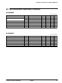
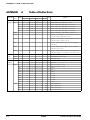
The information of the product number change
Starting April 1, 2001, the product number will be changed as listed below. To order from April 1,
2001 please use the new product number. For further information, please contact Epson sales
representative.
Configuration of product number
Devices
S1
C
60N01
F
0A01
00
Packing specification
Specification
Package (D: die form; F: QFP)
Model number
Model name (C: microcomputer, digital products)
Product classification (S1: semiconductor)
Development tools
C
60R08
S5U1
D1
1
00
Packing specification
Version (1: Version 1 ∗2)
Tool type (D1: Development Tool ∗1)
Corresponding model number (60R08: for S1C60R08)
Tool classification (C: microcomputer use)
Product classification
(S5U1: development tool for semiconductor products)
∗1: For details about tool types, see the tables below. (In some manuals, tool types are represented by one digit.)
∗2: Actual versions are not written in the manuals.
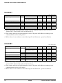
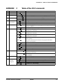
Comparison table between new and previous number
S1C60 Family processors
Previous No.
E0C6001
E0C6002
E0C6003
E0C6004
E0C6005
E0C6006
E0C6007
E0C6008
E0C6009
E0C6011
E0C6013
E0C6014
E0C60R08
New No.
S1C60N01
S1C60N02
S1C60N03
S1C60N04
S1C60N05
S1C60N06
S1C60N07
S1C60N08
S1C60N09
S1C60N11
S1C60N13
S1C60140
S1C60R08
S1C62 Family processors
Previous No.
E0C621A
E0C6215
E0C621C
E0C6S27
E0C6S37
E0C623A
E0C623E
E0C6S32
E0C6233
E0C6235
E0C623B
E0C6244
E0C624A
E0C6S46
New No.
S1C621A0
S1C62150
S1C621C0
S1C6S2N7
S1C6S3N7
S1C6N3A0
S1C6N3E0
S1C6S3N2
S1C62N33
S1C62N35
S1C6N3B0
S1C62440
S1C624A0
S1C6S460
Previous No.
E0C6247
E0C6248
E0C6S48
E0C624C
E0C6251
E0C6256
E0C6292
E0C6262
E0C6266
E0C6274
E0C6281
E0C6282
E0C62M2
E0C62T3
New No.
S1C62470
S1C62480
S1C6S480
S1C624C0
S1C62N51
S1C62560
S1C62920
S1C62N62
S1C62660
S1C62740
S1C62N81
S1C62N82
S1C62M20
S1C62T30
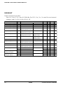
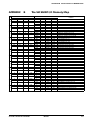
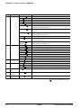
Comparison table between new and previous number of development tools
Development tools for the S1C60/62 Family
Previous No.
ASM62
DEV6001
DEV6002
DEV6003
DEV6004
DEV6005
DEV6006
DEV6007
DEV6008
DEV6009
DEV6011
DEV60R08
DEV621A
DEV621C
DEV623B
DEV6244
DEV624A
DEV624C
DEV6248
DEV6247
New No.
S5U1C62000A
S5U1C60N01D
S5U1C60N02D
S5U1C60N03D
S5U1C60N04D
S5U1C60N05D
S5U1C60N06D
S5U1C60N07D
S5U1C60N08D
S5U1C60N09D
S5U1C60N11D
S5U1C60R08D
S5U1C621A0D
S5U1C621C0D
S5U1C623B0D
S5U1C62440D
S5U1C624A0D
S5U1C624C0D
S5U1C62480D
S5U1C62470D
Previous No.
DEV6262
DEV6266
DEV6274
DEV6292
DEV62M2
DEV6233
DEV6235
DEV6251
DEV6256
DEV6281
DEV6282
DEV6S27
DEV6S32
DEV6S37
EVA6008
EVA6011
EVA621AR
EVA621C
EVA6237
EVA623A
New No.
S5U1C62620D
S5U1C62660D
S5U1C62740D
S5U1C62920D
S5U1C62M20D
S5U1C62N33D
S5U1C62N35D
S5U1C62N51D
S5U1C62560D
S5U1C62N81D
S5U1C62N82D
S5U1C6S2N7D
S5U1C6S3N2D
S5U1C6S3N7D
S5U1C60N08E
S5U1C60N11E
S5U1C621A0E2
S5U1C621C0E
S5U1C62N37E
S5U1C623A0E
Previous No.
EVA623B
EVA623E
EVA6247
EVA6248
EVA6251R
EVA6256
EVA6262
EVA6266
EVA6274
EVA6281
EVA6282
EVA62M1
EVA62T3
EVA6S27
EVA6S32R
ICE62R
KIT6003
KIT6004
KIT6007
New No.
S5U1C623B0E
S5U1C623E0E
S5U1C62470E
S5U1C62480E
S5U1C62N51E1
S5U1C62N56E
S5U1C62620E
S5U1C62660E
S5U1C62740E
S5U1C62N81E
S5U1C62N82E
S5U1C62M10E
S5U1C62T30E
S5U1C6S2N7E
S5U1C6S3N2E2
S5U1C62000H
S5U1C60N03K
S5U1C60N04K
S5U1C60N07K
Hardware
I.
S1C6S2N7
Technical Hardware
CONTENTS
CONTENTS
CHAPTER 2
INTRODUCTION ............................................................... I-1
1.1
Configuration ................................................................... I-1
1.2
Features .......................................................................... I-2
1.3
Block Diagram ................................................................. I-3
1.4
Pin Layout Diagram ......................................................... I-4
1.5
Pin Description ................................................................ I-5
Hardware
CHAPTER 1
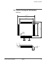
POWER SUPPLY AND INITIAL RESET ................................ I-6
2.1
Power Supply .................................................................. I-6
2.2
Initial Reset ...................................................................... I-8
Oscillation detection circuit ...................................... I-9
Reset pin (RESET) .................................................... I-9
Simultaneous high input to input ports (K00–K03) ... I-9
Internal register following initialization .................... I-10
2.3
CHAPTER 3
Test Pin (TEST) .............................................................. I-10
CPU, ROM, RAM ............................................................ I-11
3.1
CPU ................................................................................ I-11
3.2
ROM ............................................................................... I-12
3.3
RAM ............................................................................... I-12
S1C6S2N7 TECHNICAL HARDWARE
EPSON
I-i
CONTENTS
CHAPTER 4
PERIPHERAL CIRCUITS AND OPERATION ...................... I-13
4.1
Memory Map .................................................................. I-13
4.2
Oscillation Circuit ............................................................ I-19
Crystal oscillation circuit ......................................... I-19
CR oscillation circuit ............................................... I-19
4.3
Input Ports (K00–K03) .................................................... I-20
Configuration of input port ......................................
Interrupt function ...................................................
Mask option ............................................................
Control of input port ...............................................
4.4
I-20
I-20
I-22
I-23
Output Ports (R00–R03) ................................................. I-25
Configuration of output port .................................... I-25
Mask option ............................................................ I-26
Control of output port ............................................. I-28
4.5
I/O Ports (P00–P03) ....................................................... I-31
Configuration of I/O port ........................................
I/O control register and I/O mode ...........................
Mask option ............................................................
Control of I/O port ..................................................
4.6
LCD Driver (COM0–COM3, SEG0–SEG25) .................. I-35
Configuration of LCD driver .....................................
Switching between dynamic and static drive ............
Mask option (segment allocation) .............................
Control of LCD driver ..............................................
4.7
I-31
I-32
I-32
I-32
I-35
I-41
I-42
I-44
Clock Timer .................................................................... I-45
Configuration of clock timer .................................... I-45
Interrupt function ................................................... I-46
Control of clock timer .............................................. I-47
I-ii
EPSON
S1C6S2N7 TECHNICAL HARDWARE
CONTENTS
Stopwatch Timer ............................................................ I-49
Configuration of stopwatch timer ............................
Count-up pattern ....................................................
Interrupt function ...................................................
Control of stopwatch timer ......................................
4.9
I-49
I-50
I-51
I-52
Supply Voltage Detection (SVD) Circuit
and Heavy Load Protection Function ............................. I-55
Configuration of SVD circuit
and heavy load protection function ..........................
Operation of SVD detection timing ..........................
Operation of heavy load protection function ............
Control of SVD circuit
and heavy load protection function ..........................
I-55
I-57
I-58
I-59
4.10 Stepping Motor Driver .................................................... I-61
Configuration of motor driver ..................................
Drive pulse ..............................................................
Mask option ............................................................
Interrupt function ...................................................
Control of motor driver ............................................
I-61
I-62
I-62
I-62
I-63
4.11 Interrupt and HALT ......................................................... I-65
Interrupt factors ......................................................
Specific masks and factor flags for interrupt ............
Interrupt vectors .....................................................
Control of interrupt .................................................
I-67
I-68
I-69
I-70
CHAPTER 5
BASIC EXTERNAL WIRING DIAGRAM ............................. I-72
CHAPTER 6
ELECTRICAL CHARACTERISTICS .................................... I-74
6.1
Absolute Maximum Rating ............................................. I-74
6.2
Recommended Operating Conditions ............................ I-75
S1C6S2N7 TECHNICAL HARDWARE
EPSON
I-iii
Hardware
4.8
CONTENTS
CHAPTER 7
CHAPTER 8
I-iv
6.3
DC Characteristics ......................................................... I-77
6.4
Analog Circuit Characteristics and Current Consumption . I-79
6.5
Oscillation Characteristics .............................................. I-85
6.6
Motor Driver Characteristics ........................................... I-87
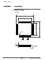
PACKAGE ...................................................................... I-88
7.1
Plastic Package .............................................................. I-88
7.2
Ceramic Package for Test Samples ............................... I-89
PAD LAYOUT .................................................................. I-90
8.1
Diagram of Pad Layout ................................................... I-90
8.2
Pad Coordinates ............................................................. I-91
EPSON
S1C6S2N7 TECHNICAL HARDWARE
CHAPTER 1: INTRODUCTION
CHAPTER 1
INTRODUCTION
Each member of the S1C6S2N7 Series of single chip microcomputers features a 4-bit S1C6200A core CPU, 1,536
words of ROM (12 bits per word), 80 words of RAM (4 bits
per word), an LCD driver, 4 bits for input ports (K00–K03), 4
bits for output ports (R00–R03), 4 bits for I/O ports (P00–
P03), two timers (clock timer and stopwatch timer) and a
motor driver.
The S1C6S2N7 Series features low-voltage operation and
low current consumption, this makes it suitable for battery
driven systems such as combination quartz watches.
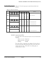
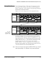
1.1 Configuration
The S1C6S2N7 Series is configured as follows, depending on
the supply voltage.
Table 1.1.1
Configuration of the
S1C6S2N7 Series
Model
Supply Voltage
S1C6S2N7
Oscillation Circuit
2.2–3.6 V
Crystal or CR (Typ. 65 kHz)
2.2–3.6 V
CR (Typ. 200 kHz)
0.9–3.6 V
Crystal or CR (Typ. 65 kHz)
0.9–1.8 V
Crystal
(Normal Type)
S1C6S2A7
(High Speed Type)
S1C6S2B7
(Wide Power Type)
S1C6S2L7
(Low Power Type)
S1C6S2N7 TECHNICAL HARDWARE
EPSON
I-1
CHAPTER 1: INTRODUCTION
1.2 Features
Built-in oscillation circuit
Crystal or CR oscillation circuit, 32.768 kHz (typ.)
Instruction set
100 instructions
ROM capacity
1,536 words ×12 bits
RAM capacity (data RAM)
80 words × 4 bits
Input port
4 bits (Supplementary pull-down resistors may be used )
Output port
4 bits (Piezo buzzer direct drive and programmable
frequency output are possible by mask option)
Input/output port
4 bits
LCD driver
26 segments × 4, 3 or 2 common
1/4, 1/3 or 1/2 duty
Motor driver
1 system
Timer
2 systems: clock timer/stopwatch timer
Supply voltage detection
circuit (SVD)
1.2 V / 2.4 V
Interrupts:
External interrupt Input port interrupt
1 system
Internal interrupt Timer interrupt
2 systems
Motor driver interrupt 1 system
Supply voltage
1.5 V (0.9–1.8 V)
1.5 V (0.9–3.6 V)
3.0 V (2.2–3.6 V)
Current consumption (typ.)
During HALT (typ.)
0.7 µA (S1C6S2N7,
0.6 µA (S1C6S2L7,
0.7 µA (S1C6S2B7,
60 µA (S1C6S2A7,
During operation (typ.)
1.9 µA (S1C6S2N7,
1.7 µA (S1C6S2L7,
1.9 µA (S1C6S2B7,
70 µA (S1C6S2A7,
Supply form
I-2
S1C6S2L7
S1C6S2B7
S1C6S2N7, S1C6S2A7, S1C6S2B7
Crystal oscillation CLK = 32.768 kHz)
Crystal oscillation CLK = 32.768 kHz)
Crystal oscillation CLK = 32.768 kHz)
CR oscillation CLK = 200 kHz)
Crystal oscillation CLK = 32.768 kHz)
Crystal oscillation CLK = 32.768 kHz)
Crystal oscillation CLK = 32.768 kHz)
CR oscillation CLK = 200 kHz)
QFP6-60pin (plastic) or chip
EPSON
S1C6S2N7 TECHNICAL HARDWARE
CHAPTER 1: INTRODUCTION
ROM
1,536 × 12
RESET
OSC1
OSC2
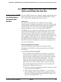
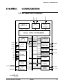
1.3 Block Diagram
OSC
System
Reset
Control
Core CPU S1C6200A
RAM
80 × 4
COM0
|
COM3
SEG0
|
SEG25
VDD
VL1
|
VL3
CA
CB
VS1
VSS
(FOUT/BUZZER)
(BUZZER)
Interrupt
Generator
LCD
Driver
Power
Controller
Input Port
Test Port
K00–K03
I/O Port
P00–P03
Output Port
R00–R03
TEST
Timer
SVD
Stop
Watch
Fout
&
Buzzer
Motor
Driver
A01, A02
DT1, DT2
Fig. 1.3.1
Block diagram
S1C6S2N7 TECHNICAL HARDWARE
EPSON
I-3
CHAPTER 1: INTRODUCTION
1.4 Pin Layout Diagram
QFP6-60pin
45
31
46
30
Index
60
16
1
Fig. 1.4.1
15
Pin No.
Pin Name
Pin No.
Pin Name
Pin No.
Pin Name
Pin No.
Pin Name
1
OSC1
16
COM2
2
OSC2
17
COM3
31
TEST
46
P01
32
SEG13
47
P02
3
N.C.
18
SEG0
33
SEG14
48
P03
4
VS1
5
CA
19
SEG1
34
SEG15
49
RESET
20
SEG2
35
SEG16
50
K00
6
7
CB
21
SEG3
36
SEG17
51
K01
VL1
22
SEG4
37
SEG18
52
K02
8
9
VL2
23
SEG5
38
SEG19
53
K03
VL3
24
SEG6
39
SEG20
54
R00
10
DT1
25
SEG7
40
SEG21
55
R01
11
A01
26
SEG8
41
SEG22
56
R02
12
A02
27
SEG9
42
SEG23
57
R03
13
DT2
28
SEG10
43
SEG24
58
N.C.
14
COM0
29
SEG11
44
SEG25
59
VSS
15
COM1
30
SEG12
45
P00
60
VDD
Pin assignment
I-4
N.C. = No Connection
EPSON
S1C6S2N7 TECHNICAL HARDWARE
CHAPTER 1: INTRODUCTION
1.5 Pin Description
Table 1.5.1 Pin description
Pin Name
Pin No. Input/Output
Function
VDD
60
(I)
Power source (+) pin
VSS
59
(I)
Power source (-) pin
VS1
4
O
Oscillation and internal logic system regulated voltage output pin
VL1
7
O
LCD system regulated voltage output pin (approx. -1.05 V)
VL2
8
O
LCD system booster output pin (VL1 × 2)
VL3
9
O
LCD system booster output pin (VL1 × 3)
5, 6
–
Booster capacitor connecting pin
1
I
Crystal or CR oscillation input pin
CA–CB
OSC1
OSC2
2
O
Crystal or CR oscillation output pin
K00–K03
50–53
I
Input pin
P00–P03
45–48
I/O
R00–R03
54–57
O
Output pin
18–30
O
LCD segment output pin
SEG0–25
(convertible to DC output terminal by mask option)
32–44, 45
COM0–3
RESET
TEST
I/O pin
14–17
O
LCD common output pin
49
I
Initial setting input pin
Test input pin
31
I
DT1, DT2
10, 13
I/O
A01, A02
11, 12
O
S1C6S2N7 TECHNICAL HARDWARE
Motor driver test I/O pin
Motor driver pulse output pin
EPSON
I-5
CHAPTER 2: POWER SUPPLY AND INITIAL RESET
CHAPTER 2
POWER SUPPLY AND INITIAL RESET
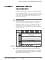
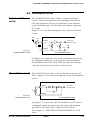
2.1 Power Supply
With a single external power supply (*1) supplied to VDD
through VSS, the S1C6S2N7 Series generates the necessary
internal voltages with the regulated voltage circuit (<VS1> for
oscillators and internal circuit, <VL1 or VL2> for LCDs) and
the voltage booster (<VL2 or VL1, VL3> for LCDs).
Figure 2.1.1 shows the power supply configuration of the
S1C6S2N7.
*1 Supply voltage:
Note -
S1C6S2N7 ....
S1C6S2A7 ....
S1C6S2B7 ....
S1C6S2L7 ....
3V
3V
3 V or 1.5 V
1.5 V
External loads cannot be driven by the output voltage of the
regulated voltage circuit and the voltage booster.
See Chapter 6, "ELECTRICAL CHARACTERISTICS", for
voltage values.
VDD
Internal
circuit
C5
External
power
supply
VS1
C2
VL1∗
C3
C4
VL2∗
VL3
CA
CB
Internal system
regulated voltage
circuit
VS1
Oscillation
circuit
LCD system
regulated voltage
circuit
VL1∗
LCD system
voltage booster
OSC1, 2
VL1∗
VL2∗
VL3
LCD driver
circuit
COM0–3
SEG0–25
C1
VSS
Fig. 2.1.1
Configuration of power
supply system
I-6
* In the S1C6S2N7 and S1C6S2A7, VL1 and VL2 are
interchanged. (The LCD system voltage regulator generates
VL2, and the LCD system voltage booster generates VL1.)
EPSON
S1C6S2N7 TECHNICAL HARDWARE
CHAPTER 2: POWER SUPPLY AND INITIAL RESET
The LCD system regulated voltage circuit use can be prohibited by
setting the mask option. In this case, external elements can be
minimized because the external capacitors for the LCD system
regulated voltage circuit are not necessary. However when the LCD
system regulated voltage circuit is not used, the display quality of
the LCD panel, when the supply voltage fluctuates (drops), is
inferior to when the LCD system regulated voltage circuit is used.
The S1C6S2B7 always uses the the LCD system regulated voltage
circuit, therefore the external capacitors are required.
Figure 2.1.2 shows the external elements when the the LCD system regulated voltage circuit is not used.
• S1C6S2A7
4.5 V LCD panel
1/4, 1/3, 1/2 duty, 1/3 bias
VDD
VS1
VL1
VL2
VL3
CA
C5
C2
C4
C1
3V
CB
VSS
Note: VL2 is shorted to VSS inside the IC.
• S1C6S2N7/S1C6S2A7
3 V LCD panel
1/4, 1/3, 1/2 duty, 1/3 bias
VDD
VS1
VL1
VL2
VL3
CA
3 V LCD panel
1/4, 1/3, 1/2 duty, 1/2 bias
VDD
VS1
VL1
VL2
VL3
CA
C5
C2
C3
C1
3V
C5
C2
C1
CB
VSS
3V
CB
VSS
Note: VL3 is shorted to VSS inside the IC.
• S1C6S2L7
3 V LCD panel
1/4, 1/3, 1/2 duty, 1/2 bias
Fig. 2.1.2
External elements when
LCD system regulated
voltage circuit is not used
S1C6S2N7 TECHNICAL HARDWARE
VDD
VS1
VL1
VL2
VL3
CA
C5
C4
1.5 V
C1
CB
VSS
Note: VL1 is shorted to VSS inside the IC.
EPSON
I-7
CHAPTER 2: POWER SUPPLY AND INITIAL RESET
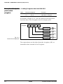
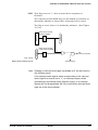
2.2 Initial Reset
To initialize the S1C6S2N7 Series circuits, an initial reset
must be executed. There are three ways of doing this.
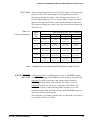
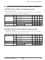
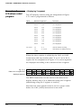
(1) Initial reset by the oscillation detection circuit
(2) External initial reset via the RESET pin
(3) External initial reset by simultaneous high input to pins
K00–K03 (depending on mask option)
Figure 2.2.1 shows the configuration of the initial reset
circuit.
OSC1
OSC1
OSC2
Oscillation
circuit
Oscillation
detection
circuit
K00
Vss
Noise
rejection
circuit
K01
Initial
reset
Noise
rejection
circuit
K02
K03
RESET
Vss
Fig. 2.2.1
Configuration of initial
reset circuit
I-8
EPSON
S1C6S2N7 TECHNICAL HARDWARE
CHAPTER 2: POWER SUPPLY AND INITIAL RESET
Oscillation detection The oscillation detection circuit outputs the initial reset
signal at power-on until the oscillation circuit starts
circuit
oscillating, or when the oscillation circuit stops oscillating
for some reason.
However, depending on the power-on sequence (voltage rise
timing), the circuit may not work properly. Therefore, use
the reset terminal or reset by simultaneous high input to the
input port (K00–K03) for initial reset after turning power on.
Reset pin (RESET)
An initial reset can be invoked externally by making the
reset pin high. This high level must be maintained for at
least 5 ms (when the oscillation frequency fosc is 32 kHz),
because the initial reset circuit contains a noise rejection
circuit. When the reset pin goes low the CPU begins to
operate.
Simultaneous high
input to input ports
(K00–K03)
Another way of invoking an initial reset externally is to input
a high signal simultaneously to the input ports (K00–K03)
selected with the mask option. This initial reset signal
passes through the noise rejection circuit. Therefore, it is
necessary to keep the specified input ports at high level for
at least a definite time. This time can be selected from 4
sec, 2 sec, 62.5 msec and 250 msec (when the oscillation
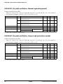
frequency fosc is 32 kHz) by mask option. Tables 2.2.1 and
2.2.2 show the combinations of input ports (K00–K03) and
the simultaneous high input detection time that can be
selected with the mask option.
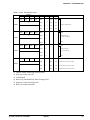
Table 2.2.1
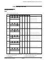
Input port combinations
Table 2.2.2
Simultaneous high input
detection time
S1C6S2N7 TECHNICAL HARDWARE
A
B
C
D
Not used
K00*K01
K00*K01*K02
K00*K01*K02*K03
1
2
3
4
2–4 [sec]
1–2 [sec]
30–62.5 [msec]
120–250 [msec]
EPSON
I-9
CHAPTER 2: POWER SUPPLY AND INITIAL RESET
When, for instance, mask option D (K00*K01*K02*K03) is
selected, an initial reset is executed when the signals input
to the four ports K00–K03 are all high at the same time.
If you use this function, make sure that the specified ports
do not go high at the same time during normal operation.
Internal register following initialization
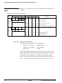
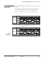
Table 2.2.3
Initial values
An initial reset initializes the CPU as shown in the table
below.
CPU Core
Name
Program counter step
Program counter page
New page pointer
Stack pointer
Index register X
Index register Y
Register pointer
General register A
General register B
Interrupt flag
Decimal flag
Zero flag
Carry flag
Signal
Number of Bits
Setting Value
PCS
PCP
NPP
SP
X
Y
RP
A
B
I
D
Z
C
8
4
4
8
8
8
4
4
4
1
1
1
1
00H
1H
1H
Undefined
Undefined
Undefined
Undefined
Undefined
Undefined
0
0
Undefined
Undefined
Peripheral Circuits
Name
Number of Bits
Setting Value
80 × 4
26 × 4
–
Undefined
Undefined
*1
RAM
Display memory
Other peripheral circuit
*1: See section 4.1, "Memory Map"
2.3 Test Pin (TEST)
This pin is used when IC is inspected for shipment.
During normal operation connect it to VSS.
I-10
EPSON
S1C6S2N7 TECHNICAL HARDWARE
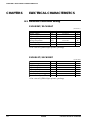
CHAPTER 3: CPU, ROM, RAM
CHAPTER 3
CPU, ROM, RAM
3.1 CPU
The S1C6S2N7 Series employs the S1C6200A core CPU, so
that register configuration, instructions, and so forth are
virtually identical to those in other processors in the family
using the S1C6200A. Refer to the "S1C6200/6200A Core
CPU Manual" for details of the S1C6200A.
Note the following points with regard to the S1C6S2N7
Series:
(1) The SLEEP operation is not provided, so the SLP instruction cannot be used.
(2) Because the ROM capacity is 1,536 words, 12 bits per
word, bank bits are unnecessary, and PCB and NBP are
not used.
(3) The RAM page is set to 0 only, so the page part (XP, YP)
of the index register that specifies addresses is invalid.
PUSH
POP
LD
LD
S1C6S2N7 TECHNICAL HARDWARE
XP
XP
XP,r
r,XP
EPSON
PUSH
POP
LD
LD
YP
YP
YP,r
r,YP
I-11
CHAPTER 3: CPU, ROM, RAM
3.2 ROM
The built-in ROM, a mask ROM for the program, has a
capacity of 1,536 × 12-bit steps. The program area is 6
pages (0–5), each consisting of 256 steps (00H–FFH). After
an initial reset, the program start address is page 1, step
00H. The interrupt vector is allocated to page l, steps 01H–
0FH.
Bank 0
00H step
0 page
Program start address
01H step
1 page
2 page
Interrupt vector area
3 page
4 page
5 page
0FH step
10H step
Program area
FFH step
Fig. 3.2.1
12 bits
ROM configuration
3.3 RAM
The RAM, a data memory for storing a variety of data, has a
capacity of 80 words, 4-bit words. When programming,
keep the following points in mind:
(1) Part of the data memory is used as stack area when
saving subroutine return addresses and registers, so be
careful not to overlap the data area and stack area.
(2) Subroutine calls and interrupts take up three words on
the stack.
(3) Data memory 000H–00FH is the memory area pointed by
the register pointer (RP).
I-12
EPSON
S1C6S2N7 TECHNICAL HARDWARE
CHAPTER 4: PERIPHERAL CIRCUITS AND OPERATION (Memory Map)
CHAPTER 4
PERIPHERAL CIRCUITS
AND OPERATION
Peripheral circuits (timer, I/O, and so on) of the S1C6S2N7
Series are memory mapped. Thus, all the peripheral circuits
can be controlled by using memory operations to access the
I/O memory. The following sections describe how the peripheral circuits operate.
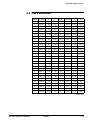
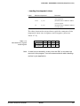
4.1 Memory Map
The data memory of the S1C6S2N7 Series has an address
space of 129 words, of which 32 words are allocated to
display memory and 17 words, to I/O memory. Figure 4.1.1
shows the overall memory map for the S1C6S2N7 Series,
and Tables 4.1.1(a)–(e), the memory maps for the peripheral
circuits (I/O space).
Address
Low
0
Page
1
2
3
4
5
6
7
8
9
A
B
C
D
E
F
High
0
M0 M1 M2 M3 M4 M5 M6 M7 M8 M9 MA MB MC MD ME MF
1
2
RAM area (000H–04FH)
80 words x 4 bits (R/W)
3
4
5
6
0
7
8
Display memory area (090H–0AFH)
32 words x 4 bits (Write only)
9
A
B
C
D
E
Fig. 4.1.1
F
I/O memory area
Memory map
Tables 4.1.1(a)–(e)
Unused area
Note Memory is not mounted in unused area within the memory map
and in memory area not indicated in this chapter. For this reason,
normal operation cannot be assured for programs that have been
prepared with access to these areas.
S1C6S2N7 TECHNICAL HARDWARE
EPSON
I-13
CHAPTER 4: PERIPHERAL CIRCUITS AND OPERATION (Memory Map)
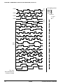
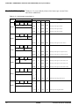
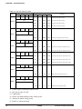
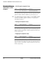
Table 4.1.1(a) I/O memory map
Address
D3
Register
D2
D1
D0
Name
K03
K02
K00
K03
–
K02
K01
R
SR *1
Comment
1
0
*2
High
Low
–
*2
High
Low
K01
–
*2
High
Low
K00
–
*2
High
Low
SWL3
0
MSB
SWL2
0
Stopwatch timer
1/100 sec (BCD)
SWL1
0
SWL0
0
LSB
SWH3
0
MSB
SWH2
0
Stopwatch timer
1/10 sec (BCD)
SWH1
0
SWH0
0
TM3
–
High
Low
Timer data (clock timer 2 Hz)
TM2
–
High
Low
Timer data (clock timer 4 Hz)
TM1
–
High
Low
Timer data (clock timer 8 Hz)
TM0
–
High
Low
Timer data (clock timer 16 Hz)
0E0H
Input port (K00–K03)
SWL3
SWL2
SWL1
SWL0
R
0E2H
SWH3
SWH2
SWH1
SWH0
R
0E3H
TM3
TM2
TM1
R
TM0
LSB
0E4H
*1
*2
*3
*4
*5
*6
I-14
Initial value following initial reset
Not set in the circuit
Undefined
Reset (0) immediately after being read
Constantly 0 when being read
Refer to main manual
EPSON
S1C6S2N7 TECHNICAL HARDWARE
CHAPTER 4: PERIPHERAL CIRCUITS AND OPERATION (Memory Map)
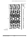
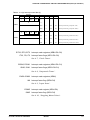
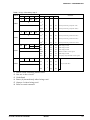
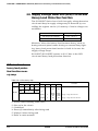
Table 4.1.1(b) I/O memory map
Address
Register
D2
D1
D3
EIK03
EIK02
EIK01
D0
Name
EIK00
EIK03
R/W
SR *1
Comment
1
0
0
Enable
Mask
Interrupt mask register (K03)
EIK02
0
Enable
Mask
Interrupt mask register (K02)
EIK01
0
Enable
Mask
Interrupt mask register (K01)
EIK00
0
Enable
Mask
Interrupt mask register (K00)
0
Enable
Mask
Interrupt mask register (motor driver)
EISW1
0
Enable
Mask
Interrupt mask register (stopwatch 1 Hz)
EISW0
0
Enable
Mask
Interrupt mask register (stopwatch 10 Hz)
EIT2
0
Enable
Mask
Interrupt mask register (clock timer 2 Hz)
EIT8
0
Enable
Mask
Interrupt mask register (clock timer 8 Hz)
EIT32
0
Enable
Mask
Interrupt mask register (clock timer 32 Hz)
0
Yes
No
Interrupt factor flag (motor driver)
0
Yes
No
Interrupt factor flag (K00–K03)
0E8H
0
0
0
EISMD
0
R/W
0
R
0E9H
0
*5
*5
*5
EISMD
0
0
EISW1
R
EISW0
0
0
R/W
*5
*5
0EAH
0
EIT2
EIT8
R
EIT32
R/W
0 *5
0EBH
0
0
0
ISMD
0 *5
0 *5
R
0ECH
0 *5
ISMD
0
0
0
R
IK0
0 *5
0 *5
0EDH
0 *5
IK0 *4
*1
*2
*3
*4
*5
*6
Initial value following initial reset
Not set in the circuit
Undefined
Reset (0) immediately after being read
Constantly 0 when being read
Refer to main manual
S1C6S2N7 TECHNICAL HARDWARE
EPSON
I-15
CHAPTER 4: PERIPHERAL CIRCUITS AND OPERATION (Memory Map)
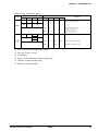
Table 4.1.1(c) I/O memory map
Address
D3
0
Register
D2
D1
0
ISW1
D0
Name
ISW0
0
1
0
0
Yes
No
Interrupt factor flag (stopwatch 1 Hz)
0
Yes
No
Interrupt factor flag (stopwatch 10 Hz)
0
Yes
No
Interrupt factor flag (clock timer 2 Hz)
0
Yes
No
Interrupt factor flag (clock timer 8 Hz)
0
Yes
No
Interrupt factor flag (clock timer 32 Hz)
R03
0
High
Low
R03 output port data
R02
0
High
Low
R02 output port data
R01
0
High
Low
R01 output port data
BUZZER
0
ON
OFF
Buzzer ON/OFF control register
R00
0
High
Low
R00 output port data
FOUT
0
ON
OFF
Frequency output ON/OFF control register
0
R
0EEH
*5
*5
*4
ISW1
*4
ISW0
0
IT2
IT8
IT32
R
0
IT2
0EFH
IT8
IT32
R03
R02
R01
BUZZER
R00
FOUT
R/W
0F3H
P03
P02
P01
R/W
P00
*5
*4
*4
*4
P03
*2
High
Low
P02
*2
High
Low
P01
*2
High
Low
P00
0 *2
High
Low
0F6H
*1
*2
*3
*4
*5
*6
I-16
Comment
SR *1
I/O port (P00–P03)
Initial value following initial reset
Not set in the circuit
Undefined
Reset (0) immediately after being read
Constantly 0 when being read
Refer to main manual
EPSON
S1C6S2N7 TECHNICAL HARDWARE
CHAPTER 4: PERIPHERAL CIRCUITS AND OPERATION (Memory Map)
Table 4.1.1(d) I/O memory map
Address
D3
Register
D2
D1
0
TMRST
R
W
D0
SR *1
1
0
TMRST
Reset
Reset
–
SWRUN
0
Run
Stop
SWRST
Reset
Reset
–
SVDON
HLMOD
0
Heavy
load
Normal
load
R/W
0
SWRUN SWRST
R/W
W
Name
0
Comment
*5
Clock timer reset
0F9H
Stopwatch timer RUN/STOP
*5
HLMOD
0
R/W
SVDDT
R
0
R/W
0
0
R
Heavy load protection mode register
*5
0FAH
CSDC
Stopwatch timer reset
SVDDT
0
Supply
voltage
low
Supply
voltage
normal
SVDON
0
ON
OFF
CSDC
0
Static
Dynamic
Output
Input
0
*5
0
*5
0
*5
Supply voltage detection data
Supply voltage detection ON/OFF
LCD drive switch
0FBH
0
0
R
0
IOC
0 *5
R/W
0 *5
0
0FCH
0 *5
IOC
*1
*2
*3
*4
*5
*6
0
I/O port P00–P03 Input/Output
Initial value following initial reset
Not set in the circuit
Undefined
Reset (0) immediately after being read
Constantly 0 when being read
Refer to main manual
S1C6S2N7 TECHNICAL HARDWARE
EPSON
I-17
CHAPTER 4: PERIPHERAL CIRCUITS AND OPERATION (Memory Map)
Table 4.1.1(e) I/O memory map
Address
Register
D2
D1
D3
D0
Name
SR *1
1
0
0
2 kHz
4 kHz
XBZR
0
XFOUT1 XFOUT0
XBZR
R/W
R
R/W
0
Comment
Buzzer frequency control
*5
0FDH
XFOUT1
XFOUT0
0
0
R
0FEH
FRUN
FTRG
R
W
0
R
0
0
I-18
FOUT frequency control:
XFOUT1(0), XFOUT0(0) -> F1
XFOUT1(0), XFOUT0(1) -> F2
XFOUT1(1), XFOUT0(0) -> F3
XFOUT1(1), XFOUT0(1) -> F4
0
*5
*5
FRUN
0
Run
Stop
Motor driver status (reading)
FTRG
–
Start
–
Motor driver trigger (writing)
0
*1
*2
*3
*4
*5
*6
0
*5
Initial value following initial reset
Not set in the circuit
Undefined
Reset (0) immediately after being read
Constantly 0 when being read
Refer to main manual
EPSON
S1C6S2N7 TECHNICAL HARDWARE
CHAPTER 4: PERIPHERAL CIRCUITS AND OPERATION (Oscillation Circuit)
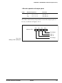
4.2 Oscillation Circuit
Crystal oscillation
circuit
The S1C6S2N7 Series has a built-in crystal oscillation
circuit. This circuit generates the operating clock for the
CPU and peripheral circuit on connection to an external
crystal oscillator (typ. 32.768 kHz) and trimmer capacitor
(5–25 pF).
Figure 4.2.1 is the block diagram of the crystal oscillation
circuit.
VDD
CG
RD
To CPU and
peripheral circuits
Rf
X'tal
OSC1
VDD
CD
OSC2
Fig. 4.2.1
Crystal oscillation circuit
The S1C6S2N7 Series
As Figure 4.2.1 indicates, the crystal oscillation circuit can
be configured simply by connecting the crystal oscillator
(X'tal) between the OSC1 and OSC2 pins and the trimmer
capacitor (CG) between the OSC1 and VDD pins.
CR oscillation circuit
The S1C6S2N7 Series has a CR oscillation circuit (typ. 65
kHz). Figure 4.2.2 is the block diagram of the CR oscillation
circuit.
OSC1
To CPU and
peripheral circuits
R
OSC2
C
Fig. 4.2.2
CR oscillation circuit
The S1C6S2N7 Series
As Figure 4.2.2 indicates, the CR oscillation circuit can be
configured simply by connecting the register (R) between
pins OSC1 and OSC2 since capacity (C) is built-in.
See Chapter 6, "ELECTRICAL CHARACTERISTICS" for R
value.
S1C6S2N7 TECHNICAL HARDWARE
EPSON
I-19
CHAPTER 4: PERIPHERAL CIRCUITS AND OPERATION (Input Ports)
4.3 Input Ports (K00–K03)
Configuration of
input port
The S1C6S2N7 Series has a 4-bit general-purpose input
port. Each of the input port pins (K00–K03) has an internal
pull-down resistance. The pull-down resistance can be
selected for each bit with the mask option.
Figure 4.3.1 shows the configuration of input port.
Interrupt
request
Kxx
Data bus
VDD
Address
Fig. 4.3.1
VSS
Configuration of input port
Mask option
Selecting "pull-down resistance enabled" with the mask
option allows input from a push button, key matrix, and so
forth. When "pull-down resistance disabled" is selected, the
port can be used for slide switch input and interfacing with
other LSIs.
Interrupt function
I-20
All four input port bits (K00–K03) provide the interrupt
function. The conditions for issuing an interrupt can be set
by the software for the four bits. Also, whether to mask the
interrupt function can be selected individually for all four
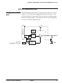
bits by the software. Figure 4.3.2 shows the configuration of
K00–K03.
EPSON
S1C6S2N7 TECHNICAL HARDWARE
CHAPTER 4: PERIPHERAL CIRCUITS AND OPERATION (Input Ports)
Data bus
Kxx
Address
Noise
rejector
Interrupt factor
flag (IK0)
Interrupt
request
Address
Fig. 4.3.2
Input interrupt circuit
configuration
(K00–K03)
Interrupt mask
register (EIK)
Mask option
Address
The interrupt mask registers (EIK00–EIK03) enable the
interrupt mask to be selected individually for K00–K03. An
interrupt occurs when the input value which are not
masked change and the interrupt factor flag (IK0) is set to 1.
Input interrupt programing related precautions
Port K input
Active status
Mask register
➀
Fig. 4.3.3
Input interrupt timing
Factor flag set Not set
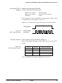
When the content of the mask register is rewritten, while
the port K input is in the active status. The input interrupt
factor flag is set at ➀.
When using an input interrupt, if you rewrite the content of
the mask register, when the value of the input terminal
which becomes the interrupt input is in the active status
(input terminal = high status), the factor flag for input
interrupt may be set.
For example, a factor flag is set with the timing of ➀ shown
in Figure 4.3.3. However, when clearing the content of the
mask register with the input terminal kept in the high
status and then setting it, the factor flag of the input interrupt is again set at the timing that has been set.
S1C6S2N7 TECHNICAL HARDWARE
EPSON
I-21
CHAPTER 4: PERIPHERAL CIRCUITS AND OPERATION (Input Ports)
Consequently, when the input terminal is in the active
status (high status), do not rewrite the mask register (clearing, then setting the mask register), so that a factor flag will
only set at the rising edge in this case. When clearing, then
setting the mask register, set the mask register, when the
input terminal is not in the active status (low status).
Mask option
The contents that can be selected with the input port mask
option are as follows:
(1) An internal pull-down resistance can be selected for each
of the four bits of the input ports (K00–K03). Having
selected "pull-down resistance disabled", take care that
the input does not float. Select "pull-down resistance
enabled" for input ports that are not being used.
(2) The input interrupt circuit contains a noise rejection
circuit to prevent interrupts form occurring through
noise. The mask option enables selection of the noise
rejection circuit for each separate pin series. When "use"
is selected, a maximum delay of 0.5 ms (fosc = 32 kHz)
occurs from the time an interrupt condition is established
until the interrupt factor flag (IK) is set to 1.
I-22
EPSON
S1C6S2N7 TECHNICAL HARDWARE
CHAPTER 4: PERIPHERAL CIRCUITS AND OPERATION (Input Ports)
Control of input port
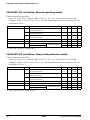
Table 4.3.1 list the input port control bits and their addresses.
Table 4.3.1 Input port control bits
Address
D3
Register
D2
D1
D0
Name
SR
1
0
K03
K02
K00
K03
–
High
Low
K02
–
High
Low
K01
–
High
Low
K00
–
High
Low
EIK03
0
Enable
Mask
Interrupt mask register (K03)
EIK02
0
Enable
Mask
Interrupt mask register (K02)
EIK01
0
Enable
Mask
Interrupt mask register (K01)
EIK00
0
Enable
Mask
Interrupt mask register (K00)
0
Yes
No
K01
R
Comment
0E0H
Input port (K00–K03)
EIK03
EIK02
EIK01
EIK00
R/W
0E8H
0
0
0
R
IK0
0
0
0EDH
0
IK0
Interrupt factor flag (K00–K03)
K00–K03 Input port data (0E0H)
The input data of the input port pins can be read with these
registers.
When 1 is read: High level
When 0 is read: Low level
Writing:
Invalid
The value read is 1 when the pin voltage of the four bits of
the input port (K00–K03) goes high (VDD), and 0 when the
voltage goes low (VSS). These bits are reading only, so
writing cannot be done.
S1C6S2N7 TECHNICAL HARDWARE
EPSON
I-23
CHAPTER 4: PERIPHERAL CIRCUITS AND OPERATION (Input Ports)
EIK00–EIK03 Interrupt mask registers (0E8H)
Masking the interrupt of the input port pins can be done
with these registers.
When 1 is written: Enable
When 0 is written: Mask
Reading:
Valid
With these registers, masking of the input port bits can be
done for each of the four bits. After an initial reset, these
registers are all set to 0.
IK0 Interrupt factor flag (0EDH D0)
This flag indicates the occurrence of an input interrupt.
When 1 is read: Interrupt has occurred
When 0 is read: Interrupt has not occurred
Writing:
Invalid
The interrupt factor flag IK0 is associated with K00–K03.
From the status of this flag, the software can decide whether
an input interrupt has occurred.
This flag is reset when the software has read it.
Reading of interrupt factor flag is available at EI, but be
careful in the following cases.
If the interrupt mask register value corresponding to the
interrupt factor flag to be read is set to 1, an interrupt
request will be generated by the interrupt factor flag set
timing, or an interrupt request will not be generated.
After an initial reset, this flag is set to 0.
I-24
EPSON
S1C6S2N7 TECHNICAL HARDWARE
CHAPTER 4: PERIPHERAL CIRCUITS AND OPERATION (Output Ports)
4.4 Output Ports (R00–R03)
Configuration of
output port
The S1C6S2N7 Series has a 4-bit general output port (R00–
R03).
Output specification of the output port can be selected in a
bit unit with the mask option. Two kinds of output specifications are available: complementary output and Pch open
drain output. Also, the mask option enables the output
ports R00 and R01 to be used as special output ports.
Figure 4.4.1 shows the configuration of the output port.
Data bus
VDD
Register
Rxx
Complementary
Pch open drain
Address
VSS
Fig. 4.4.1
Mask option
Configuration of output port
S1C6S2N7 TECHNICAL HARDWARE
EPSON
I-25
CHAPTER 4: PERIPHERAL CIRCUITS AND OPERATION (Output Ports)
The mask option enables the following output port selection.
Mask option
(1) Output specification of output port
The output specifications for the output port (R00–R03)
may be either complementary output or Pch open drain
output for each of the four bits. However, even when Pch
open drain output is selected, a voltage exceeding the
source voltage must not be applied to the output port.
(2) Special output
In addition to the regular DC output, special output can
be selected for output ports R00 and R01, as shown in
Table 4.4.1. Figure 4.4.2 shows the structure of output
ports R00–R03.
Table 4.4.1
Pin Name
When Special Output is Selected
Data bus
Special output
R00
FOUT or BUZZER
R01
BUZZER
Register
(R03)
R03
Register
(R02)
R02
BUZZER
R01
Register
(R01)
BUZZER
Register
(R00)
Fig. 4.4.2
Structure of output ports
R00–R03
I-26
R00
FOUT
Address
(0F3H)
Mask option
EPSON
S1C6S2N7 TECHNICAL HARDWARE
CHAPTER 4: PERIPHERAL CIRCUITS AND OPERATION (Output Ports)
FOUT (R00) When output port R00 is set for FOUT output, this port will
generate fosc (CPU operating clock frequency) or clock
frequency divided into fosc. Clock frequency may be selected individually for F1–F4, from among 5 types by mask
option; one among F1–F4 is selected by software and used.
The types of frequency which may be selected are shown in
Table 4.4.2.
Table 4.4.2
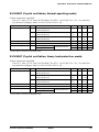
FOUT clock frequency
Mask
Option
Sets
Clock Frequency (Hz) fosc = 32.768 kHz
F1
F2
F3
F4
(D1,D0)=(0,0)
(D1,D0)=(0,1)
(D1,D0)=(1,0)
(D1,D0)=(1,1)
Set 1
256
(fosc/128)
512
(fosc/64)
1,024
(fosc/32)
2,048
(fosc/16)
Set 2
512
(fosc/64)
1,024
(fosc/32)
2,048
(fosc/16)
4,096
(fosc/8)
Set 3
1,024
(fosc/32)
2,048
(fosc/16)
4,096
(fosc/8)
8,192
(fosc/4)
Set 4
2,048
(fosc/16)
4,096
(fosc/8)
8,192
(fosc/4)
16,384
(fosc/2)
Set 5
4,096
(fosc/8)
8,192
(fosc/4)
16,384
(fosc/2)
32,768
(fosc/1)
(D1, D0) = (XFOUT1, XFOUT0)
Note A hazard may occur when the FOUT signal is turned on or off.
BUZZER, BUZZER Output ports R01 and R00 may be set to BUZZER output
(R01, R00) and BUZZER output (BUZZER reverse output), respectively,
allowing for direct driving of the piezo-electric buzzer.
BUZZER output (R00) may only be set if R01 is set to
BUZZER output. In such case, whether ON/OFF of the
BUZZER output is done through R00 register or is controlled through R01 simultaneously with BUZZER output is
also selected by mask option.
The frequency of buzzer output may be selected by software
to be either 2 kHz or 4 kHz.
S1C6S2N7 TECHNICAL HARDWARE
EPSON
I-27
CHAPTER 4: PERIPHERAL CIRCUITS AND OPERATION (Output Ports)
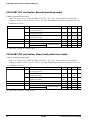
Table 4.4.3 lists the output port control bits and their addresses.
Control of output
port
Table 4.4.3 Control bits of output port
Address
Register
D2
D1
R01
R02
BUZZER
D3
R03
D0
R00
FOUT
R/W
0F3H
Comment
Name
SR
1
0
R03
0
High
Low
R03 output port data
R02
0
High
Low
R02 output port data
R01
0
High
Low
R01 output port data
BUZZER
0
ON
OFF
Buzzer ON/OFF control register
R00
0
High
Low
R00 output port data
FOUT
0
ON
OFF
Frequency output ON/OFF control register
XBZR
0
XFOUT1 XFOUT0
XBZR
0
2 kHz
4 kHz
Buzzer frequency control
R/W
R
R/W
0
XFOUT1
0
High
Low
FOUT frequency control:
XFOUT0
0
High
Low
0FDH
XFOUT1(0), XFOUT0(0) -> F1
XFOUT1(0), XFOUT0(1) -> F2
XFOUT1(1), XFOUT0(0) -> F3
XFOUT1(1), XFOUT0(1) -> F4
R00–R03 Output port data (0F3H)
Sets the output data for the output ports.
When 1 is written:
When 0 is written:
Reading:
High output
Low output
Valid
The output port pins output the data written to the corresponding registers (R00–R03) without changing it. When 1
is written to the register, the output port pin goes high
(VDD), and when 0 is written, the output port pin goes low
(VSS). After an initial reset, all the registers are set to 0.
I-28
EPSON
S1C6S2N7 TECHNICAL HARDWARE
CHAPTER 4: PERIPHERAL CIRCUITS AND OPERATION (Output Ports)
R00 (when FOUT is Special output port data (0F3H D0)
selected) Controls the FOUT (clock) output.
When 1 is written:
When 0 is written:
Reading:
Clock output
Low level (DC) output
Valid
FOUT output can be controlled by writing data to R00. After
an initial reset, this register is set to 0.
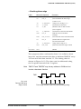
Figure 4.4.3 shows the output waveform for FOUT output.
R00 register
Fig. 4.4.3
FOUT output waveform
0
1
FOUT output
waveform
XFOUT0, XFOUT1 FOUT frequency control (0FDH D0, 0FDH D1)
Selects the output frequency when R00 port is set for FOUT
output.
Table 4.4.4
FOUT frequency selection
XFOUT1
XFOUT0
Frequency Selection
0
0
F1
0
1
F2
1
0
F3
1
1
F4
After an initial reset, these registers are set to 0.
S1C6S2N7 TECHNICAL HARDWARE
EPSON
I-29
CHAPTER 4: PERIPHERAL CIRCUITS AND OPERATION (Output Ports)
R00, R01 (when BUZZER Special output port data (0F3H D0, 0F3H D1)
and BUZZER is Controls the buzzer output.
selected)
When 1 is written:
Buzzer output
When 0 is written:
Low level (DC) output
Reading:
Valid
BUZZER and BUZZER output can be controlled by writing
data to R00 and R01.
When BUZZER output by R01 register control is selected by
mask option, BUZZER output and BUZZER output can be
controlled simultaneously by writing data to R01 register.
After an initial reset, these registers are set to 0.
Figure 4.4.4 shows the output waveform for buzzer output.
R01 (R00) register
0
1
BUZZER output
waveform
Fig. 4.4.4
Buzzer output waveform
BUZZER output
waveform
XBZR Buzzer frequency control (0FDH D3)
Selects the frequency of the buzzer signal.
When 1 is written:
When 0 is written:
Reading:
2 kHz
4 kHz
Valid
When R00 and R01 port is set to buzzer output, the frequency of the buzzer signal can be selected by this register.
When 1 is written to this register, the frequency is set in 2
kHz, and in 4 kHz when 0 is written.
After an initial reset, this register is set to 0.
I-30
EPSON
S1C6S2N7 TECHNICAL HARDWARE
CHAPTER 4: PERIPHERAL CIRCUITS AND OPERATION (I/O Ports)
4.5 I/O Ports (P00–P03)
The S1C6S2N7 Series has a 4-bit general-purpose I/O port.
Figure 4.5.1 shows the configuration of the I/O port. The
four bits of the I/O port P00–P03 can be set to either input
mode or output mode. The mode can be set by writing data
to the I/O control register (IOC).
Data bus
Configuration of I/O
port
Input
control
Register
Pxx
Address
Fig. 4.5.1
Configuration of I/O port
S1C6S2N7 TECHNICAL HARDWARE
Address
I/O control
register
(IOC)
EPSON
Vss
I-31
CHAPTER 4: PERIPHERAL CIRCUITS AND OPERATION (I/O Ports)
Input or output mode can be set for the four bits of I/O port
P00–P03 by writing data into I/O control register IOC.
To set the input mode, 0 is written to the I/O control register. When an I/O port is set to input mode, its impedance
becomes high and it works as an input port. However, the
input line is pulled down when input data is read.
I/O control register
and I/O mode
The output mode is set when 1 is written to the I/O control
register (IOC). When an I/O port set to output mode works
as an output port, it outputs a high signal (VDD) when the
port output data is 1, and a low signal (VSS) when the port
output data is 0.
After an initial reset, the I/O control register is set to 0, and
the I/O port enters the input mode.
Mask option
The output specification during output mode (IOC = 1) of the
I/O port can be set with the mask option for either complementary output or Pch open drain output. This setting can
be performed for each bit of the I/O port. However, when
Pch open drain output has been selected, voltage in excess
of the supply voltage must not be applied to the port.
Control of I/O port
Table 4.5.1 lists the I/O port control bits and their addresses.
Table 4.5.1 I/O port control bits
Address
D3
Register
D2
D1
D0
Name
SR
1
0
P03
P02
P00
P03
–
High
Low
P02
–
High
Low
P01
–
High
Low
P00
–
High
Low
0
Output
Input
P01
R/W
0F6H
Comment
I/O port (P00–P03)
0
0
R
0
IOC
0
R/W
0
0FCH
0
IOC
I-32
EPSON
I/O port P00–P03 Input/Output
S1C6S2N7 TECHNICAL HARDWARE
CHAPTER 4: PERIPHERAL CIRCUITS AND OPERATION (I/O Ports)
P00–P03 I/O port data (0F6H)
I/O port data can be read and output data can be written
through the port.
• When writing data
When 1 is written:
When 0 is written:
High level
Low level
When an I/O port is set to the output mode, the written
data is output from the I/O port pin unchanged. When 1
is written as the port data, the port pin goes high (VDD),
and when 0 is written, the level goes low (VSS). Port data
can also be written in the input mode.
• When reading data
When 1 is read:
When 0 is read:
High level
Low level
The pin voltage level of the I/O port is read. When the I/O
port is in the input mode the voltage level being input to
the port pin can be read; in the output mode the output
voltage level can be read. When the pin voltage is high
(VDD) the port data read is 1, and when the pin voltage is
low (VSS) the data is 0. Also, the built-in pull-down resistance functions during reading, so the I/O port pin is
pulled down.
Note -
-
S1C6S2N7 TECHNICAL HARDWARE
When the I/O port is set to the output mode and a low-impedance load is connected to the port pin, the data written to the
register may differ from the data read.
When the I/O port is set to the input mode and a low-level
voltage (Vss) is input by the built-in pull-down resistance, an
erroneous input results if the time constant of the capacitive
load of the input line and the built- in pull-down resistance load
is greater than the read-out time. When the input data is being
read, the time that the input line is pulled down is equivalent to
0.5 cycles of the CPU system clock. Hence, the electric potential of the pins must settle within 0.5 cycles. If this condition
cannot be met, some measure must be devised, such as
arranging a pull-down resistance externally, or performing
multiple read-outs.
EPSON
I-33
CHAPTER 4: PERIPHERAL CIRCUITS AND OPERATION (I/O Ports)
IOC I/O control register (0FCH D0)
The input or output I/O port mode can be set with this
register.
When 1 is written:
When 0 is written:
Reading:
Output mode
Input mode
Valid
The input or output mode of the I/O port is set in units of
four bits. For instance, IOC sets the mode for P00–P03.
Writing 1 to the I/O control register makes the I/O port
enter the output mode, and writing 0, the input mode.
After an initial reset, the IOC register is set to 0, so the I/O
port is in the input mode.
I-34
EPSON
S1C6S2N7 TECHNICAL HARDWARE
CHAPTER 4: PERIPHERAL CIRCUITS AND OPERATION (LCD Driver)
4.6 LCD Driver (COM0–COM3, SEG0–SEG25)
Configuration of LCD The S1C6S2N7 Series has four common pins and 26 (SEG0–
SEG25) segment pins, so that an LCD with a maximum of
driver
104 (26 × 4) segments can be driven. The power for driving
the LCD is generated by the CPU internal circuit, so there is
no need to supply power externally.
The driving method is 1/4 duty (or 1/3, 1/2 duty are
selectable by mask option) dynamic drive, adopting the four
types of potential (1/3 bias), VDD, VL1, VL2 and VL3.
Moreover, the 1/2 bias dynamic drive that uses three types
of potential, VDD, VL1 = VL2 and VL3, can be selected by
setting the mask option.
The frame frequency is 32 Hz for 1/4 duty and 1/2 duty,
and 42.7 Hz for 1/3 duty (in the case of fosc = 32.768 kHz).
Figures 4.6.1–4.6.6 show the drive waveform for 1/4 duty
(1/3 bias), 1/3 duty (1/3 bias), 1/2 duty (1/3 bias), 1/4
duty (1/2 bias), 1/3 duty (1/2 bias) and 1/2 duty (1/2 bias),
respectively.
Note fosc indicates the oscillation frequency of the oscillation circuit.
S1C6S2N7 TECHNICAL HARDWARE
EPSON
I-35
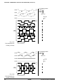
CHAPTER 4: PERIPHERAL CIRCUITS AND OPERATION (LCD Driver)
COM0
-VDD
-VL1
-VL2
-VL3
COM1
LCD lighting status
COM0
COM1
COM2
COM3
SEG0–25
COM2
Not lit
Lit
COM3
-VDD
-VL1
-VL2
-VL3
SEG
0–25
Fig. 4.6.1
Drive waveform for
Frame frequency
1/4 duty (1/3 bias)
I-36
EPSON
S1C6S2N7 TECHNICAL HARDWARE
CHAPTER 4: PERIPHERAL CIRCUITS AND OPERATION (LCD Driver)
COM0
-VDD
-VL1
-VL2
-VL3
LCD lighting status
COM0
COM1
COM2
COM1
SEG0–25
COM2
Not lit
Lit
COM3
-VDD
-VL1
-VL2
-VL3
SEG
0–25
Fig. 4.6.2
Drive waveform for
Frame frequency
1/3 duty (1/3 bias)
S1C6S2N7 TECHNICAL HARDWARE
EPSON
I-37
CHAPTER 4: PERIPHERAL CIRCUITS AND OPERATION (LCD Driver)
-VDD
-VL1
-VL2
-VL3
COM0
LCD lighting status
COM0
COM1
SEG0–25
COM1
Not lit
COM2
Lit
COM3
-VDD
-VL1
-VL2
-VL3
SEG
0–25
Fig. 4.6.3
Frame frequency
Drive waveform for
1/2 duty (1/3 bias)
I-38
EPSON
S1C6S2N7 TECHNICAL HARDWARE
CHAPTER 4: PERIPHERAL CIRCUITS AND OPERATION (LCD Driver)
-VDD
-VL1, L2
-VL3
COM0
COM1
LCD lighting status
COM0
COM1
COM2
COM3
SEG0–25
COM2
Not lit
COM3
Lit
-VDD
-VL1, L2
-VL3
SEG
0–25
Fig. 4.6.4
Drive waveform for
Frame frequency
1/4 duty (1/2 bias)
S1C6S2N7 TECHNICAL HARDWARE
EPSON
I-39
CHAPTER 4: PERIPHERAL CIRCUITS AND OPERATION (LCD Driver)
-VDD
-VL1, L2
-VL3
COM0
COM1
LCD lighting status
COM0
COM1
COM2
SEG0–25
COM2
Not lit
COM3
Lit
-VDD
-VL1, L2
-VL3
SEG
0–25
Fig. 4.6.5
Drive waveform for
Frame frequency
1/3 duty (1/2 bias)
-VDD
-VL1, L2
-VL3
COM0
COM1
LCD lighting status
COM0
COM1
SEG0–25
COM2
Not lit
COM3
Lit
-VDD
-VL1, L2
-VL3
SEG
0–25
Fig. 4.6.6
Drive waveform for
1/2 duty (1/2 bias)
I-40
Frame frequency
EPSON
S1C6S2N7 TECHNICAL HARDWARE
CHAPTER 4: PERIPHERAL CIRCUITS AND OPERATION (LCD Driver)
Switching between
dynamic and static
drive
The S1C6S2N7 Series allows software setting of the LCD
static drive. This function enables easy adjustment (cadence adjustment) of the oscillation frequency of the OSC
circuit.
The procedure for executing of the LCD static drive is as
follows:
➀ Write 1 to the CSDC register at address 0FBH D3.
➁ Write the same value to all registers corresponding to
COMs 0 through 3 of the display memory.
Note -
-
Even when l/3 duty is selected, the display data corresponding
to COM3 is valid for static drive. Hence, for static drive, set the
same value to all display memory corresponding to COMs 0
through 3.
For cadence adjustment, set the display data corresponding to
COMs 0 through 3, so that all the LCD segments go on.
Figure 4.6.7 shows the drive waveform for static drive.
LCD lighting status
-VDD
-VL1
-VL2
-VL3
COM
0–3
Frame frequency
COM0
COM1
COM2
COM3
SEG0–25
Not lit
Lit
-VDD
-VL1
-VL2
-VL3
SEG
0–25
-VDD
-VL1
-VL2
-VL3
Fig. 4.6.7
LCD static drive waveform
S1C6S2N7 TECHNICAL HARDWARE
EPSON
I-41
CHAPTER 4: PERIPHERAL CIRCUITS AND OPERATION (LCD Driver)
(1) Segment allocation
Mask option
(segment allocation)
As shown in Figure 4.l.1, the S1C6S2N7 Series display
data is decided by the display data written to the display
memory (write-only) at address 090H–0AFH.
The address and bits of the display memory can be made
to correspond to the segment pins (SEG0–SEG25) in any
combination through mask option. This simplifies design
by increasing the degree of freedom with which the liquid
crystal panel can be designed.
Figure 4.6.8 shows an example of the relationship between the LCD segments (on the panel) and the display
memory in the case of 1/3 duty.
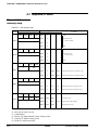
Address
Common 0
Common 1
Common 2
9A, D0
9B, D1
9B, D0
(a)
(f)
(e)
SEG11
9A, D1
9B, D2
9A, D3
(b)
(g)
(d)
SEG12
9D, D1
9A, D2
9B, D3
(f')
(c)
(p)
Data
D3
D2
D1
D0
09AH
d
c
b
a
09BH
p
g
f
e
09CH
d'
c'
b'
a'
09DH
p'
g'
f'
e'
SEG10
Display data memory allocation
Pin address allocation
a
a'
b
f
g'
g
e
c
c'
e'
p
d
SEG10
b'
f'
SEG11
p'
d'
SEG12
Common 0
Common 1
Fig. 4.6.8
Segment allocation
I-42
Common 2
EPSON
S1C6S2N7 TECHNICAL HARDWARE
CHAPTER 4: PERIPHERAL CIRCUITS AND OPERATION (LCD Driver)
(2) Drive duty
According to the mask option, either 1/4, 1/3 or 1/2
duty can be selected as the LCD drive duty.
Table 4.6.1 shows the differences in the number of segments according to the selected duty.
Table 4.6.1
Differences according to
selected duty
Note
Duty
Pins Used
in Common
Maximum Number
of Segments
Frame Frequency
(when fosc = 32 kHz)
1/4
1/3
1/2
COM0–3
COM0–2
COM0–1
104 (26 × 4)
78 (26 × 3)
52 (26 × 2)
32 Hz
42.7 Hz
32 Hz
In the S1C6S2A7 (fosc = 200 kHz), the frame frequencies for 1/
4, 1/3, 1/2 duty are 24.4 Hz, 32.6 Hz and 48.8 Hz, respectively.
(3) Output specification
➀ The segment pins (SEG0–SEG25) are selected by mask
option in pairs for either segment signal output or DC
output (VDD and VSS binary output). When DC output
is selected, the data corresponding to COM0 of each
segment pin is output.
➁ When DC output is selected, either complementary
output or Pch open drain output can be selected for
each pin by mask option.
Note
S1C6S2N7 TECHNICAL HARDWARE
The pin pairs are the combination of SEG (2*n) and SEG (2*n +
1) (where n is an integer from 0 to 12).
EPSON
I-43
CHAPTER 4: PERIPHERAL CIRCUITS AND OPERATION (LCD Driver)
Table 4.6.2 shows the control bits of the LCD driver and
their addresses. Figure 4.6.9 shows the display memory
map.
Control of LCD
driver
Table 4.6.2 Control bits of LCD driver
Address
Register
D2
D1
D3
CSDC
0
Name
SR
1
0
0
CSDC
0
Static
Dynamic
0
R
R/W
Comment
D0
LCD drive switch
0
0FBH
0
0
Address
Fig. 4.6.9
Display
090
memory map
0A0
0
1
2
3
4
5
6
7
8
9
A
B
C
D
E
F
Display memory (Write only)
32 words x 4 bits
CSDC LCD drive switch (0FBH D3)
The LCD drive format can be selected with this switch.
When 1 is written:
When 0 is written:
Reading:
Static drive
Dynamic drive
Valid
After an initial reset, dynamic drive (CSDC = 0) is selected.
Display memory (090H–0AFH)
The LCD segments are turned on or off according to this
data.
When 1 is written:
When 0 is written:
Reading:
On
Off
Invalid
By writing data into the display memory allocated to the
LCD segment (on the panel), the segment can be turned on
or off. After an initial reset, the contents of the display
memory are undefined.
I-44
EPSON
S1C6S2N7 TECHNICAL HARDWARE
CHAPTER 4: PERIPHERAL CIRCUITS AND OPERATION (Clock Timer)
4.7 Clock Timer
Configuration of
clock timer
The S1C6S2N7 Series has a built-in clock timer driven by
the source oscillator. The clock timer is configured as a
seven-bit binary counter that serves as a frequency divider
taking a 256 Hz source clock from the oscillation circuit.
The four high-order bits (16 Hz–2 Hz) can be read by the
software.
The frequencies described in this section, such as timer data
and interrupt signals, are the values when the OSC
oscillation frequency is 32.768 kHz. When CR oscillator
(typ. 65 kHz) is used as the OSC oscillation circuit, each
timer frequency becomes "CR oscillation frequency/32,768".
In the S1C6S2A7, the clock timer cannot be used.
Figure 4.7.1 is the block diagram of the clock timer.
Data bus
OSC
(oscillation circuit)
256 Hz
16 Hz–2 Hz
32 Hz, 8 Hz, 2 Hz
Fig. 4.7.1
Block diagram of
clock timer
128 Hz–32 Hz
Clock timer reset signal
Interrupt
control
Interrupt
request
Normally, this clock timer is used for all kinds of timing
purpose, such as clocks.
S1C6S2N7 TECHNICAL HARDWARE
EPSON
I-45
CHAPTER 4: PERIPHERAL CIRCUITS AND OPERATION (Clock Timer)
Interrupt function
Address
0E4H
The clock timer can interrupt on the falling edge of the 32
Hz, 8 Hz, and 2 Hz signals. The software can mask any of
these interrupt signals.
Figure 4.7.2 is the timing chart of the clock timer.
Register
Frequency
bits
D0
16 Hz
D1
8 Hz
D2
4 Hz
D3
2 Hz
Clock timer timing chart
Occurrence of
32 Hz interrupt request
Occurrence of
8 Hz interrupt request
Occurrence of
2 Hz interrupt request
Fig. 4.7.2 Timing chart of the clock timer
As shown in Figure 4.7.2, an interrupt is generated on the
falling edge of the 32 Hz, 8 Hz, and 2 Hz frequencies. When
this happens, the corresponding interrupt event flag (IT32,
IT8, IT2) is set to 1. Masking the separate interrupts can be
done with the interrupt mask register (EIT32, EIT8, EIT2).
However, regardless of the interrupt mask register setting,
the interrupt event flags will be set to 1 on the falling edge of
their corresponding signal (e.g. the falling edge of the 2 Hz
signal sets the 2 Hz interrupt factor flag to 1).
Note Write to the interrupt mask register (EIT32, EIT8, EIT2) only in the
DI status (interrupt flag = 0). Otherwise, it may cause malfunction.
I-46
EPSON
S1C6S2N7 TECHNICAL HARDWARE
CHAPTER 4: PERIPHERAL CIRCUITS AND OPERATION (Clock Timer)
Table 4.7.1 shows the clock timer control bits and their
addresses.
Control of clock
timer
Table 4.7.1 Control bits of clock timer
Address
D3
Register
D2
D1
TM3
TM2
TM1
Comment
D0
Name
SR
1
0
TM0
TM3
–
High
Low
Timer data (clock timer 2 Hz)
TM2
–
High
Low
Timer data (clock timer 4 Hz)
TM1
–
High
Low
Timer data (clock timer 8 Hz)
TM0
–
High
Low
Timer data (clock timer 16 Hz)
EIT2
0
Enable
Mask
Interrupt mask register (clock timer 2 Hz)
EIT8
0
Enable
Mask
Interrupt mask register (clock timer 8 Hz)
EIT32
0
Enable
Mask
Interrupt mask register (clock timer 32 Hz)
IT2
0
Yes
No
Interrupt factor flag (clock timer 2 Hz)
IT8
0
Yes
No
Interrupt factor flag (clock timer 8 Hz)
IT32
0
Yes
No
Interrupt factor flag (clock timer 32 Hz)
TMRST
Reset
Reset
–
Clock timer reset
SWRUN
0
Run
Stop
SWRST
Reset
Reset
–
R
0E4H
0
EIT2
EIT8
R
EIT32
R/W
0
0EBH
0
IT2
IT8
IT32
R
0
0EFH
0
TMRST
R
W
SWRUN SWRST
R/W
W
0
0F9H
Stopwatch timer RUN/STOP
Stopwatch timer reset
TM0–TM3 Timer data (0E4H)
The l6 Hz to 2 Hz timer data of the clock timer can be read
from this register. These four bits are read-only, and write
operations are invalid.
After an initial reset, the timer data is initialized to 0H.
S1C6S2N7 TECHNICAL HARDWARE
EPSON
I-47
CHAPTER 4: PERIPHERAL CIRCUITS AND OPERATION (Clock Timer)
EIT32, EIT8, EIT2 Interrupt mask registers (0EBH D0–D2)
These registers are used to mask the clock timer interrupt.
When 1 is written: Enabled
When 0 is written: Masked
Reading:
Valid
The interrupt mask register bits (EIT32, EIT8, EIT2) mask
the corresponding interrupt frequencies (32 Hz, 8 Hz, 2 Hz).
After an initial reset, these registers are all set to 0.
IT32, IT8, IT2 Interrupt factor flags (0EFH D0–D2)
These flags indicate the status of the clock timer interrupt.
When 1 is read:
When 0 is read:
Writing:
Interrupt has occurred
Interrupt has not occurred
Invalid
The interrupt factor flags (IT32, IT8, IT2) correspond to the
clock timer interrupts (32 Hz, 8 Hz, 2 Hz). The software can
determine from these flags whether there is a clock timer
interrupt. However, even if the interrupt is masked, the
flags are set to 1 on the falling edge of the signal. These
flags can be reset when the register is read by the software.
Reading of interrupt factor flags is available at EI, but be
careful in the following cases.
If the interrupt mask register value corresponding to the
interrupt factor flags to be read is set to 1, an interrupt
request will be generated by the interrupt factor flags set
timing, or an interrupt request will not be generated. Be
very careful when interrupt factor flags are in the same
address.
After an initial reset, these flags are set to 0.
TMRST Clock timer reset (0F9H D2)
This bit resets the clock timer.
When 1 is written: Clock timer reset
When 0 is written: No operation
Reading:
Always 0
The clock timer is reset by writing 1 to TMRST. The clock
timer starts immediately after this. No operation results
when 0 is written to TMRST.
This bit is write-only, and so is always 0 when read.
I-48
EPSON
S1C6S2N7 TECHNICAL HARDWARE
CHAPTER 4: PERIPHERAL CIRCUITS AND OPERATION (Stopwatch Timer)
4.8 Stopwatch Timer
Configuration of
stopwatch timer
The S1C6S2N7 Series incorporates a 1/100 sec and 1/10
sec stopwatch timer. The stopwatch timer is configured as a
two-stage, four-bit BCD timer serving as the clock source for
an approximately 100 Hz signal (obtained by approximately
dividing the 256 Hz source clock from the oscillation circuit).
Data can be read out four bits at a time by the software.
When CR oscillator (typ. 65 kHz) is used as the OSC
oscillation circuit, each timer frequency becomes "CR
oscillation frequency/32,768".
In the S1C6S2A7, the stopwatch timer cannot be used.
Figure 4.8.1 is the block diagram of the stopwatch timer.
Data bus
OSC
(oscillation circuit)
SWL timer
SWH timer
10 Hz, 1 Hz
Fig. 4.8.1
Block diagram of
stopwatch timer
10 Hz
256 Hz
Stopwatch timer reset signal
Stopwatch timer RUN/STOP signal
Interrupt
control
Interrupt
request
The stopwatch timer can be used separately from the clock
timer. In particular, digital stopwatch functions can be
easily realized by software.
S1C6S2N7 TECHNICAL HARDWARE
EPSON
I-49
CHAPTER 4: PERIPHERAL CIRCUITS AND OPERATION (Stopwatch Timer)
Count-up pattern
The stopwatch timer is configured as two four-bit BCD
timers, SWL and SWH. The SWL timer, at the stage preceding the stopwatch timer, has an approximate l00 Hz signal
as its input clock. It counts up every 1/100 sec and generates an approximate 10 Hz signal. The SWH timer has an
approximate 10 Hz signal generated by the SWL timer for its
input clock. It counts up every 1/10 sec and generates a 1
Hz signal.
Figure 4.8.2 shows the count-up pattern of the stopwatch
timer.
SWH count-up pattern
SWH count value
Counting time (S)
0
1
2
3
4
5
6
7
8
9
0
26 26 25 25 26 26 25 25 26 26
256 256 256 256 256 256 256 256 256 256
26 x 6 + 25 x 4 = 1 (S)
256
256
1 Hz
signal
generation
SWL count-up pattern 1
SWL count value
Counting time (S)
0
1
2
3
4
5
6
7
8
9
0
3
2
3
2
3
2
3
2
3
2
256 256 256 256 256 256 256 256 256 256
25
256 (S)
Approximate
10 Hz
signal
generation
SWL count-up pattern 2
SWL count value
Counting time (S)
0
1
2
3
4
5
6
7
8
9
0
3
3
3
2
3
2
3
2
3
2
256 256 256 256 256 256 256 256 256 256
Fig. 4.8.2
26 (S)
256
Count-up pattern of
stopwatch timer
Approximate
10 Hz
signal
generation
SWL generates an approximate 10 Hz signal from the 256
Hz based signal. The count-up intervals are 2/256 sec and
3/256 sec, so that two final patterns are generated: a 25/
256 sec interval and a 26/256 sec interval. Consequently,
the count-up intervals are 2/256 sec and 3/256 sec, which
do not amount to an accurate 1/100 sec. SWH counts the
approximate 10 Hz signals generated by the 25/256 sec and
26/256 sec intervals in the ratio of 4:6 to generate a l Hz
signal. The count-up intervals are 25/256 sec and 26/256
sec, which do not amount to an accurate 1/10 sec.
I-50
EPSON
S1C6S2N7 TECHNICAL HARDWARE
CHAPTER 4: PERIPHERAL CIRCUITS AND OPERATION (Stopwatch Timer)
The 10 Hz (approximate 10 Hz) and 1 Hz interrupts can be
generated by the overflow of the SWL and SWH stopwatch
timers, respectively. Also, software can separately mask the
frequencies as described earlier.
Figure 4.8.3 is the timing chart for the stopwatch timer.
Interrupt function
Register
bits
Address
Stopwatch timer (SWL) timing chart
D0
0E2H
(1/100 sec BCD)
D1
D2
D3
Occurrence of
10 Hz interrupt request
Register
bits
Address
Stopwatch timer (SWH) timing chart
D0
0E3H
(1/10 sec BCD)
Fig. 4.8.3
Timing chart for
stopwatch timer
D1
D2
D3
Occurrence of
1 Hz interrupt request
As shown in Figure 4.8.3, the interrupts are generated by
the overflow of the respective timers (9 changing to 0). Also
when this happens, the corresponding interrupt factor flags
(ISW0, ISW1) are set to 1. The respective interrupts can be
masked separately with the interrupt mask registers
(EISW0, EISW1). However, regardless of the setting of the
interrupt mask registers, the interrupt factor flags are set to
1 by the overflow of the corresponding timers.
Note Write to the interrupt mask registers (EISW0, EISW1) only in the DI
status (interrupt flag = 0). Otherwise, it may cause malfunction.
S1C6S2N7 TECHNICAL HARDWARE
EPSON
I-51
CHAPTER 4: PERIPHERAL CIRCUITS AND OPERATION (Stopwatch Timer)
Control of stopwatch Table 4.8.1 shows the stopwatch timer control bits and their
addresses.
timer
Table 4.8.1 Stopwatch timer control bits
Address
Register
D2
D1
D3
SWL3
SWL2
SWL1
Name
SR
SWL0
SWL3
0
MSB
SWL2
0
Stopwatch timer
1/100 sec (BCD)
SWL1
0
SWL0
0
LSB
SWH3
0
MSB
SWH2
0
Stopwatch timer
1/10 sec (BCD)
SWH1
0
SWH0
0
R
1
0
0E2H
SWH3
SWH2
SWH1
SWH0
R
0E3H
0
0
EISW1
EISW0
LSB
0
0
R/W
R
Comment
D0
0EAH
0
0
ISW1
ISW0
EISW1
0
Enable
Mask
Interrupt mask register (stopwatch 1 Hz)
EISW0
0
Enable
Mask
Interrupt mask register (stopwatch 10 Hz)
ISW1
0
Yes
No
Interrupt factor flag (stopwatch 1 Hz)
ISW0
0
Yes
No
Interrupt factor flag (stopwatch 10 Hz)
TMRST
Reset
Reset
–
Clock timer reset
SWRUN
0
Run
Stop
SWRST
Reset
Reset
–
0
0
R
0EEH
0
TMRST
R
W
SWRUN SWRST
R/W
W
0
0F9H
I-52
EPSON
Stopwatch timer RUN/STOP
Stopwatch timer reset
S1C6S2N7 TECHNICAL HARDWARE
CHAPTER 4: PERIPHERAL CIRCUITS AND OPERATION (Stopwatch Timer)
SWL0–SWL3 1/100 sec stopwatch timer (0E2H)
Data (BCD) of the 1/100 sec column of the stopwatch timer
can be read. These four bits are read-only, and cannot be
written to.
After an initial reset, the timer data is set to 0H.
SWH0–SWH3 1/10 sec stopwatch timer (0E3H)
Data (BCD) of the 1/10 sec column of the stopwatch timer
can be read. These four bits are read-only, and cannot be
written to.
After an initial reset, the timer data is set to 0H.
EISW0, EISW1 Interrupt mask register (0EAH D0 and D1)
These registers mask the stopwatch timer interrupt.
When 1 is written: Enabled
When 0 is written: Masked
Reading:
Valid
The interrupt mask register bits (EISW0, EISW1) are used to
mask the 10 Hz and 1 Hz interrupts, respectively.
After an initial reset, these registers are both set to 0.
ISW0, ISW1 Interrupt factor flags (0EEH D0 and D1)
These flags indicate the status of the stopwatch timer interrupt.
When 1 is read:
When 0 is read:
Writing:
Interrupt has occurred
Interrupt has not occurred
Invalid
The interrupt factor flags (ISW0, ISW1) correspond to the 10
Hz and 1 Hz interrupts, respectively. With these flags, the
software can determine whether a stopwatch timer interrupt
has occurred. However, regardless of the interrupt mask
register setting, these flags are set to 1 by the timer overflow.
They are reset when the register is read by the software.
Reading of interrupt factor flags is available at EI, but be
careful in the following cases.
If the interrupt mask register value corresponding to the
interrupt factor flags to be read is set to 1, an interrupt
request will be generated by the interrupt factor flags set
timing, or an interrupt request will not be generated.
Be very careful when interrupt factor flags are in the same
address.
After an initial reset, these flags are set to 0.
S1C6S2N7 TECHNICAL HARDWARE
EPSON
I-53
CHAPTER 4: PERIPHERAL CIRCUITS AND OPERATION (Stopwatch Timer)
SWRST Stopwatch timer reset (0F9H D0)
This bit resets the stopwatch timer.
When 1 is written: Stopwatch timer reset
When 0 is written: No operation
Reading:
Always 0
The stopwatch timer is reset when 1 is written to SWRST.
When the stopwatch timer is reset while running, operation
restarts immediately. Also, while stopped, the reset data is
maintained.
This bit is write-only, and is always 0 when read.
SWRUN Stopwatch timer run/stop (0F9H D1)
This bit controls run/stop of the stopwatch timer.
When 1 is written: Run
When 0 is written: Stop
Reading:
Valid
The stopwatch timer runs when 1 is written to SWRUN, and
stops when 0 is written.
When stopped, the timer data is maintained until the timer
next Run or is reset. Also, when the timer runs after being
stopped, the data that was maintained can be used to resume the count.
If the timer data is read while running, a correct read may
be impossible because of the carry from the low-order bit
(SWL) to the high-order bit (SWH). This occurs if reading
has extended over the SWL and SWH bits when the carry
occurs. To prevent this, read after stopping, and then
continue running. Also, the stopped duration must be
within 976 µs (256 Hz, 1/4 cycle).
After an initial reset, this register is set to 0.
I-54
EPSON
S1C6S2N7 TECHNICAL HARDWARE
CHAPTER 4: PERIPHERAL CIRCUITS AND OPERATION (SVD Circuit and Heavy Load Protection Function)
4.9 Supply Voltage Detection (SVD) Circuit and
Heavy Load Protection Function
Configuration of SVD
circuit and heavy
load protection
function
The S1C6S2N7 Series has a built-in supply voltage detection
(SVD) circuit and a heavy load protection function. Figure
4.9.1 shows the configuration of the circuit.
SVD circuit
The SVD circuit monitors the conditions of the supply
voltage (battery voltage), and software can check whether the
supply voltage has dropped below the detecting voltage level
of the SVD circuit: 2.4 V for the S1C6S2N7/S1C6S2A7
(supply voltage is 3.0 V), or l.2 V for the S1C6S2L7/
S1C6S2B7 (1.5 V). Registers SVDON (SVD control on/off)
and SVDDT (SVD data) are used for the SVD circuit. The
software can turn SVD operation on and off. When SVD is
on, the IC draws a large current, so keep SVD off unless it is.
Since supply voltage detection is automatically performed by
the hardware every 2 Hz (0.5 sec) when the heavy load
protection function operates, do not permit the operation of
the SVD circuit by the software in order to minimize power
current consumption.
Heavy load protection function
Note that the heavy load protection function on the
S1C6S2L7/S1C6S2B7 are different from the S1C6S2N7/
S1C6S2A7.
(1) In case of S1C6S2L7/S1C6S2B7
The S1C6S2L7/S1C6S2B7 have the heavy load protection function for when the battery load becomes heavy
and the source voltage drops, such as when an external
buzzer sounds or an external lamp lights. The state
where the heavy load protection function is in effect is
called the heavy load protection mode. In this mode,
operation with a lower voltage than normal is possible.
The normal mode changes to the heavy load protection
mode in the following two cases:
➀ When the software changes the mode to the heavy load
protection mode (HLMOD = 1)
➁ When supply voltage drop (SVDDT = 1) in the SVD
circuit is detected, the mode will automatically shift to
the heavy load protection mode until the supply voltage is recovered (SVTDT = 0)
S1C6S2N7 TECHNICAL HARDWARE
EPSON
I-55
CHAPTER 4: PERIPHERAL CIRCUITS AND OPERATION (SVD Circuit and Heavy Load Protection Function)
In the heavy load protection mode, the internally regulated voltage is generated by the liquid crystal driver
source output VL2 so as to operate the internal circuit.
Consequently, more current is consumed in the heavy
load protection mode than in the normal mode. Unless it
is necessary, be careful not to set the heavy load protection mode with the software. Also, to reduce current
consumption, do not set the SVDON to ON in the heavy
load protection mode.
Note that in S1C6S2L7/S1C6S2B7, the range of
operating voltage differs during CR oscillation and during
crystal oscillation.
(2) In case of S1C6S2N7/S1C6S2A7
The S1C6S2N7/S1C6S2A7 have the heavy load protection function for when the battery load becomes heavy
and the source voltage changes, such as when an external buzzer sounds or an external lamp lights. The state
where the heavy load protection function is in effect is
called the heavy load protection mode. Compared with
the normal operation mode, this mode can reduce the
output voltage variation of the constant voltage or voltage
booster of the LCD system.
The normal mode changes to the heavy load protection
mode in the following case:
• When the software changes the mode to the heavy load
protection mode (HLMOD = 1)
The heavy load protection mode switches the constant
voltage circuit of the LCD system to the high-stability
mode from the low current consumption mode. Consequently, more current is consumed in the heavy load
protection mode than in the normal mode. Unless it is
necessary, be careful not to set the heavy load protection
mode with the software.
VDD
VDD
Regurated
voltage circuit
SVD
circuit
VS1
VL1
VSS
Fig. 4.9.1
Configuration of SVD and
VSS
SVDDT
SVDON
heavy load protection circuits
I-56
HLMOD
EPSON
D3
D1
D0
Data bus
Address 0FAH
SVD sampling
control
S1C6S2N7 TECHNICAL HARDWARE
CHAPTER 4: PERIPHERAL CIRCUITS AND OPERATION (SVD Circuit and Heavy Load Protection Function)
Operation of SVD
detection timing
The following explains the timing when the SVD circuit
writes the result of supply voltage detection to the SVDDT
register.
The result of supply voltage detection is written to the
SVDDT register by the SVD circuit, and this data can be
read by the software to determine the supply voltage.
There are two methods, explained below, for executing the
detection by the SVD circuit.
(1) Sampling with HLMOD set to 1
When HLMOD is set to 1 and SVD sampling is executed,
the detection results can be written to the SVDDT register
with the following timing:
Immediately after sampling with the 2 Hz cycle output by
the oscillation circuit while HLMOD = 1 (sampling time is
122 µs in the case of fosc = 32.768 kHz).
Consequently, after HLMOD has been set to 1, the new
detection result is written in a 2 Hz.
(2) Sampling with SVDON set to 1
When SVDON is set to 1, SVD detection is executed. As
soon as SVDON is reset to 0, the result is loaded to in the
SVDDT register. To obtain a stable SVD detection result,
the SVD circuit must be on for at least l00 µs. So, to
obtain the SVD detection result, follow the programming
sequence below.
➀
➁
➂
➃
Set SVDON to 1
Maintain for 100 µs minimum
Set SVDON to 0
Read SVDDT
However, at 32 kHz for the S1C6S2N7, S1C6S2A7,
S1C6S2L7 and S1C6S2B7, the instruction cycles are long
enough, so there is no need to worry about maintaining
100 µs for SVDON = 1 in the software.
Notice that even if the SVD circuit detects a drop in the
supply voltage (l.2 V/2.4 V or less) and invokes the heavy
load protection mode, this will be the same as when the
software invokes the heavy load protection mode, in that the
SVD circuit will be sampled with a timing synchronized to
the 2 Hz output from the prescaler. If the SVD circuit
detects a voltage drop and enters the heavy load protection
mode, it will return to the normal mode once the supply
voltage recovers and the SVD circuit determines that the
supply voltage is l.2 V/2.4 V or more.
S1C6S2N7 TECHNICAL HARDWARE
EPSON
I-57
CHAPTER 4: PERIPHERAL CIRCUITS AND OPERATION (SVD Circuit and Heavy Load Protection Function)
Operation of heavy
load protection
function
The S1C6S2N7 Series has a heavy load protection function
for when the battery load becomes heavy and the supply
voltage drops, such as when a melody is played or an
external lamp lights. This functions works in the heavy load
protection mode.
(1) In cace of S1C6S2L7/S1C6S2B7
The normal mode changes to the heavy load protection
mode in the following two cases:
➀ When the software changes the mode to the heavy load
protection mode
➁ When the SVD circuit detects a supply voltage less
than l.2 V ± 0.10 V, in which case the mode is automatically changed to the heavy load protection mode
(2) In case of S1C6S2N7/S1C6S2A7
The normal mode changes to the heavy load protection
mode in the following case:
• When the software changes the mode to the heavy load
protection mode (HLMOD = 1)
Based on the operation of the SVD circuit and the heavy
load protection function, the S1C6S2L7/S1C6S2B7 obtains
an operation supply voltage as low as 0.9 V. See the
electrical characteristics for the precision of voltage
detection by the SVD circuit.
In the heavy load protection mode, the internally regulated
voltage is generated by the liquid crystal driver supply
output, VL2, in order to operate the internal circuit
(S1C6S2L7/S1C6S2B7). Consequently, more current is
consumed in the heavy load protection mode than in the
normal mode. Unless necessary, do not select the heavy
load protection mode with the software.
Note Activation of the SVD circuit by software in the heavy load protection mode causes a malfunction. Avoid such activation if possible.
I-58
EPSON
S1C6S2N7 TECHNICAL HARDWARE
CHAPTER 4: PERIPHERAL CIRCUITS AND OPERATION (SVD Circuit and Heavy Load Protection Function)
Table 4.9.1 shows the control bits and their addresses for
the SVD circuit and the heavy load protection function.
Control of SVD circuit and heavy load
protection function
Table 4.9.1 Control bits for SVD circuit and heavy load protection function
Address
D3
HLMOD
R/W
Register
D2
D1
0
SVDDT
R
D0
Name
SR
1
0
SVDON
HLMOD
0
Heavy
load
Normal
load
R/W
0
0FAH
SVDDT
0
Supply
voltage
low
Supply
voltage
normal
SVDON
0
ON
OFF
Comment
Heavy load protection mode register
Supply voltage detection data
Supply voltage detection ON/OFF
HLMOD Heavy load protection mode on/off (0FAH D3)
When 1 is written: Heavy load protection mode on
When 0 is written: Heavy load protection mode off
Reading:
Valid
When HLMOD is set to 1, the IC enters the heavy load
protection mode, and sampling control is executed for the
time the SVD circuit is on. The sampling timing is as follows:
Sampling in cycles of 2 Hz output by the oscillation circuit
while HLMOD = 1 (sampling time is 122 µs in the case of
fosc = 32.768 kHz).
When SVD sampling is done with HLMOD set to 1, the
results are written to the SVDDT register with the as following timing:
Immediately on completion of sampling in cycles of 2 Hz
output by the oscillation circuit while HLMOD = 1.
Consequently, after HLMOD is set to 1, the new detected
result is written in 2 Hz.
In the heavy load protection mode, the consumed current
becomes larger. Unless necessary, do not select the heavy
load protection mode with the software.
S1C6S2N7 TECHNICAL HARDWARE
EPSON
I-59
CHAPTER 4: PERIPHERAL CIRCUITS AND OPERATION (SVD Circuit and Heavy Load Protection Function)
SVDON SVD control on/off (0FAH D0)
When 0 is written: SVD detection off
When 1 is written: SVD detection on
Reading:
Valid
When this bit is written, the SVD detection on/off operation
is controlled. Large current is drawn during SVD detection,
so keep SVD detection off except when necessary. When
SVDON is set to 1, SVD detection is executed. As soon as
SVDON is reset to 0, the detected result is loaded into the
SVDDT register.
SVDDT SVD data (0FAH D1)
When 0 is read:
When 1 is read:
Supply voltage ≥ Criteria voltage
Supply voltage < Criteria voltage
When SVDDT is 1, the S1C6S2N7 enters the heavy load
protection mode. In this mode, the detection operation of
the SVD circuit is sampled in 2 Hz cycles and the respective
detection results are written to the SVDDT register.
I-60
EPSON
S1C6S2N7 TECHNICAL HARDWARE
CHAPTER 4: PERIPHERAL CIRCUITS AND OPERATION (Stepping Motor Driver)
4.10 Stepping Motor Driver
Configuration of
motor driver
The S1C6S2N7 Series has a built-in stepping motor driver
that is suitable for combination watches with low power
consumption.
Figure 4.10.1 shows the configuration of the motor driver.
F 4 kHz
Data bus
FTRG
FRUN
Stepping
motor
control circuit
Frequency
divider
A02
SMD circuit
ON
Output
control
circuit
Timing
clock
ISMD
Interrupt
control circuit
EISMD
FRUN
Timing
generator
A01
Timing
signal
Interruput request
Fig. 4.10.1
Configuration of
motor driver
S1C6S2N7 TECHNICAL HARDWARE
EPSON
I-61
CHAPTER 4: PERIPHERAL CIRCUITS AND OPERATION (Stepping Motor Driver)
By writing 1 to the FTRG register (address 0FEH D1), the
stepping motor drive pulse PF can be output.
The PF pulse width is selectable in 0.244 msec steps within
the range of 1.46 msec to 7.08 msec. Thus it is possible to
rotate the hands of a watch in a maximum 78 Hz.
The A01 and A02 terminals output the drive pulse PF
alternately with every 1 written to the FTRG register. The
first drive pulse after system reset is output from the A01
terminal.
Drive pulse
11.7 ms (1 sequence)
Max. 1.0 ms
FTRG
3.9 ms
PF
A01 or A02
Fig. 4.10.2
Timing chart
1.46 ms
7.08 ms
Mask option
The mask option for the motor driver enables selection of
the drive pulse (PF) width.
The drive pulse width can be selected in 0.244 msec steps
within the range of 1.464 msec to 7.076 msec.
Interrupt function
The motor driver generates an interrupt when it has finished
a pulse output sequence.
An output sequence begins within 1 msec after 1 is written
to the FTRG register and takes 11.7 msec to end. When the
sequence has finished, the interrupt factor flag (ISMD) is set
to 1 and an interrupt occurs.
The interrupt can be masked by the interrupt mask register
(EISMD). However, the interrupt factor flag is set to 1 after
a sequence is finished regardless of the interrupt mask
register setting.
Note Write to the interrupt mask register (EISMD) only in the DI status
(interrupt flag = 0). Otherwise, it may cause malfunction.
I-62
EPSON
S1C6S2N7 TECHNICAL HARDWARE
CHAPTER 4: PERIPHERAL CIRCUITS AND OPERATION (Stepping Motor Driver)
Table 4.10.1 shows the motor driver control bits and their
addresses.
Control of motor
driver
Table 4.10.1 Motor driver control bits
Address
Register
D2
D1
D3
0
0
0
R
D0
Name
EISMD
0 *5
R/W
0 *5
SR *1
1
Comment
0
0E9H
0 *5
EISMD
0
0
0
ISMD
Interrupt mask register (motor driver)
0 *5
0 *5
R
0ECH
0 *5
0
Yes
No
FRUN
0
Run
Stop
Motor driver status (reading)
FTRG
–
Start
–
Motor driver trigger (writing)
ISMD
0
0
R
0FEH
FRUN
FTRG
R
W
0
R
0
0
0
Interrupt factor flag (motor driver)
*5
*5
*5
EISMD Interrupt mask register (0E9H D0)
This register is used to mask the motor driver interrupt.
When 1 is written: Enabled
When 0 is written: Masked
Reading:
Valid
After an initial reset, this register is set to 0.
S1C6S2N7 TECHNICAL HARDWARE
EPSON
I-63
CHAPTER 4: PERIPHERAL CIRCUITS AND OPERATION (Stepping Motor Driver)
ISMD Interrupt factor flag (0ECH D0)
This is the flag that indicates a motor driver interrupt.
When 1 is read:
When 0 is read:
Writing:
Interrupt has occurred
Interrupt has not occurred
Invalid
The software can determine from this flag whether there is a
motor driver interrupt. However, this flag is set to 1 after a
motor drive sequence is finished even if the interrupt has
been masked.
This flag is reset when the software has read it.
Reading of interrupt factor flag is available at EI, but be
careful in the following cases.
If the interrupt mask register value corresponding to the
interrupt factor flag to be read is set to 1, an interrupt
request will be generated by the interrupt factor flag set
timing, or an interrupt request will not be generated.
After an initial reset, this flag is set to 0.
FRUN, FTRG PF pulse drive status/trigger (0FEH D1)
This bit is used as the PF pulse drive trigger and as the drive
status indicator.
When
When
When
When
1
0
1
0
is
is
is
is
written:
written:
read:
read:
PF pulse drive trigger
No operation
PF pulse drive status RUN state
PF pulse drive status STOP state
Note that the function of this bit is different at reading and
writing.
When 1 is written to this bit, it functions as the PF pulse
drive trigger to start a pulse output. When this bit is read,
the read content indicates the PF pulse drive status.
After an initial reset, FRUN is set to 0.
I-64
EPSON
S1C6S2N7 TECHNICAL HARDWARE
CHAPTER 4: PERIPHERAL CIRCUITS AND OPERATION (Interrupt and HALT)
4.11 Interrupt and HALT
The S1C6S2N7 Series provides the following interrupt settings, each of which is maskable.
External interrupt:
Internal interrupt:
Input interrupt (one)
Timer interrupt (one)
Stopwatch interrupt (one)
Motor driver interrupt (one)
To enable interrupts, the interrupt flag must be set to 1 (EI)
and the necessary related interrupt mask registers must be
set to 1 (enable). When an interrupt occurs, the interrupt
flag is automatically reset to 0 (DI) and interrupts after that
are inhibited.
When a HALT instruction is input, the CPU operating clock
stops and the CPU enters the halt state. The CPU is reactivated from the halt state when an interrupt request occurs.
Figure 4.11.1 shows the configuration of the interrupt
circuit.
S1C6S2N7 TECHNICAL HARDWARE
EPSON
I-65
CHAPTER 4: PERIPHERAL CIRCUITS AND OPERATION (Interrupt and HALT)
Interrupt vector
(MSB)
ISMD
:
Program counter of CPU
(four low-order bits)
EISMD
:
K00
(LSB)
EIK00
K01
INT
(Interrupt request)
EIK01
IK0
K02
Interrupt flag
EIK02
K03
EIK03
ISW0
EISW0
ISW1
EISW1
IT2
Interrupt factor flag
EIT2
Interrupt mask register
IT8
EIT8
IT32
EIT32
Fig. 4.11.1 Configuration of interrupt circuit
I-66
EPSON
S1C6S2N7 TECHNICAL HARDWARE
CHAPTER 4: PERIPHERAL CIRCUITS AND OPERATION (Interrupt and HALT)
Table 4.11.1 shows the factors that generate interrupt
requests.
Interrupt factors
The interrupt factor flags are set to 1 depending on the
corresponding interrupt factors.
The CPU is interrupted when the following two conditions
occur and an interrupt factor flag is set to 1.
• The corresponding mask register is 1 (enabled)
• The interrupt flag is 1 (EI)
The interrupt factor flag is a read-only register, but can be
reset to 0 when the register data is read.
After an initial reset, the interrupt factor flags are reset to 0.
Note Reading of interrupt factor flags is available at EI, but be careful in
the following cases.
If the interrupt mask register value corresponding to the interrupt
factor flags to be read is set to 1, an interrupt request will be
generated by the interrupt factor flags set timing, or an interrupt
request will not be generated. Be very careful when interrupt factor
flags are in the same address.
Table 4.11.1
Interrupt factors
Interrupt Factor
Clock timer 2 Hz falling edge
IT2
(0EFH D2)
Clock timer 8 Hz falling edge
IT8
(0EFH D1)
Clock timer 32 Hz falling edge
IT32
(0EFH D0)
ISW1
(0EEH D1)
ISW0
(0EEH D0)
IK0
(0EDH D0)
ISMD
(0ECH D0)
Stopwatch timer
1 Hz falling edge
Stopwatch timer
10 Hz falling edge
Input data (K00–K03)
rising edge
Motor driver
a sequence completion
S1C6S2N7 TECHNICAL HARDWARE
Interrrupt Factor Flag
EPSON
I-67
CHAPTER 4: PERIPHERAL CIRCUITS AND OPERATION (Interrupt and HALT)
Specific masks and
factor flags for interrupt
Table 4.11.2
Interrupt mask registers and
interrupt factor flags
The interrupt factor flags can be masked by the corresponding interrupt mask registers. The interrupt mask registers
are read/write registers. They are enabled (interrupt enabled) when 1 is written to them, and masked (interrupt
disabled) when 0 is written to them. After an initial reset,
the interrupt mask register is set to 0.
Table 4.11.2 shows the correspondence between interrupt
mask registers and interrupt factor flags.
Interrupt Mask Register
Interrrupt Factor Flag
EIT2
(0EBH D2)
IT2
(0EFH D2)
EIT8
(0EBH D1)
IT8
(0EFH D1)
EIT32
(0EBH D0)
IT32
(0EFH D0)
EISW1
(0EAH D1)
ISW1
(0EEH D1)
EISW0
(0EAH D0)
ISW0
(0EEH D0)
EIK03*
(0E8H D3)
EIK02*
(0E8H D2)
EIK01*
(0E8H D1)
IK0
(0EDH D0)
EIK00*
(0E8H D0)
EISMD
(0E9H D0)
ISMD
(0ECH D0)
* There is an interrupt mask register for each input port pin.
I-68
EPSON
S1C6S2N7 TECHNICAL HARDWARE
CHAPTER 4: PERIPHERAL CIRCUITS AND OPERATION (Interrupt and HALT)
When an interrupt request is input to the CPU, the CPU
begins interrupt processing. After the program being executed is suspended, interrupt processing is executed in the
following order:
Interrupt vectors
➀ The address data (value of the program counter) of the
program step to be executed next is saved on the stack
(RAM).
➁ The interrupt request causes the value of the interrupt
vector (page 1, 01H–0FH) to be loaded into the program
counter.
➂ The program at the specified address is executed (execution of interrupt processing routine).
Note The processing in steps 1 and 2, above, takes 12 cycles of the
CPU system clock.
S1C6S2N7 TECHNICAL HARDWARE
EPSON
I-69
CHAPTER 4: PERIPHERAL CIRCUITS AND OPERATION (Interrupt and HALT)
Tables 4.11.4 (a) and (b) shows the interrupt control bits
and their addresses.
Control of interrupt
Table 4.11.4 (a) Interrupt control bits (1)
Address
Register
D2
D1
D3
EIK03
EIK02
EIK01
D0
Name
EIK00
EIK03
R/W
SR *1
Comment
1
0
0
Enable
Mask
Interrupt mask register (K03)
EIK02
0
Enable
Mask
Interrupt mask register (K02)
EIK01
0
Enable
Mask
Interrupt mask register (K01)
EIK00
0
Enable
Mask
Interrupt mask register (K00)
0
Enable
Mask
Interrupt mask register (motor driver)
EISW1
0
Enable
Mask
Interrupt mask register (stopwatch 1 Hz)
EISW0
0
Enable
Mask
Interrupt mask register (stopwatch 10 Hz)
EIT2
0
Enable
Mask
Interrupt mask register (clock timer 2 Hz)
EIT8
0
Enable
Mask
Interrupt mask register (clock timer 8 Hz)
EIT32
0
Enable
Mask
Interrupt mask register (clock timer 32 Hz)
0
Yes
No
Interrupt factor flag (motor driver)
0
Yes
No
Interrupt factor flag (K00–K03)
0E8H
0
0
0
EISMD
0
R/W
0
R
0E9H
0
*5
*5
*5
EISW0
0
0
EISW1
R
EISW0
0
0
R/W
*5
*5
0EAH
0
EIT2
EIT8
R
EIT32
R/W
0 *5
0EBH
0
0
0
ISMD
0 *5
0 *5
R
0ECH
0 *5
ISMD
0
0
0
R
IK0
0 *5
0 *5
0EDH
0 *5
IK0 *4
I-70
EPSON
S1C6S2N7 TECHNICAL HARDWARE
CHAPTER 4: PERIPHERAL CIRCUITS AND OPERATION (Interrupt and HALT)
Table 4.11.4 (b) Interrupt control bits (2)
Address
D3
0
Register
D2
D1
0
ISW1
D0
Name
ISW0
0
Comment
SR
1
0
ISW1
0
Yes
No
Interrupt factor flag (stopwatch 1 Hz)
ISW0
0
Yes
No
Interrupt factor flag (stopwatch 10 Hz)
IT2
0
Yes
No
Interrupt factor flag (clock timer 2 Hz)
IT8
0
Yes
No
Interrupt factor flag (clock timer 8 Hz)
IT32
0
Yes
No
Interrupt factor flag (clock timer 32 Hz)
0
R
0EEH
0
IT2
IT8
R
IT32
0
0EFH
EIT32, EIT8, EIT2 Interrupt mask registers (0EBH D0–D2)
IT32, IT8, IT2 Interrupt factor flags (0EFH D0–D2)
See 4.7, "Clock Timer".
EISW0, EISW1 Interrupt mask registers (0EAH D0–D1)
ISW0, ISW1 Interrupt factor flags (0EEH D0–D1)
See 4.8, "Stopwatch Timer".
EIK00–EIK03 Interrupt mask registers (0E8H)
IK0 Interrupt factor flag (0EDH D0)
See 4.3, "Input Ports".
EISMD Interrupt mask register (0E9H D0)
ISMD Interrupt factor flag (0ECH D0)
See 4.10, "Stepping Motor Driver".
S1C6S2N7 TECHNICAL HARDWARE
EPSON
I-71
CHAPTER 5: BASIC EXTERNAL WIRING DIAGRAM
CHAPTER 5
BASIC EXTERNAL WIRING DIAGRAM
(1) Piezo Buzzer Single Terminal Driving
COM3
I
COM0
K00
SEG25
SEG0
LCD
PANEL
CA
CB
C1
Connection depending
on power supply and
LCD panel specification.
Please refer to pages
I-6 and I-7.
VL1
K03
VL2
VL3
P00
I/O
VDD
CG
P03
A01
Stepping
Motor
O
S1C6S2N7/6S2A7
6S2B7/6S2L7
OSC1
X'tal
RCR
OSC2
VS1
A02
RESET
R00
TEST
C5
1.5 V
or
3.0 V
Cp
R02
VSS
R01
R03
Piezo
Buzzer
Coil
Note
S1C6S2A7: CR oscillation only
S1C6S2L7: Crystal oscillation only
I-72
X'tal
Crystal oscillator
32.768 kHz CI(Max.) = 35 kΩ
CG
Trimmer capacitor
5–25 pF
C1–C5
Capacitor
0.1 µF
Cp
Capacitor
3.3 µF
RCR
Resistance for CR oscillation
470 kΩ (Typ. 65 kHz), 160 kΩ (Typ. 200 kHz)
EPSON
S1C6S2N7 TECHNICAL HARDWARE
CHAPTER 5: BASIC EXTERNAL WIRING DIAGRAM
(2) Piezo Buzzer Direct Driving
COM3
I
COM0
K00
SEG25
SEG0
LCD
PANEL
CA
CB
C1
Connection depending
on power supply and
LCD panel specification.
Please refer to pages
I-6 and I-7.
VL1
K03
VL2
VL3
P00
I/O
VDD
CG
P03
A01
Stepping
Motor
X'tal
RCR
OSC2
VS1
A02
RESET
R00
TEST
C5
1.5 V
or
3.0 V
Cp
R02
R01
R03
VSS
R00
O
S1C6S2N7/6S2A7
6S2B7/6S2L7
OSC1
Note
S1C6S2A7: CR oscillation only
S1C6S2L7: Crystal oscillation only
Piezo
Buzzer
X'tal
Crystal oscillator
32.768 kHz CI(Max.) = 35 kΩ
CG
Trimmer capacitor
5–25 pF
C1–C5
Capacitor
0.1 µF
Cp
Capacitor
3.3 µF
RCR
Resistance for CR oscillation
470 kΩ (Typ. 65 kHz), 160 kΩ (Typ. 160 kHz)
S1C6S2N7 TECHNICAL HARDWARE
EPSON
I-73
CHAPTER 6: ELECTRICAL CHARACTERISTICS
CHAPTER 6
ELECTRICAL CHARACTERISTICS
6.1 Absolute Maximum Rating
S1C6S2N7/S1C6S2A7
(VDD=0V)
Item
Symbol
Rated Value
Unit
Supply voltage
Input voltage (1)
Input voltage (2)
Operating temperature
Storage temperature
Soldering temperature / time
Allowable dissipation *1
VSS
VI
VIOSC
Topr
Tstg
Tsol
PD
-5.0 to 0.5
VSS-0.3 to 0.5
VSS-0.3 to 0.5
-20 to 70
-65 to 150
260°C, 10sec (lead section)
250
V
V
V
°C
°C
–
mW
∗1 In case of QFP6-60pin plastic package
S1C6SL27/S1C6S2B7
(VDD=0V)
Item
Symbol
Rated Value
Unit
Supply voltage
Input voltage (1)
Input voltage (2)
Operating temperature
Storage temperature
Soldering temperature / time
Allowable dissipation *1
VSS
VI
VIOSC
Topr
Tstg
Tsol
PD
-5.0 to 0.5
VSS-0.3 to 0.5
VSS-0.3 to 0.5
-20 to 70
-65 to 150
260°C, 10sec (lead section)
250
V
V
V
°C
°C
–
mW
∗1 In case of QFP6-60pin plastic package
I-74
EPSON
S1C6S2N7 TECHNICAL HARDWARE
CHAPTER 6: ELECTRICAL CHARACTERISTICS
6.2 Recommended Operating Conditions
S1C6S2N7
(Ta=-20 to 70°C)
Item
Supply voltage
Oscillation frequency
Booster capacitor
Between VDD and VL1 or VSS and VL1
Between VDD and VL2 or VSS and VL2
Capacitor between VDD and VL3
Capacitor between VDD and VS1
Symbol
VSS
fOSC
fOSC
C1
C2
C3
C4
C5
Condition
VDD=0V
Crystal oscillation
CR oscillation, R=470kΩ
Min.
Typ.
Max.
Unit
-3.6
-3.0
32.768
65
-2.2
V
kHz
kHz
µF
µF
µF
µF
µF
80
0.1
0.1
0.1
0.1
0.1
S1C6S2A7
(Ta=-20 to 70°C)
Item
Supply voltage
Oscillation frequency
Booster capacitor
Between VDD and VL1 or VSS and VL1
Capacitor between VDD and VL2
Capacitor between VDD and VL3
Capacitor between VDD and VS1
S1C6S2N7 TECHNICAL HARDWARE
Symbol
VSS
fOSC
C1
C2
C3
C4
C5
Condition
VDD=0V
CR oscillation, R=160kΩ
Min.
Typ.
Max.
Unit
-3.6
-3.0
200
-2.2
260
V
kHz
µF
µF
µF
µF
µF
0.1
0.1
0.1
0.1
0.1
EPSON
I-75
CHAPTER 6: ELECTRICAL CHARACTERISTICS
S1C6SL27
Item
Supply voltage
(Ta=-20 to 70°C)
Symbol
VSS
Condition
VDD=0V ∗3
VDD=0V
With software control ∗1
Oscillation frequency
Booster capacitor
Capacitor between VDD and VL1
Capacitor between VDD and VL2
Capacitor between VDD and VL3
Capacitor between VDD and VS1
fOSC
C1
C2
C3
C4
C5
Min.
Typ.
Max.
Unit
-1.8
-1.8
-1.5
-1.5
-1.1
-0.9 ∗2
V
V
32.768
kHz
µF
µF
µF
µF
µF
0.1
0.1
0.1
0.1
0.1
∗1 When the heavy load protection mode is set by software and the SVD circuit is
turned OFF. (For details, refer to Section 4.9).
∗2 The voltage which can be displayed on the LCD panel will differ according to the
characteristics of the LCD panel.
∗3 When there is no software control during CR oscillation or crystal oscillation.
S1C6S2B7
(Ta=-20 to 70°C)
Item
Supply voltage
Oscillation frequency
Booster capacitor
Capacitor between VDD and VL1
Capacitor between VDD and VL2
Capacitor between VDD and VL3
Capacitor between VDD and VS1
Symbol
VSS
fOSC
fOSC
C1
C2
C3
C4
C5
Condition
VDD=0V ∗3
VDD=0V
With software control ∗1
Crystal oscillation
CR oscillation, R=470kΩ
Min.
Typ.
Max.
Unit
-3.6
-3.6
-3.0
-3.0
-1.1
-0.9 ∗2
V
V
32.768
65
80
0.1
0.1
0.1
0.1
0.1
kHz
kHz
µF
µF
µF
µF
µF
∗1 When the heavy load protection mode is set by software and the SVD circuit is
turned OFF. (For details, refer to Section 4.9).
∗2 The voltage which can be displayed on the LCD panel will differ according to the
characteristics of the LCD panel.
∗3 When there is no software control during CR oscillation or crystal oscillation.
I-76
EPSON
S1C6S2N7 TECHNICAL HARDWARE
CHAPTER 6: ELECTRICAL CHARACTERISTICS
6.3 DC Characteristics
S1C6S2N7/S1C6S2A7/S1C6S2B7
Unless otherwise specified
VDD=0 V, VSS=-3.0 V, fosc=32.768 kHz, Ta=25°C, VS1, VL1, VL2 and VL3 are internal
voltages, and C1=C2=C3=C4=C5=0.1 µF
Item
Symbol
High level input voltage (1)
High level input voltage (2)
Low level input voltage (1)
Low level input voltage (2)
High level input current (1)
VIH1
VIH2
VIL1
VIL2
IIH1
High level input current (2)
IIH2
High level input current (3)
IIH3
Low level input current
IIL
High level output current (1) IOH1
High level output current (2) IOH2
Condition
VIH1=0V
Without pull down resistor
VIH2=0V
With pull down resistor
VIH3=0V
With pull down resistor
VIL=VSS
VOH1=0.1•VSS
VOH2=0.1•VSS
Min.
K00–K03, P00–P03 0.2•VSS
RESET, TEST
0.15•VSS
K00–K03, P00–P03
VSS
RESET, TEST
VSS
K00–K03, P00–P03
0
Typ.
Max.
Unit
0
V
0
V
0.8•VSS V
0.85•VSS V
µA
0.5
K00–K03
10
40
µA
P00–P03,
RESET, TEST
K00–K03, P00–P03
RESET, TEST
R02, R03, P00–P03
R00, R01
30
100
µA
-0.5
0
µA
-1
-1
mA
mA
(built-in protection resistance)
Low level output current (1)
Low level output current (2)
IOL1
IOL2
Common output current
IOH3
IOL3
IOH4
IOL4
IOH5
IOL5
R02, R03, P00–P03
R00, R01
VOL1=0.9•VSS
VOL2=0.9•VSS
mA
mA
3
3
(built-in protection resistance)
Segment output current
(during LCD output)
Segment output current
(during DC output)
S1C6S2N7 TECHNICAL HARDWARE
COM0–COM3
VOH3=-0.05V
VOL3=VL3+0.05V
VOH4=-0.05V
VOL4=VL3+0.05V
VOH5=0.1•VSS
VOL5=0.9•VSS
-3
3
SEG0–SEG25
-3
3
SEG0–SEG25
-300
300
EPSON
µA
µA
µA
µA
µA
µA
I-77
CHAPTER 6: ELECTRICAL CHARACTERISTICS
S1C6SL27
Unless otherwise specified
VDD=0 V, VSS=-1.5 V, fosc=32.768 kHz, Ta=25°C, VS1, VL1, VL2 and VL3 are internal
voltages, and C1=C2=C3=C4=C5=0.1 µF
Item
Symbol
High level input voltage (1)
High level input voltage (2)
Low level input voltage (1)
Low level input voltage (2)
High level input current (1)
VIH1
VIH2
VIL1
VIL2
IIH1
High level input current (2)
IIH2
High level input current (3)
IIH3
Low level input current
IIL
High level output current (1) IOH1
High level output current (2) IOH2
Condition
VIH1=0V
Without pull down resistor
VIH2=0V
With pull down resistor
VIH3=0V
With pull down resistor
VIL=VSS
VOH1=0.1•VSS
VOH2=0.1•VSS
Min.
K00–K03, P00–P03 0.2•VSS
RESET, TEST
0.15•VSS
K00–K03, P00–P03
VSS
RESET, TEST
VSS
K00–K03, P00–P03
0
Typ.
Max.
Unit
0
V
0
V
0.8•VSS V
0.85•VSS V
µA
0.5
K00–K03
5
20
µA
P00–P03,
RESET, TEST
K00–K03, P00–P03,
RESET, TEST
R02, R03, P00–P03
R00, R01
10
60
µA
-0.5
0
µA
-200
-200
µA
µA
(built-in protection resistance)
Low level output current (1)
Low level output current (2)
IOL1
IOL2
Common output current
IOH3
IOL3
IOH4
IOL4
IOH5
IOL5
R02, R03, P00–P03
R00, R01
VOL1=0.9•VSS
VOL2=0.9•VSS
µA
µA
700
700
(built-in protection resistance)
Segment output current
(during LCD output)
Segment output current
(during DC output)
I-78
COM0–COM3
VOH3=-0.05V
VOL3=VL3+0.05V
VOH4=-0.05V
VOL4=VL3+0.05V
VOH5=0.1•VSS
VOL5=0.9•VSS
-3
3
SEG0–SEG25
-3
3
SEG0–SEG25
-100
130
EPSON
µA
µA
µA
µA
µA
µA
S1C6S2N7 TECHNICAL HARDWARE
CHAPTER 6: ELECTRICAL CHARACTERISTICS
6.4 Analog Circuit Characteristics and Current Consumption
S1C6S2N7 (Crystal oscillation, Normal operating mode)
Unless otherwise specified
VDD=0 V, VSS=-3.0 V, fosc=32.768 kHz, Ta=25°C, CG=25 pF, VS1, VL1, VL2 and VL3
are internal voltages, and C1=C2=C3=C4=C5=0.1 µF
Item
Internal voltage
Symbol
VL1
VL2
VL3
SVD voltage
SVD circuit response time
Current consumption
Condition
Connect 1MΩ load resistor between VDD and VL1
(without panel load)
Connect 1MΩ load resistor between VDD and VL2
(without panel load)
Connect 1MΩ load resistor between VDD and VL3
(without panel load)
VSVD
tSVD
IOP
During HALT
During execution ∗1
Without panel load
Min.
Typ.
Max.
Unit
1/2•VL2
1/2•VL2
-0.1
× 0.9
-2.25 -2.10 -1.95
V
3/2•VL2
3/2•VL2
-0.1
× 0.9
-2.55 -2.40 -2.25
100
1.4
0.7
3.5
1.9
V
V
V
µs
µA
µA
∗1 The SVD circuit is turned OFF.
S1C6S2N7 (Crystal oscillation, Heavy load protection mode)
Unless otherwise specified
VDD=0 V, VSS=-3.0 V, fosc=32.768 kHz, Ta=25°C, CG=25 pF, VS1, VL1, VL2 and VL3
are internal voltages, and C1=C2=C3=C4=C5=0.1 µF
Item
Internal voltage
Symbol
VL1
VL2
VL3
SVD voltage
SVD circuit response time
Current consumption
Condition
Connect 1MΩ load resistor between VDD and VL1
(without panel load)
Connect 1MΩ load resistor between VDD and VL2
(without panel load)
Connect 1MΩ load resistor between VDD and VL3
(without panel load)
VSVD
tSVD
IOP
During HALT
During execution ∗1
Without panel load
Min.
Typ.
Max.
Unit
1/2•VL2
1/2•VL2
-0.1
× 0.85
-2.25 -2.10 -1.95
V
3/2•VL2
3/2•VL2
-0.1
× 0.85
-2.55 -2.40 -2.25
100
15
5.0
19
6.5
V
V
V
µs
µA
µA
∗1 The SVD circuit is turned OFF.
S1C6S2N7 TECHNICAL HARDWARE
EPSON
I-79
CHAPTER 6: ELECTRICAL CHARACTERISTICS
S1C6S2L7 (Crystal oscillation, Normal operating mode)
Unless otherwise specified
VDD=0 V, VSS=-1.5 V, fosc=32.768 kHz, Ta=25°C, CG=25 pF, VS1, VL1, VL2 and VL3
are internal voltages, and C1=C2=C3=C4=C5=0.1 µF
Item
Internal voltage
Symbol
VL1
VL2
VL3
SVD voltage
SVD circuit response time
Current consumption
Condition
Min.
Typ.
Max.
Unit
Connect 1MΩ load resistor between VDD and VL1
(without panel load)
Connect 1MΩ load resistor between VDD and VL2
(without panel load)
Connect 1MΩ load resistor between VDD and VL3
(without panel load)
-1.15
-1.05
-0.95
V
2•VL1
-0.1
3•VL1
-0.1
-1.30 -1.20
2•VL1
× 0.9
3•VL1
× 0.9
-1.10
100
1.1
3.0
V
VSVD
tSVD
IOP
During HALT
During execution ∗1
0.6
1.7
Without panel load
V
V
µs
µA
µA
∗1 The SVD circuit is turned OFF.
S1C6S2L7 (Crystal oscillation, Heavy load protection mode)
Unless otherwise specified
VDD=0 V, VSS=-1.5 V, fosc=32.768 kHz, Ta=25°C, CG=25 pF, VS1, VL1, VL2 and VL3
are internal voltages, and C1=C2=C3=C4=C5=0.1 µF
Item
Internal voltage
Symbol
VL1
VL2
VL3
SVD voltage
SVD circuit response time
Current consumption
Condition
Min.
Typ.
Max.
Unit
Connect 1MΩ load resistor between VDD and VL1
(without panel load)
Connect 1MΩ load resistor between VDD and VL2
(without panel load)
Connect 1MΩ load resistor between VDD and VL3
(without panel load)
-1.15
-1.05
-0.95
V
2•VL1
-0.1
3•VL1
-0.1
-1.30 -1.20
2•VL1
× 0.85
3•VL1
× 0.85
-1.10
100
2.2
6.0
V
VSVD
tSVD
IOP
During HALT
During execution ∗1
Without panel load
1.2
3.4
V
V
µs
µA
µA
∗1 The SVD circuit is turned OFF.
I-80
EPSON
S1C6S2N7 TECHNICAL HARDWARE
CHAPTER 6: ELECTRICAL CHARACTERISTICS
S1C6S2B7 (Crystal oscillation, Normal operating mode)
Unless otherwise specified
VDD=0 V, VSS=-3.0 V, fosc=32.768 kHz, Ta=25°C, CG=25 pF, VS1, VL1, VL2 and VL3
are internal voltages, and C1=C2=C3=C4=C5=0.1 µF
Item
Internal voltage
Symbol
VL1
VL2
VL3
SVD voltage
SVD circuit response time
Current consumption
Condition
Min.
Typ.
Max.
Unit
Connect 1MΩ load resistor between VDD and VL1
(without panel load)
Connect 1MΩ load resistor between VDD and VL2
(without panel load)
Connect 1MΩ load resistor between VDD and VL3
(without panel load)
-1.15
-1.05
-0.95
V
2•VL1
-0.1
3•VL1
-0.1
-1.30 -1.20
2•VL1
× 0.9
3•VL1
× 0.9
-1.10
100
1.4
3.5
V
VSVD
tSVD
IOP
During HALT
During execution ∗1
0.7
1.9
Without panel load
V
V
µs
µA
µA
∗1 The SVD circuit is turned OFF.
S1C6S2B7 (Crystal oscillation, Heavy load protection mode)
Unless otherwise specified
VDD=0 V, VSS=-3.0 V, fosc=32.768 kHz, Ta=25°C, CG=25 pF, VS1, VL1, VL2 and VL3
are internal voltages, and C1=C2=C3=C4=C5=0.1 µF
Item
Internal voltage
Symbol
VL1
VL2
VL3
SVD voltage
SVD circuit response time
Current consumption
Condition
Min.
Typ.
Max.
Unit
Connect 1MΩ load resistor between VDD and VL1
(without panel load)
Connect 1MΩ load resistor between VDD and VL2
(without panel load)
Connect 1MΩ load resistor between VDD and VL3
(without panel load)
-1.15
-1.05
-0.95
V
2•VL1
-0.1
3•VL1
-0.1
-1.30 -1.20
2•VL1
× 0.85
3•VL1
× 0.85
-1.10
100
2.8
7.0
V
VSVD
tSVD
IOP
During HALT
During execution ∗1
Without panel load
1.4
3.8
V
V
µs
µA
µA
∗1 The SVD circuit is turned OFF.
S1C6S2N7 TECHNICAL HARDWARE
EPSON
I-81
CHAPTER 6: ELECTRICAL CHARACTERISTICS
S1C6S2N7 (CR oscillation, Normal operating mode)
Unless otherwise specified
VDD=0 V, VSS=-3.0 V, fosc=65 kHz, Ta=25°C, VS1, VL1, VL2 and VL3 are internal
voltages, and C1=C2=C3=C4=C5=0.1 µF, Recommended external resistance for CR
oscillation=470 kΩ
Item
Internal voltage
Symbol
VL1
VL2
VL3
SVD voltage
SVD circuit response time
Current consumption
Condition
Min.
Connect 1MΩ load resistor between VDD and VL1
(without panel load)
Connect 1MΩ load resistor between VDD and VL2
(without panel load)
Connect 1MΩ load resistor between VDD and VL3
(without panel load)
VSVD
tSVD
IOP
During HALT
During execution ∗1
Without panel load
Typ.
Max.
Unit
1/2•VL2
1/2•VL2
-0.1
× 0.9
-2.25 -2.10 -1.95
V
3/2•VL2
3/2•VL2
-0.1
× 0.9
-2.55 -2.40 -2.25
100
14.0
6.5
18.0
9.0
V
V
V
µs
µA
µA
∗1 The SVD circuit is turned OFF.
S1C6S2N7 (CR oscillation, Heavy load protection mode)
Unless otherwise specified
VDD=0 V, VSS=-3.0 V, fosc=65 kHz, Ta=25°C, VS1, VL1, VL2 and VL3 are internal
voltages, and C1=C2=C3=C4=C5=0.1 µF, Recommended external resistance for CR
oscillation=470 kΩ
Item
Internal voltage
Symbol
VL1
VL2
VL3
SVD voltage
SVD circuit response time
Current consumption
Condition
VSVD
tSVD
IOP
Min.
Connect 1MΩ load resistor between VDD and VL1
(without panel load)
Connect 1MΩ load resistor between VDD and VL2
(without panel load)
Connect 1MΩ load resistor between VDD and VL3
(without panel load)
During HALT
During execution ∗1
Without panel load
Typ.
Max.
Unit
1/2•VL2
1/2•VL2
-0.1
× 0.85
-2.25 -2.10 -1.95
V
3/2•VL2
3/2•VL2
-0.1
× 0.85
-2.55 -2.40 -2.25
100
35.0
16.0
40.0
18.0
V
V
V
µs
µA
µA
∗1 The SVD circuit is turned OFF.
I-82
EPSON
S1C6S2N7 TECHNICAL HARDWARE
CHAPTER 6: ELECTRICAL CHARACTERISTICS
S1C6S2A7 (CR oscillation, Normal operating mode)
Unless otherwise specified
VDD=0 V, VSS=-3.0 V, fosc=200 kHz, Ta=25°C, VS1, VL1, VL2 and VL3 are internal
voltages, and C1=C2=C3=C4=C5=0.1 µF, Recommended external resistance for CR
oscillation=160 kΩ
Item
Internal voltage
Symbol
VL1
VL2
VL3
SVD voltage
SVD circuit response time
Current consumption
Condition
Connect 1MΩ load resistor between VDD and VL1
(without panel load)
Connect 1MΩ load resistor between VDD and VL2
(without panel load)
Connect 1MΩ load resistor between VDD and VL3
(without panel load)
VSVD
tSVD
IOP
During HALT
During execution ∗1
Without panel load
Min.
Typ.
Max.
Unit
1/2•VL2
1/2•VL2
-0.1
× 0.9
-2.25 -2.10 -1.95
V
3/2•VL2
3/2•VL2
-0.1
× 0.9
-2.55 -2.40 -2.25
100
110
60
130
70
V
V
V
µs
µA
µA
∗1 The SVD circuit is turned OFF.
S1C6S2A7 (CR oscillation, Heavy load protection mode)
Unless otherwise specified
VDD=0 V, VSS=-3.0 V, fosc=200 kHz, Ta=25°C, VS1, VL1, VL2 and VL3 are internal
voltages, and C1=C2=C3=C4=C5=0.1 µF, Recommended external resistance for CR
oscillation=160 kΩ
Item
Internal voltage
Symbol
VL1
VL2
VL3
SVD voltage
SVD circuit response time
Current consumption
Condition
Connect 1MΩ load resistor between VDD and VL1
(without panel load)
Connect 1MΩ load resistor between VDD and VL2
(without panel load)
Connect 1MΩ load resistor between VDD and VL3
(without panel load)
VSVD
tSVD
IOP
During HALT
During execution ∗1
Without panel load
Min.
Typ.
Max.
Unit
1/2•VL2
1/2•VL2
-0.1
× 0.85
-2.25 -2.10 -1.95
V
3/2•VL2
3/2•VL2
-0.1
× 0.85
-2.55 -2.40 -2.25
100
160
85
180
95
V
V
V
µs
µA
µA
∗1 The SVD circuit is turned OFF.
S1C6S2N7 TECHNICAL HARDWARE
EPSON
I-83
CHAPTER 6: ELECTRICAL CHARACTERISTICS
S1C6S2B7 (CR oscillation, Normal operating mode)
Unless otherwise specified
VDD=0 V, VSS=-3.0 V, fosc=65 kHz, Ta=25°C, VS1, VL1, VL2 and VL3 are internal
voltages, and C1=C2=C3=C4=C5=0.1 µF, Recommended external resistance for CR
oscillation=470 kΩ
Item
Internal voltage
Symbol
VL1
VL2
VL3
SVD voltage
SVD circuit response time
Current consumption
Condition
Min.
Typ.
Max.
Unit
Connect 1MΩ load resistor between VDD and VL1
(without panel load)
Connect 1MΩ load resistor between VDD and VL2
(without panel load)
Connect 1MΩ load resistor between VDD and VL3
(without panel load)
-1.15
-1.05
-0.95
V
2•VL1
-0.1
3•VL1
-0.1
-1.30 -1.20
2•VL1
× 0.9
3•VL1
× 0.9
-1.10
100
14.0
18.0
V
VSVD
tSVD
IOP
During HALT
During execution ∗1
6.5
9.0
Without panel load
V
V
µs
µA
µA
∗1 The SVD circuit is turned OFF.
S1C6S2B7 (CR oscillation, Heavy load protection mode)
Unless otherwise specified
VDD=0 V, VSS=-3.0 V, fosc=65 kHz, Ta=25°C, VS1, VL1, VL2 and VL3 are internal
voltages, and C1=C2=C3=C4=C5=0.1 µF, Recommended external resistance for CR
oscillation=470 kΩ
Item
Internal voltage
Symbol
VL1
VL2
VL3
SVD voltage
SVD circuit response time
Current consumption
Condition
Min.
Typ.
Max.
Unit
Connect 1MΩ load resistor between VDD and VL1
(without panel load)
Connect 1MΩ load resistor between VDD and VL2
(without panel load)
Connect 1MΩ load resistor between VDD and VL3
(without panel load)
-1.15
-1.05
-0.95
V
2•VL1
-0.1
3•VL1
-0.1
-1.30 -1.20
2•VL1
× 0.85
3•VL1
× 0.85
-1.10
100
35.0
40.0
V
VSVD
tSVD
IOP
During HALT
During execution ∗1
Without panel load
15.0
18.0
V
V
µs
µA
µA
∗1 The SVD circuit is turned OFF.
I-84
EPSON
S1C6S2N7 TECHNICAL HARDWARE
CHAPTER 6: ELECTRICAL CHARACTERISTICS
6.5 Oscillation Characteristics
Oscillation characteristics will vary according to different conditions. Use the
following characteristics are as reference values.
S1C6S2N7
Unless otherwise specified
VDD=0 V, VSS=-3.0 V, Crystal: Q13MC146, CG=25 pF, CD=built-in, Ta=25°C
Item
Oscillation start voltage
Oscillation stop voltage
Built-in capacity (drain)
Frequency voltage deviation
Frequency IC deviation
Frequency adjustment range
Higher harmonic oscillation
start voltage
Allowable leak resistance
Symbol
Vsta
(VSS)
Vstp
(VSS)
CD
f/V
f/IC
f/CG
Vhho
(VSS)
Rleak
Condition
Min.
Typ.
Max.
Unit
tsta≤5sec
-2.2
V
tstp≤10sec
-2.2
V
20
Including the parasitic capacity inside the IC
VSS=-1.8 to -3.6V
5
10
-10
40
CG=5–25pF
CG=5pF
-3.6
Between OSC1 and VDD, VSS
200
pF
ppm
ppm
ppm
V
MΩ
S1C6SL27/S1C6S2B7
Unless otherwise specified
VDD=0 V, VSS=-1.5 V, Crystal: Q13MC146, CG=25 pF, CD=built-in, Ta=25°C
Item
Oscillation start voltage
Oscillation stop voltage
Built-in capacity (drain)
Frequency voltage deviation
Frequency IC deviation
Frequency adjustment range
Higher harmonic oscillation
start voltage
Allowable leak resistance
Symbol
Vsta
(VSS)
Vstp
(VSS)
CD
f/V
f/IC
f/CG
Vhho
(VSS)
Rleak
Condition
Min.
Typ.
Max.
Unit
tsta≤5sec
-1.1
V
tstp≤10sec
-1.1
(-0.9)∗1
V
20
Including the parasitic capacity inside the IC
VSS=-1.1 to -3.6V (-0.9)∗1
-10
40
CG=5–25pF
CG=5pF
-1.8
-3.6
S1C6S2L7
S1C6S2B7
Between OSC1 and VDD, VSS
5
10
200
pF
ppm
ppm
ppm
V
V
MΩ
∗1 Items enclosed in parentheses ( ) are those used when operating at heavy load
protection mode.
S1C6S2N7 TECHNICAL HARDWARE
EPSON
I-85
CHAPTER 6: ELECTRICAL CHARACTERISTICS
S1C6S2N7 (CR oscillation)
Unless otherwise specified
VDD=0 V, VSS=-3.0 V, RCR=470 kΩ, Ta=25°C
Item
Symbol
Oscillation frequency dispersion
Oscillation start voltage
Oscillation start time
Oscillation stop voltage
fosc
Vsta
tsta
Vstp
Condition
Min.
Typ.
Max.
Unit
-20
-2.2
65kHz
20
%
V
ms
V
VSS=-2.2 to -3.6V
3
-2.2
S1C6S2A7 (CR oscillation)
Unless otherwise specified
VDD=0 V, VSS=-3.0 V, RCR=160 kΩ, Ta=25°C
Item
Symbol
Oscillation frequency dispersion
Oscillation start voltage
Oscillation start time
Oscillation stop voltage
fosc
Vsta
tsta
Vstp
Condition
Min.
Typ.
Max.
Unit
-30
-2.2
200kHz
30
%
V
ms
V
VSS=-2.2 to -3.6V
3
-2.2
S1C6S2B7 (CR oscillation)
Unless otherwise specified
VDD=0 V, VSS=-1.5 V, RCR=470 kΩ, Ta=25°C
I-86
Item
Symbol
Oscillation frequency dispersion
Oscillation start voltage
Oscillation start time
Oscillation stop voltage
fosc
Vsta
tsta
Vstp
Condition
Min.
Typ.
Max.
Unit
-20
-1.1
65kHz
20
%
V
ms
V
VSS=-1.1 to -3.6V
EPSON
3
-1.1
S1C6S2N7 TECHNICAL HARDWARE
CHAPTER 6: ELECTRICAL CHARACTERISTICS
6.6 Motor Driver Characteristics
Unless otherwise specified
VDD=0 V, VSS=-1.58 V, Crystal: Q13MC146, CG=25 pF,
CD=built-in, Ta=25°C
Item
Output voltage
Diode characteristic
Output driver leak (Pch)
S1C6S2N7 TECHNICAL HARDWARE
Symbol
Vout
ID
Ileak
Condition
VSS=-1.35V RL=2kΩ
Vn=0.6V
EPSON
Min.
Typ.
Max.
Unit
1
V
µA
MΩ
1.15
10
I-87
CHAPTER 7: PACKAGE
CHAPTER 7
PACKAGE
7.1 Plastic Package
QFP6-60pin
17.6
14.0
±0.4
±0.2
45
31
17.6
14.0
±0.4
30
±0.2
46
Index
60
16
1
15
±0.15
2.7
±0.1
0.35
0.15
±0.05
0.8
0~10°
0.85 ±0.2
1.8
I-88
EPSON
S1C6S2N7 TECHNICAL HARDWARE
CHAPTER 7: PACKAGE
7.2 Ceramic Package for Test Samples
QFP6-60pin
17.00
13.97
±0.3
±0.15
45
31
17.00
±0.15
13.97
±0.3
30
46
Index
16
60
1
15
0.35
±0.1
3.32
0.15 ±0.05
±0.1
0.80
±0.1
0~12°
0.70 ±0.1
1.515 ±0.30
S1C6S2N7 TECHNICAL HARDWARE
EPSON
I-89
CHAPTER 8: PAD LAYOUT
CHAPTER 8
PAD LAYOUT
8.1 Diagram of Pad Layout
10
15
5
1
55
Y
20
(0, 0)
X
50
25
Die No.
30
35
40
45
Chip size: 3,130 µm (X) x 3,390 µm (Y)
I-90
EPSON
S1C6S2N7 TECHNICAL HARDWARE
CHAPTER 8: PAD LAYOUT
8.2 Pad Coordinates
Pad No. Pad Name
X
Y
Pad No. Pad Name
X
Y
1
COM1
1,110
1,526
30
SEG25
-1,396
-929
2
COM2
980
1,526
31
P00
-1,333
-1,526
3
COM3
459
1,526
32
P01
-1,203
-1,526
4
SEG0
325
1,526
33
P02
-1,073
-1,526
5
SEG1
195
1,526
34
P03
-943
-1,526
6
SEG2
64
1,526
35
RESET
-757
-1,526
7
SEG3
-86
1,526
36
K00
-622
-1,526
8
SEG4
-217
1,526
37
K01
-457
-1,526
9
SEG5
-347
1,526
38
K02
-326
-1,526
10
SEG6
-498
1,526
39
K03
-196
-1,526
11
SEG7
-628
1,526
40
R00
46
-1,526
12
SEG8
-758
1,526
41
R01
176
-1,526
13
SEG9
-908
1,526
42
R02
416
-1,526
14
SEG10
-1,038
1,526
43
R03
546
-1,526
15
SEG11
-1,168
1,526
44
VSS
974
-1,526
16
SEG12
-1,299
1,526
45
VDD
1,104
-1,526
17
TEST
-1,396
858
46
OSC1
1,396
-1,125
18
SEG13
-1,396
712
47
OSC2
1,396
-971
19
SEG14
-1,396
581
48
VS1
1,396
-808
20
SEG15
-1,396
451
49
CA
1,396
-247
21
SEG16
-1,396
320
50
CB
1,396
-117
22
SEG17
-1,396
151
51
VL1
1,396
380
23
SEG18
-1,396
20
52
VL2
1,396
511
24
SEG19
-1,396
-110
53
VL3
1,396
669
25
SEG20
-1,396
-241
54
DT1
1,396
820
26
SEG21
-1,396
-371
55
A01
1,396
953
27
SEG22
-1,396
-539
56
A02
1,396
1,083
28
SEG23
-1,396
-669
57
DT2
1,396
1,284
29
SEG24
-1,396
-799
58
COM0
1,396
1,469
(Unit: µm)
S1C6S2N7 TECHNICAL HARDWARE
EPSON
I-91
Software
II.
S1C6S2N7
Technical Software
CONTENTS
CONTENTS
CHAPTER 2
CHAPTER 3
CONFIGURATION ........................................................... II-1
1.1
S1C6S2N7 Block Diagram ............................................. II-1
1.2
ROM Map ....................................................................... II-2
1.3
Interrupt Vectors ............................................................. II-3
1.4
Data Memory Map .......................................................... II-4
INITIAL RESET .................................................................. II-10
2.1
Internal Register Status on Initial Reset ........................ II-10
2.2
Initialize Program Example ............................................ II-12
PERIPHERAL CIRCUITS .................................................... II-14
3.1
Input Ports ..................................................................... II-14
Input port memory map .......................................... II-14
Control of the input port ......................................... II-15
Examples of input port control program .................. II-15
3.2
Output Ports .................................................................. II-17
Output port memory map ........................................ II-17
Control of the output port ....................................... II-17
Examples of output port control program ................ II-18
3.3
Special Use Output Ports .............................................. II-20
Special use output port memory map ...................... II-20
Control of the special use output port ..................... II-21
Examples of special use output port
control program ...................................................... II-22
S1C6S2N7 TECHNICAL SOFTWARE
EPSON
II-i
Software
CHAPTER 1
CONTENTS
3.4
I/O Ports ........................................................................ II-24
I/O port memory map ............................................. II-24
Control of the I/O port ............................................ II-25
Examples of I/O port control program ..................... II-26
3.5
LCD Driver ..................................................................... II-29
LCD driver memory map ......................................... II-29
Control of the LCD driver ........................................ II-30
Examples of LCD driver control program ................. II-32
3.6
Timer ............................................................................. II-34
Timer memory map ................................................. II-34
Control of the timer ................................................. II-35
Examples of timer control program .......................... II-36
3.7
Stopwatch Timer ........................................................... II-38
Stopwatch timer memory map ................................. II-38
Control of the stopwatch timer ................................ II-39
Examples of stopwatch timer control program ......... II-40
3.8
Supply Voltage Detection (SVD) Circuit
and Heavy Load Protection Function ............................ II-42
SVD circuit and heavy load protection
function memory map .............................................
Control of the SVD circuit .......................................
Example of SVD circuit control program ..................
Heavy load protection function ................................
Examples of heavy load protection
function control program .........................................
3.9
II-42
II-43
II-43
II-44
II-46
Motor Driver ................................................................... II-49
Motor driver memory map ....................................... II-49
Control of the motor driver ...................................... II-50
Examples of motor driver control program ............... II-50
3.10 Interrupt and Halt ........................................................... II-51
Interrupt memory map ............................................ II-51
Control of interrupts and halt ................................. II-53
Examples of interrupt and halt control program ...... II-63
II-ii
EPSON
S1C6S2N7 TECHNICAL SOFTWARE
CONTENTS
SUMMARY OF PROGRAMMING POINTS....................... II-66
APPENDIX
A
Table of Instructions ...................................................... II-70
B
The S1C6S2N7 I/O Memory Map ................................. II-75
C
Table of the ICE Commands ......................................... II-77
D
Cross-assembler Pseudo-instruction List ...................... II-79
Software
CHAPTER 4
S1C6S2N7 TECHNICAL SOFTWARE
EPSON
II-iii
CHAPTER 1: CONFIGURATION
CHAPTER 1
CONFIGURATION
ROM
1,536 × 12
RESET
OSC1
OSC2
1.1 S1C6S2N7 Block Diagram
OSC
System
Reset
Control
Core CPU S1C6200A
RAM
80 × 4
COM0
|
COM3
SEG0
|
SEG25
VDD
VL1
|
VL3
CA
CB
VS1
VSS
(FOUT/BUZZER)
(BUZZER)
Interrupt
Generator
LCD
Driver
Power
Controller
Input Port
Test Port
K00–K03
I/O Port
P00–P03
Output Port
R00–R03
TEST
Timer
SVD
Stop
Watch
Fout
&
Buzzer
Motor
Driver
A01, A02
DT1, DT2
Fig. 1.1.1
S1C6S2N7 block
diagram
S1C6S2N7 TECHNICAL SOFTWARE
EPSON
II-1
CHAPTER 1: CONFIGURATION
1.2 ROM Map
The S1C6S2N7 has a built-in mask ROM with a capacity of
1,536 steps × 12 bits for program storage. The configuration
of the ROM is shown in Figure 1.2.1.
Bank 0
00H step
0 page
Program start address
01H step
1 page
2 page
Interrupt vector area
3 page
4 page
5 page
0FH step
10H step
Program area
FFH step
Fig. 1.2.1
Configuration of built-in ROM
II-2
12 bits
EPSON
S1C6S2N7 TECHNICAL SOFTWARE
CHAPTER 1: CONFIGURATION
1.3 Interrupt Vectors
When an interrupt request is received by the CPU, the CPU
initiates the following interrupt processing after completing
the instruction being executed.
(1) The address of the next instruction to be executed (the
value of the program counter) is saved on the stack
(RAM).
(2) The interrupt vector address corresponding to the interrupt request is loaded into the program counter.
(3) The branch instruction written in the vector is executed
to branch to the software interrupt processing routine.
Note Steps 1 and 2 require 12 cycles of the CPU system clock.
The interrupt vectors are shown in Table 1.3.1.
Table 1.3.1
Interrupt requests and vectors
Page
1
Step
Interrupt Vector
00H
Initial reset
01H
Clock timer interrupt (TINT)
02H
Stopwatch interrupt (SWINT)
03H
SWINT + TINT
04H
Input (K00–K03) interrupt (KINT)
05H
KINT + TINT
06H
KINT + SWINT
07H
KINT + SWINT + TINT
08H
Motor driver interrupt (MDINT)
09H
MDINT + TINT
0AH
MDINT + SWINT
0BH
MDINT + SWINT + TINT
0CH
MDINT + KINT
0DH
MDINT + KINT + TINT
0EH
MDINT + KINT + SWINT
0FH
MDINT + KINT + SWINT + TINT
Addesses (start address of interrupt processing routines) to
jump to are written into the addresses available for interrupt
vector allocation.
S1C6S2N7 TECHNICAL SOFTWARE
EPSON
II-3
CHAPTER 1: CONFIGURATION
1.4 Data Memory Map
The S1C6S2N7 built-in RAM has 80 words of data memory,
32 words of display memory for the LCD, and I/O memory
for controlling the peripheral circuit. When writing programs, note the following:
(1) Since the stack area is in the data memory area, take
care not to overwrite the stack with data. Subroutine
calls or interrupts use 3 words on the stack.
(2) Data memory addresses 000H–00FH are memory register
areas that are addressed with register pointer RP.
Address
Low
0
Page
1
2
3
4
5
6
7
8
9
A
B
C
D
E
F
High
0
M0 M1 M2 M3 M4 M5 M6 M7 M8 M9 MA MB MC MD ME MF
1
2
RAM (80 words x 4 bits)
R/W
3
4
5
6
0
Unused area
7
8
9
Display memory
A
B
Unused area
C
D
Fig. 1.4.1
Data memory map
E
I/O memory
F
Note Memory is not mounted in unused area within the memory map
and in memory area not indicated in this chapter. For this reason,
normal operation cannot be assured for programs that have been
prepared with access to these areas.
II-4
EPSON
S1C6S2N7 TECHNICAL SOFTWARE
CHAPTER 1: CONFIGURATION
Table 1.4.1(a) I/O memory map 1
Address
D3
Register
D2
D1
D0
Name
K03
K02
K00
K03
–
K02
K01
R
SR *1
Comment
1
0
*2
High
Low
–
*2
High
Low
K01
–
*2
High
Low
K00
–
*2
High
Low
SWL3
0
MSB
SWL2
0
Stopwatch timer
1/100 sec (BCD)
SWL1
0
SWL0
0
LSB
SWH3
0
MSB
SWH2
0
Stopwatch timer
1/10 sec (BCD)
SWH1
0
SWH0
0
TM3
–
High
Low
Timer data (clock timer 2 Hz)
TM2
–
High
Low
Timer data (clock timer 4 Hz)
TM1
–
High
Low
Timer data (clock timer 8 Hz)
TM0
–
High
Low
Timer data (clock timer 16 Hz)
0E0H
Input port (K00–K03)
SWL3
SWL2
SWL1
SWL0
R
0E2H
SWH3
SWH2
SWH1
SWH0
R
0E3H
TM3
TM2
TM1
R
TM0
LSB
0E4H
*1
*2
*3
*4
*5
*6
Initial value following initial reset
Not set in the circuit
Undefined
Reset (0) immediately after being read
Always 0 when being read
Refer to main manual
S1C6S2N7 TECHNICAL SOFTWARE
EPSON
II-5
CHAPTER 1: CONFIGURATION
Table 1.4.1(b) I/O memory map 2
Address
Register
D2
D1
D3
EIK03
EIK02
EIK01
D0
Name
EIK00
EIK03
R/W
SR *1
Comment
1
0
0
Enable
Mask
Interrupt mask register (K03)
EIK02
0
Enable
Mask
Interrupt mask register (K02)
EIK01
0
Enable
Mask
Interrupt mask register (K01)
EIK00
0
Enable
Mask
Interrupt mask register (K00)
0
Enable
Mask
Interrupt mask register (motor driver)
EISW1
0
Enable
Mask
Interrupt mask register (stopwatch 1 Hz)
EISW0
0
Enable
Mask
Interrupt mask register (stopwatch 10 Hz)
EIT2
0
Enable
Mask
Interrupt mask register (clock timer 2 Hz)
EIT8
0
Enable
Mask
Interrupt mask register (clock timer 8 Hz)
EIT32
0
Enable
Mask
Interrupt mask register (clock timer 32 Hz)
0
Yes
No
Interrupt factor flag (motor driver)
0
Yes
No
Interrupt factor flag (K00–K03)
0E8H
0
0
0
EISMD
0
R/W
0
R
0E9H
0
*5
*5
*5
EISMD
0
0
EISW1
EISW0
0
R/W
R
0
*5
*5
0EAH
0
EIT2
EIT8
EIT32
R/W
R
0 *5
0EBH
0
0
0
ISMD
0 *5
0 *5
R
0ECH
0 *5
ISMD
0
0
0
R
IK0
0 *5
0 *5
0EDH
0 *5
IK0 *4
*1
*2
*3
*4
*5
*6
II-6
Initial value following initial reset
Not set in the circuit
Undefined
Reset (0) immediately after being read
Always 0 when being read
Refer to main manual
EPSON
S1C6S2N7 TECHNICAL SOFTWARE
CHAPTER 1: CONFIGURATION
Table 1.4.1(c) I/O memory map 3
Address
D3
0
Register
D2
D1
0
ISW1
D0
Name
ISW0
0
1
0
0
Yes
No
Interrupt factor flag (stopwatch 1 Hz)
0
Yes
No
Interrupt factor flag (stopwatch 10 Hz)
0
Yes
No
Interrupt factor flag (clock timer 2 Hz)
0
Yes
No
Interrupt factor flag (clock timer 8 Hz)
0
Yes
No
Interrupt factor flag (clock timer 32 Hz)
R03
0
High
Low
R03 output port data
R02
0
High
Low
R02 output port data
R01
0
High
Low
R01 output port data
BUZZER
0
ON
OFF
Buzzer ON/OFF control register
R00
0
High
Low
R00 output port data
FOUT
0
ON
OFF
Frequency output ON/OFF control register
0
R
0EEH
*5
*5
*4
ISW1
*4
ISW0
0
IT2
IT8
IT32
R
0
IT2
0EFH
IT8
IT32
R03
R02
R01
BUZZER
R00
FOUT
R/W
0F3H
P03
P02
P01
R/W
P00
*5
*4
*4
*4
P03
–
*2
High
Low
P02
– *2
High
Low
P01
– *2
High
Low
P00
– *2
High
Low
0F6H
*1
*2
*3
*4
*5
*6
Comment
SR *1
I/O port (P00–P03)
Initial value following initial reset
Not set in the circuit
Undefined
Reset (0) immediately after being read
Always 0 when being read
Refer to main manual
S1C6S2N7 TECHNICAL SOFTWARE
EPSON
II-7
CHAPTER 1: CONFIGURATION
Table 1.4.1(d) I/O memory map 4
Address
D3
Register
D2
D1
0
TMRST
R
W
D0
SR *1
1
0
TMRST
Reset
Reset
–
SWRUN
0
Run
Stop
SWRST
Reset
Reset
–
SVDON
HLMOD
0
Heavy
load
Normal
load
R/W
0
SWRUN SWRST
R/W
W
Name
0
Comment
*5
Clock timer reset
0F9H
Stopwatch timer RUN/STOP
*5
HLMOD
0
R/W
SVDDT
R
0
R/W
0
0
R
Heavy load protection mode register
*5
0FAH
CSDC
Stopwatch timer reset
SVDDT
0
Supply
voltage
low
Supply
voltage
normal
SVDON
0
ON
OFF
CSDC
0
Static
Dynamic
Output
Input
0
*5
0
*5
0
*5
Supply voltage detection data
Supply voltage detection ON/OFF
LCD drive switch
0FBH
0
0
R
0
IOC
0 *5
R/W
0 *5
0
0FCH
0 *5
IOC
*1
*2
*3
*4
*5
*6
II-8
0
I/O port P00–P03 Input/Output
Initial value following initial reset
Not set in the circuit
Undefined
Reset (0) immediately after being read
Always 0 when being read
Refer to main manual
EPSON
S1C6S2N7 TECHNICAL SOFTWARE
CHAPTER 1: CONFIGURATION
Table 1.4.1(e) I/O memory map 5
Address
Register
D2
D1
D3
D0
Name
SR *1
1
0
0
2 kHz
4 kHz
XBZR
0
XFOUT1 XFOUT0
XBZR
R/W
R
R/W
0
Comment
Buzzer frequency control
*5
0FDH
XFOUT1
XFOUT0
0
0
R
0FEH
FRUN
FTRG
R
W
0
R
0
0
FOUT frequency control:
XFOUT1(0), XFOUT0(0) -> F1
XFOUT1(0), XFOUT0(1) -> F2
XFOUT1(1), XFOUT0(0) -> F3
XFOUT1(1), XFOUT0(1) -> F4
0
*5
*5
FRUN
0
Run
Stop
Motor driver status (reading)
FTRG
–
Start
–
Motor driver trigger (writing)
0
*1
*2
*3
*4
*5
*6
0
*5
Initial value following initial reset
Not set in the circuit
Undefined
Reset (0) immediately after being read
Always 0 when being read
Refer to main manual
S1C6S2N7 TECHNICAL SOFTWARE
EPSON
II-9
CHAPTER 2: INITIAL RESET
CHAPTER 2
INITIAL RESET
2.1 Internal Register Status on Initial Reset
Following an initial reset, the internal registers and internal
data memory area are initialized to the values shown in
Tables 2.1.1 and 2.1.2.
Table 2.1.1
Initial values of internal
registers
Table 2.1.2
Initial values of internal data
memory area
II-10
Internal Register
Program counter step
Program counter page
New page pointer
Stack pointer
Index register
Index register
Register pointer
General register
General register
Interrupt flag
Decimal flag
Zero flag
Carry flag
Internal Data
Memory Area
PCS
PCP
NPP
SP
X
Y
RP
A
B
I
D
Z
C
Bit Length
RAM data
Display memory
Internal I/O register
EPSON
Bit Length
Initial Value Following Reset
8
4
4
8
8
8
4
4
4
1
1
1
1
00H
1H
1H
Undefined
Undefined
Undefined
Undefined
Undefined
Undefined
0
0
Undefined
Undefined
Initial Value
Following Reset
4 × 80
Undefined
4 × 26
Undefined
See Tables 1.4.1(a)–1.4.1(e)
Address
000H–05FH
090H–0AFH
0E0H–0FEH
S1C6S2N7 TECHNICAL SOFTWARE
CHAPTER 2: INITIAL RESET
After an initial reset, the program counter page (PCP) is
initialized to 1H, and the program counter step (PCS), to
00H. This is why the program is executed from step 00H of
the first page.
The initial values of some internal registers and internal
data memory area locations are undefined after a reset. Set
them as necessary to the proper initial values in the program.
The peripheral I/O functions (memory-mapped I/O) are
assigned to internal data memory area addresses 0E0H to
0FEH. Each address represents a 4-bit internal I/O register,
allowing access to the peripheral functions in 1-word (4-bit)
read/write units.
S1C6S2N7 TECHNICAL SOFTWARE
EPSON
II-11
CHAPTER 2: INITIAL RESET
2.2 Initialize Program Example
The following is a program that clears the RAM and LCD,
resets the flags, registers, timer, and stopwatch timer, and
sets the stack pointer immediately after resetting the system.
Label
Mnemonic/operand
Comment
ORG
JP
100H
INIT
;Jump to "INIT"
ORG
RST
110H
F,0011B
;
INIT
;Interrupt mask, decimal
;adjustment off
;
LD
RAMCLR LDPX
CP
JP
LD
LCDCLR LDPX
CP
JP
;
LD
LD
LD
LD
;
LD
OR
;
LD
OR
;
LD
OR
;
LD
OR
II-12
X,0
MX,0
XH,5H
NZ,RAMCLR
X,90H
MX,0
XM,0BH
NZ,LCDCLR
;
;
;
;
;
;
;
;
A,0
B,4
SPL,A
SPH,B
;
;
;
;
X,0F9H
MX,0101B
;
;
X,0EBH
MX,0111B
;
;
Enable timer interrupt
X,0E8H
MX,1111B
;
;
Enable input interrupt
(K03–K00)
X,0E9H
MX,0001B
;
;
Enable motor driver
interrupt
EPSON
Clear RAM (00H–4FH)
Clear LCD (90H–AFH)
Set stack pointer to 40H
Reset timer and stopwatch
timer
S1C6S2N7 TECHNICAL SOFTWARE
CHAPTER 2: INITIAL RESET
;
LD
LD
LD
LD
RST
EI
X,0
Y,0
A,0
B,0
F,0
;
;
; Reset register flags
;
;
;Enable interrupt
The above program is a basic initialization program for the
S1C6S2N7. The setting data are all initialized as shown in
Table 2.1.1 by executing this program. When using this
program, add setting items necessary for each specific
application. (Figure 2.2.1 is the flow chart for this program.)
Initialization
Reset
I (Interrupt flag)
D (Decimal adjustment flag)
Clear RAM
Set SP
I : Interrupt flag
D : Decimal adjustment flag
Clear data RAM (00H to 04FH)
Clear segment RAM (90H to 0AFH)
Set stack pointer to 40H
Reset timer,
stopwatch timer
Enable timer interrupt
Enable timer interrupt 2 Hz, 8 Hz, 32 Hz
Stopwatch timer interrupt is masked
Enable input interrupt
Enable K03–K00 input port interrupt
Enable motor driver interrupt
Enable motor driver interrupt
Reset registers (X, Y, A, B)
flags (I, Z, D, C)
EI (enable interrupt)
Fig. 2.2.1
Flow chart of the initialization
program
S1C6S2N7 TECHNICAL SOFTWARE
To next process
EPSON
II-13
CHAPTER 3: PERIPHERAL CIRCUITS (Input Ports)
CHAPTER 3
PERIPHERAL CIRCUITS
Details on how to control the S1C6S2N7 peripheral circuit is
given in this chapter.
3.1 Input Ports
Input port memory
map
Table 3.1.1 I/O memory map
Address
D3
Register
D2
D1
D0
Name
K03
K02
K00
K03
–
K02
K01
R
SR *1
Comment
1
0
*2
High
Low
–
*2
High
Low
K01
–
*2
High
Low
K00
–
*2
High
Low
EIK03
0
Enable
Mask
Interrupt mask register (K03)
EIK02
0
Enable
Mask
Interrupt mask register (K02)
EIK01
0
Enable
Mask
Interrupt mask register (K01)
EIK00
0
Enable
Mask
Interrupt mask register (K00)
0
Yes
No
0E0H
Input port (K00–K03)
EIK03
EIK02
EIK01
EIK00
R/W
0E8H
0
0
0
R
IK0
0 *5
0 *5
0EDH
0 *5
IK0 *4
*1
*2
*3
*4
*5
*6
II-14
Interrupt factor flag (K00–K03)
Initial value following initial reset
Not set in the circuit
Undefined
Reset (0) immediately after being read
Always 0 when being read
Refer to main manual
EPSON
S1C6S2N7 TECHNICAL SOFTWARE
CHAPTER 3: PERIPHERAL CIRCUITS (Input Ports)
The S1C6S2N7 has one 4-bit input port (K00–K03). Input
port data can be read as a 4-bit unit (K00–K03).
Control of
the input port
The state of the input ports can be obtained by reading the
data (bits D3, D2, D1, D0) of address 0E0H. The input ports
can be used to send an interrupt request to the CPU via the
input interrupt condition flag. See Section 3.10 "Interrupt
and Halt", for details.
Examples of input
port control
program
• Loading K00–K03 into the A register
Label
Mnemonic/operand
Comment
LD
LD
;Set address of port
;A register ← K00–K03
Y,0E0H
A,MY
As shown in Figure 3.1.1, the two instruction steps above
load the data of the input port into the A register.
A register
Fig. 3.1.1
D3
D2
D1
D0
K03 K02 K01 K00
Loading the A register
The data of the input port can be loaded into the B register
or MX instead of the A register.
S1C6S2N7 TECHNICAL SOFTWARE
EPSON
II-15
CHAPTER 3: PERIPHERAL CIRCUITS (Input Ports)
• Bit-unit checking of input ports
Label
Mnemonic/operand
DI
LD
INPUT1: FAN
JP
INPUT2: FAN
JP
Y,0E0H
MY,0010B
NZ,INPUT1
MY,0010B
Z,INPUT2
Comment
;Disable interrupt
;Set address of port
;
;Loop until K01 becomes "0"
;
;Loop until K01 becomes "1"
This program loopes until a rising edge is input to input port
K01.
The input port can be addressed using the X register instead
of the Y register.
Note When the input port is changed from high level to low level with a
pull-down resistor, the signal falls following a certain delay caused
by the time constants of the pull-down resistance and the input
gate capacitance. It is therefore necessary to observe a proper
wait time before the input port data is read.
II-16
EPSON
S1C6S2N7 TECHNICAL SOFTWARE
CHAPTER 3: PERIPHERAL CIRCUITS (Output Ports)
3.2 Output Ports
Output port
memory map
Table 3.2.1 I/O memory map
Address
D3
R03
Register
D2
D1
R01
R02
BUZZER
R/W
0F3H
*1
*2
*3
*4
*5
*6
D0
R00
FOUT
Name
SR *1
1
0
Comment
R03
0
High
Low
R03 output port data
R02
0
High
Low
R02 output port data
R01
0
High
Low
R01 output port data
BUZZER
0
ON
OFF
Buzzer ON/OFF control register
R00
0
High
Low
R00 output port data
FOUT
0
ON
OFF
Frequency output ON/OFF control register
Initial value following initial reset
Not set in the circuit
Undefined
Reset (0) immediately after being read
Always 0 when being read
Refer to main manual
Control of
the output port
S1C6S2N7 TECHNICAL SOFTWARE
The S1C6S2N7 Series have 4 bits for general output ports
(R00–R03). R00 and R01 although can be use for special use
output port as shown in later of this section. The output
port is a read/write register, output pins provide the contents of the register. The states of the output ports (R00–
R03) are decided by the data of address 0F3H. Output ports
can also be read, and output control is possible using the
operation instructions (AND, OR, etc.). The output ports are
all initialized to low level (0) after an initial reset.
EPSON
II-17
CHAPTER 3: PERIPHERAL CIRCUITS (Output Ports)
Examples of output
port control
program
• Loading B register data into R00–R03
Label
Mnemonic/operand
Comment
LD
LD
;Set address of port
;R00–R03 ← B register
Y,0F3H
MY,B
As shown in Figure 3.2.1, the two instruction steps above
load the data of the B register into the output ports.
B register
D3
D2
Fig. 3.2.1
D1
D0
Data register
R00
Data register
R01
Data register
R02
Data register
R03
Control of the output port
The output data can be taken from the A register, MX, or
immediate data instead of the B register.
II-18
EPSON
S1C6S2N7 TECHNICAL SOFTWARE
CHAPTER 3: PERIPHERAL CIRCUITS (Output Ports)
• Bit-unit operation of output ports
Label
Mnemonic/operand
Comment
LD
OR
AND
;Set address of port
;Set R01 to 1
;Set R02 to 0
Y,0F3H
MY,0010B
MY,1011B
The three instruction steps above cause the output port to
be set, as shown in Figure 3.2.2.
Address 0F3H
D3
R03
D2
R02
D1
R01
D0
R00
No change
Sets "1"
Sets "0"
No change
Fig. 3.2.2
Setting of the output port
S1C6S2N7 TECHNICAL SOFTWARE
EPSON
II-19
CHAPTER 3: PERIPHERAL CIRCUITS (Special Use Output Ports)
3.3 Special Use Output Ports
Special use output
port memory map
Table 3.3.1 I/O memory map
Address
D3
R03
Register
D2
D1
R01
R02
BUZZER
D0
R00
FOUT
R/W
0F3H
Name
SR *1
1
0
Comment
R03
0
High
Low
R03 output port data
R02
0
High
Low
R02 output port data
R01
0
High
Low
R01 output port data
BUZZER
0
ON
OFF
Buzzer ON/OFF control register
R00
0
High
Low
R00 output port data
FOUT
0
ON
OFF
Frequency output ON/OFF control register
0
2 kHz
4 kHz
Buzzer frequency control
XFOUT1
0
High
Low
FOUT frequency control:
XFOUT0
0
High
Low
XBZR
0
XFOUT1 XFOUT0
XBZR
R/W
R
R/W
0
*5
0FDH
*1
*2
*3
*4
*5
*6
II-20
XFOUT1(0), XFOUT0(0) -> F1
XFOUT1(0), XFOUT0(1) -> F2
XFOUT1(1), XFOUT0(0) -> F3
XFOUT1(1), XFOUT0(1) -> F4
Initial value following initial reset
Not set in the circuit
Undefined
Reset (0) immediately after being read
Always 0 when being read
Refer to main manual
EPSON
S1C6S2N7 TECHNICAL SOFTWARE
CHAPTER 3: PERIPHERAL CIRCUITS (Special Use Output Ports)
In addition to the regular DC, special output can be selected
for output ports R00 and R01, as shown in Table 3.3.2.
Figure 3.3.1 shows the structure of output ports R00–R03.
Control of the special use output port
Table 3.3.2
Data bus
Special output
Pin Name
When Special Output is Selected
R00
FOUT or BUZZER
R01
BUZZER
Register
(R03)
R03
Register
(R02)
R02
BUZZER
R01
Register
(R01)
BUZZER
Register
(R00)
Address
(0F3H)
R00
FOUT
Mask option
Fig. 3.3.1
Structure of output ports
R00–R03
S1C6S2N7 TECHNICAL SOFTWARE
EPSON
II-21
CHAPTER 3: PERIPHERAL CIRCUITS (Special Use Output Ports)
Examples of special
use output port
control program
• Buzzer driver output (BUZZER)
When output port R01 is set for BUZZER and R00 is set for
BUZZER, it performs 2,048 Hz or 4,096 Hz selected by
register XBZR (0FDH D3).
Label
II-22
Mnemonic/operand
Comment
LD
Y,0FDH
LD
LD
OR
:
AND
MY,1000B
Y,0F3H
MY,0010B
:
MY,1101B
;Set address of BUZZER
;frequency control register
;Select 2,048 Hz
;Set address of output port
;Turn on BUZZER
EPSON
;Turn off BUZZER
S1C6S2N7 TECHNICAL SOFTWARE
CHAPTER 3: PERIPHERAL CIRCUITS (Special Use Output Ports)
• Internal divided frequency output (FOUT)
When output port R00 is set to FOUT output, fosc or clock
frequency divided into fosc is generated. Clock frequency
may be selected individually for F1–F4, from among 5 types
by mask option; a clock frequency is then selected from 4
types (i.e., F1–F4) through XFOUT0 and XFOUT1 (0FDH D0
and D1) registers and is generated.
The clock frequency types are shown in Table 3.3.3.
Table 3.3.3
Mask option and register
selection
Mask
Option
Sets
Clock Frequency (Hz) fosc = 32.768 kHz
F1
F2
F3
F4
(D1,D0)=(0,0)
(D1,D0)=(0,1)
(D1,D0)=(1,0)
(D1,D0)=(1,1)
Set 1
256
(fosc/128)
512
(fosc/64)
1,024
(fosc/32)
2,048
(fosc/16)
Set 2
512
(fosc/64)
1,024
(fosc/32)
2,048
(fosc/16)
4,096
(fosc/8)
Set 3
1,024
(fosc/32)
2,048
(fosc/16)
4,096
(fosc/8)
8,192
(fosc/4)
Set 4
2,048
(fosc/16)
4,096
(fosc/8)
8,192
(fosc/4)
16,384
(fosc/2)
Set 5
4,096
(fosc/8)
8,192
(fosc/4)
16,384
(fosc/2)
32,768
(fosc/1)
For example mask option is set to Set 4:
Label
S1C6S2N7 TECHNICAL SOFTWARE
Mnemonic/operand
Comment
LD
Y,0FDH
LD
LD
OR
:
AND
MY,0011B
Y,0F3H
MY,0001B
:
MY,1110B
;Set address of FOUT
;frequency control register
;Select 16,384 Hz
;Set address of output port
;Turn on FOUT
EPSON
;Turn off FOUT
II-23
CHAPTER 3: PERIPHERAL CIRCUITS (I/O Ports)
3.4 I/O Ports
I/O port memory
map
Table 3.4.1 I/O memory map
Address
D3
Register
D2
D1
D0
Name
P03
P02
P00
P03
P01
R/W
SR *1
1
0
– *2
High
Low
P02
– *2
High
Low
P01
– *2
High
Low
P00
– *2
High
Low
Output
Input
0F6H
Comment
I/O port (P00–P03)
0
0
R
0
IOC
0 *5
R/W
0 *5
0FCH
0 *5
IOC
*1
*2
*3
*4
*5
*6
II-24
0
I/O port P00–P03 Input/Output
Initial value following initial reset
Not set in the circuit
Undefined
Reset (0) immediately after being read
Always 0 when being read
Refer to main manual
EPSON
S1C6S2N7 TECHNICAL SOFTWARE
CHAPTER 3: PERIPHERAL CIRCUITS (I/O Ports)
Control of
the I/O port
The S1C6S2N7 contains a 4-bit general I/O port (4 bits × 1).
This port can be used as an input port or an output port,
according to I/O port control register IOC. When IOC is "0",
the port is set for input, when it is "1", the port is set for
output.
• How to set an input port
Set "0" in the I/O port control register (D0 of address 0FCH),
and the I/O port is set as an input port. The state of the I/O
port (P00–P03) is decided by the data of address 0F6H. (In
the input mode, the port level is read directly.)
• How to set an output port
Set "1" in the I/O port control register, and the I/O port is
set as an output port. The state of the I/O port is decided by
the data of address 0F6H. This data is held by the register,
and can be set regardless of the contents of the I/O control
register. (The data can be set whether P00 to P03 ports are
input ports or output ports.)
The I/O control registers are cleared to "0" (input/output
ports are set as input ports), and the data registers are also
cleared to "0" after an initial reset.
S1C6S2N7 TECHNICAL SOFTWARE
EPSON
II-25
CHAPTER 3: PERIPHERAL CIRCUITS (I/O Ports)
Examples of I/O port • Loading P00–P03 input data into A register
control program
Label
Mnemonic/operand
Comment
LD
AND
LD
LD
;Set address of I/O control port
;Set port as input port
;Set address of port
;A register ← P00–P03
Y,0FCH
MY,1110B
Y,0F6H
A,MY
As shown in Figure 3.4.1, the four instruction steps above
load the data of the I/O ports into the A register.
Fig. 3.4.1
Loading into the A register
II-26
A register
EPSON
D3
D2
D1
D0
P03
P02
P01
P00
S1C6S2N7 TECHNICAL SOFTWARE
CHAPTER 3: PERIPHERAL CIRCUITS (I/O Ports)
• Loading P00–P03 output data into A register
Label
Mnemonic/operand
Comment
LD
Y,0FCH
OR
LD
LD
MY,0001B
Y,0F6H
A,MY
;Set the address of input/output
;port control register
;Set as output port
;Set the address of port
;A register ← P00–P03
As shown in Figure 3.4.2, the four instruction steps above
load the data of the I/O ports into the A register.
A register
D3
D2
D1
D0
P03
P02
P01
P00
Fig. 3.4.2
Control of I/O port (input)
Data register
P00
Data register
P01
Data register
P02
Data register
P03
Data can be loaded from the I/O port into the B register or
MX instead of the A register.
S1C6S2N7 TECHNICAL SOFTWARE
EPSON
II-27
CHAPTER 3: PERIPHERAL CIRCUITS (I/O Ports)
• Loading contents of B register into P00–P03
Label
Mnemonic/operand
Comment
LD
Y,0FCH
OR
LD
LD
MY,0001B
Y,0F6H
MY,B
;Set the address of input/output
;port control register
;Set port as output port
;Set the address of port
;P00–P03 ← B register
As shown in Figure 3.4.3, the four instruction steps above
load the data of the B register into the I/O ports.
B register
D3
D2
Fig. 3.4.3
Control of the I/O port (output)
D1
D0
Data register
P00
Data register
P01
Data register
P02
Data register
P03
The output data can be taken from the A register, MX, or
immediate data instead of the B register.
Bit-unit operation for the I/O port is identical to that for the
input ports (K00–K03, K10) or output ports (R00–R03).
II-28
EPSON
S1C6S2N7 TECHNICAL SOFTWARE
CHAPTER 3: PERIPHERAL CIRCUITS (LCD Driver)
3.5 LCD Driver
LCD driver memory
map
Table 3.5.1 I/O memory map
Address
D3
Register
D2
D1
CSDC
0
0
Name
SR *1
1
0
0
CSDC
0
Static
Dynamic
R
R/W
Comment
D0
0
*5
0
*5
0
*5
LCD drive switch
0FBH
*1
*2
*3
*4
*5
*6
Initial value following initial reset
Not set in the circuit
Undefined
Reset (0) immediately after being read
Always 0 when being read
Refer to main manual
Address
0
090
0A0
1
2
3
4
5
6
7
8
9
A
B
C
D
E
F
Display memory (write only)
32 words x 4 bits
Fig. 3.5.1
Display memory map
S1C6S2N7 TECHNICAL SOFTWARE
EPSON
II-29
CHAPTER 3: PERIPHERAL CIRCUITS (LCD Driver)
Control of the LCD
driver
The S1C6S2N7 contains 128 bits of display memory in
addresses 090H to 0AFH of the data memory. Each display
memory can be assigned to any 104 bits of the 128 bits for
the LCD driver (26 SEG × 4 COM) or 78 bits of the 128 bits
(26 SEG × 3 COM) by using a mask option. The remaining
24 bits or 50 bits of display memory are not connected to
the LCD driver, and are not output even when data is written. An LCD segment is on with "1" set in the display memory, and off with "0" set in the display memory. Note that the
display memory is a write-only.
• LCD drive control register (CSDC)
The LCD drive control register (CSDC: address 0FBH, D3)
can set either for dynamic drive or for static drive. Set "0" in
CSDC for 1/3 duty or 1/4 duty (time-shared) dynamic drive.
Set "1" in CSDC and the same value in the registers
corresponding to COM0 to COM2 (1/3) or COM0 to COM3
(1/4) for static drive.
Figure 3.5.2 shows the static drive control of the LCD, and
Figure 3.5.3 shows an example of the 7-segment LCD
assignment.
II-30
EPSON
S1C6S2N7 TECHNICAL SOFTWARE
CHAPTER 3: PERIPHERAL CIRCUITS (LCD Driver)
LCD lighting status
-VDD
-VL1
-VL2
-VL3
COM
0–3
COM0
COM1
COM2
COM3
Frame frequency
SEG0–25
-VDD
-VL1
-VL2
-VL3
Not lit
Lit
SEG
0–25
-VDD
-VL1
-VL2
-VL3
Fig. 3.5.2
1/1 duty drive control
(1/3 bias)
a
f
b
g
Address
090H
e
Fig. 3.5.3
7-segment LCD assignment
c
091H
Register
D3
D2
D1
D0
d
c
g
b
f
a
e
d
In the assignment shown in Figure 3.5.3, the 7-segment
display pattern is controlled by writing data to display
memory addresses 090H and 091H.
S1C6S2N7 TECHNICAL SOFTWARE
EPSON
II-31
CHAPTER 3: PERIPHERAL CIRCUITS (LCD Driver)
Examples of
LCD driver control
program
• Displaying 7-segment
The LCD display routine using the assignment of Figure
3.5.3 can be programmed as follows.
Label
Mnemonic/operand
Comment
ORG
RETD
RETD
RETD
RETD
RETD
RETD
RETD
RETD
RETD
RETD
000H
3FH
06H
5BH
4FH
66H
6DH
7DH
27H
7FH
6FH
;0 is displayed
;1 is displayed
;2 is displayed
;3 is displayed
;4 is displayed
;5 is displayed
;6 is displayed
;7 is displayed
;8 is displayed
;9 is displayed
B,0
X,090H
;Set the address of jump
;Set address of display memory
SEVENS: LD
LD
JPBA
When the above routine is called (by the CALL or CALZ
instruction) with any number from "0" to "9" set in the A
register for the assignment of Figure 3.5.4, seven segments
are displayed according to the contents of the A register.
Fig. 3.5.4
Data set in A register and
displayed patterns
A resister
Display
A resister
Display
A resister
Display
A resister
Display
A resister
0
2
4
6
8
1
3
5
7
9
Display
The RETD instruction can be used to write data to the
display memory only if it is addressed using the X register.
(Addressing using the Y register is invalid.)
Note that the stack pointer must be set to a proper value
before the CALL (CALZ) instruction is executed.
II-32
EPSON
S1C6S2N7 TECHNICAL SOFTWARE
CHAPTER 3: PERIPHERAL CIRCUITS (LCD Driver)
• Bit-unit operation of the display memory
Address
Fig. 3.5.5
Example of segment
assignment
Data
D3
D2
090H
Label
D1
D0
▲
●
▲ : SEG-A
● : SEG-B
Mnemonic/operand
Comment
LD
X,SEGBUF
LD
LD
LD
AND
LD
AND
LD
Y,090H
MX,3
MY,MX
MX,1110B
MY,MX
MX,1101B
MY,MX
;Set address display
;memory buffer
;Set address display memory
;Set buffer data
;SEG-A, B ON (●
●, ▲)
;Change buffer data
;SEG-A OFF (●, ▲ )
;Change buffer data
;SEG-B OFF (●, ▲)
For manipulation of the display memory in bit-units for the
assignment of Figure 3.5.5, a buffer must be provided in
RAM to hold data. Note that, since the display memory is
write-only, data cannot be changed directly using an ALU
instruction (for example, AND or OR).
After manipulating the data in the buffer, write it into the
corresponding display memory using the transfer command.
S1C6S2N7 TECHNICAL SOFTWARE
EPSON
II-33
CHAPTER 3: PERIPHERAL CIRCUITS (Timer)
3.6 Timer
Timer memory map
Table 3.6.1 I/O memory map
Address
D3
Register
D2
D1
TM3
TM2
TM1
D0
Name
TM0
TM3
R
SR *1
Comment
1
0
–
High
Low
Timer data (clock timer 2 Hz)
TM2
–
High
Low
Timer data (clock timer 4 Hz)
TM1
–
High
Low
Timer data (clock timer 8 Hz)
TM0
–
High
Low
Timer data (clock timer 16 Hz)
EIT2
0
Enable
Mask
Interrupt mask register (clock timer 2 Hz)
EIT8
0
Enable
Mask
Interrupt mask register (clock timer 8 Hz)
EIT32
0
Enable
Mask
Interrupt mask register (clock timer 32 Hz)
IT2 *4
0
Yes
No
Interrupt factor flag (clock timer 2 Hz)
IT8 *4
0
Yes
No
Interrupt factor flag (clock timer 8 Hz)
IT32 *4
0
Yes
No
Interrupt factor flag (clock timer 32 Hz)
TMRST
Reset
Reset
–
Clock timer reset
SWRUN
0
Run
Stop
Reset
Reset
–
0E4H
0
EIT2
EIT8
R
EIT32
R/W
0 *5
0EBH
0
IT2
IT8
IT32
R
0 *5
0EFH
0
TMRST
R
W
SWRUN SWRST
R/W
W
0
*5
0F9H
Stopwatch timer RUN/STOP
*5
SWRST
*1
*2
*3
*4
*5
*6
II-34
Stopwatch timer reset
Initial value following initial reset
Not set in the circuit
Undefined
Reset (0) immediately after being read
Always 0 when being read
Refer to main manual
EPSON
S1C6S2N7 TECHNICAL SOFTWARE
CHAPTER 3: PERIPHERAL CIRCUITS (Timer)
Control of the timer
Address
0E4H
Register
bit
Frequency
D0
16 Hz
D1
8 Hz
D2
4 Hz
D3
2 Hz
The S1C6S2N7 contains a timer with a basic oscillation of
32.768 kHz (typical). This timer is a 4-bit binary counter,
and the counter data can be read as necessary. The counter
data of the 16 Hz clock can be read by reading TM3 to TM0
(address 0E4H, D3 to D0). ("1" to "0" are set in TM3 to TM0,
corresponding to the high-low levels of the 2 Hz, 4 Hz, 8 Hz,
and 16 Hz 50 % duty waveform. See Figure 3.6.1.) The timer
can also interrupt the CPU on the falling edges of the 32 Hz,
8 Hz, and 2 Hz signals. For details, see Section 3.10, "Interrupt and Halt".
Clock timer timing chart
Occurrence of
32 Hz interrupt request
Occurrence of
8 Hz interrupt request
Occurrence of
2 Hz interrupt request
Fig. 3.6.1
Output waveform of
timer and interrupt timing
The timer is reset by setting "1" in TMRST (address 0F9H,
D2).
Note The 128 Hz to 2 Hz of the internal divider is initialized by resetting
the timer, and 128 Hz to 1 Hz of the internal divider is reset by
resetting the stopwatch timer.
The dividers of the timer and stopwatch timers are individual circuits, so resetting one circuit does not affect the
other.
S1C6S2N7 TECHNICAL SOFTWARE
EPSON
II-35
CHAPTER 3: PERIPHERAL CIRCUITS (Timer)
Examples of timer
control program
• Initializing the timer
Label
Mnemonic/operand
Comment
LD
Y,0F9H
OR
MY,0100B
;Set address of the timer
;reset register
;Reset the timer
The two instruction steps above are used to reset (clear
TM0–TM3 to 0) and restart the timer. The TMRST register is
cleared to "0" by hardware 1 clock after it is set to "1".
• Loading the timer
Label
Mnemonic/operand
Comment
LD
Y,0E4H
LD
A,MY
;Set address of
;the timer data (TM0 to TM3)
;Load the data of
;TM0 to TM3 into A register
As shown in Table 3.6.2, the two instruction steps load the
data of TM0 to TM3 into the A register.
Table 3.6.2
Loading the timer data
II-36
A register
D3
D2
TM3 (2 Hz)
TM2 (4 Hz)
EPSON
D1
D0
TM1 (8 Hz) TM0 (16 Hz)
S1C6S2N7 TECHNICAL SOFTWARE
CHAPTER 3: PERIPHERAL CIRCUITS (Timer)
• Checking timer edge
Label
Mnemonic/operand
Comment
LD
CP
X,TMSTAT
MX,0
JP
LD
LD
Z,RETURN
Y,0E4H
A,MY
LD
XOR
Y,TMDTBF
MY,A
FAN
LD
MX,0100B
MY,A
JP
ADD
Z,RETURN
MX,0FH
;Set address of the timer edge counter
;Check whether the timer edge
;counter is "0"
;Jump if "0" (Z-flag is "1")
;Set address of the timer
;Read the data of TM0 to TM3
;into A register
;Set address of the timer data buffer
;Did the count on the timer
;change?
;Check bit D2 of the timer data buffer
;Set the data of A register into
;the timer data buffer
;Jump, if the Z-flag is "1"
;Decrement the timer edge counter
;
RETURN: RET
;Return
This program takes a subroutine form. It is called at short
intervals, and decrements the data at address TMSTAT every
125 ms until the data reaches "0". The timing chart is
shown in Figure 3.6.2. The timer can be addressed using
the X register instead of the Y register.
Note TMSTAT and TMDTBF may be any address in RAM and not
involve a hardware function.
TM2
125 ms
Fig. 3.6.2
Timing of the timer
edge counter
S1C6S2N7 TECHNICAL SOFTWARE
Timer edge counter (TMSTAT) decrementing timing
EPSON
II-37
CHAPTER 3: PERIPHERAL CIRCUITS (Stopwatch Timer)
3.7 Stopwatch Timer
Stopwatch timer
memory map
Table 3.7.1 I/O memory map
Address
Register
D2
D1
D3
SWL3
SWL2
SWL1
Name
SWL0
SWL3
0
MSB
SWL2
0
Stopwatch timer
1/100 sec (BCD)
SWL1
0
SWL0
0
LSB
SWH3
0
MSB
SWH2
0
Stopwatch timer
1/10 sec (BCD)
SWH1
0
SWH0
0
R
SR *1
1
0
0E2H
SWH3
SWH2
SWH1
SWH0
R
0E3H
0
0
EISW1
EISW0
0
0
R/W
R
Comment
D0
LSB
*5
*5
0EAH
0
0
ISW1
ISW0
EISW1
0
Enable
Mask
Interrupt mask register (stopwatch 1 Hz)
EISW0
0
Enable
Mask
Interrupt mask register (stopwatch 10 Hz)
0
Yes
No
Interrupt factor flag (stopwatch 1 Hz)
0
Yes
No
Interrupt factor flag (stopwatch 10 Hz)
TMRST
Reset
Reset
–
Clock timer reset
SWRUN
0
Run
Stop
Reset
Reset
–
0
0
R
0EEH
*5
*5
*4
ISW1
*4
ISW0
0
TMRST
R
W
SWRUN SWRST
R/W
W
0
*5
0F9H
Stopwatch timer RUN/STOP
*5
SWRST
*1
*2
*3
*4
*5
*6
II-38
Stopwatch timer reset
Initial value following initial reset
Not set in the circuit
Undefined
Reset (0) immediately after being read
Always 0 when being read
Refer to main manual
EPSON
S1C6S2N7 TECHNICAL SOFTWARE
CHAPTER 3: PERIPHERAL CIRCUITS (Stopwatch Timer)
Control of the stopwatch timer
The S1C6S2N7 contains 1/100 sec and 1/10 sec stopwatch
timers.
This timer can be loaded in 4-bit units. Starting, stopping,
and resetting the timer can be controlled by register.
Figure 3.7.1 shows the operation of the stopwatch timer.
Address
Register
bits
Stopwatch timer (SWL) timing chart
D0
0E2H
(1/100 sec BCD)
D1
D2
D3
Occurrence of
10 Hz interrupt request
Address
Register
bits
Stopwatch timer (SWH) timing chart
D0
0E3H
(1/10 sec BCD)
Fig. 3.7.1
Stopwatch timer
operating timing
D1
D2
D3
Occurrence of
1 Hz interrupt request
S1C6S2N7 TECHNICAL SOFTWARE
EPSON
II-39
CHAPTER 3: PERIPHERAL CIRCUITS (Stopwatch Timer)
Examples of stopwatch timer control
program
• Initializing the stopwatch timer
Label
Mnemonic/operand
Comment
LD
OR
;Set address of the SWRST register
;Reset the stopwatch timer
Y,0F9H
MY,0001B
The two instruction steps above reset the stopwatch timer.
(SWL3 to SWL0, SWH3 to SWH0 are all cleared to "0".)
Note The stopwatch timer is reset by setting "1" in the SWRST register.
However, the SWRST register is cleared to "0" by hardware 1
clock after it is set to "1".
• Starting the stopwatch timer
Label
Mnemonic/operand
Comment
LD
OR
;Set address of SWRUN register
;Start the stopwatch timer
Y,0F9H
MY,0010B
The two instruction steps above run the stopwatch timer of
SWL0 to SWL3, and SWH0 to SWH3 (addresses 0E2H and
0E3H, respectively).
• Stopping the stopwatch timer
Label
Mnemonic/operand
Comment
LD
AND
;Set address of SWRUN register
;Stop the stopwatch timer
Y,0F9H
MY,1101B
The two instruction steps above stop the stopwatch timer of
SWL0 to SWL3, and SWH0 to SWH3 (addresses 0E2H and
0E3H, respectively).
II-40
EPSON
S1C6S2N7 TECHNICAL SOFTWARE
CHAPTER 3: PERIPHERAL CIRCUITS (Stopwatch Timer)
• Loading the stopwatch timer
Label
Mnemonic/operand
Comment
LD
Y,0E2H
LDPY
A,MY
LD
B,MY
;Set address of the SWL of
;the stopwatch
;Read the data of SWL0 to SWL3
;into A register
;Read the data of SWH0 to SWH3
;into B register
The three instruction steps above reads the contents of the
stopwatch timer into A register and B register. (Also see
Table 3.7.2.)
Table 3.7.2
Data load into A register
and B register
D3
D2
D1
D0
A register
SWL3 SWL2 SWL1 SWL0
B register
SWH3 SWH2 SWH1 SWH0
Note A read-in error caused by a carry from the SWL is not taken into
account in this program. You are recommended to add a handling
routine in your application.
S1C6S2N7 TECHNICAL SOFTWARE
EPSON
II-41
CHAPTER 3: PERIPHERAL CIRCUITS (SVD Circuit and Heavy Load Protection Function)
3.8 Supply Voltage Detection (SVD) Circuit and
Heavy Load Protection Function
The S1C6S2N7 Series has a built-in supply voltage detection
circuit and drop in supply voltage may be detected by controlling the register on the I/O memory. Criteria voltages are
as follows:
Model
Criteria Voltage
S1C6S2N7/S1C6S2A7
S1C6S2L7/S1C6S2B7
2.4 V ± 0.15 V
1.2 V ± 0.10 V
Moreover, when the battery load becomes heavy, such as
during external piezo buzzer driving or external lamp lighting, heavy load protection function is built-in in case the
supply voltage drops.
S1C6S2L7/S1C6S2B7 operate at 0.9 V due to the SVD
circuit and heavy load protection function.
SVD circuit and
heavy load protection function memory map
Table 3.8.1 I/O memory map
Address
D3
HLMOD
R/W
Register
D2
D1
0
SVDDT
R
D0
Name
SR *1
1
0
SVDON
HLMOD
0
Heavy
load
Normal
load
R/W
0
II-42
Heavy load protection mode register
*5
0FAH
*1
*2
*3
*4
*5
*6
Comment
SVDDT
0
Supply
voltage
low
Supply
voltage
normal
SVDON
0
ON
OFF
Supply voltage detection data
Supply voltage detection ON/OFF
Initial value following initial reset
Not set in the circuit
Undefined
Reset (0) immediately after being read
Always 0 when being read
Refer to main manual
EPSON
S1C6S2N7 TECHNICAL SOFTWARE
CHAPTER 3: PERIPHERAL CIRCUITS (SVD Circuit and Heavy Load Protection Function)
Control of the SVD
circuit
The SVD circuit will turn ON by writing "1" on the SVDON
register (address 0FAH, D0, R/W) and supply voltage detection will be performed. By writing "0" on the SVDON register, the detection result is stored in the SVDDT register.
However, in order to obtain a stable detection result, it is
necessary to turn the SVD circuit ON for at least 100 µs.
Accordingly, reading out the detection result from the
SVDDT register is performed through the following procedures:
➀
➁
➂
➃
Set the SVDON register to "1".
Provide at least 100 µs waiting time.
Set the SVDON register to "0".
Read-out from the SVDDT register.
Note, however, that when S1C6S2N7 is to be used with the
normal system clock at fosc = 32.768 kHz, there is no need
for the waiting time stated in the above procedure ➁ since 1
instruction cycle will take longer than 100 µs.
Because the power current consumption of the IC becomes
large when the SVD circuit is operated, turn the SVD circuit
OFF when not in use. The operation timing chart is shown
in Figure 3.8.1.
Supply voltage
Criteria voltage
100 µs or more
Fig. 3.8.1
Timing chart of
supply voltage
detection operation
through the SVDON
register
SVDON register
SVD circuit
SVDDT register
HLMOD register
Example of SVD
circuit control
program
S1C6S2N7 TECHNICAL SOFTWARE
Label
Mnemonic/operand
LD
OR
AND
LD
X,0FAH
MX,0001B
MX,1110B
A,MX
EPSON
Comment
;Sets the address of SVDON
;Sets SVDON to "1"
;Sets SVDON to "0"
;Loads the detection result
;into the A register
II-43
CHAPTER 3: PERIPHERAL CIRCUITS (SVD Circuit and Heavy Load Protection Function)
Heavy load protection function
Note that the heavy load protection function on the
S1C6S2L7/S1C6S2B7 are different from the S1C6S2N7/
S1C6S2A7.
(1) In case of S1C6S2L7/S1C6S2B7
The S1C6S2L7/S1C6S2B7 have the heavy load protection function for when the battery load becomes heavy
and the source voltage drops, such as when an external
buzzer sounds or an external lamp lights. The state
where the heavy load protection function is in effect is
called the heavy load protection mode. In this mode,
operation with a lower voltage than normal is possible.
The normal mode changes to the heavy load protection
mode in the following two cases:
➀ When the software changes the mode to the heavy load
protection mode (HLMOD = "1")
➁ When supply voltage drop (SVDDT = "1") in the SVD
circuit is detected, the mode will automatically shift to
the heavy load protection mode until the supply voltage is recovered (SVTDT = "0")
In the heavy load protection mode, the internally regulated voltage is generated by the liquid crystal driver
source output VL2 so as to operate the internal circuit.
Consequently, more current is consumed in the heavy
load protection mode than in the normal mode. Unless it
is necessary, be careful not to set the heavy load protection mode with the software. Also, to reduce current
consumption, do not set the SVDON to ON in the heavy
load protection mode.
(2) In case of S1C6S2N7/S1C6S2A7
The S1C6S2N7/S1C6S2A7 have the heavy load protection
function for when the battery load becomes heavy and the
source voltage changes, such as when an external buzzer
sounds or an external lamp lights. The state where the
heavy load protection function is in effect is called the
heavy load protection mode. Compared with the normal
operation mode, this mode can reduce the output voltage
variation of the constant voltage or voltage booster of the
LCD system.
II-44
EPSON
S1C6S2N7 TECHNICAL SOFTWARE
CHAPTER 3: PERIPHERAL CIRCUITS (SVD Circuit and Heavy Load Protection Function)
The normal mode changes to the heavy load protection
mode in the following case:
• When the software changes the mode to the heavy
load protection mode (HLMOD = "1")
The heavy load protection mode switches the constant
voltage circuit of the LCD system to the high-stability
mode from the low current consumption mode.
Consequently, more current is consumed in the heavy
load protection mode than in the normal mode. Unless it
is necessary, be careful not to set the heavy load protection mode with the software.
Supply voltage
Criteria voltage
HLMOD register
Heavy load
protection mode
Fig. 3.8.2
Timing chart of
supply voltage
detection operation
through the HLMOD
register
2 Hz clock
SVD circuit
SVDDT register
SVDON register
Supply voltage
Criteria voltage
100 µs or more
SVDON register
2 Hz clock
Fig. 3.8.3
Timing chart of heavy
load protection
SVD circuit
SVDDT register
function operation
through the SVDON
Heavy load
protection mode
register
HLMOD register
S1C6S2N7 TECHNICAL SOFTWARE
EPSON
II-45
CHAPTER 3: PERIPHERAL CIRCUITS (SVD Circuit and Heavy Load Protection Function)
Examples of heavy
load protection
function control
program
• Operation through the HLMOD register
This is a sample program when lamp is driven with the
R00 terminal during performance of heavy load protection.
Label
Mnemonic/operand
Comment
LD
OR
LD
OR
X,0FAH
MX,1000B
Y,0F3H
MY,0001B
;Sets the address of HLMOD
;Sets to the heavy protection mode
;Sets the address of R0n port
;Turns lamp ON
Y,0F3H
MY,1110B
WT1S
MX,0111B
;Sets the R0n port address
;Turns the lamp OFF
;1 second waiting time (software timer)
;Cancels the heavy load protection mode
:
:
LD
AND
CALL
AND
In the above program, the heavy load protection mode is
canceled after 1 sec waiting time provided as the time for
the battery voltage to stabilize after the lamp is turned
off; however, since this time varies according to the
nature of the battery, time setting must be done in accordance with the actual application.
II-46
EPSON
S1C6S2N7 TECHNICAL SOFTWARE
CHAPTER 3: PERIPHERAL CIRCUITS (SVD Circuit and Heavy Load Protection Function)
• Operation through the SVDON register
Label
Mnemonic/operand
Comment
LD
FAN
JP
OR
AND
FAN
JP
X,0FAH
MX,1010B
NZ,HLMOD
MX,0001B
MX,1110B
A,0010B
Z,HLMOD
;Sets the HLMOD/SVDDT address
;Checks the HLMOD/SVDDT bits
;Heavy load protection mode
;Sets the SVDON to "1"
;Sets the SVDON to "0"
;Checks the SVDDT bit
;Shifts the mode to
;the heavy load protection mode
LD
AND
RET
Y,FLAG
MY,0
;Resets the flag to "0"
Y,FLAG
MY,1
;Sets the flag to "1"
;
HLMOD: LD
OR
RET
The above program operates the heavy load protection
function by using the SVDON register. In the normal
operation mode, supply voltage detection is done from the
SVDON register and when the supply voltage drops below
the criteria voltage, the mode shifts to the heavy load
protection mode. In the heavy load protection mode,
supply voltage detection by the hardware is done every 2
Hz and the detection result is stored in the SVDDT register. Because of this, the SVDDT register will be "1" during
the heavy load protection mode. Moreover, in the above
program, supply voltage detection by the SVDON is
halted during the heavy load protection mode. If the
supply voltage become grater than the criteria voltage,
the SVDDT register value will become "0" and hence,
supply voltage detection through the SVDON register will
resume after checking the SVDDT register value. When
used as a sub-routine, the above program will enable the
user to determine whether the present operation mode is
the normal operation mode (flag = "0") or the heavy load
protection mode (flag = "1").
The flowchart for the above program is shown in the next
page.
S1C6S2N7 TECHNICAL SOFTWARE
EPSON
II-47
CHAPTER 3: PERIPHERAL CIRCUITS (SVD Circuit and Heavy Load Protection Function)
Start
HLMOD?
=1
=0
SVDDT?
=1
=0
SVDON←1
SVDON←0
SVDDT?
=1
=0
FLAG←0
FLAG←1
Fig. 3.8.4
Flowchart of operation
through the SVDON register
II-48
RET
EPSON
S1C6S2N7 TECHNICAL SOFTWARE
CHAPTER 3: PERIPHERAL CIRCUITS (Motor Driver)
3.9 Motor Driver
Motor driver
memory map
Table 3.9.1 I/O memory map
Address
Register
D2
D1
D3
0
0
0
R
D0
Name
EISMD
0 *5
R/W
0 *5
SR *1
1
0
Comment
0E9H
0 *5
EISMD
0
0
0
ISMD
Interrupt mask register (motor driver)
0 *5
0 *5
R
0ECH
0 *5
0
Yes
No
FRUN
0
Run
Stop
Motor driver status (reading)
FTRG
–
Start
–
Motor driver trigger (writing)
ISMD
0
0
R
0FEH
FRUN
FTRG
R
W
0
R
0
0
0
*1
*2
*3
*4
*5
*6
Interrupt factor flag (motor driver)
*5
*5
*5
Initial value following initial reset
Not set in the circuit
Undefined
Reset (0) immediately after being read
Always 0 when being read
Refer to main manual
S1C6S2N7 TECHNICAL SOFTWARE
EPSON
II-49
CHAPTER 3: PERIPHERAL CIRCUITS (Motor Driver)
Control of the motor
driver
By writing 1 to the FTRG register (address 0FEH D1), the
motor drive pulse PF can be output.
The PF pulse width is selectable in 0.244 msec steps within
the range of 1.46 msec to 7.08 msec.
The A01 and A02 terminals output the drive pulse PF
alternately with every 1 written to the FTRG register. The
first drive pulse after system reset is output from the A01
terminal.
11.7 ms (1 sequence)
Max. 1.0 ms
FTRG
FRUN
Interrupt generation
3.9 ms
A01
1.46–7.08 ms
3.9 ms
A02
Fig. 3.9.1
Timing chart
Examples of motor
driver control
program
1.46–7.08 ms
• Drive pulse PF output from the A01 or A02 terminals
Label
Mnemonic/operand
Comment
LD
X,0FEH
OR
MX,0010B
;Set address of the motor driver
;FTRG register
;Set FTRG to "1"
The two instruction steps output the motor drive pulse PF
from the A01 or A02 terminals.
II-50
EPSON
S1C6S2N7 TECHNICAL SOFTWARE
CHAPTER 3: PERIPHERAL CIRCUITS (Interrupt and Halt)
3.10 Interrupt and Halt
Interrupt memory
map
Table 3.10.1(a) I/O memory map
Address
Register
D2
D1
D3
EIK03
EIK02
EIK01
D0
Name
EIK00
EIK03
R/W
SR *1
Comment
1
0
0
Enable
Mask
Interrupt mask register (K03)
EIK02
0
Enable
Mask
Interrupt mask register (K02)
EIK01
0
Enable
Mask
Interrupt mask register (K01)
EIK00
0
Enable
Mask
Interrupt mask register (K00)
0
Enable
Mask
Interrupt mask register (motor driver)
EISW1
0
Enable
Mask
Interrupt mask register (stopwatch 1 Hz)
EISW0
0
Enable
Mask
Interrupt mask register (stopwatch 10 Hz)
EIT2
0
Enable
Mask
Interrupt mask register (clock timer 2 Hz)
EIT8
0
Enable
Mask
Interrupt mask register (clock timer 8 Hz)
EIT32
0
Enable
Mask
Interrupt mask register (clock timer 32 Hz)
0
Yes
No
Interrupt factor flag (motor driver)
0
Yes
No
Interrupt factor flag (K00–K03)
0E8H
0
0
0
EISMD
0
R/W
0
R
0E9H
0
*5
*5
*5
EISW0
0
0
EISW1
EISW0
0
R/W
R
0
*5
*5
0EAH
0
EIT2
EIT8
EIT32
R/W
R
0 *5
0EBH
0
0
0
ISMD
0 *5
0 *5
R
0ECH
0 *5
ISMD
0
0
0
R
IK0
0 *5
0 *5
0EDH
0 *5
IK0 *4
*1 Initial value following initial reset
*2 Not set in the circuit
*3 Undefined
S1C6S2N7 TECHNICAL SOFTWARE
*4 Reset (0) immediately after being read
*5 Always 0 when being read
*6 Refer to main manual
EPSON
II-51
CHAPTER 3: PERIPHERAL CIRCUITS (Interrupt and Halt)
Table 3.10.1(b) I/O memory map
Address
D3
0
Register
D2
D1
0
ISW1
D0
Name
ISW0
0
0
R
0EEH
*4
ISW0
IT8
R
IT32
0
IT2
0EFH
IT8
IT32
*1
*2
*3
*4
*5
*6
II-52
0
0
Yes
No
Interrupt factor flag (stopwatch 1 Hz)
0
Yes
No
Interrupt factor flag (stopwatch 10 Hz)
0
Yes
No
Interrupt factor flag (clock timer 2 Hz)
0
Yes
No
Interrupt factor flag (clock timer 8 Hz)
0
Yes
No
Interrupt factor flag (clock timer 32 Hz)
*5
*4
IT2
1
*5
ISW1
0
Comment
SR *1
*5
*4
*4
*4
Initial value following initial reset
Not set in the circuit
Undefined
Reset (0) immediately after being read
Always 0 when being read
Refer to main manual
EPSON
S1C6S2N7 TECHNICAL SOFTWARE
CHAPTER 3: PERIPHERAL CIRCUITS (Interrupt and Halt)
Control of interrupts
and halt
The S1C6S2N7 supports four types of a total of 10
interrupts. There are one motor driver interrupt, three timer
interrupts (2 Hz, 8 Hz, 32 Hz), two stopwatch interrupts (1
Hz, 10 Hz) and four input interrupts (K00–K03).
The 10 interrupts are individually enabled or masked (disabled) by interrupt mask registers. The EI and DI instructions can be used to set or reset the interrupt flag (I), which
enables or disables all the interrupts at the same time.
When an interrupt is accepted, the interrupt flag (I) is reset,
and cannot accepts any other interrupts (DI state).
Restart from the halt state created by the HALT instruction,
is done by interrupt.
S1C6S2N7 TECHNICAL SOFTWARE
EPSON
II-53
CHAPTER 3: PERIPHERAL CIRCUITS (Interrupt and Halt)
• Interrupt factor flags
IK0 This flag is set when any of the K00 to K03 input interrupts
occurs. The interrupt factor flag (IK0) is set to "1" when the
contents of the input (K00–K03) become "1" and the data of
the corresponding interrupt mask register (EIK00–EIK03) is
"1".
The contents of the IK0 flag can be loaded by software to
determine whether the K00–K03 input interrupts have
occured.
The flag is reset when loaded by software. (See Figure
3.10.1.)
Data bus
K00
K01
K02
K03
Address 0E0H
Input interrupt factor
flag register (IK0)
INT
(Interrupt request)
Data bus
FF
Interrupt flag (I)
D0
D1
D2
D3
Input interrupt mask register
(EIK00–EIK03)
Address 0E8H
Fig. 3.10.1
K00–K03
Input interrupt circuit
II-54
EPSON
S1C6S2N7 TECHNICAL SOFTWARE
CHAPTER 3: PERIPHERAL CIRCUITS (Interrupt and Halt)
IT32 This flag is set to "1" when a falling edge is detected in the
timer TM1 (32 Hz) signal.
The contents of the IT32 flag can be loaded by software to
determine whether a 32 Hz timer interrupt has occured.
The flag is reset, when it is loaded by software. (See Figure
3.10.2.)
IT8 This flag is set to "1" when a falling edge is detected in the
timer TM1 (8 Hz) signal.
The contents of the IT8 flag can be loaded by software to
determine whether an 8 Hz timer interrupt has occured.
The flag is reset, when it is loaded by software. (See Figure
3.10.2.)
IT2 This flag is set to "1" when a falling edge is detected in the
timer TM1 (2 Hz) signal.
The contents of the IT2 flag can be loaded by software to
determine whether a 2 Hz timer interrupt has occured.
The flag is reset, when it is loaded by software. (See Figure
3.10.2.)
Timer interrupt
factor flag (IT)
D0
Data bus
Basic clock counter
32 Hz
8 Hz
D1
2 Hz
D2
Address 0EFH
Timer interrupt
mask register (EIT)
Data bus
D0
INT
(Interrupt request)
D1
D2
Address 0EBH
Interrupt flag (I)
Fig. 3.10.2
Timer interrupt circuit
S1C6S2N7 TECHNICAL SOFTWARE
EPSON
II-55
CHAPTER 3: PERIPHERAL CIRCUITS (Interrupt and Halt)
ISW1 This flag is set to "1" when a falling edge is detected in the
stopwatch timer (SWH, 1 Hz).
The contents of the ISW1 flag can be loaded by software to
determine whether a 1 Hz stopwatch interrupt has occured.
The flag is reset, when it is loaded by software. (See Figure
3.10.3.)
ISW0 This flag is set to "1" when a falling edge is detected in the
stopwatch timer (SWH, 10 Hz).
The contents of the ISW0 flag can be loaded by software to
determine whether a 10 Hz stopwatch interrupt has occured.
The flag is reset, when it is loaded by software. (See Figure
3.10.3.)
Stopwatch interrupt
factor flag (ISW)
Data bus
Stopwatch
timer
10 Hz
D0
1 Hz
D1
Data bus
Stopwatch interrupt
mask register (EISW)
D0
INT
(Interrupt request)
D1
Address 0EAH
Address 0EEH
Interrupt flag (I)
Fig. 3.10.3
Stopwatch interrupt circuit
II-56
EPSON
S1C6S2N7 TECHNICAL SOFTWARE
CHAPTER 3: PERIPHERAL CIRCUITS (Interrupt and Halt)
ISMD This flag is set to "1" after a motor drive sequence is
finished.
The contents of the ISMD flag can be loaded by software to
determine whether a motor drive interrupt has occured.
Motor driver interrupt
factor flag (ISMD)
Data bus
Motor driver
The flag is reset, when it is loaded by software. (See Figure
3.10.4.)
D0
Data bus
Motor driver interrupt
mask register (EISMD)
INT
(Interrupt request)
D0
Fig. 3.10.4
Motor driver interrupt circuit
Interrupt flag (I)
Note Reading of interrupt factor flags is available at EI, but be careful in
the following cases.
If the interrupt mask register value corresponding to the interrupt
factor flags to be read is set to "1", an interrupt request will be
generated by the interrupt factor flags set timing, or an interrupt
request will not be generated. Be very careful when interrupt factor
flags are in the same address.
S1C6S2N7 TECHNICAL SOFTWARE
EPSON
II-57
CHAPTER 3: PERIPHERAL CIRCUITS (Interrupt and Halt)
• Interrupt mask registers
The interrupt mask registers are registers that individually
specify whether to enable or mask the motor driver
interrupt, timer interrupt (2 Hz, 8 Hz, 32 Hz), stopwatch
timer interrupt (1 Hz, 10 Hz), or input interrupt (K00–K03).
The following are descriptions of the interrupt mask registers.
EIK00 to EIK03 This register enables or masks the K00–K03 input interrupt.
The interrupt factor flag (IK0) is set to "1" when the contents
of the input (K00–K03) become "1" and the data of the
corresponding interrupt mask register (EIK00–EIK03) is "1".
The CPU is interrupted if it is in the EI state (interrupt flag
[I] = "1"). (See Figure 3.10.1.)
<Input interrupt programing related precautions>
Port K input
Active status
Mask register
➀
Fig. 3.10.5
Input interrupt timing
Factor flag set Not set
When the content of the mask register is rewritten, while
the port K input is in the active status. The input interrupt
factor flag is set at ➀.
When using an input interrupt, if you rewrite the content of
the mask register, when the value of the input terminal
which becomes the interrupt input is in the active status
(input terminal = high status), the factor flag for input
interrupt may be set.
For example, a factor flag is set with the timing of ➀ shown
in Figure 3.10.5. However, when clearing the content of the
mask register with the input terminal kept in the high
status and then setting it, the factor flag of the input interrupt is again set at the timing that has been set.
II-58
EPSON
S1C6S2N7 TECHNICAL SOFTWARE
CHAPTER 3: PERIPHERAL CIRCUITS (Interrupt and Halt)
Consequently, when the input terminal is in the active
status (high status), do not rewrite the mask register (clearing, then setting the mask register), so that a factor flag will
only set at the rising edge in this case. When clearing, then
setting the mask register, set the mask register, when the
input terminal is not in the active status (low status).
EIT32 This register enables or masks the 32 Hz timer interrupt.
The CPU is interrupted if it is in the EI state when the
interrupt mask register (EIT32) is set to "1" and the interrupt factor flag (IT32) is "1". (See Figure 3.10.2.)
EIT8 This register enables or masks the 8 Hz timer interrupt. The
CPU is interrupted if it is in the EI state when the interrupt
mask register (EIT8) is set to "1" and the interrupt factor flag
(IT8) is "1". (See Figure 3.10.2.)
EIT2 This register enables or masks the 2 Hz timer interrupt. The
CPU is intterrupted if it is in the EI state when the interrupt
mask register (EIT2) is set to "1" and the interrupt factor flag
(IT2) is "1". (See Figure 3.10.2.)
EISW1 This register enables or masks the 1 Hz stopwatch interrupt.
The CPU is interrupted if it is in the EI state when the
interrupt mask register (EISW1) is set to "1", and also the
interrupt factor flag (ISW1) is "1". (See Figure 3.10.3.)
EISW0 This register enables or masks the 10 Hz stopwatch interrupt. The CPU is interrupted if it is in the EI state when the
interrupt mask register (EISW0) is set to "1", and the interrupt factor flag (ISW0) is "1". (See Figure 3.10.3.)
EISMD This register enables or masks the motor driver interrupt.
The CPU is interrupted if it is in the EI state when the
interrupt mask register (EISMD) is set to "1", and the interrupt factor flag (ISMD) is "1". (See Figure 3.10.4.)
S1C6S2N7 TECHNICAL SOFTWARE
EPSON
II-59
CHAPTER 3: PERIPHERAL CIRCUITS (Interrupt and Halt)
• Interrupt vector address
The S1C6S2N7 interrupt vector address is made up of the
low-order 4 bits of the program counter (12 bits), each of
which is assigned a specific function as shown in Figure
3.10.6.
PCP3 PCP2 PCP1 PCP0 PCS7 PCS6 PCS5 PCS4 PCS3 PCS2 PCS1 PCS0
0
0
0
1
0
0
0
0
×
×
×
×
Motor driver interrupt
Fig. 3.10.6
Assignment of the interrupt
Input (K00–K03) interrupt
vector address
Clock timer interrupt
Stopwatch interrupt
Note that all of the three timer interrupts have the same
vector address, and software must be used to judge whether
or not a given timer interrupt has occurred. For instance,
when the 32 Hz timer interrupt and the 8 Hz timer interrupt
are enabled at the same time, the accepted timer interrupt
must be identified by software. (Similarly, the K00–K03
input interrupts and the 10 Hz/1 Hz stopwatch interrupts
must be identified by software.)
When an interrupt is generated, the hardware resets the
interrupt flag (I) to enter the DI state. Execute the EI instruction as necessary to recover the EI state after interrupt
processing.
Set the EI state at the start of the interrupt processing
routine to allow nesting of the interrupts.
The interrupt factor flags must always be reset before setting the EI status in the corresponding interrupt processing
routine. (The flag is reset when the interrupt factor flag is
read by software.)
If the EI instruction is executed without resetting the interrupt factor flag after generating the timer interrupt or the
stopwatch timer interrupt, and if the corresponding interrupt mask register is still "1", the same interrupt is generated once more. (See Figure 3.10.7.)
II-60
EPSON
S1C6S2N7 TECHNICAL SOFTWARE
CHAPTER 3: PERIPHERAL CIRCUITS (Interrupt and Halt)
If the EI state is set without resetting the interrupt factor
flag after generating the input interrupt (K00–K03), the same
interrupt is generated once more. (See Figure 3.10.7.)
The interrupt factor flag must always be read (reset) in the
DI state (interrupt flag [I] = "0"). There may be an operation
error if read in the EI state.
The timer interrupt factor flags (IT32, IT8, IT2) and the
stopwatch interrupt factor flags (ISW1, ISW0) are set
whether the corresponding interrupt mask register is set or
not.
The input interrupt factor flag (IK0) is allowed to be set in
the condition when the corresponding interrupt mask register (EIK00–EIK03) is set to "1" (interrupt is enabled). (See
Figure 3.10.7.)
Table 3.10.2 shows the interrupt vector map.
Table 3.10.2
Interrupt vector map
Page
1
Step
Interrupt Vector
00H
Initial reset
01H
Clock timer interrupt (TINT)
02H
Stopwatch interrupt (SWINT)
03H
SWINT + TINT
04H
Input (K00–K03) interrupt (KINT)
05H
KINT + TINT
06H
KINT + SWINT
07H
KINT + SWINT + TINT
08H
Motor driver interrupt (MDINT)
09H
MDINT + TINT
0AH
MDINT + SWINT
0BH
MDINT + SWINT + TINT
0CH
MDINT + KINT
0DH
MDINT + KINT + TINT
0EH
MDINT + KINT + SWINT
0FH
MDINT + KINT + SWINT + TINT
Addesses (start address of interrupt processing routines) to
jump to are written into the addresses available for interrupt
vector allocation.
S1C6S2N7 TECHNICAL SOFTWARE
EPSON
II-61
CHAPTER 3: PERIPHERAL CIRCUITS (Interrupt and Halt)
Interrupt vector
(MSB)
ISMD
:
Program counter of CPU
(four low-order bits)
EISMD
:
K00
(LSB)
EIK00
K01
INT
(Interrupt request)
EIK01
IK0
K02
Interrupt flag
EIK02
K03
EIK03
ISW0
EISW0
ISW1
EISW1
IT2
Interrupt factor flag
EIT2
Interrupt mask register
IT8
EIT8
IT32
EIT32
Fig. 3.10.7
Internal interrupt circuit
II-62
EPSON
S1C6S2N7 TECHNICAL SOFTWARE
CHAPTER 3: PERIPHERAL CIRCUITS (Interrupt and Halt)
Examples of interrupt • Restart from halt state by interrupt
and halt control
Main routine
program
Label
Mnemonic/operand
Comment
LD
X,0E9H
OR
MX,0001B
;Set address of motor driver
;interrupt mask register
;Enable motor driver
;input interrupt
LD
X,0E8H
OR
MX,1111B
LD
X,0EAH
OR
MX,0011B
LD
X,0EBH
OR
MX,0111B
EI
HALT
JP
MAIN
;
;Set address of K00 to K03
;interrupt mask register
;Enable K00 to K03
;input interrupt
;
;Set address of stopwatch
;interrupt mask register
;Enable 1 Hz, 10 Hz stopwatch interrupt
;
MAIN:
S1C6S2N7 TECHNICAL SOFTWARE
EPSON
;Set address of timer interrupt
;mask register
;Enable timer interrupt
;(32 Hz, 8 Hz, 2 Hz)
;Set interrupt flag (EI state is set)
;Halt mode
;Jump to MAIN
II-63
CHAPTER 3: PERIPHERAL CIRCUITS (Interrupt and Halt)
Interruption vector routine
Label
;
INTR:
Mnemonic/operand
Comment
ORG
JP
JP
JP
JP
JP
JP
JP
JP
JP
JP
JP
JP
JP
JP
JP
JP
100H
INIT
INTR
SW1RQ
INTR
IK0RQ
INTR
SW1RQ
INTR
IMDRQ
INTR
SW1RQ
INTR
IK0RQ
INTR
SW1RQ
INTR
;Timer interrupt (TINT) is generated
;Stopwatch interrupt (SWINT) is generated
;TINT, SWINT are generated
;K00 to K03 input interrupt (KINT) is generated
;TINT, KINT are generated
;SWINT, KINT are generated
;TINT, SWINT, KINT are generated
;Motor driver interrupt (MDINT) is generated
;TINT, MDINT are generated
;SWINT, MDINT are generated
;TINT, SWINT, MDINT are generated
;KINT, MDINT are generated
;TINT, KINT, MDINT are generated
;SWINT, KINT, MDINT are generated
;TINT, SWINT, KINT, MDINT are generated
LD
LD
LD
FAN
JP
CALL
X,0EFH
Y,TMFSK
MY,MX
MY,0100B
Z,TI8RQ
TINT2
;Address of timer interrupt factor flag
;Address of timer interrupt factor flag buffer
LD
FAN
JP
CALL
Y,TMFSK
MY,0010B
Z,TI32RQ
TINT8
;Address of timer factor flag buffer
;Check 8 Hz timer interrupt
;Jump if not 8 Hz timer interrupt
;Call 8 Hz timer interrupt service routine
LD
FAN
JP
CALL
Y,TMFSK
MY,0001B
Z,SW1RQ
TINT32
;Address of timer factor flag buffer
;Check 8 Hz timer interrupt
;Jump if not 32 Hz timer interrupt
;Call 32 Hz timer interrupt service routine
LD
LD
X,0EEH
Y,SWFSK
;Address of stopwatch interrupt factor flag
;Address of stopwatch interrupt
;Check 2 Hz timer interrupt
;Jump if not 2 Hz timer interrupt
;Call 2 Hz timer interrupt service routine
TI8RQ:
TI32RQ:
SW1RQ:
FAN
JP
CALL
II-64
;factor flag buffer
MY,0010B ;Check 1 Hz stopwatch interrupt
Z,SW10RQ ;Jump if not 1 Hz stopwatch interrupt
SW1IN
;Call 1 Hz stopwatch interrupt service routine
EPSON
S1C6S2N7 TECHNICAL SOFTWARE
CHAPTER 3: PERIPHERAL CIRCUITS (Interrupt and Halt)
SW10RQ:
LD
Y,SWFSK
FAN
JP
CALL
;Address of stopwatch interrupt
;factor flag buffer
MY,0010B ;Check 10 Hz stopwatch interrupt
Z,IK0RQ ;Jump if not 10 Hz stopwatch interrupt
SW10IN
;Call 10 Hz stopwatch interrupt service routine
LD
FAN
JP
CALL
X,0EDH
MX,0001B
Z,IMDRQ
IK0INT
;Address of K00 to K03 input interrupt flag
;Check K00 to K03 input interrupt
;Jump if not K00 to K03 input interrupt
;Call K00 to K03 input interrupt service routine
LD
FAN
JP
CALL
X,0ECH
MX,0001B
Z,INTEND
MDINT
;Address of motor driver interrupt flag
;Check motor driver interrupt
;Jump if not motor driver interrupt
;Call motor driver interrupt service routine
IK0RQ:
IMDRQ:
INTEND:
EI
RET
The above program is normally used to restart the CPU
when in the halt state by interrupt and to return it to the
halt state again after the interrupt processing is completed.
The processing proceeds by repeating the → halt interrupt
→ halt → interrupt cycle.
The interrupt factor flag is reset when load by the software.
Thus, when using interrupts which interrupt factor flags are
in the same address at the same time, flag check must be
done after storing the data. For example, store the 1 word
including the factor flag in the RAM. (If check is directly
done by the FAN instruction, the factor flags of the same
address are all reset.)
Reading of interrupt factor flags is available at EI, but be
careful in the following cases.
If the interrupt mask register value corresponding to the
interrupt factor flags to be read is set to "1", an interrupt
request will be generated by the interrupt factor flags set
timing, or an interrupt request will not be generated.
S1C6S2N7 TECHNICAL SOFTWARE
EPSON
II-65
CHAPTER 4: SUMMARY OF PROGRAMMING POINTS
CHAPTER 4
SUMMARY OF PROGRAMMING
POINTS
•
Core CPU
After the system reset, only the program counter (PC),
new page pointer (NPP) and interrupt flag (I) are initialized by the hardware. The other internal circuits whose
settings are undefined must be initialized with the program.
•
Power Supply
External load driving through the output voltage of
constant voltage circuit or voltage booster is not
permitted.
•
Data Memory
– Since some portions of the RAM are also used as stack
area during sub-routine call or register saving, see to it
that the data area and the stack area do not overlap.
– The stack area consumes 3 words during a sub-routine
call or interrupt.
– Address 00H–0FH in the RAM is the memory register area
addressed by the register pointer RP.
– Memory is not mounted in unused area within the memory map and in memory area not indicated in this manual. For this reason, normal operation cannot be assured
for programs that have been prepared with access to
these areas.
•
Initial Reset
– Maintain the initial reset circuit at high level for at least 4
seconds (in case of oscillation frequency fosc = 32 kHz)
because noise rejector is built-in.
– When utilizing the simultaneous high input reset function of the input ports (K00–K03), take care not to make
the ports specified during normal operation to go high
simultaneously.
II-66
EPSON
S1C6S2N7 TECHNICAL SOFTWARE
CHAPTER 4: SUMMARY OF PROGRAMMING POINTS
•
Input Port
– When modifying the input port from high level to low
level with pull-down resistance, a delay will occur at the
rise of the waveform due to time constant of the pulldown resistance and input gate capacities. Provide appropriate waiting time in the program when performing
input port reading.
– Input interrupt programing related precautions
Port K input
Active status
Mask register
➀
Fig. 4.1
Input interrupt timing
Factor flag set Not set
When the content of the mask register is rewritten, while
the port K input is in the active status. The input interrupt
factor flag is set at ➀.
When using an input interrupt, if you rewrite the content
of the mask register, when the value of the input
terminal which becomes the interrupt input is in the
active status (input terminal = high status), the factor
flag for input interrupt may be set.
For example, a factor flag is set with the timing of ➀
shown in Figure 4.1. However, when clearing the content
of the mask register with the input terminal kept in the
high status and then setting it, the factor flag of the
input interrupt is again set at the timing that has been
set.
Consequently, when the input terminal is in the active
status (high status), do not rewrite the mask register
(clearing, then setting the mask register), so that a factor
flag will only set at the rising edge in this case. When
clearing, then setting the mask register, set the mask
register, when the input terminal is not in the active
status (low status).
•
Output Port
S1C6S2N7 TECHNICAL SOFTWARE
The FOUT and BUZZER output signal may produce
hazards when the output ports R00 and R01 are turned
on or off.
EPSON
II-67
CHAPTER 4: SUMMARY OF PROGRAMMING POINTS
•
I/O Port
– When the I/O port is set to the output mode and a lowimpedance load is connected to the port pin, the data
written to the register may differ from the data read.
– When the I/O port is set to the input mode and a lowlevel voltage (VSS) is input by the built-in pull-down
resistance, an erroneous input results if the time constant of the capacitive load of the input line and the builtin pull-down resistance load is greater than the read-out
time. When the input data is being read, the time that the
input line is pulled down is equivalent to 0.5 cycles of the
CPU system clock.
Hence, the electric potential of the pins must settle within
0.5 cycles. If this condition cannot be met, some measure
must be devised, such as arranging a pull-down resistance externally, or performing multiple read-outs.
•
LCD Driver
– Because the display memory is for writing only, re-writing
the contents with computing instructions (e.g., AND, OR,
etc.) which come with read-out operations is not possible.
To perform bit operations, a buffer to hold the display
data is required on the RAM.
– Even when 1/3 duty is selected, the display data corresponding to COM3 is valid for static drive. Hence, for
static drive set the same value to all display memory
corresponding COM0–COM3.
– For cadence adjustment, set the display data including
display data corresponding to COM3.
– fosc indicates the oscillation frequency of the oscillation
circuit.
•
Supply Voltage Detection (SVD) Circuit
Since supply voltage detection is automatically performed
by the hardware every 2 Hz (0.5 sec) when the heavy load
protection function operates, do not permit the operation
of the SVD circuit by the software in order to minimize
power current consumption.
•
Heavy Load Protection Function
In the heavy load protection function (heavy load protection mode flag = "1"), supply voltage detection through
the SVDON register is not permitted in order to minimize
power current consumption.
II-68
EPSON
S1C6S2N7 TECHNICAL SOFTWARE
CHAPTER 4: SUMMARY OF PROGRAMMING POINTS
•
Interrupt
– Re-start from the HALT state is performed by the interrupt. The return address after completion of the interrupt
processing in this case will be the address following the
HALT instruction.
– When interrupt occurs, the interrupt flag will be reset by
the hardware and it will become DI state. After completion of the interrupt processing, set to the EI state
through the software as needed.
Moreover, the nesting level may be set to be programmable by setting to the EI state at the beginning of the
interrupt processing routine.
– Be sure to reset the interrupt factor flag before setting to
the EI state on the interrupt processing routine. The
interrupt factor flag is reset by reading through the
software. Not resetting the interrupt factor flag and
interrupt mask register being "1", will cause the same
interrupt to occur again.
– The interrupt factor flag will be reset by reading through
the software. Because of this, when multiple interrupt
factor flags are to be assigned to the same address,
perform the flag check after the contents of the address
has been stored in the RAM. Direct checking with the
FAN instruction will cause all the interrupt factor flag to
be reset.
– Reading of interrupt factor flags is available at EI, but be
careful in the following cases.
If the interrupt mask register value corresponding to the
interrupt factor flags to be read is set to "1", an interrupt
request will be generated by the interrupt factor flags set
timing, or an interrupt request will not be generated.
•
Vacant Register and
Read/Write
S1C6S2N7 TECHNICAL SOFTWARE
Writing data into the addresses where read/write bits
and read only bits are mixed in 1 word (4 bits) does not
affect the read only bits.
EPSON
II-69
APPENDIX A TABLE OF INSTRUCTIONS
APPENDIX
Classification
Mnemonic
A
Table of Instructions
Operation Code
Operand
Flag
B A 9 8 7 6 5 4 3 2 1 0 I D Z C
Clock
Operation
p
1 1 1 0 0 1 0 p4 p3 p2 p1 p0
5
NBP ← p4, NPP ← p3~p0
s
0 0 0 0 s7 s6 s5 s4 s3 s2 s1 s0
5
PCB ← NBP, PCP ← NPP, PCS ← s7~s0
C, s
0 0 1 0 s7 s6 s5 s4 s3 s2 s1 s0
5
PCB ← NBP, PCP ← NPP, PCS ← s7~s0 if C=1
NC, s
0 0 1 1 s7 s6 s5 s4 s3 s2 s1 s0
5
PCB ← NBP, PCP ← NPP, PCS ← s7~s0 if C=0
Z, s
0 1 1 0 s7 s6 s5 s4 s3 s2 s1 s0
5
PCB ← NBP, PCP ← NPP, PCS ← s7~s0 if Z=1
NZ, s
0 1 1 1 s7 s6 s5 s4 s3 s2 s1 s0
5
PCB ← NBP, PCP ← NPP, PCS ← s7~s0 if Z=0
JPBA
1 1 1 1 1 1 1 0 1 0 0 0
5
PCB ← NBP, PCP ← NPP, PCSH ← B, PCSL ← A
CALL s
0 1 0 0 s7 s6 s5 s4 s3 s2 s1 s0
7
M(SP-1) ← PCP, M(SP-2) ← PCSH, M(SP-3) ← PCSL+1
CALZ s
0 1 0 1 s7 s6 s5 s4 s3 s2 s1 s0
7
RET
1 1 1 1 1 1 0 1 1 1 1 1
7
RETS
1 1 1 1 1 1 0 1 1 1 1 0
12
RETD l
0 0 0 1 l7 l6 l5 l4 l3 l2 l1 l0
12
System
NOP5
1 1 1 1 1 1 1 1 1 0 1 1
5
No operation (5 clock cycles)
control
NOP7
1 1 1 1 1 1 1 1 1 1 1 1
7
No operation (7 clock cycles)
instructions HALT
1 1 1 1 1 1 1 1 1 0 0 0
5
Halt (stop clock)
X
1 1 1 0 1 1 1 0 0 0 0 0
5
X ← X+1
operation
Y
1 1 1 0 1 1 1 1 0 0 0 0
5
Y ← Y+1
instructions LD
X, x
1 0 1 1 x7 x6 x5 x4 x3 x2 x1 x0
5
XH ← x7~x4, XL ← x3~x0
Y, y
1 0 0 0 y7 y6 y5 y4 y3 y2 y1 y0
5
YH ← y7~y4, YL ← y3~y0
XH, r
1 1 1 0 1 0 0 0 0 1 r1 r0
5
XH← r
XL, r
1 1 1 0 1 0 0 0 1 0 r1 r0
5
XL ← r
YH, r
1 1 1 0 1 0 0 1 0 1 r1 r0
5
YH← r
YL, r
1 1 1 0 1 0 0 1 1 0 r1 r0
5
YL ← r
r, XH
1 1 1 0 1 0 1 0 0 1 r1 r0
5
r ← XH
r, XL
1 1 1 0 1 0 1 0 1 0 r1 r0
5
r ← XL
r, YH
1 1 1 0 1 0 1 1 0 1 r1 r0
5
r ← YH
r, YL
1 1 1 0 1 0 1 1 1 0 r1 r0
5
r ← YL
XH, i
1 0 1 0 0 0 0 0 i3 i2 i1 i0
↑ ↓
↑
↓
7
XH← XH+i3~i0+C
XL, i
1 0 1 0 0 0 0 1 i3 i2 i1 i0
↑ ↓
↑
↓
7
XL ← XL+i3~i0+C
YH, i
1 0 1 0 0 0 1 0 i3 i2 i1 i0
↑ ↓
↑
↓
7
YH← YH+i3~i0+C
YL, i
1 0 1 0 0 0 1 1 i3 i2 i1 i0
↑ ↓
↑
↓
7
YL ← YL+i3~i0+C
Branch
PSET
instructions JP
SP ← SP-3, PCP ← NPP, PCS ← s7~s0
M(SP-1) ← PCP, M(SP-2) ← PCSH, M(SP-3) ← PCSL+1
SP ← SP-3, PCP ← 0, PCS ← s7~s0
PCSL ← M(SP), PCSH ← M(SP+1), PCP ← M(SP+2)
SP ← SP+3
PCSL ← M(SP), PCSH ← M(SP+1), PCP ← M(SP+2)
SP ← SP+3, PC ← PC+1
PCSL ← M(SP), PCSH ← M(SP+1), PCP ← M(SP+2)
SP ← SP+3, M(X) ← i3~i0, M(X+1) ← l7~l4, X ← X+2
Index
INC
ADC
II-70
EPSON
S1C6S2N7 TECHNICAL SOFTWARE
APPENDIX A TABLE OF INSTRUCTIONS
Classification
Mnemonic
Operation Code
Operand
Flag
B A 9 8 7 6 5 4 3 2 1 0 I D Z C
Clock
Operation
XH, i
1 0 1 0 0 1 0 0 i3 i2 i1 i0
↑
↓
↓ ↑
7
XH-i3~i0
operation
XL, i
1 0 1 0 0 1 0 1 i3 i2 i1 i0
↑
↓
↓ ↑
7
XL-i3~i0
instructions
YH, i
1 0 1 0 0 1 1 0 i3 i2 i1 i0
↑
↓
↓ ↑
7
YH-i3~i0
YL, i
1 0 1 0 0 1 1 1 i3 i2 i1 i0
↑
↓
↓ ↑
7
YL-i3~i0
r, i
1 1 1 0 0 0 r1 r0 i3 i2 i1 i0
5
r ← i3~i0
transfer
r, q
1 1 1 0 1 1 0 0 r1 r0 q1 q0
5
r ←q
instructions
A, Mn 1 1 1 1 1 0 1 0 n3 n2 n1 n0
5
A ← M(n3~n0)
B, Mn 1 1 1 1 1 0 1 1 n3 n2 n1 n0
5
B ← M(n3~n0)
Mn, A 1 1 1 1 1 0 0 0 n3 n2 n1 n0
5
M(n3~n0) ← A
Mn, B 1 1 1 1 1 0 0 1 n3 n2 n1 n0
5
M(n3~n0) ← B
LDPX MX, i 1 1 1 0 0 1 1 0 i3 i2 i1 i0
5
M(X) ← i3~i0, X ← X+1
1 1 1 0 1 1 1 0 r1 r0 q1 q0
5
r ← q, X ← X+1
LDPY MY, i 1 1 1 0 0 1 1 1 i3 i2 i1 i0
5
M(Y) ← i3~i0, Y ← Y+1
1 1 1 0 1 1 1 1 r1 r0 q1 q0
5
r ← q, Y ← Y+1
LBPX MX, l 1 0 0 1 l7 l6 l5 l4 l3 l2 l1 l0
5
M(X) ← l3~l0, M(X+1) ← l7~l4, X ← X+2
Index
Data
CP
LD
r, q
r, q
Flag
SET
F, i
1 1 1 1 0 1 0 0 i3 i2 i1 i0 ↑ ↑ ↑ ↑
7
F ← F i3~i0
operation
RST
F, i
1 1 1 1 0 1 0 1 i3 i2 i1 i0 ↓ ↓ ↓ ↓
7
F ← F i3~i0
instructions SCF
1 1 1 1 0 1 0 0 0 0 0 1
↑
7
C← 1
RCF
1 1 1 1 0 1 0 1 1 1 1 0
↓
7
C← 0
SZF
1 1 1 1 0 1 0 0 0 0 1 0
↑
7
Z← 1
RZF
1 1 1 1 0 1 0 1 1 1 0 1
↓
7
Z← 0
SDF
1 1 1 1 0 1 0 0 0 1 0 0
↑
7
D← 1 (Decimal Adjuster ON)
RDF
1 1 1 1 0 1 0 1 1 0 1 1
↓
7
D← 0 (Decimal Adjuster OFF)
EI
1 1 1 1 0 1 0 0 1 0 0 0 ↑
7
I ← 1 (Enables Interrupt)
DI
1 1 1 1 0 1 0 1 0 1 1 1 ↓
7
I ← 0 (Disables Interrupt)
Stack
INC
SP
1 1 1 1 1 1 0 1 1 0 1 1
5
SP ← SP+1
operation
DEC
SP
1 1 1 1 1 1 0 0 1 0 1 1
5
SP ← SP-1
1 1 1 1 1 1 0 0 0 0 r1 r0
5
SP ← SP-1, M(SP) ← r
XH
1 1 1 1 1 1 0 0 0 1 0 1
5
SP ← SP-1, M(SP) ← XH
XL
1 1 1 1 1 1 0 0 0 1 1 0
5
SP ← SP-1, M(SP) ← XL
YH
1 1 1 1 1 1 0 0 1 0 0 0
5
SP ← SP-1, M(SP) ← YH
YL
1 1 1 1 1 1 0 0 1 0 0 1
5
SP ← SP-1, M(SP) ← YL
F
1 1 1 1 1 1 0 0 1 0 1 0
5
SP ← SP-1, M(SP) ← F
r
1 1 1 1 1 1 0 1 0 0 r1 r0
5
r ← M(SP), SP ← SP+1
XH
1 1 1 1 1 1 0 1 0 1 0 1
5
XH← M(SP), SP ← SP+1
XL
1 1 1 1 1 1 0 1 0 1 1 0
5
XL ← M(SP), SP ← SP+1
instructions PUSH r
POP
S1C6S2N7 TECHNICAL SOFTWARE
EPSON
II-71
APPENDIX A TABLE OF INSTRUCTIONS
Classification
Mnemonic
Operation Code
Operand
Flag
B A 9 8 7 6 5 4 3 2 1 0 I D Z C
Clock
Operation
YH
1 1 1 1 1 1 0 1 1 0 0 0
5
YH← M(SP), SP ← SP+1
operation
YL
1 1 1 1 1 1 0 1 1 0 0 1
5
YL ← M(SP), SP ← SP+1
instructions
F
↑ ↑
1 1 1 1 1 1 0 1 1 0 1 0 ↓
↑ ↓
↓ ↑
↓
5
F ← M(SP), SP ← SP+1
SPH, r 1 1 1 1 1 1 1 0 0 0 r1 r0
5
SPH ← r
SPL, r 1 1 1 1 1 1 1 1 0 0 r1 r0
5
SPL ← r
r, SPH 1 1 1 1 1 1 1 0 0 1 r1 r0
5
r ← SPH
r, SPL 1 1 1 1 1 1 1 1 0 1 r1 r0
5
r ← SPL
Stack
POP
LD
Arithmetic
r, i
1 1 0 0 0 0 r1 r0 i3 i2 i1 i0
★ ↑
↓ ↑
↓
7
r ← r+i3~i0
r, q
1 0 1 0 1 0 0 0 r1 r0 q1 q0
★ ↑
↓ ↑
↓
7
r ← r+q
r, i
1 1 0 0 0 1 r1 r0 i3 i2 i1 i0
★ ↑
↓ ↑
↓
7
r ← r+i3~i0+C
r, q
1 0 1 0 1 0 0 1 r1 r0 q1 q0
★ ↑
↓ ↑
↓
7
r ← r+q+C
SUB
r, q
1 0 1 0 1 0 1 0 r1 r0 q1 q0
★ ↑
↓ ↑
↓
7
r ← r-q
SBC
r, i
1 1 0 1 0 1 r1 r0 i3 i2 i1 i0
★ ↑
↓ ↑
↓
7
r ← r-i3~i0-C
r, q
1 0 1 0 1 0 1 1 r1 r0 q1 q0
★ ↑
↓ ↑
↓
7
r ← r-q-C
r, i
1 1 0 0 1 0 r1 r0 i3 i2 i1 i0
↑
↓
7
r ← r i3~i0
r, q
1 0 1 0 1 1 0 0 r1 r0 q1 q0
↑
↓
7
r← r q
r, i
1 1 0 0 1 1 r1 r0 i3 i2 i1 i0
↑
↓
7
r ← r i3~i0
r, q
1 0 1 0 1 1 0 1 r1 r0 q1 q0
↑
↓
7
r← r q
r, i
1 1 0 1 0 0 r1 r0 i3 i2 i1 i0
↑
↓
7
r ← r i3~i0
r, q
1 0 1 0 1 1 1 0 r1 r0 q1 q0
↑
↓
7
r← r q
r, i
1 1 0 1 1 1 r1 r0 i3 i2 i1 i0
↑
↓
↓ ↑
7
r-i3~i0
r, q
1 1 1 1 0 0 0 0 r1 r0 q1 q0
↑
↓
↓ ↑
7
r-q
r, i
1 1 0 1 1 0 r1 r0 i3 i2 i1 i0
↑
↓
7
r i3~i0
r, q
1 1 1 1 0 0 0 1 r1 r0 q1 q0
↑
↓
7
r q
RLC
r
1 0 1 0 1 1 1 1 r1 r0 r1 r0
↑
↓
↓ ↑
7
d3 ← d2, d2 ← d1, d1 ← d0, d0 ←C, C ← d3
RRC
r
1 1 1 0 1 0 0 0 1 1 r1 r0
↑
↓
↓ ↑
5
d3 ← C, d2 ← d3, d1 ← d2, d0 ← d1, C ← d0
INC
Mn
1 1 1 1 0 1 1 0 n3 n2 n1 n0
↑
↓
↓ ↑
7
M(n3~n0) ← M(n3~n0)+1
DEC
Mn
1 1 1 1 0 1 1 1 n3 n2 n1 n0
↑
↓
↓ ↑
7
M(n3~n0) ← M(n3~n0)-1
ACPX MX, r 1 1 1 1 0 0 1 0 1 0 r1 r0
★ ↑
↓
↓ ↑
7
M(X) ← M(X)+r+C, X ← X+1
ACPY MY, r 1 1 1 1 0 0 1 0 1 1 r1 r0
★ ↑
↓
↓ ↑
7
M(Y) ← M(Y)+r+C, Y ← Y+1
SCPX MX, r 1 1 1 1 0 0 1 1 1 0 r1 r0
★ ↑
↓
↓ ↑
7
M(X) ← M(X)-r-C, X ← X+1
SCPY MY, r 1 1 1 1 0 0 1 1 1 1 r1 r0
★ ↑
↓
↓ ↑
7
M(Y) ← M(Y)-r-C, Y ← Y+1
↑
↓
7
r ←r
ADD
instructions
ADC
AND
OR
XOR
CP
FAN
NOT
II-72
r
1 1 0 1 0 0 r1 r0 1 1 1 1
EPSON
S1C6S2N7 TECHNICAL SOFTWARE
APPENDIX A TABLE OF INSTRUCTIONS
Abbreviations used in the explanations have the following
meanings.
Symbols associated with A .............. A register
registers and memory B .............. B register
X .............. XHL register (low order eight bits of index register
IX)
Y .............. YHL register (low order eight bits of index
register IY)
XH ........... XH register (high order four bits of XHL register)
XL ............ XL register (low order four bits of XHL register)
YH ............ YH register (high order four bits of YHL register)
YL ............ YL register (low order four bits of YHL register)
XP ............ XP register (high order four bits of index
register IX)
YP ............ YP register (high order four bits of index
register IY)
SP ............ Stack pointer SP
SPH .......... High-order four bits of stack pointer SP
SPL .......... Low-order four bits of stack pointer SP
MX, M(X) .. Data memory whose address is specified with
index register IX
MY, M(Y) ... Data memory whose address is specified with
index register IY
Mn, M(n) .. Data memory address 000H–00FH (address
specified with immediate data n of 00H–0FH)
M(SP) ....... Data memory whose address is specified with
stack pointer SP
r, q ........... Two-bit register code
r, q is two-bit immediate data; according to the
contents of these bits, they indicate registers A,
B, and MX and MY (data memory whose addresses are specified with index registers IX and
IY)
r
S1C6S2N7 TECHNICAL SOFTWARE
q
r1
r0
q1
q0
0
0
1
1
0
1
0
1
0
0
1
1
0
1
0
1
EPSON
Registers specified
A
B
MX
MY
II-73
APPENDIX A TABLE OF INSTRUCTIONS
Symbols associated with NBP .....
program counter NPP .....
PCB .....
PCP .....
PCS .....
PCSH ..
PCSL ...
New bank pointer
New page pointer
Program counter bank
Program counter page
Program counter step
Four high order bits of PCS
Four low order bits of PCS
Symbols associated with F ......... Flag register (I, D, Z, C)
flags C ......... Carry flag
Z ......... Zero flag
D ......... Decimal flag
I .......... Interrupt flag
↓ ............. Flag reset
↑ ............. Flag set
↕ ......... Flag set or reset
Associated with p .........
immediate data s ..........
l ..........
i ..........
Five-bit immediate data or label 00H–1FH
Eight-bit immediate data or label 00H–0FFH
Eight-bit immediate data 00H–0FFH
Four-bit immediate data 00H–0FH
Associated with + ......... Add
arithmetic and other - .......... Subtract
operations ∧ ............. Logical AND
∨ ............. Logical OR
∀ ............ Exclusive-OR
★ ......... Add-subtract instruction for decimal operation
when the D flag is set
II-74
EPSON
S1C6S2N7 TECHNICAL SOFTWARE
APPENDIX B THE S1C6S2N7 I/O MEMORY MAP
APPENDIX
ADDRESS
E0
E2
E3
E4
E8
E9
EA
EB
EC
ED
EE
EF
B
The S1C6S2N7 I/O Memory Map
DATA
D3
K03
R
D2
K02
R
D1
K01
R
D0
K00
R
SWL3
R
SWL2
R
SWL1
R
SWL0
R
SWH3
R
SWH2
R
SWH1
R
SWH0
R
TM3
R
TM2
R
TM1
R
TM0
R
EIK03
R/W
EIK02
R/W
EIK01
R/W
EIK00
R/W
0
R
0
R
0
R
EISMD
R/W
0
R
0
R
EISW1
R/W
EISW0
R/W
0
R
EIT2
R/W
EIT8
R/W
EIT32
R/W
0
R
0
R
0
R
ISMD
R
0
R
0
R
0
R
IK0
R
0
R
0
R
ISW1
R
ISW0
R
0
R
IT2
R
IT8
R
S1C6S2N7 TECHNICAL SOFTWARE
IT32
R
NAME
K03
K02
K01
K00
SWL3
SWL2
SWL1
SWL0
SWH3
SWH2
SWH1
SWH0
TM3
TM2
TM1
TM0
EIK03
EIK02
EIK01
EIK00
0
0
0
EISMD
0
0
EISW1
EISW0
0
EIT2
EIT8
EIT32
0
0
0
ISMD
0
0
0
IK0
0
0
ISW1
ISW0
0
IT2
IT8
IT32
SR
–
–
–
–
0
0
0
0
0
0
0
0
–
–
–
–
0
0
0
0
–
–
–
–
–
–
0
0
–
0
0
0
–
–
–
0
–
–
–
0
–
–
0
0
–
0
0
0
1
HIGH
HIGH
HIGH
HIGH
–
–
–
–
–
–
–
–
HIGH
HIGH
HIGH
HIGH
ENABLE
ENABLE
ENABLE
ENABLE
–
–
–
ENABLE
–
–
ENABLE
ENABLE
–
ENABLE
ENABLE
ENABLE
–
–
–
YES
–
–
–
YES
–
–
YES
YES
–
YES
YES
YES
EPSON
0
LOW
LOW
LOW
LOW
–
–
–
–
–
–
–
–
LOW
LOW
LOW
LOW
MASK
MASK
MASK
MASK
–
–
–
MASK
–
–
MASK
MASK
–
MASK
MASK
MASK
–
–
–
NO
–
–
–
NO
–
–
NO
NO
–
NO
NO
NO
COMMENT
INPORT DATA K03
INPORT DATA K02
INPORT DATA K01
INPORT DATA K00
STOPWATCH TIMER DATA 3 (1/100) MSB
STOPWATCH TIMER DATA 2 (1/100)
STOPWATCH TIMER DATA 1 (1/100)
STOPWATCH TIMER DATA 0 (1/100) LSB
STOPWATCH TIMER DATA 3 (1/10) MSB
STOPWATCH TIMER DATA 2 (1/10)
STOPWATCH TIMER DATA 1 (1/10)
STOPWATCH TIMER DATA 0 (1/10) LSB
CLOCK TIMER DATA 2 Hz
CLOCK TIMER DATA 4 Hz
CLOCK TIMER DATA 8 Hz
CLOCK TIMER DATA 16 Hz
K03 INTERRUPT MASK REGISTER
K02 INTERRUPT MASK REGISTER
K01 INTERRUPT MASK REGISTER
K00 INTERRUPT MASK REGISTER
MOTOR DRIVER INTERRUPT MASK REGISTER
S/W INTERRUPT MASK REGISTER 1 Hz
S/W INTERRUPT MASK REGISTER 10 Hz
TIMER INTERRUPT MASK REGISTER 2 Hz
TIMER INTERRUPT MASK REGISTER 8 Hz
TIMER INTERRUPT MASK REGISTER 32 Hz
MOTOR DRIVER INTERRUPT FACTOR FLAG
K00–K03 INTERRUPT FACTOR FLAG
S/W INTERRUPT FACTOR FLAG 1 Hz
S/W INTERRUPT FACTOR FLAG 10 Hz
TIMER INTERRUPT FACTOR FLAG 2 Hz
TIMER INTERRUPT FACTOR FLAG 8 Hz
TIMER INTERRUPT FACTOR FLAG 32 Hz
II-75
APPENDIX B THE S1C6S2N7 I/O MEMORY MAP
ADDRESS
F3
F6
F9
FA
FB
FC
DATA
D3
R03
D2
R02
R/W
D1
R01
BUZZER
R/W
D0
R00
FOUT
R/W
R/W
P03
R/W
P02
R/W
P01
R/W
P00
R/W
0
R
TMRST
W
SWRUN
R/W
SWRST
W
HLMOD
R/W
0
R
SVDDT
R
SVDON
R/W
CSDC
R/W
0
R
0
R
0
R
0
R
0
R
0
R
IOC
R/W
XBZR
R/W
0
R
XFOUT1
R/W
XFOUT0
R/W
FD
F3
II-76
0
0
R
R
FRUN
FTRG
R
W
0
R
NAME
R03
R02
R01
BUZZER
R00
FOUT
P03
P02
P01
P00
0
TMRST
SWRUN
SWRST
HLMOD
0
SVDDT
SVDON
CSDC
0
0
0
0
0
0
IOC
XBZR
0
XFOUT1
XFOUT0
SR
0
0
0
0
0
0
–
–
–
–
–
RESET
0
RESET
0
–
0
0
0
–
–
–
–
–
–
0
0
–
0
0
1
HIGH
HIGH
HIGH
ON
HIGH
ON
HIGH
HIGH
HIGH
HIGH
–
RESET
RUN
RESET
HEAVY
–
LOW
ON
STATIC
–
–
–
–
–
–
OUT
2 kHz
–
HIGH
HIGH
0
LOW
LOW
LOW
OFF
LOW
OFF
LOW
LOW
LOW
LOW
–
–
STOP
–
NORMAL
–
NORMAL
OFF
DYNAMIC
–
–
–
–
–
–
IN
4 kHz
–
LOW
LOW
0
0
FRUN
FTRG
0
–
–
0
–
–
–
–
RUN
START
–
–
–
STOP
–
–
EPSON
COMMENT
R03 OUTPUT PORT DATA
R02 OUTPUT PORT DATA
R01 OUTPUT PORT DATA
BUZZER ON/OFF CONTROL REGISTER
R00 OUTPUT PORT DATA
FREQUENCY OUTPUT ON/OFF CONTROL REGISTER
P03 I/O PORT DATA
P02 I/O PORT DATA
P01 I/O PORT DATA
P00 I/O PORT DATA
TIMER RESET
STOPWATCH RUN/STOP CONTROL REG.
STOPWATCH RESET
HEAVY LOAD PROTECTION MODE
SVD DATA
SVD ON-OFF CONTROL REGISTER
LCD DRIVER CONTROL REG.
I/O IN-OUT CONTROL REG.
BUZZER FREQUENCY CONTROL
FOUT FREQUENCY CONTROL:
XFOUT1(0), XFOUT0(0) -> F1
XFOUT1(0), XFOUT0(1) -> F2
XFOUT1(1), XFOUT0(0) -> F3
XFOUT1(1), XFOUT0(1) -> F4
MOTOR DRIVER STATUS (READING)
MOTOR DRIVER TORIGGER (WRITING)
S1C6S2N7 TECHNICAL SOFTWARE
APPENDIX C TABLE OF THE ICE COMMANDS
APPENDIX
Item No.
Function
1
2
3
Assemble
Disassemble
Dump
4
Fill
5
Set
Run Mode
6
Trace
7
Break
C
Table of the ICE Commands
Command Format
#A,a
#L,a1,a2
#DP,a1,a2
#DD,a1,a2
#FP,a1,a2,d
#FD,a1,a2,d
#G,a
#TIM
#OTF
#T,a,n
#U,a,n
#BA,a
#BAR,a
#BD
#BDR
#BR
#BRR
#BM
#BMR
8
Move
#BRES
#BC
#BE
#BSYN
#BT
#BRKSEL,REM
#MP,a1,a2,a3
#MD,a1,a2,a3
9
Data Set
10
Change CPU
Internal
Registers
#SP,a
#SD,a
#DR
#SR
#I
#DXY
#SXY
S1C6S2N7 TECHNICAL SOFTWARE
Outline of Operation
Assemble command mnemonic code and store at address "a"
Contents of addresses a1 to a2 are disassembled and displayed
Contents of program area a1 to a2 are displayed
Content of data area a1 to a2 are displayed
Data d is set in addresses a1 to a2 (program area)
Data d is set in addresses a1 to a2 (data area)
Program is executed from the "a" address
Execution time and step counter selection
On-the-fly display selection
Executes program while displaying results of step instruction
from "a" address
Displays only the final step of #T,a,n
Sets Break at program address "a"
Breakpoint is canceled
Break condition is set for data RAM
Breakpoint is canceled
Break condition is set for Evaluation Board CPU internal registers
Breakpoint is canceled
Combined break conditions set for program data RAM address
and registers
Cancel combined break conditions for program data ROM
address and registers
All break conditions canceled
Break condition displayed
Enter break enable mode
Enter break disable mode
Set break stop/trace modes
Set BA condition clear/remain modes
Contents of program area addresses a1 to a2 are moved to
addresses a3 and after
Contents of data area addresses a1 to a2 are moved to addresses
a3 and after
Data from program area address "a" are written to memory
Data from data area address "a" are written to memory
Display Evaluation Board CPU internal registers
Set Evaluation Board CPU internal registers
Reset Evaluation Board CPU
Display X, Y, MX and MY
Set data for X and Y display and MX, MY
EPSON
II-77
APPENDIX C TABLE OF THE ICE COMMANDS
Item No.
11
Function
History
Command Format
#HSW,a
#HSR,a
#RF,file
#RFD,file
#VF,file
#VFD,file
#WF,file
#WFD,file
#CL,file
#CS,file
#CVD
#CVR
#RP
#VP
#ROM
#Q
Display history data for pointer 1 and pointer 2
Display upstream history data
Display 21 line history data
Display history pointer
Set history pointer
Sets up the history information acquisition before (S),
before/after (C) and after (E)
Sets up the history information acquisition from program area
a1 to a2
Sets up the prohibition of the history information acquisition
from program area a1 to a2
Indicates history acquisition program area
Retrieves and indicates the history information which executed
a program address "a"
Retrieves and indicates the history information which wrote or
read the data area address "a"
Move program file to memory
Move data file to memory
Compare program file and contents of memory
Compare data file and contents of memory
Save contents of memory to program file
Save contents of memory to data file
Load ICE set condition from file
Save ICE set condition to file
Indicates coverage information
Clears coverage information
Move contents of ROM to program memory
Compare contents of ROM with contents of program memory
Set ROM type
Terminate ICE and return to operating system control
#HELP
Display ICE instruction
#CHK
Report results of ICE self diagnostic test
#H,p1,p2
#HB
#HG
#HP
#HPS,a
#HC,S/C/E
#HA,a1,a2
#HAR,a1,a2
#HAD
#HS,a
12
File
13
Coverage
14
ROM Access
15
Terminate
ICE
Command
Display
Self
Diagnosis
16
17
Outline of Operation
means press the RETURN key.
II-78
EPSON
S1C6S2N7 TECHNICAL SOFTWARE
APPENDIX D CROSS-ASSEMBLER PSEUDO-INSTRUCTION LIST
APPENDIX
D
Cross-assembler Pseudo-instruction List
Item No. Pseudo-instruction
1
EQU
Meaning
Example of Use
To allocate data to label
(Equation)
2
ORG
ABC
EQU
9
BCD
EQU
ABC+1
ORG
100H
ORG
256
To define location counter
(Origin)
3
4
SET
To allocate data to label
ABC
SET
0001H
(Set)
(data can be changed)
ABC
SET
0002H
DW
To define ROM data
ABC
DW
'AB'
BCD
DW
0FFBH
PAGE
1H
PAGE
3
(Define Word)
5
PAGE
To define boundary of page
(Page)
6
SECTION
To define boundary of section
SECTION
To terminate assembly
END
(Section)
7
END
(End)
8
MACRO
To define macro
(Macro)
9
10
CHECK
MACRO
DATA
LOCAL
To make local specification of label
LOCAL
LOOP
(Local)
during macro definition
LOOP
CP
MX,DATA
JP
NZ,LOOP
ENDM
To end macro definition
ENDM
(End Macro)
CHECK
S1C6S2N7 TECHNICAL SOFTWARE
EPSON
1
II-79
International Sales Operations
AMERICA
ASIA
EPSON ELECTRONICS AMERICA, INC.
EPSON (CHINA) CO., LTD.
- HEADQUARTERS -
28F, Beijing Silver Tower 2# North RD DongSanHuan
ChaoYang District, Beijing, CHINA
Phone: 64106655
Fax: 64107319
1960 E. Grand Avenue
EI Segundo, CA 90245, U.S.A.
Phone: +1-310-955-5300
Fax: +1-310-955-5400
SHANGHAI BRANCH
4F, Bldg., 27, No. 69, Gui Jing Road
Caohejing, Shanghai, CHINA
Phone: 21-6485-5552
Fax: 21-6485-0775
- SALES OFFICES West
150 River Oaks Parkway
San Jose, CA 95134, U.S.A.
Phone: +1-408-922-0200
Fax: +1-408-922-0238
Central
101 Virginia Street, Suite 290
Crystal Lake, IL 60014, U.S.A.
Phone: +1-815-455-7630
Fax: +1-815-455-7633
Northeast
301 Edgewater Place, Suite 120
Wakefield, MA 01880, U.S.A.
Phone: +1-781-246-3600
Fax: +1-781-246-5443
EPSON HONG KONG LTD.
20/F., Harbour Centre, 25 Harbour Road
Wanchai, Hong Kong
Phone: +852-2585-4600 Fax: +852-2827-4346
Telex: 65542 EPSCO HX
EPSON TAIWAN TECHNOLOGY & TRADING LTD.
10F, No. 287, Nanking East Road, Sec. 3
Taipei
Phone: 02-2717-7360
Fax: 02-2712-9164
Telex: 24444 EPSONTB
HSINCHU OFFICE
Southeast
3010 Royal Blvd. South, Suite 170
Alpharetta, GA 30005, U.S.A.
Phone: +1-877-EEA-0020 Fax: +1-770-777-2637
13F-3, No. 295, Kuang-Fu Road, Sec. 2
HsinChu 300
Phone: 03-573-9900
Fax: 03-573-9169
EPSON SINGAPORE PTE., LTD.
No. 1 Temasek Avenue, #36-00
Millenia Tower, SINGAPORE 039192
Phone: +65-337-7911
Fax: +65-334-2716
EUROPE
EPSON EUROPE ELECTRONICS GmbH
SEIKO EPSON CORPORATION KOREA OFFICE
- HEADQUARTERS Riesstrasse 15
80992 Munich, GERMANY
Phone: +49-(0)89-14005-0
Fax: +49-(0)89-14005-110
SALES OFFICE
Altstadtstrasse 176
51379 Leverkusen, GERMANY
Phone: +49-(0)2171-5045-0
Fax: +49-(0)2171-5045-10
UK BRANCH OFFICE
Unit 2.4, Doncastle House, Doncastle Road
Bracknell, Berkshire RG12 8PE, ENGLAND
Phone: +44-(0)1344-381700
Fax: +44-(0)1344-381701
50F, KLI 63 Bldg., 60 Yoido-dong
Youngdeungpo-Ku, Seoul, 150-763, KOREA
Phone: 02-784-6027
Fax: 02-767-3677
SEIKO EPSON CORPORATION
ELECTRONIC DEVICES MARKETING DIVISION
Electronic Device Marketing Department
IC Marketing & Engineering Group
421-8, Hino, Hino-shi, Tokyo 191-8501, JAPAN
Phone: +81-(0)42-587-5816
Fax: +81-(0)42-587-5624
ED International Marketing Department Europe & U.S.A.
FRENCH BRANCH OFFICE
1 Avenue de l' Atlantique, LP 915 Les Conquerants
Z.A. de Courtaboeuf 2, F-91976 Les Ulis Cedex, FRANCE
Phone: +33-(0)1-64862350
Fax: +33-(0)1-64862355
BARCELONA BRANCH OFFICE
Barcelona Design Center
Edificio Prima Sant Cugat
Avda. Alcalde Barrils num. 64-68
E-08190 Sant Cugat del Vallès, SPAIN
Phone: +34-93-544-2490
Fax: +34-93-544-2491
421-8, Hino, Hino-shi, Tokyo 191-8501, JAPAN
Phone: +81-(0)42-587-5812
Fax: +81-(0)42-587-5564
ED International Marketing Department Asia
421-8, Hino, Hino-shi, Tokyo 191-8501, JAPAN
Phone: +81-(0)42-587-5814
Fax: +81-(0)42-587-5110
S1C6S2N7
Technical Manual
ELECTRONIC DEVICES MARKETING DIVISION
EPSON Electronic Devices Website
http://www.epson.co.jp/device/
First issue March, 1996
Printed March, 2001 in Japan M A