1
MF595-04
CMOS 4-BIT SINGLE CHIP MICROCOMPUTER
S1C62N82
Technical Manual
S1C62N82 Technical Hardware/S1C62N82 Technical Software
NOTICE
No part of this material may be reproduced or duplicated in any form or by any means without the written permission of Seiko
Epson. Seiko Epson reserves the right to make changes to this material without notice. Seiko Epson does not assume any
liability of any kind arising out of any inaccuracies contained in this material or due to its application or use in any product or
circuit and, further, there is no representation that this material is applicable to products requiring high level reliability, such
as medical products. Moreover, no license to any intellectual property rights is granted by implication or otherwise, and there
is no representation or warranty that anything made in accordance with this material will be free from any patent or copyright
infringement of a third party. This material or portions thereof may contain technology or the subject relating to strategic
products under the control of the Foreign Exchange and Foreign Trade Law of Japan and may require an export license from
the Ministry of International Trade and Industry or other approval from another government agency.
Royalty on Copyrighted Musical Pieces
When a musical selection under copyright is created in the melody ROM section of EPSON’s S1C62N82 and then marketed
in your country or any other country, permission to use the copyright is required in accordance with the Copyright Law.
For such purpose, in connection with the contract we have concluded with the Japan Music Copyright Association regarding
copyrights, customers using the S1C62N82 are required to apply with us before starting any software developments,
regardless of whether the melody ROM section will be used or not. We shall process the necessary copyrights based on said
application.
Due to the above-stated reasons, we shall bear no responsibility whatsoever in the following cases:
• When the musical selection applied with us differs from the actual musical selection used;
• When no application has been made with us in spite of the fact that musical selection has been incorporated in the ROM
section (this also applies to pirated musical pieces).
Moreover, please take note that there are exceptional cases in which processing anew of copyrights may be required in
accordance with the laws of the country of destination of the marketed product(s).
© SEIKO EPSON CORPORATION 2001 All rights reserved.
PREFACE
This part explains the function of the S1C62N82, the circuit configurations, and details the controlling method.
II. S1C62N82 Technical Software
This part explains the programming method of the S1C62N82.
Software
I. S1C62N82 Technical Hardware
Hardware
This manual is individualy described about the hardware and the software
of the S1C62N82.
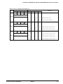
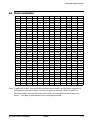
The information of the product number change
Starting April 1, 2001, the product number will be changed as listed below. To order from April 1,
2001 please use the new product number. For further information, please contact Epson sales
representative.
Configuration of product number
Devices
S1
C
60N01
F
0A01
00
Packing specification
Specification
Package (D: die form; F: QFP)
Model number
Model name (C: microcomputer, digital products)
Product classification (S1: semiconductor)
Development tools
C
60R08
S5U1
D1
1
00
Packing specification
Version (1: Version 1 ∗2)
Tool type (D1: Development Tool ∗1)
Corresponding model number (60R08: for S1C60R08)
Tool classification (C: microcomputer use)
Product classification
(S5U1: development tool for semiconductor products)
∗1: For details about tool types, see the tables below. (In some manuals, tool types are represented by one digit.)
∗2: Actual versions are not written in the manuals.
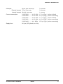
Comparison table between new and previous number
S1C60 Family processors
Previous No.
E0C6001
E0C6002
E0C6003
E0C6004
E0C6005
E0C6006
E0C6007
E0C6008
E0C6009
E0C6011
E0C6013
E0C6014
E0C60R08
New No.
S1C60N01
S1C60N02
S1C60N03
S1C60N04
S1C60N05
S1C60N06
S1C60N07
S1C60N08
S1C60N09
S1C60N11
S1C60N13
S1C60140
S1C60R08
S1C62 Family processors
Previous No.
E0C621A
E0C6215
E0C621C
E0C6S27
E0C6S37
E0C623A
E0C623E
E0C6S32
E0C6233
E0C6235
E0C623B
E0C6244
E0C624A
E0C6S46
New No.
S1C621A0
S1C62150
S1C621C0
S1C6S2N7
S1C6S3N7
S1C6N3A0
S1C6N3E0
S1C6S3N2
S1C62N33
S1C62N35
S1C6N3B0
S1C62440
S1C624A0
S1C6S460
Previous No.
E0C6247
E0C6248
E0C6S48
E0C624C
E0C6251
E0C6256
E0C6292
E0C6262
E0C6266
E0C6274
E0C6281
E0C6282
E0C62M2
E0C62T3
New No.
S1C62470
S1C62480
S1C6S480
S1C624C0
S1C62N51
S1C62560
S1C62920
S1C62N62
S1C62660
S1C62740
S1C62N81
S1C62N82
S1C62M20
S1C62T30
Comparison table between new and previous number of development tools
Development tools for the S1C60/62 Family
Previous No.
ASM62
DEV6001
DEV6002
DEV6003
DEV6004
DEV6005
DEV6006
DEV6007
DEV6008
DEV6009
DEV6011
DEV60R08
DEV621A
DEV621C
DEV623B
DEV6244
DEV624A
DEV624C
DEV6248
DEV6247
New No.
S5U1C62000A
S5U1C60N01D
S5U1C60N02D
S5U1C60N03D
S5U1C60N04D
S5U1C60N05D
S5U1C60N06D
S5U1C60N07D
S5U1C60N08D
S5U1C60N09D
S5U1C60N11D
S5U1C60R08D
S5U1C621A0D
S5U1C621C0D
S5U1C623B0D
S5U1C62440D
S5U1C624A0D
S5U1C624C0D
S5U1C62480D
S5U1C62470D
Previous No.
DEV6262
DEV6266
DEV6274
DEV6292
DEV62M2
DEV6233
DEV6235
DEV6251
DEV6256
DEV6281
DEV6282
DEV6S27
DEV6S32
DEV6S37
EVA6008
EVA6011
EVA621AR
EVA621C
EVA6237
EVA623A
New No.
S5U1C62620D
S5U1C62660D
S5U1C62740D
S5U1C62920D
S5U1C62M20D
S5U1C62N33D
S5U1C62N35D
S5U1C62N51D
S5U1C62560D
S5U1C62N81D
S5U1C62N82D
S5U1C6S2N7D
S5U1C6S3N2D
S5U1C6S3N7D
S5U1C60N08E
S5U1C60N11E
S5U1C621A0E2
S5U1C621C0E
S5U1C62N37E
S5U1C623A0E
Previous No.
EVA623B
EVA623E
EVA6247
EVA6248
EVA6251R
EVA6256
EVA6262
EVA6266
EVA6274
EVA6281
EVA6282
EVA62M1
EVA62T3
EVA6S27
EVA6S32R
ICE62R
KIT6003
KIT6004
KIT6007
New No.
S5U1C623B0E
S5U1C623E0E
S5U1C62470E
S5U1C62480E
S5U1C62N51E1
S5U1C62N56E
S5U1C62620E
S5U1C62660E
S5U1C62740E
S5U1C62N81E
S5U1C62N82E
S5U1C62M10E
S5U1C62T30E
S5U1C6S2N7E
S5U1C6S3N2E2
S5U1C62000H
S5U1C60N03K
S5U1C60N04K
S5U1C60N07K
Hardware
I.
S1C62N82
Technical Hardware
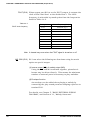
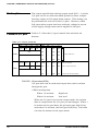
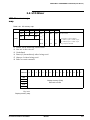
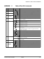
CONTENTS
CONTENTS
CHAPTER 2
INTRODUCTION ............................................................... I-1
1.1
Configuration ................................................................... I-1
1.2
Features .......................................................................... I-2
1.3
Block Diagram ................................................................. I-4
1.4
Pin Layout Diagram ......................................................... I-5
1.5
Pin Description ................................................................ I-7
POWER SUPPLY AND INITIAL RESET ................................ I-8
2.1
Power Supply .................................................................. I-8
2.2
Initial Reset ...................................................................... I-9
Oscillation detection circuit .....................................
Reset pin (RESET) ...................................................
Simultaneous high input to input ports (K00–K03) ..
Internal register following initialization ....................
2.3
CHAPTER 3
Hardware
CHAPTER 1
I-10
I-10
I-10
I-11
Test Pin (TEST) .............................................................. I-11
CPU, ROM, RAM ............................................................ I-12
3.1
CPU ............................................................................... I-12
3.2
ROM .............................................................................. I-13
3.3
RAM .............................................................................. I-13
S1C62N82 TECHNICAL HARDWARE
EPSON
I-i
CONTENTS
CHAPTER 4
PERIPHERAL CIRCUITS AND OPERATION ...................... I-14
4.1
Memory Map .................................................................. I-14
4.2
Oscillation Circuit ............................................................ I-22
OSC1 oscillation circuit ...........................................
OSC3 oscillation circuit ...........................................
Configuration of oscillation circuit ...........................
Control of oscillation circuit ....................................
4.3
Input Ports (K00–K03, K10) ........................................... I-27
Configuration of input ports ....................................
Input comparison registers and interrupt function ..
Mask option ............................................................
Control of input ports ..............................................
4.4
I-22
I-23
I-24
I-25
I-27
I-28
I-31
I-32
Output Ports (R00–R03, R10–R12) ............................... I-36
Configuration of output ports .................................. I-36
Mask option ............................................................ I-37
Control of output ports ............................................ I-39
4.5
I/O Ports (P00–P03) ....................................................... I-41
Configuration of I/O port ........................................
I/O control register and I/O mode ...........................
Mask option ............................................................
Control of I/O port ..................................................
4.6
LCD Driver ...................................................................... I-45
Configuration of LCD driver .....................................
Switching between dynamic and static drive ............
Mask option (segment allocation) .............................
Control of LCD driver ..............................................
4.7
I-41
I-41
I-42
I-42
I-45
I-48
I-49
I-51
Clock Timer .................................................................... I-53
Configuration of clock timer .................................... I-53
Interrupt function ................................................... I-54
Control of clock timer .............................................. I-55
I-ii
EPSON
S1C62N82 TECHNICAL HARDWARE
CONTENTS
Stopwatch Timer ............................................................ I-58
Configuration of stopwatch timer ............................
Count-up pattern ....................................................
Interrupt function ...................................................
Control of stopwatch timer ......................................
4.9
I-58
I-59
I-60
I-61
Supply Voltage Detection (SVD) Circuit
and Heavy Load Protection Function ............................. I-64
Configuration of SVD circuit
and heavy load protection function ..........................
Operation of SVD detection timing ..........................
Operation of heavy load protection function ............
Control of SVD circuit
and heavy load protection function ..........................
I-64
I-66
I-67
I-68
4.10 Analog Voltage Comparator ........................................... I-70
Configuration of analog voltage comparator ............. I-70
Operation of analog voltage comparator ................... I-71
Control of analog voltage comparator ...................... I-72
4.11 Melody Generator ........................................................... I-73
Outline of melody generator .................................... I-73
Melody data ............................................................ I-92
Playing of silent note ............................................... I-95
Envelope function ................................................... I-96
Playing tempo ......................................................... I-98
Playing mode .......................................................... I-100
Control of the melody generator ............................. I-104
4.12 Interrupt and HALT ........................................................ I-108
Interrupt factors .....................................................
Specific masks and factor flags for interrupt ...........
Interrupt vectors and priorities ...............................
Control of interrupt ................................................
S1C62N82 TECHNICAL HARDWARE
EPSON
I-110
I-111
I-112
I-113
I-iii
Hardware
4.8
CONTENTS
CHAPTER 5
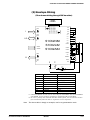
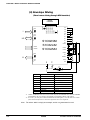
BASIC EXTERNAL WIRING DIAGRAM ........................... I-117
CHAPTER 6
ELECTRICAL CHARACTERISTICS ................................... I-121
6.1
Absolute Maximum Rating ............................................ I-121
6.2
Recommended Operating Conditions ........................... I-122
6.3
DC Characteristics ........................................................ I-123
6.4
Analog Circuit Characteristics
and Power Current Consumption .................................. I-125
6.5
CHAPTER 7
CHAPTER 8
I-iv
Oscillation Characteristics ............................................. I-131
PACKAGE ..................................................................... I-133
7.1
Plastic Package ............................................................. I-133
7.2
Ceramic Package for Test Sample ................................ I-135
PAD LAYOUT ................................................................. I-136
8.1
Diagram of Pad Layout .................................................. I-136
8.2
Pad Coordinates ............................................................ I-137
EPSON
S1C62N82 TECHNICAL HARDWARE
CHAPTER 1: INTRODUCTION
CHAPTER 1
INTRODUCTION
Each member of the S1C62N82 Series of single chip microcomputers feature a 4-bit S1C6200A core CPU, 2,048 words
of ROM (12 bits per word), 224 words of RAM (4 bits per
word), an LCD driver, 5 bits for input ports (K00–K03 and
K10), 7 bits for output ports (R00–R03 and R10–R12), one 4bit I/O port (P00–P03), two timer (clock timer and stopwatch
timer), and a melody generator.
Because of their low voltage operation and low power consumption, the S1C62N82 Series are ideal for a wide range of
applications, and are especially suitable for battery-driven
systems with a melody.
1.1 Configuration
The S1C62N82 Series are configured as follows, depending
on the supply voltage and oscillation circuits.
Table 1.1.1
Configuration of the
Model
Supply Voltage
S1C62L82
1.5 V
Single Clock (Crystal or CR)
S1C62N82 Series
S1C62N82
3.0 V
Single Clock (Crystal or CR)
S1C62A82
3.0 V
Twin Clock (Crystal or CR, Ceramic or CR)
S1C62N82 TECHNICAL HARDWARE
EPSON
Oscillation Circuits
I-1
CHAPTER 1: INTRODUCTION
1.2 Features
Built-in oscillation circuit
Crystal or CR oscillation circuit (32.768 kHz)
CR oscillation circuit or Ceramic oscillation circuit (1 MHz)
Instruction set
100 instructions
Instruction execution time
At 32 kHz : 153 µs, 214 µs, 366 µs
At 1 MHz :
5 µs,
7 µs, 12 µs
ROM capacity
2,048 words × 12 bits
RAM capacity (data RAM)
224 words × 4 bits (including segment memory)
Input port
5 bits(Supplementary pull-down resistors may be used by
mask option)
Output port
4 bits(general purpose)
1 bit (melody output)
1 bit (melody reverse output and also serves as external CR
connecting terminal for envelope)
1 bit (general purpose output)
1 bit (clock output)
Either OSC3 output or 256 Hz–32 kHz may be specified
with mask option
Input/output port
4 bits
LCD driver
42 segments × 4 common duty/38 segments × 8 common duty
(Switching between 1/4 duty and 1/8 duty,
and assignment of segment are possible
with mask option)
Melody generation circuit
1 sound source output, 31 musical intervals (from among 3
octaves), 8 notes, and tempos (from among 16 types);
the number of musical pieces is optional within the ROM
capacity (128 words).
Envelope addition and piezo buzzer direct driving are
possible through mask option selection.
Comparator
Built-in operating amplifier for the MOS input analog comparator
Supply voltage detection
circuit (SVD)
1.2 V / 2.4 V
I-2
EPSON
S1C62N82 TECHNICAL HARDWARE
CHAPTER 1: INTRODUCTION
Interrupts:
Input port interrupt
External interrupt Timer interrupt
Internal interrupt Melody interrupt
Current consumption
S1C62N82 ........ At
S1C62N82 ........ At
S1C62L82 ........ At
S1C62L82 ........ At
S1C62A82 ........ At
Supply form
80-pin QFP (plastic) or chip
S1C62N82 TECHNICAL HARDWARE
32 kHz
32 kHz
32 kHz
32 kHz
1 MHz
EPSON
2 systems
2 systems
1 system
1.5 µA (Typ.)
4.0 µA (Typ.)
1.5 µA (Typ.)
4.0 µA (Typ.)
150 µA (Typ.)
(when
(when
(when
(when
(when
halted)
executing)
halted)
executing)
executing)
I-3
CHAPTER 1: INTRODUCTION
ROM
2,048x12
OSC
RESET
OSC4
OSC3
OSC2
OSC1
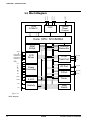
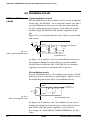
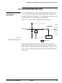
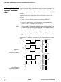
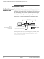
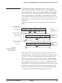
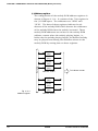
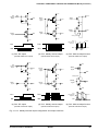
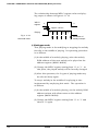
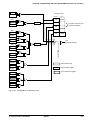
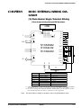
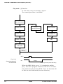
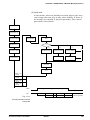
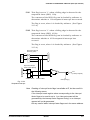
1.3 Block Diagram
System
Reset
Control
Core CPU S1C6200A
RAM
224x4
Interrupt
Generator
SEG0
COM7/SEG38
COM6/SEG39
COM5/SEG40
COM4/SEG41
LCD
Driver
I Port
Test Port
K00~K03
I/O Port
P00~P03
K10
TEST
COM0
VDD
VL1
VL4
CA
CD
VS1
Vss
CMPP
CMPM
Power
Controller
O Port
Comparator
& SVD
R00~R03
R10, R11
Timer
MO
Stop
Watch
Melody
R12
Fig. 1.3.1
Block diagram
I-4
EPSON
S1C62N82 TECHNICAL HARDWARE
CHAPTER 1: INTRODUCTION
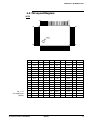
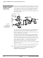
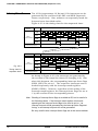
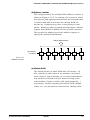
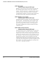
1.4 Pin Layout Diagram
QFP5
64
41
65
40
Index
80
25
1
24
Pin No Pin Name Pin No Pin Name Pin No Pin Name Pin No Pin Name Pin No Pin Name
1
VDD
17
SEG14
33
K02
49
SEG28
65
P01
2
TEST
18
SEG15
34
K01
50
SEG29
66
P00
3
SEG0
19
SEG16
35
K00
51
SEG30
67
CD
4
SEG1
20
SEG17
36
RESET
52
SEG31
68
CC
5
SEG2
21
SEG18
37
CMPP
53
SEG32
69
CB
6
SEG3
22
SEG19
38
CMPM
54
SEG33
70
CA
7
SEG4
23
R03
39
COM3
55
SEG34
71
V L4
8
SEG5
24
R02
40
COM2
56
SEG35
72
V L3
9
SEG6
25
R01
41
COM1
57
SEG36
73
V L2
10
SEG7
26
R00
42
COM0
58
SEG37
74
V L1
11
SEG8
27
MO
43
SEG22
59
75
V SS
12
SEG9
28
R12
44
SEG23
60
76
OSC4
77
OSC3
78
V S1
13
SEG10
29
R11
45
SEG24
61
Fig. 1.4.1
14
SEG11
30
R10
46
SEG25
62
SEG38
COM7
SEG39
COM6
SEG40
COM5
SEG41
COM4
Pin assignment
(QFP5)
15
SEG12
31
K10
47
SEG26
63
P03
79
OSC2
16
SEG13
32
K03
48
SEG27
64
P02
80
OSC1
S1C62N82 TECHNICAL HARDWARE
EPSON
I-5
CHAPTER 1: INTRODUCTION
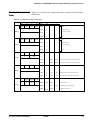
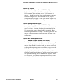
QFP14
60
41
61
40
Index
80
21
1
20
Pin No Pin Name Pin No Pin Name Pin No Pin Name Pin No Pin Name Pin No Pin Name
I-6
1
SEG0
17
SEG16
33
K00
49
SEG30
65
CD
2
SEG1
18
SEG17
34
RESET
50
SEG31
66
CC
3
SEG2
19
SEG18
35
CMPP
51
SEG32
67
CB
4
SEG3
20
SEG19
36
CMPM
52
SEG33
68
CA
5
SEG4
21
R03
37
COM3
53
SEG34
69
V L4
6
SEG5
22
R02
38
COM2
54
SEG35
70
V L3
7
SEG6
23
R01
39
COM1
55
SEG36
71
V L2
8
SEG7
24
R00
40
COM0
56
SEG37
72
V L1
9
SEG8
25
MO
41
SEG22
57
73
V SS
10
SEG9
26
R12
42
SEG23
58
74
OSC4
11
SEG10
27
R11
43
SEG24
59
75
OSC3
12
SEG11
28
R10
44
SEG25
60
SEG38
COM7
SEG39
COM6
SEG40
COM5
SEG41
COM4
76
V S1
13
SEG12
29
K10
45
SEG26
61
P03
77
OSC2
Fig. 1.4.2
Pin assignment
14
SEG13
30
K03
46
SEG27
62
P02
78
OSC1
15
SEG14
31
K02
47
SEG28
63
P01
79
VDD
(QFP14)
16
SEG15
32
K01
48
SEG29
64
P00
80
TEST
EPSON
S1C62N82 TECHNICAL HARDWARE
CHAPTER 1: INTRODUCTION
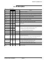
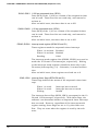
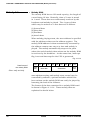
1.5 Pin Description
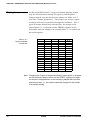
Table 1.5.1 Pin description
Terminal Name
Pin No.
QFP5
QFP14
Input/Output
V DD
1
79
(I)
Power source (+) terminal
V SS
75
73
(I)
Power source (-) terminal
V S1
78
76
–
Internal logic and oscillation system regulated voltage power source terminal
Function
V L1 –V L4
71–74 69–72
–
LCD system power source terminal
CA–CD
67–70 65–68
–
LCD system booster capacitor connector terminal
OSC1
80
78
I
Crystal or CR oscillation input terminal
OSC2
79
77
O
Crystal or CR oscillation output terminal
OSC3
77
75
I
Ceramic or CR oscillation input terminal (S1C62A82)
OSC4
76
74
O
Ceramic or CR oscillation output terminal (S1C62A82)
I
Input terminal
K00–K03
K10
32–35 30–33
31
29
P00–P03
63–66 61–64
R00–R03
23–26 21–24
I/O
I/O terminal
Ouput terminal
R10
30
28
R11
29
27
R12
28
26
MO
27
25
O
CMPP
37
35
I
Analog comparator non-inverted input terminal
CMPM
38
36
I
Analog comparator inverted input terminal
3–22
1–20
SEG0–SEG37
43–58 41–56
O
R10: FOUT output available through mask option selection
R12: Melody inverted output and envelope function
available through mask option selection
MO: Melody signal output terminal
LCD segment output terminal
O
SEG20 and 21 may be used only when the corresponding chips have been
supplied (convertible to DC output terminal by mask option)
COM0–COM3
39–42 37–40
O
LCD common output terminal
LCD segment output terminal (when selected 1/4 duty)
SEG38–SEG41 59–62 57–60
O
(convertible to DC output terminal by mask option)
LCD common output terminal (when selected 1/8 duty)
COM4–COM7
RESET
36
34
I
Initial setting input terminal
TEST
2
80
I
Test input terminal
S1C62N82 TECHNICAL HARDWARE
EPSON
I-7
CHAPTER 2: POWER SUPPLY AND INITIAL RESET
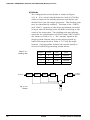
CHAPTER 2
POWER SUPPLY AND INITIAL RESET
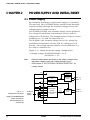
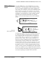
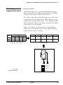
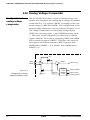
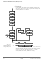
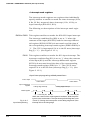
2.1 Power Supply
By externally providing a single power supply (*1) between
VDD and VSS, the S1C62N82 Series produces the internally
required voltage through the constant voltage circuit and
voltage booster/reducer circuit.
In S1C62N82/62A82, the constant voltage circuit produces
VS1 voltage for oscillation and internal circuits, and VL2
voltage for LCD driving. The voltage booster/reducer circuit
produces VL1, VL3 and VL4 based on VL2.
In S1C62L82, the constant voltage circuit VS1 voltage for
oscillation and internal circuits, and VL1 voltage for LCD
driving. The voltage booster/reducer circuit produces VL2,
VL3 and VL4 based on VL1.
Figure 2.1.1 shows the power supply configuration.
*1 Supply voltage: S1C62N82/62A82...3.0 V
S1C62L82...1.5 V
Note -
External loads cannot be driven by the output voltage of the
regulated voltage circuit and voltage booster circuit.
See Chapter 6, "ELECTRICAL CHARACTERISTICS", for
voltage values.
V DD
Internal
circuit
Internal system
regulated voltage
circuit
VS1
V S1
Oscillation
circuit
OSC1, 2
OSC3, 4
V L2 (V L1) LCD system regulated
voltage circuit
V L4
V L1 (V L2 )
V L3
Fig. 2.1.1
Configuration of power
supply S1C62N82/62A82
(items enclosed in
parentheses are for
External
power
supply
CA
CB
CC
(
CD
V L2 (V L1)
V L2 (V L1)
LCD system
voltage
booster/reducer
circuit
V L1
(V L2 )
V L3
V L4
LCD driver
circuit
COM0–7
SEG0–37
)
Vss
S1C62L82)
I-8
EPSON
S1C62N82 TECHNICAL HARDWARE
CHAPTER 2: POWER SUPPLY AND INITIAL RESET
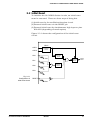
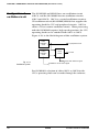
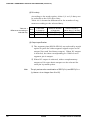
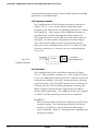
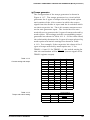
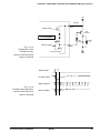
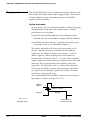
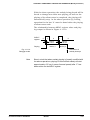
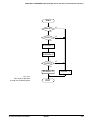
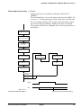
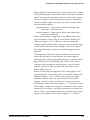
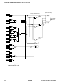
2.2 Initial Reset
To initialize the S1C62N82 Series circuits, an initial reset
must be executed. There are three ways of doing this.
(1) Initial reset by the oscillation detection circuit
(2) External initial reset via the RESET pin
(3) External initial reset by simultaneous high input to pins
K00–K03 (depending on mask option)
Figure 2.2.1 shows the configuration of the initial reset
circuit.
OSC1
OSC1
OSC2
Oscillation
circuit
Oscillation
detection
circuit
K00
Vss
Noise
rejection
circuit
K01
Initial
reset
Noise
rejection
circuit
K02
K03
Fig. 2.2.1
Configuration of
initial reset circuit
S1C62N82 TECHNICAL HARDWARE
RESET
Vss
EPSON
I-9
CHAPTER 2: POWER SUPPLY AND INITIAL RESET
Oscillation detection The oscillation detection circuit outputs the initial reset
signal at power-on until the crystal oscillation circuit starts
circuit
oscillating, or when the crystal oscillation circuit stops
oscillating for some reason.
The circuit may malfunction if the power is turned on erroneously. In such cases, use one of the following two initial
resetting methods.
Reset pin (RESET)
An initial reset can be invoked externally by making the
reset pin high. This high level must be maintained for at
least 5 ms (when oscillating frequency, fosc1 = 32 kHz),
because the initial reset circuit contains a noise rejection
circuit. When the reset pin goes low the CPU begins to
operate.
Simultaneous high
input to input ports
(K00–K03)
Another way of invoking an initial reset externally is to input
a high signal simultaneously to the input ports (K00–K03)
selected with the mask option. The specified input port pins
must be kept high for 2–4 sec (when oscillating frequency
fosc1 = 32 kHz), because of the noise rejection circuit. Table
2.2.1 shows the combinations of input ports (K00–K03) that
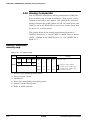
can be selected with the mask option.
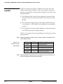
Table 2.2.1
Input port combinations
A
B
C
D
Not used
K00*K01
K00*K01*K02
K00*K01*K02*K03
When, for instance, mask option D (K00*K01*K02*K03) is
selected, an initial reset is executed when the signals input
to the four ports K00–K03 are all high at the same time.
If you use this function, make sure that the specified ports
do not go high at the same time during normal operation.
Since this function uses a timer-controlled noise rejection
circuit, if the oscillator (OSC1) is not running, or if the timer
remains reset by software, initial resetting by means of this
function is impossible. (See 4.7, Clock Timer.)
I-10
EPSON
S1C62N82 TECHNICAL HARDWARE
CHAPTER 2: POWER SUPPLY AND INITIAL RESET
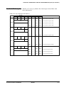
Internal register following initialization
An initial reset initializes the CPU as shown in the table
below.
Table 2.2.2
Initial values
CPU Core
Name
Program counter step
Program counter page
New page pointer
Stack pointer
Index register X
Index register Y
Register pointer
General register A
General register B
Interrupt flag
Decimal flag
Zero flag
Carry flag
Signal
Number of Bits
Setting Value
PCS
PCP
NPP
SP
X
Y
RP
A
B
I
D
Z
C
8
4
4
8
8
8
4
4
4
1
1
1
1
00H
1H
1H
Undefined
Undefined
Undefined
Undefined
Undefined
Undefined
0
0
Undefined
Undefined
Peripheral Circuits
Name
Number of Bits
Setting Value
144 × 4
80 × 4
–
Undefined
Undefined
*1
RAM
Display memory
Other peripheral circuit
*1: See Section 4.1, "Memory Map"
2.3 Test Pin (TEST)
This pin is used when IC is inspected for shipment.
During normal operation connect it to VSS.
S1C62N82 TECHNICAL HARDWARE
EPSON
I-11
CHAPTER 3: CPU, ROM, RAM
CHAPTER 3
CPU, ROM, RAM
3.1 CPU
The S1C62N82 Series employs the S1C6200A core CPU, so
that register configuration, instructions, and so forth are
virtually identical to those in other processors in the family
using the S1C6200A. Refer to the "S1C6200/6200A Core
CPU Manual" for details of the S1C6200A.
Note the following points with regard to the S1C62N82
Series:
(1) The SLEEP operation is not provided, so the SLP instruction cannot be used.
(2) Because the ROM capacity is 2,048 words, 12 bits per
word, bank bits are unnecessary, and PCB and NBP are
not used.
(3) The RAM page is set to 0 only, so the page part (XP, YP)
of the index register that specifies addresses is invalid.
PUSH
POP
LD
LD
I-12
XP
XP
XP,r
r,XP
EPSON
PUSH
POP
LD
LD
YP
YP
YP,r
r,YP
S1C62N82 TECHNICAL HARDWARE
CHAPTER 3: CPU, ROM, RAM
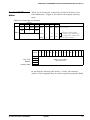
3.2 ROM
The built-in ROM, a mask ROM for the program, has a
capacity of 2,048 × 12-bit steps. The program area is 8
pages (0–7), each consisting of 256 steps (00H–FFH). After
an initial reset, the program start address is page 1, step
00H. The interrupt vector is allocated to page l, steps 02H–
0BH.
Bank 0
00H step
0 page
Program start address
01H step
1 page
02H step
2 page
Interrupt vector area
3 page
4 page
5 page
0BH step
0CH step
6 page
7 page
Program area
FFH step
Fig. 3.2.1
12 bits
ROM configuration
3.3 RAM
The RAM, a data memory for storing a variety of data, has a
capacity of 144 words, 4-bit words. When programming,
keep the following points in mind:
(1) Part of the data memory is used as stack area when
saving subroutine return addresses and registers, so be
careful not to overlap the data area and stack area.
(2) Subroutine calls and interrupts take up three words on
the stack.
(3) Data memory 000H–00FH is the memory area pointed by
the register pointer (RP).
S1C62N82 TECHNICAL HARDWARE
EPSON
I-13
CHAPTER 4: PERIPHERAL CIRCUITS AND OPERATION (Memory Map)
CHAPTER 4
PERIPHERAL CIRCUITS AND
OPERATION
Peripheral circuits (timer, I/O, and so on) of the S1C62N82
Series are memory mapped. Thus, all the peripheral circuits
can be controlled by using memory operations to access the
I/O memory. The following sections describe how the peripheral circuits operate.
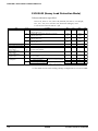
4.1 Memory Map
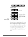
The data memory of the S1C62N82 Series has an address
space of 250 words, of which 80 words are allocated to
display memory and 26 words, to I/O memory. Figure 4.1.1
show the overall memory mas for the S1C62N82 Series, and
Tables 4.1.1 (a)–(g), the memory maps for the peripheral
circuits (I/O space).
Address
Low
0
Page
1
2
3
4
5
6
7
8
9
A
B
C
D
E
F
High
0
M0 M1 M2 M3 M4 M5 M6 M7 M8 M9 MA MB MC MD ME MF
1
2
3
4
RAM area (000H–08FH)
144 words x 4 bits (R/W)
5
6
0
7
8
9
A
Display memory area (090H–0DFH)
80 words x 4 bits (R/W) *
B
C
Fig. 4.1.1
Memory map
D
E
I/O memory area
Table 4.1.1 (a)–(g)
F
Unused area
* If the duty of the LCD driver is set to 1/8 by the mask
option in the display memory area (80 words × 4 bits), 304
bits (38 segments × 8 common bits) are used. If the duty
is set to 1/4, 168 bits (42 segments × 4 common bits) are
used. The bits unassigned as display memory can serve
as a general-purpose RAM.
Note Memory is not mounted in unused area within the memory map
and in memory area not indicated in this chapter. For this reason,
normal operation cannot be assured for programs that have been
prepared with access to these areas.
I-14
EPSON
S1C62N82 TECHNICAL HARDWARE
CHAPTER 4: PERIPHERAL CIRCUITS AND OPERATION (Memory Map)
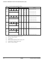
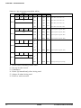
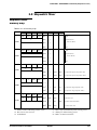
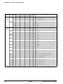
Table 4.1.1 (a) I/O memory map (0E0H–0E3H)
Address
D3
Register
D2
D1
D0
Name
K03
K02
K00
K03
–
K02
K01
R
SR *1
Comment
1
0
*2
High
Low
–
*2
High
Low
K01
–
*2
High
Low
K00
–
*2
High
Low
K10
–
*2
High
Low
SWL3
0
MSB
SWL2
0
Stopwatch timer
1/100 sec (BCD)
SWL1
0
SWL0
0
LSB
SWH3
0
MSB
SWH2
0
Stopwatch timer
1/10 sec (BCD)
SWH1
0
SWH0
0
0E0H
Input port (K00–K03)
0
0
0
K10
0 *5
0 *5
R
0E1H
0 *5
SWL3
SWL2
SWL1
SWL0
R
0E2H
SWH3
SWH2
SWH1
R
SWH0
0E3H
*1
*2
*3
*4
*5
*6
Input port (K10)
LSB
Initial value following initial reset
Not set in the circuit
Undefined
Reset (0) immediately after being read
Constantly 0 when being read
Refer to main manual
S1C62N82 TECHNICAL HARDWARE
EPSON
I-15
CHAPTER 4: PERIPHERAL CIRCUITS AND OPERATION (Memory Map)
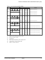
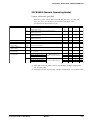
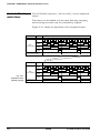
Table 4.1.1 (b) I/O memory map (0E4H–0E7H)
Address
D3
Register
D2
D1
TM3
TM2
TM1
D0
Name
TM0
TM3
R
SR *1
Comment
1
0
–
High
Low
Timer data (clock timer 2 Hz)
TM2
–
High
Low
Timer data (clock timer 4 Hz)
TM1
–
High
Low
Timer data (clock timer 8 Hz)
TM0
–
High
Low
Timer data (clock timer 16 Hz)
KCP03
0
Falling
Rising
Input comparison register (K03)
KCP02
0
Falling
Rising
Input comparison register (K02)
KCP01
0
Falling
Rising
Input comparison register (K01)
KCP00
0
Falling
Rising
Input comparison register (K00)
0
Falling
Rising
Input comparison register (K10)
0
Enable
Mask
Interrupt mask register (melody)
0E4H
KCP03
KCP02
KCP01
KCP00
R/W
0E5H
0
0
0
R
KCP10
0
R/W
0
0E6H
0
*5
*5
*5
KCP10
0
0
R
0
EIMEL
0 *5
R/W
0 *5
0E7H
0 *5
EIMEL
*1
*2
*3
*4
*5
*6
I-16
Initial value following initial reset
Not set in the circuit
Undefined
Reset (0) immediately after being read
Constantly 0 when being read
Refer to main manual
EPSON
S1C62N82 TECHNICAL HARDWARE
CHAPTER 4: PERIPHERAL CIRCUITS AND OPERATION (Memory Map)
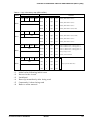
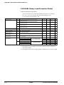
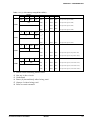
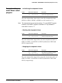
Table 4.1.1 (c) I/O memory map (0E8H–0EBH)
Address
Register
D2
D1
D3
EIK03
EIK02
EIK01
D0
Name
EIK00
EIK03
R/W
SR *1
Comment
1
0
0
Enable
Mask
Interrupt mask register (K03)
EIK02
0
Enable
Mask
Interrupt mask register (K02)
EIK01
0
Enable
Mask
Interrupt mask register (K01)
EIK00
0
Enable
Mask
Interrupt mask register (K00)
0
Enable
Mask
Interrupt mask register (K10)
EISW1
0
Enable
Mask
Interrupt mask register (stopwatch 1 Hz)
EISW0
0
Enable
Mask
Interrupt mask register (stopwatch 10 Hz)
EIT2
0
Enable
Mask
Interrupt mask register (clock timer 2 Hz)
EIT8
0
Enable
Mask
Interrupt mask register (clock timer 8 Hz)
EIT32
0
Enable
Mask
Interrupt mask register (clock timer 32 Hz)
0E8H
0
0
0
R
EIK10
0
R/W
0
0E9H
0
*5
*5
*5
EIK10
0
0
EISW1
R
EISW0
0
0
R/W
*5
*5
0EAH
0
EIT2
R
EIT8
R/W
EIT32
0 *5
0EBH
*1
*2
*3
*4
*5
*6
Initial value following initial reset
Not set in the circuit
Undefined
Reset (0) immediately after being read
Constantly 0 when being read
Refer to main manual
S1C62N82 TECHNICAL HARDWARE
EPSON
I-17
CHAPTER 4: PERIPHERAL CIRCUITS AND OPERATION (Memory Map)
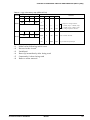
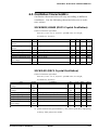
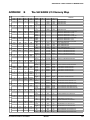
Table 4.1.1 (d) I/O memory map (0ECH–0EFH)
Address
D3
0
Register
D2
D1
0
0
D0
Name
IMEL
0
*5
0
*5
0
*5
R
SR *1
Comment
1
0
0
Yes
No
Interrupt factor flag (melody)
IK1 *4
0
Yes
No
Interrupt factor flag (K10)
IK0 *4
0
Yes
No
Interrupt factor flag (K00–K03)
0
Yes
No
Interrupt factor flag (stopwatch 1 Hz)
0
Yes
No
Interrupt factor flag (stopwatch 10 Hz)
IT2 *4
0
Yes
No
Interrupt factor flag (clock timer 2 Hz)
IT8 *4
0
Yes
No
Interrupt factor flag (clock timer 8 Hz)
IT32 *4
0
Yes
No
Interrupt factor flag (clock timer 32 Hz)
0ECH
*4
IMEL
0
0
IK1
IK0
0 *5
0 *5
R
0EDH
0
0
ISW1
ISW0
0
0
R
0EEH
*5
*5
*4
ISW1
*4
ISW0
0
IT2
IT8
R
IT32
0 *5
0EFH
*1
*2
*3
*4
*5
*6
I-18
Initial value following initial reset
Not set in the circuit
Undefined
Reset (0) immediately after being read
Constantly 0 when being read
Refer to main manual
EPSON
S1C62N82 TECHNICAL HARDWARE
CHAPTER 4: PERIPHERAL CIRCUITS AND OPERATION (Memory Map)
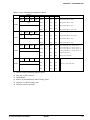
Table 4.1.1 (e) I/O memory map (0F0H–0F3H)
Address
D3
MAD3
Register
D2
D1
MAD2
MAD1
D0
Name
MAD0
MAD3
R/W
SR *1
Comment
1
0
0
High
Low
Melody ROM address (AD3)
MAD2
0
High
Low
Melody ROM address (AD2)
MAD1
0
High
Low
Melody ROM address (AD1)
MAD0
0
High
Low
Melody ROM address (AD0, LSB)
MAD6
0
High
Low
Melody ROM address (AD6, MSB)
MAD5
0
High
Low
Melody ROM address (AD5)
MAD4
0
High
Low
Melody ROM address (AD4)
CLKC1
0
High
Low
CLKC0
0
High
Low
TEMPC
0
High
Low
CLKC1(0)&CLKC0(0) : melody speed × 1
CLKC1(0)&CLKC0(1) : melody speed × 8
CLKC1(1)&CLKC0(0) : melody speed × 16
CLKC1(1)&CLKC0(1) : melody speed × 32
Tempo change control
MELC
0
ON
OFF
Melody control ON/OFF
R03
0
High
Low
R02
0
High
Low
R01
0
High
Low
R00
0
High
Low
0F0H
0
MAD6
MAD5
R
MAD4
R/W
0 *5
0F1H
CLKC1
CLKC0
TEMPC
MELC
R/W
0F2H
R03
R02
R01
R/W
R00
0F3H
*1
*2
*3
*4
*5
*6
Output port data (R00–R03)
Initial value following initial reset
Not set in the circuit
Undefined
Reset (0) immediately after being read
Constantly 0 when being read
Refer to main manual
S1C62N82 TECHNICAL HARDWARE
EPSON
I-19
CHAPTER 4: PERIPHERAL CIRCUITS AND OPERATION (Memory Map)
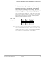
Table 4.1.1 (f) I/O memory map (0F4H, 0F6H, 0F9H–0FAH)
Address
D3
MELD
Register
D2
D1
R12
MO
ENV
Name
R11
D0
R10
FOUT
P01
P00
P03
– *2
High
Low
P02
– *2
High
Low
P01
– *2
High
Low
P00
– *2
High
Low
R/W
0F4H
P03
P02
R/W
SR *1
1
0
Disable
0
High
*6
–
–
Hz
–
0
High
0
High
ON
MELD
R12
MO
ENV
R11
R10
FOUT
Comment
0
Enable
Low
–
–
Low
Low
OFF
0F6H
Melody output mask
Output port data (R12)
Inverting melody output
Melody envelope control
Output port data (R11)
Output port data (R10)
Frequency output
I/O port (P00–P03)
0
TMRST
R
W
SWRUN SWRST
0
*5
*5
R/W
TMRST
Reset
Reset
–
SWRUN
0
Run
Stop
SWRST
Reset
Reset
–
SVDON
HLMOD
0
Heavy
load
Normal
load
R/W
0
W
Clock timer reset
0F9H
Stopwatch timer RUN/STOP
*5
HLMOD
R/W
0
SVDDT
R
I-20
Heavy load protection mode register
*5
0FAH
*1
*2
*3
*4
*5
*6
Stopwatch timer reset
SVDDT
0
Supply
voltage
low
Supply
voltage
normal
SVDON
0
ON
OFF
Supply voltage detector data
Supply voltage detector ON/OFF
Initial value following initial reset
Not set in the circuit
Undefined
Reset (0) immediately after being read
Constantly 0 when being read
Refer to main manual
EPSON
S1C62N82 TECHNICAL HARDWARE
CHAPTER 4: PERIPHERAL CIRCUITS AND OPERATION (Memory Map)
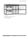
Table 4.1.1 (g) I/O memory map (0FBH–0FCH)
Address
Register
D2
D1
D3
CSDC
0
R/W
D0
CMPDT CMPON
R/W
R
Name
SR *1
0
0
Static
Dynamic
CMPDT
1
+>-
->+
CMPON
0
ON
OFF
Comparator's voltage condition:
1 = CMPP(+)input > CMPM(-)input,
0 = CMPM(-)input > CMPP(+)input
Analog voltage comparator ON/OFF
CSDC
0
OSCC
R/W
LCD drive switch
*5
0FBH
CLKCHG
Comment
1
0
IOC
CLKCHG
0
OSC3
OSC1
CPU clock switch
R
R/W
OSCC
0
ON
OFF
OSC3 oscillator ON/OFF
0
Output
Input
I/O port P00–P03 Input/Output
0FCH
0 *5
IOC
*1
*2
*3
*4
*5
*6
Initial value following initial reset
Not set in the circuit
Undefined
Reset (0) immediately after being read
Constantly 0 when being read
Refer to main manual
S1C62N82 TECHNICAL HARDWARE
EPSON
I-21
CHAPTER 4: PERIPHERAL CIRCUITS AND OPERATION (Oscillation Circuit)
4.2 Oscillation Circuit
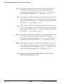
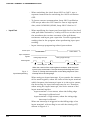
OSC1 oscillation
circuit
Crystal oscillation circuit
The S1C62N82 Series has a built-in OSC1 crystal oscillation
circuit (Typ. 32.768 kHz). As an external element, the OSC1
crystal oscillation circuit generates the operating clock for
the CPU and peripheral circuitry by connecting the crystal
oscillator (Typ. 32.768 kHz) and trimmer capacitor (5–25
pF).
Figure 4.2.1 is the block diagram of the OSC1 crystal oscillation circuit.
V DD
CGX
Fig. 4.2.1
OSC1 crystal oscillation circuit
RDX
To CPU and peripheral
circuits
RFX
X'tal
OSC1
V DD
C DX
OSC2
S1C62N82 Series
As Figure 4.2.1 indicates, the crystal oscillation circuit can
be configured simply by connecting the crystal oscillator
(X'tal) between terminals OSC1 and OSC2 to the trimmer
capacitor (CGX) between terminals OSC1 and VDD.
CR oscillation circuit
For the S1C62N82 Series, CR oscillation circuit (typ. 32.768
kHz) may also be selected by a mask option. Figure 4.2.2 is
the block diagram of the OSC1 CR oscillation circuit.
OSC1
To CPU and
peripheral circuits
RCR
OSC2
Fig. 4.2.2
OSC1 CR oscillation circuit
CCR
The S1C62N82 Series
As Figure 4.2.2 indicates, the CR oscillation circuit can be
configured simply by connecting the resistor (RCR) between
pins OSC1 and OSC2 since capacity (CCR) is built-in.
See Chapter 6, "ELECTRICAL CHARACTERISTICS" for RCR
value.
I-22
EPSON
S1C62N82 TECHNICAL HARDWARE
CHAPTER 4: PERIPHERAL CIRCUITS AND OPERATION (Oscillation Circuit)
OSC3 oscillation
circuit
In the S1C62N82 Series, the S1C62A82 has twin clock
specification. The mask option enables selection of either
the CR or ceramic oscillation circuit (OSC3 oscillation circuit) as the CPU's subclock. Because the oscillation circuit
itself is built-in, it provides the resistance as an external
element when CR oscillation is selected, but when ceramic
oscillation is selected both the ceramic oscillator and two
capacitors (gate and drain capacitance) are required.
Figure 4.2.3 is the block diagram of the OSC3 oscillation
circuit.
C CR
OSC3
RCR
To CPU
Oscillation circuit
control signal
OSC4
S1C62A82
VDD
C GC
OSC3
CDC
RFC
Fig. 4.2.3
Ceramic
To CPU
OSC4
RDC
Oscillation circuit
control signal
S1C62A82
OSC3 oscillation circuit
As indicated in Figure 4.2.3, the CR oscillation circuit can
be configured simply by connecting the resistor (RCR) between terminals OSC3 and OSC4 when CR oscillation is
selected. When 35 k is used for R CR, the oscillation frequency is about 1 MHz. When ceramic oscillation is selected, the ceramic oscillation circuit can be configured by
connecting the ceramic oscillator (Typ. 1 MHz) between
terminals OSC3 and OSC4 to the two capacitors (CGC and
CDC) located between terminals OSC3 and OSC4 and VDD.
For both CGC and CDC, connect capacitors that are about
100 pF. To lower current consumption of the OSC3 oscillation circuit, oscillation can be stopped through the software.
For the S1C62N82 and 62L82 (single clock specification), do
not connect anything to terminals OSC3 and OSC4.
S1C62N82 TECHNICAL HARDWARE
EPSON
I-23
CHAPTER 4: PERIPHERAL CIRCUITS AND OPERATION (Oscillation Circuit)
Configuration of
oscillation circuit
The S1C62N82 and 62L82 have one oscillation circuit
(OSC1), and the S1C62A82 has two oscillation circuits
(OSC1 and OSC3). OSC1 is a crystal oscillation circuit or
CR oscillation circuit (S1C62N82/62L82) that supplies the
operating clock the CPU and peripheral circuits. OSC3 is
either a CR or ceramic oscillation circuit. When processing
with the S1C62A82 requires high-speed operation, the CPU
operating clock can be switched from OSC1 to OSC3.
Figure 4.2.4 is the block diagram of this oscillation system.
OSC1
oscillation
circuit
To peripheral circuit
OSC3
oscillation
circuit
Fig. 4.2.4
Oscillation system
Clock
switch
To CPU
CPU clock selection signal
Oscillation circuit control signal
For S1C62A82, selection of either OSC1 or OSC3 for the
CPU's operating clock can be made through the software.
I-24
EPSON
S1C62N82 TECHNICAL HARDWARE
CHAPTER 4: PERIPHERAL CIRCUITS AND OPERATION (Oscillation Circuit)
Control of oscillation Table 4.2.1 lists the control bits and their addresses for the
oscillation circuit.
circuit
Table 4.2.1 Control bits of oscillation circuit and prescaler
Address
Register
D2
D1
D3
CLKCHG
OSCC
R/W
Comment
D0
Name
SR
1
0
0
IOC
CLKCHG
0
OSC3
OSC1
CPU clock switch
R
R/W
OSCC
0
ON
OFF
OSC3 oscillator ON/OFF
0
Output
Input
I/O port P00–P03 Input/Output
0FCH
0
IOC
OSCC OSC3 oscillation control (0FCH D2)
Controls oscillation ON/OFF for the OSC3 oscillation circuit.
(S1C62A82 only.)
When 1 is written:
When 0 is written:
Read-out:
The OSC3 oscillation ON
The OSC3 oscillation OFF
Valid
When it is necessary to operate the CPU of the S1C62A82 at
high speed, set OSCC to 1. At other times, set it to 0 to
lessen the current consumption.
For the S1C62N82 and 62L82, keep OSCC set to 0.
At initial reset, OSCC is set to 0.
CLKCHG The CPU's clock switch (0FCH D3)
The CPU's operation clock is selected with this register.
(S1C62A82 only.)
When 1 is written:
When 0 is written:
Read-out:
OSC3 clock is selected
OSC1 clock is selected
Valid
When the S1C62A82's CPU clock is to be OSC3, set
CLKCHG to 1; for OSC1, set CLKCHG to 0. This register
cannot be controlled for the S1C62N82 and 62L82, so that
OSC1 is selected no matter what the set value.
At initial reset, CLKCHG is set to 0.
S1C62N82 TECHNICAL HARDWARE
EPSON
I-25
CHAPTER 4: PERIPHERAL CIRCUITS AND OPERATION (Oscillation Circuit)
I-26
Note -
It takes at least 5 ms from the time the OSC3 oscillation circuit
goes ON until the oscillation stabilizes. Consequently, when
switching the CPU operation clock from OSC1 to OSC3, do this
after a minimum of 5 ms have elapsed since the OSC3 oscillation went ON.
Further, the oscillation stabilization time varies depending on
the external oscillator characteristics and conditions of use, so
allow ample margin when setting the wait time.
-
When switching the clock form OSC3 to OSC1, use a separate
instruction for switching the OSC3 oscillation OFF. An error in
the CPU operation can result if this processing is performed at
the same time by the one instruction.
EPSON
S1C62N82 TECHNICAL HARDWARE
CHAPTER 4: PERIPHERAL CIRCUITS AND OPERATION (Input Ports)
4.3 Input Ports (K00–K03, K10)
Configuration of
input ports
The S1C62N82 Series have a general-purpose input (4 bits +
1 bit). Each of the input port pins (K00–K03, K10) has an
internal pull-down resistance. The pull-down resistance can
be selected for each bit with the mask option.
Figure 4.3.1 shows the configuration of input port.
Interrupt
request
Kxx
Data bus
V DD
Address
V SS
Fig. 4.3.1
Configuration of input port
Mask option
Selecting "pull-down resistance enabled" with the mask
option allows input from a push button, key matrix, and so
forth. When "pull-down resistance disabled" is selected, the
port can be used for slide switch input and interfacing with
other LSIs.
S1C62N82 TECHNICAL HARDWARE
EPSON
I-27
CHAPTER 4: PERIPHERAL CIRCUITS AND OPERATION (Input Ports)
Input comparison
registers and interrupt function
All five input port bits (K00–K03, K10) provide the interrupt
function. The conditions for issuing an interrupt can be set
by the software for the five bits. Also, whether to mask the
interrupt function can be selected individually for all five
bits by the software. Figure 4.3.2 shows the configuration of
K00–K03 and K10.
Kxx
One for each pin series
Data bus
Address
Input comparison
register (KCP)
Noise
rejector
Interrupt factor
flag (IK)
Address
Fig. 4.3.2
Interrupt
request
Address
Mask option
(K00–K03, K10)
Interrupt mask
register (EIK)
Input interrupt
circuit configuration
(K00–K03, K10)
Address
The input interrupt timing for K00–K03 and K10 depends on
the value set in the input comparison registers (KCP00–
KCP03 and KCP10). An interrupt can be set to occur on the
rising or falling edge of the input.
The interrupt mask registers (EIK00–EIK03, EIK10) enable
the interrupt mask to be selected individually for K00–K03
and K10. An interrupt occurs when the input value which
are not masked change so they no longer match those of the
input comparison register. An interrupt for K10 can be
generated by setting the same conditions individually.
When an interrupt is generated, the interrupt factor flag (IK0
and IK1) is set to 1.
Figure 4.3.3 shows an example of an interrupt for K00–K03.
Note Writing to the interrupt mask registers (EIK00–EIK03, EIK10)
should be done only in the DI status (interrupt flag = 0).
Otherwise, it causes malfunction.
I-28
EPSON
S1C62N82 TECHNICAL HARDWARE
CHAPTER 4: PERIPHERAL CIRCUITS AND OPERATION (Input Ports)
Interrupt mask registers
Input comparison registers
EIK03 EIK02 EIK01 EIK00
KCP03 KCP02 KCP01 KCP00
1
1
1
0
1
0
1
0
With the above setting, an interrupt for K00–K03 occurs under
the following conditions.
Input ports
(1)
K03
K02
K01
K00
1
0
1
0
(Initial value)
↓
(2)
K03
K02
K01
K00
1
0
1
1
↓
(3)
K03
K02
K01
K00
0
0
1
1
↓
(4)
K03
K02
K01
K00
0
1
1
1
K03
K02
K01
K00
1
0
1
1
↓
Fig. 4.3.3
Example of interrupt of
(5)
→ Interrupt generated
K00 is masked, so the three
bits of K01–K03 cease to
match those of the input
comparison register KCP01–
KCP03, and an interrupt
occurs.
K00–K03
K00 is masked by the interrupt mask register (EIK00), so an
interrupt does not occur at (2). At (3), K03 changes to 0; the
data of the pin that is interrupt-enabled no longer matches
the data of the input comparison register, so an interrupt
occurs. As already explained, the condition for the interrupt
to occur is the change in the port data and contents of the
input comparison register so they no longer match. Hence,
in (4) or (5), when the nonmatching pattern changes to
another nonmatching pattern or matching pattern, an
interrupt does not occur. Also, pins that have been masked
for interrupt do not affect the conditions for interrupt generation.
S1C62N82 TECHNICAL HARDWARE
EPSON
I-29
CHAPTER 4: PERIPHERAL CIRCUITS AND OPERATION (Input Ports)
Input interrupt programing related precautions
Port K input
Active status
Input comparison
register
Falling edge interrupt
Active status
Rising edge interrupt
Mask register
➀
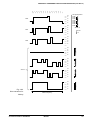
Fig. 4.3.4
Input interrupt timing
Factor flag set Not set
➁ Factor flag set
When the content of the mask register is rewritten, while the port K
input is in the active status. The input interrupt factor flags are set at
➀ and ➁, ➀ being the interrupt due to the falling edge and ➁ the
interrupt due to the rising edge.
When using an input interrupt, if you rewrite the content
of the mask register, when the value of the input terminal
which becomes the interrupt input is in the active status,
the factor flag for input interrupt may be set. Therefore,
when using the input interrupt, the active status of the
input terminal implies
input terminal = Low status, when the falling edge
interrupt is effected and
input terminal = High status, when the rising edge
interrupt is effected.
When an interrupt is triggered at the falling edge of an
input terminal, a factor flag is set with the timing of ➀
shown in Figure 4.3.4. However, when clearing the
content of the mask register with the input terminal kept
in the LOW status and then setting it, the factor flag of
the input interrupt is again set at the timing that has
been set.
Consequently, when the input terminal is in the active
status (Low status), do not rewrite the mask register
(clearing, then setting the mask register), so that a factor
flag will only set at the falling edge in this case. When
clearing, then setting the mask register, set the mask
register, when the input terminal is not in the active
status (High status).
When an interrupt is triggered at the rising edge of the
input terminal, a factor flag will be set at the timing of ➁
shown in Figure 4.3.4. In this case, when the mask
registers cleared, then set, you should set the mask
register, when the input terminal is in the Low status.
I-30
EPSON
S1C62N82 TECHNICAL HARDWARE
CHAPTER 4: PERIPHERAL CIRCUITS AND OPERATION (Input Ports)
In addition, when the mask register = 1 and the content
of the input comparison register is rewritten in the input
terminal active status, an input interrupt factor flag may
be set. Thus, you should rewrite the content of the input
comparison register in the mask register = 0 status.
Mask option
The contents that can be selected with the input port mask
option are as follows:
(1) An internal pull-down resistance can be selected for each
of the five bits of the input ports (K00–K03, K10). Having
selected "Not Use" (pull-down resistance disabled), take
care that the input does not float. Select "Use" (pulldown resistance enabled) for input ports that are not
being used.
(2) The input interrupt circuit contains a noise rejector to
prevent interrupts from occurring through noise.
Whether or not to use this noise rejector may be selected
for K00–K03 or K10. When "Use" is selected, a maximum
delay of 0.5 ms (fosc1 = 32 kHz) occurs from the time an
interrupt condition is established until the interrupt
factor flag (IK) is set to 1.
S1C62N82 TECHNICAL HARDWARE
EPSON
I-31
CHAPTER 4: PERIPHERAL CIRCUITS AND OPERATION (Input Ports)
Control of input ports Tables 4.3.1 (a) and 4.3.1 (b) list the input port control bits
and their addresses.
Table 4.3.1 (a) Input port control bits (1)
Address
D3
Register
D2
D1
D0
Name
SR
1
0
K03
K02
K00
K03
–
High
Low
K02
–
High
Low
K01
–
High
Low
K00
–
High
Low
K10
–
High
Low
KCP03
0
Falling
Rising
Input comparison register (K03)
KCP02
0
Falling
Rising
Input comparison register (K02)
KCP01
0
Falling
Rising
Input comparison register (K01)
KCP00
0
Falling
Rising
Input comparison register (K00)
0
Falling
Rising
Input comparison register (K10)
K01
R
0E0H
Comment
Input port (K00–K03)
0
0
0
K10
0
0
R
0E1H
0
KCP03
KCP02
KCP01
KCP00
R/W
Input port (K10)
0E5H
0
0
R
0
KCP10
0
R/W
0
0E6H
0
KCP10
I-32
EPSON
S1C62N82 TECHNICAL HARDWARE
CHAPTER 4: PERIPHERAL CIRCUITS AND OPERATION (Input Ports)
Table 4.3.1 (b) Input port control bits (2)
Address
D3
EIK03
Register
D2
D1
EIK02
EIK01
Comment
D0
Name
SR
1
0
EIK00
EIK03
0
Enable
Mask
Interrupt mask register (K03)
EIK02
0
Enable
Mask
Interrupt mask register (K02)
EIK01
0
Enable
Mask
Interrupt mask register (K01)
EIK00
0
Enable
Mask
Interrupt mask register (K00)
0
Enable
Mask
Interrupt mask register (K10)
IK1
0
Yes
No
Interrupt factor flag (K10)
IK0
0
Yes
No
Interrupt factor flag (K00–K03)
R/W
0E8H
0
0
0
R
EIK10
0
R/W
0
0E9H
0
EIK10
0
0
IK1
R
IK0
0
0
0EDH
K00–K03, K10 Input port data (0E0H, 0E1H D0)
The input data of the input port pins can be read with these
registers.
When 1 is read:
When 0 is read:
Writing:
High level
Low level
Invalid
The value read is 1 when the pin voltage of the five bits of
the input ports (K00–K03, K10) goes high (VDD), and 0 when
the voltage goes low (VSS). These bits are reading, so writing
cannot be done.
S1C62N82 TECHNICAL HARDWARE
EPSON
I-33
CHAPTER 4: PERIPHERAL CIRCUITS AND OPERATION (Input Ports)
KCP00–KCP03, KCP10 Input comparison registers (0E5H, 0E6H D0)
The interrupt conditions for pins K00–K03 and K10 can be
set with these registers.
When 1 is read:
When 0 is read:
Reading:
Falling edge
Rising edge
Valid
Of the five bits of the input ports, the interrupt conditions
can be set for the rising or falling edge of the input for each
of the five bits (K00–K03 and K10) through the input comparison registers (KCP00–KCP03 and KCP10).
After an initial reset, these registers are set to 0.
EIK00–EIK03, EIK10 Interrupt mask registers (0E8H, 0E9H D0)
Masking the interrupt of the input port pins can be done
with these registers.
When 1 is written:
When 0 is written:
Reading:
Enable
Mask
Valid
With these registers, masking of the input port bits can be
done for each of the five bits. After an initial reset, these
registers are all set to 0.
Writing to these registers should be done only in the DI
status (interrupt flag = 0). Otherwise, it causes malfunction.
K0, IK1 Interrupt factor flags (0EDH D0 and D1)
These flags indicate the occurrence of an input interrupt.
When 1 is read:
When 0 is read:
Writing:
Interrupt has occurred
Interrupt has not occurred
Invalid
The interrupt factor flags IK0 and IK1 are associated with
K00–K03 and K10, respectively. From the status of these
flags, the software can decide whether an input interrupt
has occurred.
These flags are reset when the software has read them.
I-34
EPSON
S1C62N82 TECHNICAL HARDWARE
CHAPTER 4: PERIPHERAL CIRCUITS AND OPERATION (Input Ports)
Reading of interrupt factor flags is available at EI, but be
careful in the following cases.
If the interrupt mask register value corresponding to the
interrupt factor flags to be read is set to 1, an interrupt
request will be generated by the interrupt factor flags set
timing, or an interrupt request will not be generated.
Be very careful when interrupt factor flags are in the same
address.
After an initial reset, these flags are set to 0.
Note -
When input ports are changed from high to low by pull-down
resistance, the fall of the waveform is delayed on account of the
time constant of the pull-down resistance and input gate capacitance. Hence, when fetching input ports, set an appropriate
wait time.
Particular care needs to be taken of the key scan during key
matrix configuration. Aim for a wait time of about 1 ms.
-
When "Use" (noise rejector enable) is selected with the mask
option, a maximum delay of 1 ms occurs from time the interrupt
conditions are established until the interrupt factor flag (IK) is
set to 1 (until the interrupt is actually generated).
Hence, pay attention to the timing when reading out (resetting)
the interrupt factor flag.
For example, when performing a key scan with the key matrix,
the key scan changes the input status to set the interrupt factor
flag, so it has to be read out to reset it. However, if the interrupt
factor flag is read out immediately after key scanning, the delay
will cause the flag to be set after read-out, so that it will not be
reset.
S1C62N82 TECHNICAL HARDWARE
EPSON
I-35
CHAPTER 4: PERIPHERAL CIRCUITS AND OPERATION (Output Ports)
4.4 Output Ports (R00–R03, R10–R12)
Configuration of
output ports
The S1C62N82 Series have 7 bits for general output ports
(R00–R03 and R10–R12).
Output specifications of the output ports can be selected
individually with the mask option. Two kinds of output
specifications are available: complementary output, and Pch
open drain output. Also, the mask option enables the
output ports R10 and R12 to be used as special output
ports. Figure 4.4.1 shows the configuration of the output
ports.
Data bus
VDD
Register
Rxx
Complementary
Pch open drain
Fig. 4.4.1
Address
VSS
Configuration of output
ports
I-36
Mask option
EPSON
S1C62N82 TECHNICAL HARDWARE
CHAPTER 4: PERIPHERAL CIRCUITS AND OPERATION (Output Ports)
The mask option enables the following output port selection.
Mask option
(1) Output specifications of output ports
The output specifications for the output ports (R00–R03,
R10–R12) may be either complementary output or Pch
open drain output for each of the seven bits. However,
even when Pch open drain output is selected, a voltage
exceeding the source voltage must not be applied to the
output port.
(2) Special output
In addition to the regular DC output, special output can
be selected for output ports R10 and R12, as shown in
Table 4.4.1. Figure 4.4.2 shows the structure of output
ports R10–R12.
Table 4.4.1
Special output
Pin Name
When Special Output is Selected
R12
R10
MO or ENV
FOUT
MO or
ENV
R12
Data bus
Register
(R12)
Register
(R11)
R11
FOUT
R10
Register
(R10)
Fig. 4.4.2
Structure of output port
R10–R12
S1C62N82 TECHNICAL HARDWARE
Address
(0F4H)
Mask option
EPSON
I-37
CHAPTER 4: PERIPHERAL CIRCUITS AND OPERATION (Output Ports)
FOUT (R10) When output port R10 is set for FOUT output, it outputs the
clock of fosc3 and fosc1 or the divided fosc1. The clock
frequency is selectable by mask option from the frequencies
listed in Table 4.4.2.
Table 4.4.2
FOUT clock frequency
Setting Value
fosc3
Clock Frequency (Hz)
1,000,000 (Typ.)
fosc1 / 1
32,768
fosc1 / 2
16,384
fosc1 / 4
8,192
fosc1 / 8
4,096
fosc1 / 16
2,048
fosc1 / 32
1,024
fosc1 / 64
512
fosc1 / 128
256
Note A hazard may occur when the FOUT signal is turned on or off.
MO, ENV (R12) R12 can select the following two functions using the mask
option as special output.
(1) Inverse output (MO) of melody output (MO)
Using the MO and MO terminals together, piezoelectric
buzzer may be driven directly. This means the minimum
number of external parts is necessary to play melodies.
(2) Envelope function
An envelope can be added when playing a melody by
connecting the play sound pressure damping capacitor to
terminal R12.
For details, see Chapter 5, "BASIC EXTERNAL WIRING
DIAGRAM", and Section 4.11, "Melody Generator".
I-38
EPSON
S1C62N82 TECHNICAL HARDWARE
CHAPTER 4: PERIPHERAL CIRCUITS AND OPERATION (Output Ports)
Table 4.4.3 lists the output port control bits and their addresses.
Control of output
ports
Table 4.4.3 Control bits of output ports
Address
D3
Register
D2
D1
D0
Name
SR
1
0
R03
R02
R00
R03
0
High
Low
R02
0
High
Low
R01
0
High
Low
R00
0
High
Low
MELD
R12
MO
ENV
R11
R10
FOUT
0
0
–
Hz
0
0
Disable
High
–
–
High
High
ON
Enable
Low
–
–
Low
Low
OFF
R01
R/W
0F3H
Output port data (R00–R03)
MELD
0F4H
Comment
R12
MO
ENV
R11
R/W
R10
FOUT
Melody output mask
Output port data (R12)
Inverting melody output
Melody envelope control
Output port data (R11)
Output port data (R10)
Frequency output
R00–R03, R10–R12 Output port data (0F3H, 0F4H D0–D2)
(DC output) Sets the output data for the output ports.
When 1 is written:
When 0 is written:
Reading:
High output
Low output
Valid
The output port pins output the data written to the corresponding registers (R00–R03, R10–R12) without changing it.
When 1 is written to the register, the output port pin goes
high (VDD), and when 0 is written, the output port pin goes
low (VSS). After an initial reset, all registers are set to 0.
S1C62N82 TECHNICAL HARDWARE
EPSON
I-39
CHAPTER 4: PERIPHERAL CIRCUITS AND OPERATION (Output Ports)
R12 (when MO or ENV is Special output port data (0F4H D2)
selected) This bit will not affect the melody (MO) or envelope (ENV)
signal at Rl2. R12 register is a general purpose register
which can be read and written.
When 1 is written:
When 0 is written:
Reading:
No effect at R12
No effect at R12
Valid
R10 (when FOUT is Special output port data (0F4H D0)
selected) Controls the FOUT (clock) output.
When 1 is written:
When 0 is written:
Reading:
Clock output
Low level (DC) output
Valid
FOUT output can be controlled by writing data to R10. After
an initial reset, this register is set to 0.
Figure 4.4.3 shows the output waveform for FOUT output.
R10 Register
Fig. 4.4.3
FOUT output waveform
0
1
FOUT output
waveform
Note A hazard may occur when the FOUT signal is turned on or off.
I-40
EPSON
S1C62N82 TECHNICAL HARDWARE
CHAPTER 4: PERIPHERAL CIRCUITS AND OPERATION (I/O Ports)
4.5 I/O Ports (P00–P03)
The S1C62N82 Series have a 4-bit general-purpose I/O port.
Figure 4.5.1 shows the configuration of the I/O port. The
four bits of the I/O port P00–P03 can be set to either input
mode or output mode. The mode can be set by writing data
to the I/O control register (IOC).
Data bus
Configuration of I/O
port
Input
control
Register
Pxx
Address
Fig. 4.5.1
Configuration of I/O port
I/O control register
and I/O mode
Address
I/O control
register
(IOC)
V SS
Input or output mode can be set for the four bits of I/O port
P00–P03 by writing data into I/O control register IOC.
To set the input mode, 0 is written to the I/O control register. When an I/O port is set to input mode, its impedance
becomes high and it works as an input port. However, the
input line is pulled down when input data is read.
The output mode is set when 1 is written to the I/O control
register (IOC). When an I/O port set to output mode works
as an output port, it outputs a high signal (VDD) when the
port output data is 1, and a low signal (VSS) when the port
output data is 0.
After an initial reset, the I/O control register is set to 0, and
the I/O port enters the input mode.
S1C62N82 TECHNICAL HARDWARE
EPSON
I-41
CHAPTER 4: PERIPHERAL CIRCUITS AND OPERATION (I/O Ports)
Mask option
The output specification during output mode (IOC = 1) of the
I/O port can be set with the mask option for either complementary output or Pch open drain output. This setting can
be performed for each bit of the I/O port. However, when
Pch open drain output has been selected, voltage in excess
of the supply voltage must not be applied to the port.
Control of I/O port
Table 4.5.1 lists the I/O port control bits and their addresses.
Table 4.5.1 I/O port control bits
Address
D3
Register
D2
D1
D0
Name
SR
1
0
P03
P02
P00
P03
–
High
Low
P02
–
High
Low
P01
–
High
Low
P00
–
High
Low
P01
R/W
0F6H
Comment
I/O port (P00–P03)
CLKCHG
R/W
OSCC
0
IOC
CLKCHG
0
OSC3
OSC1
CPU clock switch
R
R/W
OSCC
0
ON
OFF
OSC3 oscillator ON/OFF
0
Output
Input
I/O port P00–P03 Input/Output
0FCH
0
IOC
P00–P03 I/O port data (0F6H)
I/O port data can be read and output data can be written
through the port.
• When writing data
When 1 is written:
When 0 is written:
High level
Low level
When an I/O port is set to the output mode, the written
data is output from the I/O port pin unchanged. When 1
is written as the port data, the port pin goes high (VDD),
and when 0 is written, the level goes low (VSS). Port data
can also be written in the input mode.
I-42
EPSON
S1C62N82 TECHNICAL HARDWARE
CHAPTER 4: PERIPHERAL CIRCUITS AND OPERATION (I/O Ports)
• When reading data
When 1 is read:
When 0 is read:
High level
Low level
The pin voltage level of the I/O port is read. When the I/
O port is in the input mode the voltage level being input
to the port pin can be read; in the output mode the
output voltage level can be read. When the pin voltage is
high (VDD) the port data read is 1, and when the pin
voltage is low (VSS) the data is 0. Also, the built-in pulldown resistance functions during reading, so the I/O port
pin is pulled down.
Note -
-
S1C62N82 TECHNICAL HARDWARE
When the I/O port is set to the output mode and a low-impedance load is connected to the port pin, the data written to the
register may differ from the data read.
When the I/O port is set to the input mode and a low-level
voltage (Vss) is input by the built-in pull-down resistance, an
erroneous input results if the time constant of the capacitive
load of the input line and the built- in pull-down resistance load
is greater than the read-out time. When the input data is being
read, the time that the input line is pulled down is equivalent to
0.5 cycles of the CPU system clock. Hence, the electric potential of the pins must settle within 0.5 cycles. If this condition
cannot be met, some measure must be devised, such as
arranging a pull-down resistance externally, or performing
multiple read-outs.
EPSON
I-43
CHAPTER 4: PERIPHERAL CIRCUITS AND OPERATION (I/O Ports)
IOC I/O control register (0FCH D0)
The input or output I/O port mode can be set with this
register.
When 1 is written:
When 0 is written:
Reading:
Output mode
Input mode
Valid
The input or output mode of the I/O port is set in units of
four bits. For instance, IOC sets the mode for P00–P03.
Writing 1 to the I/O control register makes the I/O port
enter the output mode, and writing 0, the input mode.
After an initial reset, the IOC register is set to 0, so the I/O
port is in the input mode.
I-44
EPSON
S1C62N82 TECHNICAL HARDWARE
CHAPTER 4: PERIPHERAL CIRCUITS AND OPERATION (LCD Driver)
4.6 LCD Driver
Configuration of LCD In the S1C62N82 Series, when selecting 1/8 duty, there are
8 common terminals (COM0–COM7) and 38 segment termidriver
nals (SEG0–SEG37) available which allow up to 304 (i.e., 38
× 8) LCD segments to be driven. During selection of 1/4
duty, there are 4 common terminals (COM0–COM3) and 42
segment terminals (SEG0–SEG41) available which allow up
to 168 (i.e., 42 × 4) LCD segments to be driven.
1/8 duty and 1/4 duty may be selected by mask option.
Because the power for LCD driving is produced through the
internal circuit of the CPU, there is no particular need to
externally supply it.
Driving method is 1/8 duty dynamic driving through VDD,
VL1, VL2, VL3 and VL4 (or VDD, VL1, VL2 and VL3 if 1/4 duty
were selected). The frame frequency is 32 Hz (fosc1 =
32,768 Hz) for both 1/8 and 1/4 duties. Figure 4.6.1 shows
the drive waveform for 1/4 duty, and Figure 4.6.2 shows the
drive waveform for 1/8 duty.
Note fosc1 indicates the oscillation frequency of the oscillation circuit.
In case 1/4 duty was selected with the mask option, set CD and
VL4 to N.C. (not connected). (Refer to Chapter 5, "BASIC EXTERNAL WIRING DIAGRAM".)
S1C62N82 TECHNICAL HARDWARE
EPSON
I-45
CHAPTER 4: PERIPHERAL CIRCUITS AND OPERATION (LCD Driver)
COM0
-V DD
-V L1
-V L2
-V L3
COM1
LCD lighting status
COM0
COM1
COM2
COM3
SEG0–41
COM2
Not lit
Lit
COM3
-V DD
-V L1
-V L2
-V L3
SEG
0–41
Fig. 4.6.1
Drive waveform for
1/4 duty
I-46
Frame frequency
EPSON
S1C62N82 TECHNICAL HARDWARE
CHAPTER 4: PERIPHERAL CIRCUITS AND OPERATION (LCD Driver)
0
1
2
3
4
5
6
7
0
1
2
3
4
5
6
7
VDD
VL1
VL2
COM0
VL3
VL4
VDD
VL1
LCD lighting status
COM0
COM1
COM2
COM3
COM4
COM5
COM6
COM7
SEG0–37
VL2
COM1
VL3
VL4
Not lit
Lit
VDD
VL1
VL2
COM2
VL3
VL4
VDD
VL1
VL2
VL3
VL4
VDD
VL1
VL2
VL3
VL4
VDD
SEG0–37
VL1
VL2
VL3
VL4
VDD
VL1
VL2
VL3
VL4
Fig. 4.6.2
Drive waveform for
1/8 duty
S1C62N82 TECHNICAL HARDWARE
Frame frequency
EPSON
I-47
CHAPTER 4: PERIPHERAL CIRCUITS AND OPERATION (LCD Driver)
Switching between
dynamic and static
drive
The S1C62N82 Series members allow software setting of the
LCD static drive. This function enables easy adjustment
(cadence adjustment) of the oscillation frequency of the OSC
circuit.
The procedure for executing of the LCD static drive is as
follows:
➀ Write 1 to the CSDC register at address 0FBH D3.
➁ Write the same value to all registers corresponding to
COM0–COM7 of the display memory.
Note -
Even in case 1/4 duty were selected, when SEG terminal is set
to static driving, set the same values on all the display memories corresponding to COM4–COM7.
-
For cadence adjustment, set the display data including display
data corresponding to COM7, so that all the LCD segments go
on.
Figures 4.6.3 and 4.6.4 shows the drive waveform for static
drive.
LCD lighting status
-V DD
-V L1
-V L2
-V L3
COM
0–3
COM0
COM1
COM2
COM3
SEG0–41
Frame frequency
Not lit
Lit
-V DD
-V L1
-V L2
-V L3
SEG
0–41
Fig. 4.6.3
LCD static drive
-V DD
-V L1
-V L2
-V L3
waveform (1/4 duty)
LCD lighting status
COM
0–7
-V DD
-V L1
-V L2
-V L3
-V L4
COM0
COM1
COM2
COM3
COM4
COM5
COM6
COM7
-V DD
-V L1
-V L2
-V L3
-V L4
COM0
COM1
COM2
COM3
COM4
COM5
COM6
COM7
-V DD
-V L1
-V L2
-V L3
-V L4
COM0
COM1
COM2
COM3
COM4
COM5
COM6
COM7
Frame frequency
SEG
0–37
Fig. 4.6.4
LCD static drive
waveform (1/8 duty)
I-48
EPSON
Not lit
Lit
S1C62N82 TECHNICAL HARDWARE
CHAPTER 4: PERIPHERAL CIRCUITS AND OPERATION (LCD Driver)
(1) Segment allocation
Mask option
(segment allocation)
As shown in Figure 4.l.1, the S1C62N82 Series display
data is decided by the display data written to the display
memory (write-only) at address 090H–0DFH.
The address and bits of the display memory can be made
to correspond to the segment pins (SEG0–SEG41) in any
combination through mask option. This simplifies design
by increasing the degree of freedom with which the liquid
crystal panel can be designed.
Figure 4.6.5 shows an example of the relationship between the LCD segments (on the panel) and the display
memory in the case of 1/4 duty.
Address
0A0H
0A1H
Data
D3
d
p
D2
c
g
D1
b
f
D0
SEG10
a
e
SEG11
Display data memory allocation
Common 0
Common 1
Common 2
Common 3
A1, D1
A1, D0
A0, D2
A0, D3
(f)
(e)
(c)
(d)
A0, D0
A1, D2
A0, D1
A1, D3
(a)
(g)
(b)
(p)
Pin address allocation
a
b
f
g
e
c
p
d
SEG10
SEG11
Common 0
Common 1
Common 2
Fig. 4.6.5
Segment allocation
S1C62N82 TECHNICAL HARDWARE
Common 3
EPSON
I-49
CHAPTER 4: PERIPHERAL CIRCUITS AND OPERATION (LCD Driver)
(2) Drive duty
According to the mask option, either 1/4 or 1/8 duty can
be selected as the LCD drive duty.
Table 4.6.1 shows the differences in the number of segments according to the selected duty.
Table 4.6.1
Differences according to
selected duty
Duty
Pins Used
in Common
Maximum Number
of Segments
Frame Frequency
(when fosc1 = 32 kHz)
1/4
1/8
COM0–3
COM0–7
168 (42 × 4)
304 (38 × 8)
32 Hz
32 Hz
(3) Output specification
➀ The segment pins (SEG0–SEG41) are selected by mask
option in pairs for either segment signal output or DC
output (VDD and VSS binary output). When DC output
is selected, the data corresponding to COM0 of each
segment pin is output.
➁ When DC output is selected, either complementary
output or Pch open drain output can be selected for
each pin by mask option.
Note
I-50
The pin pairs are the combination of SEG (2*n) and SEG (2*n +
1) (where n is an integer from 0 to 20).
EPSON
S1C62N82 TECHNICAL HARDWARE
CHAPTER 4: PERIPHERAL CIRCUITS AND OPERATION (LCD Driver)
Table 4.6.2 shows the control bits of the LCD driver and
their addresses. Figure 4.6.6 shows the display memory
map.
Control of LCD
driver
Table 4.6.2 Control bits of LCD driver
Address
D3
CSDC
R/W
Register
D2
D1
0
D0
CMPDT CMPON
R
R/W
Name
SR
1
0
CSDC
0
Static
Dynamic
CMPDT
1
+>-
->+
CMPON
0
ON
OFF
Comment
LCD drive switch
0
0FBH
Address
0
1
2
3
4
5
6
Comparator's voltage condition:
1 = CMPP(+)input > CMPM(-)input,
0 = CMPM(-)input > CMPP(+)input
Voltage comparator ON/OFF
7
8
9
A
B
C
D
E
F
090
Fig. 4.6.6
Display
memory map
0A0
Display memory (R/W)
80 words x 4 bits
0B0
0C0
0D0
In the display memory (80 words × 4 bits), the memory
which is not assigned may be used as general-purpose RAM.
S1C62N82 TECHNICAL HARDWARE
EPSON
I-51
CHAPTER 4: PERIPHERAL CIRCUITS AND OPERATION (LCD Driver)
CSDC LCD drive switch (0FBH D3)
The LCD drive format can be selected with this switch.
When 1 is written:
When 0 is written:
Reading:
Static drive
Dynamic drive
Valid
After an initial reset, dynamic drive (CSDC = 0) is selected.
Display memory (090H–0DFH)
The LCD segments are turned on or off according to this
data.
When 1 is written:
When 0 is written:
Reading:
On
Off
Valid
By writing data into the display memory allocated to the
LCD segment (on the panel), the segment can be turned on
or off. After an initial reset, the contents of the display
memory are undefined.
Note The contents of the display memory is indefinite during initial reset
and until the display memory is initialized (i.e., through memory
clearing process from the CPU, etc.), the data of the memory and
the contents of LCD display will not match.
Perform display memory initialization through initializing processes.
I-52
EPSON
S1C62N82 TECHNICAL HARDWARE
CHAPTER 4: PERIPHERAL CIRCUITS AND OPERATION (Clock Timer)
4.7 Clock Timer
Configuration of
clock timer
The S1C62N82 Series have a built-in clock timer driven by
the source oscillator. The clock timer is configured as a
seven-bit binary counter that serves as a frequency divider
taking a 256 Hz source clock from a prescaler. The four
high-order bits (16 Hz–2 Hz) can be read by the software.
Figure 4.7.1 is the block diagram of the clock timer.
Data bus
256 Hz
OSC
(oscillation
circuit)
128 Hz–32 Hz
16 Hz–2 Hz
32 Hz, 8 Hz, 2 Hz
Fig. 4.7.1
Clock timer reset signal
Block diagram of
clock timer
Interrupt
control
Interrupt
request
Normally, this clock timer is used for all kinds of timing
purpose, such as clocks.
S1C62N82 TECHNICAL HARDWARE
EPSON
I-53
CHAPTER 4: PERIPHERAL CIRCUITS AND OPERATION (Clock Timer)
Interrupt function
Address
0E4H
The clock timer can interrupt on the falling edge of the 32
Hz, 8 Hz, and 2 Hz signals. The software can mask any of
these interrupt signals.
Figure 4.7.2 is the timing chart of the clock timer.
Register
Frequency
bits
D0
16 Hz
D1
8 Hz
D2
4 Hz
D3
2 Hz
Clock timer timing chart
Occurrence of
32 Hz interrupt request
Occurrence of
8 Hz interrupt request
Occurrence of
2 Hz interrupt request
Fig. 4.7.2 Timing chart of the clock timer
As shown in Figure 4.7.2, an interrupt is generated on the
falling edge of the 32 Hz, 8 Hz, and 2 Hz frequencies. When
this happens, the corresponding interrupt event flag (IT32,
IT8, IT2) is set to 1. Masking the separate interrupts can be
done with the interrupt mask register (EIT32, EIT8, EIT2).
However, regardless of the interrupt mask register setting,
the interrupt event flags will be set to 1 on the falling edge of
their corresponding signal (e.g. the falling edge of the 2 Hz
signal sets the 2 Hz interrupt factor flag to 1).
Note Reading of interrupt factor flags is available at EI, but be careful in
the following cases.
If the interrupt mask register value corresponding to the interrupt
factor flags to be read is set to 1, an interrupt request will be
generated by the interrupt factor flags set timing, or an interrupt
request will not be generated.
Be very careful when interrupt factor flags are in the same address.
I-54
EPSON
S1C62N82 TECHNICAL HARDWARE
CHAPTER 4: PERIPHERAL CIRCUITS AND OPERATION (Clock Timer)
Table 4.7.1 shows the clock timer control bits and their
addresses.
Control of clock
timer
Table 4.7.1 Control bits of clock timer
Address
D3
Register
D2
D1
TM3
TM2
TM1
Comment
D0
Name
SR
1
0
TM0
TM3
–
High
Low
Timer data (clock timer 2 Hz)
TM2
–
High
Low
Timer data (clock timer 4 Hz)
TM1
–
High
Low
Timer data (clock timer 8 Hz)
TM0
–
High
Low
Timer data (clock timer 16 Hz)
EIT2
0
Enable
Mask
Interrupt mask register (clock timer 2 Hz)
EIT8
0
Enable
Mask
Interrupt mask register (clock timer 8 Hz)
EIT32
0
Enable
Mask
Interrupt mask register (clock timer 32 Hz)
IT2
0
Yes
No
Interrupt factor flag (clock timer 2 Hz)
IT8
0
Yes
No
Interrupt factor flag (clock timer 8 Hz)
IT32
0
Yes
No
Interrupt factor flag (clock timer 32 Hz)
TMRST
Reset
Reset
–
Clock timer reset
SWRUN
0
Run
Stop
SWRST
Reset
Reset
–
R
0E4H
0
EIT2
EIT8
R
EIT32
R/W
0
0EBH
0
IT2
IT8
IT32
R
0
0EFH
0
TMRST
R
W
SWRUN SWRST
R/W
W
0
0F9H
S1C62N82 TECHNICAL HARDWARE
EPSON
Stopwatch timer RUN/STOP
Stopwatch timer reset
I-55
CHAPTER 4: PERIPHERAL CIRCUITS AND OPERATION (Clock Timer)
TM0–TM3 Timer data (0E4H)
The 16 Hz to 2 Hz timer data of the clock timer can be read
from this register. These four bits are read-only, and write
operations are invalid.
After an initial reset, the timer data is initialized to 0H.
EIT32, EIT8, EIT2 Interrupt mask registers (0EBH D0–D2)
These registers are used to mask the clock timer interrupt.
When 1 is written: Enabled
When 0 is written: Masked
Reading:
Valid
The interrupt mask register bits (EIT32, EIT8, EIT2) mask
the corresponding interrupt frequencies (32 Hz, 8 Hz, 2 Hz).
Writing to the interrupt mask registers should be done only
in the DI status. Otherwise, it causes malfunction.
After an initial reset, these registers are all set to 0.
IT32, IT8, IT2 Interrupt factor flags (0EFH D0–D2)
These flags indicate the status of the clock timer interrupt.
When 1 is read:
When 0 is read:
Writing:
Interrupt has occurred
Interrupt has not occurred
Invalid
The interrupt factor flags (IT32, IT8, IT2) correspond to the
clock timer interrupts (32 Hz, 8 Hz, 2 Hz). The software can
determine from these flags whether there is a clock timer
interrupt. However, even if the interrupt is masked, the
flags are set to 1 on the falling edge of the signal. These
flags can be reset when the register is read by the software.
Reading of interrupt factor flags is available at EI, but be
careful in the following cases.
If the interrupt mask register value corresponding to the
interrupt factor flags to be read is set to 1, an interrupt
request will be generated by the interrupt factor flags set
timing, or an interrupt request will not be generated.
Be very careful when interrupt factor flags are in the same
address.
After an initial reset, these flags are set to 0.
I-56
EPSON
S1C62N82 TECHNICAL HARDWARE
CHAPTER 4: PERIPHERAL CIRCUITS AND OPERATION (Clock Timer)
TMRST Clock timer reset (0F9H D2)
This bit resets the clock timer.
When 1 is written: Clock timer reset
When 0 is written: No operation
Reading:
Always 0
The clock timer is reset by writing 1 to TMRST. The clock
timer starts immediately after this. No operation results
when 0 is written to TMRST.
This bit is write-only, and so is always 0 when read.
S1C62N82 TECHNICAL HARDWARE
EPSON
I-57
CHAPTER 4: PERIPHERAL CIRCUITS AND OPERATION (Stopwatch Timer)
4.8 Stopwatch Timer
Configuration of
stopwatch timer
The S1C62N82 Series incorporate a 1/100 sec and 1/10 sec
stopwatch timer. The stopwatch timer is configured as a
two-stage, four-bit BCD timer serving as the clock source for
an approximately 100 Hz signal (obtained by approximately
dividing the 256 Hz signal output from the prescaler). Data
can be read out four bits at a time by the software.
Figure 4.8.1 is the block diagram of the stopwatch timer.
Data bus
OSC
(oscillation
circuit)
256 Hz
10 Hz
SWL timer
SWH timer
10 Hz, 1 Hz
Fig. 4.8.1
Block diagram of stop-
Stopwatch timer reset signal
watch timer
Stopwatch timer RUN/STOP signal
Interrupt
control
Interrupt
request
The stopwatch timer can be used separately from the clock
timer. In particular, digital stopwatch functions can be
easily realized by software.
I-58
EPSON
S1C62N82 TECHNICAL HARDWARE
CHAPTER 4: PERIPHERAL CIRCUITS AND OPERATION (Stopwatch Timer)
The stopwatch timer is configured as two four-bit BCD
timers, SWL and SWH. The SWL timer, at the stage preceding the stopwatch timer, has an approximate 100 Hz signal
as its input clock. It counts up every 1/100 sec and generates an approximate 10 Hz signal. The SWH timer has an
approximate 10 Hz signal generated by the SWL timer for its
input clock. It counts up every 1/10 sec and generates a 1
Hz signal.
Figure 4.8.2 shows the count-up pattern of the stopwatch
timer.
Count-up pattern
SWH count-up pattern
SWH count value
Counting time (S)
0
1
26
256
2
3
4
5
6
7
8
9
0
26 25 25 26
26 25 25 26 26
256 256 256 256 256 256 256 256 256
26 x 6 + 25 x 4 = 1 (S)
256
256
1 Hz
signal
generation
SWL count-up pattern 1
SWL count value
Counting time (S)
0
1
3
256
2
3
4
5
6
7
8
9
0
2
3
2
3
2
3
2
3
2
256 256 256 256 256 256 256 256 256
25
256 (S)
Approximate
10 Hz
signal
generation
SWL count-up pattern 2
SWL count value
Counting time (S)
0
1
2
3
4
5
6
7
8
9
0
3
3
3
2
3
2
3
2
3
2
256 256 256 256 256 256 256 256 256 256
26 (S)
256
Fig. 4.8.2
Count-up pattern of
Approximate
10 Hz
signal
generation
stopwatch timer
SWL generates an approximate 10 Hz signal from the 256
Hz based signal. The count-up intervals are 2/256 sec and
3/256 sec, so that two final patterns are generated: a 25/
256 sec interval and a 26/256 sec interval. Consequently,
the count-up intervals are 2/256 sec and 3/256 sec, which
do not amount to an accurate 1/100 sec. SWH counts the
approximate 10 Hz signals generated by the 25/256 sec and
26/256 sec intervals in the ratio of 4:6 to generate a 1 Hz
signal. The count-up intervals are 25/256 sec and 26/256
sec, which do not amount to an accurate 1/10 sec.
S1C62N82 TECHNICAL HARDWARE
EPSON
I-59
CHAPTER 4: PERIPHERAL CIRCUITS AND OPERATION (Stopwatch Timer)
The 10 Hz (approximate 10 Hz) and 1 Hz interrupts can be
generated by the overflow of the SWL and SWH stopwatch
timers, respectively. Also, software can separately mask the
frequencies as described earlier.
Figure 4.8.3 is the timing chart for the stopwatch timer.
Interrupt function
Stopwatch timer (SWL) timing chart
Register bit
Address
D0
0E2H
(1/100 sec BCD)
D1
D2
D3
Occurrence of
10 Hz interrupt request
Address
Stopwatch timer (SWH) timing chart
Register bit
D0
0E3H
(1/10 sec BCD)
Fig. 4.8.3
Timing chart for
stopwatch timer
D1
D2
D3
Occurrence of
1 Hz interrupt request
As shown in Figure 4.8.3, the interrupts are generated by
the overflow of the respective timers (9 changing to 0). Also
when this happens, the corresponding interrupt factor flags
(ISW0, ISW1) are set to 1. The respective interrupts can be
masked separately with the interrupt mask registers
(EISW0, EISW1). However, regardless of the setting of the
interrupt mask registers, the interrupt factor flags are set to
1 by the overflow of the corresponding timers.
Note Reading of interrupt factor flags is available at EI, but be careful in
the following cases. If the interrupt mask register value corresponding to the interrupt factor flags to be read is set to 1, an
interrupt request will be generated by the interrupt factor flags set
timing, or an interrupt request will not be generated.
Be very careful when interrupt factor flags are in the same address.
I-60
EPSON
S1C62N82 TECHNICAL HARDWARE
CHAPTER 4: PERIPHERAL CIRCUITS AND OPERATION (Stopwatch Timer)
Control of stopwatch Table 4.8.1 shows the stopwatch timer control bits and their
addresses.
timer
Table 4.8.1 Stopwatch timer control bits
Address
Register
D2
D1
D3
SWL3
SWL2
SWL1
Name
SR
SWL0
SWL3
0
MSB
SWL2
0
Stopwatch timer
1/100 sec (BCD)
SWL1
0
SWL0
0
LSB
SWH3
0
MSB
SWH2
0
Stopwatch timer
1/10 sec (BCD)
SWH1
0
SWH0
0
R
1
0
0E2H
SWH3
SWH2
SWH1
SWH0
R
0E3H
0
0
EISW1
EISW0
LSB
0
0
R/W
R
Comment
D0
0EAH
0
0
ISW1
ISW0
EISW1
0
Enable
Mask
Interrupt mask register (stopwatch 1 Hz)
EISW0
0
Enable
Mask
Interrupt mask register (stopwatch 10 Hz)
ISW1
0
Yes
No
Interrupt factor flag (stopwatch 1 Hz)
ISW0
0
Yes
No
Interrupt factor flag (stopwatch 10 Hz)
TMRST
Reset
Reset
–
Clock timer reset
SWRUN
0
Run
Stop
SWRST
Reset
Reset
–
0
0
R
0EEH
0
TMRST
R
W
SWRUN SWRST
R/W
W
0
0F9H
S1C62N82 TECHNICAL HARDWARE
EPSON
Stopwatch timer RUN/STOP
Stopwatch timer reset
I-61
CHAPTER 4: PERIPHERAL CIRCUITS AND OPERATION (Stopwatch Timer)
SWL0–SWL3 1/100 sec stopwatch timer (0E2H)
Data (BCD) of the 1/100 sec column of the stopwatch timer
can be read. These four bits are read-only, and cannot be
written to.
After an initial reset, the timer data is set to 0H.
SWH0–SWH3 1/10 sec stopwatch timer (0E3H)
Data (BCD) of the 1/10 sec column of the stopwatch timer
can be read. These four bits are read-only, and cannot be
written to.
After an initial reset, the timer data is set to 0H.
EISW0, EISW1 Interrupt mask register (0EAH D0 and D1)
These registers mask the stopwatch timer interrupt.
When 1 is written: Enabled
When 0 is written: Masked
Reading:
Valid
The interrupt mask register bits (EISW0, EISW1) are used to
mask the 10 Hz and 1 Hz interrupts, respectively. Writing
to the interrupt mask registers should be done only in the
DI status (interrupt flag = 0). Otherwise, it causes malfunction.
After an initial reset, these registers are both set to 0.
ISW0, ISW1 Interrupt factor flags (0EEH D0 and D1)
These flags indicate the status of the stopwatch timer interrupt.
When 1 is read:
When 0 is read:
Writing:
Interrupt has occurred
Interrupt has not occurred
Invalid
The interrupt factor flags (ISW0, ISW1) correspond to the 10
Hz and 1 Hz interrupts, respectively. With these flags, the
software can determine whether a stopwatch timer interrupt
has occurred. However, regardless of the interrupt mask
register setting, these flags are set to 1 by the timer overflow. They are reset when the register is read by the software.
I-62
EPSON
S1C62N82 TECHNICAL HARDWARE
CHAPTER 4: PERIPHERAL CIRCUITS AND OPERATION (Stopwatch Timer)
Reading of interrupt factor flags is available at EI, but be
careful in the following cases. If the interrupt mask register
value corresponding to the interrupt factor flags to be read
is set to 1, an interrupt request will be generated by the
interrupt factor flags set timing, or an interrupt request will
not be generated.
Be very careful when interrupt factor flags are in the same
address.
After an initial reset, these flags are set to 0.
SWRST Stopwatch timer reset (0F9H D0)
This bit resets the stopwatch timer.
When 1 is written: Stopwatch timer reset
When 0 is written: No operation
Reading:
Always 0
The stopwatch timer is reset when 1 is written to SWRST.
When the stopwatch timer is reset while running, operation
restarts immediately. Also, while stopped, the reset data is
maintained.
This bit is write-only, and is always 0 when read.
SWRUN Stopwatch timer run/stop (0F9H D1)
This bit controls run/stop of the stopwatch timer.
When 1 is written: Run
When 0 is written: Stop
Reading:
Valid
The stopwatch timer runs when 1 is written to SWRUN, and
stops when 0 is written.
When stopped, the timer data is maintained until the timer
next Run or is reset. Also, when the timer runs after being
stopped, the data that was maintained can be used to resume the count.
If the timer data is read while running, a correct read may
be impossible because of the carry from the low-order bit
(SWL) to the high-order bit (SWH). This occurs if reading
has extended over the SWL and SWH bits when the carry
occurs. To prevent this, read after stopping, and then
continue running. Also, the stopped duration must be
within 976 µs (256 Hz, 1/4 cycle).
After an initial reset, this register is set to 0.
S1C62N82 TECHNICAL HARDWARE
EPSON
I-63
CHAPTER 4: PERIPHERAL CIRCUITS AND OPERATION (SVD Circuit and Heavy Load Protection Function)
4.9 Supply Voltage Detection (SVD) Circuit and
Heavy Load Protection Function
Configuration of SVD
circuit and heavy
load protection
function
The S1C62N82 Series have a built-in supply voltage detection (SVD) circuit and a heavy load protection function.
Figure 4.9.1 shows the configuration of the circuit.
SVD circuit
The SVD circuit monitors the conditions of the supply
voltage (battery voltage), and software can check whether
the supply voltage has dropped below the detecting voltage
level of the SVD circuit: 2.4 V when supply voltage is 3.0 V
(S1C62N82), or 1.2 V when supply voltage is 1.5 V
(S1C62L82). Registers SVDON (SVD control on/off) and
SVDDT (SVD data) are used for the SVD circuit. The software can turn SVD operation on and off. When SVD is on,
the IC draws a large current, so keep SVD off unless it is.
Heavy load protection function circuit
When using the S1C62N82, the melody, lamp, and other
features impose a heavy load on the battery. Therefore, a
heavy load protection function is incorporated in case of a
voltage drop. Software-initiated switching can be effected in
heavy load protection mode. The HLMOD register controls
the heavy load protection function. Conversely, when the
SVD circuit detects a voltage drop below 1.2 V (S1C62L82),
or 2.4 V (S1C62N82/62A82), switching to heavy load protection mode is carried out automatically.
This function enables 0.9 V operation (S1C62L82).
In the heavy load protection mode, the SVD circuit is activated intermittently by hardware. The cycle is 2 Hz and the
operating time is 122 µs (when the oscillation frequency,
fosc1, of the oscillation circuit is 32,768 Hz).
I-64
EPSON
S1C62N82 TECHNICAL HARDWARE
CHAPTER 4: PERIPHERAL CIRCUITS AND OPERATION (SVD Circuit and Heavy Load Protection Function)
If the source voltage is reduced by a heavy load while in the
heavy load protection mode, the rate of decrease can be
detected by hardware. After this, the heavy load is lost and
even when the heavy load protection mode is released by
software, the mode continues until the source voltage exceeds the voltage detected by the SVD circuit. Therefore,
malfunctioning due to a reduced source voltage can be
prevented completely.
Since supply voltage detection is automatically performed by
the hardware every 2 Hz (0.5 sec) when the heavy load
protection function operates, do not permit the operation of
the SVD circuit by the software in order to minimize power
current consumption.
SVD
circuit
Regulated
voltage
circuit
VS1
VL2
VSS
Address 0FAH
HLMOD
D3
D1
SVDDT
VSS
Fig. 4.9.1
Configuration of SVD and
Data bus
SVD
sampling
control
D0
SVDON
heavy load protection circuits
S1C62N82 TECHNICAL HARDWARE
EPSON
I-65
CHAPTER 4: PERIPHERAL CIRCUITS AND OPERATION (SVD Circuit and Heavy Load Protection Function)
Operation of SVD
detection timing
The following explains the timing when the SVD circuit
writes the result of supply voltage detection to the SVDDT
register.
The result of supply voltage detection is written to the
SVDDT register by the SVD circuit, and this data can be
read by the software to determine the supply voltage.
There are two methods, explained below, for executing the
detection by the SVD circuit.
(1) Sampling with HLMOD set to 1
When HLMOD is set to 1 and SVD sampling is executed,
the detection results can be written to the SVDDT register with the following timing:
Immediately after sampling with the 2 Hz cycle output by
the oscillation circuit while HLMOD = 1 (sampling time is
122 µs in the case of fosc1 = 32,768 Hz).
Consequently, after HLMOD has been set to 1, the new
detection result is written in a 2 Hz.
(2) Sampling with SVDON set to 1
When SVDON is set to 1, SVD detection is executed. As
soon as SVDON is reset to 0, the result is loaded to in the
SVDDT register. To obtain a stable SVD detection result,
the SVD circuit must be on for at least 100 µs. So, to
obtain the SVD detection result, follow the programming
sequence below.
➀
➁
➂
➃
Set SVDON to 1
Maintain for 100 µs minimum
Set SVDON to 0
Read SVDDT
However, at 32 kHz for the S1C62N82 and S1C62L82,
the instruction cycles are long enough, so there is no
need to worry about maintaining 100 µs for SVDON = 1
in the software.
I-66
EPSON
S1C62N82 TECHNICAL HARDWARE
CHAPTER 4: PERIPHERAL CIRCUITS AND OPERATION (SVD Circuit and Heavy Load Protection Function)
Notice that even if the SVD circuit detects a drop in the
supply voltage (1.2 V/2.4 V or less) and invokes the heavy
load protection mode, this will be the same as when the
software invokes the heavy load protection mode, in that the
SVD circuit will be sampled with a timing synchronized to
the 2 Hz output from the prescaler. If the SVD circuit
detects a voltage drop and enters the heavy load protection
mode, it will return to the normal mode once the supply
voltage recovers and the SVD circuit determines that the
supply voltage is 1.2 V/2.4 V or more.
Operation of heavy
load protection
function
The S1C62N82 has a heavy load protection function for
when the battery load becomes heavy and the supply voltage
drops, such as when a melody is played or an external lamp
lights. This functions works in the heavy load protection
mode. The normal mode changes to the heavy load protection mode in the following two cases:
➀ When the software changes the mode to the heavy load
protection mode
➁ When the SVD circuit detects a supply voltage less than
2.4 V (S1C62N82/62A82) or 1.2 V (S1C62L82), in which
case the mode is automatically changed to the heavy load
protection mode
Based on the operation of the SVD circuit and the heavy
load protection function, the S1C62L82 obtains an operation supply voltage as low as 0.9 V. See the electrical characteristics for the precision of voltage detection by the SVD
circuit.
In the heavy load protection mode, the internally regulated
voltage is generated by the liquid crystal driver supply
output, VL2, in order to operate the internal circuit. Consequently, more current is consumed in the heavy load protection mode than in the normal mode. Unless necessary, do
not select the heavy load protection mode with the software.
Note Activation of the SVD circuit by software in the heavy load protection mode causes a malfunction. Avoid such activation if possible.
S1C62N82 TECHNICAL HARDWARE
EPSON
I-67
CHAPTER 4: PERIPHERAL CIRCUITS AND OPERATION (SVD Circuit and Heavy Load Protection Function)
Control of SVD circuit and heavy load
protection function
Table 4.9.1 shows the control bits and their addresses for
the SVD circuit and the heavy load protection function.
Table 4.9.1 Control bits for SVD circuit and heavy load protection function
Address
D3
HLMOD
R/W
Register
D2
D1
0
SVDDT
R
D0
Name
SR
1
0
SVDON
HLMOD
0
Heavy
load
Normal
load
R/W
0
0FAH
SVDDT
0
Supply
voltage
low
Supply
voltage
normal
SVDON
0
ON
OFF
Comment
Heavy load protection mode register
Supply voltage detector data
Supply voltage detector ON/OFF
HLMOD Heavy load protection mode on/off (0FAH D3)
When 1 is written: Heavy load protection mode on
When 0 is written: Heavy load protection mode off
Reading:
Valid
When HLMOD is set to 1, the IC enters the heavy load
protection mode, and sampling control is executed for the
time the SVD circuit is on. The sampling timing is as follows:
Sampling in cycles of 2 Hz output by the oscillation circuit
while HLMOD = 1 (sampling time is 122 µs in the case of
fosc1 = 32,768 Hz).
When SVD sampling is done with HLMOD set to 1, the
results are written to the SVDDT register with the as following timing:
Immediately on completion of sampling in cycles of 2 Hz
output by the oscillation circuit while HLMOD = 1.
Consequently, after HLMOD is set to 1, the new detected
result is written in 2 Hz.
In the heavy load protection mode, the consumed current
becomes larger. Unless necessary, do not select the heavy
load protection mode with the software.
I-68
EPSON
S1C62N82 TECHNICAL HARDWARE
CHAPTER 4: PERIPHERAL CIRCUITS AND OPERATION (SVD Circuit and Heavy Load Protection Function)
SVDON SVD control on/off (0FAH D0)
When 0 is written: SVD detection off
When 1 is written: SVD detection on
Reading:
Valid
When this bit is written, the SVD detection on/off operation
is controlled. Large current is drawn during SVD detection,
so keep SVD detection off except when necessary. When
SVDON is set to 1, SVD detection is executed. As soon as
SVDON is reset to 0, the detected result is loaded into the
SVDDT register.
SVDDT SVD data (0FAH D1)
When 0 is read:
When 1 is read:
Supply voltage ≥ Criteria voltage
Supply voltage < Criteria voltage
When SVDDT is 1, the S1C62N82 enters the heavy load
protection mode. In this mode, the detection operation of
the SVD circuit is sampled in 2 Hz cycles and the respective
detection results are written to the SVDDT register.
S1C62N82 TECHNICAL HARDWARE
EPSON
I-69
CHAPTER 4: PERIPHERAL CIRCUITS AND OPERATION (Analog Voltage Comparator)
4.10 Analog Voltage Comparator
Configuration of
analog voltage
comparator
The S1C62N82 Series have a built-in analog voltage comparator that compares two analog input voltages to produce
result data 0 or 1 in register CMPDT, according to the compared voltages, CMPP and CMPM. The configuration of the
analog voltage comparator circuit is shown in Figure 4.10.1.
The voltage comparator has two analog voltage inputs,
CMPP (non-inverting input, +) and CMPM (inverting input,
-). When the voltage comparator is turned on by control
register CMPON, the result of comparing CMPP and CMPM
will be stored in register CMPDT. Therefore, the result in
the register will indicate whether CMPP is greater than
CMPM (when CMPDT = 1) or smaller than CMPM (when
CMPDT = 0).
VDD
CMPP
CMPDT
Data bus (D1)
CMPM
Fig. 4.10.1
Configuration of analog
Output
control
VSS
voltage comparator circuit
I-70
EPSON
CMPON
Power
control
Address (0FBH)
Data bus (D0)
Address (0FBH)
S1C62N82 TECHNICAL HARDWARE
CHAPTER 4: PERIPHERAL CIRCUITS AND OPERATION (Analog Voltage Comparator)
Operation of analog
voltage comparator
Two registers, CMPON and CMPDT, are used in the analog
voltage comparator. The CMPON register switches the
analog voltage comparator on or off to reduce power consumption. The CMPDT register indicates the result of
comparison of the CMPP and CMPM pins.
Writing 1 to the CMPON register turns on the comparator
circuit. After an initial reset, this bit is set to 0. Data in the
CMPON register is read-accessible or write-accessible. A
wait time of at least 1 ms is required for analog voltage
comparator to become stable after its power is turned on.
The comparator response time depends on the potential
difference between the CMPP and CMPM inputs.
When analog voltage comparator is turned on, the circuit
compares the two analog voltages from the CMPP and
CMPM inputs, then outputs the result as binary 0
(CMPM>CMPP) or 1 (CMPP>CMPM). The result of the comparison is read from the CMPDT register. Writing to the
CMPDT register is prohibited.
Note Data in the CMPDT register becomes 1 when CMPON is 0 (analog
voltage comparator circuit is off), and undefined when the CMPP
and / or CMPM input is disconnected. Avoid reading operation
under those conditions.
S1C62N82 TECHNICAL HARDWARE
EPSON
I-71
CHAPTER 4: PERIPHERAL CIRCUITS AND OPERATION (Analog Voltage Comparator)
Control of analog
voltage comparator
Table 4.10.1 lists the control bits of the analog voltage
comparator and their addresses.
Table 4.10.1 Control bits of analog voltage comparator
Address
D3
CSDC
R/W
Register
D2
D1
0
D0
CMPDT CMPON
R
R/W
Name
SR
1
0
CSDC
0
Static
Dynamic
CMPDT
1
+>-
->+
CMPON
0
ON
OFF
Comment
LCD drive switch
0
0FBH
Comparator's voltage condition:
1 = CMPP(+)input > CMPM(-)input,
0 = CMPM(-)input > CMPP(+)input
Voltage comparator ON/OFF
CMPON Comparator on/off control (0FBH D0)
Switches the analog voltage comparator circuit to on or off.
When 1 is written: Comparator turns on
When 0 is written: Comparator turns off
Reading:
Valid
After an initial reset, this bit is set to 0.
Note While analog voltage comparator is ON, the consumed current
becomes large. Unless necessary, do not turn on the analog
comparator.
CMPDT Comparator data (0FBH D1)
Shows the result of comparing CMPP and CMPM.
When 1 is read:
When 0 is read:
Writing:
CMPP voltage is greater than
CMPM voltage
CMPP voltage is smaller than
CMPM voltage
Invalid
This bit is undefined when the CMPP and/or CMPM input
pin is disconnected, and is 1 when CMPON is 0.
After an initial reset, this bit is set to 1.
I-72
EPSON
S1C62N82 TECHNICAL HARDWARE
CHAPTER 4: PERIPHERAL CIRCUITS AND OPERATION (Melody Generator)
4.11 Melody Generator
Outline of melody
generator
The S1C62N82 Series has built-in melody generator. Outputs related to the melody function are generated from MO
terminal or R12 terminal. The following 3 types of melody
playing may be selected through the mask option:
(1) Piezo buzzer single terminal driving through the MO
terminal
The R12 output is set to DC output through the mask
option. Melody is output from the MO terminal alone.
This setting increases the number of externally fitted
parts to play the melody but since the R12 output may be
used as a common high-power current output, it is useful
when high-power current driving common output is
required.
(2) Piezo buzzer direct driving through the MO and R12
outputs
The R12 output is set to piezo direct driving through the
mask option. Reversed signal of the MO terminal output
signal is output from the R12 terminal. This allows the
piezo buzzer direct driving to materialize. This setting
makes it possible to keep the number of externally fitted
parts to the minimum.
(3) Envelope driving
The R12 output is set to the envelope function through
the mask option. Sound pressure of the playing is attenuated with time, making it possible to implement a
fully expressive playing.
Moreover, normal HIGH output and normal LOW output
may be selected for each of the above-mentioned melody
output.
Refer to Chapter 5, "BASIC EXTERNAL WIRING DIAGRAM"
for the respective external wirings.
S1C62N82 TECHNICAL HARDWARE
EPSON
I-73
CHAPTER 4: PERIPHERAL CIRCUITS AND OPERATION (Melody Generator)
The characteristics of the melody generator are as follows:
(1) Size of the Melody ROM: 128 words
Basically, one note is equivalent to one word. Any number of melodies may be written as long as it is within 128
words. Data such as note length, intervals and end of
melody may be written.
(2) Size of Scale ROM: 31 scales
C3–C6# (without frequency booster) or C4–C7# (with
frequency booster) may be selected from among 31 scales.
The use of frequency booster may also be selected by the
mask option.
(3) Playing mode:
There are 3 playing modes.
➀ One shot mode (Only 1 melody is played)
➁ Level hold mode (The same or a different melody is
continuously played)
➂ Retrigger mode (Forced change or termination of
melody)
(4) Tempo:
2 types may be selected from among 16 types through the
mask option.
(5) Playing speed:
Aside from the normal speed mode, 8 times, 16 times,
and 32 times speed mode may be controlled through
software. This function allows the generation of sound
effects.
I-74
EPSON
S1C62N82 TECHNICAL HARDWARE
CHAPTER 4: PERIPHERAL CIRCUITS AND OPERATION (Melody Generator)
The block diagram of the melody generator is shown in
Figure 4.11.1. The note and interval data of the melody to
be played is pre-written on the melody ROM. The interval
data of the melody ROM is used to specify the scale ROM
address and according to the scale ROM data read from it,
the interval generating circuit generates the interval. The
output is controlled at the melody output control circuit and
is output at the MO and R12 terminals. The note generator
is generated according to the melody ROM data. The output
is entered in the melody ROM address counter; every time
the playing of a note is completed, one address is
incremented. This results in continuous melody being
automatically played. The playing tempo is created by the
tempo generator based on the signal which divided the
oscillation frequency in the oscillation circuit. Through the
mask option, 2 types of tempo may be selected from among
16 types. Moreover, the division ratio of the divider may be
modified by software and 4 types of playing speed can be
implemented. Envelope function may also be added to the
output melody and R12 output may be implemented by
setting it to correspond with the envelope.
Frequency
booster
Interval
generating
circuit
Melody
output
control circuit
MO
R12
Melody
interrupt
generator
Address
register
Address
counter
Melody
ROM
End-of-melody
signal
generator
Controller
Divider
Tempo
generator
Note
generator
Data bus
Fig. 4.11.1
Melody generator
Data bus
Scale
ROM
32,768 Hz
Address bus
Address bus
To CPU
block diagram
S1C62N82 TECHNICAL HARDWARE
EPSON
I-75
CHAPTER 4: PERIPHERAL CIRCUITS AND OPERATION (Melody Generator)
A detailed description of the circuits which form the melody
generator is provided below.
(a) Frequency booster
The configuration of the frequency booster is shown in
Figure 4.11.2. It is a circuit which raises the input
frequency (32,768 Hz) for the melody generator to 2 times
the frequency. The output of this frequency booster is
provided with a switch through the mask option; by
selecting this switch, scale which can be output may be
changed. In other words, if frequency booster output
were selected for input to interval generating circuit,
interval can be created between C4 to C7# and if 32,768
Hz were selected as is, interval can be created between
C3 to C6#.
32,768 Hz
Fig. 4.11.2
Booster
To interval
generating circuit
Frequency booster
(b) Controller
The configuration of the controller is shown in Figure
4.11.3. The controller consists of a 4-bit register located
in the I/O RAM space and an ON/OFF control circuit and
controls the melody's ON/OFF, tempo selection, playing
speed selection. The ON/OFF control circuit controls the
turning ON/OFF of the melody playing by entering the
MELC register output and the signal from the end-ofmelody signal generator. The address of the 4-bit register
is "0F2H" and the meaning of each bit is as follows:
D0 (MELC):
This is the bit that controls the turning ON/OFF of the
melody playing. The controlling function of this bit
makes it possible to control the above-described 3
types of playing. Refer to "Playing mode" regarding the
method of control.
I-76
EPSON
S1C62N82 TECHNICAL HARDWARE
CHAPTER 4: PERIPHERAL CIRCUITS AND OPERATION (Melody Generator)
D1 (TEMPC):
This is the bit that selects the tempo. 2 types of tempo
selected by mask option may be changed. The timing
of tempo change is not done when data is written on
this bit but rather, when the next melody begins.
D2 and D3 (CLKC0 and CLKC1):
This is the bit that changes playing speed. By the
combination of CLKC0 and CLKC1, 4 types of playing
speed may be selected. The playing speed for the
selectable tempo listed in Table 4.11.7 is the normal
speed; playing speeds which are 8, 16 and 32 times
the normal speed may also be selected. This is useful
in generating sound effects. For details, see "Playing
tempo".
Note
Since playing speed is modified simultaneously with data writing
on these bits, caution must be observed when operating these
bits in the middle of a playing.
End-of-melody signal
Data bus
MELC
(D0)
TEMPC
(D1)
CLKC0
(D2)
CLKC1
(D3)
ON/OFF
control
circuit
ON/OFF
control signal
Tempo control
signal
Playing speed
control signal
Fig. 4.11.3
Controller
S1C62N82 TECHNICAL HARDWARE
Address "0F2H"
EPSON
I-77
CHAPTER 4: PERIPHERAL CIRCUITS AND OPERATION (Melody Generator)
(c) Address register
The configuration of the melody ROM address registers is
shown in Figure 4.11.4. It consists of the 7-bit register in
the I/O RAM space. The addresses are "0F0H" and
"0F1H". The data of these registers indicate the addresses of the melody ROM which become the addresses
of the melody ROM when the melody is started. These
melody ROM addresses are written to the melody ROM
address counter when the melody playing begins, i.e.,
before the the melody playing begins, the desired melody
may be played from among the melodies written in the
melody ROM by setting data on these registers.
MAD0
(D0)
MAD1
(D1)
Data bus
MAD2
(D2)
MAD3
(D3)
Address "0F0H"
To Address counter
MAD4
(D0)
MAD5
(D1)
Fig. 4.11.4
Address register
I-78
MAD6
(D2)
Address "0F1H"
EPSON
S1C62N82 TECHNICAL HARDWARE
CHAPTER 4: PERIPHERAL CIRCUITS AND OPERATION (Melody Generator)
(d) Address counter
The configuration of the melody ROM address counters is
shown in Figure 4.11.5. It consists of a counter in which
note playing end signal generated from the note generator
is entered and which increases the melody ROM addresses by 1 address every time a note playing is completed. Moreover, when a melody playing begins, address
register data (MAD0 to MAD6) are set on these counters.
This causes the address set in the address register to
specify the melody ROM address.
Melody ROM Address
MAD6
MAD5
MAD4
MAD3
MAD2
Address counters
MAD1
Fig. 4.11.5
MAD0
Note playing
end signal
(e) Melody ROM
The melody ROM is a mask ROM with 128 words × 10
bits capacity in which data of the melody to be played
(note, interval, end-of-melody, etc.) is stored beforehand.
Any number of melodies may be stored as long as the
total number of notes is within 128 words (basically, 1
note/word). Details regarding the melody ROM configuration, etc., can be found in next Section, "Melody data".
S1C62N82 TECHNICAL HARDWARE
EPSON
I-79
CHAPTER 4: PERIPHERAL CIRCUITS AND OPERATION (Melody Generator)
(f) Divider
The configuration of the divider is shown in Figure
4.11.6. It is a circuit that divides the clock (32,768 Hz)
which is input in the melody generator and inputs the
divided clock into the tempo generator. The dividing ratio
may be controlled by software. The data of the "CLKC0"
and "CLKC1" registers in the above-mentioned controller
is input and the dividing ratio will differ according to the
value of the input data. The dividing ratio and playing
speed for the combinations of CLKC0 and CLKC1 values
are shown in Table 4.11.1. The "normal" speed in the
playing speed column refers to the playing speed by
which the tempo listed in Table 4.11.7 may be implemented. playing speeds 8 times (the normal speed) or
more are useful for generating sound effects.
Table 4.11.1
CLKC0
Dividing
Ratio
0
0
1/512
Normal
0
1
1/64
8 times
1
0
1/32
16 times
1
1
1/16
32 times
Dividing ratio
32,768 Hz
1/2
divider
Playing
Speed
CLKC1
1/2
divider
1/2
divider
1/8
divider
1/8
divider
To tempo
generator
CLKC0
CLKC1
Fig. 4.11.6
Divider
I-80
EPSON
S1C62N82 TECHNICAL HARDWARE
CHAPTER 4: PERIPHERAL CIRCUITS AND OPERATION (Melody Generator)
(g) Tempo generator
The configuration of the tempo generator is shown in
Figure 4.11.7. The tempo generator is a circuit which
generates the 2 types of tempo selected by mask option
and consists of the 4-bit counter in which the output
signal from the divider is input and the 4 switches which
set their respective bit. The 4-bit counter output serves
as the note generator input. The 4 switches are automatically set to generate the 2 types of tempo selected by
mask option. Bit settings and the corresponding tempo
generated are shown in Table 4.11.2. On the other hand,
the relationship between the 2 types of tempo selected by
mask option and switch settings are shown in Table
4.11.3. For example, if the respective bit values of the 2
types of tempo selected by mask option are "1" for
TEMPC = 0 and "0" for TEMPC = 1, the switch setting for
this bit combination will be TEMPC (reverse signal of the
TEMPC register output).
Table 4.11.2
Counter setting and tempo
Table 4.11.3
Tempo and switch setting
S1C62N82 TECHNICAL HARDWARE
TS3
TS2
TS1
TS0
0
0
0
0
0
0
0
0
1
1
1
1
1
1
1
1
0
0
0
0
1
1
1
1
0
0
0
0
1
1
1
1
0
0
1
1
0
0
1
1
0
0
1
1
0
0
1
1
0
1
0
1
0
1
0
1
0
1
0
1
0
1
0
1
TEMPC=0 TEMPC=1
0
1
0
1
EPSON
0
0
1
1
30
32
34.3
36.9
40
43.6
48
53.3
60
68.6
80
96
120
160
240
480
Switch Setting
Pull down
TEMPC
TEMPC
Pull up
I-81
CHAPTER 4: PERIPHERAL CIRCUITS AND OPERATION (Melody Generator)
Divider
output
signal
1/2
divider
1/2
divider
TS0
Fig. 4.11.7
Tempo generator
1/2
divider
TS1
1/2
divider
TS2
TS3
To note generator
Mask option
VDD
VSS
TEMPC
TEMPC
(h)Note generator
This is a generator which counts the tempo generator
output and creates various notes. Its configuration is
shown in Figure 4.11.8. It consists of counters in which
3 bits can be set. Each counter is set by the 3 bits (D6–
D8) from the melody ROM causing the counter dividing
ratio to change and hence various notes are generated.
The bit settings and the corresponding notes generated
are shown in Table 4.11.4. The counter output becomes
the note playing end signal and the address of the melody
ROM is incremented 1 step at a time.
D7
D6
0
0
0
0
1
1
1
1
0
0
1
1
0
0
1
1
0
1
0
1
0
1
0
1
Fig. 4.11.8
Note generator
I-82
Note
+
1/2
divider
1/2
divider
Note playing
signal
D8
1/2
divider
D6
Tempo generator
output signal
D8
D7
Table 4.11.4
Note data and notes
Melody ROM output
(D6–D8)
EPSON
S1C62N82 TECHNICAL HARDWARE
CHAPTER 4: PERIPHERAL CIRCUITS AND OPERATION (Melody Generator)
(i) Scale ROM
This is a mask ROM in which 31 scale types which have
been optionally selected and created from either C3–C6#
(available output frequency range: 4,096 Hz–125.5 Hz;
without frequency booster) or C4–C7# (available output
frequency range: 8,192 Hz–251.1 Hz; with frequency
booster) are stored beforehand. The 15 available addresses are "00H"–"1EH". Word length is 8 bits; the data
written on them and the corresponding scale (frequency)
generated are shown in Tables 4.11.5 (a) and (b). The
maximum value which may be written as a data is "FDH".
The address is specified by the melody ROM output and
the output is entered in the interval generating circuit.
Note
S1C62N82 TECHNICAL HARDWARE
Bear in mind that the range of the data which can be written on
the scale ROM is from "00H" to "FDH". If any data beyond this
range is written, the interval generating circuit will not function
normally.
EPSON
I-83
CHAPTER 4: PERIPHERAL CIRCUITS AND OPERATION (Melody Generator)
Table 4.11.5 (a)
Scale ROM data and interval
(with frequency booster)
I-84
Scale
Data
C4
C4#
D4
D4#
E4
F4
F4#
G4
G4#
A4
A4#
B4
C5
C5#
D5
D5#
E5
F5
F5#
G5
G5#
A5
A5#
B5
C6
C6#
D6
D6#
E6
F6
F6#
G6
G6#
A6
A6#
B6
C7
C7#
Frequency MSB
(Hz)
S7 S6 S5
0 0 0
256
0 0 0
270.810
0 0 1
287.439
0 0 1
304.819
0 0 1
322.837
0 1 0
341.333
0 1 0
362.077
0 1 0
383.251
0 1 1
407.056
0 1 1
431.158
0 1 1
455.111
0 1 1
481.882
1 0 0
512
1 0 0
541.620
1 0 0
574.877
1 0 0
606.815
1 0 0
642.510
1 0 1
682.667
1 0 1
720.176
1 0 1
771.012
1 0 1
809.086
1 0 1
862.316
1 0 1
910.222
1 1 0
963.765
1 1 0
1024
1 1 0
1092.267
1 1 0
1149.754
1 1 0
1213.630
1 1 0
1285.020
1 1 0
1365.333
1 1 0
1456.356
1 1 0
1524.093
1 1 0
1638.400
1 1 0
1724.632
1 1 1
1820.444
1 1 1
1927.529
1 1 1
2048
1 1 1
2194.533
EPSON
S4
0
1
0
0
1
0
1
1
0
0
1
1
0
0
1
1
1
0
0
1
1
1
1
0
0
0
0
0
1
1
1
1
1
1
0
0
0
0
S3
0
0
0
1
1
0
0
1
0
1
0
1
0
1
0
1
1
0
1
0
0
1
1
0
0
1
1
1
0
0
1
1
1
1
0
0
0
0
S2
1
0
0
1
0
1
0
0
1
1
1
1
1
1
0
0
1
1
0
0
1
0
1
0
1
0
1
1
0
1
0
0
1
1
0
0
1
1
LSB
S1 S0
0 0
1 0
0 0
1 1
1 1
0 0
0 1
1 1
0 1
0 0
0 0
0 0
0 0
0 1
1 0
0 0
1 0
0 0
1 1
0 1
0 1
0 0
0 0
0 0
0 0
0 0
0 1
1 0
1 1
0 0
0 1
1 1
0 0
1 0
0 0
1 0
0 0
1 0
S1C62N82 TECHNICAL HARDWARE
CHAPTER 4: PERIPHERAL CIRCUITS AND OPERATION (Melody Generator)
Table 4.11.5 (b)
Scale ROM data and interval
(without frequency booster)
S1C62N82 TECHNICAL HARDWARE
Scale
Data
C3
C3#
D3
D3#
E3
F3
F3#
G3
G3#
A3
A3#
B3
C4
C4#
D4
D4#
E4
F4
F4#
G4
G4#
A4
A4#
B4
C5
C5#
D5
D5#
E5
F5
F5#
G5
G5#
A5
A5#
B5
C6
C6#
Frequency MSB
(Hz)
S7 S6
0 0
128
0 0
135.405
0 0
143.719
0 0
152.409
0 0
161.419
0 1
170.667
0 1
181.039
0 1
191.626
0 1
203.528
0 1
215.579
0 1
227.556
0 1
240.941
1 0
256
1 0
270.810
1 0
287.439
1 0
303.407
1 0
321.255
1 0
341.333
1 0
360.088
1 0
385.506
1 0
404.543
1 0
431.158
1 0
455.111
1 1
481.882
1 1
512
1 1
546.133
1 1
574.877
1 1
606.815
1 1
642.510
1 1
682.667
1 1
728.178
1 1
762.047
1 1
819.200
1 1
862.316
1 1
910.222
1 1
963.765
1 1
1024
1 1
1092.267
EPSON
S5
0
0
1
1
1
0
0
0
1
1
1
1
0
0
0
0
0
1
1
1
1
1
1
0
0
0
0
0
0
0
0
0
0
0
1
1
1
1
S4
0
1
0
0
1
0
1
1
0
0
1
1
0
0
1
1
1
0
0
1
1
1
1
0
0
0
0
0
1
1
1
1
1
1
0
0
0
0
S3
0
0
0
1
1
0
0
1
0
1
0
1
0
1
0
1
1
0
1
0
0
1
1
0
0
1
1
1
0
0
1
1
1
1
0
0
0
0
S2
1
0
0
1
0
1
0
0
1
1
1
1
1
1
0
0
1
1
0
0
1
0
1
0
1
0
1
1
0
1
0
0
1
1
0
0
1
1
LSB
S1 S0
0 0
1 0
0 0
1 1
1 1
0 0
0 1
1 1
0 1
0 0
0 0
0 0
0 0
0 1
1 0
0 0
1 0
0 0
1 1
0 1
0 1
0 0
0 0
0 0
0 0
0 0
0 1
1 0
1 1
0 0
0 1
1 1
0 0
1 0
0 0
1 0
0 0
1 0
I-85
CHAPTER 4: PERIPHERAL CIRCUITS AND OPERATION (Melody Generator)
(j) Interval generating circuit
The interval generating circuit generates the interval
(frequency) corresponding to the scale ROM output. Its
configuration is shown in Figure 4.11.9. Using the input
clock (32,768 Hz) to the melody generator or the 8-bit
divider with the booster output (65,536 Hz) as input
clock, dividing ratios (1/8–1/261) set by the scale ROM
output (S0–S7) can be attained. The divider output
passes through the output controller and becomes sound
output. Scales which can be output are C3–C6# (available output frequency range: 4,096 Hz–125.5 Hz; without
frequency booster) or C4–C7# (available output frequency
range: 8,192 Hz–251.1 Hz; with frequency booster). The
dividing ratio may be derived from S0–S7 values which
are the scale ROM output using the following equation:
N (dividing ratio) = (/S7 × 26 + /S6 × 25 + /S5 × 24 + /S4 × 23 + /S3
× 22 + /S2 × 21 + /S1 × 20 +3) × 2 + S0
(Note: /SX = reversed value of SX)
Example:
If
(S7, S6, S5, S4, S3, S2, S1, S0) = (1, 1, 1, 0, 0, 1, 0, 0),
then,
N = (0 × 26 + 0 × 25 + 0 × 24 + 1 × 23 + 1 × 22 + 0 × 21 + 1 × 20 +3)
× 2 + 0 = 32
In other words, if the input clock were 32,768 Hz, the
output will be 32,768/32 = 1,024 Hz (C6).
The selection of input clock may be done by changing the
switch (by mask option) explained in the section on
booster.
Booster
output
Divider (dividing ratio: 1/8–1/261)
To melody output
control circuit
S0–S7
Fig. 4.11.9
Interval generating circuit
I-86
Scale ROM output (8 bits)
EPSON
S1C62N82 TECHNICAL HARDWARE
CHAPTER 4: PERIPHERAL CIRCUITS AND OPERATION (Melody Generator)
(k) End-of-melody signal generator
This is a circuit that receives the end-of-melody data
written on the melody ROM and generates the end-ofmelody signal which synchronized with the end of a note
playing. The output is entered into the controller and the
melody interrupt generator and becomes the source
signal which informs the end of a melody.
(l) Melody interrupt generator
The configuration of the melody interrupt generator is
shown in Figure 4.11.10. It is a circuit that receives the
end-of-melody signal from the end-of-melody signal
generator and generates the melody interrupt signal
which informs the CPU that a certain melody has been
completed. At the same time, it sets an interrupt factor
flag the timing of which is shown in Figure 4.11.11. The
interrupt factor flag becomes valid approximately 7.8 ms
(in case of normal speed) after the end-of-melody signal is
generated. The interrupt factor flag may be read out by
software and is reset simultaneously with the read out.
The register address is "ECH D0". It can also be masked
for the interrupt signal and masking can be controlled by
software. The mask register address is "E7H D0".
Data bus
End-of-melody signal
Fig. 4.11.10
Melody interrupt generator
S1C62N82 TECHNICAL HARDWARE
IMEL
Interrupt signal
Address "0ECH"
EIMEL
Address "0E7H"
EPSON
I-87
CHAPTER 4: PERIPHERAL CIRCUITS AND OPERATION (Melody Generator)
Playing
Playing
End-of-melody
signal
Approx. 7.8 ms
Fig. 4.11.11
Interrupt generation timing
Note
Melody interrupt
signal
Valid
Interrupt factor
flag
Valid
Writing on the mask register should always be performed in the
"DI (interrupt prohibited)" state. Otherwise, misoperation may
result.
Data bus
(m)Melody output control circuit
Melody output is masked by setting MELD to 1 and is
unmasked by setting it to 0.
Since this function operates independently from the
melody generator, control of melody generator other than
this control circuit is required in order to generate
melody.
Fig. 4.11.12
Melody output control circuit
Melody signal
generator
block
Melody signal
MELD
Address "0F4H"
(n) Melody output terminal (MO and R12)
These are terminals which generate melody during
performance. The performance type (piezo buzzer direct
driving and envelope addition) of the melody is determined by mask option. The output configuration and
output waveform of these terminals are shown in Figure
4.11.13. The configuration varies with the mask option
selection of R12.
Moreover, whether each option will by set as normal
HIGH level output or normal LOW level output may be
selected through mask option.
I-88
EPSON
S1C62N82 TECHNICAL HARDWARE
CHAPTER 4: PERIPHERAL CIRCUITS AND OPERATION (Melody Generator)
VDD
VDD
R12
register
output
R12
R12
Melody
control
signal
R12
Attack
signal
Vss
Vss
VDD
Vss
VDD
VDD
Melody
signal
MO
Melody
signal
Melody
signal
MO
MO
Analog switch
Vss
Vss
R12
R12
MO
MO
(1) R12: DC output
R12
(with external
capacitor)
MO
(2) R12: Melody reverse output
(3) R12: With envelope function
(Normal HIGH level output)
(Normal HIGH level output)
(Normal HIGH level output)
VDD
VDD
VDD
R12
register
output
R12
Melody
control
signal
R12
Attack
signal
R12
Vss
Vss
VDD
Melody
signal
MO
Melody
signal
Melody
signal
R12
MO
MO
(Normal LOW level output)
Vss
Vss
R12
MO
MO
Vss
(4) R12: DC output
Analog switch
VDD
R12
(with external
capacitor)
MO
(5) R12: Melody reverse output
(6) R12: With envelope function
(Normal LOW level output)
(Normal LOW level output)
Fig. 4.11.13 Melody terminal output configuration and output waveform
S1C62N82 TECHNICAL HARDWARE
EPSON
I-89
CHAPTER 4: PERIPHERAL CIRCUITS AND OPERATION (Melody Generator)
(1) R12: DC output
(Melody output: Normal HIGH level)
Melody is output from the MO terminal and from the
R12 terminal, data written on the "R12" register is
output. The MO terminal is a complementary output
terminal and goes high when melody is not played.
Complementary output or Pch open-drain output may
be selected for the R12 terminal by mask option.
(2) R12: Melody reverse output
(Melody output: Normal HIGH level)
Using MO and R12 terminals, the piezo buzzer may be
directly driven. During playing, reverse signal of the
MO terminal is output from the R12 terminal. Both
terminals go high when melody is not being played.
The output configuration of both terminals becomes
complementary.
(3) R12: With envelope function
(Melody output: Normal HIGH level)
Envelope function can be implemented by connecting
an external capacitor to the R12 terminal. Melody is
output from the MO terminal and the signal which will
recharge the external capacitor will be output from the
R12 terminal. The R12 electric potential will turn out
supplying the negative electric potential of the MO
terminal output and when the melody signal goes high,
it will pass the analog switch and will be supplied to the
MO terminal. For details regarding the envelope function, refer to "Envelope function".
I-90
EPSON
S1C62N82 TECHNICAL HARDWARE
CHAPTER 4: PERIPHERAL CIRCUITS AND OPERATION (Melody Generator)
(4) R12: DC output
(Melody output: Normal LOW level)
Melody is output from the MO terminal and from the
R12 terminal, data written on the "R12" register is
output. The MO terminal is a complementary output
terminal and goes low when melody is not played.
Complementary output or Pch open-drain output may
be selected for the R12 terminal by mask option.
(5) R12: Melody reverse output
(Melody output: Normal LOW level)
Using MO and R12 terminals, the piezo buzzer may be
directly driven. During playing, reverse signal of the
MO terminal is output from the R12 terminal. Both
terminals go low when melody is not being played. The
output configuration of both terminals becomes complementary.
(6) R12: With envelope function
(Melody output: Normal LOW level)
Envelope function can be implemented by connecting
an external capacitor to the R12 terminal. Melody is
output from the MO terminal and the signal which will
recharge the external capacitor will be output from the
R12 terminal. The R12 electric potential will turn out
supplying the positive electric potential of the MO
terminal output and when the melody signal goes low, it
will pass the analog switch and will be supplied to the
MO terminal. For details regarding the envelope function, refer to "Envelope function".
S1C62N82 TECHNICAL HARDWARE
EPSON
I-91
CHAPTER 4: PERIPHERAL CIRCUITS AND OPERATION (Melody Generator)
Melody data
• Melody ROM
The melody ROM has an 128-word capacity, the length of
a word being 10 bits. Basically, data of 1 note is stored
in 1 word. These data are continuously read out by the
hardware and melody is played. The 4 types of data
which may be written as 1-note data are as follows:
(1) Interval data
(2) Note data
(3) End data
(4) Attack data
When melody playing starts, the start address is specified
with the address written on the address register. The
melody ROM address is then automatically increased by
the address counter one step at a time and melody is
played. The melody automatically stops at the point
where the end-of-melody data written on the melody ROM
is read out by the hardware. At the same time, interrupt
flag is set and interrupt for the CPU is generated.
Fig. 4.11.14
D9
D8
D7
D6
D5
D4
D3
D2
D1
D0
Data format of
the melody ROM
Since only melody
Attack
data
Note data
Scale data
End
data
start address setting and melody start control may be
controlled by software, optional melodies which have
been written on the melody ROM can easily be played by
lessening the load of the software.
The format of the data contained in a melody ROM word
is shown in Figure 4.11.14. These melody data are
explained in details below.
I-92
EPSON
S1C62N82 TECHNICAL HARDWARE
CHAPTER 4: PERIPHERAL CIRCUITS AND OPERATION (Melody Generator)
• Note data (D6–D8)
Note data are data which indicate the notes to be used.
As shown in Figure 4.11.14, note data are written on 3
bits: D6–D8. There are 8 types of notes which can be
used in the S1C62N82 Series and the corresponding 3
note data bits are shown in Table 4.11.6. Although notes
shorter than 32 notes may not be played, notes longer
than 2 notes may be played by operating the abovementioned attack note. This procedure is explained in
the section on attack data.
Table 4.11.6
Note data and notes
D8
D7
D6
0
0
0
0
1
1
1
1
0
0
1
1
0
0
1
1
0
1
0
1
0
1
0
1
Note
+
• Scale data (D1–D5)
Intervals to be used are pre-written on the scale ROM.
There are 31 scale ROM addresses which can be used:
"00H" to "1EH". The addresses are written on the 5 bits
(D1–D5; see Figure 4.11.14) which serve as interval data
area. Intervals written on the interval ROM address
which has been specified with the interval data (refer to
Tables 4.11.5 (a) and (b)) are generated at the interval
generating circuit. Although the scale ROM addresses
are only from "00H" to "1EH", "1FH" also exists in the
hardware and is set for silent notes. Because of this,
writing "1FH" on the melody ROM interval data area will
result in the playing of silent notes. The length of a silent
note depends on the note data written on the same word.
S1C62N82 TECHNICAL HARDWARE
EPSON
I-93
CHAPTER 4: PERIPHERAL CIRCUITS AND OPERATION (Melody Generator)
• Attack data (D9)
The attack data is a 1-bit data which determines whether
or not to make the break between notes clear. In each
melody first word, set this data to "1". Otherwise, there
will be no melody play even if the user starts play.
If envelope function is not available, writing "1" for this
bit will produce an approximately 12 ms rest every time
the melody ROM address increases by 1 step (i.e., at the
break of the playing of different notes). This is particularly useful when the same notes follow one another. As
a rule, "1" is written on the attack bit of all words. However, when long notes other than those listed in Table
4.11.6 are desired, they can be implemented by linking
several words of the same interval to a continuous address and at the same time setting the attack bit to "0".
On the other hand, when envelope function is available,
setting this bit to "1" will cause the capacitor for the
envelope function which is externally installed to be
recharged when the playing starts and increase the
sound pressure of the playing. Moreover, when this bit is
set to "0", since the capacitor will be continuously discharged without being recharged, the sound pressure of
the playing will continue to diminish. The principle of the
envelope function is explained in details in the next
section.
I-94
EPSON
S1C62N82 TECHNICAL HARDWARE
CHAPTER 4: PERIPHERAL CIRCUITS AND OPERATION (Melody Generator)
• End data (D0)
This is 1-bit data which indicate the end of a set of played
melody. If this bit were written with "1", when the word
is played, end-of-melody signal will be generated at the
end-of-melody signal generator and will then be input to
the melody interrupt generator and the controller. This
signal is received at the melody interrupt generator which
issues interrupt request to the CPU and generates interrupt flag. Moreover, the controller stops the playing
when the melody ON/OFF control register is set to "0"
when the signal is received and either repeats the same
melody or continuously plays new melodies when it is set
to "1". By dividing the 128-word melody ROM with endof-melody data, any number of melodies may be written
as long as it is within the capacity. Also, a melody which
will be repeatedly used need be written only once, i.e.,
there is no need to write the melody for as many number
of times you wish to repeat it. Repeated playing can be
easily accomplished by merely specifying the playing start
address repeatedly through the software. Control of
playing is explained in details in "Control of playing".
Playing of silent note Silent note may be played by writing "1FH" on the melody
ROM interval data. The length of the silent note is the same
as the length of the note written on the same word. For
details, refer to "Melody data".
S1C62N82 TECHNICAL HARDWARE
EPSON
I-95
CHAPTER 4: PERIPHERAL CIRCUITS AND OPERATION (Melody Generator)
Envelope function
The S1C62N82 Series may be added with envelope function
for melody playing by mask option. The IC internal circuit
when the envelope function is valid (when normal HIGH
level output is selected) and the external circuit required is
shown in Figure 4.11.15. The IC internal setting is done by
mask option and the following need to be externally installed:
-
piezo buzzer sounding body;
booster coil for raising the sound pressure of the playing;
PNP bipolar transistor to drive the sounding body (piezo
buzzer);
capacitor for implementing smooth sound pressure
attenuation; and
resistor for controlling the power current discharge of the
capacitor.
The output waveform when envelope function is shown in
Figure 4.11.16. The attack signal indicated in the diagram
will go high ("H" level) when the playing of the word starts if
the attack data written on the melody ROM were "1". The
pulse width is approximately 12 ms. The ATK (attack) signal
recharges the externally installed capacitor and the R12
terminal output level will be recharged up to the power
voltage as shown in Figure 4.11.16. This will result in the
MO terminal output amplitude becoming the power voltage
since they (R12 and MO terminals) are wired together inside
the IC as shown in Figure 4.11.15. The sound pressure of
the melody played then will be maximum. Henceforth,
because the capacitor connected to the R12 terminal is
discharged as the base current of the externally installed
transistor as time passes, the base current will drop and the
playing sound pressure will attenuate with the passing of
time. The MO terminal output waveform is shown in Figure
4.11.16. The MO terminal output amplitude will decrease
with capacitor discharge. This is the principle of the envelope function.
Furthermore, normal LOW level output may also be selected, in which case NPN transistor is used. The output
waveform in Figure 4.11.16 will also be reversed.
I-96
EPSON
S1C62N82 TECHNICAL HARDWARE
CHAPTER 4: PERIPHERAL CIRCUITS AND OPERATION (Melody Generator)
VDD
Capacitor
Attack signal
R12
PNP
Transistor
S1C62N82
Piezo
buzzer
Melody signal
Fig. 4.11.15
Configuration of the
Analog switch
envelope function
(when normal HIGH level
Booster
coil
MO
Vss
output is selected)
Attack signal
R12 pin output
Melody signal
Fig. 4.11.16
Envelope output waveform
(when normal HIGH level
MO pin output
output is selected)
S1C62N82 TECHNICAL HARDWARE
EPSON
I-97
CHAPTER 4: PERIPHERAL CIRCUITS AND OPERATION (Melody Generator)
In the S1C62N82 Series, 2 types of melody playing tempo
may be selected from among 16 types by mask option.
Tempos which may be selected are shown in Table 4.11.7
(see also "Tempo generator"). The proper use of the 2 types
of tempo selected is specified through the software. The 2
types of tempo which may selected are: the tempo to be
played when "0" is written on the TEMPC register of the
controller and the tempo to be played when "1" is written on
the said register.
Playing tempo
Table 4.11.7
Tempos available
for selection
TS3
TS2
TS1
TS0
0
0
0
0
0
0
0
0
1
1
1
1
1
1
1
1
0
0
0
0
1
1
1
1
0
0
0
0
1
1
1
1
0
0
1
1
0
0
1
1
0
0
1
1
0
0
1
1
0
1
0
1
0
1
0
1
0
1
0
1
0
1
0
1
30
32
34.3
36.9
40
43.6
48
53.3
60
68.6
80
96
120
160
240
480
Note Changing the 2 types of tempo selected by mask option is not done
on the spot when data is written on the TEMPC register but rather,
the tempo is changed when a new melody is played after the data
has been written, i.e., the tempo cannot be changed in the middle
of a melody playing.
I-98
EPSON
S1C62N82 TECHNICAL HARDWARE
CHAPTER 4: PERIPHERAL CIRCUITS AND OPERATION (Melody Generator)
Furthermore, 4 types of playing speed may be selected in
the S1C62N82 Series. The selection can be done through
the software and control is performed by writing data on
CLKC0 and CLKC1 registers of the controller. The data
written on the registers and the corresponding playing speed
are shown in Table 4.11.8. By writing "0" on CLKC0 and
CLKC1, normal speed tempo (i.e., tempo selected by mask
option) may be played. Playing at 8 times, 16 times and 32
times of the normal speed is useful for producing sound
effects for games and animal sounds.
Table 4.11.8
Playing speed
CLKC1
CLKC0
Playing Speed
0
0
Normal
0
1
8 times
1
0
16 times
1
1
32 times
Note Changing the playing speed is instantly accomplished by writing
data on CLKC0 and CLKC1 registers. When speed need not be
changed in the middle of a melody, write the playing speed data
upon completion of a melody playing, i.e., during rest.
S1C62N82 TECHNICAL HARDWARE
EPSON
I-99
CHAPTER 4: PERIPHERAL CIRCUITS AND OPERATION (Melody Generator)
Playing mode
The S1C62N82 Series have 3 modes for melody playing: one
shot mode, level hold mode and retrigger mode. The control
of these modes is done through operation of the MELC
register of the controller.
(a) One shot mode
In this mode, only one specified melody is played; playing
automatically stops when the melody ends. Control
procedures are as follows:
(1) Set the melody ROM address (start address) of the
desired melody in the address register (MAD0–MAD6).
(2) Immediately after writing "1" (before the melody playing ends), write "0" on the MELC register.
The above operation will allow only one melody to be
played. Melody playing is started from the address
written on the address register, by writing "1" on the
MELC register. When playing of the last word of a
melody (end- of-melody data is "1") ends, end-of-melody
signal is generated and interrupt request to the CPU and
interrupt flag are generated in the melody interrupt
generator. At this point, since "0" has previously been
written on the MELC register with the above operation
(2), signal to halt playing is generated in the controller
and hence, playing will stop.
The relationship between MELC register value and playing output is shown in Figure 4.11.17.
"MELC"
register
0
1
0
Approx. 125 ms
Playing
Fig. 4.11.17
Generation of
melody interrupt
One shot mode
I-100
Playing
EPSON
S1C62N82 TECHNICAL HARDWARE
CHAPTER 4: PERIPHERAL CIRCUITS AND OPERATION (Melody Generator)
Note
Bear in mind that playing will start approximately 125 ms (in
case of normal speed) after writing "1" on the MELC register.
(b) Level hold mode
Repetition of the same melody or continuous playing of
different melodies is possible in this mode. The operating
procedure are as follows:
(1) Set the melody ROM address (start address) of the
desired melody in the address register (MAD0–MAD6).
(2) Write "1" on the MELC register.
(3) Immediately after procedure (2) above (before the
melody being played ends), write the start address of
the second melody on the address register (MAD0–
MAD6). When repeating the same melody, there is no
need to write anew on the address register.
(4) Since melody interrupt will be generated when the first
melody ends, write the address for the third melody on
the address register (MAD0–MAD6) with the interrupt
routine. This operation must be completed before the
second melody ends. When the same melody is to be
repeatedly played, there is no need for this operation.
The optional melody in the melody ROM may continuously be played by repeating the above steps.
(5) To stop playing, write "0" on the MELC register while
the last melody is being played. This will cause the
playing to be automatically stopped when playing of
the last melody is completed.
S1C62N82 TECHNICAL HARDWARE
EPSON
I-101
CHAPTER 4: PERIPHERAL CIRCUITS AND OPERATION (Melody Generator)
The relationship between MELC register value and playing output is shown in Figure 4.11.18.
"MELC"
register
0
0
1
Approx. 125 ms
Playing
Melody Melody
1
2
Fig. 4.11.18
....
Melody Melody
n-1
n
Generation of
melody interrupt
Level hold mode
(c) Retrigger mode
This playing mode is for modifying or stopping the melody
forcedly in the middle of playing. Its operating procedure
is as follows:
(1) In the middle of a melody playing, write the melody
ROM address of the next melody to be played on the
address register (MAD0–MAD6).
(2) Change the MELC register setting from "0" to "1". At
this point, the played melody will be forcedly changed.
(3) After this operation, the 3 types of playing mode may
be selected freely again.
To stop a melody in the middle of its playing is also
implemented by employing this mode. The operation is
as follows:
(1) In the middle of a melody playing, set the melody ROM
address written with silent notes on the address
register (MAD0–MAD6).
(2) Change the MELC register setting from "0" to "1" and
then to "0" again.
I-102
EPSON
S1C62N82 TECHNICAL HARDWARE
CHAPTER 4: PERIPHERAL CIRCUITS AND OPERATION (Melody Generator)
With the above operation, the melody being played will be
forced to change into silent note playing; as soon as the
playing of the silent notes is completed, the playing will
automatically stop. In the above operation (2), writing
operation for the last "0" must be done before the playing
of silent notes ends.
The relationship between MELC register value and playing output is shown in Figure 4.11.19.
"MELC"
register
0
1
0
Approx.
125 ms
Playing
Melody 1
Fig. 4.11.19
S1C62N82 TECHNICAL HARDWARE
Approx.
125 ms
Melody 2
Generation of
melody interrupt
Retrigger mode
Note
0
1
Bear in mind that when melody playing is forcedly modified with
the above operations, playing of the modified melody will start
approximately 125 ms (in case of normal speed) after "1" has
been written on the MELC register.
EPSON
I-103
CHAPTER 4: PERIPHERAL CIRCUITS AND OPERATION (Melody Generator)
Operation of registers for melody control is explained in this
section.
Control of the
melody generator
Table 4.11.9 Control bits of melody generator
Address
D3
0
Register
D2
D1
0
0
R
D0
Name
EIMEL
0
R/W
0
Comment
SR
1
0
0
Enable
Mask
IMEL
0
Yes
No
Interrupt factor flag (melody)
MAD3
0
High
Low
Melody ROM address (AD3)
MAD2
0
High
Low
Melody ROM address (AD2)
MAD1
0
High
Low
Melody ROM address (AD1)
MAD0
0
High
Low
Melody ROM address (AD0, LSB)
MAD6
0
High
Low
Melody ROM address (AD6, MSB)
MAD5
0
High
Low
Melody ROM address (AD5)
MAD4
0
High
Low
Melody ROM address (AD4)
CLKC1
0
High
Low
CLKC0
0
High
Low
TEMPC
0
High
Low
CLKC1(0)&CLKC0(0) : melody speed × 1
CLKC1(0)&CLKC0(1) : melody speed × 8
CLKC1(1)&CLKC0(0) : melody speed × 16
CLKC1(1)&CLKC0(1) : melody speed × 32
Tempo change control
MELC
0
ON
OFF
Melody control ON/OFF
MELD
R12
MO
ENV
R11
R10
FOUT
0
0
–
Hz
0
0
Disable
High
–
–
High
High
ON
Enable
Low
–
–
Low
Low
OFF
Melody output mask
Output port data (R12)
Inverting melody output
Melody envelope control
Output port data (R11)
Output port data (R10)
Frequency output
0E7H
0
EIMEL
0
0
0
IMEL
R
Interrupt mask register (melody)
0
0
0ECH
0
MAD3
MAD2
MAD1
MAD0
R/W
0F0H
0
MAD6
MAD5
MAD4
R/W
R
0
0F1H
CLKC1
CLKC0
TEMPC
MELC
R/W
0F2H
MELD
0F4H
I-104
R12
MO
ENV
R11
R/W
R10
FOUT
EPSON
S1C62N82 TECHNICAL HARDWARE
CHAPTER 4: PERIPHERAL CIRCUITS AND OPERATION (Melody Generator)
MELD Melody Output Mask (0F4H D3)
The melody signal output from the melody output terminal
(MO) may be masked through this register. After initial
reset, the melody signal becomes ready for output.
When 1 is written:
When 0 is written:
Reading:
Masked (signal output stops)
Enabled
Valid
MELC Melody ON/OFF Control Register (0F2H D0)
By operating this register, control of the melody playing ON/
OFF and the 3 types playing modes—one shot mode, level
hold mode and retrigger mode—can be performed.
When 1 is written:
When 0 is written:
Reading:
Playing starts
Playing stops
Valid
TEMPC Tempo Control Register (0F2H D1)
By operating this register, 1 type of tempo may be selected
from the 2 types previously selected by mask option.
When 1 is written:
When 0 is written:
Reading:
Selects the tempo of TEMPC1
selected by mask option
Selects the tempo of TEMPC0
selected by mask option
Valid
Note Changing the tempo through this register is not possible in the
middle of a melody playing even if this register is operated while a
melody is being played. Change of melody will synchronize with
the playing of a new melody.
S1C62N82 TECHNICAL HARDWARE
EPSON
I-105
CHAPTER 4: PERIPHERAL CIRCUITS AND OPERATION (Melody Generator)
CLKC0 Playing Speed Control Register (0F2H D2)
CLKC1 Playing Speed Control Register (0F2H D3)
By operating these registers, playing speed of a melody may
be changed. The combination of CLKC0 and CLKC1 register
values and playing speed are shown in Table 4.11.10.
When 1 is written:
When 0 is written:
Reading:
1
0
Valid
Table 4.11.10
CLKC1
CLKC0
Playing Speed
Playing speed
0
0
Normal
0
1
8 times
1
0
16 times
1
1
32 times
Note Playing speeds are changed the moment these registers are
operated. Take caution when operating these registers in the
middle of a melody playing.
MAD0–MAD6 Address Registers (0F0H D0–D3 and 0F1H D0–D2)
These registers are used to set the melody playing start. By
operating the "MELC" register, when playing of a new melody starts, the addresses set in these registers are read by
the melody ROM address counter and become the melody
start addresses.
When 1 is written:
When 0 is written:
Reading:
I-106
EPSON
1
0
Valid
S1C62N82 TECHNICAL HARDWARE
CHAPTER 4: PERIPHERAL CIRCUITS AND OPERATION (Melody Generator)
EIMEL Melody Interrupt Mask Register (0E7H D0)
By operating this register, melody interrupt can be masked.
When 1 is written:
When 0 is written:
Reading:
Interrupt is valid
Interrupt is invalid
Valid
Note Be sure to operate this register in the "DI (interrupt not allowed)"
state. Otherwise, it may result in misoperation.
IMEL Melody Interrupt Factor Flag (0ECH D0)
The moment the melody playing (i.e., playing of the address
the end-of-melody data in the melody ROM of which is "1")
ends, a flag is set on this register. Due to this, the end of a
melody playing can be known by reading out this register.
This register is also reset by the hardware after the readout.
When 1 is read: Interrupt generation; 0 after readout
When 0 is read: Interrupt is not generated
Writing:
Invalid
Note Reading of interrupt factor flags is available at EI, but be careful in
the following cases.
If the interrupt mask register value corresponding to the interrupt
factor flags to be read is set to 1, an interrupt request will be
generated by the interrupt factor flags set timing, or an interrupt
request will not be generated.
S1C62N82 TECHNICAL HARDWARE
EPSON
I-107
CHAPTER 4: PERIPHERAL CIRCUITS AND OPERATION (Interrupt and HALT)
4.12 Interrupt and HALT
The S1C62N82 Series provide the following interrupt settings, each of which is maskable.
External interrupt:
Internal interrupt:
Input interrupt (two)
Timer interrupt (one)
Stopwatch interrupt (one)
Melody interrupt (one)
To enable interrupts, the interrupt flag must be set to 1 (EI)
and the necessary related interrupt mask registers must be
set to 1 (enable). When an interrupt occurs, the interrupt
flag is automatically reset to 0 (DI) and interrupts after that
are inhibited.
When a HALT instruction is input, the CPU operating clock
stops and the CPU enters the halt state. The CPU is reactivated from the halt state when an interrupt request occurs.
Figure 4.12.1 shows the configuration of the interrupt
circuit.
I-108
EPSON
S1C62N82 TECHNICAL HARDWARE
CHAPTER 4: PERIPHERAL CIRCUITS AND OPERATION (Interrupt and HALT)
IMEL
Interrupt vector
EIMEL
K10
KCP10
IK1
Address
Priority
10A
Highest
108
:
106
:
104
:
102
Lowest
EIK10
K00
KCP00
Program counter of CPU
(four low-order bits)
EIK00
K01
KCP01
INT
(Interrupt request)
EIK01
K02
IK0
KCP02
EIK02
Interrupt flag
K03
KCP03
EIK03
ISW0
EISW0
Interrupt factor flag
ISW1
Interrupt mask register
EISW1
Input comparison register
IT2
EIT2
IT8
EIT8
IT32
EIT32
Fig. 4.12.1 Configuration of interrupt circuit
S1C62N82 TECHNICAL HARDWARE
EPSON
I-109
CHAPTER 4: PERIPHERAL CIRCUITS AND OPERATION (Interrupt and HALT)
Table 4.12.1 shows the factors that generate interrupt
requests.
Interrupt factors
The interrupt factor flags are set to 1 depending on the
corresponding interrupt factors.
The CPU is interrupted when the following two conditions
occur and an interrupt factor flag is set to 1.
• The corresponding mask register is 1 (enabled)
• The interrupt flag is 1 (EI)
The interrupt factor flag is a read-only register, but can be
reset to 0 when the register data is read.
After an initial reset, the interrupt factor flags are reset to 0.
Note Reading of interrupt factor flags is available at EI, but be careful in
the following cases.
If the interrupt mask register value corresponding to the interrupt
factor flags to be read is set to 1, an interrupt request will be
generated by the interrupt factor flags set timing, or an interrupt
request will not be generated.
Be very careful when interrupt factor flags are in the same address.
Table 4.12.1
Interrupt factors
I-110
Interrupt Factor
Clock timer 2 Hz falling edge
Clock timer 8 Hz falling edge
Clock timer 32 Hz falling edge
Stopwatch timer
1 Hz falling edge
Stopwatch timer
10 Hz falling edge
Input data (K00–K03)
Rising or falling edge
Input data (K10)
Rising or falling edge
Melody generator
End of melody
EPSON
Interrupt Factor Flag
IT2
IT8
IT32
(0EFH D2)
(0EFH D1)
(0EFH D0)
ISW1
(0EEH D1)
ISW0
(0EEH D0)
IK0
(0EDH D0)
IK1
(0EDH D1)
IMEL
(0ECH D0)
S1C62N82 TECHNICAL HARDWARE
CHAPTER 4: PERIPHERAL CIRCUITS AND OPERATION (Interrupt and HALT)
Specific masks and
factor flags for interrupt
Table 4.12.2
Interrupt mask registers and
interrupt factor flags
The interrupt factor flags can be masked by the corresponding interrupt mask registers. The interrupt mask registers
are read/write registers. They are enabled (interrupt enabled) when 1 is written to them, and masked (interrupt
disabled) when 0 is written to them. After an initial reset,
the interrupt mask register is set to 0.
Table 4.12.2 shows the correspondence between interrupt
mask registers and interrupt factor flags.
Interrupt Mask Register
EIT2
EIT8
EIT32
EISW1
EISW0
EIK03 *
EIK02 *
EIK01 *
EIK00 *
EIK10 *
EIMEL
(0EBH D2)
(0EBH D1)
(0EBH D0)
(0EAH D1)
(0EAH D0)
(0E8H D3)
(0E8H D2)
(0E8H D1)
(0E8H D0)
(0E9H D0)
(0E7H D0)
Interrupt Factor Flag
IT2
IT8
IT32
ISW1
ISW0
(0EFH D2)
(0EFH D1)
(0EFH D0)
(0EEH D1)
(0EEH D0)
IK0
(0EDH D0)
IK1
(0EDH D1)
IMEL (0ECH D0)
* There is an interrupt mask register for each input port pin.
Note Writing to the interrupt mask registers should be done only in the
DI status (interrupt flag = 0). Otherwise it causes malfunction.
S1C62N82 TECHNICAL HARDWARE
EPSON
I-111
CHAPTER 4: PERIPHERAL CIRCUITS AND OPERATION (Interrupt and HALT)
Interrupt vectors and When an interrupt request is input to the CPU, the CPU
begins interrupt processing. After the program being exepriorities
cuted is suspended, interrupt processing is executed in the
following order:
➀ The address data (value of the program counter) of the
program step to be executed next is saved on the stack
(RAM).
➁ The interrupt request causes the value of the interrupt
vector (page 1, 02H–0BH) to be loaded into the program
counter.
➂ The program at the specified address is executed (execution of interrupt processing routine).
Table 4.12.3 shows the correspondence of interrupt vectors
and priorities.
Note The processing in steps 1 and 2, above, takes 12 cycles of the
CPU system clock.
Table 4.12.3
Interrupt vectors
and priorities
Vector
Priority
Interrupt Request
10AH
108H
106H
104H
102H
1
2
3
4
5
Melody interrupt
Input (K10) interrupt
Input (K00–K03) interrupt
Stopwatch timer interrupt
Clock timer interrupt
Note When multiple interrupts occur simultaneously, the interrupt vectors with higher priority will be executed.
I-112
EPSON
S1C62N82 TECHNICAL HARDWARE
CHAPTER 4: PERIPHERAL CIRCUITS AND OPERATION (Interrupt and HALT)
Tables 4.12.4 (a)–(c) shows the interrupt control bits and
their addresses.
Control of interrupt
Table 4.12.4 (a) Interrupt control bits (1)
Address
D3
KCP03
Register
D2
D1
KCP02
KCP01
Comment
D0
Name
SR
1
0
KCP00
KCP03
0
Falling
Rising
Input comparison register (K03)
KCP02
0
Falling
Rising
Input comparison register (K02)
KCP01
0
Falling
Rising
Input comparison register (K01)
KCP00
0
Falling
Rising
Input comparison register (K00)
0
Falling
Rising
Input comparison register (K10)
EIMEL
0
Enable
Mask
Interrupt mask register (melody)
EIK03
0
Enable
Mask
Interrupt mask register (K03)
EIK02
0
Enable
Mask
Interrupt mask register (K02)
EIK01
0
Enable
Mask
Interrupt mask register (K01)
EIK00
0
Enable
Mask
Interrupt mask register (K00)
R/W
0E5H
0
0
0
R
KCP10
0
R/W
0
0E6H
0
KCP10
0
0
0
R
EIMEL
0
R/W
0
0E7H
0
EIK03
EIK02
EIK01
R/W
EIK00
0E8H
S1C62N82 TECHNICAL HARDWARE
EPSON
I-113
CHAPTER 4: PERIPHERAL CIRCUITS AND OPERATION (Interrupt and HALT)
Table 4.12.4 (b) Interrupt control bits (2)
Address
Register
D2
D1
D3
0
0
0
R
D0
Name
EIK10
0
R/W
0
Comment
SR
1
0
0
Enable
Mask
Interrupt mask register (K10)
EISW1
0
Enable
Mask
Interrupt mask register (stopwatch 1 Hz)
EISW0
0
Enable
Mask
Interrupt mask register (stopwatch 10 Hz)
EIT2
0
Enable
Mask
Interrupt mask register (clock timer 2 Hz)
EIT8
0
Enable
Mask
Interrupt mask register (clock timer 8 Hz)
EIT32
0
Enable
Mask
Interrupt mask register (clock timer 32 Hz)
0
Yes
No
0E9H
0
EIK10
0
0
EISW1
EISW0
0
R/W
R
0
0EAH
0
EIT2
EIT8
EIT32
R/W
R
0
0EBH
0
0
0
R
IMEL
0
0
0ECH
0
IMEL
I-114
EPSON
Interrupt factor flag (melody)
S1C62N82 TECHNICAL HARDWARE
CHAPTER 4: PERIPHERAL CIRCUITS AND OPERATION (Interrupt and HALT)
Table 4.12.4 (c) Interrupt control bits (3)
Address
D3
0
Register
D2
D1
0
IK1
D0
Name
IK0
0
Comment
SR
1
0
IK1
0
Yes
No
Interrupt factor flag (K10)
IK0
0
Yes
No
Interrupt factor flag (K00–K03)
ISW1
0
Yes
No
Interrupt factor flag (stopwatch 1 Hz)
ISW0
0
Yes
No
Interrupt factor flag (stopwatch 10 Hz)
IT2
0
Yes
No
Interrupt factor flag (clock timer 2 Hz)
IT8
0
Yes
No
Interrupt factor flag (clock timer 8 Hz)
IT32
0
Yes
No
Interrupt factor flag (clock timer 32 Hz)
0
R
0EDH
0
0
ISW1
ISW0
0
0
R
0EEH
0
IT2
IT8
R
IT32
0
0EFH
S1C62N82 TECHNICAL HARDWARE
EPSON
I-115
CHAPTER 4: PERIPHERAL CIRCUITS AND OPERATION (Interrupt and HALT)
EIT32, EIT8, EIT2 Interrupt mask registers (0EBH D0–D2)
IT32, IT8, IT2 Interrupt factor flags (0EFH D0–D2)
See 4.7, "Clock Timer".
EISW0, EISW1 Interrupt mask registers (0EAH D0–D1)
ISW0, ISW1 Interrupt factor flags (0EEH D0–D1)
See 4.8, "Stopwatch Timer".
KCP00–KCP03 Input comparison registers (0E5H)
EIK00–EIK03 Interrupt mask registers (0E8H)
IK0 Interrupt factor flag (0EDH D0)
See 4.3, "Input Ports".
KCP10 Input comparison register (0E6H D0)
EIK10 Interrupt mask register (0E9H D0)
IK1 Interrupt factor flag (0EDH D1)
See 4.3, "Input Ports".
EIMEL Interrupt mask register (0E7H D0)
IMEL Interrupt factor flag (0ECH D0)
See 4.11, "Melody Generator".
I-116
EPSON
S1C62N82 TECHNICAL HARDWARE
CHAPTER 5: BASIC EXTERNAL WIRING DIAGRAM
BASIC EXTERNAL WIRING DIAGRAM
CHAPTER 5
(1) Piezo Buzzer Single Terminal Driving
(Piezo buzzer driving through PNP transistor)
*2
C3
CD
C4
VL1
P00
C5
VL2
I/O
C6
VL3
P03
CMPM
C2
CC
K10
CMPP
C1
CB
COM0
COM4/SEG41
CA
COM3
COM5/SEG40
K03
COM6/SEG39
I
COM7/SEG38
K00
SEG0
LCD
PANEL
*2
C7
VL4
S1C62N82
S1C62L82
S1C62A82
VDD
CGX
OSC1
RCR1
X'tal
OSC2
CGC
OSC3
RCR3
*1
Ceramic
OSC4
R00
O
VS1
CDC
C8
1.5V
or
3.0V
RESET
R03
R10
Cp
TEST
Vss
MO
R12
R11
O
Piezo
Buzzer
Coil
CI(MAX)=35 k Ω
X'tal
Crystal oscillator
32,768 Hz
RCR1
CR oscillation resistor
850 k Ω
Ceramic
Ceramic oscillator
1 MHz (Typ.)
RCR3
CR oscillation resistor
35 k Ω
CGC, C DC
Capacitor
100 pF
CGX
Trimmer capacitor
5–25 pF
C1–C8
Capacitor
0.1 µ F
Cp
Capacitor
3.3 µ F
*1 OSC3 oscillation circuit can be used only for S1C62A82. For the S1C62N82
and 62L82, do not connect anything to terminals OSC3 and OSC4.
*2 In case 1/4 duty was selected with the mask option, set CD and VL4 to N.C.
(not connected). The C3 and C7 capacitor are not required.
Note The above table is simply an example, and is not guaranteed to work.
S1C62N82 TECHNICAL HARDWARE
EPSON
I-117
CHAPTER 5: BASIC EXTERNAL WIRING DIAGRAM
(2) Piezo Buzzer Direct Driving
*2
C3
CD
C4
VL1
P00
C5
VL2
I/O
C6
VL3
P03
CMPM
C2
CC
K10
CMPP
C1
CB
COM0
COM4/SEG41
CA
COM3
COM5/SEG40
K03
COM6/SEG39
I
COM7/SEG38
K00
SEG0
LCD
PANEL
*2
C7
VL4
S1C62N82
S1C62L82
S1C62A82
VDD
CGX
OSC1
RCR1
X'tal
OSC2
OSC3
CGC
RCR3
*1
Ceramic
OSC4
R00
O
CDC
VS1
C8
1.5V
or
3.0V
RESET
R03
R10
Cp
TEST
Vss
MO
R12
R11
R1
R2
Piezo
Buzzer
CI(MAX)=35 k Ω
X'tal
Crystal oscillator
32,768 Hz
RCR1
CR oscillation resistor
850 k Ω
CGX
Trimmer capacitor
5–25 pF
Ceramic
Ceramic oscillator
1 MHz (Typ.)
RCR3
CR oscillation resistor
35 k Ω
CGC, C DC
Capacitor
100 pF
C1–C8
Capacitor
0.1 µF
Cp
Capacitor
3.3 µF
R1, R2
Protection resistance
100 Ω
*1 OSC3 oscillation circuit can be used only for S1C62A82. For the S1C62N82
and 62L82, do not connect anything to terminals OSC3 and OSC4.
*2 In case 1/4 duty was selected with the mask option, set CD and VL4 to N.C.
(not connected). The C3 and C7 capacitor are not required.
Note The above table is simply an example, and is not guaranteed to work.
I-118
EPSON
S1C62N82 TECHNICAL HARDWARE
CHAPTER 5: BASIC EXTERNAL WIRING DIAGRAM
(3) Envelope Driving
(Piezo buzzer driving through PNP transistor)
*2
C3
CD
C4
VL1
P00
C5
VL2
I/O
C6
VL3
P03
CMPM
C2
CC
K10
CMPP
C1
CB
COM0
COM4/SEG41
CA
COM3
COM5/SEG40
K03
COM6/SEG39
I
COM7/SEG38
K00
SEG0
LCD
PANEL
*2
C7
VL4
S1C62N82
S1C62L82
S1C62A82
VDD
CGX
OSC1
RCR1
X'tal
OSC2
OSC3
CGC
RCR3
*1
Ceramic
OSC4
R00
O
VS1
CDC
C8
1.5V
or
3.0V
RESET
R03
R10
Cp
TEST
Vss
MO
R12
R11
C9
R3
Piezo
Buzzer
Coil
CI(MAX)=35 k Ω
X'tal
Crystal oscillator
32,768 Hz
RCR1
CR oscillation resistor
850 k Ω
CGX
Trimmer capacitor
5–25 pF
Ceramic
Ceramic oscillator
1 MHz (Typ.)
RCR3
CR oscillation resistor
35 k Ω
CGC, C DC
Capacitor
100 pF
C1–C8
Capacitor
0.1 µF
C9
Capacitor
1 µ F–10 µ F
Cp
Capacitor
3.3 µF
R3
Protection resistance
1 kΩ
*1 OSC3 oscillation circuit can be used only for S1C62A82. For the S1C62N82
and 62L82, do not connect anything to terminals OSC3 and OSC4.
*2 In case 1/4 duty was selected with the mask option, set CD and VL4 to N.C.
(not connected). The C3 and C7 capacitor are not required.
Note The above table is simply an example, and is not guaranteed to work.
S1C62N82 TECHNICAL HARDWARE
EPSON
I-119
CHAPTER 5: BASIC EXTERNAL WIRING DIAGRAM
(4) Envelope Driving
(Piezo buzzer driving through NPN transistor)
COM4/SEG41
CA
COM0
*2
C3
CD
C4
VL1
P00
C5
VL2
I/O
C6
VL3
P03
CMPM
C2
CC
K10
CMPP
C1
CB
COM3
COM5/SEG40
K03
COM6/SEG39
I
COM7/SEG38
K00
SEG0
LCD
PANEL
*2
C7
VL4
S1C62N82
S1C62L82
S1C62A82
VDD
CGX
OSC1
RCR1
X'tal
OSC2
OSC3
CGC
RCR3
*1
Ceramic
OSC4
R00
O
VS1
CDC
C8
1.5V
or
3.0V
RESET
R03
R10
Cp
TEST
Vss
MO
R12
R11
C9
R3
Piezo
Buzzer
Coil
CI(MAX)=35 k Ω
X'tal
Crystal oscillator
32,768 Hz
RCR1
CR oscillation resistor
850 k Ω
CGX
Trimmer capacitor
5–25 pF
Ceramic
Ceramic oscillator
1 MHz (Typ.)
RCR3
CR oscillation resistor
35 k Ω
CGC, C DC
Capacitor
100 pF
C1–C8
Capacitor
0.1 µF
C9
Capacitor
1 µ F–10 µ F
Cp
Capacitor
3.3 µF
R3
Protection resistance
1 kΩ
*1 OSC3 oscillation circuit can be used only for S1C62A82. For the S1C62N82
and 62L82, do not connect anything to terminals OSC3 and OSC4.
*2 In case 1/4 duty was selected with the mask option, set CD and VL4 to N.C.
(not connected). The C3 and C7 capacitor are not required.
Note The above table is simply an example, and is not guaranteed to work.
I-120
EPSON
S1C62N82 TECHNICAL HARDWARE
CHAPTER 6: ELECTRICAL CHARACTERISTICS
CHAPTER 6
ELECTRICAL CHARACTERISTICS
6.1 Absolute Maximum Rating
S1C62N82/62A82
Item
(VDD =0V)
Symbol
Rated Value
Unit
Power voltage
Vss
-6.0 to 0.5
V
Input voltage (1)
VI
VSS -0.3 to 0.5
V
Input voltage (2)
VIOSC
VS1 -0.3 to 0.5
V
Permissible total output current *1
Σ Ivss
10
mA
Operating temperature
Topr
-20 to 70
°C
Storage temperature
Tstg
-65 to 150
°C
Soldering temperature / Time
Tsol
260°C, 10sec (lead section)
–
Allowable dissipation *2
PD
250
mW
*1 The permissible total output current is the sum total of the
current (average current) that simultaneously flows from the
output pins (or is drawn in).
*2 In case of 80-pin plastic package.
S1C62L82
(VDD =0V)
Item
Symbol
Rated Value
Unit
Power voltage
Vss
-6.0 to 0.5
V
Input voltage (1)
VI
VSS -0.3 to 0.5
V
Input voltage (2)
VIOSC
VS1 -0.3 to 0.5
V
Permissible total output current *1
Σ Ivss
10
mA
Operating temperature
Topr
-20 to 70
°C
Storage temperature
Tstg
-65 to 150
°C
Soldering temperature / Time
Tsol
260°C, 10sec (lead section)
–
Allowable dissipation *2
PD
250
mW
*1 The permissible total output current is the sum total of the
current (average current) that simultaneously flows from the
output pins (or is drawn in).
*2 In case of 80-pin plastic package.
S1C62N82 TECHNICAL HARDWARE
EPSON
I-121
CHAPTER 6: ELECTRICAL CHARACTERISTICS
6.2 Recommended Operating Conditions
S1C62N82
Condition
Item
Symbol
VDD =0V
Power voltage
Vss
Oscillation frequency fosc1
Min
-5.5
(Ta=-20 to 70°C)
Max Unit
Typ
-2.2
V
-3.0
Hz
32,768
S1C62L82
Item
Power voltage
Condition
Symbol
Vss
Oscillation frequency
VDD =0V
VDD =0V,
With software correspondence *1
VDD =0V, When analog
comparator is used
(Ta=-20 to 70°C)
Max Unit
-1.1
V
Min
-3.5
Typ
-1.5
-3.5
-1.5
-0.9
-3.5
-1.5
32,768
-1.3
fosc1
*2
V
V
Hz
*1 When switching to the heavy load protection mode.
The SVD circuit and analog voltage comparator are turned OFF.
(For details, refer to Section 4.9).
*2 The voltage which can be displayed on the LCD panel will differ
according to the characteristics of the LCD panel.
S1C62A82
Condition
Item
Symbol
VDD =0V
Power voltage
Vss
Oscillation frequency fosc1
fosc3 Duty 50±5%
I-122
EPSON
Min
-5.5
(Ta=-20 to 70°C)
Max Unit
Typ
-2.2
V
-3.0
Hz
32,768
kHz
1,000
S1C62N82 TECHNICAL HARDWARE
CHAPTER 6: ELECTRICAL CHARACTERISTICS
6.3 DC Characteristics
S1C62N82/62A82
Unless otherwise specified
VDD=0 V, VSS=-3.0 V, fosc=32,768 Hz, Ta=25°C, VS1, VL1, VL2, VL3
and VL4 are internal voltages, and C1=C2=C3=C4=C5=C6=0.1 µF
Item
High level input voltage (1)
High level input voltage (2)
Low level input voltage (1)
Low level input voltage (2)
High level input current (1)
High level input current (2)
High level input current (3)
Low level input current
High level output current (1)
High level output current (2)
High level output current (3)
Low level output current (1)
Low level output current (2)
Low level output current (3)
Common output current
1/4 duty
Segment output current
(during LCD output) 1/4 duty
Segment output current
(during DC output) 1/4 duty
Common output current
1/8 duty
Segment output current
(during LCD output) 1/8 duty
Segment output current
(during DC output) 1/8 duty
Condition
VIH1
K00–K03, K10, P00–P03
VIH2
RESET, TEST
VIL1
K00–K03, K10, P00–P03
VIL2
RESET, TEST
K00–K03, K10, P00–P03
I IH1 VIH =0V
Without pull down resistor CMPP, CMPM
K00–K03, K10
I IH2 VIH =0V
With pull down resistor
P00–P03
I IH3 VIH =0V
With pull down resistor
RESET, TEST
VIL =Vss
K00–K03, K10
I IL
P00–P03
CMPP, CMPM
RESET, TEST
R11
I OH1 VOH1 =0.1•Vss
R00–R03, R10
I OH2 VOH2 =0.1•Vss
P00–P03
MO, R12
I OH3 VOH3 =0.1•Vss
R11
I OL1 VOL1 =0.9•Vss
R00–R03, R10
I OL2 VOL2 =0.9•Vss
P00–P03
MO, R12
I OL3 VOL3 =0.9•Vss
I OH4 VOH4 =-0.05V
COM0–COM3
I OL4 VOL4 =V L3 +0.05V
I OH5 VOH5 =-0.05V
SEG0–SEG41
I OL5 VOL5 =VL3 +0.05V
I OH6 VOH6 =0.1•Vss
SEG0–SEG41
I OL6 VOL6 =0.9•Vss
I OH7 VOH7 =-0.05V
COM0–COM7
I OL7 VOL7 =VL4 +0.05V
I OH8 VOH8 =-0.05V
SEG0–SEG37
I OL8 VOL8 =VL4 +0.05V
I OH9 VOH9 =0.1•Vss
SEG0–SEG37
I OL9 VOL9 =0.9•Vss
Symbol
S1C62N82 TECHNICAL HARDWARE
EPSON
Max
Min
Typ
0
0.2•Vss
0
0.10•Vss
0.8•Vss
Vss
0.90•Vss
Vss
0.5
0
Unit
V
V
V
V
µA
5
16
µA
30
100
µA
-0.5
0
µA
-1.0
-1.0
mA
mA
-2.0
mA
mA
mA
3.0
3.0
4.5
-3
3
-3
3
-300
300
-3
3
-3
3
-300
300
mA
µA
µA
µA
µA
µA
µA
µA
µA
µA
µA
µA
µA
I-123
CHAPTER 6: ELECTRICAL CHARACTERISTICS
S1C62L82
Unless otherwise specified
VDD=0 V, VSS=-1.5 V, fosc=32,768 Hz, Ta=25°C, VS1, VL1, VL2, VL3
and VL4 are internal voltages, and C1=C2=C3=C4=C5=C6=0.1 µF
Condition
Item
Symbol
High level input voltage (1) VIH1
K00–K03, K10, P00–P03
High level input voltage (2) VIH2
RESET, TEST
Low level input voltage (1)
VIL1
K00–K03, K10, P00–P03
Low level input voltage (2)
VIL2
RESET, TEST
K00–K03, K10, P00–P03
I IH1 VIH =0V
High level input current (1)
Without pull down resistor CMPP, CMPM
K00–K03, K10
I IH2 VIH =0V
High level input current (2)
With pull down resistor
P00–P03
I IH3 VIH =0V
High level input current (3)
With pull down resistor
RESET, TEST
VIL =Vss
K00–K03, K10
I IL
Low level input current
P00–P03
CMPP, CMPM
RESET, TEST3
R11
High level output current (1) I OH1 VOH1 =0.1•Vss
R00–R03, R10
High level output current (2) I OH2 VOH2 =0.1•Vss
P00–P03
MO, R12
High level output current (3) I OH3 VOH3 =0.1•Vss
MO
High level output current (4) I OH4 VOH4 =0.1•Vss
(R12=Normal H level)
When envelope is used
R11
Low level output current (1) I OL1 VOL1 =0.9•Vss
R00–R03, R10
Low level output current (2) I OL2 VOL2 =0.9•Vss
P00–P03
MO, R12
Low level output current (3) I OL3 VOL3 =0.9•Vss
Low level output current (4) I OL4 VOL4 =0.9•Vss
MO
When envelope is used
(R12=Normal L level)
I OH5 VOH5 =-0.05V
Common output current
COM0–COM3
1/4 duty I OL5 VOL5 =V L3 +0.05V
I OH6 VOH6 =-0.05V
Segment output current
SEG0–SEG41
(during LCD output) 1/4 duty I OL6 VOL6 =VL3 +0.05V
I OH7 VOH7 =0.1•Vss
Segment output current
SEG0–SEG41
(during DC output) 1/4 duty I OL7 VOL7 =0.9•Vss
I OH8 VOH8 =-0.05V
Common output current
COM0–COM7
1/8 duty I OL8 VOL8 =VL4 +0.05V
I OH9 VOH9 =-0.05V
Segment output current
SEG0–SEG37
(during LCD output) 1/8 duty I OL9 VOL9 =VL4 +0.05V
I OH10 VOH10 =0.1•Vss
Segment output current
SEG0–SEG37
(during DC output) 1/8 duty I OL10 VOL10 =0.9•Vss
I-124
EPSON
Typ
Min
0.2•Vss
0.10•Vss
Vss
Vss
0
Max
Unit
V
V
V
V
µA
2.0
µA
9.0
µA
-0.5
µA
µA
µA
mA
mA
1,300
700
µA
µA
1.5
750
mA
µA
3
3
130
3
3
130
µA
µA
µA
µA
µA
µA
µA
µA
µA
µA
µA
µA
S1C62N82 TECHNICAL HARDWARE
CHAPTER 6: ELECTRICAL CHARACTERISTICS
6.4 Analog Circuit Characteristics and Power
Current Consumption
S1C62N82 (Normal Operating Mode)
Unless otherwise specified
VDD=0 V, VSS=-3.0 V, fosc=32,768 Hz, Ta=25°C, CG=25 pF,
VS1, VL1, VL2, VL3 and VL4 are internal voltages, and
C1=C2=C3=C4=C5=C6=0.1 µF
Item
Internal voltage
Symbol
VL1
VL2
VL3
VL4
SVD voltage
SVD circuit response time
Analog comparator
input voltage
Analog comparator
offset voltage
Analog comparator
response time
Power current
consumption
VSVD
T SVD
VIP
VIM
VOF
Condition
Connect 1M Ω load resistor between VDD and VL1
(without panel load)
Connect 1M Ω load resistor between VDD and VL2
(without panel load)
Connect 1M Ω load resistor between VDD and VL3
(without panel load)
Connect 1M Ω load resistor between VDD and VL4
(without panel load)
3•V L1
-0.1
4•V L1
-0.1
-2.55
Typ
-2.10
-2.40
Vss+0.3
Non-inverted input (CMPP)
Inverted input (CMPM)
T CMP V IP =-1.5V
V IM =VIP ±15mV
During HALT *1
I OP1
During execution *1
During HALT *1
I OP2
During execution *1
Min
0.5•VL2
-0.1
-2.25
Without panel load
OSC1 is crystal oscillation
Without panel load
OSC1 is CR oscillation
1.5
4.0
6.0
8.7
Max
0.5•VL2
+0.1
-1.95
Unit
V
3•V L1
× 0.9
4•V L1
× 0.9
-2.25
100
VDD -0.9
V
V
µs
V
10
mV
1
ms
3.0
7.0
10.5
14.0
µA
µA
µA
µA
V
V
*1 The SVD circuit and analog voltage comparator are turned OFF.
S1C62N82 TECHNICAL HARDWARE
EPSON
I-125
CHAPTER 6: ELECTRICAL CHARACTERISTICS
S1C62N82 (Heavy Load Protection Mode)
Unless otherwise specified
VDD=0 V, VSS=-3.0 V, fosc=32,768 Hz, Ta=25°C, CG=25 pF,
VS1, VL1, VL2, VL3 and VL4 are internal voltages, and
C1=C2=C3=C4=C5=C6=0.1 µF
Item
Internal voltage
Symbol
VL1
VL2
VL3
VL4
SVD voltage
SVD circuit response time
Analog comparator
input voltage
Analog comparator
offset voltage
Analog comparator
response time
Power current
consumption
VSVD
T SVD
VIP
VIM
VOF
Condition
Connect 1M Ω load resistor between VDD and VL1
(without panel load)
Connect 1M Ω load resistor between VDD and VL2
(without panel load)
Connect 1M Ω load resistor between VDD and VL3
(without panel load)
Connect 1M Ω load resistor between VDD and VL4
(without panel load)
3•V L1
-0.1
4•V L1
-0.1
-2.55
Typ
-2.10
-2.40
Vss+0.3
Non-inverted input (CMPP)
Inverted input (CMPM)
T CMP V IP =-1.5V
V IM =VIP ±15mV
During HALT *1
I OP1
During execution *1
During HALT *1
I OP2
During execution *1
Min
0.5•VL2
-0.1
-2.25
Without panel load
OSC1 is crystal oscillation
Without panel load
OSC1 is CR oscillation
11.5
14.0
16.0
18.7
Max
0.5•VL2
+0.1
-1.95
Unit
V
3•V L1
× 0.9
4•V L1
× 0.9
-2.25
100
VDD -0.9
V
V
µs
V
10
mV
1
ms
33.0
37.0
40.5
44.0
µA
µA
µA
µA
V
V
*1 The SVD circuit and analog voltage comparator are turned OFF.
I-126
EPSON
S1C62N82 TECHNICAL HARDWARE
CHAPTER 6: ELECTRICAL CHARACTERISTICS
S1C62L82 (Normal Operating Mode)
Unless otherwise specified
VDD=0 V, VSS=-1.5 V, fosc=32,768 Hz, Ta=25°C, CG=25 pF,
VS1, VL1, VL2, VL3 and VL4 are internal voltages, and
C1=C2=C3=C4=C5=C6=0.1 µF
Item
Internal voltage
Symbol
VL1
VL2
VL3
VL4
SVD voltage
SVD circuit response time
Analog comparator
input voltage
Analog comparator
offset voltage
Analog comparator
response time
Power current
consumption
VSVD
T SVD
VIP
VIM
VOF
Condition
Connect 1M Ω load resistor between VDD and VL1
(without panel load)
Connect 1M Ω load resistor between VDD and VL2
(without panel load)
Connect 1M Ω load resistor between VDD and VL3
(without panel load)
Connect 1M Ω load resistor between VDD and VL4
(without panel load)
2•V L1
-0.1
3•V L1
-0.1
4•V L1
-0.1
-1.30
Typ
-1.05
-1.20
Vss+0.3
Non-inverted input (CMPP)
Inverted input (CMPM)
T CMP V IP =-1.1V
V IM =VIP ±30mV
During HALT *1
I OP1
During execution *1
During HALT *1
I OP2
During execution *1
Min
-1.15
Without panel load
OSC1 is crystal oscillation
Without panel load
OSC1 is CR oscillation
1.5
4.0
6.0
8.7
Max
-0.95
Unit
V
2•V L1
× 0.9
3•V L1
× 0.9
4•V L1
× 0.9
-1.10
100
VDD -0.9
V
V
µs
V
20
mV
1
ms
3.0
7.0
10.5
14.0
µA
µA
µA
µA
V
V
*1 The SVD circuit and analog voltage comparator are turned OFF.
S1C62N82 TECHNICAL HARDWARE
EPSON
I-127
CHAPTER 6: ELECTRICAL CHARACTERISTICS
S1C62L82 (Heavy Load Protection Mode)
Unless otherwise specified
VDD=0 V, VSS=-1.5 V, fosc=32,768 Hz, Ta=25°C, CG=25 pF,
VS1, VL1, VL2, VL3 and VL4 are internal voltages, and
C1=C2=C3=C4=C5=C6=0.1 µF
Item
Internal voltage
Symbol
VL1
VL2
VL3
VL4
SVD voltage
SVD circuit response time
Analog comparator
input voltage
Analog comparator
offset voltage
Analog comparator
response time
Power current
consumption
VSVD
T SVD
VIP
VIM
VOF
Condition
Connect 1M Ω load resistor between VDD and VL1
(without panel load)
Connect 1M Ω load resistor between VDD and VL2
(without panel load)
Connect 1M Ω load resistor between VDD and VL3
(without panel load)
Connect 1M Ω load resistor between VDD and VL4
(without panel load)
2•V L1
-0.1
3•V L1
-0.1
4•V L1
-0.1
-1.30
Typ
-1.05
-1.20
Vss+0.3
Non-inverted input (CMPP)
Inverted input (CMPM)
T CMP V IP =-1.1V
V IM =VIP ±30mV
During HALT *1
I OP1
During execution *1
During HALT *1
I OP2
During execution *1
Min
-1.15
Without panel load
OSC1 is crystal oscillation
Without panel load
OSC1 is CR oscillation
2.5
7.0
11.5
16.5
Max
-0.95
Unit
V
2•V L1
×0.85
3•V L1
×0.85
4•V L1
×0.85
-1.10
100
VDD -0.9
V
V
µs
V
20
mV
1
ms
6.0
12.0
20.5
27.0
µA
µA
µA
µA
V
V
*1 The SVD circuit and analog voltage comparator are turned OFF.
I-128
EPSON
S1C62N82 TECHNICAL HARDWARE
CHAPTER 6: ELECTRICAL CHARACTERISTICS
S1C62A82 (Normal Operating Mode)
Unless otherwise specified
VDD=0 V, VSS=-3.0 V, fosc=32,768 Hz, Ta=25°C, CG=25 pF,
VS1, VL1, VL2, VL3 and VL4 are internal voltages, and
C1=C2=C3=C4=C5=C6=0.1 µF
Item
Internal voltage
Symbol
VL1
VL2
VL3
VL4
SVD voltage
SVD circuit response time
Analog comparator
input voltage
Analog comparator
offset voltage
Analog comparator
response time
Power current
consumption
VSVD
T SVD
VIP
VIM
VOF
Condition
Connect 1M Ω load resistor between VDD and VL1
(without panel load)
Connect 1M Ω load resistor between VDD and VL2
(without panel load)
Connect 1M Ω load resistor between VDD and VL3
(without panel load)
Connect 1M Ω load resistor between VDD and VL4
(without panel load)
*1
*2
*1
*2
3•V L1
-0.1
4•V L1
-0.1
-2.55
Typ
-2.10
-2.40
Vss+0.3
Non-inverted input (CMPP)
Inverted input (CMPM)
T CMP V IP =-1.5V
V IM =VIP ±15mV
During HALT *1
I OP1
During 32 kHz execution
During 1 MHz execution
During HALT *1
I OP2
During 32 kHz execution
During 1 MHz execution
Min
0.5•VL2
-0.1
-2.25
Without panel load
OSC1 is crystal oscillation
Without panel load
OSC1 is CR oscillation
1.70
4.0
150.0
30
30
160
Max
0.5•VL2
+0.1
-1.95
Unit
V
3•V L1
× 0.9
4•V L1
× 0.9
-2.25
100
VDD -0.9
V
V
µs
V
10
mV
1
ms
3.0
7.0
300.0
60
60
300
µA
µA
µA
µA
µA
µA
V
V
*1 The OSC3 circuit, SVD circuit and analog voltage comparator
are turned OFF.
*2 The SVD circuit and analog voltage comparator are turned OFF.
S1C62N82 TECHNICAL HARDWARE
EPSON
I-129
CHAPTER 6: ELECTRICAL CHARACTERISTICS
S1C62A82 (Heavy Load Protection Mode)
Unless otherwise specified
VDD=0 V, VSS=-3.0 V, fosc=32,768 Hz, Ta=25°C, CG=25 pF,
VS1, VL1, VL2, VL3 and VL4 are internal voltages, and
C1=C2=C3=C4=C5=C6=0.1 µF
Item
Internal voltage
Symbol
VL1
VL2
VL3
VL4
SVD voltage
SVD circuit response time
Analog comparator
input voltage
Analog comparator
offset voltage
Analog comparator
response time
Power current
consumption
VSVD
T SVD
VIP
VIM
VOF
Condition
Connect 1M Ω load resistor between VDD and VL1
(without panel load)
Connect 1M Ω load resistor between VDD and VL2
(without panel load)
Connect 1M Ω load resistor between VDD and VL3
(without panel load)
Connect 1M Ω load resistor between VDD and VL4
(without panel load)
3•V L1
-0.1
4•V L1
-0.1
-2.55
Typ
-2.10
-2.40
Vss+0.3
Non-inverted input (CMPP)
Inverted input (CMPM)
T CMP V IP =-1.5V
V IM =VIP ±15mV
During HALT *1
I OP1
During 32 kHz execution *1
During 1 MHz execution *2
During HALT *1
I OP2
During 32 kHz execution *1
During 1 MHz execution *2
Min
0.5•VL2
-0.1
-2.25
Without panel load
OSC1 is crystal oscillation
Without panel load
OSC1 is CR oscillation
11.7
14.0
160.0
40
40
200
Max
0.5•VL2
+0.1
-1.95
Unit
V
3•V L1
× 0.9
4•V L1
× 0.9
-2.25
100
VDD -0.9
V
V
µs
V
10
mV
1
ms
33.0
37.0
330.0
90
90
420
µA
µA
µA
µA
µA
µA
V
V
*1 The OSC3 circuit, SVD circuit and analog voltage comparator
are turned OFF.
*2 The SVD circuit and analog voltage comparator are turned OFF.
I-130
EPSON
S1C62N82 TECHNICAL HARDWARE
CHAPTER 6: ELECTRICAL CHARACTERISTICS
6.5 Oscillation Characteristics
Oscillation characteristics will vary according to different
conditions. Use the following characteristics are as reference values.
S1C62N82/62A82 (OSC1 Crystal Ocsillation)
Unless otherwise specified
VDD=0 V, VSS=-3.0 V, Crystal : Q13MC146, CG=25 pF,
CD=built-in, Ta=25°C
Condition
Item
Symbol
Oscillation start
Vsta Tsta ≤ 3 sec
voltage
(Vss)
Oscillation stop
Vstp Tstp≤ 10 sec
voltage
(Vss)
Including the parasitic capacity inside the IC
Built-in capacity (drain)
CD
Vss=-2.2 to -5.5 V
Frequency voltage deviation f/V
Frequency IC deviation
f/I C
Frequency adjustment range f/CG CG =5–25 pF
Higher harmonic oscillation Vhho
start voltage
(Vss)
Allowable leak resistor
Rleak Between OSC1 and VDD and Vss
Min
-2.2
Typ
Max
Unit
V
V
-2.2
20
5
10
-10
40
-5.5
pF
ppm
ppm
ppm
V
MΩ
200
S1C62L82 (OSC1 Crystal Ocsillation)
Unless otherwise specified
VDD=0 V, VSS=-1.5 V, Crystal : Q13MC146, CG=25 pF,
CD=built-in, Ta=25°C
Condition
Item
Symbol
Min
Oscillation start
-1.1
Vsta Tsta ≤ 3 sec
voltage
(Vss)
Oscillation stop
Vstp Tstp≤ 10 sec
-1.1
voltage
(Vss)
(-0.9) *1
Built-in capacity (drain)
CD Including the parasitic capacity inside the IC
Frequency voltage deviation
f/V Vss=-1.1 to -3.5 V (-0.9) *1
Frequency IC deviation
f/I C
-10
Frequency adjustment range
f/CG CG =5–25 pF
40
Higher harmonic oscillation Vhho
start voltage
(Vss)
Allowable leak resistor
Rleak Between OSC1 and VDD and Vss
200
Typ
Max
Unit
V
V
20
5
10
-3.5
pF
ppm
ppm
ppm
V
MΩ
*1 Items enclosed in parentheses ( ) are those used when operating
at heavy load protection mode.
S1C62N82 TECHNICAL HARDWARE
EPSON
I-131
CHAPTER 6: ELECTRICAL CHARACTERISTICS
S1C62N82/62A82 (OSC1 CR Ocsillation)
Unless otherwise specified
VDD=0 V, VSS=-3.0 V, RCR=850 kΩ, Ta=25°C
Condition
Min
Symbol
Item
-20
Oscillation frequency dispersion fosc1
-2.2
Vsta
Oscillation start voltage
Tsta Vss=-2.2 to -5.5 V
Oscillation start time
Vstp
-2.2
Oscillation stop voltage
Typ *
32,768 Hz
Max
20
3
Unit
%
V
ms
V
* In the S1C62A82, the Typ value of the frequency rises about 10 %.
S1C62L82 (OSC1 CR Ocsillation)
Unless otherwise specified
VDD=0 V, VSS=-1.5 V, RCR=850 kΩ, Ta=25°C
Condition
Min
Symbol
Item
-20
Oscillation frequency dispersion fosc1
-0.9
Vsta
Oscillation start voltage
Tsta Vss=-0.9 to -3.5 V
Oscillation start time
Vstp
-0.9
Oscillation stop voltage
Typ
32,768 Hz
Max
20
Unit
%
V
ms
V
Max
30
Unit
%
V
ms
V
3
S1C62A82 (OSC3 CR Ocsillation)
Unless otherwise specified
VDD=0 V, VSS=-3.0 V, RCR=35 kΩ, Ta=25°C
Condition
Min
Symbol
Item
-30
Oscillation frequency dispersion fosc3
-2.2
Vsta
Oscillation start voltage
Tsta Vss=-2.2 to -5.5 V
Oscillation start time
-2.2
Vstp
Oscillation stop voltage
Typ
1 MHz
3
S1C62A82 (OSC3 Ceramic Ocsillation)
Unless otherwise specified
VDD=0 V, VSS=-3.0 V, ceramic osillator : 1 MHz,
CGC=CDC=100 pF, Ta=25°C
Item
Oscillation start voltage
Oscillation start time
Oscillation stop voltage
I-132
Condition
Min
Symbol
-2.2
Vsta
Tsta Vss=-2.2 to -5.5 V
Vstp
-2.2
EPSON
Typ
Max
5
Unit
V
ms
V
S1C62N82 TECHNICAL HARDWARE
CHAPTER 7: PACKAGE
CHAPTER 7
PACKAGE
7.1 Plastic Package
QFP5
25.6
± 0.4
20.0
± 0.1
64
41
80
± 0.4
25
0.8
± 0.1
0.35
± 0.1
24
2.7 ± 0.1
1
0.15 ± 0.05
19.6
Index
± 0.1
40
14.0
65
0–12°
1.5
± 0.3
2.8
S1C62N82 TECHNICAL HARDWARE
EPSON
I-133
CHAPTER 7: PACKAGE
QFP14
14.0
± 0.4
12.0
± 0.1
60
41
± 0.1
± 0.4
14.0
40
12.0
61
Index
80
21
1
20
± 0.1
0.18
± 0.1
1.4
0.127 ± 0.05
0.5
± 0.1
0–12°
0.5
± 0.2
1.0
I-134
EPSON
S1C62N82 TECHNICAL HARDWARE
CHAPTER 7: PACKAGE
7.2 Ceramic Package for Test Samples
81
1
80
30
51
0.35 ±0.05
0.65 ±0.05
20.0 ±0.18
25.75 ±0.15
100
50
31
14.0 ±0.14
0.95 ± 0.08
0.76 ± 0.03
0.8
0.4 ± 0.08
19.75 ±0.15
Grass
Pin No
1
2
3
4
5
6
7
8
9
10
11
12
13
14
15
16
17
18
19
20
Pin Name
N.C.
N.C.
VDD
TEST
(K02)
SEG0
SEG1
SEG2
SEG3
SEG4
SEG5
SEG6
SEG7
SEG8
SEG9
SEG10
SEG11
SEG12
SEG13
SEG14
Pin No
21
22
23
24
25
26
27
28
29
30
31
32
33
34
35
36
37
38
39
40
Pin Name
SEG15
SEG16
SEG17
SEG18
SEG19
(SEG20)
(K03)
N.C.
N.C.
N.C.
R03
R02
R01
R00
MO
R12
R11
R10
K10
K03
Pin No
41
42
43
44
45
46
47
48
49
50
51
52
53
54
55
56
57
58
59
60
Pin Name
K02
K01
K00
RESET
CMPP
CMPM
COM3
COM2
COM1
COM0
N.C.
N.C.
N.C.
(K00)
(SEG21)
SEG22
SEG23
SEG24
SEG25
SEG26
Pin No
61
62
63
64
65
66
67
68
69
70
71
72
73
74
75
76
77
78
79
80
Pin Name Pin No
SEG27
81
SEG28
82
SEG29
83
SEG30
84
SEG31
85
SEG32
86
SEG33
87
SEG34
88
SEG35
89
SEG36
90
SEG37
91
92
SEG38/COM7
93
SEG39/COM6
94
SEG40/COM5
95
SEG41/COM4
96
(K01)
97
(VDD )
98
N.C.
99
N.C.
100
N.C.
Pin Name
(VSS )
P03
P02
P01
P00
CD
CC
CB
CA
VL4
VL3
VL2
VL1
VSS
OSC4
OSC3
VS1
OSC2
OSC1
N.C.
N.C. : No connection
Pins in parentheses correspond to unconnected pads in the plastic package.
S1C62N82 TECHNICAL HARDWARE
EPSON
I-135
CHAPTER 8: PAD LAYOUT
CHAPTER 8
PAD LAYOUT
8.1 Diagram of Pad Layout
Die No.
23 22 21 20 19 18 17 16 15 14 13 12 11 10 9
8
7
6
5
4
3
2
1
88
24
87
25
86
26
85
27
84
28
83
29
82
30
81
31
80
Y
32
79
33
(0, 0)
34
35
X
78
77
76
36
75
37
74
38
73
39
72
40
71
41
70
42
69
43
68
44 45 46 47 48 49 50 51 52 53 54 55 56 57 58 59 60 61 62 63 64 65 66 67
Chip size:
4.75 mm × 4.61 mm
Chip thickness: 400 µm
Pad opening:
95 µm
I-136
EPSON
S1C62N82 TECHNICAL HARDWARE
CHAPTER 8: PAD LAYOUT
8.2 Pad Coordinates
PAD No
PAD NAME
X
Y
PAD No
PAD NAME
X
PAD No
PAD NAME
X
Y
1
(K02)
1,957
2,138
31
R10
-2,209
508
61
SEG37
1,001
-2,139
2
SEG0
1,762
2,138
32
K10
-2,209
260
62
1,214
-2,139
3
SEG1
1,594
2,138
33
K03
-2,209
91
63
1,382
-2,139
4
SEG2
1,426
2,138
34
K02
-2,209
-77
64
1,550
-2,139
5
SEG3
1,258
2,138
35
K01
-2,209
-246
65
SEG38
COM7
SEG39
COM6
SEG40
COM5
SEG41
COM4
1,718
-2,139
6
SEG4
1,090
2,138
36
K00
-2,209
-414
66
(K01)
1,888
-2,139
7
SEG5
922
2,138
37
RESET
-2,209
-667
67
(VDD )
2,048
-2,139
8
SEG6
754
2,138
38
CMPP
-2,209
-1,025
68
(V SS )
2,209
-1,757
9
SEG7
586
2,138
39
CMPM
-2,209
-1,193
69
P03
2,209
-1,596
10
SEG8
418
2,138
40
COM3
-2,209
-1,353
70
P02
2,209
-1,436
11
SEG9
250
2,138
41
COM2
-2,209
-1,521
71
P01
2,209
-1,275
12
SEG10
82
2,138
42
COM1
-2,209
-1,682
72
P00
2,209
-1,115
13
SEG11
-85
2,138
43
COM0
-2,209
-1,849
73
CD
2,209
-849
14
SEG12
-253
2,138
44
(K00)
-1,987
-2,139
74
CC
2,209
-689
15
SEG13
-421
2,138
45
(SEG21) -1,816
-2,139
75
CB
2,209
-529
16
SEG14
-589
2,138
46
SEG22
-1,648
-2,139
76
CA
2,209
-368
17
SEG15
-757
2,138
47
SEG23
-1,480
-2,139
77
VL4
2,209
-208
18
SEG16
-925
2,138
48
SEG24
-1,312
-2,139
78
VL3
2,209
-47
19
SEG17
-1,120
2,138
49
SEG25
-1,144
-2,139
79
VL2
2,209
112
20
SEG18
-1,313
2,138
50
SEG26
-976
-2,139
80
VL1
2,209
273
21
SEG19
-1,517
2,138
51
SEG27
-757
-2,139
81
VSS
2,209
487
(SEG20) -1,736
2,138
52
SEG28
-589
-2,139
82
OSC4
2,209
647
22
Y
23
(K03)
-1,902
2,138
53
SEG29
-421
-2,139
83
OSC3
2,209
807
24
R03
-2,209
1,928
54
SEG30
-174
-2,139
84
VS1
2,209
968
25
R02
-2,209
1,768
55
SEG31
-6
-2,139
85
OSC2
2,209
1,128
26
R01
-2,209
1,607
56
SEG32
161
-2,139
86
OSC1
2,209
1,289
27
R00
-2,209
1,447
57
SEG33
329
-2,139
87
VDD
2,209
1,449
28
MO
-2,209
1,214
58
SEG34
497
-2,139
88
TEST
2,209
1,850
29
R12
-2,209
829
59
SEG35
665
-2,139
30
R11
-2,209
668
60
SEG36
833
-2,139
Note In pads K00 to K03, VDD and VSS are present at two points, and the same signal line is
connected to each pair of pads. So only one pad can be used. With VDD and VSS,
however, stability can sometimes be improved by connecting both pads to the power
source. The pads in parentheses have no package terminals.
S1C62N82 TECHNICAL HARDWARE
EPSON
I-137
Software
II.
S1C62N82
Technical Software
CONTENTS
CONTENTS
CHAPTER 2
CHAPTER 3
CONFIGURATION ........................................................... II-1
1.1
S1C62N82 Block Diagram ............................................. II-1
1.2
ROM Map ....................................................................... II-2
1.3
Interrupt Vectors ............................................................. II-3
1.4
Data Memory Map .......................................................... II-4
INITIAL RESET .................................................................. II-12
2.1
Internal Register Status on Initial Reset ........................ II-12
2.2
Initialize Program Example ............................................ II-14
PERIPHERAL CIRCUITS .................................................... II-16
3.1
Oscillation Circuit ........................................................... II-16
Oscillation circuit memory map ............................... II-16
Examples of oscillation circuit control program ....... II-17
3.2
Input Ports ..................................................................... II-19
Input port memory map .......................................... II-19
Control of the input port ......................................... II-20
Examples of input port control program .................. II-21
3.3
Output Ports .................................................................. II-22
Output port memory map ........................................ II-22
Control of the output port ....................................... II-22
Examples of output port control program ................ II-23
3.4
Special Use Output Ports .............................................. II-24
Special use output port memory map ...................... II-24
Control of the special use output port ..................... II-25
Example of special use output port control program II-26
S1C62N82 TECHNICAL SOFTWARE
EPSON
II-i
Software
CHAPTER 1
CONTENTS
3.5
I/O Ports ........................................................................ II-27
I/O port memory map ............................................. II-27
Control of the I/O port ............................................ II-28
Examples of I/O port control program ..................... II-28
3.6
LCD Driver ..................................................................... II-31
LCD driver memory map ......................................... II-31
Control of the LCD driver ........................................ II-32
Examples of LCD driver control program ................. II-34
3.7
Timer ............................................................................. II-39
Timer memory map ................................................. II-39
Control of the timer ................................................. II-40
Examples of timer control program .......................... II-41
3.8
Stopwatch Timer ........................................................... II-43
Stopwatch timer memory map ................................. II-43
Control of the stopwatch timer ................................ II-44
Examples of stopwatch timer control program ......... II-45
3.9
Supply Voltage Detection (SVD) Circuit
and Heavy Load Protection Function ............................ II-47
SVD circuit and heavy load protection
function memory map .............................................
Control of the SVD circuit .......................................
Example of SVD circuit control program
(At fosc1 = 32.768 kHz) ...........................................
Heavy load protection function ................................
Examples of heavy load protection
function control program .........................................
II-47
II-48
II-48
II-49
II-51
3.10 Analog Comparator ....................................................... II-54
Analog comparator memory map ............................. II-54
Example of CMP control program
(At fosc1 = 32.768 kHz) ........................................... II-55
II-ii
EPSON
S1C62N82 TECHNICAL SOFTWARE
CONTENTS
3.11 Melody Generator .......................................................... II-56
Melody generator memory map ................................
Address setting (Addresses 0F0H and 0F1H) ...........
Play mode control ....................................................
Melody interrupt .....................................................
Melody ROM ...........................................................
Scale ROM ..............................................................
Examples of melody control program .......................
II-56
II-57
II-57
II-64
II-64
II-66
II-66
3.12 Interrupt and Halt ........................................................... II-70
CHAPTER 4
SUMMARY OF PROGRAMMING POINTS....................... II-89
APPENDIX
A
Table of Instructions ...................................................... II-94
B
The S1C62N82 I/O Memory Map .................................. II-99
C
Table of the ICE Commands ........................................ II-101
D
Cross-assembler Pseudo Instruction List ..................... II-103
E
The Format of Melody Source File ............................... II-104
Source File Name ...................................................
Statement (line) ......................................................
Attack field ........................................................
Note field ...........................................................
Scale field ..........................................................
End bit field .......................................................
Comment field ...................................................
II-104
II-104
II-105
II-105
II-105
II-105
II-105
F
Dividing Table ............................................................... II-106
G
RAM Map ..................................................................... II-108
S1C62N82 TECHNICAL SOFTWARE
EPSON
II-iii
Software
Interrupt memory map ............................................ II-70
Control of interrupts and halt ................................. II-73
Examples of interrupt and halt control program ...... II-85
CHAPTER 1: CONFIGURATION
CHAPTER 1
CONFIGURATION
ROM
2,048x12
OSC
RESET
OSC4
OSC3
OSC2
OSC1
1.1 S1C62N82 Block Diagram
System
Reset
Control
Core CPU S1C6200A
RAM
224x4
Interrupt
Generator
SEG0
COM7/SEG38
COM6/SEG39
COM5/SEG40
COM4/SEG41
LCD
Driver
I Port
Test Port
K00~K03
I/O Port
P00~P03
K10
TEST
COM0
VDD
VL1
VL4
CA
CD
VS1
Vss
CMPP
CMPM
Power
Controller
O Port
Comparator
& SVD
R00~R03
R10, R11
Timer
MO
Stop
Watch
Melody
R12
Fig. 1.1.1
S1C62N82 block diagram
S1C62N82 TECHNICAL SOFTWARE
EPSON
II-1
CHAPTER 1: CONFIGURATION
1.2 ROM Map
The S1C62N82 has a built-in mask ROM with a capacity of
2,048 steps × 12 bits for program storage. The configuration
of the ROM is shown in Figure 1.2.1.
Bank 0
00H step
0 page
Program start address
01H step
1 page
02H step
2 page
Interrupt vector area
3 page
4 page
5 page
0BH step
0CH step
6 page
7 page
Program area
FFH step
Fig. 1.2.1
12 bits
Configuration of built-in ROM
II-2
EPSON
S1C62N82 TECHNICAL SOFTWARE
CHAPTER 1: CONFIGURATION
1.3 Interrupt Vectors
When an interrupt request is received by the CPU, the CPU
initiates the following interrupt processing after completing
the instruction being executed.
(1) The address of the next instruction to be executed (the
value of the program counter) is saved on the stack
(RAM).
(2) The interrupt vector address corresponding to the interrupt request is loaded into the program counter.
(3) The branch instruction written in the vector is executed
to branch to the software interrupt processing routine.
Note Steps 1 and 2 require 12 cycles of the CPU system clock.
The correspondence between interrupt requests and vectors
are shown in Table 1.3.1.
Table 1.3.1
Interrupt requests and vectors
Vector
Priority
Interrupt Request
10AH
108H
106H
104H
102H
1
2
3
4
5
Melody interrupt
Input (K10) interrupt
Input (K00–K03) interrupt
Stopwatch timer interrupt
Clock timer interrupt
When multiple interrupts occur simultaneously, they are
executed in order of priority.
S1C62N82 TECHNICAL SOFTWARE
EPSON
II-3
CHAPTER 1: CONFIGURATION
1.4 Data Memory Map
The S1C62N82 built-in RAM has 144 words of data memory,
80 words of display memory for the LCD, and I/O memory
for controlling the peripheral circuit. When writing programs, note the following:
(1) Since the stack area is in the data memory area, take
care not to overwrite the stack with data. Subroutine
calls or interrupts use 3 words on the stack.
(2) Data memory addresses 000H–00FH are memory register
areas that are addressed with register pointer RP.
Address
Low
0
Page
1
2
3
4
5
6
7
8
9
A
B
C
D
E
F
High
0
M0 M1 M2 M3 M4 M5 M6 M7 M8 M9 MA MB MC MD ME MF
1
2
3
4
RAM area (000H–08FH)
144 words x 4 bits (R/W)
5
6
0
7
8
9
A
Display memory area (090H–0DFH)
80 words x 4 bits (R/W) *
B
C
Fig. 1.4.1
Data memory map
D
E
I/O memory area
Table 1.4.1 (a)–(g)
F
Unused area
* If the duty of the LCD driver is set to 1/8 by the mask
option in the display memory area (80 words × 4 bits), 304
bits (38 segments × 8 common bits) are used. If the duty is
set to 1/4, 168 bits (42 segments × 4 common bits) are
used. The bits unassigned as display memory can serve
as a general-purpose RAM.
Note Memory is not mounted in unused area within the memory map
and in memory area not indicated in this chapter. For this reason,
normal operation cannot be assured for programs that have been
prepared with access to these areas.
II-4
EPSON
S1C62N82 TECHNICAL SOFTWARE
CHAPTER 1: CONFIGURATION
Table 1.4.1 (a) I/O memory map (0E0H–0E3H)
Address
D3
Register
D2
D1
D0
Name
K03
K02
K00
K03
–
K02
K01
R
SR *1
Comment
1
0
*2
High
Low
–
*2
High
Low
K01
–
*2
High
Low
K00
–
*2
High
Low
K10
–
*2
High
Low
SWL3
0
MSB
SWL2
0
Stopwatch timer
1/100 sec (BCD)
SWL1
0
SWL0
0
LSB
SWH3
0
MSB
SWH2
0
Stopwatch timer
1/10 sec (BCD)
SWH1
0
SWH0
0
0E0H
Input port (K00–K03)
0
0
0
K10
0 *5
0 *5
R
0E1H
0 *5
SWL3
SWL2
SWL1
SWL0
R
0E2H
SWH3
SWH2
SWH1
R
SWH0
0E3H
*1
*2
*3
*4
*5
*6
Input port (K10)
LSB
Initial value following initial reset
Not set in the circuit
Undefined
Reset (0) immediately after being read
Always 0 when being read
Refer to main manual
S1C62N82 TECHNICAL SOFTWARE
EPSON
II-5
CHAPTER 1: CONFIGURATION
Table 1.4.1 (b) I/O memory map (0E4H–0E7H)
Address
D3
Register
D2
D1
TM3
TM2
TM1
D0
Name
TM0
TM3
R
SR *1
Comment
1
0
–
High
Low
Timer data (clock timer 2 Hz)
TM2
–
High
Low
Timer data (clock timer 4 Hz)
TM1
–
High
Low
Timer data (clock timer 8 Hz)
TM0
–
High
Low
Timer data (clock timer 16 Hz)
KCP03
0
Falling
Rising
Input comparison register (K03)
KCP02
0
Falling
Rising
Input comparison register (K02)
KCP01
0
Falling
Rising
Input comparison register (K01)
KCP00
0
Falling
Rising
Input comparison register (K00)
0
Falling
Rising
Input comparison register (K10)
0
Enable
Mask
Interrupt mask register (melody)
0E4H
KCP03
KCP02
KCP01
KCP00
R/W
0E5H
0
0
0
R
KCP10
0
R/W
0
0E6H
0
*5
*5
*5
KCP10
0
0
R
0
EIMEL
0 *5
R/W
0 *5
0E7H
0 *5
EIMEL
*1
*2
*3
*4
*5
*6
II-6
Initial value following initial reset
Not set in the circuit
Undefined
Reset (0) immediately after being read
Always 0 when being read
Refer to main manual
EPSON
S1C62N82 TECHNICAL SOFTWARE
CHAPTER 1: CONFIGURATION
Table 1.4.1 (c) I/O memory map (0E8H–0EBH)
Address
Register
D2
D1
D3
EIK03
EIK02
EIK01
D0
Name
EIK00
EIK03
R/W
SR *1
Comment
1
0
0
Enable
Mask
Interrupt mask register (K03)
EIK02
0
Enable
Mask
Interrupt mask register (K02)
EIK01
0
Enable
Mask
Interrupt mask register (K01)
EIK00
0
Enable
Mask
Interrupt mask register (K00)
0
Enable
Mask
Interrupt mask register (K10)
EISW1
0
Enable
Mask
Interrupt mask register (stopwatch 1 Hz)
EISW0
0
Enable
Mask
Interrupt mask register (stopwatch 10 Hz)
EIT2
0
Enable
Mask
Interrupt mask register (clock timer 2 Hz)
EIT8
0
Enable
Mask
Interrupt mask register (clock timer 8 Hz)
EIT32
0
Enable
Mask
Interrupt mask register (clock timer 32 Hz)
0E8H
0
0
0
R
EIK10
0
R/W
0
0E9H
0
*5
*5
*5
EIK10
0
0
EISW1
R
EISW0
0
0
R/W
*5
*5
0EAH
0
EIT2
R
EIT8
R/W
EIT32
0 *5
0EBH
*1
*2
*3
*4
*5
*6
Initial value following initial reset
Not set in the circuit
Undefined
Reset (0) immediately after being read
Always 0 when being read
Refer to main manual
S1C62N82 TECHNICAL SOFTWARE
EPSON
II-7
CHAPTER 1: CONFIGURATION
Table 1.4.1 (d) I/O memory map (0ECH–0EFH)
Address
D3
0
Register
D2
D1
0
0
D0
Name
IMEL
0
*5
0
*5
0
*5
R
SR *1
Comment
1
0
0
Yes
No
Interrupt factor flag (melody)
IK1 *4
0
Yes
No
Interrupt factor flag (K10)
IK0 *4
0
Yes
No
Interrupt factor flag (K00–K03)
0
Yes
No
Interrupt factor flag (stopwatch 1 Hz)
0
Yes
No
Interrupt factor flag (stopwatch 10 Hz)
IT2 *4
0
Yes
No
Interrupt factor flag (clock timer 2 Hz)
IT8 *4
0
Yes
No
Interrupt factor flag (clock timer 8 Hz)
IT32 *4
0
Yes
No
Interrupt factor flag (clock timer 32 Hz)
0ECH
*4
IMEL
0
0
IK1
IK0
0 *5
0 *5
R
0EDH
0
0
ISW1
ISW0
0
0
R
0EEH
*5
*5
*4
ISW1
*4
ISW0
0
IT2
IT8
R
IT32
0 *5
0EFH
*1
*2
*3
*4
*5
*6
II-8
Initial value following initial reset
Not set in the circuit
Undefined
Reset (0) immediately after being read
Always 0 when being read
Refer to main manual
EPSON
S1C62N82 TECHNICAL SOFTWARE
CHAPTER 1: CONFIGURATION
Table 1.4.1 (e) I/O memory map (0F0H–0F3H)
Address
D3
MAD3
Register
D2
D1
MAD2
MAD1
D0
Name
MAD0
MAD3
R/W
SR *1
Comment
1
0
0
High
Low
Melody ROM address (AD3)
MAD2
0
High
Low
Melody ROM address (AD2)
MAD1
0
High
Low
Melody ROM address (AD1)
MAD0
0
High
Low
Melody ROM address (AD0, LSB)
MAD6
0
High
Low
Melody ROM address (AD6, MSB)
MAD5
0
High
Low
Melody ROM address (AD5)
MAD4
0
High
Low
Melody ROM address (AD4)
CLKC1
0
High
Low
CLKC0
0
High
Low
TEMPC
0
High
Low
CLKC1(0)&CLKC0(0) : melody speed × 1
CLKC1(0)&CLKC0(1) : melody speed × 8
CLKC1(1)&CLKC0(0) : melody speed × 16
CLKC1(1)&CLKC0(1) : melody speed × 32
Tempo change control
MELC
0
ON
OFF
Melody control ON/OFF
R03
0
High
Low
R02
0
High
Low
R01
0
High
Low
R00
0
High
Low
0F0H
0
MAD6
MAD5
R
MAD4
R/W
0 *5
0F1H
CLKC1
CLKC0
TEMPC
MELC
R/W
0F2H
R03
R02
R01
R/W
R00
0F3H
*1
*2
*3
*4
*5
*6
Output port data (R00–R03)
Initial value following initial reset
Not set in the circuit
Undefined
Reset (0) immediately after being read
Always 0 when being read
Refer to main manual
S1C62N82 TECHNICAL SOFTWARE
EPSON
II-9
CHAPTER 1: CONFIGURATION
Table 1.4.1 (f) I/O memory map (0F4H, 0F6H, 0F9H–0FAH)
Address
D3
MELD
Register
D2
D1
R12
MO
ENV
Name
R11
D0
R10
FOUT
P01
P00
P03
– *2
High
Low
P02
– *2
High
Low
P01
– *2
High
Low
P00
– *2
High
Low
R/W
0F4H
P03
P02
R/W
MELD
R12
MO
ENV
R11
R10
FOUT
SR *1
1
0
Disable
0
High
*6
–
–
Hz
–
0
High
0
High
ON
Comment
0
Enable
Low
–
–
Low
Low
OFF
0F6H
Melody output mask
Output port data (R12)
Inverting melody output
Melody envelope control
Output port data (R11)
Output port data (R10)
Frequency output
I/O port (P00–P03)
0
TMRST
R
W
SWRUN SWRST
0
*5
*5
R/W
TMRST
Reset
Reset
–
SWRUN
0
Run
Stop
SWRST
Reset
Reset
–
SVDON
HLMOD
0
Heavy
load
Normal
load
R/W
0
W
Clock timer reset
0F9H
Stopwatch timer RUN/STOP
*5
HLMOD
R/W
0
SVDDT
R
II-10
Heavy load protection mode register
*5
0FAH
*1
*2
*3
*4
*5
*6
Stopwatch timer reset
SVDDT
0
Supply
voltage
low
Supply
voltage
normal
SVDON
0
ON
OFF
Supply voltage detector data
Supply voltage detector ON/OFF
Initial value following initial reset
Not set in the circuit
Undefined
Reset (0) immediately after being read
Always 0 when being read
Refer to main manual
EPSON
S1C62N82 TECHNICAL SOFTWARE
CHAPTER 1: CONFIGURATION
Table 1.4.1 (g) I/O memory map (0FBH–0FCH)
Address
Register
D2
D1
D3
CSDC
0
CMPDT CMPON
R
R/W
D0
R/W
Name
SR *1
0
0
Static
Dynamic
CMPDT
1
+>-
->+
CMPON
0
ON
OFF
Comparator's voltage condition:
1 = CMPP(+)input > CMPM(-)input,
0 = CMPM(-)input > CMPP(+)input
Analog voltage comparator ON/OFF
CSDC
0
OSCC
R/W
LCD drive switch
*5
0FBH
CLKCHG
Comment
1
0
IOC
CLKCHG
0
OSC3
OSC1
CPU clock switch
R
R/W
OSCC
0
ON
OFF
OSC3 oscillator ON/OFF
0
Output
Input
I/O port P00–P03 Input/Output
0FCH
0 *5
IOC
*1
*2
*3
*4
*5
*6
Initial value following initial reset
Not set in the circuit
Undefined
Reset (0) immediately after being read
Always 0 when being read
Refer to main manual
S1C62N82 TECHNICAL SOFTWARE
EPSON
II-11
CHAPTER 2: INITIAL RESET
CHAPTER 2
INITIAL RESET
2.1 Internal Register Status on Initial Reset
Following an initial reset, the internal registers and internal
data memory area are initialized to the values shown in
Tables 2.1.1 and 2.1.2.
Table 2.1.1
Initial values of internal
registers
Table 2.1.2
Initial values of internal data
memory area
II-12
Internal Register
Bit Length Initial Value Following Reset
Program counter step PCS
Program counter page PCP
New page pointer
NPP
Stack pointer
SP
Index register
X
Index register
Y
Register pointer
RP
General register
A
General register
B
Interrupt flag
I
Decimal flag
D
Zero flag
Z
Carry flag
C
Internal Data
Memory Area
Bit Length
RAM data
Display memory
Internal I/O register
EPSON
8
4
4
8
8
8
4
4
4
1
1
1
1
00H
1H
1H
Undefined
Undefined
Undefined
Undefined
Undefined
Undefined
0
0
Undefined
Undefined
Initial Value
Following Reset
4 × 144
Undefined
4 × 80
Undefined
See Tables 1.4.1 (a)–(g)
Address
000H–08FH
090H–0DFH
0E0H–0FCH
S1C62N82 TECHNICAL SOFTWARE
CHAPTER 2: INITIAL RESET
After an initial reset, the program counter page (PCP) is
initialized to 1H, and the program counter step (PCS), to
00H. This is why the program is executed from step 00H of
the first page.
The initial values of some internal registers and internal
data memory area locations are undefined after a reset. Set
them as necessary to the proper initial values in the program.
The peripheral I/O functions (memory-mapped I/O) are
assigned to internal data memory area addresses 0E0H to
0FCH. Each address represents a 4-bit internal I/O register,
allowing access to the peripheral functions in 1-word (4-bit)
read/write units.
S1C62N82 TECHNICAL SOFTWARE
EPSON
II-13
CHAPTER 2: INITIAL RESET
2.2 Initialize Program Example
The following is a program that clears the RAM and LCD,
resets the flags, registers, timer, and stopwatch timer, and
sets the stack pointer immediately after resetting the system.
Label
Mnemonic/operand
Comment
ORG
JP
100H
INIT
;Jump to "INIT"
ORG
RST
110H
F,0011B
;
INIT
;Interrupt mask, decimal
;adjustment off
;
LD
RAMCLR LDPX
CP
JP
;
LD
LD
LD
LD
;
LD
OR
;
LD
OR
;
LD
OR
;
LD
LD
LD
LD
RST
EI
II-14
X,0
MX,0
XH,0EH
NZ,RAMCLR
;
;
;
;
Clear RAM (00H–8FH)
and LCD RAM (90H–DFH)
A,0
B,9
SPL,A
SPH,B
;
;
;
;
Set stack pointer to 90H
X,0F9H
MX,0101B
;
;
Reset timer and stopwatch
timer
X,0EBH
MX,0111B
;
;
Enable timer interrupt
X,0E8H
MX,1111B
;
;
X,0
Y,0
A,0
B,0
F,0
;
;
; Reset register flags
;
;
;Enable interrupt
EPSON
Enable input interrupt
(K03–K00)
S1C62N82 TECHNICAL SOFTWARE
CHAPTER 2: INITIAL RESET
The above program is a basic initialization program for the
S1C62N82. The setting data are all initialized as shown in
Table 2.1.1 by executing this program. When using this
program, add setting items necessary for each specific
application. (Figure 2.2.1 is the flow chart for this program.)
Initialization
Reset
I (Interrupt flag)
D (Decimal adjustment flag)
Clear RAM
Set SP
I: Interrupt flag
D: Decimal adjustment flag
Clear data RAM (00H to 08FH)
Clear segment RAM (90H to 0DFH)
Set stack pointer to 90H
Reset timer,
stopwatch timer
Enable timer interrupt
Enable timer interrupt 2 Hz, 8 Hz, 32 Hz
Enable input interrupt
Enable K03–K00 input port interrupt
Reset registers (X, Y, A, B)
flags (I, Z, D, C)
EI (enable interrupt)
Fig. 2.2.1
Flow chart of the initialization
To next process
program
S1C62N82 TECHNICAL SOFTWARE
EPSON
II-15
CHAPTER 3: PERIPHERAL CIRCUITS (Oscillation Circuit)
CHAPTER 3
PERIPHERAL CIRCUITS
Details on how to control the S1C62N82 peripheral circuit is
given in this chapter.
3.1 Oscillation Circuit
S1C62N82 has two built-in oscillation circuits (OSC1 and
OSC3).
When processing of S1C62A82 requires high-speed operations, the CPU's operating clock should be switched from
OSC1 to OSC3.
Oscillation circuit
memory map
Table 3.1.1 I/O memory map
Address
Register
D2
D1
D3
CLKCHG
R/W
OSCC
Name
SR
1
0
0
IOC
CLKCHG
0
OSC3
OSC1
CPU clock switch
R
R/W
OSCC
0
ON
OFF
OSC3 oscillator ON/OFF
0
Output
Input
I/O port P00–P03 Input/Output
0FCH
0
IOC
*1
*2
*3
*4
*5
*6
II-16
Comment
D0
*5
Initial value following initial reset
Not set in the circuit
Undefined
Reset (0) immediately after being read
Always 0 when being read
Refer to main manual
EPSON
S1C62N82 TECHNICAL SOFTWARE
CHAPTER 3: PERIPHERAL CIRCUITS (Oscillation Circuit)
Note – It takes at least 5 ms from the time the OSC3 oscillation circuit
goes ON until the oscillation stabilizes. Consequently, when
switching the CPU operation clock from OSC1 to OSC3, do this
after a minimum of 5 ms have elapsed since the OSC3 oscillation went ON.
Further, the oscillation stabilization time varies depending on
the external oscillator characteristics and conditions of use, so
allow ample margin when setting the wait time.
– When switching the clock from OSC3 to OSC1, use a separate
instruction for switching the OSC3 oscillation OFF.
– To lessen current consumption, keep OSC3 oscillation OFF
except when the CPU must be run at high speed. Also, with
S1C62N82/62L82, keep OSCC fixed to "0".
Examples of oscillation circuit control
program
• Switching from OSC1 to OSC3 (At fosc1 = 32.768 kHz)
Label
Mnemonic/operand
Comment
OS3:
LD
OR
X,0FCH
MX,0100B
;Set OSC3 to ON
A,0EH
A,0FH
NZ,OS3DLP
;Delay of 5.28 ms: preparation
;Loop for delay
;
MX,1000B
;Switch the CPU clock to OSC3
;Return to parent routine
;
LD
OS3DLP:ADD
JP
;
OR
RET
This subroutine first sets OSC3 to ON, and then, after about
5 ms, switches the CPU clock to OSC3.
Note A 5.28 ms delay is specified before switching to OSC3, to allow
time for the oscillation circuit to stabilize.
S1C62N82 TECHNICAL SOFTWARE
EPSON
II-17
CHAPTER 3: PERIPHERAL CIRCUITS (Oscillation Circuit)
• Switching from OSC3 to OSC1
Label
Mnemonic/operand
Comment
OS1:
LD
AND
X,0FCH
MX,0111B
;Switch the CPU clock to OSC1
;
AND
RET
MX,1011B
;Set OSC3 to OFF
;Return to parent routine
;
This subroutine switches the CPU clock to OSC1, and then
sets OSC3 to OFF.
Note To prevent an error, first switch OSC1, and then set OSC3 to OFF
in the next step.
II-18
EPSON
S1C62N82 TECHNICAL SOFTWARE
CHAPTER 3: PERIPHERAL CIRCUITS (Input Ports)
3.2 Input Ports
Input port memory
map
Table 3.2.1 (a) I/O memory map
Address
D3
Register
D2
D1
D0
Name
K03
K02
K00
K03
–
K02
K01
R
SR *1
Comment
1
0
*2
High
Low
–
*2
High
Low
K01
–
*2
High
Low
K00
–
*2
High
Low
K10
–
*2
High
Low
KCP03
0
Falling
Rising
Input comparison register (K03)
KCP02
0
Falling
Rising
Input comparison register (K02)
KCP01
0
Falling
Rising
Input comparison register (K01)
KCP00
0
Falling
Rising
Input comparison register (K00)
0
Falling
Rising
Input comparison register (K10)
0E0H
Input port (K00–K03)
0
0
0
K10
0 *5
0 *5
R
0E1H
0 *5
KCP03
KCP02
KCP01
KCP00
R/W
Input port (K10)
0E5H
0
0
R
0
KCP10
0
R/W
0
0E6H
0
*5
*5
*5
KCP10
*1
*2
*3
*4
*5
*6
Initial value following initial reset
Not set in the circuit
Undefined
Reset (0) immediately after being read
Always 0 when being read
Refer to main manual
S1C62N82 TECHNICAL SOFTWARE
EPSON
II-19
CHAPTER 3: PERIPHERAL CIRCUITS (Input Ports)
Table 3.2.1 (b) I/O memory map
Address
D3
EIK03
Register
D2
D1
EIK02
EIK01
0
0
Enable
Mask
Interrupt mask register (K03)
EIK02
0
Enable
Mask
Interrupt mask register (K02)
EIK01
0
Enable
Mask
Interrupt mask register (K01)
EIK00
0
Enable
Mask
Interrupt mask register (K00)
0
Enable
Mask
Interrupt mask register (K10)
IK1 *4
0
Yes
No
Interrupt factor flag (K10)
IK0 *4
0
Yes
No
Interrupt factor flag (K00–K03)
Name
EIK00
EIK03
R/W
Comment
1
D0
SR *1
0E8H
0
0
0
R
EIK10
0
R/W
0
0E9H
0
*5
*5
*5
EIK10
0
0
IK1
R
IK0
0 *5
0 *5
0EDH
*1
*2
*3
*4
*5
*6
Initial value following initial reset
Not set in the circuit
Undefined
Reset (0) immediately after being read
Always 0 when being read
Refer to main manual
Control of
the input port
The S1C62N82 has one 4-bit input port (K00–K03) and one
1-bit input port (K10). Input port data can be read as a 4-bit
unit (K00–K03, K10).
The state of the input ports can be obtained by reading the
data (bits D3, D2, D1, D0) of address 0E0H and the data (bit
D0) of address 0E1H. The input ports can be used to send
an interrupt request to the CPU via the input interrupt
condition flag. See Section 3.12 "Interrupt and Halt", for
details.
II-20
EPSON
S1C62N82 TECHNICAL SOFTWARE
CHAPTER 3: PERIPHERAL CIRCUITS (Input Ports)
Examples of input
port control
program
• Loading K00–K03 into the A register
Label
Mnemonic/operand
Comment
LD
LD
;Set address of port
;A register ← K00–K03
Y,0E0H
A,MY
As shown in Figure 3.2.1, the two instruction steps above
load the data of the input port into the A register.
D3
A register
D2
D1
D0
K03 K02 K01 K00
Fig. 3.2.1
Loading the A register
The data of the input port can be loaded into the B register
or MX instead of the A register.
• Bit-unit checking of input ports
Label
Mnemonic/operand
DI
LD
INPUT1: FAN
JP
INPUT2: FAN
JP
Y,0E0H
MY,0010B
NZ,INPUT1
MY,0010B
Z,INPUT2
Comment
;Disable interrupt
;Set address of port
;
;Loop until K01 becomes "0"
;
;Loop until K01 becomes "1"
This program loopes until a rising edge is input to input port
K01.
The input port can be addressed using the X register instead
of the Y register.
Note When the input port is changed from high level to low level with a
pull-down resistor, the signal falls following a certain delay caused
by the time constants of the pull-down resistance and the input
gate capacitance. It is therefore necessary to observe a proper
wait time before the input port data is read.
S1C62N82 TECHNICAL SOFTWARE
EPSON
II-21
CHAPTER 3: PERIPHERAL CIRCUITS (Output Ports)
3.3 Output Ports
Output port
memory map
Table 3.3.1 I/O memory map
Address
D3
Register
D2
D1
D0
Name
SR
1
0
R03
R02
R00
R03
0
High
Low
R02
0
High
Low
R01
0
High
Low
R00
0
High
Low
Disable
High
–
–
High
High
ON
Enable
Low
–
–
Low
Low
OFF
R01
R/W
0F3H
Output port data (R00–R03)
MELD
0F4H
*1
*2
*3
*4
*5
*6
R12
MO
ENV
R11
R/W
R10
FOUT
MELD
R12
MO
ENV
R11
R10
FOUT
0
0
*6
–
Hz
0
0
Melody output mask
Output port data (R12)
Inverting melody output
Melody envelope control
Output port data (R11)
Output port data (R10)
Frequency output
Initial value following initial reset
Not set in the circuit
Undefined
Reset (0) immediately after being read
Always 0 when being read
Refer to main manual
Control of
the output port
II-22
Comment
The S1C62N82 Series have 7 bits for general output ports
(R00–R03 and R10–R12). The output port is a read/write
register, output pins provide the contents of the register.
The states of the output ports (R00–R03) are decided by the
data of address 0F3H and R10 to R12 are decided by the
data of address 0F4H. Output ports can also be read, and
output control is possible using the operation instructions
(AND, OR, etc.). The output ports are all initialized to low
level (0) after an initial reset.
EPSON
S1C62N82 TECHNICAL SOFTWARE
CHAPTER 3: PERIPHERAL CIRCUITS (Output Ports)
Examples of output
port control
program
• Loading B register data into R00–R03
Label
Mnemonic/operand
Comment
LD
LD
;Set address of port
;R00–R03 ← B register
Y,0F3H
MY,B
As shown in Figure 3.3.1, the two instruction steps above
load the data of the B register into the output ports.
B register
D3
D2
D1
D0
Fig. 3.3.1
Control of the output port
Data register
R00
Data register
R01
Data register
R02
Data register
R03
The output data can be taken from the A register, MX, or
immediate data instead of the B register.
• Bit-unit operation of output ports
Label
Mnemonic/operand
Comment
LD
OR
AND
;Set address of port
;Set R01 to 1
;Set R02 to 0
Y,0F3H
MY,0010B
MY,1011B
The three instruction steps above cause the output port to
be set, as shown in Figure 3.3.2.
Address 0F3H
D3
R03
D2
R02
D1
R01
D0
R00
No change
Sets "1"
Sets "0"
Fig. 3.3.2
No change
Setting of the output port
S1C62N82 TECHNICAL SOFTWARE
EPSON
II-23
CHAPTER 3: PERIPHERAL CIRCUITS (Special Use Output Ports)
3.4 Special Use Output Ports
Special use output
port memory map
Table 3.4.1 I/O memory map
Address
D3
MELD
0F4H
*1
*2
*3
*4
*5
*6
II-24
Register
D2
D1
R12
MO
ENV
R11
R/W
D0
R10
FOUT
Name
SR
MELD
R12
MO
ENV
R11
R10
FOUT
0
0
*6
–
Hz
0
0
1
0
Disable
High
–
–
High
High
ON
Enable
Low
–
–
Low
Low
OFF
Comment
Melody output mask
Output port data (R12)
Inverting melody output
Melody envelope control
Output port data (R11)
Output port data (R10)
Frequency output
Initial value following initial reset
Not set in the circuit
Undefined
Reset (0) immediately after being read
Always 0 when being read
Refer to main manual
EPSON
S1C62N82 TECHNICAL SOFTWARE
CHAPTER 3: PERIPHERAL CIRCUITS (Special Use Output Ports)
Control of the special use output port
Table 3.4.2
Special output
In addition to the regular DC, special output can be selected
for output ports R10–R12, as shown in Table 3.4.2. Figure
3.4.1 shows the structure of output ports R10–R12 and MO.
Pin Name
When Special Output is Selected
R12
MO or ENV
R10
FOUT
Melody data
Register
(MELD)
MO
Data bus
MO
or ENV
Register
(R12)
R12
Register
(R11)
R11
FOUT
R10
Register
(R10)
Fig. 3.4.1
Structure of output ports
R10–R12, MO
S1C62N82 TECHNICAL SOFTWARE
Address
(0F4H)
Mask option
EPSON
II-25
CHAPTER 3: PERIPHERAL CIRCUITS (Special Use Output Ports)
Example of special
use output port
control program
• Melody output MO, MO or envelope output (R12)
MO and MO (or ENV) are the melody signal output pins for
driving a piezo or speaker through an amplifying transistor.
Refer to 3.11, "Melody Generator".
• FOUT (R10)
When output port R10 is set for FOUT, it outputs the fosc3
clock or the divided fosc1. The clock frequencies listed in
Table 3.4.3 selectable by mask option.
Table 3.4.3
Setting Value
Selectable by mask option
fosc3
Label
II-26
Clock Frequency (Hz)
1,000,000 (Typ.)
fosc1 / 1
32,768
fosc1 / 2
16,384
fosc1 / 4
8,192
fosc1 / 8
4,096
fosc1 / 16
2,048
fosc1 / 32
1,024
fosc1 / 64
512
fosc1 / 128
256
Mnemonic/operand
Comment
LD
OR
AND
;Set address of port
;Turn on FOUT
;Turn off FOUT
Y,0F4H
MY,0001B
MY,1110B
EPSON
S1C62N82 TECHNICAL SOFTWARE
CHAPTER 3: PERIPHERAL CIRCUITS (I/O Ports)
3.5 I/O Ports
I/O port memory
map
Table 3.5.1 I/O memory map
Address
D3
Register
D2
D1
D0
Name
SR
1
0
P03
P02
P00
P03
–
High
Low
P02
–
High
Low
P01
–
High
Low
P00
–
High
Low
P01
R/W
0F6H
I/O port (P00–P03)
CLKCHG
OSCC
R/W
0
IOC
CLKCHG
0
OSC3
OSC1
CPU clock switch
R
R/W
OSCC
0
ON
OFF
OSC3 oscillator ON/OFF
0
Output
Input
I/O port P00–P03 Input/Output
0FCH
0
IOC
*1
*2
*3
*4
*5
*6
Comment
*5
Initial value following initial reset
Not set in the circuit
Undefined
Reset (0) immediately after being read
Always 0 when being read
Refer to main manual
S1C62N82 TECHNICAL SOFTWARE
EPSON
II-27
CHAPTER 3: PERIPHERAL CIRCUITS (I/O Ports)
Control of
the I/O port
The S1C62N82 contains a 4-bit general I/O port (4 bits × 1).
This port can be used as an input port or an output port,
according to I/O port control register IOC. When IOC is "0",
the port is set for input, when it is "1", the port is set for
output.
• How to set an input port
Set "0" in the I/O port control register (D0 of address 0FCH),
and the I/O port is set as an input port. The state of the I/O
port (P00–P03) is decided by the data of address 0F6H. (In
the input mode, the port level is read directly.)
• How to set an output port
Set "1" in the I/O port control register, and the I/O port is
set as an output port. The state of the I/O port is decided by
the data of address 0F6H. This data is held by the register,
and can be set regardless of the contents of the I/O control
register. (The data can be set whether P00 to P03 ports are
input ports or output ports.)
The I/O control registers are cleared to "0" (input/output
ports are set as input ports), and the data registers are also
cleared to "0" after an initial reset.
Examples of I/O port • Loading P00–P03 input data into A register
control
Label
Mnemonic/operand
Comment
program
LD
AND
LD
LD
II-28
Y,0FCH
MY,1110B
Y,0F6H
A,MY
EPSON
;Set address of I/O control port
;Set port as input port
;Set address of port
;A register ← P00–P03
S1C62N82 TECHNICAL SOFTWARE
CHAPTER 3: PERIPHERAL CIRCUITS (I/O Ports)
As shown in Figure 3.5.1, the four instruction steps above
load the data of the I/O ports into the A register.
A register
Fig. 3.5.1
D3
D2
D1
D0
P03
P02
P01
P00
Loading into the A register
• Loading P00–P03 output data into A register
Label
Mnemonic/operand
Comment
LD
Y,0FCH
OR
LD
LD
MY,0001B
Y,0F6H
A,MY
;Set the address of input/output
;port control register
;Set as output port
;Set the address of port
;A register ← P00–P03
As shown in Figure 3.5.2, the four instruction steps above
load the data of the I/O ports into the A register.
A register
D3
D2
D1
D0
P03
P02
P01
P00
Fig. 3.5.2
Control of I/O port (input)
Data register
P00
Data register
P01
Data register
P02
Data register
P03
Data can be loaded from the I/O port into the B register or
MX instead of the A register.
S1C62N82 TECHNICAL SOFTWARE
EPSON
II-29
CHAPTER 3: PERIPHERAL CIRCUITS (I/O Ports)
• Loading contents of B register into P00–P03
Label
Mnemonic/operand
Comment
LD
Y,0FCH
OR
LD
LD
MY,0001B
Y,0F6H
MY,B
;Set the address of input/output
;port control register
;Set port as output port
;Set the address of port
;P00–P03 ← B register
As shown in Figure 3.5.3, the four instruction steps above
load the data of the B register into the I/O ports.
B register
D3
D2
Fig. 3.5.3
D1
D0
Data register
P00
Data register
P01
Data register
P02
Data register
P03
Control of the I/O port (output)
The output data can be taken from the A register, MX, or
immediate data instead of the B register.
Bit-unit operation for the I/O port is identical to that for the
input ports (K00–K03, K10) or output ports (R00–R03).
II-30
EPSON
S1C62N82 TECHNICAL SOFTWARE
CHAPTER 3: PERIPHERAL CIRCUITS (LCD Driver)
3.6 LCD Driver
LCD driver memory
map
Table 3.6.1 I/O memory map
Address
Register
D2
D1
D3
CSDC
0
D0
CMPDT CMPON
R
R/W
Name
SR *1
Comment
1
0
0
Static
Dynamic
CMPDT
1
+>-
->+
CMPON
0
ON
OFF
CSDC
R/W
0
*5
0FBH
*1
*2
*3
*4
*5
*6
LCD drive switch
Comparator's voltage condition:
1 = CMPP(+)input > CMPM(-)input,
0 = CMPM(-)input > CMPP(+)input
Analog comparator ON/OFF
Initial value following initial reset
Not set in the circuit
Undefined
Reset (0) immediately after being read
Always 0 when being read
Refer to main manual
Address
0
1
2
3
4
5
6
7
8
9
A
B
C
D
E
F
090
0A0
0B0
Display memory (R/W)
80 words x 4 bits
0C0
0D0
Fig. 3.6.1
Display memory map
S1C62N82 TECHNICAL SOFTWARE
EPSON
II-31
CHAPTER 3: PERIPHERAL CIRCUITS (LCD Driver)
Control of the LCD
driver
The S1C62N82 contains 320 bits of display memory in
addresses 090H to 0DFH of the data memory. Each display
memory can be assigned to any 304 bits of the 320 bits for
the LCD driver (38 SEG × 8 COM) or 168 bits of the 320 bits
(42 SEG × 4 COM) by using a mask option. The remaining
16 bits or 152 bits of display memory are not connected to
the LCD driver, and are not output even when data is written. The memory which is not assigned may be used as
general-purpose RAM. An LCD segment is on with "1" set in
the display memory, and off with "0" set in the display
memory.
Note The contents of the display memory is indefinite during initial reset
and until the display memory is initialized (i.e., through memory
clearing process from the CPU, etc.), the data of the memory and
the contents of LCD display will not match.
Perform display memory initialization through initializing processes.
• LCD drive control register (CSDC)
The LCD drive control register (CSDC: address 0FBH, D3)
can be set either for dynamic drive or for static drive. Set "0"
in CSDC for 1/8 duty or 1/4 duty (time-shared) dynamic
drive. Set "1" in CSDC and the same value in the display
memories corresponding to COM0 to COM7 for static drive.
Figure 3.6.2 is the static drive control of the LCD, and
Figure 3.6.3 is an example of the 7-segment LCD assignment.
In Figure 3.6.2 segment option set for 4 commons (COM0–
COM3), segment can use from SEG0–SEG41. If option set
for 8 commons (COM0–COM7), then segment can use from
SEG0–SEG37 only.
Note Even in case 1/4 duty were selected, when SEG terminal is set to
static driving, set the same values on all the display memories
corresponding to COM0–COM7.
II-32
EPSON
S1C62N82 TECHNICAL SOFTWARE
CHAPTER 3: PERIPHERAL CIRCUITS (LCD Driver)
LCD lighting status
-V DD
-V L1
-V L2
-V L3
COM
0–3
COM0
COM1
COM2
COM3
SEG0–41
Frame frequency
Not lit
Lit
-V DD
-V L1
-V L2
-V L3
SEG
0–41
-V DD
-V L1
-V L2
-V L3
Fig. 3.6.2
LCD static drive control
a
f
b
g
Address
090H
e
Fig. 3.6.3
7-segment LCD assignment
c
091H
Register
D3
D2
D1
D0
d
c
g
b
f
a
e
d
In the assignment shown in Figure 3.6.3, the 7-segment
display pattern is controlled by writing data to display
memory addresses 090H and 091H.
S1C62N82 TECHNICAL SOFTWARE
EPSON
II-33
CHAPTER 3: PERIPHERAL CIRCUITS (LCD Driver)
Examples of
LCD driver control
program
• Displaying 7-segment (for 4 commons)
The LCD display routine using the assignment of Figure
3.6.3 can be programmed as follows.
Label
Mnemonic/operand
Comment
ORG
RETD
RETD
RETD
RETD
RETD
RETD
RETD
RETD
RETD
RETD
000H
3FH
06H
5BH
4FH
66H
6DH
7DH
27H
7FH
6FH
;0 is displayed
;1 is displayed
;2 is displayed
;3 is displayed
;4 is displayed
;5 is displayed
;6 is displayed
;7 is displayed
;8 is displayed
;9 is displayed
B,0
X,090H
;Set the address of jump
;Set address of display memory
SEVENS: LD
LD
JPBA
When the above routine is called (by the CALL or CALZ
instruction) with any number from "0" to "9" set in the A
register for the assignment of Figure 3.6.4, seven segments
are displayed according to the contents of the A register.
Fig. 3.6.4
Data set in A register and
displayed patterns
A resister
Display
A resister
Display
A resister
Display
A resister
Display
A resister
0
2
4
6
8
1
3
5
7
9
Display
The RETD instruction can be used to write data to the
display memory only if it is addressed using the X register.
(Addressing using the Y register is invalid.)
Note that the stack pointer must be set to a proper value
before the CALL (CALZ) instruction is executed.
II-34
EPSON
S1C62N82 TECHNICAL SOFTWARE
CHAPTER 3: PERIPHERAL CIRCUITS (LCD Driver)
• Bit-unit operation of the display memory
Address
Fig. 3.6.5
Example of segment
Data
D3
D2
090H
D1
D0
▲
●
assignment
▲ : SEG - A
● : SEG - B
The LCD display routine using the assignment of Figure
3.6.5 can be programmed as follows.
Label
Mnemonic/operand
Comment
LD
LD
AND
AND
;Set address display memory
;SEG-A, B ON (●, ▲)
;SEG-A OFF (●
● , ▲)
;SEG-B OFF (●
●, ▲)
Y,090H
MY,3
MY,1110B
MY,1101B
For manipulation of the display memory in bit-units for the
assignment of Figure 3.6.5, because the LCD RAM can be
read and written, so data can be changed directly using an
ALU instruction (for example, AND or OR).
• Displaying dot matrix LCD (for 8 commons)
The dot matrix LCD display routine using the assignment of
Figure 3.6.6 can be programmed as follows.
SEG0
SEG1
SEG2
SEG3
SEG37
COM0
■ D0
■ D0
■ D0
■ D0
■ D0
COM1
■ D1
COM2
■ D2
COM3
■ D3
■ D3
■ D3
■ D3
■ D3
COM4
■ D0
■ D0
■ D0
■ D0
■ D0
COM5
■ D1
COM6
■ D2
COM7
■ D3
90H
91H
■ D1
■ D2
■ D1
■ D2
■ D3
↑
Memory address
92H
93H
■ D1
■ D2
■ D1
■ D2
94H
95H
■ D3
↑
Data bit
■ D1
■ D2
■ D1
■ D2
■ D3
96H .........
97H .........
■ D1
■ D2
■ D1
■ D2
DAH
DBH
■ D3
Fig. 3.6.6 Dot matrix LCD assignment
S1C62N82 TECHNICAL SOFTWARE
EPSON
II-35
CHAPTER 3: PERIPHERAL CIRCUITS (LCD Driver)
Label
Mnemonic/operand
Comment
YCOLUM EQU
20H
;
NUMLCD:
;* DISPLAY NUMERAL ON THE LCD PANEL
;
LD
Y,YCOLUM
LD
MY,1
;Select 1st column
LD
A,0
;Display "0"
CALL
DSPLCD
;
LD
MY,2
;Select 2nd column
LD
A,5
;Display "5"
CALL
DSPLCD
LD
MY,2
;Show the cursor on 2nd column
CALL
SHCRSR
:
:
DSPLCD:
;* DISPLAY ONE NUMERAL
RDF
LD
X,90H
DSPLC1:
ADD
MY,0FH
;Set address of display memory
CP
MY,0
JP
Z,DSPLC2
;
RCF
ADC
XL,0AH
ADC
XH,00H
JP
DSPLC1
DSPLC2:
PUSH
YL
PUSH
YH
LD
M0,A
LD
B,0
RCF
RLC
A
RLC
B
RCF
II-36
EPSON
S1C62N82 TECHNICAL SOFTWARE
CHAPTER 3: PERIPHERAL CIRCUITS (LCD Driver)
RLC
RLC
LD
ADD
ADC
POP
POP
PSET
JPBA
A
B
Y,0
A,MY
B,0
YH
YL
03H
;Set address of display pattern table
;
;
SHCRSR:
;* SHOW THE CURSOR ON THE CHARACTER
RDF
LD
X,91H
SHCRS1:
ADD
MY,0FH
;Set address of display memory
CP
MY,0
JP
Z,SHCRS2
;
RCF
ADC
XL,0AH
ADC
XH,00H
JP
SHCRS1
SHCRS2:
OR
MX,8H
;Display of underline
INC
X
INC
X
OR
MX,8H
INC
X
INC
X
OR
MX,8H
INC
X
INC
X
OR
MX,8H
INC
X
INC
X
OR
MX,8H
RET
;
ORG
0300H
S1C62N82 TECHNICAL SOFTWARE
EPSON
II-37
CHAPTER 3: PERIPHERAL CIRCUITS (LCD Driver)
;
NUM0:
LBPX
LBPX
LBPX
LBPX
RETD
:
:
ORG
MX,3EH
MX,51H
MX,49H
MX,45H
3EH
LBPX
LBPX
LBPX
LBPX
RETD
:
:
MX,27H
MX,45H
MX,45H
MX,45H
39H
;Display pattern for "0"
319H
;
NUM5:
;Display pattern for "5"
The display characters for example are shown as following:
1ST COLUMN
2ND COLUMN
COM0
1
2
3
4
5
6
II-38
EPSON
9
8
7
6
5
4
3
2
1
Example of dot matrix LCD
display assignment
7
SEG0
Fig. 3.6.7
S1C62N82 TECHNICAL SOFTWARE
CHAPTER 3: PERIPHERAL CIRCUITS (Timer)
3.7 Timer
Timer memory map
Table 3.7.1 I/O memory map
Address
D3
Register
D2
D1
TM3
TM2
TM1
D0
Name
TM0
TM3
R
SR *1
Comment
1
0
–
High
Low
Timer data (clock timer 2 Hz)
TM2
–
High
Low
Timer data (clock timer 4 Hz)
TM1
–
High
Low
Timer data (clock timer 8 Hz)
TM0
–
High
Low
Timer data (clock timer 16 Hz)
EIT2
0
Enable
Mask
Interrupt mask register (clock timer 2 Hz)
EIT8
0
Enable
Mask
Interrupt mask register (clock timer 8 Hz)
EIT32
0
Enable
Mask
Interrupt mask register (clock timer 32 Hz)
IT2 *4
0
Yes
No
Interrupt factor flag (clock timer 2 Hz)
IT8 *4
0
Yes
No
Interrupt factor flag (clock timer 8 Hz)
IT32 *4
0
Yes
No
Interrupt factor flag (clock timer 32 Hz)
TMRST
Reset
Reset
–
Clock timer reset
SWRUN
0
Run
Stop
Reset
Reset
–
0E4H
0
EIT2
EIT8
R
EIT32
R/W
0 *5
0EBH
0
IT2
IT8
IT32
R
0 *5
0EFH
0
TMRST
R
W
SWRUN SWRST
0
*5
*5
R/W
W
0F9H
Stopwatch timer RUN/STOP
*5
SWRST
*1
*2
*3
*4
*5
*6
Stopwatch timer reset
Initial value following initial reset
Not set in the circuit
Undefined
Reset (0) immediately after being read
Always 0 when being read
Refer to main manual
S1C62N82 TECHNICAL SOFTWARE
EPSON
II-39
CHAPTER 3: PERIPHERAL CIRCUITS (Timer)
Control of the timer
Address
0E4H
Register
bit
Frequency
D0
16 Hz
D1
8 Hz
D2
4 Hz
D3
2 Hz
The S1C62N82 contains a timer with a basic oscillation of
32.768 kHz (typical). This timer is a 4-bit binary counter,
and the counter data can be read as necessary. The counter
data of the 16 Hz clock can be read by reading TM3 to TM0
(address 0E4H, D3 to D0). ("1" to "0" are set in TM3 to TM0,
corresponding to the high-low levels of the 2 Hz, 4 Hz, 8 Hz,
and 16 Hz 50 % duty waveform. See Figure 3.7.1.) The
timer can also interrupt the CPU on the falling edges of the
32 Hz, 8 Hz, and 2 Hz signals. For details, see Section 3.12,
"Interrupt and Halt".
Clock timer timing chart
Occurrence of
32 Hz interrupt request
Occurrence of
8 Hz interrupt request
Occurrence of
2 Hz interrupt request
Fig. 3.7.1
Output waveform of
timer and interrupt timing
The timer is reset by setting "1" in TMRST (address 0F9H,
D2).
Note The 128 Hz to 2 Hz of the internal divider is initialized by resetting
the timer, and 128 Hz to 1 Hz of the internal divider is reset by
resetting the stopwatch timer.
The dividers of the timer and stopwatch timers are individual circuits, so resetting one circuit does not affect the
other.
II-40
EPSON
S1C62N82 TECHNICAL SOFTWARE
CHAPTER 3: PERIPHERAL CIRCUITS (Timer)
Examples of timer
control program
• Initializing the timer
Label
Mnemonic/operand
Comment
LD
Y,0F9H
OR
MY,0100B
;Set address of the timer
;reset register
;Reset the timer
The two instruction steps above are used to reset (clear
TM0–TM3 to 0) and restart the timer. The TMRST register is
cleared to "0" by hardware 1 clock after it is set to "1".
• Loading the timer
Label
Mnemonic/operand
Comment
LD
Y,0E4H
LD
A,MY
;Set address of
;the timer data (TM0 to TM3)
;Load the data of
;TM0 to TM3 into A register
As shown in Table 3.7.2, the two instruction steps load the
data of TM0 to TM3 into the A register.
Table 3.7.2
Loading the timer data
S1C62N82 TECHNICAL SOFTWARE
A register
D3
D2
TM3 (2 Hz)
TM2 (4 Hz)
EPSON
D1
D0
TM1 (8 Hz) TM0 (16 Hz)
II-41
CHAPTER 3: PERIPHERAL CIRCUITS (Timer)
• Checking timer edge
Label
Mnemonic/operand
Comment
LD
CP
X,TMSTAT
MX,0
JP
LD
LD
Z,RETURN
Y,0E4H
A,MY
LD
XOR
Y,TMDTBF
MY,A
FAN
LD
MY,0100B
MY,A
JP
ADD
Z,RETURN
MX,0FH
;Set address of the timer edge counter
;Check whether the timer edge
;counter is "0"
;Jump if "0" (Z-flag is "1")
;Set address of the timer
;Read the data of TM0 to TM3
;into A register
;Set address of the timer data buffer
;Did the count on the timer
;change?
;Check bit D2 of the timer data buffer
;Set the data of A register into
;the timer data buffer
;Jump, if the Z-flag is "1"
;Decrement the timer edge counter
;
RETURN: RET
;Return
This program takes a subroutine form. It is called at short
intervals, and decrements the data at address TMSTAT every
125 ms until the data reaches "0". The timing chart is
shown in Figure 3.7.2. The timer can be addressed using
the X register instead of the Y register.
Note TMSTAT and TMDTBF may be any address in RAM and not
involve a hardware function.
TM2
125 ms
Fig. 3.7.2
Timing of the timer
edge counter
II-42
Timer edge counter (TMSTAT) decrementing timing
EPSON
S1C62N82 TECHNICAL SOFTWARE
CHAPTER 3: PERIPHERAL CIRCUITS (Stopwatch Timer)
3.8 Stopwatch Timer
Stopwatch timer
memory map
Table 3.8.1 I/O memory map
Address
Register
D2
D1
D3
SWL3
SWL2
SWL1
Name
SWL0
SWL3
0
MSB
SWL2
0
Stopwatch timer
1/100 sec (BCD)
SWL1
0
SWL0
0
LSB
SWH3
0
MSB
SWH2
0
Stopwatch timer
1/10 sec (BCD)
SWH1
0
SWH0
0
R
SR *1
1
0
0E2H
SWH3
SWH2
SWH1
SWH0
R
0E3H
0
0
EISW1
EISW0
0
0
R/W
R
Comment
D0
LSB
*5
*5
0EAH
0
0
ISW1
ISW0
EISW1
0
Enable
Mask
Interrupt mask register (stopwatch 1 Hz)
EISW0
0
Enable
Mask
Interrupt mask register (stopwatch 10 Hz)
0
Yes
No
Interrupt factor flag (stopwatch 1 Hz)
0
Yes
No
Interrupt factor flag (stopwatch 10 Hz)
TMRST
Reset
Reset
–
Clock timer reset
SWRUN
0
Run
Stop
Reset
Reset
–
0
0
R
0EEH
*5
*5
*4
ISW1
*4
ISW0
0
TMRST
R
W
SWRUN SWRST
0
*5
*5
R/W
W
0F9H
Stopwatch timer RUN/STOP
*5
SWRST
*1 Initial value following initial reset
*2 Not set in the circuit
*3 Undefined
S1C62N82 TECHNICAL SOFTWARE
Stopwatch timer reset
*4 Reset (0) immediately after being read
*5 Always 0 when being read
*6 Refer to main manual
EPSON
II-43
CHAPTER 3: PERIPHERAL CIRCUITS (Stopwatch Timer)
Control of the stopwatch timer
The S1C62N82 contains 1/100 sec and 1/10 sec stopwatch
timers.
This timer can be loaded in 4-bit units. Starting, stopping,
and resetting the timer can be controlled by register.
Figure 3.8.1 shows the operation of the stopwatch timer.
Address
Stopwatch timer (SWL) timing chart
Register bit
D0
0E2H
(1/100 sec BCD)
D1
D2
D3
Occurrence of
10 Hz interrupt request
Address
Register bit
Stopwatch timer (SWH) timing chart
D0
0E3H
(1/10 sec BCD)
Fig. 3.8.1
Stopwatch timer
operating timing
II-44
D1
D2
D3
Occurrence of
1 Hz interrupt request
EPSON
S1C62N82 TECHNICAL SOFTWARE
CHAPTER 3: PERIPHERAL CIRCUITS (Stopwatch Timer)
Examples of stopwatch timer control
program
• Initializing the stopwatch timer
Label
Mnemonic/operand
Comment
LD
OR
;Set address of the SWRST register
;Reset the stopwatch timer
Y,0F9H
MY,0001B
The two instruction steps above reset the stopwatch timer.
(SWL3 to SWL0, SWH3 to SWH0 are all cleared to "0".)
Note The stopwatch timer is reset by setting "1" in the SWRST register.
However, the SWRST register is cleared to "0" by hardware 1
clock after it is set to "1".
• Starting the stopwatch timer
Label
Mnemonic/operand
Comment
LD
OR
;Set address of SWRUN register
;Start the stopwatch timer
Y,0F9H
MY,0010B
The two instruction steps above run the stopwatch timer of
SWL0 to SWL3, and SWH0 to SWH3 (addresses 0E2H and
0E3H, respectively).
• Stopping the stopwatch timer
Label
Mnemonic/operand
Comment
LD
AND
;Set address of SWRUN register
;Stop the stopwatch timer
Y,0F9H
MY,1101B
The two instruction steps above stop the stopwatch timer of
SWL0 to SWL3, and SWH0 to SWH3 (addresses 0E2H and
0E3H, respectively).
S1C62N82 TECHNICAL SOFTWARE
EPSON
II-45
CHAPTER 3: PERIPHERAL CIRCUITS (Stopwatch Timer)
• Loading the stopwatch timer
Label
Mnemonic/operand
Comment
LD
Y,0E2H
LDPY
A,MY
LD
B,MY
;Set address of the SWL of
;the stopwatch
;Read the data of SWL0 to SWL3
;into A register
;Read the data of SWH0 to SWH3
;into B register
The three instruction steps above reads the contents of the
stopwatch timer into A register and B register. (Also see
Table 3.8.2.)
Table 3.8.2
Data load into A register
A register
SWL3 SWL2 SWL1 SWL0
and B register
B register
SWH3 SWH2 SWH1 SWH0
D3
D2
D1
D0
Note A read-in error caused by a carry from the SWL is not taken into
account in this program. You are recommended to add a handling
routine in your application.
II-46
EPSON
S1C62N82 TECHNICAL SOFTWARE
CHAPTER 3: PERIPHERAL CIRCUITS (SVD Circuit and Heavy Load Protection Function)
3.9 Supply Voltage Detection (SVD) Circuit and
Heavy Load Protection Function
The S1C62N82 Series has built-in supply voltage detection
circuit and drop in power supply voltage may be detected by
controlling the register on the I/O memory. Criteria voltages
are as follows:
Model
Criteria Voltage
S1C62N82/62A82
S1C62L82
2.4 V ± 0.15 V
1.2 V ± 0.10 V
Moreover, when the battery load becomes heavy, such as
during external piezo buzzer driving or external lamp lighting, heavy load protection function is built-in in case the
supply voltage drops. S1C62L82 operates at 0.9 V due to the
SVD circuit and heavy load protection function.
SVD circuit and
heavy load protection function memory map
Table 3.9.1 I/O memory map
Address
D3
HLMOD
R/W
Register
D2
D1
0
SVDDT
R
D0
Name
SR
1
0
SVDON
HLMOD
0
Heavy
load
Normal
load
R/W
0
Heavy load protection mode register
*5
0FAH
*1
*2
*3
*4
*5
*6
Comment
SVDDT
0
Supply
voltage
low
Supply
voltage
normal
SVDON
0
ON
OFF
Supply voltage detector data
Supply voltage detector ON/OFF
Initial value following initial reset
Not set in the circuit
Undefined
Reset (0) immediately after being read
Always 0 when being read
Refer to main manual
S1C62N82 TECHNICAL SOFTWARE
EPSON
II-47
CHAPTER 3: PERIPHERAL CIRCUITS (SVD Circuit and Heavy Load Protection Function)
Control of the SVD
circuit
The SVD circuit will turn ON by writing "1" on the SVDON
register (address 0FAH, D0, R/W) and supply voltage detection will be performed. By writing "0" on the SVDON register,
the detection result is stored in the SVDDT register. However, in order to obtain a stable detection result, it is necessary to turn the SVD circuit ON for at least 100 µs. Accordingly, reading out the detection result from the SVDDT
register is performed through the following procedures:
➀ Set the SVDON register to "1".
➁ Provide at least 100 µs waiting time.
➂ Set the SVDON register to "0".
➃ Read-out from the SVDDT register.
Note, however, that when S1C62N82 is to be used with the
OSC1 system clock at fosc1 = 32.768 kHz, there is no need
for the waiting time stated in the above procedure ➁ since 1
instruction cycle will take longer than 100 µs. When system
clock change to OSC3, it must delay some instructions.
Because the power current consumption of the IC becomes
large when the SVD circuit is operated, turn the SVD circuit
OFF when not in use. The operation timing chart is shown
in Figure 3.9.1.
Supply voltage
Criteria voltage
100 µs or more
Fig. 3.9.1
Timing chart of supply
voltage detection operation
SVD circuit
through the SVDON
SVDDT register
register
HLMOD register
Example of SVD
circuit control
program
(At fosc1 = 32.768 kHz)
II-48
SVDON register
Label
Mnemonic/Operand
LD
OR
AND
LD
X,0FAH
MX,0001B
MX,1110B
A,MX
EPSON
Comment
;Sets the address of SVDON
;Sets SVDON to "1"
;Sets SVDON to "0"
;Loads the detection result
;into the A register
S1C62N82 TECHNICAL SOFTWARE
CHAPTER 3: PERIPHERAL CIRCUITS (SVD Circuit and Heavy Load Protection Function)
Heavy load protection function
There are two ways to operate the heavy load protection
function:
• Operation through the HLMOD register
The heavy load protection function may be operated by
writing "1" on the HLMOD register (address 0FAH, D3, R/
W). Simultaneously, the SVD circuit will turn ON and
supply voltage detection by hardware every 2 Hz (0.5 sec)
will automatically be performed.
Operation through the HLMOD register is useful when
heavy load can be anticipated such as when S1C62N82
drives the piezo buzzer. The operation timing chart is
shown in Figure 3.9.2.
Supply voltage
Criteria voltage
HLMOD register
Heavy load
protection mode
Fig. 3.9.2
2 Hz clock
Timing chart of supply
voltage detection opera-
SVD circuit
tion through the HLMOD
SVDDT
register
SVDON register
• Operation through the SVDON register
The SVD circuit will turn ON by writing "1" on the
SVDON register (address 0FAH, D0, R/W) and supply
voltage detection will be performed. By writing "0" on the
SVDON register, the detection result is stored in the
SVDDT register. If this results in the supply voltage being
lower than the criteria voltage, the heavy load protection
function will operate. In other words, the SVD circuit in
this case serves as a sensor for detecting the operational
state of the heavy load protection function.
S1C62N82 TECHNICAL SOFTWARE
EPSON
II-49
CHAPTER 3: PERIPHERAL CIRCUITS (SVD Circuit and Heavy Load Protection Function)
Operation through the SVDON circuit is useful as a
measure against unforeseen circumstances, such as drop
in supply voltage due to expiring battery life, by way of
promptly operating the heavy load protection function.
The following procedures for controlling the SVD circuit
by the software are the same as those described in "Control of the SVDON circuit":
➀
➁
➂
➃
Set the SVDON register to "1".
Provide at least 100 µs waiting time.
Set the SVDON register to "0".
Read-out from the SVDDT register.
If the supply voltage is lower than the criteria voltage, the
heavy load protection function will automatically start
operating after the above procedure ➂ has been performed.
Because supply voltage detection by hardware every 2 Hz
(0.5 sec) will automatically be performed when the heavy
load protection function operates, refrain from operating
the SVD circuit with the software in order to minimize
power current consumption. The operation timing chart
is shown in Figure 3.9.3.
Supply voltage
Criteria voltage
100 µs or more
SVDON register
2 Hz clock
Fig. 3.9.3
Timing chart of heavy
load protection
function operation
SVD circuit
SVDDT register
through the SVDON
Heavy load
protection mode
register
HLMOD register
II-50
EPSON
S1C62N82 TECHNICAL SOFTWARE
CHAPTER 3: PERIPHERAL CIRCUITS (SVD Circuit and Heavy Load Protection Function)
Examples of heavy
load protection
function control
program
• Operation through the HLMOD register
This is a sample program when lamp is driven with the
R00 terminal during performance of heavy load protection.
Label
Mnemonic/Operand
Comment
LD
OR
LD
OR
X,0FAH
MX,1000B
Y,0F3H
MY,0001B
;Sets the address of HLMOD
;Sets to the heavy protection mode
;Sets the address of R0n port
;Turns lamp ON
Y,0F3H
MY,1110B
WT1S
MX,0111B
;Sets the R0n port address
;Turns the lamp on
;1 second waiting time (software timer)
;Cancels the heavy load protection mode
:
:
LD
AND
CALL
AND
In the above program, the heavy load protection mode is
canceled after 1 sec waiting time provided as the time for
the supply voltage to stabilize after the lamp is turned off;
however, since this time varies according to the nature of
the battery, time setting must be done in accordance with
the actual application.
S1C62N82 TECHNICAL SOFTWARE
EPSON
II-51
CHAPTER 3: PERIPHERAL CIRCUITS (SVD Circuit and Heavy Load Protection Function)
• Operation through the SVDON register
Label
Mnemonic/Operand
Comment
LD
FAN
JP
OR
AND
FAN
JP
X,0FAH
MX,1010B
NZ,HLMOD
MX,0001B
MX,1110B
MX,0010B
Z,HLMOD
;Sets the HLMOD/SVDDT address
;Checks the HLMOD/SVDDT bits
;Heavy load protection mode
;Sets the SVDON to "1"
;Sets the SVDON to "0"
;Checks the SVDDT bit
;Shifts the mode to
;the heavy load protection mode
LD
AND
RET
Y,FLAG
MY,0
;Resets the flag to "0"
Y,FLAG
MY,1
;Sets the flag to "1"
;
HLMOD: LD
OR
RET
The above program operates the heavy load protection
function by using the SVDON register. In the normal
operation mode, supply voltage detection is done from the
SVDON register and when the supply voltage drops below
the criteria voltage, the mode shifts to the heavy load
protection mode. In the heavy load protection mode,
supply voltage detection by the hardware is done every 2
Hz and the detection result is stored in the SVDDT register. Because of this, the SVDDT register will be "1" during
the heavy load protection mode. Moreover, in the above
program, supply voltage detection by the SVDON is
halted during the heavy load protection mode. If the
supply voltage become grater than the criteria voltage,
the SVDDT register value will become "0" and hence,
supply voltage detection through the SVDON register will
resume after checking the SVDDT register value. When
used as a sub-routine, the above program will enable the
user to determine whether the present operation mode is
the normal operation mode (flag = "0") or the heavy load
protection mode (flag = "1").
The flow chart for the above program is shown in the next
page.
II-52
EPSON
S1C62N82 TECHNICAL SOFTWARE
CHAPTER 3: PERIPHERAL CIRCUITS (SVD Circuit and Heavy Load Protection Function)
Start
HLMOD?
=1
=0
SVDDT?
=1
=0
SVDON←1
SVDON←0
SVDDT?
=1
=0
FLAG←0
FLAG←1
Fig. 3.9.4
Flow chart of operation
through the SVDON register
S1C62N82 TECHNICAL SOFTWARE
RET
EPSON
II-53
CHAPTER 3: PERIPHERAL CIRCUITS (Analog Comparator)
3.10 Analog Comparator
The S1C62N82 contains an analog comparator (CMP) the
data of which can be read by software. This circuit can be
turned on and off to save power. The CMPON bit controls
analog comparator (CMP) power on/off. At initial reset, the
CMP circuit is off. While the circuit is not in use, keep this
bit set to "0" to save power.
The output data of the analog comparator appears in
CMPDT, this bit is "1" when CMPP > CMPM, and "0" when
CMPP < CMPM. If the CMPON bit is "0", the CMPDT bit is
fixed at "1".
Analog comparator
memory map
Table 3.10.1 I/O memory map
Address
D3
CSDC
R/W
Register
D2
D1
0
D0
CMPDT CMPON
R
R/W
Name
SR *1
1
0
0
Static
Dynamic
CMPDT
1
+>-
->+
CMPON
0
ON
OFF
CSDC
0
II-54
LCD drive switch
*5
0FBH
*1
*2
*3
*4
*5
*6
Comment
Comparator's voltage condition:
1 = CMPP(+)input > CMPM(-)input,
0 = CMPM(-)input > CMPP(+)input
Analog comparator ON/OFF
Initial value following initial reset
Not set in the circuit
Undefined
Reset (0) immediately after being read
Always 0 when being read
Refer to main manual
EPSON
S1C62N82 TECHNICAL SOFTWARE
CHAPTER 3: PERIPHERAL CIRCUITS (Analog Comparator)
Example of CMP
control program
Label
Mnemonic/operand
Comment
LOOP:
LD
OR
LD
ADD
JP
LD
AND
;Set CMP circuit address
;CMP circuit on
;
;
Wait about 1 ms
;
;A register ← CMPDT
;CMP circuit off
(At fosc1 = 32.768 kHz)
X,0FBH
MX,0001B
A,08H
A,01H
NZ,LOOP
A,MX
MX,1110B
Execution of the above program loads CMP output data
CMPDT into D1 of the A register.
It takes about 1 ms for the CMP output to become stable
when the circuit is turned on. Therefore, the program must
include a wait time of at least 1 ms before the output data is
loaded after the CMP circuit has been turned on.
S1C62N82 TECHNICAL SOFTWARE
EPSON
II-55
CHAPTER 3: PERIPHERAL CIRCUITS (Melody Generator)
3.11 Melody Generator
Melody generator
memory map
Table 3.11.1 I/O memory map
Address
D3
0
Register
D2
D1
0
0
R
D0
Name
EIMEL
0
R/W
0
1
0
0
Enable
Mask
IMEL
0
Yes
No
Interrupt factor flag (melody)
MAD3
0
High
Low
Melody ROM address (AD3)
MAD2
0
High
Low
Melody ROM address (AD2)
MAD1
0
High
Low
Melody ROM address (AD1)
MAD0
0
High
Low
Melody ROM address (AD0, LSB)
MAD6
0
High
Low
Melody ROM address (AD6, MSB)
MAD5
0
High
Low
Melody ROM address (AD5)
MAD4
0
High
Low
Melody ROM address (AD4)
CLKC1
0
High
Low
CLKC0
0
High
Low
TEMPC
0
High
Low
CLKC1(0)&CLKC0(0) : melody speed × 1
CLKC1(0)&CLKC0(1) : melody speed × 8
CLKC1(1)&CLKC0(0) : melody speed × 16
CLKC1(1)&CLKC0(1) : melody speed × 32
Tempo change control
MELC
0
ON
OFF
Melody control ON/OFF
MELD
R12
MO
ENV
R11
R10
FOUT
0
0
*6
–
Hz
0
0
Disable
High
–
–
High
High
ON
Enable
Low
–
–
Low
Low
OFF
Melody output mask
Output port data (R12)
Inverting melody output
Melody envelope control
Output port data (R11)
Output port data (R10)
Frequency output
0E7H
0
*5
*5
*5
EIMEL
0
0
0
IMEL
0
0
R
0ECH
0
MAD2
MAD1
MAD0
R/W
Interrupt mask register (melody)
*5
*5
*5
*4
MAD3
Comment
SR
0F0H
0
MAD6
MAD5
MAD4
R/W
R
0
*5
0F1H
CLKC1
CLKC0
TEMPC
MELC
R/W
0F2H
MELD
0F4H
R12
MO
ENV
R11
R/W
R10
FOUT
*1 Initial value following initial reset
*2 Not set in the circuit
*3 Undefined
II-56
*4 Reset (0) immediately after being read
*5 Always 0 when being read
*6 Refer to main manual
EPSON
S1C62N82 TECHNICAL SOFTWARE
CHAPTER 3: PERIPHERAL CIRCUITS (Melody Generator)
There are 7 bits for melody start address setting.
Address setting
(Addresses 0F0H and
0F1H)
Fig. 3.11.1
Set of melody ROM
address
0F1H
MSB
AD5
↓
↓
MAD6 MAD5
–
AD4
↓
MAD4
AD3
↓
MAD3
0F0H
AD2
AD1
↓
↓
MAD2 MAD1
LSB
↓
MAD0
Note The user programmable area is from 00H to 07FH (128 words).
Play mode control
Address 0F2H (4 bits) is for melody control.
Description MELC: (1) Melody start when this bit is set to "1".
(2) Melody stop when this bit is set to "0" and there is
an end bit come from melody ROM.
TEMPC:
Selection of tempo (TEMPC0 or TEMPC1); chosen
by mask option. Two tempos (TEMPC0 and
TEMPC1) can be chosen out of 16 tempos.
0: TEMPC0
1: TEMPC1
(See S1C62N82 Technical Hardwar, 4.11, "Playing
tempo".)
CLKC1, CLKC0: These two bits are combined to set the play
speed.
Table 3.11.2
Set of play speed
CLKC1
CLKC0
Play Speed
0
0
Play as normal speed
0
1
1
1
0
1
Play as normal speed × 8
Play as normal speed × 16
Play as normal speed × 32
Address 0F4H, D3 is for melody output control.
S1C62N82 TECHNICAL SOFTWARE
MELD = "1":
Melody sound is disable output
MELD = "0":
Melody sound is enable output
EPSON
II-57
CHAPTER 3: PERIPHERAL CIRCUITS (Melody Generator)
Play mode (1) One shot
In this mode, only one melody is played.
The control procedure is as follow:
Set melody address
10AH
Set MELD bit to "0"
Jump to
melody subroutine
Melody subroutine
Set MELC bit to "1"
Read interrupt flag
to clear
Set MELC bit to "0"
EI
RET
Set melody interrupt
mask enable
Melody end
interrupt
MELC
Fig. 3.11.2
Control procedure of
one shot mode
MO
Playing
Interrupt generate by END data setting
When the MELC bit is set to "1", it makes the melody
play. The user's program should set this bit to "0" before
the end bit from the melody ROM. If not, the function will
be like the level hold mode (see next function).
II-58
EPSON
S1C62N82 TECHNICAL SOFTWARE
CHAPTER 3: PERIPHERAL CIRCUITS (Melody Generator)
(2) Level hold
In this mode, after one melody has been played, the user
can change the next play to any other melody. If there is
no change, the melody is played repeatedly. The control
procedure is as follows:
Set MELD bit to "0"
Set counter n = 0
10AH
Set melody1 address
Jump to
melody subroutine
INC n
Set MELC bit to "1"
n=?
n=N-1
Set melody 2 address
Set MELC bit to "0"
Enable interrupt
n=1
n=2
N
Set melody 3 address
Set melody 4 address
Select tempo
Select tempo
Read interrupt factor
flag to clear
EI
RET
Melody 1 end
interrupt
Melody 2 end
interrupt
Melody 3 end
interrupt
Melody 4 end
interrupt
MELC
MO
Melody 1
Melody 2
Melody N - 1
Melody N
Interrupt generate
Fig. 3.11.3
Control procedure of level
hold mode
S1C62N82 TECHNICAL SOFTWARE
EPSON
II-59
CHAPTER 3: PERIPHERAL CIRCUITS (Melody Generator)
(3) Retrigger play
In this mode, the melody can be stopped anywhere during playing, and it can be set to any another melody. The
control procedure is as follows:
Set MELD bit to "0"
Set melody address
Set MELC bit to "1"
Set MELC bit to "0"
Enable interrupt
10AH
Jump to
melody subroutine
Set melody n address
EI
RET
Set MELC bit to "1"
Mid-way of
melody 1
Start of
melody n
Melody subroutine
Set MELC bit to "0"
Melody n end
interrupt
MELC
Fig. 3.11.4
Control procedure of
retriggrer play mode
MO
Melody n
Melody 1
Melody 1 stopped mid-way
Interrupt generate by END data setting
With this function, the user can force the melody to stop
if there is a rest note with the End data = "1" in the
melody ROM (See melody ROM data setting).
II-60
EPSON
S1C62N82 TECHNICAL SOFTWARE
CHAPTER 3: PERIPHERAL CIRCUITS (Melody Generator)
Tempo and speed control (1) Tempo
Tempo selection is asigned to address 0F2H bit D1
(TEMPC).
This bit should be set at the same time that the MELC bit
is set to "1". During playing, this bit will have no function
for the melody playing. But in the level hold mode, when
the next melody is loading, TEMPC will also be loaded.
The tempo will then be changed. The control procedure is
as follows:
Set MELD bit to "0"
Set melody 1 address
Set TEMPC
bit to "0"
Set MELC bit to "1"
10AH
Set melody 2 address
Jump to
melody subroutine
Melody subroutine
EI
RET
Set TEMPC bit to "1"
Enable interrupt
Melody 1 end
interrupt
Melody 2 end
interrupt
MELC
MO
Melody 1 with tempo 0
Fig. 3.11.5
Control procedure of tempo
S1C62N82 TECHNICAL SOFTWARE
Melody 2 with tempo 1
Interrupt generate by END data setting
EPSON
II-61
CHAPTER 3: PERIPHERAL CIRCUITS (Melody Generator)
(2) Speed
Speed control is asigned to address 0F2H, bits D2 and
D3 (CLKC0 and CLKC1). These two bits are controlled
independently. The user can change the speed during
playing, or start with a different speed. The control procedure is as follows:
0F2H D3 D2 D1 D0
II-62
0
0
0
1 → Melody start with TEMPC0, speed normal
0
1
0
1 → Melody start with TEMPC0, speed × 8
1
0
0
1 → Melody start with TEMPC0, speed × 16
1
1
0
1 → Melody start with TEMPC0, speed × 32
0
0
1
1 → Melody start with TEMPC1, speed normal
0
1
1
1 → Melody start with TEMPC1, speed × 8
1
0
1
1 → Melody start with TEMPC1, speed × 16
1
1
1
1 → Melody start with TEMPC1, speed × 32
EPSON
S1C62N82 TECHNICAL SOFTWARE
CHAPTER 3: PERIPHERAL CIRCUITS (Melody Generator)
Example of changing speed during playing:
Set MELD bit to "0"
Set melody 1 address
Set MELC bit to "1"
Set MELC bit to "0"
Enable interrupt
Set 0F2H to "4"
MELC
CLKC0
CLKC1
MO
Normal speed
Speed x 8
One melody
Interrupt generate by END data setting
Fig. 3.11.6
Control procedure of play
speed
S1C62N82 TECHNICAL SOFTWARE
EPSON
II-63
CHAPTER 3: PERIPHERAL CIRCUITS (Melody Generator)
Melody interrupt
A melody interrupt occurs when the melody ROM data is
read out with the end bit set to "1". This indicates the end of
melody playing.
0E7H, D0:
Interrupt mask bit
D0: 1 Enable interrupt at the end of melody play.
D0: 0 Interrupt cannot be generated even if play
is ending.
0ECH, D0: Interrupt factor flag
This bit will be reset to "0" when the user reads it.
D0: 1 Interrupt has occured already, and program will jump to interrupt vector 10AH.
Because the melody interrupt has the
highest priority, the interrupt service will
finish first, and this flag should be read to
be cleared.
D0: 0 Interrupt has not been generated yet.
Volume:
Word:
Melody ROM
00H–7FH (128 words)
10 bits/word
Refer to data setting as below:
Table 3.11.3
D9
D8
D7
D6
D5
D4
D3
D2
D1
D0
Melody ROM data
Attack
data
Note data
End
data
Scale data
D0: End Data
Melody play will stop after the note playing when this data is
set to "1".
End data
(D0)
0
0
1
Read
Fig. 3.11.7
End data
II-64
MO
1 note play
1 note play
1 note play
Interrupt
EPSON
S1C62N82 TECHNICAL SOFTWARE
CHAPTER 3: PERIPHERAL CIRCUITS (Melody Generator)
D1–D5: Scale Address Data (Scale ROM address)
What pitch is used depends on the address point of the
scale ROM and the scale data contained. (See scale ROM
data setting.)
D6–D8: Note Data
Note data table as below:
1
1
1
D6
D7
D8
Table 3.11.4
Note data
1
1
0
1
0
1
1
0
0
0
1
1
0
1
0
0
0
1
0
0
0
+
Note
D9: ATK Data
There will be a short break (≈12 ms) before the note playing
if this data is set to "1". Usually, two notes of the same pitch
are separated with this function, otherwise the two notes
will play continuously without any break.
In each melody first word, set this data to "1". Otherwise,
there will be no melody play even if the user starts play.
Next, according to the user's definition it can set to "1" or
"0". If the hardware mask option selects the R12 envelope
function, this data also controls the note output by envelope.
ATK data
(D9)
1
1
1
0
Envelope
Fig. 3.11.8
Waveform of envelope
S1C62N82 TECHNICAL SOFTWARE
MO
Note 1 play
EPSON
Note 2 play
Note 3 play
Note 4 play
II-65
CHAPTER 3: PERIPHERAL CIRCUITS (Melody Generator)
Scale ROM
Volume:
Word:
00H–1FH (32 words)
8 bits/word
Address 1FH is set to a rest note. The data contained is not
connected with the scale. The scale may be selected according to the definition of the scale ROM address, which is
defined by melody ROM data D5–D1. The scale data definition is as the table on the next page. The user has the
choice of 31 types of scale from this table.
Melody ROM
(D5–D1)
Scale ROM data
00H
04H
01H
02H
03H
:
1EH
1FH
Examples of
melody control
program
II-66
20H
3BH
44H
:
C4H
FFH
C major
→
→
→
→
→
→
C4 (Do)
D4 (Re)
E4 (Mi)
F4 (Fa)
C6 (Do)
Rest
For level hold
Label
Mnemonic/operand
ORG
PSET
JP
:
LD
LD
LD
LD
INC
LD
LD
AND
LD
LD
LD
Comment
10AH
004H
000H
A,00H
M0,A
X,0F0H
MX,00H
X
MX,00H
X,0F4H
MX,0111B
Y,0F2H
MY,01H
X,0F0H
EPSON
;Set counter (melody point)
;Set first melody address (00)
;Enable melody output
;Start melody with TEMPC0
;Set second melody address (06)
S1C62N82 TECHNICAL SOFTWARE
CHAPTER 3: PERIPHERAL CIRCUITS (Melody Generator)
LD
INC
LD
LD
LD
EI
:
:
ORG
PUSH
PUSH
PUSH
PUSH
PUSH
INC
LD
CP
JP
CP
JP
CP
JP
CP
JP
CP
JP
JP
MELDY3 LD
LD
INC
LD
JP
MELDY4 LD
LD
INC
LD
JP
MELDY5 LD
LD
INC
S1C62N82 TECHNICAL SOFTWARE
MX,06H
X
MX,00H
Y,0E7H
MY,01H
;Enable melody interrupt mask
;Enable interrupt
400H
XL
XH
YL
YH
A
M0
A,M0
A,01H
Z,MELDY3
A,02H
Z,MELDY4
A,03H
Z,MELDY5
A,04H
Z,MELDY6
A,05H
Z,MELSTP
MELEND
X,0F0H
MX,0AH
X
MX,00H
MELEND
X,0F0H
MX,02H
X
MX,01H
MELEND
X,0F0H
MX,08H
X
EPSON
;Melody pointer increment
;Decide which melody
;Set MEL3 address (0A)
;Set MEL4 address (12)
;Set MEL5 address (28)
II-67
CHAPTER 3: PERIPHERAL CIRCUITS (Melody Generator)
LD
LD
LD
JP
MELDY6 LD
LD
INC
LD
JP
MELSTP LD
LD
MELEND LD
LD
POP
POP
POP
POP
POP
EI
RET
MX,02H
Y,0F2H
MY,03H
MELEND
X,0F0H
MX,00H
X
MX,03H
MELEND
Y,0F2H
MY,00H
Y,0ECH
A,MY
A
YH
YL
XH
XL
;Set TEMPC1 for MEL5, 6
;Set MEL6 address (30)
;Melody stop after end
;Read clear interrupt factor flag
For one shot
Labe
Mnemonic/operand
:
LD
LD
INC
LD
LD
AND
LD
LD
LD
LD
LD
EI
:
II-68
X,0F0H
MX,00H
X
MX,00H
X,0F4H
MX,0111B
Y,0F2H
MY,01H
MY,00H
X,0E7H
MX,01H
Comment
;Set melody address
;Enable melody output
;Set melody start
;Set MELC to "0"
;Enable melody interrupt mask
;Enable interrupt
EPSON
S1C62N82 TECHNICAL SOFTWARE
CHAPTER 3: PERIPHERAL CIRCUITS (Melody Generator)
For retrigger
Label
:
LD
LD
INC
LD
LD
AND
LD
LD
LD
LD
LD
EI
:
:
LD
LD
INC
LD
LD
LD
LD
:
:
S1C62N82 TECHNICAL SOFTWARE
Mnemonic/operand
X,0F0H
MX,00H
X
MX,00H
X,0F4H
MX,0111B
Y,0F2H
MY,01H
MY,00H
X,0E7H
MX,01H
X,0F0H
MX,04H
X
MX,02H
Y,0F2H
MY,07H
MY,06H
EPSON
Comment
;Set melody 1 address
;Enable melody output
;Set melody start
;Set MELC to "0" ← Start of melody 1
;Enable melody
;Interrupt mask
;Enable interrupt
;Set melody n address
;Retrigger melody with
;TEMPC1, speed × 8 ← Mid-way through melody 1
;Set MELC to "0" ← Start of melody n
II-69
CHAPTER 3: PERIPHERAL CIRCUITS (Interrupt and Halt)
3.12 Interrupt and Halt
Interrupt memory
map
Table 3.12.1 (a) I/O memory map
Address
D3
KCP03
Register
D2
D1
KCP02
KCP01
D0
Name
KCP00
KCP03
R/W
SR *1
Comment
1
0
0
Falling
Rising
Input comparison register (K03)
KCP02
0
Falling
Rising
Input comparison register (K02)
KCP01
0
Falling
Rising
Input comparison register (K01)
KCP00
0
Falling
Rising
Input comparison register (K00)
0
Falling
Rising
Input comparison register (K10)
EIMEL
0
Enable
Mask
Interrupt mask register (melody)
EIK03
0
Enable
Mask
Interrupt mask register (K03)
EIK02
0
Enable
Mask
Interrupt mask register (K02)
EIK01
0
Enable
Mask
Interrupt mask register (K01)
EIK00
0
Enable
Mask
Interrupt mask register (K00)
0E5H
0
0
0
R
KCP10
0
R/W
0
0E6H
0
*5
*5
*5
KCP10
0
0
0
R
EIMEL
0 *5
R/W
0 *5
0E7H
0 *5
EIK03
EIK02
EIK01
R/W
EIK00
0E8H
*1
*2
*3
*4
*5
*6
II-70
Initial value following initial reset
Not set in the circuit
Undefined
Reset (0) immediately after being read
Always 0 when being read
Refer to main manual
EPSON
S1C62N82 TECHNICAL SOFTWARE
CHAPTER 3: PERIPHERAL CIRCUITS (Interrupt and Halt)
Table 3.12.1 (b) I/O memory map
Address
Register
D2
D1
D3
0
0
0
R
D0
Name
EIK10
0
R/W
0
0
0
Enable
Mask
Interrupt mask register (K10)
EISW1
0
Enable
Mask
Interrupt mask register (stopwatch 1 Hz)
EISW0
0
Enable
Mask
Interrupt mask register (stopwatch 10 Hz)
EIT2
0
Enable
Mask
Interrupt mask register (clock timer 2 Hz)
EIT8
0
Enable
Mask
Interrupt mask register (clock timer 8 Hz)
EIT32
0
Enable
Mask
Interrupt mask register (clock timer 32 Hz)
0
Yes
No
0
*5
*5
*5
EIK10
0
EISW1
EISW0
0
0
R/W
R
Comment
1
0E9H
0
SR *1
*5
*5
0EAH
0
EIT2
EIT8
EIT32
R/W
R
0 *5
0EBH
0
0
0
R
IMEL
0
*5
0
*5
0
*5
0ECH
*4
IMEL
*1
*2
*3
*4
*5
*6
Interrupt factor flag (melody)
Initial value following initial reset
Not set in the circuit
Undefined
Reset (0) immediately after being read
Always 0 when being read
Refer to main manual
S1C62N82 TECHNICAL SOFTWARE
EPSON
II-71
CHAPTER 3: PERIPHERAL CIRCUITS (Interrupt and Halt)
Table 3.12.1 (c) I/O memory map
Address
D3
0
Register
D2
D1
0
IK1
D0
IK0
Name
SR *1
1
0
Comment
0 *5
0 *5
R
0EDH
0
0
ISW1
ISW0
IK1 *4
0
Yes
No
Interrupt factor flag (K10)
IK0 *4
0
Yes
No
Interrupt factor flag (K00–K03)
0
Yes
No
Interrupt factor flag (stopwatch 1 Hz)
0
Yes
No
Interrupt factor flag (stopwatch 10 Hz)
IT2 *4
0
Yes
No
Interrupt factor flag (clock timer 2 Hz)
IT8 *4
0
Yes
No
Interrupt factor flag (clock timer 8 Hz)
IT32 *4
0
Yes
No
Interrupt factor flag (clock timer 32 Hz)
0
0
R
0EEH
*5
*5
*4
ISW1
*4
ISW0
0
IT2
IT8
R
IT32
0 *5
0EFH
*1
*2
*3
*4
*5
*6
II-72
Initial value following initial reset
Not set in the circuit
Undefined
Reset (0) immediately after being read
Always 0 when being read
Refer to main manual
EPSON
S1C62N82 TECHNICAL SOFTWARE
CHAPTER 3: PERIPHERAL CIRCUITS (Interrupt and Halt)
Control of interrupts
and halt
The S1C62N82 supports four types of a total of 11 interrupts. There are three timer interrupts (2 Hz, 8 Hz, 32 Hz),
two stopwatch interrupts (1 Hz, 10 Hz), five input interrupts
(K00–K03, K10) and one melody interrupt.
The 11 interrupts are individually enabled or masked (disabled) by interrupt mask registers. The EI and DI instructions can be used to set or reset the interrupt flag (I), which
enables or disables all the interrupts at the same time.
Individual vector addresses are assigned to the four types of
interrupt. The priority of the interrupts is determined by the
hardware. The priority of the 2 Hz, 8 Hz, and 32 Hz timer
interrupts where the vector address is the same is determined by the software. The priority of the stopwatch interrupts between 1 Hz and 10 Hz is also determined by software.
When an interrupt is accepted, the interrupt flag (I) is reset,
and cannot accepts any other interrupts (DI state).
Restart from the halt state created by the HALT instruction,
is done by interrupt.
S1C62N82 TECHNICAL SOFTWARE
EPSON
II-73
CHAPTER 3: PERIPHERAL CIRCUITS (Interrupt and Halt)
• Interrupt factor flags
IK0 This flag is set when any of the K00 to K03 input interrupts
occurs. The interrupt factor flag (IK0) is set to "1" when the
contents of the input (K00–K03) and the input comparison
register (KCP00–KCP03) do not match and the data of the
corresponding interrupt mask register (EIK00–EIK03) is "1".
The contents of the IK0 flag can be loaded by software to
determine whether the K00–K03 input interrupts have
occured.
The flag is reset when loaded by software. (See Figure
3.12.1.)
Data bus
K00
K01
K02
K03
Input comparison
register (KCP00–KCP03)
Address 0E0H
D0
Input interrupt factor
flag register (IK0)
D1
INT
(Interrupt request)
D2
FF
Data bus
D3
Address 0E5H
Interrupt flag (I)
D0
D1
D2
Fig. 3.12.1
K00–K03
input interrupt circuit
II-74
D3
Input interrupt mask register
(EIK00–EIK03)
Address 0E8H
EPSON
S1C62N82 TECHNICAL SOFTWARE
CHAPTER 3: PERIPHERAL CIRCUITS (Interrupt and Halt)
IK1 This flag is set when the K10 input interrupt occurs.
The interrupt factor flag (IK1) is set to "1" when the contents
of the input (K10) and the interrupt differential register
(KCP10) do not match, and the corresponding interrupt
mask register (EIK10) is "1".
The contents of the IK1 flag can be loaded by software to
determine whether K10 input interrupt has occured.
D0
K10
Data bus
The flag is reset when loaded by software. (See Figure
3.12.2.)
Address 0E1H
Input comparison
register (KCP10)
Input interrupt factor
flag register (IK1)
Data bus
D0
INT
(Interrupt request)
FF
Address 0E6H
Input interrupt mask register
(EIK10)
D0
Interrupt flag (I)
Address 0E9H
Fig. 3.12.2
K10 input interrupt circuit
S1C62N82 TECHNICAL SOFTWARE
EPSON
II-75
CHAPTER 3: PERIPHERAL CIRCUITS (Interrupt and Halt)
IT32 This flag is set to "1" when a falling edge is detected in the
timer TM1 (32 Hz) signal.
The contents of the IT32 flag can be loaded by software to
determine whether a 32 Hz timer interrupt has occured.
The flag is reset, when it is loaded by software. (See Figure
3.12.3.)
IT8 This flag is set to "1" when a falling edge is detected in the
timer TM1 (8 Hz) signal.
The contents of the IT8 flag can be loaded by software to
determine whether an 8 Hz timer interrupt has occured.
The flag is reset, when it is loaded by software. (See Figure
3.12.3.)
IT2 This flag is set to "1" when a falling edge is detected in the
timer TM1 (2 Hz) signal.
The contents of the IT2 flag can be loaded by software to
determine whether a 2 Hz timer interrupt has occured.
The flag is reset, when it is loaded by software. (See Figure
3.12.3.)
Timer interrupt
factor flag (IT)
D0
Data bus
Basic clock counter
32 Hz
8 Hz
D1
2 Hz
D2
Address 0EFH
Timer interrupt
mask register (EIT)
Data bus
D0
INT
(Interrupt request)
D1
D2
Address 0EBH
Interrupt flag (I)
Fig. 3.12.3
Timer interrupt circuit
II-76
EPSON
S1C62N82 TECHNICAL SOFTWARE
CHAPTER 3: PERIPHERAL CIRCUITS (Interrupt and Halt)
ISW1 This flag is set to "1" when a falling edge is detected in the
stopwatch timer (SWH, 1 Hz).
The contents of the ISW1 flag can be loaded by software to
determine whether a 1 Hz stopwatch interrupt has occured.
The flag is reset, when it is loaded by software. (See Figure
3.12.4.)
ISW0 This flag is set to "1" when a falling edge is detected in the
stopwatch timer (SWH, 10 Hz).
The contents of the ISW0 flag can be loaded by software to
determine whether a 10 Hz stopwatch interrupt has
occured.
The flag is reset, when it is loaded by software. (See Figure
3.12.4.)
Stopwatch interrupt
factor flag (ISW)
Data bus
Stopwatch
timer
10 Hz
D0
1 Hz
D1
Data bus
Stopwatch interrupt
mask register (EISW)
D0
INT
(Interrupt request)
D1
Address 0EAH
Address 0EEH
Interrupt flag (I)
Fig. 3.12.4
Stopwatch interrupt
Note Reading of interrupt factor flags is available at EI, but be careful in
the following cases.
If the interrupt mask register value corresponding to the interrupt
factor flags to be read is set to 1, an interrupt request will be
generated by the interrupt factor flags set timing, or an interrupt
request will not be generated.
Be very careful when interrupt factor flags are in the same address.
S1C62N82 TECHNICAL SOFTWARE
EPSON
II-77
CHAPTER 3: PERIPHERAL CIRCUITS (Interrupt and Halt)
• Interrupt mask registers
The interrupt mask registers are registers that individually
specify whether to enable or mask the timer interrupt (2 Hz,
8 Hz, 32 Hz), stopwatch timer interrupt (1 Hz, 10 Hz), or
input interrupt (K00–K03, K10).
The following are descriptions of the interrupt mask registers.
EIK00 to EIK03 This register enables or masks the K00–K03 input interrupt.
The interrupt condition flag (IK0) is set to "1" when the
contents of the input (K00–K03) and the interrupt differential register (KCP00–KCP03) do not match and the data of
the corresponding interrupt mask register (EIK00–EIK03) is
"1". The CPU is interrupted if it is in the EI state (interrupt
flag [I] = "1"). (See Figure 3.12.1.)
EIK10 This register enables or masks the K10 input interrupt. The
interrupt condition flag (IK1) is set to "1" when the contents
of the input (K10) and the interrupt differential register
(KCP10) do not match and the data of the corresponding
interrupt mask register (EIK10) is "1". The CPU is interrupted if it is in the EI state (interrupt flag [I] = "0"). (See
Figure 3.12.2.)
<Input interrupt programing related precautions>
Port K input
Active status
Input comparison
register
Falling edge interrupt
Active status
Rising edge interrupt
Mask register
➀
Fig. 3.12.5
Input interrupt timing
II-78
Factor flag set Not set
➁ Factor flag set
When the content of the mask register is rewritten, while the port K
input is in the active status. The input interrupt factor flags are set at
➀ and ➁, ➀ being the interrupt due to the falling edge and ➁ the
interrupt due to the rising edge.
EPSON
S1C62N82 TECHNICAL SOFTWARE
CHAPTER 3: PERIPHERAL CIRCUITS (Interrupt and Halt)
When using an input interrupt, if you rewrite the content
of the mask register, when the value of the input terminal
which becomes the interrupt input is in the active status,
the factor flag for input interrupt may be set. Therefore,
when using the input interrupt, the active status of the
input terminal implies
input terminal = Low status, when the falling edge
interrupt is effected and
input terminal = High status, when the rising edge
interrupt is effected.
When an interrupt is triggered at the falling edge of an
input terminal, a factor flag is set with the timing of ➀
shown in Figure 3.12.5. However, when clearing the
content of the mask register with the input terminal kept
in the LOW status and then setting it, the factor flag of
the input interrupt is again set at the timing that has
been set.
Consequently, when the input terminal is in the active
status (Low status), do not rewrite the mask register
(clearing, then setting the mask register), so that a factor
flag will only set at the falling edge in this case. When
clearing, then setting the mask register, set the mask
register, when the input terminal is not in the active
status (High status).
When an interrupt is triggered at the rising edge of the
input terminal, a factor flag will be set at the timing of ➁
shown in Figure 3.12.5. In this case, when the mask
registers cleared, then set, you should set the mask
register, when the input terminal is in the Low status.
In addition, when the mask register = "1" and the content
of the input comparison register is rewritten in the input
terminal active status, an input interrupt factor flag may
be set. Thus, you should rewrite the content of the input
comparison register in the mask register = "0" status.
S1C62N82 TECHNICAL SOFTWARE
EPSON
II-79
CHAPTER 3: PERIPHERAL CIRCUITS (Interrupt and Halt)
EIT32 This register enables or masks the 32 Hz timer interrupt.
The CPU is interrupted if it is in the EI state when the
interrupt mask register (EIT32) is set to "1" and the interrupt condition flag (IT32) is "1". (See Figure 3.12.3.)
EIT8 This register enables or masks the 8 Hz timer interrupt. The
CPU is interrupted if it is in the EI state when the interrupt
mask register (EIT8) is set to "1" and the interrupt condition
flag (IT8) is "1". (See Figure 3.12.3.)
EIT2 This register enables or masks the 2 Hz timer interrupt. The
CPU is intterrupted if it is in the EI state when the interrupt
mask register (EIT2) is set to "1" and the interrupt condition
flag (IT2) is "1". (See Figure 3.12.3.)
EISW1 This register enables or masks the 1 Hz stopwatch interrupt.
The CPU is interrupted if it is in the EI state when the
interrupt mask register (EISW1) is set to "1", and also the
interrupt condition flag (ISW1) is "1". (See Figure 3.12.4.)
EISW0 This register enables or masks the 10 Hz stopwatch interrupt. The CPU is interrupted if it is in the EI state when the
interrupt mask register (EISW0) is set to "1", and the interrupt condition flag (ISW0) is "1". (See Figure 3.12.4.)
Note Write to the interrupt mask registers (EIT32, EIT8, EIT2) in DI
states only (interrupt flag [I] = "0").
II-80
EPSON
S1C62N82 TECHNICAL SOFTWARE
CHAPTER 3: PERIPHERAL CIRCUITS (Interrupt and Halt)
• Interrupt control registers
KCP00 to KCP03 The data of the input comparison registers (KCP00–KCP03)
is compared with the data of the corresponding input ports
(K00–K03). If the data does not match and the corresponding input mask register (EIK00–EIK03) is "1", the interrupt
factor flag (IK0) is set to "1".
These registers are used to determine the change in the
input (K01–K03) level. (See Figure 3.12.1.)
KCP10 The data of the input comparison register (KCP10) is compared with the data of the corresponding input port (K10). If
the data does not match and the corresponding input mask
register (EIK10) is "1", the interrupt factor flag (IK1) is set to
"1".
This register is used to determine the change in the input
(K10) level. (See Figure 3.12.2.)
The input comparison register can effectively be used to
determine the on/off state of the input.
However, as shown in Figure 3.12.1, the result of comparison of the input (K00–K03) is collected in the interrupt
factor flag (IK0), so the input comparison register cannot be
used to determine the on/off state of the key matrix.
S1C62N82 TECHNICAL SOFTWARE
EPSON
II-81
CHAPTER 3: PERIPHERAL CIRCUITS (Interrupt and Halt)
• Interrupt vector address
The S1C62N82 interrupt vector address is made up of the
low-order 4 bits of the program counter (12 bits), each of
which is assigned a specific function as shown in Table
3.12.2.
Table 3.12.2 Assignment of the interrupt vector address
Interrupt Item
Melody
K10
K03–K00
Stopwatch
Timer
PCP3 PCP2 PCP1 PCP0 PCS7 PCS6 PCS5 PCS4 PCS3 PCS2 PCS1 PCS0
0
0
0
0
0
0
0
0
0
0
0
0
0
0
0
1
1
1
1
1
0
0
0
0
0
0
0
0
0
0
0
0
0
0
0
0
0
0
0
0
1
1
0
0
0
0
0
1
1
0
1
0
1
0
1
0
0
0
0
0
Interrupt
Vector Address Priority
10A
108
106
104
102
Highest
Lowest
As shown in Table 3.12.2, the lower order 4 bits of the
program counter are set according to which of the interrupts
occurs. In other words, the interrupt vector address is set at
page 1, steps 02H, 04H, 06H, 08H, 0AH.
Note that all of the three timer interrupts have the same
vector address, and software must be used to judge whether
or not a given timer interrupt has occurred. For instance,
when the 32 Hz timer interrupt and the 8 Hz timer interrupt
are enabled at the same time, the accepted timer interrupt
must be identified by software. (Similarly, the K00–K03
input interrupts and the 10 Hz/1 Hz stopwatch interrupts
must be identified by software.)
When an interrupt is generated, the hardware resets the
interrupt flag (I) to enter the DI state. Execute the EI instruction as necessary to recover the EI state after interrupt
processing.
II-82
EPSON
S1C62N82 TECHNICAL SOFTWARE
CHAPTER 3: PERIPHERAL CIRCUITS (Interrupt and Halt)
Set the EI state at the start of the interrupt processing
routine to allow nesting of the interrupts. Then the priority
of the interrupt or the nesting level is determined and set by
hardware.
The interrupt factor flags must always be reset before setting the EI status in the corresponding interrupt processing
routine. (The flag is reset when the interrupt condition flag
is read by software.)
If the EI instruction is executed without resetting the interrupt factor flag after generating the timer interrupt or the
stopwatch timer interrupt or melody, and if the corresponding interrupt mask register is still "1", the same interrupt is
generated once more. (See Figure 3.12.6.)
If the EI state is set without resetting the interrupt condition
flag after generating the input interrupt (K00–K03, K10), the
same interrupt is generated once more. (See Figure 3.12.6.)
Reading of interrupt factor flags is available at EI, but be
careful in the following cases.
If the interrupt mask register value corresponding to the
interrupt factor flags to be read is set to 1, an interrupt
request will be generated by the interrupt factor flags set
timing, or an interrupt request will not be generated.
Be very careful when interrupt factor flags are in the same
address.
The timer interrupt factor flags (IT32, IT8, IT2) and the
stopwatch interrupt factor flags (ISW1, ISW0) are set
whether the corresponding interrupt mask register is set or
not.
The input interrupt factor flags (IK0, IK1) are allowed to be
set in the condition when the corresponding interrupt mask
register (EIK00–EIK03, EIK10) is set to "1" (interrupt is
enabled). (See Figure 3.12.6.)
S1C62N82 TECHNICAL SOFTWARE
EPSON
II-83
CHAPTER 3: PERIPHERAL CIRCUITS (Interrupt and Halt)
Priority detection circuit
Interrupt vector
(low-order 4 bits)
IMEL
(MSB)
EIMEL
Program
counter
K10
KCP10
IK1
EIK10
(LSB)
K00
KCP00
EIK00
K01
KCP01
EIK01
IK0
K02
KCP02
EIK02
K03
KCP03
EIK03
ISW0
EISW0
ISW1
EISW1
IT2
EIT2
IT8
EIT8
IT32
EIT32
Fig. 3.12.6
Internal interrupt circuit
II-84
EPSON
S1C62N82 TECHNICAL SOFTWARE
CHAPTER 3: PERIPHERAL CIRCUITS (Interrupt and Halt)
Examples of interrupt • Restart from halt state by interrupt
and halt control
Main routine
program
Label
Mnemonic/operand
Comment
LD
X,0E8H
OR
MX,1111B
;Set address of K00 to K03
;interrupt mask register
;Enable K00 to K03
;input interrupt
LD
X,0EAH
OR
MX,0010B
LD
X,0EBH
OR
MX,0111B
LD
X,E7H
OR
EI
HALT
JP
MX,0001B
;
;Set address of stopwatch
;interrupt mask register
;Enable 1 Hz stopwatch interrupt
;
MAIN:
S1C62N82 TECHNICAL SOFTWARE
MAIN
EPSON
;Set address of timer interrupt
;mask register
;Enable timer interrupt
;(32 Hz, 8 Hz, 2 Hz)
;Set address of melody interrupt
;mask register
;Enable melody interrupt
;Set interrupt flag (EI state is set)
;Halt mode
;Jump to MAIN
II-85
CHAPTER 3: PERIPHERAL CIRCUITS (Interrupt and Halt)
Interruption vector routine
Label
Mnemonic/operand
ORG
JP
HALT
JP
HALT
JP
HALT
JP
HALT
JP
HALT
JP
MELINT LD
LD
RETURN EI
RET
K1INT
LD
K0INT
SWINT
II-86
;Jump to initial routine
TIINT
;Jump to timer interrupt routine
SWINT
;Jump to stopwatch interrupt routine
K0INT
;Jump to K0 input interrupt routine
K1INT
;Jump to K1 input interrupt routine
MELINT
Y,0ECH
;Jump to melody interrupt routine
;Address of melody interrupt
;factor flag
;Reset melody interrupt
;factor flag
A,MY
Y,0EDH
LD
A,MY
JP
LD
RETURN
Y,0EDH
LD
A,MY
JP
LD
RETURN
Y,0EEH
LD
X,SWFSTK
LD
MX,MY
FAN
MX,0010B
JP
Z,SW10RQ
CALL
SW1IN
SW10RQ LD
Comment
100H
INIT
X,SWFSTK
EPSON
;Address of K10 input port interrupt
;factor flag
;Reset K10 input port interrupt
;factor flag
;Address of K0n input port interrupt
;factor flag
;Reset K0n input port interrupt
;factor flag
;Address of stopwatch interrupt
;factor flag
;Address of stopwatch interrupt
;factor flag buffer
;Store stopwatch interrupt
;factor flag in buffer
;Check stopwatch 1 Hz
;factor flag
;Jump if not the 1 Hz request
;interrupt
;Stopwatch 1 Hz interrupt
;service routine
;Address of stopwatch interrupt
;factor flag buffer
S1C62N82 TECHNICAL SOFTWARE
CHAPTER 3: PERIPHERAL CIRCUITS (Interrupt and Halt)
TIINT
TI8RQ
FAN
MX,0001B
JP
CALL
Z,RETURN
SW10IN
JP
LD
RETURN
Y,0EFH
LD
X,TMFSK
LD
MX,MY
FAN
MX,0100B
CALL
TINT2
JP
LD
RETURN
X,TMFSK
FAN
MX,0010B
JP
CALL
Z,TI32RQ
TINT8
TI32RQ LD
X,TMFSK
FAN
MX,0001B
JP
CALL
Z,RETURN
TINT32
JP
RETURN
;Check stopwatch 10 Hz
;factor flag
;Return
;Stopwatch 10 Hz interrupt
;service routine
;Address of timer interrupt
;factor flag
;Address of timer interrupt
;factor flag buffer
;Store timer interrupt factor
;flag in buffer
;Check 2 Hz timer interrupt
;factor flag
;Call 2 Hz timer interrupt
;service routine
;Return
;Address of timer interrupt factor
;flag buffer
;Check 8 Hz timer interrupt
;factor flag
;Don't request interrupt
;Call 8 Hz timer interrupt
;service routine
;Address of timer interrupt factor
;flag buffer
;Check 32 Hz timer interrupt
;factor flag
;Don't request interrupt
;Call 32 Hz timer interrupt
;service routine
The above program is normally used to restart the CPU
when in the halt state by interrupt and to return it to the
halt state again after the interrupt processing is completed.
The processing proceeds by repeating the → halt interrupt
→ halt → interrupt cycle.
S1C62N82 TECHNICAL SOFTWARE
EPSON
II-87
CHAPTER 3: PERIPHERAL CIRCUITS (Interrupt and Halt)
All interrupts are enabled, and the priority when all interrupts are generated simultaneously is determined by hardware as follows:
(highest priority) Melody interrupt → K10 interrupt → K00–
K03 interrupt → stopwatch interrupt → timer interrupt
(lowest priority)
The two stopwatch interrupts (1 Hz, 10 Hz) have the same
vector address (104H). The priority is decided by software;
the stopwatch interrupt service routine first checks the 1 Hz
interrupt factor flag, so the priority is (high priority) stopwatch 1 Hz interrupt → stopwatch 10 Hz interrupt (low
priority).
The three timer interrupts (2 Hz, 8 Hz, 32 Hz) have the same
vector address (102H). The priority is decided by software;
the timer interrupt service routine first checks the 2 Hz
interrupt factor flag, then 8 Hz, and finally 32 Hz, so the
priority is (first priority) timer 2 Hz interrupt → (second
priority) timer 8 Hz interrupt → (third priority) timer 32 Hz
interrupt.
Reading of interrupt factor flags is available at EI, but be
careful in the following cases.
If the interrupt mask register value corresponding to the
interrupt factor flags to be read is set to 1, an interrupt
request will be generated by the interrupt factor flags set
timing, or an interrupt request will not be generated.
Be very careful when interrupt factor flags are in the same
address.
II-88
EPSON
S1C62N82 TECHNICAL SOFTWARE
CHAPTER 4: SUMMARY OF PROGRAMMING POINTS
CHAPTER 4
SUMMARY OF PROGRAMMING
POINTS
•
Core CPU
After the system reset, only the program counter (PC),
new page pointer (NPP) and interrupt flag (I) are initialized by the hardware. The other internal circuits whose
settings are undefined must be initialized with the program.
•
Power Supply
External load driving through the output voltage of constant voltage circuit or booster circuit is not permitted.
•
Data Memory
– Since some portions of the RAM are also used as stack
area during sub-routine call or register saving, see to it
that the data area and the stack area do not overlap.
– The stack area consumes 3 words during a sub-routine
call or interrupt.
– Address 00H–0FH in the RAM is the memory register area
addressed by the register pointer RP.
– Memory is not mounted in unused area within the memory map and in memory area not indicated in this manual. For this reason, normal operation cannot be assured
for programs that have been prepared with access to
these areas.
•
Initial Reset
•
Oscillation Circuit
S1C62N82 TECHNICAL SOFTWARE
When utilizing the simultaneous high input reset function of the input ports (K00–K03), take care not to make
the ports specified during normal operation to go high
simultaneously.
– It takes at least 5 ms from the time the OSC3 oscillation
circuit goes ON until the oscillation stabilizes. Consequently, when switching the CPU operation clock from
OSC1 to OSC3, do this after a minimum of 5 ms have
elapsed since the OSC3 oscillation went ON.
Further, the oscillation stabilization time varies depending on the external oscillator characteristics and conditions of use, so allow ample margin when setting the wait
time.
EPSON
II-89
CHAPTER 4: SUMMARY OF PROGRAMMING POINTS
– When switching the clock from OSC3 to OSC1, use a
separate instruction for switching the OSC3 oscillation
OFF.
– To lessen current consumption, keep OSC3 oscillation
OFF except when the CPU must be run at high speed.
Also, with S1C62N82/62L82, keep OSCC fixed to "0".
•
– When modifying the input port from high level to low level
with pull-down resistance, a delay will occur at the rise of
the waveform due to time constant of the pull-down
resistance and input gate capacities. Provide appropriate
waiting time in the program when performing input port
reading.
Input Port
– Input interrupt programing related precautions
Port K input
Active status
Input comparison
register
Falling edge interrupt
Active status
Rising edge interrupt
Mask register
➀
Fig. 4.1
Input interrupt timing
Factor flag set Not set
➁ Factor flag set
When the content of the mask register is rewritten, while the port K
input is in the active status. The input interrupt factor flags are set at
➀ and ➁, ➀ being the interrupt due to the falling edge and ➁ the
interrupt due to the rising edge.
When using an input interrupt, if you rewrite the content
of the mask register, when the value of the input terminal
which becomes the interrupt input is in the active status,
the factor flag for input interrupt may be set. Therefore,
when using the input interrupt, the active status of the
input terminal implies
input terminal = Low status, when the falling edge
interrupt is effected and
input terminal = High status, when the rising edge
interrupt is effected.
When an interrupt is triggered at the falling edge of an
input terminal, a factor flag is set with the timing of ➀
shown in Figure 4.1.
II-90
EPSON
S1C62N82 TECHNICAL SOFTWARE
CHAPTER 4: SUMMARY OF PROGRAMMING POINTS
However, when clearing the content of the mask register
with the input terminal kept in the LOW status and then
setting it, the factor flag of the input interrupt is again set
at the timing that has been set.
Consequently, when the input terminal is in the active
status (Low status), do not rewrite the mask register
(clearing, then setting the mask register), so that a factor
flag will only set at the falling edge in this case. When
clearing, then setting the mask register, set the mask
register, when the input terminal is not in the active
status (High status).
When an interrupt is triggered at the rising edge of the
input terminal, a factor flag will be set at the timing of ➁
shown in Figure 4.1. In this case, when the mask registers cleared, then set, you should set the mask register,
when the input terminal is in the Low status.
In addition, when the mask register = "1" and the content
of the input comparison register is rewritten in the input
terminal active status, an input interrupt factor flag may
be set. Thus, you should rewrite the content of the input
comparison register in the mask register = "0" status.
•
Output Port
•
I/O Port
The FOUT output signal may produce hazards when the
output port R10 is turned on or off.
– When the I/O port is set to the output mode and a lowimpedance load is connected to the port pin, the data
written to the register may differ from the data read.
– When the I/O port is set to the input mode and a lowlevel voltage (VSS) is input by the built-in pull-down
resistance, an erroneous input results if the time constant of the capacitive load of the input line and the builtin pull-down resistance load is greater than the read-out
time. When the input data is being read, the time that the
input line is pulled down is equivalent to 0.5 cycles of the
CPU system clock.
Hence, the electric potential of the pins must settle within
0.5 cycles. If this condition cannot be met, some measure
must be devised, such as arranging a pull-down resistance externally, or performing multiple read-outs.
S1C62N82 TECHNICAL SOFTWARE
EPSON
II-91
CHAPTER 4: SUMMARY OF PROGRAMMING POINTS
•
LCD Driver
– Becase the LCD RAM can be read and written, so data
can be changed directly using an ALU instruction (for
example, AND or OR).
– Because at initial reset, the contens of segment data
memory are undefined, there are need to initialize by
software.
– Even in case 1/4 duty were selected, when SEG terminal
is set to static driving, set the same values on all the
display memories corresponding to COM0–COM7.
•
Analog Comparator
Data in the CMPDT register becomes "1" when CMPON is
"0" (analog comparator circuit is off), and undefined when
the CMPP and/or CMPM input is disconnected. Avoid
reading operation under those conditions.
•
Supply Voltage Detection (SVD) Circuit
Since supply voltage detection is automatically performed
by the hardware every 2 Hz (0.5 sec) when the heavy load
protection function operates, do not permit the operation
of the SVD circuit by the software in order to minimize
power current consumption.
•
Heavy Load Protection Function
In the heavy load protection function (heavy load protection mode flag = "1"), supply voltage detection through
the SVDON register is not permitted in order to minimize
power current consumption.
•
Interrupt
– Even when the contents of the input data and input
comparator register change from an unmatched state to
another unmatched state or to a matched state, no
interrupt will occur.
– Re-start from the HALT state is performed by the interrupt. The return address after completion of the interrupt
processing in this case will be the address following the
HALT instruction.
– When interrupt occurs, the interrupt flag will be reset by
the hardware and it will become DI state. After completion of the interrupt processing, set to the EI state
through the software as needed.
Moreover, the nesting level may be set to be programmable by setting to the EI state at the beginning of the
interrupt processing routine.
II-92
EPSON
S1C62N82 TECHNICAL SOFTWARE
CHAPTER 4: SUMMARY OF PROGRAMMING POINTS
– Be sure to reset the interrupt factor flag before setting to
the EI state on the interrupt processing routine. The
interrupt factor flag is reset by reading through the
software. Not resetting the interrupt factor flag and
interrupt mask register being "1", will cause the same
interrupt to occur again.
– The interrupt factor flag will be reset by reading through
the software. Because of this, when multiple interrupt
factor flags are to be assigned to the same address,
perform the flag check after the contents of the address
has been stored in the RAM. Direct checking with the
FAN instruction will cause all the interrupt factor flag to
be reset.
– Reading of interrupt factor flags is available at EI, but be
careful in the following cases. If the interrupt mask
register value corresponding to the interrupt factor flags
to be read is set to 1, an interrupt request will be generated by the interrupt factor flags set timing, or an interrupt request will not be generated. Be very careful when
interrupt factor flags are in the same address.
– Be sure to perform the interrupt mask register writing
while in the DI (interrupt flag = "0") state. Writing while in
the EI (interrupt flag = "1") state may cause mis-operation.
– In case multiple interrupts occur simultaneously, interrupt processing will be done in the order of high priority
first.
•
Vacant Register and
Read/Write
S1C62N82 TECHNICAL SOFTWARE
Writing data into the addresses where read/write bits
and read only bits are mixed in 1 word (4 bits) does not
affect the read only bits.
EPSON
II-93
APPENDIX A: TABLE OF INSTRUCTIONS
APPENDIX
A
Table of Instructions
Operation Code
Flag
Classification
Mnemonic
Operand
Branch
PSET
p
1 1 1 0 0 1 0 p4 p3 p2 p1 p0
5
NBP ← p4, NPP ← p3~p0
s
0 0 0 0 s7 s6 s5 s4 s3 s2 s1 s0
5
PCB ← NBP, PCP ← NPP, PCS ← s7~s0
C, s
0 0 1 0 s7 s6 s5 s4 s3 s2 s1 s0
5
PCB ← NBP, PCP ← NPP, PCS ← s7~s0 if C=1
NC, s 0 0 1 1 s7 s6 s5 s4 s3 s2 s1 s0
5
PCB ← NBP, PCP ← NPP, PCS ← s7~s0 if C=0
Z, s
0 1 1 0 s7 s6 s5 s4 s3 s2 s1 s0
5
PCB ← NBP, PCP ← NPP, PCS ← s7~s0 if Z=1
instructions JP
B A 9 8 7 6 5 4 3 2 1 0 I D Z C
Clock
Operation
NZ, s 0 1 1 1 s7 s6 s5 s4 s3 s2 s1 s0
5
PCB ← NBP, PCP ← NPP, PCS ← s7~s0 if Z=0
JPBA
1 1 1 1 1 1 1 0 1 0 0 0
5
PCB ← NBP, PCP ← NPP, PCSH ← B, PCSL ← A
CALL s
0 1 0 0 s7 s6 s5 s4 s3 s2 s1 s0
7
M(SP-1) ← PCP, M(SP-2) ← PCSH, M(SP-3) ← PCSL+1
CALZ s
0 1 0 1 s7 s6 s5 s4 s3 s2 s1 s0
7
RET
1 1 1 1 1 1 0 1 1 1 1 1
7
RETS
1 1 1 1 1 1 0 1 1 1 1 0
12
SP ← SP-3, PCP ← NPP, PCS ← s7~s0
M(SP-1) ← PCP, M(SP-2) ← PCSH, M(SP-3) ← PCSL+1
SP ← SP-3, PCP ← 0, PCS ← s7~s0
PCSL ← M(SP), PCSH ← M(SP+1), PCP ← M(SP+2)
SP ← SP+3
PCSL ← M(SP), PCSH ← M(SP+1), PCP ← M(SP+2)
SP ← SP+3, PC ← PC+1
PCSL ← M(SP), PCSH ← M(SP+1), PCP ← M(SP+2)
RETD l
0 0 0 1 l7 l6 l5 l4 l3 l2 l1 l0
12
System
NOP5
1 1 1 1 1 1 1 1 1 0 1 1
5
No operation (5 clock cycles)
control
NOP7
1 1 1 1 1 1 1 1 1 1 1 1
7
No operation (7 clock cycles)
SP ← SP+3, M(X) ← i3~i0, M(X+1) ← l7~l4, X ← X+2
instructions HALT
1 1 1 1 1 1 1 1 1 0 0 0
5
Halt (stop clock)
X
1 1 1 0 1 1 1 0 0 0 0 0
5
X ← X+1
operation
Y
1 1 1 0 1 1 1 1 0 0 0 0
5
Y ← Y+1
instructions LD
X, x
1 0 1 1 x7 x6 x5 x4 x3 x2 x1 x0
5
XH ← x7~x4, XL ← x3~x0
Y, y
1 0 0 0 y7 y6 y5 y4 y3 y2 y1 y0
5
YH ← y7~y4, YL ← y3~y0
XH, r 1 1 1 0 1 0 0 0 0 1 r1 r0
5
XH← r
XL, r
1 1 1 0 1 0 0 0 1 0 r1 r0
5
XL ← r
YH, r 1 1 1 0 1 0 0 1 0 1 r1 r0
5
YH← r
YL, r
1 1 1 0 1 0 0 1 1 0 r1 r0
5
YL ← r
r, XH 1 1 1 0 1 0 1 0 0 1 r1 r0
5
r ← XH
r, XL
Index
INC
ADC
II-94
1 1 1 0 1 0 1 0 1 0 r1 r0
5
r ← XL
r, YH 1 1 1 0 1 0 1 1 0 1 r1 r0
5
r ← YH
r, YL
5
r ← YL
1 1 1 0 1 0 1 1 1 0 r1 r0
XH, i 1 0 1 0 0 0 0 0 i3 i2 i1 i0
↑ ↓
↑
↓
7
XH← XH+i3~i0+C
XL, i
1 0 1 0 0 0 0 1 i3 i2 i1 i0
↑ ↓
↑
↓
7
XL ← XL+i3~i0+C
YH, i 1 0 1 0 0 0 1 0 i3 i2 i1 i0
↑ ↓
↑
↓
7
YH← YH+i3~i0+C
YL, i
↑ ↓
↑
↓
7
YL ← YL+i3~i0+C
1 0 1 0 0 0 1 1 i3 i2 i1 i0
EPSON
S1C62N82 TECHNICAL SOFTWARE
APPENDIX A: TABLE OF INSTRUCTIONS
Operation Code
Flag
Classification
Mnemonic
Operand
Index
CP
XH, i 1 0 1 0 0 1 0 0 i3 i2 i1 i0
↑
↓
↓ ↑
7
XH-i3~i0
operation
XL, i
1 0 1 0 0 1 0 1 i3 i2 i1 i0
↑
↓
↓ ↑
7
XL-i3~i0
instructions
YH, i 1 0 1 0 0 1 1 0 i3 i2 i1 i0
↑
↓
↓ ↑
7
YH-i3~i0
YL, i
1 0 1 0 0 1 1 1 i3 i2 i1 i0
↑
↓
↓ ↑
7
YL-i3~i0
r, i
1 1 1 0 0 0 r1 r0 i3 i2 i1 i0
5
r ← i3~i0
transfer
r, q
1 1 1 0 1 1 0 0 r1 r0 q1 q0
5
r ←q
instructions
A, Mn 1 1 1 1 1 0 1 0 n3 n2 n1 n0
5
A ← M(n3~n0)
B, Mn 1 1 1 1 1 0 1 1 n3 n2 n1 n0
5
B ← M(n3~n0)
Mn, A 1 1 1 1 1 0 0 0 n3 n2 n1 n0
5
M(n3~n0) ← A
Mn, B 1 1 1 1 1 0 0 1 n3 n2 n1 n0
5
M(n3~n0) ← B
LDPX MX, i 1 1 1 0 0 1 1 0 i3 i2 i1 i0
5
M(X) ← i3~i0, X ← X+1
1 1 1 0 1 1 1 0 r1 r0 q1 q0
5
r ← q, X ← X+1
LDPY MY, i 1 1 1 0 0 1 1 1 i3 i2 i1 i0
Data
LD
r, q
B A 9 8 7 6 5 4 3 2 1 0 I D Z C
Clock
Operation
5
M(Y) ← i3~i0, Y ← Y+1
1 1 1 0 1 1 1 1 r1 r0 q1 q0
5
r ← q, Y ← Y+1
LBPX MX, l 1 0 0 1 l7 l6 l5 l4 l3 l2 l1 l0
5
M(X) ← l3~l0, M(X+1) ← l7~l4, X ← X+2
r, q
Flag
SET
F, i
1 1 1 1 0 1 0 0 i3 i2 i1 i0 ↑ ↑ ↑ ↑
7
F ← F i3~i0
operation
RST
F, i
1 1 1 1 0 1 0 1 i3 i2 i1 i0 ↓ ↓ ↓ ↓
7
F ← F i3~i0
instructions SCF
1 1 1 1 0 1 0 0 0 0 0 1
↑
7
C← 1
RCF
1 1 1 1 0 1 0 1 1 1 1 0
↓
7
C← 0
SZF
1 1 1 1 0 1 0 0 0 0 1 0
↑
7
Z← 1
RZF
1 1 1 1 0 1 0 1 1 1 0 1
↓
7
Z← 0
SDF
1 1 1 1 0 1 0 0 0 1 0 0
↑
7
D← 1 (Decimal Adjuster ON)
RDF
1 1 1 1 0 1 0 1 1 0 1 1
↓
7
D← 0 (Decimal Adjuster OFF)
EI
1 1 1 1 0 1 0 0 1 0 0 0 ↑
7
I ← 1 (Enables Interrupt)
DI
1 1 1 1 0 1 0 1 0 1 1 1 ↓
7
I ← 0 (Disables Interrupt)
Stack
INC
SP
1 1 1 1 1 1 0 1 1 0 1 1
5
SP ← SP+1
operation
DEC
SP
1 1 1 1 1 1 0 0 1 0 1 1
5
SP ← SP-1
1 1 1 1 1 1 0 0 0 0 r1 r0
5
SP ← SP-1, M(SP) ← r
XH
1 1 1 1 1 1 0 0 0 1 0 1
5
SP ← SP-1, M(SP) ← XH
XL
1 1 1 1 1 1 0 0 0 1 1 0
5
SP ← SP-1, M(SP) ← XL
YH
1 1 1 1 1 1 0 0 1 0 0 0
5
SP ← SP-1, M(SP) ← YH
YL
1 1 1 1 1 1 0 0 1 0 0 1
5
SP ← SP-1, M(SP) ← YL
F
1 1 1 1 1 1 0 0 1 0 1 0
5
SP ← SP-1, M(SP) ← F
r
1 1 1 1 1 1 0 1 0 0 r1 r0
5
r ← M(SP), SP ← SP+1
XH
1 1 1 1 1 1 0 1 0 1 0 1
5
XH← M(SP), SP ← SP+1
XL
1 1 1 1 1 1 0 1 0 1 1 0
5
XL ← M(SP), SP ← SP+1
instructions PUSH r
POP
S1C62N82 TECHNICAL SOFTWARE
EPSON
II-95
APPENDIX A: TABLE OF INSTRUCTIONS
Operation Code
Flag
Classification
Mnemonic
Operand
Stack
POP
YH
1 1 1 1 1 1 0 1 1 0 0 0
5
YH← M(SP), SP ← SP+1
operation
YL
1 1 1 1 1 1 0 1 1 0 0 1
5
YL ← M(SP), SP ← SP+1
instructions
F
↑ ↑
1 1 1 1 1 1 0 1 1 0 1 0 ↓
↑ ↓
↓
↓ ↑
5
F ← M(SP), SP ← SP+1
SPH, r 1 1 1 1 1 1 1 0 0 0 r1 r0
5
SPH ← r
SPL, r 1 1 1 1 1 1 1 1 0 0 r1 r0
5
SPL ← r
r, SPH 1 1 1 1 1 1 1 0 0 1 r1 r0
5
r ← SPH
r, SPL 1 1 1 1 1 1 1 1 0 1 r1 r0
5
r ← SPL
LD
Arithmetic
Clock
Operation
r, i
1 1 0 0 0 0 r1 r0 i3 i2 i1 i0
★↑
↓
↓ ↑
7
r ← r+i3~i0
r, q
1 0 1 0 1 0 0 0 r1 r0 q1 q0
★↑
↓
↓ ↑
7
r ← r+q
r, i
1 1 0 0 0 1 r1 r0 i3 i2 i1 i0
★↑
↓
↓ ↑
7
r ← r+i3~i0+C
r, q
1 0 1 0 1 0 0 1 r1 r0 q1 q0
★↑
↓
↓ ↑
7
r ← r+q+C
SUB
r, q
1 0 1 0 1 0 1 0 r1 r0 q1 q0
★↑
↓
↓ ↑
7
r ← r-q
SBC
r, i
1 1 0 1 0 1 r1 r0 i3 i2 i1 i0
★↑
↓
↓ ↑
7
r ← r-i3~i0-C
r, q
1 0 1 0 1 0 1 1 r1 r0 q1 q0
★↑
↓
↓ ↑
7
r ← r-q-C
r, i
1 1 0 0 1 0 r1 r0 i3 i2 i1 i0
↑
↓
7
r ← r i3~i0
r, q
1 0 1 0 1 1 0 0 r1 r0 q1 q0
↑
↓
7
r← r q
r, i
1 1 0 0 1 1 r1 r0 i3 i2 i1 i0
↑
↓
7
r ← r i3~i0
r, q
1 0 1 0 1 1 0 1 r1 r0 q1 q0
↑
↓
7
r← r q
r, i
1 1 0 1 0 0 r1 r0 i3 i2 i1 i0
↑
↓
7
r ← r i3~i0
r, q
1 0 1 0 1 1 1 0 r1 r0 q1 q0
↑
↓
7
r← r q
r, i
1 1 0 1 1 1 r1 r0 i3 i2 i1 i0
↑
↓
↓ ↑
7
r-i3~i0
r, q
1 1 1 1 0 0 0 0 r1 r0 q1 q0
↑
↓
↓ ↑
7
r-q
r, i
1 1 0 1 1 0 r1 r0 i3 i2 i1 i0
↑
↓
7
r i3~i0
ADD
instructions
ADC
AND
OR
XOR
CP
FAN
r, q
1 1 1 1 0 0 0 1 r1 r0 q1 q0
↑
↓
7
r q
RLC
r
1 0 1 0 1 1 1 1 r1 r0 r1 r0
↑
↓
↓ ↑
7
d3 ← d2, d2 ← d1, d1 ← d0, d0 ←C, C ← d3
RRC
r
1 1 1 0 1 0 0 0 1 1 r1 r0
↑
↓
↓ ↑
5
d3 ← C, d2 ← d3, d1 ← d2, d0 ← d1, C ← d0
INC
Mn
1 1 1 1 0 1 1 0 n3 n2 n1 n0
↑
↓
↓ ↑
7
M(n3~n0) ← M(n3~n0)+1
DEC
Mn
1 1 1 1 0 1 1 1 n3 n2 n1 n0
↑
↓
↓ ↑
7
M(n3~n0) ← M(n3~n0)-1
ACPX MX, r 1 1 1 1 0 0 1 0 1 0 r1 r0
★↑
↓
↓ ↑
7
M(X) ← M(X)+r+C, X ← X+1
ACPY MY, r 1 1 1 1 0 0 1 0 1 1 r1 r0
★↑
↓
↓ ↑
7
M(Y) ← M(Y)+r+C, Y ← Y+1
SCPX MX, r 1 1 1 1 0 0 1 1 1 0 r1 r0
★↑
↓
↓ ↑
7
M(X) ← M(X)-r-C, X ← X+1
SCPY MY, r 1 1 1 1 0 0 1 1 1 1 r1 r0
★↑
↓
↓ ↑
7
M(Y) ← M(Y)-r-C, Y ← Y+1
↑
↓
7
r ←r
NOT
II-96
B A 9 8 7 6 5 4 3 2 1 0 I D Z C
r
1 1 0 1 0 0 r1 r0 1 1 1 1
EPSON
S1C62N82 TECHNICAL SOFTWARE
APPENDIX A: TABLE OF INSTRUCTIONS
Abbreviations used in the explanations have the following
meanings.
Symbols associated with A .............. A register
registers and memory B .............. B register
X .............. XHL register (low order eight bits of index register
IX)
Y .............. YHL register (low order eight bits of index
register IY)
XH ........... XH register (high order four bits of XHL register)
XL ............ XL register (low order four bits of XHL register)
YH ............ YH register (high order four bits of YHL register)
YL ............ YL register (low order four bits of YHL register)
XP ............ XP register (high order four bits of index
register IX)
YP ............ YP register (high order four bits of index
register IY)
SP ............ Stack pointer SP
SPH .......... High-order four bits of stack pointer SP
SPL .......... Low-order four bits of stack pointer SP
MX, M(X) .. Data memory whose address is specified with
index register IX
MY, M(Y) ... Data memory whose address is specified with
index register IY
Mn, M(n) .. Data memory address 000H–00FH (address
specified with immediate data n of 00H–0FH)
M(SP) ....... Data memory whose address is specified with
stack pointer SP
r, q ........... Two-bit register code
r, q is two-bit immediate data; according to the
contents of these bits, they indicate registers A,
B, and MX and MY (data memory whose addresses are specified with index registers IX and
IY)
r
S1C62N82 TECHNICAL SOFTWARE
q
r1
r0
q1
q0
0
0
1
1
0
1
0
1
0
0
1
1
0
1
0
1
EPSON
Registers specified
A
B
MX
MY
II-97
APPENDIX A: TABLE OF INSTRUCTIONS
Symbols associated with NBP .....
program counter NPP .....
PCB .....
PCP .....
PCS .....
PCSH ..
PCSL ...
New bank pointer
New page pointer
Program counter bank
Program counter page
Program counter step
Four high order bits of PCS
Four low order bits of PCS
Symbols associated with F ......... Flag register (I, D, Z, C)
flags C ......... Carry flag
Z ......... Zero flag
D ......... Decimal flag
I .......... Interrupt flag
↓ ............. Flag reset
↑ ............. Flag set
↕ ......... Flag set or reset
Associated with p .........
immediate data s ..........
l ..........
i ..........
Five-bit immediate data or label 00H–1FH
Eight-bit immediate data or label 00H–0FFH
Eight-bit immediate data 00H–0FFH
Four-bit immediate data 00H–0FH
Associated with + ......... Add
arithmetic and other - .......... Subtract
operations ∧ ............. Logical AND
∨ ............. Logical OR
∀ ............ Exclusive-OR
★ ......... Add-subtract instruction for decimal operation
when the D flag is set
II-98
EPSON
S1C62N82 TECHNICAL SOFTWARE
APPENDIX B: THE S1C62N82 I/O MEMORY MAP
APPENDIX
ADDRESS
E0
E1
E2
E3
E4
E5
E6
E7
E8
E9
EA
EB
EC
ED
EE
EF
B
The S1C62N82 I/O Memory Map
DATA
D3
K03
R
D2
K02
R
D1
K01
R
D0
K00
R
0
R
0
R
0
R
K10
R
SWL3
R
SWL2
R
SWL1
R
SWL0
R
SWH3
R
SWH2
R
SWH1
R
SWH0
R
TM3
R
TM2
R
TM1
R
TM0
R
KCP03
R/W
KCP02
R/W
KCP01
R/W
KCP00
R/W
0
R
0
R
0
R
KCP10
R/W
0
R
0
R
0
R
EIMEL
R/W
EIK03
R/W
EIK02
R/W
EIK01
R/W
EIK00
R/W
0
R
0
R
0
R
EIK10
R/W
0
R
0
R
EISW1
R/W
EISW0
R/W
0
R
EIT2
R/W
EIT8
R/W
EIT32
R/W
0
R
0
R
0
R
IMEL
R
0
R
0
R
IK1
R
IK0
R
0
R
0
R
0
R
IT2
R
ISW1
R
IT8
R
S1C62N82 TECHNICAL SOFTWARE
ISW0
R
IT32
R
NAME
K03
K02
K01
K00
0
0
0
K10
SWL3
SWL2
SWL1
SWL0
SWH3
SWH2
SWH1
SWH0
TM3
TM2
TM1
TM0
KCP03
KCP02
KCP01
KCP00
0
0
0
KCP10
0
0
0
EIMEL
EIK03
EIK02
EIK01
EIK00
0
0
0
EIK10
0
0
EISW1
EISW0
0
EIT2
EIT8
EIT32
0
0
0
IMEL
0
0
IK1
IK0
0
0
ISW1
ISW0
0
IT2
IT8
IT32
SR
–
–
–
–
–
–
–
–
0
0
0
0
0
0
0
0
0
0
0
0
0
0
0
0
–
–
–
0
–
–
–
0
0
0
0
0
–
–
–
0
–
–
0
0
–
0
0
0
–
–
–
0
–
–
0
0
–
–
0
0
–
0
0
0
1
HIGH
HIGH
HIGH
HIGH
–
–
–
HIGH
–
–
–
–
–
–
–
–
HIGH
HIGH
HIGH
HIGH
FALLING
FALLING
FALLING
FALLING
–
–
–
FALLING
–
–
–
ENABLE
ENABLE
ENABLE
ENABLE
ENABLE
–
–
–
ENABLE
–
–
ENABLE
ENABLE
–
ENABLE
ENABLE
ENABLE
–
–
–
YES
–
–
YES
YES
–
–
YES
YES
–
YES
YES
YES
EPSON
0
LOW
LOW
LOW
LOW
–
–
–
LOW
–
–
–
–
–
–
–
–
LOW
LOW
LOW
LOW
RISING
RISING
RISING
RISING
–
–
–
RISING
–
–
–
MASK
MASK
MASK
MASK
MASK
MASK
–
–
MASK
MASK
–
MASK
MASK
MASK
–
–
–
NO
–
–
NO
NO
–
–
NO
NO
–
NO
NO
NO
COMMENT
INPORT DATA K03
INPORT DATA K02
INPORT DATA K01
INPORT DATA K00
INPORT DATA K10
STOPWATCH TIMER DATA 3 (1/100) MSB
STOPWATCH TIMER DATA 2 (1/100)
STOPWATCH TIMER DATA 1 (1/100)
STOPWATCH TIMER DATA 0 (1/100) LSB
STOPWATCH TIMER DATA 3 (1/10) MSB
STOPWATCH TIMER DATA 2 (1/10)
STOPWATCH TIMER DATA 1 (1/10)
STOPWATCH TIMER DATA 0 (1/10) LSB
CLOCK TIMER DATA 2Hz
CLOCK TIMER DATA 4Hz
CLOCK TIMER DATA 8Hz
CLOCK TIMER DATA 16Hz
K03 INPUT COMPARISON REGISTER
K02 INPUT COMPARISON REGISTER
K01 INPUT COMPARISON REGISTER
K00 INPUT COMPARISON REGISTER
K10 INPUT COMPARISON REGISTER
MELODY INTERRUPT MASK REGISTER
K03 INTERRUPT MASK REGISTER
K02 INTERRUPT MASK REGISTER
K01 INTERRUPT MASK REGISTER
K00 INTERRUPT MASK REGISTER
K10 INTERRUPT MASK REGISTER
S/W INTERRUPT MASK REGISTER 1Hz
S/W INTERRUPT MASK REGISTER 10Hz
TIMER INTERRUPT MASK REGISTER 2Hz
TIMER INTERRUPT MASK REGISTER 8Hz
TIMER INTERRUPT MASK REGISTER 32Hz
MELODY INTERRUPT FACTOR FLAG
K10 INTERRUPT FACTOR FLAG
K00–K03 INTERRUPT FACTOR FLAG
S/W INTERRUPT FACTOR FLAG 1Hz
S/W INTERRUPT FACTOR FLAG 10Hz
TIMER INTERRUPT FACTOR FLAG 2Hz
TIMER INTERRUPT FACTOR FLAG 8Hz
TIMER INTERRUPT FACTOR FLAG 32Hz
II-99
APPENDIX B: THE S1C62N82 I/O MEMORY MAP
ADDRESS
F0
F1
F2
F3
DATA
D3
MAD3
R/W
D2
MAD2
R/W
D1
MAD1
R/W
D0
MAD0
R/W
0
R
MAD6
R/W
MAD5
R/W
MAD4
R/W
CLKC1
R/W
CLKC0
R/W
TEMPC
R/W
MELC
R/W
R03
R/W
R02
R/W
R01
R/W
R00
R/W
R11
R10
FOUT
R/W
R12
MO
ENV
R/W
R/W
R/W
P03
R/W
P02
R/W
P01
R/W
P00
R/W
0
R
TMRST
W
SWRUN
R/W
SWRST
W
HLMOD
R/W
0
R
SVDDT
R
SVDON
R/W
CSDC
R/W
0
R
CMPDT
R
CMPON
R/W
CLKCHG
R/W
OSCC
R/W
0
R
IOC
R/W
MELD
F4
F6
F9
FA
FB
FC
II-100
NAME
MAD3
MAD2
MAD1
MAD0
0
MAD6
MAD5
MAD4
CLK1
CLK0
TEMPC
MELC
R03
R02
R01
R00
MELD
R12
MO
ENV
R11
R10
FOUT
P03
P02
P01
P00
0
TMRST
SWRUN
SWRST
HLMOD
0
SVDDT
SVDON
CSDC
0
CMPDT
CMPON
CLKCHG
OSCC
0
IOC
SR
0
0
0
0
–
0
0
0
0
0
0
0
0
0
0
0
0
0
–
Hz
0
0
–
–
–
–
–
RESET
0
RESET
0
–
0
0
0
–
1
0
–
–
–
0
COMMENT
1
0
HIGH
LOW
MEL. ROM ADDR. SETTING REG. AD3
HIGH
LOW
MEL. ROM ADDR. SETTING REG. AD2
HIGH
LOW
MEL. ROM ADDR. SETTING REG. AD1
HIGH
LOW
MEL. ROM ADDR. SETTING REG. LSB
–
–
HIGH
LOW
MEL. ROM ADDR. SETTING REG. MSB
HIGH
LOW
MEL. ROM ADDR. SETTING REG. AD5
HIGH
LOW
MEL. ROM ADDR. SETTING REG. AD4
HIGH
LOW
REG. TO CHANGE MELODY CLOCK
HIGH
LOW
REG. TO CHANGE MELODY CLOCK
HIGH
LOW
REG. TO CHANGE TWO KINDS OF TEMPO
ON
OFF
MELODY ON/OFF CONTROL REGISTER
HIGH
LOW
R03 OUT PORT DATA
HIGH
LOW
R02 OUT PORT DATA
HIGH
LOW
R01 OUT PORT DATA
HIGH
LOW
R00 OUT PORT DATA
DISABLE ENABLE MELODY OUTPUT MASK
HIGH
LOW
R12 OUT PORT DATA
–
–
MELODY INVERTED OUTPUT
–
–
MELODY ENVELOPE CONTROL
HIGH
LOW
R11 OUT PORT DATA
HIGH
LOW
R10 OUT PORT DATA
ON
OFF
FREQUENCY OUTPUT
HIGH
LOW
P03 I/O PORT DATA
HIGH
LOW
P02 I/O PORT DATA
HIGH
LOW
P01 I/O PORT DATA
HIGH
LOW
P00 I/O PORT DATA
–
–
RESET
–
TIMER RESET
RUN
STOP
STOPWATCH RUN/STOP CONTROL REG.
RESET
–
STOPWATCH RESET
HEAVY NORMAL HEAVY LOAD PROTECTION MODE
–
–
LOW
NORMAL SUPPLY VOLTAGE DETECTOR DATA
ON
OFF
SUPPLY VOLTAGE DETECTOR ON/OFF
STATIC DYNAMIC LCD DRIVER CONTROL REG.
–
–
+>->+
CMP DATA
ON
OFF
COMPARATOR ON-OFF CONTROL REG.
OSC3
OSC1
CPU CLOCK SWITCH
ON
OFF
OSC3 OSCILLATOR ON/OFF
–
–
OUT
IN
I/O IN-OUT CONTROL REG.
EPSON
S1C62N82 TECHNICAL SOFTWARE
APPENDIX C: TABLE OF THE ICE COMMANDS
APPENDIX
C
Item No.
Function
1
2
3
Assemble
Disassemble
Dump
4
Fill
5
Set
Run Mode
6
Trace
7
Break
Table of the ICE Commands
Command Format
#A,a
#L,a1,a2
#DP,a1,a2
#DD,a1,a2
#FP,a1,a2,d
#FD,a1,a2,d
#G,a
#TIM
#OTF
#T,a,n
#U,a,n
#BA,a
#BAR,a
#BD
#BDR
#BR
#BRR
#BM
#BMR
8
Move
#BRES
#BC
#BE
#BSYN
#BT
#BRKSEL,REM
#MP,a1,a2,a3
#MD,a1,a2,a3
9
Data Set
10
Change CPU
Internal
Registers
#SP,a
#SD,a
#DR
#SR
#I
#DXY
#SXY
S1C62N82 TECHNICAL SOFTWARE
Outline of Operation
Assemble command mnemonic code and store at address "a"
Contents of addresses a1 to a2 are disassembled and displayed
Contents of program area a1 to a2 are displayed
Content of data area a1 to a2 are displayed
Data d is set in addresses a1 to a2 (program area)
Data d is set in addresses a1 to a2 (data area)
Program is executed from the "a" address
Execution time and step counter selection
On-the-fly display selection
Executes program while displaying results of step instruction
from "a" address
Displays only the final step of #T,a,n
Sets Break at program address "a"
Breakpoint is canceled
Break condition is set for data RAM
Breakpoint is canceled
Break condition is set for Evaluation Board CPU internal registers
Breakpoint is canceled
Combined break conditions set for program data RAM address
and registers
Cancel combined break conditions for program data ROM
address and registers
All break conditions canceled
Break condition displayed
Enter break enable mode
Enter break disable mode
Set break stop/trace modes
Set BA condition clear/remain modes
Contents of program area addresses a1 to a2 are moved to
addresses a3 and after
Contents of data area addresses a1 to a2 are moved to addresses
a3 and after
Data from program area address "a" are written to memory
Data from data area address "a" are written to memory
Display Evaluation Board CPU internal registers
Set Evaluation Board CPU internal registers
Reset Evaluation Board CPU
Display X, Y, MX and MY
Set data for X and Y display and MX, MY
EPSON
II-101
APPENDIX C: TABLE OF THE ICE COMMANDS
Item No.
11
Function
History
Command Format
#HSW,a
#HSR,a
#RF,file
#RFD,file
#VF,file
#VFD,file
#WF,file
#WFD,file
#CL,file
#CS,file
#OPTLD,n,file
#CVD
#CVR
#RP
#VP
#ROM
#Q
#HELP
Display ICE instruction
#CHK
Report results of ICE self diagnostic test
#HA,a1,a2
#HAR,a1,a2
#HAD
#HS,a
12
File
13
Coverage
14
ROM Access
15
Terminate
ICE
Command
Display
Self
Diagnosis
16
17
Outline of Operation
Display history data for pointer 1 and pointer 2
Display upstream history data
Display 21 line history data
Display history pointer
Set history pointer
Sets up the history information acquisition before (S),
before/after (C) and after (E)
Sets up the history information acquisition from program area
a1 to a2
Sets up the prohibition of the history information acquisition
from program area a1 to a2
Indicates history acquisition program area
Retrieves and indicates the history information which executed
a program address "a"
Retrieves and indicates the history information which wrote or
read the data area address "a"
Move program file to memory
Move data file to memory
Compare program file and contents of memory
Compare data file and contents of memory
Save contents of memory to program file
Save contents of memory to data file
Load ICE set condition from file
Save ICE set condition to file
Load HEXA data flom file
Indicates coverage information
Clears coverage information
Move contents of ROM to program memory
Compare contents of ROM with contents of program memory
Set ROM type
Terminate ICE and return to operating system control
#H,p1,p2
#HB
#HG
#HP
#HPS,a
#HC,S/C/E
means press the RETURN key.
II-102
EPSON
S1C62N82 TECHNICAL SOFTWARE
APPENDIX D: CROSS-ASSEMBLER PSEUDO INSTRUCTION LIST
APPENDIX
D
Item No. Pseudo-instruction
1
EQU
Cross-assembler Pseudo Instruction List
Meaning
To allocate data to label
(Equation)
2
ORG
Example of Use
ABC
EQU
9
BCD
EQU
ABC+1
ORG
100H
ORG
256
To define location counter
(Origin)
3
4
SET
To allocate data to label
ABC
SET
0001H
(Set)
(data can be changed)
ABC
SET
0002H
DW
To define ROM data
ABC
DW
'AB'
BCD
DW
0FFBH
PAGE
1H
PAGE
15
(Define Word)
5
PAGE
To define boundary of page
(Page)
6
SECTION
To define boundary of section
SECTION
To terminate assembly
END
(Section)
7
END
(End)
8
MACRO
To define macro
(Macro)
9
10
CHECK
MACRO
DATA
LOCAL
To make local specification of label
LOCAL
LOOP
(Local)
during macro definition
LOOP
CP
MX,DATA
JP
NZ,LOOP
ENDM
To end macro definition
ENDM
(End Macro)
CHECK
S1C62N82 TECHNICAL SOFTWARE
EPSON
1
II-103
APPENDIX E: THE FORMAT OF MELODY SOURCE FILE
APPENDIX
E
The Format of Melody Source File
Contents of the source file, created with an editor such as
EDLIN, are configured from the S1C62N82 Series melody
codes and the pseudo-instructions described later.
Source File Name
The source file can be named with a maximum of any seven
characters. As a rule, keep to the following format.
C282YYY.MDT
Three alphanumerics are entered in the "YYY" part. Refer to
the model name from Seiko Epson. The extension must be
".MDT".
Statement (line)
Write each of the source file statements (lines) as follows:
Basic format: <attack>
<note>
Example:
.TEMPC0=5
.TEMPC1=8
.OCTAVE=32
;
1
1
4
0
4
0
2
0
3
0
7
1
5
1
6
0
;
10H
ORG
;
2
1
3
0
7
0
6
1
5
0
7
0
3
1
Attack field Note field
II-104
EPSON
<scale>
<end bit>
<comment>
C3
D4
E4#
F5
G5#
A4
B4
A4#
1
;1st Melody
C3#
$45
$E3
$97
C6
A5#
$42
1
;2nd Melody
Scale field
End bit field Comment field
S1C62N82 TECHNICAL SOFTWARE
APPENDIX E: THE FORMAT OF MELODY SOURCE FILE
The statement is made up of the five fields: attack field, note
field, scale field, end bit field, and comment field. Up to 80
characters can be written in the statement. The fields are
separated by one or more spaces or by inserting tabs.
The end bit fields and comment fields can be filled in on an
as-needed basis.
A blank line is also permitted for the CR (carriage return)
code only. However, it is not permitted on the last line.
Each of the fields can be started from any column.
Attack field
Control of the attack output is written.
When "1" is written, attack output is performed. When "0"
is written, attack output is not performed.
Note field
Eight notes can be specified with the melody ROM codes D6
through D8. Fill in the note field with numbers from 1 to 8.
No.
1
2
3
4
5
6
7
8
Note
Scale field
The scale field can be filled in with any scale data (C3
through C6#).
When inputting the code directly, prefix the code with "$".
In this case, the input code range is 00H through FDH.
End bit field
The instruction indicating the end of the melody is written
in the end bit field. When "1" is written, the melody finishes
with the melody ROM code of that address. Otherwise, write
"0", or omit it altogether.
Comment field
Any comment, such as the program index or processing
details, can be written in the comment field, with no affect
on the object file created with the assembler.
The comment field is the area between the semicolon ";" and
the CR code at the end of the line.
A line can be made up of a comment field alone. However, if
the comment extends into two or more lines, each line must
be headed with a semicolon.
S1C62N82 TECHNICAL SOFTWARE
EPSON
II-105
APPENDIX F: DIVIDING TABLE
APPENDIX
F
Dividing Table
Dividing table at no use of octave 32.768 kHz
Scale
Data
C3
C3#
D3
D3#
E3
F3
F3#
G3
G3#
A3
A3#
B3
C4
C4#
D4
D4#
E4
F4
F4#
G4
G4#
A4
A4#
B4
C5
C5#
D5
D5#
E5
F5
F5#
G5
G5#
A5
A5#
B5
C6
C6#
II-106
Frequency
(Hz)
S7
0
128
0
135.405
0
143.719
0
152.409
0
161.419
0
170.667
0
181.039
0
191.626
0
203.528
0
215.579
0
227.556
0
240.941
1
256
1
270.810
1
287.439
1
303.407
1
321.255
1
341.333
1
360.088
1
385.506
1
404.543
1
431.158
1
455.111
1
481.882
1
512
1
546.133
1
574.877
1
606.815
1
642.510
1
682.667
1
728.178
1
762.047
1
819.200
1
862.316
1
910.222
1
963.765
1
1024
1
1092.267
S6
0
0
0
0
0
1
1
1
1
1
1
1
0
0
0
0
0
0
0
0
0
0
0
1
1
1
1
1
1
1
1
1
1
1
1
1
1
1
Scale ROM Code
S5 S4 S3 S2 S1 S0
0 0 0 1 0 0
0 1 0 0 1 0
1 0 0 0 0 0
1 0 1 1 1 1
1 1 1 0 1 1
0 0 0 1 0 0
0 1 0 0 0 1
0 1 1 0 1 1
1 0 0 1 0 1
1 0 1 1 0 0
1 1 0 1 0 0
1 1 1 1 0 0
0 0 0 1 0 0
0 0 1 1 0 1
0 1 0 0 1 0
0 1 1 0 0 0
0 1 1 1 1 0
1 0 0 1 0 0
1 0 1 0 1 1
1 1 0 0 0 1
1 1 0 1 0 1
1 1 1 0 0 0
1 1 1 1 0 0
0 0 0 0 0 0
0 0 0 1 0 0
0 0 1 0 0 0
0 0 1 1 0 1
0 0 1 1 1 0
0 1 0 0 1 1
0 1 0 1 0 0
0 1 1 0 0 1
0 1 1 0 1 1
0 1 1 1 0 0
0 1 1 1 1 0
1 0 0 0 0 0
1 0 0 0 1 0
1 0 0 1 0 0
1 0 0 1 1 0
Hex.
EPSON
04
12
20
2F
3B
44
51
5B
65
6C
74
7C
84
8D
92
98
9E
A4
AB
B1
B5
B8
BC
C0
C4
C8
CD
CE
D3
D4
D9
DB
DC
DE
E0
E2
E4
E6
Dividing
Ratio
1/128
1/121
1/114
1/107
1/101
1/96
1/90
1/85
1/80
1/76
1/72
1/68
1/64
1/60
1/57
1/54
1/51
1/48
1/45
1/42
1/40
1/38
1/36
1/34
1/32
1/30
1/28
1/27
1/25
1/24
1/22
1/21
1/20
1/19
1/18
1/17
1/16
1/15
x
x
x
+
+
x
+
+
+
x
x
x
x
+
x
x
x
x
+
+
+
x
x
x
x
x
+
x
+
x
+
+
x
x
x
x
x
x
1/2
1/2
1/2
103
102
1/2
91
86
81
1/2
1/2
1/2
1/2
61
1/2
1/2
1/2
1/2
46
43
41
1/2
1/2
1/2
1/2
1/2
29
1/2
26
1/2
23
22
1/2
1/2
1/2
1/2
1/2
1/2
Absolute
Error (%)
Standard
Frequency (Hz)
0
-0.152
0.031
0.024
0.092
-0.113
0.010
-0.030
0.167
0.143
-0.226
-0.287
0
-0.153
0.031
-0.339
-0.400
-0.113
-0.542
0.503
-0.453
0.144
-0.226
-0.287
0
0.675
0.031
-0.339
-0.400
-0.113
0.563
-0.668
0.787
0.144
-0.226
-0.287
0
0.675
128
135.611
143.675
152.218
161.270
170.860
181.019
191.783
203.187
215.270
228.070
241.632
256
271.222
287.350
304.436
322.540
341.720
362.038
383.566
406.374
430.540
456.140
483.264
512
542.444
574.700
608.872
645.080
683.440
724.076
767.132
812.748
861.080
912.280
966.528
1024
1084.888
S1C62N82 TECHNICAL SOFTWARE
APPENDIX F: DIVIDING TABLE
Dividing table at no use of octave 65.536 kHz
Scale
Data
C4
C4#
D4
D4#
E4
F4
F4#
G4
G4#
A4
A4#
B4
C5
C5#
D5
D5#
E5
F5
F5#
G5
G5#
A5
A5#
B5
C6
C6#
D6
D6#
E6
F6
F6#
G6
G6#
A6
A6#
B6
C7
C7#
Frequency
(Hz)
S7
0
256
0
270.810
0
287.439
0
304.819
0
322.837
0
341.333
0
362.077
0
383.251
0
407.056
0
431.158
0
455.111
0
481.882
1
512
1
541.620
1
574.877
1
606.815
1
642.510
1
682.667
1
720.176
1
771.012
1
809.086
1
862.316
1
910.222
1
963.765
1
1024
1
1092.267
1
1149.754
1
1213.630
1
1285.020
1
1365.333
1
1456.356
1
1524.093
1
1638.400
1
1724.632
1
1820.444
1
1927.529
1
2048
1
2194.533
S1C62N82 TECHNICAL SOFTWARE
S6
0
0
0
0
0
1
1
1
1
1
1
1
0
0
0
0
0
0
0
0
0
0
0
1
1
1
1
1
1
1
1
1
1
1
1
1
1
1
Scale ROM Code
S5 S4 S3 S2 S1 S0
0 0 0 1 0 0
0 1 0 0 1 0
1 0 0 0 0 0
1 0 1 1 1 1
1 1 1 0 1 1
0 0 0 1 0 0
0 1 0 0 0 1
0 1 1 0 1 1
1 0 0 1 0 1
1 0 1 1 0 0
1 1 0 1 0 0
1 1 1 1 0 0
0 0 0 1 0 0
0 0 1 1 0 1
0 1 0 0 1 0
0 1 1 0 0 0
0 1 1 1 1 0
1 0 0 1 0 0
1 0 1 0 1 1
1 1 0 0 0 1
1 1 0 1 0 1
1 1 1 0 0 0
1 1 1 1 0 0
0 0 0 0 0 0
0 0 0 1 0 0
0 0 1 0 0 0
0 0 1 1 0 1
0 0 1 1 1 0
0 1 0 0 1 1
0 1 0 1 0 0
0 1 1 0 0 1
0 1 1 0 1 1
0 1 1 1 0 0
0 1 1 1 1 0
1 0 0 0 0 0
1 0 0 0 1 0
1 0 0 1 0 0
1 0 0 1 1 0
Hex.
EPSON
04
12
20
2F
3B
44
51
5B
65
6C
74
7C
84
8D
92
98
9E
A4
AB
B1
B5
B8
BC
C0
C4
C8
CD
CE
D3
D4
D9
DB
DC
DE
E0
E2
E4
E6
Dividing
Ratio
1/128
1/121
1/114
1/107
1/101
1/96
1/90
1/85
1/80
1/76
1/72
1/68
1/64
1/60
1/57
1/54
1/51
1/48
1/45
1/42
1/40
1/38
1/36
1/34
1/32
1/30
1/28
1/27
1/25
1/24
1/22
1/21
1/20
1/19
1/18
1/17
1/16
1/15
x
x
x
+
+
x
+
+
+
x
x
x
x
+
x
x
x
x
+
+
+
x
x
x
x
x
+
x
+
x
+
+
x
x
x
x
x
x
1/2
1/2
1/2
103
102
1/2
91
86
81
1/2
1/2
1/2
1/2
61
1/2
1/2
1/2
1/2
46
43
41
1/2
1/2
1/2
1/2
1/2
29
1/2
26
1/2
23
22
1/2
1/2
1/2
1/2
1/2
1/2
Absolute
Error (%)
Standard
Frequency (Hz)
0
-0.152
0.031
2.448
0.092
-0.113
0.011
-0.082
0.168
0.143
-0.226
-0.287
0
-0.152
0.031
-0.339
-0.400
-0.113
-0.541
0.503
-0.453
0.143
-0.226
-0.287
0
0.676
0.031
-0.339
-0.399
-0.113
0.563
-0.667
0.788
0.143
-0.226
-0.287
0
0.676
256
271.222
287.350
304.436
322.540
341.720
362.038
383.566
406.374
430.540
456.140
483.264
512
542.444
574.700
608.872
645.080
683.440
724.076
767.132
812.748
861.080
912.280
966.528
1024
1084.888
1149.400
1217.748
1290.160
1366.880
1448.152
1534.264
1625.496
1722.160
1824.560
1933.056
2048
2169.776
II-107
II-108
P
0
EPSON
LSB
MAME
MSB
5
LSB
LSB
MAME
MSB
LSB
MAME
MSB
3
4
LSB
MAME
MSB
2
1
2
3
4
5
6
7
8
9
A
B
C
D
E
/
F
G
LSB
MAME
MSB
0
APPENDIX
1
H
L
0 MAME
MSB
PROGRAM NAME: C282_____
APPENDIX G: RAM MAP
RAM Map
S1C62N82 TECHNICAL SOFTWARE
P
0
S1C62N82 TECHNICAL SOFTWARE
EPSON
LSB ZMAD0
ZMAD1
ZMAD2
ZMELC
ZR01
ZMAD5 ZTEMPC
ZMAD4
ZR02
ZCLKC0
ZMAD6
—
ZR00
ZR03
—
ZCLKC1
—
ZSWH0
ZSWH1
ZSWH2
ZSWH3
—
3
—
ZSWL0
ZSWL1
—
ZK10
ZK02
ZK01
ZSWL2
—
ZK03
—
2
ZSWL3
—
1
—
—
0
LSB ZK00
F MAME
—
MSB ZMAD3
LSB
E MAME
MSB
LSB
A MAME
MSB
H
L
9 MAME
MSB
PROGRAM NAME: C282_____
ZR10
ZR11
ZR12
ZMELD
—
ZTM0
ZTM1
ZTM2
ZTM3
—
4
—
—
—
—
6
—
—
—
—
—
ZP00
ZP01
ZP02
ZP03
—
ZKCP00 ZKCP10
ZKCP01
ZKCP02
ZKCP03
—
5
—
—
—
—
—
ZEIMEL
—
—
—
—
7
ZEIT8
ZSWRUN ZSVDDT ZCMPDT
—
—
ZTMRST
—
—
ZIMEL
—
—
—
—
C
—
ZSWRST ZSVDON ZCMPON
—
ZIOC
—
ZOSCC
ZHLMOD ZCSDC ZCLKCHG
—
—
—
—
ZEIT32
—
ZEISW0
ZEISW1
ZEIT2
—
—
ZEIK01
—
—
—
B
ZEIK10
—
ZEIK02
—
—
A
ZEIK00
—
—
9
ZEIK03
—
8
—
—
—
—
—
ZIK0
ZIK1
—
—
—
D
—
—
—
—
—
ZISW0
ZISW1
—
—
—
E
/
—
—
—
—
—
ZIT32
ZIT8
ZIT2
—
—
F
APPENDIX G: RAM MAP
II-109
International Sales Operations
AMERICA
ASIA
EPSON ELECTRONICS AMERICA, INC.
EPSON (CHINA) CO., LTD.
- HEADQUARTERS -
28F, Beijing Silver Tower 2# North RD DongSanHuan
ChaoYang District, Beijing, CHINA
Phone: 64106655
Fax: 64107319
1960 E. Grand Avenue
EI Segundo, CA 90245, U.S.A.
Phone: +1-310-955-5300
Fax: +1-310-955-5400
SHANGHAI BRANCH
4F, Bldg., 27, No. 69, Gui Jing Road
Caohejing, Shanghai, CHINA
Phone: 21-6485-5552
Fax: 21-6485-0775
- SALES OFFICES West
150 River Oaks Parkway
San Jose, CA 95134, U.S.A.
Phone: +1-408-922-0200
Fax: +1-408-922-0238
Central
101 Virginia Street, Suite 290
Crystal Lake, IL 60014, U.S.A.
Phone: +1-815-455-7630
Fax: +1-815-455-7633
Northeast
301 Edgewater Place, Suite 120
Wakefield, MA 01880, U.S.A.
Phone: +1-781-246-3600
Fax: +1-781-246-5443
EPSON HONG KONG LTD.
20/F., Harbour Centre, 25 Harbour Road
Wanchai, Hong Kong
Phone: +852-2585-4600 Fax: +852-2827-4346
Telex: 65542 EPSCO HX
EPSON TAIWAN TECHNOLOGY & TRADING LTD.
10F, No. 287, Nanking East Road, Sec. 3
Taipei
Phone: 02-2717-7360
Fax: 02-2712-9164
Telex: 24444 EPSONTB
HSINCHU OFFICE
Southeast
3010 Royal Blvd. South, Suite 170
Alpharetta, GA 30005, U.S.A.
Phone: +1-877-EEA-0020 Fax: +1-770-777-2637
13F-3, No. 295, Kuang-Fu Road, Sec. 2
HsinChu 300
Phone: 03-573-9900
Fax: 03-573-9169
EPSON SINGAPORE PTE., LTD.
No. 1 Temasek Avenue, #36-00
Millenia Tower, SINGAPORE 039192
Phone: +65-337-7911
Fax: +65-334-2716
EUROPE
EPSON EUROPE ELECTRONICS GmbH
SEIKO EPSON CORPORATION KOREA OFFICE
- HEADQUARTERS Riesstrasse 15
80992 Munich, GERMANY
Phone: +49-(0)89-14005-0
Fax: +49-(0)89-14005-110
SALES OFFICE
Altstadtstrasse 176
51379 Leverkusen, GERMANY
Phone: +49-(0)2171-5045-0
Fax: +49-(0)2171-5045-10
UK BRANCH OFFICE
Unit 2.4, Doncastle House, Doncastle Road
Bracknell, Berkshire RG12 8PE, ENGLAND
Phone: +44-(0)1344-381700
Fax: +44-(0)1344-381701
50F, KLI 63 Bldg., 60 Yoido-dong
Youngdeungpo-Ku, Seoul, 150-763, KOREA
Phone: 02-784-6027
Fax: 02-767-3677
SEIKO EPSON CORPORATION
ELECTRONIC DEVICES MARKETING DIVISION
Electronic Device Marketing Department
IC Marketing & Engineering Group
421-8, Hino, Hino-shi, Tokyo 191-8501, JAPAN
Phone: +81-(0)42-587-5816
Fax: +81-(0)42-587-5624
ED International Marketing Department Europe & U.S.A.
FRENCH BRANCH OFFICE
1 Avenue de l' Atlantique, LP 915 Les Conquerants
Z.A. de Courtaboeuf 2, F-91976 Les Ulis Cedex, FRANCE
Phone: +33-(0)1-64862350
Fax: +33-(0)1-64862355
BARCELONA BRANCH OFFICE
Barcelona Design Center
Edificio Prima Sant Cugat
Avda. Alcalde Barrils num. 64-68
E-08190 Sant Cugat del Vallès, SPAIN
Phone: +34-93-544-2490
Fax: +34-93-544-2491
421-8, Hino, Hino-shi, Tokyo 191-8501, JAPAN
Phone: +81-(0)42-587-5812
Fax: +81-(0)42-587-5564
ED International Marketing Department Asia
421-8, Hino, Hino-shi, Tokyo 191-8501, JAPAN
Phone: +81-(0)42-587-5814
Fax: +81-(0)42-587-5110
In pursuit of “Saving” Technology, Epson electronic devices.
Our lineup of semiconductors, liquid crystal displays and quartz devices
assists in creating the products of our customers’ dreams.
Epson IS energy savings.
S1C62N82
Technical Manual
ELECTRONIC DEVICES MARKETING DIVISION
EPSON Electronic Devices Website
http://www.epson.co.jp/device/
First issue November, 1991
Printed March, 2001 in Japan M B