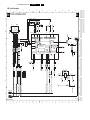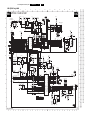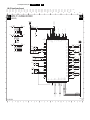
1
Color Television
Chassis
LC8.1U
LA
MG8
ME8
H_17740_000.eps
240408
Contents
Page
1. Technical Specifications, Connections, and Chassis
Overview
2
2. Safety Instructions, Warnings, and Notes
6
3. Directions for Use
7
4. Mechanical Instructions
8
5. Service Modes, Error Codes, and Fault Finding 20
6. Block Diagrams, Test Point Overview, and
Waveforms
Wiring Diagram 32" (ME8/MG8)
33
Wiring Diagram 42" & 47" (ME8/MG8)
34
Wiring Diagram 52" (ME8/MG8)
35
Block Diagram Video
36
Block Diagram Audio
37
Block Diagram Control & Clock Signals
38
SSB: Test Points (Bottom Side)
39
I2C IC Overview
40
Supply Lines Overview
41
7. Circuit Diagrams and PWB Layouts
Diagram
SSB: DC / DC Converter
(B1) 42
SSB: Tuner & Demodulator
(B2) 43
SSB: Class-D & Muting
(B3) 44
SSB: MT5382-Power & Tuner
(B4A) 45
SSB: MT5382-DDR2 SDRAM
(B4B) 46
SSB: MT5382-Flash & NVM
(B4C) 47
SSB: MT5382-LVDS
(B4D) 48
SSB: MT5382-HDMI & Mux
(B4E) 49
SSB: MT5382-Analog I/Os
(B4F) 50
SSB: MJC MT8280-Power
(B5P) 51
SSB: MJC MT8280-DDR2
(B5Q) 52
SSB: MJC MT8280-LVDS
(B5R) 53
SSB: FPGA-AmbiLight
(B6K) 54
SSB: ITV-Channel Decoder (Reserved) (B7L) 55
SSB: ITV-Pro:Idiom (Reserved)
(B7M) 56
SSB: SRP List Explanation
57
Contents
8.
9.
10.
11.
Page
SSB: SRP List Part 1
58
Keyboard Control Panel
(E) 69
Keyboard Control Panel
(E) 69
IR & LED Panel(J)
72
Alignments
75
Circuit Descriptions, Abbreviation List, and IC Data
Sheets
79
Abbreviation List
89
IC Data Sheets
91
Spare Parts List
95
Revision List
95
70
71
73
PWB
59-68
59-68
59-68
59-68
59-68
59-68
59-68
59-68
59-68
59-68
59-68
59-68
59-68
59-68
59-68
©
Copyright 2008 Koninklijke Philips Electronics N.V.
All rights reserved. No part of this publication may be reproduced, stored in a
retrieval system or transmitted, in any form or by any means, electronic,
mechanical, photocopying, or otherwise without the prior permission of Philips.
Published by WF 0864 BU TV Consumer Care
Printed in the Netherlands
Subject to modification
EN 3122 785 17741
EN 2
1.
Technical Specifications, Connections, and Chassis Overview
LC8.1U LA
1. Technical Specifications, Connections, and Chassis Overview
Index of this chapter:
1.1 Technical Specifications
1.2 Connection Overview
1.3 Chassis Overview
1.1.3
Notes:
• Figures can deviate due to the different set executions.
• Specifications are indicative (subject to change).
1.1
Technical Specifications
1.1.1
Vision
Display type
Screen size
Resolution (H × V pixels)
Dyn. contrast ratio
Viewing angle (H × V degrees)
Tuning system
Presets/channels
Tuner bands
TV Color systems
Video playback
Cable
:
:
:
:
:
:
:
:
:
:
:
:
:
:
:
:
:
:
:
:
:
Supported computer formats (60Hz) :
:
:
:
:
:
:
:
Supported video formats (60Hz)
1.1.2
:
:
:
:
:
LCD
32" (82 cm), 16:9
42" (107 cm), 16:9
47" (120 cm), 16:9
52" (132 cm), 16:9
1366×768 (32")
1366×768(42PFL34x)
1920×1080 (rest)
26000:1 (32" and
42PFL34x)
29000:1 (rest 42" &
47")
33000:1 (52")
500
2 ~ 8 (depending on
model number)
178 × 178 (rest)
160 × 160 (52")
PLL
100 presets
VHF, UHF, S, H
ATSC
NTSC
NTSC
Unscrambled digital
cable - QAM
640 × 480
800 × 600
1024 × 768
1280 × 1024
1280 × 768
1360 × 768
1920 × 1080i
1920 × 1080p (only for
full HD sets)
480i
480p
720p
1080i
1080p (only for full HD
sets)
Sound
Sound systems
Maximum power (WRMS)
Power supply:
- Mains voltage (VAC)
- Mains frequency (Hz)
: 90 - 240
: 50 / 60
Ambient conditions:
- Temperature range (°C)
- Maximum humidity
: +5 to +40
: 90% R.H.
Power consumption (values are indicative)
- Normal operation (W)
: ≈ 240
- Stand-by (W)
: <1
:
Min. light output (cd/m2)
Typ. response time (ms)
Miscellaneous
:
:
:
:
Stereo
BBE®
Dolby Digital®
20 ~ 30 (depending
on model number)
Dimensions (W × H × D inch)
- 32"
- 42"
- 47"
- 52"
:
:
:
:
32.3 × 20.4 × 3.6
40.7 × 26.2 × 3.5
44.8 × 28.5 × 4.0
51.2 × 31.4 × 4.7
Weight without stand (lb.)
- 32"
- 42"
- 47"
- 52"
:
:
:
:
31.9
45.1
60.5
83.8
Technical Specifications, Connections, and Chassis Overview
1.2
Connection Overview
LC8.1U LA
1.
EN 3
USB2.0 (16)
1
2
3
4
TV ANTENNA
2
1
3
4
R
R
R
L
L
L
Pr
Pr
Pb
5
SPDIF
OUT
11
AUDIO
6
VIDEO
Y
AV 1
12
SERV. U
L
R
AV 2
AV 3
HDMI 2
8
L
14
HDMI 4
15
USB
16
9
I_17741_001.eps
230408
Figure 1-1 Side and rear I/O connections
Note: The following connector color abbreviations are used
(acc. to DIN/IEC 757): Bk= Black, Bu= Blue, Gn= Green, Gy=
Grey, Rd= Red, Wh= White, and Ye= Yellow.
1.2.1
Side Connections
Head phone - Out (12)
Bk - Head phone
32 - 600 ohm / 10 mW
rt
Cinch: Video CVBS - In, Audio - In (13)
Ye - Video CVBS
1 VPP / 75 ohm
Wh - Audio L
0.5 VRMS / 10 kohm
Rd - Audio R
0.5 VRMS / 10 kohm
jq
jq
jq
S-Video (Hosiden): Video Y/C - In (14)
1 - Ground Y
Gnd
2 - Ground C
Gnd
3 - Video Y
1 VPP / 75 ohm
4 - Video C
0.3 VPP / 75 ohm
H
H
j
j
HDMI4: Digital Video, Digital Audio - In (15)
19
18
1
2
E_06532_017.eps
250505
Figure 1-2 HDMI (type A) connector
1
2
3
4
5
6
7
8
9
10
11
12
13
14
15
16
17
18
19
20
- D2+
- Shield
- D2- D1+
- Shield
- D1- D0+
- Shield
- D0- CLK+
- Shield
- CLK- n.c.
- n.c.
- DDC_SCL
- DDC_SDA
- Ground
- +5V
- HPD
- Ground
1
2
3
4
13
S-VIDEO
DVI AUDIO
IN
HDMI 3
10
Figure 1-3 USB (type A)
VIDEO
7
S-VIDEO
HDMI 1
Service Connector UART
R
Pb
Y
E_06532_022.eps
300904
Data channel
Gnd
Data channel
Data channel
Gnd
Data channel
Data channel
Gnd
Data channel
Data channel
Gnd
Data channel
DDC clock
DDC data
Gnd
Hot Plug Detect
Gnd
j
H
j
j
H
j
j
H
j
j
H
j
j
jk
H
j
j
H
1.2.2
- +5V
- Data (-)
- Data (+)
- Ground
Gnd
k
jk
jk
H
Rear Connections
HDMI1, 2 & 3: Digital Video, Digital Audio - In (9, 10, 11)
1 - D2+
Data channel
j
2 - Shield
Gnd
H
3 - D2Data channel
j
4 - D1+
Data channel
j
5 - Shield
Gnd
H
6 - D1Data channel
j
7 - D0+
Data channel
j
8 - Shield
Gnd
H
9 - D0Data channel
j
10 - CLK+
Data channel
j
11 - Shield
Gnd
H
12 - CLKData channel
j
13 - n.c.
14 - n.c.
15 - DDC_SCL
DDC clock
j
16 - DDC_SDA
DDC data
jk
17 - Ground
Gnd
H
18 - +5V
j
19 - HPD
Hot Plug Detect
j
20 - Ground
Gnd
H
HDMI3: Cinch: DVI Audio - In (7)
Rd - Audio - R
0.5 VRMS / 10 kohm
Wh - Audio - L
0.5 VRMS / 10 kohm
Aerial - In (1)
- - F-type (US)
Coax, 75 ohm
jq
jq
D
AV1 & 2: Cinch: Video YPbPr - In, Audio - In (2, 3)
Gn - Video Y
1 VPP / 75 ohm
Bu - Video Pb
0.7 VPP / 75 ohm
Rd - Video Pr
0.7 VPP / 75 ohm
Wh - Audio L
0.5 VRMS / 10 kohm
Rd - Audio R
0.5 VRMS / 10 kohm
jq
jq
jq
jq
jq
AV3: Cinch: Video CVBS - In, Audio - In (4)
Ye - Video CVBS
1 VPP / 75 ohm
Wh - Audio L
0.5 VRMS / 10 kohm
Rd - Audio R
0.5 VRMS / 10 kohm
jq
jq
jq
AV3: S-Video (Hosiden): Video Y/C - In (8)
1 - Ground Y
Gnd
2 - Ground C
Gnd
3 - Video Y
1 VPP / 75 ohm
4 - Video C
0.3 VPPP / 75 ohm
H
H
j
j
Service Connector UART (5)
1 - UART_TX
Transmit
2 - Ground
Gnd
3 - UART_RX
Receive
k
H
j
Cinch: S/PDIF - Out (6)
Bk - Coaxial
0.4 - 0.6VPP / 75 ohm
kq
EN 4
1.3
1.
LC8.1U LA
Technical Specifications, Connections, and Chassis Overview
Chassis Overview
A
MAIN
SUPPLY PANEL
E
KEYBOARD & CONTROL
PANEL
J
IR & LED PANEL
SMALL SIGNAL
BOARD
B
I_17741_016.eps
280108
Figure 1-4 PWB/CBA locations 32" models
A
MAIN
SUPPLY PANEL
E
KEYBOARD & CONTROL
PANEL
SMALL SIGNAL
BOARD
B
H_17650_083.eps
160108
J
IR & LED PANEL
H_17740_041.eps
240108
Figure 1-5 PWB/CBA locations 42" models
Technical Specifications, Connections, and Chassis Overview
A
MAIN
SUPPLY PANEL
E
KEYBOARD & CONTROL
PANEL
J
IR & LED PANEL
LC8.1U LA
1.
EN 5
SMALL SIGNAL
BOARD
B
I_17741_017.eps
280108
Figure 1-6 PWB/CBA locations 47" models
A
MAIN
SUPPLY PANEL
E
KEYBOARD & CONTROL
PANEL
J
IR & LED PANEL
SMALL SIGNAL
BOARD
B
I_17741_018.eps
280108
Figure 1-7 PWB/CBA locations 52" models
EN 6
2.
LC8.1U LA
Safety Instructions, Warnings, and Notes
2. Safety Instructions, Warnings, and Notes
Index of this chapter:
2.1 Safety Instructions
2.2 Warnings
2.3 Notes
2.1
•
Safety Instructions
Safety regulations require the following during a repair:
• Connect the set to the Mains/AC Power via an isolation
transformer (> 800 VA).
• Replace safety components, indicated by the symbol h,
only by components identical to the original ones. Any
other component substitution (other than original type) may
increase risk of fire or electrical shock hazard.
Safety regulations require that after a repair, the set must be
returned in its original condition. Pay in particular attention to
the following points:
• Route the wire trees correctly and fix them with the
mounted cable clamps.
• Check the insulation of the Mains/AC Power lead for
external damage.
• Check the strain relief of the Mains/AC Power cord for
proper function.
• Check the electrical DC resistance between the Mains/AC
Power plug and the secondary side (only for sets that have
a Mains/AC Power isolated power supply):
1. Unplug the Mains/AC Power cord and connect a wire
between the two pins of the Mains/AC Power plug.
2. Set the Mains/AC Power switch to the “on” position
(keep the Mains/AC Power cord unplugged!).
3. Measure the resistance value between the pins of the
Mains/AC Power plug and the metal shielding of the
tuner or the aerial connection on the set. The reading
should be between 4.5 Mohm and 12 Mohm.
4. Switch “off” the set, and remove the wire between the
two pins of the Mains/AC Power plug.
• Check the cabinet for defects, to prevent touching of any
inner parts by the customer.
2.2
•
Warnings
•
•
•
•
All ICs and many other semiconductors are susceptible to
electrostatic discharges (ESD w). Careless handling
during repair can reduce life drastically. Make sure that,
during repair, you are connected with the same potential as
the mass of the set by a wristband with resistance. Keep
components and tools also at this same potential.
Be careful during measurements in the high voltage
section.
Never replace modules or other components while the unit
is switched “on”.
When you align the set, use plastic rather than metal tools.
This will prevent any short circuits and the danger of a
circuit becoming unstable.
2.3
Notes
2.3.1
General
•
Measure the voltages and waveforms with regard to the
chassis (= tuner) ground (H), or hot ground (I), depending
on the tested area of circuitry. The voltages and waveforms
shown in the diagrams are indicative. Measure them in the
Service Default Mode (see chapter 5) with a color bar
signal and stereo sound (L: 3 kHz, R: 1 kHz unless stated
otherwise) and picture carrier at 475.25 MHz for PAL, or
61.25 MHz for NTSC (channel 3).
2.3.2
Schematic Notes
•
•
•
•
•
•
2.3.3
Where necessary, measure the waveforms and voltages
with (D) and without (E) aerial signal. Measure the
voltages in the power supply section both in normal
operation (G) and in stand-by (F). These values are
indicated by means of the appropriate symbols.
Manufactured under license from Dolby Laboratories.
“Dolby”, “Pro Logic” and the “double-D symbol”, are
trademarks of Dolby Laboratories.
All resistor values are in ohms, and the value multiplier is
often used to indicate the decimal point location (e.g. 2K2
indicates 2.2 kohm).
Resistor values with no multiplier may be indicated with
either an “E” or an “R” (e.g. 220E or 220R indicates 220
ohm).
All capacitor values are given in micro-farads (μ= × 10-6),
nano-farads (n= × 10-9), or pico-farads (p= × 10-12).
Capacitor values may also use the value multiplier as the
decimal point indication (e.g. 2p2 indicates 2.2 pF).
An “asterisk” (*) indicates component usage varies. Refer
to the diversity tables for the correct values.
The correct component values are listed in the Spare Parts
List. Therefore, always check this list when there is any
doubt.
BGA (Ball Grid Array) ICs
BGA Temperature Profiles
For BGA-ICs, you must use the correct temperature-profile,
which is coupled to the 12NC. For an overview of these profiles,
contact your local Service organization.
2.3.4
Lead-free Soldering
Due to lead-free technology some rules have to be respected
by the workshop during a repair:
• Use only lead-free soldering tin Philips SAC305 with order
code 0622 149 00106. If lead-free solder paste is required,
please contact the manufacturer of your soldering
equipment. In general, use of solder paste within
workshops should be avoided because paste is not easy to
store and to handle.
• Use only adequate solder tools applicable for lead-free
soldering tin. The solder tool must be able:
– To reach a solder-tip temperature of at least 400°C.
– To stabilize the adjusted temperature at the solder-tip.
– To exchange solder-tips for different applications.
• Adjust your solder tool so that a temperature of around
360°C - 380°C is reached and stabilized at the solder joint.
Heating time of the solder-joint should not exceed ~ 4 sec.
Avoid temperatures above 400°C, otherwise wear-out of
tips will increase drastically and flux-fluid will be destroyed.
To avoid wear-out of tips, switch “off” unused equipment or
reduce heat.
• Mix of lead-free soldering tin/parts with leaded soldering
tin/parts is possible but PHILIPS recommends strongly to
avoid mixed regimes. If this cannot be avoided, carefully
clear the solder-joint from old tin and re-solder with new tin.
Directions for Use
2.3.5
LC8.1U LA
3.
EN 7
Alternative BOM identification
MODEL
The third digit in the serial number (example:
AG2B0335000001) indicates the number of the alternative
B.O.M. (Bill Of Materials) that has been used for producing the
specific TV set. In general, it is possible that the same TV
model on the market is produced with e.g. two different types
of displays, coming from two different suppliers. This will then
result in sets which have the same CTN (Commercial Type
Number; e.g. 28PW9515/12) but which have a different B.O.M.
number.
By looking at the third digit of the serial number, one can
identify which B.O.M. is used for the TV set he is working with.
If the third digit of the serial number contains the number “1”
(example: AG1B033500001), then the TV set has been
manufactured according to B.O.M. number 1. If the third digit is
a “2” (example: AG2B0335000001), then the set has been
produced according to B.O.M. no. 2. This is important for
ordering the correct spare parts!
For the third digit, the numbers 1...9 and the characters A...Z
can be used, so in total: 9 plus 26= 35 different B.O.M.s can be
indicated by the third digit of the serial number.
PROD.NO: AG 1A0617 000001
3. Directions for Use
You can download this information from the following websites:
http://www.philips.com/support
http://www.p4c.philips.com
MADE IN BELGIUM
220-240V ~ 50/60Hz
128W
VHF+S+H+UHF
S
BJ3.0E LA
E_06532_024.eps
260308
Figure 2-1 Serial number (example)
2.3.6
Board Level Repair (BLR) or Component Level Repair
(CLR)
If a board is defective, consult your repair procedure to decide
if the board has to be exchanged or if it should be repaired on
component level.
If your repair procedure says the board should be exchanged
completely, do not solder on the defective board. Otherwise, it
cannot be returned to the O.E.M. supplier for back charging!
2.3.7
Identification: The bottom line of a type plate gives a 14-digit
serial number. Digits 1 and 2 refer to the production center (e.g.
AG is Bruges), digit 3 refers to the B.O.M. code, digit 4 refers
to the Service version change code, digits 5 and 6 refer to the
production year, and digits 7 and 8 refer to production week (in
example below it is 2006 week 17). The 6 last digits contain the
serial number.
: 32PF9968/10
Practical Service Precautions
•
•
It makes sense to avoid exposure to electrical shock.
While some sources are expected to have a possible
dangerous impact, others of quite high potential are of
limited current and are sometimes held in less regard.
Always respect voltages. While some may not be
dangerous in themselves, they can cause unexpected
reactions that are best avoided. Before reaching into a
powered TV set, it is best to test the high voltage insulation.
It is easy to do, and is a good service precaution.
EN 8
4.
LC8.1U LA
Mechanical Instructions
4. Mechanical Instructions
Index of this chapter:
4.1 Cable Dressing
4.2 Service Positions
4.3 Assy/Panel Removal ME8 Styling
4.4 Set Re-assembly
4.1
Notes:
• Figures below can deviate slightly from the actual situation,
due to the different set executions.
• Follow the disassemble instructions in described order.
• Please pay special attention to the speaker wires when reassembling the set. Place the cable tapes as shown in next
figures.
Cable Dressing
CONNECTOR WITH
LOCK INSERTED
TO PSU
CONNECTOR
WITHOUT LOCK
INSERTED TO
PANEL
Inverter Cable
AC Mains Cable
Speaker and IR cable dressing: Tape to keep out of
speaker terminals
Speaker cable dressing: Pull cable taut
underneath SSB Plate before taping to
keep out of stand area
I_17741_009.eps
280408
Figure 4-1 Cable dressing (32" models, ME8 styling)
Mechanical Instructions
LC8.1U LA
4.
EN 9
CONNECTOR WITH LOCK
INSERTED TO PSU
CONNECTOR WITHOUT LOCK
INSERTED TO PANEL
AC Mains Shield wire to be grounded to
bottom corner of PSU with screw
Detailed view of speaker cable dressing:
Pull cable taut underneath SSB Plate before
I_17741_008.eps
240408
Figure 4-2 Cable dressing (32" models, MG8 styling)
EN 10
4.
LC8.1U LA
Mechanical Instructions
Tape tweeter wire to metal frame (both ends)
to keep away from tweeter terminal
I_17741_010.eps
240408
Figure 4-3 Cable dressing (42" models, ME8 styling)
I_17741_011.eps
240408
Figure 4-4 Cable dressing (42" models, MG8 styling)
Mechanical Instructions
LC8.1U LA
4.
EN 11
Tape the 8C02 cable (IR Board to SSB) and
the short red tweeter wire together.
I_17741_013.eps
240408
Figure 4-5 Cable dressing (47" models, ME8 styling)
EN 12
4.
LC8.1U LA
Mechanical Instructions
I_17741_012.eps
240408
Figure 4-6 Cable dressing (47" models, MG8 styling)
Mechanical Instructions
LC8.1U LA
4.
EN 13
Tape inverter cable so
it stays in-between the
LCD Panel lamp
holders as shown to
avoid EMC Foam on
SSB Bars.
NOTE: For inverter cables,
the connector with ferrite
is to be inserted at the
PSU side
Note orientation
of wire saddle –
the IR and
Speaker Cables
must not be
parallel with AC
Mains cable
Tape speaker
wires to prevent
interference with
speaker terminal
I_17741_014.eps
240408
Figure 4-7 Cable dressing (52" models, ME8 styling)
EN 14
4.
LC8.1U LA
Mechanical Instructions
Tape inverter cable so
it stays in-between the
LCD Panel lamp
holders as shown to
avoid EMC Foam on
SSB Bars.
NOTE: For inverter cables,
the connector with ferrite
is to be inserted at the
PSU side
Note horizontal orientation of wire saddle –
the IR and Speaker Cables must cross the
AC Mains Cable with “X” shape and not lay
in parallel
I_17741_015.eps
250408
Figure 4-8 Cable dressing (52" models, MG8 styling)
Mechanical Instructions
4.2
4.2.1
LC8.1U LA
4.
Service Positions
4.3
Assy/Panel Removal ME8 Styling
For easy servicing of this set, there are a few possibilities
created:
• The buffers from the packaging.
• Foam bars (created for Service).
4.3.1
Back Cover
Foam Bars
1
1
Required for sets
42"
EN 15
Warning: Disconnect the mains power cord before you remove
the back cover.
Note: it is not necessary to remove the stand while removing
the back cover.
Warning: Most sets have an additional hatch located in the
back cover. These are meant for disconnecting the flat cables
to the AmbiLight units in the back cover, before the back cover
is lifted from the set. The hatches are not always located at the
same place for all sets, therefore the figures below are only
meant as indication.
It is mandatory to locate these hatches first, open them, and
unplug connectors behind. Lifting the back cover without
having done so, could result in damaging the connectors
inside!
Refer to next figures for details.
E_06532_018.eps
171106
Figure 4-9 Foam bars
The foam bars (order code 3122 785 90580 for two pieces) can
be used for all types and sizes of Flat TVs. See figure “Foam
bars” for details.
Sets with a display of 42" and larger, require four foam bars [1].
Ensure that the foam bars are always supporting the cabinet
and never only the display.
Caution: Failure to follow these guidelines can seriously
damage the display!
By laying the TV face down on the (ESD protective) foam bars,
a stable situation is created to perform measurements and
alignments. By placing a mirror under the TV, you can monitor
the screen.
4.2.2
1. First remove the screws [1] from the back cover hatch and
remove the hatch.
2. Then unplug connector(s) [3].
3. Remove the screws [2], gently lift the back cover from the
set. Make sure that wires and flat coils are not damaged
while lifting the back cover from the set.
3
Service Stands
The MkII aluminium Service Stands are not suitable for this
chassis. Use the stands that come with the set instead.
H_17740_022.eps
230108
Figure 4-10 Back Cover Removal [1/2]
EN 16
4.
Mechanical Instructions
LC8.1U LA
2
2
2
2
2
2
2
2
2
1
1
2
2
2
2
2
2
2
2
2
2
H_17740_024.eps
230108
Figure 4-11 Back Cover Removal [2/2]
4.3.2
Ambilight (if present)
4.3.3
Refer to next figure for details.
1. Unplug the connectors [1].
2. Remove the screws [2].
3. Pull the unit sidewards from the back cover.
When defective, replace the whole unit.
2
1
H_17650_097.eps
180108
Figure 4-12 Ambilight Unit
Loudspeaker (MG8 styling only)
1. Unplug the connectors.
2. Remove the screws.
3. Remove the loudspeaker.
Mechanical Instructions
4.3.4
Woofers (ME8 styling only)
4.3.7
Refer to next figure for details.
1. Remove the screws [1] and [2] and lift the whole unit from
the back cover.
Take the speakers out together with their casing. When
defective, replace the whole unit.
LC8.1U LA
4.
EN 17
Key Board
Refer to next figure for details.
1. Unplug the key board connector from the IR & LED board.
2. Remove the screws [1].
3. Lift the unit and take it out of the set.
When defective, replace the whole unit.
2
3
1
3
H_17740_023.eps
230108
1
Figure 4-13 Woofer
4.3.5
Tweeters (ME8 styling only)
Refer to next figure for details.
Warning: The speakers should never be connected or
disconnected when the set is playing! This can damage the
amplifiers on the SSB.
1. Unplug connector [1].
2. Remove screws [2] and remove unit.
Note: After repair, be sure to place the cable tapes (see also
cable dressing figures for the exact location).
H_17650_094.eps
180108
Figure 4-16 Key Board
1
4.3.8
Display Supply Panel
Refer to next figure for details. Note: depending on the set
execution, the used PSU can differ from figure below.
1. Unplug connectors [1].
2. Remove the fixation screws [2].
3. Take the board out.
2
H_17650_095.eps
180108
2
1
Figure 4-14 Tweeter
4.3.6
1
2
IR & LED Board
Refer to next figure for details.
1. Unplug connectors [1].
2. Use a flat screw driver to release the clip by pushing it in
the indicated direction [2].
3. Lift the board and take it out of the set.
When defective, replace the whole unit.
2
2
1
2
2
1
1
2
2
H_17740_021.eps
230108
Figure 4-17 Display Supply Panel
2
H_17650_098.eps
180108
Figure 4-15 IR & LED Board
EN 18
LC8.1U LA
Mechanical Instructions
Small Signal Board (SSB)
2. Unplug the connectors [2].
3. Remove the screws [3].
4. The SSB can now be taken out of the set, together with the
front shield and the side cover.
5. To remove the shield, remove the screws [4] and lift it of
while releasing clips [5].
6. Release clip [6] and slide the cover sidewards from the
SSB.
Refer to below figure for details.
Caution: it is mandatory to remount all different screws at their
original position during re-assembly. Failure to do so may result
in damaging the SSB.
Refer to next figures or details.
1. Unplug the LVDS connector(s) [1].
Caution: be careful, as this is a very fragile connector!
3
OPTIONAL
OPTIONAL
3
3
1
6
5
OPTIONAL
4.3.9
4.
3
5
2
4
4 4
4
3
4
4
4
4
3
3
5
H_17740_019.eps
230108
Figure 4-18 Small Signal Board
Mechanical Instructions
LC8.1U LA
4.
EN 19
4.3.10 LCD Panel
Refer to next figures for details. The figure used is from a 42inch model, but the other screensizes have similar
constructions.
1. Remove the stand.
2. Unplug the LVDS connector(s) [1].
Caution: be careful, as this is a very fragile connector!
3. Unplug the connectors [2].
4. Remove the fixation screws [3] from rim.
5. Take the rim from the set.
6. Remove the fixation screws [4] and [5].
7. Lift the subframe from the set.
8. The LCD panel can now be lifted from the front cabinet.
4
4
5
3
5
5
5
4
1
2
2
3
5
5
5
4
4
4
5
4
4
2
H_17740_020.eps
230108
Figure 4-19 LCD Panel (example from 42’’ model)
4.4
Set Re-assembly
To re-assemble the whole set, execute all processes in reverse
order.
Notes:
• Important: While re-assembling, make sure that all cables
and cable tapes are placed in their original position. See
figure “Cable dressing”.
• Pay special attention not to damage the EMC foams on the
SSB shields. Ensure that EMC foams are mounted
correctly.
EN 20
5.
LC8.1U LA
Service Modes, Error Codes, and Fault Finding
5. Service Modes, Error Codes, and Fault Finding
Index of this chapter:
5.1 Test Points
5.2 Service Modes
5.3 Service Tools
5.4 Error Codes
5.5 The Blinking LED Procedure
5.6 Fault Finding and Repair Tips
5.7 Software Upgrading
Test Points
In the chassis schematics and layout overviews, the test points
are mentioned. In the schematics, test points are indicated with
“Fxxx” or “Ixxx”, in the layout overviews with a “half-moon” sign.
As most signals are digital, it will be difficult to measure
waveforms with a standard oscilloscope. Several key ICs are
capable of generating test patterns, which can be controlled via
ComPair. In this way it is possible to determine which part is
defective.
Perform measurements under the following conditions:
• Service Default Mode.
• Video: Color bar signal.
• Audio: 3 kHz left, 1 kHz right.
5.2
Service Modes
The Service Mode feature is split into four parts:
• Service Default Mode (SDM).
• Service Alignment Mode (SAM).
• Customer Service Mode (CSM).
• Computer Aided Repair Mode (ComPair).
SDM and SAM offer features, which can be used by the Service
engineer to repair/align a TV set. Some features are:
• A pre-defined situation to ensure measurements can be
made under uniform conditions (SDM).
• Activates the blinking LED procedure for error identification
when no picture is available (SDM).
• The possibility to overrule software protections when SDM
is entered via the Service pins.
• Make alignments (e.g. White Tone), (de)select options,
enter options codes, reset the error buffer (SAM).
• Display information (“SDM” or “SAM” indication in upper
right corner of screen, error buffer, software version,
operating hours, options and option codes, sub menus).
The CSM is a Service Mode that can be enabled by the
consumer. The CSM displays diagnosis information, which the
customer can forward to the dealer or call centre. In CSM
mode, “CSM”, is displayed in the top right corner of the screen.
The information provided in CSM and the purpose of CSM is to:
• Increase the home repair hit rate.
• Decrease the number of nuisance calls.
• Solved customers' problem without home visit.
General
Some items are applicable to all Service Modes or are general.
These are listed below.
Life Timer
During the life time cycle of the TV set, a timer is kept (called
“Op. Hour”). It counts the normal operation hours (not the
Stand-by hours). The actual value of the timer is displayed in
SDM and SAM in a decimal value. Every two soft-resets
increase the hour by +1. Standby hours are not counted.
Software Identification, Version, and Cluster
The software ID, version, and cluster will be shown in the main
menu display of SDM, SAM, and CSM.
The screen will show: “AAAABCD X.YY”, where:
• AAAA is the chassis name: LC81.
• B is the region indication: E= Europe, A= AP/China, U=
NAFTA, L= LATAM.
• C is the display indication: L= LCD, P= Plasma.
• D is the language/feature indication: P= Philips, M=
Magnavox.
• X is the main version number: this is updated with a major
change of specification (incompatible with the previous
software version). Numbering will go from 1 - 9 and A - Z.
– If the main version number changes, the new version
number is written in the NVM.
– If the main version number changes, the default
settings are loaded.
• YY is the sub version number: this is updated with a minor
change (backwards compatible with the previous versions)
Numbering will go from 00 - 99.
– If the sub version number changes, the new version
number is written in the NVM.
– If the NVM is fresh, the software identification, version,
and cluster will be written to NVM.
Display Option Code Selection
When after an SSB or display exchange, the display option
code is not set properly, it will result in a TV with “no display”.
Therefore, it is required to set this display option code after
such a repair.
To do so, press the following key sequence on a standard RC
transmitter: “062598” directly followed by MENU and “xxx”,
where “xxx” is a 3 digit decimal value of the panel type: see
column “Panel Code” in table “Option Codes OP1...OP7” (ch.
8), or see sticker on the side/bottom of the cabinet. When the
value is accepted and stored in NVM, the set will switch to
Stand-by, to indicate that the process has been completed.
Display Option
Code
39mm
PHILIPS
ComPair Mode is used for communication between a computer
and a TV on I2C /UART level and can be used by a Service
engineer to quickly diagnose the TV set by reading out error
codes, read and write in NVMs, communicate with ICs and the
uP (PWM, registers, etc.), and by making use of a fault finding
database. It will also be possible to up and download the
software of the TV set via I2C with help of ComPair. To do this,
ComPair has to be connected to the TV set via the ComPair
connector, which will be accessible through the rear of the set
(without removing the rear cover).
27mm
5.1
5.2.1
040
MODEL:
32PF9968/10
PROD.SERIAL NO:
AG 1A0620 000001
(CTN Sticker)
E_06532_038.eps
240108
Figure 5-1 Location of Display Option Code sticker
During this algorithm, the NVM-content must be filtered,
because several items in the NVM are TV-related and not SSBrelated (e.g. Model and Prod. S/N). Therefore, “Model” and
“Prod. S/N” data is changed into “See Type Plate”.
In case a call centre or consumer reads “See Type Plate” in
CSM mode, he needs to look to the side/bottom sticker to
identify the set, for further actions.
Service Modes, Error Codes, and Fault Finding
5.2.2
Service Default Mode (SDM)
Purpose
Set the TV in SDM mode in order to be able to:
• Create a pre-defined setting for measurements to be
made.
• Override software protections.
• Start the blinking LED procedure.
• Read the error buffer.
• Check the life timer.
LC8.1U LA
5.
EN 21
On Screen Menu
After activating SDM, the following screen is visible, with SDM
in the upper right corner of the screen to indicate that the
television is in Service Default Mode.
Specifications
Table 5-1 SDM default settings
Region
Freq. (MHz)
Default syst.
Europe (except France), 475.25
AP-PAL/-Multi
PAL B/G
France
SECAM L
NAFTA, AP-NTSC
LATAM
•
•
H_17740_030.eps
230108
61.25 (channel 3) NTSC M
Figure 5-3 SDM menu
PAL M
Set linear video and audio settings to 50%, but volume to
25%. Stored user settings are not affected.
All service-unfriendly modes (if present) are disabled, since
they interfere with diagnosing/repairing a set. These
service unfriendly modes are:
– (Sleep) timer.
– Blue mute/Wall paper.
– Auto switch “off” (when there is no “ident” signal).
– Hotel or hospital mode.
– Child lock or parental lock (manual or via V-chip).
– Skipping, blanking of “Not favorite”, “Skipped” or
“Locked” presets/channels.
– Automatic storing of Personal Preset or Last Status
settings.
– Automatic user menu time-out (menu switches back/
OFF automatically.
– Auto Volume levelling (AVL).
How to Activate
To activate SDM, use one of the following methods:
• Press the following key sequence on the remote control
transmitter: “062596” directly followed by the MENU button
(do not allow the display to time out between entries while
keying the sequence).
• Short one of the “Service” jumpers on the TV board during
cold start (see Figures “Service jumper”). Then press the
mains button (remove the short after start-up).
Caution: Activating SDM by shorting “Service” jumpers will
override the DC speaker protection (error 1), the General
I2C error (error 4), and the Trident video processor error
(error 5). When doing this, the service-technician must
know exactly what he is doing, as it could damage the
television set.
Menu explanation:
• HHHHH: Are the operating hours (in decimal).
• AAAABCD-X.YY: See paragraph “Service Modes” ->
“General” -> “Software Identification, Version, and Cluster”
for the SW name definition.
• EER: Shows all errors detected since the last time the
buffer was erased. Five errors possible.
• OP: Used to read-out the option bytes. See “Options” in the
Alignments section for a detailed description. Ten codes (in
two rows) are possible.
How to Navigate
As this mode is read only, there is not much to navigate. To
switch to other modes, use one of the following methods:
• Command MENU from the user remote will enter the
normal user menu (brightness, contrast, color, etc...) with
“SDM” OSD remaining, and pressing MENU key again will
return to the last status of SDM again.
• To prevent the OSD from interfering with measurements in
SDM, command “OSD” or “i+” (“STATUS” or “INFO” for
NAFTA and LATAM) from the user remote will toggle the
OSD “on/off” with “SDM” OSD remaining always “on”.
• Press the following key sequence on the remote control
transmitter: “062596” directly followed by the OSD/
STATUS/INFO/i+ button to switch to SAM (do not allow the
display to time out between entries while keying the
sequence).
How to Exit
Switch the set to STANDBY by pressing the mains button on
the remote control transmitter or on the television set.
If you switch the television set “off” by removing the mains (i.e.,
unplugging the television), the television set will remain in SDM
when mains is re-applied, and the error buffer is not cleared.
The error buffer will only be cleared when the “clear” command
is used in the SAM menu.
Note:
• If the TV is switched “off” by a power interrupt while in SDM,
the TV will show up in the last status of SDM menu as soon
as the power is supplied again. The error buffer will not be
cleared.
• In case the set is in Factory mode by accident (with “F”
displayed on screen), by pressing and hold “VOL-“ and
“CH-” together should leave Factory mode.
H_17740_031.eps
230108
Figure 5-2 Service jumper (SSB component side)
EN 22
5.2.3
5.
LC8.1U LA
Service Modes, Error Codes, and Fault Finding
Service Alignment Mode (SAM)
Purpose
• To change option settings.
• To display / clear the error code buffer.
• To perform alignments.
Specifications
• Operation hours counter (maximum five digits displayed).
• Software version, error codes, and option settings display.
• Error buffer clearing.
• Option settings.
• Software alignments (White Tone).
• NVM Editor.
• Set screen mode to full screen (all content is visible).
How to Activate
To activate SAM, use one of the following methods:
• Press the following key sequence on the remote control
transmitter: “062596” directly followed by the OSD/
STATUS/INFO/i+ button (it depends on region which
button is present on the RC). Do not allow the display to
time out between entries while keying the sequence.
• Or via ComPair.
After entering SAM, the following screen is visible, with SAM in
the upper right corner of the screen to indicate that the
television is in Service Alignment Mode.
How to Navigate
• In the SAM menu, select menu items with the UP/DOWN
keys on the remote control transmitter. The selected item
will be indicated. When not all menu items fit on the screen,
use the UP/DOWN keys to display the next / previous
menu items.
• With the LEFT/RIGHT keys, it is possible to:
– Activate the selected menu item.
– Change the value of the selected menu item.
– Activate the selected sub menu.
• When you press the MENU button twice while in top level
SAM, the set will switch to the normal user menu (with the
SAM mode still active in the background). To return to the
SAM menu press the MENU button.
• The “OSD/STATUS/INFO/i+” key from the user remote will
toggle the OSD “on/off” with “SAM” OSD remaining always
“on”.
• Press the following key sequence on the remote control
transmitter: “062596” directly followed by the MENU button
to switch to SDM (do not allow the display to time out
between entries while keying the sequence).
How to Store SAM Settings
To store the settings changed in SAM mode (except the
OPTIONS and RGB ALIGN settings), leave the top level SAM
menu by using the POWER button on the remote control
transmitter or the television set. The mentioned exceptions
must be stored separately via the STORE button.
How to Exit
Switch the set to STANDBY by pressing the mains button on
the remote control transmitter or the television set.
Note:
• When the TV is switched “off” by a power interrupt while in
SAM, the TV will show up in “normal operation mode” as
soon as the power is supplied again. The error buffer will
not be cleared.
• In case the set is in Factory mode by accident (with “F”
displayed on screen), by pressing and hold “VOL-“ and
“CH-” together should leave Factory mode.
H_17740_025.eps
230108
Figure 5-4 SAM menu
Menu explanation:
1. System Information:
• Op. Hour. This represents the life timer. The timer
counts normal operation hours, but does not count
Stand-by hours.
• MAIN SW ID. See paragraph “Service Modes” ->
“General” -> “Software Identification, Version, and
Cluster” for the SW name definition.
• ERROR CODES. Shows all errors detected since the
last time the buffer was erased. Five errors possible.
• OP1 / OP2. Used to read-out the option bytes. See
“Options” in the Alignments section for a detailed
description. Ten codes are possible.
2. Clear. Erases the contents of the error buffer. Select the
CLEAR menu item and press the MENU RIGHT key. The
content of the error buffer is cleared.
3. Options. To set the option bits. See “Options” in the
“Alignments” chapter for a detailed description.
4. RGB Align. To align the White Tone. See “White Tone” in
the “Alignments” chapter for a detailed description.
5. NVM Editor. To change the NVM data in the television set.
See also paragraph “Fault Finding and Repair Tips”.
6. NVM Copy. Gives the possibility to copy/load the NVM file
to/from an USB stick.
Important: NVM data copied to a USB memory device is
named “TV2USB.bin”. When copied back to a TV, the file
first must be renamed to “USB2TV.bin”.
Service Modes, Error Codes, and Fault Finding
5.2.4
Customer Service Mode (CSM)
Purpose
The Customer Service Mode shows error codes and
information on the TV’s operation settings. A call centre can
instruct the customer (by telephone) to enter CSM in order to
identify the status of the set. This helps them to diagnose
problems and failures in the TV before making a service call.
The CSM is a read-only mode; therefore, modifications are not
possible in this mode.
Specifications
• Ignore “Service unfriendly modes”.
• Line number for every line (to make CSM language
independent).
• Set the screen mode to full screen (all contents on screen
is visible).
• After leaving the Customer Service Mode, the original
settings are restored.
• Possibility to use “CH+” or “CH-” for channel surfing, or
enter the specific channel number on the RC.
How to Activate
To activate CSM, press the following key sequence on a
standard remote control transmitter: “123654” (do not allow the
display to time out between entries while keying the sequence).
Upon entering the Customer Service Mode, the following
screen will appear:
LC8.1U LA
5.
EN 23
Menu Explanation
1. Model Number. Type number, e.g. 42PFL5603D/27. (*)
2. Production Serial Number. Product serial no., e.g.
SV1A0805123456 (*). SV= Production center, 1= BOM
code, A= Service version change code, 08= Production
year, o5= Production week, 123456= Serial number.
3. Software Version. Main software cluster and version is
displayed.
4. Option Code 1. Option code information (group 1).
5. Option Code 1. Option code information (group 2).
6. Codes. Error buffer contents.
7. SSB. Indication of the SSB factory ID (= 12nc). (*)
8. Display. Indication of the display ID (=12 nc). (*)
9. NVM Version. The NVM software version no.
10. PQ Version. PQ (picture quality) data version. This is a
subset of the main SW.
11. Key (HDCP). Indicates if the HDMI keys (or HDCP keys)
are valid or not.
12. Digital Signal Quality. Tuner signal condition in
percentage.
13. Blank.
14. Audio System. Gives information about the audio system
of the selected transmitter (MONO/STEREO).
15. HDAU. HDMI audio stream detection. “YES” means audio
stream detected. “NO” means no audio stream present.
Only displayed when HDMI source is selected.
16. Video Format. Gives information about the video format of
the selected transmitter (480p30/720p60/1080i50/1080i60,
etc...). Is applicable to both HDMI and CVI sources.
17. HD SW ID. Shows the HD DNM software version.
18. FPGA SW ID. Shows the FPGA software version (if
present).
19. DFI SW ID. Shows the DFI software version (if present).
20. Standby uP SW ID. Shows the Standby Processor
software version.
(*) If an NVM IC is replaced or initialized, these items must be
re-written to the NVM. ComPair will foresee in a possibility to
do this.
H_17740_028.eps
230108
Figure 5-5 CSM menu -1- (example)
H_17740_029.eps
230108
Figure 5-6 CSM menu -2- (example)
How to Exit
To exit CSM, use one of the following methods:
• Press the MENU button twice on the remote control
transmitter.
• Press the POWER button on the remote control
transmitter.
• Press the POWER button on the television set.
EN 24
5.
Service Modes, Error Codes, and Fault Finding
LC8.1U LA
5.3
Service Tools
5.4
Error Codes
5.3.1
ComPair
5.4.1
Introduction
Introduction
ComPair (Computer Aided Repair) is a Service tool for Philips
Consumer Electronics products. and offers the following:
1. ComPair helps you to quickly get an understanding on how
to repair the chassis in a short and effective way.
2. ComPair allows very detailed diagnostics and is therefore
capable of accurately indicating problem areas. You do not
have to know anything about I2C or UART commands
yourself, because ComPair takes care of this.
3. ComPair speeds up the repair time since it can
automatically communicate with the chassis (when the uP
is working) and all repair information is directly available.
4. ComPair features TV software up possibilities.
Error codes are required to indicate failures in the TV set. In
principle a unique error code is available for every:
• Activated protection.
• Failing I2C device.
• General I2C error.
• SDRAM failure.
The last five errors, stored in the NVM, are shown in the
Service menu’s. This is called the error buffer.
The error code buffer contains all errors detected since the last
time the buffer was erased. The buffer is written from left to
right. When an error occurs that is not yet in the error code
buffer, it is displayed at the left side and all other errors shift one
position to the right.
An error will be added to the buffer if this error differs from any
error in the buffer. The last found error is displayed on the left.
An error with a designated error code may never lead to a
deadlock situation. This means that it must always be
diagnosable (e.g. error buffer via OSD or blinking LED
procedure, ComPair to read from the NVM).
In case a failure identified by an error code automatically
results in other error codes (cause and effect), only the error
code of the MAIN failure is displayed.
Specifications
ComPair consists of a Windows based fault finding program
and an interface box between PC and the (defective) product.
The (new) ComPair II interface box is connected to the PC via
an USB cable. For the TV chassis, the ComPair interface box
and the TV communicate via a bi-directional cable via the
service connector(s).
How to Connect
This is described in the ComPair chassis fault finding database.
Example: In case of a failure of the I2C bus (CAUSE), the error
code for a “General I2C failure” and “Protection errors” is
displayed. The error codes for the single devices (EFFECT) is
not displayed. All error codes are stored in the same error
buffer (TV’s NVM) except when the NVM itself is defective.
TO TV
TO
UART SERVICE
CONNECTOR
ComPair II
RC in
RC out
TO
I2C SERVICE
CONNECTOR
TO
UART SERVICE
CONNECTOR
5.4.2
Multi
function
Optional Power Link/ Mode
Switch
Activity
I2C
RS232 /UART
PC
ComPair II Developed by Philips Brugge
HDMI
I2C only
Optional power
5V DC
E_06532_036.eps
150208
Figure 5-7 ComPair II interface connection
Caution: It is compulsory to connect the TV to the PC as
shown in the picture above (with the ComPair interface in
between), as the ComPair interface acts as a level shifter. If
one connects the TV directly to the PC (via UART), ICs will be
blown!
How to Order
ComPair II order codes:
• ComPair II interface: 3122 785 91020.
• ComPair UART interface cable: 3138 188 75051.
• Program software can be downloaded from the Philips
Service website.
Note: If you encounter any problems, contact your local
support desk.
5.3.2
LVDS Tool
Support of the LVDS Tool has been discontinued.
How to Read the Error Buffer
You can read the error buffer in 3 ways:
• On screen via the SAM/SDM/CSM (if you have a picture).
Example:
– ERROR: 0 0 0 0 0 : No errors detected
– ERROR: 6 0 0 0 0 : Error code 6 is the last and only
detected error
– ERROR: 9 6 0 0 0 : Error code 6 was detected first and
error code 9 is the last detected (newest) error
• Via the blinking LED procedure (when you have no
picture). See “The Blinking LED Procedure”.
• Via ComPair.
Service Modes, Error Codes, and Fault Finding
5.4.3
5.4.4
LC8.1U LA
Error Codes
5.5
The Blinking LED Procedure
In case of non-intermittent faults, write down the errors present
in the error buffer and clear the error buffer before you begin
the repair. This ensures that old error codes are no longer
present.
If possible, check the entire contents of the error buffer. In
some situations, an error code is only the result of another error
and not the actual cause of the problem (for example, a fault in
the protection detection circuitry can also lead to a protection).
5.5.1
Introduction
Code Error Description Detection via: Type
Remarks
0
No Error
-- -- --
N/A
-- -- --
1
DC Protection
MT5382
(7A01)
Protection DC_PROT = Low
2
+12V Failure
WT61P7
(7E23)
Protection POWER_DOWN = Low
3
Stand-by Control- I2C0 Bus
ler I2C
Protection Communication Error with
WT61P7
4
General I2C
I2C0 Bus
Error Log
Communication Error on
I2C0 Bus
5#
MT8280 I2C
I2C0 Bus
Error Log
Communication Error with
MT8280
6
System NVM I2C
I2C0 Bus
Protection Communication Error with
System NVM
7
Tuner
Tuner I2C Bus Error Log
Communication Error with
Tuner TDQU
8
IF/PLL Demodula- Tuner I2C Bus Error Log
tor
Communication Error with
TDA9886
9
Ambilight FPGA
I2C0 Bus
Error Log
Communication Error with
EC2S
10
Reserved
-- -- --
N/A
-- -- --
11
Reserved
-- -- --
N/A
-- -- --
12
Reserved
-- -- --
N/A
-- -- --
13
HDMI Switch I2C
I2C0 Bus
Error Log
Communication Error with
Sil9185
14
MT8280 DRAM1
DRAM R/W
(7B02/03)
Error Log
R/W Error with DRAM1 or
DRAM2
15
Reserved
-- -- --
N/A
-- -- --
16
Reserved
-- -- --
N/A
-- -- --
17
Reserved
-- -- --
N/A
-- -- --
18 #
Channel Decoder I2C0 Bus
I2C
Error Log
Communication Error with
MT5112 (reserved for
BDS modules)
19 #
Pro Idiom I2C
I2C0 Bus
Error Log
Communication Error with
Pro Idiom (reserved for
BDS modules)
21 #
Bolt-On
NVM I2C
HDMI I2C0 Bus
Error Log
Communication Error with
BDS Bolt-On (reserved for
BDS modules)
#
If IC/board available.
How to Clear the Error Buffer
The error code buffer is cleared in the following cases:
• By using the CLEAR command in the SAM menu:
• If the contents of the error buffer have not changed for 50
hours, the error buffer resets automatically.
Note: If you exit SAM by disconnecting the mains from the
television set, the error buffer is not reset.
5.
EN 25
The software is capable of identifying different kinds of errors.
Because it is possible that more than one error can occur over
time, an error buffer is available, which is capable of storing the
last five errors that occurred. This is useful if the OSD is not
working properly.
Errors can also be displayed by the blinking LED procedure.
The method is to repeatedly let the front LED pulse with as
many pulses as the error code number, followed by a period of
1.5 seconds in which the LED is “off”. Then this sequence is
repeated.
Example (1): error code 4 will result in four times the sequence
LED “on” for 0.25 seconds / LED “off” for 0.25 seconds. After
this sequence, the LED will be “off” for 1.5 seconds. Any RC5
command terminates the sequence. Error code LED blinking is
in red color.
Example (2): the content of the error buffer is “12 9 6 0 0”
After entering SDM, the following occurs:
• 1 long blink of 5 seconds to start the sequence,
• 12 short blinks followed by a pause of 1.5 seconds,
• 9 short blinks followed by a pause of 1.5 seconds,
• 6 short blinks followed by a pause of 1.5 seconds,
• 1 long blink of 1.5 seconds to finish the sequence,
• The sequence starts again with 12 short blinks.
5.5.2
Displaying the Entire Error Buffer
Additionally, the entire error buffer is displayed when Service
Mode “SDM” is entered. In case the TV set is in protection or
Stand-by: The blinking LED procedure sequence (as in SDMmode in normal operation) must be triggered by the following
RC sequence: “MUTE” “062500” “OK”.
In order to avoid confusion with RC5 signal reception blinking,
this blinking procedure is terminated when a RC5 command is
received.
EN 26
5.6
5.
LC8.1U LA
Service Modes, Error Codes, and Fault Finding
Fault Finding and Repair Tips
Table 5-2 NVM editor overview
Notes:
• It is assumed that the components are mounted correctly
with correct values and no bad solder joints.
• Before any fault finding actions, check if the correct
options are set.
5.6.4
5.6.1
Description
10
Existing value
Value
0x0000
0
New value
Store
Store?
Load Default NVM Values
It is possible to download default values automatically into the
NVM in case a blank NVM is placed or when the NVM first 20
address contents are “FF”. After the default values are
downloaded, it is possible to start-up and to start aligning the
TV set. To initiate a forced default download the following
action has to be performed:
1. Switch “off” the TV set with the mains cord disconnected
from the wall outlet (it does not matter if this is from “Standby” or “Off” situation).
2. Short-circuit the SDM jumpers on the SSB (keep short
circuited).
3. Press “P+” or “CH+” on the local keyboard (and keep it
pressed).
4. Reconnect the mains supply to the wall outlet.
5. Release the “P+” or “CH+” when the set is started up and
has entered SDM.
When the downloading has completed successfully, the set
should be into Stand-by, i.e. red LED on.
Remark on the Supply Errors
The detection of a supply dip or supply loss during the normal
playing of the set does not lead to a protection, but to a cold
reboot of the set. If the supply is still missing after the reboot,
the TV will go to protection.
Alternative method:
It is also possible to upload the default values to the NVM with
ComPair in case the SW is changed, the NVM is replaced with
a new (empty) one, or when the NVM content is corrupted.
After replacing an EEPROM (or with a defective/no EEPROM),
default settings should be used to enable the set to start-up and
allow the Service Default Mode and Service Alignment Mode to
be accessed.
Protections during Start-up
During TV start-up, some voltages and IC observers are
actively monitored to be able to optimize the start-up speed,
and to assure good operation of all components. If these
monitors do not respond in a defined way, this indicates a
malfunction of the system and leads to a protection.
Hardware Protections
5.6.5
The only real hardware protection in this chassis is (in case of
an audio problem) the audio protection circuit that will trigger
the uP to switch “off” the TV.
Repair Tip
• It is also possible that you have an audio DC protection
because of an interruption in one or both speakers (the DC
voltage that is still on the circuit cannot disappear through
the speakers).
Caution: (dis)connecting the speaker wires during the ON
state of the TV at high volume can damage the audio
amplifier.
5.6.3
Dec
0x000A
Software Protections
Most of the protections and errors use either the stand-by or the
micro processor as detection device. Since in these cases,
checking of observers, polling of ADCs, and filtering of input
values are all heavily software based, these protections are
referred to as software protections.
There are several types of software related protections, solving
a variety of fault conditions:
• Protections related to supplies: check of the 12V.
• Protections related to breakdown of the safety check
mechanism. E.g. since the protection detections are done
by means of software, failing of the software will have to
initiate a protection mode since safety cannot be
guaranteed any more.
5.6.2
Hex
Address
NVM Editor
In some cases, it can be convenient if one directly can change
the NVM contents. This can be done with the “NVM Editor” in
SAM mode. With this option, single bytes can be changed.
Caution:
• Do not change these, without understanding the
function of each setting, because incorrect NVM
settings may seriously hamper the correct functioning
of the TV set!
• Always write down the existing NVM settings, before
changing the settings. This will enable you to return to the
original settings, if the new settings turn out to be incorrect.
Display option code
Caution: In case you have replaced the SSB, always check the
display option code in SAM, even if you have picture. With a
wrong display option code it is possible that you have picture,
but that in certain conditions you have unwanted side-effects.
Service Modes, Error Codes, and Fault Finding
5.6.6
Start-up/Shut-down Flowcharts
On the next pages you will find start-up and shut-down
flowcharts, which might be helpful during fault finding.
POWER STATES
In this chassis, there are six possible power states as follows:
• Power OFF
• ON
• STANDBY
• SEMI-STANDBY
• Special Panel Mode
• PROTECTION
5.
EN 27
PROTECTION
This state is entered when an error has been detected at
startup or in the “ACTIVE” mode. All switched power supply
lines are turned “off” with only +3V3stby remaining “on”; similar
to “STANDBY” mode. This state is indicated by the blinking red
front LED with the blinking sequence denoting the type of error
detected.
When the system enters the protection mode due to a critical
error, it should be turned “off” and the failure cause needs to be
resolved. The system will function normally again after
performing a power recycling once all protection causing
failures have been resolved.
START-UP SEQUENCE
There are two cases of start-up sequences, namely:
• AC On and
• Standby Wake-up
Power
OFF
AC Mains OFF
LC8.1U LA
AC Mains OFF
AC Mains ON
AC Mains ON
Special
Panel
Mode
ERROR
detected
PROTECTION
SDM && Panel
= LOW
ERROR
detected
ERROR
detected
Last Status = ON
WAKEUP Command
Received
ON
STANDBY
Command
Auto
Clock
SEMISTANDBY
(Clock
Download)
Manual
Clock
PSU = STANDBY
LED1 = OFF
LED2 = BLINK
See also figure on next page.
Last Status = STANDBY
PSU = ON
LED1 = ON
LED2 = OFF
STANDBY
PSU = STANDBY
LED1 = OFF
LED2 = OFF
H_17740_033.eps
230108
Figure 5-8 Power States
POWER OFF
In “Power OFF” mode, the system is completely switched “off”
from AC mains. When AC power is applied, the system checks
for last status. Depending on the last standby status stored in
the system EEPROM, this mode can then transit to “ON” or
“STANDBY” mode.
ON
This is the normal operating mode, indicated by the “on” LED.
All the power supply lines are available and depending on the
sub-mode, all the circuits in the system may be active. From
this mode it shall be possible to transit to “STANDBY”, “SEMISTANDBY” and “PROTECTION” mode, or to “Power OFF”
mode if AC mains are switched “off”. The sub-modes are:
• Active Mode (Normal Consumer Mode)
• Service Modes
• Panel Modes
• Factory Modes
STANDBY
The total power consumption of the system in this mode shall
be equal or less than 150 mW. This state is indicated by no
LED when AC mains is switched “on”. Only the standby
controller WT61P7 is operational in this state, where only
+3V3stby power supply is available. From this mode it shall be
possible to transit to the “ACTIVE” or “Power OFF” mode if AC
mains are switched “off”.
SEMI-STANDBY
The semi-standby state is only accessed during transition from
ACTIVE to STANDBY when the auto clock feature is switched
“on”. The clock information download is carried out in this state
before proceeding to STANDBY.
SPECIAL PANEL MODE
The Special Panel Mode is only used during manufacturing
process to program the system EEPROM. In this mode, the
SDA0 and SCL0 ports of MT5382 are set to high impedance
after SDM and PANEL pins are both detected as “low” during
startup. This mode can be exited using a power recycle.
AC ON
In the case of start-up from AC mains, all PSU voltages start to
turn “on” as the hardware default of the active “low” STANDBY
(controlled by Standby Controller WT61P7’s STANDBY signal)
signal to the PSU is pulled “low” with respect to ground.
The MT5382 starts running boot loader once the hardware
reset circuit is released. The system will then check the last
standby status from the system EEPROM to determine
whether to complete the system start-up (load image, turn on
the audio, display etc) or proceed to standby and wait for wakeup command from user. The Standby Controller then proceeds
to verify the power status of the +12V and sends the system to
protection in case of any failures. Special Panel, SDM, and
PANEL modes are detected as well.
System recovery is always handled by Standby Controller.
Watchdog for MT5382 and MT8280 (if present) will be only
enabled during startup, and these components are able to
differentiate the normal startup and watchdog reset to trigger
system reset when applicable. The alive checking mechanism
kicks in after system startup is completed.
STANDBY WAKEUP
When the system receives a command to wake-up from
standby, the Standby Controller sets the STANDBY signal
“low” to turn “on” the switched power, and similarly detects for
the presence of +12V. The MT5382 waits for +3V3_SW to be
available before loading its image. The significance of this
voltage detection is due to the flash is also being powered by
the same mentioned voltage.
The following figure shows the start-up flowchart for both “AC
On” and “Standby Wake-up”:
EN 28
5.
LC8.1U LA
Service Modes, Error Codes, and Fault Finding
H_17740_034.eps
240108
Figure 5-9 Start-up flowchart
Service Modes, Error Codes, and Fault Finding
LC8.1U LA
5.
EN 29
STANDBY SEQUENCE
The following flowchart depicts the Standby (plus SemiStandby condition) sequence:
START
Set Last Status = STANDBY
Disable RC/LKB Key
Instruct WT61P7
to turn off LED1
Set LED1 = OFF
Stop Backlight Dimming,
PWM_DIMMING = 100%
Mute Audio, MUTEn = HIGH
Turn Off Backlight
BACKLIGHT_ON_OFF = LOW
T~200ms
AUTO-CLOCK
is ON?
Yes
SEMI-STANDBY
Enable RC/LKB Key
WT61P7
Start to Obtain Clock Info
from Selected Source
MT5382
No
No
Clock
Download
Timeout =
3sec?
No
Clock
Download
Complete?
Yes
Yes
No
Wakeup Event
Received?
Yes
Disable RC/LKB Key
Switch off LVDS Signal
Set Last Status = ACTIVE
Wait for Panel_Off_Time_2 based on
Panel ID in ms (from Panel Flash)
Wait for Next Instruction
from MT5382
Instruct WT61P7
to turn on LED1
Turn Off LVDS Power,
LCD_PWR_ON = HIGH
Disable RC/LKB Key
Yes
Proceed to
STANDBY?
PWM_Dimming = 0%
T~700ms
No
Turn On Backlight
BACKLIGHT_ON_OFF = HIGH
Disable DC_PROT &
POWER_DOWN INT
Display Startup Logo for 1sec
Set LED1 = ON
Pass Error Buffer, Clock Info and
CEC Information to WT61P7
Set Back to Last Channel
WT61P7 STANDBYn = LOW
Instruct WT61P7
to go to Standby
Unmute Audio, MUTEn = LOW
T~1300ms
Yes
T~1200ms
STANDBY due
to Protection?
Enable RC/LKB Key
WT61P7 blinks LED2
according to Error Buffer
No
Note:
Blocking for
next startup
to ensure
PSU
properly
discharged
END
(Back to ON)
Wait 3000ms
END
(STANDBY)
Note: Estimated running time.
Actual implementation to be verified.
Figure 5-10 Standby flowchart
H_17740_035.eps
240108
EN 30
5.
Service Modes, Error Codes, and Fault Finding
LC8.1U LA
POWERDOWN SEQUENCE
The following figure shows the power-down sequence
flowchart:
START
POWER_DOWN INT
based on falling
edge trigger
MT5382 Detects
POWER_DOWN INT
Reconfirm
POWER_DOWN
= LOW?
Yes
Mute Audio Output
No
Write Protect Flash and
System EEPROM
Wait for
impending
Power Off
Note: To
Avoid False
Triggering
System Idle
END
H_17740_036.eps
240108
Figure 5-11 Power-down flowchart
The power-down condition is detected by the MT5382
POWER_DOWN signal which is an interrupt pin. A “low” level
on this line signifies that power-down is detected. The two
major activities that occur over this operation is the muting of
audio output and write protecting the system flash and
EEPROM.
DC PROTECTION
The following figure shows the DC_PROT interrupt flowchart:
START
Check
DC_PROT = LOW
for 3 sec?
Yes
Mute Audio Output
No
DC Protection
[Protection]
Note: To
Avoid False
Triggering
Log Error Code
Go to STANDBY
END
H_17740_037.eps
240108
Figure 5-12 DC Protection flowchart
Service Modes, Error Codes, and Fault Finding
5.7
Software Upgrading
5.7.1
Introduction
Automatic Software Upgrade
In “normal” conditions, so when there is no major problem with
the TV, the main software and the default software upgrade
LC08SSp User software upgrade flow chart
Power off the set
A newer version of software is
detected.
Do you want to upgrade?
NO
layout 1
Plug-in the USB
stick
An equal/older version of software is
detected.
Do you want to proceed?
Note: Should be done only if
necessary.
YES
Power-on the set
NO
layout 2
Detect USB
‘break-in’ and
check autorun file
Kindly remove the USB stick and
restart the set.
layout 3
Valid auto-run
file?
N
Y
Software update failed!
Would you like to try again?
YES
Is USB sw
version > set
sw?
NO
Is USB sw
version =< set
sw?
N
N
Content browser
Photo & music
layout 4
Y
Y
Display USB
sw newer than
the TV sw.
Prompt user to
confirm
Display USB
sw equal/older
than TV sw.
Prompt user to
confirm
See layout 1
Content browser
Photo & music
N
See layout 2
Proceed?
Y
Set re-start &
Proceed with sw
upgrade
Prompt user to
remove USB
and restart the
set
See layout 3
End
Y
EN 31
How to upgrade:
1. Copy “autorun.upg” to the root of your USB stick.
2. Insert USB stick in the side I/O while the set is in “On”
mode. The set will restart and the upgrading will start
automatically. As soon as the programming is finished, you
will get the message that you can remove your USB stick
and restart the set.
Main Software Upgrade
YES
5.
application can be upgraded with the “autorun.upg” (FUS part
in the one-zip file). This can also be done by the consumers
themselves, but they will have to get their software from the
commercial Philips website or via the Software Update
Assistant in the user menu (see DFU). The “autorun.upg” file
must be placed in the root of your USB stick.
It is possible for the user to upgrade the main software via the
USB port. This allows replacement of a software image in a
stand alone set, without the need of an E-JTAG debugger. A
description on how to upgrade the main software can be found
in the DFU or on the Philips website.
5.7.2
LC8.1U LA
Successful?
Display
upgrade
progress
N
Prompt user to
try again?
See layout 4
N
Retry?
Y
H_17740_038.eps
230408
Figure 5-13 SW upgrade flowchart
EN 32
5.7.3
5.
LC8.1U LA
Service Modes, Error Codes, and Fault Finding
Content and Usage of the One-Zip Software File
Below you find a content explanation of the One-Zip file, and
instructions on how and when to use it.
•
•
•
•
•
5.7.4
Ambi_clustername_version.zip. Not to be used by
Service technicians.
Panel_clustername_version.zip. Not to be used by
Service technicians.
EDID_clustername_version.zip. Contains the EDID
content of the different EDID NVMs. See ComPair for
further instructions.
FUS_clustername_version.zip. Contains the
“autorun.upg” which is needed to upgrade the TV main
software and the software download application.
ProcessNVM_clustername_version.zip. Default NVM
content. Must be programmed via ComPair.
How to Copy NVM Data to/from USB
Write NVM data to USB
1. Insert the USB stick into the USB slot while in SAM mode.
2. Execute the command "Copy to USB", to copy the NVM
data to the USB stick. The NVM filename on the USB stick
will be named “NVM2USB.bin” (this takes a couple of
seconds).
Write NVM data to TV
1. First, rename the filename (via a PC) on the USB stick to
“USB2NVM.bin”.
2. Insert the USB stick into the USB slot while in SAM mode.
3. Execute the command "Copy from USB" to copy the USB
data to NVM (this takes about a minute to complete).
Important: The file must be located in the root directory of the
USB stick.
Block Diagrams, Test Point Overview, and Waveforms
LC8.1U LA
6.
33
6. Block Diagrams, Test Point Overview, and Waveforms
Wiring Diagram 32" (ME8/MG8)
WIRING 32" (STYLING ME8/MG8)
LCD DISPLAY (1004)
LVDS INPUT
30P
INVERTER
B
14P
8418
CN2 / 1319
14. PDIM_Select
13. PWM
12. On/Off
11. Vbri
10. GND3
9. GND3
8. GND3
7. GND3
6. GND3
5. 24Vinv
4. 24Vinv
3. 24Vinv
2. 24Vinv
1. 24Vinv
A
(1005)
F123
F124
CN6 / 1M95
1. 3V3Vstdby
2. Standby
3. GND1
4. GND1
5. GND1
6. +12V
7. +12V
8. +12V
9. +12V (audio)
10. GND2
11. -12V (audio)
1101 (B1)
11. -12VAudio
10. GNDSND
9. +12VAudio
7. +12VS
6. +12VS
5. GND
4. GND
3. GND
2. STANDBY
1. +3V3STBY
8101
1102 (B1)
CN7 / 1M99
1. +12V
2. +12V
3. GND1
4. GND1
5. BL_ON_OFF
6. DIM
7. Boost
8. ANALOG/PWM
dimming
CN1 / 1308
2. L
1. N
T 5AH 250V
T 5A 125V
F1
(1150)
MAIN POWER SUPPLY
T 5A 125V
CONTROL PANEL
E KEYBOARD
(0025)
SSB
1D01 (B4D)
1. LVSD1_SDA_DISP
2. LVDS1_SCL_DISP
.
.
40. +VDISP
41. +VDISP
8D01
8.
7.
6.
5.
4.
3.
2.
1.
8102
ANA-DIG_DIM_SELECT
BACKLIGHT_BOOST
PWM_DIMMING
BACKLIGHT_ON_OFF
GND
GND
+12Vdisp
+12Vdisp
1C02 (B4C)
9.
8.
7.
6.
5.
4.
3.
2.
1.
8408
KEYBOARD
+5V_SW
KEYBOARD
LED1
+3V3STBY
LED2
IR
GND
LIGHT_SENSOR
1301 (B3)
8301
INLET
4.
3.
2.
1.
RIGHT+
GND
GND
LEFT-
J1
GND
KEYBOARD
+3V3STBY
INTERRUPT
8C02
RIGHT SPEAKER
(5211) ME8 IN BACK COVER
(5211) MG8
J
IR LED PANEL
LIGHT-SENSOR
GNDSND
RC
LED2
+3V3-STANDBY
LED1
KEYBOARD
+5V
KEYBOARD
+ -
1.
2.
3.
4.
5.
6.
7.
8.
9.
1P10
1.
2.
3.
4.
+ -
GND
KEYBOARD
+3V3STBY
TACT_SWITCH_INT
8N10
1P11
1.
2.
3.
4.
LEFT SPEAKER
(1112)
(5212) ME8 IN BACK COVER
(5211) MG8
I_17741_005.eps
240408
Block Diagrams, Test Point Overview, and Waveforms
LC8.1U LA
6.
34
Wiring Diagram 42" & 47" (ME8/MG8)
WIRING DIAGRAM 42”- 47” (STYLING ME8/MG8)
8K05
8K04
LVDS INPUT
41/51P
*AMBI-LIGHT UNIT (IN BACK COVER)
8K01
8D01
8D02
GND
+24V
GND
+24V
1D01 (B4D)
41P
1K01 (B6K)
7. GND
6. +3V3_SW
5. +3V3_FPGA
4. GND
3. AMBI_SDA
2. GND
1. AMBI_SCL
8K03
1K04 (B6K)
4. GND_24V
3. +24V_BOLT-ON
2. GND_24V
1. +24V_BOLT-ON
B
SSB
(1150)
1K03 (B6K)
6. GND_24V
5. +24V_BOLT-ON
4. GND_24V
3. +24V_BOLT-ON
2. GND_24V
1. +24V_BOLT-ON
CN6
1. 3V3ST
2. Standby
3. GND
4. GND
5. GND
6. 12Vssb
7. 12Vssb
8. 12Vssb
9. +12Vaud
10. GND_aud
11. -12Vaud
1.
2.
3.
4.
+24V
GND
+24V
GND
J4
+24V
+24V
GND
S-SCL
S-SDA
GND
3.3V
I2C SEL2
J2
1102 (B1)
8. ANA-DIG_DIM_SELECT
7. BACKLIGHT_BOOST
6. PWM_DIMMING
5. BACKLIGHT_ON_OFF
4. GND
3. GND
2. +12Vdisp
1. +12Vdisp
8102
J1
1.
2.
3.
4.
5.
6.
7.
8.
1101 (B1)
11. -12VAudio
10. GNDSND
9. +12VAudio
7. +12VS
6. +12VS
5. GND
4. GND
3. GND
2. STANDBY
1. +3V3STBY
8101
CN7
1. 12Vssb
2. 12Vssb
3. GND
4. GND
5. INV-ON
6. DIM
7. BOOST
8. GND
BOARD TACT SW
E CONTROL
(0025)
1.
2.
3.
4.
5.
6.
7.
S-SCL
GND
S-SDA
I2C SEL1
I2C SEL2
3.3V
GND
1C02 (B4C)
9. KEYBOARD
8. +5V_SW
7. KEYBOARD
6. LED1
5. +3V3STBY
4. LED2
3. IR
2. GND
1. LIGHT_SENSOR
CN1
1. N
2. L
1301 (B3)
4. RIGHT+
3. GND
2. GND
1. LEFT-
8408
INLET
8301
(1175)
*AMBI-LIGHT UNIT (IN BACK COVER)
4.
3.
2.
1.
CN4
1. 24Vamb
2. GND
3. 24Vamb
4. GND
5. 24Vamb
6. GND
(1005)
J1
1D02 (B4D)
41P
LCD DISPLAY (1004)
MAIN POWER SUPPLY
I2C SEL2
3.3V
GND
S-SDA
S-SCL
GND
+24V
+24V
1D03 (B4D)
51P
8D03
TO BACKLIGHT
8.
7.
6.
5.
4.
3.
2.
1.
DANGEROUS
HIGH VOLTAGE
(1175)
J4
DANGEROUS
HIGH VOLTAGE
TO BACKLIGHT
GND
3.3V
I2C SEL2
I2C SEL1
S-SDA
GND
S-SCL
CN3
1. HV2
2. N.C.
3. HV2
7.
6.
5.
4.
3.
2.
1.
CN2
1. HV1
2. N.C.
3. HV1
J2
Only for 100/120Hz
1N10
GND
KEYBOARD
+3V3STBY
INTERRUPT
8C02
RIGHT SPEAKER
(5215) TWEETER
(5211) WOOFER IN BACK COVER
* AMBI-LIGHT UNITS ARE OPTIONAL
J
IR LED PANEL
(1112)
LIGHT-SENSOR
GNDSND
RC
LED2
+3V3-STANDBY
LED1
KEYBOARD
+5V
KEYBOARD
+ -
1.
2.
3.
4.
5.
6.
7.
8.
9.
1P10
1.
2.
3.
4.
+ -
GND
KEYBOARD
+3V3STBY
TACT_SWITCH_INT
8N10
1P11
1.
2.
3.
4.
LEFT SPEAKER
(5215) TWEETER
(5212) WOOFER IN BACK COVER
H_17740_056.eps
240108
Block Diagrams, Test Point Overview, and Waveforms
LC8.1U LA
6.
35
Wiring Diagram 52" (ME8/MG8)
WIRING 52" (STYLING ME8/MG8)
LCD DISPLAY (1004)
LVDS INPUT
41/51P
8D01
8D02
INVERTER
8D03
Only for 100/120Hz
1D03 (B4D)
51P
1D02 (B4D)
41P
1D01 (B4D)
41P
INVERTER
CN2 / 1319
CN6 / 1M95
A
1. 3V3 stdby
2. Standby
3. GND1
4. GND1
5. GND1
6. +12V
7. +12V
8. +12V
9. +12V (audio)
10. GND2 (audio)
11. -12V (audio)
MAIN POWER SUPPLY
(1005)
CN3 / 1316
8419
B
SSB
(1150)
CN7 / 1M99
12. N.C.
11. N.C.
10. GND3
9. GND3
8. GND3
7. GND3
6. GND3
5. 24Vinv
4. 24Vinv
3. 24Vinv
2. 24Vinv
1. 24Vinv
14P
8101
1.
2.
3.
4.
5.
6.
7.
8.
+12V
+12V
GND1
GND1
BL_ON_OFF
DIM
Boost
ANALOG/PWM
dimming
8102
1101 (B1)
11. -12VAudio
10. GNDSND
9. +12VAudio
7. +12VS
6. +12VS
5. GND
4. GND
3. GND
2. STANDBY
1. +3V3STBY
12P
8418
14. PDIM_Select
13. PWM
12. On/Off
11. Vbri
10. GND3
9. GND3
8. GND3
7. GND3
6. GND3
5. 24Vinv
4. 24Vinv
3. 24Vinv
2. 24Vinv
1. 24Vinv
F1
T 8AH 250V
8.
7.
6.
5.
4.
3.
2.
1.
ANA-DIG_DIM_SELECT
BACKLIGHT_BOOST
PWM_DIMMING
BACKLIGHT_ON_OFF
GND
GND
+12Vdisp
+12Vdisp
1C02 (B4C)
9.
8.
7.
6.
5.
4.
3.
2.
1.
2. L
1. N
CN1 / 1308
CONTROL PANEL
E KEYBOARD
(0025)
1102 (B1)
8408
KEYBOARD
+5V_SW
KEYBOARD
LED1
+3V3STBY
LED2
IR
GND
LIGHT_SENSOR
1301 (B3)
8301
INLET
4.
3.
2.
1.
RIGHT+
GND
GND
LEFT-
J1
GND
KEYBOARD
+3V3STBY
INTERRUPT
8C02
RIGHT SPEAKER
ME8 (5215) TWEETER (5211) WOOFER IN BACK COVER
MG8 (5211)
J
IR LED PANEL
LIGHT-SENSOR
GNDSND
RC
LED2
+3V3-STANDBY
LED1
KEYBOARD
+5V
KEYBOARD
+ -
1.
2.
3.
4.
5.
6.
7.
8.
9.
1P10
1.
2.
3.
4.
+ -
GND
KEYBOARD
+3V3STBY
TACT_SWITCH_INT
8N10
1P11
1.
2.
3.
4.
LEFT SPEAKER
(1112)
ME8 (5215) TWEETER (5212) WOOFER IN BACK COVER
MG8 (5211)
I_17741_006.eps
240408
Block Diagrams, Test Point Overview, and Waveforms
LC8.1U LA
6.
36
Block Diagram Video
VIDEO
B2
B4
TUNER & DEMODULATOR
B5R
MT5382
B4D
MJC MT8280 - LVDS
MT5382 - LVDS
7A01
MT5382
1203
TDQU8-T01A
IFAGC
4MHZ-REFOUT
IF _AGC_MAIN
9
LVDS_B_TXe
4
6
+5VS
7201
TDA9886T/V4
HYBRID
TUNER
1204
A-IFOUT
1D01
1
B4A TUNER
B26 IF_AGC
AIF
8
SUPPLY
1 VIF1
5
1
2 VIF2
4
TO DISPLAY
LVDS_B_TXo
20
32
15
REF
RC VCO
DIDITAL VCO COTROL
VIF-PLL
SOUND TRAPS
4.5 to 6.5 Mhz
CVBS 17
B4F ANALOG
I/O
7200
EF
CVBS_OUT
38
39
7P01
MT8280
AC26 CVBS0
B4D LVDS
40
41
+VDISP
DEMODULATOR
45MHZ75
SIF2
VIF AGC
I2C-BUS TRANSCEIVER
2
MT8280
ANALOG
MUX
MOTION ESTIMATION
MOTION COMPENSATION
LVDS_TXe
SDA
TUNER AGC
SCL
TAGC
LVDS_B_TXe
LVDS_TXo
DUAL
LVDS OUT
MAD
SIF AGC
1D02
1
DUAL LVDS
SINGLE REFERENCE QSS MIXER
INTERCARRIER MIXER AND
AM-DEMODULATOR
SIF1
TO DISPLAY
Only for
40 100/120Hz sets
41
LVDS_B_TXo
I2C
DIFOUT1
DIFOUT1
VIP_ATV
AB24
11
VIN_ATV
AC24
B4F
MT5382 - HDMI & MUX
VIP_ATV
VIN_ATV
1
2
1
RX2_2p
3
RX2_2n
RX2_1p
19
18
4
6
7
HDMI 2
CONNECTOR
AV1
1
2
19
18
Y
RX2_Cp
12
RX2_Cn
AV2
1
RX3_2p
3
RX3_2n
RX3_1p
Y
RX3_Cp
RX3_Cn
1
RXSide_2p
3
RXSide_2n
RXSide_1p
4
6
7
VIDEO
1F03
1
AF19
AV2_Pb_in
196
AV3_CVBS_in
AD26
AV3_SY_in
AF26
AV3_SC_in
AE25
3
S SVHS 5
4
2
AE26
SAV_SY_in
AF25
SAV_SC_in
AE24
1
RX1_2p
3
RX1_2n
RX1_1p
AF11
AE11
RXSide_Cn
VIDEO
1F07
1
3
2
4
0P
0N
LVDS_A_TXo
PR1P
1D03
51
50
LVDS_A_TXe
Y1P
5
4
PB1P
TO DISPLAY
MOTION
CONTROL
3
+VDISP
2
1
PR0P
Y0P
PB0P
XTALI
205
204
TO FPGA
AMBI-LIGHT
B6K
CONTROL
1201
14M31
CVBS1
B5Q
SY0
MJC MT8280 - DDR2
SC0
7Q01
EDE5116A
SDRAM
CVBS3
DRAM
SY1
7Q02
EDE5116A
SC1
MJC_RA(0-12)
1E01
1
2
AA14
MJC_RDQW(0-31)
SIDE
AV
SVHS 5
4
6
7
HDMI 1
CONNECTOR
AB14
LVDS_TXe0n
B5Q DDR2
SAV_CVBS_in
RXSide_Cp
LVDS_TXe0p
C12
1F08
RXSide_0n
12
D12
MAIN PROCESSOR
VIDEO
XTALO
RXSide_1n
RXSide_0p
9
10
GPIO1
1F04
RX3_0n
12
AD20
AV2_Y_in
Pb
RX3_1n
RX3_0p
9
10
AE22
AV2_Pr_in
Pr
AV3
1
2
AD21
GPIO0
1F02
1E04
19
18
AV1_Y_in
Pb
RX2_0n
9
10
4
6
7
HDMI (SIDE)
CONNECTOR
AE23
AV1_Pb_in
RX2_1n
RX2_0p
1E03
HDMI 3
CONNECTOR
AV1_Pr_in
Pr
1E02
QUAD LVDS
1920x1080
100/120HZ
B4D FLASH &
NVM
MT5382
MT5382 - ANALOG I/O
1F01
19
18
B4E
10
B4E HDMI
& MUX
SDRAM
AF10
RX1_1n
RX1_0p
AE10
AF9
RX1_0n
AE9
9
10
RX1_Cp
AF8
12
RX1_Cn
AE8
B4B
MT5382 - DDR2 SDRAM
7E18
SII9185ACTU
RX2_2p
28
68
RXSide_2p
RX2_2n
RX2_1p
27
25
67
65
RXSide_2n
RXSide_1p
RX2_1n
RX2_0p
24
22 R0X
64
R2X 62
RXSide_1n
RXSide_0p
61
RXSide_0n
59
RXSide_Cp
58
1
2
RXSide_Cn
RX2_0n
21
RX2_Cp
19
RX2_Cn
RX3_2p
18
48
RX3_2n
RX3_1p
47
45
RX3_1n
RX3_0p
44
42 R1X
RX3_0n
41
RX3_Cp
RX3_Cn
HDMI
SWITCH
B4B DDR2
SDRAM
(0-12)
SDRAM
RDQ(0-31)
AF15
AE15
4
RXMux_2p
RXMux_2n
RXMux_1p
5
7
RXMux_1n
RXMux_0p
AE14
AF13
8
10
RXMux_0n
RXMux_Cp
AE13
39
38
11
RXMux_Cn
AE12
TX
13
HDMI_RESET
7B02
EDE2516ACSE
(0-15)
DDR2
7B03
EDE2516ACSE
AF14
RA
(0-12)
SDRAM
AF12
(16-31)
B4C
CONTROL
H_17740_057.eps
240408
Block Diagrams, Test Point Overview, and Waveforms
LC8.1U LA
6.
37
Block Diagram Audio
AUDIO
B2
B4
TUNER & DEMODULATOR
B4B MT5382 - DDR2 SDRAM
MT5382
7A01
MT5382
1203
TDQU8-T01A
4MHZ-REFOUT
+5VS
7201
TDA9886T/V4
HYBRID
TUNER
1204
A-IFOUT
B4A TUNER
B26 IF_AGC
IF _AGC_MAIN
9
6
AIF
8
5
1 VIF1
4
2 VIF2
20
SUPPLY
1
15
REF
RC VCO
DIDITAL VCO COTROL
VIF-PLL
SOUND TRAPS
4.5 to 6.5 Mhz
B4B DDR2
SDRAM
CVBS
7B02
EDE2516ACSE
(0-12)
IF-PLL DEMODULATOR
45MHZ75
SINGLE REFERENCE QSS MIXER SIOMAD 12
INTERCARRIER MIXER AND
AM-DEMODULATOR
SIF1
SIF2
RDQ(0-31)
VIF AGC
(0-15)
DDR2
7B03
EDE2516ACSE
I2C-BUS TRANSCEIVER
SCL
TUNER AGC
AC26 CVBS0
MAD
SIF AGC
TAGC
SDRAM
SIF_OUT
SDA
IFAGC
RA
(0-12)
SDRAM
I2C
(16-31)
MT5382
B4E MT5382 - HDMI & MUX
B4F MT5382 - ANALOG I/O
B4F ANALOG
I/O
MAIN PROCESSOR
AUDIO
1F01
1
2
1E02
AV1
1
RX2_2p
3
RX2_2n
RX2_1p
19
18
4
6
7
HDMI 2
CONNECTOR
RX2_0n
RX2_Cp
12
RX2_Cn
AV1_L_in
K25
AV1_R_in
K26
AV2_L_in
L23
AV2_R_in
L24
AV3_L_in
J23
AV3_R_in
J24
AIN3_L
AIN3_R
1F02
RX2_1n
RX2_0p
9
10
AUDIO
L/R IN
AV2
AUDIO
L/R IN
B4F MT5382
1
2
1
RX3_2p
3
RX3_2n
RX3_1p
19
18
4
6
7
HDMI 2
CONNECTOR
AV3
AUDIO
L/R IN
AUDIO
IN
AIN0_L
AIN0_R
RX3_1n
RX3_0p
RX3_Cp
12
RX3_Cn
1
2
RXSide_2p
3
RXSide_2n
RXSide_1p
4
6
7
PC
AUDIO
AUDIO
L/R IN
PC_L_in
K23
PC_R_in
K24
AUDIO_OUT
19
18
SPDIF
DIGITAL
AUDIO IN
RXSide_0n
AIN2_R
RXSide_Cn
SIDE
AV
AUDIO
L/R IN
B22
J25
SAV_R_in
J26
1
2
OPCTRL5
RX1_2p
3
RX1_2n
RX1_1p
9
10
12
AF11
AE11
AE10
AF9
RX1_0n
AE9
RX1_Cp
AF8
RX1_Cn
28
68
RXSide_2p
RX2_2n
RX2_1p
27
25
67
65
RXSide_2n
RXSide_1p
RX2_1n
RX2_0p
24
22 R0X
64
62
RXSide_1n
RXSide_0p
61
RXSide_0n
59
RXSide_Cp
58
1
2
RXSide_Cn
RX2_0n
21
19
RX2_Cn
RX3_2p
18
48
RX3_2n
RX3_1p
47
45
RX3_1n
RX3_0p
44
42 R1X
R2X
HDMI
SWITCH
TX
AF15
AE15
4
RXMux_2p
RXMux_2n
RXMux_1p
5
7
RXMux_1n
RXMux_0p
AE14
AF13
RX3_0n
41
8
10
RXMux_0n
RXMux_Cp
AE13
39
RX3_Cn
38
11
RXMux_Cn
AE12
HDMI_RESET
3
Speaker R
OUT2
RIGHT+
22
4
AC7
5
ENGAGE
6302
MUTEn
AC13
DC-PROT
7306
7307
DC
DETECTION
B4E HDMI
& MUX
AL2
B4F MT5382
ANALOG I/O
E26
HP_L
HP_LOUT
1E15
2
HP_R
HP_ROUT
3
7F03-2
AR2
F25
4
ANTI_PLOP
A25
B4C
CONTROL
FAST_PLOP
B4E
CONTROL
Headphone
Out 3.5mm
MUTING
CIRCUIT
HP_DETECT
AF14
RX3_Cp
13
2
AIN1_R
AOSDATA3
RX2_2p
Speaker L
7308
AE8
7E18
SII9185ACTU
1301
1
6303
POWER_DOWN
B4E
AF10
RX1_1n
RX1_0p
LEFT-
27
IN2N
7303
AC14
HDMI
SWITCH
RX2_Cp
14
7F03-1
1
4
6
7
19
18
AIN1_L
OUT1
IN1P
CLASS D
AUDIO
AMPLIFIER
PreAmpLR
G25
PHERIPHERAL
OPCTRL3
SAV_L_in
1E01
HDMI 1
CONNECTOR
AR1
B4C FLASH
& NVM
OPCTRL1
SAV_R_in
1F08
RXSide_Cp
12
HDMI (SIDE)
CONNECTOR
2
PreAmpL
7F04-2
AIN2_L
1F05
RXSide_1n
RXSide_0p
9
10
7F04-1
F26
1F05
1E04
1
7301
TDA8932BTW/N2
B4F ANALOG
I/O
AL1
RX3_0n
9
10
CLASS-D & MUTING
AIN4_R
1F04
1E03
B3
ANALOG I/O
AIN4_L
AF12
B4C
CONTROL
H_17740_058.eps
220408
Block Diagrams, Test Point Overview, and Waveforms
LC8.1U LA
6.
38
Block Diagram Control & Clock Signals
CONTROL + CLOCK SIGNALS
B6K FPGA - AMBILIGHT
7P01
MT8280
B5R POWER
7K01
MT8280
LVDS_TXoCLKp
LVDS_TXoCLKn
AB11
AA11
B4
RESERVED
TO 1D01
B4D
LVDS CONN.
LVDS_TXeCLKp
LVDS_TXeCLKn
AB17
AA17
MT8280
AMBI FPGA
A12
LVDS_A_TXoCLKp
B12
A18
LVDS_A_TXoCLKn
LVDS_A_TXeCLKp
B18
LVDS_A_TXeCLKn
F4
nCSO
1
H16
D8
DCLK
6
H15
C3
F1
ASD0
DATA0
5
2
LVDS_B_TXoCLKp
F21
LVDS_B_TXoCLKn
M22
M21
LVDS_B_TXeCLKp
LVDS_B_TXeCLKn
MJC_RCLK0
F2
MJC_RCLK0n
F1
MJC_RCLK1
MJC_RCLK1n
J8
K8
N2
P3
SF_S0
15
D8
SF_CK
16
A7
B8
SF_CS0
SF_DO
7
8
Y18
PWN
AB6
W18
PRST
AA6
Y6
1
2Mx8
FLASH
3
2
AMBI_SDA
AMBI_SCL
1
HEAD-PHONE
CONNECTOR
CHANNEL VOLUME +
VOLUME -
AC1
RCLK1n
K8
1N15
B3
AUDIO
C23
LCD_PWR_ON
B24
+12Vdisp_DETECT
ANA-DIG_DIM_SELECT
7C05
Switch
PDD1
15
AA4
AE4
POOEn
16
B19
AE3
AD4
POCE0n
PDD0
7
8
C19
D20
INT0
B18
AD7
DC_PROT
V25
KEYBOARD
V25
LIGHT-SENSOR
U24
AC13
3P10
LED1
WHITE
6P10
+3V3STBY
7P11
7E25
LED1
6
6
LED1
7P10
LED2
RED
24
7E26
LED2
4
4
IR
3
3
LED2
25
7P14
3
10
CEC
AB14
35
3P16
+3V3STBY
IR
RECEIVER
+5V_SW
5
5
+5V_SW
8
8
LIGHT_SENSOR
1
1
+3V3STBY
7P13
7P12
STANDBY
CONTROLLER
IR
HDMI_HPD_1
C11
HDMI_HPD_2
D10
HDMI_HPD_3
E19
HDMI_HPD_SIDE
B10
HDMI_RESET
CEC
DDC_RESET
D11
12M
6P11
EDID_WE
E9
AB14
7E07
3P11
+5V_SW
19
8Mx8
FLASH
B1
SDM
4
7
SUPPLY
BACKLIGHT_BOOST
AE1
7E23
WT61P7-RG440WT
7
B1
7C04
B4E MT5382 - FLASH & NVM
KEYBOARD
PWM_DIMMING
B1
2
W25
A18
1C02
B1
7C01
M25P64-VMF6TP
AD1
PRST
IR
4
B4D
FLASH_WE
8280_DETECT
1P11
1P10
B5Q
B4C MT5382 - FLASH & NVM
E20
Y5
1N14
KEYBOARD
MEM_VREF
MEM_VREF
1N12
IR LED PANEL
4
Y26
PWN
1N11
1N13
+5V_SW
J8
B25
B4C FLASH &
NVM
USB_OC
MENU
J
RCLK1
2C39
CHANNEL +
AC2
D22
USB_PWE
4
KEYBOARD
A25
B4C
(I2C)
7F01
+5V_SW
TPS2041BD
6
2
Single-Channel
7
4
Current-Limited
OUT
EN
8
Power Distribution
5
OC
Switch
B4C MT5382 - FLASH & NVM
1N16
DDR
TERMINATION
REGULATOR
AF3
AE3
HP_DETECT
1N10/J1
ON / OFF
K8
B4A POWER & TUNER
B4F ANALOG I/O
USB 2.0
CONNECTOR
SIDE
INT0
KEYBOARD CONTROL
J8
RCLK0n
4
I2C TO
AMBI-LIGHT
MODULE
USB_DP
USB_DM
MJC_VREF
E
RCLK0
K2
1F13
8280_DETECT
V17
J2
1F10
4
3 2
A8
K3
J2
7P02
M25P16-VMF6P
9
7B01
LP2996M
DDR
SDRAM
27M
4
27M
1P01
J8
K8
MT5382
3
B4F MT5382 - ANALOG I/O
W16 FLASH_MJC_WE
7B03
EDE2516ACSE
RA(0-12)
1K05
TO 1D02
B4D
LVDS CONN.
MJC_RDQ(0-31)
MJC_R4(0-12)
RDQ(0-31)
FLASH
TO 1D03
B4D
LVDS CONN.
V22
7B02
EDE2516ACSE
B4B DDR2 SDRAM
7K02
EPCS4SI8N
V21
B5Q DDR2
7Q02
EDE5116AJBG
DDR
SDRAM
F22
B4B
7Q01
EDD2516AETA
B14
A14
J16
H2
MEM_VREF
D15
C15
LVDS_TXoCLKp
LVDS_TXoCLKn
7A01
MT5382
B4D LVDS
J15
LVDS_A
B5P POWER
LVDS_TXeCLKp
LVDS_TXeCLKn
B4B MT5382 - DDR2 SDRAM
MT5382
2C38
MJC MT8280
60M
B5
1C04
B5Q MJC MT8280 - DDR2
B10
MUTEn
B10
ANTI_PLOP
D20
POWER_DOWN
B4E
B4E
B4E
B4E
B4E
TO HDMI
CONNECTOR
B4E
B4E
B4E
B3
B3
AUDIO
B3
POWER_DOWN
9
7E27
+3V3STBY
STANDBY
+5V_SW
LIGHT-SENSOR
41
STANDBYn
11
FAST_PLOP
B1
B3
B3
H_17740_059.eps
220408
Block Diagrams, Test Point Overview, and Waveforms
LC8.1U LA
6.
39
SSB: Test Points (Bottom Side)
3139 123 6359.2
H_17740_018.eps
220108
F101
F102
F103
F104
F105
F106
F107
F108
F109
F110
F111
F112
F113
F114
F115
F116
F117
F118
F119
F120
F121
F122
F123
F124
F125
F126
F201
F203
F204
F205
F206
F207
F208
F209
F210
F211
F212
F213
F214
F215
F216
F217
F301
F302
F304
F305
F306
F307
F308
F309
F310
F311
F312
F313
F314
F315
F316
F317
F318
F332
F333
F334
F335
F336
F424
F442
F443
F444
F445
F446
F447
F448
FA01
FA02
FA03
FA04
FA05
FA06
FA07
FA08
FA09
FB01
FB02
FB03
FB04
FB05
FC01
FC02
FC03
FC04
FC05
FC06
FC08
FC09
FC10
FC11
FC12
FC13
FC14
FC15
FC16
FC17
FC18
FC19
FC20
FC21
FC22
FC23
E7
D7
E7
E8
D7
D7
D7
D7
C7
D7
E8
D8
D8
D8
D8
D8
E8
E8
E8
E8
E8
E8
A7
E4
E8
D7
B3
A4
B3
B3
B4
B3
B3
A3
A3
B3
B3
A3
A2
A2
A4
A3
F8
F8
F7
F6
F6
F7
F8
F6
F8
F8
F6
E5
F6
E5
C4
C4
E5
F8
F7
F7
F6
F7
E1
E1
D1
D1
D1
C1
C1
C1
D4
D4
E5
D4
D5
E4
D4
D4
D4
D6
D6
D6
D6
D6
C2
C2
C2
C4
C5
E8
A5
A5
C5
C5
C5
C5
C5
C5
C4
C4
C4
C4
F5
F5
C5
E5
FC25
FC26
FC27
FC28
FC29
FC30
FC31
FC32
FC33
FC34
FC35
FC36
FC37
FC38
FC39
FC40
FC41
FC42
FC43
FC44
FC46
FC47
FC48
FC49
FC50
FC51
FC52
FC53
FD01
FD02
FD03
FD04
FD05
FD06
FD07
FD08
FD09
FD10
FD11
FD12
FD13
FD14
FD15
FD16
FD17
FD18
FD19
FD20
FD22
FD23
FD24
FD25
FD26
FD27
FD28
FD30
FD31
FD32
FD33
FD34
FD35
FD36
FD41
FD42
FD43
FD44
FD45
FD55
FD56
FD57
FD58
FD59
FD60
FD61
FD62
FD63
FD64
FD65
FD66
FD67
FD68
FD69
FD70
FD71
FD72
FD73
FD74
FD75
FD76
FD77
FD78
FD79
FD80
FD81
FD82
FD83
FD84
FD85
FD86
FD87
FD88
FD89
FD90
FD91
FD92
FD93
FE01
FE02
C5
C4
C5
C5
C5
C5
C5
A5
A5
E8
E8
E8
E8
E8
E8
E8
D6
C6
D6
D6
D6
D5
E5
E5
D6
D4
C4
C4
C4
D5
A6
B8
B8
B8
A8
A5
A5
A5
B6
B6
B5
B6
B5
B5
B5
B5
B5
B6
B6
A6
A6
A6
A6
A6
A6
B6
B6
B6
B6
B6
C7
D8
B8
B8
C7
C5
A8
A7
A7
A7
A7
A7
A7
A7
A7
A7
A7
A7
A7
B8
B8
B8
B8
A8
A8
B8
B8
A8
A8
A8
A8
A7
A7
A7
A7
A7
A7
A7
A7
A7
A7
A7
A7
B5
A6
B6
E5
F5
FE03
FE04
FE05
FE06
FE07
FE08
FE09
FE10
FE11
FE12
FE13
FE14
FE15
FE16
FE17
FE18
FE19
FE20
FE26
FE27
FE28
FE31
FE32
FE33
FE34
FE35
FE36
FE37
FE38
FE39
FE40
FE41
FE42
FE43
FE44
FE45
FE47
FE48
FE49
FE50
FE51
FE52
FE53
FE54
FE55
FE56
FE57
FE58
FE59
FF02
FF03
FF05
FF07
FF09
FF11
FF12
FF13
FF14
FF15
FF16
FF17
FF18
FF19
FF20
FF21
FF22
FF23
FF25
FF26
FF27
FF28
FF29
FF30
FF31
FF32
FF33
FF34
FF35
FF36
FF37
FF38
FF39
FF40
FF41
FF42
FF43
FF44
FF45
FF46
FF47
FF49
FF50
FF51
FG18
FK01
FK02
FK03
FK04
FK05
FK06
FK07
FK08
FK09
FK10
FK11
FK12
FK13
FK14
F5
F5
F5
D1
F4
F4
F4
F4
F2
F2
F2
F2
F2
E1
E1
F1
F1
E1
F3
E3
E3
E5
F5
F4
F2
F1
F6
F4
F4
F6
F6
F6
F4
F4
F4
F5
F3
F4
F2
F1
F3
F1
F5
F4
F3
F1
F3
F3
F3
E4
E4
D4
D4
E4
E4
E4
D4
D3
D3
E2
D2
E3
D2
C2
D2
E2
D2
C4
D4
D4
D3
D3
D3
C3
D3
D3
D3
D3
D2
F1
F1
F1
F2
F5
B1
E1
B1
B1
B1
C1
E2
C2
E1
B7
B5
B4
B5
B4
B5
B8
B8
B8
B8
B8
B8
A5
A5
A4
FK15 A4
FK16 A5
FK17 A4
FK18 A5
FK19 B5
FK20 A4
FK21 A4
FK22 A5
FK23 B5
FK24 B5
FK25 A4
FK26 A4
FK27 B5
FK28 B5
FL01 A2
FL02 A2
FL03 A2
FL04 B2
FM01 B2
FM02 B2
FM03 B1
FM04 A1
FM05 B1
FM06 B2
FM07 B1
FM08 B2
FM09 A2
FM10 A1
FM11 B2
FM13 A1
FM14 A1
FM15 B1
FM16 A1
FM17 A2
FM18 A2
FM19 E8
FM20 A2
FM21 A2
FM22 A2
FM23 A2
FM24 A2
FM25 A2
FM26 F2
FM27 A2
FM28 A2
FM29 A2
FM30 A2
FM31 A2
FM32 A2
FM33 B2
FM34 B2
FP01 B6
FP02 B7
FP03 A6
FP04 A7
FP05 A7
FP06 A7
FP07 A7
FP14 B7
FP15 B8
FP16 B7
FP17 B8
FP18 A7
FP19 A6
FP20 A7
FP21 A7
FP22 A7
FP23 A6
FP24 B7
FQ01 B7
FQ02 B6
FR01 B7
FR02 B7
FR03 B7
FR04 B7
FR05 B7
FR06 A7
FR07 A7
FR08 A7
I101 E8
I102 E7
I103 E7
I105 E7
I106 E8
I107 E8
I108 E8
I109 D8
I110 D7
I111 E7
I113 E7
I114 E7
I115 D7
I116 E7
I117 E8
I118 E8
I119 E8
I120 D8
I121 D7
I122 E8
I123 D8
I124 D8
I125 D7
I126 D7
I127 D7
I128 D7
I130 D7
I131 D7
I132 D7
I133
I134
I135
I136
I137
I138
I139
I140
I141
I142
I143
I144
I145
I146
I147
I148
I149
I150
I156
I157
I158
I160
I161
I162
I163
I164
I166
I167
I168
I169
I170
I172
I174
I175
I176
I177
I178
I179
I201
I202
I203
I204
I205
I206
I207
I208
I209
I210
I211
I301
I302
I303
I304
I305
I306
I307
I309
I310
I311
I312
I313
I314
I315
I316
I317
I318
I319
I321
I322
I329
I330
I333
I335
I336
I337
I338
I339
I340
I342
I343
I344
IA01
IB01
IC01
IC02
IC06
IC07
IC08
IC10
IC11
IC14
IC15
IC16
IC17
IC18
IC19
IC21
IC23
IC24
IC25
ID01
ID02
ID03
ID04
ID05
ID06
IE06
IF24
D7
D7
D7
D7
D7
D7
D7
D7
D7
D7
D7
D7
D7
D7
D7
D7
D7
D7
E8
E7
D7
D7
C6
E7
E8
E8
E7
E7
E7
E8
D7
D7
D8
D8
D8
D8
D7
D8
B4
A3
A4
A3
A3
A3
A4
A4
B4
B4
B4
F6
F6
F7
F8
F6
F6
F7
F7
E6
F6
F6
F6
F7
F7
F7
F8
F7
F7
F6
F6
F8
F6
F7
F7
F7
F8
F7
F7
F6
C4
F6
F6
B3
D6
C4
C4
F5
F5
F5
E3
E5
F8
E8
E8
E8
D6
C4
E8
E5
C4
A5
C8
C8
A5
A5
C8
C8
F3
D3
IF27
IF28
IF29
IF30
IF31
IF32
IF33
IF34
IF38
IF39
IF40
IF41
IF42
IF43
IF44
IF45
IF46
IK01
IK02
IL01
IL02
IL03
IL04
IL05
IL06
IM01
IM02
IM03
IM04
IM05
D2
D2
E2
D2
C2
D2
E2
E3
D1
D1
C4
C4
C4
D4
C4
D4
D4
A5
B5
A2
A2
A2
A2
B2
A2
C2
B2
B2
C2
B2
Block Diagrams, Test Point Overview, and Waveforms
LC8.1U LA
6.
40
I2C IC Overview
I²C
MT5382 - FLASH & NVM
B4E
7A01
MT5382
MT5382 - HDMI & MUX
B5P
MJC MT8280 - POWER
FPGA - AMBILIGHT
B6K
ERR
13
50
3E70
70
ERR
03
3E71
71
DDC_SDA_HDMI_SIFE
3E68 DDC_SCL_HDMI_SIDE
7E02
M24C02
3C37
DDC_SCL_HDMI_MUX
OSDA2 AD2
3C38
DDC_SDA_HDMI_1
OSCL2 AD1
3C39
DDC_SCL_HDMI_1
3510
3E72 78
3E07
3E08
UART_2RX
3C99
UART_2TX
3C97
UART_0RX
3C96
MT5382 - DDR2 SDRAM
B2
RA(0-12)
3K13
3K03
3K04
3K14
1
2
3
HDMI
SIDE
1
ERR
09
+3V3_SW
7K02
EPCS4SI8N
F4
nCSO
1
D8
DCLK
6
C3
F1
ASD0
DATA0
5
2
6
4
TO
AMBI-LIGHT
MODULE
(OPTIONAL)
7
SCD
FLASH
RESERVED
MJC MT8280 - DDR2
B4C
CONTROL
DRX-DDC_1
1E01
16
DRX-DDC_1
15
5
6
7E01
M24C02
7Q01
EDE5116AJBG
HDMI 1
BACK
MJC_RDQW(0-31)
7Q02
EDE5116AJBG
MJC_RA(0-12)
4x HDMI
CONNECTOR
DDR2
SDRAM
ERR ERR
15
14
AB21
7B03
EDE2516ACSE
DDR2
SDRAM
2
UART
SERVICE
CONNECTOR
3C02
3C01
B4F
3210
3208
4
1C01
3
+5VS
TUNER & DEMODULATOR
5
3C04
3C03
HP_DETECT
3211
TUNER_SCL
RDQ(0-31
3K01 AMBI_SCL-OUT
AA20
UART_TX
3204
TUNER_SDA
D23
7B02
EDE2516ACSE
DDR2
SDRAM
ERR
05
B5Q
B4C
CONTROL
UART_RX
7C12
SN74LVC2
1
7
Switch
6
5
UART_0TX
C24
B4B
AMBI_SCL
+3V3_SW
7C13
SN74LVC2
1
7
Switch
6
5
3205
TUNER_CLK
P3
OPTIONAL
POWER &
TUNER
TUNER_DATA
FPGA
AMBI-LIGHT
EDID_WE
3C98
B4B
15
3K02 AMBI_SDA_OUT
5
EEPROM
D21
B4A
DDC_SCL_SIDE
HDMI 3
BACK
2Mx8
FLASH
PHERIPHERAL
EEPROM
EEPROM
7
C21
AC15
DDC_SDA_SIDE
1E04
16
1K01
AMBI_SDA
3207
U0TX
15
N2
EDID_WE
UART_1TX
AB15
DDC_SCL_3
HDMI 2
BACK
7E12
M24C02
7
+5VHDMI_1
UART_1RX
U0RX
DDC_SDA_3
1E03
16
7K01
EP2C5F256C7N
6
3E73 77
8Mx8
FLASH
U2RX
7E08
M24C02
5
7C01
M25P64
ERR
16
U2TX
7
6
3E10
AB3
OSCL1
3509
DDC_SDA_HDMI_MUX
5
6
EEPROM
3C36
3E53
3E50
7
+5V_SW
AC3
3E54
3E49
5
OSDA1
3E39
3E36
DDC_SCL_HDMI_3
15
DDC_SCL_2
3E35
DDC_SDA_HDMI_3
3E67
51
STANDBY
CONTROLLER
DDC_SCL_HDMI_2
+3V3_FPGA
+3V3_FPGA
H1
19
18
31
DDC_SDA_2
3E22
7P01
MT8280
1E02
16
1
2
ERR
06
DDC_SDA_HDMI_2
3E66
P2
7P02
M25P16
19
18
7E23
WT61P7-RG44
30
3E21
Y19
1
2
HDMI
SWITCH
21
AB20
19
18
20
3E69
+5VHDMI_SIDE
1
2
NVM
EEPROM
7E18
SII9185ACTU
3E40
SBY_SCL
3E01
3E95
4E03
+5VHDMI_3
+5VHDMI_2
15
19
18
7
14
STBY_SDA
3E09
SYS_EEPROM_WE
4E04
7C02
M24C64
7C06
A10
6
3E02
5
3E90
ERR
04
MT5382
3P20
SDA
SCL
3E96
SDA
SCL
3E93
3C45
3C47
3C44
B21
3C52
OSCL0
A22
3C53
OSDA0
3P19
+3V3_SW
3C46
B4C
10
11
1203
TDQU8-T01A
7201
TDA9886T
TUNER
IF
DEMODULATOR
ERR
07
ERR
08
H_17740_060.eps
220408
Block Diagrams, Test Point Overview, and Waveforms
LC8.1U LA
6.
41
Supply Lines Overview
SUPPLY LINES OVERVIEW
B1
A
B4E
DC/DC CONVERTER
B2
12Vssb
12Vssb
GND
GND
INV-ON
MAIN
POWER SUPPLY
DIM
CN7
1
1102
1
2
2
3
3
+12VS
+12Vdisp
5109
7112
VOLT.
REG.
+12VS
B1
5201
+5Vdisp
IN OUT
COM
5204
+5V_SW
5
5
BACKLIGHT_ON_OFF
6
6
PWM_DIMMING
B4C
BOOST
GND
8
8
5E02
+1V8HDMI_DMUX
B1
5E03
+3V3HDMI_AMUX
B3
HDMI 1
CONNECTOR
CLASS-D & MUTING
+12VAudio
B1
5301
3301
5305
HDMI 2
CONNECTOR
+12VAAudio
+12VDAudio
B4F
-12VAudio
HDMI 3
CONNECTOR
-12VAudio
5302
3V3ST
Standby
GND
1101
1
2
+3V3STBY
3
3
4
4
5
5
STANDBY
3302
5306
B3,B4c,e,B7m
2
-12VAAudio
12Vssb
12Vssb
12Vssb
+3V3STBY
+3V3STBY
+3V3_SW
+3V3_SW
B1
B1
+12Vaud
GND_aud
-12Vaud
B4A
+12VS
7
B1
8
8
B1
10
11
11
B3,B4f
-12VAudio
B3,B4f
B1
+3V3_SW
B4F
3107
7105-1
B1
16
+3V3_SW
7109
+2V5
IN OUT
COM
B1
B4a,f,B6k
B1
+3V3_DIG
24Vamb
GND
24Vamb
GND
24Vamb
GND
CN4
1
5
6
3108
5K04
+1V2_FPGA
5K05
+1V2_FPGA_PLL
+1V2
1K04
+24V_BOLT-ON 1
1K03
1
+3V3_DAC
TO
AMBI
LIGHT
Reserved
B7L
HOTEL TV - CHANNEL DECODER
+1V2
+1V2
B1
5L11
+1V1_CD
5F06
+2V5_VFE
5L06
+3V3_DCD
5F07
+2V5_REF
5L07
+3V3_ADC
5F08
+2V5_DVADC
5F09
+2V5_AVADC
+3V3_SW
+2V5
B1
+3V3_SW
B1
Reserved
+1V2
+1V2
+3V3STBY
+3V3STBY
5F02
+1V1_VGA
+1V1_RGBADC
B7M
HOTEL TV - PROIDIOM
+3V3_SW
+3V3_SW
B1
5M01
+5V_SW
5F03
+3V3STBY
+12VS
B1
MT5382 - LVDS
B1
+3V3_PI
+1V1_RGBFE
+12VAudio
+12VAudio
-12VAudio
-12VAudio
+5V_SW
+5V_SW
+3V3STBY
B1
Reserved
+3V3_SW
B1
+1V8_SW
4b,e,B5p,q
5D01
+3V3_LVDS
4a,e,f,B5p,r,
B6k,B7l
5D02
+3V3_PLL
+1V2
+5V_SW
+5V_SW
+12Vdisp
+12Vdisp
B5P
B1
MJC MT8280 - POWER
+1V2
+1V2
B1
2
3
4
+2V5_FPGAin
+1V2
+3V3_REFP
+3V3_SW
+3V3_SW
IN OUT
COM
5K03
+2V5
5F10
+2V5
+3V3_SW
B4D
7110
+2V5_FPGAout
+3V3_SW
5F01
+12VS
7104-1
5K02
MT5382 - ANALOG I/O
+3V3_ADC
MT5382 - FLASH & NVM
+5V_SW
B3,B4a,c,d,e,f,
B5p,r,B6k,B7l,m
+3V3_FPGA
+2V5
+3V3STBY
5F04
B1
+3V3_SW
5K01
B1
+1V2
B5q
B1
14
5105
+5VHDMI_SIDE
5F05
B1
Dual
7104-2
Out-of-Phase
Synchronous
2
Buck Controller
+5V_HDMI_SIDE
6E13
+2V5
+12VS 5103
1
+3V3_SW
B1
+0V9_VTT
VOLT.
REG.
B4C
7108
NCP5422
1E04
18
+5VHDMI_3
+3V3_SW
+1V8_SW
7B01
B2,B4c,d,e,f
15
6E12
FPGA - AMBILIGHT
+5V_SW
MT5382 - DDR2 SDRAM
+5V_SW
5102
B6K
+5VHDMI_2
+5V_HDMI_3
5F25
B1
+3V3_SW
B1
B1
+1V8_SW
14
7105-2
6E11
1E03
18
+3V3_SW
B1
B4B
5104
+5VHDMI_1
FROM
CN4
PSU
+1V8_SW
+2V5
7103-1
1
+1V2
+3V3_SW
+5V_HDMI_2
+5V_SW
5101
Dual
7103-2
Out-of-Phase
Synchronous
2
Buck Controller
6E02
1E02
18
+1V2
+1V2
+1V2
B1
+12VAudio
7107
NCP5422
MJC MT8280 - LVDS
B1
+5V_HDMI_1
+1V1_SW
+1V8_SW
10
B5R
B1
B1
MT5382 - POWER & TUNER
+1V1_SW
7
9
1E01
18
+3V3STBY
B1
B2,B4c
9
+1V8_SW
B1
B4C
6
6
HDMI SIDE
CONNECTOR
-12VDAudio
GND
GND
+0V9_VTT
+1V8_SW
+3V3_SW
B1
CN6
1
+0V9_VTT
+1V2
B4C
ANA-DIG_DIM_SELECT
B4b
B5P
B4C
BACKLIGHT_BOOST
+1V8HDMI_AMUX
+3V3_SW
B1
+5VS
+12VAudio
7
5E01
+5V_SW
5203
4
7
+5Vtuner
B1
4
MJC MT8280 - DDR2
+1V8_SW
+1V8_SW
B1
7302
B4d
5107 5108
B5Q
MT5382 - HDMI & MUX
TUNER & DEMODULATOR
TO 1K03
B6K
SSB
B1
7106-1
16
7106-2
+VDISP
7D02
5106
7D03
LCD_PWR_ON
+1V1_SW
B1
B1
B1
+1V1_SW
+1V1_SW
+1V8_SW
+1V8_SW
+3V3_SW
+3V3_SW
B4a,B5p
15
H_17740_061.eps
220408
Circuit Diagrams and PWB Layouts
LC8.1U LA
7.
42
7. Circuit Diagrams and PWB Layouts
SSB: DC / DC Converter
3
4
5
6
7
8
10
DC/DC CONVERTER
2140 22n
6108
3167
BZX384-C8V2
1K0
C
NC
+1V2
COMP
3170 22K +12Vdisp_DETECT
GND_HS
GND
6
11
2101
3169
15K I164
I166
6105
I167
3159
220R
1%
3107
10R
7113
BC847BW
IN
OUT
2
1194
EMC REF HOLE
G
I125
1197
EMC REF HOLE
1196
EMC REF HOLE
1195
EMC REF HOLE
1191
EMC REF HOLE
1193
EMC REF HOLE
1192
EMC REF HOLE
1190
EMC REF HOLE
1189
EMC REF HOLE
1188
EMC REF HOLE
2106
22u
6106
F103
I157
5104
I128
I168
2123
1n0
5 6
3158
6K8
2113
3n3
I122
I169
2108
22u
F
I121 2
3 2127 1n0
7104-2
SI4936BDY
I130
4
GNDDC2
7 8
2125
100n
2148
GND5V
GND5V
GND5V
L2
COMP
+1
-1
2
IS
ROSC
3135
39K
GNDDC2 GNDDC2
GNDDC2
+2
-2
1
I113
2
I114
3154
3K3
3117
1K0
+1V8_SW
16
7105-2
SI4936BDY
4
I115
15
I116
5
6
I117
I118
3127
2R2
3129
12 I119
11
I120
3
GND3V3
3130
3K3
2145
100n
6K8
3133
3K3
3141
3142
3K3
2151
100n
6K8
3145
3K3
3137 6K8
GNDDC2
56
10u
3123
6K8
2131
1n0
F105
2132
3n3
2141
3124
1K0
1%
2133 2134
22u 100u
16V
+3V3_SW
3122
680R
1%
F106
+1V8_SW
10u
3110
10R
2118 2119
22u 100u
16V
2117
3n3
3157
6K8
I172
2124
1n0
5 6
I149
7106-1
SI4936BDY
I146 2
3 2128 1n0
2126
100n
7 8
GND1V8
GND1V8
G
I132
10
I133
1n0
2143
100n
GND3V3
GND3V3
6110
SML-310
3139
1K0
2153
100p
+3V3_SW
3147
5K6
13
3136
39K
3118
10R
BST
H1
L1
1
H2
VFB
2
GATE
L2
1
COMP
+1
-1
2
IS
ROSC
+2
-2
1
I136
2
I137
2130
3n3
16
I138
5106
15
I139
3128
5
6
I140
I141
2R2
12
11
I143
I142
7106-2
SI4936BDY
4
3131
3K3
2146
100n
56
3
GND1V2
3132
3156
5K6
I111
2136
1n0
2137
3n3
2142
3126
270R
1%
+1V1_SW
2138 2139
22u 100u
16V
H
I147
1n0
2144
100n
+1V8_SW
3K3
2152
100n
F109
GND1V2
GND1V2
I148
3138 6K8
GNDDC2
10u
3125
6K8
6K8
3134
3K3
3140
1K0
F107
I
6K8
3146
3K3
2154
100p
3152 6K8
3155
1K0
1%
3120
1K0
3119
10R
I145
3143 I170 3144
GNDDC2 GNDDC2
3148
470R
1%
GNDDC2
GNDDC2
GNDDC2
2155
100p
9
I135
I124
+5V_SW
8
I134
GND1V8
Φ
GATE
7
I123
F102
4
I131
3171
470R
3149
15K
+1V1_SW
3150
3K3
1%
GNDDC2
GNDDC2
GNDDC2
2156
100p
I144
J
GNDDC2
GNDDC2
GNDDC2
GNDDC2
GNDDC2
GNDDC2
K
GNDDC1
GND1V2
GNDDC2
GND5V
GND1V8
GNDDC2
GND3V3
GND3V3
GNDDC2
GND1V8
GND5V
GNDDC2
GND1V2
3139 123 6359.2
1
7108
NCP5422ADR2G
14
3116
10R
3113 3114
10R 2R2
VCC
2129
3n3
5102
3151 6K8
3153
270R
1%
3115
10R
F108
1
GND
GATE
1
GND
13
2
3
100n
2147
I
100n
I110
GND5V
5105
1
3n3
7105-1
SI4936BDY
D
E
F110
2122
3
9
C
2109
22u
I160
2112
1u0
2177 2114 2115
22u 22u 100u
16V
100n
8
I109
GNDDC1
GNDDC1
7 8
2
+5V_SW
10u
3109
10R
100n
I108
H2
VFB
GNDDC1
I158
7104-1
SI4936BDY
I127
F104
2150
10
B
5103
10u
2104 100n
BAS316
3108
10R
Φ
1
2171
10n
I150
3103 3104
68R 68R
3106
220R
F126
2149
7
I107
H
14
VCC
I106
2170
100u
16V
+12VS
6102
BAS316
7102
BC817-25W
BZX384-C18
GNDDC2
7 8
3111 3112
10R 2R2
L1
GNDDC1
GNDDC1
GNDDC1
GNDDC1
GNDDC1
1198
EMC REF HOLE
1
H1
2169
100u
16V
1u0
I126
6104
5101
10u
3n3
GATE
3166
5K6
1
2
3
4
5
6
7
8
9
2164
22u
6.3V
2102
2105
22u
7103-2
SI4936BDY
I162
4
BST
6107
SS24
+2V5
+12VS
I105 2121
GNDDC2
4
3164
5K6
F124
3
MOUNTING SLOT GND
1
F101
3163
1K0
1%
MOUNTING SLOT GND
1199
EMC REF HOLE
I156
2
2111
1u0
3121
1K0
1%
3K3 1%
I178
3162
4K7
1%
2167
22p
GNDDC1
1u0
7103-1
SI4936BDY
I103
7107
NCP5422ADR2G
I177 2166 22n
+5Vdisp
10u
3165
2168
100n
3161
2K2
2103 100n
BAS316
+5V_SW
4
I179
10u 5108
5107
F125
3101 3102
68R 68R
3105
220R
F
2163
100n
6101
BAS316
7101
BC817-25W
BZX384-C18
GNDDC2
I176
GNDDC1
GNDDC1
7111
BC847BW
I163
I175
5
GND GND_HS
I161
2160
1u0
I102
I101
1
+3V3_SW
2162
22u
6.3V
3160
100R
1%
+5V_SW
4
BIAS
E
6103
SYNC
1
COM
8
FB
PG
2161
1n0
2159
1u0
F123
10
SS
3
D
OUT
EN
7
FB
2
+3V3_SW
7109
BD25KA5FP
9
IN
5
OUT
INH
MOUNTING HOLE GND
Φ
2
Φ VREF
VCC
3
GNDDC1
7110
TPS74801DRCR
1
+1V8_SW
6
/
3168
2120 22n
2135 22n
-12VAudio
A
NC
7
-12VAUD
F116
15
22u
7112
L5973D
BACKLIGHT_ON_OFF
PWM_DIMMING
BACKLIGHT_BOOST
ANA-DIG_DIM_SELECT
F119
F120
F121
F122
1735446-8
10u
FROM MJC
F118
6109
+12VAudio
1-1735446-1
14
GNDDC1
BZX384-C3V3
GNDSND
FROM MT5382
220n
+12VAUD
F115
13
B1
2165
2172
+12VS
+12Vdisp
F117
1
2
3
4
5
6
7
8
2175 22n
100n
GNDDC2
1102
ON STBY
12V 0V
12V 0V
3V
0V
3V
0V
3V
0V
0V
0V
2176 22n
1102
PIN
1
2
5
6
7
8
1K0
2158
F114
2116 22n
B
+3V3STBY
STANDBY
F111
F112
F113
1
2
3
4
5
6
7
8
9
10
11
2174 22n
1101
1101
PIN ON STBY
1 3V3 3V3
2 0V
3V
6 12V 0V
7 12V 0V
8 12V 0V
9 +12V 0V
11 -12V 0V
12
I174
5109
+12Vdisp
FROM PSU
2173 22n
A
11
PROVISION FOR 32" CMO TN PANEL
FROM PSU
2157 22n
B1
J
9
8
2
9
1
2
3
4
K
H_17740_001.eps
210108
GNDDC2
5
6
7
8
9
10
11
12
13
14
15
1101 A1
1102 A5
1188 D14
1189 D13
1190 D12
1191 C14
1192 D11
1193 D11
1194 D10
1195 C13
1196 C12
1197 C11
1198 C11
1199 C10
2101 E3
2102 E10
2103 F3
2104 F10
2105 F4
2106 F4
2108 F11
2109 F11
2111 F1
2112 F9
2113 F6
2114 F6
2115 F6
2116 B2
2117 F13
2118 F14
2119 F14
2120 B3
2121 G3
2122 G10
2123 G4
2124 G11
2125 G5
2126 G12
2127 G3
2128 G10
2129 G4
2130 G11
2131 H4
2132 H6
2133 H6
2134 H6
2135 B3
2136 H12
2137 H13
2138 H14
2139 H14
2140 B3
2141 H4
2142 H11
2143 H5
2144 H12
2145 I3
2146 I10
2147 I1
2148 I1
2149 I8
2150 I8
2151 I3
2152 I10
2153 I5
2154 I13
2155 J1
2156 J9
2157 B6
2158 A2
2159 D1
2160 D3
2161 D2
2162 D4
2163 D6
2164 D7
2165 A11
2166 B12
2167 B12
2168 B14
2169 B14
2170 B15
2171 B15
2172 C7
2173 B7
2174 B7
2175 B7
2176 B7
2177 F6
3101 E3
3102 E3
3103 E10
3104 E10
3105 E2
3106 E9
3107 F2
3108 F9
3109 F4
3110 F11
3111 G2
3112 G3
3113 G10
3114 G10
3115 G3
3116 G4
3117 G5
3118 G11
3119 G12
3120 G12
3121 H1
3122 H8
3123 H5
3124 H6
3125 H12
3126 H13
3127 H3
3128 H10
3129 H3
3130 H4
3131 H10
3132 H11
3133 H3
3134 H11
3135 I1
3136 I9
3137 I3
3138 I10
3139 I5
3140 I12
3141 I3
3142 I4
3143 I10
3144 I11
3145 I3
3146 I11
3147 I6
3148 I6
3149 I13
3150 I13
3151 I3
3152 I10
3153 J1
3154 J1
3155 J8
3156 J8
3157 F12
3158 F5
3159 D4
3160 D4
3161 D4
3162 B12
3163 B13
3164 B13
3165 B14
3166 B14
3167 B7
3168 C7
3169 B8
3170 B8
3171 H7
5101 E5
5102 H5
5103 E12
5104 F5
5105 F13
5106 H13
5107 A13
5108 A14
5109 A10
6101 E3
6102 E10
6103 E1
6104 E9
6105 E2
6106 E10
6107 B13
6108 B6
6109 B8
6110 H7
7101 E2
7102 E9
7103-1 F3
7103-2 G3
7104-1 F10
7104-2 G10
7105-1 G4
7105-2 H3
7106-1 G11
7106-2 H11
7107 G1
7108 G9
7109 C6
7110 C2
7111 B7
7112 A11
7113 B8
F101 H1
F102 I4
F103 F5
F104 F7
F105 H7
F106 H8
F107 I11
F108 F14
F109 H14
F110 F12
F111 A1
F112 A1
F113 A1
F114 B1
F115 B1
F116 B1
F117 A6
F118 A6
F119 A6
F120 B6
F121 B6
F122 B6
F123 C4
F124 C7
F125 B8
F126 F9
I101 E2
I102 E3
I103 F1
I105 F3
I106 H1
I107 H1
I108 H1
I109 H1
I110 H1
I111 J1
I113 H2
I114 H2
I115 H2
I116 H2
I117 H2
I118 H2
I119 H2
I120 I2
I121 G4
I122 G5
I123 H5
I124 I5
I125 E9
I126 E10
I127 F9
I128 F9
I130 G10
I131 H8
I132 H8
I133 H8
I134 H8
I135 H8
I136 H10
I137 H10
I138 H10
I139 H10
I140 H10
I141 H10
I142 H10
I143 I9
I144 J9
I145 H12
I146 G11
I147 H12
I148 I12
I149 G12
I150 E12
I156 F3
I157 F3
I158 F10
I160 F10
I161 D4
I162 G2
I163 B7
I164 B8
I166 F2
I167 F3
I168 G4
I169 G6
I170 I11
I172 G11
I174 A11
I175 A12
I176 B12
I177 B12
I178 B12
I179 A14
Circuit Diagrams and PWB Layouts
SSB: Tuner & Demodulator
1
2
B2
3
LC8.1U LA
4
7.
43
5
6
7
8
9
10
11
TUNER & DEMODULATOR
B2
A
A
** PROVISION FOR EXTERNAL RF-AGC
TUNER AGC
100p
2208
1n0
2235
15
21
REF
AFC
4M0
RES
1202
I211
19
220n
22p
RES
VPLL
I209
2202
2201
470n
2203
I210
330R
1n5
16
22n
2233
9
14
NC
TOP
NC
7201
TDA9886T/V4
100n
10u
47K
3200
2200
100R
13
MT 12
1
2
3
NC
4
5
6
7
8
9
10
11
B
14
15 MT
10K
TAGC
F216
DC
EXT-RFAGC
AS
SCL
SDA
4MHZ-REFOUT
+B(5V)
A-IFOUT
IFAGC
DIFOUT1
DIFOUT2
1203
RF
IN
3217
3216
+5VS
TUNER
TDQU8
2228
2229
3222
VAGC
TUNER_RF_AGC
VIF AGC
RC VCO
DIGITAL VCO CONTROL
B
+5VS
AFC DETECTOR
2204
TO ANALOG-IOs
100n
4207
NC
OFWM1971M
45M75
24
NC 23
SINGLE REFERENCE QSS MIXER
INTERCARRIER MIXER AND
AM-DEMODULATOR
SIF2
SIF1
5202
AUD
8
DEEM
5
AFD
6
SCL
SDA
DGND
SIOMAD
FMPLL
7
12
4
F206
NC
2209
10n
2218
470n
CVBS_OUT
C
Gnd_CVBS_OUT
D
OUT
COM
2216
F208
IN
5204
3
30R
F204
+5Vtuner
2220
30R
3221
0R
F
F205
5203
+5V_SW
+5VS
10u
2219
10u
SIF_OUT_GND
SIF_OUT
TUNER_SDA
TUNER_SCL
1
4208
RES
F203 5201
+12VS
100n
2230
3220
0R
3224 47R
I203
7202
L78M05CDT
2217
100n
47R 2223
3212
3223 47R
2
100R
RES
3211
2222
10n
390p
RES
100R
2221
3210
2224
2225
10n
2227
E
I205
47p
VIN_ATV
I204
5K6
1n0
2205
MFD BDS
4201 Y
-Y
4202 -Y
4203 -4204 -Y
4205 Y
--4206 Y
VIP_ATV
FATIN+
FATIN-
IF_AGC_MAIN
IF_AGC_ChDec
7200
BC847BW
1u0
OP2
10
OP1
10n
* * *
F
TUNER_SCL
TUNER_SDA
I201
I202
I207
I206
2226
4206
NARROW-BAND FM-PLL
DEMODULATOR
I2C-BUS TRANSCEIVER
+5VS
4205
AUDIO PROCESSING
AND SWITCHES
3213
NC
F201
22
AGND
18
NC
Vp
20
5209 30R I208
OUTPUT
PORTS
3
SIF
AGC
SUPPLY
F215
17
MAD
13
1n0
1n0
2238
2239
GND
CVBS
3203 220R
F210
3227 220R
3226 220R
SOUND TRAPS
4.5 to 6.5 Mhz
VIF-PLL
47p
VIF1
100n
VIF2
1
33p
33p
O1
O2
2237
2236
5207 390n
F217 3
5208 390n
4203
F214
* *
4204
10n
4K7
10n
3209
2215
2214
+5Vtuner
IF_AGC
**
F213
4201
4202
4K7
F211
F212
5205
5206
E
+5VS
3208
30R
30R
+5VS
4K7
D
3207
2211
2212
3204
3205
2213
2231
10n RES
22p RES
100R
100R
22p RES
100n RES
560n
C
I
IGND
4
5
220R
1
2
AIF
3206
2
1204
2240
F209
TUNER_RF_AGC
F207
11
4209 RES
TO POWER/TUNER
G
G
TO CHANNEL DECODER
H_17740_002.eps
210108
3139 123 6359.2
1
2
3
4
5
6
7
8
9
10
11
1202 B6
1203 A1
1204 C3
2200 A5
2201 B5
2202 B7
2203 B5
2204 B10
2205 E6
2208 B8
2209 C9
2211 D1
2212 D1
2213 D2
2214 D2
2215 D2
2216 F9
2217 F10
2218 D9
2219 G11
2220 F11
2221 E6
2222 E7
2223 E7
2224 E8
2225 E8
2226 E4
2227 E6
2228 A5
2229 A5
2230 E7
2231 D2
2233 B5
2235 A7
2236 D2
2237 D2
2238 C2
2239 C2
2240 C11
3200 A5
3203 C10
3204 D2
3205 D2
3206 C10
3207 D1
3208 D2
3209 D2
3210 E7
3211 E7
3212 E7
3213 E8
3216 B5
3217 A4
3220 F7
3221 F7
3222 A5
3223 E9
3224 E9
3226 D2
3227 D2
4201 E2
4202 E2
4203 E2
4204 E2
4205 E3
4206 E3
4207 C2
4208 F10
4209 C2
5201 E9
5202 C3
5203 F10
5204 E10
5205 E2
5206 E2
5207 E2
5208 E2
5209 D4
7200 C10
7201 B4
7202 E9
F201 D5
F203 E9
F204 E10
F205 F10
F206 C10
F207 C3
F208 F7
F209 C4
F210 C4
F211 E1
F212 E2
F213 E2
F214 E2
F215 E2
F216 B1
F217 C3
I201 C9
I202 D8
I203 E9
I204 D9
I205 E8
I206 D6
I207 D6
I208 D4
I209 B5
I210 B5
I211 B7
Circuit Diagrams and PWB Layouts
LC8.1U LA
7.
44
SSB: Class-D & Muting
2308 B9
2309 C9
2310 C10
2311 C7
2312 C8
2313 C13
2314 C12
2315 C7
2316 C7
2317 C13
2318 D11
2319 D8
2320 D7
2321 C11
2322 D8
2323 D13
2324 D8
2325 D10
2326 D13
2327 D10
1
2333 F9
2334 F9
2335 D11
2336 E11
2337 B13
2
2338 E13
2339 D2
2340 E8
2341 E13
2342 F6
2345 E9
2346 C5
2347 C5
3301 A5
3302 A8
3308 D8
3309 C11
3311 D7
3312 D10
3313 D8
3303 C7
3304 C8
3305 B13
3306 C7
3307 C7
3
3314 E13
3315 D10
3317 D11
3319 E8
3326 E8
4
3335 C4
3337 D3
3338 D2
3342 E4
3343 E4
3327 E13
3328 E13
3332 C4
3333 C3
3334 C4
5
3344 C2
3345 C3
3346 B5
3347 B5
3348 B2
4301 E6
4302 F6
5301 A5
5302 A8
5303 C12
6
5304 D12
5305 A5
5306 A8
5307 E6
5308 E6
7302 C3
7303 D3
7304 C4
7305 C4
7306 E14
6302 E3
6303 E3
6304 C2
6305 C2
7301 C9
7
7307 E14
7308 E5
7309 C2
F301 A5
F302 A8
F304 D10
F305 C7
F306 D7
F307 C15
F308 C15
8
F309 D7
F310 C15
F311 C15
F312 E7
F313 C1
F332 E15
F333 A6
F334 A6
F335 A9
F336 A9
F314 D2
F315 E1
F316 C5
F317 C5
F318 E7
9
I301 C7
I302 C8
I303 C10
I304 B13
I305 C7
10
I306 C8
I307 C10
I309 C8
I310 D7
I311 D7
I312 D8
I313 D8
I314 D10
I315 D8
I316 D10
I317 E13
I318 D10
I319 D8
I321 E8
I322 E8
11
I329 E14
I330 D2
I333 D8
I335 C11
I336 D11
I337 D13
I338 E11
I339 E11
I340 E4
I342 C4
12
I343 D3
I344 E3
13
14
CLASS-D & MUTING
F301 3301
10R
F333
11V9
+12VAAudi o
22u
A
F302
5302
-12VAudi o
F335
10R
3302
22u
B3
-12VAAudio
A
2302
100n
2301
100n
GNDSND
5305
-12V2
GNDSND
GNDSND
30R F334 12V2
+12VDAudio
5306
2304
220u
25V
F336+12V2
30R
-12VDAudio
2308
220u
25V
GNDSND
GNDSND
B
+3V3STBY
+3V3_SW
MUTING CIRCUIT
RES
5301
+12VAudio
B
TO SUBWOOFER OUT
TO ANALOG-IOs
I342
7305
2SD2704K
2SD2653K
1K0
3335
10K
932225872685
+3V3STBY
4K7
3V3
3311
3308
68K
I312
100n
100n
39K
1u0
2322
2324
3313
7303
BC857BW
I343
0V
6302
E
BAS316
I344
MUTEn
10K I311 2320
I306
I309
2312
220p
2
-2V8
3
-2V8
15
2319 -2V8
220p 14
-2V8
I313 12
-7V6
I315 10
NC
GNDSND
-12VAAudi o
F312
3342
I340
10K
STANDBYn
7308
BC847BW
2329
100n
3326
I321
10K
3343
22K
FROM STANDBY uP
F315
I319
I333
0R
3319
F318
I322
2340
I330 3338
1u0
6303
2339
3304
68K
1u0
1u0
I310
F306
F309
-12VAAudi o
BAS316
F314
10K I305 2315
2316
10K
3306
3307
3337
4K7
POWER_DOWN
7301
TDA8932BTW
100n
2310
RES
100n
2313
2314 2317
470n 1n0
GNDSND GNDSND
I335
29
20
I302
1u0
F317
PreAmpR
D
2311
RES
31
11
-8V2
18
4V7
5
3V2
6
-2V6
13
EMC
2332
GNDSND
5307
5308
2342
30R
30R
10n
RES
IN1P
IN1N
OUT1
OUT2
IN2P
DIAG
IN2N
HVP1
INREF
HVP2
OSCREF
BOOT1
OSCIO
BOOT2
HVPREF
STAB1
DREF
STAB2
TO SPEAKERS
2321
1n0
27
I303
22
I307
EMC 2318
F304 1n0
4 2V6
30
19
21 3V9
25
I318
RIGHT+
1
2
3
4
LEFT GND
GND
RIGHT +
2335
1n0
GNDSND
28 8V9
LEFTGNDSND
GNDSND
I336
GNDSND
C
1301
1735446-4
F307
F308
F310
F311
3312
RES
2325
I314
2327
I316
3315
15n
2328 2323
470n 1n0
D
GNDSND 5304
22u
15n
3317
10R
RES
TO FLASH&NVM
2326
RES
24 -1V3
I338
I337
2331
1n0
2338
RES
ENGAGE
POWERUP
TEST
CGND VSSA VSSP
1n0
2345
4301
4302
VDDP
Φ
CLASS D
POWER
AMPLIFIER
1n0
GNDSND
2330
100n
-12VDAudio
VSSD|HW
-12VAAudi o
F332
3327 I329
I339
I317
220K
3328
2336
1n0
3314
RES
220K
-12VDAudio
DC_PROT
7306
BC847BW
E
7307
BC847BW
GNDSND
1u0
0V
100u
I301
1
2
3
3309
10R
2341
7309
BC847BW
10K
3334
10K
5303
22u
1
16
17
32
3V3
HP_L
10K
3303
1302
GNDSND
VDDA
HP_R
BAS316
3344
F305
PreAmpL
8
2346 HP_LOUT
3333
ANTI_PLOP F313 6305
F316
9
TO FLASH&NVM
100u
7304
2SD2704K
2SD2653K
1K0
7302
BC857BW
26
23
3332
3345
10K
2333 100n
2334 100n
BAS316
2309
2347 HP_ROUT
932225872685
7
6304
+12VDAudio
+12VAAudio
3347
10K
33 GND_HS
3346
10K
+3V3STBY
+3V3STBY
470n
3348
10K
FROM STANDBY uP
FAST_PLOP
C
15
RES
B3
2328 D12
2329 D8
2330 E10
2331 E11
2332 E8
2337 I304 3305
1301 C15
1302 B15
2301 A6
2302 A9
2304 A6
GNDSND
GNDSND
GNDSND
DC-DETECTION
SNDGND
GNDSND
F
F
-12VAAudi o
H_17740_003.eps
210108
3139 123 6359.2
1
2
3
4
5
6
7
8
9
10
11
12
13
14
15
Circuit Diagrams and PWB Layouts
LC8.1U LA
7.
45
SSB: MT5382-Power & Tuner
1
3
4
5
6
7
8
MT5382 - POWER & TUNER
B4A
B4A
7A01-1
MT5382
5A01
5A08
5A09
30R
30R
30R
2A01
2A02
2A03
2A04
2A05
2A06
2A07
2A08
2A09
2A10
B
4u7
1u0
1u0
1u0
100n
100n
100n
100n
100n
100n
C
+3V3_SW
5A02
2A11
2A12
2A13
2A14
2A15
2A16
+1V8_SW
2A17
2A18
2A19
2A20
2A21
2A22
2A23
2A24
2A25
E
FA03
A3
A4
B4
B5
C5
C6
D6
C7
K11
M11
R11
U11
L12
N12
P12
T12
K13
U13
L14
T14
L15
T15
K16
U16
L17
N17
P17
T17
K18
M18
R18
U18
FA04
AB4
30R
AA5
4u7
F23
1u0
D24
100n
E24
100n
F10
100n
F11
100n
FA05
H1
W1
A2
4u7
B2
4u7
B3
1u0
C3
100n
C4
100n
D4
100n
M4
100n
V4
100n
D5
100n
E5
H5
J5
N5
U5
E6
F6
A
POWER
VCCK1
VCCK2
VCCK3
VCCK4
VCCK5
VCCK6
VCCK7
VCCK8
VCCK9
VCCK10
VCCK11
VCCK12
VCCK13
VCCK14
VCCK15
VCCK16
VCCK17
VCCK18
VCCK19
VCCK20
VCCK21
VCCK22
VCCK23
VCCK24
VCCK25
VCCK26
VCCK27
VCCK28
VCCK29
VCCK30
VCCK31
VCCK32
VCC3IO_1_1
VCC3IO_1_2
VCC3IO_2_1
VCC3IO_2_2
VCC3IO_2_3
VCC3IO_3_1
VCC3IO_3_2
VCC2IO1
VCC2IO2
VCC2IO3
VCC2IO4
VCC2IO5
VCC2IO6
VCC2IO7
VCC2IO8
VCC2IO9
VCC2IO10
VCC2IO11
VCC2IO12
VCC2IO13
VCC2IO14
VCC2IO15
VCC2IO16
VCC2IO17
VCC2IO18
DVSS_GND1
DVSS_GND2
DVSS_GND3
DVSS_GND4
DVSS_GND5
DVSS_GND6
DVSS_GND7
DVSS_GND8
DVSS_GND9
DVSS_GND10
DVSS_GND11
DVSS_GND12
DVSS_GND13
DVSS_GND14
DVSS_GND15
DVSS_GND16
DVSS_GND17
DVSS_GND18
DVSS_GND19
DVSS_GND20
DVSS_GND21
DVSS_GND22
DVSS_GND23
DVSS_GND24
DVSS_GND25
DVSS_GND26
DVSS_GND27
DVSS_GND28
DVSS_GND29
DVSS_GND30
DVSS_GND31
DVSS_GND32
DVSS_GND33
DVSS_GND34
DVSS_GND35
DVSS_GND36
DVSS_GND37
DVSS_GND38
DVSS_GND39
DVSS_GND40
DVSS_GND41
DVSS_GND42
DVSS_GND43
DVSS_GND44
DVSS_GND45
DVSS_GND46
DVSS_GND47
DVSS_GND48
DVSS_GND49
DVSS_GND50
DVSS_GND51
DVSS_GND52
DVSS_GND53
DVSS_GND54
E1
AB1
T4
Y4
F5
L5
R5
W5
H6
K6
L11
N11
P11
T11
K12
M12
R12
U12
L13
M13
N13
P13
R13
T13
K14
M14
N14
P14
R14
U14
K15
M15
N15
P15
R15
U15
L16
M16
N16
P16
R16
T16
K17
M17
R17
U17
L18
N18
P18
T18
E21
E22
E25
D26
USB_DM
USB_DP
+3V3_SW
+1V2
2A26
3A01
100p RES
5K1 1%
2A36
2A37
1n0 RES
1n0 RES
5A04
2A27
2A28
5A05
2A29
2A30
30R
1u0
100n
30R
4u7
100n
7A01-3
MT5382
AF2
USB_VRT
AE3
USB_DM
AF3
USB_DP
AB5
AD3
AC4
AD4
ANALOG
AVDD12_ADCPLL
AVDD12_PSCANPLL
AVDD12_DTDPLL
AVDD12_HDMIPLL
AVDD12_APLL
AVDD33_USB
AVSS33_USB AVDD12_SYSPLL
AVDD12_USB AVDD12_TVDPLL
AVDD12_DMPLL
AVSS12_USB
AVSS_PLL1
AVSS_PLL2
AVSS_PLL3
FA06
R25
T26
T24
U26
P24
R26
T25
R24
P22
R22
T22
+1V2
5A06
30R
2A33
2A34
2A35
4u7
100n
10n
B
TN0 R23
TP0 T23
FA01 (PLL)
FA02 (PLL)
C
7A01-6
MT5382
SIF_OUT
SIF_OUT_GND
2A31
2A32
TUNER
P25
SIFP|MPX0P
P26
SIFN|MPX0N
N26
AF|MPX1
NC
10n
10n
FROM PROIDIOM
TUNER_SDA
TUNER_SCL
TS_DATA(3)
TS_DATA(2)
TS_DATA(1)
*
*
3
4
4A03-1 1
4A03-2 2
TS_VALID
TS_CLK
TS_DATA(0)
TS_SOP
**
*
4A01
4A02
4A03
C24
D23
E23
C25
C26
4A01
4A02
TUNER_DATA
TUNER_CLK
ATN_DET
ATN_RX
ATN_TX
FA07 5A07
N25
AVDD25_SADC
N24
AVSS25_SADC
RF_AGC
IF_AGC
A26
B26
2A38
2A39
FA09
FA08
3A02
30R
4u7
100n
10K
+2V5
IA01 IF_AGC_MAIN
47n
+1V1_SW
+1V1_SW
+1V1_SW
D
2A40
A
D
2
6 RES
5
8
7
MFD BDS
Y
-Y
--Y
E
H_17740_004.eps
210108
3139 123 6359.2
1
2
3
4
5
6
7
8
2A01 B1
2A02 B1
2A03 B1
2A04 B1
2A05 B1
2A06 B1
2A07 B1
2A08 B1
2A09 B1
2A10 B1
2A11 D1
2A12 D1
2A13 D1
2A14 D1
2A15 D1
2A16 D1
2A17 D1
2A18 D1
2A19 D1
2A20 D1
2A21 E1
2A22 E1
2A23 E1
2A24 E1
2A25 E1
2A26 A4
2A27 B4
2A28 B4
2A29 B4
2A30 B4
2A31 D4
2A32 D4
2A33 B7
2A34 B7
2A35 B7
2A36 A4
2A37 B4
2A38 D7
2A39 D7
2A40 D8
3A01 A4
3A02 D7
4A01 D4
4A02 D4
4A03-1 D4
4A03-2 E4
5A01 A1
5A02 D1
5A04 B4
5A05 B4
5A06 B7
5A07 D7
5A08 A1
5A09 A1
7A01-1 A2
7A01-3 A6
7A01-6 C6
FA01 B7
FA02 B7
FA03 A1
FA04 C1
FA05 D1
FA06 A7
FA07 D7
FA08 D7
FA09 D7
IA01 D8
Circuit Diagrams and PWB Layouts
SSB: MT5382-DDR2 SDRAM
1
2
3
LC8.1U LA
4
5
6
7
8
9
10
11
B4B
+1V8_SW
A
1
2B03
4
C
FB05
+1V8_SW
75R
1%
3B19
RES
75R
1%
VREF
GND
100n
AVIN
100u 16V
4u7
100n
3B02
RES
6
+1V8_SW
2B06
2B07
2B08
3
VSENSE
PVIN
+0V9_VTT
FB04
1u0 RES
100n
7
8
VTT
SD_
2B04
2B05
2
TO MJC-DDR
47R
47R
47R
47R
47R
47R
47R
47R
100n
100n
100n
100n
100n
100n
100n
100n
100n
100n
100n
100n
3B11
3B12
3B13
3B14
3B15
3B16
3B17
3B18
4u7
3B09-1
2B47
8 47R
1
1
2B48
2B49
2B50
2B51
2B52
2B53
2B54
2B55
2B56
2B57
2B58
2B59
6 47R
7 47R
47R
8 47R
3
2
3B08-3
3B08-2
3B10
3B07-1
47R
47R
47R
47R
7
8
5
6
2
1
4
3
3B07-2
3B08-1
3B08-4
3B09-3
47R
47R
47R
47R
5
IB01
4K7
100n
7B01
LP2996M
4B01
RES
3B01
2B02
FB01
100u
16V
VDDQ
2B01
5
5
6
7
5B01
30R
4
4
3
2
+0V9_VTT
3B07-4
3B09-4
3B07-3
3B09-2
A
+1V8_SW
46
MT5382 - DDR2 SDRAM
B4B
B
7.
RWEn
RBA0
RBA1
RCASn
RCSn
RRASn
RODT
RCKE
RA(0)
RA(1)
RA(2)
RA(3)
RA(4)
RA(5)
RA(6)
RA(7)
RA(8)
RA(9)
RA(10)
RA(11)
RA(12)
B
C
MEM_VREF
+1V8_SW
RDQS2
RDQS2n
RDQM2
RDQ(16)
RDQ(17)
RDQ(18)
RDQ(19)
RDQ(20)
RDQ(21)
RDQ(22)
RDQ(23)
F
RDQS3
RDQS3n
RDQM3
RDQ(24)
RDQ(25)
RDQ(26)
RDQ(27)
RDQ(28)
RDQ(29)
RDQ(30)
RDQ(31)
L3
K1
L1
P6
P4
P5
K4
RCSn
RRASn
RCASn
RWEn
RBA0
RBA1
RODT
3B03
AC2
RCLK1
AC1
RCLK1_
K3
RCLK0
K2
RCLK0_
RCKE
RVREF0
RVREF1
REXTUP
REXTDN
R4
R2
R3
B1
C2
K9
K2
K3
L8
K7
L7
RBA0
RBA1
RA(0:12)
L2
L3
RA(0)
RA(1)
RA(2)
RA(3)
RA(4)
RA(5)
RA(6)
RA(7)
RA(8)
RA(9)
RA(10)
RA(11)
RA(12)
100R
RCLK1
RCLK1n
RCLK0
RCLK0n
3B04
100R
RCKE
MEM_VREF
3B05
3B06
2B09
2B10
33R
33R
+1V8_SW
100n
4u7 RES
M8
M3
M7
N2
N8
N3
N7
P2
P8
P3
M2
P7
R2
RCLK0
RCLK0n
J8
K8
RDQS0
RDQS0n
F7
E8
RDQS1
RDQS1n
B7
A8
VDD
ODT
CKE
WE
CS
RAS
CAS
VDDQ
Φ
SDRAM
NC
A2
E2
L1
R3
R7
R8
NC
RDQ(0:31)
0
BA
1
0
1
2
3
4
5
6 A
7
8
9
10
11
12
DQ
CK
0
1
2
3
4
5
6
7
8
9
10
11
12
13
14
15
UDM
LDM
LDQS
VREF
G8
G2
H7
H3
H1
H9
F1
F9
C8
C2
D7
D3
D1
D9
B1
B9
RDQ(0)
RDQ(1)
RDQ(2)
RDQ(3)
RDQ(4)
RDQ(5)
RDQ(6)
RDQ(7)
RDQ(8)
RDQ(9)
RDQ(10)
RDQ(11)
RDQ(12)
RDQ(13)
RDQ(14)
RDQ(15)
B3
F3
J2
MEM_VREF
UDQS
100n
RODT
RCKE
RWEn
RCSn
RRASn
RCASn
K9
K2
K3
L8
K7
L7
RBA0
RBA1
RA(0:12)
L2
L3
RA(0)
RA(1)
RA(2)
RA(3)
RA(4)
RA(5)
RA(6)
RA(7)
RA(8)
RA(9)
RA(10)
RA(11)
RA(12)
RDQM1
RDQM0
2B29
VSS
G
M8
M3
M7
N2
N8
N3
N7
P2
P8
P3
M2
P7
R2
2B41
2B42
2B43
2B44
2B45
2B46
VDD
ODT
CKE
WE
CS
RAS
CAS
FB03 2B31
2B32
2B33
2B34
2B35
2B36
2B37
2B38
2B39
2B40
100n
100n
100n
100n
100n
100n
100n
100n
100n
100n
D
VDDQ
Φ
SDRAM
NC
A2
E2
L1
R3
R7
R8
NC
RDQ(0:31)
0
BA
1
0
1
2
3
4
5
6 A
7
8
9
10
11
12
DQ
RCLK1
RCLK1n
J8
K8
CK
RDQS2
RDQS2n
F7
E8
LDQS
RDQS3
RDQS3n
B7
A8
VSSQ
J1
7B03
EDE2516ACSE-6E-E
100n
100n
100n
100n
100n
100n
VDDL
RODT
RCKE
RWEn
RCSn
RRASn
RCASn
VDDL
7B02
EDE2516ACSE-6E-E
100u
16V
4u7
0
1
2
3
4
5
6
7
8
9
10
11
12
13
14
15
UDM
LDM
VREF
G8
G2
H7
H3
H1
H9
F1
F9
C8
C2
D7
D3
D1
D9
B1
B9
RDQ(16)
RDQ(17)
RDQ(18)
RDQ(19)
RDQ(20)
RDQ(21)
RDQ(22)
RDQ(23)
RDQ(24)
RDQ(25)
RDQ(26)
RDQ(27)
RDQ(28)
RDQ(29)
RDQ(30)
RDQ(31)
B3
F3
UDQS
VSS
J2
MEM_VREF
100n
VSSQ
G
H_17740_005.eps
250108
3139 123 6359.2
1
F
DDR2 #2
DDR2 #1
2
3
4
5
6
7
8
9
E
RDQM3
RDQM2
2B30
VSSDL
2B23
2B24
2B25
2B26
2B27
2B28
2B61
A3
E3
J3
N1
P9
E
RCS_
RRAS_
RCAS_
RWE_
RBA0
RBA1
RODT
RA(12)
RA(11)
RA(10)
RA(9)
RA(8)
RA(7)
RA(6)
RA(5)
RA(4)
RA(3)
RA(2)
RA(1)
RA(0)
VSSDL
RDQ(8)
RDQ(9)
RDQ(10)
RDQ(11)
RDQ(12)
RDQ(13)
RDQ(14)
RDQ(15)
P3
L2
N4
N2
M6
P1
M3
N1
M5
P2
M2
N3
L4
A7
B2
B8
D2
D8
E7
F2
F8
H2
H8
RDQS1
RDQS1n
RDQM1
RA(0:12)
RA12
RA11
RA10
RA9
RA8
RA7
RA6
RA5
RA4
RA3
RA2
RA1
RA0
J7
RDQ(0)
RDQ(1)
RDQ(2)
RDQ(3)
RDQ(4)
RDQ(5)
RDQ(6)
RDQ(7)
DDR2
RDQS0
RDQS0_
RDQM0
RDQ0
RDQ1
RDQ2
RDQ3
RDQ4
RDQ5
RDQ6
RDQ7
RDQS1
RDQS1_
RDQM1
RDQ8
RDQ9
RDQ10
RDQ11
RDQ12
RDQ13
RDQ14
RDQ15
RDQS2
RDQS2_
RDQM2
RDQ16
RDQ17
RDQ18
RDQ19
RDQ20
RDQ21
RDQ22
RDQ23
RDQS3
RDQS3_
RDQM3
RDQ24
RDQ25
RDQ26
RDQ27
RDQ28
RDQ29
RDQ30
RDQ31
A1
E1
J9
M9
R1
RDQ(0:31)
F3
F2
G5
E3
D2
F4
C1
D3
E2
D1
E4
G3
G2
G4
H2
J4
J3
H4
G1
J2
K5
H3
V2
V3
U4
U3
T3
U2
T1
T2
T6
U1
T5
V5
V6
AA2
W3
Y2
W4
Y1
W2
AB2
Y3
AA3
A3
E3
J3
N1
P9
D
RDQS0
RDQS0n
RDQM0
2B60
100n
100n
100n
100n
100n
100n
100n
100n
100n
100n
J7
100n
100n
100n
100n
100n
100n
7A01-4
MT5382
FB02 2B13
2B14
2B15
2B16
2B17
2B18
2B19
2B20
2B21
2B22
A7
B2
B8
D2
D8
E7
F2
F8
H2
H8
100u
16V
4u7
J1
2B12
A1
E1
J9
M9
R1
2B11
A9
C1
C3
C7
C9
E9
G1
G3
G7
G9
RA(0:12)
A9
C1
C3
C7
C9
E9
G1
G3
G7
G9
+1V8_SW
MEM_VREF
10
11
2B01 B1
2B02 B2
2B03 C1
2B04 C3
2B05 C3
2B06 B3
2B07 B3
2B08 B3
2B09 F3
2B10 F3
2B11 C5
2B12 D5
2B13 C6
2B14 D6
2B15 D6
2B16 D6
2B17 D6
2B18 D6
2B19 D6
2B20 D6
2B21 D6
2B22 D6
2B23 D5
2B24 D5
2B25 D5
2B26 D5
2B27 D5
2B28 D5
2B29 G7
2B30 G11
2B31 C10
2B32 D10
2B33 D10
2B34 D10
2B35 D10
2B36 D10
2B37 D10
2B38 D10
2B39 D10
2B40 D10
2B41 D9
2B42 D9
2B43 D9
2B44 D9
2B45 D9
2B46 D9
2B47 B6
2B48 B6
2B49 B6
2B50 B6
2B51 B6
2B52 B6
2B53 B6
2B54 B7
2B55 B7
2B56 B7
2B57 B7
2B58 B7
2B59 B7
2B60 C9
2B61 D9
3B01 B1
3B02 C3
3B03 E3
3B04 F3
3B05 F3
3B06 F3
3B07-1 B6
3B07-2 B5
3B07-3 B5
3B07-4 B5
3B08-1 B5
3B08-2 B5
3B08-3 B5
3B08-4 B5
3B09-1 B6
3B09-2 B5
3B09-3 B5
3B09-4 B5
3B10 B5
3B11 B8
3B12 B8
3B13 B8
3B14 B8
3B15 B8
3B16 B8
3B17 B9
3B18 B9
3B19 B3
4B01 B3
5B01 A2
7A01-4 D2
7B01 B2
7B02 D5
7B03 D9
FB01 B2
FB02 C6
FB03 C10
FB04 B3
FB05 B3
IB01 B1
Circuit Diagrams and PWB Layouts
LC8.1U LA
7.
47
SSB: MT5382-Flash & NVM
1
2
3
4
6
7
8
9
10
11
12
30R
2C36
100n
30R
2C37
+3V3STBY
100n
TO PROIDIOM
TO HDMI & MUX
UART_TX
IC11
UART_RX
B
Φ
5
Y1
2
INH
1
Y2
COM GND
7
UART_0TX
6
UART_1TX
FC23
HP_DETECT
UART_RX
IC10
8
7C13
SN74LVC2G53DCU
HP_DETECT
A
VCC
A
Φ
7
Y1
2
INH
1
Y2
COM GND
UART_0RX
6
FC25
UART_1RX
FC26
UART_1TX
3C31
7C12
SN74LVC2G53DCU
5
VCC
FC22
A
3
4
UART_SEL
4C07
3C12
100R
IC14
IC15
5C05
3C13
5C06
3C14
3C15
5C07
4C06
30R
100R
30R
100R
100R
30R
RES
IR
LED2
LED1
+3V3STBY
IC16
IC17
+5V_SW
FROM ANALOG-IOs
KEYBOARD
FRONT CONTROL
1C02
LIGHT_SENSOR IC21
FC34
1
2
3
4
5
6
7
8
FC35
FC36
FC37
FC38
FC39
FC40
INT
11 10
1n0
1n0
1n0
1n0
1n0
1n0
1n0
1n0
RES
+3V3_SW
FC49
TO/FROM HDMI
10K
+3V3_SW
2C02
2C03
2C04
2C05
2C06
2C07
2C08
2C40
10K
10K
5 10K
6 10K
7 10K
8 10K
10K
RES
A5
A6
B6
B7
A7
D8
HDMI_HPD_SIDE
FC17
33R
33R
60M
100R
100R
100R
100R
100R
100R
3C40
3C79
10K
10K
RES
I
+3V3_SW
5C01
30R
2C20 1u0
2C21 100n
10K SYS_EEPROM_WE
10K
RES
A22
B21
AC3
AB3
AD2
AD1
AE2
AF1
10K
3C55
3C33
10K
10K
FC51
FC52
FC53
AVCC_XTAL
OXTAL0
OXTAL1
5C02
30R
2C22 1u0
2C23 100n
3C42
3C43
3C54
10K
4p7
+3V3_SW
22R
22R
AE1
820n
+3V3_SW
SDA
AVCC_SRV
PWRDET
4K7
100K
RES
2
F
1
2
3
0
1
2
+3V3_SW
3C82
3C83
PHERIPHERAL
OSDA0
OSCL0
OSDA1
OSCL1
OSDA2
OSCL2
OSDA3
OSCL3
OWRP2
D25
OPWM0
E20
OPWM1
D20
OPWM2
U23
W24
Y25
W26
Y26
W25
U22
V23
U25
U24
V26
NC
V25
V24
TO ANALOG-IOs
GPIO0
GPIO1
GPIO2
GPIO3
GPIO4
GPIO5
GPIO6
GPIO7
GPIO8
GPIO9
GPIO10
GPIO11
GPIO12
GPIO13
D12
C12
C20
D19
A21
B20
Y5
AA4
C19
A20
B19
B18
A18
B17
TO LVDS
USB_PWE
USB_OC
100R
100R
G
LVDS_TXe0p
LVDS_TXe0n
TS_DATA(4)
TS_DATA(5)
TS_DATA(6)
TS_DATA(7)
TO/FROM PROIDIUM
PRST
CHDEC_RESET
PWN
INT0
8280_DETECT
+3V3_SW +3V3STBY
TO CH-DECODER
FC47
TO MJC-LVDS
AD5 FC48
OPWRSB
VCXO
AB14
3C08
AVSS33_XTAL_1 OPCTRL0
AC14
AVSS33_XTAL_2 OPCTRL1
AD7
AVDD33_XTAL
OPCTRL2
AC7
3C57
XTALO
OPCTRL3
AD14
3C72
XTALI
OPCTRL4
AC13
3C73
OPCTRL5
AVSS33_SRV
AC5 RESET#
AVDD33_SRV
ORESET_
AB13 C_XREG 3C78
C_XREG
ADIN4
AB16 XREGVDD
AVDD33_REG
ADIN3
AD16
AVSS33_REG
ADIN2
ADIN1
ADIN0
TRAP MODE OPWM0 OPWM1 OPWM2
(0)
(0)
0
NOR BOOT
(0)
ICE
( ) DEFAULT VALUE
100R
FC21
FC20
100R
100R
100R
2C27
5C03
1R0
4u7
30R
7C08
VDD
ER
Φ
VOUT
SUB GND
2
3C61
10K
IC06
+3V3_SW
+3V3_SW
1
MUTEn
ANTI_PLOP
DC_PROT
+3V3_SW
BD45292G
J
H
TO CLASS-D
CEC
POWER_DOWN
4
3C66 1K0
2C39
PANEL
3C63
15K
IC07
7C11
BC847BW
IC08
3C65
7C10
BC847BW
1K0
820K
1C04
ADR
220n
2C19
3C36
3C37
3C38
3C39
3C86
3C87
3C25
SCL
7A01-2
MT5382
4C05
3C44
3C45
EDID_WE
1n0 5C04
4p7
3C35
5
5
4C03 RES
2C17
2C18
6
22R
10K
4
7C03-2
BC847BPN
3C28
3
1K0
DDC_SDA_HDMI_MUX
DDC_SCL_HDMI_MUX
DDC_SDA_HDMI_1
DDC_SCL_HDMI_1
H
22R
3C53
Φ
(8Kx8)
EEPROM
2C33
10K
1K0
3C52
SDA
WC
3C64
3C77
7
10K
1
D
FC09
3C70
7C04
BC847BW
2
VSS
7C14
PDTC114ET
FC46
10K
3
1K0
2C11
G
1u0
10u
3C29
1u0
FC06
2C10
2C34
BACKLIGHT_BOOST
7C02
M24C64-RDW
33R
SCL
3C92
IC24
FLASH_WE
NC
2C26 100n
3C51
FC08
7C06
BC847BW
IC25
2
7C03-1
BC847BPN
1
3C27
HOLD
5C09
30R
NVM
10p
10p
1K0
3C30
1K0
DU
W
3
4
5
6
11
12
13
14
E
2C24
2C25
+3V3_SW
S
PDD0
+3V3_SW
3C50
10K
+3V3_SW ANALOG DIMMING (RESERVED)
3C26
6
C
FC50
10K
F
1
3C69
IC02
9
+3V3_SW
10K
IC01
6
10K
3C24
+3V3_SW
3C34
100R
7
7
3C84
3C85
3C32
1
Y2
COM GND
16
FC43
FC44
8
FROM ANALOG-IOs
2C28
2C29
2C30
Y1
INH
C
Φ
Q
8Mx8
FLASH
D
8
Φ
2
4K7
FC42
POCE0n
B10B-PH-SM4-TBT(LF)
RES
4
A
VCC
10K
10K
2C32 2u2
POOEn
15
+3V3_SW
3
4
FC04
3C89
100n
+3V3_SW
3C91
3C48
3C49
5
2C35
IC19
7C09
BC847BW
3C59 RES 1K0
6C03
7C05
SN74LVC2G53DCU
FC05
PWM_DIMMING
30R
8
ANA-DIG_DIM_SELECT
5C10
PWM DIMMING
3C46
3C47
4C01 RES
+3V3_SW
3C76
680R
1%
BAS316
TO/FROM DC-DC
TO/FROM ANALOG-IOs
+3V3_SW
KEYBOARD
LIGHT_SENSOR
TO PROIDIOM
FC18
FC19
1211
3C16
3C17
FC32
FC33
SCL
SDA
JTAG_DBGRQ
JTAG_DBGACK
10K
10K
3C22
3C23
FC41
10
3C21
3C20
4
3
2
1
3C18
3C19-4
3C19-3
3C19-2
3C19-1
100n
1
2
3
4
5
6
7
8
9
10
PDD1
3C71
4K7
IR
6C06
100R
UART_2TX
2C01
3C81
100n
VCC
1C03
FC10
FC11
FC12
FC13
FC14
FC15
FC16
10K
RESET_PI
FC28
EJTAG
TVREF#1
JTRSTn
JTDI
JTMS
JTCK
JRTCK
JTDO
3C62
3C88
10K
UART_2RX
6C05
BAS316
100R
100R
4K7
FC27
5
100R
3C09
3C10
3C11
JTRST_
JTDO
JTCK
JTDI
JTMS
JRTCK
2C09
IC18
2C38 *NOTE : DO NOT STUFF
SDM
I
1K0
6C04
+12VS
BZX384-C8V2
IC23
J
2C31
100n
3
3C75
AD15
OIRI
E19
OIRO
5C08
30R
M25P64-VMF
10K
10K
10K
100R
100R
4K7
100R
100R
3C98
3C99
TO PROIDIOM
1u0
100n
100n
FC30
FC31
BACKLIGHT_ON_OFF
DDC_RESET
HDMI_HPD_2
3C60
+3V3_SW
7C01
LIGHT_SENSOR
KEYBOARD
3C05
3C06
3C07
FC29
SYS_EEPROM_WE
TO FPGA-AMBI
4K7
AB15
U0RX
AC15
U0TX
D21
U2RX
C21
U2TX
POCE0_
POCE1_
POOE_
POWE_
PDD0
PDD1
PDD2
PDD3
PDD4
PDD5
PDD6
PDD7
PARB_
PACLE
PAALE
4C04
4C02
10K
3C80
UART
3C94
3C95
3C74
MT5382
C8
B8
A8
E9
D9
C9
B9
E10
D10
C10
B10
A10
E11
D11
C11
3C97
100R
3C96
100R
7A01-5
POCE0n
POCE1n
POOEn
HDMI_HPD_1
PDD0
PDD1
CTRL_DISP1_uP
CTRL_DISP4_uP
HDMI_HPD_3
HDMI_RESET
TO MT5112
9
BM09B-SRSS-TBT
+3V3_SW
TO LVDS
C
B
BZX384-C3V3
6C01
5C12
TO MJC
33R
33R
BZX384-C6V8
6C02
3C03
3C04
BZX384-C6V8
1103
3
1104
5C11
HP_DETECT
FC01
FC02
2
FC03
3C01
4K7
B4C
+3V3_SW
8
1C01
MSJ-035-29D PPO (PHT)
+3V3_SW
3
4
3C02
4K7
UART (SERVICE)
1
E
14
680R
1%
+3V3_SW
D
13
MT5382 - FLASH & NVM
B4C
A
5
TO HDMI
H_17740_006.eps
210108
3139 123 6359.2
1
2
3
4
5
6
7
8
9
10
11
12
13
14
1103 B2
1104 B1
1C01 A1
1C02 B11
1C03 C11
1C04 H3
2C01 D6
2C02 C10
2C03 C10
2C04 C10
2C05 C11
2C06 C11
2C07 C11
2C08 C11
2C09 C13
2C10 G5
2C11 G2
2C17 H3
2C18 H3
2C19 I3
2C20 H6
2C21 H6
2C22 I6
2C23 I6
2C24 G8
2C25 G8
2C26 F9
2C27 I10
2C28 I9
2C29 I9
2C30 I9
2C31 J11
2C32 E6
2C33 J13
2C34 G5
2C35 E3
2C36 A4
2C37 A6
2C38 I13
2C39 I13
2C40 C11
3C01 A3
3C02 A3
3C03 A2
3C04 A2
3C05 D4
3C06 D4
3C07 D4
3C08 H9
3C09 D4
3C10 D4
3C11 D4
3C12 B10
3C13 B10
3C14 B10
3C15 B10
3C16 D7
3C17 D7
3C18 C7
3C19-1 C8
3C19-2 C8
3C19-3 C8
3C19-4 C7
3C20 C8
3C21 C8
3C22 D9
3C23 D9
3C24 D12
3C25 H5
3C26 F5
3C27 F5
3C28 G5
3C29 G3
3C30 F3
3C31 A10
3C32 G10
3C33 H7
3C34 H12
3C35 H3
3C36 G5
3C37 G5
3C38 G5
3C39 G5
3C40 H5
3C42 I5
3C43 I5
3C44 G7
3C45 G7
3C46 F7
3C47 F7
3C48 F7
3C49 F7
3C50 E8
3C51 F8
3C52 F7
3C53 F7
3C54 H7
3C55 H7
3C57 H9
3C59 F5
3C60 D3
3C61 J9
3C62 J11
3C63 I12
3C64 J13
3C65 I13
3C66 I12
3C69 H12
3C70 H12
3C71 H12
3C72 I9
3C73 I9
3C74 C3
3C75 D4
3C76 E5
3C77 G4
3C78 I9
3C79 H5
3C80 C4
3C81 D6
3C82 G9
3C83 G9
3C84 G10
3C85 G10
3C86 H5
3C87 H5
3C88 D4
3C89 F2
3C91 E6
3C92 F6
3C94 C6
3C95 C6
3C96 C6
3C97 C6
3C98 C6
3C99 C6
4C01 E3
4C02 C7
4C03 G4
4C04 C6
4C05 G6
4C06 B10
4C07 B6
5C01 H5
5C02 I5
5C03 I10
5C04 H3
5C05 B10
5C06 B10
5C07 B10
5C08 C13
5C09 E9
5C10 E3
5C11 A4
5C12 A6
6C01 B2
6C02 B2
6C03 F6
6C04 I13
6C05 J10
6C06 I11
7A01-2 G8
7A01-5 C5
7C01 C13
7C02 F9
7C03-1 F6
7C03-2 G6
7C04 G3
7C05 E3
7C06 F8
7C08 J10
7C09 E5
7C10 I12
7C11 I12
7C12 A4
7C13 A6
7C14 D13
FC01 A2
FC02 A2
FC03 B1
FC04 F2
FC05 F2
FC06 G2
FC08 F8
FC09 F9
FC10 C11
FC11 C11
FC12 C11
FC13 C11
FC14 D11
FC15 D11
FC16 D11
FC17 D11
FC18 D11
FC19 D11
FC20 H13
FC21 H13
FC22 A4
FC23 A5
FC25 A7
FC26 B7
FC27 C6
FC28 C6
FC29 D3
FC30 D3
FC31 D3
FC32 D3
FC33 D3
FC34 B10
FC35 B11
FC36 B11
FC37 B11
FC38 B11
FC39 B11
FC40 B11
FC41 C13
FC42 C13
FC43 C13
FC44 C14
FC46 D12
FC47 H9
FC48 H9
FC49 B7
FC50 D13
FC51 H8
FC52 H8
FC53 H8
IC01 F4
IC02 F4
IC06 I11
IC07 I12
IC08 I12
IC10 A4
IC11 B4
IC14 B9
IC15 B9
IC16 B9
IC17 B9
IC18 C13
IC19 E3
IC21 B9
IC23 J11
IC24 G6
IC25 F8
Circuit Diagrams and PWB Layouts
LC8.1U LA
7.
48
SSB: MT5382-LVDS
1
2
3
4
6
7
8
9
10
FD01
30R
A
100n
10K
10K
8
7D01
PCA9515A
VCC
LVDS_TXo0n
SDA
3D39
22R
LVDS_TXo0p
SCL
3D40
22R
ID03 3
SDA1
6
SDA_DISP
SCL0
SCL1
7
SCL_DISP
LVDS#2
LVDS_B_TXe4p
LVDS_B_TXe4n
ID04
10p
10p
SDA0
2
EN
NC
GND
1
NC
LVDS_B_TXeCLKp
LVDS_B_TXeCLKn
4
NC
5
2D10
2D11
LVDS_TXo2n
LVDS_TXo1p FD19
LVDS_TXeCLKn
E
LVDS_TXo1n FD20
2
3
DLW21S
1D38 1
2
DLW21S
3
2
DLW21S
3
2
DLW21S
3
LVDS_TXo2n FD18
LVDS_TXe2p
22R
22R
LVDS#1
LVSD1_SDA_DISP
LVDS1_SCL_DISP
LVDS1_TXo2n
LVDS1_TXo1p
LVDS1_TXo1n
+12Vdisp
2
3
DLW21S
1D07 1
4
2
3
DLW21S
1D08 1
4
2
DLW21S
3
100u
16V
100n
2D15
2
3
DLW21S
2D16
2
3
DLW21S
1D09 1
51
50
49
48
47
46
45
44
43
42
41
40
39
38
37
36
35
34
33
32
31
30
29
28
27
26
25
24
23
22
21
20
19
18
17
16
15
14
13
12
11
10
9
8
7
6
5
4
3
2
1
LVSD3_SDA_DISP
LVDS3_SCL_DISP
22R
22R
NC
NC
CTRL_DISP1
LVDS_SEL
CTRL_DISP2
CTRL_DISP3
CTRL_DISP4
LVDS_A_TXo1n
LVDS_A_TXo1p
FD67
FD68
FD69
FD70
FD71
FD72
LVDS_A_TXo2n
LVDS_A_TXo2p
FD73
FD74
FD75
FD76
FD77
FD78
RES
10K
RES
RES
RES
FD85
FD86
LVDS_A_TXeCLKn
LVDS_A_TXeCLKp
3D57
3D50
CTRL_DISP1_uP
FD43
3D51-1
1
8
0R05
CTRL_DISP1
FD87
FD88
FD89
FD90
LCD_PWR_ON
FD35
3D51-2
2
7
0R05
CTRL_DISP2
3D51-3
3
6
0R05
CTRL_DISP3
3D51-4
4
5
0R05
CTRL_DISP4
FD45
LVDS_SEL
STANDBYn
LVDS_A_TXe4n
LVDS_A_TXe4p
CTRL_DISP1
FD92
+VDISP
4D01
LCD_PWR_ON
FD79
FD80
FD81
FD82
FD83
FD84
LVDS_A_TXe3n
LVDS_A_TXe3p
FROM MJC-LVDS
FROM STANDBY uP
K
3D59
LCD ONLY
LVDS_SEL
1R0
1
0
1
0
1
NS
JEIDA
8bit
10bit / 8bit + FRC
3
4
5
6
7
F
G
H
I
J
K
3D60
2
E
FI-RE51S-HF
10K
BIT_SELECT
3139 123 6359.2
D
FOR LCD
LVDS_SEL
BIT_SELECT
3D58
2D27
FD44
10K
CTRL_DISP4_uP
100p
3V2
2D20
7D03
PDTC114ET
&
LVDS_A_TXe2n
LVDS_A_TXe2p
FROM FLASH
0V
3D05
3D06
TO FPGA-AMBI
FROM MJC-LVDS
LVDS_A_TXo0n
LVDS_A_TXo0p
+3V3_SW
6D04
SML-310
ID02
3D55
47K
J
SDA_DISP
SCL_DISP
RESERVED FOR PDP
/
C
60 61
58 59
56 57
54 55
52 53
BZX384-C6V8
2D23
10p RES
2D24
10p RES
LVDS_A_TXe1n
LVDS_A_TXe1p
100p
1u0
1D03
BIT_SELECT
2D19
47R
2D14
ID01
LVDS#2
LVDS_A_TXe0n
LVDS_A_TXe0p
3D49
BZX384-C6V8
FD41
6D07
BZX384-C6V8
FD42
6D08
+VDISP
3D56
1K0
7D02
SI4835BDY
B
# RESERVED FOR
DISPLAY I2C CONTROL
LVDS_A_TXo4n
LVDS_A_TXo4p
RES
30R
1
2
3
4
5
6
7
8
9
10
11
12
13
14
15
16
17
18
19
20
21
22
23
24
25
26
27
28
29
30
31
32
33
34
35
36
37
38
39
40
41
FX15SC-41S-0.5SH
LVDS1_TXe0n
3D48
5D07
42 43
44 45
46 47
48
LVDS_A_TXo3n
LVDS_A_TXo3p
3D47
3D46
30R
30R
FROM MJC-LVDS
LVDS_A_TXoCLKn
LVDS_A_TXoCLKp
100p
6D03
5D05
5D06
NC
LVDS1_TXe0p
100p
I
47K
ID06
LVDS_B_TXo0p
LVDS_B_TXo0n
FX15SC-41S-0.5SH
2D17
3D45
8
7
6
5
3
2
1
ID05
LVDS_TXe0n FD34
42 43
44 45
46 47
48
1
2
3
4
5
6
7
8
9
10
11
12
13
14
15
16
17
18
19
20
21
22
23
24
25
26
27
28
29
30
31
32
33
34
35
36
37
38
39
40
41
LVDS1_TXe1n
2D18
***
4D08 RES
4D11 RES
4D12 RES
4D05
4D06
4D07
TCON +12V +5V
4D04
-Y
4D05
Y
-4D06
Y
-4D07
Y
-Y
4D09
-Y
4D10
--
4D04 RES
4D09 RES
4D10 RES
FD36
4
+5Vdisp
*
LVDS_TXe0p FD33
2
LVDS_TXe1n FD32
FD03
FD04
FD05
FD06
FD07
LVDS1_TXe2n
LVDS1_TXe1p
3
LVDS_TXe1p FD31
LVDS1_TXeCLKn
DLW21S
LVDS_TXe2n FD30
CTRL_DISP4
CTRL_DISP3
CTRL_DISP2
CTRL_DISP1
+VDISP
LVDS1_TXe2p
2
LVDS_TXe2p FD93
LVDS1_TXe3n
DLW21S
G
LVDS1_TXe4n
LVDS1_TXeCLKp
3
LVDS_TXeCLKp
FD27
FD28
LVDS_TXeCLKn
4
LVDS_TXe3n FD26
LVDS1_TXo0n
LVDS1_TXe3p
1D10 1
LVDS_TXe3p FD25
4
LVDS_TXe0p
LVDS_TXe0n
LVDS_TXe0p
LVDS_TXe0n
LVDS_TXe4n FD24
1D11 1
LVDS_TXo4p
LVDS_TXo4n
4
LVDS_TXe4p
FROM LVDS
BIT_SELECT
LVDS1_TXe4p
1D12 1
F
LVDS_TXe4p FD23
4
LVDS_TXe4n
1D13 1
LVDS_TXe3p
LVDS_TXo0n FD22
LVDS1_TXo0p
4
LVDS_TXo0p FD91
LVDS_B_TXo1p
LVDS_B_TXo1n
1D01
LVDS_TXeCLKp
LVDS_TXe3n
FD61
FD62
FD63
FD64
FD65
FD66
LVDS_B_TXo2p
LVDS_B_TXo2n
BZX384-C6V8
2D21
10p RES
2D22
10p RES
3D37
3D38
FD59
FD60
LVDS_B_TXoCLKp
LVDS_B_TXoCLKn
BZX384-C6V8
FD10
6D02
LVDS1_TXoCLKn
FD55
FD56
FD57
FD58
LVDS_B_TXo3p
LVDS_B_TXo3n
FD09
6D01
LVDS1_TXo3n
LVDS1_TXo2p
2
LVDS_TXo2p FD17
LVDS_TXe2n
LVDS_B_TXo4p
LVDS_B_TXo4n
# RESERVED FOR
DISPLAY I2C CONTROL
LVDS1_TXoCLKp
3
LVDS_TXe1p
LVDS_TXoCLKp
FD15
FD16
LVDS_TXoCLKn
LVDS1_TXo4n
DLW21S
LVDS_TXe1n
4
LVDS_TXo3n FD14
1D39 1
LVDS_TXo3p
LVDS_B_TXe0p
LVDS_B_TXe0n
SCL_DISP
SDA_DISP
LVDS1_TXo3p
4
LVDS_TXo3p FD13
1D04 1
AVDD33_VPLL
A16
TN2
B16
TP2
LVDS_TXo4n FD12
LVDS_TXo3n
4
A17
NC C18 AVSS33_LVDS5
LVDS_TXoCLKp
LVDS_B_TXe1p
LVDS_B_TXe1n
LVDS1_TXo4p
1D05 1
E16
AVSS33_LVDS1
E17
AVSS33_LVDS2
E18
AVSS33_LVDS3
D18
AVSS33_LVDS4
LVDS_TXo4p FD11
4
A0N
A0P
A1N
A1P
A2N
A2P
CK1N
CK1P
A3N
A3P
A4N
A4P
A5N
A5P
A6N
A6P
CK2N
CK2P
A7N
A7P
A11
B11
A12
B12
A13
B13
A14
B14
A15
B15
C13
D13
C14
D14
C15
D15
C16
D16
C17
D17
1D06 1
LVDS_TXoCLKn
MT5382
LVDS
E12
AVDD33_LVDS1
E13
AVDD33_LVDS2
E14
AVDD33_LVDS3
E15
AVDD33_LVDS4
4
7A01-8
LVDS_B_TXe2p
LVDS_B_TXe2n
4D02
4D03
# RESERVED FOR
DISPLAY I2C CONTROL
LVDS_TXo2p
C
1D02
LVDS_B_TXe3p
LVDS_B_TXe3n
100u
16V
100n
4u7
30R FD082D09
5D04
2D28
4u7
5D03
3D41
3D42
100n
+5V_SW
+3V3_SW
+3V3_PLL
LVDS_TXo1p
H
15
** PROVISION FOR I2C BUFFER
I2C LEVEL
+3V3 +5V
5D03
-Y
5D04
-Y
+3V3_LVDS
LVDS_TXo1n
+3V3_PLL
14
B4D
2D05
FD02
2D07
B
D
13
TO FPGA-AMBI
TO MJC-LVDS
30R
2D06
5D02
100u
16V
100n
2D02
2D03
100n
30R
2D04
5D01
+3V3_SW
NC
12
&
TO MJC-LVDS
+3V3_LVDS
+3V3_LVDS
+3V3_LVDS
+3V3_LVDS
11
MT5382 - LVDS
B4D
A
5
H_17740_007.eps
210108
8
9
10
11
12
13
14
15
1D01 D9
1D02 B15
1D03 F15
1D04 D5
1D05 E5
1D06 E5
1D07 E5
1D08 F5
1D09 F5
1D10 G5
1D11 G5
1D12 H5
1D13 H5
1D38 C5
1D39 D5
2D02 A2
2D03 A2
2D04 A2
2D05 A2
2D06 B2
2D07 B2
2D09 A8
2D10 C6
2D11 C6
2D14 I2
2D15 H9
2D16 H9
2D17 K7
2D18 K7
2D19 K7
2D20 K7
2D21 D8
2D22 D8
2D23 F13
2D24 F13
2D27 J14
2D28 J14
3D05 G13
3D06 G13
3D37 D8
3D38 D8
3D39 B6
3D40 B6
3D41 B8
3D42 B8
3D45 I2
3D46 I1
3D47 J7
3D48 J7
3D49 J7
3D50 J7
3D51-1 J6
3D51-2 J6
3D51-3 J6
3D51-4 J6
3D55 J2
3D56 I4
3D57 J8
3D58 K6
3D59 K8
3D60 K8
4D01 J9
4D02 C8
4D03 C8
4D04 H1
4D05 H2
4D06 H2
4D07 H2
4D08 H2
4D09 H1
4D10 H1
4D11 H2
4D12 H2
5D01 A1
5D02 B1
5D03 A7
5D04 A7
5D05 H3
5D06 I3
5D07 I3
6D01 D8
6D02 D8
6D03 I2
6D04 I4
6D07 F13
6D08 F13
7A01-8 C2
7D01 B7
7D02 I3
7D03 J2
FD01 A3
FD02 B3
FD03 G9
FD04 G9
FD05 G9
FD06 G9
FD07 G9
FD08 A8
FD09 D8
FD10 D8
FD11 C5
FD12 C5
FD13 D5
FD14 D5
FD15 D5
FD16 D5
FD17 D5
FD18 E5
FD19 E5
FD20 E5
FD22 F5
FD23 F5
FD24 F5
FD25 F5
FD26 G5
FD27 G5
FD28 G5
FD30 G5
FD31 H5
FD32 H5
FD33 H5
FD34 H5
FD35 J6
FD36 H1
FD41 F14
FD42 F14
FD43 J6
FD44 J6
FD45 J8
FD55 C14
FD56 C14
FD57 C14
FD58 D14
FD59 D14
FD60 D14
FD61 D14
FD62 D14
FD63 D14
FD64 D14
FD65 D14
FD66 D14
FD67 G14
FD68 G14
FD69 G14
FD70 H14
FD71 H14
FD72 H14
FD73 H14
FD74 H14
FD75 H14
FD76 H14
FD77 H14
FD78 H14
FD79 H14
FD80 I14
FD81 I14
FD82 I14
FD83 I14
FD84 I14
FD85 I14
FD86 I14
FD87 I14
FD88 I14
FD89 I14
FD90 I14
FD91 E5
FD92 J14
FD93 G5
ID01 J2
ID02 I2
ID03 B7
ID04 B7
ID05 I2
ID06 H3
Circuit Diagrams and PWB Layouts
LC8.1U LA
7.
49
SSB: MT5382-HDMI & Mux
1
3
4
5
HDMI 1
9
10
11
12
13
14
15
16
B4E
A
1E02
DC1R019WBER220
FE33
7E01
M24C02-WMN6
4
RX3_2n
RX3_1p
RX3_1n
RX3_0p
RX3_0n
RX3_Cp
19
18
22
21
25
24
28
27
RX3_Cp
RX3_Cn
RX3_0p
RX3_0n
RX3_1p
RX3_1n
RX3_2p
RX3_2n
39
38
42
41
45
44
48
47
RXSide_Cp
RXSide_Cn
RXSide_0p
RXSide_0n
RXSide_1p
RXSide_1n
RXSide_2p
RXSide_2n
59
58
62
61
65
64
68
67
3E64
+1V8HDMI_AMUX
470R
0
DSDA 1
2
C+
C0+
0R0X
1+
12+
2-
8
Φ
(256x8)
EEPROM
SCL
ADR
1
2
3
0
1
2
4
SDA
RX1_Cn
RX1_Cp
RX1_0n
RX1_0p
RX1_1n
RX1_1p
RX1_2n
RX1_2p
AE8
AF8
AE9
AF9
AE10
AF10
AE11
AF11
EDID_WE
47K
+3V3STBY 5E04 30R
FE51
DDC_SCL_HDMI_3
DDC_SDA_HDMI_3
HDMI_HPD_3
+3V3_SW
RX0_CB
RX0_C
RX0_0B
RX0_0
RX0_1B
RX0_1
RX0_2B
RX0_2
VDD
Φ
ER
VOUT
10K
10K
7E28
PCA9515A
3E04
3
SDA0
SDA1
6
2
SCL0
SCL1
7
DDC_RESET
1
100R
100R
+5V_SW
2E28
3
10K
5
EN
+5V_HDMI_SIDE
SCL
SDA
100n
100n
100n
100n
2E11
2E12
2E13
2E14
100n
100n
2E10
2E15
10u
100n
2E09
10u
10u
100n
100n
2E17
2E18
100R
100R
DDC_SCL_HDMI_MUX
DDC_SDA_HDMI_MUX
3509
10K
+5V_SW
3510
10K
+5V_SW
RXMux_Cp
RXMux_Cn
RXMux_0p
RXMux_0n
RXMux_1p
RXMux_1n
RXMux_2p
RXMux_2n
E
3E62
Φ
7
(256x8)
EEPROM
WC
6
SCL
ADR
5
3E65
7E15
BC847BW
1K0
7E17
BC847BW
FE56
NC
7E26
BC847BW
3513
10K
2
1
2
3
LED1
3
2E35
100n
FAST_PLOP
EDID_WE
47K
3
1
0
1
2
4
SDA
2E36
100n
7E12
M24C02-WMN6
DDC_SCL_HDMI_SIDE
DDC_SDA_HDMI_SIDE
HDMI_HPD_SIDE
+3V3STBY
CEC
IR
NC
+5V_HDMI_Mux
+5V_HDMI_1
FE31
AC12
AD12
AC9
AC10
AC11
AD9
AD10
AD11
AE4
AF4
AE5
AF5
AE6
AF6
AE7
AF7
1
2E32
100n
30R
+1V2
5E05
30R
+3V3_SW
G
NC
7E23
WT61P7-RG440WT
VDD
3
NC
5E06
H
3E90
22R
STBY_SCL
3E93
22R
STBY_SDA 20
21
FE57
43
FE58
FE59
27
26
25
24
23
22
RES 4E04
RES 4E03
INT_CEC
LED2
+5VHDMI_SIDE
FE35
GND
100n
8
47K
47K
2
6E13
BAT54C
FE50
3E54
3E53
3E72
3E73
Φ
I
OSC
O
CL
DS1
DA
0
1
2
3
GPIOC
4
5
6
7
19
18
17
16
15
14
13
12
KEYBOARD
7E25
BC847BW
1
2
3E92
6E05
BAS316 3E89
3E94
2E26
3E97
3E88
+3V3STBY
3515
10K
3E99
10K
3514
10K
3E25
10K
3516
10K
+3V3STBY
+3V3STBY
11
10
9
8
7
6
5
NRST
0
1
2
3
GPIOD
4
5
6
7
0
1
2
GPIOA
3
4
5
0
1
2
3 GPIOB
4
5
6
6E06
BZX384-C6V8
2E33
100p
27K
100R
22R
10n
FE38
10K RES
10K RES
FE37
0
1
2
3
GPIOE
4
5
6
7
35
34
33
32
31
30
29
28
44
42
41
40
39
38
37
36
I
FE42
FE43
3507
3508
4K7 RES
4K7 RES
IE06
3503
3511
100R POWER_DOWN
4K7
4
2K2
NC
4E02
RES
3E48
3E49
3E50
D
NC
NC
NC
NC
2E29 22p
2E25 22p
30R
AC8
AD6
AB7
AC6
AB8
RX2_CB
RX2_C
RX2_0B
RX2_0
RX2_1B
RX2_1
RX2_2B
RX2_2
4
SUB GND
VCC
3E03
AVDD33_H1
AVDD33_H2
AVSS33_H1
AVSS33_H2
AVSS33_H3
AVSS33_H4
AVSS33_H5
AVSS33_H6
RX1_CB
RX1_C
RX1_0B
RX1_0
RX1_1B
RX1_1
RX1_2B
RX1_2
5E08
TO ANALOG/IOs
EXT_RES
OPWR0_5V
OPWR1_5V
OPWR2_5V
AVDD12_CVCC
4
TO FLASH&NVM
+5V_HDMI_2
+5V_HDMI_3
+5V_HDMI_SIDE
F
HDMI
7E24
BD45275G
1
RXSide_Cn
CEC
3E56
100K
DDC_SDA_HDMI_2
DDC_SDA_HDMI_3
DDC_SDA_HDMI_SIDE
1
WC
FE55
+5VHDMI_SIDE
3E58
22K
RES
3E57
100R
100R
100R
DGND
10K
7
7E08
M24C02-WMN6
AE12
AF12
AE13
AF13
AE14
AF14
AE15
AF15
6E14
BAS316
FE34
RXSide_0n
RXSide_Cp
3E55
1K0
3E69
3E70
3E71
EXT_SWING
RXMux_Cn
RXMux_Cp
RXMux_0n
RXMux_0p
RXMux_1n
RXMux_1p
RXMux_2n
RXMux_2p
RXSide_1n
RXSide_0p
J
30
50
70
10u
100n
RXSide_2n
RXSide_1p
21 20
23 22
DDC_SCL_HDMI_2
DDC_SCL_HDMI_3
DDC_SCL_HDMI_SIDE
2E06 100n
2E27
7E11
BC847BW
7E14
BC847BW
100R
100R
100R
MT5382
RXSide_2p
FE18
FE19
FE20
3E66
3E67
3E68
10
11
7
8
4
5
1
2
C+
C0+
0TX
1+
12+
2-
+5V_HDMI_3
+5VHDMI_3
3E52
100R
31
51
71
2E03
2
6E12
BAT54C
1K0
3E47
C
7A01-7
1
+5V_SW
7E13
BC847BW
DDC_SCL_SIDE
DDC_SDA_SIDE
+5V_HDMI_SIDE
NC
78
77
TSCL
TSDA
AGND
1E04
DC1R019JBAR190
NC
FE16
FE17
NC
53
16
36
56
76
0
HPD 1
2
HPDIN
C+
C0+
0R2X
1+
12+
2-
54
32
52
72
0
RPWR 1
2
C+
C0+
0R1X
1+
12+
2-
12
2E16
33
73
0
DSCL 1
2
2K2
+5VHDMI_3
3E44
22K
RES
3E43
HDMI (SIDE)
2E08
100n
2E22
75
D
I2CADDR
TPWR
I2CSEL
INT
RSVDL
DDC_RESET
FE49
3E42
100K
2E07
10u
100n
2E21
10u
2E20
4K7
A
CEC
2E02 100n
100R
7E10
BC847BW
3E41
1K0
K
3E63
RX2_Cp
RX2_Cn
RX2_0p
RX2_0n
RX2_1p
RX2_1n
RX2_2p
RX2_2n
3
21 20
23 22
25 24
26
3E33
5
I
35
5
FE14
FE15
DDC_SCL_3
DDC_SDA_3
+5V_HDMI_3
3E34
6
1
2
3
4
5
6
7
8
9
10
11
12
13
14
15
16
17
18
19
10K
10K
2
NC
FE12
FE13
G
H
3E61
3E17
3
9
20
26
40
46
60
66
80
RX3_Cn
CEC
47K
47K
F
10K RES
RX3_2p
FE11
10K
FE53
1
2
3
4
5
6
7
8
9
10
11
12
13
14
15
16
17
18
19
3E40
3E39
1K0
7E05
BC847BW
DC1R019WBER220
3E51
3E14
100K
1E03
3E16
22K
RES
HDMI_HPD_1
100R
100R
3E15
HDMI 3
15
3E60
HDMI
SWITCH
LSDA
EPSEL0
EPSEL1
LSCL
79
+3V3_SW
DDC_SCL_HDMI_2
DDC_SDA_HDMI_2
HDMI_HPD_2
FE54
22R
4E01
RES
+5VHDMI_1
3E13
1K0
+5V_SW
+5V_HDMI_Mux
EDID_WE
47K
7E09
BC847BW
3E35
3E36
+5V_HDMI_1
1K0
3E96
DVCC18
Φ
+3V3STBY
+3V3STBY
+3V3STBY
+3V3STBY
STANDBY
3517
3518
10K
10K
7E27
BC847BW
TO DC-DC
TO AUDIO
&
STANDBYn
3512
100R
J
TO LVDS
VSS
2
FE52
DDC_SCL_HDMI_1
DDC_SDA_HDMI_1
E
3E28
100K
14
AVCC18
RESET
1E07
4
47K
SDA
3E38
7E07
BC847BW
3E29
EDID_WE
22R
1
2
3
0
1
2
3E30
22K
RES
3E27
1K0
3E95
10K
ADR
SDA
0
1
2
SDA
8
SCL
ADR
5
13
7E02
M24C02-WMN6
SCL
+5VHDMI_2
1
2
3
100R
SCL
(256x8)
EEPROM
WC
3E59
3E24
(256x8)
EEPROM
3E12
7E04
BC847BW
7
3
5
D
WC
AVCC33
HDMI_RESET
100n
Φ
6
8
3E07
3E08
3E09
3E10
3E11
6
2E04
7E18
SII9185ACTU
+5V_HDMI_2
+5VHDMI_2
100n
Φ
7
2
6E11
BAT54C
FE48
+5VHDMI_1
FE32
1
+5V_SW
3E37
2E01
2E19
DDC_RESET
2K2
B
FE27 +1V8HDMI_DMUX
34
74
3E20
7E06
BC847BW
6
17
29
37
49
57
69
100R
23
43
55
63
3E19
12M0
21 20
23 22
25 24
26
DDC_SCL_2
DDC_SDA_2
+5V_HDMI_2
FE26 +1V8HDMI_AMUX
5E01 30R
+1V8_SW
+1V8HDMI_AMUX
+1V8HDMI_DMUX
3E23
FE09
FE10
8
6E02
BAT54C
+5V_HDMI_1
NC
FE07
FE08
+3V3HDMI_AMUX
10n
2
100R
100R
47K
47K
10K
FE45
FE47
2K2
1
+5V_SW
DDC_RESET
+3V3HDMI_AMUX
5E02 30R
RX2_Cn
CEC
22u
6.3V
3E06
7E03
BC847BW
FE28
RX2_0n
RX2_Cp
2E23
100R
5E03 30R
+3V3_SW
RX2_1n
RX2_0p
3E02
3E01
21 20
23 22
25 24
26
3E05
RX2_2n
RX2_1p
3E21
3E22
FE04
FE05
DDC_SCL_1
DDC_SDA_1
+5V_HDMI_1
3
FE44
NC
FE02
FE03
RX1_Cn
CEC
RX2_2p
FE06
2E24
RX1_0n
RX1_Cp
1
2
3
4
5
6
7
8
9
10
11
12
13
14
15
16
17
18
19
3
RX1_1n
RX1_0p
TO FLASH&NVM
RX1_2n
RX1_1p
10K
RX1_2p
FE01
47K
47K
DC1R019WBER220
C
8
HDMI 2
1E01
B
7
MT5382 - HDMI & MUX
B4E
1
2
3
4
5
6
7
8
9
10
11
12
13
14
15
16
17
18
19
6
100R
100R
A
2
K
RESERVED
STBY_SCL
STBY_SDA
L
3504
3505
ISP PROGRAMMING
+3V3STBY B4B-PH-SM4-TBT(LF)
1E06
FE39
1
100R RXD_WT
FE40
2
100R TXD_WT
FE41
3
FE36
4
6
L
5
H_17740_008.eps
210108
3139 123 6359.2
1
2
3
4
5
6
7
8
9
10
11
12
13
14
1
5
1
6
1E01 A1
1E02 A5
1E03 E5
1E04 H5
1E06 L9
1E07 H12
2E01 C3
2E02 G13
2E03 G13
2E04 C8
2E06 G14
2E07 B14
2E08 B14
2E09 B14
2E10 B15
2E11 B15
2E12 B15
2E13 B15
2E14 B15
2E15 B15
2E16 B14
2E17 B14
2E18 B14
2E19 B11
2E20 B11
2E21 B11
2E22 B11
2E23 H11
2E24 H10
2E25 H12
2E26 K11
2E27 F8
2E28 J8
2E29 H12
2E32 I12
2E33 K11
2E35 J10
2E36 J10
3503 I14
3504 L8
3505 L8
3507 I14
3508 I14
3509 E14
3510 E14
3511 J14
3512 J14
3513 J11
3514 J12
3515 J11
3516 J12
3517 J14
3518 J15
3E01 C7
3E02 C7
3E03 I10
3E04 I10
3E05 B2
3E06 C3
3E07 D2
3E08 D2
3E09 D2
3E10 D2
3E11 D2
3E12 D3
3E13 E2
3E14 E2
3E15 E3
3E16 E4
3E17 C11
3E19 B6
3E20 B7
3E21 C6
3E22 C6
3E23 H12
3E24 H11
3E25 J12
3E27 D6
3E28 D6
3E29 D7
3E30 D7
3E33 F6
3E34 F7
3E35 G6
3E36 G6
3E37 C7
3E38 D8
3E39 G7
3E40 G7
3E41 G6
3E42 H6
3E43 H7
3E44 G7
3E47 I6
3E48 I7
3E49 J6
3E50 J6
3E51 G7
3E52 H8
3E53 J7
3E54 J7
3E55 J6
3E56 K6
3E57 K7
3E58 K7
3E59 C11
3E60 C11
3E61 C11
3E62 J7
3E63 D11
3E64 F11
3E65 K8
3E66 C14
3E67 C14
3E68 C14
3E69 D14
3E70 D14
3E71 D14
3E72 D14
3E73 E14
3E88 K11
3E89 K11
3E90 I12
3E92 K11
3E93 I12
3E94 K11
3E95 C11
3E96 C11
3E97 K11
3E99 J12
4E01 J11
4E02 J11
4E03 J11
4E04 J11
5E01 A14
5E02 B14
5E03 A10
5E04 H10
5E05 G14
5E06 G14
5E08 H11
6E02 C3
6E05 K10
6E06 K11
6E11 C8
6E12 F8
6E13 I8
6E14 H12
7A01-7 F12
7E01 D3
7E02 C9
7E03 C3
7E04 D3
7E05 E3
7E06 C7
7E07 D8
7E08 G9
7E09 D6
7E10 F7
7E11 H8
7E12 J9
7E13 H6
7E14 I7
7E15 K8
7E17 K6
7E18 B12
7E23 I13
7E24 H11
7E25 J11
7E26 J11
7E27 J15
7E28 H11
FE01 A1
FE02 B1
FE03 B1
FE04 C1
FE05 C1
FE06 A5
FE07 B5
FE08 B5
FE09 C5
FE10 C5
FE11 E5
FE12 F5
FE13 F5
FE14 F5
FE15 F5
FE16 I5
FE17 I5
FE18 I5
FE19 I5
FE20 J5
FE26 A15
FE27 B15
FE28 A11
FE31 G13
FE32 D2
FE33 C7
FE34 G7
FE35 J8
FE36 L9
FE37 K11
FE38 K11
FE39 L9
FE40 L9
FE41 L9
FE42 I14
FE43 I14
FE44 B1
FE45 C2
FE47 C4
FE48 C7
FE49 F7
FE50 J8
FE51 H10
FE52 D4
FE53 E4
FE54 E8
FE55 H8
FE56 K8
FE57 I13
FE58 J13
FE59 J13
IE06 I14
Circuit Diagrams and PWB Layouts
LC8.1U LA
7.
50
SSB: MT5382-Analog I/Os
1
2
5
6
7
12
13
14
15
8
7
6
LM358D
7F04-2
2
IF46
3F57
56K
2F09
47p
PreAmpR
D
5
4F05
RES
IF41
TL082ID
7F03-2
3F51
3F52
3F54
3F55
120K
33p
HP_L
33R
33R
33R
33R
HP_R
47p
47p
47R
1%
47R
1%
3F73
2F99
2F96
3F72
6F18
SAV_SC_in
F
RES
PESD5V0S1BA
2F57 RES 33p
2F43
33p
3F76
SAV_SY_in
27R
1%
27R
1%
3F71
2
SVHS-SIDE
S419
S420
3F61
3F70
F424
4
PESD5V0S1BA
6F19
47p
47p
47R
1%
47R
1%
F442
5
AV3_SC_in
2403
2404
FF51
3
AV3_SY_in
IF34
RES
PESD5V0S1BA
2F60 RES 33p
2F46
33p
PESD5V0S1BA
6F12
IF33
3F60
27R
1%
27R
1%
3F59
GND_SV
3F78
GND_SV
0R
47R
1%
3F83
GND_CVBS
3F77
SAV_CVBS_in
27R
1%
47p
47R
1%
3F63
3F74
2F97
47p
F443
1
1F08-1
F444
2401
6F22
PESD5V0S1BA
2402
PESD5V0S1BA
MTJ-032-37BAA-432 NI
RED
8
9
R
7
1F08-3
6F21
1n0
1n0
F445
2431
22K
AV3_R_in
2432
AV3_L_in
22K
10u 3F65
IF31
S423
IF30
10u 3F64
4F01
4F02
1n0
1n0
PESD5V0S1BA
AV2_Y_in_Gnd
PESD5V0S1BA
6F15
5
1F04-3
YKC21-6040N
6F14
6
R
2407
2435
RED
2406
FF20
3
1F04-2
YKC21-6040N
G
3F86
GND_CVBS
0R
MTJ-032-37BAA-432 NI
WHITE
5
6
L
4
1F08-2
S422
FF19
L
AV2_Y_in
60R
3F15 0R
MTJ-032-37BAA-432 NI
YELLOW
2
CVBS
PESD5V0S1BA
2F54
33p
RES
AV3_CVBS_in
6F20
IF32
2405
27R
1%
PESD5V0S1BA
2F49 33p
RES
6F13
3F62
2F61
S413
2F58
22p
1 FF50
1F04-1
YKC21-6040N
S421
22p
75R
1%
3F18
75R
1%
FF17
2
WHITE 4
5F19
IF38
10u 3412
10u 3413
IF39
22K SAV_L_in
22K SAV_R_in
1
2F98
BLACK 2
USB_OC
SPDIF
FF23
1
3F80
100R
HP_DETECT
HP_LOUT
F448
1n0
HP_ROUT
FROM CLASS-D MUTING
2434
3
7
8
1
MSJ-035-10A B AG PPO
F446
3F95
F447
1n0
PC_R_in
I
5
4
2
S431
6F17
6F16
22K
1F06
J
ASPDIF
100R
33p
100R
USB_DM
0R
USB_DP
0R
3F81
K
TO POWER&TUNER
3F82
15K
RES
15K
RES
K
IF27
100n 3F68
2411
3F69
PC_L_in
2
3
DLW21S
3F79
2410
10u 3F67
IF29
22K
2433
1F05-3
YKC21-5637
IF28
10u 3F66
S430
5
1n0
2F22
100u
16V
1F05-1
YKC21-5637
1 1F13 4
6F27
NUP1301ML3
NUP1301ML3
FF41
R
PESD5V0S1BA
OC_
RED 6
+5V_SW
3
2
2429
1
IN
3
10u
BZX384-C6V8
2 OUT
2409
PESD5V0S1BA
8
FF22
1n0
30R
5
6F26
S429
6F25
S427
S428
6 5
292303-4
5F24
FF37
FF38
FF39
5V
DM
DP
100n
1F10
1
2
3
4
3
1F05-2
YKC21-5637
2
2F21
7
GND
USB
L
USB_PWE
2408
2426
FF40
4
EN_
FF21
S417
TPS2041BD
1
WHITE 4
HEADPHONE
PC-AUDIO
TO FLASH&NVM
H_17740_009.eps
210108
3139 123 6359.2
5
6
7
H
TO FLASH&NVM
5F31
270n
6
4
+12VAudi o
2F94
2F95
7F05
IMT1A
RES
C
3F92 10R
100n
100n
8
5
0R
VIN_ATV
3
100p
100p
100p
100p
100p
100p
100p
4
2F93
100p
LM358D
7F04-1
4
4F03
4F04
RES
4
3
2F39 100n
7
-12VAudi o
1
3
E
AV2_Pr_in
7F01
2
PreAmpL
56K
47p
2
2F92
100p
1
6
3F53
2F91
3F58
S411
S412
6F11
7
5
PESD5V0S1BA
6F07
PESD5V0S1BA
CVBS
3F12 0R AV2_PbPr_in_Gnd
+2V5_VFE
J
5
IF40
VIP_ATV
2440
22p
TL082ID
7F03-1
6F28
3F97
4K7
RES
60R
FF33
1
3
IF42
2F88
100p
2F38 100n
4
2F87
100p
BAS316
RES
-Y
Y
Y
Y
-Y
Y
Y
Y
-Y
FF18
2430
15
5F23
2419
2420
2421
2422
2423
2424
2425
HP_DETECT
10K
10K
10K
10K
10K
10K
+3V3_DIG
IF43
2
3F56
2F12
3F91 10R
3F49
22K
8
2F47
22p
2F44
3F96
IF45
1
S415
100R SAV_CVBS_in
100R
AV3_SY_in
100R
SAV_SY_in
100R
AV3_SC_in
100R
SAV_SC_in
6F06
6
FF35
3F22
1F02-2
HP_LOUT
HP_ROUT
13
TO CLASS-D
FLASH_WE
3F46
22K
3F47
22K
2F86
33p
3F50
120K
8
22p
75R
1%
3F07
22K
IF44
+3V3_DAC
G26
P23
N22
FF16
S414
3F32
3F33
3F34
3401
3402
10n
10n
3F48
AV3
22p
47n
47n
47n
47n
47n
100n
470n
470n
470n
470n
SAV_L_in
SAV_SY_in
SAV_R_in
FF46
0R
2F55
2F76
2F77
2F78
2443
2444
2427
1n0
GREEN/BLUE
MTJ-505H-01 NI LF
FF43
A
SAV_SC_in
B
FF49
AV2_Pb_in
75R
1%
CVBS_OUT
100R AV3_CVBS_in
2438
2439
ANA-DIG_DIM_SELECT
LCD_PWR_ON
+12Vdisp_DETECT
RES 47K
Y
Y
Y
--Y
---Y
Y
--
2
3F14
3F31
2F79
100R
100R
100R
10K
SAV_CVBS_in
FF44
B11B-PH-SM4-TBT(LF)
YKF51-5564
1
4
YELLOW
PESD5V0S1BA
17
NC 4F08
RES
FF36
6F08
47n
47n
1F03
MDC-066H-A LF
S416
NC
3F43
3F44
3F45
3F93
INT_CEC
60R
PESD5V0S1BA
8
6F09
FF34
11
AV1_Y_in
AV1_Y_in_Gnd
AV1_Pb_in
AV1_PbPr_in_Gnd
AV1_Pr_in
2437
2F75
SVHS-TOP
3
5F21
FF15
7
RED
MTJ-505H-01 NI LF
AB24
VIP_ATV
AC24
VIN_ATV
Y22
D2SA
AB25
VINDC
AB23
NC_V25
INTERRUPT
HEADPHONE 1W BATH-RM
3F55
3F91
3F92
3F96
3F97
4F03
4F04
4F05
6F28
7F03-1
7F03-2
7F05
S418
I
S407
2F26
1F02-1
AV2_Y_in
AV2_Y_in_Gnd
AV2_Pb_in
AV2_PbPr_in_Gnd
AV2_Pr_in
6F10
0R
68R
100R
68R
100R
68R
0R
68R
100R
68R
100R
68R
NC
NC
AC26
CVBS0
AD26
CVBS1
AD25
CVBS2
AE26
CVBS3
AF26
SY0
AF25
SY1
AE25
SC0
AE24
SC1
75R
1%
AV2_L_in
S408
+2V5_DVADC
+2V5_AVADC
+2V5_REF
+2V5_VFE
AC25
GND_TUNER
AD24
GND_CVBS
AF24
GND_SV
Y24
DVDD25_VADC
AA25
AVDD25_VADC
AA24
AVDD25_REF
AA23
AVDD25_VFE
W22
AVSS_CVBS_IF1
AA22
AVSS_CVBS_IF2
AB22
AVSS_CVBS_IF3
W23
AVSS_CVBS_IF4
Y23
AVSS_CVBS_IF5
AC23
AVSS_CVBS_IF6
AD23
AVSS_CVBS_IF7
3F03
AV2_R_in
22K
9
1u0
1u0
1u0
PESD5V0S1BA
6F02
22K
3F36
PESD5V0S1BA
3F35
10u
S406
VGA_SOG
VGA_G
VGA_Gn
VGA_R
VGA_Rn
MT5382
2445
2446
2447
PESD5V0S1BA
IF24
10u
2F53
S409
AF17
SOG
AE17
GP
AD17
GN
AE18
RP
AD18
RN
AD19
SOY0
AF19
Y0P
AE19
Y0N
AF20
PB0P
AE20
PBR0N
AD20
PR0P
AE21
SOY1
AD21
Y1P
AF22
Y1N
AE22
PB1P
AF23
PBR1N
AE23
PR1P
AC19
TN1
AC18
TP1
7A01-10
AV_IN
PESD5V0S1BA
2F52
FF32 AV2_Lin
1n0
FF31 AV2_Rin
6
4
3F25
3F19
3F26
3F23
3F27
3F09
3F28
3F20
3F29
3F41
3F30
3F75
Y
Y
Y
Y
--Y
Y
Y
-Y
Y
Y
---
100R
FF42
SIDE-AV
1F07
2
WHITE/RED
MTJ-505H-01 NI LF
FROM TUNER
Gnd_CVBS_OUT
AV1_Y_in_Gnd
4u7
2F11
1F02-3
TO PROIDIOM
S410
G
60R
3F04 0R
Y
Y
Y
Y
Y
Y
Y
Y
Y
Y
Y
Y
Y
Y
Y
2F84
2F85
2F86
2F87
2F88
2F91
2F94
2F95
3F48
3F49
3F50
3F51
3F52
3F53
3F54
10K
3409
2F82
2F83
2F84
2F85
+3V3_ADC
HEADPHONE 1W BATH-RM
AV1_Y_in
FF47
TO DC/DC
AV2
VGA_HSYNC
VGA_VSYNC
VGA_B
VGA_Bn
4n7
10n
10n
10n
10n
10n
4n7
10n
10n
10n
10n
10n
4u7
+3V3_REFP
+1V1_RGBFE
AC16
HSYNC
AB17
VSYNC
AF16
BP
AE16
BN
2F63
2F64
2F65
2F66
2F67
2F68
2F69
2F70
2F71
2F72
2F73
2F74
6F03
S403
2F05
2F04
AB18
AVSS12_RGB1
AB19
AVSS12_RGB2
AB20
AVSS12_RGB3
AC20
AVSS12_RGB4
100n
2F81
AV1_Pr_in
2F08
2F07
4u7
100n
+1V1_RGBADC
100n
AC21
AVDD12_RGBADC
AC17
AVDD12_RGBFE
+1V1_RGBADC
+1V1_RGBFE
5F17
2F80
FROM MJC
RES
3F98
1
2
3
4
5
6
7
8
9
10
11
12
TO FLASH&NVM
60R
FF03
2F10
YPBPR
DVDD12_VG A
2F50
22p
3F11
75R
1%
5F13
RED
MTJ-505H-01 NI LF
MT5382
AD22
+3V3_ADC
C22
B22
A24
B23
A23
D22
C23
B24
A25
B25
F26
G25
E26
F25
H23
G24
H22
G23
F24
TO DISPLAY
4
FF27
NC
AV1_PbPr_in_Gnd
ALIN
AIN0_L
ASPDIF
AIN0_R
AOMCLK
AIN1_L
AOLRCK
AIN1_R
AOBCK
AIN2_L
AOSDATA0
AIN2_R
AOSDATA1
AIN3_L
AIN3_R
AOSDATA2
AOSDATA3
AIN4_L
AOSDATA4
AIN4_R
AL1
AIN5_L
AR1
AIN5_R
AL2
AIN6_L
AR2
AIN6_R
AVDD33_ADAC1
AIN7_L
AIN7_R
AVSS33_ADAC0_2
AVDD33_AADC
AVSS33_ADAC1
AVSS33_AADC1 AVSS33_ADAC0_1
AVSS33_AADC2
AVDD33_ADAC0
AVSS33_AADC3
AVSS33_AADC4
ADAC_VCM
VMID_AADC
AVDD33_DIG
REFP_AADC
AVSS33_DIG
REFN_AADC
TO PROIDIOM
6.3V
22u
100n
9
3F08 0R
J23
J24
J25
J26
K23
K24
K25
K26
L23
L24
L25
L26
M23
M24
M25
M26
N23
J22
K22
L22
M22
H24
H25
H26
AUDIO_IN
2441
FF29
6F05
S405
15
4u7
100n
1F01-2
7A01-9
+1V1_VGA
1n0
2F15
S402
S401
NC 4F07
RES
FF30
AV3_L_in
AV3_R_in
SAV_L_in
SAV_R_in
PC_L_in
PC_R_in
AV1_L_in
AV1_R_in
AV2_L_in
AV2_R_in
AV1_Pb_in
GREEN/BLUE
MTJ-505H-01 NI LF
+1V1_VGA
MT5382
60R
PESD5V0S1BA
100n
2F33
FF02
30R
E
S404
4u7
8
+2V5_AVADC
30R
5F03
FF14
FF28
17
FF12
30R
5F02
7
11
AV1_L_in
7A01-11
5F15
6F04
4u7
4u7
100n
100n
2F31
+2V5_DVAD C
2F30
4u7
100n
4u7
5F01
1F01-1
FF11
30R
2F37
2F36
2F28
2F27
5F09
+3V3_REFP
WHITE/RED
MTJ-505H-01 NI LF
AV1_R_in
1F12
TO HDMI
3F84
3F37
RES 3F85
3F02 22K
3F38
3F40
RES 3408
10u
3F39
3F94
10u
2F42
10K
10K
ASPDIF
2F41
FF26 AV1_Lin
4u7
100n
2F20
FF13
30R
+2V5_REF
30R
D
1
16
SIDE-AV (RESERVED)
+3V3_SW
+3V3_SW +3V3_SW
TRAP
MODE AOLRCK AOBCK
0
0
NORM
(1)
(0)
ICE
( ) DEFAULT VALUE
PESD5V0S1BA
FF25 AV1_Rin
6
2F18
1n0
6F01
2
3F01 22K
2F34
100n
4u7
5F08
+3V3_DAC
+1V2
GND_CVBS
GND_SV
11
AV1
1F01-3
30R
2F17
2F16
FF07
30R
5F10
5F07
+3V3_ADC
2F19
5F25
H
10
2442
+2V5_VFE
2F24
2F13
2F14
30R
B
F
9
FF09
30R
100n
5F06
100n
+2V5
4u7
100n
+3V3_DIG
4
5F05
C
8
B4F
2436
FF05
30R
2F25
5F04
+3V3_SW
4
MT5382 - ANALOG I/Os
B4F
A
3
8
9
10
11
12
13
14
15
16
1F01-1 B5
1F01-2 D6
1F01-3 A6
1F02-1 F5
1F02-2 H6
1F02-3 E6
1F03 E10
1F04-1 G10
1F04-2 H10
1F04-3 H10
1F05-1 J10
1F05-2 I10
1F05-3 J10
1F06 I13
1F07 E13
1F08-1 G13
1F08-2 H13
1F08-3 I13
1F10 J5
1F12 A15
1F13 K7
2401 H15
2402 H15
2403 F12
2404 F12
2405 G12
2406 H11
2407 H11
2408 I11
2409 I11
2410 J11
2411 J11
2419 B15
2420 B15
2421 B15
2422 B16
2423 B16
2424 B16
2425 B16
2426 J11
2427 F7
2429 J11
2430 H11
2431 H14
2432 H14
2433 J14
2434 J14
2435 H11
2436 A4
2437 H3
2438 I3
2439 I3
2440 I4
2441 D11
2442 D12
2443 I3
2444 I3
2445 H1
2446 H1
2447 H1
2F04 D4
2F05 D4
2F07 E4
2F08 E4
2F09 D15
2F10 E4
2F11 E4
2F12 C15
2F13 A2
2F14 A2
2F15 B7
2F16 B2
2F17 B2
2F18 B7
2F19 C2
2F20 C2
2F21 J8
2F22 J9
2F24 A4
2F25 A4
2F26 F7
2F27 B4
2F28 B4
2F30 C4
2F31 C4
2F33 C4
2F34 C4
2F36 C2
2F37 C2
2F38 C14
2F39 E14
2F41 A7
2F42 A7
2F43 F15
2F44 D8
2F46 F11
2F47 C8
2F49 G11
2F50 C8
2F52 E7
2F53 F7
2F54 G15
2F55 I8
2F57 F15
2F58 G8
2F60 F11
2F61 G8
2F63 F3
2F64 G3
2F65 G3
2F66 G3
2F67 G3
2F68 G3
2F69 G3
2F70 G3
2F71 G3
2F72 G3
2F73 G3
2F74 G3
2F75 H3
2F76 H3
2F77 H3
2F78 H3
2F79 I3
2F80 C9
2F81 D9
2F82 C12
2F83 C12
2F84 C12
2F85 C12
2F86 C13
2F87 C13
2F88 D13
2F91 E13
2F92 C14
2F93 C14
2F94 D16
2F95 D16
2F96 F16
2F97 G15
2F98 J7
2F99 F15
3401 I4
3402 I4
3408 B12
3409 B12
3412 H16
3413 H16
3F01 A8
3F02 A8
3F03 D7
3F04 E8
3F07 C7
3F08 C8
3F09 G4
3F11 C8
3F12 G8
3F14 I7
3F15 I8
3F18 G7
3F19 G4
3F20 G4
3F22 H7
3F23 G4
3F25 F4
3F26 G4
3F27 G4
3F28 G4
3F29 G4
3F30 G4
3F31 H4
3F32 H4
3F33 H4
3F34 H4
3F35 E8
3F36 F8
3F37 B13
3F38 B12
3F39 B12
3F40 B12
3F41 G4
3F43 B12
3F44 B12
3F45 B12
3F46 C13
3F47 C13
3F48 C12
3F49 C13
3F50 C13
3F51 E15
3F52 E15
3F53 E13
3F54 E15
3F55 E15
3F56 C15
3F57 D15
3F58 F11
3F59 F11
3F60 F12
3F61 F12
3F62 G11
3F63 G12
3F64 H12
3F65 H12
3F66 I12
3F67 I12
3F68 J11
3F69 J11
3F70 F15
3F71 F15
3F72 F16
3F73 F16
3F74 G15
3F75 G4
3F76 F12
3F77 H12
3F78 F16
3F79 K7
3F80 K7
3F81 K8
3F82 K8
3F83 G16
3F84 B13
3F85 B13
3F86 H16
3F91 C16
3F92 C16
3F93 B12
3F94 B12
3F95 I14
3F96 C12
3F97 D13
3F98 B12
4F01 H14
4F02 H14
4F03 C13
4F04 C13
4F05 D14
4F07 C6
4F08 G6
5F01 D3
5F02 D3
5F03 E3
5F04 A1
5F05 B1
5F06 A3
5F07 B3
5F08 B3
5F09 C3
5F10 C1
5F13 D7
5F15 B7
5F17 D7
5F19 H7
5F21 F7
5F23 H7
5F24 J7
5F25 B1
5F31 I4
6F01 B7
6F02 B7
6F03 D7
6F04 C7
6F05 C7
6F06 F7
6F07 F7
6F08 H7
6F09 G7
6F10 G7
6F11 F11
6F12 F11
6F13 G11
6F14 H11
6F15 H11
6F16 J11
6F17 J11
6F18 F14
6F19 F15
6F20 G14
6F21 H15
6F22 H15
6F25 J6
6F26 J6
6F27 J6
6F28 D13
7A01-10 H2
7A01-11 B10
7A01-9 F2
7F01 I8
7F03-1 C13
7F03-2 E13
7F04-1 C15
7F04-2 D15
7F05 D14
F424 F14
F442 F14
F443 G14
F444 H14
F445 H15
F446 I14
F447 I14
F448 I14
FF02 D4
FF03 D4
FF05 A2
FF07 B2
FF09 A4
FF11 B4
FF12 C4
FF13 C2
FF14 B6
FF15 F6
FF16 F10
FF17 G10
FF18 F11
FF19 H10
FF20 H10
FF21 I10
FF22 I10
FF23 J10
FF25 A6
FF26 A6
FF27 D6
FF28 B6
FF29 D6
FF30 C6
FF31 E6
FF32 F6
FF33 H6
FF34 G6
FF35 H6
FF36 G6
FF37 J6
FF38 J6
FF39 J6
FF40 I8
FF41 J8
FF42 A15
FF43 A15
FF44 A16
FF46 A16
FF47 B15
FF49 E10
FF50 G10
FF51 E14
IF24 E8
IF27 J11
IF28 I12
IF29 I12
IF30 H12
IF31 H12
IF32 G12
IF33 F12
IF34 F12
IF38 H16
IF39 H16
IF40 E13
IF41 D13
IF42 D13
IF43 C13
IF44 C13
IF45 C15
IF46 D14
S401 B6
S402 B7
S403 D7
S404 C7
S405 C7
S406 F6
S407 F7
S408 H7
S409 G7
S410 G7
S411 F10
S412 F11
S413 G10
S414 H10
S415 H10
S416 J10
S417 J10
S418 J10
S419 F14
S420 F14
S421 G14
S422 H14
S423 H14
S427 J5
S428 J6
S429 J6
S430 J14
S431 J14
Circuit Diagrams and PWB Layouts
LC8.1U LA
7.
51
SSB: MJC MT8280-Power
1
B5P
2
3
4
5
6
7
8
9
10
+3V3_SW
MJC MT8280 - POWER
B5P
5P14
30R
FLASH
VCC
FP14
15
SF_CK
FP15
16
SF_CS0
FP16
7
SF_S0
7P01-1
MT8280
Φ
POWER
1
C
S
DU
W
HOLD
DVSS
100n
4u7
100n
4u7
100n
4u7
2P46
2P47
2P48
2P49
2P50
2P51
30R FP05
5P04
+3V3_SW
820K
1P01
27M0
TO FLASH&NVM
2P82
22p
2P81
22p
U20
V21
3P24
3P22
3P23
PRST
PWN
UART_1RX
UART_1TX
E
8280_DETECT
BACKLIGHT_ON_OFF
LCD_PWR_ON
FLASH_MJC_WE
3P17
3P18
3P29
3P25
3P30
3P31
NC
10
7P03
PDTC114ET
TO FLASH&NVM
7P01-5
MT8280
V22
DVDD10
A
FP04
30R
V20
3P09
FG18
C
10K
0R
0R
W18
Y18
W15
100R
100R
10K RES
100R
100R RES
100R RES
AB21
AA20
Y6
Y7
Y16
W16
W17
V16
AVDD33
XTAL
AVSS33
I
NS_XTAL
O
T20
SYSPLL
T22
MJCPLL
T21
DMPLL
DVDD10
5P05
100n
DVSS
+1V2
2P79
DVSS
30R
10u
DVDD18
5P06
3
4
5
6
11
12
13
14
SF_DO
B
3P32
10K
FP24
FP06
+1V2
2P80
DVSS
DVDD18
FP07
30R
10u
16V
DVDD18
5P07
+1V2
1u0
DVSS
8
VSS
FLASH_MJC_WE
A4
B5
C3
D1
D4
E2
J3
J9
J11
J12
K1
K4
K10
K13
L9
L11
L12
L14
M9
M11
M12
M14
N10
N13
P2
P9
P11
P12
R1
R4
T3
W6
Y2
Y5
AA1
2P44
DVDD33
DVDD10
9
+3V3_SW
FP02 J10
J13
J14
K9
K11
K12
K14
L10
L13
M10
M13
N9
N11
N12
N14
P10
P13
P14
4K7
Φ
Q
2Mx8
FLASH
D
+3V3_SW
2P45
C8
D9
W7
W19
Y20
FP01
A1
B2
C6
D7
F3
G1
G4
H2
M1
M4
N3
U2
V1
V4
W3
AA4
AB3
3P16
+3V3_SW
1u0
+1V1_SW
+1V1_SW
+1V1_SW
FP03
10u
C
30R
4u7
100n
100n
100n
100n
100n
1u0
30R
4u7
100n
100n
100n
100n
100n
100n
100n
100n
10n
10n
10n
10n
10n
10n
10n
1u0
1u0
30R
30R
30R
4u7
100n
100n
100n
100n
100n
100n
100n
100n
100n
100n
100n
100n
10n
10n
1u0
1u0
1u0
2P78
+1V8_SW
5P03
2P37
2P38
2P39
2P40
2P41
2P42
2P43
5P01
2P01
2P02
2P03
2P04
2P05
2P06
2P07
2P08
2P09
2P10
2P11
2P12
2P13
2P14
2P15
2P16
2P17
2P18
5P02
5P08
5P09
2P19
2P20
2P21
2P22
2P23
2P24
2P25
2P26
2P27
2P28
2P29
2P30
2P31
2P32
2P33
2P34
2P35
2P36
2P77
+3V3_SW
D
100n
2
A
B
2P89
FP17
7P02
M25P16-VMF
AVDD12
Φ
PHERIPHERAL
PRST
PWN
EFUSE
SFCS
SFCK
SFDI
SFDO
JTMS
JTRST
JRTCK
JTCK
JTDI
JTDO
RXD
TXD
0
1
2
3
4
5
SCL
SDA
INT0
GPIO
TN0
TP0
Y19
AB20
3P19
3P20
100R
100R
A7
D8
B8
A8
3P12
3P13
4K7 RES
4K7
3P14
3P15
3P02
3P07
4K7 RES
4K7
10K RES
10K
3P04
3P05
3P21
3P01
4K7
4K7 RES
0R
10K RES
Y22
W21
AA22
Y21
W20
AA21
FP18
FP19
FP20
FP21
FP22
FP23
V17
U21
NC
U22
NC
D
SCL
SDA
+3V3_SW
+3V3_SW
+3V3_SW
E
+3V3_SW
INT0
+3V3_SW
R20
R21
R22
AVSS_PLL
TRAP MODE
JTDO
TEST_CPUM
X
(1)
NORM
( ) DEFAULT MODE
F
JTRST
0
(0)
SFCK
1
(1)
F
SFDO
1
(1)
H_17740_010.eps
210108
3139 123 6359.2
1
2
3
4
5
6
7
8
9
10
1P01 D5
2P01 B1
2P02 B1
2P03 B1
2P04 B1
2P05 B1
2P06 B1
2P07 C1
2P08 C1
2P09 C1
2P10 C1
2P11 C1
2P12 C1
2P13 C1
2P14 C1
2P15 C1
2P16 C1
2P17 C1
2P18 C1
2P19 D1
2P20 D1
2P21 D1
2P22 D1
2P23 D1
2P24 D1
2P25 D1
2P26 D1
2P27 D1
2P28 D1
2P29 D1
2P30 D1
2P31 D1
2P32 E1
2P33 E1
2P34 E1
2P35 E1
2P36 E1
2P37 B1
2P38 B1
2P39 B1
2P40 B1
2P41 B1
2P42 B1
2P43 B1
2P44 C5
2P45 C5
2P46 C6
2P47 C6
2P48 C6
2P49 C6
2P50 C6
2P51 C6
2P77 D5
2P78 D5
2P79 D6
2P80 D6
2P81 D5
2P82 D5
2P89 A10
3P01 E8
3P02 E8
3P04 E8
3P05 E8
3P07 E8
3P09 D5
3P12 D8
3P13 D8
3P14 E8
3P15 E8
3P16 B9
3P17 E5
3P18 E5
3P19 D8
3P20 D8
3P21 E8
3P22 E5
3P23 E5
3P24 D5
3P25 E5
3P29 E5
3P30 E5
3P31 E5
3P32 B8
5P01 B1
5P02 C1
5P03 A1
5P04 C5
5P05 C5
5P06 B5
5P07 B5
5P08 C1
5P09 D1
5P14 A10
7P01-1 A2
7P01-5 D6
7P02 A9
7P03 B9
FG18 A10
FP01 B1
FP02 C1
FP03 A1
FP04 C6
FP05 C6
FP06 B6
FP07 B6
FP14 A9
FP15 A9
FP16 A9
FP17 A10
FP18 E8
FP19 E8
FP20 E8
FP21 E8
FP22 E8
FP23 E8
FP24 B9
Circuit Diagrams and PWB Layouts
SSB: MJC MT8280-DDR2
1
2
3
LC8.1U LA
4
7.
5
6
9
10
11
B5Q
DQ
RCLK1
DQM
0
1
2
3
BA
0
1
DQS0
DQS1
DQS2
RVREF
DQS3
RODT
UP
REXT
DN
3Q02
3Q03
3Q04
3Q05
22R
22R
22R
22R
A2
B1
Y1
AB1
MJC_RDQM0
MJC_RDQM1
MJC_RDQM2
MJC_RDQM3
N2
N1
MJC_RBA0
MJC_RBA1
A3
B3
C2
C1
W1
W2
AA2
AB2
MJC_RDQS0n
MJC_RDQS0
MJC_RDQS1n
MJC_RDQS1
MJC_RDQS2n
MJC_RDQS2
MJC_RDQS3n
MJC_RDQS3
G2
MJC_RODT
A6
B7
3Q01
3Q08
33R
33R
+1V8_SW
F
6 47R
47R
47R
47R
47R
47R
47R
47R
8
7
5
6
7
8
3
1
2
4
3
2
1
100n
100n
100n
100n
100n
100n
100n
100n
100n
100n
100n
100n
3Q13-3
3Q10
3Q12-1
3Q12-2
3Q14-4
3Q14-3
3Q14-2
3Q14-1
4u7
3Q11-3
3Q09-2
3Q11-4
3Q13-1
3Q12-3
2Q53
6 47R
3
K9
K2
K3
L8
K7
L7
MJC_RBA0
MJC_RBA1
MJC_RA(0:12)
MJC_RA(0)
MJC_RA(1)
MJC_RA(2)
MJC_RA(3)
MJC_RA(4)
MJC_RA(5)
MJC_RA(6)
MJC_RA(7)
MJC_RA(8)
MJC_RA(9)
MJC_RA(10)
MJC_RA(11)
MJC_RA(12)
3Q06
MJC_RCLK0
MJC_RCLK0n
L2
L3
M8
M3
M7
N2
N8
N3
N7
P2
P8
P3
M2
P7
R2
100R
J8
K8
MJC_RDQS0
MJC_RDQS0n
F7
E8
MJC_RDQS1
MJC_RDQS1n
B7
A8
VDD
ODT
CKE
WE
CS
RAS
CAS
VDDQ
Φ
SDRAM
NC
0
BA
1
0
1
2
3
4
5
6 A
7
8
9
10
11
12
DQ
CK
0
1
2
3
4
5
6
7
8
9
10
11
12
13
14
15
UDM
LDM
LDQS
VREF
UDQS
A3
E3
J3
N1
P9
VSS
A2
E2
L1
R3
R7
R8
NC
NC
NC
NC
NC
NC
G8
G2
H7
H3
H1
H9
F1
F9
C8
C2
D7
D3
D1
D9
B1
B9
MJC_RDQ(0:31)
MJC_RDQ(0)
MJC_RDQ(1)
MJC_RDQ(2)
MJC_RDQ(3)
MJC_RDQ(4)
MJC_RDQ(5)
MJC_RDQ(6)
MJC_RDQ(7)
MJC_RDQ(8)
MJC_RDQ(9)
MJC_RDQ(10)
MJC_RDQ(11)
MJC_RDQ(12)
MJC_RDQ(13)
MJC_RDQ(14)
MJC_RDQ(15)
B3
F3
MJC_RDQM1
MJC_RDQM0
MJC_VREF
J2
MJC_RODT
MJC_RCKE
MJC_RWEn
MJC_RCSn
MJC_RRASn
MJC_RCASn
K9
K2
K3
L8
K7
L7
MJC_RBA0
MJC_RBA1
MJC_RA(0:12)
MJC_RA(0)
MJC_RA(1)
MJC_RA(2)
MJC_RA(3)
MJC_RA(4)
MJC_RA(5)
MJC_RA(6)
MJC_RA(7)
MJC_RA(8)
MJC_RA(9)
MJC_RA(10)
MJC_RA(11)
MJC_RA(12)
3Q07
MJC_RCLK1
MJC_RCLK1n
L2
L3
M8
M3
M7
N2
N8
N3
N7
P2
P8
P3
M2
P7
R2
100R
100n
100n
100n
100n
100n
100n
100n
100n
100n
100n
100n
100n
100n
100n
100n
100n
2Q38
2Q39
2Q40
2Q41
2Q42
2Q43
2Q44
2Q45
2Q46
2Q47
2Q48
2Q49
2Q50
2Q51
2Q52
C
A9
C1
C3
C7
C9
E9
G1
G3
G7
G9
J1
A1
E1
J9
M9
R1
VDD
ODT
CKE
WE
CS
RAS
CAS
FQ022Q37
VDDL
MJC_RODT
MJC_RCKE
MJC_RWEn
MJC_RCSn
MJC_RRASn
MJC_RCASn
7Q02
EDE2516ACSE-6E-E
A9
C1
C3
C7
C9
E9
G1
G3
G7
G9
7Q01
EDE2516ACSE-6E-E
J1
MJC_RCSn
MJC_RRASn
MJC_RCASn
MJC_RWEn
MJC_RCKE
MJC_RCLK0n
MJC_RCLK0
MJC_RCLK1n
MJC_RCLK1
100u
16V
4u7
VDDQ
Φ
SDRAM
NC
0
BA
1
0
1
2
3
4
5
6 A
7
8
9
10
11
12
J8
K8
CK
MJC_RDQS2
MJC_RDQS2n
F7
E8
LDQS
MJC_RDQS3
MJC_RDQS3n
B7
A8
UDQS
VSSQ
DQ
VREF
VSS
DDR #1
0
1
2
3
4
5
6
7
8
9
10
11
12
13
14
15
UDM
LDM
VSSDL
RCLK0
J4
H1
H3
P1
R2
F1
F2
AA6
AB6
VDDL
RCS
RAS
CAS
RWE
CKE
2Q20
J7
P4
P5
RA
2Q19
100n
100n
100n
100n
100n
100n
100n
100n
100n
100n
100n
100n
100n
100n
100n
100n
A2
E2
L1
R3
R7
R8
NC
NC
NC
NC
NC
NC
D
G8
G2
H7
H3
H1
H9
F1
F9
C8
C2
D7
D3
D1
D9
B1
B9
MJC_RDQ(0:31)
MJC_RDQ(16)
MJC_RDQ(17)
MJC_RDQ(18)
MJC_RDQ(19)
MJC_RDQ(20)
MJC_RDQ(21)
MJC_RDQ(22)
MJC_RDQ(23)
MJC_RDQ(24)
MJC_RDQ(25)
MJC_RDQ(26)
MJC_RDQ(27)
MJC_RDQ(28)
MJC_RDQ(29)
MJC_RDQ(30)
MJC_RDQ(31)
B3
F3
MJC_RDQM3
MJC_RDQM2
J2
MJC_VREF
DDR #2
H_17740_011.eps
210108
3139 123 6359.2
1
2
3
4
5
6
7
8
9
E
F
VSSQ
A7
B2
B8
D2
D8
E7
F2
F8
H2
H8
2Q01
2Q03
2Q02
0
1
2
3
4
5
6
7
8
9
10
11
12
13
14
15
16
17
18
19
20
21
22
23
24
25
26
27
28
29
30
31
MJC_RA(0:12)
MJC_RA(0)
MJC_RA(1)
MJC_RA(2)
MJC_RA(3)
MJC_RA(4)
MJC_RA(5)
MJC_RA(6)
MJC_RA(7)
MJC_RA(8)
MJC_RA(9)
MJC_RA(10)
MJC_RA(11)
MJC_RA(12)
2Q22
2Q23
2Q24
2Q25
2Q26
2Q27
2Q28
2Q29
2Q30
2Q31
2Q32
2Q33
2Q34
2Q35
2Q36
A3
E3
J3
N1
P9
MJC_VREF
100n
RES 4u7
100n
C7
B4
D5
A5
B6
C5
C4
D6
G3
E3
D2
E4
D3
E1
F4
H4
U3
U1
U4
T2
T1
T4
V3
V2
Y4
AA3
AB5
Y3
W4
AA5
W5
AB4
K3
L1
L2
M2
L3
P3
K2
M3
J2
N4
L4
J1
R3
FQ012Q21
VSSDL
MJC_RDQ(0:31)
MJC_RDQ(0)
MJC_RDQ(1)
MJC_RDQ(2)
MJC_RDQ(3)
MJC_RDQ(4)
MJC_RDQ(5)
MJC_RDQ(6)
MJC_RDQ(7)
MJC_RDQ(8)
MJC_RDQ(9)
MJC_RDQ(10)
MJC_RDQ(11)
MJC_RDQ(12)
MJC_RDQ(13)
MJC_RDQ(14)
MJC_RDQ(15)
MJC_RDQ(16)
MJC_RDQ(17)
MJC_RDQ(18)
MJC_RDQ(19)
MJC_RDQ(20)
MJC_RDQ(21)
MJC_RDQ(22)
MJC_RDQ(23)
MJC_RDQ(24)
MJC_RDQ(25)
MJC_RDQ(26)
MJC_RDQ(27)
MJC_RDQ(28)
MJC_RDQ(29)
MJC_RDQ(30)
MJC_RDQ(31)
0
1
2
3
4
5
6
7
8
9
10
11
12
100u
16V
4u7
A1
E1
J9
M9
R1
2Q18
Φ
DRAM
2Q54
2Q55
2Q56
2Q57
2Q58
2Q59
2Q60
2Q61
2Q62
2Q63
2Q64
2Q65
7
5
8
6
2
4
1
3
47R
47R
47R
47R
6
7
5
8
3
2
4
1
3Q09-3
3Q11-2
3Q12-4
3Q11-1
47R
47R
47R
47R
5
7
8
5
4
2
1
4
2Q17
7P01-2
MT8280
B
+1V8_SW
+1V8_SW
J7
B
A
MJC_RBA1
MJC_RBA0
MJC_RWEn
MJC_RCKE
MJC_RCASn
MJC_RRASn
MJC_RCSn
MJC_RODT
A7
B2
B8
D2
D8
E7
F2
F8
H2
H8
MJC_VREF
MJC_RA(0:12)
MJC_RA(0)
MJC_RA(1)
MJC_RA(2)
MJC_RA(3)
MJC_RA(4)
MJC_RA(5)
MJC_RA(6)
MJC_RA(7)
MJC_RA(8)
MJC_RA(9)
MJC_RA(10)
MJC_RA(11)
MJC_RA(12)
3Q09-4
3Q13-2
3Q09-1
3Q13-4
47R
47R
47R
47R
4Q01
MEM_VREF
E
8
+0V9_VTT
A
D
7
MJC MT8280 - DDR2
B5Q
C
52
10
11
2Q01 E1 4Q01 B3
2Q02 F1 7P01-2 B2
2Q03 F1 7Q01 D5
2Q17 B5 7Q02 D9
2Q18 B5 FQ01 B6
2Q19 B9 FQ02 B10
2Q20 B9
2Q21 B6
2Q22 B6
2Q23 B6
2Q24 C6
2Q25 C6
2Q26 C6
2Q27 C6
2Q28 C6
2Q29 C6
2Q30 C6
2Q31 C6
2Q32 C6
2Q33 C6
2Q34 C6
2Q35 C6
2Q36 C6
2Q37 B10
2Q38 B10
2Q39 B10
2Q40 C10
2Q41 C10
2Q42 C10
2Q43 C10
2Q44 C10
2Q45 C10
2Q46 C10
2Q47 C10
2Q48 C10
2Q49 C10
2Q50 C10
2Q51 C10
2Q52 C10
2Q53 A6
2Q54 A6
2Q55 A6
2Q56 A6
2Q57 A6
2Q58 A7
2Q59 A7
2Q60 A7
2Q61 A7
2Q62 A7
2Q63 A7
2Q64 A7
2Q65 A7
3Q01 F3
3Q02 D3
3Q03 D3
3Q04 D3
3Q05 D3
3Q06 E5
3Q07 E8
3Q08 F3
3Q09-1 A5
3Q09-2 A5
3Q09-3 A5
3Q09-4 A5
3Q10 A8
3Q11-1 A5
3Q11-2 A5
3Q11-3 A6
3Q11-4 A6
3Q12-1 A8
3Q12-2 A8
3Q12-3 A6
3Q12-4 A5
3Q13-1 A6
3Q13-2 A5
3Q13-3 A8
3Q13-4 A5
3Q14-1 A9
3Q14-2 A9
3Q14-3 A9
3Q14-4 A9
Circuit Diagrams and PWB Layouts
LC8.1U LA
7.
53
SSB: MJC MT8280-LVDS
1
3
2
4
5
6
7
8
9
10
11
12
13
MJC MT8280 - LVDS
B5R
B5R
A
A
10n
100n
100n
10u
2R25
2R27
+3V3_SW
1u0
10u
B
2R21
2R24
100n
30R
5R07
2R26
1u0
2R23
2R22
10n
100n
10u
2R20
2R19
2R18
100n
FROM LVDS
5R06
FR07
FR08
30R
2R29
5R04
2R28
+1V2
+3V3_SW
FR06
FR05
30R
2R17
2R16
1u0
1u0
2R13
30R
10u
5R03
5R05
+3V3_SW
10u
16V
1u0
+3V3_SW
2R06
10n
10u
2R09
100n
2R07
2R08
FR04
2R15
10u
2R12
30R
100n
100n
2R11
5R02
2R14
10n
100n
10u
16V
10u
2R05
2R04
2R02
2R01
2R03
FR03
30R
1u0
5R08
+3V3_SW
FR02
FR01
30R
2R10
B
1u0
5R09
+3V3_SW
30R
+3V3_SW
RXE
RXO
LVDS
AVDD33
0N
0P
1N
1P
2N
RE
2P
3N
3P
4N
4P
Φ
LVDS_RX
N
ROCLK
P
W8
CLKGENPLL
RECLK
N
P
CLKGEN_CK
N
P
AVSS33
LVDS
RXE
RXO
AA14
AB14
AA15
AB15
AA16
AB16
AA18
AB18
AA19
AB19
3R52-3
3R52-4
3R52-1
3R52-2
3R53-3
3R53-4
3R54-3
3R54-4
3R54-1
3R54-2
AA17
AB17
3R53-1 1
3R53-2 2
3
4
1
2
3
4
3
4
1
2
0R05
0R05
0R05
0R05
0R05
0R05
0R05
0R05
0R05
0R05
LVDS_TXe0n
LVDS_TXe0p
LVDS_TXe1n
LVDS_TXe1p
LVDS_TXe2n
LVDS_TXe2p
LVDS_TXe3n
LVDS_TXe3p
LVDS_TXe4n
LVDS_TXe4p
8 0R05
7 0R05
LVDS_TXeCLKn
LVDS_TXeCLKp
6
5
8
7
6
5
6
5
8
7
AA7 NC
AB7
NC
VIPLL
B15
A15
B16
A16
B17
A17
B19
A19
B20
A20
LVDS_A_TXeCLKn
LVDS_A_TXeCLKp
B18
A18
LVDS_A_TXo0n
LVDS_A_TXo0p
LVDS_A_TXo1n
LVDS_A_TXo1p
LVDS_A_TXo2n
LVDS_A_TXo2p
LVDS_A_TXo3n
LVDS_A_TXo3p
LVDS_A_TXo4n
LVDS_A_TXo4p
B9
A9
B10
A10
B11
A11
B13
A13
B14
A14
LVDS_A_TXoCLKn
LVDS_A_TXoCLKp
B12
A12
0N
0P
1N
1P
2N
2P
3N
3P
4N
4P
TXA
A22
D20
E20
F20
G20
H20
Φ
LVDS_TX
BE
N
AECK
P
0N
0P
1N
1P
2N
2P
3N
3P
4N
4P
0N
0P
1N
1P
2N
2P
3N
3P
4N
4P
BECK
BO
AO
N
AOCK
P
C20
C
VPLL
TXB
AVDD33
AE
AVSS12
E
LVDS_A_TXe0n
LVDS_A_TXe0p
LVDS_A_TXe1n
LVDS_A_TXe1p
LVDS_A_TXe2n
LVDS_A_TXe2p
LVDS_A_TXe3n
LVDS_A_TXe3p
LVDS_A_TXe4n
LVDS_A_TXe4p
C9
C10
C11
C12
C13
C14
D19
Y11
VIPLL
0N
0P
1N
1P
2N
2P
3N
3P
4N
4P
BECK
TXA
N
P
N
P
TN2
TP2
AVSS33
TXB
J21
J22
K21
K22
L21
L22
N21
N22
P21
P22
LVDS_B_TXe0n
LVDS_B_TXe0p
LVDS_B_TXe1n
LVDS_B_TXe1p
LVDS_B_TXe2n
LVDS_B_TXe2p
LVDS_B_TXe3n
LVDS_B_TXe3p
LVDS_B_TXe4n
LVDS_B_TXe4p
M21
M22
LVDS_B_TXeCLKn
LVDS_B_TXeCLKp
C21
C22
D21
D22
E21
E22
G21
G22
H21
H22
LVDS_B_TXo0n
LVDS_B_TXo0p
LVDS_B_TXo1n
LVDS_B_TXo1p
LVDS_B_TXo2n
LVDS_B_TXo2p
LVDS_B_TXo3n
LVDS_B_TXo3p
LVDS_B_TXo4n
LVDS_B_TXo4p
F21
F22
LVDS_B_TXoCLKn
LVDS_B_TXoCLKp
B21
A21
D
E
NC
NC
VPLL
B22
6 0R05 AA11
5 0R05 AB11
0N
0P
1N
1P
2N
RO
2P
3N
3P
4N
4P
J20
K20
L20
M20
N20
P20
AA8
AB8
AA9
AB9
AA10
AB10
AA12
AB12
AA13
AB13
AVDD12
0R05
0R05
0R05
0R05
0R05
0R05
0R05
0R05
0R05
0R05
C15
C16
C17
C18
C19
3R50-3 3
3R50-4 4
8
7
6
5
8
7
8
7
6
5
FROM LVDS
7P01-3
MT8280
W11
LVDS_TXoCLKn
LVDS_TXoCLKp
1
2
3
4
1
2
1
2
3
4
W9
W10
D
3R49-1
3R49-2
3R49-3
3R49-4
3R50-1
3R50-2
3R51-1
3R51-2
3R51-3
3R51-4
Y9
Y10
Y8
CLKGENPLL
LVDS_TXo0n
LVDS_TXo0p
LVDS_TXo1n
LVDS_TXo1p
LVDS_TXo2n
LVDS_TXo2p
LVDS_TXo3n
LVDS_TXo3p
LVDS_TXo4n
LVDS_TXo4p
Y12
Y13
C
Y14
Y15
FROM LVDS
7P01-4
MT8280
FROM LVDS
F
F
H_17740_012.eps
210108
3139 123 6359.2
1
2
3
4
5
6
7
8
9
10
11
12
13
2R01 B1
2R02 B1
2R03 B2
2R04 B2
2R05 B2
2R06 B5
2R07 B4
2R08 B5
2R09 B5
2R10 C1
2R11 C2
2R12 C2
2R13 C5
2R14 C5
2R15 C5
2R16 B9
2R17 B9
2R18 B9
2R19 B10
2R20 B10
2R21 B12
2R22 B11
2R23 B12
2R24 B12
2R25 C11
2R26 C12
2R27 C12
2R28 C9
2R29 C10
3R49-1 C2
3R49-2 C2
3R49-3 C2
3R49-4 C2
3R50-1 C2
3R50-2 D2
3R50-3 D2
3R50-4 D2
3R51-1 D2
3R51-2 D2
3R51-3 D2
3R51-4 D2
3R52-1 C4
3R52-2 C4
3R52-3 C4
3R52-4 C4
3R53-1 D4
3R53-2 D4
3R53-3 C4
3R53-4 D4
3R54-1 D4
3R54-2 D4
3R54-3 D4
3R54-4 D4
5R02 B5
5R03 B5
5R04 B9
5R05 B9
5R06 B12
5R07 B12
5R08 B1
5R09 B1
7P01-3 C10
7P01-4 C3
FR01 B2
FR02 B5
FR03 B2
FR04 B5
FR05 B10
FR06 B12
FR07 B12
FR08 B10
Circuit Diagrams and PWB Layouts
LC8.1U LA
7.
54
SSB: FPGA-AmbiLight
1
2
3
4
5
6
7
8
9
10
B6K
+2V5_FPGAout
FK02
100R
AMBI_SCL_OUT
AMBI_SDA
3K02
100R
AMBI_SDA_OUT
I2S_SEL1
I2S_SEL2
4K05
30R
2K11
100n
2K12
100n
2K13
100n
5K07
+3V3_SW
2K14
100n
2K27
1n0
2K28
1n0
30R
4K06
4K04
RES
2K10
100n
2K09
100n
2K08
100n
1
2
3
4
5
6
7
FK06
FK07
FK08
FK09
FK10
FK11
2
DATA
8
Φ
SCD
CS_
DCLK
ASDI
nCSO
6
DCLK
5
ASDO
1K0
RES
1K02
TMS_FPGA
TDI_FPGA
TDO_FPGA
TCK_FPGA
3K08
3K09
3K10
3K11
FK22
FK19
FK20
FK21
FPGA_JTAG_TMS
FPGA_JTAG_TDI
FPGA_JTAG_TDO
FPGA_JTAG_TCK
8
GND
1735446-7
7
1
2
3
4
5
6
B
B6B-PH-SM4-TBT(LF)
+2V5_FPGAin
FK03
2K17
4u7
2K18
100n
2K19
100n
2K20
100n
2K21
100n
FROM LVDS
+1V2_FPGA
FK04
FROM LVDS
30R
2K22
22u
6.3V
D
2K23
100n
2K15
100n
2K24
100n
C
FROM PSU TO AMBILIGHT
PSU
1K03
5K04
FK12
FK13
FK14
FK15
FK16
FK17
100R
100R
100R
100R
+3V3_FPGA
DATA0
5K03
30R
2K07
100n
4K02
2K06
4u7
3
3K01
1
SOFTWARE DEBUGGER
FOR PROGRAMMING FPGA
(FOR DEVELOPMENT)
3K07
5K02
VCC
1K01
AMBI_SCL
7K02
EPCS4SI8
4
B
3K04
4K7
4K03
3K03
4K7
2K29
10n
3K06
2K05
100n
7
2K04
100n
4K01
RES
2K03
100n
3K05
+3V3_FPGA
+3V3_FPGA
+3V3_FPGA
+3V3_FPGA
2K02
100n
2K01
1u0
A
RES
+3V3_FPGA
FK01
5K08
30R
TO DRIVE AMBILIGHT DRIVERS
30R
+1V2
14
+3V3_FPGA
+3V3_FPGA
5K01
C
13
+3V3_FPGA
A
+2V5
12
FPGA - AMBILIGHT
B6K
+3V3_SW
11
INPUT BANK
AMBILIGHT
1K04
1
2
3
4
+24V_BOLT-ON
1
2
3
4
5
6
GND_24V
GND_24V
GND_24V
GND_24V
1735446-4
GND_24V
1735446-6
D
7K01-5
EP2C5F256C7N
Φ
BANK4
5K05
+1V2_FPGA_PLL
FK05
30R
2K25
4u7
E
2K26
100n
LVDS_TXo1p
LVDS_TXo1n
LVDS_TXo4p
LVDS_TXo4n
LVDS_TXo3p
LVDS_TXo3n
3K20
3K21
3K22
3K23
3K24
3K25
33R
33R
33R
33R
33R
33R
LVDS_TXo2p
LVDS_TXo2n
LVDS_TXo0p
LVDS_TXo0n
3K26
3K27
3K28
3K29
33R
33R
33R
33R
M11
L11
T14
R14
T13
R13
T12
R12
P12
P13
K11
K10
R10
T10
L9
L10
T11
R11
T9
R9
T8
R8
7K01-6
EP2C5F256C7N
Φ
+3V3_FPGA
A15
A2
C10
C7
E10
E7
+2V5_FPGAout
B16
G14
K14
R16
G
M10
M7
P10
P7
T15
T2
+2V5_FPGAin
G9
H10
H7
J7
+1V2_FPGA
H
LVDS_A_TXo4p
LVDS_A_TXo4n
VCCIO1
GND
VCCIO2
GND
VCCIO3
VCCIO4
GND
L6
F11
1
VCCD_PLL
2
GND_PLL1
L5
N5
GND_PLL2
D12
F12
GNDA_PLL
3K30
3K31
33R
33R
3K32
3K33
3K34
3K35
3K36
3K37
33R
33R
33R
33R
33R
33R
LVDS_A_TXo3p
LVDS_A_TXo3n
LVDS_A_TXo2p
LVDS_A_TXo2n
LVDS_A_TXo1p
LVDS_A_TXo1n
3K38
3K39
33R
33R
LVDS_A_TXo0p
LVDS_A_TXo0n
7K01-7
EP2C5F256C7N
Φ
NC
B8
C15
C16
D1
D2
D7
D9
E13
E15
F13
F14
F5
G4
NC
NC
NC
E
NC
F
Φ
+3V3_FPGA
BANK2
5K09
30R
IK01
+3V3_FPGA
1K05
DSO751SV
1
2K32
10u
3
FROM FLASH
+3V3_FPGA
4
3K12
7K01-1
EP2C5F256C7N
47R
Φ
27M0
SCL
LVDS_A_TXoCLKp
LVDS_A_TXoCLKn
LVDS_TXoCLKp
LVDS_TXoCLKn
CONTROL
FK18 H2
3K13
2K30
3K40
3K41
3K42
3K43
3K16
10K
22R
1n0
RES
33R
33R
33R
33R
H1
J2
J1
H16
H15
J15
J16
NC
FK25
FK26
DATA0
DCLK
F1
H4
0
1
2
3
4 CLK
5
6
7
CE
STATUS
CONFIG
CONF_DONE
DATA0
DCLK
TCK
TMS
TDO
TDI
MSEL
M6
1
E11
2
0
1
G5
M13
IK02
J5
L13
3K19
FK27
3K17
10K
3K18
10K
4K31
NC
10K
FK23
FK24
J13
K12
TCK_FPGA
TMS_FPGA
TDO_FPGA
TDI_FPGA
F2
G1
G2
H5
C4
C5
G7
G6
F9
F10
E6
F6
A3
B3
A4
B4
A5
B5
C6
D6
A6
B6
F8
F7
B7
A7
IO_B9|LVDS21p
IO_A9|LVDS21n
IO_D10|LVDS22p
IO_D11|LVDS22n
IO_A10|LVDS23p
IO_B10|LVDS23n
IO_G11|LVDS24p
IO_G10|LVDS24n
IO_A12|LVDS25p
IO_B12|LVDS25n
IO_A13|LVDS26p
IO_B13|LVDS26n
IO_C12|LVDS27p
IO_C13|LVDS27n
IO_A14|LVDS28p
IO_B14|LVDS28n
IO_D8|VREFB2N1
IO_C11|VREFB2N0
IO_A8
IO_A11
IO_B11
IO_C4|LVDS10p
IO_C5|LVDS10n
IO_G7|LVDS11p
IO_G6|LVDS11n
IO_F9|LVDS12p
IO_F10|LVDS12n
IO_E6|LVDS13p
IO_F6|LVDS13n
IO_A3|LVDS14p
IO_B3|LVDS14n
IO_A4|LVDS15p
IO_B4|LVDS15n
IO_A5|LVDS16p
IO_B5|LVDS16n
IO_C6|LVDS17p
IO_D6|LVDS17n
IO_A6|LVDS18p
IO_B6|LVDS18n
IO_F8|LVDS19p
IO_F7|LVDS19n
IO_B7|LVDS20p
IO_A7|LVDS20n
B9
A9
D10
D11
A10
B10
G11
G10
A12
B12
A13
B13
C12
C13
A14
B14
D8
C11
A8
A11
B11
G
NC
H
4K32
RES
7K01-4
EP2C5F256C7N
Φ
BANK3
7K01-2
EP2C5F256C7N
Φ
ASDO
nCSO
I
C3
F4
SDA
3K14
2K31
AMBI_SDA
NC P1
P2
22R
RES
N1
NC N2
NC
J
L1
L2
K4
K5
K1
K2
E1
E2
D3
D4
BANK1
IO_C3|ASDO
IO_F4|CSO_
IO_P1|LVDS0 p
IO_P2|LVDS0 n
IO_N1|LVDS1 p
IO_N2|LVDS1 n
IO_L1|LVDS2p
IO_L2|LVDS2n
IO_K4|LVDS3 p
IO_K5|LVDS3 n
IO_K1|LVDS4 n
IO_K2|LVDS4 p
IO_E1|LVDS5 p
IO_E2|LVDS5 n
IO_D3|LVDS6 p
IO_D4|LVDS6 n
IO_E3|LVDS7p
IO_E4|LVDS7n
IO_D5|LVDS8p
IO_E5|LVDS8n
IO_C1|LVDS9p
IO_C2|LVDS9n
IO_L4|PLL1_OUTp
IO_M4|PLL1_OUTn
IO_F3|VREFB1N0
IO_J4|VREFB1N1
IO_L3
IO_M1
IO_M2
IO_M3
IO_P3
E3
E4
D5
E5
C1
C2
L4
M4
F3
J4
L3
M1
M2
M3
P3
NC
NC
FK28
AMBI_SCL
D13
C14
D16
D15
G13
G12
H11
J11
F16
F15
G15
G16
J12
H12
K15
K16
L16
L15
IO_D13|LVDS29p
IO_C14|LVDS29n
IO_D16|LVDS30p
IO_D15|LVDS30n
IO_G13|LVDS31p
IO_G12|LVDS31n
IO_H11|LVDS32p
IO_J11|LVDS32n
IO_F16|LVDS33p
IO_F15|LVDS33n
IO_G15|LVDS34p
IO_G16|LVDS34n
IO_J12|LVDS35p
IO_H12|LVDS35n
IO_K15|LVDS36p
IO_K16|LVDS36n
IO_L16|LVDS37p
IO_L15|LVDS37n
IO_M16|LVDS38p
IO_M15|LVDS38n
IO_N16|LVDS39p
IO_N15|LVDS39n
IO_P16|LVDS40p
IO_P15|LVDS40n
IO_N14|LVDS41p
IO_N13|LVDS41n
IO_M12|LVDS42p
IO_N12|LVDS42n
IO_M14|VREFB3N1
IO_H13|VREFB3N0
IO_E14|PLL2_OUTp
IO_D14|PLL2_OUTn
IO_E16
IO_L14
IO_P14
M16
M15
N16
N15
P16
P15
N14
N13
M12
N12
M14
H13
E14
D14
E16
L14
P14
I
NC
J
H_17740_013.eps
210108
3139 123 6359.2
1
H6
J10
J6
K13
K6
K7
K8
N3
N4
N6
N7
P6
R6
7K01-3
EP2C5F256C7N
VCCINT
M5
1
VCCA_PLL
E12
2
+1V2_FPGA_PLL
A1
A16
B15
B2
C8
C9
E8
E9
G8
H14
H3
H8
H9
J14
J3
J8
J9
K9
M8
M9
P8
P9
R15
R2
T1
T16
2
F
POWER
B1
G3
K3
R1
T7
IO_T7|LVDS54p
R7
IO_R7|LVDS54n
T5
IO_T5|LVDS55p
R5
IO_R5|LVDS55n
T4
IO_T4|LVDS56p
R4
IO_R4|LVDS56n
P5
IO_P5|LVDS57p
P4
IO_P4|LVDS57n
T3
IO_T3|LVDS58p
R3
IO_R3|LVDS58n
N9
IO_N9|LVDS59p
N10
IO_N10|LVDS59n
L7
IO_L7|LVDS60p
L8
IO_L8|LVDS60n
N11
IO_N11|VREFB4N0
N8
IO_N8|VREFB4N1
L12
IO_L12
P11
IO_P11
T6
IO_T6
IO_M11|LVDS43 p
IO_L11|LVDS43n
IO_T14|LVDS44p
IO_R14|LVDS44 n
IO_T13|LVDS45p
IO_R13|LVDS45 n
IO_T12|LVDS46p
IO_R12|LVDS46 n
IO_P12|LVDS47p
IO_P13|LVDS47n
IO_K11|LVDS48p
IO_K10|LVDS48n
IO_R10|LVDS49 p
IO_T10|LVDS49n
IO_L9|LVDS50p
IO_L10|LVDS50n
IO_T11|LVDS51p
IO_R11|LVDS51 n
IO_T9|LVDS52p
IO_R9|LVDS52n
IO_T8|LVDS53p
IO_R8|LVDS53n
2
3
4
5
6
7
8
9
10
11
12
13
14
1K01 B9
1K02 B14
1K03 C12
1K04 C14
1K05 G6
2K01 B2
2K02 A2
2K03 A2
2K04 A3
2K05 A3
2K06 B2
2K07 B2
2K08 B2
2K09 B3
2K10 B3
2K11 B3
2K12 B4
2K13 B4
2K14 B4
2K15 D3
2K17 C2
2K18 C2
2K19 C2
2K20 C3
2K21 C3
2K22 D2
2K23 D2
2K24 D3
2K25 E2
2K26 E2
2K27 B6
2K28 B7
2K29 B10
2K30 H7
2K31 I7
2K32 G6
3K01 B6
3K02 B6
3K03 B6
3K04 B7
3K05 A12
3K06 A12
3K07 B12
3K08 B12
3K09 B12
3K10 B12
3K11 B12
3K12 G7
3K13 H7
3K14 I7
3K16 G10
3K17 G10
3K18 G11
3K19 G9
3K20 D7
3K21 E7
3K22 E7
3K23 E7
3K24 E7
3K25 E7
3K26 E7
3K27 E7
3K28 E7
3K29 E7
3K30 F7
3K31 F7
3K32 D10
3K33 E10
3K34 E10
3K35 E10
3K36 E10
3K37 E10
3K38 E10
3K39 E10
3K40 H7
3K41 H7
3K42 H7
3K43 H7
4K01 B7
4K02 B7
4K03 B7
4K04 B7
4K05 B8
4K06 B8
4K31 G11
4K32 H11
5K01 A1
5K02 B1
5K03 C1
5K04 D1
5K05 E1
5K07 B8
5K08 A10
5K09 G7
7K01-1 G8
7K01-2 I8
7K01-3 F13
7K01-4 H13
7K01-5 D8
7K01-6 F3
7K01-7 E13
7K02 B10
FK01 A2
FK02 B2
FK03 C2
FK04 D2
FK05 E2
FK06 B9
FK07 B9
FK08 B9
FK09 B9
FK10 B9
FK11 B9
FK12 B13
FK13 B13
FK14 B13
FK15 B13
FK16 B13
FK17 B13
FK18 G8
FK19 B12
FK20 B12
FK21 B12
FK22 B12
FK23 H9
FK24 H9
FK25 H8
FK26 H8
FK27 H9
FK28 J9
IK01 G6
IK02 G9
Circuit Diagrams and PWB Layouts
LC8.1U LA
7.
55
SSB: ITV-Channel Decoder (Reserved)
2L03 C2
2L04 D2
2L05 D2
2L06 D3
2L07 D3
2L08 D3
1
2L09 D3
2L10 D3
2L11 D7
2L12 D5
2L13 E5
2L14 E6
2L15 E7
2L16 D6
2L17 F5
3
2
2L21 B3
2L22 B3
2L23 B3
4
2L39 D6
2L40 D7
3L04 B6
2L27 C3
2L33 E6
2L34 B6
2L24 B3
2L25 C2
2L26 C2
3L05-1 E12
3L05-2 E12
3L05-3 E12
3L05-4 E12
3L06-1 E12
3L06-2 F12
6
5
3L06-3 F12
3L06-4 F12
3L07-1 H11
3L07-2 H11
3L07-3 H11
3L07-4 H11
7
3L12 D13
3L13 B9
3L14 B9
3L09 F6
3L10 C13
3L11 C13
8
4L01 B6
4L02 B6
5L04 D6
5L05 C6
5L06 A2
5L07 B2
9
5L10 E6
5L11 C2
7L02 C8
FL01 A3
FL02 B3
FL03 C3
FL04 G9
IL01 D6
IL02 E6
11
10
IL06 E14
IL03 E6
IL04 F7
IL05 F7
12
13
B7L
(RESERVED)
+3V3_DCD
NC
90
91
92
NC
2L17
F
2L18
93
94
18p
3L09
1M0
1L01
25M0
18p
95
IL04
96
IL05
97
NC
NC
98
99
+3V3_DCD
NC
DGND3.3
NC
GPIO2
VDD1.6
VDD3.3
NC
NC
DGND1.6
NC
ANT_DET
VDD3.3
ANT_RX
GPIO3
NC
NC
ANT_TX
DGND3.3
VDD1.6
DGND1.6
DGND1.6
SA0
SA1
TUNER_DATA
VDD3.3
TUNER_CLK
DGMD3.3
IF_AGC
VDD1.6
DGND1.6
IN-
VDD1.6
IN+
HOST_DATA
AVDD1
DGND3.3
NC
VDD3.3
AVSS
DGND1.6
REFBOT
VDD1.6
VCMEXT
TSERR
REFTOP
TSVAL
AVSS7
TSCLK
AVDD1.6
DGND3.3
AVDD7
VDD3.3
AVDD3
TSSYNC
AVDD6
TSDATA0
AVSS3
TSDATA1
AVSS6
DGND1.6
XTAL 2
VDD1.6
XTAL 1
TSDATA2
AVSS4
TSDATA3
AVDD4
DGND3.3
AVSS2
VDD3.3
1
G
DGND1.6
AVDD8
NC
100
HOST_CLK
2
3
4
5
6
7
8
9
10
11
12
14
15
16
17
18
19
20
21
22
23
24
C
49
48
3L10
100R
47
3L11
22R
3L12
22R
CHDEC_RESET
SCL
46
45
44
+1V1_CD
SDA
43
TO PROIDIOM
42
41
40
+1V1_CD
39
3L05-1 1
8 47R
TUN_FE_ERR
38
3L05-2 2
7 47R
TUN_FE_VALID
37
3L05-3 3
6 47R
TUN_FE_CLK
IL06
36
E
35
+3V3_DCD
34
3L05-4 4
5 47R
TUN_FE_SOP
33
3L06-1 1
8 47R
TUN_FE_DATA(0)
32
3L06-2 2
7 47R
TUN_FE_DATA(1)
29
3L06-3 3
6 47R
TUN_FE_DATA(2)
28
3L06-4 4
5 47R
TUN_FE_DATA(3)
31
30
+1V1_CD
F
27
26
+3V3_DCD
25
G
+3V3_ACD
+3V3_ACD
H
TUN_FE_DATA(4)
TUN_FE_DATA(5)
TUN_FE_DATA(6)
TUN_FE_DATA(7)
H_17740_014.eps
210108
3139 123 6359.2
2
3
4
5
6
7
8
9
10
11
D
+3V3_DCD
NC
FL04
H
13
50
TSDATA4
NC
89
AVSS8
5 47R
NC
IL03
RESET
3L07-4 4
88
NV
TSDATA5
IL02
GPIO1
TSDATA6
100n
100n
NC
7 47R
2L33
87
FROM FLASH
NC
6 47R
30R
2L15
51
3L07-3 3
+3V3_ACD
5L10
86
52
53
3L07-2 2
E
100n
85
54
TSDATA7
2L14
10u
2L13
NC
IL01
100n
55
GPIO0
2L12
56
8 47R
84
57
3L07-1 1
83
58
NC
NC
59
DGND1.6
82
60
VDD1.6
81
B
+1V1_CD
10n
10n
61
VDD3.3
2L40
2L11
62
DGND3.3
FATIN+
2L39
10n
RES
63
+3V3_DCD
D
5L04
10u
RES
64
AVDD3.3
FATIN-
65
NC
80
66
NC
100n
67
AVDD5
2L16
68
AVSS5
79
+1V1_CD
+3V3_DCD
+1V1_CD
4K7
1%
4K7
1%
+3V3_DCD
3L13
30R
ADVDD3.3
69
NC
+3V3_ACD
5L05
70
AVSS9
100n
78
2L10
100n
2L09
100n
2L08
100n
100n
2L07
2L06
100n
2L04
2L03
100u
16V
100n
+1V1_CD
71
NC
77
FL03
2L05
+1V2
76
72
NC
NC
NC
C
73
RF_AGC
100n
2L24
7L02
MT5112BD-L
74
NC
100n
2L23
100n
NC
+3V3_ACD
AVDD2
100n
2L22
+1V1_CD
100n
2L21
10K
75
5L11 30R
A
4L01
4L02
3L04
2L27
10u
100n
2L02
100u
16V
TUNER_SDA
TUNER_SCL
IF_AGC_ChDec
2L34
10u
100n
FL02
5L07 10u
2L26
+3V3_SW
2L20
B
2L19
2L01
100u
16V
+3V3_DCD
4n7
FL01
5L06 30R
2L25
+3V3_SW
+3V3_DCD
TO/FROM TUNER
3L14
A
1
14
HOTEL TV - CHANNEL DECODER
AVDD9
B7L
2L18 F5
2L19 B2
2L20 B2
NC
1L01 F6
2L01 B2
2L02 C2
12
13
14
Circuit Diagrams and PWB Layouts
LC8.1U LA
7.
56
SSB: ITV-Pro:Idiom (Reserved)
1
9
10
11
12
13
EP2C5F256C7N
10u
100n
100n
100n
100n
100n
100n
100n
100n
100n
100n
100n
100n
100n
100n
A3
A7
A10
A14
C1
C16
F7
F10
G6
G8
G10
H7
H9
J8
J10
K7
K9
K11
L7
L10
P1
P16
T3
T7
T10
T14
GND
3.3V
A1
A5
A12
A16
F6
F8
F9
F11
G7
G9
G11
H8
H10
J5
J6
J7
J9
J11
J12
K6
K8
K10
L6
L8
L9
L11
T1
T5
T12
T16
A
B
FROM CH-DECODER
1M01
FI-RE21S-VF-R1300
7M01-3
EP2C5F256C7N
D
E
F
NC
G
H
I
10K
10K
NC
NC
NC
L12
L13
L14
L16
M1
M2
M3
M4
M5
M6
M7
M8
M9
M10
M11
M12
M13
M14
M15
M16
N11
N12
N13
N14
N15
N16
R13
T15
T13
T11
T9
T8
T6
T4
T2
R16
R15
R12
R10
R7
R6
R5
R4
R2
R1
P15
P14
P13
P4
P3
P2
N10
N9
N8
N7
N6
N5
N4
N3
N2
N1
L15
L4
L3
L2
L1
K16
K15
K14
K13
K12
K5
K4
K3
K2
K1
J16
J15
J14
J13
J4
J3
Φ
TEST_REQNC
FLASH_SEL
SCAN_EN
TEST_MODE
FADDR5
FADDR4
FADDR3
FADDR2
FADDR1
FADDR0
FAE
F0E
FIFREN1
FIFREN2
FNVSTR
FPROG
FSERA
FMASE
FMUXENB
FTMR
FFME
FHILO
FTM3
FTM2
FTM1
FTM0
NC139
NC138
NC137
NC136
NC135
NC134
NC133
NC132
NC131
NC130
NC129
NC128
NC127
NC126
NC125
NC124
NC123
NC122
NC121
NC120
NC119
NC118
NC117
NC116
NC115
NC114
NC113
NC112
NC111
NC110
NC109
NC108
NC107
NC106
NC105
NC104
NC103
NC102
NC101
NC100
NC99
NC98
NC97
NC96
NC95
NC94
NC93
NC92
NC91
NC90
NC89
NC88
NC87
NC86
NC85
NC84
NC0
NC1
NC2
NC3
NC4
NC5
NC6
NC7
NC8
NC9
NC10
NC11
NC12
NC13
NC14
NC15
NC16
NC17
NC18
NC19
NC20
NC21
NC22
NC23
NC24
NC25
NC26
NC27
NC28
NC29
NC30
NC31
NC32
NC33
NC34
NC35
NC36
NC37
NC38
NC39
NC40
NC41
NC42
NC43
NC44
NC45
NC46
NC47
NC48
NC49
NC50
NC51
NC52
NC53
NC54
NC55
NC56
NC57
NC58
NC59
NC60
NC61
NC62
NC63
NC64
NC65
NC66
NC67
NC68
NC69
NC70
NC71
NC72
NC73
NC74
NC75
NC76
NC77
NC78
NC79
NC80
NC81
NC82
NC83
A2
A4
A6
A8
A9
A11
A13
A15
B1
B4
B5
B6
B7
B10
B11
B12
B13
B15
B16
C2
C3
C4
C13
C14
C15
D1
D2
D3
D4
D5
D6
D7
D8
D9
D10
D11
D12
D13
E1
E2
E3
E4
E6
E7
E8
E9
E10
E11
E12
E13
E15
E16
F1
F2
F3
F4
F5
F12
F13
F14
F15
F16
G2
G3
G4
G5
G12
G13
G14
G15
G16
H2
H3
H4
H5
H6
H11
H12
H13
H14
H15
H16
J1
J2
NC
3M04
10K
FM09
FM11
FM10
FM08
FM07
FM06
FM05
FM04
FM03
FM02
FM01
3M08
3M09
FM13
FM14
SCL
SDA
22R
22R
TUN_FE_CLK
TUN_FE_VALID
TUN_FE_SOP
TUN_FE_DATA(0)
TUN_FE_DATA(1)
TUN_FE_DATA(2)
TUN_FE_DATA(3)
TUN_FE_DATA(4)
TUN_FE_DATA(5)
TUN_FE_DATA(6)
TUN_FE_DATA(7)
TUN_FE_DATA(0:7)
C
TO POWER&TUNER
TO FLASH&NVM
RESET_PI
FM15
2322
2524
2726
2928
Φ
TUN_FE_DATA(7)
TUN_FE_DATA(6)
TUN_FE_DATA(5)
TUN_FE_DATA(4)
TUN_FE_DATA(3)
TUN_FE_DATA(2)
TUN_FE_DATA(1)
TUN_FE_DATA(0)
FROM ANALOG-IOs
1M02
1
2
3
4
5
6
7
8
9
10
FM17
FM18
FM19
FM20
FM21
FM22
FM23
FM24
FM25
3M23
3M24
22R
22R
3M21
3M22
4M01
22R
22R
UART_2RX
UART_2TX
+3V3STBY
1112
FM26
BM10B-SRSS-TBT
SCL
SDA
IR
INTERRUPT
STANDBY
CVBS_OUT
FROM TUNER
C12
C11
C10
C9
C8
C7
C6
C5
B9
B8
H1
TUN_FE_SOP
TUN_FE_VALID
TUN_FE_CLK
+3V3_SW 3M19
3M20
RESET_PI
10K
100R
2M29
100u
16V
FROM MT5382
IM05
B2
FM34
G1
B3
B14
CONTROL
MP_TS7
MP_TS6
MP_TS5
MP_TS4
MP_TS3
MP_TS2
MP_TS1
MP_TS0
CPT_TS7
CPT_TS6
CPT_TS5
CPT_TS4
CPT_TS3
CPT_TS2
CPT_TS1
CPT_TS0
CPT_TS_SOP MP_TS_SOP
CPT_TP_DV
MP_TS_DV
CPT_TS_CLK MP_TS_CLK
RST
27MHZ
SDA
SCL
12C_ADDR0
12C_ADDR1
SB1OUT
SB2OUT
SIDOK
R3
R14
3M30
0R
2M22 4n7
VGA_SOG
3M25
3M26
3M27
68R
68R
68R
2M17 10n
2M18 10n
2M19 10n
VGA_R
VGA_G
VGA_B
3M28
3M29
22R
22R
2M20 10n VGA_HSYNC
2M21 10n VGA_VSYNC
1M04
1
2
3
4
5
6
NC
D
7M01-1
EP2C5F256C7N
TUN_FE_DATA(0:7)
FM16
TO DMMI ANALOG BOLT-ON
IM02
IM03
IM04
10K
10K
10K
1
2
3
4
5
6
7
8
9
10
11
12
13
14
15
16
17
18
19
20
21
FM27 5M03
FM28 5M04
FM29 5M05
30R
30R
30R
FM30
FM31
7
8
+3V3_SW
FM32
BM06B-SRSS-TBT
5M02
30R
FM33
1
TRI_EN
SB2IN
SB1IN
TS_DATA(7)
TS_DATA(6)
TS_DATA(5)
TS_DATA(4)
TS_DATA(3)
TS_DATA(2)
TS_DATA(1)
TS_DATA(0)
P12
P11
P10
P9
P8
P7
P6
P5
TS_SOP
TS_VALID
TS_CLK
R9
R8
R11
3M15
3M16
3M17
3M18
E14
D14
D15
D16
L5
E5
22R
22R
10K
10K
SDA
SCL
+3V3_SW
+3V3_SW
NC
F
NC
1M03
27M0
3
3M10
G
47R
DSO751SV
3M31
3M32
3M33
100R
100R
100R
VGA_Bn
VGA_Gn
VGA_Rn
2M26 10n
2M27 10n
2M28 10n
H
I
3M07
10K
H_17740_015.eps
210108
3139 123 6359.2
1
2
E
4
Φ
2
2M01
2M02
2M03
2M04
2M05
2M06
2M07
2M08
2M09
2M10
2M11
2M12
2M13
2M14
2M15
14
B7M
10u
30R
3M05
3M06
8
2M16
5M01
3M01
3M02
3M03
7
7M01-2
POWER
C
+3V3_PI
+3V3_PI
+3V3_PI
6
2M23 15p
2M24 15p
2M25 15p
B
5
(RESERVED)
IM01
+3V3_SW
4
HOTEL TV - PROIDIOM
+3V3_PI
A
3
TO DMMI DIGITAL BOLT-ON
B7M
2
3
4
5
6
7
8
9
10
11
12
13
14
1M01 C4
1M02 E4
1M03 G9
1M04 F4
2M01 A1
2M02 A1
2M03 B1
2M04 B1
2M05 B1
2M06 B1
2M07 B1
2M08 B1
2M09 B1
2M10 B1
2M11 B1
2M12 B1
2M13 B1
2M14 B1
2M15 B1
2M16 G9
2M17 F7
2M18 F7
2M19 G7
2M20 G7
2M21 G7
2M22 F7
2M23 G6
2M24 G6
2M25 G6
2M26 G7
2M27 G7
2M28 G7
2M29 F10
3M01 D1
3M02 D1
3M03 D1
3M04 D3
3M05 I1
3M06 I1
3M07 I3
3M08 D6
3M09 D6
3M10 G10
3M15 E12
3M16 E12
3M17 F12
3M18 F12
3M19 E9
3M20 E9
3M21 E6
3M22 E6
3M23 E6
3M24 E6
3M25 F6
3M26 F6
3M27 G6
3M28 G6
3M29 G6
3M30 F6
3M31 G6
3M32 G6
3M33 G6
4M01 E6
5M01 A1
5M02 G8
5M03 F5
5M04 F5
5M05 G5
7M01-1 D11
7M01-2 A2
7M01-3 C2
FM01 D5
FM02 C5
FM03 C5
FM04 C5
FM05 C5
FM06 C5
FM07 C5
FM08 C5
FM09 C5
FM10 C5
FM11 C5
FM13 D5
FM14 D5
FM15 D5
FM16 E5
FM17 E5
FM18 E5
FM19 E5
FM20 E5
FM21 E5
FM22 E5
FM23 E5
FM24 E5
FM25 F5
FM26 F5
FM27 F5
FM28 F5
FM29 G5
FM30 G5
FM31 G5
FM32 G5
FM33 G9
FM34 F10
IM01 A1
IM02 C1
IM03 D1
IM04 D1
IM05 E10
Circuit Diagrams and PWB Layouts
LC8.1U LA
7.
57
SSB: SRP List Explanation
Example
Net Name
Diagram
+12-15V
AP1 (4x)
+12-15V
AP4 (4x)
+12-15V
AP5 (12x)
+12-15V
AP6 (4x)
+12-15V
AP7 (8x)
+12V
AP1 (4x)
+12V_NF
AP1 (2x)
+12VAL
AP1 (2x)
+25VLP
AP1 (4x)
+25VLP
AP2 (1x)
+3V3-STANDBY
AP5 (3x)
+400V-F
AP1 (2x)
+400V-F
AP2 (2x)
+400V-F
AP3 (2x)
+5V2
AP1 (6x)
+5V2
AP2 (1x)
+5V2-NF
AP1 (1x)
+5V2-NF
AP2 (1x)
+5V-SW
AP1 (6x)
+5V-SW
AP2 (1x)
+8V6
AP1 (3x)
+AUX
AP1 (2x)
+AUX
AP2 (1x)
+DC-F
AP1 (2x)
+DC-F
AP3 (2x)
+SUB-SPEAKER
AP5 (1x)
+SUB-SPEAKER
AP6 (2x)
-12-15V
AP1 (4x)
-12-15V
AP4 (6x)
-12-15V
AP5 (14x)
-12-15V
AP6 (6x)
-12-15V
AP7 (8x)
AL-OFF
AP1 (2x)
AUDIO-L
AP4 (1x)
AUDIO-L
AP5 (1x)
AUDIO-PROT
AP5 (3x)
AUDIO-R
AP4 (1x)
AUDIO-R
AP5 (1x)
AUDIO-SW
AP5 (1x)
AUDIO-SW
AP7 (1x)
BOOST
AP1 (2x)
CPROT
AP4 (2x)
CPROT
AP5 (1x)
CPROT-SW
AP5 (1x)
CPROT-SW
AP6 (2x)
-DC-F
AP1 (2x)
-DC-F
AP3 (2x)
DC-PROT
AP1 (1x)
DC-PROT
AP5 (2x)
DIM-CONTROL
AP1 (2x)
FEEDBACK+SW
AP6 (2x)
FEEDBACK-L
AP4 (2x)
FEEDBACK-R
AP4 (2x)
FEEDBACK-SW
AP6 (2x)
GND-AL
AP1 (2x)
GNDHA
AP1 (40x)
GNDHA
AP2 (20x)
GNDHA
AP3 (2x)
GNDHOT
AP3 (2x)
GND-L
AP1 (2x)
GND-L
AP4 (4x)
GND-L
AP5 (34x)
GND-LL
AP4 (7x)
GND-LL
AP5 (1x)
GND-LR
AP4 (7x)
GND-LR
AP5 (1x)
GND-LSW
AP5 (1x)
GND-LSW
AP6 (15x)
GND-S
AP1 (11x)
GND-SA
AP4 (8x)
GND-SA
AP5 (2x)
GND-SA
AP6 (8x)
GND-SA
AP7 (6x)
GNDscrew
AP3 (2x)
GNDscrew
AP5 (2x)
GND-SSB
AP5 (3x)
GND-SSP
AP1 (51x)
GND-SSP
AP2 (15x)
IN+SW
AP6 (2x)
IN-L
AP4 (2x)
IN-R
AP4 (2x)
IN-SW
AP6 (2x)
INV-MUTE
AP4 (1x)
INV-MUTE
AP5 (1x)
INV-MUTE
AP6 (1x)
LEFT-SPEAKER
AP4 (1x)
LEFT-SPEAKER
AP5 (1x)
MUTE
AP4 (2x)
MUTE
AP5 (1x)
MUTE
AP6 (2x)
ON-OFF
AP1 (3x)
OUT
AP6 (1x)
OUT
AP7 (2x)
OUTN
AP6 (1x)
OUTN
AP7 (1x)
POWER-GOOD
AP1 (2x)
POWER-OK-PLATFORM AP1 (2x)
RIGHT-SPEAKER
AP4 (1x)
RIGHT-SPEAKER
AP5 (1x)
SOUND-ENABLE
AP5 (3x)
STANDBY
AP1 (5x)
STANDBY
AP2 (1x)
-SUB-SPEAKER
AP5 (1x)
-SUB-SPEAKER
AP6 (2x)
V-CLAMP
AP1 (1x)
V-CLAMP
AP3 (2x)
1.1.
Personal Notes:
Introduction
SRP (Service Reference Protocol) is a software tool that creates a list with all references to signal lines. The list contains
references to the signals within all schematics of a PWB. It replaces the text references currently printed next to the signal
names in the schematics. These printed references are created manually and are therefore not guaranteed to be 100%
correct. In addition, in the current crowded schematics there is often none or very little place for these references.
Some of the PWB schematics will use SRP while others will still use the manual references. Either there will be an SRP
reference list for a schematic, or there will be printed references in the schematic.
1.2.
Non-SRP Schematics
There are several different signals available in a schematic:
1.2.1.
Power Supply Lines
All power supply lines are available in the supply line overview (see chapter 6). In the schematics (see chapter 7) is not
indicated where supplies are coming from or going to.
It is however indicated if a supply is incoming (created elsewhere), or outgoing (created or adapted in the current schematic).
+5V
Outgoing
1.2.2.
+5V
Incoming
Normal Signals
For normal signals, a schematic reference (e.g. B14b) is placed next to the signals.
B14b
1.2.3.
signal_name
Grounds
For normal and special grounds (e.g. GNDHOT or GND3V3 etc.), nothing is indicated.
1.3.
SRP Schematics
SRP is a tool, which automatically creates a list with signal references, indicating on which schematic the signals are used.
A reference is created for all signals indicated with an SRP symbol, these symbols are:
+5V
name
name
+5V
Power supply line.
name
Stand alone signal or switching line (used as less as possible).
name
Signal line into a wire tree.
name
name
Switching line into a wire tree.
name
Bi-directional line (e.g. SDA) into a wire tree.
name
Signal line into a wire tree, its direction depends on the circuit (e.g. ingoing for PDP, outgoing for LCD sets).
Remarks:
•
When there is a black dot on the "signal direction arrow" it is an SRP symbol, so there will be a reference to the signal
name in the SRP list.
•
All references to normal grounds (Ground symbols without additional text) are not listed in the reference list, this to keep
it concise.
•
Signals that are not used in multiple schematics, but only once or several times in the same schematic, are included
in the SRP reference list, but only with one reference.
Additional Tip:
When using the PDF service manual file, you can very easily search for signal names and follow the signal over all the
schematics. In Adobe PDF reader:
•
Select the signal name you want to search for, with the "Select text" tool.
•
Copy and paste the signal name in the "Search PDF" tool.
•
Search for all occurrences of the signal name.
•
Now you can quickly jump between the different occurrences and follow the signal over all schematics. It is advised to
"zoom in" to e.g. 150% to see clearly, which text is selected. Then you can zoom out, to get an overview of the complete
schematic.
PS. It is recommended to use at least Adobe PDF (reader) version 6.x, due to better search possibilities in this version.
E_06532_031.eps
230606
E
Circuit Diagrams and PWB Layouts
LC8.1U LA
7.
58
SSB: SRP List Part 1
Netname
Schematic
+0V9_VTT
+12VAAudio
+12VAudio
+12VAudio
+12VAudio
+12VDAudio
+12Vdisp
+12Vdisp
+12Vdisp_DETECT
+12Vdisp_DETECT
+12VS
+12VS
+12VS
+1V1_CD
+1V1_FPGA
+1V1_FPGA_PLL
+1V1_RGBADC
+1V1_RGBFE
+1V1_SW
+1V1_SW
+1V1_SW
+1V1_SW
+1V1_SW
+1V1_SW
+1V1_SW
+1V1_VGA
+1V8_SW
+1V8_SW
+1V8_SW
+1V8_SW
+1V8_SW
+1V8_SW
+1V8HDMI_AMUX
+1V8HDMI_DMUX
+24V_BOLT-ON
+2V5
+2V5
+2V5
+2V5
+2V5_AVADC
+2V5_DVADC
+2V5_FPGAin
+2V5_FPGAout
+2V5_REF
+2V5_VFE
+3V3_ACD
+3V3_ADC
+3V3_DAC
+3V3_DCD
+3V3_DIG
+3V3_FPGA
+3V3_LVDS
+3V3_PI
+3V3_PLL
+3V3_REFP
+3V3_SW
+3V3_SW
+3V3_SW
+3V3_SW
+3V3_SW
+3V3_SW
+3V3_SW
+3V3_SW
+3V3_SW
+3V3_SW
+3V3_SW
+3V3HDMI_AMUX
+3V3STBY
+3V3STBY
+3V3STBY
+3V3STBY
+3V3STBY
+5V_HDMI_1
+5V_HDMI_2
+5V_HDMI_3
+5V_HDMI_BDS
+5V_HDMI_Mux
+5V_HDMI_SIDE
+5V_SW
+5V_SW
+5V_SW
+5V_SW
+5V_SW
+5V_SW
+5Vdisp
+5Vdisp
+5VHDMI_1
+5VHDMI_2
+5VHDMI_3
+5VHDMI_SIDE
+5VS
+5Vtuner
+VDISP
-12VAAudio
-12VAudio
-12VAudio
-12VAudio
-12VDAudio
5V
8280_DETECT
8280_DETECT
AMBI_SCL
AMBI_SCL_OUT
AMBI_SDA
AMBI_SDA_OUT
ANA-DIG_DIM_SELECT
ANA-DIG_DIM_SELECT
ANA-DIG_DIM_SELECT
ANTI_PLOP
ANTI_PLOP
ASDO
ASPDIF
AV3_CVBS_in
AV3_L_in
AV3_R_in
AV3_SC_in
AV3_SY_in
BACKLIGHT_BOOST
BACKLIGHT_BOOST
BACKLIGHT_ON_OFF
BACKLIGHT_ON_OFF
BACKLIGHT_ON_OFF
B4B (2x)
B3 (2x)
B1 (1x)
B3 (1x)
B4F (1x)
B3 (2x)
B1 (2x)
B4D (1x)
B1 (2x)
B4F (1x)
B1 (3x)
B2 (1x)
B4C (1x)
B7L (8x)
B6K (2x)
B6K (2x)
B4F (2x)
B4F (2x)
B1 (3x)
B4A (5x)
B4E (1x)
B4F (1x)
B5P (4x)
B6K (1x)
B7L (1x)
B4F (2x)
B1 (3x)
B4A (1x)
B4B (7x)
B4E (1x)
B5P (1x)
B5Q (3x)
B4E (3x)
B4E (2x)
B6K (1x)
B1 (1x)
B4A (1x)
B4F (1x)
B6K (1x)
B4F (2x)
B4F (2x)
B6K (2x)
B6K (2x)
B4F (2x)
B4F (3x)
B7L (5x)
B4F (3x)
B4F (2x)
B7L (10x)
B4F (2x)
B6K (13x)
B4D (5x)
B7M (4x)
B4D (2x)
B4F (2x)
B1 (4x)
B4A (2x)
B4C (21x)
B4D (3x)
B4E (3x)
B4F (4x)
B5P (13x)
B5R (8x)
B6K (2x)
B7L (2x)
B7M (5x)
B4E (2x)
B1 (2x)
B3 (2x)
B4C (5x)
B4E (9x)
B7M (1x)
B4E (4x)
B4E (3x)
B4E (3x)
B4E (1x)
B4E (2x)
B4E (3x)
B1 (3x)
B2 (1x)
B4C (1x)
B4D (1x)
B4E (7x)
B4F (1x)
B1 (1x)
B4D (1x)
B4E (2x)
B4E (2x)
B4E (2x)
B4E (2x)
B2 (6x)
B2 (2x)
B4D (4x)
B3 (5x)
B1 (1x)
B3 (1x)
B4F (1x)
B3 (3x)
B4F (1x)
B4C (2x)
B5P (2x)
B6K (2x)
B6K (1x)
B6K (2x)
B6K (1x)
B1 (2x)
B4C (2x)
B4F (1x)
B3 (2x)
B4C (2x)
B6K (2x)
B4F (1x)
B4F (1x)
B4F (1x)
B4F (1x)
B4F (1x)
B4F (1x)
B1 (2x)
B4C (2x)
B1 (2x)
B4F (1x)
B5P (2x)
CEC
CEC
CHDEC_RESET
CHDEC_RESET
CHIP_DETECT
CTRL_DISP1_uP
CTRL_DISP1_uP
CTRL_DISP4_uP
CTRL_DISP4_uP
CVBS_OUT
CVBS_OUT
CVBS_OUT
DATA0
DC_PROT
DC_PROT
DCLK
DDC_RESET
DDC_RESET
DDC_SCL_1
DDC_SCL_2
DDC_SCL_3
DDC_SCL_HDMI_1
DDC_SCL_HDMI_1
DDC_SCL_HDMI_2
DDC_SCL_HDMI_3
DDC_SCL_HDMI_MUX
DDC_SCL_HDMI_MUX
DDC_SCL_HDMI_SIDE
DDC_SCL_SIDE
DDC_SDA_1
DDC_SDA_2
DDC_SDA_3
DDC_SDA_HDMI_1
DDC_SDA_HDMI_1
DDC_SDA_HDMI_2
DDC_SDA_HDMI_3
DDC_SDA_HDMI_MUX
DDC_SDA_HDMI_MUX
DDC_SDA_HDMI_SIDE
DDC_SDA_SIDE
DM
DP
EDID_WE
EDID_WE
FATINFATINFATIN+
FATIN+
FLASH_MJC_WE
FLASH_WE
FLASH_WE
GND_24V
Gnd_CVBS_OUT
Gnd_CVBS_OUT
GND1V2
GND1V8
GND3V3
GND5V
GNDDC1
GNDDC2
GNDSND
GNDSND
HDMI_HPD_1
HDMI_HPD_1
HDMI_HPD_2
HDMI_HPD_2
HDMI_HPD_3
HDMI_HPD_3
HDMI_HPD_SIDE
HDMI_HPD_SIDE
HDMI_RESET
HDMI_RESET
HP_DETECT
HP_DETECT
HP_LOUT
HP_LOUT
HP_ROUT
HP_ROUT
I2S_SEL1
I2S_SEL2
IF_AGC_ChDec
IF_AGC_ChDec
IF_AGC_MAIN
IF_AGC_MAIN
INT_CEC
INT_CEC
INT0
INT0
INTERRUPT
INTERRUPT
IR
IR
IR
JRTCK
JTAG_DBGACK
JTAG_DBGRQ
JTCK
JTDI
JTDO
JTMS
JTRSTn
KEYBOARD
KEYBOARD
LCD_PWR_ON
LCD_PWR_ON
LCD_PWR_ON
LED1
LED1
LED2
LED2
LEFTLVDS_A_TXe0n
LVDS_A_TXe0n
LVDS_A_TXe0p
LVDS_A_TXe0p
LVDS_A_TXe1n
LVDS_A_TXe1n
LVDS_A_TXe1p
LVDS_A_TXe1p
LVDS_A_TXe2n
LVDS_A_TXe2n
LVDS_A_TXe2p
LVDS_A_TXe2p
LVDS_A_TXe3n
B4C (2x)
B4E (7x)
B4C (2x)
B7L (2x)
B4F (1x)
B4C (2x)
B4D (2x)
B4C (2x)
B4D (2x)
B2 (2x)
B4F (2x)
B7M (2x)
B6K (2x)
B3 (2x)
B4C (2x)
B6K (2x)
B4C (2x)
B4E (8x)
B4E (1x)
B4E (1x)
B4E (1x)
B4C (2x)
B4E (2x)
B4E (2x)
B4E (1x)
B4C (2x)
B4E (2x)
B4E (1x)
B4E (1x)
B4E (1x)
B4E (1x)
B4E (1x)
B4C (2x)
B4E (2x)
B4E (2x)
B4E (1x)
B4C (2x)
B4E (2x)
B4E (1x)
B4E (1x)
B4F (1x)
B4F (1x)
B4C (2x)
B4E (8x)
B2 (2x)
B7L (2x)
B2 (2x)
B7L (2x)
B5P (1x)
B4C (1x)
B4F (1x)
B6K (5x)
B2 (1x)
B4F (1x)
B1 (5x)
B1 (5x)
B1 (5x)
B1 (5x)
B1 (14x)
B1 (29x)
B1 (1x)
B3 (22x)
B4C (2x)
B4E (2x)
B4C (2x)
B4E (2x)
B4C (2x)
B4E (2x)
B4C (1x)
B4E (2x)
B4C (2x)
B4E (2x)
B4C (4x)
B4F (3x)
B3 (2x)
B4F (3x)
B3 (2x)
B4F (2x)
B6K (1x)
B6K (1x)
B2 (2x)
B7L (2x)
B2 (2x)
B4A (2x)
B4E (1x)
B4F (1x)
B4C (2x)
B5P (1x)
B4F (1x)
B7M (2x)
B4C (3x)
B4E (1x)
B7M (2x)
B4C (2x)
B4C (2x)
B4C (2x)
B4C (2x)
B4C (2x)
B4C (2x)
B4C (2x)
B4C (2x)
B4C (2x)
B4E (2x)
B4D (3x)
B4F (1x)
B5P (2x)
B4C (2x)
B4E (1x)
B4C (2x)
B4E (1x)
B3 (2x)
B4D (2x)
B5R (2x)
B4D (2x)
B5R (2x)
B4D (2x)
B5R (2x)
B4D (2x)
B5R (2x)
B4D (2x)
B5R (2x)
B4D (2x)
B5R (2x)
B4D (2x)
LVDS_A_TXe3n
LVDS_A_TXe3p
LVDS_A_TXe3p
LVDS_A_TXe4n
LVDS_A_TXe4n
LVDS_A_TXe4p
LVDS_A_TXe4p
LVDS_A_TXeCLKn
LVDS_A_TXeCLKn
LVDS_A_TXeCLKp
LVDS_A_TXeCLKp
LVDS_A_TXo0n
LVDS_A_TXo0n
LVDS_A_TXo0p
LVDS_A_TXo1n
LVDS_A_TXo1n
LVDS_A_TXo1p
LVDS_A_TXo1p
LVDS_A_TXo2n
LVDS_A_TXo2n
LVDS_A_TXo2p
LVDS_A_TXo2p
LVDS_A_TXo3n
LVDS_A_TXo3n
LVDS_A_TXo3p
LVDS_A_TXo3p
LVDS_A_TXo4n
LVDS_A_TXo4n
LVDS_A_TXo4p
LVDS_A_TXo4p
LVDS_A_TXoCLKn
LVDS_A_TXoCLKn
LVDS_A_TXoCLKp
LVDS_A_TXoCLKp
LVDS_B_TXe0n
LVDS_B_TXe0n
LVDS_B_TXe0p
LVDS_B_TXe0p
LVDS_B_TXe1n
LVDS_B_TXe1n
LVDS_B_TXe1p
LVDS_B_TXe1p
LVDS_B_TXe2n
LVDS_B_TXe2n
LVDS_B_TXe2p
LVDS_B_TXe2p
LVDS_B_TXe3n
LVDS_B_TXe3n
LVDS_B_TXe3p
LVDS_B_TXe3p
LVDS_B_TXe4n
LVDS_B_TXe4n
LVDS_B_TXe4p
LVDS_B_TXe4p
LVDS_B_TXeCLKn
LVDS_B_TXeCLKn
LVDS_B_TXeCLKp
LVDS_B_TXeCLKp
LVDS_B_TXo0n
LVDS_B_TXo0n
LVDS_B_TXo0p
LVDS_B_TXo1n
LVDS_B_TXo1n
LVDS_B_TXo1p
LVDS_B_TXo1p
LVDS_B_TXo2n
LVDS_B_TXo2n
LVDS_B_TXo2p
LVDS_B_TXo2p
LVDS_B_TXo3n
LVDS_B_TXo3n
LVDS_B_TXo3p
LVDS_B_TXo3p
LVDS_B_TXo4n
LVDS_B_TXo4n
LVDS_B_TXo4p
LVDS_B_TXo4p
LVDS_B_TXoCLKn
LVDS_B_TXoCLKn
LVDS_B_TXoCLKp
LVDS_B_TXoCLKp
LVDS_TXe0n
LVDS_TXe0n
LVDS_TXe0n
LVDS_TXe0n_FPGA
LVDS_TXe0p
LVDS_TXe0p
LVDS_TXe0p
LVDS_TXe0p_FPGA
LVDS_TXe1n
LVDS_TXe1n
LVDS_TXe1n
LVDS_TXe1n_FPGA
LVDS_TXe1p
LVDS_TXe1p
LVDS_TXe1p
LVDS_TXe1p_FPGA
LVDS_TXe2n
LVDS_TXe2n
LVDS_TXe2n
LVDS_TXe2n_FPGA
LVDS_TXe2p
LVDS_TXe2p
LVDS_TXe2p
LVDS_TXe2p_FPGA
LVDS_TXe3n
LVDS_TXe3n
LVDS_TXe3n
LVDS_TXe3n_FPGA
LVDS_TXe3p
LVDS_TXe3p
LVDS_TXe3p
LVDS_TXe3p_FPGA
LVDS_TXe4n
LVDS_TXe4n
LVDS_TXe4n
LVDS_TXe4n
LVDS_TXe4n_FPGA
LVDS_TXe4p
LVDS_TXe4p
LVDS_TXe4p
LVDS_TXe4p
LVDS_TXe4p_FPGA
LVDS_TXeCLKn
B5R (2x)
B4D (2x)
B5R (2x)
B4D (2x)
B5R (2x)
B4D (2x)
B5R (2x)
B4D (2x)
B5R (2x)
B4D (2x)
B5R (2x)
B4D (2x)
B5R (2x)
B4D (2x)
B4D (2x)
B5R (2x)
B4D (2x)
B5R (2x)
B4D (2x)
B5R (2x)
B4D (2x)
B5R (2x)
B4D (2x)
B5R (2x)
B4D (2x)
B5R (2x)
B4D (2x)
B5R (2x)
B4D (2x)
B5R (2x)
B4D (2x)
B5R (2x)
B4D (2x)
B5R (2x)
B4D (2x)
B5R (2x)
B4D (2x)
B5R (2x)
B4D (2x)
B5R (2x)
B4D (2x)
B5R (2x)
B4D (2x)
B5R (2x)
B4D (2x)
B5R (2x)
B4D (2x)
B5R (2x)
B4D (2x)
B5R (2x)
B4D (2x)
B5R (2x)
B4D (2x)
B5R (2x)
B4D (2x)
B5R (2x)
B4D (2x)
B5R (2x)
B4D (2x)
B5R (2x)
B4D (2x)
B4D (2x)
B5R (2x)
B4D (2x)
B5R (2x)
B4D (2x)
B5R (2x)
B4D (2x)
B5R (2x)
B4D (2x)
B5R (2x)
B4D (2x)
B5R (2x)
B4D (2x)
B5R (2x)
B4D (2x)
B5R (2x)
B4D (2x)
B5R (2x)
B4D (2x)
B5R (2x)
B4D (5x)
B5R (2x)
B6K (2x)
B6K (1x)
B4D (5x)
B5R (2x)
B6K (2x)
B6K (1x)
B4D (5x)
B5R (2x)
B6K (2x)
B6K (1x)
B4D (5x)
B5R (2x)
B6K (2x)
B6K (1x)
B4D (5x)
B5R (2x)
B6K (2x)
B6K (1x)
B4D (5x)
B5R (2x)
B6K (2x)
B6K (1x)
B4D (5x)
B5R (2x)
B6K (2x)
B6K (1x)
B4D (5x)
B5R (2x)
B6K (2x)
B6K (1x)
B4C (2x)
B4D (6x)
B5R (2x)
B6K (2x)
B6K (1x)
B4C (2x)
B4D (6x)
B5R (2x)
B6K (2x)
B6K (1x)
B4D (5x)
LVDS_TXeCLKn
LVDS_TXeCLKn
LVDS_TXeCLKp
LVDS_TXeCLKp
LVDS_TXeCLKp
LVDS_TXo0n
LVDS_TXo0n
LVDS_TXo0n
LVDS_TXo0n_FPGA
LVDS_TXo0p
LVDS_TXo0p
LVDS_TXo0p
LVDS_TXo0p_FPGA
LVDS_TXo1n
LVDS_TXo1n
LVDS_TXo1n
LVDS_TXo1n_FPGA
LVDS_TXo1p
LVDS_TXo1p
LVDS_TXo1p
LVDS_TXo1p_FPGA
LVDS_TXo2n
LVDS_TXo2n
LVDS_TXo2n
LVDS_TXo2n_FPGA
LVDS_TXo2p
LVDS_TXo2p
LVDS_TXo2p
LVDS_TXo2p_FPGA
LVDS_TXo3n
LVDS_TXo3n
LVDS_TXo3n
LVDS_TXo3n_FPGA
LVDS_TXo3p
LVDS_TXo3p
LVDS_TXo3p
LVDS_TXo3p_FPGA
LVDS_TXo4n
LVDS_TXo4n
LVDS_TXo4n
LVDS_TXo4n_FPGA
LVDS_TXo4p
LVDS_TXo4p
LVDS_TXo4p
LVDS_TXo4p_FPGA
LVDS_TXoCLKn
LVDS_TXoCLKn
LVDS_TXoCLKn
LVDS_TXoCLKp
LVDS_TXoCLKp
LVDS_TXoCLKp
LVDS1_SCL_DISP
LVDS1_TXe0n
LVDS1_TXe0p
LVDS1_TXe1n
LVDS1_TXe1p
LVDS1_TXe2n
LVDS1_TXe2p
LVDS1_TXe3n
LVDS1_TXe3p
LVDS1_TXe4n
LVDS1_TXe4p
LVDS1_TXeCLKn
LVDS1_TXeCLKp
LVDS1_TXo0n
LVDS1_TXo0p
LVDS1_TXo1n
LVDS1_TXo1p
LVDS1_TXo2n
LVDS1_TXo2p
LVDS1_TXo3n
LVDS1_TXo3p
LVDS1_TXo4n
LVDS1_TXo4p
LVDS1_TXoCLKn
LVDS1_TXoCLKp
LVDS2_TXe0n
LVDS2_TXe0p
LVDS2_TXe1n
LVDS2_TXe1p
LVDS2_TXe2n
LVDS2_TXe2p
LVDS2_TXe3n
LVDS2_TXe3p
LVDS2_TXe4n
LVDS2_TXe4p
LVDS2_TXeCLKn
LVDS2_TXeCLKp
LVDS2_TXo0n
LVDS2_TXo0p
LVDS2_TXo1n
LVDS2_TXo1p
LVDS2_TXo2n
LVDS2_TXo2p
LVDS2_TXo3n
LVDS2_TXo3p
LVDS2_TXo4n
LVDS2_TXo4p
LVDS2_TXoCLKn
LVDS2_TXoCLKp
LVDS3_TXe0n
LVDS3_TXe0p
LVDS3_TXe1n
LVDS3_TXe1p
LVDS3_TXe2n
LVDS3_TXe2p
LVDS3_TXe3n
LVDS3_TXe3p
LVDS3_TXe4n
LVDS3_TXe4p
LVDS3_TXeCLKn
LVDS3_TXeCLKp
LVDS3_TXo0n
LVDS3_TXo0p
LVDS3_TXo1n
LVDS3_TXo1p
LVDS3_TXo2n
LVDS3_TXo2p
LVDS3_TXo3n
LVDS3_TXo3p
LVDS3_TXo4n
LVDS3_TXo4p
LVDS3_TXoCLKn
LVDS3_TXoCLKp
B5R (2x)
B6K (2x)
B4D (5x)
B5R (2x)
B6K (2x)
B4D (5x)
B5R (2x)
B6K (2x)
B6K (1x)
B4D (5x)
B5R (2x)
B6K (2x)
B6K (1x)
B4D (5x)
B5R (2x)
B6K (2x)
B6K (1x)
B4D (5x)
B5R (2x)
B6K (2x)
B6K (1x)
B4D (5x)
B5R (2x)
B6K (2x)
B6K (1x)
B4D (5x)
B5R (2x)
B6K (2x)
B6K (1x)
B4D (5x)
B5R (2x)
B6K (2x)
B6K (1x)
B4D (5x)
B5R (2x)
B6K (2x)
B6K (1x)
B4D (6x)
B5R (2x)
B6K (2x)
B6K (1x)
B4D (6x)
B5R (2x)
B6K (2x)
B6K (1x)
B4D (5x)
B5R (2x)
B6K (2x)
B4D (5x)
B5R (2x)
B6K (2x)
B4D (1x)
B4D (1x)
B4D (1x)
B4D (1x)
B4D (1x)
B4D (1x)
B4D (1x)
B4D (1x)
B4D (1x)
B4D (1x)
B4D (1x)
B4D (1x)
B4D (1x)
B4D (1x)
B4D (1x)
B4D (1x)
B4D (1x)
B4D (1x)
B4D (1x)
B4D (1x)
B4D (1x)
B4D (1x)
B4D (1x)
B4D (1x)
B4D (1x)
B4D (1x)
B4D (1x)
B4D (1x)
B4D (1x)
B4D (1x)
B4D (1x)
B4D (1x)
B4D (1x)
B4D (1x)
B4D (1x)
B4D (1x)
B4D (1x)
B4D (1x)
B4D (1x)
B4D (1x)
B4D (1x)
B4D (1x)
B4D (1x)
B4D (1x)
B4D (1x)
B4D (1x)
B4D (1x)
B4D (1x)
B4D (1x)
B4D (1x)
B4D (1x)
B4D (1x)
B4D (1x)
B4D (1x)
B4D (1x)
B4D (1x)
B4D (1x)
B4D (1x)
B4D (1x)
B4D (1x)
B4D (1x)
B4D (1x)
B4D (1x)
B4D (1x)
B4D (1x)
B4D (1x)
B4D (1x)
B4D (1x)
B4D (1x)
B4D (1x)
B4D (1x)
B4D (1x)
B4D (1x)
LVSD1_SDA_DISP
MEM_VREF
MEM_VREF
MJC_RA(0)
MJC_RA(1)
MJC_RA(10)
MJC_RA(11)
MJC_RA(12)
MJC_RA(2)
MJC_RA(3)
MJC_RA(4)
MJC_RA(5)
MJC_RA(6)
MJC_RA(7)
MJC_RA(8)
MJC_RA(9)
MJC_RBA0
MJC_RBA1
MJC_RCASn
MJC_RCKE
MJC_RCLK0n
MJC_RCLK1n
MJC_RCSn
MJC_RDQ(0)
MJC_RDQ(1)
MJC_RDQ(10)
MJC_RDQ(11)
MJC_RDQ(12)
MJC_RDQ(13)
MJC_RDQ(14)
MJC_RDQ(15)
MJC_RDQ(16)
MJC_RDQ(17)
MJC_RDQ(18)
MJC_RDQ(19)
MJC_RDQ(2)
MJC_RDQ(20)
MJC_RDQ(21)
MJC_RDQ(22)
MJC_RDQ(23)
MJC_RDQ(24)
MJC_RDQ(25)
MJC_RDQ(26)
MJC_RDQ(27)
MJC_RDQ(28)
MJC_RDQ(29)
MJC_RDQ(3)
MJC_RDQ(30)
MJC_RDQ(31)
MJC_RDQ(4)
MJC_RDQ(5)
MJC_RDQ(6)
MJC_RDQ(7)
MJC_RDQ(8)
MJC_RDQ(9)
MJC_RDQM0
MJC_RDQM1
MJC_RDQM2
MJC_RDQM3
MJC_RDQS0
MJC_RDQS0n
MJC_RDQS1
MJC_RDQS1n
MJC_RDQS2
MJC_RDQS2n
MJC_RDQS3
MJC_RDQS3n
MJC_RODT
MJC_RRASn
MJC_RWEn
MJC_VREF
MUTEn
MUTEn
nCSO
PC_L_in
PC_R_in
POWER_DOWN
POWER_DOWN
POWER_DOWN
PreAmpL
PreAmpL
PreAmpR
PreAmpR
PRST
PRST
PWM_DIMMING
PWM_DIMMING
PWN
PWN
RA(0)
RA(1)
RA(10)
RA(11)
RA(12)
RA(2)
RA(3)
RA(4)
RA(5)
RA(6)
RA(7)
RA(8)
RA(9)
RCLK0n
RCLK1n
RDQ(0)
RDQ(1)
RDQ(10)
RDQ(11)
RDQ(12)
RDQ(13)
RDQ(14)
RDQ(15)
RDQ(16)
RDQ(17)
RDQ(18)
RDQ(19)
RDQ(2)
RDQ(20)
RDQ(21)
RDQ(22)
RDQ(23)
RDQ(24)
RDQ(25)
RDQ(26)
B4D (1x)
B4B (4x)
B5Q (2x)
B5Q (3x)
B5Q (3x)
B5Q (3x)
B5Q (3x)
B5Q (3x)
B5Q (3x)
B5Q (3x)
B5Q (3x)
B5Q (3x)
B5Q (3x)
B5Q (3x)
B5Q (3x)
B5Q (3x)
B5Q (3x)
B5Q (3x)
B5Q (3x)
B5Q (3x)
B5Q (1x)
B5Q (1x)
B5Q (3x)
B5Q (2x)
B5Q (2x)
B5Q (2x)
B5Q (2x)
B5Q (2x)
B5Q (2x)
B5Q (2x)
B5Q (2x)
B5Q (2x)
B5Q (2x)
B5Q (2x)
B5Q (2x)
B5Q (2x)
B5Q (2x)
B5Q (2x)
B5Q (2x)
B5Q (2x)
B5Q (2x)
B5Q (2x)
B5Q (2x)
B5Q (2x)
B5Q (2x)
B5Q (2x)
B5Q (2x)
B5Q (2x)
B5Q (2x)
B5Q (2x)
B5Q (2x)
B5Q (2x)
B5Q (2x)
B5Q (2x)
B5Q (2x)
B5Q (2x)
B5Q (2x)
B5Q (2x)
B5Q (2x)
B5Q (1x)
B5Q (2x)
B5Q (1x)
B5Q (2x)
B5Q (1x)
B5Q (2x)
B5Q (1x)
B5Q (2x)
B5Q (3x)
B5Q (3x)
B5Q (3x)
B5Q (4x)
B3 (2x)
B4C (2x)
B6K (2x)
B4F (1x)
B4F (1x)
B3 (2x)
B4C (4x)
B4E (2x)
B3 (2x)
B4F (2x)
B3 (2x)
B4F (2x)
B4C (2x)
B5P (1x)
B1 (2x)
B4C (2x)
B4C (2x)
B5P (1x)
B4B (2x)
B4B (2x)
B4B (2x)
B4B (2x)
B4B (2x)
B4B (2x)
B4B (2x)
B4B (2x)
B4B (2x)
B4B (2x)
B4B (2x)
B4B (2x)
B4B (2x)
B4B (1x)
B4B (1x)
B4B (1x)
B4B (1x)
B4B (1x)
B4B (1x)
B4B (1x)
B4B (1x)
B4B (1x)
B4B (1x)
B4B (1x)
B4B (1x)
B4B (1x)
B4B (1x)
B4B (1x)
B4B (1x)
B4B (1x)
B4B (1x)
B4B (1x)
B4B (1x)
B4B (1x)
B4B (1x)
RDQ(27)
RDQ(28)
RDQ(29)
RDQ(3)
RDQ(30)
RDQ(31)
RDQ(4)
RDQ(5)
RDQ(6)
RDQ(7)
RDQ(8)
RDQ(9)
RDQM0
RDQM1
RDQM2
RDQM3
RDQS0n
RDQS1n
RDQS2n
RDQS3n
RESET_PI
RESET_PI
RIGHT+
RX1_0n
RX1_0p
RX1_1n
RX1_1p
RX1_2n
RX1_2p
RX1_Cn
RX1_Cp
RX2_0n
RX2_0p
RX2_1n
RX2_1p
RX2_2n
RX2_2p
RX2_Cn
RX2_Cp
RX3_0n
RX3_0p
RX3_1n
RX3_1p
RX3_2n
RX3_2p
RX3_Cn
RX3_Cp
RXBDS_0n
RXBDS_0p
RXBDS_1n
RXBDS_1p
RXBDS_2n
RXBDS_2p
RXBDS_Cn
RXBDS_Cp
RXMux_0n
RXMux_0p
RXMux_1n
RXMux_1p
RXMux_2n
RXMux_2p
RXMux_Cn
RXMux_Cp
RXSide_0n
RXSide_0p
RXSide_1n
RXSide_1p
RXSide_2n
RXSide_2p
RXSide_Cn
RXSide_Cp
SAV_CVBS_in
SAV_L_in
SAV_R_in
SAV_SC_in
SAV_SY_in
SCL
SCL
SCL
SCL
SCL
SCL
SCL
SCL_DISP
SDA
SDA
SDA
SDA
SDA
SDA
SDA
SDA_DISP
SIF_OUT
SIF_OUT
SIF_OUT_GND
SIF_OUT_GND
STANDBY
STANDBY
STANDBY
STANDBYn
STANDBYn
STANDBYn
TCK_FPGA
TDI_FPGA
TDO_FPGA
TMS_FPGA
TS_CLK
TS_CLK
TS_CLK
TS_DATA(0)
TS_DATA(0)
TS_DATA(1)
TS_DATA(1)
TS_DATA(2)
TS_DATA(2)
TS_DATA(3)
TS_DATA(3)
TS_DATA(4)
TS_DATA(4)
TS_DATA(5)
TS_DATA(5)
TS_DATA(6)
TS_DATA(6)
TS_DATA(7)
B4B (1x)
B4B (1x)
B4B (1x)
B4B (1x)
B4B (1x)
B4B (1x)
B4B (1x)
B4B (1x)
B4B (1x)
B4B (1x)
B4B (1x)
B4B (1x)
B4B (1x)
B4B (1x)
B4B (1x)
B4B (1x)
B4B (1x)
B4B (1x)
B4B (1x)
B4B (1x)
B4C (2x)
B7M (1x)
B3 (2x)
B4E (2x)
B4E (2x)
B4E (2x)
B4E (2x)
B4E (2x)
B4E (2x)
B4E (2x)
B4E (2x)
B4E (2x)
B4E (2x)
B4E (2x)
B4E (2x)
B4E (2x)
B4E (2x)
B4E (2x)
B4E (2x)
B4E (2x)
B4E (2x)
B4E (2x)
B4E (2x)
B4E (2x)
B4E (2x)
B4E (2x)
B4E (2x)
B4E (1x)
B4E (1x)
B4E (1x)
B4E (1x)
B4E (1x)
B4E (1x)
B4E (1x)
B4E (1x)
B4E (2x)
B4E (2x)
B4E (2x)
B4E (2x)
B4E (2x)
B4E (2x)
B4E (2x)
B4E (2x)
B4E (2x)
B4E (2x)
B4E (2x)
B4E (2x)
B4E (2x)
B4E (2x)
B4E (2x)
B4E (2x)
B4F (2x)
B4F (2x)
B4F (2x)
B4F (2x)
B4F (2x)
B4C (2x)
B4D (1x)
B4E (5x)
B5P (2x)
B6K (3x)
B7L (2x)
B7M (6x)
B4D (3x)
B4C (2x)
B4D (1x)
B4E (5x)
B5P (2x)
B6K (2x)
B7L (2x)
B7M (6x)
B4D (3x)
B2 (2x)
B4A (2x)
B2 (2x)
B4A (2x)
B1 (2x)
B4E (2x)
B7M (2x)
B3 (2x)
B4D (2x)
B4E (1x)
B6K (2x)
B6K (2x)
B6K (2x)
B6K (2x)
B4A (2x)
B4C (2x)
B7M (2x)
B4A (2x)
B7M (2x)
B4A (2x)
B7M (2x)
B4A (2x)
B7M (2x)
B4A (2x)
B7M (2x)
B4C (2x)
B7M (2x)
B4C (2x)
B7M (2x)
B4C (2x)
B7M (2x)
B4C (2x)
TS_DATA(7)
TS_SOP
TS_SOP
TS_VALID
TS_VALID
TUN_FE_CLK
TUN_FE_CLK
TUN_FE_DATA(0)
TUN_FE_DATA(0)
TUN_FE_DATA(1)
TUN_FE_DATA(1)
TUN_FE_DATA(2)
TUN_FE_DATA(2)
TUN_FE_DATA(3)
TUN_FE_DATA(3)
TUN_FE_DATA(4)
TUN_FE_DATA(4)
TUN_FE_DATA(5)
TUN_FE_DATA(5)
TUN_FE_DATA(6)
TUN_FE_DATA(6)
TUN_FE_DATA(7)
TUN_FE_DATA(7)
TUN_FE_ERR
TUN_FE_SOP
TUN_FE_SOP
TUN_FE_VALID
TUN_FE_VALID
TUNER_SCL
TUNER_SCL
TUNER_SCL
TUNER_SDA
TUNER_SDA
TUNER_SDA
TVREF#1
UART_1RX
UART_1RX
UART_1TX
UART_1TX
UART_2RX
UART_2RX
UART_2TX
UART_2TX
USB_DM
USB_DM
USB_DP
USB_DP
USB_OC
USB_OC
USB_PWE
USB_PWE
VGA_B
VGA_B
VGA_Bn
VGA_Bn
VGA_G
VGA_G
VGA_Gn
VGA_Gn
VGA_HSYNC
VGA_HSYNC
VGA_R
VGA_R
VGA_Rn
VGA_Rn
VGA_SOG
VGA_SOG
VGA_VSYNC
VGA_VSYNC
VIN_ATV
VIN_ATV
VIP_ATV
VIP_ATV
B7M (2x)
B4A (2x)
B7M (2x)
B4A (2x)
B7M (2x)
B7L (2x)
B7M (1x)
B7L (2x)
B7M (2x)
B7L (2x)
B7M (2x)
B7L (2x)
B7M (2x)
B7L (2x)
B7M (2x)
B7L (2x)
B7M (2x)
B7L (2x)
B7M (2x)
B7L (2x)
B7M (2x)
B7L (2x)
B7M (2x)
B7L (1x)
B7L (2x)
B7M (1x)
B7L (2x)
B7M (1x)
B2 (4x)
B4A (2x)
B7L (2x)
B2 (4x)
B4A (2x)
B7L (2x)
B4C (2x)
B4C (2x)
B5P (2x)
B4C (2x)
B5P (2x)
B4C (2x)
B7M (2x)
B4C (2x)
B7M (2x)
B4A (2x)
B4F (2x)
B4A (2x)
B4F (2x)
B4C (2x)
B4F (2x)
B4C (2x)
B4F (2x)
B4F (2x)
B7M (2x)
B4F (2x)
B7M (2x)
B4F (2x)
B7M (2x)
B4F (2x)
B7M (2x)
B4F (2x)
B7M (2x)
B4F (2x)
B7M (2x)
B4F (2x)
B7M (2x)
B4F (2x)
B7M (2x)
B4F (2x)
B7M (2x)
B2 (2x)
B4F (2x)
B2 (2x)
B4F (2x)
H_17740_040.eps
240108
Circuit Diagrams and PWB Layouts
LC8.1U LA
7.
59
Layout Small Signal Board (Overview Top Side)
U1
U9
U10
U11
U12
U13
D2
C2
E2
D2
D2
C2
U16
U17
U18
U20
U22
U24
D2
E2
A8
A3
A1
F7
U26
1101
1102
1188
1189
1190
E2
D1
E1
A4
A3
A1
1191
1192
1193
1194
1195
1196
D1
F1
F3
F4
F8
F6
1197
1198
1199
1203
1204
1301
A6
A8
A8
B6
A6
F1
1302
1C01
1C02
1C03
1C04
1D01
F1
C7
E1
C4
E5
A3
1D02
1D03
1D04
1D05
1D06
1D07
A2
A1
A4
A4
A4
A4
1D08
1D09
1D10
1D11
1D12
1D13
A3
A3
A3
A3
A3
A3
1D38
1D39
1E01
1E02
1E03
1E04
A4
A4
F4
F5
F7
E8
1E06
1E07
1F01
1F02
1F03
1F04
F3
F6
D6
D6
E7
D7
1F05
1F06
1F07
1F08
1F10
1F12
D7
C8
E8
D8
F8
B8
1F13
1K01
1K02
1K03
1K04
1K05
F8
B1
A5
C1
C1
A4
1L01
1M01
1M02
1M03
1M04
1P01
A7
A8
A7
B7
A7
A2
2105
2106
2108
2109
2114
2115
E1
E1
D2
D2
E2
E2
2118
2119
2123
2124
2127
2128
D2
D2
E2
D2
E2
D2
2129
2130
2131
2133
2134
2136
D2
D2
D2
D2
D2
D2
2138
2139
2141
2142
2157
2162
D2
C2
D2
D2
E1
C3
2163
2164
2169
2170
2171
2172
E2
E2
D1
D1
D1
E1
2177
2215
2216
2217
2236
2237
E2
A6
A5
A5
A6
A6
2238
2239
2301
2302
2304
2308
A6
A6
E1
F1
F2
F2
2309
2310
2311
2312
2315
2316
F2
F2
F3
F3
F3
F3
2319
2320
2322
2324
2329
2330
F3
F3
F3
F3
F2
F2
2332
2333
2334
2339
2340
2345
F3
F2
F2
F3
F3
F3
2346
2347
2408
2409
2410
2411
C5
C5
D7
E7
D7
D7
2426
2429
2437
2438
2439
2440
D7
E7
E5
E5
E5
E5
2441
2442
2445
2A01
2A26
2A31
D5
D5
E5
D4
E4
D5
Part 2
H_17740_016b.eps
Part 1
H_17740_016a.eps
Part 3
H_17740_016c.eps
3139 123 6359.2
Part 4
H_17740_016d.eps
H_17740_016.eps
220108
2A32
2A36
2A37
2A38
2A39
2A40
D5
E4
E4
D5
D5
D5
2B01
2B06
2B11
2B47
2B48
2B49
2B50
2B51
2B52
2B53
2B54
2B55
2B56
2B57
2B58
2B59
2B60
2C17
2C18
2C19
2C20
2C21
2C22
2C23
2C24
2C25
2C26
2C38
2C39
2D05
2D14
2D15
2D16
2D21
2D22
2D27
2D28
2E23
2E24
2E25
2E29
2E32
2F21
2F22
2F27
2F28
2F33
2F34
2F38
2F39
2F79
2F80
2F81
2F98
2K22
2K29
2K30
2K31
2K32
2L01
2L02
2L03
2M29
2P19
2P44
2P81
2P82
2P89
2Q17
2Q19
2Q53
2Q54
2Q55
2Q56
2Q57
2Q58
2Q59
2Q60
2Q61
2Q62
2Q63
2Q64
2Q65
2R01
2R16
2R17
3109
3110
3116
3119
3167
3168
3169
3170
3171
3209
3226
3227
3301
3302
3303
3304
3306
3307
3308
D3
D3
D3
E3
D3
D3
D3
D3
D3
D3
D3
D3
E3
E3
E3
D3
E3
E5
E5
E5
E5
E5
E5
E5
A4
A4
A4
F4
F4
C5
C1
A3
A3
A4
A4
A1
A1
F6
F6
F6
F5
F6
F7
F7
E5
E5
E5
E5
C5
D5
E5
D5
D5
F8
B5
A5
A4
A4
A4
A8
B7
A7
B8
B3
A2
A2
A2
B1
C2
C3
C2
C2
C2
C2
C2
C2
C2
C2
C2
C2
C2
C2
C2
A3
B1
B1
E2
D2
D2
D2
E1
E1
E1
E1
C3
A6
A6
A6
F1
F1
F3
F3
F3
F3
F3
3311
3313
3319
3326
3332
3333
3334
3335
3337
3338
3342
3343
3344
3345
3346
3347
3348
3504
3505
3507
3508
3A01
3A02
3B07
3B08
3B09
3B10
3B11
3B12
3B13
3B14
3B15
3B16
3B17
3B18
3C03
3C04
3C05
3C16
3C17
3C18
3C19
3C20
3C21
3C22
3C23
3C32
3C33
3C34
3C35
3C38
3C39
3C40
3C42
3C43
3C44
3C45
3C46
3C47
3C48
3C49
3C50
3C51
3C52
3C53
3C79
3C86
3C87
3D37
3D38
3D45
3D46
3D51
3D55
3D56
3D58
3D60
3E23
3E24
3F39
3F40
3F44
3F66
3F67
3F68
3F69
3F79
3F80
3F81
3F82
3F97
3K05
3K06
3K07
3K08
3K09
3K10
3K11
3K12
3K13
3K14
3K20
3K21
3K22
3K23
F3
F3
F3
F3
D5
D5
D5
D5
F3
F3
F3
F3
D5
D5
C5
C5
D5
F3
F3
F5
F5
E4
D5
D3
D3
E3
E3
E3
E3
E3
E3
E3
E3
E3
E3
C7
C7
D4
C4
C4
C4
C4
C5
C4
C5
C5
C4
D5
E4
E5
E4
E4
E4
D5
D5
D5
D5
A4
A4
A4
A4
A4
A4
A4
A4
E4
E4
E4
A4
A4
C1
C1
B1
C1
A3
B1
B1
F6
F6
D5
D5
D5
D7
E7
D7
D7
F8
F8
F8
F8
D5
A5
A5
A5
A4
A5
A5
A5
A4
A4
A4
B4
B4
B4
B4
3K24
3K25
3K26
3K27
3K28
3K29
3K42
3K43
3L05
3L06
3L07
3M08
3M09
3P09
3P12
3P13
3P16
3P17
3P18
3P19
3P20
3P32
3Q02
3Q03
3Q04
3Q05
3Q14
3R49
3R50
3R51
3R52
3R53
3R54
4201
4202
4205
4206
4A01
4A02
4A03
4C07
4D01
4D04
4D05
4D06
4D07
4D09
4D10
5101
5102
5103
5104
5105
5106
5107
5108
5109
5201
5202
5207
5208
5301
5302
5303
5304
5305
5306
5307
5A01
5A07
5A08
5A09
5C01
5C02
5C04
5C09
5D01
5D05
5D06
5D07
5E04
5F07
5F09
5F24
5F31
5K04
5K08
5K09
5L06
5L07
5L11
5P02
5P08
5P09
5P14
5R05
6108
6109
6110
6302
6303
6304
6305
6C01
6C02
B4
B4
B4
B4
B4
B4
B4
B4
A8
A8
B8
A8
A8
A2
B1
B1
B2
A3
A3
A3
A3
B2
B2
B2
B3
B3
C2
B3
B3
B3
B3
A3
A3
B6
A6
A6
A7
D5
D5
D5
D5
B1
D1
D1
D1
D1
D1
D1
E1
E2
D2
E2
D2
D2
D1
D1
D1
A5
A6
A6
A6
F1
F1
F2
E2
F1
F1
E3
D4
D5
D4
D4
E5
D5
E5
A4
C5
C1
C1
C1
F6
E5
E5
F8
E5
B5
A5
A4
A8
B7
A7
B3
B3
B3
B2
B1
E1
E1
C3
F3
F3
D5
D5
C7
C7
6D01
6D02
6D03
6D04
6E14
6F16
6F17
6F25
6F26
6F27
6F28
7103
7104
7105
7106
7109
7111
7113
7202
7301
7302
7303
7304
7305
7308
7309
7A01
7B02
7B03
7C02
7C06
7D02
7D03
7E18
7E24
7F01
7F05
7K01
7K02
7L02
7M01
7P01
7P03
7Q01
7Q02
S427
S428
S429
A4
A4
C1
A3
F6
D7
E7
F8
F8
F8
C5
E2
D2
E2
D2
E2
E1
E1
A5
F2
D5
F3
D5
C5
F3
D5
D4
D3
E3
A4
A4
C1
C1
E6
F6
F7
D5
B4
A5
A7
B7
B2
B2
C2
C2
F8
F8
F8
Circuit Diagrams and PWB Layouts
LC8.1U LA
7.
60
Layout Small Signal Board (Part 1 Top Side)
Part 1
H_17740_016a.eps
220108
Circuit Diagrams and PWB Layouts
LC8.1U LA
7.
61
Layout Small Signal Board (Part 2 Top Side)
Part 2
H_17740_016b.eps
220108
Circuit Diagrams and PWB Layouts
LC8.1U LA
7.
62
Layout Small Signal Board (Part 3 Top Side)
Part 3
H_17740_016c.eps
220108
Circuit Diagrams and PWB Layouts
LC8.1U LA
7.
63
Layout Small Signal Board (Part 4 Top Side)
Part 4
H_17740_016d.eps
220108
Circuit Diagrams and PWB Layouts
LC8.1U LA
7.
64
Layout Small Signal Board (Overview Bottom Side)
Part 2
H_17740_017b.eps
Part 1
H_17740_017a.eps
Part 3
H_17740_017c.eps
3139 123 6359.2
Part 4
H_17740_017d.eps
H_17740_017.eps
220108
U2
U15
U19
U21
U23
U25
1103
1104
1202
2101
2102
2103
2104
2111
2112
2113
2116
2117
2120
2121
2122
2125
2126
2132
2135
2137
2140
2143
2144
2145
2146
2147
2148
2149
2150
2151
2152
2153
2154
2155
2156
2158
2159
2160
2161
2165
2166
2167
2168
2173
2174
2175
2176
2200
2201
2202
2203
2204
2205
2208
2209
2211
2212
2213
2214
2218
2219
2220
2221
2222
2223
2224
2225
2226
2227
2228
2229
2230
2231
2233
2235
2240
2313
2314
2317
2318
2321
2323
2325
2326
2327
2328
2331
2335
2336
2337
2338
2341
2342
2401
2402
2403
2404
2405
2406
2407
2419
2420
2421
2422
B3
B4
A1
F6
A8
F2
C2
C2
B4
E7
D7
E7
D7
D7
D7
E8
E8
D7
D8
E7
D7
E8
D7
D8
D8
D7
D8
D8
D7
E8
D7
E8
D8
D7
D7
D8
D7
D8
D7
E8
D7
D8
C6
C6
C6
D8
D8
D8
D8
E8
E8
E8
E8
B4
B4
B4
B4
B4
A3
A4
A3
B3
B3
B3
B3
A3
A4
B3
B3
B3
B3
A3
A3
A4
A4
B4
B4
B3
B3
B4
B4
B4
F8
F8
F8
F6
F7
F8
F7
F8
F7
F8
F7
F7
F7
F8
F8
F8
D4
D1
D1
E2
E3
D2
D2
C2
B1
B1
B1
B1
2423
2424
2425
2427
2430
2431
2432
2433
2434
2435
2436
2443
2444
2446
2447
2A02
2A03
2A04
2A05
2A06
2A07
2A08
2A09
2A10
2A11
2A12
2A13
2A14
2A15
2A16
2A17
2A18
2A19
2A20
2A21
2A22
2A23
2A24
2A25
2A27
2A28
2A29
2A30
2A33
2A34
2A35
2B02
2B03
2B04
2B05
2B07
2B08
2B09
2B10
2B12
2B13
2B14
2B15
2B16
2B17
2B18
2B19
2B20
2B21
2B22
2B23
2B24
2B25
2B26
2B27
2B28
2B29
2B30
2B31
2B32
2B33
2B34
2B35
2B36
2B37
2B38
2B39
2B40
2B41
2B42
2B43
2B44
2B45
2B46
2B61
2C01
2C02
2C03
2C04
2C05
2C06
2C07
2C08
2C09
2C10
2C11
2C27
2C28
2C29
2C30
2C31
2C32
2C33
2C34
2C35
B1
C1
C1
C3
D2
D1
D1
C1
C1
C2
E4
E4
E4
E4
E4
E5
D5
E5
D5
D5
D5
D4
D4
D5
D4
D5
D4
D5
D4
E5
D5
D5
D5
D5
D5
D5
D5
D5
D5
E5
E5
E5
E5
E4
D4
D4
D6
D6
D6
D6
D6
D6
E5
E5
D6
D6
D6
D6
D6
D6
D6
D6
D6
D6
D6
D6
D6
D6
D6
D6
D6
D6
E6
E6
E6
E6
E6
E6
E6
E6
E6
E6
E6
E6
E6
E6
E6
E6
E6
E6
E5
F8
F8
E8
E8
E8
E8
E8
D5
C4
C4
E5
E5
E4
E5
E5
C4
F5
C4
C4
2C36
2C37
2C40
2D02
2D03
2D04
2D06
2D07
2D09
2D10
2D11
2D17
2D18
2D19
2D20
2D23
2D24
2E01
2E02
2E03
2E04
2E06
2E07
2E08
2E09
2E10
2E11
2E12
2E13
2E14
2E15
2E16
2E17
2E18
2E19
2E20
2E21
2E22
2E26
2E27
2E28
2E33
2E35
2E36
2F04
2F05
2F07
2F08
2F09
2F10
2F11
2F12
2F13
2F14
2F15
2F16
2F17
2F18
2F19
2F20
2F24
2F25
2F26
2F30
2F31
2F36
2F37
2F41
2F42
2F43
2F44
2F46
2F47
2F49
2F50
2F52
2F53
2F54
2F55
2F57
2F58
2F60
2F61
2F63
2F64
2F65
2F66
2F67
2F68
2F69
2F70
2F71
2F72
2F73
2F74
2F75
2F76
2F77
2F78
2F82
2F83
2F84
2F85
2F86
2F87
2F88
2F91
2F92
2F93
2F94
E5
E5
E8
D5
D5
D5
D5
D5
A5
A5
A5
A8
A8
A8
A8
B8
B8
F5
E5
E5
F4
E5
E3
F3
E3
E3
E3
F3
E3
E3
E3
E3
E3
F3
E3
E3
F3
E3
F4
F2
F1
F4
F3
F3
E4
E4
E4
E4
D4
E4
E4
D4
D4
D4
D4
D4
D4
D4
D4
D4
E4
E4
C3
E4
E4
D4
D4
D4
D4
E1
D3
E3
D4
D2
D4
C3
C3
D1
D3
E1
D3
E2
D3
E4
E4
E4
E4
E4
E4
E4
E4
E4
E4
E4
E4
E4
E4
E4
E4
D4
D4
C4
C4
C4
C4
C4
C4
D4
D4
D4
2F95
2F96
2F97
2F99
2K01
2K02
2K03
2K04
2K05
2K06
2K07
2K08
2K09
2K10
2K11
2K12
2K13
2K14
2K15
2K17
2K18
2K19
2K20
2K21
2K23
2K24
2K25
2K26
2K27
2K28
2L04
2L05
2L06
2L07
2L08
2L09
2L10
2L11
2L12
2L13
2L14
2L15
2L16
2L17
2L18
2L19
2L20
2L21
2L22
2L23
2L24
2L25
2L26
2L27
2L33
2L34
2L39
2L40
2M01
2M02
2M03
2M04
2M05
2M06
2M07
2M08
2M09
2M10
2M11
2M12
2M13
2M14
2M15
2M16
2M17
2M18
2M19
2M20
2M21
2M22
2M23
2M24
2M25
2M26
2M27
2M28
2P01
2P02
2P03
2P04
2P05
2P06
2P07
2P08
2P09
2P10
2P11
2P12
2P13
2P14
2P15
2P16
2P17
2P18
2P20
2P21
2P22
2P23
2P24
2P25
D4
E1
D1
E1
B5
B5
B4
B5
B4
B5
B5
B5
B4
B4
B4
B5
B4
B4
B5
B5
B5
B5
B5
B5
B5
B5
B4
B5
B8
B8
A2
A2
A2
A2
A2
A2
A2
A2
A2
A2
A2
A2
A2
A2
A2
A2
A2
A2
A2
A2
A2
A2
A2
A2
A2
A2
A2
A2
C2
B2
B2
B2
B2
B2
B2
B2
B2
B2
C2
B2
B2
B2
B2
B2
A1
A1
A1
A1
A1
A1
A1
A1
A1
A1
A1
A1
B6
B7
B7
B7
B6
B7
B7
B7
B7
B7
B7
B7
B7
B7
B7
B7
B7
B7
B7
B7
B7
B7
B7
B7
2P26
2P27
2P28
2P29
2P30
2P31
2P32
2P33
2P34
2P35
2P36
2P37
2P38
2P39
2P40
2P41
2P42
2P43
2P45
2P46
2P47
2P48
2P49
2P50
2P51
2P77
2P78
2P79
2P80
2Q01
2Q02
2Q03
2Q18
2Q20
2Q21
2Q22
2Q23
2Q24
2Q25
2Q26
2Q27
2Q28
2Q29
2Q30
2Q31
2Q32
2Q33
2Q34
2Q35
2Q36
2Q37
2Q38
2Q39
2Q40
2Q41
2Q42
2Q43
2Q44
2Q45
2Q46
2Q47
2Q48
2Q49
2Q50
2Q51
2Q52
2R02
2R03
2R04
2R05
2R06
2R07
2R08
2R09
2R10
2R11
2R12
2R13
2R14
2R15
2R18
2R19
2R20
2R21
2R22
2R23
2R24
2R25
2R26
2R27
2R28
2R29
3101
3102
3103
3104
3105
3106
3107
3108
3111
3112
3113
3114
3115
3117
3118
3120
3121
3122
B7
B7
B7
B7
B7
B7
B7
B7
B7
B7
B7
A6
A7
A7
B7
B7
B7
A6
A7
A7
A7
A7
A7
A7
A7
A7
A7
A7
A7
B7
B7
B7
B8
B6
B7
B7
C7
B7
C7
C7
C7
C7
C7
B7
B7
C7
C7
C7
C7
C7
B7
B7
C7
C7
C7
B7
B7
B6
B6
C6
C6
C7
C6
C7
C6
C6
B7
B7
B7
B7
B6
B7
B6
B6
B6
B7
B6
B6
B7
B6
B7
B7
B7
A7
A7
A7
A7
A7
A7
A7
B7
B7
E7
E7
D7
D7
E8
D7
E7
D7
E7
E7
D7
D7
D7
E8
D7
D7
E8
D7
3123
3124
3125
3126
3127
3128
3129
3130
3131
3132
3133
3134
3135
3136
3137
3138
3139
3140
3141
3142
3143
3144
3145
3146
3147
3148
3149
3150
3151
3152
3153
3154
3155
3156
3157
3158
3159
3160
3161
3162
3163
3164
3165
3166
3200
3203
3204
3205
3206
3207
3208
3210
3211
3212
3213
3216
3217
3220
3221
3222
3223
3224
3305
3309
3312
3314
3315
3317
3327
3328
3401
3402
3408
3409
3412
3413
3503
3509
3510
3511
3512
3513
3514
3515
3516
3517
3518
3B01
3B02
3B03
3B04
3B05
3B06
3B19
3C01
3C02
3C06
3C07
3C08
3C09
3C10
3C11
3C12
3C13
3C14
3C15
3C24
3C25
3C26
3C27
D8
D8
D7
D7
D7
D7
E8
E8
D7
D7
E8
D7
D7
D7
E8
D7
D8
D7
D7
D7
D7
D7
D7
D7
D8
D8
D7
D7
D8
D7
E8
E8
D7
D7
D7
E8
C6
C6
C6
D8
D8
D8
D8
D8
B4
B4
B3
B3
B4
B3
B3
B3
B3
B3
A3
B4
B4
B3
B3
B4
A4
A4
F8
F7
F7
F8
F7
F7
F8
F8
E4
E4
C5
D4
D1
D1
F3
E3
E3
F3
F3
F3
F3
F3
F3
F3
F3
D6
D6
E6
D6
D5
D5
D6
E5
E5
D5
C5
E4
C5
C5
C5
F8
E8
E8
E8
D6
C4
C4
C4
3C28
3C29
3C30
3C31
3C36
3C37
3C54
3C55
3C57
3C59
3C60
3C61
3C62
3C63
3C64
3C65
3C66
3C69
3C70
3C71
3C72
3C73
3C74
3C75
3C76
3C77
3C78
3C80
3C81
3C82
3C83
3C84
3C85
3C88
3C89
3C91
3C92
3C94
3C95
3C96
3C97
3C98
3C99
3D05
3D06
3D39
3D40
3D41
3D42
3D47
3D48
3D49
3D50
3D57
3D59
3E01
3E02
3E03
3E04
3E05
3E06
3E07
3E08
3E09
3E10
3E11
3E12
3E13
3E14
3E15
3E16
3E17
3E19
3E20
3E21
3E22
3E25
3E27
3E28
3E29
3E30
3E33
3E34
3E35
3E36
3E37
3E38
3E39
3E40
3E41
3E42
3E43
3E44
3E47
3E48
3E49
3E50
3E51
3E52
3E53
3E54
3E55
3E56
3E57
3E58
3E59
3E60
3E61
3E62
3E63
C4
C4
C4
E8
E5
E5
D4
C4
E5
C4
C5
E5
E5
F5
F5
F5
F5
E5
E5
E5
E5
E5
C5
C5
C4
C4
E5
D5
D5
E5
E5
E5
E5
C5
C4
C4
C4
C5
C5
E5
E5
C5
C5
B8
B8
A5
A5
A5
A5
B8
B8
B8
B8
B8
A8
F4
F4
F3
E3
F5
F5
F5
F5
F5
F5
F5
F5
F5
F5
F5
F5
F3
F4
F4
F4
F4
F3
F4
F4
F4
F4
F2
F2
F2
F2
F4
F4
F2
F2
F2
F2
F2
F2
E1
E1
E1
E1
F2
F2
F1
F1
F1
F1
F1
F1
E3
E3
E3
F1
E3
3E64
3E65
3E66
3E67
3E68
3E69
3E70
3E71
3E72
3E73
3E88
3E89
3E90
3E92
3E93
3E94
3E95
3E96
3E97
3E99
3F01
3F02
3F03
3F04
3F07
3F08
3F09
3F11
3F12
3F14
3F15
3F18
3F19
3F20
3F22
3F23
3F25
3F26
3F27
3F28
3F29
3F30
3F31
3F32
3F33
3F34
3F35
3F36
3F37
3F38
3F41
3F43
3F45
3F46
3F47
3F48
3F49
3F50
3F51
3F52
3F53
3F54
3F55
3F56
3F57
3F58
3F59
3F60
3F61
3F62
3F63
3F64
3F65
3F70
3F71
3F72
3F73
3F74
3F75
3F76
3F77
3F78
3F83
3F84
3F85
3F86
3F91
3F92
3F93
3F94
3F95
3F96
3F98
3K01
3K02
3K03
3K04
3K16
3K17
3K18
3K19
3K30
3K31
3K32
3K33
3K34
3K35
3K36
3K37
3K38
E3
F1
F3
F3
E3
F3
F3
E3
E3
E3
F3
F4
F4
F4
F4
F4
E3
E3
F4
F3
D4
D4
D3
D3
D4
D3
E4
D4
D3
D3
D3
D3
E4
E4
D3
E4
E4
E4
E4
E4
E4
E4
E4
E4
E4
E4
C3
C3
C5
C5
E4
C5
C5
D4
D4
C4
C4
C4
C4
C4
C4
C4
C4
D4
D4
E2
E3
E2
E3
D2
D2
D2
C2
E1
E1
E1
E1
D1
E4
E2
D2
E1
D1
D4
C5
D1
D4
D4
C5
C5
C1
C4
D4
B8
B8
B8
B8
B5
B5
B5
B5
A8
A8
A8
A8
A8
A8
A8
A8
A8
3K39
3K40
3K41
3L04
3L09
3L10
3L11
3L12
3L13
3L14
3M01
3M02
3M03
3M04
3M05
3M06
3M07
3M10
3M15
3M16
3M17
3M18
3M19
3M20
3M21
3M22
3M23
3M24
3M25
3M26
3M27
3M28
3M29
3M30
3M31
3M32
3M33
3P01
3P02
3P04
3P05
3P07
3P14
3P15
3P21
3P22
3P23
3P24
3P25
3P29
3P30
3P31
3Q01
3Q06
3Q07
3Q08
3Q09
3Q10
3Q11
3Q12
3Q13
4203
4204
4207
4208
4209
4301
4302
4B01
4C01
4C02
4C03
4C04
4C05
4C06
4D02
4D03
4D08
4D11
4D12
4E01
4E02
4E03
4E04
4F01
4F02
4F03
4F04
4F05
4F07
4F08
4K01
4K02
4K03
4K04
4K05
4K06
4K31
4K32
4L01
4L02
4M01
4Q01
5203
5204
5205
5206
5209
5308
5A02
A8
A8
A8
A2
A2
A2
A2
A2
A2
A2
B2
B2
B2
B2
B2
B2
B2
B2
B2
B2
C2
C2
B2
B2
A2
A2
A2
A2
A1
A1
A1
A1
A1
A1
A1
A1
A1
B6
A7
A6
A6
A7
B8
B8
B6
B6
A6
A6
B6
B6
B6
A7
B7
C7
C6
B7
C6
C7
C7
C6
C7
A2
A2
B3
A4
B3
D8
D8
D6
C4
C5
C4
C5
C4
E8
A5
A5
C8
C8
C8
F3
F3
F3
E3
D1
D1
C4
C4
C4
D3
D3
B8
B8
B8
B8
B8
B8
B5
B5
A2
A2
A2
C6
A4
B3
B3
B3
A4
D4
D4
5A04
5A05
5A06
5B01
5C03
5C05
5C06
5C07
5C08
5C10
5C11
5C12
5D02
5D03
5D04
5E01
5E02
5E03
5E05
5E06
5E08
5F01
5F02
5F03
5F04
5F05
5F06
5F08
5F10
5F13
5F15
5F17
5F19
5F21
5F23
5F25
5K01
5K02
5K03
5K05
5K07
5L04
5L05
5L10
5M01
5M02
5M03
5M04
5M05
5P01
5P03
5P04
5P05
5P06
5P07
5R02
5R03
5R04
5R06
5R07
5R08
5R09
6101
6102
6103
6104
6105
6106
6107
6C03
6C04
6C05
6C06
6D07
6D08
6E02
6E05
6E06
6E11
6E12
6E13
6F01
6F02
6F03
6F04
6F05
6F06
6F07
6F08
6F09
6F10
6F11
6F12
6F13
6F14
6F15
6F18
6F19
6F20
6F21
6F22
7101
7102
7107
7108
7110
7112
7200
7201
7306
E5
E5
D4
D6
E4
E8
E8
E8
C5
C4
E5
E5
D5
A5
A5
E3
E3
E3
E5
E5
E3
E4
E4
E4
D4
D4
E4
E4
D4
D3
D4
D4
D3
D3
D3
D4
B5
B5
B5
B4
B8
A2
A2
A2
C2
B2
A1
A1
A1
B6
A6
A7
A7
A7
A7
B6
B6
B7
A7
A7
B6
B7
E7
D7
E8
D7
E7
D7
D8
C4
F5
E5
F5
B8
B8
F5
F4
F4
F4
F2
F1
C4
D4
D3
D4
D4
C3
C3
D3
D3
D3
E2
E3
D2
D2
C2
E1
E1
D1
D1
D1
E7
D7
E7
D7
C6
D8
B4
B4
F8
7307
7B01
7C01
7C03
7C04
7C05
7C08
7C09
7C10
7C11
7C12
7C13
7C14
7D01
7E01
7E02
7E03
7E04
7E05
7E06
7E07
7E08
7E09
7E10
7E11
7E12
7E13
7E14
7E15
7E17
7E23
7E25
7E26
7E27
7E28
7F03
7F04
7P02
F8
D6
D6
C4
C4
C4
E5
C4
F5
F5
E5
E5
D6
A5
F5
F4
F5
F5
F5
F4
F4
F2
F4
F2
F2
F1
F2
E1
F1
F1
F4
F3
F3
F3
E3
C4
D4
B7
Circuit Diagrams and PWB Layouts
LC8.1U LA
7.
65
Layout Small Signal Board (Part 1 Bottom Side)
Part 1
Circuit Diagrams and PWB Layouts
LC8.1U LA
7.
66
Layout Small Signal Board (Part 2 Bottom Side)
Part 2
H_17740_017b.eps
220108
Circuit Diagrams and PWB Layouts
LC8.1U LA
7.
67
Layout Small Signal Board (Part 3 Bottom Side)
Part 3
Circuit Diagrams and PWB Layouts
LC8.1U LA
7.
68
Layout Small Signal Board (Part 4 Bottom Side)
Part 4
H_17740_017d.eps
220108
Circuit Diagrams and PWB Layouts
LC8.1U LA
7.
69
Keyboard Control Panel
E
3139 128 7976.1
Keyboard Control Panel
E
I_17441_001.eps
240408
E
3139 138 7009.1
E
I_17441_003.eps
240408
Circuit Diagrams and PWB Layouts
LC8.1U LA
7.
70
Layout Keyboard Control Panel
3139 128 7976.1
I_17441_002.eps
240408
Circuit Diagrams and PWB Layouts
LC8.1U LA
7.
71
Layout Keyboard Control Panel
3139 138 7009.1
I_17441_004.eps
240408
Circuit Diagrams and PWB Layouts
LC8.1U LA
7.
72
IR & LED Panel
1
3
4
5
7
8
IR & LED PANEL
+5V_SW
1P09
19-113/T7D-CS2T2B2-3T
1P10
FP10
FP20
FP11
FP12
FP13
FP14
FP15
FP16
FP17
LIGHT_SENSOR
3P11
1K8
3P13
270R
IP10
IP22
6P11
IP12
4P01
RES
IR
LED2
+3V3STBY
LED1
KEYBOARD
3P15
RES
6P12
IP11
B
IP15
10K
7P10
BC847BW
TACT_SWITCH_INT
10 11
+3V3STBY +3V3STBY
1P11
3P07
680R
RES
LED2
3P08
680R
RES
3P28
10K
3P14
10K
3P27
10K
FROM ME8 KEYB
KEYBOARD
C
+3V3STBY
TACT_SWITCH_INT
6
FP18
LIGHT_SENSOR
5
IR
C
6P10
IP13
7P11
BC847BW
BM09B-SRSS-TBT
1
2
3
4
A
3P10
1K8
4P02
(RES FOR BDS)
IP14
LED1
+5V_SW
3P12
270R
SML-512
5
SAME LOCATION WITH 7012
4
TO ME8 SSB
B
+3V3STBY
+3V3STBY
BM03B-SRSS-TBT
RES
1
2
3
4
5
6
7
8
9
J
"RED"
"WHITE"
TO ME8 LIGHT GUIDE
1
2
3
A
6
TSML1020
J
2
BM04B-SRSS-TBT
+5V_SW
+5V_SW
+5V_SW
+3V3STBY
"LIGHT SENSOR"
D
3P16
100R
7P12
3P09
10K
RES
3P18
100K
D
3
2
IP16
1
+5V_SW
"IR RECEIVER"
3P19
6K8
7P14
GP1UE260RKVF
VS
OUT
E
3P17
100R
IP17
7P13
BC847BW
2
3P20
IP20
1
IP18
IP19
10K
3
3P21
150K
3P22
10K
5
4
GND
2P10
10u
TEMT6000X01
3P23
100K
2P11
10u
2P12
10u
3P25
33K
2P13
10u
3P24
10K
IP21
3P26
150K
H_17650_053.eps
090108
3139 123 6327.3
1
2
3
4
5
6
7
8
E
1P09 A1
1P10 B1
1P11 C1
2P10 E5
2P11 E5
2P12 E6
2P13 E6
3P07 C3
3P08 C2
3P09 D6
3P10 A7
3P11 A5
3P12 A6
3P13 A6
3P14 B6
3P15 B4
3P16 D4
3P17 E5
3P18 D8
3P19 E4
3P20 E6
3P21 E8
3P22 E8
3P23 E4
3P24 E7
3P25 E6
3P26 E8
3P27 B5
3P28 B6
4P01 B5
4P02 B6
6P10 A7
6P11 A5
6P12 A6
7P10 B7
7P11 B5
7P12 D8
7P13 E7
7P14 E3
FP10 B1
FP11 B1
FP12 B1
FP13 B1
FP14 B1
FP15 B1
FP16 B1
FP17 B1
FP18 C1
FP20 B1
IP10 A5
IP11 A7
IP12 B5
IP13 B7
IP14 B4
IP15 B6
IP16 D5
IP17 E7
IP18 E8
IP19 E7
IP20 E4
IP21 E8
IP22 A6
Circuit Diagrams and PWB Layouts
LC8.1U LA
7.
73
Layout IR & LED Panel (Top Side)
2P10
2P11
3P07
3P08
A4
A6
A4
A4
3P09
3P10
3P11
3P12
A6
A3
A2
A6
3P13
3P14
3P15
3P16
A6
A2
A2
A4
3P17
3P18
3P19
3P20
A5
A6
A4
A6
3P21
3P22
3P23
3P24
A6
A6
A4
A6
3P25
3P26
3P27
3P28
A6
A6
A2
A3
4P01
4P02
6P10
6P11
A2
A2
A3
A3
6P12
7P10
7P11
7P12
A5
A2
A2
A5
7P13 A6
7P14 A4
Personal Notes:
H_17650_054.eps
140108
3139 123 6327.3
Layout IR & LED Panel (Bottom Side)
1P09 A4
1P10 A5
3139 123 6327.3
1P11 A1
1P12 A1
1P13 A1
H_17650_055.eps
140108
E_06532_012.eps
131004
Circuit Diagrams and PWB Layouts
LC8.1U LA
7.
74
Personal Notes:
E_06532_013.eps
131004
Alignments
LC8.1U LA
8.
EN 75
8. Alignments
Index of this chapter:
8.1 General Alignment Conditions
8.2 Hardware Alignments
8.3 Software Alignments
8.4 Option Settings
Note: Figures below can deviate slightly from the actual
situation, due to the different set executions.
General: The Service Default Mode (SDM) and Service
Alignment Mode (SAM) are described in chapter 5. Menu
navigation is done with the CURSOR UP, DOWN, LEFT or
RIGHT keys of the remote control transmitter.
8.1
General Alignment Conditions
Perform all electrical adjustments under the following
conditions:
• Power supply voltage (depends on region):
– AP-NTSC: 120 VAC or 230 VAC / 50 Hz (± 10%).
– AP-PAL-multi: 120 - 230 VAC / 50 Hz (± 10%).
– EU: 230 VAC / 50 Hz (± 10%).
– LATAM-NTSC: 120 - 230 VAC / 50 Hz (± 10%).
– US: 120 VAC / 60 Hz (± 10%).
• Connect the set to the mains via an isolation transformer
with low internal resistance.
• Allow the set to warm up for approximately 15 minutes.
• Measure voltages and waveforms in relation to correct
ground (e.g. measure audio signals in relation to
AUDIO_GND).
Caution: It is not allowed to use heatsinks as ground.
• Test probe: Ri > 10 Mohm, Ci < 20 pF.
• Use an isolated trimmer/screwdriver to perform
alignments.
8.2
Hardware Alignments
There are no hardware alignments foreseen for this chassis.
8.3
Software Alignments
With the software alignments of the Service Alignment Mode
(SAM), the RGB alignments can be performed:
• white tone (warm, normal, cool)
• black level offset
8.3.1
RGB Alignment
Before alignment, in customer menu, choose “Movie” as
predefined picture and sound setting (“Auto Mode” button on
RC). Also in customer menu “TV menu” > “TV settings” >
“Picture”, set
• “Active Control” to “Off”
• “Color Enhancement” to “Off”
• “Dynamic Contrast” to “Off”
• “DNR” to “Off”.
White Tone Alignment:
• Activate SAM
• Select “RGB Align”
• Use a 75% white screen (Fluke 54200) or “Flat73”
(Quantum Data 802BT) as input signal and set the
following values:
– All “R/G/B Gain” values initial to “128” (maximum).
– All “R/G/B Offset” values (blacklevel) to “0”.
In case you have a color analyzer:
• Measure with a calibrated (phosphor- independent) color
analyzer (e.g. Minolta CA-210) in the centre of the screen.
Consequently, the measurement needs to be done in a
dark environment.
• Adjust the correct x,y coordinates (while holding one of the
White point registers R, G or B on “128”) by means of
decreasing the value of one or two other white points to the
correct x,y coordinates (see table “White D alignment
values”). Tolerance: dx: ± 0.004, dy: ± 0.004.
• Repeat this step for the other color Temperatures that need
to be aligned.
• Select “Store” in the “RGB Align” menu to store the aligned
values to the NVM.
Table 8-1 White D alignment values
Value
Cool (11500 K)
Normal (9000 K)
x
0.276
0.289
Warm (6500 K)
0.314
y
0.277
0.291
0.319
If you do not have a color analyzer, you can use the default
values. This is the next best solution. The default values are
average values coming from production (statistics).
• Set the “R/G/B Gain” default values per temperature
according to the values in the “Tint settings” table.
• Select “Store” in the “RGB Align” menu to store the aligned
values to the NVM.
Table 8-2 Tint settings (default values)
Alignment
WARM_RED
32"
127
42"
127
47"
127
52”
127
WARM_GREEN
73
98
96
88
WARM_BLUE
61
96
86
59
NORMAL_RED
127
123
127
127
NORMAL_GREEN
81
117
105
96
NORMAL_BLUE
94
123
120
90
COOL_RED
127
99
115
126
COOL_GREEN
87
99
103
99
COOL_BLUE
115
127
127
110
Black Level Offset Alignment
• Activate SAM.
• Select “RGB Align” and choose a temperature.
• For each temperature, the “R/G/B Offset” value should be
set to “0”.
• Select “Store” in the “RGB Align” menu to store the aligned
values to the NVM.
EN 76
8.
LC8.1U LA
8.4
Option Settings
8.4.1
Introduction
Alignments
The microprocessor communicates with a large number of I2C
ICs in the set. To ensure good communication and to make
digital diagnosis possible, the microprocessor has to know
which ICs to address. The presence/absence of these specific
ICs (or functions) is made known by the option codes.
Notes:
• After changing the option(s), save them with the “Store”
command.
• The new option setting becomes active after the TV is
switched "off" and "on" again with the mains switch (the
NVM is then read again).
8.4.2
How To Set Option Codes
When the NVM is replaced, all options will require resetting. To
be certain that the factory settings are reproduced exactly, you
must set all option numbers. You can find the correct option
numbers in table “Option Codes OP1...OP10“ below.
How to Change Options Codes
An option code (or “option byte”) represents eight different
options (bits). When you change these numbers directly, you
can set all options very quickly. All options are controlled via ten
option bytes (OP1... OPA).
Activate SAM and select “Options”. Now you can select the
option byte (OP#1.. OP#A) with the CURSOR UP/ DOWN
keys, and enter the new 3 digit (decimal) value. For the correct
factory default settings, see the next table “Option code
overview“. For more detailed information, see the next tables
“Option codes at bit level“. If an option is set (value “1”), it
represents a certain decimal value.
When all the correct options (bits) are set, the sum of the
decimal values of each Option Byte (OP) will give the option
code.
Table 8-3 Option code overview
CTN/Model nr.
Option Code
Display (Code)
32PFL3403D/85 065 123 094 248 006 106 000 000 000 004 LC320WXN (136)
32PFL5403D/27 065 123 094 248 006 106 000 000 000 004 LC320WXN (136)
32PFL5413D/85 065 123 094 248 006 106 000 000 000 004 LC320WXN (136)
42MF438B/27
064 091 086 248 006 002 000 000 000 002 LC420WUE (130)
42PFL3403D/27 065 123 094 248 006 106 000 000 000 002 LC420WXE (138)
42PFL3603D/27 065 123 094 248 006 106 000 000 000 002 LC420WUE (130)
42PFL5403D/85 065 123 094 248 006 106 000 000 000 000 LC420WXE (138)
42PFL5603D/27 195 123 094 248 006 106 000 000 000 000 LC420WUE (130)
42PFL7403D/27 201 123 094 248 006 106 000 000 000 001 LC420WUF (142)
42PFL7603D/27 233 123 094 248 006 122 000 000 000 001 LC420WUF (142)
42TA648BX/37
065 123 094 248 006 106 000 000 000 000 LC420WUE (130)
47MF438B/27
064 091 086 248 006 002 000 000 000 002 LC470WUE (135)
47PFL3603D/27 065 123 094 248 006 106 000 000 000 002 LC470WUE (135)
47PFL5603D/27 195 123 094 248 006 106 000 000 000 000 LC470WUE (135)
47PFL7403D/27 201 123 094 248 006 106 000 000 000 001 LC470WUF (137)
47PFL7603D/27 233 123 094 248 006 122 000 000 000 001 LC470WUF (137)
47TA648BX/37
065 123 094 248 006 106 000 000 000 000 LC470WUE (135)
52MF438B/27
064 091 086 248 006 002 000 000 000 002 LK520D3LZ83 (158)
52PFL3603D/27 065 123 094 248 006 106 000 000 000 002 LK520D3LZ83 (158)
52PFL5603D/27 195 123 094 248 006 106 000 000 000 000 LK520D3LZ83 (158)
52PFL7403D/27 201 123 094 248 006 106 000 000 000 001 LK520D3LZ93 (151)
52PFL7603D/27 233 123 094 248 006 122 000 000 000 001 LK520D3LZ93 (151)
52TA648BX/37
065 123 094 248 006 106 000 000 000 000 LK520D3LZ83 (158)
Alignments
LC8.1U LA
8.
Option Bit Overview
Below find an overview of the Option Codes on bit level.
Table 8-4 Option codes at bit level (OP1-OP4)
Option Byte & Bit
Dec. Value
Option Name
Description
Bit 7 (MSB)
128
OPC_MT8280
ON = MT8280 is available
OFF = MT8280 is not available, i.e. DFI is used in case 120Hz (MJC) is enabled
Bit 6
64
OPC_VIRGIN_MODE
ON = Virgin Mode (PNP) is available
OFF = Virgin Mode (PNP) is not available
0 = AmbiLight is not available
1 = Mono AmbiLight is available
2 = Stereo AmbiLight is available
3 = Reserved
Byte OP1
Bit 5
32
OPC_AMBILIGHT_2
Bit 4
16
OPC_AMBILIGHT
Bit 3
8
OPC_MJC_120HZ_2
Bit 2
4
OPC_MJC_120HZ
0 = MJC (120Hz) is not available
1 = MJC (120Hz) for 768p is available (OP11 must ON too)
2 = MJC (120Hz) for 1080p is available (OP11 must ON too)
3 = Reserved
Bit 1
2
OPC_MJC_60HZ
ON = MJC (60Hz) is available
OFF = MJC (60Hz) is not available
Bit 0 (LSB)
1
OPC_PHILIPS
ON = Philips set
OFF = Magnavox set
Byte OP2
Bit 7 (MSB)
128
Reserved
Not Used (Reserved)
Bit 6
64
OPC_SHOP_MODE
ON = Shop mode is available
OFF = Shop mode is not available
Bit 5
32
OPC_LIGHT_SENSOR
ON = Light Sensor is available (ActiveControl= OFF, ON, ON w Light sensor)
OFF = Light Sensor is not available (ActiveControl= OFF, ON)
Bit 4
16
OPC_BACKLIGHT_BOOST
ON = Backlight boosting is available
OFF = Backlight boosting is not available
Bit 3
8
OPC_BACKLIGHT_DIMMING
ON = Backlight Dimming is available
OFF = Backlight Dimming is not available
Bit 2
4
Reserved
Not Used (Reserved)
Bit 1
2
OPC_BBD
ON = Black Bar Detection is available
OFF = Black Bar Detection is not available
Bit 0 (LSB)
1
OPC_WIDE_SCREEN
ON = TV is 16x9 set
OFF = TV is 4x3 set (Provision)
Bit 7 (MSB)
128
OPC_HDMI_EASY
ON = HDMI Easy is available (Provision)
OFF = HDMI Easy is not available (Provision)
Bit 6
64
OPC_CEC
ON = CEC is available
OFF = CEC is not available
Bit 5
32
OPC_EPG
ON = EPG is available (Provision)
OFF = EPG is not available (Provision)
Bit 4
16
OPC_VCHIP
ON = VChip is available (Provision)
OFF = VChip is not available (Provision)
Bit 3
8
OPC_VIEW_FOR_YOU
ON = View for you feature is available
OFF = View for you feature is not available
Bit 2
4
OPC_STEREO_DBX
ON = Stereo DBX detection is available (Provision)
OFF = Stereo DBX detection is not available (Provision)
Bit 1
2
OPC_LIP_SYNC
ON = Lip Sync is available
OFF = Lip Sync is not available
Bit 0 (LSB)
1
Reserved
Not Used (Reserved)
Bit 7 (MSB)
128
OPC_SideAV_SVHS
ON = SideAV SVHS is available
OFF = SideAV SVHS is not available
Bit 6
64
OPC_SideAV_CVBS
ON = SideAV_CVBS is available
OFF = SideAV_CVBS is not available
Bit 5
32
OPC_AV3_SVHS
ON = AV3_SVHS is available
OFF = AV3_SVHS is not available
Bit 4
16
OPC_AV3_CVBS
ON = AV3_CVBS is available
OFF = AV3_CVBS is not available
Bit 3
8
OPC_CVI2
ON = CVI2 is available
OFF = CVI2 is not available
0 = NFATA
1 = EU, AP & LATAM
2 = Reserved
3 = Reserved
4 ~7 = Reserved
Byte OP3
Byte OP4
Bit 2
4
OPC_REGION_3
Bit 1
2
OPC_REGION_2
Bit 0 (LSB)
1
OPC_REGION
EN 77
EN 78
8.
LC8.1U LA
Alignments
Table 8-5 Option codes at bit level (OP5-OPA)
Option Byte & Bit
Dec. Value
Option Name
Description
Bit 7 (MSB)
128
Reserved
Not Used (Reserved)
Bit 6
64
Reserved
Not Used (Reserved)
Bit 5
32
Reserved
Not Used (Reserved)
Byte OP5
Bit 4
16
Reserved
Not Used (Reserved)
Bit 3
8
OPC_HDMI5
ON = HDMI5 is available
OFF = HDMI5 is not available
Bit 2
4
OPC_HDMI4
ON = HDMI4 is available
OFF = HDMI4 is not available
Bit 1
2
OPC_HDMI3
ON = HDMI3 is available
OFF = HDMI3 is not available
Bit 0 (LSB)
1
OPC_VGA
ON = VGA is available
OFF = VGA is not available
Bit 7 (MSB)
128
Reserved
Not Used (Reserved)
Bit 6
64
OPC_MULTIMEDIA_PLAYER
ON = MultiMedia feature(i.e. Photo viewer & MP3 player) is available
OFF = MultiMedia feature(i.e. Photo viewer & MP3 player) is not available
Bit 5
32
OPC_ECO_VIEW_MODE_DEMO
ON = Eco view mode demo is available
OFF = Eco view mode demo is not available
Bit 4
16
OPC_AMBILIGHT_DEMO
ON = Ambilight demo is available
OFF = Ambilight demo is not available
Bit 3
8
OPC_SS_DEMO
ON = Split Screen Demo is available
OFF = Split Screen is not available
Bit 2
4
OPC_MP_ALIGN
ON = Using multi-point alignment for Gamma & White point (Provision)
OFF = Using old way for Gamma (pre-defined) & White point alignment (Provision)
Bit 1
2
OPC_SYS_RECVRY
ON = System Recovery is available
OFF = System Recovery is not available
Bit 0 (LSB)
1
Reserved
Not Used (Reserved)
Bit 7 (MSB)
128
Reserved
Not Used (Reserved)
Bit 6
64
Reserved
Not Used (Reserved)
Bit 5
32
Reserved
Not Used (Reserved)
Byte OP6
Byte OP7
Bit 4
16
Reserved
Not Used (Reserved)
Bit 3
8
Reserved
Not Used (Reserved)
Bit 2
4
Reserved
Not Used (Reserved)
Bit 1
2
Reserved
Not Used (Reserved)
Bit 0 (LSB)
1
Reserved
Not Used (Reserved)
Bit 7 (MSB)
128
Reserved
Not Used (Reserved)
Bit 6
64
Reserved
Not Used (Reserved)
Bit 5
32
Reserved
Not Used (Reserved)
Bit 4
16
Reserved
Not Used (Reserved)
Byte OP8
Bit 3
8
Reserved
Not Used (Reserved)
Bit 2
4
Reserved
Not Used (Reserved)
Bit 1
2
Reserved
Not Used (Reserved)
Bit 0 (LSB)
1
Reserved
Not Used (Reserved)
Bit 7 (MSB)
128
Reserved
Not Used (Reserved)
Bit 6
64
Reserved
Not Used (Reserved)
Bit 5
32
Reserved
Not Used (Reserved)
Byte OP9
Bit 4
16
Reserved
Not Used (Reserved)
Bit 3
8
Tuner Profile_3
Bit 2
4
Tuner Profile_2
0 = US_ALPS TDQU
1 = Not Used (Reserved)
2 = Not Used (Reserved)
3 = Not Used (Reserved)
4 = Not Used (Reserved)
5 = Not Used (Reserved)
6 = Not Used (Reserved)
7 = Not Used (Reserved)
8 = Not Used (Reserved)
9 = Not Used (Reserved)
10 = Not Used (Reserved)
Bit 1
2
Tuner Profile_1
Bit 0 (LSB)
1
Tuner Profile_0
Bit 7 (MSB)
128
Reserved
Bit 6
64
Reserved
Not Used (Reserved)
Bit 5
32
Reserved
Not Used (Reserved)
Bit 4
16
Cabinet Profile_4
Bit 3
8
Cabinet Profile_3
0 = Cabinet_Profile_0_42_ME8
1 = Cabinet_Profile_1_47_MAG8
2 = Cabinet_Profile_2_32_ME8
3 = Cabinet_Profile_3_Supernova
4 = Cabinet_Profile_4
5 = Cabinet_Profile_5
6 = Cabinet_Profile_6
7 = Cabinet_Profile_7
8 = Cabinet_Profile_8
9 = Cabinet_Profile_9
10
Byte OPA
Bit 2
4
Cabinet Profile_2
Bit 1
2
Cabinet Profile_1
Bit 0 (LSB)
1
Cabinet Profile_0
Not Used (Reserved)
Circuit Descriptions, Abbreviation List, and IC Data Sheets
LC8.1U LA
9.
EN 79
9. Circuit Descriptions, Abbreviation List, and IC Data Sheets
Index of this chapter:
9.1 Introduction
9.2 LCD Power Supply
9.3 DC/DC converters
9.4 Front-End
9.5 Video Processing
9.6 Audio Processing
9.7 HDMI
9.10 Abbreviation List
9.11 IC Data Sheets
Some key components are:
• Main processor (MT5382): audio/video processing.
• Motion estimation/compensation engine (MT8280) (in
some sets).
• FPGA; I2C output to AmbiLight modules (in some sets).
• HDMI demultiplexer (SIL9185) for driving 4 HDMI
connectors.
• Standby controller (WT61P7) for overall power
management.
• Analog IF-PLL demodulator (TDA9886).
• Audio class-D amplifier (TDA8932).
Notes:
• Only new circuits (circuits that are not published recently)
are described.
• Figures can deviate slightly from the actual situation, due
to different set executions.
• For a good understanding of the following circuit
descriptions, please use the Wiring, Block (chapter 6) and
Circuit Diagrams (chapter 7). Where necessary, you will
find a separate drawing for clarification.
9.1
9.1.1
Features
•
•
•
•
•
•
•
Introduction
9.1.2
The LC8.1U chassis (development name “LC08SP”) is a newly
developed platform using a “Mediatek” chipset. It covers
screen sizes of 32" upto 52" with a new styling called “ME8”
and “MG8”. The MG8 is like the ME8 styling, however instead
of a transparent flare, it has a in-mould color flare. Also the
speakers are front firing as i.o. back-firing, and it comes w/o
tweeters. The back cover construction is 95% same as ME8.
Hybrid NTSC/ATSC tuner.
3+1 HDMI v1.3, supporting CEC.
USB 2.0.
Digital Natural Motion (DNM) (in some sets).
Double Frame Rate (120 Hz) (in some sets).
2-sided AmbiLight (in some sets).
PSU directly drives the backlight units (no inverters
needed).
LC08SP Architecture Overview
For details of the chassis block diagrams refer to chapter
“Block diagrams, Test Point Overview, and Waveforms”. An
overview of the LC08SP architecture can be found below.
DDR2
DDR2
DDR2
DDR2
Flash
NVM
Flash
JTAG
LVDS3
Output up to
Quad LVDS
1920x1080p
100/120Hz
Digital IF
MT8280
MT5382
Tuner
Alps TDQU
LVDS2
VIF
SAW Filter
TDA9886
Front
SIF
PSU2
Or
Output up to
Dual LVDS
1920x1080p
50/60Hz
AV1 (YPbPr + LR)
AV2 (YPbPr + LR)
AV3 (CVBS/YC + LR)
LVDS1
PC LR
HP
Amp
SPDIF Output
OPTIONAL
Flash
SideAV (CVBS/YC + LR)
Headphone Output
AMBI
Ambi FPGA
EP2C5
JTAG
UART (via Headphone)
HDMI1
+5V_SW
HDMI2
HDMI3
MUX
Audio Amp
TDA8932
NCP5422
HDMI4
+3V3_SW
BD25KA5FP
+2V5
+1V8_SW
TPS74801
+1V2
PSU1
12V
uP
USB
NCP5422
Speaker
+1V1_SW
L78M05CDT
+5Vtuner
H_17740_046.eps
240108
Figure 9-1 Architecture of LC08SP
EN 80
9.1.3
9.
Circuit Descriptions, Abbreviation List, and IC Data Sheets
LC8.1U LA
SSB Cell Layout
SAW
HYBRID TUNER
DOUBLE
FRAME
RATE
FPGA
AMBI
LIGHT
iTV
CHANNEL
DECODER
FOR FUTURE USE
MPEG2
DECODER/
ENCODER
FLASH MEMORY
DC - DC CONVERSION
DDR
MAIN VIDEO/
AUDIO
PROCESSING
HDMI
DEMULTI
PLEXER
AUDIO CLASS - D
H_17740_045.eps
250108
Figure 9-2 SSB top view
9.2
LCD Power Supply
The Power Supply Unit (PSU) in this chassis is a buy-in and is
a black-box for Service. When defective, a new panel must be
ordered and the defective panel must be returned for repair,
unless the main fuse of the unit is broken. Always replace the
fuse with one with the correct specifications! This part is
commonly available in the regular market.
Different PSUs are used in this chassis:
• 32" sets use a “Delta” PSU (DPS-182CP A)
• 42" sets use an “LG” PSU (LGIT PLHL-T721A or -T720A)
• 47" sets use an “LG” PSU (LGIT PLHL-T722A)
• 52" sets use a “Delta” PSU (DPS-411AP A).
Some Power Supply Units deliver also the high voltage to drive
the backlight of the LCD panel (then called IPB= Integrated
Power Board). These LCD panels come therefore without
inverters. In addition, all PSU’s deliver the following voltages to
the chassis:
• High voltage to drive the backlight units (no inverters
needed)
• +3V3STBY to SSB
• +12 Vdisplay to SSB
• +12 Vaudio and -12 Vaudio to SSB
• +12 V to DC-DC converters to SSB
• +12 V to Bolt-on Supply (where applicable) to SSB
• +24 V to Bolt-on Supply (where applicable) to SSB.
9.3
DC/DC converters
On-board DC-DC converters convert the +12 V coming from
the PSU and deliver the following voltages:
• +5 V (+5Vtuner)
• +5 V (+5V_SW)
• +3.3 V (+3V3_SW)
• +2.5 V (+2V5)
• +1.8 V (+1V8_SW)
• +1.1 V (+1V1_SW)
• +1.2 V (+1V2)
The power supply system consists on standby, switched, and
regulated voltages. The Standby voltage, +3V3STBY, will be
available once AC supply is provided to the system. As for the
other voltages, namely switched and regulated voltages, these
are available once STANDBY signal is pulled “low” to allow
other supplies from the PSU to turn “on”. The switched supplies
are generated from the main +12V supply, while the regulated
supplies are derived from the switched supplies.
There are a number of detection circuits to detect the following
supplies; +12V, +12Vdisp and +3V3_SW. The +12V is the
main supply voltage from the PSU that enables the switched
voltages to be generated. The +12Vdisp is the supply to the
display timing controller, while the +3V3_SW is powering the
microprocessor and its flash memory.
The following diagram shows the power supply architecture of
the SSB:
Circuit Descriptions, Abbreviation List, and IC Data Sheets
9.4
+3V3-Standby
+3V3STBY
+12VSND
+12VAudio
-12VSND
-12VAudio
+12V (TCON)
+VDISP
L5973D
(provision)
+12V
L78M05DCT
(provision)
+5Vtuner
+5V_SW
DC-DC
NCP5422ADR26
+3V3_SW
BD25KA5WFP-E2
+2V5
+1V1_SW
DC-DC
NCP5422ADR26
LC8.1U LA
9.
EN 81
Front-End
All sets in this chassis use the “Alps TDQU” hybrid tuner. Refer
to diagram B2 for details.
For analog reception, the signal from the tuner is processed by
the MT5382 Main Processor via the M1971 SAW filter and
TDA9886 Analog IF-PLL demodulator.
For digital reception, the signal from the tuner is processed
directly by the MT5382 Main Processor.
In future ITV implementations, the MT5112 Channel Decoder
and ProIdiom MPEG2 decoder/encoder will be added (not
implemented in this chassis).
Refer to figure “Front-end implementation” for details.
+1V8_SW
TPS74801DRCR
+1V2
TUNER CLK
TUNER SDA
+24V
+24Vbolt-on
+12Va
+12Vbolt-on
11
TDQU ALPS
S
TUNER
STANDBY (from WT61P7)
POWER_DOWN (to MT5382 and WT61P7)
ANALOG
IF
1
ANALOG
SAW
M1971
4
5
VIF1
VIF2
1
2
10
TDA9886
C24
17
CVBS
2nd SIF
12
4.5MHz
P25/24
4 5 9 10 11
MT5382
PWRDET (to MT5382)
DIF1
+12Vdisp_DETECT (to MT5382) RES
H_17740_032.eps
230108
D23
AC24
DIF2
AC24
AB24
IF-AGC
TUNER SDA
Figure 9-3 Power Supply Architecture
TUNER CLK
H_17740_047.eps
250108
Control Signal Functions:
• STANDBY: Control of PSU to enable switched supplies,
active “low”, by Standby Controller WT61P7.
• POWER_DOWN: Signal to detect +12V presence, active
“high”.
• PWRDET: Signal to detect +3V3_SW presence for
MT5382 operation, ADC operation.
• +12Vdisp_DETECT: Signal to detect +12Vdisp presence,
active “high”.
Figure 9-4 Front-end implementation
EN 82
9.5
9.
LC8.1U LA
Circuit Descriptions, Abbreviation List, and IC Data Sheets
Video Processing
Both audio and video signals are processed by the MT5382
audio/video processor. Refer to diagram B4 for details.
In basic sets (sets without DNM/AmbiLight), the video signal is
fed directly to the panel via an LVDS connector. Refer to figure
“Video processing - basic sets” for details.
H_17740_048.eps
250108
Figure 9-5 Video processing - basic sets
In sets which support DNM/AmbiLight, the signal coming from
the MT5382 audio/video processor is fed to the MT8280 motion
engine with double frame rate output (120 Hz). Refer to
diagram B5R and figure “Video processing - DNM+AmbiLight
using MT8280 Motion Engine)” for details.
H_17740_049.eps
250108
Figure 9-6 Video processing - DNM+AmbiLight using MT8280 Motion Engine
Circuit Descriptions, Abbreviation List, and IC Data Sheets
9.6
Audio Processing
Both audio and video signals are processed by the MT5382
audio/video processor. Refer to diagram B4 for details.
LC8.1U LA
9.
EN 83
For the audio processing inside the audio/video processor,
refer to figure “Functional blocks audio processing MT5382
audio/video processor” for details.
H_17740_050.eps
250108
Figure 9-7 Functional blocks audio processing MT5382 audio/video processing
For the implementation of the MT5382 audio/video processor
for audio processing, refer to figure “Audio processing”.
H_17740_051.eps
250108
Figure 9-8 Audio processing
EN 84
9.7
9.
Circuit Descriptions, Abbreviation List, and IC Data Sheets
LC8.1U LA
HDMI
The MT5382 audio/video processor has three built-in HDMI
receivers. An external HDMI switch (SIL 9185) has been added
to support a 4th HDMI connector.
The HDMI implementation supports CEC. The standby
controller WT61P7 ensures CEC is also supported when set is
in standby mode. Refer to figure “HDMI implementation” for
details.
H_17740_052.eps
250108
Figure 9-9 HDMI implementation
Note: if on one of the HDMI inputs a DVI signal is connected,
the analog audio inputs near the HDMI3 connector are
automatically selected as audio input source.
9.8
AmbiLight (when present)
The AmbiLight units are located in the back cover. Refer to
figure “AmbiLight implementation” for details.
AL- Left
8p daisy chain (J4)
AL-Right
7p control (J2)
4p Power (J1)
1K04
1K01
SSB
J4
H_17740_053.eps
250108
Figure 9-10 AmbiLight implementation
For the connector pin assignments, refer to the Wiring Diagram
in chapter 6 “Block Diagrams, Test Points, and Waveforms”.
Circuit Descriptions, Abbreviation List, and IC Data Sheets
9.9
LC8.1U LA
9.
EN 85
Control Signal Description
The following diagram gives an overview of the control signal
flow for the LC08SP platform.
H_17740_054.eps
250108
Figure 9-11 Control Signal flow diagram
EN 86
9.
LC8.1U LA
Circuit Descriptions, Abbreviation List, and IC Data Sheets
The following GPIO table can be used for quick reference:
Table 9-1 GPIO Reference Table
Device
Pin
Symbol
Function
Reference
Type
Remarks
MT5382
C22
ALIN
INT_CEC
GPIO46
Input
Interrupt Port from Stby Controller
MT5382
A23
AOBCK
Reserved
GPIO49
N/A
Trap(0)
MT5382
B23
AOLRCK
Reserved
GPIO48
N/A
Trap(1)
MT5382
A24
AOMCLK
INTERRUPT
GPIO47
Input
Interrupt Port for BDS Bolt-On
MT5382
D22
AOSDATA0
ANA-DIG_DIM_SELECT
GPIO50
Output
Analog or Digital Dimming Selection
MT5382
C23
AOSDATA1
LCD_PWR_ON
GPIO51
Output
Vdisp On/Off Control Signal
Display Power Detection
MT5382
B24
AOSDATA2
+12VDISP_DETECT
GPIO52
Input
MT5382
A25
AOSDATA3
HEADPHONE_DETECT
GPIO53
Input
Headphone Detection Indicator
MT5382
B25
AOSDATA4
FLASH_WE
GPIO54
Output
Serial Flash Write Enable
MT5382
Y5
GPIO6
USB_PWE
GPIO6
Output
USB Power Enable
MT5382
AA4
GPIO7
USB_OC
GPIO7
Input
USB Over Current
MT5382
C19
GPIO8
PRST
GPIO8
Output
MT8280 Power On Reset
MT5382
A20
GPIO9
CHDEC_RESET
GPIO9
Output
Reset Signal for MT5112
MT8280 Power Down Mode
MT5382
B19
GPIO10
PWN
GPIO10
Output
MT5382
B18
GPIO11
INT0
GPIO11
Input
Interrupt from MT8280
MT5382
A18
GPIO12
8280_DETECT
GPIO12
Input
MT8280 Detection
MT5382
B17
GPIO13
ANA-DIG_AUD_SELECT
GPIO13
Output
Gain Selection to Pre-Amp (Reserved)
MT5382
AE1
OWRP2
EDID_WE
GPIO39
Output
WE for EDID EEPROMs
MT5382
U23
VCXO
UART_SELECT
GPIO67
Output
Service UART Selector (Reserved)
MT5382
C11
PAALE
HDMI_HPD_2
GPIO23
Output
HDMI Hotplug Detect for HDMI2
MT5382
D11
PACLE
DDC_RESET
GPIO24
Output
DDC Line Reset Signal
MT5382
E11
PARB
BACKLIGHT_ON_OFF
GPIO21
Output
LCD Backlight On/Off Control
MT5382
B9
PDD2
CTRL_DISP1_uP
GPIO25
Output
Display Control (Reserved)
MT5382
E10
PDD3
CTRL_DISP4_uP
GPIO26
Output
Display Control (Reserved)
MT5382
D10
PDD4
HDMI_HPD_3
GPIO27
Output
HDMI Hotplug Detect for HDMI3
MT5382
C10
PDD5
RESET_PI
GPIO28
Output
Reset Signal for ProIdiom
MT5382
B10
PDD6
HDMI_RESET
GPIO29
Output
Reset Signal for Sil9185
MT5382
A10
PDD7
SYS_EEPROM_WE
GPIO30
Output
WE for System EEPROM
MT5382
E9
POWE
HDMI_HPD_1
GPIO22
Output
HDMI Hotplug Detect for HDMI1
MT5382
D25
PWM0
Reserved
GPIO40
N/A
Trap(0)
MT5382
E20
PWM1
PWM_DIMMING
GPIO41
Output
PWM for Backlight Dimming / Trap(0)
LCD Backlight Boosting / Trap(0)
MT5382
D20
PWM2
BACKLIGHT_BOOST
GPIO42
Output
MT5382
AB14
OPCTRL0
CEC
GPIO200
N/A
HDMI CEC Line
MT5382
AC14
OPCTRL1
POWER_DOWN
GPIO201
Input
Power-down Indicator
MT5382
AD7
OPCTRL2
SDM
GPIO202
Input
SDM Mode Detection (Startup Only)
MT5382
AC7
OPCTRL3
MUTEn
GPIO203
Output
Audio Output Muting
MT5382
AD14
OPCTRL4
ANTI_PLOP
GPIO204
Output
Audio Anti-Plop Control / Trap(1)
MT5382
AC13
OPCTRL5
DC_PROT
GPIO205
Input
Audio Output DC Protection / Trap(1)
MT5382
E19
ORIO
HDMI_HPD_Side
GPIO43
Output
HDMI Hotplug Detect for HDMI Side
WT61P7
pin 9
GPIOB2
IR
Pin 9
Input
From IR Receiver
WT61P7
pin 10
GPIOB1
CEC
Pin 10
N/A
HDMI CEC Line
WT61P7
pin 19
GPIOC0
KEYBOARD
Pin 19
Input
Key Control (Ladder Circuit) Input
WT61P7
pin 20
DSDA1
SDA
Pin 20
N/A
Data Line to SDA Bus
Clock Line to SCL Bus
WT61P7
pin 21
DSCL1
SCL
Pin 21
N/A
WT61P7
pin 24
GPIOA3
LED1
Pin 24
Output
Main LED (White) Control
WT61P7
pin 25
GPIOA2
LED2
Pin 25
Output
Standby LED (Red) Control
WT61P7
pin 26
GPIOA1
INT_CEC
Pin 26
Output
Interrupt Output to MT5382
WT61P7
pin 35
GPIOD0
POWER_DOWN
Pin 35
Input
+12V Detection
WT61P7
pin 41
GPIOE2
STANDBYn
Pin 41
Output
Power Control Line (Inverted)
This section details the control signal descriptions. The control
signals are classified by their respective functions as follows:
• System
• Audio
• Display
• HDMI
• USB.
9.9.1
IR
The IR signal is an output from the remote control IR receiver.
This signal is connected in parallel to both MT5382 and
Standby Controller.
KEYBOARD
The KEYBOARD signal is a DC signal from the control board
ladder circuit indicating which key has been pressed.
System Control Signals
8280_DETECT
The 8280_DETECT signal is used to inform the MT5382 of the
presence of MT8280.
FLASH_WE
The FLASH_WE signal is the write enable signal for the system
flash IC. This signal is hardware-wise write enabled by default
but is put to disabled after it is written with a valid software
image file.
LED1
The LED1 control signal comes from the Standby Controller
and its function is to control the ON mode LED. The ON mode
LED is "White" in color and represents the status of the system,
where it is “on” only in normal operation. A low signal turns on
the LED, while a high signal turns off the LED.
Circuit Descriptions, Abbreviation List, and IC Data Sheets
LED2
The LED2 control signal controls the secondary LED, and is
controlled by the Standby Controller. Similar, a low signal turns
on the LED, while a high signal turns off the LED. The LED
blinks in protection mode.
ANA-DIG_AUDIO_SELECT (RESERVED)
The ANA-DIG_AUDIO_SELECT signal is used as a gain
selector for audio pre-amplifier. The purpose is to halve the
gain in the case of digital inputs, which includes HDMI and
digital TV inputs. The usage of this control signal is reserved,
so it should be set as high impedance during normal operation.
9.9.3
Display Control Signals
ANA-DIG_DIM_SELECT (RESERVED)
The ANA-DIG_DIM_SELECT control signal is used to select
between digital PWM or analog DC backlight dimming method
based on the display type (display option), by acting as a
control signal to a 2:1 analog switch. By default, only digital
PWM backlight dimming will be used. The analog DC backlight
dimming is a provision for future displays which employs the
latter methodology.
PWRDET
The PWRDET signal detects the power status of the +3V3
supply at startup. The usage of this signal is described in
chapter 5 “Service Modes, Error Codes, and Fault Finding”.
BACKLIGHT_BOOST
The BACKLIGHT_BOOST signal is a PWM output to the
backlight boost circuit for display control.
POWER_DOWN
The POWER_DOWN signal is an input from the power-down
detection circuit. For the Standby Controller, this signal is used
to detect the presence of +12V during the startup process.
BACKLIGHT_ON_OFF
The BACKLIGHT_ON_OFF signal is used to turn the display
backlight on and off.
SCL + SDA
I2C signals.
CTRL_DISP1_uP
The CTRL_DISP1_uP signal is reserved for use with SDI PDP
display control. When other displays are used, this port should
be tri-stated.
SDM
The SDM signal is used for service and is detected only at
startup. When activated, the system will go into SDM mode.
STANDBYn
The STANDBYn signal is used to control the system power
status, which is used to put the power supply unit to standby or
normal operation. This signal is controlled by the Standby
Controller.
CTRL_DISP4_uP
The CTRL_DISP4_uP signal is reserved for use with FHP PDP
display control. When other displays are used, this port should
be tri-stated.
LCD_PWR_ON
The LCD_PWR_ON signal is used to turn the supply to the
display timing controller board on and off.
SYS_EEPROM_WE
The SYS_EEPROM_WE signal is the write enable signal for
the system EEPROM IC. The signal is connected to the active
low Write Control pin of the EEPROM via a transistor inverter.
This signal is only active when the system is conducting a write
operation to the system EEPROM.
9.9.2
EN 87
MUTEn
The MUTEn signal is used as the mute control to the
TDA8932BT class-D audio amplifier in an open drain
application.
PANEL
The PANEL signal is used for service and is detected only at
startup. When activated, the system will go into PANEL mode.
+12VDISP_DETECT (RESERVED)
The +12VDISP_DETECT signal is an input from the display
timing controller power detection circuit. This signal is used to
detect any power faults on the mentioned power line.
9.
headphone socket. When a headphone connection is detected,
the speaker output should be muted.
LIGHT_SENSOR
The LIGHT_SENSOR signal is an ADC input from the ambient
light sensor. The converted digital value is used in video and
picture quality improvement algorithms; refer to Video/PQ HSI
for the details.
FLASH_MJC_WE
The MJC_FLASH_WE signal is the write enable signal for the
MT8280 flash IC. This signal is hardware wise by default write
enabled but is put to disabled after it is written with a valid
software image file.
LC8.1U LA
PWM_DIMMING
The PWM_DIMMING signal is a PWM output to the backlight
dimming circuit for display control.
9.9.4
HDMI Control Signals
HDMI_RESET
The HDMI_RESET signal is used to reset the Sil9185 HDMI
switch.
Audio Control Signals
ANTI_PLOP
The ANTI_PLOP signal is used as an as anti-plop control for
the audio muting circuit.
DC_PROT
The DC_PROT signal is used to detect DC voltage level fault
condition at the speaker output to send the system into
protection in order to protect the audio amplifier and speakers.
HEADPHONE_DETECT
The HEADPHONE_DETECT signal is used to detect the
presence of a headphone connection to the Side AV
CEC
The CEC control signal is used as the system CEC control line.
CEC is an AV systems control protocol derived from P50
adapted for HDMI control. This signal is connected to both
MT5382 and the Standby Controller, with the latter handling the
standby mode wake-up commands and the former handling all
normal operation commands.
DDC_RESET
The DDC_RESET signal is used for HDMI DDC data reset
purpose during HDMI signal detection.
EN 88
9.
LC8.1U LA
Circuit Descriptions, Abbreviation List, and IC Data Sheets
EDID_WE
The EDID_WE signal is the WE signal for the HDMI EEPROM
ICs. The signal is connected to the active low Write Control pin
of the EEPROM via a transistor inverter. This signal is only
used for the programming of EDID EEPROMs via MT5382. It is
not used during normal operation mode.
HDMI_HPD_1
The HDMI_HPD_1 signal is used for resetting the HDMI source
connected to HDMI1 during the hot plug process.
HDMI_HPD_2
The HDMI_HPD_2 signal is used for resetting the HDMI source
connected to HDMI2 during the hot plug process.
HDMI_HPD_3
The HDMI_HPD_3 signal is used for resetting the HDMI source
connected to HDMI3 during the hot plug process.
HDMI_HPD_SIDE
The HDMI_HPD_Side signal is used for resetting the HDMI
source connected to Side HDMI during the hot plug process.
INT_CEC
The INT_CEC signal is the interrupt signal from WT61P7 to
MT5382 for event notification. On the MT5382, an interrupt port
is used to receive the notification.
9.9.5
USB Control Signals
USB_OC
The USB_OC signal is an over-current indicator from the USB
power switch.
USB_PWE
The USB_PWE signal is the enable signal for the USB power
switch.
9.9.6
MT8280 Control Signals
PRST
The PRST signal is the reset signal for MT8280.
PWN
The PWN signal is used to put the MT8280 into power down
mode.
INT0
The INTERRUPT signal is reserved for interrupt signals from
BDS bolt-on modules. For operational details, refer to BDS
specifications.
Circuit Descriptions, Abbreviation List, and IC Data Sheets
9.10 Abbreviation List
1080i
1080p
2CS
2DNR
3DNR
480i
480p
AARA
AC
ACI
ADC
AFC
AGC
AM
AUO
AP
AR
ASD
AV
BDS
B/G
BTSC
CAM
CBA
CEC
CI
CL
CLUT
ComPair
COFDM
CSM
CVBS
CVBS-MON
CVBS-TER-OUT
CVI
DAC
DBE
DC
DDC
DFU
DNR
DRAM
DSP
DST
DTS
DVB(T)
1080 visible lines, interlaced
1080 visible lines, progressive scan
2 Carrier Sound
Spatial (2D) Noise Reduction
Temporal (3D) Noise Reduction
480 visible lines, interlaced
480 visible lines, progressive scan
Automatic Aspect Ratio Adaptation:
algorithm that adapts aspect ratio to
remove horizontal black bars; keeping
up the original aspect ratio
Alternating Current
Automatic Channel Installation:
algorithm that installs TV channels
directly from a cable network by
means of a predefined TXT page
analogue to Digital Converter
Automatic Frequency Control: control
signal used to tune to the correct
frequency
Automatic Gain Control: algorithm that
controls the video input of the feature
box
Amplitude Modulation
Acer Unipack Optronics
Asia Pacific
Aspect Ratio: 4 by 3 or 16 by 9
Automatic Standard Detection
Audio Video
Broadcasting Data Services (used for
EPG)
Monochrome TV system. Sound
carrier distance is 5.5 MHz
Broadcast Television System
Committee
Conditional Access Module
Circuit Board Assembly (or PWB)
Consumer Electronics Control bus;
remote control bus on HDMI
connections
Common Interface; E.g PCMCIA slot
for a CAM in a set top box
Constant Level: audio output to
connect with an external amplifier
Color Look Up Table
Computer aided rePair
Coded Orthogonal Frequency Division
Multiplexing; A multiplexing technique
that distributes the data to be
transmitted over many carriers
Customer Service Mode
Composite Video Blanking and
Synchronization
CVBS monitor signal
CVBS terrestrial out
Component Video Input
Digital to analogue Converter
Dynamic Bass Enhancement: extra
low frequency amplification
Direct Current
Display Data Channel; is a part of the
"Plug and Play" feature
Directions For Use: owner's manual
Dynamic Noise Reduction
Dynamic RAM
Digital Signal Processing
Dealer Service Tool: special
(European) remote control designed
for service technicians
Digital Theatre Sound
DVD
DVI
DW
ED
EDID
EEPROM
EU
EXT
FBL
FBL-TXT
FLASH
FM
FMR
FPGA
FRC
FTV
H
HD
HDCP
HDMI
HP
I
I2C
I2S
IBO(Z)
IC
IF
IPB
IR
IRQ
Last Status
LATAM
LC07
LCD
LED
L/L'
LPL
LS
LVDS
M/N
MOSFET
LC8.1U LA
9.
EN 89
Digital Video Broadcast; An MPEG2
based standard for transmitting digital
audio and video. T= Terrestrial
Digital Versatile Disc
Digital Visual Interface
Double Window
Enhanced Definition: 480p, 576p
Extended Display Identification Data
(VESA standard)
Electrically Erasable and
Programmable Read Only Memory
EUrope
EXTernal (source), entering the set by
SCART or by cinches (jacks)
Fast Blanking: DC signal
accompanying RGB signals
Fast Blanking Teletext
FLASH memory
Field Memory / Frequency Modulation
FM Radio
Field-Programmable Gate Array
Frame Rate Converter
Flat TeleVision
H_sync to the module
High Definition: 720p, 1080i, 1080p
High-bandwidth Digital Content
Protection; A "key" encoded into the
HDMI/DVI signal that prevents video
data piracy. If a source is HDCP coded
and connected via HDMI/DVI without
the proper HDCP decoding, the
picture is put into a "snow vision"
mode or changed to a low resolution.
For normal content distribution, the
source and the display device must be
enabled for HDCP "software key"
decoding
High Definition Multimedia Interface,
digital audio and video interface
Head Phone
Monochrome TV system. Sound
carrier distance is 6.0 MHz
Integrated IC bus
Integrated IC Sound bus
Intelligent Bolt On module. Z= Zapper;
module for DVB reception.
Integrated Circuit
Intermediate Frequency
Integrated Power Board (PSU with
integrated inverters to drive the LCD
backlight)
Infra Red
Interrupt ReQuest
The settings last chosen by the
customer and read and stored in RAM
or in the NVM. They are called at startup of the set to configure it according
the customers wishes
LATin AMerica
Philips chassis name for LCD TV 2007
project
Liquid Crystal Display
Light Emitting Diode
Monochrome TV system. Sound
carrier distance is 6.5 MHz. L' is Band
I, L is all bands except for Band I
LG Philips LCD
Loud Speaker
Low Voltage Differential Signalling,
data transmission system for high
speed and low EMI communication.
Monochrome TV system. Sound
carrier distance is 4.5 MHz
Metal Oxide Semiconductor Field
Effect Transistor
EN 90
9.
MPEG
MSP
MUTE
NAFTA
NC
NICAM
NTSC
NVM
O/C
ON/OFF LED
OAD
OSD
PAL
PC
PCB
PDP
PIG
PIP
PLL
PSU
PWB
RAM
RC
RC5 (6)
RF
RGB
RGBHV
ROM
SAM
SC
SC1-OUT
SC2-OUT
S/C
SCL
SD
SDA
SDI
SDM
SDRAM
SECAM
SIF
SMPS
SND
SOPS
S/PDIF
SRAM
SSB
LC8.1U LA
Circuit Descriptions, Abbreviation List, and IC Data Sheets
Motion Pictures Experts Group
Multi-standard Sound Processor: ITT
sound decoder
MUTE Line
North American Free Trade
Association: Trade agreement
between Canada, USA and Mexico
Not Connected
Near Instantaneous Compounded
Audio Multiplexing. This is a digital
sound system, used mainly in Europe.
National Television Standard
Committee. Color system used mainly
in North America and Japan. Color
carrier NTSC M/N = 3.579545 MHz,
NTSC 4.43 = 4.433619 MHz (this is a
VCR norm, it is not transmitted off-air)
Non Volatile Memory: IC containing
TV related data (for example, options)
Open Circuit
On/Off control signal for the LED
Over the Air Download
On Screen Display
Phase Alternating Line. Color system
used mainly in Western Europe (color
carrier = 4.433619 MHz) and South
America (color carrier PAL M =
3.575612 MHz and PAL N = 3.582056
MHz)
Personal Computer
Printed Circuit Board (or PWB)
Plasma Display Panel
Picture In Graphic
Picture In Picture
Phase Locked Loop. Used, for
example, in FST tuning systems. The
customer can directly provide the
desired frequency
Power Supply Unit
Printed Wiring Board (or PCB)
Random Access Memory
Remote Control transmitter
Remote Control system 5 (6), the
signal from the remote control receiver
Radio Frequency
Red, Green, and Blue. The primary
color signals for TV. By mixing levels
of R, G, and B, all colors (Y/C) are
reproduced.
Red, Green, Blue, Horizontal sync,
and Vertical sync
Read Only Memory
Service Alignment Mode
SandCastle: two-level pulse derived
from sync signals
SCART output of the MSP audio IC
SCART output of the MSP audio IC
Short Circuit
Clock signal on I2C bus
Standard Definition: 480i, 576i
Data signal on I2C bus
Samsung Display Industry
Service Default Mode
Synchronous DRAM
SEequence Couleur Avec Memoire.
Color system used mainly in France
and Eastern Europe. Color carriers =
4.406250 MHz and 4.250000 MHz
Sound Intermediate Frequency
Switch Mode Power Supply
SouND
Self Oscillating Power Supply
Sony Philips Digital InterFace
Static RAM
Small Signal Board
STBY
SVHS
SW
THD
TXT
uP
VL
VCR
VGA
WD
WYSIWYR
XTAL
YPbPr
Y/C
Y-OUT
YUV
Stand-by
Super Video Home System
Sub Woofer / SoftWare / Switch
Total Harmonic Distortion
TeleteXT
Microprocessor
Variable Level out: processed audio
output toward external amplifier
Video Cassette Recorder
Video Graphics Array
Watch Dog
What You See Is What You Record:
record selection that follows main
picture and sound
Quartz crystal
Component video (Y= Luminance, Pb/
Pr= Color difference signals B-Y and
R-Y, other amplitudes w.r.t. to YUV)
Video related signals: Y consists of
luminance signal, blanking level and
sync; C consists of color signal.
Luminance-signal
Baseband component video (Y=
Luminance, U/V= Color difference
signals)
Circuit Descriptions, Abbreviation List, and IC Data Sheets
LC8.1U LA
9.
EN 91
9.11 IC Data Sheets
This section shows the internal block diagrams and pin layouts
of ICs that are drawn as "black boxes" in the electrical diagrams
(with the exception of "memory" and "logic" ICs).
9.11.1 Diagram B2, Type TDA9886T (IC7201), Demodulator
Block Diagram
external
reference
VIF-PLL
filter
CVAGC pos
TOP TAGC
9
14
VAGC
4 MHz
or
(1)
AFC
REF
VPLL
19
16
21
15
CBL
CAGC neg
TUNER AGC
crystal
DIGITAL VCO CONTROL
RC VCO
VIF-AGC
AFC DETECTOR
VIF2 2
17 CVBS video output 2 V (p-p)
[1.1 V (p-p) without trap]
VIDEO TRAPS
VIF-PLL
VIF1 1
4.5 to 6.5 MHz
TDA9885
TDA9886
8 AUD
AUDIO PROCESSING
AND SWITCHES
SINGLE REFERENCE QSS MIXER/
INTERCARRIER MIXER AND
AM-DEMODULATOR
SIF2 24
SIF1 23
5 DEEM
de-emphasis
network
MAD
SUPPLY
SIF-AGC
OUTPUT
PORTS
NARROW-BAND FM-PLL
DETECTOR
I2C-BUS TRANSCEIVER
6 AFD
CAF
CAGC
20
18
13
3
22
11
10
7
VP
AGND
n.c.
OP1
OP2
SCL
SDA
DGND SIOMAD
12
4
FMPLL
sound intercarrier output
and MAD select
(1) Not connected for TDA9885.
FM-PLL filter
Pin Configuration
VIF1 1
24 SIF2
VIF2 2
23 SIF1
OP1 3
22 OP2
FMPLL 4
21 AFC
DEEM 5
20 VP
AFD 6
19 VPLL
TDA9885TS
DGND 7 TDA9886TS 18 AGND
AUD 8
17 CVBS
TOP 9
16 VAGC(1)
SDA 10
15 REF
SCL 11
14 TAGC
SIOMAD 12
13 n.c.
Figure 9-12 Internal block diagram and pin configuration
G_16510_059.eps
221106
EN 92
9.
Circuit Descriptions, Abbreviation List, and IC Data Sheets
LC8.1U LA
9.11.2 Diagram B3, Type TDA8932BT (IC7301), Class-D Audio Amplifier
Block Diagram
OSCREF
OSCIO
10
VDDA
31
8
28
IN1P
2
29
OSCILLATOR
DRIVER
HIGH
PWM
MODULATOR
VSSD
IN1N
INREF
IN2P
26
DRIVER
LOW
3
12
21
MANAGER
20
15
DRIVER
HIGH
PWM
MODULATOR
IN2N
27
CTRL
22
CTRL
23
DRIVER
LOW
14
PROTECTIONS:
OVP, OCP, OTP,
UVP, TF, WP
VDDP1
OUT1
VSSP1
BOOT2
VDDP2
OUT2
VSSP2
VDDA
STABILIZER 11 V
DIAG
BOOT1
4
25
STAB1
VSSP1
VDDA
STABILIZER 11 V
CGND
POWERUP
7
6
REGULATOR 5 V
18
DREF
5
VDDA
11
30
TEST
STAB2
VSSD
MODE
ENGAGE
24
VSSP2
VSSA
TDA8932
13
19
HVPREF
HVP1
HVP2
HALF SUPPLY VOLTAGE
9
VSSA
1, 16, 17, 32
VSSD(HW)
Pin Configuration
VSSD(HW)
1
32 VSSD(HW)
IN1P
2
31 OSCIO
IN1N
3
30 HVP1
DIAG
4
29 VDDP1
ENGAGE
5
28 BOOT1
POWERUP
6
27 OUT1
CGND
7
VDDA
8
26 VSSP1
25 STAB1
VSSA
9
TDA8932T
24 STAB2
OSCREF 10
23 VSSP2
HVPREF 11
22 OUT2
INREF 12
21 BOOT2
TEST 13
20 VDDP2
IN2N 14
19 HVP2
IN2P 15
18 DREF
VSSD(HW) 16
17 VSSD(HW)
G_16860_045.eps
300107
Figure 9-13 Internal block diagram and pin configuration
Circuit Descriptions, Abbreviation List, and IC Data Sheets
LC8.1U LA
9.
9.11.3 Diagram B4, Type MT5382 (IC7A01), Audio / Video Processor
Block Diagram
Pin Configuration
MT5382
H_17740_055.eps
250108
Figure 9-14 Internal block diagram and pin configuration
EN 93
EN 94
9.
LC8.1U LA
Circuit Descriptions, Abbreviation List, and IC Data Sheets
9.11.4 Diagram B4E Type SIL9185 (IC7E18), HDMI Multiplexer
Block Diagram
H_17370_074.eps
100807
Figure 9-15 Internal block diagram
Spare Parts List
10. Spare Parts List
For the latest spare part overview, please consult the Philips
Service website.
11. Revision List
Manual xxxx xxx xxxx.0
• First release.
Manual xxxx xxx xxxx.1
• All chapters: Added 32PFL3403D/85, 32PFL5403D/27,
32PFL5413D/85, 42MF438B/27, 42PFL3403D/27,
42PFL3603D/27, 42PFL5403D/85, 42TA648BX/37,
47PFL3603D/27, 47TA648BX/37, 52MF438B/27,
52PFL3603D/27, 52PFL5603D/27
• All chapters: Some textual improvements.
• Chapter 1: Improved connection overview drawing.
• Chapter 4: Highlighted the importance of the cable tapes.
• Chapter 5: Info added on how to copy NVM data to and
from USB stick.
• Chapter 7: Diagrams B7L and B7M indicated as
“Reserved”.
• Chapter 8: Tint settings table and Option code overview
updated.
LC8.1U LA
10.
EN 95