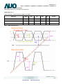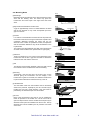
1
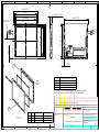
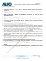
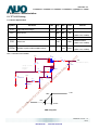
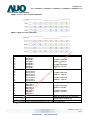
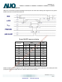
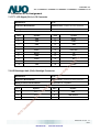
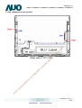
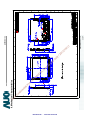
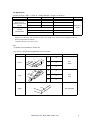
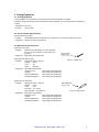
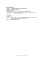
Specification
G065VN01 V2 incl. Touch - 4W
Content:
Mechanical Drawing
Appendix A: Specification of TFT G065VN01 V2
Appendix B: Specification of Touch AST-065B080A
(
Please be aware that some of the values e.g. optical, mechanical etc. of the complete unit
(assembled display plus touch panel) might differ from the original values of the individual components.
Version: March 2013
N
Note: This specification is subject to change without prior notice
1
2
4
3
155 ±0,3 ODT
139 VAT
133 AAT
132,48 AAD
A
6
5
7
8
A
12,43 (max. 12,93)
153 ±0,5 ODD
Contact
B
E
99,36 AAD
100 AAT
104 VAT
117 ±0,3 ODT
0,90 ±0,5
C
1,90 ±0,5
1
NOT TO BE DISCLOSED TO THIRD PARTY WITHOUT PERMISSION FROM
D
CONRAC GMBH / Data Modul AG
80 ±1
C
118 ±0,5 ODD
B
ODD
ODT
VAT
AAT
AAD
3
D
Outline Dimension Display
Outline Dimension Touch
Viewing Area Touch
Active Area Touch
Active Area Display
This drawing is only schematic representation of the structure.
The parts to be used are defined in the ProAlpha parts list.
000
REV.
26.02.2013 Aschenbrenner 10000 Neuanlage
DRAWN BY
E.C.-NO.
REL.DATE
MODIFICATION/DESCRIPTION
RELEASED: ja
FINISH
2
D-97990 Weikersheim
M 1:2
F
1
NO. OF
CHANGES
2
Pos.
Quantity
File Number
1
1
1009880-T
TFT-LCD MODULE 6,5"
2
1
1009864-T
Touch
3
1
1009940-T
Klebeband 3x0,13
3
Description
4
MATERIAL
DRAWING TITLE
D-80687 München
Assembly
TFT Display 6,5" + resistive Touch
FILE NUMBER:
1009941
PROJECT:
DMO_C_
TOLERANCES DIN ISO 2768-mK
SURFACES DIN ISO 1302
DRAWING/PART NUMBER
12002651
SCALE 2:3
000
SIZE ISO
A3
G065VN01 V2
□ Preliminary Specification
■ Final Specification
Module
6.5 Inch Color TFT-LCD
Model Name
G065VN01 V2
Date
Customer
Approved by
Date
2012/5/21
Checked &
Approved by
se
O
nl
y
/2
Prepared by
01
2/
10
/1
1
Leader Feng
2012/5/21
General Display Business Division / AU Optronics
corporation
AU
O
C
on
fid
en
tia
lF
or
D
AT
AM
O
D
U
Note: This Specification is subject to change
without notice.
L
In
te
rn
al
U
Yichih Chen
G065VN01 V2 Ver. 1.2
1/24
Data Modul AG - www.data-modul.com
G065VN01 V2
Contents
1. Operating Precautions .................................................................................... 4
2. General Description ........................................................................................ 5
2.1 Display Characteristics .......................................................................................................... 5
2.2 Optical Characteristics........................................................................................................... 6
3. Functional Block Diagram .............................................................................. 8
4. Absolute Maximum Ratings............................................................................ 9
4.1 Absolute Ratings.................................................................................................................... 9
4.2 Absolute Ratings of Environment .......................................................................................... 9
5. Electrical Characteristics.............................................................................. 10
5.1 TFT-LCD Driving .................................................................................................................. 10
5.2 Backlight Unit Driving........................................................................................................... 12
6. Signal Characteristic..................................................................................... 13
6.1 Pixel Format Image.............................................................................................................. 13
6.2 Scanning Direction............................................................................................................... 13
2/
10
/1
1
6.3 The Input Data Format......................................................................................................... 14
6.4 TFT- LCD Interface Signal Description................................................................................ 15
6.5 TFT- LCD Interface Timing................................................................................................... 16
/2
01
6.6 LED Backlight Unit Interface Signal Description................................................................. 17
6.7 Power ON/OFF Sequence................................................................................................... 18
O
nl
y
7. Connector & Pin Assignment ....................................................................... 19
al
U
se
7.1 TFT- LCD Signal (CN1): LCD Connector............................................................................ 19
7.2 LED Backlight Unit (CN2): Backlight Connector................................................................. 19
7.3 PIN 1 definition of CN1 and CN2 ........................................................................................ 20
D
U
L
In
te
rn
8. Reliability Test Criteria ................................................................................. 21
9. Mechanical Characteristics .......................................................................... 22
10. Label and Packaging................................................................................... 23
D
AT
AM
O
10.1 Shipping Label (on the rear side of TFT-LCD display) ..................................................... 23
10.2 Carton Package................................................................................................................. 23
11 Safety ............................................................................................................ 24
AU
O
C
on
fid
en
tia
lF
or
11.1 Keen Edge Requirements ................................................................................................. 24
11.2 Materials ............................................................................................................................. 24
11.3 Capacitors .......................................................................................................................... 24
11.4 National Test Lab Requirement ......................................................................................... 24
G065VN01 V2 Ver. 1.2
2/24
Data Modul AG - www.data-modul.com
850
,/3m
in60,1cyles0/3m
in0
G065VN01 V2
12
12
Remark
Section 2.1
Section 2.2
Section 2.2
Color Gamut
Min: TBD
1
Absolute Ratings of Environment
Operating Temperature, Max: +85
Storage Temperature, Max: +85
Color Gamut
Min: 50%
Absolute Ratings of Environment
Operating Temperature, Max: +80*
Storage Temperature, Max: +80*
*: Panel surface temperature
IrushLED
Typ: 0.37 A, Max: 0.41 A
Operating Life
Min: 50000
LED Backlight Unit Interface Signal
Description
Pin 5 LED On/Off: 3.3V-On; 0V/NC-Off
Reliability Test Criteria
IrushLED
Typ/Max: TBD
Operating Life
Min: 25000, Max: 50000
LED Backlight Unit Interface Signal
Description
Pin 5 LED On/Off: 3.3V-On; 0V-Off
Reliability Test Criteria
Section 2.2
Section 4.2
Section 5.2.1
Section 5.2.1
Section 6.6
High Temperature Operation:
300Hr
High Temperature Storage:
300Hr
Thermal Shock Test:
-2
,
Hot Start Test:
85℃/1 Hr (min.), power on/off per 5 minutes,
repeat 5 times
High Temperature Operation:
80 *, 300Hr
High Temperature Storage:
80 *, 300Hr
Thermal Shock Test:
-3
,8
min ,100cycles
Hot Start Test:
80℃*/1 Hr (min.), power on/off per 5
minutes, repeat 5 times
*: Panel surface temperature
AU
L
U
D
Section 5.2.1
Section 7.3
LED BLU Drive Absolute Ratings Voltage LED BLU Drive Absolute Ratings
Voltage range
range
Section 4.1
fid
on
C
9
O
1.3, July 03, 2012
20
VLED On/Off and VPWM range
lF
or
1.2, May 21, 2012
VLED On/Off and VPWM range
tia
12
Section 8
en
1.1, Mar. 22, 2012
AT
AM
O
D
21
In
te
rn
a
17
Red x, Red y: TBD
Green x, Green y: TBD
Blue x, Blue y: TBD
/1
9
Color / Chromaticity
Coordinates
10
6
White Luminance:
Min: 500, Typ: 700
2/
6
*:Panel surface temperature
White Luminance:
Min: 600, Typ: 800
Color / Chromaticity
Coordinates
01
6
Storage (Non-Operating): -30 to +80*
Storage (Non-Operating): -30 to +85
/2
5
Temperature Range
Operating: -30 to +80*
Temperature Range
Operating: -30 to +85
y
1.0, Oct. 22, 2009
First edition preliminary specifications
nl
All
New Description
O
0.1, Apr. 23, 2009
Old description
se
Page
lU
Version and Date
Record of Revision
12
VLED input voltage range
VLED input voltage range
Section 5.2.1
G065VN01 V2 Ver. 1.2
3/24
Data Modul AG - www.data-modul.com
G065VN01 V2
1. Operating Precautions
AU
O
C
on
fid
en
tia
lF
or
D
AT
AM
O
D
U
L
In
te
rn
a
lU
se
O
nl
y
/2
01
2/
10
/1
1
1) Display area (Polarizer) of TFT-LCD Module is easily to be damaged, please be cautious and not
to scratch it.
2) Be sure to power off your machine before connecting or disconnecting your signal cable to
TFT-LCD Module.
3) Wipe off water drop on display area immediately. Long contact with water may cause
discoloration or spots.
4) When the panel surface is soiled, wipe it with absorbent cotton or soft cloth.
5) Display area (Glass) of TFT-LCD Module may be broken or cracked if bump Module against hard
object.
6) To avoid ESD (Electro Static Discharde) damage, be sure to ground yourself before handling
TFT-LCD Module.
7) Do not open nor modify the TFT-LCD module assembly.
8) Do not press the reflector sheet at the back of the module to any direction.
9) In case if TFT-LCD module has to be put back into the packing container slot after it was taken
out from the container, do not press the center of the LED Reflector edge. Instead, press at the
far ends of the LED Reflector edge softly. Otherwise the TFT-LCD Module may be damaged.
10) When inserting or removing of your signal cable to TFT-LCD Module, be sure not to apply
abnormal force (rotate, tilt…etc.) to the Connector of the TFT-LCD Module.
11) TFT-LCD Module is not allowed to be twisted & bent even force is added on module in a very
short time. Please design your display product well to avoid external force applying to module by
end-user directly.
12) Small amount of materials without flammability grade are used in the TFT-LCD module. The
TFT-LCD module should be supplied by power complied with requirements of Limited Power
Source (IEC60950 or UL1950), or be applied exemption.
13) Severe temperature condition may result in different luminance, response time.
14) Continuous operating TFT-LCD Module under high temperature environment may accelerate
LED light bar exhaustion and reduce luminance dramatically.
15) The data on this specification sheet is applicable when TFT-LCD module is placed in landscape
position.
16) Continuous displaying fixed pattern may induce image sticking. It’s recommended to use screen
saver or moving content periodically if fixed pattern is displayed on the screen.
G065VN01 V2 Ver. 1.2
4/24
Data Modul AG - www.data-modul.com
G065VN01 V2
2. General Description
G065VN01 V2 is designed for industrial display applications with VGA (640 x RGB x 480) resolution
and 16.2M (RGB 6-bits + FRC) or 262k colors (RGB 6-bits). It is composed of a TFT-LCD panel,
driver ICs, control and power supply circuits board and a backlight unit including LED driving circuit.
G065VN01 V2 offers LVDS interface for display signal input.
2.1 Display Characteristics
The following items are G065VN01 V2 characteristics summary at 25
(Room Temperature).
Items
Unit
inch
6.5
Active Area
mm
132.48(H) x 99.36(V)
Screen Diagonal
Pixels H x V
Specifications
640x3(RGB) x 480
Pixel Arrangement
R.G.B. Vertical Stripe
Display Mode
TN, Normally White
1
0.207 x 0.207
/1
mm
10
Pixel Pitch
Volt
3.3 typ.
Typical Power Consumption
Watt
3.86W (LCD:0.86W/LED BLU: 3.0W)
All black pattern
mm
01
/2
y
1 channel LVDS
rn
a
lU
Electrical Interface
153.0(H)x 118.0(V) x 10.9(D) (typ.)
se
Physical Size
170g (typ.)
nl
Grams
O
Weight
2/
Nominal Input Voltage VDD
In
te
Surface Treatment
U
L
Support Color
AT
AM
D
C
C
o
o
-30 to +80*
-30 to +80*
*Panel surface temperature
RoHS Compliance
AU
O
C
on
fid
en
tia
RoHS Compliance
lF
or
Temperature Range
Operating
Storage (Non-Operating)
16.2M / 262K colors
6 o’clock
O
D
The most suitable view angle
Glare, AR, Hardness: 3H
G065VN01 V2 Ver. 1.2
5/24
Data Modul AG - www.data-modul.com
ith50cm
ingdstace
w
vew
1
G065VN01 V2
2.2 Optical Characteristics
The optical characteristics are measured under stable conditions at 25
Unit
cd/m2
msec
msec
msec
Rising
15
-
20
Note 4
-
10
15
Note 5
Rising + Falling
-
-
25
35
70
80
-
degree
degree
Horizontal
CR = 10
(Right)
(Left)
70
degree
degree
Vertical
CR = 10
(Upper)
(Lower)
60
70
-
0.263
0.313
0.363
0.279
0.329
0.379
0.559
0.609
0.314
0.364
Red x
Red y
Green x
0.285
Green y
nl
O
se
lU
rn
a
%
0.055
0.604
0.149
0.105
55
Note
1, 2, 3
Note 6
1
-
0.659
0.414
0.385
0.654
0.159
0.155
-
In
te
50
0.335
Note 1
-
70
y
0.554
0.099
Note 1: Measurement method
80
60
White x
Blue y
Pattern Generator, Power Supply, Digital Voltmeter, Luminance meter (SR_3 or equivalent)
Test Point
< 1 lux
lF
or
D
Environment
Center
AT
AM
Aperture
O
D
U
L
Equipment
600
Falling
Blue x
Color Gamut
400
-
White y
Color / Chromaticity
Coordinates
(CIE 1931)
1.25
800
Remark
/1
Viewing Angle
-
600
10
Response Time
Max.
5 Points
%
Contrast Ratio
Typ.
2/
Uniformity
Min.
01
White Luminance
Conditions
FPWM = 100%
(center point)
/2
Item
(Room Temperature).
tia
LCD Module
SR_3 or
AU
O
C
on
fid
en
equivalent
measuring distance
Module Driving Equipment
G065VN01 V2 Ver. 1.2
6/24
Data Modul AG - www.data-modul.com
G065VN01 V2
Note 2: Definition of 5 points position (Display active area: 132.48mm(W) x 99.36mm(H))
W
W /4
W /4
W /4
W /4
H /4
1
2
H /4
3
H
H /4
4
5
H /4
Note 3:
The luminance uniformity of 5 points is defined by dividing the maximum luminance value by the minimum luminance value
at full white condition.
/1
1
Maximum Brightness of five points
δW5 =
01
2/
10
Minimum Brightness of five points
nl
y
/2
Note 4: Definition of contrast ratio (CR):
O
Brightness @ “White” state
se
Contrast ratio (CR) =
rn
a
lU
Brightness @ “Black” state
te
Note 5: Definition of response time:
L
In
The output signals of photo detector are measured when the input signals are changed from “White” to “Black” (falling time)
AT
AM
amplitude. Please refer to the figure as below.
on
Tr
lF
or
Tf
tia
en
O
C
response
fid
Optical
AU
D
%
100
90
O
D
U
and from “Black” to “White” (rising time), respectively. The response time interval definition is between 10% and 90% of
White
Black
White
10
0
G065VN01 V2 Ver. 1.2
7/24
Data Modul AG - www.data-modul.com
V
iew
ngalisthem
aurentofcrastio4
G065VN01 V2
Note 6: Definition of viewing angle
10, at the screen center, over 180° horizontal and 180° vertical range.
The 180° horizontal (θL, θR) and 180° vertical (ΦH, ΦL) range are illustrated as following figure.
10
/1
1
3. Functional Block Diagram
AU
O
C
on
fid
en
tia
lF
or
D
AT
AM
O
D
U
L
In
te
rn
al
U
se
O
nl
y
/2
01
2/
The following diagram shows the functional block of the G065VN01 V2 color TFT/LCD module.
G065VN01 V2 Ver. 1.2
8/24
Data Modul AG - www.data-modul.com
ulbshode39@
andocensaD
B
G065VN01 V2
4. Absolute Maximum Ratings
4.1 Absolute Ratings
Symbo
Min
Max
Unit
Remark
Logic/LCD Drive Voltage
VDD
-0.3
+4.0
Volt
Ta= 25oC
LCD Input Signal Voltage
VIN
-0.3
+4.0
Volt
Ta= 25 C
LED BLU Drive Voltage
VLED
0
16
Volt
Ta= 25 C
VPWM
0
6
Volt
Ta= 25oC
Min
Max
Unit
Remark
Item
LED Dimming Input Voltage
High
o
o
4.2 Absolute Ratings of Environment
Storage Temperature
TST
Storage Humidity
Note 1: Maximum Wet-
-30
+80*
5
HST
95
5
Note 1, 2
℃
%RH
℃
95
%RH
1
HOP
+80*
tion.
Note 1, 2
/1
Operation Humidity
-30
10
TOP
2/
Operating Temperature
/2
01
Symbol
Note 1
Note 1
y
Item
O
nl
Note 2: Only operation is guaranteed. Optical and display performance should be evaluated at 25 only.
AU
O
C
on
fid
en
tia
lF
or
D
AT
AM
O
D
U
L
In
te
rn
al
U
se
*: Panel surface temperature
G065VN01 V2 Ver. 1.2
9/24
Data Modul AG - www.data-modul.com
G065VN01 V2
5. Electrical Characteristics
5.1 TFT-LCD Driving
5.1.1 Power Specification
Min
Typ
Max
Units
3.0
3.3
3.6
Volt
300
mA
Logic/LCD Drive Voltage
IDD
VDD Current
-
260
Irush
LCD Inrush Current
-
-
PDD
VDD Power
-
0.86
Allowable Logic/LCD Drive Ripple Voltage
-
-
Q3
AO6402
(VDD=3.3V, at 60Hz)
10
G
S
VR1
0.01uF/25V
VCC
O
nl
y
(LCD Module Input)
te
R2
VDD
47K
In
2
Q3
AO6402
G
C3
1
All Black Pattern
mVp-p
F1
D1
D2
D5
D6
R2
+12.0V
SW MAG-SPST
(VDD=3.3V, at 60Hz)
C1
1uF/16V
1K
SW1
100
S
R1
47K
(High to Low)
Control
Signal
All Black Pattern
Watt
2/
D6
D5
D2
D1
Note 1
/2
01
+3.3V
A
se
Note 1: Measurement condition:
(VDD=3.3V, at 60Hz)
rn
al
U
VDDrp
1.5
All Black Pattern
1
VDD
Remark
/1
Parameter
Symbol
L
1K
3.3V
90%
tia
lF
or
D
AT
AM
O
D
U
C2
1uF/25V
10%
0.5ms
AU
O
C
on
fid
en
0V
VDD rising time
G065VN01 V2 Ver. 1.2
10/24
Data Modul AG - www.data-modul.com
G065VN01 V2
5.1.2 Signal Electrical Characteristics
Input signals shall be low or Hi-Z state when VDD is off.
LVDS signal (Note 1)
LVDS Transmitter: THC63LVDM83A (THINE) or equivalent
Parameter
Symbol
Min.
Typ.
Max.
Unit
Differential Input High Threshold
VTH
-
-
100
mV
Input Differential Voltage
|VID|
600
mV
Differential Input Low Threshold
VTL
Differential Input Common Mode Voltage
-100
100
VCM
1.1
-
-
400
-
mV
1.45
V
Remark
VCM=1.20V
VCM=1.20V
VTH, VTL= ±100mV
AU
O
C
on
fid
en
tia
lF
or
D
AT
AM
O
D
U
L
In
te
rn
al
U
se
O
nl
y
/2
01
2/
10
/1
1
Note 1: LVDS Signal Waveform.
G065VN01 V2 Ver. 1.2
11/24
Data Modul AG - www.data-modul.com
(R
o
E
G065VN01 V2
Following characteristics are measured under stable condition at 25
Symbol
Parameter
Min
om Temperature).
Typ
Max
Units
12
13
Volt
VLED
Input Voltage
9
ILED
Input Current
-
0.25
Inrush Current
-
0.37
Power Consumption
IrushLED
-
3.0
On Control Voltage
3.0
Dimming control Voltage High
3.0
FPWM
Dimming Frequency
200
DPWM
Dimming duty cycle
1
VLED On/Off
Off Control Voltage
VPWM
3.3
0
Dimming control Voltage Low
100% PWM duty
A
100% PWM duty
W
5.0
Volt
5.0
Volt
30K
Hz
100
%
0.15
3.3
0
Operating Life
0.41
A
0.1
50000
100% PWM duty
Volt
Volt
Hrs
Note 2, 3
10
PLED
Remark
1
5.2.1 Parameter guideline for LED driver
/1
5.2 Backlight Unit Driving
2/
Note 1: See Section 6.6 for LED Backlight Unit Interface Signal Description.
/2
01
Note 2: If G065VN01 V2 module is driven at high ambient temperature & humidity condition. The operating life will be
reduced.
AU
O
C
on
fid
en
tia
lF
or
D
AT
AM
O
D
U
L
In
te
rn
al
U
se
O
nl
y
Note 3: Operating life means brightness goes down to 50% initial brightness. Typical operating life time is estimated data.
G065VN01 V2 Ver. 1.2
12/24
Data Modul AG - www.data-modul.com
G065VN01 V2
6. Signal Characteristic
6.1 Pixel Format Image
y
/2
01
2/
10
/1
1
Following figure shows the relationship between input signal and LCD pixel format.
O
nl
6.2 Scanning Direction
AU
O
C
on
fid
en
tia
lF
or
D
AT
AM
O
D
U
L
In
te
rn
al
U
se
The following figures show the image seen from the front view. The arrow indicates the direction of scan.
Note 1: TFT-LCD interface signal description is shown in section 6.4.
G065VN01 V2 Ver. 1.2
13/24
Data Modul AG - www.data-modul.com
G065VN01 V2
6.3 The Input Data Format
SEL68 = ”Low” or “NC” for 6 bits LVDS Input
10
2/
nl
y
For 8Bits LVDS input
MSB: R7 ; LSB: R0
rn
al
U
se
O
For 6Bits LVDS input
MSB: R5 ; LSB: R0
L
In
te
Green-pixel Data
D
O
AM
AT
D
or
lF
tia
en
Remark
/2
01
Red-pixel Data
U
Description
Red Data 7
Red Data 6
Red Data 5
Red Data 4
Red Data 3
Red Data 2
Red Data 1
Red Data 0
Green Data 7
Green Data 6
Green Data 5
Green Data 4
Green Data 3
Green Data 2
Green Data 1
Green Data 0
Blue Data 7
Blue Data 6
Blue Data 5
Blue Data 4
Blue Data 3
Blue Data 2
Blue Data 1
Blue Data 0
LVDS Data Clock
For 8Bits LVDS input
MSB: G7 ; LSB: G0
For 6Bits LVDS input
MSB: G5 ; LSB: G0
Blue-pixel Data
For 8Bits LVDS input
MSB: B7 ; LSB: B0
For 6Bits LVDS input
MSB: B5 ; LSB: B0
fid
Signal Name
R7
R6
R5
R4
R3
R2
R1
R0
G7
G6
G5
G4
G3
G2
G1
G0
B7
B6
B5
B4
B3
B2
B1
B0
RxCLKIN
/1
1
SEL68 = “High” for 8 bits LVDS Input
When the signal is high, the pixel data
shall be valid to be displayed.
RSV
Reserved Signal
“High” or “Low” is acceptable
Note 1: Output signals from any system shall be low or Hi-Z state when VDD is off.
Data Enable Signal
AU
O
C
on
DE
G065VN01 V2 Ver. 1.2
14/24
Data Modul AG - www.data-modul.com
G065VN01 V2
6.4 TFT- LCD Interface Signal Description
G065VN01 V2 TFT-LCD module includes LVDS receiver. LVDS is a differential signal technology for high-speed data
transfer LCD interface. LVDS Transmitter shall be THC63LVDM83A (THINE) or equivalent.
Pin No.
Symbol
2
VDD
1
Pin Description
VDD
3
GND
4
SEL68
5
RxIN1-
Power supply, 3.3V (typical)
Power supply, 3.3V (typical)
Ground
Selection for either 6bit or 8bit LVDS input:
SEL68 =”Low” or “NC”, accepts 6bit LVDS data input;
SEL68 = ”High”, accepts 8bit LVDS data input.
Negative LVDS differential input (R0-R5, G0)
6
RxIN1+
8
RxIN2-
Negative LVDS differential input (G1-G5, B0-B1)
9
RxIN2+
Positive LVDS differential input (G1-G5, B0-B1)
11
RxIN3-
Negative LVDS differential input (B2-B5, DE)
GND
Ground
15
RxCLKIN+
17
U/D
19
RxIN4-
20
RxIN4+
NC
/1
Negative LVDS differential clock input
Positive LVDS differential clock input
No connection
Vertical Reverse (“L” or NC: Normal, “H”: Reverse)
Horizontal Reverse (“L” or NC: Normal, “H”: Reverse)
Negative LVDS differential input (R6-R7, G6-G7, B6-B7)
NC for 6bit LVDS input.
Positive LVDS differential input (R6-R7, G6-G7, B6-B7)
NC for 6bit LVDS input.
In
te
rn
al
U
R/L
L
18
Ground
se
16
10
RxCLKIN-
GND
2/
14
13
Positive LVDS differential input (B2-B5, DE)
/2
01
RxIN3+
y
12
1
GND
nl
10
Ground
O
7
Positive LVDS differential input (R0-R5, G0)
AU
O
C
on
fid
en
tia
lF
or
D
AT
AM
O
D
U
Note 1: “Low” stands for 0V. “High” stands for 3.3V. “NC” stands for ”No Connection”.
G065VN01 V2 Ver. 1.2
15/24
Data Modul AG - www.data-modul.com
G065VN01 V2
6.5 TFT- LCD Interface Timing
6.5.1 Timing Characteristics
DE mode only
Signal
Symbol
Min.
Typ.
Max.
Unit
Remark
Clock frequency (DOTCLK)
1/ TCLOCK
20
25.2
50
MHz
Note1
Period
TH
770
800
1070
Active
THD
TCLOCK
Note1
Blanking
THB
130
160
430
Period
TV
520
525
622
Active
TVD
TLINE
Note1
Blanking
TVB
Horizontal Section
Vertical Section
Note 1: Recommended frame rate is 60 Hz.
640
480
40
45
142
/1
2/
10
Input Timing Definition ( DE Mode)
TCLOCK
1
6.5.2 Input Timing Diagram
DE
Pixel
3
Pixel
N-1
O
Pixel
2
se
Pixel
1
rn
al
U
Invaild
Data
Pixel
N
Invaild
Data
Pixel
1
te
Input
Data
nl
y
/2
01
DOTCLK
THB
U
L
In
THD
AM
O
D
TH
AT
DE
TVB
TV
AU
O
C
on
fid
en
tia
lF
or
D
TVD
G065VN01 V2 Ver. 1.2
16/24
Data Modul AG - www.data-modul.com
G065VN01 V2
6.6 LED Backlight Unit Interface Signal Description
Pin #
Symbol
Pin Description
2
VLED
12V input
1
VLED
12V input
3
GND
5
LED On/Off
4
Ground
GND
6
Ground
3.3V-On; 0V/NC-Off
PWM DIM
1~100%
AU
O
C
on
fid
en
tia
lF
or
D
AT
AM
O
D
U
L
In
te
rn
al
U
se
O
nl
y
/2
01
2/
10
/1
1
Note1: “NC stands for “No Connection””.
G065VN01 V2 Ver. 1.2
17/24
Data Modul AG - www.data-modul.com
G065VN01 V2
6.7 Power ON/OFF Sequence
VDD power, LCD interface signals and backlight on/off sequence are shown in the following chart. Signals from any system
0.5
T2
30
2/
nl
O
10
ms
40
50
ms
-
-
ms
-
-
ms
-
-
ms
T4
10
T5
10
T6
0
-
-
ms
10
-
-
ms
100
-
-
ms
T9
0
16
50
ms
T10
-
-
10
ms
In
L
U
D
O
AM
AT
D
or
lF
tia
1000
-
-
ms
on
T11
te
200
T8
en
Units
T3
T7
fid
-
Max.
rn
al
U
T1
Typ.
se
Min.
y
Value
Parameter
/2
01
Power ON/OFF sequence timing
10
/1
1
shall be Hi-Z state or low level when VDD is off.
C
ON/OFF sequence should be applied to avoid abnormal function in the display. Please make sure to turn off the power when
AU
O
you plug the cable into the input connector or pull the cable out of the connector.
G065VN01 V2 Ver. 1.2
18/24
Data Modul AG - www.data-modul.com
G065VN01 V2
7. Connector & Pin Assignment
7.1 TFT- LCD Signal (CN1): LCD Connector
Manufacturer
STM
Connector Model Number
MSB24013P20, compatible with I-PEX 20268-020E
Mating Connecter Model Number
Hirose DF19 -20S-1C or compatible
Pin#
Symbol
Pin#
Symbol
1
VDD
11
RxIN3-
3
GND
13
RxIN1-
15
RxCLKIN+
GND
17
U/D
19
RxIN4-
12
RxIN3+
14
RxCLKIN-
4
SEL68
6
RxIN1+
8
9
RxIN2-
RxIN2+
18
10
GND
20
NC
10
/1
R/L
2/
7
16
RxIN4+
/2
01
5
GND
1
VDD
y
2
rn
al
U
se
O
nl
7.2 LED Backlight Unit (CN2): Backlight Connector
STM
Connector Model Number
MS24016RHD, compatible with MOLEX 53261-0671
te
Manufacturer
STM P24016 or compatible
Symbol
1
VLED
4
GND
2
VLED
5
LED ON/OFF
3
GND
6
PWM DIM
O
Pin #
AM
Symbol
AU
O
C
on
fid
en
tia
lF
or
D
AT
Pin #
D
U
L
In
Mating Connecter Model Number
G065VN01 V2 Ver. 1.2
19/24
Data Modul AG - www.data-modul.com
G065VN01 V2
AU
O
C
on
fid
en
tia
lF
or
D
AT
AM
O
D
U
L
In
te
rn
al
U
se
O
nl
y
(Rear side of TFT-LCD)
/2
01
2/
10
/1
1
7.3 PIN 1 definition of CN1 and CN2
G065VN01 V2 Ver. 1.2
20/24
Data Modul AG - www.data-modul.com
/9%
,
40K
G065VN01 V2
8. Reliability Test Criteria
Items
Temperature Humidity Bias
Required Condition
300Hr
High Temperature Operation
Remark
Note 2
80 *, 300Hr
Low Temperature Operation
-3
High Temperature Storage
Note 2
300Hr
Note 2
80 *, 300 hours
Note 2
-30℃, 300 hours
Low Temperature Storage
Note 2
-30℃/30 min, 80℃*/30 min, 100cycles
Thermal Shock Test
Note 2
80℃*/1 Hr (min.), power on/off per 5 minutes, repeat 5 times
Hot Start Test
Note 2
-30℃/1 Hr (min.), power on/off per 5 minutes, repeat 5 times
Cold Start Test
Shock Test
(Non-Operating)
Vibration Test
(Non-Operating)
Note 2
50G,20ms,Half-sine wave, (±X, ±Y, ±Z)
Note 2
1.5G, 10~200~10Hz, Sine wave, 30mins/axis, 3 direction (X, Y, Z)
Note 2
Contact Discharge: ±8KV, 150pF(330Ω) 1sec, 8 points, 25 times/point
ESD
Note 1,2
Note 2
/2
01
Non-operating: 40,000 ft, Ramp: 2000 ft/min, 24hrs
2/
Operating: 14,000 ft, Ramp: 2000 ft/min, 8hrs
Attitude Test
10
/1
1
Air Discharge: ±15KV, 150pF(330Ω) 1sec, 8 points, 25 times/point
nl
O
rn
al
U
te
In
The reliability test is performed only to examine the TFT-LCD module capability.
To inspect TFT-LCD module after reliability test, please store it at room temperature and room humidity for 24
L
Each test is done by new TFT-LCD module. Don’t use the same TFT-LCD module repeatedly for reliability test.
hours at least in advance.
U
Water condensation is not allowed for each test items.
D
se
Note2:
is self-recoverable, no data lost and no hardware failures after test.
y
Note1: According to EN61000-4-2 ESD class B criteria, some performance degradation is allowed. TFT-LCD module
AU
O
C
on
fid
en
tia
lF
or
D
AT
AM
O
*: Panel surface temperature
G065VN01 V2 Ver. 1.2
21/24
Data Modul AG - www.data-modul.com
Data Modul AG - www.data-modul.com
U
O
or
lF
tia
on
fid
en
C
L
U
D
AM
O
D
AT
9. Mechanical
Characteristics
A
al
rn
te
In
se
U
y
nl
O
22/24
G065VN01 V2 Ver. 1.2
1
/1
10
2/
01
/2
G065VN01 V2
G065VN01 V2
10. Label and Packaging
10.1 Shipping Label (on the rear side of TFT-LCD display)
10.2 Carton Package
Max. capacity: 80 TFT-LCD module per carton (40pcs * 2 layers)
Max. weight: 16.6 kg per carton
AU
O
C
on
fid
en
tia
lF
or
D
AT
AM
O
D
U
L
In
te
rn
al
U
se
O
nl
y
/2
01
2/
10
/1
1
Outside dimension of carton: 425(L)mm* 386(W)mm* 430(H)mm
G065VN01 V2 Ver. 1.2
23/24
Data Modul AG - www.data-modul.com
G065VN01 V2
11 Safety
11.1 Keen Edge Requirements
There will be no keen edges or corners on the display assembly that could cause injury.
11.2 Materials
11.2.1 Toxicity
There will be no carcinogenic materials used anywhere in the TFT-LCD module. If toxic materials are used, they will be
reviewed and approved by the responsible AUO toxicologist.
11.2.2 Flammability
All components including electrical components that do not meet the flammability grade UL94-V1 in the TFT-LCD
Module will complete the flammability rating exception approval process.
The printed circuit board will be made from material rated 94-V1 or better. The actual UL flammability rating will be
2/
10
/1
1
printed on the printed circuit board.
01
11.3 Capacitors
/2
If any polarized capacitors are used in the TFT-LCD module, provisions will be made to keep them from being inserted
O
nl
y
backwards.
U
se
11.4 National Test Lab Requirement
rn
al
The TFT-LCD Module will satisfy all requirements for compliance to UL 60950 (U.S.A. Information Technology
AU
O
C
on
fid
en
tia
lF
or
D
AT
AM
O
D
U
L
In
te
Equipment).
G065VN01 V2 Ver. 1.2
24/24
Data Modul AG - www.data-modul.com
Specification
AST/ATP Series
Revision 11
Version March 23, 2010
Data Modul AG - www.data-modul.com
Table of Contents
1. Product Specifications ...........................................................................................................................3
1-1. Product Applicable .............................................................................................................................3
1-2. Structure.............................................................................................................................................3
1-3. Environmental Specifications .............................................................................................................3
1-4. Mechanical Characteristics ................................................................................................................3
1-5. Electrical Characteristics ....................................................................................................................3
1-6. Appearance ........................................................................................................................................4
2. Testing Regulation ..................................................................................................................................5
2-1. Testing Regulation..............................................................................................................................5
2-2. Environmental Specifications .............................................................................................................5
2-3. Mechanical Characteristics ................................................................................................................5
2-4. Electrical Characteristics ....................................................................................................................6
2-5. Appearance ........................................................................................................................................6
3. Reliability Condition ...............................................................................................................................7
3-1. Temperature Condition .......................................................................................................................7
4. Recommended Connector .....................................................................................................................7
4-1. Recommended Connector .................................................................................................................7
5. Handling Notes........................................................................................................................................8
5-1. Precautions ........................................................................................................................................8
5-2. Handling Notes...................................................................................................................................8
5-3. Construction Notes.............................................................................................................................8
5-4. Electrical & Software Notice ...............................................................................................................8
5-5. Mounting Notes ..................................................................................................................................9
6. Warranty ................................................................................................................................................10
6-1. Warranty Period ...............................................................................................................................10
6-2. Warranty Target................................................................................................................................10
6-3. Warranty Exceptions ........................................................................................................................10
6-4. Tools.................................................................................................................................................10
6-5. Changes...........................................................................................................................................10
7. Revision history .................................................................................................................................... 11
2
Rev. 11©1999 - 2010 DMC Co., Ltd.
Data Modul AG - www.data-modul.com
2
1. Product Specifications
1-1. Product Applicable
§ This specification is applied to the analog resistive touchscreen: ATP/AST Series.
1-2. Structure
§ Dimensions, structure, and shape are referred on the drawing attached.
1-3. Environmental Specifications
Specification
Value
Operating Temperature
-20°C to 70°C (no condensation)
Operating Humidity
-20°C to 60°C Less than 90%RH (no condensation)
3
Exceeding 60°C 133.8g/m (no condensation)
Storage Temperature
-40°C to 80°C (no condensation)
Storage Humidity
-40°C to 60°C Less than 95%RH (no condensation)
Exceeding 60°C 142.9g/m3 (no condensation)
Chemical Resistance
(top surface)
Toluene, Tricholoroethylene, Athetone, Alcohol,
Gasoline, Machine Oil, Ammonia, Glass Cleaner,
Mayonnaise, Ketchup, Wine, Salad Oil, Vinegar, Lipstick, etc.
1-4. Mechanical Characteristics
Specification
Value
Activation Force
0.05N to 0.8N
Operating Life
Input (finger)
10,000,000 hits
Character Input (pen)
100,000 characters
Light Transmittance
Over 80% (typical value at full wavelength)
Surface Hardness
Over 2H (by JIS pencil hardness)
1-5. Electrical Characteristics
Specification
Value
Maximum Voltage
Maximum Current
Linearity
Terminal Resistance
Insulation Resistance
Chattering
DC6V
Top Electrode
100mA
Bottom Electrode
100mA
Between the Top and Bottom
0.5mA
Under ±2% (Under ±1% (typical value))
Top Electrode
Less than 1kΩ
Bottom Electrode
Less than 1kΩ
Neighboring Terminals
Over 20MΩ at 25V
Active Area Electrodes
Over 20MΩ at 25V
Less than 10msec at ON/OFF.
3
Rev. 11©1999 - 2010 DMC Co., Ltd.
Data Modul AG - www.data-modul.com
3
1-6. Appearance
§ Scratch, dust (W = width, L = length, D = average diameter = (longest + shortest) /2)
Item
Width (mm)
Length (mm)
Acceptable Numbers
Linear(Scratch/Dust)
Over 0.1mm in
diameter refer to the
Circular.
0.1≥W>0.05
4≥L
1pcs in φ30mm
0.05≥W>0.03
10≥L
2pcs in φ20mm
0.03≥W
20≥L
Acceptable
Circular
(Scratch/Dust)
0.4≥D>0.3 *1
1pcs in viewing area *1
0.3≥D>0.2
2pcs in φ30mm
0.2≥D
Acceptable
Total
Within 5pcs
/panel
Applied only in the Active Area. Scratches or dusts in the outside of the Active Area are acceptable unless the
electrical characteristics are affected.
*1 Applied to the size of 14 inches or more.
§ Dirt
Acceptable if not noticeable on a black mat.
§ Tip, crack (t = glass thickness) (applicable only for the glass)
Item
Size (mm)
Z
Corner
X
Y
X
Y
Side
Z
Acceptable Numbers
X
≤3
Y
≤3
Z
≤t
X
≤5
Y
≤3
Z
≤t
Crack
2pcs
/panel
2pcs
/side
Not acceptable
4
Rev. 11©1999 - 2010 DMC Co., Ltd.
Data Modul AG - www.data-modul.com
4
2. Testing Regulation
2-1. Testing Regulation
§ If the regulation is not specified, the test is performed under the supplier’s regulation.
§ Tests are performed under the room temperature unless specified. The room temperature is referred as
follows:
Temperature: 20°C±5°C
Humidity:
65%±10%RH
2-2. Environmental Specifications
§ Chemical Resistance Test
Condition:
Tested after leaving the chemical on the surface for 12 hours being wiped off by cloth.
Judgement:
Must be no effect in appearance.
2-3. Mechanical Characteristics
§ Activation Force Test
Condition:
Judgement:
Measured by depressing the point between
the dots to the conduction by the testing rod
(Figure 1).
Must satisfy the specification.
Silicon Rubber
(Hardness: 60°)
Tip: R = 4.0
§ Operating Life Test (Finger)
Condition:
Testing rod: Refer to Figure 1
Voltage:
DC5V
Load:
3N
Cycle:
2 hits/sec
Judgement:
Must satisfy the following:
Activation Force:
Linearity:
Terminal Resistance:
Insulation Resistance:
Figure 1. Testing rod 1
Must satisfy the specification.
Must satisfy the specification.
Must satisfy the specification.
Must satisfy the specification.
§ Operating Life Test (Pen)
Condition:
Testing rod: Refer to Figure 2
Voltage:
DC5V
Load:
2.5N
Input size: 10 x 10 mm
Input character: A to Z/minute
Judgement:
Must satisfy the following:
Activation Force:
Linearity:
Terminal Resistance:
Insulation Resistance:
Polyacetal resin
Tip: R = 0.8
Figure 2. Testing rod 2
Must satisfy the specification.
Must satisfy the specification.
Must satisfy the specification.
Must satisfy the specification.
5
Rev. 11©1999 - 2010 DMC Co., Ltd.
Data Modul AG - www.data-modul.com
5
2-4. Electrical Characteristics
§ Terminal Resistance Test
Condition:
Top and bottom electrodes are measured at the terminal.
Judgement:
Must satisfy the specification.
§ Insulation Resistance Test
Neighboring Terminals: Measured by applying the reference voltage to the terminals
Active Area Electrodes: Measured by applying the reference voltage to the top and bottom electrodes.
Judgement:
Must satisfy the specification.
2-5. Appearance
§ Appearance Test
Condition:
Tested by an examiner with over 1.0 eyesight at 30cm away from the product under the
transmittable light at over 60° the surface of the product.
Judgement:
Must satisfy the specification.
Data Modul AG - www.data-modul.com
6
3. Reliability Condition
3-1. Temperature Condition
§ Temperature Condition Test
Following test are performed in the condition with no dew condensation:
Cold Test:
Tested after leaving the parts in -40°C±3°C for 240 hours and in the room temperature
for 2 hours.
Heat Test:
Tested after leaving the parts in 80°C±3°C for 240 hours and in the room temperature for
2 hours.
Humidity Test: Tested after leaving the parts in the temperature 60°C±3°C, humidity 90 to 95% for 240
hours and in the room temperature for 2 hours.
Cycle Test:
Tested after 5 cycles of leaving the parts in the temperature -30°C±3°C for 1 hour and in
the room temperature for 0.5 hours, then leaving the parts in the temperature 70°C±3°C
for 1 hour and in the room temperature for 0.5 hours.
Judgement:
Must satisfy the following:
Activation Force:
Must satisfy the specification.
Linearity:
Must satisfy the specification.
Terminal Resistance:
Must satisfy the specification.
Insulation Resistance: Must satisfy the specification.
Appearance:
Must satisfy the specification.
4. Recommended Connector
4-1. Recommended Connector
Part No.
Pins
Pitch
KCA-K4R
4 pin Double-sided
1.25mm
7
Rev. 11©1999 - 2010 DMC Co., Ltd.
Data Modul AG - www.data-modul.com
7
5. Handling Notes
5-1. Precautions
§ This product is intended for use in standard applications (computers, office automation, and other office
equipment, industrial, communications, and measurement equipment, personal and household devices,
etc.) Please avoid using this product for special applications where failure or abnormal operation may
directly affect human lives, or cause physical injury or property damage, or where extremely high levels
of reliability are required (such as aerospace systems, vehicle operating control, atomic energy controls,
medical devices for life support, etc.).
5-2. Handling Notes
§ Do not depress or scratch the product with any object with a sharp edge or end.
§ Do not forcibly bend or fold the product.
§ When the product is stored, make sure it is packed in a packing box and stored in a storage temperature
range, eliminating any outside load.
§ Do not use or store the product under a condition where the product will be exposed to water, organic
solution or acid.
§ Do not use the product under the direct sunlight.
§ Do not disassemble the product.
§ When you handle the product, Hold the product by its body. Do not hold by the tail.
§ Clean the product with a soft cloth or a soft cloth with neutral detergent or alcohol. When contaminated
by chemicals, wipe them off immediately with caution not to cause injury to human body.
§ The edge of the glass is not rounded and may cause injury.
5-3. Construction Notes
§ The environmental specifications, mechanical characteristics, and electrical characteristics are only
applied to the Active Area.
§ Do not use the touchscreen when the condensation occurs. The condensation inside of the touchscreen
is a natural phenomenon and should disappear after the touchscreen is warmed up.
5-4. Electrical & Software Notice
The best performance can be obtained when used with the original analog resistive touchscreen controller,
“TSC-10” Series. If the touchscreen controller or controller software is to be developed by the customer,
please note the following:
§ There is a contact resistance between the top and bottom electrodes and it changes by the pressure of a
finger or a pen. The data must be read after the contact resistance becomes stabilized.
§ The terminal resistance of the analog resistive touchscreen varies by the individual, time, and
environment. The controller software must have the calibration function to adjust the input position and
the display position.
§ The analog resistive touchscreen outputs 2 point input as 1 point in between the 2 points. The controller
software must not be designed to have the 2 point input function.
§ For drawing applications, the line may be intermittent when the pen comes on the dot spacers. A
software compensation is needed.
8
Rev. 11©1999 - 2010 DMC Co., Ltd.
Data Modul AG - www.data-modul.com
8
5-5. Mounting Notes
Bezel
Bezel edge must be positioned in the area between the Active
Area and the Viewing Area. The bezel may press the
touchscreen and cause input if the edge enters the Active
Area.
§ Gap between the Bezel and Touchscreen
Active Area
Viewing Area
Bezel
Top Electrode
A gap of approximately 0.5mm is needed between the bezel
and the top electrode. It may cause unexpected input if the
gap is too narrow.
0.5mm
§ Bezel Edge
§ Cushion
If a cushion is used between the bezel and the top electrode,
the cushion must be free enough to absorb the expansion and
contraction difference between the bezel and the top
electrode. If the cushion is squashed too hard, the expansion
and the contraction difference may cause the distortion to the
top electrode.
The cushion must be positioned more than 1mm outward from
an inside of the insulation area. (Please refer to right figure)
Bezel
Cushion
Top Electrode
Insulation Area
Minimum 1mm
§ Tolerance
There is a tolerance of 0.2 to 0.3mm for the dimensions of the
touchscreen and the tail. A gap must be made to absorb the
tolerance in the case and the connector.
0.2 - 0.3mm
Case
§ Tail
The tail must not be forcibly stressed or bent too hard to avoid
the conduction in the insulated area and wire breaking.
Tail
§ Mounting
Bezel
Touchscreen must be held from the bottom such as the
structure gluing the touchscreen onto the display. If the
touchscreen is glued to the bezel, the adhesion between the
top and bottom electrode is stressed and may come off.
Display
§ Forbidden Area
The area within 2mm from the insulation area is structurally
week for the pressure, espcially for pen use. The film may be
forcibly bent and may cause defection. This area must be
protected by the bezel and input must be avoided.
§ Air Vent
Bezel
Forbidden Area
Most of the touchscreens have the air vent to equalize the
inside air pressure to the outside one. The air vent must be
open and liquid contact must be avoided as the liquid may be
absorbed if the lquid is accumilated near the air vent. The top
electlode must not be swelled by the air pressure from inside
of the case.
Data Modul AG - www.data-modul.com
9
6. Warranty
6-1. Warranty Period
§ The warranty period is limited to 1 year from the date of shipping. The warranty for the initial defection
such as appearance defection is limited to 1 month.
§ Any defected parts under proper use will be examined by the supplier and replaced by the new parts if
the defection is considered to be caused by the supplier.
§ The replacement is subject to be included in the next lot.
6-2. Warranty Target
§ The warranty only covers the product itself and does not cover any damage to others caused by using
this product. Onsite repair or replacement is not supported.
§ We will do our best for delivery problem and product defections, but the warranty for the production line
is not covered.
§ Resistive touchscreens are structurally not repairable. All defections are subject to replacement.
6-3. Warranty Exceptions
Following conditions are not covered with the warranty and subject to charge.
§ Any malfunctions and damages during transportation and transfer by the user.
§ Any malfunctions and damages caused by a natural disaster or a fire.
§ Any malfunctions and damages caused by static electricity
§ Any malfunctions and damages caused by the failure of the associated equipment.
§ If the product is remodeled, disassembled or repaired by the user.
§ If the product is glued onto the equipment and uninstalled.
§ Any malfunctions and damages caused by an improper usage and handling against the specifications
and notes.
6-4. Tools
§ To maintain the quality, the printing screens and the die-cut plates are generally limited to use up to 1
year. Reorders after 1 year from the initial order or from the last renewal are subject to the tooling charge
for replacing the printing screens and the die-cut plates. Reorders for the discontinued standard parts are
also subject to tooling charge.
§ All the tools, such as CAD data (except for the drawing for approval), block copies (films), printing
screens, and die-cut plates are not to be provided for administrative purpose.
6-5. Changes
§ Because of the manufacturing process, changing the dimensions, circuit pattern, and the tail position
requires replacing most of the tools and is subject to high tooling charge. Please be careful when
ordering and approving the drawing.
§ Circuit pattern and the materials that does not affect the environmental, electrical, and mechanical
characteristics such as film, glass, ink and glue are subject to change for the supplier’s reason or for
improvement within the specifications.
§ Standard products are subject to change for improvement without notice.
10
Rev. 11©1999 - 2010 DMC Co., Ltd.
Data Modul AG - www.data-modul.com
10
7. Revision history
Rev1 (April 15, 1998)
Initial release
Rev2 (June 1, 1999)
The overall revision by specification review.
Rev3 (April 1, 2002)
The address in the office was changed by the move.
Rev4 (August 16, 2002)
1-4.Activation Force is changed “50g± 30g” to “0.5N±0.3”.
1-4.Light Transmission is changed 76% to 80%(TYP).
Rev5 (September 3, 2002)
1-3.Operating Temperature is changed “0°C to 60°C” to “-20°C to 70°C”.
1-3.Storing Temperature is changed “-20°C to 70°C” to “-40°C to 80°C”
1-4.Operating Life is changed “1,000,000 hits” to “10,000,000 hits”.
1-5.Linearity is changed “Under ±2%” to “Under ±1% (typical value)”.
Rev6 (June 28, 2004)
1-3.Operating Humidity is changed “Less than 90%RH (no condensation)” to “-20°C to 60°C Less than
3
90%RH (no condensation) Exceeding 60°C 133.8g/m (no condensation)”.
1-3.Storing Humidity is changed “Less than 95%RH (no condensation)” to “-40°C to 60°C Less than
95%RH (no condensation), Exceeding 60°C 142.9g/m3 (no condensation)”.
1-5.Maximum Voltage is changed “DC5V” to “DC6V”.
1-5.Linearity is changed “Under ±1% (typical value)” to “Under ±2% (Under ±1% (typical value))”.
Rev7 (October 15, 2004)
4-4.Electrical & Software Notice: Changed “FIT-10 series” to “TSC-10 series”.
Rev8 (April 7, 2005)
Added Item4 Recommended Connector.
Rev9 (September 6, 2005)
2-3.Mechanical Characteristics: Added Operating Life Test (Pen).
11
Rev. 11©1999 - 2010 DMC Co., Ltd.
Data Modul AG - www.data-modul.com
11
Rev10 (November 10, 2006)
The specification item name was changed.
1-3.”Storing Temperature” to “Storage Temperature”
1-3.”Storing Humidity” to “Storage Humidity”
1-4.”Operating Load” to “Activation Force”
1-4.”Light Transmissivity” to “Light Transmittance”
1-4.”Top Surface Hardness” to “Surface Hardness”
2-3.”Operating Load Test” to “Activation Force Test”
2-3.”Operating Load” to “Activation Force”
3-1.”Operationg Load” to “Activation Force”
1-4.Operating Force is changed “0.5N±0.3N” to “0.05N to 0.8N”.
1-5.Insulation Resistance is changed “Over 100MΩ at 25V” to “Over 20MΩ at 25V”.
1-6.Tip, crack: Deleted “Applied only in the Active Area. Scratches or dusts in the outside of the Active
Area are acceptable unless the electrical characteristics are affected.”.
2-3. § Operating Life Test (Pen) Load: 300g to 250g
5-5. § Cushion: Added an installation position of a cushion.
7.Added Revision History.
Rev11 (March 23, 2010)
1-6. Appearance specification was revised. Characters of scratch/dust were classified into Circular and
Linear. The total acceptable number of scratch/dust was added.
2-3. Unit of Load (g) changed to (N) to unify the unit
2-3. Operating Life Test (Finger) Activation Force, Within ±50% of the specification → Must satisfy
the specification. (Clerical error was corrected)
2-3. Operating Life Test (Pen) Activation Force, Within ±50% of the specification → Must satisfy the
specification. (Clerical error was corrected)
3-1. Temperature Condition
Cold Test -30℃→ -40℃ (Clerical error was corrected)
3-1. Activation Force, Within ±50% of the specification. → Must satisfy the specification
(Clerical error was corrected)
12
Rev. 11©1999 - 2010 DMC Co., Ltd.
Data Modul AG - www.data-modul.com
12
DI SPLAYS AND EMBEDDED SOLUTIONS
DI SPLAYS AND EMBEDDED SOLUTIONS
DATA MODUL Headquarters Munich
Landsberger Str. 322
D-80687 Munich - Germany
Phone: +49-89-56017-0
Fax: +49-89-56017-119
www.data-modul.com
Sales Office Hamburg
Borsteler Chaussee 51
D-22453 Hamburg - Germany
Phone: +49-40-42947377-0
Sales Office Duesseldorf
Fritz-Vomfelde-Str. 8
D-40547 Duesseldorf - Germany
Phone: +49-211-52709-0
Sales Office Scandinavia
Lundsmindevej 5
DK-6000 Kolding - Denmark
Phone: +45-75-224477
DATA MODUL France, S.A.R.L.
Bat B – Hall 204
1-3 Rue des Campanules
F-77185 Lognes - France
Phone: +33-1-60378100
DATA MODUL Italy, S.r.l.
Regus Center Senigallia
Via Senigallia 18/2
I-20161 Milano - Italy
Phone: +39-02-64672509
DATA MODUL Iberia, S.L.
c/ Adolfo Pérez Esquivel 3
Edificio Las Americas III Oficina 40
28230 Parque Empresarial Las Rozas / Madrid - Spain
Phone: +34-916-366458
DATA MODUL Suisse GmbH
Stationsstr. 57
CH-8606 Nänikon - Switzerland
Phone: +41-44-94091-50
DATA MODUL Ltd. / UK
Collins Building
3 Vigo Place - Aldridge - Walsall WS9 8UG - United Kingdom
Phone: +44-121-6988641
DATA MODUL Inc. / USA
275 Marcus Blvd, Unit K
Hauppauge, NY 11788 - USA
Phone: +1-631-951-0800
2 Data Modul AG | Landsberger Str. 322 | 80687 Munich | Tel. +49-89-56017-0 | Fax +49-89-56017-119 | www.data-modul.com