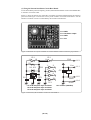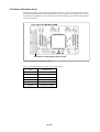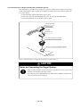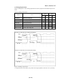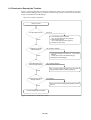
1
To our customers,
Old Company Name in Catalogs and Other Documents
On April 1st, 2010, NEC Electronics Corporation merged with Renesas Technology
Corporation, and Renesas Electronics Corporation took over all the business of both
companies. Therefore, although the old company name remains in this document, it is a valid
Renesas Electronics document. We appreciate your understanding.
Renesas Electronics website: http://www.renesas.com
April 1st, 2010
Renesas Electronics Corporation
Issued by: Renesas Electronics Corporation (http://www.renesas.com)
Send any inquiries to http://www.renesas.com/inquiry.
Notice
1.
2.
3.
4.
5.
6.
7.
All information included in this document is current as of the date this document is issued. Such information, however, is
subject to change without any prior notice. Before purchasing or using any Renesas Electronics products listed herein, please
confirm the latest product information with a Renesas Electronics sales office. Also, please pay regular and careful attention to
additional and different information to be disclosed by Renesas Electronics such as that disclosed through our website.
Renesas Electronics does not assume any liability for infringement of patents, copyrights, or other intellectual property rights
of third parties by or arising from the use of Renesas Electronics products or technical information described in this document.
No license, express, implied or otherwise, is granted hereby under any patents, copyrights or other intellectual property rights
of Renesas Electronics or others.
You should not alter, modify, copy, or otherwise misappropriate any Renesas Electronics product, whether in whole or in part.
Descriptions of circuits, software and other related information in this document are provided only to illustrate the operation of
semiconductor products and application examples. You are fully responsible for the incorporation of these circuits, software,
and information in the design of your equipment. Renesas Electronics assumes no responsibility for any losses incurred by
you or third parties arising from the use of these circuits, software, or information.
When exporting the products or technology described in this document, you should comply with the applicable export control
laws and regulations and follow the procedures required by such laws and regulations. You should not use Renesas
Electronics products or the technology described in this document for any purpose relating to military applications or use by
the military, including but not limited to the development of weapons of mass destruction. Renesas Electronics products and
technology may not be used for or incorporated into any products or systems whose manufacture, use, or sale is prohibited
under any applicable domestic or foreign laws or regulations.
Renesas Electronics has used reasonable care in preparing the information included in this document, but Renesas Electronics
does not warrant that such information is error free. Renesas Electronics assumes no liability whatsoever for any damages
incurred by you resulting from errors in or omissions from the information included herein.
Renesas Electronics products are classified according to the following three quality grades: “Standard”, “High Quality”, and
“Specific”. The recommended applications for each Renesas Electronics product depends on the product’s quality grade, as
indicated below. You must check the quality grade of each Renesas Electronics product before using it in a particular
application. You may not use any Renesas Electronics product for any application categorized as “Specific” without the prior
written consent of Renesas Electronics. Further, you may not use any Renesas Electronics product for any application for
which it is not intended without the prior written consent of Renesas Electronics. Renesas Electronics shall not be in any way
liable for any damages or losses incurred by you or third parties arising from the use of any Renesas Electronics product for an
application categorized as “Specific” or for which the product is not intended where you have failed to obtain the prior written
consent of Renesas Electronics. The quality grade of each Renesas Electronics product is “Standard” unless otherwise
expressly specified in a Renesas Electronics data sheets or data books, etc.
“Standard”:
8.
9.
10.
11.
12.
Computers; office equipment; communications equipment; test and measurement equipment; audio and visual
equipment; home electronic appliances; machine tools; personal electronic equipment; and industrial robots.
“High Quality”: Transportation equipment (automobiles, trains, ships, etc.); traffic control systems; anti-disaster systems; anticrime systems; safety equipment; and medical equipment not specifically designed for life support.
“Specific”:
Aircraft; aerospace equipment; submersible repeaters; nuclear reactor control systems; medical equipment or
systems for life support (e.g. artificial life support devices or systems), surgical implantations, or healthcare
intervention (e.g. excision, etc.), and any other applications or purposes that pose a direct threat to human life.
You should use the Renesas Electronics products described in this document within the range specified by Renesas Electronics,
especially with respect to the maximum rating, operating supply voltage range, movement power voltage range, heat radiation
characteristics, installation and other product characteristics. Renesas Electronics shall have no liability for malfunctions or
damages arising out of the use of Renesas Electronics products beyond such specified ranges.
Although Renesas Electronics endeavors to improve the quality and reliability of its products, semiconductor products have
specific characteristics such as the occurrence of failure at a certain rate and malfunctions under certain use conditions. Further,
Renesas Electronics products are not subject to radiation resistance design. Please be sure to implement safety measures to
guard them against the possibility of physical injury, and injury or damage caused by fire in the event of the failure of a
Renesas Electronics product, such as safety design for hardware and software including but not limited to redundancy, fire
control and malfunction prevention, appropriate treatment for aging degradation or any other appropriate measures. Because
the evaluation of microcomputer software alone is very difficult, please evaluate the safety of the final products or system
manufactured by you.
Please contact a Renesas Electronics sales office for details as to environmental matters such as the environmental
compatibility of each Renesas Electronics product. Please use Renesas Electronics products in compliance with all applicable
laws and regulations that regulate the inclusion or use of controlled substances, including without limitation, the EU RoHS
Directive. Renesas Electronics assumes no liability for damages or losses occurring as a result of your noncompliance with
applicable laws and regulations.
This document may not be reproduced or duplicated, in any form, in whole or in part, without prior written consent of Renesas
Electronics.
Please contact a Renesas Electronics sales office if you have any questions regarding the information contained in this
document or Renesas Electronics products, or if you have any other inquiries.
(Note 1) “Renesas Electronics” as used in this document means Renesas Electronics Corporation and also includes its majorityowned subsidiaries.
(Note 2) “Renesas Electronics product(s)” means any product developed or manufactured by or for Renesas Electronics.
User’s Manual
M3062PT-EPB
User’s Manual
Emulation Probe for M16C/62 Group M16C/62P
Rev.1.00 2003.07
* IC61-1004-051 is a trademark of Yamaichi Electronics Co., Ltd.
* NQPACK, YQPACK, YQSOCKET, YQ-GUIDE, HQPACK, TQPACK and TQSOCKET are trademarks of Tokyo Eletech Corporation.
Keep safety first in your circuit designs!
• Renesas Technology Corporation and Renesas Solutions Corporation put the maximum effort into making semiconductor products better
and more reliable, but there is always the possibility that trouble may occur with them. Trouble with semiconductors may lead to personal
injury, fire or property damage. Remember to give due consideration to safety when making your circuit designs, with appropriate
measures such as (i) placement of substitutive, auxiliary circuits, (ii) use of nonflammable material or (iii) prevention against any
malfunction or mishap.
Notes regarding these materials
• These materials are intended as a reference to assist our customers in the selection of the Renesas Technology product best suited to
the customer's application; they do not convey any license under any intellectual property rights, or any other rights, belonging to Renesas
Technology Corporation, Renesas Solutions Corporation or a third party.
• Renesas Technology Corporation and Renesas Solutions Corporation assume no responsibility for any damage, or infringement of any
third-party's rights, originating in the use of any product data, diagrams, charts, programs, algorithms, or circuit application examples
contained in these materials.
• All information contained in these materials, including product data, diagrams, charts, programs and algorithms represents information
on products at the time of publication of these materials, and are subject to change by Renesas Technology Corporation and Renesas
Solutions Corporation without notice due to product improvements or other reasons. It is therefore recommended that customers contact
Renesas Technology Corporation, Renesas Solutions Corporation or an authorized Renesas Technology product distributor for the latest
product information before purchasing a product listed herein. The information described here may contain technical inaccuracies or
typographical errors. Renesas Technology Corporation and Renesas Solutions Corporation assume no responsibility for any damage,
liability, or other loss rising from these inaccuracies or errors. Please also pay attention to information published by Renesas Technology
Corporation and Renesas Solutions Corporation by various means, including the Renesas home page (http://www.renesas.com).
• When using any or all of the information contained in these materials, including product data, diagrams, charts, programs, and algorithms,
please be sure to evaluate all information as a total system before making a final decision on the applicability of the information and
products. Renesas Technology Corporation and Renesas Solutions Corporation assume no responsibility for any damage, liability or
other loss resulting from the information contained herein.
• Renesas Technology semiconductors are not designed or manufactured for use in a device or system that is used under circumstances
in which human life is potentially at stake. Please contact Renesas Technology Corporation, Renesas Solutions Corporation or an
authorized Renesas Technology product distributor when considering the use of a product contained herein for any specific purposes,
such as apparatus or systems for transportation, vehicular, medical, aerospace, nuclear, or undersea repeater use.
• The prior written approval of Renesas Technology Corporation and Renesas Solutions Corporation is necessary to reprint or reproduce
in whole or in part these materials.
• If these products or technologies are subject to the Japanese export control restrictions, they must be exported under a license from the
Japanese government and cannot be imported into a country other than the approved destination. Any diversion or reexport contrary to
the export control laws and regulations of Japan and/or the country of destination is prohibited.
• Please contact Renesas Technology Corporation or Renesas Solutions Corporation for further details on these materials or the products
contained therein.
Precautions to be taken when using this product
• This product is a development supporting unit for use in your program development and evaluation stages. In mass-producing your
program you have finished developing, be sure to make a judgment on your own risk that it can be put to practical use by performing
integration test, evaluation, or some experiment else.
• In no event shall Renesas Solutions Corporation be liable for any consequence arising from the use of this product.
• Renesas Solutions Corporation strives to cope with the issues given below at some charge or without charge.
• This product has been developed by assuming its use for program development and evaluation in laboratories. Therefore, it does not fall
under the application of Electrical Appliance and Material Safety Law and protection against electromagnetic interference when used in
Japan.
For inquiries about the contents of this document or product, fill in the text file the installer of the emulator debugger generates in the
following directory and email to your local distributor.
\SUPPORT\Product-name\SUPPORT.TXT
Renesas Tools Homepage http://www.renesas.com/en/tools
( 2 / 80 )
Preface
The M3062PT-EPB is an emulation probe for the M16C/62 Group M16C/62P MCUs. The
M3062PT-EPB is used by connecting to the PC7501 emulator main unit.
This user's manual mainly describes specifications of the M3062PT-EPB emulation probe and how
to setup it. For details on the following products, which are used with the M3062PT-EPB, refer to
each product's user's manual.
• Emulator:
• Emulator debugger:
PC7501 User's Manual
M3T-PD30F User's Manual
All the components of this product are shown in "Table 2.1 Package components" (page 20). If there
is any question or doubt about this product, contact your local distributor.
To use the product properly
Precautions for Safety:
• In both this user's manual and on the product itself, several icons are used to insure
proper handling of this product and also to prevent injuries to you or other persons,
or damage to your properties.
• The icons' graphic images and meanings are given in "Chapter 1. Precautions for
Safety" (page 7). Be sure to read this chapter before using the product.
( 3 / 80 )
Contents
Chapter 1. Precautions for Safety ........................................................................................... 7
1.1 Safety Symbols and Meanings .............................................................................. 8
WARNING ................................................................................................................. 9
Warning for Installation ................................................................................... 9
Warning for Use Environment ......................................................................... 9
CAUTION ................................................................................................................. 10
Caution to Be Taken for Modifying This Product ......................................... 10
Cautions to Be Taken for Turning On the Power .......................................... 10
Cautions to Be Taken for Handling This Product .......................................... 10
Caution to Be Taken for Malfunctions .......................................................... 10
Caution to Be Taken for External Trigger Input Voltage .............................. 10
IMPORTANT ........................................................................................................... 11
Notes on Downloading Firmware .................................................................. 11
Notes on Self-check ....................................................................................... 11
Note on Quitting the Emulator Debugger ...................................................... 11
Note on Final Evaluation ............................................................................... 11
Notes on Power Supply to the Target System ............................................... 11
Note on RESET* Input .................................................................................. 11
Note on NMI* Input ...................................................................................... 12
Note on RDY* Input ...................................................................................... 12
Note on HOLD* Input ................................................................................... 12
Notes on Maskable Interrupts ........................................................................ 12
Note on Clock Supply to the MCU ................................................................ 12
Note on Access Prohibited Area .................................................................... 13
Notes on Stack Area ...................................................................................... 13
Notes on Reset Vector Area ........................................................................... 13
Note on Accessing Address 00000h .............................................................. 13
Note on Stop and Wait Modes ....................................................................... 13
Note on Display of MCU Status .................................................................... 14
Note on Breaks ............................................................................................... 14
Notes on Address-Match Breaks ................................................................... 14
Notes on Address-Match Interrupts ............................................................... 15
Notes on Software Breaks .............................................................................. 15
Note on Differences between the Actual MCU and Emulator ...................... 16
Note on the Watchdog Function .................................................................... 16
Note on DMA Transfer .................................................................................. 16
Note on Protect Register ................................................................................ 17
Notes on Pullup Control ................................................................................ 17
Note on Operating Frequency ........................................................................ 17
Notes on Internal Flash ROM of the MCU .................................................... 17
Notes on Debugging in CPU Rewrite Mode ................................................. 18
Chapter 2. Preparation .......................................................................................................... 19
2.1 Package Components .......................................................................................... 20
2.2 Other Tool Products Required for Development ................................................ 20
2.3 Name of Each Part .............................................................................................. 21
2.3.1 System Configuration ........................................................................... 21
2.3.2 Names and Functions of the PC7501 Upper Panel LEDs .................... 21
2.4 When Using the Emulator for the First Time ...................................................... 24
2.4.1 Downloading Firmware ........................................................................ 24
2.4.2 Self-check ............................................................................................. 24
( 4 / 80 )
Chapter 3. Setup ................................................................................................................... 25
3.1 Selecting Clock Supply ....................................................................................... 26
3.1.1 Clocks ................................................................................................... 26
3.1.2 Using an Internal Oscillator Circuit Board ........................................... 26
3.1.3 Using the Oscillator Circuit on the Target System ............................... 29
3.1.4 Using the Internal Generator Circuit .................................................... 30
3.2 Switch Settings .................................................................................................... 30
3.3 A-D Conversion Bypass Capacitors .................................................................... 31
3.4 Pullup of Emulation Ports ................................................................................... 32
3.5 Connecting the PC7501 ....................................................................................... 33
3.6 Connecting the Target System ............................................................................ 34
3.6.1 Connecting to an 80-pin 0.65-mm-pitch Foot Pattern ..........................35
3.6.2 Connecting to a 100-pin LCC Socket ................................................... 36
3.6.3 Connecting to a 100-pin 0.65-mm-pitch Foot Pattern (Part 1) ............. 37
3.6.4 Connecting to a 100-pin 0.65-mm-pitch Foot Pattern (Part 2) ............. 38
3.6.5 Connecting to a 100-pin 0.65-mm-pitch Foot Pattern (Part 3) ............. 39
3.6.6 Connecting to a 100-pin 0.5-mm-pitch Foot Pattern (Part 1) ............... 40
3.6.7 Connecting to a 100-pin 0.5-mm-pitch Foot Pattern (Part 2) ............... 41
3.6.8 Connecting to a 100-pin 0.5-mm-pitch Foot Pattern (Part 3) ............... 42
3.6.9 Connecting to a 128-pin 0.5-mm-pitch Foot Pattern ............................ 43
Chapter 4. Usage .................................................................................................................. 45
4.1 Turning On the Power ......................................................................................... 46
4.1.1 Checking Connections of the Emulator System ...................................46
4.1.2 Turning ON/OFF the Power ................................................................. 46
4.1.3 Power Supply to the Target System ...................................................... 46
4.1.4 LED Display When the PC7501 Starts Up Normally ........................... 47
4.2 Downloading Firmware ...................................................................................... 48
4.2.1 When It is Necessary to Download Firmware ...................................... 48
4.2.2 Downloading Firmware in Maintenance Mode .................................... 48
4.3 Self-check ............................................................................................................ 49
4.3.1 Self-check Procedure ............................................................................ 49
4.3.2 If an Error is Detected in the Self-check ............................................... 50
Chapter 5. Specifications ...................................................................................................... 51
5.1 Specifications ...................................................................................................... 52
5.2 Operation Timing of Memory Expansion Mode and Microprocessor Mode (5 V) ....... 53
5.3 Operation Timing of Memory Expansion Mode and Microprocessor Mode (3 V) ....... 58
5.4 Connection Diagram ........................................................................................... 63
5.5 External Dimensions ........................................................................................... 65
5.5.1 External Dimensions of the Emulation Probe ....................................... 65
5.5.2 External Dimensions of the Converter Board M30800T-PTC ............. 66
5.5.3 External Dimensions of the Converter Board M3062PT-80FPB ......... 67
5.5.4 External Dimensions of the Converter Board M3T-F160-100NSD .....67
5.5.5 External Dimensions of the Converter Board M3T-F160-128NRD .... 68
Chapter 6. Troubleshooting .................................................................................................. 69
6.1 Flowchart to Remedy the Troubles ..................................................................... 70
6.2 When the Emulator Debugger Does Not Start Up Properly ............................... 71
Chapter 7. Maintenance and Guarantee ................................................................................ 75
7.1 Maintenance ........................................................................................................ 76
7.2 Guarantee ............................................................................................................ 76
7.3 Repair Provisions ................................................................................................ 76
7.4 How to Request for Repair .................................................................................. 77
( 5 / 80 )
Terminology
Some specific words used in this user's manual are defined as follows:
PC7501 system
This means an emulator system built around the PC7501 emulator. The PC7501 emulator system is
configured with an emulator main unit PC7501, emulation probe M3062PT-EPB, emulator debugger
M3T-PD30F and host machine.
Emulator main unit PC7501
This means an emulator for the M16C Family MCUs. You can configure your emulator system by
changing emulation probes according to your target MCU.
Emulation probe M3062PT-EPB
This means the emulation probe (this product) for the M16C/62 Group M16C/62P. It is used with the
emulator main unit PC7501.
Emulator debugger M3T-PD30F
This means a software tool for the M16C Series. You can control the emulator from a host machine
through various interfaces.
Firmware
This means a program stored in the flash ROM of the emulator main unit PC7501. It analyzes contents
of communication with the emulator debugger and controls the emulator PC7501. This program is
downloadable from the emulator debugger to upgrade firmware or to support other MCUs.
Host machine
This means a personal computer used to control the PC7501 emulator system.
Target MCU
This means the microcomputer you are going to debug.
Target system
This means a user's application system using the microcomputer to be debugged.
User program
This means a user's application program to be debugged.
Evaluation MCU
This means a microcomputer mounted on the emulation probe which is operated in the special mode
for the emulator.
*
In this user's manual, this symbol is used to show active LOW. (e.g. RESET*)
( 6 / 80 )
Chapter 1. Precautions for Safety
This chapter describes precautions for using this product safely and properly.
For precautions for the emulator main unit and the emulator debugger, refer to each user's manual included with your
product.
1.1 Safety Symbols and Meanings ..................................................................................................... 8
WARNING
CAUTION
IMPORTANT
Warning for Installation ............................................................................................... 9
Warning for Use Environment ..................................................................................... 9
Caution to Be Taken for Modifying This Product ..................................................... 10
Cautions to Be Taken for Turning On the Power ...................................................... 10
Cautions to Be Taken for Handling This Product ...................................................... 10
Caution to Be Taken for Malfunctions ...................................................................... 10
Caution to Be Taken for External Trigger Input Voltage .......................................... 10
Notes on Downloading Firmware .............................................................................. 11
Notes on Self-check ................................................................................................... 11
Note on Quitting the Emulator Debugger .................................................................. 11
Note on Final Evaluation ........................................................................................... 11
Notes on Power Supply to the Target System ........................................................... 11
Note on RESET* Input .............................................................................................. 11
Note on NMI* Input................................................................................................... 12
Note on RDY* Input .................................................................................................. 12
Note on HOLD* Input ............................................................................................... 12
Notes on Maskable Interrupts .................................................................................... 12
Note on Clock Supply to the MCU ............................................................................ 12
Note on Access Prohibited Area ................................................................................ 13
Notes on Stack Area................................................................................................... 13
Notes on Reset Vector Area ....................................................................................... 13
Note on Accessing Address 00000h .......................................................................... 13
Note on Stop and Wait Modes ................................................................................... 13
Note on Display of MCU Status ................................................................................ 14
Note on Breaks ........................................................................................................... 14
Notes on Address-Match Breaks ............................................................................... 14
Notes on Address-Match Interrupts ........................................................................... 15
Notes on Software Breaks .......................................................................................... 15
Note on Differences between the Actual MCU and Emulator .................................. 16
Note on the Watchdog Function ................................................................................ 16
Note on DMA Transfer .............................................................................................. 16
Note on Protect Register ............................................................................................ 17
Notes on Pullup Control............................................................................................. 17
Note on Operating Frequency .................................................................................... 17
Notes on Internal Flash ROM of the MCU ................................................................ 17
Notes on Debugging in CPU Rewrite Mode: ............................................................ 18
( 7 / 80 )
1.1 Safety Symbols and Meanings
In both the User's Manual and on the product itself, several icons are used to insure proper handling
of this product and also to prevent injuries to you or other persons, or damage to your properties.
This chapter describes the precautions which should be taken in order to use this product safely and
properly. Be sure to read this chapter before using this product.
WARNING
If the requirements shown in the "WARNING"
sentences are ignored, the equipment may
cause serious personal injury or death.
CAUTION
If the requirements shown in the "CAUTION"
sentences are ignored, the equipment may
malfunction.
IMPORTANT
It means important information on using this
product.
In addition to the three above, the following are also used as appropriate.
means WARNING or CAUTION.
Example:
CAUTION AGAINST AN ELECTRIC SHOCK
means PROHIBITION.
Example:
DISASSEMBLY PROHIBITED
means A FORCIBLE ACTION.
Example:
UNPLUG THE POWER CABLE FROM THE RECEPTACLE.
The following pages describe the symbols "WARNING", "CAUTION", and "IMPORTANT".
( 8 / 80 )
WARNING
Warning for Installation:
• Do not set this product in water or areas of high humidity. Make sure that the main unit does not
get wet. Spilling water or some other liquid into the main unit can cause an unrepairable damage.
Warning for Use Environment:
• This equipment is to be used in an environment with a maximum ambient temperature of 35°C. Care
should be taken that this temperature is not exceeded.
( 9 / 80 )
CAUTION
Caution to Be Taken for Modifying This Product:
• Do not modify this product. Modifying or disassembling this product will void your warranty.
Cautions to Be Taken for Turning On the Power:
• Turn on the power of the emulator and target system as simultaneously as possible.
• Turn off the power of the emulator and target system as simultaneously as possible.
• Do not leave either the emulator or target system powered on, because of leakage current the
internal circuits may be damaged.
• When turning on the power again after shutting off the power, wait about 10 seconds.
Cautions to Be Taken for Handling This Product:
• Use caution when handling the main unit. Be careful not to apply a mechanical shock.
• Do not touch the connector pins of the emulator main unit and the target MCU connector pins. Static
electricity may damage the internal circuits.
• Do not pull this product by the flexible cable for connecting to the emulator main unit and emulation
probe. The cable may cause a break.
• Do not flex the flexible cable for connecting to the emulator main unit and emulation probe
excessively. The cable may cause a break.
• Do not use inch-size screws for this equipment. The screws used in this equipment are all ISO
(meter-size) type screws. When replacing screws, use same type screws as equipped before.
Caution to Be Taken for Malfunctions:
• If the emulator malfunctions because of interference like external noise, do the following to remedy
the trouble.
(1) Press the system reset switch on the emulator front panel.
(2) If normal operation is not restored after step (1), shut OFF power to the emulator once and then
reactivate it.
Caution to Be Taken for External Trigger Input Voltage:
• Keep an external trigger input voltage of the emulator main unit less than a Vcc2 voltage.
Overvoltage may cause damage to the internal circuits.
( 10 / 80 )
IMPORTANT
Notes on Downloading Firmware:
• Before using this product for the first time, it is necessary to download the dedicated firmware.
Please note that, to do this, it is necessary to start up the emulator main unit in maintenance mode.
For downloading firmware, see "4.2 Downloading Firmware" (page 48). Once the firmware has
been downloaded, the product can be used by simply turning on the power.
• Do not shut off the power while downloading the firmware. If this happens, the product will not
start up properly. If the power is shut off unexpectedly, redownload the firmware.
• Download the firmware with the target system not connected.
Notes on Self-check:
• If the self-check does not result normally (excluding target system errors), the emulation probe may
be damaged. Then contact your local distributor.
• Run the self-check with the target system not connected.
Note on Quitting the Emulator Debugger:
• To restart the emulator debugger, always shut power to the emulator module off once and then on
again.
Note on Final Evaluation:
• Be sure to evaluate your system with an evaluation MCU. Before starting mask production,
evaluate your system and make final confirmation with a CS (Commercial Sample) version MCU.
Notes on Power Supply to the Target System:
• Pins Vcc1 and Vcc2 are connected to the target system to observe the voltage. Therefore, the power
is not supplied to the target system from the emulator, design your system so that the target system
is powered separately.
• The voltage of the target system should be as follows.
(1) When JP1 is set as Vcc1 = Vcc2:
2.7 V ≤ Vcc1 = Vcc2 ≤ 5.5 V
(2) When JP1 is set as Vcc1 > Vcc2:
4.8 V ≤ Vcc1 ≤ 5.2 V
2.7 V ≤ Vcc2 < Vcc1
• Do not change the voltage of the target system after turning on the power.
Note on RESET* Input:
• A low input to pin RESET* from the target system is accepted only when a user program is being
executed (when the RUN status LED on the PC7501's front panel is lit).
( 11 / 80 )
IMPORTANT
Note on NMI* Input:
• A low input to pin NMI* from the target system is accepted only when a user program is being
executed (when the RUN status LED on the PC7501's front panel is lit).
Note on RDY* Input:
• Be sure to input a low to pin RDY* of the target system during the user program execution (only
while the RUN status LED on the PC7501's upper panel is lit). Inputting a low signal to pin RDY*
when the user program is stopped may cause a malfunction of the emulator.
Note on HOLD* Input:
• Be sure to input a low to pin HOLD* of the target system during the user program execution (only
while the RUN status LED on the PC7501's upper panel is lit). Inputting a low signal to pin HOLD*
when the user program is stopped may cause a malfunction of the emulator.
Notes on Maskable Interrupts:
• Even if a user program is not being executed (including when run-time debugging is being
performed), the evaluation MCU keeps running so as to control the emulation probe. Therefore,
timers and other components do not stop running.
If a maskable interrupt is requested when the user program is not being executed (including when
run-time debugging is being performed), the maskable interrupt request cannot be accepted,
because the emulator disables interrupts. The interrupt request is accepted immediately after the
user program execution is started.
• Take note that when the user program is not being executed (including when run-time debugging
is being performed), a peripheral I/O interruption is not accepted.
Note on Clock Supply to the MCU:
• A clock supplied to the evaluation MCU is selected by the Emulator tab in the Init dialog box of
the emulator debugger.
(1) When "Internal" is selected:
A clock generated by the oscillator circuit board in the PC7501 is supplied. It is continually
supplied regardless of the status of the target system clock and that of the user program
execution.
(2) When "External" is selected:
A clock generated by the oscillator in the target system is supplied. It depends on the status
of the oscillation (on/off) of the target system.
(3) When "Generate" is selected:
A clock generated by the dedicated circuit in the PC7501 is supplied. It is continually supplied
regardless of the status of the target system clock and that of the user program execution.
( 12 / 80 )
IMPORTANT
Note on Access Prohibited Area:
• You cannot use internally reserved areas. Write signals to the areas will be ignored, and values read
will be undefined.
Notes on Stack Area:
• With this product, a maximum 8 bytes of the user stack is consumed as a work area.
Even if the user stack does not have an enough area, do not use areas which cannot be used as a stack
(SFR area, RAM area which stores data, or ROM area) as a work area. Using areas like this is a cause
of user program crashes and destabilized emulator control.
• With this product, the interrupt stack pointer (ISP) is set at 00500h and used as a stack area after
a reset is released.
Notes on Reset Vector Area:
• Memory in the emulator main unit is always selected as a reset vector area (FFFFCh--FFFFFh) in
order to operate the evaluation MCU in the emulator-dedicated mode. Set the contents of the reset
vector area in one of the following ways.
(1) Download a user program to an area including the reset vector area.
(2) Set the reset vector using a memory window of the emulator debugger etc.
• You can change data in the reset vector area only when the user program is stopped.
• Do not access the reset vector area as data. It may not be accessed properly, and the program may
not run properly in the next bus cycle.
Note on Accessing Address 00000h:
• With the M16C Series MCUs, when a maskable interrupt is generated, the interrupt data (interrupt
number and interrupt request level) stored in address 00000h is read out. Also, the interrupt request
bit is cleared when address 00000h is read out. Consequently, when the address 00000h readout
instruction is executed or when address 00000h is read out in the cause of a program runaway, a
malfunction occurs in that the interrupt is not executed despite the interrupt request, because the
request bit of the highest priority interrupt factor enabled is cleared.
For this malfunction, when the reading out to address 00000h is generated excluding the interrupt, the
WARNING LED (yellow) lights up to alarm. When this LED lights, there is a possibility of wrong
access, therefore check the user program.
Note on Stop and Wait Modes:
• Do not single step an instruction shifting to stop or wait mode. It may cause communication errors.
( 13 / 80 )
IMPORTANT
Note on Display of MCU Status:
• "MCU status" you can refer to in the MCU tab of the MCU Setting dialog box of the emulator
debugger shows pin levels of the target system. Make sure that proper pin levels are specified
according to the mode you use.
(1) When single-chip mode is used:
CNVss: Low
(2) When memory expansion mode 16-bit data bus width is used:
CNVss: Low, BYTE: Low, HOLD*: High, RDY*: High
(3) When memory expansion mode 8-bit data bus width is used:
CNVss: Low, BYTE: High, HOLD*: High, RDY*: High
(4) When microprocessor mode 16-bit data bus width is used:
CNVss: High, BYTE: Low, HOLD*: High, RDY*: High
(5) When microprocessor mode 8-bit data bus width is used:
CNVss: High, BYTE: High, HOLD*: High, RDY*: High
Note on Breaks:
• The area displaying break points in the program window of the emulator debugger shows the
following breaks.
(1) Address-match break "A"
This is a debugging function which breaks a program, using the address-match interrupt
function of the MCU, immediately before the system executes an instruction at a specified
address. The instruction at the preset address will not be executed.
(2) Software break "B"
This is a debugging function which generates a BRK interruption by changing an instruction
at a specified address to a BRK instruction (00h) to break a program immediately before the
system executes an instruction at a specified address. The instruction at the preset address will
not be executed.
(3) Hardware break "H"
This is a debugging function which breaks a program by setting the detection of an execution
of an instruction at a specified address as a break event. The program will break after the
instruction at the specified address is executed.
Notes on Address-Match Breaks:
• As the processing speed of setting and canceling address-match breaks is relatively fast, you can
save the times of writing into the internal flash ROM of an MCU. Therefore, address-match breaks
precede the other breaks when setting breakpoints in the internal flash ROM area of an MCU.
• Address-match breaks can be set only in RAM and ROM areas of an MCU.
• Address-match breaks can be set at up to four points. The other breaks are set as software breaks.
• Address-match breaks can be set or canceled even when the user program is being executed.
( 14 / 80 )
IMPORTANT
Notes on Address-Match Interrupts:
• When you use the address-match interrupt function in a user program, uncheck "Enable the Address
Match Interrupt Break Function" in the MCU tab of the Init dialog box of the emulator debugger.
Thus, normal software breaks are used for the internal RAM and ROM areas of an MCU.
• Do not set a software break at an address where an address-match interrupt occurs. Otherwise, a
user program may be run out of control. Set a software or hardware break in the top address in
address-match interrupt processing.
• When you single step an address where an address-match interrupt occurs, the program stops after
executing the first instruction after returning from address-match interrupt processing.
Notes on Software Breaks:
• Software breaks change the instruction at a specified address to a BRK (00h). Therefore, take note
that when you reference the result of a trace in bus mode, "00h" is displayed.
• The BRK instruction can be used for the emulator only. You cannot use it in a user program.
• You can neither set nor cancel a software breakpoint in the internal ROM area of an MCU during
user program execution, while you can set or cancel it in the internal RAM area of an MCU and
the area (emulation memory) where the map setting is INTERNAL in chip-select CS3* to CS0*.
( 15 / 80 )
IMPORTANT
Note on Differences between the Actual MCU and Emulator:
• Operations of the emulator system differ from those of actual MCUs as listed below.
(1) Reset condition
Set the time for starting up (0.2 Vcc to 0.8 Vcc) 1 µs or less.
(2) Initial values of internal resource data of an MCU at power-on
(3) Interrupt stack pointer (ISP) after a reset is released
(4) Capacities of the internal memories (ROM and RAM)
The evaluation MCU of this product has RAM of 31 KB (00400h--07FFFh) and flash ROM
of 4 KB (0F000h--0FFFFh) and 384 KB (A0000h--FFFFFh).
(5) Oscillator circuit
In the oscillator circuit where an oscillator is connected between pins XIN and XOUT, oscillation
does not occur because a converter board is used between the evaluation MCU and the target
system. It is same for pins XCIN and XCOUT. For notes on when using the oscillator circuit on
the target system, refer to "3.1.3 Using the Oscillator Circuit on the Target System" (page 29).
(6) A-D conversion
The characteristics of the A-D converter differ from those of actual MCU because there are
a converter board and other devices between the evaluation MCU and the target system.
(7) Ports P0 to P5, P10
This product emulates some I/O ports (P0 to P5, P10). Therefore, the electrical characteristics
of these ports differ from those of an actual MCU.
(8) Address and status of BHE*
When the internal RAM or ROM area of an MCU is accessed during user program execution,
actual MCUs retain a preceding address and status of BHE*, while this product does not.
(9) Status of a data bus
In stop or wait mode, actual MCUs retain a preceding status of a data bus, while with this
product a data bus is floating.
Note on the Watchdog Function:
• If the reset circuit of the target system has a watchdog timer, disable it when using the emulator.
Note on DMA Transfer:
• With this product, the program is stopped with a loop program to a specific address. Therefore, if
a DMA request is generated while the program is stopped, DMA transfer is executed. However,
make note that DMA transfer while the program is stopped may not be performed correctly. Also
note that the below registers have been changed to generate DMA transfer as explained here even
when the program is stopped.
(1) DMA0 transfer counter: TCR0
(2) DMA1 transfer counter: TCR1
( 16 / 80 )
IMPORTANT
Note on Protect Register:
• The protect is not canceled when bit 2 of protect register PRCR (PRC2), which enables writing into
the port P9 direction register and the SI/Oi control register, is changed with the below procedure.
(1) Step execution of an instruction setting PRC2 to "1"
(2) Setting a break point between an instruction setting PRC2 to "1" and a point where the port
P9 direction register or the SI/Oi control register is set
(3) Setting PRC2 to "1" by the memory window or script window
Notes on Pullup Control:
• Because this product emulates some I/O ports (P0 to P5, P10), you can not pullup ports P0 to P5
by the pullup control registers. Install the included resistor arrays (51 kΩ) as necessary.
• The initial value of pullup control register 1 PUR1 of this product is different from that of an actual
MCU. When a Vcc level is input to pin CNVss, the value of an actual MCU is "02h" (bit 1 PU11
is "1"), while that of this product is "00h".
Note on Operating Frequency:
• You can not use this product with a main clock (XIN-XOUT) less than 1 MHz. To use it with a main
clock less than 1 MHz, contact your local distributor.
Notes on Internal Flash ROM of the MCU:
• This product downloads a user program to the flash ROM in an MCU when debugging in singlechip or memory expansion mode. By checking "Disable the Internal Flash ROM" in the MCU tab
of the MCU setting dialog box of the emulator debugger, you can disable the operation of the
internal flash ROM of the MCU to use the emulation memory. However, the maximum operating
frequency is 10 MHz.
• Because the number of write/erase cycles of the internal flash ROM of the MCU is limited, it must
be replaced at the end of its service-life.
• If the following errors occur frequently when downloading a program, replace the MCU board.
(1) Flash ROM erase error occurred ERROR (16258)
(2) Flash ROM verify error occurred ERROR (16259)
To purchase products for replacement, contact your local distributor.
( 17 / 80 )
IMPORTANT
Notes on Debugging in CPU Rewrite Mode:
• When you debug an M16C/62P MCU of the M16C/62 group in CPU rewrite mode, do not change
the block 0 area (FF000h--FFFFFh) of the flash memory. Otherwise, the emulator will be
uncontrollable.
• If you check "Debug the program using CPU Rewrite Mode" in the MCU tab of the Init dialog box
of the emulator debugger, you cannot use the following functions.
(1) Setting software breakpoints in an internal ROM area
(2) Executing COME in an internal ROM area
• In the rewrite control program area (from setting CPU rewrite mode to releasing it), do not use the
following functions.
(1) Single-stepping
(2) Setting software breakpoints
(3) Setting hardware breakpoints
• To reference data after executing CPU rewrite, stop the program at a point which is not a rewrite
control program area and use a memory window etc.
• As the following interrupt vectors are used by the emulator system, the read data is different from
expected value.
(1) BRK instruction (FFFE4h--FFFE7h)
(2) Address match (FFFE8h--FFFEBh)
(3) Single-step (FFFECh--FFFEFh)
(4) DBC (FFFF4h--FFFF7h)
( 18 / 80 )
Chapter 2. Preparation
This chapter describes the package components, the system configuration and the preparation for using this product for the
first time.
2.1 Package Components ................................................................................................................... 20
2.2 Other Tool Products Required for Development ......................................................................... 20
2.3 Name of Each Part ....................................................................................................................... 21
2.3.1 System Configuration ........................................................................................................ 21
2.3.2 Names and Functions of the PC7501 Upper Panel LEDs ................................................. 21
2.4 When Using the Emulator for the First Time .............................................................................. 24
2.4.1 Downloading Firmware ..................................................................................................... 24
2.4.2 Self-check .......................................................................................................................... 24
( 19 / 80 )
2.1 Package Components
The M3062PT-EPB package consists of the following items. When unpacking it, check to see if your
M3062PT-EPB contains all of these items.
Table 2.1 Package components
Item
Quantity
M3062PT-EPB emulation probe
1
M30800T-PTC converter board for 100-pin 0.65-mm-pitch LCC
1
IC61-1004-051 LCC socket (100-pin 0.65-mm-pitch) made by Yamaichi Electronics Co., Ltd.
1
OSC-3 (16 MHz) oscillator circuit board
1
OSC-2 oscillator circuit bare board
1
Resistor arrays (51 kΩ) for ports P0 to P5 pullup
6
Hardware tool user registration FAX sheet (English)
1
Hardware tool user registration FAX sheet (Japanese)
1
M3062PT-EPB user's manual (this manual)
1
M3062PT-EPB user's manual (Japanese)
1
* Please keep the M3062PT-EPB's packing box and cushion material in your place for reuse at a
later time when sending your product for repair or other purposes. Always use these packing box
and cushion material when transporting this product.
* If there is any question or doubt about the packaged product, contact your local distributor.
* For purchasing the IC61-1004-051 or for technical information, contact Yamaichi Electronics Co., Ltd.
http://www.yamaichi.co.jp/e/index.shtml
2.2 Other Tool Products Required for Development
To bring forward programs development on an M16C/62P MCU of the M16C/62 Group, the products
listed below are necessary in addition to those contained package above. Get them separately.
Table 2.2 Other tool products required for development
Product
Product name
Notes
Emulator main unit
PC7501
Required
Emulator debugger
M3T-PD30F
Required
80-pin 0.65-mm-pitch QFP
(80P6S-A)
M3062PT-80FPB
Converter boards
M3T-100LCC-DMS
+
M3T-DIRECT100S
M3T-100LCC-DMS
+
M3T-DUMMY100S
100-pin 0.65-mm-pitch QFP
(100P6S-A)
M3T-100LCC-DMS
+
M3T-FLX-100NRB
M3T-F160-100NSD
M3T-100LCC-QSD
100-pin 0.5-mm-pitch LQFP
(100P6Q-A)
128-pin 0.5-mm-pitch LQFP
(128P6Q-A)
M3T-100LCC-DMS
+
M3T-FLX-100NSD
M3T-F160-128NRD
* For purchasing these products, contact your local distributor.
( 20 / 80 )
Required according to a foot
pattern of a target system
2.3 Name of Each Part
2.3.1 System Configuration
Figure 2.1 shows a configuration of the PC7501 system.
Emulator debugger
M3T-PD30F
(1) Emulation probe
M3062PT-EPB
(2) Converter board
M30800T-PTC
Emulator PC7501
Host machine
Target system
LPT parallel, USB or LAN interface
Figure 2.1 System configuration
(1) Emulation probe M3062PT-EPB
This emulation probe consists of the interface board PCA7501EPBA for the M16C Series and
MCU board M3062PT-EPBM for the M16C/62P. The M3062PT-EPBM with an evaluation
MCU is separately available for replacement.
(2) Converter board M30800T-PTC
This is a converter board for connecting to 100-pin 0.65-mm-pitch LCC socket IC61-1004-051
on the target system. For details, refer to "3.6 Connecting the Target System" (page 34).
2.3.2 Names and Functions of the PC7501 Upper Panel LEDs
Figure 2.2 shows the names of the LEDs on the upper panel of the PC7501.
System status LEDs
Target status LEDs
Figure 2.2 Names of the LEDs on the upper panel of the PC7501
( 21 / 80 )
(1) System Status LEDs
The system status LEDs indicate the emulator PC7501's power supply, firmware operating status,
etc. Table 2.3 lists the definition of each system status LED.
Table 2.3 Definition of the system status LEDs
Name
Status
POWER
ON
PC7501 system is turned ON.
OFF
PC7501 system is turned OFF.
ON
PC7501 system is operating normally.
SAFE
Flashing
Meaning
1. The self-check is being executed.
2. Downloaded firmware is being written into memory.
3. If the ERROR LED is flashing or turned on at the same time, the selfcheck cannot be executed because of malfunction of the target
system.
ERROR
OFF
PC7501 system is not operating normally (system status error).
ON
PC7501 system is not operating normally (system status error).
Flashing
1. Firmware is being downloaded.
2. If the SAFE LED is flashing at the same time or alternately, the selfcheck cannot be executed because of malfunction of the target
system.
OFF
PC7501 system is operating normally.
(2) Target Status LEDs
The target status LEDs indicate operating status of the target MCU and power supply of the target
system. Table 2.4 lists the definition of each target status LED.
Table 2.4 Definition of the target status LEDs
Name
Status
POWER
ON
Power is supplied to the target system.
OFF
Power is not supplied to the target system.
ON
Target MCU clock is oscillating.
OFF
Target MCU clock is not oscillating.
ON
Target MCU is being reset.
OFF
Target MCU is not being reset.
ON
User program is being executed.
OFF
User program has been halted.
ON
Address 00000h has been read out.
OFF
Address 00000h has not been read out.
CLOCK
RESET
RUN
WARNING
Meaning
( 22 / 80 )
IMPORTANT
Note on Usage in Memory Expansion or Microprocessor Mode:
• When you use this product in memory expansion or microprocessor mode, be sure
to design your system so that pins RDY* and HOLD* are not active at startup.
Otherwise, it cannot startup normally.
Note on the Target Status POWER LED:
• If your MCU has two or more Vcc terminals, the LED does not light unless power
is supplied to all the terminals.
Note on the Target Status CLOCK LED:
• If the LED is not turned on, check the following.
(1) After powering on the PC7501 (before starting up the emulator debugger):
Make sure that the oscillator circuit board is properly installed in the PC7501 and
it is oscillating normally.
(2) After the emulator debugger is started up (after the Init dialog box settings are
completed):
Make sure that the oscillator selected in the Init dialog box is oscillating normally.
Note on Accessing Address 00000h:
• With the M16C Series MCUs, when a maskable interrupt is generated, the interrupt
data (interrupt number and interrupt request level) stored in address 00000h is read
out. Also, the interrupt request bit is cleared when address 00000h is read out.
Consequently, when the address 00000h readout instruction is executed or when
address 00000h is read out in the cause of a program runaway, a malfunction occurs
in that the interrupt is not executed despite the interrupt request, because the request
bit of the highest priority interrupt factor enabled is cleared.
For this malfunction, when the reading out to address 00000h is generated excluding
the interrupt, the WARNING LED (yellow) lights up to alarm. When this LED
lights, there is a possibility of wrong access, therefore check the user program.
( 23 / 80 )
2.4 When Using the Emulator for the First Time
2.4.1 Downloading Firmware
If you have purchased this emulation probe newly, you need to download the firmware. The
download procedure is given in Figure 2.3.
Before downloading the firmware, check that emulator debugger M3T-PD30F is installed to your
host machine and the PC7501 is connected to the host machine. For more details, see each user's
manual of the emulator debugger M3T-PD30F and the PC7501.
Install oscillator circuit board OSC-3 (16 MHz)
included with this product to the PC7501
See "3.1 Selecting Clock Supply"
(page 26).
Connect this product and the PC7501.
See "3.5 Connecting the PC7501"
(page 33).
Within 2 seconds of turning the power ON,
press the system reset switch of the PC7501
and check it is in maintenance mode.
See "4.2 Downloading Firmware"
(page 48).
Startup emulator debugger M3T-PD30F
and download the firmware.
Quit the emulator debugger
and shut down the PC7501.
Figure 2.3 Firmware download procedure
2.4.2 Self-check
Execute the self-check after downloading the firmware to check that the emulation probe operates
properly. Figure 2.4 shows the self-check procedure.
Within 2 seconds of turning the power ON,
press the system reset switch of the PC7501
and check it is in maintenance mode.
Press the system reset switch of the PC7501
to start the self-check.
After about 30 seconds, check that the self-check is
terminated normally and shut down the PC7501.
Figure 2.4 Self-check procedure
( 24 / 80 )
See "4.3 Self-check" (page 49).
Chapter 3. Setup
This chapter describes switch settings required for using this product and how to connect this product to the PC7501 and
the target system.
3.1 Selecting Clock Supply ............................................................................................................... 26
3.1.1 Clocks ................................................................................................................................ 26
3.1.2 Using an Internal Oscillator Circuit Board ........................................................................ 26
3.1.3 Using the Oscillator Circuit on the Target System ............................................................ 29
3.1.4 Using the Internal Generator Circuit ................................................................................. 30
3.2 Switch Settings ............................................................................................................................ 30
3.3 A-D Conversion Bypass Capacitors ............................................................................................ 31
3.4 Pullup of Emulation Ports ........................................................................................................... 32
3.5 Connecting the PC7501 ............................................................................................................... 33
3.6 Connecting the Target System ..................................................................................................... 34
3.6.1 Connecting to an 80-pin 0.65-mm-pitch Foot Pattern ....................................................... 35
3.6.2 Connecting to a 100-pin LCC Socket ................................................................................ 36
3.6.3 Connecting to a 100-pin 0.65-mm-pitch Foot Pattern (Part 1) .......................................... 37
3.6.4 Connecting to a 100-pin 0.65-mm-pitch Foot Pattern (Part 2) .......................................... 38
3.6.5 Connecting to a 100-pin 0.65-mm-pitch Foot Pattern (Part 3) .......................................... 39
3.6.6 Connecting to a 100-pin 0.5-mm-pitch Foot Pattern (Part 1) ............................................ 40
3.6.7 Connecting to a 100-pin 0.5-mm-pitch Foot Pattern (Part 2) ............................................ 41
3.6.8 Connecting to a 100-pin 0.5-mm-pitch Foot Pattern (Part 3) ............................................ 42
3.6.9 Connecting to a 128-pin 0.5-mm-pitch Foot Pattern ......................................................... 43
( 25 / 80 )
3.1 Selecting Clock Supply
3.1.1 Clocks
You can choose a clock supplied to the evaluation MCU by the Emulator tab in the Init dialog box
of the emulator debugger. Table 3.1 shows the clocks and their initial settings.
Table 3.1 Clock supply to the MCU
Clock
Main (XIN-XOUT)
Display of
emulator debugger
Description
Default
setting
Internal
Internal oscillator circuit board
(OSC-3 or OSC-2)
Yes
External
Oscillator circuit on the target system
-
Generate
Internal generator circuit
(1.0--16.0 MHz)
-
Internal
Internal oscillator circuit
(32.768 kHz)
-
External
Oscillator circuit on the target system
Yes
Sub (XCIN-XCOUT)
3.1.2 Using an Internal Oscillator Circuit Board
(1) Kinds of Oscillator Boards
The PC7501 comes with an oscillator circuit board OSC-3 (30 MHz). And an oscillator circuit board
OSC-3 (16 MHz) and a oscillator circuit bare board OSC-2 are included with this product. If you use
an internal oscillator circuit board of the PC7501 as a main clock, choose "Internal" in the emulator
debugger after replacing oscillator circuit boards to change a clock supplied to an MCU.
(2) Replacing an Oscillator Circuit Board
1. Remove the four screws of both sides of this product and lift off the upper cover (see Figure 3.1).
Figure 3.1 Removing the upper cover
( 26 / 80 )
2. Replace the oscillator circuit board (see Figure 3.2).
The oscillator circuit board of the PC7501 is in the lower right
corner of the board.
Oscillator circuit board
Unscrew the screw securing the oscillator circuit board.
Lift off the oscillator circuit board.
Attach another oscillator circuit board to the connector.
Secure the new oscillator circuit board with the screw.
Figure 3.2 Replacing the oscillator circuit board
3. Reinstall the upper cover and secure the four screws.
CAUTION
Note on Replacing the Oscillator Circuit Board:
• Always shut OFF power when removing the upper cover or replacing oscillator
circuit board. Otherwise, internal circuits may be damaged.
( 27 / 80 )
(3) Using the Internal Oscillator Circuit Bare Board
To use the emulation probe at a frequency you like, build a desired oscillator circuit on the included OSC2 oscillator circuit bare board.
Figure 3.3 shows an external view of the OSC-2 oscillator circuit bare board and where the connector
pins are located. Figure 3.4 shows the circuitry of the oscillator circuit bare board OSC-2. Use the
number of oscillator circuits recommended by the oscillator manufacturer.
J1-4: GND
J1-3: Oscillator output
J1-2: GND
J1-1: Vcc
Figure 3.3 External view of the oscillator circuit board OSC-2 and its connector pin positions
IC1
IC1
11
10
CLK
8
9
J1-3
R1
*
*
X1 ,X 2
C2
X3*
Vcc
2
1
R2
C1
3
4
5
6
13
12
C3
7
J1-2
GND
J1-4
IC1
GND
* X1: 5.08-mm-pitch 2-pin oscillator
* X2: 2.54-mm-pitch 2-pin oscillator
* X3: 2.54-mm-pitch 3-pin oscillator
IC1: Inverter (Unbuffer)
Figure 3.4 Circuits of the oscillator circuit bare board OSC-2
( 28 / 80 )
J1-1
14
IC1
3.1.3 Using the Oscillator Circuit on the Target System
To operate this product with an external clock, construct the oscillator circuit as shown in Figure 3.5
in the target system and input the oscillator output at 50% duty (within the operating range of the
evaluation MCU) into pin XIN. And pin XOUT should be open. Choose "External" in the emulator
debugger to use this clock.
Figure 3.5 External oscillator circuit
Make note that in the oscillator circuit shown in Figure 3.6 where a resonator is connected between
pins XIN and XOUT, oscillation does not occur because a converter board and other devices are used
between the evaluation MCU and the target system. It is same for sub-clock oscillator circuits (XCIN
and XCOUT).
Figure 3.6 Circuit in which oscillation does not occur
( 29 / 80 )
3.1.4 Using the Internal Generator Circuit
The dedicated circuit in the PC7501 can generate any arbitrary frequency specified by the emulator
debugger, and it can be supplied as a main clock. It does not depend on either the oscillator circuit
board in the PC7501 or the oscillator circuit on the target system. If you want to debug programs
without the target system or change a frequency temporarily, you can check its operation before
purchasing an oscillator. If you want to use the internal generator circuit in the PC7501 as a main
clock, choose "Generate" in the emulator debugger and specify a frequency you like to use this clock.
Although you can change a frequency between 1.0 and 99.9 MHz by 0.1 MHz for the PC7501, do
not specify a value exceeding the maximum input frequency of the XIN of an MCU.
IMPORTANT
Note on Using the Internal Generator Circuit:
• The internal generator circuit is equipped for temporary debugging purposes.
Temperature characteristics of frequencies are not guaranteed.
3.2 Switch Settings
Set jumper switch JP1 according to a power supply you use. Figure 3.7 shows the positions of jumper
switch JP1. Table 3.2 lists how to set the switch.
Front side of the M3062PT-EPBM
Figure 3.7 Position of the JP1
Table 3.2 Switch settings of the JP1
Switch
Setting
Voltage
(Factory-setting)
2.7 V ≤ Vcc1 = Vcc2 ≤ 5.5 V
VCC1 = 2
VCC1 > 2
JP1
VCC1 = 2
VCC1 > 2
( 30 / 80 )
4.8 V ≤ Vcc1 ≤ 5.2 V
and
2.7 V ≤ Vcc2 < Vcc1
3.3 A-D Conversion Bypass Capacitors
There is a foot pattern on the M3062PT-EPBM board for mounting bypass capacitors for the A-D
conversion circuit near the MCU. Mount suitable bypass capacitors as occasion demands. Figure 3.8
shows where they are installed and the configuration of this product.
Back side of the M3062PT-EPBM
Figure 3.8 Foot pattern for A-D conversion bypass capacitors and the configuration of this product
IMPORTANT
Note on the A-D Converter Function:
• Because a converter board and other devices are used between the evaluation MCU
and the target system, the A-D converter operates differently from that of an actual
MCU. Make the final evaluation of the A-D converter with an actual MCU.
( 31 / 80 )
3.4 Pullup of Emulation Ports
Because this product emulates some I/O ports (P0 to P5, P10), you can not pullup ports P0 to P5 by
the pullup control registers. Install the included resistor arrays (51 kΩ) as necessary. Figure 3.9 shows
the positions of the pullup resistors. And, Table 3.2 lists the emulation port numbers and the pullup
resistor part numbers.
Front side of the M3062PT-EPBM
Positions to install pullup resistor arrays
Figure 3.9 Positions of the pullup resistors
Table 3.3 Emulation ports and pullup resistor part numbers
Port
Resistor part
P00--P07
RM1 (51 kΩ pullup)
P10--P17
RM2 (51 kΩ pullup)
P20--P27
RM3 (51 kΩ pullup)
P30--P37
RM4 (51 kΩ pullup)
P40--P47
RM5 (51 kΩ pullup)
P50--P57
RM6 (51 kΩ pullup)
( 32 / 80 )
3.5 Connecting the PC7501
Figure 3.10 shows how to connect the PC7501 and the emulation probe.
M3T-FLX160-EPB
M3062PT-EPB
Figure 3.10 Connecting the PC7501 and the emulation probe
CAUTION
Note on Connecting the PC7501:
• When connecting the emulation probe, be sure to hold the both sides of the emulation
probe horizontally and insert it directly.
• Always shut OFF power before connecting the emulation probe. Otherwise, internal
circuits may be damaged.
• The connectors of the M3062PT-EPB are guaranteed for only 50 insertion/removal
iterations.
( 33 / 80 )
3.6 Connecting the Target System
Figure 3.11 shows how to connect this product according to your target system.
Emulation probe
100-pin
80-pin
0.65-mm-pitch
128-pin
0.5-mm-pitch
0.5-mm-pitch
0.65-mm-pitch
M30800T-PTC
(included)
M30800T-PTC
(included)
M3T-100LCC-DMS
(not included)
M3T-100LCC-DMS
(not included)
M3T-FLX100-T
(not included)
M3T-FLX100-R
(not included)
M3T-FLX100-T
(not included)
M3T-FLX100-R
(not included)
*1
M3062PT-80FPB
80-pin QFP
(not included)
LCC socket
100-pin LCC
(included)
M3T-DIRECT100S M3T-DUMMY100S M3T-FLX-100NRB M3T-F160-100NSD M3T-100LCC-QSD M3T-FLX-100NSD M3T-F160-128NRD
100-pin QFP
100-pin QFP
100-pin QFP
100-pin LQFP
100-pin LQFP
100-pin LQFP
128-pin LQFP
(not included)
(not included)
(not included)
(not included)
(not included)
(not included)
(not included)
: No. 1 pin
*1: These three products are available in one package.
Figure 3.11 Connecting the target system according to target systems
CAUTION
Note on Connecting the Target System:
• Take care not to attach a converter board in a wrong direction. It may cause a fatal
damage to the emulator and targets system.
( 34 / 80 )
3.6.1 Connecting to an 80-pin 0.65-mm-pitch Foot Pattern
Here following is a procedure of connecting to an 80-pin 0.65-mm-pitch foot pattern on the target
system using the M3062PT-80FPB (not included). For details on the M3062PT-80FPB (not
included), refer to its user's manual.
(1) Attach the NQPACK080SB included with the M3062PT-80FPB to the target system.
(2) Attach the YQPACK080SB included with the M3062PT-80FPB to the NQPACK080SB and
secure it with the YQ-GUIDE's.
(3) Attach the CN2 side of the M3062PT-80FPB to the J4 side of the M3062PT-EPB.
(4) Attach the M3062PT-80FPB to the YQPACK080SB.
M3T-FLX100-EPB
M3062PT-EPB
(3)
CN2 side
M3062PT-80FPB (not included)
Evaluation with
actual MCU
(4)
YQ-GUIDE (x4)
*
HQPACK080SB
(not included)
YQPACK080SB
(3)
(2)
NQPACK080SB
These corners are not round.
(1)
MCU with flash
ROM etc.
80-pin 0.65-mm-pitch
(80P6S-A) foot pattern
No. 1 pin
* Available in one package
Target system
Figure 3.12 Connecting to an 80-pin 0.65-mm-pitch foot pattern
CAUTION
Notes on Connecting the Target System:
• Take care not to attach a converter board in a wrong direction. It may cause a fatal
damage to the emulator and targets system.
• The connectors of the M3062PT-80FPB are guaranteed for only 50 insertion/
removal iterations.
( 35 / 80 )
3.6.2 Connecting to a 100-pin LCC Socket
Here following is a procedure of connecting to a 100-pin LCC socket (IC61-1004-051 of Yamaichi
Electronics Co., Ltd.) on the target system using the included M30800T-PTC.
(1) Attach the CN2 side of the M30800T-PTC to the J4 side of the M3062PT-EPB.
(2) Attach the M30800T-PTC to the 100-pin LCC socket.
M3T-FLX160-EPB
M3062PT-EPB
(1)
(2)
CN2 side
M30800T-PTC
100-pin LCC socket
No. 1 pin
Target board
Figure 3.13 Connecting to a 100-pin LCC socket
CAUTION
Notes on Connecting the Target System:
• Take care not to attach a converter board in a wrong direction. It may cause a fatal
damage to the emulator and targets system.
• The connectors of the M30800T-PTC are guaranteed for only 50 insertion/removal
iterations.
• For purchasing the IC61-1004-051 or for technical information, contact Yamaichi
Electronics Co., Ltd.
http://www.yamaichi.co.jp/e/index.shtml
( 36 / 80 )
3.6.3 Connecting to a 100-pin 0.65-mm-pitch Foot Pattern (Part 1)
Here following is a procedure of connecting to a 100-pin 0.65-mm-pitch foot pattern on the target
system using the M3T-DIRECT100S (not included). For details on the M3T-100LCC-DMS (not
included) and M3T-DIRECT100S, refer to each user's manual.
(1) Attach the M3T-DIRECT100S to the target system.
(2) Attach the M3T-100LCC-DMS to the M3T-DIRECT100S.
(3) Attach the CN2 side of the M30800T-PTC to the J4 side of the M3062PT-EPB.
(4) Attach the M30800T-PTC to the M3T-100LCC-DMS.
M3T-FLX160-EPB
M3062PT-EPB
CN2 side
(3)
M30800T-PTC
(4)
M3T-100LCC-DMS (not included)
(2)
M3T-DIRECT100S (not included)
(1)
100-pin 0.65-mm-pitch (100P6S) foot pattern
No. 1 pin
Target board
Figure 3.14 Connecting to a 100-pin 0.65-mm-pitch foot pattern (Part 1)
CAUTION
Notes on Connecting the Target System:
• Take care not to attach a converter board in a wrong direction. It may cause a fatal
damage to the emulator and targets system.
• The connectors of the M30800T-PTC are guaranteed for only 50 insertion/removal
iterations.
• The connectors of the M3T-100LCC-DMS and M3T-DIRECT100S are guaranteed
for only 20 insertion/removal iterations.
( 37 / 80 )
3.6.4 Connecting to a 100-pin 0.65-mm-pitch Foot Pattern (Part 2)
Here following is a procedure of connecting to a 100-pin 0.65-mm-pitch foot pattern on the target
system using the M3T-DUMMY100S (not included). For details on the M3T-100LCC-DMS (not
included) and M3T-DUMMY100S, refer to each user's manual.
(1) Attach the M3T-DUMMY100S to the target system.
(2) Attach the M3T-100LCC-DMS to the M3T-DUMMY100S.
(3) Attach the CN2 side of the M30800T-PTC to the J4 side of the M3062PT-EPB.
(4) Attach the M30800T-PTC to the M3T-100LCC-DMS.
M3T-FLX160-EPB
M3062PT-EPB
CN2 side
(3)
(4)
M30800T-PTC
M3T-100LCC-DMS (not included)
Evaluation with
actual MCU
(2)
M3T-DUMMY100S
(not included)
MCU with flash
ROM etc.
(1)
100-pin 0.65-mm-pitch (100P6S) foot pattern
No. 1 pin
Target board
Figure 3.15 Connecting to a 100-pin 0.65-mm-pitch foot pattern (Part 2)
CAUTION
Notes on Connecting the Target System:
• Take care not to attach a converter board in a wrong direction. It may cause a fatal
damage to the emulator and targets system.
• The connectors of the M30800T-PTC are guaranteed for only 50 insertion/removal
iterations.
• The connectors of the M3T-100LCC-DMS and M3T-DUMMY100S are guaranteed for only 20 insertion/removal iterations.
( 38 / 80 )
3.6.5 Connecting to a 100-pin 0.65-mm-pitch Foot Pattern (Part 3)
Here following is a procedure of connecting to a 100-pin 0.65-mm-pitch foot pattern on the target system
using the M3T-FLX-100NRB (not included). For details on the M3T-100LCC-DMS (not included) and
M3T-FLX-100NRB, refer to each user's manual.
(1) Attach the M3T-FLX-100NRB to the target system.
(2) Attach the M3T-100LCC-DMS to the M3T-FLX-100NRB.
(3) Attach the CN2 side of the M30800T-PTC to the J4 side of the M3062PT-EPB.
(4) Attach the M30800T-PTC to the M3T-100LCC-DMS.
M3T-FLX160-EPB
M3062PT-EPB
(3)
CN2 side
M30800T-PTC
(4) M3T-100LCC-DMS (not included)
(2) M3T-FLX-100NRB (not included)
The HQPACK100RB cannot be used.
Please use the HQPACK100RB168.
YQSOCKET100RBF
*
YQPACK100RB
NQPACK100RB
These corners are not round.
Evaluation with
actual MCU
HQPACK100RB
(not included)
MCU with flash
ROM etc.
(1) 100-pin 0.65-mm-pitch (100P6S) foot pattern
No. 1 pin
Target board
* Available in one package
Figure 3.16 Connecting to a 100-pin 0.65-mm-pitch foot pattern (Part 3)
CAUTION
Notes on Connecting the Target System:
• Take care not to attach a converter board in a wrong direction. It may cause a fatal
damage to the emulator and targets system.
• The connectors of the M30800T-PTC are guaranteed for only 50 insertion/removal
iterations.
• The connectors of the M3T-100LCC-DMS and M3T-FLX-100NRB are guaranteed
for only 20 insertion/removal iterations.
( 39 / 80 )
3.6.6 Connecting to a 100-pin 0.5-mm-pitch Foot Pattern (Part 1)
Here following is a procedure of connecting to a 100-pin 0.5-mm-pitch foot pattern on the target
system using the M3T-F160-100NSD (not included). For details on the M3T-F160-100NSD, refer
to its user's manual.
(1) Attach the NQPACK100SD included with the M3T-F160-100NSD to the target system.
(2) Attach the YQPACK100SD included with the M3T-F160-100NSD to the NQPACK100SD
and secure it with the YQ-GUIDE's.
(3) Attach the CN2 side of the M3T-F160-100NSD to the J4 side of the M3062PT-EPB.
(4) Attach the M3T-F160-100NSD to the YQPACK100SD.
M3T-FLX160-EPB
M3062PT-EPB
CN2 side
(3)
M3T-F160-100NSD (not included)
Evaluation with
actual MCU
(4)
YQ-GUIDE (x4)
*
HQPACK100SD
(not included)
YQPACK100SD
(2)
NQPACK100SD
(1)
100-pin 0.5-mm-pitch (100P6Q) foot pattern
MCU with flash
ROM etc.
These corners are not round.
No. 1 pin
* Available in one package
Target board
Figure 3.17 Connecting to a 100-pin 0.5-mm-pitch foot pattern (Part 1)
CAUTION
Notes on Connecting the Target System:
• Take care not to attach a converter board in a wrong direction. It may cause a fatal
damage to the emulator and targets system.
• The connectors of the M3T-F160-100NSD are guaranteed for only 50 insertion/
removal iterations.
( 40 / 80 )
3.6.7 Connecting to a 100-pin 0.5-mm-pitch Foot Pattern (Part 2)
Here following is a procedure of connecting to a 100-pin 0.5-mm-pitch foot pattern on the target
system using the M3T-100LCC-QSD (not included). For details on the M3T-100LCC-QSD, refer
to its user's manual.
(1) Attach the M3T-100LCC-QSD to the target system.
(2) Attach the CN2 side of the M30800T-PTC to the J4 side of the M3062PT-EPB.
(3) Attach the M30800T-PTC to the M3T-100LCC-QSD.
M3T-FLX160-EPB
M3062PT-EPB
CN2 side
(2)
M30800T-PTC
(3)
M3T-100LCC-QSD (not included)
(1)
100-pin 0.5-mm-pitch (100P6Q) foot pattern
No. 1 pin
Target board
Figure 3.18 Connecting to a 100-pin 0.5-mm-pitch foot pattern (Part 2)
CAUTION
Notes on Connecting the Target System:
• Take care not to attach a converter board in a wrong direction. It may cause a fatal
damage to the emulator and targets system.
• The connectors of the M30800T-PTC and M3T-100LCC-QSD are guaranteed for
only 50 insertion/removal iterations.
( 41 / 80 )
3.6.8 Connecting to a 100-pin 0.5-mm-pitch Foot Pattern (Part 3)
Here following is a procedure of connecting to a 100-pin 0.5-mm-pitch foot pattern on the target
system using the M3T-FLX-100NSD (not included). For details on the M3T-100LCC-DMS (not
included) and M3T-FLX-100NSD, refer to each user's manual.
(1) Attach the M3T-FLX-100NSD to the target system.
(2) Attach the M3T-100LCC-DMS to the M3T-FLX-100NSD.
(3) Attach the CN2 side of the M30800T-PTC to the J4 side of the M3062PT-EPB.
(4) Attach the M30800T-PTC to the M3T-100LCC-DMS.
M3T-FLX160-EPB
M3062PT-EPB
(3)
CN2 side
M30800T-PTC
(4) M3T-100LCC-DMS (not included)
(2) M3T-FLX-100NSD (not included)
Evaluation with
actual MCU
YQ-GUIDE (x4)
*
HQPACK100SD
(not included)
YQPACK100SD
NQPACK100SD
These corners are not round.
MCU with flash
ROM etc.
(1) 100-pin 0.5-mm-pitch (100P6Q) foot pattern
No. 1 pin
* Available in one package
Target board
Figure 3.19 Connecting to a 100-pin 0.5-mm-pitch foot pattern (Part 3)
CAUTION
Notes on Connecting the Target System:
• Take care not to attach a converter board in a wrong direction. It may cause a fatal
damage to the emulator and targets system.
• The connectors of the M30800T-PTC are guaranteed for only 50 insertion/removal
iterations.
• The connectors of the M3T-100LCC-DMS and M3T-FLX-100NSD are guaranteed
for only 20 insertion/removal iterations.
( 42 / 80 )
3.6.9 Connecting to a 128-pin 0.5-mm-pitch Foot Pattern
Here following is a procedure of connecting to a 128-pin 0.5-mm-pitch foot pattern on the target
system using the M3T-F160-128NRD (not included). For details on the M3T-F160-128NRD, refer
to its user's manual.
(1) Attach the NQPACK128RD included with the M3T-F160-128NRD to the target system.
(2) Attach the YQPACK128RD included with the M3T-F160-128NRD to the NQPACK128RD
and secure it with the YQ-GUIDE's.
(3) Attach the CN2 side of the M3T-F160-128NRD to the J4 side of the M3062PT-EPB.
(4) Attach the M3T-F160-128NRD to the YQPACK128RD.
M3T-FLX160-EPB
M3062PT-EPB
(3)
CN2 side
M3T-FLX-128NRD (not included)
Evaluation with
actual MCU
(4)
YQ-GUIDE (x4)
(2)
HQPACK128RD
(not included)
YQPACK128RD
*
(2)
NQPACK128RD
(1)
128-pin 0.5-mm-pitch (128P6Q) foot pattern
MCU with flash
ROM etc.
These corners are not round.
No. 1 pin
* Available in one package
Target board
Figure 3.20 Connecting to a 128-pin 0.5-mm-pitch foot pattern
CAUTION
Notes on Connecting the Target System:
• Take care not to attach a converter board in a wrong direction. It may cause a fatal
damage to the emulator and targets system.
• The connectors of the M3T-F160-128NRD are guaranteed for only 50 insertion/
removal iterations.
( 43 / 80 )
MEMO
( 44 / 80 )
Chapter 4. Usage
This chapter describes from turning on the power of this product to starting up the emulator debugger.
4.1 Turning On the Power ................................................................................................................. 46
4.1.1 Checking Connections of the Emulator System ................................................................ 46
4.1.2 Turning ON/OFF the Power .............................................................................................. 46
4.1.3 Power Supply to the Target System .................................................................................. 46
4.1.4 LED Display When the PC7501 Starts Up Normally ....................................................... 47
4.2 Downloading Firmware ............................................................................................................... 48
4.2.1 When It is Necessary to Download Firmware ................................................................... 48
4.2.2 Downloading Firmware in Maintenance Mode ................................................................. 48
4.3 Self-check .................................................................................................................................... 49
4.3.1 Self-check Procedure ......................................................................................................... 49
4.3.2 If an Error is Detected in the Self-check ........................................................................... 50
( 45 / 80 )
4.1 Turning On the Power
4.1.1 Checking Connections of the Emulator System
Before turning the power ON, check the connection of the interface cable to the host machine,
PC7501, emulation probe, and target system.
4.1.2 Turning ON/OFF the Power
• Turn ON the power of the emulator and target system as simultaneously as possible.
• Turn OFF the power of the emulator and target system as simultaneously as possible.
• Do not leave either the emulator or target system powered on, because of leakage current the
internal circuits may be damaged.
• When turning ON the power again after shutting OFF the power, wait for 10 seconds.
4.1.3 Power Supply to the Target System
• Pins Vcc1 and Vcc2 are connected in order to monitor target system voltage. For this reason, the
emulator cannot supply power to the target system. Therefore, provide the target system with a
separate power supply.
• The voltage of the target system should be as follows.
(1) When JP1 is set as Vcc1 = Vcc2:
2.7 V ≤ Vcc1 = Vcc2 ≤ 5.5 V
(2) When JP1 is set as Vcc1 > Vcc2:
4.8 V ≤ Vcc1 ≤ 5.2 V
2.7 V ≤ Vcc2 < Vcc1
• Do not change the voltage of the target system after turning on the power.
( 46 / 80 )
4.1.4 LED Display When the PC7501 Starts Up Normally
Figure 4.1 shows upper panel LED lighting status when the emulator started up properly. Check it
when starting up the emulator system.
• If this LED does not light, check the voltage of the target system.
• Check that power is supplied to all the power terminals.
• When the target system is not connected, this LED does not light.
POWER
POWER
SAFE
CLOCK
ERROR
RESET
RUN
WARNING
SYSTEM
STATUS
TARGET
STATUS
: ON
: OFF
: Flashing
Figure 4.1 LED display of the PC7501 when the power turned on
IMPORTANT
Note on Memory Expansion or Microprocessor Mode:
• To use the memory expansion or microprocessor mode, be sure to set pins RDY* and
HOLD* so that they are not active at startup. Otherwise the emulator system will not
start up correctly.
Note on the Target Status POWER LED:
• If your MCU has two or more Vcc terminals, the LED does not light unless power
is supplied to all the terminals.
Note on the Target Status CLOCK LED:
• If the LED is not turned on, check the following.
(1) After powering on the PC7501 (before starting up the emulator debugger):
Make sure that the oscillator circuit board is properly installed in the PC7501 and
it is oscillating normally.
(2) After the emulator debugger is started up (after the Init dialog box settings are
completed):
Make sure that the oscillator selected in the Init dialog box is oscillating normally.
( 47 / 80 )
4.2 Downloading Firmware
4.2.1 When It is Necessary to Download Firmware
It is necessary to download the firmware in the cases listed below. Normally, the following are
automatically detected when the emulator debugger is started up, and the firmware is downloaded.
• When you use this product for the first time
• When the emulator debugger or firmware has been upgraded
• When you use this product with a PC7501 which was used with another emulation probe before
When you use this product for the first time or when the power is unexpectedly shut down,
redownload the firmware in maintenance mode.
4.2.2 Downloading Firmware in Maintenance Mode
Download firmware in the special mode called maintenance mode as explained here following.
Figure 4.2 shows LED displays when downloading firmware.
The target system must not be connected when you download the firmware.
(1) Set the interface select switch on the rear panel of the PC7501 to the LPT side and connect
the LPT parallel interface cable to the PC7501 and the host machine.
(2) Within 2 seconds of activating power to the emulator, press the system reset switch on the
PC7501 front panel to start maintenance mode. When the emulator is switched to maintenance
mode, the System Status SAFE LED begins to flash.
(3) Start up the emulator debugger. When settings in the Init dialog box is complete, the dialog
which urges to download the firmware will appear. Download firmware following messages.
Required time for downloading the firmware is about 60 seconds.
POWER
POWER
POWER
POWER
POWER
POWER
SAFE
CLOCK
SAFE
CLOCK
SAFE
CLOCK
ERROR
RESET
ERROR
RESET
ERROR
RESET
SYSTEM
STATUS
RUN
RUN
WARNING
WARNING
TARGET
STATUS
SYSTEM
STATUS
TARGET
STATUS
Maintenance mode started
POWER
POWER
POWER
POWER
SAFE
CLOCK
SAFE
CLOCK
ERROR
RESET
ERROR
RESET
SYSTEM
STATUS
RUN
RUN
WARNING
WARNING
TARGET
STATUS
SYSTEM
STATUS
TARGET
STATUS
RUN
WARNING
SYSTEM
STATUS
TARGET
STATUS
Downloading firmware
: ON
: OFF
: Flashing
Download complete
Figure 4.2 LEDs during firmware download
IMPORTANT
Note on Downloading Firmware:
• Do not shut OFF power while firmware is being downloaded. Doing so, the emulator
will not start up properly. If power is shut off by mistake, redownload the firmware
in maintenance mode.
( 48 / 80 )
4.3 Self-check
4.3.1 Self-check Procedure
To run the self-check of the emulator, do so as explained here below. While the self-check is in
progress, the LEDs will change as shown in Figure 4.3.
(1) If the target system is connected, disconnect it.
(2) Within 2 seconds of activating power to the emulator, press the system reset switch on the
emulator front panel to switch the emulator to maintenance mode.
(3) Check the SAFE LED starts flashing and then press the system reset switch again.
(4) The self-check will start. If the normal result is displayed in about 30 seconds, the self-check
terminated normally.
POWER
POWER
POWER
POWER
SAFE
CLOCK
SAFE
CLOCK
ERROR
RESET
ERROR
RESET
RUN
WARNING
SYSTEM
STATUS
: OFF
WARNING
TARGET
SYSTEM
STATUS
Maintenance mode started
: ON
RUN
STATUS
TARGET
: Flashing
STATUS
Self-check terminated normally
ERROR 1
SAFE and ERROR flash
POWER
POWER
SAFE
CLOCK
ERROR
RESET
RUN
WARNING
SYSTEM
STATUS
TARGET
• When the firmware does not
support the emulation probe
• When the emulation probe is not
connected properly
STATUS
Emulation probe and firmware
do not match
ERROR 2
SAFE flashes and
ERROR lights
POWER
POWER
SAFE
CLOCK
ERROR
RESET
• When the PC7501 system is not
working properly
RUN
WARNING
SYSTEM
STATUS
TARGET
STATUS
PC7501 system status error
ERROR 3
SAFE and ERROR
light alternately
POWER
POWER
SAFE
CLOCK
ERROR
RESET
• When a clock is not supplied to the
emulation probe
RUN
WARNING
SYSTEM
STATUS
TARGET
STATUS
Emulation probe initialization error
ERROR 4
SAFE goes out and
ERROR lights
POWER
POWER
SAFE
CLOCK
ERROR
RESET
RUN
WARNING
SYSTEM
STATUS
TARGET
STATUS
Emulation probe status error
Figure 4.3 LED displays in the self-check
( 49 / 80 )
• When the emulation probe is not
working properly
4.3.2 If an Error is Detected in the Self-check
If the self-check does not result normally (ERROR 1 to ERROR 4 in Figure 4.3), check the following.
• Whether the emulation probe and PC7501 are connected properly.
• Whether the proper firmware has been downloaded.
IMPORTANT
Note on Self-check:
• If the self-check do not result normally (excluding target system errors), the
emulation probe may be damaged. Then contact your local distributor.
( 50 / 80 )
Chapter 5. Specifications
This chapter describes specifications of this product.
5.1 Specifications .............................................................................................................................. 52
5.2 Operation Timing of Memory Expansion Mode and Microprocessor Mode (5 V) .................... 53
5.3 Operation Timing of Memory Expansion Mode and Microprocessor Mode (3 V) .................... 58
5.4 Connection Diagram .................................................................................................................... 63
5.5 External Dimensions ................................................................................................................... 65
5.5.1 External Dimensions of the Emulation Probe ................................................................... 65
5.5.2 External Dimensions of the Converter Board M30800T-PTC .......................................... 66
5.5.3 External Dimensions of the Converter Board M3062PT-80FPB ...................................... 67
5.5.4 External Dimensions of the Converter Board M3T-F160-100NSD.................................. 67
5.5.5 External Dimensions of the Converter Board M3T-F160-128NRD ................................. 68
( 51 / 80 )
5.1 Specifications
Table 5.1 Specifications of the M3062PT-EPB
Emulator
PC7501
Applicable MCU
M16C/62 Group M16C/62P
Evaluation MCU
M30627FHPGP (two pieces)
ROM: 384 KB + 4 KB, RAM: 31 KB
Usable MCU mode
Single-chip mode
Memory expansion mode (NORMAL, 4 MB)
Microprocessor mode (NORMAL, 4 MB)
Emulation memory
(1) 384 KB + 4 KB for internal ROM of MCU
(0F000h--0FFFFh, A0000h--FFFFFh, maximum operating
frequency: 24 MHz, 0 wait)
* When "Disable the Internal Flash ROM" is checked in the
MCU tab of the emulator debugger's MCU Setting dialog box,
it is 10 MHz, 0 wait.
(2) 31 KB for internal RAM
(00400h--07FFFh, maximum operating frequency: 24 MHz, 0
wait)
(3) CS3*--CS0* area
(Possible to allocate by 4 KB, maximum operating frequency: 10
MHz, 0 wait)
Maximum operating frequency 24 MHz (Operating voltage: 3.0 to 5.5 V) (When using PLL)
10 MHz (Operating voltage: 2.7 to 3.0 V)
Clock oscillator
XIN-XOUT (1 to 16 MHz):
Internal oscillator circuit board (OSC-3)
Switchable to external oscillator input or internal generator circuit
XCIN-XCOUT (32.768 kHz):
Internal oscillator circuit board
Switchable to external oscillator input
Operating frequency
Vcc1 = Vcc2: 2.7 to 5.5 V
Vcc1 > Vcc2: 4.8 V ≤ Vcc1 ≤ 5.2 V, 2.7 V ≤ Vcc2 < Vcc1
Operating temperature
5 to 35°C (no dew)
Storage temperature
-10 to 60°C (no dew)
Power supply to emulator
Supplied from DC power supply of the emulator main unit
Connection to target system
For 80-pin 0.65-mm-pitch QFP (80P6S-A):
(see 3.6 "Connecting the Target
M3062PT-80FPB (not included)
System" on page 34)
For 100-pin LCC socket:
M30800T-PTC (included) + IC61-1004-051 (included)
For 100-pin 0.65-mm-pitch QFP (100P6S-A):
(1) M30800T-PTC (included) + M3T-100LCC-DMS (not included)
+ M3T-DIRECT100S (not included)
(2) M30800T-PTC (included) + M3T-100LCC-DMS (not included)
+ M3T-DUMMY100S (not included)
(3) M30800T-PTC (included) + M3T-100LCC-DMS (not included)
+ M3T-FLX-100NRB (not included)
For 100-pin 0.5-mm-pitch LQFP (100P6Q-A):
(1) M3T-F160-100NSD (not included)
(2) M30800T-PTC (included) + M3T-100LCC-QSD (not included)
(3) M30800T-PTC (included) + M3T-100LCC-DMS (not included)
+ M3T-FLX-100NSD (not included)
For 128-pin 0.5-mm-pitch LQFP (128P6Q-A):
M3T-FLX-128NRD (not included)
( 52 / 80 )
Vcc1 = Vcc2 = 5 V
5.2 Operation Timing of Memory Expansion Mode and Microprocessor Mode (5 V)
(1) Separate Bus Timing
Table 5.2 and Figure 5.1 show the bus timing in memory expansion mode and microprocessor mode.
Table 5.2 Memory expansion mode and microprocessor mode (3-wait, accessing external area)
Item
Symbol
Actual MCU
[ns]
Min.
Max.
This product
[ns]
Min.
25
td(BCLK-AD)
Address output delay time
th(BCLK-AD)
Address output hold time (BCLK standard)
4
See left
th(RD-AD)
Address output hold time (RD standard)
0
See left
th(WR-AD)
Address output hold time (WR standard)
(*2)
See left
td(BCLK-CS)
Chip-select output delay time
th(BCLK-CS)
Chip-select output hold time (BCLK standard)
td(BCLK-ALE)
ALE signal output delay time
th(BCLK-ALE)
ALE signal output hold time
td(BCLK-RD)
RD signal output delay time
th(BCLK-RD)
RD signal output hold time
td(BCLK-WR)
WR signal output delay time
th(BCLK-WR)
WR signal output hold time
td(BCLK-DB)
Data output delay time (BCLK standard)
th(BCLK-DB)
Data output hold time (BCLK standard)
4
See left
td(DB-WR)
Data output delay time (WR standard)
(*1)
See left
th(WR-DB)
Data output hold time (WR standard)
(*2)
See left
f (BCLK)
-40 [ns]
25
-4
f (BCLK)
25
0
( 53 / 80 )
See left
See left
25
0
See left
See left
40
n: "3" for 3-wait
[ns]
See left
See left
*2 Calculated by the following formula according to the frequency of BCLK.
0.5x10⁹
See left
See left
*1 Calculated by the following formula according to the frequency of BCLK.
(n - 0.5)x109
See left
25
4
Max.
See left
Vcc1 = Vcc2 = 5 V
Read
Write
Figure 5.1 Memory expansion mode and microprocessor mode (3-wait, accessing external area)
( 54 / 80 )
Vcc1 = Vcc2 = 5 V
(2) Multiplex Bus Timing
Table 5.3 and Figure 5.2 show the bus timing in memory expansion mode and microprocessor mode
(2-wait, accessing external area, using multiplex bus).
Table 5.3 Memory expansion mode and microprocessor mode (2-wait, accessing external area, using
multiplex bus)
Item
Symbol
Actual MCU
[ns]
Min.
td(BCLK-AD)
Address output delay time
th(BCLK-AD)
Address output hold time (BCLK standard)
th(RD-AD)
Max.
This product
[ns]
Min.
25
See left
4
See left
Address output hold time (RD standard)
(*1)
See left
th(WR-AD)
Address output hold time (WR standard)
(*1)
See left
td(BCLK-CS)
Chip-select output delay time
th(BCLK-CS)
Chip-select output hold time (BCLK standard)
th(RD-CS)
25
See left
4
See left
Chip-select output hold time (RD standard)
(*1)
See left
th(WR-CS)
Chip-select output hold time (WR standard)
(*1)
See left
td(BCLK-RD)
RD signal output delay time
th(BCLK-RD)
RD signal output hold time
td(BCLK-WR)
WR signal output delay time
th(BCLK-WR)
WR signal output hold time
td(BCLK-DB)
Data output delay time (BCLK standard)
th(BCLK-DB)
Data output hold time (BCLK standard)
4
See left
td(DB-WR)
Data output delay time (WR standard)
(*2)
See left
th(WR-DB)
Data output hold time (WR standard)
(*1)
td(BCLK-ALE)
ALE output delay time (BCLK standard)
th(BCLK-ALE)
ALE output hold time (BCLK standard)
td(AD-ALE)
25
0
See left
See left
25
0
See left
See left
40
See left
See left
25
See left
-4
See left
ALE output delay time (Address standard)
(*3)
See left
th(ALE-AD)
ALE output hold time (Address standard)
30
See left
td(AD-RD)
After address RD signal output delay time
0
See left
td(AD-WR)
After address WR signal output delay time
0
See left
tdz(RD-AD)
Address output floating start time
8
*1 Calculated by the following formula according to the frequency of BCLK.
0.5x10⁹
[ns]
f (BCLK)
*2 Calculated by the following formula according to the frequency of BCLK.
(n - 0.5)x109
f (BCLK)
-40 [ns]
n: "2" for 2-wait
*3 Calculated by the following formula according to the frequency of BCLK.
0.5x10⁹
f (BCLK)
-25 [ns]
( 55 / 80 )
Max.
See left
Vcc1 = Vcc2 = 5 V
Read
Write
Figure 5.2 Memory expansion mode and microprocessor mode (2-wait, accessing external area,
using multiplex bus)
( 56 / 80 )
Vcc1 = Vcc2 = 5 V
(3) Timing Requirements
Tables 5.4 and Figure 5.3 list the timing requirements.
Table 5.4 Timing requirements
Symbol
Item
Actual MCU
[ns]
Min.
Max.
This product
[ns]
Min.
tsu(DB-RD)
Data input setup time
40
55
tsu(RDY-BCLK)
RDY* input setup time
30
45
tsu(HOLD-BCLK)
HOLD* input setup time
40
55
th(RD-DB)
Data input hold time
0
See left
th(BCLK-RDY)
RDY* input hold time
0
See left
th(BCLK-HOLD)
HOLD* input hold time
0
See left
td(BCLK-HLDA)
HLDA* output delay time
40
Max.
See left
Common to "with wait" and "no-wait" (actual MCU)
Common to "with wait" and "no-wait" (this product)
Figure 5.3 Timing requirements
* Compared with an actual MCU, this product enters high-impedance state after a 0.5 cycle delay.
( 57 / 80 )
Vcc1 = Vcc2 = 3 V
5.3 Operation Timing of Memory Expansion Mode and Microprocessor Mode (3 V)
(1) Separate Bus Timing
Table 5.5 and Figure 5.4 show the bus timing in memory expansion mode and microprocessor mode.
Table 5.5 Memory expansion mode and microprocessor mode (3-wait, accessing external area)
Symbol
Item
Actual MCU
[ns]
Min.
Max.
This product
[ns]
Min.
td(BCLK-AD)
Address output delay time
th(BCLK-AD)
Address output hold time (BCLK standard)
4
See left
th(RD-AD)
Address output hold time (RD standard)
0
See left
th(WR-AD)
Address output hold time (WR standard)
(*2)
See left
td(BCLK-CS)
Chip-select output delay time
30
See left
30
4
See left
th(BCLK-CS)
Chip-select output hold time (BCLK standard)
td(BCLK-ALE)
ALE signal output delay time
th(BCLK-ALE)
ALE signal output hold time
td(BCLK-RD)
RD signal output delay time
th(BCLK-RD)
RD signal output hold time
td(BCLK-WR)
WR signal output delay time
th(BCLK-WR)
WR signal output hold time
td(BCLK-DB)
Data output delay time (BCLK standard)
th(BCLK-DB)
Data output hold time (BCLK standard)
4
See left
td(DB-WR)
Data output delay time (WR standard)
(*1)
See left
th(WR-DB)
Data output hold time (WR standard)
(*2)
See left
See left
30
-4
30
0
See left
See left
30
0
See left
See left
40
f (BCLK)
*2 Calculated by the following formula according to the frequency of BCLK.
0.5x10⁹
[ns]
( 58 / 80 )
See left
See left
*1 Calculated by the following formula according to the frequency of BCLK.
(n - 0.5)x109
-40 [ns]
n: "3" for 3-wait
f (BCLK)
Max.
See left
Vcc1 = Vcc2 = 3 V
Read
Write
Figure 5.4 Memory expansion mode and microprocessor mode (3-wait, accessing external area)
( 59 / 80 )
Vcc1 = Vcc2 = 3 V
(2) Multiplex Bus Timing
Table 5.6 and Figure 5.5 show the bus timing in memory expansion mode and microprocessor mode
(2-wait, accessing external area, using multiplex bus).
Table 5.6 Memory expansion mode and microprocessor mode (2-wait, accessing external area, using
multiplex bus)
Item
Symbol
Actual MCU
[ns]
Min.
td(BCLK-AD)
Address output delay time
th(BCLK-AD)
Address output hold time (BCLK standard)
th(RD-AD)
Max.
This product
[ns]
Min.
50
See left
4
See left
Address output hold time (RD standard)
(*1)
See left
th(WR-AD)
Address output hold time (WR standard)
(*1)
See left
td(BCLK-CS)
Chip-select output delay time
th(BCLK-CS)
Chip-select output hold time (BCLK standard)
th(RD-CS)
50
See left
4
See left
Chip-select output hold time (RD standard)
(*1)
See left
th(WR-CS)
Chip-select output hold time (WR standard)
(*1)
See left
td(BCLK-RD)
RD signal output delay time
th(BCLK-RD)
RD signal output hold time
td(BCLK-WR)
WR signal output delay time
th(BCLK-WR)
WR signal output hold time
td(BCLK-DB)
Data output delay time (BCLK standard)
th(BCLK-DB)
Data output hold time (BCLK standard)
4
See left
td(DB-WR)
Data output delay time (WR standard)
(*2)
See left
th(WR-DB)
Data output hold time (WR standard)
(*1)
See left
td(BCLK-ALE)
ALE output delay time (BCLK standard)
th(BCLK-ALE)
ALE output hold time (BCLK standard)
td(AD-ALE)
40
0
See left
See left
40
0
See left
See left
50
See left
40
See left
-4
See left
ALE output delay time (Address standard)
(*3)
See left
th(ALE-AD)
ALE output hold time (Address standard)
30
See left
td(AD-RD)
After address RD signal output delay time
0
See left
td(AD-WR)
After address WR signal output delay time
0
See left
tdz(RD-AD)
Address output floating start time
8
*1 Calculated by the following formula according to the frequency of BCLK.
0.5x10⁹
[ns]
f (BCLK)
*2 Calculated by the following formula according to the frequency of BCLK.
(n - 0.5)x109
f (BCLK)
-50 [ns]
n: "2" for 2-wait
*3 Calculated by the following formula according to the frequency of BCLK.
0.5x10⁹
-40 [ns]
f (BCLK)
( 60 / 80 )
Max.
See left
Vcc1 = Vcc2 = 3 V
Read
Write
Figure 5.5 Memory expansion mode and microprocessor mode (2-wait, accessing external area,
using multiplex bus)
( 61 / 80 )
Vcc1 = Vcc2 = 3 V
(3) Timing Requirements
Table 5.7 and Figures 5.6 show timing requirements in memory expansion mode and microprocessor
mode.
Table 5.7 Timing requirements
Item
Symbol
Actual MCU
[ns]
Min.
Max.
This product
[ns]
Min.
tsu(DB-RD)
Data input setup time
50
65
tsu(RDY-BCLK)
RDY* input setup time
40
55
tsu(HOLD-BCLK)
HOLD* input setup time
50
65
th(RD-DB)
Data input hold time
0
See left
th(BCLK-RDY)
RDY* input hold time
0
See left
th(BCLK-HOLD)
HOLD* input hold time
0
See left
td(BCLK-HLDA)
HLDA* output delay time
40
Max.
See left
Common to "with wait" and "no-wait" (actual MCU)
Common to "with wait" and "no-wait" (this product)
Figure 5.6 Timing requirements
* Compared with an actual MCU, this product enters high-impedance state after a 0.5 cycle delay.
( 62 / 80 )
5.4 Connection Diagram
Figures 5.7 shows a connection diagram of the M3062PT-EPB. This connection diagram mainly
shows the interface section. The circuits not connected to the target system such as the emulator's
control system are omitted. The signals not shown in Figure 5.7 connect the evaluation MCU and the
target system directly.
Pullup resistors indicated by
dashed lines: socket mounted
: Connected to emulator
Figure 5.7 Connection diagram
( 63 / 80 )
Target system
Tables 5.8 and 5.9 show IC electric characteristics of this product for reference purposes.
Table 5.8 Electrical characteristics of 74HC4066
Symbol
RON
RON
IOFF
IIZ
Item
Condition
Standard values
Min.
Standard
Max.
ON resistor
Vcc = 4.5 V
-
96
200
ON resistor difference
Vcc = 4.5 V
-
10
-
Leak current (Off)
Vcc = 12.0 V
-
-
±1
Leak current (On, output: open)
Vcc = 12.0 V
-
-
±1
Unit
Ω
µA
Table 5.9 Electrical characteristics of port emulation EPGA
Symbol
Condition
Item
VIH
"H" level input voltage
VIL
"L" level input voltage
VOH
VOL
"H" level output voltage
"L" level output voltage
Standard values
Min.
Standard
Max.
2.0
-
5.5
-0.5
-
0.8
IOH = -8 mA DC,
Vcc = 4.75 V
2.4
-
-
IOH = -8 mA DC,
Vcc = 3.00 V
2.4
-
-
IOL = 8 mA DC,
Vcc = 4.75 V
-
-
0.45
IOL = 8 mA DC,
Vcc = 3.00 V
-
-
0.45
Unit
V
IOZ
Leak current (Tristate)
Vo = Vcc or GND
-40
-
40
µA
CIN
I/O pin input capacitance
VIN = 0 V,
f = 1.0 MHz
-
-
8
pF
( 64 / 80 )
5.5 External Dimensions
5.5.1 External Dimensions of the Emulation Probe
Figure 5.8 shows external dimensions of the M3062PT-EPB and M30800T-PTC.
Unit: mm
Figure 5.8 External dimensions of the emulation probe
( 65 / 80 )
5.5.2 External Dimensions of the Converter Board M30800T-PTC
Figure 5.9 shows external dimensions of the converter board M30800T-PTC (included) for a 100pin LCC.
When connected to a 100-pin LCC socket
Unit: mm
Figure 5.9 External dimensions of the converter board M30800T-PTC
( 66 / 80 )
5.5.3 External Dimensions of the Converter Board M3062PT-80FPB
Figure 5.10 shows external dimensions and a sample foot pattern of the converter board M3062PT80FPB (not included) for an 80-pin 0.65-mm-pitch LQFP.
Unit: mm
Figure 5.10 External dimensions and a sample foot pattern of the converter board M3062PT-80FPB
5.5.4 External Dimensions of the Converter Board M3T-F160-100NSD
Figure 5.11 shows external dimensions and a sample foot pattern of the converter board M3T-F160100NSD (not included) for a 100-pin 0.5-mm-pitch LQFP.
Unit: mm
Figure 5.11 External dimensions and a sample foot pattern of the converter board M3T-F160-100NSD
( 67 / 80 )
5.5.5 External Dimensions of the Converter Board M3T-F160-128NRD
Figure 5.12 shows external dimensions and a sample foot pattern of the converter board M3T-F160128NRD (not included) for a 128-pin 0.5-mm-pitch LQFP.
Unit: mm
Figure 5.12 External dimensions and a sample foot pattern of the converter board M3T-F160-128NRD
( 68 / 80 )
Chapter 6. Troubleshooting
This chapter describes how to troubleshoot when this product does not work properly.
6.1 Flowchart to Remedy the Troubles ............................................................................................. 70
6.2 When the Emulator Debugger Does Not Start Up Properly ........................................................ 71
( 69 / 80 )
6.1 Flowchart to Remedy the Troubles
Figure 6.1 shows the flowchart to remedy the troubles from when power to the emulator is activated
until the emulator debugger starts up. Check this while the target system is disconnected. For the latest
FAQs visit the Renesas Tool Homepage.
http://www.renesas.com/en/tools
Turning on PC7501
Front panel LED of PC7501
Not normal
1. Check emulator system connections.
See, "3.5 Connecting the PC7501" (page 33).
Normal
2. Redownload the firmware.
See "4.2 Downloading Firmware" (page 48).
3. Restart the PC7501 system.
Init dialog box of emulator
debugger displayed
Not normal/Error displayed
1. Check the operating environment etc. of the emulator
debugger.
Normal
See the user's manual of the emulator debugger.
2. Reinstall the emulator debugger.
MCU Setting dialog box of
emulator debugger displayed
Not normal/Error displayed
See "6.2 (3) MCU Setting Dialog Box Does Not Appear at
Debugger Startup (target not connected)" (page 73).
Normal
Program window of emulator
debugger displayed
Error displayed
See "6.2 (4) Errors Occur at Debugger Startup (target connected)"
(page 73).
Normal
Emulator debugger startup completed
Figure 6.1 Flowchart to remedy the troubles
( 70 / 80 )
6.2 When the Emulator Debugger Does Not Start Up Properly
(1) When the LEDs of the PC7501 Shows an Error
Table 6.1 Errors LEDs show and their checkpoints
Error
Connection to
the target system
Checkpoint
-
Check that the power cable is connected to the
PC7501.
LEDs do not light up.
See the user's manual of the PC7501.
All LEDs remain lit.
-
Check that the connection between the PC7501
and this product.
See "3.5 Connecting the PC7501" (page 33).
Target Status POWER
LED does not light up.
Connected
Target Status CLOCK
LED does not light up.
Check that power is properly supplied to the target
system and that the target system is properly
grounded.
(1) Check that both the main and sub clocks of the
emulator debugger are not set to "EXT".
Not connected
See the CLK command of the emulator
debugger.
(2) Check that the oscillator circuit board is properly
installed in the emulator and is oscillating.
See "3.1 Selecting Clock Supply" (page 26).
Target Status RESET
LED does not go out.
Connected
Check that the oscillator circuit in the target system
is oscillating properly.
Connected
Check that the reset pin of the target system is
pulled up.
( 71 / 80 )
(2) MCU Setting Dialog Box Does Not Appear at Debugger Startup (target connected)
Table 6.2 Checkpoints of errors at debugger startup (target connected)
Error
Checkpoint
Communication error occurred.
Data was not sent to the target.
Check that all emulator debugger settings, interface
cable settings and switches on the rear of the PC7501
match.
See the user's manuals of the PC7501 and emulator
debugger.
Target system cannot be properly built.
(1) Download the proper firmware.
See "4.2 Downloading Firmware" (page 48).
(2) Check that the connection between the PC7501 and
this product.
See "3.5 Connecting the PC7501" (page 33).
M3T-PD30F version is not the same version Download the proper firmware.
as the firmware in the target.
See "4.2 Downloading Firmware" (page 48).
Target MCU is in the reset state.
(1) Check that the reset pin of the target system is pulled
up.
(2) Check that the reset pin of the target system has
changed from Low to High level.
Target MCU cannot be reset.
(1) Check that pin NMI* is held High.
(2) If in memory expansion mode or microprocessor
mode, check pins RDY* and HOLD* are held High.
(3) If the reset circuit of the target system has a watchdog
timer, disable the timer.
(4) Check that power is properly supplied to the target
system and that the target system is properly
grounded.
Target is in "HOLD" state.
(1) If in memory expansion mode or microprocessor
mode, check pins RDY* and HOLD* are held High.
(2) The MCU is either in stop mode or wait mode. Either
reset the MCU or cancel the mode with an interrupt.
See MCU specifications.
Target clock is stopped.
Check that the oscillator circuit of the target system is
oscillating properly.
Target MCU is not receiving power.
Check that power is properly supplied to the target
system and that the target system is properly grounded.
( 72 / 80 )
(3) MCU Setting Dialog Box Does Not Appear at Debugger Startup (target not connected)
Table 6.3 Checkpoints of errors at debugger startup (target not connected)
Error
Checkpoint
Communication error occurred.
Data was not sent to the target.
Check that all emulator debugger settings, interface
cable settings and switches on the rear of the PC7501
match.
See the user's manuals of the PC7501 and emulator
debugger.
Target system cannot be properly built.
(1) Download the proper firmware.
See "4.2 Downloading Firmware" (page 48).
(2) Recheck that the connection between the PC7501
and this product.
See "3.5 Connecting the PC7501" (page 33).
M3T-PD30F version is not the same version Download the proper firmware.
as the firmware in the target.
See "4.2 Downloading Firmware" (page 48).
Target is in HOLD state.
(1) If in memory expansion mode or microprocessor
mode, check pins RDY* and HOLD* are held High.
(2) The MCU is either in stop mode or wait mode. Either
reset the MCU or cancel the mode with an interrupt.
See MCU specifications.
(4) Errors Occur at Debugger Startup (target connected)
Table 6.4 Checkpoints of errors at debugger startup (target connected)
Error
Checkpoint
Target MCU is uncontrollable.
(1) Check that pin NMI* is held High.
(2) If in Memory expansion mode or microprocessor
mode, check that pins RDY* and HOLD* are held
High.
( 73 / 80 )
MEMO
( 74 / 80 )
Chapter 7. Maintenance and Guarantee
This chapter describes how to maintenance, repair provisions and how to request for repair.
7.1 Maintenance................................................................................................................................. 76
7.2 Guarantee ..................................................................................................................................... 76
7.3 Repair Provisions ......................................................................................................................... 76
7.4 How to Request for Repair .......................................................................................................... 77
( 75 / 80 )
Chapter 7. Maintenance and Guarantee
7.1 Maintenance
If dust or dirt collects on any equipment of your emulation system, wipe it off with a dry soft cloth.
Do not use thinner or other solvents because these chemicals can cause the equipment's surface
coating to separate.
7.2 Guarantee
If your product becomes faulty within one year after its purchase while being used under good
conditions by observing "Precautions for Safety" described in Chapter 1 of this user's manual, we will
repair or replace your faulty product free of charge. Note, however, that if your product's fault is raised
by any one of the following causes, we will repair it or replace it with new one with extra-charge:
• Misuse, abuse, or use under extraordinary conditions
• Unauthorized repair, remodeling, maintenance, and so on
• Inadequate user's system or misuse of it
• Fires, earthquakes, and other unexpected disasters
In the above cases, contact your local distributor. If your product is being leased, consult the leasing
company or the owner.
7.3 Repair Provisions
(1) Repair with extra-charge
The products elapsed more than one year after purchase can be repaired with extra-charge.
(2) Replacement with extra-charge
If your product's fault falls in any of the following categories, the fault will be corrected by
replacing the entire product instead of repair, or you will be advised to purchase new one,
depending on the severity of the fault.
• Faulty or broken mechanical portions
• Flaw, separation, or rust in coated or plated portions
• Flaw or cracks in plastic portions
• Faults or breakage caused by improper use or unauthorized repair or modification
• Heavily damaged electric circuits due to overvoltage, overcurrent or shorting of power supply
• Cracks in the printed circuit board or burnt-down patterns
• Wide range of faults that makes replacement less expensive than repair
• Unlocatable or unidentified faults
(3) Expiration of the repair period
When a period of one year elapses after the model was dropped from production, repairing
products of the model may become impossible.
(4) Transportation fees at sending your product for repair
Please send your product to us for repair at your expense.
( 76 / 80 )
7.4 How to Request for Repair
If your product is found faulty, follow the procedure below to send your product for repair.
Customer
Fill in the Repair Request Sheet included with this product, then send it
along with this product for repair to your local distributor. Make sure
that information in the Repair Request Sheet is written in as much detail
as possible to facilitate repair.
Distributor
After checking the contents of fault, the distributor should please send
the faulty product along with the Repair Request Sheet to Renesas
Solutions Corp.
Renesas Solutions
When the faulty product is repaired, it will be returned to the customer
at the earliest convenience.
CAUTION
Note on Transporting the Product:
• When sending your product for repair, use the packing box and cushion material supplied with this
product when delivered to you and specify handling caution for it to be handled as precision
equipment. If packing of your product is not complete, it may be damaged during transportation.
When you pack your product in a bag, make sure to use conductive polyvinyl supplied with this
product (usually a blue bag). When you use other bags, they may cause a trouble on your product
because of static electricity.
( 77 / 80 )
MEMO
( 78 / 80 )
M3062PT-EPB User's Manual
Rev. 1.00
July 1, 2003
REJ10J0074-0100Z
COPYRIGHT ©2003 RENESAS TECHNOLOGY CORPORATION
AND RENESAS SOLUTIONS CORPORATION ALL RIGHTS RESERVED
M3062PT-EPB
User’s Manual
1753, Shimonumabe, Nakahara-ku, Kawasaki-shi, Kanagawa 211-8668 Japan
REJ10J0074-0100Z