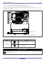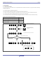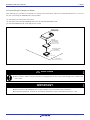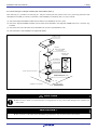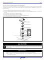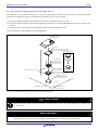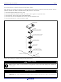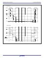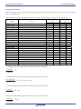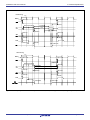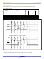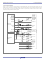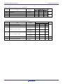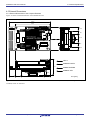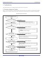
1
To our customers,
Old Company Name in Catalogs and Other Documents
On April 1st, 2010, NEC Electronics Corporation merged with Renesas Technology
Corporation, and Renesas Electronics Corporation took over all the business of both
companies. Therefore, although the old company name remains in this document, it is a valid
Renesas Electronics document. We appreciate your understanding.
Renesas Electronics website: http://www.renesas.com
April 1st, 2010
Renesas Electronics Corporation
Issued by: Renesas Electronics Corporation (http://www.renesas.com)
Send any inquiries to http://www.renesas.com/inquiry.
Notice
1.
2.
3.
4.
5.
6.
7.
All information included in this document is current as of the date this document is issued. Such information, however, is
subject to change without any prior notice. Before purchasing or using any Renesas Electronics products listed herein, please
confirm the latest product information with a Renesas Electronics sales office. Also, please pay regular and careful attention to
additional and different information to be disclosed by Renesas Electronics such as that disclosed through our website.
Renesas Electronics does not assume any liability for infringement of patents, copyrights, or other intellectual property rights
of third parties by or arising from the use of Renesas Electronics products or technical information described in this document.
No license, express, implied or otherwise, is granted hereby under any patents, copyrights or other intellectual property rights
of Renesas Electronics or others.
You should not alter, modify, copy, or otherwise misappropriate any Renesas Electronics product, whether in whole or in part.
Descriptions of circuits, software and other related information in this document are provided only to illustrate the operation of
semiconductor products and application examples. You are fully responsible for the incorporation of these circuits, software,
and information in the design of your equipment. Renesas Electronics assumes no responsibility for any losses incurred by
you or third parties arising from the use of these circuits, software, or information.
When exporting the products or technology described in this document, you should comply with the applicable export control
laws and regulations and follow the procedures required by such laws and regulations. You should not use Renesas
Electronics products or the technology described in this document for any purpose relating to military applications or use by
the military, including but not limited to the development of weapons of mass destruction. Renesas Electronics products and
technology may not be used for or incorporated into any products or systems whose manufacture, use, or sale is prohibited
under any applicable domestic or foreign laws or regulations.
Renesas Electronics has used reasonable care in preparing the information included in this document, but Renesas Electronics
does not warrant that such information is error free. Renesas Electronics assumes no liability whatsoever for any damages
incurred by you resulting from errors in or omissions from the information included herein.
Renesas Electronics products are classified according to the following three quality grades: “Standard”, “High Quality”, and
“Specific”. The recommended applications for each Renesas Electronics product depends on the product’s quality grade, as
indicated below. You must check the quality grade of each Renesas Electronics product before using it in a particular
application. You may not use any Renesas Electronics product for any application categorized as “Specific” without the prior
written consent of Renesas Electronics. Further, you may not use any Renesas Electronics product for any application for
which it is not intended without the prior written consent of Renesas Electronics. Renesas Electronics shall not be in any way
liable for any damages or losses incurred by you or third parties arising from the use of any Renesas Electronics product for an
application categorized as “Specific” or for which the product is not intended where you have failed to obtain the prior written
consent of Renesas Electronics. The quality grade of each Renesas Electronics product is “Standard” unless otherwise
expressly specified in a Renesas Electronics data sheets or data books, etc.
“Standard”:
8.
9.
10.
11.
12.
Computers; office equipment; communications equipment; test and measurement equipment; audio and visual
equipment; home electronic appliances; machine tools; personal electronic equipment; and industrial robots.
“High Quality”: Transportation equipment (automobiles, trains, ships, etc.); traffic control systems; anti-disaster systems; anticrime systems; safety equipment; and medical equipment not specifically designed for life support.
“Specific”:
Aircraft; aerospace equipment; submersible repeaters; nuclear reactor control systems; medical equipment or
systems for life support (e.g. artificial life support devices or systems), surgical implantations, or healthcare
intervention (e.g. excision, etc.), and any other applications or purposes that pose a direct threat to human life.
You should use the Renesas Electronics products described in this document within the range specified by Renesas Electronics,
especially with respect to the maximum rating, operating supply voltage range, movement power voltage range, heat radiation
characteristics, installation and other product characteristics. Renesas Electronics shall have no liability for malfunctions or
damages arising out of the use of Renesas Electronics products beyond such specified ranges.
Although Renesas Electronics endeavors to improve the quality and reliability of its products, semiconductor products have
specific characteristics such as the occurrence of failure at a certain rate and malfunctions under certain use conditions. Further,
Renesas Electronics products are not subject to radiation resistance design. Please be sure to implement safety measures to
guard them against the possibility of physical injury, and injury or damage caused by fire in the event of the failure of a
Renesas Electronics product, such as safety design for hardware and software including but not limited to redundancy, fire
control and malfunction prevention, appropriate treatment for aging degradation or any other appropriate measures. Because
the evaluation of microcomputer software alone is very difficult, please evaluate the safety of the final products or system
manufactured by you.
Please contact a Renesas Electronics sales office for details as to environmental matters such as the environmental
compatibility of each Renesas Electronics product. Please use Renesas Electronics products in compliance with all applicable
laws and regulations that regulate the inclusion or use of controlled substances, including without limitation, the EU RoHS
Directive. Renesas Electronics assumes no liability for damages or losses occurring as a result of your noncompliance with
applicable laws and regulations.
This document may not be reproduced or duplicated, in any form, in whole or in part, without prior written consent of Renesas
Electronics.
Please contact a Renesas Electronics sales office if you have any questions regarding the information contained in this
document or Renesas Electronics products, or if you have any other inquiries.
(Note 1) “Renesas Electronics” as used in this document means Renesas Electronics Corporation and also includes its majorityowned subsidiaries.
(Note 2) “Renesas Electronics product(s)” means any product developed or manufactured by or for Renesas Electronics.
User’s Manual
M3062PT3-CPE
User’s Manual
Compact Emulator for M16C/62P, M16C/30P
Groups
Rev.4.00 2009.07
Notes regarding these materials
1. This document is provided for reference purposes only so that Renesas customers may select the appropriate
Renesas products for their use. Renesas neither makes warranties or representations with respect to the
accuracy or completeness of the information contained in this document nor grants any license to any
intellectual property rights or any other rights of Renesas or any third party with respect to the information in
this document.
2. Renesas shall have no liability for damages or infringement of any intellectual property or other rights arising
out of the use of any information in this document, including, but not limited to, product data, diagrams, charts,
programs, algorithms, and application circuit examples.
3. You should not use the products or the technology described in this document for the purpose of military
applications such as the development of weapons of mass destruction or for the purpose of any other military
use. When exporting the products or technology described herein, you should follow the applicable export
control laws and regulations, and procedures required by such laws and regulations.
4. All information included in this document such as product data, diagrams, charts, programs, algorithms, and
application circuit examples, is current as of the date this document is issued. Such information, however, is
subject to change without any prior notice. Before purchasing or using any Renesas products listed in this
document, please confirm the latest product information with a Renesas sales office. Also, please pay regular
and careful attention to additional and different information to be disclosed by Renesas such as that disclosed
through our website. (http://www.renesas.com )
5. Renesas has used reasonable care in compiling the information included in this document, but Renesas
assumes no liability whatsoever for any damages incurred as a result of errors or omissions in the information
included in this document.
6. When using or otherwise relying on the information in this document, you should evaluate the information in
light of the total system before deciding about the applicability of such information to the intended application.
Renesas makes no representations, warranties or guaranties regarding the suitability of its products for any
particular application and specifically disclaims any liability arising out of the application and use of the
information in this document or Renesas products.
7. With the exception of products specified by Renesas as suitable for automobile applications, Renesas
products are not designed, manufactured or tested for applications or otherwise in systems the failure or
malfunction of which may cause a direct threat to human life or create a risk of human injury or which require
especially high quality and reliability such as safety systems, or equipment or systems for transportation and
traffic, healthcare, combustion control, aerospace and aeronautics, nuclear power, or undersea communication
transmission. If you are considering the use of our products for such purposes, please contact a Renesas
sales office beforehand. Renesas shall have no liability for damages arising out of the uses set forth above.
8. Notwithstanding the preceding paragraph, you should not use Renesas products for the purposes listed below:
(1) artificial life support devices or systems
(2) surgical implantations
(3) healthcare intervention (e.g., excision, administration of medication, etc.)
(4) any other purposes that pose a direct threat to human life
Renesas shall have no liability for damages arising out of the uses set forth in the above and purchasers who
elect to use Renesas products in any of the foregoing applications shall indemnify and hold harmless Renesas
Technology Corp., its affiliated companies and their officers, directors, and employees against any and all
damages arising out of such applications.
9. You should use the products described herein within the range specified by Renesas, especially with respect
to the maximum rating, operating supply voltage range, movement power voltage range, heat radiation
characteristics, installation and other product characteristics. Renesas shall have no liability for malfunctions or
damages arising out of the use of Renesas products beyond such specified ranges.
10. Although Renesas endeavors to improve the quality and reliability of its products, IC products have specific
characteristics such as the occurrence of failure at a certain rate and malfunctions under certain use
conditions. Please be sure to implement safety measures to guard against the possibility of physical injury, and
injury or damage caused by fire in the event of the failure of a Renesas product, such as safety design for
hardware and software including but not limited to redundancy, fire control and malfunction prevention,
appropriate treatment for aging degradation or any other applicable measures. Among others, since the
evaluation of microcomputer software alone is very difficult, please evaluate the safety of the final products or
system manufactured by you.
11. In case Renesas products listed in this document are detached from the products to which the Renesas
products are attached or affixed, the risk of accident such as swallowing by infants and small children is very
high. You should implement safety measures so that Renesas products may not be easily detached from your
products. Renesas shall have no liability for damages arising out of such detachment.
12. This document may not be reproduced or duplicated, in any form, in whole or in part, without prior written
approval from Renesas.
13. Please contact a Renesas sales office if you have any questions regarding the information contained in this
document, Renesas semiconductor products, or if you have any other inquiries.
M3062PT3-CPE User’s Manual
Regulatory Compliance Notices
Regulatory Compliance Notices
European Union regulatory notices on Electromagnetic compatibility
CE Certifications:
This product complies with the following European EMC standards.
・EMC Directive 2004/108/EC
EN 55022 Class A
WARNING: This is a Class A product. In a domestic environment this product may cause radio
interference in which case the user may be required to take adequate measures.
EN 55024
Information for traceability:
・Authorised representative
Name:
Renesas Technology Corp.
Address:
Nippon Bldg., 2-6-2, Ote-machi, Chiyoda-ku, Tokyo 100-0004, Japan
・Manufacturer
Name:
Renesas Solutions Corp.
Address:
Nippon Bldg., 2-6-2, Ote-machi, Chiyoda-ku, Tokyo 100-0004, Japan
・Person responsible for placing on the market
Name:
Renesas Technology Europe Limited European Headquaters
Address:
Dukes Meadow, Millboard Road, Bourne End, Buckinghamshire, SL8 5FH,
U.K.
United States Regulatory notices on Electromagnetic compatibility
FCC Certifications:
This equipment has been tested and found to comply with the limits for a Class A digital device, pursuant to
Part 15 of the FCC Rules. These limits are designed to provide reasonable protection against harmful
interference when the equipment is operated in a commercial environment. This equipment generates, uses,
and can radiate radio frequency energy and, if not installed and used in accordance with the instruction
manual, may cause harmful interference to radio communications. Operation of this equipment in a
residential area is likely to cause harmful interference in which case the user will be required to correct the
interference at his own expense.
This device complies with Part 15 of the FCC Rules. Operation is subject to the following two conditions: (1)
this device may not cause harmful interference, and (2) this device must accept any interference received,
including interference that may cause undesired operation.
CAUTION: Changes or modifications not expressly approved by the party responsible for compliance could void
the user's authority to operate the equipment.
REJ10J1007-0400 Rev.4.00
July 29, 2009
Page 3 of 108
M3062PT3-CPE User’s Manual
Preface
Preface
The M3062PT3-CPE is a compact emulator for the M16C Family M16C/60 Series M16C/62P Group and M16C/30 Series
M16C/30P Group MCUs with the real-time trace function.
This user's manual mainly describes specifications of the M3062PT3-CPE compact emulator and how to setup it. For details
on the emulator debugger and C compiler package M3T-NC30WA evaluation version (C compiler NC30, assembler AS30 and
integrated development environment High-performance Embedded Workshop), which are included with the M3062PT3-CPE,
refer to each product's online manual.
All the components of this product are shown in "1.1 Package Components" (page 14). If there is any question or doubt about
this product, contact your local distributor.
The related manuals for using this product are listed below. You can download the latest manuals from the Renesas Tools
homepage (http://www.renesas.com/tools).
Related manuals
Item
Integrated development environment
Emulator debugger
C compiler
Assembler
REJ10J1007-0400 Rev.4.00
Manual
High-performance Embedded Workshop User’s Manual
M16C R8C Compact Emulator Debugger User’s Manual
C Compiler Package for M16C Series and R8C Family
C Compiler User's Manual
C Compiler Package for M16C Series and R8C Family
Assembler User's Manual
July 29, 2009
Page 4 of 108
M3062PT3-CPE User’s Manual
Important
Important
Before using this product, be sure to read the user’s manual carefully.
Keep this user’s manual, and refer to this when you have questions about this product.
Emulator:
The emulator in this document refers to the following products that are manufactured by Renesas Technology Corp.:
(1) Compact emulator main unit
(2) Package converter board for connecting the user system
The emulator herein does not include the customer’s user system and host machine.
Purpose of use of the emulator:
This emulator is a device to support the development of a system that uses the M16C Family M16C/60 Series M16C/62P
Group and M16C/30 Series M16C/30P Group of Renesas 16-bit single-chip MCUs. It provides support for system
development in both software and hardware.
Be sure to use this emulator correctly according to said purpose of use. Please avoid using this emulator for other than its
intended purpose of use.
For those who use this emulator:
This emulator can only be used by those who have carefully read the user’s manual and know how to use it.
Use of this emulator requires the basic knowledge of electric circuits, logical circuits, and MCUs.
When using the emulator:
(1) This product is a development supporting unit for use in your program development and evaluation stages. In massproducing your program you have finished developing, be sure to make a judgment on your own risk that it can be put to
practical use by performing integration test, evaluation, or some experiment else.
(2) In no event shall Renesas Solutions Corp. be liable for any consequence arising from the use of this product.
(3) Renesas Solutions Corp. strives to renovate or provide a workaround for product malfunction at some charge or without
charge. However, this does not necessarily mean that Renesas Solutions Corp. guarantees the renovation or the provision
under any circumstances.
(4) This product has been developed by assuming its use for program development and evaluation in laboratories. Therefore,
it does not fall under the application of Electrical Appliance and Material Safety Law and protection against
electromagnetic interference when used in Japan.
(5) Renesas Solutions Corp. cannot predict all possible situations or possible cases of misuse where a potential danger exists.
Therefore, the warnings written in this user’s manual and the warning labels attached to this emulator do not necessarily
cover all of such possible situations or cases. Please be sure to use this emulator correctly and safely on your own
responsibility.
REJ10J1007-0400 Rev.4.00
July 29, 2009
Page 5 of 108
M3062PT3-CPE User’s Manual
Important
Usage restrictions:
This emulator has been developed as a means of supporting system development by users. Therefore, do not use it as a device
used for equipment-embedded applications. Also, do not use it for developing the systems or equipment used for the following
purposes either:
(1) Transportation and vehicular
(2) Medical (equipment where human life is concerned)
(3) Aerospace
(4) Nuclear power control
(5) Undersea repeater
If you are considering the use of this emulator for one of the above purposes, please be sure to consult your local distributor.
About product changes:
We are constantly making efforts to improve the design and performance of this emulator. Therefore, the specification or
design of this emulator or its user’s manual may be changed without prior notice.
About the rights:
(1) We assume no responsibility for any damage or infringement on patent rights or any other rights arising from the use of
any information, products or circuits presented in this user’s manual.
(2) The information or data in this user’s manual does not implicitly or otherwise grant a license for patent rights or any other
rights belonging to us or third parties.
(3) This user’s manual and this emulator are copyrighted, with all rights reserved by us. This user’s manual may not be copied,
duplicated or reproduced, in whole or part, without prior written consent of us.
About diagrams:
The diagrams in this user’s manual may not all represent exactly the actual object.
REJ10J1007-0400 Rev.4.00
July 29, 2009
Page 6 of 108
M30290T2-CPE User’s Manual
Precautions for Safety
Precautions for Safety
Definitions of Signal Words
In both the user’s manual and on the product itself, several icons are used to insure proper handling of this product and also to
prevent injuries to you or other persons, or damage to your properties.
This chapter describes the precautions which should be taken in order to use this product safely and properly. Be sure to read
this chapter before using this product.
This symbol represents a warning about safety. It is used to arouse caution about a potential
danger that will possibly inflict an injury on persons. To avoid a possible injury or death,
please be sure to observe the safety message that follows this symbol.
DANGER
DANGER indicates an imminently dangerous situation that will cause death or heavy wound
unless it is avoided. However, there are no instances of such danger for the product presented
in this user's manual.
WARNING
WARNING indicates a potentially dangerous situation that will cause death or heavy wound
unless it is avoided.
CAUTION
CAUTION indicates a potentially dangerous situation that will cause a slight injury or a
medium-degree injury unless it is avoided.
CAUTION
CAUTION with no safety warning symbols attached indicates a potentially dangerous
situation that will cause property damage unless it is avoided.
IMPORTANT
This is used in operation procedures or explanatory descriptions to convey exceptional
conditions or cautions to the user.
In addition to the five above, the following are also used as appropriate.
means WARNING or CAUTION.
Example:
CAUTION AGAINST AN ELECTRIC SHOCK
means PROHIBITION.
Example:
DISASSEMBLY PROHIBITED
means A FORCIBLE ACTION.
Example:
UNPLUG THE POWER CABLE FROM THE RECEPTACLE.
REJ10J1007-0400 Rev.4.00
July 29, 2009
Page 7 of 108
M30290T2-CPE User’s Manual
Precautions for Safety
WARNING
Warnings for AC Power Supply:
z If the attached AC power cable does not fit the receptacle, do not alter the AC power cable and do not plug it
forcibly. Failure to comply may cause electric shock and/or fire.
z Use an AC power cable which complies with the safety standard of the country.
z Do not touch the plug of the AC power cable when your hands are wet. This may cause electric shock.
z This product is connected signal ground with frame ground. If your developing product is transformless (not
having isolation transformer of AC power), this may cause electric shock. Also, this may give an unrepairable
damage to this product and your developing one.
While developing, connect AC power of the product to commercial power through isolation transformer in
order to avoid these dangers.
z If other equipment is connected to the same branch circuit, care should be taken not to overload the circuit.
z Use the power supply which complies with CE marking requirements.
z When installing this equipment, insure that a reliable ground connection is maintained.
z If you smell a strange odor, hear an unusual sound, or see smoke coming from this product, then disconnect
power immediately by unplugging the AC power cable from the outlet.
Do not use this as it is because of the danger of electric shock and/or fire. In this case, contact your local
distributor.
z Before setting up this emulator and connecting it to other devices, turn off power or remove a power cable to
prevent injury or product damage.
Warnings to Be Taken for This Product:
z Do not disassemble or modify this product. Personal injury due to electric shock may occur if this product is
disassembled and modified. Disassembling and modifying the product will void your warranty.
z Make sure nothing falls into the cooling fan on the top panel, especially liquids, metal objects, or anything
combustible.
Warning for Installation:
z Do not set this product in water or areas of high humidity. Make sure that the product does not get wet. Spilling
water or some other liquid into the product may cause unrepairable damage.
Warning for Use Environment:
z This equipment is to be used in an environment with a maximum ambient temperature of 35°C. Care should be
taken that this temperature is not exceeded.
REJ10J1007-0400 Rev.4.00
July 29, 2009
Page 8 of 108
M30290T2-CPE User’s Manual
Precautions for Safety
CAUTION
Notes on Connecting the Power Supply of the Emulator:
z Do not use any power cable other than the one that is included with the product.
z The power cable included with the product has its positive and negative poles color-coded by red and black,
respectively.
z Pay attention to the polarities of the power supply. If its positive and negative poles are connected in reverse,
the internal circuit may be broken.
z Do not apply any voltages exceeding the product’s rated power supply voltage (5.0 V ±5%). Extreme voltages
may cause a burn due to abnormal heat or cause the internal circuit to break down.
Cautions to Be Taken for Turning On the Power:
z Turn ON/OFF the power of the emulator and user system as simultaneously as possible.
z Do not leave either the emulator or user system powered on, because of leakage current the internal circuits may
be damaged.
z When turning on the power again after shutting off the power, wait about 10 seconds.
Cautions to Be Taken for Handling This Product:
z Use caution when handling the main unit. Be careful not to apply a mechanical shock.
z Do not touch the connector pins of the emulator main unit and the target MCU connector pins directly. Static
electricity may damage the internal circuits.
z Do not pull this emulator by the communications interface cable or the flexible cable for connecting the user
system. And, excessive flexing or force may break conductors.
Caution to Be Taken for System Malfunctions:
z If the emulator malfunctions because of interference like external noise, do the following to remedy the trouble.
(1) Press the RESET switch on the emulator upper panel.
(2) If normal operation is not restored after step (1), shut OFF the emulator once and then reactivate it.
REJ10J1007-0400 Rev.4.00
July 29, 2009
Page 9 of 108
M3062PT3-CPE User’s Manual
Contents
Contents
Page
Regulatory Compliance Notices ...................................................................................................................................3
Preface..........................................................................................................................................................................4
Important.......................................................................................................................................................................5
Precautions for Safety ..................................................................................................................................................7
Contents......................................................................................................................................................................10
User Registration ........................................................................................................................................................12
Terminology ................................................................................................................................................................13
1. Outline.....................................................................................................................................................................14
1.1 Package Components ...................................................................................................................................14
1.2 System Configuration ....................................................................................................................................15
1.2.1 Names and Functions of each part of the Emulator............................................................................16
1.3 Specifications ................................................................................................................................................19
1.4 Operating Environment..................................................................................................................................21
2. Setup.......................................................................................................................................................................22
2.1 Flowchart of Starting Up the Emulator ..........................................................................................................22
2.2 Installing the Included Software ....................................................................................................................23
2.3 Attaching the Ferrite Core .............................................................................................................................23
2.4 Connecting the Power Supply for the Emulator ............................................................................................24
2.5 Connecting the Host Machine .......................................................................................................................25
2.6 Turning ON the Power...................................................................................................................................26
2.6.1 MCU Power Supply Source Selection Jumper/MCU Power Supply Voltage Selection Jumper.........26
2.6.2 VCC1, VCC2 power selection jumper (Jumper of the M3062PT2-EPBM) .........................................27
2.6.3 Checking Connections of the Emulator System..................................................................................28
2.6.4 Turning ON/OFF the Power ................................................................................................................28
2.6.5 LED Display When the Emulator Starts Up Normally .........................................................................29
2.7 Self-check ......................................................................................................................................................31
2.7.1 Self-check Procedure ..........................................................................................................................31
2.7.2 If an Error is Detected in the Self-check..............................................................................................32
2.8 Connecting the User System.........................................................................................................................33
2.8.1 Connecting to an 80-pin 0.65mm pitch Foot Pattern ..........................................................................34
2.8.2 Connecting to a 100-pin LCC Socket..................................................................................................35
2.8.3 Connecting to a 100-pin 0.65mm pitch Foot Pattern (Part 1) .............................................................36
2.8.4 Connecting to a 100-pin 0.65mm pitch Foot Pattern (Part 2) .............................................................37
2.8.5 Connecting to a 100-pin 0.65mm pitch Foot Pattern (Part 3) .............................................................38
2.8.6 Connecting to a 100-pin 0.65mm pitch Foot Pattern (Part 4) .............................................................39
2.8.7 Connecting to a 100-pin 0.5mm pitch Foot Pattern (Part 1) ...............................................................40
2.8.8 Connecting to a 100-pin 0.5mm pitch Foot Pattern (Part 2) ...............................................................41
2.8.9 Connecting to a 100-pin 0.5mm pitch Foot Pattern (Part 3) ...............................................................42
2.8.10 Connecting to a 128-pin 0.5mm pitch Foot Pattern ..........................................................................43
2.9 Changing Settings .........................................................................................................................................44
2.9.1 Selecting Clock Supply .......................................................................................................................44
2.9.2 A/D Conversion Bypass Capacitors ....................................................................................................48
2.9.3 Pullup of Emulation Ports....................................................................................................................49
REJ10J1007-0400 Rev.4.00
July 29, 2009
Page 10 of 108
M3062PT3-CPE User’s Manual
Contents
Page
3. Usage (How to Use the Emulator Debugger) .........................................................................................................50
3.1 Starting Up the Emulator Debugger ..............................................................................................................50
3.2 INIT Dialog Box .............................................................................................................................................50
3.3 MCU Setting Dialog Box................................................................................................................................54
3.4 Checking Connections of the Emulator System ............................................................................................57
3.5 Program Execution ........................................................................................................................................58
3.6 Hardware Breakpoint Setting Window...........................................................................................................63
3.7 Trace Window................................................................................................................................................68
3.8 RAM Monitor Window....................................................................................................................................73
4. Hardware Specifications .........................................................................................................................................76
4.1 Target MCU Specifications............................................................................................................................76
4.2 Access Timing ...............................................................................................................................................77
4.2.1 Operation Timing of Memory Expansion Mode and Microprocessor Mode (VCC1=VCC2=5V) ........77
4.2.2 Operation Timing of Memory Expansion Mode and Microprocessor Mode (VCC1=VCC2=3V) ........82
4.3 Differences between the Actual MCU and Emulator.....................................................................................87
4.4 Connection Diagram......................................................................................................................................91
4.5 External Dimensions......................................................................................................................................93
4.5.1 External Dimensions of the Compact Emulator ..................................................................................93
4.6 Notes on Using This Product.........................................................................................................................94
5. Troubleshooting ....................................................................................................................................................100
5.1 Flowchart to Remedy the Troubles .............................................................................................................100
5.2 When the Emulator Debugger Does Not Start Up Properly ........................................................................101
5.3 How to Request for Support ........................................................................................................................103
6. Maintenance and Guarantee ................................................................................................................................104
6.1 User Registration.........................................................................................................................................104
6.2 Maintenance ................................................................................................................................................104
6.3 Guarantee....................................................................................................................................................104
6.4 Repair Provisions ........................................................................................................................................104
6.5 How to Make Request for Repair ................................................................................................................105
REJ10J1007-0400 Rev.4.00
July 29, 2009
Page 11 of 108
M3062PT3-CPE User’s Manual
User Registration
User Registration
When you install debugger software, a text file for user registration is created on your PC. Fill it in and email it to your local
distributor. If you have replaced an emulator main unit or emulation probe, rewrite an emulator name and serial number in the
text file you filled in earlier to register your new hardware products.
Your registered information is used for only after-sale services, and not for any other purposes. Without user registration, you
will not be able to receive maintenance services such as a notification of field changes or trouble information. So be sure to
carry out the user registration.
For more information about user registration, please contact your local distributor.
REJ10J1007-0400 Rev.4.00
July 29, 2009
Page 12 of 108
M3062PT3-CPE User’s Manual
Terminology
Terminology
Some specific words used in this user’s manual are defined as follows:
Emulator M3062PT3-CPE
This means the compact emulator (this product) for the M16C Family M16C/60 Series M16C/62P Group and M16C/30 Series
M16C/30P Group MCUs.
Emulator system
This means an emulator system built around the M3062PT3-CPE emulator. The M3062PT3-CPE emulator system is
configured with an emulator main unit M3062PT3-CPE, integrated development environment High-performance Embedded
Workshop, emulator debugger and host machine.
Renesas Integrated development environment High-performance Embedded Workshop
This tool provides powerful support for the development of embedded applications for Renesas microcomputers. It has an
emulator debugger function allowing for the emulator to be controlled from the host machine via an interface. Furthermore, it
permits a range of operations from editing a project to building and debugging it to be performed within the same application.
What’s more, it supports version management.
Emulator debugger
This means a software tool which starts up in the integrated development environment High-performance Embedded
Workshop to control the emulator for the M16C Family and enables debugging.
Firmware
This means a program stored in the flash ROM of the emulator. It analyzes contents of communication with the emulator
debugger and controls the emulator M3062PT3-CPE. This program is downloadable from the emulator debugger to upgrade
the firmware, etc.
Host machine
This means a personal computer used to control the M3062PT3-CPE emulator system.
Target MCU
This means the microcomputer you are going to debug.
User system
This means a user’s application system using the microcomputer to be debugged.
User program
This means a user’s application program to be debugged.
Evaluation MCU
This means a microcomputer mounted on the emulator which is operated in the special mode for the emulator.
#
In this user’s manual, this symbol is used to show active LOW. (e.g. RESET#)
REJ10J1007-0400 Rev.4.00
July 29, 2009
Page 13 of 108
M3062PT3-CPE User’s Manual
1. Outline
1. Outline
This chapter describes the package components, the system configuration and the preparation for using this product for the first
time.
1.1 Package Components
The M3062PT3-CPE package consists of the following items. When unpacking it, check to see if your M3062PT3-CPE
contains all of these items.
Table 1.1 Package components
Item
Quantity
1
1
1
6
1
1
1
1
1
1
1
1
1
1
1
1
M3062PT3-CPE compact emulator
OSC-3 (16MHz) oscillator circuit board
OSC-2 oscillator circuit bare board
Network resistors for ports P0--P5 pullup (51kΩ x 8)
USB interface cable for connecting host machine and emulator
Power supply cable for compact emulator
Ferrite core for connecting power supply cable
H/W Tool Customer Registration Sheet (English)
H/W Tool Customer Registration Sheet (Japanese)
Repair request sheet (English)
Repair request sheet (Japanese)
M3062PT3-CPE User’s Manual (this manual)
M3062PT3-CPE User’s Manual (Japanese)
M3062PT3-CPE Release Notes (English)
M3062PT3-CPE Release Notes (Japanese)
CD-ROM
• Emulator debugger
M16C R8C Compact Emulator Debugger
• C compiler package M3T-NC30WA (evaluation version)
- C compiler for M16C Series and R8C Family NC30
- Assembler for M16C Series and R8C Family AS30
- Integrated development environment
High-performance Embedded Workshop
* Please keep the M3062PT3-CPE’s packing box and cushion material in your place for reuse at a later time when sending
your product for repair or other purposes. Always use these packing box and cushion material when transporting this
product.
* If there is any question or doubt about the packaged product, contact your local distributor.
REJ10J1007-0400 Rev.4.00
July 29, 2009
Page 14 of 108
M3062PT3-CPE User’s Manual
1. Outline
1.2 System Configuration
Figure 1.1 shows a configuration of the M3062PT3-CPE system.
(3) Power supply for emulator
(not included)
Power supply cable
(2) USB interface cable
(5) Power supply for user system
(not included)
(4) User system
(not included)
(6) Host machine
(not included)
(1) Compact emulator
(7) Package converter board
(not included)
Figure 1.1 System configuration
(1) Compact emulator M3062PT3-CPE (this product)
This is a compact emulator for the M16C/62P and M16C/30P Groups with the real-time trace functions (hereafter,
emulator). The M3062PT2-EPBM on which an evaluation MCU is mounted can be also purchased separately.
(2) USB interface cable (included)
This is an interface cable for the host machine and the emulator.
(3) Power supply for emulator
This is a power supply for the emulator. Supply 5.0 V ±5% (DC).
Prepare a power supply which complies with CE marking requirements separately. The power cable is included with this
product.
Note: Be aware that there are some AC adapters whose power supply voltage varies rather widely with its load. You are
recommended to use an AC adapter with a switching power supply or a stabilized power supply.
(4) User system
This is your application system. This emulator can be used without the user system.
REJ10J1007-0400 Rev.4.00
July 29, 2009
Page 15 of 108
M3062PT3-CPE User’s Manual
1. Outline
(5) Power supply for the user system
This is a power supply for the user system. As this emulator cannot supply the power to the user system, supply the power
to the user system separately from the emulator.
(6) Host machine
This is a personal computer for controlling the emulator.
(7) Package converter board such as M30800T-PTC
This is a package converter board for connecting to an MCU foot pattern on the user system. For details, refer to “2.8
Connecting the User System” (page 33).
1.2.1 Names and Functions of each part of the Emulator
Figure 1.2 shows the names of the LEDs on the upper panel of the emulator.
J1 : Power connector
J2 : USB interface connector
POWER USB
5.0V
512
SYSTEM
STATUS
EXT
JP1
INT
b0
M3062PT3-CPE
JP2
MCU
POWER
COMPACT EMULATOR
5.0V
JP2
3.3V
EXT 3.3V 5.0V
System reset switch
LED2
JP1
POWER
SAFE
SAFE
INT
P0
P1
P2
VCC2 b7
System Status LEDs
LED1 : Emulator Power (POWER)
LED2 : Emulator Status (SAFE)
LED1
POWER
JP2 : MCU power supply voltage
Selection Jumper
(factory-setting: 5.0V)
JP1 : MCU power supply source
selection jumper
(factory-setting: INT)
b7
LED5 LED4
LED3
POWER
CLOCK
RESET
RUN
LED6
b0
Target Status LEDs
LED3 : User system power (POWER)
LED4 : Clock oscillation (CLOCK)
LED5 : MCU RESET pin status (RESET)
LED6 : Program Execution (RUN)
POWER
CLOCK
RESET
RUN
TARGET
STATUS
COMPACT EMULATOR
MADE MADE IN JAPAN
P5 P4 P3
Figure 1.2 Names of the LEDs on the upper panel of the M3062PT3-CPE
(1) System Status LEDs
The system status LEDs indicate the emulator main unit’s operating status etc. Table 1.2 lists the definition of the system status
LEDs.
Table 1.2 Definitions of the system status LEDs
Name
POWER
SAFE
Number
LED1
Color
Orange
LED2
Green
REJ10J1007-0400 Rev.4.00
Status
ON
OFF
ON
OFF
Meaning
Power is supplied to the emulator.
Power is not supplied to the emulator.
Emulator system has started normally.
Emulator system has not started normally.
July 29, 2009
Page 16 of 108
M3062PT3-CPE User’s Manual
1. Outline
(2) Target Status LEDs
The target status LEDs indicate the target MCU’s power supply and operating status. Table 1.3 lists the definition of each
target status LED.
Table 1.3 Definitions of the target status LEDs
Name
POWER
Number
LED3
Color
Orange
CLOCK
LED4
Green
RESET
LED5
Red
RUN
LED6
Green
Status
ON
OFF
ON
OFF
ON
OFF
ON
OFF
Meaning
Power is supplied to the target MCU.
Power is not supplied to the target MCU.
The target MCU internal clock is oscillating.
The target MCU internal clock is not oscillating.
Target MCU is being reset, or reset signal of the user system is held low.
Target MCU is not being reset.
User program is being executed.
User program is not being executed.
IMPORTANT
Note on Usage in Memory Expansion or Microprocessor Mode:
z When you use this product in memory expansion or microprocessor mode, it cannot startup normally if the pins
RDY# and HOLD# are at “L” level.
Note on the Target Status POWER LED:
z If your MCU has two or more VCC terminals, the LED does not light unless power is supplied to all the
terminals.
(3) System Reset Switch
By pressing the system reset switch, you can initialize the emulator system. Table 1.4 shows the functions of the system reset
switch depending on the state of the emulator.
Table 1.4 Functions of the system reset switch
State of Emulator
When the user’s program is halted
When the user’s program is executed
Function
Initializes the emulator and waits for a command from the
emulator debugger
Stops the user’s program, initializes the emulator, and
waits for a command from the emulator debugger.
IMPORTANT
Notes on a System Reset:
z After pressing the system reset switch, restart the emulator debugger. Otherwise the display of emulator
debugger and the actual value (in the emulator) may not match.
z When the emulator debugger does not start up normally even after rebooting, turn off the emulator and then turn
on again.
REJ10J1007-0400 Rev.4.00
July 29, 2009
Page 17 of 108
M3062PT3-CPE User’s Manual
1. Outline
(4) Power Connector (J1)
This is a connector for connecting the power supply to this product. For details, refer to “2.4 Connecting the Power Supply for
the Emulator” (page 24).
(5) USB Cable Connector (J2)
This is a USB cable connector for connecting the host machine to this product. For details, “2.5 Connecting the Host Machine”
(page 25).
(6) MCU Power Supply Source Selection Jumper (JP1)
This is a jumper switch to set the power supply source to the MCU. For details on this switch, see “2.6.1 MCU Power Supply
Source Selection Jumper/MCU Power Supply Voltage Selection Jumper” (page 26).
(7) MCU Power Supply Voltage Selection Jumper (JP2)
This is a jumper switch to set the power supply voltage of the MCU. This setting is valid when the MCU power supply source
selection jumper is set to INT only. For details on this switch, see “2.6.1 MCU Power Supply Source Selection Jumper/MCU
Power Supply Voltage Selection Jumper” (page 26).
REJ10J1007-0400 Rev.4.00
July 29, 2009
Page 18 of 108
M3062PT3-CPE User’s Manual
1. Outline
1.3 Specifications
Tables 1.5 and 1.6 list specifications of the M3062PT3-CPE.
Table 1.5 M3062PT3-CPE specifications (1/2)
Applicable MCUs
Usable mode
M16C/60 Series M16C/62P and M16C/30 Series M16C/30P Groups
Single-chip mode,
Memory-expansion mode (NORMAL, 4MB),
Microprocessor mode (NORMAL, 4MB) *1
Maximum ROM/RAM capacity
1. Internal flash ROM : 512KB + 4KB
0F000h--0FFFFh, 80000h--FFFFFh
2. Internal RAM : 31KB
00400h--07FFFh
Maximum operating frequency
3.0 to 5.5 V: 24 MHz (when using a PLL)
2.7 V: 10 MHz
Applicable power supply
User system connected
VCC1 = VCC2:
2.7--5.5V
VCC1 > VCC2:
VCC1 = 5.0 ± 0.2V,
2.7V ≤ VCC2 < VCC1
User system not connected 3.3 V or 5.0 V
(supplied from the emulator)
Emulation memory *1
External area (CS3#--CS0# area)
In the MAP tab in the MCU setting dialog box of the emulator debugger, memory
area assigned to the emulation memory can be allocated up to 4 areas by 4KB.
- Maximum operating frequency (at 5.0 V)
0 wait:
7 MHz
1 wait:
20 MHz
2 wait, 3 wait: 24 MHz
- Maximum operating frequency (at 3.0 V)
0 wait:
6 MHz
1 wait:
17 MHz
2 wait, 3 wait: 24MHz
Basic debugging functions
- Download
- Address match break (max 8 points)
- Software break (max. 64 points)
- Program execution/stop (allows free-run execution supporting software breaks)
- Memory reference/setting (reference/setting C-variables, run-time execution)
- Register reference/setting
- Disassemble display
- C-level debugging, etc.
Real-time trace function
- 64K-cycle bus information recordable
(20-bit address 16-bit data 12-bit MCU status)
- 5 trace modes supported (Break/Before/About/After/Full)
- Can be recorded ON/OFF by events
Real-time RAM monitor function
- 1,024 bytes (256 bytes x4)
- Data/last access result
Hardware break function
2 points (Address match, bus match, max. 255 pass counts) *2
Execution time measurement function
Time between program start and stop
*1 Emulation memory board R0E33062PMSRC0 (not included) is necessary for a microprocessor mode and emulation
memory function support.
*2 The hardware break function and trace point setting of the real-time trace function cannot be used simultaneously.
REJ10J1007-0400 Rev.4.00
July 29, 2009
Page 19 of 108
M3062PT3-CPE User’s Manual
1. Outline
Table 1.6 M3062PT3-CPE specifications (2/2)
For 80-pin 0.65mm pitch QFP (PRQP0080JA-A, Previous code: 80P6S-A):
Connection to user system
M3062PT-80FPB (not included)
(see “2.8 Connecting the User System”
*3
For
100-pin LCC socket:
on page 33)
M30800T-PTC (not included) + IC61-1004-051 (not included)
For 100-pin 0.65mm pitch QFP (PRQP0100JB-A, Previous code: 100P6S-A):
(1) M3T-F160-100NRB (not included)
(2) M30800T-PTC (not included) + M3T-100LCC-DMS (not included)
+ M3T-DIRECT100S (not included)
(3) M30800T-PTC (not included) + M3T-100LCC-DMS (not included)
+ M3T-DUMMY100S (not included)
(4) M30800T-PTC (not included) + M3T-100LCC-DMS (not included)
+ M3T-FLX-100NRB (not included)
For 100-pin 0.5mm pitch LQFP (PLQP0100KB-A, Previous code: 100P6Q-A):
(1) M3T-F160-100NSD (not included)
(2) M30800T-PTC (not included) + M3T-100LCC-QSD (not included)
(3) M30800T-PTC (not included) + M3T-100LCC-DMS (not included)
+ M3T-FLX-100NSD (not included)
For 128-pin 0.5mm pitch LQFP (PLQP0128KB-A, Previous code:128P6Q-A):
M3T-FLX-128NRD (not included)
Power supply for emulator
DC 5.0 V ±5 %/(2 A) externally supplied (Prepare a power supply which
complies with CE marking requirements separately.)
Host machine interface
USB *4 (USB 1.1 full-speed, mini-B standard connector)
*3 Set packages which consist of the compact emulator and converter board are available.
*4 Available to connect the host machine that supports USB 2.0. With the USB interface, not all hardware (such as host
machine, USB devices, USB hub) combination will work and guaranteed.
REJ10J1007-0400 Rev.4.00
July 29, 2009
Page 20 of 108
M3062PT3-CPE User’s Manual
1. Outline
1.4 Operating Environment
Be sure to use thins emulator with the operating environmental of the emulator and host machine listed in Tables 1.7 and 1.8.
Table 1.7 Operating environmental conditions
Item
Operating temperature
Storage temperature
Description
5 to 35°C (no dew)
-10 to 60°C (no dew)
Table 1.8 Operating environment of the host machine
Item
Description
Host machine
OS
IBM PC/AT compatibles
Windows® XP *1
Windows® 2000
CPU
Pentium III 600 MHz or more recommended
Memory
128 MB or more recommended
Host machine interface
USB 1.1 full-speed *2
Pointing device such as mouse
Mouse or any other pointing device usable with the above OS that can be
connected to the main body of the host machine.
CD drive
Needed to install the emulator debugger or refer to the user’s manual
*1 Windows is either a registered trademark or trademark of Microsoft Corporation in the United States and other countries.
*2 Available to connect the host machine that supports USB 2.0. With the USB interface, not all hardware (such as host
machine, USB devices, USB hub) combination will work and guaranteed.
REJ10J1007-0400 Rev.4.00
July 29, 2009
Page 21 of 108
M3062PT3-CPE User’s Manual
2. Setup
2. Setup
This chapter describes the preparation for using this product, the procedure for starting up the emulator and how to change
settings.
2.1 Flowchart of Starting Up the Emulator
The procedure for starting up the emulator is shown in Figure 2.1. For details, refer to each section hereafter. And, when the
emulator does not start up normally, refer to “5. Troubleshooting” (page 100).
Check the package components.
Refer to “1.1 Package Components (page 14).
↓
User registration
Refer to “User Registration” (page 12).
↓
Install the included software.
Install it from the included CD-ROM.
↓
Set the MCU power voltage
selection jumper (JP2).
↓
Select a power voltage supplied to the target MCU.
Connect the USB interface cable.
Connect the USB interface cable to the USB interface connector
(J2) of the emulator and the USB port of the host machine.
↓
Connect the power supply for the emulator.
Connect a power supply to the power connector (J1). Power supply
should be 5.0 V ±5%, 2 A.
↓
Connect the user system.
Connect the user system as occasion demands.
↓
Turning on the power supply.
Turn on the power to the emulator and the user system as
simultaneously as possible.
↓
Check the LED display of the emulator.
↓
Start up the emulator debugger from the
High-performance Embedded Workshop.
↓
Set the operating environment
of the emulator debugger.
↓
Debug a program with various functions of
the emulator debugger.
Check that the system status LED, and POWER and RESET of
target status LED are lighting. When the user system is not
connected, the POWER LED does not light up.
Start up the High-performance Embedded Workshop, and the
emulator debugger.
Set the INIT dialog box and MCU Setting dialog box of the
emulator debugger.
For how to use the High-performance Embedded Workshop and the
emulator debugger, refer to each online manual.
Figure 2.1 Flowchart of starting up the emulator
REJ10J1007-0400 Rev.4.00
July 29, 2009
Page 22 of 108
M3062PT3-CPE User’s Manual
2. Setup
2.2 Installing the Included Software
If the OS used in your host machine is Windows® XP or Windows® 2000, this installation must be executed by a user with
administrator rights. Be aware that users without administrator rights cannot complete the installation.
Install the software as instructed by the displayed messages by inserting the included CD into the CD-ROM drive.
In process of installation, “user information” dialog box to enter the user information (contractor, section, contact address, and
host machine) will open. The supplied information will be turned into a format by which technical support will be provided by
e-mail.
2.3 Attaching the Ferrite Core
Attach the ferrite core included with this product close to the DC plug of the power cable. Without the ferrite core it may cause
interference.
The power cable should be wound around the ferrite core as shown in Figure 2.2, and close the ferrite core until it clicks.
Figure 2.2 Attaching the ferrite core
REJ10J1007-0400 Rev.4.00
July 29, 2009
Page 23 of 108
M3062PT3-CPE User’s Manual
2. Setup
2.4 Connecting the Power Supply for the Emulator
Connect the power supply for the emulator to the power connector (J1). The specification of the power supply for the emulator
is listed in Table 2.1.
Table 2.1 Specification of power supply of the emulator
DC 5.0 V±5%/2 A
Power supply voltage
Figures 2.3 and 2.4 show the specifications of the power connector (J1) and an applicable plug, respectively.
Electrode (+)
φ1.7mm(Inside diameter)
Electrode (-)
φ4.75mm
Figure 2.3 Power connector specifications
Figure 2.4 Applicable plug specifications
CAUTION
Notes on Connecting a Power Supply of the Emulator:
z The power cable included in this product package is colored red (+) and black (-).
z Be careful about the polarity of the power supply. Connecting to the wrong electrode could destroy internal
circuits.
z Do not apply a voltage exceeding the specified voltage of the product (5.0 V ±5%), because it may cause burn
injuries and the failure of internal circuits.
z Use the power supply which complies with CE marking requirements.
REJ10J1007-0400 Rev.4.00
July 29, 2009
Page 24 of 108
M3062PT3-CPE User’s Manual
2. Setup
2.5 Connecting the Host Machine
Connect the emulator and the host machine with the USB interface cable.
Connect the USB interface cable (included) to the USB interface connector (J2) and the USB port of the host machine (see
Figure 2.5).
To emulator powe supply
To host machine
b
Connect the USB
interface cable to
connector J2.
Connect the power
cable to connector J1.
POWER USB
5.0V
512
SYSTEM
STATUS
MCU
POWER
b7
LED2
COMPACT EMULATOR
b0
M3062PT3-CPE
5.0V
JP2
3.3V
EXT
JP1
INT
EXT 3.3V 5.0V
JP1
JP2
POWER
SAFE
SAFE
INT
P0
P1
P2
VCC2
LED1
POWER
b7
LED5 LED4
LED3
POWER
CLOCK
RESET
RUN
LED6
b0
P5 P4 P3
POWER
CLOCK
RESET
RUN
TARGET
STATUS
COMPACT EMULATOR
MADE MADE IN JAPAN
Figure 2.5 Connecting the emulator system
REJ10J1007-0400 Rev.4.00
July 29, 2009
Page 25 of 108
M3062PT3-CPE User’s Manual
2. Setup
2.6 Turning ON the Power
2.6.1 MCU Power Supply Source Selection Jumper/MCU Power Supply Voltage Selection Jumper
Set the MCU power supply source selection jumper and the MCU power supply voltage selection jumper of the emulator
according to conditions of use.
b0
M3062PT3-CPE
JP1 : MCU power supply source
selection jumper
(factory-setting : INT)
JP2 : MCU power supply voltage
selection jumper
(factory-setting : 5.0V)
b7
LED5 LED4
CLOCK
RESET
RUN
LED6
b0
P5 P4 P3
POWER
CLOCK
RESET
RUN
EXT
EXT
JP1
INT
JP1
5.0V
JP2
3.3V
INT
MCU
POWER
b7
COMPACT EMULATOR
LED3
POWER
3.3V 5.0V
SYSTEM
STATUS
LED2
3.3V 5.0V
5.0V
EXT 3.3V
EXT
JP1
JP1
JP2
POWER
SAFE
SAFE
INT
INT
P0
P1
P2
VCC2
LED1
POWER
JP2
POWER USB
5.0V
512
TARGET
STATUS
COMPACT EMULATOR
MADE MADE IN JAPAN
Figure 2.6 Jumper switch locations
These are the jumper switches to select power supply to the MCU and its power voltage. As shown in Table 2.2 below, set the
switch according to the connection to the user system.
Table 2.2 Setting jumper switches
Connection to
the user system
MCU power supply
source selection
jumper (JP1)
MCU power supply
voltage selection
jumper (JP2)
3.3 V
Not connected
INT
5.0 V
Connected
EXT
Invalid
Description
Supplied from the emulator. The MCU operating
voltage is 3.3 V.
Supplied from the emulator. The MCU operating
voltage is 5.0 V.
Supplied from the user system. This emulator
consumes max. 500mA of electrical current from the
user system.
CAUTION
Note on Jumper Switch Settings:
z Always shut OFF the emulator before changing the setting of the jumper switches. Otherwise the internal circuit
may cause a break.
REJ10J1007-0400 Rev.4.00
July 29, 2009
Page 26 of 108
M3062PT3-CPE User’s Manual
2. Setup
2.6.2 VCC1, VCC2 power selection jumper (Jumper of the M3062PT2-EPBM)
Set the VCC1, VCC2 power selection jumper of the M3062PT2-EPBM according to conditions of use.
Figure 2.7 shows the position of the VCC1, VCC2 power selection jumper, and Table 2.3 lists the switch settings of the VCC1,
VCC2 power selection jumper.
POWER USB
5.0V
512
POWER
SAFE
SYSTEM
60.0
EXT
JP1
INT
b0
M3062PT3-CPE
JP2
JP1
MCU
POWER
b7
COMPACT EMULATOR
5.0V
JP2
3.3V
EXT 3.3V 5.0V
STATUS
LED2
INT
P0
P1
P2
VCC2
LED1
POWER
SAFE
b7
LED5 LED4
LED3
POWER
CLOCK
RESET
RUN
LED6
POWER
CLOCK
RESET
RUN
TARGET
STATUS
b0
COMPACT EMULATOR
MADE MADE IN JAPAN
P5 P4 P3
M3062PT2-EPBM
VCC1,VCC2 power
selection Jumper
Figure 2.7 Jumper switch locations
Table 2.3 Setting jumper switches
Switch
Setting
VCC1=2
VCC1, VCC2 power
selection jumper
VCC1>2
Description
2.7[V] ≤ VCC1 = VCC2 ≤ 5.5[V]
(Factory-settings)
VCC1=2
VCC1>2
VCC1 = 5.0 ± 0.2V and
2.7V ≤ VCC2 < VCC1
CAUTION
Note on Jumper Switch Settings:
z Always shut OFF the emulator before changing the setting of the jumper switches. Otherwise the internal circuit
may cause a break.
REJ10J1007-0400 Rev.4.00
July 29, 2009
Page 27 of 108
M3062PT3-CPE User’s Manual
2. Setup
2.6.3 Checking Connections of the Emulator System
Before turning the power ON, check the connection of the interface cable to the host machine, emulator, and user system.
2.6.4 Turning ON/OFF the Power
Turn ON/OFF the power of the emulator and user system as simultaneously as possible.
Do not leave either the emulator or user system powered on, because of leakage current the internal circuits may be damaged.
When turning ON the power again after shutting OFF the power, wait for about 10 seconds.
IMPORTANT
Notes on Power Supply:
z The emulator's pin VCC is connected to the user system in order to monitor user system voltage. For this
reason, the emulator cannot supply power to the user system. Therefore, provide the user system with a separate
power supply from that of the emulator.
z This emulator consumes max. 500mA of electrical current from the user system. Please consider the capacity of
the power supply of the user system.
z The voltage of the user system should be as follows.
(1) When VCC1, VCC2 power selection jumper (JP1 of the M3062PT2-EPBM) is set as VCC1 = 2:
2.7 V ≤ VCC1 = VCC2 ≤ 5.5 V
(2) When VCC1, VCC2 power selection jumper (JP1 of the M3062PT2-EPBM) is set as VCC1 > 2:
VCC1 = 5.0 ± 0.2V
2.7 V ≤ VCC2 < VCC1
z Do not change user system power supply voltage after power has been activated.
REJ10J1007-0400 Rev.4.00
July 29, 2009
Page 28 of 108
M3062PT3-CPE User’s Manual
2. Setup
2.6.5 LED Display When the Emulator Starts Up Normally
After the emulator starts up, check the status of the LEDs to see whether the emulator operation is enabled or not. Figure 2.8
shows the positions of the emulator status LEDs.
POWER USB
5.0V
512
SYSTEM
MCU
POWER
b7
COMPACT EMULATOR
5.0V
JP2
3.3V
EXT
JP1
INT
b0
M3062PT3-CPE
JP2
STATUS
LED2
EXT 3.3V 5.0V
POWER
SAFE
SAFE
JP1
LED1
POWER
INT
P0
P1
P2
VCC2
System status LEDs
b7
LED5 LED4
LED4
LED5
LED3
POWER
CLOCK
RESET
RUN
LED6
Target status LEDs
b0
P5 P4 P3
POWER
CLOCK
RESET
RUN
TARGET
STATUS
COMPACT EMULATOR
MADE MADE IN JAPAN
Figure 2.8 Positions of the system status LEDs and target status LEDs
(1) System status LEDs
Check that the LED1 and LED2 of the system status LEDs are lit immediately after the power is activated. If it is not lit, shut
off the emulator and check the power supply for the emulator is properly connected.
(2) Target status LEDs
Target status LEDs light as shown in Figure 2.9 when the user system is not connected and as shown in Figure 2.10 when a
user system is connected. When the target status LEDs do not display as shown in Figures 2.9 and 2.10, refer to “5.
Troubleshooting” (page 100).
When the user system NOT connected:
The POWER LED does not light.
POWER
LED3
POWER
LED3
CLOCK
LED4
CLOCK
LED4
RESET
LED5
RESET
LED5
RUN
LED6
RUN
LED6
: ON
: OFF
(After turning the power ON)
(After starting up the emulator debugger)
Figure 2.9 Target status LEDs display when the emulator starts up normally (when user system not connected)
REJ10J1007-0400 Rev.4.00
July 29, 2009
Page 29 of 108
M3062PT3-CPE User’s Manual
2. Setup
When the user system connected :
If the POWER LED does not light, shut off
the system and check the setting of the
jumper switches and if the power is properly
supplied to the user system.
: ON
: OFF
POWER
LED 3
POWER
LED 3
CLOCK
LED 4
CLOCK
LED 4
RESET
LED 5
RESET
LED 5
RUN
LED 6
RUN
LED 6
(After turning the power ON)
(After starting up the emulator debugger)
Figure 2.10 Target status LEDs display when the emulator starts up normally (when user system connected)
IMPORTANT
Note on the Target Status CLOCK LED:
z If the LED is not turned on, check the following.
After the emulator debugger is started up (after the Init dialog box settings are completed):
- Make sure that the oscillator selected in the Init dialog box is oscillating normally.
REJ10J1007-0400 Rev.4.00
July 29, 2009
Page 30 of 108
M3062PT3-CPE User’s Manual
2. Setup
2.7 Self-check
2.7.1 Self-check Procedure
To run the self-check of the emulator, do so as explained here below. While the self-check is in progress, the LEDs will change
as shown in Figure 2.11.
(1)
(2)
(3)
(4)
(5)
If the user system is connected, disconnect it.
Set the switches as the factory-settings to execute the self-check (see Table 2.4).
Within 2 seconds of activating power to the emulator, press the system reset switch on the emulator upper panel.
Check the SAFE LED starts flashing and then press the system reset switch again.
The self-check will start. If the normal result is displayed in about 20 seconds, the self-check terminated normally.
Table 2.4 Switch settings for the self-check
Switch
Setting
MCU power supply source selection jumper (JP1)
INT
MCU power supply voltage selection jumper (JP2)
VCC1, VCC2 power selection jumper (JP1 of the
M3062PT2-EPBM)
5V
VCC1=2
POWER
CLOCK
RESET
RUN
POWER
SAFE
LED 3
LED 4
LED 5
LED 6
LED 1
LED 2
POWER
CLOCK
RESET
RUN
POWER
SAFE
LED 3
LED 4
LED 5
LED 6
LED 1
LED 2
RESET
(1 ) Within 2 seconds of activating power ,
press the reset switch .
RESET
(2) Check that the SAFE LED starts
blinking, then press the system reset
switch again.
Self - check starts .
POWER
RESET
CLOCK
RUN
POWER
SAFE
(3 ) Target status LEDs start blinking at random intervals .
LED 3
LED 4
LED 5
LED 6
LED 1
LED 2
It takes 10 seconds at XIN = 16 MHz .
OFF
Blinking
SAFE LED status
ON
Normal
Error
POWER
CLOCK
RESET
RUN
POWER
SAFE
POWER
CLOCK
RESET
RUN
POWER
SAFE
LED 3
LED 4
LED 5
LED 6
LED 1
LED 2
LED 3
LED 4
LED 5
LED 6
LED 1
LED 2
SAFE LED is turned off and one or more target status
LEDs start blinking according to the error type
.
LED display
ON
Blinking
OFF
Figure 2.11 Self-check procedure
REJ10J1007-0400 Rev.4.00
July 29, 2009
Page 31 of 108
M3062PT3-CPE User’s Manual
2. Setup
2.7.2 If an Error is Detected in the Self-check
Table 2.5 lists how to remedy the troubles if the target status LED display is abnormal in the self-check. When an error is
detected, shut off the emulator and the user system and follow the steps in the Table 2.5.
Table 2.5 Error display in the self-check and how to remedy it
LED display
Problem & Remedy
Blinking
POWER
CLOCK
OFF
RESET
RUN
The emulator system is not working properly.
- Check that power is supplied to the emulator.
- The emulator may be damaged. Contact your local distributor.
A clock is not supplied to the emulator.
- Check that the oscillator circuit board (OSC-3) is attached.
The power is not supplied to the emulator.
- Check that the power supply cable is connected properly.
- Check of jumper switch settings (see Table 2.2).
The vector areas (DBC interrupt vector, single-step interrupt vector and BRK interrupt
vector) which are used by the emulator may be rewritten when debugging in CPU rewrite
mode.
- Start the emulator debugger and execute the program (single-step execution can be
used) to reset the vector areas which are used by the emulator. Then, execute the selfcheck.
The emulation memory board R0E33062PMSRC0 (not included) is not working
properly.
- The emulation memory board may be damaged. Contact your local distributor.
Others
The emulator system is not working properly.
- The emulator may be damaged. Contact your local distributor.
IMPORTANT
Notes on the Self-check:
z Be sure to disconnect the user system before executing the self-check.
Use the preinstalled oscillator circuit board OSC-3 (16MHz) to execute the self-check.
z If the self-check does not result normally (excluding target status errors), the emulator may be damaged. Then,
contact your local distributor.
REJ10J1007-0400 Rev.4.00
July 29, 2009
Page 32 of 108
M3062PT3-CPE User’s Manual
2. Setup
2.8 Connecting the User System
Figure 2.12 shows the connection of the M3062PT3-CPE and the user system.
Compact emulator
80-pin
0.65mm pitch
128-pin
0.5mm pitch
100-pin
0.5mm pitch
0.65mm pitch
M30800T-PTC
(not included)
M30800T-PTC
(not included)
M3T-100LCC-DMS
(not included)
M3T-FLX100-T
(not included)
M3T-100LCC-DMS
(not included)
M3T-FLX100-R
(not included)
M3T-FLX100-T
(not included)
M3T-FLX100-R
(not included)
*1
M3062PT-80FPB
80-pin QFP
(not included)
M3T-F160-100NRB
100-pin QFP
(not included)
LCC socket
100-pin LCC
(not included)
M3T-DIRECT100S
100-pin QFP
(not included)
M3T-DUMMY100S
100-pin QFP
(not included)
M3T-FLX-100NRB
100-pin QFP
(not included)
M3T-F160-100NSD
100-pin LQFP
(not included)
M3T-100LCC-QSD
100-pin LQFP
(not included)
M3T-FLX-100NSD
100-pin LQFP
(not included)
M3T-F160-128NRD
128-pin LQFP
(not included)
●: No.1 pin
*1: These three products are available in one package.
Figure 2.12 Connection of the M3062PT3-CPE and user system
CAUTION
Note on Connecting the User System:
z Take care not to attach the converter board in a wrong direction. It may cause a fatal damage to the emulator
and user system.
* NQPACK, YQPACK, YQSOCKET, YQ-GUIDE, HQPACK, TQPACK and TQSOCKET are trademarks of Tokyo Eletech
Corporation.
REJ10J1007-0400 Rev.4.00
July 29, 2009
Page 33 of 108
M3062PT3-CPE User’s Manual
2. Setup
2.8.1 Connecting to an 80-pin 0.65mm pitch Foot Pattern
Here following is a procedure of connecting to an 80-pin 0.65mm pitch foot pattern on the user system using the M3062PT80FPB (not included). For details on the M3062PT-80FPB (not included), refer to its user's manual.
(1) Attach the NQPACK080SB included with the M3062PT-80FPB to the user system.
(2) Attach the YQPACK080SB included with the M3062PT-80FPB to the NQPACK080SB and secure it with the YQGUIDE's.
(3) Attach the CN2 side of the M3062PT-80FPB to the J4 side of the M3062PT3-CPE.
(4) Attach the M3062PT-80FPB to the YQPACK080SB.
M3062PT3-CPE
CN2 side
(3)
M3062PT-80FPB(not included)
Evaluation with
actual MCU
(4)
YQ-GUIDE(X4)
*
HQPACK080SB
(not included)
YQPACK080SB
(2)
NQPACK080SB
(1)
80-pin 0.65mm pitch
(PRQP0080JA-A) foot pattern
These corners are not round
MCU with flash
ROM etc.
No.1 pin
* Available in one package
User System
Figure 2.13 Connecting to an 80-pin 0.65mm pitch foot pattern
CAUTION
Note on Connecting the User System:
z Take care not to attach a converter board in a wrong direction. It may cause a fatal damage to the emulator and
user system.
IMPORTANT
Note on the Connectors of the Converter Board:
z The connectors of the M3062PT-80FPB are guaranteed for only 50 insertion/removal iterations.
REJ10J1007-0400 Rev.4.00
July 29, 2009
Page 34 of 108
M3062PT3-CPE User’s Manual
2. Setup
2.8.2 Connecting to a 100-pin LCC Socket
Here following is a procedure of connecting to a 100-pin LCC socket (IC61-1004-051 of Yamaichi Electronics Co., Ltd.) on
the user system using the M30800T-PTC (not included).
(1) Attach the LCC socket to the user system.
(2) Attach the CN2 side of the M30800T-PTC to the J4 side of the M3062PT3-CPE.
(3) Attach the M30800T-PTC to the 100-pin LCC socket.
M3062PT3-CPE
CN2 side
(2)
M30800T-PTC
(not included)
100-pin LCC socket
(not included)
(3)
(1)
No. 1 pin
User system
Figure 2.14 Connecting to a 100-pin LCC socket
CAUTION
Note on Connecting the User System:
z Take care not to attach a converter board in a wrong direction. It may cause a fatal damage to the emulator and
user system.
IMPORTANT
Notes on Connectors of the Converter Board:
z The connectors of the M30800T-PTC are guaranteed for only 50 insertion/removal iterations.
z For purchasing the IC61-1004-051 or for technical information, contact Yamaichi Electronics Co., Ltd.
REJ10J1007-0400 Rev.4.00
July 29, 2009
Page 35 of 108
M3062PT3-CPE User’s Manual
2. Setup
2.8.3 Connecting to a 100-pin 0.65mm pitch Foot Pattern (Part 1)
Here following is a procedure of connecting to a 100-pin 0.65mm pitch foot pattern on the user system using the M3T-F160100NRB (not included). For details on the M3T-F160-100NRB (not included), refer to its user's manual.
(1) Attach the NQPACK100RB included with the M3T-F160-100NRB to the user system.
(2) Attach the YQPACK100RB included with the M3T-F160-100NRB to the NQPACK100RB and secure it with the YQGUIDE's.
(3) Attach the CN2 side of the M3T-F160-100NRB to the J4 side of the M3062PT3-CPE.
(4) Attach the M3T-F160-100NRB to the YQPACK100RB.
M3062PT3-CPE
CN2 side
M3T-F160-100NRB
(not included)
(3)
Evaluation with
actual MCU
(4)
YQ-GUIDE(x4)
HQPACK100RB168
*
YQPACK100RB
(2)
NQPACK100RB
These corners are not round.
(not included)
MCU with flash
ROM etc.
100-pin 0.65mm pitch
(PRQP0100JB-A) foot pattern
(1)
No. 1 pin
*: Available in one package.
User system
Figure 2.15 Connecting to a 100-pin 0.65mm pitch foot pattern (Part 1)
CAUTION
Note on Connecting the User System:
z Take care not to attach a converter board in a wrong direction. It may cause a fatal damage to the emulator and
user system.
IMPORTANT
Note on Connectors of the Converter Board:
z The connectors of the M3T-F160-100NRB are guaranteed for only 50 insertion/removal iterations.
REJ10J1007-0400 Rev.4.00
July 29, 2009
Page 36 of 108
M3062PT3-CPE User’s Manual
2. Setup
2.8.4 Connecting to a 100-pin 0.65mm pitch Foot Pattern (Part 2)
Here following is a procedure of connecting to a 100-pin 0.65mm pitch foot pattern on the user system using the M3TDIRECT100S (not included). For details on the M3T-100LCC-DMS (not included) and M3T-DIRECT100S (not included),
refer to each user's manual.
(1)
(2)
(3)
(4)
Attach the M3T-DIRECT100S to the user system.
Attach the M3T-100LCC-DMS to the M3T-DIRECT100S.
Attach the CN2 side of the M30800T-PTC to the J4 side of the M3062PT3-CPE.
Attach the M30800T-PTC to the M3T-100LCC-DMS.
M3062PT3-CPE
CN2 side
(3)
M30800T-PTC
(not included)
(4)
M3T-100LCC-DMS
(not included)
(2)
M3T-DIRECT100S
(not included)
(1)
100-pin 0.65mm pitch
(PRQP0100JB-A) foot pattern
No.1 pin
User System
Figure 2.16 Connecting to a 100-pin 0.65mm pitch foot pattern (Part 2)
CAUTION
Note on Connecting the User System:
z Take care not to attach a converter board in a wrong direction. It may cause a fatal damage to the emulator and
user system.
IMPORTANT
Notes on Connectors of the Converter Board:
z The connectors of the M30800T-PTC are guaranteed for only 50 insertion/removal iterations.
z The connectors of the M3T-100LCC-DMS and M3T-DIRECT100S are guaranteed for only 20
insertion/removal iterations.
REJ10J1007-0400 Rev.4.00
July 29, 2009
Page 37 of 108
M3062PT3-CPE User’s Manual
2. Setup
2.8.5 Connecting to a 100-pin 0.65mm pitch Foot Pattern (Part 3)
Here following is a procedure of connecting to a 100-pin 0.65mm pitch foot pattern on the user system using the M3TDUMMY100S (not included). For details on the M3T-100LCC-DMS (not included) and M3T-DUMMY100S (not included),
refer to each user's manual.
(1)
(2)
(3)
(4)
Attach the M3T-DUMMY100S to the user system.
Attach the M3T-100LCC-DMS to the M3T-DUMMY100S.
Attach the CN2 side of the M30800T-PTC to the J4 side of the M3062PT3-CPE.
Attach the M30800T-PTC to the M3T-100LCC-DMS.
M3062PT3-CPE
CN2 side
(3)
(4)
M30800T-PTC
(not included)
M3T-100LCC-DMS
(not included)
Evaluation with
Actual MCU
(2)
M3T-DUMMY100S
(not included)
MCU with
Flash ROM etc.
(1)
100-pin 0.65mm pitch
(PRQP0100JB-A) foot pattern
No.1 pin
User System
Figure 2.17 Connecting to a 100-pin 0.65mm pitch foot pattern (Part 3)
CAUTION
Note on Connecting the User System:
z Take care not to attach a converter board in a wrong direction. It may cause a fatal damage to the emulator and
user system.
IMPORTANT
Notes on Connectors of the Converter Board:
z The connectors of the M30800T-PTC are guaranteed for only 50 insertion/removal iterations.
z The connectors of the M3T-100LCC-DMS and M3T-DUMMY100S are guaranteed for only 20
insertion/removal iterations.
REJ10J1007-0400 Rev.4.00
July 29, 2009
Page 38 of 108
M3062PT3-CPE User’s Manual
2. Setup
2.8.6 Connecting to a 100-pin 0.65mm pitch Foot Pattern (Part 4)
Here following is a procedure of connecting to a 100-pin 0.65mm pitch foot pattern on the user system using the M3T-FLX100NRB (not included). For details on the M3T-100LCC-DMS (not included) and M3T-FLX-100NRB (not included), refer to
each user's manual.
(1) Attach the NQPACK100RB included with the M3T-FLX-100NRB to the user system.
(2) Attach the YQPACK100RB included with M3T-FLX-100NRB to the NQPACK100RB and secure it with the YQGUIDE's.
(3) Attach the M3T-FLX-100NRB to the YQPACK100RB.
(4) Attach the M3T-100LCC-DMS to the M3T-FLX-100NRB
(5) Attach the CN2 side of the M30800T-PTC to the J4 side of the M3062PT3-CPE.
(6) Attach the M30800T-PTC to the M3T-100LCC-DMS.
M3062PT3-CPE
CN2 side
(5)
M30800T-PTC (not included)
(6)
M3T-100LCC-DMS (not included)
(4)
M3T-FLX-100NRB (not included)
Evaluation with
actual MCU
(3)
YQ-GUIDE(X4)
YQPACK100RB
*
(2)
These corners are not round .
(1)
HQPACK100RB168
(not included)
NQPACK100RB MCU with flash
ROM etc.
100-pin 0.65mm pitch
(PRQP0100JB-A) foot pattern
No.1 pin
* Avaiable in one package
User System
Figure 2.18 Connecting to a 100-pin 0.65mm pitch foot pattern (Part 4)
CAUTION
Note on Connecting the User System:
z Take care not to attach a converter board in a wrong direction. It may cause a fatal damage to the emulator and
user system.
IMPORTANT
Notes on Connectors of the Converter Board:
z The connectors of the M30800T-PTC are guaranteed for only 50 insertion/removal iterations.
z The connectors of the M3T-100LCC-DMS and M3T-FLX-100NRB are guaranteed for only 20
insertion/removal iterations.
REJ10J1007-0400 Rev.4.00
July 29, 2009
Page 39 of 108
M3062PT3-CPE User’s Manual
2. Setup
2.8.7 Connecting to a 100-pin 0.5mm pitch Foot Pattern (Part 1)
Here following is a procedure of connecting to a 100-pin 0.5mm pitch foot pattern on the user system using the M3T-F160100NSD (not included). For details on the M3T-F160-100NSD, refer to its user's manual.
(1) Attach the NQPACK100SD-ND included with the M3T-F160-100NSD to the user system.
(2) Attach the YQPACK100SD included with the M3T-F160-100NSD to the NQPACK100SD-ND and secure it with the YQGUIDE's.
(3) Attach the CN2 side of the M3T-F160-100NSD to the J4 side of the M3062PT3-CPE.
(4) Attach the M3T-F160-100NSD to the YQPACK100SD.
M3062PT3-CPE
CN2 side
(3)
M3T-F160-100NSD (not included)
Evaluation with actual
MCU
(4)
YQ-GUIDE(X4)
*
HQPACK100SD
(not included)
YQPACK100SD
(2)
NQPACK100SD-ND
These corners are not round .
(1)
MCU with flash
ROM etc.
100-pin 0.5mm pitch
(PLQP0100KB-A) foot pattern
No.1 pin
* Avaiable in one package
User System
Figure 2.19 Connecting to a 100-pin 0.5mm pitch foot pattern (Part 1)
CAUTION
Note on Connecting the User System:
z Take care not to attach a converter board in a wrong direction. It may cause a fatal damage to the emulator and
user system.
IMPORTANT
Note on Connectors of the Converter Board:
z The connectors of the M3T-F160-100NSD are guaranteed for only 50 insertion/removal iterations.
REJ10J1007-0400 Rev.4.00
July 29, 2009
Page 40 of 108
M3062PT3-CPE User’s Manual
2. Setup
2.8.8 Connecting to a 100-pin 0.5mm pitch Foot Pattern (Part 2)
Here following is a procedure of connecting to a 100-pin 0.5mm pitch foot pattern on the user system using the M3T-100LCCQSD (not included). For details on the M3T-100LCC-QSD, refer to its user's manual.
(1)
(2)
(3)
(4)
(5)
Attach the TQPACK100SD to the user system.
Attach the TQSOCKET100SDG included with the M3T-100LCC-QSD to the TQPACK100SD.
Attach the M3T-100LCC-QSD to the TQSOCKET100SDG.
Attach the CN2 side of the M30800T-PTC to the J4 side of the M3062PT3-CPE.
Attach the M30800T-PTC to the M3T-100LCC-QSD.
M3062PT3-CPE
CN2 side
(4)
M30800T-PTC (not included)
(5)
M3T-100LCC-QSD (not included)
(3)
TQSOCKET100SDG
(2)
TQPACK100SD
(1)
100-pin 0.5mm pitch
(PLQP0100KB-A) foot pattern
*
No.1 pin
* Avaiable in one package
User System
Figure 2.20 Connecting to a 100-pin 0.5mm pitch foot pattern (Part 2)
CAUTION
Note on Connecting the User System:
z Take care not to attach a converter board in a wrong direction. It may cause a fatal damage to the emulator and
user system.
IMPORTANT
Note on Connectors of the Converter Board:
z The connectors of the M30800T-PTC and M3T-100LCC-QSD are guaranteed for only 50 insertion/removal
iterations.
REJ10J1007-0400 Rev.4.00
July 29, 2009
Page 41 of 108
M3062PT3-CPE User’s Manual
2. Setup
2.8.9 Connecting to a 100-pin 0.5mm pitch Foot Pattern (Part 3)
Here following is a procedure of connecting to a 100-pin 0.5mm pitch foot pattern on the user system using the M3T-FLX100NSD (not included). For details on the M3T-100LCC-DMS (not included) and M3T-FLX-100NSD (not included), refer to
each user's manual.
(1)
(2)
(3)
(4)
Attach the M3T-FLX-100NSD to the user system.
Attach the M3T-100LCC-DMS to the M3T-FLX-100NSD.
Attach the CN2 side of the M30800T-PTC to the J4 side of the M3062PT3-CPE.
Attach the M30800T-PTC to the M3T-100LCC-DMS.
M3062PT3-CPE
CN2 side
(3)
(4)
(2)
M30800T-PTC (not included)
M3T-100LCC-DMS (not included)
M3T-FLX-100NSD (not included)
Evaluation with
actual MCU
YQ-GUIDE(x4)
*
HQPACK100SD
(not included)
YQPACK100SD
NQPACK100SD-ND MCU with flash
ROM etc.
These corners are not round .
(1)
100-pin 0.5mm pitch
(PLQP0100KB-A) foot pattern
No.1 pin
* Avaiable in one package
User System
Figure 2.21 Connecting to a 100-pin 0.5mm pitch foot pattern (Part 3)
CAUTION
Note on Connecting the User System:
z Take care not to attach a converter board in a wrong direction. It may cause a fatal damage to the emulator and
user system.
IMPORTANT
Notes on Connectors of the Converter Board:
z The connectors of the M30800T-PTC are guaranteed for only 50 insertion/removal iterations.
z The connectors of the M3T-100LCC-DMS and M3T-FLX-100NSD are guaranteed for only 20
insertion/removal iterations.
REJ10J1007-0400 Rev.4.00
July 29, 2009
Page 42 of 108
M3062PT3-CPE User’s Manual
2. Setup
2.8.10 Connecting to a 128-pin 0.5mm pitch Foot Pattern
Here following is a procedure of connecting to a 128-pin 0.5mm pitch foot pattern on the user system using the M3T-F160128NRD (not included). For details on the M3T-F160-128NRD, refer to its user's manual.
(1) Attach the NQPACK128RD included with the M3T-F160-128NRD to the user system.
(2) Attach the YQPACK128RD included with the M3T-F160-128NRD to the NQPACK128RD and secure it with the YQGUIDE's.
(3) Attach the CN2 side of the M3T-F160-128NRD to the J4 side of the M3062PT3-CPE.
(4) Attach the M3T-F160-128NRD to the YQPACK128RD.
M3062PT3-CPE
CN2 side
(3)
M3T-F160-128NRD (not included)
Evaluation with actual
MCU
(4)
YQ-GUIDE(X4)
*
HQPACK128RD
(not included)
YQPACK128RD
(2)
NQPACK128RD
These corners are not round .
(1)
MCU with flash
ROM etc.
128-pin 0.5mm pitch
(PLQP0128KB-A) foot pattern
No.1 pin
* Avaiable in one package
User System
Figure 2.22 Connecting to a 128-pin 0.5mm pitch foot pattern
CAUTION
Note on Connecting the User System:
z Take care not to attach a converter board in a wrong direction. It may cause a fatal damage to the emulator and
user system.
IMPORTANT
Note on Connectors of the Converter Board:
z The connectors of the M3T-F160-128NRD are guaranteed for only 50 insertion/removal iterations.
REJ10J1007-0400 Rev.4.00
July 29, 2009
Page 43 of 108
M3062PT3-CPE User’s Manual
2. Setup
2.9 Changing Settings
2.9.1 Selecting Clock Supply
You can choose a clock supplied to the evaluation MCU by the Emulator tab in the Init dialog box of the emulator debugger.
Table 2.6 shows the clocks and their initial settings.
Table 2.6 Clock supply to the MCU
Clock
Main (XIN-XOUT)
Sub (XCIN-XCOUT)
Emulator debugger display
Internal
External
Internal
External
Description
Internal oscillator circuit board (OSC-3 or OSC-2)
Oscillator circuit on the user system
Internal oscillator circuit (32.768 kHz)
Oscillator circuit on the user system
Initial setting
Yes
Yes
(1) Using an Internal Oscillator Circuit Board
1. Kinds of Oscillator Boards
The M3062PT3-CPE comes with an oscillator circuit board OSC-3 (16MHz). And an oscillator circuit bare board OSC-2 is
included with this product. If you use an internal oscillator circuit board of the emulator as a main clock, choose "Internal" in
the emulator debugger after replacing oscillator circuit boards to change a clock supplied to an MCU.
REJ10J1007-0400 Rev.4.00
July 29, 2009
Page 44 of 108
M3062PT3-CPE User’s Manual
2. Setup
2. Replacing Oscillator Circuit Boards
Figure 2.23 shows how to replace the oscillator circuit boards.
POWER USB
5.0V
512
MCU
POWER
b7
COMPACT EMULATOR
b0
M3062PT3-CPE
5.0V
JP2
3.3V
EXT
JP1
INT
JP2
STATUS
LED2
EXT 3.3V 5.0V
SAFE
SYSTEM
Oscillator
circuit board
b7
LED5 LED4
LED3
POWER
CLOCK
RESET
RUN
LED6
b0
P5 P4 P3
POWER
CLOCK
RESET
RUN
The oscillator circuit board of the emulator is in the lower right
corner of the board.
JP1
POWER
SAFE
INT
P0
P1
P2
VCC2
LED1
POWER
TARGET
STATUS
COMPACT EMULATOR
MADE MADE IN JAPAN
Unscrew the screw securing the oscillator circuit board.
Lift off the oscillator circuit board.
Attach the oscillator circuit board for replacement to the
connector of the emulator.
Secure the new oscillator circuit board with the screw.
Figure 2.23 Replacing oscillator circuit boards
CAUTION
Note on Replacing the Oscillator Circuit Board:
z When replacing the oscillator circuit boards, be sure to shut OFF the power supply. Otherwise the internal
circuit may cause a break.
REJ10J1007-0400 Rev.4.00
July 29, 2009
Page 45 of 108
M3062PT3-CPE User’s Manual
2. Setup
3. Using the Internal Oscillator Circuit Bare Board
To use this product at a frequency you like, build a desired oscillator circuit on the included OSC-2 oscillator circuit bare board.
Figure 2.24 shows an external view of the OSC-2 oscillator circuit bare board and the connector pin locations. Figure 2.25
shows the circuitry of the oscillator circuit bare board OSC-2. Use the number of oscillator circuits recommended by the
oscillator manufacturer.
J1-4: GND
J1-3: Oscillation output
J1-2: GND
J1-1: VCC
Figure 2.24 External view of the oscillator circuit board OSC-2 and its connector pin locations
IC1
IC1
11
10
9
C LK
8
J1-3
R1
*
*
X1 ,X2
C2
X3*
1
Vcc
2
J1-1
R2
C1
3
4
5
6
13
12
IC1
C3
14
IC1
7
J1-2
GND
J1-4
GND
2-pin oscillator
*X1:5.08-mm-pitch
.
X2:2.54-mm-pitch 2-pin oscillator
X3:2.54-mm-pitch 3-pin oscillator
IC1:Inverter (Unbuffer)
Figure 2.25 Circuits of the oscillator circuit bare board OSC-2
REJ10J1007-0400 Rev.4.00
July 29, 2009
Page 46 of 108
M3062PT3-CPE User’s Manual
2. Setup
(2) Using an Oscillator Circuit on the User System
To operate this product with an external clock, construct an oscillator circuit as shown in Figure 2.26 in the user system and
input the oscillator output at 50% duty (within the operating range of the evaluation MCU) into pin XIN. And pin XOUT should
be open. Choose "External" in the emulator debugger to use this clock.
Figure 2.26 External oscillator circuit
Make note that in the oscillator circuit shown in Figure 2.27 where a resonator is connected between pins XIN and XOUT,
oscillation does not occur because a package converter board is used between the evaluation MCU and the user system. It is
same for sub-clock oscillator circuits (XCIN and XCOUT).
Figure 2.27 Circuit in which oscillation does not occur
REJ10J1007-0400 Rev.4.00
July 29, 2009
Page 47 of 108
M3062PT3-CPE User’s Manual
2. Setup
2.9.2 A/D Conversion Bypass Capacitors
There is a foot pattern on the M3062PT2-EPBM board for mounting bypass capacitors for an A/D conversion circuit near the
MCU. Mount suitable bypass capacitors as occasion demands. Figure 2.28 shows where they are installed and the
configuration of this product.
F r o n t s i d e o f t h e M3 0 6 2 P T 2 - E P B M
512
VREF-AVSS bypass capacitor
VREF
AVSS
M3062PT2- EPBM
C2
AVCC-AVSS bypass capacitor
AVCC
AVSS
C1
Figure 2.28 Foot pattern for A/D conversion bypass capacitors and the configuration of this product
IMPORTANT
Note on the A/D Converter Function:
z Because a converter board and other devices are used between the evaluation MCU and the user system, the
A/D converter operates differently from that of an actual MCU. Make the final evaluation of the A/D converter
with an actual MCU.
REJ10J1007-0400 Rev.4.00
July 29, 2009
Page 48 of 108
M3062PT3-CPE User’s Manual
2. Setup
2.9.3 Pullup of Emulation Ports
Because this product emulates some I/O ports (P0 to P5 and P10), you can not pullup ports P0 to P5 by the pullup control
registers. Install the included resistor arrays (51kΩ) as necessary. Figure 2.29 shows the positions of the pullup resistors.
POWER USB
5.0V
512
SYSTEM
b0
M3062PT3-CPE
EXT
JP1
INT
JP2
MCU
POWER
b7
COMPACT EMULATOR
5.0V
JP2
3.3V
EXT 3.3V 5.0V
STATUS
LED2
JP1
POWER
SAFE
SAFE
INT
P0
P1
P2
VCC2
LED1
POWER
b7
LED5 LED4
LED3
POWER
CLOCK
RESET
RUN
LED6
b0
P5 P4 P3
POWER
CLOCK
RESET
RUN
TARGET
STATUS
COMPACT EMULATOR
MADE
MADE IN JAPAN
Positions to install pullup resistor arrays
Figure 2.29 Positions of the pullup resistors
Table 2.7 Emulation ports and pullup resistor part numbers
Port
Resistor part
P00--P07
RM1 (51kΩ pullup)
P10--P17
RM2 (51kΩpullup)
P20--P27
RM3 (51kΩpullup)
P30--P37
RM4 (51kΩpullup)
P40--P47
RM5 (51kΩpullup)
P50--P57
RM6 (51kΩpullup)
IMPORTANT
Note on Pullup Control:
z The initial value of pullup control register 1 PUR1 of this product is different from that of an actual MCU.
When a VCC level is input to pin CNVss, the value of an actual MCU is “02h” (bit 1 PU11 is “1”), while that of
this product is “00h”.
REJ10J1007-0400 Rev.4.00
July 29, 2009
Page 49 of 108
M3062PT3-CPE User’s Manual
3. Usage (How to Use the Emulator Debugger)
3. Usage (How to Use the Emulator Debugger)
This chapter describes how to start up the emulator debugger and how to use the major windows.
3.1 Starting Up the Emulator Debugger
When debugging the completed programs, switch the session. The session can be changed by the drop down list of the tool bar
shown below.
You will have as many sessions created as the number of targets you selected when creating a project, so select the session that
corresponds to the target to be connected from the drop-down list. To connect to the M16C Compact Emulator, select
“SessionM16C_R8C_Compact_Emulator.”
3.2 INIT Dialog Box
After specifying the session, an Init dialog box to connect the target is displayed. The Init dialog box is used to set the items
that need to be set when the emulator debugger starts up. The contents set in this dialog box remain effective the next time you
start the debugger.
When the tab settings of 1 to 4 are completed, click OK button.
(1) MCU tab
1. Specifying the MCU file
Specifying the MCU file
Click the “Refer...” button.
A Select MCU File dialog box will be displayed, so select
the MCU file “M16C62P_512.mcu” for the target MCU.
- The MCU file contains the information specific to the
target MCU.
- The MCU file you have selected is displayed in the MCU
section of the MCU tab.
Serial No.
Shows the currently connected emulators in list form. Select
the serial No. of the emulator you want to be connected.
REJ10J1007-0400 Rev.4.00
July 29, 2009
Page 50 of 108
M3062PT3-CPE User’s Manual
3. Usage (How to Use the Emulator Debugger)
2. Using or not using the address match break function
Using or not using the address match break
function
Specify whether or not to use the address match break
function.
- To use the address match break function (default), select
the check box. In this case, the address match interrupt is
used by the emulator, and cannot be used in the user
program.
- When not using the address match break function,
deselect the check box (check mark cleared). In this case,
the address match interrupt can be used in the user
program.
This option can be selected or deselected only when you are
starting up the emulator debugger.
3. Using or not using the CPU rewrite mode
Using or not using CPU rewrite mode
Specify whether or not to debug in CPU rewrite mode. To
debug the user system that uses CPU rewrite mode, select
the check box. This option can be selected or deselected
only when you are starting up the emulator debugger.
[Supplementary explanation]
When debugging in CPU rewrite mode is enabled, the
following functions cannot be used:
- Software breakpoint setting in the internal ROM area
- Execution of COME in the internal ROM area
4. Using or not using the trace point function
Using or not using the trace point function
The emulator has two-point events, which are shared by the
trace function and the hardware break function. Specify
whether or not to use the trace point function.
- When not using the trace point function (default),
deselect the check box. In this case, the events are used
for the hardware break function.
- To use the trace point function, select the check box.
In this case, the events are used for the trace point
function. The hardware break function is disabled.
REJ10J1007-0400 Rev.4.00
July 29, 2009
Page 51 of 108
M3062PT3-CPE User’s Manual
3. Usage (How to Use the Emulator Debugger)
5. Executing the self-check
Executing the self-check
Enable this function when you want the emulator to be selfchecked at startup. Be sure to select the check box only
when you want the emulator to be self-checked at startup.
This function may be enabled in the following cases:
- When you are using the emulator you have just
purchased
- When you successfully download the firmware, but fail
to start up the emulator
- When you want to confirm whether the emulator is
operating normally because, for example, the MCU runs
out of control or something is wrong with the trace
results
This function can be enabled only when you are starting up
the emulator debugger.
(2) Debugging Information tab
Specifying the compiler used and the object
format
Displays the compiler used and its object format.
Please specify the compiler used and its format in the dialog
opened by menu [Debug]->[Debug settings…].
Specifying the method for storing debug
information
There are two methods for storing debug information: onmemory method and an on-demand method (by default, On
Memory is selected).
When selecting the on demand method, check the [On
Demand] check box.
Cancel
Help
- On Memory
Debugging information is stored in the internal memory
of your computer. This method is suitable when the load
module (user program) size is small.
- On Demand
Debugging information is stored in a reusable temporary
file on the hard disk of your computer.
Because the stored debugging information is reused, the
next time you download the same load module it can be
downloaded at high speed. This method is suitable when
the load module (user program) size is large.
REJ10J1007-0400 Rev.4.00
July 29, 2009
Page 52 of 108
M3062PT3-CPE User’s Manual
3. Usage (How to Use the Emulator Debugger)
(3) Emulator tab
Specifying the target clock
Specify the clock sources supplied to the MCU (main clock
and sub clock). Select the appropriate clock sources
according to the clock used by your target MCU.
- Internal
Emulator’s internal clock
- External
User system clock
The option you have specified here remains effective the
next time you start up.
Cancel
Help
(4) Script tab
Automatically executing a script command
To automatically execute a script command when starting
up the debugger, click the “Refer...” button and specify the
script file to be executed.
Clicking the “Refer...” button brings up a file selection
dialog box. The script file you have selected is displayed in
the Init File: section of the dialog box shown here. If you do
not want to automatically execute a script command, delete
the character string displayed in the Init File: section of the
dialog box.
What you specify here is reflected at only startup. If you
specify back again in the Init dialog box after startup,
Cancel
Help
whatever you specified has no effect. (Be sure to restart the
emulator debugger.)
.
REJ10J1007-0400 Rev.4.00
July 29, 2009
Page 53 of 108
M3062PT3-CPE User’s Manual
3. Usage (How to Use the Emulator Debugger)
3.3 MCU Setting Dialog Box
The MCU Setting dialog box is used to set the user system information. It is displayed after you closed the Init dialog box.
When you have finished the settings of 1 to 3, click OK
(1) MCU tab
1. Specifying the processor mode
Specifying the processor mode
Select the appropriate processor mode that suits your system.
Specifying the bus width
When specifying memory expansion mode or microprocessor
mode, select “16-bit” or “8-bit” for “External Data Bus Width”.
Using or not using the memory space
expansion function
Specifies whether or not to use the memory space expansion
function when selecting memory expansion mode or
microprocessor mode. When using the memory space expansion
function, select “4MB Mode”. When not, select “Normal Mode”
Using or not using the internal reserved area
expansion
Specifies whether or not to expand the internal reserved area.
Check the box if the internal reserved area expansion bit (PM13)
is “1”.
PM13 = 0:
Internal RAM area: 00400h--03FFFh
Internal ROM area: D0000h--FFFFFh
PM13 = 1:
Internal RAM area: 00400h--07FFFh
Internal ROM area: 80000h--FFFFFh
Specifying the PM10 (bit 0 of the address
00005h)
When using the CS2 Area Switch Bit (PM10) as “1”, check this
box. Specify the processor mode according to the user system.
*1 When the emulation memory board R0E33062PMSRC0 (not included) was connected, MAP tab is displayed.
IMPORTANT
Notes on Selecting a Processor Mode:
z When setting single-chip mode or memory expansion mode, the level of pin CNVSS of the MCU status should
be "L".
z When setting microprocessor mode, the level of pin CNVSS of the MCU status should be "H".
(This mode can be set only when using the emulation memory board R0E33062PMSRC0.)
z When setting memory expansion mode or microprocessor mode, pins RDY# and HOLD# of the user system
should be "H".
z When the user system is not connected (targetless), following modes are available.
(1) When not using the emulation memory board, single-chip mode and memory expansion mode are available.
(2) When using the emulation memory board, all modes are available.
REJ10J1007-0400 Rev.4.00
July 29, 2009
Page 54 of 108
M3062PT3-CPE User’s Manual
3. Usage (How to Use the Emulator Debugger)
IMPORTANT
Notes on Debugging M16C/30P Group MCUs:
z When debugging the M16C/30P Group MCUs, be sure to deselect the box of the internal reserved area
expansion bit (PM13), then start the emulator debugger.
z The M16C/62P Groups MCUs are used as an evaluation MCU for this product. An initial value of the internal
reserved area expansion bit (PM13) for the M16C/62P Group is different from that of for the M16C/30P Group.
(1) An initial value of the internal reserved area expansion bit (PM13) for the M16C/62P Group: 1
(2) An initial value of the internal reserved area expansion bit (PM13) for the M16C/30P Group: 0
z When developing the program for the M16C/30P Group, be sure to set the initial value of the internal reserved
area expansion bit (PM13) to “0” in the program.
2. Referring to the MCU Status
Referring to the MCU Status
It shows the status of each MCU pin. Check it to see if the MCU
status matches the selected processor mode. “NC” means that the
pin status is indeterminate.
*1 When the emulation memory board R0E33062PMSRC0 (not included) was connected, MAP tab is displayed.
IMPORTANT
Notes on Selecting a Processor Mode:
z The MCU status is shown in “MCU Status” of the MCU setting dialog box. Check that it matches to the
processor mode to be set.
z When memory expansion mode or microprocessor mode is selected, check that the RDY# and HOLD# are “H”
level. If they are “L” level, the emulator debugger shows an error.
REJ10J1007-0400 Rev.4.00
July 29, 2009
Page 55 of 108
M3062PT3-CPE User’s Manual
3. Usage (How to Use the Emulator Debugger)
(2) MAP tab
Specifying the emulation memory allocation
Sets the memory area assigned to the emulation memory by 4KB.
Up to four areas can be set.
An area set to [INTERNAL] will be allocated to the emulation
memory. An unchecked area or an unset area will be allocated to
external area. The unselected areas and the areas which have
nothing specified are allocated to external areas (on the user
system).
The setting is effective only in the CS3#, CS2#, CS1# and CS0#.
The maps of SFR, internal ROM and RAM are set automatically.
*1 When the emulation memory board R0E33062PMSRC0 (not included) was connected, MAP tab is displayed.
(3) Flash Clear tab
Setting to clear the MCU’s internal flash ROM
Specify whether or not you want the MCU’s internal flash ROM
to be cleared when downloading the user program or data. (When
cleared, the content of the flash ROM is initialized to FFh.) The
MCU’s internal flash ROM is listed in block units.
- Any block which has had its check box selected is not cleared
when downloading. The memory content of this block remains
intact unless overwritten by downloading.
- Any block which has had its check box deselected is cleared
when downloading.
- Click the Select All button, and all blocks will be selected
(marked by a check mark, so that none of the blocks is cleared
when downloading).
- Click the Clear All button, and all blocks will be deselected
(check marks removed, so that all of them are cleared when
downloading).
The option you have specified here remains effective the next
time you start up.
REJ10J1007-0400 Rev.4.00
July 29, 2009
Page 56 of 108
M3062PT3-CPE User’s Manual
3. Usage (How to Use the Emulator Debugger)
3.4 Checking Connections of the Emulator System
Checking connections of the emulator
system
When the emulator debugger is connected correctly to
the emulator after you have finished setting up the Init
dialog box and the MCU Setting dialog box, you will see
a message “Connected” displayed on the Debug tab of
the Output window.
REJ10J1007-0400 Rev.4.00
July 29, 2009
Page 57 of 108
M3062PT3-CPE User’s Manual
3. Usage (How to Use the Emulator Debugger)
3.5 Program Execution
(1) Downloading the program
1. Downloading from the work space window
Downloading the program
Download the object program you want to debug.
Select Download from “xxx.x30” of “Download module”.
Or you can select “Download module” from the “Debug”
menu for the same effect.
2. Showing the source program
Editor (source) window
The editor (source) window is a window that always shows
the content of the source file corresponding to the current
position of the program counter (hereafter, PC).
The PC position is marked by a yellow arrow. Here, you can
execute the program up to the cursor position, and set or
clear software breakpoints.
Because the present emulator uses the MCU’s internal flash
ROM, the initial value for the ROM area data at the time of
purchase is “FFh.”
REJ10J1007-0400 Rev.4.00
July 29, 2009
Page 58 of 108
M3062PT3-CPE User’s Manual
3. Usage (How to Use the Emulator Debugger)
(2) Program execution
1 Resetting the user program
CPU reset
Resets the target MCU.
Or you can select “CPU Reset” from “Debug" menu for the
same effect.
2 Executing the user program (Go)
Go
Runs the program beginning with the current PC position.
Or you can select “Go” from “Debug" menu for the same
effect.
3 Executing the user program (Go Free)
Go Free
Runs the program beginning with the current PC position.
The software and hardware breaks set in it are ignored.
4 Executing the user program (Reset Go)
Reset Go
Runs the program after reset.
Or you can select “Reset Go” from “Debug" menu for the
same effect.
5 Step execution of the user program
Step In
Single-steps
the
program
executing
each
statement
(including those in functions).
Step Over
Single-steps the program executing each function call as one
step.
Step Out
Exists a function and stops at a statement in the program
next to the one that called the function.
Or you can select “Step In” or other corresponding
commands from “Debug” menu for the same effect.
REJ10J1007-0400 Rev.4.00
July 29, 2009
Page 59 of 108
M3062PT3-CPE User’s Manual
3. Usage (How to Use the Emulator Debugger)
6 Stopping the user program
STOP
Stops the program.
Or you can select “Stop” from “Debug” menu for the same
effect.
7 Editor (Source) window after you have stopped the user program
Editor (Source) window
The position at which the user program has stopped is
marked by a yellow arrow.
REJ10J1007-0400 Rev.4.00
July 29, 2009
Page 60 of 108
M3062PT3-CPE User’s Manual
3. Usage (How to Use the Emulator Debugger)
(3) Setting breakpoints
1. Screen after breakpoint setup
Screen after breakpoint setup
There are three types of breakpoints as described below.
- Address match breakpoint
This breakpoint can be set only when you chose to use
the address match break function on the MCU tab of the
Init dialog box.
A breakpoint can be set or cleared by double-clicking in
the address match breakpoint display area in the editor
(source) window. (A blue circle is displayed at the setting
line)
Up to eight breakpoints can be set.
The address match break causes the program to stop
before executing the address at which a breakpoint is set.
- Software breakpoint
A software breakpoint can be set or cleared by doubleclicking the software breakpoint display area in the editor
(source) window (A red circle is displayed at the setting
line).
This is rewritten to a break instruction, therefore, because
of rewriting flash ROM, program execution starts with a
delay of several seconds after setting ROM area.
If the breakpoint you set is a software breakpoint, the
program stops before executing the instruction at the set
breakpoint.
- Hardware breakpoint
A hardware breakpoint can be set or cleared in the
hardware breakpoint setting window.
If the breakpoint you set is a hardware breakpoint, the
program stops after executing the instruction at the set
breakpoint (after several cycles).
REJ10J1007-0400 Rev.4.00
July 29, 2009
Page 61 of 108
M3062PT3-CPE User’s Manual
3. Usage (How to Use the Emulator Debugger)
(4) Executing up to the cursor position
1. Setup procedure for running the program up to the cursor position
Setup procedure for running the program
up to the cursor position
Enlarged view
(1) Click the line in the editor (source) window that you
want to be executed.
(2) Click the execution button to the cursor position.
Or you can select “Go to Cursor” from “Debug” menu for
the same effect.
2. After the execution has finished
The cursor stops in the position where the come command
was executed.
The statement specified with the come command is not
executed.
REJ10J1007-0400 Rev.4.00
July 29, 2009
Page 62 of 108
M3062PT3-CPE User’s Manual
3. Usage (How to Use the Emulator Debugger)
3.6 Hardware Breakpoint Setting Window
(1) Breakpoint setup dialog box
1. Opening the hardware breakpoint setup dialog box
Hardware Break Point
Clicking this button opens the hardware breakpoint setup
dialog box.
2. Hardware Break Point Setting Window in initial state
H/W breakpoint Setting Window in initial
state
Select the “Enable H/W Break” check box, and this break
function will be enabled, allowing you to set hardware
breakpoints.
3. Opening the break event setting dialog box
Setting Break Event
Click the event line at which you want set a break event.
REJ10J1007-0400 Rev.4.00
July 29, 2009
Page 63 of 108
M3062PT3-CPE User’s Manual
3. Usage (How to Use the Emulator Debugger)
4. Opening the break event setting dialog box
Specifying the event type
Select the event type that you want to set from the dropdown list.
- FETCH
Detects an instruction prefetch.
- DATA ACCESS
Detects a memory access.
- BIT SYMBOL
Detects a bit access.
(2) When FETCH is selected
1. Window for setting addresses
Setting the address
You can set eight conditions, e.g., a specified address, a
specified address range, etc. When you have finished setting
the address, click OK.
REJ10J1007-0400 Rev.4.00
July 29, 2009
Page 64 of 108
M3062PT3-CPE User’s Manual
3. Usage (How to Use the Emulator Debugger)
(3) When DATA ACCESS is selected
1. Window for setting the address
Setting the address
You can set eight conditions, e.g., a specified address, a
specified address range, etc.
2. Window for setting data
Setting data
You can set two conditions, e.g., specified data or not to
compare data.
Setting the access condition
You can set three conditions, e.g., read, write, and
read/write. When you have finished setting the data and
access condition, click OK.
REJ10J1007-0400 Rev.4.00
July 29, 2009
Page 65 of 108
M3062PT3-CPE User’s Manual
3. Usage (How to Use the Emulator Debugger)
3. Example Data Settings
Event setting for even-address word access
Setting a break event
MOV.W
A1
R0,512h(R0=0203h)
High-order and low-order data effective
Event setting for odd-address word access
MOV.W
R0,519h(R0=0203h)
Odd-address high-order data effective
Even-address low-order data effective
Address 1
: 000512
Data 1
: 0203
MASK
: FFFF
Access
: WRITE
Setting a break event (using 2 events)
A1
A2
Address 1
: 000519
Address 1
: 00051A
Data 1
: 0300
Data 1
: 0002
MASK
: FF00
MASK
: 00FF
Access
: WRITE
Access
: WRITE
Set the combinatorial events to AND.
Event setting for even-address byte access
Setting a break event
MOV.B R0L,516h(R0L=03h)
A1
Low-order data effective
Event setting for odd-address byte access
MOV.B R0L,515h(R0L=03h)
: 000516
Data 1
: 0003
MASK
: 00FF
Access
: WRITE
Setting a break event
A1
High-order data effective
REJ10J1007-0400 Rev.4.00
Address 1
July 29, 2009
Address 1
: 000515
Data 1
: 0300
MASK
: FF00
Access
: WRITE
Page 66 of 108
M3062PT3-CPE User’s Manual
3. Usage (How to Use the Emulator Debugger)
(4) Setting the hardware breakpoint combinatorial condition
1. Window for setting the combinatorial condition
Setting the combinatorial condition
There are following three conditions that you can choose for
the combinatorial condition.
- OR
The program breaks when one of the specified events
occurs.
- AND
The program breaks when all of the specified events
occur.
- AND (Same Time)
The program breaks when the specified events occur at
the same time.
For each event, a pass count (number of passing) is
specifiable (1--255). When “AND” (same time) is specified
for Combination, you can not specify the pass count (fixed
to one).
When you have finished setting the combinatorial event
condition, click the “Set” button.
REJ10J1007-0400 Rev.4.00
July 29, 2009
Page 67 of 108
M3062PT3-CPE User’s Manual
3. Usage (How to Use the Emulator Debugger)
3.7 Trace Window
(1) Trace window
1. Opening the trace window
Trace window
Clicking this button opens the trace window.
Or you can select “Trace” from “Trace” of “Display” menu
for the same effect.
2. Trace window
Trace window
The trace window is used to show the results of real-time
trace measurements. It has the following three display
modes:
- Bus mode
Bus information per cycle can be inspected. The contents
are displayed in order of execution paths.
- Disassemble mode
The execution paths of the executed instructions can be
inspected. The contents are displayed in order of
execution paths.
- Source mode
The execution paths of the source program can be
inspected.
Operating buttons of the tool bar can reference the
execution paths.
The trace window shows the measurement result when a
real-time trace measurement has finished. The trace window
remains blank until the real-time trace measurement in
progress finishes.
REJ10J1007-0400 Rev.4.00
July 29, 2009
Page 68 of 108
M3062PT3-CPE User’s Manual
3. Usage (How to Use the Emulator Debugger)
3. Trace window (bus display)
Explanation of the trace window (bus
display)
The following explains the displayed contents, from left to
right.
- Cycle
Shows trace cycles. Double-click here to bring up a
dialog box to change the displayed cycle.
- Label
Shows labels corresponding to address bus information.
Double-click here to bring up a dialog box to search for
addresses.
- Address
Shows the status of the address bus.
- Data
Shows the status of the data bus.
- BUS
Shows the width of the external data bus. In the present
emulator, “16b” for 16 bits wide bus and “8b” for 8 bits
wide bus are displayed.
4. Trace window (disassemble display)
- BHE
Shows the status (0 or 1) of the BHE (Byte High Enable)
signal. If this signal = 0, the odd-address data is valid.
- BIU
Shows the status between the BIU (Bus Interface Unit)
and memory or I/O.
Symbol Status
–
Non-active
DMA
Data access by other than the CPU, e.g., by
DMA
INT
Interrupt acknowledge cycle start
IB
Instruction code read by the CPU (in bytes)
DB
Data access by the CPU (in bytes)
IW
Instruction code read by the CPU (in words)
DW
Data access by the CPU (in words)
- R/W
Shows the status of the data bus.
Displayed as “R” for Read, “W” for Write, and “–” for
5. Trace window (source display)
no access.
- RWT
This is the signal to indicate a valid bus cycle. When
valid, RWT = 0. The Address, Data, and the BIU signals
are effective when this signal is 0.
- CPU
Shows the status between the CPU and BIU (Bus
Interface Unit).
Symbol Status
–
REJ10J1007-0400 Rev.4.00
July 29, 2009
Non-active
CB
Op-code read (in bytes)
RB
Operand read (in bytes)
QC
CW
RW
Instruction queue buffer clear
Op-code read (in words)
Operand read (in words)
Page 69 of 108
M3062PT3-CPE User’s Manual
3. Usage (How to Use the Emulator Debugger)
(2) Suspending and resuming trace measurement
1. Suspending trace measurement
Suspend
Click this toolbar button to suspend the trace measurement
in progress.
2. Resuming trace measurement
Re-Start
Click this toolbar button to resume the trace measurement in
progress.
REJ10J1007-0400 Rev.4.00
July 29, 2009
Page 70 of 108
M3062PT3-CPE User’s Manual
3. Usage (How to Use the Emulator Debugger)
(3) Trace point setup dialog box
1. Opening the trace point setup dialog box
Trace Point
Clicking this toolbar button opens the trace point setting
window.
2. Trace Point Setting Window in initial state
Trace Point Setting Window in initial state
Be sure to select “Enable the trace point” in the Init dialog
box before you set up in this window. Here, you can set
events in the same way as for the hardware breakpoints.
REJ10J1007-0400 Rev.4.00
July 29, 2009
Page 71 of 108
M3062PT3-CPE User’s Manual
3. Usage (How to Use the Emulator Debugger)
3. Specifying a trace area
Specifying a trace area
You can specify a trace range for the trace event.
- Break
64K cycles of instruction execution before the user
program stopped is recorded.
- Before
64K cycles of instruction execution before a trace point
condition was met is recorded.
- About
32K cycles of instruction execution before and after a trace
point condition was met is recorded.
- After
64K cycles of instruction execution after a trace point
condition was met is recorded.
- Full
64K cycles of instruction execution after a trace began is
recorded.
4. Setting the trace write condition
Setting the trace write condition
You can specify a condition for the cycles to be written into
the trace memory.
- Total
All cycles are written into memory.
- Pick up
Only the cycles in which the specified condition was met
are written into memory.
- Exclude
Only the cycles in which the specified condition was not
met are written into memory.
When you have finished setting the trace write condition,
click this button. The Realtime-trace Write Condition dialog
box shown below will appear.
Realtime-trace Write Condition
Only the cycle in which the specified Start event occurred
A range of cycles from when the specified Start event
occurred to when the specified Start event became
nonexistent
A range of cycles from when the specified Start event
occurred to when the specified End event occurred
REJ10J1007-0400 Rev.4.00
July 29, 2009
Page 72 of 108
M3062PT3-CPE User’s Manual
3. Usage (How to Use the Emulator Debugger)
3.8 RAM Monitor Window
(1) RAM monitor window
1 Opening the RAM monitor window
RAM monitor
Clicking this button opens the RAM monitor window.
Or you can select “RAM monitor” from “CPU” of
“Display” menu for the same effect.
2. RAM monitor window
RAM monitor window
This window shows changes of memory contents while the
user program is executed. This is accomplished by using the
real-time RAM monitor function, and the memory contents
corresponding to the RAM monitor area are displayed in
dump form. The memory contents displayed here are
updated at given intervals (by default, every 100 ms) during
user program execution.
REJ10J1007-0400 Rev.4.00
July 29, 2009
Page 73 of 108
M3062PT3-CPE User’s Manual
3. Usage (How to Use the Emulator Debugger)
(2) RAM monitor area setting window
1. Opening RAM monitor area setting window
RAM monitor area setting
Clicking this toolbar button opens the RAM monitor area
setting window.
2. RAM monitor area setting window in initial state
RAM Monitor Area Setting Window in initial
state
By default, the monitor area is set to 000400h through
0007FFh. To change it, click the “Add…” or “Remove”
button.
REJ10J1007-0400 Rev.4.00
July 29, 2009
Page 74 of 108
M3062PT3-CPE User’s Manual
3. Usage (How to Use the Emulator Debugger)
3. RAM monitor area setting dialog box
Specifying the start address
You can set the start address of the RAM area to be
monitored.
Specifying the size
You can set the size to be monitored by specifying the
number of blocks from the start address. One block is 256
bytes in size.
4. RAM monitor area setting dialog box when RAM monitor area is changed from 400h to 1 block
Specifying the start address
You can set the start address of the RAM area to be
monitored. To add a RAM monitor area, click the "Add..."
button. The RAM Monitor Area Setting Window will be
displayed.
5. RAM monitor area setting dialog box
Changing the RAM monitor display area
You can change the manner in which the RAM monitor area
you have set in the above dialog box is displayed.
- ↑
Shows the blocks at the preceding addresses.
- ↓
Shows the blocks at the following addresses.
The background colors of the data display and the code
display sections change with the access attribute as
described below.
- Green Addresses accessed for read
- Red
Addresses accessed for write
- White Addresses not accessed
The background colors can be changed as necessary.
REJ10J1007-0400 Rev.4.00
July 29, 2009
Page 75 of 108
M3062PT3-CPE User’s Manual
4. Hardware Specifications
4. Hardware Specifications
This chapter describes specifications of this product.
4.1 Target MCU Specifications
Table 4.1 lists the specifications of target MCUs which can be debugged with this product.
Table 4.1 Specifications of target MCUs for the M3062PT3-CPE
Item
Applicable MCU
Evaluation MCU
Description
M16C/60 Series M16C/62P and M16C/30 Series M16C/30P Groups
M30627FJPGP, M30627FHPGP
ROM size : 512KB+4KB , RAM size : 31KB
Applicable MCU mode
Single-chip mode
Memory expansion mode (NORMAL, 4MB)
Microprocessor mode (NORMAL, 4MB) *
Maximum ROM/RAM capacity
1. Internal flash ROM: 512 KB + 4KB
0F000h--0FFFFh, 80000h--FFFFFh
2. Internal RAM: 31KB
00400h--07FFFh
VCC1=VCC2:
2.7--5.5[V]
Power supply voltage
VCC1 > VCC2: VCC1 = 5.0 ± 0.2V, 2.7[V] ≤ VCC2 < VCC1
Operating voltage/frequency
Power supply voltage 3.0--5.5V: 24MHz (when using PLL)
Power supply voltage 2.7V: 10MHz
* Emulation memory board R0E33062PMSRC0 (not included) is necessary for a microprocessor mode and emulation
memory function support.
REJ10J1007-0400 Rev.4.00
July 29, 2009
Page 76 of 108
M3062PT3-CPE User’s Manual
4. Hardware Specifications
4.2 Access Timing
Because this product emulates some ports, access timings are different from those of the actual MCUs. Chapters 4.2.1 and
4.2.2 describe the access timing using this product.
4.2.1 Operation Timing of Memory Expansion Mode and Microprocessor Mode (VCC1=VCC2=5V)
(1) Separate Bus Timing
Table 4.2 and Figure 4.1 show the bus timing in memory expansion mode and microprocessor mode (3 wait, accessing external
area).
Table 4.2 Memory expansion mode and microprocessor mode (3 wait, accessing external area)
Actual MCU
Symbol
Item
[ns]
Min.
Max.
Address output delay time
25
td(BCLK-AD)
Address output hold time (BCLK standard)
4
th(BCLK-AD)
Address output hold time (RD standard)
0
th(RD-AD)
Address output hold time (WR standard)
(*2)
th(WR-AD)
Chip-select output delay time
25
td(BCLK-CS)
Chip-select
output
hold
time
(BCLK
standard)
4
th(BCLK-CS)
ALE signal output delay time
25
td(BCLK-ALE)
ALE signal output hold time
-4
th(BCLK-ALE)
RD signal output delay time
25
td(BCLK-RD)
RD signal output hold time
0
th(BCLK-RD)
WR signal output delay time
25
td(BCLK-WR)
WR signal output hold time
0
th(BCLK-WR)
Data output delay time (BCLK standard)
40
td(BCLK-DB)
Data
output
hold
time
(BCLK
standard)
4
th(BCLK-DB)
Data output delay time (WR standard)
(*1)
td(DB-WR)
Data output hold time (WR standard)
(*2)
th(WR-DB)
This product
[ns]
Min.
Max.
28
See left
-4
(*3)
See left
See left
See left
See left
See left
See left
28
See left
See left
See left
See left
(*3)
*1 Calculated by the following formula according to the frequency of BCLK.
(n − 0.5) × 10 9
f ( BCLK )
− 40
[ns] n: "3" for 3 wait
*2 Calculated by the following formula according to the frequency of BCLK.
0.5 × 10 9
f ( BCLK )
[ns]
*3 Calculated by the following formula according to the frequency of BCLK.
0.5 × 10⁹
− 8 [ns]
f ( BCLK )
REJ10J1007-0400 Rev.4.00
July 29, 2009
Page 77 of 108
M3062PT3-CPE User’s Manual
4. Hardware Specifications
Read timing
BCLK
td(BCLK-CS)
th(BCLK-CS)
CSi
th(RD-CS)
tcyc
td(BCLK-AD)
th(BCLK-AD)
ADi
BHE
td(BCLK-ALE)
th(RD-AD)
th(BCLK-ALE)
ALE
td(BCLK-RD)
th(BCLK-RD)
RD
tac2(RD-DB)
Hi-Z
DBi
tsu(DB-RD)
th(RD-DB)
Write timing
BCLK
td(BCLK-CS)
th(BCLK-CS)
CSi
tcyc
th(WR-CS)
td(BCLK-AD)
th(BCLK-AD)
ADi
BHE
td(BCLK-ALE)
th(BCLK-ALE)
th(WR-AD)
td(BCLK-WR)
th(BCLK-WR)
ALE
WR,
WRL ,WRH
th(BCLK-DB)
td(BCLK-DB)
DBi
Hi-Z
td(DB-WR)
th(WR-DB)
Figure 4.1 Memory expansion mode and microprocessor mode (3 wait, accessing external area)
REJ10J1007-0400 Rev.4.00
July 29, 2009
Page 78 of 108
M3062PT3-CPE User’s Manual
4. Hardware Specifications
(2) Multiplex Bus Timing
Table 4.3 and Figure 4.2 show the bus timing in memory expansion mode and microprocessor mode (2 wait, accessing external
area, using multiplex bus).
Table 4.3 Memory expansion mode and microprocessor mode (2 wait, accessing external area, using multiplex bus)
Actual MCU
This product
Symbol
Item
[ns]
[ns]
Min.
Max.
Min.
Max.
Address output delay time
25
28
td(BCLK-AD)
Address output hold time (BCLK standard)
4
See left
th(BCLK-AD)
Address output hold time (RD standard)
(*1)
(*4)
th(RD-AD)
Address output hold time (WR standard)
(*1)
(*4)
th(WR-AD)
Chip-select output delay time
25
See left
td(BCLK-CS)
Chip-select
output
hold
time
(BCLK
standard)
4
See
left
th(BCLK-CS)
Chip-select output hold time (RD standard)
(*1)
(*4)
th(RD-CS)
Chip-select output hold time (WR standard)
(*1)
(*4)
th(WR-CS)
RD signal output delay time
25
See left
td(BCLK-RD)
RD signal output hold time
0
See left
th(BCLK-RD)
WR signal output delay time
25
28
td(BCLK-WR)
WR signal output hold time
0
See left
th(BCLK-WR)
Data output delay time (BCLK standard)
40
See left
td(BCLK-DB)
Data
output
hold
time
(BCLK
standard)
4
See
left
th(BCLK-DB)
Data output delay time (WR standard)
(*2)
See left
td(DB-WR)
Data output hold time (WR standard)
(*1)
(*4)
th(WR-DB)
ALE output delay time (BCLK standard)
25
See left
td(BCLK-ALE)
ALE output hold time (BCLK standard)
-4
See left
th(BCLK-ALE)
ALE output delay time (Address standard)
(*3)
See left
td(AD-ALE)
ALE output hold time (Address standard)
30
See left
th(ALE-AD)
After address RD signal output delay time
0
See left
td(AD-RD)
After address WR signal output delay time
0
See left
td(AD-WR)
Address output floating start time
8
15
tdz(RD-AD)
*1 Calculated by the following formula according to the frequency of BCLK.
0.5 × 10 9
f ( BCLK )
[ns]
*2 Calculated by the following formula according to the frequency of BCLK.
(n − 0.5) × 10 9
f ( BCLK )
− 40
[ns] n: "2" for 2 wait
*3 Calculated by the following formula according to the frequency of BCLK.
0.5 × 10 9
− 25
f ( BCLK )
[ns]
*4 Calculated by the following formula according to the frequency of BCLK.
0.5 × 10 9
− 12 [ns]
f ( BCLK )
REJ10J1007-0400 Rev.4.00
July 29, 2009
Page 79 of 108
M3062PT3-CPE User’s Manual
4. Hardware Specifications
Read timing
tcyc
BCLK
td(BCLK-CS)
th(BCLK-CS)
CSi
ADi
/DBi
th(RD-CS)
tac3(RD-DB)
td(AD-ALE) th(ALE-AD)
Hi-Z
tdz(RD-AD)
tsu(DB-RD)
th(RD-DB)
td(AD-RD)
td(BCLK-AD)
th(BCLK-AD)
ADi
BHE
td(BCLK-ALE)
th(RD-AD)
ALE
th(BCLK-ALE)
td(BCLK-RD)
th(BCLK-RD)
RD
Write timing
tcyc
BCLK
td(BCLK-CS)
th(BCLK-CS)
CSi
th(WR-CS)
td(AD-ALE) th(ALE-AD)
th(BCLK-DB)
td(BCLK-DB)
ADi
/DBi
td(DB-WR)
td(BCLK-AD)
td(AD-WR)
th(WR-DB)
th(BCLK-AD)
ADi
BHE
td(BCLK-ALE)
th(WR-AD)
ALE
th(BCLK-ALE)
td(BCLK-WR)
th(BCLK-WR)
WR,
WRL ,WRH
Figure 4.2 Memory expansion mode and microprocessor mode (2 wait, accessing external area, using multiplex bus)
REJ10J1007-0400 Rev.4.00
July 29, 2009
Page 80 of 108
M3062PT3-CPE User’s Manual
4. Hardware Specifications
(3) Timing Requirements
Tables 4.4 and Figure 4.3 list the timing requirements in memory expansion mode and microprocessor mode.
Table 4.4 Timing requirements
Symbol
tsu(DB-RD)
tsu(RDY-BCLK)
tsu(HOLD-BCLK)
th(RD-DB)
th(BCLK-RDY)
th(BCLK-HOLD)
td(BCLK-HLDA)
Actual MCU
[ns]
Min.
Max.
40
30
40
0
0
0
40
Item
Data input setup time
RDY# input setup time
HOLD# input setup time
Data input hold time
RDY# input hold time
HOLD# input hold time
HLDA# output delay time
This product
[ns]
Min.
Max.
55
45
55
See left
See left
See left
See left
Common to “with wait” and “no wait” (actual MCU)
BCLK
th(BCLK-HOLD)
tsu(HOLD-BCLK)
HOLD input
HLDA output
td(BCLK-HLDA)
td(BCLK-HLDA)
P0,P1,P2,P3,P4,
P50 - P5 2
Hi -Z
Common to “with wait” and “no wait” (this product)
BCLK
th(BCLK-HOLD)
tsu(HOLD-BCLK)
HOLD input
HLDA output
td(BCLK-HLDA)
td(BCLK-HLDA)
P0,P1,P2,P3,P4,
P50 - P5 2
Hi -Z
Figure 4.3 Timing requirements
* Compared with an actual MCU, this product enters high-impedance state after a 0.5 cycle delay.
REJ10J1007-0400 Rev.4.00
July 29, 2009
Page 81 of 108
M3062PT3-CPE User’s Manual
4. Hardware Specifications
4.2.2 Operation Timing of Memory Expansion Mode and Microprocessor Mode (VCC1=VCC2=3V)
(1) Separate Bus Timing
Table 4.5 and Figure 4.4 show the bus timing in memory expansion mode and microprocessor mode (3 wait, accessing external
area).
Table 4.5 Memory expansion mode and microprocessor mode (3 wait, accessing external area)
Actual MCU
Symbol
Item
[ns]
Min.
Max.
Address output delay time
30
td(BCLK-AD)
Address output hold time (BCLK standard)
4
th(BCLK-AD)
Address output hold time (RD standard)
0
th(RD-AD)
Address output hold time (WR standard)
(*2)
th(WR-AD)
Chip-select output delay time
30
td(BCLK-CS)
Chip-select output hold time (BCLK standard)
4
th(BCLK-CS)
ALE signal output delay time
30
td(BCLK-ALE)
ALE signal output hold time
-4
th(BCLK-ALE)
RD signal output delay time
30
td(BCLK-RD)
RD signal output hold time
0
th(BCLK-RD)
WR signal output delay time
30
td(BCLK-WR)
WR
signal
output
hold
time
0
th(BCLK-WR)
Data output delay time (BCLK standard)
40
td(BCLK-DB)
Data output hold time (BCLK standard)
4
th(BCLK-DB)
Data output delay time (WR standard)
(*1)
td(DB-WR)
Data output hold time (WR standard)
(*2)
th(WR-DB)
This product
[ns]
Min.
Max.
35
See left
-6
(*3)
See left
See left
See left
See left
See left
See left
See left
See left
See left
See left
See left
(*3)
*1 Calculated by the following formula according to the frequency of BCLK.
(n − 0.5) × 10 9
f ( BCLK )
− 40
[ns] n: "3" for 3 wait
*2 Calculated by the following formula according to the frequency of BCLK.
0.5 × 10 9
f ( BCLK )
[ns]
*3 Calculated by the following formula according to the frequency of BCLK.
0.5 × 10⁹
− 15 [ns]
f ( BCLK )
REJ10J1007-0400 Rev.4.00
July 29, 2009
Page 82 of 108
M3062PT3-CPE User’s Manual
4. Hardware Specifications
Read timing
BCLK
td(BCLK-CS)
th(BCLK-CS)
CSi
th(RD-CS)
tcyc
td(BCLK-AD)
th(BCLK-AD)
ADi
BHE
td(BCLK-ALE)
th(BCLK-ALE)
th(RD-AD)
ALE
td(BCLK-RD)
th(BCLK-RD)
RD
tac2(RD-DB)
DBi
Hi-Z
tsu(DB-RD)
th(RD-DB)
Write timing
BCLK
td(BCLK-CS)
th(BCLK-CS)
CSi
tcyc
th(WR-CS)
td(BCLK-AD)
th(BCLK-AD)
ADi
BHE
td(BCLK-ALE)
th(BCLK-ALE)
th(WR-AD)
ALE
th(BCLK-WR)
td(BCLK-WR)
WR ,
WRL,WRH
th(BCLK-DB)
td(BCLK-DB)
DBi
Hi-Z
td(DB-WR)
th(WR-DB)
Figure 4.4 Memory expansion mode and microprocessor mode (3 wait, accessing external area)
REJ10J1007-0400 Rev.4.00
July 29, 2009
Page 83 of 108
M3062PT3-CPE User’s Manual
4. Hardware Specifications
(2) Multiplex Bus Timing
Table 4.6 and Figure 4.5 show the bus timing in memory expansion mode and microprocessor mode (2 wait, accessing external
area, using multiplex bus).
Table 4.6 Memory expansion mode and microprocessor mode (2 wait, accessing external area, using multiplex bus)
Actual MCU
This product
Symbol
Item
[ns]
[ns]
Min.
Max.
Min.
Max.
Address output delay time
50
See left
td(BCLK-AD)
Address output hold time (BCLK standard)
4
See left
th(BCLK-AD)
Address output hold time (RD standard)
(*1)
(*4)
th(RD-AD)
Address output hold time (WR standard)
(*1)
(*4)
th(WR-AD)
Chip-select output delay time
50
See left
td(BCLK-CS)
Chip-select
output
hold
time
(BCLK
standard)
4
See
left
th(BCLK-CS)
Chip-select output hold time (RD standard)
(*1)
(*4)
th(RD-CS)
Chip-select output hold time (WR standard)
(*1)
(*4)
th(WR-CS)
RD signal output delay time
40
See left
td(BCLK-RD)
RD signal output hold time
0
See left
th(BCLK-RD)
WR signal output delay time
40
See left
td(BCLK-WR)
WR signal output hold time
0
See left
th(BCLK-WR)
Data output delay time (BCLK standard)
50
See left
td(BCLK-DB)
Data
output
hold
time
(BCLK
standard)
4
See
left
th(BCLK-DB)
Data output delay time (WR standard)
(*2)
See left
td(DB-WR)
Data output hold time (WR standard)
(*1)
(*4)
th(WR-DB)
ALE output delay time (BCLK standard)
40
See left
td(BCLK-ALE)
ALE output hold time (BCLK standard)
-4
See left
th(BCLK-ALE)
ALE output delay time (Address standard)
(*3)
See left
td(AD-ALE)
ALE output hold time (Address standard)
30
See left
th(ALE-AD)
After address RD signal output delay time
0
-10
td(AD-RD)
After
address
WR
signal
output
delay
time
0
-10
td(AD-WR)
Address output floating start time
8
15
tdz(RD-AD)
*1 Calculated by the following formula according to the frequency of BCLK.
0.5 × 10 9
f ( BCLK )
[ns]
*2 Calculated by the following formula according to the frequency of BCLK.
(n − 0.5) × 10 9
f ( BCLK )
− 50 [ns] n: "2" for 2 wait
*3 Calculated by the following formula according to the frequency of BCLK.
0.5 × 10 9
− 40
f ( BCLK )
[ns]
*4 Calculated by the following formula according to the frequency of BCLK.
0.5 × 10⁹
− 15 [ns]
f ( BCLK )
REJ10J1007-0400 Rev.4.00
July 29, 2009
Page 84 of 108
M3062PT3-CPE User’s Manual
4. Hardware Specifications
Read timing
tcyc
BCLK
td(BCLK-CS)
th(BCLK-CS)
CSi
ADi
/DBi
th(RD-CS)
tac3(RD-DB)
td(AD-ALE) th(ALE-AD)
Hi-Z
tdz(RD-AD)
tsu(DB-RD)
th(RD-DB)
td(AD-RD)
td(BCLK-AD)
th(BCLK-AD)
ADi
BHE
td(BCLK-ALE)
th(RD-AD)
ALE
th(BCLK-ALE)
td(BCLK-RD)
th(BCLK-RD)
RD
Write timing
tcyc
BCLK
td(BCLK-CS)
th(BCLK-CS)
CSi
th(WR-CS)
td(AD-ALE) th(ALE-AD)
th(BCLK-DB)
td(BCLK-DB)
ADi
/DBi
td(DB-WR)
td(BCLK-AD)
td(AD-WR)
th(WR-DB)
th(BCLK-AD)
ADi
BHE
td(BCLK-ALE)
th(WR-AD)
ALE
th(BCLK-ALE)
td(BCLK-WR)
th(BCLK-WR)
WR,
WRL,WRH
Figure 4.5 Memory expansion mode and microprocessor mode (2 wait, accessing external area, using multiplex bus)
REJ10J1007-0400 Rev.4.00
July 29, 2009
Page 85 of 108
M3062PT3-CPE User’s Manual
4. Hardware Specifications
(3) Timing Requirements
Table 4.7 and Figures 4.6 show timing requirements in memory expansion mode and microprocessor mode.
Table 4.7 Timing requirements
Symbol
Actual MCU
[ns]
Min.
Max.
50
40
50
0
0
0
40
Item
tsu(DB-RD)
tsu(RDY-BCLK)
tsu(HOLD-BCLK)
th(RD-DB)
th(BCLK-RDY)
th(BCLK-HOLD)
td(BCLK-HLDA)
Data input setup time
RDY# input setup time
HOLD# input setup time
Data input hold time
RDY# input hold time
HOLD# input hold time
HLDA# output delay time
This product
[ns]
Min.
Max.
65
60
70
See left
See left
See left
See left
Common to “with wait” and “no wait” (actual MCU)
BCLK
th(BCLK-HOLD)
tsu(HOLD-BCLK)
HOLD input
HLDA output
td(BCLK-HLDA)
P0,P1,P2,P3,P4,
P5 0 - P5 2
H i -Z
td(BCLK-HLDA)
Common to “with wait” and “no wait” (this product)
BCLK
tsu(HOLD-BCLK)
th(BCLK-HOLD)
HOLD input
HLDA output
td(BCLK-HLDA)
P0,P1,P2,P3,P4,
P5 0 - P5 2
Hi-Z
td(BCLK-HLDA)
Figure 4.6 Timing requirements
* Compared with an actual MCU, this product enters high-impedance state after a 0.5 cycle delay.
REJ10J1007-0400 Rev.4.00
July 29, 2009
Page 86 of 108
M3062PT3-CPE User’s Manual
4. Hardware Specifications
4.3 Differences between the Actual MCU and Emulator
Differences between the actual MCU and emulator are shown below. When debugging the MCU using this product, be careful
about the following precautions.
IMPORTANT
Note on Differences between the Actual MCU and Emulator:
z Operations of the emulator system differ from those of actual MCUs as listed below.
(1) Reset condition
Set the time for starting up (0.2 VCC to 0.8 VCC) 1 μs or less.
(2) Initial values of internal resource data of an MCU at power-on
(3) Interrupt stack pointer (ISP) after a reset is released
(4) Capacities of the internal memories (ROM and RAM)
The evaluation MCU of this product has RAM of 31KB (00400h--07FFFh) and flash ROM of 4KB
(0F000h--0FFFFh) and 512KB (80000h--FFFFFh).
(5) Oscillator circuit
In the oscillator circuit where an oscillator is connected between pins XIN and XOUT, oscillation does not
occur because a package converter board is used between the evaluation MCU and the user system. It is
same for pins XCIN and XCOUT. For notes on when using an oscillator circuit on the user system, refer to
"2.9.1 (2) Using an Oscillator Circuit on the User System" (page 47).
(6) A/D conversion
The characteristics of the A/D converter differ from those of actual MCU because there are a converter
board and other devices between the evaluation MCU and the user system.
(7) Ports P0 to P5, P10
This product emulates some I/O ports (P0 to P5, P10). Therefore, the electrical characteristics of these
ports differ from those of an actual MCU.
(8) Address and status of BHE#
When the internal RAM or ROM area of an MCU is accessed during user program execution, actual
MCUs retain a preceding address and status of BHE#, while this product does not.
(9) Status of a data bus
In stop or wait mode, actual MCUs retain a preceding status of a data bus, while with this product a data
bus is floating.
(10) Operation after releasing the reset
After releasing the reset, for about max. 380 cycles, a program to control the emulator will be executed.
Note that this will be included in the user program execution time and tracing result.
Note on RESET# Input:
z A low input to pin RESET# from the user system is accepted during the user program execution (only while the
RUN status LED on the emulator's upper panel is lit).
Note on RDY# Input:
z Be sure to input "L" to pin RDY# of the user system during the user program execution (when the RUN status
LED on the emulator’s upper panel is lit). Inputting "L" to pin RDY# during the user program is being stopped
may cause a malfunction of the emulator.
Note on HOLD# Input:
z Be sure to input "L" to pin HOLD# of the user system during the user program execution (when the RUN status
LED on the emulator’s upper panel is lit). Inputting "L" to pin HOLD# during the user program is being
stopped may cause a malfunction of the emulator.
Note on NMI# Input:
z A low input to pin NMI# from the user system is accepted during the user program execution (only while the
RUN status LED on the emulator's upper panel is lit).
REJ10J1007-0400 Rev.4.00
July 29, 2009
Page 87 of 108
M3062PT3-CPE User’s Manual
4. Hardware Specifications
IMPORTANT
Notes on Maskable Interrupts:
z Even if a user program is not being executed (including when run-time debugging is being performed), the
evaluation MCU keeps running so as to control the emulation probe. Therefore, timers and other components do
not stop running. If a maskable interrupt is requested when the user program is not being executed (including
when run-time debugging is being performed), the maskable interrupt request cannot be accepted, because the
emulator disables interrupts. The interrupt request is accepted immediately after the user program execution is
started.
z Take note that when the user program is not being executed (including when run-time debugging is being
performed), a peripheral I/O interruption is not accepted.
Note on DMA Transfer:
z With this product, the program is stopped with a loop program to a specific address. Therefore, if a DMA
request is generated while the program is stopped, DMA transfer is executed. However, make note that DMA
transfer while the program is stopped may not be performed correctly. Also note that the below registers have
been changed to generate DMA transfer as explained here even when the program is stopped.
(1) DMA0 transfer counter: TCR0
(2) DMA1 transfer counter: TCR1
Note on Voltage Detect Circuit:
z With this product, as the power voltage cannot be change after powering on the user system, the voltage detect
circuit (voltage down detect interrupt, voltage down detect reset, etc.) cannot be used with this product.
Note on Access Prohibited Area:
z You cannot use internally reserved areas. Write signals to the areas will be ignored, and values read will be
undefined.
Notes on Stack Area:
z With this product, a maximum 8 bytes of the interrupt stack is consumed as a work area. Therefore, ensure the
+8 byte maximum capacity used by the user program as the user stack area. If the interrupt stack does not have
enough area, do not use areas which cannot be used as stack (SFR area, RAM area which stores data, or ROM
area) as work area. Using areas like this is a cause of user program crashes and destabilized emulator control.
z With this product, the interrupt stack pointer (ISP) is set at 00500h and used as a stack area after a reset is
released.
Notes on Reset Vector Area:
z Memory in the emulator main unit is always selected as a reset vector area (FFFFCh--FFFFFh) in order to
operate the evaluation MCU in the emulator-dedicated mode. Set the contents of the reset vector area in one of
the following ways.
(1) Download a user program to an area including the reset vector area.
(2) Set the reset vector using a memory window of the emulator debugger etc.
z You can change data in the reset vector area only when the user program is stopped.
z Do not access the reset vector area as data. It may not be accessed properly, and the program may not run
properly in the next bus cycle.
REJ10J1007-0400 Rev.4.00
July 29, 2009
Page 88 of 108
M3062PT3-CPE User’s Manual
4. Hardware Specifications
IMPORTANT
Note on Accessing Addresses 00000h and 00001h:
z With the M16C/60 Series MCUs, when a maskable interrupt is generated, the interrupt data (interrupt number
and interrupt request level) stored in addresses 00000h and 00001h are read out. Also, the interrupt request bit is
cleared when address 00000h or 00001h is read out. Consequently, when the address 00000h or 00001h readout
instruction is executed or when address 00000h or 00001h is read out in the cause of a program runaway, a
malfunction occurs in that the interrupt is not executed despite the interrupt request, because the request bit of
the highest priority interrupt factor enabled is cleared.
Note on Operating Frequency:
z You can not use this product with a main clock (XIN-XOUT) less than 1MHz. To use it with a main clock less
than 1MHz, contact your local distributor.
Note on Timeout Setting:
z If you download, execute or single-step a program at a low operating frequency, a communication timeout error
may occur.
Execute the command shown below in the Script Window after starting the emulator debugger.
[Command]
_settimeout 300, 300
Once this command is executed, it remains effective the next time you start the emulator debugger. Therefore,
you do not need to execute this command again.
If the error still occurs in this setting, contact your local distributor.
Notes on Pullup Control:
z Because this product emulates some I/O ports (P0 to P5, P10), you can not pullup ports P0 to P5 by the pullup
control registers, Install the included resistor arrays (51kΩ) as necessary.
z The initial value of pullup control register 1 PUR1 of this product is different from that of an actual MCU.
When a VCC level is input to pin CNVss, the value of an actual MCU is “02h” (bit 1 PU11 is “1”), while that of
this product is “00h”.
Note on Setting "1" to Protect Bit 2 (PRC2) with Sub Clock:
z When the CPU clock is set to the sub-clock (low-speed mode or low power dissipation mode), even if you
enable the PRC2 bit, writing to the register protected by the PRC2 bit (PD9, S3C and S4C) cannot be done
properly. When you enable the PRC2 bit and write to the register protected by the PRC2 (PD9, S3C and S4C),
do not set the CPU clock to the sub-clock.
Note on Setting "1" to Protect Bit 2 (PRC2) in Division by 2 Mode:
z Under the following conditions, even if you enable the PRC2 bit, writing to the register protected by the PRC2
bit (PD9, S3C and S4C) cannot be done properly.
(1) Between when stop mode is released and when a hardware reset is executed
(2) Between when low power dissipation mode is enabled and when a hardware reset is executed
Therefore, if the condition (1) or (2) applies, when you enable the PRC2 bit and write to the register protected
by the PRC2 (PD9, S3C and S4C), set the CPU clock neither to the main clock in division by 2 mode nor to the
on-chip oscillator clock in division by 2 mode.
REJ10J1007-0400 Rev.4.00
July 29, 2009
Page 89 of 108
M3062PT3-CPE User’s Manual
4. Hardware Specifications
IMPORTANT
Note on the Input Thresholds for the Pins P1_5/D13/INT3, P1_6/D14/INT4 and P1_7/D15/INT5
z With this product, regarding pins P1_5/D13/INT3, P1_6/D14/INT4 and P1_7/D15/INT5, a device which port or
data bus inputs to and a device which INT interrupt inputs to are different as follows:
Device which port or data bus inputs to: Port emulation FPGA (input level: TTL)
Device which INT interrupt inputs to: Evaluation MCU for emulating peripheral functions (input level:
CMOS Schmidt)
Therefore, the port input level can be read as “H” immediately after an INT interrupt (falling), and the port input
level can be read as “H” immediately before an INT interrupt (rising).
Note on Input Level for KI0# to KI3#:
z With this product, the KI0# to KI3# are TTL input level using the port emulation FPGA although these are the
CMOS Schmidt input level with the actual MCU. Therefore, the wrong interrupt may occur near the threshold
of the TTL level (2.0V to 0.8V) when the input signal is slow changing.
Note on Debugging M16C/30P Group MCUs:
z When debugging the M16C/30P Group MCUs, be sure to deselect the box of the internal reserved area
expansion bit (PM13), then start the emulator debugger.
z The M16C/62P Groups MCUs are used as an evaluation MCU for this product. An initial value of the internal
reserved area expansion bit (PM13) for the M16C/62P Group is different from that of for the M16C/30P Group.
(1) An initial value of the internal reserved area expansion bit (PM13) for the M16C/62P Group: 1
(2) An initial value of the internal reserved area expansion bit (PM13) for the M16C/30P Group: 0
z When developing the program for the M16C/30P Group, be sure to set the initial value of the internal reserved
area expansion bit (PM13) to “0” in the program.
Note on Final Evaluation:
z Be sure to evaluate your system with an evaluation MCU. Before starting mask production, evaluate your
system and make final confirmation with a CS (Commercial Sample) version MCU.
REJ10J1007-0400 Rev.4.00
July 29, 2009
Page 90 of 108
M3062PT3-CPE User’s Manual
4. Hardware Specifications
4.4 Connection Diagram
Figure 4.7 shows a part of the connection diagram of the M3062PT3-CPE. This connection diagram mainly shows the
interface section. The circuits not connected to the user system such as the emulator's control system are omitted. The signals
not shown in Figure 4.7 connect the evaluation MCU and the user system directly. Tables 4.8 and 4.9 show IC electric
characteristics of this product for reference purposes.
IC20
P67--P60
P77--P70
P84--P80
P97--P90
P117--P110
P127--P120
P137--P130
P141, P140
510kΩ
100Ω
VCC1
P85/NMI#
P67--P60
P77--P70
P84--P80
P97--P90
P117--P110
P127--P120
P137--P130
P141, P140
P85/NMI#
*
P86/Xcout
P86/Xcout
74HC4066
M16C/62P
I/O Emulate
*
510kΩ
74HC4066
VCC1
P87/Xcin
P87/Xcin
74HC4066
Xout
Xout
AN7--AN0
74HC4066
*
7WH125
74HC4066
VCC1
P107--P100
74HC4066
INT5#--INT3#
IC8
51kΩ
R3:0Ω
Pullup resistors in dashed
line indicate that the socket
is mounted.
VCC2
51kΩ
VCC2
74HC4066
User system
74HC4066
P07--P00
R2:0Ω
VCC2
51kΩ
VCC2
P27--P20
VCC2
Port Emulation
FPGA
51kΩ
VCC2
P17--P15
VCC2
51kΩ
VCC2
P14--P10
P37--P30
P47--P40
P57--P50
*
CNVss
*
BYTE
510kΩ
VCC1
510kΩ
VCC1
*
RESET#
*
Xin
*: Connected to the inside of the emulator.
Figure 4.7 Connection diagram
REJ10J1007-0400 Rev.4.00
July 29, 2009
Page 91 of 108
M3062PT3-CPE User’s Manual
4. Hardware Specifications
Table 4.8 Electrical characteristics of the 74HC4066
Symbol
RON
ΔRON
IOFF
IIZ
Item
ON resistor
ON resistor difference
Leak current (Off)
Leak current (On, output: open)
Condition
VCC=4.5V
VCC=4.5V
VCC=12.0V
VCC=12.0V
Standard values
Min.
Standard
Max.
96
200
10
±1
±1
Unit
Ω
μA
Table 4.9 Electrical characteristics of port emulation FPGA
Symbol
VIH
VIL
VOH
VOL
Item
Condition
High level input voltage
Low level input voltage
High level output voltage
Low level output voltage
IOZ
Leak current (Tristate)
CIN
I/O pin input capacitance
REJ10J1007-0400 Rev.4.00
July 29, 2009
IOH=-8mA DC,
VCC=4.75V
IOH=-8mA DC,
VCC=3.00V
IOL=8mA DC,
VCC=4.75V
IOL=8mA DC,
VCC=3.00V
Vo=VCC or GND
VIN=0V,
f=1.0MHz
Min.
2.0
-0.5
Standard values
Standard Max.
5.5
0.8
Unit
2.4
-
-
2.4
-
-
-
-
0.45
-
-
0.45
-40
-
40
µA
-
-
8
pF
V
Page 92 of 108
M3062PT3-CPE User’s Manual
4. Hardware Specifications
4.5 External Dimensions
4.5.1 External Dimensions of the Compact Emulator
Figure 4.8 shows external dimensions of the M3062PT3-CPE.
100.0
85.0
POWER USB
5.0V
512
STATUS
COMPACT EMULATOR
60.0
b0
M3062PT3-CPE
5.0V
JP2
3.3V
EXT
JP1
INT
9.5
JP2
MCU
POWER
b7
LED2
EXT 3.3V 5.0V
SAFE
10.0
SYSTEM
JP1
POW ER
SAFE
21.0
INT
P0
P1
P2
VCC2
LED1
POWER
b7
LED5 LED4
LED3
POWER
CLOCK
RESET
RUN
LED6
POW ER
CLOCK
RESET
RUN
9.5
TARGET
STATUS
10.0
b0
COMPACT EMULATOR
MADE MADE IN JAPAN
P5 P4 P3
OSC-3
M30290T2-CPEA
41.1
M3062PT2-EPBM
5.5
M30800T-PTC
10.8
15.0
15.0
55.0
15.0
unit:[mm]
Figure 4.8 External dimensions of the M3062PT3-CPE when the M30800T-PTC (not included) and 100-pin LCC (not
included) socket are mounted
REJ10J1007-0400 Rev.4.00
July 29, 2009
Page 93 of 108
M3062PT3-CPE User’s Manual
4. Hardware Specifications
4.6 Notes on Using This Product
Notes on using this product are listed below. When debugging the MCU using this product, be careful about the following
precautions.
IMPORTANT
Note on the Version of the Emulator Debugger:
z Be sure to use this product with one of the following emulator debuggers.
M16C R8C Compact Emulator debugger V.1.01 Release 00 or later
Notes on the Self-check:
z If the self-check does not result normally (excluding target status errors), the emulator may be damaged. Then
contact your local distributor.
z Run the self-check with the user system not connected.
Note on Quitting the Emulator Debugger:
z To restart the emulator debugger, always shut power to the emulator module off once and then on again.
Notes on the User System (Power Supply, Order of Powering On):
z When the user system is connected, be sure to set the JP1 of the emulator to "EXT".
z This emulator cannot supply the power to the user system. Therefore design your system so that the user system
is powered separately.
z This emulator consumes max. 500mA of electric current from the user system.
z The voltage of the user system should be as follows.
2.7 V ≤ VCC ≤ 5.5 V
z Do not change the voltage of the user system after turning on the power.
z Before powering on your emulator system, check that the host machine, the emulator, the converter board and
user system are all connected correctly. Next, turn on the power to each equipment following the procedure
below.
(1) Turn ON/OFF the user system and the emulator as simultaneously as possible.
(2) When the emulator debugger starts up, check the target status LEDs on the emulator to see if this product
is ready to operate.
Is the power supplied? Check that target status LED (POWER) is ON.*1
Is the BCLK is oscillating?
Check that target status LED (CLOCK) is ON.
*1 When the user system is not connected the target status LED (POWER) does not light.
REJ10J1007-0400 Rev.4.00
July 29, 2009
Page 94 of 108
M3062PT3-CPE User’s Manual
4. Hardware Specifications
IMPORTANT
Note on Clock Supply to the MCU:
z A clock supplied to the evaluation MCU is selected by the Emulator tab in the Init dialog box of the emulator
debugger.
(1) When "Internal" is selected:
A clock generated by the oscillator circuit board in the emulator is supplied. It is continually supplied
regardless of the status of the user system clock and that of the user program execution.
(2) When "External" is selected:
A clock generated by the oscillator in the user system is supplied. It depends on the status of the oscillation
(on/off) of the user system.
Note on Stop and Wait Modes:
z Do not single step an instruction shifting to stop or wait mode. It may cause communications errors.
Note on Display of MCU Status:
z "MCU status" you can refer to in the MCU tab of the MCU Setting dialog box of the emulator debugger shows
pin levels of the user system. Make sure that proper pin levels are specified according to the mode you use.
(1) When single-chip mode is used:
CNVss: Low
(2) When memory expansion mode 16-bit data bus width is used:
CNVss: Low, BYTE: Low, HOLD#: High, RDY#: High
(3) When memory expansion mode 8-bit data bus width is used:
CNVss: Low, BYTE: High, HOLD#: High, RDY#: High
(4) When microprocessor mode 16-bit data bus width is used:
CNVss: High, BYTE: Low, HOLD#: High, RDY#: High
(5) When microprocessor mode 8-bit data bus width is used:
CNVss: High, BYTE: High, HOLD#: High, RDY#: High
Note on Breaks:
z The area displaying break points in the program window of the emulator debugger shows the following breaks.
(1) Address-match break
This is a debugging function which breaks a program, using the address-match interrupt function of the
MCU, immediately before the system executes an instruction at a specified address. The instruction at the
preset address will not be executed.
(2) Software break
This is a debugging function which generates a BRK interruption by changing an instruction at a specified
address to a BRK instruction (00h) to break a program immediately before the system executes an
instruction at a specified address. The instruction at the preset address will not be executed.
(3) Hardware break
This is a debugging function which breaks a program by setting the detection of an execution of an
instruction at a specified address as a break event. The program will break after the instruction at the
specified address is executed.
REJ10J1007-0400 Rev.4.00
July 29, 2009
Page 95 of 108
M3062PT3-CPE User’s Manual
4. Hardware Specifications
IMPORTANT
Notes on Address-Match Breaks:
z As the processing speed of setting and canceling address-match breaks is relatively fast, you can save the times
of writing into the internal flash ROM of an MCU.
z Address-match breaks can be set only in RAM and ROM areas of an MCU.
z Address-match breaks can be set at up to 8 points.
z Address-match breaks can be set or canceled even when the user program is being executed.
Notes on Address-Match Interrupts:
z When you use the address-match interrupt function in a user program, uncheck "Enable the Address Match
Interrupt Break Function" in the MCU tab of the Init dialog box of the emulator debugger. Thus, normal
software breaks are used for the internal RAM and ROM areas of an MCU.
z Do not set a software break at an address where an address-match interrupt occurs. Otherwise, a user program
may be run out of control. Set a software or hardware break in the top address in address-match interrupt
processing.
z When you single step an address where an address-match interrupt occurs, the program stops after executing the
first instruction after returning from address-match interrupt processing.
Notes on Software Breaks:
z Software breaks change the instruction at a specified address to a BRK (00h). Therefore, take note that when
you reference the result of a trace in bus mode, "00h" is displayed.
z As the BRK instruction is used for the emulator, do not use it in a user program.
z You can neither set nor cancel a software breakpoint in the internal ROM area of an MCU during user program
execution, while you can set or cancel it in the internal RAM area of an MCU.
Note on the Watchdog Timer:
z If the reset circuit of the user system has a watchdog timer function, disable it when using the emulator.
Note on Protect Register:
z The protect is not canceled when bit 2 of protect register PRCR (PRC2), which enables writing into the port P9
direction register and the SI/Oi control register, is changed with the below procedure.
(1) Step execution of an instruction setting PRC2 to "1"
(2) Setting a break point between an instruction setting PRC2 to "1" and a point where the port P9 direction
register or the SI/Oi control register is set
(3) Setting PRC2 to "1" by the memory window or script window
REJ10J1007-0400 Rev.4.00
July 29, 2009
Page 96 of 108
M3062PT3-CPE User’s Manual
4. Hardware Specifications
IMPORTANT
Note on Internal Flash ROM of the MCU:
z Because the number of write/erase cycles of the internal flash ROM of the MCU is limited, it must be replaced
at the end of its service-life. If the following errors occur frequently when downloading a program, replace the
MCU board.
(1) Flash ROM erase error occurred ERROR (16258)
(2) Flash ROM verify error occurred ERROR (16259)
To purchase products for replacement, contact your local distributor.
Notes on Debugging in CPU Rewrite Mode:
z When you debug M16C/60 Series MCUs in CPU rewrite mode, do not change the block 0 area (FF000h-FFFFFh) of the flash ROM. Otherwise, the emulator will be uncontrollable.
z If you check "Debug the program using CPU Rewrite Mode" in the MCU tab of the Init dialog box of the
emulator debugger, you cannot use the following functions.
(1) Setting software breakpoints in an internal ROM area
(2) Executing COME in an internal ROM area
z Do not stop the program in CPU rewrite mode or erase suspend mode. And do not single-step the instructions
shifting to the CPU rewrite mode. The emulator will go out of control in CPU rewrite mode.
z As the following interrupt vectors are used by the emulator system, the read data is different from expected
value.
(1) BRK instruction (FFFE4h--FFFE7h)
(2) Address match (FFFE8h--FFFEBh)
(3) Single-step (FFFECh--FFFEFh)
(4) DBC (FFFF4h--FFFF7h)
Note on Returning from Stop Mode with the On-chip Oscillator Clock:
z When this product shifts from on-chip oscillator mode or on-chip oscillator low power dissipation mode to stop
mode, it cannot be returned with an interrupt other than the NMI.
Interrupts with which this product cannot return:
- Key input interrupt
- INT interrupt
- Interrupts of timers A and B
- Serial I/O interrupt
REJ10J1007-0400 Rev.4.00
July 29, 2009
Page 97 of 108
M3062PT3-CPE User’s Manual
4. Hardware Specifications
IMPORTANT
Note on Access Prohibited Area:
z You cannot use internally reserved areas. Write signals to the areas will be ignored, and values read will be
undefined.
Note on Memory Area Expansion Function (Normal Mode):
z When connecting the emulation memory board R0E33062PMSRC0 (not included) and debugging in memory
expansion mode or microprocessor mode with this product, the emulation memory can be allocated. The
emulation memory can be specified up to 4 areas by 4 KB in the MAP tab of the MCU setting dialog box of the
emulator debugger.
Each maximum operating frequency is as follows.
- Maximum operating frequency (at 5.0 V) 0 wait:
7MHz
1 wait:
20MHz
2 wait, 3 wait:
24MHz
- Maximum operating frequency (at 3.0 V) 0 wait:
6MHz
1 wait:
17MHz
2 wait, 3 wait:
24MHz
Note on Memory Area Expansion Function (4-MByte Mode):
z When connecting the emulation memory board R0E33062PMSRC0 (not included) and using the memory area
expansion function (4-Mbyte mode), please note that the memory to which the evaluation MCU is connected
varies depending on processor mode and debugger settings. For details, refer to a table below.
When not connecting the emulation memory board R0E33062PMSRC0, the memory on the user system will be
allocated to these areas.
Areas connected when using the memory area expansion function (4-Mbyte mode)
Processor mode
PM13*1
1
Memory expansion mode
OFS*2
Accessed area of target MCU
Banks 0--5
Bank 6
Bank 7
0
40000h--7FFFFh
EXT*3
EXT
MAP*4
1
0
0
1
0
Microprocessor mode
--1
40000h--7FFFFh
EXT
EXT
MAP
40000h--7FFFFh
EXT
EXT
MAP
80000h--BFFFFh
EXT
EXT
MAP
40000h--7FFFFh
EXT
EXT
MAP
80000h--BFFFFh
EXT
MAP
---
40000h--7FFFFh
EXT
EXT
MAP
80000h--BFFFFh
EXT
EXT
---
C0000h--FFFFFh
---
---
MAP
40000h--7FFFFh
EXT
EXT
MAP
80000h--BFFFFh
EXT
MAP
---
*1: Indicates bit 3 at address 00005h.
*2: Indicates bit 2 at address 0000Bh.
*3: Indicates memory access in the user system.
*4: Indicates area access dependent on how the MAP tab of the debugger’s MCU settings dialog box is set
(INT: internal emulation memory of the emulator, EXT: memory in the user system).
REJ10J1007-0400 Rev.4.00
July 29, 2009
Page 98 of 108
M3062PT3-CPE User’s Manual
4. Hardware Specifications
IMPORTANT
Notes on Power Supply to the User System:
z Pins VCC1 and VCC2 are connected to the user system to observe the voltage. Therefore, the power is not
supplied to the user system from the emulator, design your system so that the user system is powered separately.
z The voltage of the user system should be as follows.
(1) When VCC1, VCC2 power selection jumper (JP1 of the M3062PT2-EPBM) is set as VCC1 = 2:
2.7V ≤ VCC1 = VCC2 ≤ 5.5V
(2) When VCC1, VCC2 power selection jumper (JP1 of the M3062PT2-EPBM) is set as VCC1 > 2:
VCC1 = 5.0 ± 0.2V,
2.7V ≤ VCC2 < VCC1
z Do not change the voltage of the user system after turning on the power.
Notes on CE Declaration of Conformity:
z Please use this product with care as described below.
* Electrostatic Discharge Precautions must be taken when handling the product.
* Must not be used within 30 meters of a domestic radio or television receiver.
* For correct operation of this product, it is recommended that Mobile phones are not used within 10 meters of
this product system.
* This product should be powered down when not in use.
* Use the power supply which complies with CE marking requirements.
z This product generates, uses, and can radiate radio frequency energy and may cause harmful interference to
radio communications.
z If this product causes harmful interference to radio or television reception, which can be determined by turning
this product off or on, you are encouraged to try to correct the interference by one or more of the following
methods;
* Ensure attached cables do not lie across the probe board and converter board.
* Reorient the receiving antenna.
* Increase the distance between the product and the receiver.
* Connect the product into an outlet on a circuit different from that to which the receiver is connected.
* Consult the dealer or experienced radio/TV technician for help.
z Attach the ferrite core included with this product close to the DC plug of the power cable. Without the ferrite
core it may cause interference.
The power cable should be wound around the ferrite core as shown in the figure, and close the ferrite core until
it clicks.
REJ10J1007-0400 Rev.4.00
July 29, 2009
Page 99 of 108
M3062PT3-CPE User’s Manual
5. Troubleshooting
5. Troubleshooting
This chapter describes how to troubleshoot when this product does not work properly.
5.1 Flowchart to Remedy the Troubles
Figure 5.1 shows the flowchart to remedy the troubles from when power to the emulator is activated until the emulator
debugger starts up. Check this while the user system is disconnected. For the latest FAQs visit the Renesas Tools Homepage.
http://www.renesas.com/en/tools
Turning on emulator and user
system
Front panel LED of emulator
Normal
Not normal
Check connection of the power supply cable.
See "2.4 Connecting the Powe Supply for Emulator".
Starting up emulator debugger
Init dialog displayed
Normal
Check serial No.
in Init dialog box
Normal
Not normal / Error message displayed
1. Check the operating environment etc. of the emulator
debugger.
2. Reinstall the emulator debugger
Not normal / Error message displayed
Check that the USB interface cable is connected and the
USB driver is installed properly.
Init dialog setting
Mcu Setting dialog box
displayed and setting
Normal
Connected message on
Output Window displayed
Normal
Not normal / Error message displayed
See "5.2 (2) MCU Setting dialog Box Does Not Appear at
Debugger Startup".
Not normal / Error message displayed
See "5.2 (3) Errors Occur at Emulator Debugger Startup".
Emulator debugger startup
completed
Figure 5.1 Flowchart to remedy the troubles
REJ10J1007-0400 Rev.4.00
July 29, 2009
Page 100 of 108
M3062PT3-CPE User’s Manual
5. Troubleshooting
5.2 When the Emulator Debugger Does Not Start Up Properly
(1) When the LEDs of the M3062PT3-CPE Do Not Display Normally
Table 5.1 Errors LEDs show and their checkpoints
Connection to
the user system
-
Error
LEDs do not light up.
Target Status POWER LED does
not light up.
Target Status CLOCK LED does
not light up.
Target Status RESET LED does
not go out.
Connected
Not connected
Checkpoint
Check that the power cable is connected.
See "2.4 Connecting the Power Supply for the Emulator" (page 24).
Check that power (VCC1, VCC2 and GND) is properly supplied to
the user system.
(1) Check that both the main and sub clocks of the emulator
debugger are not set to "EXT".
See the CLK command of the emulator debugger.
(2) Check that the oscillator circuit board is properly installed in
the emulator and is oscillating.
See "2.9.1 Selecting Clock Supply" (page 44).
Connected
When the clock is supplied from an external oscillator, check that
the oscillator circuit in the user system is oscillating properly.
Connected
Check that the reset pin of the user system is held high.
(2) MCU Setting Dialog Box Does Not Appear at Debugger Startup
Table 5.2 Checkpoints of errors at debugger startup
Error
Communication error occurred.
Data was not sent to the target.
Checkpoint
Check that the USB cable is connected properly.
See "2.5 Connecting the Host Machine" (page 25).
Not compact emulator.
Check that an emulator other than the compact emulator (such as
PC4701, PC7501) is not selected.
REJ10J1007-0400 Rev.4.00
July 29, 2009
Page 101 of 108
M3062PT3-CPE User’s Manual
5. Troubleshooting
(3) Errors Occur at Emulator Debugger Startup
Table 5.3 Checkpoints of errors at debugger startup
Error
Target MCU is in the reset state.
Checkpoint
(1) Check that the reset pin of the user system is pulled up.
(2) Check that the reset pin of the user system has changed from Low to
High level.
Target MCU cannot be reset.
(1) Check that pin NMI# is held High.
(2) In memory expansion mode or microprocessor mode, check pins
RDY# and HOLD# are at “H” level.
(3) If the reset circuit of the user system has a watchdog timer, disable
the timer.
(4) Check that power is properly supplied to the user system and that
the user system is properly grounded.
Target is in "HOLD" state.
(1) In memory expansion mode or microprocessor mode, check pins
RDY# and HOLD# at “H” level.
(2) The MCU is either in stop mode or wait mode. Either reset the MCU
or cancel the mode with an interrupt.
See MCU specifications.
Target clock is stopped.
When the clock is supplied from an external oscillator, check that the
oscillator circuit in the user system is oscillating properly.
Target MCU is not receiving power.
Check that power is properly supplied to the user system and that the
user system is properly grounded.
Target MCU is uncontrollable.
(1) Check that the NQPACK etc. mounted on the user system is
soldered properly.
(2) Check that the connector is installed properly to the user system.
(3) In memory expansion mode or microprocessor mode, check pins
RDY# and HOLD# are at “H” level.
REJ10J1007-0400 Rev.4.00
July 29, 2009
Page 102 of 108
M3062PT3-CPE User’s Manual
5. Troubleshooting
5.3 How to Request for Support
After checking the items in "5 Troubleshooting", fill in the text file which is downloaded from the following URL, then send
the information to your local distributor.
http://tool-support.renesas.com/eng/toolnews/registration/support.txt
For prompt response, please specify the following information:
(1) Operating environment
- Operating voltage:
[V]
- Operating frequency:
[MHz]
- Clock supply to the MCU:
Internal oscillator/External oscillator
(2) Condition
- The emulator debugger starts up/does not start up
- The error is detected/not detected in the self-check
- Frequency of errors: always/frequency (
(3) Problem
REJ10J1007-0400 Rev.4.00
July 29, 2009
)
Page 103 of 108
M3062PT3-CPE User’s Manual
6. Maintenance and Guarantee
6. Maintenance and Guarantee
This chapter describes how to maintenance, repair provisions and how to request for repair.
6.1 User Registration
When you purchase our product, be sure register as a user. For user registration, refer to “User registration” (page 12) of this
user's manual.
6.2 Maintenance
(1) If dust or dirt collects on any equipment of your emulation system, wipe it off with a dry soft cloth. Do not use thinner or
other solvents because these chemicals can cause the equipment's surface coating to separate.
(2) When you do not use this product for a long period, for safety purposes, disconnect the power cable from the power
supply.
6.3 Guarantee
If your product becomes faulty within one year after its purchase while being used under good conditions by observing
"IMPORTANT" and "Precautions for Safety" described in this user's manual, we will repair or replace your faulty product free
of charge. Note, however, that if your product's fault is raised by any one of the following causes, we will repair it or replace it
with new one with extra-charge:
- Misuse, abuse, or use under extraordinary conditions
- Unauthorized repair, remodeling, maintenance, and so on
- Inadequate user's system or misuse of it
- Fires, earthquakes, and other unexpected disasters
In the above cases, contact your local distributor. If your product is being leased, consult the leasing company or the owner.
6.4 Repair Provisions
(1) Repair with extra-charge
The products elapsed more than one year after purchase can be repaired with extra-charge.
(2) Replacement with extra-charge
If your product's fault falls in any of the following categories, the fault will be corrected by replacing the entire product
instead of repair, or you will be advised to purchase new one, depending on the severity of the fault.
- Faulty or broken mechanical portions
- Flaw, separation, or rust in coated or plated portions
- Flaw or cracks in plastic portions
- Faults or breakage caused by improper use or unauthorized repair or modification
- Heavily damaged electric circuits due to overvoltage, overcurrent or shorting of power supply
- Cracks in the printed circuit board or burnt-down patterns
- Wide range of faults that makes replacement less expensive than repair
- Unlocatable or unidentified faults
REJ10J1007-0400 Rev.4.00
July 29, 2009
Page 104 of 108
M3062PT3-CPE User’s Manual
6. Maintenance and Guarantee
(3) Expiration of the repair period
When a period of one year elapses after the model was dropped from production, repairing products of the model may
become impossible.
(4) Transportation fees at sending your product for repair
Please send your product to us for repair at your expense.
6.5 How to Make Request for Repair
If your product is found faulty, fill in a Repair Request Sheet downloadable from the following URL. And email the sheet and
send the product to your local distributor.
http://www.renesas.com/repair
CAUTION
Note on Transporting the Product:
z When sending your product for repair, use the packing box and cushion material supplied with this product
when delivered to you and specify handling caution for it to be handled as precision equipment. If packing of
your product is not complete, it may be damaged during transportation. When you pack your product in a bag,
make sure to use conductive polyvinyl supplied with this product (usually a blue bag). When you use other
bags, they may cause a trouble on your product because of static electricity.
REJ10J1007-0400 Rev.4.00
July 29, 2009
Page 105 of 108
M3062PT3-CPE User’s Manual
6. Maintenance and Guarantee
This page is blank.
REJ10J1007-0400 Rev.4.00
July 29, 2009
Page 106 of 108
Compact Emulator for M16C/62P, M16C/30P Groups
M3062PT3-CPE User's Manual
Publication Date:
Jul. 29, 2009
Rev.4.00
Published by:
Sales Strategic Planning Div.
Renesas Technology Corp.
Edited by:
Microcomputer Tool Development Department
Renesas Solutions Corp.
© 2009. Renesas Technology Corp. and Renesas Solutions Corp., All rights reserved. Printed in Japan.
M3062PT3-CPE
User’s Manual
1753, Shimonumabe, Nakahara-ku, Kawasaki-shi, Kanagawa 211-8668 Japan
REJ10J1007-0400(T)