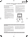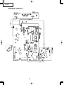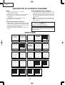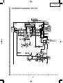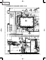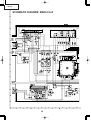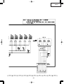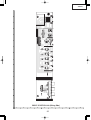
1
32SF670
SERVICE MANUAL
No.S47E632SF670/
COLOR TELEVISION
Chassis No. GB-D7
MODEL
32SF670
In the interests of user-safety (Required by safety regulations in some countries ) the set should be restored to its
original condition and only parts identical to those specified should be used.
CONTENTS
Page
» ELECTRICAL SPECIFICATIONS ......................................................................................................... 1
» IMPORTANT SERVICE SAFETY PRECAUTION ................................................................................. 2
» LOCATION OF USER'S CONTROL ..................................................................................................... 5
» INSTALLATION AND SERVICE INSTRUCTIONS ................................................................................ 6
» SERVICE ADJUSTMENT ................................................................................................................... 16
» CHASSIS LAYOUT ............................................................................................................................. 20
» BLOCK DIAGRAM .............................................................................................................................. 21
» DESCRIPTION OF SCHEMATIC DIAGRAMS & WAVEFORMS ........................................................ 22
» SCHEMATIC DIAGRAMS ................................................................................................................... 23
» PRINTED WIRING BOARD ASSEMBLIES ........................................................................................ 32
» PARTS LIST ........................................................................................................................................ 38
» PACKING OF THE SET ...................................................................................................................... 47
ELECTRICAL SPECIFICATIONS
POWER INPUT ..................................................... 120V AC, 60 Hz
POWER RATING .................................................................. 150W
PICTURE SIZE ........................................... 3074 cm2 (476sq inch)
CONVERGENCE ............................................................. Magnetic
SWEEP DEFLECTION .................................................... Magnetic
FOCUS ............................................... Hi-Bi-Potential Electrostatic
INTERMEDIATE FREQUENCIES
Picture IF Carrier Frequency ...... 45.75 MHz (Analog Terrestrial)
Sound IF Carrier Frequency ....... 41.25 MHz (Analog Terrestrial)
Color Sub-Carrier Frequency ..... 42.17 MHz (Analog Terrestrial)
IF Center Frequency ........................ 44 MHz (Digital Terrestrial)
(Nominal)
AUDIO POWER
OUTPUT RATING .............. 5.0W + 5.0W (at 10% distortion and
Dual CH Operate)
SPEAKER
SIZE ........................................................ 12 x 6 cm oval (2 pcs.)
VOICE COIL IMPEDANCE ............................... 8 ohm at 400 Hz
ANTENNA INPUT IMPEDANCE
VHF/UHF ..................................................... 75 ohm Unbalanced
TUNING RANGES
VHF-Channels ............................................................... 2 thru 13
UHF-Channels ............................................................ 14 thru 69
CATV Channels ............................................ 1 thru 125 (Analog)
CATV Channels ............................................. 1 thru 135 (Digital)
Digital Terrestrial Broadcast (VHF/UHF) ....................... 2 thru 69
(EIA, Channel Plan U.S.A.)
Specifications are subject to change without
prior notice.
This document has been published to be used for after
sales service only.
The contents are subject to change without notice.
32SF670
IMPORTANT SERVICE SAFETY PRECAUTION
Ë
Service work should be performed only by qualified service technicians who are
thoroughly familiar with all safety checks and the servicing guidelines which follow:
WARNING
X-RADIATION AND HIGH VOLTAGE LIMITS
1. For continued safety, no modification of any circuit
should be attempted.
2. Disconnect AC power before servicing.
3. Semiconductor heat sinks are potential shock hazards
when the chassis is operating.
4. The chassis in this receiver has two ground systems
which are separated by insulating material. The nonisolated (hot) ground system is for the B+ voltage
regulator circuit. The isolated ground system is for
the low B+ DC voltages and the secondary circuit of
the high voltage transformer.
To prevent electrical shock use an isolation
transformer between the line cord and power
receptacle, when servicing this chassis.
1. Be sure all service personnel are aware of the
procedures and instructions covering X-radiation. The
only potential source of X-ray in current solid state
TV receivers is the picture tube. However, the picture
tube does not emit measurable X-Ray radiation, if
the high voltage is as specified in the "High Voltage
Check" instructions.
It is only when high voltage is excessive that Xradiation is capable of penetrating the shell of the
picture tube including the lead in the glass material.
The important precaution is to keep the high voltage
below the maximum level specified.
2. It is essential that servicemen have available at all
times an accurate high voltage meter.
The calibration of this meter should be checked
periodically.
3. High voltage should always be kept at the rated value
−no higher. Operation at higher voltages may cause
a failure of the picture tube or high voltage circuitry
and;also, under certain conditions, may produce
radiation in exceeding of desirable levels.
4. When the high voltage regulator is operating properly
there is no possibility of an X-radiation problem. Every
time a color chassis is serviced, the brightness should
be tested while monitoring the high voltage with a
meter to be certain that the high voltage does not
exceed the specified value and that it is regulating
correctly.
5. Do not use a picture tube other than that specified or
make unrecommended circuit modifications to the
high voltage circuitry.
6. When trouble shooting and taking test measurements
on a receiver with excessive high voltage, avoid being
unnecessarily close to the receiver.
Do not operate the receiver longer than is necessary
to locate the cause of excessive voltage.
4A 125V
CAUTION: FOR CONTINUED
PROTECTION AGAINST A
RISK OF FIRE, REPLACE
ONLY WITH SAME TYPE 4A125V FUSE.
SERVICING OF HIGH VOLTAGE SYSTEM
AND PICTURE TUBE
When servicing the high voltage system,
remove the static charge by connecting a
10k ohm resistor in series with an insulated
wire (such as a test probe) between the picture tube ground and the anode lead. (AC
line cord should be disconnected from AC
outlet.)
1. Picture tube in this receiver employs integral
implosion protection.
2. Replace with tube of the same type number for
continued safety.
3. Do not lift picture tube by the neck.
4. Handle the picture tube only when wearing
shatterproof goggles and after discharging the high
voltage anode completely.
2
32SF670
IMPORTANT SERVICE SAFETY PRECAUTION
(Continued)
• Connect the resistor connection to all exposed metal
parts having a return to the chassis (antenna, metal
cabinet, screw heads, knobs and control shafts,
escutcheon, etc.) and measure the AC voltage drop
across the resistor.
AII checks must be repeated with the AC line cord
plug connection reversed. (If necessary, a nonpolarized adapter plug must be used only for the
purpose of completing these check.)
Any current measured must not exceed 0.5 milliamp.
Any measurements not within the limits outlined
above indicate of a potential shock hazard and
corrective action must be taken before returning the
instrument to the customer.
BEFORE RETURNING THE RECEIVER
(Fire & Shock Hazard)
Before returning the receiver to the user, perform
the following safety checks.
1. Inspect all lead dress to make certain that leads are
not pinched or that hardware is not lodged between
the chassis and other metal parts in the receiver.
2. Inspect all protective devices such as non-metallic
control knobs, insulating materials, cabinet backs,
adjustment and compartment covers or shields,
isolation resistor-capacity networks, mechanical
insulators, etc.
3. To be sure that no shock hazard exists, check for
leakage current in the following manner.
• Plug the AC cord directly into a 120 volt AC outlet,
(Do not use an isolation transformer for this test).
• Using two clip leads, connect a 1.5k ohm, 10 watt
resistor paralleled by a 0.15µF capacitor in series with
all exposed metal cabinet parts and a known earth
ground, such as electrical conduit or electrical ground
connected to earth ground.
• Use an AC voltmeter having with 5000 ohm per volt,
or higher, sensitivity to measure the AC voltage drop
across the resistor.
1.5k ohm
10W
0.15µF
TEST PROBE
TO EXPOSED
METAL PARTS
CONNECT TO
KNOWN EARTH
GROUND
12345678901234567890123456789012123456789012345678901234567890121234567890123456789012345678901212
12345678901234567890123456789012123456789012345678901234567890121234567890123456789012345678901212
12345678901234567890123456789012123456789012345678901234567890121234567890123456789012345678901212
SAFETY NOTICE
Many electrical and mechanical parts in television
receivers have special safety-related characteristics.
These characteristics are often not evident from visual
inspection, nor can protection afforded by them be
necessarily increased by using replacement components
rated for higher voltage, wattage, etc.
Replacement parts which have these special safety
characteristics are identified in this manual; electrical
components having such features are identified by "å"
and shaded areas in the Replacement Parts Lists and
Schematic Diagrams.
For continued protection, replacement parts must be
identical to those used in the original circuit. The use of
substitute replacement parts which do not have the same
safety characteristics as the factory recommended
replacement parts shown in this service manual, may
create shock, fire, X-radiation or other hazards.
12345678901234567890123456789012123456789012345678901234567890121234567890123456789012345678901212
12345678901234567890123456789012123456789012345678901234567890121234567890123456789012345678901212
12345678901234567890123456789012123456789012345678901234567890121234567890123456789012345678901212
12345678901234567890123456789012123456789012345678901234567890121234567890123456789012345678901212
3
32SF670
Precautions for using lead-free solder
1 Employing lead-free solder
"PWBs" of this model employs lead-free solder. The LF symbol indicates lead-free solder, and is attached on the
PWBs and service manuals. The alphabetical character following LF shows the type of lead-free solder.
Example:
LFa
Indicates lead-free solder of tin, silver and copper.
2 Using lead-free wire solder
When fixing the PWB soldered with the lead-free solder, apply lead-free wire solder. Repairing with conventional
lead wire solder may cause damage or accident due to cracks.
As the melting point of lead-free solder (Sn-Ag-Cu) is higher than the lead wire solder by 40°C, we recommend you
to use a dedicated soldering bit, if you are not familiar with how to obtain lead-free wire solder or soldering bit,
contact our service station or service branch in your area.
3 Soldering
As the melting point of lead-free solder (Sn-Ag-Cu) is about 220°C which is higher than the conventional lead solder
by 40°C, and as it has poor solder wettability, you may be apt to keep the soldering bit in contact with the PWB for
extended period of time. However, since the land may be peeled off or the maximum heat-resistance temperature
of parts may be exceeded, remove the bit from the PWB as soon as you confirm the steady soldering condition.
Lead-free solder contains more tin, and the end of the soldering bit may be easily corroded. Make sure to turn on
and off the power of the bit as required.
If a different type of solder stays on the tip of the soldering bit, it is alloyed with lead-free solder. Clean the bit after
every use of it.
When the tip of the soldering bit is blackened during use, file it with steel wool or fine sandpaper.
Be careful when replacing parts with polarity indication on the PWB silk.
Lead-free wire solder for servicing
Part No.
ZHNDAi123250E
ZHNDAi126500E
ZHNDAi12801KE
★
J
J
J
Description
φ0.3mm
250g(1roll)
φ0.6mm
500g(1roll)
φ1.0mm
1kg(1roll)
4
Code
BL
BK
BM
32SF670
LOCATION OF USER'S CONTROL
Front Panel
POWER
MENU
– VOL +
CH
PULL-OPEN
POWER
MENU
– VOL +
CH
POWER
Press → On.
Press again → Off.
VIDEO/AUDIO IN 2
TERMINALS
(INSIDE DOOR)
REMOTE CONTROL
SENSOR
MENU
Press → Accesses MAIN MENU.
Press again → Exits MAIN MENU.
VOLUME UP/DOWN
(k) Increases sound.
(l) Decreases sound.
CHANNEL UP/DOWN
(a) Selects next higher channel.
(s) Selects next lower channel.
Basic Remote Control Functions
Infrared Transmitter Window
POWER
Press → On.
Press again → Off.
INPUT
Press → Switches to external video
INPUT 1 mode.
Press twice → Switches to external
video INPUT 2 mode.
Press 3 times → Switches to external
video INPUT 3 mode or
COMPONENT mode.
Press 4 times → Switches back to
the original TV mode.
DISPLAY
To display receiving channel
information.
MUTE
Press → Mutes sound.
Press again → Restores sound.
REMOTE KEYPAD (0 – 9)
Sets the channel.
VOLUME UP/DOWN
(VOL k) Increases sound.
(VOL l) Decreases sound.
• (DOT)
Sets the channel.
CHANNELUP/DOWN
(CH r) Selects next higher channel.
(CH s) Selects next lower channel.
PERSONAL PREFERENCE
With the Personal Preference buttons,
you can program your favorite
programs by using the 4 categories A,
B, C and D. The channels can be
accessed quickly by using these
buttons.
ENTER
Sets the channel.
FLASHBACK
Returns to previous channel.
EDIT
To enter Personal Preference setting
screen/to exit from Personal
Preference setting screen.
FLASHBACK
Switches between Screen Format
mode.
CC
Switches between Closed Caption
service type.
AUDIO
Switches between the audio
service type.
a/b/c/d
Press to select a desired item on
the screen or adjust a selected
item.
GUIDE
Display the programme list.
MENU
Press → Accesses MAIN MENU.
Press again → Exits MAIN MENU.
RETURN
Returns to the previous screen.
Note:
• The TV set and remote control illustrations and the on-screen displays in this manual may differ from
their actual appearance.
5
32SF670
INSTALLATION AND SERVICE INSTRUCTIONS
Note:
(1) When performing any adjustments to resistor controls and transformers use non-metallic
screwdrivers or TV alignment tools.
(2) Before performing adjustments, the TV set must be on at least 15 minutes.
CIRCUIT PROTECTION
HIGH VOLTAGE CHECK
The receiver is protected by a 4.0A fuse (F701),
mounted on PWB-A, wired into one side of the AC
line input.
High voltage is not adjustable but must be checked
to verify that the receiver is operating within safe
and efficient design limitations as specified checks
should be as follows:
X-RADIATION PROTECTOR CIRCUIT TEST
1. Connect an accurate high voltage meter between
ground and anode of picture tube.
2. Operate receiver for at least 15 minutes at 120V AC
line voltage, with a strong air signal or a properly tuned
in test signal.
3. Enter the service mode and select the service
adjustment "V95" and Bus data "02" (Y-mute on, CRT
Cut Off).
4. The voltage should be below 35.0kV (at zero beam).
If a correct reading cannot be obtained, check circuitry
for malfunctioning components. After the voltage test,
make Y-mute off to the normal mode.
After service has been performed on the horizontal
deflection system, high voltage system, B+ system,
test the X-Radiation protection circuit to ascertain
proper operation as follows:
1. Apply 120V AC using a variac transformer for accurate
input voltage.
2. Allow for warm up and adjust all customer controls
for normal picture and sound.
3. Receive a good local channel.
4. Connect a digital voltmeter to TP651-3 (P651, 3Pin)
and make sure that the voltmeter reads 13.65 ±0.6V
DC.
5. Apply external 17.3V DC at TP651-3 by using an
external DC supply, TV must be shut off.
6. To reset the protector, unplug the AC cord and plug
the AC cord power on. Now make sure that normal
picture appears on the screen.
7. If the operation of the horizontal oscillator does not
stop in step 5, the circuit must be repaired before the
set is returned to the customer.
6
32SF670
For adjustments of this model, the bus data is converted to various analog signals by the D/A converter
circuit.
Note: There are still a few analog adjustments in this series such as focus and master screen voltage.
Follow the steps below whenever the service adjustment is required. See "Table-B" to determine, if service adjustments are required.
1. Service mode
4. Donau and Main Micon version Check
Before putting unit into the service mode, check that
customer adjustments are in the normal mode. Use
the reset function in the video adjustment menu to
ensure customer controls are in their proper (reset)
position.
1. After television power on, press test key “0x31”
and the following screen will display.
VERSION NUMBER
ANALOG
: 1.00-2-R2
DIGITAL
: 1.00
2. Service number selection
Once in the service mode, press the Ch-up or Chdown button on the remote controller or at the set.
The ser vice adjustment number will var y in
increments of one, from "D01" to "M07". Select the
item you wish to adjust.
* ANALOG – Main Micon IC (RH-IXB945WJQZQ)
Software Version
3. Data number selection
Press the Vol-up or Vol-down button to adjust the data
number.
1.00 - 2 - R2
Main Micon
Version
To enter the service mode and exit service mode.
EEPROM Version
Number
To enter the service mode manually just press and hold
the Vol-down and Ch-up buttons at the same time, plug
the AC cord into a wall socket.
Now the TV set is switched on and enters the service
mode.
To exit the service mode, turn the television off by
pressing the power button.
* DIGITAL – Renesas IC (Inside Tuner) Software
Version
2. The version display screen will disappear after 30
second or pressing any key (except test key) will
cancel the version display.
DATA NUMBER
SERVICE ADJUSTMENT
NUMBER
CHANNEL
V05 111
Number of
ROM Correct
3. Alternatively, for analog version only, go to service
mode. Press menu key/button until "INFO" page
appears in OSD. Version will display at bottom right
corner. Explanation as below
12
MASK : 0S
SOFT : (Main micon software ver.)
CHK1 : (ROM1 correct)
CHK2 : (ROM2 correct)
INFO
12
Figure A.
MASK: 0S
SOFT: V1.00
CHK1: ACT
CHK2: ACT
Figure B.
7
32SF670
4:3-Def-Adj
A. Deflection Bus Setting
no.
Item.
DATA
D01
V-SHIFT
FIX
D02
H-SHIFT
D03
Range
Remark
0…7
0
ADJ
V-SHIFT
[13h D2…D0]
H-PHASE
[16h D4…D0]
0 … 31
H-PHASE.DTV
V-POS-4:3
ADJ
µ-con
0 … 255
V-PHASE.DTV
D04
V-SIZE-4:3
ADJ
0 … 63
V-SIZE.DTV
D05
H-SIZE-4:3
ADJ
0 … 63
H-SIZE.DTV
D06
VS-CORRECT
-4:3
V-LINEARITY
-4:3
E/W PARABOLA
-4:3
E/W TRAPEZIUM
-4:3
E/W CORNER
-4:3
ADJ
0 … 63
VS-CORRECT.DTV
0 … 63
V-LINEARITY.DTV
D07
D08
D09
D10
16:9-Def-Adj
REG
ADJ
ADJ
ADJ
ADJ
D11
V-SHIFT-16:9
FIX
D12
H-SHIFT-16:9
ADJ
D13
V-POS-16:9
ADJ
D14
V-SIZE-16:9
ADJ
D15
H-SIZE-16:9
ADJ
D16
D17
D18
D19
D20
D21
D22
VS-CORRECT
-16:9
V-LINEARITY
-16:9
E/W PARABOLA
-16:9
E/W TRAPEZIUM
-16:9
E/W CORNER
-16:9
V-BLK-TOP
-16:9
V-BLK-BOTTOM
-16:9
ADJ
ADJ
ADJ
ADJ
ADJ
FIX
FIX
V-SIZE
[11h D5…D0]
H-SIZE
[1Bh D5…D0]
VS CORRECTION
[19h D5…D0]
V-LINEARITY
[1Dh D5…D0]
E/W PARABOLA
[18h D5…D0]
E/W TRAPEZIUM
[1Ah D5…D0]
E/W CORNER
[1Ch D5…D0]
V-SHIFT
[13h D2 ..D0]
H-PHASE
[16h D4 ..D0]
µ-con
V-SIZE
[11h D5…D0]
H-SIZE
[1Bh D5…D0]
V S CORRECTION
[19h D5…D0]
V-LINEARITY
[1Dh D5…D0]
E/W PARABOLA
[18h D5…D0]
E/W TRAPEZIUM
[1Ah D5…D0]
E/W CORNER
[1Ch D5…D0]
Vert. Blanking Top
[2Ch D3…D2]
Vert. Blanking Bottom
[2Ch D1…D0]
8
0 … 63
0 … 63
0 … 63
E/W
PARABOLA.DTV
E/W
TRAPEZIUM.DTV
E/W
CORNER.DTV
0…7
0
0 … 31
H-PHASE.DTV
0 … 255
V-PHASE.DTV
0 … 63
V-SIZE.DTV
0 … 63
H-SIZE.DTV
0 … 63
VS-CORRECT.DTV
0 … 63
V-LINEARITY.DTV
0 … 63
E/W
PARABOLA.DTV
E/W
TRAPEZIUM.DTV
E/W
CORNER.DTV
0 … 63
0 … 63
0…3
2
0…3
2
Revision
/ Change
32SF670
no.
Item.
DATA
D23
AFC1-IF
FIX
D24
AFC2
FIX
D25
V-FREE
FIX
D26
H-FREE
FIX
D27
HV-FREE
FIX
D28
1W-TV
FIX
D29
1W-AV-SAV
FIX
D30
1W-YUV-DTV
FIX
D31
SL-TV
FIX
D32
SL-AV
FIX
D33
SL-SAV
FIX
D34
SL-YUV
FIX
D35
SL-DTV
FIX
D36
VD-DYTV
FIX
D37
VD-AV
FIX
D38
AS-TV
FIX
D39
AS-AV
FIX
D40
AS-SAV
FIX
D41
AS-YUV
FIX
D42
AS-DTV
FIX
D43
FBP-TV
FIX
D44
AS-SPEED-UP
FIX
D45
AS-SPEED-DN
FIX
REG
AFC1 Gain
[27h D6]
AFC2-G
[15h D6]
V-FREE
[10h D6]
H-FREE
[13h D7]
HV-FREE
[25h D5]
V.Window
[13h D6]
V.Window
[13h D6]
V.Window
[13h D6]
S-SLICE DN
[14h D3…D2] [24h D6]
S-SLICE DN
[14h D3…D2] [24h D6]
S-SLICE DN
[14h D3…D2] [24h D6]
S-SLICE DN
[14h D3…D2] [24h D6]
S-SLICE DN
[14h D3…D2] [24h D6]
Vsync-Det
[27h D3] [16h D7]
Vsync-Det
[27h D3] [16h D7]
Auto-Slice
[16h D6]
Auto-Slice
[16h D6]
Auto-Slice
[16h D6]
Auto-Slice
[16h D6]
Auto-Slice
[16h D6]
FBP VTH L
[16h D5]
AS SPEED UP
[28h D4]
AS SPEED DOWN
[28h D5]
9
Range
Remark
0/1
0
0/1
0
0/1
1
0/1
0
0/1
0
0/1
0
0/1
0
0/1
0
0…7
5
0…7
5
0…7
5
0…7
5
0…7
5
0…3
0
0…3
0
0/1
1
0/1
1
0/1
1
0/1
1
0/1
1
0/1
0
0/1
0
0/1
0
Revision
/ Change
32SF670
DTV-Picture-Adj
YUV-Picture-Adj
TV-Picture-Adj
B. Video Bus Setting
no.
Item.
DATA
V01
SUB-CON
ADJ
V02
SUB-TINT
ADJ
V03
SUB-COL
ADJ
V04
SUB-BRI
ADJ
V05
SUB-SHP
FIX
V06
R-CUT
ADJ
V07
G-CUT
ADJ
V08
B-CUT
ADJ
V09
R-DRI
ADJ
V10
B-DRI
ADJ
V11
SUB-CON-YUV
ADJ
V12
SUB-BB-TINT-YUV
ADJ
V13
SUB-COL-YUV
ADJ
V14
SUB-BRI-YUV
ADJ
V15
SUB-SHP-YUV
FIX
V16
R-CUT-YUV
ADJ
V17
G-CUT-YUV
ADJ
V18
B-CUT-YUV
ADJ
V19
R-DRI-YUV
ADJ
V20
B-DRI-YUV
ADJ
V21
SUB-CON-DTV
ADJ
V22
SUB-BB-TINT-DTV
ADJ
V23
SUB-COL-DTV
ADJ
V24
SUB-BRI-DTV
ADJ
REG
CONTRAST
[05h D6…D0]
TINT
[07h D6…D0]
COLOR
[08h D6…D0]
BRIGHT
[0Ah D7…D0]
VIDEO-TONE
[04h D5…D0]
R-CUTOFF
[0Dh D7…D0]
G-CUTOFF
[0Eh D7…D0]
B-CUTOFF
[0Fh D7…D0]
R-DRIVE
[0Bh D6…D0]
B-DRIVE
[0Ch D6…D0]
CONTRAST
[05h D6..D0]
BASEBAND-TINT
[17h D6…D0]
COLOR
[08h D6…D0]
BRIGHT
[0Ah D7…D0]
VIDEO-TONE
[04h D5…D0]
R-CUTOFF
[0Dh D7…D0]
G-CUTOFF
[0Eh D7…D0]
B-CUTOFF
[0Fh D7…D0]
R-DRIVE
[0Bh D6…D0]
B-DRIVE
[0Ch D6…D0]
CONTRAST
[05h D6..D0]
BASEBAND-TINT
[17h D6…D0]
COLOR
[08h D6…D0]
BRIGHT
[0Ah D7…D0]
10
Range
Remark
0 … 127
PIC.DTV
0 … 127
TINT.DTV
0 … 127
COLOR.DTV
0 … 255
PIC.DTV
0 … 63
40
0 … 255
WHITE.DTV
0 … 255
WHITE.DTV
0 … 255
WHITE.DTV
0 … 127
WHITE.DTV
0 … 127
WHITE.DTV
0 … 127
PIC.DTV
0 … 127
TINT.DTV
0 … 127
COLOR.DTV
0 … 255
PIC.DTV
0 … 63
37
0 … 255
WHITE.DTV
0 … 255
WHITE.DTV
0 … 255
WHITE.DTV
0 … 127
WHITE.DTV
0 … 127
WHITE.DTV
0 … 127
PIC.DTV
0 … 127
TINT.DTV
0 … 127
COLOR.DTV
0 … 255
PIC.DTV
Revision
/ Change
no.
Item.
DATA
V25
SUB-SHP-DTV
FIX
V26
R-CUT-DTV
ADJ
V27
G-CUT-DTV
ADJ
V28
B-CUT-DTV
ADJ
V29
B-DRI-DTV
ADJ
V30
R-DRI-DTV
ADJ
V31
SHPG-YUV
FIX
V32
YDL-YUV
FIX
V33
CrDL-FINE-YUV
FIX
V34
CbDL-FINE-YUV
FIX
V35
CB-P-YUV
FIX
V36
CR-P-YUV
FIX
V37
C-ANGLE-YUV
FIX
V38
SHPG-DTV
FIX
V39
YDL-DTV
FIX
V40
CrDL-FINE-DTV
FIX
V41
CbDL-FINE-DTV
FIX
V42
CB-P-DTV
FIX
V43
CR-P-DTV
FIX
V44
C-ANGLE-DTV
FIX
V45
SHPG-TV
FIX
V46
YDL-TV-AV
FIX
V47
TAKE-OFF-TV
FIX
V48
C-ANGLE
FIX
TV
DTV
Component
DTV-Picture-Adj
32SF670
REG
VIDEO TONE
[04h D5…D0]
R-CUTOFF
[0Dh D7…D0]
G-CUTOFF
[0Eh D7…D0]
B-CUTOFF
[0Fh D7…D0]
B-DRIVE
[0Ch D6…D0]
R-DRIVE
[0Bh D6…D0]
V-TONE
[02h D3]
Y-Delay
[06h D2…D0]
CrDL FINE ADJ.
[21h D3…D2]
CbDL FINE ADJ.
[21h D1…D0]
CB PEDESTAL ADJ.
[29h D3…D0]
CR PEDESTAL ADJ.
[28h D3…D0]
C.ANGLE 95
[15h D1]
V-TONE
[02h D3]
Y-Delay
[06h D2…D0]
CrDL FINE ADJ.
[21h D3…D2]
CbDL FINE ADJ.
[21h D1…D0]
CB PEDESTAL ADJ.
[29h D3…D0]
CR PEDESTAL ADJ.
[28h D3…D0]
C.ANGLE 95
[15h D1]
V-TONE
[02h D3]
Y-Delay
[06h D2…D0]
TAKE OFF
[02h D0]
C.ANGLE 95
[15h D1]
11
Range
Remark
0 … 63
35
0 … 255
WHITE.DTV
0 … 255
WHITE.DTV
0 … 255
WHITE.DTV
0 … 127
WHITE.DTV
0 … 127
WHITE.DTV
0/1
1
0…7
1
0…3
0
0…3
0
0 … 15
7
0 … 15
7
0/1
0
0/1
1
0…7
1
0…3
0
0…3
0
0 … 15
7
0 … 15
7
0/1
0
0/1
1
0…7
5
0/1
0
0/1
0
Revision
/ Change
RR-AV
F-AV
S-VIDEO
COLOR TEMP
32SF670
no.
Item.
DATA
V49
R-R2
FIX
V50
R-R
FIX
V51
R-B
FIX
V52
B-R2
FIX
V53
B-R
FIX
V54
B-B
FIX
V55
BRIGHT-OFF-SAV
FIX
V56
CON-OFF-SAV
FIX
V57
TINT-OFF-SAV
FIX
V58
COL-OFF-SAV
FIX
V59
SHP-OFF-SAV
FIX
V60
YDL-SAV
FIX
V61
BRIGHT-OFF-FAV
FIX
V62
CON-OFF-FAV
FIX
V63
TINT-OFF-FAV
FIX
V64
COL-OFF-FAV
FIX
V65
SHP-OFF-FAV
FIX
V66
BRIGHT-OFF-AV
FIX
V67
CON-OFF-AV
FIX
V68
TINT-OFF-AV
FIX
V69
COL-OFF-AV
FIX
V70
SHP-OFF-AV
FIX
V71
TINT-OFF-ADJ-TV
FIX
V72
CON-OFF-16:9
FIX
REG
R-DRI(OFFSET)
[0Bh D6…D0]
R-DRI(OFFSET)
[0Bh D6…D0]
R-DRI(OFFSET)
[0Bh D6…D0]
B-DRI(OFFSET)
[0Ch D6…D0]
B-DRI(OFFSET)
[0Ch D6…D0]
B-DRI(OFFSET)
[0Ch D6…D0]
BRIGHT (OFFSET)
[0Ah D7…D0]
CONTRAST(OFFSET)
[05h D6…D0]
TINT(OFFSET)
[07h D6…D0]
COLOR(OFFSET)
[08h D6…D0]
VIDEO-TONE(OFFSET)
[04h D6…D0]
Y-Delay
[06h D2…D0]
BRIGHT(OFFSET)
[0Ah D7…D0]
CONTRAST(OFFSET)
[05h D6…D0]
TINT(OFFSET)
[07h D6…D0]
COLOR(OFFSET)
[08h D6…D0]
VIDEO-TONE(OFFSET)
[04h D6…D0]
BRIGHT(OFFSET)
[0Ah D7…D0]
CONTRAST(OFFSET)
[05h D6…D0]
TINT(OFFSET)
[07h D6…D0]
COLOR(OFFSET)
[08h D6…D0]
VIDEO-TONE(OFFSET)
[04h D6…D0]
TINT
[07h D6..D0]
CONTRAST(OFFSET)
[05h D6…D0]
12
Range
Remark
-32 … +32
13
-32 … +32
2
-32 … +32
-6
-32 … +32
-23
-32 … +32
-8
-32 … +32
5
-63 … +63
7
-32 … +32
11
-32 … +32
1
-32 … +32
5
-32 … +32
0
0…7
1
-63 … +63
-7
-32 … +32
15
-32 … +32
2
-32 … +32
1
-32 … +32
0
-63 … +63
-5
-32 … +32
15
-32 … +32
3
-32 … +32
1
-32 … +32
0
-32 … +32
0
-15 … +15
-7
Revision
/ Change
32SF670
no.
Item.
DATA
V73
BRI-OFF-16:9
FIX
V74
TRAP-FINE-TV-AV
FIX
V75
TRAP-TV-AV
FIX
V76
SHPG-AV
FIX
V77
SHPG-SAV
FIX
V78
COL-OFF-16:9
FIX
V79
TRAP-DTV-YUV
FIX
V80
TAKE-OFF-AV
FIX
V81
TAKE-OFF-SAV
FIX
V82
RF-AGC
ADJ
V83
VIF-AGC
FIX
V84
VIF-G
FIX
V85
V-AGC
FIX
V86
VIF-VCO
ADJ
V87
H-VCO
ADJ
V88
BS
FIX
V89
BS-GAIN
FIX
V90
BS-D
FIX
V91
BS-C
FIX
V92
ABCL
FIX
V93
ABCL-Gain
FIX
V94
GAMMA
FIX
V95
Y-MUTE
FIX
V96
CbCr-G
FIX
V97
STP
FIX
V98
RGB-CLIP
FIX
REG
BRIGHT(OFFSET)
[0Ah D7…D0]
TRAP-FINE
[12h D1…D0]
C-TRAP OFF
[02h D4]
V-TONE
[02h D3]
V-TONE
[02h D3]
COLOR(OFFSET)
[08h D6…D0]
C-TRAP OFF
[02h D4]
TAKE OFF
[02h D0]
TAKE OFF
[02h D0]
RF-Delay
[00h D6…D0]
VIF AGC Clip
[27h D1]
VIF-GAIN
[06h D7…D5]
V-AGC
[1Dh D6]
VIF-VCO
[01h D5…D0]
H-VCO
[10h D2…D0]
BS-OFF
[02h D1]
BLACK STRETCH GAIN
[15h D2]
BS-DISCHARGE
[14h D7…D6]
BS-CHARGE
[14h D5…D4]
ABCL
[02h D2]
ABCL-G
[04h D7]
GAMMA
[12h D3…D2]
µ-con
CbCr GAIN UP
[29h D6]
Test Pattern Signal
[2Fh D3…D0]
ExtRGB-Clip
[05h D7]
13
Range
Remark
-15 … +15
0
0…3
2
0/1
1
0/1
1
0/1
1
-15 … +15
0
0/1
1
0/1
0
0/1
0
0 … 127
AGC.DTV
0/1
0
0…7
7
0/1
0
0 … 63
VIF-VCO.DTV
0…7
H-VCO.DTV
0/1
0
0/1
0
0…3
2
0…3
0
0/1
0
0/1
0
0…3
0
0,1,2
0
0/1
1
0 … 15
0
0/1
0
Revision
/ Change
32SF670
no.
Item.
DATA
V99
OSD-LVL
FIX
V100
YLPF
FIX
V101
C.Clip Level
FIX
V102
S-TRAP
FIX
V103
S-TRAP OFF
FIX
V104
OM-DET
FIX
V105
R-MTX-DN
FIX
V106
CTI
FIX
V107
KILLER-LVL
FIX
V108
SIF-BW
FIX
V109
E-SAVE
FIX
V110
MONITORING
FIX
V111
OFF-ADJ-TINT-YUV
FIX
V112
OFF-ADJ-TINT-DTV
FIX
V113
CC-POS
ADJ
V114
CC LEVEL
V115
REG
Range
Remark
0/1
0
0/1
1
0/1
0
0 … 31
16
0/1
1
0/1
0
0/1
0
0/1
1
0/1
1
0…3
1
0 … 63
30
0 … 31
21
-32 … +32
0
-32 … +32
0
µ-con
0 … 255
CC.DTV
FIX
µ-con
0 … 31
0
OSD POS
FIX
µ-con
0 … 31
0
V116
DIGITAL POW OFF TIM
FIX
µ-con
0…255
50
V117
BSW CONTROL
FIX
µ-con
0…100
77
V118
SVM-SAV
FIX
0…3
0
V119
SVM-COMP
FIX
0…3
0
V120
SVM-DTV
FIX
DELAY Y ADJ
[22h D5…D4]
DELAY Y ADJ
[22h D5…D4]
DELAY Y ADJ
[22h D5…D4]
0…3
0
V121
RGB ADJ
FIX
µ-con
0…127
127
V122
ChromaBPF
FIX
ChromaBPF
[26h D6]
OSD LEVEL
[15h D5]
YSW-LPF
[13h D5]
C.Clip Level
[02h D5]
S-TRAP
[20h D7] [1Fh D7…D5]
S-TRAP OFF
[1Eh D7]
OM DETECTOR
[15h D3]
R MTX DOWN
[23h D6]
CTI
[23h D3]
KILLER LEVEL
[15h D0]
SIF BPF WIDE
[2Bh D5…D4]
CONTRAST(OFFSET)
[05h D6…D0]
Intelligent MON
[1Ah D6][12h D7…D4]
BB Tint Control
[17h D6…D0]
BB Tint Control
[17h D6…D0]
14
1
Revision
/ Change
32SF670
C. Sound Bus Setting
no.
Item.
DATA
M01
MTS-ATT
ADJ
M02
MTS-VCO
FIX
M03
MTS-FILT
FIX
M04
MTS-WBND
ADJ
M05
MTS-SPEC
ADJ
M06
SUB-VOL
FIX
M07
FAO-VOL
FIX
REG
ATT
[00h D3..D0]
VCO
[01h D5..D0]
FILTER
[02h D5..D0]
WIDEBAND
[04h D5..D0]
SPECTRAL
[03h D5..D0]
VOL
[07h,08h D5..D0]
VOL
[07h,08h D5..D0]
D. Option Setting
no.
Item.
DATA
O 01
SPEAKER
1
O 02
FAO
1
O 03
VIEW TIMER
1
O 04
PON-CH
1
O 05
FAV-COL
1
O 06
AV3/COMPONENT
1
O 07
AV
1
O 08
AV2
1
O 09
MTS
1
O 10
TONE-CTRL
1
O 11
AUTO-OFF
1
O 12
INIT-LANG
0
O 13
S-IN
1
O 14
COMB
0
O 15
AUTO-INPUT
1
O 16
FLAT
1
O 17
WHITE-OUT
0
O 18
CURSOR R/C
1
O 19
EDIT KEY R/C
1
REMARKS
15
Range
Remark
0 … 15
MS.DTV
0 … 63
32
0 … 63
28
0 … 63
SEPA.DTV
0 … 63
SEPA.DTV
0 … 63
63
0 … 50
26
Revision /
Change
32SF670
Holding down both the VOL-up and CH-up buttons on the TV set at service mode for more than 2 seconds will
automatically write the above initial values into IC2101.
PART REPLACED
ADJUSTMENT
NECESSARY
UNNECESSARY
NOTES
IC801
X
The adjustment is needed to compensate for characteristics of parts
including IC801 and MTS level (M01).
IC2101
X
Holding down both the VOL-up and CH-up buttons on the TV set in
the service mode for more than 2 seconds will automatically write the
above initial values into IC2101 Then perform a complete adjustment.
CRT
X
Adjust items related to picture tube only.
IC3001
X
Adjust items related to MTS only (M01~M07).
SERVICE ADJUSTMENT
2
Screen Adjustment
H-VCO ADJ (I C BUS CONTROL) (Auto &
Manual Adj.)
• Manual Adj.
1. In No Signal (RASTER) condition.
2. Go to service mode, choose service data V87.
3. Connect oscilloscope to IC801 Pin 15, adjust V03
until frequency becomes 15.75 ± 0.15kHz.
• Auto Adj.
4. In No Signal (RASTER) condition.
5. Go to service mode, choose service data V87, by
pressing R/C Auto (HEX 44) key, OSD will appear
"OK" at screen.
6. If appear "NG", please repeat step 3.
VIF-VCO ADJ (I2C bus CONTROL) (Auto &
Manual Adj.)
• Manual Adj.
1. In No Signal (RASTER) condition.
2. Go to service mode, choose service data V86.
3. Connect oscilloscope to IC801 Pin 9, adjust V86 until
voltage becomes 2.5 ± 1.0V.
• Auto Adj.
4. In No Signal (RASTER) condition.
5. Go to service mode, choose service data V86.
6. Press the R/C Auto (HEX C5) key, OSD will appear
"OK" at screen.
7. If appear "NG", please repeat step 3.
RF AGC Adjustment
1. Receive a good local channel.
2. Enter the service mode and select the service
adjustment "V82".
3. Set the data value to point where no noise or beat
appears.
4. Select another channel to confirm that no noise or
beat appears.
Note 1 : You will have to come out of the service
mode to select another channel.
Note 2 : Setting the data to "00" will produce a black
raster.
16
1. Receive a good local channel.
2. Enter the service mode and select the service
adjustment "V03" and set the data value to "00" to
set the color level to minimum. (Record original data
code under adjustment "V03" before changing) You
may skip this step, if you selected a B/W picture or
monoscope pattern.
3. Select the service adjustment "V95" and adjust the
data value to "02", this turn off the luminance signal
(Y-mute).
4. Adjust the master screen control until the raster
darkness to the point where raster is barely seen.
5. Adjust the service adjustments "V06" red, "V07" green
and "V08" blue to obtain a good grey scale with
normal whites at low brightness level.
6. Select the service adjustment "V95" and reset data
to "00". Select the service adjustment "V03" and reset
data to obtain normal color level.
7. For component input, the data value of "V16" red,
"V17" green and "V18" blue is adjusted to follow the
data value of "V06", "V07" and "V08" respectively.
8. For digital RF input, the data value of "V26" red, "V27"
green and "V28" blue is adjusted to follow the data
value of "V06", "V07" and "V08" respectively.
9. Reset the master screen control to obtain normal
brightness range.
White Balance Adjustment
1. Receive a good local channel.
2. Enter the service mode and select the service
adjustment "V03" and set to "00" (minimum color)
(Record original data code under adjustment "V03"
before changing). "V03" does not have to be adjusted,
if you selected a B/W picture or monoscope pattern.
3. Alternately adjust the service adjustment data of "V09"
and "V10" until a good grey scale with normal whites
is obtained. (RF Input)
4. For component input, the data value of "V19" and
"V20" is adjusted to follow the data value of "V09"
and "V10" respectively.
5. For digital RF input, the data value of "V29" and "V30"
is adjusted to follow the data value of "V09" and "V10"
respectively.
6. Select the service adjustment "V03" and reset data
to obtain normal color level.
32SF670
Sub-picture and Sub-Bright Adjustments
Sub-Color Adjustment
1. Receive the window pattern signal.
• RF INPUT (TU1101)
2. Get into service adjustment data "V01" and "V04"
and set the luminance as shown in figure "A" and
"B" as below respectively.
• COMPONENT INPUT
3. Get in service adjustment data "V11" and "V14" and
set the luminance as shown in figure "A" and "B" as
below respectively.
1. Receive a good local channel.
2. Make sure the customer color control is set to center
position .
• RF INPUT (TU1101)
3. Enter the service mode and select service adjustment
"V03".
4. Adjust "V03" data value to obtain a normal color level.
• Component Input
5. Enter the service mode and select service adjustment
“V13”.
6. Adjust “V13” data value to obtain a normal color level.
• Digital RF Input (TU1101).
7. Input data of “V23” = “V03” + 50 steps.
A
B
Focus Adjustment
LUMINESCENCE CONFIRMATION
A: 95±10cd/m2
B: 1.5±0.5cd/m2
• DIGITAL RF INPUT (TU1101)
4. Get in service adjustment data "V21", "V24".
4-1 Input data of “V21” = “V01” + 05 STEPS.
4-2 Input data of “V24” = “V04” + 40 STEPS.
1. Receive a good local channel.
2. Adjust the FOCUS VR of the flyback transformer to
make the image as fine as possible.
C. C Display Position Adjustment
1. Receive the lion head pattern signal.
2. Select "V113" to display the text box.
3. Adjust the "V113" bus data to let the text box displayed
in the center.
DISPLAY OF TEXT BOX
Sub-Tint Adjustment
1. Receive the half color bar signal.
• RF INPUT (TU1101)
2. Get into Y-Mute by R/C, or by setting the "V95" bus
data to "01".
3. Vary the "V02" bus data until the waveform becomes
as stated below.
4. Reset "V95" bus data to "00".
• Component Input
5. Get into Y-Mute by R/C, or by setting the "V95" bus
data to "01".
6. Vary the "V12" bus data until the waveform becomes
as stated below.
7. Reset "V95" bus data to "00".
• Digital RF Input (TU1101)
8. Input data of "V22" = "V02" + 13 steps.
9. Reset "V95" bus data to "00".
LEVEL
B-AMP Base waveform in step
(TP47B)
TEXT BOX
A
| A-B | / 2
B
< 5mm
SPEC INSPECTION:| A-B | / 2 =
Vertical-Size, Linearity and VS-Correct
Adjustments
1. Receive a good local channel.
(SCREEN FORMAT 4:3)
2. Enter the service mode and select the service
adjustment "D04" for V-size.
3. Adjust the "D04" bus data to get the proper V-size.
4. For V-linearity adjustment, select data bus "D07" and
adjust to get the proper vertical linearity.
5. For VS-Correct adjustment, select data bus "D06"
and adjust to get the proper VS-Correction.
(SCREEN FORMAT 16:9)
6. Input data of "D14" to minus 33 steps from "D04” data.
(V-SIZE)
7. Input data of "D17" to minus 3 steps from "D07” data.
(V-LIN)
8. Input data of "D16" is plus 14 steps of data "D06".
(VS-CORRECT)
Note: Aging for 10 min before adjustment. After the
adjustment of V-center and V-size, readjustment for this V-line.
17
32SF670
Ë MTS ADJUSTMENT
Vertical Phase Adjustment
(SCREEN FORMAT 4:3)
1. Enter the service mode and input data of “00” on
"D01".
2. Adjust "D03" data value so that picture is centered.
(SCREEN FORMAT 16:9)
3. Input data of "00" on "D11".
4. Input data of "D13" is additional 10 steps from data
"D03".
MTS Level Adjustment
1. Set the sound volume above 1.
Monoral signal: 400Hz, 100% modulation
2. Vary the "M01" bus data until the voltage to pin (39)
of IC3001 to become the value as stated below.
SETTING VOLTAGE
ADJ spec : 490±10mVrms
CHK spec: 490±20mVrms
Horizontal Position Adjustment
1. Receive a good local channel.
(SCREEN FORMAT 4:3)
2. Enter the service mode and select the service
adjustment "D02".
3. Adjust "D02" data value so that picture is centered.
(SCREEN FORMAT 16:9)
4. Input data of "D12" same as "D02" data.
Separation Adjustment
1. Input "SIGNAL 1" and vary the "M04" bus data to get
the minimun AC voltage to pin (39) of IC3001.
2. Input "SIGNAL 2" and vary the "M05" bus data to get
the minimun AC voltage to pin (39) of IC3001.
SIGNAL 1: 300Hz, 30% modulation, Lch only, NR-ON
SIGNAL 2: 3kHz, 30% modulation, Lch only, NR-ON
Note: SIGNAL 1 Adj. for wideband
SIGNAL 2 Adj. for spectral
Check the output of the speaker at the maximum
volume as stated below.
Confirmation spec:
ADJ spec: above 25 dB
CHK spec: above 20 dB
Horizontal-Size Adjustment
1. Receive a good local channel.
(SCREEN FORMAT 4:3)
2. Enter the service mode and select the service
adjustment "D05" for H-size.
3. Adjust the "D05" bus data to get the proper H-size.
(SCREEN FORMAT 16:9)
4. Input data of "D15" same as "D05" data.
EW-Parabola
1. Receive a good local channel.
(SCREEN FORMAT 4:3)
2. Enter the service mode and select the service
adjustment "D08" for EW parabola.
3. Adjust the "D08" bus data to get the proper vertical
straight line for both left and right side.
(SCREEN FORMAT 16:9)
4. Input data of "D18" to minus 10 steps from "D08"
data.
EW-Corner
1. Receive a good local channel.
(SCREEN FORMAT 4:3)
2. Enter the service mode and select the service
adjustment "D10" for EW-Corner.
3. Adjust the "D10" bus data to get the best position
display.
(SCREEN FORMAT 16:9)
4. Input data of "D20" is minus 2 steps of data "D10".
EW-Trapezium
1. Receive a good local channel. (SCREEN FORMAT
4:3)
2. Enter the service mode and select the service
adjustment "D09" for EW-Trapezium.
3. Adjust the "D08" bus data to get the best position
display. (SCREEN FORMAT 16:9)
4. Input data of "D19" is minus 4 steps of "D09" data.
18
32SF670
-MEMO-
19
32SF670
CHASSIS LAYOUT
20
32SF670
BLOCK DIAGRAM
21
32SF670
DESCRIPTION OF SCHEMATIC DIAGRAMS
WAVEFORM MEASUREMENT CONDITIONS:
1. Photographs taken on a standard gated color bar
signal, the tint setting adjusted for proper color. The
wave shapes at the red, green and blue cathodes of
the picture tube depend on the tint, color level and
picture control.
2.
indicates waveform check points (See chart,
waveforms are measured from point indicated to
chassis ground.)
NOTES:
1. The unit of resistance "ohm" is omitted.
(K=kW=1000W, M=MW)
2. All resistors are 1/16 watt, unless otherwise noted.
3. All capacitors are µ F, unless otherwise noted.
(P=pF=µµF)
4. (G) indicates ±2% tolerance may be used.
5.
indicates line isolated ground.
VOLTAGE MEASUREMENT CONDITIONS:
1. All DC voltages are measured with DVM connected
between points indicated and chassis ground, line
voltage set at 120V AC and all controls set for normal
picture unless otherwise indicated.
2. All voltages measured with 1000µ V B & W or Color
signal.
å
ç
AND SHADED (
) COMPONENTS
= SAFETY RELATED PARTS.
MARK= X-RAY RELATED PARTS.
This circuit diagram is a standard one, printed circuits
may be subject to change for product improvement
without prior notice.
WAVEFORMS
2007/02/05
15:32:56
NORM:50MS/s
20us/div
Stopped
(20us/div)
=Trace2=
CH2=1V
DC
=Filter=
Smoothing :
BW : FULL
11.0 Vp-p
22.1 Vp-p
2007/02/05
15:38:07
NORM:2MS/s
=Record Length=
Main : 10K
Zoom : 10K
=Trigger=
Mode : AUTO
Type : EDGE CH2
:
0.0V
Delay
:
0.0V
Holdoff
:
0.0ns
:
MINIMUM
30.9 Vp-p
40.56 Vp-p
53.0 Vp-p
(5ms/div)
=Trace2=
CH2=1V
P-P
DC
ON
1.280V
10:1
=Offset=
=Filter=
:
=Offset=
:
0.00V
:
0.00V
CH3
CH4
5ms/div
Stopped
Smoothing
BW : FULL
CH1
CH2
ON
P-P
10:1
=Record
CH1
CH2
:
:
0.00V
0.00V
CH3
CH4
:
:
0.0V
0.0V
Main
Zoom
Length=
:
:
100K
100K
=Trigger=
Mode
Type
:
:
Delay :
Holdoff
AUTO
EDGE
:
CH2
0.0ns
MINIMUM
65.0 Vp-p
71.3 Vp-p
813.6 Vp-p
932 Vp-p
053 Vp-p
q2.6 Vp-p
w0.8 Vp-p
e146 Vp-p
r12 Vp-p
t960 Vp-p
2007/02/05
16:11:02
NORM:200MS/s
Stopped
20us/div
DC
=Filter=
Smoothing :
BW : FULL
CH1
CH2
ON
CH3
CH4
y320 Vp-p
2007/02/05
16:13:18
NORM:200MS/s
Stopped
20us/div
2007/02/05
DC
ON
CH1
CH2
CH3
CH4
P-P
0V
0.0V
NORM:200MS/s
=Trigger=
Mode : AUTO
Type : EDGE CH2
Delay :
Holdoff
:
0.0ns
MINIMUM
a6.1 Vp-p
20us/div
CH2=50V
DC
=Record Length=
Main : 40K
Zoom : 40K
=Filter=
Smoothing :
BW : FULL
i27.0 Vp-p
2007/02/05
ON
CH1
CH2
CH3
CH4
P-P
0V
0.0V
=Record Length=
Main : 40K
Zoom : 40K
=Trigger=
Mode : AUTO
Type : EDGE CH2
Delay :
Holdoff
:
0.0ns
MINIMUM
s124 Vp-p
NORM:200MS/s
20us/div
DC
2007/02/05
=Filter=
Smoothing :
BW : FULL
ON
CH1
CH2
CH3
CH4
=Offset=
:
0.00V
:
0.0V
:
:
Delay :
Holdoff
16:22:52
=Record Length=
Main : 40K
Zoom : 40K
=Trigger=
Mode : AUTO
Type : EDGE CH2
Delay :
Holdoff
:
0.0ns
MINIMUM
d92 Vp-p
22
=Filter=
Smoothing :
BW : FULL
0.0ns
MINIMUM
NORM:200MS/s
=Filter=
Smoothing :
BW : FULL
ON
CH1
CH2
CH3
CH4
=Offset=
:
0.00V
:
0.0V
:
:
0.00V
0.0V
P-P
=Record Length=
Main : 40K
Zoom : 40K
=Trigger=
Mode : AUTO
Type : EDGE CH2
Delay :
Holdoff
:
0.0ns
MINIMUM
f114 Vp-p
=Trace2=
ON
CH1
CH2
=Offset=
:
0.00V
:
0.00V
:
:
P-P
10:1
0V
0.0V
=Record Length=
Main : 40K
Zoom : 40K
=Trigger=
Mode : AUTO
Type : EDGE CH2
Delay :
Holdoff
:
0.0ns
MINIMUM
p5.6 Vp-p
20us/div
10:1
20us/div
(20us/div)
CH3
CH4
(20us/div)
CH2=50V
92.00V
DC
0.00V
0.0V
:
Stopped
P-P
10:1
=Trigger=
Mode : AUTO
Type : EDGE CH2
=Record Length=
Main : 40K
Zoom : 40K
0V
0.0V
=Trace2=
CH2=50V
NORM:200MS/s
CH2=2V
6.560V
DC
=Offset=
:
0.00V
:
0.00V
:
:
16:12:26
Stopped
=Trace2=
P-P
10:1
o6.6 Vp-p
(20us/div)
=Trace2=
124.0V
10:1
=Offset=
:
0.00V
:
0.0V
:
:
16:23:32
Stopped
(20us/div)
=Trace2=
6.080V
10:1
=Offset=
:
0.00V
:
0.00V
:
:
16:15:58
Stopped
(20us/div)
CH2=2V
=Filter=
Smoothing :
BW : FULL
u222 Vp-p
2007/02/05
(20us/div)
CH2=2V
=Trace2=
114.0V
5.600V
3.040V
32SF670
SCHEMATIC DIAGRAM: CRT Unit
H
G
F
E
D
C
B
A
1
2
3
4
5
6
23
7
8
9
10
32SF670
SCHEMATIC DIAGRAM: MAIN-1 Unit
H
G
F
E
D
C
B
A
1
2
3
4
5
24
6
7
8
9
10
32SF670
10
11
12
13
14
15
25
16
17
18
19
32SF670
SCHEMATIC DIAGRAM: MAIN-2 Unit
H
G
F
E
D
C
B
A
1
2
3
4
5
26
6
7
8
9
10
32SF670
10
11
12
13
14
15
27
16
17
18
19
32SF670
SCHEMATIC DIAGRAM: 2-LINE Y/C Unit
H
G
F
E
D
C
B
A
1
2
3
4
5
28
6
7
8
9
10
32SF670
10
11
12
13
14
15
29
16
17
18
19
32SF670
SCHEMATIC DIAGRAM: CONTROL Unit
H
G
F
E
D
C
B
A
1
2
3
4
5
30
6
7
8
9
10
32SF670
10
11
12
13
14
15
31
16
17
18
19
32SF670
PRINTED WIRING BOARD ASSEMBLIES
PWB-A: MAIN Unit (Wiring Components Side)
H
G
F
E
D
C
B
A
1
2
3
4
5
32
6
7
8
9
10
32SF670
10
11
12
13
14
15
33
16
17
18
19
32SF670
PWB-A: MAIN Unit (Components side)
H
G
F
E
D
C
B
A
1
2
3
4
5
34
6
7
8
9
10
32SF670
10
11
12
13
14
15
35
16
17
18
19
32SF670
H
G
F
E
D
PWB-B: CRT Unit (Wiring Side)
C
B
A
PWB-D: 2-LINE Y/C Unit (Wiring Side)
1
2
3
4
PWB-D: 2-LINE Y/C Unit (Chip Parts Side)
5
6
36
7
8
9
10
32SF670
H
G
F
E
D
C
B
A
PWB-F: CONTROL Unit (Wiring Side)
1
2
3
4
5
6
37
7
8
9
10
32SF670
Ref. No.
Part No.
★
Description
Code
Ref. No.
PARTS LIST
Replacement parts which have these special safety characteristics identified in this manual ; electrical components having such features are
identified by å and shaded areas in the Replacement Parts Lists and
Schematic Diagrams. The use of a substitute replacement part which
does no have the same safety characteristic as the factory recommended replacement parts shown in this service manual may create
shock, fire or other hazards.
2. REF. NO.
4. DESCRIPTION
Contact your nearest SHARP Parts Distributor to order. For
location of SHARP Parts Distributor, Please call Toll-Free; 1800-BE-SHARP
★ MARK: SPARE PARTS-DELIVERY SECTION
'
Ref. No.
MARK: X-RAY RELATED PARTS
Part No.
★
Description
Code
TUNER
NOTE: THE PARTS HERES SHOWN ARE SUPPLIED AS AN
ASSEMBLY BUT NOT INDEPENDENTLY.
TU1101 RTUDAA006WJQZ X Tuner
"HOW TO ORDER REPLACEMENT PARTS"
To have your order filled promptly and correctly, please furnish the following informations.
in USA:
Description
DUNTKD872WEA2
PWB-A MAIN UNIT
PARTS REPLACEMENT
1. MODEL NUMBER
3. PART NO.
★
Part No.
Code
BT
INTEGRATED CIRCUITS
IC303
IC501
IC530
IC602
å IC700
å IC702
IC751
IC752
IC801
IC900
IC901
IC1101
IC1102
IC1103
IC2101
IC2102
IC3001
IC3002
VHILA42102A-1
VHILA78141+-1
VHIHA17358B-1Y
VHIHA17358B-1Y
VHISTRW6535-1
RH-FXA003WJZZ
VHIPQ090DNA-1Y
VHIBA50B0WP-1Y
RH-IXB945WJQZQ
VHICXA2089Q-2Y
VHIBH3544F+-1Y
VHIPQ033DNA-1Y
VHIBA50B0WP-1Y
VHITL52055D-1Y
VHIBR24L16F-1Y
VHIBD4845G+-1Y
VHICXA2194Q-1Y
VHIHA17358B-1Y
Q201
Q301
Q402
Q451
Q460
Q471
Q472
Q473
Q481
Q491
Q492
Q530
Q601
å Q602
Q603
Q671
Q672
Q673
Q751
Q752
Q753
Q755
Q757
Q758
Q759
Q760
Q802
Q803
Q907
Q908
Q910
Q2201
Q3001
Q8851
VS2SC2735//1EY
VS2SA1530AR-1Y
VS2SA1530AR-1Y
VS2SA1530AR-1Y
VSRT1N441C/-1Y
VS2SC3928AR-1Y
VS2SC3928AR-1Y
VS2SC3928AR-1Y
VS2SC3928AR-1Y
VS2SC3928AR-1Y
VS2SA1530AR-1Y
VS2SC3928AR-1Y
VS2SC2482//-1+
VS2SC5931++-F
VS2SC3928AR-1Y
VS2SC3928AR-1Y
VS2SA1266-Y-1+
VS2SD1830//1E
VS2SC3198-G-1+
VS2SC3928AR-1Y
VS2SD468-C/-1+
VS2SC3928AR-1Y
VS2SC3928AR-1Y
VS2SA1530AR-1Y
VS2SA1275Y/-1+
VS2SC2229O/1E+
VS2SC3928AR-1Y
VS2SC3928AR-1Y
VS2SC3928AR-1Y
VS2SC3928AR-1Y
VS2SA1530AR-1Y
VS2SC3928AR-1Y
VS2SC3928AR-1Y
VS2SD468-C/-1+
å
å
X
X
J
J
X
J
J
J
X
X
J
J
J
X
J
X
X
J
LA42102A-E
LA78141-E
HA17358B
HA17358B
STR-W6535A LF NO.2003
PC123Y82
PQ090DNA1ZPH
BA50BC0WFP-E2
CXA2089Q-T6
BH3544F-E2
PQ033DNA1ZPH
BA50BC0WFP-E2
TL52055DR
BR24L16F-WE2
BD4845G-TR
CXA2194Q-T6
HA17358B
AH
AG
AE
AE
AM
AD
AE
AF
AU
AM
AE
AE
AF
AE
AF
AC
AS
AE
PICTURE TUBE
TRANSISTORS
çå
VB80ALB20X+2E X Picture Tube
RCILGA141WJN1 X Degaussing Coil
QEARCA006WJZZ X Ground-Part
CS
AV
AH
PRINTED WIRING BOARD ASSEMBLIES
(NOT REPLACEMENT ITEM)
PWB-A DUNTKD872WEA2
PWB-B DUNTKA527WEF3
PWB-D DUNTKB572WEA1
PWB-F DUNTKB207WEA5
–
–
–
–
MAIN Unit
CRT Unit
2-LINE Y/C Unit
CONTROL Unit
—
—
—
—
38
J
J
J
J
J
J
J
J
J
J
J
J
J
J
J
J
J
J
J
J
J
J
J
J
J
J
J
J
J
J
J
J
J
J
2SC2735
2SA1530AR
2SA1530AR
2SA1530AR
RT1N441C
2SC3928AR
2SC3928AR
2SC3928AR
2SC3928AR
2SC3928AR
2SA1530AR
2SC3928AR
2SC2482
2SC5931
2SC3928AR
2SC3928AR
2SA1266
2SD1830
2SC3198
2SC3928AR
2SD468
2SC3928AR
2SC3928AR
2SA1530AR
2SA1275Y
2SC2229O
2SC3928AR
2SC3928AR
2SC3928AR
2SC3928AR
2SA1530AR
2SC3928AR
2SC3928AR
2SD468
AC
AB
AB
AB
AB
AB
AB
AB
AB
AB
AB
AB
AD
AM
AB
AB
AA
AF
AA
AB
AD
AB
AB
AB
AD
AC
AB
AB
AB
AB
AB
AB
AB
AD
32SF670
Ref. No.
★
Part No.
Description
Code
Ref. No.
DIODES
D301
D302
D303
D454
D455
D501
D510
å D605
å D606
å D607
D621
å D622
çå D651
çå D652
çå D653
çå D654
å D673
D702
D703
å D704
D708
å D709
D712
D725
D726
D751
D752
D753
D754
D755
D756
D757
å D758
D761
D762
D770
D801
D802
D803
D804
D807
D808
D809
D906
D907
D2101
RH-EX0611GEZZY
VHDHSS4148+-1Y
VHDHSS4148+-1Y
RH-EX0628GEZZY
VHDHSS4148+-1Y
RH-DX0302CEZZY
RH-DX0441CEZZY
RH-DX0255CEZZ
RH-DX0302CEZZY
RH-DX0471CEZZY
RH-EX0614GEZZY
RH-DX0131CEZZY
VHD1SS244//-1Y
RH-EX0641GEZZY
VHDHSS4148+-1Y
VHDHSS4148+-1Y
RH-DXA006WJZZ
VHDHSS4148+-1Y
VHD1SS244//-1Y
RH-DX0477CEZZ
RH-EX0621GEZZY
RH-DXA006WJZZ
RH-DX0468CEZZ
RH-DX0302CEZZY
RH-DX0406CEZZY
VHDHSS4148+-1Y
VHDHSS4148+-1Y
VHDHSS4148+-1Y
VHDHSS4148+-1Y
VHDHSS4148+-1Y
VHDHSS4148+-1Y
RH-EX0624GEZZY
VHIMM1431AT-1+
RH-EX0611GEZZY
VHDHSS4148+-1Y
RH-DX0406CEZZY
RH-EX0627GEZZY
RH-EX1034CEZZY
RH-EX1034CEZZY
VHDHSS4148+-1Y
RH-EX0263TAZZY
RH-EX0263TAZZY
RH-EX0263TAZZY
RH-EX0631GEZZY
RH-EX0631GEZZY
RH-EX0609GEZZY
TH501
TH700
TP701
å VA701
å VA702
X801
RH-HZ0004GEZZ+
RH-HXA014WJZZ+
QLUGP0102PEZZ
RH-VXA021WJZZ
RH-VXA021WJZZ
RCRSAA019WJZZ
CF401
L201
L401
L491
L671
L672
å L701
å L702
L705
L728
L729
L801
L802
L803
L804
L807
L965
SF201
RFILC0446CEZZ+
VP-XF1R2K0000Y
VP-XF100K0000Y
VP-XF330K0000Y
RCILZ1005CEZZ
RCILZA062WJZZ
RCILF0345CEZZ
RCILF0345CEZZ
RCILP0177CEZZ+
RCILP0179CEZZ+
RCILP0179CEZZ+
VP-DF100K0000Y
VP-DF100K0000Y
VP-DF220K0000Y
VP-DF100K0000Y
VP-DF100K0000Y
VP-XF8R2K0000Y
RFILCA055WJQZS
J
J
J
J
J
J
J
J
J
J
J
J
J
J
J
J
J
J
J
J
J
J
J
J
J
J
J
J
J
J
J
J
J
J
J
J
J
J
J
J
J
J
J
J
J
J
Zener Diode MTZJT-725.1A
HSS4148TA-E
HSS4148TA-E
Zener Diode MTZJT-728.2C
HSS4148TA-E
Zener Diode EU2A
Zener Diode IN4002G23
Zener Diode RH4FLF-L1
Zener Diode EU2A
Zener Diode EG01ZV1
Zener Diode MTZJT-725.6A
Zener Diode EU1V
1SS244T-72
Zener Diode MTZJT-7212C
HSS4148TA-E
HSS4148TA-E
Zener Diode RU4AM LF NO.015-308
HSS4148TA-E
1SS244T-72
Zener Diode D5SB60
Zener Diode MTZJT-726.8B
Zener Diode RU4AM LF NO.015-308
Zener Diode S3L20U
Zener Diode EU2A
Zener Diode RK16V1
HSS4148TA-E
HSS4148TA-E
HSS4148TA-E
HSS4148TA-E
HSS4148TA-E
HSS4148TA-E
Zener Diode MTZJT-727.5B
MM1431ATT
Zener Diode MTZJT-725.1A
HSS4148TA-E
Zener Diode RK16V1
Zener Diode MTZJT-728.2B
Zener Diode
Zener Diode
HSS4148TA-E
Zener Diode PDZ8.2B,115
Zener Diode PDZ8.2B,115
Zener Diode PDZ8.2B,115
Zener Diode MTZJT-729.1C
Zener Diode MTZJT-729.1C
Zener Diode MTZJT-724.7B
Thermistor 100D-5FT
Thermistor B57237-S0479-A004
Lug
Varistor B72210S2271K102
Varistor B72210S2271K102
Crystal
AE
AD
AA
AC
AC
AF
FILTERS AND COILS
J
J
J
J
J
X
J
J
J
J
J
J
J
J
J
J
J
X
Filter
Coil Peaking 1.2uH
Coil Peaking 10uH
Coil Peaking 33uH
Coil
Coil
Coil
Coil
Coil
Coil
Coil
Coil Peaking 10uH
Coil Peaking 10uH
Coil Peaking 22uH
Coil Peaking 10uH
Coil Peaking 10uH
Coil Peaking 15uH
Filter
★
Description
Code
TRANSFORMERS
AA
AA
AA
AC
AA
AC
AC
AC
AC
AE
AB
AC
AB
AA
AA
AA
AD
AA
AB
AF
AB
AD
AE
AC
AD
AA
AA
AA
AA
AA
AA
AB
AD
AA
AA
AD
AA
AB
AB
AA
AC
AC
AC
AA
AA
AA
PACKAGED CIRCUITS
J
J
J
X
X
J
Part No.
AD
AB
AB
AB
AH
AG
AH
AH
AC
AD
AD
AB
AB
AB
AB
AB
AB
AE
å
çå
å
T601
T602
T702
RTRNZ0057PEZZ J Transformer
RTRNFA106WJZZ X H-Volt Transformer
RTRNWA268WJQZ X Transformer
AK
AW
AP
CAPACITORS
C201
C202
C203
C204
C301
C302
C304
C306
C307
C308
C309
C310
C311
C312
C313
C314
C403
C406
C407
C429
C436
C437
C451
C452
C471
C473
C474
C475
C476
C481
C491
C492
C493
C494
C501
C502
C505
C506
C507
C510
C511
C512
C514
C516
C517
C518
C522
C523
C524
C530
C531
C532
C533
C606
C607
C608
çå C609
C610
C611
C614
C615
C616
C622
C623
C652
C674
C675
C677
çå C678
39
VCKYCY1HB102KY J
VCKYCY1HB103KY J
VCKYCY1HB102KY J
VCCCCY1HH5R0CYJ
VCEA0A1EW476M+ J
VCEA0A1HW105M+J
VCEA0A1HW105M+J
VCEA0A1CW106M+J
VCEA0A1EW108M+ J
VCKYPA1HF103Z+ J
VCQYTA1HM104J+ J
VCQYTA1HM104J+ J
VCQYTA1HM104J+ J
VCQYTA1HM104J+ J
VCQYTA1HM104J+ J
VCEA0A1CW107M+J
VCEA0A1EW476M+ J
VCCCCY1HH220JY J
VCCCCY1HH101JY J
VCKYCY1HB103KY J
VCKYCY1CF104ZY J
VCKYCY1CF104ZY J
VCQYTA2AA104K+ J
VCEA0A1EW336M+X
VCKYCY1HB103KY J
VCCCCY1HH331JY J
VCKYCY1HB103KY J
VCKYCY1CF104ZY J
VCKYCY1HB103KY J
VCKYCY1HB103KY J
VCEA0A1CW106M+J
VCCCCY1HH820JY J
VCKYCY1CF105ZY J
VCEA0A1CW106M+J
VCKYPA2HB102K+ J
VCEA0A1VW477M+ J
VCEA0A1AW107M+ J
VCKYCY1HB103KY J
VCKYCY1HB103KY J
RC-FZ0272CEZZ+ J
VCCSPA2HL7R0D+ J
VCKYCY1HB102KY J
VCEA0A1VW107M+ J
VCKYCY1HB472KY J
VCKYCY1HF103ZY J
VCQYTA2AA104K+ J
VCFYFA1HA334J+ J
VCEA0A1HW105M+J
VCEA0A1HW475M+J
VCKYCY1CF104ZY J
VCFYFA1HA474J+ J
VCKYCY1HB103KY J
VCKYCY1CF104ZY J
VCKYPA2HB102K+ J
VCKYPA1HB472K+ J
RC-KZ0033CEZZ J
VCFPVC3ZA163H J
RC-KZ0006TAZZ
J
VCEA0A1EW477M+ J
VCEA0A1EW108M+ J
VCFYSB2EB823J J
VCKYPA2HB471K+ J
VCKYPA2HB102K+ J
VCEA4A2EN106M+ J
VCEA0A1HW476M+J
VCKYCY1HB391KY J
VCEA0A1HW106M+J
RC-FZA178WJZZ J
VCQPPC2GB473J J
1000p 50V Ceramic
0.01 50V Ceramic
1000p 50V Ceramic
5p 50V Ceramic
47 25V Electrolytic
1 50V Electrolytic
1 50V Electrolytic
10 16V Electrolytic
1000 25V Electrolytic
0.01 50V Ceramic
0.1 50V Mylar
0.1 50V Mylar
0.1 50V Mylar
0.1 50V Mylar
0.1 50V Mylar
100 16V Electrolytic
47 25V Electrolytic
22p 50V Ceramic
100p 50V Ceramic
0.01 50V Ceramic
0.1 16V Ceramic
0.1 16V Ceramic
0.1 100V Mylar
33 25V Electrolytic
0.01 50V Ceramic
330p 50V Ceramic
0.01 50V Ceramic
0.1 16V Ceramic
0.01 50V Ceramic
0.01 50V Ceramic
10 16V Electrolytic
82p 50V Ceramic
1 16V Ceramic
10 16V Electrolytic
1000p 500V Ceramic
470 35V Electrolytic
100 10V Electrolytic
0.01 50V Ceramic
0.01 50V Ceramic
0.39 100V Mylar
7p 500V Ceramic
1000p 50V Ceramic
100 35V Electrolytic
4700p 50V Ceramic
0.01 50V Ceramic
0.1 100V Mylar
0.33 50V Mylar
1 50V Electrolytic
4.7 50V Electrolytic
0.1 16V Ceramic
0.47 50V Mylar
0.01 50V Ceramic
0.1 16V Ceramic
1000p 500V Ceramic
4700p 50V Ceramic
150p 2kV Ceramic
0.016 1800V Metalized Polypro Film
270p 2kV
470 25V Electrolytic
1000 25V Electrolytic
0.082 250V Mylar
470p 500V Ceramic
1000p 500V Ceramic
10 250V Electrolytic
47 50V Electrolytic
390p 50V Ceramic
10 50V Electrolytic
4.7 63V
0.047 400V Film
AA
AA
AA
AA
AB
AB
AB
AB
AD
AA
AB
AB
AB
AB
AB
AC
AB
AA
AA
AA
AA
AA
AB
AA
AA
AA
AA
AA
AA
AA
AB
AA
AA
AB
AA
AB
AB
AA
AA
AD
AB
AA
AC
AA
AA
AB
AB
AB
AB
AA
AC
AA
AA
AA
AB
AB
AD
AB
AD
AD
AD
AA
AA
AD
AB
AA
AB
AG
AB
32SF670
Ref. No.
C681
C682
C685
C691
C692
å C700
å C701
C702
å C703
å C705
å C708
C710
C711
C712
C713
C714
C715
å C723
å C725
C726
C729
C730
C731
C732
C733
C739
C741
C746
C747
C750
C752
C753
C755
C756
C763
C780
C781
C790
C791
C801
C802
C803
C804
C805
C806
C807
C808
C809
C810
C811
C813
C814
C815
C816
C818
C819
C820
C821
C824
C825
C826
C827
C828
C830
C831
C832
C833
C834
C837
C838
C839
C840
C841
C842
C843
C844
Part No.
★
VCFPFA2EB394J J
VCKYPA2HB102K+ J
VCKYCY1CB333KY J
VCQYTA1HM682J+ J
VCFYFA1HA104J+ J
RC-KZ0103GEZZ J
RC-FZA146WJZZ X
VCQYTA1HM682J+ J
RC-KZ0092GEZZ X
RC-EZ0722CEZZ J
RC-FZA146WJZZ X
VCFYFA1HA103J+ J
VCEA0A1HW476M+J
RC-KZ018JCEZZ J
RC-KZA279WJZZ X
RC-KZ018JCEZZ J
VCQYTA1HM104J+ J
RC-EZ0724CEZZ J
RC-EZA065WJZZ J
RC-KZ0226CEZZ+ J
VCEA0A1HW106M+J
VCEA4A1EN108M+ X
RC-EZ0385CEZZ+ X
VCKYPA2HB102K+ J
VCKYPA2HB102K+ J
RC-EZ0385CEZZ+ X
VCEA4A2AN105M+ X
VCKYPA2HB102K+ J
VCEA0A1HW475M+J
VCKYCY1HF103ZY J
VCEA0A1CW476M+J
VCEA0A1CW476M+J
VCEA0A1EW476M+ J
VCKYCY1HB683KY X
VCKYCY1HB103KY J
VCEA0A1AW476M+ J
VCEA0A1AW477M+ J
VCEA0A1CW108M+J
VCKYPA2HB102K+ J
VCFYFA1HA154J+ J
VCEA0A1AW107M+ J
VCKYCY1HB103KY J
VCEA0A1HW474M+J
VCKYCY1HB153KY J
VCEA0A1CW476M+J
VCKYCY1HB103KY J
VCKYCY1HB103KY J
VCEA0A1CW476M+J
VCKYCY1HF103ZY J
VCFYFA1HA104J+ J
VCKYCY1HB271KY J
VCKYCY1CB563KY J
VCKYCY1HB103KY J
VCEA0A1HW474M+J
VCEA0A1CW476M+J
VCKYCY1HB103KY J
VCFYFA1HA104J+ J
VCEA0A1HW476M+J
VCKYCY1CF105ZY J
VCEA0A1HW474M+J
VCEA0A1HW105M+J
VCEA0A1HW105M+J
VCEA0A1HW474M+J
VCKYCY1HB103KY J
VCEA0A1CW227M+J
VCFYFA1HA104J+ J
VCEA0A1HW104M+J
VCKYCY1CF104ZY J
VCEA0A1CW226M+J
VCEA0A1CW477M+J
VCKYCY1HF103ZY J
VCKYCY1HB104KY J
VCKYCY1HB103KY J
VCKYCY1HF224ZY J
VCKYCY1HB104KY J
VCKYCY1HB102KY J
Description
0.39 250V Metalized Polypro Film
1000p 500V Ceramic
0.033 16V Ceramic
6800p 50V Mylar
0.1 50V
1000p 4kV Ceramic
0.33 275V
6800p 50V Mylar
3300p 4kV Ceramic
820 200V
0.33 275V
0.01 50V
47 50V Electrolytic
0.01 250V Ceramic
2200p 2kV
0.01 250V Ceramic
0.1 50V Mylar
100 160V Electrolytic
560p 2kV Ceramic
10 50V Electrolytic
1000 25V Electrolytic
1000 16V Electrolytic
1000p 500V Ceramic
1000p 500V Ceramic
1000 16V Electrolytic
1 100V Electrolytic
1000p 500V Ceramic
4.7 50V Electrolytic
0.01 50V Ceramic
47 16V Electrolytic
47 16V Electrolytic
47 25V Electrolytic
0.068 50V Ceramic
0.01 50V Ceramic
47 10V Electrolytic
470 10V Electrolytic
1000 16V Electrolytic
1000p 500V Ceramic
0.15 50V
100 10V Electrolytic
0.01 50V Ceramic
0.47 50V Electrolytic
0.015 50V Ceramic
47 16V Electrolytic
0.01 50V Ceramic
0.01 50V Ceramic
47 16V Electrolytic
0.01 50V Ceramic
0.1 50V
270p 50V Ceramic
0.056 16V Ceramic
0.01 50V Ceramic
0.47 50V Electrolytic
47 16V Electrolytic
0.01 50V Ceramic
0.1 50V
47 50V Electrolytic
1 16V Ceramic
0.47 50V Electrolytic
1 50V Electrolytic
1 50V Electrolytic
0.47 50V Electrolytic
0.01 50V Ceramic
220 16V Electrolytic
0.1 50V
0.1 50V Electrolytic
0.1 16V Ceramic
22 16V Electrolytic
470 16V Electrolytic
0.01 50V Ceramic
0.1 50V Ceramic
0.01 50V Ceramic
0.22 50V Ceramic
0.1 50V Ceramic
1000p 50V Ceramic
Code
AD
AA
AA
AB
AA
AD
AC
AB
AC
AR
AC
AB
AB
AC
AD
AC
AB
AG
AK
AC
AB
AD
AD
AA
AA
AD
AB
AA
AB
AA
AB
AB
AB
AB
AA
AB
AC
AD
AA
AB
AB
AA
AB
AA
AB
AA
AA
AB
AA
AA
AA
AB
AA
AB
AB
AA
AA
AB
AA
AB
AB
AB
AB
AA
AC
AA
AB
AA
AB
AC
AA
AA
AA
AA
AA
AA
40
Ref. No.
C845
C846
C847
C848
C901
C902
C903
C904
C905
C906
C907
C908
C909
C910
C911
C912
C913
C914
C915
C916
C917
C918
C919
C920
C921
C922
C923
C926
C928
C930
C934
C935
C936
C937
C938
C939
C940
C941
C942
C943
C944
C953
C962
C965
C966
C1013
C1102
C1103
C1104
C1105
C1106
C1107
C1108
C1109
C1112
C1113
C1114
C1115
C1116
C1117
C1118
C1120
C1841
C1842
C1852
C1853
C1858
C1860
C2101
C2102
C2103
C2201
C2501
C2603
C3001
C3002
Part No.
★
VCKYCY1HB221KY J
VCKYCY1CF105ZY J
VCKYPA1HB471K+ J
VCKYCY1HB104KY J
VCKYCY1HB103KY J
VCEA0A1HW475M+J
VCEA0A1HW475M+J
VCKYCY1HB103KY J
VCEA0A1CW476M+J
VCKYCY1HB103KY J
VCEA0A1AW477M+ J
VCEA0A1HW475M+J
VCEA0A1HW105M+J
VCEA0A1HW105M+J
VCEA0A1HW105M+J
VCEA0A1HW105M+J
VCEA0A1HW105M+J
VCKYCY1HB681KY J
VCKYPA1HF103Z+ J
VCKYCY1HB103KY J
VCEA0A1HW105M+J
VCKYCY1HB681KY J
VCEA0A1HW105M+J
VCEA0A1HW105M+J
VCKYCY1HB681KY J
VCKYCY1CF104ZY J
VCEA0A1CW107M+J
VCEA0A1EW476M+ J
VCEA0A1HW105M+J
VCEA0A1HW475M+J
VCKYCY1HB104KY J
VCEA0A1HW475M+J
VCKYCY1HB103KY J
VCKYCY1HB103KY J
VCKYCY1HB681KY J
VCKYCY1HB681KY J
VCKYCY1HB103KY J
VCKYCY1HB103KY J
VCEA0A1HW105M+J
VCEA0A1HW105M+J
VCEA0A1HW105M+J
VCKYCY1HB681KY J
VCCCCY1HH470JY J
VCKYCY1HB221KY J
VCKYCY1HB102KY J
VCKYCY1HB103KY J
VCEA0A1AW477M+ J
VCEA0A1CW476M+J
VCKYCY0JF105ZY J
VCKYCY1CF104ZY J
VCKYCY0JF105ZY J
VCKYCY0JF105ZY J
VCKYCY0JF105ZY J
VCKYCY0JF105ZY J
VCKYCY0JF105ZY J
VCEA0A1CW476M+J
VCKYCY0JF105ZY J
VCKYCY0JF105ZY J
VCEA0A1AW477M+ J
VCEA0A0JW108M+ J
VCEA0A1CW476M+J
VCEA0A1HW475M+J
VCEA0A1CW477M+J
VCKYCY1HB103KY J
VCKYCY1HB103KY J
VCEA0A1CW476M+J
VCCCCY1HH220JY J
VCCCCY1HH220JY J
VCKYCY1CF104ZY J
VCEA0A1EW476M+ J
VCKYCY1HB472KY J
VCKYCY1HB681KY J
VCKYCY1HB102KY J
VCCCCY1HH101JY J
VCEA0A1HW475M+J
VCKYCY1HB562KY J
Description
220p 50V Ceramic
1 16V Ceramic
470p 50V Ceramic
0.1 50V Ceramic
0.01 50V Ceramic
4.7 50V Electrolytic
4.7 50V Electrolytic
0.01 50V Ceramic
47 16V Electrolytic
0.01 50V Ceramic
470 10V Electrolytic
4.7 50V Electrolytic
1 50V Electrolytic
1 50V Electrolytic
1 50V Electrolytic
1 50V Electrolytic
1 50V Electrolytic
680p 50V Ceramic
0.01 50V Ceramic
0.01 50V Ceramic
1 50V Electrolytic
680p 50V Ceramic
1 50V Electrolytic
1 50V Electrolytic
680p 50V Ceramic
0.1 16V Ceramic
100 16V Electrolytic
47 25V Electrolytic
1 50V Electrolytic
4.7 50V Electrolytic
0.1 50V Ceramic
4.7 50V Electrolytic
0.01 50V Ceramic
0.01 50V Ceramic
680p 50V Ceramic
680p 50V Ceramic
0.01 50V Ceramic
0.01 50V Ceramic
1 50V Electrolytic
1 50V Electrolytic
1 50V Electrolytic
680p 50V Ceramic
47p 50V Ceramic
220p 50V Ceramic
1000p 50V Ceramic
0.01 50V Ceramic
470 10V Electrolytic
47 16V Electrolytic
1 6.3V Ceramic
0.1 16V Ceramic
1 6.3V Ceramic
1 6.3V Ceramic
1 6.3V Ceramic
1 6.3V Ceramic
1 6.3V Ceramic
47 16V Electrolytic
1 6.3V Ceramic
1 6.3V Ceramic
470 10V Electrolytic
1000 6.3V Electrolytic
47 16V Electrolytic
4.7 50V Electrolytic
470 16V Electrolytic
0.01 50V Ceramic
0.01 50V Ceramic
47 16V Electrolytic
22p 50V Ceramic
22p 50V Ceramic
0.1 16V Ceramic
47 25V Electrolytic
4700p 50V Ceramic
680p 50V Ceramic
1000p 50V Ceramic
100p 50V Ceramic
4.7 50V Electrolytic
5600p 50V Ceramic
Code
AA
AA
AA
AA
AA
AB
AB
AA
AB
AA
AC
AB
AB
AB
AB
AB
AB
AA
AA
AA
AB
AA
AB
AB
AA
AA
AC
AB
AB
AB
AA
AB
AA
AA
AA
AA
AA
AA
AB
AB
AB
AA
AA
AA
AA
AA
AC
AB
AB
AA
AB
AB
AB
AB
AB
AB
AB
AB
AC
AC
AB
AB
AC
AA
AA
AB
AA
AA
AA
AB
AA
AA
AA
AA
AB
AA
32SF670
Ref. No.
★
Part No.
C3003
C3004
C3005
C3006
C3007
C3008
C3009
C3010
C3011
C3012
C3013
C3014
C3015
C3016
C3017
C3018
C3019
C3020
C3021
C3022
C3025
C3027
C3028
C3029
C3036
C3038
C3039
C3040
C3041
C3043
C8851
C8852
C8853
C8861
VCKYCY1EB123KY J
VCEA0A1HW105M+J
VCEA0A1HW475M+J
VCEA0A1HW106M+J
VCEA0A1HW475M+J
VCKYCY1CF104ZY J
VCEA0A1CW477M+J
VCE9GA1HW475M+J
VCEA0A1HW475M+J
VCEA0A1HW475M+J
VCKYCY1HB272KY J
VCKYCY1CB473KY J
VCEACA1HC335K+ X
VCE9GA1HW475M+J
VCEACA1CC106K+ X
VCEA0A1HW105M+J
VCEA0A1HW475M+J
VCEA0A1HW475M+J
VCEA0A1HW475M+J
VCEA0A1HW475M+J
VCKYCY1CB473KY J
VCKYCY1CB473KY J
VCKYCY1HB682KY J
VCKYCY1HB682KY J
VCEA0A1HW475M+J
VCKYCY1HB102KY J
VCEA0A1HW475M+J
VCEA0A1AW227M+ J
VCKYCY1HB102KY J
VCEA0A1CW106M+J
VCEA0A1CW476M+J
VCKYCY0JF105ZY J
VCKYCY0JF105ZY J
VCKYCY1HB821KY J
RJ2
RJ3
RJ4
RJ7
RJ12
RJ15
RJ16
RJ18
RJ25
RJ28
RJ31
RJ32
RJ33
RJ36
RJ38
RJ39
RJ40
RJ41
RJ46
RJ47
RJ48
RJ49
RJ50
RJ53
RJ55
RJ57
RJ58
RJ61
RJ62
RJ63
RJ64
RJ65
RJ66
RJ67
RJ68
RJ71
RJ72
RJ73
RJ74
RJ76
VRS-CY1JF000JY
VRS-CY1JF000JY
VRS-CY1JF000JY
VRS-CY1JF000JY
VRS-CY1JF000JY
VRS-CY1JF000JY
VRS-CY1JF000JY
VRS-CY1JF000JY
VRS-CY1JF000JY
VRS-CY1JF000JY
VRS-CY1JF000JY
VRS-CY1JF000JY
VRS-CY1JF000JY
VRS-CY1JF000JY
VRS-CY1JF000JY
VRS-CY1JF000JY
VRS-CY1JF000JY
VRS-CY1JF000JY
VRS-CY1JF000JY
VRS-CY1JF000JY
VRS-CY1JF000JY
VRS-CY1JF000JY
VRS-CY1JF000JY
VRS-CY1JF000JY
VRS-CY1JF000JY
VRS-CY1JF000JY
VRS-CY1JF000JY
VRS-CY1JF000JY
VRS-CY1JF000JY
VRS-CY1JF000JY
VRS-CY1JF000JY
VRS-CY1JF000JY
VRS-CY1JF000JY
VRS-CY1JF000JY
VRS-CY1JF000JY
VRS-CY1JF000JY
VRS-CY1JF000JY
VRS-CY1JF000JY
VRS-CY1JF000JY
VRS-CY1JF000JY
Description
Code
Ref. No.
0.012 25V Ceramic
1 50V Electrolytic
4.7 50V Electrolytic
10 50V Electrolytic
4.7 50V Electrolytic
0.1 16V Ceramic
470 16V Electrolytic
4.7 50V Electrolytic (N.P)
4.7 50V Electrolytic
4.7 50V Electrolytic
2700p 50V Ceramic
0.047 16V Ceramic
3.3 50V Electrolytic
4.7 50V Electrolytic (N.P)
10 16V Electrolytic
1 50V Electrolytic
4.7 50V Electrolytic
4.7 50V Electrolytic
4.7 50V Electrolytic
4.7 50V Electrolytic
0.047 16V Ceramic
0.047 16V Ceramic
6800p 50V Ceramic
6800p 50V Ceramic
4.7 50V Electrolytic
1000p 50V Ceramic
4.7 50V Electrolytic
220 10V Electrolytic
1000p 50V Ceramic
10 16V Electrolytic
47 16V Electrolytic
1 6.3V Ceramic
1 6.3V Ceramic
820p 50V Ceramic
AA
AB
AB
AB
AB
AA
AC
AB
AB
AB
AA
AA
AC
AB
AC
AB
AB
AB
AB
AB
AA
AA
AA
AA
AB
AA
AB
AB
AA
AB
AB
AB
AB
AA
RJ77
RJ78
RJ79
RJ80
R201
R202
R203
R204
R206
R207
R301
R302
R303
R304
R305
R306
R307
R308
R309
R310
R311
R312
R313
R314
R315
R430
R431
R432
R433
R434
R437
R438
R442
å R451
R452
R453
R454
R456
R460
R461
R462
R463
R464
R467
R471
R472
R473
R474
R475
R476
R477
R478
R479
R480
R481
R482
R483
R491
R492
R493
R494
R495
R496
R497
R498
å R501
R502
R503
R510
R512
R513
R521
å R523
å R524
R530
R531
RESISTORS
J
J
J
J
J
J
J
J
J
J
J
J
J
J
J
J
J
J
J
J
J
J
J
J
J
J
J
J
J
J
J
J
J
J
J
J
J
J
J
J
0 1/16W Metal Oxide
0 1/16W Metal Oxide
0 1/16W Metal Oxide
0 1/16W Metal Oxide
0 1/16W Metal Oxide
0 1/16W Metal Oxide
0 1/16W Metal Oxide
0 1/16W Metal Oxide
0 1/16W Metal Oxide
0 1/16W Metal Oxide
0 1/16W Metal Oxide
0 1/16W Metal Oxide
0 1/16W Metal Oxide
0 1/16W Metal Oxide
0 1/16W Metal Oxide
0 1/16W Metal Oxide
0 1/16W Metal Oxide
0 1/16W Metal Oxide
0 1/16W Metal Oxide
0 1/16W Metal Oxide
0 1/16W Metal Oxide
0 1/16W Metal Oxide
0 1/16W Metal Oxide
0 1/16W Metal Oxide
0 1/16W Metal Oxide
0 1/16W Metal Oxide
0 1/16W Metal Oxide
0 1/16W Metal Oxide
0 1/16W Metal Oxide
0 1/16W Metal Oxide
0 1/16W Metal Oxide
0 1/16W Metal Oxide
0 1/16W Metal Oxide
0 1/16W Metal Oxide
0 1/16W Metal Oxide
0 1/16W Metal Oxide
0 1/16W Metal Oxide
0 1/16W Metal Oxide
0 1/16W Metal Oxide
0 1/16W Metal Oxide
AA
AA
AA
AA
AA
AA
AA
AA
AA
AA
AA
AA
AA
AA
AA
AA
AA
AA
AA
AA
AA
AA
AA
AA
AA
AA
AA
AA
AA
AA
AA
AA
AA
AA
AA
AA
AA
AA
AA
AA
41
Part No.
★
VRS-CY1JF000JY J
VRS-CY1JF000JY J
VRS-CY1JF000JY J
VRS-CY1JF000JY J
VRS-CY1JF151JY J
VRS-CY1JF122JY J
VRS-CY1JF682JY J
VRS-CY1JF270JY J
VRD-RA2BE101JY J
VRS-CY1JF331JY J
VRS-CY1JF102JY J
VRD-RA2BE222JY J
VRS-CY1JF102JY J
VRD-RA2BE222JY J
VRS-CY1JF472JY J
VRN-RL3LBR56J+ X
VRD-RM2HD2R2JY J
VRD-RM2HD2R2JY J
VRD-RM2HD2R2JY J
VRD-RM2HD2R2JY J
VRD-RA2BE222JY J
VRS-CY1JF222JY J
VRS-CY1JF101JY J
VRS-CY1JF562JY J
VRS-CY1JF103JY J
VRS-CY1JF471JY J
VRS-CY1JF471JY J
VRD-RA2BE102JY J
VRS-CY1JF000JY J
VRS-CY1JF221JY J
VRD-RA2BE101JY J
VRD-RA2BE101JY J
VRD-RA2BE101JY J
VRS-RG3AB103J+ J
VRD-RM2HD473JY J
VRD-RM2HD333JY J
VRS-CY1JF471JY J
VRS-CY1JF103JY J
VRS-CY1JF471JY J
VRS-CY1JF562JY J
VRS-CY1JF332JY J
VRD-RA2EE680JY J
VRS-CY1JF683JY J
VRS-CY1JF123JY J
VRS-CY1JF333JY J
VRS-CY1JF273JY J
VRS-CY1JF471JY J
VRS-CY1JF681JY J
VRS-CY1JF102JY J
VRS-CY1JF393JY J
VRS-CY1JF182JY J
VRS-CY1JF151JY J
VRS-CY1JF473JY J
VRS-CY1JF223JY J
VRS-CY1JF152JY J
VRS-CY1JF100JY J
VRS-CY1JF103JY J
VRS-CY1JF101JY J
VRS-CY1JF471JY J
VRS-CY1JF392JY J
VRS-CY1JF222JY J
VRS-CY1JF221JY J
VRS-CY1JF682JY J
VRS-CY1JF822JY J
VRS-CY1JF222JY J
VRN-RL3ABR47J+ J
VRN-RA2BK103FY J
VRS-CY1JF101JY J
VRN-RA2BK103FY J
VRN-RA2BK822FY J
VRD-RM2HD1R5JY J
VRS-CY1JF473JY J
VRN-RL3DB1R0J+ J
VRS-RG3AB561J+ X
VRS-CY1JF104FY J
VRS-CY1JF332FY J
Description
Code
0 1/16W Metal Oxide
0 1/16W Metal Oxide
0 1/16W Metal Oxide
0 1/16W Metal Oxide
150 1/16W Metal Oxide
1.2k 1/16W Metal Oxide
6.8k 1/16W Metal Oxide
27 1/16W Metal Oxide
100 1/8W Carbon
330 1/16W Metal Oxide
1k 1/16W Metal Oxide
2.2k 1/8W Carbon
1k 1/16W Metal Oxide
2.2k 1/8W Carbon
4.7k 1/16W Metal Oxide
0.56 3.0W Metal Film
2.2 1/2W Carbon
2.2 1/2W Carbon
2.2 1/2W Carbon
2.2 1/2W Carbon
2.2k 1/8W Carbon
2.2k 1/16W Metal Oxide
100 1/16W Metal Oxide
5.6k 1/16W Metal Oxide
10k 1/16W Metal Oxide
470 1/16W Metal Oxide
470 1/16W Metal Oxide
1k 1/8W Carbon
0 1/16W Metal Oxide
220 1/16W Metal Oxide
100 1/8W Carbon
100 1/8W Carbon
100 1/8W Carbon
10k 1W Metal Oxide
47k 1/2W Carbon
33k 1/2W Carbon
470 1/16W Metal Oxide
10k 1/16W Metal Oxide
470 1/16W Metal Oxide
5.6k 1/16W Metal Oxide
3.3k 1/16W Metal Oxide
68 1/4W Carbon
68k 1/16W Metal Oxide
12k 1/16W Metal Oxide
39k 1/16W Metal Oxide
27k 1/16W Metal Oxide
470 1/16W Metal Oxide
680 1/16W Metal Oxide
1k 1/16W Metal Oxide
39k 1/16W Metal Oxide
2.2k 1/16W Metal Oxide
150 1/16W Metal Oxide
47k 1/16W Metal Oxide
22k 1/16W Metal Oxide
1.5k 1/16W Metal Oxide
10 1/16W Metal Oxide
10k 1/16W Metal Oxide
100 1/16W Metal Oxide
470 1/16W Metal Oxide
3.9k 1/16W Metal Oxide
2.2k 1/16W Metal Oxide
680 1/16W Metal Oxide
6.8k 1/16W Metal Oxide
8.2k 1/16W Metal Oxide
2.2k 1/16W Metal Oxide
0.47 1W Metal Film
10k 1/8W Metal Film
100 1/16W Metal Oxide
10k 1/8W Metal Film
8.2k 1/8W Metal Film
1.5 1/2W Carbon
47k 1/16W Metal Oxide
1 2W Metal Film
560 1W Metal Oxide
100k 1/16W Metal Oxide
3.3k 1/16W Metal Oxide
AA
AA
AA
AA
AA
AA
AA
AA
AA
AA
AA
AA
AA
AA
AA
AC
AA
AA
AA
AA
AA
AA
AA
AA
AA
AA
AA
AA
AA
AA
AA
AA
AA
AB
AA
AA
AA
AA
AA
AA
AA
AA
AA
AA
AA
AA
AA
AA
AA
AA
AA
AA
AA
AA
AA
AA
AA
AA
AA
AA
AA
AA
AA
AA
AA
AB
AB
AA
AB
AB
AA
AA
AB
AB
AA
AA
32SF670
Ref. No.
R532
R533
R534
R535
R536
R538
R539
R540
R541
R543
R603
å R604
R605
R606
å R609
R610
å R611
å R615
å R621
å R622
R623
å R624
R625
å R627
R628
çå R651
çå R652
çå R653
çå R654
R663
R672
R673
R674
R675
R681
R684
R685
R686
R687
å R688
å R690
R691
R692
R693
R694
R695
R696
R697
R698
R699
R700
R703
R704
R705
R707
R711
å R717
R725
R726
R743
R751
R752
R753
R754
R755
R756
å R757
R758
R759
R761
R763
R764
R765
R766
R767
R769
Part No.
VRS-CY1JF473JY
VRS-CY1JF103FY
VRS-CY1JF103JY
VRS-CY1JF000JY
VRS-CY1JF103JY
VRS-CY1JF000JY
VRS-CY1JF102JY
VRS-CY1JF103JY
VRS-CY1JF472JY
VRS-CY1JF333JY
VRS-CY1JF102JY
VRS-KA3NG472J
VRD-RM2HD331JY
VRD-RM2HD331JY
VRS-RG3DB332J+
VRD-RM2HD150JY
VRS-KA3NG1R5K
VRS-KA3NG1R8K
VRN-RL3DB1R5J+
VRN-RL3ABR47J+
VRN-RL3AB4R7J+
VRS-RG3DB182J+
VRD-RA2BE102JY
VRN-RL3ABR47J+
VRN-RL3ABR47J+
VRS-RG2HC270J+
VRD-RA2EE103GY
VRD-RA2EE562GY
VRD-RA2BE683JY
VRS-CY1JF102JY
VRS-CY1JF102JY
VRS-CY1JF272JY
VRD-RA2BE472JY
VRS-CY1JF152JY
VRS-CY1JF000JY
VRD-RA2BE472JY
VRD-RA2BE822JY
VRD-RA2EE332JY
VRD-RA2BE103JY
VRN-RL3DB3R3J+
VRS-RG3LB122J+
VRS-CY1JF394JY
VRS-CY1JF153JY
VRS-CY1JF683JY
VRS-CY1JF102JY
VRS-CY1JF683JY
VRS-CY1JF000JY
VRS-CY1JF684JY
VRS-CY1JF274JY
VRD-RA2BE333JY
VRD-RA2BE220JY
VRD-RA2BE682JY
VRS-RG2HC221J+
VRD-RA2BE102JY
VRD-RA2BE222JY
VRD-RA2BE393JY
RR-HZ0014GEZZY
VRD-RM2HD392JY
VRS-CY1JF182JY
VRD-RA2BE470JY
VRD-RA2BE473JY
VRD-RA2BE392JY
VRS-CY1JF222JY
VRS-CY1JF222JY
VRS-CY1JF473JY
VRD-RA2BE152JY
VRN-RL3DB4R7J+
VRS-RG3DB121J+
VRS-CY1JF103JY
VRS-CY1JF332JY
VRS-CY1JF000JY
VRD-RM2HD332JY
VRS-CY1JF124FY
VRS-CY1JF104JY
VRD-RM2HD680JY
VRS-CY1JF124FY
★
J
J
J
J
J
J
J
J
J
J
J
J
J
J
X
J
X
X
J
J
J
X
J
J
J
X
J
J
J
J
J
J
J
J
J
J
J
J
J
J
X
J
J
J
J
J
J
J
J
J
J
J
X
J
J
J
J
J
J
J
J
J
J
J
J
J
J
J
J
J
J
J
J
J
J
J
Description
Code
47k 1/16W Metal Oxide
10k 1/16W Metal Oxide
10k 1/16W Metal Oxide
0 1/16W Metal Oxide
10k 1/16W Metal Oxide
0 1/16W Metal Oxide
1k 1/16W Metal Oxide
10k 1/16W Metal Oxide
4.7k 1/16W Metal Oxide
33k 1/16W Metal Oxide
1k 1/16W Metal Oxide
4.7k 7.0W Metal Oxide
330 1/2W Carbon
330 1/2W Carbon
3.3k 2W Metal Oxide
15 1/2W Carbon
1.5 7.0W Metal Oxide
1.8 7.0W Metal Oxide
1.5 2W Metal Film
0.47 1W Metal Film
4.7 1W Metal Film
1.8k 2W Metal Oxide
1k 1/8W Carbon
0.47 1W Metal Film
0.47 1W Metal Film
27 1/2W Metal Oxide
10k 1/4W Carbon
5.6k 1/4W Carbon
68k 1/8W Carbon
1k 1/16W Metal Oxide
1k 1/16W Metal Oxide
2.7k 1/16W Metal Oxide
4.7k 1/8W Carbon
1.5k 1/16W Metal Oxide
0 1/16W Metal Oxide
4.7k 1/8W Carbon
8.2k 1/8W Carbon
3.3k 1/4W Carbon
10k 1/8W Carbon
3.3 2W Metal Film
1.2k 3.0W Metal Oxide
390k 1/16W Metal Oxide
15k 1/16W Metal Oxide
68k 1/16W Metal Oxide
1k 1/16W Metal Oxide
68k 1/16W Metal Oxide
0 1/16W Metal Oxide
680k 1/16W Metal Oxide
270k 1/16W Metal Oxide
33k 1/8W Carbon
22 1/8W Carbon
6.8k 1/8W Carbon
220 1/2W Metal Oxide
1k 1/8W Carbon
2.2k 1/8W Carbon
39k 1/8W Carbon
12M 1W Coat-insulated fixed anti-surge
3.9k 1/2W Carbon
1.8k 1/16W Metal Oxide
47 1/8W Carbon
47k 1/8W Carbon
3.9k 1/8W Carbon
2.2k 1/16W Metal Oxide
2.2k 1/16W Metal Oxide
47k 1/16W Metal Oxide
1.5k 1/8W Carbon
4.7 2W Metal Film
120 2W Metal Oxide
10k 1/16W Metal Oxide
3.3k 1/16W Metal Oxide
0 1/16W Metal Oxide
3.3k 1/2W Carbon
120k 1/16W Metal Oxide
100k 1/16W Metal Oxide
68 1/2W Carbon
120k 1/16W Metal Oxide
AA
AA
AA
AA
AA
AA
AA
AA
AA
AA
AA
AD
AA
AA
AB
AA
AD
AD
AB
AB
AB
AB
AA
AB
AB
AA
AA
AA
AA
AA
AA
AA
AA
AA
AA
AA
AA
AA
AA
AB
AB
AA
AA
AA
AA
AA
AA
AA
AA
AA
AA
AA
AA
AA
AA
AA
AE
AA
AA
AA
AA
AA
AA
AA
AA
AA
AB
AB
AA
AA
AA
AA
AA
AA
AA
AA
42
Ref. No.
R770
R771
R772
R775
R776
å R780
R781
R799
R801
R802
R803
R804
R805
R806
R807
R808
R809
R810
R811
R812
R813
R814
R815
R817
R818
R819
R820
R821
R822
R823
R824
R825
R826
R827
R828
R829
R830
R832
R833
R834
R836
R838
R839
R840
R841
R843
R844
R845
R848
R901
R902
R903
R904
R905
R908
R915
R922
R923
R924
R925
R926
R927
R929
R930
R931
R932
R933
R934
R935
R936
R937
R938
R939
R940
R941
R942
Part No.
★
VRS-CY1JF124JY
VRS-CY1JF472FY
VRD-RM2HD683JY
VRS-CY1JF332JY
VRS-CY1JF332JY
VRN-RL3LB2R7J+
VRD-RA2BE393JY
VRD-RA2BE270JY
VRS-CY1JF472JY
VRS-RG3AB271J+
VRS-CY1JF101JY
VRS-CY1JF101JY
VRD-RA2BE101JY
VRS-CY1JF822JY
VRS-CY1JF124JY
VRS-CY1JF101JY
VRD-RA2BE101JY
VRS-CY1JF472JY
VRS-CY1JF103JY
VRS-CY1JF822JY
VRS-CY1JF101JY
VRS-CY1JF101JY
VRS-CY1JF101JY
VRS-CY1JF000JY
VRS-CY1JF220JY
VRS-CY1JF223JY
VRS-CY1JF223JY
VRD-RA2BE682JY
VRD-RA2BE102JY
VRS-CY1JF101JY
VRS-CY1JF101JY
VRS-CY1JF103JY
VRS-CY1JF103JY
VRS-CY1JF181JY
VRS-CY1JF181JY
VRS-CY1JF181JY
VRS-CY1JF333JY
VRS-CY1JF222JY
VRS-CY1JF222JY
VRS-CY1JF222JY
VRS-CY1JF101JY
VRS-CY1JF472JY
VRS-CY1JF102JY
VRS-CY1JF332JY
VRS-CY1JF101JY
VRS-CY1JF101JY
VRS-CY1JF101JY
VRS-CY1JF103JY
VRS-CY1JF102JY
VRS-CY1JF221JY
VRS-CY1JF221JY
VRS-CY1JF822JY
VRS-CY1JF000JY
VRS-CY1JF104JY
VRS-CY1JF102JY
VRS-CY1JF102JY
VRD-RA2BE102JY
VRD-RA2BE102JY
VRS-CY1JF750JY
VRS-CY1JF750JY
VRS-CY1JF680JY
VRS-CY1JF750JY
VRS-CY1JF473JY
VRS-CY1JF473JY
VRS-CY1JF750JY
VRS-CY1JF473JY
VRS-CY1JF473JY
VRS-CY1JF103JY
VRS-CY1JF101JY
VRS-CY1JF223JY
VRS-CY1JF101JY
VRS-CY1JF223JY
VRS-CY1JF333JY
VRS-CY1JF8R2JY
VRS-CY1JF101JY
VRS-CY1JF223JY
J
J
J
J
J
X
J
X
J
J
J
J
J
J
J
J
J
J
J
J
J
J
J
J
J
J
J
J
J
J
J
J
J
J
J
J
J
J
J
J
J
J
J
J
J
J
J
J
J
J
J
J
J
J
J
J
J
J
J
J
J
J
J
J
J
J
J
J
J
J
J
J
J
J
J
J
Description
120k 1/16W Metal Oxide
4.7k 1/16W Metal Oxide
68k 1/2W Carbon
3.3k 1/16W Metal Oxide
3.3k 1/16W Metal Oxide
2.7 3.0W Metal Film
39k 1/8W Carbon
27 1/8W Carbon
4.7k 1/16W Metal Oxide
270 1W Metal Oxide
100 1/16W Metal Oxide
100 1/16W Metal Oxide
100 1/8W Carbon
8.2k 1/16W Metal Oxide
120k 1/16W Metal Oxide
100 1/16W Metal Oxide
100 1/8W Carbon
4.7k 1/16W Metal Oxide
10k 1/16W Metal Oxide
8.2k 1/16W Metal Oxide
100 1/16W Metal Oxide
100 1/16W Metal Oxide
100 1/16W Metal Oxide
0 1/16W Metal Oxide
22 1/16W Metal Oxide
22k 1/16W Metal Oxide
22k 1/16W Metal Oxide
6.8k 1/8W Carbon
1k 1/8W Carbon
100 1/16W Metal Oxide
100 1/16W Metal Oxide
10k 1/16W Metal Oxide
10k 1/16W Metal Oxide
180 1/16W Metal Oxide
180 1/16W Metal Oxide
180 1/16W Metal Oxide
33k 1/16W Metal Oxide
2.2k 1/16W Metal Oxide
2.2k 1/16W Metal Oxide
2.2k 1/16W Metal Oxide
100 1/16W Metal Oxide
4.7k 1/16W Metal Oxide
1k 1/16W Metal Oxide
3.3k 1/16W Metal Oxide
100 1/16W Metal Oxide
100 1/16W Metal Oxide
100 1/16W Metal Oxide
10k 1/16W Metal Oxide
1k 1/16W Metal Oxide
220 1/16W Metal Oxide
220 1/16W Metal Oxide
8.2k 1/16W Metal Oxide
0 1/16W Metal Oxide
100k 1/16W Metal Oxide
1k 1/16W Metal Oxide
1k 1/16W Metal Oxide
1k 1/8W Carbon
1k 1/8W Carbon
75 1/16W Metal Oxide
75 1/16W Metal Oxide
68 1/16W Metal Oxide
75 1/16W Metal Oxide
47k 1/16W Metal Oxide
47k 1/16W Metal Oxide
75 1/16W Metal Oxide
47k 1/16W Metal Oxide
47k 1/16W Metal Oxide
10k 1/16W Metal Oxide
100 1/16W Metal Oxide
22k 1/16W Metal Oxide
100 1/16W Metal Oxide
22k 1/16W Metal Oxide
33k 1/16W Metal Oxide
8.2 1/16W Metal Oxide
100 1/16W Metal Oxide
22k 1/16W Metal Oxide
Code
AA
AA
AA
AA
AA
AC
AA
AA
AA
AA
AA
AA
AA
AA
AA
AA
AA
AA
AA
AA
AA
AA
AA
AA
AA
AA
AA
AA
AA
AA
AA
AA
AA
AA
AA
AA
AA
AA
AA
AA
AA
AA
AA
AA
AA
AA
AA
AA
AA
AA
AA
AA
AA
AA
AA
AA
AA
AA
AA
AA
AA
AA
AA
AA
AA
AA
AA
AA
AA
AA
AA
AA
AA
AA
AA
AA
32SF670
Ref. No.
R943
R944
R945
R946
R947
R948
R949
R950
R951
R952
R953
R954
R955
R957
R958
R959
R960
R961
R962
R963
R964
R965
R967
R968
R970
R971
R972
R973
R974
R975
R1092
R1101
R1102
R1103
R1104
R1105
R1106
R1112
R1113
R1114
R1115
R1116
R1118
R1119
R1120
R1121
R1122
R1123
R1124
R1125
R1128
R1131
R1132
R1136
R1137
R1143
R1144
R1145
R1150
R2101
R2102
R2103
R2104
R2105
R2106
R2107
R2201
R2202
R2203
R2401
R2402
R2403
R2404
R2501
R2502
R2503
Part No.
VRD-RA2BE101JY
VRS-CY1JF223JY
VRS-CY1JF101JY
VRS-CY1JF103JY
VRS-CY1JF101JY
VRS-CY1JF101JY
VRS-CY1JF101JY
VRS-CY1JF560JY
VRS-CY1JF680JY
VRS-CY1JF333JY
VRD-RA2BE220JY
VRD-RA2BE221JY
VRD-RA2BE221JY
VRD-RA2BE101JY
VRS-CY1JF101JY
VRS-CY1JF103JY
VRD-RA2BE101JY
VRS-CY1JF221FY
VRS-CY1JF101FY
VRS-CY1JF151FY
VRS-CY1JF101JY
VRS-CY1JF121JY
VRS-CY1JF682JY
VRS-CY1JF102JY
VRD-RA2BE6R8JY
VRD-RA2BE101JY
VRS-CY1JF101JY
VRS-CY1JF000JY
VRS-CY1JF103JY
VRD-RA2BE333JY
VRS-CY1JF472JY
VRS-CY1JF393JY
VRS-CY1JF101JY
VRS-CY1JF470JY
VRS-CY1JF393JY
VRS-CY1JF101JY
VRS-CY1JF101JY
VRS-CY1JF101JY
VRD-RA2BE101JY
VRD-RA2BE101JY
VRD-RA2BE101JY
VRD-RA2BE101JY
VRD-RA2BE470JY
VRD-RA2BE101JY
VRS-CY1JF470JY
VRS-CY1JF101JY
VRD-RA2BE101JY
VRS-CY1JF101JY
VRD-RA2BE101JY
VRS-CY1JF101JY
VRD-RA2BE101JY
VRS-CY1JF101JY
VRS-CY1JF101JY
VRS-CY1JF393JY
VRS-CY1JF124JY
VRS-CY1JF104JY
VRS-CY1JF104JY
VRS-CY1JF472JY
VRS-CY1JF823JY
VRS-CY1JF101JY
VRS-CY1JF101JY
VRS-CY1JF562JY
VRS-CY1JF562JY
VRD-RA2BE102JY
VRS-CY1JF103JY
VRD-RA2BE101JY
VRS-CY1JF222JY
VRS-CY1JF103JY
VRS-CY1JF473JY
VRS-CY1JF101JY
VRS-CY1JF101JY
VRD-RA2BE101JY
VRS-CY1JF101JY
VRS-CY1JF183JY
VRS-CY1JF183JY
VRS-CY1JF103JY
★
Description
Code
J
J
J
J
J
J
J
J
J
J
J
J
J
J
J
J
J
J
J
J
J
J
J
J
J
J
J
J
J
J
J
J
J
J
J
J
J
J
J
J
J
J
J
J
J
J
J
J
J
J
J
J
J
J
J
J
J
J
J
J
J
J
J
J
J
J
J
J
J
J
J
J
J
J
J
J
100 1/8W Carbon
22k 1/16W Metal Oxide
100 1/16W Metal Oxide
10k 1/16W Metal Oxide
100 1/16W Metal Oxide
100 1/16W Metal Oxide
100 1/16W Metal Oxide
56 1/16W Metal Oxide
68 1/16W Metal Oxide
33k 1/16W Metal Oxide
22 1/8W Carbon
220 1/8W Carbon
220 1/8W Carbon
100 1/8W Carbon
100 1/16W Metal Oxide
10k 1/16W Metal Oxide
100 1/8W Carbon
220 1/16W Metal Oxide
100 1/16W Metal Oxide
150 1/16W Metal Oxide
100 1/16W Metal Oxide
120 1/16W Metal Oxide
6.8k 1/16W Metal Oxide
1k 1/16W Metal Oxide
6.8 1/8W Carbon
100 1/8W Carbon
100 1/16W Metal Oxide
0 1/16W Metal Oxide
10k 1/16W Metal Oxide
33k 1/8W Carbon
4.7k 1/16W Metal Oxide
39k 1/16W Metal Oxide
100 1/16W Metal Oxide
47 1/16W Metal Oxide
39k 1/16W Metal Oxide
100 1/16W Metal Oxide
100 1/16W Metal Oxide
100 1/16W Metal Oxide
100 1/8W Carbon
100 1/8W Carbon
100 1/8W Carbon
100 1/8W Carbon
47 1/8W Carbon
100 1/8W Carbon
47 1/16W Metal Oxide
100 1/16W Metal Oxide
100 1/8W Carbon
100 1/16W Metal Oxide
100 1/8W Carbon
100 1/16W Metal Oxide
100 1/8W Carbon
100 1/16W Metal Oxide
100 1/16W Metal Oxide
39k 1/16W Metal Oxide
120k 1/16W Metal Oxide
100k 1/16W Metal Oxide
100k 1/16W Metal Oxide
4.7k 1/16W Metal Oxide
82k 1/16W Metal Oxide
100 1/16W Metal Oxide
100 1/16W Metal Oxide
5.6k 1/16W Metal Oxide
5.6k 1/16W Metal Oxide
1k 1/8W Carbon
10k 1/16W Metal Oxide
100 1/8W Carbon
2.2k 1/16W Metal Oxide
10k 1/16W Metal Oxide
47k 1/16W Metal Oxide
100 1/16W Metal Oxide
100 1/16W Metal Oxide
100 1/8W Carbon
100 1/16W Metal Oxide
18k 1/16W Metal Oxide
18k 1/16W Metal Oxide
10k 1/16W Metal Oxide
AA
AA
AA
AA
AA
AA
AA
AA
AA
AA
AA
AA
AA
AA
AA
AA
AA
AA
AA
AA
AA
AA
AA
AA
AA
AA
AA
AA
AA
AA
AA
AA
AA
AA
AA
AA
AA
AA
AA
AA
AA
AA
AA
AA
AA
AA
AA
AA
AA
AA
AA
AA
AA
AA
AA
AA
AA
AA
AA
AA
AA
AA
AA
AA
AA
AA
AA
AA
AA
AA
AA
AA
AA
AA
AA
AA
Ref. No.
R2504
R2509
R3001
R3002
R3003
R3004
R3005
R3007
R3008
R3010
R3011
R3012
R3017
R3018
R3024
R3025
R3027
R3029
R3030
R3031
R3032
R3033
R3034
R3035
R3036
R3037
R3038
R3039
R3706
R8842
R8848
R8849
R8850
R8851
R8852
R8853
R8854
R8855
R8856
R8857
R8858
R8859
R8860
R8861
R8865
Part No.
VRS-CY1JF103JY
VRS-CY1JF000JY
VRD-RA2BE221JY
VRD-RA2BE221JY
VRS-CY1JF105JY
VRS-CY1JF104JY
VRS-CY1JF623JY
VRS-CY1JF332JY
VRS-CY1JF302JY
VRS-CY1JF392JY
VRD-RA2BE123JY
VRD-RA2BE123JY
VRS-CY1JF102JY
VRS-CY1JF102JY
VRS-CY1JF222JY
VRS-CY1JF122JY
VRS-CY1JF000JY
VRS-CY1JF153JY
VRS-CY1JF473JY
VRS-CY1JF474JY
VRS-CY1JF102JY
VRS-CY1JF474JY
VRS-CY1JF000JY
VRS-CY1JF102JY
VRS-CY1JF102JY
VRS-CY1JF153JY
VRS-CY1JF473JY
VRS-CY1JF102JY
VRS-VV3DB104J
VRS-CY1JF102JY
VRS-CY1JF154JY
VRS-CY1JF105JY
VRD-RA2BE101JY
VRS-CY1JF101JY
VRS-CY1JF101JY
VRS-CY1JF101JY
VRD-RA2BE333JY
VRD-RA2BE101JY
VRS-CY1JF103JY
VRD-RA2BE101JY
VRD-RA2BE101JY
VRD-RA2BE101JY
VRD-RA2BE101JY
VRS-CY1JF471JY
VRS-CY1JF473JY
★
Description
Code
J
J
J
J
J
J
J
J
J
J
J
J
J
J
J
J
J
J
J
J
J
J
J
J
J
J
J
J
J
J
J
J
J
J
J
J
J
J
J
J
J
J
J
J
J
10k 1/16W Metal Oxide
0 1/16W Metal Oxide
220 1/8W Carbon
220 1/8W Carbon
1M 1/16W Metal Oxide
100k 1/16W Metal Oxide
62k 1/16W Metal Oxide
3.3k 1/16W Metal Oxide
3.0k 1/16W Metal Oxide
3.9k 1/16W Metal Oxide
12k 1/8W Carbon
12k 1/8W Carbon
1k 1/16W Metal Oxide
1k 1/16W Metal Oxide
2.2k 1/16W Metal Oxide
1.2k 1/16W Metal Oxide
0 1/16W Metal Oxide
15k 1/16W Metal Oxide
47k 1/16W Metal Oxide
470k 1/16W Metal Oxide
1k 1/16W Metal Oxide
470k 1/16W Metal Oxide
0 1/16W Metal Oxide
1k 1/16W Metal Oxide
1k 1/16W Metal Oxide
15k 1/16W Metal Oxide
47k 1/16W Metal Oxide
1k 1/16W Metal Oxide
100k 2W Metal Oxide
1k 1/16W Metal Oxide
150k 1/16W Metal Oxide
1M 1/16W Metal Oxide
100 1/8W Carbon
100 1/16W Metal Oxide
100 1/16W Metal Oxide
100 1/16W Metal Oxide
33k 1/8W Carbon
100 1/8W Carbon
10k 1/16W Metal Oxide
100 1/8W Carbon
100 1/8W Carbon
100 1/8W Carbon
100 1/8W Carbon
470 1/16W Metal Oxide
47k 1/16W Metal Oxide
AA
AA
AA
AA
AA
AA
AA
AA
AA
AA
AA
AA
AA
AA
AA
AA
AA
AA
AA
AA
AA
AA
AA
AA
AA
AA
AA
AA
AB
AA
AA
AA
AA
AA
AA
AA
AA
AA
AA
AA
AA
AA
AA
AA
AA
BALUNES
FB601 RBLN-0047CEZZY
FB705 RBLN-0047CEZZY
FB707 RBLN-0020CEZZ+
FB1103 RBLN-0210TAZZY
FB1104 RBLN-0210TAZZY
J
J
J
J
J
Balun
Balun
Balun
Balun
Balun
AB
AB
AB
AB
AB
MISCELLANEOUS PARTS
ACC701 QACCDA012WJPZ
F701 QFS-B4023CEZZ
FH701 QFSHD1013CEZZ+
FH702 QFSHD1014CEZZ+
å HM603 LX-GZ3001PEZZ
å HM604 LX-GZ3001PEZZ
å HM605 LX-GZ3001PEZZ
å HM606 LX-GZ3001PEZZ
å HM607 LX-GZ3002PEZZ
å HM611 LX-GZ3002PEZZ
HM613 LX-GZ3001PEZZ
HM614 LX-GZ3001PEZZ
HM615 LX-GZ3001PEZZ
HM621 LX-GZ3001PEZZ
HM623 LX-GZ3001PEZZ
HM624 LX-GZ3002PEZZ
HM625 LX-GZ3002PEZZ
HM626 LX-GZ3001PEZZ
HM627 LX-GZ3001PEZZ
HM628 LX-GZ3001PEZZ
HM630 LX-GZ3002PEZZ
HM631 LX-GZ3002PEZZ
å
å
43
J
J
J
J
J
J
J
J
J
J
J
J
J
J
J
J
J
J
J
J
J
J
AC Cord
Fuse
Fuse Holder
Fuse Holder
Screw
Screw
Screw
Screw
Screw
Screw
Screw
Screw
Screw
Screw
Screw
Screw
Screw
Screw
Screw
Screw
Screw
Screw
AN
AC
AC
AC
AB
AB
AB
AB
AB
AB
AB
AB
AB
AB
AB
AB
AB
AB
AB
AB
AB
AB
32SF670
Ref. No.
HM632
HM634
HM635
HM636
å HM673
HM701
HM702
HM706
HM707
HM714
HM715
å HM716
å HM717
HM733
å HM734
J905
J921
P361
P401
å P601
P621
P651
P702
P703
P1301
P2003
P2401
å PR701
å RDA303
å RDA501
RDA601
RDA671
å RDA701
å RY701
å SG701
N
N
N
N
N
N
N
N
N
N
N
å
å
★
Part No.
LX-GZ3002PEZZ
J
LX-GZ3002PEZZ
J
LX-GZ3001PEZZ
J
LX-GZ3001PEZZ
J
LX-GZ3002PEZZ
J
LX-GZ3001PEZZ
J
LX-GZ3001PEZZ
J
LX-GZ3002PEZZ
J
LX-GZ3002PEZZ
J
LX-GZ3001PEZZ
J
LX-GZ3001PEZZ
J
LX-GZ3001PEZZ
J
LX-GZ3001PEZZ
J
LX-GZ3001PEZZ
J
LX-GZ3001PEZZ
J
QTANJA108WJQZ X
QSOCD0456CEZZ J
QPLGN0461CEZZA J
QPLGN0861CEZZA X
QPLGN0161FJZZ J
QPLGN0761CEZZA J
QPLGN0361CEZZA X
QPLGN0269GEZZ J
QPLGN0260CEZZ J
QPLGN0661CEZZA X
QPLGN0561CEZZA J
QPLGN0661CEZZA X
RMPTP0092CEZZ J
PRDARA422WJFW X
PRDARA421WJFW X
PRDARA041WJFW X
PRDARA057WJFW X
PRDARA119WJFW J
RRLYJ0081CEZZ J
QSPGC0001GEZZY J
CRDARA041WE14 X
CRDARA057WE04 X
CRDARA119WE31 X
CRDARA421WE02 X
CRDARA422WE01 X
LX-BZ3049GEF7
J
LX-BZ3049GEF7
J
LX-BZ3049GEF7
J
LX-BZ3100CEF7
J
LX-BZ3100CEF7
J
LX-TZ3004CEF7
J
Description
Code
Screw
Screw
Screw
Screw
Screw
Screw
Screw
Screw
Screw
Screw
Screw
Screw
Screw
Screw
Screw
Jack Terminal
Socket
Plug 4pin
Plug 8pin
Plug 6pin
Plug 7pin
Plug 3pin
Plug 2pin
Plug 2pin
Plug 6pin
Plug 5pin
Plug 6pin
Packaged Circuit
Heat Sink
Heat Sink
Heat Sink
Heat Sink
Heat Sink
Relay
Spark Gap
Screw
Screw
Screw
Screw
Screw
Screw
AB
AB
AB
AB
AB
AB
AB
AB
AB
AB
AB
AB
AB
AB
AB
AG
AE
AB
AC
AE
AC
AB
AB
AC
AB
AB
AB
AH
AF
AG
AG
AE
AF
AL
AF
AN
AH
AN
AL
AL
AA
AA
AA
AA
AA
AA
DUNTKA527WEF3
PWB-B CRT UNIT
INTEGRATED CIRCUIT
IC850 VHITDA6103Q-1
J TDA6103Q/N3,112
AL
TRANSISTORS
å
Q850
Q851
Q1504
Q1505
Q1506
Q1507
VS2SA1266-Y-1+
VS2SC3198-G-1+
VS2SC3198-G-1+
VS2SA1266-Y-1+
VS2SA2005++1E
VS2SC5511++1E
D850
D851
D852
D853
D854
D855
D862
D1502
D1503
RH-DX0443CEZZY
RH-DX0443CEZZY
RH-DX0443CEZZY
RH-EX0647GEZZY
VHDHSS4148+-1Y
VHDHSS4148+-1Y
VHDHSS4148+-1Y
VHDHSS4148+-1Y
VHDHSS4148+-1Y
J
J
J
J
J
J
2SA1266
2SC3198
2SC3198
2SA1266
2SA2005
2SC5511
AA
AA
AA
AA
AE
AE
DIODES
J
J
J
J
J
J
J
J
J
Zener Diode IN4004G23
Zener Diode IN4004G23
Zener Diode IN4004G23
Zener Diode MTZJT-7215C
HSS4148TA-E
HSS4148TA-E
HSS4148TA-E
HSS4148TA-E
HSS4148TA-E
AB
AB
AB
AA
AA
AA
AA
AA
AA
44
Ref. No.
Part No.
★
Description
Code
D1506 RH-DX0487CEZZY J Zener Diode 1SR153-400T-31 AC
D1507 RH-DX0487CEZZY J Zener Diode 1SR153-400T-31 AC
D1510 VHDHSS4148+-1Y J HSS4148TA-E
AA
CAPACITORS
C850
C851
C852
C853
C854
C855
C856
C1501
C1506
C1508
C1509
C1510
C1511
C1515
C1516
C1517
C1518
C1519
VCFYSB2EB224K J
RC-KZ018JCEZZ J
VCEA0A1CW107M+J
VCFYFA1HA224J+ J
VCEA0A1CW227M+J
VCEA0A2EW106M+ J
VCEA0A1HW106M+J
VCEA0A1CW476M+J
VCKYPA1HF103Z+ J
VCKYPA2HB472K+ J
VCKYPA1HB472K+ J
VCKYPA1HF103Z+ J
VCKYPA1HF103Z+ J
VCEA0A1HW476M+J
VCEA0A1HW476M+J
VCEA0A2AW106M+ J
VCCSPA2HL560K+ J
VCEA0A2CW106M+J
0.22 250V Mylar
0.01 250V Ceramic
100 16V Electrolytic
0.22 50V Electrolytic
220 16V Electrolytic
10 250V Electrolytic
10 50V Electrolytic
47 16V Electrolytic
0.01 50V Ceramic
4700p 500V Ceramic
4700p 50V Ceramic
0.01 50V Ceramic
0.01 50V Ceramic
47 50V Electrolytic
47 50V Electrolytic
10 100V Electrolytic
56p 500V Ceramic
10 160V Electrolytic
AD
AC
AC
AB
AC
AD
AB
AB
AA
AB
AB
AA
AA
AB
AB
AC
AA
AB
RESISTORS
å
å
å
R850
R851
R852
å R853
å R854
å R855
R856
R857
R858
R861
R862
R863
R864
å R867
å R868
R869
R870
R871
R872
R873
R874
R875
R876
R877
å R878
R1511
å R1513
R1514
R1515
R1516
R1517
R1518
R1519
R1520
R1521
R1525
R1526
R1527
R1528
å R1529
R1530
VRS-SV2HC392J
VRS-SV2HC392J
VRS-SV2HC392J
VRS-SV2HC272J
VRS-SV2HC272J
VRS-SV2HC272J
VRD-RM2HD274JY
VRD-RM2HD274JY
VRD-RM2HD274JY
VRD-RM2HD104JY
VRC-MA2HG152KY
VRC-MA2HG152KY
VRC-MA2HG152KY
VRS-SV2HC392J
VRS-SV2HC222J
VRD-RA2BE682JY
VRD-RA2BE223JY
VRD-RA2BE472JY
VRD-RA2EE680JY
VRD-RM2HD224JY
VRD-RM2HD274JY
VRD-RM2HD274JY
VRD-RM2HD274JY
VRD-RA2BE103JY
VRS-SV2HC120J
VRD-RA2BE101JY
VRS-VV3DB561J
VRD-RA2BE100JY
VRD-RA2BE820JY
VRD-RA2BE820JY
VRD-RA2BE122JY
VRD-RA2BE683JY
VRD-RA2BE123JY
VRD-RA2BE683JY
VRD-RA2BE122JY
VRD-RA2EE560JY
VRD-RA2EE560JY
VRD-RM2HD1R5JY
VRD-RM2HD1R5JY
VRS-VV3DB221J
VRD-RA2BE122JY
FB1501
P854
P860
å P861
RDA850
RDA1506
RDA1507
RBLN-0020CEZZ+
QPLGN0741CEZZ
QPLGN0841CEZZ
QPLGN0241CEZZ
PRDAR0248PEFW
PRDAR5072CEFW
PRDAR5072CEFW
J
J
J
J
J
J
J
J
J
J
J
J
J
J
J
J
J
J
J
J
J
J
J
J
J
J
J
J
J
J
J
J
J
J
J
J
J
J
J
J
J
3.9k 1/2W Metal Oxide
3.9k 1/2W Metal Oxide
3.9k 1/2W Metal Oxide
2.7k 1/2W Metal Oxide
2.7k 1/2W Metal Oxide
2.7k 1/2W Metal Oxide
270k 1/2W Carbon
270k 1/2W Carbon
270k 1/2W Carbon
100k 1/2W Carbon
1.5k 1/2W Solid
1.5k 1/2W Solid
1.5k 1/2W Solid
3.9k 1/2W Metal Oxide
2.2k 1/2W Metal Oxide
6.8k 1/8W Carbon
22k 1/8W Carbon
4.7k 1/8W Carbon
68 1/4W Carbon
220k 1/2W Carbon
270k 1/2W Carbon
270k 1/2W Carbon
270k 1/2W Carbon
10k 1/8W Carbon
12 1/2W Metal Oxide
100 1/8W Carbon
560 2W Metal Oxide
10 1/8W Carbon
82 1/8W Carbon
82 1/8W Carbon
1.2k 1/8W Carbon
68k 1/8W Carbon
12k 1/8W Carbon
68k 1/8W Carbon
1.2k 1/8W Carbon
56 1/4W Carbon
56 1/4W Carbon
1.5 1/2W Carbon
1.5 1/2W Carbon
220 2W Metal Oxide
1.2k 1/8W Carbon
AA
AA
AA
AA
AA
AA
AA
AA
AA
AA
AA
AA
AA
AA
AA
AA
AA
AA
AA
AA
AA
AA
AA
AA
AA
AA
AA
AA
AA
AA
AA
AA
AA
AA
AA
AA
AA
AA
AA
AA
AA
MISCELLANEOUS PARTS
J
J
J
J
J
J
J
Balun
Plug 7pin
Plug 8pin
Plug 2pin
Heat Sink
Heat Sink
Heat Sink
AB
AC
AB
AA
AF
AC
AC
32SF670
Ref. No.
SC850
N
N
N
N
N
N
★
Part No.
QSOCV1011CEZZ
CRDAR0248WE37
CRDAR5072WE86
CRDAR5072WE87
LX-BZ3100CEF7
LX-BZ3100CEF7
LX-BZ3100CEF7
J
X
X
X
J
J
J
Description
Socket 12pin
Screw
Screw
Screw
Code
Ref. No.
P1401 QPLGZ0810CEZZ
J 2SD601AR
J 2SD601AR
J 2SB709AR
VP-XF100K0000Y
VP-XF100K0000Y
VP-XF100K0000Y
VP-XF220K0000Y
VP-XF220K0000Y
VP-XF100K0000Y
J
J
J
J
J
J
C1401
C1402
C1404
C1405
C1406
C1407
C1408
C1409
C1410
C1411
C1412
C1413
C1414
C1415
C1416
C1417
C1418
C1419
C1420
C1423
C1424
C1429
C1430
C1431
C1432
VCKYCY1HB103KY J
VCEA0A1AW227M+ J
VCCCCY1HH181JY J
VCKYCY1HB103KY J
VCKYCY1HB103KY J
VCKYCY1HB103KY J
VCKYCY1HB103KY J
VCEA0A1CW476M+J
VCKYCY1HB103KY J
VCKYCY1HB103KY J
VCKYCY1HB103KY J
VCKYCY1HB103KY J
VCE9GA1HW105M+J
VCCCCY1HH120JY J
VCCCCY1HH3R0CYJ
VCCCCY1HH270JY J
VCCCCY1HH120JY J
VCCCCY1HH3R0CYJ
VCCCCY1HH270JY J
VCFYFA1HA474J+ J
VCEA0A1CW107M+J
VCEA0A1CW107M+J
VCKYCY1CB104KY J
VCKYCY1HB103KY J
VCKYCY1HB103KY J
R1401
R1402
R1403
R1415
R1416
R1417
R1421
R1423
R1427
R1428
R1429
R1430
VRS-CY1JF821JY
VRS-CY1JF000JY
VRS-CY1JF361JY
VRS-CY1JF391JY
VRS-CY1JF102JY
VRS-CY1JF152JY
VRS-CY1JF152FY
VRS-CY1JF102FY
VRS-CY1JF000JY
VRD-RA2BE332JY
VRS-CY1JF000JY
VRS-CY1JF151JY
Coil Peaking 10uH
Coil Peaking 10uH
Coil Peaking 10uH
Coil Peaking 22uH
Coil Peaking 22uH
Coil Peaking 10uH
AM
AB
AB
AB
820 1/16W Metal Oxide
0 1/16W Metal Oxide
360 1/16W Metal Oxide
390 1/16W Metal Oxide
1k 1/16W Metal Oxide
1.5k 1/16W Metal Oxide
1.5k 1/16W Metal Oxide
1k 1/16W Metal Oxide
0 1/16W Metal Oxide
3.3k 1/8W Carbon
0 1/16W Metal Oxide
150 1/16W Metal Oxide
R4001
R4006
R4007
R4009
R4011
R4020
VRD-RA2BE470JY
VRD-RA2BE822JY
VRD-RA2BE822JY
VRD-RA2BE183JY
VRD-RA2BE183JY
VRD-RA2BE750JY
J
J
J
J
J
J
J4001
P4001
P4004
RMC4001
S4001
S4002
S4003
S4004
S4005
S4006
QJAKGA023WJZZ X
QPLGN0641CEZZ J
QPLGN0541CEZZ J
RRMCUA022WJZZ J
QSW-KA003WJZZ+ J
QSW-KA003WJZZ+ J
QSW-KA003WJZZ+ J
QSW-KA003WJZZ+ J
QSW-KA003WJZZ+ J
QSW-KA003WJZZ+ J
47 1/8W Carbon
8.2k 1/8W Carbon
8.2k 1/8W Carbon
18k 1/8W Carbon
18k 1/8W Carbon
75 1/8W Carbon
AA
AA
AA
AA
AA
AA
MISCELLANEOUS PARTS
AB
AB
AB
AB
AB
AB
AA
AB
AA
AA
AA
AA
AA
AB
AA
AA
AA
AA
AB
AA
AA
AA
AA
AA
AA
AC
AC
AC
AB
AA
AA
RESISTORS
J
J
J
J
J
J
J
J
J
J
J
J
AB
RESISTORS
CAPACITORS
0.01 50V Ceramic
220 10V Electrolytic
180p 50V Ceramic
0.01 50V Ceramic
0.01 50V Ceramic
0.01 50V Ceramic
0.01 50V Ceramic
47 16V Electrolytic
0.01 50V Ceramic
0.01 50V Ceramic
0.01 50V Ceramic
0.01 50V Ceramic
1 50V Electrolytic (N.P)
12p 50V Ceramic
3p 50V Ceramic
27p 50V Ceramic
12p 50V Ceramic
3p 50V Ceramic
27p 50V Ceramic
0.47 50V Mylar
100 16V Electrolytic
100 16V Electrolytic
0.1 16V Ceramic
0.01 50V Ceramic
0.01 50V Ceramic
AD
INTEGRATED CIRCUIT
COILS
L1401
L1402
L1403
L1404
L1405
L1408
J Plug 8pin
C4001 VCEA0A1HW476M+J 47 50V Electrolytic
TRANSISTORS
Q1401 VS2SD601AR/-1Y
Q1402 VS2SD601AR/-1Y
Q1404 VS2SB709AR/-1Y
Code
DUNTKB207WEA5
PWB-F CONTROL UNIT
INTEGRATED CIRCUIT
J TC90A45FG(ELP)
Description
MISCELLANEOUS PARTS
AF
AL
AE
AE
AA
AA
AA
DUNTKB572WEA1
PWB-D 2-LINE Y/C UNIT
IC1401 VHITC90A45F-1Y
★
Part No.
AA
AA
AA
AA
AA
AA
AA
AA
AA
AA
AA
AA
45
Jack 9pin
Plug 6pin
Plug 5pin
Remote Receiver
Switch
Switch
Switch
Switch
Switch
Switch
AD
AB
AB
AG
AB
AB
AB
AB
AB
AB
32SF670
Ref. No.
Part No.
★
Description
Code
Ref. No.
VSP1206PB708A
VSP1206PB708A
QCNW-A475WJZZ
QCNW-B176WJZZ
QCNW-B240WJZZ
QCNW-B241WJZZ
QCNW-F380WJQZ
X
X
X
X
X
X
X
Speaker (L)
Speaker (R)
Connecting Cord
Connecting Cord
Connecting Cord
Connecting Cord
Connecting Cord
AL
AL
AE
AE
AG
AD
AF
S1
S2
S3
S4
SPAKCD146WJZZ
SPAKX0131GJZZ
SPAKP0110GJZZ
SSAKA0101GJZZ
Code
–
–
–
–
Packing Case
Buffer Material
Wrapping Sheet
Wrapping Sack
—
—
—
—
CABINET PARTS
SUPPLIED ACCESSORIES
X1
X2
Description
PACKING PARTS
(NOT REPLACEMENT ITEM)
MISCELLANEOUS PARTS
SP1
SP2
★
Part No.
RRMCGA536WJSA X Infrared Remote Control Unit AP
TINS-C820WJZZ
X Operation Manual
AP
TGAN-A216WJN1 X Guarantee Card
AC
1
1-1
1-2
1-4
1-5
1-6
1-7
1-8
1-9
CCABAB216WEH4
Not Available
Not Available
HBDGB3141CESA
HDECQ0104GJKA
HDECQ0105GJSA
HINDPC204WJSA
JBTN-0128GJKA
JBTN-0129GJKA
X
–
–
J
X
X
X
X
X
Front Cabinet Assembly
Front Cabinet
Door
SHARP Badge
Decoration Plate
R/C Cover
Indication Plate
Control Button
Power Button
BS
—
—
AG
AH
AD
AE
AF
AD
2
2-1
GCABBA707WJKA X Rear Cabinet Assembly
Not Available
– Rear Cabinet
BK
—
CABINET PARTS LOCATION
1
1-1
2
1-4
1-9
1-5 1-6 1-8 1-2 1-7
46
2-1
32SF670
PACKING OF THE SET
S4
X1
X2
S3
S2
FRONT
S1
Use tape to
fix the top side of
packing case.
REAR
Use 12 staples to
fix the bottom side
of packing case.
47
32SF670
COPYRIGHT © 2007 BY SHARP CORPORATION
ALL RIGHTS RESERVED.
No part of this publication may be reproduced,
stored in a retrieval system, or transmitted in
any form or by any means, electronic, mechanical,
photocopying, recording, or otherwise, without
prior written permission of the publisher.
TQ2170-S
Apr. 2007 Printed in Japan
SA. KG
SHARP CORPORATION
AV Systems Group
CS Promotion Center
Yaita, Tochigi 329-2193, Japan