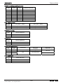
1
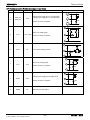
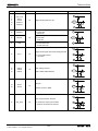
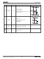
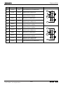
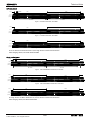
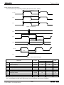
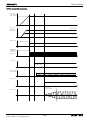
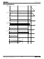
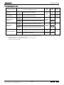
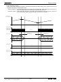
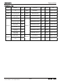
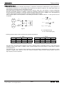
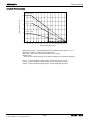
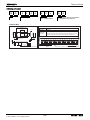
Middle Power Class-D Speaker Amplifiers
Class-D Speaker Amplifier
for Digital Input
BD5446EFV
No.11075ECT14
●Description
BD5446EFV is a Class D Speaker Amplifier designed for Flat-panel TVs in particular for space-saving and low-power
consumption, delivers an output power of 20W+20W. This IC employs state-of-the-art Bipolar, CMOS, and DMOS (BCD)
process technology that eliminates turn-on resistance in the output power stage and internal loss due to line resistances up
to an ultimate level. With this technology, the IC can achieve high efficiency of 87% (10W+10W output with 8Ω load). In
addition, the IC is packaged in a compact reverse heat radiation type power package to achieve low power consumption
and low heat generation and eliminates necessity of external heat-sink up to a total output power of 40W. This product
satisfies both needs for drastic downsizing, low-profile structures and many function, high quality playback of sound system.
●Features
1) BD5446EFV has two system of digital audio interface.
2
(I S/LJ format, SDATA: 16 / 20 / 24bit, LRCLK: 32kHz / 44.1kHz / 48kHz, BCLK: 64fs (fixed), SYS_CLK: 256fs (fixed))
2) Within the wide range of the power supply voltage, it is possible to operate in a single power supply. (10~26V)
3) It contributes to miniaturizing, making to the thin type, and the power saving of the system by high efficiency and low heat.
4) S/N of the system can be optimized by adjusting the gain setting among 8 steps. (20~34dB / 2dB step)
5) It has the output power limitation function that can be adjusted to an arbitrary output power.
6) The decrease in sound quality because of the change of the power supply voltage is prevented with the feedback
circuitry of the output. In addition, a low noise and low distortion are achieved.
7) It provides with the best stereo DAC output for the headphone usage. As a result, the output of the selection of the
digital input in two systems is possible.
8) Eliminates pop noise generated when the power supply goes on/off, or when the power supply is suddenly shut off.
High quality muting performance is realized by using the soft-muting technology.
9) BD5446EFV is a highly reliable design to which it has various protection functions.
(High temperature protection, Under voltage protection, Output short protection, Output DC voltage protection and
Clock stop protection)
●Applications
Flat Panel TVs (LCD, Plasma), Home Audio, Desktop PC, Amusement equipments, Electronic Music equipments, etc.,
www.rohm.com
© 2011 ROHM Co., Ltd. All rights reserved.
1/31
2011.06 - Rev.C
Technical Note
BD5446EFV
●Absolute maximum ratings (Ta=25℃)
Parameter
Supply voltage
Symbol
VCC
Ratings
Unit
Conditions
30
V
Pin 25, 28, 29, 53, 54
2.0
W
*3
*4
*1 *2
Power dissipation
Pd
4.5
W
6.2
W
*5
Input voltage
VIN
-0.3 ~ 4.5
V
Pin 7 ~ 18, 21
*1
Pin24
*1
Open-drain terminal voltage
VERR
-0.3 ~ 30
V
Operating temperature range
Topr
-25 ~ +85
℃
Storage temperature range
Tstg
-55 ~ +150
℃
Maximum junction temperature
Tjmax
+150
℃
*1 The voltage that can be applied reference to GND (Pin 6, 36, 37, 45, 46).
*2 Do not, however exceed Pd and Tjmax=150℃.
*3 70mm×70mm×1.6mm, FR4, 1-layer glass epoxy board (Copper on bottom layer 0%)
Derating in done at 16mW/℃ for operating above Ta=25℃.
*4 70mm×70mm×1.6mm, FR4, 2-layer glass epoxy board (Copper on bottom layer 100%)
Derating in done at 36mW/℃ for operating above Ta=25℃. There are thermal via on the board.
*5 70mm×70mm×1.6mm, FR4, 4-layer glass epoxy board (Copper on bottom layer 100%)
Derating in done at 49.6mW/℃ for operating above Ta=25℃. There are thermal via on the board.
●Operating conditions (Ta=25℃)
Parameter
Symbol
Ratings
Unit
VCC
10 ~ 26
V
Pin 25, 28, 29, 53, 54
Minimum load impedance
(Speaker Output)
RL_SP
5.4
Ω
*6
Minimum load impedance
(DAC Output)
RL_DA
20
kΩ
Pin 22, 23
Supply voltage
Conditions
*1 *2
*6 Do not, however exceed Pd.
* No radiation-proof design.
www.rohm.com
© 2011 ROHM Co., Ltd. All rights reserved.
2/31
2011.06 - Rev.C
Technical Note
BD5446EFV
●Electrical characteristics
(Unless otherwise specified Ta=25℃,Vcc=13V,f=1kHz,RL_SP=8Ω,RL_DA=20kΩ,RESETX=3.3V,MUTEX=3.3V,PDX=3.3V,
Gain=20dB,fs=48kHz)
Limits
Item
Symbol
Unit
Conditions
Min
Typ
Max
Total circuit
Circuit current
Pin 25, 28, 29, 53, 54
No load
Pin 25, 28, 29, 53, 54,No load
RESETX=0V,MUTEX=0V,PDX=0V
ICC1
-
45
90
mA
ICC2
-
1.5
3
mA
VERR
-
-
0.8
V
Pin 24,IO=0.5mA
Regulator output voltage 1
VREG_G
5.0
5.5
6.0
V
Pin 1, 27
Regulator output voltage 2
VREG_3
3.0
3.3
3.6
V
Pin 5
High level input voltage
VIH
2.5
-
3.3
V
Pin 7 ~ 18, 21
Low level input voltage
VIL
0
-
0.8
V
Pin 7 ~ 18, 21
IIH
33
66
132
µA
Pin 7 ~ 18, 21,VIN = 3.3V
PO1
-
10
-
W
PO2
-
20
-
W
THDSP
-
0.07
-
%
PO=1W, BW=20~20kHz
*7
CTSP
65
80
-
dB
PO=1W, BW=IHF-A
*7
VNO_SP
-
140
280
µVrms -∞dBFS, BW=IHF-A
*7
VNOR_SP
-
5
10
µVrms MUTEX=0V,-∞dBFS, BW=IHF-A
*7
fPWM1
-
512
-
KHz
fs=32kHz
*7
fPWM2
-
705.6
-
KHz
fs=44.1kHz
*7
fPWM3
-
768
-
KHz
fs=48kHz
*7
VOMAX
0.85
1.0
-
Vrms
0dBFS,THD+n=1%
CB
-1
0
1
dB
0dBFS
THDDA
-
0.05
0.5
%
-20dBFS,BW=20~20kHz
CTDA
65
80
-
dB
0dBFS,BW=IHF-A
Output noise voltage
VNO_DA
-
10
20
µVrms -∞dBFS, BW=IHF-A
Residual noise voltage
VNOR_DA
-
3
10
µVrms
Circuit current
(Power down mode)
Open-drain terminal
Low level voltage
Input current
(Input pull-down terminal)
Speaker Output
Maximum momentary
output power 1
Maximum momentary
output power 2
Total harmonic distortion
Crosstalk
Output noise voltage
(Sampling mode)
Residual noise voltage
(Mute mode)
PWM sampling frequency
THD+n=10%
GAIN=26dB
VCC=18V, THD+n=10%
GAIN =26dB
*7
*7
DAC Output
Maximum output voltage
Channel Balance
Total harmonic distortion
Crosstalk
MUTEX=0V,PDX=0V,
-∞dBFS, BW=IHF-A
*7 These items show the typical performance of device and depend on board layout, parts, and power supply.
The standard value is in mounting device and parts on surface of ROHM’s board directly.
www.rohm.com
© 2011 ROHM Co., Ltd. All rights reserved.
3/31
2011.06 - Rev.C
Technical Note
BD5446EFV
●Electrical characteristic curves(VCC=13V,Ta=25℃,RL_SP=8Ω,RL_DA=20kΩ,Gain=20dB,fin=1kHz,fs=48kHz)
Measured by ROHM designed 4 layer board.
80
Sampling
60
50
40
Mute
30
20
10
0
3
THD=10%
THD=1%
0
Fig.1
VOLTAGE GAIN(dB)
EFFICIENCY(%)
80
70
60
50
40
30
20
10
0
8
10
30
28
26
24
22
20
18
16
14
12
10
20 25
30
Without signal
BW=20~20KHz
-20
-40
-60
-80
-100
-140
100
1k
10k
100k
10
100
1k
10k
FREQUENCY(Hz)
FREQUENCY(Hz)
Fig.4
Fig.5
Fig.6
Efficiency - Output power
Voltage gain - Frequency
Po=1W
BW=20~20KHz
6KHz
1KHz
0.1
0.001 0.01
0.1
1
1
0.1
100Hz
0.01
CROSSTALK(dB)
THD+N(%)
10
10
0.01
100
10
100
1k
10k
100k
FREQUENCY(Hz)
OUTPUT POWER(W)
100k
FFT of Output noise voltage
100
BW=20~20KHz
1
40
-120
10
10
35
0
12
100
THD+N(%)
15
Fig.3
Po=1W
L=22µH
C=0.47µF
Cg=0.068µF
OUTPUT PO WER(W/ch)
CROSSTALK(dB)
10
Current consumption
- Output power
Output power
- Power supply voltage
100
90
6
5
TOTAL OUTPUT POWER(W)
Fig.2
Current consumption
- Power supply voltage
4
0
VCC(V)
VCC(V)
2
VCC=18V
1
8 10 12 14 16 18 20 22 24 26 28
8 10 12 14 16 18 20 22 24 26 28
0
VCC=13V
2
NOISE FFT(dBV)
ICC(mA)
70
44
40
36
32
28
24
20
16
12
8
4
0
ICC(A)
OUTPUT POWER(W/ch)
100
90
0
-10
-20
-30
-40
-50
-60
-70
-80
-90
-100
BW=20~20KHz
0.001
0.01
0.1
1
10
OUTPUT POWER(W)
Fig.7
Fig.8
Fig.9
THD+N - Output power
THD+N - Frequency
Crosstalk - Output power
0
-10
-20
-30
-40
-50
-60
-70
-80
-90
-100
fin=300Hz
Po=3.3W
Po=1W
BW=20~20KHz
Speaker output
fin=300Hz
Po=3.3W
Speaker output
5V/div
5V/div
MUTEX
2V/div
MUTEX
2V/div
10ms/div
10ms/div
10
100
1k
10k
100k
FREQUENCY(Hz)
Fig.10
Crosstalk –Frequency
www.rohm.com
© 2011 ROHM Co., Ltd. All rights reserved.
Fig.11
Wave form when
Releasing Soft-mute
4/31
Fig.12
Wave form when
Activating Soft-mute
2011.06 - Rev.C
Technical Note
BD5446EFV
●Electrical characteristic curves(VCC=18V,Ta=25℃,RL_SP=8Ω,RL_DA=20kΩ,Gain=20dB,fin=1kHz,fs=48kHz)
Measured by ROHM designed 4layer board.
100
70
60
50
40
30
20
10
36
34
Po=1W
L=22µH
C=0.47µF
Cg=0.068µF
32
30
28
26
5
10
15
20
-80
-100
-140
10
100
OUTPUT POWER(W /ch)
1k
10k
10
100k
100
1k
10k
100k
FREQUENCY(Hz)
FREQUENCY(Hz)
Fig.13
Fig.14
Fig.15
Efficiency – Output power
Voltage gain - Frequency
FFT of output noise voltage
100
100
Po=1W
BW=20~20KHz
BW=20~20KHz
1
6KHz
1KHz
0.1
CROSSTALK(dB)
10
THD+N(%)
10
THD+N(%)
-60
20
0
1
0.1
100Hz
0.01
0.01
0.001 0.01
0.1
1
10
100
OUTPUT POWER(W)
0
-10
-20
-30
-40
-50
-60
-70
-80
10
100
1k
10k
100k
FREQUENCY(Hz)
Fig.16
THD+N - Output power
CROSSTALK(dB)
-40
-120
24
22
0
Without signal
BW=20~20KHz
-20
NOISE FFT(dBV)
VOLTAGE GAIN(dB)
80
EFFICIENCY(%)
0
40
38
90
Fig.17
THD+N - Frequency
0
-10
-20
-30
-40
-50
-60
-70
-80
-90
-100
BW=20~20KHz
0.001 0.01
0.1
1
10
100
OUTPUT POWER(W)
Fig.18
Crosstalk - Output power
Po=1W
BW=20~20KHz
-90
-100
10
100
1k
10k
100k
FREQUENCY(Hz)
Fig.19
Crosstalk - Frequency
www.rohm.com
© 2011 ROHM Co., Ltd. All rights reserved.
5/31
2011.06 - Rev.C
Technical Note
BD5446EFV
●Pin configuration and Block diagram
VCCP1
1
REG_G1
54
2
FILP
53
3
Power
Limiter
NC 52
4
FILA
51
5
REG_3
50
REG_G1
GNDA
6
49
Driver
1P
7
NC 48
NC 47
8
9
I2S/LJ
Interface
46
Driver
1N
10
45
GNDP1
11
44
12
43
Control
Interface
13
14
15
REG_G1
I2S/LJ
Selector
42
×8 Over
Sampling
Digital
Filter
PWM
Modulator
NC
40
REG_G2
39
16
17
Gain
Selector
38
Driver
2N
18
19
37
GNDP2
TEST
36
NC 35
20
21
41
DAC
Selector
Driver
2P
NC 34
22
33
DAC
REG_G2
23
32
24
31
25
26
VCCA
NC
27
High Temperature Protection
Under Voltage Protection
Clock Stop Protection
29
Output Short Protection
Output DC Voltage Protection
VCCP2
REG_G2
www.rohm.com
© 2011 ROHM Co., Ltd. All rights reserved.
NC 30
6/31
28
2011.06 - Rev.C
Technical Note
BD5446EFV
●Pin function explanation (Provided pin voltages are typ. Values)
No.
Pin name
Pin voltage
Pin explanation
Internal equivalence circuit
53,54
28,29
1
27
REG_G1
REG_G2
5.5V
Internal power supply pin for ch1 Gate driver
Internal power supply pin for ch2 Gate driver
1
27
550K
Please connect the capacitor.
45,46
36,37
25
Bias pin for PWM signal
2
FILP
1.75V~2.55V
2
Please connect the capacitor.
6
25
3
PLMT
0V
Power limiter setting terminal
3
400K
6
27
4
50K
Bias pin for Analog signal
FILA
4
2.5V
Please connect the capacitor.
50K
6
25
Internal power supply pin for Digital circuit
5
REG3
5
3.3V
Please connect the capacitor.
500K
6
6
GNDA
0V
www.rohm.com
© 2011 ROHM Co., Ltd. All rights reserved.
GND pin for Analog signal
7/31
-
2011.06 - Rev.C
Technical Note
BD5446EFV
No.
Pin name
7
8
9
10
11
SYS_CLK
BCLK
LRCLK
SDATA1
SDATA2
Pin voltage
Pin explanation
Internal equivalence circuit
5
0V
Digital audio signal input pin
7,8,9
10,11
50K
6
12
RESETX
13
MUTEX
14
Reset pin for Digital circuit
H: Reset OFF
L: Reset ON
0V
Speaker output mute control pin
H: Mute OFF
L: Mute ON
Power down control pin
H: Power down OFF
L: Power down ON
PDX
5
12,13,14
50K
6
5
Digital audio signal data format setting terminal
15
IIS_LJ
0V
H: Left Justified format
2
L: I S format
15
50K
6
5
16
17
18
GAIN1
GAIN2
GAIN3
Gain setting terminal
0V
16,17,18
Gain=20dB~34dB, 2dB step
50K
6
5
19
20
TEST1
TEST2
Test pin
0V
19,20
Please connect to GND.
50K
6
5
DAC output selection terminal
21
SEL_DAC
0V
H: SDATA2 is output from the DAC
L: SDATA1 is output from the DAC
21
50K
6
www.rohm.com
© 2011 ROHM Co., Ltd. All rights reserved.
8/31
2011.06 - Rev.C
Technical Note
BD5446EFV
No.
Pin name
Pin voltage
Pin explanation
Internal equivalence circuit
25
OUT_DAC2
OUT_DAC1
22,23
2.5V
Please connect it with the latter part circuit
through the capacitor.
50K
22
23
ch2 DAC output pin
ch1 DAC output pin
6
25
Error flag pin
500
24
ERROR
3.3V
Please connect pull-up resistor.
H: While Normal
L: While Error
24
6
25
VCCA
VCC
26,30
34,35
41,47
48,52
N.C.
-
www.rohm.com
© 2011 ROHM Co., Ltd. All rights reserved.
Power supply pin for Analog signal
-
Non connection pin
-
9/31
2011.06 - Rev.C
Technical Note
BD5446EFV
No.
Pin name
Pin voltage
28,29
VCCP2
Vcc
31,32
OUT2P
Vcc~0V
Pin explanation
Internal equivalence circuit
Power supply pin for ch2 PWM signal
28,29
33
BSP2P
-
36,37
GNDP2
0V
38,39
OUT2N
Vcc~0V
Output pin of ch2 positive PWM
Please connect to Output LPF.
Boot-strap pin of ch2 positive
Please connect the capacitor.
33
40
31,32
38,39
GND pin for ch2 PWM signal
Output pin of ch2 negative PWM
Please connect to Output LPF.
40
BSP2N
-
Boot-strap pin of ch2 negative
Please connect the capacitor.
42
BSP1N
-
Boot-strap pin of ch1 negative
Please connect the capacitor.
43,44
OUT1N
Vcc~0V
36,37
53,54
45,46
GNDP1
0V
GND pin for ch1 PWM signal
Boot-strap pin of ch1 positive
Please connect the capacitor.
49
BSP1P
-
50,51
OUT1P
Vcc~0V
53,54
VCCP1
Output pin of ch1 negative PWM
Please connect to Output LPF.
-
www.rohm.com
© 2011 ROHM Co., Ltd. All rights reserved.
Output pin of ch1 positive PWM
Please connect to Output LPF.
42
49
43,44
50,51
45,46
Power supply pin for ch1 PWM signal
10/31
2011.06 - Rev.C
Technical Note
BD5446EFV
●GAIN1 pin, GAIN2 pin, GAIN3 pin function
GAIN3
(18pin)
GAIN2
(17pin)
GAIN1
(16pin)
Speaker output gain
L
L
L
20dB
L
L
H
22dB
L
H
L
24dB
L
H
H
26dB
H
L
L
28dB
H
L
H
30dB
H
H
L
32dB
H
H
H
34dB
●SEL_DAC pin function
SEL_DAC
(21pin)
OUT_DAC1 (23pin)
OUT_DAC2 (24pin)
L
The Lch signal of SDATA1 is output
The Rch signal of SDATA1 is output
H
The Lch signal of SDATA2 is output
The Rch signal of SDATA2 is output
●RESETX pin function
RESETX
(10pin)
State of Digital block
L
Reset ON
H
Reset OFF
●RESETX pin
RESETX
(12pin)
State of Digital block
L
Reset ON
H
Reset OFF
●PDX pin,MUTEX pin function
PDX
(12pin)
MUTEX
(11pin)
Power Down
DAC output
(24,25pin)
L
L or H
ON
HiZ_Low
H
L
H
H
OFF
Normal operation
PWM output
(33,34,38,39,43,44,48pin)
HiZ_Low
Normal operation
●IIS_LJ pin function
IIS_LJ
(15pin)
Digital data format
L
I2S
H
Left Justified
www.rohm.com
© 2011 ROHM Co., Ltd. All rights reserved.
11/31
2011.06 - Rev.C
Technical Note
BD5446EFV
●Input digital audio signal sampling frequency (fs) explanation
PWM sampling frequency, Soft-start, Soft-mute time, and the detection time of the DC voltage protection in the speaker
depends on sampling frequency (fs) of the digital audio input.
Sampling frequency of the
digital audio input
(fs)
32kHz
PWM sampling frequency
(fpwm)
Soft-start / Soft-mute time
DC voltage protection in
the speaker detection time
512kHz
64msec.
64msec.
44.1kHz
705.6kHz
46msec.
46msec.
48kHz
768kHz
43msec.
43msec.
●For voltage gain (Gain setting)
BD5446EFV prescribe voltage gain at speaker output (BTL output) under the definition 0dBV (1Vrms) as full scale input of
the digital audio input signal. For example, digital audio input signal = Full scale input, Gain setting = 20dB, Load resistance
2
RL_SP = 8Ω will give speaker output (BTL output) amplitude as Vo=10Vrms. (Output power Po = Vo /RL_SP = 12.5W )
●Speaker output and DAC output
Digital audio input signal SDATA1 will be output to the speaker. (SDATA2 will not be output to the speaker. DAC output can
be selected either from digital audio input signal SDATA1 or SDATA2.)
●Format of digital audio input
・SYS_CLK: It is System Clock input signal.
It will input LRCLK, BCLK, SDATA1 (SDATA2) that synchronizes with this clock that are 256 times of sampling frequency
(256fs).
・LRCLK: It is L/R clock input signal.
It corresponds to 32kHz/44.1kHz/48kHz with those clock (fs) that are same to the sampling frequency (fs) .
The data of a left channel and a right channel for one sample is input to this section.
・BCLK: It is Bit Clock input signal.
It is used for the latch of data in every one bit by sampling frequency’s 64 times sampling frequency (64fs).
・SDATA1 & SDATA2: It is Data input signal.
It is amplitude data. The data length is different according to the resolution of the input digital audio data.
It corresponds to 16/ 20/ 24 bit.
www.rohm.com
© 2011 ROHM Co., Ltd. All rights reserved.
12/31
2011.06 - Rev.C
Technical Note
BD5446EFV
●I2S data format
1/64fs
LRCLK
Lch
Rch
BCLK
SDATA1
MSB
22 21 20 19 18 17 16 15 14 13 12 11 10 9 8 7 6 5 4 3 2
1 LSB
MSB
22 21 20 19 18 17 16 15 14 13 12 11 10 9 8
7 6 5 4 3 2
1
LSB
(SDATA2)
32 clocks
32 clocks
Fig.20
I2S Data Format 64fs, 24 bit Data
Lch
LRCLK
Rch
BCLK
SDATA1
MSB
18 17 16 15 14 13 12 11 10 9 8 7 6 5 4 3 2 1
MSB
LSB
18 17 16 15 14 13 12 11 10 9 8 7 6 5 4 3 2 1
LSB
(SDATA2)
Fig.21
I2S Data Format 64fs, 20 bit Data
Lch
LRCLK
Rch
BCLK
SDATA1
MSB
14 13 12 11 10 9 8 7 6 5 4 3 2 1
MSB
LSB
14 13 12 11 10 9 8 7 6 5 4 3 2 1
LSB
(SDATA2)
Fig.22
2
I S Data Format 64fs, 16 bit Data
The Low section of LRCLK becomes Lch, the High section of LRCLK becomes Rch.
After changing LRCLK, second bit becomes MSB.
●Left-justified format
1/64fs
LRCLK
Lch
Rch
BCLK
SDATA1
(SDATA2)
MSB
22 21 20 19 18 17 16 15 14 13 12 11 10 9 8
7 6 5 4 3 2
1 LSB
MSB
22 21 20 19 18 17 16 15 14 13 12 11 10 9 8
32 clocks
7 6 5 4 3 2 1
32 clocks
Fig.23
Left-Justified Data Format 64fs, 24 bit Data
Lch
LRCLK
LSB
Rch
BCLK
SDATA1
MSB
18 17 16 15 14 13 12 11 10 9 8 7 6 5 4 3 2 1
MSB
LSB
18 17 16 15 14 13 12 11 10 9 8 7 6 5 4 3 2 1
LSB
(SDATA2)
Fig.24
Left-Justified Data Format 64fs, 20 bit Data
Lch
LRCLK
Rch
BCLK
SDATA1
MSB
14 13 12 11 10 9 8 7 6 5 4 3 2 1
MSB
LSB
14 13 12 11 10 9 8 7 6 5 4 3 2 1
LSB
(SDATA2)
Fig.25
Left-Justified Data Format 64fs, 16 bit Data
The High section of LRCLK becomes Lch, the Low section of LRCLK becomes Rch.
After changing LRCLK, first bit becomes MSB.
www.rohm.com
© 2011 ROHM Co., Ltd. All rights reserved.
13/31
2011.06 - Rev.C
Technical Note
BD5446EFV
●Audio Interface format and timing
Recommended timing and operating conditions (MCLK, BCLK, LRCLK, SDATA)
1/f
/ SYS_CLK
SYS_CLK
1/fLRCLK
LRCLK
1/fBCLK
BCLK
Fig-26 Clock timing
LRCLK
tHD;LR
tSU;LR
BCLK
tHD ; SD
tSU ; SD
SDATA
Fig-27 Audio Interface timing (1)
SYS_CLK
tHD ; BC
tSU ; BC
BCLK
Fig-28 Audio Interface timing (2)
Parameter
Symbol
Limit
Unit
Min.
Max.
fSYS_CLK
8.192
12.288
MHz
fLRCLK
32
48
kHz
1
SYS_CLK frequency
2
LRCLK frequency
3
BCLK frequency
fBCLK
2.048
3.072
MHz
4
Setup time, LRCLK※1
tSU;LR
20
-
ns
5
Hold time, LRCLK※1
tHD;LR
20
-
ns
6
Setup time, SDATA
tSU;SD
20
-
ns
7
Hold time, SDATA
tHD;SD
20
-
ns
8
Setup time, BCLK※2
tSU;BC
2.5
-
ns
9
Hold time, BCLK※2
tHD;BC
3.5
-
※1 This regulation is to keep rising edge of LRCK and rising edge of BCLK from overlapping.
※2 This regulation is to keep rising edge of SYS_CLK and rising edge of BCLK from overlapping.
ns
www.rohm.com
© 2011 ROHM Co., Ltd. All rights reserved.
14/31
2011.06 - Rev.C
Technical Note
BD5446EFV
●Power supply start-up sequence
VCCA (25pin)
VCCP1 (53, 54pin)
VCCP2 (28, 29pin)
①Power up VCCA, VCCP1, VCCP2 simultaneously.
t
REG_3 (5pin)
REG_G1 (1pin)
REG_G2 (27pin)
REG_G1, REG_G2
REG_3
t
RESETX (12pin)
②Set RESETX to High after power up.
t
SYS_CLK (7pin)
BCLK (8pin)
LRCLK (9pin)
SDATA1 (10pin)
SDATA2 (11pin)
③Degital audio data communication.
t
PDX (14pin)
④Set PDX to High.
t
OUT_DAC1 (23pin)
OUT_DAC2 (22pin)
t
MUTEX (13pin)
⑤Set MUTEX to High.
t
Soft-start
43msec(fs=48kHz)
Speaker output
t
www.rohm.com
© 2011 ROHM Co., Ltd. All rights reserved.
15/31
2011.06 - Rev.C
Technical Note
BD5446EFV
●Power supply shut-down sequence
VCCA (25pin)
VCCP1 (53, 54pin)
VCCP2 (28, 29pin)
⑤Power down VCCA, VCCP1, VCCP2, simultaneously.
t
REG_3 (5pin)
REG_G1 (1pin)
REG_G2 (27pin)
REG_G1, REG_G2
REG_3
t
RESETX (12pin)
④Set RESETX to Low
t
SYS_CLK (7pin)
BCLK
(8pin)
LRCLK (9pin)
SDATA1 (10pin)
SDATA2 (11pin)
③Stop digital audio date signal.
t
PDX (14pin)
②Set PDX to Low.
t
OUT_DAC1 (23pin)
OUT_DAC2 (22pin)
t
MUTEX (13pin)
①Set MUTEX to Low.
t
Soft-mute
43msec(fs=48kHz)
t
www.rohm.com
© 2011 ROHM Co., Ltd. All rights reserved.
16/31
2011.06 - Rev.C
Technical Note
BD5446EFV
●About the protection function
Protection function
Detecting & Releasing condition
Output short
protection
Detecting
condition
Detecting current = 10A (TYP.)
DC voltage protection
in the speaker
Detecting
condition
PWM output Duty=0% or 100%
43msec(fs=48kHz) above fixed
Detecting
condition
Chip temperature to be above 150℃ (TYP.)
High temperature
protection
Under voltage
protection
DAC
Output
Normal
operation
Chip temperature to be below 120℃ (TYP.)
Detecting
condition
Power supply voltage to be below 8V (TYP.)
ERROR
Output
HiZ_Low
(Latch)
L
(Latch)
HiZ_Low
(Latch)
L
(Latch)
HiZ_Low
Normal
operation
Releasing
condition
PWM
Output
H
Normal
operation
HiZ_Low
Normal
operation
H
Releasing
condition
Normal
operation
Power supply voltage to be above 9V (TYP.)
Detecting
condition
No change to SYS_CLK more than 1usec (TYP.)
Irregular
output
HiZ_Low
Releasing
condition
Normal input to SYS_CLK
Normal
operation
Normal
operation
Clock stop protection
H
* The ERROR pin is Nch open-drain output.
* Once an IC is latched, the circuit is not released automatically even after an abnormal status is removed.
The following procedures ① or ② is available for recovery.
①After the MUTEX pin is made Low once, the MUTEX pin is returned to High again.
②Turning on the power supply again.
www.rohm.com
© 2011 ROHM Co., Ltd. All rights reserved.
17/31
2011.06 - Rev.C
Technical Note
BD5446EFV
1) High temperature protection
This IC has the high temperature protection circuit that prevents thermal reckless driving under an abnormal state for the
temperature of the chip to exceed Tjmax=150℃.
Detecting condition - It will detect when MUTE pin is set High and the temperature of the chip becomes 150℃(TYP.) or
more. The speaker output is muted through a soft-mute when detected.
Releasing condition - It will release when MUTE pin is set High and the temperature of the chip becomes 120℃(TYP.)
or less. The speaker output is outputted through a soft-start when released.
Temperature of
IC chip junction(℃)
150℃
120℃
t
OUT1P (50, 51pin)
OUT1N (43, 44pin)
OUT2P (31, 32pin)
OUT2N (38, 39pin)
HiZ-Low
t
Speaker output
Soft-mute
43msec(fs=48KHz)
Soft-start
43msec(fs=48KHz)
t
ERROR (24pin)
3.3V
t
OUT_DAC1 (23pin)
OUT_DAC2 (22pin)
t
www.rohm.com
© 2011 ROHM Co., Ltd. All rights reserved.
18/31
2011.06 - Rev.C
Technical Note
BD5446EFV
2) Under voltage protection
This IC has the under voltage protection circuit that make speaker output mute once detecting extreme drop of the power
supply voltage.
Detecting condition – It will detect when MUTE pin is set High and the power supply voltage becomes lower than 8V.
The speaker output is muted through a soft-mute when detected.
Releasing condition – It will release when MUTE pin is set High and the power supply voltage becomes more than 9V.
The speaker output is outputted through a soft-start when released.
VCCA (25pin)
VCCP1 (53, 54pin)
VCCP2 (28, 29pin)
9V
8V
t
OUT1P (50, 51pin)
OUT1N (43, 44pin)
OUT2P (31, 32pin)
OUT2N (38, 39pin)
HiZ-Low
t
Speaker output
Soft-mute
43msec(fs=48kHz)
Soft-start
43msec(fs=48kHz)
t
ERROR (24pin)
3.3V
t
OUT_DAC1 (23pin)
OUT_DAC2 (22pin)
t
www.rohm.com
© 2011 ROHM Co., Ltd. All rights reserved.
19/31
2011.06 - Rev.C
Technical Note
BD5446EFV
3) Clock stop protection
This IC has the clock stop protection circuit that make the speaker output mute when the SYS_CLK signal of the digital
audio input stops.
Detecting condition - It will detect when MUTE pin is set High and the SYS_CLK signal stops for about 1usec or more.
The speaker output is muted through a soft-mute when detected.
Releasing condition - It will release when MUTE pin is set High and the SYS_CLK signal returns to the normal clock
operation. The speaker output is outputted through a soft-start when released.
Clock stop
Clock recover
SYS_CLK (7pin)
t
Protection start with
about 1μsec clock stop.
OUT1P (50, 51pin)
OUT1N (43, 44pin)
OUT2P (31, 32pin)
OUT2N (38, 39pin)
HiZ-Low
t
Soft-start
43msec(fs=48kHz)
Speaker output
t
ERROR (24pin)
3.3V
t
OUT_DAC1 (23pin)
OUT_DAC2 (22pin)
Unstable
t
www.rohm.com
© 2011 ROHM Co., Ltd. All rights reserved.
20/31
2011.06 - Rev.C
Technical Note
BD5446EFV
4)Output short protection(Short to the power supply)
This IC has the PWM output short protection circuit that stops the PWM output when the PWM output is short-circuited to
the power supply due to abnormality.
Detecting condition - It will detect when MUTE pin is set High and the current that flows in the PWM output pin
becomes 10A(TYP.) or more. The PWM output instantaneously enters the state of HiZ-Low if
detected, and IC does the latch.
Releasing method - ①After the MUTEX pin is set Low once, the MUTEX pin is set High again.
②Turning on the power supply again.
Short to VCC
Release from short to VCC
OUT1P (50, 51pin)
OUT1N (43, 44pin)
OUT2P (31, 32pin)
OUT2N (38, 39pin)
t
PWM out : IC latches with HiZ-Low.
Released from latch state.
Over current
10A(TYP.)
t
ERROR (24pin)
t
1μsec(TYP.)
MUTEX(13pin)
Latch release
t
5) Output short protection(Short to GND)
This IC has the PWM output short protection circuit that stops the PWM output when the PWM output is short-circuited to
GND due to abnormality.
Detecting condition - It will detect when MUTE pin is set High and the current that flows in the PWM output terminal
becomes 10A(TYP.) or more. The PWM output instantaneously enters the state of HiZ-Low if
detected, and IC does the latch.
Releasing method – ①After the MUTEX pin is set Low once, the MUTEX pin is set High again.
②Turning on the power supply again.
Short to GND
Release from short to
GND
OUT1P (50, 51pin)
OUT1N (43, 44pin)
OUT2P (31, 32pin)
OUT2N (38, 39pin)
t
PWM out : IC latches with HiZ-Low.
Released from latch state.
Over current
10A(TYP.)
t
ERROR (24pin)
t
1μsec(TYP.)
MUTEX(13pin)
Latch release
t
www.rohm.com
© 2011 ROHM Co., Ltd. All rights reserved.
21/31
2011.06 - Rev.C
Technical Note
BD5446EFV
6) DC voltage protection in the speaker
When the DC voltage in the speaker is impressed due to abnormality, this IC has the protection circuit where the speaker
is defended from destruction.
Detecting condition - It will detect when MUTE pin is set High or Low and PWM output Duty=0% or 100% ,
43msec(fs=48kHz) or above. Once detected, The PWM output instantaneously enters the state
of HiZ-Low, and IC does the latch.
Releasing method – ①After the MUTEX pin is set Low once, the MUTEX pin is set High again.
②Turning on the power supply again
Abnormal state release.
PWM out locked duty=100% abnormal state.
OUT1P (50, 51pin)
OUT1N (43, 44pin)
OUT2P (31, 32pin)
OUT2N (38, 39pin)
t
PWM output : IC latche with HiZ-Low.
Latch release state.
Speaker output
t
Soft-start
Protection start surge current
into speaker output for 43msec
(fs=48kHz) and over.
43msec(fs=48kHz)
ERROR (24pin)
t
MUTEX(13pin)
Latch release
t
www.rohm.com
© 2011 ROHM Co., Ltd. All rights reserved.
22/31
2011.06 - Rev.C
Technical Note
BD5446EFV
●Output power limiter function
This IC is provided with an output power limiter function to protect speakers from destruction by an excessive output.
Limiter values are freely specified by changing external resistors R1/R2 as shown in Fig-26. Fig-27 shows a speaker output
waveform that is generated with use of the output limiter function. Because the waveform is soft-clipped, unusual noises on
audible signals are significantly reduced under operation of limiter.
Use resistors with a high degree of accuracy for R1 and R2 (±1% or higher accuracy is recommended). The capacitor C is
for the noise removal of output power limitation terminal (3pin). Provide grounding with a 1µF capacitor. Specify a resistor of
10kΩ or higher resistor R1 and R2. If the output power limiter function is not used, R1, R2 and C is unnecessary. However,
connect 3pin with GNDA.
Power
Limiter
REG_3
3
R1
R2
Speaker
output
5
C
1μF
5pin
3.3V
Soft Clip
1μF
Fig-30
GNDA
Fig-29
10
OUTPUT POWER(W/ch) .
9
8
7
6
5
4
3
VCC=13V, RL=8Ω, f=1kHz
Gain=20dB, 5pin=3.3V
2
1
0
1
1.2
1.4
1.6
1.8
2
3pin terminal voltage [V]
Fig.31
Output power
– 3pin terminal voltage
www.rohm.com
© 2011 ROHM Co., Ltd. All rights reserved.
23/31
2011.06 - Rev.C
Technical Note
BD5446EFV
●Application Circuit Example(RL_SP=8Ω)
C1
3.3μF
GNDP1
VCCP1
1
C2
1μF
)
)
( )
(
(
C4
1μF
C5
VCCP1
REG_G1
2
FILP
53
3
Power
Limiter
NC 52
4
FILA
51
5
REG_3
50
1μF
REG_G1
GNDA
GNDA
6
Driver
1P
7
0
Digital Audio
Source
LRCLK
(fs=32kHz~48kHz)
(NOP)
9
GNDP1
Control
Interface
I2S/LJ
Selector
×8 Over
Sampling
Digital
Filter
NC
40
Gain
Selector
OUT_DAC2
(Rch)
GNDP2
Driver
2N
37
GNDP2
OUT_DAC1
(Lch)
ERROR
VCCA
DAC
Selector
100kΩ
32
24
31
25
26
3.3μF
C27
REG_G2
VCCA
NC
High Temperature Protection
Under Voltage Protection
Clock Stop Protection
1μF
C28
220μF
C28D
www.rohm.com
© 2011 ROHM Co., Ltd. All rights reserved.
R31B GNDP2
5.6Ω
C31B
470pF
8Ω
Rch
(SDATA1)
C31A
0.068μF
1μF
C31
22μH
L31
29
VCCP2
REG_G2
0.33μF
C31C
NC 30
Output Short Protection
Output DC Voltage Protection
27
C38A
5.6Ω
R38B
33
DAC
10μF C25D
GNDP2
NC 34
22
GNDA
GNDA
36
23
3.3V
R24
C25
0.1μF
Driver
2P
0.068μF
470pF
C38B
NC 35
1μFC23
L38
22μH
38
20
21
1μF
C38
39
TEST
1μF
C22
0.068μF
41
REG_G2
19
VSS
Lch
(SDATA1)
22μH
L43
42
PWM
Modulator
18
VSS
8Ω
C42
1μF
REG_G1
16
17
R43B GNDP1
5.6Ω
C43B
470pF
C43A
43
14
15
0.33μF
C43C
44
13
3.3V
C50A
C53D
5.6Ω
220μF R50B
45
12
PDX
C53
1μF
GNDP1
11
MUTEX
0.068μF
470pF
C50B
46
Driver
1N
10
RESETX
μ-con
I2S/LJ
Interface
0
SDATA2
C49
1μF
NC 47
0
SDATA1
NC 48
8
0
L50
22μH
49
SYS_CLK (256fs) 0
BCLK (64fs)
54
28
VCCP2
24/31
2011.06 - Rev.C
Technical Note
BD5446EFV
●BOM list(RL_SP=8Ω)
Parts
Parts No.
Value
Company
Product No.
Rated
Voltage
Tolerance
Size
IC
U1
-
ROHM
BD5446EFV
-
-
18.5mm×9.5mm
TOKO
1168ER-0001
-
(±20%)
10.3mm×7.6mm
SAGAMI
DBE7210H-220M
-
(±20%)
10.5mm×6.4mm
ROHM
MCR18PZHZFL5R60
1/4W
F(±1%)
3.2mm×1.6mm
Inductor
Resistor
Capacitor
L31, L38, L43, L50
22μH
R31B, R38B
R43B, R50B
5.6Ω
C31, C38, C42, C49
1μF
GRM185B31C105KE43
16V
B(±10%)
1.6mm×0.8mm
C25, C28, C53
0.1μF
GRM188B31H104KA92
50V
B(±10%)
1.6mm×0.8mm
C31A, C38A
C43A, C50A
0.068μF
GRM21BB11H683KA01
50V
B(±10%)
2.0mm×1.25mm
C31C, C43C
0.33μF
GRM219B31H334KA87
50V
B(±10%)
2.0mm×1.25mm
C1, C27
3.3μF
GRM188B31A335KE15
10V
B(±10%)
1.6mm×0.8mm
C2, C4, C5
C22, C23
1μF
GRM185B30J105KE25
6.3V
B(±10%)
1.6mm×0.8mm
C31B, C38B
C43B, C50B
470pF
GRM188B11H471KA
50V
B(±10%)
2.0mm×1.2mm
C28D, C53D
220μF
ECA1VMH221
35V
±20%
φ8mm×11.5mm
EEUFC1H100L
50V
±20%
φ5mm×11mm
Electrolytic
Capacitor
MURATA
Panasonic
C25D
www.rohm.com
© 2011 ROHM Co., Ltd. All rights reserved.
10μF
25/31
2011.06 - Rev.C
Technical Note
BD5446EFV
●Application Circuit Example(RL_SP=6Ω)
C1
3.3μF
GNDP1
VCCP1
1
C2
1μF
)
)
( )
(
(
C4
1μF
C5
VCCP1
REG_G1
2
FILP
53
3
Power
Limiter
NC 52
4
FILA
51
5
REG_3
50
1μF
REG_G1
GNDA
SYS_CLK (256fs) 0
Digital Audio
Source
(NOP)
Driver
1P
0
(fs=32kHz~48kHz)
9
I2S/LJ
Interface
10
GNDP1
Control
Interface
I2S/LJ
Selector
×8 Over
Sampling
Digital
Filter
NC
40
Gain
Selector
OUT_DAC2
(Rch)
GNDP2
Driver
2N
37
GNDP2
OUT_DAC1
(Lch)
ERROR
VCCA
100kΩ
DAC
Selector
32
24
31
25
26
3.3μF
C27
REG_G2
VCCA
NC
High Temperature Protection
Under Voltage Protection
Clock Stop Protection
1μF
C28
220μF
C28D
www.rohm.com
© 2011 ROHM Co., Ltd. All rights reserved.
R31B GNDP2
5.6Ω
C31B
470pF
6Ω
Rch
(SDATA1)
C31A
0.1μF
1μF
C31
15μH
L31
29
VCCP2
REG_G2
0.47μF
C31C
NC 30
Output Short Protection
Output DC Voltage Protection
27
0.1μF C38A
470pF
C38B
5.6Ω
R38B
33
DAC
10μF C25D
GNDP2
NC 34
22
GNDA
GNDA
Driver
2P
23
3.3V
R24
C25
0.1μF
36
NC 35
1μFC23
L38
15μH
38
20
21
1μF
C38
39
TEST
1μF
C22
0.1μF
41
REG_G2
19
VSS
Lch
(SDATA1)
15μH
L43
42
PWM
Modulator
18
VSS
6Ω
C42
1μF
REG_G1
16
17
R43B GNDP1
5.6Ω
C43B
470pF
C43A
43
14
15
0.47μF
C43C
44
13
3.3V
C53D
5.6Ω
220μF R50B
45
12
PDX
C53
1μF
GNDP1
11
MUTEX
0.1μF C50A
470pF
C50B
46
Driver
1N
0
RESETX
C49
1μF
NC 47
0
SDATA2
NC 48
8
LRCLK
L50
15μH
49
7
0
SDATA1
μ-con
GNDA
6
BCLK (64fs)
54
28
VCCP2
26/31
2011.06 - Rev.C
Technical Note
BD5446EFV
●BOM list(RL_SP=6Ω)
Parts
Parts No.
Value
Company
Product No.
Rated
Voltage
Tolerance
Size
IC
U1
-
ROHM
BD5446EFV
-
-
18.5mm×9.5mm
Inductor
L31, L38, L43, L50
15μH
SAGAMI
DBE7210H-150M
-
(±20%)
10.5mm×6.4mm
Resistor
R31B, R38B
R43B, R50B
5.6Ω
ROHM
MCR18PZHZFL5R60
1/4W
F(±1%)
3.2mm×1.6mm
C31, C38, C42, C49
1µF
GRM185B31C105KE43
16V
B(±10%)
1.6mm×0.8mm
C25, C28, C53, C31A,
C38A, C43A, C48A
0.1μF
GRM188B31H104KA92
50V
B(±10%)
1.6mm×0.8mm
C31C, C43C
0.47μF
GRM21BB31H474KA87
50V
B(±10%)
2.0mm×1.2mm
Capacitor
MURATA
C1, C27
3.3μF
GRM188B31A335KE15
10V
B(±10%)
1.6mm×0.8mm
C2, C4, C5
C22, C23
1μF
GRM185B30J105KE25
6.3V
B(±10%)
1.6mm×0.8mm
C31B, C38B
C43B, C50B
470pF
GRM188B11H471KA
50V
B(±10%)
2.0mm×1.2mm
C28D, C53D
220μF
ECA1VMH221
35V
±20%
φ8mm×11.5mm
EEUFC1H100L
50V
±20%
φ5mm×11mm
Electrolytic
Capacitor
Panasonic
C25D
www.rohm.com
© 2011 ROHM Co., Ltd. All rights reserved.
10μF
27/31
2011.06 - Rev.C
Technical Note
BD5446EFV
●Output LC Filter Circuit
An output filter is required to eliminate radio-frequency components exceeding the audio-frequency region supplied to a
load (speaker). Because this IC uses sampling clock frequencies from 200kHz to 400kHz in the output PWM signals, the
high-frequency components must be appropriately removed.
This section takes an example of an LC type LPF shown in Fig.29, in which coil L and capacitor C compose a differential
filter with an attenuation property of -12dB/oct. A large part of switching currents flow to capacitor C, and only a small part
of the currents flow to speaker RL. This filter reduces unwanted emission this way. In addition, coil L and capacitor Cg
compose a filter against in-phase components, reducing unwanted emission further.
Filter constants depend on load impedances. The following are formulas to calculate values of L, C, and Cg when Q=0.707
is specified.
48, 49
or
38, 39
L =
L
Cg
C
45, 46
or
33, 34
L
RL
2
1
C =
RL
H
4π f C
F
2 π f C RL
2
Cg
Cg = 0 .2 C
F
Fig. 29
RL : Load impedance (Ω)
fC : LPF cut off frequency (Hz)
Following presents output LC filter constants with typical load impedances.
fC = 30kHz
fC = 40kHz
RL
L
C
Cg
RL
L
C
Cg
6Ω
22µH
0.68µF
0.15µF
6Ω
15µH
0.47µF
0.1µF
8Ω
33µH
0.47µF
0.1µF
8Ω
22µH
0.33µF
0.068µF
16Ω
68µH
0.22µF
0.047µF
16Ω
47µH
0.15µF
0.033µF
Use coils with a low direct-current resistance and with a sufficient margin of allowable currents. A high direct-current
resistance causes power losses. In addition, select a closed magnetic circuit type product in normal cases to prevent
unwanted emission.
Use capacitors with a low equivalent series resistance, and good impedance characteristics at high frequency ranges
(100kHz or higher). Also, select an item with sufficient withstand voltage because flowing massive amount of
high-frequency currents is expected.
www.rohm.com
© 2011 ROHM Co., Ltd. All rights reserved.
28/31
2011.06 - Rev.C
Technical Note
BD5446EFV
●Notes for use
1 ) Absolute maximum ratings
Use of the IC in excess of absolute maximum ratings such as the applied voltage or operating temperature range may result in IC
damage. Assumptions should not be made regarding the state of the IC (short mode or open mode) when such damage is suffered. A
physical safety measure such as a fuse should be implemented when use of the IC in a special mode where the absolute maximum
ratings may be exceeded is anticipated.
2 ) Power supply lines
As return of current regenerated by back EMF of output coil happens, take steps such as putting capacitor between power supply and
GND as a electric pathway for the regenerated current. Be sure that there is no problem with each property such as emptied capacity at
lower temperature regarding electrolytic capacitor to decide capacity value. If the connected power supply does not have sufficient
current absorption capacity, regenerative current will cause the voltage on the power supply line to rise, which combined with the product
and its peripheral circuitry may exceed the absolute maximum ratings. It is recommended to implement a physical safety measure such
as the insertion of a voltage clamp diode between the power supply and GND pins.
3 ) GND potential(Pin 6, 36, 37, 45, 46).
Any state must become the lowest voltage about GND terminal and VSS terminal.
4 ) Input terminal
The parasitic elements are formed in the IC because of the voltage relation. The parasitic element operating causes the wrong operation
and destruction. Therefore, please be careful so as not to operate the parasitic elements by impressing to input terminals lower voltage
than GND and VSS. Please do not apply the voltage to the input terminal when the power-supply voltage is not impressed.
5 ) Setting of heat
Use a thermal design that allows for a sufficient margin in light of the power dissipation (Pd) in actual operating conditions. This IC
exposes its frame of the backside of package. Note that this part is assumed to use after providing heat dissipation treatment to improve
heat dissipation efficiency. Try to occupy as wide as possible with heat dissipation pattern not only on the board surface but also the
backside.
Class D speaker amplifier is high efficiency and low heat generation by comparison with conventional Analog power amplifier. However,
In case it is operated continuously by maximum output power, Power dissipation (Pdiss) may exceed package dissipation. Please
consider about heat design that Power dissipation (Pdiss) does not exceed Package dissipation (Pd) in average power (Poav). (Tjmax :
Maximum junction temperature=150℃, Ta : Peripheral temperature[℃], θja : Thermal resistance of package[℃/W], Poav : Average
power[W], η : Efficiency)
Package dissipation : Pd(W)=(Tjmax - Ta)/θja
Power dissipation
: Pdiss(W)= Poav ×(1/η- 1)
6 ) Actions in strong magnetic field
Use caution when using the IC in the presence of a strong magnetic field as doing so may cause the IC to malfunction.
7 ) Thermal shutdown circuit
This product is provided with a built-in thermal shutdown circuit. When the thermal shutdown circuit operates, the output transistors are
placed under open status. The thermal shutdown circuit is primarily intended to shut down the IC avoiding thermal runaway under
abnormal conditions with a chip temperature exceeding Tjmax = 150℃.
8 ) Shorts between pins and misinstallation
When mounting the IC on a board, pay adequate attention to orientation and placement discrepancies of the IC. If it is misinstalled and
the power is turned on, the IC may be damaged. It also may be damaged if it is shorted by a foreign substance coming between pins of
the IC or between a pin and a power supply or a pin and a GND.
9 ) Power supply on/off (Pin 25, 28, 29, 53, 54)
In case power supply is started up, RESETX(Pin 12), MUTEX(Pin 13) and PDX (Pin 14) always should be set Low. And in case power
supply is shut down, it should be set Low likewise. Then it is possible to eliminate pop noise when power supply is turned on/off. And also,
all power supply terminals should start up and shut down together.
10 ) ERROR terminal(Pin 24)
A error flag is outputted when Output short protection and DC voltage protection in the speaker are operated. These flags are the
function which the condition of this product is shown in.
11 ) N.C. terminal(Pin 26, 30, 34, 35, 41, 47, 48, 52)
N.C. terminal (Non Connection Pin) does not connect to the inside circuit. Therefore, possible to use open.
12 ) TEST terminal(Pin 19, 20)
TEST terminal connects with ground to prevent the malfunction by external noise.
13 ) Precautions for Spealer-setting
If the impedance characteristics of the speakers at high-frequency range while increase rapidly, the IC might not have stable-operation
in the resonance frequency range of the LC-filter. Therefore, consider adding damping-circuit, etc., depending on the impedance of
the speaker.
14) Notes about the phase of SYS_CLK (Pin7) and BCLK (Pin8)
If the rising edge of SYS_CLK (Pin7) and BCLK (Pin8) becomes simultaneous, noise or sound shutdown may occur.
Please cope with it, when the rising edge of CYC_CLK and BCLK becomes simultaneous. (Example: Insert RC filter in BCLK)
www.rohm.com
© 2011 ROHM Co., Ltd. All rights reserved.
29/31
2011.06 - Rev.C
Technical Note
BD5446EFV
●Allowable Power Dissipation
7
PCB③ 6.2W
Power Dissipation Pd (W)
6
5
PCB② 4.5W
4
3
PCB① 2.0W
2
1
0
0
10
20
30
40
50
60
70
80
90 100 110 120 130 140 150
Ambient Temperature:Ta( ℃)
Measuring instrument : TH-156(Shibukawa Kuwano Electrical Instruments Co., Ltd.)
Measuring conditions : Installation on ROHM’s board
Board size : 70mm×70mm×1.6mm(with thermal via on board)
Material : FR4
・The board on exposed heat sink on the back of package are connected by soldering.
PCB① : 1-layer board(back copper foil size: 0mm×0mm), θja=62.5℃/W
PCB② : 2-layer board(back copper foil size: 70mm×70mm),θja=27.8℃/W
PCB③ : 4-layer board(back copper foil size: 70mm×70mm),θja=20.2℃/W
www.rohm.com
© 2011 ROHM Co., Ltd. All rights reserved.
30/31
2011.06 - Rev.C
Technical Note
BD5446EFV
●Ordering part number
B
D
5
Part No.
4
4
6
Part No.
E
F
V
-
Package
EFV : HTSSOP-B54
E
2
Packaging and forming specification
E2: Embossed tape and reel
HTSSOP-B54
<Tape and Reel information>
18.5±0.1
(MAX 18.85 include BURR)
+6°
4° −4°
(6.0)
1PIN MARK
1.0±0.2
0.5±0.15
(5.0)
1
Embossed carrier tape (with dry pack)
Quantity
1500pcs
28
7.5±0.1
9.5±0.2
54
Tape
Direction
of feed
E2
The direction is the 1pin of product is at the upper left when you hold
( reel on the left hand and you pull out the tape on the right hand
)
27
+0.05
0.17 -0.03
0.8
0.08±0.05
1.0MAX
0.85±0.05
S
0.08 S
0.65
+0.05
0.22 -0.04
0.08
1pin
M
Reel
(Unit : mm)
www.rohm.com
© 2011 ROHM Co., Ltd. All rights reserved.
31/31
Direction of feed
∗ Order quantity needs to be multiple of the minimum quantity.
2011.06 - Rev.C
Datasheet
Notice
Precaution on using ROHM Products
1.
Our Products are designed and manufactured for application in ordinary electronic equipments (such as AV equipment,
OA equipment, telecommunication equipment, home electronic appliances, amusement equipment, etc.). If you
(Note 1)
, transport
intend to use our Products in devices requiring extremely high reliability (such as medical equipment
equipment, traffic equipment, aircraft/spacecraft, nuclear power controllers, fuel controllers, car equipment including car
accessories, safety devices, etc.) and whose malfunction or failure may cause loss of human life, bodily injury or
serious damage to property (“Specific Applications”), please consult with the ROHM sales representative in advance.
Unless otherwise agreed in writing by ROHM in advance, ROHM shall not be in any way responsible or liable for any
damages, expenses or losses incurred by you or third parties arising from the use of any ROHM’s Products for Specific
Applications.
(Note1) Medical Equipment Classification of the Specific Applications
JAPAN
USA
EU
CHINA
CLASSⅢ
CLASSⅡb
CLASSⅢ
CLASSⅢ
CLASSⅣ
CLASSⅢ
2.
ROHM designs and manufactures its Products subject to strict quality control system. However, semiconductor
products can fail or malfunction at a certain rate. Please be sure to implement, at your own responsibilities, adequate
safety measures including but not limited to fail-safe design against the physical injury, damage to any property, which
a failure or malfunction of our Products may cause. The following are examples of safety measures:
[a] Installation of protection circuits or other protective devices to improve system safety
[b] Installation of redundant circuits to reduce the impact of single or multiple circuit failure
3.
Our Products are designed and manufactured for use under standard conditions and not under any special or
extraordinary environments or conditions, as exemplified below. Accordingly, ROHM shall not be in any way
responsible or liable for any damages, expenses or losses arising from the use of any ROHM’s Products under any
special or extraordinary environments or conditions. If you intend to use our Products under any special or
extraordinary environments or conditions (as exemplified below), your independent verification and confirmation of
product performance, reliability, etc, prior to use, must be necessary:
[a] Use of our Products in any types of liquid, including water, oils, chemicals, and organic solvents
[b] Use of our Products outdoors or in places where the Products are exposed to direct sunlight or dust
[c] Use of our Products in places where the Products are exposed to sea wind or corrosive gases, including Cl2,
H2S, NH3, SO2, and NO2
[d] Use of our Products in places where the Products are exposed to static electricity or electromagnetic waves
[e] Use of our Products in proximity to heat-producing components, plastic cords, or other flammable items
[f] Sealing or coating our Products with resin or other coating materials
[g] Use of our Products without cleaning residue of flux (even if you use no-clean type fluxes, cleaning residue of
flux is recommended); or Washing our Products by using water or water-soluble cleaning agents for cleaning
residue after soldering
[h] Use of the Products in places subject to dew condensation
4.
The Products are not subject to radiation-proof design.
5.
Please verify and confirm characteristics of the final or mounted products in using the Products.
6.
In particular, if a transient load (a large amount of load applied in a short period of time, such as pulse. is applied,
confirmation of performance characteristics after on-board mounting is strongly recommended. Avoid applying power
exceeding normal rated power; exceeding the power rating under steady-state loading condition may negatively affect
product performance and reliability.
7.
De-rate Power Dissipation (Pd) depending on Ambient temperature (Ta). When used in sealed area, confirm the actual
ambient temperature.
8.
Confirm that operation temperature is within the specified range described in the product specification.
9.
ROHM shall not be in any way responsible or liable for failure induced under deviant condition from what is defined in
this document.
Precaution for Mounting / Circuit board design
1.
When a highly active halogenous (chlorine, bromine, etc.) flux is used, the residue of flux may negatively affect product
performance and reliability.
2.
In principle, the reflow soldering method must be used; if flow soldering method is preferred, please consult with the
ROHM representative in advance.
For details, please refer to ROHM Mounting specification
Notice - GE
© 2014 ROHM Co., Ltd. All rights reserved.
Rev.002
Datasheet
Precautions Regarding Application Examples and External Circuits
1.
If change is made to the constant of an external circuit, please allow a sufficient margin considering variations of the
characteristics of the Products and external components, including transient characteristics, as well as static
characteristics.
2.
You agree that application notes, reference designs, and associated data and information contained in this document
are presented only as guidance for Products use. Therefore, in case you use such information, you are solely
responsible for it and you must exercise your own independent verification and judgment in the use of such information
contained in this document. ROHM shall not be in any way responsible or liable for any damages, expenses or losses
incurred by you or third parties arising from the use of such information.
Precaution for Electrostatic
This Product is electrostatic sensitive product, which may be damaged due to electrostatic discharge. Please take proper
caution in your manufacturing process and storage so that voltage exceeding the Products maximum rating will not be
applied to Products. Please take special care under dry condition (e.g. Grounding of human body / equipment / solder iron,
isolation from charged objects, setting of Ionizer, friction prevention and temperature / humidity control).
Precaution for Storage / Transportation
1.
Product performance and soldered connections may deteriorate if the Products are stored in the places where:
[a] the Products are exposed to sea winds or corrosive gases, including Cl2, H2S, NH3, SO2, and NO2
[b] the temperature or humidity exceeds those recommended by ROHM
[c] the Products are exposed to direct sunshine or condensation
[d] the Products are exposed to high Electrostatic
2.
Even under ROHM recommended storage condition, solderability of products out of recommended storage time period
may be degraded. It is strongly recommended to confirm solderability before using Products of which storage time is
exceeding the recommended storage time period.
3.
Store / transport cartons in the correct direction, which is indicated on a carton with a symbol. Otherwise bent leads
may occur due to excessive stress applied when dropping of a carton.
4.
Use Products within the specified time after opening a humidity barrier bag. Baking is required before using Products of
which storage time is exceeding the recommended storage time period.
Precaution for Product Label
QR code printed on ROHM Products label is for ROHM’s internal use only.
Precaution for Disposition
When disposing Products please dispose them properly using an authorized industry waste company.
Precaution for Foreign Exchange and Foreign Trade act
Since our Products might fall under controlled goods prescribed by the applicable foreign exchange and foreign trade act,
please consult with ROHM representative in case of export.
Precaution Regarding Intellectual Property Rights
1.
All information and data including but not limited to application example contained in this document is for reference
only. ROHM does not warrant that foregoing information or data will not infringe any intellectual property rights or any
other rights of any third party regarding such information or data. ROHM shall not be in any way responsible or liable
for infringement of any intellectual property rights or other damages arising from use of such information or data.:
2.
No license, expressly or implied, is granted hereby under any intellectual property rights or other rights of ROHM or any
third parties with respect to the information contained in this document.
Other Precaution
1.
This document may not be reprinted or reproduced, in whole or in part, without prior written consent of ROHM.
2.
The Products may not be disassembled, converted, modified, reproduced or otherwise changed without prior written
consent of ROHM.
3.
In no event shall you use in any way whatsoever the Products and the related technical information contained in the
Products or this document for any military purposes, including but not limited to, the development of mass-destruction
weapons.
4.
The proper names of companies or products described in this document are trademarks or registered trademarks of
ROHM, its affiliated companies or third parties.
Notice - GE
© 2014 ROHM Co., Ltd. All rights reserved.
Rev.002
Datasheet
General Precaution
1. Before you use our Pro ducts, you are requested to care fully read this document and fully understand its contents.
ROHM shall n ot be in an y way responsible or liabl e for fa ilure, malfunction or acci dent arising from the use of a ny
ROHM’s Products against warning, caution or note contained in this document.
2. All information contained in this docume nt is current as of the issuing date and subj ect to change without any prior
notice. Before purchasing or using ROHM’s Products, please confirm the la test information with a ROHM sale s
representative.
3.
The information contained in this doc ument is provi ded on an “as is” basis and ROHM does not warrant that all
information contained in this document is accurate an d/or error-free. ROHM shall not be in an y way responsible or
liable for an y damages, expenses or losses incurred b y you or third parties resulting from inaccur acy or errors of or
concerning such information.
Notice – WE
© 2014 ROHM Co., Ltd. All rights reserved.
Rev.001