1
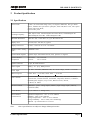
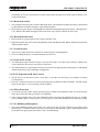
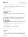
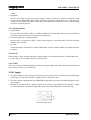
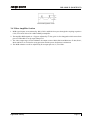
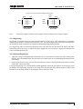
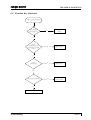
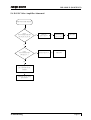
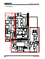
R
Service Manual
19-inch Color Monitor
B1997PNST (MD 1998LE)
Service Manual Versions and Revision
N o.
1.
Ve rs ion
R e le as e D ate
R e vis ion
1.0
N ov. 21, 2000
O riginal release
Copyright
Trademarks
Copyright 2000 LiteOn Technology Corp.
LiteOn is a registered trademark of LiteOn
Technology Corp.
All Rights Reserved
This manual may not, in whole or in part, be
copied, photocopied, reproduced, translated, or
converted to any electronic or machine readable
form without prior written permission of LiteOn
Technology Corp.
MD 1998LE (B1997PNST) Service Manual.
Printed in Taiwan.
All other trademarks are the property of their
respective owners.
MD 1998LE (B1997PNST)
Table of Contents
1. Precautions.........................................................................................................2
2. Product Specifications .......................................................................................5
3. Operation Theory................................................................................................9
4. Alignments and Adjustments ........................................................................... 14
5. Troubleshooting ............................................................................................... 18
6. Recommended Spare Parts List ....................................................................... 22
7. Block Diagram ................................................................................................ 24
8. Exploded Diagrams.................................................................................. Inserted
9. PCB Diagrams ......................................................................................... Inserted
10. Schematic Diagrams ................................................................................ Inserted
Page 1
MD 1998LE (B1997PNST)
1
Precautions
Please follow these safety and servicing precautions to prevent damage and to protect against potential
hazards such as electrical shock and X-rays.
1-1 Safety Precautions
1-1-1 Warnings
1. For safety purpose, do not attempt to modify
the circuit board, and always disconnect the AC
power before performing servicing on the
monitor.
2. Operation of the monitor outside its cabinet or
with the cover removed involves the risk of
shock hazard. Repair work on the monitor
should only be attempted by service personnel
who are thoroughly familiar with all necessary
safety precautions and procedures for working
on high voltage equipment.
3. Do not lift the CRT by the neck. After
completely discharging the high voltage anode,
handle the CRT only when wearing shatterproof
goggles. Try to keep the CRT away from the
body during handling.
4. High voltage should always be kept at the rated
value, no higher. Only when high voltage is
excessive are X-rays capable of penetrating the
shell of the CRT. Operation at high voltages
may also cause failure of the CRT or high
voltage circuitry.
5. The CRT is especially constructed to limit Xray emission to 0.5mR/HR at 300 microamperes
anode current. To ensure continued X-ray
protection, replace the CRT with only the same
or equivalent type as the original, and adjust the
anode’s voltage to the designated maximum
rating, never to exceed.
nonmetallic control knobs, insulating materials,
cabinet backs, adjustment and compartment
covers or shields, isolation resistor-capacitor
networks, mechanical insulators, etc.
3. AC Leakage Current Check
Always perform the AC Leakage Current
Check on the exposed metal parts, including
metal cabinets, screwheads and control shafts,
as follows:
a) Plug the AC line cord directly into a rated
AC outlet. Do not use an isolation
transformer during the check.
b) Use an AC voltmeter with at least 5000
ohms per volt sensitivity as follows:
Connect a 1500 ohms, 10 watt resistor
paralleled by a 0.15uF AC capacitor in series
with all exposed metal cabinet parts and a
known earth ground, such as electrical
conduct or electrical ground connected to
earth ground, as shown in the Figure 1-1.
Measure the AC voltage across the
combination of resistor and capacitor.
Figure 1-1. Set Up For AC Leakage Current Check
To ex pos ed m e ta l
ca bin et p art
To kn ow n
ea rth g ro un d
0.15 ufd
1500 ohm 10 w att
1-1-2 Safety Checks
Before returning the monitor to the user, perform
the following safety checks:
1. Inspect to make certain that each lead dress is
not pinched or that hardware is not lodged
between the chassis and other metal parts in
the monitor.
2. Inspect all protective devices such as
Page 2
c) Reverse the AC plug at the AC outlet and
repeat the steps for AC voltage
measurements for each exposed metal part.
d) Voltage reading must not exceed 0.3 volts
RMS, equivalent to 0.2 milliampere AC. Any
value exceeding this limit ill constitute a
potential shock hazard and must be
corrected immediately.
Precautions
MD 1998LE (B1997PNST)
1-1-3 Product Safety Notices
Many electrical and mechanical parts in this chassis have special safety-related characteristics which are
often not evident from visual inspection, the protection afforded by them may not be obtained by replacing
them with components rated for higher voltage, wattage, etc. Before replacing any of these components,
consult the Recommended Spare Parts List given at the end of this manual. Any of the replacements that do
not provide the same safety characteristics may result in shock, fire, X-ray emission or other hazards.
1-2 Servicing Precautions
Warning: An electrolytic capacitor installed with the wrong polarity might explode.
Caution: Before performing servicing covered by this service manual, read and follow the Safety Precautions
section of this manual.
Note:
If unforeseen conflict between the following servicing precautions and any of the safety
precautions, always follow the safety precautions
1. Follow closely the servicing precautions printed on the monitor cabinet and chassis.
2. Always unplug the AC power cord from the AC power source before removing or installing any component
or assembly, disconnecting PCB plugs or connectors and connecting a test component in parallel with a
capacitor.
3. When replacing parts or circuit boards, clamp the lead wires around the component before soldering.
4. When replacing a high wattage resistor (>0.5W metal oxide film resistor) in the circuit board, keep the
resistor about 1 cm (1/2 inch) away from the circuit board.
5. Keep wires away from the high voltage or high temperature components.
6. Keep wires in their original positions so as to minimize interference.
7. Always connect a test instrument’s ground lead to the instrument chassis ground before connecting the
positive lead; always remove the instrument’s ground lead last.
After putting the rear cover back and make sure the monitor is working properly, the Hi-Pot &
Ground Continuity tests MUST BE performed before the monitor is returned to user.
1-3 Hi-Pot Test
1. Test Equipment
Puncture test model PM5530 ADT or KIKUSU TOS-8750 voltage tester or equivalent approved equipment.
Note : The test equipment must be calibrated in regular period.
2. Test Setup
a) Apply voltage : DC 2100 VDC
b) Test duration : 3 seconds
c) Cutoff current should be set to 3 mA
3. Test Procedure
a) Unplug power cord from AC source.
b) Put the power switch of the monitor in the “ON” position.
c) Leave signal cable unconnected.
Precautions
Page 3
MD 1998LE (B1997PNST)
d) Plug monitor power cord to the Hi Pot tester terminals.
e) Turn on tester and watch the indicator or beeper.
f) If the indicator lamp lighten, or beeper beeps, the test fails.
1-4 Ground Continuity Test
1. Test Equipment
AC low ohm tester TOS-6100 or equivalent approved equipment.
Note : The test equipment must be calibrated in regular period.
2. Test Setup
a) Test duration : 3 seconds
b) Set current limit at 25 A
c) The grounding resistance must be less than 0.1 ohm.
3. Test Procedure
a) Plug the monitor power cord to the tester terminals.
b) Make sure all connections are well-contacted.
c) Turn on monitor power and tester power.
d) Press “Test” button.
e) If green light shows up, means test OK.
If red light shows up, means test fails.
f) If the Tester has a digital display, the resistance value must not exceed 0.1 ohm.
Note : Be sure not to touch the metal portion of the signal cable head during testing.
Page 4
Precautions
MD 1998LE (B1997PNST)
2
Product Specifications
2-1 Specifications
Picture Tube
19-inch (18-inch Visual image area), 95 degrees deflection, dot type black
matrix, medium short persistence phosphor, dark bulb,direct etch, Flat square
screen with Invar Mask,
0.26 mm dot pitch
Scanning Frequency
VGA, Super VGA, 1024x768@60/70/75/85/100 Hz, 1280x960@85 Hz
1280x1024@60/75/85 Hz, 1600x1200@60/75 Hz
Maximum Resolution
1600 dots (H) x 1200 lines (V) @75 Hz refresh rate
Display Area
360 mm (H) x 270 mm (V) typical
Display Characters
80 char. x 60 rows on a 10 x 10 matrix
Display Colors Analog
Input
Unlimited Colors
Synchronizatin Signals
Separate Sync: horizontal/vertical, TTL, positive or negative
Synchronization
Frequencies
Horizontal :
Vertical :
Signal Connectors
15-pin, D-shell connector
Video Signals
Analog : 0.7 Vp-p, RGB positive
Power Input
150 Watts maximum (PHILIPS CRT) AC rated voltage, 90VAC to 264VAC
Misconvergence
Center Area : < 0.2 mm; Corner Area : < 0.35 mm
User Controls
Power On/Off, Contrast, Brightness, Horizontal Size, Horizontal Position,
Vertical Size, Vertical Position, Pincushion, Trapezoid, Rotation, Unbalance,
Parallelogram, Degauss, Top Corner, Bottom Corner, Recall,
V. Moire, H. Moire
Service Controls
PWB1498 : power voltage adjust (VR801), high voltage adjust (VR102),
F1/F2/G2 (FBT)
Preset Modes
13 (see Table 2- 2. Timing Chart)
Environmental
Considerations
Operation temperature : 10o C to 35 oC ambient
Humidity : 20% to 80% ambient
Storage temperature : -40 oC to 65 oC ambient
Storage Humidity : 10% to 90% (non-condensing)
Altitude : up to3000m above sea level
Note:
30 to 98 kHz
50 to 120 Hz
Above specifications are subject to change without prior notice.
Product Specifications
Page 5
MD 1998LE (B1997PNST)
2-2 Signal Cable Pin Connections
Table 2-1. Signal Cable Pin Assignment
Note:
Page 6
Pin
Signal
Pin
Signal
1
Red vi de o
9
+5V ( fr om PC)
2
Gr een vi deo
10
Gr ound
3
Bl ue vi de o
11
Gr ound
4
Gr ound
12
SDA
5*
NC
13
H- Sync
6
Red gr ound
14
V- Sync
7
Gr een gr ound
15
SCL
8
Bl ue gr ound
This pin is used for selftest detection. Connect this pin to ground at the PC end.
Product Specifications
MD 1998LE (B1997PNST)
2-3 Timing Chart
This section describes the timings that the computer industry recognizes as standard for computer-generated
video signals.
Table 2-2. Timing Chart
Mode
1
2
3
4
5
6
7
8
9
10
11
12
13
H. Dot s
640
720
640
800
1152
800
1024
1024
1280
1280
1024
1600
1280
V. Dot s
480
400
480
600
864
600
768
768
1024
1024
768
1200
960
31.47
37.93
43.27
46.8
67.5
53.67
60.03
68.67
80
91.146
80
93.75
85.938
-
-
-
+
+
+
+
+
+
+
+
+
+
A pe riod us
31.78
26.366
23.11
21.33
14.815
18.631
16.66
14.561
12.504
10.971
12.376
10.667
11.636
B Blking us
6.356
6.085
5.33
5.172
4.148
4.409
3.657
3.725
3.022
2.844
3.624
2.765
3.017
C Sync us
3.81
2.028
1.556
1.616
1.185
1.138
1.219
1.016
1.067
1.016
1.231
0.948
1.077
D B.P. us
1.907
3.042
2.22
3.232
2.37
2.702
2.235
2.201
1.837
1.422
2.12
1.501
1.508
E Act ive us
25.42
20.282
17.78
16.16
10.667
14.222
13
10.836
9.481
8.127
8.752
7.901
8.62
F F. P. us
0.636
1.014
1.556
0.323
0.593
0.569
0.203
0.508
0.119
0.406
0.273
0.316
0.431
V- f re q ( Hz )
59.94
85.04
85
75
75
85
75.03
84.99
75
85
100
75
85
-
+
-
+
+
+
+
+
+
+
+
+
+
O Pe riod ms
16.68
11.759
11.76
13.33
13.333
11.756
13.33
11.765
13.329
11.761
9.988
13.333
11.764
P Blk ing ms
1.43
1.213
0.67
0.533
0.533
0.578
0.533
0.582
0.525
0.527
0.483
0.533
0.593
Q Sync ms
0.064
0.079
0.069
0.064
0.044
0.056
0.05
0.044
0.038
0.033
0.074
0.032
0.035
R B.P. us
1.02
1.107
0.578
0.448
0.474
0.503
0.466
0.524
0.475
0.483
0.397
0.491
0.547
S Ac t ive us
15.25
10.546
11.09
12.8
12.8
11.179
12.8
11.183
12.804
11.235
9.505
12.8
11.171
T F.P. us
0.35
0.026
0.023
0.021
0.015
0.019
0.017
0.015
0.013
0.011
0.013
0.011
0.012
H- f re q ( k Hz )
Sync
Polarit y
Sync
Polarit y
S ep era te S y n c
H o rizo n tal
B
Vid e o
D
K
Vertic al
E
J
F
L
Sync
Sync
C
I
A
H.Parameters:
H
Vid e o
G
V.Parameters:
A: Period
B: Blanking Time
G: Period
H: Blanking Time
C: Sync Width
D: Back Porch
I: Sync Width
J: Back Porch
E: Active Time
F: Front Porch
K: Active Time
L: Front Porch
Product Specifications
Page 7
MD 1998LE (B1997PNST)
2-4 Display Power Management Signal (DPMS)
Note:
These power-saving states exceed the Environmental Protection Agency (EPA) Energy Star
requirements and the Video Electronics Standard Association (VESA) for Display Power
Management Signal (DPMS) .
Table 2-3. Display Power Management Signal (DPMS)
State
LED Co lo r
H- S y nc
V- Sy nc
Po we r
Co ns umpt io n
ON
Gr e e n
P ul s e
P ul s e
No r ma l
S TANDBY
Ye l l o w
No P ul s e
P ul s e
<1 5 w a tts
S US P END
Ye l l o w
P ul s e
No P ul s e
<1 5 w a tts
OF F
Amb e r
No P ul s e
No P ul s e
<8 w a tts
2-5 TCO Version
The monitor meets the energy saving, electric and magnetic field requirements. Also it is compliant with
TCO 99 labelling scheme.
2-5-1 TCO 99 Version
TCO 99 will append the color temperature specification.
Page 8
Product Specifications
MD 1998LE (B1997PNST)
3
Operation Theory
This is an I2C-bus fully digital controlled multi-sync color monitor, compliant with VESA DDC1/2B and
DPMS standards. Besides, it also meets TCO95 and MPRII requirements. It provides user friendly OSM
(On-Screen display Menu) controls, and offers the following main features.
3-1 Main Features
1. Simplified chassis design with minimum components.
2. Fully digital controlled via 8-bit microcontroller NT6861AU.
3. Auto switching to off mode under “OUT OF RANGE” (Fh < 29KHz or Fh > 99KHz).
4. Reliable chassis design through various internal circuit protections.
5. Universal full range AC input and low power consumption.
6. Five-country OSM language available for easy user controls.
7. Adjustable OSM display time and position.
8. Twelve preset modes up to 1600 x 1200 75Hz (Fh =93.75KHz).
3-2 Microcontrol Section
1. The microcontroller provides I2C bus (pin 27 & 28) for geometric controls via I401 TDA4856 and video
controls via I501 M52743. The geometric controls include H-size, H-position, V-size, V-position, Pincushion,
Pin-balance, Trapezoid, Corner, Parallelogram, H-focus, V-focus, H-moire and V-moire. The video controls
cover Contrast, Brightness, R/G/B gain and cutoff control alignments. Through 8-bit PWM’s (pin 1, 2, 3,
32, 36, 40) it provides factory controls for G1, NS-trapezoid, H-linearity, ABL, user control for Rotation
and one F/V for H-frequency driver compensation . Two I/O’s (pin 27, 28) are provided for I2C bus used
for I502 MTV021N-21 on-screen display.
2. In addition, the microcontroller offers Auto Mode detection via Hsync (pin 41) and Vsync (pin 42) inputs.
According to Auto Mode detection, VESA DPMS power saving (pin 29, 30) will limit the output power
under 15W for Standby or Suspend mode, under 8W for OFF mode. VESA DPMS mode indication is
done via I/O pin 17 & 18 to drive LED display on the front cover. Normal mode displays green LED,
Standby or Suspend modes displays Yellow LED while OFF mode displays Amber LED.
3. Auto factory alignment (ATE) and VESA DDC2B communication are through DDC I2C bus (pin 27, 28),
I704 24LC211 is dedicated for DDC EDID E2PROM. In order to get optimal H-linearity performance for
the full range frequency (31KHz - 98KHz), 4-channel CS are used at pin 20, 21, 22, 23, 24. F1, F2, UP
and DOWN function keys’ scanning are through 2 ADCs on pin 14 & 15. Q701 and Q702 delay circuits
are used for power-on reset at pin 4. In order to avoid I2C interference during H-size, H-position, V-size,
V-position, Contrast and Brightness alignments, the HUNLK from I401 TDA4856 is applied from Q703
inverter to IRQ at pin 16.
4. There are 12 factory preset modes and 8 user modes available. Related information data of those modes
are stored at 2 EEPROM’s (I702, I703) 24LC04.
3-3 Deflection Section
1. I2C -- autosync deflection controller is TDA4856.
2. The TDA4856 is a high performance and efficient solution for autosync monitors. All functions are
Operation Theory
Page 9
MD 1998LE (B1997PNST)
controllable by I2C bus. SDA and SCL signals coming from microprocessor feed to pin 19 and pin 18 to
control all functions.
3-3-1 Horizontal Section
1. The oscillator is driven by the currents in R424 and R423. The minimum oscillator frequency is determined
by R424 and the maximum frequency is determined by R423.
2. Horizontal sync goes into pin 15 through R314. And horizontal flyback pulse goes into pin 1 through C455,
C437, R404, C458, R40E and bypass filter C401 from Vcp of Q424 collector for AFC loop.
3-3-2 Horizontal O/P Section
1. Horizontal driver (pin8) signal is sent to Q402 via R496, C451.
2. Signal from Q427 direct drive T403, through R493 (shunt with R4A4, R40F, R40G) and L405 to horizontal
output transistor Q424.
3-3-3 Vertical Section
1. Vertical sync signal from micro controller is connected to pin 14 through R313.
2. The free running frequency is determined by R319 and C312.
3-3-4 Vertical O/P section
1. The differential output currents from pin 13 of Vout1 and pin 12 of Vout2 can be directly coupled to the
vertical deflection booster pin 1 and pin 2 of TDA8351.
2. The TDA8351 has two output stages which are current driven in opposite phase and operate in combination
with the deflection coil in a full bridge configuration.
3-3-5 E-W/Trapezoid and H. Size Controls
1. The B+ driver for step down circuit is from pin 6, it provides 20~80% duty cycle outputs according
to H-frequency.
2. The E/W / Trapezoid and H-size controls are through B+ modulation at I401 TDA4856. The EW output
signal is from pin 11, it’s not tracking with H-frequency.
3-3-6 X-Ray Protection
1. To avoid X-ray hazard, a DC voltage generated at pin 3 of FBT and rectified by D108, C121 is divided by
R126, R129 and C402 filter go into pin 2 of TDA4856.
2. If this voltage is higher than 6.39 V, then TDA4856 will be activated to float HUNLOCK (pin 17), H. DRV
( pin 8), B DRV (pin 6), VOUT1 (pin 12), VOUT2 (pin 13). After that all deflection circuit stop working.
3-3-7 G1, Blanking and Brightness
1. The vertical blanking signal comes in two ways. One is from pin 8 of I301 (TDA8351), the other is from
HUNLK (pin 17 of I401). These two positive vertical pulses through Q42A, Q42C, Q42E amplified and
converted into negative pulse and sent to G1 for vertical blanking.
Page 10
Operation Theory
MD 1998LE (B1997PNST)
2. In protection mode or out-of-range situation, HUNLock will send 5 V pulse to saturate Q706, then pin 8
of I902 will be low state and open Q509, so G1 will go down to -140V. During the mode change, Mute
acts as same as HUNLock’s.
3. The brightness is controlled by CPU, pin 27 and pin 28 comes into pin 20 and pin 21 of I501, DC level can
be changed by I2C bus from 0~5V of D/A output at pin 23 of I501, high voltage causes high current to get
brighter raster, low voltage gets lower brightness.
3-4 Power Supply Section
3-4-1
AC Rectifier
The circuit can accept 90 V to 264 V AC input through D801 bridge diode and C810 filtering to get DC 126
V~364 V for power conversion in T805.
3-4-2
Line Filter
It consists of L801, L802, P801A, C803, C804, C805, C806, C807, C871, C80A, C80C, C80E, T801 and
T802 and meets EMI regulation.
3-4-3
PFC
It consists of T804, Q814, D807, I804 and other auxiliary components. It is similiar to Booster circuit. The
working voltage is provided by D815, C821, R825, C819 and ZD810, but it is not working in Stand-by,
Suspend and Off modes. The output voltage C810 is 180 V~380V DC and generated through input
voltage C816 step up. The maximum voltage is decided by R826 and R827, while the minimum voltage is
decided by C817. In the meanwhile, it will get a similiar to input voltage waveform of input current to
acquire a good PF value.
3-4-4
Power LED Status
1. The LED has 3 leads common cathode with green and amber color for different power saving states. It
is controlled by CPU.
2. Normal : Green light
Amber LED is off because CPU pin 17 is high and pin 18 is low, only green LED is turned on.
3. Standby / Suspend : Yellow light
CPU pin 17 and pin 18 are low, then green and amber LED are turned on. That is yellow.
4. Off Mode : Amber light
CPU pin 18 is high and pin 17 is low, then green is off and amber is on.
3-4-5 Auto Degaussing
When SMPS works, the 6.6 V power source is applied to Q801 and CPU let Q801 turn on a few seconds,
then drive the armature of RL801 to perform the degaussing function.
3-4-6 PWM Control
1. Start Up
The I802 gets power from C874, C841, R834, ZD807, D802, C859, R806 and pin 7 voltage reaches 9 V
for starting up. The I802 starts oscillation at 20 kHz, sawtooth on pin 4 and pin 6 output to drive Q802/
T805. Once Q802 switches on, D812, C840 set up an 17 V to keep I802 working through D828 auxiliary
Operation Theory
Page 11
MD 1998LE (B1997PNST)
voltage.
2. Regulation
The DC O/P voltage is proportional to the auxiliary voltage, so I802 pin 2 senses the feedback voltage
from the divider R895, R888, R868, R897 and VR801 to compare with the built-in 2.5 volts reference
voltage for error amplifier operation. Finally pin 6 can modulate the different duty cycle by VR801 setting
to achieve regulation purpose.
3-4-7 Synchronization
1. Normal Mode
The sync pulse from FBT (31 kHz~93.75 kHz) via R820, C833, D806, R818 and C832 to pin 4 of I802 to
keep I802 synchronized with horizontal sync input frequency.
2. Power Saving Modes: Standby/Suspend
Because there is no pulse from FBT, so the free-run frequency is decided by R817 and C832 and the
SMPS works at 20 kHz.
3. Override
The horizontal free run frequency is about 62 kHz under override condition, SMPS is synchronized to this
frequency.
3-4-8 O.V.P.
If the auxiliary voltage is higher than zener voltage ZD806 (22 volts) and makes pin 3 of I802 higher than
1 V, pin 6 duty cycle is limited to have the OVP activated.
3-4-9 O.P.P.
The excess current of T805 through R819 can develop enough voltage on pin 3 then limit the power delivered
because the pin 6 duty cycle is limited too.
3-5 HV Supply
1. HV (High Voltage) start up is triggered by H-pls at pin 4 via R107. I103 3843 provides the PWM output
control (pin 6) to drive the step up B+ supplier Q103 via D105 and C108.
2. The time constant is dependent on the H-DRIVER through R140 via inverter I101 and buffer Q106 /Q107
to drive Q104.
3. I401 pin 32 provides the H+V composite signals to drive the two-stage dynamic focus amplifier. Output
of vertical amplitude is around 150 Vpp, while output of horizontal amplitude is around 670 Vpp.
Vertical dynamic focus
Page 12
Operation Theory
MD 1998LE (B1997PNST)
Horizontal dynamic focus
3-6 Video Amplifier Section
1. RGB signal inputs are terminated by R501, R531 and R561 then pass through the coupling capacitors
C502, C532 and C562 to I501 M52743BSP preamplifier.
2. The amplifier RGB signals (0~3 Vpp) are adjusted by I2C bus, pin 19 is for clamp pulse which comes from
pin 16 of TDA4856 to set up equal clamp level.
3. The video output stages is I901 LM2402, the output resistors R904, R934 and R964 are 47 ohm, R913,
R943 and R973 are 56 ohm for arcing protection and the power dissipation is minimized.
4. The RGB cathodes cut off are adjusted by D/A output pins 24, 25, 26 of I501.
Operation Theory
Page 13
MD 1998LE (B1997PNST)
4
Alignments and Adjustments
This section of the service manual explains how to make permanent adjustments to the monitor settings.
4-1 General Adjustments
4-1-1 Adjustment Conditions
a) Power Supply
Apply AC 115 V or 220 V
b) Warm-up Time
The monitor must be powered on for 15 minutes before starting any alignment, but requires 30 minutes of
warm-up time for convergence adjustment.
c) Signal Input
1. Video: RGB Analog, 0.7 Vp-p, positive
2. Synchronization:
Horizontal and vertical TTL signal, separate, positive or negative
3. All adjustments should be made using a signal of FH = 93.75 kHz, FV = 75 Hz, unless otherwise
defined.
4-1-2 Equipment Required
The following equipments are necessary for adjustment procedures:
1. Volt-ohm-A meter (Sanwa FD-750C or equivalent)
2. 30 kV high voltage probe (HP34111A)
3. Oscilloscope (TEK2235 or equivalent)
4. Minolta Color Analyzer II
5. Signal generator (IBM PC with proper display cards or Chroma 2250 or equivalent)
6. Screwdriver
4-1-3 Switching Power Supply and Regulator Adjustment
a. The regulated B+ control has been preset in the factory and needs no adjustment. However, if any repair
is made on the power supply section, the following readjustment procedures are recommended:
1. Allow the monitor to warm-up for about 15 minutes.
2. Apply (1600 x 1200 @ 93.75Khz / 75 Hz) / crosshatch pattern to the monitor.
3. Connect a DC voltage meter to D820, Heat Sink and adjust VR801 for 17.5 ± 0.1 V.
4. If a fuse is broken during adjustment, remember to replace it with the exact same type of fuse.
b. If necessary, follow the following procedure to enter the factory preset mode:
1. At power off mode, turn S701 SW to alignment position close to CRT side.
2. Press both
key and
key simultaneously then power on to enter the factory preset mode.
3. Turn on the power again to return back to normal mode (user mode).
4. After finishing the manual alignment, S701 SW has to be returned back to its normal stage (close to
FBT side). Otherwise the DDC can not be read.
Page 14
Alignments and Adjustments
MD 1998LE (B1997PNST)
4-2 Alignment Procedures
4-2-1 High Voltage Adjustment
CONDITION
Display image : Crosshatch pattern
PROCEDURE
Connect DC meter to TP001 and adjust VR102 to obtain a DC voltage of -152 ± 1V DC .
4-2-2 Screen and White Balance Adjustment
CONDITION
Switch S701 to factory mode, then press “ ” and ” ” buttons simultaneously when switching the
power “On”.
Warm up 30 minutes
Mode : 93 KHz / 1600 x 1200
Display image : No video
PROCEDURE
1-a
Set Brightness to maximum, G1 at “70” OSD-step, and G2=625 V, Contrast to maximum.
Select “preset color” then choose “9300°K”
1-b
Adjust Green cut-off around “70” OSD-step.
1-c
Adjust G1 and R/B cut-off to get 0.8+0.15 / -0.1 FL of raster light output.
1-d
Confirm x=283±5, y=297±5.
CONDITION
Display image : 50 mm x 50 mm white block pattern
PROCEDURE
2-a
Set Brightness to mid-level.
2-b
Adjust Contrast to maximum.
2-c
R/B signal off and adjust green gain to get Y=25 ± 0.2 FL.
2-d
R/B signal on, adjust R/B gain to get x=283±5, y=297±5.
CONDITION
Display image : Full white pattern
PROCEDURE
3-a
Set Brightness and Contrast to maximum.
3-b
Adjust “ABL” to 32±1 FL.
4-a
Repeat all the procedure in 4-2-2 section until the best white balance is obtained, then power off.
4-b
After screen and white balance adjustments, S701 must be switched to Normal mode.
Alignments and Adjustments
Page 15
MD 1998LE (B1997PNST)
4-2-3 Focus Adjustment
CONDITION
Display image : “e” character pattern
PROCEDURE
1. Set Brightness and Contrast used for a normal display.
2. Adjust the static focus control on the high voltage resistor block to obtain the best focus over the entire
display area.
4-2-4 Static Convergence Adjustments
Static convergence involves alignment of the red, blue and green lines in the center area of the display.
Note :
The monitor requires 30 minutes of warm-up time for convergence adjustment.
CONDITION
Display image : Crosshatch pattern
Warm-up Time : 30 minutes
PROCEDURE
1. Set Brightness and Contrast to display a well-defined pattern.
2. Ensure the convergence magnet rings are correctly positioned on the CRT.
Figure 4-1. Convergence Magnets on the CRT
1
11
+
P
CRT
FRONT
10
9 87654
3
2
1) Setup Bolt
2) Bow Magnet
3) Band
4) 2-Pole Magnet
5) Spacer
9) Holder
6) 4-Pole Magnet
10) Band
7) Spacer
11) Tabs
8) 6-Pole Magnet
3. Rotate the individual rings of 4-pole convergence magnets by changing the spacing between the 2 tabs to
converge the vertical red and blue lines at the center of the screen.
4. Rotate the pair of rings of 4-pole convergence magnets by maintaining spacing between the 2 tabs to
converge the horizontal red and blue lines at the center of the screen.
5. Rotate the individual rings of 6-pole convergence magnets by changing the spacing between the 2 tabs to
converge the vertical red, blue and green lines.
6. Rotate the pair of rings of 6-pole convergence magnets by maintaining spacing between the 2 tabs to
converge the horizontal red, blue and green lines.
7. Repeat the steps from 3~6 until the best convergence is obtained.
Page 16
Alignments and Adjustments
MD 1998LE (B1997PNST)
Figure 4-2. 4-pole and 6-pole Magnets Movement
Blue
Blue
Red/
Blue
Red
Green
4-pole m agnets
m ovem ent
Note :
Red/
Blue
Red
G reen
6-pole m agnets
m ovem ent
The 4-pole magnets and the 6-pole magnets interact, making dot movement complex.
4-2-5 Degaussing
Degaussing is required when poor color impurity appears on the screen. This monitor uses an automatic
degaussing circuit that is activated when the power is on. The manual degaussing will be fully functional after
the monitor has been in operation for 20 minutes through OSM degaussing function.
The degaussing effect is confined to the picture tube since the coils are mounted at the back of the tube.
Should any part of the chassis or cabinet becomes magnetized, it is necessary to degauss the affected area
with a external degaussing coil.
4-2-6 External Degaussing
1. Apply line voltage to the degaussing coil and move it in a rotary motion over the front, sides, and top of the
monitor. The coil should be kept away from the rear of the monitor to avoid damaging the magnetic neck
components.
2. Slowly rotate and move the coil away from the monitor to about 6 feet beyond the point where no effect
on the CRT will be noticeable.
For proper degaussing, it is essential that the field be gradually reduced by moving the coil slowly away from
the monitor. The degaussing coil must never be shut off or disconnected while near the monitor, as this would
introduce a strong field instead of canceling the effect of the stray fields.
Alignments and Adjustments
Page 17
MD 1998LE (B1997PNST)
5
Troubleshooting
5-1 No Raster
No Raster
Measure
H voltage of B+
at T402 on
PWB-MAIN
Check
I401, Q424,
Q416, D409
No
0V
Yes
Short Circuit
at load?
T101 pin 2 HV
B+
High
(50 V or more)
Yes
Video
Check
I401, ZD401,
Q416, Q424
Yes
No
Check AC I/P on
T805
Yes
Check
D801
Page 18
HIGH
48 V
Normal
(40 V, 31.5 kHz)
0V
I103, I102
Check voltage
of cathode,
heater, Grid
1, Grid 2, etc.
Q103, Q104,
R8A3, I103
Check DC B+
line, F801
Check
I802, R894, R867, Q802,
D820, D819, D822, D826,
D824, D827,D831,
ZD802, ZD803
Troubleshooting
MD 1998LE (B1997PNST)
5-2
Function Key Abnormal
Function Key Abnormal
Check 5V from
I810 regulator?
No
Repair power
supply
Yes
Power
ON/OFF again and
check X701, oscillator
OK?
No
Replace X701
No
Replace I701
No
Replace
Q701 or Q702
Yes
Check
I701 uC OK?
Yes
Check LED LD701 OK?
Yes
END
Troubleshooting
Page 19
MD 1998LE (B1997PNST)
5-3 Vertical Scan (Raster is one horizontal line)
Vertical Scan Abnormal
Check voltage of
pin 3 at I301
(about 17.3 V)
No
Replace I301.
Abnormal
Check pin 12 & pin
13 waveform at
I401
Yes
Check
pin 4 or pin 7 waveform
at I301
OK
Normal
Replace I301
Check R307 short ?
Yes
Still no vertical scan
Check or replace CRT
Page 20
Replace R307
Troubleshooting
MD 1998LE (B1997PNST)
5-4 R.G.B. Video Amplifier Abnormal
RGB Video AMP Abnormal
Check
the waveform at the I501
pin 29, pin 32, pin 35
No
Check B+
(pin17, pin36)
No
Check B+ pin 10, 6
Yes
Check the
waveform at pin
2, 6, 11, 19, 27
Yes
Check I501
Yes
Check
the waveform at the
I901 pin 3, 5, 1
Yes
Check I901
Yes
Video signal present at the
pin of the CRT R.G.B.
Cathode
Yes
Defective cut-off circuit
(DC restore)
Troubleshooting
Page 21
MD 1998LE (B1997PNST)
6
Recommended Parts List
Note:1.
The components identified by “
exactly the same parts specified.
2.
“ mark are critical for X-ray safety. Replace these with
There is only OTP IC at the model beginning (FPR stage or before). When it put in mass
production and there must be Mask coming out. If you have spart parts need, please use BOM
to get the last release part number and related information.
No.
Location
Part Number
Description
1
C810
6312647122
ALU uF 470 400V F 105C 30x45
2
D801
6417001100
DIODE BRIDGE FBI4K7M1 4A/800V
3
D819 D824
D831 D827
6412010807
DIODE BYM26C 2.3A/600V
4
D820 D826
6412000520
DIODE RL4A 3A/600V
5
D822
6412022207
DIODE SF20-02G 2A/200V
6
F801
6851504051
FUSE TIME LAG H-BRK 19181-4A
7
I301
6442011210
IC TDA8351/N6 9P SIL PHILIPS
8
I401
6442025200
IC TDA4856 32P SDIP (PHILIPS)
9
I501
6442024210
IC M52743BSP 36P SDIP MITSUBISHI
10
I701
6448014500
IC NT68P61AU 42P PDIP OTP NOVAT
11
I703
6448007930
IC KS24C04 (SAMSUNG)
12
I802
6442006720
IC KA3843B 8P PDIP
13
I901
6442025000
IC LM2402 11P TO-220 NS
14
L405
6111169130
COIL CHOKE 1.65 uH DR6X8
15
L404
6881001505
BEAD CORE W5 RH3.5x6x1.0T
16
Q104
6426006300
FET N-CHNL SSH7N90A FAIRCHILD
17
Q416
6427000900
FET P-CHNL SFS9634 FAIRCHILD
18
Q402
6421000325
TR NPN 2SC1815-Y(TPE2) TOSHIBA
19
Q103
6426006300
TR N-CHNL IRFS634A FAIRCHILD
20
Q424
6421005200
TR NPN 2SC5515 (PANASONIC)
Page 22
Recommended Spare Parts List
MD 1998LE (B1997PNST)
No.
Location
Part Number
Description
21
Q802
6426002201
FET N-CHNL SSH 10N 80A
22
I501
6442024210
IC 52743BSP 36P MITSUBISHI
23
R415
6212147254
CF KOHM 4.7 1/4W J T26 MINI
24
ZD401
6414150004
HZ15-2 ZNR 15V/0.5W
25
R803
6203459017
POSISTOR 4.5 DGC3D4R5Q27C 3PIN
26
R802
6201100052
THERMISTOR 10 OHM 8A P=7.5 TKS
27
R822
6221222852
MOF OHM 0.22 2W J HOR
28
T402
6119003205
COIL LINEAR DYNAMIC TLN-1032E
29
T40A
6139000300
XFRMER H-CENT 5mH THC-1003
30
T801 T802
6138003100
LINE FILTER
31
T805
6131051820
XFRMER PWR TPW1069 ER42/15 LSE
32
X701
6449000700
CRYSTAL HC49/U 8MHZ 50PPM 7pF
33
I804
6442030500
IC MC33260 8P MOTOROLA
34
D807
6412000520
DIODE RL4A/600V 50ns SANKEN
35
Q814
6426005410
FET N-CHNL IRFS840A 4.6A/500V
36
R823
6231039852
WW 0.39ohm 5WJ HOR
Recommended Spare Parts List
Page 23
Page 24
P502B
I704
DDC
LINE
FILTER
E2P R O M
DDC-SDA
DDC-SCL
V
H
LD701
LED
INDICATION
S702
KEY
SCAN
PFC
CKT
DEG CKT
I702
I703
E PROM
2
I701
NT6861AU
BRIDGE
DIODE
H
V
I301
TDA8351
VERT.
BOOST
T805
POWER
TRANS
VFLB
V-
V+
H-
D.Y
6.7V
6.1V
5V
82V
17.6V
35.5V
200V
H+
H
OUTPUT
Q424
H-LIN &
CS CRT
DEFLECTION
Q416
STEP
DOWN
POWER SUPPLY
HOUT
BDRV
I502 OSD
H
DRIVER
FB
B-OSD
G-OSD
R-OSD
HFLB
SDA
SCL
I501
M52743BSP
VIDEO PREAMP
I401
TDA 4856
DEFLECTION
CONTROLLER
SCL
SDA
I802
PWM
CONTROL
SCL
SDA
B
G
VDEF
HOT
H-PLS
VBLK
BRIGHTNESS
CONTROL
DC RESTORE
DYNAMIC
FOCUS
AMPLIFIER
I103
PWM
CONTROL
880Vp-p
Q104
H-PLS
DRIVER
Q103
UP
BLANKING / MUTING
SOPT KILLER
B
G
I103
REGULATOR
I901
LM2402 CRT
AMPLIFIER
R
F2
G2
F1
T101
FLYBACK
TRANS
FOCUS
-136V
RASTER
CENTER
ABL
HV S
VIDEO
BOARD
H
V
19"
CRT
7
MICRO CONTROLLER
MAIN BOARD
P501
R
MD 1998LE (B1997PNST)
Block Diagram
Block Diagram
G1
R
LITE-ON TECHNOLOGY CORP.
5 F, No. 16, Sec. 4, Nanking E. Road, Taipei, Taiwan
Tel: 886-2-25706999
Fax: 886-2-25706888
URL:// www.liteontc.com.tw
Printed in Taiwan