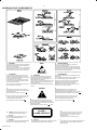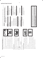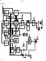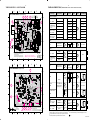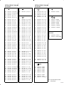
1
CD Stereo Radio Recorder
AZ2785
all versions
TABLE OF CONTENTS
chapter
Handling chip components and safety ............................. 1 - 1
Technical Specification & Service Tools .......................... 2 - 1
Service Measurement .................................................. 2 - 2
Connections & Controls ................................................ 3 - 1
Instructions for use ................................................. 3 - 2 to 3 - 6
Disassembly Diagram ................................................... 4 - 1
CD Service Test Program ........................................ 4 - 2 to 4 - 3
chapter
RECORDER BOARD
circuit diagram ....................................................... 10 - 1
layout diagram ....................................................... 10 - 2
Block Diagram ............................................................. 5 - 1
Wiring Diagram ........................................................... 6 - 1
EXPLODED VIEW DIAGRAM
cabinet ................................................................. 12 - 1
tape deck ............................................................ 12 - 2
FRONT BOARD
circuit diagram ....................................................... 7 - 1
layout diagram ....................................................... 7 - 2
Mechanical partslist ..................................................... 12 - 2
Electrical partslist ............................................... 13 - 1 to 13 - 7
CD MODULE
circuit diagram ................................................ 11 - 2 to 11 - 3
layout diagram .................................................. 11 - 1, 11 - 4
TUNER BOARD
circuit diagram ....................................................... 8 - 1
layout diagram ....................................................... 8 - 2
MAIN BOARD
circuit diagram ....................................................... 9 - 1
layout diagram ....................................................... 9 - 2
Safety regulations require that the set be restored to its original
condition and that parts which are identical with those specified
be used.
CLASS 1
LASER PRODUCT
C
Copyright 1995 Philips Consumer Electroncis B.V. Eindhoven, The Netherlands
All rights reserved. No part of this publication may be reproduced, stored in a retrieval
system or transmitted, in any form or by any means, electronic, mechanical, photocopying,
or otherwise without the prior permission of Philips.
Published by SS 0115 Service Audio
PCS 107 296
Printed in The Netherlands
Copyright reserved
Subject to modification
GB
3140 785 22640
1-1
HANDLING CHIP COMPONENTS
©
WARNING
ESD
All ICs and many other semiconductors are susceptible to
electrostatic discharges (ESD). Careless handling during
repair can reduce life drastically.
When repairing, make sure that you are connected with the
same potential as the mass of the set via a wristband with
resistance. Keep components and tools at this potential.
f
ATTENTION
Tous les IC et beaucoup d´autres semi-conducteurs sont
sensibles aux décharges statiques (ESD). Leur longévite
pourrait être considérablement écourtée par le fait qu´aucune
précaution nést prise à leur manipulation.
Lors de réparations, s´assurer de bien être relié au même
potentiel que la masse de l´appareil et enfileer le bracelet
serti d´une résistance de sécurité.
Veiller à ce que les composants ainsi que les outils que l´on
utilise soient également à ce potentiel.
d
WARNUNG
Alle ICs und viele andere Halbleiter sind empfindlich
gegenüber elektrostatischen Entladungen (ESD).
Unsorgfältige Behandlung im Reparaturfall kann die
Lebensdauer drastisch reduzieren.
Sorgen Sie dafür, daß Sie im Reparaturfall über ein Pulsarmband mit Widerstand mit dem Massepotential des
Gerätes verbunden sind.
Halten Sie Bauteile und Hilfsmittel ebenfalls auf diesem
Potential.
©
SAFETY
Safety regulations require that the set be restored to its
original condition and that parts which are identical with
those specified be used.
Safety components are marked by the symbol
ñ
WAARSCHUWING
Alle IC´s en vele andere halfgeleiders zijn gevoelig voor
electrostatische ontladingen (ESD).
Onzorgvuldig behandelen tijdens reparatie kan de levensduur
drastisch doen vermindern. Zorg ervoor dat u tijdens reparatie
via een polsband met weerstand verbonden bent met hetzelfde
potentiaal als de massa van het apparaat.
Houd componenten en hulpmiddelen ook op ditzelfde potentiaal.
i
AVVERTIMENTO
Tutti IC e parecchi semi-conduttori sono sensibili alle scariche
statiche (ESD).
La loro longevità potrebbe essere fortemente ridatta in caso di
non osservazione della più grande cauzione alla loro
manipolazione. Durante le riparationi occorre quindi essere
collegato allo stesso potenziale che quello della massa
delápparecchio tramite un braccialetto a resistenza.
Assicurarsi che i componenti e anche gli utensili con quali si
lavora siano anche a questo potenziale.
ñ
Veiligheidsbepalingen vereisen, dat het apparaat in zijn
oorspronkeliijke toestand wordt teruggebracht en dat
onderdelen, identiek aan de gespecificeerde, worden toegepast.
De Veiligheidsonderdelen zijn aangeduid met het symbool
f
i
Les normes de sécurité exigent que l`appareil soit remis
à l`état d`origine et que soient utilisées les pièces de
rechange identiques à celles spécifiées.
Les composants de sécurité sont marqués
Le norme di sicurezza estigono che l´apparecchio venga
rimesso nelle condizioni originali e che siano utilizzati i
pezzi di ricambiago identici a quelli specificati.
Componenty di sicurezza sono marcati con
©
DANGER: Invisible laser radiation when open.
AVOID DIRECT EXPOSURE TO BEAM.
d
Bei jeder Reparatur sind die geltenden Sicherheitsvorschriften zu beachten. Der Originalzustand des Gerätes
darf nicht verändert werden. Für Reparaturen sind Originalersatzteile zu verwenden.
Sicherheitsbauteile sind durch das Symbol
markiert.
CLASS 1
LASER PRODUCT
s Varning !
Osynlig laserstrålning när apparaten är öppnad och
spärren är urkopplad. Betrakta ej strålen.
©
After servicing and before returning the set to customer
perform a leakage current measurement test from all
exposed metal parts to earth ground, to assure no
shock hazard exists.
The leakage current must not exceed 0.5mA.
∂ Advarsel !
ß Varoitus !
f
Usynlig laserstråling ved åbning når sikkerhedsafbrydere
er ude af funktion. Undgå udsaettelse for stråling.
Avatussa laitteessa ja suojalukituksen ohitettaessa olet alttiina
näkymättömälle laserisäteilylle. Älä katso säteeseen !
"Pour votre sécurite, ces documents doivent être utilisés par
des spécialistes agréés, seuls habilités à réparer votre
appareil en panne".
PCS 104 437
2-1
TECHNICAL SPECIFICATIONS
GENERAL
Mains voltage
Mains frequency
Battery
Power consumption
Dimension (W x H x D)
Weight
TUNER - AM SECTION
-/01/16
-/17
-/01/16
-/17
mains
remote
:
:
:
:
:
:
:
:
:
120/230 V
120 V
50 / 60 Hz
60 Hz
9 V (R20 x 6)
3V (R03 x 2)
35 W
655 x 260 x 210mm
7 Kg
Tuning range
IF frequency
Sensitivity
Selectivity
IF rejection ratio
Image rejection ratio
MW : 516 - 1620 kHz
-/17 : 520 - 1730 kHz
: 468 kHz ± 3 kHz
MW : £ 4000µV/m 26dB S/N
MW : ≥ 16 dB
MW : ≥ 24 dB
MW : ≥ 28 dB
AUDIO CASSETTE RECORDER
AMPLIFIER
Output power
Speaker impedance
Frequency response
mains : 2 x 2 W
battery : 2 x 2 W
: 2 x 4 ohm
: 100 Hz - 8 kHz (±3dB)
Tape speed
Wow & flutter
Fast wind/rewind C60
Frequency response
S/N ratio
Erase ration
Bias frequency
:
:
:
P/B :
:
:
:
4.76 cm/sec ± 3%
< 0.5 WTD DIN
< 120 sec.
125 - 6300 Hz
> 40 dB
> 50 dB (w/BPF)
73 ± 1.5 kHz
TUNER - FM SECTION
COMPACT DISC
Tuning range
IF frequency
Sensitivity
Selectivity
IF rejection
Image rejection
:
:
:
:
:
:
87 - 108.5 MHz
10.7 MHz
£ 22 dB at 26dB S/N
≥ 20 dB at ±300kHz
≥ 54 dB
≥ 20 dB
Frequency response
S/N ratio
Channel difference
Channel crosstalk
Laser wavelength
Laser light power
:
:
1 kHz :
1 kHz :
:
:
63 Hz - 16 kHz
> 60 dB
< 2 dB
> 50 dB
780 ± 20nm
< 0.3 mW
SERVICE TOOLS
Audio signal disc SBC 429.......................................................................4822 397 30184
Playability test disc SBC 444...................................................................4822 397 30245
Test disc 5 (disc without errors ) +
Test disc 5A (disc with dropout errors, black spots and fingerprints)
SBC 426/426A.....................................................................4822 397 30096
Burn in test disc (65 min. 1kHz signal at -30 dB level without “pause”) .....4822 397 30155
Universal test cassette Fe SBC 420 ........................................................4822 397 30071
PCS 107 297
SS LEN
SS
LENSS
ACCO
AC
COUS
USTIC
TIC BA
BA
8
ACK
RECORD
REC
ORD
DECK A
RECORD
PLAYB
DBB
POWER
CD
STOP
PLAYY
PLA
+
R
–
AC
MAINS
STOP/EJE
STO
P/EJECT
CT PAU
PAUSE
SE
–
+
L
SPEAKERS 4
9
SEARCH
SEA
RCH
TUNER
PROG
FM
0
PLAY
PLAY
SEARCH
SEAR
CH
!
PAUSEE
PAUS
&
^
%
DECK B
PLAYBACK
TUNER
PRESET
7
STOP/EJEC
STOP
/EJECTT
AM
BAND
ELECTRONIC
SOURCE
SELECT
L TUNE
R
PLAY/PAUSE
TAPE
CASSETTE RECORD
ER
SEARCH
DIGITA
BASS REF
LEX SPE
AKER SYS
TEM
REPEAT
SHUFFLE
AZ2765 CD RADIO
#
1 23 54 6
@
2
4
6
9
$
l
SEAR
CH
REPE
AT
TUNIN
G
VOLU
ME
eC
ontro
STOP
tal R
emot
Digi
SEAR
CH
SHUF
FLE
PRES
ET
ACCO
COUST
USTIC
IC BA
SS LEN
S
1
3
5
7
8
Deck 2:
PLAY 2 - to start playback
SEARCH 5 or 6 - to fast rewind/ wind the
tape
STOP•EJECT 9/ - to stop the tape and to
open the cassette
holder
PAUSE ; - to pause recording or playback
0 CD PLAYER:
SHUFFLE - to play tracks CD/ program in
random order
REPEAT - to repeat a track/ CD/ program
STOP 9 - to stop playback
- to erase a program
SEARCH ¡ , ™ / 5 , 6
CD: - to skip or search a passage/ track
backwards or forward
Tuner: - to tune to a station (down,up)
PLAY/PAUSE 2; - to start or pause CD play
1 POWER - ON/OFF switch
2 DBB (Dynamic Bass Boost) - to enhance
bass response
3 VOLUME - to adjust volume level
4 CD, TUNER, TAPE - to select the source of
sound
5 REMOTE SENSOR - for the remote control
(for AZ 2765 model only)
6 CD Display - to show the CD functions
7 OPEN - to open/ close the CD door
8 p 3.5 mm jack for stereo headphone
connection
Note: Connecting headphones will mute the
speakers
9 CASSETTE RECORDER:
Deck 1:
RECORD 0 - to start recording
PLAY 2 - to start playback
SEARCH 5 or 6 - to fast rewind/wind the
tape
STOP•EJECT 9/ - to stop the tape and to
open the cassette door
PAUSE ; - to interrupt recording or playback
TOP AND FRONT PANELS
1 VOLUME 3,4 - adjusts volume level
2 PRESET 3,4 - (up, down) selects a preset
radio station
3 TUNING ∞, § - (down, up) tunes to radio
stations
4 SHUFFLE - to play CD tracks in random order
5 REPEAT - repeats a track/ CD program/ entire
CD
6 2; - starts CD playback/ interrupts CD
playback
7 ¡, ™ - skips to the beginning of a current
track/ previous/ subsequent track
8 STOP 9 - stops CD playback or erases a CD
program
9 SEARCH 5, 6 - searches backwards or
forwards within a track/CD
REMOTE CONTROL (for AZ 2765 model only)
# Telescopic antenna - to improve FM
reception
$ Speaker levers - to unlock the loudspeaker
boxes
% Speaker - loudspeaker terminals
^ AC MAINS - inlet for power cord
& Battery door - to open the battery
compartment
& Voltage selector (located inside the battery
compartment. Some versions only) - selects
the correct local voltage 110/220 V before
plugging in the set
BACK PANEL
TUNER:
! BAND - to select FM/MW (AM) waveband
@ PRESET 4 , 3 - to select a preset station
(down, up)
PROG - to program and review programmed
track numbers
CD: - to program and review programmed
track numbers
Tuner: - to program tuner preset stations
CONNECTIONS AND CONTROLS
3-1
PCS 107 298
PCS 107 299
Switching POWER on/off: Save energy
Whether you are using mains or battery supply, to avoid
unnecessary energy consumption always push the POWER
button to the off position after using the set.
The type plate is located on the bottom of the set.
Using AC POWER
1. Check if the power voltage as shown on the type plate on
the base of the set, corresponds to your local power supply.
If it does not, consult your dealer or service center.
2. Connect the power cord to the MAINS inlet and the wall
outlet. The power supply is now connected and ready for use.
3. To switch off completely, withdraw the power cord from the
wall outlet.
– Disconnect the power cord from the wall outlet to protect
your set during heavy thunderstorms.
Batteries contain chemical substances, so they should
be disposed of properly.
2. Replace the compartment door, making sure the batteries are
firmly and correctly in place. The set is now ready to operate.
Incorrect use of batteries can cause electrolyte leakage and will
corrode the compartment or cause the batteries to burst.
Therefore:
• Do not mix battery types: e.g. alkaline with carbon zinc.
Only use batteries of the same type for the set.
• When inserting new batteries, do not try to mix old batteries
with the new ones.
• Remove the batteries if the set is not to be used for a long
time.
Remote control
Open the battery compartment and insert two batteries,
type AAA, R03 or UM4 (preferably alkaline).
1. Open the battery compartment and insert six batteries, type
R-20, UM-1 or D-cells, (preferably alkaline) with the correct
polarity as indicated by the "+" and "-" symbols inside the
compartment.
BATTERIES (OPTIONAL)
Whenever convenient, use the power supply if you want to
conserve battery life. Make sure you remove the plug from the
set and wall outlet before inserting batteries.
AC
MAINS
6 x R20 • UM-1 • D-CELLS
+
R
–
+
L
SPEAKERS 4
–
MAINS
REMOVABLE LOUDSPEAKERS
1. Press POWER to on position.
– A source indicator lights up.
2. Select and press your source button CD, TUNER or TAPE.
– The selected source indicator lights up.
3. Operate sound source according to the instructions of the
respective chapter about the function.
4. Adjust the sound using the VOLUME and DBB controls.
– For AZ 2765 model only: The volume level is briefly indicated
in the display when you press VOLUME 4 , 3 on the set or
remote control.
5. Press POWER to off position to switch off the set.
– The selected source indicator goes out.
GENERAL OPERATION
Note:
– Speakers with an impedance of 4 Ohms or higher other than as
supplied may be used instead. Speakers with a lower
impedance, however, are unsuitable and will damage your set.
– When headphones are inserted into the headphone jack
the speakers are disconnected.
1. Connect the right speaker to the R terminal, with the red
marked wire to "+" and the black wire to "-".
2. Clip the exposed portion of wire into the corresponding color
terminal.
3. Repeat the wiring procedure for the left speaker to terminal L,
making sure that you connect the red wire to "+" and black to
"-".
CONNECTING THE SPEAKERS
Attaching the speakers
Slide the speakers from above into the sleeves on the sides of the
cabinet. The speakers will click into position.
Taking off the speakers
Keep the lever (found on the back corner of the speaker) pressed
and slide the speaker upwards.
DBB
POWER
+
R
SHUFFLE
–
+
L
SPEAKERS 4
CD
–
CASSETTE RECORD
ER
TUNER
AZ2765 CD RADIO
INSTRUCTIONS FOR USE
3-2
Tuning to preset stations
Press PRESET 4 or 3 once or more until the desired preset
number appears in the display.
Programming radio stations
You can store up to a total of 29 radio stations in the memory.
1. Tune to your desired station (see Tuning to radio stations).
2. Press PROG to activate programming.
– Display: PROGRAM flashes.
3. Press PRESET 4 or 3 once or more to allocate a number from
1 to 29 to this station.
4. Press PROG again to confirm the setting.
– Display: PROGRAM disappears, the preset number and the
frequency of the preset station are shown.
5. Repeat the above four steps to store other stations.
– You can overwrite a preset station by storing another
frequency in its place
To improve radio reception
– For FM, pull out the telescopic antenna. Incline and turn the
antenna. Reduce its length if the signal is too strong (very
close to a transmitter).
– For MW (AM), the set is provided with a built-in antenna so
the telescopic antenna is not needed. Direct the antenna by
turning the whole set.
6. Adjust the sound using VOLUME and DBB.
7. Press POWER to off position to switch off the set.
– The TUNER indicator goes out.
1. Press POWER to on position.
2. Press TUNER source button.
– The TUNER indicator lights up.
3. Press BAND once or more to select the desired
FM/ MW (AM) waveband.
4. To tune to a radio station press SEARCH ¡ or ™ for more than
1 second and release when the frequency in the display starts to
change.
– The radio automatically tunes to a station with sufficient
reception. Display shows Srch during automatic tuning.
5. Repeat step 4 until you find the desired station.
– To tune to a weak station, press SEARCH ¡ or ™ briefly and
repeatedly until the correct frequency is shown.
TUNING TO RADIO STATIONS
DBB
POWER
REPEAT
SHUFFLE
STOP
CD
DBB
POWER
TUNER
FM
R
PROG
TUNER
FM
BAND
CASSETTE RECORD
ER
PROGRAM
PLAY/PAUSE
TAPE
TUNER
L TUNE
SEARCH
DIGITA
CD
CASSETTE RECORD
ER
SHUFFLE
AZ2765 CD RADIO
AZ2765 CD RADIO
program memory full
no disc/error in CD operation or with the
CD (see Troubleshooting)
program cancelled/ PROG pressed for more
than 2 seconds
and PROGRAM;
when you program a selected track number
elapsed playback time freezes and flashes
elapsed playback time of current track and
current track number
total track number and total playback time
CD inserted
– SHUFFLE/ REPEAT
modes
when the respective mode is activated
FULL
– PAUSE
– During CD
playback
– In stop mode
CD door open
DISPLAY INDICATION FOR CD FUNCTIONS
CD
CD
CD
CD
PROGRAM
REPEAT ALL
INSTRUCTIONS FOR USE
3-3
PCS 104 446
POWER
SHUFFLE
SHUFFLE
CD
AZ2765 CD RADIO
CASSETTE RECORD
ER
PCS 104 447
Finding a passage within a track
1. Press and hold down SEARCH ¡ or ™.
• The CD is played at high speed and low volume.
2. When you recognize the passage you want release the
SEARCH control.
Selecting a different track
During playback, you can use SEARCH keys to select a particular
track.
– If you have selected a track number in the stop or pause
position, press PLAY/PAUSE 2; to start playback.
• Press SEARCH ™ once briefly for the next track, or press
repeatedly until the desired track number appears in the
display.
• Press SEARCH ¡ once briefly to return to the beginning of a
current track.
• Press SEARCH ¡ more than once briefly for a previous track.
Note: CD playback will also stop when:
– you press the CD door open;
– TUNER or TAPE source is pressed;
– the CD has reached to the end.
DBB
CD
STOP
CD
STOP
R
L TUNE
DIGITA
SEARCH
TUNER
TAPE
PLAY/PAUSE
PLAY/PAUSE
R
L TUNE
DIGITA
SEARCH
TAPE
CASSETTE RECORD
ER
TUNER
AZ2765 CD RADIO
BASS RE
FLEX SPE
AKER SYS
TEM
REPEAT
SHUFFLE
REPEAT
DBB
PROG
PROG
TUNER
FM
FM
MW
BAND
MW
BAND
Erasing a program
You can erase the contents of the memory by:
– pressing the CD door open;
– pressing TUNER or TAPE source button;
– pressing STOP 9 twice during playback/ in stop position
• The display shows '
' briefly when the program is
cancelled.
Reviewing your set program
• In the stop position, press and hold down PROG for one
second or more.
The display shows all your stored track numbers in sequence.
– You can also review the program during playback.
• To play your program press PLAY/PAUSE 2;.
Programming track numbers
You may store up to 20 tracks in the desired sequence. If you like,
store any track more than once.
1. In the stop position, press SEARCH ¡ or ™ for your desired
track.
2. When your chosen track number appears, press PROG once to
store the track.
– The display shows '
' and PROGRAM and the selected track
number.
3. Repeat steps 1. and 2. to select and store all desired tracks in
this way.
1. In the stop position or during playback, select your play mode
by pressing SHUFFLE or REPEAT once or more until the desired
play mode is shown.
– You can use SEARCH ¡ or ™ to skip tracks during the
SHUFFLE/ REPEAT modes.
The SHUFFLE/ REPEAT play options can be combined and used
with a program: e.g. SHUFFLE REPEAT ALL - repeats the entire
CD in random order.
2. To return to normal playback press SHUFFLE/ REPEAT until
the various SHUFFLE/ REPEAT modes are no longer shown.
– You can also press STOP 9 to quit the play mode.
SHUFFLE - all tracks are played in random order
REPEAT - plays the current track continuously
REPEAT ALL - repeats the entire CD
The SHUFFLE and REPEAT buttons allow you to select various
play modes. The modes can be selected or changed during
playback.
1. Press POWER to on position.
2. Press CD source button.
– The CD indicator lights up.
3. To open the CD door, press OPEN on the CD door.
4. Insert a CD with the printed side facing up and press the CD
door gently to close.
5. Press PLAY/PAUSE 2; on the set to start playback.
6. Adjust the sound using VOLUME and DBB.
7. To interrupt playback press PLAY/PAUSE 2;. To resume,
press PLAY/PAUSE 2; again.
8. To stop CD play, press STOP 9.
9. Press POWER to off position to switch off the set.
– The CD indicator goes out.
POWER
DIFFERENT PLAY MODES : SHUFFLE AND REPEAT
PLAYING A CD
POWER
CD
STOP
CD
STOP
TUNER
CD
CD
L TUNE
SEARCH
DIGITA
R
TAPE
R
FM
PROG
FM
PROGRAM
PLAY/PAUSE
TAPE
PROG
SHUFFLE
PLAY/PAUSE
CASSETTE RECORD
ER
CD
L TUNE
AZ2765 CD RADIO
BASS RE
FLEX SPE
AKER SYS
TEM
REPEAT
SHUFFLE
TUNER
SEARCH
DIGITA
BASS RE
FLEX SPE
AKER SYS
TEM
REPEAT
SHUFFLE
MW
BAND
MW
BAND
INSTRUCTIONS FOR USE
3-4
∑
BASSSS
LELENS
NS
ACACCO
COUSUS
TIC BA
TIC
• Recording is permissible insofar as copyright or other rights of
third parties are not infringed.
• Recording is only possible on deck 1.
• This deck is not suitable for recording on CHROME (IEC II) or
METAL (IEC IV) type cassettes. For recording, use NORMAL
type cassettes (IEC I) on which the tabs have not been broken.
• The best recording level is set automatically. Altering the
VOLUME and DBB controls will not affect the recording in
progress.
• At the very beginning and end of the tape, no recording will
take place during the 7 seconds, when the leader tape passes
the recorder heads.
• To protect a tape from accidental erasure, have the tape in
front of you and break out the left tab.
Recording on this side is no longer possible. To record over this
side again, cover the tabs with a piece of adhesive tape.
GENERAL INFORMATION ON RECORDING
Continuous Playback
1. Repeat steps 1 - 4 above, but load both decks. Press PLAY 2
on deck 2 and deck 2 will start.
2. Press PAUSE ; on deck 1 and then PLAY 2. As soon as
deck 2 stops (end of tape or STOP•EJECT 9/ pressed),
PAUSE ; on deck 1 is released and deck 1 will start
playback.
Press POWER to on position.
Press TAPE source button.
The TAPE indicator lights up.
Press STOP•EJECT 9/ to open the cassette holder and
insert a cassette.
4. Press the cassette holder shut.
5. Press PLAY 2 to start playback.
6. Adjust the sound using the VOLUME and DBB.
7. To pause playback press PAUSE ;. To resume, press the key
again.
8. By pressing 5 or 6,fast winding of the tape is possible in
both directions.To stop fast winding, press STOP•EJECT 9/.
9. To stop the tape, press STOP•EJECT 9/.
– The keys are automatically released at the end of the tape,
except if PAUSE ; has been activated.
10. Press POWER to off position to switch off the set.
– The TAPE indicator goes out.
1.
2.
–
3.
PLAYING A CASSETTE
DBB
PLA
PLAYY
REPEAT
SHUFFLE
STOP
CD
SEA
SEARCH
RCH
PLA
PLAYY
STO
STOP/EJE
P/EJECT
CT
REC
RECORD
ORD
BACK
DECK A
RECORD
PLAY
PLAY/PAUSE
TAPE
REPEAT
SHUFFLE
PROG
STOP
CD
PAUSE
PAU
SE
DECK B
PLAYBACK
SEA
SEARCH
RCH
STO
STOP/EJ
P/EJECT
ECT PAU
PAUSE
SE
L TUNE
BAND
DIGITA
SEARCH
R
CASSETTE RECORD
ER
TUNER
AZ2765 CD RADIO
BASS RE
FLEX SPE
AKER SYS
TEM
R
L TUNE
DIGITA
SEARCH
TUNER
DBB
POWER
RECORDING
Recording from the radio
1. Select TUNER mode and BAND.
2. Tune to the desired radio station (See TUNING TO RADIO
STATIONS).
3. Press STOP•EJECT 9/ of deck 1 to open the cassette
holder and insert a blank tape.
4. Press the cassette holder shut.
5. Press RECORD 0 to start recording.
6. For brief interruptions, press PAUSE ;. To resume recording,
press PAUSE ; again.
7. To stop recording, press STOP•EJECT 9/.
To select and record a particular passage
During CD playback, press and hold down the SEARCH ¡ or ™ on
the set to find your passage.
• Press PLAY/PAUSE 2; to put the CD player on pause at the
selected passage.
– Recording will begin from this exact point in the track when
you press RECORD 0.
1. Select CD source.
2. Insert a CD and if desired, program track numbers.
3. Press STOP•EJECT 9/ to open the cassette holder. Insert a
blank tape.
4. Press the cassette holder shut.
5. Press RECORD 0 to start recording.
– Playing of the CD program starts automatically from the
beginning of the program. It is not necessary to start the CD
player separately.
6. For brief interruptions press PAUSE ;. To resume recording,
press PAUSE ; again.
7. To stop recording, press STOP•EJECT 9/.
SYNCHRO START CD RECORDING
Dubbing: Copying from deck 2 to 1
For best results, use mains power or fresh batteries.
1. Select TAPE source.
2. Press both STOP•EJECT 9/ keys and insert a recorded tape
into deck 2 and a suitable tape for recording in deck 1.
3. Press PAUSE ; on deck 1 and then RECORD 0.
4. To start dubbing, press PLAY 2 on deck 2. PAUSE ; on
deck 1 is then released.
– By pressing PAUSE ; on deck 1, you can omit undesired
passages while deck 2 continues. Press deck 1 PAUSE ; to
resume dubbing.
– Pressing PAUSE ; on deck 2 will create pauses.
5. To stop recording, press both STOP•EJECT 9/ keys.
DBB
RECO
RECORD
RD
DECK A
RECORD
PLAYBACK
POWER
DBB
DBB
PLAY
PLAY
REPEAT
SHUFFLE
REPEAT
SHUFFLE
SEAR
SEARCH
CH
REPEAT
SHUFFLE
CD
STOP
CD
STOP
TUNER
TUNER
BACK
TUNER
REC
RECORD
ORD
PLAYBACK
PLA
PLAYY
R
PROG
STOP
STOP/EJEC
/EJECTT
PROG
TAPE
STO
STOP/EJ
P/EJECT
ECT PAU
PAUSE
SE
PROG
STO
STOP/EJ
P/EJECT
ECT PAU
PAUSE
SE
PLAY/PAUSE
SEA
SEARCH
RCH
L TUNE
SEARCH
DIGITA
DECK A
RECORD
SEA
SEARCH
RCH
R
TAPE
SEAR
SEARCH
CH
PLAY/PAUSE
CASSETTE RECORD
ER
PLA
PLAYY
AZ2765 CD RADIO
REC
RECORD
ORD
PLAY
PLAY
L TUNE
SEARCH
DIGITA
DECK A
RECORD
PLAY
R
TAPE
PLAY/PAUSE
ELECTRO
NIC SOU
RCE SELE
CT
L TUNE
SEARCH
DIGITA
STOP
STOP/EJEC
/EJECTT
PAUS
PAUSEE
STOP
CD
BAND
BAND
45
FM
PAUSEE
PAUS
DECK B
PLAYBACK
BAND
RECORDING
INSTRUCTIONS FOR USE
3-5
PCS 104 448
∑
PRECAUTIONS AND SYSTEM MAINTENANCE
PCS 104 449
CD player and CD handling
• The lens of the CD player should never be touched!
• Sudden changes in the surrounding temperature can cause
condensation to form and the lens of your CD player to cloud
over. Playing a CD is then not possible. Do not attempt to clean
the lens but leave the set in a warm environment until the
moisture evaporates.
• Use only Digital Audio CDs.
• Always shut the CD door to keep the CD compartment dustfree. To clean, dust the compartment with a soft dry cloth.
• To take a CD out of its box, press the center spindle while
lifting the CD. Always pick up the CD by the edge and replace
the CD back in its box after use to avoid scratching and dust.
• To clean the CD, wipe in a straight line from the center
towards the edge using a soft, lint-free cloth. Do not use
cleaning agents as they may damage the disc.
• Never write on a CD or attach any stickers to it.
Tape deck maintenance
To ensure quality recording and playback of the tape deck, clean
parts A,B and C shown in the diagram below, after approx. 50
hours of operation, or on average once a month. Use a cotton bud
slightly moistened with alcohol or a special head cleaning fluid to
clean both decks.
1. Open the cassette holder by pressing STOP•EJECT 9/.
2. Press PLAY 2 and clean the rubber pressure rollers C.
3. Press PAUSE ; and clean the magnetic heads A and also the
capstan B .
4. After cleaning, press STOP•EJECT 9/.
Cleaning of the heads can also be done by playing a cleaning
cassette through once.
• Place the set on a hard, flat surface so that the system does
not tilt.
• Do not expose the set, batteries, CDs or cassettes to humidity,
rain, sand or excessive heat caused by heating equipment or
direct sunlight.
• Do not cover the set. Adequate ventilation with a minimum
gap of 15 cm between the ventilation holes and surrounding
surfaces is necessary to prevent heat build-up.
• The mechanical parts of the set contain self-lubricating
bearings and must not be oiled or lubricated.
• To clean the set, use a soft, slightly dampened chamois
leather. Do not use any cleaning agents containing alcohol,
ammonia, benzene or abrasives as these may harm the
housing.
X
A
A B C
Remote control does not function properly
– Batteries dead/ incorrectly inserted
• Insert (fresh) batteries correctly
– Distance between the set too large
• Reduce the distance
For AZ 2765 model only
Recording does not work
– Cassette tab(s) may be broken
• Apply a piece of adhesive tape over the
missing tab space.
Poor cassette sound quality
– Dust and dirt on the heads, etc.
• Clean deck parts etc., see maintenance
– Use of incompatible cassette types (METAL
or CHROME).
• Only use NORMAL (IEC I) for recording.
The CD skips tracks
– CD is damaged or dirty
• Replace or clean the CD
– SHUFFLE or a program is active
• Quit SHUFFLE/PROGRAM mode(s)
Your set consists of materials which can be recycled if disassembled by a specialized
company. Please observe the local regulations regarding the disposal of packing
materials, dead batteries and old equipment.
All unnecessary packaging material has been omitted. The packaging can be easily separated into
three materials: cardboard, polystyrene and plastic.
Environmental information
CD playback does not work
– CD is badly scratched/ dirty
• Replace/ clean CD (see MAINTENANCE)
– Laser lens steamed up
• Wait until lens has acclimatized
Display does not function properly/ No
reaction to operation of any of the controls
– Electrostatic discharge
• Switch off set, disconnect the power plug
and reconnect after a few seconds
No sound/power
– VOLUME is not adjusted
• Adjust the VOLUME
– Headphones connected
• Disconnect headphones
– Power cord not securely connected
• Connect AC power cord properly
– Batteries dead/ incorrectly inserted
• Insert (fresh) batteries correctly
PROBLEM
– POSSIBLE CAUSE
• REMEDY
circumstances should you try to repair the set yourself, as this would
invalidate the warranty.
WARNING: Do not open the set as there is a risk of electric shock. Under no
If a fault occurs, first check the points listed below before taking the set for repair.
If you are unable to remedy a problem by following these hints, consult your dealer or service center.
INSTRUCTIONS FOR USE
3-6
4-1
4-1
DISASSEMBLY DIAGRAM
A. To remove Front Cabinet Assembly
B. To remove Top Cabinert
C. To remove Main Board
D. To remove Tuner Board Bracket
E. To remove Tape Deck
F. To remove Front Board
G. To remove LCD Panel
PCS 104 450
4-2
4-2
CD SERVICE TEST PROGRAM
To enter Service
Testprogramm hold
PLAY & STOP buttons
depressed while switching
CD mode on.
* STOP button pressed in any step returns
to begin of Service Testprogram.
* To leave Service Testprogram switch mode switch
to off-position.
* Door switch is ignored Æ CD door can be opened.
* Volume up/down buttons function independentely
of the service testprogram.
Display shows
version number
of the µP - software.
DISPLAY TEST
N
CD TEST
TUNER TEST
Display shows
version number
of the µP - software.
Slide servo, Radial servo, Focus servo, Disc motor
and Laser are switched off.
Mute is switched on via decoder IC.
CD SERVO TEST
NEXT button
pressed?
DISPLAY TEST
PLAY button
pressed?
N
Display shows all
segments and flags.
TUNER TEST
PROG button
NEXT button
pressed?
N
Y
Y
To enter Service
Testprogramm hold
PLAY & STOP buttons
depressed while switching
RADIO mode on.
Y
Y
Service preset frequencies
acc. table 1 are copied
to the RAM.
Display shows all
segments and flags.
Display shows
see figure 1
see figure 1
SLIDE test
N
(Tuner)
pressed?
IF-OFFSET CORRECTION 3)
DISC MOTOR test
Tuner is normal working
except the PROGRAM key.
fig. 1
N
STOP button
pressed?
N
PLAY button
pressed?
Y
NEXT button
pressed?
Y
Y
N
PREV. button
pressed?
N
PROG. button
pressed?
Y
Y
N
SHUFFLE button N
pressed?
N
Y
STOP button
pressed?
PROG button
pressed?
Y
N
STOP button
pressed?
N
Y
Y
FOCUS search
Display shows
objective moves up&down
disc motor for 160ms "on"
Slide moves
outside as long as
button is held
depressed.
Slide moves
inside as long as
button is held
depressed.
Disc motor turns
counter clockwise
as long as button
is held depressed.
(brake)
Disc motor turns
clockwise
as long as button
is held depressed.
(accelerate)
IF - OFFSET correction
activated 2).
N
FOCUS found?
Y
Display shows
SERVICE PRESET FREQUENCIES
REGION
disc motor turns.
EUROPE
EUROPE
East EUROPE
USA
FM/MW/LW
FM/MW/LW/SW
FM/MW/LW
FM/MW
OVERSEAS
KOREA
CHINA
FM/MW
FM/MW/SW
FM/MW-stereo
FM/MW/SW
1)Grid switchable
1)Grid switchable
OVERSEAS
10-100kHz/9-50kHz 10-100kHz/9-50kHz
/00/05/20/25
/00/05/20/25
/14/34
/17/37
/01/21
/01/21
/13/33
/15/35
1
87,5 MHz
87,5 MHz
65,81 MHz
87,5 MHz
87,5 MHz
87,5 MHz
87,5 MHz
87,5 MHz
2
108 MHz
108 MHz
108 MHz
108 MHz
108 MHz
108 MHz
108 MHz
108 MHz
3
531 kHz
531 kHz
74 MHz
530 kHz
530/531 kHz
530/531 kHz
531 kHz
531 kHz
4
1602 kHz
1602 kHz
87,5 MHz
1700 kHz
1602 kHz
1602 kHz
PRESET
N
PLAY button
pressed?
Y
Display shows
automatic
adjustment of
TRACK BALANCE
Y
SHUFFLE button N
pressed?
while autom. track balance adjustment is active
as soon as track balance adjustment finished.
(1 - 6) indicates the actual setting.
If the margin settings 0 or 7 are displayed the required
setting is possibly out of the adjustment range.
Æ check disc drive and/or electronic circuitry
N
PLAY button
pressed?
Y
Display shows
automatic
adjustment of
FOCUS GAIN
Y
SHUFFLE button N
pressed?
while autom. focus gain adjustment is active
5
558 kHz
558 kHz
531 kHz
560 kHz
6
1494 kHz
1494 kHz
1602 kHz
1500 kHz
7
153 kHz
153 kHz
558 kHz
3,9 MHz
5,9 MHz
8
279 kHz
279 kHz
1494 kHz
12,1 MHz
17,9 MHz
560/558 kHz
560/558 kHz
9
198 kHz
1500/1494 kHz 1500/1494 kHz
558 kHz
558 kHz
1494 kHz
1494 kHz
198 kHz
153 kHz
4,2 MHz
6,2 MHz
10
5,9 MHz
279 kHz
11 MHz
17MHz
11
17,9 MHz
198 kHz
12
6,2 MHz
13
17MHz
as soon as focus gain adjustment finished.
(1 - 6) indicates the actual setting.
If the margin settings 0 or 7 are displayed the required
setting is possibly out of the adjustment range.
Æ check disc drive and/or electronic circuitry
N
PLAY button
pressed?
1700/1602 kHz 1700/1602 kHz
table 1
1) How to set frequency grid:
Y
AM - 9 kHz / FM - 50 kHz : Hold BAND & TUNING DOWN buttons depressed while switching MODE-switch to RADIO.
Display shows
automatic
adjustment of
TRACK GAIN
while autom. track gain adjustment is active
as soon as track gain adjustment finished.
(1 - 6) indicates the actual setting.
If the margin settings 0 or 7 are displayed the required
setting is possibly out of the adjustment range.
Æ check disc drive and/or electronic circuitry
track servo switched on
Y
SHUFFLE button N
pressed?
N
PLAY button
pressed?
Y
PLAY test
Purpose of PLAY test:
Display shows
To check if the Audio signal is reproduced.
Subcode info is ignored during this test Æ
If the CD player functions well in this testmode,
but not in the normal Play mode check quality
of the eye-pattern signal.
Æ Play mode
MUTE is switched off
NEXT button
pressed?
Y
CUE - mode
jumps in steps of
16 tracks forward
PREV button
pressed?
Y
AM - 10 kHz / FM - 100 kHz : Hold BAND & TUNING UP buttons depressed while switching MODE-switch to RADIO.
Selected frequency grid is stored in the EEPROM.
2) In sets with 30kHz grid on FM band it may occur that the
tuned frequency is indicated wrong on the display because
of tolerances of the discriminator filter.
For that reason the testsoftware is prepared for an
automatic IF-offset correction.
Note: This test functions only with the East European
tuner version used in /14/34 set versions.
The test was executed on every set in the production line.
In case the discriminator filter or the EEPROM has to be
exchanged the automatic IF-offset correction should also be
executed after repair.
To execute the automatic IF-offset correction proceed as follows:
* feed a strong 87.5MHz signal to the antenna
* press the PROGRAM button
The µP starts now several times the search mode.
If the transmitter was found at 87.5MHz the stop-frequency sent by the
radio IC is compared with the nominal frequency else the display shows "00E".
When the same difference is found twice the value will be stored as offset.
The actual used offset is shown on the display ( -3, -2, -1, 0, 1, 2, 3 ).
REVIEW - mode
jumps in steps of
16 tracks backwards
servtest EVA-PLL, 221098
PCS 104 451
4-3
4-3
CD STARTUP PROCEDURE
Abbreviations and Pin-description of CD ICs
BEGIN
Remark: To check focus servo, slide servo, track servo and turntable
use service test program
N
CD switched on?
(mode switch)
Y
+5,+Servo
supplied to
CD part?
N
- Battery empty?
- check +5 and +Servo
Y
RESET line becomes
HIGH and µP initializes
Decoder 7801
µP moves slide inside
(4s time-out starts)
N
inner switch
closed?
N
Y
4s time-out over?
Y
µP moves slide outside
(0,2s time-out starts)
N
inner switch open?
N
Y
0,2s time-out over?
Y
SERVO PROCESSOR
M62475FP
Pin
Name
Direction
Description
1-3
4-5
6
7
8
9
10
11
12
13
14
15
16
17
18
19
20
21
22
23
24
25
26
27
28
29
30
31
32
33
34
35
36
37
38
39
40
41
42
A, B, C
E, F
SGT
TE TEGain
TG1
TE out
TC/Shock
TS +
TG2
TS TS out
SS +
SS Slide out
DET. FILTER
BIAS
GND
MLA/DIS
JP1/SG
MCK
MSD
Dout
CLPF
IREF
VCC
FSOUT
FS FEGain
FE SGF
CFSR
ALPC +
ALPC ALPCOUT
MRC
HF
HFI
ABC
Diode array Æ
Servo processor
Diode array Æ
Servo processor
Servo processor Æ
Track error ampl. Input
not connected
Servo processor Æ
Servo driver
Servo processor Æ
Motor driver
Servo processor Æ
external electronic
m p Æ Servo processor
m p Æ Servo processor
m p Æ Servo processor
m pÆ
Servo processor
Servo processor Æ
m p
Servo processor Æ
Servo driver
Servo processor Æ Focus error ampl. Input
Servo processor Æ
Laser driver
Servo processor Æ
Decoder
-
Current input (central photo diode signal input
Current input (satellite photo diode signal input
Signal generator output to track servo, sends 1700Hz for adjustment procedure
Inverting input of track error amplifier
Gain control pin of track error amplifier
Track Gain 1 - switch: controls the gain of the track servo amplifier
Track Error amplifier output
Track Cross/Shock detector input
Non inverting input of track servo amplifier
Track Gain 2 - switch: controls the gain of the track servo amplifier
Inverting input of side servo amplifier
Output of track servo amplifier
Non inverting input of track servo amplifier
Inverting input of side servo amplifier
Output of slide servo amplifier
Pin for connection of DETection FILter capacitor of ADJUST LOGIC
Reference Voltage output Vcc/2 of internal BIAS-generator
Ground connection pin (negative supply)
Serial interface Microprocessor Latch control/DIScharge control for adjustment
Serial interface Jump control line/Signal Generator input line for adjustment
Serial interface Clock input line
Serial interface Data input line
Serial interface Data output line
Pin for connection of Low Pass Filter capacitor of ADJUST LOGIC
Reference current input
Positive supply connection pin (4V - 5.5V)
Output of focus servo amplifier
Inverting input of focus serco amplifier
Gain control pin of focus error amplifier
Inverting input of focus error amplifier
Signal generator output to focus servo, sends 1700Hz for adjustment procedure
Charge capacitor for Focus Search triangle-generator
Non inverting input of Automatic Laser Power amplifier
Inverting input of Automatic Laser Power Control amplifier
Output of Automatic Laser Power Control amplifier
Connection pin for capacitor of Mirror detector
Output of HF amplifier
Inverting input of HF amplifier
Sum output of amplified A, B and C input (central photo diode signal input)
to external ac-coupling capacitor
SIGNAL PROCESSOR
slide off
Door closed?
N
Display shows
check: - door switch
Y
Laser on
Disc motor 100ms on
FOCUS search on
N
focus found?
N
3s time-out over?
Y
check: - Laser light on ? - Check pin 38 of 7803 and LASER CONTROL circuit
- Focus Servo
Y
µP initializes Decoder
and Servo IC:
-start turntable
-adj. track bal. and gain
-read subcode (TOC)
Y
5V
TOC
found?
check: - Motor control pin 37/38 of Decoder 7801 and
Disc Motor driver 7805
- HF Signal
- Signal on pin7 of Decoder 7801
N
startup proc.
stopped,
display shows
13,3ms
display shows
max. trackno.
STOP MODE
STARTUP FAILED
M65821FP
Pin
Name
Direction
Description
1
2
3
4
5
6
7
8
9
10
11
12-14
15
16
17
18
19
20
21
22
23
24
25
26
27
28
29
30
31
32
33
34
35-36
37
38
39-41
42
VDD1
EMP
SYCLK
LOCK
SCAND
CRCF
SBQS
MSD
RESET
MCK
MLA
MODx
VDD2
IREF
HFD
LPF
HF
TLC
VSS2
C846
C423
EST2
EST1
XI
XO
DOTX
DO1
DO2
CKSEL
DSCK
WDCK
LRCK1
not used
PWM1
PWM2
not used
VSS1
not connected
not connected
not connected
not connected
not connected
Signal processor Æ µP
µP ´
Signal processor
Reset circuit Æ Signal processor
µP Æ
Signal processor
µP Æ
Signal processor
µP Æ
Signal processor
Signal processor Æ µP
Servo processor Æ
Signal processor
not connected
Signal processor Æ µP
not connected
not connected
X-Tal Æ
Signal processor
Signal processor Æ X-Tal
not connected
Signal processor Æ DAC
not connected
not connected
Signal processor Æ DAC
Signal processor Æ DAC
Signal processor Æ DAC
+supply for signal processor
Emphasis flag output
Frame synchronize output
Low disc rotation detect output
Subcode sync signal detection
Subcode Q CRC check flag output
Interrupt signal to read out subcode Q data
Data line
System reset
Clock input
Latch clock input
Mode setting inputs (0,1,2)
+supply for data slicer and VCO
Current reference
HF signal detect
PLL loop filter
HF signal input
Output from slice level control
Ground
8,4672MHz clock output
4,2336MHz clock output
Error monitor output 2
Error monitor output 1
Crystal oscillator input
Crystal oscillator output
Output of digital interface
Serial data output to DAC
Serial data output to Dual DAC
Crystal selector input. H=8MHz, L=16MHz
Data shift clock
Word clock
Left/Right clock
Left/Right clock
Disc motor driving (Pulse Width Modulation) output 1
Disc motor driving (Pulse Width Modulation) output 2
Signal processor Æ
Signal processor Æ
GND
Motor driver
Motor driver
Digital system ground
Startup CD97, 970310
PCS 99 199
5-1
BLOCK DIAGRAM
PCS 104 452
5-1
6-1
6-1
WIRING DIAGRAM
PCS 104 453
7-1
FRONT BOARD - CIRCUIT DIAGRAM
PCS 104 454
7-1
7-2
7-2
FRONT BOARD - LAYOUT DIAGRAM
PCS 104 455
8-1
8-1
TUNER BOARD ECO5 - CIRCUIT DIAGRAM
10
11
12
13
3
3105
220R
100n
100p
3113t
1k
2111t
AM-IF2
FM
Mixout
AM
Mixout
FM-IF1 in
10u
FM-In
1.4V
34
VSTABB
FM-IF2 33 0.7V
5114
3
AM-AFC
6120
3156
3157
3170
remark
x
-
-
-
7111
not mounted
/00 FM/MW/LW/SW-Eu
-
-
-
-
/01 FM/MW-Stereo
-
-
x
-
/01 FM/MW
-
x
-
x
/01 FM/MW/SW-Ov
-
x
-
-
/06 FM-Japan/MW-stereo
-
-
-
x
/13 FM/MW-Stereo
-
-
x
-
/14 FM-OIRT/MW/LW
x
-
x
x
/14 FM-OIRT/MW
x
-
x
-
/17 FM/AM-Stereo
-
-
x
-
/17 FM/AM
x
-
-
x
/.. FM/MW/2xSW
-
-
x
x
/15 FM/MW/SW-Eu
-
x
x
x
450 kHz
T015 1
AM-AFC 32 1.4V
CLOCK 27
FM
dd
r
3144
1k
MPX
to 1121
DISCRIMINATOR
buffer amplifier
1N4148
6107
220n
7125 z
BC848C
z
3152
470R
T045
6
4
data
3
clock
stereo
1
T025
2
GND
T026
3
right
T027
(5.4 - 13V) 4
5.4V
11.5V 5
Vcc
left
3154
120R
T030
1
T031
2
Low=AM mono
P0
4
T033
5
T034
6
T035
7
T036
8
2137 x
15n_y22n
2134
15n_y22n
2136
2135 x
220n
V+
stereo
T038
10
VCO-kill
R-out
L-out
L-FM
T039
11
6
R-FM
+FM
GND
6
3134
22k
560p
2125
10p_w
3
2
BC848C
FM
w
7124
BC848C
1
2122
3137
22k
22n
2k2
LW
w
3180 w
22k
LW=high
L
2160 u
4
7122 w
w
390p
5122
3128 w
K
AM-IF
Signal path
7109w
BC858B
2120
1
2158
3123 w
4k7
9117 u
w
P0
MW=high
6105
3n3
M
w
3125
10k
4108
2123 w
P0
3132
47R
Vdd
J
3
2
Vdd
AM-IF
I
STSIG
9
P1
4106
MW
L
N
Chip jumper
1
8
2
7
3
6
4
5
41..
HN1V02H
r....for RDS version only
s...for East European version (/14/34) only
t....for Japanese version (/06/26) only
u...for 2-band (FM/AM) version only
v...for SW-version 3.9-12.1MHz only
w...for LW only
x....not for all versions
y....for USA version (/17/37) only
z....for AM-STEREO (/06/13/26/33) versions only
AM
MPX (Audio Frequency)
PCS 104 456
2
3
4
5
6
7
8
9
10
11
12
13
14
15
16
17
18
19
M
AF - left/right
.............
V EVM
Vdc FM mode stereo
V
Vdc MW mode
V
Vdc LW mode
N
Voltages measured while set is tuned to a strong transmitter
ECO5 PA, discr.coil, 030998
1
G
1130 z
1131 z
22p
w_27p
5123
4
Vcc2
K
4
F
1122
T024
3
HN1V02H 3
6
6105
5
3
22n
2130
3147
3M3
AM-OSCILLATOR
T011
2
5
E
enable
3158
470R
3157
100k
3170
100k
22n
2148
4.8V
3155
22R
2143
T017
T042
220p
2147
Vcc2
Vdd T018
220n
J
4
stereo
H
3173
330R
2140 exchanged by 2164
(SMD type 0805)
from layout stage 3317.9 onwards
respectively 3103 303 3380.1
and 3103 308 3396.1
3140 and 5120
provisional as
alternative
3167
120R
Vcc1
3.3V
0.2V
mono
Vcc2
11.5V
22 11.4V
2
r
Vdd
3146
22R
BZX79-C11
1M
3179z
1
21 2V
(2140)
2164
470n
23 4.8V
1n
version detection
Vcc2
2142
2139
2
Vdd
12p
2166
1u
470n
3
2168
5119
Fieldstrength Indic.
19 1.2V 20 1.2V
AFC+
AFC-
18 1V
T041
FILTER
PILOT
1u
470n
2133
17
6
3143
22k
r
7103
BC858C
IF GND
AFC
2u2
16 1V
2138
15 0.7V
r
I
14 0.7V
4
2132
Vcc1
2131
3145
2k2
H
right
12 0.8V 13 0.7V
0.1V
left
LPF
MUTE
220n
CDA10.7MG61KA
STEREO
DECODER
2127 1.2V 11 MPX-IN
Mono/
Stereo
75KHz
3169
150k
24 stereo 0.3V
mono 3.5V
7111
BC848C
3156
100k
P1
6120
OSC.
Mono/
Stereo
2167
25
1.3V
2144
7101
XTAL
2145
TEA5757
z_TEA5759
T012 0.7V 10 AF-Out
3176
1k
26
3
stereo 0.4V
mono 3.6V
stereo
MPX
1126
1
0.3V
T022
T023
220p
Dig.GND
150kHz, 50mVpp
0V
GND
2
MPX
from 3144
T021
DET
Charge
Pump
1.3V 9 VCO
1V
T020
3178z
3M3
5
3161
470R
3160
470R
3159
470R
220p
STABILIZER
C
1121 r
1
x
28
DATA
FM-Demod.
1
2126
G
Programmable
Output Ports
P0
100n
Write 29
Enable
5121
3141
56k
330p
4103
4101u
1
100n
100n
VCO
3142
100k
T032
2146
V
SW
5V
Ripple
8 I-TUNE
10n
2102
3
1u
w
2107
5103
P0
30
2163
AM
DET
VSTABB
SW
3153
470R
AGC
Vcc1 T040 3.3V 7 Vcc1
FM-OSCILLATOR
3110
47R
31
2161 x
Multiplexer
0V 6 AM-OSC.
B
x = component mounted
P1
IF2
CONTROL
VSTABA
P1
T037
FM
Prescaler
SW
D
FM
MIXER
FM
OSC
A
SW = Software initialisation
IF
FM
Frontend
RF-GND
21
/00 FM/MW/LW
10k
3177 z
1n
2103
3-11p
printed
F
2
10p
w
100p
2109 w
2108
0.7V
35
IF1
Vcc2
6
1.4V
36
15p
5120
3101
33k
s_5k6
HN1V02H
P0
MW=high
0.7V
37
AGC
33p
4102 u
0
w_330k
LW
2106
MW
4
T047
1.4V
38
AM
OSC
4
2159
3
B
4p7
2155
1SV228
2154 x
2
7
1
1
w
7105
BC338-40
5110
AM
MIXER
0V 3 FM-RF
t_2p2 15p s_12p
5130
7104w
BC338-40
to 1130,1131
AM Stereo module
FM-IF2
VSTABA
AGC
0V 5 FM-OSC.
3-11p
w_4-20p
w
T014
AM-IF
FM
AM
Frontend
0V 2 AM-RF
1SV228
3181y
1k8
2153
6105
5
4
3109w
3k3
AM IF
6
2
6130
MW
5102
E
3175 z
2k7
FM-IF1
AGC
5131
T006
F
T043 2.1V 1 Ripple
100n
6
5109
1V
39
20
VERSION PROGRAMMING COMPONENTS
4
2
82p
3140
150R
6131
T005
LW=high 3108
2k2
RF-GND
1.4V
40
19
AM
2152
1
AM Det.
1.4V
41
42
CONTROL
9101
33n s_560p
2
2165
7102
2SA838B
3102
100k
1103
3103
18k
t_18k
Q-MULTIPLIER
0.7V
43
18
AM-IF2
1
7119t
2SC1047
P0
MW/LW-RF
AM FRAME AERIAL
0.15V
44
0.7V
2129
100u
9119
D
to 3103
REF
REF
FM-RF
4156 4155
C
T044
T009
2128
3106
10k
C
AGC
2101
100p
BA484
9114
6104
2104
printed
100p
1N4148
6103
A
4104 x
SFU450B
3104
180R
AM-IF1-in
remove
9100
6101
2105
T002
1N4148
1105
100p
B
3119t
330R
4105x
Service Solution for
Local/DX - switching
2
T013
17
450 kHz
E
1
z
2150
6
5113
16
5112
3
450 kHz
Telescopic
antenna
15
AM-IF1
5111
T046 4
A
14
to/from
FRONT BOARD 1490
9
to/from
AUDIO BOARD 1262
8
to/from
AM-stereo module
7
22n
6
2149
5
FM-IF2
4
T016
3
100n
2
2141
1
20
21
1103 D 2
1105 B 2
1121 E20
1122 G20
1126 E20
1130 I20
1131 I20
2101 C 6
2102 G 7
2103 D 9
2104 B 6
2106 F 5
2107 G 6
2108 G 3
2109 G 3
2111 C13
2120 L11
2122 N11
2123 M11
2125 M11
2126 G 9
2127 G10
2128 C11
2129 C 9
2130 H17
2131 I10
2132 I10
2133 H11
2134 J17
2135 J18
2136 J17
2137 I18
2138 H12
2139 H13
2140 H14
2141 H14
2142 H14
2143 I17
2144 I17
2145 G16
2146 F15
2147 F16
2148 F16
2149 C15
2150 B13
2152 F 7
2153 E 8
2154 E 7
2155 D 8
2158 M11
2159 F 9
2160 M12
2161 D16
2163 E16
2164 H14
2165 C 9
2166 G16
2167 F16
2168 I 13
3101 E 7
3102 E 7
3103 C 8
3104 B11
3105 D 6
3108 E 3
3109 F 2
3110 F 6
3113 C13
3119 B13
3123 M 7
3125 M 6
3128 M 8
3132 L 9
3134 M12
3137 M13
3140 I 13
3141 G10
3142 G 9
3143 I10
3144 I10
3145 H10
3146 I17
3147 I15
3152 H18
3153 H19
3154 H18
3155 H17
3156 G17
3157 F17
3158 F18
3159 F18
3160 E18
3161 E18
3167 G18
3169 G15
3170 F17
3173 H15
3175 B16
3176 J 9
3177 I18
3178 I15
3179 I18
3180 M7
3181 E8
4101 G 5
4102 F 5
4103 G 9
4104 B13
4105 B11
4106 K12
4108 L 9
5102 E 4
5103 F 4
5109 B13
5110 B14
5111 A13
5112 A15
5113 B12
5114 C16
5119 I 12
5120 H13
5121 F15
5122 M11
5123 L11
5130 E 8
5131 D 8
6103 C 2
6104 C 3
6105 K12
6105 E 6
6107 H17
6120 G16
6130 E 7
6131 D 7
7101 G11
7102 D 8
7103 I 9
7104 E 3
7105 F 2
7109 M 7
7111 F18
7119 B13
7122 M 9
7124 M13
7125 I15
9100 B 4
9101 D 6
9117 L10
8-2
8-2
TUNER BOARD ECO5 - LAYOUT DIAGRAM
1
TUNER ADJUSTMENT TABLE ( ECO5 FM/MW- stereo versions with AM-frame aerial )
2
3
4
5
2110
5103
B
2128
1119
AM-IF2
2129
VCC2
GND
VCC
LW-RF
LW-RF
9133
9124
1127
1123
1126
1125
1120
1121
3152
B
SEARCH
SENS.
41-50-89 26933 303 3013
C
2SA... BC...
2
3
87.5MHz
check
4.3V ±0.5V
FM Japan
76 - 90MHz plus
107,75MHz
5130
8V ±0.2V
76MHz
check
1700kHz
5123
8V ±0.2V
530kHz
check
1.1V ±0.4V
1602kHz
5123
6.9V ±0.2V
531kHz
check
1.1V ±0.4V
B
C
E
4
MW
1
2.4V ±0.5V
FM/MW-version, 9kHz grid
FM
E
B
C
ECO5 3396 stage .2, 250698
1
87.5 - 108MHz
IC 7101
F
21
shortcircuit
to block AFC
2141
5119
108MHz
108MHz
2155
87.5 - 108MHz
87.5MHz
A
87.5MHz
5131
FM Japan
76 - 90MHz plus
107.75MHz
mod=1kHz
D f=±22.5kHz
107.75MHz
2155
76MHz
5131
98MHz
3142
Ch1 95.75MHz, Ch2 101,75MHz,
Ch3 107.75MHz
5
10.7MHz, 50mV
continuous wave
2
0 ± 3 mV DC
5
MAX
3
152kHz ±1kHz 1)
FM RF
FM
marked components to be assembled
as service solution for Local/DX - switching
Scope/Voltmeter
FM IF
6107
This assembly drawing shows a summary
of all possible versions.
For components used in a specific version
see schematic diagram respectively partslist.
8V ±0.2V
531 - 1602kHz
1131 1130
3149
1
7105
9111
9137
6120
5127
5112
2137
Connector for
AM - stereo Module
2148
9122
5130
530 - 1700kHz
3154
9130
1
EMARF MA
7104
AM-AFC
2135
11
B
MW-RF
1103
5114
AM-IF1
2106
5102
MW-RF
5110
9120
9118
SW-RF
AM FRAME AERIAL
5111
1 2107
6109
C
5113
7107
SW-RF
9119
B
5104
SW-ANT
9105
5
4
2115
Output
FM/AM-version, 10kHz grid
AM-IF
GND
+FM
R-FM
L-FM
L out
R out
VCOkill
STSIG
STEREO
V+
21
7119
1104
5126
9101
5105
108MHz
MW
2144
51
5109
6106
5106
SW
3132
C
Adjust
Ch1 95.75MHz, Ch2 101,75MHz,
Ch3 107.75MHz
3157
DISCRIMINATOR
5120
43
5124
SW-OSC
3105
9114
9113
9134
B
1
D
C
9117
9123
A
1101
A
5119
9115
5123
MW-OSC
C
B
SW
9129
LW-OSC
1102
3
9126
5122
Tuned to
2138
3171
3170
3147
2105
2125
2133
Input
FM
11
FM 300 OHM
2130
FM-RF
E
9136
C
2123
FM
1105
VCC2
VCC
RIGHT
GND
LEFT
ENABLE
VCO
A
2155
C
3142
9131
A
6101
9128
FM 75 OHM
1124
FM-OSC
FM-RF
2104
3172
9121
Voltage multiplier board
6102
9100 2162
9125
A
E
Input frequency
VARICAP ALIGNMENT
3160
3161
3173
7102
3158
3159
5130
5131
5116
1122
5115
6103
6104
3110
1
A
4
C
1
F
1
1
component side view
DATA
STEREO
CLOCK
DATA
ENABLE
MPX
GND
Waverange
ECO 5 TUNER BOARD /
76MHz
VCO
5
4
3
2
98MHz, 1mV
1
FM
(83MHz for Japan)
continuous wave
ECO 5 TUNER BOARD / copper side view
E
A
(83MHz for Japan)
AM IF
IC 7101 36
67
2166
2164 2141
21
23
2 B
A
C
1
41.. Chip jumper
(not all items shown
in schematic diagram)
B E
5
F
C
4
marked components to be assembled
as service solution for Local/DX - switching
4
3
2
2134
2147
2146
max.
220R
C
5112
fo
symmetric
5114
2
5240
4
0 ± 2 mV DC
VRF = 10mV
D f=±15kHz
VRF = 1mV
2145
2132
2131
3153
100nF
E
4111
AM RF 3)
4163
C
3
This assembly drawing shows a summary
of all possible versions.
For components used in a specific version
see schematic diagram respectively partslist.
ECO5 3396 stage .2, 250698
1
see
remark 2)
50R
MW
E
4162
5
5
IC 7101 40
100nF
IF stereo module
MW
1494kHz
FM/MW-version, 9kHz grid
531 - 1602kHz
MW
C
continuous wave
5111
558kHz
1500kHz
FM/AM-version, 10kHz grid
530 - 1700kHz
B
560kHz
D f = ±30kHz
VRF as low as
possible
1494kHz
2106
558kHz
5102
1500kHz
2106
560kHz
5102
max.
3167
3145
2159
3143
7103 3141
connect pin 6 of
IC 7101 (AM Osc.)
with short wire to
ground (pin 4)
100nF
max.
49
21
3169
450kHz
D f=±15kHz
VRF = 3mV
220R
4160
4161
3148
9119
3177
3156
3119
4150
4120
2126
3101
2103
2127
4103
2151
4154
2142
2136
2102
MW
AM AFC
4158
A
3178
2139 3140 2168
3176
3144
6101
C
3104 2
1
50
A6131
A
7111
MW
7101
C
2152
3102 C
3103
3106
2101
3113
3114
4105
3126
3127
3181
2153
6130
2154
4107
2143
4110
3116
2117
3123
3115
3168
4151
2122
2118
9114
2112
4153 4106
2120
3134
2158
4157
2160
2156
E 7124
2105
3128
7121
7125
3179
11
FM
A
7123
2111
12
3137 3136
C
4159
1
C
3118
C
4109
3122
7120
7122B
3155
34
A 6111
3175
34
B
2119
4108
3120 2116
2157
4104
2165 4152
3133
SW
2161
3112
3125
3109
2114
5
7108
3121
3117
5
2113
8
4
3180
3108 2109
4101
4155
1
6110
6105
4
B
D
3111
2163
1
2124 1
7106 7109
B
4102
3103 303 33962 98-05-14
AM FRAME
A
2108
C
3146
4156
4
fo
symmetric
ECO5 AM stereo, discr.coil 090797
Use service test program. By selecting the TUNER TEST test frequencies will be stored as preset frequencies automatically.
1) If sensitivity of frequency counter is too low adjust to max. channel separation
2) RC network serves for damping the IF-filter while adjusting the other one.
(input signal: stereo left 90% + 9%, adjust output on right channel to minimum)
3) For AM RF adjustments the original frame antenna has to be used !
Repeat
PCS 104 457
9-1
MAIN BOARD - CIRCUIT DIAGRAM
PCS 104 458
9-1
9-2
MAIN BOARD - LAYOUT DIAGRAM
9-2
RECTIFIER BOARD - CIRCUIT DIAGRAM
RECTIFIER BOARD - LAYOUT DIAGRAM
POWER SWITCH BOARD - LAYOUT DIAGRAM
PCS 104 459
10-1
10-1
RECORDER BOARD - CIRCUIT DIAGRAM
71 G17
1702 E17
1703 J17
1704 I17
1707a G 9
1707c G 5
1707c J 9
1707d J 5
1707e H13
1707f F11
1709 A17
1711 I11
1713
1716
2701
2702
2703
2704
1
I3
B4
I11
I12
H16
K7
2705
2706
2708
2709
2710
2711
J13
H5
E5
B8
B6
C5
2712
2713
2714
2715
2716
2718
2
K5
G8
G6
C9
E9
J9
2719
2721
2722
2723
2724
2727
3
G9
K13
J13
I13
I12
I8
2728
2729
2730
2731
2732
2733
G10
G10
G9
G8
G8
G6
2734
2735
2736
2737
2738
2739
4
G6
K10
K10
K9
J8
E8
2740
2741
2742
2743
2744
2745
F10
C10
C8
E5
E6
C5
5
2746
2747
2748
2749
2750
2751
B6
D6
J8
J5
J6
F6
2752
2759
2760
2761
2762
2763
6
J8
F2
F3
H5
K5
H14
3701
3704
3705
3706
3707
3708
7
G12
H16
H16
K8
K14
J13
3709
3711
3712
3713
3714
3715
I13
F11
G12
F4
F3
I7
3716
3717
3718
3719
3720
3721
8
I8
G11
H11
G10
H10
H6
3722
3723
3724
3725
3726
3727
H6
G6
H5
I8
I7
J10
9
3728
3729
3730
3731
3733
3734
K10
J10
K10
H7
E9
E9
3736
3737
3738
3739
3740
3741
10
C9
F6
E6
E5
F7
F5
3742
3743
3744
3745
3746
3747
11
D6
C6
B5
D7
C5
C9
3748
3749
3750
3751
3752
3753
B9
K6
K6
J6
K5
F9
3758
3759
3760
3780
3781
3782
12
H15
H14
G15
C7
H9
K10
3783
3784
3787
3788
3789
5701
H8
K8
J13
J4
G4
I12
13
6703 K 8
7704 J13
7711a C 7
7711b E 7
7712a G 7
7712b J 7
7720
7721
8701
8702
T001
T003
14
H9
K9
B4
I3
I3
K13
T004
T005
T006
T007
T008
T013
I8
B16
B4
C4
C4
A16
15
T014
T015
T016
T017
T018
T019
B16
A16
I3
I8
I3
C16
T020
T021
T023
T024
T025
T026
16
C16
K7
H16
H16
E16
E16
T027 H16
T029 F16
17
18
map
1709
A
DECK A
8701
1716
RIGHT
2745
2n2
2 T007
2
of
LEFT
C
od
10 IN2
0V
16
RF
Vcc
2711
3743
220
2709
220u
+5V6
3748
5
L IN
T014
4
GND
3
+5V6
+5V6
ALC2
13
OP2
2V2
of
4V1
5
3780
150k
22
1V8
3736
15k
2741
1n
2742
100p
12
REF1
2715
T020
2
T019
1
R OUT
22u
NF2
3746
T015
A
B
REF2
11
R IN
T005
7711a
1V3
6
14
AN7318S
47u
3 T008
3
2746
470p
3744
470
1 T006
1
5V
15
5k6
B
5V
2710
47u
220
oG
T013
C
L OUT
3747
3742
150k
2747
3745
4k7
15n
H
1
RIGHT
1
2761
680p
11
NF2
1V3
REF1
5
3721
1V8
3731
150k
3715
1k2
T018
2
I
2
2730
8n2
0V
0V
71
2728
15n
3701
3717
T001
3
3726
1k2
3704
10
3783
3718
RECORD 15
14
13
3709
T017
2724
680p
3725
8k2
1711
T004
1
of
2712
3750
220
6
150k
ALL TUBULAR CERAMIC CAPACITORS
UNLESS OTHERWISE STATED.
OP1
2718
of
2748 47u
22n
4 2V5
ALC-TC
NF1
5
2
1
T021
3749
of
2704
22u
7721
BC548C
6703
1N4148
3784
10k
3706
0V
0V
2737
8n2
T027
5
4V9
c
d
I
2723
10n
7
2705
4u7
8
2722
3n3
1704
DECK A
1703
DECK B
OPTIONAL
J
9
3787
3727 3729
2735
15n
7704
BC337-25
10
T003
V67
2736
330p
3782
470
3730
0V
V7
3705
1k
2703
M
33
2738
22n
AN7318S
GND
2762
680p
0V
7712b
1V3
3752
22
K
IN1
2750
470p
47u
ALL CARBON RESISTORS E12 SERIES
0.33W ± 5% UNLESS OTHERWISE STATED.
3
ALC1
2749
2n2
3788
7
of
H
B
47u
5701
oG
3
RECORD
6
4 PLAY
f = 25V
3728
V13
2721
22n
d = 10V
3707
K
G = 50V
10k
2k2
RECORD 12
0V
1707c
3k3
3751
470
11
3n3
3k3
J
1707d
2763
100u
A
4
3708
2
330
PLAY 10
4M7
4
of
T023
3759
10
PLAY
3
6
a
b
2701 2702
47p 100p
T024
3758
500
1707e
2752
4
G
2
3720
7720
BC548C
3n3
T016
1
2729
330p
3781
470
LEFT
3
3712
3716
8k2
2727
F
REC INFO
3760
3 RECORD
3719
2719
47u
0V
V7
4V1
4
10k
220
of
2732
22n
12
+1
16 PLAY
1 PLAY
330
OP2
REF2
T029
18 RECORD
22
22
47u
22n
13 2V5
2
10k
3724
150k
2k2
of
ALC2
7712a
AN7318S
3722
220
2706
2731 +5V6
0V
GND MOTOR
3753
1707a
14
IN2
2734
470p
2733
2n2
16
Vcc
RF
0V 10
2713
220u
3k3
7
od
5V
3k3
3723
470
8
3789
1713
17
15
2
3
3711
1707f
10k
68k
9
8702
2740
1n
3740
4k7
5V
2714
47u
+ MOTOR
10
22
1707c
RECORD
PLAY
3734
15n
oG
G
1
3737
150k
2751
3713
T026
5k6
GND
2760
470p
DECK B
2
3741
1702
1
E
2739
100p
ALC-TC
NF1
T025
3733
15k
of 2716
2V2
22u
1V3
47u
3714
68k
F
AN7318S
6
4
OP1
68k
3738
220
of 2708
ALC1
7711b
2744
470p
E
2759
470p
3
IN1
15k
0V 7
2743
2n2
1k
3739
470
D
15k
D
PLATE CERAMIC CAPACITOR
1707
MYLAR CAPACITOR
L
o
1
PLAY ---V
2
3
4
5
6
7
8
9
10
11
PLAY
---V
ELECTROLYTIC CAPACITOR
1
PCS 99 248
RECORD
12
13
2
3
4
5
6
14
7
8
9
10
11
15
12
13
14
15
16
16
17
RECORD
L
18
17
18
10-2
10-2
RECORDER BOARD - LAYOUT DIAGRAM
2
3
1 71 3
2 7 27
2752
2 71 4
B
7720
1 7 20
37 0 4
9 74 6
71
97 2 1
9701
857 2. 5
2 703
3 7 58
3 70 3
97 2 3
1 7 06
27 5 5
7718
3775
9704
9 7 05
2703
97 2 2
17 0 2
37 0 2
7702
3761
67 0 5
1708
3 7 54
3 77 6 9 7 43
77 0 1
C
6 7 09
3 76 2
37 7 7
3 7 73
8725
9 7 45
97 3 6
9744
3 7 55
37 0 6
7 71 9
3790
3 7 91
2754
37 8 1
3 7 74
3 7 83
2730
2 71 3
9 7 37
2 75 6
3 74 9
37 2 9
8 72 2
67 0 8
8 7 23
37 5 9
3 76 7 7 71 5
37 6 6
2732
3 72 4
37 3 1 2 7 33
97 3 9
3 76 9
1 7 19
2753
2 7 25
77 1 6
9747
3723
3 7 30
2762
2704
97 3 8
6703
7 71 4
3765
2706
2 73 6
97 0 9
97 2 8
3 7 89
37 5 1
2 71 2
3 78 2
6 71 1
3 78 6
2 70 7
27 4 0
2748
72
27 5 8
3710
37 3 2
3 7 33
3760
37 6 4
37 3 7
27 3 9
27 5 1
9 72 5
37 4 1
1701
7 71 3
37 7 1
7709
3 7 36
3 73 8
2750
3770
67 0 6
9 70 8
27 3 1
7712
97 3 5
87 2 3
6 7 07
9749
7 7 17
97 3 3
3 77 2
3 76 8
2 7 41
27 0 8
3 7 35
9 7 03
27 6 1
2 71 9
27 3 8
9 7 02
6710
9 73 4
3780
2 74 3
3 73 9
3 73 4
3 7 15
3 7 16
3 7 25
3 7 88
2 7 02
97 0 6
9 7 16
8721
3721
3753
3750
97 2 4
3748
97423756
37 5 7
27 2 6
9 71 0
2734
8720
37 7 9
37 7 8
2 71 5
7711
2744
37 2 8
2 7 37
27 1 8
2 70 9
A
9741
3712
2 7 35
37 2 2
3 78 4
97 0 7
2 72 9
9 7 11
9 7 14
2749
3752
77 2 1 7 7 10
27 5 7
97 1 9
2746
3 74 0
1709
17 1 1
27 4 2
37 4 2
2747
27 4 5
3 74 4
37 4 6
27 1 0
2716
3718
3 70 8
2722
7 7 04
3 74 3
2705
87 2 5
3 7 45
3 74 7
6 70 4
3 78 5
3 7 09
2 7 63
2 71 1
D
27 2 8
3 7 27
3 7 87
37 0 7
C
9 7 48
37 1 9
3717
3711
2721
1 7 16
3726
37 1 4
37 1 3
97 2 7
3701
9 72 6
1 70 7
B
2760
2 75 9
2 7 01
9 7 17
2 7 24
17 1 0
9 73 0
A
9 71 8
2 72 3
5 7 01
3075. 5
3 7 20
1
3 70 5
D
17 2 1
55703 311 0413
59581 150 0428
8240 051 18615
1
2
71
72
1701
1702
1706
1707
1708
1709
1710
1711
1713
1716
1719
1720
1721
2701
2702
2703
2704
2705
2706
2707
2708
2709
2710
2711
2712
2713
2714
2715
2716
2718
2719
2721
2722
2723
2724
2725
2726
2727
2728
2729
2730
2731
2732
2733
2734
2735
2736
2737
2738
2739
2740
2741
2742
2743
D
D
D
D
D
A
D
A
A
A
A
C
D
D
D
A
A
D
C
A
B
D
D
C
B
B
B
B
B
C
D
B
B
A
A
A
A
B
A
A
A
A
B
B
B
B
B
A
A
C
C
D
D
C
B
C
3
2
1
3
3
2
2
3
1
1
2
1
1
3
3
1
1
3
3
1
3
1
1
1
1
1
2
3
3
1
1
1
3
1
1
1
1
3
3
3
3
2
3
3
3
2
2
3
2
2
3
1
1
1
1
1
2744
2745
2746
2747
2748
2749
2750
2751
2752
2753
2754
2755
2756
2757
2758
2759
2760
2761
2762
2763
3701
3702
3703
3704
3705
3706
3707
3708
3709
3710
3711
3712
3713
3714
3715
3716
3717
3718
3719
3720
3721
3722
3723
3724
3725
3726
3727
3728
3729
3730
3731
3732
3733
3734
3735
3736
C
C
C
B
B
B
B
D
A
D
D
C
C
B
D
A
A
B
C
B
A
D
D
D
D
C
B
A
B
D
A
A
A
A
A
A
A
A
A
A
B
B
B
B
A
A
A
A
C
C
B
D
D
C
C
C
1
1
1
1
3
2
2
1
2
1
2
3
3
1
1
2
3
3
2
1
1
3
3
3
3
3
1
1
1
1
3
3
2
2
2
2
3
3
3
3
3
3
2
2
2
2
3
2
2
2
2
1
1
1
1
1
3737
3738
3739
3740
3741
3742
3743
3744
3745
3746
3747
3748
3749
3750
3751
3752
3753
3754
3755
3756
3757
3758
3759
3760
3761
3762
3764
3765
3766
3767
3768
3769
3770
3771
3772
3773
3774
3775
3776
3777
3778
3779
3780
3781
3782
3783
3784
3785
3786
3787
3788
3789
3790
3791
5701
6703
D
D
C
D
D
B
B
C
B
C
B
C
C
B
B
B
B
C
C
A
A
C
D
D
D
C
D
D
B
B
D
C
C
D
D
B
C
C
C
C
C
C
C
B
C
C
B
A
D
A
A
A
D
D
A
C
1
1
1
1
1
1
1
1
1
1
1
1
2
2
2
2
3
3
3
3
3
3
2
2
3
3
1
1
3
3
1
2
2
1
1
3
3
3
3
3
2
2
1
3
2
3
2
1
1
1
2
2
2
2
1
2
6704
6705
6706
6707
6708
6709
6710
6711
7701
7702
7704
7709
7710
7711
7712
7713
7714
7715
7716
7717
7718
7719
7720
7721
9701
9702
9703
9704
9705
9706
9707
9708
9709
9710
9711
9714
9716
9717
9718
9719
9721
9722
9723
9724
9725
9726
9727
9728
9730
9733
9734
9735
9736
9737
9738
9739
A
D
C
D
C
C
C
B
D
D
A
D
B
C
B
D
D
B
B
C
C
C
B
B
D
C
C
D
D
A
C
D
A
B
B
B
B
A
A
B
D
D
D
C
D
A
A
A
A
D
C
C
C
C
C
C
1
2
1
1
2
3
1
3
3
2
1
1
1
1
2
1
1
3
3
2
3
3
3
1
3
2
1
3
3
2
1
1
2
3
2
2
2
1
1
1
3
3
3
1
2
1
2
2
1
2
2
2
3
3
3
2
9741
9742
9743
9744
9745
9746
9747
9748
9749
A
A
C
C
D
D
B
A
D
3
3
3
3
3
3
2
2
1
3
CASSETTE ADJUSTMENT
Adjustment
Cassette
SK ....
Deck 1
Deck 2
Azimuth
10kHz
SBC420*
Tape
Play
Azimuth
10kHz
SBC420*
Tape
--
Motor
Speed
3150kHz
SBC420*
Tape
Play
Measure
on
Read
on
Adjust
with
Adjust
to
--
H/P Jack
3758
mV meter
Left screw
of P. Head
on Deck 1
max.
output
Play
H/P Jack
3758
mV meter
Left screw
of P. Head
on Deck 2
--
H/P Jack
3758
Wow and
flutter
meter
3758
L=R
**a
* SBC420 : 4822 397 30071
**a The maximum permissible speed deviation is ± 3%.
Morever, the wow and flutter value can be read.
This value should not exceed 0.3%.
PCS 99 249
11-1
11-1
CD97 (DA11 MK I) - LAYOUT DIAGRAM
TRANSFER OF AUDIO SAMPLES VIA SERIAL INTERFACE
CLOCK
4V
DISC MOTOR
PWM
4V
4.23MHz
WORD SELECT
4V
left channel
176.4kHz
right channel
TB 2us/Div
2
3
4
LSB
MSB
3
2
1
INNERSWITCH
DOOR SWITCH
Copperside view
9816
3880
3894
3893
3899
9812
3890
9000
DATA
CLOCK
JP1/ADJUST
9817
3855
9839
9818
3851
3808
9849
3802
1
5060
2803
22
2804
3857
2808
5030
+5V
3853
9827
3870
9820
3858
2850
9821
2815
2829
2831
3839
9815
GND
1300 9001
2817
9801
3844
3828
3829
9809
2822
3849
9502
2823
2816
2819
9806
E
2821
eye-pattern
C
B
E
CD97 Mk1 Layout stage .4 19980825
HF
TB=0,5 us/DIV
4
3
2
D
2820
3856
3824
3826
9807
2865
3889
3822
3888
21
3823
3860
2841
2818
9825 1
3827
9828
7803
SERVO PROCESSOR
1802
9826
22
2833
42
1
9002
E
2844
2832
2843
3821
D
3815
3817
2811
3805
9831
3816
3809
2812
3818
+SERVO
C
2828
2824
GND
CD_R
+ 2V
0.3s
7804
9829
2837
5
9814
3835
2825
3886
3832
3830
3831
3859
3836
3833
5803
B
Focus search
Service step 2
9
16
2827
42
7802
DAC
6001
9823
7801
SIGNAL PROCESSOR
4
8
2860
2826
7807
1
2836
1
3837
3838
2830
3896
9802
DATA
3882
3810
3895
3898
3897
5050
CD_L
WS
CLK
5040
MLA
MLA/DISCHARGE
2805
21
9948
9822
+5V
GND
2834
2835
3850
3848
3854
2848
7806
SERVO DRIVER
(FOCUS/TRACK)
3884
3841
3842
3881
DATAOUT
2849
1
2802
3846
3845
3847
3852
2846
2839
RESET
2807
3807
2813
3803
2806
3806
9811
A
16
7805
MOTOR DRIVER
(DISC/SLIDE)
8
3801
3892
3891
SBQS
2838
MOD0
M
1804
3840
MOD1
DISC
MOTOR
+
+
9
2842
9804
INNERSWITCH
C
M
3883
DOORSWITCH
B
SLIDE
MOTOR
97-03-14
3103 303 33694
3811
3812
6000
9808
1805
A
3819
3820
2814
5020
E
B
C
4
4
2
2
4
4
4
4
2
4
4
4
4
4
4
3
3
4
4
4
1
1
1
4
4
4
2
1
1
4
3
3
1
1
4
1
3
2
1
1
2
1
2
1
1
3
2
3
3
1
1
2
3
4
2
2
2
3
2
9830
3821
2843
E
This assembly drawing shows a summary of all possible versions.
For components used in a specific version
see schematic diagram respectively partslist.
1
D
9803
9001 1300
2817
5010
2809
2841
+SERVO
5000
2816
9826
3860
2818
3823
3888
3822
3889
9002
2819
2810
1802
9830
2833
2865
3856
2821
1
9825
1
21
9807
3826
3824
9828
3827
2820
42
7803
SERVO PROCESSOR
2814
3820
3819
22
2823
E
3815
3817
2811
3805
9831
3816
3809
2812
3818
B
A
A
A
B
C
C
C
A
E
D
D
D
B
C
B
C
A
C
C
C
A
B
C
B
E
E
E
D
C
E
A
E
E
A
D
B
A
B
D
A
A
B
C
C
B
C
D
D
C
E
C
E
D
B
B
B
C
D
2809
2815
+5V
3891
3892
3893
3894
3895
3896
3897
3898
3899
5000
5010
5020
5030
5040
5050
5060
5803
6000
6001
7802
7804
7805
7806
7807
9000
9001
9002
9502
9801
9802
9803
9804
9806
9807
9808
9809
9811
9812
9814
9815
9816
9817
9818
9820
9821
9822
9823
9825
9826
9827
9828
9829
9830
9831
9839
9849
9948
7801
7803
2810
CD_R
1801
GND
2808
5030
3
3
4
4
3
3
4
4
4
4
4
3
3
3
2
2
2
2
1
1
1
2
2
2
2
2
2
2
2
2
1
1
1
1
1
1
1
1
1
1
2
1
1
1
2
1
3
1
2
3
1
4
3
4
4
4
1
3
2
2
4
9803
2804
3857
2824
2840
CD_L
B
B
E
B
A
A
C
D
D
D
E
E
E
E
E
E
E
E
E
D
D
C
C
C
C
C
C
C
C
D
C
C
C
D
B
A
B
B
D
B
B
B
C
B
A
E
D
C
C
E
C
C
A
B
B
A
C
C
E
E
A
3814
3871
5040
8
3807
3808
3809
3810
3811
3812
3814
3815
3816
3817
3818
3819
3820
3821
3822
3823
3824
3826
3827
3828
3829
3830
3831
3832
3833
3835
3836
3837
3838
3839
3840
3841
3842
3844
3845
3846
3847
3848
3849
3850
3851
3852
3853
3854
3855
3856
3857
3858
3859
3860
3870
3871
3880
3881
3882
3883
3884
3886
3888
3889
3890
5010
5
C
4
4
4
3
4
1
4
1
2
3
3
3
3
4
4
4
4
4
3
3
3
2
2
2
2
1
1
1
1
2
3
3
2
2
1
2
1
2
1
1
1
2
3
3
1
4
3
2
3
1
1
1
2
1
2
2
2
3
3
4
3
5000
9808
7802
DAC
5803
2826
MLA/DISCHARGE
5050
1
2832
3844
9801
3828
3829
9809
2822
3849
9502
PCS 99 278
1803
MLA
GND
2844
9806
GND
22
3833
3836
3859
3831
3830
3832
3886
2825
3839
9815
D
6000
42
9829
2829
B
+5V
2828
2831
CLOCK
21
4
2830
3838
3837
3842
3841
3884
9821
3840
3858
2850
DATA
JP1/ADJUST
7801
SIGNAL PROCESSOR
2827
DATAOUT
9000
3871
3814
3835
RESET
3881
2805
1
9823
7804
3853
9827
3870
9820
SBQS
7807
9948
2836
2860
3892
3891
6001
3801
50603802
2803
9822
2807
3807
2813
3803
2806
3806
9811
E
B
D
D
A
A
A
A
B
D
B
B
A
D
D
D
D
E
B
E
D
E
E
E
E
E
E
D
E
D
C
C
C
D
D
C
D
D
D
A
A
C
C
B
B
C
E
A
E
D
B
B
B
C
C
E
B
B
B
D
B
5020
3808
MOD0
1800
2849
9849
2839
16
9814
MOD1
3890
1
9
INNERSWITCH
3895
3810
3882
3855
9839
9818
3851
7806
SERVO DRIVER
(FOCUS/TRACK)
C
3894
3893
3899
9812
2838
2802
3846
3845
3847
3852
2846
A
DOORSWITCH
9802
3896
3897
3898
8
2834
2835
3850
3848
3854
2848
B
2842
1
1805
3883
9817
7805
MOTOR DRIVER
(DISC/SLIDE)
3811
9
9804
16
9816
1804
A
3880
41-30-79
49633 303 3013
3812
M
2837
+
1300
1800
1801
1802
1803
1804
1805
2802
2803
2804
2805
2806
2807
2808
2809
2810
2811
2812
2813
2814
2815
2816
2817
2818
2819
2820
2821
2822
2823
2824
2825
2826
2827
2828
2829
2830
2831
2832
2833
2834
2835
2836
2837
2838
2839
2840
2841
2842
2843
2844
2846
2848
2849
2850
2860
2865
3801
3802
3803
3805
3806
1803
Componentside view
SLIDE
MOTOR
+
M
4
DOOR SWITCH
INNERSWITCH
DISC
MOTOR
LSB
4
1800
3
2840
2
1801
1
TB 0.5µs/Div
DATA
MSB
4V
1
11-2
CD97 (DA11 MK I) - CIRCUIT DIAGRAM
1
2
3
4
11-2
5
6
7
8
9
10
11
12
13
14
15
11-2
16
17
18
19
20
21
22
23
24
25
26
27
28
29
30
31
+5V
4.80V
2836
5060
100u
3810
22k
B
3811
22k
3812
22k
3801
4E7
1
470u
CD PART
PW
7801
M65821FP
EFM TMG GEN.
VDD1
SYNCH
2
EMP
3
SYCLK
4
LOCK
5
SCAND
DET.
42
VSS1
EFM
PHASE
CONTR
DEM.
3/4 DET
FREQ
CONTR
CLC SERV CON
PW
SCCK
41
EFFK
40
SBCO
39
PWM1
38
1805
18K S RAM
4.23MHz
PW PW
4V
left channel
36
MOD0
13
MOD1
2
DATA
3
CLOCK
4
5
5040
ferrite bead
5050
ferrite bead
6
GND
7
MLA
8
MLA/DISCHARGE
9
RESET
14
DATA-OUT
15
PW
3802
180K
CLOCK
JP1/ADJUST
16
PW
MLA
2805
470P
560N
3803
3M3
3808
2k7
1n5
MLA/DISCHARGE
32
CKSEL
31
DO2
30
DO1
29
DOTX
28
CLOCK
+5V to:
DATA
VDD2
VCO
17
Continuous Calibration DAC
DIG AUDIO
IREF
FREQ DET
3806
2K2
27
XO
INTERFACE
CLK
GEN
HFD
18
LPF
19
HF
5803
8.46MHZ
26
XI
EST1
25
EST2
24
right out
CHANNEL
DIVIDER
HF COMPARATOR
1 BCK
CLOCK
21
TLC
C423
23
C846
22
VSS2
DATA
3
AND
CHANNEL
TIMING
REGISTER
1801
+Servo 9V(6-13V) 9001
to 7805,7806
PW
+5V
2810
6
5000
ferrite bead
5010
ferrite bead
5020
ferrite bead
5
4
3816
1k
CD_R
1u
Iref 7
6
3.0V
left out
4 DATA
GND
SIGNAL PROCESSOR
PW
3818
470E
3.0V
LEFT
CONTROL
2 WS
WORD SELECT
8
REGISTER
VREF
DIG SIL DET
PW
RIGHT
FREQUENCY
SEL
20
3801
3810
3811
3812
3814
3849
3857
3870
5040
7807
7802
TDA1311A/N2
2.70V
2813
PW
H
INT
MOD2
PHASE DET
2806
PW
3895
1k
3882
1k
33
DSCK
DAC
4fs DIG FIL
PW
+5V
PW
WDCK
WORD SELECT
PW
DATA
2804
34
TB 0.5µs/Div
3
2
5030
ferrite bead
1
A
11k
3881
1k
3899
1k
3893
1k
3894
1k
3883
1k
DE-EMPH FIL
LRCK1
3896
2k2
3897
2k2
3898
2k2
DATA-OUT
MCU INTERFACE
SBQS
INTERPOL
MUTE CONTR
35
3809
47k
12
MOD1
RESET
LRCK2
2812
MOD0
X`TAL TIMING GEN
MLA
2807
1
9000
MCK
11
2803
RESET
G
10
MLA
2n2
5
5.0V
+5V
CLOCK
ERROR MON
MOD0
1800
JP1/ADJUST
9
100n
4
E
F
RESET
MSD
MOD1
3807
33K
3
MOD0
INNERSWITCH
2838
2
MOD1
SBQS
8
22n
INNERSWITCH
3880
1k
3891
1k
3892
1k
3890
1k
22p
D
DATA
1
176.4kHz
right channel
DATA
4V
5
5.0V
VDD
6001
3817
470E
2809
3871
100E
+5V
A
CD_L
A
1u
3815
1k
3805
47k
LRCK3
LSB
CIRC DEC
SBQS
3845
680k
7
3847
680k
SBQS
1803
DOORSWITCH
WORD SELECT
150p
SUBCODE Q reg
37
PWM2
150p
MOD
2811
CRCF
CLOCK
4V
PWM
MEMO CONTR
SUBCODE CRC
6
TRANSFER OF AUDIO SAMPLES VIA SERIAL INTERFACE
SUBCODE DEM
LSB
SEL
MSB
C
6000
+
1
MSB
2
BZX79C5V6
DOORSWITCH
1N4148
A
2808
22n
TRACK
A
PW
PW
1
B
0.47u
2
REF
2.5V
5n6
2843
10
TE OUT
FE- 33
Generator
Foc Adj.
TG1
9
8
TEGain
7
TE-
on/off
F
4
A
D
+
B
D
5
F
2.45V
6
2.3V
Generator
track adj.
C
C
6
5
7
4
F
9
39p
2841
8
PW
O
MONITOR
LASER
MONITOR
10
LASER
11
GND
12
TRACK-
13
FOCUS-
14
TRACK+
15
FOCUS+
2
3
4
0.2V
MONITOR
from 1802
ALPC OUT
38
HF detected
MIRROR
-
C
REF
MRC 39
40
B
1
HFI
-
- (A+B+C)
selfadjusting
42 2824
3830
15k
+
3848
18k
3
PW
TO 3880
INNERSWICH
5
11
SLIDE MOTOR
-
SLIDE
10
6
M
PW
9
+
INNERSWITCH
4
4.3V
FOCUS
3851
10k
Adj. of TRACK BALANCE
in Servicestep 3
eye-pattern
2.1V
3832
390
2825
TB=5ms
TB=0,5 us/DIV
REF
16 4.3V
REF
2.5V
7
2.5V
FOCUS+
FOCUS
+
VDD
+
Focus actuator
14
13
TRACK
8
+
+ 2V
-
PW
0.3s
FOCUS4.4V
12 4.4V
13
TRACK+
14
11
-
Focus search
Service step 2
15
15
4
9.0V 5
REF
3853
18k
200mV
+
-
3
6
TRACK
HF
0.47u
2.5V
REF
120Hz
TB=5ms
1
2
100mV
2.1V
7806
TDA7073A
REF
HF
41
12 4.4V
-
SERVO DRIVER
PW
normal play mode
-
A
-+ 0.2V
+5V
PW
7804
BC558C
3.3V
3870
4E7
+
2
4.0V
VDD
M
+Servo
0.3s
4.0V
PW
REF
0.47u
HF
-
2826
13
-
8
REF
2.1V
LASER CONTROL
4.9V
3833
27k
on/off
+
3
3841
680k
36
+
PW
Track actuator
10
PW
9
TRACK12
4.3V
1802
15p
REF
REF
PW
1.9V
P
1
ALPC+
INTERFACE
+
E
Focus search
Service step 2
0.2V
DISC
2
PW
REF
2828
I/O
A
DIODE ARRAY
REF
2.5V
37
7
1
14
33n
35
ALPC-
47n
CN1
1804
15
DISC MOTOR
2.5V
FOCUS SEARCH C FSR
A-B
SGT
+
E
N
3819
1M5
2802
2829
10u
-
2814
3
39p
3820
180k
E
SGF 34
82p
1u
3855
27k
5
2.5V 6
100n
+
DA11
2818
3n3
SLIDE
3836
1k
DISC-DRIVE
2817
22n
3840
1k
3884
39k
+
+
4
9.0V
PW
REF
3839
1M
3822
27k
2816
+
PW
2831
FEGain 32
-
TB 10ms/Div
3831
18k
2.5V REF
1802
3823
100k
9002
3821
1k5
3860
1k2
2.45V
3838
100k
100n
2815
11 TC/SHOCK
31
2830
4.9V
FS-
12 TS+
3837
4M7
2.5V
16 4.7V
3
PW
2.4V
100n
L
+5V
330u
3857
3k3
REF
FS OUT 30
2
2839
29
V cc
TG2
13
1
100n
3850
18k
TS-
0V
3824
150
2819
3849
4E7
4.9V
100n
2834
3846
1k
I REF
FOC
3844
56k
CD-Drive
7805
TDA7073A
2842
2849
REF
2u2
28 0.7V
MOTOR DRIVER
470p
3852
470
TRACK
4V
2832
2846
C LPF 27
Signal Generator
TB 2us/Div
2835
Communication
470p
3854
1k5
SS+
DATA-OUT
D OUT 26
2848
14
DATA
ADJUST LOGIC
15 TS OUT
3826
6k8
MSD 25
TB 2us/Div
47u
FOCUS/ALPC on,off
SS-
A
TB=0.2ms
2860
TC/SHOCK
4V
1300Hz Focusgain
1700Hz Trackgain
3835
18E
TRACK
CLOCK
47u
16
3856
8k2
47n
K
MIRROR
18 SLIDE OUT
17
MCK 24
2827
REF
+5V
REF
10u
2820
2.6V
JP1/ADJUST
3859
10k
3858
1E
2821
22n
3829
47k
3828
68k
3827
3k3
23
JP1
SG
3.9V 19 DET.FILTER
REF
REF
V cc
2
BIAS
DISC MOTOR
PWM
4V
MLA/DISCHARGE
47u
4u7
2822
20
4V
3842
68k
PW
2823
DISC MOTOR
PWM
While adj. procedure
MLA 22
DIS
RESET
2833
BIAS
PW
J
7803
M62475FP
GND
SERIAL DATA
21
2.5V
REF
V cc
220p
Vcc
INTERFACE
I
2844
7803
SLIDE
PW
220p
PW
A
220u
A
2837
M
1300 E29
1800 E11
1801 F31
1802 Q 5
1803 D11
1804 K26
1805 D 8
2802 L22
2803 F17
2804 G16
B 2805 G18
2806 G18
2807 G17
2808 H27
2809 G28
2810 G28
2811 H29
2812 G29
2813 H18
2814 M 7
C 2815 L 6
2816 M 7
2817 L 7
2818 L 8
2819 L 7
2820 K 7
2821 J 7
2822 J 8
2823 J 8
D 2824 O12
2825 O13
2826 N12
2827 N14
2828 M13
2829 L13
2830 L12
2831 L13
2832 K12
2833 K13
E 2834 K22
2835 K22
2836 B18
2837 H26
2838 F18
2839 O23
2841 O 8
2842 M23
2843 M 7
F 2844 I12
2846 N21
2848 O21
2849 I13
2850 O14
2860 N16
2865 M 7
3801 B17
3802 F18
3803 G18
G 3805 H29
3806 G18
3807 G18
3808 G17
3809 G29
3810 B16
3811 B16
3812 B15
3815 G30
H 3816 G30
3817 G28
3818 G28
3819 N 8
3820 M 8
3821 M 8
3822 L 7
3823 L 8
3824 L 8
3826 K 8
I
3827 K 8
3828 J 8
3829 J 8
3830 O12
3831 O13
3832 O13
3833 N13
3835 N14
3836 N13
J 3837 M12
3838 L12
3839 M13
3840 L13
3841 L13
3842 L13
3844 K12
3845 D23
3846 L22
3847 D23
K 3848 K23
3849 K14
3850 M22
3851 N21
3852 N22
3853 O21
3854 O22
3855 L21
3856 K 8
3857 L 5
L 3858 N14
3859 N14
3860 M 8
3870 N16
3871 H28
3880 D13
3881 E13
3882 G13
3883 F13
M 3884 M13
3886 P 6
3888 M 8
3889 L 8
3890 E13
3891 D13
3892 D13
3893 F13
3894 F13
3895 G13
N 3896 G23
3897 G24
3898 G24
3899 F13
5000 F30
5010 F30
5020 F30
5030 G30
5040 G11
O 5050 G11
5060 A18
5803 F22
6000 E11
6001 H28
7801 A19
7802 F25
7803 I 9
7804 N14
7805 J25
P 7806 M25
9000 F10
9001 F29
9002 M 8
A
A
5
3886
1M
0.2V
4.8V
ATTENTION:
Take care of ESD
MONITOR
to 7803 pin 36
6
7
8
CD97 DA11 MK1 19980626
9
10
11
12
13
14
15
16
17
18
19
20
21
22
23
24
25
26
27
28
29
30
31
PCS 99 279
1
2
3
4
11-3
11-3
11-3
CD97 (DA11 MK I) - CIRCUIT DIAGRAM
5
6
7
8
9
10
11
12
13
14
15
16
17
18
19
20
21
22
23
24
25
26
27
28
29
30
31
map
+5V
Servo IC are changed from
TDA7073A to TCA0372DP1.
3801
4E7
A
+5V
1
VDD1
2
EMP
M65821FP
EFM TMG GEN.
VSS1
42
SCCK
41
PW
3
SYCLK
4
LOCK
5
SCAND
6
CRCF
SBQS
7
SBQS
DATA
8
EFM
DET.
DEM.
PHASE
CONTR
CLC SERV CON
SEL
EFFK
40
SBCO
39
PWM1
38
PWM2
37
LRCK3
36
LRCK2
35
18K S RAM
SUBCODE DEM
SUBCODE CRC
C
PWM
MEMO CONTR
TB 2us/Div
MOD
SUBCODE Q reg
CIRC DEC
D
SBQS
1803
PW
MOD0
12
MLA
MOD0
MOD0
MOD1
1800
+5V
PW
3895
1k
3882
1k
PW
8
T820
9
100n
2838
DOTX
3808
2k7
2804
1n5
MLA
MLA/DISCHARGE
29
7802
TDA1311A/N2
16
VCO
IREF
PHASE DET
17
Continuous Calibration DAC
DIG AUDIO
XO
INTERFACE
FREQ DET
27
CLK
GEN
HFD
18
XI
26
PW
+5V
5803
8.46MHZ
LPF
EST1
25
EST2
24
HF
HF COMPARATOR
DIVIDER
TLC
C423
23
1 BCK
WORD SELECT
2
DIG SIL DET
21
C846
VSS2
DATA
22
3
3904
15K
2.45V
C
O
A
7
MONITOR
LASER
LASER
11
GND
12
TRACK-
13
FOCUS-
14
TRACK+
15
FOCUS+
Q
PW
SGT
4
E
100p
SEARCH
Generator
track adj.
C FSR
35
36
0.2V
APC-
37
0.2V
APC OUT
I/O
HF detected
MIRROR
MRC
39
+
3
C
2
B
HF
-
40
2826
0.47u
2850
1
A
3870
4E7
4.9V
A+B+C
-
42
2824
0.47u
3830
15k
T833
7804
BC558C
2825
15p
eye-pattern
T807
MREF
1.9V
REF
4.8V
T805
2866
1n
2867
1n
2
1804
PW
MONITOR
to 7803 pin 36
7809
TCA0372DP1
GND
-
6
4
PW
+
5
+Servo
MREF
3
VCC
REF
2
+
8
-
1
PCS 104 460
SLIDE
6
PW
N
O
*) changed values only for drive DA11
GND
-
6
T839
+Servo
FOCUS+
3
7
VCC
T838
2
FOCUS-
+
8
-
T837
1
TRACK+
3914
22R
2888
220n
PW
2880
220n
1%
2887
220n
3913
22R
T836
2879
220n
3912
33K
1%
3919
22R
2886
220n
2878
1n5
3911
15K
CD94V5
3827
1k5
3k3
DA 11
3828
12k
68k
3829
33k
47k
3853
15k
3855
33k
27k
2841
100p
39p
P
4
PW
+
ITEM
}
t
o
1
8
0
2
18k
Q
R
TRACK-
S
* provided for AZ1602/AZ1607
3
2884
220n
PW
3918
22R
1%
2885
220n
1%
2882
1n5
3916
15K
+ provided for ESD-reasons
2
M
5
T819
3852
2K2
3910
2K2
2846
1n5
2883
220n
# provisional
1
M
INNERSWITCH
T816
T817
3902
22R
2892
220n
PW
TCA0372DP1
7
3917
33K
*) changed values only for drive DA11
S
L
4
2869
220n
PW
M
2
3
PW
1%
3901
22R
1%
2834
100n
3850
22K
DISC
T814
1
1802
R
CN1
1
-
7808
5
TB=0,5 us/DIV
REF
3886
1M
0.2V
A
J
K
+
8
3915
2K2
3854
2K2
2839
1n5
PW
T847
HF
3832
390
3801
3810
3811
3812
3814
3849
3857
3870
3871
5040
7807
3871
100
3814 #
4k7
FOCUS
100n
-
4.9V
+5V
HF
HFI 41
+
T802
4.0V
PW
+
PW
+5V
LASER CONTROL
T832
3.3V
I
A
5.0V
3
VCC
3900
47K
3841
680k
1%
PW
REF
3833
27k
REF
1%
PW
MONITOR
from 1802
38
1
REF
INTERFACE
-
-
REF
2828
10u
2.5V
APC+
T840
PW
+
2891
220n
34
A
T818
2829
33n
3815
1k
PW
4
2868
220n
33
3838
100k
2830
82p
FESGF
3839
1M
FOCUS
+
*) 2841
10
6
2.3V
T804
T801
MONITOR
TE-
F
8
P
TEGain
7
5
DIODE ARRAY
9
8
T806
6
2831
22n
3840
1k
3884
39k
1
+5V to:
6001
GND
7
+
8
2873
100n
3905
15K
2881
220p
C
Generator
Foc Adj.
TG1
2
2876
220p
5
F
TE OUT
9
3837
4M7
#
3819
1M5
D
+
D
10
VCC
2877
220p
4
A
B
2.45V
2
5030
ferrite bead
3
A
1N4148
6
7807#
BC548C
4.3V
T815
2848
220p
2814
F
E
REF
5n6
3
31
FEGain 32
+
REF
3851
22K
REF
E
FS-
11 TC/SHOCK
7
PW
2.4V
2837
22n
TB 10ms/Div
3836
1k
2
N
2.5V
0.47u
2843
12 TS+
+5V
3831
18k
B
3888
12k
#
2.5V
PW
3823
100k
3889
5k6
9002
3821
1k5
3860
1k2
A-B
T803
1
2818
1u
#
2815
100n
+
DISC-DRIVE CD94V5
2817
3822 3n3
27k
2865
REF
2816 0.22u
REF
39p
3820
180k
4.9V
FS OUT 30
-
2.5V
M
TG2
13
+
3857
3k3
0V
3824
150
2819
100n
REF
3849
4E7
4.9V
T841
G
4
CD94V5
REF
3909
22R
3844
56k
29
5
MREF
4V
2890
220n
28 0.7V
Vcc
MREF
3
2875
220n
IREF
VCC
REF
+Servo
3908
22R
FOC
14 TS-
2832
2u2
PW
+
6
5
2889
220n
27
MREF
4
2874
220n
C LPF
DATA-OUT
2871
220p
26
2872
220p
D OUT
5
A
A
CD_L
VDD
TCA0372DP1
-
2809
1u
left out
1%
25
REGISTER
3817
470E
3.0V
+Servo
7805
GND
3906
33K
TRACK
DATA
MSD
TIMING
DATA
PW
3903
2K2
3848
2K2
2835
10n
TCA0372DP1
5
5000
ferrite bead
5010
ferrite bead
T843
5020
ferrite bead
T842
6
T844
H
Iol 6
A
A
7806
VCC
1%
Signal Generator
15 TS OUT
3826
6k8
INNERSWITCH
Communication
ADJUST LOGIC
16 SS+
L
on,off
JP1/ADJUST
3816
1k
CD_R
T845
A
3887
820R
3907
2K2
3846
2K2
2802
1n5
CLOCK
3921
15K
FOCUS/ALPC
17 SS-
24
3920
18k
TC/SHOCK
23
2860
47u
2.6V 18 SLIDE OUT
JP1
SG
MCK
3835
18E
TRACK
MIRROR
#
*)
BIAS
3853
6K8
MLA/DISCHARGE
3859
10k
3858 2827
1E
47u
REF
20
3.9V 19 DET.FILTER
22
3855
22K
CHANNEL
2870
100n
REF
3842
68k
*)
REF
2823
4u7
2822
22n
3829
33k
3828
12k
3827
1k5
3856
8k2
RESET
V cc
2
MLA
DIS
2833
47u
*)
+5V
SERVO PROCESSOR
SERIAL DATA
K
PW
V cc
selfadjusting
INTERFACE
REF
2821
10u
2820
47n
GND
BIAS
PW
REF
T846 21
2.5V
REF
2844
220p
V cc
J
SLIDE
AND
2842
470u
TRACK
PW
M62475FP
1%
2810
1u
Iref 7
LEFT
CONTROL
GND
PW
I
7803
WS
3818
470E
3.0V
REGISTER
VREF
CLOCK
20
Ior 8
CHANNEL
SEL
19
2.70V
PW
right
out
RIGHT
FREQUENCY
4
PW
1801
9001
28
3896
2k2
3897
2k2
3898
2k2
2806
2805 470P 3806
2K2
560N 3803
3M3
PW
3807
33K
H
VDD2
PW
2807
22p
7
22n
2803
CLOCK
*
5040
ferrite bead
5050
ferrite bead
T821
6
3802
180K
2813
2n2
9000
PW
JP1/ADJUST
F
30
9V(6-13V)
DO1
VSS
T822
5
15
INT
TLC
4
14
4fs DIG FIL
HF
G
DO2
9.0V
T630mA
DAC
MOD2
PW
DATA
1300
+Servo
31
to 7805,7806
MOD1
RESET
DATA-OUT
TB 0.2us/Div
32
C423
T823
DE-EMPH FIL
LPF
3
DSCK
HFD
T824
E
4V
EST1
T825
2
176.4kHz
TB 1us/Div
DATA
VDD2
1
13
33
CKSEL
MOD1
3881
1k
3899
1k
3893
1k
3894
1k
3883
1k
T826
5.0V
Vref
F
MUTE CONTR
WDCK
#
11
SBQS
INTERPOL
3809
47k
MLA
MCK
8.46MHz
TB 50ns/Div
4V
3805
47k
MOD0
10
34
2812
150p
T827
5
CLOCK
LRCK1
WORD SELECT
2811
150p
4
CLOCK
220p
T828
PW
MOD1
2849
PW
RESET
CLOCK
4V
#
T829
3
9
RESET
MCU INTERFACE
+
ERROR MON
MLA
2
MSD
INNERSWITCH
2840
100u
3880
1k
3891
1k
3892
1k
3890
1k
T830
ALCR
E
6000
BZX79C5V6
1
X‘TAL TIMING GEN
T831
1
CLOCK
1805
2
DATA
DOORSWITCH
DISC MOTOR
PWM
4V
2808
220u
D
3/4 DET
FREQ
CONTR
11k
PW
SYNCH
3845
22k
2836
470u
3810
22k
3812
22k
3811
22k
4.80V
C
B
7801
3847
22k
B
5060
100u
A
PW
4
5
6
7
8
9
10
11
12
13
14
15
16
17
18
19
20
PW
21
PW
22
23
PW
24
25
26
27
28
29
30
31
1300
1800
1801
1802
1803
1804
1805
2802
2803
2804
2805
2806
2807
2808
2809
2810
2811
2812
2813
2814
2815
2816
2817
2818
2819
2820
2821
2822
2823
2824
2825
2826
2827
2828
2829
2830
2831
2832
2833
2834
2835
2836
2837
2838
2839
2840
2841
2842
2843
2844
2846
2848
2849
2850
2860
2865
2866
2867
2868
2869
2870
2871
2872
2873
2874
2875
2876
2877
2878
2879
2880
2881
2882
2883
2884
2885
2886
2887
2888
2889
2890
2891
2892
3801
3802
3803
3805
3806
3807
3808
3809
3810
3811
3812
3814
3815
3816
3817
3818
3819
3820
3821
3822
3823
3824
3826
3827
3828
3829
3830
3831
3832
3833
3835
3836
3837
3838
3839
3840
3841
3842
3844
3845
3846
3847
3848
3849
3850
3851
3852
3853
3854
3855
3856
3857
3858
3859
3860
3870
3871
3880
3881
3882
3883
3884
3886
3887
3888
3889
3890
3891
3892
3893
3894
3895
3896
3897
3898
3899
3900
3901
3902
3903
3904
3905
3906
3907
3908
3909
3910
3911
3912
3913
3914
3915
3916
3917
3918
3919
3920
3921
5000
5010
5020
5030
5040
5050
5060
5803
6000
6001
7801
7802
7803
7804
7805
7806
7807
7808
7809
9000
9001
9002
T801
T802
T803
F29
F11
G31
Q 5
D11
L26
D 8
J20
F17
H16
H18
G18
H17
J27
H28
G28
I29
H29
I18
N 7
M 6
N 7
M 7
M 8
M 7
L 7
K 7
K 8
J 8
P12
P13
O12
O14
N13
M13
M12
M13
L12
L13
L23
J23
C18
I26
G18
P20
J28
O 8
J24
N 7
J12
P23
P19
E18
O14
O16
N 7
K22
L22
N23
N24
I21
K19
L19
L20
N20
N21
P22
Q22
R23
S23
S24
Q19
R20
S20
S21
R20
R21
R23
R24
M20
M21
M23
M24
A18
G18
H18
I29
H18
H18
H17
H29
C16
C15
C15
J28
H30
G30
H28
G28
O 8
N 8
N 8
M 7
M 8
M 8
L 8
L 8
K 8
K 8
P12
P13
P13
O13
O14
O13
N12
M12
N12
M13
M12
M13
L12
D23
J20
D23
J23
L14
M23
P18
O23
I18
O20
J18
L 8
M 5
O14
O13
N 8
N16
J28
E13
F13
H13
G13
M13
Q 6
I21
M 7
M 8
E13
E13
E13
G13
G13
H13
G23
G24
G24
F13
M22
M23
M24
J23
I21
M20
M19
J20
M20
M21
O23
R23
R22
R23
R24
O20
R20
R19
R20
R21
K18
L18
G30
G30
G30
H30
H11
H11
B18
G22
E10
J27
B19
F25
J 9
O14
K22
K20
I28
P20
P22
G10
G29
N 8
P 7
P 7
N 5
T804
T805
T806
T807
T814
T815
T816
T817
T818
T819
T820
T821
T822
T823
T824
T825
T826
T827
T828
T829
T830
T831
T832
T833
T836
T837
T838
T839
T840
T841
T842
T843
T844
T845
T846
T847
O 7
Q 7
O 7
P 7
L26
L26
L26
M26
M26
M26
H11
H11
G11
G11
G11
F11
F11
F11
E11
E11
E11
E 9
N14
O15
R26
Q26
Q26
P26
H30
H30
G30
G30
G30
G30
J 8
O15
11-4
2 84 4
2892
2866
2867
3916
2881
2848
2 8 8 63 8 5 4
2887
3 9 1 93 9 1 7 2 8 8 5
2883
3918
2877
7809
3850
2 8 78
4818
2880
A
3848
3901 4800
4808
3911
3914 2879
B
2884
3921
2870
3904
3835
3920
3838
4817
3841
2850
3842
3858
3859
2830
2825
3886
3832
C
2834
4812
2 8 7 6 3 9 1 23 9 1 3
3910
4811
2 8 46
4815
1 8 00
2 8 40
3 8 71
3 8 14
78 0 7
6 00 1
2868
3900
4807
4806
9895
B
50 4 0
3 89 8
3 89 7
2 80 8
7 8 05
2869
2891
3899
C
3837
4803
3 8 15
2809
3846
2872 2874 3909
3884
3893
C
3902
2875
3908
2873
2889
4814
18 0 3
4810 2890
3906 2871
7801
5 03 0
28 1 0
2 81 6
7803
2
5 0 20
38 1 8
D
9 8 03
9 8 30
38 2 0
38 1 9
28 1 4
28 4 3
38 2 1
2817
2812
28 4 1
5 0 10
3809
9 0 0 1 1 3 00
3
D
D
5 0 00
38 6 0
2818
3 8 89
90 0 2
2 81 9
28 1 1
38 0 5
9831
38 1 6
98 2 6
38 2 3
3 8 88
3 8 22
2 8 65
38 2 4
38 2 6
9 80 7
3 8 56
3 82 7
9 82 8
98 0 6
2 82 0
3857
2815
FL EXPRI NT
9 50 2
1
A
5 0 50
7 8 02
9 82 5 18 0 2
2823
2 8 21
B2
B1
B2
A2
B2
B2
C1
B1
B2
D2
38 1 7
2 82 2
3 84 9
D
3 89 6
98 0 2
5803
3801
28 3 3
3 82 9
9 80 9
4811
4812
4813
4814
4815
4816
4817
4818
7801
7803
1
3894
B
2 8 05
2 8 32
38 4 4
98 0 1
3 82 8
B1
B1
B1
A1
A2
C2
C1
A1
A1
A1
A1
A1
A2
A1
2
4809
1 8 01
3 8 39
3919
3920
3921
4800
4801
4802
4803
4804
4805
4806
4807
4808
4809
4810
9 0 00
9 81 1
28 2 4
2829
B1
A2
A1
A1
A1
A1
B1
B1
B1
B1
B1
A1
B1
B1
2849
38 0 6
2804
2 83 1
3904
3905
3906
3907
3908
3909
3910
3911
3912
3913
3914
3916
3917
3918
3 8 81
38 0 3
28 0 6
3 8 82
38 0 2
28 2 8
A1
A1
B1
C2
C2
C1
C2
B1
A2
A2
A2
A1
A1
A1
3907
4805
2837
9 82 0
3 83 3
3848
3850
3854
3858
3859
3884
3886
3887
3893
3894
3899
3900
3901
3902
3840
3 89 1
2 86 0
3836
A1
A1
A1
A1
C2
C2
C2
B1
C1
C1
C1
C1
C1
A1
3887
38 0 7
3 8 10
5 0 60
3 89 2
2 82 7
3 87 0
9 81 5
A
3 89 0
2 83 6
9 8 99
9821
2889
2890
2891
2892
3830
3831
3832
3835
3837
3838
3840
3841
3842
3846
3
9 8 22
78 0 4
A1
A1
A1
B1
B1
B1
B1
B1
B1
B1
B1
B1
B1
B1
28 1 3
38 5 1
2 84 6
2 8 39
9898
3 85 3
2873
2874
2875
2876
2877
2879
2880
2881
2883
2884
2885
2886
2887
2888
2888
3 80 8
7 80 9
B2
C2
C1
A1
B1
A2
C1
A1
A1
A1
A1
B1
A1
A1
1 8 05
28 0 7
3895
38 4 7
9 89 7
9 89 5
3 8 45
3 85 2
2803
2825
2830
2834
2848
2849
2850
2866
2867
2868
2869
2870
2871
2872
C1
C1
B2
D2
D2
B1
D1
D3
D3
A1
A1
B1
B1
A2
3905
4804
6000
3812
9948
78 0 6
98 1 4
C
9820
9821
9822
9825
9826
9827
9828
9830
9831
9895
9897
9898
9899
9948
8 24 0 05 1 22 3 4 1
78 0 8
98 2 7
D3
D2
D1
D1
B3
D3
A2
D1
D1
A3
D1
B3
A2
B1
C1
A2
B1
A1
3 88 0
98 1 6
2802
3 85 5
2 87 8
9 81 7
9001
9002
9502
9801
9802
9803
9804
9806
9807
9808
9809
9811
9812
9814
9815
9816
9817
9818
3 8 83
3915
B
D3
D3
D3
C3
B3
B3
B2
C3
A3
C3
C3
C1
A1
A1
C3
B1
B1
B3
8 2 40 0 51 22 3 2 1
2 84 2
39 0 3
2 8 82
5000
5010
5020
5030
5040
5050
5060
5803
6000
6001
7802
7804
7805
7806
7807
7808
7809
9000
3
31 12 43 02 2 1 1 35 0 3 20 35
4 2 18
8 2 4 0 0 5 1 2 2 32 1
0 0 - 04 - 10
9 8 18
2835
7 8 05
D2
C1
C3
A3
A3
B3
A3
D2
D2
A3
A3
A3
B3
B3
B3
B3
A1
B1
2
1 80 4
A
3860
3870
3871
3880
3881
3882
3883
3888
3889
3890
3891
3892
3895
3896
3897
3898
3903
3915
9808
1
D1
D1
D1
C1
C1
C2
C2
C1
D1
A2
A2
D1
B2
B1
B1
A2
D1
C2
2803
3824
3826
3827
3828
3829
3833
3836
3839
3844
3845
3847
3849
3851
3852
3853
3855
3856
3857
4816
D3
B3
A3
A2
D3
B3
A2
A3
C3
C3
D3
C3
D3
D2
D2
D2
D2
D2
3831
4802
3805
3806
3807
3808
3809
3810
3811
3812
3814
3815
3816
3817
3818
3819
3820
3821
3822
3823
11-4
4801
A1
B2
C3
B2
B1
C3
D3
A2
D2
C1
B1
B2
D1
A1
A1
C2
B2
A3
4813
2835
2836
2837
2838
2839
2840
2841
2842
2843
2844
2846
2860
2865
2878
2882
3801
3802
3803
98 0 4
3 81 1
D2
C2
D2
D2
D2
D1
D1
D1
D1
D1
C2
C2
C2
C2
C1
C1
C2
D1
2 83 8
2814
2815
2816
2817
2818
2819
2820
2821
2822
2823
2824
2826
2827
2828
2829
2831
2832
2833
28 2 6
D3
B3
C3
C2
A3
A1
A3
A1
C2
B3
B3
A3
C3
C3
D3
C3
D3
A3
9 81 2
1300
1800
1801
1802
1803
1804
1805
2802
2804
2805
2806
2807
2808
2809
2810
2811
2812
2813
11-4
3830
CD97 (DA11 MK I) - LAYOUT DIAGRAM
3
2
1
Servo IC are changed from
TDA7073A to TCA0372DP1.
PCS 104 461
EXPLODED VIEW DIAGRAM - CABINET
12-1
12-1
12-1
464
401
SCREWS LIST
11 (2x)
1. C M2 x 3
2. C M2.6 x 4
3. C M2.6 x 6
4. C M2.6 x 8
5. C M2.6 x 10
6. C 3 x 6
7. C 3 x 8
8. C 3 x 10
9. C 3 x 12
10. C 3 x 14
11. C 3 x 16
12. C 3 x 25
13. C P/W 2 x 12
14. C P/W 2.6 x 8
15. C P/W 3 x 8
463
511
VO
LU
ME
2
SH
UF
FL
E
RE
PE
AT
SE
AR
CH
ST
OP
461
406
462
SE
AR
CH
Dig
ita
lR
em
ote
Co
ntr
ol
4 (3x)
7 (4x)
11
407
473
459
509
8 (2x)
458
457
12 (2x)
472
456
454
508
404
471
449
14 (2x)
7 (2x)
9 (2x)
452
453
469
446
451
8 (2x)
1
403
447
14 (2x)
448
402
518
7 (4x)
436
6 (2x)
10
438
4 (8x)
503
13 (2x)
10
9 (6x)
437
5 (2x)
517
15 (2x)
8
501
434
506
7
507
468
8 (2x)
15 (2x)
439
8
516
442
423
441
14
414
6 (4x)
412
411
12 (2x)
444
504
419
409
466
7 (2x)
426
416
433
14
14 (4x)
513
14
3 (2x)
9 (3x)
408
417
422
421
8 (2x)
429
424
427
502
428
514
413
512
8
432
431
PCS 107 300
519
443
3 (2x)
418
467
15 (2x)
13 (2x)
4 (2x)
7 (3x)
12-2
12-2
EXPLODED VIEW DIAGRAM - TAPE DECK
MECHANICAL PARTSLIST- CABINET
401
402
403
404
406
9965 000 08780
9965 000 08779
9965 000 08782
9965 000 08781
9965 000 08783
SPEAKER REAR CAB (L)
SPEAKER GRILL
SPEAKER FRONT CAB
SPEAKER REAR CAB (R)
SPEAKER CABINET COVER
446
447
448
449
451
9965 000 08786
4822 492 11061
9965 000 08764
4822 402 11306
4822 529 10433
TAPE DECK CDS83WPB-05
SPRING RECORDING
RECORDING CASS BRACKET
LEVER RECORDING
CD DAMPER (FRONT)
407
408
409
411
412
9965 000 08179
9965 000 08762
9965 000 08772
4822 410 12426
4822 410 12427
SPEAKER CORD WINDER
DISPLAY LENS
FACE COVER
FUNCTION SELECTOR (CD)
FUNCTION SELECTOR (TUNER)
452
453
454
456
457
9965 000 08785
4822 529 10432
4822 492 11748
9965 000 08767
9965 000 08144
CD MECHANISM DA11N
CD DAMPER (REAR)
ASSIST OPENING SPRING
CD COVER
CD TRAY
413
414
416
417
418
4822 410 12428
4822 380 10269
4822 380 10271
4822 380 10272
4822 402 11305
FUNCTION SELECTOR (TAPE)
LED LIGHT GUIDE (CD)
LED LIGHT GUIDE (TUNER)
LED LIGHT GUIDE (TAPE)
FUNCTION SELECTOR BRACKET
458
459
461
462
463
9965 000 08769
9965 000 08145
9965 000 02794
9965 000 08778
9965 000 08776
STABILIZER
DISC HOLDER BRACKET
MAGNET
CD DOOR SPRING
CD DOOR
419
421
422
423
424
9965 000 08148
9965 000 08147
9965 000 08149
9965 000 08759
9965 000 08760
SHUFFLE BUTTON
CD FUNCTION KNOB
PROGRAM BUTTON
CASS DOOR LENS (L)
CASS DOOR LENS (R)
464
466
467
468
469
4822 450 10653
4822 492 11749
4822 492 11751
9965 000 08771
4822 303 14091
CD DOOR LENS
BATTERY SPRING (-)
BATTERY SPRING (+,-)
BATTERY DOOR
ROD ANTENNA
426
427
428
429
431
9965 000 08774
9965 000 08775
4822 492 11746
4822 462 11182
9965 000 08161
CASS DOOR (L)
CASS DOOR (R)
CASS SPRING
RUBBER FOOT
TUNING KNOB (UP/DOWN)
471
472
472
473
9965 000 08770
4822 321 10249
4822 321 11466
3139 228 87580
9965 000 08768
HANDLE
MAINS CORD (FOR -/01/16)
MAINS CORD (FOR -/17)
REMOTE RC331402/01
REMOTE SENSOR HOLDER
432
434
436
437
438
9965 000 08146
9965 000 08159
4822 410 12429
9965 000 08150
4822 402 11304
TUNING KNOB ADAPTOR
VOLUME KNOB (UP/DOWN)
POWER BUTTON
BASS BOOST BUTTON
LCD BRACKET
9965 000 08777
9965 000 08784
9965 000 08178
FM ANTENNAWIRE
INSTR MANUAL (FOR -/01/16)
INSTR MANUAL (FOR -/17)
439
441
442
443
444
9965 000 08160
9965 000 08773
4822 522 10761
4822 410 12444
4822 410 12445
BAND KNOB
DOOR GEAR HOLDER
DOOR GEAR
CASSETTE KEYS A (CASS A)
CASSETTE KEYS B (CASS B)
Note: Only these parts mentioned in the list are
normal service parts.
MECHANICAL PARTSLIST - TAPE DECK
10
11
74
106
107
110
4822 528 70849
4822 528 70695
4822 403 30792
4822 358 31125
4822 358 31124
4822 278 90663
Pinch Roller Arm
Pinch Roller Assy
Eject Hook
Main Belt
Sub Belt
Leaf Switch
111
112
113
115
116
4822 249 30218
4822 249 40306
4822 249 30218
4822 361 21592
4822 528 91493
4822 691 10481
R/P Head
Erase Head
R/P Head
Motor
Motor Pulley
Tape Deck CDS-83WPB
Note: Only these parts mentioned in the list are
normal service parts.
PCS 107 301
13-1
13-1
ELECTRICAL PARTSLIST - ECO5 TUNER BOARD
ELECTRICAL PARTSLIST - ECO5 TUNER BOARD
- CAPACITORS -
- COIL & FILTER -
- RESISTORS -
2101
2102
2103
2104
2106
5322 122 32531
4822 122 33177
5322 122 31647
4822 122 33195
4822 125 60101
100pF 5% NP0 50V
10nF 20% X7R 50V
1nF 10% X7R 63V
100pF 10% 50V
3pF-11pF N450 100V
3110
3132
3134
3141
3142
4822 116 52195
4822 116 52195
4822 051 20223
4822 117 11148
4822 100 12159
47R
5% 0,5W
47R
5% 0,5W
22K 5% 0,1W
56K
1% 0,1W
100K 30%
2107
2120
2125
2126
2127
4822 121 51319
5322 122 32658
4822 121 10673
5322 122 31863
4822 126 13473
1µF 10% 63V
22pF 5% 50V
560pF 1% 630V
330pF 5% NP0 63V
220nF 80-20% 50V
3145
3146
3152
3153
3154
4822 117 11449
4822 051 20229
4822 116 83883
4822 051 20471
4822 116 52206
2K2 5% 0,1W
22R 5% 0,1W
470R
5% 0,5W
470R
5% 0,1W
120R
5% 0,5W
2128
2129
2130
2131
2132
4822 124 40248
4822 124 41584
4822 126 11585
4822 126 13482
4822 126 13482
10µF 20% 63V
100µF 20% 10V
22nF +80-20% Y5V 25V
470nF 80/20% 16V
470nF 80/20% 16V
3155
3158
3159
3160
3161
4822 051 20229
4822 116 83883
4822 116 83883
4822 116 83883
4822 116 83883
22R 5% 0,1W
470R
5% 0,5W
470R
5% 0,5W
470R
5% 0,5W
470R
5% 0,5W
2133
2134
2135
2136
2137
4822 124 21913
5322 122 32654
4822 124 40746
5322 122 32654
4822 124 40746
1µF 20% 63V
22nF 10% X7R 63V
0,22µF 20% 63V
22nF 10% X7R 63V
0,22µF 20% 63V
3167
3169
3170
3173
3181
4822 051 20121
4822 051 20154
4822 116 52234
4822 116 52219
4822 051 20182
120R
5% 0,1W
150K
5% 0,1W
100K
5% 0,5W
330R
5% 0,5W
1K8 5% 0,1W
2138
2139
2141
2142
2143
4822 124 22652
4822 126 14236
4822 126 13838
4822 126 13838
4822 126 13473
2,2µF 20% 50V
15pF 5% 50V
100nF +80-20% Y5V 50V
100nF +80-20% Y5V 50V
220nF 80-20% 50V
4101
4102
4103
4104
4105
4822 051 20008
4822 051 20008
4822 051 20008
4822 051 20008
4822 051 20008
Jumper
Jumper
Jumper
Jumper
Jumper
2144
2145
2146
2147
2148
4822 124 21913
4822 122 33575
4822 122 33575
4822 122 33575
4822 126 11585
1µF 20% 63V
220pF 5% NP0 63V
220pF 5% NP0 63V
220pF 5% NP0 63V
22nF +80-20% Y5V 25V
4106
4108
4111
4120
4150
4822 051 20008
4822 051 20008
4822 051 20008
4822 051 20008
4822 051 20008
Jumper
Jumper
Jumper
Jumper
Jumper
2149
2150
2152
2153
2155
5322 122 32654
4822 122 33496
4822 126 12105
4822 126 13486
4822 125 60101
22nF 10% X7R 63V
100nF 10% X7R 63V
33nF 5% X7R 50V
15pF 2% NP0 63V
3pF-11pF N450 100V
4152
4153
4154
4157
4158
4822 051 20008
4822 051 20008
4822 051 20008
4822 051 20008
4822 051 20008
Jumper
Jumper
Jumper
Jumper
Jumper
2159
2160
2164
2165
2166
5322 122 32659
5322 122 32654
4822 126 13482
4822 126 13838
5322 122 31647
33pF 5% 50V
22nF 10% X7R 63V
470nF 80/20% 16V
100nF 80/20Y 5V 50V
1nF 10% X7R 63V
4159
4163
4822 051 20008
4822 051 20008
Jumper
Jumper
2167
2168
4822 122 33926
4822 126 13695
12pF 50V
82pF 1% NP0 63V
- RESISTORS 3101
3102
3103
3104
3105
PCS 104 464
4822 051 20333
4822 117 10837
4822 117 10965
4822 117 11448
4822 116 83872
33K 5% 0,1W
100K
1% 0.1W
18K
1% 0,1W
180R
1% 0,1W
220R
5% 0,5W
- COIL & FILTER 5102
5109
5110
5111
5112
4822 157 71634
4822 242 70665
4822 242 70665
4822 158 60511
4822 157 70302
MW Aerial
Filter SFE10,7MS3-A
Filter SFE10,7MS3-A
Coil AM-1F
Coil F7MCS-12216N
5114
5119
5121
5123
5130
4822 157 70302
4822 157 11443
4822 242 10261
4822 157 60517
4822 157 11843
Coil F7MCS-12216N
Coil 2µ4 10M7
Crystal 75KHz T6252F00
Coil 110,00µH 8%
Coil MD7B-01F
5131
4822 157 11843
Coil MD7B-01F
- DIODES 6103
6104
6105
6107
6120
4822 130 30621
4822 130 30621
4822 130 83075
4822 130 34488
4822 130 30621
Diode 1N4148
Diode 1N4148
Diode HN1V02H-B
Diode BZX79-B11
Diode 1N4148
6130
6131
4822 130 82833
4822 130 82833
Diode 1SV228
Diode 1SV228
- IC & TRANSISTORS 7101
7102
7111
9351 740 80557
4822 130 60093
5322 130 42755
IC SM TEA5757H/V1
Trans 2SA838B
Trans BC847C
Note: Only these parts mentioned in the list are
normal service parts.
13-2
13-2
ELECTRICAL PARTSLIST - CD (DA11 MKI)
ELECTRICAL PARTSLIST - CD (DA11 MKI)
7805 = TDA7073A/N2
7805 = TDA7073A/N2
2802
2803
2804
2805
2806
4822 126 12785
4822 126 11585
4822 126 12878
4822 121 51412
4822 122 33519
47nF Y5V TUB 50V
22nF +80-20% Y5V 25V
1,5nF 10% 16V
560nF 5% 63V
470pF 10% 50V
2860
4822 124 23178
47µF 20% 16V
3847
3848
3849
3850
3851
4822 116 52298
4822 116 52251
4822 052 10478
4822 116 52251
4822 116 52244
680K
5% 0,5W
18K
5% 0,5W
4R7 5% 0,33W
18K
5% 0,5W
15K
5% 0,5W
6001
4822 130 30621
Diode 1N4148
2807
2808
2809
2810
2811
4822 122 33191
4822 124 22263
4822 124 40242
4822 124 40242
4822 122 33849
22pF 5% 50V
220µF 20% 25V
1µF 20% 63V
1µF 20% 63V
150pF 10%Y5P 50V
3801
3802
3803
3805
3806
4822 052 10478
4822 116 52252
4822 111 50499
4822 116 83884
4822 116 52256
4R7 5% 0,33W
180K 5% 0,5W
3M3
5% 0,2W
47K
5% 0,5W
2K2 5% 0,5W
3852
3853
3854
3855
3856
4822 116 83883
4822 116 52251
4822 116 52243
4822 116 52264
4822 116 52303
470R
5% 0,5W
18K
5% 0,5W
1K5 5% 0,5W
27K
5% 0,5W
8K2 5% 0,5W
7801
7802
7803
7804
7805
4822 209 13703
4822 209 32421
4822 209 90496
4822 130 42231
4822 209 32852
IC M65821FP
IC TDA1311A/N2
IC M62475FP
Trans BC557C
IC TDA7073A/N2
2812
2813
2814
2815
2816
4822 122 33849
4822 126 12339
4822 126 13677
4822 126 12882
4822 124 41407
150pF 10%Y5P 50V
2,2nF 10% Y5R
39pF 5% 50V
100nF +80-20% 50V
0,47µF 20% 63V
3807
3808
3809
3810
3811
4822 116 52271
4822 116 52263
4822 116 83884
4822 116 52257
4822 116 52257
33K
2K7
47K
22K
22K
3857
3858
3859
3860
3870
4822 116 52269
4822 116 80176
4822 116 83864
4822 116 52207
4822 052 10478
3K3
1R
10K
1K2
4R7
7806
4822 209 32852
IC TDA7073A/N2
2817
2818
2819
2820
2821
4822 121 42687
4822 124 40242
5322 121 42386
4822 121 43526
4822 124 41579
3,3nF 10% 63V
1µF 20% 63V
100nF 5% 63V
47nF 5% 250V
10µF 20% 50V
3812
3815
3816
3817
3818
4822 116 52257
4822 050 11002
4822 050 11002
4822 116 83883
4822 116 83883
22K
5% 0,5W
1K 1% 0,4W
1K 1% 0,4W
470R 5% 0,5W
470R 5% 0,5W
3871
3880
3881
3882
3883
4822 116 52175
4822 050 11002
4822 050 11002
4822 050 11002
4822 050 11002
100R
5% 0,5W
1K 1% 0,4W
1K 1% 0,4W
1K 1% 0,4W
1K 1% 0,4W
2822
2823
2824
2825
2826
4822 122 10167
4822 124 40769
4822 124 41407
4822 122 10462
4822 124 41407
22nF 30% 25V
4,7µF 20% 100V
0,47µF 20% 63V
15pF 5% NP0
0,47µF 20% 63V
3819
3820
3821
3822
3823
4822 117 11825
4822 116 52252
4822 116 52243
4822 116 52264
4822 116 52234
1M5 5%
180K
5% 0,5W
1K5 5% 0,5W
27K
5% 0,5W
100K
5% 0,5W
3884
3886
3890
3891
3892
4822 116 83882
4822 116 52235
4822 050 11002
4822 050 11002
4822 050 11002
39K
5% 0,5W
1M
5% 0,5W
1K 1% 0,4W
1K 1% 0,4W
1K 1% 0,4W
2827
2828
2829
2830
2831
4822 124 23178
4822 124 41579
5322 121 42489
4822 122 10319
4822 121 41856
47µF
10µF
33nF
82pF
22nF
3824
3826
3827
3828
3829
4822 116 83868
4822 116 83961
4822 116 52269
4822 116 52297
4822 116 83884
150R
5% 0,5W
6K8 5%
3K3 5% 0,5W
68K
5% 0,5W
47K
5% 0,5W
3893
3894
3895
3896
3897
4822 050 11002
4822 050 11002
4822 050 11002
4822 116 52256
4822 116 52256
1K 1% 0,4W
1K 1% 0,4W
1K 1% 0,4W
2K2 5% 0,5W
2K2 5% 0,5W
2832
2833
2834
2835
2836
4822 124 41576
4822 124 40433
4822 126 12882
4822 126 12882
4822 124 80791
2,2µF 20% 50V
47µF 20% 25V
100nF +80-20% 50V
100nF +80-20% 50V
470µF 20% 16V
3830
3831
3832
3833
3835
4822 116 52244
4822 116 52251
4822 116 83881
4822 116 52264
4822 116 52184
15K
18K
390R
27K
18R
0,5W
0,5W
0,5W
0,5W
0,5W
3898
3899
4822 116 52256
4822 050 11002
2K2 5%
1K00 1%
2837
2838
2839
2841
2842
4822 126 11585
4822 126 12882
4822 126 12882
4822 126 13677
4822 124 40849
22nF +80-20% Y5V 25V
100nF +80-20% 50V
100nF +80-20% 50V
39pF 5% 50V
330µF 20% 16V
3836
3837
3838
3839
3840
4822 050 11002
4822 111 30893
4822 116 52234
4822 116 52235
4822 050 11002
1K 1% 0,4W
4M7
5% 0,2W
100K
5% 0,5W
1M
5% 0,5W
1K 1% 0,4W
5000
5010
5020
5030
5040
4822 526 10494
4822 526 10494
4822 526 10494
4822 526 10494
4822 526 10494
Ferrite Bead
Ferrite Bead
Ferrite Bead
Ferrite Bead
Ferrite Bead
2843
2844
2846
2848
2849
4822 126 13098
4822 122 10466
4822 122 33519
4822 122 33519
4822 122 10466
5,6nF
220pF
470pF
470pF
220pF
3841
3842
3844
3845
3846
4822 116 52298
4822 116 52297
4822 116 52291
4822 116 52298
4822 050 11002
680K
5% 0,5W
68K
5% 0,5W
56K
5% 0,5W
680K
5% 0,5W
1K 1% 0,4W
5050
5060
5803
4822 526 10494
4822 157 50964
4822 242 73557
Ferrite Bead
Coil 100µH
20% 16V
20% 50V
5% 250V
5% 50V
5% 250V
20%
10%
10%
10%
10%
16V
50V
50V
50V
50V
5% 0,5W
5% 0,5W
5% 0,5W
5% 0,5W
5% 0,5W
5%
5%
5%
5%
5%
5%
5%
5%
5%
5%
0,5W
0,5W
0,5W
0,5W
0,33W
- MISCELLANEOUS 1802
8000
4822 265 10925
4822 320 12178
Connector 15P
Flexible Foil 15P 65mm
0,5W
0,4W
Filter CST8,46MTW-TF01
Note : Only those parts mentioned in the list are
normal service parts.
PCS 104 465
13-3
13-3
ELECTRICAL PARTSLIST - CD97 DA11 MKI
ELECTRICAL PARTSLIST - CD97 DA11 MKI
7805 = TCA0372DP1
7805 = TCA0372DP1
- CAPACITORS -
- CAPACITORS -
- RESISTORS -
- RESISTORS -
2802
2803
2804
2805
2806
4822 126 12878
5322 122 32654
4822 126 12878
4822 121 51412
4822 122 33519
1,5nF 10% 16V
22nF 10% X7R 63V
1,5nF 10% 16V
560nF 5% 63V
470pF 10% 50V
2870
2871
2872
2873
2874
4822 126 14585
4822 122 33575
4822 122 33575
4822 126 14585
4822 126 13561
100nF 10% X7R 50V
220pF 5% NP0 63V
220pF 5% NP0 63V
100nF 10% X7R 50V
220nF 10% X7R 16V
3830
3831
3832
3833
3835
4822 116 83933
4822 117 10965
4822 051 20391
4822 116 52264
4822 051 20189
15K
18K
390R
27K
18R
2807
2808
2809
2810
2811
4822 122 33191
4822 124 80144
4822 124 21913
4822 124 21913
4822 122 33849
22pF 5% 50V
220F 20% 25V
1µF 20% 63V
1µF 20% 63V
150pF 10% Y5P 50V
2875
2876
2877
2878
2879
4822 126 13561
4822 122 33575
4822 122 33575
4822 126 12878
4822 126 13561
220nF 10% X7R 16V
220pF 5% NP0 63V
220pF 5% NP0 63V
1,5nF 10% 16V
220nF 10% X7R 16V
3836
3837
3838
3839
3840
4822 050 11002
4822 051 20475
4822 117 10837
4822 116 83866
4822 051 10102
2812
2813
2814
2815
2816
4822 122 33849
4822 126 12339
4822 126 13677
4822 126 12882
4822 124 41407
150pF 10% Y5P 50V
2,2nF 10% Y5R
39pF 5% 50V
100nF +80-20% 50V
0,47µF 20% 63V
2880
2881
2882
2883
2884
4822 126 13561
4822 122 33575
4822 126 12878
4822 126 13561
4822 126 13561
220nF 10% X7R 16V
220pF 5% NP0 63V
1,5nF 10% 16V
220nF 10% X7R 16V
220nF 10% X7R 16V
3841
3842
3844
3845
3846
2817
2818
2819
2820
2821
4822 121 42687
4822 124 21913
5322 121 42386
4822 121 43526
4822 124 40248
3,3nF 10%
1µF 20%
100nF 5%
47nF 5%
10µF 20%
2885
2886
2887
2888
2889
4822 126 13561
4822 126 13561
4822 126 13561
4822 126 13561
4822 126 13561
220nF 10% X7R
220nF 10% X7R
220nF 10% X7R
220nF 10% X7R
220nF 10% X7R
16V
16V
16V
16V
16V
2822
2823
2824
2825
2826
4822 126 11585
4822 124 40769
4822 124 41407
4822 126 13486
4822 124 41407
22nF +80-20% Y5V 25V
4,7µF 20% 100V
0,47µF 20% 63V
15pF 2% NP0 63V
0,47µF 20% 63V
2890
2891
2892
4822 126 13561
4822 126 13561
4822 126 13561
2827
2828
2829
2830
2831
4822 124 81286
4822 124 40248
5322 121 42489
4822 126 13695
4822 121 41856
47µF 20% 16V
10µF 20% 63V
33nF 5% 250V
82pF 1% NP0 63V
22nF 5% 250V
3801
3802
3803
3805
3806
2832
2833
2834
2835
2836
4822 124 22652
4822 124 40433
4822 126 14585
4822 122 30043
4822 124 80791
2,2µF 20% 50V
47µF 20% 25V
100nF 10% X7R 50V
10nF 80% 63V
470µF 20% 16V
2837
2838
2839
2841
2842
4822 126 11585
4822 126 12882
4822 126 12878
4822 126 13677
4822 124 80791
2843
2844
2846
2848
2849
2860
2866
2867
2868
2869
PCS 104 466
3903
3904
3905
3906
3907
4822 116 52256
4822 116 83933
4822 116 83933
2120 108 92632
4822 117 11449
2K2
15K
15K
33K
2K2
1K 1% 0,4W
4M7 5% 0,1W
100K
1% 0.1W
1M
5% 0,5W
1K 2% 0,25W
3908
3909
3910
3911
3912
4822 051 20229
4822 051 20229
4822 117 11449
4822 116 83933
2120 108 92632
22R 5% 0,1W
22R 5% 0,1W
2K2 5% 0,1W
15K 1% 0,1W
33K 1%
4822 051 20684
4822 051 20683
4822 116 52291
4822 116 52257
4822 117 11449
680K 5% 0,1W
68K 5% 0,1W
56K
5% 0,5W
22K
5% 0,5W
2K2
5% 0,1W
3913
3914
3915
3916
3917
4822 051 20229
4822 051 20229
4822 116 52256
4822 116 83933
2120 108 92632
22R 5% 0,1W
22R 5% 0,1W
2K2 5% 0,5W
15K 1% 0,1W
33K 1%
3847
3848
3849
3850
3851
4822 116 52257
4822 117 11449
4822 052 10478
4822 117 10354
4822 116 52257
22K
2K2
4R70
22K
22K
5%
5%
5%
1%
5%
3918
3919
3920
3921
4800
4822 051 20229
4822 051 20229
4822 117 12342
4822 116 83933
4822 051 20008
22R 5% 0,1W
22R 5% 0,1W
18K 1% 0,1W
15K 1% 0,1W
Jumper
220nF 10% X7R 16V
220nF 10% X7R 16V
220nF 10% X7R 16V
3852
3853
3854
3855
3856
4822 116 52256
4822 116 83961
4822 117 11449
4822 116 52257
4822 116 52303
2K2
6K8
2K2
22K
8K2
5% 0,5W
5%
5% 0,1W
5% 0,5W
5% 0,5W
4801
4802
4803
4804
4805
4822 051 20008
4822 051 20008
4822 051 20008
4822 051 20008
4822 051 20008
Jumper
Jumper
Jumper
Jumper
Jumper
4822 052 10478
4822 116 52252
4822 111 50499
4822 116 83884
4822 116 52256
4R7
180K
3M3
47K
2K2
5% 0,33W
5% 0,5W
5% 0,2W
5% 0,5W
5% 0,5W
3857
3858
3859
3860
3870
4822 116 52269
4822 051 20108
4822 117 10833
4822 116 52207
4822 052 10478
3K3 5% 0,5W
1R 5% 0,1W
10K
1% 0,1W
1K2 5% 0,5W
4R70 5% 0,33W
4806
4807
4808
4809
4810
4822 051 20008
4822 051 20008
4822 051 20008
4822 051 20008
4822 051 20008
Jumper
Jumper
Jumper
Jumper
Jumper
3807
3808
3809
3810
3811
4822 050 23303
4822 116 52263
4822 116 83884
4822 116 52257
4822 116 52257
33K
2K7
47K
22K
22K
1% 0,6W
5% 0,5W
5% 0,5W
5% 0,5W
5% 0,5W
3871
3880
3881
3882
3883
4822 116 52175
4822 050 11002
4822 050 11002
4822 050 11002
4822 050 11002
100R
5% 0,5W
1K 1% 0,4W
1K 1% 0,4W
1K 1% 0,4W
1K 1% 0,4W
4811
4812
4813
4814
4815
4822 051 20008
4822 051 20008
4822 051 20008
4822 051 20008
4822 051 20008
Jumper
Jumper
Jumper
Jumper
Jumper
22nF +80-20% Y5V 25V
100nF +80-20% 50V
1,5nF 10% 16V
39pF 5% 50V
470µF 20% 16V
3812
3815
3816
3817
3818
4822 116 52257
4822 050 11002
4822 050 11002
4822 116 83883
4822 116 83883
22K
5% 0,5W
1K 1% 0,4W
1K 1% 0,4W
470R 5% 0,5W
470R 5% 0,5W
3884
3886
3890
3891
3892
4822 051 20393
4822 051 20105
4822 050 11002
4822 050 11002
4822 050 11002
39K 5%
1M 5%
1K 1%
1K 1%
1K 1%
0,1W
0,1W
0,4W
0,4W
0,4W
4816
4817
4818
4822 051 20008
4822 051 20008
4822 051 20008
Jumper
Jumper
Jumper
4822 126 13098
4822 122 10466
4822 126 12878
4822 122 33575
4822 122 33575
5,6nF 20% 16V
220pF 10% 50V
1,5nF 10% 16V
220pF 5% NP0 63V
220pF 5% NP0 63V
3819
3820
3821
3822
3823
4822 117 11825
4822 116 52252
4822 116 52243
4822 116 52264
4822 116 52234
1M5 5%
180K 5% 0,5W
1K5 5% 0,5W
27K 5% 0,5W
100K
5% 0,5W
3893
3894
3895
3896
3897
4822 051 10102
4822 051 10102
4822 050 11002
4822 116 52256
4822 116 52256
1K 2% 0,25W
1K 2% 0,25W
1K 1% 0,4W
2K2 5% 0,5W
2K2 5% 0,5W
5000
5010
5020
5030
5040
4822 157 70826
4822 157 70826
4822 157 70826
4822 157 70826
4822 157 70826
Coil 2,4µH
Coil 2,4µH
Coil 2,4µH
Coil 2,4µH
Coil 2,4µH
4822 124 81286
5322 122 31647
5322 122 31647
4822 126 13561
4822 126 13561
47µF 20% 16V
1nF 10% X7R 63V
1nF 10% X7R 63V
220nF 10% X7R 16V
220nF 10% X7R 16V
3824
3826
3827
3828
3829
4822 116 83868
4822 116 83961
4822 116 52269
4822 116 52297
4822 116 83884
150R
6K8
3K3
68K
47K
3898
3899
3900
3901
3902
4822 116 52256
4822 051 10102
4822 117 10834
4822 051 20229
4822 051 20229
2K2 5% 0,5W
1K 2% 0,25W
47K
1% 0,1W
22R 5% 0,1W
22R 5% 0,1W
5050
5060
5803
4822 157 70826
4822 157 50964
4822 242 73557
Coil 2,4µH
Coil 100µH
Filter CST8,46MTW-TF01
63V
63V
63V
250V
63V
- RESISTORS -
5% 0,5W
5%
5% 0,5W
5% 0,5W
5% 0,5W
1%
1%
5%
5%
5%
0,1W
0,1W
0,1W
0,5W
0,1W
0,5W
0,1W
0,33W
0,1W
0,5W
5%
1%
1%
1%
5%
0,5W
0,1W
0,1W
0,1W
- COILS & FILTER -
13-4
ELECTRICAL PARTSLIST - CD97 DA11 MKI
7805 = TCA0372DP1
- DIODE 6001
4822 130 30621
Diode 1N4148
- IC & TRANSISTOR 7801
7802
7803
7804
7805
4822 209 13703
4822 209 32421
4822 209 90496
9336 500 90126
4822 209 62059
IC M65821FP
IC TDA1311A/N2
IC M62475FP
Trans BC557C
IC TCA0372DP1
7806
7808
7809
4822 209 62059
4822 209 62059
4822 209 62059
IC TCA0372DP1
IC TCA0372DP1
IC TCA0372DP1
- MISCELLANEOUS 1802
4822 265 10925
FFC 15P
Note: Only these parts mentioned in the list are
normal service parts.
PCS 104 467
13-5
ELECTRICAL PARTSLIST - MAIN BOARD
- COILS L101
L801
- MISCELLANEOUS 4822 157 11371
4822 157 11371
COIL 47µH
COIL 47µH
- DIODES -
4822 265 11614
4822 276 14099
STEREO PHONE JACK
POWER SWITCH
Note: Only these parts mentioned in the list are
normal service parts.
D101
D102
D103
D104
D105
4822 130 30621
4822 130 30621
4822 130 30621
4822 130 30621
4822 130 30621
DIODE 1N4148
DIODE 1N4148
DIODE 1N4148
DIODE 1N4148
DIODE 1N4148
D107
D110
D802
D803
D804
4822 130 30621
4822 130 30621
4822 130 30621
4822 130 30621
4822 130 30621
DIODE 1N4148
DIODE 1N4148
DIODE 1N4148
DIODE 1N4148
DIODE 1N4148
D805
D806
Z101
Z801
4822 130 30621
4822 130 31438
5322 130 31504
4822 130 34488
DIODE 1N4148
DIODE 1N4001G
DIODE BZX79-B3V3
DIODE BZX79-B11
- IC & TRANSISTORS IC101
IC102
Q101
Q102
Q103
9965 000 01767
4822 209 31544
4822 130 44503
4822 130 41327
4822 130 44503
IC PT233
IC TA8227P
TRANS BC547C
TRANS BC327-40
TRANS BC547C
Q104
Q106
Q108
Q109
Q110
4822 130 44503
4822 130 41327
4822 130 44503
4822 130 44503
4822 130 44568
TRANS BC547C
TRANS BC327-40
TRANS BC547C
TRANS BC547C
TRANS BC557B
Q111
Q112
Q113
Q114
Q115
4822 130 44568
4822 130 44568
4822 130 44568
4822 130 41344
4822 130 41344
TRANS BC557B
TRANS BC557B
TRANS BC557B
TRANS BC337-40
TRANS BC337-40
Q116
Q117
Q118
Q119
Q120
4822 130 44503
4822 130 41327
4822 130 41327
4822 130 44568
4822 130 42231
TRANS BC547C
TRANS BC327-40
TRANS BC327-40
TRANS BC557B
TRANS BC557C
Q122
Q123
Q801
Q802
Q803
4822 130 41344
4822 130 41344
4822 130 44568
4822 130 40959
4822 130 40959
TRANS BC337-40
TRANS BC337-40
TRANS BC557B
TRANS BC547B
TRANS BC547B
Q804
4822 130 40959
TRANS BC547B
PCS 107 302
JK1
SW101
13-6
13-6
ELECTRICAL PARTSLIST - RECORDER BOARD
ELECTRICAL PARTSLIST - RECORDER BOARD
- CAPACITORS -
- RESISTORS -
- CAPACITORS -
2703
2704
2705
2706
2708
4822 124 41397
4822 124 41596
4822 124 40246
4822 124 41397
4822 124 41397
47µF 20% 25V
22µF 20% 50V
4,7µF 20% 63V
220µF 20% 10V
220µF 20% 10V
100µF 20% 10V
3752
3753
3756
3757
3759
4822 116 52186
4822 116 83872
4822 116 52238
4822 116 52238
4822 116 52176
22R 5% 0,5W
220R 5% 0,5W
12K 5% 0,5W
12K 5% 0,5W
10R 5% 0,5W
- RESISTORS -
2709
2710
2711
2712
2713
4822 124 80144
4822 124 41397
4822 124 41397
4822 124 41397
4822 124 80144
220µF 20% 25V
47µF 20% 25V
47µF 20% 25V
47µF 20% 25V
220µF 20% 25V
3701
3704
3705
3706
3707
4822 116 83863
4822 116 52176
4822 116 83863
4822 111 30893
4822 116 52176
1K 5% 0,5W
10R 5% 0,5W
1K 5% 0,5W
4M7 5% 0,2W
10R 5% 0,5W
3760
3766
3767
3779
3780
4822 116 83864
4822 116 83864
4822 116 83864
4822 116 83864
4822 116 52245
10K 5% 0,5W
10K 5% 0,5W
10K 5% 0,5W
10K 5% 0,5W
150K 5% 0,5W
2714
2715
2716
2718
2719
4822 124 41397
4822 124 41596
4822 124 41596
4822 124 41397
4822 124 41397
47µF
22µF
22µF
47µF
47µF
3708
3711
3712
3713
3714
4822 116 52297
4822 116 52244
4822 116 52244
4822 116 52297
4822 116 52297
68K
15K
15K
68K
68K
3781
3782
3783
3784
3785
4822 116 52224
4822 116 52224
4822 116 83864
4822 116 83864
4822 116 83872
470R 5% 0,5W
470R 5% 0,5W
10K 5% 0,5W
10K 5% 0,5W
220R 5% 0,5W
2721
2722
2723
2724
2727
4822 126 11585
4822 122 10577
4822 121 51304
4822 122 33169
4822 122 10577
22nF +80-20% Y5V 25V
3,3nF 10% 16V
10nF 10% 50V
680pF 10% 50V
3,3nF 10% 16V
3715
3716
3717
3718
3719
4822 116 52207
4822 116 52303
4822 116 52219
4822 116 83864
4822 116 52269
1K2 5% 0,5W
8K2 5% 0,5W
330R 5% 0,5W
10K 5% 0,5W
3K3 5% 0,5W
3787
3788
3789
4822 116 52191
4822 116 52256
4822 116 52256
33R 5% 0,5W
2K2 5% 0,5W
2K2 5% 0,5W
2728
2729
2730
2731
2732
4822 121 51305
4822 126 12787
4822 121 43898
4822 126 11585
4822 126 11585
15nF 10% 50V
330pF 10% Y5V 50V
8,2nF 5% 250V
22nF +80-20% Y5V 25V
22nF +80-20% Y5V 25V
3720
3721
3722
3723
3724
4822 116 52269
4822 116 52245
4822 116 83872
4822 116 52224
4822 116 52186
3K3 5% 0,5W
150K 5% 0,5W
220R 5% 0,5W
470R 5% 0,5W
22R 5% 0,5W
5701
4822 157 10371
Coil 126XNS-8430D
4822 130 30621
Diode 1N4148
2733
2734
2735
2736
2737
4822 126 12339
5322 122 32311
4822 121 51305
4822 126 12787
4822 121 43898
2,2nF 10% Y5R
470pF 10% 100V
15nF 10% 50V
330pF 10% Y5V 50V
8,2nF 5% 250V
3725
3726
3727
3728
3729
4822 116 52303
4822 116 52207
4822 116 52219
4822 116 83864
4822 116 52269
8K2 5% 0,5W
1K2 5% 0,5W
330R 5% 0,5W
10K 5% 0,5W
3K3 5% 0,5W
2738
2739
2740
2741
2742
4822 126 11585
4822 122 33195
4822 122 33197
4822 122 33197
4822 122 33195
22nF +80-20% Y5V 25V
100pF 10% 50V
1nF 10% 50V
1nF 10% 50V
100pF 10% 50V
3730
3731
3733
3734
3736
4822 116 52269
4822 116 52245
4822 116 52244
4822 116 52289
4822 116 52244
3K3 5% 0,5W
150K 5% 0,5W
15K 5% 0,5W
5K6 5% 0,5W
15K 55 0,5W
2743
2744
2745
2746
2747
4822 126 12339
5322 122 32311
4822 126 12339
5322 122 32311
4822 121 51305
2,2nF 10% Y5R
470pF 10% 100V
2,2nF 10% Y5R
470pF 10% 100V
15nF 10% 50V
3737
3738
3739
3740
3741
4822 116 52245
4822 116 83872
4822 116 52224
4822 116 52283
4822 116 52186
150K 5% 0,5W
220R 5% 0,5W
470R 55 0,5W
4K7 5% 0,5W
22R 5% 0,5W
2748
2749
2750
2751
2752
4822 126 11585
4822 126 12339
5322 122 32311
4822 121 51305
4822 122 10577
22nF +80-20% Y5V 25V
2,2nF 10% Y5R
470pF 10% 100V
15nF 10% 50V
3,3nF 10% 16V
3742
3743
3744
3745
3746
4822 116 52245
4822 116 83872
4822 116 52224
4822 116 52283
4822 116 52186
150K 5% 0,5W
220R 5% 0,5W
470R 55 0,5W
4K7 5% 0,5W
22R 5% 0,5W
2755
2759
2760
2761
2762
4822 124 41596
4822 122 33519
4822 122 33519
4822 122 33169
4822 122 33169
22µF 20% 50V
470pF 10% 50V
470pF 10% 50V
680pF 10% 50V
680pF 10% 50V
3747
3748
3749
3750
3751
4822 116 52289
4822 116 83872
4822 116 52245
4822 116 83872
4822 116 52224
5K6 5% 0,5W
220R 5% 0,5W
150K 55 0,5W
220R 5% 0,5W
470R 55 0,5W
20%
20%
20%
20%
20%
25V
50V
50V
25V
25V
2763
4822 124 41584
5%
5%
5%
5%
5%
0,5W
0,5W
0,5W
0,5W
0,5W
- COIL -
- DIODE 6703
- IC & TRANSISTORS 7704
7711
7712
7715
7716
4822 130 40981
4822 209 32918
4822 209 32918
5322 130 44779
5322 130 44779
Trans BC337-25
IC AN7318S
IC AN7318S
Trans BC338-40
Trans BC338-40
7720
7721
4822 130 44196
4822 130 44196
Trans BC548C
Trans BC548C
- MISCELLANEOUS 1707
4822 277 11504
Slide Switch 6D2POS
Note: Only these parts mentioned in the list are
normal service parts.
PCS 104 469
13-7
13-7
ELECTRICAL PARTSLIST - FRONT BOARD
ELECTRICAL PARTSLIST - RECTIFIER BOARD
- COIL & FILTER -
- DIODES -
CY201
L201
4822 242 11034
9965 000 08177
FILTER DCRHTL4.19
INDUCTOR 100µH
D110
D111
D112
D113
- DIODES -
5322 130 30684
5322 130 30684
5322 130 30684
5322 130 30684
DIODE 1N4002RL
DIODE 1N4002RL
DIODE 1N4002RL
DIODE 1N4002RL
D201
D202
D203
D204
D205
4822 130 30621
4822 130 30621
4822 130 31554
4822 130 30621
4822 130 30621
DIODE 1N4148
DIODE 1N4148
DIODE BZX79-B4V3
DIODE 1N4148
DIODE 1N4148
- MISCELLANEOUS -
D206
D207
D208
D209
D210
4822 130 11632
4822 130 11632
4822 130 11632
4822 130 10621
4822 130 30621
LED L-934EC (RED)
LED L-934EC (RED)
LED L-934EC (RED)
DIODE HZS2C-1/MTZJ2.2B
DIODE 1N4148
Note: Only these parts mentioned in the list are
normal service parts.
D211
D212
D213
D214
D215
4822 130 30621
4822 130 30621
4822 130 30621
4822 130 30621
4822 130 30621
DIODE 1N4148
DIODE 1N4148
DIODE 1N4148
DIODE 1N4148
DIODE 1N4148
- MISCELLANEOUS -
Note: Only these parts mentioned in the list are
normal service parts.
- IC & TRANSISTORS IC201
IC202
IC203
IC204
Q201
4822 209 16811
4822 209 17536
9965 000 05603
9965 000 08176
4822 130 63014
IC TMP47C823F-AZ1209/14.1
IC BU4093BF
IC ST24C01
IR RECEIVER PIC26043T2
TRANS 2SC536G
Q202
Q203
Q204
4822 130 63014
4822 130 63014
4822 130 63014
TRANS 2SC536G
TRANS 2SC536G
TRANS 2SC536G
- MISCELLANEOUS LCD
SW201
SW202
SW203
SW204
9965 000 02796
4822 276 14101
4822 276 13797
4822 276 13797
4822 276 13797
LCD DISPLAY
PUSH SWITCH
TACT SWITCH 1P2T
TACT SWITCH 1P2T
TACT SWITCH 1P2T
SW205
SW206
SW207
SW208
SW209
4822 276 13797
4822 276 13797
4822 276 13797
4822 276 13797
4822 276 13797
TACT SWITCH 1P2T
TACT SWITCH 1P2T
TACT SWITCH 1P2T
TACT SWITCH 1P2T
TACT SWITCH 1P2T
SW210
SW211
SW212
SW213
SW214
4822 276 13797
4822 276 13797
4822 276 13797
4822 276 13797
4822 276 13797
TACT SWITCH 1P2T
TACT SWITCH 1P2T
TACT SWITCH 1P2T
TACT SWITCH 1P2T
TACT SWITCH 1P2T
SW215
SW216
4822 276 13797
4822 276 13797
TACT SWITCH 1P2T
TACT SWITCH 1P2T
Note: Only these parts mentioned in the list are
normal service parts.
PCS 107 303
F1
4822 070 31602
4822 265 11615
4822 277 11887
FUSE 1.6A
SPEAKER TERMINAL
VOLTAGE SELECTOR
ELECTRICAL PARTSLIST - MISCELLANEOUS
4822 240 10377
4822 146 11192
4822 146 11158
4822 265 10741
4822 265 20644
SPEAKER 5" 4 OHM
TRANSF 120/230V (FOR -/01/16)
TRANSF 120V (FOR -/17)
AC SOCKET (FOR -/01/16)
AC SOCKET (FOR -/17)