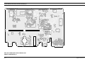
1
Table of Contents
Chapter 5
Band Specific Information
Table of Contents
Chapter
Page
5A
UHF (403-470MHz) ............................................................................. 5A.1-i
5B
VHF (136-174MHz) .............................................................................. 5B.1-i
5C
Midband (66-88MHz) ............................................................................ 5C.1-i
Band Specific Information
5-i
Table of Contents
5-ii
Band Specific Information
Table of Contents
Chapter 5A
403-470MHz Specific Information
Table of Contents
Chapter
5A.1
Model Chart and Test Specifications
5A.2
Radio Tuning Procedure
5A.3
Theory of Operation
5A.4
PCB/Schematic Diagrams and Parts Lists
403-470MHz Specific Information
5A-i
Table of Contents
5A-ii
403-470MHz Specific Information
Table of Contents
Chapter 5A.1
Model Chart and Test Specifications
Table of Contents
Paragraph
Page
1.0
Overview ..................................................................................................... 1
2.0
Model Chart ................................................................................................ 1
2.1
Service Options ........................................................................................... 2
3.0
Test Specifications .................................................................................... 3
3.1
General ........................................................................................................ 3
3.2
3.3
3.4
Transmitter................................................................................................... 3
Receiver....................................................................................................... 4
Self-quieting Frequencies ............................................................................ 4
Model Chart and Test Specifications
5A.1-i
Table of Contents
5A.1-ii
Model Chart and Test Specifications
Overview
1.0
Overview
This chapter lists the UHF (403-470MHz) models and technical specifications available for the
GM950 mobile radio.
GM950 403-470 MHz 12.5 kHz 25W HHCM
GM950 403-470 MHz 12.5 kHz 25W
GM950 403-470 MHz 12.5 kHz 25W D
GM950 403-470 MHz 12.5 kHz 25W KD
GM950 403-470 MHz 20/25 kHz 25W HHCM
GM950 403-470 MHz 20/25 kHz 25W
GM950 403-470 MHz 20/25 kHz 25W D
GM950 403-470 MHz 20/25 kHz 25W KD
M08RHF4AN1_N
M08RHE4AN2_N
M08RHF4AN3_N
M08RHH4AN4_N
M08RHF6AN1_N
M08RHE6AN2_N
M08RHF6AN3_N
M08RHH6AN4_N
Model Chart
Description
2.0
Model
5A.1
GM950
403-470 MHz UHF
X = Indicates one of each required
Item
X
X
X
X
X
X
X
X
GBN6147_
Packaging Kit
GMN6151_
Hand Held Control Microphone N1
GCN6106_
Control Head Model N2 Non-Display
GCN6107_
Control Head Model N3 Display
X
GCN6108_
Control Head Model N4 Keypad/Display
Enhanced Compact Microphone
X
X
X
X
X
X
X
Description
X
X
X
X
X
X
X
X
GMN6146_
X
X
X
X
X
X
X
X
GLN7324_
Low Profile Trunnion Kit
X
X
X
GUE1120_
RF & HSG UHF 12.5kHz 5-25W
X
X
GUE1121_
RF & HSG UHF 20/25kHz 5-25W
GUE1122_
RF & HSG UHF 12.5kHz 5-25W
X
GUE1123_
RF & HSG UHF 20/25kHz 5-25W
X
GKN6270_
Power Cable
68P64110B02
GM950 User Guide M/L (N2/N3 Models)
68P64110B06
GM950 User Guide M/L (N4 Model)
X
X
X
X
X
X
X
X
X
X
X
X
X
X
X
X
Model Chart and Test Specifications
X
5A.1-1
Model Chart
Description
GM950 403-470 MHz 12.5 kHz 25W HHCM
GM950 403-470 MHz 12.5 kHz 25W
GM950 403-470 MHz 12.5 kHz 25W D
GM950 403-470 MHz 12.5 kHz 25W KD
GM950 403-470 MHz 20/25 kHz 25W HHCM
GM950 403-470 MHz 20/25 kHz 25W
GM950 403-470 MHz 20/25 kHz 25W D
GM950 403-470 MHz 20/25 kHz 25W KD
M08RHF4AN1_N
M08RHE4AN2_N
M08RHF4AN3_N
M08RHH4AN4_N
M08RHF6AN1_N
M08RHE6AN2_N
M08RHF6AN3_N
M08RHH6AN4_N
Service Options
Model
2.1
GM950
403-470 MHz UHF
X = Indicates one of each required
Item
ENUE1005AS
X
X
X
X
X
X
X
X
5A.1-2
Description
GM950 UHF 12.5kHz MD534AD
ENUE1006AS
GM950 UHF 25kHz MD514AD
ENUE1044AS
GM950 UHF 12.5kHz MD534AA
ENUE1045AS
GM950 UHF 25kHz MD514AA
ENUE1046AS
GM950 UHF 12.5kHz MD534AB
ENUE1047AS
GM950 UHF 25kHz MD514AB
ENUE1057AS
GM950 UHF 12.5kHz MD534AE
ENUE1058AS
GM950 UHF 25kHz MD514AE
Model Chart and Test Specifications
Technical Specification
3.0
3.1
Technical Specification
General
SPECIFICATION ITEM
Frequency Range
UHF: 403-470 MHz
Channel Spacing
12.5 or 20/25 kHz
Frequency Stability
± 2ppm
Power Supply
10.8 to 15.6V dc, negative earth
Dimensions
44x168x160 mm (HxWxD)
Weight
1030g
Operational Temperature
- 25°C to + 55°C
Storage Temperature
- 40°C to + 85°C
Antenna Connection
50Ω BNC
Environmental
- Mechanical
- Electrical
3.2
TYPICAL VALUE
Vibration IEC 68/2/27 and Shock IEC 28/2/6
European Dust & Water protection IP54
ETS300-086 RF Specifications
ETS300-113 Cyclic Keying Requirements
ETS300-279 EMC Requirements
ETS300-219 Signalling
Transmitter
SPECIFICATION ITEM
TYPICAL VALUE
Channel Spacing
12.5 or 20/25 kHz
Output Power
5-25W
Modulation Limiting
<± 2.5kHz (12.5kHz); <± 4kHz (20kHz);
<± 5kHz (25kHz)
FM hum & noise (CCITT)
>40dB (12.5kHz); >45dB (25kHz) CCITT
Conducted/Radiated Emission
<0.25uW (0.1...1000MHz); <1uW (1...4GHz)
Adjacent Channel Power
<-60dB (12.5kHz); <-70dB (25kHz)
Audio Response (300 - 3000 Hz)
Flat or pre-emphasised
Audio Distortion
<5% @ 1kHz, 60% deviation
Transmit turn on time
<25msec
Model Chart and Test Specifications
5A.1-3
Technical Specification
3.3
Receiver
SPECIFICATION ITEM
3.4
TYPICAL VALUE
Channel Spacing
12.5 or 20/25 kHz
Sensitivity @ 12.5 kHz
< 0.35uV (12dB SINAD)
Sensitivity @ 25 kHz
< 0.35uV (12dB SINAD)
Intermodulation
>65dB ETS; >70dB with Base Option
Adjacent Channel Selectivity
>60dB (12.5kHz); >70dB (20/25kHz)
Spurious Rejection
>70dB ETS
Audio Distortion @ Rated Audio
<5%
Hum and Noise (CCITT)
>40dB (12.5kHz); >45dB (20/25kHz) CCITT
Audio Response (300 - 3000 Hz)
Flat or De-Emphasised
Co-channel Rejection
<12dB (12.5kHz) , <8dB (20/25kHz) ETS
Conducted /Radiated Emission
<2nW (0,1..1000MHz); <20nW (1..4GHz)
Receive after transmit time
<25msec
Audio Output Power
4W (internal speaker); <13W external
ETS
Self-Quieting Frequencies
Self-quieting frequencies are frequencies that are also generated by the radio and cause internal
interference. On these frequencies the interference caused by the self-quieter spur is great enough
that a radio will not meet its receiver sensitivity specification.
The frequencies are: UHF 403.2, 420, 436.8 and 453.6MHz.
5A.1-4
Model Chart and Test Specifications
Table of Contents
Chapter 5A.2
Radio Tuning Procedure
Table of Contents
Paragraph
Page
1.0
UHF (403-470MHz) Tuning Procedure ...................................................... 1
1.1
1.2
1.3
1.4
1.5
General ........................................................................................................
PA Bias Voltage...........................................................................................
Battery Threshold ........................................................................................
Transmitter Power .......................................................................................
Reference Oscillator ....................................................................................
1
3
3
4
4
1.6
1.7
1.8
1.9
1.10
1.11
1.12
Front-End Filter............................................................................................
Rated Volume ..............................................................................................
Squelch........................................................................................................
Transmit Modulation Balance (Compensation)............................................
Transmit Deviation Limit ..............................................................................
5 Tone (SELECT 5) Transmit Deviation ......................................................
DTMF Transmit Deviation............................................................................
5
6
6
7
7
8
9
Radio Tuning Procedure
5A.2-i
Table of Contents
5A.2-ii
Radio Tuning Procedure
UHF (403-470MHz) Tuning Procedure
5A.2
1.0
UHF (403-470MHz) Tuning Procedure
1.1
General
The recommended hardware platform is a 386 or 486 DX 33 PC (personal computer) with 8 MBytes
RAM, MS-DOS™ 5.0, Windows™ 3.1, and RSS (Radio Service Software). These are required to
align the radio. Refer to your RSS Installation Manual for installation and setup procedures for the
required software; the user manual is accessed (and can be printed if required) via the RSS.
To perform the alignment procedures, the radio must be connected to the PC, RIB (Radio Interface
Box), and Universal Test Set as shown in figure 2-1.
30 dB PAD
SERVICE MONITOR
OR COUNTER
30 dB PAD
WATTMETER
TRANSMIT
BNC
RF GENERATOR
SMA-BNC
58-80348B33
RECEIVE
AUDIO IN
MIC IN
TX
AUDIO GENERATOR
TEST SET
RTX-4005B/
GTF180B
RADIO
RX
TEST CABLE
GTF-376A
SINAD METER
AC VOLTMETER
Note: Battery can be used in RIB
making power supply optional
PROGRAM/
TEST CABLE
GTF-374A
25PIN
COMPUTER
15PIN
DATA
RIB
RLN-4008B
GND
COMPUTER INTERFACE CABLE
30-80369B72 (IBM "AT" 9PIN ONLY)
30-80369B71 (IBM "XT" 25PIN ONLY)
RIB POWER SUPPLY
EPN4041A (230 VAC. Euro)/
EPN4040A (230 VAC. UK)
Figure 2-1 Radio Alignment Test Setup.
All tuning procedures are performed from the Service menu.
Before going into the Service menu, the radio must first be read using the File / Read Radio menu (if
the radio has just been programmed with data loaded from disk or from a newly created codeplug,
then it must still be read so that the RSS will have the radio’s actual tuning values).
All Service windows read and program the radio codeplug directly; you do NOT have to use the RSS
Read Radio / Write Radio functions to program new tuning values.
Radio Tuning Procedure
5A.2-1
UHF (403-470MHz) Tuning Procedure
CAUTION:
DO NOT switch radios in the middle of any Service procedure. Always use the
Program or Cancel key to close the tuning window before disconnecting the radio.
Improper exits from the Service window may leave the radio in an improperly
configured state and result in seriously degraded radio or system performance.
The Service windows introduce the concept of the “Softpot”, an analog SOFTware controlled
POTentiometer used for adjusting all transceiver alignment controls. A softpot can be selected by
clicking with the mouse at the value or the slider or by hitting the TAB key until the value or the slider
is highlighted.
Each Service window provides the capability to increase or decrease the ‘softpot’ value with the
mouse, the arrow keys or by entering a value with the keyboard. The window displays the minimum,
maximum, and step value of the softpot. In addition transmitter tuning windows indicate the
transmitter frequency and whether the radio is keyed.
Adjusting the softpot value sends information to the radio to increase (or decrease) a DC voltage in
the corresponding circuit. For example, increasing the value in the Reference Oscillator tune window
instructs the radio microprocessor to increase the voltage across a varactor in the reference
oscillator to increase the frequency. Clicking the Program button stores all the softpot values of the
current window permanently in the radio.
In ALL cases, the softpot value is just a relative number corresponding to a D/A (Digital-to-Analog)
generated voltage in the radio. All standard measurement procedures and test equipment are
similar to previous radios.
Refer to the RSS on-line help for information on the tuning software.
Perform the following procedures in the sequence indicated.
Note:
5A.2-2
All tuning procedures must be performed at a supply voltage of 13.2V unless otherwise
stated. The Modulation Analyser to measure the deviation should be set to frequency
modulation with de-emphasis switched off and all high pass filters switched off.
Radio Tuning Procedure
UHF (403-470MHz) Tuning Procedure
1.2
PA Bias Voltage
Adjustment of the PA Bias is critical for proper radio operation. Improper adjustment will result in
poor operation and may damage the PA FET device. For this reason, the PA bias must be set before
the transmitter is keyed the first time.
Note:
For certain radio models there are two bias voltage settings. For these radios both ‘ Bias 1
Voltage ’ and ‘ Bias 2 Voltage ‘ need to be adjusted when aligning the PA Bias. For models
that only have one bias voltage setting, the ‘ Bias 2 Voltage ‘ will be shown in grey on the
service menu. After entering the tuning window the bias is switched off and the quiescent
current is 0mA. The status bar will indicate whether the bias is switched on or off.
1.
From the Service menu, select Tx Alignments.
2.
Select Bias Voltage to open the bias voltage tuning window. If the control voltage is out of
range, an error message will be displayed. In this case the radio hardware has a problem and
tuning must be stopped immediately.
3.
Measure the DC current of the radio. Note the measured value and add the specified quiescent
current shown in table 2-1. The result is the tuning target.
4.
Click the Toggle Bias button to switch on the quiescent current.
5.
Adjust the current per the target calculated in step 3.
6.
Click the Toggle Bias button to switch on the quiescent current again.
7.
Click the Program button to store the softpot value.
Table 2-1 Quiescent Current Alignment.
1.3
RF-Band
Target
UHF
440mA± 10%
Battery Threshold
The radio uses 2 battery threshold levels Tx High and Tx Low to determine the battery condition.
The Program buttons must only be activated when the power supply is set to the indicated voltage. If
the RSS detects that the voltage is not within the expected range for the threshold in question then a
message will be displayed to warn that the radio may not be set up correctly for the alignment
operation.
CAUTION:
Inadvertant Use Of The Program Buttons May Result In Radio Failure.
1.
From the Service menu, select Tx Alignments.
2.
Select Battery Thresholds to open the battery thresholds tuning window.
3.
Set the supply voltage to the value indicated for Tx High.
4.
Click the Tx High Program button to store the softpot value for Tx High.
5.
Set the supply voltage to the value indicated for Tx Low.
6.
Click the Tx Low Program button to store the softpot value for Tx Low.
7.
Close the window by pressing Cancel.
Radio Tuning Procedure
5A.2-3
UHF (403-470MHz) Tuning Procedure
1.4
Transmitter Power
The radio has two power level settings, a high power level setting, and a low power level setting.
IMPORTANT:
To set the transmitter power for customer applications use the Per Radio window
under the Edit menu and set the “Power 1” and “Power 2” powers to the desired
values. Only if the transmitter components have been changed or the transmitter
does not transmit with the power set in the Per Radio window, should the
following procedure be performed.
The advanced power setting technology employed in the radio makes use of two reference power
level settings along with parameters describing the circuit behaviour. To determine these parameters
the RSS requires the power values measured for two different settings.
1.
From the Service menu, select Tx Alignments.
2.
Select RF Power to open the RF power tuning window. The window will indicate the transmit
test frequencies to be used.
3.
Select the Point 1 value of the first frequency.
4.
Click the Toggle PTT button to key the radio. The status bar will indicate that the radio is
transmitting.
5.
Measure the transmitter power on your power meter.
6.
Enter the measured value in the box Point 1.
7.
Select the Point 2 value of the first frequency.
8.
Measure the transmitter power on your power meter.
9.
Enter the measured value in the box Point 2.
10. Click the Toggle PTT button to dekey the radio.
11. Repeat steps 3 - 10 for all test frequencies shown in the window.
12. Click the Program button to store the softpot values.
1.5
Reference Oscillator
Adjustment of the reference oscillator is critical for proper radio operation. Improper adjustment will
not only result in poor operation, but also a misaligned radio that will interfere with other users
operating on adjacent channels. For this reason, the reference oscillator should be checked every
time the radio is serviced. The frequency counter used for this procedure must have a stability of
0.1ppm (or better).
5A.2-4
1.
From the Service menu, select Tx Alignments.
2.
Select Reference Oscillator to open the reference oscillator tuning window. The tuning window
will indicate the target transmit frquency.
3.
Click the Toggle PTT button to key the radio. The status bar will indicate that the radio is
transmitting.
4.
Measure the transmit frequency on your frequency counter.
5.
Adjust the reference oscillator softpot in the tuning window to achieve a transmit frequency
within the limits shown in table 2-2.
6.
Click the Toggle PTT button again to dekey the radio and then click the Program button to store
the softpot value.
Radio Tuning Procedure
UHF (403-470MHz) Tuning Procedure
Table 2-2 Reference Oscillator Alignment.
1.6
RF-Band
Target
All bands
±150 Hz
Front-End Filter
Alignment of the front-end pre-selector is normally not required on these radios. Only if the radio has
poor receiver sensitivity or the pre-selector parts have been replaced the following procedure should
be performed. The softpot value sets the control voltage of the pre-selector. Its value needs to be set
at 7 frequencies across the frequency range. If the radio supports 20 or 25 kHz channel spacing
selection, use the parameters for 25 kHz channel spacing.
1.
Set the test box (GTF180) meter selection switch to the “Audio PA” position and connect a
SINAD meter to the “METER” port.
2.
From the Service menu, select Rx Alignments.
3.
Select Front End Filter to open the pre-selector tuning window. The window will indicate the
receive test frequencies to be used.
4.
Select the first test frequency shown, and set the corresponding value to the start value shown
in table 2-4.
5.
Set the RF test generator to the receive test frequency, and set the RF level to 10µV modulated
with a 1kHz tone at the normal test deviation shown in table 2-3.
6.
Measure the RSSI voltage at accessory connector pin 15 with a dc voltmeter capable of 1 mV
resolution.
7.
Change the softpot value by the stepsize shown in table 2-4 and note the RSSI voltage.The
target softpot value is achieved when the measured RSSI voltage change between step 6 and
step 7 is lower than the tuning target for the first time. The tuning target, shown in table 2-4, is
expressed as the percentage of the measured RSSI voltage and must be recalculated for every
tuning step. If the measured RSSI voltage decreases before the target value has been
achieved, approximation should be stopped and the current softpot value should be used as
target value. Set test box (GTF180) audio switch to the “SPKR” position. The 1 kHz tone must
be audible at the target value to make sure the radio is receiving.
8.
Repeat steps 4 - 7 for all test frequencies shown in the window.
9.
Click the Program button to store the softpot values.
Table 2-3 Normal Test Deviation.
Channel Spacing
Deviation
12.5 kHz
20 kHz
25 kHz
1.5 kHz
2.4 kHz
3 kHz
Table 2-4 Start Value for Front-End Pre-selector Tuning.
Radio Tuning Procedure
RF-Band
Target
Stepsize
Start Value
UHF
0.5%
-2
Maximum
5A.2-5
UHF (403-470MHz) Tuning Procedure
1.7
Rated Volume
The rated volume softpot sets the maximum volume at normal test modulation.
1.8
1.
Set test box (GTF180) meter selection switch to the “AUDIO PA” position and the speaker load
switch to the “MAXAR” position. Connect an AC voltmeter to the test box meter port.
2.
From the Service menu, select Rx Alignments.
3.
Select Rated Volume to open the rated volume tuning window. The screen will indicate the
receive test frequency to be used.
4.
Set the RF test generator to the receive test frequency, and set the RF level to 1mVolt
modulated with a 1kHz tone at the normal test deviation shown in table 2-3. Set test box
(GTF180) audio switch to the “SPKR” position. The 1kHz tone must be audible to make sure
the radio is receiving.
5.
Adjust the value of the softpot to obtain rated audio volume (as close to 3.87 Vrms)
Note: The voltage at the meter port of the testbox GTF180 is only half the voltage at the
speaker.
6.
Click the Program to store the softpot value.
Squelch
The squelch softpots set the signal to noise ratio at which the squelch opens. The squelch value
needs to be set at 7 frequencies across the frequency range. If the radio supports 20 or 25 kHz
channel spacing selection, the radio stores separate tuning data for 20 kHz and 25 kHz channel
spacing. Therefore, both sets of tuning data should be tuned independently.
1.
Set the test box (GTF180) meter selection switch to the “Audio PA” position and connect a
SINAD meter to the “METER” port.
2.
From the Service menu, select Rx Alignments.
3.
Select ‘Squelch’ to open the squelch tuning window. This window is used to set the values for
12.5kHz radios and the 25kHz data for 20/25kHz radios. The window will indicate the receive
test frequencies to be used.
4.
Select the first test frequency shown, and set the corresponding value to 0.
5.
Set the RF test generator to the test frequency and modulate the signal generator at the normal
test deviation shown in table 2-3, with 1kHz tone. Adjust the generator for a 8-10 dB SINAD
level (weighted with psophometric filter).
6.
Adjust the softpot value until the squelch just closes.
7.
Monitor for squelch chatter; if chatter is present, repeat step 6.
8.
When no chatter is detected, select the next softpot and repeat steps 4 - 7 for all test
frequencies shown in the window.
9.
Click the Program button to store the softpot values.
10. If the radio supports 20 or 25kHz channel spacing selection, repeat steps 2-9 for 20kHz
channel spacing using the ‘Squelch (20kHz)’ window.
5A.2-6
Radio Tuning Procedure
UHF (403-470MHz) Tuning Procedure
1.9
Transmit Modulation Balance (Compensation)
Compensation alignment balances the modulation sensitivity of the VCO and reference modulation
(synthesizer low frequency port) lines. Compensation algorithm is critical to the operation of
signalling schemes that have very low frequency components (e.g. DPL) and could result in
distorted waveforms if improperly adjusted. The compensation value needs to be set at 7
frequencies across the frequency range. If the radio supports 20 or 25 kHz channel spacing
selection, the procedure must only be performed for 25 kHz channel spacing. Values for 20 kHz
channel spacing are calculated by the radio software.
1.
From the Service menu, select Tx Alignments.
2.
Select ‘Modulation Balance’ to open the deviation balance tuning window. The window will
indicate the transmit test frequencies to be used.
3.
Set the Test Box (GTF180) meter selector switch to the „GEN“ position, and inject a 80 Hz tone
at 200 mVrms into the "Audio In" port. (The deviation measured at step 6 should be in the
range of 1 - 4 kHz.) Connect an AC meter to the meter port to insure the proper input signal
level.
4.
Select the first test frequency shown in the window.
5.
Click the Toggle PTT button to key the radio. The status bar will indicate that the radio is
transmitting.
6.
Measure the transmitter deviation.
7.
Change the input tone to 3 kHz, 200 mVrms.
8.
Adjust the deviation to within ±2% of the value recorded in step 6.
9.
Check the deviation at 80 Hz again and repeat steps 7 - 8, if it has changed since step 6.
10. Click the Toggle PTT button to dekey the radio.
11. Repeat steps 3 - 10 for the remaining test frequencies.
12. Click the Program button to store the softpot values.
Note:
1.10
The step size change for step 8 is approximately 2.5% of the softpot value.
Transmit Deviation Limit
The transmit deviation limit softpot sets the maximum deviation of the carrier. The deviation value
needs to be set at 7 frequencies across the frequency range. If the radio supports 20 or 25 kHz
channel spacing selection, the procedure must only be performed for 25 kHz channel spacing.
Values for 20 kHz channel spacing are calculated by the radio software.
1.
From the Service menu, select Tx Alignments.
2.
Select Deviation Limit to open the deviation limit tuning window. This window is used to set the
values for 12.5 kHz radios and the 25 kHz data for 20/25 kHz radios. The window will indicate
the transmit test frequencies to be used.
3.
Set the Test Box (GTF180) meter selector switch to the “GEN” position, and inject a 1 kHz tone
at 800 mVrms into the "Audio In" port. Connect an AC meter to the meter port to insure the
proper input signal level.
4.
Select the first test frequency shown in the window.
5.
Click the Toggle PTT button to key the radio. The status bar will indicate that the radio is
transmitting.
6.
Adjust the transmitter deviation to the value shown in table 2-5.
Radio Tuning Procedure
5A.2-7
UHF (403-470MHz) Tuning Procedure
7.
Click the Toggle PTT button to dekey the radio.
8.
Repeat steps 4 - 7 for the remaining test frequencies.
9.
Click the Program button to store the softpot values.
.
Table 2-5 Transmitter Deviation.
1.11
Channel Spacing
Deviation
12.5 kHz
2.2-2.3 kHz
20 kHz
3.4-3.6 kHz
25 kHz
4.3-4.6 kHz
5 Tone (SELECT 5) Transmit Deviation
The 5 Tone (SELECT 5) Deviation Softpot is used to tune the SELECT 5 signalling deviation. Tuning
is performed at one frequency. The radio generates the required tones while the tuning window is
open. Values for other frequencies are calculated by the radio software. If the radio supports 20 or
25 kHz channel spacing selection, the procedure must only be performed for 25 kHz channel
spacing. Values for 20 kHz channel spacing are calculated by the radio software.
1.
From the Service menu, select Tx Alignments.
2.
Select Signalling Deviation to open the signalling deviation tuning window. This window is used
to set the values for 12.5 kHz radios and the 25 kHz data for 20/25 kHz radios.
3.
Click the Toggle PTT button to key the radio. The status bar will indicate that the radio is
transmitting.
4.
Adjust the transmitter deviation to the value shown in table 2-6.
5.
Click the Toggle PTT button to dekey the radio.
6.
Click the Program button to store the softpot values.
.
Table 2-6 Signalling Deviation.
5A.2-8
Channel Spacing
5 Tone (Select 5)
12.5 kHz
1.6-1.8 kHz
20 kHz
2.6-2.9 kHz
25 kHz
3.3-3.7 kHz
Radio Tuning Procedure
UHF (403-470MHz) Tuning Procedure
1.12
DTMF Transmit Deviation
The DTMF Deviation Softpot is used to tune the DTMF deviation. Tuning is performed at one
frequency. The radio generates the required tones while the tuning window is open. Values for other
frequencies are calculated by the radio software. If the radio supports 20 or 25 kHz channel spacing
selection, the procedure must only be performed for 25 kHz channel spacing. Values for 20 kHz
channel spacing are calculated by the radio software.
1.
From the Service menu, select Tx Alignments.
2.
Select DTMF Deviation to open the DTMF deviation tuning window. This window is used to set
the values for 12.5 kHz radios and the 25 kHz data for 20/25 kHz radios.
3.
Click the Toggle PTT button to key the radio. The status bar will indicate that the radio is
transmitting.
4.
Adjust the transmitter deviation to the value shown in table 2-7.
5.
Click the Toggle PTT button to dekey the radio.
6.
Click the Program button to store the softpot values.
.
Table 2-7 DTMF Deviation.
Radio Tuning Procedure
Channel Spacing
DTMF
12.5 kHz
1.5-1.8 kHz
20 kHz
2.5-2.8 kHz
25 kHz
3.0-3.4 kHz
5A.2-9
UHF (403-470MHz) Tuning Procedure
5A.2-10
Radio Tuning Procedure
Table of Contents
Chapter 5A.3
Theory of Operation
Table of Contents
Paragraph
Page
1.0
Overview..................................................................................................... 1
2.0
Open Controller.......................................................................................... 1
2.1
2.2
2.3
2.4
2.5
2.6
2.7
2.8
2.9
2.10
2.11
2.12
2.13
General ........................................................................................................
Voltage Regulators ......................................................................................
Electronic On/Off .........................................................................................
Emergency...................................................................................................
Mechanical On/Off .......................................................................................
Ignition .........................................................................................................
Hook RSS ....................................................................................................
Microprocessor Clock Synthesizer ..............................................................
Serial Peripheral Interface (SPI) ..................................................................
SPEB Serial Interface ..................................................................................
General Purpose Input/Output.....................................................................
Normal Microprocessor Operation...............................................................
FLASH Electronically Erasable Programmable Memory
(FLASH EEPROM) ......................................................................................
Electrically Erasable Programmable Memory (EEPROM)...........................
Static Random Access Memory (SRAM).....................................................
2.14
2.15
1
1
2
3
3
3
3
4
4
5
6
6
8
8
9
Controller Board Audio and Signalling Circuits
3.0
General ....................................................................................................... 9
3.1
3.2
Audio Signalling Filter IC (ASFIC) ............................................................... 9
Audio Ground............................................................................................... 9
4.0
Transmit Audio Circuits........................................................................... 10
4.1
4.2
4.3
Mic Input Path............................................................................................ 10
External Mic Path....................................................................................... 11
PTT Sensing and TX Audio Processing .................................................... 11
Theory of Operation
5A.3-i
Table of Contents
Paragraph
Page
4.4
TX Secure Audio (optional) ....................................................................... 11
5.0
Transmit Signalling Circuits ................................................................... 12
5.1
5.2
5.3
Sub-audible Data (PL/DPL) ....................................................................... 12
High Speed Data ....................................................................................... 13
Dual Tone Multiple Frequency (DTMF) Data............................................. 13
6.0
Receive Audio Circuits............................................................................ 14
6.1
6.2
6.3
6.4
6.5
6.6
Squelch Detect ..........................................................................................
Audio Processing and Digital Volume Control ...........................................
Audio Amplification Speaker (+) Speaker (-) .............................................
Handset Audio ...........................................................................................
Filtered Audio ............................................................................................
RX Secure Audio (optional) .......................................................................
7.0
Receive Signalling Circuits..................................................................... 17
7.1
7.2
Sub-audible Data Decoder (PL/DPL) ........................................................ 17
Alert Tone Circuits ..................................................................................... 17
14
15
15
16
16
16
UHF Specific Circuit Description
8.0
Receiver Front-End.................................................................................. 19
8.1
8.2
8.3
Front-End Band-Pass Filter & Pre-Amplifier .............................................. 19
Mixer and Intermediate Frequency (IF) Section ........................................ 19
IF IC (U5201) .............................................................................................. 20
9.0
Transmitter Power Amplifier (PA) 5-25W ............................................... 20
9.1
9.2
9.3
9.4
9.5
9.6
Power Controlled Stage.............................................................................
PA Stages..................................................................................................
Directional Coupler ....................................................................................
Antenna Switch..........................................................................................
Harmonic Filter ..........................................................................................
Power Control ............................................................................................
10.0
Frequency Synthesis............................................................................... 23
10.1
10.2
10.3
10.4
Reference Oscillator ..................................................................................
Fractional-N Synthesizer (U5701) .............................................................
Voltage Controlled Oscillator (VCO) ..........................................................
Synthesizer Operation ...............................................................................
5A.3-ii
20
21
21
21
22
22
23
23
24
24
Theory of Operation
Overview
5A.3
1.0
Overview
This section provides a detailed theory of operation for the radio and its components.
The main radio is a single board design, consisting of the transmitter, receiver, and controller
circuits.
The main board is designed to accept one additional option board. This may provide functions such
as secure voice/data or DTMF decoder. The control head is mounted directly on the front of the
radio or connected via an extension cable in remote mount operation. The control head contains a
speaker, LED indicators, a microphone connector, buttons and dependent of radio type, a display.
These provide the user with interface control over the various features of the radio.
In addition to the power cable and antenna cable, an accessory cable can be attached to a
connector on the rear of the radio. The accessory cable provides the necessary connections for
items such as external speaker, emergency switch, foot operated PTT, ignition sensing, etc.
2.0
Open Controller
2.1
General
The radio controller consists of 4 main subsections:
■
Digital Control
■
Audio Processing
■
Power Control
■
Voltage Regulation
The digital control section of the radio board is based upon an open architecture controller
configuration. It consists of a microprocessor, support memory, support logic, signal MUX ICs, the
On/Off circuit, and general purpose Input/Output circuitry.
The controller uses the Motorola 68HC11K1 microprocessor (U0101). In addition to the
microprocessor, the controller has 3 external memory devices. The 3 memory devices consist of a
32 Kbyte SRAM (U0103), a 256 Kbyte FLASH EEPROM (U0102), and a 4kbyte EEPROM (U0104).
Note:
2.2
From this point on the 68HC11K1 microprocessor will be referred to as µP or K1µP.
References to a control head will be to the N3 radio model - control head with display.
Voltage Regulators
Voltage regulation for the controller is provided by 3 separate devices; U0631 (LP2951CM) +5V,
U0601 (LM2941T) +9.3V, and UNSW 5V (a combination of R0621 and VR0621). An additional
regulator is located in the RF section.
Voltage regulation providing 5V for the digital circuitry is done by U0631. Input and output capacitors
(C0631/C0632 and C0633-C0635) are used to reduce high frequency noise and provide proper
operation during battery transients. This regulator provides a reset output (pin 5) that goes to 0 volts
if the regulator output goes out of regulation. This is used to reset the controller to prevent improper
operation. Diode D0631 prevents discharge of C0632 by negative spikes on the 9V3 voltage
Theory of Operation
5A.3-1
Open Controller
Regulator U0601 is used to generate the 9.3 volts required by some audio circuits, the RF circuitry
and power control circuitry. Input and output capacitors (C0601-C0603 and C0604/C0605) are used
to reduce high frequency noise. R0602/R0603 set the output voltage of the regulator. If the voltage
at pin 1 is greater than 1.3 volts the regulator output decreases and if the voltage is less than 1.3
volts the regulator output increases. This regulator output is electronically enabled by a 0 volt signal
on pin 2. Q0601 and associated circuitry (R0601/R0604/R0605) are used to disable the regulator
when the radio is turned off.
UNSW 5V is only used in a few areas which draw low current and require 5 V while the radio is off.
UNSW 5V CL is used to buffer the internal RAM. C0622 allows the battery voltage to be
disconnected for a couple of seconds without losing RAM parameters. Diode D0621 prevents radio
circuitry from discharging this capacitor.
The voltage 9V3 SUPP is only used in the VHF radio (T1) to supply the drain current for the RF MOS
FET in the PA. The voltage SW B+ is monitored by the µP through the voltage divider R0641/R0642
and line BATTERY VOLTAGE. Diode VR0641 limits the divided voltage to 5.1V to protect the µP.
Diode D5601 (UHF) / D3601 (VHF) / D2601 (MB) located on the PA section acts as protection
against transients and wrong polarity of the supply voltage.
2.3
Electronic On/Off
The radio has circuitry which allows radio software and/or external triggers to turn the radio on or off
without direct user action. For example, automatic turn on when ignition is sensed and off when
ignition is off.
Before version 0102726B09_Cntl: Q0611 is used to provide SW B+ to the various radio circuits.
Q0611 acts as an electronic on/off switch controlled by Q0612. The switch is on when the collector
of Q0612 is low. When the radio is off Q0612 is cutoff and the voltage at Q0611-base is at A+. This
effectively prevents current flow through Q0611 from emitter to collector. When the radio is turned on
the voltage at the base of Q0612 is high (about 0.6V) and Q0612 switches on (saturation) and pulls
down the voltage at Q0611-base. With Transistor Q0611 now enabled current flows through the
device. This path has a very low impedance (less than 1Ω) from emitter to collector. This effectively
provides the same voltage level at SWB+ as at A+.
Version 0102726B09_Cntl and following versions: Q0611 is used to provide SW B+ to the various
radio circuits. Q0611 contains a pnp and an npn transistor and acts as an electronic on/off switch.
The switch is on when the collector of the npn transistor (Q0611-1) is low. When the radio is off the
pnp transistor is cutoff and the voltage at pin 1 is at A+. This effectively prevents current flow through
the pnp transistor from emitter (pin 3) to collector (pin 2).
When the radio is turned on the voltage at the Q0611 pin 4 is high (about 4.4V) and the npn
transistor switches on (saturation) and pulls down the voltage at the base of the pnp transistor. With
Transistor Q0611 now “enabled” current flows through the device from pin 3 to pin 2. This path has a
very low impedance (less than 1 ohm) from emitter to collector. This effectively provides the same
voltage level at SWB+ as at A+.
The electronic on/off circuitry can be enabled by the microprocessor (through ASFIC port GCB2,
line B+ CONTROL), the emergency switch (line EMERGENCY CONTROL), the mechanical On/Off
button on the control head (line ON OFF CONTROL), or the ignition sense circuitry (line IGNITION
CONTROL). If any of the 4 paths cause a low at the collector of Q0612 (before version
0102726B09_Cntl) or Q0611 pin 1 (version 0102726B09_Cntl and after), the electronic ON is
engaged.
5A.3-2
Theory of Operation
Open Controller
2.4
Emergency
The emergency switch (J0400-9), when engaged, grounds the base of Q0441 and pulls the line
EMERGENCY CONTROL to low via D0441. EMER IGN SENSE is pulled high by R0441. When the
emergency switch is released the base of Q0441 is pulled high by R0442. This causes the collector
of transistor Q0441 to go low (0.2V), thereby setting the EMER IGN SENSE line to low.
While EMERGENCY CONTROL is low, SW B+ is on, the microprocessor starts execution, reads
that the emergency input is active through the voltage level of EMER IGN SENSE, and sets the B+
CONTROL output of the ASFIC pin B4 to a logic high. This high will keep Q0611 switched on. This
operation allows a momentary press of the emergency switch to power up the radio. When the
microprocessor has finished processing the emergency press, it sets the B+ CONTROL line to a
logic 0. This turns off Q0611 and the radio turns off. Notice that the microprocessor is alerted to the
emergency condition via line EMER IGN SENSE. If the radio was already on when emergency was
triggered then B+ CONTROL would already be high.
2.5
Mechanical On/Off
This refers to the typical on/off button, located on the control head, and which turns the radio on and
off. If the radio is turned off and the on/off button is pressed, line ON OFF CONTROL goes high and
switches the radio on as long as the button is pressed. The microprocessor is alerted through line
ANALOG 3 which is pulled to low by Q0925 (Control Head with display) while the on/off button is
pressed. If the software detects a low state it asserts B+ CONTROL via ASFIC pin B4 high which
keeps Q0611, and in turn the radio switched on.
If the on/off button is pressed and held while the radio is on, the software detects the line ANALOG
3 changing to low and switches the radio off by setting B+ CONTROL to low.
2.6
Ignition
Ignition sense is used to prevent the radio from draining the vehicle’s battery because the engine is
not running.
When the IGNITION input (J0400-10) goes above 6 volts Q0611 is turned on via line IGNITION
CONTROL. Q0611 turns on SW B+ and the microprocessor starts execution. A high IGNITION input
reduces the voltage of line EMER IGN SENSE by turning on Q0450. The software reads the line
EMER IGN SENSE, determines from the level (Emergency has a different level) that the IGNITION
input is active and sets the B+ CONTROL output of the ASFIC pin B4 to high to latch on SW B+.
When the IGNITION input goes below 6 volts, Q0450 switches off and R0449, R0450 pull line
EMER IGN SENSE high. The software is alerted by line EMER IGN SENSE to switch off the radio
by setting B+ CONTROL to low. The next time the IGNITION input goes above 6 volts the above
process will be repeated.
2.7
Hook RSS
The HOOK RSS input is used to inform the µP when the Microphone’s hang-up switch is engaged.
Dependent on the radio model the µP may take actions like turning the audio PA on or off.
The signal is routed from J0101-3 and J0400-14 through transistor Q0101 to the K1µP U0101-23.
The voltage range of HOOK RSS in normal operating mode is 0-5V.
Theory of Operation
5A.3-3
Open Controller
To start SBEP communication this voltage must be above 6V. This condition generates a µP
interrupt via VR0102, Q0105, Q0104, Q0106 and enables the BUS+ line for communication via
Q0122, Q0121.
2.8
Microprocessor Clock Synthesizer
The clock source for the microprocessor system is generated by the ASFIC (U0201). Upon powerup the synthesizer U5701 (UHF) / U3701 (VHF) / U2701 (MB) generates a 2.1 MHz waveform that is
routed from the RF section (via C0202) to the ASFIC (on U0201-E1) For the main board controller
the ASFIC uses 2.1MHz as a reference input clock signal for its internal synthesizer. The ASFIC, in
addition to audio circuitry, has a programmable synthesizer which can generate a synthesized signal
ranging from 1200Hz to 32.769MHz in 1200 Hz steps.
When power is first applied, the ASFIC will generate its default 3.6864 MHz CMOS square wave µP
CLK (on U0201-D1) and this is routed to the microprocessor (U0101-73). After the microprocessor
starts operation, it reprograms the ASFIC clock synthesizer to a higher µP CLK frequency (usually
7.9488 MHz) and continues operation.
The ASFIC may be reprogrammed to change the clock synthesizer frequencies at various times
depending on the software features that are executing. In addition, the clock frequency of the
synthesizer is changed in small amounts if there is a possibility of harmonics of this clock source
interfering with the desired radio receive frequency.
The ASFIC synthesizer loop uses C0228, C0229 and R0222 to set the switching time and jitter of
the clock output. If the synthesizer cannot generate the required clock frequency it will switch back to
its default 3.6864MHz output.
Because the ASFIC synthesizer and the µP system will not operate without the 2.1MHz reference
clock, it (and the voltage regulators) should be checked first when debugging the system.
2.9
Serial Peripheral Interface (SPI)
The µP communicates to many of the ICs through its SPI port. This port consists of SPI TRANSMIT
DATA (MOSI) (U0101-1), SPI RECEIVE DATA (MISO) (U0101-80), SPI CLK (U0101-2) and chip
select lines going to the various ICs, connected on the SPI PORT (BUS). This BUS is a synchronous
bus, in that the timing clock signal CLK is sent while SPI data (SPI TRANSMIT DATA or SPI
RECEIVE DATA) is sent. Therefore, whenever there is activity on either SPI TRANSMIT DATA or SPI
RECEIVE DATA there should be a uniform signal on CLK. The SPI TRANSMIT DATA is used to send
serial from a µP to a device, and SPI RECEIVE DATA is used to send data from a device to a µP. The
only device from which data can be received via SPI RECEIVE DATA is the EEPROM (U0104 or
U0107) and a control head with graphical display (N4 model).
On the controller there are three ICs on the SPI BUS, ASFIC (U0201-F2), EEPROM (U0104-1 or
U0107-1) and D/A (U0731-6). In the RF sections there is one IC on the SPI BUS which is the
FRAC-N Synthesizer. The SPI TRANSMIT DATA and CLK lines going to the RF section are filtered
by L0131/L0132 to minimize noise. The chip select lines for the IC´s are decoded by the address
decoder U0105.
The SPI BUS is also used for the control head. U0106-2,3 buffer the SPI TRANSMIT DATA and CLK
lines to the control head. U0106-1 switch off the CLK signal for the LCD display if it is not selected
via LCD CE and Q0141.
5A.3-4
Theory of Operation
Open Controller
When the µP needs to program any of these IC’s it brings the chip select line for that IC to a logic 0
and then sends the proper data and clock signals. The amount of data sent to the various IC’s are
different, for example the FRAC-N can receive up to 21 bytes (168 bits) while the DAC can receive
up to 3 bytes (24 bits). After the data has been sent the chip select line is returned to a logic 1.
Version 0102726B09_Cntl and following versions: When the control head with graphical display
wants to communicate to the µP it brings request line ANALOG 2 (J0101-11) to a logic “0“. The µP
reads this line via one of the analogue to digital converters (U0101-48) and then starts
communication by activating the control head select line (LED CHT CE) via U0105-9 and J0101-12,
sending the clock signal via U0106-3 and J0101-5 and sending data via U0106-2 and J0101-6 or
receiving data via J0101-10 and gate U0171. During data transfer gate U0171 is switched on by line
LED CHT CE via transistor Q0171 and gate U0172-1. Gate U0172-1 is enabled by the µP via ASFIC
output GCB4 (U0201-A2).
The Option board interfaces are different in that the µP can also read data back from devices
connected.The timing and operation of this interface is specific to the option connected, but
generally follows the pattern:
2.10
1.
an option board device generates an interrupt via J0103-8, Q0124, Q0125 and µP pin 61
(IRQ). The µP determines the interrupt source by reading a high at the collector of Q0124 via
µP pin 7 and R0129.
2.
the main board asserts a chip select for that option board device via U0105-10, J0102-5,
3.
the main board µP generates the CLK (J0102-6),
4.
the main board µP writes serial data via J0102-4 and reads serial data via J0102-2 and,
5.
when data transfer is complete the main board terminates the chip select and CLK activity.
SPEB Serial Interface
The SBEP serial interface allows the radio to communicate with the Radio Service Software (RSS)
via the Radio Interface Box (RIB). This interface connects to the Microphone connector (J0903/
J0803) via Control Head connector (J0101-15) or to the accessory connector J0400-6 and
comprises BUS+ (J0101-15). The line is bi-directional, meaning that either the radio or the RSS can
drive the line.
When the RIB (Radio Interface Box) is connected to the radio, a voltage on the HOOK RSS line
above 6 volts switches on Q0105. The low state at collector of Q0105 switches Q0104 off and in
turn, Q0106 on. A high to low transition at the collector of Q0106 generates an interrupt via µP pin
61. The µP determines the interrupt source by reading a high at the collector of Q0104 via µP pin 6
and R0125. The switched on Q0105 also switches off Q0122 enabling the µP to read BUS+ via pin
78 and to write BUS+ via pin 79 and transistors Q0123,Q0121. While the radio is sending serial data
at pin 79 via Q0123 and Q0121 it receives an “echo” of the same data at pin 78.
When the voltage on the HOOK RSS line is below 6 volts (RIB is not connected), the high collector
of Q0105 turns on Q0122. The low collector of Q0122 prevents the µP from writing data to BUS+ via
Q0123. In this mode line BUS+ is used for signal SCI RX of the Serial Communication Interface
(SCI). The µP reads the SCI via signal SCI RX (pin 78) and writes via signal SCI TX (pin 79). Both
signals are available on the accessory connector J0400 (SCI DATA OUT, SCI DATA IN).
Theory of Operation
5A.3-5
Open Controller
2.11
General Purpose Input/Output
The Controller provides one general purpose line (GP I/O) available on the accessory connector
J0400-12 to interface to external options. The software and the hardware configuration of the radio
model defines the function of the port. The port uses an output transistor (Q0432) controlled by µP
via ASFIC port GCB3 (pin B3) and an input transistor (Q0431) read by µP port PA7 (pin 4). To use
the GP as input the µP must turn off the output transistor.
An external alarm output, available on J0400 pin 4 is generated by the µP via ASFIC port GCB1 (pin
A3) and transistor Q0411. Input EXTERNAL PTT on J0400 pin 3 is read by the µP via line REAR
PTT and µP pin 8.
From version 0102726B09_Cntl on: Pin 13 of the accessory connector J0400 provides a voltage at
battery level while the radio is switched on. The output is capable to drive a dc current up to 300 mA
and has a short circuit protection. When the radio is switched on, the voltage 9V3 turns on transistor
Q0482. Transistor Q0482 switches on Q0481 and enables a current flow from emitter to collector of
Q0481. This path has a very low impedance and effectively provides the same voltage level at SW
FLT A+ as at FLT A+. If the radio is switched off the voltage 9V3 is at ground level which switches off
Q0482 and in turn cuts off the current from emitter to collector of Q0481. If the accessory connector
output J0400-13 is connected to ground while the radio is on, the diode D0481 pulls the base of
Q0482 down to about 0.6V. With a voltage drop of about 0.6V across D0482 the base to emitter
voltage of Q0482 is about 0V. This cuts off the collector current of Q0482 and switches off Q0481
until the short is removed.
2.12
Normal Microprocessor Operation
For this radio, the µP is configured to operate in one of two modes, expanded and bootstrap. In
expanded mode the µP uses external memory devices to operate, whereas in bootstrap operation
the µP uses only its internal memory. In normal operation of the radio the µP is operating in
expanded mode as described below.
In expanded mode on this radio, the µP (U0101) has access to three external memory devices;
U0102 (FLASH EEPROM), U0103 (SRAM), U0104 or U0107 (optional EEPROM). Also, within the
µP there are 768 bytes of internal RAM and 640 bytes of internal EEPROM, as well as logic to select
external memory devices.
The (optional) external EEPROM (U0104 or U0107) as well as the µP’s own internal EEPROM
space contain the information in the radio which is customer specific, referred to as the codeplug.
This information consists of items such as: 1) what band the radio operates in, 2) what frequencies
are assigned to what channel, and 3) tuning information. In general tuning information and other
more frequently accessed items are stored in the internal EEPROM (space within the 68HC11K1),
while the remaining data is stored in the external EEPROM. (See the particular device subsection
for more details.)
The external SRAM (U0103) as well as the µP’s own internal RAM space are used for temporary
calculations required by the software during execution. All of the data stored in both of these
locations is lost when the radio powers off (See the particular device subsection for more details).
The FLASH EEPROM contains the actual Radio Operating Software. This software is common to all
open architecture radios within a given model type. For example Securenet radios may have a
different version of software in the FLASH EEPROM than a non-secure radio (See the particular
device subsection for more details).
5A.3-6
Theory of Operation
Open Controller
The K1µP provides an address bus of 16 address lines (A0-A15), and a data bus of 8 data lines (D0D7). There are also three control lines; CSPROG (U0101-29) to chip select U0102-30 (FLASH
EEPROM), CSGP2 (U0101-28) to chip select U0103-20 (SRAM) and PG7_R_W to select whether
to read or to write. All other chips (ASFIC/PENDULLUM/DAC/FRACN/LCD/LED/optional EEPROM/
OPTION BOARD) are selected by 3 lines of the µP using address decoder U0105. When the µP is
functioning normally, the address and data lines should be toggling at CMOS logic levels.
Specifically, the logic high levels should be between 4.8 and 5.0 V, and the logic low levels should be
between 0 and 0.2 V. No other intermediate levels should be observed, and the rise and fall times
should be <30 ns.
The low-order address lines (A0-A7) and the data lines (D0-D7) should be toggling at a high rate,
i.e., you should set your oscilloscope sweep to 1 us/div. or faster to observe individual pulses. High
speed CMOS transitions should also be observed on the µP control lines.
On the µP the lines XIRQ (U0101-30), MODA LIR (U0101-77), MODB VSTPY (U0101-76) and
RESET (U0101-75) should be high at all times during normal operation. Whenever a data or
address line becomes open or shorted to an adjacent line, a common symptom is that the RESET
line goes low periodically, with the period being in the order of 20 msecs. In the case of shorted lines
you may also detect the line periodically at an intermediate level, i.e. around 2.5 V when 2 shorted
lines attempt to drive to opposite rails.
The MODA LIR (U0101-77) and MODB VSTPY (U0101-76) inputs to the µP must be at a logic 1 for
it to start executing correctly. After the µP starts execution it will periodically pulse these lines to
determine the desired operating mode. While the Central Processing Unit (CPU) is running, MODA
LIR is an open-drain CMOS output which goes low whenever the µP begins a new instruction (an
instruction typically requires 2-4 external bus cycles, or memory fetches).
However, since it is an open-drain output, the waveform rise assumes an exponential shape similar
to an RC circuit.
There are eight analogue to digital converter ports (A/D) on U0101. They are labelled within the
device block as PE0-PE7. These lines sense the voltage level ranging from 0 to 5 V of the input line
and convert that level to a number ranging from 0 to 255 which can be read by the software to take
appropriate action.
For example, U0101-46 is the battery voltage detect line. R0641 and R0642 form a resistor divider
on SWB+. With 30K and 10K and a voltage range of 11 V to 17 V, that A/D port would see 2.74 V to
4.24 V which would then be converted to ~140 to 217 respectively.
U0101-51 is the high reference voltage for the A/D ports on the µP. Resistor R0106 and capacitor
C0106 filter the +5 V reference. If this voltage is lower than +5 V the A/D readings will be incorrect.
Likewise U0101-50 is the low reference for the A/D ports. This line is normally tied to ground. If this
line is not connected to ground, the A/D readings will be incorrect.
Capacitors C0104, C0105, C0113, C0114 serve to filter out any AC noise which may ride on +5V at
U0101.
Input IRQ (U101-61) generates an interrupt, if either HOOK RSS (J0101-3) is higher than 6V (SBEP
communication) and turns Q0106 on via Q0105, Q0104, or a low at the option interrupt pin (J01038) turns Q0124 off and Q0125 on. The µP determines the interrupt source by reading the collector of
Q0104 via U0101-6 and the collector Q0124 via U0101-7.
Theory of Operation
5A.3-7
Open Controller
2.13
FLASH Electronically Erasable Programmable Memory
(FLASH EEPROM)
The 256 KByte FLASH EEPROM (U0102) contains the radio operating software. This software is
common to all open architecture radios within a given model type. This is, as opposed to the
codeplug information stored in EEPROM (U0104) which could be different from one user to another
in the same company.
In normal operating mode, this memory is only read, not written to. The memory access signals (CE,
OE and WE) are generated by the µP.
To upgrade/reprogram the FLASH software, the µP must be set in bootstrap operating mode, and
the FLASH device pin (U0102-9) Vpp must be between 11.4 and 12.6 V. Taking diode D0102 into
account, the voltage at J400-12 to enable FLASH programming may range between 12.1 and 13.1V.
This voltage also switches Q0102 on and in turn Q0103 off. The low state at collector of Q0102 pulls
MODA LIR (U0101-77) and MODB VSTBY (U0101-76) via diode D0101 to low which enables the
bootstrap operating mode after power up. The high state at collector of Q0103 enables the µP to
control the FLASH EN OE (U0102-32) input via U0106-4. Chip select (U102-30) and read or write
operation (U102-7) are controlled by µP pins 29 and 33. In normal operating mode VPP is below 5V
which switches Q0102 off and Q0103 on.
Resistor divider pair R0132 and R0133 set up 4.1 V on U0102-9 which reduces the chance of logic
transitions. The FLASH device may be reprogrammed 1,000 times without issue. It is not
recommended to reprogram the FLASH device at a temperature below 0°C.
Capacitor C0131 serves to filter out any AC noise which may ride on +5V at U0101, and C0132
filters out any AC noise on Vpp.
2.14
Electrically Erasable Programmable Memory (EEPROM)
The optional EEPROM (U0104 or U0107) contains additional radio operating parameters such as
operating frequency and signalling features, commonly known as the codeplug. It is also used to
store radio operating state parameters such as current mode and volume. U0104 can have up to
8Kbyte and U0107 up to 16 Kbyte. This memory can be written to in excess of 100,000 times and
will retain the data when power is removed from the radio. The memory access signals (SI, SO and
SCK) are generated by the µP and chip select (CS) is generated by address decoder U0105-4.
Additional EEPROM is contained in the µP (U0101). This EEPROM is used to store radio tuning and
alignment data. Like the external EEPROM this memory can be programmed multiple times and will
retain the data when power is removed from the radio.
Note:
5A.3-8
The external EEPROM plus the 640 bytes of internal EEPROM in the 68HC11K1 comprise
the complete codeplug.
Theory of Operation
General
2.15
Static Random Access Memory (SRAM)
The SRAM (U0103) contains temporary radio calculations or parameters that can change very
frequently, and which are generated and stored by the software during its normal operation. The
information is lost when the radio is turned off. The device allows an unlimited number of write
cycles. SRAM accesses are indicated by the CS signal U103-20 (which comes from U101-CSGP2)
going low. U0103 is commonly referred to as the external RAM as opposed to the internal RAM
which is the 768 bytes of RAM which is part of the 68HC11K1. Both RAM spaces serve the purpose.
However, the internal RAM is used for the calculated values which are accessed most often.
Capacitor C0133 serves to filter out any ac noise which may ride on +5V at U0103.
CONTROLLER BOARD AUDIO AND SIGNALLING CIRCUITS
3.0
General
3.1
Audio Signalling Filter IC (ASFIC)
The ASFIC (U0201) used in the controller has 4 functions;
■
■
■
■
RX/TX audio shaping, i.e. filtering, amplification, attenuation
RX/TX signalling, PL/DPL/HST/MDC/MPT
Squelch detection
Microprocessor clock signal generation (see Microprocessor Clock Synthesizer Description
Block).
The ASFIC is programmable through the SPI BUS (U0201-E3/F1/F2), normally receiving 21 bytes.
This programming sets up various paths within the ASFIC to route audio and/or signalling signals
through the appropriate filtering, gain and attenuator blocks. The ASFIC also has 6 General Control
Bits GCB0-5 which are CMOS level outputs and used for AUDIO PA ENABLE (GCB0) to switch the
audio PA on and off, EXTERNAL ALARM (GCB1) and B+ CONTROL (GCB2) to switch the voltage
regulators (and the radio) on and off. GCB3 controls output GPI/O (accessory connector J0400-12),
HIGH LOW BAND (GCB4) can be used to switch between band splits and GCB5 is available on the
option board connector J0102-3. From version 0102726B09_Cntl on, output GCB4 controls gate
U0171 via U0172-1 which enables the µP to receive data from the control head. The supply voltage
for the ASFIC has additional filtering provided by Q0200, D0200, R0200, L0200 and C0200. Diode
D0200 increases the voltage at the base of Q0200 about 0.6 volts above the 5 volt supply voltage to
compensate the base - emiter voltage drop of Q0200.
3.2
Audio Ground
VAG is the dc bias used as an audio ground for the op-amps that are external to the Audio Signalling
Filter IC (ASFIC). U0251-1 form this bias by dividing 9.3V with resistors R0251, R0252 and buffering
the 4.65V result with a voltage follower. VAG emerges at pin 1 of U0251-1. C0253 is a bypass
capacitor for VAG. The ASFIC generates its own 2.5V bias for its internal circuitry. C0221 is the
bypass for the ASFIC’s audio ground dc bias. Note that while there are ASFIC VAG, and BOARD
VAG (U0201-1) each of these are separate. They do not connect together.
Theory of Operation
5A.3-9
Transmit Audio Circuits
4.0
Transmit Audio Circuits
Refer to Figure 3.1 for reference for the following sections.
4.1
Mic Input Path
The radio supports two distinct microphone paths known as internal (from Control Head) and
external mic (from accessory connector J0400-2) and an auxiliary path (FLAT TX AUDIO). The
microphones used for the radio require a DC biasing voltage provided by a resistive network.
These two microphone audio input paths enter the ASFIC at U0201-A7 (external mic) and U0201B8 (internal mic). Following the internal mic path; the microphone is plugged into the radio control
head and is connected to the controller board via J101-16.
From here the signal is routed to R0206. R0204 and R0205 provide the 9.3VDC bias and R0206
provides input protection for the CMOS amplifier input. R0205 and C0209 provide a 1kohm AC path
to ground that sets the input impedance for the microphone and determines the gain based on the
emitter resistor in the microphone’s amplifier circuit.
J0103-3
IN
OPTION
BOARD
OUT
J0103-1
J0101
A6
C7
TX IN
MIC AMP OUT
16
MIC
CONTROL HEAD
CONNECTOR
B8
MIC
IN
J0400
EXT MIC
FLAT TX
AUDIO
2
A7
5
D7
EXT
MIC
IN
MIC
IN
FILTERS AND
PREEMPHASIS
ASFIC U0201
LS SUMMER
SPLATTER
FILTER
AUX
TX IN
ACCESSORY
CONNECTOR
VCO
ATN
HS SUMMER
LIMITER
PRE EMP OUT
ATTENUATOR
MOD IN
H8
TO
RF
SECTION
(SYNTHESIZER)
LIM IN
C8
E8
GEPD 5426-1
Figure 3.1 Transmit Audio Paths
Filter capacitor C0210 provides low-pass filtering to eliminate frequency components above 3 kHz,
and C0211 serves as a DC blocking capacitor. The audio signal at U0201-B8 should be
approximately 80mV for 1.5kHz or 3kHz of deviation with 12.5kHz or 25 kHz channel spacing.
The FLAT TX AUDIO signal from accessory connector J0400-5 is buffered by op-amp U0202-1 and
fed to the ASFIC U0201-D7 through C0205.
5A.3-10
Theory of Operation
Transmit Audio Circuits
4.2
External Mic Path
The external microphone signal enters the radio on accessory connector J0400 pin 2 and is routed
to the ASFIC (U0201-A7) through resistor R0414, capacitor C0413 and line EXT MIC, with DC bias
provided by R0415 / R0416. R0415 and C0417 provide a 1kΩ AC path to ground that sets the input
impedance for the microphone and determines the gain based on the emitter resistor in the
microphone’s amplifier circuit. Filter capacitor C0414 provides low-pass filtering to eliminate
frequency components above 3 kHz, and C0413 serves as a DC blocking capacitor.
4.3
PTT Sensing and TX Audio Processing
Mic PTT coming from the Control Head via connector J101-4 is sensed by the µP U0101 pin 22. An
external PTT can be generated by grounding pin 3 on the accessory connector. When microphone
PTT is sensed, the µP will always configure the ASFIC for the ”internal” mic audio path, and external
PTT will result in the external mic audio path being selected for models with separated MIC and EXT
MIC signals.
Inside the ASFIC, the MIC audio is filtered to eliminate frequency components outside the 3003000Hz voice band, pre-emphasized if pre-emphasis is enabled. The capacitor between ASFIC preemphasis out U0201-C8 and ASFIC limiter in U0201-E8 AC couples the signal between ASFIC
blocks and prevents the DC bias at the ASFIC output U0201-H8 from shifting when the ASFIC
transmit circuits are powered up. The signal is then limited to prevent the transmitter from over
deviating. The limited MIC audio is then routed through a summer which, is used to add in signalling
data, and then to a splatter filter to eliminate high frequency spectral components that could be
generated by the limiter. The audio is then routed to two attenuators, which are tuned in the factory
or the field to set the proper amount of FM deviation. The TX audio emerges from the ASFIC at
U0201-H8 MOD IN, at which point it is routed to the RF section.
4.4
TX Secure Audio (optional)
The audio follows the normal transmit audio processing until it emerges from the ASFIC MIC AMP
OUT pin (U0201-A6), which is fed to the Secure board residing at option connector J0103-3. The
Secure board contains circuitry to amplify, encrypt, and filter the audio. The encrypted signal is then
fed back from J0103-1 to the ASFIC TX IN input (U0201-C7). The signal level at this pin should be
about 80mVrms. The signal is then routed through the TX path in the ASFIC and emerges at VCO
ATN pin H8.
Theory of Operation
5A.3-11
Transmit Signalling Circuits
5.0
Transmit Signalling Circuits
Refer to Figure 3.2 for reference for the following sections. From a hardware point of view, there are
three types of signalling:
1.
Sub-audible data (PL/DPL/Connect Tone) that gets summed with transmit voice or signalling,
2.
DTMF data for telephone communication in trunked and conventional systems, and
3.
Audible signalling including Select 5, MPT-1327, MDC, High speed Trunking.
NOTE: All three types are supported by the hardware while the radio software determines which
signalling type is available.
HS
SUMMER
MICRO
CONTROLLER
5
G1 HIGH SPEED
CLOCK IN
5-3-2 STATE
ENCODER
7
G2 DTMF
CLOCK
DTMF
ENCODER
U0101
SPLATTER
FILTER
ASFIC U0201
6
C3 LOW SPEED
CLOCK
PL
ENCODER
LS
SUMMER
ATTENUATOR
H8
MOD IN
TO RF
SECTION
(SYNTHESIZER)
GEPD 5433
Figure 3.2 Transmit Signalling Paths
5.1
Sub-audible Data (PL/DPL)
Sub-audible data implies signalling whose bandwidth is below 300Hz. PL and DPL waveforms are
used for conventional operation and connect tones for trunked voice channel operation. The trunking
connect tone is simply a PL tone at a higher deviation level than PL in a conventional system.
Although it is referred to as ”sub-audible data,” the actual frequency spectrum of these waveforms
may be as high as 250 Hz, which is audible to the human ear. However, the radio receiver filters out
any audio below 300Hz, so these tones are never heard in the actual system.
Only one type of sub-audible data can be generated by U0201 (ASFIC) at any one time. The
process is as follows, using the SPI BUS, the µP programs the ASFIC to set up the proper lowspeed data deviation and select the PL or DPL filters. The µP then generates a square wave which
strobes the ASFIC PL / DPL encode input PL CLK U0201-C3 at twelve times the desired data rate.
For example, for a PL frequency of 103Hz, the frequency of the square wave would be 1236Hz.
This drives a tone generator inside U0201 which generates a staircase approximation to a PL sine
wave or DPL data pattern. This internal waveform is then low-pass filtered and summed with voice
or data. The resulting summed waveform then appears on U0201-H8 (MOD IN), where it is sent to
the RF board as previously described for transmit audio. A trunking connect tone would be
generated in the same manner as a PL tone.
5A.3-12
Theory of Operation
Transmit Signalling Circuits
5.2
High Speed Data
High speed data refers to the 3600 baud data waveforms, known as Inbound Signalling Words
(ISWs) used in a trunking system for high speed communication between the central controller and
the radio. To generate an ISW, the µP first programs the ASFIC (U0201) to the proper filter and gain
settings. It then begins strobing U0201-G1 (TRK CLK IN) with a pulse when the data is supposed to
change states. U0201’s 5-3-2 State Encoder (which is in a 2-state mode) is then fed to the postlimiter summer block and then the splatter filter.
From that point it is routed through the modulation attenuators and then out of the ASFIC to the RF
board. MPT 1327 and MDC are generated in much the same way as Trunking ISW. However, in
some cases these signals may also pass through a data pre-emphasis block in the ASFIC. Also
these signalling schemes are based on sending a combination of 1200 Hz and 1800 Hz tones only.
Microphone audio is muted during High Speed Data signalling.
5.3
Dual Tone Multiple Frequency (DTMF) Data
DTMF data is a dual tone waveform used during phone interconnect operation. It is the same type of
tones which are heard when using a ”Touch Tone” telephone.
There are seven frequencies, with four in the low group (697, 770, 852, 941Hz) and three in the high
group (1209, 1336, 1477Hz).
The high-group tone is generated by the µP (U0101-5) strobing U0201-G1 at six times the tone
frequency for tones less than 1440Hz or twice the frequency for tones greater than 1440Hz. The low
group tone is generated by the µP (U0101-7) strobing U0201-G2 (DTMF CLCK) at six times the tone
frequency. Inside U0201 the low-group and high-group tones are summed (with the amplitude of the
high group tone being approximately 2 dB greater than that of the low group tone) and then preemphasized before being routed to the summer and splatter filter. The DTMF waveform then follows
the same path as was described for high-speed data.
Theory of Operation
5A.3-13
Receive Audio Circuits
6.0
Receive Audio Circuits
Refer to Figure 3.3 for reference for the following sections.
ACCESSORY
CONNECTOR
11
FLT RX AUDIO
J0400
1
AUDIO
PA
U0401
9
4
SPKR +
16
SPKR -
1
EXTERNAL
SPEAKER
6
INT
SPKR+
INT
SPKRCONTROL
HEAD
CONNECTOR
2
ATTEN.
INTERNAL
SPEAKER
1
J0101
IN 2 J0103-4
RX AUD OUT
H5 UNAT RX OUT
VOLUME
ATTEN.
J5 EXP AUDIO IN
OUT
J0103-2
HANDSET
AUDIO
J4
B2
UNIV IO
OPTION
BOARD
14
ASFIC
U0201
H6 RX IN
FILTER AND
DEEMPHASIS
IN 1
J0103-5
J6 AUX RX IN
J7 PL IN
LIMITER, RECTIFIER
FILTER, COMPARATOR
SQ IN
*
DET AUDIO
(DISCRIMINATOR AUDIO)
Version before 0102726B09
Version 0102726B09/10
PIN no is 25
PIN no is 40
A4
SQUELCH
CIRCUIT
SQ DET
CH ACT
H2
H7
FROM
RF
SECTION
(IF IC)
PL
LIM
PL FILTER
LIMITER
H1
*
43
MICRO
CONTROLLER
10
U0101
GEPD 5428-2
Figure 3.3 Receive Audio Paths.
6.1
Squelch Detect
The radio’s RF circuits are constantly producing an output at the discriminator U5201-28 (UHF) /
U5201-28 (VHF) / U2201-28 (MB). This signal (DET AUDIO) is routed to the ASFIC’s squelch detect
circuitry input SQ IN (U0201-H7). All of the squelch detect circuitry is contained within the ASFIC.
Therefore from a user’s point of view, DET AUDIO enters the ASFIC, and the ASFIC produces two
CMOS logic outputs based on the result. They are CH ACT (U0201-H2) and SQ DET (U0201-H1).
The squelch signal entering the ASFIC is amplified, filtered, attenuated, and rectified. It is then sent
to a comparator to produce an active high signal on CH ACT. A squelch tail circuit is used to produce
SQ DET (U0201-H1) from CH ACT. The state of CH ACT and SQ DET is high (logic 1) when carrier
is detected, otherwise low (logic 0).
5A.3-14
Theory of Operation
Receive Audio Circuits
CH ACT is routed to the µP pin 25 (pin 40 from version 0102726B09_Cntl on) while SQ DET adds
up with LOCK DET, weighted by resistors R0113, R0114, and is routed to one of the µP´s ADC
inputs U0101-43. From the voltage weighted by the resistors the µP determines whether SQ DET,
LOCK DET or both are active.
SQ DET is used to determine all audio mute/unmute decisions except for Conventional Scan. In this
case CH ACT is a pre-indicator as it occurs slightly faster than SQ DET.
6.2
Audio Processing and Digital Volume Control
The receiver audio signal enters the controller section from the IF IC U5201-28 (UHF) / U5201-28
(VHF) / U2201-28 (MB) on DET AUDIO and passes through RC filter, R0203 and C0208 which
filters out IF noise. The signal is AC coupled by C0207 and enters the ASFIC via the PL IN pin
U0201-J7.
Inside the ASFIC, the signal goes through 2 paths in parallel, the audio path and the PL/DPL path.
The audio path has a programmable amplifier, whose setting is based on the channel bandwidth
being received, then a LPF filter to remove any frequency components above 3000Hz and then an
HPF to strip off any sub-audible data below 300Hz. Next, the recovered audio passes through a deemphasis filter if it is enabled (to compensate for Pre-emphasis which is used to reduce the effects
of FM noise). The IC then passes the audio through the 8-bit programmable attenuator whose level
is set depending on the value of the volume control. Finally the filtered audio signal passes through
an output buffer within the ASFIC. The audio signal exits the ASFIC at RX AUDIO (U0201-J4).
The µP programs the attenuator, using the SPI BUS, based on the volume setting. The minimum /
maximum settings of the attenuator are set by codeplug parameters.
Since sub-audible signalling is summed with voice information on transmit, it must be separated
from the voice information before processing. Any sub-audible signalling enters the ASFIC from the
IF IC at PL IN U0201-J7. Once inside it goes through the PL/DPL path.
The signal first passes through one of 2 low pass filters, either PL low pass filter or DPL/LST low
pass filter. Either signal is then filtered and goes through a limiter and exits the ASFIC at PL LIM
(U0201-A4). At this point the signal will appear as a square wave version of the sub-audible signal
which the radio received. The microprocessor (U0101-10) will decode the signal directly to
determine if it is the tone/code which is currently active on that mode.
6.3
Audio Amplification Speaker (+) Speaker (-)
The output of the ASFIC’s digital volume pot, U0201-J4 is routed through a voltage divider formed
by R0401 and R0402 to set the correct input level to the audio PA (U0401). This is necessary
because the gain of the audio PA is 46 dB, and the ASFIC output is capable of overdriving the PA
unless the maximum volume is limited.
The audio then passes through C0401 which provides AC coupling and low frequency roll-off.
C0402 provides high frequency roll-off as the audio signal is routed to pins 1 and 9 of the audio
power amplifier U0401.
The audio power amplifier has one inverted and one non-inverted output that produces the
differential audio output SPK+ / SPK- (U0401-4/6). The inputs for each of these amplifiers are pins 1
and 9 respectively; these inputs are both tied to the received audio. The audio PA’s DC biases are
not activated until the audio PA is enabled at pin 8.
Theory of Operation
5A.3-15
Receive Audio Circuits
The audio PA is enabled via AUDIO PA ENABLE signal from the ASFIC (U0201-B5). When the base
of Q0401 is low, the transistor is off and U0401-8 is high, using pull up resistor R0406, and the Audio
PA is ON. The voltage at U0401-8 must be above 8.5VDC to properly enable the device. If the
voltage is between 3.3 and 6.4V, the device will be active but has its input (U0401-1/9) off. This is a
mute condition which is not employed in this radio design. R0404 ensures that the base of Q0401 is
high on power up. Otherwise there may be an audio pop due to R0406 pulling U0401-8 high before
the software can switch on Q0401.
The SPK+ and SPK- outputs of the audio PA have a DC bias which varies proportionately with FLT
A+ (U0401-7). FLT A+ of 11V yields a DC offset of 5V, and FLT A+ of 17V yields a DC offset of 8.5V.
If either of these lines is shorted to ground, it is possible that the audio PA will be damaged. SPK+
and SPK- are routed to the accessory connector (J400-16 and 1) and to the control head (connector
J0101-1 and 2).
6.4
Handset Audio
Certain hand held accessories have a speaker within them which require a different voltage level
than that provided by U0401. For those devices HANDSET AUDIO is available at J0101-14.
The received audio from the output of the ASFIC’s digital volume attenuator is also routed to U02024 pin 9 where it is amplified 15 dB; this is set by the 10k/68k combination of R0233 and R0232. This
signal is routed from the output of the op amp U202-4 pin 8 to J0101-14. The control head sends this
signal directly out to the microphone jack. The maximum value of this output is 6.6Vp-p.
6.5
Filtered Audio
The ASFIC has an audio whose output at U0201-B2 has been filtered and de-emphasized, but has
not gone through the digital volume attenuator. From ASFIC U0201-B2 the signal is AC coupled to
U0202-2 by capacitor C0230. R0224 and R0225 determine the gain of op-amp U0202-2. The output
of U0202-2 is the routed to J0400-11.Note that any volume adjustment of the signal on this path
must be done by the accessory.
6.6
RX Secure Audio (optional)
Discriminator audio, which is now encrypted audio, enters the Secure board at connector J0103-5.
On the Secure board, the encrypted signal is converted back to normal audio format, and then fed
back through (J0103-2) to RX IN of the ASFIC (U0201-H6). From then on it follows a path identical
to conventional receive audio, where it is filtered (0.3 - 3kHz) and de-emphasized. The signal UNAT
RX OUT from the ASFIC (U0201-H5), also routed to option connector J0103-4, is not used for the
Secure board but for other option boards.
5A.3-16
Theory of Operation
Receive Signalling Circuits
7.0
Receive Signalling Circuits
Refer to Figure 3.4 for reference for the following sections.
C3
G1
DATA FILTER
AND DEEMPHASIS
DET AUDIO
DISCRIMINATOR AUDIO
FROM RF SECTION
(IF IC)
J7
6
LOW SPEED
CLOCK
HIGH SPEED
CLOCK
PL
IN
LIMITER
RX G4
LIM
OUT
11
PL A4
LIM
10
MICRO
CONTROLLER
ASFIC
U0201
FILTER
LOW SPEED
LIM CAP
C5
5
U0101
LIMITER
RX LIM
CAP
J3
GEPD 5431
Figure 3.4 Receive Signalling Path.
7.1
Sub-audible Data (PL/DPL) and High Speed Data Decoder
The ASFIC (U0201) is used to filter and limit all received data. The data enters the ASFIC at U0201J7. Inside U0201 the data is filtered according to data type (HS or LS), then it is limited to a 0-5V
digital level. The MDC and trunking high speed data appear at U0201-G4, where it connects to the
µP U0101-11
The low speed limited data output (PL, DPL, and trunking LS) appears at U0201-A4, where it
connects to the µP U0101-10. While receiving low speed data, the µP may output a sampling
waveform, depending on the sampling technique, to U0201-C3 between 1 and 2 kHz.
The low speed data is read by the µP at twice the frequency of the sampling waveform; a latch
configuration in the ASFIC stores one bit every clock cycle. The external capacitors C0226, C0225,
and C0223 set the low frequency pole for a zero crossings detector in the limiters for PL and HS
data. The hysteresis of these limiters is programmed based on the type of received data. Note that
during HS data the µP may generate a sampling waveform seen at U0201-G1.
7.2
Alert Tone Circuits
When the software determines that it needs to give the operator an audible feedback (for a good key
press, or for a bad key press), or radio status (trunked system busy, phone call, circuit failures), it
sends an alert tone to the speaker.
It does so by sending SPI BUS data to U0201 which sets up the audio path to the speaker for alert
tones. The alert tone itself can be generated in one of two ways: internally by the ASFIC, or
externally using the µP and the ASFIC.
Theory of Operation
5A.3-17
Receive Signalling Circuits
The allowable internal alert tones are 304, 608, 911, and 1823Hz. In this case a code contained
within the SPI BUS load to the ASFIC sets up the path and determines the tone frequency, and at
what volume level to generate the tone. (It does not have to be related to the voice volume setting).
For external alert tones, the µP can generate any tone within the 100-3000Hz audio band. This is
accomplished by the µP generating a square wave which enters the ASFIC at U0201-C3.
Inside the ASFIC, this signal is routed to the alert tone generator. The output of the generator is
summed into the audio chain just after the RX audio de-emphasis block. Inside U0201 the tone is
amplified and filtered, then passed through the 8-bit digital volume attenuator, which is typically
loaded with a special value for alert tone audio. The tone exits at U0201-J4 and is routed to the
audio PA like receive audio.
5A.3-18
Theory of Operation
Receiver Front-End
5A.3
UHF SPECIFIC CIRCUIT DESCRIPTION
8.0
Receiver Front-End
The receiver is able to cover the UHF range from 403 to 470 MHz. It consists of four major blocks:
front-end, mixer, first IF section and IF IC. Antenna signal pre-selection is performed by two varactor
tuned bandpass filters. A double balanced shottky diode mixer converts the signal to the first IF at
45.1 MHz.
Two crystal filters in the first IF section and two ceramic filters in the second IF section provide the
required selectivity. The second IF at 455 kHz is mixed, amplified and demodulated in the IF IC. The
processing of the demodulated audio signal is performed by an audio processing IC located in the
controller section.
8.1
Front-End Band-Pass Filter & Pre-Amplifier
A two pole pre-selector filter tuned by the varactor diodes D5301 and D5302 pre-selects the
incoming signal (PA RX) from the antenna switch to reduce spurious effects to following stages. The
tuning voltage (FE CNTL VLTG) ranging from 2 volts to 8 volts is controlled by a Digital to Analogue
(D/A) converter (U0731-11) in the controller section. A dual hot carrier diode (D5303) limits any
inband signal to 0 dBm to prevent damage to the pre-amplifier.
The RF pre-amplifier is an SMD device (Q5301) with collector base feedback to stabilize gain,
impedance, and intermodulation. The collector current of approximately 11-16 mA is drawn from the
voltage 9V3 via L5302 and R5302. A 3dB pad (R5306 - R5308 and R5317 - R5319) stabilizes the
output impedance and intermodulation performance.
A second two pole varactor tuned bandpass filter provides additional filtering to the amplified signal.
The varactor diodes D5304 and D5305 are controlled by the same signal which controls the preselector filter. A following 1 dB pad (R5310, R5314, R5316) stabilizes the output impedance and
intermodulation performance
If the UHF radio is configured for a base station application, R5319 is not placed and TP5301 and
TP5302 are shorted.
8.2
Mixer and Intermediate Frequency (IF) Section
The signal coming from the front-end is converted to the first IF (45.1 MHz) using a double balanced
schottky diode mixer (D5401). Its ports are matched for incoming RF signal conversion to the
45.1MHz IF using low side injection. The injection signal (VCO MIXER) coming from the mixer buffer
(Q5771) is filtered by the lowpass consisting of (L5403, L5404, C5401 - C5403) and has a level of
approximately 10 dBm.
The mixer IF output signal (RX IF) from transformer T5401 pin 2 is fed to the first two pole crystal
filter Y5201. The filter output in turn is matched to the following IF amplifier.
The IF amplifier Q5201 is actively biased by a collector base feedback (R5201, R5202) to a current
drain of approximately 5 mA drawn from the voltage 5V STAB. Its output impedance is matched to
the second two pole crystal filter Y5202. A dual hot carrier diode (D5201) limits the filter output
voltage swing to reduce overdrive effects at RF input levels above -27 dBm.
Theory of Operation
5A.3-19
Transmitter Power Amplifier (PA) 5-25W
8.3
IF IC (U5201)
The first IF signal from the crystal filters feeds the IF IC (U5201) at pin 6. Within the IF IC the
45.1MHz first IF signal mixes with the second local oscillator (LO) at 44.645MHz to the second IF at
455 kHz. The second LO uses the external crystal Y5211. The second IF signal is amplified and
filtered by two external ceramic filters (FL5201, FL5202). Back in the IF IC the signal is demodulated
in a phase-lock detector and fed from IF IC pin 28 to the audio processing circuit ASFIC U0201
located in the controller section (line DET AUDIO).
The squelch circuit of the IF IC is not used. Instead the squelch circuit inside the audio processing
IC ASFIC (U0201) determines the squelch performance and sets the squelch threshold. The
detector output signal from IF IC (U5201) pin 28 (DET_AUDIO) is fed to the ASFIC pin H7.At IF IC
pin 11 an RSSI signal is available with a dynamic range of 70 dB.
The RSSI signal is interpreted by the microprocessor (U0101 pin 44) and in addition after buffering
by op-amp U0202-3 available at accessory connector J0400-15.
9.0
Transmitter Power Amplifier (PA) 5-25W
The radio’s 5-25 W PA is a four stage amplifier used to amplify the output from the exciter to the
radio transmit level. It consists of the following four stages in the line-up. The first (Q5510) is a
bipolar stage that is controlled via the PA control line (line PWR CNTL). It is followed by another
bipolar stage (Q5520), a MOS FET stage (Q5530) and a final bipolar stage (Q5536).
Devices Q5510 and Q5520 are surface mounted. Bipolar Transistor Q5536 and MOS FET Q5530
are directly attached to the heat sink.
9.1
Power Controlled Stage
The first stage (Q5510) amplifies the RF signal from the VCO (line EXCITER PA) and controls the
output power of the PA. The output power of the transistor Q5510 is proportional to its collector
current which is adjusted by a voltage controlled current source consisting of Q5612, Q5611 and
Q5621. The whole stage operates off the K9V1 source which is 9.1V in transmit mode and nearly 0V
in receive mode.
The collector current of Q5510 causes a voltage drop across the resistors R5623 and R5624.
Transistor Q5612 adjusts the voltage drop across R5621 controlled through the PA control line
(PWR CNTL). The current source Q5621 adjusts the collector current of Q5510 by modifying its
base voltage via (R5502, L5501) until the voltage drop across R5623 and R5624 plus VBE (0.6V)
equals the voltage drop across R5621 plus VBE (0.6V) of Q5611. If the voltage of PWR CNTL is
raised, the base voltage of Q5612 will also rise causing more current to flow to the collector of
Q5612 and a higher voltage drop across R5621. This in turn results in more current driven into the
base of Q5510 by Q5621 so that the collector current of Q5510 is increased. The collector current
settles when the voltage over the series configuration of R5623 and R5624 plus VBE (0.6V) of
Q5621 equals the voltage over R5621 plus VBE (0.6V) of Q5611.
By controlling the output power of Q5510 and in turn the input power of the following stages the ALC
loop is able to regulate the output power of the transmitter. Q5611 is used for temperature
compensation of the PA output power.
In receive mode the PA control line (PWR CNTL) is at ground level and switches off the collector
current of Q5612 which in turn switches off the current source transistor Q5621 and the RF
transistor Q5510.
5A.3-20
Theory of Operation
Transmitter Power Amplifier (PA) 5-25W
9.2
PA Stages
The bipolar transistor Q5520 is driven by Q5510. To reduce the collector - emitter voltage and in turn
the power dissipation of Q5510 its collector current is drawn from the antenna switch circuit.
In transmit mode the base of Q5520 is slightly positive biased by a divided K9V1 signal. This bias
along with the RF signal from Q5510 allows a collector current to be drawn from the antenna switch
circuit and in turn switches the antenna switch to transmit, while in receive mode the low K9V1
signal with no RF signal present cuts off the collector current and in turn switches the antenna
switch to receive.
The following stage uses an enhancement mode N-Channel MOS FET device (Q5530) and requires
a positive gate bias and a quiescent current flow for proper operation. The voltage of the line BIAS
VLTG is set in transmit mode by a Digital to Analogue (D/A) converter (U0731-4) and fed to the gate
of Q5530 via the resistive network R5521, R5522 and R5523. The bias voltage is tuned in the
factory. If the transistor is replaced, the bias voltage must be tuned with the Radio Service Software
(RSS). Care must be taken, not to damage the device by exceeding the maximum allowed bias
voltage. The collector current is drawn from the supply voltage A+ via L5532.
The final stage uses the bipolar device Q5536 and operates off the A+ supply voltage. For class C
operation the base is DC grounded by two series inductors (L5533, L5534). A matching network
consisting of C5541-C5544 and two striplines transforms the impedance to 50 Ohms and feeds the
directional coupler.
9.3
Directional Coupler
The directional coupler is a microstrip printed circuit which couples a small amount of the forward
power off the RF power from Q5536. The coupled signal is rectified to an output power proportional
negative DC voltage by the diode D5553 and sent to the power control circuit in the controller
section via the line PWR DETECT for output power control. The power control circuit holds this
voltage constant, thus ensuring the forward power out of the radio to be held to a constant value.
9.4
Antenna Switch
The antenna switch is switched synchronously with the K9V1 voltage and feeds either the antenna
signal coming through the harmonic filter to the receiver or the transmitter signal coming from the PA
to the antenna via the harmonic filter.
In transmit mode, this K9V1 voltage is high and biases Q5520 and along with the RF signal from
Q5510 allows a collector current to be drawn. The collector current of Q5520 drawn from A+ flows
via L5542,L5541, directional coupler, D5551, L5551, D5631, L5631, R5616, R5617 and L5611 and
switches the PIN diodes D5551 and D5631 to the low impedance state. D5551 leads the RF signal
from the directional coupler to the harmonic filter. The low impedance of D5631 is transformed to a
high impedance at the input of the harmonic filter by the resonant circuit formed by L5551,C5633
and the input capacitance of the harmonic filter.
In receive mode the low K9V1 and no RF signal present from Q5510 turn off the collector current of
Q5520. With no current drawn by Q5520 and resistor R5615 pulling the voltage at PIN diode D5631
to A+ both PIN diodes are switched to the high impedance state. The antenna signal, coming
through the harmonic filter, is channeled to the receiver via L5551, C5634 and line PA RX.
Theory of Operation
5A.3-21
Transmitter Power Amplifier (PA) 5-25W
A high impedance resonant circuit formed by D5551 in off state and L5554, C5559 prevents an
influence of the receive signal by the PA stages. The high impedance of D5631 in off state doesn´t
influence the receiver signal.
9.5
Harmonic Filter
The transmitter signal from the antenna switch is channelled through the harmonic filter to the
antenna connector J5501.The harmonic filter is formed by inductors L5552, L5553, and capacitors
C5557,C5552 through C5555. This network forms a low-pass filter to attenuate harmonic energy of
the transmitter to specifications level. R5550 is used for electro - static protection.
9.6
Power Control
The power control loop regulates transmitter power with an automatic level control (ALC) loop and
provides protection features against excessive control voltage and high operating temperatures.
MOS FET device bias, power and control voltage limit are adjusted under microprocessor control
using a Digital to Analogue (D/A) converter (U0731). The microprocessor writes the data into the D/
A converter via serial interface (SRL) composed of the lines SPI CLCK SRC (clock), SPI DATA SRC
(data) and DAC CE (chip enable). The D/A adjustable control voltage limit increases transmitter rise
time and reduces adjacent channel splatter as it is adjusted closer to the actual operating control
voltage.
The microprocessor controls K9V1 ENABLE (U0101-3) to switch on the first and the second PA
stage via transistors Q0741, Q0742 and signal K9V1. The antenna switch is turned on by the
collector current of the second PA stage. PA DISABLE, also microprocessor controlled (U0101-26 or
U0101-34 from version 8486072B01_Cntl onwards), sets BIAS VLTG (U0731-4) and VLTG LIMIT
SET (U0731-13) via Q0731, D0731 in receive mode to low to switch off the bias of the MOS FET
device Q5530 and to switch off the power control voltage (PWR CNTL).
Through an Analogue to Digital (A/D) input (VLTG LIMIT) the microprocessor can read the PA
control voltage (PWR CNTL) during the tuning process.
The ALC loop regulates power by adjusting the PA control line PWR CNTL to keep the forward
power voltage PWR DETECT at a constant level.
Opamp U0701-2 and resistors R0701 to R0703 and R0731 subtract the negative PWR DETECT
voltage from the PA PWR SET D/A output U0731 pin 2. The result is connected to opamp inverting
input U0701-4 pin 9 which is compared with a 4.6 volt reference VAG present at noninverting input
U0701-4 pin 10 and controls the output power of the PA via pin 8 and control line PWR CNTL. The
4.6 volt reference VAG is set by a resistive divider circuit (R0251, R0252) which is connected to
ground and 9.3 volts and buffered by opamp U0251-1.
During normal transmitter operation the voltages at the opamp inputs U0701-4 pins 9 and 10 should
be equal to 4.6 volts and the PA control voltage output at pin 8 should be between 4 and 7 volts. If
power falls below the desired setting, PWR DETECT becomes less negative, causing the output at
U0701-2 pin 7 to decrease and the opamp output U0701-4 pin 8 to increase.
A comparator formed by U0701-4 increases the PA control voltage PA CNTL until PWR DETECT is
at the desired level. The power set D/A output voltage PWR SET (U0731-2) at U0701-2 pin 5 adjusts
power in steps by adjusting the required value of PWR DETECT. As PA PWR SET (U0731-2)
decreases, transmitter power must increase to make PWR DETECT more negative and keep the
inverting input U0701-4 pin 9 at 4.6 volts.
5A.3-22
Theory of Operation
Frequency Synthesis
Loop frequency response is controlled by opamp feedback components R0712 and C0711. Opamp
U0701-3 compares the power control voltage PWR CNTL divided by resistors R0717 to R0719 with
the voltage limit setting VLTG LIMIT SET from the D/A converter (U0731-13) and keeps the control
voltage constant via Q0711 if the control voltage, reduced by the resistive divider (R0717 to R0719),
approaches the voltage of VLTG LIMIT SET (U0731-13).
Rise and fall time of the output power during transmitter keying and dekeying is controlled by the
comparator formed by opamp U0701-3.
During normal transmitter operation the voltage at U701-3 pin 13 is higher than the voltage at pin 12
causing the output at pin 14 being low and switching off transistor Q0711. Diode D0732 reduces the
bias voltage BIAS VLTG for low control voltage levels.
The temperature of the PA area is monitored by opamp U0701-1 using thermistor R5641 (located in
the PA section). If the temperature increases, the resistance of the thermistor decreases, decreasing
the voltage PA TEMP. The inverting amplifier formed by U0701-1 amplifies the PA TEMP voltage and
if the voltage at opamp pin 1 approaches 4.6 V plus the voltage (ON) across D0721, U701-1
simulates an increased power which in turn decreases the power control voltage until the voltage at
U0701-4 pin 9 is 4.6V again. Resistor R0724, R0722, R0723 set the factor of the decrease in output
power per temperature increase while R0721 through R0723 set the threshold were the temperature
starts reducing the output power. During normal transmitter operation the output voltage of opamp
U701-1 pin 1 is below 4.6V. Diode D5601 located in the PA section acts as protection against
transients and wrong polarity of the supply voltage.
10.0
Frequency Synthesis
The complete synthesizer subsystem consists of the Reference Oscillator (Y5701 or U5702), the
Fractional-N synthesizer (U5701), the Voltage Controlled Oscillator (Q5741), the RX and TX buffer
stages (Q5751, Q5771, Q5781) and the feedback amplifier (Q5791).
10.1
Reference Oscillator
The Reference Oscillator (Y5702) contains a temperature compensated crystal oscillator with a
frequency of 16.8 MHz. An Analogue to Digital (A/D) converter internal to U5701 (FRAC-N) and
controlled by the microprocessor via serial interface (SRL) sets the voltage at the warp output of
U5701 pin 16 to set the frequency of the oscillator. The output of the oscillator (pin 2 of Y5702) is
applied to pin 14 (XTAL1) of U5701 via a RC series combination.
Some models use the Reference Oscillator U5702 instead of Y5702. The Reference Oscillator
(U5702) contains a temperature compensated crystal oscillator with a frequency of 16.8 MHz. This
oscillator is tuned by a temperature referenced 5 bit Analogue to Digital (A/D) converter. The output
of the oscillator (pin 10 of U5702) is applied to pin 14 (XTAL1) of U5701 via a RC series
combination. The serial interface (SRL) for control is connected to the microprocessor via the data
line SPI DATA (U5702-25), clock line SPI CLK (U5702-22), and chip enable line PEND CE (U570224).
In applications were less frequency stability is required the oscillator inside U5701 is used along with
an external crystal Y5701, the varactor diode D5702, C5708, C5710 and R5704. The crystal may
not be replaced in case of failure. Instead of the crystal, the reference oscillator Y5702 must be
soldered in along with C5706, C5707, R5703. Components Y5701, C5708, C5710, R5704, D5702
must be removed and the value of C5709 must be changed. Afterwards the radio must be retuned.
Theory of Operation
5A.3-23
Frequency Synthesis
10.2
Fractional-N Synthesizer (U5701)
The FRAC-N synthesizer IC (U5701) consists of a pre-scaler, a programmable loop divider, control
divider logic, a phase detector, a charge pump, an A/D converter for low frequency digital
modulation, a balance attenuator to balance the high frequency analogue modulation and low
frequency digital modulation, a 13V positive voltage multiplier, a serial interface for control, and
finally a super filter for the regulated 9.3 volts.
A voltage of 9.3V applied to the super filter input (U5701 pin 19) supplies an output voltage of 8.6
VDC at pin 18. It supplies the VCO (Q5741), VCO modulation bias circuit (via R5714) and the
synthesizer charge pump resistor network (R5723, R5724, R5726). The synthesizer supply voltage
is provided by the 5V regulator U5801.
In order to generate a high voltage to supply the phase detector (charge pump) output stage at pin
VCP (U5701-32), a voltage of 13 VDC is being generated by the positive voltage multiplier circuitry
(D5701-1-3, C5716, C5717). This voltage multiplier is basically a diode capacitor network driven by
two (1.05MHz) 180 degrees out of phase signals (U5701-9 and -10).
Output LOCK (U5701-2) provides information about the lock status of the synthesizer loop. A high
level at this output indicates a stable loop. IC U5701 divides the 16.8 MHz reference frequency down
to 2.1 MHz and provides it at pin 11. This signal is used as clock signal by the controller.
The serial interface (SRL) is connected to the microprocessor via the data line SPI DATA (U5701-5),
clock line SPI CLK (U5701-6), and chip enable line FRACN CE (U5701-7).
10.3
Voltage Controlled Oscillator (VCO)
The Voltage Controlled Oscillator (VCO) is formed by the colpitts oscillator FET Q5741. Q5741
draws a drain current of 12 mA from the FRAC-N IC super filter output. The oscillator frequency is
half of the desired frequency and mainly determined by L5743, C5742, C5743, C5745 - C5748 and
varactor diodes D5741 / D5742. Diode D5743 controls the amplitude of the oscillator.
A balanced frequency doubler T5751, D5751 converts the oscillator fundamental to the desired UHF
frequency. With a steering voltage from 2.5V to 10.5V at the varactor diodes the full RX and TX
frequency range from 357.9 MHz to 470 MHz is covered.
After the doubler a 3-pole bandpass filter rejects unwanted harmonics at the first and third oscillator
fundamental frequency and matches the output to the Common VCO Buffer Q5751. Q5751 draws a
collector current of 13 mA from the stabilized 5V (U5801) and drives the Pre-scaler Buffer Q5791,
the PA Buffer Q5781 (Pout = 13dBm) and Mixer Buffer Q5771 (Pout = 10dBm). Q5791 draws a
collector current of 8 mA from the stabilized 5V and Q5771, Q5781 both draw 17mA form the 9V3
source. The buffer stages Q5771, Q5781 and the feedback amplifier Q5791 provide the necessary
gain and isolation for the synthesizer loop.
Q5731 is controlled by output AUX3 of U5701 (pin 1) and enables the RX or TX buffer. In RX mode
AUX3 is nearly at ground level, in TX mode about 5V DC. In TX mode with R5732 pulled to ground
level by Q5731 the modulation signal coming from the FRAC-N synthesizer IC (U5701 pin28)
modulates the VCO via varactor diode D5731 while in RX mode the modulation circuit is disabled by
pulling R5732 to a higher level through R5772.
5A.3-24
Theory of Operation
Frequency Synthesis
10.4
Synthesizer Operation
The complete synthesizer subsystem works as follows. The output signal of the VCO (Q5741) is
frequency doubled by doubler D5751 and, buffered by Common VCO Buffer Q5751. To close the
synthesizer loop, the collector of Q5791 is connected to the PREIN port of synthesizer U5701 (pin
20). The buffer output (Q5751) also provides signals for the Mixer Buffer Q5771 and the PA Buffer
(Q5781).
The pre-scaler in the synthesizer (U5701) is basically a dual modulus pre-scaler with selectable
divider ratios. This divider ratio of the pre-scaler is controlled by the loop divider, which in turn
receives its inputs via the SRL. The output of the pre-scaler is applied to the loop divider. The output
of the loop divider is connected to the phase detector, which compares the loop divider´s output
signal with the reference signal.The reference signal is generated by dividing down the signal of the
reference oscillator (Y5702 or Y5701).
The output signal of the phase detector is a pulsed DC signal which is routed to the charge pump.
The charge pump outputs a current at pin 29 (I OUT of U5701). The loop filter (which consists of
R5715-R5717, C5723-C5725, C5727, R5741, C5741) transforms this current into a voltage that is
applied to the varactor diodes D5741, D5742 and alters the output frequency of the VCO (Q5741).
The current can be set to a value fixed in the FRAC-N IC or to a value determined by the currents
flowing into CPBIAS 1 (U5701-27) or CPBIAS 2 (U5701-26). The currents are set by the value of
R5724 or R5726 respectively. The selection of the three different bias sources is done by software
programming.
To reduce synthesizer lock time when new frequency data has been loaded into the synthesizer the
magnitude of the loop current is increased by enabling the IADAPT line (U5701-31) for a certain
software programmable time (Adapt Mode). The adapt mode timer is started by a low to high
transient of the FRACN CE line. When the synthesizer is within the lock range the current is
determined only by the resistors connected to CPBIAS 1, CPBIAS 2, or the internal current source.
A settled synthesizer loop is indicated by a high level of signal LOCK DET (U5701-2).
LOCK DET adds up with signal SQ DET, weighted by resistors R0113, R0114, and is routed to one
of the uP´s ADCs input U0101-43. From the voltage weighted by the resistors the uP determines
whether SQ DET, LOCK DET or both are active.
In order to modulate the PLL the two spot modulation method is utilized. Via pin 8 (MODIN) on
U5701 the audio signal is applied to both the A/D converter (low freq path) as well as the balance
attenuator (high freq path). The A/D converter converts the low frequency analogue modulating
signal into a digital code that is applied to the loop divider, thereby causing the carrier to deviate. The
balance attenuator is used to adjust the VCO’s deviation sensitivity to high frequency modulating
signals. The output of the balance attenuator is present at the MODOUT port (U5701-28) and
connected to the VCO modulation diode D5731 via L5731, C5732.
Theory of Operation
5A.3-25
Frequency Synthesis
5A.3-26
Theory of Operation
Table of Contents
Chapter 5A.4
PCB/Schematic Diagrams and Parts Lists
Table of Contents
Description
Page
UHF (403-433MHz) PCB 8402626Y08_T4
PCB Layout Top Side . . . . . . . . . . . . . . . . . . . . . . . . . . . . . . . . . . . . . . . . . . . . . . . . . . . . 1
PCB Layout Bottom Side . . . . . . . . . . . . . . . . . . . . . . . . . . . . . . . . . . . . . . . . . . . . . . . . . 2
Open Controller Schematic Diagram 1 of 2 . . . . . . . . . . . . . . . . . . . . . . . . . . . . . . . . . . 3
Open Controller_IO Schematic Diagram 2 of 2 . . . . . . . . . . . . . . . . . . . . . . . . . . . . . . . 5
Parts List . . . . . . . . . . . . . . . . . . . . . . . . . . . . . . . . . . . . . . . . . . . . . . . . . . . . . . . . . . . 4/6
Supply Voltage Schematic Diagram. . . . . . . . . . . . . . . . . . . . . . . . . . . . . . . . . . . . . . . . . 7
Parts List . . . . . . . . . . . . . . . . . . . . . . . . . . . . . . . . . . . . . . . . . . . . . . . . . . . . . . . . . . . . . 8
Power Control Schematic Diagram . . . . . . . . . . . . . . . . . . . . . . . . . . . . . . . . . . . . . . . . . 9
Parts List . . . . . . . . . . . . . . . . . . . . . . . . . . . . . . . . . . . . . . . . . . . . . . . . . . . . . . . . . . . . 10
Power Amplifier 5-25W Schematic Diagram . . . . . . . . . . . . . . . . . . . . . . . . . . . . . . . . . 11
Parts List . . . . . . . . . . . . . . . . . . . . . . . . . . . . . . . . . . . . . . . . . . . . . . . . . . . . . . . . . . . . 12
Synthesizer Schematic Diagram . . . . . . . . . . . . . . . . . . . . . . . . . . . . . . . . . . . . . . . . . . 13
Parts List . . . . . . . . . . . . . . . . . . . . . . . . . . . . . . . . . . . . . . . . . . . . . . . . . . . . . . . . . . . . 14
Voltage Controlled Oscillator Schematic Diagram . . . . . . . . . . . . . . . . . . . . . . . . . . . . . 15
Parts List . . . . . . . . . . . . . . . . . . . . . . . . . . . . . . . . . . . . . . . . . . . . . . . . . . . . . . . . . . . . 16
RX-FE Schematic Diagram . . . . . . . . . . . . . . . . . . . . . . . . . . . . . . . . . . . . . . . . . . . . . . 17
Parts List . . . . . . . . . . . . . . . . . . . . . . . . . . . . . . . . . . . . . . . . . . . . . . . . . . . . . . . . . . . . 18
RX-IF Schematic Diagram . . . . . . . . . . . . . . . . . . . . . . . . . . . . . . . . . . . . . . . . . . . . . . 19
Parts List . . . . . . . . . . . . . . . . . . . . . . . . . . . . . . . . . . . . . . . . . . . . . . . . . . . . . . . . . . . . 20
UHF (403-433MHz) PCB 8486072B01_T1
PCB Layout Top Side . . . . . . . . . . . . . . . . . . . . . . . . . . . . . . . . . . . . . . . . . . . . . . . . . . . 21
PCB Layout Bottom Side . . . . . . . . . . . . . . . . . . . . . . . . . . . . . . . . . . . . . . . . . . . . . . . . 22
Open Controller Schematic Diagram 1 of 3 . . . . . . . . . . . . . . . . . . . . . . . . . . . . . . . . . 23
Open Controller_AUDIO Schematic Diagram 2 of 3. . . . . . . . . . . . . . . . . . . . . . . . . . . 25
PCB/Schematic Diagrams and Parts Lists
5A.4-i
Table of Contents
Paragraph
Page
Open Controller_IO Schematic Diagram 3 of 3 . . . . . . . . . . . . . . . . . . . . . . . . . . . . . . 27
Parts List. . . . . . . . . . . . . . . . . . . . . . . . . . . . . . . . . . . . . . . . . . . . . . . . . . . . . . . 24/26/28
Supply Voltage Schematic Diagram . . . . . . . . . . . . . . . . . . . . . . . . . . . . . . . . . . . . . . . 29
Parts List. . . . . . . . . . . . . . . . . . . . . . . . . . . . . . . . . . . . . . . . . . . . . . . . . . . . . . . . . . . . 30
5A.4-ii
PCB/Schematic Diagrams and Parts Lists
UHF (403-470MHz) Main Board Top Side PCB No. 8402626Y08_T4
Q0141
C5801
C5802
C5803
R5801
C5214
FL5201
R5212 C5213
C5212
Y5202
L5211
L5201
R5211 C5211
Y5201
T5402
Y5211
C5402
C5323
C5300
C5304
C5305
C5306
E5301
R5301
C5303
C5302
C5301
C5308
R5303
R5313
D5301
C5326
D5302
C5327
R5304
Q5301
R5306 C5309
L5302 R5305
C5312 C5325
R5310
D0732
R5307
C5314 C5313
R5314
C5318
R5781
Q5781C5781
C5763
R5782
L5754 C5762
R5783
R5302 C5310
C5311
R5308
C5404
R5316
C5761
R5756
R5754
T5401
C5307
R5309
L5402
C5754
C5319
L5401
R5401
C5753
C5751
R5790
C0713
C0732
R0733
R0715
R5785
C5782
R5786
R5784
R0741
D5304
C5324
C5328
C5321
C5315
C5316
C5329
C5317
D5305
C5320
C5401
L5403
D5401
R5755C5760
Q5751
C5235
C5706
C5403 L5404
C5759
D5751
T5751
FL5202
U5801
C5704
C5731
C5733
C5750
C5786
U0601
C5741
C5746
C5784
C5787 R5787
R5788C5783
C0741
R0721
R5732
Q5731 C5752
R5753
C5756
Q5741
R5744 R5789
L5744
C0613
R0632
R0631
R0601
R0605 R0604
L5742
D5743
C5747
R5743C5748
L5781
R5752
C5749
R5751
R5742
C0633 C0631
L5741
L5731
D5731
C5743
C5744
D5741
C5732
C5742
C5734 R5733
C5745
D0631
D5742
C0641
R0641
R0642
U0631
C0622
VR0641
L5743
C0701
Q0742 C0721
R0731
C5709
E5732
C0100
R0113
R0114
C0226
C0225
C0212
R0207
D0731
U0731
R0732
C0731
C0134
R0139
C0207
R0251
U0104
R0137
R5708
L0132
R0742
R0138
C5702 R5702
R5701 C5713
C5703
Q0741
R0136
C0105
R0134
R0131
C0106 C0113
R0106
Q0731
R0147
C0147
C0221
C0254
R0719
R0105
5A.4-19
C5724
R5221
C5727
C0206
C0208
R0203
R0210
R0209
R0208
C0234 C0252
R0233
R0232 R0252
C0233
C0104
C0110
R0145
Y5702
C0202
R0223
C0253
C5226
R5705
D5702
R0221
U0202
C5728
R0146
C0146
U0201
C5707
C0205
R5723 R5726
C5701
C0231
U0251
5A.4-17
C0228
C0211
C0230
R0201
R0202
C0223 C0243
C0201
R0222 C0229
R0123
R0231R0224
R0225
R0204 R0205
C0222
R0206
C0111
U0101
R5703
C5726 R5724
R0104C0112
R0108
U0103
R0127C0251
R0120
R0110
R0112
Q0125
R0124
C0114
R0119
RX-IF
R0121
R0125
RX-FE
C0151
R0144
R0143
5A.4-15
U0106
Voltage Controlled Oscillator
R0122
R0116
Q0103
5A.4-13
R0115
Synthesizer
C0132
5A.4-11
R0132
Power Amplifier
C0133 C0131
5A.4-9
R0135
C0107
R0133
Power Control
R0129
VR0101 Q0102 D0101
5A.4-7
C0135
R0111
Supply Voltage
D0102
5A.4-3
5A.4-5
Q0101
Controller
Controller_IO
C0121
R0128
C0232
VR0102
E5702
Q0124
Page
J0101
Q0123 Q0121
R0126 R0130
R0142
U0105
UHF PCB : 8402626Y08_T4
R0140
R0141
Associated Schematics
D5303
R0401
R0404
L5542
C5548
C5616
Q5510
C5553
C5536
C5557
C5554
C5555
C5543
C5537
R5550
C5552
C5535
C5533
R5526
C5534
R5641
R5527
C5541
C5542
Q0411
R0417
C0408
R0420
C0425
C0442
C0427
R0419
R0418
C0423
C0410
C0426
C0421
C0411
R0411
VR0427 R0451VR0441 VR0426 VR0425 VR0402 R0412
C0451
L5553
L5552
C5522
D0441
R0414
R0413
R0423
R0424
R0421
R0428
VR0451
Q0421
C5600
C5632
L5631
C5547
Q5520
L5600
D5631
C5551
C5513
C5512
R5614
R5513
R5512
R5511
C5634
L5551
C5617
C5521 R5525
C0419
C5544
C5530
L5611
U0401
C0414
C0413
R0416
R0415
L5541
D5551
C5501
L5503
C5623
C5511
C5633
C5503
L5554 C5559
R5501 L5501
Q5621
R5624
R0407
C5502
C5611R5502
C5613
R0406
R5623 C5622
C0405 C0406
C0402
R0405
Q0401C0403
C0409
L0402
C0401
L0401
C0404
R0402
J5501
J5601
J0400
Component Side 8402626Y08 GEPD5514
UHF (403-470MHz) Main Board Top Side
PCB No. 8402626Y08_T4
Diagrams and Parts Lists
5A.4-1
C0109
R0109
R0100
C0102
C0103
R0103
R0101
C0101
R0102
C5729
C5700
VR5701
C0242
C0241
C0204
E5701
C5718
R5225
E5703
C5227
C5232
C5220
R5224
C5234
R5223C5230C5229 C5238
R5222 R5216
C5237 C5233
C5224
R0220
C0209
C0224
J0103
U5701
C0210
C5720
C0611
R0613
U0102
R0612
R0603 R0602 C0605
R0704
R0717
R0716
C0716
C0711
R0712
R0711
U0701
C0733
R0701
R0735
C0604
R0107
D0721
R0734
C0603
C0108
R0722
R0725
R0724
R0703
R0702 C0702
R0714
C0723
C0712
C0602 R0606
C0703
Q0611
R0621
R0611
C0601
R5775
C5772
C5331
R0118
Q0122
R0614
VR0621 D0621
R0617
R5779
C5322
R5312 R5319
Q0106
D0611
C0722
R0723
C5771
R5772
R5771
Q5771
L5771
R5773
C0632
Q0601
C5792
R5774
C5785
C5774
C5775
C5773
R5778
R5315
R5318
R5776
R5777
R5793
C5791
Q5791
R5791
R5794
R5792 R5795
E5731
Q0612
C0612
R0616
R0615
C0621
C0634
C5793
R5317
C0635
R5712
C5712
C5723
R5716R5717
R5715
C5725 R5714
R5741
C5740
R5713
C5722
R5718
R5201
C5201
C5200
C5205
C5203R5203
C5202 R5202
Q5201
L5202
R5311
Q0104
Q0105
R0117
C5221
L5203
D5201
R5205
R5207
Q5302
L0200
C5719
C5207 R5204
C5208
C0200 R0200
C5714
C5204
C5206
C5228
C5222
C5223
R5700
D0200
C0227
Q0200
C5708
R5710
C5710
R5704
C5225
C5717
C5715
D5701 C5716
L0131
C5236
U5201
C0136
C0203
Y5701
C5711
C5239
R5711
C5721
C5231
UHF (403-470MHz) Main Board Bottom Side PCB No. 8402626Y08_T4
Q0711
C0714 R0713
R0718
J0102
C5631
R5612
C5612
R5541
C5618
R5616
R5613
C5619
C5615
R5621C5614
R5552
R5551
C5556
R5611
Q5612
C5558
D5553
R5553
R0150
C5621
R5622
Q5611
C5531
R5615
R5617
Q0431
R0425
R0426
VR0401
C0407
C0418
C0416
VR0415 VR0412 VR0422VR0421 VR0431VR0416
D5601
R0449
C0433
R0450
R0435
R0427
R0452
Q0441
Q0432
VR0420
Q0422
C0431
R5531
R0429
C0417
L5533
R0432
R0440R0433
C0441R0441
R0442
C5601
C5642
R0422
Q5530
R0431 Q0450
C0432
C0415
C0412
C0422
L5534
Q5540
L5601
C5603
C5604
R5523
C5602
C5532
R5522 C5523
R5521
L5532
VR0410
Solder Side 8402626Y08 GEPD5515
UHF (403-470MHz) Main Board Bottom Side
PCB No. 8402626Y08_T4
5A.4-2
Diagrams and Parts Lists
UHF (403-470MHz) Controller Schematic Diagram
UHF (403-470MHz) Controller Schematic Diagram
1 of 2
Diagrams and Parts Lists
5A.4-3
UHF (403-470MHz) Controller Schematic Diagram
Controller
Parts List
Circuit
Ref
Motorola
Part No.
Circuit
Ref
Description
Motorola
Part No.
Description
Circuit
Ref
Motorola
Part No.
Description
Circuit
Ref
Motorola
Part No.
Description
C0207
2113743F08
220nF 5% 50V
L0132
2462587Q40
COIL CHIP 270nH
R0119
0662057A73
10k 1/16W 5%
C0208
2113741F13
330pF 50V
L0200
2462587K26
CHIP IND 33000 NH
R0120
0662057A89
47k 1/16W 5%
C0100
2113741F17
470pF 50V
C0209
2311049J26
TANT CP 10uF 20% 16V
Q0101
4880048M01
NPN DIG 47k/47k
R0121
0662057A65
4k7 1/16W 5%
C0101
2113743K15
100nF 16V
C0210
2113741M53
22nF 50V
Q0102
4880048M01
NPN DIG 47k/47k
R0122
0662057A89
47k 1/16W 5%
C0102
2113743K15
100nF 16V
C0211
2113743A19
100nF 16V
Q0103
4880048M01
NPN DIG 47k/47k
R0123
0662057A89
47k 1/16W 5%
C0103
2113743K15
100nF 16V
C0212
2113743K15
100nF 16V
Q0104
4880048M01
NPN DIG 47k/47k
R0124
0662057A65
4k7 1/16W 5%
C0104
2113741F49
10nF 50V
C0221
2113743K15
100nF 16V
Q0105
4813824A10
NPN 40V .2A B=50-150
R0125
0662057A73
10k 1/16W 5%
C0105
2311049A42
TANT CP 3.3uF 10% 6V
C0222
2311049A07
TANT CP 1uF 10% 16V
Q0106
4880048M01
NPN DIG 47k/47k
R0126
0662057A73
10k 1/16W 5%
C0106
2113743K15
100nF 16V
C0223
2113741A57
33nF 50V
Q0121
4880048M01
NPN DIG 47k/47k
R0127
0662057A65
4k7 1/16W 5%
C0107
2113741F49
10nF 50V
C0224
2311049J11
TANT CP 4.7uF 10% 16V
Q0122
4880048M01
NPN DIG 47k/47k
R0128
0662057A73
10k 1/16W 5%
C0108
2113741F25
1nF 50V
C0225
2113741F49
10nF 50V
Q0123
4880048M01
NPN DIG 47k/47k
R0129
0662057A73
10k 1/16W 5%
C0109
2113741F17
470pF 50V
C0226
2113743K15
100nF 16V
Q0124
4880048M01
NPN DIG 47k/47k
R0130
0662057A73
10k 1/16W 5%
C0110
2113741F17
470pF 50V
C0227
2311049A99
TANT CP 47uF 20% 10V
Q0125
4880048M01
NPN DIG 47k/47k
R0131
0662057A65
4k7 1/16W 5%
C0111
2113741F49
10nF 50V
C0228
2311049A01
TANT CP 100nF 10% 35V
Q0141
4880048M01
NPN DIG 47k/47k
R0132
0662057A81
22k 1/16W 5%
C0112
2113741F49
10nF 50V
C0229
2113741F49
10nF 50V
Q0200
4813824A10
NPN 40V .2A B=50-150
R0133
0662057A97
100k 1/16W
C0113
2113741F49
10nF 50V
C0230
2311049J23
TANT CP 10uF 10% 6V
R0100
0662057A65
4k7 1/16W 5%
R0135
0662057A73
10k 1/16W 5%
C0114
2113741F49
10nF 50V
C0231
2113741F49
10nF 50V
R0101
0662057B05
200k 1/16W
R0137
0662057B47
0 1/16W
C0121
2113741F49
10nF 50V
C0233
2113740F39
33pF 5% 50V
R0102
0662057B05
200k 1/16W
R0138
0662057B47
0 1/16W
C0131
2113743K15
100nF 16V
C0234
2113743K15
100nF 16V
R0103
0662057B05
200k 1/16W
R0140
0662057B47
0 1/16W
C0132
2311049A07
TANT CP 1uF 10% 16V
C0241
2113741F17
470pF 50V
R0104
0662057A89
47k 1/16W 5%
R0142
0662057A73
10k 1/16W 5%
C0133
2113743K15
100nF 16V
C0242
2113741F17
470pF 50V
R0105
0662057A65
4k7 1/16W 5%
R0144
0662057A65
4k7 1/16W 5%
C0134
2113743K15
100nF 16V
C0243
2113741F17
470pF 50V
R0106
0662057A73
10k 1/16W 5%
R0146
0662057A35
270 1/16W 5%
C0135
2113743K15
100nF 16V
C0251
2113743K15
100nF 16V
R0107
0662057A57
2k2 1/16W 5%
R0147
0662057A35
270 1/16W 5%
C0136
2113741F17
470pF 50V
C0252
2311049J23
TANT CP 10uF 10% 6V
R0108
0662057A73
10k 1/16W 5%
R0200
0662057A73
10k 1/16W 5%
C0146
2113740F36
24pF 5% 50V
C0253
2311049A07
TANT CP 1uF 10% 16V
R0109
0662057A35
270 1/16W 5%
R0201
0662057A89
47k 1/16W 5%
C0151
2113743K15
100nF 16V
C0254
2113743K15
100nF 16V
R0110
0662057A35
270 1/16W 5%
R0202
0662057A89
47k 1/16W 5%
C0200
2113743K15
100nF 16V
D0101
4813833C02
DUAL SOT MMBD6100
R0111
0662057A65
4k7 1/16W 5%
R0203
0662057A73
10k 1/16W 5%
C0201
2113741F17
470pF 50V
D0102
4813833C02
DUAL SOT MMBD6100
R0112
0662057A65
4k7 1/16W 5%
R0204
0662057A25
100 1/16W 5%
C0202
2113741F17
470pF 50V
D0200
4813833C02
DUAL SOT MMBD6100
R0113
0662057A85
33k 1/16W 5%
R0205
0662057A49
1k 1/16W 5%
C0203
2113741F17
470pF 50V
J0101
0902636Y01
Connector Flex Side Entry
R0114
0662057A93
68k 1/16W 5%
R0206
0662057A41
470 1/16W 5%
C0204
2113741F17
470pF 50V
J0102
0904424J03
Connector 8 POS SMD T&R
R0115
0662057A89
47k 1/16W 5%
R0208
0662057A73
10k 1/16W 5%
C0205
2113743F08
220nF 5% 50V
J0103
0904424J03
Connector 8 POS SMD T&R
R0116
0662057A73
10k 1/16W 5%
R0209
0662057A73
10k 1/16W 5%
C0206
2113743K15
100nF 16V
L0131
2462587Q40
COIL CHIP 270nH
R0118
0662057A89
47k 1/16W 5%
R0210
0662057A49
1k 1/16W 5%
5A.4-4
Diagrams and Parts Lists
UHF (403-470MHz) Controller_IO Schematic Diagram
UHF (403-470MHz) Controller_IO Schematic Diagram
2 of 2
Diagrams and Parts Lists
5A.4-5
UHF (403-470MHz) Controller_IO Schematic Diagram
Circuit
Ref
R0220
Motorola
Part No.
Description
0662057A77
0662057A84
15k 1/16W 5% (12.5kHz)
30k 1/16W 5% (20/25kHz)
R0221
0662057B47
0 1/16W
R0222
0662057A89
47k 1/16W 5%
R0223
0662057R92
47.5k .1W 1%
R0224
0662057A73
10k 1/16W 5%
R0225
0662057A83
27k 1/16W 5%
R0231
0662057B47
0 1/16W
R0232
0662057A93
68k 1/16W 5%
R0233
0662057A73
10k 1/16W 5%
R0251
0662057R92
47.5k .1W 1%
R0252
0662057R92
47.5k .1W 1%
U0101
5195136A02
SFTWR MASKED
68HC11K4
U0102
5105625U73
IC 256K x 8 FLS ROM NIN
TSOP
U0103
5105662U54
HYBRID 32KX8 SRAM
TEST
U0104
5108444S49
IC 4Kx8 EEPROM
U0105
5113805A30
IC 10F8 DCDR/REMUX
74HC138
Controller_IO
Parts List
Circuit
Ref
Circuit
Ref
Motorola
Part No.
Description
Motorola
Part No.
Description
Motorola
Part No.
Description
L0402
2484657R01
Ferrite Bead
R0442
0662057A73
10k 1/16W 5%
Q0401
4813824A10
NPN 40V .2A B=50-150
R0449
0662057A85
33k 1/16W 5%
C0401
2113743A19
100nF
Q0411
4880052M01
NPN DRLNGTN MXTA
R0450
0662057A65
4k7 1/16W 5%
C0402
2113741F37
3.3nF 50V
Q0431
4880048M01
NPN DIG 47k/47k
R0451
0662057A65
4k7 1/16W 5%
C0404
2311049A99
TANT CP 47uF 20% 10V
Q0432
4813824A10
NPN 40V .2A B=50-150
U0401
5109699X01
AUDIO PA TDA1915C
C0405
2113741F25
1nF 50V
Q0441
4880048M01
NPN DIG 47k/47k
VR0410
4813830A27
14V 5% 225mW
C0406
2113741F25
1nF 50V
Q0450
4880048M01
NPN DIG 47k/47k
VR0412
4813830A40
SOC23 AUTO SDN
C0407
2113741F49
10nF 50V
R0401
0662057A65
4k7 1/16W 5%
VR0415
4813830A27
14V 5% 225mW
C0408
2113741F49
10nF 50V
R0402
0662057A49
1k 1/16W 5%
VR0416
4813830A27
14V 5% 225mW
C0409
2109720D14
CER LOW DIST 100nF
R0404
0662057A73
10k 1/16W 5%
VR0420
4813830A15
5.6V 5% 225mW
C0410
2113741F17
470pF 50V
R0405
0662057A73
10k 1/16W 5%
VR0422
4813830A27
14V 5% 225mW
C0412
2113741F17
470pF 50V
R0406
0662057A81
22k 1/16W 5%
VR0425
4813830A15
5.6V 5% 225mW
C0413
2113743E20
100nF 16V
R0407
0662057A77
15k 1/16W 5%
VR0426
4813830A27
14V 5% 225mW
C0414
2113741F33
2.2nF 50V
R0411
0662057A73
10k 1/16W 5%
VR0427
4813830A27
14V 5% 225mW
C0415
2113741F17
470pF 50V
R0412
0662057A65
4k7 1/16W 5%
VR0431
4813830A27
14V 5% 225mW
C0416
2113741F17
470pF 50V
R0414
0662057A41
470 1/16W 5%
VR0441
4813830A40
SOC23 AUTO SDN
C0417
2311049A57
TANT CP 10uF 10% 16V
R0415
0662057A49
1k 1/16W 5%
VR0451
4813830A15
5.6V 5% 225mW
C0418
2311049A05
TANT CP 470nF 10% 25V
R0416
0662057A25
100 1/16W 5%
C0419
2311049A99
TANT CP 47uF 20% 10V
R0417
0662057A97
100k 1/16W
U0106
5105492X36
74AC08 4 AND GATES
C0421
2113741F17
470pF 50V
R0418
0662057A43
560 1/16W 5%
U0201
5105835U45
ASFIC
C0422
2113741F17
470pF 50V
R0419
0662057A97
100k 1/16W
U0202
5183222M49
IC QUAD OPAMP __3403_
C0423
2113741F17
470pF 50V
R0420
0662057A35
270 1/16W 5%
U0251
5113818A03
IC High Performance SI
C0425
2113741F17
470pF 50V
R0421
0662057A43
560 1/16W 5%
VR0101
4813830A23
10V 5% 20mA 350mW
C0426
2113741F17
470pF 50V
R0422
0662057A35
270 1/16W 5%
VR0102
4813830A14
5.1V 5% 225mW
C0427
2113741F17
470pF 50V
R0423
0662057A65
4k7 1/16W 5%
C0431
2113741F17
470pF 50V
R0424
0662057A35
270 1/16W 5%
C0433
2113741F49
10nF 50V
R0425
0662057A09
22 1/16W
C0441
2113741F17
470pF 50V
R0431
0662057A73
10k 1/16W 5%
C0442
2113741F17
470pF 50V
R0432
0662057A65
4k7 1/16W 5%
C0451
2113741F17
470pF 50V
R0433
0662057A65
4k7 1/16W 5%
D0441
4813833C02
DUAL SOT MMBD6100
R0435
0662057A73
10k 1/16W 5%
J0400
2804503J01
CONNECTOR ACCY 16 PIN
R0440
0662057A93
68k 1/16W 5%
L0401
2484657R01
Ferrite Bead
R0441
0662057A65
4k7 1/16W 5%
5A.4-6
Circuit
Ref
Diagrams and Parts Lists
UHF (403-470MHz) Supply Voltage Schematic Diagram
USW_+5V
+5V
+5V
D0621
2
+5V
FLT_A+_8
R0621
1
2.2K
C0621
470pF
VR0621
5.1V
2
R0601
10K
C0601
470pF
C0602
.1uF
VIN
VOUT
ON_OFF*
R0606
0
ADJ
9V3_1_8
5
9V3_8
9V3
1
R0631
10
R0602
7.5K
GND
3
C0603
10uF
C0622
47uF
9V3
U0601
LM2941T
4
USW_+5V_CL
3
FLT_A+
D0631
U0631
LP2951CM
1
3
C0604
33uF
C0605
.1uF
2
R0632
10
C0631
.1uF
C0632
33uF
8
1
INPUT
OUTPUT
7
5
FEEDBACK
ERROR
3
2
SHUTDOWN SENSE
6
5V_TAP
+5V
C0633
.022uF
C0634
47uF
C0635
.1uF
GND
4
R0603
1.2K
Q0601
R0604
3.3K
R0605
22K
RESET
SW_B+
Q0611
SW_B+_8
SW_B+
R0611
R0612
820
R0613 3.3K
R0617
C0613
470pF
3.3K
R0641
30K
3.3K
R0642
10K
C0641
0.1uF
EMERGENCY_CONTROL
VR0641
5.1V
ON_OFF_CONTROL
B+_CONTROL
IGNITION_CONTROL
1
3
R0614
1K
R0615
10K
Q0612
2
D0611
C0611
47uF
R0616
10K
C0612
0.1uF
0102725B31
GEPD5402-2
SUPPLY VLTG
UHF (403-470MHz) Supply Voltage Schematic Diagram
Diagrams and Parts Lists
5A.4-7
UHF (403-470MHz) Supply Voltage Schematic Diagram
Supply Voltage
Parts List
Circuit
Ref
Motorola
Part No.
Circuit
Ref
Description
Motorola
Part No.
Description
R0612
0660076A61
RES CHIP 3300 5 1/8
R0613
0660076A61
RES CHIP 3300 5 1/8
C0601
2113741F17
CHIP 470pF 50V
R0614
0662057A49
RES CHP 1k 1/16W 5%
C0602
2109720D14
CER LOW DIST 100nF
R0615
0662057A73
RES CHP 10k 1/16W 5%
C0603
2380090M24
CHIP LYT 10uF 50V 20%
R0616
0662057A73
RES CHP 10k 1/16W 5%
C0604
2311049J40
TANT CP 33uF 20% 16V
R0617
0660076A61
RES CHIP 3300 5 1/8
C0605
2109720D14
CER LOW DIST 100nF
R0621
0662057A57
RES CHP 2k2 1/16W 5%
C0611
2311049J44
TANT CP 47uF 20% 10V
R0631
0662057A01
RES CHP 10 1/16W 5%
C0612
2113743K15
CHIP 100nF 16V Y5V
R0632
0662057A01
RES CHP 10 1/16W 5%
C0613
2113741F17
CHIP 470pF 50V
R0641
0662057A84
RES CHP 30k 1/16W 5%
C0621
2113741F17
CHIP 470pF 50V
R0642
0662057A73
RES CHP 10k 1/16W 5%
C0622
2311049J44
TANT CP 47uF 20% 10V
U0601
5105625U25
IC 9.3V REG 2941
C0631
2109720D14
CER LOW DIST 100nF
U0631
5105469E65
IC VLTG REGLTR LP2951C
C0632
2311049J40
TANT CP 33uF 20% 16V
VR0621
4813830A14
DIODE 5.1V 5% 225mW
C0633
2113743E07
CHIP 22nF 16V
VR0641
4813830A14
DIODE 5.1V 5% 225mW
C0634
2311049J44
TANT CP 47uF 20% 10V
C0635
2109720D14
CER LOW DIST 100nF
C0641
2113743K15
CHIP 100nF 16V Y5V
D0611
4813833C02
DIODE DUAL SOT
MMBD6100
D0621
4813833C02
DIODE DUAL SOT
MMBD6100
D0631
4813833C02
DIODE DUAL SOT
MMBD6100
Q0601
4813824A10
NPN 40V .2A B=50-150
Q0611
4805128M27
PNP SOT89 BSR33 LH
Q0612
4813824A10
NPN 40V .2A B=50-150
R0601
0662057A73
RES CHP 10k 1/16W 5%
R0602
0660076E70
RES CHIP FILM 7500 1 1
R0603
0660076E51
RES CHIP FILM 1200 1 1
R0604
0662057A61
RES CHP 3k3 1/16W 5%
R0605
0662057A81
RES CHP 22k 1/16W 5%
R0606
0662057B47
RES CHIP 0 1/16W
R0611
0662057A47
RES CHP 820 1/16W 5%
5A.4-8
Diagrams and Parts Lists
UHF (403-470MHz) Power Control Schematic Diagram
(CNTL)
VAG
VAG_7
C0711
R0712
R0702
330
39000pF
47K
PWR_DETECT_7
(PA)
R0701
6
PWR_DETECT
68K
5
U0701-2
MC3403
R0704
7
9
68K
R0711
C0702
100pF
C0701
100pF
10
22K
PWR_CNTL_7
8
U0701-4
PWR_CNTL
(PA)
C0713
100pF
MC3403
9V3
C0712
R0716
560K
43pF
R0703
10K
R0714
Q0711
22K
U0701-3
12
C0716
3300pF
13
MC3403
R0713
3.3K
VAG
14
R0717
33K
R0718
68K
VLTG_LIMIT_7
VLTG_LIMIT
9V3_7
(SV)
(CNTL)
C0714
9V3
9V3
R0719
68K
R0725
10K
.100uF
R0715
22K
3
D0721
R0721
10K
PA_TEMP_7
(PA)
C0723
100pF
C0722
100pF
2
3
R0722
PA_TEMP
U0701-1
1
3
100K
2
22K
9V3
MC3403
C0731
47K
2
1
U0731
16
PA_PWR_SET VDD
10
CLK
SPI_CLCK_SRC
DAC_CE_7
6
DAC_CE
SPI_DATA_SRC_7
(CNTL)
R0731
22K
0.1uF
SPI_CLCK_SRC_7
(CNTL)
D0732
R0723
C0721
100pF
(CNTL)
1
R0724
1
SPI_DATA_SRC
EN
2
Q1
4
Q2
11
Q3
13
Q4
3
R1
5
R2
12
R3
14
R4
D_IN
8
NC
9
NC1
MC144111
BIAS_VLTG_7
R0733
BIAS_VLTG
47K
(PA)
C0732
100pF
D0731
1
R0732
4.7K
3
2
D_OUT 15
GND
7
C0733
.220uF
R0735
FE_CNTL_VLTG_7
FE_CNTL_VLTG
PA_ENABLE_7
(CNTL)
47K
PA_ENABLE
47K
0
(FE)
Q0731
R0734
47.5K
9V3
C0703
SW_B+_7
(SV)
Q0742
SW_B+
4
VCC
U0701-5
K9V1
R0742
1K
PWR_GND
GND
11
0102725B24
K9V1_7
0.1uF
(PA)
C0741
100pF
R0741
1K
UHF PWR CNTL
K9V1_ENABLE_7
(CNTL)
47K
K9V1_ENABLE
Q0741
47K
GEPD 5403-1
UHF (403-470MHz) Power Control Schematic Diagram
Diagrams and Parts Lists
5A.4-9
UHF (403-470MHz) Power Control Schematic Diagram
Power Control
Parts List
Circuit
Ref
Circuit
Ref
Motorola
Part No.
Description
Motorola
Part No.
Description
R0714
0662057A81
22k 1/16W 5%
R0715
0662057A81
22k 1/16W 5%
C0701
2113740F51
100pF 5% 50V
R0716
0662057B16
560k 1/16W 5%
C0702
2113740F51
100pF 5% 50V
R0717
0662057A85
33k 1/16W 5%
C0703
2113743K15
100nF 16V Y5V
R0718
0662057A93
68k 1/16W 5%
C0711
2113741A59
39000
R0719
0662057A93
68k 1/16W 5%
C0712
2113740F42
43pF 5% 50V
R0721
0662057A73
10k 1/16W 5%
C0713
2113740F51
100pF 5% 50V
R0722
0662057A81
22k 1/16W 5%
C0714
2113743A19
100nF 16V
R0723
0662057A89
47k 1/16W 5%
C0716
2113741A33
3300
R0724
0662057A97
100k 1/16W
C0721
2113740F51
100pF 5% 50V
R0725
0662057A73
10k 1/16W 5%
C0722
2113740F51
100pF 5% 50V
R0731
0662057A81
22k 1/16W 5%
C0723
2113740F51
100pF 5% 50V
R0732
0662057A65
4k7 1/16W 5%
C0731
2113743K15
100nF 16V Y5V
R0733
0662057A89
47k 1/16W 5%
C0732
2113740F51
100pF 5% 50V
R0734
0662057R92
47.5k .1W 1%
C0733
2113743A23
220nF 16V
R0735
0662057C01
0 1/10W 5%
C0741
2113740F51
100pF 5% 50V
R0741
0662057A49
1k 1/16W 5%
D0721
4813833C02
DIODE DUAL SOT
MMBD6100
R0742
0662057A49
1k 1/16W 5%
U0701
5183222M49
IC QUAD OPAMP __3403_
D0731
4813833C02
DIODE DUAL SOT
MMBD6100
U0731
5113811G02
IC D/A CONV & BIT 4 CHAN
D0732
4813833C02
DIODE DUAL SOT
MMBD6100
Q0711
4813824A10
TSTR NPN 40V .2A
Q0731
4880048M01
TSTR NPN DIG 47k/47k
Q0741
4880048M01
TSTR NPN DIG 47k/47k
Q0742
4805128M27
TSTR PNP SOT89 BSR33
R0701
0662057A93
68k 1/16W 5%
R0702
0662057A89
47k 1/16W 5%
R0703
0662057A73
10k 1/16W 5%
R0704
0662057A93
68k 1/16W 5%
R0711
0662057A81
22k 1/16W 5%
R0712
0662057A37
330 1/16W 5%
R0713
0662057A61
3k3 1/16W 5%
5A.4-10
Diagrams and Parts Lists
UHF (403-470MHz) Power Amplifier 5-25W Schematic Diagram
A+
L5600
FLT_A+_1
1
J5601
2
FLT_A+
L5601
D5601
C5600
330pF
C5604
10uF
C5601
10uF
C5531
C5548
.01uF
BIAS_VLTG_1
.01uF
BIAS_VLTG
R5541
10
L5532
TP5201
K9V1_1
R5623
R5624
C5622
4.7
4.7
.01uF
C5603
.001uF
C5602
100pF
A+
C5532
L5542
C5530
C5547
.1uF
100pF
K9V1
C5621
.001uF
R5621
680
C5611
.01uF
R5622
10K
NU
C5623
Q5621
C5614
.001uF
NU
10K
PWR_CNTL
R5612
2K
C5612
.01uF
EXCITER_PA_1
C5503
XCITER_PA
27pF
R5513
2.2K
R5501
L5501
4.7
7.66nH
C5541
36pF
C5533
36pF
R5525
Q5510
MRF
6
7
10
2
3
C5512 1.5mmx2mm
C5501
10pF
1
4
5
8
C5511
4.7pF
NU
R5512
C5521
Q5520
MRF557 1
1.5mmx2mm
5mmx3mm
PART OF
HARDWARE KIT
C5522
43pF
2
C5535
1.5mmx2mm
C5542
36pF
1mmx3mm
30pF
C5534
30pF
R5526
C5536
27pF
L5533
13.85nH
L5541
18nH
C5543
27pF
C5544
13pF
D5553
Q5540
C5537
27pF MRF650
C5558
5.1pF
PART OF
HARDWARE KIT
R5552
51
TP5204
PWR_DETECT_1
L5534
R5531
10
PWR_D
C5556
.001uF
R5614
51
L5611
C5616
330pF
R5553
120
R5527
4.7
4
DIRECTIONAL COUPLER
1.5mmx25mm
4.7
27pF
3
10
C5513
20pF
Q5530
MRF5015
4.7
R5511
18pF
22nH
R5523
47K
NU
.01uF
R5502
68
L5503
C5523
.01uF
C5502
C5619
100pF
R5613
1K
1K
1K
C5613
.01uF
NU
Q5612
R5611
R5522
R5521
100pF
TP5202
PWR_CNTL_1
100pF
Q5611
R5551
10K
C5617
330pF
TP5203
PA_TEMP_1
PA_TEMP
C5642
.001uF
R5641
100K
L5554
120nH
C5618
.1uF
D5551
C5559
.001uF
HARMONIC FILTER
C5551
100pF
R5616
10
L5551
18nH
R5617
10
C5557
8.2pF
NU
L5552
L5553
18nH
18nH
C5552
9.1pF
C5553
12pF
J5501
C5554
6.8pF
2
R5550
10K
3
C5555
160pF
0102725B23
PA ASSEMBLY
GLN7309A
HARDWARE KIT
A+
R5615
L5631
4,7K
470nH
C5634
D5631
PA_RX_1
PA_RX
GEPD 5404-1
o
C5615
.001uF
C5631
.001uF
100pF
C5632
68pF
C5633
3.3pF
UHF (403-470MHz) Power Amplifier 5-25W Schematic Diagram
Diagrams and Parts Lists
5A.4-11
UHF (403-470MHz) Power Amplifier 5-25W Schematic Diagram
Power Amplifier 5-25W
Parts List
Circuit
Ref
Motorola
Part No.
Circuit
Ref
Description
Motorola
Part No.
Description
Circuit
Ref
Motorola
Part No.
Description
Circuit
Ref
Motorola
Part No.
Description
C5602
2113740F51
100pF 5% 50V
L5600
2484657R01
Ferrite Bead
R5617
0680194M01
10 1W 5%
C5603
2113741F25
1nF 50V
L5601
2484657R01
Ferrite Bead
R5621
0662057A45
680 OHMS 5%
C5501
2113740F27
10pF 5% 50V
C5604
2311049A45
TANT CP 10uF 10% 35V
L5611
2484657R01
Ferrite Bead
R5623
0662057C19
4R7 1/10W 5%
C5502
2113741F49
10nF 50V
C5611
2113741F49
10nF 50V
L5631
2462587T23
COIL CHIP 470nH
R5624
0662057C19
4R7 1/10W 5%
C5503
2113740F37
27pF 5% 50V
C5612
2113741F49
10nF 50V
Q5510
4813827A26
NPN SML SIG MRF8372
R5641
0680149M02
C5512
2113740F33
18pF 5% 50V
C5615
2113741F25
1nF 50V
Q5520
4813827D03
G=9.0DB 870MHZ
THERMISTOR CHIP 100K
@25C
C5513
2113740F34
20pF 5% 50V
C5616
2113740A67
330pF 5% 50V
Q5530
4805537W01
TRANS MOS 1 FET
C5521
2113740A39
27pF 5% 50V
C5617
2113740A67
330pF 5% 50V
Q5540
4880225C30
TSTR RF 14W/50W UHF
C5522
2113740A44
43pF 5% 50V
C5618
2311049A01
TANT CP 100nF 10% 35V
Q5611
4805128M17
PNP40V .2A
C5523
2113741F49
10nF 50V
C5619
2113740F51
100pF 5% 50V
Q5612
4813824A10
NPN 40V .2A
C5530
2311049A01
TANT CP 100nF 10% 35V
C5621
2113741F25
1nF 50V
Q5621
4805128M17
PNP40V .2A
C5531
2113741F49
10nF 50V
C5622
2113741F49
10nF 50V
R5501
0662057C19
4R7 1/10W 5%
C5532
2113740F51
100pF 5% 50V
C5623
2113740F51
100pF 5% 50V
R5502
0662057A21
68 1/16W 5%
C5533
2111078B31
HQ 36pF 5%
C5631
2113741F25
1nF 50V X7R
R5511
0662057A01
10 1/16W 5%
C5534
2111078B27
HQ 30pF 5%
C5632
2111078B38
HQ 68pF 5%
R5512
0662057A01
10 1/16W 5%
C5535
2111078B27
HQ 30pF 5%
C5633
2113740F15
3.3pF 5% 50V
R5513
0662057A57
2k2 1/16W 5%
C5536
2111078B25
HQ 27pF 5%
C5634
2113740F51
100pF 5% 50V
R5521
0662057A49
1k 1/16W 5%
C5537
2111078B25
HQ 27pF 5%
C5642
2113741F25
1nF 50V
R5522
0662057A49
1k 1/16W 5%
C5541
2111078B31
HQ 36pF 5%
D5551
4802482J02
DIODE PIN MA/COM
R5525
0662057C19
4R7 1/10W 5%
C5542
2111078B31
HQ 36pF 5%
D5553
4880236E05
DIODE CHIP SCHOTTKY
R5526
0662057C19
4R7 1/10W 5%
C5543
2111078B25
HQ 27pF 5%
D5601
4813832B35
DIODE TRANSORB
R5527
0662057C19
4R7 1/10W 5%
C5544
2111078B16
HQ 13pF 5%
D5631
4802482J02
DIODE PIN MA/COM
R5531
0680194M01
10 1W 5%
C5547
2111078B42
HQ 100pF 5%
L5501
2460591A11
SQUARE COIL 7.66nH 3T
R5541
0680194M01
10 1W 5%
C5548
2113741F49
10nF 50V
L5503
2462587T38
COIL CHIP 22nH 5%
R5550
0662057A73
10k 1/16W 5%
C5551
2111078B42
HQ 100pF
L5532
2484657R01
Ferrite Bead
R5551
0662057A73
10k 1/16W 5%
C5552
2111078B12
HQ 9.1pF 5%
L5533
2460591C23
SQUARE COIL 16nH 3T
R5552
0662057A18
51 1/16W 5%
C5553
2111078B15
HQ 12pF 5%
L5534
2484657R01
Ferrite Bead
R5553
0683962T51
120 1W 5%
C5554
2111078B09
HQ 6.8pF 5%
L5541
2460591X01
COIL SQUARE
R5611
0662057A73
10k 1/16W 5%
C5555
2111078B48
HQ 160pF 5%
L5542
2484657R01
Ferrite Bead
R5612
0662057A56
2k 1/16W 5%
C5556
2113741F25
1nF 50V
L5551
2460591X01
COIL SQUARE
R5613
0662057A49
1k 1/16W 5%
C5558
2113740F20
5.1pF 5% 50V
L5552
2460591X01
COIL SQUARE
R5614
0662057A18
51 1/16W 5%
C5559
2113741F25
1nF 50V
L5553
2460591X01
COIL SQUARE
R5615
0662057A65
4,7k 1/16W 5%
C5600
2113740A67
330pF 5% 50V
L5554
2462587T16
COIL CHIP 120nH
R5616
0680194M01
10 1W 5%
5A.4-12
Diagrams and Parts Lists
UHF (403-470MHz) Synthesizer Schematic Diagram
Not Used
UHF (403-470MHz) Synthesizer Schematic Diagram
Diagrams and Parts Lists
5A.4-13
UHF (403-470MHz) Synthesizer Schematic Diagram
Synthesizer
Parts List
Circuit
Ref
Motorola
Part No.
Circuit
Ref
Description
Motorola
Part No.
Description
R5705
0662057A89
47k 1/16W 5%
R5708
0662057A01
10 1/16W 5%
C5700
2113743K15
100nF 16V
R5711
0662057A15
39 1/16W 5%
C5701
2113740F51
100pF 5% 50V
R5712
0662057A59
2k7 1/16W 5%
C5702
2113741F13
330pF 50V
R5713
0662057A59
2k7 1/16W 5% (12.5kHz)
C5703
2113743K15
100nF 16V
R5714
0662057B02
150k 1/16W
C5704
2113741F49
10nF 50V
R5715
0662057A41
470 1/16W 5%
C5706
2113741F49
10nF 50V
R5716
0662057A47
820 1/16W 5%
C5707
2113741F49
10nF 50V
R5717
0662057A15
39 1/16W 5%
C5709
2113743K15
100nF 16V
R5718
0662057B16
560k 1/16W 5%
C5711
2311049A63
TANT CP 10uF 10% 10V
R5723
0662057A73
10k 1/16W 5%
C5712
2311049J26
TANT CP 10uF 20% 16V
R5724
0662057B16
560k 1/16W 5%
C5713
2113741F25
1nF 50V
U5701
5105457W72
CC CONT 5105191W59
C5714
2113741F49
10nF 50V
VR5701
4813830A23
C5715
2113740F39
33pF 5% 50V
DIODE 10V 5% 20mA
350mW
C5716
2113743K15
100nF 16V
Y5702
4809863M01
REF OSC 16.8 MHz
TEMPUS
C5717
2113743K15
100nF 16V
C5718
2113743K15
100nF 16V
C5719
2311049A19
TANT CP 10uF 10% 25V
C5720
2113741F49
10nF 50V
C5721
2113741F49
10nF 50V
C5722
2311049A07
TANT CP 1uF 10% 16V
C5723
2109720D14
CER LOW DIST 100nF
C5725
2109720D14
CER LOW DIST 100nF
C5726
2113741F49
10nF 50V
C5727
0811051A19
MTLZ POLY 1uF 5%
D5701
4802233J09
DIODE TRIPLE SOT143-RH
E5701
2605915V01
SHLD PCB MOUNT 1
R5700
0662057A01
0662057B47
10 1/16W 5%
0 ohms
R5701
0662057A35
270 1/16W 5%
R5702
0662057A35
270 1/16W 5%
R5703
0662057A49
1k 1/16W 5%
5A.4-14
Diagrams and Parts Lists
UHF (403-470MHz) Voltage Controlled Oscillator Schematic Diagram
UHF (403-470MHz) Voltage Controlled Oscillator Schematic Diagram
Diagrams and Parts Lists
5A.4-15
UHF (403-470MHz) Voltage Controlled Oscillator Schematic Diagram
Voltage Controlled Oscillator
Parts List
Circuit
Ref
Motorola
Part No.
Description
Circuit
Ref
Motorola
Part No.
Description
Circuit
Ref
Motorola
Part No.
Description
C5785
2113741F49
10nF 50V
R5742
0662057A97
100k 1/16W
C5786
2113740F18
4.3pF 5%
R5743
0662057A13
33 1/16W 5%
C5731
2113741F25
1nF 50V
C5787
2113741F49
10nF 50V
R5744
0662057A13
33 1/16W 5%
C5732
2113740F37
27pF 5% 50V
C5791
2113740F51
100pF 5% 50V
R5751
0662057A45
680 Ohms 5%
C5733
2113741F49
10nF 50V
C5792
2113741F25
1nF 50V
R5752
0662057A41
470 1/16W 5%
C5734
2113740F11
2.2pF 5% 50V
C5801
2113743A23
220nF 16V
R5753
0662057A35
270 1/16W 5%
C5741
2113741A45
10nF 50V
C5802
2113743E07
22nF 16V
R5754
0662057A53
1k5 1/16W 5%
C5742
2113740F41
39pF 5% 50V
C5803
2311049A63
TANT CP 10uF 10% 10V
R5755
0662057A41
470 1/16W 5%
C5743
2113740F39
33pF 5% 50V
D5731
4805649Q13
DIODE VCTR 1SV228
R5756
0662057A29
150 1/16W 5%
C5745
2113740F41
39pF 5% 50V
D5741
4805649Q13
DIODE VCTR 1SV228
R5771
0662057A61
3k3 1/16W 5%
C5746
2113740F29
12pF 5% 50V
D5742
4805649Q13
DIODE VCTR 1SV228
R5772
0662057A61
3k3 1/16W 5%
C5747
2113740F29
12pF 5% 50V
D5743
4880236E05
DIODE CHIP SCHOTTKY
R5773
0662057A73
10k 1/16W 5%
C5748
2113740F45
56pF 5% 50V
D5751
4805218N57
DIODE DUAL SCHOTTKY
R5774
0662057A73
10k 1/16W 5%
C5749
2113741F25
1nF 50V
E5731
2605915V01
SHLD PCB MOUNT 1
R5775
0662057A25
100 1/16W 5%
C5750
2113741F25
1nF 50V
E5732
2602641Y01
SHIELD VCO
R5776
0662057A29
150 1/16W 5%
C5751
2113741F13
330pF 50V
L5731
2462587T38
COIL CHIP 22nH 5%
R5777
0662057A13
33 1/16W 5%
C5752
2113740F17
3.9pF 5% 50V
L5741
2462587T18
COIL CHIP 180nH
R5778
0662057A29
150 1/16W 5%
C5753
2113740F25
8.2pF 5% 50V
L5742
2462587T16
COIL CHIP 120nH
R5779
0662057A01
10 1/16W 5%
C5754
2113740F25
8.2pF 5% 50V
L5743
2405619V01
COIL HEL MOLDED SMD
R5782
0662057A13
33 1/16W 5%
C5756
2113740F25
8.2pF 5% 50V
L5744
2462587T20
COIL CHIP 270nH
R5783
0662057A29
150 1/16W
C5759
2113740F41
39pF 5% 50V
L5754
2462587T38
COIL CHIP 22nH 5%
R5784
0662057A73
10k 1/16W
C5760
0662057A09
22 1/16W 5%
L5771
2462587T38
COIL CHIP 22nH 5%
R5785
0662057A73
10k 1/16W
C5761
2113743K15
100nF 16V
L5781
2462587T38
COIL CHIP 22nH 5%
R5786
0662057A25
100 1/16W
C5762
2113741F49
10nF 50V
Q5731
4805921T09
XSTR DUAL ROHM FMG8
R5787
0662057A29
150 1/16W
C5763
2113740F21
5.6pF 5% 50V
Q5741
4813823A05
R5788
0662057A01
10 1/16W 5%
C5771
2113740F51
100pF 5% 50V
TSTR N-CH RF JFET
MMBU310LT1
R5789
0662057A13
33 1/16W 5%
Q5751
4882022N70
TRANSISTOR NPN
R5791
0662057A41
470 1/16W
Q5771
4882022N70
TRANSISTOR NPN
R5792
0662057A18
51 1/16W 5%
Q5781
4882022N70
TRANSISTOR NPN
R5793
0662057A41
470 1/16W
Q5791
4882022N70
TRANSISTOR NPN
R5794
0662057A59
2k7 1/16W
R5732
0662057A97
100k 1/16W
R5801
0662057A09
22 1/16W 5%
R5733
0662057A89
47k 1/16W 5%
T5751
2505515V03
XFMR JEDI MIXER SMD 4:1
R5741
0662057A25
100 1/16W 5%
U5801
5105469E65
IC VLTG REGLTR LP2951C
C5772
C5773
C5774
C5781
C5782
C5783
C5784
5A.4-16
2113741F13
2113740F19
2113741F49
2113740F51
2113740F45
2113740F21
2113740F35
330pF 50V
4.7pF 5% 50V
10nF 50V
100pF 5% 50V
56pF 5% 50V
5.6pF 5% 50V
22pF 5% 50V
Diagrams and Parts Lists
UHF (403-470MHz) RX-FE Schematic Diagram
9V3_2
R5302
9V3
330
C5307
.0033uF
R5401
Q5302
NU
1.8pF
PA_RX_2
3
PA_RX
D5301
C5303
L5408
33pF
3
D5302
C5322
.01uF
NU
C5326
1.8pF
C5300
43pF
R5301
100K
C5304
43pF
C5305
43pF
C5306
36pF
R5306
270
R5308
270
L5407
C5313
C5314
1.8pF
12pF
D5304
D5305
C5404
82pF
L5409
100pF
R5307
10K
C5308
.001uF
C5327
1.8pF
1
C5323
36pF
C5309
R5305
3 D5303
C5301
2.2pF
R5313
10K
NU
R5318
150
L5402
150nH
68
R5303
2.7K
R5319
Q5301
2
R5304
3.9K
C5312
3
3
D5401
R5310
10
5
.001uF
C5328
1.8pF
C5325
3.9pF
C5329
1.8pF
33
C5324
36pF
C5321
36pF
R5309
100K
C5315
36pF
C5316
36pF
R5316
470
NU
R5314
270
T5402
T5401
1
4
C5302
51
R5317
150
L5302
470nH
2
C5318
10pF
4
3
C5317
36pF
C5401
6.2pF
FE_CNTL_VLTG
5
L5406
R5312
4.7K
NU
TP5302
3
R5311
4.7K
NU
9V3
RX_IF
470nH
2
9V3_2_3
C5311
.0033uF
RX_IF_2
L5401
TP5301
C5310
330pF
1
C5331
330pF
L5403
L5404
27nH
15nH
C5402
16pF
C5403
16pF
FE_CNTL_VLTG_2
C5319
.001uF
C5320
.001uF
R5315
10
VCO_MIXER_2
VCO_MIXER
5V_STAB_2_IN
5V_STAB_2_OUT
5V_STA
5V_STAB
IF_4
0102725B28
FRONT END
GEPD 5407
o
E5202
E5301
NU
NU
DUMMY
UHF (403-470MHz) RX-FE Schematic Diagram
Diagrams and Parts Lists
5A.4-17
UHF (403-470MHz) RX-FE Schematic Diagram
RX-FE
Parts List
Circuit
Ref
Motorola
Part No.
Circuit
Ref
Description
Motorola
Part No.
Description
C5402
2113740F32
16pF 5% 50V
C5403
2113740F32
16pF 5% 50V
C5300
2113740F42
43pF 5% 50V
C5404
2113740F49
82pF 5% 50V
C5301
2113740F11
2.2pF 5% 50V
D5301
4862824C01
VARACTOR CHIP
C5302
2113740F09
1.8pF 5% 50V
D5302
4862824C01
VARACTOR CHIP
C5303
2113740F39
33pF 5% 50V
D5303
4880154K03
DUAL SCHOTTKY SOT23
C5304
2113740F42
43pF 5% 50V
D5304
4862824C01
DIODE VARACTOR
C5305
2113740F42
43pF 5% 50V
D5305
4862824C01
DIODE VARACTOR
C5306
2113740F40
36pF 5% 50V
D5401
4880174R01
QUAD SOIC 8 PIN
C5307
2113741F37
3.3nF 50V
L5302
2462587T23
COIL CHIP 470nH
C5308
2113741F25
1nF 50V
L5401
2462587T23
COIL CHIP 470nH
C5309
2113740F51
100pF 5% 50V
L5402
2462587T17
COIL CHIP 150nH
C5310
2113741F13
330pF 50V
L5403
2462587X46
IND CHIP LO-PRO 27.0 N
C5311
2113741F37
3.3nF 50V
L5404
2462587X43
IND CHIP LO-PRO 15.0 N
C5312
2113741F25
1nF 50V
Q5301
4882022N70
TRANSISTOR NPN
C5313
2113740F09
1.8pF 5% 50V
R5301
0662057A97
100k 1/16W
C5314
2113740F29
12pF 5% 50V
R5302
0662057A37
330 1/16W 5%
C5315
2113740F40
36pF 5% 50V
R5303
0662057A59
2k7 1/16W 5%
C5316
2113740F40
36pF 5% 50V
R5304
0662057A63
3k9 1/16W 5%
C5317
2113740F40
36pF 5% 50V
R5305
0662057A73
10k 1/16W 5%
C5318
2113740F27
10pF 5% 50V
R5306
0662057A35
270 1/16W 5%
C5319
2113741F25
1nF 50V
R5307
0662057A21
68 1/16W 5%
C5320
2113741F25
1nF 50V
R5308
0662057A35
270 1/16W 5%
C5321
2113740F40
36pF 5% 50V
R5309
0662057A97
100k 1/16W
C5323
2113740F40
36pF 5% 50V
R5310
0662057A01
10 1/16W 5%
C5324
2113740F40
36pF 5% 50V
R5314
0662057A35
270 1/16W 5%
C5325
2113740F17
3.9pF 5% 50V
R5315
0680194M01
10 1W 5%
C5326
2113740F09
1.8pF 5% 50V
R5317
0662057A29
150 1/16W 5%
C5327
2113740F09
1.8pF 5% 50V
R5318
0662057A29
150 1/16W 5%
C5328
2113740F09
1.8pF 5% 50V
R5319
0662057A13
33 1/16W 5%
C5329
2113740F09
1.8pF 5% 50V
R5401
0662057A18
51 1/16W 5%
C5331
2113741F13
330pF 50V
T5401
2505515V03
XFMR JEDI MIXER SMD 4:1
C5401
2113740F22
6.2pF 5% 50V
T5402
2505515V04
XMFR MIXER 5:1
5A.4-18
Diagrams and Parts Lists
UHF (403-470MHz) RX-IF Schematic Diagram
UHF (403-470MHz) RX-IF Schematic Diagram
Diagrams and Parts Lists
5A.4-19
RX-IF
Parts List
Circuit
Ref
Motorola
Part No.
Circuit
Ref
Description
C5200
2113740F35
22pF 5% 50V
C5201
2113740F19
4.7pF 5% 50V
C5202
2113740F31
15pF 5% 50V
C5203
2113743A19
100nF 16V
C5204
2113743A19
100nF 16V
C5205
2113740F33
18pF 5% 50V
C5208
2113743A19
100nF 16V
C5211
2113740F31
15pF 5% 50V
C5212
2113740F31
15pF 5% 50V
C5213
2113740F40
36pF 5% 50V
C5214
2113740F17
3.9pF 5% 50V
C5220
2113741F49
10nF 50V
C5221
2311049J25
TANT CP 10uF 10% 16V
C5222
2113743K15
100nF 16V
C5223
2113743E20
100nF 16V
C5224
2113741F29
1.5nF 50V
C5225
2311049J11
TANT CP 4.7uF 10% 16V
C5226
2113743K07
2113743K15
47nF 16V (12.5kHz)
100nF 16V (20/25kHz)
C5227
2311049J11
TANT CP 4.7uF 10% 16V
C5228
2113743K15
100nF 16V
C5229
2113741F41
2113741F25
4.7nF 50V (12.5kHz)
1nF (20/25kHz)
C5230
2113741F49
10nF 50V
C5231
2311049A07
C5232
Motorola
Part No.
Description
C5239
2113740F44
51pF 5% 50V
D5201
4880154K03
DUAL SCHOTTKY SOT23
FL5201
9180098D04
FILTER CER 4-EL 455kHz
(12.5kHz)
FILTER CER 4-EL 455kHz
(20/25kHz)
9180098D06
FL5202
9180097D04
9180097D06
2462587N69
CHIP IND 1200 NH
L5203
2483411T74
Inductor Chip Shielded
L5211
2483411T74
Inductor Chip Shielded
Q5201
4882022N70
Transistor NPN
R5201
0662057A73
10k 1/16W 5%
R5202
0662057A85
33k 1/16W 5%
R5203
0662057A69
6k8 1/16W 5%
R5204
0662057A25
100 1/16W 5%
R5205
0662057A56
2k 1/16W 5%
R5207
0662057B47
0 1/16W
R5211
0662057A47
820 1/16W 5%
R5212
0662057A67
5k6 1/16W 5%
R5216
0662057A73
0662057A69
10k 1/16W 5% (12.5kHz)
4k7 1/16W 5% (20/25kHz)
R5221
0662057B02
0662057B05
150k 1/16W (12.5kHz)
200k 1/16W (20/25kHz)
R5222
0662057A93
68k 1/16W 5%
R5223
0662057A69
0662057A63
6k8 1/16W 5% (12.5kHz)
3k9 1/16W 5% (20/25kHz)
TANT CP 1uF 10% 16V
R5224
0662057A76
13k 1/16W 5%
2113740F51
100pF 5% 50V
R5225
C5233
2113740F51
100pF 5% 50V
0662057A25
0662057A61
100 1/16W 5% (12.5kHz)
3k3 1/16W 5% (20/25kHz)
C5234
2113743K15
100nF 16V
U5201
5180207R01
IF IC
C5235
2113740F51
100pF 5% 50V
Y5201
9102651Y01
C5236
2113740F51
100pF 5% 50V
XTAL FLTR 45.1MHz
12.5KHz 80dB
XTAL FLTR 45.1MHz
20/25KHz 80dB
C5237
2113743K15
100nF 16V
C5238
2113743K15
100nF 16V Y5V
5A.4-20
Y5202
Motorola
Part No.
9102651Y02
9102652Y02
Y5211
4802653Y01
Description
XTAL FLTR 45.1MHz
12.5KHz 60dB
XTAL FLTR 45.1MHz
20/25KHz 60dB
XTAL OSC 44.645MHz
FILTER CER 6-EL 455kHz
(12.5kHz)
FILTER CER 6-EL 455kHz
(20/25kHz)
L5201
9102652Y01
Circuit
Ref
Diagrams and Parts Lists
UHF (403-470MHz) Main Board Top Side PCB No. 8486072B01_T1
R0241 R0240
Associated Schematics
8
9
Q0141
J0101
Q0123 Q0121
R0142
VR0102
R0126 R0130
Q0124
C0121
U0105
R0128
R0225
F1
G1
C5781
C5763
R5782
L5754
R5783
R5781
Y5211
1
4
1
L5401
R5401
C5320
T5401
R5302
R5309
C5404
R5316
C5314
R5308
R5307
R5305
C5311
E5301
R5301
D5302
R5304 C5327 C5326
D5301
C5303
R5303
C5308
C5309
R5313
C5313
C5312
C5761
R5310
C5762
C5319
C5310
C5329
L5402 D5305
C5754
C5307
C5323
C5300
C5304
C5305
C5306
C5759
D5401
Q5301
Q5781
L5211
L5403
5
C5760
C5751 R5755
Q5751
3
C5211
8
2
1
2
R5306
D0732
C0732 C0713
5
1
3
2
L5302
1
R0731
R0715 R0733
T5751
R5787
C5783
R5784
1
2
C5402
D5304
R5790
C5784
T5402
C5328
U0601
C5750
1
R5211
Y5202
L5201
L5404
D5751 C5756
C5753 R5756
R5754
C5787
R5788
C5786
Y5201
R5753
3
4
FL5203
C5212
C5731 C5403
R5785
C5782
R5786
R0732
R0735
C
C0134
16
C0731
2 1
C5213
R5212
C5324
C5321
C5315
C5316
C5317
R0605 R0604
Q5741
D5743
1
FL5201
C5214
C5401
R0601
R0742
3 2 1 C0701
Q0742 C0721
R0720
R5742
1
C0631
C5741 C5733
R5732
L5741
L5731
C5744 D5731
D5741
C5732
R5733
C5742
C5734
C5745
C5752
C5746
C5747 Q5731
4
5
3
C5803
R5801
C5743
R5743C5748
L5781
R5752
C5749
R5751
Q0741
L5743
R5744 R5789
D0733
U0731
R0136
16
9
C0226
L5744
U0107
R0138
C0100
R0113
R0721
C0742
1
8
R5217
R5206
C5704
D5742
8486072B01-T1
R0632
R0631
Q0731
9
C5709
R5708
E5732
R0642
8
R0401
D0731
C5235
L5206
4
L0132
H1
C0212
C0206
R0105
C5727
C0225
FL5202
U5801
1
C5706
J2
R0207 C0622
C5802
R5221
D5702
R5701 C5713
C5703
U0631
VR0641
R0641
8
R0236
C0641 D0631
C0633
C0613
C0254
R0741
R0131
R0134
R0137
R0139
U0172
E1
C0207
C0113
R0106
R0171
Q0171
U0201
R0737 5 4
R0147
U0104
C0106
C0105
C0172
R0203
80
C0147
C0171
B1
C1
D1
H8
C0208
61
C0173
U0171
B8
1
60
5A.4-19
R0251
8
C5701
5
5
E5702
R5705
4
C5226
8
C5702 R5702
A2
C8
D8
R0235
U0251
C0235
8
A7
C0221 E8
R0223 F8
G8
C0253
1
5
21
C5724
J7
4
R0145
5A.4-17
Y5702
L5742
R0252
U0101
5A.4-15
C5707
R5723
C5728
R0114
14
C0252
U0103
C0205
20
U0202
R0210
R0209
R0208
C0234
R0233
C0110
21
1
R0232
C0233
R0110
40
41
R0202
C0231
R0127
7
C0251
C0151 R0143
R0119 R0120
R0124R
C0112
R0170
R0104
C0111 8
R0108
1
C0230
R0201
R0144
C0104
5A.4-13
18
C0157 R0109 C0109
R0123
R0231R0224
U0106
14
R0121
C0114
R0112
7
R0129
Q0125
28
1
22
5A.4-11
R0116
12
R5222
R5726
C0154
7
0125
RX-IF
C0131
1
R0115 R0122
Q0103
RX-FE
C0133
16
VR0101 Q0102 D0101
Voltage Controlled Oscillator
R0133
C0132
Synthesizer
C0135
R0111
Power Amplifier
5A.4-9
C0107
R0132
Power Control
5A.4-29
D0102
Supply Voltage
5A.4-23
5A.4-25
5A.4-27
Q0101
Controller
Controller_Audio
Controller_IO
6
C0232
8
R5223
C5801
1
1997
Page
MOTOROLA
UHF PCB : 8486072B01_T1
C5229 C5230
C5238
R5703
C5726 R5724
C5302
C5301
D5303
C5325
C5318 R5314
R0404
Q0401
R5623
R5624
R0406
5
R5501
C5503
C5633
C5634
R5502
C5622
9
L5503
L5501
L5542
C5501
5
8
L5541
C5544
D5551
1
C5502
C5611
C5613
R0407
C0406
C0405
C0403
Q5621
C0402
R0405
C0409
L5554
C0401
L0401
L0402
C0404
R0402
C5559
D5631
L5551
C5632
L5631
C5548
C5623
C5616
Q5510
C5617
1
C5511
U0401
C5512
4
C5547
C5530
L5611
C5513
R5512
C5520
C5536
Q5520
C5521
R5525
R5527
R5526
L5553
L5552
C5557
C5533
C5554
C5552
C5535
VR0425
VR0421
R0451
R0417 C0425
R5550
C5555
C5543
J5601
1
R0424
C0431 R0452 C0421 C0426 R0420
13
11
9
7
5
3
1
16 14
12
10
8
6
4
2
15
R5641
R0423
VR0402
VR0451
C0410
C0407
VR0431
R0449
R0450
C0451 Q0450
VR0426 C0418
VR0410
C5600
C5522
L5600
C5541
C5534
R5511
C5553
C5551
R5513 R5614
C5537
C5542
3
2
J5501
C0408
J0400
Component Side 8486072B01_T1 GEPD5570
UHF (403-470MHz) Main Board Top Side
PCB No. 8486072B01_T1
Diagrams and Parts Lists
5A.4-21
R5791
C5791
R5772
R0153
R0164
R0163
R0162
R0100
R0152
R0154
R0101
R0102
R0103
Q0200
3
R0603 R0602
C0741 2
C0605
C5772
C0603
C0604
1
7
C0703
C0702
1
R0701
R0705
C0705
C0738
R0738
U0701
8
C0733
TP5788
C
R0736
R0703 R0725
5
Q0732
C0602
R5771
C5771
R5779
R5775
U0102
R0734
R0621
C0601
R0606
Q0601
C5331
R5319
C0611
Q0611
R0724
14
R0717
C0108 TP0108
R0722
D0721
R0714
C0714
R0718
MOTOROLA
1997
R0712
R0107
TP0104
R0713
TP0102
C5614
R5611 Q5612
C5558
R5553
C5631
R5552
R5551
R5616
C5615
R0416
TP5201
Q5611
C5618
TP5203
C5556
C0413
C5621
R5622
R5621
TP5202
R5541
R0483
R5613
Q0432
TP0111
TP0110
TP0121
C0411
3
D0481
C0433
Q0431
R0413
2
TP0109 R0432
R0431
C0432
R0422
R0429
R0411
1
Q0411
Q0481
R5615 C5619
C5531
J0102
R0415
C0414
R0414
D0482
TP5204
R0435
R0719
VR0423
R5612 C5612
32
TP0101
Q0711
R0150
D5553
17
TP0122
R0711
R0433
R0441
Q0441
R5792
C0632
R0614
Q0422
R5793
R5773
R5795
C0634
D0611
C0417
C5775
R5778
C5322
R5714
1
16
C0621
C0723
R5774
Q5302
R5318
C5792
R5777 R5776
C5773
TP5301
TP5302
C5785 C5774
Q0105
C0222
C0635
R5794
C5793
TP0106
Q0106
R0155
R0204
C0712
E5731
R0118
Q0104
R0205
C0722
R0723
C5202 C5201
R5315
R5317
R5311
C0227
R0716
L5202
TP5704
C5200
C5712
C5723
R5716
R5717
R5715
C5725
R5741
Q0122
C0716
R5201
C5206
R5207
C0223
TP200
VR0621 D0621
C5205
C5203
L5203
R5718
TP0133
C0209
R0206
R0246
C0202
8486072B01-T1
R5713 R5712
C5722
Q5201
VR0161
R0221
R5704
C5208
R5312
C0246
C0201
R5203 R5202
R5205
J0103
D0200
L0200
C0211
R0222
C0229
TP100
R5204 C5204
D5201
C0224 C0210
C0228
L0131
Q5791
C5228
C5207
TP5701
C5740
C5222
TP5705
C0136
C0203
R0702
R5711
C5721
C5225
12
C5223
17
8
16
C5717 9
C5715
C5708
D5701
C5716
R5710
C5710
R5700
C5714
C5719
Q5771
5
C5221
C5215
C5720
C0711
R0704
TP5702
Y5701
R0161
C0200
R0200
C5711
C5239
17
C5700
U5701
C5236
36
1
24
R0220
C0242 C0204
R0151
1
L5771
U5201
C5216
C5729 TP5703
25
32
C5227
23
C5224
E5701
C5718
VR5701
E5703
R5216
C5233
C5237
30
C0153
C0155
C0150
C0156
C0101
C0161
C0102
C0103
C0152
C0164
C0163
C0162
C0159
C0158
C0141
R5225
TP5777
R5224
C5234
C5231
C5232
C5220
UHF (403-470MHz) Main Board Bottom Side PCB No. 8486072B01_T1
C0441
R0440
R0443
R0412 R0442
R5617
R0482
L5532
D0441
R0481
Q0482
R5523
C5532
R5521
L5534
Q5540
C5601
C5603
C5602
C5523
Q5530
R5522
C5604
L5601
VR0427
C5642
R0421 R0428
Q0421
L5533
C0419
VR0420
R5531
VR0412 VR0422
D5601
C0412 C0422
C0415
1
2
VR0441
VR0416
VR0415
R0418
R0425
R0419
VR0401
R0426
C0442 C0427 C0423 C0416
15
16
Solder Side 8486072B01_T1 GEPD5571
UHF (403-470MHz) Main Board Bottom Side
PCB No. 8486072B01_T1
5A.4-22
Diagrams and Parts Lists
UHF (403-470MHz) Controller Schematic Diagram
CHT_ENABLE
RESET
AN(0:7)
AN(0:7)
K9V1_ENABLE
Q0171
LCD_CE
47K
3 U0106-1
74AC08 1
R0122
47K
+5V
HANDSET_AUDIO J0101-14
INT_SPKR+ J0101-1
INT_SPKR- J0101-2
ON_OFF_CONTROL
D0101
R0151
16
1
MIC
10
14
3
R0152
TP0106
2
HANDSET_AUDIO
10
1
INT_SPKR+
2
+5V
+5V
10
11
12
13
INT_SPKRR0116
10K
R0115
47K
PFO_ADDR0
PF1_ADDR1
PF2_ADDR2
PF3_ADDR3
PF4_ADDR4
PF5_ADDR5
PF6_ADDR6
PF7_ADDR7
PBO_ADDR8
PB1_ADDR9
PB2_ADDR10
PB3_ADDR11
PB4_ADDR12
PB5_ADDR13
PB6_ADDR14
PB7_ADDR15
76
C0152 C0153 C0154 C0155 C0156 C0157 C0158
470pF 470pF 470pF 470pF 470pF 470pF 470pF
VR0101
VPP
R0104
10V
+5V
Q0102
Q0103
47K
47K
47K
47K
R0124
4.7K
J0101-15
BUS+
15
Q0106
47K
47K
XTAL 74
EXTAL 73
PG6 34
40
39
38
37
36
35
0 1 2
47K
Q0122
Q0121
Q0123
47K
R0118
47K
47K
47K
47K
47K
0
8
9
30 EN_CEVCC VPP
32 EN_OE
7 EN_WE
20
19
18
17
16
15
14
13
3
2
31
1
12
4
5
11
10
6
0
1
2
3
4
5
6
7
8
9
10
11
12
13
14
15
16
17
0
1
2
3
4
5
6
7
14
15
16
17
18
A0
A1
A2
A3
A4
A5
A6
A7
A8
A9
A10
A11
A12
A13
A14
A15
A16
A17
D0
D1
D2
D3
D4
D5
D6
D7
21
22
23
25
26
27
28
29
0
1
2
3
4
5
6
7
U0102
28F020
0
1
2
3
4
5
6
7
11
12
13
15
16
17
18
19
28
VCC CS
OE
U0103 WE
MB84256A
A0
A1
IO1
A2
IO2
A3
IO3
A4
IO4
A5
IO5
A6
IO6
A7
IO7
A8
IO8
A9
A10
A11
A12
A13
A14
GND
14
0
PD(0:4)
1
7 6 5 4 3
PA(0:7)
6
2 1 0
PA(0:7)
4
R0129
10K
Q0125
2
4
3
7
3
R0144
4.7K
NU
R0128
10K
+5V
47K
1
2
6
4
7
5
3
8
6
5
3
R0138 0
Q0124
47K
C0121
.01uF
0102726B09 GM950T
0102726B10 GM950T
(12,5kHz)
(12,5kHz)
+5V
R0136
10K
NU
8
VCC
7
SCK HOLD
SI
WP
SO
CS
VSS
4
2 R0134
0
NU
C0134
.1uF
NU
3
1
U0104
EEPROM_X25040
PD(0:4)
0
J0102-1
J0102-2
J0102-6
J0102-4
J0102-7
J0102-5 OPTION_BD_CE
J0102-3 OPTION_BD_INPUT
J0102-8 +5V
0
PD(0:4)
U0107 NU
EEPROM_X25128
R0131
4.7K
4 3
0
3
NC
4
NC
5
NC
6
NC
VSS
8
+5V
3 4
SPI_CLCK_SRC_5
SPI_CLCK_SRC
SPI_DATA_SRC_5
SPI_DATA_SRC
R0137
0
47K
0
1
BUS+
SCI_TX
REAR_PTT
14
NC
13
NC
12
NC
11
NC
4
3
3 4 2
R0139
EEPROM_CE
VCC
15
10
HOLD
SCK
9
7
SI
WP
1
2
CS
SO
4
3
2
TP0109 TP0110 TP0111
47K
47K
C0150
470pF
0
1
2
3
4
5
6
7
8
9
10
11
12
13
14
2
TP0122
C0136
470pF
OPTION_BD_CE +5V
16
A(0:18)
TP0121
DAC_CE_5
DAC_CE
FRACN_CE_5
FRACN_CE
ASFIC_CE
20
22
27
10
9
8
7
6
5
4
3
25
24
21
23
2
26
1
15
14
13
12
11
10
9
7
GND
8
GND
24
A(0:18)
PD(0:4)
+5V
R0123
47K
0
1
2
3
4
5
6
7
U0106-4
12 74AC08 11
10K
NU
3
R0154
270
PD(0:4)
10K
47K
Q0105
C0112
.01uF
PG0_XA13
PG1_XA14
PG2_XA15
PG3_XA16
PG4_XA17
PG5_XA18
NU R0170
18
A(0:18)
+5V
R0119
10K
R0120
47K
R0155
47K
NU
49
48
47
46
45
44
43
42
+5V
Q0104
C0133
.1uF
13
PA(0:7)
10K
+5V
R0125
10K
R0127
4.7K
5
C0132
1uF
2
PD(0:4)
+5V
R0130
VR0102
5.1V
+5V
C0107
.01uF
47K
270
C0159
470pF
PE0_AN0
PE1_AN1
PE2_AN2
PE3_AN3
PE4_AN4
PE5_AN5
PE6-AN6
PE7_AN7
R0145
R0126
3
62
63
64
65
66
67
68
69
+5V
47K
HOOK_RSS J0101-3
PC0_DATA0
PC1_DATA1
PC2_DATA2
PC3_DATA3
PC4_DATA4
PC5_DATA5
PC6_DATA6
PC7_DATA7
A(0:18)
R0143
10K
NU
Q0101
HOOK_RSS
R0133
100K
1 A0
2 A1
Y0
3 A2
Y1
MC74HC138A Y2
U0105 Y3
+5V
Y4
6 CS1
Y5
4 CS2
Y6
5 CS3
Y7
4
47K
R0111
4.7K
R0153
26
27
28
29
68HC11K1_QFP
+5V
C0131
.1uF
ASFIC_CE
J0101-16
18
0
1
2
3
4
5
6
7
8
9
R0112
4.7K
FLT_A+
U0101
16
VDD
D(0:7)
PA(0:7)
MIC
TP0102
NU
R0150 0
C0147
24pF
NU
PA(0:7)
ON_OFF_CONTROL J0101-18
+5V
17
60
59
58
57
56
55
54
53
21
20
19
18
17
16
15
14
IRQ
XIRQ
RESET
PD5_SS
PG7_R_W
MODA_LIR
OPTION_BD_REQ
+5V J0101-9
FLT_A+ J0101-17
C0108
.001uF
61
30
75
3
33
77
78
PD0_RxD
79
PD1_TxD
80 PD2_MISO
C0109
470pF
+5V
TP0101
9
72 E
TP0108
270
+5V
R0108
10K
9
PA2_IC1
10
PA1_IC2
11
PA0_IC3
R0107
2.2K
R0109
4
R0147
270
PH4_CSIO
PH5_CSGP1
PH6_CSGP2
PH7_CSPROG
+5V +5V
R0100
4.7K
PTT J0101-4
R0105
4.7K
22
23
24
25
VR0161
5.6V
TP
0104
PH0_PW1
PH1_PW2
PH2_PW3
PH3_PW4
+5V
C0161
470pF
C0106
.1uF
3
4
LED_CHT_CE
100
C0162
470pF
C0135
.1uF
+5V R0132
22K
TP0100
AVDD 41
VRH 51
VRL 50
R0161
12
2
R0106
10K
PA7_PA1_OC1
PA6_OC2_OC1
PA5_OC3_OC1
PA4_OC4_OC1
PA3_IC4_OC5_OC1
8 U0106-3
74AC08 9
3
VPP
3.3uF
3
+5V
10
R0162
C0164
470pF
.01uF
+5V
1
4
5
6
7
8
6 U0106-2
74AC08 4
5
C0163
470pF
C0114
C0105
4
100
LED_CHT_CE J0101-12
.01uF
D0102
TP0133
5
R0163
100
SPI_CLCK_BUF J0101-5
C0113
.01uF
+5V
VDD 12
VDD 31
VDD 71
SPI_DATA_BUF J0101-6
+5V
.01uF
MODB_VSTBY
13
VSS
32
VSS
52
AVSS
70
VSS
100
6
PD(0:4)
LCD_CE_BUF J0101-8
2
R0164
8
C0104
LCD_CE
47K
C0111
.01uF
LED_CHT_CE
Q0141
C0103
470pF
270
PD(0:4)
47K
C0110
470pF
uP_CLCK
C0102
470pF
J0101-7
J0101-19
J0101-20
R0110
47K
R0142
10K
C0101
.1uF
GND
XX
PD(0:4)
ANALOG1_MISO J0101-10 10
ANALOG2 J0101-11 11
ANALOG3 J0101-13 13
5 4 3
PG7_RW
GND
3
+5V
U0172-1
TC7S08F
C0173
47K
NU
0
LCD_CE
LED_CHT_CE
PG7_RW
OPTION_BD_INPUT
VLTG_LIMIT
XX
6
ADAPT
C0141
470pF
7
4 5 6 7
R0171
10K
CHANNEL_ACTIVE
VLT_LIMIT_5
1
ADAPT_5
2
PH(0:7)
PH(0:7)
0 1 2 3
XX
1
PD3_MOSI 1
PD4_SCK 2
C0100
470pF
TC7S08F
5
VDD
IN_OUT*
4
CONT
2
OUT_IN*
PH(0:7)
+5V
PG7_RW
U0171
TE85L
R0103 200K
R0101 200K
33K
R0102 200K
LOCK_DET_5
PA_ENABLE
2
PD(0:4)
+5V
PA_ENABLE_5
C0171
.1uF
+5V
R0114 68K
R0113
LOCK_DET
K9V1_ENABLE_5
2 1 0
PD(0:4)
3 5 6 4
LED_CHT_CE
7
EMER_IGN_SENSE
BATTERY_VOLTAGE
RSSI
SQDET
GPI1
L0131
270nH
L0132
270nH
SPI_DATA_5
SPI_DATA
SPI_CLK_5
SPI_CLK
+5V
+5V
XX
VCC
U0172-2
PWR_GND
GND
XX
C0172
.1uF
14
VCC
U0106-5
PWR_GND
GND
7
C0151
.1uF
CONTROLLER SHEET 1
GEPD5574
R0121
USW_+5V_CL
4.7K
from/to sheet 2
UHF (403-470MHz) Controller Schematic Diagram
1 of 2
Diagrams and Parts Lists
5A.4-23
UHF (403-470MHz) Controller Schematic Diagram
Controller
Parts List
Circuit
Ref
Motorola
Part No.
Circuit
Ref
Description
Motorola
Part No.
Description
Circuit
Ref
Motorola
Part No.
Description
Circuit
Ref
Motorola
Part No.
Description
C0159
2113741F17
CAP CHIP 470pF 50V
C0235
2113743A19
CAP CHIP 100nF 16V
C0442
2113741F17
CAP CHIP 470pF 50V
C0161
2113741F17
CAP CHIP 470pF 50V
C0242
2113741F17
CAP CHIP 470pF 50V
C0451
2113741F17
CAP CHIP 470pF 50V
C0100
2113741F17
CHIP 470pF 50V
C0162
2113741F17
CAP CHIP 470pF 50V
C0246
2113740F36
CAP CHIP 24pF 5% 50V
D0101
4813833C02
DUAL SOT MMBD6100
C0101
2113743E20
CHIP 100nF 16V
C0163
2113741F17
CAP CHIP 470pF 50V
C0251
2113743E20
CAP CHIP 100nF 16V
D0102
4813833C02
DUAL SOT MMBD6100
C0102
2113741F17
CHIP 470pF 50V
C0164
2113741F17
CAP CHIP 470pF 50V
C0252
2311049J23
CAP TANT CP 10uF 10% 6V
D0200
4813833C02
DUAL SOT MMBD6100
C0103
2113741F17
CHIP 470pF 50V
C0171
2113743E20
CAP CHIP 100nF 16V
C0253
2311049A07
CAP TANT CP 1uF 10% 16V
D0441
4813833C02
DUAL SOT MMBD6100
C0104
2113741F49
CHIP 10nF 50V
C0172
2113743E20
CAP CHIP 100nF 16V
C0254
2113743E20
CAP CHIP 100nF 16V
D0481
4813833C02
DUAL SOT MMBD6100
C0105
2311049A42
TANT CP 3.3uF 10% 6V
C0200
2113743E20
CAP CHIP 100nF 16V
C0401
2113743A19
CAP CHIP 100nF 16V
D0482
4813833C02
DUAL SOT MMBD6100
C0106
2113743E20
CHIP 100nF 16V
C0201
2113741F17
CAP CHIP 470pF 50V
C0402
2113741F37
CAP CHIP 3.3nF 50V
J0101
0902636Y01
Connector Flex Side Entry
C0107
2113741F49
CHIP 10nF 50V
C0202
2113741F17
CAP CHIP 470pF 50V
C0404
2311049A99
TANT CP 47uF 20% 10V
J0102
0904424J03
Connector 8 POS SMD T&R
C0108
2113741F25
CAP CHIP 1nF 50V
C0203
2113741F17
CAP CHIP 470pF 50V
C0405
2113741F25
CAP CHIP 1nF 50V
J0103
0904424J03
Connector 8 POS SMD T&R
C0109
2113741F17
CAP CHIP 470pF 50V
C0204
2113741F17
CAP CHIP 470pF 50V
C0406
2113741F25
CAP CHIP 1nF 50V
J0400
2804503J01
CONNECTOR ACCY 16 PIN
C0110
2113741F17
CAP CHIP 470pF 50V
C0205
2113743F08
CAP CHIP 220nF 5% 50V
C0407
2113741F49
CAP CHIP 10nF 50V
L0131
2462587Q40
COIL CHIP 270nH
C0111
2113741F49
CAP CHIP 10nF 50V
C0206
2113743E20
CAP CHIP 100nF 16V
C0408
2113741F49
CAP CHIP 10nF 50V
L0132
2462587Q40
COIL CHIP 270nH
C0112
2113741F49
CAP CHIP 10nF 50V
C0207
2113743F08
CAP CHIP 220nF 5% 50V
C0409
2109720D14
CAP CER LOW DIST 100nF
L0200
2462587K26
CHIP IND 33000 NH
C0113
2113741F49
CAP CHIP 10nF 50V
C0208
2113741F13
CAP CHIP 330pF 50V
C0410
2113741F17
CAP CHIP 470pF 50V
L0401
2484657R01
Ferrite Bead
C0114
2113741F49
CAP CHIP 10nF 50V
C0209
2311049J26
TANT CP 10uF 20% 16V
C0412
2113741F17
CAP CHIP 470pF 50V
L0402
2484657R01
Ferrite Bead
C0121
2113741F49
CAP CHIP 10nF 50V
C0210
2113741M53
CAP CHIP 22nF 50V
C0413
2113743E20
CAP CHIP 100nF 16V
Q0101
4880048M01
TSTR NPN DIG 47k/47k
C0131
2113743E20
CAP CHIP 100nF 16V
C0211
2113743A19
CAP CHIP 100nF 16V
C0414
2113741F33
CAP CHIP 2.2nF 50V
Q0102
4880048M01
TSTR NPN DIG 47k/47k
C0132
2311049A07
CAP TANT CP 1uF 10% 16V
C0212
2113743E20
CAP CHIP 100nF 16V
C0415
2113741F17
CAP CHIP 470pF 50V
Q0103
4880048M01
TSTR NPN DIG 47k/47k
C0133
2113743E20
CAP CHIP 100nF 16V
C0221
2113743E20
CAP CHIP 100nF 16V
C0416
2113741F17
CAP CHIP 470pF 50V
Q0104
4880048M01
TSTR NPN DIG 47k/47k
C0135
2113743E20
CAP CHIP 100nF 16V
C0222
2311049A07
CAP TANT CP 1uF 10% 16V
C0417
2311049A57
TANT CP 10uF 10% 16V
Q0105
4813824A10
NPN 40V .2A B=50-150
C0136
2113741F17
CAP CHIP 470pF 50V
C0223
2113741A57
CAP CHIP 33nF 50V
C0418
2311049A05
TANT CP 470nF 10% 25V
Q0106
4880048M01
TSTR NPN DIG 47k/47k
C0141
2113741F17
CAP CHIP 470pF 50V
C0224
2311049J11
TANT CP 4.7uF 10% 16V
C0419
2311049A99
TANT CP 47uF 20% 10V
Q0121
4880048M01
TSTR NPN DIG 47k/47k
C0150
2113741F17
CAP CHIP 470pF 50V
C0225
2113741F49
CAP CHIP 10nF 50V
C0421
2113741F17
CAP CHIP 470pF 50V
Q0122
4880048M01
TSTR NPN DIG 47k/47k
C0151
2113743E20
CAP CHIP 100nF 16V
C0226
2113743E20
CAP CHIP 100nF 16V
C0422
2113741F17
CAP CHIP 470pF 50V
Q0123
4880048M01
TSTR NPN DIG 47k/47k
C0152
2113741F17
CAP CHIP 470pF 50V
C0227
2311049A99
TANT CP 47uF 20% 10V
C0423
2113741F17
CAP CHIP 470pF 50V
Q0124
4880048M01
TSTR NPN DIG 47k/47k
C0153
2113741F17
CAP CHIP 470pF 50V
C0228
2311049A01
TANT CP 100nF 10% 35V
C0425
2113741F17
CAP CHIP 470pF 50V
Q0125
4880048M01
TSTR NPN DIG 47k/47k
C0154
2113741F17
CAP CHIP 470pF 50V
C0229
2113741F49
CAP CHIP 10nF 50V
C0426
2113741F17
CAP CHIP 470pF 50V
Q0141
4880048M01
TSTR NPN DIG 47k/47k
C0155
2113741F17
CAP CHIP 470pF 50V
C0230
2311049J23
CAP TANT CP 10uF 10% 6V
C0427
2113741F17
CAP CHIP 470pF 50V
Q0171
4880048M01
TSTR NPN DIG 47k/47k
C0156
2113741F17
CAP CHIP 470pF 50V
C0231
2113741F49
CAP CHIP 10nF 50V
C0431
2113741F17
CAP CHIP 470pF 50V
Q0200
4813824A10
NPN 40V .2A B=50-150
C0157
2113741F17
CAP CHIP 470pF 50V
C0233
2113740F39
CAP CHIP 33pF 5% 50V
C0433
2113741F49
CAP CHIP 10nF 50V
Q0401
4813824A10
NPN 40V .2A B=50-150
C0158
2113741F17
CAP CHIP 470pF 50V
C0234
2113743E20
CAP CHIP 100nF 16V
C0441
2113741F17
CAP CHIP 470pF 50V
Q0411
4880052M01
NPN DRLNGTN MXTA
5A.4-24
Diagrams and Parts Lists
PD(0:4)
ASFIC_CE
uP_CLCK
OPTION_BD_INPUT
9V3
CHANNEL_ACTIVE
9V3
PA(0:7)
+5V
PD(0:4)
+5V
OPTION_BD_REQ
UHF (403-470MHz) Controller_Audio Schematic Diagram
VAG
9V3
VAG_5
VAG
R0251
47.5K
1
U0251-1
MC33072
2
1
3
3 4
PA(0:7)
RSSI_5
RSSI
RSSI
12
C0203
470pF
R0252
47.5K
ASFIC_CE
U0202-3
MC3403
C0253
1uF
C0252
10uF
R0240 0
14
13
R0209
R0210
10K
1K
RSSI_BUF
R0241 0
7
NU
R0208
10K
8
VAG
FLAT_TX_AUDIO
R0201
47K
DET_AUDIO_5
DET_AUDIO
3
R0207
30K
NU
note 1
C0212
.1uF
U0202-1
MC3403
C0205
1
.22uF
2
C0206
.1uF
R0202
47K
R0203
10K
C0204
470pF
C0207
U0201
DATA
EXTVOLIN
EXPAUDIO
RXIN
AUXRXIN
EXTMICIN
TXIN
AUXTXIN
SQIN
PLIN
MICIN
LIMIN
RSSI
GCB0
GCB1
GCB2
GCB3
GCB4
GCB5
RESET
B5
A3
B4
B3
A2
C4
J2
CHACT
SQDET
LOOPCAP
UNIVIO
TIMINGCAP
RXLIMCAP
LCAP
LOWSPCAP
DCAP
BUFFDISC
VAGCAP
BIASRES
H2
H1
C1
B2
H3
J3
A5
C5
B6
D6
E7
F8
35U45
.22uF
C0208
330pF
GNDD
GND1
GND2
GND3
GND4
GND5
GND6
GND7
GND8
GND9
GND10
GND11
GND12
GND13
9V3
D2
D3
F3
G3
D4
E4
F4
D5
E5
F5
G5
E6
F6
G6
R0204
100
R0205
1K
C0210
.022uF
RESET
EXT_MIC
PWR_GND
GND
11
*
VCC
U0251-3
PWR_GND
GND
6
5 U0202-2
10K
7
FLT_RX_AUDIO
MC3403
ASFIC_5V
R0222
47K
C0228
.1uF
9V3
C0254
.1uF
+5V
R0200
10K
C0229
D0200
2
L0200
47.5K
33000nH
C0227
47uF
note 1: value depending on channel spacing
R220 12,5kHz
15k
R220 20/25kHz
30k
3
Q0200
R0223
9V3
C0251
.1uF
RX_AUDIO
27K
R0224
VAG
8
VCC
U0202-5
47uF
NU
R0225
SQDET
C0230
10uF
C0211
.100uF
9V3
U0202-4
MC3403
C0242
470pF
.01uF
4
10
MOD_IN
MIC
R0206
470
VAG
HANDSET_AUDIO
C0232
AUDIO_PA_ENABLE
EXTERNAL_ALARM
B+_CONTROL
GPO1
CHT_ENABLE
GNDA
C0209
10uF
J0103-3
0
9
MOD_IN_5
.1uF
*
E3
H4
J5
H6
J6
A7
C7
D7
H7
J7
B8
E8
G8
.1uF
C0226
R0220
3
J0103-4
R0231
68K
8
.01uF
5
G2
DTMFCLK
F2 PGMENAB
R0233
10K
C0234
C0225
2
J0103-5
G1 TRKCLKIN
4
R0232
4.7uF
J0103-2
6
U0251-2
MC33072
C0246
24pF
C0224
1
270
1
0
33000pF
J0103-1
4
C0233
33pF
C0223
E1 XTALIN
E2
A4
G4
J4
H5
A6
C6
F7
G7
C8
D8
H8
1uF
C3 PLCLK
XTALOUT
PLLIM
RXLIMOUT
RXAUDOUT
UNATRXOUT
MICAMPOUT
VOXO
DACO
REFATN
PREMP
VAGOUT
VCOATN
5
VAG
C0222
5
CLK
7
R0246
0
F1
470pF
J0103-6
6
68K
2
R0221
VDD
MDCREFOUT B1
UPCLK D1
.1uF
2_1MHZ
ASFIC_5V
C2
C0221
PA(0:7)
.01uF
B7
TP0200
C0202
6
33K
R0235
PA(0:7)
C0231
C0201
470pF
J0103-8
R0236
C0235
.100uF
2_1MHZ_5
J0103-7
1
C0200
.1uF
0102726B09
0102726B10
GM950T
GM950T
(12,5kHz)
(20/25kHz)
CONTROLLER SHEET2
GEPD5575
4
UHF (403-470MHz) Controller_Audio Schematic Diagram
2 of 3
Diagrams and Parts Lists
5A.4-25
UHF (403-470MHz) Controller_Audio Schematic Diagram
Circuit
Ref
Motorola
Part No.
Description
Circuit
Ref
Motorola
Part No.
Description
Circuit
Ref
Motorola
Part No.
Description
Circuit
Ref
Motorola
Part No.
Description
Q0431
4880048M01
NPN DIG 47k/47k
R0128
0662057A73
10k 1/16W 5%
R0221
0662057B47
0 1/16W
R0425
0662057A09
22 1/16W 5%
Q0432
4813824A10
NPN 40V .2A B=50-150
R0129
0662057A73
10k 1/16W 5%
R0222
0662057A89
47k 1/16W 5%
R0431
0662057A73
10k 1/16W 5%
Q0441
4880048M01
NPN DIG 47k/47k
R0130
0662057A73
10k 1/16W 5%
R0223
0662057R92
47.5k .1W 1%
R0432
0662057A65
4k7 1/16W 5%
Q0450
4880048M01
NPN DIG 47k/47k
R0131
0662057A65
4k7 1/16W 5%
R0224
0662057A73
10k 1/16W 5%
R0433
0662057A65
4k7 1/16W 5%
Q0481
4805128M27
PNP SOT89 BSR33 LH
R0132
0662057A81
22k 1/16W 5%
R0225
0662057A83
27k 1/16W 5%
R0435
0662057A73
10k 1/16W 5%
Q0482
4813824A10
NPN 40V .2A B=50-150
R0133
0662057A97
100k 1/16W
R0231
0662057B47
0 1/16W
R0440
0662057A93
68k 1/16W 5%
R0100
0662057A65
4k7 1/16W 5%
R0137
0662057B47
0 1/16W
R0232
0662057A93
68k 1/16W 5%
R0441
0662057A65
4k7 1/16W 5%
R0101
0662057B05
200k 1/16W
R0138
0662057B47
0 1/16W
R0233
0662057A73
10k 1/16W 5%
R0442
0662057A61
3k3 1/16W 5%
R0102
0662057B05
200k 1/16W
R0142
0662057A73
10k 1/16W 5%
R0235
0662057A93
68k 1/16W 5%
R0443
0662057A89
47k 1/16W 5%
R0103
0662057B05
200k 1/16W
R0144
0662057A65
4k7 1/16W 5%
R0236
0662057A85
33k 1/16W 5%
R0449
0662057A85
33k 1/16W 5%
R0104
0662057A89
47k 1/16W 5%
R0147
0662057A35
270 1/16W 5%
R0240
0662057B47
0 1/16W
R0450
0662057A65
4k7 1/16W 5%
R0105
0662057A65
4k7 1/16W 5%
R0151
0662057A01
10 1/16W 5%
R0246
0662057A35
270 1/16W 5%
R0451
0662057A65
4k7 1/16W 5%
R0106
0662057A73
10k 1/16W 5%
R0152
0662057A01
10 1/16W 5%
R0251
0662057R92
47.5k .1W 1%
R0481
0662057A49
1k 1/16W 5%
R0107
0662057A57
2k2 1/16W 5%
R0153
0662057A35
270 1/16W 5%
R0252
0662057R92
47.5k .1W 1%
R0482
0662057A43
560 1/16W 5%
R0108
0662057A73
10k 1/16W 5%
R0154
0662057A35
270 1/16W 5%
R0401
0662057A65
4k7 1/16W 5%
R0483
0662057A53
1k5 1/16W 5%
R0109
0662057A35
270 1/16W 5%
R0155
0662057A89
47k 1/16W 5%
R0402
0662057A49
1k 1/16W 5%
U0101
5113802A48
R0110
0662057A35
270 1/16W 5%
R0161
0662057A25
100 1/16W 5%
R0404
0662057A73
10k 1/16W 5%
PROC350 PLAT S/W
R010000 A3
R0111
0662057A65
4k7 1/16W 5%
R0162
0662057A25
100 1/16W 5%
R0405
0662057A73
10k 1/16W 5%
U0102
5105625U73
IC 256K x 8 FLS ROM
NIN TSOP
R0112
0662057A65
4k7 1/16W 5%
R0163
0662057A25
100 1/16W 5%
R0406
0662057A81
22k 1/16W 5%
U0103
5105662U54
HYBRID 32KX8 SRAM Test
R0113
0662057A85
33k 1/16W 5%
R0164
0662057A25
100 1/16W 5%
R0407
0662057A77
15k 1/16W 5%
U0104
5108444S49
IC 4Kx8 EEPROM
R0114
0662057A93
68k 1/16W 5%
R0171
0662057A73
10k 1/16W 5%
R0411
0662057A73
10k 1/16W 5%
U0105
5113805A30
R0115
0662057A89
47k 1/16W 5%
R0200
0662057A73
10k 1/16W 5%
R0412
0662057A65
4k7 1/16W 5%
IC 10F8 DCDR/REMUX
74HC138
R0116
0662057A73
10k 1/16W 5%
R0201
0662057A89
47k 1/16W 5%
R0414
0662057A41
470 1/16W 5%
U0106
5105492X36
74AC08 4 AND GATES
R0118
0662057A89
47k 1/16W 5%
R0202
0662057A89
47k 1/16W 5%
R0415
0662057A49
1k 1/16W 5%
U0171
5105750U28
SNGL Analog Switch SMD
R0119
0662057A73
10k 1/16W 5%
R0203
0662057A73
10k 1/16W 5%
R0416
0662057A25
100 1/16W 5%
U0172
5105279V65
Unknown
R0120
0662057A89
47k 1/16W 5%
R0204
0662057A25
100 1/16W 5%
R0417
0662057A97
100k 1/16W
U0201
5105835U45
ASFIC
R0121
0662057A65
4k7 1/16W 5%
R0205
0662057A49
1k 1/16W 5%
R0418
0662057A43
560 1/16W 5%
U0202
5183222M49
IC QUAD OPAMP __3403_
R0122
0662057A89
47k 1/16W 5%
R0206
0662057A41
470 1/16W 5%
R0419
0662057A97
100k 1/16W
U0251
5113818A03
IC High Performance SI
R0123
0662057A89
47k 1/16W 5%
R0208
0662057A73
10k 1/16W 5%
R0420
0662057A35
270 1/16W 5%
U0401
5109699X01
AUDIO PA TDA1915C
R0124
0662057A65
4k7 1/16W 5%
R0209
0662057A73
10k 1/16W 5%
R0421
0662057A43
560 1/16W 5%
VR0101
4813830A23
10V 5% 20mA 350mW
R0125
0662057A73
10k 1/16W 5%
R0210
0662057A49
1k 1/16W 5%
R0422
0662057A35
270 1/16W 5%
VR0102
4813830A14
5.1V 5% 225mW
R0126
0662057A73
10k 1/16W 5%
R0220
0662057A77
15k 1/16W 5%
R0423
0662057A65
4k7 1/16W 5%
VR0161
4813830A15
5.6V 5% 225mW
R0127
0662057A65
4k7 1/16W 5%
0662057A84
30k 1/16W 5%
R0424
0662057A35
270 1/16W 5%
VR0410
4813830A27
14V 5% 225mW
5A.4-26
Diagrams and Parts Lists
UHF (403-470MHz) Controller_IO Schematic Diagram
FLT_A+
+5V
FLT_A+
FLT_A+
SW_B+
SW_B+
9V3
R0441
4.7K
FLT_A+
Q0481
EMER_IGN_SENSE
SW_FLT_A+
Q0441
68K
XX
+5V
R0481
1K
XX
1K
560
VPP
R0443
47K
47K
D0481
Q0482
XX
R0482
C0441
470pF
XX
9V3
47K
2
EMERGENCY_CONTROL
3
D0482
1
XX
+5V
R0451
R0483
1K
1.5K
R0432
4.7K
IGNITION_CONTROL
R0449
R0450
33K
4.7K
Q0450
Q0431
C0432
.01uF
NU
4.7K
+5V
R0431
10K
GPI1
C0451
470pF
VR0451
5.6V
R0421
C0431
470pF
FLT_A+
SCI_TX
VR0431
14V
560
Q0421
NU
VR0420
5.6V
47K
R0412
4.7K
10K
C0433
.01uF
+5V
2
R0411
1
EXTERNAL_ALARM
C0412
470pF
Q0411
10K
FLT_A+
R0401
C0401
4.7K
.100uF
RX_AUDIO
R0402
1K
SW_B+
C0402
.0033uF
R0406
22K
+5V
R0407
15K
R0404
10K
R0405
10K
U0401
TDA1519C
7
VCC
9
1 INV
4
OUT1
3 NINV
6
8 RR
M_SS* OUT2
GND1 GND2
2
5
R0422
270
VR0423
5.6V
RSSI_BUF
C0409
.1uF
C0410
470pF
VR0410
14V
C0407
.01uF
VR0401
14V
NU
C0422
470pF
47K
C0405
.001uF
L0401
+5V
R0423
4.7K
R0420
270
L0402
R0424
C0406
.001uF
C0403
.1uF
NU
SW_FLT_A+
C0408
.01uF
270
VR0402
14V
NU
VR0425
5.6V
C0425
470pF
FLAT_TX_AUDIO
INT_SPKR+
0102726B10_IO
GM950T (20/25kHz)
C0423
470pF
R0425
22
C0418
INT_SPKR-
0102726B09_IO
GM950T (12,5kHz)
J0400
9 EMERGENCY_SWITCH
10 IGNITION
8 SCI_DATA_OUT
6 SCI_DATA_IN
12
4 EXTERNAL_ALARM
15 RSSI
16 EXT_SPKR+
1 EXT_SPKR2 EXTERNAL_MIC_AUDIO
14 HOOK
3 EXTERNAL_PTT
5 FLAT_TX_AUDIO
11 FLAT_RX_AUDIO
13 ANALOG_GND/SW_B+
7 GROUND
REAR_PTT
C0404
47uF
VR0422
14V
NU
Q0422
NU
47K
Q0401
AUDIO_PA_ENABLE
R0429
4.7K
NU
VR0412
33V
BUS+
3
C0411
.01uF
NU
VR0421
14V
NU
C0421
470pF
47K
Q0432
GPO1
10K
NU
R0428
4.7K
NU
47K
47K
47K
R0452
FLT_A+
+5V
47K
R0433
4.7K
R0435
C0442
470pF
VR0441
33V
D0441
XX
9V3
+5V
R0442
3.3K
R0440
R0413
MIC
C0413
VR0426
14V
0
NU
R0414
R0415
R0416
1K
100
EXT_MIC
9V3
.1uF
470
C0414
.0022uF
C0415
470pF
VR0415
14V
.47uF
R0417
100K
C0419
47uF
FLT_RX_AUDIO
C0417
10uF
VR0427
14V
C0426
470pF
R0426
0
NU
R0418
51
560
R0419
100K
C0427
470pF
HOOK_RSS
GEPD5576
C0416
470pF
VR0416
14V
0102726B09_IO
UHF (403-470MHz) Controller_IO Schematic Diagram
3 of 3
Diagrams and Parts Lists
5A.4-27
UHF (403-470MHz) Controller_IO Schematic Diagram
Circuit
Ref
Motorola
Part No.
VR0412
4813830A40
SOC23 AUTO SDN
VR0415
4813830A27
14V 5% 225mW
VR0416
4813830A27
14V 5% 225mW
VR0420
4813830A15
5.6V 5% 225mW
VR0423
4813830A15
5.6V 5% 225mW
VR0425
4813830A15
5.6V 5% 225mW
VR0426
4813830A27
14V 5% 225mW
VR0427
4813830A27
14V 5% 225mW
VR0431
4813830A27
14V 5% 225mW
VR0441
4813830A40
SOC23 AUTO SDN
VR0451
4813830A15
5.6V 5% 225mW
5A.4-28
Description
Diagrams and Parts Lists
UHF (403-470MHz) Supply Voltage Schematic Diagram
USW_+5V
D0621
2
+5V
FLT_A+_8
3
R0621
FLT_A+
USW_+5V_CL
1
2.2K
VR0621
5.1V
C0621
470pF
C0622
47uF
U0601
9V3
LM2941T
4
R0601
10K
C0601
470pF
C0602
.1uF
2
VIN
VOUT
ON_OFF*
ADJ
R0606
0
5
9V3_8
9V3
1
R0602
7.5K
GND
3
C0603
10uF
9V3_1_8
C0604
33uF
C0605
.1uF
R0631
10
D0631
U0631
LP2951CM
1
3
2
R0632
10
C0631
.1uF
C0632
33uF
8
INPUT
7
FEEDBACK
3
SHUTDOWN
1
OUTPUT
5
ERROR
2
SENSE
6
5V_TAP
+5V
C0633
.022uF
C0634
47uF
C0635
.1uF
GND
R0603
1.2K
4
Q0601
R0604
1K
R0605
6.8K
RESET
SW_B+
Q0611
FMC2A
3
SW_B+_8
2
4
5
SW_B+
C0613
470pF
R0641
30K
BATTERY_VOLTAGE
1
ON_OFF_CONTROL
D0611
B+_CONTROL
IGNITION_CONTROL
R0642
10K
1
3
2
C0641
.1uF
VR0641
5.1V
R0614
1K
C0611
47uF
EMERGENCY_CONTROL
+5V
+5V
0102726B19
SUPPLY VLTG
GEPD5577
UHF (403-470MHz) Supply Voltage Schematic Diagram
Diagrams and Parts Lists
5A.4-29
UHF (403-470MHz) Supply Voltage Schematic Diagram
Supply Voltage
Parts List
Circuit
Ref
Motorola
Part No.
Circuit
Ref
Description
Motorola
Part No.
Description
R0642
0662057A73
10k 1/16W 5%
U0601
5105625U25
IC 9.3V REG 2941
C0601
2113741F17
470pF 50V
U0631
5105469E65
IC VLTG REGLTR LP2951C
C0602
2113741B69
100nF 50V
VR0621
4813830A14
5.1V 5% 225mW
C0603
2380090M24
LYT 10uF 50V 20%
VR0641
4813830A14
5.1V 5% 225mW
C0604
2311049A97
TANT CHIP 33 UF 16
C0605
2113743E20
100nF 16V
C0611
2311049A99
TANT CP 47uF 20% 10V
C0613
2113741F17
470pF 50V
C0621
2113741F17
470pF 50V
C0622
2311049A99
TANT CP 47uF 20% 10V
C0631
2113743E20
100nF 16V
C0632
2311049A97
TANT CHIP 33 UF 16
C0633
2113743E07
22nF 16V
C0634
2311049A99
CP 47uF 20% 10V
C0635
2113743E20
100nF 16V
C0641
2113743E20
100nF 16V
D0611
4813833C02
DUAL SOT MMBD6100
D0621
4813833C02
DUAL SOT MMBD6100
D0631
4813833C02
DUAL SOT MMBD6100
Q0601
4813824A10
NPN 40V .2A B=50-150
Q0611
4805921T02
DUAL ROHM FMC2 RH
R0601
0662057A73
10k 1/16W 5%
R0602
0660076E70
FILM 7500 1 1
R0603
0660076E51
FILM 1200 1 1
R0604
0662057A49
1k 1/16W 5%
R0605
0662057A69
6k8 1/16W 5%
R0606
0662057B47
0 1/16W
R0614
0662057A49
1k 1/16W 5%
R0621
0662057A57
2k2 1/16W 5%
R0631
0662057A01
10 1/16W 5%
R0632
0662057A01
10 1/16W 5%
R0641
0662057A84
30k 1/16W 5%
5A.4-30
Diagrams and Parts Lists