1
SLC 500 Instruction
Set
Catalog Numbers 1747-L20x,
1747-L30x, 1747-L40x, 1747-L511,
1747-L514, 1747-L524, 1747-L531,
1747-L532, 1747-L533, 1747-L541,
1747-L542, 1747-L543, 1747-L551,
1747-L552, 1747-L553
Reference Manual
Important User Information
Solid state equipment has operational characteristics differing from those of
electromechanical equipment. Safety Guidelines for the Application, Installation and
Maintenance of Solid State Controls, publication SGI-1.1, available from your local
Rockwell Automation sales office or online at
http://www.literature.rockwellautomation.com), describes some important differences
between solid state equipment and hard-wired electromechanical devices. Because of
this difference, and also because of the wide variety of uses for solid state equipment,
all persons responsible for applying this equipment must satisfy themselves that each
intended application of this equipment is acceptable.
In no event will Rockwell Automation, Inc. be responsible or liable for indirect or
consequential damages resulting from the use or application of this equipment.
The examples and diagrams in this manual are included solely for illustrative purposes.
Because of the many variables and requirements associated with any particular
installation, Rockwell Automation, Inc. cannot assume responsibility or liability for
actual use based on the examples and diagrams.
No patent liability is assumed by Rockwell Automation, Inc. with respect to use of
information, circuits, equipment, or software described in this manual.
Reproduction of the contents of this manual, in whole or in part, without written
permission of Rockwell Automation, Inc., is prohibited.
Throughout this manual, when necessary, we use notes to make you aware of safety
considerations.
WARNING
IMPORTANT
ATTENTION
Publication 1747-RM001G-EN-P - November 2008
Identifies information about practices or circumstances
that can cause an explosion in a hazardous environment,
which may lead to personal injury or death, property
damage, or economic loss.
Identifies information that is critical for successful
application and understanding of the product.
Identifies information about practices or circumstances
that can lead to personal injury or death, property
damage, or economic loss. Attentions help you identify a
hazard, avoid a hazard, and recognize the consequences.
SHOCK HAZARD
Labels may be located on or inside the equipment (for
example, drive or motor) to alert people that dangerous
voltage may be present.
BURN HAZARD
Labels may be located on or inside the equipment (for
example, drive or motor) to alert people that surfaces may
be dangerous temperatures.
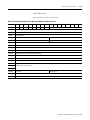
Summary of Changes
The information below summarizes the changes to this manual since the last
printing.
To help you find new and updated information in this release of the manual,
we have included change bars as shown next to this paragraph.
The table below lists the sections that document new features and additional
or updated information about existing features.
1
For This Information
See Page
Addition of a powerup error to Table 16.1.
16-4
Revision of the company name from "Allen-Bradley" to "Rockwell Automation".
G-1
Publication 1747-RM001G-EN-P - November 2008
2
Summary of Changes
Notes:
Publication 1747-RM001G-EN-P - November 2008
Table of Contents
Preface
Who Should Use This Manual. . . . . . . . . . . . . . . . . . . . . . . . . . . . . . .
Purpose of This Manual. . . . . . . . . . . . . . . . . . . . . . . . . . . . . . . . . . . .
Related Documentation. . . . . . . . . . . . . . . . . . . . . . . . . . . . . . . . .
Common Techniques Used in This Manual . . . . . . . . . . . . . . . . . . . .
P-1
P-1
P-2
P-2
Chapter 1
Processor Files
File Structure . . . . . . . . . . . . . . . . . . . . . . . . . . . . . . . . . . . . . . . . . . . . 1-1
Output and Input Data Files (Files O0: and I1:) . . . . . . . . . . . . . 1-2
Status File (File S2:) . . . . . . . . . . . . . . . . . . . . . . . . . . . . . . . . . . . . 1-3
Bit Data File (B3:) . . . . . . . . . . . . . . . . . . . . . . . . . . . . . . . . . . . . . 1-3
Timer Data File (T4:). . . . . . . . . . . . . . . . . . . . . . . . . . . . . . . . . . . 1-4
Addressing Structure . . . . . . . . . . . . . . . . . . . . . . . . . . . . . . . . . . . 1-5
Counter Data File Elements (C5:). . . . . . . . . . . . . . . . . . . . . . . . . 1-6
Entering Parameters . . . . . . . . . . . . . . . . . . . . . . . . . . . . . . . . . . . 1-7
Addressing Structure . . . . . . . . . . . . . . . . . . . . . . . . . . . . . . . . . . . 1-7
Control Data File (R6:) . . . . . . . . . . . . . . . . . . . . . . . . . . . . . . . . . 1-8
Integer Data File (N7:) . . . . . . . . . . . . . . . . . . . . . . . . . . . . . . . . 1-10
Float Data File (F8:). . . . . . . . . . . . . . . . . . . . . . . . . . . . . . . . . . . 1-11
Chapter 2
Basic Instructions
i
About the Basic Instructions . . . . . . . . . . . . . . . . . . . . . . . . . . . . . . . . 2-2
Bit Instructions Overview . . . . . . . . . . . . . . . . . . . . . . . . . . . . . . . . . . 2-2
Examine if Closed (XIC) . . . . . . . . . . . . . . . . . . . . . . . . . . . . . . . . . . . 2-3
Examine if Open (XIO). . . . . . . . . . . . . . . . . . . . . . . . . . . . . . . . . . . . 2-3
Output Energize (OTE) . . . . . . . . . . . . . . . . . . . . . . . . . . . . . . . . . . . 2-4
Output Latch (OTL) and Output Unlatch (OTU) . . . . . . . . . . . . . . . 2-4
Using OTL . . . . . . . . . . . . . . . . . . . . . . . . . . . . . . . . . . . . . . . . . . . 2-4
Using OTU. . . . . . . . . . . . . . . . . . . . . . . . . . . . . . . . . . . . . . . . . . . 2-5
One-shot Rising (OSR) . . . . . . . . . . . . . . . . . . . . . . . . . . . . . . . . . . . . 2-5
Entering Parameters . . . . . . . . . . . . . . . . . . . . . . . . . . . . . . . . . . . 2-5
Timer Instructions Overview . . . . . . . . . . . . . . . . . . . . . . . . . . . . . . . 2-7
Entering Parameters . . . . . . . . . . . . . . . . . . . . . . . . . . . . . . . . . . . 2-7
Timer On-delay (TON) . . . . . . . . . . . . . . . . . . . . . . . . . . . . . . . . . . . . 2-9
Using Status Bits . . . . . . . . . . . . . . . . . . . . . . . . . . . . . . . . . . . . . . 2-9
Timer Off-delay (TOF) . . . . . . . . . . . . . . . . . . . . . . . . . . . . . . . . . . . 2-10
Using Status Bits . . . . . . . . . . . . . . . . . . . . . . . . . . . . . . . . . . . . . 2-10
Retentive Timer (RTO) . . . . . . . . . . . . . . . . . . . . . . . . . . . . . . . . . . . 2-11
Using Status Bits . . . . . . . . . . . . . . . . . . . . . . . . . . . . . . . . . . . . . 2-12
Counter Instructions Overview. . . . . . . . . . . . . . . . . . . . . . . . . . . . . 2-13
How Counters Work . . . . . . . . . . . . . . . . . . . . . . . . . . . . . . . . . . 2-13
Count Up (CTU) . . . . . . . . . . . . . . . . . . . . . . . . . . . . . . . . . . . . . . . . 2-13
Using Status Bits . . . . . . . . . . . . . . . . . . . . . . . . . . . . . . . . . . . . . 2-14
Count Down (CTD). . . . . . . . . . . . . . . . . . . . . . . . . . . . . . . . . . . . . . 2-14
Using Status Bits . . . . . . . . . . . . . . . . . . . . . . . . . . . . . . . . . . . . . 2-15
High-speed Counter (HSC) . . . . . . . . . . . . . . . . . . . . . . . . . . . . . . . . 2-15
High-speed Counter Data Elements. . . . . . . . . . . . . . . . . . . . . . 2-16
Publication 1747-RM001G-EN-P - November 2008
ii
Table of Contents
High-speed Counter Operation . . . . . . . . . . . . . . . . . . . . . . . . . 2-17
Reset (RES). . . . . . . . . . . . . . . . . . . . . . . . . . . . . . . . . . . . . . . . . . . . . 2-20
Chapter 3
Comparison Instructions
About the Comparison Instructions . . . . . . . . . . . . . . . . . . . . . . . . . .
Comparison Instructions Overview . . . . . . . . . . . . . . . . . . . . . . . . . .
Using Indexed Word Addresses . . . . . . . . . . . . . . . . . . . . . . . . . .
Using Indirect Word Addresses . . . . . . . . . . . . . . . . . . . . . . . . . .
Equal (EQU) . . . . . . . . . . . . . . . . . . . . . . . . . . . . . . . . . . . . . . . . . . . .
Not Equal (NEQ) . . . . . . . . . . . . . . . . . . . . . . . . . . . . . . . . . . . . . . . .
Less Than (LES). . . . . . . . . . . . . . . . . . . . . . . . . . . . . . . . . . . . . . . . . .
Less Than or Equal (LEQ) . . . . . . . . . . . . . . . . . . . . . . . . . . . . . . . . .
Greater Than (GRT) . . . . . . . . . . . . . . . . . . . . . . . . . . . . . . . . . . . . . .
Greater Than or Equal (GEQ) . . . . . . . . . . . . . . . . . . . . . . . . . . . . . .
Masked Comparison for Equal (MEQ). . . . . . . . . . . . . . . . . . . . . . . .
Entering Parameters . . . . . . . . . . . . . . . . . . . . . . . . . . . . . . . . . . .
Limit Test (LIM) . . . . . . . . . . . . . . . . . . . . . . . . . . . . . . . . . . . . . . . . .
Entering Parameters . . . . . . . . . . . . . . . . . . . . . . . . . . . . . . . . . . .
3-1
3-2
3-2
3-2
3-2
3-2
3-3
3-3
3-3
3-4
3-4
3-4
3-5
3-5
Chapter 4
Math Instructions
Publication 1747-RM001G-EN-P - November 2008
About the Math Instructions . . . . . . . . . . . . . . . . . . . . . . . . . . . . . . . . 4-2
Math Instructions Overview . . . . . . . . . . . . . . . . . . . . . . . . . . . . . . . . 4-2
Entering Parameters . . . . . . . . . . . . . . . . . . . . . . . . . . . . . . . . . . . 4-2
Using Indexed Word Addresses . . . . . . . . . . . . . . . . . . . . . . . . . . 4-2
Using Indirect Word Addresses . . . . . . . . . . . . . . . . . . . . . . . . . . 4-2
Updates to Arithmetic Status Bits. . . . . . . . . . . . . . . . . . . . . . . . . 4-3
Overflow Trap Bit, S:5/0 . . . . . . . . . . . . . . . . . . . . . . . . . . . . . . . 4-3
Updates to the Math Register, S:13 and S:14 . . . . . . . . . . . . . . . . 4-3
Using Floating Point Data File (F8:). . . . . . . . . . . . . . . . . . . . . . . 4-4
Add (ADD). . . . . . . . . . . . . . . . . . . . . . . . . . . . . . . . . . . . . . . . . . . . . . 4-5
Updates to Arithmetic Status Bits. . . . . . . . . . . . . . . . . . . . . . . . . 4-5
Subtract (SUB) . . . . . . . . . . . . . . . . . . . . . . . . . . . . . . . . . . . . . . . . . . . 4-5
Updates to Arithmetic Status Bits. . . . . . . . . . . . . . . . . . . . . . . . . 4-5
32-Bit Addition and Subtraction . . . . . . . . . . . . . . . . . . . . . . . . . . . . . 4-6
Math Overflow Selection Bit S:2/14. . . . . . . . . . . . . . . . . . . . . . . 4-6
Multiply (MUL) . . . . . . . . . . . . . . . . . . . . . . . . . . . . . . . . . . . . . . . . . . 4-8
Updates to Arithmetic Status Bits. . . . . . . . . . . . . . . . . . . . . . . . . 4-8
Updates to the Math Register, S:13 and S:14 . . . . . . . . . . . . . . . . 4-9
Divide (DIV) . . . . . . . . . . . . . . . . . . . . . . . . . . . . . . . . . . . . . . . . . . . . 4-9
Updates to Arithmetic Status Bits. . . . . . . . . . . . . . . . . . . . . . . . . 4-9
Updates to the Math Registers, S:13 and S:14 . . . . . . . . . . . . . . 4-10
Double Divide (DDV) . . . . . . . . . . . . . . . . . . . . . . . . . . . . . . . . . . . . 4-11
Updates to Arithmetic Status Bits. . . . . . . . . . . . . . . . . . . . . . . . 4-11
Updates to the Math Registers, S:13 and S:14 . . . . . . . . . . . . . . 4-11
Clear (CLR). . . . . . . . . . . . . . . . . . . . . . . . . . . . . . . . . . . . . . . . . . . . . 4-12
Table of Contents
iii
Updates to Arithmetic Status Bits. . . . . . . . . . . . . . . . . . . . . . . .
Square Root (SQR). . . . . . . . . . . . . . . . . . . . . . . . . . . . . . . . . . . . . . .
Updates to Arithmetic Status Bits. . . . . . . . . . . . . . . . . . . . . . . .
Scale with Parameters (SCP) . . . . . . . . . . . . . . . . . . . . . . . . . . . . . . .
Entering Parameters . . . . . . . . . . . . . . . . . . . . . . . . . . . . . . . . . .
Updates to Arithmetic Status Bits. . . . . . . . . . . . . . . . . . . . . . . .
Application Examples . . . . . . . . . . . . . . . . . . . . . . . . . . . . . . . . .
Scale Data (SCL). . . . . . . . . . . . . . . . . . . . . . . . . . . . . . . . . . . . . . . . .
Entering Parameters . . . . . . . . . . . . . . . . . . . . . . . . . . . . . . . . . .
Updates to Arithmetic Status Bits. . . . . . . . . . . . . . . . . . . . . . . .
Application Example 1 - Converting 4 to 20 mA Analog
Input Signal to PID Process Variable . . . . . . . . . . . . . . . . . . . . .
Application Example 2 - Scaling an Analog Input to
Control an Analog Output . . . . . . . . . . . . . . . . . . . . . . . . . . . . .
Ramp Instruction (RMP) . . . . . . . . . . . . . . . . . . . . . . . . . . . . . . . . . .
Instruction Operation . . . . . . . . . . . . . . . . . . . . . . . . . . . . . . . . .
RMP Equation . . . . . . . . . . . . . . . . . . . . . . . . . . . . . . . . . . . . . . .
Continuous Operation. . . . . . . . . . . . . . . . . . . . . . . . . . . . . . . . .
Absolute (ABS). . . . . . . . . . . . . . . . . . . . . . . . . . . . . . . . . . . . . . . . . .
Entering Parameters . . . . . . . . . . . . . . . . . . . . . . . . . . . . . . . . . .
Updates to Arithmetic Status Bits. . . . . . . . . . . . . . . . . . . . . . . .
Compute (CPT) . . . . . . . . . . . . . . . . . . . . . . . . . . . . . . . . . . . . . . . . .
Entering Parameters . . . . . . . . . . . . . . . . . . . . . . . . . . . . . . . . . .
Updates to Arithmetic Status Bits. . . . . . . . . . . . . . . . . . . . . . . .
Application Example . . . . . . . . . . . . . . . . . . . . . . . . . . . . . . . . . .
Swap (SWP) . . . . . . . . . . . . . . . . . . . . . . . . . . . . . . . . . . . . . . . . . . . .
Entering Parameters . . . . . . . . . . . . . . . . . . . . . . . . . . . . . . . . . .
Arc Sine (ASN). . . . . . . . . . . . . . . . . . . . . . . . . . . . . . . . . . . . . . . . . .
Updates to Arithmetic Status Bits. . . . . . . . . . . . . . . . . . . . . . . .
Arc Cosine (ACS) . . . . . . . . . . . . . . . . . . . . . . . . . . . . . . . . . . . . . . . .
Updates to Arithmetic Status Bits. . . . . . . . . . . . . . . . . . . . . . . .
Arc Tangent (ATN) . . . . . . . . . . . . . . . . . . . . . . . . . . . . . . . . . . . . . .
Updates to Arithmetic Status Bits. . . . . . . . . . . . . . . . . . . . . . . .
Cosine (COS) . . . . . . . . . . . . . . . . . . . . . . . . . . . . . . . . . . . . . . . . . . .
Updates to Arithmetic Status Bits. . . . . . . . . . . . . . . . . . . . . . . .
Natural Log (LN) . . . . . . . . . . . . . . . . . . . . . . . . . . . . . . . . . . . . . . . .
Updates to Arithmetic Status Bits. . . . . . . . . . . . . . . . . . . . . . . .
Log to the Base 10 (LOG) . . . . . . . . . . . . . . . . . . . . . . . . . . . . . . . . .
Updates to Arithmetic Status Bits. . . . . . . . . . . . . . . . . . . . . . . .
Sine (SIN) . . . . . . . . . . . . . . . . . . . . . . . . . . . . . . . . . . . . . . . . . . . . . .
Updates to Arithmetic Status Bits. . . . . . . . . . . . . . . . . . . . . . . .
Tangent (TAN). . . . . . . . . . . . . . . . . . . . . . . . . . . . . . . . . . . . . . . . . .
Updates to Arithmetic Status Bits. . . . . . . . . . . . . . . . . . . . . . . .
X to the Power of Y (XPY) . . . . . . . . . . . . . . . . . . . . . . . . . . . . . . . .
Updates to Arithmetic Status Bits. . . . . . . . . . . . . . . . . . . . . . . .
4-12
4-12
4-12
4-13
4-13
4-14
4-14
4-15
4-16
4-16
4-17
4-18
4-20
4-22
4-23
4-23
4-24
4-24
4-24
4-25
4-25
4-26
4-26
4-28
4-28
4-29
4-29
4-29
4-29
4-30
4-30
4-30
4-30
4-31
4-31
4-31
4-31
4-32
4-32
4-32
4-32
4-33
4-33
Publication 1747-RM001G-EN-P - November 2008
iv
Table of Contents
Chapter 5
Data Handling Instructions
Publication 1747-RM001G-EN-P - November 2008
Convert to BCD (TOD) . . . . . . . . . . . . . . . . . . . . . . . . . . . . . . . . . . . 5-2
Updates to Arithmetic Status Bits. . . . . . . . . . . . . . . . . . . . . . . . . 5-2
Updates to the Math Register, S:13 and S:14 . . . . . . . . . . . . . . . . 5-3
Convert from BCD (FRD) . . . . . . . . . . . . . . . . . . . . . . . . . . . . . . . . . 5-5
Updates to Arithmetic Status Bits. . . . . . . . . . . . . . . . . . . . . . . . . 5-5
Changes to the Math Register, S:13 and S:14 . . . . . . . . . . . . . . . . 5-6
Radian to Degrees (DEG) . . . . . . . . . . . . . . . . . . . . . . . . . . . . . . . . . . 5-8
Entering Parameters . . . . . . . . . . . . . . . . . . . . . . . . . . . . . . . . . . . 5-8
Updates to Arithmetic Status Bits. . . . . . . . . . . . . . . . . . . . . . . . . 5-9
Degrees to Radians (RAD) . . . . . . . . . . . . . . . . . . . . . . . . . . . . . . . . . 5-9
Entering Parameters . . . . . . . . . . . . . . . . . . . . . . . . . . . . . . . . . . . 5-9
Updates to Arithmetic Status Bits. . . . . . . . . . . . . . . . . . . . . . . . 5-10
Decode 4 to 1 of 16 (DCD). . . . . . . . . . . . . . . . . . . . . . . . . . . . . . . . 5-10
Entering Parameters . . . . . . . . . . . . . . . . . . . . . . . . . . . . . . . . . . 5-11
Encode 1 of 16 to 4 (ENC) . . . . . . . . . . . . . . . . . . . . . . . . . . . . . . . . 5-11
Entering Parameters . . . . . . . . . . . . . . . . . . . . . . . . . . . . . . . . . . 5-12
Updates to Arithmetic Status Bits. . . . . . . . . . . . . . . . . . . . . . . . 5-12
Copy File (COP) and Fill File (FLL) Instructions . . . . . . . . . . . . . . 5-13
Using COP . . . . . . . . . . . . . . . . . . . . . . . . . . . . . . . . . . . . . . . . . . 5-13
Using FLL . . . . . . . . . . . . . . . . . . . . . . . . . . . . . . . . . . . . . . . . . . 5-14
Move and Logical Instructions Overview. . . . . . . . . . . . . . . . . . . . . 5-16
Entering Parameters . . . . . . . . . . . . . . . . . . . . . . . . . . . . . . . . . . 5-16
Using Indexed Word Addresses . . . . . . . . . . . . . . . . . . . . . . . . . 5-16
Updates to Arithmetic Status Bits. . . . . . . . . . . . . . . . . . . . . . . . 5-16
Using Indirect Word Addresses . . . . . . . . . . . . . . . . . . . . . . . . . 5-16
Updates to the Math Register, S:13 and S:14 . . . . . . . . . . . . . . . 5-17
Entering Mask Values . . . . . . . . . . . . . . . . . . . . . . . . . . . . . . . . . 5-17
Move (MOV) . . . . . . . . . . . . . . . . . . . . . . . . . . . . . . . . . . . . . . . . . . . 5-17
Entering Parameters . . . . . . . . . . . . . . . . . . . . . . . . . . . . . . . . . . 5-17
Updates to Arithmetic Status Bits. . . . . . . . . . . . . . . . . . . . . . . . 5-17
Masked Move (MVM) . . . . . . . . . . . . . . . . . . . . . . . . . . . . . . . . . . . . 5-18
Entering Parameters . . . . . . . . . . . . . . . . . . . . . . . . . . . . . . . . . . 5-18
Updates to Arithmetic Status Bits. . . . . . . . . . . . . . . . . . . . . . . . 5-18
And (AND) . . . . . . . . . . . . . . . . . . . . . . . . . . . . . . . . . . . . . . . . . . . . 5-20
Updates to Arithmetic Status Bits. . . . . . . . . . . . . . . . . . . . . . . . 5-20
Or (OR) . . . . . . . . . . . . . . . . . . . . . . . . . . . . . . . . . . . . . . . . . . . . . . . 5-21
Updates to Arithmetic Status Bits. . . . . . . . . . . . . . . . . . . . . . . . 5-21
Exclusive Or (XOR) . . . . . . . . . . . . . . . . . . . . . . . . . . . . . . . . . . . . . 5-22
Updates to Arithmetic Status Bits. . . . . . . . . . . . . . . . . . . . . . . . 5-22
Not (NOT) . . . . . . . . . . . . . . . . . . . . . . . . . . . . . . . . . . . . . . . . . . . . . 5-23
Updates to Arithmetic Status Bits. . . . . . . . . . . . . . . . . . . . . . . . 5-23
Negate (NEG) . . . . . . . . . . . . . . . . . . . . . . . . . . . . . . . . . . . . . . . . . . 5-24
Updates to Arithmetic Status Bits. . . . . . . . . . . . . . . . . . . . . . . . 5-24
FIFO and LIFO Instructions Overview . . . . . . . . . . . . . . . . . . . . . . 5-25
Entering Parameters . . . . . . . . . . . . . . . . . . . . . . . . . . . . . . . . . . 5-25
Table of Contents
Effects on Index Register S:24 . . . . . . . . . . . . . . . . . . . . . . . . . .
FIFO Load (FFL) and FIFO Unload (FFU) . . . . . . . . . . . . . . . . . .
FFL Instruction Operation . . . . . . . . . . . . . . . . . . . . . . . . . . . . .
FFU Instruction Operation . . . . . . . . . . . . . . . . . . . . . . . . . . . . .
LIFO Load (LFL) and LIFO Unload (LFU) . . . . . . . . . . . . . . . . . .
LFL Instruction Operation . . . . . . . . . . . . . . . . . . . . . . . . . . . . .
LFU Instruction Operation. . . . . . . . . . . . . . . . . . . . . . . . . . . . .
v
5-26
5-26
5-27
5-27
5-28
5-29
5-29
Chapter 6
Program Flow Instructions
About the Program Flow Control Instructions . . . . . . . . . . . . . . . . . 6-1
Jump to Label (JMP) and Label (LBL) . . . . . . . . . . . . . . . . . . . . . . . . 6-2
Entering Parameters . . . . . . . . . . . . . . . . . . . . . . . . . . . . . . . . . . . 6-2
Using JMP . . . . . . . . . . . . . . . . . . . . . . . . . . . . . . . . . . . . . . . . . . . 6-2
Using LBL . . . . . . . . . . . . . . . . . . . . . . . . . . . . . . . . . . . . . . . . . . . 6-3
Jump to Subroutine (JSR), Subroutine (SBR), and Return (RET) . . . 6-3
Nesting Subroutine Files . . . . . . . . . . . . . . . . . . . . . . . . . . . . . . . . 6-4
Using JSR . . . . . . . . . . . . . . . . . . . . . . . . . . . . . . . . . . . . . . . . . . . . 6-4
Using SBR . . . . . . . . . . . . . . . . . . . . . . . . . . . . . . . . . . . . . . . . . . . 6-5
Using RET . . . . . . . . . . . . . . . . . . . . . . . . . . . . . . . . . . . . . . . . . . . 6-5
Master Control Reset (MCR). . . . . . . . . . . . . . . . . . . . . . . . . . . . . . . . 6-6
Processor Operation . . . . . . . . . . . . . . . . . . . . . . . . . . . . . . . . . . . 6-6
Temporary End (TND) . . . . . . . . . . . . . . . . . . . . . . . . . . . . . . . . . . . . 6-7
Suspend (SUS) . . . . . . . . . . . . . . . . . . . . . . . . . . . . . . . . . . . . . . . . . . . 6-8
Entering Parameters . . . . . . . . . . . . . . . . . . . . . . . . . . . . . . . . . . . 6-8
Immediate Input with Mask (IIM) . . . . . . . . . . . . . . . . . . . . . . . . . . . 6-8
Entering Parameters . . . . . . . . . . . . . . . . . . . . . . . . . . . . . . . . . . . 6-8
Immediate Output with Mask (IOM) . . . . . . . . . . . . . . . . . . . . . . . . . 6-9
Entering Parameters . . . . . . . . . . . . . . . . . . . . . . . . . . . . . . . . . . . 6-9
I/O Refresh (REF) . . . . . . . . . . . . . . . . . . . . . . . . . . . . . . . . . . . . . . 6-10
Using an SLC 5/02 Processor. . . . . . . . . . . . . . . . . . . . . . . . . . . 6-10
Using SLC 5/03 and Higher Processors. . . . . . . . . . . . . . . . . . . 6-10
Chapter 7
Application Specific Instructions
About the Application Specific Instructions. . . . . . . . . . . . . . . . . . . .
Bit Shift Instructions Overview. . . . . . . . . . . . . . . . . . . . . . . . . . . . . .
Entering Parameters . . . . . . . . . . . . . . . . . . . . . . . . . . . . . . . . . . .
Effects on Index Register S:24 . . . . . . . . . . . . . . . . . . . . . . . . . . .
Bit Shift Left (BSL)
Bit Shift Right (BSR) . . . . . . . . . . . . . . . . . . . . . . . . . . . . . . . . . . . . . .
Use BSL . . . . . . . . . . . . . . . . . . . . . . . . . . . . . . . . . . . . . . . . . . . . .
Use BSR . . . . . . . . . . . . . . . . . . . . . . . . . . . . . . . . . . . . . . . . . . . . .
Sequencer Instructions Overview . . . . . . . . . . . . . . . . . . . . . . . . . . . .
Effects on Index Register S:24 . . . . . . . . . . . . . . . . . . . . . . . . . . .
Applications Requiring More than 16 Bits . . . . . . . . . . . . . . . . . .
7-2
7-2
7-2
7-4
7-4
7-4
7-5
7-5
7-5
7-6
Publication 1747-RM001G-EN-P - November 2008
vi
Table of Contents
Sequencer Output (SQO)
Sequencer Compare (SQC) . . . . . . . . . . . . . . . . . . . . . . . . . . . . . . . . . 7-6
Enter Parameters . . . . . . . . . . . . . . . . . . . . . . . . . . . . . . . . . . . . . . 7-6
Use SQO . . . . . . . . . . . . . . . . . . . . . . . . . . . . . . . . . . . . . . . . . . . . 7-8
Use SQC. . . . . . . . . . . . . . . . . . . . . . . . . . . . . . . . . . . . . . . . . . . . 7-10
Sequencer Load (SQL). . . . . . . . . . . . . . . . . . . . . . . . . . . . . . . . . . . . 7-12
Enter Parameters . . . . . . . . . . . . . . . . . . . . . . . . . . . . . . . . . . . . . 7-12
Operation . . . . . . . . . . . . . . . . . . . . . . . . . . . . . . . . . . . . . . . . . . . 7-14
Read High-speed Clock and Compute Time Difference Overview 7-15
RHC Instruction Operation . . . . . . . . . . . . . . . . . . . . . . . . . . . . 7-15
TDF Instruction Operation . . . . . . . . . . . . . . . . . . . . . . . . . . . . 7-16
Read High-speed Clock Instruction (RHC) . . . . . . . . . . . . . . . . . . . 7-17
Enter Parameters . . . . . . . . . . . . . . . . . . . . . . . . . . . . . . . . . . . . . 7-17
Compute Time Difference Instruction (TDF) . . . . . . . . . . . . . . . . . 7-17
Enter Parameters . . . . . . . . . . . . . . . . . . . . . . . . . . . . . . . . . . . . . 7-17
File Bit Comparison (FBC) and Diagnostic Detect (DDT) . . . . . . . 7-18
Select the Search Mode . . . . . . . . . . . . . . . . . . . . . . . . . . . . . . . . 7-18
Enter Parameters . . . . . . . . . . . . . . . . . . . . . . . . . . . . . . . . . . . . . 7-20
Use Status Bits . . . . . . . . . . . . . . . . . . . . . . . . . . . . . . . . . . . . . . . 7-21
Read Program Checksum (RPC) . . . . . . . . . . . . . . . . . . . . . . . . . . . . 7-23
Enter Parameters . . . . . . . . . . . . . . . . . . . . . . . . . . . . . . . . . . . . . 7-23
Chapter 8
Block Transfer Instructions
Block Transfer Instructions (BTR and BTW) . . . . . . . . . . . . . . . . . . 8-1
RIO Block Transfer General Functional Overview. . . . . . . . . . . 8-2
Entering Parameters for BTR and BTW . . . . . . . . . . . . . . . . . . . 8-2
Control Status Bits . . . . . . . . . . . . . . . . . . . . . . . . . . . . . . . . . . . . . 8-3
Instruction Operation . . . . . . . . . . . . . . . . . . . . . . . . . . . . . . . . . . 8-7
Programming Examples . . . . . . . . . . . . . . . . . . . . . . . . . . . . . . . . 8-8
Comparison to the PLC-5 BTR and BTW . . . . . . . . . . . . . . . . . 8-11
Chapter 9
Proportional Integral Derivative
Instruction
Publication 1747-RM001G-EN-P - November 2008
Overview. . . . . . . . . . . . . . . . . . . . . . . . . . . . . . . . . . . . . . . . . . . . . . . .
The PID Concept. . . . . . . . . . . . . . . . . . . . . . . . . . . . . . . . . . . . . . . . .
The PID Equation . . . . . . . . . . . . . . . . . . . . . . . . . . . . . . . . . . . . . . . .
The PID Instruction . . . . . . . . . . . . . . . . . . . . . . . . . . . . . . . . . . . . . .
Entering Parameters . . . . . . . . . . . . . . . . . . . . . . . . . . . . . . . . . . .
PID Control Block Layout . . . . . . . . . . . . . . . . . . . . . . . . . . . . . . . . .
Controller Gain (Kc) . . . . . . . . . . . . . . . . . . . . . . . . . . . . . . . . . . .
Reset Term (Ti) . . . . . . . . . . . . . . . . . . . . . . . . . . . . . . . . . . . . . . .
Rate Term (Td) . . . . . . . . . . . . . . . . . . . . . . . . . . . . . . . . . . . . . . .
Feed Forward/Bias . . . . . . . . . . . . . . . . . . . . . . . . . . . . . . . . . . . .
Mode (TM). . . . . . . . . . . . . . . . . . . . . . . . . . . . . . . . . . . . . . . . . . .
Loop Update . . . . . . . . . . . . . . . . . . . . . . . . . . . . . . . . . . . . . . . . .
Deadband . . . . . . . . . . . . . . . . . . . . . . . . . . . . . . . . . . . . . . . . . . . .
9-1
9-1
9-2
9-3
9-3
9-5
9-6
9-6
9-7
9-7
9-7
9-8
9-8
Table of Contents
vii
Scaled Error . . . . . . . . . . . . . . . . . . . . . . . . . . . . . . . . . . . . . . . . . . 9-9
Auto / Manual (AM) . . . . . . . . . . . . . . . . . . . . . . . . . . . . . . . . . . . 9-9
Control (CM) . . . . . . . . . . . . . . . . . . . . . . . . . . . . . . . . . . . . . . . . 9-10
Deadband (DB) . . . . . . . . . . . . . . . . . . . . . . . . . . . . . . . . . . . . . . 9-10
Reset and Gain Enhancement Bit (RG) . . . . . . . . . . . . . . . . . . . 9-10
Setpoint Scaling (SC) . . . . . . . . . . . . . . . . . . . . . . . . . . . . . . . . . 9-11
Loop Update Time Too Fast (TF) . . . . . . . . . . . . . . . . . . . . . . . 9-11
Derivative Rate Action Bit (DA). . . . . . . . . . . . . . . . . . . . . . . . . 9-12
Output Alarm Upper Limit (UL) . . . . . . . . . . . . . . . . . . . . . . . . 9-12
Output Alarm Lower Limit (LL). . . . . . . . . . . . . . . . . . . . . . . . . 9-12
Setpoint Out Of Range (SP) . . . . . . . . . . . . . . . . . . . . . . . . . . . . 9-13
PV Out Of Range (PV) . . . . . . . . . . . . . . . . . . . . . . . . . . . . . . . . 9-13
PID Done (DN) . . . . . . . . . . . . . . . . . . . . . . . . . . . . . . . . . . . . . 9-13
PID Rational Approximation Bit (RA). . . . . . . . . . . . . . . . . . . . 9-14
PID Enable (EN). . . . . . . . . . . . . . . . . . . . . . . . . . . . . . . . . . . . . 9-14
Integral Sum . . . . . . . . . . . . . . . . . . . . . . . . . . . . . . . . . . . . . . . . . 9-14
Input Parameters . . . . . . . . . . . . . . . . . . . . . . . . . . . . . . . . . . . . . . . . 9-15
Setpoint (SP) . . . . . . . . . . . . . . . . . . . . . . . . . . . . . . . . . . . . . . . . 9-15
Scaled Process Variable (SPV) . . . . . . . . . . . . . . . . . . . . . . . . . . 9-16
Setpoint Maximum Scaled (SMAX) . . . . . . . . . . . . . . . . . . . . . . 9-16
Setpoint Minimum Scaled (SMIN) . . . . . . . . . . . . . . . . . . . . . . . 9-17
Output Parameters . . . . . . . . . . . . . . . . . . . . . . . . . . . . . . . . . . . . . . . 9-18
Control Variable (CV) . . . . . . . . . . . . . . . . . . . . . . . . . . . . . . . . . 9-18
Control Variable Percent (CV%) . . . . . . . . . . . . . . . . . . . . . . . . 9-19
Output Limiting Enable (OL) . . . . . . . . . . . . . . . . . . . . . . . . . . . 9-19
Output Maximum (CVH) . . . . . . . . . . . . . . . . . . . . . . . . . . . . . . 9-20
Output Minimum (CVL) . . . . . . . . . . . . . . . . . . . . . . . . . . . . . . . 9-20
Runtime Errors. . . . . . . . . . . . . . . . . . . . . . . . . . . . . . . . . . . . . . . . . . 9-21
PID and Analog I/O Scaling. . . . . . . . . . . . . . . . . . . . . . . . . . . . . . . 9-23
Using the SCL Instruction. . . . . . . . . . . . . . . . . . . . . . . . . . . . . . 9-24
Using the SCP Instruction. . . . . . . . . . . . . . . . . . . . . . . . . . . . . . 9-24
Application Notes . . . . . . . . . . . . . . . . . . . . . . . . . . . . . . . . . . . . . . . 9-27
Input/Output Ranges . . . . . . . . . . . . . . . . . . . . . . . . . . . . . . . . . 9-27
Scaling to Engineering Units . . . . . . . . . . . . . . . . . . . . . . . . . . . . 9-27
Output Alarms . . . . . . . . . . . . . . . . . . . . . . . . . . . . . . . . . . . . . . . 9-28
Output Limiting with Anti-Reset Windup . . . . . . . . . . . . . . . . . 9-29
The Manual Mode . . . . . . . . . . . . . . . . . . . . . . . . . . . . . . . . . . . . 9-29
PID Rungstate . . . . . . . . . . . . . . . . . . . . . . . . . . . . . . . . . . . . . . . 9-30
Time Proportioning Outputs . . . . . . . . . . . . . . . . . . . . . . . . . . . 9-30
Chapter 10
ASCII Instructions
ASCII Instruction Overview . . . . . . . . . . . . . . . . . . . . . . . . . . . . . . .
Protocol Parameter Overview . . . . . . . . . . . . . . . . . . . . . . . . . . . . . .
Entering Parameters . . . . . . . . . . . . . . . . . . . . . . . . . . . . . . . . . .
Test ASCII Buffer for Line (ABL) . . . . . . . . . . . . . . . . . . . . . . . . . .
Entering Parameters . . . . . . . . . . . . . . . . . . . . . . . . . . . . . . . . . .
10-2
10-2
10-5
10-6
10-6
Publication 1747-RM001G-EN-P - November 2008
viii
Table of Contents
Number of ASCII Characters In Buffer (ACB) . . . . . . . . . . . . . . . . 10-7
Entering Parameters . . . . . . . . . . . . . . . . . . . . . . . . . . . . . . . . . . 10-7
String to Integer (ACI). . . . . . . . . . . . . . . . . . . . . . . . . . . . . . . . . . . . 10-8
ASCII Clear Receive and/or Transmit Buffer (ACL) . . . . . . . . . . . 10-9
Entering Parameters . . . . . . . . . . . . . . . . . . . . . . . . . . . . . . . . . 10-10
String Concatenate (ACN). . . . . . . . . . . . . . . . . . . . . . . . . . . . . . . . 10-11
Entering Parameters . . . . . . . . . . . . . . . . . . . . . . . . . . . . . . . . . 10-11
String Extract (AEX) . . . . . . . . . . . . . . . . . . . . . . . . . . . . . . . . . . . . 10-12
Entering Parameters . . . . . . . . . . . . . . . . . . . . . . . . . . . . . . . . . 10-12
ASCII Handshake Lines (AHL) . . . . . . . . . . . . . . . . . . . . . . . . . . . 10-13
Entering Parameters . . . . . . . . . . . . . . . . . . . . . . . . . . . . . . . . . 10-13
Integer to String (AIC). . . . . . . . . . . . . . . . . . . . . . . . . . . . . . . . . . . 10-14
ASCII Read Characters (ARD) . . . . . . . . . . . . . . . . . . . . . . . . . . . . 10-15
Entering Parameters . . . . . . . . . . . . . . . . . . . . . . . . . . . . . . . . . 10-15
Timing Diagram for a Successful ARD, ARL, AWA, and
AWT Instructions . . . . . . . . . . . . . . . . . . . . . . . . . . . . . . . . . . . 10-16
ASCII Read Line (ARL). . . . . . . . . . . . . . . . . . . . . . . . . . . . . . . . . . 10-17
Entering Parameters . . . . . . . . . . . . . . . . . . . . . . . . . . . . . . . . . 10-17
String Search (ASC) . . . . . . . . . . . . . . . . . . . . . . . . . . . . . . . . . . . . . 10-18
Entering Parameters . . . . . . . . . . . . . . . . . . . . . . . . . . . . . . . . . 10-18
ASCII String Compare (ASR) . . . . . . . . . . . . . . . . . . . . . . . . . . . . . 10-19
Entering Parameters . . . . . . . . . . . . . . . . . . . . . . . . . . . . . . . . . 10-19
ASCII Write with Append (AWA) . . . . . . . . . . . . . . . . . . . . . . . . . 10-20
Entering Parameters . . . . . . . . . . . . . . . . . . . . . . . . . . . . . . . . . 10-20
Using Inline Indirection. . . . . . . . . . . . . . . . . . . . . . . . . . . . . . . 10-21
ASCII Write (AWT) . . . . . . . . . . . . . . . . . . . . . . . . . . . . . . . . . . . . . 10-22
Entering Parameters . . . . . . . . . . . . . . . . . . . . . . . . . . . . . . . . . 10-22
ASCII Instruction Error Codes. . . . . . . . . . . . . . . . . . . . . . . . . . . . 10-24
ASCII Conversion Table . . . . . . . . . . . . . . . . . . . . . . . . . . . . . . . . . 10-25
Chapter 11
Understanding Interrupt Routines
Publication 1747-RM001G-EN-P - November 2008
User Fault Routine Overview . . . . . . . . . . . . . . . . . . . . . . . . . . . . . . 11-2
Status File Data Saved . . . . . . . . . . . . . . . . . . . . . . . . . . . . . . . . . 11-3
Creating a User Fault Subroutine . . . . . . . . . . . . . . . . . . . . . . . . 11-3
User Interrupt Routine Application Example . . . . . . . . . . . . . . 11-4
Selectable Timed Interrupt Overview . . . . . . . . . . . . . . . . . . . . . . . . 11-8
Basic Programming Procedure for the STI Function . . . . . . . . 11-8
Operation . . . . . . . . . . . . . . . . . . . . . . . . . . . . . . . . . . . . . . . . . . . . . . 11-9
STI Subroutine Content . . . . . . . . . . . . . . . . . . . . . . . . . . . . . . . 11-9
Interrupt Latency and Interrupt Occurrences . . . . . . . . . . . . . . 11-9
Interrupt Priorities . . . . . . . . . . . . . . . . . . . . . . . . . . . . . . . . . . . 11-11
Status File Data Saved . . . . . . . . . . . . . . . . . . . . . . . . . . . . . . . . 11-11
STI Parameters . . . . . . . . . . . . . . . . . . . . . . . . . . . . . . . . . . . . . . . . . 11-12
STD and STE Instructions . . . . . . . . . . . . . . . . . . . . . . . . . . . . . . . 11-16
Selectable Timed Disable - STD . . . . . . . . . . . . . . . . . . . . . . . . 11-16
Selectable Timed Enable - STE. . . . . . . . . . . . . . . . . . . . . . . . . 11-16
Table of Contents
STD/STE Zone Example . . . . . . . . . . . . . . . . . . . . . . . . . . . . .
Selectable Timed Start (STS) . . . . . . . . . . . . . . . . . . . . . . . . . . . . . .
Discrete Input Interrupt Overview . . . . . . . . . . . . . . . . . . . . . . . . .
Basic Programming Procedure for the DII Function . . . . . . .
Operation . . . . . . . . . . . . . . . . . . . . . . . . . . . . . . . . . . . . . . . . . . . . .
Counter Mode . . . . . . . . . . . . . . . . . . . . . . . . . . . . . . . . . . . . . .
Event Mode . . . . . . . . . . . . . . . . . . . . . . . . . . . . . . . . . . . . . . . .
DII Subroutine Content . . . . . . . . . . . . . . . . . . . . . . . . . . . . . .
Interrupt Latency and Interrupt Occurrences . . . . . . . . . . . . .
Interrupt Priorities . . . . . . . . . . . . . . . . . . . . . . . . . . . . . . . . . . .
Status File Data Saved . . . . . . . . . . . . . . . . . . . . . . . . . . . . . . . .
Reconfigurability . . . . . . . . . . . . . . . . . . . . . . . . . . . . . . . . . . . .
DII Parameters . . . . . . . . . . . . . . . . . . . . . . . . . . . . . . . . . . . . . . . . .
Discrete Input Interrupt Application Example . . . . . . . . . . . .
I/O Interrupt Overview (ISR). . . . . . . . . . . . . . . . . . . . . . . . . . . . .
Basic Programming Procedure for the I/O Interrupt
Function . . . . . . . . . . . . . . . . . . . . . . . . . . . . . . . . . . . . . . . . . . .
Operation . . . . . . . . . . . . . . . . . . . . . . . . . . . . . . . . . . . . . . . . . . . . .
Interrupt Subroutine (ISR) Content . . . . . . . . . . . . . . . . . . . . .
Interrupt Latency and Interrupt Occurrences . . . . . . . . . . . . .
Interrupt Priorities . . . . . . . . . . . . . . . . . . . . . . . . . . . . . . . . . . .
Status File Data Saved . . . . . . . . . . . . . . . . . . . . . . . . . . . . . . . .
I/O Interrupt Parameters . . . . . . . . . . . . . . . . . . . . . . . . . . . . . . . .
I/O Interrupt Disable (IID) and I/O Interrupt Enable (IIE). . . .
IID Operation . . . . . . . . . . . . . . . . . . . . . . . . . . . . . . . . . . . . . .
IIE Operation . . . . . . . . . . . . . . . . . . . . . . . . . . . . . . . . . . . . . .
IID/IIE Zone Example . . . . . . . . . . . . . . . . . . . . . . . . . . . . . .
Reset Pending Interrupt (RPI). . . . . . . . . . . . . . . . . . . . . . . . . . . . .
Entering Parameters . . . . . . . . . . . . . . . . . . . . . . . . . . . . . . . . .
Interrupt Subroutine (INT) . . . . . . . . . . . . . . . . . . . . . . . . . . . . . . .
ix
11-16
11-17
11-18
11-18
11-19
11-19
11-20
11-20
11-21
11-22
11-22
11-22
11-23
11-25
11-27
11-27
11-27
11-28
11-28
11-29
11-30
11-30
11-32
11-32
11-33
11-33
11-34
11-34
11-34
Chapter 12
SLC Communication Instructions
About the Communication Instructions . . . . . . . . . . . . . . . . . . . . . . 12-2
Service Communications (SVC) . . . . . . . . . . . . . . . . . . . . . . . . . . . . 12-3
Use an SLC 5/02 Processor . . . . . . . . . . . . . . . . . . . . . . . . . . . . 12-3
Use SLC 5/03 and Higher Processors . . . . . . . . . . . . . . . . . . . . 12-3
Channel Servicing . . . . . . . . . . . . . . . . . . . . . . . . . . . . . . . . . . . . 12-4
Message Instruction Overview . . . . . . . . . . . . . . . . . . . . . . . . . . . . . 12-5
MSG Instruction Operation . . . . . . . . . . . . . . . . . . . . . . . . . . . . 12-5
MSG Instruction Configuration Options . . . . . . . . . . . . . . . . . 12-11
MSG Instruction Parameters. . . . . . . . . . . . . . . . . . . . . . . . . . . 12-11
MSG Instruction Setup Screen Parameters . . . . . . . . . . . . . . . 12-13
MSG Instruction Setup Screen Status Bits . . . . . . . . . . . . . . . . 12-27
MSG Instruction Control Block . . . . . . . . . . . . . . . . . . . . . . . . 12-30
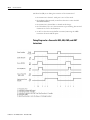
Status Bit Sequencing for SLC 5/03, SLC 5/04, and
SLC 5/05 MSG Instruction. . . . . . . . . . . . . . . . . . . . . . . . . . . . . . . 12-37
Publication 1747-RM001G-EN-P - November 2008
x
Table of Contents
Rung Goes True. . . . . . . . . . . . . . . . . . . . . . . . . . . . . . . . . . . . .
Next End of Scan . . . . . . . . . . . . . . . . . . . . . . . . . . . . . . . . . . .
Successful Receipt of Packet . . . . . . . . . . . . . . . . . . . . . . . . . . .
An ACK is Not Received . . . . . . . . . . . . . . . . . . . . . . . . . . . . .
Target Node Sends a Reply Packet . . . . . . . . . . . . . . . . . . . . . .
MSG Instruction Error Codes. . . . . . . . . . . . . . . . . . . . . . . . . . . . .
Explicit Message Instruction Overview . . . . . . . . . . . . . . . . . . . . .
ControlNet Explicit Message (CEM) . . . . . . . . . . . . . . . . . . . . . . .
CEM Instruction Parameters . . . . . . . . . . . . . . . . . . . . . . . . . .
CEM Instruction Setup Screen Parameters . . . . . . . . . . . . . . .
DeviceNet Explicit Message (DEM). . . . . . . . . . . . . . . . . . . . . . . .
DEM Instruction Parameters . . . . . . . . . . . . . . . . . . . . . . . . . .
DEM Instruction Setup Screen Parameters . . . . . . . . . . . . . . .
EtherNet/IP Explicit Message (EEM) . . . . . . . . . . . . . . . . . . . . . .
EEM Instruction Parameters . . . . . . . . . . . . . . . . . . . . . . . . . .
EEM Instruction Setup Screen Parameters . . . . . . . . . . . . . . .
12-37
12-39
12-39
12-40
12-40
12-41
12-44
12-45
12-45
12-46
12-52
12-52
12-52
12-58
12-58
12-58
Chapter 13
SLC Communication Channels
Publication 1747-RM001G-EN-P - November 2008
Communication Driver Overview. . . . . . . . . . . . . . . . . . . . . . . . . . . 13-2
DH-485 Communications . . . . . . . . . . . . . . . . . . . . . . . . . . . . . . . . . 13-4
DH-485 Network Protocol . . . . . . . . . . . . . . . . . . . . . . . . . . . . . 13-4
DH-485 Network Considerations. . . . . . . . . . . . . . . . . . . . . . . . 13-5
Configuring a Channel for DH-485 . . . . . . . . . . . . . . . . . . . . . . 13-7
DH-485 Channel Status. . . . . . . . . . . . . . . . . . . . . . . . . . . . . . . . 13-9
Data Highway Plus Communications . . . . . . . . . . . . . . . . . . . . . . . 13-10
Configuring Channel 1 for DH+ . . . . . . . . . . . . . . . . . . . . . . . 13-12
DH+ Channel Status . . . . . . . . . . . . . . . . . . . . . . . . . . . . . . . . . 13-13
Global Status Word Overview . . . . . . . . . . . . . . . . . . . . . . . . . 13-18
Ethernet Communications. . . . . . . . . . . . . . . . . . . . . . . . . . . . . . . . 13-22
SLC 5/05 Performance Considerations . . . . . . . . . . . . . . . . . . 13-22
SLC 5/05 and PC Connections to the Ethernet Network . . . 13-23
Configuring Channel 1 for Ethernet. . . . . . . . . . . . . . . . . . . . . 13-24
Ethernet Channel Status . . . . . . . . . . . . . . . . . . . . . . . . . . . . . . 13-28
Configuration Via BOOTP . . . . . . . . . . . . . . . . . . . . . . . . . . . . . . . 13-31
Using the Rockwell BOOTP Utility . . . . . . . . . . . . . . . . . . . . . 13-33
SLC 5/05 Embedded Web Server Capability . . . . . . . . . . . . . . . . . 13-35
Module Information . . . . . . . . . . . . . . . . . . . . . . . . . . . . . . . . . 13-35
TCP/IP Configuration . . . . . . . . . . . . . . . . . . . . . . . . . . . . . . . 13-36
Diagnostic Information . . . . . . . . . . . . . . . . . . . . . . . . . . . . . . . 13-37
Data Table Memory Map . . . . . . . . . . . . . . . . . . . . . . . . . . . . . 13-38
Data Table Monitor . . . . . . . . . . . . . . . . . . . . . . . . . . . . . . . . . . 13-40
User Provided Pages . . . . . . . . . . . . . . . . . . . . . . . . . . . . . . . . . 13-41
DF1 Full-duplex Communications . . . . . . . . . . . . . . . . . . . . . . . . . 13-49
Configuring Channel 0 for DF1 Full-duplex . . . . . . . . . . . . . . 13-49
DF1 Full-duplex Channel Status. . . . . . . . . . . . . . . . . . . . . . . . 13-53
Table of Contents
xi
DF1 Half-duplex Communications. . . . . . . . . . . . . . . . . . . . . . . . . 13-55
DF1 Half-duplex Master Broadcast . . . . . . . . . . . . . . . . . . . . . 13-55
DF1 Half-duplex Slave Broadcast. . . . . . . . . . . . . . . . . . . . . . . 13-55
Configuring Channel 0 for Standard Polling Mode DF1
Half-duplex Master . . . . . . . . . . . . . . . . . . . . . . . . . . . . . . . . . . 13-56
Minimum DF1 Half-duplex Master Channel 0 ACK Timeout 13-61
Determining Minimum Master ACK Timeout . . . . . . . . . . . . 13-62
Monitor Active Stations . . . . . . . . . . . . . . . . . . . . . . . . . . . . 13-63
Configuring Channel 0 for Message-based Polling Mode DF1
Half-duplex Master . . . . . . . . . . . . . . . . . . . . . . . . . . . . . . . . . . 13-63
DF1 Half-duplex Master Channel Status . . . . . . . . . . . . . . . . . 13-68
Configuring Channel 0 for DF1 Half-duplex Slave . . . . . . . . . 13-69
Configuring Channel 0 Poll Timeout . . . . . . . . . . . . . . . . . . . . 13-73
DF1 Half-duplex Slave Channel Status . . . . . . . . . . . . . . . . . . 13-74
DF1 Radio Modem Communications. . . . . . . . . . . . . . . . . . . . . . . 13-76
DF1 Radio Modem System Limitations . . . . . . . . . . . . . . . . . . 13-77
Configuring Channel 0 for DF1 Radio Modem . . . . . . . . . . . . 13-78
DF1 Radio Modem Channel Status . . . . . . . . . . . . . . . . . . . . . 13-81
Configuring the Store & Forward Table. . . . . . . . . . . . . . . . . . 13-82
Using Modems that Support DF1 Communication Protocols . . . 13-84
Dial-up Phone Modems . . . . . . . . . . . . . . . . . . . . . . . . . . . . . . 13-84
Leased-line Modems . . . . . . . . . . . . . . . . . . . . . . . . . . . . . . . . . 13-84
Radio Modems . . . . . . . . . . . . . . . . . . . . . . . . . . . . . . . . . . . . . . 13-85
Line Drivers . . . . . . . . . . . . . . . . . . . . . . . . . . . . . . . . . . . . . . . . 13-85
Modem Control Line Operation in SLC 5/03, SLC 5/04 and
SLC 5/05 Processors . . . . . . . . . . . . . . . . . . . . . . . . . . . . . . . . . . . . 13-86
DF1 Full-duplex. . . . . . . . . . . . . . . . . . . . . . . . . . . . . . . . . . . . . 13-86
DF1 Half-duplex Slave . . . . . . . . . . . . . . . . . . . . . . . . . . . . . . . 13-86
DF1 Half-duplex Master . . . . . . . . . . . . . . . . . . . . . . . . . . . . . . 13-87
DF1 Radio Modem . . . . . . . . . . . . . . . . . . . . . . . . . . . . . . . . . . 13-88
Modbus RTU Master. . . . . . . . . . . . . . . . . . . . . . . . . . . . . . . . . 13-88
RTS Send Delay and RTS Off Delay Parameters . . . . . . . . . . 13-89
Modbus RTU Protocol . . . . . . . . . . . . . . . . . . . . . . . . . . . . . . . . . . 13-90
Modbus RTU Master. . . . . . . . . . . . . . . . . . . . . . . . . . . . . . . . . 13-90
Configuring a Channel for Modbus RTU Master . . . . . . . . . . 13-91
Modbus RTU Master Channel Status . . . . . . . . . . . . . . . . . . . . 13-94
Modbus Commands . . . . . . . . . . . . . . . . . . . . . . . . . . . . . . . . . 13-96
Modbus Error Codes. . . . . . . . . . . . . . . . . . . . . . . . . . . . . . . . . 13-97
ASCII Communications. . . . . . . . . . . . . . . . . . . . . . . . . . . . . . . . . . 13-98
Configuring Channel 0 for ASCII Communications . . . . . . . . 13-98
Chapter 14
SLC Passthru Communications
Remote I/O Passthru . . . . . . . . . . . . . . . . . . . . . . . . . . . . . . . . . . . .
DeviceNet Passthru . . . . . . . . . . . . . . . . . . . . . . . . . . . . . . . . . . . . . .
Channel-to-channel Passthru. . . . . . . . . . . . . . . . . . . . . . . . . . . . . . .
Additional SLC 5/03 Passthru Status Bits . . . . . . . . . . . . . . . . .
14-1
14-2
14-2
14-4
Publication 1747-RM001G-EN-P - November 2008
xii
Table of Contents
Using RSLinx Classic, version 2.50 and higher, with SLC 5/03
Passthru . . . . . . . . . . . . . . . . . . . . . . . . . . . . . . . . . . . . . . . . . . . . 14-5
SLC 5/03 Passthru Error Codes . . . . . . . . . . . . . . . . . . . . . . . . . 14-7
Using RSLinx Classic, version 2.50 and higher, with SLC 5/04
Passthru . . . . . . . . . . . . . . . . . . . . . . . . . . . . . . . . . . . . . . . . . . . . 14-8
Creating and Filling out the Passthru Routing Table File . . . . . 14-9
Using RSLinx Classic, version 2.50 and higher, with SLC 5/05
Passthru . . . . . . . . . . . . . . . . . . . . . . . . . . . . . . . . . . . . . . . . . . . 14-11
SLC 5/05 Passthru Error Codes . . . . . . . . . . . . . . . . . . . . . . . . 14-13
Optimizing RSLinx Channel 1 to DF1 Half-duplex Master/DF1
Radio Modem Passthru . . . . . . . . . . . . . . . . . . . . . . . . . . . . . . . 14-13
Chapter 15
Messaging Examples
Publication 1747-RM001G-EN-P - November 2008
Local versus Remote type Message . . . . . . . . . . . . . . . . . . . . . . . . . . 15-1
Local Message . . . . . . . . . . . . . . . . . . . . . . . . . . . . . . . . . . . . . . . 15-1
Remote Message . . . . . . . . . . . . . . . . . . . . . . . . . . . . . . . . . . . . . 15-1
Remote Terminology . . . . . . . . . . . . . . . . . . . . . . . . . . . . . . . . . . . . . 15-2
Remote Bridge Address. . . . . . . . . . . . . . . . . . . . . . . . . . . . . . . . 15-2
Remote Station Address . . . . . . . . . . . . . . . . . . . . . . . . . . . . . . . 15-2
Remote Bridge Link ID. . . . . . . . . . . . . . . . . . . . . . . . . . . . . . . . 15-2
SLC 5/03 Passthru Examples . . . . . . . . . . . . . . . . . . . . . . . . . . . . . . 15-3
Passthru Example: DF1 to DH-485 . . . . . . . . . . . . . . . . . . . . . . 15-3
Passthru Example: DH-485 to DF1 . . . . . . . . . . . . . . . . . . . . . . 15-6
Passthru Example: DH-485 to DH-485 . . . . . . . . . . . . . . . . . . . 15-9
SLC 5/04 Passthru Examples . . . . . . . . . . . . . . . . . . . . . . . . . . . . . 15-12
Passthru Example: DF1 to DH+ . . . . . . . . . . . . . . . . . . . . . . . 15-12
Passthru Example: DH+ to DF1 . . . . . . . . . . . . . . . . . . . . . . . 15-15
Passthru Example: DH-485 to DH+ . . . . . . . . . . . . . . . . . . . . 15-16
Passthru Example: DH+ to DH-485 . . . . . . . . . . . . . . . . . . . . 15-17
SLC 5/05 Passthru Examples . . . . . . . . . . . . . . . . . . . . . . . . . . . . . 15-18
Passthru Example: DF1 to Ethernet . . . . . . . . . . . . . . . . . . . . 15-18
SLC 5/05 (IP Address 100.100.115.9) Bridge . . . . . . . . . . . . . 15-20
Passthru Routing Table . . . . . . . . . . . . . . . . . . . . . . . . . . . . . . . 15-21
Passthru Example: Ethernet to DF1 . . . . . . . . . . . . . . . . . . . . 15-22
Passthru Example: DH-485 to Ethernet . . . . . . . . . . . . . . . . . 15-23
Passthru Example: Ethernet to DH-485 . . . . . . . . . . . . . . . . . 15-24
Remote Examples . . . . . . . . . . . . . . . . . . . . . . . . . . . . . . . . . . . . . . 15-25
Remote Example: Network Overview . . . . . . . . . . . . . . . . . . . 15-25
Network Message Example: SLC 5/04 to SLC 5/02
via DHRIO and KA5 . . . . . . . . . . . . . . . . . . . . . . . . . . . . . . . . 15-26
Network Message Example: SLC 5/04 to SLC 5/03
via DHRIO and KA5 . . . . . . . . . . . . . . . . . . . . . . . . . . . . . . . . 15-27
Network Message Example: SLC 5/04 to SLC 5/04
via DHRIO . . . . . . . . . . . . . . . . . . . . . . . . . . . . . . . . . . . . . . . . 15-28
Network Message Example: SLC 5/04 to SLC 5/02
via KA5 . . . . . . . . . . . . . . . . . . . . . . . . . . . . . . . . . . . . . . . . . . . 15-29
Table of Contents
Network Message Example: SLC 5/04 to SLC 5/03
via KA5 . . . . . . . . . . . . . . . . . . . . . . . . . . . . . . . . . . . . . . . . . . .
Network Message Example: SLC 5/04 to SLC 5/05
via DHRIO and ENET. . . . . . . . . . . . . . . . . . . . . . . . . . . . . . .
Network Message Example: SLC 5/05 to SLC 5/04
via ENET and DHRIO. . . . . . . . . . . . . . . . . . . . . . . . . . . . . . .
Network Message Example: SLC 5/05 to SLC 5/03
via ENET, CNB and KFC . . . . . . . . . . . . . . . . . . . . . . . . . . . .
Network Message Example: SLC 5/05 to SLC 5/03
via ENET, DHRIO and KA5. . . . . . . . . . . . . . . . . . . . . . . . . .
Network Message Example: PLC 5/20E to SLC 500 CH0
via ENI. . . . . . . . . . . . . . . . . . . . . . . . . . . . . . . . . . . . . . . . . . . .
xiii
15-30
15-31
15-32
15-33
15-34
15-35
Chapter 16
Troubleshooting Faults
Automatically Clear Faults . . . . . . . . . . . . . . . . . . . . . . . . . . . . . . . . . 16-1
SLC Processors . . . . . . . . . . . . . . . . . . . . . . . . . . . . . . . . . . . . . . 16-1
Manually Clear Faults . . . . . . . . . . . . . . . . . . . . . . . . . . . . . . . . . . . . . 16-2
Use the Fault Routine . . . . . . . . . . . . . . . . . . . . . . . . . . . . . . . . . 16-2
SLC Processor Faults . . . . . . . . . . . . . . . . . . . . . . . . . . . . . . . . . . . . . 16-3
Powerup Errors . . . . . . . . . . . . . . . . . . . . . . . . . . . . . . . . . . . . . . 16-3
Going-to-run Errors . . . . . . . . . . . . . . . . . . . . . . . . . . . . . . . . . . 16-4
Run Errors . . . . . . . . . . . . . . . . . . . . . . . . . . . . . . . . . . . . . . . . . . 16-6
User Program Instruction Errors . . . . . . . . . . . . . . . . . . . . . . . . 16-9
I/O Errors . . . . . . . . . . . . . . . . . . . . . . . . . . . . . . . . . . . . . . . . . 16-11
Troubleshoot SLC 5/03 and Higher Processors . . . . . . . . . . . . . . 16-15
Powerup LED Display . . . . . . . . . . . . . . . . . . . . . . . . . . . . . . . 16-15
Identify Processor Errors while Downloading an
Operating System. . . . . . . . . . . . . . . . . . . . . . . . . . . . . . . . . . . . 16-15
Appendix A
SLC 5/03 (OS30x), SLC 5/04 (OS40x) OS300, Series A, FRN 1
released: June 1993 . . . . . . . . . . . . . . . . . . . . . . . . . . . . . . . . . . . . . . . A-1
and SLC 5/05 (OS50x) Firmware
Original Release . . . . . . . . . . . . . . . . . . . . . . . . . . . . . . . . . . . . . . A-1
History
OS300, Series A, FRN 2
released: July 1993 . . . . . . . . . . . . . . . . . . . . . . . . . . . . . . . . . . . . . . .
Enhancements . . . . . . . . . . . . . . . . . . . . . . . . . . . . . . . . . . . . . . .
OS300, Series A, FRN 3
released: March 1994 . . . . . . . . . . . . . . . . . . . . . . . . . . . . . . . . . . . . .
Enhancements . . . . . . . . . . . . . . . . . . . . . . . . . . . . . . . . . . . . . . .
OS300, Series A, FRN 4
released: May 1994 . . . . . . . . . . . . . . . . . . . . . . . . . . . . . . . . . . . . . . .
Enhancements . . . . . . . . . . . . . . . . . . . . . . . . . . . . . . . . . . . . . . .
OS301, Series A, FRN 5
released: August 1994. . . . . . . . . . . . . . . . . . . . . . . . . . . . . . . . . . . . .
Enhancements . . . . . . . . . . . . . . . . . . . . . . . . . . . . . . . . . . . . . . .
A-1
A-1
A-1
A-1
A-1
A-1
A-2
A-2
Publication 1747-RM001G-EN-P - November 2008
xiv
Table of Contents
OS400, Series A, FRN 1
released: August 1994. . . . . . . . . . . . . . . . . . . . . . . . . . . . . . . . . . . . .
Original Release . . . . . . . . . . . . . . . . . . . . . . . . . . . . . . . . . . . . . .
OS301, Series A, FRN 6
OS400, Series A, FRN 2
released: November 1994. . . . . . . . . . . . . . . . . . . . . . . . . . . . . . . . . .
Enhancements . . . . . . . . . . . . . . . . . . . . . . . . . . . . . . . . . . . . . . .
OS301, Series A, FRN 7
0S400, Series A, FRN 3
released: March 1995 . . . . . . . . . . . . . . . . . . . . . . . . . . . . . . . . . . . . .
Enhancements . . . . . . . . . . . . . . . . . . . . . . . . . . . . . . . . . . . . . . .
OS301, Series A, FRN 8
OS400, Series A, FRN 4
released: April 1995 . . . . . . . . . . . . . . . . . . . . . . . . . . . . . . . . . . . . . .
Enhancements . . . . . . . . . . . . . . . . . . . . . . . . . . . . . . . . . . . . . . .
OS302, Series A, FRN 9
OS401, Series A, FRN 5
released: December 1995 . . . . . . . . . . . . . . . . . . . . . . . . . . . . . . . . . .
Enhancements . . . . . . . . . . . . . . . . . . . . . . . . . . . . . . . . . . . . . . .
OS401, Series A, FRN 6
released: May 1996 . . . . . . . . . . . . . . . . . . . . . . . . . . . . . . . . . . . . . . .
Enhancements . . . . . . . . . . . . . . . . . . . . . . . . . . . . . . . . . . . . . . .
OS302, Series B, FRN 10
OS401, Series B, FRN 7
released: July 1997 . . . . . . . . . . . . . . . . . . . . . . . . . . . . . . . . . . . . . . .
Enhancements . . . . . . . . . . . . . . . . . . . . . . . . . . . . . . . . . . . . . . .
Special Note . . . . . . . . . . . . . . . . . . . . . . . . . . . . . . . . . . . . . . . . .
OS500, Series A, FRN 1
released: October 1997. . . . . . . . . . . . . . . . . . . . . . . . . . . . . . . . . . . .
Original Release . . . . . . . . . . . . . . . . . . . . . . . . . . . . . . . . . . . . . .
OS302, Series B, FRN 11
OS401, Series B, FRN 8
OS500, Series A, FRN 2
released: November 1997. . . . . . . . . . . . . . . . . . . . . . . . . . . . . . . . . .
Enhancements . . . . . . . . . . . . . . . . . . . . . . . . . . . . . . . . . . . . . . .
OS302, Series B, FRN 12
released: November 1998
OS401, Series B, FRN 9
released: July, 1999
OS501, Series A, FRN 3
released: July 1998 . . . . . . . . . . . . . . . . . . . . . . . . . . . . . . . . . . . . . . .
Enhancements (OS501 only). . . . . . . . . . . . . . . . . . . . . . . . . . . .
Publication 1747-RM001G-EN-P - November 2008
A-3
A-3
A-3
A-3
A-3
A-3
A-4
A-4
A-4
A-4
A-5
A-5
A-5
A-5
A-5
A-6
A-6
A-6
A-6
A-6
A-6
Table of Contents
xv
OS302, Series B, FRN 12
released: November 1998
OS401, Series B, FRN 9
released: July 1999
OS501, Series A, FRN 4
released: February 1999 . . . . . . . . . . . . . . . . . . . . . . . . . . . . . . . . . . . A-6
Enhancements . . . . . . . . . . . . . . . . . . . . . . . . . . . . . . . . . . . . . . . A-6
OS302, Series B, FRN 14
OS401, Series B, FRN 9
released: July 1999
OS501, Series A, FRN 4
released: February, 1999. . . . . . . . . . . . . . . . . . . . . . . . . . . . . . . . . . . A-6
Enhancements . . . . . . . . . . . . . . . . . . . . . . . . . . . . . . . . . . . . . . . A-6
OS501, Series A, FRN 5
released: April 1999 . . . . . . . . . . . . . . . . . . . . . . . . . . . . . . . . . . . . . . A-7
Enhancements . . . . . . . . . . . . . . . . . . . . . . . . . . . . . . . . . . . . . . . A-7
OS302, Series C, FRN 3
OS401, Series C, FRN 3
OS501, Series C, FRN 3
released: September 2000. . . . . . . . . . . . . . . . . . . . . . . . . . . . . . . . . . A-7
Enhancements . . . . . . . . . . . . . . . . . . . . . . . . . . . . . . . . . . . . . . . A-7
OS302, Series C, FRN 4
OS401, Series C, FRN 4
OS501, Series C, FRN 4
released: February 2001 . . . . . . . . . . . . . . . . . . . . . . . . . . . . . . . . . . A-11
Enhancements . . . . . . . . . . . . . . . . . . . . . . . . . . . . . . . . . . . . . . A-11
OS302, Series C, FRN 5
OS401, Series C, FRN 5
OS501, Series C, FRN 5
released: October 2001. . . . . . . . . . . . . . . . . . . . . . . . . . . . . . . . . . . A-12
Enhancements . . . . . . . . . . . . . . . . . . . . . . . . . . . . . . . . . . . . . . A-12
OS302, Series C, FRN 6
OS401, Series C, FRN 6
OS501, Series C, FRN 6
released: November 2002. . . . . . . . . . . . . . . . . . . . . . . . . . . . . . . . . A-13
Enhancements . . . . . . . . . . . . . . . . . . . . . . . . . . . . . . . . . . . . . . A-13
OS302, Series C, FRN 7
OS401, Series C, FRN 7
OS501, Series C, FRN 7
released: November 2003. . . . . . . . . . . . . . . . . . . . . . . . . . . . . . . . . A-15
Enhancements . . . . . . . . . . . . . . . . . . . . . . . . . . . . . . . . . . . . . . A-15
Publication 1747-RM001G-EN-P - November 2008
xvi
Table of Contents
OS302, Series C, FRN 8
OS401, Series C, FRN 8
OS501, Series C, FRN 8
released: May 2004 . . . . . . . . . . . . . . . . . . . . . . . . . . . . . . . . . . . . . .
Enhancements . . . . . . . . . . . . . . . . . . . . . . . . . . . . . . . . . . . . . .
OS501, Series C, FRN 9
released: November 2004. . . . . . . . . . . . . . . . . . . . . . . . . . . . . . . . .
Enhancements . . . . . . . . . . . . . . . . . . . . . . . . . . . . . . . . . . . . . .
OS302, Series C, FRN 10
OS401, Series C, FRN 10
OS501, Series C, FRN 10
released: January 2006 . . . . . . . . . . . . . . . . . . . . . . . . . . . . . . . . . . .
Enhancements . . . . . . . . . . . . . . . . . . . . . . . . . . . . . . . . . . . . . .
OS302, Series C, FRN 11
OS401, Series C, FRN 11
OS501, Series C, FRN 11
released: June 2008 . . . . . . . . . . . . . . . . . . . . . . . . . . . . . . . . . . . . . .
Enhancements . . . . . . . . . . . . . . . . . . . . . . . . . . . . . . . . . . . . . .
A-16
A-16
A-16
A-16
A-19
A-19
A-21
A-21
Appendix B
SLC Status File
Status File Overview . . . . . . . . . . . . . . . . . . . . . . . . . . . . . . . . . . . . . . B-1
Status File Details . . . . . . . . . . . . . . . . . . . . . . . . . . . . . . . . . . . . . . . . . B-4
Conventions Used in the Displays . . . . . . . . . . . . . . . . . . . . . . . . B-4
Appendix C
Memory Usage
Publication 1747-RM001G-EN-P - November 2008
Memory Usage Overview . . . . . . . . . . . . . . . . . . . . . . . . . . . . . . . . . . C-1
Fixed and SLC 5/01 Processors . . . . . . . . . . . . . . . . . . . . . . . . . . . . . C-2
Estimating Total Memory Usage of Your System Using a
Fixed or SLC 5/01 Processor . . . . . . . . . . . . . . . . . . . . . . . . . . . . C-4
Fixed Controller Memory Usage Example . . . . . . . . . . . . . . . . . . C-5
SLC 5/01 Processor Memory Usage Example. . . . . . . . . . . . . . . C-6
SLC 5/02 Processor . . . . . . . . . . . . . . . . . . . . . . . . . . . . . . . . . . . . . . . C-7
Estimating Total Memory Usage of Your System Using a
SLC 5/02 Processor. . . . . . . . . . . . . . . . . . . . . . . . . . . . . . . . . . . C-10
SLC 5/02 Memory Usage Example . . . . . . . . . . . . . . . . . . . . . . C-11
User Word Comparison Between SLC 5/03 (and higher)
Processors and the SLC 5/02 Processor. . . . . . . . . . . . . . . . . . . . . . C-12
Instruction Words . . . . . . . . . . . . . . . . . . . . . . . . . . . . . . . . . . . . C-12
Data Words . . . . . . . . . . . . . . . . . . . . . . . . . . . . . . . . . . . . . . . . . C-13
SLC 5/03, SLC 5/04, and SLC 5/05 Processor . . . . . . . . . . . . . . . . C-13
Estimating Total Memory Usage of Your System Using an
SLC 5/03, SLC 5/04, or SLC 5/05 Processor . . . . . . . . . . . . . . C-19
SLC 5/03, SLC 5/04, or SLC 5/05 Memory Usage Example. . C-20
Table of Contents
xvii
Appendix D
Programming Instruction
References
Valid Addressing Modes and File Types. . . . . . . . . . . . . . . . . . . . . . D-1
Understanding the Different Addressing Modes . . . . . . . . . . . . D-2
Appendix E
Data File Organization and
Addressing
Understanding File Organization . . . . . . . . . . . . . . . . . . . . . . . . . . . . E-1
Processor File Overview . . . . . . . . . . . . . . . . . . . . . . . . . . . . . . . . E-1
Addressing Data Files . . . . . . . . . . . . . . . . . . . . . . . . . . . . . . . . . . . . . E-3
Specifying Logical Addresses . . . . . . . . . . . . . . . . . . . . . . . . . . . . E-5
Specifying Indexed Addresses . . . . . . . . . . . . . . . . . . . . . . . . . . . E-10
Monitoring Indexed Addresses . . . . . . . . . . . . . . . . . . . . . . . . . . E-13
Specifying an Indirect Address . . . . . . . . . . . . . . . . . . . . . . . . . . E-14
Addressing File Instructions - Using the File Indicator (#) . . . E-15
Numeric Constants . . . . . . . . . . . . . . . . . . . . . . . . . . . . . . . . . . . E-18
M0 and M1 Data Files - Specialty I/O Modules . . . . . . . . . . . . . . . E-19
Addressing M0-M1 Files . . . . . . . . . . . . . . . . . . . . . . . . . . . . . . . E-20
Restrictions on Using M0 and M1 Data File Addresses . . . . . . E-20
Monitoring Bit Addresses . . . . . . . . . . . . . . . . . . . . . . . . . . . . . . E-20
Transferring Data Between Processor Files and M0 or
M1 Files . . . . . . . . . . . . . . . . . . . . . . . . . . . . . . . . . . . . . . . . . . . . E-21
Access Time . . . . . . . . . . . . . . . . . . . . . . . . . . . . . . . . . . . . . . . . . E-22
Minimizing the Scan Time. . . . . . . . . . . . . . . . . . . . . . . . . . . . . . E-22
Capturing M0-M1 File Data . . . . . . . . . . . . . . . . . . . . . . . . . . . . E-24
Specialty I/O Modules with Retentive Memory . . . . . . . . . . . . E-24
G Data Files - Specialty I/O Modules . . . . . . . . . . . . . . . . . . . . . . . E-25
Editing G File Data . . . . . . . . . . . . . . . . . . . . . . . . . . . . . . . . . . . E-25
Appendix F
Number Systems
Binary Numbers . . . . . . . . . . . . . . . . . . . . . . . . . . . . . . . . . . . . . . . . . .
Positive Decimal Values . . . . . . . . . . . . . . . . . . . . . . . . . . . . . . . .
Negative Decimal Values. . . . . . . . . . . . . . . . . . . . . . . . . . . . . . . .
Hexadecimal Numbers. . . . . . . . . . . . . . . . . . . . . . . . . . . . . . . . . . . . .
Hex Mask . . . . . . . . . . . . . . . . . . . . . . . . . . . . . . . . . . . . . . . . . . . . . . .
Binary Floating-point Arithmetic . . . . . . . . . . . . . . . . . . . . . . . . . . . .
F-1
F-1
F-2
F-3
F-5
F-6
Appendix G
Application Example Programs
Paper Drilling Machine Application Example . . . . . . . . . . . . . . . . . G-1
Paper Drilling Machine Operation Overview. . . . . . . . . . . . . . . . . . G-3
Drill Mechanism Operation . . . . . . . . . . . . . . . . . . . . . . . . . . . . G-5
Conveyor Operation . . . . . . . . . . . . . . . . . . . . . . . . . . . . . . . . . . G-6
Drill Calculation and Warning. . . . . . . . . . . . . . . . . . . . . . . . . . G-10
Time Driven Sequencer Application Example . . . . . . . . . . . . . . . . G-14
Time Driven Sequencer Ladder Program . . . . . . . . . . . . . . . . . . . . G-14
Event Driven Sequencer Application Example . . . . . . . . . . . . . . . G-15
Event Driven Sequencer Ladder Program . . . . . . . . . . . . . . . . . . . G-15
Publication 1747-RM001G-EN-P - November 2008
xviii
Table of Contents
On/Off Circuit Application Example. . . . . . . . . . . . . . . . . . . . . . .
On/Off Circuit Ladder Program. . . . . . . . . . . . . . . . . . . . . . . . . . .
Interfacing with Enhanced Bar Code Decoders Over DH-485
Network Using the MSG Instruction . . . . . . . . . . . . . . . . . . . . . . .
Processor and Decoder Operation . . . . . . . . . . . . . . . . . . . . . .
System Set Up . . . . . . . . . . . . . . . . . . . . . . . . . . . . . . . . . . . . . .
Operating Sequence . . . . . . . . . . . . . . . . . . . . . . . . . . . . . . . . . .
Sequence of Events . . . . . . . . . . . . . . . . . . . . . . . . . . . . . . . . . .
Optimizing MSG Time-out. . . . . . . . . . . . . . . . . . . . . . . . . . . .
Example MSG Instruction Configuration . . . . . . . . . . . . . . . .
Example Scanner and Decoder Configuration. . . . . . . . . . . . .
Example Ladder Program . . . . . . . . . . . . . . . . . . . . . . . . . . . . .
G-16
G-17
G-17
G-17
G-18
G-19
G-20
G-21
G-21
G-22
G-23
Appendix H
Supported Read/Write Commands Supported Read/Write Commands. . . . . . . . . . . . . . . . . . . . . . . . . . H-1
Index
SLC 500 Alphabetical List of Instructions . . . . . . . . . . . . . . . . . 1-11
Rockwell Automation Support . . . . . . . . . . . . . . . . . . . . . . . . . . . . . 1-12
Installation Assistance . . . . . . . . . . . . . . . . . . . . . . . . . . . . . . . . . 1-12
New Product Satisfaction Return . . . . . . . . . . . . . . . . . . . . . . . . 1-12
Publication 1747-RM001G-EN-P - November 2008
Preface
Read this preface to familiarize yourself with the rest of the manual. It
provides information concerning:
•
•
•
•
Who Should Use This
Manual
who should use this manual.
the purpose of this manual.
related documentation.
common techniques used in this manual
Use this manual if you are responsible for designing, installing, programming,
or troubleshooting control systems that use SLC 500 programmable
controllers.
You should have a basic understanding of electrical circuitry and familiarity
with relay logic. If you do not, obtain the proper training before using this
product.
Purpose of This Manual
This manual is a reference guide for SLC 500 controllers. This manual:
• provides status file functions.
• provides the instructions used in your ladder logic programs.
• compliments the online help available at the terminal.
1
Publication 1747-RM001G-EN-P - November 2008
2
Preface
Related Documentation
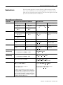
The following documents contain additional information concerning Rockwell
Automation products. To obtain a copy, contact your local Rockwell
Automation office or distributor.
For
Read This Document
Document Number
An overview of the SLC 500 family of products.
SLC 500 System Overview
1747-SO001
A description on how to install and use your Modular SLC 500
programmable controller.
Installation & Operation Manual for
Modular Hardware Style Programmable
Controllers
1747-UM011
A description on how to install and use your Fixed SLC 500
programmable controller.
Installation & Operation Manual for Fixed
Hardware Style Programmable Controllers
1747-6.21
In-depth information on grounding and wiring Allen-Bradley
programmable controllers.
Allen-Bradley Programmable Controller
Grounding and Wiring Guidelines
1770-4.1
A description of important differences between solid-state
Application Considerations for Solid-State
programmable controller products and hard-wired electromechanical Controls
devices.
SGI-1.1
An article on wire sizes and types for grounding electrical
equipment.
National Electrical Code - Published by the National Fire Protection
Association of Boston, MA.
A glossary of industrial automation terms and abbreviations.
Allen-Bradley Industrial Automation
Glossary
AG-7.1
If you would like a manual, you can:
• download a free electronic version from the Internet at
www.literature.rockwellautomation.com
• purchase a printed manual by contacting your local distributor or
Rockwell Automation representative
Common Techniques Used
in This Manual
Publication 1747-RM001G-EN-P - November 2008
The following conventions are used throughout this manual.
• Bulleted lists such as this one provide information, not procedural steps
• Numbered lists provide sequential steps or hierarchical information
• Italic type is used for emphasis
Chapter
1
Processor Files
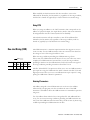
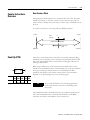
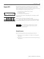
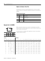
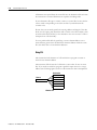
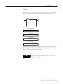
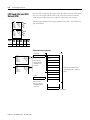
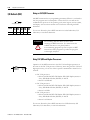
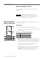
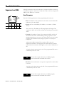
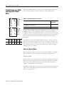
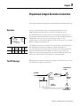
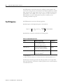
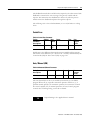
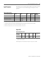
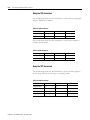
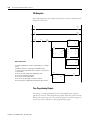
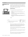
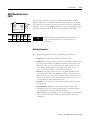
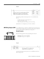
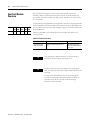
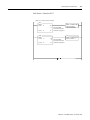
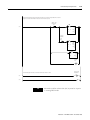
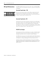
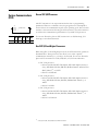
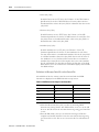
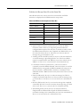
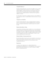
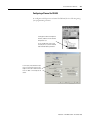
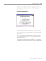
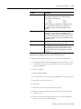
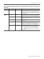
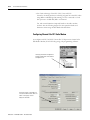
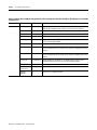
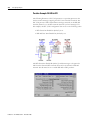
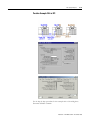
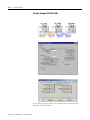
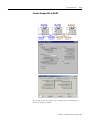
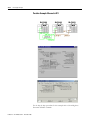
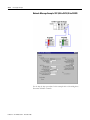
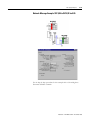
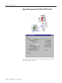
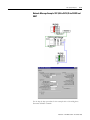
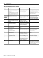
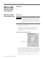
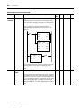
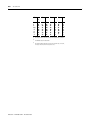
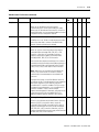
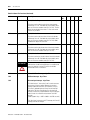
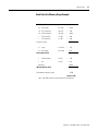
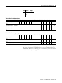
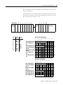
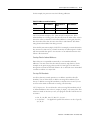
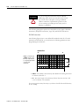
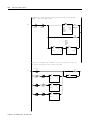
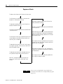
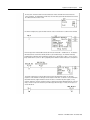
File Structure
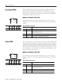
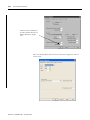
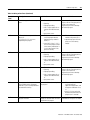
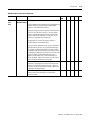
SLC 500 user memory is comprised of Data Files and Program Files.
TIP
The file types shown below for data files 3 through 8
are the default values. Files 9 to 255 can be
configured to be bit, timer, counter, control, integer,
floating point, ASCII, or String files.
0
2
3
Input File
Status File
Bit File
Timer File
Counter File
4
5
6
Data
Files
Floating Point File
Control File
7
Integer File
Output File
1
8
9 to 255
B Bit
T Timer
C Counter
R Control
N Integer
F Floating Pt.(1)
ST String(1)
A ASCII(1)
Program
Files
0
2
3 to 255
Program File 2
Program Files
3 to 255
System File 1
System File 0
1
(1) SLC 5/03 and higher processors only.
1
Publication 1747-RM001G-EN-P - November 2008
1-2
Processor Files
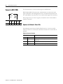
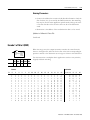
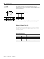
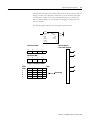
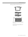
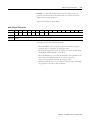
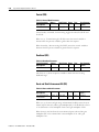
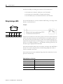
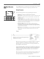
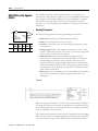
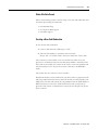
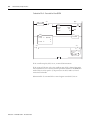
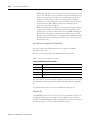
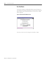
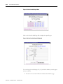
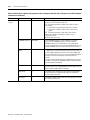
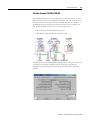
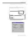
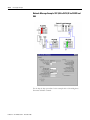
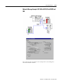
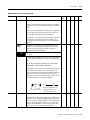
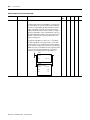
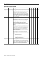
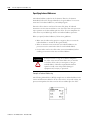
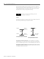
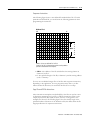
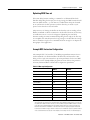
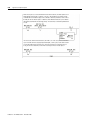
Output and Input Data Files (Files O0: and I1:)
Data Files 0 and 1 represent external outputs and inputs, respectively. Bits in
file 1 are used to represent external inputs. In most cases, a single 16-bit word
in these files will correspond to a slot location in your controller, with bit
numbers corresponding to input or output terminal numbers. Unused bits of
the word are not available for use.
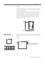
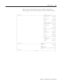
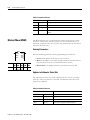
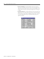
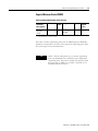
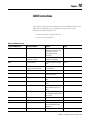
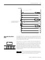
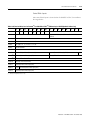
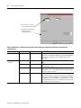
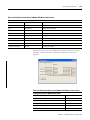
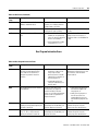
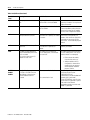
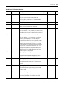
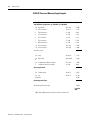
Table 1.1 explains the addressing format for outputs and inputs. Note that the
format specifies e as the slot number and s as the word number. When
referencing output and input data file words, refer to the element as e.s (slot
and word), taken together.
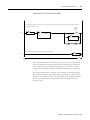
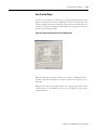
Table 1.1 Output and Input Data File Addressing Formats
Format
Explanation
O:e.s/b
O
Output
I:e.s/b
I
Input
:
Element delimiter
e
Slot number (decimal)
Slot 0, adjacent to the power supply in the first chassis, applies to the
processor module (CPU). Succeeding slots are I/O slots, numbered from 1
to a maximum of 30.
.
Word delimiter.
Required only if a word number is necessary as noted below.
s
Word number
Required if the number of inputs or outputs exceeds 16 for the slot.
Range: 0-255 (range accommodates multi-word “specialty cards”)
/
Bit delimiter
b
Terminal number
Inputs: 0-15
Outputs: 0-15
Examples:
O:3/15
O:5/0
O:10/11
I:7/8
I:2.1/3
Output 15, slot3
Output 0, slot 5
Output 11, slot 10
Input 8, slot 7
Input 3, slot 2, word 1
O:5
O:5.1
I:8
Output word 0, slot 5
Output word 1, slot 5
Input word 0, slot 8
Default Values: Your programming device will display an address more formally. For example, when you assign the address O:5/0, the
programming device will show it as O:5.0/0 (Output file, slot 5, word 0, terminal 0).
Publication 1747-RM001G-EN-P - November 2008
Processor Files
1-3
Status File (File S2:)
You cannot add to or delete from the status file. See Table 1.2 to understand
how to address various bits and words within the status file. You can address
various bits and words as follows.
Table 1.2 Status File Addressing Format
Format
Explanation
S:e/b
S
Status file
:
Element delimiter
e
Element number
/
Bit delimiter
b
Bit number
Ranges from 0 to 15 in a fixed or SLC 5/01 controller,
0 to 32 in an SLC 5/02,
0 to 82 in an SLC 5/03 and
0 to 82 in an SLC 5/05,
0 to 96 in an SLC 5/04 OS400, and
0 to 163 in an SLC 5/04 OS401 processors.
These are 1-word elements. 16 bits per element.
Bit location within the element. Ranges from 0 to 15.
Examples:
S:1/15
Element 1, bit 15. This is the “first pass” bit, which you can use to initialize instructions in your program.
S:3
Element 3. The lower byte of this element is the current scan time. The upper byte is the watchdog scan time.
Bit Data File (B3:)
File 3 is the bit file, used primarily for bit (relay logic) instructions, shift
registers, and sequencers. The maximum size of the file is 256 1-word
elements, a total of 4096 bits. You can address bits by specifying the element
number (0 to 255) and the bit number (0 to 15) within the element. You can
also address bits by numbering them in sequence, 0 to 4095.
You can also address elements of this file. See Table 1.3 for a detailed format
description. Note the two different possible formats that can be used.
Publication 1747-RM001G-EN-P - November 2008
1-4
Processor Files
Table 1.3 Bit File Addressing Format
Format
Explanation
Bf:e/b
B
Bit type file
f
File number. Number 3 is the default file. A file number between 9-255 can be used if
additional storage is required.
:
Element delimiter
e
Element number
/
Bit delimiter
b
Bit number
B
f
/
Same as above.
Same as above.
Same as above.
b
Bit number
Bf/b
Ranges from 0-255. These are 1-word elements. 16 bits per
element.
Bit location within the element. Ranges from 0-15.
Numerical position of the bit within the file. Ranges from 0-4095.
Examples:
B3:3/14
Bit 14, element 3
B3:252/00
Bit 0, element 252
B3:9
Bit 62
B3/62
Bit 62
B3/4032
Bit 4032
Timer Data File (T4:)
TIP
Timing could be inaccurate if Jump (JMP), Label
(LBL), Jump to Subroutine (JSR), or Subroutine (SBR)
instructions skip over the rung containing a timer
instruction while the timer is timing. If the skip
duration is less than 2.5 seconds, no time will be lost;
if the skip duration exceeds 2.5 seconds, an
undetectable timing error occurs. When using
subroutines, a timer must be executed at least every
2.5 seconds to prevent a timing error.
Timer instructions use various control bits. These are 3-word elements, used
with Bit, TON, TOF and RTO instructions. Word 0 is the status word, word 1
indicates the preset value, and word 2 indicates accumulator value. This is
shown in Table 1.4.
Publication 1747-RM001G-EN-P - November 2008
Processor Files
1-5
Table 1.4 Timer Control Fields
15
14
13
EN
TT
DN
12
11
10
9
8
7
6
5
4
3
2
1
0
Word
0
Internal Use(1)
Preset Value (PRE)
1
Accumulator Value (ACC)
2
(1)
Bits labeled “Internal Use” are not addressable.
Table 1.5 Timer Elements
Addressable Bits
Addressable Words
EN = Enable (Bit 15)
PRE = Preset Value
TT = Timer Timing (Bit 14)
ACC = Accumulated Value
DN = Done (Bit 13)
Addressing Structure
Address bits and words using the format Tf:e.s/b.
Table 1.6 Timer Addressing Format
Explanation
T
Timer file
f
File number. For SLC 500 processors the default is 4. A file
number between 9 to 255 can be used for additional
storage.
:
Element delimiter
e
Element number
These are 3-word elements.
The range is 0 to 255.
.
Word Delimiter
Range 0 to 2
s
Word Number
/
Bit delimiter
b
Bit Number
Range 0 to 15
Examples
T4:0/15 or T4:0/EN
Enable bit
T4:0/14 or T4:0/TT
Timer timing bit
T4:0/13 or T4:0/DN
Done bit
T4:0.1 or T4:0.PRE
Preset value of the timer
T4:0.2 or T4:0.ACC
Accumulated value of the timer
T4:0.1/0 or T4:0.PRE/0
Bit 0 of the preset value
T4:0.2/0 or T4:0.ACC/0
Bit 0 of the accumulated value
Publication 1747-RM001G-EN-P - November 2008
1-6
Processor Files
Counter Data File Elements (C5:)
Each Counter address is made of a 3-word data file element. Word 0 is the
control word, containing the status bits of the instruction. Word 1 is the preset
value. Word 2 is the accumulated value.
The control word for counter instructions includes five status bits, as indicated
below.
Table 1.7 Counter Control Fields
15
14
13
12
11
10
CU
CD
DN
OV
UN
UA(1)
09
08
07
06
05
04
03
02
01
00
Word
0
Internal Use(2)
Preset Value (PRE)
1
Accumulator Value (ACC)
2
(1)
Fixed SLC 500 only.
(2)
Bits labeled “Internal Use” are not addressable.
Table 1.8 Counter Elements
Addressable Bits
Addressable Words
CU = Count up enable (Bit 15)
PRE = Preset
CD = Count down enable (Bit 14)
ACC = Accum
DN = Done bit (Bit 13)
OV = Overflow bit (Bit 12)
UN = Underflow bit (Bit 11)
UA = Update Accumulator bit (Bit 10) (Fixed
Controller Only)
Publication 1747-RM001G-EN-P - November 2008
Processor Files
1-7
Entering Parameters
There are several parameters associated with Counter instructions. The
following parameters detail the operations of the counter.
Accumulator Value (ACC)
This is the number of false-to-true transitions that have occurred since the
counter was last reset.
Preset Value (PRE)
Specifies the value which the counter must reach before the controller sets the
done bit (DN). When the accumulator value becomes equal to or greater than
the preset value, the done status bit is set. You can use the done bit (DN) to
control an output device.
Preset and accumulated values for counters range from -32,768 to +32,767,
and are stored as signed integers. Negative values are stored in two’s
complement form.
Addressing Structure
Assign counter addresses using the format Cf:e.s/b.
Table 1.9 Counter File Addressing Format
Explanation
C
Counter
f
File number. For SLC 500 processors the default is 5. A file
number between 9 to 255 can be used for additional storage.
:
Element delimiter
e
Element number
.
Word Delimiter
s
Word Element
/
Bit delimiter
b
Bit Number
These are 3-word elements.
The range is 0 to 255.
0 to 2
0 to 15
Examples
C5:0/15 or C5:0/CU
Count up enable bit
C5:0/14 or C5:0/CD
Count down enable bit
C5:0/13 or C5:0/DN
Done bit
C5:0/12 or C5:0/OV
Overflow bit
Publication 1747-RM001G-EN-P - November 2008
1-8
Processor Files
Table 1.9 Counter File Addressing Format
Explanation
C5:0/11 or C5:0/UN
Underflow bit
C5:0/10 or C5:0/UA
Update accum. bit (use with HSC in fixed controller only)
C5:0.1 or C5:0.PRE
Preset value of the counter
C5:0.2 or C5:0.ACC
Accumulated value of the counter
C5:0.1/0 or
C5:0.PRE/0
Bit 0 of the preset value
C5:0.2/0 or
C5:0.ACC/0
Bit 0 of the accumulated value
Control Data File (R6:)
These instructions use various control bits. These are 3-word elements, used
with bit shift, FIFO, LIFO, sequencer instructions, and ASCII instructions
ABL, ACB, AHL, ARD, ARL, AWA, and AWT. Word 0 is the status word,
word 1 indicates the length of stored data, and word 2 indicates position. This
is shown in Table 1.10.
In the control element, there are eight status bits and an error code byte. A
fixed controller and an SLC 5/01 control element has six bits. Bits EU and
EM are not used by the processor.
Table 1.10 Three Word Element Structure
15
14
13
12
11
10
09
08
07
06
EN
EU(1)
DN
EM(1) ER
UL
IN
FD
Error Code
05
04
03
02
01
00
Word
0
Length of Bit Array or File (LEN)
1
Bit Pointer or Position (POS)
2
(1)
Not used in Fixed or SLC 5/01.
Table 1.11 Control Elements
Publication 1747-RM001G-EN-P - November 2008
Addressable Bits
Addressable Words
EN = Enable
LEN = Length
EU = Update Enable
POS = Position
Processor Files
1-9
Table 1.11 Control Elements
DN = Done
EM = Stack Empty
ER = Error
UL = Unload
IN = Inhibit
FD = Found
Assign control addresses as follows.
Table 1.12 Control File Addressing Format
Format
Rf:e
Rf:e.s/b
Explanation
R
Control file
f
File number. Number 6 is the default file. A
file number between 9 and 255 can be used
if additional storage is required.
:
Element delimiter
e
Element number
Rf:e
Explained above.
.
Word delimiter
s
Indicates word
/
Bit delimiter
b
Bit
Ranges from 0 to
255. These are
3-word elements.
See figure above.
Examples:
R6:2
Element 2, control file 6
Address bits and words by using the format Rf:e.s/b
R6:2/15 or R6:2/EN
R6:2/14 or R6:2/EU
R6:2/13 or R6:2/DN
R6:2/12 or R6:2/EM
R6:2/11 or R6:2/ER
R6:2/10 or R6:2/UL
R6:2/9 or R6:2/IN
R6:2/8 or R6:2/FD
Enable bit
Unload Enable bit
Done bit
Stack Empty bit
Error bit
Unload bit
Inhibit bit
Found bit
R6:2.1 or R6:2.LEN
R6:2.2 or R6:2.POS
Length value
Position value
R6:2.1/0
R6:2.2/0
Bit 0 of length value
Bit 0 of position value
Publication 1747-RM001G-EN-P - November 2008
1-10
Processor Files
Integer Data File (N7:)
Use these addresses as your program requires. These are 1-word elements,
addressable at the element and bit level.
Assign integer addresses as follows.
Table 1.13 Integer File Addressing Format
Format
Nf:e/b
Explanation
N
Integer file
f
File number. Number 7 is the default file. A
file number between 9 to255 can be used if
additional storage is required.
:
Element delimiter
e
Element number
/
Bit delimiter
b
Bit number
Ranges from 0 to
255. These are
1-word elements.
16 bits per element.
Bit location within
the element. Ranges
from 0 to 15.
Examples:
N7:2
N7:2/8
N10:36
Publication 1747-RM001G-EN-P - November 2008
Element 2, integer file 7
Bit 8 in element 2, integer file 7
Element 36, integer file 10 (file 10 designated as an integer file by
the user)
Processor Files
1-11
Float Data File (F8:)
Use these addresses as your program requires. These are 2-word elements,
addressable at the element and bit level.
Assign float addresses as follows.
Table 1.14 Float File Addressing Format
Format
Ff:e
Explanation
F
Integer file
f
File number. Number 8 is the default file. A
file number between 9 to 255 can be used if
additional storage is required.
:
Element delimiter
e
Element number
Ranges from 0 to
255. These are
2-word elements.
32 bits per element.
Examples:
F8:2
Element 2, float file 8
TIP
Float data type cannot be accessed at the bit level.
Publication 1747-RM001G-EN-P - November 2008
1-12
Processor Files
Notes:
Publication 1747-RM001G-EN-P - November 2008
Chapter
2
Basic Instructions
This chapter contains general information about the basic instructions and
explains how they function in your application program. Each of the basic
instructions includes information on:
• the instruction symbol.
• the instruction format.
• the instruction usage.
The Basic Instructions detailed in this chapter are listed in Table 2.1.
Table 2.1 Basic Instructions
Instruction
Mnemonic
Instruction Name
Purpose
Page
XIC
Examine if Closed
Examines a bit for an On condition.
2-3
XIO
Examine if Open
Examines a bit for an Off condition.
2-3
OTE
Output Energize
Turns a bit On or Off.
2-4
OTL and OTU
Output Latch and
OTL turns a bit on when the rung is executed, and this bit retains its
state when the rung is not executed or a power cycle occurs. OTU
turns a bit off when the rung is executed, and this bit retains its
state when the rung is not executed or when power cycle occurs.
2-4
Output Unlatch
1
OSR
One-shot Rising
Triggers a one-time event.
2-5
TON
Timer On-delay
Counts timebase intervals when the instruction is true.
2-9
TOF
Timer Off-delay
Counts timebase intervals when the instruction is false.
2-10
RTO
Retentive Timer
Counts timebase intervals when the instruction is true and retains
the accumulated value when the instruction goes false or when
power cycle occurs.
2-11
CTU
Count Up
Increments the accumulated value at each false-to-true transition
and retains the accumulated value when the instruction goes false
or when power cycle occurs.
2-13
CTD
Count Down
Decrements the accumulated value at each false-to-true transition
and retains the accumulated value when the instruction goes false
or when power cycle occurs.
2-14
HSC
High-speed Counter
Counts high-speed pulses from a fixed controller high-speed input.
2-15
RES
Reset
Resets the accumulated value and status bits of a timer or counter.
Do not use with TOF timers.
2-20
Publication 1747-RM001G-EN-P - November 2008
2-2
Basic Instructions
About the Basic
Instructions
Basic instructions, when used in ladder programs, represent hardwired logic
circuits used for the control of a machine or equipment.
The basic instructions are separated into three groups: bit, timer, and counter.
Before you learn about the instructions in each of these groups, we suggest
that you read the overviews that follow:
• Bit Instructions Overview.
• Timer Instructions Overview.
• Counter Instructions Overview.
Bit Instructions Overview
Bit instructions operate on a single bit of data. During operation, the processor
may set or reset the bit, based on logical continuity of ladder rungs. You can
address a bit as many times as your program requires.
TIP
Using the same address with multiple output
instructions is not recommended.
Bit instructions are used with the following data files.
•
•
•
•
Publication 1747-RM001G-EN-P - November 2008
Output/Input Files
Status File
Bit File
Timer File
Basic Instructions
2-3
Use the XIC instruction in your ladder program to determine if a bit is On.
When the instruction is executed, if the bit addressed is on (1), then the
instruction is evaluated as true. When the instruction is executed, if the bit
addressed is off (0), then the instruction is evaluated as false.
Examine if Closed (XIC)
Table 2.2 XIC Bit State
] [
Fixed SLC SLC SLC SLC SLC
5/01 5/02 5/03 5/04 5/05
•
•
•
•
•
Bit Address State
XIC Instruction
0
False
1
True
•
Input Instruction
Examples of devices that turn on or off include:
• a push button wired to an input (addressed as I:0/4).
• an output wired to a pilot light (addressed as O:0/2).
• a timer controlling a light (addressed as T4:3/DN).
Use the XIO instruction in your ladder program to determine if a bit is Off.
When the instruction is executed, if the bit addressed is off (0), then the
instruction is evaluated as true. When the instruction is executed, if the bit
addressed is on (1), then the instruction is evaluated as false.
Examine if Open (XIO)
Table 2.3 XIO Bit State
]/[
Fixed SLC SLC SLC SLC SLC
5/01 5/02 5/03 5/04 5/05
•
•
•
•
Input Instruction
•
Bit Address State
XIO Instruction
0
True
1
False
•
Examples of devices that turn on or off include:
• motor overload normally closed (N.C.) wired to an input (I:0/10).
• an output wired to a pilot light (addressed as O:0/4).
• a timer controlling a light (addressed as T4:3/DN).
Publication 1747-RM001G-EN-P - November 2008
2-4
Basic Instructions
Use the OTE instruction in your ladder program to turn on a bit when rung
conditions are evaluated as true.
Output Energize (OTE)
An example of a device that turns on or off is an output wired to a pilot light
(addressed as O:0/4).
( )
OTE instructions are reset when:
Fixed SLC SLC SLC SLC SLC
5/01 5/02 5/03 5/04 5/05
•
•
•
•
•
•
Output Instruction
• the SLC enters or returns to the REM Run or REM Test mode or
power is restored.
• the OTE is programmed within an inactive or false Master Control
Reset (MCR) zone.
TIP
A bit that is set within a subroutine using an OTE
instruction remains set until the subroutine is
scanned again.
OTL and OTU are retentive output instructions. OTL can only turn on a bit,
while OTU can only turn off a bit. These instructions are usually used in pairs,
with both instructions addressing the same bit.
Output Latch (OTL) and
Output Unlatch (OTU)
Your program can examine a bit controlled by OTL and OTU instructions as
often as necessary.
(L)
(U)
Fixed SLC SLC SLC SLC SLC
5/01 5/02 5/03 5/04 5/05
•
•
•
•
•
ATTENTION
•
Output Instructions
Under fatal error conditions, physical outputs are
turned off. Once the error conditions are cleared, the
controller resumes operation using the data table
value of the operand.
Using OTL
When you assign an address to the OTL instruction that corresponds to the
address of a physical output, the output device wired to this screw terminal is
energized when the bit is set (turned on or enabled).
When rung conditions become false (after being true), the bit remains set and
the corresponding output device remains energized.
Publication 1747-RM001G-EN-P - November 2008
Basic Instructions
2-5
When enabled, the latch instruction tells the controller to turn on the
addressed bit. Thereafter, the bit remains on, regardless of the rung condition,
until the bit is turned off (typically by a OTU instruction in another rung).
Using OTU
When you assign an address to the OTU instruction that corresponds to the
address of a physical output, the output device wired to this screw terminal is
de-energized when the bit is cleared (turned off or disabled).
The unlatch instruction tells the controller to turn off the addressed bit.
Thereafter, the bit remains off, regardless of the rung condition, until it is
turned on (typically by a OTL instruction in another rung).
The OSR instruction is a retentive input instruction that triggers an event to
occur one time. Use the OSR instruction when an event must start based on
the change of state of the rung from false-to-true.
One-shot Rising (OSR)
[OSR]
Fixed SLC SLC SLC SLC SLC
5/01 5/02 5/03 5/04 5/05
•
•
•
•
Input Instruction
•
When the rung conditions preceding the OSR instruction go from
false-to-true, the OSR instruction will be true for one scan. After one scan is
complete, the OSR instruction becomes false, even if the rung conditions
preceding it remain true. The OSR instruction will only become true again if
the rung conditions preceding it transition from false-to-true.
•
The SLC 500 and SLC 5/01 processors allow you to use one OSR instruction
per output in a rung; the OSR cannot be within a branch. The SLC 5/02 and
higher processors allow you to use one OSR instruction per output in a rung;
putting the OSR within a branch is permitted.
Entering Parameters
The address assigned to the OSR instruction is not the one-shot address
referenced by your program, nor does it indicate the state of the OSR
instruction. This address allows the OSR instruction to remember its previous
rung state.
Use a bit address from either the bit or integer data file. The addressed bit is
set (1) for one scan when rung conditions preceding the OSR instruction are
true (even if the OSR instruction becomes false); the bit is reset (0) when rung
conditions preceding the OSR instruction are false.
Publication 1747-RM001G-EN-P - November 2008
2-6
Basic Instructions
TIP
The bit address you use for this instruction must be
unique. Do not use it elsewhere in the program.
Do not use an input or output address to program the address parameter of
the OSR instruction.
Examples
The following rungs illustrate the use of the OSR instruction. The first four
rungs apply to SLC 500 and SLC 5/01 processors. The fifth rung involves
output branching and applies to the SLC 5/02 and higher processors.
SLC 500 and SLC 5/01 Processors
O:3.0
I:1.0
B3
( )
] [
[OSR]
0
0
0
When the input instruction goes from false-to-true, the OSR instruction
conditions the rung so that the output goes true for one program scan. The
output goes false and remains false for successive scans until the input makes
another false-to-true transition.
I:1.0
] [
0
B3
[OSR]
0
TOD
TO BCD
Source
Dest
Tf:0.ACC
O:3
In this case, the accumulated value of a timer is converted to BCD and moved to an
output word where an LED display is connected. When the timer is running, the
accumulated value is changing rapidly. This value can be frozen and displayed for
each false-to-true transition of the input condition of the rung.
Using an OSR Instruction in a Branch (SLC 500 and SLC 5/01 Processors)
I:1.0
] [
0
B3
[OSR]
0
O:3.0
( )
0
O:3.0
( )
1
In the above rung, the OSR instruction is not permitted inside a branch.
I:1.0
] [
0
B3
[OSR]
0
O:3.0
( )
0
O:3.0
( )
1
In this case, the OSR instruction is not in the branch so the rung is legal.
Publication 1747-RM001G-EN-P - November 2008
Basic Instructions
2-7
The SLC 500 and SLC 5/01 processors allow you to use only one OSR
instruction per rung.
ATTENTION
When using a SLC 500 or SLC 5/01 processor, do not
place input conditions after the OSR instruction in a
rung. Unexpected operation may occur.
SLC 5/02 (and higher) Processors
I:1.0
] [
0
B3
]/[
1
B3 O:3.0
B3
[OSR] ] [ ( )
0
0
4
B3
] [
2
B3
[OSR]
3
B3 O:3.0
]/[ ( )
5
1
The SLC 5/02 and higher processors allow you to use one OSR instruction
per output in a rung. They also allow input conditions after the OSR
instruction. Input branching around an OSR instruction is not allowed.
Timer Instructions
Overview
Entering Parameters
These are several parameters associated with Timer instructions. The
following paragraphs detail the operation of the timer instruction.
Accumulator Value (.ACC)
This is the time elapsed since the timer was last reset. When enabled, the timer
updates this continually.
Preset Value (.PRE)
This specifies the value which the timer must reach before the controller sets
the done bit. When the accumulated value becomes equal to or greater than
the preset value, the done (DN) bit is set. You can use this bit to control an
output device.
Preset and accumulated values for timers range from 0 to +32,767. If a timer
preset or accumulated value is a negative number, a runtime error occurs.
Publication 1747-RM001G-EN-P - November 2008
2-8
Basic Instructions
Timebase
The timebase determines the duration of each timebase interval. For Fixed and
SLC 5/01 processors, the timebase is set at 0.01 second.
EXAMPLE
If the timer base is set to 0.01, it would take 100
counts as the preset value (PRE) to equal 1 seconds
worth of timing.
Timer Accuracy
Timer accuracy refers to the length of time between the moment a timer
instruction is enabled and the moment the timed interval is complete.
Inaccuracy caused by the program scan can be greater than the timer timebase.
You must also consider the time required to energize the output device.
Timing accuracy is -0.01 to 0 seconds, with a program scan of up to 2.5
seconds. The 1-second timer maintains accuracy with a program scan of up to
1.5 seconds. If your programs can exceed 1.5 or 2.5 seconds, repeat the timer
instruction rung so that the rung is scanned within these limits.
Publication 1747-RM001G-EN-P - November 2008
Basic Instructions
2-9
Use the TON instruction to turn an output on or off after the timer has been
on for a preset time interval. The TON instruction begins to count timebase
intervals when rung conditions become true. As long as rung conditions
remain true, the timer adjusts its accumulated value (ACC) each evaluation
until it reaches the preset value (PRE). The accumulated value is reset when
rung conditions go false, regardless of whether the timer has timed out.
Timer On-delay (TON)
Using Status Bits
TON
(EN)
TIMER ON DELAY
T4:0
0.01
120
0
Timer
Time Base
Preset
Accum
(DN)
Table 2.4 Setting TON Status Bits
Fixed SLC SLC SLC SLC SLC
5/01 5/02 5/03 5/04 5/05
•
•
•
•
•
This Bit
Is Set When
And Remains Set Until
One of the Following
Timer Done Bit DN (bit 13)
accumulated value is equal
to or greater than the preset
value
rung conditions go false
Timer Timing Bit TT (bit 14)
rung conditions are true and
the accumulated value is
less than the preset value
rung conditions go false or
when the done bit is set
Timer Enable Bit EN (bit 15)
rung conditions are true
rung conditions go false
•
Output Instruction
When the processor changes from the REM Run or REM Test mode to the
REM Program mode or user power is lost while the instruction is timing but
has not reached its preset value, the following occur.
• Timer Enable (EN) bit remains set
• Timer Timing (TT) bit remains set
• Accumulated value (ACC) remains the same
On returning to the REM Run or REM Test mode, the following can happen.
Table 2.5 Returning to REM Run or REM Test Mode
Condition
Result
If the rung is true:
EN bit remains set.
TT bit remains set.
ACC value is reset.
If the rung is false:
EN bit is reset.
TT bit is reset.
ACC value is reset.
Publication 1747-RM001G-EN-P - November 2008
2-10
Basic Instructions
Use the TOF instruction to turn an output on or off after its rung has been off
for a preset time interval. The TOF instruction begins to count timebase
intervals when the rung makes a true-to-false transition. As long as rung
conditions remain false, the timer increments its accumulated value (ACC)
based on the timebase for each scan until it reaches the preset value (PRE).
The accumulated value is reset when rung conditions go true regardless of
whether the timer has timed out.
Timer Off-delay (TOF)
Using Status Bits
TOF
TIMER OFF DELAY
Timer
T4:1
Time Base
0.01
Preset
120
Accum
0
(EN)
(DN)
Table 2.6 Setting TOF Status Bits
Fixed SLC SLC SLC SLC SLC
5/01 5/02 5/03 5/04 5/05
•
•
•
•
•
•
This Bit
Is Set When
And Remains Set Until
One of the Following
Timer Done Bit DN (Bit 13)
rung conditions are true
rung conditions go false and
the accumulated value is
greater than or equal to the
preset value
Timer Timing Bit TT (Bit 14)
rung conditions are false
rung conditions go true or
and the accumulated value when the done bit is reset
is less than the preset value
Timer Enable Bit EN (Bit 15)
rung conditions are true
Output Instruction
rung conditions go false
When processor operation changes from the REM Run or REM Test mode to
the REM Program mode or user power is lost while a timer off-delay
instruction is timing but has not reached its preset value, the following occurs.
•
•
•
•
Timer Enable (EN) bit remains set
Timer Timing (TT) bit remains set
Timer Done (DN) bit remains set
Accumulated value (ACC) remains the same
On returning to the REM Run or REM Test mode, the following can happen.
Table 2.7 Returning to REM Run or REM Test Mode
Publication 1747-RM001G-EN-P - November 2008
Condition
Result
If the rung is true:
TT bit is reset
DN bit remains set
EN bit is set
ACC value is reset.
If the rung is false:
TT bit is reset
DN bit is reset
EN bit is reset
ACC value is set equal to the preset value.
Basic Instructions
ATTENTION
TIP
•
•
(EN)
(DN)
•
The TOF timer times inside an inactive MCR Pair.
The RTO instruction retains its accumulated value when any of the following
occurs.
Fixed SLC SLC SLC SLC SLC
5/01 5/02 5/03 5/04 5/05
•
The Reset (RES) instruction cannot be used with the
TOF instruction because RES always clears the status
bits as well as the accumulated value. (See 2-20)
Use the RTO instruction to turn an output on or off after its timer has been on
for a preset time interval. The RTO instruction is a retentive instruction that
begins to count timebase intervals when rung conditions become true.
Retentive Timer (RTO)
RTO
RETENTIVE TIMER ON
Timer
T4:2
Time Base
0.01
Preset
120
Accum
0
2-11
•
•
• Rung conditions become fals.
• You change processor operation from the REM Run or REM Test
mode to the REM Program mode
• The processor loses power (provided that battery backup is maintained)
• A fault occurs
Output Instruction
When you return the processor to the REM Run or REM Test mode and/or
rung conditions go true, timing continues from the retained accumulated
value. By retaining its accumulated value, retentive timers measure the
cumulative period during which rung conditions are true.
Publication 1747-RM001G-EN-P - November 2008
2-12
Basic Instructions
Using Status Bits
Table 2.8 Setting RTO Status Bits
This Bit
Is Set When
And Remains Set Until
One of the Following
Timer Done Bit DN (Bit 13)
accumulated value is equal
to or greater than the preset
value
the appropriate RES
instruction is enabled
Timer Timing Bit TT (Bit 14)
rung conditions are true and
the accumulated value is
less than the preset value
Rung conditions go false or
when the done bit is set
Timer Enable Bit EN (Bit 15)
rung conditions are true
rung conditions go false or
if the timer is reset with the
RES instruction
TIP
To reset the retentive timer’s accumulated value and
status bits after the RTO rung goes false, you must
program a reset (RES) instruction with the same
address in another rung.
When the processor changes from the REM Run or REM Test mode to the
REM Program or REM Fault mode, or user power is lost while the timer is
timing but not yet at the preset value, the following occurs.
• Timer Enable (EN) bit remains set
• Timer Timing (TT) bit remains set
• Accumulated value (ACC) remains the same
On returning to the REM Run or REM Test mode or when power is restored,
the following can happen.
Table 2.9 Returning to REM Run or REM Test Mode
Publication 1747-RM001G-EN-P - November 2008
Condition
Results
If the rung is true:
TT bit remains set.
EN bit remains set.
ACC value remains the same and resumes incrementing.
If the rung is false:
TT bit is reset.
DN bit remains in its last state.
EN bit is reset.
ACC value remains in its last state.
Basic Instructions
Counter Instructions
Overview
2-13
How Counters Work
The figure below demonstrates how a counter works. The count value must
remain in the range of − 32768 to + 32767. If the count value goes above +
32767 or below − 32768, the counter status overflow (OV) or underflow (UN)
bit is set.
A counter can be reset to zero using the reset (RES) instruction.
-32,768
(CTU)
Count Up
+32,767
0
Counter Accumulated Value
Count Down
(CTD)
Underflow
The CTU is an instruction that counts false-to-true rung transitions. Rung
transitions can be caused by events occurring in the program (from internal
logic or by external field devices) such as parts traveling past a detector or
actuating a limit switch.
Count Up (CTU)
CTU
COUNT UP
Counter
Preset
Accum
When rung conditions for a CTU instruction have made a false-to-true
transition, the accumulated value is incremented by one count, provided that
the rung containing the CTU instruction is evaluated between these
transitions. The ability of the counter to detect false-to-true transitions
depends on the speed (frequency) of the incoming signal.
(CU)
C5:0
120
0
Overflow
(DN)
Fixed SLC SLC SLC SLC SLC
5/01 5/02 5/03 5/04 5/05
•
•
•
•
Output Instruction
•
•
TIP
The on and off duration of an incoming signal must
not be faster than the scan time x2 (assuming a 50%
duty cycle).
The accumulated value is retained when the rung conditions again become
false. The accumulated count is retained until cleared by a reset (RES)
instruction that has the same address as the counter reset.
Publication 1747-RM001G-EN-P - November 2008
2-14
Basic Instructions
Using Status Bits
Table 2.10 Setting CTU Status Bits
This Bit
Is Set When
And Remains Set Until
One of the Following
Count Up Overflow Bit OV
(Bit 12)
accumulated value wraps
around to -32,768 (from
+32,767) and continues
counting up from there
a RES instruction having the
same address as the CTU
instruction is executed OR
the count is decremented
less than or equal to
+32,767 with a CTD
instruction
Done Bit DN (Bit 13)
accumulated value is equal
to or greater than the preset
value
the accumulated value
becomes less than the
preset value
Count Up Enable Bit CU
(Bit 15)
rung conditions are true
rung conditions go false OR
a RES instruction having the
same address as the CTU
instruction is enabled
The accumulated value is retained after the CTU instruction goes false, or
when power is removed from and then restored to the controller. Also, the on
or off status of counter done, overflow, and underflow bits is retentive. The
accumulated value and control bits are reset when the appropriate RES
instruction is enabled. The CU bits are always set prior to entering the REM
Run or REM Test modes.
The CTD is an instruction that counts false-to-true rung transitions. Rung
transitions can be caused by events occurring in the program such as parts
traveling past a detector or actuating a limit switch.
Count Down (CTD)
CTD
COUNT DOWN
Counter
C5:1
Preset
120
Accum
0
When rung conditions for a CTD instruction have made a false-to-true
transition, the accumulated value is decremented by one count, provided that
the rung containing the CTD instruction is evaluated between these
transitions.
(CD)
(DN)
Fixed SLC SLC SLC SLC SLC
5/01 5/02 5/03 5/04 5/05
•
•
•
•
•
•
Output Instruction
Publication 1747-RM001G-EN-P - November 2008
The accumulated counts are retained when the rung conditions again become
false. The accumulated count is retained until cleared by a reset (RES)
instruction that has the same address as the counter reset.
Basic Instructions
2-15
Using Status Bits
Table 2.11 Setting CTD Status Bits
This Bit
Is Set When
And Remains Set Until
One of the Following
Count Down Underflow Bit
UN (Bit 11)
accumulated value wraps
around to +32,767 (from
-32,768) and continues
counting down from there
a RES instruction having the
same address as the CTD
instruction is enabled. OR
the count is incremented
greater than or equal to
+32,767 with a CTU
instruction
Done Bit DN (Bit 13)
accumulated value is equal
to or greater than the preset
value
the accumulated value
becomes less than the
preset
Count Down Enable Bit CD
(Bit 14)
rung conditions are true
rung conditions go false OR
a RES instruction having the
same address as the CTD
instruction is enabled
The accumulated value is retained after the CTD instruction goes false, or
when power is removed from and then restored to the controller. Also, the on
or off status of counter done, overflow, and underflow bits is retentive. The
accumulated value and control bits are reset when the appropriate RES
instruction is executed. The CD bits are always set prior to entering the REM
Run or REM Test modes.
High-speed Counter (HSC)
HSC
HIGH SPEED COUNTER
Counter
C5:0
Preset
120
Accum
0
(CU)
(DN)
Fixed SLC SLC SLC SLC SLC
5/01 5/02 5/03 5/04 5/05
•
Output Instruction
The High-speed Counter is a variation of the CTU counter. The HSC
instruction is enabled when the rung logic is true and disabled when the rung
logic is false.
IMPORTANT
Do not place the XIC instruction with address I:0/0
in series with the HSC instruction because counts
will be lost.
The HSC instruction counts transitions that occur at input terminal I:0/0. The
HSC instruction does not count rung transitions. You enable or disable the
HSC rung to enable or disable the counting of transitions occurring at input
terminal I:0/0. We recommend placing the HSC instruction in an
unconditional rung.
The HSC is a special CTU counter for use with 24 VDC SLC fixed controllers.
The HSC’s status bits and accumulated values are non-retentive.
Publication 1747-RM001G-EN-P - November 2008
2-16
Basic Instructions
This instruction provides high-speed counting for fixed I/O controllers with
24 VDC inputs. One HSC instruction is allowed per controller. To use the
instruction, you must cut the jumper as shown below. A shielded cable is
recommended to reduce noise to the input.
High-speed Counter Data Elements
Address C5:0 is the HSC counter 3-word element.
Table 2.12 High Speed Counter Structure
15
14
13
12
11
10
CU
CD
DN
OV
UN
UA
09
08
07
06
05
04
03
02
Not Used
01
00
Word
0
Preset Value
1
Accumulator Value
2
CU
Count up enable (Bit 15)
CD
Count down enable (Bit 14)
DN
Done bit (Bit 13)
OV
Overflow bit (Bit 12)
UN
Underflow bit (Bit 11)
UA
Update accumulator (HSC only) (Bit 10)
• Word 0 contains the following status bits of the HSC instruction.
– Bit 10 (UA) updates the accumulator word of the HSC to reflect the
immediate state of the HSC when true.
– Bit 12 (OV) indicates if a HSC overflow has occurred.
– Bit 13 (DN) indicates if the HSC preset value has been reached.
– Bit 15 (CU) shows the Enable/Disable state of the HSC instruction.
• Word 1 contains the preset value that is loaded into the HSC when
either the RES instruction is executed, when the Done bit is set, or
when powerup takes place. The valid range is + 1 to + 32767.
• Word 2 contains the HSC accumulator value. This word is updated each
time the HSC instruction is evaluated and when the update accumulator
bit is set using an OTE instruction. This accumulator is read only. Any
value written to the accumulator is overwritten by the actual high-speed
counter on instruction evaluation, reset, or REM Run mode entry.
Publication 1747-RM001G-EN-P - November 2008
Basic Instructions
2-17
High-speed Counter Operation
For high-speed counter operation you must:
1. Turn off power to the fixed controller.
2. Remove the SLC 500 cover.
3. Locate and cut jumper wire J2. Do not remove completely but make
certain that the ends of the cut jumper wire are not touching each other.
The High-speed Counter jumper is located either beneath the
battery connector OR to the right of the battery connector.
4. Replace the cover.
Input I:0/0 then operates in the high-speed mode. The address of the
high-speed counter enable bit is C5:0/CU. When rung conditions are true,
C5:0/CU is set and transitions occurring at input I:0/0 are counted.
To begin high-speed counting, load a preset value into C5:0.PRE and enable
the counter rung. To load a preset value, do one of the following.
• Change to the REM Run or REM Test mode from another mode
• Power up the processor in the REM Run mode
• Reset the HSC using the RES instruction
Automatic reloading occurs when the HSC itself sets the DN bit on interrupt.
Each input transition that occurs at input I:0/0 causes the HSC accumulated
value to increment. When the accumulated value equals the preset value, the
Done bit (C5:0/DN) is set, the accumulated value is cleared, and the preset
value (C5:0.PRE) is loaded into the HSC in preparation for the next
high-speed transition at input I:0/0.
Your ladder program should poll the Done bit (C5:0/DN) to determine the
state of the HSC. Once the Done bit has been detected as set, the ladder
program should clear bit C5:0/DN (using the unlatch OTU instruction)
before the HSC accumulated again reaches the preset value, or the overflow
bit (C5:0/OV) will be set.
Publication 1747-RM001G-EN-P - November 2008
2-18
Basic Instructions
The HSC differs from the CTU and CTD counters. The CTU and CTD are
software counters. The HSC is a hardware counter and operates
asynchronously to the ladder program scan. The HSC accumulated value
(C5:0.ACC) is normally updated each time the HSC rung is evaluated in the
ladder program. This means that the HSC hardware accumulator value is
transferred to the HSC software accumulator. Only use the OTE instruction
to transfer this value. The HSC instruction immediately clears bit C5:0/UA
following the accumulated update.
Many HSC counts may occur between HSC evaluations, which would make
C5:0.ACC inaccurate when used throughout a ladder program. To allow for an
accurate HSC accumulated value, the update accumulator bit (C5:0/UA)
causes C5:0.ACC to be immediately updated to the state of the hardware
accumulator when set.
Use the RES instruction to reset the high-speed counter at address C5:0. The
HSC instruction clears the status bits, the accumulator, and loads the preset
value during:
• power up.
• entry into the REM Run mode.
• a reset.
Application Example
In the following figures, rungs 1, 18, and 31 of the main program file each
consist of an XIC instruction addressed to the HSC done bit and a JSR
instruction. These rungs poll the status of the HSC done bit. When the Done
bit is set at any of these poll points, program execution moves to subroutine
file 3, executing the HSC logic. After the HSC logic is executed, the Done bit
is reset by an unlatch instruction, and program execution returns to the main
program file.
Publication 1747-RM001G-EN-P - November 2008
Basic Instructions
2-19
Application Example - File 2 (Poll for DN Bit in Main Program)
JSR
Rung
1
C5:0
] [
DN
Rung
2
] [
] [
] [
( )
] [
] [
( )
JUMP TO SUBROUTINE
•
•
•
Rung
17
] [
Rung
18
C5:0
] [
DN
Rung
19
] [
] [
] [
( )
] [
] [
( )
•
•
•
Rung
30
] [
Rung
31
C5:0
] [
DN
Rung
32
] [
3
JSR
JUMP TO SUBROUTINE
3
JSR
JUMP TO SUBROUTINE
( )
] [
] [
3
Application Example - File 3 (Execute HSC Logic)
Rung
0
] [
Rung
1
] [
( )
] [
Application
Logic
( )
] [
•
•
•
Rung
20
Rung
21
C5:0
(U)
DN
Unlatch DN Bit
RET
RETURN
Publication 1747-RM001G-EN-P - November 2008
2-20
Basic Instructions
Use a RES instruction to reset a timer or counter. When the RES instruction is
enabled, it resets the Timer On Delay (TON), Retentive Timer (RTO), Count
Up (CTU), or Count Down (CTD) instruction having the same address as the
RES instruction.
Reset (RES)
Table 2.13 Using an RES Instruction
(RES)
Fixed SLC SLC SLC SLC SLC
5/01 5/02 5/03 5/04 5/05
•
•
•
•
•
Using a RES instruction for a:
The processor resets the:
Timer
(Do not use a RES instruction with a TOF.)
ACC value to 0
DN bit
TT bit
EN bit
Counter
ACC value to 0
OV bit
UN bit
DN bit
CU bit
CD bit
Control
POS value to 0
EN bit
EU bit
DN bit
EM bit
ER bit
UL bit
IN and FD go to last state
•
Output Instruction
When resetting a counter, if the RES instruction is enabled and the counter
rung is enabled, the CU or CD bit is reset.
If the counter preset value is negative, the RES instruction sets the
accumulated value to zero. This in turn causes the done bit to be set by a count
down or count up instruction.
ATTENTION
Publication 1747-RM001G-EN-P - November 2008
Because the RES instruction resets the accumulated
value, and the done, timing, and enabled bits, do not
use the RES instruction to reset a timer address used
in a TOF instruction. Otherwise, unpredictable
machine operation or injury to personnel may occur.
Chapter
3
Comparison Instructions
This chapter contains general information about comparison instructions and
explains how they function in your application program. Each of the
comparison instructions includes information on:
• the instruction symbol.
• instruction usage.
Table 3.1 Comparison Instructions
Instruction Mnemonic
EQU
Instruction Name
Equal
NEQ
Not Equal
LES
Less Than
LEQ
Less Than or
Equal
GRT
Greater Than
GEQ
Greater Than or Equal
MEQ
Masked
Comparison for Equal
LIM
Limit Test
About the Comparison
Instructions
Purpose
Test whether two values are
equal.
Test whether one value is not
equal to a second value.
Test whether one value is less
than a second value.
Test whether one value is less
than or equal to a second value.
Test whether one value is greater
than another.
Test whether one value is greater
than or equal to a second value.
Test portions of two values to see
whether they are equal.
Compares 16-bit data of a source
address to 16-bit data at a
reference address through a
mask.
Test whether one value is within
the limit range of two other
values.
Page
3-2
3-2
3-3
3-3
3-3
3-4
3-4
3-5
Comparison instructions are used to test pairs of values to condition the
logical continuity of a rung. As an example, suppose a LES instruction is
presented with two values. If the first value is less than the second, then the
comparison instruction is true.
To learn more about the compare instructions, we suggest that you read the
Compare Instructions Overview that follows.
1
Publication 1747-RM001G-EN-P - November 2008
3-2
Comparison Instructions
Comparison Instructions
Overview
The following general information applies to comparison instructions.
Using Indexed Word Addresses
When using comparison instructions, you have the option of using indexed
word addresses for instruction parameters specifying word addresses.
Using Indirect Word Addresses
You have the option of using indirect word-level and bit-level addresses for
instructions specifying word addresses when using an SLC 5/03 OS302, SLC
5/04 OS401, or SLC 5/05 processors.
Equal (EQU)
EQU
Equal
Source A
Use the EQU instruction to test whether two values are equal. If source A and
source B are equal, the instruction is logically true. If these values are not
equal, the instruction is logically false.
N7:0
0<
N7:1
0<
Source B
Fixed SLC SLC SLC SLC SLC
5/01 5/02 5/03 5/04 5/05
•
•
•
•
•
Source A must be an address. Source B can either be a program constant or a
address. Negative integers are stored in two’s complement form.
•
Input Instruction
Not Equal (NEQ)
NEQ
Not Equal
Source A
Source B
Use the NEQ instruction to test whether two values are not equal. If source A
and source B are not equal, the instruction is logically true. If the two values
are equal, the instruction is logically false.
N7:2
0<
N7:3
0<
Fixed SLC SLC SLC SLC SLC
5/01 5/02 5/03 5/04 5/05
•
•
•
•
•
•
Input Instruction
Publication 1747-RM001G-EN-P - November 2008
Source A must be an address. Source B can be either a program constant or an
address. Negative integers are stored in two’s complement form.
Comparison Instructions
Less Than (LES)
Use the LES instruction to test whether one value (source A) is less than
another (source B). If source A is less than the value at source B, the
instruction is logically true. If the value at source A is greater than or equal to
the value at source B, the instruction is logically false.
LES
Less Than (A<B)
Source A
N7:4
0<
Source B
N7:5
0<
Fixed SLC SLC SLC SLC SLC
5/01 5/02 5/03 5/04 5/05
•
•
•
•
3-3
•
Source A must be an address. Source B can either be a program constant or an
address. Negative integers are stored in two’s complement form.
•
Input Instruction
Less Than or Equal (LEQ)
LEQ
Less Than or Eql (A<=B)
Source A
N7:6
0<
Source B
N7:7
0<
Fixed SLC SLC SLC SLC SLC
5/01 5/02 5/03 5/04 5/05
•
•
•
•
•
Use the LEQ instruction to test whether one value (source A) is less than or
equal to another (source B). If the value at source A is less than or equal to the
value at source B, the instruction is logically true. If the value at source A is
greater than the value at source B, the instruction is logically false.
Source A must be an address. Source B can either be a program constant or an
address. Negative integers are stored in two’s complement form.
•
Input Instruction
Greater Than (GRT)
Use the GRT instruction to test whether one value (source A) is greater than
another (source B). If the value at source A is greater than the value at source
B, the instruction is logically true. If the value at source A is less than or equal
to the value at source B, the instruction is logically false.
GRT
Greater Than (A>B)
Source A
N7:8
0<
Source B
N7:9
0<
Fixed SLC SLC SLC SLC SLC
5/01 5/02 5/03 5/04 5/05
•
•
•
•
•
Source A must be an address. Source B can either be a program constant or an
address. Negative integers are stored in two’s complement form.
•
Input Instruction
Publication 1747-RM001G-EN-P - November 2008
3-4
Comparison Instructions
Greater Than or Equal (GEQ)
GEQ
Grtr Than or Eql (A>=B)
Source A
N7:10
0<
Source B
N7:11
0<
Fixed SLC SLC SLC SLC SLC
5/01 5/02 5/03 5/04 5/05
•
•
•
•
•
Use the GEQ instruction to test whether one value (source A) is greater than
or equal to another (source B). If the value at source A is greater than or equal
to the value at source B, the instruction is logically true. If the value at source
A is less than the value at source B, the instruction is logically false.
Source A must be an address. Source B can either be a program constant or an
address. Negative integers are stored in two’s complement form.
•
Input Instruction
Masked Comparison for
Equal (MEQ)
Use the MEQ instruction to compare data at a source address with data at a
compare address. Use of this instruction allows portions of the data to be
masked by a separate word.
MEQ
Masked Equal
Source
N7:12
0<
Mask
00FFh
255<
Compare
255
255<
Fixed SLC SLC SLC SLC SLC
5/01 5/02 5/03 5/04 5/05
•
•
•
•
•
•
Input Instruction
Entering Parameters
• Source is the address of the value you want to compare.
• Mask is the address of the mask through which the instruction moves
data. The mask can also be a hexadecimal value (constant).
• Compare is an integer value or the address of the reference.
If the 16 bits of data at the source address are equal to the 16 bits of data at the
compare address (less masked bits), the instruction is true. The instruction
becomes false as soon as it detects a mismatch. Bits in the mask word mask
data when reset; they pass data when set.
Publication 1747-RM001G-EN-P - November 2008
Comparison Instructions
Limit Test (LIM)
LIM
Limit Test
Low Lim
Test
High Lim
Use the LIM instruction to test for values within or outside a specified range,
depending on how you set the limits.
5
5<
N7:13
7<
8
8<
Entering Parameters
Fixed SLC SLC SLC SLC SLC
5/01 5/02 5/03 5/04 5/05
•
3-5
•
Input Instruction
•
•
The Low Limit, Test, and High Limit values can be word addresses or
constants, restricted to the following combinations:
• If the Test parameter is a program constant, both the Low Limit and
High Limit parameters must be word addresses.
• If the Test parameter is a word address, the Low Limit and High Limit
parameters can be either a program constant or a word address.
True/False Status of the Instruction
If the Low Limit has a value equal to or less than the High Limit, the
instruction is true when the Test value is between the limits or is equal to
either limit. If the Test value is outside the limits, the instruction is false, as
shown below.
False
True
False
-32,768
+32,767
Low Limit
High Limit
Example, low limit less than high limit:
Low Limit
High Limit
Instruction is True Instruction is False
when Test value is when Test value is
5
8
5 through 8
-32,768 through 4 and
9 through 32,767
If the Low Limit has a value greater than the High Limit, the instruction is
false when the Test value is between the limits. If the Test value is equal to
either limit or outside the limits, the instruction is true, as shown below.
True
False
True
-32,768
+32,767
High Limit
Low Limit
Example, low limit greater than high limit:
Low Limit
High Limit
Instruction is True
when Test value is
8
5
-32,768 through 5 and 8
through 32,767
Instruction is False
when Test value is
6 and 7
Publication 1747-RM001G-EN-P - November 2008
3-6
Comparison Instructions
Notes:
Publication 1747-RM001G-EN-P - November 2008
Chapter
4
Math Instructions
This chapter contains general information about math instructions and
explains how they function in your logic program. Each of the math
instructions includes information on:
• instruction symbol.
• instruction usage.
Table 4.1 Math Instructions
Instruction
Mnemonic
ADD
SUB
MUL
DIV
DDV
CLR
SQR
SCP
SCL
RMP
ABS
CPT
SWP
ASN
ACS
ATN
COS
LN
LOG
SIN
TAN
XPY
1
Purpose
Name
Add
Subtract
Multiply
Divide
Page
Adds source A to source B and stores the result in the destination.
Subtracts source B from source A and stores the result in the destination.
Multiplies source A by source B and stores the result in the destination.
Divides source A by source B and stores the result in the destination and the
math register.
Double Divide
Divides the contents of the math register by the source and stores the result in
the destination and the math register.
Clear
Sets all bits of a word to zero.
Square Root
Calculates the square root of the source and places the integer result in the
destination.
Scale with
Produces a scaled output value that has a linear relationship between the input
Parameters
and scaled values.
Scale Data
Multiplies the source by a specified rate, adds to an offset value, and stores
the result in the destination.
Ramp
Provides the ability to create linear, acceleration, deceleration, and “S” curve
ramp output data wave forms.
Absolute
Calculates the absolute value of the source and places the result in the
destination.
Compute
Evaluates an expression and stores the result in the destination.
Swap
Swaps the low and high bytes of a specified number of words in a bit, integer,
ASCII, or string file.
Arc Sine
Takes the arc sine of a number and stores the result (in radians) in the
destination.
Arc Cosine
Takes the arc cosine of a number and stores the result (in radians) in the
destination.
Arc Tangent
Takes the arc tangent of a number and stores the result (in radians) in the
destination.
Cosine
Takes the cosine of a number and stores the result in the destination.
Natural Log
Takes the natural log of the value in the source and stores it in the destination.
Log to the Base 10 Takes the log base 10 of the value in the source and stores the result in the
destination.
Sine
Takes the sine of a number and stores the result in the destination.
Tangent
Takes the tangent of a number and stores the result in the destination.
X to the Power of Y Raise a value to a power and stores the result in the destination.
4-5
4-5
4-8
4-9
4-11
4-12
4-12
4-13
4-15
4-20
4-24
4-25
4-28
4-29
4-29
4-30
4-30
4-31
4-31
4-32
4-32
4-33
Publication 1747-RM001G-EN-P - November 2008
4-2
Math Instructions
About the Math Instructions
The majority of the instructions take two input values, perform the specified
arithmetic function, and output the result to an assigned memory location.
For example, both the ADD and SUB instructions take a pair of input values,
add or subtract them, and place the result in the specified destination. If the
result of the operation exceeds the allowable value, an overflow or underflow
bit is set.
To learn more about the math instructions, we suggest that you read the Math
Instructions Overview that follows.
Math Instructions Overview
The following general information applies to math instructions.
Entering Parameters
• Source is the address(es) of the value(s) on which the mathematical,
logical, or move operation is to be performed. This can be word
addresses or program constants. An instruction that has two source
operands does not accept program constants in both operands.
• Destination is the address of the result of the operation. Signed integers
are stored in two’s complement form and apply to both source and
destination parameters.
When using either an SLC 5/03 (OS301 and higher), SLC 5/04, or SLC 5/05
processor; floating point and string values (specified at the word level) are
supported.
Using Indexed Word Addresses
You have the option of using indexed word addresses for instruction
parameters specifying word addresses (except for fixed and SLC 5/01
processors).
Using Indirect Word Addresses
You have the option of using indirect word-level and bit-level addresses for
instructions specifying word addresses when using an SLC 5/03 (OS302), SLC
5/04 (OS401), or SLC 5/05 processors.
Publication 1747-RM001G-EN-P - November 2008
Math Instructions
4-3
Updates to Arithmetic Status Bits
The arithmetic status bits are found in Word 0, bits 0 to 3 in the controller
status file. After an instruction is executed, the arithmetic status bits in the
status file are updated.
Table 4.2 Processor Function
With this Bit
The Controller
S:0/0
Carry (C)
sets if carry is generated; otherwise cleared.
S:0/1
Overflow (V)
indicates that the actual result of a math instruction does
not fit in the designated destination.
S:0/2
Zero (Z)
indicates a 0 value after a math, move, or logic instruction.
S:0/3
Sign (S)
indicates a negative (less than 0) value after a math, move,
or logic instruction.
Overflow Trap Bit, S:5/0
Minor error bit (S:5/0) is set upon detection of a mathematical overflow or
division by zero. If this bit is set upon execution of an END statement, a
Temporary End (TND) instruction, or an I/O Refresh (REF), the recoverable
major error code 0020 is declared.
In applications where a math overflow or divide by zero occurs, you can avoid
a CPU fault by using an unlatch (OTU) instruction with address S:5/0 in your
program. The rung must be between the overflow point and the END, TND,
or REF statement.
Updates to the Math Register, S:13 and S:14
Status word S:13 contains the least significant word of the 32-bit value of the
MUL instruction. It contains the remainder for DIV and DDV instructions. It
also contains the first four BCD digits for the Convert from BCD (FRD) and
Convert to BCD (TOD) instructions.
Status word S:14 contains the most significant word of the 32-bit value of the
MUL instruction. It contains the unrounded quotient for DIV and DDV
instructions. It also contains the most significant digit (digit 5) for TOD and
FRD instructions.
TIP
When using floating point, S:13 and S:14 are not used.
Publication 1747-RM001G-EN-P - November 2008
4-4
Math Instructions
Using Floating Point Data File (F8:)
This file type is valid for SLC 5/03 (OS301 and higher), SLC 5/04, and SLC
5/05 processors. These are 2-word elements and addressable only at the
element level.
Assign floating point addresses as follows.
Table 4.3 Addressing Format
Format
Ff:e
Explanation
F
f
:
e
Examples:
Publication 1747-RM001G-EN-P - November 2008
F8:2
F10:36
Floating Point file
File number. Number 8 is the default file. A
file number between 9- 255 can be used if
additional storage is required.
Element delimiter
Element number
Ranges from 0- 255.
These are 2-word
elements.
Non-extended 32-bit
numbers
Element 2, floating point file 8
Element 36, floating point file 10 (file 10
designated as a floating point file by the
user)
Math Instructions
4-5
Use the ADD instruction to add one value (source A) to another value (source
B) and place the result in the destination.
Add (ADD)
Updates to Arithmetic Status Bits
ADD
Add
Source A
N7:14
6<
N7:15
8<
N7:16
0<
Source B
Dest
The arithmetic status bits are found in Word 0, bits 0 to 3 in the status file.
After an instruction is executed, the arithmetic status bits in the status file are
updated.
Fixed SLC SLC SLC SLC SLC
5/01 5/02 5/03 5/04 5/05
•
•
•
•
•
•
Table 4.4 Processor Function
With this Bit
The Processor
S:0/0
Carry (C)
sets if carry is generated; otherwise resets (integer). For floating
point, it is cleared.
S:0/1
Overflow (V) sets if overflow is detected at destination; otherwise resets. On
overflow, the minor error flag is also set. For floating point, the
overflow value is placed in the destination. For an integer, the
value -32,768 or 32,767 is placed in the destination. Exception: If
you are using an SLC
5/02 or higher processor and have S:2/14 (math overflow
selection bit) set, then the unsigned, truncated overflow remains
in the destination.
S:0/2
Zero (Z)
sets if result is zero; otherwise resets.
S:0/3
Sign (S)
sets if result is negative; otherwise resets.
Output Instruction
Use the SUB instruction to subtract one value (source B) from another (source
A) and place the result in the destination.
Subtract (SUB)
Updates to Arithmetic Status Bits
SUB
Subtract
Source A
Source B
Dest
N7:17
0<
N7:18
0<
N7:19
0<
The arithmetic status bits are found in Word 0, bits 0 to 3 in the status file.
After an instruction is executed, the arithmetic status bits in the status file are
updated.
Fixed SLC SLC SLC SLC SLC
5/01 5/02 5/03 5/04 5/05
•
•
•
•
Output Instruction
•
•
Table 4.5 Processor Function
With this Bit
The Processor
S:0/0
Carry (C)
sets if borrow is generated; otherwise resets (integer). For
floating point it is cleared.
S:0/1
Overflow (V) sets if underflow; otherwise reset. On underflow, the minor error
flag is also set. For floating point, the overflow value is placed in
the destination. For an integer, the value -32,768 or 32,767 is
placed in the destination. Exception: If you are using an SLC 5/02
or higher processor and have S:2/14 (math overflow selection
bit) set, then the unsigned, truncated overflow remains in the
destination.
S:0/2
Zero (Z)
sets if result is zero; otherwise resets.
S:0/3
Sign (S)
sets if result is negative; otherwise resets.
Publication 1747-RM001G-EN-P - November 2008
4-6
Math Instructions
You have the option of performing 16-bit or 32-bit signed integer addition and
subtraction. This is facilitated by status file bit S:2/14 (math overflow selection
bit).
32-Bit Addition and
Subtraction
Math Overflow Selection Bit S:2/14
Fixed SLC SLC SLC SLC SLC
5/01 5/02 5/03 5/04 5/05
•
•
•
•
Set this bit when you intend to use 32-bit addition and subtraction. When
S:2/14 is set, and the result of an ADD, SUB, MUL, DIV, or NEG instruction
cannot be represented in the destination address (due to math underflow or
overflow.:
• The overflow bit S:0/1 is set
• The overflow trap bit S:5/0 is se.
• The destination address contains the unsigned, truncated, least
significant 16 bits of the result
TIP
For MUL, DIV, integer, and all floating point
instructions with an integer destination, when S:2/14
is set, the state change takes effect immediately.
When S:2/14 is reset (default condition), and the result of an ADD, SUB,
MUL, DIV, or NEG instruction cannot be represented in the destination
address (due to math underflow or overflow).
• The overflow bit S:0/1 is set
• The overflow trap bit S:5/0 is set
• The destination address contains 32767 if the result is positive or -32768
if the result is negative
TIP
Additionally, the SLC 5/03 and higher processors
only assert the state of bit S:2/14 at the end of scan
for the ADD, SUB, and NEG instructions.
Note that the status of bit S:2/14 has no effect on the DDV instruction. Also,
it has no effect on the math register content when using MUL and DIV
instructions.
TIP
Publication 1747-RM001G-EN-P - November 2008
The SLC 5/03 and higher processors only interrogate
the S:2/14 bit upon going to the Run mode and
end-of-scan. Use the Data Monitor function to make
this selection prior to entering the Run mode.
Math Instructions
4-7
Example of 32-bit Addition
The following example shows how a 16-bit signed integer is added to a 32-bit
signed integer. Remember that S:2/14 must be set for 32-bit addition.
Note that the value of the most significant 16 bits (B3:3) of the 32-bit number
is increased by 1 if the carry bit S:0/0 is set and it is decreased by 1 if the
number being added (B3:1) is negative.
The largest possible number is 2,147,483,647
(7FFF FFFF)h.
TIP
To avoid a major error from occurring at the end of the scan, you must
unlatch overflow trap bit S:5/0 as shown in the example ladder diagram to
follow.
Table 4.6 Add 16-bit value B3:1 to 32-bit value B3:3 B3:2
Add Operation
Binary
Hex
Decimal(1)
Addend
Addend
B3:3 B3:2
B3:1
0000 0000 0000 0011 0001 1001 0100 0000 0003 1940
0101 0101 1010 1000 55A8
203,072
21,928
Sum
B3:3 B3:2
0000 0000 0000 0011 0110 1110 1110 1000 0003 6EE8
225,000
(1)
The programming device displays 16-bit decimal values only. The decimal value of a 32-bit integer is derived from the displayed binary or hex value. For example, 0003
1940 Hex is 164x3 +163x1 + 162x9 + 161x4 + 160x0 = 203,072.
Publication 1747-RM001G-EN-P - November 2008
4-8
Math Instructions
B3
] [
0
When rung goes true for a
single scan, B3:1 is added to
B3:2. The result is placed in
B3:2
ADD
B3
[OSR]
1
ADD
Source A
B3:1
0101010110101000
Source B
B3:2
0001100101000000
Dest
B3:2
0001100101000000
S:0
] [
0
If a carry is generated (S:0/0
set), 1 is added to B3:3.
ADD
ADD
Source A
1
Source B
B3:3
0000000000000011
Dest
B3:3
0000000000000011
B3
] [
31
SUB
SUBTRACT
Source A
B3:3
0000000000000011
Source B
1
If B3:1 is negative (B3/31
set), 1 is subtracted from
B3:3.
Dest
B3:3
0000000000000011
S:5
(U)
0
END
TIP
Overflow trap bit S:5/0 is
unlatched to prevent a major
error from occurring at the
end of the scan.
You can use the rung above with a DDV instruction
and a counter to find the average value of B3:1.
Use the MUL instruction to multiply one value (source A) by another (source
B) and place the result in the destination.
Multiply (MUL)
Updates to Arithmetic Status Bits
MUL
Multiply
Source A
Source B
Dest
N7:20
0<
N7:21
0<
N7:22
0<
The arithmetic status bits are found in Word 0, bits 0 to 3 in the status file.
After an instruction is executed, the arithmetic status bits in the status file are
updated.
Fixed SLC SLC SLC SLC SLC
5/01 5/02 5/03 5/04 5/05
•
•
•
•
•
•
Output Instruction
Publication 1747-RM001G-EN-P - November 2008
Math Instructions
4-9
Table 4.7 Processor Function
With this Bit
The Processor
S:0/0
Carry (C)
always resets.
S:0/1
Overflow (V)
sets if overflow is detected at destination; otherwise resets. On
overflow, the minor error flag is also set. The value -32,768 or
32,767 is placed in the destination. Exception: If you are using
an SLC 5/02 or higher processor and have S:2/14 (math overflow
selection bit) set, then the unsigned, truncated least significant
16-bits of the result remains in the destination. For floating
point destinations, the overflow result remains in the
destination.
S:0/2
Zero (Z)
sets if result is zero; otherwise resets.
S:0/3
Sign (S)
sets if result is negative; otherwise resets.
Updates to the Math Register, S:13 and S:14
During integer operation, S:13 and S:14 contain the 32-bit signed result of the
multiply instruction. This result is valid at overflow.
TIP
Divide (DIV)
DIV
Divide
Source A
Source B
Dest
Use the DIV instruction to divide one value (source A) by another (source B).
The rounded quotient is then placed in the destination. If the remainder is 0.5
or greater, round up occurs in the destination. The unrounded quotient is
stored in the most significant word of the math register. The remainder is
placed in the least significant word of the math register.
N7:23
0<
N7:24
0<
N7:25
0<
Fixed SLC SLC SLC SLC SLC
5/01 5/02 5/03 5/04 5/05
•
•
•
•
Output Instruction
For floating point operation, the math register does
not change.
•
Updates to Arithmetic Status Bits
•
The arithmetic status bits are found in Word 0, bits 0 to 3 in the status file.
After an instruction is executed, the arithmetic status bits in the status file are
updated.
Publication 1747-RM001G-EN-P - November 2008
4-10
Math Instructions
Table 4.8 Processor Function
With this Bit
The Processor
S:0/0
Carry (C)
always resets.
S:0/1
Overflow (V)
sets if division by zero or overflow is detected; otherwise resets.
On overflow, the minor error flag is also set. The value 32,767 is
placed in the destination. Exception: If you are using an SLC1
5/02 or higher processor and have S:2/14 (math overflow
selection bit) set, then the unsigned, truncated overflow remains
in the destination. For floating point destinations, the overflow
result remains in the destination.
S:0/2
Zero (Z)
sets if result is zero; otherwise resets; undefined if overflow is
set.
S:0/3
Sign (S)
sets if result is negative; otherwise resets; undefined if overflow
is set.
Updates to the Math Registers, S:13 and S:14
During integer operation, the unrounded quotient is placed in the most
significant word (S:14), the remainder is placed in the least significant word
(S:13).
TIP
For floating point operation, the math register does
not change.
Example
The remainder of 11/2 is 0.5, so the quotient is rounded up to 6 and is stored
in the destination. The unrounded quotient, which is 5, is stored in S:14 and
the remainder, which is 1, is stored at S:13.
DIV
DIVIDE
Source A
Source B
Dest
Publication 1747-RM001G-EN-P - November 2008
N7:0
11
N7:1
2
N7:2
6
where:
N7:0 = 11
N7:1 = 2
N7:2 = 6
result:
S:14 = 5
S:13 = 1
Math Instructions
4-11
The 32-bit content of the math register is divided by the 16-bit source value
and the rounded quotient is placed in the destination. If the remainder is 0.5 or
greater, the destination is rounded up.
Double Divide (DDV)
DDV
Double Divide
Source
N7:26
0<
Dest
N7:27
0<
This instruction typically follows a MUL instruction
that creates a 32-bit result.
TIP
Fixed SLC SLC SLC SLC SLC
5/01 5/02 5/03 5/04 5/05
•
•
•
•
•
•
Updates to Arithmetic Status Bits
Output Instruction
The arithmetic status bits are found in Word 0, bits 0 to 3 in the status file.
After an instruction is executed, the arithmetic status bits in the status file are
updated.
Table 4.9 Processor Function
With this Bit
The Processor
S:0/0
Carry (C)
always resets.
S:0/1
Overflow (V)
sets if division by zero or if result is greater than 32,767 or
less than -32,768; otherwise resets. On overflow, the minor
error flag is also set. The value 32,767 is placed in the
destination.
S:0/2
Zero (Z)
sets if result is zero; otherwise resets.
S:0/3
Sign (S)
sets if result is negative; otherwise resets; undefined if
overflow is set.
Updates to the Math Registers, S:13 and S:14
Initially contains the dividend of the DDV operation. Upon instruction
execution, the unrounded quotient is placed in the most significant word of
the math register. The remainder is placed in the least significant word of the
math register.
Publication 1747-RM001G-EN-P - November 2008
4-12
Math Instructions
Use the CLR instruction to set the destination value of a word to zero.
Clear (CLR)
Updates to Arithmetic Status Bits
CLR
Clear
Dest
N7:27
0<
Fixed SLC SLC SLC SLC SLC
5/01 5/02 5/03 5/04 5/05
•
•
•
•
•
•
Output Instruction
With this Bit
The Processor
S:0/0
Carry (C)
always resets.
S:0/1
Overflow (V)
always resets.
S:0/2
Zero (Z)
always sets.
S:0/3
Sign (S)
always resets.
The instruction calculates the square root of a negative number without
overflow or faults. In applications where the source value may be negative, use
a comparison instruction to evaluate the source value to determine if the
destination may be invalid.
SQR
Square Root
Source
N7:28
0<
Dest
N7:29
0<
Fixed SLC SLC SLC SLC SLC
5/01 5/02 5/03 5/04 5/05
•
Table 4.10 Processor Function
When this instruction is evaluated as true, the square root of the absolute value
of the source is calculated and the rounded result is placed in the destination.
Square Root (SQR)
•
The arithmetic status bits are found in Word 0, bits 0 to 3 in the status file.
After an instruction is executed, the arithmetic status bits in the status file are
updated.
•
Updates to Arithmetic Status Bits
•
Output Instruction
The arithmetic status bits are found in Word 0, bits 0 to 3 in the status file.
After an instruction is executed, the arithmetic status bits in the status file are
updated.
Table 4.11 Processor Function
Publication 1747-RM001G-EN-P - November 2008
With this Bit
The Processor
S:0/0
Carry (C)
is reserved (integer). For floating point, it is always cleared.
S:0/1
Overflow (V)
always resets.
S:0/2
Zero (Z)
sets when destination value is zero.
S:0/3
Sign (S)
always resets.
Math Instructions
4-13
Use the SCP instruction to produce a scaled output value that has a linear
relationship between the input and scaled values. This instruction supports
integer and floating point values. Use this instruction with SLC 5/03 (OS302),
SLC 5/04 (OS401), and SLC 5/05 processors.
Scale with Parameters
(SCP)
Use the following formula to convert analog input data to engineering units.
SCP
Scale w/Parameters
Input
N7:30
100<
Input Min.
0
0<
Input Max.
32767
32767<
Scaled Min.
0
0<
Scaled Max.
10000
10000<
Output
N7:31
0<
y = mx + b
Where:
y = scaled output
m = slope = (scaled MAX. - scaled MIN.) / (input MAX. - input MIN.)
x = input value
b = offset (y intercept) = scaled MIN - (input MIN. x m)
Fixed SLC SLC SLC SLC SLC
5/01 5/02 5/03 5/04 5/05
•
Output Instruction
•
•
TIP
The Input Minimum, Input Maximum, Scaled
Minimum, and Scaled Maximum are used to
determine the slope and offset values. The input
value can go outside of the specified input limits and
no ordering is required. For example, the scaled
output value is not necessarily clamped between the
scaled minimum and scaled maximum values.
Entering Parameters
Enter the following parameters when programming this instruction.
• Input value can be a word address or an address of floating point data
elements.
• Input Minimum and Input Maximum values determine the range of
data that appears in the Input Value parameter. The value can be a word
address, an integer constant, floating point data element, or a floating
point constant.
• Scaled Minimum and Scaled Maximum values determine the range
of data that appears in the Scaled Output parameter. The value can be a
word address, an integer constant, floating point data element, or a
floating point constant.
• Scaled Output value can be a word address or an address of floating
point data elements.
Publication 1747-RM001G-EN-P - November 2008
4-14
Math Instructions
Updates to Arithmetic Status Bits
The arithmetic status bits are found in Word 0, bits 0 to 3 in the status file.
After an instruction is executed, the arithmetic status bits in the status file are
updated.
Table 4.12 Processor Function
With this Bit
The Processor
S:0/0
Carry (C)
always resets.
S:0/1
Overflow (V)
sets if overflow generated or an unsupported input is detected;
otherwise resets.
S:0/2
Zero (Z)
sets when destination value is zero; otherwise resets.
S:0/3
Sign (S)
sets if the destination value is negative; otherwise resets.
Application Examples
Example 1
In the first example, an analog I/O combination module (1746-NIO4I) is in
slot 1 of the chassis. A pressure transducer is connected to input 0 and we
want to read the value in engineering units. The pressure transducer measures
pressures from 0 to 1000 psi and provides a 0 to 10V signal to the analog
module. For a 0 to 10V signal, the analog module provides a range between 0
to 32,767. The following program rung places a number between 0 and 1000
into N7:20 based on the input signal coming from the pressure transducer into
the analog module.
0000
SCP
Scale w/Parameters
Input
Input Min.
Input Max.
Scaled Min.
Scaled Max.
Output
0001
Publication 1747-RM001G-EN-P - November 2008
I:1.0
0<
0
0<
32767
32767<
0
0<
1000
1000<
N7:20
0<
END
Math Instructions
4-15
Example 2
In the second example, an analog I/O combination module (1746-NIO4I) is
in slot 1 of the chassis. We want to control the proportional valve connected
to output 0. The valve takes a
4 to 20 mA signal to control how far it opens (0 to 100%). (Assume that
additional logic is present in the program that calculates how far to open the
valve in percent and places a number between 0 and 100 into N7:21.) The
analog module provides a 4 to 20 mA output signal for a number between
6242 to 31,208. The following program rung directs an analog output to
provide a 4 to 20 mA signal to the proportional valve (N7:21), based on a
number between 0 and 100.
SCP
Scale w/Parameters
Input
0000
Input Min.
Input Max.
Scaled Min.
Scaled Max.
Output
N7:21
0<
0
0<
100
100<
6242
6242<
31208
31208<
O:1.0
0<
END
0001
When this instruction is true, the value at the source address is multiplied by
the rate value. The rounded result is added to the offset value and placed in the
destination.
Scale Data (SCL)
Example
SCL
SCALE
Source
Rate [/10000]
Offset
SCL
Dest
SCALE
Source
Rate
Fixed SLC SLC SLC SLC SLC
5/01 5/02 5/03 5/04 5/05
•
•
•
[/10000]
N7:0
100
25000
Offset
127
Dest
N7:1
377
The source 100 is multiplied by 25000 and
divided by 10000 and added to 127. The
result, 377, is placed in the destination.
•
Output Instruction
Publication 1747-RM001G-EN-P - November 2008
4-16
Math Instructions
TIP
Anytime an underflow or overflow occurs in the
destination file, minor error bit S:5/0 must be reset
by the program. This must occur before the end of
the current scan to prevent major error code 0020
from being declared. This instruction can overflow
before the offset is added.
Note that the term rate is sometimes referred to as slope. The rate function is
limited to the range -3.2768 to 3.2767. For example, -32768/10000 to
+32767/10000.
Entering Parameters
The value for the following parameters is between -32,768 to 32,767.
• Source can be either a constant or a word address
• Rate (or slope) is the positive or negative value you enter divided by
10,000. It can be either a constant or a word address
• Offset can be either a constant or a word address
Updates to Arithmetic Status Bits
The arithmetic status bits are found in Word 0, bits 0 to 3 in the status file.
After an instruction is executed, the arithmetic status bits in the status file are
updated.
Table 4.13 Processor Function
With this Bit
The Processor
S:0/0
Carry (C)
is reserved.
S:0/1
Overflow (V)
sets if an overflow is detected; otherwise resets. On overflow,
minor error bit S:5/0 is also set and the value -32,768 or 32,767
is placed in the destination. The presence of an overflow is
checked before and after the offset value is applied.(1)
S:0/2
Zero (Z)
sets when destination value is zero.
S:0/3
Sign (S)
sets if the destination value is negative; otherwise resets.
(1)
Publication 1747-RM001G-EN-P - November 2008
If the result of the Source times the Rate, divided by 10000, is greater than 32767, the SCL instruction
overflows, causing error 0020 (Minor Error Bit), and places 32767 in the Destination. This occurs regardless of
the current offset.
Math Instructions
4-17
Application Example 1 - Converting 4 to 20 mA Analog Input
Signal to PID Process Variable
16,383
(Scaled MAX.)
Scaled Value
0
(Scaled MIN.)
3,277
(Input MIN.)
Input Value
16,384
(Input MAX.)
Calculating the Linear Relationship
Use the following equations to express the linear relationship between the
input value and the resulting scaled value.
Scaled value = (Input Value X Rate) + Offset
Rate = (Scaled MAX. - Scaled MIN.) / (Input MAX. - Input MIN.)
(16,383 - 0)/(16,384 - 3277) = 1.249 (or 12,490/10000)
Offset = Scaled MIN. - (Input MIN. X Rate)
0 - (3277 x 1.249) = -4093
Publication 1747-RM001G-EN-P - November 2008
4-18
Math Instructions
Application Example 2 - Scaling an Analog Input to Control an
Analog Output
32,764 10V
(Scaled MAX.)
Scaled Value
0 0V
(Scaled MIN.)
3,277 4 mA
(Input MIN.)
16,384 20 mA
(Input MAX.)
Input Value
Calculating the Linear Relationship
Use the following equations to calculate the scaled units.
Scaled value = (Input Value X Rate) + Offset
Rate = (Scaled MAX. - Scaled MIN.) / (Input MAX. - Input MIN.)
(32,764 - 0) / (16,384 - 3277) = 2.4997 (or 24,997/10000)
Offset = Scaled MIN. - (Input MIN. x rate)
0 - (3277 x 2.4997) = - 8192
The above offset and rate values are correct for the SCL instruction. However,
if the input exceeds 13,107, the instruction overflows and sets S:5/0 math
overflow bit. For example:
17 mA = 13,926 x 2.2997 = 34,810 (actual overflow)
34,810 - 8192 = 26,618
To avoid an overflow, we recommend shifting the linear relationship along the
input value axis and reduce the values.
Publication 1747-RM001G-EN-P - November 2008
Math Instructions
4-19
Notice that an overflow occurred even though the final value was correct. This
happens because the overflow condition occurred during the rate calculation.
The following graph shows the shifted linear relationship. The input minimum
value of 3,277 is subtracted from the input maximum value of 16,384, resulting
in the value of 13,107.
32,764 10V
(Scaled MAX.)
Scaled Value
0 0V
(Scaled MIN.)
0 4 mA
(Shifted Input MIN.)
13,107 20 mA
(Shifted Input MAX.)
Input Value
Calculating the Shifted Linear Relationship
Use the following equations to calculate the scaled units.
Scaled value = (Input Value × Rate) + offset
Scaled MAX. – Scaled MIN.
Rate = ------------------------------------------------------------------------Input MAX. – Input MIN.
32, 764 – 0
----------------------------- = 2.4997 (or 24,997/10000
13, 107 – 0
Offset = Scaled MIN. – (Input MIN. × Rate)
0 – ( 0 × 2.4997 ) = 0
Publication 1747-RM001G-EN-P - November 2008
4-20
Math Instructions
In this example, the SCL instruction is entered in the ladder logic program as
follows.
Apply the Shift
SUB
SUBTRACT
Source
A
Source
B
Dest
Analog Input
I:1.0
3277
N7:0
Scale Shifted Analog Value
SCL
SCALE
Source
Rate [/10000]
Offset
Dest
N7:0
24997
0
O:2.0
Analog Output
The Ramp (RMP) instruction provides the ability to create linear, acceleration,
deceleration, and “S” curve ramp output data wave forms. This instruction
provides a means to ramp analog outputs when using them to control devices
such as valves.
Ramp Instruction (RMP)
The instruction has the following parameters.
RMP
Ramp
Control
Dest
N7:0
N7:7
Fixed SLC SLC SLC SLC SLC
5/01 5/02 5/03 5/04 5/05
•
•
•
Output Instruction
Publication 1747-RM001G-EN-P - November 2008
• Control - Control Block is an integer file address that is user selectable.
It is a 7-element file, which consists of the following bits and registers:
– Word 0 Bit 15 - Enable bit, follows rung state of ramp instruction.
– Word 0 Bit 14 - Ramping bit, when set, RMP function is working.
– Word 0 Bit 13 - Done bit, set once the RMP function completes
(current time = desired time).
– Word 0 Bit 12 - Error bit, set if invalid parameters are specified.
– Word 0 Bits 0 to 7 - Ramp Algorithm Type.
– Word 1 Desired Time - This word defines the time duration of the
ramp, in timebase units (1 second or 10 milliseconds).
(integer value, valid range = +1 to +32767)
– Word 2 Current Time - This word is the current time position of
ramp, in timebase units (1 second or 10 milliseconds). The
instruction updates the current time when the rung state is true.
(integer value, valid range = 0 to +32767)
– Word 3 Beginning Output Value - Starting point of ramp
(integer value, valid range = -32768 to +32767).
– Word 4 Ending Output Value - Ending point of ramp
(integer value, valid range = -32768 to +32767)
– Words 5 and 6 - These words are for internal use only.
• Destination - The Destination is any user defined integer word.
Math Instructions
4-21
Table 4.14 Ramp Instruction Control Structure
Word 0
15
14
13
12
EN
RMP
DN
ER
11
10
9
8
7
Desired Time
Word 2
Current Time
Word 3
Beginning Output Value
Word 4
Ending Output Value
Words
5 and 6
Internal use only
(1)
TB = 0, Timebase = 0.01 seconds
TB = 1, Timebase = 1.0 second
(2)
Waveform = 00 Linear
Waveform = 01 Acceleration
Waveform = 10 Deceleration
Waveform = 11 “S” Curve
5
4
3
2
1
0
TB(1)
0
0
Waveform(2)
Ramp Algorithm Type
0
Word 1
6
0
0
The following illustrations show Linear Ramp, Acceleration, Deceleration and
“S” Curve Ramp waveforms.
Ending Ramp
Output Value
Ending Ramp
Output Value
Ramp Output
Beginning Ramp
Output Value
Beginning Ramp
Output Value
Beginning Ramp
Output Value
Length of Ramp, in seconds
Length of Ramp, in seconds
“S” Curve Ramp Waveform
Ending Ramp
Output Value
Ramp Output
Deceleration Waveform
Ramp Output
Ending Ramp
Output Value
Acceleration Waveform
Ramp Output
Linear Ramp Waveform
Beginning Ramp
Output Value
Length of Ramp, in seconds
Length of Ramp, in seconds
Publication 1747-RM001G-EN-P - November 2008
4-22
Math Instructions
Instruction Operation
When the rung state is true all parameters are validated to be in range. If the
parameters are valid, the ramp function places the calculated output value in
the destination register. The parameters are validated for every scan when the
rung state is true. When the Ramp instruction is scanned and the rung state is
true, the current time is updated, the destination value is calculated, and done
condition is checked.
ATTENTION
ATTENTION
Changing words 1 through 4 during instruction
execution causes loss of resolution of one unit of
measurement (1 second or 0.01 seconds depending
on ramp). If these values are modified during
execution the destination value automatically
recalculates for the new value on the next scan.
Modification of words 5 and 6 could result in
unpredictable operation, possibly causing equipment
damage and/or injury to personnel.
When the rung state is false, the current time is not updated and the
destination value is not calculated. When the rung state sees another false to
true change the current time is determined from the last updated position. An
accuracy of +/- one unit (1 second or 0.01 seconds depending on ramp) or
one scan, whichever is larger, can be expected for a false-to-true or
true-to-false rung transition.
The Ramp instruction is retentive. If a Ramp instruction is executing when a
power cycle occurs, the instruction continues to operate starting with the last
updated position. The accuracy is limited to one unit or one scan, whichever is
larger. Ramp instructions can be cascaded.
Publication 1747-RM001G-EN-P - November 2008
Math Instructions
4-23
RMP Equation
The Ramp instruction is defined based on the following equations.
Linear: Output = ( E – S ) × P
--- + S
L
P P
Acceleration: Output = ( E – S ) × --- × --- + S
L L
– P- L
–P
Deceleration: Output = ( E – S ) × ⎛ 1 – L
-----------× -------------⎞⎠ + S
⎝
L
L
While 0 ≤P ≤L ⁄ 2
“S” Curve:
While ( L ⁄ 2 ) < P < L
L–P L–P
P
P
Output = ( E – S ) × ⎛⎝ 1 – 2 × ------------- × -------------⎞⎠ + S
Output = ( E – S ) × 2 × --- × --- + S
L
L
L L
•
•
•
•
•
S = the Beginning Output value
E = the Ending Output value
P = the Current Time
L = the Overall Time
Output = the RMP output value
Continuous Operation
RMP
Ramp
Control
Dest
N7:0
13
N7:0
N7:0
N7:7
CLR
Clear
Dest
N7:2
12
Publication 1747-RM001G-EN-P - November 2008
4-24
Math Instructions
Use the ABS instruction to calculate the absolute value of the Source and place
the result in the Destination. This instruction supports integer and floating
point values. Use this instruction with SLC 5/03 (OS302), SLC 5/04 (OS401),
and SLC 5/05 processors.
Absolute (ABS)
Entering Parameters
ABS
Absolute Value
Source
N7:34
0<
Dest
N7:35
0<
Enter the following parameters when programming this instruction.
Fixed SLC SLC SLC SLC SLC
5/01 5/02 5/03 5/04 5/05
•
•
• Source can be a word address, an integer constant, floating point data
element, or a floating point constant
• Destination can only be a word address or a floating point data element
•
Output Instruction
Updates to Arithmetic Status Bits
The arithmetic status bits are found in Word 0, bits 0 to 3 in the status file.
After an instruction is executed, the arithmetic status bits in the status file are
updated
Table 4.15 Processor Function
Publication 1747-RM001G-EN-P - November 2008
With this Bit
The Processor
S:0/0
Carry (C)
always resets.
S:0/1
Overflow (V)
always resets with a floating point value; sets if the input is
-32,768 (integer value).
S:0/2
Zero (Z)
sets when destination value is zero; otherwise resets.
S:0/3
Sign (S)
always resets.
Math Instructions
The CPT instruction performs copy, arithmetic, logical, and conversion
operations. You define the operation in the Expression and the result is
written in the Destination. The CPT uses functions to operate on one or more
values in the Expression to perform operations such as:
Compute (CPT)
CPT
Compute
Dest
Expression
4-25
N7:36
3<
( N7:13 AND N7:14 ) OR N7:15
• converting from one number format to another.
• manipulating numbers.
• performing trigonometric functions.
Use this instruction with SLC 5/03 (OS302), SLC 5/04 (OS401), and SLC
5/05 processors.
Fixed SLC SLC SLC SLC SLC
5/01 5/02 5/03 5/04 5/05
•
Output Instruction
•
•
Instructions that can be used in the Expression include:
+, -, *, | (DIV), SQR, - (NEG), NOT, XOR, OR, AND, TOD, FRD, LN,
TAN, ABS, DEG, RAD, SIN, COS, ATN, ASN, ACS, LOG, and ** (XPY).
TIP
The execution time of a CPT instruction is longer
than a single arithmetic operation and uses more
instruction words.
Entering Parameters
Enter the following parameters when programming this instruction.
• Destination can be a word address or the address of a floating-point
data element
• Expression is zero or more lines, with up to 28 characters per line, up to
255 characters
Publication 1747-RM001G-EN-P - November 2008
4-26
Math Instructions
Updates to Arithmetic Status Bits
The arithmetic status bits are found in Word 0, bits 0 to 3 in the status file.
After an instruction is executed, the arithmetic status bits in the status file are
updated.
Table 4.16 Processor Function
With this Bit
The Processor
S:0/0
Carry (C)
sets based on the result of the last instruction in the Expression.
S:0/1
Overflow (V) sets any time an overflow occurs during the evaluation of the
Expression.
S:0/2
Zero (Z)
sets based on the result of the last instruction in the Expression.
S:0/3
Sign (S)
sets based on the result of the last instruction in the Expression.
The above bits are cleared at the start of the CPT instruction. Status file bit
S:34/2 is for special handling of the math status bits when using floating point.
Application Example
This application example uses Pythagorean’s theorem to find the length of the
long leg of a triangle, knowing the two other leg lengths. Use the following
equation.
c2 = a2 + b2
where c =
N10:0 =
Publication 1747-RM001G-EN-P - November 2008
( a2 + b2 )
( N7:1 ) 2 + ( N7:2 ) 2
Math Instructions
4-27
Rung 2:0 uses standard math instructions to implement Pythagorean’s
theorem. Rung 2:1 uses the CPT instruction to obtain the same calculation.
| Rung 2:0
+XPY–––––––––––––––+
|
|–––––––––––––––––––––––––––––––––––––––––––––––––––––+–+X TO POWER OF Y
+–+–|
|
| |Source A
N7:1| | |
|
| |
3| | |
|
| |Source B
2| | |
|
| |
| | |
|
| |Dest
N7:3| | |
|
| |
0| | |
|
| +––––––––––––––––––+ | |
|
| +XPY–––––––––––––––+ | |
|
+–+X TO POWER OF Y
+–+ |
|
| |Source A
N7:2| | |
|
| |
4| | |
|
| |Source B
2| | |
|
| |
| | |
|
| |Dest
N7:4| | |
|
| |
0| | |
|
| +––––––––––––––––––+ | |
|
| +ADD–––––––––––––––+ | |
|
+–+ADD
+–+ |
|
| |Source A
N7:3| | |
|
| |
0| | |
|
| |Source B
N7:4| | |
|
| |
0| | |
|
| |Dest
N7:5| | |
|
| |
0| | |
|
| +––––––––––––––––––+ | |
|
| +SQR–––––––––––––––+ | |
|
+–+SQUARE ROOT
+–+ |
|
|Source
N7:5|
|
|
|
0|
|
|
|Dest
N7:0|
|
|
|
0|
|
|
+––––––––––––––––––+
|
| Rung 2:1
+CPT––––––––––––––––––––––––+ |
|––––––––––––––––––––––––––––––––––––––––––––––––+COMPUTE
+–|
|
|Dest
N10:0| |
|
|
0| |
|
|Expression
| |
|
|SQR ((N7:1 ** 2) + (N7:2 **| |
|
|2))
| |
|
+–––––––––––––––––––––––––––+ |
| Rung 2:2
|
|–––––––––––––––––––––––––––––––––––––+END+––––––––––––––––––––––––––––––––––––|
|
|
Publication 1747-RM001G-EN-P - November 2008
4-28
Math Instructions
Use this instruction to swap the low and high bytes of a specified number of
words in a bit, integer, ASCII, or string file. Use this instruction with SLC 5/03
(OS302), SLC 5/04 (OS401), and SLC 5/05 processors.
Swap (SWP)
Entering Parameters
SWP
Swap
Source #ST10:1.DATA[0]
Length
5
Enter the following parameters when programming this instruction.
Fixed SLC SLC SLC SLC SLC
5/01 5/02 5/03 5/04 5/05
•
•
•
Output Instruction
• Source can only be an indexed word address
• Length refers to the number of words to be swapped, regardless of the
file type. The address is limited to integer constants. For bit, integer, and
ASCII file types, the length range is 1 to 128. For the string file type, the
length range is 1 to 41. Note that this instruction is restricted to a single
string element and cannot cross a string element boundary.
The following example shows how the SWP instruction works.
SWP
SWAP
Source
Length
#ST10:1.1
13
Before:
ST10:1 = abcdefghijklmnopqrstuvwxyz
After
ST10:1 = badcfehgjilknmporqtsvuxwzy
Publication 1747-RM001G-EN-P - November 2008
Math Instructions
4-29
Use the ASN instruction to take the arc sine of a number and store the result
(in radians) in the destination. The source must be greater than or equal to -1
and less than or equal to 1. The resulting value in the destination is always
greater than or equal to -Pi/2 and less than or equal to Pi/2, where Pi =
3.141592. Use this instruction with SLC 5/03 (OS302), SLC 5/04 (OS401),
and SLC 5/05 processors.
Arc Sine (ASN)
Updates to Arithmetic Status Bits
ASN
Arc Sine
Source
Dest
N7:37
0<
N7:38
0<
The arithmetic status bits are found in Word 0, bits 0 to 3 in the status file.
After an instruction is executed, the arithmetic status bits in the status file are
updated.
Fixed SLC SLC SLC SLC SLC
5/01 5/02 5/03 5/04 5/05
•
•
•
Output Instruction
Table 4.17 Processor Function
With this Bit
The Processor
S:0/0
Carry (C)
always resets.
S:0/1
Overflow (V)
sets if an overflow is generated or an unsupported input is
detected; otherwise resets.
S:0/2
Zero (Z)
sets if the result is zero; otherwise resets.
S:0/3
Sign (S)
sets if the result is negative; otherwise resets.
Use the ACS instruction to take the arc cosine of a number (source in radians)
and store the result (in radians) in the destination. The source must be greater
than or equal to -1 and less than or equal to 1. The resulting value in the
destination is always greater than or equal to 0 and less than or equal to Pi,
where Pi = 3.141592. Use this instruction with SLC 5/03 (OS302), SLC 5/04
(OS401), and SLC 5/05 processors.
Arc Cosine (ACS)
Updates to Arithmetic Status Bits
ACS
Arc Cosine
Source
N7:39
0<
Dest
N7:40
0<
The arithmetic status bits are found in Word 0, bits 0 to 3 in the status file.
After an instruction is executed, the arithmetic status bits in the status file are
updated.
Fixed SLC SLC SLC SLC SLC
5/01 5/02 5/03 5/04 5/05
•
Output Instruction
•
•
Table 4.18 Processor Function
With this Bit
The Processor
S:0/0
Carry (C)
always resets.
S:0/1
Overflow (V) sets if an overflow is generated or an unsupported input is
detected; otherwise resets.
S:0/2
Zero (Z)
sets if the result is zero; otherwise resets.
S:0/3
Sign (S)
always resets.
Publication 1747-RM001G-EN-P - November 2008
4-30
Math Instructions
Use the ATN instruction to take the arc tangent of a number (source) and
store the result (in radians) in the destination. The resulting value in the
destination is always greater than or equal to -Pi/2 and less than or equal to
Pi/2, where Pi = 3.141592. Use this instruction with SLC 5/03 (OS302), SLC
5/04 (OS401), and SLC 5/05 processors.
Arc Tangent (ATN)
Updates to Arithmetic Status Bits
ATN
Arc Tangent
Source
N7:41
0<
Dest
N7:42
0<
The arithmetic status bits are found in Word 0, bits 0 to 3 in the status file.
After an instruction is executed, the arithmetic status bits in the status file are
updated.
Fixed SLC SLC SLC SLC SLC
5/01 5/02 5/03 5/04 5/05
•
•
•
Output Instruction
Table 4.19 Processor Function
With this Bit
The Processor
S:0/0
Carry (C)
always resets.
S:0/1
Overflow
(V)
sets if an overflow is generated or an unsupported input is
detected; otherwise resets.
S:0/2
Zero (Z)
sets if the result is zero; otherwise resets.
S:0/3
Sign (S)
sets if the result is negative; otherwise resets.
Use the COS instruction to take the cosine of a number (source in radians) and
store the result in the destination. The source must be greater than or equal to
-205887.4 and less than or equal to 205887.4. The greatest accuracy is achieved
when the source is greater than -2 Pi and less than 2 Pi, where Pi = 3.141592.
The resulting value in the destination is always greater than or equal to -1 and
less than or equal to 1. Use this instruction with SLC 5/03 (OS302), SLC 5/04
(OS401), and SLC 5/05 processors.
Cosine (COS)
Updates to Arithmetic Status Bits
COS
Cosine
Source
Dest
N7:43
0<
N7:44
0<
The arithmetic status bits are found in Word 0, bits 0 to 3 in the status file.
After an instruction is executed, the arithmetic status bits in the status file are
updated.
Fixed SLC SLC SLC SLC SLC
5/01 5/02 5/03 5/04 5/05
•
•
•
Output Instruction
Publication 1747-RM001G-EN-P - November 2008
Table 4.20 Processor Function
With this Bit
The Processor
S:0/0
Carry (C)
always resets.
S:0/1
Overflow (V)
sets if an overflow is generated or an unsupported input is
detected; otherwise resets.
S:0/2
Zero (Z)
sets if the result is zero; otherwise resets.
S:0/3
Sign (S
sets if the result is negative; otherwise resets.
Math Instructions
4-31
Use the LN instruction to take the natural log of the value in the source and
store the result in the destination. The source must be greater than zero. The
resulting value in the destination is always greater than or equal to -87.33654
and less than or equal to 88.72284. Use this instruction with SLC 5/03
(OS302), SLC 5/04 (OS401), and SLC 5/05 processors.
Natural Log (LN)
Updates to Arithmetic Status Bits
LN
Natural Log
Source
N7:45
0<
Dest
N7:46
0<
The arithmetic status bits are found in Word 0, bits 0 to 3 in the status file.
After an instruction is executed, the arithmetic status bits in the status file are
updated.
Fixed SLC SLC SLC SLC SLC
5/01 5/02 5/03 5/04 5/05
•
•
•
Output Instruction
Table 4.21 Processor Function
With this Bit
The Processor
S:0/0 Carry (C)
always resets.
S:0/1 Overflow (V) sets if an overflow is generated or an unsupported input is
detected; otherwise resets.
Log to the Base 10 (LOG)
S:0/2 Zero (Z)
sets if the result is zero; otherwise resets.
S:0/3 Sign (S)
sets if the result is negative; otherwise resets.
Use the LOG instruction to take the log base 10 of the value in the source and
store the result in the destination. The source must be greater than zero. The
resulting value in the destination is always greater than or equal to -37.92978
and less than or equal to 38.53184. Use this instruction with SLC 5/03
(OS302), SLC 5/04 (OS401), and SLC 5/05 processors.
Updates to Arithmetic Status Bits
LOG
Log Base 10
Source
N7:47
0<
Dest
N7:48
0<
Fixed SLC SLC SLC SLC SLC
5/01 5/02 5/03 5/04 5/05
•
Output Instruction
•
The arithmetic status bits are found in Word 0, bits 0 to 3 in the status file.
After an instruction is executed, the arithmetic status bits in the status file are
updated.
Table 4.22 Processor Function
•
With this Bit
The Processor
S:0/0
Carry (C)
always resets.
S:0/1
Overflow (V) sets if an overflow is generated or an unsupported input is
detected; otherwise resets.
S:0/2
Zero (Z)
sets if the result is zero; otherwise resets.
S:0/3
Sign (S)
sets if the result is negative; otherwise resets.
Publication 1747-RM001G-EN-P - November 2008
4-32
Math Instructions
Use the SIN instruction to take the sine of a number (source in radians) and
store the result in the destination. The source must be greater than or equal to
-205887.4 and less than or equal to 205887.4. The greatest accuracy is achieved
when the source is greater than -2 Pi and less than 2 Pi, where Pi = 3.141592.
The resulting value in the destination is always greater than or equal to -1 and
less than or equal to 1. Use this instruction with SLC 5/03 (OS302), SLC 5/04
(OS401), and SLC 5/05 processors.
Sine (SIN)
Updates to Arithmetic Status Bits
SIN
Sine
Source
Dest
N7:49
0<
N7:50
0<
The arithmetic status bits are found in Word 0, bits 0 to 3 in the status file.
After an instruction is executed, the arithmetic status bits in the status file are
updated.
Table 4.23 Processor Function
Fixed SLC SLC SLC SLC SLC
5/01 5/02 5/03 5/04 5/05
•
•
•
Output Instruction
With this Bit
The Processor
S:0/0
Carry (C)
always resets.
S:0/1
Overflow (V)
sets if an overflow is generated or an unsupported input is
detected; otherwise resets.
S:0/2
Zero (Z)
sets if the result is zero; otherwise resets.
S:0/3
Sign (S)
sets if the result is negative; otherwise resets.
Use the TAN instruction to take the tangent of a number (source in radians)
and store the result in the destination. The value in the source must be greater
than or equal to -102943.7 and less than or equal to 102943.7. The greatest
accuracy is achieved when the source is greater than -2 Pi and less than 2 Pi,
where Pi = 3.141592. The resulting value in the destination is either a real
number or infinity. Use this instruction with SLC 5/03 (OS302), SLC 5/04
(OS401), and SLC 5/05 processors.
Tangent (TAN)
Updates to Arithmetic Status Bits
TAN
Tangent
Source
Dest
N7:51
0<
N7:52
0<
The arithmetic status bits are found in Word 0, bits 0 to 3 in the status file.
After an instruction is executed, the arithmetic status bits in the status file are
updated.
Fixed SLC SLC SLC SLC SLC
5/01 5/02 5/03 5/04 5/05
•
•
•
Output Instruction
Publication 1747-RM001G-EN-P - November 2008
Table 4.24 Processor Function
With this Bit
The Processor
S:0/0
Carry (C)
always resets.
S:0/1
Overflow (V)
sets if an overflow is generated or an unsupported input is
detected; otherwise resets.
S:0/2
Zero (Z)
sets if the result is zero; otherwise resets.
S:0/3
Sign (S)
sets if the result is negative; otherwise resets.
Math Instructions
X to the Power of Y (XPY)
4-33
Use the XPY instruction to raise a value (source A) to a power (source B) and
store the result in the destination. If the value in source A is negative, the
exponent (source B) should be a whole number. If it is not a whole number,
the overflow bit is set and the absolute value of the base is used in the
calculation. Use this instruction with SLC 5/03 (OS302), SLC 5/04 (OS401),
and SLC 5/05 processors.
The XPY instruction uses the following algorithm.
XPY
X To Power of Y
Source A
N7:53
2<
Source B
N7:54
3<
Dest
N7:55
0<
XPY = 2 ** (Y * log2 (X))
If any of the intermediate operations in this algorithm produce an overflow,
the Arithmetic Overflow Status bit (S:0/1) is set.
Fixed SLC SLC SLC SLC SLC
5/01 5/02 5/03 5/04 5/05
•
•
•
Updates to Arithmetic Status Bits
Output Instruction
The arithmetic status bits are found in Word 0, bits 0 to 3 in the status file.
After an instruction is executed, the arithmetic status bits in the status file are
updated.
Table 4.25 Processor Function
With this Bit
The Processor
S:0/0
Carry (C)
always resets.
S:0/1
Overflow (V)
sets if an overflow is generated or an unsupported input is
detected; otherwise resets.
S:0/2
Zero (Z)
sets if the result is zero; otherwise resets.
S:0/3
Sign (S)
sets if the result is negative; otherwise resets.
Publication 1747-RM001G-EN-P - November 2008
4-34
Math Instructions
Notes:
Publication 1747-RM001G-EN-P - November 2008
Chapter
5
Data Handling Instructions
This chapter contains general information about the data handling instructions
and explains how they function in your application program. Each of the
instructions includes information on:
• what the instruction symbol looks like.
• how to use the instruction.
Table 5.1 Data Handling Instructions
Instruction
Mnemonic
TOD
Name
Convert to BCD
FRD
Convert from BCD
DEG
DCD
Convert from Radians to
Degrees
Convert from Degrees to
Radians
Decode 4 to 1 of 16
ENC
Encode 1 of 16 to 4
COP and FLL
Copy File and
RAD
Fill File
MOV
MVM
Move
Masked Move
AND
OR
XOR
NOT
NEG
FFL and FFU
And
Or
Exclusive Or
Not
Negate
FIFO Load and
FIFO Unload
LFL and LFU
LIFO Load and
LIFO Unload
1
Purpose
Page
Converts the integer source value to BCD format and stores it in the
destination.
Converts the BCD source value to an integer and stores it in the
destination.
Converts radians (source) to degrees and stores the result in the
destination.
Converts degrees (source) to radians and stores the result in the
destination.
Decodes a 4-bit value (0 to 15), turning on the corresponding bit in the
16-bit destination.
Encodes a 16-bit source to a 4-bit value. Searches the source from the
lowest to the highest bit, and looks for the first set bit. The corresponding
bit position is written to the destination as an integer.
The COP instruction copies data from the source file to the destination file
The FLL instruction loads a source value into each position in the
destination file.
Moves the source value to the destination.
Moves data from a source location to a selected portion of the
destination.
Performs a bitwise AND operation.
Performs a bitwise inclusive OR operation.
Performs a bitwise exclusive OR operation.
Performs a NOT operation.
Changes the sign of the source and stores it in the destination.
The FFL instruction loads a word into a FIFO stack on successive
false-to-true transitions. The FFU unloads a word from the stack on
successive false- to-true transitions. The first word loaded is the first to be
unloaded.
The LFL instruction loads a word into a LIFO stack on successive
false-to-true transitions. The LFU unloads a word from the stack on
successive false-to-true transitions. The last word loaded is the first to be
unloaded.
5-2
5-5
5-8
5-9
5-10
5-11
5-13
5-17
5-18
5-20
5-21
5-22
5-23
5-24
5-26
5-28
Publication 1747-RM001G-EN-P - November 2008
5-2
Data Handling Instructions
Use this instruction to convert 16-bit integers into BCD values.
Convert to BCD (TOD)
TOD
To BCD
Source
Dest
With Fixed and SLC 5/01 processors, the destination can only be the math
register. With SLC 5/02 and higher processors, the destination parameter can
be a word address in any data file, or it can be the math register, S:13 and S:14.
N7:56
824<
N7:57
0000h<
Fixed SLC SLC SLC SLC SLC
5/01 5/02 5/03 5/04 5/05
•
•
•
•
•
•
Output Instruction
If the integer value you enter is negative, the absolute value of the number is
used for conversion.
Updates to Arithmetic Status Bits
The arithmetic status bits are found in Word 0, bits 0 to 3 in the status file.
After an instruction is executed, the arithmetic status bits in the status file are
updated.
Table 5.2 Processor Function
Publication 1747-RM001G-EN-P - November 2008
With this Bit
The Processor
S:0/0
Carry (C)
always resets.
S:0/1
Overflow (V)
sets if the BCD result is larger than 9999. Overflow results in
a minor error.
S:0/2
Zero (Z)
sets if destination value is zero.
S:0/3
Sign (S)
sets if the source word is negative; otherwise resets.
Data Handling Instructions
5-3
Updates to the Math Register, S:13 and S:14
Contains the 5-digit BCD result of the conversion. This result is valid at
overflow.
Example 1
The integer value 9760 stored at N7:3 is converted to BCD and the BCD
equivalent is stored in N10:0. The maximum BCD value possible is 9999.
TOD
TO BCD
Source
Dest
The destination value is displayed in BCD
format.
N7:3
9760
N10:0
9760
9
7
6
0
N7:3
Decimal
0010
0110
0010
0000
9
7
6
0
N10:0
4-digit BCD
1001
0111
0110
0000
Example 2
The integer value 32760 stored at N7:3 is converted to BCD. The 5-digit BCD
value is stored in the math register. The lower 4 digits of the BCD value is
moved to output word O:2 and the remaining digit is moved through a mask
to output word O:3.
When using the math register as the destination parameter in the TOD
instruction, the maximum BCD value possible is 32767.
TIP
However, for BCD values above 9999, the overflow
bit is set, resulting in minor error bit S:5/0 also being
set. Your ladder program can unlatch S:5/0 before the
end of the scan to avoid major error 0020, as done in
this example.
Publication 1747-RM001G-EN-P - November 2008
5-4
Data Handling Instructions
0
0
15
S:14
0
3
2
7
6
0
N7:3 Decimal
3
2
7
6
0
S:13 & S:14 5-digit BCD
0
15
0
S:13
This example will output the absolute value (0 to 32767) contained in N7:3 as 5 BCD digits in
output slots 2 and 3.
TOD
] [
TO BCD
Source
Dest
N7:3
32760
S:13
00032760
S:13 and S:14 are
displayed in BCD
format.
S:5
(U)
0
S:0
] [
1
Minor Error Bit
MOV
MOVE
Source
Dest
S:13
10080
O:2.0
10080
0010 0111 0110 0000
MVM
MASKED MOVE
Source
S:14
Mask
000F
3
Dest
O:3.0
3
Publication 1747-RM001G-EN-P - November 2008
0000 0000 0000 0011
Data Handling Instructions
5-5
Use this instruction to convert BCD values to integer values. With Fixed and
SLC 5/01 processors, the source can only be the math register. With SLC 5/02
and higher processors, the source parameter can be a word address in any data
file, or it can be the math register, S:13.
Convert from BCD (FRD)
Updates to Arithmetic Status Bits
FRD
From BCD
Source
N7:58
0156h<
Dest
N7:59
0<
The arithmetic status bits are found in Word 0, bits 0 to 3 in the status file.
After an instruction is executed, the arithmetic status bits in the status file are
updated.
Fixed SLC SLC SLC SLC SLC
5/01 5/02 5/03 5/04 5/05
•
•
•
•
Output Instruction
•
•
Table 5.3 Processor Function
With this Bit
The Processor
S:0/0
Carry (C)
always resets.
S:0/1
Overflow (V)
sets if non-BCD value is contained at the source or the value to
be converted is greater than 32,767; otherwise reset. Overflow
results in a minor error.
S:0/2
Zero (Z)
sets if destination value is zero.
S:0/3
Sign (S)
always resets.
TIP
S:1
]/[
15
We recommend that you always provide ladder logic
filtering of all BCD input devices prior to performing
the FRD instruction. The slightest difference in
point–to–point input filter delay can cause the FRD
instruction to overflow due to the conversion of a
non-BCD digit.
EQU
EQUAL
Source A
Source B
FRD
N7:1
0
I:0.0
0
FROM BCD
Source
Dest
I:0.0
0
N7:2
0
MOV
MOVE
Source
Dest
I:0.0
0
N7:1
0
In the above example, the two rungs cause the processor to verify that the
value at I:0.0 remains the same for two consecutive scans before it executes
the FRD. This prevents the FRD from converting a non–BCD value during an
input value change.
Publication 1747-RM001G-EN-P - November 2008
5-6
Data Handling Instructions
To convert numbers larger than 9999 BCD, the
source must be the Math Register (S:13). You must
reset the Minor Error bit (S:5/0) to prevent an error.
TIP
Changes to the Math Register, S:13 and S:14
Used as the source for converting the entire number range of a register.
Example 1
The BCD value 9760 at source N7:3 is converted and stored in N10:0. The
maximum source value is 9999, BCD.
FRD
FROM BCD
Source
Dest
Publication 1747-RM001G-EN-P - November 2008
The source value is displayed in
BCD format.
N7:3
9760
N10:0
9760
9
7
6
0
N7:3
4-digit BCD
1001
0111
0110
0000
9
7
6
0
N10:0
Decimal
0010
0110
0010
0000
Data Handling Instructions
5-7
Example 2
The BCD value 32760 in the math register is converted and stored in N7:0.
The maximum source value is 32767, BCD.
FRD
FROM BCD
Source
Dest
S:14
0000
15
0
0000 0000 0011
0
0
0
3
3
S:13
00032760
N7:0
32760
S:13 and S:14 are displayed in
BCD format.
S:13
0010 0111 0110 0000
15
0
5-digit BCD
2
7
6
0
2
7
6
0
N7:0 Decimal 0111 1111 1111 1000
You should convert BCD values to integer before you manipulate them in
your ladder program. If you do not convert the values, the processor
manipulates them as integers and their value is lost.
TIP
If the math register (S:13 and S:14) is used as the
source for the FRD instruction and the BCD value
does not exceed 4 digits, be sure to clear word S:14
before executing the FRD instruction. If S:14 is not
cleared and a value is contained in this word from
another math instruction located elsewhere in the
program, an incorrect decimal value will be placed
in the destination word.
Publication 1747-RM001G-EN-P - November 2008
5-8
Data Handling Instructions
Clearing S:14 before executing the FRD instruction is shown.
I:1
] [
0
MOV
MOVE
Source
N7:2
4660
S:13
4660
Dest
0001 0010 0011 0100
CLR
CLEAR
Dest
S:14
0
FRD
FROM BCD
Source
Dest
S:13
00001234
N7:0
1234
S:13 and S:14 are
displayed in BCD
format.
0000 0100 1101 0010
When the input condition is set (1), a BCD value (transferred from a 4-digit
thumb wheel switch for example) is moved from word N7:2 into the math
register. Status word S:14 is then cleared to make certain that unwanted data is
not present when the FRD instruction is executed.
Radian to Degrees (DEG)
Source * 180/Π
where Π = 3.141592
DEG
Radians to Degrees
Source
N7:60
0<
Dest
N7:61
0<
Use this instruction with SLC 5/03 (OS302), SLC 5/04 (OS401), and
SLC 5/05 processors.
Fixed SLC SLC SLC SLC SLC
5/01 5/02 5/03 5/04 5/05
•
Use this instruction to convert radians (source) to degrees and store the result
in the destination. The following formula applies:
•
Example: Convert 3 radians to degrees. Using ratio where 180° = Π in radians,
we have:
•
Output Instruction
180
--------Π
--x- = 180
--------3
Π
180
x = 3 ⎛ ---------⎞
⎝ Π⎠
x = 171.89 degrees
Entering Parameters
• Source is the integer and/or floating point values.
• Destination is the address of the word where the data is to be stored.
Publication 1747-RM001G-EN-P - November 2008
Data Handling Instructions
5-9
Updates to Arithmetic Status Bits
The arithmetic status bits are found in Word 0, bits 0 to 3 in the status file.
After an instruction is executed, the arithmetic status bits in the status file are
updated.
Table 5.4 Processor Function
Degrees to Radians (RAD)
S:0/0
Carry (C)
always resets.
S:0/1
Overflow (V)
sets if overflow generated or an unsupported input is
detected; otherwise resets
S:0/2
Zero (Z)
sets if the result is zero; otherwise resets
S:0/3
Sign (S)
sets if the result is negative; otherwise resets
Use this instruction to convert degrees (source) to radians and store the result
in the destination. The following formula applies.
Use this instruction with SLC 5/03 (OS302), SLC 5/04 (OS401), and
SLC 5/05 processors.
Fixed SLC SLC SLC SLC SLC
5/01 5/02 5/03 5/04 5/05
Output Instruction
The Processor
Source * Π/ 180
where Π = 3.141592
RAD
Degrees to Radians
Source
N7:61
0<
Dest
N7:60
0<
•
With this Bit
•
•
Example: Convert 135 degrees to radians.
Π-------180
x - = -------Π-------135
180
Π
x = 135 ⎛ ---------⎞
⎝ 180⎠
x = 2.356 Radians
Entering Parameters
• Source is the integer and/or floating point values.
• Destination is the address of the word where the data is to be stored.
Publication 1747-RM001G-EN-P - November 2008
5-10
Data Handling Instructions
Updates to Arithmetic Status Bits
The arithmetic status bits are found in Word 0, bits 0 to 3 in the status file.
After an instruction is executed, the arithmetic status bits in the status file are
updated.
Table 5.5 Processor Function
With this Bit
The Processor
S:0/0
Carry (C)
always resets.
S:0/1
Overflow (V)
sets if overflow generated or an unsupported input is detected;
otherwise resets
S:0/2
Zero (Z)
sets if the result is zero; otherwise resets
S:0/3
Sign (S)
sets if the result is negative; otherwise resets
Decode 4 to 1 of 16 (DCD)
When executed, this instruction sets one bit of the destination word. The
particular bit that is turned on depends on the value of the first four bits of the
source word. See the table below.
DCD
Decode 4 to 1 of 16
Source
N7:62
0003h<
Dest
N7:63
0000000000000100<
Use this instruction to multiplex data in applications such as rotary switches,
keypads, and bank switching.
Fixed SLC SLC SLC SLC SLC
5/01 5/02 5/03 5/04 5/05
•
•
•
•
•
•
Output Instruction
Source
Bit
Destination
15-04
03
02
01
00
15
14
13
12
11
10
09
08
07
06
05
04
03
02
01
00
x
x
x
x
x
x
x
x
x
x
x
x
x
x
x
x
0
0
0
0
0
0
0
0
1
1
1
1
1
1
1
1
0
0
0
0
1
1
1
1
0
0
0
0
1
1
1
1
0
0
1
1
0
0
1
1
0
0
1
1
0
0
1
1
0
1
0
1
0
1
0
1
0
1
0
1
0
1
0
1
0
0
0
0
0
0
0
0
0
0
0
0
0
0
0
1
0
0
0
0
0
0
0
0
0
0
0
0
0
0
1
0
0
0
0
0
0
0
0
0
0
0
0
0
0
1
0
0
0
0
0
0
0
0
0
0
0
0
0
0
1
0
0
0
0
0
0
0
0
0
0
0
0
0
0
1
0
0
0
0
0
0
0
0
0
0
0
0
0
0
1
0
0
0
0
0
0
0
0
0
0
0
0
0
0
1
0
0
0
0
0
0
0
0
0
0
0
0
0
0
1
0
0
0
0
0
0
0
0
0
0
0
0
0
0
1
0
0
0
0
0
0
0
0
0
0
0
0
0
0
1
0
0
0
0
0
0
0
0
0
0
0
0
0
0
1
0
0
0
0
0
0
0
0
0
0
0
0
0
0
1
0
0
0
0
0
0
0
0
0
0
0
0
0
0
1
0
0
0
0
0
0
0
0
0
0
0
0
0
0
1
0
0
0
0
0
0
0
0
0
0
0
0
0
0
1
0
0
0
0
0
0
0
0
0
0
0
0
0
0
1
0
0
0
0
0
0
0
0
0
0
0
0
0
0
0
Publication 1747-RM001G-EN-P - November 2008
Data Handling Instructions
5-11
Entering Parameters
• Source is the address that contains the bit decode information. Only the
first four bits (0 to 3) are used by the DCD instruction. The remaining
bits may be used for other application specific needs. Change the value
of the first four bits of this word to select one bit of the destination
word.
• Destination is the address of the word where the data is to be stored.
Updates to Arithmetic Status Bits
Unaffected.
Encode 1 of 16 to 4 (ENC)
When the rung is true, this output instruction searches the source from the
lowest to the highest bit, and looks for the first set bit. The corresponding bit
position is written to the destination as an integer as shown in the table below.
ENC
Encode 1 of 16 to 4
Source
N7:64
0000000000000100<
Dest
N7:65
0003h<
Use this instruction to multiplex data in applications such as rotary switches,
keypads, and bank switching.
Fixed SLC SLC SLC SLC SLC
5/01 5/02 5/03 5/04 5/05
•
•
•
Output Instruction
Source
Bit
Destination
15
14
13
12
11
10
09
08
07
06
05
04
03
02
01
00
15 to 04 03
x
x
x
x
x
x
x
x
x
x
x
x
x
x
x
1
x
x
x
x
x
x
x
x
x
x
x
x
x
x
1
0
x
x
x
x
x
x
x
x
x
x
x
x
x
1
0
0
x
x
x
x
x
x
x
x
x
x
x
x
1
0
0
0
x
x
x
x
x
x
x
x
x
x
x
1
0
0
0
0
x
x
x
x
x
x
x
x
x
x
1
0
0
0
0
0
x
x
x
x
x
x
x
x
x
1
0
0
0
0
0
0
x
x
x
x
x
x
x
x
1
0
0
0
0
0
0
0
x
x
x
x
x
x
x
1
0
0
0
0
0
0
0
0
x
x
x
x
x
x
1
0
0
0
0
0
0
0
0
0
x
x
x
x
x
1
0
0
0
0
0
0
0
0
0
0
x
x
x
x
1
0
0
0
0
0
0
0
0
0
0
0
x
x
x
1
0
0
0
0
0
0
0
0
0
0
0
0
x
x
1
0
0
0
0
0
0
0
0
0
0
0
0
0
x
1
0
0
0
0
0
0
0
0
0
0
0
0
0
0
1
0
0
0
0
0
0
0
0
0
0
0
0
0
0
0
x
x
x
x
x
x
x
x
x
x
x
x
x
x
x
x
0
0
0
0
0
0
0
0
1
1
1
1
1
1
1
1
02
01
00
0
0
0
0
1
1
1
1
0
0
0
0
1
1
1
1
0
0
1
1
0
0
1
1
0
0
1
1
0
0
1
1
0
1
0
1
0
1
0
1
0
1
0
1
0
1
0
1
Publication 1747-RM001G-EN-P - November 2008
5-12
Data Handling Instructions
Entering Parameters
• Source is the address of the word to be encoded. Only one bit of this
word should be on at any time. If more than one bit in the source is set,
the destination bits are set based on the least significant bit that is set. If
a source of zero is used, all of the destination bits are reset and the
arithmetic status zero bit (S:0/2) is set.
• Destination is the address that contains the bit encode information. Bits
4 to 15 of the destination are reset by the ENC instruction.
Updates to Arithmetic Status Bits
The arithmetic status bits are found in Word 0, bits 0 to 3 in the status file.
After an instruction is executed, the arithmetic status bits in the status file are
updated.
Table 5.6 Controller Function
With this Bit
Publication 1747-RM001G-EN-P - November 2008
The Controller
S:0/0
Carry (C)
always resets.
S:0/1
Overflow (V)
sets if more than one bit in the source is set; otherwise
reset. The math overflow bit (s:5/0) is not set.
S:0/2
Zero (Z)
sets if destination value zero.
S:0/3
Sign (S)
always resets.
Data Handling Instructions
Copy File (COP) and
Fill File (FLL) Instructions
FLL
Fill File
Source
0
Dest
#ST14:0
Length
3
Using COP
Fixed SLC SLC SLC SLC SLC
5/01 5/02 5/03 5/04 5/05
•
•
The destination file type determines the number of words that an instruction
transfers. For example, if the destination file type is a counter and the source
file type is an integer, three integer words are transferred for each element in
the counter-type file.
After a COP or FLL instruction is executed, index register S:24 is cleared to
zero.
COP
Copy File
Source #ST14:0
Dest
#ST14:10
Length
3
•
5-13
•
•
•
This instruction copies blocks of data from one location into another. It uses
no status bits. If you need an enable bit, program an output instruction (OTE)
in parallel using an internal bit as the output address. The following figure
shows how file instruction data is manipulated.
Output Instruction
Source
Destination
File to File
Entering Parameters
Enter the following parameters when programming this instruction.
• Source is the address of the file you want to copy. You must use the file
indicator (#) in the address.
• Destination is the starting address where the instruction stores the copy.
You must use the file indicator (#) in the address.
• Length is the number of elements in the file you want to copy.
– Maximum length is based on destination file type. If the destination
file type is 3 words per element (Timer or Counter), you can specify a
maximum length of 42. If the destination file type is 1 word per
element, you can specify a maximum length of 128 words.
TIP
The maximum lengths are based on destination file
type.
Publication 1747-RM001G-EN-P - November 2008
5-14
Data Handling Instructions
All elements are copied from the source file into the destination file each time
the instruction is executed. Elements are copied in ascending order.
If your destination file type is a timer, counter, or control file, be sure that the
source words corresponding to the status words of your destination file
contains zeros.
Be sure that you accurately specify the starting address and length of the data
block you are copying. The instruction will not write over a file boundary (such
as between files N16 and N17) at the destination. An error occurs if a write is
attempted over a file boundary.
You can perform file shifts by specifying a source element address one or
more elements greater than the destination element address within the same
file. This shifts data to lower element addresses.
Using FLL
This instruction loads elements of a file with either a program constant or
value from an element address.
The instruction fills the words of a file with a source value. It uses no status
bits. If you need an enable bit, program a parallel output that uses a storage
address. The following figure shows how file instruction data is manipulated.
Destination
Source
Word to File
Publication 1747-RM001G-EN-P - November 2008
Data Handling Instructions
5-15
Entering Parameters
Enter the following parameters when programming this instruction.
• Source is the program constant or element address. The file indicator
(#) is not required for an element address. When using either an SLC
5/03 (OS301 or higher), SLC 5/04 (OS401), or SLC 5/05 processor,
floating point and string values are supported.
• Destination is the destination starting address of the file you want to fill.
You must use the file indicator (#) in the address. When using either an
SLC 5/03 (OS301 or higher), SLC 5/04 (OS401), or SLC 5/05
processor, floating point and string values are supported.
• Length is the number of elements in the file you want filled.
– Maximum length is based on destination file type. If the destination
file type is 3 words per element (Timer or Counter), you can specify a
maximum length of 42. If the destination file type is 1 word per
element, you can specify a maximum length of 128 words.
TIP
TIP
The maximum lengths are based on destination file
type.
All elements are filled from the source value (typically
a constant) into the specified destination file each
scan the rung is true. Elements are filled in ascending
order.
The instruction will not write over a file boundary (such as between files N16
and N17) at the destination. An error is declared if a write is attempted over a
file boundary.
Publication 1747-RM001G-EN-P - November 2008
5-16
Data Handling Instructions
Move and Logical
Instructions Overview
The following general information applies to move and logical instructions.
Entering Parameters
• Source is the address of the value on which the logical or move
operation is to be performed. The source can be a word address or a
program constant, unless otherwise described. If the instruction has two
source operands, it does not accept program constants in both
operands.
When using either an SLC 5/03 (OS301 or higher), SLC 5/04 (OS401),
or
SLC 5/05 processor, floating point and string values are supported.
• Destination is the result address of a move or logical operation. It must
be a word address.
Using Indexed Word Addresses
You have the option of using indexed word addresses for instruction
parameters specifying word addresses. Refer to Specifying Indexed Addresses
on page E-10 for more information.
Updates to Arithmetic Status Bits
The arithmetic status bits are found in Word 0, bits 0 to 3 in the controller
status file. After an instruction is executed, the arithmetic status bits in the
status file are updated.
Using Indirect Word Addresses
You have the option of using indirect word-level and bit-level addresses for
instructions specifying word addresses when using an SLC 5/03 (OS302), SLC
5/04 (OS401), or SLC 5/05 processors. Refer to Specifying an Indirect
Address on page E-14 for more information.
Publication 1747-RM001G-EN-P - November 2008
Data Handling Instructions
5-17
Updates to the Math Register, S:13 and S:14
Move and logical instructions do not affect the math register.
Entering Mask Values
TIP
When entering constants, you can use ‘b’ or ‘h’ to
change the radix of your entry. For example, instead
of entering -1 as a constant, you could enter
1111111111111111b or FFFFh.
This output instruction moves the source value to the destination location. As
long as the rung remains true, the instruction moves the data each scan.
Move (MOV)
Entering Parameters
MOV
Move
Source
Dest
N7:66
0<
N7:14
6<
Enter the following parameters when programming this instruction.
Fixed SLC SLC SLC SLC SLC
5/01 5/02 5/03 5/04 5/05
•
•
•
•
Output Instruction
•
• Source is the address or constant of the data you want to move
• Destination is the address where the instruction moves the data
•
TIP
If you wish to move one word of data without
affecting the arithmetic bits, use a copy (COP)
instruction with a length of 1 word instead of the
MOV instruction.
Updates to Arithmetic Status Bits
The arithmetic status bits are found in Word 0, bits 0 to 3 in the controller
status file. After an instruction is executed, the arithmetic status bits in the
status file are updated.
Publication 1747-RM001G-EN-P - November 2008
5-18
Data Handling Instructions
Table 5.7 Controller Function
With this Bit
The Controller
S:0/0
Carry (C)
always resets.
S:0/1
Overflow (V)
always resets.
S:0/2
Zero (Z)
sets if result is zero; otherwise resets.
S:0/3
Sign (S)
sets if result is negative (most significant bit is set); otherwise
resets.
The MVM instruction is a word instruction that moves data from a source
location to a destination, and allows portions of the destination data to be
masked by a separate word. As long as the rung remains true, the instruction
moves the data each scan.
Masked Move (MVM)
Entering Parameters
MVM
Masked Move
Source
N7:68
0<
Mask
7FFFh
32767<
Dest
N7:67
0<
Enter the following parameters when programming this instruction.
Fixed SLC SLC SLC SLC SLC
5/01 5/02 5/03 5/04 5/05
•
•
•
•
•
• Source is the address of the data you want to move
• Mask is the address of the mask through which the instruction moves
data; the mask can also be a hexadecimal value (constant)
• Destination is the address where the instruction moves the data
•
Output Instruction
Updates to Arithmetic Status Bits
The arithmetic status bits are found in Word 0, bits 0 to 3 in the controller
status file. After an instruction is executed, the arithmetic status bits in the
status file are updated.
Table 5.8 Controller Function
With this Bit
Publication 1747-RM001G-EN-P - November 2008
The Controller
S:0/0
Carry (C)
always resets.
S:0/1
Overflow (V)
always resets.
S:0/2
Zero (Z)
sets if result is zero; otherwise resets.
S:0/3
Sign (S)
sets if result is negative; otherwise resets.
Data Handling Instructions
5-19
Operation
When the rung containing this instruction is true, data at the source address
passes through the mask to the destination address. See the figure below.
MVM
MASKED MOVE
Source
B3:0
Mask
F0F0
Dest
B3:2
B3:2 before move
1111111111111111
source B3:0
0101010101010101
Mask F0F0
1111000011110000
B3:2 after move
0101111101011111
Mask data by resetting bits in the mask; pass data by setting bits in the mask to
one. The bits of the mask can be fixed by a constant value, or you can vary
them by assigning the mask a direct address.
TIP
Bits in the destination that correspond to zeros in the
mask are not altered.
Publication 1747-RM001G-EN-P - November 2008
5-20
Data Handling Instructions
This instruction performs a bit-by-bit logical AND. The operation is
performed using the value at source A and the value at source B. The result is
stored in the destination.
And (AND)
AND
Bitwise AND
Source A
Source B
Dest
Table 5.9 Truth Table for A AND B = Dest
B3:1
C0E0h<
255
255<
B3:1
C0E0h<
Fixed SLC SLC SLC SLC SLC
5/01 5/02 5/03 5/04 5/05
•
•
•
•
•
A
B
Dest
0
0
0
1
0
0
0
1
0
1
1
1
•
Output Instruction
Source A and B can either be a word address or a constant; however, both
sources cannot be a constant. The destination must be a word address.
Updates to Arithmetic Status Bits
The arithmetic status bits are found in Word 0, bits 0 to 3 in the controller
status file. After an instruction is executed, the arithmetic status bits in the
status file are updated.
Table 5.10 Controller Function
With this Bit
Publication 1747-RM001G-EN-P - November 2008
The Controller
S:0/0
Carry (C)
always resets.
S:0/1
Overflow (V)
always resets.
S:0/2
Zero (Z)
sets if result is zero; otherwise resets.
S:0/3
Sign (S)
sets if most significant bit is set; otherwise resets.
Data Handling Instructions
5-21
Or (OR)
This instruction performs a bit-by-bit logical OR. The operation is performed
using the value at source A and the value at source B. The result is stored in
the destination.
OR
Bitwise Inclusive OR
Source A
B3:2
16C8h<
Source B
B3:3
EF0Ch<
Dest
B3:4
FFCCh<
Fixed SLC SLC SLC SLC SLC
5/01 5/02 5/03 5/04 5/05
•
•
•
•
Output Instruction
•
•
Table 5.11 Truth Table for A OR B = Dest
A
B
Dest
0
0
0
1
0
1
0
1
1
1
1
1
Source A and B can either be a word address or a constant; however, both
sources cannot be a constant. The destination must be a word address.
Updates to Arithmetic Status Bits
The arithmetic status bits are found in Word 0, bits 0 to 3 in the controller
status file. After an instruction is executed, the arithmetic status bits in the
status file are updated.
Table 5.12 Controller Function
With this Bit
The Controller
S:0/0
Carry (C)
always resets.
S:0/1
Overflow (V)
always resets.
S:0/2
Zero (Z)
sets if result is zero; otherwise resets.
S:0/3
Sign (S)
sets if result is negative (most significant bit is set)
otherwise resets.
Publication 1747-RM001G-EN-P - November 2008
5-22
Data Handling Instructions
This instruction performs a bit-by-bit logical XOR. The operation is
performed using the value at source A and the value at source B. The result is
stored in the destination.
Exclusive Or (XOR)
XOR
Bitwise Exclusive OR
Source A
B3:2
16C8h<
Source B
B3:3
EF0Ch<
Dest
B3:5
F9C4h<
Table 5.13 Truth Table for A XOR B = Dest
Fixed SLC SLC SLC SLC SLC
5/01 5/02 5/03 5/04 5/05
•
•
•
•
•
•
Output Instruction
A
B
Dest
0
0
0
1
0
1
0
1
1
1
1
0
Source A and B can either be a word address or a constant; however, both
sources cannot be a constant. The destination must be a word address.
Updates to Arithmetic Status Bits
The arithmetic status bits are found in Word 0, bits 0 to 3 in the controller
status file. After an instruction is executed, the arithmetic status bits in the
status file are updated.
Table 5.14 Controller Function
With this Bit
Publication 1747-RM001G-EN-P - November 2008
The Controller
S:0/0
Carry (C)
always resets.
S:0/1
Overflow (V)
always resets.
S:0/2
Zero (Z)
sets if result is zero; otherwise resets
S:0/3
Sign (S)
sets if result is negative (most significant bit is
set); otherwise resets.
Data Handling Instructions
This instruction performs a bit-by-bit logical NOT. The operation is
performed using the value at source A. The result (one’s complement of A) is
stored in the destination.
Not (NOT)
NOT
NOT
Source
B3:2
0001011011001000<
Dest
B3:6
1110100100110111<
Table 5.15 Truth Table for A Not = Dest
Fixed SLC SLC SLC SLC SLC
5/01 5/02 5/03 5/04 5/05
•
•
5-23
•
•
•
•
A
Dest
0
1
1
0
The source and destination must be word addresses.
Output Instruction
Updates to Arithmetic Status Bits
The arithmetic status bits are found in Word 0, bits 0 to 3 in the controller
status file. After an instruction is executed, the arithmetic status bits in the
status file are updated.
Table 5.16 Controller Function
With this Bit
The Controller
S:0/0
Carry (C)
always resets.
S:0/1
Overflow (V)
always resets.
S:0/2
Zero (Z)
sets if result is zero; otherwise resets.
S:0/3
Sign (S)
sets if result is negative (most significant bit is
set); otherwise resets.
Publication 1747-RM001G-EN-P - November 2008
5-24
Data Handling Instructions
Use the NEG instruction to change the sign of the source and then place it in
the destination. The destination contains the two’s complement of the source.
For example, if the source is 5, the destination would be -5.
Negate (NEG)
The source and destination must be word addresses.
NEG
Negate
Source
B3:2
0001011011001000<
Dest
B3:7
1110100100111000<
Updates to Arithmetic Status Bits
Fixed SLC SLC SLC SLC SLC
5/01 5/02 5/03 5/04 5/05
•
•
•
•
•
•
The arithmetic status bits are found in Word 0, bits 0 to 3 in the controller
status file. After an instruction is executed, the arithmetic status bits in the
status file are updated.
Output Instruction
Table 5.17 Controller Function
With this Bit
Publication 1747-RM001G-EN-P - November 2008
The Controller
S:0/0
Carry (C)
clears if 0 or overflow, otherwise sets.
S:0/1
Overflow (V)
sets if overflow, otherwise reset. Overflow occurs only if
-32,768 is the source. On overflow, the minor error flag is
also set. The value 32,767 is placed in the destination. If
S:2/14 is set, then the unsigned, truncated overflow
remains in the destination.
For floating point destinations, the overflow result
remains in the destination.
S:0/2
Zero (Z)
sets if result is zero; otherwise resets.
S:0/3
Sign (S)
sets if result is negative; otherwise resets.
Data Handling Instructions
FIFO and LIFO Instructions
Overview
5-25
FIFO (First in First out) instructions load words into a file and unload them in
the same order as they were loaded. The first word in is the first word out.
LIFO (Last in First out) instructions load words into a file and unload them in
the opposite order as they were loaded. The last word in is the first word out.
Entering Parameters
Enter the following parameters when programming these instructions.
• Source is a word address or constant (-32,768 to 32,767) that becomes
the next value in the stack
• Destination is a word address that stores the value that exits from the
stack
Table 5.18 Instruction Function
This Instruction
Unloads the Value from
FIFO’s FFU
First word
LIFO’s LFU
The last word entered
• FIFO/LIFO is the address of the stack. It must be an indexed word
address in the bit, input, output, or integer file.
• Length specifies the maximum number of words in the stack. This is
128 words. Address the length value by mnemonic (LEN).
• Position is the next available location where the instruction loads data
into the stack. This value changes after each load or unload operation.
Address the position value by mnemonic (POS).
• Control is a control file address. The status bits, the stack length, and
the position value are stored in this element. Use the same control file
address for the associated FFL and FFU instructions; use the same
control file address for the associated LFL and LFU instructions. Do
not use the control file address for any other instruction.
Status bits of the control structure are addressed by mnemonic. These include:
• Empty Bit EM (bit 12) is set by the processor to indicate the stack is
empty.
• Done Bit DN (bit 13) is set by the processor to indicate the stack is full.
This inhibits loading the stack.
• FFU/LFU Enable Bit EU (bit 14) is set on a false-to-true transition of
the FFU/LFU rung and is reset on a true-to-false transition.
• FFL/LFL Enable Bit EN (bit 15) is set on a false-to-true transition of
the FFL/LFL rung and is reset on a true-to-false transition.
Publication 1747-RM001G-EN-P - November 2008
5-26
Data Handling Instructions
Effects on Index Register S:24
The value present in S:24 is overwritten with the position value when a
false-to-true transition of the FFL/FFU or LFL/LFU rung occurs. For the
FFL/LFL, the position value determined at instruction entry is placed in S:24.
For the FFU/LFU, the position value determined at instruction exit is placed
in S:24.
When the DN bit is set, a false-to-true transition of the FFL/LFL rung does
not change the position value or the index register value. When the EM bit is
set, a false-to-true transition of the FFU/LFU rung does not change the
position value or the index register value.
FIFO Load (FFL) and FIFO
Unload (FFU)
FFL
FIFO Load
Source
N7:69
FIFO
#N7:76
Control
R6:0
Length
48<
Position
0<
Instruction parameters have been programmed in the FFL-FFU instruction
pair shown on page 5-27.
EN
DN
EM
FFU
FIFO Unload
FIFO
#N7:76
Dest
N7:70
Control
R6:0
Length
48<
Position
0<
EU
DN
EM
Fixed SLC SLC SLC SLC SLC
5/01 5/02 5/03 5/04 5/05
•
•
FFL and FFU instructions are used in pairs. The FFL instruction loads words
into a user-created file called a FIFO stack. The FFU instruction unloads
words from the FIFO stack, in the same order as they were entered.
•
•
Output Instructions
Publication 1747-RM001G-EN-P - November 2008
Data Handling Instructions
5-27
Table 5.19 Instruction Function
Destination
FFL
FIFO LOAD
Source
FIFO
Control
Length
Position
FFU
FIFO UNLOAD
FIFO
Dest
Control
Length
Position
N7:10
#N7:12
R6:0
34
9
#N7:12
N7:11
R6:0
34
9
(EN)
(DN)
(EM)
(EU)
(DN)
(EM)
N7:11
FFU instruction
unloads data from
stack #N7:12 at
position 0, N7:12
Position
N7:12
0
N7:13
1
N7:14
2
3
4
5
6
34 words are allocated for FIFO
stack starting at N7:12, ending
at N7:45
7
Source
8
N7:10
9
FFL instruction loads
data into stack
#N7:12 at the next
available position, 9
in this case.
N7:45
33
FFL Instruction Operation
When rung conditions change from false-to-true, the FFL enable bit (EN) is
set. This loads the contents of the source, N7:10, into the stack element
indicated by the position number, 9. The position value then increments.
The FFL instruction loads an element at each false-to-true transition of the
rung, until the stack is filled (34 elements). The processor then sets the done
bit (DN), inhibiting further loading.
FFU Instruction Operation
When rung conditions change from false-to-true, the FFU enable bit (EU) is
set. This unloads the contents of the element at stack position 0 into the
destination, N7:11. All data in the stack is shifted one element toward position
zero, and the highest numbered element is zeroed. The position value then
decrements.
The FFU instruction unloads an element at each false-to-true transition of the
rung, until the stack is empty. The processor then sets the empty bit (EM).
Publication 1747-RM001G-EN-P - November 2008
5-28
Data Handling Instructions
LFL and LFU instructions are used in pairs. The LFL instruction loads words
into a user-created file called a LIFO stack. The LFU instruction unloads
words from the LIFO stack in the opposite order as they were entered.
LIFO Load (LFL) and LIFO
Unload (LFU)
LFL
LIFO Load
Source
N7:71
LIFO
#N7:80
Control
R6:1
Length
10<
Position
0<
Instruction parameters have been programmed in the LFL - LFU instruction
pair shown below.
EN
DN
EM
LFU
LIFO Unload
LIFO
#N7:80
Dest
N7:72
Control
R6:1
Length
10<
Position
0<
EU
DN
EM
Fixed SLC SLC SLC SLC SLC
5/01 5/02 5/03 5/04 5/05
•
•
•
•
Output Instruction
Table 5.20 Instruction Function
Destination
LFL
LIFO LOAD
Source
LIFO
Control
Length
Position
LFU
LIFO UNLOAD
LIFO
Dest
Control
Length
Position
N7:10
#N7:12
R6:0
34
9
#N7:12
N7:11
R6:0
34
9
(EN)
(DN)
(EM)
(EU)
(DN)
(EM)
N7:11
LFU instruction
unloads data from
stack #N7:12 at
position 8.
Position
N7:12
0
N7:13
1
N7:14
2
3
4
5
6
34 words are allocated for FIFO
stack starting at N7:12, ending at
N7:45
7
Source
8
N7:10
9
LFL instruction loads
data into stack
#N7:12 at the next
available position, 9
in this case.
N7:45
33
Loading and Unloading of Stack #N7:12
Publication 1747-RM001G-EN-P - November 2008
Data Handling Instructions
5-29
LFL Instruction Operation
When rung conditions change from false-to-true, the LFL enable bit (EN) is
set. This loads the contents of the source, N7:10, into the stack element
indicated by the position number, 9. The position value then increments.
The LFL instruction loads an element at each false-to-true transition of the
rung, until the stack is filled (34 elements). The processor then sets the done
bit (DN), inhibiting further loading.
LFU Instruction Operation
When rung conditions change from false-to-true, the LFU enable bit (EU) is
set. This unloads data from the last element loaded into the stack (at the
position value minus 1), placing it in the destination, N7:11. The position value
then decrements.
The LFU instruction unloads one element at each false-to-true transition of
the rung, until the stack is empty. The processor then sets the empty bit (EM).
Publication 1747-RM001G-EN-P - November 2008
5-30
Data Handling Instructions
Notes:
Publication 1747-RM001G-EN-P - November 2008
Chapter
6
Program Flow Instructions
This chapter contains general information about the program flow instructions
and explains how they function in your application program. Each of the
instructions includes information on:
• what the instruction symbol looks like.
• how to use the instruction.
Table 6.1 Program Flow Instructions
Instruction Mnemonic
Instruction Name
Purpose
Page
JMP and LBL
Jump to Label and Label
Jump forward or backward to
the specified label instruction.
6-2
JSR, SBR, and RET
Jump to Subroutine, Subroutine, Jump to a designated subroutine 6-3
and Return from Subroutine
and return.
MCR
Master Control Reset
Turn off all non-retentive outputs 6-6
in a section of ladder program.
TND
Temporary End
Mark a temporary end that halts
program execution.
6-7
SUS
Suspend
Identifies specific conditions for
program debugging and system
troubleshooting.
6-8
IIM
Immediate Input with Mask
Program an Immediate Input
with Mask.
6-8
IOM
Immediate Output with Mask
Program an Immediate Output
with Mask.
6-9
REF
Refresh
Interrupt the program scan to
6-10
execute the I/O scan and service
communications.
About the Program Flow
Control Instructions
Use these instructions to control the sequence in which your program is
executed.
Control instructions allow you to change the order in which the processor
scans a ladder program. Typically, these instructions are used to minimize scan
time, create a more efficient program, and troubleshoot a ladder program.
1
Publication 1747-RM001G-EN-P - November 2008
6-2
Program Flow Instructions
Jump to Label (JMP) and
Label (LBL)
Use these instructions in pairs to skip portions of the ladder program.
(JMP)
Table 6.2 Program Function
]LBL[
Fixed SLC SLC SLC SLC SLC
5/01 5/02 5/03 5/04 5/05
•
•
•
•
•
•
If the Rung
Containing the
Jump Instruction
is
Then the Program
True
Skips from the rung containing the JMP instruction to the rung
containing the designated LBL instruction and continues executing.
You can jump forward or backward.
False
Does not execute the JMP instruction.
Jumping forward to a label saves program scan time by omitting a program
segment until needed. Jumping backward lets the controller execute program
segments repeatedly.
TIP
Be careful not to jump backwards an excessive
number of times. The watchdog timer could time out
and fault the controller. Use a counter, timer, or the
program scan register (system status register, word
S:3, bits 0 to 7) to limit the amount of time you spend
looping inside of JMP/LBL instructions.
Entering Parameters
Enter a decimal label number from 0 to 255 in each subroutine file.
Using JMP
The JMP instruction causes the controller to skip rungs. You can jump to the
same label from one or more JMP instructions.
Publication 1747-RM001G-EN-P - November 2008
Program Flow Instructions
6-3
Using LBL
This input instruction is the target of JMP instructions having the same label
number. You must program this instruction as the first instruction of a rung.
This instruction has no control bits.
You can program multiple jumps to the same label by assigning the same label
number to multiple JMP instructions. However, label numbers must be
unique.
TIP
Jump to Subroutine (JSR),
Subroutine (SBR), and
Return (RET)
The JSR, SBR, and RET instructions are used to direct the controller to
execute a separate subroutine file within the ladder program and return to the
instruction following the JSR instruction.
JSR
JUMP TO SUBROUTINE
SBR file number
.
.
.
TIP
SBR
SUBROUTINE
RET
RETURN
Fixed SLC SLC SLC SLC SLC
5/01 5/02 5/03 5/04 5/05
•
•
•
•
•
•
Do not jump (JMP) into an MCR zone. Instructions
that are programmed within the MCR zone starting at
the LBL instruction and ending at the END MCR
instruction are always evaluated as though the MCR
zone is true, regardless of the true state of the Start
MCR instruction.
If you use the SBR instruction, the SBR instruction
must be the first instruction on the first rung in the
program file that contains the subroutine.
Use a subroutine to store recurring sections of program logic that must be
executed from several points within your application program. A subroutine
saves memory because you program it only once.
Update critical I/O within subroutines using immediate input and/or output
instructions (IIM, IOM), especially if your application calls for nested or
relatively long subroutines. Otherwise, the controller does not update I/O
until it reaches the end of the main program (after executing all subroutines).
ATTENTION
Outputs controlled within a subroutine remain in
their last state until the subroutine is executed again.
Publication 1747-RM001G-EN-P - November 2008
6-4
Program Flow Instructions
Nesting Subroutine Files
Nesting subroutines allows you to direct program flow from the main program
to a subroutine and then on to another subroutine. The following rules apply
when nesting subroutines.
• With Fixed and SLC 5/01 processors, you can nest subroutines up to
four levels
• With SLC 5/02 and higher processors, you can nest subroutines up to
eight levels. If you are using an STI subroutine, DII subroutine, I/O
event-driven interrupt subroutine, or user fault routine, you can nest
subroutines up to three levels from each subroutine.
The following figure illustrates how subroutines may be nested.
Main
Program
Level 1
Subroutine File 6
6
JSR
SBR
Level 2
Subroutine File 7
SBR
Level 3
Subroutine File 8
SBR
7
JSR
8
JSR
RET
RET
RET
An error occurs if more than the allowable levels of subroutines are called
(subroutine stack overflow) or if more returns are executed than there are call
levels (subroutine stack underflow).
Using JSR
When the JSR instruction is executed, the controller jumps to the subroutine
instruction (SBR) at the beginning of the target subroutine file and resumes
execution at that point. You cannot jump into any part of a subroutine except
the first instruction in that file.
Publication 1747-RM001G-EN-P - November 2008
Program Flow Instructions
6-5
You must program each subroutine in its own program file by assigning a
unique file number (3 to 255)
IMPORTANT
Fixed and SLC 5/01 specific - The JSR instruction
cannot be programmed in nested output branches. A
compiler error will occur if a rung containing
multiple outputs with conditional logic and a JSR
instruction is encountered.
Using SBR
The target subroutine is identified by the file number that you entered in the
JSR instruction. This instruction serves as a label or identifier for a program
file as a regular subroutine file.
This instruction has no control bits. It is always evaluated as true. The
instruction must be programmed as the first instruction of the first rung of a
subroutine. Use of this instruction is optional; however, we recommend using
it for clarity.
Using RET
This output instruction marks the end of subroutine execution or the end of
the subroutine file. It causes the controller to resume execution at the
instruction following the JSR instruction. If a sequence of nested subroutines
is involved, the instruction causes the processor to return program execution
to the previous subroutine.
The rung containing the RET instruction may be conditional if this rung
precedes the end of the subroutine. In this way, the controller omits the
balance of a subroutine only if its rung condition is true.
Without an RET instruction, the END instruction (always present in the
subroutine) automatically returns program execution to the instruction
following the JSR instruction in your calling ladder file.
TIP
The RET instruction terminates execution of the DII
subroutine (SLC 5/03 and higher processors), STI
subroutine, I/O event-driven interrupt subroutine,
and the user fault routine (SLC 5/02 or higher
processor).
Publication 1747-RM001G-EN-P - November 2008
6-6
Program Flow Instructions
Master Control Reset (MCR)
(MCR)
Table 6.3 Controller Function
Fixed SLC SLC SLC SLC SLC
5/01 5/02 5/03 5/04 5/05
•
•
•
Use MCR instructions in pairs to create program zones that turn off all the
non-retentive outputs in the zone. Rungs within the MCR zone are still
scanned, but scan time is reduced due to the false state of non-retentive
outputs.
•
•
•
If the MCR Rung
that Starts the
Zone is
Then the Controller
True
Executes the rungs in the MCR zone based on each rung’s
individual input condition (as if the zone did not exist).
False
Resets all non-retentive output instructions in the MCR zone
regardless of each rung’s individual input conditions.
MCR zones let you enable or inhibit segments of your program, such as for
recipe applications.
When you program MCR instructions, note that:
• you must end the zone with an unconditional MCR instruction.
• you cannot nest one MCR zone within another.
• do not jump into an MCR zone. If the zone is false, jumping into it
activates the zone.
• always place the MCR instruction as the last instruction in a rung.
Processor Operation
Do not jump (JMP) into an MCR zone. Instructions that are programmed
within the MCR zone starting at the LBL instruction and ending at the END
MCR instruction are always evaluated as though the MCR zone is true,
regardless of the true state of the Start MCR instruction. If the zone is false,
jumping into it activates the zone from the LBL to the end of the zone.
Publication 1747-RM001G-EN-P - November 2008
Program Flow Instructions
ATTENTION
6-7
If you start instructions such as timers or counters in
an MCR zone, instruction operation ceases when the
zone is disabled. Re-program critical operations
outside the zone if necessary.
The TOF timer activates when placed inside of a false
MCR zone.
The MCR instruction is not a substitute for a
hard-wired master control relay. We recommend that
your programmable controller system include a
hard-wired master control relay and emergency stop
switches to provide I/O power shut down.
Emergency stop switches can be monitored but
should not be controlled by the ladder program. Wire
these devices as described in the installation manual.
SLC 5/03 and higher processors - When online and an
unmatched MCR instruction exists in your program,
the END instruction acts as the second unconditional
MCR instruction and all of the rungs following the
first MCR instruction execute via the current MCR
instruction state.
You can save the program while online if unmatched
MCR instructions exist. However, if you are offline
and unmatched MCR instructions exist, an error will
occur.
This instruction, when its rung is true, stops the processor from scanning the
rest of the program file, updates the I/O, and resumes scanning at rung 0 of
the main program (file 2). If this instruction’s rung is false, the processor
continues the scan until the next TND instruction or the END statement. Use
this instruction to progressively debug a program, or conditionally omit the
balance of your current program file or subroutines.
Temporary End (TND)
(TND)
Fixed SLC SLC SLC SLC SLC
5/01 5/02 5/03 5/04 5/05
•
•
•
•
•
TIP
If you use this instruction inside a nested subroutine,
execution of all nested subroutines is terminated.
•
Output Instruction
Publication 1747-RM001G-EN-P - November 2008
6-8
Program Flow Instructions
When this instruction is executed, it causes the processor to enter the Suspend
Idle mode and stores the Suspend ID in word 7 (S:7) of the status file. All
outputs are de-energized.
Suspend (SUS)
Use this instruction to trap and identify specific conditions for program
debugging and system troubleshooting.
SUS
Suspend
Suspend ID
0
Fixed SLC SLC SLC SLC SLC
5/01 5/02 5/03 5/04 5/05
•
•
•
•
•
•
Output Instruction
Entering Parameters
Enter a suspend ID number from -32,768 to + 32,767 when you program the
instruction.
When the SUS instruction is executed, the programmed suspend ID, S:7 (word
7), as well as the program file ID, S:8 (word 8), from which the SUS instruction
executed is placed in the system status file.
Immediate Input with Mask
(IIM)
This instruction allows you to update data prior to the normal input scan.
When the IIM instruction is enabled, the program scan is interrupted. Data
from a specified I/O slot is transferred through a mask to the input data file,
making the data available to instructions following the IIM instruction in the
ladder program.
Entering Parameters
IIM
Immediate Input w/Mask
Slot
I:1.0
Mask
0FF00h
Length
1
Fixed SLC SLC SLC SLC SLC
5/01 5/02 5/03 5/04 5/05
•
•
•
•
•
•
Input Instruction
Slot - Specify the input slot number and the word number pertaining to the
slot. Word 0 of a slot need not be specified. Fixed and SLC 5/01 processors
can have up to 8 words associated with the slot. The SLC 5/02 and higher
processors can have up to 32 words associated with the slot (0 to 31).
For 16 I/O controllers, O:0/0 to 5 are valid and O:0/6 to 15 are considered
unused outputs. (They do not physically exist). For 32 I/O controllers, O:0/0
to 11 are valid and O:0/12 to 15 are considered unused outputs.
Example
I:2
Inputs of slot 2, word 0
I:2.1
Inputs of slot 2, word 1
I:1
Inputs of slot 1, word 0
Mask - Specify a hexadecimal constant or register address.
For the mask, a 1 in an input’s bit position passes data from the source
(physical input) to the destination (input image table). A 0 inhibits data from
passing from the source to the destination.
Publication 1747-RM001G-EN-P - November 2008
Program Flow Instructions
6-9
Refer to Entering Mask Values on page 5-17 for information about entering
mask.
Length - For SLC 5/03 and higher processors, this parameter is used to
transfer more than one word per slot. Valid value is from 1 to 32.
This instruction allows you to update the outputs prior to the normal output
scan. When the IOM instruction is enabled, the program scan is interrupted to
transfer data to a specified I/O slot through a mask. The program scan then
resumes.
Immediate Output with
Mask (IOM)
Entering Parameters
IOM
Immediate Output w/Mask
Slot
O:2.0
Mask
00FFh
Length
1
Fixed SLC SLC SLC SLC SLC
5/01 5/02 5/03 5/04 5/05
•
•
•
•
Output Instruction
•
•
Slot - Specify the slot number and the word number pertaining to the slot.
Word 0 of a slot need not be specified. Fixed and SLC 5/01 processors can
have up to 8 words associated with the slot. The
SLC 5/02 and higher processors can have up to 32 words associated with the
slot (0 to 30).
For 16 I/O controllers, O:0/0 to 5 are valid and O:0/6 to 15 are considered
unused outputs. (They do not physically exist). For 32 I/O controllers, O:0/0
to 11 are valid and O:0/12 to 15 are considered unused outputs.
Example
O:2
O:1
O:2.1
Outputs of slot 2, word 0
Outputs of slot 1, word 0
Outputs of slot 2, word 1
Mask - Specify a hexadecimal constant or register address.
For the mask, a 1 in the output bit position passes data from the source
(output image table) to the destination (physical output). A 0 inhibits the data
from passing from the source to the destination.
Refer to Entering Mask Values on page 5-17 for information about entering
mask.
Length - For SLC 5/03 and higher processors, this parameter is used to
transfer more than one word per slot. Valid value is from 1 to 32.
Publication 1747-RM001G-EN-P - November 2008
6-10
Program Flow Instructions
I/O Refresh (REF)
Using an SLC 5/02 Processor
(REF)
SLC 5/02 Processor
Fixed SLC SLC SLC SLC SLC
5/01 5/02 5/03 5/04 5/05
•
•
•
•
The REF instruction has no programming parameters. When it is evaluated as
true, the program scan is interrupted to execute the I/O scan and service
communication portions of the operating cycle (write outputs, service comms,
read inputs). The scan then resumes at the instruction following the REF
instruction.
You are not allowed to place a REF instruction in an STI subroutine, I/O
subroutine, or user fault subroutine.
Output Instruction
ATTENTION
The watchdog and scan timers are reset when
executing the REF instruction. You must insure that
an REF instruction is not placed inside a
non-terminating program loop. Do not place an REF
instruction inside a program loop unless the program
is thoroughly analyzed.
Using SLC 5/03 and Higher Processors
REF
Refresh I/O
Channel 0
Channel 1
Yes
No
Operation of the REF instruction in the SLC 5/03 and higher processors is
the same as the SLC 5/02 processor. However, when using the SLC 5/03 and
higher processors, you can also select a specific communication channel to be
serviced.
• SLC 5/03 processor.
– channel 0 is RS-232/DF1 Full-duplex, DF1 Half-duplex (master or
slave), DF1 Radio Modem, DH-485, or ASCII
– channel 1 is DH-485
• SLC 5/04 processor.
– channel 0 is RS-232/DF1 Full-duplex, DF1 Half-duplex (master or
slave), DF1 Radio Modem, DH-485, or ASCII
– channel 1 is DH+
• SLC 5/05 processor.
– channel 0 is RS-232/DF1 Full-duplex, DF1 Half-duplex (master or
slave), DF1 Radio Modem, DH-485, or ASCII
– channel 1 is Ethernet
You are not allowed to place a REF instruction in a DII subroutine, STI
subroutine, I/O subroutine, or user fault subroutine.
Publication 1747-RM001G-EN-P - November 2008
Chapter
7
Application Specific Instructions
This chapter contains general information about the application specific
instructions and explains how they function in your application program. Each
of the instructions includes information on:
• what the instruction symbol looks like.
• how to use the instruction.
Table 7.1 Application Specific Instructions
Instruction Mnemonic
Instruction Name
Purpose
Page
BSL and BSR
Bit Shift Left and
Loads a bit of data into a bit
array, shifts the pattern of data
through the array, and unloads
the last bit of data in the array.
The BSL shifts data to the left
and the BSR shifts data to the
right.
7-4
Bit Shift Right
1
SQO and SQC
Sequencer Output and
Sequencer Compare
Controls sequential machine
operations by transferring 16-bit
data through a mask to image
addresses.
7-6
SQL
Sequencer Load
Captures referenced conditions
by manually stepping the
machine through its operating
sequences.
7-12
RHC
Read High Speed Clock
Provides a high performance
time-stamp for performance
diagnostics and preforming
calculations such as velocity.
7-17
TDF
Compute Time Difference
Calculates the number of 10 µs
“ticks” between any two
time-stamps captured using the
RHC instruction.
7-17
FBC
File Bit Comparison
7-18
DDT
Diagnostic Detect
Used to monitor machine or
process operations to detect
malfunctions.
RPC
Read Program Checksum
Copies the program checksum
from processor memory or from
the memory module into the
data table.
7-18
7-23
Publication 1747-RM001G-EN-P - November 2008
7-2
Application Specific Instructions
These instructions simplify your ladder program by allowing you to use a
single instruction or pair of instructions to perform common complex
operations.
About the Application
Specific Instructions
In this chapter you will find a general overview preceding groups of
instructions. Before you learn about the instructions in each of these groups,
we suggest that you read the overview that precedes each section. This chapter
contains the following overviews.
• Bit Shift Instructions Overview
• Sequencer Instructions Overview
• RHC/TDF Instructions Overview
The following general information applies to bit shift instructions.
Bit Shift Instructions
Overview
Entering Parameters
Enter the following parameters when programming these instructions.
• File is the address of the bit array you want to manipulate. You must
use the file indicator (#) in the bit array address.
• Control is the control element that stores the status byte of the
instruction and the size of the array (in number of bits). Note that the
control address should not be used for any other instruction.
Table 7.2 Control File Structure
15
14
13
12
Word 0
EN
DN
Word 1
Size of bit array (number of bits)
Word 2
Reserved
Publication 1747-RM001G-EN-P - November 2008
11
10
ER
UL
09
08
07
06
Not Used
05
04
03
02
01
00
Application Specific Instructions
7-3
Status bits of the control element may be addressed by mnemonic. They
include:
– Unload Bit UL (bit 10) stores the status of the bit exited from the
array each time the instruction is enabled.
– Error Bit ER (bit 11), when set, indicates the instruction detected an
error such as entering a negative number for the length or position.
Avoid using the output bit when this bit is set.
– Done Bit DN (bit 13), when set, indicates the bit array has shifted
one position.
– Enable Bit EN (bit 15) is set on a false-to-true transition of the rung
and indicates the instruction is enabled.
When the register shifts and input conditions go false, the enable, done,
and error bits are reset.
• Bit Address is the address of the source bit that the instruction inserts
in the first (lowest) bit position (BSL) or the last (highest) bit position
(BSR).
• Length (size of bit array) is the number of bits in the bit array, up to
2048 bits. A length value of 0 causes the input bit to be transferred to
the UL bit.
A length value that points past the end of the programmed file causes a
runtime major error to occur.
TIP
If you alter a length value with your ladder program,
make certain that the altered value is valid.
The instruction invalidates all bits beyond the last bit in the array (as defined
by the length) up to the next word boundary
TIP
If a String element address is used for the file
parameter, the maximum length for SLC 5/03 and
higher processors is 672 bits. Additionally, String
element boundaries cannot be crossed.
Publication 1747-RM001G-EN-P - November 2008
7-4
Application Specific Instructions
Effects on Index Register S:24
The shift operation clears the index register S:24 to zero.
BSL and BSR are output instructions that load data into a bit array one bit at a
time. The data is shifted through the array, then unloaded one bit at a time.
Bit Shift Left (BSL)
Bit Shift Right (BSR)
Use BSL
BSL
Bit Shift Left
File
Control
Bit Address
Length
#B3:1
R6:14
I:1/4
58<
BSR
Bit Shift Right
File
Control
Bit Address
Length
#B3:2
R6:15
I:1/6
28<
EN
When the rung goes from false-to-true, the processor sets the enable bit (EN
bit 15) and the data block is shifted to the left (to a higher bit number) one bit
position. The specified bit at the bit address is shifted into the first bit position.
The last bit is shifted out of the array and stored in the unload bit (UL bit 10).
The shift is completed immediately.
DN
EN
DN
For wraparound operation, set the position of the bit address to the last bit of
the array or to the UL bit, whichever applies.
Fixed SLC SLC SLC SLC SLC
5/01 5/02 5/03 5/04 5/05
•
•
•
•
•
•
Output Instructions
The figure below illustrates how the Bit Shift Left instruction works.
BSL
BIT SHIFT
LEFT
File
#B3:1
Control
R6:14
Bit Address
I:22/12
Length
58
(EN)
(DN)
Source Bit
I:22/12
Data block is shifted one bit at a time
from bit 16 to bit 73.
31 30 29 28 27 26 25
47 46 45 44 43 42 41
63 62 61 60 59 58 57
INVALID
73
24
40
56
72
23
39
55
71
22
38
54
70
21
37
53
69
20
36
52
68
19
35
51
67
18
34
50
66
17
33
49
65
16
32
48
64
58 Bit Array #B3:1
Unload Bit
(R6:14/10)
If you wish to shift more than one bit per scan, you must create a loop in your
application using the JMP, LBL, and CTU instructions.
Publication 1747-RM001G-EN-P - November 2008
Application Specific Instructions
7-5
Use BSR
When the rung goes from false-to-true, the enable bit (EN bit 15) is set and
the data block is shifted to the right (to a lower bit number) one bit position.
The specified bit at the bit address is shifted into the last bit position. The first
bit is shifted out of the array and stored in the unload bit (UL bit 10) in the
status byte of the control element. The shift is completed immediately.
For wraparound operation, set the position of the bit address to the first bit of
the array or to the UL bit, whichever applies.
The figure below illustrates how the Bit Shift Right instruction works.
BSR
(EN)
(DN)
BIT SHIFT
RIGHT
File
#B3:2
Control
R6:15
Bit Address
I:23/06
Length
32
Unload Bit
(R6:15/10)
47 46 45
63 62 61
INVALID
44
60
43
59
42
58
41
57
40
56
39
55
38
54
37
53
69
36
52
68
35
51
67
34
50
66
33
49
65
32
48
64
32 Bit Array
#B3:2
Data block is shifted one bit at a time
from bit 69 to bit 32.
Source Bit
I:23/06
If you wish to shift more than one bit per scan, you must create a loop in your
application using the JMP, LBL, and CTU instructions.
Sequencer Instructions
Overview
The following general information applies to sequencer instructions.
Effects on Index Register S:24
The value present in the index register S:24 is overwritten when the sequencer
instruction is true. The index register value will equal the position value of the
instruction.
Publication 1747-RM001G-EN-P - November 2008
7-6
Application Specific Instructions
Applications Requiring More than 16 Bits
When your application requires more than 16 bits, use parallel multiple
sequencer instructions.
TIP
Sequencer Output (SQO)
Sequencer Compare (SQC)
If a String element address is used for the file
parameter, the maximum length for SLC 5/03 and
higher processors is 41 words. Additionally, String
element boundaries cannot be crossed.
These instructions transfer 16-bit data to word addresses for the control of
sequential machine operations.
Enter Parameters
SQO
Sequencer Output
File
#B20:1
Mask
0F0Fh
Dest
O:2.0
Control
R6:20
Length
4<
Position
2<
SQC
Sequencer Compare
File
#B20:6
Mask
0FFF0h
Source
I:1.0
Control
R6:2
Length
4<
Position
2<
EN
Enter the following parameters when programming these instructions.
DN
• File is the address of the sequencer file. You must use the file indicator
(#) for this address.
EN
Table 7.3 Instructions for Sequential Machine Operation
DN
FD
Fixed SLC SLC SLC SLC SLC
5/01 5/02 5/03 5/04 5/05
•
•
•
•
•
•
Output Instructions
Instruction
Sequencer File Stores
SQO
Data for controlling outputs
SQC
Reference data for monitoring inputs
• Mask (SQO, SQC) is a hexadecimal code or the address of the mask
word or file through which the instruction moves data. Set mask bits to
pass data and reset mask bits to mask data. Use a mask word or file if
you want to change the mask according to application requirements.
If the mask is a file, its length will be equal to the length of the
sequencer file. The two files track automatically.
• Source is the address of the input word or file for a SQC from which
the instruction obtains data for comparison to its sequencer file.
• Destination is the address of the output word or file for a SQO to
which the instruction moves data from its sequencer file.
Publication 1747-RM001G-EN-P - November 2008
Application Specific Instructions
7-7
You can address the mask, source, or destination of a
sequencer instruction as a word or file. If you address
it as a file, the instruction automatically steps through
the source, mask, or destination file.
TIP
• Control (SQO, SQC) is the control structure that stores the status byte
of the instruction, the length of the sequencer file, and the instantaneous
position in the file. You should not use the control address for any other
instruction.
Table 7.4 Control File Structure
15
14
13
Word 0
EN
DN
Word 1
Length of sequencer file
Word 2
Position
12
11
ER
10
09
08
07
06
FD
Not Used
05
04
03
02
01
00
Status bits of the control structure include:
– Found Bit FD (bit 08) - SQC only. When the status of all
non-masked bits in the source address match those of the
corresponding reference word, the FD bit is set. This bit is assessed
each time the SQC instruction is evaluated while the rung is true.
– Error Bit ER (bit 11) is set when the processor detects a negative
position value, or a negative or zero length value. This results in a
major error if not cleared before the END or TND instruction is
executed.
– Done Bit DN (bit 13) is set by the SQO or SQC instruction after it
has operated on the last word in the sequencer file. It is reset on the
next false-to-true rung transition after the rung goes false.
– Enable EN (bit 15) is set by a false-to-true rung transition and
indicates the SQO or SQC instruction is enabled.
• Length is the number of steps of the sequencer file starting at position
1. The maximum number you can enter is 255 words. Position 0 is the
startup position. The instruction resets (wraps) to position 1 at each
cycle completion.
The address assigned for a sequencer file is step zero. Sequencer
instructions use length +1 word of data table files for each file
referenced in the instruction. This applies to the source, mask, and/or
destination if addressed as files.
A length value that points past the end of the programmed file causes a
runtime major error to occur.
Publication 1747-RM001G-EN-P - November 2008
7-8
Application Specific Instructions
TIP
If you alter a length value with your ladder program,
make certain that the altered value is valid.
• Position is the word location or step in the sequencer file from/to
which the instruction moves data.
A position value that points past the end of the programmed file causes
a runtime major error to occur.
TIP
You may use the reset (RES) instruction to reset a
sequencer. All control bits (except FD) will be reset to
zero. The Position will also be set to zero. Program
the address of your control register in the RES (for
example,R6:0).
Use SQO
This output instruction steps through the sequencer file whose bits have been
set to control various output devices.
When the rung goes from false-to-true, the instruction increments to the next
step (word) in the sequencer file. Data stored there is transferred through a
mask to the destination address specified in the instruction. Current data is
written to the corresponding destination word every scan that the rung
remains true.
The done bit is set when the last word of the sequencer file is transferred. On
the next false-to-true rung transition, the instruction resets the position to step
one.
If the position is equal to zero at startup, when you switch the processor from
the program mode to the run mode instruction operation depends on whether
the rung is true or false on the first scan.
• If true, the instruction transfers the value in step zero.
• If false, the instruction waits for the first rung transition from
false-to-true and transfers the value in step one.
Publication 1747-RM001G-EN-P - November 2008
Application Specific Instructions
7-9
The bits mask data when reset and pass data when set. The instruction will not
change the value in the destination word unless you set mask bits. The mask
can be fixed or variable. If you enter a hexadecimal code, it is fixed. If you
enter an element address or a file address for changing the mask with each
step, it is variable.
The following figure indicates how the SQO instruction works.
SQO
SEQUENCER
File
Mask
Dest
Control
Length
Position
Destination O:14.0
15
0000
8
0101
7
0000
0
1010
Mask Value 0F0F
15
8
7
0000 1111 0000
0
1111
Sequencer Output File #B10:1
Word
B10:1
2
3
4
5
0000
1010
1111
0101
0000
0000
0010
0101
0101
1111
0000
1111
0100
0101
0000
0000
0101
1010
0101
1111
Step
0
1
2
3
4
(EN)
OUTPUT
#B10:1
0F0F
O:14.0
R6:20
(DN)
4
2
External Outputs
Associated with O:14
00
01
02
03
04
05
06
07
08
09
10
Current Step
11
12
13
14
15
ON
ON
ON
ON
Publication 1747-RM001G-EN-P - November 2008
7-10
Application Specific Instructions
Use SQC
When the status of all non-masked bits in the source word match those of the
corresponding reference word, the instruction sets the found bit (FD) in the
control word. Otherwise, the found bit (FD) is cleared.
The bits mask data when reset and pass data when set. The instruction will not
change the value in the destination word unless you set the mask bits. The
mask can be fixed or variable. If you enter a hexadecimal code, it is fixed. If
you enter an element address or a file address for changing the mask with each
step, it is variable.
When the rung goes from false-to-true, the instruction increments to the next
step (word) in the sequencer file. Data stored there is transferred through a
mask and compared against the source data for equality. If the source data
equals the reference data, the FD bit is set in the SQC’s control counter.
Current data is compared against the source every scan that the rung evaluates
as true.
Publication 1747-RM001G-EN-P - November 2008
Application Specific Instructions
7-11
Applications of the SQC instruction include machine diagnostics. The
following figure explains how the SQC instruction works.
SQC
SEQUENCER
File
Mask
Source
Control
Length
Position
(EN)
(DN)
(FD)
COMPARE
#B10:11
FFF0
I:3.0
R6:21
4
2
Input Word I:3.0
0010 0100 1001
1101
Mask Value FFF0
1111 1111 1111
0000
Sequencer Ref File #B10:11
Word
B10:11
12
13
0010 0100 1001 0000
14
15
Step
0
1
2
3
4
SQC FD bit is set when the instruction detects that an
input word matches (through mask) its corresponding
reference word.
The FD bit R6:21/FD is set in the example, since the
input word matches the sequencer reference value
using the mask value.
Publication 1747-RM001G-EN-P - November 2008
7-12
Application Specific Instructions
The SQL instruction stores 16-bit data into a sequencer load file at each step
of sequencer operation. The source of this data can be an I/O or storage word
address, a file address, or a constant.
Sequencer Load (SQL)
Enter Parameters
SQL
Sequencer Load
File
#B20:0
Source
I:1.0
Control
R6:3
Length
2<
Position
1<
EN
Enter the following parameters when programming this instruction.
DN
Fixed SLC SLC SLC SLC SLC
5/01 5/02 5/03 5/04 5/05
•
•
•
•
•
• File is the address of the sequencer file. You must use the indexed file
indicator (#) for this address.
• Source can be a word address, file address, or a constant (-32768 to
32767).
•
Output Instruction
If the source is a file address, the file length equals the length of the
sequencer load file. The two files will step automatically, per the position
value.
• Length is the number of steps of the sequencer load file (and also of
the source if the source is a file address), starting at position 1. The
maximum number you can enter is 255 words. Position 0 is the startup
position. The instruction resets (wraps) to position 1 at each cycle
completion.
The position address assigned for a sequencer file is step zero.
Sequencer instructions use length plus one word of data for each file
referenced in the instruction. This applies to the source if addressed as a
file.
A length value that points past the end of the programmed file causes a
runtime major error to occur.
TIP
If you alter a length value with your ladder program,
make certain that the altered value is valid.
• Position is the word location or step in the sequencer file to which data
is moved.
A position value that points past the end of the programmed file causes
a runtime major error to occur.
TIP
Publication 1747-RM001G-EN-P - November 2008
If you alter a length value with your ladder program,
make certain that the altered value is valid.
Application Specific Instructions
7-13
• Control is a control file address. The status bits, length value, and
position value are stored in this element. Do not use the control file
address for any other instruction.
The control element is shown below.
Table 7.5 Control File Structure
15
Word 0
EN
Word 1
Length
Word 2
Position
14
13
DN
12
11
ER
10
9
8
7
6
5
4
3
2
1
0
Not Used
Status bits of the control structure include:
– Error Bit ER (bit 11) is set when the processor detects a negative
position value, or a negative or zero length value.
– For SLC processors, this results in a major error if not cleared before
the END or TND instruction is executed.
– Done Bit DN (bit 13) is set after the instruction has operated on the
last word in the sequencer load file. It is reset on the next
false-to-true rung transition after the rung goes false.
– Enable Bit EN (bit 15) is set on a false-to-true transition of the SQL
rung and reset on a true-to-false transition.
Publication 1747-RM001G-EN-P - November 2008
7-14
Application Specific Instructions
Operation
Instruction parameters have been programmed in the SQL instruction shown
below. Input word I:1.0 is the source. Data in this word is loaded into integer
file #N7:30 by the sequencer load instruction.
SQL
SEQUENCER
File
Source
Control
Length
Position
LOAD
#N7:30
I:1.0
R6:4
8
0101
7
0000
0
1010
Sequencer Output File #N7:30
Word
N:7:30
31
32
33
34
0000
1010
0000
0000
0000
0000
0010
0101
0000
0000
0000
1111
0000
0000
0000
0000
0101
1010
0000
0000
(DN)
4
2
Source I:1.0
15
0000
(EN)
Step
0
1
2
3
4
External Inputs Associated with
I:1.0
00
01
02
03
04
05
06
Current Step
07
08
09
10
11
12
13
14
15
ON
ON
ON
ON
When rung conditions change from false-to-true, the SQL enable bit (EN) is
set. The control element R6:4 increments to the next position in the sequencer
file, and loads the contents of source I:1.0 into this location. The SQL
instruction continues to load the current data into this location each scan that
the rung remains true. When the rung goes false, the enable bit (EN) is reset.
The instruction loads data into a new file element at each false-to-true
transition of the rung. When step 4 is completed, the done bit (DN) is set.
Operation cycles to position 1 at the next false-to-true transition of the rung
after position 4.
If the source were a file address such as #N7:40, files #N7:40 and #N7:30
would both have a length of 5 (0 to 4) and would track through the steps
together per the position value.
Publication 1747-RM001G-EN-P - November 2008
Application Specific Instructions
Read High-speed Clock and
Compute Time Difference
Overview
7-15
TDF and RHC instructions are used together. The RHC is used to record the
start and stop time of an event. The TDF is used to calculate the time
difference between the recorded start and stop times from the RHC
instruction.
RHC Instruction Operation
SLC 500 maintains a 20-bit integer free running clock. This 20-bit value
increments every 10 μs. The free running clock is non-retentive, a power cycle
resets the free running clock to 0. It is accessed using the RHC instruction.
When the RHC rung is true, the instruction moves the current value of the 10
μs free running clock into the destination address. If the destination is an
integer address, the RHC moves the first 16 least significant bits to the
destination address. If the destination is a float address, the instruction
converts the 20-bit free running clock integer value into a float and moves this
value to the destination address. Once the free running clock reaches 0x000F
FFFF (10.48575 seconds), it wraps around to 0 and continues incrementing.
TIP
The RHC instruction does have an inherent latency
due to execution time. The 20-bit float and 16-bit
integer do not have the same amount of latency. A
20-bit float destination has additional latency due to
the integer to float conversion. The accuracy of this
instruction is based on the latency of the RHC
instruction and potential hardware interrupts. See Table
7.6, “Accuracy (in counts: 1 count = 10 µs),” for more
information.
Table 7.6 Accuracy (in counts: 1 count = 10 µs)
Processor
SLC 5/05
SLC 5/04
SLC 5/03
Best Case
Worst Case
Typical
Integer
1
26
1
Float
1
29
2
Integer
1
26
1
Float
1
29
2
Integer
1
53
2
Float
2
62
3
Publication 1747-RM001G-EN-P - November 2008
7-16
Application Specific Instructions
TIP
Measurements were calculated with both
communication channels active and no devices
connected to the processor. Worst case accuracy is
improved by shutting down an unused
communication channel.
TDF Instruction Operation
When the TDF is evaluated with a true rung state, the instruction calculates
the number of 10 µs ticks that have elapsed from the Start value to the Stop
value and places the result into the Destination location. The TDF instruction
with float addresses accurately computes the time difference between the Start
and Stop timestamps captured within 10.48575 seconds of each other
(1048575 10 µs ticks). The TDF with float addresses calculates an invalid result
if more than 10.48575 seconds have elapsed between the Start and Stop
timestamps. The TDF with integer addresses accurately computes the time
difference between the Start and Stop timestamps captured within 655.36 ms
of each other (65536 10 µs ticks). The TDF with integer address calculates an
invalid result if more than 655.36 ms have elapsed between the Start and Stop
timestamps. It is up to you to assure that the timestamps are captured within
the valid time difference range.
Publication 1747-RM001G-EN-P - November 2008
Application Specific Instructions
7-17
The Read High-speed Clock Instruction (RHC) provides a high performance
timestamp for performance diagnostics and performing calculations such as
velocity.
Read High-speed Clock
Instruction (RHC)
Enter Parameters
RHC
Read High Speed Clock
Dest
N7:0
Fixed SLC SLC SLC SLC SLC
5/01 5/02 5/03 5/04 5/05
•
•
Destination - The address to store the current value of the 10 µs free running
clock. It can be an integer address (Nx:x) or Float address (Fx:x). The integer
address supports 16 bits range time (0 to 655.36 ms). The float address gives
the exact time for the free running clock value with 20 bits range time (0 to
10.48575 seconds).
•
Compute Time Difference
Instruction (TDF)
The compute Time Difference Instruction (TDF) is used to calculate the
number of 10 µs ticks between any two time-stamps captured using the RHC
instruction. This lets your program determine the time difference between any
two events using a 10 µs timebase.
Enter Parameters
This instruction has three parameters. All of these parameters should be of the
same data type (Nx:x or Fx:x).
TDF
Compute Time Difference
Start
N7:72
Stop
N7:73
Dest
N7:74
Fixed SLC SLC SLC SLC SLC
5/01 5/02 5/03 5/04 5/05
•
•
•
• Start - The address of the earliest value previously captured using the
RHC instruction.
• Stop - The address of a later value captured using the RHC instruction.
• Destination - The address to store the result of the time difference
calculation.
Publication 1747-RM001G-EN-P - November 2008
7-18
Application Specific Instructions
File Bit Comparison (FBC)
and Diagnostic Detect
(DDT)
FBC
File Bit Comparison
Source
#B3:0
Reference
#B3:10
Result
#N7:0
Control
R6:0
Length
48<
Position
0<
Control
R6:1
Length
10<
Position
0<
DDT
Diagnostic Detect
Source
#B3:0
Reference
#B3:10
Result
#N7:0
Control
R6:0
Length
48<
Position
0<
Control
R6:1
Length
10<
Position
0<
EN
Table 7.7 Available Diagnostic Instructions
DN
FD
If You Want to Detect Malfunctions By
Use this
Instruction
Comparing bits in a file of real-time inputs with a reference bit file
that represents correct operation
FBC
Change-of-state diagnostics
DDT
IN
ER
EN
DN
Both the FBC and DDT instructions compare bits in a file of real-time
machine or process values (input file) with bits in a reference file, detect
deviations, and record mismatched bit numbers. These instructions record the
position of each mismatch found and place this information in the result file.
If no mismatches are found, the DN bit is set and the result file remains
unchanged.
FD
IN
ER
Fixed SLC SLC SLC SLC SLC
5/01 5/02 5/03 5/04 5/05
•
The FBC and DDT diagnostic instructions are output instructions that you
use to monitor machine or process operations to detect malfunctions.
•
•
The difference between the DDT and FBC instruction is that each time the
DDT instruction finds a mismatch, the processor changes the reference bit to
match the source bit. The FBC instruction does not change the reference bit.
Use the DDT instruction to update your reference file to reflect changing
machine or process conditions.
Select the Search Mode
Select whether the diagnostic instruction searches for a mismatch one bit at a
time or whether it searches for all mismatches during one program scan.
One Bit at a Time
With each false-to-true rung transition, the instruction compares the next bit
between the input and reference files. If a mismatch is detected, the instruction
stops and sets the found FD bit. Then the instruction enters the position
number of the mismatch into the result file.
The DDT instruction also changes the status of the reference bit to match the
status of the corresponding input bit. The instructions resets the found bit
when the rung goes false.
Publication 1747-RM001G-EN-P - November 2008
Application Specific Instructions
7-19
After the instruction compares the last bit in two files, the done bit (bit 13 DN
on the compare control element) is set. Then, when the rung goes false, the
instruction resets the:
•
•
•
•
enable bit.
found bit (if set).
compare done bit.
result done bit (if set).
The control position counters are reset on the next false-to-true rung
transition. To enable this mode of operation, set the inhibit bit (IN=1) either
by ladder program or manually before program execution.
All Per Scan
After a false-to-true rung transition, the instruction searches for all mismatches
between the input and reference files in one program scan. Upon finding
mismatches, the instruction enters the position numbers of mismatched bits
into the result file in the order it finds them. After reaching the end of the
input and reference files, the instruction sets the FD bit if it finds at least one
mismatch. Then the instruction sets the DN bit.
If you use a result file that cannot hold all detected mismatches (if the result
file fills), the instruction stops and requires another false-to-true rung
transition to continue operation. The instruction wraps the new mismatched
bit positions into the beginning of the result file writing over the old.
TIP
To detect one mismatch at a time, set the result
length value to one.
After completing the comparison and when the rung goes false, the instruction
resets the:
•
•
•
•
enable bit.
found bit (if set).
compare done bit.
result done bit (if set).
The control position counters are reset on the next false-to-true rung
transition. To enable this mode of operation, reset the inhibit bit (IN=0) by
ladder program or manually before program execution.
Publication 1747-RM001G-EN-P - November 2008
7-20
Application Specific Instructions
Enter Parameters
To program these instructions, you need to provide the processor with the
following information.
• Source - The indexed address of your input file.
• Reference - The indexed address of the file that contains the data with
which you compare your input file.
• Result - The indexed address of the file where the instruction stores the
position (bit) number of each detected mismatch.
• Control - The control is the address of TWO continuous control
structures (i.e. R6:0 and R6:1). The first control structure is a
comparison control, which stores status bits, the length of the source
and reference files (in bits), and the next bit position during operation.
The second control structure is a result control, which stores the bit
position number each time the instruction finds a mismatch between
source and reference files.
Use the result control address with mnemonic when you address these
parameters.
• Length (.LEN) is the decimal number of elements in the result file.
Make the length long enough to record the maximum number of
expected mismatches.
• Position (.POS) is the current position in the result file. Enter a value
only if you want the instruction to start at an offset concurrent with a
control file offset for one scan.
ATTENTION
Publication 1747-RM001G-EN-P - November 2008
Do not use the same address for more than one
control structure. Duplication of these addresses
could result in unpredictable operation, possibly
causing equipment damage and/or injury to
personnel.
Application Specific Instructions
7-21
Use Status Bits
To use the FBC or DDT instruction correctly, examine the control bits in both
the comparison and result control elements. You address these bits by
mnemonic.
Table 7.8 FBC and DDT Status Bits
Bit
Function
Comparison
Control Bits
Result Control
Bits
Enable EN (bit 15)
Starts operation on a false-to-true rung transition. If the IN bit is set for one
bit-at-a-time operation, the ladder program must toggle the EN bit after the
instruction compares each bit.
Done DN (bit 13)
Is set when the processor reaches the end of the source and reference files.
Error ER (bit 11)
Is set when the processor detects an error and stops operation of the
instruction. For example, an error occurs if the length (LEN) is less than or
equal to zero or if the position (POS) is less than zero. The ladder program
must reset the ER bit if the instruction detects an error.
Inhibit IN (bit 09)
Determines the mode of operation. When this bit is reset, the processor
detects all mismatches in one scan. When this bit is set, the processor stops
the search at each bit and waits for the ladder program to re-enable the
instruction before continuing the search.
Found FD (bit 08)
Is set each time the processor records a mismatch bit number in the result file
(one bit-at-a-time operation) or after recording all mismatches (all per scan).
Done DN (bit 13)
Is set when the result file fills. The instruction stops and requires another
false-to-true rung transition to reset the result DN bit and then continue. If the
instruction finds another mismatch, it wraps the new position number around
to the beginning of the file, writing over previous position numbers.
The instruction control bits are reset when the rung’s input conditions go false.
The instruction control elements reset on a false-to-true rung transition under
the following conditions.
• Compare position equals compare length (clears compare position and
result position)
• Result position equals result length (clears result position)
DDT
Diagnostic Detect
Source
#B3:0
Reference
#B3:10
Result
#N7:0
Control
R6:0
Length
48<
Position
0<
Control
R6:1
Length
10<
Position
0<
EN
DN
FD
IN
ER
EXAMPLE
The DDT instruction below compares the bits in the
source file (B3:0) with the bits in the reference file
(B3:10), recording the mismatched bit positions in
the result file (N7:0).
Publication 1747-RM001G-EN-P - November 2008
7-22
Application Specific Instructions
Source
File #B3:0
15
08
07
bit 3
00
1 1 1 1 1 1 1 1 0 0 0 0 1 0 0 0
bit 31
Result File (2)
(mismatched bit #s)
#N7:0
Reference File (1)
#B3:10
15
08
07
00
1 1 1 1 1 1 1 1 0 0 0 0 0 0 0 0
1 0 1 1 0 0 1 1 0 0 1 1 0 0 1 1
0 0 1 1 0 0 1 1 0 0 1 1 0 0 1 1
1 1 1 1 0 0 0 1 1 1 1 1 0 0 0 1
1 1 1 1 0 0 0 0 1 1 1 1 0 0 0 0
bit 40
bit 32
0
3
1
31
2
32
3
40
9
The FBC and DDT instructions detect mismatches and record their locations by bit number in a result file.
(1) The DDT instruction changes the status of the corresponding bit in the reference file to match the input file
when it detects a mismatch.
(2) The length of the result file is the length that you enter for RESULT CONTROL.
Table 7.9 FBC and DDT Explanation
This Parameter Tells the Processor
Publication 1747-RM001G-EN-P - November 2008
Source (B3:0)
Where to find input data for comparison.
Reference
(B3:10)
Where to find the reference file.
Results (N7:0)
Where to store mismatched bit numbers.
Compare Control
(R6:0)
What control structure controls the comparison.
Length (48)
The number of bits to be compared (2048 max).
Position (0)
To start at the beginning of the file.
Result Control
(R6:1)
What control structure controls the result.
Length (10)
The number of words reserved for mismatches (256 max).
Position (0)
To start at the beginning of the file.
Application Specific Instructions
Read Program Checksum
(RPC)
Fixed SLC SLC SLC SLC SLC
5/01 5/02 5/03 5/04 5/05
•
•
•
7-23
The Read Program Checksum (RPC) instruction copies the checksum of the
user ladder program from either the processor’s RAM memory or from the
installed memory module into the designated destination integer file location.
The program checksum is a 16-bit value that is calculated for the entire ladder
logic image, excluding the data table values. The checksum changes any time
program edits are made. Therefore, the RPC instruction can be used within the
ladder logic to determine whether online edits have changed the checksum
from a known value or can verify the program in the memory module matches
the program in the processors RAM memory. If a mismatch is detected,
additional ladder logic may trigger an alarm bit for a higher level HMI to
evaluate or even fault the processor so that it cannot run with a modified
program.
This instruction requires RSLogix 500 software, version 7.10 or higher, for
programming.
Output Instructions
Enter Parameters
• Proc/Mmod selects the source of the program checksum;
PROC-MEM for processor RAM memory or MEM-MOD for memory
module.
• Destination is the integer file address where to copy the selected
program checksum.
Publication 1747-RM001G-EN-P - November 2008
7-24
Application Specific Instructions
Notes:
Publication 1747-RM001G-EN-P - November 2008
Chapter
8
Block Transfer Instructions
This chapter contains general information about block transfer instructions
and explains how they function in your application program. Each of the block
transfer instructions includes information on:
• what the instruction symbol looks like.
• how to use the instruction.
Table 8.1 Block Transfer Instructions
Instruction Mnemonic
Instruction Name
Purpose
Page
BTR
Block Transfer Read
A BTR is used to receive data
from a remote device.
8-1
BTW
Block Transfer Write
A BTW is used to send data to a
remote device.
8-1
Block Transfer Instructions
(BTR and BTW)
BTW
Block Transfer Write
Rack
Group
Slot
Control Block
Data File
Buffer File
Requested Word Count
Transmitted Word Count
Block transfer instructions are supported by SLC 5/03 (OS302, Series C),
SLC 5/04 (OS401, Series C) and SLC 5/05 (OS501, Series C) and higher
processors using RSLogix 500 version 4.10 and higher. With block-transfer
instructions, you can transfer up to 64 words to or from a remote device over
an Allen-Bradley Remote I/O (RIO) link. A Block Transfer Read (BTR) is
used to receive data from a remote device. A Block Transfer Write (BTW) is
used to send data to a remote device. The RIO Series B scanner (1747-SN)
modules and the back-up scanner (1747-BSN) modules perform block
transfers via M0 and M1 file buffers.
EN
0
0
0
N10:10
N20:0
M0:1.100
0
0
DN
ER
Fixed SLC SLC SLC SLC SLC
5/01 5/02 5/03 5/04 5/05
•
1
•
•
A false-to-true rung transition initiates a BTW or BTR instruction. The BTW
instruction tells the processor to write data stored in the BTW Data File to a
device at the specified RIO rack/group/slot address. The BTR instruction tells
the processor to read data from a device at the specified RIO rack/group/slot
address and store it in the BT Data File. The Data File may be any valid
integer, floating point or binary data table file. A total of 32 block transfer
buffers are available; you can execute a maximum of 32 different block
transfers. Each buffer is made up of 100 consecutive words. The processor
runs each block transfer request in the order it is requested. When the
processor changes to Program mode, all pending block transfers are cancelled.
Publication 1747-RM001G-EN-P - November 2008
8-2
Block Transfer Instructions
A BTR or BTW instruction writes information into its control structure
address (a three-word integer Control Block) when the instruction is entered.
The processor uses these values to execute the transfer.
You must enter an M1 file address into BTR Instructions and an M0 file
address into BTW Instructions. However, each instruction uses both the M0
and M1 file for that one hundred word buffer (1 through 32). For example, to
use the first available buffer (1) for a BTR, enter M1:e.100 into the “Buffer
File” field. However, M0:e.100 is also used by this BTR. So, the next BT
instruction must use another M-file buffer (2 through 32).
RIO Block Transfer General Functional Overview
The RIO scanner performs block transfers through control/status buffers
allocated in the scanner’s M0 and M1 files. For BTW’s, the data stored in the
Data File is copied into the M0 block transfer buffer, the M0 block transfer
buffer is then transferred to the RIO device. The corresponding M1 block
transfer buffer contains only BTW status information. For BTR’s, the M0
block transfer buffer contains only BTR control information. The actual data
read from the remote device is received in the scanner’s M1 block transfer
buffer. This data is then copied into the BTR Data File. A total of 32 block
transfer control/status buffers exist in the M0 (output/control) and the M1
(input/status) files.
Entering Parameters for BTR and BTW
The instructions have the following parameters.
• Data File - The address in the SLC processor’s data file containing the
BTW or BTR data. Valid file types are B, N and F.
• BTR/BTW Buffer File - Block transfer buffer file address;
i.e. M0: e.x00, where “e” is the slot number of the scanner and “x” is the
buffer number. The range of the buffer number is from 1 to 32. Each
BTR and BTW instruction uses both the M1 and M0 files for a specific
buffer number. M0 is used for BTR control and for BTW data. M1 is
used for BTW status and BTR data.
TIP
Publication 1747-RM001G-EN-P - November 2008
Since buffer number 32 is utilized by the SLC
processor for Remote I/O passthru, you should not
assign buffer number 32 to a block transfer
instruction unless you do not intend to ever use
Remote I/O passthru.
Block Transfer Instructions
8-3
• Control - The control block is an integer data file address that stores all
the block transfer control and status information. The control block is
three words in length. Note that these integer file addresses should not
be used for any other instructions. You should provide the following
information for the control structure.
– Rack - The I/O rack number (0 to 3) of the I/O chassis in which
you placed the target I/O module.
– Group - The I/O group number (0 to 7) which specifies the position
of the target I/O module in the I/O chassis. When using 1/2-slot
addressing, only even group numbers are valid.
– Slot - The slot number (0 or 1) within the group. When using 2-slot
addressing, the 0 slot is the low (right) slot and the 1 slot is the high
(left) slot within the group. When using 1-slot or 1/2-slot addressing,
always select slot 0.
– Requested Word Count - The number of words to transfer. If you
set the length to 0, the processor reserves 64 words for block transfer
data. The block transfer module transfers the maximum words the
adapter can handle. If you set the length from 1 to 64, the processor
transfers the number of words specified.
The three-word control block has the following
structure. Before executing a block transfer, the BTR
and BTW instructions clear all status bits and
initialize word 2 to 0. See Table 8.2, “Control Block
Structure,” for more information.
TIP
Table 8.2 Control Block Structure
15
14
13
12
11
Word 0
EN
ST
DN
ER
Word 1
Requested word count
Word 2
Transmitted word count/Error code
10
EW
9
8
7
6
TO
RW
Rack
5
4
3
Group
2
1
0
Slot
Control Status Bits
To use the BTR and BTW instructions correctly, examine the instruction’s
control and status bits stored in the control structure. These bits are mapped
to bits in word 0 of the control block structure.
Publication 1747-RM001G-EN-P - November 2008
8-4
Block Transfer Instructions
Figure 8.1 Successful Block Transfer
Control Information
Control Bits
EN
TO
Status Information
Status Bits
EW
ST
ER
DN
122
3
4
5
Successful Block Transfer Read/Write
Figure 8.1 illustrates a successful BT operation.
1. The SLC control program copies new data to the data file (BTW only)
and solves the BT rung true, which sets the enable (EN) bit.
2. The scanner detects that the EN bit is set, validates the control block
information, puts the BT request on the RIO link successfully, and since
no other BTs are pending for the same logical rack, sets the enable
waiting (EW) and start (ST) bits.
3. The scanner receives a BT reply (with no errors) from the RIO link
device, copies the received data to the data file (BTR only) and sets the
done (DN) bit.
4. The SLC control program detects the DN bit, processes the BTR data
and solves the BT rung false, which clears the enable (EN) bit.
5. The scanner detects that the SLC control program has completed
processing (because the EN bit is clear) and clears the EW, ST and DN
bits. At this point, the SLC control program could re-initiate the same
BT operation by solving the BT rung true again.
Publication 1747-RM001G-EN-P - November 2008
Block Transfer Instructions
TIP
IMPORTANT
TIP
8-5
Except for the time-out bit, TO (bit 08), do not
modify any controller status bits while the block
transfer is in progress.
The BTR/BTW instruction must be scanned (true or
false) in order to update the control and status bits.
In order to conserve scan time, place each block
transfer instruction in its own subroutine and only
call the subroutine while the block transfer
instruction is enabled.
Table 8.3 Control and Status Bit Descriptions
Control/Status Bit
Description
Enable EN (bit 15)
Block Transfer Enabled - (EN = Enabled). The processor sets/resets this bit depending on the rung state
(true/false). The processor sends the enable bit to the RIO scanner when the BTR/BTW instruction is
scanned. If the BT is not waiting (EW set) and is not started (ST set), and the EN bit sees a false-to-true
transition, the RIO scan triggers a BT.
Start ST (bit 14)
Block Transfer Started - (ST = Started). When the instruction is scanned (true or false), the processor reads
this bit from the RIO scanner. The scanner sets this bit when the BT starts. The scanner resets this bit when
the ladder logic (processor) clears the EN bit indicating the BT is finished.
Done DN (bit 13)
Block Transfer Successful - (DN = Done). When this bit is set, it indicates the successful completion of a
block transfer operation. When the instruction is scanned (true or false), the processor reads the DN bit from
the RIO scanner. The scanner clears the DN bit when the ladder logic (processor) clears the EN bit.
Error ER (bit 12)
Block Transfer Error - (ER = Error). When this bit is set, it indicates that the process detected a failed block
transfer. When the instruction is scanned (true or false), the processor reads the ER bit from the RIO scanner.
The scanner clears the ER bit when the ladder logic (processor) clears the EN bit.
Enable-waiting EW (bit 10)
Block Transfer Enabled and waiting for block transfer to start - (EW = Enable Waiting). When the EW bit is
set and the ST bit is clear, this indicates that a block transfer operation is pending. When the instruction is
scanned (true or false), the processor reads the EW bit from the scanner. The scanner clears the EW bit after
the ladder logic (processor) clears the EN bit.
Time Out TO (bit 08)
Block Transfer Time-out (TO = Time-out). You can set this bit to cancel block transfer operation by forcing the
BT to time out once the Enabled Waiting (EW) bit sets and before the RIO scanner’s internal four-second
block transfer timer times out or the block transfer completes. Cancelling a block transfer causes an error
(ER) bit to set and an error code of -9 to display in the control structure. Note that the Time-out (TO) bit must
be cleared before initiating a new block transfer. The RIO scanner ignores a block transfer request if both TO
and EN bits are set at the same time.
Read-Write RW (bit 07)
Block Transfer Type. This bit is controlled by the instruction type. A “0” indicates a write operation (BTW); a
“1” indicates a read operation (BTR).
Publication 1747-RM001G-EN-P - November 2008
8-6
Block Transfer Instructions
In addition to the control and status bits, the control block contains two other
parameters the processor uses to execute the block transfer instructions.
Requested Word Count, Word 1 (RLEN)
This is used to configure BTR/BTW length information (0 to 64). Length is
the number of BTR/BTW words read from or written to the RIO device. If
RLEN = 0 for a BTW instruction, 64 words are sent. If RLEN = 0 for a BTR
instruction, the actual length is determined by the RIO device responding to
the block transfer read request.
Transmitted Word Count/Error Code, Word 2 (DLEN)
Transmitted Word Count is the status of the actual number of BTW words
sent or the number of BTR words received. The processor uses this number to
verify the transfer. This number should match the requested word count
(unless the transmitted word count is zero). If these numbers do not match,
the processor sets the ER bit (bit 12). If there is an error, the processor gives
the error code in Word 2 of the control structure in the form of a negative
number. See Table 8.4, “BTR/BTW Error Codes,” for a list of error codes.
Only one error code is stored at a time (a new error code overwrites the
previous error code).
Table 8.4 BTR/BTW Error Codes
Publication 1747-RM001G-EN-P - November 2008
Error Code
Description
0
The block transfer completed successfully.
-6
Illegal block transfer length requested.
-7
Block transfer communication error occurred when block transfer
request was initiated.
-8
Error in block transfer protocol.
-9
Block Transfer Time-out - Either the SLC user program cancelled the
block transfer or the scanner’s block transfer timer timed out. Note
that a time-out error occurs if a block transfer is attempted at a
location that is not configured for block transfer operation (for
example, requesting a block transfer for a location that is an output
module).
-10
No RIO channel configured.
-11
Attempted a block transfer either to a non-configured block transfer
device (i.e., an invalid logical rack, group, or slot), or at a
complementary device location where there is no corresponding
primary image space allocated.
-12
Attempted a block transfer to an inhibited device.
Block Transfer Instructions
8-7
Instruction Operation
1. The scanner processes the BTR/BTW when it detects that the SLC
control program rung, which contains the BTR/BTW, goes true.
If the RIO scanner detects any problem at this point (such as invalid
block transfer control field, or unconfigured device), the control
structure word 2 fills with the error code and the ER bit (bit 12) is set. If
no problems occur, the EW bit (bit 10) and ST bit (bit 14) are set in the
control block.
TIP
The ST bit is not set if the scanner is already in the
process of block transferring data to a location within
the same logical RIO rack. The ST bit is set only after
any previous pending block transfers to the same
logical rack are completed and the block transfer
request is scheduled on the RIO link.
The SLC control program can monitor the block transfer by examining
bits in word 0 of the control block. They indicate when the scanner has
started processing (EW and ST) the block transfer and whether the
block transfer operation completed successfully (DN) or failed (ER).
The SLC control program can take different actions based on these
status bits.
2. When a block transfer completes successfully, the DN bit is set. This
indicates that the block transfer control block has been updated with the
actual transmitted word count. This is important for BTR instructions,
because this indicates the number of valid data words received from the
remote device. This data is stored in the BTR data file.
3. If the block transfer fails, the length field and the data file are not
updated. The ER bit is set and the error code field indicates the
problem.
4. The SLC control program must indicate to the scanner when it is done
processing the status word in the control structure (because DN or ER
was set) so the corresponding control bits can be reused for another
block transfer operation. The SLC control program indicates that it is
done processing the block transfer when it solves the BT rung false,
which clears the EN bit in the control block.
5. When the RIO scanner detects that the EN bit cleared, it then clears the
EW, ST and DN or ER bits, as well as the Transmitted Word
Count/Error Code. This ensures that the status bits in the control block
are not reflecting the results of the previous block transfer operation.
Publication 1747-RM001G-EN-P - November 2008
8-8
Block Transfer Instructions
IMPORTANT
To prevent configuration conflicts, it is highly
recommended that each M-file buffer (My:e.x00)
should be used by only one block transfer
instruction.
Programming Examples
Table 8.5 Block Transfer Programming Examples
Figure 8.2, "Directional" on page 8-8
Figure 8.3, "Directional Repeating" on page 8-9
Figure 8.4, "Directional Continuous" on page 8-9
Figure 8.5, "Bi-directional Continuous" on page 8-9
Figure 8.6, "Bi-directional Alternating" on page 8-10
Figure 8.7, "Bi-directional Alternating Repeating" on page 8-10
Figure 8.2 Directional
Publication 1747-RM001G-EN-P - November 2008
Block Transfer Instructions
8-9
Figure 8.3 Directional Repeating
Figure 8.4 Directional Continuous
Figure 8.5 Bi-directional Continuous
Publication 1747-RM001G-EN-P - November 2008
8-10
Block Transfer Instructions
Figure 8.6 Bi-directional Alternating
Figure 8.7 Bi-directional Alternating Repeating
Publication 1747-RM001G-EN-P - November 2008
Block Transfer Instructions
8-11
Comparison to the PLC-5 BTR and BTW
BTR/BTW in SLC processors are quite similar to the instructions in the
PLC-5. However, some differences exist between them, as shown in the table
below.
Table 8.6 Block Transfer Comparison
Parameter
SLC
PLC-5
Control Block
3-element integer (N) type
5-element integer (N) type or 1-element
block transfer (BT) type.
EN (Enable Bit)
Follows BT rung state.
Gets set when BT rung goes true. Remains
set until the BT finishes or fails, and the BT
rung goes false.
NR (No Response bit)
None
This bit is in control block word 0 bit 9.
CO (Continuous bit)
None
This bit is in control block word 0 bit 11.
FILE (File Number)
None
This word is control block word 3.
ELEM (Element Number)
None
This word is control block word 4.
Error Codes
7 error codes
11 error codes
BTR/BTW number limitation for one
scanner/channel
32
64
BT Status Bits
Can only change when BT rung is scanned.
Can change at any point in the program
scan.
IMPORTANT
Do not manipulate the I/O image words of the RIO
scanner for modules you are block transferring to.
These words are used by the RIO scanner and the
remote device as block transfer handshake bits. Any
manipulation of them by the user program while a
block transfer is in progress causes the block transfer
to fail.
Publication 1747-RM001G-EN-P - November 2008
8-12
Block Transfer Instructions
Notes:
Publication 1747-RM001G-EN-P - November 2008
Chapter
9
Proportional Integral Derivative Instruction
This chapter describes the Proportional Integral Derivative (PID) instruction.
This is an output instruction that controls physical properties such as
temperature, pressure, liquid level, or flow rate using process loops.
Overview
PID
PID
Control Block
Process Variable
Control Variable
Control Block Length
Setup Screen
The PID instruction normally controls a closed loop using inputs from an
analog input module and provides an output to an analog output module. For
temperature control, you can convert the analog output to a time
proportioning on/off output for driving a heater or cooling unit. An example
appears on pages 9-30 through 9-31.
N18:0
N18:23
N18:24
23
Fixed SLC SLC SLC SLC SLC
5/01 5/02 5/03 5/04 5/05
•
•
Output Instruction
The PID Concept
•
•
The PID instruction can be operated in the timed mode or the STI mode. In
the timed mode, the instruction updates its output periodically at a
user-selectable rate. In the STI mode, the instruction should be placed in an
STI interrupt subroutine. It then updates its output every time the STI
subroutine is scanned. The STI time interval and the PID loop update rate
must be the same in order for the equation to execute properly.
PID closed loop control holds a process variable at a desired set point. A flow
rate/fluid level example is shown below.
Feed Forward
or Bias
Set Point
∑
Error
Flow Rate
PID
Equation
Process
Variable
∑
Control
Output
Level
Detector
Control Valve
1
Publication 1747-RM001G-EN-P - November 2008
9-2
Proportional Integral Derivative Instruction
The PID equation controls the process by sending an output signal to the
control valve. The greater the error between the setpoint and process variable
input, the greater the output signal, and vice versa. An additional value (feed
forward/bias) can be added to the control output as an offset. The result of
PID calculation (control variable) drives the process variable you are
controlling toward the set point.
The PID Equation
The PID instruction uses the following algorithm:
Standard equation with dependent gains is shown below.
1
D ( PV )
Output = K C ( E ) + ----- ∫ ( E ) dt + T D ⋅ ----------------- + Feed Forward/Bias
TI
df
Standard Gains constants are listed in the following table.
Table 9.1 Standard Gain Constants
Term
Range (Low to High)
Reference
Controller Gain KC
0.1 to 25.5 (dimensionless)(1)
Proportional
0.01 to 327.67 (dimensionless)(2)
Reset Term 1/TI
25.5 to 0.1 (minutes per repeat)(1)
327.67 to 0.01 (minutes per repeat)(2)
Integral
Rate Term TD
0.1 to 25.5 (minutes)(1)
Derivative
0.01 to 327.67 (minutes)(2)
(1)
SLC 5/02 processors.
(2)
Applies to SLC 5/03 and higher processors PID ranges when bit Reset and Gain Range (RG) bit is set to 1.
The derivative term (rate) provides smoothing by means of a low-pass filter.
The cutoff frequency of the filter is 16 times greater than the corner frequency
of the derivative term.
Publication 1747-RM001G-EN-P - November 2008
Proportional Integral Derivative Instruction
The PID Instruction
9-3
The figure below shows a PID instruction with typical addresses for these
parameters entered.
PID
PID
Control
Process
Control
Control
Block
Variable
Variable
Block
Length
N10:0
N10:28
N10:29
23
Place the PID instruction on a rung without any conditional logic. If a PID
instruction goes false, the integral term is cleared.
TIP
The PID instruction is an integer-only type of PID
algorithm and does not allow you to enter floating point
values for any of its parameters. If you attempt to move a
floating point value to one of the PID parameters using
ladder logic, a floating point-to-integer conversion occurs.
During programming, enter the Control Block, Process Variable, and Control
Variable addresses after you have placed the PID instruction on a rung.
Entering Parameters
• Control Block is a file that stores the data required to operate the
instruction. The file length is fixed at 23 words and should be entered as
an integer file address. For example, an entry of N10:0 will allocate
elements N10:0 through N10:22. The control block layout is shown on
page 9-5.
Do not write to control block addresses with other instructions in your
program except as described later in this chapter. If you are re-using a
block of data which was previously allocated for some other use, it is
good practice to first zero the data.
TIP
Use a unique data file to contain your PID control blocks
(for example, N10:0). This avoids accidental re-use of the
PID control block addresses by other instructions in your
program.
Publication 1747-RM001G-EN-P - November 2008
9-4
Proportional Integral Derivative Instruction
• Process Variable PV is an element address that stores the process
input value. This address can be the location of the analog input word
where the value of the input A/D is stored. This value could also be an
integer value if you choose to pre-scale your input value to the range 0
to 16383.
• Control Variable CV is an element address that stores the output of the
PID instruction. The output value ranges from 0 to 16383, with 16383
being the 100% on value. This is normally an integer value, so that you
can scale the PID output range to the particular analog range your
application requires.
Publication 1747-RM001G-EN-P - November 2008
Proportional Integral Derivative Instruction
PID Control Block Layout
9-5
The control block length is fixed at 23 words and should be programmed as an
integer file. PID instruction flags (word 0) and other parameters are listed in
the following table.
Table 9.2 Control Block Structure
15
14
13
12
11
10
09
08
07
06
05
04
03
02
01
00
Word 0
EN
RA(1)
DN
PV
SP
LL
UL
DB
DA(2)
TF
SC
RG(2)
OL(3)
CM(3)
AM(3)
TM(3)
Word 1
PID Sub Error Code (MSbyte)
Word 2
Setpoint SP
Word 3
Gain Kc
Word 4
Reset Ti
Word 5
Rate Td
Word 6
Feed Forward/Bias
Word 7
Setpoint Max (SMax)
Word 8
Setpoint Min (SMin)
Word 9
Deadband
Word 10
Internal Use Do Not Change
Word 11
Output Max
Word 12
Output Min
Word 13
Loop Update
Word 14
Scaled Process Variable
Word 15
Scaled Error SE
Word 16
Output CV% (0 to 100%)
Word 17
MSW Integral Sum
Word 18
LSW Integral Sum
Word 19
Internal Use Do Not Change
Word 20
Internal Use Do Not Change
Word 21
Internal Use Do Not Change
Word 22
Internal Use Do Not Change
(1)
Applies to SLC 5/03 and higher processors with OS Series C FRN 11 and higher firmware.
(2)
Applies to the SLC 5/03 and higher processors.
(3)
You may alter the state of these values with your ladder program.
ATTENTION
Do not alter the state of any PID control block value unless
you fully understand its function and related effect on your
process.
Publication 1747-RM001G-EN-P - November 2008
9-6
Proportional Integral Derivative Instruction
Controller Gain (Kc)
Table 9.3 Controller Gain Parameter
Tuning Parameter
Descriptions
Address
Data Format Range
Type
KC - Controller Gain
Word 3
word (INT)
control
0 to 32,767
User
Program
Access
read/write
Gain Kc (word 3) is the proportional gain, ranging from 0 to 3276.7 (when RG
= 0), or 0 to 327.67 (when RG = 1). Set this gain to one-half the value needed
to cause the output to oscillate when the reset (Ti) and rate terms (Td) (below)
are set to zero.
TIP
Controller gain is affected by the reset and gain range (RG)
bit. For information, see Reset and Gain Enhancement Bit
(RG) on page 9-10.
Reset Term (Ti)
Table 9.4 Reset Term Parameter
Tuning Parameter Address
Descriptions
TI - Reset Term - Ti Word 4
Data
Range
Format
word
0 to 32,767
(INT)
Type
control
User Program
Access
read/write
Reset Term Ti (word 4) is the Integral gain, ranging from 0 to 3276.7 (when
RG = 0), or 327.67 (when RG = 1) minutes per repeat. Set the reset time equal
to the natural period measured in the above gain calibration. A Kc value of 1
adds the maximum integral term into the PID equation.
TIP
Publication 1747-RM001G-EN-P - November 2008
Reset term is affected by the reset and gain range (RG) bit.
For information, see Reset and Gain Enhancement Bit (RG)
on page 9-10.
Proportional Integral Derivative Instruction
9-7
Rate Term (Td)
Table 9.5 Rate Term Parameter
Tuning Parameter Address
Descriptions
TD - Rate Term - Td Word 5
Data Format Range
Type
word (INT)
control
0 to 32,767
User Program
Access
read/write
Rate Td (word 5) is the Derivative term. The adjustment range is 0 to 327.67
minutes. Set this value to 1/8 of the integral gain Ti.
TIP
This word is not affected by the reset and gain range (RG)
bit. For information, see Reset and Gain Enhancement Bit
(RG) on page 9-10.
Feed Forward/Bias
Applications involving transport lags may require that a bias be added to the
CV output in anticipation of a disturbance. This bias can be accomplished
using the processor by writing a value to the Feed Forward/Bias element, the
seventh element (word 6) in the control block file (See page 9-5.) The value
you write is added to the output, allowing a feed forward action to take place.
You may add a bias by writing a value between -16383 and +16383 to word 6
with your programming terminal or ladder program.
Mode (TM)
Table 9.6 Mode Bit Parameter
Tuning Parameter
Descriptions
TM - Mode
Address
Data
Format
Word 0, Bit 0 binary
Range
Type
0 or 1
control
User Program
Access
read/write
The mode bit specifies when the PID is in timed mode (1) or STI mode (0).
This bit can be set or cleared by instructions in your ladder program.
When set for timed mode, the PID executes and updates the CV at the rate
specified in the loop update parameter (word 13).
Publication 1747-RM001G-EN-P - November 2008
9-8
Proportional Integral Derivative Instruction
When set for STI mode, the PID executes and updates the CV every time the
PID instruction is scanned in the control program. When you select STI,
program the PID instruction in the STI interrupt subroutine. The STI routine
should have a time interval equal to the setting of the PID “loop update”
parameter. Set the STI period in word S:30. For example, if the loop update
time contains the value 10 (for 100 ms), then the STI time interval must also
equal 100 (for 100 ms).
TIP
When using timed mode, your processor scan time should
be at least ten times faster than the loop update time to
prevent timing inaccuracies or disturbances.
Loop Update
Table 9.7 Loop Update Parameter
Tuning Parameter
Descriptions
Address
Data Format Range
Type
Loop Update
Word 13
word (INT)
control
1 to 1024
User
Program
Access
read/write
The loop update (word 13) is the time interval between PID calculations. The
entry is in 0.01 second intervals. Enter a loop update time five to ten times
faster than the natural period of the load. The natural period of the load is
determined by setting the reset and rate parameters to zero and then increasing
the gain until the output begins to oscillate. When in STI mode, this value
must equal the STI time interval value loaded in S:30. The valid range is 0.01 to
10.24 seconds. See page 11-12 for help entering STI setpoint.
Deadband
Table 9.8 Deadband Parameter
Tuning Parameter
Descriptions
DB - Deadband
Publication 1747-RM001G-EN-P - November 2008
Address
Word 9
Data
Format
word
(INT)
Range
Type
0 to 32,767
control
User Program
Access
read/write
Proportional Integral Derivative Instruction
9-9
The deadband extends above and below the setpoint by the value entered. The
deadband is entered at the zero crossing of the process variable and the
setpoint. This means that the deadband is in effect only after the process
variable enters the deadband and passes through the setpoint.
The valid range is 0 to the scaled maximum, or 0 to 16,383 when no scaling
exists.
Scaled Error
Table 9.9 Scaled Error Parameter
Tuning
Parameter
Descriptions
Scaled Error
Address
Data
Format
Range
Type
Word 15
word
(INT)
-32,768 to +32,767
status
User
Program
Access
read only
Scaled error is the difference between the process variable and the setpoint.
The format of the difference (E = SP-PV or E = PV-SP) is determined by the
control mode (CM) bit. See Control (CM) on page 9-10.
Auto / Manual (AM)
Table 9.10 Automatic/Manual Parameter
Tuning Parameter
Descriptions
Address
Data Format Range Type
AM - Automatic/Manual Word 0, Bit 1 binary (bit)
0 or 1
control
User
Program
Access
read/write
The auto/manual bit can be set or cleared by instructions in your ladder
program. When off (0), it specifies automatic operation. When on (1), it
specifies manual operation. In automatic operation, the instruction controls
the control variable (CV). In manual operation, the user/control program
controls the CV. During tuning, set this bit to manual.
TIP
Output limiting is also applied when in manual.
Publication 1747-RM001G-EN-P - November 2008
9-10
Proportional Integral Derivative Instruction
Control (CM)
Table 9.11 Control Mode Parameter
Tuning Parameter
Descriptions
CM - Control Mode
Address
Data Format Range
Word 0, Bit 2 binary (bit)
0 or 1
Type
control
User Program
Access
read/write
Control mode, or forward-/reverse-acting, toggles the values E=SP-PV and
E=PV-SP.
When set (1) - Forward acting (E=PV-SP) causes the control variable to
increase when the process variable is greater than the setpoint.
When cleared (0) - Reverse acting (E=SP-PV) causes the control variable to
decrease when the process variable is greater than the setpoint.
Deadband (DB)
Table 9.12 Deadband Parameter
Tuning Parameter
Descriptions
DB - PV in Deadband
Address
Data Format Range
Word 0, Bit 8 binary (bit)
0 or 1
Type
status
User Program
Access
read/write
This bit is set (1) when the process variable is within the zero-crossing
deadband range.
Reset and Gain Enhancement Bit (RG)
Table 9.13 Reset and Gain Parameter
Tuning Parameter
Descriptions
RG - Reset and Gain
Enhancement
Address
Data Format Range Type
Word 0, Bit binary (bit)
4
0 or 1
control
User Program
Access
read/write
When set (1), the reset and gain range enhancement bit (RG) causes the reset
minute/repeat value (TI) and the gain multiplier (KC) to be divided by a factor
of 10. That means a reset multiplier of 0.01 and a gain multiplier of 0.01.
When clear (0), this bit allows the reset minutes/repeat value and the gain
multiplier value to be evaluated with a reset multiplier of 0.1 and a gain
multiplier of 0.1.
Publication 1747-RM001G-EN-P - November 2008
Proportional Integral Derivative Instruction
9-11
Example with the RG bit set: The reset term (TI) of 1 indicates that the integral
value of 0.01 minutes/repeat (0.6 seconds/repeat) is applied to the PID
integral algorithm. The gain value (KC) of 1 indicates that the error is
multiplied by 0.01 and applied to the PID algorithm.
Example with the RG bit clear: The reset term (TI) of 1 indicates that the integral
value of 0.1 minutes/repeat (6.0 seconds/repeat) is applied to the PID integral
algorithm. The gain value (KC) of 1 indicates that the error is multiplied by 0.1
and applied to the PID algorithm.
TIP
The rate multiplier (TD) is not affected by this selection.
Valid on SLC 5/03 and higher processors.
Setpoint Scaling (SC)
Table 9.14 Setpoint Scaling Parameter
Tuning Parameter Address
Data Format Range
Descriptions
SC - Setpoint Scaling Word 0, Bit binary (bit)
0 or 1
5
Type
control
User Program
Access
read/write
The SC bit is cleared when setpoint scaling values are specified.
Loop Update Time Too Fast (TF)
Table 9.15 Loop Update Time Too Fast Parameter
Tuning Parameter Address
Data Format Range
Descriptions
TF - Loop Update Too Word 0, Bit 6 binary (bit)
0 or 1
Fast
Type
status
User Program
Access
read/write
The TF bit is set by the PID algorithm if the loop update time specified cannot
be achieved by the controller due to scan time limitations.
If this bit is set, correct the problem by updating your PID loop at a slower
rate or move the PID instruction to an STI interrupt routine. Reset and rate
gains will be in error if the instruction operates with this bit set.
Publication 1747-RM001G-EN-P - November 2008
9-12
Proportional Integral Derivative Instruction
Derivative Rate Action Bit (DA)
Table 9.16 Derivative Rate Action Bit Parameter
Tuning Parameter
Descriptions
Address
DA - Derivative Action Bit Word 0, Bit
7
Data Format Range
Type
binary (bit)
control
0 or 1
User
Program
Access
read/write
When set (1), the derivative (rate) action (DA) bit causes the derivative (rate)
calculation to be evaluated on the error instead of the process variable (PV).
When clear (0), this bit allows the derivative (rate) calculation to be evaluated
where the derivative is performed on the PV.
Output Alarm Upper Limit (UL)
Table 9.17 Output Alarm Upper Limit Parameter
Tuning Parameter
Address Data Format Range Type
Descriptions
UL - Output Alarm Upper Word 0, Bit binary (bit)
0 or 1 status
Limit
9
User Program
Access
read/write
The control variable upper limit alarm bit is set (1) when the calculated CV
output exceeds the upper CV limit.
Output Alarm Lower Limit (LL)
Table 9.18 Output alarm Lower Limit Parameter
Tuning Parameter
Address Data Format Range Type
Descriptions
LL - Output Alarm Lower Word 0, Bit binary (bit)
0 or 1 status
Limit
10
User Program
Access
read/write
The control variable lower limit alarm bit is set (1) when the calculated CV
output is less than the lower CV limit.
Publication 1747-RM001G-EN-P - November 2008
Proportional Integral Derivative Instruction
9-13
Setpoint Out Of Range (SP)
Table 9.19 Setpoint Out Of Range Parameter
Tuning Parameter
Descriptions
Address
Data Format Range Type
SP - Setpoint Out of Range Word 0, Bit binary (bit)
11
0 or 1
status
User
Program
Access
read/write
This bit is set (1) when the setpoint:
• exceeds the maximum scaled value, or
• is less than the minimum scaled value.
PV Out Of Range (PV)
Table 9.20 PV Out Of Range Parameter
Tuning Parameter Address
Descriptions
PV - PV Out of Range Word 0,
Bit 12
Data Format Range
Type
binary (bit)
status
0 or 1
User Program
Access
read/write
The process variable out of range bit is set (1) when the unscaled process
variable (PV):
• exceeds 16,383, or
• is less than zero.
PID Done (DN)
Table 9.21 PID Done Parameter
Tuning Parameter Address
Descriptions
DN - PID Done
Word 0,
Bit 13
Data Format Range
Type
binary (bit)
status
0 or 1
User Program
Access
read only
The PID done bit is set (1) for one scan when the PID algorithm is computed.
It resets automatically.
Publication 1747-RM001G-EN-P - November 2008
9-14
Proportional Integral Derivative Instruction
PID Rational Approximation Bit (RA)
Table 9.22 PID Rational Approximation Parameter
Tuning Parameter Address
Descriptions
RA - Rational
Word 0,
Approximation
Bit 14
Data Format Range
Type
binary (bit)
control
0 or 1
User Program
Access
read/write
When the RA bit is set, rational approximation method is used for PID
computation, resulting in a more accurate output.
PID Enable (EN)
Table 9.23 PID Enable Parameter
Tuning Parameter Address
Descriptions
EN - PID Enable
Word 0,
Bit 15
Data Format Range
Type
binary (bit)
status
0 or 1
User Program
Access
read only
The PID enabled bit is set (1) whenever the PID instruction is enabled. It
follows the rung state.
Integral Sum
Table 9.24 Integral Sum Parameter
Tuning
Parameter
Descriptions
Integral Sum
Address
Data Format Range
Word 17
and 18
long word
(32-bit INT)
1
This is the result of the integration---T
I
Publication 1747-RM001G-EN-P - November 2008
Type
User Program
Access
-2,147,483,648 to status read/write
2,147,483,647
∫
E ( dt ) .
Proportional Integral Derivative Instruction
Input Parameters
9-15
The table below shows the input parameter addresses, data formats, and types
of user program access. See the indicated pages for descriptions of each
parameter.
Table 9.25 Input Parameters
Input Parameter Descriptions
Address
Range
Type
User Program For More
Access
Information
SP - Setpoint
Word 2
0 to 16383(2)
control
read/write
9-15
SPV - Process Variable Scaled
Word 14
0 to 16383
status
read only
9-16
SMAX - Maximum Setpoint (1)
Word 7
0 to 16383(3)
control
read/write
9-16
SMIN - Minimum Setpoint
Word 8
0 to 16383(4)
control
read/write
9-17
(1)
The SMAX must be greater than SMIN or the processor will fault with error code.
(2)
The range listed in the table is for when scaling is not enabled. With scaling, the range is from minimum scaled (SMIN) to maximum scaled (SMAX).
(3)
Maximum SP scaling range: SLC 5/02 is -16382 to +16383; SLC 5/03 and higher is -32767 to +32767.
(4)
Minimum SP scaling range: SLC 5/02 is -16383 to +16382; SLC 5/03 and higher is -32768 to +32766.
Setpoint (SP)
Table 9.26 Setpoint Parameter
Input
Parameter
Descriptions
Address
Data
Format
Range
Type
User Program
Access
SP - Setpoint
Word 2
word (INT)
0 to
16383(1)
control
read/write
(1)
The range listed in the table is for when scaling is not enabled. With scaling, the range is from minimum scaled
(SMIN) to maximum scaled (SMAX).
The SP (Setpoint) is the desired control point of the process variable.
Publication 1747-RM001G-EN-P - November 2008
9-16
Proportional Integral Derivative Instruction
Scaled Process Variable (SPV)
Table 9.27 Scaled Process Variable Parameter
Input
Parameter
Descriptions
Address
Data
Format
Range
Type
User Program
Access
SPV - Scaled
Process Variable
Word 14
word (INT)
0 to 16383
control
read/write
The SPV (Scaled Process Variable) is the analog input variable. If scaling is
enabled, the range is the minimum scaled value (SMIN) to maximum scaled
value (SMAX).
If the SPV is configured to be read in engineering units, then this parameter
corresponds to the value of the process variable (PV) in engineering units.
Setpoint Maximum Scaled (SMAX)
Table 9.28 Setpoint Maximum Scaled Parameter
Input
Parameter
Descriptions
Address
Data
Format
Range
Type
User
Program
Access
SMAX Maximum
Scaled
Word 7
word
(INT)
-32,767 to
+32,767(1)
control
read/write
(1)
SLC 5/02 valid range is -16382 to +16383.
If the SPV is read in engineering units, then the SMAX (Setpoint Maximum)
parameter corresponds to the value of the setpoint in engineering units when
the control input is at its maximum value.
Publication 1747-RM001G-EN-P - November 2008
Proportional Integral Derivative Instruction
9-17
Setpoint Minimum Scaled (SMIN)
Table 9.29 Setpoint Minimum Scaled Parameter
Input
Parameter
Descriptions
Address
Data
Range
Format
Type
User
Program
Access
SMIN Minimum
Scaled
Word 8
word
(INT)
control
read/write
(1)
-32,768 to
+32,766(1)
SLC 5/02 valid range is -16383 to +16382.
If the SPV is read in engineering units, then the SMIN (Setpoint Minimum)
parameter corresponds to the value of the setpoint in engineering units when
the control input is at its minimum value.
TIP
SMIN - SMAX scaling allows you to work in engineering
units. The deadband, error, and SPV are also displayed in
engineering units. The process variable, PV, must be within
the range of 0 to 16383. Use of SMIN - SMAX does not
minimize PID PV resolution.
Publication 1747-RM001G-EN-P - November 2008
9-18
Proportional Integral Derivative Instruction
The table below shows the output parameter addresses, data formats, and
types of user program access. See the indicated pages for descriptions of each
parameter.
Output Parameters
Table 9.30 Output Parameters
Output Parameter Descriptions Address
Data Format Range
Type
User Program
Access
For More
Information
CV - Control Variable
User-defined
word (INT)
0 to 16,383
control
read/write
9-18
CV% - Output CV Percent
Word 16
word (INT)
0 to 100
control
read
9-19
OL - Output Limiting Enable
Word 0, Bit 3
binary
1 = enabled
control
read/write
9-19
0 = disabled
CVH - Output Maximum
Word 11
word (INT)
0 to 100%
control
read/write
9-20
CVL - Output Minimum
Word 12
word (INT)
0 to 100%
control
read/write
9-20
Control Variable (CV)
Table 9.31 Control Variable Parameter
Output Parameter Address
Descriptions
CV - Control
Variable
Data
Format
User-defined word
(INT)
Range
Type
User
Program
Access
0 to 16,383
control
read/write
The CV (Control Variable) is user-defined. See the ladder rung below.
∑
Publication 1747-RM001G-EN-P - November 2008
∑
Proportional Integral Derivative Instruction
9-19
Control Variable Percent (CV%)
Table 9.32 Control Variable Percent Parameter
Output Parameter Address
Descriptions
Data
Format
Range
Type
User
Program
Access
CV% - Control
Variable Percent
word
(INT)
0 to 100
status
read only
Word 16
CV% (Control Variable Percent) displays the control variable as a percentage.
The range is 0 to 100%. If the AM bit (word 0, bit 1 of the PID Control Block)
is off (automatic mode), this value tracks the control variable (CV) output
being calculated by the PID equation. If the AM bit is on (manual mode), this
value tracks the value that can be manipulated in the control variable (CV) data
word. If no change is made to the CV while in manual mode, the CV% will
display the last value calculated by the PID equation.
Output Limiting Enable (OL)
Table 9.33 Output Limiting Enable Parameter
Output
Parameter
Descriptions
Address
Data
Format
Range
Type
User Program
Access
OL - Output
Limiting Enable
Word 0,
Bit 3
binary
1 = enabled
0 = disabled
control
read/write
A value of one enables output limiting to the values defined in Control
Variable Maximum (Word 11) and Control Variable Minimum (Word 12).
A value of zero disables OL (Output Limiting).
Publication 1747-RM001G-EN-P - November 2008
9-20
Proportional Integral Derivative Instruction
Output Maximum (CVH)
Table 9.34 Output Maximum Parameter
Output Parameter Address
Descriptions
Data
Format
Range
Type
User
Program
Access
CVH - Output
Maximum
word (INT)
0 to 100%
control
read/write
Word 11
When the output limiting bit (OL) word 0, bit 3 of PID Control Block is
enabled (1), the CVH (Control Value High) you enter is the maximum output
(in percent) that the control variable attains. If the calculated CV exceeds the
CVH, the CV is set (overridden) to the CVH value you entered and the upper
limit alarm bit (UL) is set.
When the output limiting bit (OL) word 0, bit 3 of PID Control Block is
disabled (0), the CVH value you enter determines when the upper limit alarm
bit (UL) is set. If CV exceeds the maximum value, the output is not overridden
and the upper limit alarm bit (UL) is set.
Output Minimum (CVL)
Table 9.35 Output Minimum Parameter
Output
Parameter
Descriptions
Address
Data
Range
Format
Type
User Program
Access
CVL - Output
Minimum
Word 12
word
(INT)
control
read/write
0 to 100%
When the output limiting bit (OL) word 0, bit 3 of PID Control Block is
enabled (1), the CVL (Control Value Low) you enter is the minimum output
(in percent) that the Control Variable attains. If the calculated CV is below the
minimum value, the CV is set (overridden) to the CVL value you entered and
the lower limit alarm bit (LL) is set.
When the output limiting bit (OL) word 0, bit 3 of PID Control Block is
disabled (0), the CVL value you enter determines when the lower limit alarm
bit (LL) is set. If CV is below the minimum value, the output is not overridden
and the lower limit alarm bit (LL) is set.
Publication 1747-RM001G-EN-P - November 2008
Proportional Integral Derivative Instruction
9-21
Error code 0036 appears in the status file when a PID instruction runtime
error occurs. Code 0036 covers the following PID error conditions, each of
which has been assigned a unique single byte code value that appears in the MS
byte of the second word of the control block.
Runtime Errors
Table 9.36 PID Instruction Runtime Errors
Error Code
Description of Error Condition or Conditions
Corrective Action
11H
SLC 5/02
SLC 5/02
12H
SLC 5/03 and higher
1. Loop update time
Dt > 255
1. Loop update time
Dt > 1024
2. Loop update time
Dt = 0
2. Loop update time
Dt = 0
SLC 5/02
SLC 5/03 and higher
1. Proportional gain
Kc > 255, or
1. Proportional gain
Kc < 0
SLC 5/03 and higher
1. Change loop update
time Dt to 0 < Dt <
255
Change loop update time 0 <
Dt < 1024
SLC 5/02
SLC 5/03 and higher
Change proportional gain Kc to
0 < Kc < 255
Change proportional gain Kc
to Kc ≥ 0
2. Proportional gain
Kc = 0
13H
14H
21H
(SLC 5/02 only)
SLC 5/02
SLC 5/03 and higher
SLC 5/02
SLC 5/03 and higher
Integral gain (reset)
Integral gain (reset)
Ti > 255
Ti < 0
Change integral gain (reset) Ti
to 0 < Ti < 255
Change integral gain
(reset) Ti to Ti ≥ 0
SLC 5/02
SLC 5/03 and higher
SLC 5/02
SLC 5/03 and higher
Derivative gain (rate)
Derivative gain (rate)
Td> 255
Td < 0
Change derivative gain (rate) Td
to 0 < Td < 255
Change derivative gain (rate)
Td to Td ≥ 0
1. Scaled setpoint max Smax > 16383, or
Change scaled setpoint max Smax to
-16383 < Smax < 16383
2. Scaled setpoint max Smax < -16383
22H
(SLC 5/02 only)
1. Scaled setpoint min Smin > 16383, or
Change scaled setpoint min Smin to
-16383 < Smin < Smax < 16383
2. Scaled setpoint min Smin < -16383
23H
31H
Smin > Scaled setpoint max Smax
Change scaled setpoint min Smin to
-16383 < Smin < Smax < 16383
If you are using setpoint scaling and
Smin > setpoint SP > Smax, or
If you are using setpoint scaling, then change
the setpoint SP to Smin < SP < Smax, or
If you are not using setpoint scaling and
0 > setpoint SP > 16383,
If you are not using setpoint scaling, then change
Scaled setpoint min
(SLC 5/03 and higher -32768 to +32767)
the setpoint SP to 0 < SP < 16383.
then during the initial execution of the PID loop, this
error occurs and bit 11 of word 0 of the control block is
set. However, during subsequent execution of the PID
loop if an invalid loop setpoint is entered, the PID loop
continues to execute using the old setpoint, and bit 11
of word 0 of the control block is set.
Publication 1747-RM001G-EN-P - November 2008
9-22
Proportional Integral Derivative Instruction
Table 9.36 PID Instruction Runtime Errors
Error Code
Description of Error Condition or Conditions
Corrective Action
41H
Scaling Selected
Scaling Selected
Scaling Deselected
1. Deadband < 0, or
1. Deadband < 0, or Change deadband to
0 < deadband <
(Smax - Smin) < 16383
2. Deadband >
(Smax - Smin), or
2. Deadband >
16383
Scaling Deselected
Change deadband to
0 < deadband < 16383
3. Deadband > 16383
(5/02 specific)
51H
1. Output high limit < 0, or
Change output high limit to
0 < output high limit < 100
2. Output high limit > 100
52H
1. Output low limit < 0, or
Change output low limit to
0 < output low limit < output high limit < 100
2. Output low limit > 100
53H
Output low limit > output high limit
60H
SLC 5/02 - PID is being entered for the second time. (PID You have at least three PID loops in your program: One in
loop was interrupted by an I/O interrupt, which is then the main program or subroutine file, one in an I/O
interrupted by the PID STI interrupt.
interrupt file, and one in the STI subroutine file. You must
alter your ladder program and eliminate the potential
nesting of PID loops.
Publication 1747-RM001G-EN-P - November 2008
Change output low limit to
0 < output low limit < output high limit < 100
Proportional Integral Derivative Instruction
PID and Analog I/O Scaling
9-23
For the SLC 500 PID instruction, the numerical scale for both the process
variable (PV) and the control variable (CV) is 0 to 16383. To use engineering
units, such as PSI or degrees, you must first scale your analog I/O ranges
within the above numerical scale. To do this, use the Scale (SCL) instruction
and follow the steps below.
1. Scale your analog input by calculating the slope (or rate) of the analog
input range to the PV range (0 to 16383.) For example, an analog input
with a range of 4 to 20mA has a decimal range of 3277 to 16384. The
decimal range must be scaled across the range of 0 to 16383 for use as
PV.
2. Scale the CV to span evenly across your analog output range. For
example, an analog output which is scaled at 4 to 20mA has a decimal
range of 6242 to 31208. In this case, 0 to 16383 must be scaled across
the range of 6242 to 31208.
Once you have scaled your analog I/O ranges to/from the PID
instruction, you can enter the minimum and maximum engineering units
that apply to your application. For example, if the 4 to 20mA analog
input range represents 0 to 300 PSI, you can enter 0 and 300 as the
minimum (Smin) and maximum (Smax) parameters respectively. The
Process Variable, Error, Setpoint, and Deadband are displayed in
engineering units in the PID Data Monitor screen. Setpoint and
Deadband can be entered into the PID instruction using engineering
units.
The following equations show the linear relationship between the input value
and the resulting scaled value.
Scaled value = (input value x slope) +offset
Slope = (scaled MAX. −scaled MIN.) / (input MAX. −input MIN)
Offset = scaled MIN. −(input MIN. x slope)
Publication 1747-RM001G-EN-P - November 2008
9-24
Proportional Integral Derivative Instruction
Using the SCL Instruction
Use the following values in an SCL instruction to scale common analog input
ranges to PID process variables
Table 9.37 SLC Instruction
Parameter
4 to 20mA
0 to 5V
0 to 10V
Rate/10,000
12,499
10,000
5,000
Offset
-4096
0
0
Use the following values in an SCL instruction to scale control variables to
common analog outputs.
Table 9.38 SLC Instruction
Parameter
4 to 20mA
0 to 5V
0 to 10V
Rate/10,000
15,239
10,000
19,999
Offset
6242
0
0
Using the SCP Instruction
Use the following values in an SCP instruction to scale your analog inputs to
the PV range and scale the CV range to your analog output
Table 9.39 SCP Instruction
Publication 1747-RM001G-EN-P - November 2008
Parameter
4 to 20mA
0 to 5V
0 to 10V
Input minimum
3277
0
0
Input maximum
16384
16384
32767
Scaled minimum
0
0
0
Scaled maximum
16383
16383
16383
Proportional Integral Derivative Instruction
9-25
Use the following values in an SCP instruction to scale control variables to
common analog outputs.
Table 9.40 SCP Instruction
Parameter
4 to 20mA
0 to 5V
0 to 10V
Input minimum
0
0
0
Input maximum
16383
16383
16383
Scaled minimum
6242
0
0
Scaled maximum
31208
16384
32764
Example
The following ladder diagram shows a typical PID loop that is programmed in
the STI mode. This example is provided primarily to show the proper scaling
techniques. It shows a 4 to 20mA analog input and a 4 to 20mA analog output.
The following parameters are:
• STI subroutine file (S:31) = 3.
• STI Setpoint (S:30) = 10.
• STI Enabled bit (S:2/1) = 1.
Publication 1747-RM001G-EN-P - November 2008
9-26
Proportional Integral Derivative Instruction
This rung immediately updates the analog input used for PV.
IIM
Rung
3:0
IMMEDIATE
Slot
Mask
IN w MASK
I:1.0
FFFF
These two rungs ensure the analog input value to be scaled remains within the limits of 3277 to 16384.
This is necessary to prevent “out of range” conversion errors in both the SCL and PID instructions. The latch
bits can be used elsewhere in your program to identify the particular out of range condition that occurred.
Under range
LES
Rung
3:1
LESS THAN
Source
A
Source
B
B3
(L)
0
I:1.0
0
3277
MOV
MOVE
Source
3277
Dest
I:1.0
0
Over range
GRT
Rung
3:2
GREATER THAN
Source
A
Source
B
B3
(L)
1
I:1.0
0
16384
MOV
MOVE
Source
16384
Dest
I:1.0
0
The source to be scaled is the input I:1 and its destination is the process variable of the PID instruction.
These values are calculated knowing that the input range is 3277 to 16384, while the scaled range (PV) is 0
to 16383.
SCL
Rung
3:3
SCALE
Source
Rate
Rung
3:4
[/10000]
I:1.0
0
12499
Offset
–4096
Dest
N10:28
0
PID
PID
Control
Process
Control
Control
Block
Variable
Variable
Block
Length
N10:0
N10:28
N10:29
23
The STI routine should have a time interval equal to the setting of the PID
“loop update” parameter.
Publication 1747-RM001G-EN-P - November 2008
Proportional Integral Derivative Instruction
Application Notes
9-27
The following sections discuss:
•
•
•
•
•
•
•
input/output ranges.
scaling to engineering units.
output alarms.
output limiting with anti-reset windup.
the manual mode.
PID rung state.
time proportioning outputs.
Input/Output Ranges
The input module measuring the process variable (PV) must have a full scale
binary range of 0 to 16383. If this value is less than 0 (bit 15 set), then a value
of zero is used for PV and the Process var out of range bit is set (bit 12 of
word 0 in the control block). If the process variable is >16383 (bit 14 set), then
a value of 16383 is used for PV and the Process var out of range bit is set.
The Control Variable, calculated by the PID instruction, has the same range of
0 to 16383. The Control Output (word 16 of the control block) has the range
of 0 to 100%. You can set lower and upper limits for the instruction’s
calculated output values (where an upper limit of 100% corresponds to a
Control Variable limit of 16383).
Scaling to Engineering Units
Scaling lets you enter the setpoint and zero-crossing deadband values in
engineering units, and display the process variable and error values in the same
engineering units. Remember, the process variable PV must still be within the
range 0-16383. The PV is displayed in engineering units, however.
Select scaling as follows:
1. Enter the maximum and minimum scaling values Smax and Smin in the
PID control block. Refer to the control block of the PID instruction on
page 9-5. The Smin value corresponds to an analog value of zero for the
lowest reading of the process variable, and Smax corresponds to an
analog value of 16383 for the highest reading. These values reflect the
process limits. Setpoint scaling is selected by entering a non-zero value
for one or both parameters. If you enter the same value for both
parameters, setpoint scaling is disabled.
Publication 1747-RM001G-EN-P - November 2008
9-28
Proportional Integral Derivative Instruction
For example, if measuring a full scale temperature range of
-270°C (PV=0) to +1000°C (PV=16383), enter a value of -270 for Smin
and 1000 for Smax. Remember that inputs to the PID instruction must
be 0 to 16383. Signal conversions could be as follows:
Table 9.41 Signal Conversions
Parameter
Range
Process limits
− 270 to + 1000 °C
Transmitter output (if used)
+ 4 to + 20 mA
Output of analog input module
0 to 16383
PID instruction, Smin to Smax
− 270 to + 1000 °C
2. Enter the setpoint (word 2) and deadband (word 9) in the same scaled
engineering units. Read the scaled process variable and scaled error in
these units as well. The control output percentage (word 16) is displayed
as a percentage of the 0 to 16383 CV range. The actual value transferred
to the CV output is always between 0 and 16383.
When you select scaling, the instruction scales the setpoint, deadband, process
variable, and error. You must consider the effect on all these variables when
you change scaling.
Output Alarms
You may set an output alarm on the control output (CO) at a selected value
above and/or below a selected output percent. When the instruction detects
that the output (CO) has exceeded either value, it sets an alarm bit (bit 10 for
lower limit, bit 9 for upper limit) in word 0 of the PID control block. Alarm
bits are reset by the instruction when the output (CO) comes back inside the
limits. The instruction does not prevent the output (CO) from exceeding the
alarm values unless you select output limiting.
Select upper and lower output alarms by entering a value for the upper alarm
(word 11) and lower alarm (word 12). Alarm values are specified as a
percentage of the output. If you do not want alarms, enter zero and 100%
respectively for lower and upper alarm values and ignore the alarm bits.
Publication 1747-RM001G-EN-P - November 2008
Proportional Integral Derivative Instruction
9-29
Output Limiting with Anti-Reset Windup
You may set an output limit (percent of output) on the control output. When
the instruction detects that the output (CO) has exceeded a limit, it sets an
alarm bit (bit 10 for lower limit, bit 9 for upper limit) in word 0 of the PID
control block, and prevents the output (CO) from exceeding either limit value.
The instruction limits the output (CO) to 0 and 100% if you choose not to
limit.
Select upper and lower output limits by setting the limit enable bit (bit 3 of
control word 0), and entering an upper limit (word 11) and lower limit (word
12). Limit values are a percentage (0 to 100%) of the control output (CO).
The difference between selecting output alarms and output limits is that you
must select output limiting to enable limiting. Limit and alarm values are
stored in the same words. Entering these values enables the alarms, but not
limiting. Entering these values and setting the limit enable bit enables limiting
and alarms.
Anti-reset windup is a feature that prevents the integral term from becoming
excessive when the output (CO) reaches a limit. When the sum of the PID and
bias terms in the output (CO) reaches the limit, the instruction stops
calculating the integral sum until the output (CO) comes back in range. The
integral sum is contained in words 17 and 18 of the control block.
The Manual Mode
In the manual mode, the PID algorithm does not compute the value of the
control variable. Rather, it uses the value as an input to adjust the integral sum
(words 17 and 18) so that a bumpless transfer takes place upon re-entering the
AUTO mode.
To set the manual output level, design your ladder program to write to the CV
address when in the manual mode. Note that this number is in the range of 0
to 16383, not 0 to 100. Writing to the CV percent (word 16) with your ladder
program has no effect in the manual mode but adversely effects bumpless
transfer.
The example on the next page shows how you can manually control the
control variable (CV) output with your ladder program.
Publication 1747-RM001G-EN-P - November 2008
9-30
Proportional Integral Derivative Instruction
PID Rungstate
If the PID rung is false, the integral sum (words 17 and 18) is cleared and CV
remains in its last state.
I:2.0
] [
2
N7:10
(L)
1
I:2.0
] [
1
N7:10
(U)
1
N7:10
] [
1
I:2.0
] [
0
FRD
B3
[OSR]
0
FROM BCD
Source
I1:1.0
Dest
MUL
LIM
LIMIT
TEST
Low Lim
Test
High
N7:0
0
N7:0
Lim
100
MULTIPLY
Source
A
Source
B
N7:0
16384
Dest
N7:2
DDV
DOUBLE
Source
Notes on Operation
DIVIDE
100
Dest
A 3-digit BCD thumbwheel is wired to an input module at I1:1.0 (range
0-100).
A pushbutton wired to I1:2.0/0 accepts the thumbwheel value.
A selector switch for auto/manual mode is wired to I1:2.0/1 (auto) and
I1:2.0/2 (manual).
N7:0 stores the value entered on the thumbwheel switch.
N7:2 stores an intermediate calculation.
N7:8 is the PID control variable address.
N7:10 is the control block address of the PID instruction.
N7:26 Percent output is updated automatically by the PID instruction.
N7:8
S:5
(U)
0
LIM
LIMIT
TEST
Low Lim
Test
High
101
B3
( )
3
N7:0
Lim
–1
Time Proportioning Outputs
For heating or cooling applications, the Control Variable analog output is
typically converted to a time-proportioning output. While this cannot be done
directly with the processor, you can use the program on the following page to
convert the Control Variable to a time proportioning output.
Publication 1747-RM001G-EN-P - November 2008
Proportional Integral Derivative Instruction
9-31
In this program, cycle time is the preset of timer T4:0. Cycle time relates to
% on-time as follows:
T4:0.PRE is the cycle time
% on-time
100% output on-time
Example - Time proportioning outputs
PID
PID
Control
Process
Control
Control
Block
Variable
Variable
Block
Length
N7:2
N7:0
N7:1
23
TON
TIMER ON DELAY
Timer
Time Base
Preset
Accum
(EN)
T4:0
0.01
1000
0
(DN)
Cycle Time of Output
GRT
O:1.0
(U)
0
GREATER THAN
Source
A
T4:0.ACC
0
Source
B
N7:25
0
T4:0
] [
DN
T4:0
(RES)
NEQ
NOT EQUAL
Source
A
Source
N7:25
0
0
B
O:1.0
(L)
0
Control Variable
MUL
N7:2
] [
13
MULTIPLY
Source
A
Source
PID Instruction
Done Bit
Time Proportioning
Output Contacts
B
Dest
N7:1
0
T4:0.PRE
1000
N7:25
0
DDV
DOUBLE
Source
Dest
DIVIDE
Output as a Fraction of
Cycle Time
16383
N7:25
0
CLR
CLEAR
Dest
Clears Minor Error Flag
S:5
0
END
Publication 1747-RM001G-EN-P - November 2008
9-32
Proportional Integral Derivative Instruction
Notes:
Publication 1747-RM001G-EN-P - November 2008
Chapter
10
ASCII Instructions
This chapter contains general information about the ASCII instructions and
explains how they function in your application program. Each of the
instructions includes information on:
• what the instruction symbol looks like.
• how to use the instruction.
Table 10.1 ASCII Instruction
1
Instruction Mnemonic
Instruction Name
Purpose
Page
ABL
Test ASCII Buffer for Line
Determine the number of
characters in the buffer, up to
and including the user
configured end of line
character(s).
10-6
ACB
Number of ASCII
Characters in Buffer
Determine the total number of
characters in the buffer.
10-7
ACI
String to Integer
Convert a string to an integer
value.
10-8
ACL
ASCII Clear
Receive and/or Send Buffer
Clear the receive and/or
transmit buffers.
10-9
ACN
String Concatenate
Link two strings into one.
10-11
AEX
String Extract
Extract a portion of a string to
create a new string.
10-12
AHL
ASCII Handshake Lines
Set or reset modem handshake
lines.
10-13
AIC
Integer to String
Convert an integer value to a
string.
10-14
ARD
ASCII Read Characters
Read characters from the input
buffer and place them into a
string.
10-15
ARL
ASCII Read Line
Read one line of characters from 10-17
the input buffer and place them
into a string.
ASC
String Search
Search a string.
10-18
ASR
ASCII String Compare
Compare two strings.
10-19
AWA
ASCII Write with Append
Write a string with
user-configured character(s)
appended.
10-20
AWT
ASCII Write
Write a string.
10-22
Publication 1747-RM001G-EN-P - November 2008
10-2
ASCII Instructions
ASCII Instruction Overview
ASCII instructions are available in SLC 5/03 OS301 and above processors,
and all SLC 5/04 and SLC 5/05 processors. There are two types of ASCII
instructions.
• ASCII port control - these include instructions that use or alter the
communication channel for receiving or transmitting data. When using
these instructions, the system configuration for channel 0 must be set to
“User Mode.”
(ABL, ACB, ACL*, AHL*, ARD, ARL, AWA*, AWT*)
*may be executed in either user or system mode
ASCII port control instructions are queued in the order that they are
scanned and are dependent on one another to execute (except ACL
which executes immediately). For example, if you have an ARD (ASCII
Read instruction) and then an AWT (ASCII Write instruction), the
Done bit or the Error bit of the ARD must be set before the AWT can
begin executing (even if the AWT was enabled while the processor was
executing the ARD). A second ASCII port control instruction cannot
begin executing until the first has completed. However, the processor
does not wait for an ASCII port control instruction to complete before
continuing to execute your ladder program.
• ASCII string control - these include instructions that manipulate string
data. (ACI, ACN, AEX, AIC, ASC, ASR)
ASCII string control instructions execute immediately. They are never
sent to the queue to wait their turn for execution.
Protocol Parameter
Overview
Listed below are the ASCII protocol parameters that you set via the Channel 0
configuration screens in your programming software.
Table 10.2 ASCII Protocol Parameters
Publication 1747-RM001G-EN-P - November 2008
Description
Specification
Baud Rate
Toggles between 110, 300, 600, 1.2K, 2.4K, 4.8K, 9.6K, and
19.2K (additional rate of 38.4K for SLC 5/04 and SLC 5/05
only). The default is 19.2K.
Start Bits
The default is 1 and cannot be changed.
Stop Bits
Options include 1, 1.5, and 2 The default is 1.
Parity
Toggles between None, Odd, and Even. The default is None.
ASCII Instructions
10-3
Table 10.2 ASCII Protocol Parameters
Description
Specification
Data Bits
Toggles between 7 and 8. The default is 8.
Termination Characters
Allows you to configure up to 2 ASCII characters. The
default is CR.
Append Characters
Allows you to configure up to 2 ASCII characters. The AWA
instruction adds the characters to the end of every string to
serve as termination characters for the receiving device.
The default is CR LF.
Using the ASCII Data File Type
These are 1-word elements. Assign ASCII addresses as follows.
Table 10.3 Addressing Format
Format
Explanation
A
ASCII file
f
File number. A file number between 9 to 255 can be used.
:
Element delimiter
e
Element number
/
Bit delimiter
b
Bit number
Bit location within the element. Ranges from 0
to 15.
A9:2
Element 2, ASCII file 9
A10:0/7
Bit 7, Element 0, ASCII file 10
Af:e/b
Examples
Ranges from 0 to 255. This is a 1-word element.
Using the String (ST) Data File Type
This file type is valid for SLC 5/03 OS301 and higher, SLC 5/04, and SLC
5/05 processors. These are 42-word elements. You can address string lengths
by adding a .LEN to any string address (for example, ST17:1.LEN). Valid
string data file numbers are 9 to 255.
String lengths must be between 0 and 82 bytes. In general, lengths that are
outside of this range cause the processor to set the ASCII Error bit (S:5/15)
and the instruction is not executed.
TIP
You can enter ASCII strings characters either directly
into the ST file or as \ followed by the Hex value of
the ASCII character. Refer to See Table 10.9 for more
information.
Publication 1747-RM001G-EN-P - November 2008
10-4
ASCII Instructions
You configure append or end-of-line characters via
the Channel Configuration screen. The default
append characters are carriage return and line feed;
the default end-of-line (termination) character is a
carriage return.
TIP
All instructions except ACL and AHL will error if the
port is disabled.
Assign string addresses as follows.
Table 10.4 Addressing Formats
Format
STf:e.s/b
Examples
Publication 1747-RM001G-EN-P - November 2008
Explanation
ST
String file
f
File number. A file number between 9 to 255 can be used.
:
Element delimiter
e
Element number
.
Subelement delimiter
s
Subelement number Ranges from 0 to 41. Word 0 is the
length,.LEN. Words 1 to 41 are
entered in as .DATA[0] to .DATA[40]
/
Bit delimiter
b
Bit number
Bit location within the element.
Ranges from 0 to 15.
ST9:2
Element 2, string file 9
ST9:2.LEN
Length, in bytes of element 2,
string file 9
ST9:2.DATA[0]
Word 1 of element 2, string file 9
ST9:2.DATA[0]/15
Bit 15 of word 1 of element 2,
string file 9
Ranges from 0 to 255. These are
42-word elements.
ASCII Instructions
10-5
Entering Parameters
The control element for ASCII instructions includes eight status bits, an error
code byte, and two character words.
Table 10.5 ASCII Control Element
15
14
13
12
11
10
09
08
07
06
Word 0
EN
EU
DN
EM
ER
UL
IN
FD
Error Code
Word 1
Number of Characters For Sending or Receiving (LEN)
Word 2
Number of Characters Sent or Received (POS)
05
04
03
02
01
00
EN = Enable Bit
EU = Queue Bit
DN = Asynchronous Done Bit
EM = Synchronous Done Bit
ER = Error Bit
UL = Unload Bit
IN = Running Bit (This is the IN Bit in the control data file [R6:].)
FD = Found Bit
• Found Bit FD (bit 8) indicates that the instruction found the end of line
or termination characters in the buffer (applies to ABL and ACB
instructions).
• Running Bit IN (bit 9) indicates that a queued instruction is executing.
• Unload Bit UL (bit 10) ceases instruction operation before (may be
queued) or during execution. If this bit is set while an instruction is
executing, any data already processed is sent to the destination. Note
that the instruction is not removed from the queue; any remaining data
is just not processed. You set this bit.
• Error Bit ER (bit 11) indicates that an error occurred while executing
the instruction, such as a mode change via channel 1, or the instruction
was cancelled using the UL bit or ACL instruction.
• Synchronous Done Bit EM (bit 12) is set concurrently to a program
scan to indicate the completion of an ASCII instruction.
• Asynchronous Done Bit DN (bit 13) is set opposite to a program scan
when an instruction successfully completes its operation. Note that an
instruction can take longer than one program scan to finish executing.
• Queue Bit EU (bit 14) indicates that an ASCII instruction was placed in
the ASCII queue. This action is delayed if the queue is already filled. The
queue may contain up to 16 instructions.
• Enable Bit EN (bit 15) indicates that an instruction is enabled due to a
false-to-true transition. This bit remains set until the instruction has
completed executing or errors.
Publication 1747-RM001G-EN-P - November 2008
10-6
ASCII Instructions
Test ASCII Buffer for Line
(ABL)
Use the ABL instruction to determine the total number of characters in the
input buffer, up to and including the end-of-line characters (termination). This
instruction looks for two termination characters that you configure via the
ASCII port configuration screen. On a false-to-true transition, the processor
reports the number of characters in the POS field of the ASCII control block.
The serial port must be configured for User mode.
Entering Parameters
ABL
Ascii Test For Line
Channel
0
Control
R16:0
Characters
0
Error
0
EN
Enter the following parameters when programming this instruction.
DN
ER
Fixed SLC SLC SLC SLC SLC
5/01 5/02 5/03 5/04 5/05
•
•
•
Output Instruction
• Channel is the number of the RS-232 port (Channel 0).
• Control is the area that stores the control register required to operate
the instruction.
• Characters are the number of characters in the buffer that the
processor finds (0-1024). This parameter is display only and resides in
word 2 of the control block.
• Error displays the hexadecimal error code that indicates why the ER bit
was set in the control data file (R6). See page 10-24 error code
descriptions.
Example
When the rung goes from false-to-true, the Enable bit (EN) is set. The
instruction is put in the ASCII instruction queue, the Queue bit (EU) is set,
and program scan continues. The instruction is then executed outside of the
program scan. However, if the queue is empty the instruction executes
immediately. Upon execution, the Running bit (IN) is set.
The processor determines the number of characters (up to and including the
end-of-line/termination characters) and puts this value in the position field.
The Done bit (DN) is then set.
If a zero appears in the POS field, no end-of-line/termination characters were
found. The Found bit (FD) is set if the position field was set to a non-zero
value.
When the program scans the instruction and finds the Done bit (DN) set, the
processor then sets the Synchronous Done bit (EM). The EM bit acts as a
secondary done bit corresponding to the program scan.
Publication 1747-RM001G-EN-P - November 2008
ASCII Instructions
10-7
The Error bit (ER) is set during the execution of the instruction if:
• the instruction is aborted - serial port not in User mode.
• the instruction is aborted due to channel mode change.
• the Unload bit (UL) is set and the instruction is not executed.
Number of ASCII
Characters In Buffer (ACB)
Use the ACB instruction to determine the total characters in the buffer. On a
false-to-true transition, the processor determines the total number of
characters and records it in the position field of the ASCII control block. The
serial port must be in User mode.
Entering Parameters
ACB
Ascii Chars In Buffer
Channel
0
Control
R16:1
Characters
0
Error
0
EN
Enter the following parameters when programming this instruction.
DN
ER
Fixed SLC SLC SLC SLC SLC
5/01 5/02 5/03 5/04 5/05
•
Output Instruction
•
•
• Channel is the number of the RS-232 port (Channel 0).
• Control is the area that stores the control register required to operate
the instruction.
• Characters are the number of characters in the buffer that the
processor finds (0-1024). This parameter is display only.
• Error displays the hexadecimal error code that indicates why the ER bit
was set in the control data file (R6). See page 10-24 for error
descriptions.
Example
When the rung goes from false-to-true, the Enable bit (EN) is set. When the
instruction is placed in the ASCII queue, the Queue bit (EU) is set. The
Running bit (IN) is set when the instruction is executing. The Done bit (DN)
is set upon completion of the instruction.
The processor determines the number of characters in the buffer and puts this
value in the position field of the control block. The Done bit (DN) is then set.
If a zero appears in the characters field, no characters were found.
When the program scans the instruction and finds the Done bit (DN) set, the
processor then sets the Synchronous bit (EM). The EM bit acts as a secondary
done bit corresponding to the program scan.
Publication 1747-RM001G-EN-P - November 2008
10-8
ASCII Instructions
The Error bit (ER) is set during the execution of the instruction if:
• the instruction is aborted - serial port not in User mode.
• the instruction is aborted due to channel mode change.
• the Unload bit (UL) is set and the instruction is not executed.
Use the ACI instruction to convert a numeric ASCII string to an integer value
between -32,768 and 32,767.
String to Integer (ACI)
Example
ACI
String to Integer
Source
ST10:0
Dest
N7:75
0<
Fixed SLC SLC SLC SLC SLC
5/01 5/02 5/03 5/04 5/05
•
•
•
Output Instruction
The processor searches the source (file type ST) for the first character between
0 and 9. All numeric characters are extracted until a non-numeric character or
the end of the string is reached. Action is taken only if numeric characters are
found. If the string contains an invalid length (<0 or >82) the ASCII Error bit
S:5/15 is set. Commas and signs (+, -) are allowed in the string. However, only
the minus sign is displayed in the data table.
The extracted numeric string is then converted to an integer. The ASCII Error
bit S:5/15 is set if the string contains an invalid string length. The value of
32,767 is returned as the result.
This instruction also sets the arithmetic flags (found in word 0, bits 0-3 in the
processor status file S:0).
Table 10.6 Processor Function
With this Bit
The Processor
Publication 1747-RM001G-EN-P - November 2008
S:0/0
Carry (C)
is reserved.
S:0/1
Overflow (V)
sets if the integer value is outside of the valid range.
S:0/2
Zero (Z)
sets if the integer value is zero.
S:0/3
Sign (S)
sets if the result is negative.
ASCII Instructions
ASCII Clear Receive and/or
Transmit Buffer (ACL)
ACL
Ascii Clear Buffers
Channel
Receive Buffer
Transmit Buffer
0
Yes
No
Fixed SLC SLC SLC SLC SLC
5/01 5/02 5/03 5/04 5/05
•
Output Instruction
•
•
10-9
Use this instruction to clear an ASCII buffer. ASCII instructions are removed
from the queue and then the Error bit (ER) is set. This instruction clears the
ASCII buffers immediately upon the rung transitioning to a true state. The
instruction works when the channel is in User Mode or System Mode
configured for DF1 Full-duplex or Half-duplex drivers. In System Mode, only
the ASCII transmit buffer can be cleared.
For OS Series C, FRN 7 and higher, the ACL instruction can also be used to
clear the DF1 communication buffers when the channel is configured for any
of the DF1 communication drivers. Select 0 for the channel number and Yes
for both the receive and transmit buffers. When the ACL instruction is
executed, any pending outgoing DF1 replies, incoming DF1 commands, and
outgoing DF1 commands are flushed. Any MSG instructions in progress on
that channel will error out with an error code of 0x0C. The DF1
communication buffers are cleared at end-of-scan or during REF instruction
execution.
IMPORTANT
For OS Series C, FRN 7 and higher, when the ACL
instruction is executed with both the Receive Buffer
and Transmit buffer set to Yes while channel 0 is in
System Mode and configured for DF1, two actions
occur.
• The ASCII transmit buffer is cleared and any AWA
and AWT instructions in the ASCII queue are
removed.
• Any pending outgoing DF1 replies, incoming DF1
commands, and outgoing DF1 commands are
flushed.
In addition, for SLC 5/03 processors with OS302 Series C, FRN 7 or higher,
the ACL instruction can be used to clear the Local Passthru Queue when
channel 0 is configured for DF1 and the DF1 Remote/Local Passthru bit
(S:34/6) is set to Local. Select No for the receive buffer and Yes for the
transmit buffer.
Publication 1747-RM001G-EN-P - November 2008
10-10
ASCII Instructions
IMPORTANT
For SLC 5/03 with OS302, Series C, FRN 7 and higher,
when the ACL instruction is executed with:
• the receive buffer set to No and the Transmit
buffer set to Yes while channel 0 is in System
Mode and configured for DF1.
• the DF1 Remote/Local Passthru bit is set for Local
(S34/6=1).
Two actions occur.
• The ASCII transmit buffer is cleared and any AWA
and AWT instructions in the ASCII queue are
removed
• The Local Passthru queue is flushed
Entering Parameters
Enter the following parameters when programming this instruction.
• Channel is the number of the RS-232 port (Channel 0).
• Receive Buffer, when set to Yes, clears the receive buffer and removes
the ARD and ARL instructions from the queue. The Error bit (ER) is
set in each of these instructions.
• Transmit Buffer, when set to Yes, clears the transmit buffer and
removes the AWA and AWT instructions from the queue. The Error bit
(ER) is set in each of these instructions.
Example
When the rung goes true, the selected buffer(s) will be cleared and the ASCII
instruction(s) are removed from the ASCII instruction queue.
Publication 1747-RM001G-EN-P - November 2008
ASCII Instructions
String Concatenate (ACN)
10-11
The ACN instruction combines two strings using ASCII strings as operands.
The second string is appended to the first and the result stored in the
destination.
Entering Parameters
Enter the following parameters when programming this instruction.
Fixed SLC SLC SLC SLC SLC
5/01 5/02 5/03 5/04 5/05
•
•
• Source A is the first string in the concatenation procedure.
• Source B is the second string in the concatenation procedure.
• Destination is where the result of Source A and B is stored.
•
Output Instruction
Example
Only the first 82 characters (0 to 81) are written to the destination.
If the result is > 82 the ASCII Error bit S:5/15 is set.
Publication 1747-RM001G-EN-P - November 2008
10-12
ASCII Instructions
Use the AEX instruction to create a new string by taking a portion of an
existing string and linking it to a new string.
String Extract (AEX)
Entering Parameters
AEX
String Extract
Source
ST28:0
Index
32
Number
10
Dest
ST14:3
Enter the following parameters when programming this instruction.
Fixed SLC SLC SLC SLC SLC
5/01 5/02 5/03 5/04 5/05
•
•
•
Output Instruction
• Source is the existing string. The source value is not affected by this
instruction.
• Index is the starting position (from 1 to 82) of the string you want to
extract. (An index of 1 indicates the left-most character of the string.)
• Number is the number of characters (from 1 to 82) you want to extract,
starting at the indexed position. If the index plus the number is greater
than the total characters in the source string, the destination string will
be the characters from the index to the end of the source string.
• Destination is the string element (ST) where you want the extracted
string stored.
Example
The following conditions cause the processor to set the ASCII Error bit
(S:5/15).
• Invalid source string length or string length of zero
• Index or number values outside of range
• Index value greater than the length of the source string
The destination string is not changed in any of the above error conditions.
However, the destination will be changed if the index value plus the number
value are greater than the string length. Note that the ASCII Error bit (S:5/15)
is not set.
Publication 1747-RM001G-EN-P - November 2008
ASCII Instructions
10-13
ASCII Handshake Lines
(AHL)
AHL
Ascii Handshake Lines
Channel
0
AND Mask
0FF03h
OR Mask
0FDEBh
Control
R6:4
Channel Status
0000h
Error
0
Use the AHL instruction to set or reset the RS-232 Data Terminal Ready
(DTR) and Request to Send (RTS) handshake control lines for your modem.
On a false-to-true transition, the processor uses the two masks to determine
whether to set or reset the DTR and RTS lines, or leave them unchanged. This
instruction will operate when the port is in either mode or is disabled.
EN
DN
ER
Fixed SLC SLC SLC SLC SLC
5/01 5/02 5/03 5/04 5/05
•
Output Instruction
•
•
TIP
Make sure the automatic modem control used by the
port, in system mode, does not conflict with this
instruction.
Entering Parameters
Enter the following parameters when programming this instruction.
• Channel is the number of the RS-232 port (Channel 0).
• AND Mask is the type of mask used to reset the DTR and RTS control
lines. Bit 0 corresponds to the DTR line and bit 1 corresponds to the
RTS control line. A 1 at the mask bit causes the line to be reset; a 0
leaves the line unchanged. Note that mask values do not have a
one-to-one correspondence to the modem control lines.
• OR Mask is the type of mask used to set the DTR and RTS control
lines. Bit 0 corresponds to the DTR line and bit 1 corresponds to the
RTS control line. A 1 at the mask bit causes the line to be set; a 0 leaves
the line unchanged. Note that mask values do not have a one-to-one
correspondence to the modem control lines.
• Control is the area that stores the control register required to operate
the instruction.
• Channel Status displays the current status (0000 to 001F) of the
handshake lines for the channel, specified above. This field is display
only and resides in word 2 of the control element.
• Error displays the hexadecimal error code that indicates why the ER bit
was set in the control data file (R6). See page 10-24 for error code
descriptions.
Publication 1747-RM001G-EN-P - November 2008
10-14
ASCII Instructions
Example
The following shows the channel status as 001F.
Table 10.7 Control Block Structure
Channel
Status
Bit
15
14
Bit
Reserved
Line
0
Channel
Status
0
13
0
12
0
0
11
0
10
0
0
9
0
8
0
7
0
1
6
0
5
0
4
3
2
1
0
DTR
DCD
DSR
RTS
CTS
1
1
1
1
1
F
Example
The Error bit (ER) is set during the execution of the instruction if:
• the instruction is aborted due to channel mode change.
• the Unload bit (UL) is set and the instruction is not executed.
The AIC instruction converts an integer value (-32,768 and 32,767) to an
ASCII string. The source can be a constant or an integer address.
Integer to String (AIC)
Example
AIC
Integer to String
Source
N7:98
0<
Dest
ST10:6
Fixed SLC SLC SLC SLC SLC
5/01 5/02 5/03 5/04 5/05
•
•
•
Output Instruction
Publication 1747-RM001G-EN-P - November 2008
ASCII Instructions
10-15
Use the ARD instruction to read characters from the buffer and store them in
a string. To repeat the operation, the rung must go from false-to-true.
ASCII Read Characters
(ARD)
Entering Parameters
ARD
ASCII Read
Channel
Dest
Control
String Length
Characters Read
Error
EN
0
ST10:7
R6:5
20<
0
0
Enter the following parameters when programming this instruction.
DN
ER
Fixed SLC SLC SLC SLC SLC
5/01 5/02 5/03 5/04 5/05
•
Output Instruction
•
•
• Channel is the number of the RS-232 port (Channel 0).
• Destination is the string element where you want the characters stored.
• Control is the address of the control block used to store data for the
ARD instruction.
• String Length (.LEN) is the number of characters you want to read
from the buffer. The maximum is 82 characters. If you specify a length
larger than 82, only the first 82 characters will be read. (A 0 defaults to
82.) This is word 1 in the control block.
• Characters Read (.POS) are the number of characters that the
processor moved from the buffer to the string (0 to 82). This field is
updated during the execution of the instruction and is display only. This
is word 2 in the control block.
• Error displays the hexadecimal error code that indicates why the ER bit
was set in the control data file (R6). See page 10-24 for error code
descriptions.
Example
When the rung goes from false-to-true, the Enable bit (EN) is set. When the
instruction is placed in the ASCII queue, the Queue bit (EU) is set. The
Running bit (IN) is set when the instruction is executing. The DN bit is set
upon completion of the instruction.
Once the requested number of characters are in the buffer, the characters are
moved to the destination string. The number of characters moved is put in the
POS field of the control block. The number in the Characters Read field is
continuously updated and the Done bit (DN) is not set until all of the
characters are read.
When the program scans the instruction and finds the Done bit (DN) set, the
processor then sets the Synchronous Done bit (EM). The EM bit acts as a
secondary done bit corresponding to the program scan.
Publication 1747-RM001G-EN-P - November 2008
10-16
ASCII Instructions
The Error bit (ER) is set during the execution of the instruction if:
• the instruction is aborted - serial port is not in User mode.
• the modem is disconnected (control line selection is other than NO
HANDSHAKING).
• the instruction is aborted due to channel mode change.
• the Unload bit (UL) is set. The instruction stops executing, but received
characters are sent to the destination.
• an ACL to clear the receive buffer is executed, removing the ARD
instruction from the ASCII queue.
Timing Diagram for a Successful ARD, ARL, AWA, and AWT
Instructions
Publication 1747-RM001G-EN-P - November 2008
ASCII Instructions
10-17
Use the ARL instruction to read characters from the buffer, up to and
including the end-of-line (termination) characters, and store them in a string.
The end-of-line characters are specified via the ASCII Configuration screen.
ASCII Read Line (ARL)
Entering Parameters
ARL
ASCII Read Line
Channel
Dest
Control
String Length
Characters Read
Error
EN
0
ST10:8
R6:6
16<
0
0
Enter the following parameters when programming this instruction.
DN
ER
Fixed SLC SLC SLC SLC SLC
5/01 5/02 5/03 5/04 5/05
•
Output Instruction
•
•
• Channel is the number of the RS-232 port (Channel 0).
• Destination is the string element where you want the characters stored.
• Control is the address of the control block used to store data for the
ARL instruction.
• String Length (LEN) is the number of characters you want to read
from the buffer. The maximum is 82 characters. If you specify a length
larger than 82, only the first 82 characters are read and moved to the
destination. (A 0 defaults to 82.) This is word 1 in the control block.
• Characters Read (POS) are the number of characters that the
processor moved from the buffer to the string (0 to 82). This field is
display only and resides in word 2 of the control block.
• Error displays the hexadecimal error code that indicates why the ER bit
was set in the control data file (R6). See page 10-24 for error code
descriptions.
Example
When the rung goes from false-to-true, the control element Enable (EN) bit is
set. When the instruction is placed in the ASCII queue, the Queue bit (EU) is
set. The Running bit (IN) is set when the instruction is executing. The DN bit
is set upon completion of the instruction.
Once either the end of line character(s) are received or, the requested number
of characters are in the buffer, all characters (including the end-of-line
characters) are moved to the destination string. The number of characters
moved is stored in the POS word of the control block. The number in the
Characters Read field is continuously updated and the Done bit (DN) is not
set until either the end of line character(s) are received or, all of the characters
have been read.
Publication 1747-RM001G-EN-P - November 2008
10-18
ASCII Instructions
When the program scans the instruction and finds the Done bit (DN) set, the
processor then sets the Synchronous bit (EM). The EM bit acts as a secondary
done bit corresponding to the program scan.
The Error bit (ER) is set during the execution of the instruction if:
• the instruction is aborted - serial port is not in User mode.
• the modem is disconnected (when control line selection is other than
“NO HANDSHAKING”).
• the instruction is aborted due to channel mode change.
• the Unload bit (UL) is set. The instruction stops executing, but received
characters are sent to the destination.
• an ACL to clear the receive buffer is executed, removing the ARL
instruction from the ASCII queue.
TIP
For information on the timing of this instruction, refer
to the timing diagram on page 10-16.
Use the ASC instruction to search an existing string for an occurrence of the
source string.
String Search (ASC)
Entering Parameters
ASC
String Search
Source
Index
String Search
Result
ST10:9
22
ST10:10
N7:99
0<
Enter the following parameters when programming this instructio.:
Fixed SLC SLC SLC SLC SLC
5/01 5/02 5/03 5/04 5/05
•
•
•
Output Instruction
Publication 1747-RM001G-EN-P - November 2008
• Source is the string you want to find when examining the search string.
• Index is the starting position (from 1 to 82) of the portion of the string
you want to find. (An index of 1 indicates the left-most character of the
string.)
• String Search is the string you want to examine.
• Result is an integer where the processor stores the position of the
search string where the source string begins. If no match is found, result
is set equal to zero.
ASCII Instructions
10-19
Example
The following conditions cause the processor to set the ASCII Error bit
(S:5/15).
• Invalid string length or string length of zero
• Index value outside of range
• Index value greater than the length of the source string
The destination is not changed in any of the above conditions.
ASCII String Compare (ASR)
Use the ASR instruction to compare two ASCII strings. The system looks for
a match in length and upper/lower case characters. If two strings are identical,
the rung is true; if there are any differences, the rung is false.
Entering Parameters
ASR
ASCII String Compare
Source A
ST10:8
Source B
ST10:9
Enter the following parameters when programming this instruction.
Fixed SLC SLC SLC SLC SLC
5/01 5/02 5/03 5/04 5/05
•
•
• Source A is string one for comparison.
• Source B is string two for comparison.
•
Input Instruction
Example
An invalid string length causes the processor to set ASCII Error bit S:5/15,
and the rung goes false.
Publication 1747-RM001G-EN-P - November 2008
10-20
ASCII Instructions
ASCII Write with Append
(AWA)
Use the AWA instruction to write characters from a source string to an
external device. This instruction adds the one or two appended characters that
you configure on the ASCII Configuration screen. The default is a carriage
return and line feed appended to the end of the string. When using this
instruction you can also perform in-line indirection. See page 10-21 for more
information.
Entering Parameters
AWA
ASCII Write Append
Channel
0
Source
ST10:11
Control
R6:7
String Length
3<
Characters Sent
0
Error
0
EN
Enter the following parameters when programming this instruction.
DN
ER
Fixed SLC SLC SLC SLC SLC
5/01 5/02 5/03 5/04 5/05
•
•
•
Output Instruction
• Channel is the number of the RS-232 port (Channel 0).
• Source is the string element you want to write.
• Control is the area that stores the control register required to operate
the instruction.
• String Length (.LEN) is the number of characters you want to write
from the source string (0 to 82). If you enter a 0, the entire string will be
written. This is word 1 in the control block.
• Characters Sent (.POS) are the number of characters that the
processor sent to the display area (0 to 82). This field is continuously
updated during the execution of the instruction. This value can be
greater than the string length if appended characters or inserted values
from in-line indirection are used. If the string length is greater than 82,
the string written to the destination is truncated to 82 characters. This is
word 2 in the control block.
• Error displays the hexadecimal error code that indicates why the ER bit
was set in the control data file (R6). See page 10-24 for error code
descriptions.
Example
When the rung goes from false-to-true, the control element Enable (EN) bit is
set. When the instruction is placed in the ASCII queue, the Queue bit (EU) is
set. The Running bit (IN) is set when the instruction is executing. The DN bit
is set on completion of the instruction.
The system sends 25 characters from the start of string ST37:42 to the display
device and then sends user-configured append characters. The Done bit (DN)
is set and a value of 27 is present in .POS word of the ASCII control block.
Publication 1747-RM001G-EN-P - November 2008
ASCII Instructions
10-21
When the program scans the instruction and finds the Done bit (DN) set, the
processor then sets the Synchronous Done bit (EM) to act as a secondary
done bit corresponding to the program scan.
The Error bit (ER) is set during execution of the instruction if:
• the modem is disconnected (control line selection is other than NO
HANDSHAKING).
• port is in System Mode and is configured for DH-485 or DF1 Radio
Modem.
• the Unload bit (UL) is set. The instruction stops executing, but received
characters are sent to the destination.
• an ACL to clear the send buffer is executed, removing the AWA
instruction from the ASCII queue.
TIP
For information on the timing of this instruction, refer
to the timing diagram on page 10-16.
Using Inline Indirection
This allows you to insert integer and floating point values into ASCII strings.
The Running bit (IN) must be set before the string value can be used.
The following conditions apply to performing in-line indirection.
• All valid integer (N) and floating point (F) files can be used.
Valid ranges include 7, 8, and 9-255
• file types are not case sensitive and can include either a colon (:)
or semicolon (;)
• positive values and leading zeros are not printed. Negative values are
printed with a leading minus sign
Publication 1747-RM001G-EN-P - November 2008
10-22
ASCII Instructions
Examples
For the following examples:
N7:0 = 250
N7:1 = -37
F8:0 = 2.015000
F8:1 = 0.873000
Valid in-line direction:
Input:
Flow rate is currently [N7:0] GPH and contains [F8:0] PPM contaminants.
Output:
Flow rate is currently 250 GPH and contains 2.015000 PPM contaminants.
Input:
Current position is [N7:1] at a speed of [F8:1] RPM.
Output:
Current position is -37 at a speed of 0.873000 RPM.
Invalid in-line indirection:
Input:
Current position is [N5:1] at a speed of [F8:1] RPM.
Output:
Current position is [N5:1] at a speed of 0.873000 RPM.
TIP
Truncation occurs in the output string if the
indirection causes the output to exceed 80 characters.
The appended characters are always applied to the
output.
Use the AWT instruction to write characters from a source string to an
external device. To repeat the instruction, the rung must go from false-to-true.
When using this instruction you can also perform in-line indirection. See page
10-21 for more information.
ASCII Write (AWT)
Entering Parameters
AWT
ASCII Write
Channel
Source
Control
String Length
Characters Sent
Error
EN
0
ST10:12
R6:8
12<
0
0
Enter the following parameters when programming this instruction.
DN
ER
Fixed SLC SLC SLC SLC SLC
5/01 5/02 5/03 5/04 5/05
•
•
•
Output Instruction
Publication 1747-RM001G-EN-P - November 2008
• Channel is the number of the RS-232 port (Channel 0).
• Source is the string element you want to write.
• Control is the area that stores the control register required to operate
the instruction.
• String Length (LEN) is the number of characters you want to write
from the source string (0 to 82). If you enter a 0, the entire string will be
written.
ASCII Instructions
10-23
• Characters Sent (POS) is the number of characters that the processor
sent to the display area (0 to 82). Only after the entire string is sent is
this field updated (no running total for each character is stored). This
field is display only. This value can be greater than the string length if
inserted values from in-line indirection are used. If the string length is
greater than 82, the string written to the destination is truncated to 82
characters.
• Error displays the hexadecimal error code that indicates why the ER bit
was set in the control data file (R6). See page 10-24 for error code
descriptions.
Example
When the rung goes from false-to-true, the control element Enable (EN) bit is
set. When the instruction is placed in the ASCII queue, the Queue bit (EU) is
set. The Running bit (IN) is set when the instruction is executing. The DN bit
is set on completion of the instruction.
Forty characters from string ST37:40 are sent through channel 0. The Done
bit (DN) is set and a value of 40 is present in the POS word of the ASCII
control block.
When the program scans the instruction and finds the Done bit (DN) set, the
processor then sets the Synchronous Done bit (EM) to act as a secondary
done bit corresponding to the program scan.
The Error bit (ER) is set during execution of the instruction if:
• the modem is disconnected (control line selection is other than “NO
HANDSHAKING”).
• port is in System Mode and is configured for DH-485 or DF1 Radio
Modem.
• the Unload bit (UL) is set. The instruction stops executing, but received
characters are sent to the destination.
• an ACL to clear the transmit buffer is executed, removing the AWT
instruction from the ASCII queue.
TIP
For information on the timing of this instruction, refer
to the timing diagram on page 10-16.
Publication 1747-RM001G-EN-P - November 2008
10-24
ASCII Instructions
ASCII Instruction Error
Codes
The following error codes indicate why the Error bit (ER) is set in the control
data file (R6).
Table 10.8 ASCII Error Codes
Error
Code
(HEX)
Conditions Resulting in the
Setting of the ER Bit
Recommended Action
00
No error. The instruction completed successfully.
None required.
02
Operation cannot be completed because the modem went offline.
Check modem cabling to communication
channel. If the channel is configured for modem
handshaking, both the DCD
(Data-Carrier-Detect) and DSR (Data-Set-Ready)
lines to the channel must be active for the
modem to be online.
03
Transmission cannot be completed because the Clear-to-Send signal was
lost.
Check modem and modem cabling connections.
04
Cannot perform ASCII receives because the communication channel is
configured for System Mode.
Reconfigure the communication channel for
User Mode.
05
While attempting to perform ASCII transmission, System Mode (DF1)
communication was detected.
Verify that the modem is online and
communicating with required devices.
07
Cannot perform ASCII send or receive because channel configuration has
been shut down via the channel configuration menu.
Reconfigure the channel configuration menu
and retry operation.
08
Cannot perform ASCII write due to an ASCII transmission already in
progress.
Resend the transmission.
09
ASCII communication requested is not supported by current channel
configuration. (Channel 0 is configured for DH-485 or DF1 Radio Modem
while trying to initiate an ASCII transmission or modem handshake control.)
Configure channel 0 for DF1 Full-duplex, DF1
Half-duplex Master, or DF1 Half-duplex Slave.
0A
The Unload bit (UL) was set, stopping instruction execution.
None required.
0B
The requested length for the string is either a negative number or greater
than 82. Applies to ARD and ARL instructions.
Enter a valid string length and retry operation.
0C
The length of the source string is either a negative number or greater than
82. Applies to AWA and AWT instructions.
Enter a valid string length and retry operation.
0D
The requested length (.LEN) in the control block is a negative number or a
value greater than 82. Applies to AWA and AWT instructions.
Enter a valid length and retry operation.
0E
The ACL instruction was aborted.
None required.
0F
The channel configuration mode was changed.
None required.
Publication 1747-RM001G-EN-P - November 2008
ASCII Instructions
ASCII Conversion Table
10-25
The table below lists the decimal, hexadecimal, and ASCII conversions.
Table 10.9 ASCII Conversion Table
ASCII
Hex
Decimal
Enter as
Displayed as
NUL
00
0
\00
\00
SOH
01
1
^A or ^a or \01
^A
STX
02
2
^B or ^b or \02
^B
ETX
03
3
^C or ^c or \03
^C
EOT
04
4
^D or ^d or \04
^D
ENQ
05
5
^E or ^e or \05
^E
ACK
06
6
^F or ^f or \06
^F
BEL
07
7
^G or ^g or \07
^G
BS
08
8
^H or ^h or \08
^H
HT
09
9
^I or ^i or \09
^I
LF
0A
10
^J or ^j or \0A or \0a
^J
VT
0B
11
^K or ^k or \0B or \0b
^K
FF
0C
12
^L or ^l or \0C or \0c
^L
CR
0D
13
^M or ^m or \0D or \0d
^M
SOH
0E
14
^N or ^n or \0E or \0e
^N
SI
0F
15
^O or ^o or \0F or \0f
^O
DLE
10
16
^P or ^p or \10
^P
DC1
11
17
^Q or ^q or \11
^Q
DC2
12
18
^R or ^r or \12
^R
DC3
13
19
^S or ^s or \13
^S
DC4
14
20
^T or ^t or \14
^T
HAK
15
21
^U or ^u or \15
^U
SYN
16
22
^V or ^v or \16
^V
ETB
17
23
^W or ^w or \17
^W
CAN
18
24
^X or ^x or \18
^X
EM
19
25
^Y or ^y or \19
^Y
SUB
1A
26
^Z or ^z or \1A or \1a
^Z
ESC
1B
27
\1B or \1b
\1B
FS
1C
28
\1C or \1c
\1C
GS
1D
29
\1D or \1d
\1D
RS
1E
30
\1E or \1e
\1E
US
1F
31
\1F or \1f
\1F
SP
20
32
\20
Publication 1747-RM001G-EN-P - November 2008
10-26
ASCII Instructions
Table 10.9 ASCII Conversion Table (Continued)
ASCII
Hex
Decimal
Enter as
Displayed as
!
21
33
! or \21
!
““““
22
34
“““ or \22”
““““
#
23
35
# or \23
#
$
24
36
$ or \24
$
%
25
37
% or \25
%
&
26
38
& or \26
&
‘
27
39
‘ or \27
‘
(
28
40
( or \28
(
)
29
41
) or \29
)
*
2A
42
* or \2A or \2a
*
+
2B
43
+ or \2B or \2b
+
,
2C
44
, or \2C or \2c
,
-
2D
45
- or \2D or \2d
-
.
2E
46
. or \2E or \2e
.
/
2F
47
/ or \2F or \2f
/
0
30
48
0 or \30
0
1
31
49
1 or \31
1
2
32
50
2 or \32
2
3
33
51
3 or \33
3
4
34
52
4 or \34
4
5
35
53
5 or \35
5
6
36
54
6 or \36
6
7
37
55
7 or \37
7
8
38
56
8 or \38
8
9
39
57
9 or \39
9
:
3A
58
: or \3A or \3a
:
;
3B
59
; or \3B or \3b
;
<
3C
60
< or \3C or \3c
<
=
3D
61
= or \3D or \3d
=
>
3E
62
> or \3E or \3e
>
?
3F
63
? or \3F or \3f
?
@
40
64
@ or \40
@
A
41
65
A or \41
A
B
42
66
B or \42
B
C
43
67
C or \43
C
D
44
68
D or \44
D
Publication 1747-RM001G-EN-P - November 2008
ASCII Instructions
10-27
Table 10.9 ASCII Conversion Table (Continued)
ASCII
Hex
Decimal
Enter as
Displayed as
E
45
69
E or \45
E
F
46
70
F or \46
F
G
47
71
G or \47
G
H
48
72
H or \48
H
I
49
73
I or \49
I
J
4A
74
J or \4A or \4a
J
K
4B
75
K or \4B or \4b
K
L
4C
76
L or \4C or \4c
L
M
4D
77
M or \4D or \4d
M
N
4E
78
N or \4E or \4e
N
O
4F
79
O or \4F or \4f
O
P
50
80
P or \50
P
Q
51
81
Q or \51
Q
R
52
82
R or \52
R
S
53
83
S or \53
S
T
54
84
T or \54
T
U
55
85
U or \55
U
V
56
86
V or \56
V
W
57
87
W or \57
W
X
58
88
X or \58
X
Y
59
89
Y or \59
Y
Z
5A
90
Z or \5A or \5a
Z
[
5B
91
[ or \5B or \5b
[
\
5C
92
\ or \5C or \5c
\
]
5D
93
] or \5D or \5d
]
^
5E
94
\^ or \5E or \5e
\^
_
5F
95
_ or \5F or \5f
_
‘
60
96
‘ or \60
‘
a
61
97
a or \61
a
b
62
98
b or \62
b
c
63
99
c or \63
c
d
64
100
d or \64
d
e
65
101
e or \65
e
f
66
102
f or \66
f
g
67
103
g or \67
g
h
68
104
h or \68
h
Publication 1747-RM001G-EN-P - November 2008
10-28
ASCII Instructions
Table 10.9 ASCII Conversion Table (Continued)
ASCII
Hex
Decimal
Enter as
Displayed as
i
69
105
I or \69
i
j
6A
106
j or \6A or \6a
j
k
6B
107
k or \6B or \6b
k
l
6C
108
l or \6C or \6c
l
m
6D
109
m or \6D or \6d
m
n
6E
110
n or \6E or \6e
n
o
6F
111
o or \6F or \6f
o
p
70
112
p or \70
p
q
71
113
q or \71
q
r
72
114
r or \72
r
s
73
115
s or \73
s
t
74
116
t or \74
t
u
75
117
u or \75
u
v
76
118
v or \76
v
w
77
119
w or \77
w
x
78
120
x or \78
x
y
79
121
y or \79
y
z
7A
122
z or \7A or \7a
z
{
7B
123
{ or \7B or \7b
{
|
7C
124
| or \7C or \7c
|
}
7D
125
} or \7D or \7d
}
~
7E
126
~ or \7E or \7e
~
DEL
7F
127
\7F or \7f
?
80 to FF
128 to 255
\80 to \FF
Publication 1747-RM001G-EN-P - November 2008
Chapter
11
Understanding Interrupt Routines
This chapter contains general information about interrupt routines and
explains how they function in your logic program. Each interrupt routine
includes:
•
•
•
•
an overview.
programming procedure.
operational description.
associated bit description.
In addition, each interrupt routine contains an application example that shows
the interrupt routine in use.
Table 11.1 Interrupt Routine Instructions
Instruction Mnemonic
1
Instruction Name
Purpose
Page
User Fault Routine
Provides the option of preventing a processor shutdown.
11-2
STI
Selectable Timed Interrupt
Allows you to interrupt the scan of the main program file
automatically, on a periodic basis, to scan a specified
subroutine file.
11-8
STD
Selectable Timed Disable
Disables STI’s from occurring.
11-16
STE
Selectable Timed Enable
Enables STI’s to occur.
11-16
STS
Selectable Timed Start
Sets or changes the file number or setpoint frequency of
the STI routine.
11-17
DII
Discrete Input Interrupt
Allows the processor to execute a subroutine when the
input bit pattern of a discrete I/O card matches a compare
value that you programmed.
11-18
ISR
I/O Interrupt
Allows a specialty I/O module to interrupt the normal
processor operating cycle in order to scan a specified
subroutine file.
11-27
IID
I/O Interrupt Disable
Disables I/O interrupts from occurring.
11-32
IIE
I/O Interrupt Enable
Enables I/O interrupts to occur.
11-32
RPI
Reset Pending Interrupt
Aborts a pending I/O Interrupt.
11-34
INT
Interrupt Subroutine
Optional instruction to identify interrupt subroutines.
11-34
Publication 1747-RM001G-EN-P - November 2008
11-2
Understanding Interrupt Routines
The user fault routine gives you the option of preventing a processor
shutdown when a specific user fault occurs. The file is executed when any
recoverable or non-recoverable user fault occurs. The file is not executed for
non-user faults.
User Fault Routine
Overview
Fixed SLC SLC SLC SLC SLC
5/01 5/02 5/03 5/04 5/05
•
•
•
•
A fault routine is programmed in a program file other than 2. The program file
used is specified as the fault routine in word S:29 in the status file. More than
one user fault routine can exist. The example on page 11-5 shows how this can
be accomplished.
Faults are classified as recoverable and non-recoverable user faults, and
non-user faults.
Table 11.2 Fault Classification
Non-User Fault
Non-Recoverable User Fault
Recoverable User Fault
The Fault Routine
does not execute.
The Fault Routine executes for 1
pass.
The Fault Routine may
clear the fault by clearing
bit S:1/13.
TIP
TIP
You may initiate a MSG instruction to another node to
identify the fault condition of the processor.
For SLC 5/02 processors: You must save your program
with test single step selected in order for S:20 and S:21 to be
activated.
For SLC 5/03 and higher processors: If your program
contains four message instructions with the Continuous
Operation (CO) bit set, the fault routine’s message
instruction is not executed.
Publication 1747-RM001G-EN-P - November 2008
Understanding Interrupt Routines
11-3
Status File Data Saved
Data in the following words is saved on entry to the user fault subroutine and
re-written upon exiting the subroutine.
• S:0 Arithmetic flags
• S:13 and S:14 Math register
• S:24 Index register
Creating a User Fault Subroutine
To use the user fault subroutine:
1. Create a subroutine file: valid range is 3-255.
2. Enter the file number in word S:29 of the status file.
Project Tree - Controller Folder - Processor Status File - Errors Tab
The occurrence of recoverable or non-recoverable user faults causes the
processor to read S:29 and execute the subroutine number contained in S:29.
If the fault is recoverable, the routine can be used to correct the problem and
clear the fault bit S:1/13. The processor then continues in the REM Run
mode.
The routine does not execute for non-user faults.
Words S:20 and S:21 can be examined in your fault routine to pinpoint the file
and rung number where the fault occurred. If the fault occurred outside of the
ladder scan, this value will contain the rung number where the TND, END, or
REF instruction is located. Use words S:20 and S:21 with your power-up
protection fault routine to determine the exact point that the previous power
down occurred.
Publication 1747-RM001G-EN-P - November 2008
11-4
Understanding Interrupt Routines
User Interrupt Routine Application Example
Suppose you have a program in which you want to control major errors 0020h
(MINOR ERROR AT END OF SCAN) and 0034h (NEGATIVE VALUE
IN TIMER PRE OR ACC) under the following conditions.
• Prevent a processor shutdown if the overflow trap bit S:5/0 is set.
Permit a processor shutdown when S:5/0 is set more than five times.
• Prevent a processor shutdown if the accumulator value of timer T4:0
becomes negative. Reset the negative accumulator value to zero.
Energize an output to indicate that the accumulator has gone negative
one or more times.
• Allow a processor shutdown for all other user faults.
A possible method of accomplishing this is shown in the following examples.
The user fault routine is designated as file 3.
When a recoverable or non-recoverable user error occurs, the processor scans
subroutine file 3. The processor jumps to file 4 if the error code is 0020 and it
jumps to file 5 if the error code is 0034h. For all other recoverable and
non-recoverable errors, the processor exits the fault routine and halts
operation in the fault mode.
Publication 1747-RM001G-EN-P - November 2008
Understanding Interrupt Routines
11-5
Fault Routine - Subroutine File 3
Word S:6 is the fault code (in decimal).
EQU
EQUAL
Source A
S:6
Fault Code 0020
0
(Enter &H20. Decimal
Source B
32
equivalent 32 appears.)
EQU
EQUAL
Source
A
S:6
0
Source
B
52
Fault Code 0034
(Enter &H34. Decimal
equivalent 52 appears.)
JSR
JUMP TO SUBROUTINE
SBR file number 4
JSR
JUMP TO SUBROUTINE
SBR file number 5
END
Publication 1747-RM001G-EN-P - November 2008
11-6
Understanding Interrupt Routines
Subroutine File 4 - Executed for Error 0020h
S:5
] [
0
SBR
SUBROUTINE
CTU
COUNT UP
Counter
Preset
Accum
EQU
EQUAL
Source
A
C5:0.ACC
0
Source
B
5
C5:0
(U)
S5:0
120
0
CU
(CU)
(DN)
RET
RETURN
S:5
] [
0
S:5
(U)
0
S:1
(U)
13
RET
RETURN
END
If the overflow trap bit, S:5/0 is set, counter C5:0 increments.
If the count of C5:0 is 4 or less, the overflow trap, S:5/0 is cleared, the major
error halted bit S:1/13 is cleared, and the processor remains in the REM Run
mode. If the count is equal to 5, the processor sets S:5/0 and S:1/13 and
enters the Fault mode.
Subroutine file 5 is executed if the control register error bit S:5/2 is set.
Publication 1747-RM001G-EN-P - November 2008
Understanding Interrupt Routines
11-7
Subroutine File 5 - Executed for Error 0034h
The following rung toggles an output every time an error code of 0034h has occurred in the processor assuming the reason for the error
was a negative value in timer T4:0.
0000
SBR
Subroutine
Major
Error
Halted
S:1
U
13
LES
Less Than (A<B)
Source
A T4:0.ACC
Source
B
0<
0
0<
CLR
Clear
Dest T4:0.ACC
0<
The following run returns program execution back to the main program.
0001
0002
O:2
O:2
0
1746-OW8
0
1746-OW8
RET
Return
END
If the accumulator value of timer T4:0 is negative, the major error halted bit,
S:1/13 is unlatched, preventing the processor from entering the Fault mode.
At the same time, the accumulator value T4:0 ACC is cleared to zero and
output O:2.0/0 is energized. Fault code 0034h is displayed in the status file.
If the preset of timer T4:0 is negative, S:1/13 remains set and the processor
enters the Fault mode (O:2.0/0 will be reset if previously set). Also, if either
the preset or accumulator value of any other timer in the program is negative,
S:1/13 is set and the processor enters the Fault mode. If previously set,
O:2.0/0 is reset.
Publication 1747-RM001G-EN-P - November 2008
11-8
Understanding Interrupt Routines
Selectable Timed Interrupt
Overview
This function allows you to interrupt the scan of the processor automatically,
on a periodic basis, to scan a specified subroutine file. Afterward, the
processor resumes executing from the point where it was interrupted.
This section describes:
Fixed SLC SLC SLC SLC SLC
5/01 5/02 5/03 5/04 5/05
•
•
•
•
•
•
•
•
STI programming procedure.
STI operation and parameters.
STD and STE instructions.
STS instruction.
Basic Programming Procedure for the STI Function
To use the STI function in your application file:
1. Create a subroutine file and enter the desired ladder rungs. This is your
STI subroutine file. The valid range is 3 to 255.
2. Enter the STI subroutine file number in word S:31 of the status file
(Project Tree - Controller Folder - Processor Status File - STI Tab).
Refer to page B-45 in this manual for more information. A file number
of zero disables the STI function.
3. Enter the setpoint (the time between successive interrupts) in word S:30
of the status file. Refer to page B-45 for more information.
• For SLC 5/02: The range is 10 to 2550 ms (entered in 10 ms
increments). A setpoint of zero disables the STI function. Refer to
page B-16 in this manual for more information about the STI
Resolution bit S:2/10.
• For SLC 5/03: The range is 2 to 32,767 ms. A setpoint of zero
disables the STI function. Refer to page B-16 in this manual for more
information about the STI Resolution bit S:2/10.
• For SLC 5/04 and higher processors: The range is from 1 to 32,767
ms (entered in 1 ms increments). A setpoint of zero disables the STI
function.
TIP
Publication 1747-RM001G-EN-P - November 2008
The setpoint value must be a longer time than the execution
time of the STI subrouting file plus the maximum interrupt
latency, or a minor error bit is set. For all processors, the
STI Pending bit and STI Overflow bit will be set.
Additionally, for the SLC 5/03 and higher processors, the
STI Lost bit may be set.
Understanding Interrupt Routines
Operation
11-9
After you download your program and enter the REM Run mode, the STI
begins operation as follows.
1. The STI timer begins timing.
2. When the STI interval expires, the STI timer is reset, the processor scan
is interrupted and the STI subroutine file is scanned.
3. If while executing the STI subroutine, another STI interrupt occurs, the
STI Pending bit (S:2/0) is set.
4. If while an STI is pending, the STI timer expires, the STI Lost bit
(S:36/9) is set. (For SLC 5/02 processors, the Overflow (S:5/10) bit is
set.)
5. When the STI subroutine scan is completed, scanning of the main
program file resumes at the point where it left off, unless an STI is
pending. In this case, the subroutine is immediately scanned again.
6. The cycle repeats.
For identification of your STI subroutine, include an INT instruction as the
first instruction on the first rung of the file.
STI Subroutine Content
The STI subroutine contains the rungs of your application logic. You can
program any instruction inside the STI subroutine except a TND, REF, or
SVC instruction. IIM or IOM instructions are needed in an STI subroutine if
your application requires immediate update of input or output points. End the
STI subroutine with an RET instruction.
JSR stack depth is limited to 3. You may call other subroutines to a level 3
deep from an STI subroutine.
Interrupt Latency and Interrupt Occurrences
Interrupt latency is the interval between the STI time-out and the start of the
interrupt subroutine. STI interrupts can occur at any point in your program,
but not necessarily at the same point on successive interrupts. The tables
below show the interaction between an interrupt and the processor operating
cycle.
Publication 1747-RM001G-EN-P - November 2008
11-10
Understanding Interrupt Routines
SLC 5/02 STI
SLC 5/03 and Higher
STI with Bit S:33/8 set
SLC 5/03 and Higher
STI with Bit S:33/9
cleared
Input Scan
Between slot updates
Between word updates
Between slot updates
Program Scan
Between instruction
updates
Between word updates
Between rung updates
Output Scan
Between slot updates
Between word updates
Between slot updates
Communications
Between communication Between word packet
packets
updates
Between
communication packets
Processor Overhead
At start and end
Between word updates
Between word updates
Events in the Processor Operating Cycle
Note that STI execution time adds directly to the overall scan time. During the
latency period, the processor is performing operations that cannot be
disturbed by the STI interrupt function.
Latency periods are:
• SLC 5/02 processors interrupts are serviced within 2.4 ms maximum.
• SLC 5/03 and higher processors: If an interrupt occurs while the
processor is performing a multi-word slot update and your interrupt
subroutine accesses that same slot, the multi-word transfer finishes to
completion prior to performing the interrupt subroutine slot access. The
Interrupt Latency Control bit (S:33/8) functions:
• when the bit is set (1), interrupts are serviced within the interrupt
latency time.
• when the bit is clear (0), INTs are serviced per rung, slot, and packet
execution time.
The default state is cleared (0). To determine the interrupt latency with S:33/8
clear, you must calculate the execution time of each and every rung in your
program. Use the longest calculated execution time plus your maximum
interrupt latency.
Publication 1747-RM001G-EN-P - November 2008
Understanding Interrupt Routines
11-11
Interrupt Priorities
Table 11.3 Interrupt Priorities
SLC 5/02 Processor
SLC 5/03 and Higher Processors
1. User Fault Routine
1. User Fault Routine
2. Selectable Timed Interrupt
Subroutine
2. Discrete Input Interrupt (DII)
3. Interrupt Subroutine (ISR)
3. Selectable Timed Interrupt
Subroutine
4. Interrupt Subroutine (ISR)
An executing interrupt can only be interrupted by an interrupt having higher
priority.
TIP
Under certain conditions, though, it is possible for a lower
priority task to run during the DII execution.
Status File Data Saved
Data in the following words is saved on entry to the STI subroutine and
re-written upon exiting the STI subroutine.
• S:0 Arithmetic flags
• S:13 and S:14 Math register
• S:24 Index register
Publication 1747-RM001G-EN-P - November 2008
11-12
Understanding Interrupt Routines
STI Parameters
The following parameters are associated with the STI function. These
parameters have status file addresses that are described here.
• STI file number (Word S:31) - This can be any number from 3 to 255. A
value of zero disables the STI function. An invalid number generates
fault 0023h.
• Setpoint (Word S:30) - This is the time between the starting point of
successive scans of the STI file. It can be any value from 10 to 2550
milliseconds. (For SLC 5/02 see page 11-8.) You enter a value of 1 to
255, which results in a 10 to 2550 ms setpoint. A value of zero disables
the STI function. An invalid time generates fault 0024h.
SLC 5/03 and higher processors: If S:2/10 is set, time is in 1 ms increments.
If this bit is clear, time is in 10 ms increments.
If the STI is initiated while in the REM Run mode by loading the status
registers, the interrupt starts timing from the end of the program scan in
which the status registers were loaded. If the STI has been previously
configured (with a different setpoint), the new setpoint takes effect only
after the previously-configured STI has timed out.
• STI Pending Bit (S:2/0) - This bit is set when the STI timer has timed
out and the STI routine is waiting to be executed. This bit is reset upon
starting the STI routine, execution of a true STS instruction, power-up,
or exit from the REM Run or Test mode.
SLC 5/02 specific: The STI pending bit is not set if the STI timer expires
while executing the fault routine.
SLC 5/03 and higher processors: This bit is set if the STI timer expires
while executing the DII subroutine or fault routine.
• STI Enable Bit (S:2/1) - The default value is 1 (set). When a file number
between 3 and 255 is present in word S:31 and a setpoint value between
1 and 255 is present in word S:30, a set enable bit allows scanning of the
STI file. If the bit is reset by an STD instruction, scanning of the STI file
no longer occurs. If the bit is set by an STE or STS instruction, scanning
is again allowed. The enable bit only enables/disables the scanning of
the STI subroutine. It does not affect the STI timer. The STS
instruction affects both the enable bit and the STI timer. The default
state is enabled. If this bit is set or reset using the STE, STD, or STS
instruction, enable/disable takes effect immediately. If this bit is set in
the user program using an instruction other than STE, STD, or STS, it
takes effect at the next end of scan.
SLC 5/02 specific: If this bit is set or reset by the user program or
communications, it does not take effect until the next end of scan.
Publication 1747-RM001G-EN-P - November 2008
Understanding Interrupt Routines
11-13
SLC 5/03 and higher processors: If this bit is set or reset by the user
program or communications, it takes effect upon the STI timer
expiration or next end of scan (whichever occurs first).
• STI Executing Bit (S:2/2) - This bit is set when the STI file is being
scanned and cleared when the scan is completed. The bit is also cleared
on power-up and entry into the REM Run mode.
• STI Resolution Selection Bit (S:2/10) - This bit is clear by default. When
clear, this bit selects a 10 ms increment for the STI Setpoint (S:30) value.
When set, this bit selects a 1 ms increment for the STI Setpoint (S:30)
value. To program this feature, use the data monitor function to
set/clear this bit, or address this bit with your ladder program.
This bit is user configurable and takes effect on a REM PROG to REM
RUN mode transition.
• Overflow Bit (S:5/10) - This minor error bit is set whenever the STI
timer expires while the STI routine is executing or disabled while the
pending bit is set. When this occurs, the STI timer continues to operate
at the rate present in word S:30. If the overrun bit becomes set, take the
corrective action your application dictates, then clear the bit.
• STI Lost Bit (Word S:36/9) - This bit is set anytime an STI interrupt
occurs while the STI Pending bit is also set. When set, you are notified
that a STI interrupt has been lost. For example, the interrupt is lost
because a previous interrupt was already pending and waiting execution.
Examine this bit in your user program and take appropriate action if
your application cannot tolerate this condition. Then clear this bit with
your user program in order to prepare for the next possible occurrence
of this error.
Use the following rungs to initialize and measure the amount of time between
two consecutive STI subroutine executions. The 10 µs timer is also available in
the DII interrupt and I/O interrupt. This application example can also be used
for the Event I/O interrupt or the DII interrupt by replacing S:43 with either
S:44 or S:45 respectively.
Publication 1747-RM001G-EN-P - November 2008
11-14
Understanding Interrupt Routines
STI Example
The following program will demonstrate a STI.
The follwoing values need to be loaded into S:30 (1), S:31 (4) and S:2/10 (0) in STI setup.
This will guarantee that subroutine (4) will be executed every 10 ms.
The subroutine program will calculate the time difference from its last execution.
The following rung will ensure that the interrupt measurement is initialized each time the run mode is entered
Indicate Valid
Measurement
B3:0
U
0
First Pass
S:1
0000
15
MOV
Move
Source
0
0<
N10:2
0<
Dest
The following rung will allow a timer to self reset every 1/2 second.
T4:0
0001
DN
TON
Timer On Delay
Timer
Time Base
Preset
Accum
EN
T4:0
0.01
50<
0<
DN
Each time the timer completes, a reading will be displayed for visual purposes.
T4:0
0002
DN
MOV
Move
Source
Dest
0003
Publication 1747-RM001G-EN-P - November 2008
N10:2
0<
N10:3
0<
END
Understanding Interrupt Routines
11-15
The following rung will measure the time difference between consecutive interrupt subroutine executions.
Integer N10.2 contains the number of microsecond "ticks" that have occured.
Indicate Valid
Measurement
B3:0
SUB
Subtract
Source A
0000
0
S:43
0<
N10:1
0<
N10:2
0<
Source B
Dest
Processor
Arithmetic
Sign
Flag
S:0
3
ADD
Add
Source A
Source B
Dest
32767
32767<
N10:2
0<
N10:2
0<
MOV
Move
Source
Dest
S:43
0<
N10:1
0<
Overflow
Trap
S:5
U
0
The following rung will set B3:0/0 to indicate that the value in N10.2 is valid.
0001
Indicate Valid
Measurement
B3:0
L
0
END
0002
TIP
The math overflow selection bit (S:2/14) must be set prior
to entering RUN mode.
Publication 1747-RM001G-EN-P - November 2008
11-16
Understanding Interrupt Routines
STD and STE Instructions
The STD and STE instructions are used to create zones in which STI ladder
execution cannot occur. The STI timer continues to operate at the rate present
in word S:30.
Selectable Timed Disable - STD
Fixed SLC SLC SLC SLC SLC
5/01 5/02 5/03 5/04 5/05
•
•
•
•
When true, this instruction resets the STI enable bit and prevents the STI
subroutine from executing. When the rung goes false, the STI enable bit
remains reset until a true STS or STE instruction is executed. The STI timer
continues to operate while the enable bit is reset.
Selectable Timed Enable - STE
This instruction, upon a false-true transition of the rung, sets the STI enable
bit and allows execution of the STI subroutine. When the rung goes false, the
STI enable bit remains set until a true STD instruction is executed. This
instruction has no effect on the operation of the STI timer or setpoint. When
the enable bit is set, the first execution of the STI subroutine can occur at any
fraction of the timing cycle up to a full timing cycle later.
STD/STE Zone Example
In the program that follows, the STI function is in effect. The STD and STE
instructions in rungs 6 and 12 are included in the ladder program to avoid
having STI subroutine execution at any point in rungs 7 through 11.
The STD instruction (rung 6) resets the STI enable bit and the STE instruction
(rung 12) sets the enable bit again. The STI timer increments and may time out
in the STD zone, setting the pending bit S:2/0 and overrun bit S:5/10.
The first pass bit S:1/15 and the STE instruction in rung 0 are included to
insure that the STI function is initialized following a power cycle. You should
include this rung any time your program contains an STD/STE zone or an
STD instruction.
Publication 1747-RM001G-EN-P - November 2008
Understanding Interrupt Routines
11-17
Program File 3
STI Example
3
The following program will demonstrate a STE and a STD.
First Pass
S:1
STE
Selectable
0000
Timed Enable
15
Any Bit
B3:0
Any Bit
B3:2
0001
0
0
Any Bit
B3:0
Any Bit
B3:2
0002
1
0
STD
Selectable
0003
STI interrupt execution does not
occur between STD and STE.
Any Bit
B3:0
Any Bit
B3:1
2
2
Timed Disable
Any Bit
B3:2
0004
0
Any Bit
B3:0
Any Bit
B3:2
0005
3
0
STE
Selectable
0006
Timed Enable
Any Bit
B3:0
Any Bit
B3:2
4
0
Any Bit
B3:0
Any Bit
B3:2
5
0
0007
0008
0009
END
Use the STS instruction to condition the start of the STI timer upon entering
the REM Run mode - rather than starting automatically. You can also use it to
set up or change the file number or setpoint/frequency of the STI routine that
is executed when the STI timer expires.
Selectable Timed Start
(STS)
This instruction is not required to configure a basic STI interrupt application.
STS
Selectable
File
Time
Timed Start
Fixed SLC SLC SLC SLC SLC
5/01 5/02 5/03 5/04 5/05
•
•
•
•
The STS instruction requires you to enter two parameters, the STI file number
and the STI setpoint. Upon a true execution of the rung, this instruction enters
the file number and setpoint in the status file (S:31, S:30), overwriting the
existing data. At the same time, the STI timer is reset and begins timing; at
timeout, the STI subroutine execution occurs. When the rung goes false, the
STI function remains enabled at the setpoint and file number you’ve entered in
the STS instruction.
TIP
SLC 5/03 and higher processors: The STS instruction uses
the setting of the STI resolution bit S:2/10 to determine the
timebase to be used upon STS instruction execution.
Publication 1747-RM001G-EN-P - November 2008
11-18
Understanding Interrupt Routines
Use the Discrete Input Interrupt (DII) for high-speed processing applications
or any application that needs to respond to an event quickly. This instruction
allows the processor to execute a ladder subroutine when the input bit pattern
of a discrete I/O card matches a compare value that you programmed.
Discrete Input Interrupt
Overview
Fixed SLC SLC SLC SLC SLC
5/01 5/02 5/03 5/04 5/05
•
•
•
The status file contains six bit values and six word values used to program and
monitor the DII function. The DII does not require ladder logic instructions
for configuration. You program the DII to examine the input bit pattern of the
first bits of any single I/O slot, which contains any discrete input card (such as
IG16, IV16, IB8, IB32). When the input bit pattern matches the compare
value, the accumulator is incremented. The DII accumulator counts to the
preset value and, once the interrupt is generated, it immediately wraps around
and begins counting again at zero.
While scanning the DII subroutine, you can reconfigure the DII to look for an
entirely different event. This facilitates DII sequencing. The DII can be
programmed to compare each input point to either a high (1) or low (0) state.
The accumulator is incremented on the input transition that causes the input
points to match the compare value.
IIM or IOM instructions are needed in the DII subroutine if your application
requires immediate update of input or output points. End the DII subroutine
with an RET instruction.
Basic Programming Procedure for the DII Function
To use the DII function with your main program file:
1. Create a subroutine file (range is from 3 to 255) and enter the desired
ladder rungs. This is your DII subroutine file.
(Project Tree - Controller Folder - Processor Status File - DII Tab)
2. Enter the Input Slot number (word S:47).
3. Enter the Bit Mask (word S:48). Valid Bit Masks range from 0 to 255.
4. Enter the Compare Value (word S:49). Valid Compare Values range
from 0 to 255.
5. Enter the Preset Value (word S:50). Valid Preset Values range from 0 to
32,767.
6. Enter the DII subroutine File Number in word S:46 of the status file.
(See page B-55.) A zero value disables the DII function.
Publication 1747-RM001G-EN-P - November 2008
Understanding Interrupt Routines
TIP
11-19
PLC users: The main difference between the DII and the
PLC 5/40 PII is that the DII requires all stated transitions
to occur prior to generating a count, while the PII requires
that only one of the stated transitions occur. Also, the PLC
term “count” is referred to as “preset” in the DII.
Example
The DII can be programmed to count items on a high-speed conveyer. Each
time 100 items pass a photo-switch, the DII subroutine is executed. The DII
subroutine then uses Immediate I/O instructions to package the products.
Operation
After you download your program and enter the REM Run mode, the DII
begins operation as follows.
Counter Mode
This mode is active when the Preset Value (S:50) contains a value greater
than 1.
1. The DII reads the first byte of input data of a selected discrete input
card at least once every 100µs.(1) Note that this “polling” of the input
data has no effect on processor scan time.
2. When the input data matches the programmed masked value, the
accumulator is incremented by one. The next count occurs when input
data transitions to non-matched and then back to matched.
3. When the accumulator reaches or exceeds the preset value, between 1
and 32,767, the interrupt is generated and the accumulator is reset to
zero.
4. The DII subroutine is executed.
5. The cycle repeats.
(1)
You must add interrupt latency time to the final transition or count that causes the interrupt subroutine to
execute.
Publication 1747-RM001G-EN-P - November 2008
11-20
Understanding Interrupt Routines
Event Mode
This mode is active when the preset value (S:50) contains a 0 or 1.
1. The DII reads the first byte of input data of a selected discrete input
card at least once every 100µs.(1) Note that this “polling” of the input
data has no effect on processor scan time.
2. When the input data matches the programmed masked value, the
interrupt is generated.
3. The DII subroutine is executed.(2)
4. The cycle repeats.(1)
DII Subroutine Content
For identification of your DII subroutine, use the INT instruction as the first
instruction in your first rung.
The DII subroutine contains the rungs of your application logic. You can
program any instruction inside the DII subroutine except a TND, REF, or
SVC instruction. IIM or IOM instructions are needed in a DII subroutine if
your application requires immediate update of input or output points. End the
DII subroutine with an RET instruction.
JSR stack depth is limited to 3. You may call other subroutines to a level 3
deep from an DII subroutine.
Publication 1747-RM001G-EN-P - November 2008
(1)
You must add interrupt latency time to the final transition or count that causes the interrupt subroutine to
execute.
(2)
The DII continues to compare the input data to the programmed masked value while executing the DII
subroutine.
Understanding Interrupt Routines
11-21
Interrupt Latency and Interrupt Occurrences
Interrupt latency is the interval between DII detection and the start of the
interrupt subroutine. DII interrupts can occur at any point in your program,
but not necessarily at the same point on successive interrupts. Interrupts can
occur between instructions in your program, inside the I/O scan (between
slots), or between the servicing of communications packets. The table below
shows the interaction between an interrupt and the processor operating cycle.
DII
DII with Bit S:33/8
set
DII with Bit S:33/8
cleared
Input Scan
Between slot updates
Between word updates Between slot updates
Program Scan
Between instruction
updates
Between word updates Between rung updates
Output Scan
Between slot updates
Between word updates Between slot updates
Communications
Between communication Between word packet
packets
updates
Processor Overhead
At start and end
Between
communication packets
Between word updates Between word updates
Events in the Processor Operating Cycle
If an interrupt occurs while the SLC 5/03 (or higher) processor is performing
a multi-word slot update and your interrupt subroutine accesses that same slot,
the multi-word transfer completes prior to performing the interrupt
subroutine slot access.
Note that DII execution time adds directly to the overall scan time. During the
latency period, the processor is performing operations that cannot be
disturbed by the DII interrupt function. The Interrupt Latency Control Bit
(S:33/8) functions as follows.
• When the bit is set (1) interrupts are serviced within the minimum time
possible. The time will vary depending upon which processor and
communication protocol you are using.
• The default state is cleared (0). When S:33/8 is clear (0), user interrupts
occur between rungs and I/O slot updates. To determine the interrupt
latency with S:33/8 clear, you must calculate the execution time of each
and every rung of your program, then the add the execution time of the
longest rung to the latency time.
Publication 1747-RM001G-EN-P - November 2008
11-22
Understanding Interrupt Routines
Interrupt Priorities
Interrupt priorities for the SLC 5/03 and higher processors are:
1. User fault routine.
2. Discrete Input Interrupt (DII).
3. STI Subroutine.
4. I/O Interrupt Subroutine.
An executing interrupt subroutine can only be interrupted by the fault routine.
TIP
Under certain conditions, though, it is possible for a lower
priority task to run during the DII execution.
Status File Data Saved
Data in the following words is saved on entry to the DII subroutine and
re-written upon exiting the DII subroutine.
• S:0 Arithmetic flags
• S:13 and S:14 Math register
• S:24 Index register
Reconfigurability
You can reconfigure the DII entirely or in part, depending on the particular
parameter(s) you choose. You can reconfigure some of the parameters simply
by writing the new value over the old value. Other values require you to set the
reconfiguration bit in addition to writing the new value. The DII is
non-retentive and always reconfigures itself upon entry into the REM Run
mode. Refer to "DII Parameters" for details on reconfiguring each parameter.
Example
The DII can be programmed to count items on a high-speed conveyer. Each
time 100 items pass a photo-switch, the DII subroutine is executed. The DII
subroutine then uses Immediate I/O instructions to package the products.
Publication 1747-RM001G-EN-P - November 2008
Understanding Interrupt Routines
11-23
If you want to vary the number of items that are packaged together, simply
change the number in the DII preset parameter using a MOV instruction.
DII Parameters
The following parameters are associated with the DII function. These
parameters have status file addresses that are described here.
• DII Pending Bit (S:2/11) - When set, this bit indicates that the DII
Accumulator (S:52) equals the DII preset (S:50) and the ladder file
number specified by the DII File Number (S:46) is waiting to be
executed. It is cleared when the DII File Number (S:46) begins
executing, or on exit from the REM Run or REM Test mode.
• DII Enable Bit (S:2/12) - To program this feature, use the data monitor
function to set/clear this bit, or address this bit with your ladder
program. This bit is set in its default condition. If set, it allows execution
of the DII subroutine if the DII File Number (S:46) is non-zero. If clear,
when the interrupt occurs, the DII subroutine will not execute and the
DII Pending bit is be set. The DII function continues to run anytime
the DII file (S:46) is non-zero. If the pending bit is set, the enable bit is
examined at the next end of scan.
• DII Executing Bit (S:2/13) - When set, this bit indicates that the DII
interrupt has occurred and the DII subroutine is currently being
executed. This bit is cleared on completion of the DII routine,
power-up, or REM Run mode entry.
• DII Overflow Bit (S:5/12) - This bit is set whenever the DII interrupt
occurs while still executing the DII subroutine or whenever the DII
interrupt occurs while pending or disabled.
• Reconfigure Bit (S:33/10) - When this bit is set (1), it indicates that at
the next end of scan (END, TND, or REF), fault routine exit, STI ISR
exit, Event ISR exit, or next DII ISR exit the:
– DII accumulator is cleared,
– values at status words S:47 to S:50 are applied,
– the pending bit is cleared, and
– the DII Reconfigure bit is cleared.
• DII Lost Bit (S:36/8) - This bit is set if a DII interrupt occurs while the
DII Pending bit is set.
• File Number (Word S:46) - Enter a program file number (3 to 255) to be
used as the discrete input interrupt subroutine. Write a 0 value to disable
the function. This value is applied upon detection of a DII Reconfigure
bit, each DII ISR exit, and each end of scan (END, TND, or REF).
• Slot Number (Word S:47) - You enter the slot number (1 to 30) to be
used as the discrete input interrupt subroutine. A zero value disables the
function. This value is applied on detection of the DII Reconfigure bit,
or on entry into the REM Run mode.
Publication 1747-RM001G-EN-P - November 2008
11-24
Understanding Interrupt Routines
• Bit Mask (Word S:48) - You enter the bit-mapped value that
corresponds to the bits you wish to monitor on the discrete I/O module
(0 to 255). Only bits 0 to 7 are used in the DII function. Setting a bit
indicates that you wish to include the bit in the comparison of the
discrete I/O card’s bit pattern to the DII compare value (S:49). This
value is applied on detection of the DII Reconfigure bit, each DII ISR
exit, and at each end of scan (END, TND, or REF).
• Compare Value (Word S:49) - You enter a bit-mapped value that
corresponds to the bit pattern that must occur on the discrete I/O card
for a count or interrupt to occur (0 to 255). Only bit 0 to 7 are used in
the DII function. The bit must be set (1) or cleared (0) in order to satisfy
the compare condition for that bit. An interrupt or count is generated
upon the last bit transition of the compare value. This value is applied
on detection of DII Reconfigure bit, each DII ISR exit, and at each end
of scan (END, TND, or REF).
To provide protection from inadvertent data monitor alteration of your
selection, program an unconditional MOV instruction containing the
compare value of the DII to S:49.
• Preset (Word S:50) - When this value is equal to 0 or 1, an interrupt is
generated each time the comparison specified in words S:48 and S:49 is
satisfied. When this value is between 2 and 32767, a count occurs each
time the bit comparison is satisfied. An interrupt is generated when the
accumulator value reaches 1 or exceeds the preset value. This value is
applied on detection of DII Reconfigure bit, each DII ISR exit, and at
each end of scan (END, TND, or REF).
To provide protection from inadvertent data monitor alteration of your
selection, program an unconditional MOV instruction containing the
preset value of the DII to S:50.
• Return Mask (Word S:51) - The Return Mask is updated immediately
preceding entry into the DII subroutine. This value contains the bit map
of the last bit transition that caused the interrupt. If more than one bit
transitions in the same 100µs DII sample period, it is included in the
return mask. This bit is cleared by the processor on exit from the DII
subroutine. Use this value to validate the last interrupt transition that
caused the input pattern to match the compare value. Or when
dynamically reconfiguring (sequencing) the DII, use this value inside of
your DII’s subroutine to help determine/validate its position of the
sequence.
• Accumulator (Word S:52) - The DII accumulator contains the number
of counts that have occurred. When a count occurs and the accumulator
is greater than or equal to the preset value, a DII interrupt is generated
and the accumulator is cleared.
Publication 1747-RM001G-EN-P - November 2008
Understanding Interrupt Routines
11-25
For applications that measure the rate of incoming DII pulses while
using a STI (Selectable Timed Interrupt), SLC 5/03 OS301 and above
updates the DII accumulator prior to executing the first rung of the STI
subroutine.
Discrete Input Interrupt Application Example
The following example shows how to use the Discrete Input Interrupt to
control a high-speed application. In the example, the DII is used to ensure that
all bottles exiting a filling and capping machine have their caps installed.
The bottle proximity switch is used as the DII input. When a bottle passes the
proximity switch, the processor executes the DII subroutine. In the subroutine
the processor reads the state of the cap proximity switch. If the cap is installed,
the chute solenoid does not energize; allowing the bottle to continue down the
line. If the cap is missing, the chute solenoid energizes, causing the defective
bottle to divert down the chute and into the reject bin.
Cap Proximity (I:1/8)
Bottle Proximity (I:1/0)
Chute (O:2/0)
Reject Bin
The following parameters are used to program the DII for the above
application.
•
•
•
•
•
•
S:33/8 Interrupt Latency Control Bit = 1
S:46 File = 3
S:47 Slot = 1
S:48 Mask = 00000001
S:49 Compare = 00000001
S:50 Preset = 1
Publication 1747-RM001G-EN-P - November 2008
11-26
Understanding Interrupt Routines
Ladder Diagram for the Bottling Application
DII Example
4
The following program will demonstrate a DII.
The following values need to be loaded into S:33/8 (1), S:46 (3), S:47 (1), S:49 (1) and S:50 (1) in the DII setup.
This will guarantee that subroutine (3) will be executed every time that I:1.0/0 is true.
0000
INT
I/O Interrupt
IIM
Immediate
Slot
Mask
Length
Cap Proximity
I:1
Bottle Proximity
I:1
8
1746-IA16
0
1746-IA16
Chute Open
O:2
U
0
1746-OW8
0001
IOM
Immediate
Slot
Mask
Length
0002
8
1746-IA16
IOM
Immediate
Slot
Mask
Length
0004
Publication 1747-RM001G-EN-P - November 2008
Output w/Mask
O:2.0
0001h
1
Chute Open
O:2
L
0
1746-OW8
Cap Proximity
I:1
e
0003 e
e
e
Input w/Mask
I:1.0
0064h
1
Output w/Mask
O:2.0
0001h
1
RET
Return
END
Understanding Interrupt Routines
I/O Interrupt Overview (ISR)
Fixed SLC SLC SLC SLC SLC
5/01 5/02 5/03 5/04 5/05
•
•
•
•
11-27
This function allows a specialty I/O module to interrupt the normal processor
operating cycle in order to scan a specified subroutine file. Interrupt operation
for a specific module is described in the user’s manual for the module.
Not all specialty I/O modules are capable of generating I/O interrupts. Refer
to the user manual of the specific specialty I/O module to see if it supports
this feature. For example, you cannot use a standard discrete I/O module to
accomplish an I/O event-driven interrupt.
This section describes:
•
•
•
•
•
I/O operation.
I/O interrupt parameters.
IID and IIE instructions.
RPI instruction.
INT instruction.
Basic Programming Procedure for the I/O Interrupt Function
• When you are configuring the specialty I/O module slot with the
programming device, make sure you program the “ISR” (interrupt
subroutine) program file number (range 3 to 255) that you want the
processor to execute when the module generates an interrupt. Specialty
I/O modules that create interrupts should be configured in the lowest
numbered I/O slots.
• Create the subroutine file that you have specified as the ISR number in
the I/O module slot configuration.
Operation
When you restore your program and enter the REM Run mode, the I/O
interrupt begins operation as follows.
1. The specialty I/O module determines that it needs servicing and
generates an interrupt request to the SLC processor.
2. The processor is interrupted from what it is doing, and the specified
interrupt subroutine file (ISR) is scanned.
3. When the ISR scan is completed, the specialty I/O module is notified.
This informs the specialty I/O module that it is allowed to generate a
new interrupt.
4. The processor resumes normal operation from where it left off.
Publication 1747-RM001G-EN-P - November 2008
11-28
Understanding Interrupt Routines
Interrupt Subroutine (ISR) Content
The Interrupt Subroutine (INT) instruction should be the first instruction in
your ISR. This identifies the subroutine file as an I/O interrupt subroutine.
The ISR contains the rungs of your application logic. You can program any
instruction inside an ISR except a TND, REF, or SVC instruction. IIM or
IOM instructions are needed in an ISR if your application requires immediate
update of input or output points. Terminate the ISR with an RET (return)
instruction.
JSR stack depth is limited to 3. That is, you may call other subroutines to a
level 3 deep from an ISR.
Interrupt Latency and Interrupt Occurrences
Interrupt latency is the interval between the I/O module’s request for service
and the start of the interrupt subroutine. I/O interrupts can occur at any point
in your program, but not necessarily at the same point on successive
interrupts. Interrupts can only occur between instructions in your program,
inside the I/O scan (between slots), or between the servicing of
communication packets. The following table shows the interaction between an
interrupt and the processor operating cycle.
SLC 5/02 I/O Interrupts 5/03 and Higher I/O
Interrupts with Bit
S:33/8 set
5/03 and Higher I/O
Interrupts with Bit
S:33/8 cleared
Input Scan
Between slot updates
Between word updates Between slot updates
Program Scan
Between instruction
updates
Between word updates Between rung updates
Output Scan
Between slot updates
Between word updates Between slot updates
Communications
Between communication Between word packet
packets
updates
Processor Overhead
At start and end
Between communication
packets
Between word updates Between word updates
Events in the Processor Operating Cycle
Note that ISR execution time adds directly to the overall scan time. During the
latency period, the processor is performing operations that cannot be
disturbed by the ISR interrupt function.
Publication 1747-RM001G-EN-P - November 2008
Understanding Interrupt Routines
11-29
Latency periods are:
• SLC 5/02 interrupts are serviced within 2.4ms maximum.
• SLC 5/03 and higher processors: If an interrupt occurs while the
processor is performing a multi-word slot update and your interrupt
subroutine accesses that same slot, the multi-word transfer finishes to
completion prior to performing the interrupt subroutine slot access. The
Interrupt Latency Control bit (S:33/8) functions:
• when the bit is set (1) interrupts are serviced within the interrupt
latency time.
• when S:33/8 is clear (0), user interrupts occur between rungs and
I/O slot updates.
The default state is cleared (0). To determine the interrupt latency with S:33/8
clear, you must calculate the execution time of each and every rung in your
program.
Interrupt Priorities
Interrupt priorities are as follows.
Table 11.4 Interrupt Priorities
SLC 5/02 Processor
SLC 5/03 and Higher Processors
1. Fault Routine
1. Fault Routine
2. STI Subroutine
2. Discrete Input Interrupt (DII)
3. I/O Interrupt Subroutine (ISR)
3. STI Subroutine
4. I/O Interrupt Subroutine (ISR)
An executing interrupt can only be interrupted by an interrupt having higher
priority. The I/O interrupt cannot interrupt an executing fault routine, an
executing DII subroutine, an executing STI subroutine, or another executing
I/O interrupt subroutine. If an I/O interrupt occurs while the fault routine,
DII, or STI subroutine is executing, the processor waits until the higher
priority interrupts are scanned to completion. The I/O interrupt subroutine is
then scanned.
Publication 1747-RM001G-EN-P - November 2008
11-30
Understanding Interrupt Routines
TIP
SLC 5/02 specific: It is important to understand that the
I/O pending bit associated with the interrupting slot
remains clear during the time that the processor is waiting
for the fault routine or STI subroutine to finish.
SLC 5/03 and higher processors: The I/O pending bit is
always set when the interrupt occurs. You can examine the
state of these bits within your higher priority interrupt
routines.
If a major fault occurs while executing the I/O interrupt subroutine, execution
immediately switches to the fault routine. If the fault was recovered by the
fault routine, execution resumes at the point that it left off in the I/O interrupt
subroutine. Otherwise, the fault mode is entered.
If a DII interrupt occurs while executing the I/O interrupt subroutine,
execution immediately switches to the DII subroutine. When the DII
subroutine is scanned to completion, execution resumes at the point that it left
off in the I/O interrupt subroutine.
If the STI timer expires while executing the I/O interrupt subroutine,
execution immediately switches to the STI subroutine. When the STI
subroutine is scanned to completion, execution resumes at the point that it left
off in the I/O interrupt subroutine.
If two or more I/O interrupt requests are detected by the processor at the
same instant, or while waiting for a higher or equal priority interrupt
subroutine to finish, the interrupt subroutine associated with the specialty I/O
module in the lowest slot number is scanned first. For example, if slot 2 (ISR
20) and slot 3 (ISR 11) request interrupt service at the same instant, the
processor first scans ISR 20 to completion, then ISR 11 to completion.
Status File Data Saved
Data in the following words is saved on entry to the I/O interrupt subroutine
and re-written upon exiting the I/O interrupt subroutine.
• S:0 Arithmetic flags
• S:13 and S:14 Math register
• S:24 Index register
I/O Interrupt Parameters
Publication 1747-RM001G-EN-P - November 2008
The I/O interrupt parameters below have status file addresses. They are
described here.
Understanding Interrupt Routines
11-31
• ISR Number - Specifies the subroutine file number that will be executed
when an I/O interrupt is generated by an I/O module. The ISR
Numbers are not part of the status file, but they are part of the I/O
configuration for each slot in the SLC system.
• I/O Slot Enables (Words S:11 and S:12) - These words are bit mapped
to the 30 I/O slots. Bits S:11/1 through S:12/14 refer to slots 1 through
30. Bits S:11/0 and S:12/15 are reserved.
The enable bit associated with an interrupting slot must be set when an
interrupt occurs. Otherwise a major fault will occur. Changes made to
these bits using the Data Monitor function take effect at the next end of
scan.
• I/O Interrupt Pending Bits (Words S:25 and S:26) - These words are bit
mapped to the 30 I/O slots. Bits S:25/1 through S:26/14 refer to slots 1
through 30. Bits S:25/0 and S:26/15 are reserved. The pending bit
associated with an interrupting slot is set when the corresponding I/O
slot interrupt enable bit is clear at the time of an interrupt request. It is
cleared when the corresponding I/O event interrupt enable bit is set, or
when an associated RPI instruction is executed. The pending bit for an
executing I/O interrupt subroutine remains clear when the ISR is
interrupted by a DII, STI, or fault routine.
SLC 5/02 specific: Likewise, the pending bit remains clear if interrupt
service is requested at the time that a higher or equal priority interrupt is
executing (fault routine, STI, or other ISR).
SLC 5/03 and higher processors: This bit is set if interrupt service is
requested at the time a higher or equal priority interrupt is executing
(fault routine, DII, STI, or other ISR).
• I/O Interrupt Enables (Words S:27 and S:28) - These words are bit
mapped to the 30 I/O slots. Bits S:27/1 through S:28/14 refer to slots 1
through 30. Bits S:27/0 and S:28/15 are reserved. The enable bit
associated with an interrupting slot must be set when the interrupt
occurs to allow the corresponding ISR to execute. Otherwise the ISR
will not execute and the associated I/O slot interrupt pending bit will be
set.
SLC 5/02 specific: Changes made to these bits using the data monitor
function or ladder instruction take effect at the next end of scan.
SLC 5/03 and higher processors: Changes made to these bits using the data
monitor function or ladder instruction take effect immediately.
Publication 1747-RM001G-EN-P - November 2008
11-32
Understanding Interrupt Routines
• I/O Interrupt Executing (Word S:32) - This word contains the slot
number of the specialty I/O module that generated the currently
executing ISR. This value is cleared upon completion of the ISR, run
mode entry, or upon power up. You can interrogate this word inside of
your DII or STI subroutine or fault routine if you wish to know if these
higher priority interrupts have interrupted an executing ISR. You may
also use this value to discern interrupt slot identity when multiplexing
two or more specialty I/O module interrupts to the same ISR.
I/O Interrupt Disable (IID)
and
I/O Interrupt Enable (IIE)
Use these instructions together to create a zone in your main ladder program
file or subroutine file in which I/O interrupts cannot occur. Both instructions
take effect immediately upon execution. You must specify a subroutine to be
executed upon receipt of such an interrupt.
IID
I/O Interrupt Disable
Slots
0
IIE
I/O Interrupt Enable
Slots
0
Fixed SLC SLC SLC SLC SLC
5/01 5/02 5/03 5/04 5/05
•
•
These instructions are generally used in pairs to prevent I/O interrupts from
occurring during time-critical or sequence-critical portions of your main
program or subroutine. The I/O Event-Driven Interrupt function is used with
specialty I/O modules capable of generating an interrupt.
•
•
SLC 5/02 specific: Setting/clearing the I/O interrupt enable bits (S:27 and S:28)
with a programming device or standard instruction such as MVM takes effect
at the END of the scan only.
SLC 5/03 and higher processors: Setting/clearing the I/O interrupt enable bits
(S:27 and S:28) with a programming device or standard instruction such as
MVM takes effect immediately.
IID Operation
When true, this instruction clears the I/O interrupt enable bits (S:27/1
through S:28/14) corresponding to the slots parameter of the instruction.
Interrupt subroutines of the affected slots are not able to execute when an
interrupt request is made. Instead, the corresponding I/O pending bits (S:25/1
through S:26/14) are set. The ISR is not executed until an IIE instruction with
the same slot parameter is executed, or until the end of the scan during which
you use a programming device to set the corresponding status file bit.
Publication 1747-RM001G-EN-P - November 2008
Understanding Interrupt Routines
11-33
IIE Operation
When true, this instruction sets the I/O interrupt enable bits (S:27/1 through
S:28/14) corresponding to the slots parameter of the instruction. Interrupt
subroutines of the affected slots regain the ability to execute when an interrupt
request is made. If an interrupt was pending (S:25/1 through S:26/14) and the
pending slot corresponds to the IIE slots parameter, the ISR associated with
that slot executes immediately.
IID/IIE Zone Example
In the program below, slots 1, 2, and 7 are capable of generating I/O
interrupts. The IID and IIE instructions in rungs 6 and 12 are included to
avoid having I/O interrupt ISRs execute as a result of interrupt requests from
slots 1, 2, or 7. This allows rungs 7 through 11 to execute without interruption.
The first pass bit S:1/15 and the IIE instruction
in rung 0 are included to insure that the I/O
interrupt function is initialized following a
power cycle. You should include a rung such as
this any time your program contains an IID/IIE
zone or an IID instruction.
IIE IID Example 5
The following program will demonstrate a IIE and a IID.
S:1
First Pass
IIE
I/OInterrupt Enable
Slots
1-2,7
0000
15
Any Bit
B3:0
Any Bit
B3:2
0001
The IID instruction in rung 6 clears the I/O
interrupt enable bits associated with slots 1,2,
and 7 (S:27/1, S:27/2, and S:27/7). The IIE
instruction in rung 12 sets these same bits. If an
I/O interrupt is detected by the processor while
the processor is executing rungs 7-11, the
interrupt will be marked as pending. (S:25//1,
S:25/2, and/or S:25/7 will be set.) All interrupts
marked as pending are serviced upon execution
of rung 12. The lowest numbered slot is serviced
first when multiple pending bits are set.
0
0
Any Bit
B3:0
Any Bit
B3:2
0002
1
0
IID
I/OInterrupt Disable
Slots
1-2,7
0003
ISR execution
will not occur
between IID
and IIE
instructions.
Any Bit
B3:0
Any Bit
B3:1
2
2
Any Bit
B3:2
0004
Any Bit
B3:0
0
Any Bit
B3:2
0005
3
0
IIE
I/OInterrupt Enable
Slots
1-2,7
0006
Any Bit
B3:0
Any Bit
B3:2
0007
4
0
Any Bit
B3:0
Any Bit
B3:2
5
0
0008
0009
END
Publication 1747-RM001G-EN-P - November 2008
11-34
Understanding Interrupt Routines
This instruction resets the pending status of the specified slots and informs the
corresponding I/O modules that you have aborted their interrupt requests.
This instruction is not required to configure a basic I/O interrupt application.
Reset Pending Interrupt
(RPI)
RPI
Reset Pending Interrupt
Slots
0
Fixed SLC SLC SLC SLC SLC
5/01 5/02 5/03 5/04 5/05
•
•
•
When true, this instruction clears the I/O pending bits (S:25/1 through
S:26/14) corresponding to the slots parameter of the instruction. In addition,
the processor notifies the specialty I/O modules in those slots that their
interrupt request was aborted. Following this notice, the slot may once again
request interrupt service. This instruction does not affect the I/O slot interrupt
enable bits (S:27/1 through S:28/14).
•
Entering Parameters
Enter the I/O slot numbers (1 to 30) involved.
Table 11.5 I/O Slot Numbers
Interrupt Subroutine (INT)
Fixed SLC SLC SLC SLC SLC
5/01 5/02 5/03 5/04 5/05
•
•
•
•
Publication 1747-RM001G-EN-P - November 2008
Slot #
Slot Indicated
6
indicates slot 6
6,8
indicates slots 6 and 8
6 to 8
indicates slots 6, 7, and 8
1 to 30
indicates all slots
Use the INT instruction in I/O event-driven interrupt subroutines (ISRs) and
STIs for identification purposes. Use of this instruction is optional.
This instruction has no control bits and is always evaluated as true. When used,
the INT should be programmed as the first instruction of the first rung of the
ISR.
Chapter
12
SLC Communication Instructions
This chapter contains general information about the SLC communication
instructions. Each of the instructions includes information on:
• what the instruction symbol looks like.
• how to use the instruction.
Table 12.1 Communication Instructions
1
Instruction Mnemonic
Instruction Name
Purpose
Page
SVC
Service Communications
The SVC instruction interrupts the program scan to
execute the service communication portion of the
operating cycle.
12-3
MSG
Message Read/Write
This instruction transmits data from one node to another
on the communication network.
12-5
CEM
ControlNet Explicit Message
This instruction transmits CIP generic commands to other
ControlNet nodes via the 1747-SCNR.
12-45
DEM
DeviceNet Explicit Message
This instruction transmits CIP generic commands to other
DeviceNet nodes via the 1747-SDN.
12-52
EEM
EtherNet/IP Explicit Message
This instruction transmits CIP generic commands to other
EtherNet/IP nodes via channel 1.
12-58
Publication 1747-RM001G-EN-P - November 2008
12-2
SLC Communication Instructions
About the Communication
Instructions
Use the SVC instruction to enhance communication performance of your
processor. Use the various message instructions to send and receive data from
other processors and devices.
In this chapter you will find a general overview preceding each type of
instruction.
• Service Communication instruction for SLC 5/02 and higher
processors.
• General message instruction for the SLC 5/02 and higher processors.
• ControlNet Explicit Message instruction for the SLC 5/03 and higher
processors (requires series C, FRN 10 or higher OS firmware).
• DeviceNet Explicit Message instruction for the SLC 5/03 and higher
processors (requires series C, FRN 10 or higher OS firmware).
• Ethernet/IP Explicit Message instruction for the SLC 5/05 processor
(requires series C, FRN 10 or higher OS firmware).
Publication 1747-RM001G-EN-P - November 2008
SLC Communication Instructions
Service Communications
(SVC)
SVC
SERVICE
Channel
Channel
SLC 5/03 and higher
Fixed SLC SLC SLC SLC SLC
5/01 5/02 5/03 5/04 5/05
•
Use an SLC 5/02 Processor
The SVC instruction is an output instruction that has no programming
parameters. When it is evaluated as true, the program scan is interrupted to
execute the service communications part of the operating cycle. The scan then
resumes at the instruction following the SVC instruction. Use this instruction
to enhance the communication performance of your SLC 5/02 processor.
COMMUNICATIONS
0
1
•
12-3
•
You are not allowed to place an SVC instruction in an STI interrupt, I/O
interrupt, or user fault subroutine.
•
Output Instruction
Use SLC 5/03 and Higher Processors
When using SLC 5/03 and higher processors, the SVC instruction operates as
described above. These processors also allow you to select a specific
communication channel (0, 1, or both) to be serviced. You are not allowed to
place an SVC instruction in a Fault, DII, STI, or I/O Event subroutine.
• SLC 5/03 processor
– channel 0 is RS-232/DF1 Full-duplex, DF1 Half-duplex (master or
slave), DF1 Radio Modem, DH-485, Modbus Remote Terminal Unit
(RTU) Master(1), or ASCII
– channel 1 is DH-485
• SLC 5/04 processor
– channel 0 is RS-232/DF1 Full-duplex, DF1 Half-duplex (master or
slave), DF1 Radio Modem, DH-485, Modbus RTU Master(1), or
ASCII
– channel 1 is DH+
• SLC 5/05 processor
– channel 0 is RS-232/DF1 Full-duplex, DF1 Half-duplex (master or
slave), DF1 Radio Modem, DH-485, Modbus RTU Master(1), or
ASCII
– channel 1 is Ethernet
(1)
SLC 5/03, SLC 5/04, SLC 5/05 OS Series C FRN 11 and above
Publication 1747-RM001G-EN-P - November 2008
12-4
SLC Communication Instructions
The following status bits let you customize or monitor communications
servicing.
Table 12.2 Status Bits for Customizing Communication Servicing
Channel 1
Channel 0(1)
S:2/5
Incoming Command Pending Bit
S:33/0
Incoming Command Pending Bit
S:2/6
Message Reply Pending Bit
S:33/1
Message Reply Pending Bit
S:2/7
Outgoing Message Command
Pending Bit
S:33/2
Outgoing Message Command
Pending Bit
S:2/15
Communications Servicing
Selection Bit
S:33/5
Communications Servicing
Selection Bit
S:33/6
Message Servicing Selection
Bit
S:33/7(1) Message Servicing Selection Bit
(1)
SLC 5/03 and higher processors only.
Channel Servicing
Whether you select a channel to be serviced by the SVC instruction or not,
that channel is still serviced normally at the end of the scan.
TIP
Publication 1747-RM001G-EN-P - November 2008
You may program the SVC instruction unconditionally
across the rungs. This is the normal programming technique
for the SVC instruction.
SLC Communication Instructions
The message instruction is an output instruction that lets you read or write
data from one processor to another processor via the communication
channel(s). The SLC 5/02 processor can service one message instruction at
any given time. The SLC 5/03 and higher processors can service up to four
message instructions per channel at a time, for a maximum of eight message
instructions at any given time. Only one message instruction is serviced at a
time for Modbus RTU Master protocol.
Message Instruction
Overview
MSG
READ/WRITE MESSAGE
Read/write
Target Device
Control Block
Control Block Length
Setup Screen
12-5
To invoke the MSG instruction, toggle the MSG instruction rung from
false-to-true. Do not toggle the rung again until the MSG instruction has
successfully or unsuccessfully completed the previous message, indicated by
the processor setting either the DN or ER bit.
(EN)
(DN)
(ER)
7
SLC 5/02
MSG
READ/WRITE MESSAGE
Type
Read/write
Target Device
Local/Remote
Control Block
Control Block Length
Setup Screen
MSG Instruction Operation
(EN)
(DN)
(ER)
SLC 5/02 - Although only one message instruction can be serviced at a time,
the processor may hold several messages enabled and waiting (control block
status bits EN and EW set). Waiting messages are serviced one at a time in
sequential order.
14
SLC 5/03 and higher
Fixed SLC SLC SLC SLC SLC
5/01 5/02 5/03 5/04 5/05
•
•
Output Instruction
•
•
Ladder logic should be included with every SLC 5/02 MSG instruction to time
out the message in the event that the MSG starts transmitting successfully
(MSG control block ST bit set), but the response is not received back in a
reasonable amount of time. See Figure 12.1 and Figure 12.2 on how to use the
MSG control block TO bit to accomplish this.
Publication 1747-RM001G-EN-P - November 2008
12-6
SLC Communication Instructions
Figure 12.1 SLC 5/02 Messaging Example with MSG Timeout
MSG_TRIGGER
B3:0
0000
0
MSG_ST_BIT
N9:0
0001
14
SLC_502_MSG
MSG
Read/Write Message
Read/Write
Target Device
Control Block
Control Block Length
Setup Screen
MSG_TIMEOUT
TON
Timer On Delay
Timer
Time Base
Preset
Accum
MSG_TIMEOUT/DN
T4:0
DN
MSG_DN_BIT
N9:0
0002
13
MSG_ER_BIT
N9:0
12
0003
Publication 1747-RM001G-EN-P - November 2008
EN
Read
500CPU
N9:0
7
EN
T4:0
1.0
5<
0<
DN
MSG_TO_BIT
N9:0
L
8
MSG_TRIGGER
B3:0
U
0
MSG_TO_BIT
N9:0
8
END
MSG_TO_BIT
N9:0
U
8
DN
ER
SLC Communication Instructions
12-7
Figure 12.2 SLC 5/02 Repeating Messaging Example with MSG Timeout
SLC_502_MSG
MSG
Read/Write Message
Read/Write
Target Device
Control Block
Control Block Length
Setup Screen
0000
MSG_ST_BIT
N9:0
0001
14
MSG_TIMEOUT
TON
Timer On Delay
Timer
Time Base
Preset
Accum
MSG_TIMEOUT/DN
T4:0
DN
0002
13
12
0003
DN
ER
EN
T4:0
1.0
5<
0<
DN
MSG_TO_BIT
N9:0
L
8
MSG_EN_BIT
N9:0
U
15
MSG_DN_BIT
N9:0
MSG_ER_BIT
N9:0
EN
Read
500CPU
N9:0
7
MSG_TO_BIT
N9:0
8
MSG_TO_BIT
N9:0
U
8
END
SLC 5/03 and higher - If a MSG instruction has entered one of the four
channel dependent transmission buffers and is waiting to be transmitted, its
control block will have status bits EN and EW set. If more than four MSG
instructions for that channel are enabled at one time, a channel dependent
overflow queue is used to store the MSG instruction header blocks (not the
data for a MSG write) from the fifth instruction to the fourteenth. If the
channel is configured for Modbus RTU Master, the second through the
eleventh instructions will be added to a channel-dependent overflow queue.
These instructions, queued in a FIFO order, will only have control block status
bit EN set.
If more than 14 (11 for Modbus RTU Master) MSG instructions are enabled at
one time for any one channel, only control block status bit WQ is set, as there
is no room available to currently queue the instruction. This instruction must
be re-scanned with true rung conditions until space exists in the overflow
queue.
Publication 1747-RM001G-EN-P - November 2008
12-8
SLC Communication Instructions
TIP
If you consistently enable more MSG instructions than the
buffers and queues can accommodate, the order in which
MSG instructions enter the queue is determined by the
order in which they are scanned. This means MSG
instructions closest to the beginning of the program enter
the queue regularly and MSG instructions later in the
program may not ever enter the queue.
You can use the timeout control similar to the SLC 5/02 MSG instruction or
use the built in timeout control (recommended). If the timeout value is set to
0, the functionality is similar to the SLC 5/02 MSG instruction. It differs in
that once the TO bit is set, it will be reset automatically along with the ER bit
on the next MSG rung false-to-true transition. We highly recommend setting
the internal timeout value to something other than zero.
Figure 12.3 SLC 5/03, SLC 5/04, and SLC 5/05 Non-repeating
MSG_TRIGGER
B3:0
0000
0
MSG_DN_BIT
N9:0
0001
13
SLC_503_504_505_MSG
MSG
Read/Write Message
Type
Read/Write
Target Device
Local/Remote
Control Block
Control Block Length
Setup Screen
EN
Peer-To-Peer
Read
500CPU
Local
N9:0
14
DN
ER
MSG_TRIGGER
B3:0
U
0
MSG_ER_BIT
N9:0
12
0002
Publication 1747-RM001G-EN-P - November 2008
END
SLC Communication Instructions
12-9
Figure 12.4 SLC 5/03, SLC 5/04, and SLC 5/05 Repeating Messaging Example
SLC_503_504_505_MSG
MSG
Read/Write Message
Type
Read/Write
Target Device
Local/Remote
Control Block
Control Block Length
Setup Screen
0000
MSG_DN_BIT
N9:0
0001
13
EN
Peer-To-Peer
Read
500CPU
Local
N9:0
14
DN
ER
MSG_EN_BIT
N9:0
U
15
MSG_ER_BIT
N9:0
12
0002
END
For the SLC 5/05 Channel 1 Ethernet, TCP/IP protocol is used to establish
Ethernet connections, in order to send the MSG commands. Connections can
be initiated by either a client program (INTERCHANGE or RSLinx
application) or a processor.
The client program or processor must first establish a connection to the SLC
5/05 to enable the SLC 5/05 to receive solicited messages from a client
program or another processor (incoming connection). The client program
must also establish a connection to the SLC 5/05 to enable the SLC 5/05 to
send unsolicited messages to a client program (outgoing connection).
To send a peer message, the SLC 5/05 must first establish a connection with
the destination node at a specified IP address on the Ethernet network. A
connection is established when a MSG instruction executes and no previous
connection to the same device exists. When a MSG instruction executes, the
SLC 5/05 checks to see whether a connection has been established with the
destination node. If a connection has not been established, the SLC 5/05
attempts to establish a connection of the peer type.
Publication 1747-RM001G-EN-P - November 2008
12-10
SLC Communication Instructions
Table 12.3 Dedicated Connections
Number of Connections(1)
Dedicated to:
4
peer messages (outgoing)
4
client messages (incoming)
8(2), 16(3), 24(4), 40(5), 56(6)
either peer or client messages
(1)
Connections established by an INTERCHANGE client, RSLinx client, and peers are all included
when counting the number of connections
(2)
All series A/B 16 K (1747-L551) processors and series A/B 32 K (1747-L552) and 64 K
(1747-L553) processors with OS 501, series C, FRN 4 and lower firmware.
(3)
Series A/B 32 K (1747-L552) and 64 K (1747L553) processors with OS 501, series C, FRN 5 and
higher firmware.
(4)
Series C 16 K (1747-L551) processors.
(5)
Series C 32 K (1747-L552) processors.
(6)
Series C 64 K (1747-L553) processors.
IMPORTANT
Publication 1747-RM001G-EN-P - November 2008
For peer connections, no more than one connection per
destination node is established. If multiple MSG instructions
use the same destination node, they share the same
connection.
SLC Communication Instructions
12-11
MSG Instruction Configuration Options
The following configuration options are available on all SLC 5/02 and higher
processors.
• Peer-to-peer Read/Write on a local network to another SLC 500
processor
• Peer-to-peer Read/Write on a local network to a 485CIF device (PLC-2
emulation)
In addition, the following configuration options are available on all
SLC 5/03 and higher processors.
• Peer-to-peer Read/Write on a local network to a PLC-5 processor
• Peer-to-peer Read/Write on a remote network to another SLC 500
processor
• Peer-to-peer Read/Write on a remote network to a 485CIF device
(PLC-2 emulation)
• Peer-to-peer Read/Write on a remote network to a PLC-5 processor
• Peer-to-peer Read/Write on a local network to Modbus slave devices
In addition, the following configuration option is available on SLC 5/05
processors.
• Peer-to-peer Read/Write Multihop from Ethernet to a Logix processor
(ControlLogix, FlexLogix, and CompactLogix), or other EtherNet/IP
device, or through ControlLogix gateway to ControlNet, DH+, or
DH-485.
MSG Instruction Parameters
Enter the following parameters when programming this instruction.
• Read/Write - Read indicates the local processor (processor in which
the instruction is located) is receiving data; write indicates the local
processor is sending data.
• Target Device identifies the type of device which responds to the MSG
command. Valid options are:
– 500CPU, if the target device is another SLC processor
– 485CIF, if the target device is a PLC-2 emulator device
– PLC-5, if the target device accepts PLC-5 commands(1)
– Modbus, if the target device is configured as Modbus RTU Slave
(1)
SLC 5/03 and higher only.
Publication 1747-RM001G-EN-P - November 2008
12-12
SLC Communication Instructions
• Local or Remote identifies if the message is sent to a device on a local
network, or to a remote device on another network through a bridge.
Valid options are:
– Local, if the target device is on the local network
– Remote, if the target device is on a remote network(1)
• Control Block is an integer file address that you select. It is a block of
words, containing the status bits, target file address, and other data
associated with the message instruction.
• Control Block Length is a display-only field that indicates how many
integer file words are being used by the control block.
See Table 12.4 for possible control block lengths.
The MSG control block length increases from 7 to at least
14 words when changing from an SLC 5/02 to an
SLC 5/03, SLC 5/04, or SLC 5/05 processor program. For
ease of program portability between SLC processors,
dedicate an integer file to each MSG instruction control
block.
TIP
Table 12.4 MSG Instruction Control Block Lengths
485 CIF
500 CPU
PLC-5
PLC-5 with Logical
ASCII/Symbolic
Addressing
Modbus RTU Master
SLC 5/02
7
7
Not Applicable
Not Applicable
Not Applicable
SLC 5/03
14
14
14
56(1)
14(3) (Channel 0 only)
SLC 5/04
14
14
14
56(2)
14(3) (Channel 0 only)
SLC 5/05 Channel 0
14
14
14
56
14(3)
SLC 5/05 Channel 1
51
51
51
93
Not Applicable
(1)
OS302, Series C, FRN 5 or higher with RSLogix 500 version 4.5 or higher.
(2)
OS401, Series C, FRN 5 or higher with RSLogix 500 version 4.5 or higher.
(3)
Series C, FRN 11 or higher with RSLogix 500 version 8.10 or higher.
Publication 1747-RM001G-EN-P - November 2008
SLC Communication Instructions
12-13
MSG Instruction Setup Screen Parameters
Parameters for This Controller
• Data Table Address
– For a Read, this is the starting address which receives the data that is
read from the target device.
– For a Write, this is the starting address of the data which is written to
the target device.
– For Modbus RTU Master, this is the starting address to receive or
send data.
• Size in Elements
– Specifies the length of the message in elements. The maximum
number of elements that are transferred via a MSG instruction is
determined by the size of the destination data type.
– For a Read, the data type in the local processor determines the
maximum number of elements.
– For a Write, the data type in the target device determines the
maximum number of elements. The maximum number of elements
that are transferred may be further limited based on the processor
type.
Table 12.5 MSG Instruction Maximum Number of Elements (except Modbus RTU)
File Types
SLC 500, SLC
5/01, SLC 5/02
SLC 5/03, SLC 5/04,
SLC 5/05 Channel 0
SLC 5/05 Channel 1
Non-Multihop
Multihop to SLC
Multihop to PLC-5
O, I, B, N
41
103
256
119
115
T
13
34(1)
256(3)
39
38(4)
C, R
13
34
256
39
38
F
Not Applicable
51
256
59
57
St
Not Applicable
2(2)
25
2
1
A
Not Applicable
103
256
119
115
(1)
PLC-5 type timer element maximum is 20.
(2)
PLC-5 type string element maximum is 1.
(3)
PLC-5 type timer element maximum is 208.
(4)
PLC-5 type timer element maximum is 23.
Publication 1747-RM001G-EN-P - November 2008
12-14
SLC Communication Instructions
Table 12.6 MSG Instruction Maximum Number of Elements for Modbus RTU Master
File Types
Channel 0 on SLC 5/03, SLC 5/04, SLC 5/05
B
1856 bits
N
116 words
F
58 registers (32-bit)
• Channel(1)
Specifies the communication channel that is used to transmit the
message request.
– SLC 5/03 - (Channel 0, RS-232) or (Channel 1, DH-485)
– SLC 5/04 - (Channel 0, RS-232) or (Channel 1, DH+)
– SLC 5/05 - (Channel 0, RS-232) or (Channel 1, Ethernet)
Parameters for Target Device (except Modbus RTU)
• Message Timeout(2)
Specifies the length of the message timer in seconds. A timeout of 0
seconds means that there is no timer and a message that has been
acknowledged waits indefinitely for a reply. Valid range is 0, 1 to 255.
Message Timeout for a channel 0 DF1 Full-duplex MSG instruction
should be configured greater than the channel 0 [ACK Timeout x (ENQ
Retries + 1)] in seconds.
Message Timeout for a channel 0 DF1 Half-duplex Master MSG
instruction with polling mode set to ‘message based’ should be
configured greater than the channel 0 [ACK Timeout x (2 x Message
Retires + 1)] in seconds.
Message Timeout for a channel 0 DF1 Half-duplex Master MSG with
polling mode set to standard should be configured greater than the
channel 0 [ACK Timeout x (Message Retires + 1) x number of slave
stations] in seconds.
Message Timeout for a channel 0 DF1 Half-duplex Slave MSG should
be configured greater than the Master’s channel 0 [2 x ACK Timeout x
(message retries + 1) x number of slave stations] in seconds.
Publication 1747-RM001G-EN-P - November 2008
(1)
SLC 5/03 and higher only.
(2)
SLC 5/03 and higher only.
SLC Communication Instructions
12-15
Message Timeout for any SLC 5/05 channel 1 MSG cannot be modified
in the Ethernet Message Setup dialog box. It is assigned by the
processor and is determined by adding the Channel 1 MSG Connection
Timeout to the MSG Reply Timeout, then adding five seconds. This
value can be modified by changing one or both of the timeout values in
the channel 1 channel configuration screen. The modified message
timeout applies to all MSG instructions.
• Data Table Address(1)
– For a Read, this is the starting address where the data is being read
from.
– For a Write, this is the starting address where the data is being written
to.
– To enter in a PLC-5 type logical ASCII address, begin the address
name with a $ and enclose the name in double quotes (example:
‘$N7:0’). To enter in a PLC-5 type symbolic address, enclose the
name in double quotes (example: ‘READ_TAG’).
TIP
You may use the PLC-5 type symbolic address to
read/write controller tags in Logix controllers. The
supported address forms are:
• tag_name.
• tag_name[x].
• tag_name[x,y] or tag_name[x][y].
• tag_name[x,y,z] or tag_name[x][y][z].
Use INT data type for integer files or REAL data type for
floating point files.
• Data Table Offset(2)
Specifies the word offset into an SLC 500 or MicroLogix Common
Interface File (CIF) or byte offset into a PLC-5 or Logix PLC-2
compatibility file. Valid range is 0 to 255.
• Local Node Addr (dec)/(oct)(3) (4)
(1)
500 CPU and PLC-5 Target Devices only.
(2)
485 CIF Target Devices only.
(3)
Local MSG only.
(4)
All processors except SLC 5/05 Channel 1.
Publication 1747-RM001G-EN-P - November 2008
12-16
SLC Communication Instructions
Specifies the node number of the target device that is receiving the
message.
Table 12.7 Valid Range of Local Node Address, Local Bridge Address, and Remote
Station Address Parameters
Protocol
Decimal
Octal
DH-485
0-31
0-37
DH+
0-63
0-77
DF1
0-254
0-376
Processors running OS Series C, FRN 6 and higher, can execute a
broadcast write MSG command by entering in a target device local node
address of 255 (decimal) using RSLogix 500 version 5.20 or higher. A
broadcast write command is executed simultaneously by every node that
receives it, but no node acknowledges or responds to it. The broadcast
write command is valid for DH-485 and DF1 networks only. Broadcast
is not supported for read commands or any remote messages.
• Ethernet (IP) Address (1)
Specifies the Ethernet IP address of the target device that is receiving
the message. When using OS501, Series C, FRN 5, or higher firmware
and RSLogix 500 version 5.20, or higher programming software, you
may optionally enter in the device name (as defined on your local
network’s Domain Name System (DNS) servers), in place of the target
device’s Ethernet IP address. (RSLogix 500 versions 6.30 and below
place an additional restriction on the device name that it must start with
an alpha character A to Z.) This device name must be no longer than 41
characters. You must have a Primary Name Server and/or Secondary
Name Server defined in the Channel 1 Ethernet configuration to
successfully use this device name functionality. If you have a Default
Domain Name defined in the Channel 1 Ethernet configuration, then
the Default Domain Name is appended to the device name when
requesting the corresponding IP address from the DNS server.
• MultiHop(2)
Specifies whether or not the message is either routed to an EtherNet/IP
device, such as a Logix controller or an Ethernet Network interface
(1761-NET-ENI), or through a ControlLogix gateway (1756-ENBT). If
yes, then the target device Ethernet address or MSG route must be
configured in the MultiHop tab of the MSG Setup Screen.
Refer to page 12-26 for more information.
Publication 1747-RM001G-EN-P - November 2008
(1)
SLC 5/05 channel 1 only; no Multihop.
(2)
SLC 5/05 channel 1 only.
SLC Communication Instructions
12-17
• Local Bridge Addr (dec)/(oct)(1) (2)
Specifies the node number of the bridge device on the local network.
Refer to page 12-16 for the valid range of addresses.
• Remote Bridge Addr (dec)(1)
Specifies the node number of the bridge device on the bridging network,
when the bridge is configured for gateway mode. Otherwise, leave at 0.
• Remote Station Addr (dec)(1)
Specifies the node number of the target device on the remote network.
Refer to page 12-16 for the valid range of addresses.
• Remote Bridge Link ID(1)
Specifies the link ID of the remote network where the target device
resides. Valid range is 0 to 255.
Parameters for Target Device (Modbus RTU)
(1)
Remote MSG only.
(2)
All processors except SLC 5/05 Channel 1.
Publication 1747-RM001G-EN-P - November 2008
12-18
SLC Communication Instructions
• Data Table Address
This variable defines the starting address in the local controller. Valid
file types for the Data Table Address are shown below:
Table 12.8 Valid File Types for Data Table Address
Message Read
Message Write
Bit (B)
Bit (B)
Integer (N)
Integer (N)
Floating Point (F)
Floating Point (F)
Only Bit (B) and Integer (N) file types are valid for Modbus Command
messages. Starting data table address for coil/input bit commands (1, 2,
5, and 15) require a bit address. Starting data table addresses for register
commands (3, 4, 6, and 16) require a word address.
Floating Point (F) file type is valid for Modbus Command messages for
Holding Registers (commands 03, 06 and 16) when data is configured
for 32 bits.
• Size in Elements
This variable defines the amount of data (in elements) to exchange with
the target device. The maximum amount of data that can be transferred
via an MSG instruction is 116 words for Modbus commands and is
determined by the destination data type.
The destination data type is defined by the type of message: read or
write. When a read message is used, the destination file is the data file in
the local or originating processor. When a write message is used, the
destination file is the data file in the target processor.
TIP
Input, output, string, and RTC file types are not valid for
read messages.
The mazimum number of elements that can be transmitted or received
are shown in the following table.
TIP
Publication 1747-RM001G-EN-P - November 2008
The table is not intended to illustrate file compatibility. It
only illustrates the maximum number of elements that can
be exchanged in each case.
SLC Communication Instructions
12-19
Message Type
File Type
Element Size
Maximum Number of
Elements per Message
Modbus
Commands
B, N (command 5)
1-bit
1
B, N, F (command 6)
1-word or
32-bit register
(float file type)
1
B, N (commands 1, 2,
and 15)
1-bit
1856 Modbus bit elements
(116 words)
Commands 1 and 2 are
read-only, command 15 is
write-only.)
B, N, F (commands 3
and 16)
B, N (command 4)
multi-register
116 16-bit Modbus
register elements (or 58
32-bit Modbus register
elements)
Modbus RTU Master protocol is implemented with support for 32-bit
registers.
When Modbus command 3, 4, 6 or 16 is selected, a selector for register
size appears. There are two different word orders for 32-bit registers.
For example, a value of aabbccdd h may be represented as:
– aabb ccdd h, or
– ccdd aabb h
To support different processors and file types, the word-swap option
for 32-bit registers is made available.
TIP
When reading and writing with 32-bit registers, verify with
RSLogix 500 if the value appears as intended after the
transfer. Toggle word-swap if necessary.
Word-swap is required when reading and writing to Float
file type with another MicroLogix processor.
Publication 1747-RM001G-EN-P - November 2008
12-20
SLC Communication Instructions
Here are two examples of Read Register commands.
Example 1: A 32-bit Read Request for an Integer (N) command
RSLogix 500 Data View (dec)
SLC Processor
(hex)
MLX Processor
(hex)
RSLogix 500 Data View (dec)
Read no swap
8192
error
18417
18417
8192
2000 47F1
2000 47F1
47F1 2000
Rea
d
8192
18417
ap
d-sw
r
o
w
Example 2: A 32-bit Read Request for an Float (F) command
RSLogix 500 Data View (dec)
SLC Processor
(hex)
MLX Processor
(hex)
RSLogix 500 Data View (dec)
Read no swap
error
1.086583e-19
123456
123456
2000 47F1
2000 47F1
p
swa
ordw
d
Rea
47F1 2000
Note the format differences between Float File and Integer File.
– If the destination is Floating File (Example 1), word-swap may be
necessary.
– If the destination is Integer File (Example 2), word-swap may not be
necessary.
Here, it is assumed the peer device has not already swapped the word
order in the reply. You need to validate the word order by checking the
received value in RSLogix 500, prior to implementation on the network.
Here are two examples of Write Register commands.
Example 3: A 32-bit Write Request for an Integer (N) command
RSLogix 500 Data View (dec)
SLC Processor
(hex)
MLX Processor
(hex)
RSLogix 500 Data View (dec)
Write no swap
8192
18417
2000 47F1
Writ
e wo
rd-sw
ap
Publication 1747-RM001G-EN-P - November 2008
2000 47F1
8192
18417
47F1 2000
18417
8192
error
SLC Communication Instructions
12-21
Example 4: A 32-bit Write Request for a Float (F) command
RSLogix 500 Data View (dec)
SLC Processor
(hex)
MLX Processor
(hex)
RSLogix 500 Data View (dec)
Write no swap
123456
47F1 2000
Writ
e wo
rd-sw
ap
47F1 2000
1.086583e-19
2000 47F1
123456
error
Similar to the Read Register command,
– If the source file is a Floating file (Example 3), word-swap is
recommended.
– If the source file is an Integer file (Example 4), word-swap is
unnecessary.
Here, it is assumed the peer device does not swap received word order.
You need to validate the word order prior to implemention on the
network.
IMPORTANT
Since a 32-bit register is not defined in the Modbus
protocol specification, you are advised to first test if the
word order is decoded correctly. Some devices may require
word-swap and others may not.
RSLogix and SLC firmware do not determine word order
based on element file type. You need to specify if a 32-bit
word-swap is desired.
• Channel
FRN 11 of SLC 5/03, SLC 5/04, and SLC 5/05 supports Modbus RTU
Master on Channel 0 only. Channel 0 is the RS-232 port.
• Message Timeout
This value defines how long, in seconds, the message instruction has to
complete its operation once it has started. Timing begins when the
false-to-true rung transition occurs, enabling the message. If the timeout
period expires, the message instruction will generate a specific error (see
MSG Instruction Error Codes on page 12-41). The amount of time that
is acceptable should be based on application requirements and network
capacity and loading. The default value is 2 seconds for Modbus
commands. The maximum timeout value is 255 seconds.
Publication 1747-RM001G-EN-P - November 2008
12-22
SLC Communication Instructions
If the message timeout is set to zero, the message instruction will never
timeout. Set the Time Out bit (TO = 1) to flush a message instruction
from its buffer if the destination device does not respond to the
communications request.
• Modbus - MB Data Address (1-65536)
Modbus addressing is limited to 16 bits per memory group, each with a
range of 1 to 65,536. There are four memory groups, one for each
function:
–
–
–
–
coils (generally addressed as 0xxxx)
contacts (1xxxx)
input registers (3xxxx)
holding registers (4xxxx)
Coils and contacts are addressed at the bit level. Coils are outputs and
can be read and written. Contacts are inputs and are read-only.
Input registers and holding registers are addressed at the word level.
Input registers are generally used for internally storing input values.
They are read-only. Holding registers are general purpose and can be
both read and written.
The most significant digit of the address is considered a prefix, and does
not get entered into the MB Data Address field when configuring the
message instruction.
When the message is sent, the address is decremented by 1 and
converted into a 4-character hex number to be transmitted via the
network (with a range of 0-FFFFh); the slave increments the address by
1, and selects the appropriate memory group based on the Modbus
function.
TIP
Modbus protocol may not be consistently implemented in
all devices. The Modbus specification calls for the
addressing range to start at 1; however, some devices start
addressing at 0.
The Modbus Data Address in the Message Setup Screen
may need to be incremented by one to properly access a
Modbus slave’s memory, depending on that slave’s
implementation of memory addressing.
• Slave Node Address
This is the destination device's node number if the devices are on a
Modbus network.
Publication 1747-RM001G-EN-P - November 2008
SLC Communication Instructions
12-23
The default Slave Node Address is 1. The range is 0 to 247. Zero is the
Modbus broadcast address and is only valid for Modbus write
commands (5, 6, 15 and 16).
TIP
To initiate a broadcast message on a Modbus network, set
the slave node address to 0. Do not initiate more than one
Modbus broadcast message at a time. When sequentially
triggering multiple Modbus broadcast messages, insert at
least 10 msec. delay in between each message.
• Modbus Address
This is the translated Modbus address from the MB Data Address.
Configure a Modbus Message
This section describes how to configure a local message using the Modbus
communication commands. Since configuration options are dependent on
which channel is selected, the programming software has been designed to
only show the options available for the selected channel.
Before configuring the MSG instruction, open the Channel Configuration
screen and set the Driver to Modbus RTU Master. For more information on
Channel Configuration, see Configuring a Channel for Modbus RTU Master
on page 13-91.
Figure 12.1 Message Setup Screen
Rung 0 shows a standard RSLogix 500 message (MSG) instruction preceded
by conditional logic.
1. Double-click Setup Screen to access the message setup screen.
2. The RSLogix 500 Message Setup Screen appears. This screen is used to
setup or monitor message parameters for “This Controller”, “Target
Device”, and “Control Bits”. Descriptions of each of these sections
follow.
Publication 1747-RM001G-EN-P - November 2008
12-24
SLC Communication Instructions
Figure 12.2 “This Controller” Parameters
Modbus Command
Modbus command is configured at rung setup. If a Channel configured for
Modbus Master is selected in the Channel field of the Message Setup Screen,
the following Modbus Command options will become available.
The controller supports eight Modbus commands. If the target device
supports any of these Modbus command types, the controller should be
Publication 1747-RM001G-EN-P - November 2008
SLC Communication Instructions
12-25
capable of exchanging data with the device. Supported Modbus commands
include:
Modbus Command Types
Modbus Command
Used For
01 Read Coil Status
reading bits
02 Read Input Status
reading bits
03 Read Holding Registers
reading words
04 Read Input Registers
reading words
05 Write Single Coil
writing 1 bit
06 Write Single Register
writing 1 word
15 Write Multiple Coil
writing multiple bits
16 Write Multiple Registers
writing multiple words
Publication 1747-RM001G-EN-P - November 2008
12-26
SLC Communication Instructions
Configure MultiHop Tab
To message to an Ethernet Network Interface (ENI) or MicroLogix 1100,
enter the target device’s IP address in the first row ‘To Address’ field.
To message to a CompactLogix, ControlLogix, or FlexLogix controller, enter
the controller’s Ethernet interface IP address in the first row ‘To Address’
field, press the keyboard insert key to add a hop (which appends a second row
labeled ControlLogix Backplane) and enter the controller’s backplane slot
number (0 to 16 for ControlLogix, always 0 for CompactLogix and FlexLogix)
in the second row ‘To Address’ field.
To message through a ControlLogix gateway to ControlNet, DH+, or
DH-485, enter the slot number of the desired network interface module in the
second row ‘To Address’ field, press the keyboard insert key to add another
hop (which appends a third row), select the appropriate ‘From Device’ and
‘From Port’ (if applicable) and enter the node address in ‘To Address’ field.
Some message routes may require adding additional hops. Not all message
routes entered with the software are valid. The software validates the construct
of the message route when the rung is verified.
Publication 1747-RM001G-EN-P - November 2008
SLC Communication Instructions
12-27
MSG Instruction Setup Screen Status Bits
The column in the table below lists the various status bits associated with the
SLC 500 MSG instruction as displayed in the RSLogix 500 MSG instruction
setup screen.
Table 12.9 MSG Instruction Setup Screen Status Bits
Bit Definition
Bit Mnemonic
Bit Address
Ignore if timed out
TO
08
To be retried
NR
09
Awaiting execution
EW
10
Continuous run
CO
11
Error
ER
12
Message done
DN
13
Message transmitting
ST
14
Message enabled
EN
15
Waiting for queue space
WQ
07
• Timeout Bit TO (word 0, bit 8):Set this bit in your application to
remove an active message instruction from processor control. You must
use your own timeout control routine for the SLC 5/02 MSG
instruction (See Figure 12.1 on page 12-6). You may use the internal
timeout control for SLC 5/03 and higher processors. For these
processors, we recommend using the built-in timeout control because it
simplifies the user program. Default values are 5 seconds for SLC 5/03,
SLC 5/04, and SLC 5/05 channel 0, and 23 seconds for SLC 5/05
channel 1.
To utilize the internal timeout control, a value greater than 0 must be
entered for the MSG instruction timeout parameter. A timeout value of
0 means no timeout value. In other words, if communication is
interrupted, the processor will wait forever for a reply. If an
acknowledgement is received (as indicated by the ST bit being set), but
the reply is not received, the MSG instruction will appear to be locked
up, although it is merely waiting for the reply.
When a value greater than 0 is entered for the MSG timeout parameter
and communication is interrupted, the MSG instruction will timeout
and error after the time expires, allowing the user program to retry the
same message if desired.
Publication 1747-RM001G-EN-P - November 2008
12-28
SLC Communication Instructions
With an SLC 5/02 MSG instruction, the ladder logic must reset the
Timeout Bit before triggering the MSG instruction.
TIP
When programming timeout control in SLC 5/03 and
higher processors, omit the Timeout Bit manual reset rung.
• No Response Bit NR (bit 9) is set if the target processor responds to the
MSG instruction that it cannot process the message at the current time
(for DH-485 and DH+ protocols only). This means that the MSG
should be retried. The NR bit is reset the next time the MSG instruction
gets scanned. Do not set or reset this bit. It is informational only.
• Enabled and Waiting Bit EW (bit 10) is set after the enable bit is set and
the message is physically placed in one of the four available transmit
buffers. The EW bit is reset when either the ST or ER bit is set. Do not
set or reset this bit. It is informational only.
• Continuous Operation CO (bit 11)(1) Set this bit if you wish to
continually resend the MSG instruction. We recommend that internal
timeout control be used for this option and the rung be unconditionally
true. Use this bit to turn the mode on and off. A MSG instruction
occupies one of the four channel transmission buffers when its CO bit
is set. Therefore, a maximum of four MSG instructions per channel may
have their CO bit set.
This mode will continuously operate provided that the rung is
continually scanned. If the instruction errors prior to the MSG timeout,
it will automatically retry until it is successful. If the instruction errors
due to a MSG timeout, the MSG stops triggering. The EN bit must be
toggled off and back on to resume operation.
TIP
If your program contains four message instructions assigned
to the same channel with the Continuous Operation (CO)
bit set, no other message instructions can be executed out
that same channel, including message instructions which
may be in the fault routine.
• Error Bit ER (bit 12) is set when message transmission has failed. The
ER bit is reset the next time the associated rung goes from false to true.
Do not set or reset this bit. It is informational only.
• Done Bit DN (bit 13) is set when the message is transmitted
successfully. The DN bit is reset the next time the associated rung goes
from false to true. Do not set or reset this bit. It is informational only.
(1)
Publication 1747-RM001G-EN-P - November 2008
SLC 5/03 and higher processors only.
SLC Communication Instructions
12-29
• Start Bit ST (bit 14) is set when the processor receives acknowledgment
(ACK) from the target device. The ST bit is reset when the DN, ER, or
TO bit is set. Do not set or reset this bit. It is informational only.
For SLC 5/05 Ethernet (channel 1) communications, the ST bit
indicates internally that the Ethernet daughterboard has received a
command and it is acceptable for a transmission attempt. The command
has not yet been transmitted.
For all broadcast message writes, and for DF1 Radio Modem
communications, the ST bit only indicates that the command has been
successfully transmitted.
• Enable Bit EN (bit 15) is set when rung conditions go true and there is
space available in either the MSG buffer or MSG queue. It remains set
until message transmission is completed and the rung goes false. You
may reset this bit once either the ER or DN bit is set in order to
retrigger a MSG instruction with true rung conditions on the next scan.
Do not set this bit.
• Waiting for Queue Space Bit WQ (Word 7, bit 0)(1) is set when the
queue is full. This bit is cleared when space is available in the active
queue. Do not set or reset this bit. It is informational only.
For a MSG write instruction, when the WQ bit is set, or
when only the EN bit is set, your source data is unbuffered.
If your application requires buffered (or snapshot) data, wait
until the EW bit is set before overwriting your source data.
TIP
Table 12.10 Setting Bits for Buffered Data
WQ
EN
EW
Description
1
0
0
MSG not queued or buffered
0
1
0
MSG is queued, source data not buffered
0
1
1
MSG and source data is buffered
(1)
SLC 5/03 and higher processors only.
Publication 1747-RM001G-EN-P - November 2008
12-30
SLC Communication Instructions
MSG Instruction Control Block
Limitations for Manipulating the Control Block Bits
Do not manipulate the MSG instruction control block values except as noted
below. For example, do not clear the first word of the control block, do not
unlatch the time-out control bit (except in an SLC 5/02 MSG instruction), and
so on.
The only MSG instruction control bits that may be manipulated by the ladder
program without adversely affecting the operation of the instruction are the
CO, EN, and TO bits. The enable bit (EN = bit 15) may be unlatched, but
only when the done bit (DN = bit 13) or error bit (ER = bit 12) has been set,
indicating the successful or unsuccessful completion of the previous message.
In addition, when a MSG is in progress and the ladder program wishes to
terminate it for any reason, this may be done by enabling the time-out bit (TO
= bit 8). The next time the processor scans the MSG instruction with the TO
bit set, it will error the MSG (ER = 1). The MSG instruction may then be
re-enabled with a false-to-true transition on the next program scan.
Publication 1747-RM001G-EN-P - November 2008
SLC Communication Instructions
12-31
Control Block Layouts
The control block layout is shown below for 500CPU or PLC-5 controller as
the target device.
Table 12.11 Read or Write, Local or Remote(1) to a 500 CPU or PLC-5(1) (Without Logical ASCII/Symbolic Addressing)
15
14
13
12
11
10
09
08
07
Word 0
EN
ST
DN
ER
CO(1)
EW
NR
TO
Error Code
Word 1
Reserved
Word 2
Number of Elements
Word 3
File Number
Word 4
File Type (S, B, T, C, R, N) (O, I, F, ST, A)(1)
Word 5
Element Number
Word 6
Not Used
Word 7(1)
Remote Bridge Address (Remote only)
Reserved (Internal Messaging Bits)
Word 8(1)
Reserved (Internal Messaging Bits)
Message Timer Preset
Word 9(1)
Message Timer Scaled Zero
Word 10(1)
Message Timer Accumulator
Word 11(1)
Reserved (Internal Messaging Bits)
Word 12(1)
AO=0 Reserved (Internal Messaging Bits)
Word 13(1)
Reserved (Internal Messaging Bits)
(1)
06
05
04
03
02
01
0
Target Node Address (Local)/Remote Station Address
(Remote)
WQ
SLC 5/03 and higher processors only.
Publication 1747-RM001G-EN-P - November 2008
12-32
SLC Communication Instructions
The control block layout is shown below for 485CIF as the target device.
Table 12.12 Read or Write, Local or Remote(1) to a 485 CIF
(1)
15
14
13
12
11
10
09
08
07
Word 0
EN
ST
DN
ER
CO(1)
EW
NR
TO
Error Code
Word 1
Not Used
Word 2
Number of Words
Word 3
Offset in Words
Word 4
Not Used
Word 5
Not Used
Word 6
Not Used
Word 7(1)
Remote Bridge Address (Remote only)
Reserved (Internal Messaging Bits)
Word 8(1)
Reserved (Internal Messaging Bits)
Message Timer Preset
Word 9(1)
Message Timer Scaled Zero
Word 10(1)
Message Timer Accumulator
Word 11(1)
Reserved (Internal Messaging Bits)
Word 12(1)
Reserved (Internal Messaging Bits)
Word 13(1)
Reserved (Internal Messaging Bits)
SLC 5/03 and higher processors only.
Publication 1747-RM001G-EN-P - November 2008
06
05
04
03
02
01
0
Target Node Address (Local)/Remote Station Address
(Remote)
WQ
SLC Communication Instructions
12-33
Table 12.13 Read or Write, Local or Remote to a PLC-5 (with Logical ASCII/Symbolic Addressing)(1) (2) (3)
15
14
13
12
11
10
09
08
07
06
05
04
03
02
Word 0
EN
ST
DN
ER
CO
EW
NR
TO
Error Code
Word 1
Not Used
Word 2
Number of Elements
Word 3
Not Used
Word 4
File Type (based on local source or destination address)
Word 5
Not Used
Word 6
Not Used
Word 7
Remote Bridge Address (Remote only)
Reserved (Internal Messaging Bits)
Word 8
Reserved (Internal Messaging Bits)
Message Timer Preset
Word 9
Message Timer Scaled Zero
Word 10
Message Timer Accumulator
Word 11
Reserved (Internal Messaging Bits)
Word 12
AO=1
Word 13
Reserved (Internal Messaging Bits)
Word 14
Logical ASCII Address String Length including NULL Termination Character (bytes)
Word 15
First Byte of Address String
Second Byte of Address String
Word 16
Third Byte of Address String
...
...
...
...
...
...
...
Word 55
Eighty-first Byte of ASCII Address String
NULL Byte of Longest ASCII Address String
01
0
Target Node Address (Local)/Remote Station Address
(Remote)
WQ
Reserved (Internal Messaging Bits)
(1)
SLC 5/05 Channel 0.
(2)
SLC 5/04 OS401, Series C, FRN 5 or higher with RSLogix 500 version 4.5 or higher.
(3)
SLC 5/03 OS302, Series C, FRN 5 or higher with RSLogix 500 version 4.5 or higher.
Lower byte internal use.
Publication 1747-RM001G-EN-P - November 2008
12-34
SLC Communication Instructions
Table 12.14 SLC 5/05 Channel 1 Read or Write, Local or Remote to an SLC 500 CPU or PLC-5 (without Logical ASCII/Symbolic
Addressing)
15
14
13
12
11
10
09
08
07
06
05
04
03
02
01
Word 0
EN
ST
DN
ER
CO
EW
NR
TO
Error Codes
Word 1
Reserved
Word 2
Number of Elements
Word 3
File Number
Word 4
File Type (based on local source or destination address)
Word 5
Element Number
Word 6
Not Used
Word 7
Remote Bridge Address (Remote Only)
Reserved (Internal Messaging Bits)
Word 8
Reserved (Internal Messaging Bits)
Message Timer Preset
Word 9
Message Timer Scaled Zero
Word 10
Message Timer Accumulator
Word 11
Reserved (Internal Messaging Bits)
Word 12
AO=
0
Word 13
Reserved (Internal Messaging Bits)
Word 14
First Byte of IP Address String(1)
Second Byte of IP Address String
Word 15
Third Byte of IP Address String
...
...
...
...
...
...
...
Word 34
Forty-First Byte of IP Address String
NULL Byte of Longest IP Address String
Word
35(3)
Not Used
Ethernet Message Type = 0(2), 10h(3), or 11h(3)
Word
36(3)
ASA Service
Internal Object Identifier (IOI) Size in Words (1 to 5)
Words
37 - 41(3)
ASA Internal Object Identifier (IOI)
Word
42(3)
Not Used
Words
43 - 50(3)
Connection Path
00
Remote Station Address (Remote only)
WQ
Reserved (Internal Messaging Bits)
Connection Path Size in Words (1 to 8)
(1)
The IP Address format is up to 42 ASCII characters including a terminating NULL character. The first byte in the array is the left most character in the string as written. For
example: If the IP Address is 423.156.78.012, the first byte is the ASCII character “4”. If the MSG destination is an INTERCHANGE client on a host computer, the destination
is specified as “client” and stored as a NULL terminated string.
(2)
Not MultiHop MSG.
(3)
MultiHop MSG.
Publication 1747-RM001G-EN-P - November 2008
SLC Communication Instructions
12-35
Table 12.15 Modbus RTU Master Control Block
15
14
13
12
11
10
09
08
07
06
05
04
03
Word 0
EN
ST
DN
ER
CO
EW
NR
TO
Error Codes
Word 1
Not Used - Always 0
Word 2
Number of Elements
Word 3
Target Data Address (decrement user input by 1)
Word 4
Reserved (unused, default to 0)
Word 5
Reserved (unused, default to 0)
Word 6
Not Used - Always 0
Word 7
Not Used - Always 0
Reserved (Internal Messaging Bits)
Word 8
Reserved (Internal Messaging Bits)
Message Timer Preset
Word 9
Message Timer Scaled Zero
Word 10
Message Timer Accumulator
Word 11
Reserved (Internal Messaging Bits)
Word 12
AO=
0
Word 13
Reserved (Internal Messaging Bits)
02
01
00
Target Node
Start-Bit/Coil/Input at
Physical Address
Register
Size
WQ
Reserved (Internal Messaging Bits)
Publication 1747-RM001G-EN-P - November 2008
12-36
SLC Communication Instructions
Table 12.16 SLC 5/05 Channel 1 Read or Write, Local or Remote to a PLC-5 (with Logical ASCII/Symbolic Addressing)
15
14
13
12
11
10
09
08
07
06
05
04
03
02
EN
ST
DN
ER
CO
EW
NR
TO
Error Code
Reserved
Remote Station Address (Remote only)
Number of Elements
Not Used
File Type (Based on Local Source or Destination Address)
Not Used
Not Used
Remote Bridge Address (Remote only)
Reserved (Internal Messaging Bits)
Reserved (Internal Messaging Bits)
Message Timer Preset
Message Timer Scaled Zero
Message Timer Accumulator
Reserved (Internal Messaging Bits)
AO=1 Reserved (Internal Messaging Bits)
Reserved (Internal Messaging Bits)
Logical ASCII Address String Length including NULL Termination Character (bytes)
First Byte of ASCII Address String
Second Byte of ASCII Address String
Third Byte of ASCII Address String
...
...
...
...
...
Word 55 Eighty-First Byte of ASCII Address String
NULL Byte of Longest ASCII Address String
Word 56 First Byte of IP Address String(1)
Second Byte of IP Address String
01
Word 0
Word 1
Word 2
Word 3
Word 4
Word 5
Word 6
Word 7
Word 8
Word 9
Word 10
Word 11
Word 12
Word 13
Word 14
Word 15
Word 16
Word 57 Third Byte of IP Address String
...
...
Word 76 Forty-First Byte of IP Address String
Word 77 Not Used
Word
78(3)
Words
79 83(3)
Word
84(3)
Words
85 92(3)
ASA Service
00
WQ
...
...
...
NULL Byte of Longest IP Address String
Ethernet Message Type = 0(2), 10h(3), or 11h(3)
Internal Object Identifier (IOI) Size in Words (1 to 5)
ASA Internal Object Identifier (IOI)
Not Used
Connection Path Size in Words (1 to 8)
Connection Path
(1)
The IP Address format is up to 42 ASCII characters including a terminating NULL character. The first byte in the array is the left most character in the string as written. For
example: If the IP Address is 423.156.78.012, the first byte is the ASCII character “4”. If the MSG destination is an INTERCHANGE client on a host computer, the
destination is specified as “client” and stored as a NULL terminated string.
(2)
Not MultiHop MSG.
(3)
MultiHop MSG.
Publication 1747-RM001G-EN-P - November 2008
SLC Communication Instructions
The following section describes the status bit sequencing for an SLC 5/03,
SLC 5/04, or SLC 5/05 MSG instruction.
Status Bit Sequencing for
SLC 5/03, SLC 5/04, and
SLC 5/05 MSG Instruction
1.Rung goes True.
1
EN
1
0
EW
1
0
ST
1
0
DN
ER
12-37
2.Target node
receives packet.
2
3.Acknowledge sent
of successful receipt.
3
4.Not shown.
5.Target node processes packet
successfully and returns data
(read) or writes data (success).
5
1
0
1
0
1
0
1
TO
0
WQ 1
0
NR
Rung Goes True
When the MSG rung becomes true and the MSG is scanned, if there is room
in any of the four active MSG buffers and no other MSG are in the queue, the
MSG is immediately placed in an available buffer, and the EN and EW bits are
set. If this was a MSG Write instruction, the source data would be transferred
to the MSG buffer at this time. If there is no room in the four MSG buffers or
other MSG instructions are already in the queue, and a position is available in
the MSG queue, then the MSG enters the queue and only the EN bit is set.
The 10-position MSG queue works on a first-in-first-out basis that allows the
SLC processor to remember the order the MSG instructions were enabled.
Note that the program does not have access to the SLC MSG queue.
If there is no room in any of the four MSG buffers and no room in the
10-position MSG queue, only the WQ bit is set. Note that when the WQ bit is
set, the MSG instruction must be re-scanned with true rung conditions at a
later time when there is room in either the four MSG buffers or the
10-position MSG queue.
Publication 1747-RM001G-EN-P - November 2008
12-38
SLC Communication Instructions
Once the EN bit is set, it remains set until the entire MSG process is complete
and either the DN, ER, or TO bit is set. The MSG Timeout period begins
timing when the EN bit is set. If the timeout period expires before the MSG
instruction completes it function, the ER bit is set and an error code (37H) is
placed in the MSG block to inform you of the timeout error.
If you choose to set the CO bit, your MSG instruction will take up permanent
residence in one of the four active MSG buffers. The MSG instruction
continues to re-transmit its data each time the DN or ER bit is set. If this were
a MSG Write instruction, your source data would be updated each MSG cycle.
Publication 1747-RM001G-EN-P - November 2008
SLC Communication Instructions
12-39
Next End of Scan
At the next end of scan or SVC, the SLC processor determines if it should
examine the MSG queue for “something to do.” The processor bases its
decision on the state of bits S:2/15, S:33/7, S:33/5, S:33/6, network
communication requests from other nodes, and if previous MSG instructions
are already in progress. If the SLC processor determines that it should not
access the queue, the MSG instruction remains as it was. (Either the EN and
EW bits remain set, or only the EN bit is set, or only the WQ bit is set until the
next end of scan or SVC. If only the WQ bit is set, the MSG instruction must
be re-scanned later with true rung conditions.)
If the SLC processor determines that it has something to do, it unloads the
MSG queue entries into the MSG buffers until all four MSG buffers are full.
Each MSG buffer contains a valid network packet. If a packet cannot be
successfully built from the MSG queue, the ER bit is set and a code is placed
in the MSG block to inform you of an error. When a MSG instruction is
loaded into a MSG buffer, the EN and EW bits are set.
The SLC processor then exits the end of scan or SVC portion of the scan. The
processor’s background communication function sends the packets to the
Target Nodes that you specified in your MSG instruction. Depending on the
state of bits S:2/15, S:33/7, S:33/5, and S:33/6 you can have up to eight MSG
instructions (four from each channel) active at any given time.
Successful Receipt of Packet
If the Target Node successfully receives the packet, it sends back an ACK
(acknowledge). The ACK causes the processor to clear the EW bit and set the
ST bit. The Target Node has not yet examined the packet, to see if it
understands your request. Note that the Target Node is not required to
respond within any given time frame.
For broadcast write commands, Ethernet and DF1 Radio Modem
communication, there is no ACK/NAK mechanism. For the SLC 5/05, the
ST bit is set when the Ethernet daughterboard internally indicates it has
received the command from the main processor and will send it out. For
broadcast write commands and DF1 Radio Modem, the ST bit is set when the
command has successfully been transmitted. Skip step 4 for Ethernet and DF1
Radio Modem communications.
TIP
If the Target Node faults or power cycles during this time
frame of a MSG transaction, you will not receive a reply. As
a result, use a MSG Timeout value in your MSG instruction.
Publication 1747-RM001G-EN-P - November 2008
12-40
SLC Communication Instructions
Step 4 is not shown in the timing diagram.
An ACK is Not Received
If you do not receive an ACK, step 3 does not occur. Instead, either no
response or a NAK (no acknowledge) is received. When this happens, the ST
bit remains clear.
These conditions can cause no response.
• The target node is not there.
• The target node does not respond because the packet became too
corrupted in transmission to be properly received.
• The response was corrupted in transmission back.
These conditions can cause a NAK.
• Target node is too busy.
• Target node received a corrupt packet.
Target Node Sends a Reply Packet
Following the successful receipt of the packet, the Target Node sends a reply
packet. The reply packet will contain one of the following responses.
• The write request was successfully performed.
• The read request was successfully performed and here is the data.
• The request was not performed because of an error.
At the next end of scan or SVC, following the Target Node’s reply, the SLC
processor examines the packet from the target device. If the reply contains
successfully performed the write request, the DN bit is set and the ST bit is
cleared. The MSG instruction function is complete. If the MSG rung is false,
the EN bit is cleared the next time the MSG instruction is scanned.
If the reply contains successfully performed the read request, and here is the
data, the data is written to the data table, the DN bit is set and the ST bit is
cleared. The MSG instruction function is complete. If the MSG rung is false,
the EN bit is cleared the next time the MSG instruction is scanned.
If the reply contains the request was not performed because of an error, the
ER bit is set and the ST bit is cleared. The MSG instruction function is
complete. If the MSG rung is false, the EN bit is cleared the next time the
MSG instruction is scanned.
Publication 1747-RM001G-EN-P - November 2008
SLC Communication Instructions
12-41
For SLC 5/03 (OS301 and higher), SLC 5/04, and SLC 5/05 processors, there
are four MSG buffers per channel. Each channel has its own 10-position MSG
queue. The SLC processor unloads the two MSG queues into the MSG buffers
evenly at end of scan or SVC. This gives both channels equal access to
communications. If you program a SVC instruction that is configured to
service only one channel, then only that channel will have its MSG queue
unloaded into the MSG buffers (until the next end of scan or SVC when both
channels will again be unloaded evenly).
MSG Instruction Error
Codes
When the processor detects an error during the transfer of message data, the
processor sets the ER bit and enters an error code that you can monitor from
your programming software.
Table 12.17 MSG Instruction Error Codes
Error Code
Description of Error Condition
02H
Target node is busy. The MSG instruction will automatically reload. If other messages are waiting, the message is
placed at the bottom of the stack.
03H
Target node cannot respond because message is too large.
04H
Target node cannot respond because it does not understand the command parameters OR the control block may have
been inadvertently modified.
05H
Local processor is offline (possible duplicate node situation).
06H
Target node cannot respond because requested function is not available.
07H
Target node does not respond.
08H
Target node cannot respond.
09H
Local modem connection has been lost.
0AH
Buffer unavailable to receive SRD reply.
0BH
Target node does not accept this type of MSG instruction.
0CH
Received a master link reset (one possible source is from the DF1 master).
10H
Target node cannot respond because of incorrect command parameters or unsupported command, or the data file
specified does not exist.
11H
Local file has constant file protection.
12H
Local channel configuration protocol error exists.
13H
Local MSG configuration error in the Remote MSG parameters.
14H
Local communication driver is incompatible with the MSG instruction.
15H
Local channel configuration parameter error exists.
16H
Target or Local Bridge address is higher than the maximum node address.
17H
Local service is not supported.
18H
Broadcast (Node Address 255) is not supported.
Publication 1747-RM001G-EN-P - November 2008
12-42
SLC Communication Instructions
Table 12.17 MSG Instruction Error Codes (Continued)
Error Code
Description of Error Condition
19H
Improperly formatted Logical ASCII Address string. String not properly terminated with a NULL character or the string
length does not match the value in the length parameter.
20H
Target Node responded with: Host has a problem and will not communicate.
30H
Target Node responded with: Remote station host is not there, disconnected, or shutdown.
37H
Message timed out in local processor.
38H
Message disabled pending link response.
40H
Target Node responded with: Host could not complete function due to hardware fault.
45h
Parameters of a reply to a MSG command do not match what was expected.
50H
Target node is out of memory.
60H
Target node cannot respond because file is protected.
70H
Target Node responded with: Processor is in Program Mode.
80H
Target Node responded with: Compatibility mode file missing or communication zone problem.
81H
Modbus Error 1: Illegal Function. The function code sent by the Master is not supported by the slave or has an incorrect
parameter.
82H
Modbus Error 2: Illegal Data Address. The data address referenced in the Master command does not exist in the slave, or
access to that address is not allowed.
83H
Modbus Error 3: Illegal Data Value. The data value being written is not allowed, either because it is out of range, or
because it is being written to a read-only address.
84H
Modbus Error 4: Slave Device Failure. An irrecoverable error occurred while the slave was attempting to perform the
requested action.
85H
Modbus Error 5: Acknowledge. The slave has accepted the request, but a long duration of time will be required to process
the request.
86H
Modbus Error 6: Slave Device Busy. The slave is currently processing a long-duration command.
87H
Modbus Error 7: Negative Acknowledge. The slave cannot perform the program function received in the command.
88H
Modbus Error 8: Memory Parity Error. The slave attempted to read extended memory, but detected a parity error in the
memory.
89H
Modbus Error: Non-standard reply. An error code greater than 8 was returned by the slave.
90H
Target Node responded with: Remote station cannot buffer command.
B0H
Target Node responded with: Remote station problem due to download.
C0H
Target Node responded with: Cannot execute command due to active IPBs.
D0H
No IP address configured for the network, -orBad command - unsolicited message error, -orBad address - unsolicited message error, -orNo privilege - unsolicited message error, -orMultihop messaging cannot route request.
D1H
Maximum connections used - no connections available
D2H
Invalid internet address or host name
D3H
No such host
D4H
Cannot communicate with the name server
D5H
Connection not completed before user-specified timeout
Publication 1747-RM001G-EN-P - November 2008
SLC Communication Instructions
12-43
Table 12.17 MSG Instruction Error Codes (Continued)
Error Code
Description of Error Condition
D6H
Connection timed out by the network
D7H
Connection refused by destination host
D8H
Connection was broken
D9H
Reply not received before user-specified timeout
DAH
No network buffer space available
DBH
Multi-hop messaging CIP message format error
DFH
MSG has no IP address configured for network
E1H
Target Node responded with: Illegal Address Format, a field has an illegal value.
E2H
Target Node responded with: Illegal Address format, not enough fields specified.
E3H
Target Node responded with: Illegal Address format, too many fields specified.
E4H
Target Node responded with: Illegal Address, symbol not found.
E5H
Target Node responded with: Illegal Address Format, symbol is 0 or greater than the maximum number of characters
support by this device.
E6H
Target Node responded with: Illegal Address, address does not exist, or does not point to something usable by this
command.
E7H
Target node cannot respond because length requested is too large.
E8H
Target Node responded with: Cannot complete request, situation changed (file size, for example) during multi-packet
operation.
E9H
Target Node responded with: Data or file is too large. Memory unavailable.
EAH
Target Node responded with: Request is too large; transaction size plus word address is too large.
EBH
Target node cannot respond because target node denies access.
ECH
Target node cannot respond because requested function is currently unavailable.
EDH
Target Node responded with: Resource is already available; condition already exists.
EEH
Target Node responded with: Command cannot be executed.
EFH
Target Node responded with: Overflow; histogram overflow.
F0H
Target Node responded with: No access
F1H
Local processor detects illegal target file type.
F2H
Target Node responded with: Invalid parameter; invalid data in search or command block.
F3H
Target Node responded with: Address reference exists to deleted area.
F4H
Target Node responded with: Command execution failure for unknown reason; PLC-3 histogram overflow.
F5H
Target Node responded with: Data conversion error.
F6H
Target Node responded with: The scanner is not able to communicate with a 1771 rack adapter.
F7H
Target Node responded with: The adapter is not able to communicate with a module.
F8H
Target Node responded with: The 1771 module response was not valid - size, checksum, etc.
F9H
Target Node responded with: Duplicated Label.
FAH
Target node cannot respond because another node is file owner (has sole file access).
FBH
Target node cannot respond because another node is program owner (has sole access to all files).
Publication 1747-RM001G-EN-P - November 2008
12-44
SLC Communication Instructions
Table 12.17 MSG Instruction Error Codes (Continued)
Error Code
Description of Error Condition
FCH
Target Node responded with: Disk file is write protected or otherwise inaccessible (off-line only).
FDH
Target Node responded with: Disk file is being used by another application; update not performed (off-line only).
FFH
Local communication channel is shut down.
TIP
Explicit Message
Instruction Overview
The MSG error code reflects the STS field of the reply to
your MSG instruction.
Codes E0 - EF represent EXT STS codes 0 - F.
Codes F0 - FC represent EXT STS codes 10 - 1C.
The CEM, DEM, and EEM explicit message instructions allow generic
Common Industrial Protocol (CIP) commands to be initiated to devices, such
as drives, communicating on ControlNet, DeviceNet, and EtherNet/IP
networks. Each instruction requires RSLogix 500 version 7.10 or higher
software for programming.
The CEM instruction utilizes the explicit message capability built into the
1747-SCNR ControlNet scanner module, while the DEM instruction utilizes
the explicit message capability built into the 1747-SDN DeviceNet scanner
module. While not adding any additional capability over what already exists in
the scanner modules, the CEM and DEM instructions greatly simplify the
programming, configuration, monitoring, and troubleshooting of explicit
messages on ControlNet and DeviceNet. Unlike I/O configured in the
scanner module’s scan list, which is updated on a continual basis, explicit
messages allow data to be sent and received on an as-needed basis, minimizing
network traffic. For instance, you may only want to write configuration
parameters to a drive once at machine start-up time. The CEM and DEM
instructions can be used with any SLC 5/03, 5/04, or 5/05 processor that is at
OS firmware level Series C, FRN 10 or higher.
The EEM instruction explicit message capability is implemented through the
channel one Ethernet port of the SLC 5/05 processor. It shares the same
queuing and buffering scheme, as well as Ethernet connection resources, that
are used by the MSG instruction. Like the standard MSG instruction, data can
be sent and received on an as-needed basis. Ethernet explicit messages are
useful for communicating with third party EtherNet/IP devices that don’t
understand standard MSG commands, as well as providing access to data in
Allen-Bradley EtherNet/IP devices that isn’t accessible via standard MSG
instruction commands. The EEM instruction can be used with any SLC 5/05
processor at OS firmware level Series C, FRN 10 or higher.
Publication 1747-RM001G-EN-P - November 2008
SLC Communication Instructions
12-45
All three instructions use an integer control block for storing the instruction
parameters and a configuration setup screen, similar to the MSG instruction.
The CIP commands consist of a Service Code; the object Class, Instance, and
Attribute; and Send and Receive Data (if required for the selected Service
Code). The setup screen provides a list of standard CIP Services to select
from, including:
•
•
•
•
•
•
Read Assembly.
Write Assembly.
Read Parameter.
Write Parameter.
Generic Get Attribute Single.
Generic Set Attribute Single.
In addition, a Custom setting lets you enter any Service Code. For the CEM
and EEM instructions, send data and receive data are stored in separate data
table files. For the DEM instruction, send data and receive data are both
stored within the instruction control block.
This is an output instruction that lets you initiate unconnected CIP Generic
messages via a 1747-SCNR ControlNet scanner module installed in the local
chassis. These messages can be initiated to any nodes on the same ControlNet
network as the 1747-SCNR, regardless of whether the destination node is in
the scanner’s scan list or not, and regardless of whether the scanner is in Run
mode or Idle mode. Each scanner module can process only one CEM
instruction at a time. The instruction is similar in operation to a standard MSG
instruction.
ControlNet Explicit
Message (CEM)
Fixed SLC SLC SLC SLC SLC
5/01 5/02 5/03 5/04 5/05
•
Output Instruction
•
•
CEM Instruction Parameters
Enter the following parameters when programming this instruction.
• Control Block is an integer file address that you select. It is a block of
words, containing the status bits and other data associated with the
CEM instruction.
• Control Block Length is a display-only field that indicates how many
integer file words are being used by the control block. For the CEM
instruction, the length is always 67 words.
Publication 1747-RM001G-EN-P - November 2008
12-46
SLC Communication Instructions
CEM Instruction Setup Screen Parameters
The following sections provide parameters for the CEM instruction setup
screens.
Parameters for This Controller on the General Tab
• 1747-SCNR Slot
This drop-down field lists all of the local slots that contain ControlNet
scanner (1747-SCNR) modules within the IO Configuration. Select the
slot number of the particular scanner module that this explicit message
will be initiated through.
• Size in Words (Receive Data)
This field defines the size of the integer data file that will be used to
store the data that is returned by this explicit message command. For
best performance, define this file size to only be as large as is required. If
no receive data is expected, you may leave this field at 0 and no receive
data file will be defined. If unsure of how much data will be returned,
you may select up to the maximum size of 250 words, and then reduce
the size later based on experience.
• Size in Words (Send Data)
This field defines the size of the integer data file that will be used to
store the data that is sent along with this explicit message command. For
best performance, define this file size to only be as large as is required. If
no send data is required, you may leave this field at 0 and no send data
file will be defined. If unsure of how much data will be sent, you may
select up to the maximum size of 248 words when defining the
instruction, and then reduce the size later based on experience.
• Data Table Address (Send Data)
If Size in Words (Send Data) is non-zero, then this field requires a
starting integer (N) file address for storing the Send Data.
• Data Table Address (Receive Data)
If Size in Words (Receive Data) is non-zero, then this field requires a
starting integer (N) file address for storing the Receive Data.
Publication 1747-RM001G-EN-P - November 2008
SLC Communication Instructions
12-47
Parameters for Target Device on the General Tab
• Message Timeout(x1 ms)
The amount of time in milliseconds that the scanner will wait for a reply
to the explicit message command. Range is 2 to 32767.
• ControlNet Addr (dec)
The target ControlNet node address. Valid range is 1 to 99. If you enter
in the local scanner’s ControlNet node address, the command is
executed by the local scanner.
• Service
This dropdown allows you to select services based on name rather than
Service Code. The Custom service allows you to enter in any Service
Code in the hexadecimal range of 1 to 7F. The services listed in the
dropdown selection are:
–
–
–
–
–
–
–
–
–
–
–
–
–
–
–
Read Assembly.
Write Assembly.
Write Output Point.
Read Output Point.
Read Input Point.
Read Parameter.
Write Parameter.
Read Analog Input.
Write Analog Output.
Generic Get Attribute Single.
Generic Set Attribute Single.
Generic Get Member.
Generic Set Member.
Reset Identity Object.
Custom.
• Service Code (hex)
This field is read-only unless the Custom Service is selected. Possible
Service Codes are 1 to 7F (hex). See Volume 1 of the CIP Common
Specification, Appendix A, for the list of valid explicit messaging Service
Codes.
Publication 1747-RM001G-EN-P - November 2008
12-48
SLC Communication Instructions
• Class (hex)/(dec)
Possible Classes are 0 to FF (hex). See Volume 1 of the CIP Common
Specification for the list of defined Classes. You may either enter in a
hexadecimal Class value in the (hex) field or a decimal Class value in the
(dec) field.
• Instance (hex)/(dec)
Possible Instances are 0 to FFFF (hex). See Volume 1 of the CIP
Common Specification for the list of valid Instances for each Class. You
may either enter in a hexadecimal Instance value in the (hex) field or a
decimal Instance value in the (dec) field.
• Attribute (hex)/(dec)
Possible Attributes are 0 to FFFF (hex). See Volume 1 of the CIP
Common Specification for the list of valid Attributes for each Class.
You may either enter in a hexadecimal Attribute value in the (hex) field
or a decimal Attribute value in the (dec) field.
• Member (hex)/(dec)
Possible Members are 0 to FFFF (hex). See Volume 1 of the CIP
Common Specification for the list of valid Members for each Class. You
may either enter in a hexadecimal Member value in the (hex) field or a
decimal Member value in the (dec) field.
Definitions for Message Status Bits on the General Tab
The table below lists the various status bits associated with the CEM
instruction as displayed in the CEM instruction setup screen.
Table 12.18 CEM Instruction Setup Screen Status Bits
Bit Definition
Bit Mnemonic
Bit Address
Timeout
TO
08
Error
ER
12
Done
DN
13
Enabled
EN
15
Waiting for slot
WS
10
• Timeout bit TO (word 0, bit 8) is set when the scanner module times
out the message either due to no response from the target device or due
to no reply being returned within the configured timeout period. The
ER bit will be set at the same time the TO bit is set. This bit is reset the
next time the message rung goes from false to true. Do not set or reset
this bit. It is informational only.
Publication 1747-RM001G-EN-P - November 2008
SLC Communication Instructions
12-49
• Error bit ER (word 0, bit 12) is set when the message has failed to
complete successfully. This bit is reset the next time the message rung
goes from false to true. Do not set or reset this bit. It is informational
only.
• Done bit DN (word 0, bit 13) is set when the message has completed
successfully. This bit is reset the next time the message rung goes from
false to true. Do not set or reset this bit. It is informational only.
• Enabled bit EN (word 0, bit 15) is set after the message rung goes from
false to true AND the scanner module accepts this message because it is
not currently processing any other explicit messages. (The scanner
module can process only one CEM instruction at a time.) If the message
rung goes false before the scanner module accepts this message, then
the enable bit will remain off and the message will not be executed. This
bit is reset when the message has completed with either the Done bit set
or the Error bit set and the message rung goes false. If the message rung
conditions remain true, you may retrigger the message instruction by
resetting this bit after either the ER or DN bit has been set, indicating
that the previous execution has completed.
• Waiting for Slot bit WS (word 0, bit 10) is set when the message rung
goes from false to true, but the scanner module is still processing
another CEM instruction. In order to ensure that this message gets
processed, you must leave the message rung conditions true until the
WS bit is reset and the EN bit is set, indicating that the scanner module
has accepted this message for processing. Do not set or reset this bit. It
is informational only.
Scanner Status, Error, and Error Description on the General Tab
The Scanner Code displays the explicit message status returned by the scanner
module. A scanner code of 0 means no errors. Table 12.19 lists other valid
scanner codes.
Table 12.19 CEM Instruction Scanner Codes
Scanner Code
Description of Scanner Status
201H
Invalid command data size
202H
Internal fault detected
204H
Invalid service code
205H
Invalid IOI size
206H
Invalid CIP request block contents
207H
CIP message request timeout
208H
CIP timeout value too small
Publication 1747-RM001G-EN-P - November 2008
12-50
SLC Communication Instructions
A scanner code of 0x207 results in an error code of 1. All other scanner codes
listed result in an Error Code of 2. Table 12.20 list all valid CEM instruction
Error Codes.
Table 12.20 Valid CEM Instruction Error Codes
Error Code
Description of Error Condition
0
No error.
1
Timeout error. ControlNet explicit message timed out by scanner.
2
Scanner error. See Scanner Status.
3
Configuration error. Send file length > 248 or invalid IOI size.
5
Processor error. Invalid response.
6
Processor error. Unsolicited response received.
7
Configuration error. Size of response data > receive data size.
For error code 4, the error description displays the CIP response error code
and description as documented in the CIP Common Specification, Appendix
B.
Any time the Error Code is non-zero, the CEM error (ER) bit is set.
Send Data Tab
The Send Data Tab provides a convenient way of viewing and entering in data
to be sent along with the explicit message command. The data is shown in byte
format with a selectable radix of either Decimal or Hex/BCD. The display
only shows the number of words that are defined in the Size in Words (Send
Data) field, starting with the low byte of the first word as defined in the Data
Table Address (Send Data) field. If the Size in Words is zero, then no data is
displayed. You can also change the data being viewed, but only when offline or
during an online edit. Click on the data and enter in a byte value based on the
current radix (0 to 255 for Decimal and 0 to FF for Hex/BCD). The changed
data gets copied to the Send Data data table file when the rung is accepted. To
update the Send Data display with the current values stored in the Send Data
data table file, click on the Refresh button.
Receive Data Tab
The Receive Data Tab provides a convenient way of viewing the data that is
returned by the target device in response to the explicit message command
sent. The data is shown in byte format with a selectable radix of either Decimal
or Hex/BCD. The display only shows the number of words that are defined in
the Size in Words (Receive Data) field, starting with the low byte of the first
word as defined in the Data Table Address (Receive Data) field. If the Size in
Words is zero, then no data is displayed. To update the Receive Data display
with the current values stored in the Receive Data data table file, click on the
Refresh button.
Publication 1747-RM001G-EN-P - November 2008
SLC Communication Instructions
12-51
Control Block Layout
The control block layout is shown below.
Table 12.21 SLC 5/0x ControlNet Explicit Message (CEM) Control Block Structure
15
14
13
12
DN
ER
11
10
09
07
06
TO
Reserved by 1747-SCNR
Word 0
EN
Word 1
Target MAC ID
Word 2
Message Timeout Preset (x1 ms)
Word 3
Complex I0I Size
Word 4
Reserved
Service Code
Word 5
Reserved
Class
Word 6
Instance
Word 7
Attribute
Word 8
Member
Word 9
Size of Command Data (Words)
Word 10
Request Status - Scanner Status (Scanner Code)
Word 11
Response Status
Word 12
Extended Status Size (Words)
Word 13
Size of response and status (Words)
Word 14
Complex IOI Buffer
(Allows you to manually set IOI)
-------
WS
08
05
04
03
02
01
0
Word 63
Word 64
Error Code
Word 65
Extended Status Debug Word 1
Word 66
Extended Status Debug Word 2
Transaction ID
Publication 1747-RM001G-EN-P - November 2008
12-52
SLC Communication Instructions
This is an output instruction that lets you initiate unconnected CIP Generic
messages via a 1747-SDN DeviceNet scanner module installed in the local
chassis. These messages can be initiated to any node on the same DeviceNet
network as the 1747-SDN, as long as the node is in the scanner’s scan list. The
scanner can be in either Idle mode or Run mode. Each scanner module can
only process one DEM instruction at a time. The instruction is similar in
operation to a standard MSG instruction.
DeviceNet Explicit
Message (DEM)
Fixed SLC SLC SLC SLC SLC
5/01 5/02 5/03 5/04 5/05
•
•
DEM Instruction Parameters
•
Enter the following parameters when programming this instruction:
• Control Block is an integer file address that you select. It is a block of
words, containing the status bits and other data associated with the
DEM instruction. It also contains the Send and Receive data.
• Control Block Length is a display-only field that indicates how many
integer file words are being used by the control block. For the DEM
instruction, the length is always 70 words.
DEM Instruction Setup Screen Parameters
The following sections provide parameters for the DEM instruction setup
screens.
Parameters for This Controller on the General Tab
• 1747-SDN Slot
This drop-down field lists all of the local slots that contain DeviceNet
scanner (1747-SDN) modules within the IO Configuration. Select the
slot number of the particular scanner module that this explicit message
will be initiated through.
• Size in Send Data (Bytes)
This field defines how many bytes of data are sent along with this
explicit message command. If unsure of how much data will be sent,
you may select up to the maximum size of 52 bytes when defining the
instruction, and then reduce the size later based on experience.
Publication 1747-RM001G-EN-P - November 2008
SLC Communication Instructions
12-53
Parameters for Target Device on the General Tab
• Message Timeout(x1 sec)
The amount of time in seconds that the processor will wait for a reply
from the scanner to the explicit message command. Range is 0, 2 to 255.
Like the Message Timeout in a standard MSG instruction, a value of 0
disables the Message Timeout and a value of 1 second gets bumped to 2
seconds upon instruction execution. If the built-in Message Timeout is
disabled, user programmed timeout logic must be included to avoid a
message lockup in the case where a reply is lost.
• DeviceNet Addr (dec)
The target DeviceNet node address. Valid range is 0 to 63. If you enter
in the local scanner’s DeviceNet node address, the command is
executed by the local scanner.
• Service
This pulldown lets you select services based on name rather than Service
Code. The Custom service allows you to enter in any Service Code in
the hexadecimal range of 1 to 7F. The services listed in the pulldown
selection are:
– Read Assembly.
– Write Assembly.
– Write Output Point.
– Read Output Point.
– Read Input Point.
– Read Parameter.
– Write Parameter.
– Read Analog Input.
– Write Analog Output.
– Generic Get Attribute Single.
– Generic Set Attribute Single.
– Reset Identity Object.
– Custom.
• Service Code (hex)
This field is read-only unless the Custom Service is selected. Possible
Service Codes are 1 to 7F (hex). See Volume 1 of the CIP Common
Specification, Appendix A, for the list of valid explicit messaging Service
Codes.
Publication 1747-RM001G-EN-P - November 2008
12-54
SLC Communication Instructions
• Class (hex)/(dec)
Possible Classes are 0 to FF (hex). See Volume 1 of the CIP Common
Specification for the list of defined Classes. You may either enter in a
hexadecimal Class value in the (hex) field or a decimal Class value in the
(dec) field.
• Instance (hex)/(dec)
Possible Instances are 0 to FFFF (hex). See Volume 1 of the CIP
Common Specification for the list of valid Instances for each Class. You
may either enter in a hexadecimal Instance value in the (hex) field or a
decimal Instance value in the (dec) field.
• Attribute (hex)/(dec)
Possible Attributes are 0 to FF (hex). See Volume 1 of the CIP
Common Specification for the list of valid Attributes for each Class.
You may either enter in a hexadecimal Attribute value in the (hex) field
or a decimal Attribute value in the (dec) field. Note that if the value of
the Attribute is set to 0, the DeviceNet scanner does not transmit an
Attribute byte. Some Service Codes require that a zero-value Attribute
byte be transmitted. For these Service Codes, the first byte of the Send
Data must be set to zero and the Size of Send Data (Bytes) must include
this additional byte.
Definitions for Message Status Bits on the General Tab
The table below lists the various status bits associated with the DEM
instruction as displayed in the DEM instruction setup screen.
Table 12.22 DEM Instruction Setup Screen Status Bits
Bit Definition
Bit Mnemonic
Bit Address
Abort
AB
08
Error
ER
12
Done
DN
13
Enabled
EN
15
Waiting for slot
WS
10
• Abort bit AB (word 0, bit 8) lets you abort an executing DEM
instruction by setting this bit. The ER bit will be set as soon as the AB
bit is set. This bit is reset the next time the message rung goes from false
to true.
• Error bit ER (word 0, bit 12) is set when the message has failed to
complete successfully. This bit is reset the next time the message rung
goes from false to true. Do not set or reset this bit. It is informational
only.
Publication 1747-RM001G-EN-P - November 2008
SLC Communication Instructions
12-55
• Done bit DN (word 0, bit 13) is set when the message has completed
successfully. This bit is reset the next time the message rung goes from
false to true. Do not set or reset this bit. It is informational only.
• Enabled bit EN (word 0, bit 15) is set after the message rung goes from
false to true AND the scanner module accepts this message because it is
not currently processing any other explicit messages. (The scanner
module can only process one DEM instruction at a time.) If the message
rung goes false before the scanner module accepts this message, then
the enable bit will remain off and the message will not be executed. This
bit is reset when the message has completed with either the Done bit set
or the Error bit set and the message rung goes false. If the message rung
conditions remain true, you may retrigger the message instruction by
resetting this bit after either the ER or DN bit has been set, indicating
that the previous execution has completed.
• Waiting for Slot bit WS (word 0, bit 10) is set when the message rung
goes from false to true, but the scanner module is still processing
another DEM instruction. To ensure that this message gets processed,
you must leave the message rung conditions true until the WS bit is reset
and the EN bit is set, indicating that the scanner module has accepted
this message for processing. Do not set or reset this bit. It is
informational only.
Scanner Status, Error, and Error Description on the General Tab
The error code displays the explicit message status returned by the scanner
module. An error code of 01h means Transaction completed successfully.
Table 12.23 DEM Instruction Scanner Codes
Scanner Code
Description of Scanner Status
2H
Transaction in progress.
3H
Slave not in scan list.
4H
Slave offline.
5H
DeviceNet port disabled/offline.
6H
Transaction TXID unknown.
7H
Slave not responding to explicit request.
8H
Invalid command code.
9H
Scanner out of buffers.
10H
Another transaction in progress.
11H
Could not connect to slave device.
12H
Response data too large for block.
13H
Invalid port.
14H
Invalid size specified.
15H
Connection busy.
Publication 1747-RM001G-EN-P - November 2008
12-56
SLC Communication Instructions
All error codes listed above result in an error code of 2.
Table 12.24 Complete List of Valid DEM Error Codes
Error Code
Description of Error Condition
0
No error.
1
Timeout error. DeviceNet explicit message timed out by processor.
2
Scanner error. See Scanner Status.
3
User error. DeviceNet explicit message aborted by user.
For error code 4, the error description displays the CIP response error code
and description as documented in the CIP Common Specification, Appendix
B.
Any time the error code is non-zero, the DEM error (ER) bit is set.
Send Data Tab
The Send Data Tab provides a convenient way of viewing and entering in data
to be sent along with the explicit message command. The data is shown in byte
format with a selectable radix of either Decimal or Hex/BCD. The display
only shows the number of words that are defined in the Size of Send Data
(Bytes) field, starting with the low byte of the first word. If the Size of Send
Data is zero, then no data is displayed. You can also change the data being
viewed, but only when offline or during an online edit. Click on the data and
enter in a byte value based on the current radix (0 to 255 for Decimal and 0 to
FF for Hex/BCD). The changed data gets copied to the DEM control block
when the rung is accepted. To update the Send Data display with the current
values stored in the DEM control block, click on the Refresh button.
Receive Data Tab
The Receive Data Tab provides a convenient way of viewing the data that is
returned by the target device in response to the explicit message command
sent. The data is shown in byte format with a selectable radix of either Decimal
or Hex/BCD. The display shows 58 bytes of receive data, starting with the low
byte of the first word. To update the Receive Data display with the current
values stored in the DEM control block, click on the Refresh button.
Publication 1747-RM001G-EN-P - November 2008
SLC Communication Instructions
12-57
Control Block Layout
The control block layout is shown below.
Table 12.25 SLC 5/0x DeviceNet Explicit Message (DEM) Control Block Structure
15
Word 0
14
EN
13
12
DN
ER
11
Word 1
10
WS
09
08
07
06
05
04
AB
Error Code
IMR
Message Timeout Preset
Word 2
Message Timeout Accumulator
Word 3
Message Timer Scaled Zero
Word 4
Unused
Word 5
Unused
Word 6
Transaction ID
Scanner Command
Word 7
Scanner Port (always 0x00)
Size of Send Data (in bytes)
Word 8
Service Code
Target MAC ID
Word 9
Reserved (not transmitted)
Class
Word 10
Instance
Word 11
Reserved (not transmitted)
Word 12
Transaction Send Data
(next 26 words)
----------
03
02
01
0
Attribute (optional)
Word 37
Word 38
Transaction ID
Scanner Status
Word 39
Scanner Port (always 0x00)
Size of Reply Data (in bytes)
Word 40
Reply Service Code
Target MAC ID
Word 41
Transaction Reply/Receive Data
(next 29 words)
---------Word 69
Publication 1747-RM001G-EN-P - November 2008
12-58
SLC Communication Instructions
This output instruction lets you initiate connected CIP Generic messages via
channel 1 on a SLC 5/05 processor. These messages can be initiated to
EtherNet/IP nodes on the same Ethernet network as the SLC 5/05 or can be
bridged through a ControlLogix gateway to nodes on remote ControlNet or
Ethernet networks. The instruction is similar in operation to a standard MSG
instruction.
EtherNet/IP Explicit
Message (EEM)
Fixed SLC SLC SLC SLC SLC
5/01 5/02 5/03 5/04 5/05
•
EEM Instruction Parameters
Enter the following parameters when programming this instruction:
• Control Block is an integer file address that you select. It is a block of
words, containing the status bits and other data associated with the
EEM instruction.
• Control Block Length is a display-only field that indicates how many
integer file words are being used by the control block. For the EEM
instruction, the length is always 58 words.
EEM Instruction Setup Screen Parameters
Parameters for This Controller on the General Tab
• Channel
Always 1.
• Size in Words (Receive Data)
This field defines the size of the integer data file that will be used to
store the data that is returned by this explicit message command. For
best performance, define this file size to only be as large as is required. If
no receive data is expected, you may leave this field at 0 and no receive
data file will be defined. If unsure of how much data will be returned,
you may select up to the maximum size of 124 words, and then reduce
the size later based on experience.
• Size in Words (Send Data)
This field defines the size of the integer data file that will be used to
store the data that is sent along with this explicit message command. For
best performance, define this file size to only be as large as is required. If
no send data is required, you may leave this field at 0 and no send data
file will be defined. If unsure of how much data will be sent, you may
select up to the maximum size of 124 words when defining the
instruction, and then reduce the size later based on experience.
Publication 1747-RM001G-EN-P - November 2008
SLC Communication Instructions
12-59
• Data Table Address (Send Data)
If Size in Words (Send Data) is non-zero, then this field requires a
starting integer (N) file address for storing the Send Data.
• Data Table Address (Receive Data)
If Size in Words (Receive Data) is non-zero, then this field requires a
starting integer (N) file address for storing the Receive Data.
Parameters for Target Device on the General Tab
• Message Timeout (x1 sec)
Message Timeout for the EEM cannot be modified in the Setup Screen.
It is assigned by the processor and is determined by adding the Channel
1 Msg Connection Timeout value to the Channel 1 Msg Reply Timeout
value, then adding five seconds. This value can be modified by changing
one or both of the timeout values in the Channel 1 Channel
Configuration Screen. The modified message timeout applies to all
EEM and Ethernet MSG instructions.
• MultiHop
Always Yes.
• Service
This pulldown lets you select services based on name rather than Service
Code. The Custom service lets you enter in any Service Code in the
hexadecimal range of 1 to 7F. The services listed in the pulldown
selection are:
–
–
–
–
–
–
–
–
–
–
–
–
–
Read Assembly.
Write Assembly.
Write Output Point.
Read Output Point.
Read Input Point.
Read Parameter.
Write Parameter.
Read Analog Input.
Write Analog Output.
Generic Get Attribute Single.
Generic Set Attribute Single.
Reset Identity Object.
Custom.
Publication 1747-RM001G-EN-P - November 2008
12-60
SLC Communication Instructions
• Service Code (hex)
This field is read-only unless the Custom Service is selected. Possible
Service Codes are 1 to 7F (hex). See Volume 1 of the CIP Common
Specification, Appendix A, for the list of valid explicit messaging Service
Codes.
• Class (hex)/(dec)
Possible Classes are 0 to FFFF (hex). See Volume 1 of the CIP
Common Specification for the list of defined Classes. You may either
enter in a hexadecimal Class value in the (hex) field or a decimal Class
value in the (dec) field.
• Instance (hex)/(dec)
Possible Instances are 0 to FFFF (hex). See Volume 1 of the CIP
Common Specification for the list of valid Instances for each Class. You
may either enter in a hexadecimal Instance value in the (hex) field or a
decimal Instance value in the (dec) field.
• Attribute (hex)/(dec)
Possible Attributes are 0 to FF (hex). See Volume 1 of the CIP
Common Specification for the list of valid Attributes for each Class.
You may either enter in a hexadecimal Attribute value in the (hex) field
or a decimal Attribute value in the (dec) field.
Publication 1747-RM001G-EN-P - November 2008
SLC Communication Instructions
12-61
Definitions for Message Status Bits on the General Tab
The table below lists the various status bits associated with the EEM
instruction as displayed in the EEM instruction setup screen.
Table 12.26 EEM Instruction Setup Screen Status Bits
Bit Definition
Bit Mnemonic
Bit Address
Ignore if timed out
TO
0/8
Awaiting execution
EW
0/10
Continuous run
CO
0/11
Error
ER
0/12
Done
DN
0/13
Transmitting
ST
0/14
Enabled
EN
0/15
Waiting for queue space
WQ
7/0
• Ignore if timed out bit TO (word 0, bit 8) is set when the EEM
instruction times out due to no reply being returned within the
configured timeout period. You may also set this bit in order to abort
the EEM instruction before it has completed. The ER bit will be set at
the same time the TO bit is set. This bit is reset the next time the
message rung goes from false to true.
• Awaiting execution bit EW (word 0, bit 10) is set after the enable bit is
set and the message is physically placed in one of the four available
channel 1 transmit buffers. The EW bit is reset when either the ST or
ER bit is set. Do not set or reset this bit. It is informational only.
• Continuous run bit CO (word 0, bit 11) can be set in order to
continually resend the EEM command. Once the CO bit is set and the
EEM instruction is triggered, the EEM command will occupy one of
the four channel 1 transmit buffers. Therefore, a maximum of four
EEM and channel 1 MSG instructions may have their CO bits set at the
same time.
• Error bit ER (word 0, bit 12) is set when the message has failed to
complete successfully. This bit is reset the next time the message rung
goes from false to true. Do not set or reset this bit. It is informational
only.
• Done bit DN (word 0, bit 13) is set when the message has completed
successfully. This bit is reset the next time the message rung goes from
false to true. Do not set or reset this bit. It is informational only.
• Transmitting bit ST (word 0, bit 14) is set when the Ethernet
daughtercard has validated and accepted the EEM command for a
transmission attempt. The command may not have been transmitted yet.
Do not set or reset this bit. It is informational only.
Publication 1747-RM001G-EN-P - November 2008
12-62
SLC Communication Instructions
• Enabled bit EN (word 0, bit 15) is set after the message rung goes from
false to true and there is space available in either the channel 1 message
buffers or message queue. It remains set until message transmission is
completed and the rung goes false. If the message rung conditions
remain true, you may retrigger the message instruction by resetting this
bit after either the ER or DN bit has been set, indicating that the
previous execution has completed.
• Waiting for Queue Space bit WQ (word 7, bit 0) is set when the message
rung goes from false to true, but the channel 1 message buffers and
message queue are full. In order to assure that this EEM command gets
processed, you must leave the message rung conditions true until the
WQ bit is reset and the EN bit is set, indicating that the EEM command
has been placed into the message queue. Do not set or reset this bit. It is
informational only.
Error and Error Description on the General Tab
The error codes for the EEM instruction are a superset of the MSG
instruction error codes.
Refer to p. 12-41 for a listing of the MSG instruction error codes.
Table 12.27 lists other valid error codes.
Table 12.27 EEM Instruction Error Codes
Error Code
Description of Error Condition
51
CIP response error code.
52
Configuration error. Receive/send data size exceeds 124 words.
53
Configuration error. Response data > receive data file size.
54
Response error. Unsupported response format.
For error code 51, the error description displays the CIP response error code
and description as documented in the CIP Common Specification, Appendix
B.
Any time the Error Code is nonzero, the EEM error (ER) bit is set.
MultiHop Tab
The MultiHop Tab provides a way for the path to the destination node to be
configured. This path can be as simple as the IP address of the destination
node, or can include bridging through a Logix gateway to a remote ControlNet
destination node or to a remote Ethernet destination node.
Publication 1747-RM001G-EN-P - November 2008
SLC Communication Instructions
12-63
Send Data Tab
The Send Data Tab provides a convenient way of viewing and entering in data
to be sent along with the explicit message command. The data is shown in byte
format with a selectable radix of either Decimal or Hex/BCD. The display
only shows the number of words that are defined in the Size in Words (Send
Data) field, starting with the low byte of the first word as defined in the Data
Table Address (Send Data) field. If the Size in Words is zero, then no data is
displayed. You can also change the data being viewed, but only when offline or
during an online edit. Click on the data and enter in a byte value based on the
current radix (0 to 255 for Decimal and 0 to FF for Hex/BCD). The changed
data gets copied to the Send Data data table file when the rung is accepted. To
update the Send Data display with the current values stored in the Send Data
data table file, click the Refresh button.
Receive Data Tab
The Receive Data Tab provides a convenient way of viewing the data that is
returned by the target device in response to the explicit message command
sent. The data is shown in byte format with a selectable radix of either Decimal
or Hex/BCD. The display shows only the number of words that are defined in
the Size in Words (Receive Data) field, starting with the low byte of the first
word as defined in the Data Table Address (Receive Data) field. If the Size in
Words is zero, then no data is displayed. To update the Receive Data display
with the current values stored in the Receive Data data table file, click the
Refresh button.
Publication 1747-RM001G-EN-P - November 2008
12-64
SLC Communication Instructions
Control Block Layout
Table 12.28 SLC 5/05 EtherNet/IP Explicit Message (EEM) Control Block Structure
15
14
13
12
11
10
09
08
07
06
TO
Error Code
05
Word 0
EN
ST
DN
ER
CO
EW
Word 1
Extended STS Size (in words)
Word 2
Extended Status Debug Word 1
Word 3
Extended Status Debug Word 2
Word 4
Total Response Size (in bytes)
Word 5
Unused
Word 6
Unused
Word 7
Unused
Reserved (internal bits)
Word 8
Reserved (internal bits)
Message Timer Preset
Word 9
Message Timer Scaled Zero
Word 10
Message Timer Accumulator
Word 11
Reserved (internal bits)
Word 12
AO=0 Reserved (internal bits)
Word 13
Reserved (internal bits)
Word 14
1st byte of IP Address String
Word 15
3rd byte of IP Address String
04
03
2nd byte of IP Address String
Word 34
41st byte of Address String
NULL byte of Longest String
Word 35
Unused
Message Type = 0 x 13
Word 36
ASA Service Code
Internal Object Identifier (IOI): Size
Word 37
Internal Object Identifier (0)
Word 38
Internal Object Identifier (1)
Word 39
Internal Object Identifier (2)
Word 40
Internal Object Identifier (3)
Word 41
Internal Object Identifier (4)
Word 42
Reserved
Word 43
Connection Path (0)
Word 44
Connection Path (1)
Word 45
Connection Path (2)
Word 57
Connection Path (14)
Publication 1747-RM001G-EN-P - November 2008
01
0
General STS
----------
----------
02
Connection Path Size in Words
WQ
Chapter
13
SLC Communication Channels
Use the information in this chapter to understand how to configure and
monitor the SLC 500 communication channels including passthru. The
following communication drivers are supported.
Table 13.1 Supported Communication Drivers
Communication Drivers
SLC 500
Fixed
SLC 5/01
SLC 5/02
SLC 5/03
Channel 1
x
x
x
x
DH-485
DH+
SLC 5/04
x
13-12
x
13-24
DH-485
x
x
x
13-7
DF1
Full-duplex
x
x
x
13-49
DF1
Half-duplex
Master
x(1)
x
x
13-56
DF1
Half-duplex
Slave
x
x
x
13-69
DF1 Radio
Modem
x(2)
x(5)
x(6)
13-76
Modbus RTU
Master
x(3)
x(3)
x(3)
13-90
ASCII
x(4)
x
x
13-98
(1)
OS302, Series A, FRN 9 and higher.
(2)
OS302, Series C, FRN 6 and higher.
(3)
OS302 Series C / OS401 Series C / OS501 Series C, FRN 11 and higher
(4)
OS301 Series A, FRN 5 and higher.
(5)
OS401, Series C, FRN 6 and higher.
(6)
OS501, Series C, FRN 6 and higher.
1
Page
13-7
Ethernet
Channel 0
SLC 5/05
Publication 1747-RM001G-EN-P - November 2008
13-2
SLC Communication Channels
Communication Driver
Overview
DH-485 - The SLC 500 Fixed, SLC 5/01, SLC 5/02 and SLC 5/03 have a
dedicated channel for DH-485. SLC 5/03, SLC 5/04 and SLC 5/05 RS-232
channel 0 can be reconfigured for DH-485. This network is a multi-master,
token-passing network protocol capable of supporting up to 32 devices
(nodes). This protocol allows:
• monitoring of data and processor status, along with program uploading
and downloading of any device on the network from one location.
• SLC processors to pass data to each other (peer-to-peer
communication).
• operator interface devices on the network to access data from any SLC
processor on the network.
Data Highway Plus (DH+) - The Data Highway Plus protocol is used by
the SLC 5/04 processor. This protocol is similar to DH-485, except that it can
support up to 64 devices (nodes) and runs at faster communication (baud)
rates.
Ethernet - The Ethernet TCP/IP protocol is used by the SLC 5/05
processor. Standard Ethernet, utilizing the TCP/IP protocol, is used as the
backbone network in many office and industrial buildings. Ethernet is a local
area network that provides communication between various devices at 10
Mbps or higher. This network provides the same capabilities as DH+ or
DH-485 networks, plus:
• SNMP support for Ethernet network management.
• optional dynamic configuration of the processor IP address using
BOOTP or DHCP.
• ability to message entire SLC 5/05 data files.
• an unlimited number of nodes on a single network are possible
compared to DH-485 (32) and DH+ (64).
• 64 maximum message connections opened at one time (for 64 K
processors); 4 incoming, 4 outgoing and 56 either incoming or outgoing.
Publication 1747-RM001G-EN-P - November 2008
SLC Communication Channels
13-3
DF1 Full-duplex - DF1 Full-duplex protocol (also referred to as DF1
point-to-point protocol) allows two devices to communicate with each other
at the same time. This protocol allows:
• transmission of information across full-duplex modems (dial-up, leased
line, radio, or direct cable connections).
• communication to occur between Allen-Bradley products and
third-party products.
DF1 Half-duplex (Master and Slave) - DF1 Half-duplex protocol provides
a multi-drop single master/multiple slave network capable of supporting up to
255 devices (nodes). This protocol also provides modem support and is ideal
for SCADA (Supervisory Control and Data Acquisition) applications because
of the multidrop capability.
DF1 Radio Modem - DF1 Radio Modem protocol is a peer-to-peer protocol
that supports up to 255 devices (nodes) and is optimized for radio modem
communications. It allows Report-by-Exception messaging; any node can
initiate to any other node at any time (as long as the radio modem network
supports full-duplex data port buffering and radio transmission collision
avoidance). It also supports Store and Forward, which allows messages
between two out-of range nodes to be routed through one or more in-range
nodes.
Modbus RTU Master - Modbus protocol exchanges message instructions to
transfer information between the data files in the Modbus RTU Master and
the Modbus RTU Slaves.
ASCII - The ASCII protocol provides connection to other ASCII devices,
such as bar code readers, weigh scales, serial printers, and other intelligent
devices.
Publication 1747-RM001G-EN-P - November 2008
13-4
SLC Communication Channels
DH-485 Communications
The DH-485 network offers:
•
•
•
•
•
interconnection of 32 devices.
multi-master capability.
token passing access control.
the ability to add or remove nodes without disrupting the network.
maximum network length of 1219 m (4,000 ft).
DH-485 Network Protocol
The following section describes the protocol used to control message transfers
on the DH-485 network. The protocol supports two classes of devices:
initiators and responders. All initiators on the network get a chance to initiate
message transfers. To determine which initiator has the right to transmit, a
token passing algorithm is used.
DH-485 Token Rotation
A node holding the token can send valid packets onto the data link. The token
hold parameter determines the number of transmissions allowed (plus retries)
each time the node receives the token.
After a node sends one message packet, it attempts to give the token to its
successor by sending a token pass packet. If no network activity occurs, the
initiator attempts to find a new successor.
The node address range for an initiator is 0 to 31. The node address range for
all responders is 1 to 31. There must be at least one initiator on the network.
TIP
The maximum address that the initiator searches for before
wrapping to zero is the value in the configurable parameter
maximum node address. The default value of this parameter
is 31 for all initiators and responders.
SLC 500 processors do not allow node address zero to be
applied. If you attempt to apply a zero, node address one
becomes the processor node address. Node address zero is
reserved for a programming device, such as the Hand-Held
Terminal (HHT) or personal computer running
programming software.
Publication 1747-RM001G-EN-P - November 2008
SLC Communication Channels
13-5
DH-485 Network Initialization
Network initialization begins when a period of inactivity exceeds the time of a
link dead timeout. When the time for the link dead timeout is exceeded, usually
the initiator with the lowest address claims the token.
Building a network begins when the initiator that claimed the token tries to
pass the token to the successor node. If the attempt to pass the token fails, or
if the initiator has no established successor (for example, when it powers up), it
begins a linear search for a successor starting with the node above it. It will
wrap to node 0 upon reaching its maximum node address value.
When the initiator finds another active initiator, it passes the token to that
node, which repeats the process until the token is passed all the way around
the network to the first node. At this point, the network is in a state of normal
operation.
DH-485 Network Considerations
DH-485 Network considerations include the configuration of the network and
the parameters that can be set to the specific requirements of the network. The
following are major configuration factors that have a significant effect on
network performance.
•
•
•
•
•
•
•
Number of nodes on the network
Addresses of those nodes
Baud rate
Maximum node address selection
SLC 5/03 and higher - token hold factor
Maximum number of communicating devices
Broadcasting
The following sections explain network considerations and describe ways to
select parameters for optimum network performance (speed).
Number of Nodes
The number of nodes on the network directly affects the data transfer time
between nodes. Unnecessary nodes (such as a second programming terminal
that is not being used) slow the data transfer rate. The maximum number of
nodes on the network is 32.
Publication 1747-RM001G-EN-P - November 2008
13-6
SLC Communication Channels
Setting Node Addresses
The best network performance occurs when node addresses start at 0 and are
assigned in sequential order. SLC 500 processors default to node address 1.
The node address is stored in the processor status file (S:15L). Processors
cannot be node 0. Also, initiators such as personal computers should be
assigned the lowest numbered addresses to minimize the time required to
initialize the network.
If some nodes are connected on a temporary basis, do not assign addresses to
them. Simply create nodes as needed and delete them when they are no longer
required.
Setting Processor Baud Rate
The best network performance occurs at the highest baud rate. All devices
must be at the same baud rate. The default DH-485 baud rate for SLC 500
devices is 19.2K baud. The baud rate is stored in the processor status file
(S:15H).
Maximum Node Address Setting
The maximum node address parameter should be set as low as possible. This
minimizes the amount of time used in soliciting successors when initializing
the network. If all nodes are addressed in sequence from 0, and the maximum
node address is equal to the address of the highest addressed node, the token
rotation will improve by the amount of time required to transmit a solicit
successor packet plus the slot timeout value.
Maximum Number of Communicating Devices
SLC 500 fixed and SLC 5/01 processors can be selected by no more than two
initiators at the same time. Using more than two initiators to select the same
SLC 500 fixed and SLC 5/01 processors at the same time can cause
communication time-outs.
Broadcasting
A broadcast write command is sent as a DH-485 Send Data No
Acknowledgement (SDN) packet. No acknowledgement or reply is returned.
Broadcasting is the most efficient way to write the same data to multiple
devices on the DH-485 network.
Publication 1747-RM001G-EN-P - November 2008
SLC Communication Channels
13-7
Configuring a Channel for DH-485
To configure an SLC processor channel for DH-485, do the following using
your programming software:
To bring up the Channel Configuration
interface, double-click on the Channel
Configuration icon.
For an SLC 500 Fixed, SLC 5/01 and
SLC 5/02 processor, enter in the Baud
Rate and Node Address parameters.
For SLC 5/03, SLC 5/04 and SLC 5/05
processors, define the location of the
diagnostic file used for Channel Status
here. See Table 13.2 for diagnostic file
details.
Publication 1747-RM001G-EN-P - November 2008
13-8
SLC Communication Channels
1. On the Channel 1 or 0 tab,
choose DH-485 for your Driver.
2. Configure the communication
driver characteristics
according to Table 13.2.
Table 13.2 Define these communication parameters when configuring an SLC 5/03 or higher processor for DH-485
communications.
Tab
Parameter
Default
Selections
General
Diagnostic File
0
Select an unused file (9 to 255) to store channel status
information. You must define a diagnostic file in order to be able to
view channel 0 or channel 1 status. See Table 13.3 for a file
description.
19200
Toggles between the communication rate of 1200, 2400, 9600, and
19200.
Node Address
1
This is the node address of the processor on the DH-485 network.
The valid range is 1 to 31.
Max Node Address
31
This is the maximum node address of an active processor. The
valid range is 1 to 31. The SLC 500 Fixed, SLC 5/01 and SLC 5/02
processors are factory set to 31.
Token Hold Factor
1
Determines the number of transactions allowed to make each
DH-485 token rotation. Increasing this value allows your processor
to increase its DH-485 throughput. This also decreases throughput
to other processors on the DH-485 link. The valid range is 1 to 4 for
SLC 5/03 and higher processors. The SLC 500 Fixed, SLC 5/01 and
SLC 5/02 processors are factory set to 1.
Channel 0 or Channel Baud Rate
1 System
Publication 1747-RM001G-EN-P - November 2008
SLC Communication Channels
13-9
DH-485 Channel Status
For SLC 5/03 (OS302, Series C and higher), SLC 5/04 (OS401, Series C and
higher) and SLC 5/05, channel status data is stored in the diagnostic file
defined on the Channel Configuration screen. Table 13.3 on page 13-9
explains information regarding the diagnostic counter data displayed.
Double-click on the Channel Status
Icon Located beneath the
Configuration icon to bring up the
Channel Status screen.
See Table 13.3 for details concerning
the DH-485 Channel Status Screen.
Table 13.3 SLC 5/03 Channel 1 and SLC 5/03 and Higher Channel 0 DH-485 Channel Status
Status field
Bytes
Displays the
Messages Received
0,1
Number of error-free messages that the station has received.
Messages Sent
2,3
Number of messages sent by the channel.
Messages Retry
4
Number of messages resent due to errors.
Retry Limit Exceeded
5
Number of times that the processor exceeded its retry limit in trying to send a message.
No Memory Sent/NAK
6
Number of times the processor could not receive a message because it did not have enough
memory.
No Memory
Received/NAK
7
Number of negative acknowledgements received by the processor.
Publication 1747-RM001G-EN-P - November 2008
13-10
SLC Communication Channels
Table 13.3 SLC 5/03 Channel 1 and SLC 5/03 and Higher Channel 0 DH-485 Channel Status (Continued)
Status field
Bytes
Displays the
Total Bad Packets
Received
8
Number of incorrect data packets the processor has received.
Packets with bad type
byte
9
Number of messages that the processor could not receive because they were of an illegal type
that contained a bad control byte.
Packets with bad CRC
10
Number of messages received with a CRC (cyclic redundancy check) transmission integrity error.
Packets with Parity Error
11
Number of messages that could not be processed because of a parity error. Parity is used to detect
errors in data bytes. If the parity of a received character is invalid, this counter is incremented.
Packets with Framing
error
12
Number of messages containing misaligned data. Each data byte has a start bit and a stop bit.
These bits “frame” the actual data byte. If a character is received where these bits are not
correctly placed, the character is invalid and this counter is incremented. These errors normally
mean an electrically noisy environment or poorly terminated cabling.
Bad Packets due to
Overrun
13
Number of messages that could not be handled because the processor could not move data fast
enough before new data arrived. In this case data characters are lost and the transmission is bad.
Unexpected Characters
Received
14
Number of characters the processor received with parity or with errors and discarded. If this is not
zero, it could indicate that an internal hardware problem has occurred. This problem could be that
the communication channel’s receiver has been disabled, but the DH-485 driver is still receiving
characters. If the controller is operating properly, this counter should remain at zero.
For processors running OS Series C, FRN 6 and higher, clicking the Clear
button while monitoring Channel Status of either channel 1 or channel 0
online, will reset all of the channel status diagnostic counters for both channels
to zero. Prior to OS Series C, FRN 6, the only channel status diagnostic
counters that are reset when the Clear button is clicked are the ones on the
channel that the programming terminal is connected to. For example, if your
programming terminal is connected online via channel 0 and you are
monitoring the Channel Status of channel 1, when you click on the Clear
button, only channel 0 diagnostic counters will be reset, not channel 1
diagnostic counters.
Data Highway Plus
Communications
Data Highway Plus (DH+) implements peer-to-peer communication with a
token-passing scheme to rotate link mastership among a maximum of 64
nodes. Since this method does not require polling, it helps provide
time-efficient reliable data transport. The DH+network features:
• remote programming of PLC-5 and SLC 500 processors on your
network.
• direct connections to PLC-5 processors and industrial programming
terminals.
• easy re-configuration and expansion if you want to add more nodes
later.
• communication rates of 57.6K baud, 115.2K baud, or 230.4K baud.
Publication 1747-RM001G-EN-P - November 2008
SLC Communication Channels
13-11
The DH+network uses factory set time-outs to restart token-passing
communication if the token is lost because of a defective or powered down
node.
Example
The example below shows the connectivity of an SLC 5/04 processor to a
PLC-5 processor using the DH+ protocol. A communication rate of 57.6K
baud is used.
A Personal Computer with one of the following:
1784-KTX (ISA)
1784-KTXD (ISA)
1784-PKTX (PCI)
1784-PKTXD (PCI)
1784-PCMK/B (PCMCIA)
PLC-5/40
DH+ Network
SLC 5/04
Modular I/O Controller
Example
The example below shows a DH+ protocol using two SLC 5/04 controllers
using the higher baud rates of 115.2K baud or 230K baud.
TIP
In the example below, the programming terminal is
connected to the serial port of the SLC 5/04 processor to
communicate on the DH+ network at the higher baud rate.
This method uses the DF1 to DH+ passthru feature.
SLC 5/04
Modular I/O Controller
SLC 5/04
Modular I/O Controller
DH+ Network
Publication 1747-RM001G-EN-P - November 2008
13-12
SLC Communication Channels
Configuring Channel 1 for DH+
To configure an SLC 5/04 processor channel for DH+, do the following using
your programming software.
To bring up the Channel Configuration
interface, double-click on the Channel
Configuration icon.
Define the location of the diagnostic
file used for Channel Status here. See
Table 13.5 on page 13-15 for diagnostic
file details.
Publication 1747-RM001G-EN-P - November 2008
SLC Communication Channels
13-13
1. On the Channel 1 tab, choose
DH+ for your Driver.
2. Configure the communication
driver characteristics
according to Table 13.4.
Table 13.4 Define these communication parameters when configuring an SLC 5/04 for DH+ communications.
Tab
Parameter
Default
Selections
General
Diagnostic File
0
Select an unused file (9 to 255) to store channel status
information. You must define a diagnostic file in order to be able to
view channel 1 status. See Table 13.5 for a file description.
Channel 1 System
Baud Rate
57.6k
Toggles between the communication rates of 57.6k, 115.2k and
230.4k.
Node Address
1
Valid range is 0 to 77 octal.
DH+ Channel Status
For SLC 5/04 (OS401, Series C and higher), channel status data is stored in
the diagnostic file defined on the Channel 1 Configuration screen. See Table
13.5 on page 13-15 for information regarding the diagnostic counter data
displayed.
Publication 1747-RM001G-EN-P - November 2008
13-14
SLC Communication Channels
Double-click on the Channel Status
Icon Located beneath the
Configuration icon to bring up the
Channel Status screen.
See Table 13.5 for details concerning
the DH+ Channel Status Screens for
Messages, General, Data Sent with
Acknowledgement, and Data Sent
without Acknowledgement.
Publication 1747-RM001G-EN-P - November 2008
SLC Communication Channels
13-15
Table 13.5 SLC 5/04 Channel 1 DH+ Channel Status
Status field
Messages
Word
Displays the
Received
0
Number of error-free messages the station has received. This number is the sum of the
SDA and SDN received counters.
Sent
1
Total number of messages sent by the station. This number is the sum of the send data
acknowledge counters (SDA) and send data no acknowledge (SDN) transmit confirm
counters.
Received with error
2
Number of invalid messages that the station has received. This number is the sum of the
SDA received with error and the SDA received SAP off counters.
Sent with error
3
Number of messages sent that were not acknowledged. This number is the sum of the
following.
• SDA transmit NAK misc
• Transmit NAK full
• SDA transmit NAKed SAP
• SDA/SDN retrans
• Dropped token
Unable to receive
4
Total number of times the station NAKed an incoming message due to the lack of an
available buffer. This number should be the same as the SDA received but full counter.
Publication 1747-RM001G-EN-P - November 2008
13-16
SLC Communication Channels
Table 13.5 SLC 5/04 Channel 1 DH+ Channel Status (Continued)
Status field
General
Word
Displays the
Network dead
5
Number of times the station detects no traffic on the network. This usually occurs when
the station with the token is powered down or is removed from the network. The other
stations are waiting for the token to be passed to them. Eventually a network dead
situation is declared and a claim token sequence is initiated. (See claims won for more
information.)
Claims won
6
Number of times the station has won the claim token sequence. All the stations
initiated a claim token sequence when a network goes down, is just powered up and the
stations on the network detect that no one has the token, or when a station with the
token is powered down or removed from the network. A claim token sequence is when
all the stations on a network attempt to claim the token. When multiple stations
attempt to claim the token, the lowest numbered station wins.
Claims lost
7
Number of times the station did not win the claim token sequence. See claims won for
more information.
New successor
8
Number of times the station found a new successor for the token. A new successor
occurs when the station detects that a new station with a station number between its
and a the station it was passing the token to was added to the link. The station now
must past the token to the newly added station.
Token retry
9
Number of times the station had to re-transmit a token pass. The station re-transmits a
token pass if it detects that the station it passed the token to did not receive the token.
Noise can cause this to occur.
Token failed
10
Number of times station could not pass token to its listed successor. This usually occurs
due to:
• the station being removed from the network.
• noise or cabling problems.
Started linear scan
11
Number of times the station has attempted to pass the token to everyone in its active
node table and no one has responded. The station will then start a linear scan where it
solicits every station number until a station responds.
Linear scan failed
12
Number of times the station solicited every station number without getting a response.
See started linear scan for more information.
Duplicate node
13
Number of times the station has detected the same station address as itself on the
network. As a result, the station goes offline.
Dropped token
14
Number of times that the station detected that a duplicate node existed on the link and
consequently dropped itself off the link.
A station determines that there is a duplicate node when it detects that the response to
a message or solicit successor is incorrect. For example, if a response is received from a
station which was not communicated with, then the sending station assumes that the
response is for a packet sent by another station with the same node number. Once the
station drops itself off the link, it waits indefinitely to be solicited back into the network.
It will only be solicited back into the network if the duplicate node is removed from the
link, because station numbers that already exist on the link are not solicited into the
network.
SDA/SDN
retransmissions
24
Total number of SDA or SDN messages that were re-transmitted. Some reasons why the
station would retry a message are:
• the ACK was lost or corrupted on an SDA message, indicating a possible noise
problem.
• the original message was NAKed.
Publication 1747-RM001G-EN-P - November 2008
SLC Communication Channels
13-17
Table 13.5 SLC 5/04 Channel 1 DH+ Channel Status (Continued)
Status field
General
Solicit rotations
Received
Data Sent
with
Received with error
Acknowledgement
(SDA)
Word
Displays the
30
Number of times a complete solicit successor of all stations not on the link is
completed. A solicit successor occurs during a token pass around the link. Here a station
that is currently not on the link is solicited to see if it has been added to the link. During
each token pass, a different station number is solicited; solicitation occurs sequentially.
A station can only join the link when it is solicited into it.
15
Number of error-free SDA messages that the station received.
16
Number of invalid SDA messages that the station received. Some causes are:
• bad CRC.
• the message has an invalid source address.
• the message has an unrecognizable control byte.
• the transmission was aborted.
This counter indicates noise; increase the cable’s shielding from noise.
Received
retransmissions
17
Number of times the sending station re-transmitted an SDA message, which was
ACKed or NAKed. If node sends a message but does not receive an ACK or a NAK
response, the node will re-transmit the message. If a node retransmitted a message
because the acknowledge response to the first message was lost, the node receiving
the message detects the retransmission and sends an acknowledge response. But the
receiving node discards the duplicate message. High counts of this counter indicates
noise or cable problems; check that the cable is secure and properly shielded from
noise.
Received but full
18
Number of SDA messages that the station could not receive because of lack of memory.
Received SAP off
19
Number of SDA messages that the station received but could not process because its
service access point (SAP) was off.
This counter should always be 0.
Transmit confirm
20
Number of SDA messages successfully sent to and acknowledged by the addressed
station.
Transmit NAK misc.
21
Number of incoming SDA messages that were NAKed due to reasons other than the
NAKed full and NAKed inactive counters (for example, a NAK due to a bad CRC).
Transmit time-out
22
Number of SDA messages that were sent but not ACKed or NAKed by the receiving
station. This counter increments even if the message does get through during a retry
and if the receiving station is unable to communicate. This counter indicates a noise or a
cabling problem (the receiving station is not seeing the messages).
Transmit not ACKed
23
Number of SDA messages that were sent but were not ACKed by the receiving station.
The following could have occurred.
• Message could have been NAKed
• An invalid ACK was returned
• Nothing was returned
This counter can indicate:
• a noise or a cabling problem.
• the receiving station has been removed from the link.
• the receiving station cannot communicate.
Publication 1747-RM001G-EN-P - November 2008
13-18
SLC Communication Channels
Table 13.5 SLC 5/04 Channel 1 DH+ Channel Status (Continued)
Status field
Word
Displays the
Transmit failed
Data Sent
with
AcknowledTransmit NAK full
gement
(SDA)
25
Number of SDA messages sent by the station that were determined to be in error. This
counter is the sum of the SDA transmit not ACKed and SDA transmit time-out counter.
26
Number of times the station received NAK to a message because the destination station
was full. This indicates that messages are being sent to the receiving station faster than
the processor can process them. Most likely, more than one station on the DH+ link is
sending messages to the same station. Check to see that you are:
• not scheduling unnecessary traffic (for example, you are sending continuous
messages when you only need updates once per second).
• implementing report-by-exception so that data is sent only if it is new data.
Transmit NAKed SAP
Transmit confirm
Data Sent
without
Transmit failed
Acknowledgement
(SDN)
Received
27
Number of SDA messages that were successfully sent to but were NAKed by the
addressed station because the SAP specified in the message was illegal. This counter
should always be 0.
28
Number of valid SDN messages sent by the station.
29
Number of SDN messages sent by the station that were in error. This error should never
be seen.
31
Number of valid SDN messages received.
For processors running OS Series C, FRN 6 and higher, clicking the Clear
button while monitoring Channel Status of either channel 1 or channel 0
online, will reset all of the channel status diagnostic counters for both channels
to zero. Prior to OS Series C, FRN 6 the only channel status diagnostic
counters that are reset when the Clear button is clicked are the ones on the
channel that the programming terminal is connected to. For example, if your
programming terminal is connected online via channel 0 and you are
monitoring the Channel Status of channel 1, when you click on the Clear
button, only channel 0 diagnostic counters will be reset, not channel 1
diagnostic counters.
Global Status Word Overview
When a processor passes the DH+ token to the next node, it can also send a
16-bit word called the Global Status Word (GSW). Every node on the network
sees the token pass message, but only the “next” node on the network accepts
the token. However, all of the nodes on the network read the Global Status
Word sent with each token pass and save it to memory. Each processor on the
DH+ network has a table in memory to store Global Status Word(s) it receives
from other nodes. In each SLC 5/04 processor’s status file, there is a
designation for the:
• Global Status Word.
Publication 1747-RM001G-EN-P - November 2008
SLC Communication Channels
13-19
This word is located in memory at S:99. If, S:34/3 is set, data in this
memory location is transmitted every time the processor passes the
DH+ token. Note that all other DH+ nodes see this data.
• Global Status File.
This file is located in memory at S:100 to S:163, representing one
memory location for each of the 64 possible nodes on the DH+
network. As other nodes transmit Global Status information with their
token passes, the SLC 5/04 processor collects this information and
stores it in the Global Status File. Memory location S:100 corresponds
to node #0 (octal), S:101 corresponds to node #1 (octal), and S:163
corresponds to node #77 (octal).
One word of every node’s Global Status File is updated each token pass. This
can function as a high-speed broadcast message, useful for status passing and
synchronization of processors.
If the Global Status Word Transmit Enable bit (S:34/3) and Global Status
Word Receive bit (S:34/4) are never set, you can use the Global Status File
(S:100 to S:163) for other storage uses. If these bits are reset, this area in the
System Status File is never altered by the SLC 5/04 processor, even after a
power cycle to the processor.
S:34/3 Global Status Word Transmit Enable Bit
Transmission of the Global Status Word is enabled by setting bit S:34/3 in the
status file. If this bit is set (1), the processor transmits the data in S:99 with
every DH+ token pass. If this bit is not set (0), the processor passes the token
and does not attach the Global Status Word. This bit is dynamically
configurable and the default setting is zero. Keep the following guidelines in
mind when using the Global Status Word Transmit Enable bit.
• If this bit is not set, the DH+ Token Pass transmitted out Channel 1 will
contain no Global Status Word bytes
• If this bit is set, but the SLC 5/04 is not in RUN mode, REMote Run, or
one of the three test modes, the DH+ Token Pass transmission will
contain a 2-byte Global Status Word of 0x0000.
• If this bit is set and the SLC 5/04 is in RUN mode, REMote Run, or one
of the three tests modes the DH+ Token Pass transmission will contain
a 2-byte GSW equal to the value in S:99 (Global Status Word). The
word is also placed in the 64-word Global Status File (S:100 to S:163) in
the location corresponding to the DH+ node address associated with
the SLC 5/04 processor.
For example, if the SLC 5/04 processor is operating at octal address 22
(18 decimal), the transmitted GSW is written to word S:118.
Publication 1747-RM001G-EN-P - November 2008
13-20
SLC Communication Channels
• The word in the Global Status File corresponding to the SLC 5/04
processor’s DH+ address will be set to 0x0000 if any thing is done to
inhibit the transmission of the Global Status Word from S:99. This
includes:
– clearing S:34/3, Global Status Word Transmit Enable bit
– placing the SLC 5/04 into a mode other than Run mode or Test
mode
– disabling Channel 1
– an error occurring on the DH+ link to cause the Channel 1 LED to
flash red or go solid red (This could be caused by a duplicate node
address.)
– having an OS400 user program downloaded to the SLC 5/04
processor
• If S:34/3 is not set from the time the SLC 5/04 is powered up, the word
corresponding to its DH+ address in the Global Status File will never
be written to during the end-of-scan.
S:34/4 Global Status Word Receive Enable Bit
Receiving the Global Status Words of other processors on the network is
enabled by setting bit S:34/4 in the status file. If this bit is set (1), the
processor fills in the Global Status File with Global Status Words transmitted
by other processors on the network. If this bit is not set (0), the processor
ignores any Global Status Word activity on the network. This bit is
dynamically configurable and the default setting is zero. Note that transmitting
and receiving Global Status Words are independent of each other.
Keep the following guidelines in mind when using the Global Status Word
Receive Enable bit:
• If this bit is not set, the Global Status File (S:100 to S:163) is not
updated with Global Status Word information being passed on the link.
• An error occurring on the DH+ link to cause the Channel 1 LED to
flash red or go solid red disables Global Status Word receptions. (This
could be caused by a duplicate node address.)
• Global Status File (S:100-S:163) support is enabled when the following
four conditions are met:
– Channel 1 is configured for DH+ protocol communication
– the System Status File is at least 164 words in length
– the Global Status Word Receive Enable bit (S:34/3) is set
– operation on the DH+ link is working (Channel 1 LED is green)
• Global Status Word reception will not occur while downloading a
program.
Publication 1747-RM001G-EN-P - November 2008
SLC Communication Channels
13-21
Note that all 164 words are updated during each end-of-scan. The following
table describes possible states of the DH+ node address and the value written
to the Global Status Word (S:99).
Table 13.6 DH+ Node Address State
State of the DH+ Node Address
Value written into S:99 by the SLC 5/04
processor
Device is not active on the DH+ link
0x0000
Device is active on the DH+ link, but not
sending GSW bytes in its Token Pass
0x0000
Device is active on the DH+ link and is
sending 1 byte of GSW data in its Token
Pass
High byte is set to 0x00; Low byte is set
equal to 1 byte of GSW data
Device is active on the DH+ link and is
sending 2 bytes of GSW data in its Token
Pass
High byte is set equal to the second byte;
Low byte is set equal to the first byte (or
High and Low bytes are set equal to each
other)
Device is active on the DH+ link and is
sending 3 or 4 bytes of GSW data in its
Token Pass
High byte is set equal to the second byte;
Low byte is set equal to the first byte, and
the third and fourth bytes are ignored
• If the Global Status File (S:100-S:163) is working and then Channel 1 is
disabled, the entire Global Status File is zeroed out.
• If the Global Status File (S:100-S:163) is working and bit S:34/4 is reset,
the entire Global Status File is zeroed out except for the one word
corresponding to the Channel 1 DH+ node address.
• If the Global Status File (S:100-S:163) is working and then a DH+ link
error occurs, the entire Global Status File is zeroed out. If the SLC 5/04
processor recovers from the error on its own, then the Global Status
File updating resumes automatically.
• If the Global Status File (S:100-S:163) is working and then a user
program with a System Status File of less than 164 words is
downloaded, the SLC 5/04 processor detects this before any further
updating of the Global Status File is attempted. In other words, no
corruption of the user program results even if all other criteria are still
met to support the GSW reception table feature.
TIP
The SLC 5/04 processor maintains a working Global Status
Word table regardless if Channel 1 DH+ Active Node Table
operation is enabled, (by setting S:34/1).
Publication 1747-RM001G-EN-P - November 2008
13-22
SLC Communication Channels
Ethernet Communications
This section:
•
•
•
•
•
describes SLC 5/05 performance considerations.
describes Ethernet network connections and media.
explains how the SLC 5/05 establishes node connections.
lists Ethernet configuration parameters and procedures.
describes configuration for subnet masks and gateways.
The SLC 5/05 supports Ethernet communication via the Ethernet
communication channel 1. Ethernet is a local area network that provides
communication between various devices at 10 Mbps or higher. The physical
communication media options for the SLC 5/05 are:
• built-in.
10/100 Mbps twisted pair (10Base-T/100Base-Tx)
• with media converters, hubs, or switches.
– fiber optic
– broadband
– thick-wire coaxial cable (10Base-5)
– thin-wire coaxial cable (10Base-2)
– 1,000 Mbps twisted pair (1000Base-T)
SLC 5/05 Performance Considerations
Actual performance of an SLC 5/05 processor varies according to:
•
•
•
•
size of Ethernet messages.
frequency of Ethernet messages.
network loading.
the implementation and performance of your processor application
program, including status file bit settings.
For the best channel 1 Ethernet performance, clear both the channel 1
Communications Servicing Selection bit S:2/15, and the channel 1 Message
Servicing Selection bit, S:33/7. Refer to Appendix A for additional
information regarding these status file bits.
Publication 1747-RM001G-EN-P - November 2008
SLC Communication Channels
13-23
Optimal Performance: PC to SLC 5/05 Processor (2-node Ethernet network)
Table 13.7 Optimal Performance: RSLinx to SLC 5/05 Processor (2-node Ethernet
network)
Operation
Words MSG per Second
Words per Second
Single Typed Read
1
105
105
Single Typed Read
20
99
1980
Single Typed Read
100
86
8600
Single Typed Read
256
71
18176
SLC 5/05 and PC Connections to the Ethernet Network
TCP/IP is the mechanism used to transport Ethernet messages.
The SLC 5/05 processor uses TCP/IP to establish sessions and to send MSG
commands. Connections can be initiated by either a client program
(INTERCHANGE or RSLinx application) or a processor. Refer to the MSG
instruction operation in chapter 12 for information on how connections are
established using the MSG instruction.
The SLC 5/05 Ethernet connector conforms to ISO/IEC 8802-3 STD 802.3
and utilizes twisted pair media. Connections are made directly from the SLC
5/05 to an Ethernet hub or switch. The network setup is simple and cost
effective. The typical network topology is pictured below, as well as an
alternate point-to-point connection using an RJ-45 cross-over cable.
Typical Network
Topology
to PC Ethernet Card
Alternate Point-to-Point
Connection
to PC Ethernet
Card
Ethernet Hub or
switch
RJ45 connectors on both
ends of straight-through
cable (twisted pair)
to SLC 5/05
Channel 1
RJ45 connectors on both ends of the
cross-over cable (twisted pair)
to SLC 5/05
Channel 1
Publication 1747-RM001G-EN-P - November 2008
13-24
SLC Communication Channels
IMPORTANT
The SLC 5/05 processor contains an RJ45 Ethernet
connector which connects to standard Ethernet switches via
8-wire twisted pair straight-through cable. To access other
Ethernet mediums, use RJ45 media converters or Ethernet
switches that can be connected together via fiber, thin-wire,
or thick-wire coaxial cables, or any other physical media
commercially available with Ethernet switches.
There are two ways to configure the SLC 5/05 Ethernet channel 1. The
configuration can be done via a BOOTP or DHCP request at processor
powerup, or by manually setting the configuration parameters using RSLogix
500 Programming Software (refer to Configuring Channel 1 for Ethernet).
Configuring Channel 1 for Ethernet
To configure and SLC 5/05 processor channel 1 for Ethernet, do the
following using your programming software:
To bring up the Channel Configuration
interface, double-click on the Channel
Configuration icon.
Publication 1747-RM001G-EN-P - November 2008
SLC Communication Channels
13-25
Define the location of the diagnostic
file used for Channel Status here.
See Table 13.10 on page 13-30 for
diagnostic file details.
Configure the communication
driver characteristics according
to Table 13.8.
Publication 1747-RM001G-EN-P - November 2008
13-26
SLC Communication Channels
Table 13.8 Define these communication parameters when configuring an SLC 5/05 processor for Ethernet communications.
Tab
Parameter
Default
Selections
General
Diagnostic File
0
Select an unused file to store channel status information. You must define a diagnostic file
in order to be able to view channel 1 status. The Diagnostic File Number must be an
integer within the limits of 9 to 255. See Table 13.10 for a file description.
Hardware
Address
Ethernet
hardware
address
The SLC 5/05 Ethernet hardware address.
IP Address
0, 0, 0, 0
(undefined)
The SLC 5/05 internet address (in network byte order). The internet address must be
specified to connect to the TCP/IP network.
Subnet Mask
0, 0, 0, 0
The SLC 5/05 subnet mask (in network byte order). The Subnet Mask is used to interpret IP
addresses when the internet is divided into subnets. A Subnet Mask of all zeros indicates
that no subnet mask has been configured.
Gateway
Address
0, 0, 0, 0
The address of a gateway (in network byte order) that provides connection to another IP
network. A Gateway Address of all zeros indicates that no gateway has been configured.
Default Domain
Name
Channel 1
System
This is the portion of the Domain Name that is the same for every device on the local
Ethernet network. When a target device name is entered in the Ethernet MSG instruction
in place of the target device IP address, then the Default Domain Name is appended to the
device name when the MSG is triggered and a request is made for the corresponding IP
address from the DNS server. The default domain name can have the following formats:
’a.b.c’, ’a.b’ or ’a’, where a, b, c must start with a letter, end with a letter or digit, and have
as interior characters only letters, digits or hyphens. Maximum length is 47 characters.
Primary Name
Server(1)
0.0.0.0
This is the IP address of the computer acting as the local Ethernet network Primary Domain
Name System (DNS) server.
Secondary
Name Server(1)
0.0.0.0
This is the IP address of the computer acting as the local Ethernet network Secondary
Domain Name System (DNS) server.
DHRIO Link ID
0
The link ID assigned to this SLC 5/05 in a 1756-DHRIO module routing table so that DH+
devices can initiate communications to this SLC 5/05.
Pass Thru
Routing Table
File
0
Enter an integer file from 9 to 255. This file (routing table) stores up to 128 IP addresses
that may be accessed by devices connected to channel 0 using either DF1 Full-duplex, DF1
Master, DF1 Radio Modem, or DH-485 protocols.
User Provided
Web Pages
Starting Data
File Number(2)
0 (disabled)
Enter the first in an unused block of data table file numbers within range of 9 to 252. This is
the starting data table file number used to store user-provided web pages. Each page is
stored in a block of four consecutive 256-element ASCII files.
User Provided
Web Pages
Number of
Pages(2)
1
Enter 1 to 16. This is the total number of user-provided web pages. Each web page
allocates four contiguous 256 element ASCII files. All web pages reside in a contiguous
block of ASCII files from four to 64 files in length.
MSG
Connection
Timeout
15,000 ms
The amount of time (in ms) allowed for a MSG instruction to establish a connection with
the destination node. The MSG Connection Timeout has a range from 250 ms to 65,500 ms.
MSG Reply
Timeout
3,000 ms
The amount of time (in ms) that the SLC 5/05 waits for a reply to a command that it has
initiated via a MSG instruction. The MSG Reply Timeout has a range from 250 ms to 65,500
ms. This timeout also applies to Ethernet-to-channel 0 passthru commands.
Publication 1747-RM001G-EN-P - November 2008
SLC Communication Channels
13-27
Table 13.8 Define these communication parameters when configuring an SLC 5/05 processor for Ethernet communications.
(Continued)
Tab
Parameter
Default
Selections
Inactivity
Timeout(3)
30 minutes
The amount of time (in minutes) that a MSG connection may remain inactive before it is
terminated. The Inactivity Timeout has a 1 minute resolution and a range from 1 to 65,500
minutes.
BOOTP Enable
enabled
The BOOTP enable switch. When BOOTP is enabled, the SLC 5/05 attempts to learn its
network related parameters at powerup via a BOOTP request. There must be a BOOTP
server on the network capable of responding to this BOOTP request. When BOOTP is
disabled, the SLC 5/05 uses the locally configured network related parameters (IP Address,
Subnet Mask, etc.).
DHCP Enable(4)
disabled
The DHCP enable switch. When DHCP is enabled, the SLC 5/05 attempts to learn its
network related parameters at powerup via a DHCP request. There must be a DHCP server
on the network capable of responding to this DHCP request. When DHCP is disabled, the
SLC 5/05 uses the locally configured network related parameters (IP Address, Subnet
Mask, etc.).
SNMP Server
Enable(5)
enabled
The SNMP enable switch. When SNMP is enabled, the SLC 5/05 responds to requests
from a Simple Network Management Protocol Client.
HTTP Server
Enable(6)
enabled
The HTTP enable switch. When HTTP is enabled, the SLC 5/05 web server responds to web
browser requests.
Auto Negotiate
and Port
Setting(6)
Auto
Negotiate
disabled
and Port
Setting 10
Mbps/Halfduplex
When Auto Negotiate is disabled (unchecked), the Ethernet speed/duplex is forced to
either 10 Mbps/Half-duplex, 10 Mbps/Full-duplex, 100 Mbps/Half-duplex, or 100
Mbps/Full-duplex, as selected in the Port Setting field.
When Auto Negotiate is enabled (checked), the Port Setting Field allows you to select the
range of speed/duplex settings that the SLC 5/05 will negotiate.
Refer to table 13.9 for the setting choices and order of negotiation for each setting.
(1)
Parameter is only functional in OS501, Series C, FRN 5 and higher.
(2)
Parameter is only functional in OS501, Series C, FRN 6 and higher.
(3)
Only applies to non-Multi-hop MSGs. Multi-hop MSG Inactivity Timeout is fixed at 4.5 minutes.
(4)
Parameter is only functional in OS501, Series C, FRN 10 and higher, Series A-C hardware.
(5)
Parameter is only functional in OS501, Series C, FRN 9 and higher, Series A-C hardware.
(6)
Parameter is only functional in OS501, Series C, FRN 9 and higher, Series C hardware.
Publication 1747-RM001G-EN-P - November 2008
13-28
SLC Communication Channels
Table 13.9 Configuration Setting
Setting
100 Mbps
Full-duplex
100 Mbps
Half-duplex
10 Mbps
Full-duplex
10 Mbps
Half-duplex
10/100 Mbps Full-duplex/Half-duplex
1st
2nd
3rd
4th
100 Mbps Full-duplex or 100 Mbps Half-duplex
1st
2nd
-
3rd
100 Mbps Full-duplex or 10 Mbps Half-duplex
1st
-
2nd
3rd
100 Mbps Half-duplex or 10 Mbps Full-duplex
-
1st
2nd
3rd
100 Mbps Full-duplex
1st
-
-
2nd
100 Mbps Half-duplex
-
1st
-
2nd
10 Mbps Full-duplex
-
-
1st
2nd
10 Mbps Half-duplex Only
-
-
-
1st
IMPORTANT
Both the SLC 5/05 Channel 1 and its link partner (typically
an Ethernet switch) must be configured to Auto Negotiate
or to the same forced speed and duplex. Otherwise a
reduction in either system performance and/or system
reliability may be observed.
Ethernet Channel Status
For SLC 5/05 processors, channel status data is stored in the diagnostic file
defined on the Channel 0 Configuration screen. See Table 13.10 on page 13-30
for information regarding the diagnostic counter data displayed.
Double-click on the Channel Status
Icon located beneath the Configuration
icon to bring up the Channel Status
screen.
Publication 1747-RM001G-EN-P - November 2008
SLC Communication Channels
13-29
See Table 13.10 for details
concerning the Ethernet
Channel Status Screen.
Publication 1747-RM001G-EN-P - November 2008
13-30
SLC Communication Channels
Table 13.10 SLC 5/05 Channel 1 Ethernet Channel Status
Status field
Commands
Replies
General
Words
Displays the number of
Sent
0,1
Commands sent by the channel.
Received
2,3
Commands received by the channel.
Sent
4,5
Replies sent by the channel.
Sent with error
6.7
Replies containing errors sent by the channel.
Received
8,9
Replies received by the channel.
Received with error
10,11
Replies containing errors received by the channel.
Timed Out
12,13
Replies not received within the specified time-out period.
In Octets
14,15
Octets received on the channel.
Out Octets
16,17
Octets sent on the channel.
In Packets
18,19
Packets received on the channel, including broadcast packets.
Out Packets
20,21
Packets sent on the channel, including broadcast packets.
Alignment Errors
22,23
Frames received on the channel that are not an integral number of octets in length.
FCS Errors
24,25
Frames received on the channel that do not pass the FCS check.
Carrier Sense Errors
26,27
Times that the carrier sense condition was lost or never asserted while trying to
transmit a frame.
Excessive Collisions
28,29
Frames for which a transmission fails due to excessive collisions.
Excessive Deferrals
30,31
Frames for which transmission is deferred for an excessive period of time.
MAC Receive Errors
32,33
Frames for which reception on an interface fails due to internal MAC sublayer
receive error.
MAC Transmit Errors
34,35
Frames for which reception on an interface fails due to internal MAC sublayer
transmit error.
Single Collisions
36,37
Successfully transmitted frames for which transmission was delayed because of
collision.
Multiple Collisions
38,39
Successfully transmitted frames for which transmission was delayed more than
once because of collision.
Deferred Transmission 40,41
Frames for which the first transmission attempt is delayed because the medium is
busy.
Late Collisions
42,43
Times that a collision is detected later than 512 bit–times into the transmission of a
packet.
Network Storm(2)
44
Times that extremely high levels of Ethernet traffic, or network storms, have been
detected.
Ethernet (Hardware)
Address(2)
45
Processor’s Ethernet hardware address, which is unique to every processor.
through
47
(assigned) IP
Address(2)
48,49
Publication 1747-RM001G-EN-P - November 2008
Each of the four bytes holds one of the numbers of the assigned IP address in hex in
the dot address format. For example, an IP address of 142.169.121.1 will be
displayed in hex as 8EA97901.
SLC Communication Channels
13-31
Table 13.10 SLC 5/05 Channel 1 Ethernet Channel Status (Continued)
Status field
Connections
Port(1)
Words
Displays the number of
Total Message
Connections(2)
50
Total existing Ethernet message connections.
Incoming Message
Connections(2)
51
Existing incoming Ethernet message connections.
Outgoing Message
Connections(2)
52
Existing outgoing Ethernet message connections.
Maximum
Connections
Allowed(3)
53
Maximum number of connections allowed.
Auto Negotiate Status 54; bit 4 0 = Disabled, 1 = Enabled
Port Speed
54; bit 2 0 = 10 Mbps, 1 = 100 Mbps
Port Duplex
54; bit 3 0 = Half-duplex, 1 = Full-duplex
Link States
54; bit 5 0 = Online, 1 = Offline
SNMP Server
54; bit 1 0 = Enabled, 1 = Disabled
HTTP Server
54; bit 0 0 = Enabled, 1 = Disabled
(1)
OS501, Series C, FRN9 and higher.
(2)
OS501, Series C, FRN3 and higher.
(3)
OS501, Series C, FRN5 and higher.
For processors running OS Series C, FRN 6 and higher, clicking the Clear
button while monitoring Channel Status of either channel 1 or channel 0
online, will reset all of the channel status diagnostic counters for both channels
to zero. Prior to OS Series C, FRN 6 the only channel status diagnostic
counters that are reset when the Clear button is clicked are the ones on the
channel that the programming terminal is connected to. For example, if your
programming terminal is connected online via channel 0 and you are
monitoring the Channel Status of channel 1, when you click on the Clear
button, only channel 0 diagnostic counters will be reset, not channel 1
diagnostic counters.
Configuration Via BOOTP
BOOTP (bootstrap protocol) is a low-level protocol that TCP/IP nodes use
to obtain start-up information. By default, the SLC 5/05 broadcasts BOOTP
requests at powerup. The BOOTP Valid parameter remains clear until a
BOOTP reply has been received. BOOTP lets you dynamically assign IP
Addresses to processors on the Ethernet Link.
To use BOOTP, a BOOTP Server must exist on the local Ethernet subnet.
The server is a computer that has BOOTP Server software installed and reads
a text file containing network information for individual nodes on the
network.
Publication 1747-RM001G-EN-P - November 2008
13-32
SLC Communication Channels
The host system’s BOOTP configuration file must be updated to service
requests from SLC 5/05 processors. The following parameters must be
configured.
Table 13.11 BOOTP Configuration Parameters
Parameter
Description
IP Address
A unique IP Address for the SLC 5/05 processor.
Subnet Mask
Specifies the net and local subnet mask as per the standard on subnetting
RFC 950, Internet Standard Subnetting Procedure.
Gateway
Specifies the IP address of a gateway on the same subnet as the
SLC 5/05 that provides connections to another IP network.
TIP
You can use any commercially available BOOTP server. If
you do not have BOOTP Server capabilities on your
network, and you want to dynamically configure Channel 1,
you can download the free Rockwell Automation BOOTP
server from the Rockwell Automation website. Go to
www.ab.com/networks/bootp/index.html
When BOOTP is enabled, the following events occur at power-up.
• The processor broadcasts a BOOTP-request message containing its
hardware address over the local network or subnet.
• The BOOTP server compares the hardware address with the addresses
in its look-up table.
• The BOOTP server sends a message back to the processor with the IP
address and other network information that corresponds to the
hardware address it received.
With all hardware and IP addresses in one location, you can easily change IP
addresses in the BOOTP configuration file if your network needs change.
The BOOTP request can be disabled by clearing the BOOTP Enable
parameter in the channel Configuration File. When BOOTP Enable is cleared
(disabled), the SLC 5/05 uses the existing channel configuration data.
IMPORTANT
Publication 1747-RM001G-EN-P - November 2008
If BOOTP is disabled, or no BOOTP server exists on the
network, you must use SLC 500 programming software to
enter/change the IP address for each processor.
SLC Communication Channels
13-33
Using the Rockwell BOOTP Utility
The Rockwell BOOTP utility is a standalone program that incorporates the
functionality of standard BOOTP software with a user-friendly graphical
interface. It is located in the Utils directory on the
RSLogix 5000 installation CD. It can also be downloaded from
www.ab.com/networks/bootp/index.html web page. The device must
have BOOTP enabled (factory default) to use the utility.
To configure your device using the BOOTP utility:
1. Run the BOOTP software. In the BOOTP Request History panel you
will see the hardware addresses of devices issuing BOOTP requests.
2. Double-click on the hardware address of the device you want to
configure. You will see the New Entry pop-up window with the
device's Ethernet Address (MAC).
3. Enter the IP Address, Subnet Mask, and Gateway you want to assign
to the device, and click on OK.
The device will be added to the Relation List, displaying the Ethernet
Address (MAC) and corresponding IP Address, Subnet Mask, and
Gateway (if applicable).
Publication 1747-RM001G-EN-P - November 2008
13-34
SLC Communication Channels
Publication 1747-RM001G-EN-P - November 2008
SLC Communication Channels
SLC 5/05 Embedded Web
Server Capability
13-35
SLC 5/05 processors with OS501, Series C, FRN 6 (or higher) include an
enhanced embedded web server (introduced in Series C, FRN 5) which allows
viewing of not only module information, TCP/IP configuration, and
diagnostic information, but also includes the data table memory map, data
table monitor screen, and user-provided web pages via Ethernet using a
standard web browser.
In order to view the web server main menu from a standard web browser,
type:
http://www.xxx.yyy.zzz for the web address
The www.xxx.yyy.zzz is the IP address of the SLC 5/05 processor.
The following topics appear on the main menu.
•
•
•
•
•
•
Module Information
TCP/IP Configuration
Diagnostic Information
Data Table Memory Map
Data Table Monitor
User Provided Pages
Figure 13.1 SLC 5/05 Home Page
Module Information
The module information page displays a table with information about the
processor. The specific information displayed includes the processor model,
series/revision of the processor, mode of the processor and the name of the
program in the processor. Also displayed is the revision/build of the Ethernet
firmware and the module uptime (time since power was last applied).
Publication 1747-RM001G-EN-P - November 2008
13-36
SLC Communication Channels
Figure 13.2 SLC 5/05 Module Information Page
TCP/IP Configuration
This page displays a table with information about the current TCP/IP
configuration parameters. Included are the module’s IP address, the subnet
mask, gateway address, the Ethernet hardware address and whether BOOTP is
enabled. Also included are the name server, secondary name server and the
default domain name parameters, if configured.
Figure 13.3 SLC 5/05 TCP/IP Configuration Page
Publication 1747-RM001G-EN-P - November 2008
SLC Communication Channels
13-37
Diagnostic Information
This section gives you access to the various diagnostic information screens
that are available. It is divided into two sections, the Network Stack Statistics
and Application Level Statistics. The Network Stack Statistics detail
information about the TCP/IP stack, while the Application Level Statistics are
related to the Allen-Bradley Client Server Protocol (CSP) and Common
Industrial Protocol (CIP) diagnostics.
The individual diagnostic screens automatically refresh using a time which is
configurable by the user and defaults to 15 seconds.
Figure 13.4 SLC 5/05 Diagnostic Information Main Page
Publication 1747-RM001G-EN-P - November 2008
13-38
SLC Communication Channels
Data Table Memory Map
The Data Table Memory Map page displays a list of the data table files, their
type, and size in elements for a connected SLC 5/05, as shown in the
following example.
Figure 13.5 Data Table Memory Map Page
Publication 1747-RM001G-EN-P - November 2008
SLC Communication Channels
13-39
Each file contains a hyperlink that takes you to the specific Data Table
Monitor page for that file. When you click on a particular file, the Data Table
Monitor page appears, displaying the contents of the data table file you
selected.
Figure 13.6 Data Table Monitor Page
The available and default display formats depend on the data type of the file.
Press the Prev or Next buttons to display the previous or next page of the data
table file, if any.
You can change the Data Table Address, Display Format, and Refresh Data
Every xx seconds fields by entering data in the text boxes and clicking the
Change Parameters button.
To change the refresh data function back to the default of 15 seconds, click
the Default field. To disable the refresh data function, click the Disable button.
Publication 1747-RM001G-EN-P - November 2008
13-40
SLC Communication Channels
Data Table Monitor
You may also go directly to the Data Table Monitor screen by selecting it on
the home page or by clicking on D/T Monitor on the bottom row of the other
pages. In this case, since a particular data file has not been chosen, a default
screen is displayed.
Figure 13.7 Default Data Table Monitor Screen
From here you may enter in the starting data table address to display.
Publication 1747-RM001G-EN-P - November 2008
SLC Communication Channels
13-41
User Provided Pages
You can use a text editor to generate up to 16 user-provided web pages. Each
page is stored in four consecutive ASCII files of the SLC 5/05 processor. The
channel configuration feature of RSLogix 500 (version 6.0 or later) allows you
to select the starting file number and the number of user pages to be stored, as
shown in the following example.
Figure 13.8 Channel Configuration Screen in RSLogix 500
RSLogix 500 (version 6.0 or later) allows you to import an HTML file from
your PC to specified ASCII files in the SLC 5/05 processor. See page 13-45
for details.
RSLogix 500 (version 6.3 or higher) allows you to export a page from the SLC
5/05 processor into an HTML source file on your PC. Refer to page 13-48 for
more information.
Publication 1747-RM001G-EN-P - November 2008
13-42
SLC Communication Channels
HTML Pages
Referencing Other Pages/Servers - following are some basic considerations
when referencing other pages or servers.
• Reference User Specified Pages in the SLC 5/05 by using the names
user1.html through user16.html
• To reference a page on the same processor, specify a URL such as
/user2.html
• To reference a page on another processor, specify a URL such as
http://www.xxx.yyy.zzz/user2.html, where www.xxx.yyy.zzz is the IP
address of the processor
• You can reference other WWW servers and display images from other
sources without affecting your usage of data table memory (except for
the size of the HTTP reference)
Referencing Data Table Memory - reference data table memory locations
by placing custom tags into your HTML source which specify the data table
location and optional formatting information. Use the following format for the
custom tag:
<!ABDTR-file_type{file_number}:{file_element}[,#elements][%format
]>
The items surrounded by {} are sometimes optional. The items surrounded by
[] are always optional.
You must always specify the basic file reference. Depending on which file is
being referenced, file_number or file_element may be defaulted. If the
file_type is I, O or S, the file_number does not need to be specified, but the
file_element must be specified. If the file_type is not one of the three special
files, the file_number must be specified and the file_element may default to
zero (the input, output and status files have fixed file numbers).
Publication 1747-RM001G-EN-P - November 2008
SLC Communication Channels
13-43
When defining your custom tag, consider the following:
Table 13.12 Custom Tags:
Tag Item
Description
#elements
If not specified, this defaults to one. If it is less than one, it also
defaults to one. Each element is output using the same format
(whether specified with %format or defaulted).
%format
Legal values are %d for decimal and %x for hexadecimal. The
following file types allow the format to be specified.
•
•
•
•
Input
Output
Status
Integer
• Timer
• Counter
• Control
Display format
defaults
Input and Output file elements are output in decimal format. Status
file elements are output in hexadecimal format with a leading 0x.
Integer file elements are output in decimal format. Complex data
types (Timer, Counter, Control) are output as a table with bits and
important words specified.
Fixed display
formats
Float files are always output in floating point format (“C”%g
format). ASCII and STring files are always output as a null
terminated text string. Binary files are always output as two binary
bytes.
HTML Examples - the following example shows an HTML code segment
with a short description of what you would see on a web browser
Table 13.13 HTML Examples:
Examples
HTML Code
Web Browser Displays
Input image word I:0 <!ABDTR-I:0>
the value of the first word of the
input image table in the default
format of decimal with bold type
Timer T4:0
<!ABDTR-T4:0>
the values of the timer in T4:0 in
the default format of a table
Timer T4:0
<!ABDTR-T4:0%d>
the values of the three words
comprising timer T4:0 in decimal
with bold type
N24:0 to N24:3
<!ABDTR-N24:0,4>
the values of the four words in
N24:0 through N24:3 in decimal
with bold type
S:21 to S:23
<!ABDTR-S:21, 3%d>
the values of the three words in
S:21 through S:23 in decimal with
bold type
Publication 1747-RM001G-EN-P - November 2008
13-44
SLC Communication Channels
Generating Custom Data Table Monitor Pages
You can generate Custom Data Table Monitor pages with your text editor
then download them to the SLC 5/05 processor using RSLogix 500 version
6.0 or later. The first element of the file must contain a special tag as follows:
<!ABCDM-xx>
where xx is the automatic refresh rate in seconds (01-99).
A value outside the range defaults to a “snapshot” display.
You can modify the refresh rate three different ways.
• Enter the desired refresh rate and press the Change button
• Select the Default button for a 15 second refresh
• Disable the refresh by selecting the Disable button
Referencing Data Table Memory - the Data Table locations in the Custom
Data Table Monitor are referenced by placing custom tags into the ASCII file
of the processor. The format of the custom tag is:
<!ABDTR-file_type{file_number}:{file_element}[,#elements][%format]
[#expand][!comment]>
The items surrounded with {} are sometimes optional, whereas the items
surrounded by [] are always optional.
You must always specify the basic file reference. Depending on which file is
being referenced, file_number or file_element may be defaulted. If the
file_type is I, O or S, the file_number does not need to be specified, but the
file_element must be specified. If the file_type is not one of the three special
files, the file_number must be specified and the file_element may default to
zero (because the input, output and status files have fixed numbers).
When defining your custom tag, consider the following:
Table 13.14 Custom Tag Definition
Publication 1747-RM001G-EN-P - November 2008
Tag Item
Description
#elements
If not specified, this defaults to one. If it is less than one,
also defaults to one. Each element is output using the same
format (whether specified with %format or defaulted). Any
associated comment is displayed only for the first element.
SLC Communication Channels
Tag Item
Description
%format
Legal values are %b for binary, %d for decimal, %0 for
octal and %x for hexadecimal. The following file types
allow the format to be specified.
• Input
• Output
13-45
• Status
• Integer
All other file types are displayed in an appropriate format.
If a %format modifier is present, the format may be
changed by clicking on the file type/number via a web
browser.
#expand
Legal values are #c and #e. This modifier determines
whether the structure file types are displayed in their
expanded or compact formats. If a # modifier is present, the
format may be changed by clicking on the [+]/[-] via a web
browser. If a #modifier is not present, the default display of
expanded is used.
!comment
Data after the exclamation point and up to the closing > is
displayed in the Comment column of the monitor.
Fixed display formats
Float files are always output in floating point format
(“C”%g format). String files are always output as a null
terminated text string. Binary files are always output as
four binary nibbles. ASCII files are displayed in a memory
dump format.
Importing User Provided Page Files to the SLC 5/05 Processor
Use RSLogix 500 to import user page files to the SLC 5/05 ASCII files:
1. In the Project folder (under the Data Files folder), right-click on the first
of the block of four consecutive ASCII files where you will import the
user page HTML file.
2. Click on Properties.
3. Click on Import HTML.
4. Use the browser to locate the user page HTML file you want to import.
5. Double-click on the file to select it.
6. Click OK.
7. Repeat this process for each desired user page file.
8. When all user page files have been imported, go online with your SLC
5/05 processor.
9. Select the User Provided Pages link to view the User Provided Pages
menu, as shown in the following example.
Publication 1747-RM001G-EN-P - November 2008
13-46
SLC Communication Channels
Figure 13.9 User Provided Pages Menu
Click on the User Provided Page #X to display that specific page.
Figure 13.10 User Provided Page #5 Displayed
You can change the radix display of I, O, S, and N file addresses, which appear
with an underline.
1. Go back to the User-Provided Custom Data Table Monitor page.
Publication 1747-RM001G-EN-P - November 2008
SLC Communication Channels
13-47
2. In the Address column, click on an underlined address to display the
radix selection page.
3. Click on a radio button to select the desired radix type.
To see the Sample Extended Format page:
1. Go back to the User-Provided Custom Data Table Monitor page.
2. In the Address column, click on the + before an address to display the
Sample Extended Format.
Click on the link under the file heading to display an ASCII dump of the
ASCII file. For example, click on the A116 to display the following screen.
Figure 13.11 File A116 Dump
Publication 1747-RM001G-EN-P - November 2008
13-48
SLC Communication Channels
Exporting User Provided Page Files from the SLC 5/05 Processor
To export user provided pages to HTML files:
1. In the Project folder (under the Data Files folder), right click on the first
block of four consecutive ASCII files you want to export.
2. Click on Properties.
3. Click on Export HTML.
4. Name the file and browse to the subdirectory to save it in.
5. Click OK.
6. Repeat this process for each desired user page file.
Publication 1747-RM001G-EN-P - November 2008
SLC Communication Channels
DF1 Full-duplex
Communications
13-49
DF1 Full-duplex protocol (also referred to as DF1 point-to-point protocol) is
provided for applications where RS-232 point-to-point communication is
required. This type of protocol supports simultaneous transmissions between
two devices in both directions. You can use channel 0 as a programming port,
or as a peer-to-peer port using the MSG instruction.
In full-duplex mode, the SLC 5/03 (or higher) processor can send and receive
messages. When the processor receives messages, it acts as an end device - a
device that stops the transmission of data packets. The processor ignores the
destination and source addresses received in the data packets. However, the
processor exchanges these addresses in the reply that it transmits in response
to any command data packet that it has received.
If you use a modem with DF1 channel 0 in the full-duplex mode, it must be
capable of operating in full-duplex mode. Typically, a dial-up modem is used
for communication over telephone lines.
Configuring Channel 0 for DF1 Full-duplex
To configure an SLC 5/03, SLC 5/04 or SLC 5/05 processor channel 0 for
DF1 full-duplex, do the following using your programming software.
To bring up the Channel Configuration
interface, double-click on the Channel
Configuration icon.
Publication 1747-RM001G-EN-P - November 2008
13-50
SLC Communication Channels
Define the location of the diagnostic
file used for Channel Status here. For
channel status details, refer to 13-53.
1. On the Channel 0 tab, choose
DF1 Full-Duplex for your
Driver.
2. Configure the communication
driver characteristics
according to table 13.15.
Publication 1747-RM001G-EN-P - November 2008
SLC Communication Channels
13-51
Table 13.15 Define these communication parameters when configuring a SLC 5/03, 5/04, or 5/05 processor for DF1 full-duplex
communication.
Tab
Parameter
Default
Selections
General
Diagnostic File
0
SLC 5/03 (OS 302, Series C or higher), SLC 5/04 (OS 401, Series C or
higher) and SLC 5/05 only. Select an unused file (9 to 255) to store
channel status information. You must define a diagnostic file in order
to be able to view channel 0 status. See Table 13.25 on page 13-82
for a file description.
Channel 0
System
Baud Rate
19,200
Select a communication rate that all devices in your system support.
Configure all devices in the system for the same communication rate.
Parity
None
Parity provides additional message packet error detection. To
implement even parity checking, choose Even. To implement no parity
checking, choose None.
Stop Bits
1
Match the number of stop bits to the devices with which you are
communicating.
Source ID
9
This is the address, in decimal, that is used as the source address in
any message initiated by this processor. When DF1 passthru is
enabled (S:34/5 is set), configure the source ID to equal the channel
1 DH+ address in an SLC 5/04, or zero in an SLC 5/05 processor.
Control Line
No Handshaking
This parameter defines the mode in which the driver operates.
Choose a method appropriate for your system’s configuration.
• If you are not using a modem, choose NO HANDSHAKING.
• If you are using full-duplex modems, choose FULL-DUPLEX
MODEM.
See page 13-86 for descriptions of the control line operation settings
Publication 1747-RM001G-EN-P - November 2008
13-52
SLC Communication Channels
Table 13.15 Define these communication parameters when configuring a SLC 5/03, 5/04, or 5/05 processor for DF1 full-duplex
communication. (Continued)
Tab
Parameter
Default
Selections
Channel 0
System
Error Detection
CRC
With this selection, you choose the how the processor checks the
accuracy of each DF1 packet transmission.
BCC: This algorithm provides a medium level of data security. It
cannot detect:
• transposition of bytes during transmission of a packet.
• the insertion or deletion of data values of zero within a
packet.
CRC: This algorithm provides a higher level of data security.
Select an error detection method that all devices in your
configuration can use.
When possible, choose CRC.
Embedded Responses
Auto-detect
To use embedded responses, choose Enabled. If you want the
processor to use embedded responses only when it detects
embedded responses from another device, choose Auto-detect.
If you are communicating with another Allen-Bradley device, choose
Enabled. Embedded responses increase network traffic efficiency.
Duplicate Packet
Detect
Enabled
Duplicate Detect lets the SLC detect if it has received a message that
is a duplicate of its most recent message from the master station. If
you choose duplicate detect, the processor will acknowledge (ACK)
the message but will not act on it since it has already performed the
message’s task when it received the command from the first
message.
If you want to detect duplicate packets and discard them, check this
parameter. If you want to accept duplicate packets and execute them,
leave this parameter unchecked.
ACK Timeout
50
The amount of time in 20 millisecond increments that you want the
processor to wait for an acknowledgment to the message it has sent
before sending an enquiry (ENQ) for the reply.
NAK Retries
3
The number of times the processor will resend a message packet
because the processor received a NAK response to the previous
message packet transmission.
ENQ Retries
3
The number of enquiries (ENQs) that you want the processor to send
after an ACK timeout occurs.
Publication 1747-RM001G-EN-P - November 2008
SLC Communication Channels
13-53
DF1 Full-duplex Channel Status
Channel Status data is stored in the diagnostic file defined on the Channel 0
Configuration screen. See Table 13.25 for information regarding the diagnostic
counter data displayed.
Double-click on the Channel Status
Icon Located beneath the
Configuration icon to bring up the
Channel Status screen.
See the following table for details
concerning the DF1 Full-duplex
Channel Status Screen.
Publication 1747-RM001G-EN-P - November 2008
13-54
SLC Communication Channels
Table 13.16 SLC 5/03 and Higher Channel 0 DF1 Full-duplex Channel Status
Status Field
Diagnostic File Location
Definition
DCD Recover
word 11
The number of times the processor detects the DCD handshaking line has
gone low to high
Messages Sent
word 1
The total number of DF1 messages sent by the processor (including
message retries)
Messages Received
word 2
The number of messages received with no errors
Inquiry Received
word 6
The number of ENQs received by the processor
Received NAK
word 5
The number of NAKs received by the processor
Lack of Memory/Sent NAK
word 8
The number of times the processor could not receive a message because
it did not have available memory
Lost Modem
word 12
The number of times the lost modem bit has gone low to high
Undelivered Messages
word 3
The number of messages that were sent by the processor but not
acknowledged by the destination device
Duplicate Messages
Received
word 9
The number of times the processor received a message packet identical
to the previous message packet
Inquiry Sent
word 4
The number of ENQs sent by the processor
Bad Packet/No ACK
word 7
The number of incorrect data packets received by the processor for which
a NAK was returned
DTR (Data Terminal Ready)
word 0;bit 4
The status of the DTR handshaking line (asserted by the processor)
DSR (Data Set Ready)
word 0;bit 2
The status of the DSR handshaking line (received by the processor)
RTS (Request to Send)
word 0;bit 1
The status of the RTS handshaking line (asserted by the processor)
CTS (Clear to Send)
word 0;bit 0
The status of the CTS handshaking line (received by the processor)
DCD (Data Carrier Detect)
word 0;bit 3
The status of the DCD handshaking line (received by the processor)
For processors running OS Series C, FRN 6 and higher, clicking the Clear
button while monitoring Channel Status of either channel 1 or channel 0
online, will reset all of the channel status diagnostic counters for both channels
to zero. Prior to OS Series C, FRN 6 the only channel status diagnostic
counters that are reset when the Clear button is clicked are the ones on the
channel that the programming terminal is connected to. For example, if your
programming terminal is connected online via channel 0 and you are
monitoring the Channel Status of channel 1, when you click on the Clear
button, only channel 0 diagnostic counters will be reset, not channel 1
diagnostic counters.
Publication 1747-RM001G-EN-P - November 2008
SLC Communication Channels
DF1 Half-duplex
Communications
13-55
DF1 Half-duplex Master/Slave protocol provides a multi-drop single
master/multiple slave network. In contrast to DF1 full-duplex,
communication takes place in one direction at a time.
The master device initiates all communication by “polling” each slave device.
The slave device may only transmit data packets when it is polled by the
master. It is the master’s responsibility to poll each slave on a regular and
sequential basis to collect data. During a polling sequence, the master polls a
slave repeatedly until the slave indicates that it has no more data packets to
transmit. The master then transmits the data packets for that slave.
Many Allen-Bradley products support half-duplex master protocol. They
include the enhanced PLC-5 processors, SLC 5/03 (OS301 and higher), SLC
5/04, and SLC 5/05 processors. RSLinx (V2.0 and higher) software also
supports DF1 half-duplex master protocol.
Typically, the master keeps two separate tables - one for online slaves and one
for offline slaves. The online slaves are polled on a regular basis. The offline
slaves are polled occasionally to see if they have come back online.
A master device supports routing of data packets from one slave to another.
DF1 half-duplex supports up to 255 slave devices (address 0 to 254) with
address 255 reserved for master broadcasts. Either half-duplex or full-duplex
modem types can be used for DF1 half-duplex network. All SLC 5/03, SLC
5/04, and SLC 5/05 processors support broadcast reception, but only
processors running OS Series C, FRN 6 or higher can initiate broadcast write
commands.
DF1 Half-duplex Master Broadcast
A broadcast write command initiated by the DF1 half-duplex master is
received and executed by all DF1 half-duplex slaves. A broadcast write
command received by the DF1 half-duplex master after polling a DF1
half-duplex slave is received, acknowledged and re-broadcast without being
executed by the DF1 half-duplex master. It is treated like any other
slave-to-slave command, except that no acknowledgement is expected after
the re-broadcast.
DF1 Half-duplex Slave Broadcast
When a broadcast write command is initiated by a DF1 half-duplex slave, it is
queued up just like any other MSG command until it receives a poll from the
DF1 half-duplex master. After transmitting the broadcast write command, the
DF1 half-duplex slave receives an acknowledgement that the DF1 half-duplex
Publication 1747-RM001G-EN-P - November 2008
13-56
SLC Communication Channels
master received the packet without error. When the DF1 half-duplex master
re-broadcasts the broadcast write command, the initiating DF1 half-duplex
slave receives and executes the command along with all of the other slave
nodes receiving the broadcast packet. No acknowledgement or reply is
returned.
Configuring Channel 0 for Standard Polling Mode DF1 Half-duplex
Master
Choose DF1 half-duplex master in standard polling mode if you want to query
slave stations for information based upon user-configured polling ranges. This
mode is used most often in point-to-multipoint configurations.
To configure the processor for a master station using standard polling mode,
place the processor into program mode and do the following using your
programming software:
To bring up the Channel Configuration
interface, double-click on the Channel
Configuration icon.
Publication 1747-RM001G-EN-P - November 2008
SLC Communication Channels
13-57
Define the location of the diagnostic
file used for Channel Status here. For
Channel Status details, see page
13-68.
1. On the Channel 0 tab, choose
DF1 Half-Duplex for your
Driver.
2. Choose a Standard Polling
Mode.
3. Configure the rest of the
communication driver
characteristics according to
Table 13.16.
Publication 1747-RM001G-EN-P - November 2008
13-58
SLC Communication Channels
Table 13.17 Define these parameters when configuring a SLC 5/03, 5/04, or 5/05 processor as a master station using standard
polling mode to communicate with slave stations
Tab
Parameter
Default
Selections
General
Diagnostic File
0
SLC 5/03 (OS 302, Series C or higher), SLC 5/04 (OS 401, Series C or
higher) and SLC 5/05 only. Select an unused file (9 to 255) to store
channel status information. You must define a diagnostic file in order
to be able to view channel 0 status. See Table 13.21 on page 13-68
for a file description.
Channel 0
System
Baud Rate
1200
Select a communication rate that all devices in your system support.
Configure all devices in the system for the same communication
rate.
Parity
None
Parity provides additional message packet error detection. To
implement even parity checking, choose Even. To implement no
parity checking, choose None.
Stop Bits
1
Match the number of stop bits to the device with which you are
communicating.
Node Address
0
A node address identifies the processor on the DF1 half-duplex link.
Each station on a link must have a unique address. Choose an
address between 010 and 25410. Node address25510 is the broadcast
address, and cannot be selected as a station’s individual address
Control Line
No Handshaking
This parameter defines the mode in which the driver operates.
Choose a method appropriate for your system’s configuration.
• If you are not using a modem, choose NO HANDSHAKING.
• If the master modem is full duplex, choose FULL-DUPLEX
MODEM.
• If all the modems in the system are half-duplex, choose
HALF-DUPLEX WITHOUT CONTINUOUS CARRIER.
Error Detection
CRC
With this selection, you choose the how the processor checks the
accuracy of each DF1 packet transmission.
BCC: This algorithm provides a medium level of data security. It
cannot detect:
• transposition of bytes during transmission of a packet.
• the insertion or deletion of data values of zero within a
packet.
CRC: This algorithm provides a higher level of data security.
Select an error detection method that all devices in your
configuration can use.
When possible, choose CRC.
Publication 1747-RM001G-EN-P - November 2008
SLC Communication Channels
13-59
Table 13.17 Define these parameters when configuring a SLC 5/03, 5/04, or 5/05 processor as a master station using standard
polling mode to communicate with slave stations (Continued)
Tab
Parameter
Default
Selections
Polling Mode
Message Based
If you want to receive:
• only one message from a slave station per its turn, choose
STANDARD (SINGLE MESSAGE TRANSFER PER NODE
SCAN). Choose this method only if it is critical to keep the
poll list scan time to a minimum.
• as many messages from a slave station as it has, choose
STANDARD (MULTIPLE MESSAGE TRANSFER PER NODE
SCAN).
Duplicate Packet
Detect
Checked
Duplicate Detect lets the SLC detect if it has received a message
that is a duplicate of its most recent message from another station.
If you choose duplicate detect, the processor will acknowledge (ACK)
the message but will not act on it since it has already performed the
message’s task when it received the command from the first
message.
If you want to detect duplicate packets and discard them, leave this
parameter checked. If you want to accept duplicate packets and
execute them, uncheck this parameter.
ACK Timeout
50
The amount of time in 20 millisecond increments that you want the
processor to wait for an acknowledgment to the message it has sent
before the processor retries the message or the message errors out.
This timeout value is also used for the poll response timeout.
RTS Off Delay
0
Defines the amount of time in 20 millisecond increments that
elapses between the end of the message transmission and the
de-assertion of the RTS signal. This time delay is a buffer to make
sure that the modem has transmitted the message but should
normally be left at zero.
RTS Send Delay
0
Defines the amount of time in 20 millisecond increments that
elapses between the assertion of the RTS signal and the beginning
of the message transmission. This time allows the modem to
prepare to transmit the message. The Clear-to-Send (CTS) signal
must be high for transmission to occur.
Pre-Transmit Delay
0
Defines the amount of time in 1 millisecond increments that elapses
between when the processor has a message to send and when it
either asserts the RTS signal (if handshaking is selected) or begins
transmitting (if no handshaking is selected).
Message Retries
3
Defines the number of times a master station retries either:
• a message before it declares the message undeliverable.
• or a poll packet to an active station before the master station
declares that station to be inactive.
A poll packet is transmitted prior to each message retry.
Priority Polling Range
– High
0
Select the last slave station address to priority poll.
Priority Polling Range
– Low
255
Select the first slave station address to priority poll. Entering 255
disables priority polling.
Publication 1747-RM001G-EN-P - November 2008
13-60
SLC Communication Channels
Table 13.17 Define these parameters when configuring a SLC 5/03, 5/04, or 5/05 processor as a master station using standard
polling mode to communicate with slave stations (Continued)
Tab
Parameter
Default
Selections
Normal Polling Range
– High
0
Select the last slave station address to normal poll.
Normal Polling Range
– Low
255
Select the first slave station address to normal poll. Entering 255
disables normal polling.
Normal Poll Group
Size
0
Enter the quantity of active stations located in the normal poll range
that you want polled during a scan through the normal poll range
before returning to the priority poll range. If no stations are
configured in the Priority Polling Range, leave this parameter at 0.
Publication 1747-RM001G-EN-P - November 2008
SLC Communication Channels
13-61
Minimum DF1 Half-duplex Master Channel 0 ACK Timeout
The governing timeout parameter to configure for a DF1 Half-duplex Master
is the channel 0 ACK Timeout. The ACK Timeout is the amount of time you
want the processor to wait for an acknowledgment of its message
transmissions. Set in 20 millisecond intervals, the value is the amount of time
the master will wait for:
• an ACK to be returned by a slave when the master has just sent it a
message, or
• a poll response or message to be returned by a slave when the master
has just sent it a poll packet.
The timeout must be long enough that after the master has transmitted the last
character of the poll packet, there is enough time for a slave to transmit (and
the master receive) a maximum sized packet before the time expires.
To calculate the minimum ACK timeout, you must know:
• the modem baud rate.
• maximum sized data packet (the maximum number of data words that a
slave write command or read reply packet might contain).
• the RTS/CTS or turnaround delay of the slave modem.
• the configured RTS Send Delay in the slave.
• the program scan time of the slave.
Publication 1747-RM001G-EN-P - November 2008
13-62
SLC Communication Channels
Determining Minimum Master ACK Timeout
To determine the minimum ACK Timeout, you must first calculate the
transmission time by multiplying the maximum sized data packet for your
processor by the modem rate in ms/byte. For an example we will assume an
SLC 5/03 processor (103 data words or 224 bytes total packet size including
overhead) and a 9600 bps modem, which transmits at approximately 1
ms/byte. Therefore, the message transmission time is 224 ms. For
approximate modem transmission rates, see the following table.
Table 13.18 Approximate modem transmission rates
modem bps
approx. ms/byte
4800
2 ms/byte
9600
1 ms/byte
19200
.5 ms/byte
Next, you need to determine the average slave program scan time. In RSLogix
500, double click on the Processor Status icon and then locate Average on the
Scan Times tab. For this example, lets assume an average slave program scan
time of 20 ms. Remember, program scan time will vary by application.
Finally, you must determine the larger of two values, either the configured
slave RTS Send Delay or the turnaround time of the slave modem. The RTS
Send Delay time can be found by double-clicking on the slave’s Channel
Configuration icon and looking at the Chan. 0 System tab of the Channel
Configuration screen. Note that the RTS Send Delay time is in intervals of 20
ms, so with a value of 3 in the box, the RTS Send Delay time would be 20 ms
multiplied by 3. Using this value (60 ms) for our example, and assuming that
the turnaround time of the modem is 50 ms (which will vary by modem) you
would choose to use the RTS Send Delay time of 60 ms for your calculation.
Having determined the maximum message transmission time (224 ms), the
average slave program scan time (20 ms) and the largest of either RTS Send
Delay (60 ms) or the modem turnaround time, the minimum ACK timeout is
simply the sum of these values.
Table 13.19 Sum of the Transmission Rates
Use only the largest of these
two values
Publication 1747-RM001G-EN-P - November 2008
Parameter
Example Values (in ms)
Max message transmission
time
224
Average program scan time
20
RTS Send Delay
60
SLC Communication Channels
13-63
Table 13.19 Sum of the Transmission Rates
Parameter
Example Values (in ms)
modem turnaround time
50
calculated ACK Timeout
304
round up to nearest 20 ms
320
Monitor Active Stations
To see what stations are active, view the channel 0 active node table in the SLC
5/03, SLC 5/04, or SLC 5/05 processor status file (S:67/0-S:82/15). Each bit
in the file represents a station on the link. The stations are numbered in order
as a continuous bitstream file starting with the first bit in word S:67 (See Figure
13.12 below).
Figure 13.12 Example Active Node Table
At powerup or after reconfiguration, the master station assumes that all slave
stations are inactive. A station is shown active only after it responds to a poll
packet.
Configuring Channel 0 for Message-based Polling Mode DF1
Half-duplex Master
Choose DF1 half-duplex master in message-based polling mode if you want to
use MSG instructions in user programming to communicate with one station
at a time. If your application uses satellite transmission or public switched
telephone network transmission, consider choosing message-based.
Communication to a slave station can be initiated on an as-needed basis.
Publication 1747-RM001G-EN-P - November 2008
13-64
SLC Communication Channels
Message-based communication should also be used in redundant SLC master
station systems implemented with the 1746-BSN backup communication
module.
With message-based mode, you do not have an active node file that you can
use to monitor station status. Also, you cannot implement slave
station-to-slave station messaging.
To configure the processor for a master station using message-based polling
mode, place the processor in program mode and do the following using your
programming software.
To bring up the Channel Configuration
interface, double-click on the Channel
Configuration icon.
Define the location of the diagnostic file
used for Channel Status here. For
Channel Status details, see page 13-68.
Publication 1747-RM001G-EN-P - November 2008
SLC Communication Channels
13-65
1. On the Channel 0 tab, choose
DF1 Half-Duplex Master for
your Driver.
2. Choose a Message-based
Polling Mode.
3. Configure the communication
driver characteristics
according to Table 13.20.
Publication 1747-RM001G-EN-P - November 2008
13-66
SLC Communication Channels
Table 13.20 Define these parameters when configuring a SLC 5/03, 5/04, or 5/05 processor as a master station using
message-based polling mode to communicate with slave stations.
Tab
Parameter
Default
Selections
General
Diagnostic File 0
SLC 5/03 (OS 302, Series C or higher), SLC 5/04 (OS 401, Series C or higher) and SLC 5/05
only. Select an unused file (9-255) to store channel status information. You must define a
diagnostic file in order to be able to view channel 0 status. See Table 13.21 on page 13-68
for a file description.
Channel 0
System
Baud Rate
1200
Select a communication rate that all devices in your system support. Configure all devices in
the system for the same communication rate.
Parity
None
Parity provides additional message packet error detection. To implement even parity
checking, choose Even. To implement no parity checking, choose None.
Stop Bits
1
Match the number of stop bits to the devices with which you are communicating.
Node Address
0
A node address identifies the processor on the DF1 half-duplex link. Each station on a link
must have a unique address. Choose an address between 010 and 25410. Node address25510
is the broadcast address, and cannot be selected as a station’s individual address
Control Line
No
This parameter defines the mode in which the driver operates. Choose a method appropriate
Handshaking for your system’s configuration.
• If you are not using a modem, choose NO HANDSHAKING.
• If the master modem is full duplex, choose FULL-DUPLEX.
• If all the modems in the system are half-duplex, choose HALF-DUPLEX WITHOUT
CONTINUOUS CARRIER.
See page 13-86 for descriptions of control line operation settings.
Error
Detection
CRC
With this selection, you choose the how the processor checks the accuracy of each DF1
packet transmission.
BCC: This algorithm provides a medium level of data security. It cannot detect:
• transposition of bytes during transmission of a packet.
• the insertion or deletion of data values of zero within a packet.
CRC: This algorithm provides a higher level of data security.
Select an error detection method that all devices in your configuration can use.
When possible, choose CRC.
Publication 1747-RM001G-EN-P - November 2008
SLC Communication Channels
13-67
Table 13.20 Define these parameters when configuring a SLC 5/03, 5/04, or 5/05 processor as a master station using
message-based polling mode to communicate with slave stations. (Continued)
Tab
Parameter
Default
Selections
Channel 0
System
Polling Mode
Message
Based
If you want to accept unsolicited messages from slave stations, choose MESSAGE BASED
(ALLOW SLAVES TO INITIATE MESSAGES)
Slave station-initiated messages are acknowledged and processed after all master
station-initiated (solicited) messages.
Note: Slave stations can only send messages when they are polled. If the message-based
master station never sends a slave station a message, the master station will never send the
slave station a poll. Therefore, to regularly obtain a slave station-initiated message from a
slave station, you should choose to use standard communication mode instead.
Ignore unsolicited messages from slave stations, choose MESSAGE BASED (DO NOT ALLOW
SLAVES TO INITIATE MESSAGES)
Slave station-initiated messages are acknowledged and discarded. The master station
acknowledges the slave station-initiated message so that the slave station removes the
message from its transmit queue, which allows the next packet slated for transmission into
the transmit queue.
Duplicate
Packet Detect
Checked
Duplicate Detect lets the SLC detect if it has received a message that is a duplicate of its
most recent message from another station. If you choose duplicate detect, the processor will
acknowledge (ACK) the message but will not act on it since it has already performed the
message’s task when it received the command from the first message.
If you want to detect duplicate packets and discard them, leave this parameter checked. If
you want to accept duplicate packets and execute them, uncheck this parameter.
Reply
1
Message Wait
Time
Define the amount of time in 20 millisecond increments that the master station will wait
after receiving an ACK (to a master-initiated message) before polling the slave station for a
reply.
Choose a time that is, at minimum, equal to the longest time that a slave station needs to
format a reply packet. This would typically be the maximum scan time of the slave station.
ACK Timeout
50
The amount of time in 20 millisecond increments that you want the processor to wait for an
acknowledgment to the message it has sent before the processor retries the message or the
message errors out. This timeout value is also used for the poll response timeout.
RTS Off Delay
0
Defines the amount of time in 20 millisecond increments that elapses between the end of
the message transmission and the de-assertion of the RTS signal. This time delay is a buffer
to make sure that the modem has transmitted the message but should normally be left at
zero. See page 13-89 for further guidelines for setting this parameter.
RTS Send
Delay
0
Defines the amount of time in 20 millisecond increments that elapses between the assertion
of the RTS signal and the beginning of the message transmission. This time allows the
modem to prepare to transmit the message. The Clear-to-Send (CTS) signal must be high for
transmission to occur.
Pre-Transmit
Delay
0
Defines the amount of time in 1 millisecond increments that elapses between when the
processor has a message to send and when it asserts the RTS signal (if handshaking is
selected) or begins transmitting (if no handshaking is selected).
Message
Retries
3
Defines the number of times a master station retries a message before it declares the
message undeliverable. A poll packet is transmitted prior to each message retry.
Publication 1747-RM001G-EN-P - November 2008
13-68
SLC Communication Channels
DF1 Half-duplex Master Channel Status
Channel Status data is stored in the diagnostic file defined on the Channel 0
Configuration screen. See Table 13.21 on page 13-68 for information
regarding the diagnostic counter data displayed.
Double-click on the Channel Status
Icon Located beneath the
Configuration icon to bring up the
Channel Status screen.
See Table 13.21 for details concerning
the DF1 Half-Duplex Master Channel
Status Screen.
Table 13.21 SLC 5/03 and Higher Channel 0 DF1 Half-duplex Master Channel Status
Status Field
Diagnostic File Location
Definition
DCD Recover
word 11
The number of times the processor detects the DCD handshaking line has
gone low to high
Messages Sent
word 1
The total number of DF1 messages sent by the processor (including
message retries)
Messages Received
word 2
The number of messages received with no errors
EOT Received on First Poll
word 8
Not implemented
Last Normal Poll List Scan
word 5
Time in 100 ms increments of last scan through Normal Poll List
Last Priority Poll List Scan
word 10
Time in 100 ms increments of last scan through Priority Poll List
Lost Modem
word 12
The number of times the lost modem bit has gone low to high
Publication 1747-RM001G-EN-P - November 2008
SLC Communication Channels
13-69
Table 13.21 SLC 5/03 and Higher Channel 0 DF1 Half-duplex Master Channel Status (Continued)
Status Field
Diagnostic File Location
Definition
Message Retry
word 4
The number of message retries sent by the processor
Undelivered Messages
word 3
The number of messages that were sent by the processor but not
acknowledged by the destination device
Duplicate Messages
Received
word 9
The number of times the processor received a message packet identical
to the previous message packet
Bad Packet/No ACK
word 7
The number of incorrect data packets received by the processor for which
no ACK was returned
Max Normal Poll List Scan
word 6
Maximum time in 100 ms increments to scan the Normal Poll List
Max Priority Poll List Scan
word 13
Maximum time in 100 ms increments to scan the Priority Poll List
DTR (Data Terminal Ready)
word 0;bit 4
The status of the DTR handshaking line (asserted by the processor)
DSR (Data Set Ready)
word 0;bit 2
The status of the DSR handshaking line (received by the processor)
RTS (Request to Send)
word 0;bit 1
The status of the RTS handshaking line (asserted by the processor)
CTS (Clear to Send)
word 0;bit 0
The status of the CTS handshaking line (received by the processor)
DCD (Data Carrier Detect)
word 0;bit 3
The status of the DCD handshaking line (received by the processor)
For processors running OS Series C, FRN 6 and higher, clicking the Clear
button while monitoring Channel Status of either channel 1 or channel 0
online, will reset all of the channel status diagnostic counters for both channels
to zero. Prior to OS Series C, FRN 6 the only channel status diagnostic
counters that are reset when the Clear button is clicked are the ones on the
channel that the programming terminal is connected to. For example, if your
programming terminal is connected online via channel 0 and you are
monitoring the Channel Status of channel 1, when you click on the Clear
button, only channel 0 diagnostic counters will be reset, not channel 1
diagnostic counters.
Configuring Channel 0 for DF1 Half-duplex Slave
To configure an SLC 5/03, SLC 5/04 or SLC 5/05 processor channel 0 for
DF1 half-duplex slave, do the following using your programming software:
To bring up the Channel Configuration
interface, double-click on the Channel
Configuration icon.
Publication 1747-RM001G-EN-P - November 2008
13-70
SLC Communication Channels
Define the location of the diagnostic
file used for Channel Status here. For
Channel Status details, see page 13-74.
1. On the Channel 0 tab, choose
DF1 Half-Duplex Slave for
your Driver.
2. Configure the communication
driver characteristics
according to Table 13.22.
Publication 1747-RM001G-EN-P - November 2008
SLC Communication Channels
13-71
Table 13.22 Define these parameters when configuring a SLC 5/03, 5/04, or 5/05 processor as a slave station.
Tab
Parameter
Default
Selections
General
Diagnostic
File
0
SLC 5/03 (OS 302, Series C or higher), SLC 5/04 (OS 401, Series C or higher) and SLC 5/05 only.
Select an unused file (9 to 255) to store channel status information. You must define a diagnostic
file in order to be able to view channel 0 status. See Table 13.23 on page 13-74 for a file
description.
Chan. 0
System
Baud Rate
1200
Select a communication rate that all devices in your system support. Configure all devices in the
system for the same communication rate.
Parity
None
Parity provides additional message packet error detection. To implement even parity checking,
choose Even. To implement no parity checking, choose None.
Stop Bits
1
Match the number of stop bits to the device with which you are communicating.
Node
Address
0
A node address identifies the processor on the DF1 half-duplex link. Each station on a link must
have a unique node address. Choose an address between 010 and 25410. Node address 25510 is
the broadcast address, which you cannot select as a station’s individual address.
Control Line
No
This parameter defines the mode in which the driver operates. Choose a method appropriate for
Handshaking your system’s configuration.
• If you are not using a modem, choose NO HANDSHAKING.
• If the master modem is full duplex and the slave modem is half-duplex, choose
HALF-DUPLEX WITH CONTINUOUS CARRIER.
• If all the modems in the system are half-duplex, choose HALF-DUPLEX WITHOUT
CONTINUOUS CARRIER.
See page 13-86 for descriptions of the control line operation settings.
Publication 1747-RM001G-EN-P - November 2008
13-72
SLC Communication Channels
Table 13.22 Define these parameters when configuring a SLC 5/03, 5/04, or 5/05 processor as a slave station. (Continued)
Tab
Parameter
Default
Selections
Error
Detection
CRC
With this selection, you choose the how the processor checks the accuracy of each DF1 packet
transmission.
BCC: This algorithm provides a medium level of data security. It cannot detect:
• transposition of bytes during transmission of a packet.
• the insertion or deletion of data values of zero within a packet.
CRC: This algorithm provides a higher level of data security.
Select an error detection method that all devices in your configuration can use.
When possible, choose CRC.
Duplicate
Packet
Detect
Checked
Duplicate Detect lets the SLC detect if it has received a message that is a duplicate of its most
recent message from the master station. If you choose duplicate detect, the processor will
acknowledge (ACK) the message but will not act on it since it has already performed the
message’s task when it received the command from the first message.
If you want to detect duplicate packets and discard them, leave this parameter checked. If you
want to accept duplicate packets and execute them, uncheck this parameter.
Poll Timeout
3000
The timer keeps track of how often in 20 ms increments that the station is polled. If the station
has a message to send, it starts the timer.
If the poll timeout expires before the message timeout, which you specify in the MSG control
block, the MSG error bit is set and the message is removed from the transmit queue.
If the message timeout, which you specify in the MSG control block, expires before the poll
timeout expires, the MSG error bit and MSG timeout bit are set. You should always make the
MSG timeout greater than the poll timeout so this does not happen.
The poll timeout can be disabled by entering a zero. See page page 13-73 for recommendations
to minimize this value
RTS Off
Delay
0
Defines the amount of time in 20 millisecond increments that elapses between the end of the
message transmission and the de-assertion of the RTS signal. This time delay is a buffer to
make sure that the modem has transmitted the message, but should normally be left at zero. See
page 13-89 for further guidelines for setting this parameter.
RTS Send
Delay
0
Defines the amount of time in 20 millisecond increments that elapses between the assertion of
the RTS signal and the beginning of the message transmission. This time allows the modem to
prepare to transmit the message. The Clear-to-Send (CTS) signal must be high for transmission
to occur.See page 13-89 for further guidelines for setting this parameter.
Publication 1747-RM001G-EN-P - November 2008
SLC Communication Channels
13-73
Table 13.22 Define these parameters when configuring a SLC 5/03, 5/04, or 5/05 processor as a slave station. (Continued)
Tab
Parameter
Default
Selections
Message
Retries
3
Defines the number of times a slave station resends its message to the master station before
the slave station declares the message undeliverable.
Pre-Transmit 0
Delay
Defines the amount of time in 1 millisecond increments that elapses between when the
processor has a message to send and when it asserts the RTS signal (if handshaking is selected)
or begins transmitting (if no handshaking is selected).
EOT
Suppression
If you want to minimize traffic on the network, you can choose to have the slave station not send
EOT packets to the master station. When EOT packets are suppressed, the master station
automatically assumes a slave station has no data to give if the slave station does not send a
message packet as a response to a poll. A disadvantage of suppressing EOTs is that the master
station cannot distinguish between an active station that has no data to transmit and an inactive
station. A possible application for suppressing EOTs is the following: conserving power with a
radio modem because the radio transmitter does not have to power-up to transmit a DLE EOT
packet (no data to give packet). To suppress EOTs, check this parameter. To have the processor
send EOTs, leave this parameter unchecked.
Unchecked
Configuring Channel 0 Poll Timeout
The Channel 0 Poll Timeout is only used when the DF1 half-duplex slave is
initiating MSG instructions in ladder logic. This implies that the Master is most
likely configured for Standard Polling Mode. The minimum Poll Timeout
value is dependent on the maximum Master poll scan rate. Since the Master’s
polling and the Slave’s triggering of a MSG instruction are asynchronous
events, it is possible that in the instant just after the slave was polled, the MSG
instruction gets triggered. This means the MSG instruction will remain
queued-up for transmission until the Master has polled every other slave first.
Therefore, the minimum Slave channel 0 Poll Timeout value is equal to the
maximum Master poll scan rate rounded up to the next 20 ms increment.
Minimum Channel 0 Poll Timeout = (maximum Master scan poll rate)
Publication 1747-RM001G-EN-P - November 2008
13-74
SLC Communication Channels
DF1 Half-duplex Slave Channel Status
Channel Status data is stored in the diagnostic file defined on the Channel 0
Configuration screen. See Table 13.23 for information regarding the diagnostic
counter data displayed.
Double-click on the Channel Status
Icon Located beneath the
Configuration icon to bring up the
Channel Status screen.
See Table 13.23 for details concerning
the DF1 Half-Duplex Slave Channel
Status Screen.
Table 13.23 SLC 5/03 and Higher Channel 0 DF1 Half-duplex Slave Channel Status
Status Field
Diagnostic File Location
Definition
DCD Recover
word 11
The number of times the processor detects the DCD handshaking line has
gone low to high
Messages Sent
word 1
The total number of DF1 messages sent by the processor (including
message retries)
Messages Received
word 2
The number of messages received with no errors
Polling Received
word 6
The number of master poll packets received by the processor
Received NAK
word 5
The number of NAKs received by the processor
Lack of Memory/No ACK
Sent
word 8
The number of times the processor could not receive a message because
it did not have available memory
Lost Modem
word 12
The number of times the lost modem bit has gone low to high
Publication 1747-RM001G-EN-P - November 2008
SLC Communication Channels
13-75
Table 13.23 SLC 5/03 and Higher Channel 0 DF1 Half-duplex Slave Channel Status (Continued)
Status Field
Diagnostic File Location
Definition
Messages Retry
word 4
The number of message retries sent by the processor
Undelivered Messages
word 3
The number of messages that were sent by the processor but not
acknowledged by the destination device
Duplicate Messages
Received
word 9
The number of times the processor received a message packet identical
to the previous message packet
Bad Packet/No ACK
word 7
The number of incorrect data packets received by the processor for which
no ACK was returned
DTR (Data Terminal Ready)
word 0;bit 4
The status of the DTR handshaking line (asserted by the processor)
DSR (Data Set Ready)
word 0;bit 2
The status of the DSR handshaking line (received by the processor)
RTS (Request to Send)
word 0;bit 1
The status of the RTS handshaking line (asserted by the processor)
CTS (Clear to Send)
word 0;bit 0
The status of the CTS handshaking line (received by the processor)
DCD (Carrier Detect)
word 0;bit 3
The status of the DCD handshaking line (received by the processor)
For processors running OS Series C, FRN 6 and higher, clicking the Clear
button while monitoring Channel Status of either channel 1 or channel 0
online, will reset all of the channel status diagnostic counters for both channels
to zero. Prior to OS Series C, FRN 6 the only channel status diagnostic
counters that are reset when the Clear button is clicked are the ones on the
channel that the programming terminal is connected to. For example, if your
programming terminal is connected online via channel 0 and you are
monitoring the Channel Status of channel 1, when you click on the Clear
button, only channel 0 diagnostic counters will be reset, not channel 1
diagnostic counters.
Publication 1747-RM001G-EN-P - November 2008
13-76
SLC Communication Channels
DF1 Radio Modem
Communications
Processors running OS Series C FRN 6 and higher firmware include a new
channel 0 system mode driver called DF1 Radio Modem. This driver
implements a protocol, optimized for use with radio modem networks, that is
a hybrid between DF1 Full-duplex protocol and DF1 Half-duplex protocol,
and therefore is not compatible with either of these protocols.
IMPORTANT
IMPORTANT
The DF1 Radio Modem driver should only be used among
devices that support and are configured for the DF1 Radio
Modem protocol.
There are some radio modem network configurations that
will not work with the DF1 Radio Modem driver. (See DF1
Radio Modem System Limitations on page 13-77.) In these
configurations, continue to use DF1 Half-duplex protocol.
Like DF1 Full-duplex protocol, DF1 Radio Modem allows any node to initiate
to any other node at any time (if the radio modem network supports
full-duplex data port buffering and radio transmission collision avoidance).
Like DF1 Half-duplex protocol, a node ignores any packets received that have
a destination address other than its own, with the exception of broadcast
packets, store and forward packets, and passthru packets (see Chapter 14 for
more information about channel-to-channel passthru capabilities).
Unlike either DF1 Full-duplex or DF1 Half-duplex protocols, DF1 Radio
Modem protocol does not include ACKs, NAKs, ENQs, or poll packets. Data
integrity is ensured by the BCC or CRC (recommended) checksum.
The primary advantage of using DF1 Radio Modem protocol for radio modem
networks is in transmission efficiency. Each read/write transaction (command
and reply) requires only one transmission by the initiator (to send the
command) and one transmission by the responder (to return the reply). This
minimizes the number of times the radios need to key-up to transmit, which
maximizes radio life and minimizes radio power consumption. In contrast,
DF1 Half-duplex protocol requires five transmissions for the DF1 Master to
complete a read/write transaction with a DF1 Slave - three by the master and
two by the slave.
The DF1 Radio Modem driver can be used in a pseudo Master/Slave mode
with any radio modems, as long as the designated Master node is the only node
initiating MSG instructions, and as long as only one MSG instruction is
triggered at a time.
Publication 1747-RM001G-EN-P - November 2008
SLC Communication Channels
13-77
For modern serial radio modems that support full-duplex data port buffering
and radio transmission collision avoidance, the DF1 Radio Modem driver can
be used to set up a masterless peer-to-peer radio network, where any node can
initiate communications to any other node at any time, as long as all of the
nodes are within radio range so that they receive each other’s transmissions.
DF1 Radio Modem also supports Store & Forward capability in order to
forward packets between nodes that are outside of radio range of each other.
Each node that is enabled for Store & Forward has a user-configured Store &
Forward Table to indicate which received packets it should re-broadcast, based
on the packet’s source and destination addresses.
A broadcast write command initiated by any DF1 radio modem node is
executed by all of the other DF1 radio modem nodes that receive it. No
acknowledgement or reply is returned.
DF1 Radio Modem System Limitations
The following questions need to be answered in order to determine if you can
implement the DF1 Radio Modem driver in your radio modem network:
• Are all of the devices SLC 5/03, 5/04, 5/05, MicroLogix 1100, 1200 or
1500 processors?
If so, the SLC processors must all be at FRN C/6 or higher in order to
be configured with the DF1 Radio Modem driver using RSLogix 500
version 5.50 or higher. The MicroLogix 1200 must be Series C, FRN 8
or higher and the MicroLogix 1500 must be Series C FRN 9 or higher.
The MicroLogix requires RSLogix 500 version 6.0 or higher to be
configured for DF1 Radio Modem. Once channel 0 of the SLC
processor is configured for DF1 Radio Modem, you will need to use
channel 1 to locally monitor and program your SLC processor using
RSLogix 500.
• Do the radio modems require RTS/CTS hardware handshaking?
If so, you need OS Series C, FRN 7 or higher, together with RSLogix
500 version 6.10 or higher.
• Do the radio modems handle full-duplex data port buffering and radio
transmission collision avoidance?
If so, then you can take full advantage of the peer-to-peer message
initiation capability in every node (for example, the ladder logic in any
node can trigger a MSG instruction to any other node at any time). If
not, then you may still be able to use the DF1 Radio Modem driver, but
only if you limit MSG instruction initiation to a single ‘master’ node.
Publication 1747-RM001G-EN-P - November 2008
13-78
SLC Communication Channels
• Can I take advantage of the SLC 5/03, 5/04, and 5/05
channel-to-channel passthru to remotely program the other SLC nodes
using RSLinx and RSLogix 500 running on a PC connected to a local
SLC processor via DH-485, DH+ or Ethernet?
Yes, with certain limitations imposed based on the radio modem
network. See the following chapter for more passthru details and
limitations when using the DF1 Radio Modem driver.
Configuring Channel 0 for DF1 Radio Modem
To configure an SLC 5/03, SLC 5/04 or SLC 5/05 processor channel 0 for
DF1 Radio Modem, do the following using your programming software.
To bring up the Channel Configuration
interface, double-click on the Channel
Configuration icon.
Define the location of the diagnostic
file used for Channel Status here. See
Table 13.25 on page 13-82 for
diagnostic file details.
Publication 1747-RM001G-EN-P - November 2008
SLC Communication Channels
13-79
1. On the Channel 0 tab, choose
DF1 Radio Modem for your
Driver.
2. Configure the communication
driver characteristics
according to Table 13.24.
Table 13.24 Define these communication parameters when configuring a SLC 5/03, 5/04, or 5/05 processor for DF1 Radio
Modem communication.
Tab
Parameter
Default
Selections
General
Diagnostic File
0
Select an unused file (9 to 255) to store channel status information.
You must define a diagnostic file in order to be able to view channel
0 status. See Table 13.25 on page 13-82 for a file description.
Chan. 0 System
Baud Rate
19,200
Select a communication rate that all devices in your system support.
Configure all devices in the system for the same communication rate.
Parity
None
Parity provides additional message packet error detection. To
implement even parity checking, choose Even. To implement no parity
checking, choose None.
Stop Bits
1
Match the number of stop bits to the devices with which you are
communicating.
Node Address
1
A node address identifies the processor on the DF1 half-duplex link.
Each station on a link must have a unique node address. Choose an
address between 010 and 25410. Node address 25510 is the broadcast
address, which you cannot select as a station’s individual address.
Store and Forward(1)
Unchecked
When checked, enables Store and Forward capability and duplicate
packet detection. Refer to Applying DF1 Radio Modem Protocol on
page 13-83 for more information.
Publication 1747-RM001G-EN-P - November 2008
13-80
SLC Communication Channels
Table 13.24 Define these communication parameters when configuring a SLC 5/03, 5/04, or 5/05 processor for DF1 Radio
Modem communication. (Continued)
Tab
Parameter
Default
Selections
Chan. 0 System
Control Line
No Handshaking
This parameter defines the mode in which the driver operates.
Choose a method appropriate for your system’s configuration.
• If you are not using a modem, choose NO HANDSHAKING.
• Half-duplex with continuous carrier(1)
• Half-duplex without continuous carrier(1)
See page 13-86 for descriptions of the control line operation settings
Error Detection
CRC
With this selection, you choose the how the processor checks the
accuracy of each DF1 packet transmission.
BCC: This algorithm provides a medium level of data security. It
cannot detect:
• transposition of bytes during transmission of a packet.
• the insertion or deletion of data values of zero within a
packet.
CRC: This algorithm provides a higher level of data security.
Select an error detection method that all devices in your
configuration can use.
When possible, choose CRC.
(1)
RTS Off Delay(1)
0
Defines the amount of time in 20 millisecond increments that elapses
between the end of the message transmission and the de-assertion
of the RTS signal. This time delay is a buffer to make sure that the
modem has transmitted the message, but should normally be left at
zero. See page 13-89 for further guidelines for setting this parameter.
RTS On Delay(1)
0
Defines the amount of time in 20 millisecond increments that elapses
between the assertion of the RTS signal and the beginning of the
message transmission. This time allows the modem to prepare to
transmit the message. The Clear-to-Send (CTS) signal must be high
for transmission to occur.See page 13-89 for further guidelines for
setting this parameter.
DCD Wait Delay(1)
1
Only used with Half-duplex without Continuous Carrier Control Line
setting. Defines how long, in seconds, the processor will wait for
DCD to go low so that it can transmit, before giving up and erroring
out MSG.
Pre-Transmit Delay
0
Defines the amount of time in 1 millisecond increments that elapses
between when the processor has a message to send and when it
asserts the RTS signal (if handshaking is selected) or begins
transmitting (if no handshaking is selected).
OS Series C, FRN 7and higher.
Publication 1747-RM001G-EN-P - November 2008
SLC Communication Channels
13-81
DF1 Radio Modem Channel Status
Channel Status data is stored in the diagnostic file defined on the Channel 0
Configuration screen. See Table 13.25 for information regarding the diagnostic
counter data displayed.
Double-click on the Channel Status
Icon Located beneath the
Configuration icon to bring up the
Channel Status screen.
See Table 13.25 for details
concerning the DF1 Radio
Modem Channel Status Screen.
Publication 1747-RM001G-EN-P - November 2008
13-82
SLC Communication Channels
Table 13.25 SLC 5/03 and Higher Channel 0 DF1 Radio Modem Channel Status
Status Field
Diagnostic File Location
Definition
Messages Sent
word 1
The total number of DF1 messages sent by the processor
Messages Received
word 2
The number of messages received with no errors
Lack of Memory/Packet
Dropped
word 8
The number of times the processor could not receive a message because
it did not have available memory
Lost Modem
word 12
The number of times the lost modem bit has gone low to high
Undelivered Messages
word 3
The number of messages that could not be sent by the processor because
of incorrect modem handshaking conditions.
Duplicate Messages
Received
word 9
The number of times the processor received a message packet identical
to the previous message packet
Bad Packets Received
word 7
The number of data packets received with transmission errors by the
processor
DTR (Data Terminal Ready)
word 0;bit 4
The status of the DTR handshaking line (asserted by the processor)
DSR (Data Set Ready)
word 0;bit 2
The status of the DSR handshaking line (received by the processor)
RTS (Request to Send)
word 0;bit 1
The status of the RTS handshaking line (asserted by the processor)
CTS (Clear to Send)
word 0;bit 0
The status of the CTS handshaking line (received by the processor)
DCD (Data Carrier Detect)
word 0;bit 3
The status of the DCD handshaking line (received by the processor)
Clicking the Clear button while monitoring Channel Status of either channel 1
or channel 0 online, will reset all of the channel status diagnostic counters for
both channels to zero.
Configuring the Store & Forward Table
The Store & Forward Table occupies status file words S:67 to S:82. Each bit in
this range corresponds to a DF1 Radio Modem node address. In order to
configure an SLC to Store & Forward message packets between two other
nodes, the bits corresponding to the addresses of those two other nodes must
be set. For instance, if node 2 is used to Store & Forward message packets
between nodes 1 and 3, then both bits S:67/1 and S:67/3 would have to be set
in the Store & Forward Table (see Figure 13.14). You can set bit 255 (S:82/15)
to enable Store & Forward of broadcast packets, as well.
IMPORTANT
Publication 1747-RM001G-EN-P - November 2008
Once Store & Forward is enabled, duplicate packet
detection is also automatically enabled. Whenever Store &
Forward is used within a radio modem network, every node
should have Store & Forward enabled, even if all of the bits
in the file are cleared, so that duplicate packets will be
ignored.
SLC Communication Channels
13-83
Figure 13.13 Applying DF1 Radio Modem Protocol
(2nd Rebroadcast)
REPLY 1
Note 4
(1st Rebroadcast)
REPLY 1
Node 1
No Bits
Note 1
CMD 1
(DST = 4, SRC = 1)
Node 2
Node 3
1, 3, 4
1, 2, 4
CMD1
(1st Rebroadcast)
Note 2
Note 3
REPLY 1
(DST = 1, SRC = 4)
Node 4
No Bits
CMD 1
(2nd Rebroadcast)
Note 1 – The link layer of Node 1 blocks the re-transmission of a packet that is received with the SRC byte equal to the
receiving node’s station address. Packets received that originate from the receiving node should never be re-transmitted.
Note 2 – To prevent Node 2 from re-transmitting a duplicate packet, the link layer of Node 2 updates the duplicate packet
table with the last 20 packets received.
Note 3 – The link layer of Node 4 blocks the re-transmission of a packet that is received with the SRC byte equal to the
receiving node’s station address. Packets received that originate from the receiving node should never be re-transmitted.
Note 4 – To prevent Node 3 from re-transmitting a duplicate packet, the link layer of Node 3 updates the duplicate packet
table with the last 20 packets received.
Figure 13.14 Store & Forward Table for Node 2
Publication 1747-RM001G-EN-P - November 2008
13-84
SLC Communication Channels
Using Modems that Support
DF1 Communication
Protocols
The types of modems that you can use with SLC processors include dial-up
phone modems, leased-line modems, radio modems and line drivers. For
point-to-point full-duplex modem connections, use DF1 Full-duplex protocol.
For radio modem connections, use DF1 Radio Modem. For general
point-to-multipoint modem connections, use DF1 Half-duplex Master and
Slave protocols. In this case, one (and only one) of the other devices must be
configured for DF1 Half-duplex Master protocol. Do not attempt to use
DH-485 protocol through modems under any circumstance.
Dial-up Phone Modems
Dial-up phone line modems support point-to-point full-duplex
communications. Normally an SLC processor, on the initiating or receiving
end of the dial-up connection, will be configured for DF1 full-duplex protocol
with the control line parameter set for Full-duplex Modem. See page 13-86 for
details on the operation of the RS-232 modem control signals when
Full-duplex Modem is selected.
When an SLC processor is the initiator of the dial-up connection, use one of
the ASCII write instructions to send out the AT dial-up string (for example:
ATDT 555-1212). The status file modem lost bit (S:5/14) provides the
feedback that the connection has been successfully made. To hang up the
connection, use the ASCII AHL instruction to temporarily lower the DTR
signal.
Leased-line Modems
Leased-line modems are used with dedicated phone lines that are typically
leased from the local phone company. The dedicated lines may be in a
point-to-point topology supporting full-duplex communications between two
modems or in a point-to-multipoint topology supporting half-duplex
communications between three or more modems. In the point-to-point
topology, configure the SLC processor for DF1 Full-duplex protocol with the
control line parameter set to Full-duplex Modem. In the point-to-multipoint
topology, configure the SLC processors for DF1 Half-duplex Master or Slave
protocol with the control line parameter set to Half-duplex Modem without
Continuous Carrier. See page 13-87 for details on the operation of the RS-232
modem control signals when Half-duplex Modem without Continuous Carrier
is selected.
Publication 1747-RM001G-EN-P - November 2008
SLC Communication Channels
13-85
Radio Modems
Radio modems may be implemented in a point-to-point topology supporting
either half-duplex or full-duplex communications, or in a point-to-multipoint
topology supporting half-duplex communications between three or more
modems. In the point-to-point topology using full-duplex radio modems,
configure the SLC processors for DF1 Full-duplex protocol. In the
point-to-point topology using half-duplex radio modems, or
point-to-multipoint topology using half-duplex radio modems, configure the
SLC processors for DF1 Radio Modem protocol. If these radio modems
require RTS/CTS handshaking, configure the control line parameter to
Half-duplex Modem without Continuous Carrier. See page 13-87 for details on
the operation of the RS-232 modem control signals when Half-duplex Modem
without Continuous Carrier is selected.
Line Drivers
Line drivers, also called short-haul modems, do not actually modulate the serial
data, but rather condition the electrical signals to operate reliably over long
transmission distances (up to several miles). Allen-Bradley’s AIC+ Advanced
Interface Converter is a half-duplex line driver that converts an RS-232
electrical signal into an RS-485 electrical signal, increasing the signal
transmission distance from 50 to 4000 feet. In a point-to-point line driver
topology, configure the SLC processor for DF1 full-duplex protocol. In a
point-to-multipoint line driver topology, configure the SLC processors for
DF1 half-duplex slave protocol. If these line drivers require RTS/CTS
handshaking, configure the control line parameter to Half-duplex Modem
without Continuous Carrier.
Publication 1747-RM001G-EN-P - November 2008
13-86
SLC Communication Channels
Modem Control Line
Operation in SLC 5/03, SLC
5/04 and SLC 5/05
Processors
The following sections explain the operation of the SLC 5/03, SLC 5/04, and
SLC 5/05 modem control when you configure the RS232 channel for a
particular modem handshaking method.
DF1 Full-duplex
When you configure the SLC 5/03, SLC 5/04, and SLC 5/05 processors for
full-duplex DF1, the following control line operation takes effect:
No Handshaking Selected - DTR is always active and RTS is always
inactive. Receptions and transmissions take place regardless of the states of
DSR, CTS, or DCD inputs. This selection should only be made when the SLC
5/03, SLC 5/04 and SLC 5/05 processors are directly connected to another
DTE device.
Full-duplex Modem Selected - DTR and RTS are always active except at the
following times. If DSR goes inactive, both DTR and RTS are dropped for 1
to 2 seconds then reactivated. The modem lost bit (S:5/14) is turned on
immediately. While DSR is inactive, the state of DCD is ignored. Neither
receptions nor transmissions are performed.
If DCD goes inactive while DSR is active, then receptions are not allowed. If
DCD remains inactive for 9 to 10 seconds, then DTR is set inactive until DSR
goes inactive. At this point, the modem lost bit is also set. If DSR does not go
inactive, then DTR is raised again in 5 to 6 seconds.
Transmission requires all three inputs (CTS, DCD, and DSR) to be active.
Whenever DSR and DCD are both active, the modem lost bit is reset.
DF1 Half-duplex Slave
When you configure the SLC 5/03, SLC 5/04, and SLC 5/05 processors for
DF1 half-duplex slave, the following control line operation takes effect:
No Handshaking Selected - DTR is always active and RTS is always
inactive. Receptions and transmissions take place regardless of the states of
DSR, CTS, or DCD inputs. This selection should only be made when the
processor is directly connected to another DTE device.
Half-duplex Modem with Continuous Carrier Selected - DTR is always
active and RTS is only activated during transmissions (and any programmed
delays before or after transmissions). The handling of DCD and DSR are
exactly the same as with Full-duplex Modem. Transmissions require CTS and
DSR to be active.
Publication 1747-RM001G-EN-P - November 2008
SLC Communication Channels
13-87
Transmission requires all three inputs (CTS, DCD, and DSR) to be active.
Whenever DSR and DCD are both active, the modem lost bit is reset.
Half-duplex Modem without Continuous Carrier Selected - This is
exactly the same as Half-duplex Modem with Continuous Carrier except
monitoring of DCD is not performed. DCD is still required for receptions but
is not required for transmissions. Transmissions still require CTS and DSR.
The modem lost bit will only be set when DSR is inactive.
DF1 Half-duplex Master
When you configure the SLC 5/03, SLC 5/04, and SLC 5/05 processors for
DF1 half-duplex master, the following control line operation takes effect:
No Handshaking Selected - DTR is always active and RTS is always
inactive. Receptions and transmissions take place regardless of the states of
DSR, CTS, or DCD inputs. This selection should only be made when the
processor is directly connected to another DTE device.
Full-duplex Modem Selected - DTR and RTS are always active except at the
following times. If DSR goes inactive, both DTR and RTS are dropped for 1
to 2 seconds then reactivated. The modem lost bit (S:5/14) is turned on
immediately. While DSR is inactive, the state of DCD is ignored. Neither
receptions nor transmissions are performed.
If DCD goes inactive while DSR is active, then receptions are not allowed. If
DCD remains inactive for 9 to 10 seconds, then DTR is set inactive until DSR
goes inactive. At this point, the modem lost bit is also set. If DSR does not go
inactive, then DTR is raised again in 5 to 6 seconds.
Transmission requires all three inputs (CTS, DCD, and DSR) to be active.
Whenever DSR and DCD are both active, the modem lost bit is reset.
Half-duplex Modem without Continuous Carrier Selected - DTR is
always active and RTS is only active during transmissions (and any
programmed delays before and after transmissions). The processor does not
monitor DCD.
If DSR goes inactive, RTS is dropped. The modem lost bit (S:5/14) is turned
on immediately. While DSR is inactive, neither receptions nor transmissions
are performed.
Transmission requires two inputs, CTS and DSR, to be active. Whenever DSR
is active, the modem lost bit is reset.
Publication 1747-RM001G-EN-P - November 2008
13-88
SLC Communication Channels
DF1 Radio Modem
When you configure the SLC 5/03, SLC 5/04, and SLC 5/05 processors for
DF1 Radio Modem, the following control line operation takes effect:
No Handshaking Selected - DTR is always active and RTS is always
inactive. Receptions and transmissions take place regardless of the states of
DSR, CTS, or DCD inputs. This selection should only be made when the
processor is directly connected to another DTE device.
Half-duplex with Continuous Carrier Selected- DTR is always active. RTS
is activated during transmission and during any programmed delays before or
after transmissions. Programmed delays include RTS Send delay and RTS Off
Delay. The DSR input signal must remain active for transmissions or
receptions to occur. The modem lost bit is set whenever DSR is inactive. The
DCD input signal is ignored.
Transmission requires CTS and DSR to be active. If CTS is inactive at the
onset of transmission, one second will be provided to wait for CTS to become
active before the message packet is discarded.
Half-duplex without Continuous Carrier Selected- DTR is always active.
RTS is activated during transmissions and during any programmed delays
before and after transmissions. Programmed delays include RTS Send Delay
and RTS Off Delay. The DSR input signal must remain active for
transmissions or receptions to occur. The modem lost bit is set whenever DSR
is inactive. The DCD input signal is monitored to determine if transmissions
are acceptable. If DCD is active, receptions are possible.
Transmission requires CTS and DSR to be active and DCD ti be inactive. IF
DCD is active at the onset of transmission, a configurable delay (DCD Wait
Delay) will wait for DCD to become inactive before discarding the packet. If
CTS is inactive at the onset of transmission, one second will be provided to
wait for CTS to become active before the message packet is discarded.
Modbus RTU Master
When you configure the SLC 5/03, SLC 5/04, and SLC 5/05 processors for
Modbus RTU Master, the following control line operation takes effect:
No Handshaking - DTR is always active and RTS is always inactive.
Receptions and transmissions take place regardless of the states of DSR, CTS,
or DCD inputs. This selection should only be made when the processor is
directly connected to another DTE device.
Publication 1747-RM001G-EN-P - November 2008
SLC Communication Channels
13-89
Full Duplex Modem - DTR and RTS are always active except at the
following times. If DSR goes inactive, modem lost bit (S:5/14) is turned on
immediately. While DSR is inactive, neither reception nor transmission is
performed. The processor does not monitor DCD. Transmission requires
CTS & DSR inputs to be active. .
Half Duplex without Continuous Carrier - DTR is always active and RTS is
only active during transmissions (and any programmed delays before and after
transmissions). The processor does not monitor DCD.
If DSR goes inactive, RTS is dropped. The modem lost bit (S:5/14) is turned
on immediately. While DSR is inactive, neither receptions nor transmissions
are performed. Transmission requires two inputs, CTS and DSR, to be active.
Whenever DSR is active, the modem lost bit is reset.
RTS Send Delay and RTS Off Delay Parameters
Through your programming software, the parameters RTS Send Delay and
RTS Off Delay give you the flexibility of selecting modem control during
transmissions. These parameters only apply when you select half-duplex
modem with or without continuous carrier.
For use with half-duplex modems that require extra time to “key up” their
transmitter even after they have activated CTS, the RTS Send Delay specifies
in 20 millisecond increments the amount of delay time after activating RTS to
wait before checking to see if CTS has been activated by the modem. If CTS is
not yet active, RTS remains active and as long as CTS is activated within one
second, the transmission occurs. After one second, if CTS is still not activated,
then RTS is set inactive and the transmission is aborted.
For modems that do not supply a CTS signal at all, tie RTS to CTS and use the
shortest delay possible without losing reliable operation.
TIP
If an RTS Send Delay of 0 is selected, then transmission
starts as soon as CTS is activated. If CTS does not go active
within 1 second after RTS is raised, RTS is set inactive and
the transmission is aborted.
Certain modems will drop their carrier link when RTS is lost
even though the transmission has not been finished yet. The
RTS Off Delay parameter specifies in 20 millisecond
increments the delay between when the last serial character
is sent to the modem and when RTS is deactivated. This
gives the modem extra time to transmit the last character of
a packet.
Publication 1747-RM001G-EN-P - November 2008
13-90
SLC Communication Channels
Modbus RTU Protocol
This section shows the configuration parameters for Modbus RTU (Remote
Terminal Unit transmission mode) protocol. For more information about the
Modbus RTU protocol, see the Modbus Protocol Specification (available from
http://www.modbus.org).
SLC 5/03, SLC 5/04, and SLC 5/05 support Modbus RTU Master from
Series C FRN11 onwards.
Modbus RTU Master
Message instructions are used to transfer information between the data files in
the Modbus RTU Master and the Modbus RTU Slaves. See the section,
Configuring a Channel for Modbus RTU Master, for detailed information
about configuring a MSG instruction for Modbus Communications.
Modbus addressing is limited to 16 bits per memory group, each with a range
of 1 to 65,536. There are four memory groups, one for each function:
•
•
•
•
coils (generally addressed as 0xxxx)
contacts (1xxxx)
input registers (3xxxx)
holding registers (4xxxx)
Coils and contacts are addressed at the bit level. Coils are like outputs and can
be read and written to. Contacts are like inputs and are read-only. Input
registers and holding registers are addressed at the word level. Input registers
are generally used for internally storing input values. They are read-only.
Holding registers are general purpose and can be both read and written to.
The most significant digit of the address is considered a prefix, and does not
get entered into the Modbus Data Address field when configuring the message
instruction.
When the message is sent, the address is decremented by 1 and converted into
a 4-character hex number to be transmitted via the network (with a range of
0-FFFFh); the slave increments the address by 1, and selects the appropriate
memory group based on the Modbus function.
Publication 1747-RM001G-EN-P - November 2008
SLC Communication Channels
IMPORTANT
13-91
Modbus protocol may not be consistently implemented in
the field. The Modbus specification calls for the addressing
range to start at 1; however, some devices start addressing
at 0.
The Modbus Data Address in the Message Setup Screen
may need to be incremented by one to properly access a
Modbus slave’s memory, depending on that slave’s
implementation of memory addressing.
Configuring a Channel for Modbus RTU Master
To configure a channel for Modbus RTU master, first place the processor into
program mode and do the following using your programming software:
To bring up the Channel Configuration
interface, double-click on the Channel
Configuration icon.
Publication 1747-RM001G-EN-P - November 2008
13-92
SLC Communication Channels
Define the location of the diagnostic
file used for Channel Status here. For
Channel Status details, see page
13-94.
Select the Modbus RTU Master from the Channel Configuration menu as
shown below.
Publication 1747-RM001G-EN-P - November 2008
SLC Communication Channels
13-93
The Baud defaults to 19200.
The Control Line can be configured as:
• No Handshaking
• Full-Duplex Modem
• Half Duplex without Continuous Carrier
The Protocol Control defaults are:
• No Handshaking
• InterChar. Timeout = 0
• Pre Transmit Delay = 0.
When the system driver is Modbus RTU Master, the following communication
port parameters can be changed:
Table 13.26 Modbus RTU Master Channel Configuration Parameters
Parameter
Options
Channel
Driver
Baud Rate
Parity
Control Line
Inter-character
Timeout (x1 ms)
RTS Off Delay
(x20 ms)
RTS Send Delay
(x20 ms)
Pre Transmit Delay
(x1 ms)
Channel 0
Modbus RTU Master
110, 300, 600, 1200, 2400, 4800, 9600, 19.2K, 38.4K
none, even, odd
No Handshaking, Full-Duplex Modem, Half-Duplex without Continuous Carrier
0 to 65535 (can be set in 1 ms increments); 0 = 3.5 character times
Programming
Software Default
0
19.2K
none
No Handshaking
0
Specifies the minimum delay between characters that indicates the end of a message packet.
0
0 to 65535 (can be set in 20 ms increments)
Specifies the delay time between when the last serial character is sent to the modem and
when RTS is deactivated. Gives the modem extra time to transmit the last character of a
packet.
0 to 65535 (can be set in 20 ms increments)
0
Specifies the time delay between setting RTS until checking for the CTS response. For use
with modems that are not ready to respond with CTS immediately upon receipt of RTS.
0 to 65535 (can be set in 1 ms increments)
0
When the Control Line is set to No Handshaking or Full-Duplex Modem, this is the delay time
before transmission. Required for 1761-NET-AIC physical Half-Duplex networks. The
1761-NET-AIC needs 2 ms of delay time to change from receive to transmit mode.
Stop Bits
When the Control Line is set to Half-Duplex Modem, this is the minimum time delay before
RTS assertion.
1, 1.5, 2
1
Publication 1747-RM001G-EN-P - November 2008
13-94
SLC Communication Channels
Modbus RTU Master Channel Status
Channel Status data is stored in the diagnostic file defined on the Channel 0
Configuration screen.
Double-click on the Channel Status
Icon Located beneath the
Configuration icon to bring up the
Channel Status screen.
The Channel Status dialog box similar to the following appears. Data for the
data link layer diagnostic counters is displayed. See Table 13.27 for information
regarding the diagnostic counter data displayed.
Publication 1747-RM001G-EN-P - November 2008
SLC Communication Channels
13-95
Table 13.27 SLC 5/03 and Higher Channel 0 Modbus RTU Master Channel Status
Data Link Layer Diagnostic Counters (Modbus Master RTU)
Status Field
Diagnostic File Location
Definition
DTR
Word 0; Bit 4
DTR (Data Terminal Ready)
DCD
Word 0; Bit 3
DCD (Data Carrier Detect)
DSR
Word 0; Bit 2
DSR (Data Set Ready)
RTS
Word 0; Bit 1
RTS (Request to Send)
CTS
Word 0; Bit 0
CTS (Clear to Send)
Messages Sent
Word 1
Total Message Packets Sent
Messages Received
Word 2
Total Message Packets Received
Link Layer Error Count
Word 3
Link Layer Error Count
Link Layer Error Code
Word 4
Link Layer Error Code
Click the Channel 0 - Ext tab to display data for the PL diagnostic counters.
See Table 13.28 for information regarding the diagnostic counter data
displayed.
Table 13.28 SLC 5/03 and Higher Channel 0 Modbus RTU Master Channel Status
PL Diagnostic Counters (Modbus Master RTU)
Status Field/Description
Diagnostic File Location
Error Code 1 Counter
Word 7
Last Device Reporting Error Code 1
Word 8
Error Code 2 Counter
Word 9
Last Device Reporting Error Code 2
Word 10
Error Code 3 Counter
Word 11
Publication 1747-RM001G-EN-P - November 2008
13-96
SLC Communication Channels
Table 13.28 SLC 5/03 and Higher Channel 0 Modbus RTU Master Channel Status
PL Diagnostic Counters (Modbus Master RTU)
Status Field/Description
Diagnostic File Location
Last Device Reporting Error Code 3
Word 12
Error Code 4 Counter
Word 13
Error Code 5 Counter
Word 14
Error Code 6 Counter
Word 15
Error Code 7 Counter
Word 16
Error Code 8 Counter
Word 17
Non-Standard Response Counter
Word 18
Last Device Reporting Error Code 4-8 or Non-Standard
Response
Word 19
If you click the Clear button while monitoring Channel Status online, it will
reset all the channel status diagnostic counters to zero.
Modbus Commands
The controller configured for Modbus RTU Master responds to the Modbus
command function codes listed in the following table:
Table 13.29 Supported Modbus Commands as a Modbus RTU Master
Command
Function Code
(decimal)
Subfunction Code
(decimal)
Read Coil Status
1
-
Read Input Status
2
-
Read Holding Registers
3
-
Read Input Registers
4
-
Write Single Coil(1)
5
-
Write Single Holding Register(1)
6
-
Write Multiple Coils(1)
15
-
Write Multiple Holding Registers(1)
16
-
(1)
Publication 1747-RM001G-EN-P - November 2008
Broadcast is supported for this command.
SLC Communication Channels
13-97
Modbus Error Codes
Upon receiving a Modbus command that is not supported or improperly
formatted, the controller configured for Modbus RTU Master will respond
with one of the exception codes listed in the following table:
Table 13.30 Modbus Error Codes in Modbus RTU Master MSG Instruction
Error
Code
Error
Description
Received Exception
Code
81
Illegal Function
The function code sent by the Master is not supported by the slave 1
or has an incorrect parameter.
82
Illegal Data Address
The data address referenced in the Master command does not exist 2
in the slave, or access to that address is not allowed.
83
Illegal Data Value
The data value being written is not allowed, either because it is out 3
of range, or it is being written to a read-only address.
84
Slave Device Failure
An unrecoverable error occurred while the slave was attempting to 4
perform the requested action.
85
Acknowledge
The slave has accepted the request, but a long duration of time will 5
be required to process the request.
86
Slave Device Busy
The slave is currently processing a long-duration command.
6
87
Negative Acknowledge
The slave cannot perform the program function received in the
command.
7
88
Memory Parity Error
The slave attempted to read extended memory, but detected a
parity error in the memory.
8
89
Non-standard Error Code
An error code greater than 8 was returned by the slave.
>8
Publication 1747-RM001G-EN-P - November 2008
13-98
SLC Communication Channels
ASCII Communications
The SLC 5/03 (OS301 and higher), SLC 5/04, and SLC 5/05 processors
support user-defined ASCII protocol by configuring channel 0 for User mode.
In User mode, all received data is placed in a buffer. To access the data, use the
ASCII instructions in your ladder program. You can also send ASCII string
data to most attached devices that accept ASCII protocol.
TIP
Only ASCII instructions can be used when User mode is
configured. If you use a Message (MSG) instruction that
references channel 0, a 14H error occurs.
Configuring Channel 0 for ASCII Communications
To configure an SLC 5/03, SLC 5/04 or SLC 5/05 processor channel 0 for
ASCII communications, do the following using your programming software.
To bring up the Channel Configuration
interface, double-click on the Channel
Configuration icon.
Publication 1747-RM001G-EN-P - November 2008
SLC Communication Channels
13-99
Select User Mode
1. On the Channel 0 user tab,
choose ASCII for your Driver.
2. Configure the communication
driver characteristics
according to Table 13.31.
Publication 1747-RM001G-EN-P - November 2008
13-100
SLC Communication Channels
Table 13.31 Define these communication parameters when configuring an SLC 5/03, SLC 5/04, or SLC 5/05 processor for ASCII
communication.
Tab
Parameter
Default
Selections
Channel 0 User
Baud Rate
19200
Toggles between the communication rate of 110, 300, 600, 1.2K, 2.4K, 4.8K,
9.6K and 19.2K (additional rate of 38.4K for SLC 5/04 and SLC 5/05 only).
Parity
None
Toggles between None, Odd, and Even.
Stop Bits
1
Toggles between 1, 1.5, and 2.
Data Bits
8
Toggles between 7 and 8.
Delete Mode
Ignore
Toggles between Ignore, CRT, and printer. This parameter is dependent on the
Echo parameter being Enabled.
Echo
Disabled
Toggles between Disabled and Enabled.
RTS Off Delay
0
Allows you to select the RTS off delay value in increments of 20 ms. Valid
range is 0 to 65535 (in 20 ms increment). Only valid for Half-duplex Control Line
settings.
RTS Send Delay
0
Allows you to select the RTS send delay value in increments of 20 ms. Valid
range is 0 to 65535 (in 20 ms increment). Only valid for Half-duplex Control Line
settings.
Control Line
No Handshaking
Toggles between No Handshaking, Half-duplex With Continuous Carrier,
Half-duplex Without Continuous Carrier, and Full-duplex Modem.
XON/XOFF
Disabled
Toggles between Disabled and Enabled.
Termination 1
Termination 2
\d
\ff
Specify \ff for no termination character.
Append 1
Append 2
\d
\a
Specify \ff for no append character.
Publication 1747-RM001G-EN-P - November 2008
Chapter
14
SLC Passthru Communications
There are three types of communications passthru (or bridging) supported by
SLC 5/03, SLC 5/04 and SLC 5/05 processors.
• Remote I/O passthru via the 1747-SN and 1747-BSN remote I/O
scanner modules
• DeviceNet passthru via the 1747-SDN DeviceNet scanner module
• Channel-to-channel passthru
The following table summarizes the processor OS firmware/passthru
capability.
Table 14.1 Operating System (OS) Processor Firmware Required for Passthru Capability
Passthru
Capability
Channel 0
DH-485
Channel 0 DF1
Full-duplex
Channel 0
DF1-Half
Duplex Master
Channel 0 DF1
Radio Modem
Remote I/O
(1747-SN/BSN)
DeviceNet
(1747-SDN(1))
Channel 1
EtherNet
OS500 A FRN 1
OS500 A FRN 1
OS501 C FRN 6
OS501 C FRN 6
OS500 A FRN 1
OS500 A FRN 1
Channel 1 DH+
OS400 A FRN 1
OS401 A FRN 5
OS401 C FRN 6
OS401 C FRN 6
OS401 A FRN 5
OS400 A FRN 1
Channel 1
DH-485
OS302 C FRN 7
OS302 C FRN 7
OS302 C FRN 7
OS302 C FRN 7
OS302 A FRN 9
OS300 A FRN 1
Remote I/O
(1747-SN/BSN)
OS302 A FRN 9
OS302 A FRN 9
OS302 A FRN 9
OS302 C FRN 6
N/A
N/A
OS401 A FRN 5
OS401 A FRN 5
OS401 A FRN 5
OS401 C FRN 6
OS500 A FRN 1
OS500 A FRN 1
OS500 A FRN 1
OS501 C FRN 6
OS300 A FRN 1
OS300 A FRN 1
OS302 A FRN 9
OS302 C FRN 6
N/A
N/A
OS400 A FRN 1
OS400 A FRN 1
OS401 A FRN 5
OS401 C FRN 6
OS500 A FRN 1
OS500 A FRN 1
OS500 A FRN 1
OS501 C FRN 6
DeviceNet
(1747-SDN(1))
(1)
Requires FRN 4.015 or higher firmware.
Remote I/O Passthru
This type of passthru allows the SLC processor system to act as a bridge
between the channel 0 or channel 1 network, and the remote I/O network
supported by the 1747-SN and 1747-BSN remote I/O scanner modules. This
allows personal computers on Ethernet, DH+, DH-485 or DF1 networks to
upload or download applications to devices such as PanelView operator
terminals and power monitors on the remote I/O network.
Refer to the remote I/O device software documentation to get details on how
to upload and download that device via remote I/O passthru
1
Publication 1747-RM001G-EN-P - November 2008
14-2
SLC Passthru Communications
IMPORTANT
DeviceNet Passthru
Remote I/O passthru uses buffer number 32 in the
M0 and M1 files of the remote I/O scanner module.
Avoid using these buffers for block transfer
read/write instructions if you intend to use the
remote I/O passthru capability.
DeviceNet passthru allows the SLC processor system to act as a bridge
between the channel 0 or channel 1 network, and the DeviceNet network
supported by the 1747-SDN DeviceNet scanner module. This allows personal
computers on Ethernet, DH+, DH-485 or DF1 networks to upload or
download applications to devices such as PanelView operator terminals and
power monitors on the DeviceNet network.
The minimum firmware revision level of the 1747-SDN that supports passthru
is 4.015, and the minimum RSLinx revision with a 1747-SDN passthru driver
(1747-SDNPT) is version 2.00. For 1747-SDN firmware revisions from 4.015
to 5.001, the module M0/M1 file size must be configured offline by RSLogix
500 to be a length of 361 (words) in order for passthru to work. For
1747-SDN firmware revisions 6.002 and higher, the module M0/M1 file size
must be set to a length of 395 (words) in order for passthru to work. This
M-file increase accommodates larger passthru messages, which now allows
DeviceNet PanelView applications to successfully download. This also
requires an enhanced 1747-SDNPT passthru driver in RSLinx version 2.31, or
higher, which will adjust the passthru packet size based on the SDN firmware
revision level.
TIP
Channel-to-channel
Passthru
Publication 1747-RM001G-EN-P - November 2008
DeviceNet passthru is recommended for an
occasional upload, download, or the configuration of
one parameter at a time; not a complete network
startup. This capability is not a replacement for a
dedicated DeviceNet computer interface such as a
1770-KFD, 1784-PCD, or 1784-PCID.
SLC 5/03, 5/04 and 5/05 processors have two communication channels, 0
and 1, allowing the processor to be connected to two separate networks.
Channel-to-channel passthru allows devices connected on one of the networks
to communicate with devices on the other network using the SLC processor as
a communications bridge. When passthru is enabled, this communications
bridging occurs whether the processor is in Program mode or Run mode. In
Run mode, the processor services passthru communications along with other
SLC Passthru Communications
14-3
processor communications during end-of-scan. In program mode, the
processor continuously services communications including passthru.
TIP
Channel-to-channel passthru only works for single
hop bridging. One end node must be connected to
the channel 0 network and the other end node must
be connected to the channel 1 network. The channel
1 passthru link ID must match the network link ID of
the end node connected on the channel 1 network.
If channel 0 is configured for DH-485, then channel
0 passthru link ID must match the network link ID of
the end node connected on the channel 0 DH-485
network.
The Passthru Link IDs for channel 0 and channel 1 are configured on the
General tab of the Channel Configuration screen. The default Passthru Link
IDs are one for channel 0 and two for channel 1. Valid Link IDs are 1 to
65,534.
IMPORTANT
SLC remote message instructions can only be
configured to bridge to remote networks configured
with link IDs in the range of 1 to 254.
Devices on the channel 1 network can initiate remote packets through the
passthru processor by setting the destination link ID equal to the passthru
processor’s channel 0 link ID. If channel 0 is configured for DH-485, then
devices on the channel 0 DH-485 network can initiate remote packets through
the passthru processor by setting the destination link ID equal to the passthru
processor’s channel 1 link ID.
When channel 0 is configured for DF1 Full-duplex protocol, the DF1
destination address becomes the channel 1 destination address. When channel
0 is configured for DF1 Half-duplex Master or DF1 Radio Modem protocol,
the DF1 destination address is 128 plus the channel 1 destination address. This
allows addresses 0 to 127 to be used within the DF1 Half-duplex or Radio
Modem networks, and addresses 128 and above to be used for passthru. Valid
channel 1 destination addresses are 0 to 31 for the 5/03, 0 to 63 (or 0 to 77
octal) for the 5/04 and 1 through up to 126 for the 5/05 depending on how
many valid IP addresses are entered into the Passthru Routing Table. DF1
Full-duplex packets received with a destination address equal to the passthru
processor’s channel 1 network address or outside of the valid channel 1
address range are kept and executed by the passthru processor. DF1
Half-duplex Master and DF1 Radio Modem packets received with a
Publication 1747-RM001G-EN-P - November 2008
14-4
SLC Passthru Communications
destination equal to 128 plus the processor’s channel 1 network address are
kept and executed by the passthru processor. DF1 Half-duplex Master packets
received with a destination address outside of the valid channel 1 address range
are rebroadcast as slave-to-slave messages. DF1 Radio Modem packets
received with a destination address outside of the valid channel 1 address range
are ignored.
Channel-to-channel passthru is enabled using one of two different status file
bits, depending on whether channel 0 is configured for DH-485 or DF1
protocols. Depending on firmware revision, valid DF1 protocols for passthru
are Full-duplex only or Full-duplex, Half-duplex Master and Radio Modem.
If channel 0 is configured for DH-485, S:34/0 enables and disables
channel-to-channel passthru as follows.
• If S:34/0 is 0 (default setting), channel-to-channel passthru is enabled.
• If S:34/0 is 1, channel-to-channel passthru is disabled.
If channel 0 is configured for DF1, S:34/5 enables and disables
channel-to-channel passthru as follows.
• If S:34/5 is 0 (default setting), channel-to-channel passthru is disabled.
• If S:34/5 is 1, channel-to-channel passthru is enabled.
IMPORTANT
For the SLC 5/05, a valid passthru routing table file
number must also be configured in order to enable
channel-to-channel passthru.
Additional SLC 5/03 Passthru Status Bits
The SLC 5/03 has two additional status file bits associated with
channel-to-channel passthru. The bits are:
• DF1 Remote/Local Passthru bit (S:34/6).
• Local Passthru Queue Full bit (S:34/7).
The DF1 Remote/Local Passthru bit controls whether DF1 commands
received by channel 0 are passed through to the channel 1 DH-485 network as
remote DH-485 packets (S:34/6=0) or as local DH-485 packets (S:34/6=1).
The DF1 Remote/Local Passthru bit only affects passthru operation when
channel 0 is configured for DF1 and channel-to-channel passthru is enabled
(S:34/5=1)
Publication 1747-RM001G-EN-P - November 2008
SLC Passthru Communications
TIP
14-5
The SLC 500 Fixed, SLC 5/01, SLC 502, ControlLogix,
FlexLogix, and CompactLogix controllers can only
respond to local DH-485 packets. Set S34/6=1 when
using SLC 5/03 channel-to-channel passthru to
communicate with the SLC 500 Fixed, SLC 5/01, SLC
502, ControlLogix, FlexLogix, and CompactLogix
controllers via DH-485 on channel 1.
The Local Passthru Queue Full bit is a monitor only bit that is set to a one
anytime this 30-slot local passthru queue becomes full. The local passthru
queue can be flushed at anytime by executing the ACL instruction with the
Receive Buffer set to No and the Transmit Buffer set to Yes.
When the DF1 Remote/Local Passthru bit is set to Local, any DF1 commands
received at channel 0 and passed through to channel 1 DH-485 are stored in a
30-slot local passthru queue until a reply is received from the channel 1
DH-485 network. This is done so that the the processor can determine
whether local replies received on the channel 1 DH-485 are for MSG
instructions initiated by the processor or for passthru back to the channel 0
DF1 network. If a DH-485 device that is actively passing the token does not
reply to the DF1 command, one slot in the 30-slot local passthru queue will be
lost until the next power cycle.
TIP
As the Local Passthru Queue approaches capacity,
S34:/7 may toggle between 0 and 1. To verify that
the Local Passthru Queue is completely full, use the
Local Passthru Queue Full bit as a pre-condition to a
timer (TON) with a preset of ten seconds or longer.
Then use the timer done bit as a pre-condition for
executing the ACL instruction.
Using RSLinx Classic, version 2.50 and higher, with SLC 5/03
Passthru
RSLinx Classic, version 2.42 and below, only supports channel 0 to channel 1
passthru, when channel 0 is configured for DF1 Full-duplex or DF1
Half-duplex Master. RSLinx Classic, version 2.43 supports all modes of
channel-to-channel passthru described below, except when channel 0 control
line handshaking is enabled. RSLinx Classic, version 2.50 and higher supports
all modes of channel-to-channel passthru as described below.
Publication 1747-RM001G-EN-P - November 2008
14-6
SLC Passthru Communications
When channel 0 is configured for DF1 Full-duplex and S:34/5=1, the SLC
5/03 passthru processor can be used by RSLinx to go online through channel
0 to the channel 1 DH-485 network. The RSLinx RS-232 DF1 driver is used,
with Device configured for 1770-KF3/1747-KE. Remember to set S:34/6=1
if attempting to browse or go online with SLC 500 fixed, SLC 5/01, SLC 5/02,
ControlLogix, FlexLogix, and/or CompactLogix controllers on DH-485. The
passthru processor will show up on the RSWho browse at its DH-485 node
address.
IMPORTANT
In order to download a DH-485 PanelView standard
terminal using RSLinx in this passthru setup, the DF1
remote/local passthru bit must be cleared (S:34/6=0).
When channel 0 is configured for DF1 Half-duplex Master and S:34/5=1, the
SLC 5/03 passthru processor can be used by RSLinx to go online through
channel 0 to the channel 1 DH-485 network. The RSLinx DF1 Slave driver is
used. The SLC 5/03 passthru processor channel 0 configuration must be set
up in Standard Polling Mode, and the slave address of RSLinx must be
included in the polling range. The DF1 Slave driver properties in RSWho must
be modified to poll for the valid 5/03 DF1 Half-duplex Master passthru range
of addresses, which is 128 to 159 (for DH-485 nodes 0 to 31). The S:34/6=1
should be set if attempting to browse or go online with SLC 500 fixed, SLC
5/01, SLC 5/02, ControlLogix, FlexLogix, or CompactLogix controllers on
DH-485. The passthru processor will show up on the RSWho browse at 128
plus its DH-485 node address.
When channel 0 is configured for DH-485 and S:34/0=0, the SLC 5/03
passthru processor can be used by RSLinx to go online through channel 0 to
the channel 1 DH-485 network, when the PC running RSLinx is directly
connected to the channel 0 DH-485 network through a 1784-KTX(D),
1784-PKTX(D), or 1784-PCMK card. When RSWho is browsing the SLC
5/03 on DH-485 with S:34/0=0, then a ‘+’ sign will appear to the left of the
SLC 5/03 icon. Clicking on the ‘+’ sign will expose a DH-485 network
underneath the SLC 5/03 icon. Clicking on the ‘+’ sign to the left of the
DH-485 network will result in RSWho browsing for nodes 0 to 31 on the
DH-485 network. You should configure the properties of the DH-485
network within RSWho to browse the specific range of the addresses that are
being used on the DH-485 network.
When channel 0 is configured for either DF1 Full-duplex, DF1 Half-duplex
Master, DF1 Radio Modem (with S:34/5=1), or DH-485 (with S:34/0=0), the
SLC 5/03 passthru processor can be used by RSLinx to go online through
channel 1 to the channel 0 DF1 or DH-485 network, as long as the PC
running RSLinx is directly connected to the DH-485 network through a
1784-KTX(D), 1784-PKTX(D), or 1784-PCMK card. When RSWho is
browsing the SLC 5/03 on DH-485, and channel 0 is either configured for
Publication 1747-RM001G-EN-P - November 2008
SLC Passthru Communications
14-7
DH-485 with S:34/0=0 or for DF1 Full-duplex with S:34/5=1, then a ‘+’ sign
will appear to the left of the SLC 5/03 icon. Clicking on the ‘+’ sign will
expose a DH-485 or DF1 network underneath the SLC 5/03 icon. Clicking on
the ‘+’ sign to the left of the DH-485 or DF1 network will result in RSWho
browsing for nodes 0 to 31 on the DH-485 network or for node 1 on the DF1
network.
Refer to the steps on page 14-13 for browsing multiple nodes when channel 0
is configured for DF1 Half-duplex Master or DF1 Radio Modem.
SLC 5/03 Passthru Error Codes
A SLC 5/03 passthru processor may respond to a MSG instruction or RSLinx
with error codes of 20H or 30H, under the following conditions.
• A packet is received in either channel to be passed through to the other
channel’s DH-485 network, but the DH-485 node at the remote station
address is not currently present in the other channel’s DH-485 active
node table (30H).
• A remote packet is received in either channel where the remote link ID
doesn’t equal either channel’s link ID (20H).
• A remote packet is received in either channel to be passed through to
the other channel’s DH-485 network, with a remote station address that
is equal to the other channel’s DH-485 address (20H).
• A remote packet is received in either channel to be passed through to
the other channel’s DH-485 network, with a remote station address that
is greater than 31 (20H).
• A DF1 packet is received in channel 0 to a valid DH-485 destination
address with S:34/6=1 and the Local Passthru Queue is full (20H).
Publication 1747-RM001G-EN-P - November 2008
14-8
SLC Passthru Communications
Using RSLinx Classic, version 2.50 and higher, with SLC 5/04
Passthru
RSLinx Classic, version 2.42 and below, only supports DF1 Full-duplex to
DH+, DF1 Half-duplex Master to DH+, DH-485 to DH+, DH+ to DF1
Full-duplex, and DH+ to DH-485 passthru. RSLinx Classic, version 2.43
supports all modes of channel-to-channel passthru described below, except
when channel 0 control line handshaking is enabled. RSLinx Classic, version
2.50 and higher supports all modes of channel-to-channel passthru as
described below.
When channel 0 is configured for DF1 Full-duplex and S:34/5=1, the SLC
5/04 passthru processor can be used by RSLinx to go online through channel
0 to the channel 1 DH+ network. The RSLinx RS-232 DF1 driver is used,
with the device configured for 1770-KF2/1785-KE. The passthru processor
will appear on the RSWho browse at its DH+ node address. You should
configure the properties of the DH+ network within RSWho to only browse
the specific range of addresses that are being utilized on the DH+ network.
When channel 0 is configured for DF1 Half-duplex Master and S:34/5=1, the
SLC 5/04 passthru processor can be used by RSLinx to go online through
channel 0 to the channel 1 DH+ network. The RSLinx DF1 Slave driver is
used. The SLC 5/04 passthru processor channel 0 configuration must be set
up in Standard Polling Mode, and the slave address of RSLinx must be
included in the polling range. The DF1 Slave driver properties in RSWho must
be modified to poll for the valid 5/04 DF1 Half-duplex Master passthru range
of addresses, which is 128 to 191 (for DH+ nodes 0 to 77 octal or 0 to 63
decimal). The passthru processor will appear on the RSWho browse at 128
plus its decimal DH+ node address. You should configure the properties of
the DH+ network within RSWho to only browse the specific range of
addresses that are being utilized on the DH+ network.
When channel 0 is configured for DH-485 and S:34/0=0, the SLC 5/04
passthru processor can be used by RSLinx to go online through channel 0 to
the channel 1 DH+ network, when the PC running RSLinx is directly
connected to the DH-485 network through a 1784-KTX(D), -PKTX(D), or –
PCMK card. When RSWho is browsing the SLC 5/04 on DH-485 with
S:34/0=0, then a ‘+’ sign will appear to the left of the SLC 5/04 icon. Clicking
on the ‘+’ sign will expose a DH+ network underneath the SLC 5/04 icon.
Clicking on the ‘+’ sign to the left of the DH+ network will result in RSWho
browsing for nodes 0 to 77 (octal) on the DH+ network. You should
configure the properties of the DH+ network within RSWho to browse the
specific range of addresses that are being utilized on the DH+ network.
When channel 0 is configured for either DF1 Full-duplex, DF1 Half-Duple
Master, DF1 Radio Modem (with S:34/5=1), or DH-485 (with S:34/0=0), the
SLC 5/04 passthru processor can be used by RSLinx to go online through
channel 1 to the channel 0 DF1 or DH-485 network, as long as the PC
running RSLinx is directly connected to the DH+ network through a
Publication 1747-RM001G-EN-P - November 2008
SLC Passthru Communications
14-9
1784-KT, -KTX(D), -PKTX(D), or –PCMK card. When RSWho is browsing
the SLC 5/04 on DH+, and channel 0 is either configured for DH-485 with
S:34/0=0 or for DF1 with S:34/5=1, then a ‘+’ sign will appear to the left of
the SLC 5/04 icon. Clicking on the ‘+’ sign will expose a DH-485 or DF1
network underneath the SLC 5/04 icon. Clicking on the ‘+’ sign to the left of
the DH-485 or DF1 network will result in RSWho browsing for nodes 0-31 on
the DH-485 network or for node 1 on the DF1 network.
Refer to the steps on page 14-13 for browsing multiple nodes when channel 0
is configured for DF1 Half-duplex Master or DF1 Radio Modem.
Creating and Filling out the Passthru Routing Table File
The SLC 5/05 processor uses a routing table to cross-reference the one-byte
addressing used by DF1 and DH-485 protocols with the four-byte IP address
needed to support Ethernet communication. The routing table is stored in a
user-selectable integer Data File and uses two word elements of the integer file
to store one IP address.
The Routing Table data file is defined in the Chan. 1 – System menu under
Channel Configurations.
The routing table file number must be between 9 and 255 (a valid data table
address). A value of zero will disable the routing table and disable passthru
functionality. The routing table file must be at least two words in length.
Publication 1747-RM001G-EN-P - November 2008
14-10
SLC Passthru Communications
Access to the passthru routing table is located under the channel configuration
selection in RSLogix 500 Programming Software. If a Passthru Routing Table
File number was entered in the General Tab in the Channel Configuration
dialog box, click on the + in front of Channel Configuration to reveal the
routing table selection.
Double-click on Routing Table to view and modify the passthru routing table.
IMPORTANT
Publication 1747-RM001G-EN-P - November 2008
All Ethernet devices that information needs to be
passed to or from, must have their IP Address listed
in the Passthru Routing Table.
SLC Passthru Communications
IMPORTANT
14-11
Only Ethernet devices that support Client Server
Protocol (CSP), such as SLC 5/05 processors, PLC-5
processors, PLC-5 Ethernet sidecars (1785-ENET),
and RSLinx software, can use SLC 5/05 passthru.
Passthru does not work with Ethernet devices
supporting only EtherNet/IP protocol.
Using RSLinx Classic, version 2.50 and higher, with SLC 5/05
Passthru
RSLinx Classic, version 2.42 and below, only supports DF1 Full-duplex to
Ethernet, DF1 Half-duplex Master to Ethernet, DH-485 to Ethernet,
Ethernet to DF1 Full-duplex, and Ethernet to DH-485 passthru. RSLinx
Classic, version 2.43 supports all modes of channel-to-channel passthru
described below, except when channel 0 control line handshaking is enabled.
RSLinx Classic, version 2.50 and higher supports all modes of
channel-to-channel passthru as described below.
When channel 0 is configured for DF1 Full-duplex and S:34/5=1, the SLC
5/05 passthru processor can be used by RSLinx to go online through channel
0 to the channel 1 Ethernet network. Each Ethernet device that RSLinx
browses uses up an outgoing SLC 5/05 connection. See Table 12.3 to
determine how many available outgoing connections the SLC 5/05 has
available. The RSLinx RS-232 DF1 driver is used, with Device configured for
either 1770-KF3/1747-KE, which allows browsing of Ethernet devices from a
block of entries within the range of 1 to 31 in the Passthru Routing Table, or
for 1770-KF2/1785-KE, which allows browsing of Ethernet devices from a
block of entries within the range of 1 to 77 octal (1 to 63 decimal). The size of
the block of entries must not exceed the number of available outgoing
connections. The passthru processor will show up on the RSWho browse at
node 0. You should configure the properties of the DF1 network within
RSWho to browse the specific range of addresses that are being used in the
passthru routing table.
When channel 0 is configured for DF1 Half-duplex Master and S:34/5=1, the
SLC 5/05 passthru processor can be used by RSLinx to go online through
channel 0 to the channel 1 Ethernet network. The RSLinx DF1 Slave driver is
used. The SLC 5/05 passthru processor channel 0 configuration must be set
up in Standard Polling Mode, and the slave address of RSLinx must be
included in the polling range. The DF1 Slave driver properties in RSWho must
be modified to poll for a block of entries within the range of 129 to 254 (the
valid 5/05 passthru range of addresses, which is 128 plus the Passthru Routing
Table entry numbers of 1 to 126). The size of the block of entries must not
Publication 1747-RM001G-EN-P - November 2008
14-12
SLC Passthru Communications
exceed the number of available outgoing connections. The passthru processor
will show up on the RSWho browse at node 128.
When channel 0 is configured for DH-485 and S:34/0=0, the SLC 5/05
passthru processor can be used by RSLinx to go online through channel 0 to
the channel 1 Ethernet network, as long as the PC running RSLinx is directly
connected to the DH-485 network through a 1784-KTX(D), -PKTX(D), or –
PCMK card. When RSWho is browsing the SLC 5/05 on DH-485 with
S:34/0=0, then a ‘+’ sign will appear to the left of the SLC 5/05 icon. Clicking
on the ‘+’ sign will expose an Ethernet network underneath the SLC 5/05
icon. The Ethernet network properties in RSWho must be modified to poll for
a block of entries within the range of 129 to 254 (the valid 5/05 passthru range
of addresses, which is 128 plus the Passthru Routing Table entry numbers of 1
to 126). The size of the block of entries must not exceed the number of
available outgoing connections. Clicking on the ‘+’ sign to the left of the
Ethernet network will result in RSWho browsing for those nodes on the
Ethernet network.
When channel 0 is configured for either DF1 Full-duplex, DF1 Half-Duplex
Master, DF1 Radio Modem (with S:34/5=1) or DH-485 (with S:34/0=0), the
SLC 5/05 passthru processor can be used by RSLinx to go online through
channel 1 to the channel 0 DF1 or DH-485 network, as long as the PC
running RSLinx is directly connected to the Ethernet network. The PC’s IP
address must be present in the Passthru Routing Table for RSLinx Ethernet to
channel 0 passthru to work. When RSWho is browsing the SLC 5/05 on
Ethernet with the AB_ETH driver, and channel 0 is either configured for
DH-485 with S:34/0=0 or for DF1 with S:34/5=1, then a ‘+’ sign will appear
to the left of the SLC 5/05 icon. Clicking on the ‘+’ sign will expose a DH-485
or DF1 network underneath the SLC 5/05 icon. Clicking on the ‘+’ sign to the
left of the DH-485 or DF1 network will result in RSWho browsing for nodes 0
to 31 on the DH-485 network or for node 1 on the DF1 network.
Refer to the steps on page 14-13 for browsing multiple nodes when channel 0
is configured for DF1 Half-duplex Master or DF1 Radio Modem.
Publication 1747-RM001G-EN-P - November 2008
SLC Passthru Communications
14-13
SLC 5/05 Passthru Error Codes
A SLC 5/05 passthru processor may respond to a MSG instruction or RSLinx
with an error code of 20H under the following conditions.
• The routing table integer file number is out of range (9 to 255).
• The routing table file does not exist in the user program directory or is
less than 2 word elements in length.
• The IP address entry in the routing table does not exist.
• Lack of available connections.
Optimizing RSLinx Channel 1 to DF1 Half-duplex Master/DF1
Radio Modem Passthru
Use the following procedure to get RSWho to browse from channel 1 through
the SLC 5/03, 5/04, and 5/05 processors when either the DF1 Half-duplex
Master or DF1 Radio Modem channel 0 driver is configured.
1. If using a SLC 5/05 as the passthru processor, be sure to configure the
IP address of the PC running RSLinx/RSWho into the SLC 5/05
Passthru Routing Table.
2. Make sure that the DF1 passthru enable bit (S:34/5) is set in the
passthru processor.
3. Configure the appropriate RSLinx driver to communicate via DH-485
with an SLC 5/03 passthru processor, via DH+ with an SLC 5/04
passthru processor or via Ethernet with an SLC 5/05 passthru
processor.
TIP
RSLinx must be directly connected on the same
network (DH-485, DH+, or Ethernet) as the
passthru processor for passthru to work.
Publication 1747-RM001G-EN-P - November 2008
14-14
SLC Passthru Communications
4. When you run RSWho on that passthru processor network, the SLC
5/03, 5/04, or 5/05 passthru processor should appear with a ‘+’ sign to
the left of its icon as shown below:
Figure 14.1 SLC 5/04 Passthru Processor on RSWho
5. Click on the ‘+’ sign and verify that a Channel 0, DF1 network appears
below the SLC 5/04 (or SLC 5/03 or 5/05), as shown below:
Figure 14.2 Channel 0, DF1 Network
Before browsing this Channel 0 DF1 network, you should configure RSWho
to only browse the range of remote node addresses that you expect to find.
You should also limit RSWho to browse only one node at a time. To
accomplish this, right click on the Shortcut DF1 network and select properties.
Publication 1747-RM001G-EN-P - November 2008
SLC Passthru Communications
14-15
6. Check Browse only the specified addresses: and specify the low and high
addresses of the range to be browsed:
Figure 14.3 Configuring RSWho Browse Addresses
7. Click on the Advanced Browse Settings tab, check the Use custom
browse settings box and enter 1 for the Maximum concurrent packets to
this network:
Figure 14.4 Advanced RSWho Browse Settings
Publication 1747-RM001G-EN-P - November 2008
14-16
SLC Passthru Communications
If channel 0 is configured for DF1 Half-duplex Master, then the RSWho Poll
Timeout should be set to:
Channel 0 ACK Timeout * [1+ (2 * channel 0 message retries)]
If channel 0 of an SLC 5/05 is configured for DF1 Radio Modem, then the
RSWho Poll Timeout should be set the same as the Ethernet channel 1 MSG
Reply Timeout.
The RSWho Poll Timeout for known stations should be set to the time it takes
to poll the entire range of addresses.
Click OK and close RSWho (but you can leave RSLinx running). Start RSWho
again and now you should be able to browse through the passthru processor to
any remote nodes in the configured address range that are able to respond on
the half-duplex or radio modem network.
TIP
Your passthru processor will show up as remote
node 0 when using RSWho, as shown below.
Therefore, it is a good idea to configure the
channel 0 node address of the passthru processor as
zero.
Figure 14.5 Passthru Processor in RSWho
Publication 1747-RM001G-EN-P - November 2008
Chapter
15
Messaging Examples
The purpose of this chapter is to illustrate some of the more common but
elaborate messaging examples using the SLC 500 processors.
Not all examples will appear with a full detailed step by step procedure
necessary.
Step by Step procedures are available for all of the examples in
KnowledgeBase Documents at the following website:
http://support.rockwellautomation.com/knowledgebase
Search for the associated Knowledge Base Document Number referenced
after the associated example.
It may be necessary to register and obtain a username and password if
accessing the website for the first time or if your web browser does not have
cookies enabled.
IMPORTANT
Local versus Remote type
Message
Refer to the SLC 500 Modular Hardware Style User
Manual, publication 1747-UM011, for the setup of
DH-485, DH+, and Ethernet networks, as well as DF1
communication.
Local Message
A Local MSG is used to transmit data from one processor to another on the
same network. If two processors are connected together a Local type message
is used to transfer information from one to the other.
Remote Message
A Remote MSG is used to exchange information to a device that is not
connected on the local network. A device (another processor or an actual
bridging device) on the local network will act as a bridge or gateway to the
destination network.
1
Publication 1747-RM001G-EN-P - November 2008
15-2
Messaging Examples
IMPORTANT
Remote Terminology
In a multi-network environment, each network must
have a unique Link ID (Pass Thru Link ID) for help
in obtaining acceptable results.
Remote Bridge Address
Remote Bridge Address is the remote node address of the bridge device used
to connect two networks together.
TIP
SLC Fixed Processors, SLC 5/01 and SLC 5/02 are all
non-remote MSG capable processors. When issuing a
remote message and the target device is non-remote
capable, a remote bridge address is needed.
Remote Station Address
Remote Station Address is the final destination address of a remote MSG
instruction.
Remote Bridge Link ID
Remote Bridge Link ID is a user assigned address that differentiates same type
networks from each other when multiple networks are connected together.
Passthru Link ID’s are required when initiating a Remote MSG.
All processors on a particular network need to have all the Passthru Link ID’s
set to the same address. Valid Link ID addresses are from 1 to 65,534. Note:
SLC processors can only initiate to remote networks with Link IDs in the
range of 1 to 254.
TIP
Publication 1747-RM001G-EN-P - November 2008
Make sure that all processors on the same network
share the same Link ID.
Messaging Examples
TIP
15-3
Link ID’s are modified in each processors Channel
Configuration properties.
The default Passthru Link ID for the SLC 5/03, 5/04 and 5/05 processors
channel 0 port is 1.
The default Passthru Link ID for the SLC 5/03, 5/04 and 5/05 processors
channel 1 port is 2.
Refer to Chapter 14 for more information regarding passthru.
SLC 5/03 Passthru
Examples
Passthru Example: DF1 to DH-485
The following illustrates a SLC 5/03 processor as a passthru processor. The
SLC 5/03 processor will forward messages received on the DF1 network
(channel 0) to the DH-485 network (channel 1). For this example, the SLC
5/03’s configuration bits are set to the following values.
• DF1 Pass-Thru Enable bit (S2:34/5) is set
• DH-485 Pass-Thru Disable bit (S2:34/0) is set
• DF1 Remote/Local Pass-Thru (S2:34/6) is clear
The DF1 Pass-Thru Enable Bit (S2:34/5) enables messages to be passed to
and from the channel 0 DF1 network from and to the channel 1 DH-485
network. This bit must be set to enable DH-485-to-DF1 passthru.
Publication 1747-RM001G-EN-P - November 2008
15-4
Messaging Examples
The DF1 Remote/Local Pass-Thru bit (S2:34/6) is cleared in order to send
messages to the channel 1 DH-485 network as remote DH-485 packets. This
is the default setting for this bit. The DF1 Remote/Local Pass-Thru bit
(S2:34/6) is needed when non-remote capable devices exist on the channel 1
DH-485 network, such as SLC 500 Fixed, SLC 5/01, SLC 5/02, ControlLogix,
FlexLogix, and CompactLogix controllers. The DF1 Remote/Local Pass-Thru
bit (S2:34/6) should be set for passthru messaging to these controllers.
RSLogix500 V 6.10.10 and earlier do not reference S2:34/6 in structured
display formats. In order to alter this bit, change the RADIX from structured
to binary.
TIP
Publication 1747-RM001G-EN-P - November 2008
No programming logic is necessary in the passthru
processor.
Messaging Examples
15-5
The following is the ladder logic necessary for the SLC 5/04 processor.
The following is the MSG setup for the SLC 5/04 processor.
The type of MSG instruction is Local. The local node address is the node
number of the destination DH-485 address.
For the step by step procedure for this example, refer to Knowledgebase
Document Number: G63635969.
Publication 1747-RM001G-EN-P - November 2008
15-6
Messaging Examples
Passthru Example: DH-485 to DF1
The following illustrates a SLC 5/03 processor as a passthru processor that
receives remote messages targeting the SLC 5/04 on the DF1 network. The
SLC 5/03 processor will forward remote messages received on the DH-485
network (channel 1) to the DF1 network (channel 0) as local messages. For
this example, the SLC 5/03’s configuration bits are set to the following values.
• DF1 Pass-Thru Enable bit (S2:34/5) is set
• DH-485 Pass-Thru Disable bit (S2:34/0) is set
The DF1 Pass-Thru Enable Bit (S2:34/5) enables messages to be passed to
and from the channel 0 DF1 network from and to the channel 1 DH-485
network. This bit must be set to enable DH-485-to-DF1 passthru.
Publication 1747-RM001G-EN-P - November 2008
Messaging Examples
TIP
15-7
No programming logic is necessary in the passthru
processor.
The following is the ladder logic necessary for the SLC 5/03 processor (node
2).
The following is the MSG Setup for the SLC 5/03 processor (node 2).
Publication 1747-RM001G-EN-P - November 2008
15-8
Messaging Examples
The type of MSG instruction is Remote.
Local Bridge Address is the node number of the passthru DH-485 processor.
Remote Bridge Address is not required.
Remote Station Address is the node number of the target processor. A DF1
Full-duplex target device does not require a Remote Station Address.
Remote Bridge Link ID is the Link ID number of the DF1 destination
network.
For the step by step procedure for this example, refer to Knowledgebase
Document Number: G63059559.
Publication 1747-RM001G-EN-P - November 2008
Messaging Examples
15-9
Passthru Example: DH-485 to DH-485
The following illustrates a SLC 5/03 processor as a passthru processor when
both channel’s networks are configured for DH-485. The SLC 5/03 processor
will forward remote messages received on the DH-485 network (channel 1) to
the DH-485 network (channel 0) as remote messages. For this example, the
SLC 5/03’s configuration bits are set to the following values.
• DF1 Pass-Thru Enable bit (S2:34/5) is clear
• DH-485 Pass-Thru Disable bit (S2:34/0) is clear
The DH-485 Pass-Thru Disabled Bit (S2:34/0) enables messages to be passed
to and from the channel 1 DH-485 network from and to the channel 1
DH-485 network. This bit must be cleared to enable DH-485-to-DH-485
passthru.
Publication 1747-RM001G-EN-P - November 2008
15-10
Messaging Examples
TIP
No programming logic is necessary in the passthru
processor.
The following is the ladder logic necessary for the SLC 5/03 processor (node
2).
The following is the MSG Setup for the SLC 5/03 processor (node 2).
The type of MSG instruction is Remote.
Publication 1747-RM001G-EN-P - November 2008
Messaging Examples
15-11
Local Bridge Address is the node number of the passthru DH-485 processor.
Remote Bridge Address is not required if the target device is remote capable.
Remote Station Address is the node number of the target processor.
Remote Bridge Link ID is the Link ID number of the destination network.
The SLC 5/04 processor (node 15) is also capable of messaging to the SLC
5/03 (node 2). The following MSG setup information would be required in the
SLC 5/04 MSG instruction.
For the step by step procedure for this example, refer to Knowledgebase
Document Number: G62931042.
Publication 1747-RM001G-EN-P - November 2008
15-12
Messaging Examples
SLC 5/04 Passthru
Examples
Passthru Example: DF1 to DH+
The following illustrates a SLC5/03 sending a local message via DF1 (CH0) to
a SLC5/04 processor. The SLC5/04 processor that receives the initial message
will send the message out DH+ to the SLC5/04 processor whose address
matches the Local Bridge Address on the DH+ network as long as DF1
Passthru is enabled.
1747-CP3 cable is used to connect the SLC5/03 CH0 port to the SLC5/04
CH0 port.
Status File Bit (S:34/5) must be set in the passthru processor in order to enable
the DF1-to-DH+ Passthru.
TIP
Publication 1747-RM001G-EN-P - November 2008
No programming logic is necessary in the passthru
processor.
Messaging Examples
15-13
The following is the ladder logic necessary for the SLC5/03 processor.
MSG Instruction
The following rung triggers the MSG instruction with a true-to-false transition upon entering into the run mode.
Each time the MSG instruction either reaches Error or Done, rung 2:1 unlatches the enable bit, giving the
instruction a false-to-true transition the next scan. The MSG instruction sends its command for each false-to-true
transition of its rung, provided it is not in the process of sending a message.
MSG
Read/Write Message
Type
Peer-To-Peer
Read/Write
Read
Target Device
500CPU
Local/Remote
Local
Control Block
N7:100
Control Block Length
14
Setup Screen
0000
MSG_ERROR_BIT
N7:100
0001
12
EN
DN
ER
MSG_ENABLE_BIT
N7:100
U
15
MSG_DONE_BIT
N7:100
13
END
0002
The following is the MSG Setup for the SLC5/03 processor.
Local Bridge Address is the node number of the destination DH+ address.
The type of MSG instruction is Local.
Publication 1747-RM001G-EN-P - November 2008
15-14
Messaging Examples
The following is the Channel Configuration MSG Setup for the SLC5/03
processor.
Channel 0 Mode is set for System.
Chan. 0 - System driver is set for DF1 Full Duplex.
For the step by step procedure for this example, refer to Knowledgebase
Document Number: G20023.
Publication 1747-RM001G-EN-P - November 2008
Messaging Examples
15-15
Passthru Example: DH+ to DF1
For the Step by Step procedure for this example refer to Knowledgebase
Document Number: G20024.
Publication 1747-RM001G-EN-P - November 2008
15-16
Messaging Examples
Passthru Example: DH-485 to DH+
For the Step by Step procedure for this example refer to Knowledgebase
Document Number: G20025.
Publication 1747-RM001G-EN-P - November 2008
Messaging Examples
15-17
Passthru Example: DH+ to DH-485
For the Step by Step procedure for this example refer to Knowledgebase
Document Number: G20026.
Publication 1747-RM001G-EN-P - November 2008
15-18
Messaging Examples
SLC 5/05 Passthru
Examples
Passthru Example: DF1 to Ethernet
The IP Addresses used in the following illustration are for example purposes
only. Contact your system administrator for IP addresses unique to your
network.
In the following diagram, a SLC 5/03 will send a local message via DF1 to the
SLC 5/05 (IP Address 100.100.115.9). The SLC 5/05 acts as a bridge, sending
the message out via Ethernet to the SLC 5/05 (IP Address 100.100.115.1),
whose address is stored in the routing table.
IMPORTANT
Publication 1747-RM001G-EN-P - November 2008
In the SLC 5/05 (IP Address 100.100.115.9) bridge,
Status File Bit S:34/5 must be set to 1 to enable
DF1-to-Ethernet passthru.
Messaging Examples
15-19
The following is the logic necessary for the SLC5/03 processor.
MSG Instruction
The following rung triggers the MSG instruction with a true-to-false transition upon entering into the run mode.
Each time the MSG instruction either reaches Error or Done, rung 2:1 unlatches the enable bit, giving the
instruction a false-to-true transition the next scan. The MSG instruction sends its command for each false-to-true
transition of its rung, provided it is not in the process of sending a message.
MSG
Read/Write Message
Type
Peer-To-Peer
Read/Write
Read
Target Device
500CPU
Local/Remote
Local
Control Block
N7:100
Control Block Length
14
Setup Screen
0000
MSG_ERROR_BIT
N7:100
0001
12
EN
DN
ER
MSG_ENABLE_BIT
N7:100
U
15
MSG_DONE_BIT
N7:100
13
END
0002
The following is the MSG Setup for the SLC5/03 processor.
Publication 1747-RM001G-EN-P - November 2008
15-20
Messaging Examples
Local node address is the station address in the SLC 5/05 (IP Address
100.100.115.9) routing table where the target IP address for SLC 5/05 (IP
Address 100.100.115.1) is stored.
SLC 5/05 (IP Address 100.100.115.9) Bridge
Ladder logic is not required for the SLC 5/05 which acts as the bridge from
DF1-to-Ethernet. However, you must set up a passthru routing table when
configuring the bridge. The General channel configuration page is shown
below, followed by the Channel 1 System configuration page with the Pass
Thru Routing Table File entry.
Passthru Link IDs are used by other processors to send remote MSG packets
through the SLC 5/05 (IP Address 100.100.115.9) when channel-to-channel
passthru is used. Passthru Link IDs must be properly specified in the remote
MSG instructions to enable channel-to-channel passthru. The default Passthru
Link ID for Channel 0 is one. The default Passthru Link ID for Channel 1 is
two.
Publication 1747-RM001G-EN-P - November 2008
Messaging Examples
15-21
The Passthru Routing Table File is the integer file used by the processor to
store routing table IP addresses and link them to unique node addresses.
IMPORTANT
Channel 0 Source ID must be set to 0 when SLC 5/05
(IP Address 100.100.115.9) is used as the bridge
between DF1 full-duplex and Ethernet.
Passthru Routing Table
The passthru routing table is located under the channel configuration selection
in RSLogix 500 Programming Software. If a Passthru Routing Table File
number was entered in the Chan. 1 - System tab in the Channel Configuration
dialog box, click on the + in front of Channel Configuration to reveal the
routing table selection.
IMPORTANT
The routing table must contain the IP address of SLC
5/05 (IP Address 100.100.115.1) at station target node
one, as shown in the routing table above. Target
node one was identified as the target node in the SLC
5/03 Message Setup dialog box.
For the Step by Step procedure for this example refer to Knowledgebase
Document Number: G20027.
Publication 1747-RM001G-EN-P - November 2008
15-22
Messaging Examples
Passthru Example: Ethernet to DF1
For the Step by Step procedure for this example refer to Knowledgebase
Document Number: G20028.
Publication 1747-RM001G-EN-P - November 2008
Messaging Examples
15-23
Passthru Example: DH-485 to Ethernet
For the Step by Step procedure for this example refer to Knowledgebase
Document Number: G20029.
Publication 1747-RM001G-EN-P - November 2008
15-24
Messaging Examples
Passthru Example: Ethernet to DH-485
For the Step by Step procedure for this example refer to Knowledgebase
Document Number: G20030.
Publication 1747-RM001G-EN-P - November 2008
Messaging Examples
Remote Examples
15-25
All of the following remote examples were constructed for the following
network.
Remote Example: Network Overview
Publication 1747-RM001G-EN-P - November 2008
15-26
Messaging Examples
Network Message Example: SLC 5/04 to SLC 5/02 via DHRIO and
KA5
For the Step by Step procedure for this example refer to Knowledgebase
Document Number: G20031.
Publication 1747-RM001G-EN-P - November 2008
Messaging Examples
15-27
Network Message Example: SLC 5/04 to SLC 5/03 via DHRIO and
KA5
For the Step by Step procedure for this example refer to Knowledgebase
Document Number: G20032.
Publication 1747-RM001G-EN-P - November 2008
15-28
Messaging Examples
Network Message Example: SLC 5/04 to SLC 5/04 via DHRIO
For the Step by Step procedure for this example refer to Knowledgebase
Document Number: G20033.
Publication 1747-RM001G-EN-P - November 2008
Messaging Examples
15-29
Network Message Example: SLC 5/04 to SLC 5/02 via KA5
For the Step by Step procedure for this example refer to Knowledgebase
Document Number: G20034.
Publication 1747-RM001G-EN-P - November 2008
15-30
Messaging Examples
Network Message Example: SLC 5/04 to SLC 5/03 via KA5
For the Step by Step procedure for this example refer to Knowledgebase
Document Number: G20035.
Publication 1747-RM001G-EN-P - November 2008
Messaging Examples
15-31
Network Message Example: SLC 5/04 to SLC 5/05 via DHRIO and
ENET
For the Step by Step procedure for this example refer to Knowledgebase
Document Number: G20036.
Publication 1747-RM001G-EN-P - November 2008
15-32
Messaging Examples
Network Message Example: SLC 5/05 to SLC 5/04 via ENET and
DHRIO
For the Step by Step procedure for this example refer to Knowledgebase
Document Number: G20037.
Publication 1747-RM001G-EN-P - November 2008
Messaging Examples
15-33
Network Message Example: SLC 5/05 to SLC 5/03 via ENET, CNB
and KFC
For the Step by Step procedure for this example refer to Knowledgebase
Document Number: G20038.
Publication 1747-RM001G-EN-P - November 2008
15-34
Messaging Examples
Network Message Example: SLC 5/05 to SLC 5/03 via ENET, DHRIO
and KA5
For the Step by Step procedure for this example refer to Knowledgebase
Document Number: G20039.
Publication 1747-RM001G-EN-P - November 2008
Messaging Examples
15-35
Network Message Example: PLC 5/20E to SLC 500 CH0 via ENI
For the Step by Step procedure for this example refer to Knowledgebase
Document Number: G20040.
Publication 1747-RM001G-EN-P - November 2008
15-36
Messaging Examples
Notes:
Publication 1747-RM001G-EN-P - November 2008
Chapter
16
Troubleshooting Faults
This chapter lists the major error fault codes, indicates the probable causes of
faults, and recommends corrective action. This chapter also explains the
operating system download faults for the SLC 5/03 (and higher) processors.
Automatically Clear Faults
The following section describes the different ways to automatically clear a fault
using your programming software.
SLC Processors
• Set the Fault Override at Powerup Bit S:1/8 in the status file to clear the
fault when power is cycled, assuming the user program is not corrupt.
• Designate a User Fault Routine Number in S:29 and program that
ladder subroutine file to attempt to correct the fault and clear S:1/13.
• Set the Startup Protection Fault Bit, S:1/9 which executes the user fault
routine prior to the execution of the first scan of the ladder program
when a fault condition exists.
• Set one of the autoload bits S:1/10, S:1/11, or S:1/12 in the status file
of the program in an EEPROM to automatically transfer a new
non-faulted program from the memory module to RAM when power is
cycled.
TIP
1
You can declare your own application-specific major fault by
writing your own unique value to S:6 and then setting bit
S:1/13.
Publication 1747-RM001G-EN-P - November 2008
16-2
Troubleshooting Faults
Manually Clear Faults
The following section describes the different ways to manually clear a fault
when using an SLC processor.
• Manually clear the major fault bit S:1/13, and the minor and major error
bits S:5/0-7 in the status file, using a programming device or a Data
Table Access Module. Place the processor in the REM Program mode.
Correct the condition causing the fault, then return the processor to
either REM Run or any of the REM Test modes.
• SLC 5/03 and higher processors: Toggle the keyswitch from RUN to
PROGram and then back to RUN.
ATTENTION
ATTENTION
SLC 5/03 and higher processors: Clearing these bits with
the keyswitch in the RUN position causes the processor to
immediately enter the Run mode.
If you are online with an SLC 5/03 (or higher) processor
with the keyswitch position in RUN and you press the clear
major fault function key, you are warned that the processor
will enter the Run mode once you clear the fault.
Use the Fault Routine
When designating a subroutine file, the occurrence of recoverable or
non-recoverable user faults causes the designated subroutine to be executed
for one scan. If the fault is recoverable, the subroutine can be used to correct
the problem and clear the fault bit S:1/13. The processor then continues in the
RUN mode. If the fault is non-recoverable, the subroutine can send a message
via a Message instruction to another node with error code information and/or
can do an orderly shutdown of the process.
The subroutine does not execute for non-user faults.
Publication 1747-RM001G-EN-P - November 2008
Troubleshooting Faults
SLC Processor Faults
16-3
The processor faults are divided into the following types.
•
•
•
•
Powerup errors
Going-to-run errors
Run errors
User program instruction errors
Powerup Errors
Table 16.1 Powerup Errors
Error Code
(Hex)
Description
0001
NVRAM error.
Probable Cause
Recommended Action
• Either noise,
• lightning,
• improper grounding,
• lack of surge suppression on
outputs with inductive loads,
or
Correct the problem, reload the
program, and run. You can use the
autoload feature with a memory
module to automatically reload the
program and enter the Run mode.
• poor power source.
• Loss of battery or capacitor
backup.
0002
Unexpected hardware watchdog
timeout.
• Either noise,
• lightning,
• improper grounding,
• lack of surge suppression on
outputs with inductive loads,
or
Correct the problem, reload the
program, and run. You can use the
autoload feature with a memory
module to automatically reload the
program and enter the Run mode.
• poor power source.
0003
Memory module memory error. This
error can also occur when going to
the REM Run mode.
Memory module is corrupted.
Re-program the memory module. If
the error persists, replace the
memory module.
0007
Failure during memory module
transfer.
Memory module is corrupted.
Re-program the memory module. If
the error persists, replace the
memory module.
Publication 1747-RM001G-EN-P - November 2008
16-4
Troubleshooting Faults
Table 16.1 Powerup Errors
Error Code
(Hex)
Description
Probable Cause
Recommended Action
0008
Internal software error.
An unexpected software error
occurred due to:
Correct the problem, reload the
program, and run. You can use the
autoload feature with a memory
module to automatically reload the
program and enter the Run mode.
If the problem re-occurs, contact your
RSI representative.
• Either noise,
• lightning,
• improper grounding,
• lack of surge suppression on
output with inductive loads, or
• poor power source.
0009
Internal hardware error.
An unexpected hardware error
occurred due to:
• Either noise,
• lightning
• improper grounding,
• lack of surge suppression on
output with inductive loads,
or
Correct the problem, reload the
program, and run. You can use the
autoload feature with a memory
module to automatically reload the
program and enter the Run mode.
If the problem re-occurs, contact your
local Rockwell Automation
representative.
• poor power source.
—
With the keyswitch in the RUN
position, the SLC processor powers
up in a non-RUN state.
The keyswitch may be damaged.
Connect RS Logix 500 to the SLC
processor. If the processor status
shows "Remote Download in
Progress" and status bits S:1/0-4 are
all cleared, please contact your local
Rockwell Automation representative.
Going-to-run Errors
Table 16.2 Going-to-Run Errors
Error Code
(Hex)
Description
Probable Cause
Recommended Action
0010
The processor does not meet the
required revision level.
The revision level of the processor is
not compatible with the revision level
for which the program was
developed.
Consult your your local Rockwell
Automation representative to
purchase an upgrade kit for your
processor.
0011
The executable program file number 2 Incompatible or corrupt program is
is absent.
present.
Publication 1747-RM001G-EN-P - November 2008
Reload the program or reprogram
with RSI programming software.
Troubleshooting Faults
16-5
Table 16.2 Going-to-Run Errors (Continued)
Error Code
(Hex)
Description
0012
The ladder program has a memory
error.
Probable Cause
Recommended Action
• Either noise,
• lightning,
• improper grounding,
• lack of surge suppression on
outputs with inductive loads,
or
Correct the problem, reload the
program, and run. If the error persists,
be sure to use current RSI
programming software to develop
and load the program.
• poor power source.
0013
•The required memory module is
absent, or
•S:1/10 or S:1/11 is not set as
required by the program.
• Either one of the status bits is
set in the program but the
required memory module is
absent, or
• status bit S:1/10 or S:1/11 is
not set in the program stored
in the memory module, but it
is set in the program in the
processor memory.
0014
Internal file error.
• Either noise,
• lightning,
• improper grounding,
• lack of surge suppression on
outputs with inductive loads,
or
• Either install a memory
module in the processor, or
• upload the program from the
processor to the memory
module.
Correct the problem, reload the
program, and run. If the error persists,
be sure to use current RSI
programming software to develop
and load the program.
• poor power source.
0015
Configuration file error.
• Either noise,
• lightning,
• improper grounding,
• lack of surge suppression on
outputs with inductive loads,
or
Correct the problem, reload the
program, and run. If the error persists,
be sure to use current RSI
programming software to develop
and load the program.
• poor power source.
0016
Startup protection after power loss.
Error condition exists at powerup
when bit S:1/9 is set and powerdown
occurred while running.
Status bit S:1/9 has been set by the
user program.
• Either reset bit S:1/9 if this is
consistent with the
application requirements, and
change the mode back to run,
or
• clear S:1/13, the major fault
bit, before the end of the first
program scan is reached.
0017
NVRAM/memory module user
program mismatch.
Bit S:2/9 is set and the memory
module user program does not match
the NVRAM user program.
Transfer the memory module program
to NVRAM then change to Run mode.
Publication 1747-RM001G-EN-P - November 2008
16-6
Troubleshooting Faults
Table 16.2 Going-to-Run Errors (Continued)
Error Code
(Hex)
Description
Probable Cause
Recommended Action
0018
Incompatible user program.
Operating system type mismatch.
This error can also occur during
powerup.
The user program is too advanced to
be executed in the current operating
system.
Contact your your local Rockwell
Automation representative to
purchase an upgrade kit for your
processor.
0019
A duplicate label number was
detected.
A duplicate or missing label
instruction was found in a subroutine.
• Either remove the duplicate
label, or
• add a label.
Run Errors
Table 16.3 Run Errors
Error Code
(Hex)
Description
Probable Cause
001F
A program integrity problem occurred
during an online editing session.
Either noise, communication loss, or a Reload the program and re-enter your
power cycle occurred during an online changes.
edit session.
0004
Memory error occurred while in the
Run mode.
• Either noise,
• lightning,
• improper grounding,
• lack of surge suppression on
outputs with inductive loads,
or
Recommended Action
Correct the problem, reload the
program, and run. You can use the
autoload feature with a memory
module to automatically reload the
program and enter the Run mode.
• poor power source.
0020
A minor error bit is set at the end of
the scan. Refer to S:5 minor error bits
(lower byte only).
• Either a math or FRD
instruction overflow has
occurred,
• sequencer or shift register
instruction error was
detected,
• a major error was detected
while executing a user fault
routine, or
• M0-M1 file addresses were
referenced in the user
program for a disabled slot.
Publication 1747-RM001G-EN-P - November 2008
Correct the programming problem,
reload the program and enter the run
mode.
Troubleshooting Faults
16-7
Table 16.3 Run Errors (Continued)
Error Code
(Hex)
Description
Probable Cause
0021
A remote power failure of an
expansion I/O chassis has occurred.
Fixed and FRN 1 to 4 SLC 5/01
Fixed in FRN 1 to 4 SLC 5/01
processors: Cycle power on the local
processors: Power was removed or
the power dipped below specification chassis.
for an expansion chassis.
Note: A modular system that
encounters an over-voltage or
over-current condition in any of its
power supplies can produce any of
the I/O error codes listed on pages
page 16-12 through page 16-14
(instead of code 002). The
over-voltage or over-current condition
is indicated by the power supply LED
being off.
ATTENTION
Recommended Action
SLC 5/02 processors and above and
FRN 5 SLC 5/01 processors: Re-apply
SLC 5/02 processors and above and
FRN 5 SLC 5/01 processors: This error power to the expansion chassis.
code is present only while power is
not applied to an expansion chassis.
This is the only self-clearing error
code. When power is re-applied to
the expansion chassis, the fault will
be cleared.
Fixed and FRN 1 through 4 SLC 5/01 processors: If the remote power failure occurred while the
processor was in the REM Run mode, error 0021 will cause the major error halted bit (S:1/13) to
be cleared at the next powerup of the local chassis.
SLC 5/02 and above processors and FRN 5 SLC 5/01 processors: Power to the local chassis does
not need to be cycled to resume the REM Run mode. Once the remote chassis is re-powered,
the CPU will restart the system.
0022
0023
0024
The user watchdog scan time has
been exceeded.
Invalid or non-existent STI interrupt
file.
Invalid STI interrupt interval (greater
than 2550 ms or negative).
• Either Watchdog time is set
too low for the user program,
or
• Either increase the watchdog
timeout in the status file
(S:3H), or
• user program caught in a loop.
• correct the user program
problem.
• Either an STI interrupt file
number was assigned in the
status file, but the subroutine
file was not created, or
• Either disable the STI
interrupt setpoint (S:30) and
file number (S:31) in the
status file, or
• the STI interrupt file number
assigned was 0, 1, or 2.
• create an STI interrupt
subroutine file for the file
number assigned in the status
file (S:31). The file number
must not be 0, 1, or 2.
The STI setpoint is out of range
(greater than 2550 ms or negative).
• Either disable the STI
interrupt setpoint (S:30) and
file number (S:31) in the
status file, or
• create an STI interrupt routine
for the file number referenced
in the status file (S:31). The
file number must not be 0, 1,
or 2.
Publication 1747-RM001G-EN-P - November 2008
16-8
Troubleshooting Faults
Table 16.3 Run Errors (Continued)
Error Code
(Hex)
Description
Probable Cause
Recommended Action
0025
Excessive stack depth/JSR calls for
the STI routine.
A JSR instruction is calling for a file
number assigned to an STI routine.
Correct the user program to meet the
requirements and restrictions for the
JSR instruction, then reload the
program and run.
0026
Excessive stack depth/JSR calls for
an I/O interrupt routine.
A JSR instruction is calling for a file
number assigned to an I/O interrupt
routine.
Correct the user program to meet the
requirements and restrictions for the
JSR instruction, then reload the
program and run.
0027
Excessive stack depth/JSR calls for
the user fault routine.
A JSR instruction is calling for a file
number assigned to the user fault
routine.
Correct the user program to meet the
requirements and restrictions for the
JSR instruction, then reload the
program and run.
0028
Invalid or non-existent “startup
protection” fault routine file value.
• Either a fault routine file
number was created in the
status file, but the fault
routine file was not physically
created, or
• the file number created was
0, 1, or 2.
0029
Indexed address reference is outside
of the entire data file space (range of
B3:0 through the last file).
ATTENTION
The program is referencing through
indexed addressing an element
beyond the allowed range. The range
is from B3:0 to the last element of the
last data file created by the user.
• Either disable the fault routine
file number (S:29) in the
status file, or
• create a fault routine for the
file number referenced in the
status file (S:29). The file
number must not be 0, 1, or 2.
Correct and reload the user program.
This problem cannot be corrected by
writing to the index register word
(S:24).
The SLC processor uses an index value of zero for the faulted instruction following error
recovery.
002A
Indexed address reference is beyond
the specific referenced data file.
The program is referencing through
indexed addressing an element
beyond a file boundary.
002B
An invalid file number for an indirect
address exists.
The file number exists, but it is not
Check the file type or create the file
the correct file type or the file number number.
does not exist.
002C
The referenced indirect address
element is outside data file limits.
The indirectly referenced element
does not exist, but the file type is
correct and it exists.
Publication 1747-RM001G-EN-P - November 2008
Correct the user program, allocate
more data space using the memory
map, or re-save the program allowing
crossing of file boundaries. Reload
the user program. This problem
cannot be corrected by writing to the
index register word (S:24).
Create the indirectly referenced
element.
Troubleshooting Faults
16-9
Table 16.3 Run Errors (Continued)
Error Code
(Hex)
Description
Probable Cause
Recommended Action
002D
An invalid referenced indirect
address subelement exists.
Either a subelement is referenced
incorrectly or an indirect reference
has been made to an M-file.
Correct the references and try again.
002E
Invalid DII Input slot.
The referenced slot is empty or a
non-discrete I/O card is present.
Change the input slot to a discrete
I/O card.
002F
Invalid or non-existent DII interrupt
file.
• Either an DII interrupt file
number was assigned in the
status file, but the subroutine
file was not created, or
Either disable the DII function by
writing a zero to this location, or
change the value to a valid ladder file
(3-255).
• the DII interrupt file number
assigned was 0, 1, or 2.
User Program Instruction Errors
Table 16.4 User Program Instruction Errors
Error Code
(Hex)
Description
0030
An attempt was made to jump to one
too many nested subroutine files.
This code can also mean that a
program has potential recursive
routines.
Probable Cause
Recommended Action
• Either more than the
maximum of 4 (8 if you are
using a 5/02 or 5/03
processor) levels of nested
subroutines are called for in
the user program, or
Correct the user program to meet the
requirements and restrictions for the
JSR instruction, then reload the
program and run.
• nested subroutine(s) are
calling for subroutine(s) of a
previous level.
0031
An unsupported instruction reference
was detected.
The type or series level of the
processor does not support an
instruction residing in the user
program, or you have programmed a
constant as the first operand of a
compare instruction.
• Either replace the processor
with one that supports the
user program, or
• modify the user program so
that all instructions are
supported by the processor,
then reload the program and
run.
0032
A sequencer instruction
The program is referencing an
length/position parameter points past element beyond a file boundary set
the end of a data file.
up by the sequencer instruction.
Correct the user program or allocate
more data file space using the
memory map, then reload and run.
0033
The length parameter of an LFU, LFL,
FFU, FFL, BSL, or BSR instruction
points past the end of a data file.
Correct the user program or allocate
more data file space using the
memory map, then reload and run.
The program is referencing an
element beyond a file boundary set
up by the instruction.
Publication 1747-RM001G-EN-P - November 2008
16-10
Troubleshooting Faults
Table 16.4 User Program Instruction Errors (Continued)
Error Code
(Hex)
Description
Probable Cause
Recommended Action
0034
A negative value for a timer
accumulator or preset value was
detected.
Fixed processors with 24 VDC input
only: A negative or zero HSC preset
was detected in a HSC instruction.
The accumulated or preset value of a
timer in the user program was
detected as being negative.
If the user program is moving values
to the accumulated or preset word of
a timer, make certain these values
cannot be negative. Correct the user
program, reload, and run.
A negative or zero HSC preset was
0034
(related to fixed detected in an HSC instruction.
5/01 HSC
instruction)
The preset value for the HSC
instruction is out of the valid range.
Valid range is 1 to 32767.
If the user program is moving values
to the preset word of the HSC
instruction, make certain the values
are within the valid range. Correct
the user program, reload, and run.
0035
TND, SVC, or REF instruction is called
within an interrupting or user fault
routine.
A TND, SVC, or REF instruction is
being used in an interrupt or
user-fault routine. This is illegal.
Correct the user program, reload, and
run.
0036
An invalid value is being used for a
PID instruction parameter.
Code 0036 is discussed on page 9-21.
An invalid value was loaded into a
PID instruction by the user program or
by the user via the data monitor
function for this instruction.
0038
A RET instruction was detected in a
non-subroutine file.
A RET instruction resides in the main
program.
xx39
An invalid string length was detected
in a string file.
The first word of string data contains Check the first word of the string data
a negative, zero, or value greater than elements for invalid values and
82.
correct the user data.
Correct the user program, reload, and
run.
(xx = data file number)
003A
An attempt to write to a protected
data file occurred.
An attempt was made to write to an
indirect address located in a file that
has constant data file protection.
Remove the protection and retry the
function.
003B
Motherboard and Daughter Card
firmware do not match.
Motherboard and Daughter Card
were not flash upgraded as a pair.
Flash upgrade both Motherboard and
Daughter Card to latest version.
003C
STI Watchdog timer time-out
STI setpoint set too low. The
processor was not able to service the
STI interrupt before its watchdog
timer timeout. See page B-31.
Increase the value of the STI setpoint
(S:30).
005F
Invalid Rack ID
Invalid rack setup or problem with
rack.
For a multi-rack system, make sure no
more than three racks are configured.
For a single-rack system, replace the
rack, the rack may be bad.
Publication 1747-RM001G-EN-P - November 2008
Troubleshooting Faults
16-11
I/O Errors
ERROR CODES: The characters xx in the following codes represent the slot
number, in hexadecimal. If the exact slot cannot be determined, the characters
xx become 03 for fixed controllers and 1F for modular controllers. Refer to
the table below.
Table 16.5 Slot Numbers
Slot
xx
Slot
xx
Slot
xx
Slot
xx
8
9
10
11
12
13
14
15
08
09
0A
0B
0C
0D
0E
0F
16
17
18
19
20
21
22
23
10
11
12
13
14
15
16
17
24
25
26
27
28
29
30
*
18
19
1A
1B
1C
1D
1E
1F
(1)
0
1
2
**3
4
5
6
7
(1)
00
01
02
03
04
05
06
07
Slot numbers (xx) in hexadecimal.
RECOVERABLE I/O FAULTS (SLC 5/02 and higher processors only):
Many I/O faults are recoverable. To recover, you must disable the specified
slot, xx, in the user fault routine. If you do not disable slot xx, the processor
will fault at the end of the scan.
TIP
An I/O card that is severly damaged may cause the
processor to indicate that an error exists in slot 1.
Publication 1747-RM001G-EN-P - November 2008
16-12
Troubleshooting Faults
Table 16.6 I/O Errors
Error Code
(Hex)
Description
xx50
A chassis data error is detected.
Probable Cause
• Either noise,
• lightning,
Recommended Action
Correct the problem, clear the fault,
and re-enter Run mode.
• improper grounding,
• lack of surge suppression on
outputs with inductive loads,
or
• poor power source.
xx51
A “stuck” runtime error is detected
on an I/O module.
If this is a discrete I/O module, this is
a noise problem. If this is a specialty
I/O module, refer to the applicable
user manual for the probable cause.
xx52
A module required for the user
program is detected as missing or
removed.
An I/O module configured for a
particular slot is missing or has been
removed.
xx53
When going-to-run, a user program
declares a slot as unused, and that
slot is detected as having an I/O
module inserted.
Cycle power to the system. If this
does not correct the problem, replace
the module.
• Either disable the slot in the
status file (S:11 and S:12), or
• insert the required module in
the slot.
• Either the I/O slot is not
configured for a module, but a
module is present, or
• Either disable the slot in the
status file (S:11 and S:12),
clear the fault and run,
• the I/O module has reset itself.
• remove the module, clear the
fault and run, or
This code can also mean that an I/O
module has reset itself.
• modify the I/O configuration to
include the module, then
reload the program and run.
• If you suspect that the module
has reset itself, clear the major
fault and run.
xx54
SLC 5/03 specific - An attempt was
made to enter the run or test mode
with an empty chassis.
A chassis is void of all I/O modules.
A module required for the user
program is detected as being the
wrong type.
An I/O module in a particular slot is a
different type than was configured for
that slot by the user.
Disable all slots in the empty chassis
(see S:11 and S:12).
• Either replace the module with
the correct module, clear the
fault, and run, or
• change the I/O configuration
for the slot, reload the
program, and run.
xx55
A discrete I/O module required for
the user program is detected as
having the wrong I/O count.
• If this is a discrete I/O module,
the I/O count is different from
that selected in the I/O
configuration.
This code can also mean that a
specialty card driver is incorrect.
• If this is a specialty I/O
module, the card driver is
incorrect.
• If this is a discrete I/O module,
replace it with a module
having the I/O count selected
in the I/O configuration. Then,
clear the fault and run, or
• change the I/O configuration to
match the existing module,
then reload the program and
run.
• If this is a specialty I/O
module, refer to the user
manual for that module.
Publication 1747-RM001G-EN-P - November 2008
Troubleshooting Faults
16-13
Table 16.6 I/O Errors (Continued)
Error Code
(Hex)
Description
Probable Cause
Recommended Action
xx56
The chassis configuration specified
in the user program is detected as
being incorrect.
The chassis configuration specified by Correct the chassis configuration,
the user does not match the hardware. reload the program and run.
xx57
A specialty I/O module has not
responded to a Lock Shared
Memory command within the
required time limit.
The specialty I/O module is not
responding to the processor in the
time allowed.
xx58
Refer to the user manual of the
A specialty I/O module has
generated a generic fault. The card specialty I/O module.
fault bit is set (1) in the module’s
status byte.
xx59
A specialty I/O module has not
responded to a command as being
completed within the required time
limit.
A specialty I/O module did not
complete a command from the
processor in the time allowed.
Refer to the user manual for the
specialty I/O module. You may have to
replace the module.
xx5A
Hardware interrupt problem.
If this is a discrete I/O module, this is
a noise problem. If this is a specialty
I/O module, refer to the user manual
for the module.
Cycle chassis power. Check for a
noise problem and be sure proper
grounding practices are used. If this is
a specialty I/O module, refer to the
user manual for the module. You may
have to replace the module.
xx5B
G file configuration error - user
program G file size exceeds the
capacity of the module.
G file is incorrect for the module in
this slot.
Refer to the user manual for the
specialty I/O module. Reconfigure the
G file as directed in the manual, then
reload and run.
xx5C
M0-M1 file configuration error user program M0-M1 file size
exceeds capacity of the module.
M0-M1 files are incorrect for the
module in this slot.
Refer to the user manual for the
specialty I/O module. Reconfigure the
M0-M1 files as directed in the
manual, then reload and run.
xx5D
Interrupt service requested is not
supported by the processor.
The specialty I/O module has
requested service and the processor
does not support it.
Refer to the user manual for the
specialty I/O module to determine
which processors support use of the
module. Change processor to one that
supports the module.
xx5E
Processor I/O driver (software)
error.
Corrupt processor I/O driver software.
Reload program using RSLogix
software.
xx60
through
xx6F
Identifies an I/O module specific
recoverable major error.
-
-
xx70
through
xx7F
Identifies an I/O module specific
non-recoverable major error.
-
-
xx80
through
xx8F
Identifies a specialty I/O module
specific non-recoverable major
error.
-
-
Cycle chassis power. If this does not
correct the problem, refer to the user
manual for the specialty I/O module.
You may have to replace the module.
Cycle chassis power. If this does not
correct the problem, refer to the user
manual for the specialty I/O module.
You may have to replace the module.
Publication 1747-RM001G-EN-P - November 2008
16-14
Troubleshooting Faults
Table 16.6 I/O Errors (Continued)
Error Code
(Hex)
Description
Probable Cause
Recommended Action
xx90
Interrupt problem on a disabled
slot.
A specialty I/O module requested
service while a slot was disabled.
Refer to the user manual for the
specialty I/O module. You may have to
replace the module.
xx91
A disabled slot has faulted.
A specialty I/O module in a disabled
slot has faulted.
Cycle chassis power. If this does not
correct the problem, refer to the user
manual for the specialty I/O module.
You may have to replace the module.
xx92
Invalid or non-existent module
interrupt subroutine (ISR) file.
The I/O configuration/ISR file
information for a specialty I/O module
is incorrect.
Correct the I/O configuration/ISR file
information for the specialty I/O
module. Refer to the user manual for
the module for the correct ISR file
information. Then reload the program
and run.
xx93
Unsupported I/O module specific
major error.
The processor does not recognize the
error code from a specialty I/O
module.
Refer to the user manual for the
specialty I/O module.
xx94
A module has been detected as
being inserted under power in the
run or test mode.
This can also mean that an I/O
module has reset itself.
The module was inserted in the
chassis under power, or the module
has reset itself.
No module should ever be inserted in
a chassis under power. If this occurs
and the module is not damaged,
• Either remove the module,
clear the fault and run, or
• add the module to the I/O
configuration, reference the
module in the user program
where required, reload the
program, and run.
0x00A0
0x00A1
0x00A2
A major fault unique to the
SLC 5/04 or SLC 5/05. The error
code indicates communication
channel hardware fault has
occurred.
Publication 1747-RM001G-EN-P - November 2008
Ethernet communication fault.
or
DH+ communication fault.
The fault may be cleared via a write to
the System Status File, but
Ethernet/DH+/RS-232
communications will be disabled until
a power cycle is performed.
For the SLC 5/05 only, word 15 of the
System Status File provides a specific
fault code for the Ethernet
daughterboard when user fault code
0x00A1 is generated.
Troubleshooting Faults
Troubleshoot SLC 5/03 and
Higher Processors
16-15
Between the time you apply power to the processor, and it has a chance to
establish communication with a connected programming device, the only form
of communication between you and the processor is through the LED display.
Powerup LED Display
When power is applied, all the LEDs flash on momentarily and then off. This
is part of the normal power-up sequence. Following the self test by the
processor, all of the LEDs flash on again momentarily. If a user program is in
a running state, the RUN LED is illuminated. If a fault exists within the
processor, the FLT LED is illuminated.
Identify Processor Errors while Downloading an Operating
System
The download process takes up to 90 seconds. During this time, watch the
LED display for status information. While the download is in progress, the
RUN and FLT LEDs remain off. The RS232, DH-485 or DH+, Ethernet,
FORCE, and BATT LEDs illuminate in a pre-defined sequence. If the
download is successful, the above LEDs are illuminated.
If during the download process of an operating system type memory module
or during the normal power-up self test process an error occurs, the FLT LED
is illuminated and the four LEDs flash on and off at a rate of 2 seconds.
Publication 1747-RM001G-EN-P - November 2008
16-16
Troubleshooting Faults
The following table describes the possible LED combinations that are
displayed every other time the LEDs flash on.
Table 16.7 LED Combinations
ON LED Display
Description
FAULT, FORCE, DH-485, DH+, or Ethernet
Fatal hardware error exists.
FAULT, FORCE, RS232, DH-485 or DH+
A hardware watchdog timeout exists.
FAULT, BATT
NVRAM error exists.
FAULT, BATT, RS232
The contents of the operating system memory module are corrupt.
FAULT, BATT, DH-485 or DH+
The downloadable operating system is not compatible with the hardware.
FAULT, BATT, RS232, DH-485, DH+, or Ethernet
An attempt was made to download the operating system onto write-protected
memory.
FAULT, BATT, FORCE
Flash EEPROM failure.
FAULT, BATT, FORCE, RS232
Failure during transmission of downloadable operating system.
FAULT, BATT, FORCE, DH-485, DH+, or Ethernet
The operating system is missing or has been corrupted.
Publication 1747-RM001G-EN-P - November 2008
Appendix
A
SLC 5/03 (OS30x), SLC 5/04 (OS40x) and SLC
5/05 (OS50x) Firmware History
OS300, Series A, FRN 1
released: June 1993
Original Release
OS300, Series A, FRN 2
released: July 1993
Enhancements
OS300, Series A, FRN 3
released: March 1994
Enhancements
None
• On-Line Editing
Several changes were made to the On-Line Editing sub-system to
decrease the impact to scan time.
• Instruction Performance
The IOM, JMP, JSR and OSR instructions have been modified to
enhance performance.
• DII accumulator update during an STI
The STI instruction has been modified to include copying of the DII
accumulator during an STI.
OS300, Series A, FRN 4
released: May 1994
1
Enhancements
None
Publication 1747-RM001G-EN-P - November 2008
A-2
SLC 5/03 (OS30x), SLC 5/04 (OS40x) and SLC 5/05 (OS50x) Firmware History
OS301, Series A, FRN 5
released: August 1994
Enhancements
• ASCII Instructions
The ASCII instructions ABL, ACB, ACI, ACL, ACN, AEX, AHL, AIC,
ARD, ARL, ASC, ASR, AWA, and AWT are supported in this release.
The STRING and ASCII data types are also supported.
• Floating Point Instructions
The instructions EQU, NEQ, LES, LEQ, GRT, GEQ, ADD, SUB,
MUL, DIV, NEG, CLR, SQR, MOV, FLL, COP, LIM support floating
point data in this release.
• 10usec User Interrupt Timer
The lower 16 bits of the processor’s 20-bit 10usec internal free running
clock is copied to either S:43 (STI), S:44(IOI), or S:45(DII) prior to
executing the user interrupt ladder file. This allows a user to determine
the amount of time that has elapsed between consecutive interrupt
subroutines.
• PLC-5 Read/Write Capability
PLC-5 typed read and write commands can now be initiated and
received.
• Average Scan Time Calculation
The average scan time calculation has been changed to more accurately
calculate the average scan time.
• DTR Control
The controlling of the DTR signal has been changed so that it is turned
back ON only if the forcing control bit is enabled when the processor
goes from a RUN to non-RUN mode.
• Dual Message Buffering
The dual message buffering capabilities has been increased from 4
buffers for both channels to 4 buffers per channel.
• Remote Messaging
Remote messaging is now allowed beyond the maximum node address.
Publication 1747-RM001G-EN-P - November 2008
SLC 5/03 (OS30x), SLC 5/04 (OS40x) and SLC 5/05 (OS50x) Firmware History
OS400, Series A, FRN 1
released: August 1994
Original Release
OS301, Series A, FRN 6
OS400, Series A, FRN 2
released: November 1994
Enhancements
OS301, Series A, FRN 7
0S400, Series A, FRN 3
released: March 1995
Enhancements
A-3
None
• Selection of number of data bits and stop bits with generic ASCII
communications added
The Generic ASCII protocol has been expanded to allow 7 or 8 data bits
and 1, 1.5, or 2 stop bits. Generic ASCII communications is selected
when Channel 0 is placed into User Mode.
• Poll Time-out with DF1 Half-duplex Slave Communication
The Poll Time-out feature associated with DF1 Half-duplex Slave
communications on Channel 0 has been changed so that reply data
packets queued to be transmitted when a Poll Time-out occurs will no
longer be purged from the queue. The only event which will now purge
the reply packets is reception of a NAK from the DF1 Master. This
ensures that no matter how much time elapses between when a DF1
Master sends a command packet to the 5/03 and when the master polls
that same 5/03, the reply to that command will be returned by that
5/03. Command data packets generated by MSG Instructions and
which are queued and waiting for transmission will still be purged with
their associated MSG Instruction being errored with the type 0005 code.
• Read of Initialized Data Files during download
The 5/03 processor uses hardware to CRC data files. As a data byte is
written, a CRC is generated in the next byte. When the data is read back
from the processor, the CRC is automatically checked. If it fails, then a
hardware error occurs and the processor resets. Therefore, by the way
the CRC works, data cannot be read from the processor until it has been
written. In one application, the user was continuously polling all of the
processors for information by reading various data files. Since this
polling could happen anytime, they were often colliding with a
download procedure and causing processors to reset. A change was
made in the firmware to not make use of the automatic CRC checking
of data files during a download, thereby preventing this from happening.
Publication 1747-RM001G-EN-P - November 2008
A-4
SLC 5/03 (OS30x), SLC 5/04 (OS40x) and SLC 5/05 (OS50x) Firmware History
OS301, Series A, FRN 8
OS400, Series A, FRN 4
released: April 1995
Enhancements
OS302, Series A, FRN 9
OS401, Series A, FRN 5
released: December 1995
Enhancements
None
• Indirect Addressing
Allows for simplified programming.
• Trigonometric and Exponential Math Functions
Includes SIN, COS, TAN, ASN, ACS, ATN, LN, LOG, ABS, DEG,
RAD, and XPY.
• Compute (CPT) Instruction
Allows for complex math computations.
• Swap (SWP) Instruction
Allows for the exchange of the high and low bytes of a 16-bit word,
providing easier manipulation of ASCII data within the SLC processors.
• Scale with Parameters (SCP) Instruction
Simplifies scaling of analog parameters.
• DF1 Half-duplex Master Protocol
Allows the processor to support SCADA master RTU applications.
• Multi-Point List
Allows for monitoring of any 32 bits from one screen.
• Global Status Flags on DH+ (OS401 only)
Provides for high-speed broadcast to all processors.
• DF1 to DH+ Passthru (OS401 only)
Allows user to connect to the SLC 5/04 processor’s serial port with a
computer and then access any node on the DH+ network, regardless of
the baud rate of the DH+ network.
Publication 1747-RM001G-EN-P - November 2008
SLC 5/03 (OS30x), SLC 5/04 (OS40x) and SLC 5/05 (OS50x) Firmware History
A-5
• Remote I/O (RIO) Passthru via a 1747-SN Scanner Module (OS401
only)
Allows an SLC 5/04 processor to act as a bridge between DH+ and
RIO. Remote I/O passthru also supports uploads/downloads of
applications to RIO devices.
• Program Memory of 12K, 28K, or 60K words and 4K of additional data
words (OS401 only)
Offers a variety of modular processors that fit a variety of memory
requirements.
Catalog # Memory
Previous: 1747-L542 20k words + 4k
New: 1747-L541
1747-L542
1747-L543
12k words + 4k
28k words + 4k
60k words + 4k
OS401, Series A, FRN 6
released: May 1996
Enhancements
OS302, Series B, FRN 10
OS401, Series B, FRN 7
released: July 1997
Enhancements
None
• Day of the Week
System Status File word S:53 = 0 for Sunday, 1 for Monday, up to 6 for
Saturday. It will contain a random value until a legal date is entered into
the System Status File. A download of a user program with a valid date
or manual entry of a valid date will work. Once a value is entered, it will
be non-volatile.
Special Note
This is the first firmware release for the 8k SLC 5/03.
Publication 1747-RM001G-EN-P - November 2008
A-6
SLC 5/03 (OS30x), SLC 5/04 (OS40x) and SLC 5/05 (OS50x) Firmware History
OS500, Series A, FRN 1
released: October 1997
Original Release
OS302, Series B, FRN 11
OS401, Series B, FRN 8
OS500, Series A, FRN 2
released: November 1997
Enhancements
OS302, Series B, FRN 12
released: November 1998
OS401, Series B, FRN 9
released: July, 1999
OS501, Series A, FRN 3
released: July 1998
Enhancements (OS501 only)
OS302, Series B, FRN 12
released: November 1998
OS401, Series B, FRN 9
released: July 1999
OS501, Series A, FRN 4
released: February 1999
Enhancements
OS302, Series B, FRN 14
OS401, Series B, FRN 9
released: July 1999
OS501, Series A, FRN 4
released: February, 1999
Enhancements
19200 DF1 FD Default Baud Rate (OS302 and OS401 only)
The default baud rate of channel 0 has been modified from 1200 to
19200.
• Channel 0 (DF1 FD & DH-485) to Channel 1 (Ethernet) Passthru
• Channel 1 (Ethernet) Remote Messaging
None
• Daughtercard Fault Signal (OS302 and OS401 only)
When the daughtercard sends a fault signal to the motherboard, the
motherboard will stop the communication of the processor and set
error code 0xA1. Communications will be restored after power is cycled
to the processor.
• Improve Interrupt Performance
Publication 1747-RM001G-EN-P - November 2008
SLC 5/03 (OS30x), SLC 5/04 (OS40x) and SLC 5/05 (OS50x) Firmware History
A-7
In the previous release, it took 60 μsec when saving interrupt
information at the end of scan. This has been improved to
40 μsec.
• Improve Accuracy of Last Scan Time
• Autoload Memory Module Program
In the previous release, when the bit S2:1/10 (Load Memory Module on
Memory Error bit) is set, if the processor has a hardware error of 0x01
at power up, the program in a memory module can be automatically
transferred from memory to the processor. In the current release, when
the bit S2:1/10 (Load Memory Module on Memory Error bit) is set, if
the processor has a hardware error of 0x01 to 0x0F at power up, the
program in a memory module can be automatically transferred from
memory to the processor.
OS501, Series A, FRN 5
released: April 1999
Enhancements
Multi-hop Messaging
Support was added for sending messages to and receiving messages
from ControlLogix Ethernet cards.
OS302, Series C, FRN 3
OS401, Series C, FRN 3
OS501, Series C, FRN 3
released: September 2000
Enhancements
• Added Block Transfer Instructions (BTR and BTW)
With block-transfer instructions, you can transfer up to 64 words to or
from a remote device over an Allen-Bradley RIO link. A Block Transfer
Read (BTR) is used when a remote device transfers data to the SLC. A
Block Transfer Write (BTW) is used when an SLC processor writes data
to a remote device. The RIO scanners (1747-SN and 1747-BSN)
perform block transfer through M0 and M1 files buffers.
A BTR or BTW instruction writes information into its control structure
address (a three-word control file) when the instruction is entered. The
processor uses these values to execute the transfer.
• Read High Speed Clock Instruction (RHC)
The SLC processor maintains a 10μS long integer free running
clock/counter. This 20-bit value increments every 10uS. It is accessed
using the RHC instruction. When the RHC is evaluated with a false rung
state, during prescan, or inside of a false MCR zone, no operation is
performed. When the RHC is evaluated with a true rungstate, the
Publication 1747-RM001G-EN-P - November 2008
A-8
SLC 5/03 (OS30x), SLC 5/04 (OS40x) and SLC 5/05 (OS50x) Firmware History
instruction moves the current value of the 10uS free running clock into
the destination address. If it is an integer address, it only moves the least
16 bits into the address. If it is a float address, it converts the long
integer value into a float and moves it to the relative address. After the
free running clock reaches 0xfffff value (10.4857 sec), it will wrap
around to 0 and continues incrementing. The RESET signal or Power
Cycle will set this free running clock to 0.
• Compute Time Difference Instruction (TDF)
The compute Time Difference Instruction (TDF) is used to calculate
the elapsed time between any 2 timestamps captured using the RHC
instruction. This allows the user program to time any event using a 10uS
timebase.
When the TDF is evaluated with a false rungstate, during pre-scan, or
inside a false MCR zone, no operation is performed. When the TDF is
evaluated with a true rungstate, the instruction calculates the number of
10uS “ticks” that have elapsed from the Start value to the Stop value
and places the result into the Destination. The TDF instruction with
float address will accurately compute the time difference between any 2
timestamps captured within 10.48575 seconds of each other (1048575
10uS ticks). The TDF with float address will calculate an invalid result if
more than 10.48575 seconds have elapsed between the start and stop
timestamps. Meanwhile, the TDF instruction with integer address will
compute the positive time difference between the START and END
timestamps. The TDF with integer address will calculate an invalid
result if more than 327.67ms have elapsed between the start and stop
timestamps.
• Encode 1 of 16 to 4 Instruction (ENC)
The ENC instruction provides the ability to give the first set bit position
in an integer value.
When the rung is true, this output instruction searches the source from
the lowest to the highest bit, and looks for the first set bit. The
corresponding bit position is written to the destination integer.
• Ramp Instruction (RMP)
The Ramp (RMP) instruction provides the ability to create linear,
acceleration, deceleration, and “S” curve ramp output data wave forms.
The instruction provides a means to ramp analog outputs when using
them to control devices such as valves.
When the Ramp function is triggered, parameters are validated to be in
range. If the parameters are valid, the ramp function places the
Beginning Output Value in the Destination register. The format of the
control block will be defined as part of the development process. It is
Publication 1747-RM001G-EN-P - November 2008
SLC 5/03 (OS30x), SLC 5/04 (OS40x) and SLC 5/05 (OS50x) Firmware History
A-9
permissible for the control block to take up User Ladder Program space
as well as use additional user memory for storing runtime ramp
information that is not user accessible.
• File Bit Comparison Instruction (FBC) and Diagnostic Detect
Instruction (DDT)
The FBC and DDT diagnostic instructions are output instructions that
you can use to monitor machine or process operations to detect
malfunctions. If you want to detect malfunction by comparing bits in a
file of real-time inputs with a reference bit file that represents correct
operation, use FBC instruction. If you want to change the reference file
to match the input file, use DDT.
Both the FBC and DDT instructions compare bits in a file of real-time
machine or process values (input file) with bits in a reference file, detect
deviations, and record mismatched bit numbers. They record the
position of each mismatch found and place this information in the result
file. If no mismatches are found, the DN bit is set but the result file
remains unchanged.
The difference between the FBC and DDT instructions is that each time
the DDT instruction finds a mismatch, the processor changes the
reference bit to match the source bit. The FBC instruction does not
change the reference bit. Use the DDT instruction to update your
reference file to reflect changing machine or process conditions.
• Messaging Interrupt Message Reply
Change ‘Message Reply’ disable/enable interrupt scheme to enhance
system performance during STI execution.
• RIO Passthru Function for BSN
The passthru function is now enabled for both the 1747-SN and the
1747-BSN.
• Error Code Trapping ‘Operating System’
The error code trapping is used to get the latest 8 error structures for
hard faults. Error structures are retentive after power cycle, assuming
the battery is connected and charged. Error code trapping only works
for hard faults (0x00—0x0F).
• Updated Operating System Flash programming Algorithm to include
5V ‘JEDEC’
This change is required to allow memory module hardware upgrades to
5V flash technology.
Publication 1747-RM001G-EN-P - November 2008
A-10
SLC 5/03 (OS30x), SLC 5/04 (OS40x) and SLC 5/05 (OS50x) Firmware History
• Message Error Code (OS501 only)
After a Unix Server has defined the unsolicited “Client” IP address in
SLC 5/05, the Server is removed from the network. The SLC 5/05
“Client” messages continue to be initiated since the user program
re-triggers them on a message error. The “Client” messages normally
error out with a 0x10 error code (invalid command parameters),
probably since the Server’s IP address has been removed from the
“Client” IP table. However, the messages stop re-triggering after several
seconds indicating that the message was “done” with an error code
0x10.
The mother board firmware will add one feature to give more error
information for the MSG instruction. Two more bits (word 12 bit 0 and
word 12 bit 1) in control block are used to give the error information.
When daughtercard returns error code, .ER is set, bit 1 (word 12 bit 0)
in control block is set, error code, which is a non-zero value, will be put
into the control block. When daughtercard returns no error code, and
motherboard got an error code in the PCCC command reply, .ER is set,
bit 2 (word 12 bit 1) is set, error code, which is a non-zero value, will be
put into the control block. When daughtercard has no error return, and
motherboard get the right PCCC reply without error,. DN is set, bit 1
and bit 2 are reset error code in control block will be 0. Bits.ER, bit 1
and bit 2 will be reset once the MSG is enabled.
• Daughtercard Firmware Revision/Series Check (OS501 only)
A new feature will be added in the current release to check the daughter
card firmware revision/series. This feature will be implemented in the
power up. When the daughter card series is not same to a specific
number, or daughter card revision is not same to a specific number, a
non-user fault (0x3B) will occur. If series is 9999, no fault occurs.
• Expanded Channel 1 Diagnostic File (OS501 only)
The processor can support channel 1 diagnostic file. This diagnostic file
can be any user defined integer file, which file number is in the range of
9 to 255. The existing diagnostic information structure size in firmware
is 44 words. However, the new daughtercard supports 50 words
information. The 45th word contains the number of network storms
since the last power cycle. The 46th word to 48th word contains the
Ethernet hardware address. The 49th word and 50th word contains IP
address. In the new firmware release, the diagnostic information
structure in firmware will be expanded to 50 words to get all the channel
1 information from daughtercard to match daughtercard requirement.
• Update NETBSD TCP/IP Stack (OS501 only)
The Berkley NETBSD TCP/IP stack was recently ported over to the
1756-ENET module to replace the Berkley Software Distribution
Publication 1747-RM001G-EN-P - November 2008
SLC 5/03 (OS30x), SLC 5/04 (OS40x) and SLC 5/05 (OS50x) Firmware History
A-11
(BSD) that has been in use since the development of the PLC-5
Ethernet over eight years ago. This stack was also ported over to the
legacy Ethernet products to let us take advantage of any bug fixes we
did not pickup over the years, enhanced UDP message support and the
ability to do super-netting.
• Addition of Connection Count Added to Diagnostics (OS501 only)
The diagnostic sub-segment in the dualport was modified to contain a
count of the total ethernet connections, the inbound connections and
the outbound connections. This data is transferred to the ethernet
channel diagnostic file (if of sufficient length) during the motherboard
housekeeping. The counts are available at word 50 (total), 51 (inbound)
and 52 (outbound) in the diagnostic file for the ethernet channel.
• Addition of IBD (I Be Dead) Data Added to Diagnostics (OS501 only)
The diagnostic sub-segment in the dualport was modified to contain
IBD data upon crash of the daughtercard. If the crash occurs after
communication with the motherboard is established, this data is
transferred to the ethernet channel diagnostic file (if of sufficient length)
during the motherboard housekeeping. The data contains register, stack,
address, traceback and error information about the crash. The data
starts at word offset 5 of the diagnostic file. This will allow the IBD data
to be maintained in the diagnostic file over subsequent power-cycles,
allowing for support analysis.
• Memory Module Bootp problem (OS501 only)
Currently, there is a bug for the memory module. If S2:1/10 bit (Load
Memory Module on Memory Error Bit) is set, when processor has
hardware fault, program in memory module will be loaded into the
processor, the IP address in memory module will be applied with bootp
is disabled in the memory module. However, current processor applies
the IP address set by bootp under above situation.
OS302, Series C, FRN 4
OS401, Series C, FRN 4
OS501, Series C, FRN 4
released: February 2001
Enhancements
None
Publication 1747-RM001G-EN-P - November 2008
A-12
SLC 5/03 (OS30x), SLC 5/04 (OS40x) and SLC 5/05 (OS50x) Firmware History
OS302, Series C, FRN 5
OS401, Series C, FRN 5
OS501, Series C, FRN 5
released: October 2001
Enhancements
• Additional Ethernet connections for 32k and 64k processors (OS501
only)
The total number of available Ethernet connections has increased by
eight from 16 to 24 in the 32k (L552) and 64k (L553) SLC 5/05
processors. Four connections are reserved for incoming (client)
messages, four connections are reserved for outgoing (peer) messages
and 16 connections can be used for either incoming or outgoing
messages. Therefore, the maximum number of connections in either
direction is 20.
For the 16k (L551) SLC 5/05 processor, the total number of available
Ethernet connections remains at 16, and the maximum number of
connections in either direction remains at 12.
• Embedded web server capability for module information, TCP/IP
configuration and diagnostic information (OS501 only)
The SLC 5/05 processor now includes an embedded web server which
allows viewing of module information, TCP/IP configuration and
diagnostic information via Ethernet using a standard web browser. In
order to view the web server main menu, type in
“http://www.xxx.yyy.zzz” for the web address in the web browser,
where www.xxx.yyy.zzz is the IP address of the SLC 5/05 processor.
• Domain Name System (DNS) support in the Ethernet message
instruction (OS501 only)
The SLC 5/05 Ethernet MSG instruction now includes DNS support,
which allows entering in a device name of up to 41 characters in place of
an IP addresses. Before making a connection to that device, the SLC
5/05 will query a Domain Name Server on the Ethernet network for the
IP address of the device with that name. In order to successfully use the
DNS capability, a “Primary Name Server” must be defined in the
Channel 1 Ethernet Configuration. A “Secondary Name Server” and
“Default Domain Name” may also be configured. If a “Default Domain
Name” is configured, then it gets appended to every device name that is
entered into an Ethernet MSG instruction.
TIP
Publication 1747-RM001G-EN-P - November 2008
RSLogix 500 version 5.20 or higher must be used to take
advantage of this DNS capability.
SLC 5/03 (OS30x), SLC 5/04 (OS40x) and SLC 5/05 (OS50x) Firmware History
OS302, Series C, FRN 6
OS401, Series C, FRN 6
OS501, Series C, FRN 6
released: November 2002
A-13
Enhancements
• Response support for additional PLC-5 style commands
SLC 5/03, 5/04 and 5/05 processors now can receive and respond to
the following additional PLC-5 style commands received through
channel 0 or channel 1.
The Bit Write and Read-Modify-Write commands are used to write one
or more bits within a particular word of data in any data table integer or
binary file, as well as bits within status file words.
The Word Range Read command allows a block of words (up to the
maximum supported by the receiving channel) to be read from any data
table file.
The Word Range Write command allows a block of words to be written
(up to the maximum supported by the receiving channel) to any data
table file (subject to configured file write protection, if any), except for
the I/O image files.
For all four commands, the PLC-5 system address may be encoded as
either a logical binary address or a logical ASCII address.
• Channel diagnostic counter reset command
When a diagnostic counter reset command is sent to the processor
(RSWho, RSLogix 500 or another application), the diagnostic counters
for both channel 0 and channel 1 are reset. Previously, only the counters
on the channel where the command was received was reset.
• DF1/DH-485 broadcast support
Broadcast write commands received through channel 0 can be executed
with the previously unsupported channel 0 system mode drivers (DF1
Full-duplex and DF1 Radio Modem).
Broadcast write commands can be initiated via the MSG instruction for
all channel 0 system mode drivers and for channel 1 (DH-485) on the
SLC 5/03 processor.
Previously, SLC 5/03, 5/04 and 5/05 processors supported the
reception of broadcast write commands via DF1 Half-duplex and
DH-485 networks. Broadcast write commands are commands sent to
node 255. When a broadcast write command is received without error,
the receiver attempts to execute the command, but never returns a reply
to the write command. This allows a single command to synchronize all
of the devices receiving that command on the local network. This can be
used to simultaneously set all of the device clocks on the network or to
Publication 1747-RM001G-EN-P - November 2008
A-14
SLC 5/03 (OS30x), SLC 5/04 (OS40x) and SLC 5/05 (OS50x) Firmware History
coordinate a timed sequence of events among multiple processors on
the network.
• DF1 radio modem channel 0 driver
This driver implements a protocol, optimized for use with radio modem
networks, that is a hybrid between DF1 Full-duplex protocol and DF1
Half-duplex protocol, and therefore is not compatible with either of
these protocols.
Like DF1 Full-duplex protocol, DF1 Radio Modem allows any node to
initiate to any other node at any time (if the radio modem network
supports full-duplex data port buffering and radio transmission collision
avoidance). Like DF1 Half-duplex protocol, a node ignores any packets
received that have a destination address other than its own, with the
exception of broadcast packets and passthru packets.
Unlike either DF1 Full-duplex or DF1 Half-duplex protocols, DF1
Radio Modem protocol does not include ACKs, NAKs, ENQs, or poll
packets. Data integrity is ensured by the CRC checksum.
• DF1 channel-to-channel passthru
Channel 0 DF1-to-Channel 1 passthru on the SLC 5/04 and 5/05
processors can work with the DF1 Half-duplex Master and DF1 Radio
Modem drivers, in addition to the DF1 Full-duplex driver. The S:34/5
Status File bit is used to enable DF1 passthru functionality for the
channel 0 DF1 Half-duplex Master and DF1 Radio Modem drivers, as
well as for the DF1 Full-duplex driver. For the SLC 5/05 processor, a
Passthru Routing Table must also exist and be configured before
channel-to-channel passthru can occur.
• SLC 5/05 embedded web server capability
SLC 5/05 processors with OS501, Series C, FRN 6 (or higher) includes
the data table memory map, data table monitor screen, and
user-provided web pages via Ethernet using a standard web browser.
In order to view the web server main menu from a standard web
browser, type in http://www.xxx.yyy.zzz for the web address, where
www.xxx.yyy.zzz is the IP address of the SLC 5/05 processor.
Publication 1747-RM001G-EN-P - November 2008
SLC 5/03 (OS30x), SLC 5/04 (OS40x) and SLC 5/05 (OS50x) Firmware History
OS302, Series C, FRN 7
OS401, Series C, FRN 7
OS501, Series C, FRN 7
released: November 2003
A-15
Enhancements
• SLC 5/03 channel-to-channel passthru including the following
operations:
– Channel 0 DF1 Local to Channel 1 DH-485 Remote
– Channel 0 DF1 Local to Channel 1 DH-485 Local
– Channel 0 DH-485 Remote to Channel 1 DH-485 Remote
– Channel 1 DH-485 Remote to Channel 0 DH-485 Remote
• DF1 radio modem driver
Additions of Store and Forward and several handshaking protocols to
the DF1 Radio Modem driver enhance the flexibility of this driver. Store
and Forward operation allows nodes to re-broadcast packets received
that are not targeting the listening node. This is an important addition
for messaging to out-of-range nodes using in-range nodes as repeaters.
Two handshaking protocols were added to support handshaking
methods used by many radio modems. The two new handshaking
protocols include:
– Half-duplex with Continuous Carrier
– Half-duplex without Continuous Carrier
Half-duplex with Continuous Carrier implies that the state of the carrier
input signal DCD is ignored for transmissions.
Half-duplex without Continuous Carrier implies that the state of the
carrier input signal DCD determines if the SLC processor can transmit
or receive. If the DCD is high, then receptions are possible. If DCD is
low, then transmissions are possible.
• Clearing DF1 communication buffers with ASCII Clear Buffer (ACL)
instruction
This enhancement provides the ability to clear DF1 communication
buffers using the ACL instruction. This enhancement is useful in
Master/Slave applications when communication errors result in the
slave buffers filling up so that it can no longer respond to the Master,
and the Master is not polling the Slave because it is no longer getting any
responses. In this situation the Channel 0 Incoming Command Pending
bit, S:33/0 will be set.
Publication 1747-RM001G-EN-P - November 2008
A-16
SLC 5/03 (OS30x), SLC 5/04 (OS40x) and SLC 5/05 (OS50x) Firmware History
OS302, Series C, FRN 8
OS401, Series C, FRN 8
OS501, Series C, FRN 8
released: May 2004
Enhancements
OS501, Series C, FRN 9
released: November 2004
Enhancements
None
IMPORTANT
Only SLC 5/05 Series C processor hardware can support
100 Mbps Ethernet and increased Ethernet connections.
Updating processor hardware Series A and B to OS501,
Series C, FRN 9 does not increase either the Ethernet port
speed or the number of available Ethernet connections on
the processors.
• Enable/Disable HTTP (Web) Server
Using RSLogix 500 V6.30 and higher, you can disable the SLC 5/05
HTTP web server functionality from within the Channel 1
Configuration by unchecking the HTTP Server Enable check box
shown in Figure A.1.
Figure A.1 Channel 1 System Configuration Defaults
SNMP Server Enable
HTTP Server Enable
The default (checked HTTP Server Enable box shown in Figure A.1)
allows you to connect to the SLC 5/05 using a web browser. Although
this parameter can be downloaded to the processor as part of a program
download or changed and applied while online with the processor, a
processor power cycle is required in order for the change to take affect.
• Enable/Disable Simple Network Management Protocol (SNMP)
Publication 1747-RM001G-EN-P - November 2008
SLC 5/03 (OS30x), SLC 5/04 (OS40x) and SLC 5/05 (OS50x) Firmware History
A-17
Using RSLogix 500 V6.30 and higher, you can disable the SLC 5/05
SNMP functionality from within the Channel 1 Configuration by
unchecking the SNMP Server Enable check box shown in Figure A.1.
The default (checked SNMP Server Enable box shown in Figure A.1)
allows you to connect to the SLC 5/05 using an SNMP client. Although
this parameter can be downloaded to the processor as part of a program
download or changed and applied while online with the processor, a
processor power cycle is required in order for the change to take affect.
IMPORTANT
Since SNMP is used as part of the ControlFlash firmware
upgrade process, the SNMP server must be enabled prior
to beginning the firmware upgrade.
• Selectively Disabling Individual Data Files from Web View
Using RSLogix 500 V6.30 and higher, you can disable individual data
files from being viewed via any web browser by selecting the data file’s
properties page and checking the Web View Disable check box as
shown in Figure A.2. Any data file property changes must be made
offline and downloaded to the processor.
Figure A.2 Web View Disable Check Box
Web View Disable
• More Secure Processor Ownership Behavior
Several RSLogix 500 online operations require obtaining the processor
Edit Resource/Processor Ownership in order to ensure that one
programming terminal has exclusive capability of performing any of
these operations at a time. These operations include downloading,
online editing, and applying channel configuration changes. An
enhancement was made in FRN 9 to ensure this ownership exclusivity
via EtherNet/IP, even when multiple programming terminals are
routing through a single ControlLogix gateway. With FRN 9, if routing
through a ControlLogix gateway or connecting to the same Ethernet
Publication 1747-RM001G-EN-P - November 2008
A-18
SLC 5/03 (OS30x), SLC 5/04 (OS40x) and SLC 5/05 (OS50x) Firmware History
network as the SLC 5/05 using the RSLinx Ethernet/IP driver
(AB_ETHIP-x), the RSLinx CIP Options need to be configured for
Messaging as shown in Figure A.3.
Figure A.3 RSLinx CIP Options Configuration
In addition to reducing the number of RSLinx Messaging Connections
per PLC to one, it is also recommended that the Messaging Connection
Retry Interval be increased from the default of 1.25 seconds to 8
seconds as shown in Figure A.3.
Publication 1747-RM001G-EN-P - November 2008
SLC 5/03 (OS30x), SLC 5/04 (OS40x) and SLC 5/05 (OS50x) Firmware History
OS302, Series C, FRN 10
OS401, Series C, FRN 10
OS501, Series C, FRN 10
released: January 2006
A-19
Enhancements
• Three new explicit message instructions:
– CEM (ControlNet Explicit Message)
– DEM (DeviceNet Explicit Message)
– EEM (EtherNet/IP Explicit Message) – SLC 5/05 only
The CEM, DEM and EEM explicit message instructions allow generic
Common Industrial Protocol (CIP) commands to be initiated to
devices, such as drives, communicating on ControlNet, DeviceNet and
EtherNet/IP networks, respectively. All three instructions require
RSLogix 500 version 7.10 or higher software for programming.
The CEM instruction utilizes the explicit message capability built into
the 1747-SCNR ControlNet scanner module, while the DEM
instruction utilizes the explicit message capability built into the
1747-SDN DeviceNet scanner module. While not adding any additional
capability over what already exists in the scanner modules, the CEM and
DEM instructions greatly simplify the programming, configuration,
monitoring and troubleshooting of explicit messages on ControlNet and
DeviceNet.
The EEM instruction provides new explicit message capability for the
SLC 5/05 processor on an EtherNet/IP network. This capability is
implemented through the processor’s channel one Ethernet port. It
shares the same queuing and buffering scheme, as well as Ethernet
connection resources, that are used by the Ethernet MSG instruction.
• New Read Program Checksum (RPC) instruction
The RPC instruction copies the checksum of the processor program
from either the processor’s RAM memory or from the installed memory
module into the designated destination integer file location. The
program checksum is a 16-bit value that is calculated for the entire
ladder logic image, excluding data table values. The checksum changes
any time program edits are made. Therefore, the RPC instruction can be
used within the user ladder logic to determine whether online edits have
changed the checksum from a known value or can verify that the
program in the memory module matches the program in the processor’s
RAM memory.
This instruction requires RSLogix 500 version 7.10 or higher software
for programming.
• Dynamic Host Configuration Protocol (DHCP) capability – SLC 5/05
only
Publication 1747-RM001G-EN-P - November 2008
A-20
SLC 5/03 (OS30x), SLC 5/04 (OS40x) and SLC 5/05 (OS50x) Firmware History
DHCP is another option for dynamically configuring the IP address of
the SLC 5/05 processor channel 1 Ethernet port (in addition to
BOOTP). When the SLC 5/05 is configured for DHCP, it will
broadcast a DHCP request at every power-up requesting that an IP
address be assigned to it. Any DHCP server that receives the request
can respond to it. The main difference between DHCP and BOOTP is
that while a BOOTP server will normally assign the same IP address
every time to a particular Ethernet device, based on its MAC address, a
DHCP server may assign any IP address from a pool of valid addresses.
This capability requires RSLogix 500 version 7.10 or higher software for
configuring.
• Secured processor capability using RSAssetSecurity
Using the RSAssetSecurity software service of the FactoryTalk
Automation Platform, RSLogix 500 version 7.10 or higher
programming software can configure a processor to be “permanently”
secured against future unauthorized programming software access.
Once secured, only users who have been authenticated and authorized
via RSAssetSecurity will be able to go online and upload/download this
processor using RSLogix 500 version 7.10 or higher. The only way to
unsecure a secured processor is to either disconnect the battery and
clear processor memory back to factory default, or to install a memory
module with an unsecured program configured to auto-load at
power-up.
The Secure Processor checkbox is found on the Controller Properties
General tab. A new read-only status file bit, S:34/8, reflects the secured
status of the processor (0=unsecured, 1=secured).
Publication 1747-RM001G-EN-P - November 2008
SLC 5/03 (OS30x), SLC 5/04 (OS40x) and SLC 5/05 (OS50x) Firmware History
OS302, Series C, FRN 11
OS401, Series C, FRN 11
OS501, Series C, FRN 11
released: June 2008
A-21
Enhancements
• Modbus RTU Master capability on RS232 Channel 0
Modbus RTU Master capability is added to RS232 Channel 0
communication.
Modbus Message commands supported:
–
–
–
–
–
–
–
–
–
01 Read Coil Status
02 Read Input Status
03 Read Holding Registers
04 Read Input Registers
05 Force (Write) Single Coil (Latch/Unlatch)
06 Preset (Write) Single Register
15 Force (Write) Multiple Coils
16 Preset (Write) Multiple Registers
"Force" and "Preset" are presented as "Write"
• PID Rational Approximation enhancement
Added rational approximation method for better calculation accuracy.
This bit is disabled by default so as to maintain existing program
behavior when upgrading from previous FRN. For the new design,
enable Rational Approximation method by setting Word 0, bit 14 to ’1’
in the PID control block.
Publication 1747-RM001G-EN-P - November 2008
A-22
SLC 5/03 (OS30x), SLC 5/04 (OS40x) and SLC 5/05 (OS50x) Firmware History
Notes:
Publication 1747-RM001G-EN-P - November 2008
Appendix
B
SLC Status File
This appendix lists the:
• SLC processor status file overview
• status file detailed word/bit descriptions
This appendix discusses the status file functions of the Fixed, SLC 500, SLC
5/01, SLC 5/02, SLC 5/03, SLC 5/04 and SLC 5/05 processors. The
processors function similarly, but the higher numbered processors utilize more
features. The tables in this appendix indicate which functions are supported by
each processor.
The appendix starts with an overview listing of the status file. A more detailed
description of each status word follows. Use the overview list to find the page
number of the detailed description.
Status File Overview
The status file lets you monitor how your operating system works and lets you
direct how you want it to work. This is done by using the status file to set up
interrupts, load memory module programs, and monitor both hardware and
software faults.
TIP
1
Do not write to status file data unless the word or bit
is listed as dynamic/static configuration in the
descriptions that follow. If you intend writing to status
file data, it is imperative that you first understand the
function fully.
Publication 1747-RM001G-EN-P - November 2008
B-2
SLC Status File
The status file contains the following words:
Table B.1 Status File Location
Publication 1747-RM001G-EN-P - November 2008
Word
Function
Applies To
Page
S:0
Arithmetic and Scan Status Flags
B-5
S:1
Processor Mode Status/Control
all
processors
S:2
Processor Alternate Mode Status/Control
B-13
S:3L
Current Scan Time
B-19
S:3H
Watchdog Scan Time
B-20
S:4
Free Running Clock
B-21
S:5
Minor Error Bits
B-21
S:6
Major Error Fault Code
B-26
S:7, S:8
Suspend Code/Suspend File
B-35
S:9
DH-485 Active Nodes (Fixed, SLC 5/01, SLC
5/02)
Channel 1 Active Nodes (SLC 5/03)
Unused (SLC 5/04)
Ethernet Daughterboard Firmware Series (SLC
5/05)
B-35
S:10
DH-485 Active Nodes (Fixed, SLC 5/01, SLC
5/02)
Channel 1 Active Nodes (SLC 5/03)
Unused (SLC 5/04)
Ethernet Daughterboard Firmware Revision
(SLC 5/05)
B-35
S:11, S;12
I/O Slot Enables
B-36
S:13, S:14
Math Register
B-37
S:15L
DH-485 Node Address (Fixed, SLC 5/01, SLC
5/02)
Channel 1 DH-485 Node Address (SLC 5/03)
Channel 1 DH+ Node Address (SLC 5/04)
Ethernet Daughterboard Fault Code (SLC 5/05)
B-38
S:15H
DH-485 Baud Rate (Fixed, SLC 5/01, SLC 5/02)
Channel 1 DH-485 Baud Rate (SLC 5/03)
Channel 1 DH+ Baud Rate (SLC 5/04)
Ethernet Daughterboard Fault Code (SLC 5/05)
B-39
B-6
SLC Status File
B-3
Table B.1 Status File Location (Continued)
Word
Function
Applies To
Page
S:16, S:17
Word Single Step Rung/File
S:18, S:19
Single Step Breakpoint Rung/File
SLC 5/02 and B-40
higher
B-40
S:20, S:21
Word Fault Powerdown Rung/File
B-41
S:22
Maximum Observed Scan Time
B-42
S:23
Average Scan Time
B-42
S:24
Index Register
B-43
S:25, S:26
I/O Interrupt Pending
B-43
S:27, S28
I/O Interrupt Enabled
B-44
S:29
User Fault Routine File Number
B-44
S:30
Selectable Timed Interrupt Set Point
B-45
S:31
Selectable Timed Interrupt File Number
B-45
S:32
I/O Interrupt Executing
B-46
S:33
Extended Processor Status and Control
S:34
Processor Extended Mode Status/Control
S:35
Last 1 ms Scan Time
B-52
S:36
Extended Minor Error Bits Reserved
B-52
S:37
Clock/Calendar Year
B-53
S:38
Clock/Calendar Month
B-53
S:39
Clock/Calendar Day
B-54
S:40
Clock/Calendar Hours
B-54
S:41
Clock/Calendar Minutes
B-54
S:42
Clock/Calendar Seconds
B-54
S:43
Selectable Timed Interrupt Time
B-54
S:44
I/O Event Interrupt Time
B-54
S:45
Discrete Input Interrupt Time
B-54
S:46
Discrete Input Interrupt File Number
B-55
S:47
Discrete Input Interrupt Input Slot
B-55
S:48
Discrete Input Interrupt Bit Mask
B-55
S:49
Discrete Input Interrupt Compare Value
B-56
S:50
Discrete Input Interrupt Down Count
B-56
S:51
Discrete Input Interrupt Return Mask
B-56
S:52
Discrete Input Interrupt Accumulator
B-56
S:53L
Day-of-Week (SLC 5/03 OS302 Series B and
higher, SLC 5/04 OS401 Series B and higher,
and SLC 5/05)
B-57
S:53H
Reserved
B-57
SLC 5/03 and B-46
higher
B-51
Publication 1747-RM001G-EN-P - November 2008
B-4
SLC Status File
Table B.1 Status File Location (Continued)
Word
Function
Applies To
S:54
Last Major Error Fault Code
S:55
Last DII ISR Scan Time
SLC 5/03 and B-57
higher
B-57
S:56
Maximum DII ISR Scan Time
B-57
S:57
Operating System Catalog Number
B-57
S:58
Operating System Series
B-57
S:59
Operating System FRN
B-57
S:60
Processor Catalog Number
B-57
S:61
Processor Series
B-58
S:62
Processor Revision
B-58
S:63
User Program Type
B-58
S:64
User Program Functionality Index
B-58
S:65
User RAM Size
B-58
S:66
Flash EEPROM Size
B-58
S:67 to S:82
Channel 0 Active Node Table
B-58
S:83 to S:86
Channel 1 Active Node Table
S:87 to S:98
Reserved
B-59
S:99
Global Status Word
B-59
S:100 to S:163 Global Status File
Status File Details
SLC 5/04
Page
B-59
B-59
Conventions Used in the Displays
The following tables describe the status file functions, beginning at address S:0
and ending at address S:163. A bullet (•) indicates that the function applies to
the specified processor.
The following classifications are used:
• Status - Use these words, bytes, or bits to monitor processor options or
processor status information. The information is seldom written to the
user program or programming device (unless you want to reset or clear a
function such as a minor error bit).
• Dynamic Configuration - Use these words, bytes, or bits to select
processor options while in the RUN mode.
• Static Configuration - Use these words, bytes, or bits to select
processor options prior to entering the RUN mode. Note that some
options must be selected while in the offline program mode, prior to
restoring the user program.
Publication 1747-RM001G-EN-P - November 2008
SLC Status File
B-5
Table B.2 Status File Functions
Address
Classification
S:0
Description
Fixed
5/01
5/02
5/03
5/04
5/05
Arithmetic and Scan Status Bits
•
•
•
•
•
•
•
•
•
•
•
•
•
•
•
•
•
•
•
•
•
•
•
•
•
•
•
•
•
•
•
•
•
•
•
•
•
•
•
The arithmetic flags are assessed by the processor following
the execution of any math, logical, or move instruction. The
state of these bits remains in effect until the next math,
logical, or move instruction in the program is executed.
S:0/0
Status
Carry Bit
This bit is set by the processor if a mathematical carry or
borrow is generated. Otherwise the bit remains cleared. This
bit is assessed as if a function of unsigned math.
When a STI, I/O Slot, or Fault Routine interrupts normal
execution of your program, the original value of S:0/0 is
restored when execution resumes.
When a DII interrupts normal execution of your program, the
original value of S:0/0 is restored when execution resumes.
S:0/1
Status
•
Overflow Bit
This bit is set by the processor when the result of a
mathematical operation does not fit in its destination.
Otherwise the bit remains cleared. Whenever this bit is set,
the overflow trap bit S:5/0 is also set. Refer to S:5/0.
When a STI, I/O Slot, or Fault Routine interrupts normal
execution of your program, the original value of S:0/1 is
restored when execution resumes.
When a DII interrupts normal execution of your program, the
original value of S:0/1 is restored when execution resumes.
S:0/2
Status
•
Zero Bit
This bit is set by the processor when the result of a math,
logical, or move instruction is zero. Otherwise the bit remains
cleared.
When a STI, I/O Slot, or Fault Routine interrupts normal
execution of your program, the original value of S:0/2 is
restored when execution resumes.
When a DII interrupts normal execution of your program, the
original value of S:0/2 is restored when execution resumes.
Publication 1747-RM001G-EN-P - November 2008
B-6
SLC Status File
Table B.2 Status File Functions (Continued)
Address
Classification
Description
Fixed
5/01
5/02
5/03
5/04
5/05
S:0/3
Status
Sign Bit
•
•
•
•
•
•
•
•
•
•
•
•
This bit is set by the processor when the result of a math,
logical, or move instruction is negative. Otherwise the bit
remains cleared.
When a STI, I/O Slot, or Fault Routine interrupts normal
execution of your program, the original value of S:0/3 is
restored when execution resumes.
When a DII interrupts normal execution of your program, the
original value of S:0/3 is restored when execution resumes.
S:0/4 to
S:0/15
NA
Reserved
•
•
•
•
•
S:1/0
Status
Processor Mode Status/Control
•
•
•
•
•
•
•
•
•
•
•
Bits 0-4 function as follows:
to
S:1/4
TIP
0 0000 = (0)
Remote Download in progress.
0 0001 = (1)
Remote Program mode (the fault mode exists
when bit S:1/13 is set along with mode 0 0001)
0 0011 = (3)
Suspend Idle (operation halted by SUS
instruction execution) fault mode exists when
bit S:1/13 is set along with mode 0 0011.
0 0110 = (6)
Remote Run mode
0 0111 = (7)
Remote Test continuous mode
0 1000 = (8)
Remote Test single scan mode
0 1001 = (9)
Remote Test single step (step until)
All modes in the fixed, SLC 5/01, and SLC 5/02 processors are
considered as remote because they do not have a keyswitch.
1 0000 = (16) Download in progress (keyswitch=PROGram)
1 0001 = (17) PROGram mode - the fault mode exists when
bit S:1/13 is set along with mode 1 0001.
1 1011 = (27) Suspend Idle - the fault mode exists when bit
S:1/13 is set along with mode 1 1011
(keyswitch=RUN)
1 1110 = (30) RUN - the fault mode exists when bit S:1/13 is
set along with mode 1 1110 (keyswitch=RUN).
All other values for bits 0-4 are reserved.
S:1/5
Status
Forces Enabled Bit
This bit is set by the processor if you have enabled forces in a
ladder program. Otherwise, the bit remains cleared. The
processor Forced I/O LED is on continuously when forces are
enabled.
Publication 1747-RM001G-EN-P - November 2008
•
•
SLC Status File
B-7
Table B.2 Status File Functions (Continued)
Address
Classification
Description
Fixed
5/01
5/02
5/03
5/04
5/05
S:1/6
Status
Forces Installed Bit
•
•
•
•
•
•
•
•
•
•
•
•
•
•
•
•
•
•
•
This bit is set by the processor if you have installed forces in a
ladder program. The forces may or may not be enabled.
Otherwise the bit remains cleared. The processor Forced I/O
LED flashes when forces are installed, but not enabled.
S:1/7
Status
Communications Active Bit (Channel 1)
This bit is set by the processor when at least one other node is
present on the network attached to channel 1. Otherwise, the
bit remains cleared. When the node is active, it is a recognized
participant in a DH-485 or DH+ token-passing network. For
Ethernet communications, this bit is only an indication that the
Ethernet daughter board is functioning properly, not
necessarily that there are any other active Ethernet nodes, or
that channel 1 is connected to an Ethernet network.
S:1/8
Dynamic
Config
Fault Override at Powerup Bit
When set, this bit causes the processor to clear the Major
Error Halted bit S:1/13 and Minor error bits S:5/0 to S:5/7 on
power up; if the processor had previously been in the REM Run
mode and had faulted. The processor then attempts to enter
the REM Run mode. When this bit remains cleared (default
value), the processor remains in a major fault state at power
up. To program this feature, set this bit using the Data Monitor
function.
S:1/9
Dynamic
Config
Startup Protection Fault Bit
When this bit is set and power is cycled while the processor is
in the REM Run mode, the processor executes your fault
routine prior to the execution of the first scan of your program.
You then have the option of clearing the Major Error Halted bit
S:1/13 to resume operation in the REM Run mode. If your fault
routine does not reset bit S:1/13, the fault mode results.
To program this feature, use the Data Monitor function, then
program your fault routine logic accordingly. When executing
the startup protection fault routine, S:6 (major error fault code)
will contain the value 0016H.
Publication 1747-RM001G-EN-P - November 2008
B-8
SLC Status File
Table B.2 Status File Functions (Continued)
Address
Classification
Description
Fixed
5/01
5/02
5/03
5/04
5/05
S:1/10
Static Config
Load Memory Module on Memory Error Bit
•
•
•
•
•
(See table on
page B-60 for all
setting
combinations.)
You can use this bit to transfer a memory module program to
the processor in the event that a processor memory error is
detected at power-up. A memory error means the processor
cannot run the program in the RAM because the program has
been corrupted, as detected by a parity or checksum error. This
type of error is caused by battery or capacitor drain, noise, or a
power problem.
You must set S:1/10 in the status file of the program in the
memory module. When a memory module is installed that has
bit S:1/10 set, a processor memory error detected at power-up
causes the memory module program to be transferred to the
processor, and the REM Run mode to be entered.
When S:1/10 is cleared in the memory module, the processor
remains in a major fault condition if a memory error is detected
on power-up, regardless if a memory module exists.
When S:1/10 is set in the status file of the user program in
RAM memory, the memory module must be installed at all
times to enter the REM Run or REM Test modes.
To program this feature, set this bit using the Data Monitor
function. Then store the program in the memory module.
Publication 1747-RM001G-EN-P - November 2008
SLC Status File
B-9
Table B.2 Status File Functions (Continued)
Address
Classification
Description
S:1/11
Static Config
Load Memory Always Bit
(See table on
page B-60 for all
setting
combinations.)
When this bit is set, you can overwrite a processor program
with a memory module program by cycling processor power. A
programming device is not required. The processor mode after
powerup is as follows for SLC 5/02 and higher processors:
TIP
Fixed
5/01
Mode before Powerdown
Mode after Powerup
REM Test/Program
REM Run
Fault after REM
Test/Program
Fault after REM Run
REM Idle
REM Download
REM Program
REM Run
REM Program
REM Run
REM Program
REM Program
Mode before Powerdown
Mode after Powerup (same
keyswitch position)
Run
Program
Idle
Fault after Run
Fault after Program
RUN
PROGram
RUN
RUN
PROGram
All modes in the fixed, SLC 5/01, and SLC 5/02 processors are
considered to be remote because they do not have a
keyswitch.
5/02
5/03
5/04
5/05
•
•
•
•
•
•
•
•
•
•
•
•
•
•
The memory module you install in the processor must have
status file bit S:1/11 set. Loading takes place if the master
password and/or password in the processor and memory
module match. Loading can also take place if the processor has
neither a password nor master password.
When S:1/11 is also set in the status file of the user program
in RAM, the memory module must be installed at all times to
enter the REM Run or REM Test modes.
ATTENTION
The overwriting process, including data tables, is repeated
each time you cycle power.
To program this feature, set this bit using the Data Monitor
function. Then store the program in the memory module.
You may choose not to overwrite data files on a per file basis.
Publication 1747-RM001G-EN-P - November 2008
B-10
SLC Status File
Table B.2 Status File Functions (Continued)
Address
Classification
Description
Fixed
5/01
S:1/12
Static Config
Load Memory Module and Run Bit
(See table on
page B-60 for all
setting
combinations.)
With this bit, you can overwrite a processor program with a
memory module program by cycling processor power. A
programming device is not required. The processor will
attempt to enter the REM Run mode, regardless of what mode
was in effect before cycling power:
Mode before Powerdown
Mode after Powerup
REM Test/Rem Program
REM Run/Rem Fault
REM Idle/Rem Download
REM Run
REM Run
REM Run
Mode before Powerdown
Mode after Powerup
(same keyswitch position)
Run
Idle
Program/Download
Fault after Run
Fault after Program
RUN
Run
PROGram
RUN
PROGram
Publication 1747-RM001G-EN-P - November 2008
5/02
5/03
5/04
5/05
•
•
•
•
•
•
•
•
•
•
•
SLC Status File
B-11
Table B.2 Status File Functions (Continued)
Address
S:1/12
Classification
TIP
continued
Description
Fixed
5/01
All modes in the fixed, SLC 5/01, and SLC 5/02 processors are
considered to be remote because they do not have a
keyswitch.
5/02
5/03
5/04
5/05
•
•
•
•
•
•
•
The memory module you install in the processor must have a
status file bit S:1/12 set. Loading takes place if the master
password and/or password in the processor and memory
module match. Loading can also take place if the processor has
neither a password not master password.
When S:1/12 is set in the status file of the user program in
RAM, it does not require the presence of the memory module
to enter the REM Run or REM Test mode.
Application example: Set both S:1/11 and S:1/12 to
autoload and run every power cycle, and require the presence
of the memory module to enter the REM Run or REM Test
modes.
ATTENTION
If you leave the memory module installed, the overwriting
process, including data tables, is repeated each time you cycle
power. The mode is changed to REM Run each and every
power cycle.
To program this feature, use the Data Monitor function. Then
store the program in the memory module. This feature is
particularly useful when you are troubleshooting hardware
failures with “spares” (replacement modules). Use this feature
to facilitate application logic upgrades in the field without a
programming device.
You may choose not to overwrite data files on a per file basis.
Publication 1747-RM001G-EN-P - November 2008
B-12
SLC Status File
Table B.2 Status File Functions (Continued)
Address
Classification
Description
Fixed
5/01
5/02
5/03
5/04
5/05
S:1/13
Dynamic
Config
Major Error Halted Bit
•
•
•
•
•
•
•
•
•
•
•
•
•
•
•
•
This bit is set by the processor any time a major error is
encountered. The processor enters a fault condition. Word S:6,
Fault Code will contain a code which can be used to diagnose
the fault condition. Any time bit S:1/13 is set, the processor:
• either places all outputs in a safe state and energizes
the fault LED, or
• enters the user fault routine with outputs active,
allowing the fault routine ladder logic to attempt
recovery from the fault condition. If your fault routine
determines that recovery is required, clear S:1/13 using
ladder logic prior to exiting the fault routine. If the fault
routine ladder logic does not understand the fault code,
or if the routine determines that it is not desirable to
continue operation, exit the fault routine with bit
S:1/13 set. The outputs will be placed in a safe state
and the fault LED will be energized.
When you clear bit S:1/13 using a programming device, the
processor mode changes from fault to either Remote Program,
or Remote Idle Suspend depending on the previous mode of
the processor. You can move a value to S:6, then set S:1/13 in
your ladder program to generate an application specific Major
Error.
TIP
TIP
Once a major fault state exists, you must correct the condition
causing the fault, and you must also clear this bit in order for
the processor to accept a mode change attempt (into REM
Program, REM Run, or REM Test). Also, clear S:6 to avoid the
confusion of having an error code but no fault condition.
Do not re-use error codes that are defined in the SLC error code
list in chapter as application specific error codes. Instead,
create your own unique codes. This prevents you from
confusing application errors with system errors. We
recommend using error codes FFOO to FFOF to indicate
application specific major errors.
When you clear bit S:1/13 using a programming device, the
processor mode changes from fault to either Program, Run, or
Idle Suspend depending on the previous mode of the processor.
You can move a value to S:6, then set S:1/13 in your ladder
program to generate an application specific major error.
ATTENTION
•
If you clear this bit with the keyswitch in RUN, the processor
immediately enters the RUN mode.
You can clear faults S:1/13 and S:6 by cycling the keyswitch to
PROGram and then to RUN
Publication 1747-RM001G-EN-P - November 2008
SLC Status File
B-13
Table B.2 Status File Functions (Continued)
Address
Classification
Description
Fixed
5/01
5/02
5/03
5/04
5/05
S:1/14
Status
Access Denied Bit (OEM Lock)
•
•
•
•
•
•
•
•
•
•
This bit is set during execution of the startup protection fault
routine. Refer to S:1/9 for more information.
•
•
•
•
STI (Selectable Timed Interrupt) Pending Bit
•
•
•
•
•
•
•
You can allow or deny future access to a processor file. Set
this bit to deny access. This indicates that a programming
device must have a matching copy of the processor file in its
memory in order to monitor the ladder program. A
programming device that does not have a matching copy of the
processor file is denied access.
To program this feature, select “Future Access Disallow” when
saving your program. To provide protection from inadvertent
data monitor alteration of your selection, program an
unconditional OTL instruction at address S:1/14, to deny future
access. Program an unconditional OTU instruction at address
S:1/14 to allow future access.
When this bit is cleared, it indicates that any compatible
programming device can access the ladder program (provided
that password conditions are satisfied).
When access is denied, the programming device (APS or HHT)
may not access the ladder program. Functions such as change
mode, clear memory, restore program, and transfer memory
module are allowed regardless of this selection. A device such
as the DTAM is not affected by this function.
S:1/15
Status
First Pass Bit
Use this bit to initialize your program as the application
requires. When this bit is set by the processor, it indicates that
the first scan of the user program is in progress (following
power up in the RUN mode or entry into a REM Run or REM
Test mode). The processor clears this bit following the first
scan.
When this bit is cleared, it indicates that the program is not in
the first scan of a REM Test or REM Run mode.
S:2/0
Status
When set, this bit indicates that the STI timer has timed out
and the STI routine is waiting to be executed. This bit is
cleared upon starting of the STI routine, power up, exit of the
REM Run mode, or execution of a true STS instruction.
The STI pending bit will not be set if the STI timer expires
while executing the fault routine.
•
This bit is set if the STI timer expires while executing the DII
subroutine or fault routine.
Publication 1747-RM001G-EN-P - November 2008
B-14
SLC Status File
Table B.2 Status File Functions (Continued)
Address
Classification
Description
S:2/1
Static Config
STI (Selectable Timed Interrupt) Enabled Bit
Fixed
5/01
5/02
5/03
5/04
5/05
•
•
•
•
•
•
•
•
•
•
•
•
•
•
•
•
•
•
•
•
•
This bit is set in its default condition, or when set by the STE or
STS instruction. If set, it allows execution of the STI if the STI
file (S:31) and STI setpoint (S:30) are non-zero. If clear, when
an interrupt occurs, the STI subroutine does not execute and
the STI Pending bit is set. The STI Timer continues to run when
disabled. The STD instruction clears this bit.
S:2/2
Dynamic
Config
Use the Data Monitor function to set and clear this bit, or
address this bit with your ladder logic program. This bit is set
in its default condition, or when set by the STE or STS
instruction. If set, it allows execution of the STI if the STI file
(word 31) and STI rate (word 30) are non-zero. If clear, the STI
subroutine does not execute and the STI pending bit is set. The
STI timer continues to run. The STD instruction clears this bit.
Status
STI (Selectable Timed Interrupt) Executing Bit
When set, this bit indicates that the STI timer has timed out
and the STI subroutine is currently being executed. This bit is
cleared upon completion of the STI routine, powerup, or REM
Run mode entry.
Application example: You can examine this bit in your fault
routine to determine if your STI was executing when the fault
occurred.
S:2/3
Static Config
Index Addressing File Range Bit
When clear, the index register can only index within the same
data file of the specified base address. When set, the index
register can index anywhere from data file B3:0 to the end of
the last declared data file. This bit is selected at the time you
save your program.
The SLC 5/03 and higher processors allow you to index from
0:0 to the last data file.
TIP
S:2/4
Static Config
Change this bit while in the offline mode only. Save the
program after changing the bit.
Saved with Single Step Test Enabled Bit
•
When clear, the Single Step Test mode function is not
available. Clear also indicates that debug registers S:16
through S:21 are inoperative. When set, the program can
operate in the Single Step Test mode. See descriptions of S:16
through S:21. When set, your program requires 0.375
instruction words (3 bytes) per rung of additional memory. This
bit is selected at the time you save your program.
TIP
This bit is not applicable to the SLC 5/03 and higher processors
since its functionality is always available and requires no
special compile time selection.
Publication 1747-RM001G-EN-P - November 2008
SLC Status File
B-15
Table B.2 Status File Functions (Continued)
Address
Classification
Description
S:2/5
Status
Incoming Command Pending Bit (Channel 1)
Fixed
5/01
5/02
5/03
5/04
5/05
•
•
•
•
•
•
•
•
•
•
•
•
•
•
•
•
This bit is set when the processor determines that another
node on the network has requested information or supplied a
command to it. This bit can be set at any time. This bit is
cleared when the processor services the request (or command).
Use this bit as a condition of an SVC instruction to enhance the
communication capability of your processor.
S:2/6
Status
Message Reply Pending Bit (Channel 1)
This bit is set when another node on the network has supplied
the information you requested in the MSG instruction of your
processor. This bit is cleared when the processor stores the
information and updates your MSG instruction.
Use this bit as a condition of an SVC instruction to enhance the
communication capability of your processor.
S:2/7
Status
Outgoing Message Command Pending Bit (Channel 1)
This bit is set when one or more messages in your program are
enabled and waiting, but no message is being transmitted at
the time. As soon as transmission of a message begins, the bit
is cleared. After transmission, the bit is set again if there are
further messages waiting. It remains cleared if there are no
further messages waiting.
Use this bit as a condition of an SVC instruction to enhance the
communication capability of your processor.
S:2/8
Dynamic
Config
CIF (Common Interface File) Addressing Mode
This bit controls the mode used to address elements in the CIF
file (data file 9) when processing a communication request.
Word address mode - in effect when the bit is clear (0): This is
the default setting, compatible with other SLC 500 devices on
the DH-485 network.
Byte address mode - in effect when the bit is set (1): This mode
is used when the processor is receiving a message from a
device on the network, possibly through a bridge or gateway.
This setting is compatible with Allen-Bradley PLC
inter-processor communication.
Publication 1747-RM001G-EN-P - November 2008
B-16
SLC Status File
Table B.2 Status File Functions (Continued)
Address
Classification
Description
S:2/9
Static Config
Memory Module Program Compare
Fixed
5/01
5/02
5/03
5/04
5/05
•
•
•
•
•
•
•
•
•
•
•
•
•
•
•
When this bit is set inside a valid program that is contained in
a memory module, no modification of the NVRAM user
program files is allowed. This includes online editing, program
downloading, and clear memory commands. Use this feature to
prevent a programming device from altering the NVRAM
program from the program contained in the Memory Module. If
a memory module is installed with this bit set, and a different
NVRAM user program is contained in NVRAM, the processor
will not enter the Run mode. You must transfer the memory
module program to NVRAM in order to enter the Run mode.
S:2/10
Static Config
STI Resolution Selection (1 ms or 10 ms) Bit
This bit is cleared by default. When clear, this bit uses a 10 ms
timebase for the STI Setpoint (S:30) value. For example, the
value 4 uses a 40 ms STI setpoint. When set, this bit uses a 1
ms timebase for the STI Setpoint (S:30). For example, the value
4 uses a 4 ms STI setpoint. To program this feature, use the
Data Monitor function to set, clear, or address this bit with
your ladder program.
S:2/11
Status
Discrete Input Interrupt Pending Bit
When set, this bit indicates that the DII accumulator (S:52)
equals the DII preset (S:50) and the ladder file number
specified by the DII file number (S:46) is waiting to be
executed. It is cleared when the DII file number (S:46) begins
executing, or on exit of the REM Run or REM Test mode.
S:2/12
Dynamic
Config
Discrete Input Interrupt Enabled Bit
To program this feature, use the Data Monitor function to set,
clear, or address this bit with your ladder program. This bit is
set in its default condition. If set, it allows execution of the DII
Subroutine if the DII file (S:46) is non-zero. If clear, when the
interrupt occurs, the DII subroutine does not execute and the
DII Pending bit is set. The DII function continues to run anytime
the DII file (S:46) is non-zero. If the pending bit is set, the
enable bit is examined at the next end of scan.
S:2/13
Status
Discrete Input Interrupt Executing Bit
When set, this bit indicates that the DII interrupt has occurred
and the DII subroutine is currently being executed. This bit is
cleared on completion of the DII routine, power up, or REM Run
mode entry.
Application example: You can examine this bit in your fault
routine to determine if your DII was executing when the fault
occurred.
Publication 1747-RM001G-EN-P - November 2008
SLC Status File
B-17
Table B.2 Status File Functions (Continued)
Address
Classification
Description
S:2/14
Dynamic
Config
Math Overflow Selection Bit
Fixed
5/01
5/02
5/03
5/04
5/05
•
•
•
•
Set this bit when you intend to use 32-bit addition and
subtraction. When S:2/14 is set, and the result of an ADD,
SUB, MUL, or DIV instruction cannot be represented in the
destination address (underflow or overflow),
• the overflow bit S:0/1 is set,
• the overflow trap bit S:5/0 is set, and
• the destination address contains the unsigned
truncated least significant 16 bits of the result
The default condition of S:2/14 is reset (0). When S:2/14 is
reset, and the result of an ADD, SUB, MUL, or DIV instruction
cannot be represented in the destination address (underflow or
overflow),
• the overflow bit S:0/1 is set,
• the overflow trap bit S:5/0 is set, and
• the destination address contains 32767 if the result
is positive or - 32768 if the result is negative.
TIP
The status of bit S:2/14 has no effect on the DDV instruction.
Also, it has no effect on the math register content when using
MUL and DIV instructions.
To program this feature, use the Data Monitor function to set
or clear this bit. To provide protection from inadvertent data
monitor alteration of your selection, program an unconditional
OTL instruction at address S:2/14 to ensure the new math
overflow operation. Program an unconditional OTU instruction
at address S:2/14 to ensure the original math overflow
operation.
See page 4-7 in this manual for an application example of
32-bit signed math.
Publication 1747-RM001G-EN-P - November 2008
B-18
SLC Status File
Table B.2 Status File Functions (Continued)
Address
Classification
Description
S:2/15
Dynamic
Config
Communications Servicing Selection Bit
(Ethernet Channel 1 for SLC 5/05)
(DH+ Channel 1 for SLC 5/04)
(DH-485 Channel 1 for SLC 5/03)
When set, only one communication request/command can be
serviced per END, TND, REF, or SVC. When clear, all
serviceable incoming or outgoing communication
requests/commands can be serviced per END, TND, REF, or
SVC. When clear, communication throughput increases.
However, your scan time will increase if several
communication requests/commands are received in the same
scan.
One communication request/command consists of either an
incoming command, a message reply, or an outgoing message
command. See S:2/5, S:2/6, and S:2/7 and S:33/7.
To program this feature, use the Data Monitor function to set
or clear this bit. To provide protection from inadvertent data
monitor alteration of your selection, program an unconditional
OTL instruction at address S:2/15 to ensure one
request/command operation, or program an unconditional OTU
instruction at address S:2/15 to ensure multiple
request/command operation. Alternately, your program may
change the state of this bit using ladder logic if your
application requires dynamic selection of this function.
Application example: Suppose you have a system consisting
of an SLC 5/03 processor, programming software, and a DTAM.
The program scan time for your user program is extremely long.
Because of this, the programming device or DTAM takes an
unusually long time to update its screen. Improve this update
time by clearing S:2/15.
In a case such as this, the additional time spent by the
processor to service all communication at the end of the scan
is insignificant compared to the time it takes to complete one
scan. You could increase communication throughput even
further by using an SVC instruction. See page 12-3 in this
manual for more information.
Publication 1747-RM001G-EN-P - November 2008
Fixed
5/01
5/02
5/03
5/04
5/05
•
•
•
•
SLC Status File
B-19
Table B.2 Status File Functions (Continued)
Address
Classification
Description
Fixed
5/01
5/02
S:3L
Status
Current/Last 10 ms Scan Time
•
•
5/03
5/04
5/05
•
•
•
The value of this byte tells you how much time elapses in a
program cycle. A program cycle includes:
• scanning the ladder program,
• housekeeping,
• scanning the I/O, and
• servicing of the communication port.
The byte value is zeroed by the processor each scan,
immediately preceding the execution of rung 0 of program file
2 (main program file) or on return from the REF instruction. The
byte is incremented every 10 ms thereafter, and indicates, in
10 ms increments, the amount of time elapsed in each program
cycle. If this value ever equals the value in S:3H Watchdog, a
user watchdog major error will be declared (code 0022).
The resolution of the scan time value is+0 to -10 ms. Example:
The value 9 indicates that 80-90 ms has elapsed since the start
of the program cycle.
TIP
When SVC or REF instructions are contained in your program,
this value will appear to be erratic when you monitor it with a
programming device. This is because the SVC or REF
instructions allow this value to be read in mid-scan, while it is
still incrementing.
•
Publication 1747-RM001G-EN-P - November 2008
B-20
SLC Status File
Table B.2 Status File Functions (Continued)
Address
Classification
S:3L
continued
Description
Fixed
5/01
5/02
5/03
5/04
5/05
•
•
•
•
•
Application example: Your application requires that each
and every program scan execute in the same length of time.
You measure the maximum and minimum scan times and find
them to be 40 ms and 20 ms.
You can make every scan equal to precisely 50 ms by
programming the following rungs as the last rungs of your
program.
MOV
1
]LBL[
MOVE
Source
S:3
Dest
N7:0
AND
BITWISE
Source
A
255
Source
B
N7:0
Dest
N7:0
LES
LESS THAN
Source
A
Source
1
(JMP)
N7:0
B
AND
5
This example assumes that your I/O scan and communication
servicing takes less than 10 ms. If it exceeds 10 ms, the
resolution of +0 to -1 tick (10 ms) must be added to the scan
time.
S:3H
Dynamic
Config
Watchdog Scan Time Byte
This byte value contains the number of 10 ms ticks allowed to
occur during a program cycle. The default value is 10 (100 ms),
but you can increase this to 250 (2.5 seconds) or decrease it to
2, as your application requires. If the program scan S:3L value
equals the watchdog value, a watchdog major error will be
declared (code 0022). This value is applied each END, TND, or
REF.
Publication 1747-RM001G-EN-P - November 2008
SLC Status File
B-21
Table B.2 Status File Functions (Continued)
Address
Classification
Description
Fixed
5/01
S:4
Status
Free Running Clock
•
5/02
5/03
5/04
5/05
•
•
•
•
•
•
•
•
Only the first 8 bits (byte value) of this word are assessed by
the processor. This value is zeroed at powerup in the REM Run
mode.
You can use any individual bit of this byte in your user program
as a 50% duty cycle clock bit. Clock rates for S:4/0 to S:4/7
are: 20, 40, 80, 160, 320, 640, 1280, and 2560 ms.
The application using the bit must be evaluated at a rate more
than two times faster than the clock rate of the bit. This is
illustrated in the following example for SLC 5/02 and higher
processors.
Dynamic
Config
TIP
All 16 bits of this word are assessed by the processor. The
value of this word is zeroed upon power up in the REM Run
mode or entry into the REM Run or REM Test mode. It is
incremented every 10 ms thereafter.
You can write any value to S:4. It will begin incrementing from
this value.
You can use any individual bit of this word in your user program
as a 50% duty cycle clock bit. Clock rates for S:4/0 to S:4/15
are:
20, 40, 80, 160, 320, 640,1280, 2560, 5120, 10240, 20480,
40960, 81920, 163840, 327680, and 655360 ms
The application using the bit must be evaluated at a rate more
than two times faster than the clock rate of the bit. In the
following example, bit S:4/3 toggles every 80 ms, producing a
160 ms clock rate. To maintain accuracy of this bit in your
application, the instruction using bit S:4/3 (O:1/0 in this case)
must be evaluated at least once every 79.999 ms.
160 ms
S:4/3 cycles in 160 ms
S:5
S:4
O:1
] [
( )
0
3
Both S:4/3 and Output O:1/0
toggle every 80 ms. O:1/0
must be evaluated at least
•
Minor Error Bits
The bits of this word are set by the processor to indicate that a
minor error has occurred in your ladder program. Minor errors,
bits 0 to 7, revert to major error 0020H if any bit is detected as
being set at the end of the scan. HHT users: If the processor
faults for error code 0020H, you must clear minor error bits
S:5/0-7 along with S:1/13 to attempt error recovery.
Publication 1747-RM001G-EN-P - November 2008
B-22
SLC Status File
Table B.2 Status File Functions (Continued)
Address
Classification
Description
Fixed
5/01
5/02
5/03
5/04
5/05
S:5/0
Dynamic
Config
Overflow Trap Bit
•
•
•
•
•
When this bit is set by the processor, it indicates that a
mathematical overflow has occurred in the ladder program.
See S:0/1 for more information.
If this bit is ever set upon execution of the END, TND, or REF
instruction, major error (0020) will be declared. To avoid this
type of major error from occurring, examine the state of this bit
following a math instruction (ADD, SUB, MUL, DIV, DDV, NEG,
SCL, TOD, or FRD), take appropriate action, and then clear bit
S:5/0 using an OTU instruction with S:5/0 or a CLR instruction
with S:5.
S:5/1
NA
Reserved
•
•
•
•
•
S:5/2
Dynamic
Config
Control Register Error Bit
•
•
•
•
•
•
•
•
•
The LFU, LFL, FFU, FFL, BSL, BSR, SQO, SQC, and SQL
instructions are capable of generating this error. When bit
S:5/2 is set, it indicates that the error bit of the control
instruction has been set.
If this bit is ever set upon execution of the END, TND, or REF
instruction, major error (0020) will be declared. To avoid this
type of major error from occurring, examine the state of this bit
following a control register instruction, take appropriate
action, and then clear bit S:5/2 using an OTU instruction with
S:5/2 or a CLR instruction with S:5.
S:5/3
Dynamic
Config
Major Error Detected while Executing User Fault
Routine Bit
When set, the major error code (S:6) represents the major error
that occurred while processing the fault routine due to another
major error.
If this bit is ever set upon execution of the END, TND, or REF
instruction, major error (0020) will be declared. To avoid this
type of major error from occurring, examine the state of this bit
inside your fault routine, take appropriate action, and then
clear bit S:5/3 using an OTU instruction with S:5/3 or a CLR
instruction with S:5.
Application example: Suppose you are executing your fault
routine for fault code 0016H Startup Protection. At rung 3
inside this fault routine, a TON containing a negative preset is
executed. When rung 4 is executed, fault code 0016H is
overwritten to indicate code 0034H, and S:5/3 is set.
If your fault routine did not determine that S:5/3 was set,
major error 0020H would be declared at the end of the first
scan. To avoid this problem, examine S:5/3, followed by S:6,
prior to returning from your fault routine. If S:5/3 is set, take
appropriate action to remedy the fault, then clear S:5/3.
Publication 1747-RM001G-EN-P - November 2008
SLC Status File
B-23
Table B.2 Status File Functions (Continued)
Address
Classification
Description
S:5/4
Dynamic
Config
M0-M1 Referenced on Disabled Slot Bit
Fixed
5/01
5/02
5/03
5/04
5/05
•
•
•
•
•
•
•
•
•
•
•
•
•
•
•
•
•
•
•
•
•
•
•
This bit is set whenever any instruction references an M0 or
M1 module file element for a slot that is disabled (via its I/O
slot enable bit). When set, the bit indicates that an instruction
could not execute properly due to the unavailability of the
addressed M0 or M1 data.
If this bit is ever set upon execution of the END, TND, or REF
instruction, major error (0020) is declared. To avoid this type of
major error from occurring, examine the state of this bit
following a M0-M1 referenced instruction, take appropriate
action, and then clear bit S:5/4 using an OTU instruction with
S:5/4 or a CLR instruction with S:5.
S:5/5 to
S:5/7
NA
Reserved
Reserved for minor errors that revert to major errors at the end
of the scan.
S:5/8
Status
Memory Module Boot Bit
When this bit is set by the processor, it indicates that a
memory module program has been transferred to the
processor. This bit is not cleared by the processor.
Your program can examine the state of this bit on entry into the
REM Run mode to determine if the memory module content
has been transferred. Bit S:1/15 will be set to indicate REM
Run mode entry. This information is useful when you have an
application that contains retentive data and a memory module
that has only bit S:1/10 set (Load Memory Module on Memory
error). Use this bit to indicate that retentive data has been lost.
This bit is also helpful when using bits S:1/11 (Load Memory
Module Always) or S:1/12 (Load Memory Module Always and
Run) to distinguish a power up REM Run mode entry from a
REM Program (or REM Test) mode to REM Run mode entry.
S:5/9
Status
Memory Module Password Mismatch Bit
This bit is set on REM Run mode entry, whenever loading from
the memory module is specified (word 1, bits 11 or 12) and the
processor user program is password protected, and the
memory module program does not match that password.
Use this bit to inform your application program that an
autoloading memory module is installed but did not load due to
a password mismatch.
S:5/10
Status
STI (Selectable Timed Interrupt) Overflow Bit
This bit is set whenever the STI timer expires while the STI
routine is either executing or disabled and the pending bit is
already set.
Publication 1747-RM001G-EN-P - November 2008
B-24
SLC Status File
Table B.2 Status File Functions (Continued)
Address
Classification
Description
S:5/11
Status
Battery Low Bit
Fixed
5/01
5/02
5/03
5/04
5/05
•
•
•
•
•
•
•
•
•
•
•
•
•
This bit is set whenever the Battery Low LED is on. The bit is
cleared when the Battery Low LED is off.
S:5/12
Status
Discrete Input Interrupt Overflow Bit
This bit is set whenever the DII interrupt occurs while still
executing the DII subroutine or whenever the DII interrupt
occurs while pending or disabled.
S:5/13
Dynamic
Config
Unsuccessful Operating System Load Was Attempted
This bit is set whenever an operating system memory module
load is attempted and is unsuccessful. Unsuccessful loads can
occur when either the protection jumper is in the protect
position or is missing, or if the operating system memory
module is incompatible with the SLC 5/03, SLC 5/04, or SLC
5/05 processors’ hardware platform. Examine the state of this
bit with your user program to diagnose this condition.
S:5/14
Status
Channel 0 Modem Lost
This bit indicates the status of the modem connected to
Channel 0 (RS232 serial port). The state of the bit is
determined by:
• the protocol Channel 0 is configured for
• the Control Line selected
• the states of DCD (Data Carrier Detect) and DSR (Data
Set Ready)
If the bit is set, then the modem is not properly connected to
Channel 0 or it is in a state where unreliable communication
exchanges may take place via Channel 0. The following
conditions apply:
• If Channel 0 is disabled or configured for DH-485, the
bit is always cleared.
• If Channel 0 is configured for one of the DF1
protocols in System Mode or Generic ASCII in User
Mode, then the Control Line selection determines
how DCD and DSR affect the modem status:
- If Control Line = NO HANDSHAKING: The bit is
always set.
- If Control Line = FULL-DUPLEX or HALF-DUPLEX
WITHOUT CONTINUOUS CARRIER: The bit is set if DSR
goes inactive and cleared when DSR goes active. (DCD
has no affect on modem status in this case.)
- If Control Line = HALF-DUPLEX WITH CONTINUOUS
CARRIER: The bit is set if either DSR goes inactive or
DCD remains inactive for more than 10 seconds. This
bit is cleared when both DSR and DCD go active.
Publication 1747-RM001G-EN-P - November 2008
SLC Status File
B-25
Table B.2 Status File Functions (Continued)
Address
Classification
Description
S:5/15
Status
ASCII String Manipulation Error
Fixed
5/01
5/02
5/03
5/04
5/05
•
•
•
This bit applies to SLC 5/03 (OS301 and higher), SLC 5/04, and
SLC 5/05 processors.
This bit is set to 1 when an attempt is made to process a string
using an ASCII instruction that exceeds 82 characters in length.
Publication 1747-RM001G-EN-P - November 2008
B-26
SLC Status File
Table B.2 Status File Functions (Continued)
Address
Classification
Description
Fixed
5/01
5/02
5/03
5/04
5/05
S:6
Status
Major Error Fault Code
•
•
•
•
•
•
•
•
•
•
•
•
•
A hexadecimal code is entered in this word by the processor
when a major error is declared. Refer to S:1/13. The code
defines the type of fault, as indicated on the following pages.
This word is not cleared by the processor. Error codes are
presented, stored, and displayed in a hexadecimal format.
If you enter a fault code as a parameter in an instruction in
your ladder program, you must convert the code to decimal. For
example, if you program an EQU instruction to go true when
the error 0016 occurs, enter S:6 as source A and 22, the
decimal equivalent of 0016H, as source B:
EQU
EQUAL
Source
A
Source
B
S:6
22
Application example: You can declare your own application
specific major fault by writing a unique value to S:6 and then
setting bit S:1/13. SLC 5/02 processor users: Interrogate the
value of S:6 in your fault routine to determine the type of fault
that occurred. If your program was saved with the test single
step enabled, you can also interrogate S:20 and S:21 to
pinpoint the exact rung that was executing when the fault
occurred. Fault Classifications: Faults are classified as
Non-User, Non-Recoverable, and Recoverable.
Non-User
Non-Recoverable
Recoverable
Fault
User Fault
User Fault
The fault
routine does
not execute.
The fault routine
executes for 1 pass.
(You may initiate a
MSG instruction to
another node to
identify the fault
condition of the
processor.)
The fault routine
may clear the
fault by clearing
bit S:1/13.
Error code descriptions and classifications are listed on pages
B-27 through B-34. Categories are:
• powerup errors
• going-to-run errors
• runtime errors
• user program instruction errors
• I/O errors
Publication 1747-RM001G-EN-P - November 2008
•
SLC Status File
B-27
Table B.3 S:6 Error Codes
Address
S:6
continued
Error
Code
(Hex)
Errors
Fault Classification
NonUser
Processor
User
NonRecov
Recov
Fixed
5/01
5/02
5/03
5/04
5/05
0001
NVRAM error.
X
•
•
•
•
•
0002
Unexpected hardware watchdog
timeout.
X
•
•
•
•
•
0003
Memory module memory error. This
error can also occur while going into
the REM Run mode.
X
•
•
•
•
0004
Memory error occurred while in the Run X
mode.
•
•
•
•
0005
Reserved
X
•
•
•
0006
Reserved
X
•
•
•
0007
Failure during memory module transfer.
X
•
•
•
0008
Internal software error.
X
•
•
•
0009
Internal hardware error.
X
•
•
•
0010
The Processor does not meet the
required revision level.
X
•
•
•
•
•
0011
The executable program file number 2
is absent.
X
•
•
•
•
•
0012
The ladder program has a memory error. X
•
•
•
•
•
0013
• The required memory module is
absent or
•
•
•
•
•
X
• S:1/10 or S:1/11 is not set as
required by the program.
0014
Internal file error.
X
•
•
•
•
•
0015
Configuration file error.
X
•
•
•
•
•
0016
Startup protection after power loss.
Error condition exists at powerup when
bit S:1/9 is set and powerdown
occurred while running.
•
•
•
•
0017
NVRAM/memory module user program
mismatch.
•
•
•
0018
Incompatible user program - Operating
system type mismatch. This error can
also occur during powerup.
•
•
•
0019
Missing or duplicate label was
detected.
•
•
•
001F
A program integrity problem occurred
during an online editing session.
•
•
•
X
X
X
X
X
Publication 1747-RM001G-EN-P - November 2008
B-28
SLC Status File
Table B.3 S:6 Error Codes (Continued)
Address
S:6
continued
Error
Code
(Hex)
Errors
Fault Classification
NonUser
0020
A minor error bit is set at the end of the
scan. Refer to S:5 minor error bits.
0021
Remote power failure of an expansion
I/O chassis occurred.
TIP
ATTENTION
User
NonRecov
Recov
X
X
Processor
Fixed
5/01
5/02
5/03
5/04
5/05
•
•
•
•
•
•
•
•
•
•
A modular system that encounters an over-voltage or over-current
condition in any of its power supplies can produce any of the I/O error
codes listed on pages -32 and -34 (instead of code 0021). The
over-voltage or over-current condition is indicated by the power supply
LED being off.
Fixed and FRN 1 to 4 SLC 5/01 processors - If the remote power failure
occurred while the processor was in the REM Run mode, error 0021
will cause the major error halted bit (S:1/13) to be cleared at the next
powerup of the local chassis.
SLC 5/02 processors and above and FRN 5 SLC 5/01 processors Power to the local chassis does not need to be cycled to resume the
REM Run mode. Once the remote chassis is re-powered, the CPU will
restart the system.
0022
The user watchdog scan time has been
exceeded.
X
0023
Invalid or non-existent STI interrupt file.
0024
•
•
•
•
X
•
•
•
•
Invalid STI interrupt interval (greater
than 2559 ms or negative).
X
•
•
•
•
0025
Excessive stack depth/JSR calls for STI
routine.
X
•
•
•
•
0026
Excessive stack depth/JSR calls for I/O
interrupt routine.
X
•
•
•
•
0027
Excessive stack depth/JSR calls for
user fault routine.
X
•
•
•
•
0028
Invalid or non-existent “startup
protection” fault routine file value.
•
•
•
•
0029
Indexed address reference outside of
entire data file space (range of B3:0
through the last file).
ATTENTION
002A
Indexed address reference is beyond
specific referenced data file.
Publication 1747-RM001G-EN-P - November 2008
•
X
X
•
The SLC 5/02 processor uses an index value of zero for the faulted
instruction following error recovery.
X
•
•
•
•
SLC Status File
B-29
Table B.3 S:6 Error Codes (Continued)
Address
S:6
continued
Error
Code
(Hex)
Errors
Fault Classification
NonUser
Processor
User
NonRecov
Recov
Fixed
5/01
5/02
5/03
5/04
5/05
002B
Either the file number exists, but it is
not the correct file type, or the file
number does not exist.
X
•
•
•
002C
The indirectly referenced element does
not exist, but the file type is correct and
it exists. For example, T4:[N7:0]
N7:0=10, but T4 only goes to T4:9.
X
•
•
•
002D
Either a subelement is referenced
incorrectly or an indirect reference has
been made to an M-file.
X
•
•
•
002E
Invalid DII Input slot.
X
•
•
•
002F
Invalid or non-existent DII interrupt file.
•
•
•
X
I/O Errors
ERROR CODES: The characters xx in the following codes represent the slot
number, in hexadecimal. If the exact slot cannot be determined, the characters
xx become 1F.
RECOVERABLE I/O FAULTS (SLC 5/02, SLC 5/03, SLC 5/04, and
SLC 5/05 processors only): Many I/O faults are recoverable. To recover, you
must disable the specified slot, xx, in the user fault routine. If you do not
disable slot xx, the processor will fault at the end of the scan.
TIP
An I/O card that is severely damaged may cause the
processor to indicate that an error exists in slot 1 even
though the damaged card is installed in a slot other
than 1.
Publication 1747-RM001G-EN-P - November 2008
B-30
SLC Status File
Slot
xx
Slot
xx
Slot
xx
Slot
xx
8
9
10
11
12
13
14
15
08
09
0A
0B
0C
0D
0E
0F
16
17
18
19
20
21
22
23
10
11
12
13
14
15
16
17
24
25
26
27
28
29
30
18
19
1A
1B
1C
1D
1E
1F
(2)
0
1
2
3(1)
4
5
6
7
Publication 1747-RM001G-EN-P - November 2008
00
01
02
03
04
05
06
07
(3)
(1)
This value indicates that the slot was not found (500 fixed controller).
(2)
Slot Numbers (xx) in hexadecimal
(3)
This value indicates that the slot was not found (SLC 5/01, SLC 5/02,
SLC 5/03, SLC 5/04, and SLC 5/05 processors).
SLC Status File
B-31
Table B.3 S:6 Error Codes
Address
S:6
continued
Error
Code
(Hex)
User Program Instruction
Errors
Fault Classification
NonUser
Processor
User
NonRecov
Recov
Fixed
5/01
5/02
5/03
5/04
5/05
0030
Attempt was made to jump to
one too many nested subroutine
files. This code can also mean
that a program has potentially
recursive routines.
X
•
•
•
•
•
0031
An unsupported instruction
reference was detected.
X
•
•
•
•
•
0032
A sequencer length/position
parameter points past the end of
a data file.
X
•
•
•
•
•
0033
The length of LFU, LFL, FFU, FFL,
BSL, or BSR instruction points
past the end of a data file.
X
•
•
•
•
•
0034
A negative value for a timer
accumulator or preset value was
detected.
X
•
•
•
•
•
Fixed processors with 24 VDC
inputs only: A negative or zero
HSC preset was detected in a
HSC instruction.
X
•
•
•
•
•
•
•
•
•
•
•
•
•
•
•
•
•
•
•
0035
TND, SVC, or REF instruction is
called within an interrupting or
user fault routine.
0036
An invalid value is being used
for a PID instruction parameter.
0038
A RET instruction was detected
in a non-subroutine file.
xx39
Invalid string length was
detected in a string file.
(xx = data file number)
003A
An attempted write to a
constant data file.
003B
Motherboard and Daughter Card
firmware do not match.
003C
STI watchdog time-out.
•
•
003D
J4 jumper in wrong position.
•
•
005F
Invalid Rack ID
•
•
•
xx50
A chassis data error is detected.
(xx = slot number)
•
•
•
X
X
X
•
X
•
X
•
•
•
Publication 1747-RM001G-EN-P - November 2008
B-32
SLC Status File
Table B.3 S:6 Error Codes (Continued)
Address
S:6
continued
Error
Code
(Hex)
User Program Instruction
Errors
Fault Classification
NonUser
Processor
User
NonRecov
Recov
5/02
5/03
5/04
5/05
•
•
•
•
•
xx51
A “stuck” runtime error is
detected on an I/O module.
(xx = slot number)
xx52
A module required for the user
program is detected as missing
or removed.
(xx = slot number)
X
•
•
•
•
•
xx53
When going-to-run, a user
program declares a slot as
unused, and that slot is detected
as having an I/O module
inserted. This can also mean
that an I/O module has reset
itself.
(xx = slot number)
X
•
•
•
•
•
An attempt to enter the run or
test mode was made with an
empty chassis.
X
•
•
•
xx54
A module required for the user
program is detected as being the
wrong type.
(xx = slot number)
X
•
•
•
•
•
xx55
A discrete I/O module required
for the user program is detected
as having the wrong I/O count.
This code can also mean that a
specialty card driver is incorrect.
(xx = slot number)
X
•
•
•
•
•
0056
The chassis configuration
specified in the user program is
detected as being incorrect.
•
•
•
•
•
xx57
A specialty I/O module has not
responded to a lock shared
memory command within the
required time limit.
(xx = slot number)
•
•
•
•
•
xx58
A specialty I/O module has
generated a generic fault. The
card fault bit is set (1) in the
module’s status byte.
(xx = slot number)
•
•
•
•
•
xx59
A specialty I/O module has not
responded to a command as
being completed within the
required time limit.
(xx = slot number)
•
•
•
•
•
Publication 1747-RM001G-EN-P - November 2008
X
Fixed
5/01
X
X
X
X
SLC Status File
B-33
Table B.3 S:6 Error Codes (Continued)
Address
S:6
continued
Error
Code
(Hex)
User Program Instruction
Errors
Fault Classification
NonUser
Processor
User
NonRecov
Recov
X
Fixed
5/01
5/02
5/03
5/04
5/05
•
•
•
•
xx5A
Hardware interrupt problem.
(xx = slot number)
xx5B
G file configuration error - user
program G file size exceeds
capacity of the module.
(xx = slot number)
X
•
•
•
•
xx5C
M0-M1 file configuration error user program M0-M1 file size
exceeds capacity of the module.
(xx = slot number)
X
•
•
•
•
xx5D
Interrupt service requested is
not supported by the processor.
(xx = slot number)
X
•
•
•
•
xx5E
Processor I/O driver (software)
error.
(xx = slot number)
X
•
•
•
•
005F
Invalid rack ID (handshake error) X
•
•
•
xx60
to
xx6F
Identifies an I/O module specific
recoverable major error. Refer to
the user manual supplied with
the specialty module.
(xx = slot number)
•
•
•
•
xx70
to
xx7F
Identifies an I/O module specific
non-recoverable major error.
Refer to the user manual
supplied with the specialty
module.
(xx = slot number)
•
•
•
•
X
X
Publication 1747-RM001G-EN-P - November 2008
B-34
SLC Status File
Table B.3 S:6 Error Codes (Continued)
Address
S:6
continued
Error
Code
(Hex)
User Program Instruction
Errors
Fault Classification
NonUser
Processor
User
NonRecov
Recov
Fixed
5/01
5/02
5/03
5/04
5/05
•
•
•
xx80
to
xx8F
Identifies a specialty I/O module X
specific major error. Refer to the
user manual supplied with the
specialty module.
(xx = slot number)
xx90
Interrupt problem on disabled
slot.
X
•
•
•
•
xx91
A disabled slot has faulted.
X
•
•
•
•
xx92
An invalid or non-existent
module interrupt subroutine
(ISR) file.
X
•
•
•
•
xx93
Unsupported I/O module specific
major error.
X
•
•
•
•
xx94
In the REM Run or REM Test
mode, a module has been
detected as being inserted under
power. This can also mean that
an I/O module has reset itself.
(xx = slot number)
X
•
•
•
•
0x00A0
0x00A1
0x00A2
X
Indicates a communications
channel hardware fault has
occurred. With the SLC 5/05,
only the Ethernet channel
(channel 1) may generate this
fault. With the SLC 5/04 only the
DH+ channel (channel 1) may
generate this fault. Ethernet,
DH+ and RS-232
communications will be disabled
until a power cycle is performed.
For the SLC 5/05, system status
file word 15 (S:15) provides a
specific fault code for the
Ethernet Daughterboard.
•
•
Publication 1747-RM001G-EN-P - November 2008
SLC Status File
B-35
Table B.4 Status File Functions
Address
Classification
Description
Fixed
5/01
5/02
5/03
5/04
5/05
S:7
and
S:8
Status
Suspend Code/Suspend File
•
•
•
•
•
When a non-zero value appears in S:7, it indicates that the
SUS instruction identified by this value has been evaluated
as true, and the Suspend Idle mode is in effect. This
pinpoints the conditions in the application that caused the
Suspend Idle mode. This value is not cleared by the
processor.
Word S:8 contains the program file number in which a true
SUS instruction is located. This value is not cleared by the
processor.
Use the SUS instruction with startup troubleshooting, or as
runtime diagnostics for detection of system errors.
Application example: You believe that limit switches
connected to I:1/0 and I:1/1 cannot be energized at the
same time, yet your application program acts as if they can
be. To determine if you have a limit switch problem or a
ladder logic problem, add the following rung to your
program:
I:1.0
] [
0
I:1.0
] [
1
SUS
SUSPEND
Suspend
ID
1
If your program enters the SUS Idle mode for code 1 when
you run the program, you have a limit switch control
problem; if the SUS Idle mode for code 1 does not occur, you
have a ladder logic problem.
S:9
Status
Ethernet Daughter Board Firmware Series (Channel 1
- SLC 5/05 processors)
•
A value of 1 corresponds to Series 1, for example.
S:10
Status
•
Ethernet Daughter Board Firmware Revision (Channel
1 - SLC 5/05 processors)
A value of 12 corresponds to Revision 12, for example.
S:9
and
S:10
Status
•
Active Nodes (Channel 1-SLC 5/03 processors)
•
•
These two words are bit mapped to represent the 32
possible nodes on a DH-485 link. S:9/0 through S:10/15
represent node addresses 0-31. These bits are set by the
processor when a node exists on the DH-485 link that your
processor is connected to. The bits are cleared when a node
is not present on the link.
Publication 1747-RM001G-EN-P - November 2008
B-36
SLC Status File
Table B.4 Status File Functions (Continued)
Address
Classification
Description
Fixed
5/01
5/02
5/03
5/04
5/05
S:11
and
S:12
Dynamic Config
I/O Slot Enables
•
•
•
•
•
•
•
•
•
•
•
•
These two words are bit mapped to represent the 30
possible I/O slots in an SLC 500 system. S:11/0 represents
I/O slot 0 for fixed I/O systems. (Slot 0 is used for the CPU in
modular systems.) S:11/1 through S:12/14 represent I/O
slots 1-30. S:12/15 is unused.
When a bit is set (default condition), it allows the I/O
module contained in the reference slot to be updated in the
I/O scan of the processor operating cycle.
When you clear a bit, it causes the I/O module in the
referenced slot to be ignored. That is, an I/O slot enable
value of 0 causes the input image data of an input module to
freeze at its last value. Also, the outputs of an output
module will freeze at their last values, regardless of values
contained in the output image. Outputs remain frozen until:
• either power is removed,
• the REM Run mode is exited, or
• a major fault occurs.
At that time the outputs are zeroed, until the slot is again
enabled (set).
Disabled slots do not have to match the user program
configuration.
ATTENTION
TIP
ATTENTION
Make certain that you have thoroughly examined the effects
of disabling (clearing) a slot enable bit before doing so in
your application.
The SLC 5/02 and higher processors inform each specialty
I/O module that has been disabled/enabled. Some I/O
modules may perform other actions when disabled or
re-enabled. Refer to the user information supplied with the
specialty I/O module for possible differences from the above
descriptions.
The DII instruction ignores the slot enable/disable status.
Do not run the DII on a faulted slot. If you apply the DII on a
disabled slot, the interrupt will occur. However, the input
image will not reflect the present state of the card.
This bit is applied upon detection of a DII Reconfigure bit,
each DII ISR exit, and at each end of scan (END, TND, or
REF).
Publication 1747-RM001G-EN-P - November 2008
SLC Status File
B-37
Table B.4 Status File Functions (Continued)
Address
Classification
Description
Fixed
5/01
5/02
5/03
5/04
5/05
S:13
and
S:14
Status and
Dynamic Config
Math Register
•
•
•
•
•
•
•
•
•
•
•
•
Use this double register to produce 32-bit signed divide and
multiply operations, precision divide or double divide
operations, and 5-digit BCD conversions.
These two words are used in conjunction with the MUL, DIV,
DDV, FRD, and TOD math instructions. The math register
value is assessed upon execution of the instruction and
remains valid until the next MUL, DIV, DDV, FRD, or TOD
instruction is executed in the user program.
An explanation of how the math register operates is
included with the instruction definitions.
If you store 32-bit signed data values, you must manage this
data type without the aid of an assigned 32-bit data type.
For example, combine B10:0 and B10:1 to create a 32-bit
signed data value. We recommend that you keep all 32-bit
signed data in a unique data file and that you start all 32-bit
values on an even or odd word boundary for ease of
application and viewing. Also, we recommend that you
design, document, and view the contents of 32-bit signed
data in either the hexadecimal or binary radix.
When an STI, I/O Slot, or Fault Routine interrupts normal
execution of your program, the original value of the math
register is restored when execution resumes. Note that
S:13 and S:14 are not used when the source or destination
is defined as floating point data.
When a DII interrupts normal execution of your program, the
original value of the math register is restored when
execution resumes.
Publication 1747-RM001G-EN-P - November 2008
B-38
SLC Status File
Table B.4 Status File Functions (Continued)
Address
Classification
Description
Fixed
5/01
5/02
5/03
5/04
S:15L
Static Config
Node Address
•
•
•
•
This byte value contains the node address of your processor
on the DH-485 or DH+ link. Each device on the DH-485 link
must have a unique address between the decimal values 0
and 31. Each device on the DH+ link must have a unique
address between the decimal values 0 and 63. To change a
processor node address, write a value between 1 and 31 for
DH-485 and between 0 and 63 for DH+ using either the Data
Monitor or node function of your programmer, then cycle
power to the processor.
The default node address of a processor is 1. The default
DH-485 node address of HHT programmer is 0. To provide
runtime protection from inadvertent data monitor alteration
of your selection, program this value using an unconditional
MVM instruction. Use the MOV instruction in place of MVM
if you also wish to protect the baud rate. The following
example show runtime protection of node address 3
MOV
MOVE
Source
Dest
3
N7:100
MVM
MASKED MOVE
Source
N7:100
Publication 1747-RM001G-EN-P - November 2008
Mask
00FF
Dest
S:15
5/05
SLC Status File
B-39
Table B.4 Status File Functions (Continued)
Address
Classification
Description
Fixed
5/01
S:15H
Static Config
When a configure channel command is received for channel
1, the node address is overwritten with the value contained
in your channel configuration.
Baud Rate
This byte value contains a code used to select the baud rate
of the processor on the DH-485 or DH+ link. SLC 5/01 and
fixed processors provide a baud rate of 19.2K or 9.6K only.
SLC 5/02 and SLC 5/03 processors provide a baud rate of
19.2K, 9.6K, 2.4K, or 1.2K. SLC 5/04 processors provide a
baud rate of 57.6K, 115.2K, and 230.4K. To change the baud
rate from the default values of 19.2K or 57.6K, use either
the Data Monitor or baud function of your programmer. The
processor uses code 1 for 1.2K, code 2 for 2.4K, code 3 for
9.6K, code 4 for 19.2 K, code 11 for 57.6K, code 12 for
115.2K, and code 13 for 230.4K baud.
Example showing runtime protection of baud rate 19.2K
(code 4):
•
5/02
•
5/03
5/04
•
•
•
•
•
•
5/05
MOV
MOVE
Source
Dest
1024
N7:100
MVM
MASKED MOVE
Source
N7:100
Mask
FF00
Dest
S:15
S:15H equal to 4
= 1024 decimal = 0400 hex
= 0000 0100 0000 0000 binary
Static Config
Example showing runtime protection for both baud rate
19200 (code 4) and node address 3:
MOV
MOVE
Source
1027
Dest
S:15
S:15H equal to 4 and S:15L equal to 3
= 1027 decimal
= 0403 hex
= 0000 0100 0000 0011 binary
When a configure channel command is received for channel
1, the baud rate is overwritten with the value contained in
your channel configuration.
Static Config
Ethernet Daughter Board Fault Code
This word value contains a fault code when an Ethernet
communication channel fault occurs.
•
Publication 1747-RM001G-EN-P - November 2008
B-40
SLC Status File
Table B.4 Status File Functions (Continued)
Address
Classification
Description
S:16
and
S:17
Status
Test Single Step - Start Step On - Rung/File
Fixed
5/01
5/02
5/03
5/04
5/05
•
•
•
•
•
•
•
•
•
•
•
•
•
These registers indicate the executable rung (word S:16)
and file (word S:17) number that the processor executes
next when operating in the Test Single Step mode. To
enable this feature, you must select the Test Single Step
option at the time you save your program.
These values are updated upon completion of every rung.
Refer to word S:2/4 for more information. Your programming
device interrogates this value when providing “start step on
file x, rung y” status line information. There is no known use
for this feature when addressed by your ladder program.
This feature is built into the SLC 5/03 and higher processors.
Selection is not required.
S:18
and
S:19
Status and
Dynamic Config
Test Single Step - Breakpoint - Rung/File
•
These registers indicate the executable rung (word S:18)
and file (word S:19) number that the processor should stop
in front of when executing in the Test Single Step mode. To
enable this feature, you must select the Test Single Step
option at the time you save your program.
If both the rung and file number are 0, the processor steps to
the next rung only; otherwise the processor continues until
it finds a rung/file equaling the S:18/S:19 value.
The processor stops, then clears S:18 and S:19 when it finds
a match, while remaining in the Test Single Step mode. The
processor operates indefinitely if it cannot find the end
rung/file that you have entered. It operates until it finds a
match, receives a mode change, or powers down. See S:2/4.
Your programming device interrogates this value when
providing “end step before file x, rung y” status line
information. Your programming device also writes this value
when prompting you for “set end rung.” There is no known
use for this feature when addressed by your ladder program.
This feature is built into the SLC 5/03 and higher processors.
Selection is not required.
Publication 1747-RM001G-EN-P - November 2008
SLC Status File
B-41
Table B.4 Status File Functions (Continued)
Address
Classification
Description
Fixed
5/01
S:20
and
S:21
Status
Test - Fault/Powerdown - Rung/File
5/02
5/03
5/04
5/05
•
•
•
•
•
•
•
These registers indicate the executable rung (word S:20)
and file (word S:21) number that the processor last executed
before a major error or powerdown occurred. To enable this
feature, you must select the Test Single Step option at the
time you save your program. You can use these registers to
pinpoint the execution point of the processor at the last
powerdown or fault routine entry. This function is also
active in the REM Run mode. See S:2/4.
Application example: Suppose your program contains
several TON instructions. TON T4:6 in file 2, rung 25
occasionally obtains a negative preset. Recovery from the
negative preset fault is possible by placing the preset at 100
and resetting the timer.
Place the following rung in your fault routine to accomplish
this. Bit B3/0 is latched as evidence that an application
recovery has been initiated.
This feature is built into the SLC 5/03 and higher processors.
Selection is not required.
EQU
EQU
EQU
MOV
EQUAL
Source
A
EQUAL
Source
A
EQUAL
Source
A
MOVE
Source
Source
B
Source
B
Source
B
S:6
52
The value 52 equals
0034 Hex. This is the
error code for a
negative timer preset.
S:20
25
Rung
Number
S:21
2
File Number
Dest
100
T4:6.PRE
T4:6
(RES)
B3
(L)
0
S:1
(U)
13
(RET)
Publication 1747-RM001G-EN-P - November 2008
B-42
SLC Status File
Table B.4 Status File Functions (Continued)
Address
Classification
Description
Fixed
5/01
S:22
Status
Maximum Observed Scan Time
5/02
5/03
5/04
5/05
•
•
•
•
•
•
•
•
•
•
•
•
•
This word indicates the maximum observed interval
between consecutive scans.
Consecutive scans are defined as intervals between file
2/rung 0 and the END, TND, or the REF instruction. This
value indicates, in 10 ms increments, the time elapsed in
the longest program cycle of the processor. The processor
compares each last scan value to the value contained in
S:22. If the processor determines that the last scan value is
larger than the value stored at S:22, the last scan value is
written to S:22.
Resolution of the maximum observed scan time value is + 0
to -10 ms. For example, the value 9 indicates that 80 to 90
ms was observed as the longest program cycle.
Interrogate this value using the Data Monitor function if you
need to determine or verify the longest scan time of your
program.
The Scan Time Selection Bit (S:33/13) determines the
timebase used for average and maximum Scan Times. When
clear, operation is as described above. When set, the
timebase is expressed in 1 ms increments (instead of 10 ms
increments). When S:33/13 is set, resolution of the
maximum observed scan time value is + 0 to -10 ms. For
example, the value 9 indicates that 8 to 9 ms was observed
as the largest program cycle.
S:23
Status
Average Scan Time
•
This word indicates a weighted running average time. The
value indicates, in 10 ms increments, the time elapsed in
the average program cycle of the processor.
For every Scan t:
Avg = (Avg * 7) +Scan t
8
Resolution of the average scan time value is + 0 to -10 ms.
For example, the value 2 indicates that 10 to 20 ms was
calculated as the average program cycle.
The Scan Time Selection bit S:33/13 determines the
timebase used for average Scan time. When clear,
operation is as described above. When set, the timebase is
expressed in 1 ms increments (instead of 10 ms increments).
When S:33/13 is set, resolution of the average scan time
value is + 0 to -10 ms. For example: the value 2 indicates
that 1 to 2 ms was calculated as the average program cycle.
Publication 1747-RM001G-EN-P - November 2008
SLC Status File
B-43
Table B.4 Status File Functions (Continued)
Address
Classification
Description
S:24
Dynamic Config
Index Register
Fixed
5/01
5/02
5/03
5/04
5/05
•
•
•
•
•
•
•
•
•
•
•
•
•
This word indicates the element offset used in indexed
addressing.
When an STI, I/O Slot, or Fault Routine interrupts normal
execution of your program, the original value of this register
is restored when execution resumes.
When a DII interrupts normal execution of your program, the
original value of this register is restored when execution
resumes.
S:25
and
S:26
Status
•
I/O Interrupt Pending
These two words are bit-mapped to the 30 I/O slots. Bits
S:25/1 through S:26/14 refer to slots 1 through 30. Bits
S:25/0 and S:26/15 are reserved.
The pending bit associated with an interrupting slot is set
when the corresponding I/O Slot Interrupt Enable bit is clear
at the time of an interrupt request. It is cleared when the
corresponding I/O Event Interrupt Enable bit is set, or when
an associated RPI instruction is executed.
The pending bit for an executing I/O interrupt subroutine
remains clear when the ISR is interrupted by an STI or fault
routine. Likewise, the pending bit remains clear if interrupt
service is requested at the time that a higher or equal
priority interrupt is executing (fault routine, STI, or other
ISR).
The pending bit associated with an interrupting slot is set
when the corresponding I/O Slot Interrupt Enable bit is clear
at the time of an interrupt request. It is cleared when the
corresponding I/O Event Interrupt Enable bit is set, or when
an associated RPI instruction is executed. The pending bit is
always set when interrupt service is requested and the
processor is executing an interrupt of equal or higher
priority. Interrupt priority does not affect the setting of these
bits.
For example, while executing an STI subroutine, slot 6
requests an I/O Event Interrupt. The STI executes to
completion; however, slot 6 pending bit (S:25/6) becomes
set within execution of the STI. Examine the state of these
bits within your interrupt subroutines if your application
requires this information.
Publication 1747-RM001G-EN-P - November 2008
B-44
SLC Status File
Table B.4 Status File Functions (Continued)
Address
Classification
Description
S:27
and
S:28
Status
I/O Interrupt Enabled
Fixed
5/01
5/02
5/03
5/04
5/05
•
•
•
•
•
•
•
•
•
•
These two words are bit-mapped to the 30 I/O slots. Bits
S:27/1 through S:28/14 refer to slots 1 through 30. Bits
S:27/0 and S:28/15 are reserved.
The default value of each bit is 1 (set). The enable bit
associated with an interrupting slot must be set when the
interrupt occurs to allow the corresponding ISR to execute.
Otherwise, the ISR does not execute and the associated I/O
slot interrupt pending bit becomes set.
Changes made to these bits using the Data Monitor function
or ladder instructions other than IID or IIE take affect at the
next end of scan.
S:29
Dynamic Config
These bits may be set/reset by the user program, comms., or
with the IIE or IID instruction. Changes made to these bits
using a programming terminal’s Data Monitor function or
any ladder instruction take effect immediately.
Dynamic Config
User Fault Routine File Number
You enter a program file number (3 to 255) to be used in all
recoverable and non-recoverable major errors. Program the
ladder logic of your fault routine in the file you have
specified. Write a zero value to disable the fault routine.
To provide protection from inadvertent Data Monitor
alteration of your selection, program an unconditional MOV
instruction containing the program file number of your fault
routine to S:29, or program a CLR instruction at S:29 to
prevent fault routine operation.
Publication 1747-RM001G-EN-P - November 2008
•
SLC Status File
B-45
Table B.4 Status File Functions (Continued)
Address
Classification
Description
S:30
Dynamic Config
Selectable Timed Interrupt - Setpoint
Fixed
5/01
5/02
5/03
5/04
5/05
•
•
•
•
•
•
•
•
•
•
You enter the timebase, in tens of milliseconds, to be used
in the selectable timed interrupt. Your STI routine executes
per the value you enter. Write a zero value to disable the
STI.
To provide protection from inadvertent Data Monitor
alteration of your selection, program an unconditional MOV
instruction containing the setpoint value of your STI to S:30,
or program a CLR instruction at S:30 to prevent STI
operation.
If the STI is initiated while in the REM Run mode by loading
the status registers, the interrupt starts timing from the end
of the program scan in which the status registers were
loaded. If the STI has been previously configured (with a
different setpoint), the new setpoint takes effect only after
the previously-configured STI has timed out.
Selectable timed interrupts are discussed on page 11-8 of
this manual.
The STI Setpoint timebase can be either 10 ms or 1 ms
depending on the value of the STI Setpoint Selection bit
S:2/10. When clear, operation is as described above. When
set, the timebase is expressed in 1 ms increments. The STE
enables and STD disables the STI instruction.
S:31
Dynamic Config
•
Selectable Timed Interrupt - File Number
You enter a program file number (3 to 255) to be used as the
selectable timed interrupt subroutine. Write a zero value to
disable the STI.
To provide protection from inadvertent Data Monitor
alteration of your selection, program an unconditional MOV
instruction containing the file number value of your STI to
S:31, or program a CLR instruction at S:31 to prevent STI
operation.
Selectable timed interrupts are discussed on page 11-8 of
this manual.
Publication 1747-RM001G-EN-P - November 2008
B-46
SLC Status File
Table B.4 Status File Functions (Continued)
Address
Classification
Description
S:32
Status
I/O Interrupt Executing
Fixed
5/01
5/02
5/03
5/04
5/05
•
•
•
•
You can interrogate this word inside your DII subroutine if
you wish to know if these higher priority interrupts have
interrupted an executing ISR. You may also use this value to
discern interrupt slot identity when multiplexing two or
more specialty I/O module interrupts to the same ISR.
•
•
•
Incoming Command Pending (Channel 0)
•
•
•
•
•
•
•
•
•
This word indicates the slot number of the specialty I/O
module that generated the currently executing ISR. This
value is cleared upon completion of the ISR, REM Run mode
entry, or upon power-up.
You can interrogate this word inside of your STI subroutine
or fault routine if you wish to know if these higher priority
interrupts have interrupted an executing ISR. You may also
use this value to discern interrupt slot identity when
multiplexing two or more specialty I/O module interrupts to
the same ISR.
I/O interrupts are discussed on page 11-27 of this manual.
S:33/0
Status
This bit becomes set when the processor determines that
another node on the channel 0 network has requested
information or supplied a command to it. This bit can be set
at any time. This bit is cleared when the processor services
the request (or command).
Use this bit as a condition of an SVC instruction to enhance
the communication capability of your processor.
S:33/1
Status
Message Reply Pending (Channel 0)
This bit becomes set when another node on the channel 0
network has supplied the information that you requested in
the MSG instruction of your processor. This bit is cleared
when the processor stores the information and updates your
MSG instruction.
Use this bit as a condition of an SVC instruction to enhance
the communication capability of your processor.
S:33/2
Status
Outgoing Message Command Pending (Channel 0)
This bit is set when one or more channel 0 messages in your
program are enabled and waiting, but no message is being
transmitted at the time. As soon as transmission of a
message begins, the bit is cleared. After transmission, the
bit is set again if there are further messages waiting, or it
remains cleared if there are no further messages waiting.
Publication 1747-RM001G-EN-P - November 2008
SLC Status File
B-47
Table B.4 Status File Functions (Continued)
Address
Classification
Description
S:33/3
Status
Selection Status (Channel 0)
Fixed
5/01
5/02
5/03
5/04
5/05
•
•
•
•
•
•
•
•
•
•
•
•
When set, this bit indicates that the channel 0
communication port is in the System mode (DF1 mode).
When reset, this bit indicates that channel 0 is in the User
mode (ASCII mode). Use your programming devices channel
configuration utility to change this selection.
S:33/4
Status
Communications Active (Channel 0)
DH-485 protocol only: This bit is set by the processor when
at least one other node is active on channel 0 DH-485
network. Otherwise the bit remains cleared.
S:33/5
Dynamic Config
Communications Servicing Selection (Channel 0)
When set, only one channel 0 communication request/
command will be serviced per END, TND, REF, or SVC
instruction. When clear, all serviceable incoming or
outgoing communication requests/commands will be
serviced per END, TND, REF, or SVC instruction.
One communication request/command consists of either a
channel 0 Incoming Command, channel 0 Message Reply, or
channel 0 Outgoing Message Command. Refer to Words
S:33/0, S:33/1, S:33/2, and S:33/6 for more information.
Note: When clear, your communication throughput will
increase. Your scan time will also increase if several
communication commands/requests are received in the
same scan.
To program this feature, use the Data Monitor function to
set and clear this bit. To provide protection from inadvertent
data monitor alteration of your selection, program an
unconditional OTL instruction at address S:33/5 to ensure
one request/command operation, or an unconditional OTU
instruction at address S:33/5 to ensure multiple
request/command operation. Alternately, your program may
change the state of this bit using ladder logic if your
application requires dynamic selection of this function.
S:33/6
Dynamic Config
Message Servicing Selection (Channel 0)
This bit is only valid when the channel 0 Comms Servicing
Selection (S:33/5) is clear (which selects service all
commands). When S:33/6 is clear and S:33/5 is clear, all
outgoing channel 0 MSG instructions will be serviced per
END, TND, SVC, or REF instruction. Otherwise, only one
outgoing channel 0 MSG command or reply will be serviced
per END, TND, SVC, or REF instruction.
Publication 1747-RM001G-EN-P - November 2008
B-48
SLC Status File
Table B.4 Status File Functions (Continued)
Address
Classification
Description
S:33/7
Dynamic Config
Message Servicing Selection (Channel 1)
Fixed
5/01
5/02
5/03
5/04
5/05
•
•
•
•
•
•
•
•
•
This bit is only valid when the channel 1 Comms Servicing
Selection bit (S:2/15) is clear (which selects service all
commands). When S:33/7 is clear and S:2/15 is clear, all
outgoing channel 1 MSG instructions are serviced per END,
TND, SVC, or REF instruction. Otherwise, only one outgoing
channel 1 MSG command or reply is serviced per END, TND,
SVC, or REF instruction.
S:33/8
Static Config
Interrupt Latency Control Bit
When set, interrupt latency occurs for user interrupts (DII,
STI, and I/O Event). This means that when an interrupt
occurs, you are guaranteed to be at rung 0 of your interrupt
subroutine within the stated interrupt latency period
(assuming no interrupt of equal or higher priority is
executing). You must select this at the time you save your
program.
When clear, user interrupts may only interrupt the processor
at predefined points of execution in the user program cycle.
Interrupt latency is then defined as the longest period of
time that can occur between any two predefined points.
When S:33/8 is clear, you must analyze each user program.
The bit is clear by default.
The following points are the only points in which user
interrupt subroutines are allowed to execute when S:33/8 is
clear:
• at the start of each rung
• following the servicing of communication
• between slots when updating the input or output
image, or any specialty I/O card
S:33/9
Status
Scan Toggle Bit
This bit is cleared upon entry into the RUN mode. This bit
changes state each and every execution of an END, TND, or
REF instruction. Use this bit in your user program for
applications such as multiplexing subroutine execution.
Publication 1747-RM001G-EN-P - November 2008
SLC Status File
B-49
Table B.4 Status File Functions (Continued)
Address
Classification
Description
Fixed
5/01
S:33/10
Dynamic Config
Discrete Input Interrupt Reconfiguration Bit
5/02
5/03
5/04
5/05
•
•
•
•
•
•
Set this bit with your user program or programming terminal
to cause the DII function to reconfigure itself at the next
interrupt occurrence or end of each scan (END, TND, or REF).
This bit is applied upon a DII ISR, fault routine, STI ISR, or
Event ISR exit.
The following occurs when the DII is reconfigured:
1. The DII Accumulator is cleared (S:52).
2. DII parameters located in words S:46 through S:50
are applied.
3. The DII reconfigure bit is cleared by the processor.
For example, use the following ladder structure to cause a
DII reconfiguration from your main ladder file each time
input 0 is cycled on.
I:1/0
] [
B3/0
[OSR]
S:33/10
(L)
Use the following ladder structure to cause a DII
reconfiguration from an event based subroutine. The
subroutine is only executed once, each time the DII
reconfiguration is possible.
S:33/10
(L)
I:1/0
] [
S:33/11 and
S:33/12
Status
Online Edit Status
These two bits represent the four possible Online Edit
states:
Bit 12 Bit 11 Online Edit Status
0
0
No online edits exist
0
1
Online edits are disabled
1
1
Testing online edits
1
0
not used
Examine the state of these bits with your user program to
count the number of online edit sessions, flag an alarm, or
place your application in a special state designed for online
edit sessions.
Publication 1747-RM001G-EN-P - November 2008
B-50
SLC Status File
Table B.4 Status File Functions (Continued)
Address
Classification
Description
S:33/13
Static Config
Scan Time Timebase Selection
Fixed
5/01
5/02
5/03
5/04
5/05
•
•
•
•
•
•
•
•
•
This bit determines the timebase used to average the Scan
time (S:23) and the maximum Scan Time (S:22). When clear,
the value contained in the average and maximum scan times
represent the number of 10 ms increments that have
occurred. When set, the value contained in the average and
maximum scan times represent the number of 1 ms
increments that have occurred. This value is clear by default
(10 ms timebase).
S:33/14
Dynamic Config
DTR Control Bit (Channel 0)
This bit is used to enable DTR dialing. When clear, the
channel 0 DTR signal (pin 4) is directly controlled by the
standard communication driver. When set, you can perform
DTR dialing by writing to S:33/15, DTR Force Bit.
Bit S:33/14 is examined and applied at each end of scan
(END, TND, or REF). When in Program, Suspend, or Fault
mode, DTR is enabled and remains enabled until an
auto-disconnect sequence is detected by the
communication driver.
An auto-disconnect occurs if the communication driver
detects that channel 0 CD signal (pin 1) has been absent for
more than 10 seconds or if the channel 0 DSR signal (pin 6)
has been disabled. Refer to S:5/14 Channel 0 Modem Lost
bit for more information. During an auto-disconnect, the
standard communication driver keeps the DTR disabled until
either the channel 0 DSR signal is enabled, or 5 seconds
elapse.
Note: When channel 0 is configured for DH-485, S:33/14
must be clear for proper operation.
S:33/15
Dynamic Config
DTR Force Bit (Channel 0)
This bit is used to force the DTR pin high or low. When
S:33/14 is set, the channel 0 DTR signal (pin 4) is applied at
each end of scan (END, TND, or REF) using the state of
S:33/15. When S:33/14 is clear, this bit has no effect on
DTR.
When S:33/15 is set, DTR is forced high. When clear
(default), DTR is forced low. When in the REM Test or REM
Run mode, this bit is only applied at end of scan (END, TND,
or REF). When in Program, Suspend, or Fault mode (or on
power up), DTR is set unless the communication driver is
performing an auto-disconnect.
Publication 1747-RM001G-EN-P - November 2008
SLC Status File
B-51
Table B.4 Status File Functions (Continued)
Address
Classification
Description
S:34/0
Dynamic Config
DH-485 Passthru Disabled Bit
Fixed
5/01
5/02
5/03
5/04
5/05
•
•
•
When channel 0 is configured for DH-485 protocol, this bit
provides the capability to pass received packets between
channels. When set, the processor does not support
passthru. When reset, the processor allows packets to be
passed from one channel to the other. Only packets that
contain the Internet network layer remote MSG packets and
whose Destination Link ID equals that specified for the
opposite channel will be passed. The default is reset.
The default Link ID for channel 0 is one. The default Link ID
for channel 1 is two.
S:34/1
Static Config
•
DH+ Active Node Table Enable Bit
This bit enables processing of the DH+ active node table.
When set, the DH+ active node table is processed. When
clear, the DH+ active node table is not processed. The
default is clear.
This bit is evaluated upon each entry into the REM Run
mode. Note that the processor updates individual status
words S:83 to S:86.
S:34/2
Dynamic Config
•
Floating Point Math Flag Disable Bit
•
This bit disables the processing of math flags when using
floating point math (F8:). The math flags effected are
Overflow (S:0/1), Zero (S:0/2), Sign (S:0/3), and the Minor
Error Overflow Trap bit (S:5/0). When the bit is clear, the
math flags are processed. When the bit is set, the math
flags are cleared except for the Minor Error Overflow Trap
bit which remains in its last state. The Carry Flag (S:0/0) is
reserved for internal use during all floating point operations.
The default is clear.
Instructions effected by floating point include ADD, SUB,
MUL, DIV, NEG, SQR, and MOV. Setting this bit reduces the
execution times for the above instructions. This bit is
evaluated when each instruction is executed.
S:34/3
Dynamic Config
•
Global Status Word Transmit Enable Bit
When this bit is set, the Global Status Word at S:99 is
transmitted with every DH+ token pass. When clear, the
token is passed without the Global Status Word.
S:34/4
Dynamic Config
•
Global Status Word Receive Enable Bit
When this bit is set, the processor collects the Global Status
Word being transmitted by other devices on the DH+
network and stores them in the Global Status File
(S:100-S:163). When clear, the processor ignores the Global
Status information from other devices on the network.
Publication 1747-RM001G-EN-P - November 2008
B-52
SLC Status File
Table B.4 Status File Functions (Continued)
Address
Classification
Description
S:34/5
Dynamic Config
DF1 Passthru Enabled Bit
Fixed
5/01
5/02
5/03
5/04
5/05
•
•
•
•
•
•
•
•
•
•
•
•
If channel 0 is enabled with a DF1 protocol and this bit is
SET, then the passthru operation is enabled between
Channel 0 and Channel 1. Passthru supported DF1 protocols
include DF1 Full-duplex, DF1 Half-duplex, and DF1 Radio
Modem. Refer to Chapter 14 for additional passthru
information.
S:34/6
Dynamic Config
DF1 Remote/Local Passthru bit
•
When set, SLC 5/03 DF1 passthru command packets are
transmitted on the channel 1 DH-485 network as local
command packets. This is important to set when trying to
access nodes on a DH-485 network that do not support
remote packets. When reset, the SLC 5/03 DF1 passthru
command packets are transmitted on the DH-485 network
as remote command packets. The default is reset.
S:34/7
Status
Local Passthru Queue Full bit
•
This bit is set by the SLC 5/03 processor when there are no
available entries in the passthru queue. Entries may be lost
if active nodes on the Channel 1 DH-485 network fail to
respond. Use this bit in conjunction with the ACL
instructions to flush the passthru queue. Refer to chapter 10
for more information regarding the ACL instruction.
S:34/8
Status
Processor Secured Bit
This bit indicates that the processor has been secured
through RSLogix 500 version 7.10 or higher. Once you have
been authenticated and authorized via RSAssetSecurity, you
will be able to go online and upload and download this
processor using RSLogix 500 version 7.10 or higher. If the
processor is secured, the only way to unsecure it is to either
disconnect the battery and clear processor memory back to
factory default, or install a memory module with an
unsecured program configured to autoload at powerup.
S:35
Status
Last 1 ms Scan Time
The value of this word tells you how much time elapsed in a
program cycle. A program cycle includes the ladder
program, housekeeping, I/O scan, and servicing of the
communication port. This word value is only updated by the
processor once each scan, immediately preceding the
execution of rung 0, file 2 (or upon return of a REF
instruction).
S:36/0 to
S:36/7
NA
Reserved
Publication 1747-RM001G-EN-P - November 2008
SLC Status File
B-53
Table B.4 Status File Functions (Continued)
Address
Classification
Description
S:36/8
Status
DII Lost
Fixed
5/01
5/02
5/03
5/04
5/05
•
•
•
•
•
•
•
•
•
This bit is set anytime a DII interrupt occurs while the DII
Pending bit (S:2/11) is also set. When set, you are notified
that a DII interrupt has been lost. For example, the interrupt
is lost because a previous interrupt was already pending
and waiting execution. Examine this bit in your user
program and take appropriate action if your application
cannot tolerate this condition. Then clear this bit with your
user program to prepare for the next possible occurrence of
this error.
S:36/9
Status
STI Lost
This bit is set anytime an STI interrupt occurs while the STI
Pending bit (S:2/0) is also set. When set, you are notified
that a STI interrupt has been lost. For example, the interrupt
is lost because a previous interrupt was already pending
and waiting execution. Examine this bit in your user program
and take appropriate action if your application cannot
tolerate this condition. Then clear this bit with your user
program to prepare for the next possible occurrence of this
error.
S:36/10
Status
Memory Module Data File Overwrite Protection
Use this bit to determine the validity of retentive data
following a memory module transfer. This bit is always set
when a memory module to processor transfer occurs with
Data File Overwrite Protection selected and protected files
are overwritten. Protected files are overwritten anytime a
memory module program does not match the processor
program at the time of the transfer. This bit is not cleared by
the processor.
S:36/11 to
S:36/15
NA
Reserved for additional minor errors.
•
•
•
S:37
Dynamic Config
Clock/Calendar Year
•
•
•
•
•
•
This value contains the year value of the clock/calendar.
Valid range is 0 to 65535. To disable the clock/calendar,
write zeros to all clock/calendar words (S:37 to S:42).
S:38
Dynamic Config
Clock/Calendar Month
This value contains the month value of the clock/ calendar.
Valid range is 1 to 12. To disable the clock/calendar, write
zeros to all clock or calendar words (S:37 to S:42). January
equals the value of 1.
Publication 1747-RM001G-EN-P - November 2008
B-54
SLC Status File
Table B.4 Status File Functions (Continued)
Address
Classification
Description
S:39
Dynamic Config
Clock/Calendar Day
Fixed
5/01
5/02
5/03
5/04
5/05
•
•
•
•
•
•
•
•
•
•
•
•
•
•
•
This value contains the day value of the clock/calendar.
Valid range is 1 to 31. To disable the clock/calendar, write
zeros to all clock or calendar words (S:37 to S:42). The first
day of the month equals the value of 1. See status word
S:53 for Day-of-Week.
S:40
Dynamic Config
Clock/Calendar Hours
This value contains the hour value of the clock/calendar.
Valid range is 0 to 23. To disable the clock/calendar, write
zeros to all clock or calendar words (S:37 to S:42). 0000
hundred hours equals the value of 0.
S:41
Dynamic Config
Clock/Calendar Minutes
This value contains the minute value of the clock/calendar.
Valid range is 0 to 59. To disable the clock/calendar, write
zeros to all clock or calendar words (S:37 to S:42).
S:42
Dynamic Config
Clock/Calendar Seconds
This value contains the seconds value of the clock/calendar.
Valid range is 0 to 59. To disable the clock/calendar, write
zeros to all clock or calendar words (S:37 to S:42).
ATTENTION
S:43
Status
The second value may not reliably increment every second,
and therefore should not be relied upon for seconds-based
control or selection. Use the STI function for reliable
time-based control or calculations.
Selectable Timed Interrupt - 10 µs Timer
S:44
I/O Event Interrupt - 10 µs Timer
S:45
Discrete Input Interrupt - 10 µs Timer
This 16-bit value is “free running” and is used to measure
the amount of time that expires between consecutive
interrupt subroutine executions (in increments of 10 µs).
This value is updated upon each entry into the interrupt
subroutine. The 10 µs timer dictates that the maximum
amount of time that can expire between any two interrupts
and still result in a valid time measurement is 0.32767
seconds.
(16-bit signed x 10 µs = 32767 x .00001 = 0.32767 seconds)
The 10 µs timer is common to the STI interrupt, the Event I/O
interrupt, and the DII interrupt.
Publication 1747-RM001G-EN-P - November 2008
SLC Status File
B-55
Table B.4 Status File Functions (Continued)
Address
Classification
Description
S:46
Dynamic Config
Discrete Input Interrupt - File Number
Fixed
5/01
5/02
5/03
5/04
5/05
•
•
•
•
•
•
•
•
•
You enter a program file number (3-255) to be used as the
discrete input interrupt subroutine. Write a zero value to
disable the function. This value is applied upon detection of
a DII Reconfigure bit, each DII ISR exit, and each end of scan
(END, TND, or REF).
To provide protection from inadvertent data monitor
alteration of your selection, program an unconditional MOV
instruction containing the file number value of your DII to
S:46 or program a CLR instruction at S:46 to prevent DII
operation.
S:47
Dynamic Config
Discrete Input Interrupt - Slot Number
You enter the slot number (1-30) that contains the Discrete
I/O module to be used as the discrete input interrupt slot.
The processor will fault if the slot is empty or contains a
non-discrete I/O module. For example, an analog module
causes a processor fault to occur. This bit is applied upon
detection of the DII Reconfigure bit.
This value is only applied upon execution of the DII
reconfiguration function (setting bit S:33/10 or upon REM
Run mode entry with the DII Enable bit S:2/12 set).
To provide protection from inadvertent data monitor
alteration of your selection, program an unconditional MOV
instruction containing the slot number value of your DII to
S:47.
S:48
Dynamic Config
Discrete Input Interrupt - Bit Mask
You enter a bit mapped value that corresponds to the bits
that you wish to monitor on the discrete I/O module. Only
bits 0 to 7 are used in the DII function. Setting a bit
indicates that you wish to include the bit in the comparison
of the discrete I/O module’s bit transition to the DII Compare
Value (S:49). Clearing a bit indicates that the transition state
of that particular bit is a “don’t care” bit. This value is
applied upon detection of a DII Reconfigure bit, each DII ISR
exit, and at each end of scan (END, TND, or REF).
To provide protection from inadvertent data monitor
alteration of your selection, program an unconditional MOV
instruction containing the bit mask value of your DII to S:48.
Publication 1747-RM001G-EN-P - November 2008
B-56
SLC Status File
Table B.4 Status File Functions (Continued)
Address
Classification
Description
S:49
Dynamic Config
Discrete Input Interrupt - Compare Value
Fixed
5/01
5/02
5/03
5/04
5/05
•
•
•
•
•
•
•
•
•
•
•
•
You enter a bit mapped value that corresponds to the bit
transitions that must occur in the discrete I/O card for a
count or interrupt to occur. Only bits 0 to 7 are used in the
DII function. Setting a bit indicates that the bit must
transition from a 0 to a 1 to satisfy the compare condition
for that bit. Clearing a bit indicates that the bit must
transition from a 1 to a 0 in order to satisfy the compare
condition for that bit. An interrupt or count will be generated
upon the last bit transition of the compare value. This value
is applied upon detection of a DII Reconfigure bit, each DII
ISR exit, and each end of scan (END, TND, or REF).
To provide protection from inadvertent data monitor
alteration of your selection, program an unconditional MOV
instruction containing the compare value of your DII to S:49.
S:50
Dynamic Config
Discrete Input Interrupt - Preset
When this value is equal to 0 or 1, an interrupt is generated
each time the comparison specified in words S:48 and S:49
is satisfied. When this value is between 2 and 32767, a
count will occur each time the bit comparison is satisfied.
An interrupt will be generated when the accumulator value
reaches 1 or exceeds the preset value. This value is applied
on detection of DII Reconfigure bit, each DII ISR exit, and at
each end of scan (END, TND, or REF).
To provide protection from inadvertent data monitor
alteration of your selection, program an unconditional MOV
instruction containing the preset value of your DII to S:50.
S:51
Status
Discrete Input Interrupt - Return Mask
The return mask is updated immediately preceding entry
into the DII subroutine. This value contains the bit map of
the bit transitions that caused the interrupt. The bit is set if
it was included in the list of bit transitions that caused the
interrupt, (specified to transition in the S:48 and S:49
comparisons). The bit is cleared if it was masked. This value
is cleared by the processor upon exit of the DII subroutine.
Use this value to validate the interrupt transitions. Or when
dynamically reconfiguring (sequencing) the DII, you can use
this value inside your DII’s subroutine to help determine or
validate its position in the sequence.
S:52
Status
Discrete Input Interrupt - Accumulator
The DII accumulator contains the number of counts that
have occurred (see S:50.) When a count occurs, and the
accumulator is greater than or equal to the preset value, a
DII interrupt is generated.
Publication 1747-RM001G-EN-P - November 2008
SLC Status File
B-57
Table B.4 Status File Functions (Continued)
Address
Classification
Description
S:53L
Dynamic Config
Day-of-Week
Fixed
5/01
5/02
5/03
5/04
5/05
•
•
•
This value contains the day-of-week value of the
clock/calendar. Valid range is 0 to 6 (Sunday=0). To disable
the clock/calendar, write zeros to all clock and calendar
words (S:37 to S:42).
S:53H
NA
Reserved
•
•
•
S:54
Status
Last Major Error Fault Code
•
•
•
•
•
•
•
•
•
•
•
•
•
•
•
•
•
•
•
•
•
Mirrors the last error code value stored in S:6.
S:55
Status
Last Discrete Input Interrupt Scan Time
This value indicates, in 1 ms increments, the amount of time
elapsed by the most recent DII subroutine. The resolution of
this value is +0 to -1 ms.
S:56
Status
Maximum Observed Discrete Input Scan Time
This value indicates, in 1 ms increments, the maximum
amount of time elapsed by any single DII subroutine
execution. The processor compares each last DII scan value
(S:55) to the maximum DII scan value contained in S:56. If
the processor determines that the last DII scan value is
larger than the value stored at S:56, the last scan value
(S:55) is written to S:56, thus becoming the new maximum
DII scan time. The resolution of this value is +0 to -1 ms.
Interrogate this value using a programming device Data
Monitor function if you need to determine or verify the
longest scan time of your program.
S:57
Status
Operating System Catalog Number
Indicates the operating system catalog number. For
example, the value of 300 indicates operating system
-OS300, the value of 301 indicates -OS301.
S:58
Status
Operating System Series
Indicates the operating system series. For example, the
value of 0 indicates series A and the value of 1 indicates
series B.
S:59
Status
Operating System FRN
Indicates the operating system firmware release number.
For example, the value of 1 indicates FRN1 and the value of
2 indicates FRN2.
S:60
Status
Processor Catalog Number
Indicates the catalog number of the processor. For example,
the value of 532 indicates -L532 and the value of 534
indicates -L534.
Publication 1747-RM001G-EN-P - November 2008
B-58
SLC Status File
Table B.4 Status File Functions (Continued)
Address
Classification
Description
S:61
Status
Processor Series
Fixed
5/01
5/02
5/03
5/04
5/05
•
•
•
•
•
•
•
•
•
•
•
•
•
•
•
•
•
•
Indicates the processor series. For example, the value of 0
indicates series A and the value of 1 indicates series B.
S:62
Status
Processor Revision
Indicates the processor revision. For example, the value of 1
indicates REV1 and the value of 2 indicates REV2.
S:63
Status
User Program Type
Indicates the programming device that created the user
program.
S:64
Status
User Program Functionality Index
Indicates the level of functionality contained in a given
program type.
S:65
Status
User RAM Size
Applies to SLC 5/03 (OS302), SLC 5/04 (OS401), and SLC
5/05 processors.
Indicates the size of NVRAM in instruction words. For
example, the value 64 equals 64K instruction words of
NVRAM.
S:66
Status
Flash EEPROM Size
Indicates the size of operating system memory in 16 bit K
words. For example, the value of 128 equals 128K words of
memory.
S:67 to S:82
Status
Channel 0 Active Node Table
When channel 0 is configured for DF1 Half-duplex Master or
DH-485, these 16 words are bit mapped to represent status
of the nodes on the network. For the DH-485 network only
32 possible nodes are allowed. For the DF1 Half-duplex
Master network 255 nodes are allowed. Bit S:67/0
represents node 0, bit S:82/14 represents node 254, and bit
S:82/15 is not used since address 255 is reserved for
broadcasts.
DF1 Half-duplex Master configured for either of the two
standard polling modes has these bits set by the processor
when a node is polled and it responds to the master poll. A
node’s bit is cleared if no response is received after a
master poll.
In DH-485 configuration, these bits are set by the processor
when a node exists on the DH-485 link that your processor
is connected to. These bits are cleared when a node is not
present on the link.
Publication 1747-RM001G-EN-P - November 2008
SLC Status File
B-59
Table B.4 Status File Functions (Continued)
Address
Classification
Description
S:67 to S:82
Dynamic Config
DF1 Radio Modem Store and Forward Table
Fixed
5/01
5/02
5/03
5/04
5/05
•
•
•
In DF1 Radio Modem with Store and Forward enabled in the
channel configuration, these 16 words are bit mapped to
represent the 255 possible nodes and the broadcast
address. The user is required to set these bits to enable
Store and Forward operation. For a node on the radio
modem network to rebroadcast a message, both the
message’s destination and source addresses must have
their respective bits set in this table. To rebroadcast a
broadcast message (destination = 255) only bit S:82/15
needs to be set.
S:83 to S:86
Status
•
Channel 1 Active Node Table
These 4 words are bit mapped to represent the 64 possible
nodes on a DH+ link. S:83/0 through S:86/15 represent node
addresses 0 to 63 (0 to 77 octal). These bits are set by the
processor when a node exists on the DH+ link that your
processor is connected to. These bits are cleared when a
node is not present on the link.
Note that S:34/1 must be set for the above words to work.
S:87 to S:98
NA
Reserved
•
S:99
Dynamic Config
Global Status Word
•
Data placed in this memory location is transmitted as the
processor’s Global Status Word and is sent to all other
devices on the DH+ network every time the processor
passes the DH+ token.
S:100 to
S:163
Static
Config
•
Global Status File
When a processor passes the DH+ token to the next node, it
also sends a 16-bit word called the Global Status Word
(S:99 and above). All of the nodes on the network read the
Global Status Word sent by each processor and saves the
word to memory. Each processor has a table (Global Status
File) in memory where global status words from other
processors are stored. This table is completely updated
every token rotation. (Example: The word from node “x” is
placed at S:100 + x.)
You can use the Global Status File as a high-speed
broadcast message for status passing and synchronization
of processors.
Publication 1747-RM001G-EN-P - November 2008
B-60
SLC Status File
The following table lists all combination settings for S:1/10, S:1/11 and
S:1/12.
Table B.5 Combination Settings for S:1/10, S:1/11, and S:1/12
S:1/10
S:1/11
S:1/12
Memory SLC
Memory Mode Before/After Powerdown
Module Memory Module
Present? Error?
Transfer?
Major Fault
Before/After
Powerdown
0
0
0
don’t care N/A
no
don’t care/same
don’t care/same
1
0
0
no
no
(REM) PROG/(REM) PROG
dont’ care/same
REM RUN/faulted REM PROG
no fault/faulted
N/A
RUN/faulted RUN
yes
no
no
don’t care/same
don’t care/same
yes
yes
yes
faulted PROG/PROG
faulted/no fault
faulted REM PROG/REM RUN
faulted RUN/RUN
0
1
0
no
N/A
no
(REM) PROG/(REM) PROG
don’t care/same
REM RUN/faulted REM PROG
no fault/faulted
RUN/faulted RUN
0
0
1
yes
N/A
yes
don’t care/same
don’t care/no fault
no
N/A
no
(REM) PROG/(REM) PROG
don’t care/same
(REM) RUN/(REM) RUN
yes
N/A
yes
PROG/PROG
don’t care/no fault
REM PROG/REM RUN
(REM) RUN/(REM) RUN
0
1
1
no
N/A
no
(REM) PROG/(REM) PROG
don’t care/same
REM RUN/faulted REM PROG
no fault/faulted
RUN/faulted RUN
yes
N/A
yes
PROG/PROG
REM PROG/REM RUN
(REM) RUN/(REM) RUN
Publication 1747-RM001G-EN-P - November 2008
don’t care/no fault
Appendix
C
Memory Usage
This appendix provides:
• instruction words for the Fixed, SLC 5/01, SLC 5/02, SLC 5/03, SLC
5/04, and SLC 5/05 processor.
• examples on how to estimate the total memory usage of your system.
Memory Usage Overview
If you want to use a
See page
Fixed or SLC 5/01 processor
C-2
SLC 5/02 processor
C-7
SLC 5/03 processor
C-13
SLC 5/04 or SLC 5/05 processor
C-13
SLC 500 controllers have the following user memory capacities.
Table C.1 Processor Memory Capacity
Type of Processor
User Memory Capacity
Fixed and SLC 5/01
1,024 instruction words
SLC 5/02
4,096 instruction words
SLC 5/03 8k
4,096 words
SLC 5/03, SLC 5/04,
SLC 5/05 16k
12,288 words(1)
SLC 5/04, SLC 5/05 32k
SLC 5/04, SLC 5/05 64k
28,672 words(1)
61,440 words(1)
(1)
When your ladder program is larger than 12k words, you must split
your program into two files. A main (file 2) and at least one subroutine
for(3 to 255) is required.
The following definitions apply when figuring your memory usage.
• fixed, SLC 5/01, and SLC 5/02: 1 instruction word = 4 data words = 8
bytes
• SLC 5/03, SLC 5/04, and SLC 5/05: 1 instruction word = 1 data word
1
Publication 1747-RM001G-EN-P - November 2008
C-2
Memory Usage
The number of words used by an instruction is indicated in the following table.
Since the program is compiled by the programmer, it is only possible to
establish estimates for the instruction words used by individual instructions. The
calculated memory usage will normally be greater than the actual memory
usage, due to compiler optimization.
Fixed and SLC 5/01
Processors
Table C.2 SLC 500 Fixed and SLC 5/01 List of Instructions
Mnemonic
Memory Usage
(user words)
Name
Instruction Type
Page
ADD
1.5
Add
Math
4-5
AND
1.5
And
Data Handling
5-20
BSL
2.00
Bit Shift Left
Application Specific
7-4
BSR
2.00
Bit Shift Right
Application Specific
7-4
CLR
1.00
Clear
Math
4-12
COP
1.50
File Copy
Data Handling
5-13
CTD
1.00
Count Down
Basic
2-14
CTU
1.00
Count Up
Basic
2-13
DCD
1.50
Decode 4 to 1 of 16
Data Handling
5-10
DDV
1.00
Double Divide
Math
4-11
DIV
1.50
Divide
Math
4-9
EQU
1.50
Equal
Comparison
3-2
FLL
1.50
Fill File
Data Handling
5-13
FRD
1.00
Convert from BCD
Data Handling
5-5
GEQ
1.50
Greater Than or Equal
Comparison
3-4
GRT
1.50
Greater Than
Comparison
3-3
HSC
1.00
High-speed Counter
High-speed Counter
2-15
IIM
1.50
Immediate Input with Mask
Program Flow Control
6-8
IOM
1.50
Immediate Output with Mask
Program Flow Control
6-9
JMP
1.00
Jump to Label
Program Flow Control
6-2
JSR
1.00
Jump to Subroutine
Program Flow Control
6-3
LBL
0.50
Label
Program Flow Control
6-2
LEQ
1.50
Less Than or Equal
Comparison
3-3
LES
1.50
Less Than
Comparison
3-3
MCR
0.50
Master Control Reset
Program Flow Control
6-6
MEQ
1.50
Masked Compare for Equal
Comparison
3-4
MOV
1.50
Move
Data Handling
5-17
MUL
1.50
Multiply
Math
4-8
MVM
1.50
Masked Move
Data Handling
5-18
Publication 1747-RM001G-EN-P - November 2008
Memory Usage
C-3
Table C.2 SLC 500 Fixed and SLC 5/01 List of Instructions (Continued)
Mnemonic
Memory Usage
(user words)
Name
Instruction Type
Page
NEG
1.50
Negate
Data Handling
5-24
NEQ
1.50
Not Equal
Comparison
3-2
NOT
1.00
Not
Data Handling
5-23
OR
1.50
Or
Data Handling
5-21
OSR
1.00
One-shot Rising
Basic
2-5
OTE
0.75
Output Energize
Basic
2-4
OTL
0.75
Output Latch
Basic
2-4
OTU
0.75
Output Unlatch
Basic
2-4
RES
1.00
Reset
Basic
2-20
RET
0.50
Return from Subroutine
Program Flow Control
6-3
RTO
1.00
Retentive Timer
Basic
2-11
SBR
0.50
Subroutine
Program Flow Control
6-3
SQC
2.00
Sequencer Compare
Application Specific
7-6
SQO
2.00
Sequencer Output
Application Specific
7-6
SUB
1.50
Subtract
Math
4-5
SUS
1.50
Suspend
Program Flow Control
6-8
TND
0.50
Temporary End
Program Flow Control
6-7
TOD
1.00
Convert to BCD
Data Handling
5-2
TOF
1.00
Timer Off-delay
Basic
2-10
TON
1.00
Timer On-delay
Basic
2-9
XIC
1.00
Examine If Closed
Basic
2-3
XIO
1.00
Examine If Open
Basic
2-3
XOR
1.50
Exclusive Or
Data Handling
5-22
Publication 1747-RM001G-EN-P - November 2008
C-4
Memory Usage
Estimating Total Memory Usage of Your System Using a Fixed or
SLC 5/01 Processor
__________
1. Calculate the total instruction words used by the instructions in your program and enter the result.
Refer to the table on page C-2.
__________
2. Multiply the total number of rungs by 0.375 and enter the result.
__________
3. Multiply the total number of data words (excluding the status field and I/O data words) by 0.25 and
enter the result.
__________
4. Add 1 word for each data table file and enter the result
__________
5. Multiply the highest numbered program file used by 2 and enter the result.
__________
6. Multiply the total number of I/O data words by 0.75 and enter the result.
__________
7. Multiply the total number of I/O slots, used or unused, by 0.75 and enter the result.
__________
8. To account for processor overhead, enter 65 if you are using a fixed controller, enter 67 if you are
using a 1747-L511 or 1747-L514.
Total: __________
9. Total steps 1 through 8. This is the estimated total memory usage of your application system.
Remember, this is an estimate, actual compiled programs may differ by ±12%.
10. If you wish to determine the estimated amount of memory remaining in the processor you have
selected, do the following:
If you are using a fixed controller or 1747-L511, subtract the total from 1024. If you are using a
1747-L514, subtract the total from 4096.
The result of this calculation will be the estimated total memory remaining in your selected
processor.
TIP
Publication 1747-RM001G-EN-P - November 2008
The calculated memory usage may vary from the
actual compiled program by ±12%.
Memory Usage
C-5
Fixed Controller Memory Usage Example
L20B Fixed I/O Controller
42
XIC and XIO
42 x 1.00
=
42.00
10
OTE instructions
10 x 0.75
=
7.50
10
TON instructions
10 x 1.00
=
10.00
1
CTU instruction
1 x 1.00
=
1.00
1
RES instruction
1 x 1.00
=
1.00
Instruction Usage
61.50
21
rungs
21 x 0.375
=
7.87
37
data words
37 x 0.250
=
9.25
User Program Total
78.62
2
I/O data words
2 x 0.75
=
1.50
1
slot
1 x 0.75
=
0.75
Overhead
65.00
I/O Configuration Total
67.25
Estimated total memory usage:
145.87
(round to 146)
1024 - 146 = 878 instruction words remaining in the processor
Publication 1747-RM001G-EN-P - November 2008
C-6
Memory Usage
SLC 5/01 Processor Memory Usage Example
1747-L514 processor, 30-slot configuration, (15) 1746-IA16, (10) 1746-OA8, (1)
1747-DCM full configuration, (1) 1746-NI4, (1) 1746-NIO4I
50
XIC and XIO
50 x 1.00
= 50.00
15
OTE instructions
15 x 0.75
= 11.25
5
TON instructions
5 x 1.00
= 5.00
3
GRT instructions
3 x 1.50
= 4.50
1
SCL instruction
1 x 1.75
= 1.75
1
TOD instruction
1 x 1.00
= 1.00
3
MOV instructions
3 x 1.50
= 4.50
10
CTU instructions
10 x 1.00
= 10.00
10
RES instructions
10 x 1.00
= 10.00
Instruction Usage
98.00
30
rungs
30 x 0.375
= 11.25
10
0
data words
100 x 0.250
= 25.00
10
is highest data table file number
10 x 1.00
= 10.00
4
is highest program file number
4 x 2.00
= 8.00
User Program Total
163.50
49
I/O data words
49 x 0.75
= 36.75
30
slot
30 x 0.75
= 22.50
Overhead
67.00
I/O Configuration Total
126.25
Estimated total memory usage:
289.75
(round to
290)
4096 - 290 = 3806 instruction words remaining in the processor
Publication 1747-RM001G-EN-P - November 2008
Memory Usage
C-7
The number of instruction words used by an instruction is indicated in the
following table. Since the program is compiled by the programmer, it is only
possible to establish estimates for the instruction words used by individual
instructions. The calculated memory usage will normally be greater than the
actual memory usage, due to compiler optimization.
SLC 5/02 Processor
Table C.3 SLC 5/02 List of Instructions
Mnemonic
Memory Usage
(user words)
Name
Instruction Type
Page
ADD
1.5
Add
Math
4-5
AND
1.5
And
Data Handling
5-20
BSL
2.00
Bit Shift Left
Application Specific
7-4
BSR
2.00
Bit Shift Right
Application Specific
7-4
CLR
1.00
Clear
Math
4-12
COP
1.50
File Copy
Data Handling
5-13
CTD
1.00
Count Down
Basic
2-14
CTU
1.00
Count Up
Basic
2-13
DCD
1.50
Decode 4 to 1 of 16
Data Handling
5-10
DDV
1.00
Double Divide
Math
4-11
DIV
1.50
Divide
Math
4-9
1.50
Equal
Comparison
3-2
FFL
1.50
FIFO Load
Data Handling
5-26
FFU
1.50
FIFO Unload
Data Handling
5-26
FLL
1.50
Fill File
Data Handling
5-13
FRD
1.00
Convert from BCD
Data Handling
5-5
GEQ(1)
1.50
Greater Than or Equal
Comparison
3-4
GRT(1)
1.50
Greater Than
Comparison
3-3
IID
1.25
I/O Interrupt Disable
Interrupt
11-32
IIE
1.25
I/O Interrupt Enable
Interrupt
11-32
IIM
1.50
Immediate Input with Mask
Program Flow Control
6-8
INT
0.50
Interrupt Subroutine
Interrupt
11-34
IOM
1.50
Immediate Output with Mask
Program Flow Control
6-9
JMP
1.00
Jump to Label
Program Flow Control
6-2
JSR
1.00
Jump to Subroutine
Program Flow Control
6-3
LBL
0.50
Label
Program Flow Control
6-2
LEQ(1)
1.50
Less Than or Equal
Comparison
3-3
LES(1)
1.50
Less Than
Comparison
3-3
EQU
(1)
Publication 1747-RM001G-EN-P - November 2008
C-8
Memory Usage
Table C.3 SLC 5/02 List of Instructions (Continued)
Mnemonic
Memory Usage
(user words)
Name
Instruction Type
Page
LIM
1.50
Limit Test
Comparison
3-5
LFL
1.50
LIFO Load
Data Handling
5-28
LFU
1.50
LIFO Unload
Data Handling
5-28
MCR
0.50
Master Control Reset
Program Flow Control
6-6
MEQ(1)
1.50
Masked Comparison for Equal
Comparison
3-4
MOV
1.50
Move
Data Handling
5-17
MSG
34.75
Message
Communication
12-5
MUL
1.50
Multiply
Math
4-8
MVM
1.50
Masked Move
Data Handling
5-18
NEG
1.50
Negate
Data Handling
5-24
NEQ(1)
1.50
Not Equal
Comparison
3-2
NOT
1.00
Not
Data Handling
5-23
OR
1.50
Or
Data Handling
5-21
OSR
1.00
One-shot Rising
Basic
2-5
OTE
0.75
Output Energize
Basic
2-4
OTL
0.75
Output Latch
Basic
2-4
OTU
0.75
Output Unlatch
Basic
2-4
PID
23.25
Proportional Derivative
PID
9-3
REF
0.50
Refresh
Program Flow Control
6-10
RES
1.00
Reset
Basic
2-20
RET
0.50
Return from Subroutine
Program Flow Control
6-3
RPI
1.25
Reset Pending Interrupt
Interrupt
11-34
RTO
1.00
Retentive Timer
Basic
2-11
SBR
0.50
Subroutine
Program Flow Control
6-3
SCL
1.75
Scale Data
Math
4-15
SQC
2.00
Sequencer Compare
Application Specific
7-6
SQL
2.00
Sequencer Load
Application Specific
7-12
SQO
2.00
Sequencer Output
Application Specific
7-6
SQR
1.25
Square Root
Math
4-12
STD
0.50
Selectable Timer Interrupt Disable Interrupt
11-16
STE
0.50
Selectable Timer Interrupt Enable
Interrupt
11-16
STS
1.25
Selectable Timer Interrupt Start
Interrupt
11-17
SUB
1.50
Subtract
Math
4-5
SUS
1.50
Suspend
Program Flow Control
6-8
Service Comms
Communication
12-3
SVC
Publication 1747-RM001G-EN-P - November 2008
Memory Usage
C-9
Table C.3 SLC 5/02 List of Instructions (Continued)
Mnemonic
Memory Usage
(user words)
Name
Instruction Type
Page
TND
0.50
Temporary End
Program Flow Control
6-7
TOD
1.00
Convert to BCD
Data Handling
5-2
TOF
1.00
Timer Off-delay
Basic
2-10
TON
1.00
Timer On-delay
Basic
2-9
XIC(1)
1.00
Examine If Closed
Basic
2-3
XIO(1)
1.00
Examine If Open
Basic
2-3
XOR
1.50
Exclusive Or
Data Handling
5-22
(1)
These instructions take zero execution time if they are preceded by conditions that guarantee the state of the rung. Rung logic is solved left to right. Branches are solved
top to bottom.
Publication 1747-RM001G-EN-P - November 2008
C-10
Memory Usage
Estimating Total Memory Usage of Your System Using a SLC 5/02
Processor
__________
1. Calculate the total instruction words used by the instructions in your program and enter the result.
Refer to the table on page -7.
__________
2. Multiply the total number of rungs by 0.375 and enter the result.
__________
3. If you are using a 1747-L524 and have enabled the Single Step Test mode, multiply the total number
of rung by 0.375 and enter the result.
__________
4. Multiply the total number of data words (excluding the status file and I/O data words by 0.25 and
enter the result.
__________
5. Add 1 word for each data table file used and enter the result.
__________
6. Multiply the highest numbered program file used by 2 and enter the result.
__________
7. Multiply the total number of I/O data words by 0.75 and enter the result.
__________
8. Multiply the total number of I/O slots, used or unused, by 0.75 and enter the result.
__________
9. To account for processor overhead, enter 204
Total: __________
10. Total steps 1 through 9. This is the estimated total memory usage of your application system.
Remember, this is an estimate, actual compiled programs may differ by ±12%.
11. If you wish to determine the estimated amount of memory remaining in the processor you have
selected, do the following:
If you are using a 1747-L524, subtract the total from 4096.
The result of this calculation will be the estimated total memory remaining in your selected
processor.
TIP
Publication 1747-RM001G-EN-P - November 2008
The calculated memory usage may vary from the
actual compiled program by ±12%.
Memory Usage
C-11
SLC 5/02 Memory Usage Example
1747-L524 series C processor, 30-slot configuration, (15) 1746-IA16, (10) 1746-OA8,
(1) 1747-DCM full configuration, (1) 1746-NI4, (1) 1746-NIO4I
50
XIC and XIO
50 x 1.00
=
50.00
15
OTE instructions
15 x 0.75
=
11.25
5
TON instructions
5 x 1.00
=
5.00
3
GRT instructions
3 x 1.50
=
4.50
1
SCL instruction
1 x 1.75
=
1.75
1
TOD instruction
1 x 1.00
=
1.00
3
MOV instructions
3 x 1.50
=
4.50
10
CTU instructions
10 x 1.00
=
10.00
10
RES instructions
10 x 1.00
=
10.00
Instruction Usage
98.00
30
rungs
30 x 0.375
=
11.25
100
data words
100 x 0.250
=
25.00
10
is highest data table file number
10 x 1.00
=
10.00
4
is highest program file number
4 x 2.00
=
8.00
User Program Total
163.50
49
I/O data words
49 x 0.75
=
36.75
30
slot
30 x 0.75
=
22.50
Overhead
204.00
I/O Configuration Total
263.25
Estimated total memory usage:
426.75
(round to 427)
4096 - 290 = 3806 instruction words remaining in the processor
Publication 1747-RM001G-EN-P - November 2008
C-12
Memory Usage
User Word Comparison
Between SLC 5/03 (and
higher) Processors and the
SLC 5/02 Processor
The SLC 5/03 (and higher) processors and the SLC 5/02 processor
accumulate user words differently during the creation of a user program. The
SLC 5/02 processor is generally more efficient in its word usage than the SLC
5/03 (and higher) processors. However, the SLC 5/02 processor word usage is
difficult to estimate since it is tied to the architecture of the microprocessor.
The SLC 5/03 (and higher) processors accumulates words in a way that is
easier to understand and estimate than the SLC 5/02 processor. The SLC 5/03
(and higher) processors accumulate words similar to a PLC-5.
See page C-1 for user memory capacities for the various SLC processors. It is
important to realize that this does not mean that a 16k, SLC 5/03 processor
can hold a user program that is three times larger than an equivalent SLC 5/02
program. Use the information below to determine the SLC 5/03 user program
size based on existing SLC 5/02 programs.
Instruction Words
Some instructions use the same amount of memory, while other instructions
do not use the same amount of memory. For example, a CTU instruction
always uses 1 word. However, an ADD instruction in an SLC 5/02 processor
uses 1.5 words; in a SLC 5/03 (or higher) processor an ADD instruction uses
3 words. Also note additional differences below:
Table C.4 Memory Usage
Condition
SLC 5/02 Words
SLC 5/03 Words
SLC 5/04 and
SLC 5/05 Words
Each rung
0.375
1
1
Each additional Program File 1
5
5
Each additional Data File
1
5
5
Each I/O Slot
0.75
3
3
Overhead
216
236
250
Exact program content determines the program size difference. An SLC 5/03
program consumes 20% to 150% more instruction words than its SLC 5/02
equivalent.
Publication 1747-RM001G-EN-P - November 2008
Memory Usage
C-13
Data Words
Files 0 and 1
In the SLC 5/02 processor, each I/O data word consumes 0.75 words of
memory. In the SLC 5/03 processor, each I/O data word consumes 3 words
of data.
File 2
The status file word usage is contained in the overhead values for both the
SLC 5/02 and SLC 5/03 processors.
File 3 to 255
In the SLC 5/02 processor, 4 data words consume the same amount of
memory as 1 instruction word. This is why the SLC 5/02 processor is said to
offer 4K of Instruction words or 16K of Data words. This dynamic amount of
Data word storage is due to the architecture of the SLC 5/02’s
microprocessor.
The following table shows memory usage times for the SLC 5/03, SLC 5/04,
and SLC 5/05 processors. Instructions that support floating point are included
within this table. When using a SLC 5/03 processor, it is important to
remember that 1 instruction word equals 1 data word.
SLC 5/03, SLC 5/04, and
SLC 5/05 Processor
Table C.5 SLC 5/03, SLC 5/04 and SLC 5/05 List of Instructions
OS302, OS401,
OS501 Series C, FRN 10+
Page
OS302, OS401,
OS501 Series C
ABS
•
Instruction Type
OS302, OS401, OS501
OS300
ABS
Name
•
•
•
•
2.00
Test Buffer for Line
ASCII
10-6
•
•
•
•
2.00
Absolute
Math
4-24
•
•
•
2.00
Absolute
Math
4-24
FP = floating
point
ABL
Memory Usage
(user words)
OS301, OS400
Applies to SLC
Mnemonic
FP
ACB
•
•
•
•
2.00
Number of Characters in Buffer
ASCII
10-7
ACI
•
•
•
•
2.00
String to Integer
ASCII
10-8
Publication 1747-RM001G-EN-P - November 2008
C-14
Memory Usage
Table C.5 SLC 5/03, SLC 5/04 and SLC 5/05 List of Instructions (Continued)
Instruction Type
Page
OS302, OS401,
OS501 Series C, FRN 10+
Name
OS302, OS401,
OS501 Series C
Memory Usage
(user words)
OS302, OS401, OS501
Applies to SLC
OS301, OS400
Mnemonic
ACL
•
•
•
•
2.00
ASCII Clear Receive and/or Send
Buffer
ASCII
10-9
ACN
•
•
•
•
3.00
String Concatenate
ASCII
10-11
•
•
•
2.00
Arc Cosine
Math
4-29
•
•
•
3.00, 4.00
Add
Math
4-5
•
•
•
4.00
Add
Math
4-5
OS300
FP = floating
point
ACS
ADD
ADD
•
•
FP
AEX
•
•
•
•
4.00
String Extract
ASCII
10-12
AHL
•
•
•
•
4.00
ASCII Handshake Lines
ASCII
10-13
AIC
•
•
•
•
2.00
Integer to String
ASCII
10-14
•
•
•
•
3.00
And
Data Handling
5-20
ARD
•
•
•
•
3.00
ASCII Read Characters
ASCII
10-15
ARL
•
•
•
•
3.00
ASCII Read Line
ASCII
10-17
ASC
•
•
•
•
4.00
String Search
ASCII
10-18
•
•
•
2.00
Arc Sine
Math
4-29
•
•
•
3.00
ASCII String Compare
ASCII
10-19
•
•
•
2.00
Arc Tangent
Math
4-30
AND
ASN
•
FP
ASR
ATN
•
FP
AWA
•
•
•
•
3.00
ASCII Write with Append
ASCII
10-20
AWT
•
•
•
•
3.00
ASCII Write
ASCII
10-22
BSL
•
•
•
•
•
3.00
Bit Shift Left
Application Specific
7-4
BSR
•
•
•
•
•
3.00
Bit Shift Right
Application Specific
7-4
BTR
•
•
5.00
Block Transfer Read
Block Transfer
8-1
BTW
•
•
5.00
Block Transfer Write
Block Transfer
8-1
•
73.00
ControlNet Explicit Message
Communication
12-45
CEM
CLR
CLR
•
FP
COP
COS
•
•
•
FP
CPT
•
•
•
3.00, 1.00
Clear
Math
4-12
•
•
•
1.00
Clear
Math
4-12
•
•
•
3.00
File Copy
Data Handling
5-13
•
•
•
2.00
Cosine
Math
4-30
•
•
•
(1)
Compute
Math
4-25
CTD
•
•
•
•
•
1.00
Count Down
Basic
2-14
CTU
•
•
•
•
•
1.00
Count Up
Basic
2-13
Publication 1747-RM001G-EN-P - November 2008
Memory Usage
C-15
Table C.5 SLC 5/03, SLC 5/04 and SLC 5/05 List of Instructions (Continued)
OS302, OS401, OS501
OS302, OS401,
OS501 Series C
OS302, OS401,
OS501 Series C, FRN 10+
•
•
2.00
Decode 4 to 1 of 16
Data Handling
5-10
•
•
•
•
2.00
Double Divide
Math
4-11
•
•
6.00
Diagnostic Detect
Application Specific
7-18
•
•
2.00
Degree
Data Handling
5-8
•
74.00
DeviceNet Explicit Message
Communication
12-52
FP
•
DEM
DIV
•
•
FP
•
•
•
3.00, 4.00
Divide
Math
4-9
•
•
•
4.00
Divide
Math
4-9
•
64.00
Ethernet/IP Explicit Message
Communication
12-58
•
•
2.00
Encode 1 of 16 to 4
Data Handling
5-11
EEM
ENC
EQU
EQU
Page
•
DDT
DIV
Instruction Type
•
DDV
DEG
Name
•
FP = floating
point
DCD
Memory Usage
(user words)
OS301, OS400
Applies to SLC
OS300
Mnemonic
•
FP
•
•
•
•
3.00
Equal
Comparison
3-2
•
•
•
•
3.00
Equal
Comparison
3-2
•
•
6.00
File Bit Comparison
Application Specific
7-18
FBC
FFL
•
•
•
•
•
3.00
FIFO Load
Data Handling
5-26
FFU
•
•
•
•
•
4.00
FIFO Unload
Data Handling
5-26
FLL
•
•
•
•
•
3.00
Fill File
Data Handling
5-13
FRD
•
•
•
•
•
2.00
Convert from BCD
Data Handling
5-5
GEQ
•
•
•
•
•
3.00
Greater Than or Equal
Comparison
3-4
•
•
•
•
3.00
Greater Than or Equal
Comparison
3-4
•
•
•
•
3.00
Greater Than
Comparison
3-3
•
•
•
•
3.00
Greater Than
Comparison
3-3
GEQ
FP
GRT
GRT
•
FP
IID
•
•
•
•
•
2.00
I/O Interrupt Disable
Interrupt
11-32
IIE
•
•
•
•
•
2.00
I/O Interrupt Enable
Interrupt
11-32
IIM
•
•
•
•
•
6.00
Immediate Input with Mask
Program Flow Control 6-8
INT
•
•
•
•
•
1.00
Interrupt Subroutine
Interrupt
IOM
•
•
•
•
•
6.00
Immediate Output with Mask
Program Flow Control 6-9
JMP
•
•
•
•
•
1.00
Jump to Label
Program Flow Control 6-2
JSR
•
•
•
•
•
1.00
Jump to Subroutine
Program Flow Control 6-3
LBL
•
•
•
•
•
2.00
Label
Program Flow Control 6-2
LEQ
•
•
•
•
•
3.00
Less Than or Equal
Comparison
11-34
3-3
Publication 1747-RM001G-EN-P - November 2008
C-16
Memory Usage
Table C.5 SLC 5/03, SLC 5/04 and SLC 5/05 List of Instructions (Continued)
LES
•
FP
Page
OS302, OS401,
OS501 Series C, FRN 10+
LES
Instruction Type
OS302, OS401,
OS501 Series C
OS300
FP
Name
•
•
•
•
3.00
Less Than or Equal
Comparison
3-3
•
•
•
•
3.00
Less Than
Comparison
3-3
•
•
•
•
3.00
Less Than
Comparison
3-3
FP = floating
point
LEQ
Memory Usage
(user words)
OS302, OS401, OS501
Applies to SLC
OS301, OS400
Mnemonic
LFL
•
•
•
•
•
3.00
LIFO Load
Data Handling
5-28
LFU
•
•
•
•
•
3.00
LIFO Unload
Data Handling
5-28
LIM
•
•
•
•
•
1.00
Limit Test
Comparison
3-5
•
•
•
•
1.00
Limit Test
Comparison
3-5
LIM
FP
LN
FP
•
•
•
2.00
Natural Log
Math
4-31
LOG
FP
•
•
•
2.00
Log to the Base 10
Math
4-31
MCR
•
•
•
•
•
1.00
Master Control Reset
Program Flow Control 6-6
MEQ
•
•
•
•
•
4.00
Masked Comparison for Equal
Comparison
3-4
MOV
•
•
•
•
•
2.00
Move
Data Handling
5-17
•
•
•
•
2.00
Move
Data Handling
5-17
MOV
FP
MSG
•
•
•
•
•
20.00
Message
Communication
12-5
MUL
•
•
•
•
•
3.00
Multiply
Math
4-8
•
•
•
3.00
Multiply
Math
4-8
MUL
FP
MVM
•
•
•
•
•
3.00, 4.00
Masked Move
Data Handling
5-18
NEG
•
•
•
•
•
3.00
Negate
Data Handling
5-24
•
•
•
3.00
Negate
Data Handling
5-24
•
•
•
•
3.00
Not Equal
Comparison
3-2
•
•
•
•
3.00
Not Equal
Comparison
3-2
NEG
FP
NEQ
NEQ
•
FP
NOT
•
•
•
•
•
3.00
Not
Data Handling
5-23
OR
•
•
•
•
•
3.00
Or
Data Handling
5-21
OTE
•
•
•
•
•
1.00
Output Energize
Basic
2-4
OTL
•
•
•
•
•
1.00
Output Latch
Basic
2-4
OTU
•
•
•
•
•
1.00
Output Unlatch
Basic
2-4
PID
•
•
•
•
•
26.00
Proportional Integral Derivative
PID
9-1
•
•
•
2.00
Radian
Data Handling
5-9
•
•
•
1.00
I/O Refresh
Program Flow Control 6-10
RAD
REF
FP
•
•
Publication 1747-RM001G-EN-P - November 2008
Memory Usage
C-17
Table C.5 SLC 5/03, SLC 5/04 and SLC 5/05 List of Instructions (Continued)
Page
2-20
OS302, OS401,
OS501 Series C, FRN 10+
Instruction Type
OS302, OS401,
OS501 Series C
Name
OS302, OS401, OS501
Memory Usage
(user words)
OS301, OS400
Applies to SLC
OS300
Mnemonic
RES
•
•
•
•
•
1.00
Reset
Basic
RET
•
•
•
•
•
1.00
Return from Subroutine
Program Flow Control 6-3
RHC
•
•
2.00
Read High Speed Clock
Application Specific
7-17
RMP
•
•
2.00
Ramp
Math
4-20
•
3.00
Read Program Checksum
Application Specific
7-23
FP = floating
point
RPC
RPI
•
•
•
•
•
2.00
Reset Pending Interrupt
Interrupt
11-34
RTO
•
•
•
•
•
1.00
Retentive Timer
Basic
2-11
SBR
•
•
•
•
•
1.00
Subroutine
Program Flow Control 6-3
•
•
•
4.00
Scale Data
Math
4-15
•
•
•
6.00
Scale with Parameters
Math
4-13
SCL
FP
SCP
SCP
FP
•
•
•
6.00
Scale with Parameters
Math
4-13
SIN
FP
•
•
•
2.00
Sine
Math
4-32
SQC
•
•
•
•
•
5.00
Sequencer Compare
Application Specific
7-6
SQL
•
•
•
•
•
4.00
Sequencer Load
Application Specific
7-12
SQO
•
•
•
•
•
5.00
Sequencer Output
Application Specific
7-6
SQR
•
•
•
•
•
2.00, 3.00
Square Root
Math
4-12
•
•
•
3.00
Square Root
Math
4-12
SQR
FP
STD
•
•
•
•
•
1.00
Selectable Timer Interrupt Disable
Interrupt
11-16
STE
•
•
•
•
•
1.00
Selectable Timer Interrupt Enable
Interrupt
11-16
STS
•
•
•
•
•
3.00
Selectable Timer Interrupt Start
Interrupt
11-17
SUB
•
•
•
•
•
3.00
Subtract
Math
4-5
•
•
•
4.00
Subtract
Math
4-5
SUB
FP
SUS
•
•
•
•
•
2.00
Suspend
Program Flow Control 6-8
SVC
•
•
•
•
•
1.00
Service Communication
Communication
12-3
•
•
•
2.00
SWAP
Math
4-28
•
•
•
2.00
Tangent
Math
4-32
•
•
3.00
Compute Time Difference
Application Specific
7-17
SWP
TAN
FP
TDF
TND
•
•
•
•
•
1.00
Temporary End
Program Flow Control 6-7
TOD
•
•
•
•
•
2.00
Convert to BCD
Data Handling
5-2
Publication 1747-RM001G-EN-P - November 2008
C-18
Memory Usage
Table C.5 SLC 5/03, SLC 5/04 and SLC 5/05 List of Instructions (Continued)
Page
OS302, OS401,
OS501 Series C, FRN 10+
Instruction Type
OS302, OS401,
OS501 Series C
Name
OS302, OS401, OS501
Memory Usage
(user words)
OS301, OS400
Applies to SLC
OS300
Mnemonic
TOF
•
•
•
•
•
1.00
Timer Off-delay
Basic
2-10
TON
•
•
•
•
•
1.00
Timer On-delay
Basic
2-9
XIC
•
•
•
•
•
1.00
Examine If Closed
Basic
2-3
XIO
•
•
•
•
•
1.00
Examine If Open
Basic
2-3
XOR
•
•
•
•
•
3.00
Exclusive Or
Data Handling
5-22
•
•
•
3.00
X to the Power of Y
Math
4-33
FP = floating
point
XPY
(1)
FP
To calculate the memory usage, do the following: Take 2 plus the number of instruction words for each operation performed plus the number of operations performed in
the compute. For example, 2 + ADD + SUB + 2 =10.
Publication 1747-RM001G-EN-P - November 2008
Memory Usage
C-19
Estimating Total Memory Usage of Your System Using an SLC
5/03, SLC 5/04, or SLC 5/05 Processor
__________
1. Add the total number of data file words used (excluding the status file and I/O data words) and
enter the result.
__________
2. Multiply the total number of I/O data words by 3 and enter the result.
__________
3. Multiply the total number of I/O slots, used or unused, by 3 and enter the result.
__________
4. To account for processor overhead, enter 236.
__________
5. Multiply the highest numbered program file used by 5 and enter the result.
__________
6. Multiply the highest numbered program file used by 5 and enter the result.
Subtotal: __________
4096
- (step 7 value)
7. Add steps 1 through 6. Enter this as the subtotal (additional 4K word usage).
8. Subtract the value in step 7 from 4096; if the result is positive, enter 12,288 in step 14. If the
result is negative, subtract the absolute value from 12,288 and enter the result in step 14. (This
decreases the value.)
__________
__________
9. Calculate the total number of words used by the instructions in your program and enter the result.
Refer to Table C.5 on page C-13.
__________
10. Add the total number of rungs (1 word per rung) and enter the result.
__________
11. Add 1 word for each indexed address reference and enter the result.
__________
12. Add 2 words per rung for each rung that contains an indexed address reference and enter the
result
Subtotal: __________
13. Add steps 9 through 12 and enter the result.
__________
14. Enter the result from step 8. This is the available memory.
__________
15. Enter the result from step 13. This is the total number of words used.
Total: __________
16. Subtract step 15 from step 14. This number is the amount of memory available to your system.
Publication 1747-RM001G-EN-P - November 2008
C-20
Memory Usage
SLC 5/03, SLC 5/04, or SLC 5/05 Memory Usage Example
1747-L532 processor, 30-slot configuration, (15) 1746-IA16, (10) 1746-OA8, (1)
1747-DCM full configuration, (1) 1746-NI4, (1) 1746-NIO4I
100 data words
100 x 1.00
= 100.00
49
I/O data words
49 x 3.00
= 147.00
30
slot
30 x 3.00
= 90.00
Overhead
236.00
10
is the highest data table file number
10 x 5.00
= 50.00
4
is the highest program file number
4 x 5.00
= 20.00
Subtotal
643.00
Account for additional 4K data space
4096 - 643 = 3453 (result is positive; therefore
12,288 words are available)
50
XIC and XIO
50 x 1.00
= 50.00
15
OTE instructions
15 x 1.00
= 15.00
5
TON instructions
5 x 1.00
= 5.00
3
GRT instructions
3 x 3.00
= 9.00
1
SCL instruction
1 x 4.00
= 4.00
t
TOD instruction
1 x 2.00
= 2.00
3
MOV instructions
3 x 2.00
= 6.00
10
CTU instructions
10 x 1.00
= 10.00
10
RES instructions
10 x 1.00
= 10.00
Instruction USage
30
rungs
0
indexed address
0
indexed address reference
30 x 1.00
= 30.00
= 0.00
0.00
Subtotal
141.00
Available memory
12,288.00
Words used
Estimated total memory available:
Publication 1747-RM001G-EN-P - November 2008
111.00
- 141.00
12,147.00
Appendix
D
Programming Instruction References
This appendix lists all of the available programming instructions along with
their parameters, valid addressing modes, and file types.
Valid Addressing Modes
and File Types
The following addressing modes are available.
Table D.1 Available Addressing Modes
Addressing Mode
Example
Direct
N7:0
Indexed Direct
#N7:0
Indirect
N7:[N10:3]
Indexed Indirect
#N7:[N10:3]
The following file types are available.
Table D.2 Available File Types
1
Abbreviation
File Type
O
Output
I
Input
S
Status
B
Binary
T
Timer
C
Counter
R
Control
N
Integer
F
Float(1)(2)
A
ASCII(1)(2)
ST
String(1)(2)
M
M0/M1(3)
Immediate
indicates that a constant is a valid file type
(1)
Supported only by SLC 5/03 (OS301 and higher), SLC 5/04, and SLC 5/05 processors.
(2)
Not supported by Fixed SLC, SLC 5/01, and SLC 5/02 processors.
(3)
Not supported by Fixed SLC and SLC 5/01 processors.
Publication 1747-RM001G-EN-P - November 2008
D-2
Programming Instruction References
Understanding the Different Addressing Modes
The following descriptions will help you understand how to structure a
specific type of address.
Direct Addressing
The data stored in the specified address is used in the instruction. For example:
N7:0
ST20:5
T4:8.ACC
Indexed Addressing
You may specify an address as being indexed by placing the “#” character in
front of the address. When an address of this form is encountered in the
program, the processor takes the element number of the address and adds to it
the value contained in the Index Register S:24, then uses the result as the actual
address. For example:
#N7:10 where S:24 = 15
The actual address used by the instruction is N7:25.
Indirect Addressing
You may specify an address as being indirect by replacing the file number,
element number, or sub-element number with a [Xf:e.s] symbol. The word
address inside of the bracket is queried for a value. The queried value then
becomes the file, element, or sub-element portion of the indirect address. For
example:
B3:[N10:2] states that the element address of Bit file 3 is contained in
address N10:2. Therefore, if N10:2 contains the value 5, B3:[N10:2]
indirectly refers to address B3:5. Other examples include:
N7:[N7:0]
N7:[T4:0.ACC]
N[N7:0]:[N7:1]
C5:[N7:0]
Indexed Indirect Addressing
You may specify a combination of indirect and indexed addressing. The
processor first resolves the indirect portion of the address and then adds the
offset from the Index Register S:24 to come up with the final address. For
example:
Publication 1747-RM001G-EN-P - November 2008
Programming Instruction References
D-3
#N7:[N10:3] where N10:3 = 20 and S:24 = 15
The actual address used by the instruction is N7:35.
Table D.3 Available Addressing Modes
Instruction
Description
Instruction
Parameter
ABL(1)
ASCII Test Buffer for Line channel
control
Valid Addressing
Mode(s)
Valid File Types
0
direct
R
characters
ABS(2)
ACB(1)
Absolute Value
ASCII Number of
Characters in Buffer
ACI
ACL(1)
ACN
(1)
ACS(2)
ADD
AEX(1)
ASCII String to Integer
ASCII Clear Buffer
ASCII String
Concatenate
Arc Cosine
Add
ASCII String Extract
none
0-1024
source
direct, indexed direct
indirect, indexed indirect
O, I, S, B, T, C, R, N,
F, A, ST, M
-32,768 to 32,767
f-min to f-max
destination
direct, indexed direct
indirect, indexed indirect
O, I, S, B, T, C, R, N,
F, A, ST, M
none
channel
control
0
direct
R
characters
(1)
Immediate
Values
none
0 to 1024
source
direct, indirect
ST
none
destination
direct, indexed direct
indirect, indexed indirect
O, I, S, B, T, C, R, N,
A, ST, M
none
channel
0
transmit buffer
0=no or 1=yes
receive buffer
0=no or 1=yes
source A
direct, indirect
ST
none
source B
direct, indirect
ST
none
destination
direct
ST
none
source
direct, indexed direct
indirect, indexed indirect
O, I, S, B, T, C, R, N,
F, A, ST M
-32,768 to 32,767
f-min to f-max
destination
direct, indexed direct
indirect, indexed indirect
O, I, S, B, T, C, R, N,
F, A, ST, M
none
source A
direct, indexed direct
indirect, indexed indirect
O, I, S, B, T, C, R, N,
F, A, ST, M
-32,768 to 32,767
f-min to f-max
source B
direct, indexed direct
indirect, indexed indirect
O, I, S, B, T, C, R, N,
F, A, ST, M
-32,768 to 32,767
f-min to f-max
destination
direct, indexed direct
indirect, indexed indirect
O, I, S, B, T, C, R, N,
F, A, ST, M
none
source
direct, indirect
ST
none
index
direct, indexed direct
indirect, indexed indirect
O, I, S, B, T, C, R, N,
A, ST, M
1 to 82
number
direct, indexed direct
indirect, indexed indirect
O, I, S, B, T, C, R, N,
A, ST, M
1 to 82
destination
direct
ST
none
Publication 1747-RM001G-EN-P - November 2008
D-4
Programming Instruction References
Table D.3 Available Addressing Modes (Continued)
Instruction
Description
Instruction
Parameter
AHL(1)
ASCII Set/Reset
Handshake Lines
channel
Valid Addressing
Mode(s)
Valid File Types
0
AND mask
direct, indexed direct
indirect, indexed indirect
O, I, S, B, T, C, R, N,
A, ST, M
0 to FFFF
OR mask
direct, indexed direct
indirect, indexed indirect
O, I, S, B, T, C, R, N,
A, ST, M
0 to FFFF
control
direct
R
none
channel status
AIC(1)
AND
ARD(1)
ARL(1)
ASC(1)
ASN(2)
ASR(1)
ASCII Integer to String
Logical AND
ASCII Read Characters
ASCII Read Line
ASCII String Search
Arc Sine
ASCII String Compare
Publication 1747-RM001G-EN-P - November 2008
Immediate
Values
0 to 001F
source
direct, indexed direct
indirect, indexed indirect
O, I, S, B, T, C, R, N,
A, ST, M
-32,768 to 32,767
destination
direct
ST
none
source A
direct, indexed direct
indirect, indexed indirect
O, I, S, B, T, C, R, N,
A, ST, M
-32,768 to 32,767
source B
direct, indexed direct
indirect, indexed indirect
O, I, S, B, T, C, R, N,
A, ST, M
-32,768 to 32,767
destination
direct, indexed direct
indirect, indexed indirect
O, I, S, B, T, C, R, N,
A, ST, M
none
channel
0
destination
direct
ST
none
control
direct
R
none
string length
0 to 82
characters read
0 to 82
channel
0
destination
direct
ST
none
control
direct
R
none
string length
0 to 82
characters read
0 to 82
source
direct, indirect
ST
none
index
direct, indexed direct
indirect, indexed indirect
O, I, S, B, T, C, R, N,
A, ST, M
1 to 82
search
direct, indirect
ST
none
result
direct, indexed direct
indirect, indexed indirect
O, I, S, B, T, C, R, N,
A, ST, M
none
source
direct, indexed direct
indirect, indexed indirect
O, I, S, B, T, C, R, N,
F, A, ST, M
-32,768 to 32,767
f-min to f-max
destination
direct, indexed direct
indirect, indexed indirect
O, I, S, B, T, C, R, N,
F, A, ST, M
none
source A
direct, indirect
ST
none
source B
direct, indirect
ST
none
Programming Instruction References
D-5
Table D.3 Available Addressing Modes (Continued)
Instruction
Description
Instruction
Parameter
Valid Addressing
Mode(s)
Valid File Types
Immediate
Values
ATN(2)
Arc Tangent
source
direct, indexed direct
indirect, indexed indirect
O, I, S, B, T, C, R, N,
F, A, ST, M
-32,768 to 32,767
f-min to f-max
destination
direct, indexed direct
indirect, indexed indirect
O, I, S, B, T, C, R, N,
F, A, ST, M
none
AWA(1)
AWT
BSL
(1)
ASCII Write with Append channel
ASCII Write
Bit Shift Left
0
source
direct
ST
none
control
direct
R
none
string length
0 to 82
characters sent
0 to 82
channel
0
source
direct
ST
none
control
direct
R
none
string length
0 to 82
characters sent
0 to 82
file
indexed direct
indexed indirect
O, I, S, B, N, A, ST
none
control
direct
R
none
bit address
direct, indirect
O, I, S, B, T, C, R, N,
A, ST, M
none
length
BSR
Bit Shift Right
0 to 2048
file
indexed direct
indexed indirect
O, I, S, B, N, A, ST
none
control
direct
R
none
bit address
direct, indirect
O, I, S, B, T, C, R, N,
A, ST, M
none
length
BTR
BTW
Block Transfer Read
Block Transfer Write
0 to 2048
control
direct
N
source “Data”
direct
I, O, S, B, N, A, F
buffer
direct M1 file address
M
control
direct
N
source “Data”
direct
I, O, S, B, N, A, F
buffer
direct M0 file address
M
Publication 1747-RM001G-EN-P - November 2008
D-6
Programming Instruction References
Table D.3 Available Addressing Modes (Continued)
Instruction
Description
Instruction
Parameter
Valid Addressing
Mode(s)
Valid File Types
Immediate
Values
CEM
ControlNet Explicit
Message
control block
direct
N
none
control block
length
67
1747-SCNR slot
1 to 30
size in words
(receive data)
0 to 248
size in words
(send data)
0 to 248
data table
address (receive
data)
direct
N
none
data table
address (send
data)
direct
N
none
message timeout
(x1 ms)
2 to 32767
ControlNet
address
1 to 99
service
service code (hex)
1 to 7F
class (hex)
0 to FF
instance (hex)
0 to FFFF
attribute (hex)
0 to FFFF
member (hex)
0 to FFFF
CLR
Clear
destination
direct, indexed direct
indirect, indexed indirect
O, I, S, B, T, C, R, N,
F, A, ST, M
none
COP
Copy File
source
indexed direct
indexed indirect
O, I, S, B, T, C, R, N,
F, A, ST, M
none
destination
indexed direct
indexed indirect
O, I, S, B, T, C, R, N,
F, A, ST, M
none
length
COS(2)
CPT(2)
Cosine
Compute
source
direct, indexed direct
indirect, indexed indirect
O, I, S, B, T, C, R, N,
F, A, ST, M
-32,768 to 32,767
f-min to f-max
destination
direct, indexed direct
indirect, indexed indirect
O, I, S, B, T, C, R, N,
F, A, ST, M
none
destination
direct, indexed direct
indirect, indexed indirect
O, I, S, B, T, C, R, N,
F, A, ST, M
none
expression
Publication 1747-RM001G-EN-P - November 2008
1 to 128
<expression>
Programming Instruction References
D-7
Table D.3 Available Addressing Modes (Continued)
Instruction
Description
Instruction
Parameter
Valid Addressing
Mode(s)
Valid File Types
Immediate
Values
CTD
Count Down
counter
direct
C
none
CTU
DCD
DDV
DDT
DEG(2)
DEM
Count Up
Decode 4 to 1 of 16
Double Divide
Diagnostic Detect
Radians to Degrees
DeviceNet Explicit
Message
preset
-32,768 to 32,767
accum
-32,768 to 32,767
counter
direct
C
none
preset
-32,768 to 32,767
accum
-32,768 to 32,767
source
direct, indexed direct
indirect, indexed indirect
O, I, S, B, T, C, R, N,
A, ST, M
none
destination
direct, indexed direct
indirect, indexed indirect
O, I, S, B, T, C, R, N,
A, ST, M
none
source
direct, indexed direct
indirect, indexed indirect
O, I, S, B, T, C, R, N,
A, ST, M
-32,768 to 32,767
destination
direct, indexed direct
indirect, indexed indirect
O, I, S, B, T, C, R, N,
A, ST, M
none
control
direct
R
source “file”
index direct
I, O, S, B, N, A
reference “file”
index direct
I, O, S, B, N, A
result “file”
index direct
I, O, S, B, N, A
source
direct, indexed direct
indirect, indexed indirect
O, I, S, B, T, C, R, N,
F, A, ST, M
-32,768 to 32,767
f-min to f-max
destination
direct, indexed direct
indirect, indexed indirect
O, I, S, B, T, C, R, N,
F, A, ST, M
none
control block
direct
N
none
control block
length
70
1747-SDN slot
0 to 30
size of send data
(bytes)
0 to 52
message timeout
(x1 sec)
0 to 255
DeviceNet
address
0 to 63
service
service code (hex)
1 to 7F
class (hex)
0 to FF
instance (hex)
0 to FFFF
attribute (hex)
0 to FF
Publication 1747-RM001G-EN-P - November 2008
D-8
Programming Instruction References
Table D.3 Available Addressing Modes (Continued)
Instruction
Description
Instruction
Parameter
Valid Addressing
Mode(s)
Valid File Types
Immediate
Values
DIV
Divide
source A
direct, indexed direct
indirect, indexed indirect
O, I, S, B, T, C, R, N,
F, A, ST, M
-32,768 to 32,767
f-min to f-max
source B
direct, indexed direct
indirect, indexed indirect
O, I, S, B, T, C, R, N,
F, A, ST, M
-32,768 to 32,767
f-min to f-max
destination
direct, indexed direct
indirect, indexed indirect
O, I, S, B, T, C, R, N,
F, A, ST, M
none
control block
direct
N
none
EEM
EtherNet/IP Explicit
Message
control block
length
58
size in words
(receive data)
0 to 124
size in words
(send data)
0 to 124
data table
address (receive
data)
direct
N
none
data table
address (send
data)
direct
N
none
service
ENC
EQU
FBC
Encode 1 of 16 to 4
Equal
File Bit Comparison
Publication 1747-RM001G-EN-P - November 2008
service code (hex)
1 to 7F
class (hex)
0 to FFFF
instance (hex)
0 to FFFF
attribute (hex)
0 to FF
source
direct, indirect, index,
indirect index
I, O, S, B, N, A, T
destination
direct, indirect, index,
indirect index
I, O, S, B, N, A, C, R
source A
direct, indexed direct
indirect, indexed indirect
O, I, S, B, T, C, R, N,
F, A, ST, M
none
source B
direct, indexed direct
indirect, indexed indirect
O, I, S, B, T, C, R, N,
F, A, ST, M
-32,768 to 32,767
f-min to f-max
control
direct
R
source “file”
index direct
I, O, S, B, N, A
reference “file”
index direct
I, O, S, B, N, A
result “file”
index direct
I, O, S, B, N, A
Programming Instruction References
D-9
Table D.3 Available Addressing Modes (Continued)
Instruction
Description
Instruction
Parameter
Valid Addressing
Mode(s)
Valid File Types
Immediate
Values
FFL(3)
FIFO Load
source
direct, indexed direct
indirect, indexed indirect
O, I, S, B, T, C, R, N,
A, ST, M(4)
-32,768 to 32,767
FIFO array
indexed direct
indexed indirect
O, I, S, B, N, A
none
FIFO control
direct
R
none
FFU(3)
FLL
FIFO Unload
Fill File
length
1 to 128
position
0 to 127
FIFO array
indexed direct
indexed indirect
O, I, S, B, N, A
none
destination
direct, indexed direct
indirect, indexed indirect
O, I, S, B, T, C, R, N,
A, ST, M(4)
none
FIFO control
direct
R
none
length
1 to 128
position
0 to 127
source
direct, indirect
O, I, S, B, T, C, R, N,
F, A, ST, M
-32,768 to 32,767
f-min to f-max
destination
indexed direct
indexed indirect
O, I, S, B, T, C, R, N,
F, A, ST, M
none
length
FRD
GEQ
GRT
From BCD to Binary
Greater Than or Equal
Greater Than
1 to 128
source (SLC 5/01)
direct
O, I, S, B, T, C, R, N,
A, ST, M
none
source (SLC 5/02,
5/03, 5/04, 5/05)
direct, indexed direct
indirect, indexed indirect
O, I, S, B, T, C, R, N
none
destination
direct, indexed direct
indirect, indexed indirect
O, I, S, B, T, C, R, N,
A, ST, M
none
source A
direct, indexed direct
indirect, indexed indirect
O, I, S, B, T, C, R, N,
F, A, ST, M
none
source B
direct, indexed direct
indirect, indexed indirect
O, I, S, B, T, C, R, N,
F, A, ST, M
-32,768 to 32,767
f-min to f-max
source A
direct, indexed direct
indirect, indexed indirect
O, I, S, B, T, C, R, N,
F, A, ST, M
none
source B
direct, indexed direct
indirect, indexed indirect
O, I, S, B, T, C, R, N,
F, A, ST, M
-32,768 to 32,767
f-min to f-max
Publication 1747-RM001G-EN-P - November 2008
D-10
Programming Instruction References
Table D.3 Available Addressing Modes (Continued)
Instruction
Description
Instruction
Parameter
HSC(5)
High-speed Counter (SLC counter
5/01)
preset
counter
Valid Addressing
Mode(s)
Valid File Types
Immediate
Values
none
1 to 32,767
direct
C
none
preset
-32,768 to 32,767
accum
-32,768 to 32,767
source
direct
B and N
none
length
always 5
IID(6)
I/O Interrupt Disable
slots
double hex word
(list of slots)
IIE(6)
I/O Interrupt Enable
slots
double hex word
(list of slots)
IIM
Immediate Input with
Mask
slot
direct
I
none
mask
direct, indexed direct
indirect, indexed indirect
O, I, S, B, T, C, R, N,
A, ST, M
-32,768 to 32,767
length
(SLC 5/03, 5/04,
and 5/05)
INT(3)
I/O Interrupt
IOM
Immediate Output with
Mask
1 to 32
none
slot
direct
O
none
mask
direct, indexed direct
indirect, indexed indirect
O, I, S, B, T, C, R, N,
A, ST, M
-32,768 to 32,767
length
(SLC 5/03, 5/04,
and 5/05)
1 to 32
JMP
Jump
label number
0 to 999
JSR
Jump to Subroutine
subroutine file
number
3 to 255
LBL
Label Declaration
label number
0 to 999
LEQ
Less Than or Equal To
source A
direct, indexed direct
indirect, indexed indirect
O, I, S, B, T, C, R, N,
F, A, ST, M
none
source B
direct, indexed direct
indirect, indexed indirect
O, I, S, B, T, C, R, N,
F, A, ST, M
-32,768 to 32,767
f-min to f-max
source A
direct, indexed direct
indirect, indexed indirect
O, I, S, B, T, C, R, N,
F, A, ST, M
none
source B
direct, indexed direct
indirect, indexed indirect
O, I, S, B, T, C, R, N,
F, A, ST, M
-32,768 to 32,767
f-min to f-max
LES
Less Than
Publication 1747-RM001G-EN-P - November 2008
Programming Instruction References
D-11
Table D.3 Available Addressing Modes (Continued)
Instruction
Description
Instruction
Parameter
Valid Addressing
Mode(s)
Valid File Types
Immediate
Values
LFL(3)
LIFO Load
source
direct, indexed direct
indirect, indexed indirect
O, I, S, B, T, C, R, N,
A, ST, M(4)
-32,768 to 32,767
LIFO array
indexed direct
indexed indirect
O, I, S, B, N, A
none
LIFO control
direct
R
none
LFU(3)
LIM(3)
LN(2)
LOG(2)
LIFO Unload
Limit Test (circ)
Natural Log
Log to the Base 10
MCR
Master Control Relay
MEQ
Mask Compare Equal To
MOV
Move
length
1 to 128
position
0 to 127
LIFO array
indexed direct
indexed indirect
O, I, S, B, N, A
none
destination
direct, indexed direct
indirect, indexed indirect
O, I, S, B, T, C, R, N,
A, ST, M(4)
none
LIFO control
direct
R
none
length
1 to 128
position
0 to 127
low limit
direct, indexed direct
indirect, indexed indirect
O, I, S, B, T, C, R, N,
F, A, ST, M
-32,768 to 32,767
f-min to f-max
test
direct, indexed direct
indirect, indexed indirect
O, I, S, B, T, C, R, N,
F, A, ST, M
-32,768 to 32,767
f-min to f-max
high limit
direct, indexed direct
indirect, indexed indirect
O, I, S, B, T, C, R, N,
F, A, ST, M
-32,768 to 32,767
f-min to f-max
source
direct, indexed direct
indirect, indexed indirect
O, I, S, B, T, C, R, N,
F, A, ST, M
-32,768 to 32,767
f-min to f-max
destination
direct, indexed direct
indirect, indexed indirect
O, I, S, B, T, C, R, N,
F, A, ST, M
none
source
direct, indexed direct
indirect, indexed indirect
O, I, S, B, T, C, R, N,
F, A, ST, M
-32,768 to 32,767
f-min to f-max
destination
direct, indexed direct
indirect, indexed indirect
O, I, S, B, T, C, R, N,
F, A, ST, M
none
none
source
direct, indexed direct
indirect, indexed indirect
O, I, S, B, T, C, R, N,
A, ST, M
none
source mask
direct, indexed direct
indirect, indexed indirect
O, I, S, B, T, C, R, N,
A, ST, M
-32,768 to 32,767
compare
direct, indexed direct
indirect, indexed indirect
O, I, S, B, T, C, R, N,
A, ST, M
-32,768 to 32,767
source
direct, indexed direct
indirect, indexed indirect
O, I, S, B, T, C, R, N,
F, A, ST, M
-32,768 to 32,767
f-min to f-max
destination
direct, indexed direct
indirect, indexed indirect
O, I, S, B, T, C, R, N,
F, A, ST, M
none
Publication 1747-RM001G-EN-P - November 2008
D-12
Programming Instruction References
Table D.3 Available Addressing Modes (Continued)
Instruction
Description
Instruction
Parameter
MSG
(5/02 only)
Message
read/write
0=read,1=write
target device
2=500CPU,
4=485CIF
control block
Valid Addressing
Mode(s)
direct
Valid File Types
N
control block
length
local address
message length
Publication 1747-RM001G-EN-P - November 2008
none
7
direct
O, I, S, B, T, C, R, N,
A
target node
target address
Immediate
Values
none
0 to 31
direct
O, I, S, B, T, C, R, N,
A
0 to 255
T, C, R
1 to 13
I, O, S, B, N
1 to 41
Programming Instruction References
D-13
Table D.3 Available Addressing Modes (Continued)
Instruction
Description
MSG
Message
(5/03, 5/04, and
5/05(7))
Instruction
Parameter
Valid Addressing
Mode(s)
Valid File Types
Immediate
Values
type
64=peer-to-peer
read/write
0=read, 1=write
target device
2=500CPU,
4=485CIF, 8=PLC5
local/remote
16=local,
32=remote
control block
direct
N
none
control block
length
14(8)
channel number
5/03 and 5/04: 0
or 1
5/05: 0 only
target node
0 to 31,
0 to 254 if 485CIF
remote bridge link
ID
0 to 254, 0 when
local
remote bridge
node address
0 to 254, 0 when
local
local bridge node
address
0 to 254,
0xFFFF when local
local file address
direct
O, I, S, B, T, C, R, N,
F, A, ST, M(9)
none
target file address direct
O, I, S, B, T, C, R, N,
F, A, ST, M(9)
0 to 255
message length
O, I, B, N, A(9)
1 to 103
S(9)
5/03 and 5/05: 1
to 83
5/04: 1 to 164
F(9)
1 to 51
T
1 to 34 (if PLC5: 1
to 20)
C, R
1 to 34
ST(9)
2 (if PLC5: 1)
message timeout
0 to 255 (SLC
5/05-23 seconds,
read only)
Publication 1747-RM001G-EN-P - November 2008
D-14
Programming Instruction References
Table D.3 Available Addressing Modes (Continued)
Instruction
Description
Instruction
Parameter
MSG
(5/05 Ethernet)
Message
type
64=peer-to-peer
read/write
0=read, 1=write
target device
2=500CPU,
4=485CIF, 8=PLC5
local
16=local
control block
Valid Addressing
Mode(s)
direct
Valid File Types
N
Immediate
Values
none
control block
length
51
(93 if logical ASCII
addressing is
used)
channel number
1 (Ethernet)
not applicable
target node,
remote bridge link
ID, local and
remote bridge
node address
IP address
(ww.xx.yy.zz)
local file address
any legal IP
address
direct
O, I, S, B, T, C, R, N,
F, A, ST, M
none
target file address direct
O, I, S, B, T, C, R, N,
F, A, ST, M
0 to 255
message timeout
(1)
Supported only by SLC 5/03 (OS301 and higher), SLC 5/04, and SLC 5/05 processors.
(2)
Supported only by SLC 5/03 (OS302), and SLC 5/04 (OS401), and SLC 5/05 processors.
(3)
Not supported by SLC 5/01 processors and Fixed controllers.
(4)
Indexed addressing is not allowed when using T, C, R, or M addresses.
(5)
Supported only by L20, L30, and L40 Fixed SLC processors with DC inputs.
(6)
Supported only by SLC 5/02, SLC 5/03, SLC 5/04, and SLC 5/05 processors.
(7)
SLC 5/05 Channel 0 (RS-232 serial port) only.
(8)
For SLC 5/05, control block length = 55 if logical ASCII addressing is used.
(9)
File types F, A, and ST only apply to SLC 5/03 (OS301 or later), SLC 5/04, and SLC 5/05 processors.
Publication 1747-RM001G-EN-P - November 2008
0 to 255
Programming Instruction References
D-15
Table D.4 Available Addressing Modes
Instruction
Description
Instruction
Parameter
Valid Addressing
Mode(s)
Valid File Types
Immediate
Values
MUL
Multiply
source A
direct, indexed direct
indirect, indexed indirect
O, I, S, B, T, C, R, N,
F, A, ST, M
-32,768 to 32,767
f-min to f-max
source B
direct, indexed direct
indirect, indexed indirect
O, I, S, B, T, C, R, N,
F, A, ST, M
-32,768 to 32,767
f-min to f-max
destination
direct, indexed direct
indirect, indexed indirect
O, I, S, B, T, C, R, N,
F, A, ST, M
none
source
direct, indexed direct
indirect, indexed indirect
O, I, S, B, T, C, R, N,
A, ST, M
none
source mask
direct, indexed direct
indirect, indexed indirect
O, I, S, B, T, C, R, N,
A, ST, M
-32,768 to 32,767
destination
direct, indexed direct
indirect, indexed indirect
O, I, S, B, T, C, R, N,
A, ST, M
none
source
direct, indexed direct
indirect, indexed indirect
O, I, S, B, T, C, R, N,
F, A, ST, M
none
destination
direct, indexed direct
indirect, indexed indirect
O, I, S, B, T, C, R, N,
F, A, ST, M
none
source A
direct, indexed direct
indirect, indexed indirect
O, I, S, B, T, C, R, N,
F, A, ST, M
none
source B
direct, indexed direct
indirect, indexed indirect
O, I, S, B, T, C, R, N,
F, A, ST, M
-32,768 to 32,767
f-min to f-max
source
direct, indexed direct
indirect, indexed indirect
O, I, S, B, T, C, R, N,
A, ST, M
none
destination
direct, indexed direct
indirect, indexed indirect
O, I, S, B, T, C, R, N,
A, ST, M
none
source A
direct, indexed direct
indirect, indexed indirect
O, I, S, B, T, C, R, N,
A, ST, M
-32,768 to 32,767
source B
direct, indexed direct
indirect, indexed indirect
O, I, S, B, T, C, R, N,
A, ST, M
-32,768 to 32,767
destination
direct, indexed direct
indirect, indexed indirect
O, I, S, B, T, C, R, N,
A, ST, M
none
MVM
NEG
NEQ
NOT
OR
Masked Move
Negate
Not Equal To
Logical NOT
Logical OR
OSR
One-shot Rising
bit address
direct, indirect
O, I, S, B, T, C, R, N,
A, ST
none
OTE
Output Energize
bit address
direct, indirect
O, I, S, B, T, C, R, N,
A, ST, M
none
OTL
Output Latch
bit address
direct, indirect
O, I, S, B, T, C, R, N,
A, ST, M
none
OTU
Output Unlatch
bit address
direct, indirect
O, I, S, B, T, C, R, N,
A, ST, M
none
PID(1)
PID
control block
direct
N
none
process variable
direct, indirect
O, I, B, T, C, R, N, A
none
control variable
direct, indirect
O, I, B, T, C, R, N, A
none
control block length
23 always
Publication 1747-RM001G-EN-P - November 2008
D-16
Programming Instruction References
Table D.4 Available Addressing Modes (Continued)
Instruction
Description
Instruction
Parameter
Valid Addressing
Mode(s)
Valid File Types
Immediate
Values
RAD(2)
Degrees to Radians
source
direct, indexed direct
indirect, indexed indirect
O, I, S, B, T, C, R, N,
F, A, ST, M
-32,768 to 32,767
f-min to f-max
destination
direct, indexed direct
indirect, indexed indirect
O, I, S, B, T, C, R, N,
F, A, ST, M
none
REF(1)
I/O Refresh
channel 0
0=no, 1=yes
channel 1
0=no, 1=yes
RES
Timer/Counter Reset
RET
Return
RHC
Read High Speed Clock
destination
direct
N, F
RMP
Ramp
control
direct
N
destination
direct
O, I, S, B, N
RPC
structure
direct
T, C, R
none
Read Program Checksum Proc/Mmod
destination
RPI(1)
Reset Pending Interrupt
slots
RTO
Retentive Timer On
timer
SBR
Subroutine
SCL(3)
Scale
Publication 1747-RM001G-EN-P - November 2008
none
0=PROC-MEM,
1=MEM-MOD
direct
N
double hex word
(list of slots)
direct
T
none
time base (SLC
5/01)
0.01 only
time base (SLC
5/02, 5/03, 5/04,
5/05)
0.01 or 1.00
preset
0 to 32,767
accum
0 to 32,767
none
source
direct, indexed direct
indirect, indexed indirect
O, I, S, B, T, C, R, N,
A, ST, M
none
rate
direct, indexed direct
indirect, indexed indirect
O, I, S, B, T, C, R, N,
A, ST, M
-32,768 to 32,767
offset
direct, indexed direct
indirect, indexed indirect
O, I, S, B, T, C, R, N,
A, ST, M
-32,768 to 32,767
destination
direct, indexed direct
indirect, indexed indirect
O, I, S, B, T, C, R, N,
A, ST, M
none
Programming Instruction References
D-17
Table D.4 Available Addressing Modes (Continued)
Instruction
Description
Instruction
Parameter
Valid Addressing
Mode(s)
Valid File Types
Immediate
Values
SCP(2)
Scale with Parameters
input
direct, indexed direct
indirect, indexed indirect
O, I, S, B, T, C, R, N,
F, A, ST, M
none
input min.
direct, indexed direct
indirect, indexed indirect
O, I, S, B, T, C, R, N,
F, A, ST, M
-32,768 to 32,767
f-min to f-max
input max.
direct, indexed direct
indirect, indexed indirect
O, I, S, B, T, C, R, N,
F, A, ST, M
-32,768 to 32,767
f-min to f-max
scaled min.
direct, indexed direct
indirect, indexed indirect
O, I, S, B, T, C, R, N,
F, A, ST, M
-32,768 to 32,767
f-min to f-max
scaled max.
direct, indexed direct
indirect, indexed indirect
O, I, S, B, T, C, R, N,
F, A, ST, M
-32,768 to 32,767
f-min to f-max
scaled output
direct, indexed direct
indirect, indexed indirect
O, I, S, B, T, C, R, N,
F, A, ST, M
none
source
direct, indexed direct
indirect, indexed indirect
O, I, S, B, T, C, R, N,
F, A, ST, M
-32,768 to 32,767
f-min to f-max
destination
direct, indexed direct
indirect, indexed indirect
O, I, S, B, T, C, R, N,
F, A, ST, M
none
file
indexed direct
indexed indirect
O, I, S, B, N, A, ST
none
mask
direct, indexed direct(4)
indirect, indexed indirect
O, I, S, B, T, C, R, N,
A, ST, M
-32,768 to 32,767
source
direct, indexed direct(4)
O, I, S, B, T, C, R, N,
A, ST, M
none
R
none
SIN(2)
SQC
Sine
Sequencer Compare
indirect, indexed indirect
control
SQL(3)
Sequencer Load
direct
length
1 to 255
position
0 to 255
file
indexed direct
indexed indirect
O, I, S, B, N, A, ST
none
source
direct, indexed direct(4)
indirect, indexed indirect
O, I, S, B, T, C, R, N,
A, ST, M
-32,768 to 32,767
control
direct
R
none
length
1 to 255
position
0 to 255
Publication 1747-RM001G-EN-P - November 2008
D-18
Programming Instruction References
Table D.4 Available Addressing Modes (Continued)
Instruction
Description
Instruction
Parameter
Valid Addressing
Mode(s)
Valid File Types
Immediate
Values
SQO
Sequencer Output
file
indexed direct
indexed indirect
O, I, S, B, N, A, ST
none
mask
direct, indexed direct(4)
indirect, indexed indirect
O, I, S, B, T, C, R, N,
A, ST, M
-32,768 to 32,767
destination
direct, indexed direct(4)
indirect, indexed indirect
O, I, S, B, T, C, R, N,
A, ST, M
none
control
direct
R
none
SQR(3)
Square Root
length
1 to 255
position
0 to 255
source
direct, indexed direct
indirect, indexed indirect
O, I, S, B, T, C, R, N,
F, A, ST, M
-32,768 to 32,767
f-min to f-max
destination
direct, indexed direct
indirect, indexed indirect
O, I, S, B, T, C, R, N,
F, A, ST, M
none
STD(3)
Selectable Timed
Interrupt Disable
none
STE(3)
Selectable Timed
Interrupt Enable
none
STS(3)
Selectable Timed
Interrupt Start
SUB
Subtract
file
direct, indexed direct
indirect, indexed indirect
O, I, S, B, T, C, R, N,
A, ST, M
0, 3 to 255
time
direct, indexed direct
indirect, indexed indirect
O, I, S, B, T, C, R, N,
A, ST, M
0 to 255 (SLC
5/02),
0 to 32,767 (SLC
5/03, 5/04, 5/05)
source A
direct, indexed direct
indirect, indexed indirect
O, I, S, B, T, C, R, N,
F, A, ST, M
-32,768 to 32,76
f-min to f-max
source B
direct, indexed direct
indirect, indexed indirect
O, I, S, B, T, C, R, N,
F, A, ST, M
-32,768 to 32,767
f-min to f-max
destination
direct, indexed direct
indirect, indexed indirect
O, I, S, B, T, C, R, N,
F, A, ST, M
none
SUS
Suspend
SVC(1)
Service Communications channel 0 (SLC
5/03, 5/04, 5/05)
0=no, 1=yes
channel 1 (SLC
5/03, 5/04, 5/05)
0=no, 1=yes
SWP(2)
Swap
suspend ID
source
length
Publication 1747-RM001G-EN-P - November 2008
-32,768 to 32,767
indexed direct
indexed indirect
B, N, A, ST
none
1 to 128: bit, 1 to
128: integer, 1 to
41: string, 1 to
128: ASCII
Programming Instruction References
D-19
Table D.4 Available Addressing Modes (Continued)
Instruction
Description
Instruction
Parameter
Valid Addressing
Mode(s)
Valid File Types
Immediate
Values
TAN(2)
Tangent
source
direct, indexed direct
indirect, indexed indirect
O, I, S, B, T, C, R, N,
F, A, ST, M
-32,768 to 32,767
f-min to f-max
destination
direct, indexed direct
indirect, indexed indirect
O, I, S, B, T, C, R, N,
F, A, ST, M
none
start
direct
N, F
stop
direct
N, F
destination
direct
N, F
TDF
Compute Time
Difference
TND
Temporary End
TOD
Convert to BCD
TOF
TON
Timer Off Delay
Timer on Delay
none
source (SLC 5/01)
direct
O, I, S, B, T, C, R, N
none
source (SLC 5/02,
5/03, 5/04, 5/05)
direct, indexed direct
indirect, indexed indirect
O, I, S, B, T, C, R, N,
A, ST, M
destination
direct
O, I. S. B. T, C, R, N,
A, ST, M
none
timer
direct
T
none
time base (SLC
5/01)
0.01 only
time base (SLC
5/02, 5/03, 5/04,
5/05)
0.01 or 1.00
preset
0 to 32,767
accum
0 to 32,767
timer
direct
T
none
0.01 only
time base
(SLC 5/01)
0.01 or 1.00
0 to 32,767
time base
(SLC 5/02, 5/03, 5/04,
5/05)
0 to 32,767
preset
accum
XIC
Examine On (Examine if
Closed Contact)
source bit
direct, indirect
O, I, S, B, T, C, R, N,
A, ST, M
none
XIO
Examine Off (Examine if
Open Contact)
source bit
direct, indirect
O, I, S, B, T, C, R, N,
A, ST, M
none
XOR
Logical Exclusive OR
address A
direct, indexed direct
indirect, indexed indirect
O, I, S, B, T, C, R, N,
A, ST, M
-32,768 to 32,767
address B
direct, indexed direct
indirect, indexed indirect
O, I, S, B, T, C, R, N,
A, ST, M
-32,768 to 32,767
destination
direct, indexed direct
indirect, indexed indirect
O, I, S, B, T, C, R, N,
A, ST, M
none
Publication 1747-RM001G-EN-P - November 2008
D-20
Programming Instruction References
Table D.4 Available Addressing Modes (Continued)
Instruction
Description
Instruction
Parameter
Valid Addressing
Mode(s)
Valid File Types
Immediate
Values
XPY(2)
X to the Power of Y
source A
direct, indexed direct
indirect, indexed indirect
O, I, S, B, T, C, R, N,
F, A, ST, M
-32,768 to 32,767
f-min to f-max
source B
direct, indexed direct
indirect, indexed indirect
O, I, S, B, T, C, R, N,
F, A, ST, M
-32,768-32,767
f-min-f-max
destination
direct, indexed direct
indirect, indexed indirect
O, I, S, B, T, C, R, N,
F, A, ST, M
none
(1)
Supported by SLC 5/02, SLC 5/03, SLC 5/04, and SLC 5/05 processors.
(2)
Supported by SLC 5/03 (OS302), SLC 5/04 (OS401), and SLC 5/05 processors.
(3)
Not supported by SLC 5/01 processors and FIxed controllers.
(4)
Indexed addressing is not allowed when using T, C, R, or M addresses.
Publication 1747-RM001G-EN-P - November 2008
Programming Instruction References
D-21
Message lengths for SLC 5/05 processors are shown in the next table.
TIP
Message lengths are based on Ethernet buffer size of 2108 bytes (includes command
header and system addressing in addition to actual file data). The local file is the
destination file for reads and the source files for writes.
In the following table, byte values are the maximum byte length argument values the
compiler should generate to be passed to the MSG instruction and then written to word
11 of the MSG control block by the processor at run time.
Table D.5 SLC 5/05 Message Lengths
File
Type
485CIF and 500CPU Read/Write
PLC5 Read
PLC5 Write
Elements
Bytes
Elements
Bytes
Elements
Bytes
O,I
256
512
256
512
256
512
S
83
166
83
166
83
166
B
256
512
256
512
256
512
T
256
1536
256 (208 when
target file type is
Timer)
1536 (1248 when
target file type is
Timer)
208 (201 when
using logical ASCII
addressing)
1248 (1206 when
using logical ASCII
addressing)
C
256
1536
256
1536
256
1536
R
256
1536
256
1536
256
1536
N
256
512
256
512
256
512
F
256
1024
256
1024
256
1024
A
256
512 - Treat an
ASCII file element
here as a whole
16-bit word.
256
512 - Treat an
ASCII file element
here as 1 byte like
PLCs do;
compensate by
doubling the
number of
elements that can
be read.
256
512 - Treat an
ASCII file element
here as 1 byte like
PLCs do;
compensate by
doubling the
number of
elements that can
be read.
ST
25 (24 for 500CPU
write)
2100 (2016 for
500CPU write)
1
M
256
512
256
1
512
256
512
Publication 1747-RM001G-EN-P - November 2008
D-22
Programming Instruction References
Notes:
Publication 1747-RM001G-EN-P - November 2008
Appendix
E
Data File Organization and Addressing
This chapter discusses the following topics.
• Data file organization and addressing
• Specifying indexed addressing
• Specifying indirect addressing
(SLC 5/03 OS302, SLC 5/04 OS401, and SLC 5/05 processors)
• Specifying indirect indexed addressing
(SLC 5/03 OS302, SLC 5/04 OS401, and SLC 5/05 processors)
• Addressing file instructions (using the file indicator #)
• Numeric constants
• M0-M1 files, G files
(SLC 5/02 and higher processors with specialty I/O modules)
Understanding File
Organization
The processor provides control through the use of a program you create,
called a processor file. This file contains other files that break your program
down into more manageable parts.
Processor File Overview
Most of the operations you perform with the programming device involve the
processor file and the two components created with it; program files and data
files.
Processor File
Program Files
Data Files
The programming device stores processor files on hard disk (or floppy disk).
Monitoring and editing of processor files is done in the workspace of the
computer. After you select a file from disk and edit it, you then save the file
1
Publication 1747-RM001G-EN-P - November 2008
E-2
Data File Organization and Addressing
hard to disk, replacing the original disk version with the edited version. The
hard disk is the recommended location for a processor file.
PROGRAMMING DEVICE
Hard Disk
Workspace
01
01
02
03
04
Uniquely named
processor files
Processor files are created in the offline mode using the programming device.
These files are then restored (downloaded), to the processor for online
operation.
Program Files
Program files contain controller information, the main ladder program,
interrupt subroutines, and any subroutine programs. These files are:
• System Program (file 0) - This file contains various system related
information and user-programmed information such as processor type,
I/O configuration, processor file name, and password.
• Reserved (file 1) - This file is reserved.
• Main Ladder Program (file 2) - This file contains user-programmed
instructions defining how the controller is to operate.
• Subroutine Ladder Program (file 3 to 255) - These files are
user-created and accessed according to subroutine instructions residing
in the main ladder program file.
Data Files
Data files contain the status information associated with external I/O and all
other instructions you use in your main and subroutine ladder program files. In
addition, these files store information concerning processor operation. You
can also use the files to store “recipes” and look-up tables if needed.
These files are organized by the type of data they contain. The data file types
are:
• Output (file 0) - This file stores the state of the output terminals for the
controller.
• Input (file 1) - This file stores the status of the input terminals for the
controller.
Publication 1747-RM001G-EN-P - November 2008
Data File Organization and Addressing
E-3
• Status (file 2) - This file stores controller operation information. This
file is useful for troubleshooting controller and program operation.
• Bit (file 3) - This file is used for internal relay logic storage.
• Timer (file 4) - This file stores the timer accumulator and preset values
and status bits.
• Counter (file 5) - This file stores the counter accumulator and preset
values and the status bits.
• Control (file 6) - This file stores the length, pointer position, and status
bits for specific instructions such as shift registers and sequencers.
• Integer (file 7) - This file is used to store numeric values or bit
information.
• Floating Point (file 8) - This file stores single precision non-extended
32-bit numbers. Applies to SLC 5/03 (OS301 and higher), SLC 5/04,
and SLC 5/05 processors.
• String (user-defined file) - Applies to SLC 5/03 (OS301 and higher),
SLC 5/04, and SLC 5/05 processors.
• ASCII (user-defined file) - Applies to SLC 5/03 (OS301 and higher),
SLC 5/04, and SLC 5/05 processors.
Addressing Data Files
For the purposes of addressing, each data file type is identified by a letter
(identifier) and a file number.
File numbers 0 through 7 are the default files that fixed, SLC 5/01, SLC 5/02,
and SLC 5/03 OS300 processors create for you. File number 8 applies only to
SLC 5/03 (OS301 and higher), SLC 5/04, and SLC 5/05 processors. If you
need additional storage, you can create files by specifying the appropriate
identifier and a file number from 9 to 255.
Publication 1747-RM001G-EN-P - November 2008
E-4
Data File Organization and Addressing
Table E.1 Data file types, identifiers, and numbers (data files in processor memory)
File Type
Identifier
File
Number
Output
Input
Status
Bit
Timer
Counter
Control
Integer
Float
O
I
S
B
T
C
R
N
F
0
1
2
3
4
5
6
7
8
User-Defined Files
File Type
Identifier
File
Number
Bit
Timer
Counter
Control
Integer
Float
String
ASCII
B
T
C
R
N
F
St
A
9 to 255
TIP
Publication 1747-RM001G-EN-P - November 2008
Floating point, string, and ASCII file types are only
available when using SLC 5/03 (OS301 and higher),
SLC 5/04, and SLC 5/05 processors.
Data File Organization and Addressing
E-5
Specifying Logical Addresses
You assign logical addresses to instructions from the highest level (element) to
the lowest level (bit). Addressing examples are shown in the table below.
To specify the address
of a
Use these parameters(1)
Word within an integer
file
N 7 :
2
File Type
File Number
File Delimiter
Word Number
Word within a structure
file (for example, a timer
file)
T 4 :
7 .
ACC
N 7 :
2 /
5
File Type
File Number
File Delimiter
Structure Number
Delimiter
Word
Bit within an integer file
File Type
File Number
File Delimiter
Word Number
Bit Delimiter
Bit Number
(1)
Some programming devices support short addressing. This allows you to eliminate the file number and file delimiter from addresses.
Consult your programming device’s user manual for information on addressing capabilities. (For example: N7:2 = N2; T4:12.ACC =
T12.ACC; B3:2/12 = B2/12)
Publication 1747-RM001G-EN-P - November 2008
E-6
Data File Organization and Addressing
To specify the address
of a
Use these parameters(1)
Bit within a bit file
B 3 /
31
File Type
File Number
Bit Delimiter
Bit Number
R 6 :
Bit within an integer file
7 /
DN
File Type
File Number
File Delimiter
Structure Number
Delimiter
Mnemonic
(1)
Some programming devices support short addressing. This allows you to eliminate the file number and file delimiter from addresses.
Consult your programming device’s user manual for information on addressing capabilities. (For example: N7:2 = N2; T4:12.ACC =
T12.ACC; B3:2/12 = B2/12)
You can also address at the bit level using mnemonics for timer, counter, or
control data types. The available mnemonics depend on the type of data.
I/O Addressing for a Fixed I/O Controller
In the following figure, a fixed I/O controller has 24 inputs and 16 outputs.
An expansion chassis has been added. Slot 1 of the chassis contains a module
having 6 inputs and 6 outputs. Slot 2 contains a module having 8 outputs.
The following tables show how these outputs and inputs are arranged in data
files 0 and 1. For these files, the element size is always 1 word.
Slot numbers
0 1
Publication 1747-RM001G-EN-P - November 2008
2
I/O
I/O
I/O
Fixed I/O Controller
Expansion Chassis
Data File Organization and Addressing
Slot
Inputs
Outputs
0
1
2
24
6
None
16
6
8
E-7
Table E.2 Data File 0 - Output Image
15
14
13
12
11
10
09
08
07
06
05
Slot 0 Outputs (0 to
15)
Slot 1 Outputs (0 to
5)
04
03
02
01
00
x
O:0
INVALID
O:1
Slot 2 Outputs (0 to
7)
x
O:2
Table E.3 Data File 1 - Input Image
15
14
Slot 0 Inputs (0 to
15)
x
Slot 0 Inputs (16 to
23)
INVALID
Slot 1 Inputs (0 to 5)
INVALID
13
12
11
10
09
08
07
06
05
04
x
x
03
02
01
00
I:0
I:0.1
x
I:1
The table on the following page explains the addressing format for outputs
and inputs. Note that the format specifies e as the slot number and s as the
word number. When you are dealing with file instructions, refer to the element
as e.s (slot and word), taken together.
Publication 1747-RM001G-EN-P - November 2008
E-8
Data File Organization and Addressing
Assign I/O addresses to fixed I/O controllers
Table E.4 Addressing Format
Format
Explanation
O
Output
I
Input
:
Element delimiter
Slot number Fixed I/O controller: 0
(decimal)
e
Left slot of expansion chassis: 1
Right slot of expansion chassis: 2
O:e.s/b
I:e.s/b
.
Word delimiter. Required only if a word number is necessary as noted
below.
s
Word
number
/
Bit delimiter
b
Terminal
number
Required if the number of inputs or outputs exceeds 16 for
the slot. Range: 0 to 255 (range accommodates multi-word
“specialty cards”)
Inputs: 0 to 15 (or 0 to 23, slot 0)
Outputs: 0 to 15
Examples (applicable to the controller shown on page F-10):
O:0/4
O:2/7
I:1/4
I:0/15
I:0.1/7
Controller output 4 (slot 0)
Output 7, slot 2 of the expansion chassis
Input 4, slot 1 of the expansion chassis
Controller input 15 (slot 0)
Controller input 23 (bit 07, word 1 of slot 0)
Alternate way of addressing I/O terminals 16 and higher: As indicated above, address
I:0.1/7 applies to input terminal 23 of slot 0. You can also address this terminal as I:0/23.
Word addresses:
O:1
I:0
I:0.1
Output word 0, slot 1
Input word 0, slot 0
Input word 1, slot 0
Default Values: Your programming device will display an address more formally. For
example, when you assign the address I:1/4, the programming device will show it as
I:1.0/4 (input file, slot 1, word 0, terminal 4).
I/O Addressing for a Modular Controller
With modular controllers, slot number 0 is reserved for the processor module
(CPU). Slot 0 is invalid as an I/O slot.
The figure below shows a modular controller configuration consisting of a
7-slot chassis interconnected with a 10-slot chassis. Slot 0 contains the CPU.
Publication 1747-RM001G-EN-P - November 2008
Data File Organization and Addressing
E-9
Slots 1 through 10 contain I/O modules. The remaining slots are saved for
future I/O expansion.
The figure indicates the number of inputs and outputs in each slot and also
shows how these inputs and outputs are arranged in the data files. For these
files, the element size is always 1 word.
Slot numbers
0
1
2
3
4
5
6
Power CPU
Supply
I/O I/O I/O I/O I/O I/O I/O
7
8
9
10
Power I/O I/O I/O I/O
Supply
Future
Expansion
Modular controller using a 7-slot chassis interconnected with a 10-slot chassis.
Slot
Inputs Outputs
1
2
3
4
5
6
7
8
9
10
6
32
None
8
None
16
16
8
None
None
6
None
16
8
32
None
None
None
16
16
Data File 0 - Output Image
1 1 1 1 1 1 9 8 7 6 5 4 3 2 1 0
5 4 3 2 1 0
Slot 1 outputs (0 to 5) INVALID
O:0
Slot 3 outputs (0 to
x
O:3
15)
Slot 4 outputs (0 to 7) INVALID
O:4
Slot 5, word 0 outputs
x O:5
(0 to 15)
Slot 5, word 1 outputs
O:5.
(0 to 15)
1
Slot 9 outputs (0 to
O:9
15)
Slot 10 outputs (0 to
x
O:10
15)
Data File 0 - Input Image
1 1 1 1 1 1 9 8 7 6 5 4 3 2 1 0
5 4 3 2 1 0
Slot 1 inputs (0 to 5) INVALID
I:1
Slot 2, word 0 inputs x
I:2
(0 to 15)
Slot 2, word 1 inputs
x
I:2.1
(0 to 15)
Slot 4 inputs (0 to 7) INVALID
x I:4
Slot 6 inputs (0 to 15)
I:6
Slot 7 inputs (0 to 15)
x
I:7
Slot 8 outputs (0 to 7) INVALID
I:8
x = See the examples on the next page.
Publication 1747-RM001G-EN-P - November 2008
E-10
Data File Organization and Addressing
Specifying Indexed Addresses
The indexed address symbol is the # character. Place the # character
immediately before the file-type identifier in a logical address. You can use
more than one indexed address in your ladder program.
Enter the offset value in word 24 of the status file (S:24). All indexed
instructions use the same word S:24 to store the offset value. The processor
starts operation at the base address plus the offset. You can manipulate the
offset value in your ladder logic before each indexed address operation.
When you specify indexed addresses, follow these guidelines.
• Make sure the index value (positive or negative) does not cause the
indexed address to exceed the file type boundary.
• When an instruction uses more than two indexed addresses, the
processor uses the same index value for each indexed address.
• Set the index word to the offset value you want immediately before
enabling an instruction that uses an indexed address.
ATTENTION
Instructions with a # sign in an address manipulate
the offset value stored at S:24. Make sure you monitor
or load the offset value you want prior to using an
indexed address. Otherwise unpredictable machine
operation could occur with possible damage to
equipment and/or injury to personnel.
Example of Indexed Addressing
The following Masked Move (MVM) example uses an indexed address in the
source and destination addresses. If the offset value is 10 (stored in S:24), the
processor manipulates the data stored at the base address plus the offset.
Publication 1747-RM001G-EN-P - November 2008
Data File Organization and Addressing
E-11
In this example, the processor uses the following addresses:
Table E.5 Addresses used for Indexing
Value:
Base Address:
Offset Value in
S:24
Offset Address:
Source
N7:10
10
N7:20
Destination
N7:50
10
N7:60
SLC 5/03 (OS301 and higher), SLC 5/04, and SLC 5/05 processors: If the
indexed address is a floating point (F8:) data file, then the index offset value in
S:24 is the offset in elements. If the indexed address is a string (ST) data file,
then the index offset value in S:24 is the offset in sub-elements. This limits
string element boundaries from being crossed.
Note that file instructions (SQO, COP, LFL for example) overwrite S:24 when
they execute. For this reason, you must insure that the index register is loaded
with the intended value prior to the execution of an indexed instruction that
follows a file instruction.
Creating Data for Indexed Addresses
Data tables are not expanded automatically to accommodate indexed
addresses. You must create this data with the memory map function. In the
example on the previous page, data words N7:3 through N7:12 and N11:6
through N11:15 must be allocated. Failure to do so will result in an unintended
overwrite condition or a major fault.
Crossing File Boundaries
An offset value may extend operation to an address outside the data file
boundary. You can either allow or disallow crossing file boundaries. If you
choose to disallow crossing file boundaries, a runtime error occurs if you use
an offset value which would result in crossing a file boundary.
SLC 5/02 processors: You are allowed to select crossing file boundaries only if
no indexed addresses exist in the O: (output), I: (input), or S: (status) files. This
selection is made at the time you save your program. The file order from start
to finish is:
• O0:, I1:, S2:, B3:, T4:, C5:, R6:, N7:, x9:, x10: . . .
• x9: and x10: . . . are application-specific files where x can be of types B,
T, C, R, N.
Publication 1747-RM001G-EN-P - November 2008
E-12
Data File Organization and Addressing
SLC 5/03 (OS301 and higher) SLC 5/04, and SLC 5/05 processors: When an
indexed string data file is specified, indexed addressing is not allowed to cross
a string element boundary. A run-time error will occur if you use an offset
value that results in crossing a string element boundary.
TIP
If a file is constant protected, indexing across file
boundaries is not allowed.
Example
The figure below indicates the maximum offset for word address #T4:3.ACC
when allowing and disallowing crossing file boundaries.
T4:0.ACC
Maximum
negative of 3
#T4:3.ACC
#T4:3.ACC
T4:9.ACC
B3:0
Maximum
positive of 6
End of highest
file created
Crossing file boundaries disallowed
Crossing file boundaries allowed
Crossing file boundaries disallowed: In the example above, the highest
numbered element in the timer data file is T4:9. This means that #T4:3.ACC
can have a maximum negative offset of -3 and a maximum positive offset of 6.
Crossing file boundaries allowed: The maximum negative offset extends to
the beginning of data file 3. The maximum positive offset extends to the end
of the highest numbered file created.
Publication 1747-RM001G-EN-P - November 2008
Data File Organization and Addressing
E-13
Monitoring Indexed Addresses
The offset address value is not displayed when you monitor an indexed
address. For example, the value at N7:2 appears when you monitor indexed
address #N7:2.
Example
If your application requires you to monitor indexed data, we recommend that
you use a MOV instruction to store the value.
N10:2 will contain the data value that was added to T4:0.ACC.
File Instructions
The # symbol is also required for addresses in file instructions. The indexed
addresses used in these file instructions also make use of word S:24 to store an
offset value upon file instruction completion. Refer to the next page for a list
of file instructions that use the # symbol for addressing.
ATTENTION
File instructions manipulate the offset value stored in
word S:24. Make sure that you load the correct offset
value in S:24 prior to using an indexed address that
follows a file instruction. Otherwise, unpredictable
operation could occur, resulting in possible personal
injury and/or damage to equipment.
Publication 1747-RM001G-EN-P - November 2008
E-14
Data File Organization and Addressing
Effects of Program Interrupts on Index Register S:24
When normal program operation is interrupted by the user error handler, an
STI, or an I/O interrupt, the content of index register S:24 is saved; then,
when normal program operation is resumed, the content of index register S:24
is restored. This means that if you alter the value in S:24 in these interrupt
subroutines, the system will overwrite your alteration with the original value
contained on subroutine entry.
Specifying an Indirect Address
Indirect addressing allows you to write less complex ladder logic programs and
saves you memory space. You have the option of using word-level and
bit-level indirect addresses when using an SLC 5/03 (OS302), SLC 5/04
(OS401), and SLC 5/05 processors. Indirect bit addresses are based on the
form of the indirect address and the type of bit instruction.
Use indirect addressing for applications such as indexing sequential batch files
in a multiple batch operation. For example, at completion of each operation,
let a counter accumulated value call out the next batch file, such as:
N10, N11, N12,...N[C5:0.ACC].
When you specify indirect addresses, follow these guidelines.
• You can indirectly address:
– file number.
– word number (element + sub-element).
– bit number (in a binary file).
• The substitute address must be any address specified to the word level.
• Enter the substitute address in brackets [ ].
Publication 1747-RM001G-EN-P - November 2008
Data File Organization and Addressing
E-15
Examples
Table E.6 Valid Addresses
Valid Address
Variable
Explanation
N7:[C5:7.ACC]
Word number
The word number is the accumulated value of counter 7 in file 5.
B3/[I:0.17]
Bit number
The bit number is stored in input word 17.
N[N7:0]:[N9:1]
File and word
number
The file number is stored in integer address N7:0 and the word number in integer address N9:1.
St10:[N7:0].1
Element number
The element number is stored in N7:0.
I:[N7:0].1/1
Slot number
The slot number is stored in N7:0.
Creating Data for Indirect Addresses
Data tables are not expanded automatically to accommodate indirect
addresses. You must create this data with your programming software.
Crossing File Boundaries
Crossing file boundaries is not allowed. A runtime error occurs if you use an
offset value which would result in crossing a file boundary.
Monitoring Indirect Addresses
An asterisk is displayed at all times when monitoring an indirect address.
Addressing File Instructions - Using the File Indicator (#)
File instructions employ user-created files. These files are addressed with the #
sign. They store an offset value in word S:24, just as with indexed addressing
discussed in the last section.
COP
FLL
BSL
BSR
FFL
FFU
Copy File
Fill File
Bit Shift Left
Bit Shift Right
(FIFO Load)*
(FIFO Unload)*
LFL
LFU
SQO
SQC
SQL
(LIFO Load)*
(LIFO Unload)*
Sequencer Output
Sequencer Compare
Sequencer Load*
* Available in the SLC 5/02 and higher processors.
Publication 1747-RM001G-EN-P - November 2008
E-16
Data File Organization and Addressing
ATTENTION
If you are using file instructions and also indexed
addressing, make sure that you monitor and/or load
the correct offset value prior to using an indexed
address. Otherwise, unpredictable operation could
occur, resulting in possible personal injury and/or
damage to equipment.
The following paragraphs explain user-created files as they apply to Bit Shift
instructions, Sequencer instructions, Copy File, and Fill File instructions.
Bit Shift Instructions
The following figure shows a user-defined file within bit data file 3. For this
particular user-defined file, you would enter the following parameters when
programming the instruction:
Bit Data File 3
15
Address of the bit array
is #B3:2. Length of the
bit array is 58, entered
as a separate parameter
in the Bit Shift
instruction.
INVALID
0
0
1
2
3
4
5
#B3:2
6
• #B3:2 - The address of the bit array. This defines the starting bit as bit 0
in element 2, data file 3.
• 58 - This is the length of the bit array, 58 bits. Note that the bits “left
over” in element 5 are unusable.
You can program as many bit arrays as you like in a bit file. Be careful that they
do not overlap.
Publication 1747-RM001G-EN-P - November 2008
Data File Organization and Addressing
E-17
Sequencer Instructions
The following figure shows a user-defined file within bit data file 3. For this
particular user-defined file, you would enter the following parameters when
programming the instruction.
Bit Data File 3
15
0
0
1
2
3
4
5
6
7 #B3:4
8
9
10
11
0
1
2
3
4
5
6
Address of the user-defined file is #B3:4.
Length of the file is 6 elements beyond the starting address
(elements labeled 0-6 in the diagram).
• #B3:4 - The address of the file. This defines the starting element as
element 4, bit file 3.
• 6 - The specified length of the file, 6 elements beyond the starting address
(totals 7 elements).
You can use user-defined integer files or bit files with sequencer instructions,
depending on the application. You can program as many files as you like
within another file. However, be careful that the files do not overlap.
Copy File and Fill File Instructions
These instructions manipulate user-defined files. The files are used as source
or destination parameters in Copy File or Fill File instructions. Files can be
Output, Input, Status, Bit, Timer, Counter, Control, or Integer files. Two
examples are shown in the following figure. Note that the file length is the
specified number of elements of the destination file; this differs from the file
length specification for sequencer instructions.
Publication 1747-RM001G-EN-P - November 2008
E-18
Data File Organization and Addressing
The following figure shows a user-defined file within Data File 0- Output
Image. We used this particular data file configuration in regard to I/O
addressing on page B-12. Here, we are defining a file 5 elements long.
Note that for the output file (and the input file as well), an element is always
one word, referenced as the slot and word taken together. For example,
element O:3.0 refers to output file, slot 3, word 0. This defaults to O:3, where
word 0 is implied.
Data File 0 - Output Image
15
INVALID
INVALID
0
O:1
O:3
O:4
O:5
O:5.
1
O:9 #O:3
O:10
File #O:3 shown above is 5 elements long: Elements 3, 4, 5, 5.1, 9
Numeric Constants
You can enter numeric constants directly into many of the instructions you
program. The range of values for most instructions is -32,768 through
+32,767. These values can be displayed or entered in several radixes. The
radixes that can be displayed are:
•
•
•
•
Publication 1747-RM001G-EN-P - November 2008
integer.
binary.
ASCII.
hexadecimal.
Data File Organization and Addressing
E-19
When entering values into an instruction or data table element, you can specify
the radix of your entry using the appropriate suffix. The radixes that can be
used to enter data into an instruction or data table element are:
•
•
•
•
integer (D).
binary (B).
hexadecimal (H).
octal (O).
Numeric constants are used in place of data file elements. They cannot be
manipulated by the user program. You must enter the offline program editor
to change the value of a constant.
M0 and M1 Data Files Specialty I/O Modules
M0 and M1 files are data files that reside in specialty I/O modules only. There
is no image for these files in the processor memory. The application of these
files depends on the function of the particular specialty I/O module. For some
modules, the M0 file is regarded as a module output file and the M1 file is
regarded as a module input file. In any case, both M0 and M1 files are
considered read/write files by the SLC 5/02 and higher processors.
M0 and M1 files can be addressed in your ladder program and they can also be
acted upon by the specialty I/O module-independent of the processor scan. It
is important that you keep the following in mind in creating and applying your
ladder logic.
TIP
During the processor scan, M0 and M1 data can be
changed by the processor according to ladder
diagram instructions addressing the M0 and M1 files.
During the same scan, the specialty I/O module can
change M0 and M1 data, independent of the rung
logic applied during the scan.
Publication 1747-RM001G-EN-P - November 2008
E-20
Data File Organization and Addressing
Addressing M0-M1 Files
The addressing format for M0 and M1 files is below:
Mf:e.s/b
Where
M = module
f = file type (0 or 1)
e = slot (1 to 30)
s = word (0 to max. supplied by module)
b = bit (0 to 15)
Restrictions on Using M0 and M1 Data File Addresses
M0 and M1 data file addresses can be used in all instructions except the OSR
instruction and the instruction parameters noted below.
Table E.7 Instruction parameters not available for Use with M0 and M1 data File
Addresses
Instruction
Parameter (uses file indicator #)
BSL, BSR
File (bit array)
SQO, SQC, SQL
File (sequencer file)
LFL, LFU
LIFO (stack)
FFL, FFU
FIFO (stack)
Monitoring Bit Addresses
SLC 5/02 and Higher Processors with M0 and M1 Monitoring Disabled
When you monitor a ladder program in the run or test mode, the following bit
instructions, addressed to an M0 or M1 file, are indicated as false regardless of
their actual true/false logical state.
Publication 1747-RM001G-EN-P - November 2008
Data File Organization and Addressing
Mf:e.s
b
Mf:e.s
b
Mf:e.s
b
Mf:e.s
Mf:e.s
L
U
b
b
E-21
f = file (0 or 1)
When you are monitoring the ladder program in the run or test mode, the programming terminal
does not show these instructions as being true when the processor evaluates them as true.
SLC 5/03 and Higher Processors
The SLC 5/03 and higher processors allow you to monitor the actual state of
each addressed M0/M1 address (or data table). The highlighting appears
normal when compared to the other processor data file. The SLC 5/03’s
performance is degraded to the degree of M0/M1 referenced screen data. For
example, if your screen has only one M0/M1 element, degradation is minimal.
If your screen has 69 M0/M1 elements, degradation is significant.
If you need to show the state of the M0 or M1 addressed bit, you can transfer
the state to an internal processor bit. This is illustrated in the following figure,
where an internal processor bit is used to indicate the true/false state of a rung.
This rung will not show its true rungstate
because the EQU instruction is always shown
as true and the M0 instruction is always
shown as false.
OTE instruction B3/2 has been added to the
rung. This instruction shows the true or false
state of the rung.
Transferring Data Between Processor Files and M0 or M1 Files
As pointed out earlier, the processor does not contain an image of the M0 or
M1 file. As a result, you must edit and monitor M0 and M1 file data via
instructions in your ladder program. For example, you can copy a block of data
from a processor data file to an M0 or M1 data file or vice versa using the COP
instruction in your ladder program.
The COP instructions below copy data from a processor bit file and integer
file to an M0 file. Suppose the data is configuration information affecting the
operation of the specialty I/O module.
Publication 1747-RM001G-EN-P - November 2008
E-22
Data File Organization and Addressing
First scan bit. It makes
this rung true only for the
first scan after entering
the Run mode.
The COP instruction that follows copies data form an M1 data file to an
integer file. This technique is used to monitor the contents of an M0 or M1
data file indirectly, in a processor data file.
Access Time
During the program scan, the processor must access the specialty I/O card to
read/write M0 or M1 data. This access time must be added to the execution
time of each instruction referencing M0 or M1 data.
Minimizing the Scan Time
You can keep the processor scan time to a minimum by economizing on the
use of instructions addressing the M0 or M1 files. For example, XIC
instruction M0:2.1/1 is used in rungs 1 and 2 of the figure below, adding
approximately 2 ms to the scan time if you are using an SLC 5/02, Series B
processor.
XIC instructions in rungs 1 and 2 are addressed to the M0 data file. Each of these instructions
adds approximately 1 ms to the scan time (SLC 5/02, Series B processor).
Publication 1747-RM001G-EN-P - November 2008
Data File Organization and Addressing
E-23
In the equivalent rungs of the following figure, XIC instruction M0:2.1/1 is
used only in rung 1, reducing the scan time by approximately 1 ms.
These rungs provide equivalent operation to those of figure A by substituting XIC instruction
B3/10 for XIC instruction M0:2.1/1 in rung 2. Scan time is reduced by approximately 1 ms
(SLC 5/02, Series B processor).
The following figure illustrates another economizing technique. The COP
instruction addresses an M1 file, adding approximately 4.29 ms to the scan
time if you are using an SLC 5/02, Series B processor. Scan time economy is
realized by making this rung true only periodically, as determined by clock bit
S:4/8. (Clock bits are discussed in appendix in this manual.) A rung such as
this might be used when you want to monitor the contents of the M1 file, but
monitoring need not be on a continuous basis.
S:4/7 causes the #M1:4.3
file to update the #N10:0
file every 2.56 seconds.
Publication 1747-RM001G-EN-P - November 2008
E-24
Data File Organization and Addressing
Capturing M0-M1 File Data
The first two ladder diagrams in the last section illustrate a technique allowing
you to capture and use M0 or M1 data as it exists at a particular time. In the
first figure, bit M0:2.1/1 could change state between rungs 1 and 2. This could
interfere with the logic applied in rung 2. The second figure avoids the
problem. If rung 1 is true, bit B3/10 captures this information and places it in
rung 2.
In the second example of the last section, a COP instruction is used to
monitor the contents of an M1 file. When the instruction goes true, the 6
words of data in file #M1:4.3 is captured as it exists at that time and placed in
file #N10.0.
Specialty I/O Modules with Retentive Memory
Certain specialty I/O modules retain the status of M0-M1 data after power is
removed. See your specialty I/O module user’s manual. This means that an
OTE instruction having an M0 or M1 address remains on if it is on when
power is removed. A “hold-in” rung as shown below will not function as it
would if the OTE instruction were non-retentive on power loss. If the rung is
true at the time power is removed, the OTE instruction latches instead of
dropping out; when power is again applied, the rung is evaluated as true
instead of false.
ATTENTION
When used with a specialty I/O module having
retentive outputs, this rung can cause unexpected
start-up on powerup.
You can achieve non-retentive operation by unlatching the retentive output
with the first pass bit at powerup.
Publication 1747-RM001G-EN-P - November 2008
Data File Organization and Addressing
E-25
This rung is true for
the first scan after
powerup to unlatch
M0:2.1/1.
G Data Files - Specialty I/O
Modules
Some specialty I/O modules use G (confiGuration) files (indicated in the
specific specialty I/O module user’s manual). These files can be thought of as
the software equivalent of DIP switches.
The content of G files is accessed and edited offline under the I/O
Configuration function. You cannot access G files under the Monitor File
function. Data you enter into the G file is passed on to the specialty I/O
module when you download the processor file and enter the REM Run or any
one of the REM Test modes.
Editing G File Data
Data in the G file must be edited according to your application and the
requirements of the specialty I/O module. You edit the data offline under the
I/O configuration function only. With the decimal and hex/bcd formats, you
edit data at the word level.
• G1:1 = 234 (decimal format)
G1:1 = 00EA (hex/bcd format)
TIP
Word 0 of the G file is configured automatically by
the processor according to the particular specialty I/O
module. Word 0 cannot be edited.
Publication 1747-RM001G-EN-P - November 2008
E-26
Data File Organization and Addressing
Notes:
Publication 1747-RM001G-EN-P - November 2008
Appendix
F
Number Systems
This appendix:
• covers binary and hexadecimal numbers.
• explains the use of a hex mask to filter data in certain programming
instructions.
Binary Numbers
The processor memory stores 16-bit binary numbers. As indicated in the
following figure, each position in the number has a decimal value, beginning at
the right with 20 and ending at the left with 215.
Each position can be 0 or 1 in the processor memory. A 0 indicates a value of
0; a 1 indicates the decimal value of the position. The equivalent decimal value
of the binary number is the sum of the position values.
Positive Decimal Values
The far left position will always be 0 for positive values. As indicated in the
figure, this limits the maximum positive decimal value to 32767. All positions
are 1 except the far left position.
Other examples:
0000 1001 0000 1110
= 211+28+23+22+21
= 2048+256+8+4+2 = 2318
0010 0011 0010 1000
= 213+29+28+25+23
= 8192+512+256+32+8
= 9000
1
Publication 1747-RM001G-EN-P - November 2008
F-2
Number Systems
0111
1111
1111
1111
1x214 = 16384
1x213 = 8192
1x212 = 4096
1x211 = 2048
1x210 = 1024
1x29 = 512
1x28 = 256
1x27 = 128
1x26 = 64
1x25 = 32
1x24 = 16
1x23 = 8
1x22 = 4
1x21 = 2
1x20 = 1
32767
0x215 = 0 This position is always zero for positive numbers.
Negative Decimal Values
The 2s complement notation is used. The far left position is always 1 for
negative values. The equivalent decimal value of the binary number is obtained
by subtracting the value of the far left position, 32768, from the sum of the
values of the other positions. In the following figure, the value is 32767 32768 = -1. All positions are 1.
Another example:
1111 1000 0010 0011 =
(214+213+212+211+25+21+20) - 215 =
(16384+8192+4096+2048+32+2+1) - 32768 =
30755 - 32768 = -2013.
An often easier way to calculate a value is to locate the last 1 in the string of 1s
beginning at the left, and subtract its value from the total value of positions to
the right of that position. For example,
1111 1111 0001 1010 = (24+23+21) - 28 = (16+8+2) - 256 = -230.
Publication 1747-RM001G-EN-P - November 2008
Number Systems
1111
1111
1111
F-3
1x214 = 16384
1x213 = 8192
1x212 = 4096
1x211 = 2048
1x210 = 1024
1x29 = 512
1x28 = 256
1x27 = 128
1x26 = 64
1x25 = 32
1x24 = 16
1x23 = 8
1x22 = 4
1x21 = 2
1x20 = 1
32767
1111
1x215 = 32768 This position is always 1 for negative numbers.
Hexadecimal Numbers
Hexadecimal numbers use single characters with equivalent decimal values
ranging from 0 to 15.
HEX
0
1
2
3
4
5
6
7
8
9
A
B
C
D
E
F
Decimal 0
1
2
3
4
5
6
7
8
9
10
11
12
13
14
15
The position values of hexadecimal numbers are powers of 16, beginning with
160 at the right:
163
162
161
160
Example
Hexadecimal number 218A has a decimal equivalent value of 8586.
Publication 1747-RM001G-EN-P - November 2008
F-4
Number Systems
218A
2x163 = 8192
1x162 = 256
8x161 = 128
10x160 = 10
8586
Hexadecimal and binary numbers have the following equivalence.
Hexadecimal
Binary
218A
= 8586
0010
0001
1000
1010
8192
1x213
256
1x28
128
1x27
10
1x23+1x21
= 8586
Example
Decimal number -8586 in equivalent binary and hexadecimal form.
Binary
1101
Hexadecimal
1110
0111
DE76
0110
= -8586
= 56950
(negative number, -8586)
Hexadecimal number DE76 = 13x163+14x162+7x161+6x160 = 56950. We
know this is a negative number because it exceeds the maximum positive value
of 32767. To calculate its value, subtract 164 (the next higher power of 16)
from 56950: 56950 - 65536 = -8586.
Publication 1747-RM001G-EN-P - November 2008
Number Systems
Hex Mask
F-5
This is a 4-character code, entered as a parameter in SQO, SQC, and other
instructions to exclude selected bits of a word from being operated on by the
instruction. The hexadecimal values are used in their binary equivalent form, as
indicated in the figure below. The figure also shows an example of a
hexadecimal code and the corresponding mask word.
Hex
Value
Binary
Value
0
1
2
3
4
5
6
7
8
9
A
B
C
D
E
F
0000
0001
0010
0011
0100
0101
0110
0111
1000
1001
1010
1011
1100
1101
1110
1111
Hex Code
00FF
0000
0000
1111
1111
Mask Word
Bits of the mask word that are set (1) will pass data from a source to a
destination. Reset bits (0) will not. In the example below, data in bits 0-7 of the
source word is passed to the destination word. Data in bits 8-15 of the source
word is not passed to the destination word.
Source Word
1110
1001
1100
1010
Mask Word
0000
0000
1111
1111
Destination Word 0 0 0 0
(all bits 0 initially)
0000
1100
1010
Publication 1747-RM001G-EN-P - November 2008
F-6
Number Systems
Binary Floating-point
Arithmetic
The SLC 5/03, OS301 and higher, SLC 5/04, and SLC 5/05 processors
support the use of floating-point. Use floating-point when you want to
manipulate numbers outside of the range −32768 to +32767 or for a resolution
finer than one unit. For example, 2.075. Floating-point arithmetic does not
support non-normalized, Not a Number (NaN), and infinity. The valid range
for a floating-point number is ±3.40282 x 1038 to ±1.17550 x 10-38
The following example shows the representation of a floating-point number
using the IEEE 754 standard for Single precision floating-point.
The following is the spatial representation of the 32 bits in the register.
sign
bit
exponent
fraction
sxxxxxxxxmmmmmmmmmmmmmmmmmmmmmmm
where:
s = sign
x = exponent
m = mantissa
When converting to floating-point arithmetic, the following must occur.
1. The sign bit must be set. If the number is positive, then the sign bit is 0
or Off. If the number is negative, then the sign bit is 1 or On.
2. The exponent must be normalized. Do this by always adding +127 to
the exponent.
3. The mantissa must be normalized. For example, the binary value of
1010.01 equals 1.01001
4. The fraction must be extracted from the mantissa. For example, the
fractional part of 1.01001 is .01001.
The 32-bit floating-point representation of 10.25 decimal equals:
0 10000010 01001000000000000000000
Publication 1747-RM001G-EN-P - November 2008
Appendix
G
Application Example Programs
This appendix is designed to illustrate various instructions described
previously in this manual. Application example programs include:
•
•
•
•
paper drilling machine using most of the instructions.
time driven sequencer using TON and SQO instructions.
event driven sequencer using SQC and SQO instructions.
on/off circuit using basic, program flow, and application specific
instructions.
• interfacing with enhanced bar code decoders over DH-485.
Because of the variety of uses for this information, the user of and those
responsible for applying this information must satisfy themselves as to the
acceptability of each application and use of the program. In no event will
Rockwell Automation be responsible or liable for indirect or consequential
damages resulting from the use of application of this information.
The illustrations, chart, and examples shown in this appendix are intended
solely to illustrate the principles of the controller and some of the methods
used to apply them. Particularly because of the many requirements associated
with any particular installation, Rockwell Automation cannot assume
responsibility or liability for actual use based upon the illustrative uses and
applications.
Paper Drilling Machine
Application Example
For a detailed explanation of:
• XIC, XIO, OTE, RES, OTU, OTL, and OSR instructions, see Chapter
2.
• EQU and GEQ instructions, see Chapter 3.
• CLR, ADD, and SUB instructions, see Chapter 4.
• MOV and FRD instructions, see Chapter 5.
• JSR and RET instructions, see Chapter 6.
• INT instruction, see Chapter 11.
• SQO instruction, see Chapter 7.
This machine can drill 3 different hole patterns into bound manuals. The
program tracks drill wear and signals the operator that the bit needs
replacement. The machine shuts down if the signal is ignored by the operator.
1
Publication 1747-RM001G-EN-P - November 2008
G-2
Application Example Programs
OPERATOR PANEL
Start I:1/6 Stop I:1/7
Change Drill Now
Change Drill Soon
O:3/4
Thumbwheel for
Thickness in 1/4 in. Drill Change Reset
O:3/6
5 Hole
3 Hole
I:1/11-I:1/14
(Keyswitch)
Drilled
Holes
I:1/9-I:1/10
I:1/8
Drill Home
I:1/5
Drill Depth
I:1/4
Quadrature A-B Encoder and Drive
I:1/0 I:1/1
Drill On/Off O:3/1
Drill Retract O:3/2
Drill Forward O:3/3
Photo-Eye Reset I:1/2
Counter Hold I:1/3
Photo-Eye
Reflector
Conveyor Enable wired in series to the Drive O:3/5
Conveyor Drive Start/Stop wired in series to the Drive O:3/0
Publication 1747-RM001G-EN-P - November 2008
7 Hole
Application Example Programs
Paper Drilling Machine
Operation Overview
G-3
Undrilled books are placed onto a conveyor taking them to a single spindle
drill. Each book moves down the conveyor until it reaches the first drilling
position. The conveyor stops moving and the drill lowers and drills the first
hole. The drill then retracts and the conveyor moves the same book to the
second drilling position. The drilling process is repeated until there are the
desired holes per book.
Book Drilling Machine
The following ladder logic will start a conveyor in motion when the START button is pressed.
There are conditions that must be met before the conveyor will start.
The drill must be in it's fully retracted position (home) and the drill bit must not be past its
maximum useful life.
The conveyor will stop if the stop button is pressed or if the drill life is exceeded.
Start
Button
I:1
Drill Home
Limit Switch
I:1
Machine Run
Latch
B3:0
Stop
Button
I:1
0000
6
1746-IA16
5
1746-IA16
7
1746-IA16
0
Machine Run
Latch
B3:0
0
The following rung will control the Activate Drill Motor and Conveyor.
Machine Run
Latch
B3:0
Drill Motor
On
O:3
0
1
1746-OA16
0001
B3:0
OSR
1
The following rung will stop the conveyor
Machine Run
Latch
B3:0
0002
0
if any conditions
Conveyor
Start/Stop
O:3
L
0
1746-OA16
exist that unlatch the "Machine RUN Latch" bit.
Conveyor
Start/Stop
O:3
U
0
1746-OA16
Publication 1747-RM001G-EN-P - November 2008
G-4
Application Example Programs
The following rung will call the drill sequence subroutine. The subroutine manages the operation
the drilling sequence and will restars the conveyor upon completion of the drilling sequence.
JSR
Jump T o Subroutine
SBR File Number
0003
The following rung will call the subroutine
drill bit.
JSR
Jump T o Subroutine
SBR File Number
The following rung will call the subroutine
First Pass
S:1
0005
15
Publication 1747-RM001G-EN-P - November 2008
U:6
that is used to track the amount of wear on the current
0004
0006
of
used to initialize logic neseccary
U:7
for the DII on power up.
JSR
Jump T o Subroutine
SBR File Number
U:4
END
Application Example Programs
G-5
Drill Mechanism Operation
When the operator presses the start button, the drill motor turns on. After the
book is in the first drilling position, the conveyor subroutine sets a drill
sequence start bit, and the drill moves toward the book. When the drill has
drilled through the book, the drill body hits a limit switch and causes the drill
to retract up out of the book. When the drill body is fully retracted, the drill
body hits another limit switch indicating that it is in the home position. Hitting
the second limit switch unlatches the drill sequence start bit and causes the
conveyor to move the book to the next drilling position.
Drill Up & Down Motion
The following logic will control the up/down motion of the drill.
When the conveyor positions the book under the drill, the DRILL SQUENCE
START BIT will be set.
This rung uses that bit to begin the drilling operation. Because the bit is set for the entire
drilling operation, the OSR is required to be able to turn off the forward signal so the drill
can retract.
Drill Sequence
Start
B3:2
0000
0
Drill
Forward
O:3
L
3
1746-OA16
B3:3
OSR
0
When the drill has drilled through a book, the body of the drill will actuate the DRILL DEPTH
limit switch. When this happens, the DRILL FORWARD
signal is turned off and the DRILL
RETRACT
signal is turned on.
Drill Depth
Limit Switch
I:1
Drill
Forward
O:3
U
3
1746-OA16
0001
4
1746-IA16
First Pass
S:1
15
Drill Home
Limit Switch
I:1
Drill
Retract
O:3
L
2
1746-OA16
5
1746-IA16
Activate Drill Motor and Conveyor.
Drill Home
Limit Switch
I:1
Drill
Retract
O:3
U
2
1746-OA16
Drill
Retract
O:3
0002
5
1746-IA16
2
1746-OA16
Drill Sequence
Start
B3:2
U
0
Machine Run
Latch
B3:0
0
0003
Conveyor
Start/Stop
O:3
L
0
1746-OA16
END
Publication 1747-RM001G-EN-P - November 2008
G-6
Application Example Programs
Conveyor Operation
When the start button is pressed, the conveyor moves the books forward. As
the first book moves close to the drill, the book trips a photo-eye sensor. This
tells the machine where the leading edge of the book is. Based on the position
of the selector switch, the conveyor moves the book until it reaches the first
drilling position. The drill sequence start bit is set and the first hole is drilled.
The drill sequence start bit is now unlatched and the conveyor moves the same
book to the second drilling position. The drilling process is then repeated until
there are the desired holes per book. The machine then looks for another book
to break the photo-eye beam and the process is repeated. The operator can
change the number of drilled holes by changing the selector switch.
The following rung resets the hole count sequencers each time the processor enters the RUN mode. This
ensures that the first p reset value is loaded into the DII preset at each e ntry into the run mode.
INT
I/O Interrupt
0000
First Pass
S:1
R6:4
RES
15
R6:5
RES
R6:6
RES
The following rung tells the DII to look for the presence of a book at the photo-eye and an encoder pulse. By
triggering on these two conditions, the DII only counts pulses when there is a book present, otherwise it holds
at its existing number of counts. S:49 is the DII PRESET
value.
0001
Discrete
Input
InterruptCompare
Value
MOV
Move
Source
Dest
Publication 1747-RM001G-EN-P - November 2008
5
5<
S:49
0<
Application Example Programs
G-7
The following rung will keep track of the hole number that is being drilled and loads the next correct DII preset
based on the hole count. This rung is only active when the "HOLE SELECTOR"
switch is in the "3-HOLE"
position. The sequencer uses step 0 a s a null step upon reset. It uses the last step as a "go forever" in
anticipation o f the "end of manual". Movin g a 0 i n to S :4 9 t e lls th e D II to trigger an interrupt when the trailing
edge of the current book is detected.
I:1
SQO
Sequencer
File
Mask
Dest
Control
Length
Position
I:1
0002
9
1746-IA16
10
1746-IA16
Output
#N10:0
0FFFFh
S:50
R6:4
4<
0<
EN
DN
R6:4
U
EN
EQU
Equal
Source A
Source B
The following rung is identical to the previous
switch is in the "5-HOLE" position.
I:1
R6:4.POS
0<
4
4<
Dest
rung except that it is only active when the "HOLE
I:1
SQO
Sequencer
File
Mask
Dest
Control
Length
Position
0003
9
1746-IA16
Discrete
Input
InterruptCompare
Value
MOV
Move
Source
10
1746-IA16
Output
#N10:5
0FFFFh
S:50
R6:5
6<
0<
0
0<
S:49
0<
SELECTOR"
EN
DN
R6:5
U
EN
EQU
Equal
Source A
Source B
R6:5.POS
0<
6
6<
Discrete
Input
InterruptCompare
Value
MOV
Move
Source
Dest
0
0<
S:49
0<
Publication 1747-RM001G-EN-P - November 2008
G-8
Application Example Programs
The following rung is identical to the previous two rungs except that it is only active when the "HOLE
SELECTOR"
switch is in the "7-HOLE" position.
I:1
I:1
SQO
Sequencer Output
File
#N10:12
Mask
0FFFFh
Dest
S:50
Control
R6:6
Length
8<
Position
0<
0004
9
1746-IA16
10
1746-IA16
EN
DN
R6:6
U
EN
Discrete
Input
InterruptCompare
Value
MOV
Move
Source
EQU
Equal
Source A R6:6.POS
0<
8
8<
Source B
Dest
0
0<
S:49
0<
If the processor is in this subroutine either for initialization or due to sensing the trailing edge of a manual, just
return and skip the logic that stops the conveyor and starts the drill sequence.
First Pass
S:1
B3:0
15
2
0005
I:1
9
1746-IA16
I:1
10
1746-IA16
Source B
I:1
9
1746-IA16
I:1
10
1746-IA16
9
1746-IA16
I:1
10
1746-IA16
0<
1
1<
EQU
Equal
Source A R6:6.POS
Source B
Publication 1747-RM001G-EN-P - November 2008
0<
1
1<
EQU
Equal
Source A R6:5.POS
Source B
I:1
RET
Return
EQU
Equal
Source A R6:4.POS
0<
1
1<
Application Example Programs
G-9
The following rung stops the conveyor and signals the main program (file 2) to initialize a drilling sequence.
The DRILL SEQUENCE
subroutine (program file 6) resets the drill sequence start bit and sets the conveyor
drive bit (O:3/0) upon completion of the drilling sequence.
0006
Drill Sequence
Start
B3:2
L
0
Conveyor
Start/Stop
O:3
U
0
1746-OA16
0007
END
Publication 1747-RM001G-EN-P - November 2008
G-10
Application Example Programs
Drill Calculation and Warning
The program tracks the number of holes drilled and the number of inches of
material that have been drilled through using a thumbwheel. The thumbwheel
is set to the thickness of the book per 1/4 inch. (If the book is 1 1/2 inches
thick, the operator would set the thumbwheel to 6.) When 25,000 inches have
been drilled, the Change Drill Soon pilot light turns on. When 25,500 inches
have been drilled, the Change Drill Soon pilot light flashes. When 26,000
inches have been drilled, the Change Drill Now pilot light turns on and the
machine turns off. The operator changes drill bits and then resets the internal
drill wear counter by turning the Drill Change Reset keyswitch.
The following rung examines the number of 1/4" thousands that have accumulated over the life of the current
drill bit. If the bit has drilled between 1 00,000 and 101,999 1/4" increments of paper, then the "CHANGE
DRILL" light will illuminate steady. When the value is between 102,000 and 103,999, then the "CHANGE
DRILL" light will flash at a 1.28 second rate. When the value reaches 105,000, then the "CHANGE DRILL" light
will flash, and the "CHAGE DRILL NOW" light will illuminate.
0000
100,000 1/4"
Increments
Occured
B3:1
GEQ
Grtr Than or Eql (A>=B)
Source A
N7:11
0<
Source B
100
100 <
0
102,000 1/4"
Increments
Occured
B3:1
GEQ
Grtr Than or Eql (A>=B)
Source A
N7:11
0<
Source B
102
102 <
1
Change Drill Bit
Now!
O:3
GEQ
Grtr Than or Eql (A>=B)
Source A
N7:11
0<
Source B
105
105 <
100,000 1/4"
Increments
Occured
B3:1
Publication 1747-RM001G-EN-P - November 2008
6
1746-OA16
102,000 1/4"
Increments
Occured
B3:1
Change Drill Bit
Soon!
O:3
0
1
100,000 1/4"
Increments
Occured
B3:1
102,000 1/4"
Increments
Occured
B3:1
4
1746-OA16
Time Base
S:4
0
1
7
Application Example Programs
The following rung will reset the number o f 1/4" increments
RESET" keyswitch is energized.
Drill Change Reset
Keyswitch
I:1
0001
8
1746-IA16
and the 1/4" thousands
when the "DRILL
CLR
Clear
Dest
CLR
Clear
Dest
BCD thumbwheel
G-11
CHANGE
N7:11
0<
N7:10
0<
input
Thumbwheel Section
Comment Bit
B3:1
0002
2
The following rung will move the single digit BCD thumbwheel value into an internal integer register. This is
done to properly align the four BCD input signals prior to executing the BCD to integer instruction (FRD). The
thumbwheel is used to allow the operator to enter the thickness of the paper that is to be drilled. The thickness
is entered in 1/4" increments. This provides a range of 1/4" to 2.25"
BCD Bit 0
I:1
FRD Bit 0
N7:14
0003
11
1746-IA16
BCD Bit 1
I:1
12
1746-IA16
0
FRD Bit 1
N7:14
1
BCD Bit 2
I:1
FRD Bit 2
N7:14
13
1746-IA16
2
BCD Bit 3
I:1
14
1746-IA16
Bit 3
N7:14
3
Publication 1747-RM001G-EN-P - November 2008
G-12
Application Example Programs
The following rung will convert the BCD thumbwheel value from BCD to integer. This is done because the
processor operates upon integer values. This rung also "debounces" the thumbwheel to ensure that
conversion only occurs on valid BCD values. Note that invalid BCD values can occur while the operator is
changing the BCD thumbwheel. This is due to input filter p ropagation delay differences between the 4 input
circuits that provide the BCD input value.
First Pass
S:1
0004
15
EQU
Equal
Source A
Source B
N7:13
0<
N7:14
0<
FRD
From BCD
Source
Dest
N7:14
0000h <
N7:12
0<
Processor
Arithmetic
Underflow/
Overflow
Flag
S:0
Overflow
Trap
S:5
U
0
1
MOV
Move
Source
Dest
N7:14
0<
N7:13
0<
The following rung will ensure that the operator cannot select a paper thickness of 0. If this were allowed, the
drill bit life calculation could be defeated resulting in poor quality holes due to a dull drill bit. Therefore the
minimum paper thickness that will be used to calculate drill bit wear is ¼".
0005
EQU
Equal
Source A
Source B
Publication 1747-RM001G-EN-P - November 2008
N7:12
0<
0
0<
MOV
Move
Source
Dest
1
1<
N7:12
0<
Application Example Programs
G-13
The following rung will keep a running total of how many inches of paper have been drilled with the current drill
bit. Every time a hole is drilled, add the thickness (in ¼"s) to the running total (kept in ¼"s). The same OSR is
necessary because the ADD will execute every scan that the rung is true, and the drill body would actuate the
DRILL DEPTH limit switch for more than 1 program scan. Integer N7:12 is the integer-converted
value of the
BCD thumbwheel on inputs I:3/11 - I:3/14.
Drill Depth
Limit Switch
I:1
0006
4
1746-IA16
B3:1
OSR
8
ADD
Add
Source A
Source B
Dest
N7:12
0<
N7:10
0<
N7:10
0<
The following rung will keep track of the number of counts that are past 1,000.
0007
GEQ
Grtr Than or Eql (A>=B)
Source A
N7:10
0<
Source B
1000
1000 <
SUB
Subtract
Source A
Source B
Dest
ADD
Add
Source A
Source B
Dest
MOV
Move
Source
Dest
0008
N7:10
0<
1000
1000 <
N7:20
0<
1
1<
N7:11
0<
N7:11
0<
N7:20
0<
N7:10
0<
END
Publication 1747-RM001G-EN-P - November 2008
G-14
Application Example Programs
The following application example illustrates the use of the TON and SQO
instructions in a traffic signal at an intersection. The timing requirements are:
Time Driven Sequencer
Application Example
• Red light - 30 seconds.
• Yellow light - 15 seconds.
• Green light - 60 seconds.
The timer, when it reaches its preset, steps the sequencer that in turn controls
which traffic signal is illuminated. For a detailed explanation of:
• XIC, XIO, and TON instructions, see Chapter 2.
• SQO and SQC instructions, see Chapter 7.
Time Driven Sequencer
Ladder Program
The function of this rung is called a regenerative timer. Every time the timer reaches its preset, the DONE bit
is set for one scan - this causes this rung to become FALSE for one scan and resets the timer. On the following
scan, when this rung becomes TRUE again, the timer begins timing.
Timer
Enable
T4:0
0000
DN
TON
Timer On Delay
Timer
T4:0
Time Base
Preset
0.01
1
Accum
0001
0
Controls the RED, GREEN, and YELLOW lights wired to outputs O:3/0, O:3/1 and O:3/2, and controls how long
the regenerative timer times between each step. When this rung goes from false-to-true (by the timer reaching
reaching its preset), the first sequencer changes which traffic light is illuminated, and the second sequencer
changes the preset of the timer to determine how long this next light is illuminated.
RED, YELLOW AND GREEN LIGHTS
T4:0
SQO
EN
Sequencer
Output
File
#N7:0
DN
DN
Mask
0007
Dest
O:3.0
Control
R6:0
Length
3<
Position
0<
Timer Presets for each light
SQO
Sequencer
Output
File
#N7:5
Mask
FFFF
Dest
T4:0.PRE
Control
R6:1
Length
3<
Position
0<
0002
Publication 1747-RM001G-EN-P - November 2008
EN
DN
END
Application Example Programs
Event Driven Sequencer
Application Example
G-15
The following application example illustrates how the FD (found) bit on an
SQC instruction can be used to advance as SQO to the next step (position).
This application program is used when a specific order of events is required to
occur repeatedly. By using this combination, you can eliminate using the XIO,
XIC, and other instructions. For a detailed explanation of:
• XIC, XIO, and RES instructions, see Chapter 2.
• SQO and SQC instructions, see Chapter 7.
Event Driven Sequencer
Ladder Program
Ensures that the SQO always resets to step (position) 1 each REM Run mode entry. (This rung actually resets
the control register's position and EN enable bit to 0. Due to this the following rung sees a false-to-true
transition and asserts step (position) 1 on the first scan.)
Eliminate this rung for retentive operation.
R6:0
S:1
RES
0000
15
The SQC instruction and SQO instruction share the same Control Register. This is acceptable due to the careful
planning of the rungstate condition. You could cascade (branch) many more SQO instructions below the SQO if you
desired, all using the same Control Register (R6:0 in this case). Notice that we are only comparing Inputs 0 to 3
and are only asserting Outputs 0 to 3 (per Mask Value).
R6:0
SQC
Sequencer
File
Mask
Dest
Control
Length
Position
0001
FD
R6:0
FD
0002
SQO
Sequencer
File
Mask
Dest
Control
Length
Position
Compare
#N7:0
000F
I:1.0
R6:0
9<
2<
Output
#N7:10
000F
O:3.0
R6:0
9<
2<
EN
DN
EN
DN
END
The following table displays the FILE DATA for both sequencers. The SQC
compare data starts at N7:9. While the SQO output data starts at N7:10 and
ends at N7:19. Please note that the step 0 of the SQO is never active. The reset
rung combined with the rung logic of the sequencers guarantees that the
sequencers always start at step 1. Both sequencers also roll over to step 1.
Roll Over to step 1 is integral to all sequencer instructions.
Publication 1747-RM001G-EN-P - November 2008
G-16
Application Example Programs
Table G.1 SQC Compare Data
Addresses
Data (Radix = Decimal)
N7:0
0
1
2
3
4
5
6
7
8
9
N7:10
0
0
1
2
3
4
5
6
7
8
If the high-speed counter reached its high preset of 350 (indicates that the holding area reached maximum capacity), it would energize O:0/0,
shutting down the filling operation. Before re-starting the filler, allow the packer to empty the holding area until it is about 1/3 full.
HSC Interr
due to
High Preset
C5:0
0006
IH
On/Off Circuit Application
Example
LES
Less Than (A<B)
Source A
C5:0.ACC
0
Source B
150
HSC Interr due
to High Preset
O:3
U
0
C5:0
U
IH
The following application example illustrates how to use an input to toggle an
output either on or off. For a detailed explanation of:
• XIC, XIO, OTE, OTU, OTL, and OSR instructions, see Chapter 2.
• JMP and LBL instructions, see Chapter 6.
Publication 1747-RM001G-EN-P - November 2008
Application Example Programs
G-17
On/Off Circuit Ladder
Program
Does a one-shot from the input push button to an internal bit - the internal bit is true for only one scan. This prevents
toggling of the physical outpout in case the push button is held "ON" for more than one scan (always the case).
Push Botton
Input
Push Button
False-to-True
OSR #1
I:1
B3
OSR
B3
0
1
0
0000
If the push button input has gone from false-to-true and the output is presently OFF, turn the output ON and jump
over the following rung. If the JMP instruction was missing, the following rung would be true and would turn the
output back OFF.
Push Button
False-to-True
B3
Toggling Output
Toggling Output
O:3
L
O:3
0001
0
Push Button
False-to-True
B3
0
Go to rest of
program
1
0
JMP
Toggling Output
Toggling Output
O:3
O:3
U
0
0
0002
0
Contains the label corresponding to the jump instruction in rung 1. The remainder of your actual program would be
placed below this rung.
Dummy Bit
Go to rest of program
1
B3
0003
LBL
2
END
0004
Interfacing with Enhanced
Bar Code Decoders Over
DH-485 Network Using the
MSG Instruction
The purpose of this section is to illustrate how to interface Allen-Bradley
Enhanced Bar Code Decoders to SLC 5/03 and higher processors via the
DH-485 network. Enhanced Bar Code Decoders act only as slave devices on
this network. This means that these decoders cannot initiate the transfer of
data to a host device, such as the SLC 5/03 (or higher) processor on DH-485.
The SLC processor must initiate commands to a decoder and poll that decoder
for the reply to those commands.
Processor and Decoder Operation
The Enhanced Bar Code Decoder (catalog number 2755-DS/DD, Series B),
when used as a node on a DH-485 network can act as a slave only. This means
that the decoder may not initiate communications to any other node on the
network. Therefore, in order for a device to get bar code data from an
Enhanced Bar Code Decoder on a DH-485 network, that device must send a
read command and then poll the decoder for the reply with data.
Publication 1747-RM001G-EN-P - November 2008
G-18
Application Example Programs
The only devices capable of polling a slave device on DH-485 are the SLC
5/03 and higher processors. For the SLC 5/03 processors (1747-OS302,
FRN10 or later), polling can be done via channels 0 and 1. For the SLC 5/04
processors (1747-OS401, FRN7 or later), channel 0 supports this capability.
There are many ways to trigger bar code decoders to read a bar code label
when a label is present.
• A package detect switch wired to both an SLC input module and the bar
code decoder
• A package detect switch wired only to an SLC input and an SLC output
then used to trigger the decoder
• Via a software trigger command from the SLC processor
For this example, the software trigger is used. However, the basic principal is
the same for all trigger modes.
System Set Up
In this example, a photo switch is located such that when it detects a product is
in position for the bar code scanner to read a bar code label on the product, a
discrete input to the SLC 5/03 processor is energized.
SLC 5/03
1747 Chassis
DH-485
Power
Supp