1
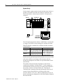
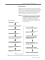
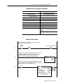
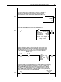
Document Update SLC 5/03 and SLC 5/04 Operating Systems (1747-OS302, FRN10 and 1747-OS401, FRN7) Read this document prior to using the SLC 5/03 or SLC 5/04 processors. This document update contains information that updates or clarifies previously published information. See the “Summary of Update” table below for specifics. Purpose of This Document Summary of Update Affected Pages Action to Take This Document Update revises the following publication. Keep this Document Update for reference. Publication Name Publication Number SLC 500t and MicroLogixt 1000 Instruction Set Reference Manual 17476.15 The following table summarizes the information contained in this Document Update. Change 8-22 8-33 Read the MSG Instruction Operation" section in this publication. Note Change in your Reference Manual. page 822, Using Status Bits: Replace the Time Out Bit TO" text with the Setting the Internal TimeOut Value" text from this publication. page 833, Using Ladder Logic: Disregard the ladder logic examples. Refer to the Example Ladder Programs" in this publication. B-72 Read the DayofWeek with Real Time Clock" section in this publication. Note Change in your Reference Manual. For Status Word S:53, add: Clock/Calendar DayofWeek This value contains the dayofweek value of the clock/calendar. Valid range is 0-6 (Sunday=0). To disable the clock/calendar, write zeros to all clock and calendar words (S:37 to S:41). D-5 thru D-7 Read the Interrupt Latency" section in this publication. Note Change in your Reference Manual Change the Entry Time values for SLC 5/03 and SLC 5/04 processors to the new values listed in this publication. H-28 Read the Interfacing with Enhanced Bar Code Decoders" section in this publication. Note Change in your Reference Manual. Add the Interfacing with Enhanced Bar Code Decoders" section of this publication to Appendix H - Application Example Programs. Publication 17476.15DU1 - May 1997 2 SLC 5/03 and SLC 5/04 Operating Systems MSG Instruction Operation for SLC 5/03 Processors (1747OS302, FRN9 or later) and SLC 5/04 Processors (1747OS401, FRN5 or later) The following recommendations for the use of the MSG (message) instruction apply to SLC 5/03 processors (1747-OS302, FRN9 or later) and SLC 5/04 processors (1747-OS401, FRN5 or later). The recommendations must be followed for proper operation of the MSG instruction. Two example ladder programs are included to illustrate programming the MSG instruction. Recommendations for Using the MSG Instruction Limitations for Manipulating the Control Block Bits Do not manipulate the MSG instruction control block values. For example, do not clear the first word of the control block, do not unlatch the time-out control bit, and so on. The only MSG instruction control bits that may be manipulated by the ladder program without adversely affecting the operation of the instruction are the EN and TO bits. The enable bit (EN = bit 15) may be unlatched, but only when the done bit (DN = bit 13) or error bit (ER = bit 12) has been set, indicating the successful or unsuccessful completion of the previous message. In addition, when a MSG is in progress and the ladder program wishes to terminate it for any reason, this may be done by enabling the time-out bit (TO = bit 8). The next time the processor scans the MSG instruction with the TO bit set, it will error the MSG (ER = 1). The MSG instruction may then be re-enabled with a false-to-true transition on the next program scan. Initiating the MSG Instruction To invoke the MSG instruction, toggle the MSG instruction rung from false-to-true. Do not toggle the rung again until the MSG instruction has successfully or unsuccessfully completed the previous message, indicated by the processor setting either the DN or ER bit. Setting the Internal Time-Out Value A value greater than 0 must be entered for the MSG instruction time-out parameter. A time-out value of 0 means no time-out value. In other words, if communication is interrupted, the processor will wait forever for a reply. If a reply is not received, the MSG instruction will appear to be locked up. When a value greater than 0 is entered for the MSG time-out parameter and communication is interrupted, the MSG instruction will time-out after the time-out expires, allowing the user program to retry the same message if desired. Publication 17476.15DU1 - May 1997 3 SLC 5/03 and SLC 5/04 Operating Systems Example Ladder Programs Enabling the MSG Instruction Via Ladder Logic 0000 The MSG instruction will be enabled during the initial processor program scan, and each time the MSG completes, i.e. when the DN or ER bit is set. MSG Read/Write Message Type Peer-to-Peer Read/Write Read Target Device 500CPU Local/Remote Local Control Block N7:0 Control Block Length 14 (EN) (DN) (ER) Setup Screen 0001 MSG Done Bit N7:0 ] [ 13 MSG Enable Bit N7:0 (U) 15 MSG Error Bit N7:0 ] [ 12 0002 END Enabling the MSG Instruction Via User Supplied Input As long as input I:1/0 is set, or anytime it becomes set, the MSG instruction in the next rung will be enabled. This program is an example of controlling when the MSG instruction operates. Input I:1/0 could be any user supplied bit used to control when MSGs are sent. 0000 I:1 ] [ 0 MSG Enable Bit N7:0 ]/[ 15 B3:0 (L) 0 The MSG instruction will be enabled with each falsetotrue transition of bit B3:0/0. 0001 B3:0 ] [ 0 MSG Read/Write Message Type Peer-to-Peer Read/Write Read Target Device 500CPU Local/Remote Local Control Block N7:0 Control Block Length 14 (EN) (DN) (ER) Setup Screen 0002 MSG Done Bit N7:0 ] [ 13 B3:0 (U) 0 MSG Error Bit N7:0 ] [ 12 0003 END Publication 17476.15DU1 - May 1997 4 SLC 5/03 and SLC 5/04 Operating Systems DayofWeek with Real Time Clock The SLC 5/03 (1747-OS302, FRN10) and SLC 5/04 (1747-OS401, FRN7) processors now support the Day-of-Week feature as part of the Real Time Clock. Although this feature is not yet supported by programming software, you can access Day-of-Week via ladder programming. The Day-of-Week status word must be initialized. Initialization is done by setting the year, month, and date in the system status file. The status words for setting these values are: Calendar Status Words Status Word Valid Range Year S:37 0-65535 Month S:38 1-12 (January = 1) Date S:39 1-31 (first day of month = 1) Once the date has been set, the processor determines the Day-of-Week and writes it to S:53. S:53 is read-only and non-volatile. Interpret the Day-of-Week values as shown below: DayofWeek Integer Values Sunday Monday Tuesday Wednesday Thursday Friday Saturday 0 1 2 3 4 5 6 Note: Interrupt Latency If the status of word S:53 is not properly initialized, it will contain a random value. There are new interrupt latency specifications for the SLC 5/03 (1747-OS302, FRN10) and SLC 5/04 (1747-OS401, FRN7) processors. Use the values shown below for calculating interrupt latency for Selectable Timed Interrupt (STI), Discrete Input Interrupt (DII), and I/O Interrupt (IOI). Entry Time Publication 17476.15DU1 - May 1997 SLC 5/03 Processors SLC 5/04 Processors STI 425 µs 355 µs DII 440 µs 365 µs IOI 715 µs 595 µs SLC 5/03 and SLC 5/04 Operating Systems Interfacing with Enhanced Bar Code Decoders Over DH485 Network Using the MSG Instruction 5 The purpose of this section is to illustrate how to interface Allen-Bradley Enhanced Bar Code Decoders to SLC 5/03 and 5/04 processors via the DH-485 network. Enhanced Bar Code Decoders act only as slave devices on this network. This means that these decoders cannot initiate the transfer of data to a host device, such as the SLC 5/03 or SLC 5/04 processor on DH-485. The SLC processor must initiate commands to a decoder and “poll” that decoder for the reply to those commands. Processor and Decoder Operation The Enhanced Bar Code Decoder (catalog number 2755-DS/DD, Series B), when used as a node on a DH-485 network can act as a slave only. This means that the decoder may not initiate communications to any other node on the network. Therefore, in order for a device to get bar code data from an Enhanced Bar Code Decoder on a DH-485 network, that device must send a “read” command and then “poll” the decoder for the reply with data. The only devices capable of polling a slave device on DH-485 are the SLC 5/03 and 5/04 processors. For the SLC 5/03 processors (1747-OS302, FRN10 or later), polling can be done via channels 0 and 1. For the SLC 5/04 processors (1747-OS401, FRN7 or later), channel 0 supports this capability. There are many ways to “trigger” bar code decoders to read a bar code label when a label is present. • a package detect switch wired to both an SLC input module and the bar code decoder • a package detect switch wired only to an SLC input and an SLC output then used to “trigger” the decoder • via a software “trigger” command from the SLC processor For this example, the software “trigger” is used. However, the basic principal is the same for all “trigger” modes. Publication 17476.15DU1 - May 1997 6 SLC 5/03 and SLC 5/04 Operating Systems System Set Up In this example, a photo switch is located such that when it detects a product is in position for the bar code scanner to read a bar code label on the product, a discrete input to the SLC 5/03 processor is energized. SLC 5/03 1747 Chassis DH485 Power Supply 1747AIC Host Port Photo Switch 2755DS/DD Enhanced Bar Code Decoder The 5/03 ladder program then initiates a “MSG Write” to the decoder to “trigger” the decoder to start scanning for a valid bar code label. When the decoder is scanning for a valid bar code label, it operates as shown below: Result of Scan Bar Code Decoder Response Processor Response Good Read turns on its Good Read" onboard output wired to the SLC processor NoRead turns on its NoRead" onboard output wired to the SLC processor When one of these two inputs to the SLC are turned on, the SLC will initiate a MSG Read" to the decoder to get the label data or noread message data. In this case, the good read output will be turned on as soon as a valid read occurs, and the no-read output will be turned on after the decoder has attempted to read a label for a specified amount of time and could not. The amount of time the decoder will attempt to read a label is variable and is called the “No-Read Timer”. For this example it is assumed that the product is moving by the scanner and if the label is not read in 2 seconds, it will not be read at all. Therefore the “No-Read Timer” parameter in the bar code decoder will be set to 2 seconds. Refer to the DS/DD Series B Enhanced Bar Code Decoders (Bulletin 2755) User’s Manual, publication 2755-833, for details concerning the configuration of your Allen-Bradley Enhanced Bar Code Decoder. Publication 17476.15DU1 - May 1997 SLC 5/03 and SLC 5/04 Operating Systems 7 Operating Sequence With the bar code decoder configured as previously described, the following series of events will take place when a product with a good bar code label breaks the photo switch and this input to the SLC goes from false-to-true. The SLC 5/03 ladder program logic to make it happen is also included. Please note that, as previously stated, a bar code/SLC system may be configured in a variety of ways. Important: Sequence of Events The photo switch input to the SLC goes from falsetotrue. Messages sent by the SLC processor to the Enhanced Bar Code Decoder must be programmed as shown by the example ladder program on page 9. If this logic is not followed, the communication between the two DH-485 devices could become out of sequence, resulting in no data transfers between the decoder and the SLC processor. To correct such a problem, cycle power to the decoder. The SLC processors sends a trigger" command to the decoder via a MSG Write" command. The decoder immediately replies to the SLC that it has properly received the command. The reply sets the MSG DN bit and clears the MSG DA bit in the SLC processor. The SLC processor then waits a specified amount of time and reenables the same MSG instruction which now sends the poll" to the decoder. The decoder then responds to this poll" with its reply to the trigger" command. The SLC processor then sets the MSG DN and MSG DA bits. The decoder then reads the bar code label and turns on the good read" output wired to the SLC processor. When this good read" input to the SLC goes from falsetotrue, the SLC sends a MSG Read" to the decoder. The decoder immediately replies to the SLC that it has properly received the command. The reply sets the MSG DN bit and clears the MSG DA bit in the SLC processor. The decoder then processes the command and formulates a reply to the MSG Read" command with the decoded label data included in this reply, and places it into its output buffer awaiting a poll". The SLC processor waits a specified amount of time, then reenables the same MSG Read" instruction which now sends the poll" to the decoder. The decoder then responds to the poll" command with its reply to the MSG Read" command which includes the bar code label data. The SLC processor then sets the MSG DN and MSG DA bits to signify its receipt of the data. NOTE: These events are described in more detail by the comments listed within the example ladder program page 9. Publication 17476.15DU1 - May 1997 8 SLC 5/03 and SLC 5/04 Operating Systems Optimizing MSG TimeOut If the time delay between sending a command to an Enhanced Bar Code Decoder and “polling” for the reply is not long enough, the MSG instruction will time-out (MSG TO bit = 1) each time it is enabled from that point forward. To re-synchronize the SLC processor and the decoder, you will need to cycle power on the decoder to clear its buffer. There are other ways of clearing the buffers in the decoder, such as sending a “Clear Buffers” command or a “Reset” command to the decoder. However, the best way to handle this issue is to never let it happen. Optimizing the time delay between sending the initial command and “polling” for the reply is the best way to accomplish this. The delay must be long enough so the decoder will have enough time to formulate a reply to the command and short enough to not impact the throughput of the application. Example MSG Instruction Configuration The example SLC 5/03 and SLC 5/04 ladder program demonstrates how to send commands to an Enhanced Bar Code Decoder, and then after a time delay, “poll” for a reply. The internal setup screen parameters for the two MSG instructions in the example ladder program are shown below, along with the necessary Enhanced Bar Code Decoder configuration parameters. SLC 5/03 and SLC 5/04 Internal Set Up Screen Parameters MSG #1 MSG #2 Type peertopeer peertopeer Read/write write read Target device 485CIF 485CIF Local/remote local local Control block N7:0 N7:20 Channel 1 1 Target Node 2 2 Our source file address N7:15 N7:40 ➀ Target CIF offset 0 0 Message length in elements 1 10 Message timeout (seconds) 5 5 ➀ The Target CIF Offset when working with Enhanced Bar Code Decoders as slaves on DH485 must contain a value greater than 255. However, 255 is the largest value SLC programming software will allow you to enter into this parameter in a MSG instruction. Therefore, use an unconditioned rung with a MOV instruction to move the proper value into the Target CIF Offset field. The example ladder program in this section demonstrates this. Note that 1588 decimal in a MSG Write" is the value which results in a properly configured Enhanced Bar Code Decoder to initiate the trigger" function. A value of 256 in a MSG Read" requests a specified number of words of data from the bar code decoder. In this example, we are reading 10 words or 20 characters (bytes). Publication 17476.15DU1 - May 1997 9 SLC 5/03 and SLC 5/04 Operating Systems Example Scanner and Decoder Configuration Scanner Configuration Parameters 2755DS/DD Series B Enhanced Bar Code Decoder Configuration Parameters Host Communications Page Scanner Control Page Discrete I/O: Baud Rate: 19200 Laser Light: Read Package 25ms NoRead Package 25ms Triggered Bits/Char: 8 Data 1 Stop Decode Mode: Host Parity: Even NoRead Time: 2000 ms Host Protocol: DH485 PCCC1 Inter Scan Time: none Device Address: 2 Capture Count: 2 ACK Char: none Symbols/Scan: 1 NAK Char: none Large Buffer: No Symbols/Package: 1 Match Complete: 1 Send Host Message: Package Transmission Check: Immediately after Valid none Example Ladder Program This rung detects the Photo Switch input going from falsetotrue, and latches internal storage bit B3/1. 0000 0001 Photo Switch I:1 ] [ 0 Initiate Write MSG B3:0 (L) 1 B3:0 [OSR] 0 This rung moves the decimal value for the bar code decoder trigger" command into the MSG instructions Offset" parameter. The programming software does not allow values greater than 255 decimal to be entered into a MSG control block Offset" value. MOV Move Source Dest The internal storage bit (B3/1) gives the MSG instruction a falsetotrue transition to send the initial command. B3/1 remains latched until both the DN and DA bits are set for the MSG instruction. 0002 B3:0 ] [ 1 MSG Read/Write Message Type Peer-to-Peer Read/Write Write Target Device 485CIF Local/Remote Local Control Block N7:0 Control Block Length 14 1588 1588 < N7:3 0< (EN) (DN) (ER) Setup Screen Publication 17476.15DU1 - May 1997 10 SLC 5/03 and SLC 5/04 Operating Systems 0003 The initial reply from an Enhanced Bar Code Decoder will result in MSG DN = 1 and MSG DA = 0. This simply indicates that the decoder has received the command, but has not yet formulated a reply. The maximum time delay needed between sending the initial command and sending a poll to get the reply is 250 ms. In most cases this delay could be much less (30 ms to 100 ms), depending on the number of features the decoder is configured for. MSG DA Bit MSG DN Bit (Data Available) N7:0 N7:7 TON ] [ ]/[ Timer On Delay 13 1 Timer T4:0 Time Base 0.01 Preset 25 < Accum 0< (EN) (DN) The internal storage bit, B3/1, holds the MSG instruction true until DN and DA are both set, indicating completion of the command sent and reply received sequence. When DN is set and DA is reset, unlatching the MSG EN bit will effectively toggle the MSG instruction the same as if the MSG rung were toggled, i.e. rung conditions made false, then true. The MSG instruction is toggled one time after DN and NOT DA plus some time delay, to send a final poll to the decoder to get the MSG reply. When the reply is received, the SLC processor will set DN and DA. 0004 0005 MSG EN Bit N7:0 (U) 15 T4:0 ] [ DN When the SLC processor sets both DN and DA for a MSG instruction, the MSG sequence to an Enhanced Bar Code Decoder is complete. In this case, the decoder has received the trigger" command and has performed this command. Therefore, unlatch B3/1 at this time to be ready for the next request for trigger". MSG DA Bit MSG DN Bit (Data Available) N7:0 N7:7 B3:0 (U) ] [ ] [ 1 13 1 If an error occurs with the MSG instruction, the ER bit is set. If this occurs, the user can either try to resend the same message again by unlatching EN, or at this point, could sound an alarm or route the product down a rework loop or some other similar action. If the latter choice is used, you must also unlatch B3/1 at this time to be ready for the next request for trigger". 0006 MSG ER Bit N7:0 ] [ 12 MSG EN Bit N7:0 (U) 15 This rung detects falsetotrue transitions of either a good read or a noread input from the bar code decoder and latches internal storage bit B3/2. B3/2 will then, in the next rung, initialize the MSG read command to the decoder. This is done if either a good read or a noread occurs, because the noread message configured in the decoder is data as much as actual bar code label data. Therefore, the ladder program must distinguish between data that means noread as well as actual bar code label data. 0007 Good Read Input from Bar Code Decoder I:1 ] [ 1 1746-I*16 No-Read Input from Bar Code Decoder I:1 ] [ 2 1746-I*16 Publication 17476.15DU1 - May 1997 B3:0 [OSR] 3 B3:0 (L) 2 11 SLC 5/03 and SLC 5/04 Operating Systems This rung moves the decimal value for the bar code decoder Read" command into the MSG instruction's Offset" parameter. The programming software does not allow values greater than 255 decimal to be entered into a MSG control block Offset" value. 0008 MOV Move Source Dest 0009 The internal storage bit, B3/2, gives the MSG instruction a falsetotrue transition to send the initial command. B3/2 remains latched until both DN and DA are set. B3:0 MSG ] [ Read/Write Message 2 Type Peer-to-Peer Read/Write Read Target Device 485CIF Local/Remote Local Control Block N7:20 Control Block Length 14 1588 1588 < N7:3 0< (EN) (DN) (ER) Setup Screen 0010 0011 The initial reply from an Enhanced Bar Code Decoder will result in MSG DN = 1 and MSG DA = 0. This indicates that the decoder has received the command, but has not yet formulated a reply. The maximum time delay needed between sending the initial command and sending a poll to get the reply is 250 ms. In most cases this delay could be much less (30 ms to 100 ms), depending on the number of features the decoder is configured for. MSG DA Bit MSG DN Bit (Data Available) N7:20 N7:27 TON ] [ ]/[ Timer On Delay 13 1 Timer T4:1 Time Base 0.01 Preset 250 < Accum 0< (EN) (DN) The internal storage bit, B3/2, holds the MSG instruction true until DN and DA are both set, indicating completion of the command sent and reply received sequence. When DN is set and DA is reset, unlatching the MSG EN bit will effectively toggle the MSG instruction the same as if the MSG rung were toggled, i.e. rung conditions made false, then true. The MSG instruction is toggled one time after DN and NOT DA plus some time delay, to send a final poll to the decoder to get the MSG reply. When the reply is received, the SLC processor will set DN and DA. MSG EN Bit T4:1 N7:20 ] [ (U) DN 15 Publication 17476.15DU1 - May 1997 0012 When the SLC processor sets both DN and DA for a MSG instruction, the MSG sequence to an Enhanced Bar Code Decoder is complete. In this case, the decoder has received the Read" command and has formulated a reply to this command. Therefore, unlatch B3/2 at this time to be ready for the next Read" request. In addition, when DN and DA are both set, this indicates that the data received with the read reply (except noread" data) is valid and may be buffered or used. MSG DA Bit MSG DN Bit (Data Available N7:20 N7:27 B3:0 (U) ] [ ] [ 2 13 1 COP Copy File Source #N7:40 Dest #N7:100 Length 10 If an error occurs with the MSG instruction, the ER bit is set. If this occurs, the user can either try to resend the same message again by unlatching EN, or at this point, could sound an alarm or route the product down a rework loop or some other similar action. If the latter choice is used, you must also unlatch B3/2 at this time to be ready for the next Read" request. 0013 MSG ER Bit N7:20 ] [ 12 MSG EN Bit N7:20 (U) 15 0014 END PLC-5 is a registered trademark of Rockwell International Corporation. PLC-5/250, SLC 500, SLC 5/03, and SLC 5/04 are trademarks of Rockwell International Corporation. AllenBradley, a Rockwell Automation Business, has been helping its customers improve productivity and quality for more than 90 years. We design, manufacture and support a broad range of automation products worldwide. They include logic processors, power and motion control devices, operator interfaces, sensors and a variety of software. Rockwell is one of the world's leading technology companies. Worldwide representation. Argentina • Australia • Austria • Bahrain • Belgium • Brazil • Bulgaria • Canada • Chile • China, PRC • Colombia • Costa Rica • Croatia • Cyprus • Czech Republic • Denmark • Ecuador • Egypt • El Salvador • Finland • France • Germany • Greece • Guatemala • Honduras • Hong Kong • Hungary • Iceland • India • Indonesia • Ireland • Israel • Italy • Jamaica • Japan • Jordan • Korea • Kuwait • Lebanon • Malaysia • Mexico • Netherlands • New Zealand • Norway • Pakistan • Peru • Philippines • Poland • Portugal • Puerto Rico • Qatar • Romania • Russia-CIS • Saudi Arabia • Singapore • Slovakia • Slovenia • South Africa, Republic • Spain • Sweden • Switzerland • Taiwan • Thailand • Turkey • United Arab Emirates • United Kingdom • United States • Uruguay • Venezuela • Yugoslavia AllenBradley Headquarters, 1201 South Second Street, Milwaukee, WI 53204 USA, Tel: (1) 414 3822000 Fax: (1) 414 3824444 Publication 17476.15DU1 - May 1997 PN 40071-030-01 (A) E 1997 Rockwell International Corporation. All rights reserved.- Printed in USA Publication 17476.15DU1 May 1997