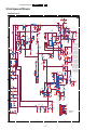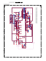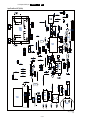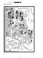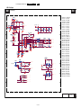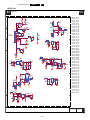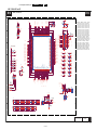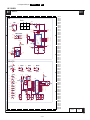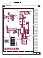
1
Colour Television Chassis TPM4.1E LA 18850_000_100107.eps 100209 Contents Page Revision List 2 Technical Specifications, Connections 2 Precautions, Notes, and Abbreviation List 5 Mechanical Instructions 9 Service Modes, Error Codes, and Fault Finding 14 Alignments 18 Circuit Descriptions 20 IC Data Sheets 24 Block Diagrams Wiring Diagram (32") 29 Wiring Diagram (42") 30 Block Diagram 31 10. Circuit Diagrams and PWB Layouts Drawing Power Board: Power, 32" (A01) 32 Power Board: Inverter, 32" (A02) 33 Power Board: Power, 42" (A01) 36 Power Board: Inverter, 42" (A02) 37 SSB: D-Sub Input (B01) 40 SSB: REAR I/O (B02) 41 SSB: Scart (B03) 42 SSB: SIDE Input (B04) 43 SSB: CVBS/ Audio Out (B05) 44 SSB: Tuner (B06) 45 SSB: HDMI Input (B07) 46 SSB: WT6703F (Stand-by MCU) (B08) 47 SSB: MTK8222 (B09) 48 SSB: DDR1 Memory (B10) 49 SSB: KEYBOARD, IR/LED & ComPair I/F (B11) 50 SSB: Audio Switch (B12) 51 SSB: AUDIO Preamplifier (B13) 52 SSB: Audio Amplifier (B14) 53 SSB: DC/DC Power (B15) 54 SSB: T-CON, LCD Panel I/F (B16) 55 SSB: T-CON DC/DC (B17) 56 Contents 1. 2. 3. 4. 5. 6. 7. 8. 9. Page SSB: T-CON TGMA , Level-Shifter SSB: T-CON Mini-LVDS I/F IR/LED Board 11. Styling Sheets Styling Sheet 32" Styling Sheet 42" (B18) 57 (B19) 58 (J) 61 59-60 59-60 62 63 64 PWB 34-35 34-35 38-39 38-39 59-60 59-60 59-60 59-60 59-60 59-60 59-60 59-60 59-60 59-60 59-60 59-60 59-60 59-60 59-60 59-60 59-60 © Copyright 2011 Koninklijke Philips Electronics N.V. All rights reserved. No part of this publication may be reproduced, stored in a retrieval system or transmitted, in any form or by any means, electronic, mechanical, photocopying, or otherwise without the prior permission of Philips. Published by WEP/WS 1161 BU TV Consumer Care, the Netherlands Subject to modification EN 3122 785 18873 2011-Jan-21 EN 2 1. Revision List TPM4.1E LA 1. Revision List Manual xxxx xxx xxxx.0 • First release. Manual xxxx xxx xxxx.1 • Added “/60” models to Table 6-3. Manual xxxx xxx xxxx.2 • Chapter 4: added information on returning a defect LCD panel. • Chapter 6: updated Option code overview. Manual xxxx xxx xxxx.3 • Added 32PFL3205/12 to the manual. 2. Technical Specifications, Connections 2.2 Index of this chapter: 2.1 Technical Specifications 2.2 Directions for Use 2.3 Connections 2.4 Chassis Overview Directions for use can be downloaded from the following websites: http://www.philips.com/support http://www.p4c.philips.com Notes: • Figures can deviate due to the different set executions. • Specifications are indicative (subject to change). 2.1 Technical Specifications For on-line product support please use the links in. Here is product information available, as well as getting started, user manuals, frequently asked questions and software & drivers. Table 2-1 Described Model Numbers: Model Number Styling Published in 32PFL3205/12 Dali 3122 785 18873 32PFL3605/12 Dali 3122 785 18870 32PFL3605/60 Dali 3122 785 18870 42PFL3605/12 Dali 3122 785 18870 42PFL3605/60 Dali 3122 785 18870 Note: The given Model Numbers are subject to change. 2011-Jan-21 Directions for Use Technical Specifications, Connections 2.3 TPM4.1E LA 2. EN 3 Connections 1 6 4 8 9 2 10 3 11 7 5 18870_001_100107.eps 100308 Figure 2-1 Connection overview 15 16 17 18 19 20 Note: The following connector colour abbreviations are used (acc. to DIN/IEC 757): Bk= Black, Bu= Blue, Gn= Green, Gy= Grey, Rd= Red, Wh= White, Ye= Yellow. 2.3.1 Side Connections 1 - Cinch: Video CVBS - In, Audio - In Ye - Video CVBS 1 VPP / 75 Rd - Audio R 0.5 VRMS / 10 k Wh - Audio L 0.5 VRMS / 10 k - DDC_SCL - DDC_SDA - Ground - +5V - HPD - Ground DDC clock DDC data Gnd Hot Plug Detect Gnd 3 - USB2.0 jq jq jq 1 1 2 3 4 Figure 2-2 HDMI (type A) connector - D2+ - Shield - D2- D1+ - Shield - D1- D0+ - Shield - D0- CLK+ - Shield - CLK- n.c. - n.c. Data channel Gnd Data channel Data channel Gnd Data channel Data channel Gnd Data channel Data channel Gnd Data channel 3 4 Figure 2-3 USB (type A) 1 2 10000_017_090121.eps 090428 1 2 3 4 5 6 7 8 9 10 11 12 13 14 2 10000_022_090121.eps 090121 2 - HDMI: Digital Video, Digital Audio - In 19 18 j jk H j j H j H j j H j j H j j H j 2.3.2 - +5V - Data (-) - Data (+) - Ground Gnd k jk jk H Rear Connections 4 - TV ANTENNA - In Signal input from an antenna, cable or satellite. 5 - Audio - Out: Left / Right Wh - Audio - L 0.5 VRMS / 10 k Rd - Audio - R 0.5 VRMS / 10 k kq kq 2011-Jan-21 EN 4 2. TPM4.1E LA Technical Specifications, Connections 20 0.5 VRMS / 10 kW 0.5 VRMS / 10 kW jq jq 8 - Audio - In: Left / Right, VGA Gn - Audio L/R in 0.5 VRMS / 10 kW jq Wh - Audio - L Rd - Audio - R 6 - EXT1 - 2: Video RGB/YC - In, CVBS - In/Out, Audio In/Out 2 21 1 10000_001_090121.eps 090121 9 - PC IN:VGA Figure 2-4 SCART connector 1 6 11 1 2 3 4 5 6 7 8 - Audio R - Audio R - Audio L - Ground Audio - Ground Blue - Audio L - Video Blue/C-out - Function Select 9 10 11 12 13 14 15 16 - Ground Green - n.c. - Video Green - n.c. - Ground Red - Ground P50 - Video Red/C - Status/FBL 17 18 19 20 21 - Ground Video - Ground FBL - Video CVBS - Video CVBS/Y - Shield 0.5 VRMS / 1 k 0.5 VRMS / 10 k 0.5 VRMS / 1 k Gnd Gnd 0.5 VRMS / 10 k 0.7 VPP / 75 0 - 2 V: INT 4.5 - 7 V: EXT 16:9 9.5 - 12 V: EXT 4:3 Gnd j Gnd Gnd 0.7 VPP / 75 0 - 0.4 V: INT 1 - 3 V: EXT / 75 Gnd Gnd 1 VPP / 75 1 VPP / 75 Gnd H H j Chassis Overview Refer to 9. Block Diagrams for PWB/CBA locations. 2011-Jan-21 j H 0.7 VPP / 75 7 - EXT3: Video YPbPr - In, Audio - In Gn - Video - Y 1 VPP / 75 W Bu - Video - Pb 0.7 VPP / 75 W Rd - Video - Pr 0.7 VPP / 75 W 2.4 k j k H H j jk j H H k j H jq jq jq 5 10 15 10000_002_090121.eps 090127 Figure 2-5 VGA connector 1 2 3 4 5 6 7 8 9 10 11 12 13 14 15 - Video Red - Video Green - Video Blue - n.c. - Ground - Ground Red - Ground Green - Ground Blue - +5VDC - Ground Sync - Ground Red - DDC_SDA - H-sync - V-sync - DDC_SCL 10 - Service / UART 1 - Ground 2 - UART_TX 3 - UART_RX 0.7 VPP / 75 0.7 VPP / 75 0.7 VPP / 75 j j j Gnd Gnd Gnd Gnd +5 V Gnd Gnd DDC data 0-5V 0-5V DDC clock H H H H j H H j j j j Gnd Transmit Receive H k j 11 - HDMI 1: Digital Video, Digital Audio - In See 2 - HDMI: Digital Video, Digital Audio - In. Precautions, Notes, and Abbreviation List TPM4.1E LA 3. EN 5 3. Precautions, Notes, and Abbreviation List • Index of this chapter: 3.1 Safety Instructions 3.2 Warnings 3.3 Notes 3.4 Abbreviation List 3.1 Safety Instructions 3.3.2 Safety regulations require that after a repair, the set must be returned in its original condition. Pay in particular attention to the following points: • Route the wire trees correctly and fix them with the mounted cable clamps. • Check the insulation of the Mains/AC Power lead for external damage. • Check the strain relief of the Mains/AC Power cord for proper function. • Check the electrical DC resistance between the Mains/AC Power plug and the secondary side (only for sets that have a Mains/AC Power isolated power supply): 1. Unplug the Mains/AC Power cord and connect a wire between the two pins of the Mains/AC Power plug. 2. Set the Mains/AC Power switch to the “on” position (keep the Mains/AC Power cord unplugged!). 3. Measure the resistance value between the pins of the Mains/AC Power plug and the metal shielding of the tuner or the aerial connection on the set. The reading should be between 4.5 M and 12 M. 4. Switch “off” the set, and remove the wire between the two pins of the Mains/AC Power plug. • Check the cabinet for defects, to prevent touching of any inner parts by the customer. • • • • • 3.3.3 All resistor values are in ohms, and the value multiplier is often used to indicate the decimal point location (e.g. 2K2 indicates 2.2 k). Resistor values with no multiplier may be indicated with either an “E” or an “R” (e.g. 220E or 220R indicates 220 ). All capacitor values are given in micro-farads ( 10-6), nano-farads (n 10-9), or pico-farads (p 10-12). Capacitor values may also use the value multiplier as the decimal point indication (e.g. 2p2 indicates 2.2 pF). An “asterisk” (*) indicates component usage varies. Refer to the diversity tables for the correct values. The correct component values are listed on the Philips Spare Parts Web Portal. Spare Parts For the latest spare part overview, consult your Philips Spare Part web portal. 3.3.4 BGA (Ball Grid Array) ICs Introduction For more information on how to handle BGA devices, visit this URL: http://www.atyourservice-magazine.com. Select “Magazine”, then go to “Repair downloads”. Here you will find Information on how to deal with BGA-ICs. BGA Temperature Profiles For BGA-ICs, you must use the correct temperature-profile. Where applicable and available, this profile is added to the IC Data Sheet information section in this manual. 3.3.5 3.2 Schematic Notes • Safety regulations require the following during a repair: • Connect the set to the Mains/AC Power via an isolation transformer (> 800 VA). • Replace safety components, indicated by the symbol h, only by components identical to the original ones. Any other component substitution (other than original type) may increase risk of fire or electrical shock hazard. Where necessary, measure the waveforms and voltages with (D) and without (E) aerial signal. Measure the voltages in the power supply section both in normal operation (G) and in stand-by (F). These values are indicated by means of the appropriate symbols. Lead-free Soldering Warnings • • • • 3.3 Notes 3.3.1 General • Due to lead-free technology some rules have to be respected by the workshop during a repair: • Use only lead-free soldering tin. If lead-free solder paste is required, please contact the manufacturer of your soldering equipment. In general, use of solder paste within workshops should be avoided because paste is not easy to store and to handle. • Use only adequate solder tools applicable for lead-free soldering tin. The solder tool must be able: – To reach a solder-tip temperature of at least 400°C. – To stabilize the adjusted temperature at the solder-tip. – To exchange solder-tips for different applications. • Adjust your solder tool so that a temperature of around 360°C - 380°C is reached and stabilized at the solder joint. Heating time of the solder-joint should not exceed ~ 4 sec. Avoid temperatures above 400°C, otherwise wear-out of tips will increase drastically and flux-fluid will be destroyed. To avoid wear-out of tips, switch “off” unused equipment or reduce heat. • Mix of lead-free soldering tin/parts with leaded soldering tin/parts is possible but PHILIPS recommends strongly to avoid mixed regimes. If this cannot be avoided, carefully clear the solder-joint from old tin and re-solder with new tin. All ICs and many other semiconductors are susceptible to electrostatic discharges (ESD w). Careless handling during repair can reduce life drastically. Make sure that, during repair, you are connected with the same potential as the mass of the set by a wristband with resistance. Keep components and tools also at this same potential. Be careful during measurements in the high voltage section. Never replace modules or other components while the unit is switched “on”. When you align the set, use plastic rather than metal tools. This will prevent any short circuits and the danger of a circuit becoming unstable. Measure the voltages and waveforms with regard to the chassis (= tuner) ground (H), or hot ground (I), depending on the tested area of circuitry. The voltages and waveforms shown in the diagrams are indicative. Measure them in the Service Default Mode with a colour bar signal and stereo sound (L: 3 kHz, R: 1 kHz unless stated otherwise) and picture carrier at 475.25 MHz for PAL, or 61.25 MHz for NTSC (channel 3). 3.3.6 Alternative BOM identification It should be noted that on the European Service website, “Alternative BOM” is referred to as “Design variant”. 2011-Jan-21 EN 6 3. TPM4.1E LA Precautions, Notes, and Abbreviation List The third digit in the serial number (example: AG2B0335000001) indicates the number of the alternative B.O.M. (Bill Of Materials) that has been used for producing the specific TV set. In general, it is possible that the same TV model on the market is produced with e.g. two different types of displays, coming from two different suppliers. This will then result in sets which have the same CTN (Commercial Type Number; e.g. 28PW9515/12) but which have a different B.O.M. number. By looking at the third digit of the serial number, one can identify which B.O.M. is used for the TV set he is working with. If the third digit of the serial number contains the number “1” (example: AG1B033500001), then the TV set has been manufactured according to B.O.M. number 1. If the third digit is a “2” (example: AG2B0335000001), then the set has been produced according to B.O.M. no. 2. This is important for ordering the correct spare parts! For the third digit, the numbers 1...9 and the characters A...Z can be used, so in total: 9 plus 26= 35 different B.O.M.s can be indicated by the third digit of the serial number. Identification: The bottom line of a type plate gives a 14-digit serial number. Digits 1 and 2 refer to the production centre (e.g. AG is Bruges), digit 3 refers to the B.O.M. code, digit 4 refers to the Service version change code, digits 5 and 6 refer to the production year, and digits 7 and 8 refer to production week (in example below it is 2006 week 17). The 6 last digits contain the serial number. 3.4 Abbreviation List 0/6/12 AARA ACI ADC AFC AGC AM AP AR ASF ATSC MODEL : 32PF9968/10 PROD.NO: AG 1A0617 000001 MADE IN BELGIUM 220-240V ~ 50/60Hz 128W VHF+S+H+UHF S BJ3.0E LA 10000_024_090121.eps 100105 Figure 3-1 Serial number (example) 3.3.7 Board Level Repair (BLR) or Component Level Repair (CLR) If a board is defective, consult your repair procedure to decide if the board has to be exchanged or if it should be repaired on component level. If your repair procedure says the board should be exchanged completely, do not solder on the defective board. Otherwise, it cannot be returned to the O.E.M. supplier for back charging! 3.3.8 Practical Service Precautions • • ATV Auto TV It makes sense to avoid exposure to electrical shock. While some sources are expected to have a possible dangerous impact, others of quite high potential are of limited current and are sometimes held in less regard. Always respect voltages. While some may not be dangerous in themselves, they can cause unexpected reactions that are best avoided. Before reaching into a powered TV set, it is best to test the high voltage insulation. It is easy to do, and is a good service precaution. AV AVC AVIP B/G BDS BLR BTSC B-TXT C CEC CL CLR ComPair CP CSM CTI CVBS DAC DBE DCM DDC D/K DFI 2011-Jan-21 SCART switch control signal on A/V board. 0 = loop through (AUX to TV), 6 = play 16 : 9 format, 12 = play 4 : 3 format Automatic Aspect Ratio Adaptation: algorithm that adapts aspect ratio to remove horizontal black bars; keeps the original aspect ratio Automatic Channel Installation: algorithm that installs TV channels directly from a cable network by means of a predefined TXT page Analogue to Digital Converter Automatic Frequency Control: control signal used to tune to the correct frequency Automatic Gain Control: algorithm that controls the video input of the feature box Amplitude Modulation Asia Pacific Aspect Ratio: 4 by 3 or 16 by 9 Auto Screen Fit: algorithm that adapts aspect ratio to remove horizontal black bars without discarding video information Advanced Television Systems Committee, the digital TV standard in the USA See Auto TV A hardware and software control system that measures picture content, and adapts image parameters in a dynamic way External Audio Video Audio Video Controller Audio Video Input Processor Monochrome TV system. Sound carrier distance is 5.5 MHz Business Display Solutions (iTV) Board-Level Repair Broadcast Television Standard Committee. Multiplex FM stereo sound system, originating from the USA and used e.g. in LATAM and AP-NTSC countries Blue TeleteXT Centre channel (audio) Consumer Electronics Control bus: remote control bus on HDMI connections Constant Level: audio output to connect with an external amplifier Component Level Repair Computer aided rePair Connected Planet / Copy Protection Customer Service Mode Color Transient Improvement: manipulates steepness of chroma transients Composite Video Blanking and Synchronization Digital to Analogue Converter Dynamic Bass Enhancement: extra low frequency amplification Data Communication Module. Also referred to as System Card or Smartcard (for iTV). See “E-DDC” Monochrome TV system. Sound carrier distance is 6.5 MHz Dynamic Frame Insertion Precautions, Notes, and Abbreviation List DFU DMR DMSD DNM DNR DRAM DRM DSP DST DTCP DVB-C DVB-T DVD DVI(-d) E-DDC EDID EEPROM EMI EPG EPLD EU EXT FDS FDW FLASH FM FPGA FTV Gb/s G-TXT H HD HDD HDCP HDMI HP I I2 C I2 D I2 S IF IR IRQ ITU-656 Directions For Use: owner's manual Digital Media Reader: card reader Digital Multi Standard Decoding Digital Natural Motion Digital Noise Reduction: noise reduction feature of the set Dynamic RAM Digital Rights Management Digital Signal Processing Dealer Service Tool: special remote control designed for service technicians Digital Transmission Content Protection; A protocol for protecting digital audio/video content that is traversing a high speed serial bus, such as IEEE-1394 Digital Video Broadcast - Cable Digital Video Broadcast - Terrestrial Digital Versatile Disc Digital Visual Interface (d= digital only) Enhanced Display Data Channel (VESA standard for communication channel and display). Using E-DDC, the video source can read the EDID information form the display. Extended Display Identification Data (VESA standard) Electrically Erasable and Programmable Read Only Memory Electro Magnetic Interference Electronic Program Guide Erasable Programmable Logic Device Europe EXTernal (source), entering the set by SCART or by cinches (jacks) Full Dual Screen (same as FDW) Full Dual Window (same as FDS) FLASH memory Field Memory or Frequency Modulation Field-Programmable Gate Array Flat TeleVision Giga bits per second Green TeleteXT H_sync to the module High Definition Hard Disk Drive High-bandwidth Digital Content Protection: A “key” encoded into the HDMI/DVI signal that prevents video data piracy. If a source is HDCP coded and connected via HDMI/DVI without the proper HDCP decoding, the picture is put into a “snow vision” mode or changed to a low resolution. For normal content distribution the source and the display device must be enabled for HDCP “software key” decoding. High Definition Multimedia Interface HeadPhone Monochrome TV system. Sound carrier distance is 6.0 MHz Inter IC bus Inter IC Data bus Inter IC Sound bus Intermediate Frequency Infra Red Interrupt Request The ITU Radio communication Sector (ITU-R) is a standards body subcommittee of the International Telecommunication Union relating to radio communication. ITU-656 (a.k.a. ITV LS LATAM LCD LED L/L' LPL LS LVDS Mbps M/N MHEG MIPS MOP MOSFET MPEG MPIF MUTE MTV NC NICAM NTC NTSC NVM O/C OSD OAD OTC P50 PAL TPM4.1E LA 3. EN 7 SDI), is a digitized video format used for broadcast grade video. Uncompressed digital component or digital composite signals can be used. The SDI signal is self-synchronizing, uses 8 bit or 10 bit data words, and has a maximum data rate of 270 Mbit/s, with a minimum bandwidth of 135 MHz. Institutional TeleVision; TV sets for hotels, hospitals etc. Last Status; The settings last chosen by the customer and read and stored in RAM or in the NVM. They are called at start-up of the set to configure it according to the customer's preferences Latin America Liquid Crystal Display Light Emitting Diode Monochrome TV system. Sound carrier distance is 6.5 MHz. L' is Band I, L is all bands except for Band I LG.Philips LCD (supplier) Loudspeaker Low Voltage Differential Signalling Mega bits per second Monochrome TV system. Sound carrier distance is 4.5 MHz Part of a set of international standards related to the presentation of multimedia information, standardised by the Multimedia and Hypermedia Experts Group. It is commonly used as a language to describe interactive television services Microprocessor without Interlocked Pipeline-Stages; A RISC-based microprocessor Matrix Output Processor Metal Oxide Silicon Field Effect Transistor, switching device Motion Pictures Experts Group Multi Platform InterFace MUTE Line Mainstream TV: TV-mode with Consumer TV features enabled (iTV) Not Connected Near Instantaneous Compounded Audio Multiplexing. This is a digital sound system, mainly used in Europe. Negative Temperature Coefficient, non-linear resistor National Television Standard Committee. Color system mainly used in North America and Japan. Color carrier NTSC M/N= 3.579545 MHz, NTSC 4.43= 4.433619 MHz (this is a VCR norm, it is not transmitted off-air) Non-Volatile Memory: IC containing TV related data such as alignments Open Circuit On Screen Display Over the Air Download. Method of software upgrade via RF transmission. Upgrade software is broadcasted in TS with TV channels. On screen display Teletext and Control; also called Artistic (SAA5800) Project 50: communication protocol between TV and peripherals Phase Alternating Line. Color system mainly used in West Europe (color carrier= 4.433619 MHz) and South America (color carrier PAL M= 2011-Jan-21 EN 8 3. PCB PCM PDP PFC PIP PLL POD POR PSDL PSL PSLS PTC PWB PWM QRC QTNR QVCP RAM RGB RC RC5 / RC6 RESET ROM RSDS R-TXT SAM S/C SCART SCL SCL-F SD SDA SDA-F SDI SDRAM SECAM SIF SMPS SoC SOG SOPS SPI S/PDIF SRAM SRP SSB SSC STB STBY SVGA 2011-Jan-21 TPM4.1E LA Precautions, Notes, and Abbreviation List 3.575612 MHz and PAL N= 3.582056 MHz) Printed Circuit Board (same as “PWB”) Pulse Code Modulation Plasma Display Panel Power Factor Corrector (or Preconditioner) Picture In Picture Phase Locked Loop. Used for e.g. FST tuning systems. The customer can give directly the desired frequency Point Of Deployment: a removable CAM module, implementing the CA system for a host (e.g. a TV-set) Power On Reset, signal to reset the uP Power Supply for Direct view LED backlight with 2D-dimming Power Supply with integrated LED drivers Power Supply with integrated LED drivers with added Scanning functionality Positive Temperature Coefficient, non-linear resistor Printed Wiring Board (same as “PCB”) Pulse Width Modulation Quasi Resonant Converter Quality Temporal Noise Reduction Quality Video Composition Processor Random Access Memory Red, Green, and Blue. The primary color signals for TV. By mixing levels of R, G, and B, all colors (Y/C) are reproduced. Remote Control Signal protocol from the remote control receiver RESET signal Read Only Memory Reduced Swing Differential Signalling data interface Red TeleteXT Service Alignment Mode Short Circuit Syndicat des Constructeurs d'Appareils Radiorécepteurs et Téléviseurs Serial Clock I2C CLock Signal on Fast I2C bus Standard Definition Serial Data I2C DAta Signal on Fast I2C bus Serial Digital Interface, see “ITU-656” Synchronous DRAM SEequence Couleur Avec Mémoire. Color system mainly used in France and East Europe. Color carriers= 4.406250 MHz and 4.250000 MHz Sound Intermediate Frequency Switched Mode Power Supply System on Chip Sync On Green Self Oscillating Power Supply Serial Peripheral Interface bus; a 4wire synchronous serial data link standard Sony Philips Digital InterFace Static RAM Service Reference Protocol Small Signal Board Spread Spectrum Clocking, used to reduce the effects of EMI Set Top Box STand-BY 800 × 600 (4:3) SVHS SW SWAN SXGA TFT THD TMDS TS TXT TXT-DW UI uP UXGA V VESA VGA VL VSB WYSIWYR WXGA XTAL XGA Y Y/C YPbPr YUV Super Video Home System Software Spatial temporal Weighted Averaging Noise reduction 1280 × 1024 Thin Film Transistor Total Harmonic Distortion Transmission Minimized Differential Signalling Transport Stream TeleteXT Dual Window with TeleteXT User Interface Microprocessor 1600 × 1200 (4:3) V-sync to the module Video Electronics Standards Association 640 × 480 (4:3) Variable Level out: processed audio output toward external amplifier Vestigial Side Band; modulation method What You See Is What You Record: record selection that follows main picture and sound 1280 × 768 (15:9) Quartz crystal 1024 × 768 (4:3) Luminance signal Luminance (Y) and Chrominance (C) signal Component video. Luminance and scaled color difference signals (B-Y and R-Y) Component video Mechanical Instructions TPM4.1E LA 4. EN 9 4. Mechanical Instructions Index of this chapter: 4.1 Cable Dressing 4.2 Service Positions 4.3 Assy/Panel Removal 32" 4.4 Assembly/Panel Removal 42" 4.5 Returning a defect LCD panel 4.6 Set Re-assembly 4.1 Notes: • Figures below can deviate slightly from the actual situation, due to the different set executions. Cable Dressing 18870_101_100204.eps 100204 Figure 4-1 Cable dressing (32") 2011-Jan-21 EN 10 4. TPM4.1E LA Mechanical Instructions 18870_100_100107.eps 100308 Figure 4-2 Cable dressing (42") 4.2 Service Positions For easy servicing of a TV set, the set should be put face down on a soft flat surface, foam buffers or other specific workshop tools. Ensure that a stable situation is created to perform measurements and alignments. When using foam bars take care that these always support the cabinet and never only the display. Caution: Failure to follow these guidelines can seriously damage the display! Ensure that ESD safe measures are taken. 4.3 Assy/Panel Removal 32" 4.3.1 Rear Cover Warning: Disconnect the mains power cord before removing the rear cover. 1. Remove the fixation screws that secure the rear cover. 2. Lift the rear cover from the TV. Make sure that wires and flat foils are not damaged while lifting the rear cover from the set. 4.3.2 Small Signal Board (SSB) Caution: it is mandatory to remount all different screws at their original position during re-assembly. Failure to do so may result in damaging the SSB. 1. Release the clips from both the LVDS Flat Foil connectors. Caution: be careful, as these are very fragile connectors! Take the flat foils out of their connectors. 2. Unplug all other connectors. 3. Release the tape near the bottom side of the set from the LCD panel. 4. Remove all other fixation screws from the SSB. 2011-Jan-21 5. Take out the SSB together with its shielding. 6. Remove the screws near the HDMI and L/R audio connectors. 7. The SSB can now be shifted sidewards away from the side connector cover and take out of the shielding. Caution: be careful not to damage the thermal pad between the SSB and shielding. 4.3.3 Power Supply Unit (PSU) Caution: it is mandatory to remount all different screws at their original position during re-assembly. Failure to do so may result in damaging the PSU. 1. Unplug power connector from the SSB. 2. Unplug all other connectors from the PSU. 3. Remove all fixation screws from the PSU. 4. The PSU can now be taken out of the set. When defective, replace the whole unit. Mechanical Instructions 4.3.4 2 1 18850_104_100203.eps 100203 Figure 4-4 Keyboard Control Panel (32") 4.3.9 18850_102_100203.eps 100203 Remove the SSB as described earlier. Remove the PSU as described earlier. Remove the speaker as described earlier. Remove the stand as described earlier. Remove the Stand support as described earlier. Remove the clips at the bottom that secure the LCD panel with the bezel. 7. Remove the fixation screws that secure the LCD panel with the bezel. 8. Lift the LCD Panel from the bezel. When defective, replace the whole unit. Speakers 1. Unplug the speaker connector from the SSB and remove the wire wrap from this cable. 2. Remove the fixation screws from the speaker. 3. Take the speaker out. When defective, replace the whole unit. Stand support plate 1. Release the IR/LED/Keyboard Control cable from its clamps and put it aside. 2. Remove the SSB as described earlier. 3. Remove the PSU as described earlier. 4. Remove the Stand as described earlier. 5. Release the tape and take out of the set. 4.4 Assembly/Panel Removal 42" 4.4.1 Rear Cover Warning: Disconnect the mains power cord before removing the rear cover. 1. Remove the fixation screws that secure the rear cover. 2. Lift the rear cover from the TV. Make sure that wires and flat foils are not damaged while lifting the rear cover from the set. IR/LED Board 1. Release the IR/LED/Keyboard Control cable from its clamps. 2. Remove the fixation screw in the middle-bottom of the stand that secures the stand with the bezel, see Figure 4-3 [3]. 3. Remove the clips at the bottom that secure the LCD panel with the bezel. 4. Remove the fixation screws that secure the LCD panel with the bezel. 5. Remove the bezel from the set. 6. Unplug the connectors from the IR/LED board. 7. Release the clips that hold the board and take it from the bezel. When defective, replace the whole unit. Keyboard Control Panel 1. Release the IR/LED/Keyboard Control cable from its clamps. 2. Remove the fixation screw in the middle-bottom of the stand that secures the stand with the bezel, see Figure 4-3 [3]. 3. Remove the clips at the bottom that secure the LCD panel with the bezel. 4. Remove the fixation screws that secure the LCD panel with the bezel. LCD Panel 1. 2. 3. 4. 5. 6. Figure 4-3 Stand (32") 4.3.8 2 2 3 4.3.7 EN 11 1 1 4.3.6 4. 5. Remove the bezel from the set. 6. Unplug the connectors from the IR/LED board. 7. See Figure 4-4, unplug the connector [1] from the Keyboard Control Panel. 8. Release the clips that secure the Keyboard Control Panel [2]. When defective, replace the whole unit. Stand removal See Figure 4-3. Caution: it is mandatory to remount all different screws at their original position during re-assembly. Be sure to put the set in the Service Position. 1. Remove the SSB as described earlier up till step 5 and including step 5. 2. Remove the fixation screws [1], (M3). 3. Remove the fixation screws [2], (M4). 4. Remove the fixation screws [3], (Parker). 5. Take out the stand. 4.3.5 TPM4.1E LA 4.4.2 Small Signal Board (SSB) Caution: it is mandatory to remount all different screws at their original position during re-assembly. Failure to do so may result in damaging the SSB. 1. Release the clips from both the LVDS Flat Foil connectors. Caution: be careful, as these are very fragile connectors! Take the flat foils out of their connectors. 2. Unplug all other connectors. 3. Release the tape near the tuner from the LCD panel. 4. Release the tape near the processor shielding from the LCD panel. 5. Remove the fixation screw that connects the ground cable. 6. Remove all other fixation screws from the SSB. 7. Take out the SSB together with its shielding. 8. Remove the screws near the HDMI and L/R audio connectors. 9. The SSB can now be shifted sidewards away from the side connector cover and take out of the shielding. Caution: be careful not to damage the thermal pad between the SSB and shielding. 2011-Jan-21 EN 12 4.4.3 4. TPM4.1E LA Mechanical Instructions 4. Remove the clips that secure the LCD panel with the bezel. 5. Remove the fixation screws that secure the LCD panel with the bezel. 6. Lift the LCD Panel from the bezel. 7. Unplug the connector [1] from the Keyboard Control Panel. 8. Release the clips that secure the Keyboard Control Panel [2]. When defective, replace the whole unit. Power Supply Unit (PSU) Caution: it is mandatory to remount all different screws at their original position during re-assembly. Failure to do so may result in damaging the PSU. 1. Unplug power connector from the SSB and take the cable out of the cable clamp. 2. Unplug all other connectors from the PSU. 3. Remove all fixation screws from the PSU. 4. The PSU can now be taken out of the set. When defective, replace the whole unit. 4.4.4 1 Stand removal See Figure 4-5. Caution: it is mandatory to remount all different screws at their original position during re-assembly. Be sure to put the set in the Service Position. 1. Remove the fixation screws [1], (Parker). 2. Remove the fixation screws [2], (M4). 3. Take out the stand. 18850_104_100203.eps 100203 Figure 4-6 Keyboard Control Panel (42") 4.4.9 2 1 1 2 Remove the stand as described earlier. Remove the speakers as described earlier. Remove the SSB as described earlier. Remove the PSU as described earlier. Remove the Stand support as described earlier. Remove the clips that secure the LCD panel with the bezel. Remove the fixation screws that secure the LCD panel with the bezel. 8. Lift the LCD Panel from the bezel. When defective, replace the whole unit. 1 1 Figure 4-5 Stand (42") Speakers 1. Unplug the speaker connector from the SSB. 2. Remove the stand, as described earlier. 3. Take the speakers out together with their casing. When defective, replace the whole unit. 4.4.6 4.5 Returning a defect LCD panel To return a defect LCD panel to the factory, all boards, cabling, mechanical supports, shieldings, clamps, spacers, the bezel and tapes have to be removed from the panel, see Figure 4-7. Be sure to carefully pack the area’s of the panel that are visible during normal use. Stand support plate 1. 2. 3. 4. 4.4.7 LCD Panel 1. 2. 3. 4. 5. 6. 7. 18850_105_100203.eps 100203 4.4.5 2 Remove the stand as described earlier. Remove the SSB as described earlier. Remove the PSU as described earlier. Remove all fixation screws from the stand support plate and take it out of the set. IR/LED Board 1. 2. 3. 4. Remove the stand as described earlier. Remove the speakers as described earlier. Remove the SSB as described earlier. Remove the clips at the bottom that secure the LCD panel with the bezel. 5. Remove the fixation screws that secure the LCD panel with the bezel. 6. Lift the LCD Panel from the bezel. 7. Unplug the connectors from the IR/LED board. 8. Release the clips that hold the board and take it from the bezel. When defective, replace the whole unit. 4.4.8 Keyboard Control Panel See Figure 4-6. 1. Remove the stand as described earlier. 2. Remove the speakers as described earlier. 3. Remove the SSB as described earlier. 2011-Jan-21 18931_100_100510.eps 100510 Figure 4-7 LCD panel Mechanical Instructions 4.6 TPM4.1E LA 4. EN 13 Set Re-assembly To re-assemble the whole set, execute all processes in reverse order. Notes: • While re-assembling, make sure that all cables are placed and connected in their original position. See Figure 4-1 and Figure 4-2. • Pay special attention not to damage the EMC foams on the SSB shields. Ensure that EMC foams are mounted correctly. 2011-Jan-21 EN 14 5. TPM4.1E LA Service Modes, Error Codes, and Fault Finding 5. Service Modes, Error Codes, and Fault Finding Index of this chapter: 5.1 Service Modes 5.2 Service Tools 5.3 Software Upgrading 5.4 Error Codes 5.5 Fault Finding and Repair Tips 5.1 Service Modes The Customer Service Mode (CSM) is used for communication between the call centre and the customer, while the Service Alignment Mode (SAM) offers several features for the service technician. This chassis also offers the option of using ComPair, a hardware interface between a computer and the TV chassis. It offers the abilities of structured troubleshooting, error code reading, and software version read-out for all chassis. 5.1.1 18870_211_100310.eps 100310 Figure 5-2 CSM Menu [2/3] Customer Service Mode (CSM) Purpose The Customer Service Mode shows error codes and information on the TV's operation settings.The call centre can instruct the customer (by telephone) to enter CSM in order to identify the status of the set.This helps the call centre to diagnose problems and failures in the TV set before making a service call. The CSM is a read-only mode; therefore, modifications are not possible in this mode. How to Activate CSM Key in the code “123654” via the standard RC transmitter. Note: Activation of the CSM is only possible if there is no (user) menu on the screen! 18870_211_100310.eps 100310 Figure 5-3 CSM Menu [3/3] How to Navigate By means of the “CURSOR-DOWN/UP” knob (or the scroll wheel) on the RC-transmitter, can be navigated through the menus. 18870_201_100209.eps 100310 Figure 5-1 CSM Menu [1/3] General • 1.1 Set Type NVM read/write (max. 16 characters). • 1.2 Production code NVM read/write (max. 16 characters). • 1.4 Option Code Store in NVM (set feature grouping as option) panel code. • 1.5 Codes Error code Layer 2. Store in NVM. 10 error buffers: 000 = No problem, 011 = I2C bus error, 012 = tuner error, 013 = panel. • 1.6 SSB 12NC NVM read/write (12 characters). • 1.7 Display 12NC NVM read/write (12 characters). • 1.8 PSU 12NC NVM read/write (12 characters). • 2.1 Current Main SW Detects and displays software version. • 2.4 NVM version Detects and displays software version. • 3.1 Signal Quality/Present analog/digital signal strength. • 3.2 TV lock Detects and displays. • 3.3 HDCP keys Detects and displays. • 3.6 HDMI audio format input stream Per supported format e.g. Dolby TrueHD, DTS-HD Master Audio, MPCM. • 3.7 HDMI video format input stream Per Supported format. e.g. 576i 50 Hz, 576p 50 Hz, 720p 50 Hz, 1080i 50 Hz, 1080p 50 Hz How to Exit CSM Press “MENU” on the RC-transmitter. 2011-Jan-21 Service Modes, Error Codes, and Fault Finding 5.1.2 TPM4.1E LA 5. EN 15 Service Alignment Mode (SAM) How to enter To enter the factory mode, use the following method: • Press the following key sequence on the remote control transmitter: “062596” directly followed by the “INFO” button. After entering the factory mode, the following screen is visible on the top and right of the panel. 18870_202_100209.eps 100209 Figure 5-4 Example of SAM Table 5-1 Contents of SAM Action Items Range Default Value Description 32" Scaler Brand 42" MT8222T MT8222T PHILIPS PHILIPS Scaler IC type Set brand Date Jan 26 2010 Jan 26 2010 Panel type LG LC320WUY-SCA1 LG LC420WUY-SCA1 example of released Software date Panel type number Panel ID 117 116 Panel ID identify Current source TV TV Selected source Auto color GO GO PC: any pattern has black and white YPbPr: SMPTE bar (colour bar), any timing. Analogue to Digital Converter Gain for each colour, AutoColor affects this and it value is depends on the input Gain 0 - 255 R0G0B0 R0G0B0 Offset 0 - 255 R0G0B0 R0G0B0 Analogue to Digital Converter Offset for each colour, AutoColor affects this and it value is depends on the input Normal Normal colour temperature settings, normal, cool, or warm R 127 G 124 B119 R 127 G 126 B113 Back-End Scaler R G B Gain NVM hasYPbPr NORMAL, WARM, COOL, CUSTOMER four sets. Other source use offset with hardcoding Color temp Gain 0 - 255 Burn in Off Off Resets the set to manufacturer's mode EEPROM init GO GO Resets the EEPROM to initial mode Backlight time 1 hr(s) 1 hr(s) Setsthe backlight time Reset PBS setting GO GO Resets the PBS setting NVM address 0 0 Example of an NVM address value 77 77 Example of an NVM value store GO GO Stores the NVM setting Copy to USB Copy to USB Use this to copy the NVM data from the TV to the USB Copy from USB Copy from USB Use this to copy the NVM data from the USB to the TV NVM copy Virgin mode Off Off Resets the set to its initial status ACI On On ACI “On” or “Off” On On ATS “On” or “Off” ATS V - Com adjust Press OK V-Com adjust Pattren White GAM1 862 35E GMA2 821 335 GMA3 754 2F2 GMA4 638 27E GMA5 390 186 GMA6 270 10E GMA7 205 CD GMA8 162 A2 VCOM 455 1C7 Store Default init Yes Exit Exit Press OK How to Navigate With the up/down cursor keys can be used to navigate through the menu, while with the Left/Right cursor the values can be changed. How to EXIT Choose “EXIT”, and press the “OK” button. 5.2 Service Tools 5.2.1 ComPair Introduction ComPair (Computer Aided Repair) is a Service tool for Philips Consumer Electronics products. and offers the following: V-Com adjust Pattren White GAM1 879 36F GMA2 Adjusts the V-Com setting 834 342 GMA3 768 300 GMA4 649 289 GMA5 388 184 GMA6 261 105 GMA7 195 C3 GMA8 151 97 VCOM 417 1A1 Store Default init Yes Exit Exit from factory mode 1. ComPair helps to quickly get an understanding on how to repair the chassis in a short and effective way. 2. ComPair allows very detailed diagnostics and is therefore capable of accurately indicating problem areas. No knowledge on I2C or UART commands is necessary, because ComPair takes care of this. 3. ComPair speeds up the repair time since it can automatically communicate with the chassis (when the uP is working) and all repair information is directly available. 4. ComPair features TV software upgrade possibilities. Specifications ComPair consists of a Windows based fault finding program and an interface box between PC and the (defective) product. The ComPair II interface box is connected to the PC via an USB cable. For the TV chassis, the ComPair interface box and 2011-Jan-21 EN 16 5. Service Modes, Error Codes, and Fault Finding TPM4.1E LA the TV communicate via a bi-directional cable via the service connector(s). The ComPair fault finding program is able to determine the problem of the defective television, by a combination of automatic diagnostics and an interactive question/answer procedure. 5.3.2 Before starting the software upgrade procedure, it is advised to check that what the current TV software: 1. Press the “Menu” button on your remote control. 2. Select “Setup” and press “OK”, then select [Software update] > [Current software]. If the current software version of your TV is the same as the latest update file found on http://www.philips.com/support, it is not necessary to update the TV software. How to Connect This is described in the chassis fault finding database in ComPair. 5.3.3 TO TV TO UART SERVICE CONNECTOR ComPair II RC in RC out TO I2C SERVICE CONNECTOR TO UART SERVICE CONNECTOR I2C Download the latest software 1. Point your web browser to http://www.philips.com/support. 2. Find information and software related to your TV. 3. Select the latest software update file and download it to your PC. 4. Insert a USB flash drive into one of the USB ports of your PC. 5. Decompress the downloaded ZIP file and copy the “autorun.upg” to the root directory of the USB flash drive. Multi function Optional Power Link/ Mode Switch Activity Check the current TV software version RS232 /UART PC 5.3.4 ComPair II Developed by Philips Brugge HDMI I2C only Optional power 5V DC 10000_036_090121.eps 091118 Figure 5-5 ComPair II interface connection Caution: It is compulsory to connect the TV to the PC as shown in the picture above (with the ComPair interface in between), as the ComPair interface acts as a level shifter. If one connects the TV directly to the PC (via UART), ICs will be damaged! How to Order ComPair II order codes: • ComPair II interface: 3122 785 91020. • Programming software can be downloaded from the Philips Service portal. • ComPair UART interface cable for TPM4.1x xx. 3122 785 90630. Update the TV software 1. Power off your TV and disconnect all memory devices. 2. Insert the USB flash drive that contains the software update file. 3. Switch on your TV, and TV will display the Main Menu upon detection of USB portable. 4. Select [Setup] and press OK. See Figure 5-6. Note:If the USB flash drive is not detected after power up, disconnect it and re-insert it. 5. Select [Software update] > [Local updates] and press OK. See Figure 5-7 and Figure 5-8. 6. When prompted, select [Cancel] or [OK] and press OK. See Figure 5-9. 7. To proceed, In next menu select [Start] and press OK to start software updates. See Figure 5-10. 8. Upgrading will now begins and the status of the updating progress will be displayed. See Figure 5-11. 9. When the TV software is updated, the TV automatically restarts and the TV starts up with the new software. Note: While having problems, contact the local support desk. 5.3 Software Upgrading 5.3.1 Introduction Philips continuously tries to improve its products, and we recommend that you update the TV software when updates are available. Software update files can be obtained from your dealer or can be downloaded from the following websites: http://www.philips.com/support Preparing a portable memory for software upgrade You require the following: 1. A personal computer connected to the Internet. 2. An archive utility that supports the ZIP-format (e.g. WinZip for Windows or Stufflt for Mac OS). 3. A USB flash drive (preferably empty). Note: 1. Only FAT/DOS-formatted flash drives are supported. 2. Only use software update files that can be found on the http://www.philips.com/support web site. 2011-Jan-21 18870_203_100209.eps 100209 Figure 5-6 Update the TV software [1/6] Service Modes, Error Codes, and Fault Finding TPM4.1E LA 5. 18870_204_100209.eps 100209 EN 17 18870_208_100209.eps 100209 Figure 5-7 Update the TV software [2/6] Figure 5-11 Update the TV software [6/6] Notes: • Do not remove the USB flash drive during the software update. • If a power failure occurs during the update, do not remove the USB flash drive from the TV. The TV will continue the software update as soon as power comes back. • If an error occurs during the update retry the procedure or contact your dealer. • We do not recommend downgrading to an older version. • Once the upgrade is finished, use your PC to remove the TV software from your USB portable memory. 5.4 Error Codes 18870_205_100209.eps 100209 The error code buffer contains all errors detected since the last time the buffer was erased. The buffer is written from left to right. When an error occurs that is not yet in the error code buffer, it is displayed at the left side and all other errors shift one position to the right. Figure 5-8 Update the TV software [3/6] Basically there are three kinds of error codes: Error Code Event 000 No problem 011 I2C bus error 012 Tuner error 5.5 Fault Finding and Repair Tips 5.5.1 Speakers 18870_206_100209.eps 100209 Make sure that the volume is set to minimum during disconnecting the speakers in the ON-state of the TV. The audio amplifier can be damaged by disconnecting the speakers during ON-state of the set! Figure 5-9 Update the TV software [4/6] 5.5.2 Tuner Attention: In case the tuner is replaced, always check the tuner options. 18870_207_100209.eps 100209 Figure 5-10 Update the TV software [5/6] 2011-Jan-21 EN 18 6. Alignments TPM4.1E LA 6. Alignments values. This is the next best solution. The default values are average values coming from production. • Select a COLOUR TEMPERATURE (e.g. COOL, NORMAL, or WARM). • Set the RED, GREEN and BLUE default values according to the values in Table 6-2 • When finished press OK on the RC, then press STORE (in the SAM root menu) to store the aligned values to the NVM. • Restore the initial picture settings after the alignments. Index of this chapter: 6.1 General Alignment Conditions 6.2 Hardware Alignments 6.3 TV Mode display adjust 6.4 PC mode display adjustment 6.5 Gamma upload and V-com adjustment 6.6 Option Settings 6.7 Serial Number Definition Note: The Service Alignment Mode (SAM) are described in chapter 5. Service Modes, Error Codes, and Fault Finding. Menu navigation is done with the CURSOR UP, DOWN, LEFT or RIGHT keys of the remote control transmitter. 6.1 6.2 Table 6-2 White tone default settings Screen size Colour temperature Picture mode General Alignment Conditions Normal 32" 127 124 119 42" 127 126 113 Perform all electrical adjustments under the following conditions: • Power supply voltage: 195 - 264 VAC, 50/60 ± 3 Hz. • Connect the set to the mains via an isolation transformer with low internal resistance. • Allow the set to warm up for approximately 15 minutes. • Measure voltages and waveforms in relation to correct ground. Caution: It is not allowed to use heatsinks as ground. • Test probe: Ri > 10 M, Ci < 20 pF. • Use an isolated trimmer/screwdriver to perform alignments. Cool 32" 119 114 127 42" 125 121 127 32" 127 114 73 42" 127 118 72 Warm Red Green Blue Luminance >400 cd/m2 in the centre of the screen when “stand” picture at contrast 50, Video contrast 50 and brightness 100, with temp color “cool”. Note: This group setting about colour temp is also applied in TV/EX1/EX2/EXT3/VGA/HDMI/HDMI SIDE/AV SIDE. It means that TV/EX1/EX2/EXT3/VGA/HDMI/HDMI SIDE/ AV SIDE use one same setting. Hardware Alignments Not applicable. 6.4 PC mode display adjustment 6.3 TV Mode display adjust 6.4.1 AUTO colour adjustment 6.3.1 White balance adjustment Set Brightness 100, Contrast 50, and apply 1024 × 768 @ 60Hz mode with 50 Black and 50 White pattern at the factory mode. Activate AUTO-COLOR function for auto ADC offset and gain setup. See Figure 6-1. Equipment Requirements: Quantum Data Pattern Generator 801GD or 802G or 802R; Apply 720P/60 at the pattern TVBAR100. Alignment method: Set Smart picture as “personal” (Brightness = 50, Contrast = 50, Video contrast = 50, Colour = 50); Access to SAM first, then to enable AUTO_COLOR to get HD ADC OFFSET and HD ADC GAIN. Check whether 32 gray scales are distinguishable. 6.3.2 Colour Temperature Alignment Apply full white pattern, select smart setting to be Personal (Brightness = 50, Contrast = 50, Video contrast = 50, and Colour = 50). Adjust SCALER GAIN R G B to reach W/D and luminance in SAM mode as below. Select Color Temp in the SAM OSD. The 1931 CIE chromaticity (X, Y) coordinates must be adjusted according to Table 6-1. 18870_209_100209.eps 100308 Figure 6-1 50-Black 50-White Table 6-1 Reading with Minolta CA-110 Picture Temp x y Normal 0.287 0.005 0.296 0.005 Cool 0.276 0.005 0.282 0.005 Warm 0.313 0.005 0.329 0.005 If you do not have a colour analyser, you can use the default 2011-Jan-21 6.5 Gamma upload and V-com adjustment 6.5.1 Gamma Upload Press Remote control “123789+Info” Key, Gamma data will be load in IC MAX9668ETP by FW Alignments 6.5.2 TPM4.1E LA 6. EN 19 V-com adjustment Press Remote control “147852+info” Key, or press “062596+Info” for TV V-com adjustment, enter the V-com adjustment mode with a pattern (Green 2) as shown in Figure 6-2. R G B R G B R G B R G B R G B Row 1 Row 2 Row 3 127 gray Row 4 0 gray 18850_207_100107.eps 100107 Figure 6-2 1920 × 1080 @ 60 Hz, Pixel ON/OFF pattern Press up/down key of remote control to select V-com in the OSD. Press the right/left buttons on the remote control to fine-tune V-com untill minimum or no flicker is detected. Press the “Store” key to save the aligned VCOM data into NVM. Note: Make sure you get the optimum result before saving. This data is saved in the NVM of the IC MAX9668ETP (U7401). This device can only be rewritten 100 times! 6.6 Option Settings 6.6.1 Reset Options In SAM, after reset “Reset option code”, restart the set immediately. 6.6.2 Option Code Overview Table 6-3 Option code overview 6.7 CTN_ALT BOM# Panel Type Panel ID 32PFL3205/12_1 LG LC320WUY-SCB1 117 32PFL3605/12_1 LG LC320WUY-SCB1 117 42PFL3605/12_1 LG LC420WUY-SCB1 116 32PFL3605/60_1 LG LC320WUY-SCB1 117 42PFL3605/60_1 LG LC420WUY-SCB1 116 Serial Number Definition Table 6-4 BOM Code Panel Supplier Code AU 1 CPT 2 LPL (LG) 3 QDI 4 CMO 5 HSD 6 SVA 7 2011-Jan-21 EN 20 7. Circuit Descriptions TPM4.1E LA 7. Circuit Descriptions Index of this chapter: 7.1 Introduction 7.2 Power Architecture 7.3 T-CON Architecture 7.1 Introduction Notes: • Only new circuits (circuits that are not published recently) are described. • Figures can deviate slightly from the actual situation, due to different set executions. • For a good understanding of the following circuit descriptions, please use the wiring, block (see chapter 9. Block Diagrams) and circuit diagrams (see chapter 10. Circuit Diagrams and PWB Layouts).Where necessary, you will find a separate drawing for clarification. 7.1.1 The TPM4.1E LA chassis is using the MT8222 for main processing. A key component of this chassis is the TCON TL2428MC 7.1.2 TPM4.1E LA Architecture Overview • For details about the chassis diagrams refer to chapter 10. Circuit Diagrams and PWB Layouts. An overview of the TPM4.1E LA architecture can be found in Figure 7-1. 24C32 NVRAM TV_CVBS (CVBS 0P) MM Tuner Implementation 24C02 DSUB EDID 24C02 DVI EDID SIF_P HDMI 1 I2C WT6703 STDBY MCU HDMI 2 SPI Flash ROM / 4M SPI I2C DDR RP,GP,BP D-SUB Side AV CVBS1P Side S -Video Tcon TV OUT SCART 1 Audio In CVBS2P TTL/LVDS Audio out(AR2, AL2) MAX9728 MT8222 LCD Panel TL2428 MC Y,Pb,Pr 1 YPbPr 1 UART1 Com Pair CVBS3P YPbPr 1 Audio Y,Pb,Pr 2 Cloning (iTV-1) CVBS out AV IN Audio out(AR3, AL3) MAX9728 YPbPr 2 Monitor Out (5P) Video I/F (7P) IR Board (3P) Key Board (iTV-2) AR1,AL1 DAC CVBS_SC0 AUDR, AUDL SCART 2 CS4334 Audio In Side AV Audio 74HC4052D MUX 10P AV Audio LIPS/PS control MAX9728 PC Audio Side USB HP YPbPr 2 Audio Remark : Reserve only for iTV function 2 × (2P) TPA3110D L-R Speaker 18870_210_100308.eps 100308 Figure 7-1 Architecture of TPM4.1E LA 2011-Jan-21 Circuit Descriptions 7.1.3 TPM4.1E LA 7. EN 21 SSB Cell Layout DC - DC CONVERSION TUNER ANALOG I/O SERVICE CONNECTOR TCON DIGITAL I/O MTK8222 AUDIO CLASS - D 18870_200_100204.eps 100308 Figure 7-2 SSB layout cells (top view) 2011-Jan-21 EN 22 7.2 7. Circuit Descriptions TPM4.1E LA Power Architecture Refer to figure Figure 7-3 for the power architecture of this platform. +5V_STBY +3.3V_STBY WT6703F U4101 TPS62203 U7101 +5V FLASH U4104 G973 U7106 +3V3 24C32 U4103 LDO G912T63U 1A/1.2V U7104 AME5106 U7105 SI4835 Q7106 +5V_ON G9084T43U U7102 5V_PWR_SW LP2996 U5102 OPTION SI4835 Q7102 +12V AV12 DV10 MT8222 U4201 DDRV VTT +1.25V DDR U5101 PANEL_VCC OPTION OPTION PANEL_PWR_CTL OPTION TUNER TU1601 7805 U1602 +5V_TUNER CS4344 U4203 Audio switch U6101 U6102 +24V SI4835 Q7106 AUD_PWR_SW TPA3110 U6301 AMP_EN Audio OP U1501 U1502 U6202 18870_404_100211.eps 100308 Figure 7-3 Power Architecture TPM4.1E LA platform 7.2.1 Power Supply Unit 1. +5V: It will transform 3.3V, DV 1.0V,5V on. 2. 3.3V: it can’t be controlled by MCU. It transform AV1.2 V for analog core power. 3. DV1.0V: It is digital core power. 4. 5V on: it can be controlled by MCU. It transform 2.6V V for DDR power. 5. 12V: it is for panel power, it can be controlled by MCU. 6. 24V: it is for audio power, it can be controlled by MCU. 2011-Jan-21 Circuit Descriptions 7.3 TPM4.1E LA 7. EN 23 T-CON Architecture Refer to figure Figure 7-4 for the power architecture of this platform. EEPROM 24C32 Gamma P-Gamma/V com V-com buffer Mini LVDS LVDS from Scaler chip T-con chip TL2428MC GCLK Level shifter Panel Module DC to DC (HVDD) Panel Vcc DC to DC (VGH/VDD/VCC/VGL) 18870_404_100211.eps 100308 Figure 7-4 T-CON Architecture TPM4.1E platform 7.3.1 T-CON Unit The T-CON section includes the T-CON IC, a Level shift IC, a DC to DC conversion IC and a correction Gamma IC. The T-CON IC will transform the LVDS signal into a mini-LVDS signal with a 6 pairs Level shifter IC. This is a 9 channel level-shifter intended for use in LCD display applications such as TVs and monitors. The device converts the logic-level signals generated by the Timing Controller (T-CON) to the high-level signals used by the display panel. The gamma IC outputs eight voltage references for gamma correction in TFT LCDs and one voltage reference for VCOM. Each gamma reference voltage has its own 10-bit digital-to-analog converter (DAC) and buffer to ensure a stable voltage. The VCOM reference voltage has its own 10-bit DAC and an amplifier to ensure a stable voltage when critical levels and patterns are displayed. The DC to DC IC multiple-output power-supply controller generates all the supply rails for thin-film transistor (TFT) liquid-crystal display (LCD) panels in TVs and monitors operating from a regulated 12 V input. It includes a step-down and a step-up regulator, a positive and a negative charge pump, a dual-mode logic controlled high-voltage switch control block, and an adjustable timing power-good output. The positive and negative charge-pump regulators provide the TFT gate driver supply voltages. 2011-Jan-21 EN 24 8. IC Data Sheets TPM4.1E LA 8. IC Data Sheets This section shows the internal block diagrams and pin configurations of ICs that are drawn as “black boxes” in the electrical diagrams (with the exception of “memory” and “logic” ICs). 8.1 Diagram B09 SSB: MTK8222, MTK8222TMMU/B LQFP256 (IC U4201) Block diagram Analog Front End CVBS / SV YPbPr ADC (2 ×) Main Path HDTVD ADC ADC VGAD MDDi DS PIP Path MDDi DS HDMI × 3 Digital Path Control Signal (GPIO,...) LVDS LVDS Tx DRAM VGA 8032 3D TVD MUX (Customer) External Switches (8 ×) ADC OSD Merge Color US Gamma Color US Dithering DSP 18870_300_100211.eps 100616 Figure 8-1 Internal block diagram 2011-Jan-21 IC Data Sheets TPM4.1E LA 8. EN 25 Pinning information 18870_301_100211.eps 100305 Figure 8-2 Pin configuration 2011-Jan-21 EN 26 8.2 8. IC Data Sheets TPM4.1E LA Diagram B16 SSB: T-CON, LCD Panel I/F, TL2428MC LQPF-176 (IC U7201) Block diagram 14 RLV0~6P/M LLV0~6P/M 14 SOE,POL Source Driver 1 Source Driver 2 Source Driver 5 Source Driver 8 Internal SSIC 1RxA~E VST OPC + ODC TCON mini-LVDS 2RxA~E 1RxCLK 2RxCLK SDA SCL Frame Memory SDRAM (16Mbit) EEPROM (LUT) 16Kbit or 32Kbit CLK1(FLK), … , GCLK3(GSC), … , GCLK6 LVDS Input 2 Gate Driver 1 Gate in panel 1 Gate Driver 2 Gate in panel 2 Gate Driver n Gate in panel n TFT LCD ARRAY 132 131 130 129 128 127 126 125 124 123 122 121 120 119 118 117 116 115 114 113 112 111 110 109 108 107 106 105 104 103 102 101 100 99 98 97 96 95 94 93 92 91 90 89 GIP_EN MPVSS MPVDD RLV0+ RLV0MLVDD RLV1+ RLV1MLVSS RLV2+ RLV2RLV3+ RLV3MLVDD RLV4+ RLV4RLV5+ RLV5MLVSS RLV6+ RLV6MLVDD LLV0+ LLV0MLVSS LLV1+ LLV1LLV2+ LLV2MLVDD LLV3+ LLV3LLV4+ LLV4MLVSS LLV5+ LLV5LLV6+ LLV6MLVDD MLVSS RMLVDS MPVSS MPVDD Pinning information 133 134 135 136 137 138 139 140 141 142 143 144 145 146 147 148 149 150 151 152 153 154 155 156 157 158 159 160 161 162 163 164 165 166 167 168 169 170 171 172 173 174 175 176 88 87 86 85 84 83 82 81 80 79 78 77 76 75 74 73 72 71 70 69 68 67 66 65 64 63 62 61 60 59 58 57 56 55 54 53 52 51 50 49 48 47 46 45 TESTB TESTA CGND CVDD EEP_SIZE NC GCLK6 GCLK5 NC NC OGND OVDD GCLK4(OPT_P) GCLK3 GCLK2 GCLK1(GSP_R) CGND CVDD VDD_EVEN(GOE) VDD_ODD(GSC) VST(GSP) EIVSS EIVDD FLK1 DPM CGND CVDD EIVSS EIVDD RESET EIVSS EIVSS VCORES TEST D TEST C OGND OVDD CGND CVDD EIVDD EIVSS ODC_BYPASS MODE[ 1] MODE[ 0] 1 2 3 4 5 6 7 8 9 10 11 12 13 14 15 16 17 18 19 20 21 22 23 24 25 26 27 28 29 30 31 32 33 34 35 36 37 38 39 40 41 42 43 44 XIN XOUT EOVDD EOVSS OPT_N H_CONV EOVDD EOVSS POL SOE CVDD CGND EOVDD EOVSS CVDD CGND EIVSS EIVDD I2C_EN NC WP EOVSS EOVDD OVDD OGND CVDD CGND WPWM REFMODE LEDON EOVDD EOVSS REVERSE CVDD CGND OVDD OGND EOVSS EOVDD SDA SCL DISM OVDD OGND OGND OVDD RBF FSEL BIT_SEL CVDD CGND R2EP R2EM R2DP R2DM LGND R2CLKP R2CLKM R2CP R2CM LVDD R2BP R2BM R2AP R2AM R1EP R1EM R1DP R1DM LGND R1CLKP R1CLKM R1CP R1CM LVDD R1BP R1BM R1AP R1AM LVDD LGND CGND CVDD OPC_EN PWM_TOUT PWM_TIN OVDD OGND 18850_305_100107.eps 100223 Figure 8-3 Internal block diagram and pin configuration 2011-Jan-21 IC Data Sheets 8. EN 27 Diagram B17 SSB: T-CON DC/DC, TPS65192RHDR QFN-28 (IC U7402) Block diagram FLK1 FLK2 VGH1 FLK3 RE IN1 OUT1 IN2 OUT2 IN3 OUT3 IN4 OUT4 IN5 OUT5 IN6 OUT6 IN7 OUT7 - VSENSE V REF DISCHARGE + GND VGL VGH2 IN8 OUT8 IN9 OUT9 V S E NS E FLK 1 FLK 2 FLK 3 RE G ND D IS C H A R G E 28 27 26 25 24 23 22 Pinning information IN9 1 21 OUT9 IN8 2 20 OUT8 IN7 3 19 OUT7 18 OUT6 Exposed OUT3 14 15 OUT 2 7 13 IN3 OUT 1 OUT4 12 16 V G H2 6 11 IN4 VGL OUT5 10 17 V G H1 5 9 IN5 IN 1 4 8 IN6 IN 2 8.3 TPM4.1E LA 18850_306_100107.eps 100223 Figure 8-4 Internal block diagram and pin configuration 2011-Jan-21 EN 28 8.4 8. IC Data Sheets TPM4.1E LA Diagram B17 SSB: T-CON DC/DC, MAX9668ETP+ TQFN-EP-20 (IC U7401) Block diagram AVDD MTP MEMORY 10 10 10-BIT DAC GMA1 10 10 10-BIT DAC GMA2 10 10 10-BIT DAC GMA3 10 10 10-BIT DAC GMA4 REGISTERS10 '$& REGISTERS 10 10-BIT DAC GMA5 10 10 10-BIT DAC GMA6 10 10 10-BIT DAC GMA7 10 10 10-BIT DAC GMA8 10 10 10-BIT DAC I2C AVDD_AMP VCOM VCOM_FB GND_AMP DVDD SDA SCL A0 I2C INTERFACE MAX9668 GND GMA4 14 13 GMA2 GMA5 15 GMA3 GMA6 Pinning information 12 11 10 GMA1 AVDD 16 N.C. 17 9 N.C. 8 AVDD 7 AVDD_AMP 6 VCOM_FB MAX9668 GMA7 18 GMA8 19 1 2 3 4 5 A0 DVDD AGND_AMP VCOM + SDA SCL 20 EP* 18850_307_100107.eps 100223 Figure 8-5 Internal block diagram and pin configuration 2011-Jan-21 Block Diagrams TPM4.1E LA 9. EN 29 9. Block Diagrams Wiring Diagram (32") WIRING DIAGRAM 32" Board Level Repair Component Level Repair Only For Authorized Workshop DANGEROUS HIGH VOLTAGE KEYBOARD CONTROL PANEL DANGEROUS HIGH VOLTAGE CN802 1. HV2 2. HV2 3. HV2 1. ENA 2. DIM 3. +12V 4. +12V 5. GND 6. GND 7. GND 8. +24V 9. +24V 10. S/B 11. +5V 12. +5V 13. 14. INV_OK CN5401 13.GND 12.LIGHT_SENSOR 11.+5V_ON 10.DC_ON_OFF 9. KEY2 8. KEY1 7. GND 6. +3V3 5. +3V3 4. GND 3. RC_IR_5V 2. LED1_ON 1. LED_2STBY 8807 MAIN POWER SUPPLY A CN7101 13. LED_ON_OUT 12. +5V_STBY 11. +5V_STBY 10. STANDBY 9. +24V 8. +24V 7. GND 6. GND 5. GND 4. +12V 3. +12V 2. BRIGHTNESS_PWM 1. INVERTER_ON_OFF CN902 CN803 1. HV2 2. HV2 3. HV2 CN7501 (1054) 1. GND 2. GMA1 3. GMA3 4. GMA4 5. GMA6 6. GMA7 7. GMA9 8. GMA10 ... 62. GND 8802 B SSB (1053) 8006 CN7502 8803 INLET 1. N 2. L CN1 TO BACKLIGHT 1. GND 2. Z_OUT 3. CLK1 4. CLK2 5. CLK3 6. CLK4 7. CLK5 8. CLK6 ... 62. GND CN6301 1. ROUT2. ROUT+ 3. LOUT4. LOUT+ 1172 LCD DISPLAY (1050) IR LED BOARD CN0201 CN0202 8P 4P J 18870_400_100107.eps 100308 2010-Jan-21 Block Diagrams TPM4.1E LA 9. EN 30 Wiring Diagram (42") WIRING DIAGRAM 42" Board Level Repair Component Level Repair Only For Authorized Workshop DANGEROUS HIGH VOLTAGE KEYBOARD CONTROL PANEL DANGEROUS HIGH VOLTAGE CN802 1. HV2 2. HV2 3. HV2 1. ENA 2. DIM 3. +12V 4. +12V 5. GND 6. GND 7. GND 8. +24V 9. +24V 10. S/B 11. +5V 12. +5V 13. 14. POK CN5401 13.GND 12.LIGHT_SENSOR 11.+5V_ON 10.DC_ON_OFF 9. KEY2 8. KEY1 7. GND 6. +3V3 5. +3V3 4. GND 3. RC_IR_5V 2. LED1_ON 1. LED_2STBY 8807 MAIN POWER SUPPLY A CN7101 13. LED_ON_OUT 12. +5V_STBY 11. +5V_STBY 10. STANDBY 9. +24V 8. +24V 7. GND 6. GND 5. GND 4. +12V 3. +12V 2. BRIGHTNESS_PWM 1. INVERTER_ON_OFF CN903 CN803 1. HV2 2. HV2 3. HV2 (1054) CN7501 1. GND 2. GMA1 3. GMA3 4. GMA4 5. GMA6 6. GMA7 7. GMA9 8. GMA10 ... 62. GND 8803 B SSB (1053) 8006 CN7502 8802 INLET 1. N 2. L CN1 TO BACKLIGHT 1. GND 2. Z_OUT 3. CLK1 4. CLK2 5. CLK3 6. CLK4 7. CLK5 8. CLK6 ... 62. GND CN6301 1. ROUT2. ROUT+ 3. LOUT4. LOUT+ 1172 LCD DISPLAY (1050) IR/LED BOARD CN0201 CN0202 8P 4P J RIGHT SPEAKER RIGHT SPEAKER 18870_401_100107.eps 100308 2010-Jan-21 Block Diagrams TPM4.1E LA 9. EN 31 Block Diagram 24C32 NVRAM TV_CVBS (CVBS 0P) MM Tuner 24C02 DSUB EDID 24C02 DVI EDID SIF_P HDMI 1 I2C WT6703 STDBY MCU HDMI 2 SPI Flash ROM / 4M SPI I2C DDR RP,GP,BP D-SUB Side AV CVBS1P Side S -Video Tcon TV OUT MAX9728 SCART 1 Audio In CVBS2P TTL/LVDS Audio out(AR2, AL2) MT8222 LCD Panel TL2428 MC Y,Pb,Pr 1 YPbPr 1 UART1 Com Pair CVBS3P YPbPr 1 Audio Y,Pb,Pr 2 Cloning (iTV-1) CVBS out AV IN Audio out(AR3, AL3) (5P) MAX9728 YPbPr 2 (iTV-2) AR1,AL1 Monitor Out Video I/F DAC (7P) IR Board (3P) Key Board CVBS_SC0 AUDR, AUDL SCART 2 CS4334 Audio In Side AV Audio 74HC4052D MUX 10P AV Audio LIPS/PS control MAX9728 PC Audio Side USB HP YPbPr 2 Audio Remark : Reserve only for iTV function 2 × (2P) TPA3110D L-R Speaker 18870_403_100107.eps 100308 2010-Jan-21 Circuit Diagrams and PWB Layouts TPM4.1E LA 10. EN 32 10. Circuit Diagrams and PWB Layouts Power Board: Power, 32" 1 2 3 4 5 A01 Power A01 C904 2200PF/250V ! C905 2200PF/250V_NC B+ D917 FB906 1 3 C949 10UF/50V ! 1 LED B+ 2 BF-L25030W-768 IC904 KIA431A-AT/P D916 1N4148 2 3 9 D912 SP1060 8 1 SG902 GS41-201MA L901 14mH 2.0A C914 0.1uF 1 SG901 GS41-201MA C913 100pF 3 1 4 4 C906 0.47uF/275V ! 2 C910 1500pF C937 TH901 NTCR 3 4 F901 22N 50V_NC ! 1 ! E D902 BAV21 1 2 ZD902 BZX79-C9V1 R906 100K 1/4W RV901 TVR14561KFC4FY BC857C Q902 ! 2 1 ! FB905 BEAD R907 430K C915 0.33uF R910 15K OHM 2W T5.0AH 250V 2 3 C935 R950 0.1uF 0R051/8W IC907 KIA431A-AT/P R947 10K5 1/8W 1% COLD 1 2 3 4 5 6 7 8 9 10 11 12 13 14 R909 1K 1/4W 5% Q909 PMBTA45 R908 2K2 1/8W 5% CN901 SOCKET 1 D CN902 HOT 2 1 C936 0.01uF R944 0R 2 ! R913 390K ZD908 MTZJ T-72 6.2B 1 2 IC901 2 1KOHM +-5% 1/8W R945 12K 1/8W 1% R949 3.3K IC906 EL817MA 2 1 2 ! 4 S D S S BP/M S EN/UV 3 5 6 7 8 ZD910 BZX79-C9V1 ! R901 1M2 5% 1/2W_NC R948 100R 1/8W 5% 5 2 R911 12K TNY274PN-TL 1 D ! ZD903 BZX79-C15 C908 0.47uF/275V S/B R942 330K 7 R918 0R05 1/4W R943 Q907 C934 RK7002 47uF/50V 4 D904 RGP10D C912 47uF/50V CN901 E1 CN902 E4 C901 C1 C903 C1 C904 A4 C905 A4 C907 A3 C908 D1 C909 A1 C911 C4 C912 D3 C913 D3 C915 E3 C916 C3 C917 B4 C919 A3 C920 B4 C921 B3 B C923 B3 C924 A4 C925 A5 C927 A5 C928 A5 C929 B5 C931 B5 C932 C4 C933 C4 C935 D4 C936 D5 C937 E3 C939 E4 C940 E4 C941 E5 C943 B1 C944 B1 C945 B1 C947 B2 C948 B4 C949 C3 D902 E3 D904 D4 D905 C4 D907 B4 D908 A4 D909 A4 D911 B5 D912 C4 D913 B4 D915 C2 D916 C3 D917 A2 FB902 C1 FB903 C4 FB904 A1 FB906 A2 F901 E1 HD912 C4 HQ904 A2 IC901 D3 IC902 B3 IC904 C5 IC905 C4 IC906 D4 IC909 B1 LED901 C2 L901 D1 L903 A5 L904 B5 L905 C4 Q901 B4 Q902 E3 Q903 C3 Q905 A4 Q907 C5 Q909 E4 Q911 A3 Q912 C2 RV901 E1 R906 E3 R907 E3 R908 E3 R910 E4 R911 D3 R912 D3 R914 C3 R915 C3 R916 B3 R918 D4 R919 A4 R920 B4 R922 B4 R923 B4 R924 B4 R926 A4 R930 A5 R931 A5 R933 A5 R934 A5 R935 B5 R937 B5 R938 B5 R939 C5 R941 C5 R942 D5 R943 D5 R945 D4 R947 D4 R948 D4 R950 D4 R953 A5 R954 A2 R956 A2 R957 A1 R958 A1 R960 B1 R961 A2 R962 B2 R964 B2 R965 B1 R966 B2 C R968 C2 R969 C2 R970 C3 R972 A3 R973 A3 R974 A3 R976 B3 SG901 D1 SG902 D1 SG904 C1 TH901 E1 T901 A4 ZD902 E3 ZD903 D3 ZD904 C4 ZD906 A5 ZD907 C4 ZD908 D4 ZD910 D3 ZD911 A4 ZD912 B3 +5VSB C933 + 2200uF 10V + + BD901 B1 C902 C1 C906 D1 C910 E2 C914 D3 C918 B4 C922 B4 C926 A5 C930 B5 C934 D5 C938 A2 C942 A1 C946 A1 C950 C1 D906 B4 D910 A5 D914 B2 FB901 C1 FB905 E1 HQ901 B4 IC903 B4 IC907 D4 L902 C1 L906 A2 Q904 B2 Q910 B2 R901 D1 R909 E3 R913 D3 R936 R917 A3 2.61K R921 B4 R925 B4 R932 A5 R936 C5 R940 B4 R944 D4 R949 D4 R955 A2 R959 B1 R963 B2 R967 C2 R971 A2 R975 A2 SG903 C1 T902 C4 ZD905 A4 ZD909 B3 R941 2.2K OHM 1/8W L905 0.8uH 2 R912 47R C930 47uF/50V C932 0.0022uF/500V 10 3 + 2 1 1 D905 UF1007 2 R939 1.5K HD912 FB903 T902 ZD904 P6KE160A PPH7019AL 1 2 Q912 RK7002 C902 470pF/250V C931 22nF25V 1 4 R969 220R 1/8W 5% LED901 + 12V 1 C948 330N 50V R920 1.5K 1/4W 2 R940 100 OHM IC905 EL817MA C911 2n2/500V R970 1M 1/8W 5% ! C901 470pF/250V R914 R968 220R 1/8W 5% ! R938 1K OHM 1/8W C916 0.01uF_NC 1 4 R935 10K 1/8W 1% R925 0R82 1W 5% ! 2 D915 BA591WS L902 SG903 6mH 2.0A GS41-201MA 3 R937 4.7K OHM 1/8W IC903 EL817MA C918 1N 50V 22K 1/8W 1 1 2 1 L904 0.8uH C929 1000uF/16V 2 2 C921 22uF/50V 4 1 2 ! + ZD906 P6KE13A ! R915 10K OHM 1/4W C SG904 GS41-201MA Q903 MMBT2907AK 3 2 R967 22R 1/6W 5% C950 470pF/250V 2 + R953 1.2K OHM 1W_NC HQ901 R924 1K 1/8W - ! R921 100 OHM +-5% 1/8W NCP1271D65R2G Vdd-S FB902 BEAD C903 470pF/250V R922 10 OHM LL4148 1 5 R916 4.7R ! C924 0.0022uF/500V 2 6 DRV D911 SR310-24 1 2 FB901 BEAD 2 VCC GND R966 0R15 1W 1% C945 10N 50V 3 CS 4 2 Q901 TO-220F FQPF3N80C 4 1 R965 330R + BD901 TS4B06G ZD912 MTZJ T-72 3.3B_NC 3 D907 2 ! 7 1 ZD907 MTZJT-7213B R959 33K B 1 R972 100K_NC 1N4148 NC C928 470PF/1KV 2 5 HV FB R933 100 OHM 11 12 1 ZCD SG6961 Skip/latch 2 C927 47uF/50V + 100 OHM 3 CS R964 22K 24V L903 0.8uH C926 R934 470uF 35V 47R + 1 4 C947 220PF/1KV_NC D914 100 OHM R931 R932 POWER ER-28 R923 22K +-5% 1/8W 6 8 R930 D910 100 OHM HER303G-18 9 10 R926 100 OHM 1/4W 6 D906 RGP10D 7 GND IC902 + A 2 3 D913 RGP10D Driver Mult ZD905 BZX79-B18 1 C925 470PF/1KV 7 8 D908 RGP10D C922 1U 25V Comp 3 Q910 PMBTA45_NC ! T901 5 1 2 R962 47R C923 100P 50V 8 R976 33K_NC Vcc Q904 FMV11N60ES R963 4R7 1/8W 5% 1 IC909 FB 2 1 C944 1U 25V C943 330N 25V R961 47KOHM +-5% 1/8W 2U2 25V R919 10KOHM +-5% 1/8W R975 3.3M_NC 3.3M_NC 1 R960 39K HQ904 COLD 1 D909 UF1007 1 C946 R974 ZD909 BZX79-C20 R958 R957 18.7K 620R 1/8W 1% 2 C942 560PF 1MOHM +-1% 1/4W Q905 BC857C C917 330P 50V 1M 1/4W 1% 1M 1/4W 1% FB904 BEAD 1 C919 0.01uF R956 ZD911 P6KE200A R917 10K R955 1 R954 + R973 3.3M_NC R971 0R C938 1.5NF/1KV 5 4 8 7 6 C909 1uF/520V C907 120uF 450V C920 47UF 50V_NC ! L906 CC-011310 Q911 PBHV9040T_NC 3 2 1 12 HOT A 31DF6 4 ENA DIM 12V C940 0.1uF C939 0.1uF 24V S/B +5VSB INV_OK C941 0.1uF E 715G3816-P01 32" LIPS 5 18850_504_100107.eps 100107 2010-Jan-21 Circuit Diagrams and PWB Layouts TPM4.1E LA 10. EN 33 Power Board: Inverter, 32" 1 3 2 A02 Inverter HOT 4 A02 COLD 5 IFB ! B+ A CSWP NC 20 6 CT NC 19 7 CF GL 18 PGND 17 8 9 B 0 OHM +-5% 1/8W C816 56P 50V C823 NF 470P 50V 10 11 12 IREF VDD 16 SGND EN 15 COMM PWMa 14 N,FAULT PWMd 13 CPWM UBA2071 R802 22R 1/8W 5% Q802 FQPF8N60C 2 5 3 8 3 21 C827 22N 50V 4 7 R835 10K 1/8W 1% C802 330NF 450V Vdd 4 C804 2U2 25V Q806 BC848CLG R804 470R 1/8W 1% R827 0 OHM +-5% 1/8W ! 3 C819 100N 50V R809 39KOHM +-5% 1/8W IC803 EL817MA Q810 PMBS3904 1 1 C D803 C808 1N2 50V R812 2K7 1/8W 1% C810 470P 50V 3 2 2 1 DIM C832 10N 50V R821 68K 1/8W 1% 12V C834 10N 50V R832 10K 1/6W 5% 12V 1 4 Q803 RK7002 3 IC805 EL817MA 2 ! D Vshort R824 10K 1/6W 5% C829 100N 50V R820 390KOHM +-1% C821 100N 50V 1 2 3 4 12V D806 2 IC806 EL817MA 3 R815 3K6 1/8W 1% 1 C824 10N 50V D805 R831 56K 1/8W +/-1% 1N4148 D E Q808 KIA431A-AT/P 1N4148 B C830 100N 50V C817 R830 56K 1/8W +/-1% R829 5K6 +-1% 1/8W Q805 RK7002 R817 2K7 1/8W 1% D804 A R826 10K 1/8W 1%_NC Q807 KIA431A-AT/P ! R828 5K6 +-1% 1/8W Q804 C831 100N 50V RK7002 C R816 47K 1/8W 1% C C R814 2K7 1/8W 1% D R836 33K 1/8W 1% C825 2N7 50V CN802 CONN 3 2 1 R838 10K 1/8W 1% R819 390KOHM +-5% 1/4W_NC Q809 KIA431A-AT/P 1 B C809 15pF/6KV 12V 3 BAV99 ENA Q811 PMBS3904 2 BAV99 D802 C828 220P 50V_NC R837 10K 1/8W 1% C833 10N 50V 1 4 6 R822 10K 1/8W 1% R813 2K7 1/8W 1% 3 IC804 EL817MA 2 HOT COLD 2 ! 5 D ! Vdd-S A B 3 12V C R807 100K 1/8W 1% T801 TRF-UU9.8 ZD801 MTZJT-7213B CN803 A3 C801 A2 C802 B2 C804 B2 C805 A4 C806 A3 C808 C3 C809 C3 C810 C4 C812 A1 C813 B1 C814 B1 C816 B1 C817 E3 C819 C1 C823 B1 C824 E2 C825 C4 C827 B4 C828 C3 C829 D4 C831 D4 C832 C5 C833 C2 D801 A4 D802 C4 D803 C4 D805 E5 D806 E3 IC801 A1 IC804 C2 IC805 D2 IC806 E2 Q802 B2 Q803 D4 Q804 D4 Q806 B2 Q807 D2 Q808 E2 Q810 C2 Q811 C2 R801 A2 R803 B4 R804 B2 R805 E3 R807 C1 R808 B2 R809 C1 R811 B2 R812 C2 R813 C2 R815 E2 R816 E2 R817 E2 R819 C5 R820 D3 R821 C4 R823 B3 R824 D2 R825 B3 R827 B1 R828 D5 R829 E5 R831 E4 R832 D4 R834 A2 R836 C5 R837 C3 R838 C2 R803 68K 1/8W 1% 2 NC 3 CVFB D801 BAV99 1N2 50V 1 4 5 T803 TRF-UU28 1 R834 10K 1/8W 1% 1 22 5 SH C826 100P 50V_NC C806 4 VFB ! 6 R823 27R +-1% 1/8W 3 C801 100N 50V R825 24R 1/8W 1% 23 2 FS 1 CIFB 1 24 32 GH R811 100K 1/8W 1% R810 IFB 4 C812 220N 50V C813 2N7 50V C814 220N 50V C815 56P 50V R806 33K 1/8W 1% 1 2 R808 100K 1/8W 1% C811 15N 50V C805 470P 50V Q801 FQPF8N60C 2 R801 22R 1/8W 5% 4 C807 15pF/6KV IC801 CN802 C4 C803 A2 C807 A3 C811 A1 C815 B1 C821 D3 C826 A3 C830 E4 C834 D2 D804 D5 IC803 C2 Q801 A2 Q805 E4 Q809 C4 R802 B2 R806 B1 R810 B1 R814 D2 R818 E2 R822 B3 R826 D3 R830 D4 R835 B2 CN803 CONN 3 2 1 C803 10nF A INVERTER 5 E 56P 50V 1 BAV99 R805 330K 1/8W 1% R818 150K 1/8W +/-1% 2 3 4 5 18850_525_100107.eps 100107 2010-Jan-21 Circuit Diagrams and PWB Layouts TPM4.1E LA 10. EN 34 Layout Power Board, 32" (Top Side) J917 J924 J923 C807 D804 T801 J912 J922 CN803 D805 Q808 IC806 Q801 J901 IC803 Q809 Q807 J919 Q802 J921 T803 J904 C803 ZD907 ZD801 J905 IC804 R967 C930 IC904 J906 D916 C949 CN802 R832 R824 IC805 ZD906 CN902 IC903 J918 L904 C928 C809 C924 D911 J914 R934 C802 C929 ZD911 D909 T901 IC905 J909 C905 D917 C934 C932 C933 D904 IC906 R915 J929 J907 J911 R966FB906 T902 ZD903 L905 D912 ZD910 ZD912 L906 J908 J927 IC901 J928 HD912 FB903 C911 D905 J925 J931 ZD904 J926 D913 C947 D914 J910 J930 C927 C926 J920 C921 Q904 C925 J915 ZD909 Q901 R925 D906 R953 L903 D910 D908 ZD905 J913 C920 IC907 R916 C904 C912 D902 R909 ZD908 J916 ZD902 R956 J903 C938 FB905 TH901 L901 C906 F901 RV901 R910 C907 R901 L902 C910 C908 C909 FB904 C902 C901 BD901FB902 C950 J902 FB901 CN901 C903 y18850_526_100107.eps 100308 2010-Jan-21 Circuit Diagrams and PWB Layouts TPM4.1E LA 10. EN 35 Layout Power Board, 32" (Bottom Side) C810 C817 R818 C806 C827 C824 D803 C826 R803 D801 D802 R838 D915 R937 R940 RJ903 C931 R938 R935 C939 R939 R813 R968 LED901 Q811 R969 C940 C834 R936 R834 R802 R835 R811 R812 Q810 C801 IC801 RJ904 R814 R801 R809 R808 R827 C832 C811 C812 C813 C814 C815 C816 R806 R807 C819 R836 R815 R825 R823 R816 Q803 C823 R810 C833 R837 R819 C831 C830 R831 C804 Q806 Q912 R804 R970 C918 R933 R932 C948 IC902 R958 R959 R963 R957 R954 R955 Q910 R975 R972 Q903 C944 C942 R964 R961 Q902 C915 R974 R950 R907 C943 R906 R948 R913 R914 R960 C946 R976 C935 IC909 C913 R908 R944 R949 R945 R947 R912 R965 C914 R971 R911 R918 C945 R962 C923 R924 R922 R921 R923 R919 Q905 C919 C922 D907 R941 R943 C917 Q907 C916 R942 R920 R931 C936 R917 R926 R930 C941 R829 R820 R826 C821 Q805 D806 R817 Q804 C825 R821 C805 R830 C829 R822 R805 C808 C828 R828 Q911 R973 C937 Q909 18850_527_100107.eps 100107 2010-Jan-21 Circuit Diagrams and PWB Layouts TPM4.1E LA 10. EN 36 Power Board: Power, 42" 1 2 3 4 6 5 ! STTH5L06FP D901 ZCD 5 22K OHM 1/8W R950 1K OHM 1/4W C955 33P 50V HQ903 - R942 100 OHM 2 SR310-24 C903 R927 10 OHM D913 1N4148 C961 100N 50V R943 100 OHM 12V L922 C932 0.8uH 1000uF/16V + C960 100N 50V C937 47UF 50V ! R928 22K OHM 1/8W 0.001uF/250V HOT COLD R937 1K OHM 1/8W R924 1R2 5% 2W ! 4 R958 240 OHM +-5% 1/8W R963 4K7 +-5% 1/8W 3 Vdd-S 2 2 Q907 MMBT2907AK R938 1.5K ZD925 MTZJT-7213B R925 22K 1/8W 1 1 R949 10K 1/8W C935 0.022uF/25V 2 C915 1U 25V C923 1N5 50V 3 2 4 2 + C922 2.2uF 50V 4 SG905 GS41-201MA_NC 2 C938 47uF/50V D921 + R915 47R 1/6W 5% 6 5 C918 220P 50V + IC921 KIA431A-AT/P R941 2.61K 1 6mH 4 ! C901 470pF/250V EL817MA IC904 C902 470pF/250V C914 10N 50V ! 3 ! 1 ! R926 10K 1/8W 2 D + IC903 EL817MA ! L902 3 C934 270PF 1KV 1 R930 1K 1/4W C905 470pF/250V SG904 GS41-201MA R954 820 OHM 3W 6 FB906 BEAD C906 470pF/250V 24V L921 C933 0.8uH 470UF 35V Q903 FQPF3N80C 8 IC901 NCP1271D65R2G Q916 PMBTA45_NC 9 10 ! Skip/latch HV FB CS VCC GND DRV R920 33K +-5% 1/8W_NC 1 R923 82K OHM 1W R910 100K 1/8W _NC 1 2 3 4 C954 470P 50V R906 3M3 1/4W_NC 2 1 C929 330P 50V_NC R919 0.22OHM 2W BD901 KBJ608G 3 2 R929 SG6961 5 100 OHM 1/4W 1 CS + + HER303G-18 11 12 C936 150PF 1KV 4 D910 1N4148 R912 22K 1/8W 5% R935 100 OHM 3 C927 270PF 1KV_NC 6 R916 4.7 OHM ZD905 MTZJ T-72 16B 1 2 R936 100 OHM D922 2 D923 BAV21 C919 22uF 50V_NC GND 1 C925 0.01uF Comp R932 4.7K 1/8W Driver 7 Mult ! 1 Vcc FB 3 R914 39K 1/8W R913 10K 1/8W 2 FB901 BEAD C939 1uF/25V_NC C912 1U 25V 1 2 7 8 D902 FR107 Q905 BC857C 270PF 1KV C931 T901 1 R961 R917 47OHM +-5% 1/8W C928 220PF/1KV_NC B Q917 MPSA94A_NC R905 3M3 1/4W_NC 2 Q902 AOTF12N60 8 3 1 C907 120uF/450V 1 R918 47K 1/8W IC902 C916 10N 50V R907 1 MOHM +-1% 1/4W HQ902 C917 330N 50V R908 1 MOHM +-1% 1/4W R939 1.5K 1/4W C913 470P 50V ! C921 0.0022uF/500V R911 18.7K OHM + R904 3M3 1/4W_NC 3 R931 0R05 1/4W Q919 PBHV9040T_NC C924 1.5NF/1KV 4 5 1 R909 1 MOHM +-1% 1/4W C920 1uF/25V COLD C904 470pF/250V 2 T902 ER-28L C911 1UF450V 11 FB905 1 12 B+ FB904 BEAD ! 395V A 10 A01 HOT LIPS-1 C 9 8 7 A01 Power R944 2.2K OHM 1/8W C909 680N 275V Q909 RK7002 ! L901 6mH SG901 GS41-201MA_NC 3 SG902 GS41-201MA C926 10nF C945 0.0022uF/500V D914 P6KE180A 4 C930 10NF 25V ! R901 1MOHM +-5% 1/2W_NC ! C940 100N 50V CN903 C948 0.1uF ZD907 BZX79-C9V1 R967 10KOHM +-5% 1/8W IC907 EL817MA R970 390K +-5% 1/8W 1 ZD903 B6V2 R966 330K 1/8W 5% D904 BAV21 IC908 KIA431A-AT/P R957 10K5 1/8W 1% R975 220R 1/8W 5% 1 LED902 LED Q918 PMBTA45 COLD 42" D927 BAV21P 2 HOT 2 B C D E F CONN C942 330N 25V t TH903 PTC POK C952 0.1uF 1 1 R934 15K 5% 3W +5VSB R956 12K 1/8W 1% R921 3.3K R955 0 OHM Q915 BC857C ZD909 BZX79-C9V1 G C947 100pF 24V S/B A R946 1K 1/8W R973 220R 1/8W 5% 1 4 + C959 10UF/50V R953 47OHM +-5% 1/8W 1 C910 1500pF ! 1 R962 47R 1/4W 5% 2 1 IC905 CN901 SOCKET ENA DIM 12V T904 EF20 2 ZD908 MTZJ15B 4 2 S D S S BP/M S EN/UV 3 1 5 6 7 8 R965 2M2 1/6W 5% 2 2 T5.0AH 250V 1 1 2 3 4 5 6 7 8 9 10 11 12 13 14 TNY277PN-TL ! 1 2 C946 47UF 50V 4 R959 0 OHM 1/4W 5 D916 RGP10D 1 ZD912 BZX79-C9V1 2 F901 HD917 7 8 C951 470uF/16V 2 1 2 2 ! + R922 15K 1/8W 2 1 R951 47R FB903 BEAD 3 4 +5VSB + C950 + 2200uF 10V 6 RV901 TVR14561 t FB902 BEAD 2 3 D917 SP1060 2 1 F 10 9 3 C908 680N 275V ! TH902 SCK15037 D915 FR107 L907 0.8uH 1 1 ! S/B R964 47K +-5% 1/8W G R974 220R 1/8W 5% LED901 LED 2 E FB907 1 2 R945 4.7K OHM C949 0.01uF 100V BD901 C1 CN901 F2 CN903 F10 C901 D1 C902 D2 C903 B8 C904 A8 C905 C2 C906 C1 C907 A6 C908 E2 C909 E1 C910 G3 C911 A2 C912 B2 C913 B2 C914 D4 C915 D6 C916 B2 C917 B7 C918 C5 C919 B7 C920 B3 C921 A7 C922 D3 C923 C8 C924 A5 C925 B5 C926 E6 C927 B7 C928 B4 C929 B6 C930 E8 C931 A8 C932 B9 C933 B9 C934 B8 C935 D9 C936 C7 C937 B9 C938 B10 C939 B2 C940 E10 C942 G5 C945 E5 C946 F5 C947 F5 C948 F5 C949 E7 C950 E7 C951 E9 C952 F8 C954 C5 C955 C3 C958 G10 C959 F4 C960 B10 C961 B10 D901 A4 D902 B7 D904 G3 D910 B4 D913 C6 D914 E6 D915 E6 D916 F5 D917 E7 D921 B8 D922 A8 D923 B7 D926 G10 D927 G9 FB901 B1 FB902 F1 FB903 F2 FB904 C1 FB905 A5 FB906 C2 FB907 E7 F901 F1 HD917 E7 HQ902 B5 HQ903 B8 IC901 B6 IC902 B3 IC903 C8 IC904 D8 IC905 F4 IC907 F6 IC908 G7 IC921 D8 LED901 G9 LED902 G9 L901 E1 L902 D1 L907 E8 L921 A9 L922 B9 Q902 B4 Q903 C7 Q905 B6 Q907 D4 Q909 E8 Q915 G5 Q916 C5 Q917 A5 Q918 G4 Q919 A5 Q920 G9 RV901 F2 R901 E2 R904 B6 R905 B5 R906 C5 R907 A5 R908 A4 R909 A3 R910 A6 R911 A2 R912 B6 R913 B2 R914 B2 R915 C6 R916 B4 R917 B4 R918 B3 R919 B4 R920 C4 R921 F7 R922 F5 R923 A7 R924 C7 R925 D4 R926 D4 R927 C7 R928 C7 R929 B4 R930 C7 R931 A5 R932 B5 R934 G3 R935 A9 R936 A9 R937 C9 R938 D9 R939 B6 R941 D9 R942 B9 R943 B9 R944 D8 R945 E9 R946 G4 R948 G5 R949 D9 R950 B3 R951 F5 R953 F7 R954 B9 R955 F7 R956 F8 R957 G8 R958 C9 R959 F6 R961 B8 R962 F6 R963 C8 R964 E8 R965 F4 R966 G4 R967 G3 R970 F6 R973 G10 R974 G9 R975 G9 R976 G9 SG901 E1 SG902 E2 SG904 D1 SG905 D2 TH902 F1 TH903 G4 T901 A8 T902 A3 T904 E6 ZD903 G6 ZD905 B6 ZD907 F5 ZD908 F5 ZD909 G3 ZD912 F4 + C958 10UF/50V Q920 RK7002 R948 2.2K R976 1M 1/8W 5% D926 BAV21P H H 1 2 3 4 5 6 7 8 9 10 11 18850_500_100107.eps 100107 2010-Jan-21 Circuit Diagrams and PWB Layouts TPM4.1E LA 10. EN 37 Power Board: Inverter, 42" 1 2 5 4 3 7 6 8 9 11 10 A02 A02 Inverter T802 TRF-UU28 COLD 2 6 3 7 5 4 8 395V 4 CVFB NC 21 5 CSWP NC 20 NC 19 6 7 CT 7 CF 8 IREF 11 GL 18 PGND 17 CPWM VDD 16 SGND EN 15 COMM PWMa 14 N,FAULT PWMd 13 R802 12 8 ! Q806 BC848C 10K R822 R804 470R 1N 50V D807 BAV99 C827 4N7 50V C804 1U 25V Vdd 4 C802 470N 450V R833 47K +-5% 1/8W 10 OHM +-5% 1/8W HOT C805 C806 1.8NF 50V 4 Q802 AOTF10N60 1 2 C816 82pF 50V C823 470P 50V 3 VS1 3 22 6 Vdd-S 1 T801 6TRF-UU10.5 2 5 3 4 R823 10 R R825 10 R ZD801 RLZ13B UBA2071 1 R811 100K C819 12V IC803 EL817MA R809 39K 1/6W 5% 32 3 100N 50V Q808 PMBS3904 1 R812 470R R807 100K 1 4 2 32 1 3 ! 1 4 D C828 2N7 50V CN802 CONN 3 2 1 DIM E IC810 KIA431A-AT/P R826 330K 1/8W 1%_NC R820 30K 1/8W 1% R814 470R C821 1U 25V 12V 1 4 C810 2 3 R824 10K 1/6W ! 2 IC806 EL817MA 3 R816 47K 3 12V R827 1K IC805 EL817MA ! E R813 470R C832 10N 50V 2 JR902 0 OHM 1/4W C809 15PF 6KV 1K 1/4W 5% Q809 PMBS3904 1 C R821 1N 50V47KOHM +-5% 1/8W 12V IC804 EL817MA B 1 VS2 ENA R835 ZD802 BZT52C5V1-7-F_NC D808 BAV99 C831 10N 50V 2 ! D C808 1.8NF 50V 1K 1/4W 5% A D809 BAV99 2 R828 1 R808 100K 4 JR901 0 OHM 1/4W 1 R829 0 OHM +-5% 1/8W 2 SH 2 3 VFB R832 47K +-5% 1/8W C825 470P 25V_NC 3 C801 100N 50V C826 330P_NC 23 COLD 5 FS R810 9 0 OHM +-5% 1/8W 10 C 2 CIFB C807 15PF 6KV CN803 B7 C802 C6 C804 C4 C806 B7 C808 D7 C810 D8 C812 B2 C814 C2 C816 C2 C818 B2 C821 E6 C824 F5 C826 D7 C828 D8 C830 F3 C832 E5 D807 B8 D809 C8 IC801 B3 IC804 D5 IC806 F5 IC809 G6 JR901 C4 J919 F6 Q802 B5 Q808 D5 R801 B4 R804 C5 R806 C2 R808 C4 R810 C2 R812 D5 R814 F5 R816 F4 R819 F5 R821 D8 R823 C8 R825 C9 R827 E5 R829 C3 R831 G6 R833 C4 T801 C7 T803 B6 ZD802 D4 4 R806 33K GH 2 5 1 Q801 AOTF10N60 10 OHM +-5% 1/8W 1 R801 2 C812 220N 50V C813 4N7 50V C814 220N 50V C815 22P 50V IFB 24 3 C811 47N 50V IC801 1 3 C818 47N 50V B NC T803 TRF-UU28 ! 2 C803 10nF R805 0 OHM +-5% 1/8W CN803 CONN 3 2 1 2 HQ801 CN802 D7 C801 B4 C803 B4 C805 B8 C807 B7 C809 D7 C811 B2 C813 B2 C815 C2 C817 F7 C819 D4 C823 C2 C825 B7 C827 C8 C829 G6 C831 D5 D806 F6 D808 D8 HQ801 B5 IC803 D5 IC805 E5 IC808 F5 IC810 E5 JR902 D4 Q801 B5 Q806 C5 Q809 D5 R802 C4 R805 B3 R807 D4 R809 D4 R811 C4 R813 D5 R815 F4 R818 F5 R820 E6 R822 C7 R824 E4 R826 E7 R828 D5 R830 G7 R832 B4 R835 D5 T802 A6 ZD801 C5 5 1 A 1 HOT F F C824 100N 50V R818 30K 1/8W 1% C817 56P 50V J919 2 D806 BAV99 HOT COLD C829 10N 50V R830 330K 1/8W 1% 2 IC809 KIA431A-AT/P COLD HOT 3 R815 5K6 1/8W 5% 1 C830 1N 50V_NC R819 390K 1/6W 5% 1 IC808 KIA431A-AT/P R831 100KOHM +-5% 1/8W G G H H 1 2 3 4 5 6 7 8 9 10 11 18850_501_100107.eps 100308 2010-Jan-21 Circuit Diagrams and PWB Layouts TPM4.1E LA 10. EN 38 Layout Power Board, 42" (Top Side) R819 J937 J938 C807 C958 IC903 J925 C932 ZD905 C931 C927 C919 D923 Q902 ZD909 D904 R965 J914 R919 D901 C950 D917 IC908 ZD903 IC907 C946 C903 J921 J941 C949 C959 R962 D916 ZD912 J915 J928 FB907 T904 ZD908 ZD907 C951 L907 C904 IC905 C924 FB905 J905 FPAD2 C926C945 D915 J912 D910 J909 J908 J907 J906 J917 J910 C928 Q917 J916 C933 IC904 D914 J918 D913 R915 C922 J932 R924 C802 C938 D922 Q903 R945 C803 FPAD4 L921 T901 C936 D902 J931 J922 J911 J923 J920 R954 D921 R923 C809 IC921 J935 ZD925 C934 C921 CN802 CN903 C937 L922 J939 J940 IC803 R828 R835 J933 R809 R824 J924 IC805 IC804 Q802 IC810 IC806 J934 CN803 T802 T803 J902 J936 J927 Q801 IC809 J930 T801 J926 IC808 J929 J903 FB902 T902 C907 C910 C911 FB904 J943 FB901BD901 J913 J919 J901 R934 L902 R901 C908 F901 RV901 FB903 C909 L901 FB906 J942 CN901 C905 C906 C901 C902 18850_502_100107.eps 100308 2010-Jan-21 Circuit Diagrams and PWB Layouts TPM4.1E LA 10. EN 39 R814 R810 R806 R811 R801 C819 Q806 R804 R930 Q905 R928 R925 R932 Q907 R939 C954 C914 R926 R944 R927 C917 C918 C925 C929 IC901 C915 R961 Q909 R912 R943 R829 C804 R936 C930 R807 C823 LED902 R935 R964 C801 IC801 R808 C923 LED901 ZD802 JR902 Q809 D927 C832 C831 R975 Q808 C811 C830 C812 C813 C814 C818 C815 C816 R942 R974 R805 R825 R815 R827 R963 C935 R941 R937 C940 R816 R820 D809 Q920 R938 R813 R949 R812 R973 R976 D926 C960 C961 R958 R823 R832 C828 C810 R826 C817 C821 R821 C805 C808 R833 C806 C826 R830 ZD801 R802 D807 D808 C825 JR901 C827 R822 C824 R818 C829 D806 R831 Layout Power Board, 42" (Bottom Side) Q916 R913 R920 R907 R910 R931 R906 R916 Q919 R908 Q915 Q918 R922 R951 R950 R909 R911 C920 C916 C913 C912 C939 IC902 R917 R914 C955 R918 R959 R921 R955 R953 C952 R957 R956 R948 R966 C942 R946 R929 C948 C947 R970 R905 R904 R967 18850_503_100107.eps 100202 2010-Jan-21 Circuit Diagrams and PWB Layouts TPM4.1E LA 10. EN 40 SSB: D-Sub Input B01 D-Sub Input 1 B01 2 3 D1101 BAT54C +5V 1 5 4 7 6 8 10 9 11 VGA5V 2 3 A A 10K1/16W 10K1/16W C1102 100N 16V R1144 0R05OHM1/16W(NC) B 1 2 3 4 A0 VCC A1 WP A2 SCL VSS SDA +3V3_STBY 8 7 6 5 DDCWP_PC R1105 +3V3_ESD 10 2 0R05OHM1/16W R1143 2 10K(NC) C1106 M24C02-WMN6TP 33P (NC) C1107 33P (NC) R1106 10R 1/16W 5% R1107 10R 1/16W 5% R R1108 22K1/16W D1102 BAV99(NC) 3 C1103 G C1104 B D1103 BAV99(NC) 3 0R05 1/16W(NC) 13 12 12 13 RX1 R1129 0R05 1/16W(NC) 6 1 7 2 8 3 9 4 10 5 11 DDCSDA 12 HS 13 VS 14 R1113 0R05 1/16W(NC) R1122 2K2 1/16W 5% 3 BZX84-C5V6(NC) ZD1103 1 ZD1105 BZX84-C5V6(NC) 1 3 ZD1104 BZX84-C5V6(NC) 1 3 D 15 ZD1101 BZX84-C5V6(NC) 1 3 DDCSCL FB1102 1 FB1103 1 FB1104 1 R G B 30R/700mA 2 30R/700mA 2 30R/700mA 2 R1111 68OHM 1/16W R1114 68OHM 1/16W R1115 68OHM 1/16W VGA5V 1 2 FB1101 120R/3000mA 3 ZD1102 BZX84-C5V6(NC) R1112 0R05OHM1/16W R1137 R1116 R1117 R1118 C1112 C1113 C1114 5PF 50V 5PF 50V 5PF 50V C1101 R1119 100R 1/16W 5% 75R 1/16W 1% 75R 1/16W 1% 75R 1/16W 1% 100N 16V C1108 10N 50V PC_R_IN 13 C1109 10N 50V PC_G_IN 13 C1110 10N 50V PC_B_IN 13 C1111 4700P 50V PC_SOG 13 C1115 10N 50V PC_GND 13 C D 1 C TX1 B 100N(NC) 17 VGA_SDA ISP1_SDA ISP1_SCL VGA_SCL CN1101 D-SUB 15P C1105 1 1 R1110 0R05 1/16W(NC) 16 R1109 0R05OHM1/16W D1104 BAV99(NC) 3 100N(NC) 100N 16V(NC) 1 TCON_SEL R1101 10K1/16W R1104 2 R1103 U1101 R1120 0R05 1/16W R1121 0R05 1/16W PC_HSYNC 12 PC_VSYNC 12 R1123 2K2 1/16W 5% R1139 0R05OHM1/16W(NC) E E FB1106 600R/200mA PHONEJACK 3 1 2 R1126 10K 1/16W 5% PC_AUDIO R1127 12KOHM +-5% 1/16W C1118 330pF 50V 2 1 CN1102 PC_AUR_IN 2N7002 Q1101 16 VGA_SCL C1119 330pF 50V +3V3 FB1105 600R/200mA F 1 2N7002 Q1102 R1142 4.7K1/16W 2 R1124 10K 1/16W 5% PC_AUL_IN R1125 12KOHM +-5% 1/16W C1116 330pF 50V TCON_SCL 20 TCON_SEL 13,20 TCON_SDA 20 R1141 F 33K 1/16W(NC) 16 C1117 330pF 50V R1140 33K 1/16W(NC) VGA_SDA G R1132 10R 1/16W 5%(NC) U0RX 13,15 R1133 10R 1/16W 5%(NC) U0TX 13,15 Q1103 2N7002 Q1104 2N7002 CN1101 C4 C1101 D5 C1103 B7 C1105 B10 C1107 B2 C1109 C9 C1111 C9 C1113 C7 C1115 D9 C1117 F5 C1119 E5 D1102 B7 D1104 B9 FB1102 C7 FB1104 C7 FB1106 E3 Q1102 E9 Q1104 F9 R1103 A2 R1105 B7 R1107 B3 R1109 B2 R1111 C8 R1113 C2 R1115 C8 R1117 C6 R1119 D8 R1121 D4 R1123 D4 R1125 F4 R1127 E4 R1132 G4 R1134 G4 R1137 B5 R1139 E8 R1141 F9 R1143 B1 U1101 A2 ZD1102 D5 ZD1104 D3 CN1102 E2 C1102 A2 C1104 B8 C1106 B2 C1108 C9 C1110 C9 C1112 C7 C1114 C8 C1116 F3 C1118 E3 D1101 A2 D1103 B8 FB1101 C5 FB1103 C7 FB1105 F3 Q1101 E8 Q1103 F8 R1101 A4 R1104 A3 R1106 B2 R1108 B4 R1110 B2 R1112 C2 R1114 C8 R1116 C6 R1118 C6 R1120 D4 R1122 D3 R1124 F4 R1126 E4 R1129 C5 R1133 G4 R1135 G4 R1138 G8 R1140 F9 R1142 F8 R1144 B1 ZD1101 D3 ZD1103 D4 ZD1105 D4 G R1138 RX1 R1134 10R 1/16W 5% U0TX 13,15 TX1 R1135 10R 1/16W 5% U0RX 13,15 0R05OHM1/16W(NC) H H 1 2 3 4 5 6 7 8 9 10 11 C D-Sub Input 2010-01-14 715G3786 18870_501_100107.eps 100308 2010-Jan-21 Circuit Diagrams and PWB Layouts TPM4.1E LA 10. EN 41 SSB: REAR I/O B02 Rear I/O 1 B02 2 3 5 4 6 7 8 9 11 10 A A 6 SCT1_R_IN 6 SCT1_G_IN 6 SCT1_B_IN CN1201A 2 1 4 3 B 6 FB1201 1 30R/700mA 2 R1201 68OHM 1/16W C1201 10N 50V COMP1_Y_IN FB1202 1 30R/700mA 2 R1202 68OHM 1/16W C1202 10N 50V COMP1_PB_IN 13 FB1203 1 30R/700mA 2 R1203 68OHM 1/16W C1203 10N 50V C1232 4700P 50V(NC) C1204 10N 50V R1231 0R05OHM1/16W(NC) 5 C1205 AV5-8.4-02-01(NC) R1205 R1206 C1206 13 B C1207 COMP1_PR_IN 13 SOY1/FB1 6,13 COMP1_GND 13 R1207 15PF50V 15PF50V 15PF50V R1208 100R 1/16W 5% 75R 1/16W 1% 75R 1/16W 1% 75R 1/16W 1% C 6 SCT1_AUL_IN 6 SCT1_AUR_IN C FB1204 CN1201B 8 1 R1209 10K 1/16W 5% 2 600R/200mA 7 D 10 C1211 330pF 50V D FB1205 9 1 R1211 10K 1/16W 5% 2 600R/200mA C1212 330pF 50V AV5-8.4-02-01(NC) E COMP1_AUL_IN 16 R1210 12KOHM +-5% 1/16W C1210 330pF 50V CN1202A FB1206 1 2 COMP1_AUR_IN 16 R1212 12KOHM +-5% 1/16W 30R/700mA 2 R1204 68OHM 1/16W C1213 330pF 50V C1208 10N 50V COMP2_Y_IN CVBS INPUT 13 1 4 3 6 FB1207 1 30R/700mA 2 FB1208 1 30R/700mA 2 5 C1220 JACK R1223 R1224 C1221 R1219 68OHM 1/16W C1209 10N 50V R1221 68OHM 1/16W C1215 10N 50V C1235 4700P 50V C1217 10N 50V R1234 0R05 1/16W C1222 6 SCT1_CVBSIN COMP2_PB_IN 13 COMP2_PR_IN 13 COMP2_SOG 13 COMP2_GND 13 R1227 10K 1/16W 5% 2 600R/200mA C1214 330pF 50V FB1210 9 1 JACK C1227 330pF 50V R1229 10K 1/16W 5% 2 600R/200mA G C1228 330pF 50V F 5105-870-083-98(NC) COMP2_AUL_IN 16 R1228 12KOHM +-5% 1/16W 7 10 6 5 R1215 100R 1/16W 5% 75R 1/16W 1% 75R 1/16W 1% 75R 1/16W 1% FB1209 1 4 3 6 SCT2_AURIN 15PF50V 15PF50V 15PF50V 8 2 1 6 SCT2_AULIN R1225 F CN1202B E CN1203 N1201A B1 N1201B D1 N1202A E1 N1202B F1 CN1203 E10 C1201 B6 C1202 B6 C1203 B6 C1204 C6 C1205 B4 C1206 B4 C1207 B4 C1208 E5 C1209 E5 C1210 D3 C1211 D5 C1212 D3 C1213 D5 C1214 G3 C1215 E5 C1217 F5 C1220 F3 C1221 F3 C1222 F4 C1227 F5 C1228 G3 C1230 G5 C1232 B6 C1235 F5 FB1201 A3 FB1202 B3 FB1203 B3 FB1204 D2 FB1205 D2 FB1206 E3 FB1207 E3 FB1208 E3 FB1209 F2 FB1210 G2 R1201 B5 R1202 B5 R1203 B5 R1204 E4 R1205 B2 R1206 B3 R1207 B3 R1208 C5 R1209 D4 R1210 D4 R1211 D4 R1212 D4 R1215 F4 R1219 E4 R1221 E4 R1223 F2 R1224 F2 R1225 F2 R1227 F3 R1228 F4 R1229 G3 R1230 G4 R1231 B5 COMP2_AUR_IN 16 R1230 12KOHM +-5% 1/16W G C1230 330pF 50V H H 1 2 3 4 5 6 7 8 9 10 11 C Rear I/O 2010-01-14 715G3786 18870_502_100107.eps 100308 2010-Jan-21 Circuit Diagrams and PWB Layouts TPM4.1E LA 10. EN 42 SSB: Scart Scart B03 B03 1 2 3 5 4 7 6 8 FULL SCART A 10 9 11 HALF SCART A FB1302 SCT2_CVBSY_IN FB1301 5 SCT1_CVBSIN R1302 75R 1/16W 1% 1 C1301 R1301 100R 1/16W 5% 2 120R/500mA R1304 75R 1/16W 1% CN1302 SCT1_CVBS_IN 13 SCART 47N 16V C1303 47pF 50V 23 CN1301 SCART 1 2 120R/500mA SCT2_CVBS_Y_IN 13 47N 16V C1305 47pF 50V 23 SCT1_CVBSIN C1302 R1303 100R 1/16W 5% 21 20 19 21 20 B SCT2_CVBS_OUT 8 18 17 19 16 SCT1_CVBS_OUT 9 18 15 17 FB1303 SCT2_SC_IN 14 1 R1305 2 100R 1/16W 5% 120R/500mA 16 SCT1_R_IN 5 SCT1_G_IN 5 12 11 CVBS OUT 13 12 10 8 SCT2_CVBS_OUT 8 7 SCT1_B_IN 6 8 CST_AUL_OUT 4 3 SCT1_AUL_OUT 8 1 SCT1_AUR_OUT 8 2 9 R1317 0R05 1/16W(NC) 2 5 5 R1318 0R05 1/16W 7 5 6 SCT2_AULIN 5 1 4 4 2 5 SCT2_AURIN 3 SCT2_AUL_OUT 8 1 SCT2_AUR_OUT 8 C 3 8 CST_AUR_OUT C1310 47pF 50V R1306 75R 1/16W 1% 8 CN1304 9 C 10 13 R1319 0R05 1/16W 6 22 11 SCT2_S_C_IN 47N 16V 13 15 14 B C1308 22 5 5105-870-083-98(NC) CN1303 2 A 1 SCT1_AUR_IN 5 D SCT1_FB_IN R1307 0R05 1/16W R1309 33K 1/16W R1308 33K 1/16W 4 SCT1_AUL_IN 5 SOY1/FB1 5,13 SCT1_FS_IN 13 3 B C1311 47pF 50V R1311 75R 1/16W 1% D JACK C1312 47pF 50V +3V3_ESD SCT1_CVBSIN D1309 BAV99(NC) 3 C1325 SCT2_CVBSY_IN 2 2 FB1304 2 E D1308 BAV99(NC) 3 C1324 SCT2_SC_IN SCT2_AURIN 1 2 600R/200mA D1310 BAV99(NC) 3 SCT2_AULIN 1 1 1 1 2 600R/200mA C1321 SCT1_B_IN 3 D1305 BAV99(NC) D1306 BAV99(NC) C1322 SCT1_FB_IN D1307 BAV99(NC) 3 100N(NC) SCT2_AUL_IN R1316 12KOHM +-5% 1/16W 16 C1318 330pF 50V C1323 F 1 100N(NC) 1 100N(NC) 1 1 100N(NC) C1316 330pF 50V R1315 10K 1/16W 5% C1317 330pF 50V 2 2 2 2 C1320 SCT1_G_IN 3 SCT2_AUR_IN 16 R1314 12KOHM +-5% 1/16W FB1305 +3V3_ESD D1304 BAV99(NC) E R1313 10K 1/16W 5% C1315 330pF 50V 100N(NC) 100N 16V(NC) SCT1_R_IN 3 13 R1312 10K 1/16W 5% C1313 47pF 50V F SCT2_FS_IN R1310 10K 1/16W 5% G G H H 1 2 3 4 5 6 7 8 9 10 CN1301 B2 CN1303 D6 C1301 A4 C1303 B3 C1308 B10 C1311 D8 C1313 D1 C1316 E9 C1318 F9 C1321 F3 C1323 F5 C1325 E3 D1305 F2 D1307 F5 D1309 E2 FB1301 A3 FB1303 B9 FB1305 E7 R1302 A3 R1304 A9 R1306 B9 R1308 D8 R1310 D8 R1312 D3 R1314 E8 R1316 F8 R1318 C5 CN1302 B8 CN1304 C6 C1302 A10 C1305 A9 C1310 B10 C1312 D2 C1315 E7 C1317 F7 C1320 F2 C1322 F4 C1324 E4 D1304 F1 D1306 F4 D1308 E4 D1310 E5 FB1302 A9 FB1304 E7 R1301 A3 R1303 A9 R1305 B10 R1307 D3 R1309 D3 R1311 D2 R1313 E8 R1315 E8 R1317 C5 R1319 C5 11 C Scart 2010-01-14 715G3786 18870_503_100107.eps 100308 2010-Jan-21 Circuit Diagrams and PWB Layouts TPM4.1E LA 10. EN 43 SSB: SIDE Input Side Input B04 B04 1 2 3 FB1401 A SVY1_IN CN1406 4 3 2 1 6 5 SIDE_SVY_IN 13 2 HP_ROUT 17 R1405 C1407 100R 1/16W 5%(NC) 1 2 120R/500mA(NC) SIDE_SVC_IN 13 47N 16V(NC) C1402 47pF 50V(NC) R1406 75R 1/16W 1%(NC) 13 2 HP_LOUT 17 R1418 1K(NC) C1418 22N 16V(NC) FB1404 CN1405 2 120R/500mA R1408 75R 1/16W 1% 2 PHONEJACK(NC) HPROUT 5 4 3 2 6 7 1 R1407 100R 1/16W 5% C1408 C1403 47pF 50V 47N 16V SIDE_CVBS_IN 1 HPLOUT EARPDET 2 1 FB1409 600R/200mA(NC) EARP_DET B 1 1 FB1408 600R/200mA(NC) FB1403 SVC1_IN C1413 CN1404 R1419 1K(NC) CN1402 D1 CN1404 B7 CN1406 A1 C1402 B3 C1404 A3 C1406 D3 C1408 B3 C1413 B6 C1415 C2 C1417 C3 FB1401 A2 FB1403 B2 FB1405 C2 FB1407 A6 FB1409 B6 R1402 A3 R1405 B3 R1407 B3 R1409 C2 R1411 C5 R1413 C5 R1415 C5 R1417 D1 R1419 B6 U1401 D2 U2108 C7 CN1403 C6 CN1405 C1 C1401 A3 C1403 C2 C1405 D2 C1407 B3 C1409 D3 C1414 C3 C1416 C2 C1418 B5 FB1402 D3 FB1404 B2 FB1406 C2 FB1408 B6 R1401 A2 R1404 D1 R1406 B2 R1408 B2 R1410 C2 R1412 C5 R1414 C2 R1416 C2 R1418 B5 TH1401 D3 U2107 C7 U2109 D7 B 22N 16V(NC) 13 1 10,11,13 HDMI3_DDC_SDA 10,11,13 HDMI3_DDC_SCL 1 10R 1/16W 5% 10R 1/16W 5% 10,11 FB1406 JACK R1412 R1415 2 600R/200mA R1414 10K 1/16W 5% C1416 330pF 50V SIDE_CVBS_AUR_IN R1416 12KOHM +-5% 1/16W 16 C1417 330pF 50V CEC 11,13 HDMI3_CK11,13 HDMI3_CK+ 11,13 HDMI3_D011,13 HDMI3_D0+ 11,13 HDMI3_D111,13 HDMI3_D1+ 11,13 HDMI3_D211,13 HDMI3_D2+ USB_OC t CONN CN1402 USB_5V 5 1 C1405 R1404 0R05 1/16W + FB1402 C1406 120R/3000mA 100uF 10V C1409 HDMI3_D1+ HDMI3_D1- 7 6 HDMI3_D0+ HDMI3_D0- 10 9 OUT1 OUT2 HDMI3_CK+ HDMI3_CK- 7 6 OUT3 OUT4 OUT1 OUT2 OUT3 OUT4 U2108 TH3 22 TH1 20 IN1 IN2 1 2 IN3 IN4 4 5 HDMI3_D2+ HDMI3_D2- 7,13 7,13 HDMI3_D1+ HDMI3_D1- 7,13 7,13 C RClamp0524P.TCT(NC) IN1 IN2 1 2 HDMI3_D0+ HDMI3_D0- 7,13 7,13 IN3 IN4 4 5 HDMI3_CK+ HDMI3_CK- 7,13 7,13 D TH1401 8V 0R4 22U 10V(NC) U2109 RClamp0524P.TCT(NC) HDMI3_DDC_SCL 10 9 OUT1 OUT2 HDMI3_DDC_SDA HDMI3_HPD 7 6 OUT3 OUT4 IN1 IN2 1 2 HDMI3_DDC_SCL IN3 IN4 4 5 HDMI3_DDC_SDA 7,10,13 HDMI3_HPD 7,10 7,10,13 3 3 U1401 RClamp0520B.TCT(NC) 10 9 2 USB_DN USB_DP 1 R1417 0R05 1/16W 100N 16V 13 13 TH4 RClamp0524P.TCT(NC) U2107 HDMI3_D2+ HDMI3_D2- HDMI 1 2 6 4 3 2 1 1 2 3 4 2 13 +5V_ON 21 23 GND HDMI3_5V TH2 GND C1414 330pF 50V HP DET +5V GND DDC DATA DDC CLK NC CE Remote CKCK Shield CK+ D0D0 Shield D0+ D1D1 Shield D1+ D2D2 Shield D2+ GND 5 R1410 12KOHM +-5% 1/16W 19 18 17 16 15 14 13 12 11 10 9 8 7 6 5 4 3 2 1 8 C C1415 330pF 50V 16 3 6 C SIDE_CVBS_AUL_IN GND R1409 10K 1/16W 5% 8 2 600R/200mA GND 1 470K 1/16W 5% GND 3 R1411 R1413 1K1/16W 3 FB1405 8 B CN1403 10,11 HDMI3_HPD 4 D 8 FB1407 600R/200mA(NC) DIN JACK(NC) A 7 47N 16V(NC) C1401 47pF 50V(NC) R1401 75R 1/16W 1%(NC) 6 A R1402 C1404 100R 1/16W 5%(NC) 2 1 120R/500mA(NC) 5 4 E E 1 2 3 4 5 6 7 8 C Side Input 2010-01-14 715G3786 18870_504_100107.eps 100308 2010-Jan-21 Circuit Diagrams and PWB Layouts TPM4.1E LA 10. EN 44 SSB: CVBS/ Audio Out CVBS/Audio Out B05 B05 1 2 +5V_TUNER C1503 + A +5V_TUNER 6 13 ITV_AUOutL R1533 100R(NC) C1539 1U(NC) R1531 10OHM1/10W(NC) ITV_AUOutR R1534 100R(NC) C1538 1U(NC) R1532 10OHM1/10W(NC) R1517 10OHM1/10W R1518 10OHM1/10W 8 C1541 2200pF(NC) C1502 100N 16V Q1502 BC847C 7 13 C1540 2200pF(NC) R1502 10K 1/16W 5% R1503 10R 1/16W 5% CVBS_OUT 5 4 R1535 22K(NC) R1536 22K(NC) A R1504 CST_AUL_OUT 6 + 13 3 47uF 16V R1505 33K 1/16W SCT2_CVBS_OUT 6 C1504 75R 1/16W 1% 470uF 10V C1505 1UF 6.3V CST_AUR_OUT 6 OP_5V R1506 75R 1/10W 1% 1 11 R1521 10OHM1/10W OUTR 10 R1522 10OHM1/10W MAX9728AETC+ SVss IN_L U1501 R1526 47KOHM(NC) AR3 C1516 R1509 10K 1/16W 5% C1522 1.8NF 50V +5V_ON B SCT2_AUR_OUT 6 C1531 1.8NF 50V C1515 1.8NF 50V B2 A1 A5 C1 C5 B7 B7 C5 B7 C4 E4 D2 E4 E3 B7 D7 A6 A6 C1 A2 A2 B4 B2 C3 E3 E3 A7 D6 B7 B3 B6 D6 D3 A7 A4 A5 B4 C1502 C1504 C1506 C1508 C1511 C1514 C1516 C1518 C1520 C1522 C1524 C1526 C1528 C1530 C1533 C1538 C1540 Q1502 R1502 R1504 R1506 R1508 R1510 R1512 R1514 R1516 R1518 R1520 R1522 R1524 R1526 R1528 R1530 R1532 R1534 R1536 U1502 A2 A2 C1 A5 D5 C5 B2 A5 C5 C3 C4 C3 E3 D7 D2 A6 A5 A2 A2 A3 A2 B2 C3 D4 D2 D2 A7 D6 B7 B3 B5 D6 D3 A7 A4 A6 C4 C1510 1UF 6.3V 1UF 6.3V C SCT2_AUL_OUT 6 R1525 47KOHM(NC) R1524 10K 1/16W 5% 13 C1519 1.8NF 50V C1P 12 OUTL 6 R1523 10K 1/16W 5% 1UF 6.3V VDD SHDN IN R R1508 10K1/16W PVss 5 9 C1501 PGND 3 C1N AL3 C1513 1.8NF 50V 10uF 10V 4 SGND 13 10OHM1/10W 8 B R1507 POP_MUTE 7 17 2 C1508 C1518 1U 25V C1501 C1503 C1505 C1507 C1510 C1513 C1515 C1517 C1519 C1521 C1523 C1525 C1527 C1529 C1531 C1537 C1539 C1541 R1501 R1503 R1505 R1507 R1509 R1511 R1513 R1515 R1517 R1519 R1521 R1523 R1525 R1527 R1529 R1531 R1533 R1535 U1501 C1526 1.8NF 50V C1521 180P 50V C1524 180P 50V R1510 30KOHM 1/16W +/-5% R1511 30KOHM 1/16W +/-5% OP_5V C R1501 C1514 1UF 6.3V 0R05 1/10W C1506 + OP_5V C1507 470uF 10V C1517 2 1 C1P SCT1_AUL_OUT 6 C1530 1.8NF 50V PVss VDD 12 5 SHDN OUTL 11 R1519 10OHM1/10W 6 IN_L OUTR 10 R1520 10OHM1/10W U1502 MAX9728AETC+ SVss R1529 10K 1/16W 5% 10uF 10V 4 IN R R1514 10K 1/16W 5% 1UF 6.3V C1520 1U 25V R1527 47KOHM(NC) SCT1_AUR_OUT 6 C1537 1.8NF 50V D R1528 47KOHM(NC) 9 C1525 10OHM1/10W SGND AL2 R1512 8 13 D POP_MUTE 7 17 PGND C1N 3 100N 16V R1530 10K 1/16W 5% 13 AR2 C1533 R1516 10K 1/16W 5% C1511 1UF 6.3V 1UF 6.3V C1529 1.8NF 50V C1528 1.8NF 50V C1527 180P 50V C1523 180P 50V R1513 30KOHM 1/16W +/-5% R1515 30KOHM 1/16W +/-5% E E 1 2 3 4 5 6 7 8 C CVBS/Audio Out 2010-01-14 715G3786 18870_505_100107.eps 100308 2010-Jan-21 Circuit Diagrams and PWB Layouts TPM4.1E LA 10. EN 45 SSB: Tuner Tuner B06 2 3 5 4 NC NC GND +B(5V) RF AGC GND SDA SCL TU AS NC NC NC SIF NC AUDIO VIDEO 1 1 2 3 4 5 6 7 8 9 10 11 12 13 14 15 16 L1601 150uH(NC) 1 IN A C1625 C1626 330N 25V(NC) +5V_ON VS_TUNER TU_AGC C1601 TU_SDA TU_SCL TU_AS 2U2 16V(NC) R1601 0R(NC) C1604 100N 16V + C1624 3 OUT 8 FB1601 120R/6000mA(NC) +5V_TUNER 1 2 U1602 L7805CD2T-TR(NC) R1607 15 OHM +-5% 1/4W(NC) R1614 15 OHM +-5% 1/4W(NC) R1628 15 OHM +-5% 1/4W(NC) 2 +5V_TUNER 100N 25V(NC) C1603 1000uF 10V 10uF 10V R1606 R1602 10K 1/16W 5% 0R05 1/16W C1609 R1605 Q1602 BC847C TU_CVBS + TH4 TH3 TH2 TH1 TU1601 TUNER 7 +12V FB1602 120R/6000mA A 6 GND 1 2 B06 B 20 19 18 17 R1608 C1610 10R 1/16W 5% 47uF 25V TU_AVI 75R 1/16W 1% R1612 75R 1/10W 1% R1611 33K 1/16W B R1609 100R 1/16W 5% TV_CVBS C1601 A2 C1604 A3 C1610 B6 C1613 C7 C1616 C7 C1618 C6 C1620 C4 C1622 D5 C1625 A7 C1627 B6 FB1602 A5 Q1601 D6 Q1603 C7 Q1605 E6 R1601 A3 R1605 B4 R1607 A5 R1609 B5 R1611 B3 R1613 C5 R1615 C3 R1617 C3 R1619 C3 R1621 C7 R1623 D6 R1625 D5 R1627 D6 TU1601 A1 C1603 A4 C1609 B3 C1612 B5 C1615 C4 C1617 C3 C1619 C6 C1621 D5 C1624 A4 C1626 A6 FB1601 A7 L1601 A5 Q1602 B4 Q1604 D7 Q1606 E7 R1602 B3 R1606 B3 R1608 B5 R1610 B5 R1612 B4 R1614 A5 R1616 C7 R1618 C7 R1620 C5 R1622 C3 R1624 D5 R1626 E6 R1628 A5 U1601 C6 13 47N 16V R1610 75R 1/16W 1% C1612 47pF 50V C1627 Tuner_CVBS_GND 13 1UF 6.3V R1615 0R05 1/16W R1617 C1615 R1619 2K2(NC) C1617 100N 16V SIF_P 13 +5V_TUNER 0R05 1/16W 22P 50V C1620 100N 16V SIF_N R1613 10K 1/16W 5% 13 C1613 U1601 R1622 0R05 1/16W C SCT1_CVBS_OUT_CTL# 13+5V_TUNER 1 2 3 +5V_TUNER B1 S GND VCC B0 A R1616 Q1603 C1616 BC847C NC7SB3157P6X R1620 33K 1/16W C1618 100N 16V R1627 C 100N 16V 6 5 4 10R 1/16W 5% + TU_SIF C1619 1U 25V R1618 75R 1/16W 1% SCT1_CVBS_OUT 6 470uF 10V R1621 75R 1/16W 1% 0R(NC) +5V_ON +3V3 D D R1623 4.7K1/16W TU_SCL TU_SDA R1624 R1625 C1621 33P 50V Q1601 2N7002 Q1604 2N7002 10R 1/16W 5% 10R 1/16W 5% C1622 +5V_ON MT_SCL 12,13 MT_SDA 12,13 +3V3 33P 50V R1626 4.7K1/16W Q1605 2N7002 Q1606 2N7002 E E IIC LEVEL SHIFT 1 2 3 4 5 6 7 8 C Tuner 2010-01-14 715G3786 18870_506_100107.eps 100308 2010-Jan-21 Circuit Diagrams and PWB Layouts TPM4.1E LA 10. EN 46 SSB: HDMI Input HDMI Input B07 6 HDMI1_5V 19 18 17 16 15 14 13 12 11 10 9 8 7 6 5 4 3 2 1 47K1/16W R1707 R1708 10R 1/16W 5% 10R 1/16W 5% 10K 1/16W 5% 47K1/16W HDMI1_5V HDMI1_DDC_SDA 11,13 HDMI1_DDC_SCL 11,13 R1704 R1705 R1706 7 6 OUT3 OUT4 100N 16V IN1 IN2 1 2 IN3 IN4 4 5 HDMI1_D2+ HDMI1_D2- 10,13 10,13 HDMI1_D1+ HDMI1_D1- 10,13 10,13 A U1702 11,13 11,13 HDMI1_D1HDMI1_D1+ 11,13 11,13 HDMI1_D2HDMI1_D2+ 11,13 11,13 DDCWP_HDMI1 11,13 HDMI1_DDC_SCL 11,13 HDMI1_DDC_SDA 47K1/16W U1701 RClamp0520B.TCT(NC) R1726 7 6 OUT3 OUT4 R1728 IN1 IN2 1 2 HDMI1_D0+ HDMI1_D0- 10,13 10,13 IN3 IN4 4 5 HDMI1_CK+ HDMI1_CK- 10,13 10,13 RClamp0524P.TCT(NC) R2101 0R05 1/16W(NC) CEC_E 10 HDMI1_DDC_SCL 9 3 R1727 HDMI1_DDC_SDA HDMI1_HPD 7 6 OUT1 OUT2 OUT3 OUT4 100N 16V 8 7 6 5 12 DDCWP_HDMI3 7,11,13 HDMI3_DDC_SCL 7,11,13 HDMI3_DDC_SDA R1718 0R(NC) 0R05 1/16W +5V IN1 IN2 1 2 IN3 IN4 4 5 VCC E0 WC E1 SCL E2 SDA VSS R1729 100K(NC) Q1708 2N7002 CEC MT_CEC 13 R1730 0R(NC) 0R05 1/16W +3V3 HDMI1_HPD R1710 R1732 10K 1/16W 5% 10R 1/16W 5% 3 11 CEC_E CEC HDMI1_DDC_SCL 10,13 HDMI1_DDC_SDA HDMI1_HPD 10 7,10 10,13 1 2 3 4 M24C02-WDW6P 2N7002(NC) R1731 HDMI1_CK+ HDMI1_CK- RClamp0524P.TCT(NC) U1704 MCU_CEC Q1707 OUT1 OUT2 U2103 2 Q1704 2N7002 3 10 9 +5V C1703 Q1703 2N7002(NC) HDMI1_D0+ HDMI1_D0- B D1707 BAT54C 10K 1/16W 5% +5V_STBY R1717 U2102 R1709 100K(NC) 47K1/16W 1 1 2 3 4 M24C02-WDW6P 1 2 VCC E0 WC E1 SCL E2 SDA VSS GND HDMI1_D0HDMI1_D0+ 8 7 6 5 GND 11,13 11,13 GND HDMI1_CKHDMI1_CK+ HDMI3_5V 7,11 HDMI1_D1+ HDMI1_D1- C1701 B C OUT1 OUT2 8 HP DET +5V GND DDC DATA DDC CLK NC CE Remote CKCK Shield CK+ D0D0 Shield D0+ D1D1 Shield D1+ D2D2 Shield D2+ 10 9 RClamp0524P.TCT(NC) 3 TH5 TH4 TH3 TH2 TH1 2 HDMI1_D2+ HDMI1_D2- GND 24 23 22 21 20 1 11 470K 1/16W 5% 1K1/16W U2101 +5V 8 8 A HDMI1_HPD R1701 R1703 D1705 BAT54C 3 CN1701 HDMI 7 GND 5 4 GND 3 8 2 3 1 3 B07 R1 Q1702 PDTC114EU 10R 1/16W 5% HDMI1_HPD_CTL 13 4 R2 DDCWP_PC 2 D Q1701 BC847C 1R1711 DDCWP_HDMI1 R1719 LS4148 D1702 LS4148 D1704 LS4148 DDC_WP 10R 1/16W 5% 3 7,11 HDMI3_HPD D1701 R1 Q1706 PDTC114EU 1R1721 10R 1/16W 5% DDCWP_HDMI3 HDMI3_HPD_CTL 13 2 R2 13 CN1701 A1 C1703 B5 D1702 D6 D1705 A5 Q1701 D6 Q1703 C2 Q1706 D3 Q1708 C2 R1703 A2 R1705 A4 R1707 A2 R1709 B5 R1711 D4 R1718 C2 R1721 D4 R1727 B4 R1729 C5 R1731 C2 R2101 B8 U1702 A5 U2101 A7 C1701 A5 D1701 D6 D1704 D6 D1707 B5 Q1702 D3 Q1704 C2 Q1707 C2 R1701 A2 R1704 A4 R1706 A5 R1708 A2 R1710 D3 R1717 C2 R1719 D3 R1726 B4 R1728 B5 R1730 C2 R1732 D6 U1701 C1 U1704 C5 U2102 A7 E C D E 1 2 3 4 5 6 7 8 C HDMI Input 2010-01-14 715G3786 18870_507_100203.eps 100203 2010-Jan-21 Circuit Diagrams and PWB Layouts TPM4.1E LA 10. EN 47 SSB: WT6703F (Stand-by MCU) WT6703F (Stand-by MCU) 5 B R4123 R4125 47R 1/16W 5%(NC) 100R 1/16W 5% R4131 +3V3_STBY C4103 10U 6V3(NC) C4101 100N 16V(NC) R4121 R4117 R4118 R4119 RESET_WT 47 OHM 1/16W(NC) 47 OHM 1/16W(NC) 47 OHM 1/16W(NC) 47 OHM 1/16W(NC) R4127 R4128 R4129 R4130 47 OHM 1/16W(NC) 47 OHM 1/16W(NC) 47 OHM 1/16W(NC) 47 OHM 1/16W(NC) R4132 R4133 R4134 R4135 R4136 47 OHM 1/16W(NC) 22R 1/16W 5%(NC) 22R 1/16W 5%(NC) 47 OHM 1/16W(NC) 47 OHM 1/16W(NC) 23 C4104 4.7uF 10V(NC) U4101 4 22 21 20 19 12 11 10 9 8 7 18 17 16 15 14 13 NPST GPIOA0/AD0 GPIOA1/AD1 GPIOA2/AD2 GPIOA3/AD3/IR GPIOB2/IRQ0 GPIOB3/IRQ1 GPIOB4/VIN GPIOB5/HIN GPIOB6/IRQ2/TXD GPIOB7/IRQ3/RXD GPIOA4/SCL3 GPIOA5/SDA3 GPIOA6/SCL1 GPIOA7/SDA1 GPIOB0/SCL2 GPIOB1/SDA2 WT6703F-SG240WT(NC) +3V3 Q4110 2N7002(NC) 4 A R4120 33K 1/16W(NC) 32KOSCO 32KOSCI 1 2 GPIOC1/PWM1 GPIOC0/PWM0 5 6 OSCO OSCI R4124 47 OHM 1/16W(NC) R4126 47R(NC) R4122 33 OHM 1/16W(NC) DC_ON_OFF RST_MT8222 Q4105 2N7002(NC) MT_VSYNC 15 13 TXD1 U4102 +3V3_STBY 3 R4155 10K 1/16W 5%(NC) MT_TXD1 R4145 0R05OHM1/16W B Q4102 2N7002(NC) C4102 100N 16V(NC) R4153 10K 1/16W 5%(NC) 1 2 C4106 13,15 X4101 13 C4105 32.768KHz(NC) 22P 50V(NC) 22P 50V(NC) +3V3 +3V3 PC_VSYNC 11 +3V3_STBY R4152 10K 1/16W 5%(NC) Q4103 2N7002(NC) 10 9 2 1 120R/3000mA(NC) 47R 1/16W 5%(NC) C 8 24 R4103 10K 1/16W 5%(NC) 10K 1/16W 5% 6K8 1/16W 5%(NC) R4116 10K 1/16W 5% R4114 R4115 10K 1/16W 5%(NC) R4113 10K 1/16W 5% 10K 1/16W 5% 33K 1/16W(NC) R4112 R4111 R4110 10K(NC) 10K1/16W R4109 10K 1/16W 5%(NC) R4108 R4107 10K 1/16W 5% 10K 1/16W 5%(NC) R4101 13,15 KEY1 13,19 STANDBY 13,19 5V_PWR_SW 13,15 RC_IR_3V3 13 MT_INT 10 MCU_CEC 4 PC_VSYNC 4 PC_HSYNC 15 TXD1 15 RXD1 13,18 AUD_PWR_SW 13,15 LED2STBY 4 ISP1_SCL 4 ISP1_SDA 20 SCL 20 SDA R4106 Q4109 2N7002(NC) R4151 10K 1/16W 5%(NC) R4105 27K 1/16W A R4104 +3V3 10K 1/16W 5% +3V3_STBY 7 6 FB4101 VDD 4 VDD_RTC 3 VSS 2 3 1 B08 D4101 LS4148(NC) B08 GND 1 RESET 2 Vcc RESET_WT AP1701FWL(NC) C R4102 100K1/16W(NC) 13,15 R4147 0R05OHM1/16W +3V3 +3V3 Q4104 2N7002(NC) R4154 10K 1/16W 5%(NC) Q4106 2N7002(NC) D 4 PC_HSYNC MT_HSYNC 13 15 R4146 0R05OHM1/16W RXD1 MT_RXD1 R4157 10K 1/16W 5%(NC) SCL Q4108 2N7002(NC) MT_SCL 9,13 20 R4140 1K 1/10W R4149 0R05OHM1/16W R4143 33 OHM 1/16W R4158 10K 1/16W 5%(NC) 13 MT_SDA SDA 8M flash ROM +3V3_F +3V3 Q4107 2N7002(NC) E D 13,15 R4148 0R05OHM1/16W +3V3 20 R4156 10K 1/16W 5%(NC) 13 13 U4104 1 2 3 4 SPI_CS# SPI_SI FLASH_WR# 9,13 /CS VCC DO /HOLD /WP CLK GND DI +3V3_F 8 7 6 5 SPI_SO W25Q32BVSSIG R4150 0R05OHM1/16W 13 C4108 C4109 10uF 10V 100N 16V E U4105 13 13 FB4103 +3V3_F +3V3 2 R4137 10K 1/16W 5%(NC) 1 120R/3000mA R4139 10K 1/16W 5% R4138 10K 1/16W 5%(NC) 16 15 14 13 12 11 10 9 SPISCK SPI_SO +3V3_F U4103 F MT_SCL MT_SDA VCC A0 WP A1 SCL A2 SDA GND 1 2 3 4 C4107 SPI_CS# SPI_SI 13 13 F R4142 10K(NC) 100N 16V 3 9,13 9,13 R4141 8 7 47 OHM 1/16W 6 5 HOLD 1 SCLK VCC 2 SI/SIO0 NC NC 3 NC NC 4 NC NC 5 NC NC 6 GND CS 7 WP SO/SIO1 8 /ACC MX25L6405DMI-12G(NC) AT24C32CN-SH-T 1 13 EEPROM_WP R1 Q4101 PDTC114EU 2 R2 System E2PROM G G H C4101 A6 C4103 A6 C4105 B9 C4107 F4 C4109 E10 FB4101 A5 Q4101 F3 Q4103 C2 Q4105 C5 Q4107 E2 Q4109 A2 R4101 A3 R4103 A5 R4105 A3 R4107 A3 R4109 A3 R4111 A4 R4113 A4 R4115 A4 R4117 B5 R4119 B5 R4121 B5 R4123 B2 R4125 B2 R4127 B5 R4129 B5 R4131 B2 R4133 B5 R4135 B5 R4137 F2 R4139 F3 R4141 F3 R4143 E7 R4146 D3 R4148 D5 R4150 E5 R4152 C2 R4154 D3 R4156 D6 R4158 E6 U4102 C9 U4104 E8 C4102 C9 C4104 A5 C4106 B10 C4108 E10 D4101 A5 FB4103 E3 Q4102 B7 Q4104 D2 Q4106 D5 Q4108 E5 Q4110 C2 R4102 C9 R4104 A3 R4106 A3 R4108 A3 R4110 A4 R4112 A4 R4114 A4 R4116 A4 R4118 B5 R4120 A8 R4122 B8 R4124 B7 R4126 B7 R4128 B5 R4130 B5 R4132 B5 R4134 B5 R4136 C5 R4138 F3 R4140 D7 R4142 F7 R4145 C3 R4147 C5 R4149 E3 R4151 A2 R4153 C3 R4155 C6 R4157 E3 U4101 A6 U4103 F4 U4105 E8 H 1 2 3 4 5 6 7 8 9 10 11 C WT6703F (Stand-by MCU) 2010-01-14 715G3786 18870_508_100203.eps 100308 2010-Jan-21 Circuit Diagrams and PWB Layouts TPM4.1E LA 10. EN 48 SSB: MTK8222 MTK8222 3 2 R4202 10K 1/16W 5% DV33 DV10 D AV12_LVDSPLL 129 130 131 132 133 RDQ2 134 RDQ3 135 RDQ4 136 137 RDQ5 138 RDQ6 139 RDQ7 140 141 142 RDQS0 14 143 144 14 RDQM0 145 146 RDQM1 14 147 148 14 RDQS1 149 RDQ8 150 RDQ9 151 152 RDQ10 153 RDQ11 154 RDQ12 155 156 RDQ13 157 RDQ14 158 RDQ15 159 160 AV12_MEMPLL 161 162 14 RCLK0# 163 14 RCLK0 164 RA[12..0] 165 14 RCKE RA12 166 RA11 167 168 RA9 169 RA8 170 RA7 171 RA6 172 RA5 173 RA4 174 175 14 RWE# 176 14 RCAS# 177 14 RRAS# 178 14 RCS# 179 14 RBA0 180 14 RBA1 RA10 181 RA0 182 RA1 183 184 RA2 185 RA3 186 MEM_VREF 187 188 C4223 189 DV33 190 100N 16V 191 4 VGA_SDA 192 4 VGA_SCL RDQ[15..0] RST_MT8222 Reset IC +3V3 12 R4207 DVDD10_2 DVDD10_2 RDQ0 RDQ1 VCC2IO_2 RDQ2 RDQ3 RDQ4 VCC2IO_2 RDQ5 RDQ6 RDQ7 VCC2IO_3 RDQS0 VCC2IO_2 RDQM0 DVDD10_2 RDQM1 VCC2IO_2 RDQS1 VCC2IO_2 RDQ8 RDQ9 VCC2IO_2 RDQ10 RDQ11 RDQ12 VCC2IO_2 RDQ13 RDQ14 RDQ15 AVDD12_MEMPLL_1 VCC2IO_1 RCLK0# RCLK0 VCC2IO_2 RCKE RA12 RA11 VCC2IO_2 RA9 RA8 RA7 RA6 RA5 RA4 RWE# RCAS# RRAS# RCS# RBA0 RBA1 RA10 RA0 RA1 DVDD10 RA2 RA3 VCC2IO_1 RVREF0 DVDD10_2 VDD33_2 VGA_SDA VGA_SCL MT8222AMMU/A AV33_USB HDMI3_5V F AV12_USB AV33_HDMI AV12_HDMI 64 63 62 61 60 59 58 57 56 55 54 53 52 51 50 49 48 47 46 45 44 43 42 41 40 39 38 37 36 35 34 33 32 31 30 29 28 27 26 25 24 23 22 21 20 19 18 17 16 15 14 13 12 11 10 9 8 7 6 5 4 3 2 1 C4240 C4241 C4242 C4243 C4244 C4246 C4247 C4248 AV12_PLL AV12_PLL 10uF 6.3V 4,15 4,15 AV33_XTL SCT2_FS_IN 6 SCT1_FS_IN 6 R4219 0R05 1/16W C4298 C4279 C4280 C4281 C4282 C4283 C4284 C4285 C4286 C4287 100N 16V 1 2 3 4 5 SOY1/FB1 COMP1_Y_IN COMP1_GND COMP1_PB_IN COMP1_PR_IN COMP2_SOG COMP2_Y_IN COMP2_GND COMP2_PB_IN COMP2_PR_IN C4294 C4295 12,15 12,15 MAIN_AOR 17 C4301 MAIN_AOL 17 100N 16V C4302 1 B OPS_5V 2 120R/3000mA 10uF 10V +3V3 KEYBOARD 10uF 10V 3K3 1/16W 1% R4213 3K3 1/16W 1% R4248 ADIN2 Q4201 2N7002(NC) 15 KEY2 C ADIN1 FB4202 DV33 +3V3 1 2 120R/3000mA + C4209 C4206 C4210 KEY1 12,15 R4230 0R05OHM1/16W C4211 C4212 C4213 100uF/25V 100N 16V 100N 16V 100N 16V 100N 16V ADIN5 DC_ON_OFF C4218 120R/3000mA C4216 10uF 6.3V C4217 4.7UF 10V 12,15 0R05OHM1/16W R4241 100N 16V D FB4204 AV33_SIF 2 C4220 120R/3000mA C4219 10uF 6.3V C4221 4.7UF 10V 8 +3V3 R4243 10K 1/16W 5% MT_RC_3V3 HDMI1_D0+ 10,11 HDMI1_D010,11 HDMI1_D1+ 10,11 HDMI1_D110,11 HDMI1_D2+ 10,11 HDMI1_D210,11 HDMI1_CK+ 10,11 HDMI1_CK10,11 HDMI1_DDC_SCL 10,11 HDMI1_DDC_SDA 10,11 C4224 10uF 6.3V +3V3 1 100N 16V E AV33_CVBS 2 120R/3000mA C4228 C4226 4.7UF 10V C4227 10uF 6.3V 100N 16V FB4207 +3V3 AV33_LVDS 1 2 120R/3000mA C4229 4.7UF 10V SIDE HDMI HDMI3_D0+ 7,11 HDMI3_D07,11 HDMI3_D1+ 7,11 HDMI3_D17,11 HDMI3_D2+ 7,11 HDMI3_D27,11 HDMI3_CK+ 7,11 HDMI3_CK7,11 HDMI3_DDC_SCL 7,10,11 HDMI3_DDC_SDA 7,10,11 12,15 0R05OHM1/16W FB4206 HDMI HDMI3_D0+ HDMI3_D0HDMI3_D1+ HDMI3_D1HDMI3_D2+ HDMI3_D2HDMI3_CK+ HDMI3_CKHDMI3_DDC_SCL HDMI3_DDC_SDA RC_IR_3V3 R4237 C4225 120R/3000mA 5,6 5 5 5 5 Q4202 2N7002(NC) AV33_DAC 2 C4222 4.7UF 10V HDMI1_D0+ HDMI1_D0HDMI1_D1+ HDMI1_D1HDMI1_D2+ HDMI1_D2HDMI1_CK+ HDMI1_CKHDMI1_DDC_SCL HDMI1_DDC_SDA IR/LED 100N 16V FB4205 +3V3 1 6 5 5 5 5 5 Q4203 2N7002(NC) AV33_VGA 2 +3V3 1 4 4 4 4 4 12 12 +3V3 R4242 10K 1/16W 5% FB4203 +3V3 1 C4215 27P 50V 33P 50V COMP1 input SOY0/FB0 Y0P YPBPR0_N PB0P PR0P 10 9 8 7 6 SDIN AOUTR VA DEM/SCLK LRCK GND AOUTL MCLK FILT+ VQ CS4344-CZZ R4217 C4214 820K 1/10W 5% VGA input PC_R_IN PC_GND PC_SOG PC_G_IN PC_B_IN MT_HSYNC MT_VSYNC MT_TXD1 MT_RXD1 C4201 A8 C4202 A7 C4203 C7 C4204 C7 C4205 C7 C4206 C8 C4207 C7 C4208 C7 C4209 C9 C4210 C9 C4211 C9 C4212 C9 C4213 C10 C4214 D7 C4215 D7 C4216 D9 C4217 D8 C4218 D9 C4219 D9 C4220 D9 C4221 D8 C4222 E8 C4223 E1 C4224 E9 C4225 E9 C4226 E8 C4227 E9 C4228 E9 C4229 F8 C4230 F9 C4231 F9 C4232 F9 C4233 F9 C4234 F9 C4235 F10 C4236 F8 C4237 F10 C4238 G4 C4239 G1 C4240 G1 C4241 G1 C4242 G1 C4243 G2 C4244 G2 C4245 G4 C4246 G2 C4247 G2 C4248 G2 C4249 G8 C4250 G9 C4251 G9 C4252 G10 C4253 G10 C4254 G1 C4255 G1 C4256 G1 C4257 G2 C4258 G2 C4259 G2 C4260 G2 C4261 G2 C4262 G4 C4263 G5 C4264 G5 C4265 G5 C4266 G6 C4267 G3 C4268 G3 C4269 G3 C4270 G4 C4271 G6 C4272 G7 C4273 G8 C4274 G9 C4275 G9 C4276 G10 C4277 G10 C4278 G1 C4279 G1 C4280 G1 C4281 G2 C4282 G2 C4283 G2 C4284 G2 C4285 G2 C4286 G3 C4287 G3 C4288 H4 C4289 H5 C4290 H5 C4291 H6 C4292 H6 C4293 G3 C4294 G3 C4295 G3 C4296 G4 C4297 G5 C4298 C7 C4299 C7 C4300 C9 C4301 C9 C4302 C10 C4303 A9 D4201 A8 FB4201 F4 FB4202 C9 FB4203 D9 FB4204 D9 FB4205 E9 FB4206 E9 FB4207 F9 FB4208 F9 FB4209 F9 FB4210 G9 FB4211 G9 FB4212 G1 FB4213 G3 FB4214 G4 FB4215 G5 FB4216 G6 FB4217 G9 FB4218 G9 FB4219 G4 FB4220 G5 FB4221 B10 Q4201 C11 Q4202 D10 Q4203 D10 R4202 A2 R4204 A8 R4205 A9 R4206 A7 R4207 A5 R4210 B6 R4211 B6 R4212 B7 R4213 C10 R4214 B9 R4215 B9 R4216 B7 R4217 D7 R4219 D6 R4220 B9 R4221 F2 R4222 A1 R4223 B6 R4224 B6 R4226 A1 R4227 B9 R4228 B7 R4229 A6 R4230 C10 R4231 B7 R4232 B7 R4233 C7 R4235 A5 R4236 A5 R4237 E10 R4238 A5 R4239 A5 R4240 A5 R4241 D10 R4242 D10 R4243 D10 R4248 C10 U4201 A2 U4202 A7 U4203 B8 C4230 C4231 10uF 10V 100N 16V 100N 16V C4232 F FB4208 FB4209 +3V3 1 AV33_ADC 2 120R/3000mA C4236 10uF 10V C4233 AV33_HDMI 2 +3V3 1 C4234 120R/3000mA C4235 C4237 4.7UF 10V 100N 16V 10uF 6.3V 100N 16V 2 C4238 FB4210 C4245 +3V3 1 FB4214 C4293 20 20 20 20 20 20 20 20 20 20 20 20 C4300 9 9 SCT2_CVBS_Y_IN SCT2_S_C_IN 6 SIDE_SVY_IN 7 SIDE_SVC_IN 7 0R(NC) 0R(NC) FB4221 22R 1/16W 5% 22R 1/16W 5% 22R 1/16W 5% 22R 1/16W 5% TV_CVBS 9 Tuner_CVBS_GND 9 SIDE_CVBS_IN 7 SCT1_CVBS_IN 6 REDP VGAGND VGASOG GRNP BLUP VGAHSYNC# VGAVSYNC# R4220 R4227 FB4215 AV12 AV12_USB 1 2 120R/3000mA C4270 4.7UF 10V C4263 C4262 4.7UF 10V100N 16V FB4216 AV12 1 AV12_HDMI 2 120R/3000mA C4264 4.7UF 10V C4265 C4266 AV12 1 FB4211 AV33_USB 2 120R/3000mA C4249 10uF 10V AV12D_RGB 120R/3000mA AV12 1 120R/3000mA C4288 4.7UF 10V 100N 16V 100N 16V 100N 16V 100N 16V 100N 16V 100N 16V 100N 16V 100N 16V 100N 16V 100N 16V 100N 16V 100N 16V C4296 C4297 100N 16V C4253 4.7UF 10V 100N 16V AV33_XTL 1 2 C4274 C4273 4.7UF 10V +3V3 1 C4275 10uF 6.3V 100N 16V AV33_ADCREF 2 120R/3000mA C4276 C4277 4.7UF 10V 100N 16V 2 120R/3000mA C4289 4.7UF 10V 4.7UF 10V 100N 16V 10uF 10V 120R/3000mA C4252 FB4218 +3V3 AV12A_RGB 1 C4251 FB4217 C4272 FB4220 AV12_MEMPLL 2 C4250 G C4271 4.7UF 10V 100N 16V 4.7UF 10V 100N 16V AV12 AV33_SIFDIG 2 +3V3 1 2 120R/3000mA C4278 RXE0RXE0+ RXE1RXE1+ RXE2RXE2+ RXECRXEC+ RXE3RXE3+ RXE4RXE4+ A U4203 R4228 R4231 R4232 R4233 LIGHT_SENSOR 15 AV33_SIFDIG SIF_N SIF_P AV33_SIF AV33_CVBS CVBS_OUT E0N E0P E1N E1P E2N E2P ECKN ECKP E3N E3P E4N E4P R4214 10K 1/16W 5%(NC) U0TX U0RX 4.7UF 10V AV33_VGA FB4219 4.7UF 10V 20 20 20 20 20 20 20 20 20 20 20 20 100N 16V AV12_LVDSPLL FB4213 DDRV RXO0RXO0+ RXO1RXO1+ RXO2RXO2+ RXOCRXOC+ RXO3RXO3+ RXO4RXO4+ R4216 10K 1/16W 5% 10uF 10V 100N 16V FB4212 12 R4212 10K(NC) X4201 27MHz 2 1 XTALI XTALO AV33_XTL ADIN5 ADIN4 ADIN3 ADIN2 ADIN1 ADIN0 AV33_SIFDIG SOY1 Y1P YPBPR1_N PB1P PR1P 120R/3000mA AV12 AV12_PLL AV12 AV12_LVDS 1 2 1 2 C4256 C4258 C4257 C4259 C4260 120R/3000mA C4255 120R/3000mA C4254 C4267 C4268 C4269 4.7UF 10V100N 16V 100N 16V 100N 16V 3N3 50V 3N3 50V C4261 4.7UF 10V 4.7UF 10V 10uF 10V 100N 16V 100N 16V SPISCK C4303 5PF 50V Serial Flash IF 4.7UF 10V 100N 16V 100N 16V 100N 16V 100N 16V 100N 16V 100N 16V 100N 16V 100N 16V G 100R 1/16W 5% O0N O0P O1N O1P O2N O2P OCKN OCKP O3N O3P O4N O4P +3V3 AUDIN_SEL3 16 BRIGHTNESS_PWM 19 R4224 10R 1/16W 5% MT_TXD1 12,15 R4223 10R 1/16W 5% MT_RXD1 12,15 R4210 10R 1/16W 5% MT_SCL 9,12 R4211 10R 1/16W 5% MT_SDA 9,12 GPIO_25 OP_MUTE 17 GPIO_24 AMP_GAIN1 18 GPIO_23 AMP_GAIN0 18 GPIO_22 AMP_EN 18 GPIO_21 PWR_OK 19 GPIO_20 AUDIN_SEL1 16 AUDIN_SEL2 16 AOSDATA0 AOBCK AOLRCK AOMCLK DV33 AV33_DAC DV33 DV10 C4299 DV10 AR1 C4203 ITV_AUOutR 8 AL1 10uF 10V ITV_AUOutL 8 4.7UF 10V AVICM AR2 C4205 C4204 AR2 8 AL2 AL2 8 AR3 4.7UF 10V 100N 16V AR3 8 AL3 AL3 8 AV33_DAC AV33_ADCREF AV33_ADCREF AUD_R AUD_R 16 AUD_L AUD_L 16 AUD_VMID AV33_ADC C4207 C4208 AV33_ADC FB4201 C4239 R4205 R4215 10K 1/16W 5%(NC) COMP2 input AV12 1 SPI_SCK C4201 1U 25V R4206 100K1/16W 1 SPI_SI SPI_SO SPI_CS# SPI_SI SPI_SO SPI_CS# +3V3 Close to MT8222 As possible R4221 5K1 1/10W 1% DV10 2RST_MT8222 R4229 10K 1/16W 5% AV12D_RGB AV12A_RGB HDMI1_5V 11 LVDS U4202 SOY1 Y1P YPBPR1_N PB1P PR1P SOY0/FB0 Y0P YPBPR0_N PB0P PR0P AV12D_RGB AV12A_RGB VGAVSYNC# VGAHSYNC# BLUP VGASOG GRNP VGAGND REDP HDMI1_DDC_SDA HDMI1_DDC_SCL HDMI1_CKHDMI1_CK+ HDMI1_D0HDMI1_D0+ HDMI1_D1HDMI1_D1+ HDMI1_D2HDMI1_D2+ DV10 MT_CEC USB_DN USB_DP HDMI3_DDC_SDA HDMI3_DDC_SCL HDMI3_CKHDMI3_CK+ HDMI3_D0HDMI3_D0+ HDMI3_D1- 10 HDMI3_D1+ HDMI3_D2HDMI3_D2+ AV33_USB USBVRT 7 7 VCC GND 16 12 193 194 195 196 197 198 199 200 201 202 203 204 205 206 207 208 209 210 211 212 213 214 215 216 217 218 219 220 221 222 223 224 225 226 227 228 229 230 231 232 233 234 235 236 237 238 239 240 241 242 243 244 245 246 247 248 249 250 251 252 253 254 255 256 E 10 +3V3 PWM1 PWM0 SPDIF_OUT TXD1 RXD1 HW_SCL HW_SDA GPIO25 GPIO24 GPIO23 GPIO22 GPIO21 GPIO20 I2S_ADIN I2S_AOSDATA0 I2S_AOBCLK I2S_AOLRCK I2S_AOMCLK VDD33_1 DVDD10_3 AR1 AL1 AVICM2 AR2 AL2 AR3 AL3 AVDD33_ADAC AVDD33_REFP_AADC AIN_R AIN_L VMID AVDD33_AADC AVDD12_APLL AVDD12_SYSPLL AVDD12_ADCPLL AVDD12_PSPLL AVDD12_DMPLL XTALI XTALO AVDD33_XTAL ADIN5 ADIN4 ADIN3 ADIN2 ADIN1 ADIN0 AVDD33_DIG MPX1 MPX2_N MPX2_P AVDD33_SIF AVDD33_CVBS CVBS_BYPASS1 CVBS_BYPASS0 CVBS0P CVBS0N CVBS1P CVBS2P CVBS3P CVBS_SY0 CVBS_SC0 CVBS_SY1 CVBS_SC1 U4201 RESET 3 C4202 100N 16V AUDIN_SEL4 EEPROM_WP 12 12 12 R4204 10K 1/16W 5% AP1701FWL 17 1K1/16W ICE SPI_SCK SPI_SI SPI_SO SPI_CS# GPIO_11 GPIO_10 GPIO_9 GPIO_8 GPIO_7 GPIO_6 GPIO_5 GPIO_4 GPIO_3 GPIO_2 GPIO_1 GPIO_0 DV33 AC_OFF 9 8 +3V3 USB_DM0 USB_DP0 AVDD33_USB USB_VRT AVDD12_USB USB_DM1 USB_DP1 DVDD10 HDMI_CEC PWR5V_2 HDMI_SDA2 HDMI_SCL2 RX2_CB RX2_C RX2_0B RX2_0 RX2_1B RX2_1 RX2_2B RX2_2 PWR5V_1 HDMI_SDA1 HDMI_SCL1 AVDD33_HDMI RX1_CB RX1_C RX1_0B RX1_0 RX1_1B RX1_1 RX1_2B RX1_2 PWR5V_0 HDMI_SDA0 HDMI_SCL0 RX0_CB RX0_C RX0_0B RX0_0 RX0_1B RX0_1 RX0_2B RX0_2 AVDD12_HDMI_3 VSYNC HSYNC BP SOG GP COM RP AVDD33_VGA SOY1 Y1P COM1 PB1P PR1P SOY0 Y0P COM0 PB0P PR0P AVDD12_DIG_RGB AVDD12_RGB 14 AV12_LVDS GPIO11 GPIO10 GPIO9 GPIO8 GPIO7 GPIO6 GPIO5 GPIO4 GPIO3 GPIO2 GPIO1 GPIO0 VDD33_2 DVDD10_3 DVDD10_3 O0N O0P O1N O1P O2N O2P AVDD33_LVDSA OCKN OCKP O3N O3P O4N O4P AVDD12_LVDS E0N E0P E1N E1P E2N E2P AVDD33_LVDSB ECKN ECKP E3N E3P E4N E4P TP AVDD12_VPLL DVDD10_4 VDD33_1 UP35 UP34 UP33 UP31 UP30 TXD0 RXD0 IR_ INT0_ SPI_CS1 SPI_SCK SPI_SI SPI_SO SPI_CS0 PRST# ICE PWM3 PWM2 TH1 RDQ0 RDQ1 C AV33_LVDS 7 12,18 12,15 12,19 12 12,19 128 127 126 125 124 123 122 121 120 119 118 117 116 115 114 113 112 111 110 109 108 107 106 105 104 103 102 101 100 99 98 97 96 95 94 93 92 91 90 89 88 87 86 85 84 83 82 81 80 79 78 77 76 75 74 73 72 71 70 69 68 67 66 65 GPIO_7 GPIO_8 GPIO_9 GPIO_10 GPIO_11 DDRV DV10 B 6 R4240 0R05OHM1/16W 257 14 5 R4238 0R05OHM1/16W AUD_PWR_SW LED2_STBY R4239 0R05OHM1/16W LED2STBY R4235 10R 1/16W 5% STANDBY FLASH_WR# R4236 0R05OHM1/16W 5V_PWR_SW +3V3 R4222 100K 1/10W 12 MT_INT 19 INVERTER_ON_OFF 9 SCT1_CVBS_OUT_CTL# EARP_DET 7 15 LED1_ON 4 DV10 DV33 UP35 UP34 UP33 UP31 UP30 U0TX U0RX MT_RC_3V3 A R4226 51K 1/16W 5% GPIO_0 GPIO_1 GPIO_2 GPIO_3 GPIO_4 GPIO_5 GPIO_6 DV10 O0N O0P O1N O1P O2N O2P AV33_LVDS OCKN OCKP O3N O3P O4N O4P 19 PANEL_PWR_CTL ODSEL 20 10 HDMI1_HPD_CTL 20,4 TCON_SEL 10 HDMI3_HPD_CTL 10 DDC_WP 7 USB_OC D4201 LS4148(NC) 1 B09 E0N E0P E1N E1P E2N E2P AV33_LVDS ECKN ECKP E3N E3P E4N E4P B09 C4290 C4291 C4292 10uF 10V 100N 16V 3N3 50V H H 1 2 3 4 5 6 7 8 9 10 11 C MTK8222 2010-01-14 715G3786 18870_509_100203.eps 100308 2010-Jan-21 Circuit Diagrams and PWB Layouts TPM4.1E LA 10. EN 49 SSB: DDR1 Memory DDR1 Memory B10 B10 1 2 3 5 4 6 7 8 U5101 MEM_ADDR0 MEM_ADDR1 MEM_ADDR2 MEM_ADDR3 MEM_ADDR4 MEM_ADDR5 MEM_ADDR6 MEM_ADDR7 MEM_ADDR8 MEM_ADDR9 MEM_ADDR10 MEM_ADDR11 MEM_ADDR12 MEM_WE# MEM_CAS# MEM_RAS# A B C 29 30 31 32 35 36 37 38 39 40 28 41 42 21 22 23 A0 A1 A2 A3 A4 A5 A6 A7 A8 A9 A10/AP A11 A12 WE CAS RAS MEM_DQS0 MEM_DQS1 16 51 LDQS UDQS MEM_DQM0 MEM_DQM1 20 47 LDM UDM MEM_BA0 MEM_BA1 26 27 BA0 BA1 MEM_CS# 24 CS 14 17 NC NC 34 48 66 6 12 52 58 64 VSS VSS VSS VSSQ VSSQ VSSQ VSSQ VSSQ D E DQ0 DQ1 DQ2 DQ3 DQ4 DQ5 DQ6 DQ7 2 4 5 7 8 10 11 13 MEM_DQ0 MEM_DQ1 MEM_DQ2 MEM_DQ3 MEM_DQ4 MEM_DQ5 MEM_DQ6 MEM_DQ7 DQ8 DQ9 DQ10 DQ11 DQ12 DQ13 DQ14 DQ15 54 56 57 59 60 62 63 65 MEM_DQ8 MEM_DQ9 MEM_DQ10 MEM_DQ11 MEM_DQ12 MEM_DQ13 MEM_DQ14 MEM_DQ15 VREF 49 CLK CLK CKE 46 45 44 NC NC NC NC NC 19 25 43 50 53 MVDD MVDD MVDD VDDQ VDDQ VDDQ VDDQ VDDQ 1 18 33 3 9 15 55 61 VTT RDQ[15..0] C5102 C5103 4.7UF 10V 100N 16V 5 RP5101 4 6 3 7 2 8 1 MEM_DQ0 MEM_DQ1 MEM_DQ2 MEM_DQ3 5 RP5102 4 6 3 7 2 8 1 MEM_DQ4 MEM_DQ5 MEM_DQ6 MEM_DQ7 5 RP5104 4 6 3 7 2 8 1 150R 1/16W 5% 5 RP5103 4 6 3 7 2 8 1 C5104 3N3 50V 47 OHM 1/16W 5% 47 OHM 1/16W 5% 150R 1/16W 5% MEM_VREF R5102 R5104 R5106 R5108 C5105 MEM_CLK0# MEM_CLK0 MEM_CLKEN C5101 100N 16V 150OHM 1/16W +/-5% 150OHM 1/16W +/-5% 150OHM 1/16W +/-5% 150OHM 1/16W +/-5% MEM_DQS0 MEM_DQM0 MEM_DQM1 MEM_DQS1 R5103 R5105 R5107 R5109 5 RP5105 4 6 3 7 2 1 8 C5106 3N3 50V MEM_DQ8 MEM_DQ9 MEM_DQ10 MEM_DQ11 + C5108 C5107 100uF 10V C5109 4.7UF 10V100N 16V 5 RP5107 4 6 3 7 2 8 1 MEM_DQ12 MEM_DQ13 MEM_DQ14 MEM_DQ15 C RDQ8 RDQ9 RDQ10 RDQ11 D 5 RP5109 4 6 3 7 2 8 1 C5110 C5113 C5114 C5115 C5118 C5116 C5119 4.7UF 10V 100N 16V 100N 16V 100N 16V 100N 16V 5 RP5111 4 6 3 7 2 8 1 3N3 50V 3N3 50V 3N3 50V 3N3 50V C5121 100N 16V VTT C5125 5 RP5113 4 6 3 7 2 8 1 C5123 C5122 100N 16V 3N3 50V R5101 4.7K 1/10W GND VTT SD PVIN VSENSE AVIN VREF VDDQ 9 MEM_VREF C5127 100N 16V 13 13 13 5 RP5112 4 6 3 7 2 8 1 MEM_ADDR4 MEM_ADDR5 MEM_ADDR6 MEM_ADDR7 4 RP5114 5 3 6 2 7 8 1 RCS# RBA0 RBA1 RA10 RCS# RBA0 RBA1 13 13 RA[12..0 13 F 13 22 OHM +-5% 1/16W RA4 RA5 RA6 RA7 G 22 OHM +-5% 1/16W DDRV HS MEM_VREF RWE# RCAS# RRAS# 22 OHM +-5% 1/16W MEM_CS# MEM_BA0 MEM_BA1 MEM_ADDR10 150R 1/16W 5% U5102 1 2 3 4 RWE# RCAS# RRAS# 5 RP5110 4 6 3 7 2 1 8 150R 1/16W 5% VTT E 47 OHM 1/16W 5% MEM_WE# MEM_CAS# MEM_RAS# C5120 10uF 6.3V 100uF 10V RDQ12 RDQ13 RDQ14 RDQ15 5 RP5108 4 6 3 7 2 8 1 150R 1/16W 5% H 13 13 13 13 47 OHM 1/16W 5% 150R 1/16W 5% 3N3 50V 10uF 6.3V RDQS0 RDQM0 RDQM1 RDQS1 DDRV C5112 C5124 + RDQS0 RDQM0 RDQM1 RDQS1 5 RP5106 4 3 6 7 2 8 1 150R 1/16W 5% C5117 G 22R 1/16W 5% 22R 1/16W 5% 22R 1/16W 5% 22R 1/16W 5% 100N 16V DDRV C5111 B RDQ4 RDQ5 RDQ6 RDQ7 MEM_VREF W9425G6EH-4 F A 13 RDQ0 RDQ1 RDQ2 RDQ3 C5101 C3 C5102 A4 C5103 A5 C5104 B5 C5105 C5 C5106 D5 C5107 E5 C5108 E4 C5109 E5 C5110 E5 C5111 F1 C5112 F2 C5113 F2 C5114 F2 C5115 F3 C5116 F3 C5117 F1 C5118 F3 C5119 F3 C5120 F3 C5121 F5 C5122 G2 C5123 G5 C5124 G1 C5125 G2 C5126 H5 C5127 H2 C5128 H3 C5129 H3 C5130 I4 C5131 I5 RP5101 A5 RP5102 A6 RP5103 B5 RP5104 B6 RP5105 D5 RP5106 D6 RP5107 D5 RP5108 D6 RP5109 E5 RP5110 E6 RP5111 F5 RP5112 F6 RP5113 G5 RP5114 G6 RP5115 H5 RP5116 H6 RP5117 H5 RP5118 H6 R5101 G2 R5102 C5 R5103 C6 R5104 C5 R5105 C6 R5106 C5 R5107 C6 R5108 C5 R5109 C6 R5110 I6 R5111 I6 R5112 J6 R5113 J6 U5101 A2 U5102 H2 8 7 6 5 LP2996MRX 4 RP5115 5 3 6 2 7 1 8 C5126 100N 16V C5128 + MEM_ADDR12 MEM_ADDR11 MEM_ADDR9 MEM_ADDR8 5 RP5116 4 6 3 7 2 8 1 MEM_ADDR0 MEM_ADDR1 MEM_ADDR2 MEM_ADDR3 5 RP5118 4 6 3 7 2 8 1 150R 1/16W 5% C5129 100uF 10V 5 RP5117 4 6 3 7 2 1 8 100N 16V C5130 C5131 4.7UF 10V 3N3 50V I H 22 OHM +-5% 1/16W 150R 1/16W 5% RA0 RA1 RA2 RA3 I 22 OHM +-5% 1/16W MEM_CLK0 R5110 22R 1/16W 5% R5111 100R 1/16W 1% RCLK0 MEM_CLK0# R5112 22R 1/16W 5% RCLK0# MEM_CLKEN R5113 22R 1/16W 5% RCKE J RA12 RA11 RA9 RA8 RCLK0 13 RCLK0# 13 RCKE 13 J K K 1 2 3 4 5 6 7 8 C DDR1 Memory 2010-01-14 715G3786 18870_510_100203.eps 100308 2010-Jan-21 Circuit Diagrams and PWB Layouts TPM4.1E LA 10. EN 50 SSB: KEYBOARD, IR/LED & ComPair I/F KEYBOARD, IR/LED & ComPair I/F 1 B11 2 3 IR & KEYBOARD I/F +3V3_STBY A 5 4 +3V3_STBY +5V_ON+3V3_STBY 6 7 8 ComPair I/F +5V_STBY A R5403 22R 1/16W 5%(NC) TX0 U0RX R5405 22R 1/16W 5%(NC) RX0 R5406 22R 1/16W 5% MT_RXD1 3 R5413 47K(NC) CN5401 R5416 R5417 12,13 LED2STBY 13 LED1_ON 100R 1/16W 5% 100R 1/16W 5% 1 2 3 4 5 6 7 8 9 10 11 12 13 B R5402 R5404 R5418 12,13 KEY1 13 KEY2 12,13 DC_ON_OFF 4.7 OHM +-5% 1/16W 4.7 OHM +-5% 1/16W 100R 1/16W 5% PWR_ON_OFF_IN PORT for iTV Level 1 C5405 C5402 C5401 C5404 C5407 C5410 C5408 C5409 C5406 C5403 33P 50V 100N 16V 100N 16V 100N 16V 100N 16V(NC) 100N 16V 100N 16V(NC) 100N 16V(NC) 100N 16V(NC) 100N 16V(NC) 3 1 ZD5402 BZX84-C5V6(NC) C BZX84-C5V6(NC) 1 ZD5401 3 13 LIGHT_SENSOR CN5306 D4 CN5402 A8 C5401 C3 C5403 C4 C5405 C3 C5407 C4 C5409 C4 FB5401 A4 Q5303 D2 R5323 D2 R5327 D2 R5336 D2 R5403 A7 R5405 A7 R5412 B4 R5414 A3 R5417 B2 R5419 A7 ZD5301 D3 ZD5303 D3 ZD5401 C2 ZD5403 B7 CONN +5V_STBY Q5303 BC857C TH5301 8V 0R4 R5323 100R 1/16W 5% 2 RC_IR_OUT 1 2 3 4 5 3 1 ZD5304 BZX84-C5V6 3 ZD5303 1 3 BZX84-C5V6 ZD5302 1 1 BZX84-C5V6 100R 1/16W 5% 100R 1/16W 5% 3 R5326 R5327 ZD5301 RXD1 TXD1 C5333 100N 16V(NC) 12 12 CN5306 t BZX84-C5V6(NC) RC_IR_5V D 1 R5336 10K 1/16W 5% CONN E 1 2 3 4 1 2 3 CONN B +5V_STBY R5330 10K 1/16W 5% 3 U0TX ZD5404 BZX84-C5V6 12,13 22R 1/16W 5% 1 4,13 R5419 ZD5403 BZX84-C5V6 4,13 MT_TXD1 1 R5412 47K(NC) 12,13 1 47 OHM 1/16W 2N7002 Q5401 2 1 R5414 12,13 RC_IR_3V3 2 RC_IR_5V 600R/200mA FB5402 CN5402 600R/200mA(NC) FB5401 B11 5 6 CN5401 B5 C5333 D2 C5402 C3 C5404 C3 C5406 C4 C5408 C4 C5410 C4 FB5402 A5 Q5401 A2 R5326 D2 R5330 D2 R5402 B2 R5404 B2 R5406 A7 R5413 B4 R5416 B2 R5418 B2 TH5301 D3 ZD5302 D3 ZD5304 D3 ZD5402 C3 ZD5404 B7 7 C D E 8 C Key, IR/LED & ComPair I/F 2010-01-14 715G3786 18870_511_100203.eps 100308 2010-Jan-21 Circuit Diagrams and PWB Layouts TPM4.1E LA 10. EN 51 SSB: Audio Switch Audio Switch B12 B12 1 2 3 5 4 6 7 8 +5V_ON +5V_ON C6112 R6102 2K2 1/16W 5% R6101 2K2 1/16W 5% A C6111 1UF 6.3V 5 COMP2_AUR_IN 4 PC_AUR_IN 6 SCT2_AUR_IN 7 SIDE_CVBS_AUR_IN C6103 1UF 6.3V R6118 470K 1/16W 5% C6104 1UF 6.3V R6119 470K 1/16W 5% C6106 1UF 6.3V R6120 470K 1/16W 5% C6107 1UF 6.3V R6129 470K 1/16W 5% C6108 1UF 6.3V R6130 470K 1/16W 5% C6109 1UF 6.3V R6131 470K 1/16W 5% C6110 1UF 6.3V R6132 470K 1/16W 5% R6113 470K 1/16W 5% 5 COMP1_AUL_IN AUD_MUX_L C6113 1UF 6.3V R6122 470K 1/16W 5% C6114 1UF 6.3V R6123 470K 1/16W 5% R6111 470K 1/16W 5% R6115 470K 1/16W 5% 5 COMP1_AUR_IN AUD_MUX_R C6117 1UF 6.3V R6135 470K 1/16W 5% C6118 1UF 6.3V R6136 470K 1/16W 5% 3 AUD_MUX_L +5V_ON R6126 10K 1/16W 5% 3 A B Y C6119 10K 1/16W 5% EN VEE VDD +5V_ON R6128 AUDIN_SEL2 Q6103 R2 PDTC114EU 10 9 A B R2 7 16 +5V_ON C6121 10K 1/16W 5%(NC) 1 Y0 Y1 Y2 Y3 R1 R2 Q6105 PDTC114EU(NC) 22uF 10V C6122 13 C6124 Y 3 C6125 EN VEE VDD 100N 16V R6133 0R05OHM1/16W E 2 3 4 5 6 10uF 6.3V R6137 0R05 1/16W 10uF 6.3V R6138 0R05 1/16W C6101 C6103 C6105 C6107 C6109 C6111 C6113 C6117 C6119 C6122 C6124 Q6101 Q6103 R6101 R6103 R6111 R6113 R6115 R6119 R6122 R6125 R6127 R6129 R6131 R6133 R6136 R6138 D 1 R6112 470K 1/16W 5% X 2 13 AUDIN_SEL4 R1 1 5 2 4 6 100N 16V 13 1 X0 X1 X2 X3 R1 Q6102 PDTC114EU 3 22uF 10V C6123 1 AUDIN_SEL3 2 7 16 +5V_ON 13 3 C +5V_ON R6127 10 9 AUD_MUX_R 12 14 15 11 2 Q6101 R2 PDTC114EU Y0 Y1 Y2 Y3 X GND AUDIN_SEL1 1 5 2 4 6 R1 2 13 1 X0 X1 X2 X3 13 8 10K 1/16W 5% 3 +5V_ON R6125 12 14 15 11 A U6102 74HC4052D U6101 74HC4052D B C6105 1UF 6.3V(NC) 470K 1/16W 5% GND 6 SCT2_AUL_IN 7 SIDE_CVBS_AUL_IN R6114 8 PC_AUL_IN 1UF 6.3V R6103 2K2 1/16W 5% 4 C6102 C6101 1UF 6.3V(NC) 5 COMP2_AUL_IN R6104 2K2 1/16W 5% 1UF 6.3V A4 A2 A7 A2 B2 A4 A5 B5 C2 C6 B7 C1 C1 A4 A4 A7 A3 A3 A2 A6 C1 C1 A2 B2 C5 B6 B8 7 AUD_R 13 AUD_L 13 B C6102 C6104 C6106 C6108 C6110 C6112 C6114 C6118 C6121 C6123 C6125 Q6102 Q6105 R6102 R6104 R6112 R6114 R6118 R6120 R6123 R6126 R6128 R6130 R6132 R6135 R6137 U6101 A2 A2 A2 B2 B2 A8 A5 B5 C6 C2 B7 C5 C5 A7 A7 A7 A2 A2 A2 A6 B5 C5 B2 B2 B6 B8 B3 C D E 8 C Audio Switch 2010-01-14 715G3786 18870_512_100203.eps 100308 2010-Jan-21 Circuit Diagrams and PWB Layouts TPM4.1E LA 10. EN 52 SSB: AUDIO Preamplifier B13 Audio Preamplifier B13 1 2 3 5 4 6 7 8 A +24V_SW OPS_5V +5V_ON +5V_ON R6220 R6202 100 OHM 1/10W OUT 1 C6204 + C6201 470uF 10V R6204 100 OHM 1/10W OP_MUTE Q6201 BC847C AC_OFF R6216 10K 1/16W 5% D6201 LS4148 D6202 LS4148 POP_MUTE Q6202 BC847C C6203 13 100N(NC) 10uF 10V R6205 470OHM +-5% 1/10W 2 B IN R6207 1.8KOHM 1/10W 3 3 C6214 1U 25V 13 ZD6201 BZX84C3V6 1 2 1 120R/3000mA(NC) GND U6201 L78L05ACU-TR(NC) FB6201 R6219 10K 1/16W 5% R6203 1.8KOHM 1/10W 3 R6221 0R05 1/10W 0R05 1/10W R1 1 Q6203 PDTC114EU 2 R2 OPS_5V 2 1 AUD_LOUT 18 10 AUD_ROUT 18 HP_ROUT 7 5 SHDN OUTL 6 IN_L OUTR U6202 MAX9728AETC+ R6214 SVss R6217 10K 1/16W 5% B C 11 12 7 C6210 1.8NF 50V A 0R05 1/10W(NC) 7 VDD IN R 10OHM1/10W R6210 10K 1/16W 5% C6203 B6 C6205 C5 C6207 C2 C6209 C5 C6211 D3 C6213 D4 C6215 D2 D6202 B6 Q6201 B4 Q6203 B5 R6203 A4 R6205 B4 R6209 C2 R6211 C6 R6213 D4 R6215 E4 R6217 C3 R6219 A5 R6221 A2 U6202 C4 0R05 1/10W(NC) 9 MAIN_AOL 1UF 6.3V 10uF 10V HP_LOUT PVss 8 13 C6207 C6205 1U 25V R6211 4 SGND R6209 POP_MUTE C6209 C1P C PGND C1N 3 C6206 1UF 6.3V 8 C6201 B2 C6204 B3 C6206 C4 C6208 D4 C6210 C3 C6212 D4 C6214 B1 D6201 B6 FB6201 B1 Q6202 B6 R6202 A4 R6204 B6 R6207 A6 R6210 C2 R6212 D2 R6214 C6 R6216 A7 R6218 D3 R6220 A1 U6201 B2 R6218 10K 1/16W 5% 13 MAIN_AOR C6215 1UF 6.3V R6212 10K 1/16W 5% C6208 1UF 6.3V C6211 1.8NF 50V D C6212 47pF 50V R6213 30KOHM 1/16W +/-5% C6213 R6215 D 47pF 50V 30KOHM 1/16W +/-5% E E 1 2 3 4 5 6 7 8 C Audio Preamplifier 2010-01-14 715G3786 18870_513_100204.eps 100204 2010-Jan-21 Circuit Diagrams and PWB Layouts TPM4.1E LA 10. EN 53 SSB: Audio Amplifier B14 Audio Amplifier B14 1 2 3 5 4 6 7 +24V +24V_SW 13 AMP_EN R6303 470K 1/16W 5%(NC) D6303 LS4148 +5V_ON C6301 470uF 35V R6308 1.8K OHM 1/10W 5% ZD6301 BZX84-C20(NC) 29 PVCCL 28 +24V_AMP 10R 1/16W 5% 2 FAULTZ PVCCL Q6303 BC847C(NC) C6307 100N 50V LINN OUTPL C6312 1N 50V 25 R6313 13 AMP_GAIN0 5 GAIN0 PGND +24V_AMP Diversity R6317 7 AVCC BSNL C6317 100N 50V 8 C6324 10OHM1/16W 100N 50V C6326 33P 50V(NC) R6322 6K8 1/10W 1% BSNR 21 C6321 220N 25V 47uH GVDD OUTNR 10 PLIMIT C6325 1N 50V 20 1 100nF 2.2uF C6319 100nF 2.2uF C6324 100nF 2.2uF C6328 100nF 2.2uF C CONN 10OHM1/16W PGND 19 OUTPR 18 FB6306 120R/6000mA(NC) 2 1 D L6304 11 RINN LOUT+ C6329 47uH E 1 2 3 4 LOUT- C6323 AGND C6311 CN6301 L6303 R6321 6K8 1/10W 1% C6328 100N 50V C6332 1N 50V C6302 A6 C6303 A7 C6306 B4 C6307 B4 C6310 B6 C6311 B3 C6314 C6 C6315 C4 C6318 C3 C6319 C2 C6322 C5 C6323 C6 C6326 D2 C6327 D2 C6330 D6 C6331 D4 C6334 E4 C6335 E4 D6303 A3 FB6301 A1 FB6304 C5 FB6305 C5 L6302 C5 L6303 C5 Q6302 A7 Q6303 B2 R6301 A1 R6302 A6 R6305 A6 R6306 B1 R6309 B1 R6310 B2 R6313 B2 R6314 C2 R6317 C4 R6318 C1 R6321 D3 R6322 D2 R6325 A1 R6326 C1 32" 12 RINP BSPR R6323 17 C6331 220N 25V 10OHM1/16W 13 NC PVCC 16 C6330 C6320 33P 50V(NC) 22 C6315 220N 25V 10OHM1/16W FB6305 120R/6000mA(NC) 2 1 470N 50V C6318 47uF 50V C6316 1N 50V 470N 50V 47uH C6314 ROUT- 23 1N 50V OUTNL 470N 50V 100N 50V 42" item L6302 6 GAIN1 R6316 10 OHM +-5% 1/4W C6327 1U 25V C6301 A1 C6305 B4 C6309 B5 C6313 C5 C6317 C3 C6321 C4 C6325 C4 C6329 D5 C6333 E4 D6302 A8 FB6303 B5 L6301 B5 Q6301 B1 Q6305 A5 R6304 A5 R6308 B2 R6312 B2 R6316 C2 R6320 C4 R6324 A1 C6304 100N 50V B FB6304 120R/6000mA(NC) 2 1 24 R6320 CN6301 C6 C6304 A8 C6308 B4 C6312 B4 C6316 C4 C6320 C2 C6324 D2 C6328 D3 C6332 D4 D6301 A2 FB6302 A7 FB6306 D5 L6304 D5 Q6304 A6 R6303 A6 R6307 A7 R6311 B4 R6315 C2 R6319 D1 R6323 D4 10UF/50V(NC) C6310 47uH R6311 4 9 R6327 10K1/16W +24V_SW C6303 + R6307 10K 1/16W 5%(NC) A ROUT+ 26 C6308 220N 25V 1N 50V C6319 10OHM1/16W R6326 10K1/16W 17 AUD_LOUT D6302 S3B Q6305 PDTC114EU(NC) 470N 50V BSPL 1N 50V C6311 100N 50V LINP + D R2 FB6303 120R/6000mA(NC) 2 1 10OHM1/16W R6315 0R(NC) C R6319 8 7 6 5 SI4835DDY(NC) C6302 470N 50V(NC) Q6304 PDTC114EU(NC) R1 AMP_GAIN1 R6314 0R(NC) 13 10K(NC) R6312 10K(NC) R6306 470 OHM 1/10W(NC) 17 AUD_ROUT 1 2 3 4 L6301 3 +3V3 R6318 470uF 35V 27 1 12,13 AUD_PWR_SW 2 120R/6000mA Q6302 R1 R2 + C6306 R6305 18K 1/10W 5%(NC) FB6302 2 SDZ C6305 100N 50V Q6301 BC847C(NC) B 1 3 1 2 R6310 Thermal Pad 3 D6301 LS4148 2 R6309 47K 1/10W 5%(NC) R6304 47K 1/10W 5%(NC) 1N 50V + U6301 +24V_AMP C6309 R6301 330 OHM 1/10W(NC) 3 POP_MUTE +3V3 FB6301 120R/6000mA 1 1 13 C6313 A R6302 56K 1/10W 5%(NC) C6322 +5V_ON R6325 0R05 1/10W(NC) R6324 0R05 1/10W(NC) 1 8 +24V_AMP C6333 100N 50V 14 PBTL PVCC 15 + TPA3110D2 2 3 C6334 100N 50V E C6335 470uF 35V 4 5 6 7 8 C Audio Amplifier 2010-01-14 715G3786 18870_514_100204.eps 100204 2010-Jan-21 Circuit Diagrams and PWB Layouts TPM4.1E LA 10. EN 54 SSB: DC/DC Power DC/DC Power 3 5 4 +5V_ON 7 6 8 R7121 1K 1/10W +12V R7103 47K 1/10W 5% R7145 470OHM +-5% 1/10W A R7146 2KOHM 1/10W Q7101 BC847C INVERTER_ON_OFF FB7104 120R/6000mA(NC) FB7103 120R/6000mA 13 R7105 3.3KOHM 1/10W C7117 100N 50V FB7101 +12V 2 120R/6000mA 1 13 PANEL_PWR_CTL + C7110 C7108 470uF 25V 100N 50V FB7106 1 +24V 100N 50V PWR_OK +5V_ON FB7102 C7109 100N 50V B DDRV + 12,13 C7103 100uF 10V R7155 10K 1/16W 1%(NC) VIN C7104 100N 50V VOUT 2 + C7106 C7105 C 470uF 10V 100N 50V R7107 100R 1/10W 1% +5V_STBY R7108 110R 1/10W 1% C7115 100N 50V + C7142 470uF 10V R7109 C7111 10K 1/10W 220N 25V U7102 3 1 2 120R/6000mA STANDBY 2 FB7107 120R/6000mA R1 PANEL_VCC 13 R7154 3.9K 1/16W R7156 5K1 1/16W 5%(NC) 1 SI4835DDY BAT54(NC) R7106 100K 1/10W FB7105 2 1 120R/6000mA R2 R7153 10K 1/16W 1% C7112 + C7113 470uF 35V C7116 100N 50V C 3 2 120R/6000mA +5V_ON CONN 1 8 7 6 5 2 FROM POWER BOARD Q7103 PDTC114EU +12V 1 1 2 3 4 ZD7105 ADJ B BRIGHTNESS_PWM 13 C7107 4U7(NC) A Q7102 1 1 2 3 4 5 6 7 8 9 10 11 12 13 10OHM1/10W 3 R7104 CN7101 11 +5V_STBY 2 C7102 100N 50V 10 9 +5V_STBY 1 2 2 1 B15 1 B15 LED_ON_OUT 20 C7114 100N 50V C7125 10uF 10V(NC) R7120 C7129 100K 1/16W 1%(NC)180P 50V(NC) E FB7119 +5V_STBY 1 R7129 15K 1/10W(NC) 3 1 2 3 4 3 R7130 100K 1/10W AME5106AIHAADJZ R7137 2K2 1/10W 1% 100N 50V +5V_ON 8 7 6 5 U7104 FB7111 +3V3 1 2 120R/6000mA FB7113 1 2 120R/6000mA R7131 10K 1/10W 3 + C7155 100uF 10V VI C7154 100N 50V C7137 470N 10V R1 FB7115 8 7 6 5 L7104 35uH ZD7103 SSA34-E3 C7146 100N 50V DV10 2 1 120R/6000mA + C7147 470uF 10V R7138 1.5K +-1% 1/10W E AV12 VO 2 F C7156 100N 50V + C7157 100uF 10V Q7107 PDTC114EU 2 R2 Q7106 SI4835DDY BAT54 R2 Q7108 PDTC114EU(NC) R1 C7128 47uF 25V(NC) FB GND EN GND OCSET SW SW IN 2 12,13 5V_PWR_SW 1 1 3 R7152 0R05OHM1/16W C7143 + FB7112 120R/6000mA(NC) R7126 1K 1/10W ZD7104 1 2 3 4 R7117 0R05 1/10W R7135 5.1K 1/10W +5V 1 2 120R/6000mA +3V3_STBY U7105 100N 50V GND R7119 0R05 1/16W(NC) C7141 R7132 100K 1/10W 1 33P 50V(NC) C7126 R7133 3KOHM 1/10W 820R 1/10W 1% C7139 R7134 100N 50V 2 47uF 25V(NC) 4U7 10V(NC) F C7140 100N 50V +3V3 470uF 10V 1 C7124 + +3V3_STBY C7127 100N 16V(NC) C7123 L7101 35uH(NC) U7101 TPS62203DBVRG4(NC) 1 IN SW 5 2 GND 3 EN FB 4 +5V_STBY D FB7114 1 2 120R/6000mA C7138 + 2 +5V 1 D G G C7153 + 10K 1/10W U7106 10K 1/10W C7149 100N 16V 8 7 6 5 VEN POK VPP VIN G973-120ADJF11U C7160 47uF 25V 10uF 16V +3V3 TH1 1 2 R7144 120R/6000mA R7139 9 +5V FB7116 GND ADJ VO VO 1 2 3 4 R7142 CN7101 B2 C7102 A2 C7103 C8 C7104 C8 C7105 C9 C7106 C9 C7107 B4 C7108 B3 C7109 B10 C7110 B3 C7111 B9 C7112 B5 C7113 B5 C7114 D2 C7115 C3 C7116 B2 C7117 B3 C7123 E1 C7124 E2 C7125 E3 C7126 E4 C7127 E4 C7128 E4 C7129 E3 C7137 F3 C7138 D7 C7139 D9 C7140 D7 C7141 D8 C7142 C3 C7143 E7 C7146 E10 C7147 E10 C7149 H2 C7153 H2 C7154 F8 C7155 F7 C7156 F9 C7157 F9 C7158 G5 C7159 H5 C7160 H2 FB7101 B2 FB7102 C7 FB7103 A8 FB7104 A9 FB7105 B10 FB7106 B4 FB7107 C2 FB7111 F7 FB7112 F4 FB7113 F5 FB7114 D6 FB7115 E10 FB7116 G1 FB7119 E4 L7101 D3 L7104 E9 Q7101 A3 Q7102 A9 Q7103 B8 Q7106 F4 Q7107 F3 Q7108 F2 R7103 A4 R7104 A4 R7105 A8 R7106 B9 R7107 C8 R7108 C8 R7109 B10 R7117 D5 R7119 E3 R7120 E3 R7121 A3 R7126 F3 R7129 F2 R7130 F3 R7131 F4 R7132 D7 R7133 D7 R7134 D8 R7135 D9 R7137 E8 R7138 E10 R7139 G2 R7140 H2 R7141 H4 R7142 G4 R7144 G2 R7145 A4 R7146 A3 R7152 F2 R7153 B6 R7154 B6 R7155 C4 R7156 C4 U7101 D2 U7102 C8 U7104 F8 U7105 D9 U7106 G3 ZD7103 E9 ZD7104 F3 4K7 OHM 1/10W 1% + C7158 C7159 R7141 100N 16V 1.5K +-1% 1/10W 47uF 25V R7140 10K 1/10W H H 1 2 3 4 5 6 7 8 9 10 11 C DC/DC Power 2010-01-14 715G3786 18870_515_100204.eps 100204 2010-Jan-21 Circuit Diagrams and PWB Layouts TPM4.1E LA 10. EN 55 SSB: T-CON, LCD Panel I/F TCON, LCD Panel I/F B16 B16 2 1 3 4 6 5 8 7 9 10 11 R7249 1K 1/16W 5% R7248 1K 1/16W 5% 23 23 X7201 10MHz H_CONV OPT_N 23 23 SOE_A POL_A WP2 I2C_EN LED_ON +1V8 A REVERSE DISN TCON_SCL VCC TCON_SDA VCC 22 22 PANEL_VCC 1 R7201 10K(NC) C7201 + 2 PANEL_HIGH 47uF 25V C7242 22P 50V 1M 1/10W 1% R7203 C7243 R7202 2.7K(NC) A C7202 100N 16V(NC) 27P 50V MODE_0 42 C 1K 1/16W(NC) DISN R7229 1K 1/16W 5% I2C_EN R7230 1K 1/16W(NC) R7231 1K 1/16W(NC) R7232 1K 1/16W(NC) R7221 1K 1/16W 5% R7233 1K 1/16W(NC) R7234 1K 1/16W(NC) D ODC_BYPASS R1AM R1AP R1BM R1BP 13 13 13 13 R1CM R1CP R1CLKM R1CLKP 13 13 13 13 13 13 13 13 R1DM R1DP R1EM R1EP R2AM R2AP R2BM R2BP 13 13 13 13 R2CM R2CP R2CLKM R2CLKP 13 13 13 13 R2DM R2DP R2EM R2EP GIP_EN C10S8 FSEL RBF EEP_SIZE +1V8 REVERSE VCORES C7203 1uF 25V(NC) C10S8 VCC GIP_EN MPVSS MPVDD RLV0+ RLV0MLVDD RLV1+ RLV1MLVSS RLV2+ RLV2RLV3+ RLV3MLVDD RLV4+ RLV4RLV5+ RLV5MLVSS RLV6+ RLV6MLVDD LLV0+ LLV0MLVSS LLV1+ LLV1LLV2+ LLV2MLVDD LLV3+ LLV3LLV4+ LLV4MLVSS LLV5+ LLV5LLV6+ LLV6MLVDD MLVSS RMLVDS MPVSS MPVDD 45 46 47 48 49 50 51 52 53 54 55 56 57 58 59 60 61 62 63 64 65 66 67 68 69 70 71 72 73 74 75 76 77 78 79 80 81 82 83 84 85 86 87 88 R7217 1K 1/16W(NC) FSEL E OGND OVDD PWM_TIN PWM_TOUT OPC_EN CVDD CGND LGND LVDD R1AM R1AP R1BM R1BP LVDD R1CM R1CP R1CLKM R1CLKP LGND R1DM R1DP R1EM R1EP R2AM R2AP R2BM R2BP LVDD R2CM R2CP R2CLKM R2CLKP LGND R2DM R2DP R2EM R2EP CGND CVDD BIT_SEL FSEL RBF OVDD OGND 13 13 132 131 130 129 128 127 126 125 124 123 122 121 120 119 118 117 116 115 114 113 112 111 110 109 108 107 106 105 104 103 102 101 100 99 98 97 96 95 94 93 92 91 90 89 PANEL_HIGH RXE4+ RXE3+ RXE4+ RXE3+ 13 RXEC+ 13 13 13 RXE2+ RXE1+ RXE0+ RXEC+ GIP_EN RMLV5N RMLV5P 23 23 RMLV4N RMLV4P 23 23 RMLV3N RMLV3P RMCLKN RMCLKP 23 23 23 23 RMLV2N RMLV2P RMLV1N RMLV1P 23 23 23 23 RMLV0N RMLV0P 23 23 LMLV5N LMLV5P 23 23 LMLV4N LMLV4P LMLV3N LMLV3P 23 23 23 23 LMCLKN LMCLKP LMLV2N LMLV2P 23 23 23 23 LMLV1N LMLV1P LMLV0N LMLV0P 23 23 23 23 13 13 RXO4+ RXO3+ 13 RXOC+ 13 13 13 RXO2+ RXO1+ RXO0+ RXE2+ RXE1+ RXE0+ RXO4+ RXO3+ RXOC+ RXO2+ RXO1+ RXO0+ 13 RXE4RXE3RXECRXE2RXE1RXE0RXO4RXO3RXOCRXO2RXO1RXO0- ODSEL 13 RXE4RXE3RXEC- 13 RXE2RXE1RXE0- 13 13 13 RXO4RXO3- 13 13 RXOC- 13 RXO2RXO1RXO0- 13 13 13 C 13 R2EM RXO413 RXO4+ 13 RXO313 R7205 100R 1/16W 1% RXEC+ RXE2- 13 R2CLKP 13 R2CM RXE2+ RXE1- R7216 13K 1/16W 1% 13 13 R1CLKP R1CM RXO2+ 13 RXO113 D 13 13 R1CP R1BM 13 13 R7214 100R 1/16W 1% 13 R2BP 13 R2AM RXO1+ 13 RXO013 R7209 100R 1/16W 1% RXE0+ 13 13 R7213 100R 1/16W 1% 13 R2CP 13 R2BM RXE1+ RXE0- R1DP R1CLKM RXOC+ 13 RXO213 R7208 100R 1/16W 1% R7218 0R05OHM1/16W 13 13 R7212 100R 1/16W 1% R7207 100R 1/16W 1% 13 13 R1EP R1DM RXO3+ 13 RXOC13 R7206 100R 1/16W 1% 13 13 13 R7211 100R 1/16W 1% 13 R2DP 13 R2CLKM RXE3+ RXEC- R1EM R7210 100R 1/16W 1% 13 R2EP 13 R2DM RXE4+ RXE3- 13 13 B CN7201 60949(NC) R7204 100R 1/16W 1% 13 13 13 R7242 13 0R05 1/16W(NC) R1BP R1AM 13 13 R7215 100R 1/16W 1% 13 R2AP RXO0+ 13 R1AP E 13 EEP_SIZE GCLK5 GCLK6 GCLK1 GCLK2 GCLK3 GCLK4 GVST GVDD_ODD GVDD_EVEN DPM FLK 21 22 RESET VCORES 21 R7222 1K 1/16W(NC) RBF ODC_BYPASS MODE_0 MODE_1 R7255 4.7K1/16W(NC) R7245 4.7K1/16W(NC) R7244 4.7K1/16W(NC) R7241 0R05 1/16W(NC) 40 38 36 34 32 30 28 26 24 22 20 18 16 14 12 10 8 6 4 2 RXE4- 13 22 TCON_SDA WP1 22 22 22 22 22 22 22 22 22 OPC_EN F 22 TCON_SCL R7223 1K 1/16W(NC) 1K 1/16W(NC) D7201 BAT54C 19 R7256 10R 1/16W 5% 10R 1/16W 5% R7257 R7258 10R 1/16W 5% 3 R7259 VCC 0R05OHM1/16W CONN Q7201 PDTC114EU R1 A0 VCC A1 WP A2 SCL GND SDA 8 7 6 5 1 TCON_SEL 13,4 G R2 R7237 2 R7235 33K 1/16W 5% C7223 100N 16V C7222 100N 16V C7221 100N 16V C7220 100N 16V C7219 100N 16V C7218 100N 16V C7217 100N 16V C7216 100N 16V C7215 100N 16V C7214 100N 16V C7213 100N 16V C7212 100N 16V C7211 100N 16V C7210 100N 16V C7209 100N 16V C7208 100N 16V C7207 100N 16V C7206 100N 16V C7205 100N 16V C7204 100N 16V U7202 1 2 3 4 R7247 4.7K1/16W R7246 4.7K1/16W G +1V8 1 2 3 4 I2C_EN +3V3 3 LED_ON_OUT 2 CN7202 R7225 LED_ON 1 F PANEL_VCC 39 37 35 33 31 29 27 25 23 21 19 17 15 13 11 9 7 5 3 1 41 177 176 175 174 173 172 171 170 169 168 167 166 165 164 163 162 161 160 159 158 157 156 155 154 153 152 151 150 149 148 147 146 145 144 143 142 141 140 139 138 137 136 135 134 133 ASIC Option VCC 13 13 13 13 GND CGND CVDD DISM SCL SDA EOVDD EOVSS OGND OVDD CGND CVDD REVERSE EOVSS EOVDD LEDON REFMODE WPWM CGND CVDD OGND OVDD EOVDD EOVSS WP NC I2C_EN EIVDD EIVSS CGND CVDD EOVSS EOVDD CGND CVDD SOE POL EOVSS EOVDD H_CONV OPT_N EOVSS EOVDD XOUT XIN 1 2 3 4 5 6 7 8 9 10 11 12 13 14 15 16 17 18 19 20 21 22 23 24 25 26 27 28 29 30 31 32 33 34 35 36 37 38 39 40 41 42 43 44 OPC_EN R7228 U7201 TL2428MC MODE[0] MODE[1] ODC_BYPASS EIVSS EIVDD CVDD CGND OVDD OGND TEST C TEST D VCORES EIVSS EIVSS RESET EIVDD EIVSS CVDD CGND DPM FLK1 EIVDD EIVSS VST(GSP) VDD_ODD(GSC) VDD_EVEN(GOE) CVDD CGND GCLK1(GSP_R) GCLK2 GCLK3 GCLK4(OPT_P) OVDD OGND NC NC GCLK5 GCLK6 NC EEP_SIZE CVDD CGND TESTA TESTB B R7251 1K 1/16W 5%(NC) R7250 1K 1/16W 5%(NC) MODE_1 CN7201 B10 CN7202 F11 C7201 A9 C7202 A10 C7203 E2 C7204 G1 C7205 G2 C7206 G2 C7207 G2 C7208 G2 C7209 G3 C7210 G3 C7211 G3 C7212 G3 C7213 G3 C7214 G4 C7215 G4 C7216 G4 C7217 G4 C7218 G4 C7219 G5 C7220 G5 C7221 G5 C7222 G5 C7223 G6 C7224 H1 C7225 H2 C7226 H2 C7227 H2 C7228 H2 C7229 H3 C7230 H3 C7231 H3 C7232 H3 C7233 H3 C7234 H4 C7235 H4 C7236 H4 C7237 H4 C7238 H4 C7239 H5 C7240 H5 C7242 A8 C7243 A8 D7201 F9 Q7201 G10 R7201 A10 R7202 A10 R7203 A8 R7204 C9 R7205 D9 R7206 D9 R7207 D9 R7208 E9 R7209 E9 R7210 C10 R7211 D10 R7212 D10 R7213 D10 R7214 E10 R7215 E10 R7216 E7 R7217 E3 R7218 E3 R7221 D1 R7222 F1 R7223 F1 R7225 F1 R7228 C1 R7229 D1 R7230 D1 R7231 D1 R7232 D1 R7233 E1 R7234 E1 R7235 G7 R7236 H7 R7237 G7 R7238 G7 R7241 B11 R7242 B11 R7244 E1 R7245 E2 R7246 G7 R7247 G7 R7248 A2 R7249 A2 R7250 B2 R7251 B2 R7255 E2 R7256 F10 R7257 F10 R7258 F10 R7259 G9 U7201 B5 U7202 G6 10R 1/16W 5% WP1 R7238 1K 1/16W 5% WP2 TCON_SCL TCON_SDA 22 22 AT24C32CN-SH-T 1 2 3 4 C7240 100N 16V C7239 100N 16V C7238 100N 16V C7237 100N 16V C7236 100N 16V C7235 100N 16V C7234 100N 16V C7233 100N 16V C7232 100N 16V C7231 100N 16V C7230 100N 16V C7229 100N 16V C7228 100N 16V C7227 100N 16V C7226 100N 16V H R7236 10K1/16W(NC) C7225 100N 16V C7224 100N 16V VCC H 5 6 7 8 9 10 11 C TCON, LCD Panel I/F 2010-01-14 715G3786 18870_516_100204.eps 100308 2010-Jan-21 Circuit Diagrams and PWB Layouts TPM4.1E LA 10. EN 56 SSB: T-CON DC/DC TCON DC/DC B17 1 B17 2 3 4 5 6 8 7 PGMA Diversity R7432 0R05OHM1/16W(NC) 23 item 42" 32" R7433 1.6K 10R 1/8W 5% R7403 0R05OHM1/16W R7404 0R05OHM1/16W TCON_SCL TCON_SDA VCC VCOMR 23 VCOML R7405 0R05OHM1/16W 23 1 2 3 4 5 VCOM_PG PANEL_VCC SDA A0 DVDD AGND_AMP VCOM R7433 1.6KOHM 5% 1/16W R7437 0R05OHM1/16W(NC) VCOM_FB VCOM_PG GMA13 GMA12 GMA7 GMA6 GMA4 23 23 23 23 23 MAX9668ETP+ GMA3 23 VCOM_FB 0R05OHM1/16W R7434 9 8 7 6 5 C7405 100N 50V Thermal Pad N.C N.C VDD INAINA+ OUTA GND N.C 15 14 13 12 11 GMA6 GMA5 GMA4 GMA3 GMA2 C7404 100N 50V R7435 430R 1/16W 1%(NC) 1 2 3 4 R7436 0R05OHM1/16W(NC) 23 23 B R7438 1K 1/16W 5%(NC) C7418 1uF 25V(NC) GMA16 GMA15 U7401 6 7 8 9 10 B 20 20 C7403 100N 16V VCOM_PG A 21 20 19 18 17 16 R7407 1K 1/16W 1% VCOM_OP C7402 10UF/50V 1K VCOMRFB R7402 0R05OHM1/16W(NC) + Thermal Pad SCL GMA8 GMA7 N.C. AVDD VCOM_FB VCOM_FB AVDD_AMP AVDD N.C. GMA1 VCOMLFB C7401 100N 50V 23 A R7401 VDD R7406 1K 1/16W 1% VCOM_OP U7403 MAX9650ATA+(NC) LEVEL SHIFTER C C VCC R7409 10R 1/16W 5%(NC) 20 FLK R7408 4.7K1/16W VGL FLK_IN R7410 0R05OHM1/16W R7411 0R05OHM1/16W VGL R7412 0R05OHM1/16W(NC) VGL VGH VGH C7406 1uF 6.3V(NC) VGI_P 23 DISCHG VGL_I R7413 0R05OHM1/16W(NC) 23 VGI_N R7414 0R05OHM1/16W(NC) 23 R7415 0R05OHM1/16W VCC 0R05OHM1/16W R7430 GCLK2_I 20 GCLK1 0R05OHM1/16W R7431 GCLK1_I R7423 20ohm +-1% 1/16W 1 R7439 20ohm +-1% 1/16W VGH R7440 3K1/16W DISCHG VDD_ODD VDD_EVEN VST CLK1 CLK2 CLK3 CLK4 D C7421 100N 16V(NC) 23 23 23 23 23 23 23 TPS65192RHDR C7409 10uF 16V GCLK2 FLK_IN R7420 560R 1/16W 5% R7441 3K1/16W C7417 100nF 25V 20 CLK6 CLK5 28 27 26 25 24 23 22 21 20 19 18 17 16 15 C7408 1uF 16V GCLK3 23 23 Thermal Pad 20 0R05OHM1/16W R7429 GCLK3_I 29 0R05OHM1/16W R7425 GCLK4_I C7407 100N 16V GCLK4 IN9 VSENSE IN8 FLK1 IN7 FLK2 IN6 FLK3 IN5 RE GND IN4 IN3 DISCHARGE IN2 OUT9 IN1 OUT8 VGH1 OUT7 VGL OUT6 VGH2 OUT5 OUT1 OUT4 OUT2 OUT3 C7414 1uF 16V 20 U7402 1 2 3 4 5 6 7 8 9 10 11 12 13 14 C7416 100nF 25V GCLK5 C7415 1uF 16V 20 0R05OHM1/16W R7422 GCLK5_I C7411 1uF 50V 0R05OHM1/16W R7421 GCLK6_I C7410 100N 50V GCLK6 20 R7417 100OHM1/16W GVDD_ODD_I GVDD_EVEN_I 23 GVST_I GCLK1_I GCLK2_I GCLK3_I GCLK4_I GCLK5_I GCLK6_I C7413 1uF 50V 0R05OHM1/16W R7419 GVDD_EVEN_I ZD7401 UDZSNP9.1B(NC) 2 0R05OHM1/16W R7418 GVDD_ODD_I C7420 1uF 50V GVDD_EVEN ZD7402 UDZSNP9.1B(NC) 2 20 VGH R7426 10OHM1/16W R7427 C7412 10OHM1/16W R7428 100N 50V 10OHM1/16W(NC) D VDD C7419 100N 50V GVDD_ODD VGL 23 1 20 GVST VDD R7424 10OHM1/16W 20 0R05OHM1/16W R7416 GVST_I E E 1 2 3 4 5 6 7 8 C7401 A5 C7402 A5 C7403 B4 C7404 B6 C7405 B6 C7406 C1 C7407 E6 C7408 E6 C7409 E6 C7410 E3 C7411 E3 C7412 E4 C7413 E4 C7414 E5 C7415 E4 C7416 E5 C7417 E6 C7418 B2 C7419 D3 C7420 D4 C7421 D7 R7401 A5 R7402 A2 R7403 A3 R7404 B2 R7405 B3 R7406 A2 R7407 A2 R7408 C1 R7409 C1 R7410 C3 R7411 C4 R7412 C5 R7413 C3 R7414 C4 R7415 C5 R7416 D1 R7417 D6 R7418 D1 R7419 D1 R7420 D6 R7421 D1 R7422 D1 R7423 D4 R7424 D3 R7425 D1 R7426 D4 R7427 D4 R7428 D4 R7429 E1 R7430 E1 R7431 E1 R7432 A1 R7433 B5 R7434 B5 R7435 B1 R7436 B1 R7437 B3 R7438 B2 R7439 D4 R7440 D7 R7441 D6 U7401 A5 U7402 D5 U7403 B2 ZD7401 D3 ZD7402 D4 C TCON DC/DC 2010-01-14 715G3786 18870_517_10020.eps 100308 2010-Jan-21 Circuit Diagrams and PWB Layouts TPM4.1E LA 10. EN 57 SSB: T-CON TGMA , Level-Shifter TCON TGMA, Level-shifter B18 B18 1 3 2 5 4 HVDD U7301 G5795F11U R7310 39K 1/16W 1% R7311 18Kohm 1/16W +/-1% C7322 10uF 25V R7312 9K1 1/16W 5% C7313 1uF 25V ZD7303 SSA34-E3(NC) C7312 1uF 50V(NC) C7354 4N7 50V 1 FB_HVDD A C7310 0.1UF50V VDD R7346 15K 1/16W(NC) R7356 2.2R 1% C7314 R7314 15K 1/16W C7330 1N 50V R7315 10K1/16W 1500P50V VCC ZD7302 R7316 10K1/16W 20 RESET L7302 2 1 22uH SSA34-E3 C7318 100uF 25V R7307 47K1/16W C7317 100nF 25V 9 C7311 100nF 25V 8 7 6 5 FB_HVDD EN2 D7307 BAV99 C7316 1uF 25V GND BS SS IN EN LX COMP GND FB 1 3 VDD 32"=+16.03V 42"=+16.5V 2 2 R7302 220K 1%(NC) 47UF 25V R7357 1.5K 1/16W R7308 21K 1% 1/16W()NC) R7358 1.5K 1/16W L7301 22uH R7309 R7303 11K OHM 1/16W 1% 84.5K1/16W 0.5% C7332 + C7328 100nF 25V 1 2 3 4 R7306 R7344 15K 1/8W 1% 18K +-5% 1/8W VDD C7309 1uF 25V(NC) C7353 10nF 50V H_VDD + C7315 10uF 25V C7308 100nF 25V C7306 100nF 25V + D7301 LS4148(NC) C7307 47uF/25V A R7304 150K 1/16W 1% C7305 22UF 50V PANEL_VCC H_VDD 32"=+8.01V 42"=+8.0V C7304 1uF 25V(NC) R7305 18Kohm 1/16W +/-1%(NC) R7301 0R051/8W + C7319 1uF Z 10V R7318 10R 1/16W 5% C7337 100nF 25V(NC) R7332 R7355 0R05OHM1/16W C7339 1uF 25V Diversity C7338 100N 50V R7326 150K 348K DPM + C7348 100uF 10V 100N 50V R7331 10K 16K R7355 0 1K R7337 150K R7339 27K R7310 39K R7337 150K EN2 R7336 0 OHM +-5% 1/8W R7324 1K 1/16W 5% R7337 150K 1/16W 1% PANEL_VCC 187K 36K R7317 360 OHM 1/16W 43K C7334 100uF 25V 1 3 R7334 5.1K 1/16W 1% + R7335 0R05OHM1/16W R7320 0R05OHM1/16W 20 C VCC=+3.3V VGL_FB C7349 1uF 16V R7339 27K 1/16W 1% REF VGL VGL 32"=-4.94V 42"=-5.3V C7351 100nF 25V C7347 4 C7346 100N 50V 2 4 GND VO 1 C7345 1UF16V VI 16K +1V8 VCC 3 VCC 32" 56K 22uH ZD7305 SSA34-E3 C7344 0.1UF50V + VCC R7333 0 OHM +-5% 1/8W L7303 1 U7303 42" R7321 2 Item D7306 BAV99 R7338 0R05OHM1/16W(NC) TCON LDO +1.8V R7327 1K1/16W C7336 100N 50V 2 C R7329 0R05OHM1/16W(NC) 11 12 13 14 15 16 17 18 19 20 D7304 BAV99 0R05OHM1/16W R7343 0R05OHM1/16W R7331 10K 1/16W 1% PANEL_VCC C7335 100nF 25V 1 VGH_FB EN1 R7325 0R05OHM1/16W C7333 1uF 25V VGH_FB 3 VL EN2 C7343 100uF 16V 2 R7328 0R05OHM1/16W 30 29 28 27 26 25 24 23 22 21 C7350 10uF 16V VDD C7331 1uF 50V VL=+5V PGND EN2 VL DEL2 EN1 FSEL VIN IN2 IN2 OUT R7340 3K6 1/16W 1% R7326 150K 1/16W 1% C7329 1uF 50V(NC) C7323 0.1UF50V CTL DRVN AGND FBN REF DEL1 FB2 BST LX2 LX2 C7327 1uF 50V 1 THR DRVP GND2 SRC GON DRN MODE DLP FBP CPGND VGL_FB REF 8V 0R4(NC) 2 1 2 3 4 5 6 7 8 9 10 3 U7302 PF57 R7330 1K1/16W(NC) 41 40 39 38 37 36 35 34 33 32 31 TH7301 t C7326 4.7uF 50V R7341 R7342 18K +-5% 1/8W 18K +-5% 1/8W R7345 47K +-1% 1/16W R7322 0R05OHM1/16W R7321 56K 1% C7324 1uF 50V(NC) 2 1 VGH Thermal Pad AGND CRST PGOOD COMP FB1 SWO SWI LX1 LX1 PGND R7323 0 OHM +-5% 1/8W C7325 100N 50V VGH 32"=+27.19V 42"=+23.19V D7303 BAV99 B C7342 100nF 25V D7305 BAV99 3 1 EN2 C7320 2200pF 50V C7340 150pF 50V 2 C7321 150pF 50V B C7352 220N 25V EN1 R7319 360 OHM 1/16W(NC) 187K D D R7347 0R05 1/10W R7348 0R05 1/10W 1 R7349 0R05 1/10W R7350 0R05 1/10W R7351 0R05 1/10W 2 R7352 0R05 1/10W R7353 0R05 1/10W R7354 0R05 1/10W 3 4 C7304 A4 C7306 A4 C7308 A1 C7310 A4 C7312 A3 C7314 B3 C7316 A4 C7318 B4 C7320 B4 C7322 A4 C7324 B3 C7326 C1 C7328 A1 C7330 B4 C7332 A1 C7334 C5 C7336 C4 C7338 C4 C7340 C4 C7343 C4 C7345 C1 C7347 C1 C7349 D4 C7351 D4 C7353 A2 D7301 B3 D7304 C3 D7306 C3 L7301 A2 L7303 C4 R7302 A1 R7304 A3 R7306 A4 R7308 B1 R7310 A3 R7312 A2 R7315 B3 R7317 D3 R7319 D3 R7321 B1 R7323 B1 R7325 C4 R7327 C4 R7329 C3 R7331 C1 R7333 C5 R7335 C3 R7337 C4 R7339 D4 R7341 C1 R7343 C2 R7345 B2 R7347 D1 R7349 D1 R7351 D2 R7353 D3 R7355 C1 R7357 A1 TH7301 B2 U7302 B3 ZD7302 B4 C7305 A4 C7307 A1 C7309 A4 C7311 A2 C7313 A4 C7315 A4 C7317 B4 C7319 B3 C7321 B3 C7323 B4 C7325 C1 C7327 C2 C7329 C2 C7331 C3 C7333 C4 C7335 C5 C7337 C3 C7339 C3 C7342 C4 C7344 C4 C7346 C1 C7348 C1 C7350 D4 C7352 D4 C7354 A2 D7303 B3 D7305 B1 D7307 A5 L7302 B4 R7301 A5 R7303 A1 R7305 A3 R7307 A2 R7309 B1 R7311 A3 R7314 B2 R7316 B3 R7318 B4 R7320 C3 R7322 B2 R7324 C3 R7326 C1 R7328 C2 R7330 C4 R7332 C3 R7334 C4 R7336 C5 R7338 D3 R7340 D4 R7342 C1 R7344 A4 R7346 A2 R7348 D1 R7350 D2 R7352 D2 R7354 D3 R7356 B4 R7358 A1 U7301 A2 U7303 C1 ZD7303 A2 5 C TCON TGMA, Level-shifter 2010-01-14 715G3786 18870_518_10020.eps 100308 2010-Jan-21 Circuit Diagrams and PWB Layouts TPM4.1E LA 10. EN 58 SSB: T-CON Mini-LVDS I/F TCON Mini-LVDS I/F B19 1 2 3 Left Right 22 22 VCOMLFB VCOML 60 59 58 57 56 55 54 53 52 51 50 49 48 47 46 45 44 43 42 41 40 39 38 37 36 35 34 33 32 31 H_VDD C7513 10U 16V 20 20 20 20 LMLV5N LMLV5P LMLV4N LMLV4P 1 2 3 4 5 6 7 8 9 10 11 12 13 14 15 16 17 18 19 20 21 22 23 24 25 26 27 28 29 30 61 CN7501 GMA1 GMA3 GMA4 GMA6 GMA7 GMA9 GMA10 GMA12 GMA13 GMA15 GMA16 GMA18 22 22 22 22 22 22 22 22 22 22 22 22 22 22 22 22 GMA1 GMA3 GMA4 GMA6 GMA7 GMA9 GMA10 GMA12 GMA13 GMA15 GMA16 GMA18 20 OPT_N H_CONV_I GVST_I 22 POL SOE 20 OPT_N H_CONV_I 22 GVST_I POL SOE LMLV0P LMLV0N LMLV1P LMLV1N LMLV2P LMLV2N LMCLKP LMCLKN LMLV3P LMLV3N 20 20 20 20 20 20 20 20 20 20 20 20 20 20 20 20 20 20 20 20 RMLV5N RMLV5P RMLV4N RMLV4P RMLV3N RMLV3P RMCLKN RMCLKP RMLV2N RMLV2P 60 59 58 57 56 55 54 53 52 51 50 49 48 47 46 45 44 43 42 41 40 39 38 37 36 35 34 33 32 31 C7508 100nF 25V C7506 100nF 25V C7505 10nF 50V C7504 100nF 25V 61 B 22 22 22 22 22 22 22 22 22 22 22 22 Z_OUT CLK1 CLK2 CLK3 CLK4 CLK5 CLK6 VGI_N VGI_P VDD_ODD VDD_EVEN VGL_I VST CN7501 B1 C7501 A1 C7503 A1 C7505 A3 C7507 A3 C7509 B4 C7511 B3 C7513 C1 R7502 B4 VCC VDD C7503 10uF 25V C7502 100nF 25V C7501 10nF 50V VCC VDD A 5 4 C7507 10uF 25V B19 CN7502 1 2 3 4 5 6 7 8 9 10 11 12 13 14 15 16 17 18 19 20 21 22 23 24 25 26 27 28 29 30 Z_OUT CLK1 CLK2 CLK3 CLK4 CLK5 CLK6 VGI_N VGI_P VDD_ODD VDD_EVEN VGL_I VST 22 22 22 22 22 22 22 22 22 22 22 22 VCOMRFB VCOMR 22 22 C7511 10U 16V H_VDD CN7502 B3 C7502 A1 C7504 A1 C7506 A3 C7508 A3 C7510 B4 C7512 C4 R7501 B4 R7503 B4 A R7501 10R 1/16W 5% 20 POL_A POL C7509 15PF50V B R7502 0R05OHM1/16W 20 SOE_A SOE C7510 15PF50V(NC) R7503 0R05OHM1/16W 20 H_CONV H_CONV_I C7512 15PF50V(NC) RMLV0P RMLV0N RMLV1P RMLV1N 20 20 20 20 62 C 62 C CONN CONN D D 1 2 3 4 5 C TCON Mini-LVDS I/F 2010-01-14 715G3786 18870_519_10020.eps 100204 2010-Jan-21 Circuit Diagrams and PWB Layouts TPM4.1E LA 10. EN 59 Layout Small Signal Board (Overview Top Side) C1119 CN7101 C1325 R1127 R1126 C1118 C7114 FB1105 R1304 C1116 C1311 R1310 C1604 R1316 Q1605 R1315 CN5402 R1534 R1536 R1529 C1528 C1235 R1234 C1402 U1701 R4143 R4153 R4235 R4238 R7228 R7238 R7257 R7256 R7225 R7221 R7357 U4201 R7358 C7328 R7346 R7302 C7332 R7309 C7343 R6310 R6308 R6306 R6203 FB7111 R7348 D1707 R7342 Q1706 R7144 R7142 C7159 C7153 U1401 R1417 R1404 Q1104 C5101 R5108 R1140 R1139 R5106 C1405 Q1102 R1141 R1142 R1138 C4280 C4282 U5101 Q1103 L7104 C5131 C1406 C1409 R5104 RP5105 FB1402 R5102 C5126 C5113 RP5103 FB1409 D6202 C7147 C5105 RP5111 C7106 U6201 RP5115 C5130 R1419 C1413 C5123 FB1408 CN6301 C7103 C5104 R7138 RP5113 R7135 C7139 C7146 R7137 R7134 C5108 U7102 CN1404 FB1407 C1418 C5106 R7107 C7105 R7108 FB7114 FB7115 C5114 C5111 U4203 C4302 RP5117 R1418 C7143 R7133 R7132 C7141 C7138 C7140 C7104 C4299 C4298 C4300 C4301 R6211 C5107 R6221 FB7102 R6205 C6207 R6210 R6215 R6202 C6326 R6219 C6213 R6217 R6214 R6324 R6218 C6212 R6319 R6301 R6325 Q6201 TH1401 ZD7103 C5109 C6211 R6309 Q6203 CN1402 RP5107 C5103 C5118 C5119 FB7116 R7141 R5110 R5113 C5116 C5117 R5101 C5127 C5125 C4281 C5128 Q1701 C4293 C4295 C4294 R5112 C4285 C4247 R5107 R5109 C4283 C4286 R5103 C4242 C7325 C4279 R7323 R7341 TH7301 C7329 R7343 D7307 U7106 Q1101 C7349 R7336 C7350 R7335 D7303 R7328 C7326 C5122 C4284 C7322 R7139 RP5101 C5102 C6201 U6202 R6318 C6309 C6310 R7140 C7160 RP5110 RP5112 RP5114 RP5118 C5110 C5121 RP5109 C6215 R6212 R6213 ZD6301 C6204 C6335 U5102 C6208 D6201 ZD6201 FB6303 C7305 Q6202 C6320 FB6301 C6301 C4223 RP5116 C5129 R7347 C6206 R6207 RP5108 R1411 R1732 R5111 C6203 R6204 R6315 C6314 L6301 C7330 C7317 R7351 R6314 R6313 RP5106 R1413 R1721 R1719 C4244 C7158 C5124 R6216 R6209 R6312 RP5104 R7356 C6318 RP5102 C5115 C5112 C7314 C7313 L7302 D7301 R7316 R1412 U7105 Q6303 C6307 C6333 R6316 R6321 C6319 D6301 C6312 C7318 C6327 C7319 R7306 C7320 ZD7302 C6311 R6326 C6308 R6311 FB6304 C6313 C6323 L6302 U6301 R6322 Q6301 C6316 C6317 C6331 C6325 D6302 C6330 C6305 D6303 R6317 C6329 C6332 C6321 R6320 FB6305 L6304 C6322 FB6306 L6303 C6315 R6323 FB6302 Q6302 R6307 C7310 R6327 R6304 R6305 R6302 C6302 R6303 C6328 C6334 C6304 C7309 C7306 C6324 C6303 C7304 C7315 Q6304 R7352 C7401 R7401 C6306 C4278 D1704 U7104 C7155 C4287 CN1403 R1415 U2109 R4202 C7324 C7331 R7305 R7310 D7305 D7304 R7304 R7311 C7316 R7318 Q6305 R7345 R7344 C7333 R7324 C7402 C7321 C7323 R7320 R7315 R7319 C1703 C7327 C7342 C7336 R7327 R7317 R4222 U2108 U1704 R1729 R7329 C7337 R7322 R7332 U2107 R1726 C7157 R1728 R7331 R7355 R7321 U7302 R7330 R7437 U7401 R4226 C7339 C7312 U7403 R7436 R7325 C7418 R7435 D7306 R7339 R7326 C7335 R7438 R7353 R7405 R7403 R7402 R7407 R7433 R7404 R7406 C7404 C7405 R7334 R7338 C7338 C7340 C7352 C7344 R7333 C7348 R7337 C7351 CN7202 R7434 Q1708 R1727 ZD7305 C7149 C7334 C4254 C7307 R7301 C7311 FB4221 U7301 R7307 R7340 R7258 Q7201 R7312 C7154 C7353 C7354 U7303 R7432 Q1704 Q1707 L7303 C7308 R7247 D7201 C7347 R7303 R7308 Q1703 R7246 R7237 C7346 C7345 CN7502 X7201 R7235 R7314 R7259 ZD7303 R7236 U7202 R5105 R7229 R7203 R7255 R7245 C7242 C7243 R1406 R1701 U1101 R4146 R1115 R1718 R1717 R4239 R1114 C1110 D1101 R1101 C1107 C1106 R1730 R1731 R4140 R4142 R1111 R1119 C1109 C1111 R4236 L7301 R7223 C1108 C1115 R1103 R4240 U2101 R1106 R1204 D1701 C1208 R1144 C4303 R4220 U2102 R1143 R1215 R4154 R6115 R1219 C1217 FB1403 U2103 CN1701 R1221 C1209 R4227 R7349 R7215 R2101 R4205 R4237 R7213 R1708 R1208 R1201 R1231 R1711 Q4104 U4105 R7212 R1202 C1204 C1232 CN1406 R1704 R1707 R4145 U4104 R7211 R1203 C1202 C1201 C1215 R4207 R7210 C1404 C1407 R1705 Q4103 CN7201 R7209 C6101 R6113 R6103 R6101 C6111 R7206 R7208 FB1401 R1706 R1709 R1402 R1405 C1203 R7207 C6121 C1701 U1702 C6112 C1610 R1609 C1627 C1615 R1617 Q4201 C4227 R4219 C1620 R1622 C4228 R6133 C4253 R4213 R4248 C4225 C4275 C4277 D1702 U6101 C4219 R6138 R6137 R4216 C4234 C1502 R4230 C4202 C4205 R1502 R7205 R4228 Q1502 R7204 R4217 C4207 FB4202 R1503 R4233 C4209 R4232 R4231 C4215 C4214 C4220 C1503 C4208 C1504 C6125 C6124 X4201 C1401 R1508 C1501 R1401 C6122 R1511 C1516 C1526 R1317 TH5301 R4212 R4156 FB1406 U6102 R4210 Q4106 C1416 ZD5303 R1523 C1521 R1509 R1505 R7214 ZD5302 CN5306 U1501 R1524 R1504 R1506 U7201 ZD5301 ZD5304 R7241 C7202 C5333 R5330 C1518 C1505 R4211 R4155 R7242 R1408 R5323 R5336 C1508 C1524 D4101 R4224 R4147 R7201 R7202 R7233 R7222 R7244 R7249 R7248 R7250 R7217 R7218 R7251 C7203 C1514 Q5303 C1507 C1520 Q4105 R7230 CN7501 U1502 C1517 X4101 C1403 R1113 R4103 R7440 R1407 C1102 R4121 R1530 R1515 C1527 C1523 R4124 R4120 C4104 C1408 C1101 R1112 R1108 R4116 U4101 ZD1102 D1104 R1107 R4117 C1515 R1104 R4118 R4115 R1522 R1512 R4114 R1313 FB1304 C1511 R4130 R4110 FB1101 C1531 C1112 R1118 C1105 C1538 R1535 R1319 R4129 R4111 R4119 CN1405 ZD1104 R1122 R1516 R1514 C1529 R4157 R4128 R4132 R4131 R4113 R1314 D1103 C1533 C1525 Q4109 Q4107 Q4108 R4151 C1626 R7350 R4123 R4158 R4133 R4109 C4105 R4122 C4106 R7232 R7502 R4127 C7201 R7420 C7510 R4134 R1521 C1315 CN1304 R4112 R4106 FB4101 R7430 R4150 R4125 R4101 R7431 R7216 R7501 R7441 R7503 C7509 C7420 R7429 U7402 C7512 ZD7402 R7422 R7425 R4137 R4136 CN1301 CN1201 CN1202 CN1101 FB1404 CN1303 R4135 CN1302 C1316 ZD1105 R1123 ZD1101 R4223 R4148 C4102 R7439 R7423 C7415 R7427 R7426 R7421 ZD7401 C7411 R7428 C7410 C7419 R4149 R4105 R4108 C7412 R4139 R4138 R4104 R4107 C7413 C7416 R7424 R4141 U4102 R7354 U4202 C4103 ZD7105 C4201 FB7105 R4204 U4103 Q4101 R4102 D4201 C7109 R1602 R1610 R7109 FB4103 C4107 C4101 C1619 C7111 FB1601 C1625 C1612 R1628 Q7103 C1618 R1608 R7106 C1613 R1605 R1611 R1613 R1614 Q1603 C1624 Q7102 R1620 U1601 C1603 L1601 Q1602 R1627 R1612 R7105 FB7104 C5410 R1616 R1621 FB7103 R7154 R7153 R5412 R5413 R5416 R1513 U1602 R7117 R1607 R5417 C1541 R1532 R1531 C1539 R1533 R1318 C1540 C1616 C1317 FB1305 R1501 Q1606 C1510 C1506 Q1601 Q1604 FB1602 R1120 R1121 C1113 R1117 C1104 C1318 R1507 Q7107 C1601 R1601 R1619 R1510 L7101 R7234 Q5401 C5408 R1308 R1615 C1617 R1606 C1621 R1624 R1623 C1622 R1625 R1626 R1618 ZD1103 D1102 FB1405 C1308 R7129 C5403 R1109 R1105 R1305 C1522 R7152 Q7108 FB5402 R1110 D1705 C7126 C1310 ZD7104 ZD5404 Q1702 R7130 CN5401 R7126 CN1203 FB1303 U7101 C1609 ZD5402 ZD5403 R1129 R1134 R5419 C1114 R1116 C1103 C7137 FB7119 R5402 R5404 C5402 C5401 ZD5401 C7123 R7119 R7120 Q7106 C5406 C5405 FB5401 R5414 C7128 C7127 R5418 C5404 C7125 C7129 C5409 D1310 R1306 R7131 FB7112 C7124 R5405 R5406 R1135 R1137 R1132 R1133 R5403 C1415 TU1601 FB7113 C5407 R1125 C1324 R1710 C7108 R7103 C1117 C1302 R4206 R7145 R1124 C1305 R1303 C7142 C7113 R4229 R7146 Q7101 FB1302 R1703 FB7107 C7115 FB1102 C7112 R5327 R5326 FB7106 C7110 FB1103 FB7101 FB1104 R7104 C7107 C7102 R7121 CN1102 FB1106 D1308 18870_523_100208.eps 100308 2010-Jan-21 Circuit Diagrams and PWB Layouts TPM4.1E LA 10. EN 60 Layout Small Signal Board (Overview Bottom Side) C1301 R1301 C1303 R1302 R1223 FB1206 C1222 FD4 C7116R7155 R7156 C1206 D1309 R1206 FB1301 C1221 FB1207 R1224 C7117 FD9 C1212C1213 C1210C1211 C1321 C1207 C1323 C1205 C1320 C1322 R1307 D1304C1313 D1306 D1307 D1305 R1311 R1205 R1207 FB1202 R1212 R1211 FB1203 C1312 R1312 R1309 R1228 C1227 R1227 C1214 FB1209 R1230 C1230 R1229 C1228 FB1210 FB1204 R1210 R1209 FB1201 FB1205 C1220 FB1208 R1225 C1530 C1537 R1519 R1527 R1520 R1528 R4152 Q4102 C7409 R4126 Q6103 C6107 C6110 R6127 C6104 R6125 C6102 C6109 C6108 C6103 C6123 C6106 C6119 C7216 C7511 C7212 C7232 C7226 R7409 R7408 C7406 C4108 C4109 FB4205 C4222 C7211 C7204 C7205 C7239 C7240 C7224 C4276 FB4218 C4224 C7225 C4203 C7505 C7506 C7215 C7209 C7508 C7507 C7214 C7210 C7221 C4264 C7236 C7222 C7217 C7220 C7229 C7228 C7218 C7219 C7234 C7235 C7237 C7206 R4243 Q4202 C4229 R4215 R4214 FB4201 C7230 C7227 C4238 C7233 C7223 C7238 C4213 C4248 C7208 C7213 C7231 C4289 FB4215 C7207 C4240 C4239 C4232 FB4207 C4255 FB4212 C4258C4256 C4257C4259 C4260 FB4216 FB4220 C4210 C4290 C7156 C4241 C4217 C4271 C4291 FB4203 C4292 C4206 C4236 C4204 C4226 C4265 C4272 C4266 FB4208 C4233 C4273 FB4204 C4252 FB4217 C4274 R4242 R4241 Q4203 C4221 FB4206FB4211 C4218 C4216 R7416 R7419 C7408C7407 R7418 R7417 C7421 R7412 R7415 R7410 R7413 R7411 R7414 C1519 C1513 Q6101 R6129 R6132 R6119 R6114 R6131 R6130 R6118 R6120 C7414C7417 R1525 R1518 R1526 R1517 R1409 C1414 R1410 R1414 C1417 R1416 R6102 C6105 R6104 R6112 R6111 R6126 R6128 R6136 C6113 R6122 C6118 C6114 C6117 R6123 R6135 Q4110 Q6102 Q6105 R7231 C4245 C4230 C4269 C7503 C4261 FB4213 C4267 C4231 C4268 C7504 C7502 C7501 C7513 C4246 C4288 C4270 FB4214 C4212 C4249 C4250 C4251 R4221 FB4210 C4263 C4235 FB4209 C4262 C4237 C4243 C4297 C4211 C4296 FB4219 C7403 R6220 FB6201 C6210 C6209 C6205 C6214 C5120 FD12 FD10 18870_524_100208.eps 100308 2010-Jan-21 Circuit Diagrams and PWB Layouts TPM4.1E LA 10. EN 61 IR/LED Board IR/LED Board J01 J01 2 1 3 4 5 VCC_STBY 1 R0202 10K1/16W Q0201 BC847C B VCC_STBY R0205 10K1/16W R0204 4K7 1/16W 5% LED2_STBY CN0201 CONN W Q0202 BC847C R0206 10K1/16W VCC_STBY R0207 4K7 1/16W 5% 1 2 FB0201 600R/200mA 9 LED_ON 1 2 FB0202 600R/200mA B R0209 220 OHM 1/16W R0208 1 2 3 4 5 6 7 8 2K7 1/16W 5% 1 2 FB0203 600R/200mA OUT GND TSOP34336SB1 C ZD0201 BZX84-C5V1 1 2 FB0206 600R/200mA C0204 1 2 FB0207 600R/200mA C0203 C0202 C0201 1 CN0202 CONN VS 1 3 1 2 FB0205 600R/200mA CN0202 C1 C0202 C3 C0204 C2 FB0201 B2 FB0203 C2 FB0205 C2 FB0207 C2 ED0202 A3 Q0202 B4 R0202 A4 R0205 B3 R0207 B4 R0209 B5 ZD0201 C5 U0201 3 2 C0205 1UF 10V 1 2 FB0204 600R/200mA 10 C 2 LED LED0201 2 LED LED0202 R A 1 R0201 3.9K 1/16W A CN0201 C1 C0201 C3 C0203 C2 C0205 C5 FB0202 B2 FB0204 C2 FB0206 C2 ED0201 A4 Q0201 B3 R0201 A3 R0204 B3 R0206 B4 R0208 B4 U0201 C5 100N 16V100P 50V 100N 16V100N 16V 4 3 2 1 D D 1 2 3 4 5 A IR/LED Board 2010-02-08 715G3815 18870_520_100208.eps 100616 2010-Jan-21 Circuit Diagrams and PWB Layouts TPM4.1E LA 10. EN 62 C0205 R0208 R0209 R0202 LED0201 R0201 LED0202 Q0201 Q0202 C0201 R0205 R0204 Personal Notes: R0206 FB0201 R0207 FB0202 C0202 FB0203 C0204 FB0204 FB0205 FB0206 FB0207 C0203 Layout IR/LED Board (Top Side) ZD0201 U0201 18870_521_100208.eps 100308 Layout IR/LED Board (Bottom Side) CN0202 CN0201 18870_522_100208.eps 100308 10000_012_090121.eps 090121 2010-Jan-21 Styling Sheets TPM4.1E LA 11. EN 63 11. Styling Sheets Styling Sheet 32" DALI 32" 40 90 50 Pos No. 31 40 50 90 1176 31 Description FRONT CABINET REAR COVER STAND ASSY STAND NECK REMOTE CONTROL Remarks FOR ELECTRICAL PARTS/ASSEMBLIES SEE WIRING DIAGRAM CHAPTER 9 18850_800_100309.eps 100309 2010-Jan-21 Styling Sheets TPM4.1E LA 11. EN 64 Styling Sheet 42" DALI 42" 90 40 50 Pos No. 31 40 50 90 1176 31 Description FRONT CABINET REAR COVER STAND ASSY STAND NECK REMOTE CONTROL Remarks FOR ELECTRICAL PARTS/ASSEMBLIES SEE WIRING DIAGRAM CHAPTER 9 18850_801_100309.eps 100309 2010-Jan-21