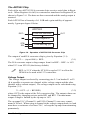
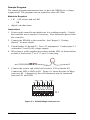
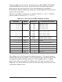
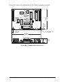
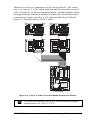
1
XP 86 00 XP8 900 XP8600 and XP8900 Digital-to-Analog Conversion Expansion Boards Users Manual Revision C XP8600 and XP8900 Users Manual Part Number 019-0064 Revision C Last revised on July 21, 2000 Printed in U.S.A. Copyright © 1999 Z-World, Inc. All rights reserved. Z-World reserves the right to make changes and improvements to its products without providing notice. Trademarks ® Dynamic C is a registered trademark of Z-World, Inc. ® Windows is a registered trademark of Microsoft Corporation PLCBus is a trademark of Z-World, Inc. ® Hayes Smart Modem is a registered trademark of Hayes Microcomputer Products, Inc. Notice to Users When a system failure may cause serious consequences, protecting life and property against such consequences with a backup system or safety device is essential. The buyer agrees that protection against consequences resulting from system failure is the buyers responsibility. This device is not approved for life-support or medical systems. All Z-World products are 100 percent functionally tested. Additional testing may include visual quality control inspections or mechanical defects analyzer inspections. Specifications are based on characterization of tested sample units rather than testing over temperature and voltage of each unit. Z-World may qualify components to operate within a range of parameters that is different from the manufacturers recommended range. This strategy is believed to be more economical and effective. Additional testing or burn-in of an individual unit is available by special arrangement. Company Address Z-World, Inc. 2900 Spafford Street Davis, California 95616-6800 USA Telephone: Facsimile: Web Site: E-Mail: (530) 757-3737 (530) 753-5141 http://www.z w orld.com [email protected] TABLE OF CONTENTS About This Manual vii XP8600 Chapter 1: Overview 13 Chapter 2: Getting Started 15 Chapter 3: I/O Configurations 21 Chapter 4: Software Reference 27 XP8600 Components ........................................................................... 16 Connecting Expansion Boards to a Z-World Controller ...................... 17 Setting Expansion Board Addresses .................................................... 18 Power ................................................................................................... 19 XP8600 Pin Assignments ..................................................................... 22 Voltage or Current Output ............................................................... 22 XP8600 Circuitry ................................................................................. 23 The AD7543 Chip ........................................................................... 24 Voltage Output .............................................................................. 24 Current Output .............................................................................. 25 Reset and Power-Up Delay ........................................................... 25 Expansion Board Addresses ................................................................ 28 XP8600 ........................................................................................... 28 Logical Addresses ......................................................................... 28 LED .............................................................................................. 28 XP8600 Software ................................................................................. 29 Dynamic C Libraries ....................................................................... 29 Using Digital-to-Analog Converter Boards .................................... 30 Reset Boards on PLCBus ............................................................. 30 Address Target Board ................................................................... 31 Operate Target Board .................................................................... 31 Sample Program .............................................................................. 31 XP8600/XP8900 Table of Contents s iii Advanced Programming ...................................................................... 33 Functions in PLC_EXP.LIB ............................................................ 33 Sample Program ........................................................................... 34 Functions in PBUS_LG.LIB ............................................................ 36 Functions in Other Libraries ........................................................... 37 XP8900 Chapter 5: Overview 41 Chapter 6: Getting Started 43 Chapter 7: I/O Configurations 49 Chapter 8: Software Reference 53 XP8900 Series Components ................................................................ 44 Connecting Expansion Boards to a Z-World Controller ...................... 45 Setting Expansion Board Addresses .................................................... 46 Power ................................................................................................... 47 XP8900 Series Pin Assignments .......................................................... 50 XP8900 Series Circuitry ...................................................................... 51 Expansion Board Addresses ................................................................ 54 XP8900 Series ................................................................................. 54 XP8900 Series Software ...................................................................... 55 Dynamic C Libraries ....................................................................... 55 Using Digital-to-Analog Converter Boards .................................... 56 Reset Boards on PLCBus ............................................................. 56 Address Target Board ................................................................... 57 Operate Target Board .................................................................... 58 Sample Program .............................................................................. 62 APPENDICES Appendix A: PLCBus 67 PLCBus Overview ............................................................................... 68 Allocation of Devices on the Bus ........................................................ 72 4-Bit Devices .................................................................................. 72 8-Bit Devices .................................................................................. 73 Expansion Bus Software ...................................................................... 73 iv s Table of Contents XP8600/XP8900 Appendix B: Specifications 79 Appendix C: Connecting and Mounting Multiple Boards 85 Appendix D: Simulated PLCBus Connections 89 Index 93 XP8600 Hardware Specifications ........................................................ 80 XP8900 Hardware Specifications ........................................................ 82 Connecting Multiple Boards ................................................................ 86 Mounting Expansion Boards ................................................................ 88 BL1000 ................................................................................................ 90 BL1100 ................................................................................................ 91 BL1300 ................................................................................................ 91 BL1400 and BL1500 ........................................................................... 92 XP8600/XP8900 Table of Contents s v Blank vi s Table of Contents XP8600/XP8900 ABOUT THIS MANUAL This manual provides instructions for installing, testing, configuring, and interconnecting the Z-World XP8600 and XP8900 Series digital-to-analog conversion expansion boards. Instructions are also provided for using Dynamic C® functions. Assumptions Assumptions are made regarding the user's knowledge and experience in the following areas: Ability to design and engineer the target system that the controller used with the XP8600 or XP8900 Series expansion boards will control. Understanding of the basics of operating a software program and editing files under Windows on a PC. Knowledge of the basics of C programming. $ For a full treatment of C, refer to the following texts. The C Programming Language by Kernighan and Ritchie C: A Reference Manual by Harbison and Steel Knowledge of basic Z80 assembly language and architecture for controllers with a Z180 microprocessor. $ For documentation from Zilog, refer to the following texts. Z180 MPU User's Manual Z180 Serial Communication Controllers Z80 Microprocessor Family User's Manual Knowledge of basic Intel assembly language and architecture for controllers with an Intel386 EX processor. $ For documentation from Intel, refer to the following texts. Intel386 EX Embedded Microprocessor Users Manual Intel386 SX Microprocessor Programmers Reference Manual XP8600/XP8900 About This Manual s vii Acronyms Table 1 lists and defines the acronyms that may be used in this manual. Table 1. Acronyms Acronym Meaning EPROM Erasable Programmable Read-Only Memory EEPROM Electronically Erasable Programmable Read-Only Memory LCD Liquid Crystal Display LED Light-Emitting Diode NMI Nonmaskable Interrupt PIO Parallel Input/Output Circuit (Individually Programmable Input/Output) PRT Programmable Reload Timer RAM Random Access Memory RTC Real-Time Clock SIB Serial Interface Board SRAM Static Random Access Memory UART Universal Asynchronous Receiver Transmitter Icons Table 2 displays and defines icons that may be used in this manual. Table 2. Icons Icon $ ( Meaning Meaning Refer to or see ! Note Please contact 7LS Tip Caution FD Icon High Voltage Factory Default viii s About This Manual XP8600/XP8900 Conventions Table 3 lists and defines the typographical conventions that may be used in this manual. Table 3. Typographical Conventions Example Description while Courier font (bold) indicates a program, a fragment of a program, or a Dynamic C keyword or phrase. // IN-01… Program comments are written in Courier font, plain face. Italics Indicates that something should be typed instead of the italicized words (e.g., in place of filename, type a file’s name). Edit Sans serif font (bold) signifies a menu or menu selection. ... An ellipsis indicates that (1) irrelevant program text is omitted for brevity or that (2) preceding program text may be repeated indefinitely. [ ] Brackets in a C function’s definition or program segment indicate that the enclosed directive is optional. < > Angle brackets occasionally enclose classes of terms. a | b | c A vertical bar indicates that a choice should be made from among the items listed. Pin Number 1 A black square indicates pin 1 of all headers. Pin 1 J1 Measurements All diagram and graphic measurements are in inches followed by millimeters enclosed in parenthesis. XP8600/XP8900 About This Manual s ix Blank x s About This Manual XP8600/XP8900 XP8600 Blank This page is blank intentionally. CHAPTER 1: OVERVIEW Chapter 1 provides an overview and description of the XP8600 digital-toanalog conversion expansion boards. XP8600 Overview s 13 The XP8600 is a 12-bit digital-to-analog (D/A) converter expansion board that can be used in conjunction with any Z-World PLCBus-compatible controller. Like other Z-World expansion boards, the XP8600 can be installed in modular plastic circuit-board holders attached to a DIN rail. The XP8600 can also be mounted, with plastic standoffs, on any surface that will accept screws. Eight or more different XP8600 board addresses may be used on one PLCBus; up to 64 different logical addresses are provided for. The XP8600 has two D/A output channels. Each channel can be operated either as a voltage source or a current source. The AD7543 D/A chips have a linearity of ±1 LSB and a gain stability of about 5 ppm per degree Celsius. A factory-installed LT1021 provides a precision 10 V reference when used with 24 V controllers. An optional LT1019 provides a precision 2.5 V reference for 12 V controllers. ( Z-World offers the XP8600 for quantity orders with the optional LT1019 factory-installed. For more information, call your Z-World Sales Representative at (530) 757-3737. ( 14 s Overview For ordering information, call your Z-World Sales Representative at (530) 757-3737. XP8600 CHAPTER 2: GETTING STARTED Chapter 2 provides instructions for connecting XP8600 expansion boards to a Z-World controller. The following sections are included. XP8600 Components Connecting Expansion Boards to a Z-World Controller Setting Expansion Board Addresses Power XP8600 Getting Started s 15 XP8600 Components The XP8600 boards offer two channels of 12-bit digital-to-analog conversion outputs. Figure 2-1 illustrates the basic layout and orientation of components, headers, and connectors. J3 U8 R1 U10 U12 5V (J4) C15 C1 PAL Power +15 V Latch C16 U9 C6 U7 C3 RP1 P2 DAC R4 (Z1) U11 U13 R5 DAC P1 C2 REF+ C5 U2 U8 Op-Amps C4 U6 U4 C10 U5 U3 C9 RP2 J1 J2 R3 R2 R6 D1 H1 Figure 2-1. XP8600 Board Layout 16 s Getting Started XP8600 Connecting Expansion Boards to a Z-World Controller Use the 26-conductor ribbon cable supplied with an expansion board to connect the expansion board to the PLCBus on a Z-World controller. See Figure 2-2. The expansion boards two 26-pin PLCBus connectors, P1 and P2, are used with the ribbon cable. Z-World recommends using the cable supplied to avoid any connection problems. Controller PLCBus Port J3 Pin 1 P1 1 P2 J2 J1 H1 XP8600 Controller With PLCBus Figure 2-2. Connecting XP8600 Expansion Board to Controller PLCBus Be sure power to the controller is disconnected before adding any expansion board to the PLCBus. Follow these steps to connect an expansion board to a Z-World controller. 1. Attach the 26-pin ribbon cable to the expansion boards P2 PLCBus header. 2. Connect the other end of the ribbon cable to the PLCBus port of the controller. Be sure pin 1 of the connector cable matches up with pin 1 of both the controller and the expansion board(s). 3. If additional expansion boards are to be added, connect header P2 on the new board to header P1 of the board that is already connected. Lay the expansion boards side by side with headers P1 and P2 on adjacent boards close together, and make sure that all expansion boards are facing right side up. $ XP8600 See Appendix C, Connecting and Mounting Multiple Boards, for more information on connecting multiple expansion boards. Getting Started s 17 4. Each expansion board comes with a factory-default board address. If more than one expansion board of each type is to be used, be sure to set a unique address for each board. $ The following section on Setting Expansion Board Addresses, and Chapter 4, Software Reference, provide details on how to set and use expansion board addresses. 5. Power may be applied to the controller once the controller and the expansion boards are properly connected using the PLCBus ribbon cable. $ See Appendix D, Simulated PLCBus Connections, for details on the special connections that enable these expansion boards to be used with the BL1000, BL1100, BL1400, and BL1500 controllers. Setting Expansion Board Addresses Z-World has established an addressing scheme for the PLCBus on its controllers to allow multiple expansion boards to be connected to a controller. ! Remember that each expansion board must have a unique PLCBus address if multiple boards are to be connected. If two boards have the same address, communication problems will occur that may go undetected by the controller. XP8600 expansion boards are shipped from the factory with no pins on header J3 connected. Each XP8600 can have one of eight different PALs. There are eight different ways to configure the three pairs of pins on header J3, and so up to 64 different logical XP8600 addresses are possible for a single PLCBus. $ See Chapter 4, Software Reference, for further details on how to determine the physical address for XP8600 expansion boards based on which pins on header J3 are connected. 18 s Getting Started XP8600 Power Z-Worlds expansion boards receive power from the controller over the +24 V line of the PLCBus. An onboard regulator converts this to the +5 V and the ±10 V reference used by the expansion boards. With no output, the XP8600 expansion boards draw about 30 mA; with all their output channels operating at maximum current (22 mA per channel), the XP8600 draws 75 mA. XP8600 Getting Started s 19 Blank 20 s Getting Started XP8600 CHAPTER 3: I/O CONFIGURATIONS Chapter 3 describes the built-in flexibility of the XP8600 expansion boards, and describes how to configure the available inputs/outputs. The following sections are included. XP8600 Pin Assignments XP8600 Circuitry XP8600 I/O Configurations s 21 XP8600 Pin Assignments Analog signals (voltage or current output) leave the XP8600 via terminals 1 and 3 on Wago connector H1. Terminals 2 and 4 provide ground. Other terminals provide access to board voltages. When the XP8600 is used with a BL1200, BL1600, BL1700, PK2100, or PK2200 controller, the +24 V from the PLCBus serves as the power source, and is accessible on pin 8 of Wago connector H1. When the XP8600 is used with BL1000, BL1100, BL1300, BL1400, or BL1500 controllers, the +24 V is not available and must be supplied from an external source to pin 8 on H1 or to the BL1400/BL1500 adapter board. Figure 3-1 shows the pin assignments for Wago connector H1. GND GND VI2 VI1 +24 V V VCC V+ H1 1 2 3 4 5 6 7 8 Figure 3-1. XP8600 Wago Connector H1 Voltage or Current Output The XP8600 uses two jumper blocks, J1 and J2, to set the mode of output channel 1 (VI1 on H1) and output channel 2 (VI2 on H1), respectively. Connect pins 23 to select a voltage output for the channel corresponding to the jumper block, and connect pins 12 to select a current output. Figure 3-2 summarizes the jumper settings. Output Channel 1 J1 Output Channel 2 J2 Voltage Output FD J1 J2 Current Output Figure 3-2. XP8600 Output Channel Jumper Settings 22 s I/O Configurations XP8600 XP8600 Circuitry The XP8600s D/A circuitry consists of two 12-bit AD7543 D/A converters, U3 and U4, and an LM324N quad op-amp chip, U1. The outputs of the D/A converters are amplified, and resistor packs RP1 and RP2 allow both current output and voltage output. The outputs appear on headers J1 and J2, and at Wago connector H1. The input comes on the PLCBus from the program running on the controller. Figure 3-3 illustrates the operation of the D/A conversion. V+ /LD1 STB1 SDI DAC1 OUT1 + U1A V REF RP1A 100 kΩ RP1B 100 kΩ RP2A V+ I1 J1 2 kΩ + U1D R2 Voltage 10 Ω Current RP2B V C7 V1 2 kΩ 330 pF V+ /LD2 STB2 SDI DAC2 OUT2 REF + U1B V RP1C 100 kΩ RP1D 100 kΩ RP2C V+ I2 J2 2 kΩ + U1C RP2D V C8 2 kΩ R3 Voltage 10 Ω Current V2 330 pF Figure 3-3. Schematic Illustration of D/A Conversion in XP8600 Capacitors C7 and C8 are normally not installed. Be sure to install C7 and C8 for applications that operate at more than ~100 Hz. XP8600 I/O Configurations s 23 The AD7543 Chip Each of the two AD7543 D/A converter chips receives serial data in Register A. When Register A is full, its contents are transferred to Register B, as shown in Figure 3-4. The data are then converted and the analog output is asserted. Each AD7543 has a linearity of ±1 LSB and a gain stability of approximately 5 ppm per degree Celsius. AD7543 REF 12-bit D/A converter LD Load Register B STB SDI 12-bit shift reg (A) OUT Figure 3-4. Operation of AD7543 D/A Converter Chip The output of each D/A converter chip is given by Equation (3-1). OUT = (input/4096) × REF (3-1) The D/A converter output voltage ranges from 0 to REF. REF is 10 V when U13 is an LT1021 (the factory default). ! REF- is 2.5 V when the LT1019 is used at U13 to allow the XP8600 to be used with 12 V controllers. Voltage Output The voltage output is selected by connecting pins 23 on header J1 or J2. (It is possible to operate one channel with a voltage output and the other channel with a current output.) The voltage output can be calculated using Equation (3-2). V = OUT × (1 + RP2/RP1) (3-2) where OUT is the output of the D/A converter chip. The output values can be changed by changing resistor packs RP1 and RP2. The maximum output voltage is limited by the op-amp to 14 V. The op-amps U1C (Channel 1) and U1D (Channel 2) can carry a maximum of 20 mA. When using a channel in the voltage-output mode, its load must have a resistance of at least 700 Ω to keep the op-amp from saturating prematurely. 24 s I/O Configurations XP8600 Current Output A current output is selected by connecting pins 12 on jumper block J1 or J2. (It is possible to operate one channel with a voltage output and the other channel with a current output.) The current output can be calculated using Equation (3-3). I1 = (OUT1/R2) × (RP2/RP1) I2 = (OUT2/R3) × (RP2/RP1) where OUT1 and OUT2 are the outputs of the D/A converter chips. The output values can be changed by changing resistor packs RP1 and RP2. The maximum output current is limited by the op-amp to 20 mA. (3-3) The op-amps U1C (Channel 1) and U1D (Channel 2) can carry a maximum of 20 mA. The output channels can each put out a maximum of 14 V, and so an output load must be less than 700 Ω if the maximum current is to be delivered. Reset and Power-Up Delay The XP8600 has a reset device, U12, to monitor VCC. Whenever VCC is interrupted, U12 pulls /RST low. The /RST line remains low until ~350 ms after VCC has been restored, allowing time for the power supply and the D/A circuits to stabilize. U12 also monitors the /RST line. When it detects a low-going edge, U12 pulls /RST low for at least 350 ms. Thus, the board may be reset with either software or a pushbutton. Software must allow a 350 ms delay after each reset or power-up cycle. XP8600 I/O Configurations s 25 Blank 26 s I/O Configurations XP8600 CHAPTER 4: SOFTWARE REFERENCE Chapter 4 describes the Dynamic C functions used to initialize the XP8600 and XP8900 Series expansion boards and to control the resulting analog outputs. The following major sections are included. Expansion Board Addresses XP8600 Software Advanced Programming XP8600 Software Reference s 27 Expansion Board Addresses XP8600 Up to 64 XP8600s may be addressed individually over a single PLCBus. Each XP8600 board has a 12-bit address. Once the board has latched its address, the board may be accessed repeatedly without having to send its address again. The 12-bit address of a particular XP8600 is determined by the encoding of PAL chip U7 on the board and by jumper block J3. Eight different PALs are available, and J3 may be set eight different ways, giving 64 unique addresses in the form 000z 001y pppx where x = 1 when J3 pins 12 are not connected y = 1 when J3 pins 34 are not connected z = 1 when J3 pins 56 are not connected and the PAL determines ppp. The 12-bit address can be placed on the bus using 4-bit addressing. The functions set12adr, read12data, and write12data (in DRIVERS.LIB) use 12-bit bus addresses. When using these, and certain other functions, swap the first and third nibbles of the physical address before passing the address to the function. For example, if the address is 0x125, pass 0x521. Logical Addresses PLCBus expansion boards have logical addresses. D/A-specific software defines 64 integer board addresses, 063. The formula mapping physical address to logical address is logical address = ppp × 8 + zyx where ppp (PAL encoding) and x, y and z (jumper bits) are defined above. For example, an XP8600 has PAL FPO4850 (ppp = 101) and J3 pins 34 connected (xyz = 101). Its physical address is 000z 001y pppx = 0001 0010 1011 = 0x12B. The XP8600s logical address is 101B × 8 + 101B = 45 = 0x2D. Certain library functions expect a logical D/A address. LED The XP8600 has an LED, D1, which is illuminated whenever the board is selected. 28 s Software Reference XP8600 XP8600 Software This section describes a set of simple software functions to use when controlling the XP8600 expansion boards. Dynamic C Libraries Several Dynamic C function libraries need to be used with the routines defined in this section. The chart in Table 4-1 identifies which libraries are used with particular Z-World controllers. Table 4-1. Dynamic C Libraries Required by Z-World Controllers for XP8600 Expansion Boards Library Needed Controller VDRIVER.LIB All controllers EZIOCMMN.LIB All controllers EZIOPBDV.LIB All controllers EZIOTGPL.LIB BL1000 EZIOLGPL.LIB BL1100 EZIOMGPL.LIB BL1400, BL1500 EZIOPLC.LIB BL1200, BL1600, PK2100, PK2200 EZIOPLC2.LIB BL1700 Before using one of these libraries in an application, first include the library name in a #use command. For example, to use functions in the library PLC_EXP.LIB, be sure there is a line at the beginning of the program in the following format. #use PLC_EXP.LIB XP8600 Software Reference s 29 Using Digital-to-Analog Converter Boards The follow steps summarize how to use the D/A converter boards. 1. Send a reset command to the PLCBus. 2. Place the address of the D/A converter on the PLCBus. 3. Send data serially to one of the D/A converters (Register A). When Register A is filled, load the data to D/A converter Register B where it is converted and output. 4. Use the boards analog output to control motors, attenuators or other analog devices. These steps are done using software drivers in Dynamic C function libraries. Reset Boards on PLCBus These Dynamic C functions are used to initialize the PLCBus. Use these functions in a program before introducing any code to operate the relays. VdInit() Initializes the timer mechanism. LIBRARY: VDRIVER.LIB void plcBusReset() Resets all expansion boards connected to the PLCBus. When using this function, initialize timers with VdInit() before resetting the PLCBus. All PLCBus devices must reset before performing any subsequent operations. LIBRARY: EZIOPBDV.LIB void eioPlcRstWait() Provides a delay long enough for the PLCBus to reset. This function provides a delay of 12 seconds to ensure devices on the PLCBus reset. Call this function after resetting the PLCBus. LIBRARY: EZIOPBDV.LIB long int eioErrorCode Represents a global bit-mapped variable whose flags reflect error occurrences. This register for this variable is initially set to 0. If the application tries to access an invalid channel, the flag EIO_NODEV (the first bit flag) is set in this register. Note that the other bits in EIO_NODEV deal with networked controllers. 30 s Software Reference XP8600 Address Target Board int plcXP86Init( int Addr ) Initializes and turns on XP8600. Call this function before calling plcXP86Out. PARAMETERS: Addr is the logical address of the board set by jumpers, and ranges from 07. With special PALs, the address can range from 063. RETURN VALUE: 1 if the board cannot be found, 0 if the initialization is completed. LIBRARY: EZIOPBDV.LIB Operate Target Board int plcXP86Out( int Addr, unsigned int oValue ) Sends the 12-bit oValue to the proper D/A converter channel. Call plcXP86Init before calling plcXP86Out. PARAMETERS: Addr, the logical address of the D/A converter channel, is 2*board_number + channel_number. Note that board_number and channel_number start from zero. Without a special PAL, board_number ranges from 0 to 7 as set by the address jumpers. With the special PAL, board_number can range from 0 to 63. channel_number ranges from 0 to 1. oValue is the 12-bit value to send to the D/A converter. RETURN VALUE: -1 if the D/A converter cannot be found, 0 if the operation is successful. LIBRARY: EZIOPBDV.LIB Sample Program The sample program XP86_1.C in the Dynamic C SAMPLES\PLCBUS subdirectory demonstrates higher level function calls for the D/A converter outputs. The program is used to detect XP8600 boards attached to the PLCBus, and maximizes the D/A converter outputs. XP8600 Software Reference s 31 Use the following steps to run the sample program. 1. Compile the program by pressing F3 or by choosing Compile from the COMPILE menu. Dynamic C compiles and downloads the program into the controllers memory. During compilation, Dynamic C rapidly displays several messages in the compiling window, which is normal. 2. Run the program by pressing F9 or by choosing Run from the RUN menu. It is also possible to single-step through the program with F7 or F8. 3. To halt the program, press <CTRL-Z>. 4. To restart the program, press F9. XP86_1.C #use eziocmmnn.lib #use eziobl17.lib #use ezioplc2.lib char TITLE[] = "XP86xx DAC Output"; main(){ int i; unsigned long delayCounter; printf("%s\n\n", TITLE); plcBusReset(); // reset the PLCBs for (delayCounter = 0x8000; delayCounter--;) hitwd(); // delay // locate all possible jumper-set addresses // from 0 to 7 and display status for (i = 0; i <= 7; ++i) { if (plcXP86Init(i)==-1) { // do a read to locate the board printf("board %d is not located\n\n",i); } else { printf("Board %d is located \n",i); plcXP86Out(i*2,0x0ffff); } printf("\n"); hitwd(); } } ! Check the board jumpers, PLCBus connections, and the PC/ controller communications if an error message appears. $ See the Dynamic C Technical Reference manual for more detailed instructions. 32 s Software Reference XP8600 Advanced Programming Functions in PLC_EXP.LIB int plcdac_addr( int bd ) Converts logical board address 063 to 12-bit (3-nibble) PLCBus analog address. RETURN VALUE: 12-bit (nibble-interchanged) bus address for an XP8600 identified by a logical address (063). void plc_fdac1( int dac_value ) void plc_sdac1( int dac_value ) Each of these routines writes data serially to DAC1 (U3) on the presently addressed XP8600. These functions are equivalent and may be used interchangeably. However, plc_fdac1 is slightly faster, whereas plc_sdac1 is smaller (50 bytes vs. 130). A call to one of these functions must be followed by a call to plc_latch1or its equivalent in user-supplied codeotherwise no digital-to-analog conversion occurs. void plc_fdac2( int dac_value ) void plc_sdac2( int dac_value ) Each of these routines writes data (serially) to DAC2 (U4) on the presently addressed XP8600. These functions are equivalent and may be used interchangeably. However, plc_fdac2 is slightly faster, whereas plc_sdac2 is smaller (50 bytes vs. 130). A call to one of these functions must be followed by a call to plc_latch2or its equivalent in user-supplied codeotherwise no digital-to-analog conversion occurs. void dac_latch1() Transfers the data in Register A of DAC1 (U3) to Register B of DAC1, whereupon the data are converted and the analog signal is output. A call to this function must be preceded by a call to plc_fdac1 or plc_sdac1or their equivalent in user-supplied code. void dac_latch2() Transfers the data in Register A of DAC2 (U3) to Register B of DAC2, whereupon the data are converted and the analog signal is output. A call to this function must be preceded by a call to plc_fdac2 or plc_sdac2or their equivalent in user-supplied code. void dac_init() Initializes the presently addressed XP8600. Sets both D/A converter outputs to zero. Board must be currently addressed on PLCBus with set12adr(). XP8600 Software Reference s 33 Sample Program The sample program demonstrates how to drive the XP8600 in a voltageoutput mode. The program runs on controllers with a PLCBus. Materials Required 1 kΩ, ¼ W resistor and an LED OR digital volt-ohm meter Instructions 1. Power up the controller and make sure it is working properly. Consult the controller users manual, if necessary. Now disconnect power from the controller. 2. Connect the XP8600 to the controller. See Chapter 2, Getting Started, for more details. 3. Check headers J1 through J3. Leave J3 unjumpered. Connect pins 23 on headers J1 and J2 (for voltage output). 4. Wire-wrap or solder together the resistor and the LED, as shown below, to make a load circuit 3" to 4" (7 cm to 10 cm) long. 5. Connect the resistor end of the load circuit to V/I1 on header H1. Connect the LED to GND on H1. Figure 4-1 shows the pins on Wago connector H1. Alternatively, the volt-ohm meter may be connected between V/I1 and GND. GND GND VI2 VI1 V VCC +24 V V+ H1 1 2 3 4 5 6 7 8 Figure 4-1. XP8600 Wago Connector H1 34 s Software Reference XP8600 6. Power up the controller and bring up Dynamic C on the PC. 7. Open and run the sample program DASAMPL1.C in the Dynamic C SAMPLES\PLCBUS subdirectory . 8. The LED will increase and decrease in intensity as the program runs. 9. If the LED does not light up at all, its polarity may be reversed. Try turning the circuit around, connecting the LED at V/I1 and the resistor at GND. Program The program demonstrates how to drive the XP8600 in voltage output mode. The program first polls the PLCBus, looking for XP8600s. It saves the highest address found. The program then increments the voltage at both output channels on the selected board. When it reaches maximum voltage, it resets the voltage to zero and repeats the process indefinitely. The setup requires a 1 kΩ resistor and LED in seriesor a volt-ohm meter between V/I1 and GND on header H1 to show the behavior of the program. DASAMPL1.C main(){ int i, log_addr, hi_addr; reset_pbus(); // reset all boards on PLCBus hitwd(); reset_pbus_wait(); // delay after reset // Locate XP8600s; save highest addr found for( log_addr=0; log_addr<64; log_addr++ ){ if( find_dac(log_addr) ) hi_addr = log_addr; } // Set PLCBus to XP8600, initialize DAC set12adr( plcdac_addr(hi_addr) ); dac_init(); // initialize both channels // Increment Voltages on Channels out 1 and 2 while(1){ for( i=0; i<4097; i++ ){ plc_fdac1(i); // // dac_latch1(); // plc_sdac2(i); // // dac_latch2(); // hitwd(): } } fdac1 (fast but big), writes to DAC channel 1 convert data sdac2 (slower, smaller), write to DAC channel 2 convert data } XP8600 Software Reference s 35 Use the following steps to run the sample program. 1. Compile the program by pressing F3 or by choosing Compile from the COMPILE menu. Dynamic C compiles and downloads the program into the controllers memory. During compilation, Dynamic C rapidly displays several messages in the compiling window, which is normal. 2. Run the program by pressing F9 or by choosing Run from the RUN menu. It is also possible to single-step through the program with F7 or F8. 3. To halt the program, press <CTRL-Z>. 4. To restart the program, press F9. ! Check the board jumpers, PLCBus connections, and the PC/ controller communications if an error message appears. $ See the Dynamic C Technical Reference manual for more detailed instructions. Functions in PBUS_LG.LIB int DAC_Board_Addr( int bd ) Converts a logical D/A converter board address to a physical PLCBus address. PARAMETER: bd must be a number between 0 and 63 representing the D/A converter board to access. This number has the binary form pppzyx where ppp is determined by the board PAL number and x, y, and z are determined by jumper block J3 on the board. ppp values of 000, 001, 010, etc., correspond to PAL numbers of FPO4800, FPO4810, FPO4820, etc.; x, y, and z correspond to jumper block J3 pins 12, 34, and 56, respectively (0 = closed, 1 = open). The resulting address is in the form pppx001y000z. RETURN VALUE: Nibble-interchanged PLCBus address of the board specified. This address may be passed directly to PBus12_Addr. void write_DAC1( int val ) Writes data serially to DAC1 (U3) on the presently addressed XP8600. The board address must have been set previously with a call to PBus12_Addr. A call to one of these functions must be followed by a call to latch_DAC1or its equivalent in user-supplied code otherwise no digital-to-analog conversion occurs. 36 s Software Reference XP8600 void write_DAC2( int val ) Writes data serially to DAC2 (U4) on the presently addressed XP8600. The board address must have been set previously with a call to PBus12_Addr. A call to one of these functions must be followed by a call to latch_DAC2or its equivalent in user-supplied code otherwise no digital-to-analog conversion occurs. void latch_DAC1() Transfers the data in Register A of DAC1 (U3) to Register B of DAC1, whereupon it is converted and the analog signal is output. The board address must have been set previously with a call to PBus12_Addr. A call to this function must be preceded by a call to write_DAC1 or its equivalent in user-supplied code. void latch_DAC2() Transfers the data in Register A of DAC2 (U4) to Register B of DAC2, whereupon it is converted and the analog signal is output. The board address must have been set previously with a call to PBus12_Addr. A call to this function must be preceded by a call to write_DAC2 or its equivalent in user-supplied code. void Init_DAC() Initializes the presently addressed XP8600, setting both outputs to zero. The board address must have been set previously with a call to PBus12_Addr. void Set_DAC1( int val ) void Set_DAC2( int val ) Combines the functions of write_DACx and latch_DACx into a single function for convenience. The board address must have been set previously with a call to PBus12_Addr. Functions in Other Libraries Functions in the other libraries listed in Table 4-1 are equivalent to those listed above except for minor internal details. XP8600 Software Reference s 37 Blank 38 s Software Reference XP8600 XP8900 Blank This page is blank intentionally. CHAPTER 5: OVERVIEW Chapter 5 provides an overview and description of the XP8900 digital-toanalog conversion expansion boards. XP8900 Overview s 41 The XP8900 Series is a 12-bit digital-to-analog (D/A) converter expansion board that can be used in conjunction with any Z-World PLCBus-compatible controller. Like other Z-World expansion boards, the XP8900 Series boards can be installed in modular plastic circuit-board holders attached to a DIN rail. The XP8900 Series boards can also be mounted, with plastic standoffs, on any surface that will accept screws. Up to eight different XP8900 board addresses may be used on one PLCBus. The XP8900 Series consists of two boards, the XP8900 with eight channels of D/A converter outputs, and the XP8910 with four channels of D/A converter outputs. Each channel produces a bipolar output of up to ±10 V DC. The XP8900 Series features an onboard voltage regulator for PLCBuspowered operation. The XP8900 Series has connectors for user-supplied analog voltage rails, and is able to sink or source up to 7 mA with the user rails, or up to 2 mA on its own. The D/A outputs are monotonic. ( An XP8900 Series board can be factory-built with one to eight D/A channels, with 8-bit or 10-bit D/A outputs, or with user-defined output voltage ranges. For more information, call your Z-World Sales Representative at (530) 757-3737. ( 42 s Overview For ordering information, call your Z-World Sales Representative at (530) 757-3737. XP8900 CHAPTER 6: GETTING STARTED Chapter 6 provides instructions for connecting XP8900 Series expansion boards to a Z-World controller. The following sections are included. XP8900 Series Components Connecting Expansion Boards to a Z-World Controller Setting Expansion Board Addresses Power XP8900 Getting Started s 43 XP8900 Series Components The XP8900 Series of expansion boards offers up to eight channels of digital-to-analog conversion outputs. Figure 6-1 shows the basic layout and orientation of components, headers, and connectors. U2 + + U4 P1 + C28 H3 H2 C24 U17 C3 H4 C20 H1 U16 U1 CPLD C16 C27 C21 R32 R14 R31 R13 U3 C23 C22 C36 R19 R4 R20 R3 R10 R25 R9 R26 C29 C25 R27 R12 R28 R11 RN1 P2 C32 Op-Amps Op-Amps R2 R17 R1 R18 + + + R39 R33 U10 U11 U12 U13 U14 U15 C19 R34 Q1 C13 C14 C15 C2 C11 C12 C18 C26 C31 C30 R22 R24 R6 R16 R30 R21 R23 R5 R15 R29 R37 C7 C5 C8 C35 + R7 R8 C34 R35 + C1 C17 C9 + U9 + R36 + 12 V Reg + C33 U7 R38 C6 C4 U6 U5 5V Reg P3 U8 + (J3) C10 J1 J2 Figure 6-1. XP8900 Series Board Layout 44 s Getting Started XP8900 Connecting Expansion Boards to a Z-World Controller Use the 26-conductor ribbon cable supplied with an expansion board to connect the expansion board to the PLCBus on a Z-World controller. See Figure 6-2. The expansion boards two 26-pin PLCBus connectors, P1 and P2, are used with the ribbon cable. Z-World recommends using the cable supplied to avoid any connection problems. + + + + + + + Controller PLCBus Port P1 + + + Pin 1 U4 + + Op-Amps + P2 XP8900 Controller With PLCBus Figure 6-2. Connecting XP8600 Expansion Board to Controller PLCBus Be sure power to the controller is disconnected before adding any expansion board to the PLCBus. Follow these steps to connect an expansion board to a Z-World controller. 1. Attach the 26-pin ribbon cable to the expansion boards P2 PLCBus header. 2. Connect the other end of the ribbon cable to the PLCBus port of the controller. Be sure pin 1 of the connector cable matches up with pin 1 of both the controller and the expansion board(s). 3. If additional expansion boards are to be added, connect header P2 on the new board to header P1 of the board that is already connected. Lay the expansion boards side by side with headers P1 and P2 on adjacent boards close together, and make sure that all expansion boards are facing right side up. $ XP8900 See Appendix C, Connecting and Mounting Multiple Boards, for more information on connecting multiple expansion boards. Getting Started s 45 4. Each expansion board comes with a factory-default board address. If more than one expansion board of each type is to be used, be sure to set a unique address for each board. $ The following section on Setting Expansion Board Addresses, and Chapter 8, Software Reference, provide details on how to set and use expansion board addresses. 5. Power may be applied to the controller once the controller and the expansion boards are properly connected using the PLCBus ribbon cable. $ See Appendix D, Simulated PLCBus Connections, for details on the special connections that enable these expansion boards to be used with the BL1000, BL1100, BL1400, and BL1500 controllers. Setting Expansion Board Addresses Z-World has established an addressing scheme for the PLCBus on its controllers to allow multiple expansion boards to be connected to a controller. ! Remember that each expansion board must have a unique PLCBus address if multiple boards are to be connected. If two boards have the same address, communication problems will occur that may go undetected by the controller. Every XP8900 Series board is shipped from the factory with a default address of 7. An XP8900 Series board may be assigned any address between 0 and 7 using jumpers on the pins of header P3 to configure the board address. Figure 6-3 shows the jumper settings to set addresses 07. A maximum of eight XP8900 Series boards may be addressed by a controller at one time. ! Pins 12 on header P3 are on the lower end of P3 when the XP8900 board is oriented in line with a controller and other expansion boards as shown in Figure 6-2. 46 s Getting Started XP8900 2 1 0 3 7 8 7 8 7 8 7 6 5 6 5 6 5 6 5 4 3 4 3 4 3 4 3 2 1 2 1 2 1 2 1 8 P3 P3 P3 P3 P3 P3 P3 P3 8 7 8 7 8 7 8 6 5 6 5 6 5 6 4 3 4 3 4 3 4 2 1 2 1 2 1 2 4 5 6 1 7 FD Figure 6-3. P3 Jumper Settings for XP8900 Series PLCBus Addresses Power Z-Worlds expansion boards receive power from the controller over the +24 V line of the PLCBus. An onboard regulator converts this to the +5 V and the ±12 V reference used by the expansion boards. With no output, the XP8900 Series expansion boards draw about 30 mA; with all their output channels operating at maximum current (2 mA per channel on internal power, 7 mA per channel with external voltage), the XP8900 draws 45 mA (75 mA if the external power rails are connected). XP8900 Getting Started s 47 Blank 48 s Getting Started XP8900 CHAPTER 7: I/O CONFIGURATIONS Chapter 7 describes the built-in flexibility of the XP8900 Series expansion boards, and describes how to configure the available inputs/outputs. The following sections are included. XP8900 Series Pin Assignments XP8900 Series Circuitry XP8900 I/O Configurations s 49 XP8900 Series Pin Assignments The XP8900 has eight channels of bipolar voltage outputs, each with its own individual ground, and terminals for user-supplied positive and negative voltage rails, also with their own individual grounds. These are all located on Wago connectors J1 and J2, as shown in Figure 7-1. The pin assignments for the XP8910 are similar, except there are only four output channels. There are no outputs on pin 9 of J1, and there are no outputs on pins 1, 3, and 5 of J2. GND GND GND GND GND GND GND GND GND GND OUT0 OUT1 OUT2 OUT3 OUT4 OUT5 OUT6 OUT7 +12IN -12IN 1 2 3 4 5 6 7 8 9 10 1 2 3 4 5 6 7 8 9 10 J1 J2 Figure 7-1. XP8900 Wago Connectors J1 and J2 No special configurations are needed for the D/A converter outputs, which are controlled by the software drivers. An external ±12 V DC may be connected to the XP8900 Series boards to reduce analog noise or to increase the current drive. Figure 7-2 provides the jumper settings for headers H1, H2, and H3 to accommodate the external power. The external ±12 V supply is connected to the XP8900 Series board via pins 7 and 9 on Wago connector J2. H1 H2 H3 FD +12 V from PLCBus H1 +12 V from external source -12 V from PLCBus H2 H3 -12 V from external source Figure 7-2. XP8900 Series ±12 V Supply Jumper Settings 50 s I/O Configurations XP8900 XP8900 Series Circuitry The XP8900s D/A circuitry consists of eight 12-bit AD5320 D/A converters, U9 to U16, and two OP497G quad op-amp chips, U3 and U4. The outputs of the D/A converters are amplified, and the analog outputs appear on Wago connectors J1 and J2. The input comes on the PLCBus from the program running on the controller. Figure 7-3 illustrates the operation of the D/A conversion. 12 V Reg IN +V +12 V REF +12IN U7 OUT GND U2 +12 V H1 VS REF +5 V REF SLEEP OUT GND R39 36 kΩ +2 V REF R33 30 kΩ Q1 OUT[0–7] – U9–U16 DA_DATA DA_CLK DA_EN[0–7] V+ U3 or U4 FDV301N H3 CPIN C+ GND C– + /2V_EN +12 V U17 R34 11 kΩ DIN DAC SCLK VOUT /SYNC 200 kΩ 205 kΩ 205 kΩ 200 kΩ VOUT CPOUT -12 V REF –12IN H2 Figure 7-3. Schematic Illustration of D/A Conversion in XP8900 Series The analog outputs do not need any special configuration. The desired analog output voltage is set using the software drivers. The XP8900 Series expansion boards derive +5 V digital power from the +24 V PLCBus supply via LM7805 at U6. When operating without usersupplied external voltage rails, the XP8900 Series D/A converters get their +12 V analog power from the PLCBus +24 V supply via LM7812 at U7. Charge pump NJU7662 at U17 inverts this for onboard -12 V analog power. Precision +5 V and + 2 V reference voltages are derived from the +12 V supply via REF195 at U2 and the voltage divider formed from R33, R34, and R39. The n-channel FET FDV301N at Q1 is used to switch the 2 V reference to 0 V during a power-on reset. The XP8900 Series D/A converters have the capability of receiving their +12 V or -12 V supply from an external source. This provides for greater control of electrical noise in the analog output signals. ! XP8900 The XP8900 Series D/A converters may be used with 12 V controllers only when ±12 V is supplied externally to pins 7 and 9 of Wago connector J2. Remember to set the jumpers on headers H1, H2, and H3 as shown in Figure 7-2. I/O Configurations s 51 Blank 52 s I/O Configurations XP8900 CHAPTER 8: SOFTWARE REFERENCE Chapter 4 describes the Dynamic C functions used to initialize the XP8600 and XP8900 Series expansion boards and to control the resulting analog outputs. The following major sections are included. Expansion Board Addresses XP8600 Software XP8900 Series Software XP8900 Software Reference s 53 Expansion Board Addresses XP8900 Series Up to eight XP8900 Series expansion boards may be addressed over a single PLCBus using a logical address of 0 to 7. The 12-bit address of a particular XP8900 is determined by the jumper setting on header P3. P3 may be set eight different ways. The unique physical address is in the form 0010 000x yzRR where x = 1 when P3 pins 12 are not connected y = 1 when P3 pins 34 are not connected z = 1 when P3 pins 56 are not connected and RR is reserved for the registers. There are no PAL codes. The 12-bit address can be placed on the bus using 4-bit addressing. The functions set12adr, read12data, and write12data (in DRIVERS.LIB) use 12-bit bus addresses. When the address is passed to set12adr, it should be in the format yzRR 000x 0010 where the least significant nibble in the physical address, yzRR, has swapped places with the most significant nibble in the physical address, 0010. 54 s Software Reference XP8900 XP8900 Series Software This section describes a set of simple software functions to use when controlling the XP8900 Series expansion boards. Dynamic C Libraries Several Dynamic C function libraries need to be used with the routines defined in this section. The chart in Table 8-1 identifies which libraries must be used with particular Z-World controllers. Table 8-1. Dynamic C Libraries Required by Z-World Controllers for XP8900 Series Expansion Boards Library Needed Controller EZIOCMMN.LIB All controllers EZIOPBDV.LIB All controllers EZIOTGPL.LIB BL1000 EZIOLGPL.LIB BL1100 EZIOMGPL.LIB BL1400, BL1500 EZIOPLC.LIB BL1200, BL1600, PK2100, PK2200 EZIOPLC2.LIB BL1700 EZIOBL17.LIB BL1700 Before using one of these libraries in an application, first include the library name in a #use command. For example, to use functions in the library EZIOPLC.LIB, be sure there is a line at the beginning of the program in the following format. #use ezioplc.lib ! XP8900 The #use eziopbdv.lib already included in other library calls for the XP8900 Series expansion boards, and does not have to be repeated. Software Reference s 55 Using Digital-to-Analog Converter Boards The follow steps summarize how to use the D/A converter boards. 1. Send a reset command to the PLCBus. 2. Place the address of the D/A converter on the PLCBus. 3. Send data serially to one of the D/A converters (Register A). When Register A is filled, load the data to D/A converter Register B where it is converted and output. 4. Use the boards analog output to control motors, attenuators or other analog devices. These steps are done using software drivers in Dynamic C function libraries. Reset Boards on PLCBus These Dynamic C functions are used to initialize the PLCBus. Use these functions in a program before introducing any code to operate the relays. VdInit() Initializes the timer mechanism. LIBRARY: VDRIVER.LIB void plcBusReset() Resets all expansion boards connected to the PLCBus. When using this function, initialize timers with VdInit() before resetting the PLCBus. All PLCBus devices must reset before performing any subsequent operations. LIBRARY: EZIOPBDV.LIB ! The XP8900 output voltages cannot be reset by resetting the PLCBus. The rest of this chapter provides information on setting or resetting the XP8900 output voltages. void eioPlcRstWait() Provides a delay long enough for the PLCBus to reset. This function provides a delay of 12 seconds to ensure devices on the PLCBus reset. Call this function after resetting the PLCBus. LIBRARY: EZIOPBDV.LIB 56 s Software Reference XP8900 long int eioErrorCode Represents a global bit-mapped variable whose flags reflect error occurrences. This register for this variable is initially set to 0. If the application tries to access an invalid channel, the flag EIO_NODEV (the first bit flag) is set in this register. Note that the other bits in EIO_NODEV deal with networked controllers. Address Target Board int plcXP89Init( int Addr ) Initializes XP8900 Series board. Call this function before using the other plcXP89 functions. This function also initializes the XP8900 Series D/A converters to tristate their outputs. Call plcXP89Sw to turn the voltage reference on. The first plcXP89Out call enables the output of the corresponding D/A converter channel. Both the voltage reference and the D/A converter channel must be set up correctly to get the proper output. PARAMETER: Addr is the logical address, 07, of the board set by jumpers. RETURN VALUE: 1 if the board cannot be found, 0 if the initialization is completed. LIBRARY: EZIOPBDV.LIB void main(void){ plcBusReset(); // reset the PLCBus if(plcXP89Init(4)){ ... } else { ... } } XP8900 Software Reference s 57 Operate Target Board int plcXP89Sw( int Addr, int state ) Turns the D/A converters and references to op-amps on or off. Note that all channels on a particular board are switched at the same time. PARAMETERS: Addr is the logical address, 07, of the board set by jumpers. Both the reference (switched on by this call) and the D/A converter output (switched off by this call, switched on by plcX89Out) must be set correctly to get the proper output. state indicates whether the D/A converter and reference voltage should be turned on or off. The reference is turned on when state is nonzero. Otherwise the D/A converters will tristate and the reference will output 0. The output voltage of all channels should be approximately 0 at the op-amp when the D/A converter is off. RETURN VALUE: 1 if the board cannot be found, 0 if the operation is completed. LIBRARY: EZIOPBDV.LIB ! The XP8900 output voltages may fluctuate to 2 V for each channel while plcX89Sw is executing to turn on the op-amp reference and to switch off the D/A converter. int plcXP89Out( int Addr, unsigned int oValue ) Sends the 12-bit oValue to the proper D/A converter channel. Call plcXP89Init and plcXP89Sw before calling plcXP89Out. Note that plcXP89Out does not switch the voltage reference on or off. Both the D/A converter and the voltage reference must be set up correctly to get the proper voltage output. plcXP89Sw enables the voltage reference. PARAMETERS: Addr is 8*board_number + channel_number. Note that board_number and channel_number start from zero. board_number ranges from 0 to 7 as set by the address jumpers. channel_number ranges from 0 to 7 (XP8900), or from 0 to 3 (XP8910). oValue is the 12-bit value to send to the D/A converter. RETURN VALUE: 1 if the D/A converter cannot be found, 0 if the operation is successful. If the D/A converter does not exist, this function also bit-ors the constant EIO_NODEV to eioErrorCode. LIBRARY: EZIOPBDV.LIB plcXP89Out(42,2048) // make channel 2 on board 5 output about 0 V 58 s Software Reference XP8900 Table 8-2 summarizes these three functions. The order in which they appear in Table 8-2 is the sequence in which they should be used to start an XP8900 Series board. Table 8-2. Summary of Basic XP8900 Series Function Calls Function plcXP89Init Description Disables everything, leaves output of 0 V for all channels plcXP89Sw Enables voltage reference so the output will be at the voltage level specified by plcXP89Out plcXP89Out Sets all channels to midpoint or other acceptable value (the output experiences a slight jump as channels are being set; remember to set all 4 or 8 channels since one call sets only one channel) int plcXP89WrCalib( int chan, struct _eioAdcCalib *pCalib ) Writes a calibration structure to the EEPROM storage corresponding to a channel on the XP8900 Series board. PARAMETERS: chan is the channel number, 063, of the XP8900 Series D/A channel. chan = 8*board_number + channel_number. _eioAdcCalib *pCalib is a pointer to a calibration structure initialized by calling eioAdcMakeCoeff. RETURN VALUE: 0 if the calibration is successful, otherwise returns a negative number. LIBRARY: EZIOPBDV.LIB plcXP89WrCalib(15,&cstruct) // write calib info in cstruct to channel 7 of // XP8900 Series board 1 XP8900 Software Reference s 59 int plcXP89RdCalib( int chan, struct _eioAdcCalib *pCalib ) Reads the calibration structure of a D/A channel from an XP8900 Series board. PARAMETERS: chan is the channel number, 063, of the XP8900 Series D/A channel. chan = 8*board_number + channel_number. _eioAdcCalib *pCalib is a pointer to a calibration structure. Use eioAdcDigitize to compute the actual D/A output of a given analog value. RETURN VALUE: 0 if the operation is successful, otherwise returns a negative number. LIBRARY: EZIOPBDV.LIB plcXP89RdCalib(32,&cinfo) // read calib info of channel 0 of XP8900 // XP8900 Series board 4 into cinfo int eioAdcMakeCoeff( struct _eioAdcCalib *cnvrsn, unsigned d1, unsigned d2, float f1, float f2 ) Takes the raw values and actual values of two data points, then computes the calibration coefficients (assumes linearity). PARAMETERS: struct _eioAdcCalib *cnvrsn is a pointer to a calibration structure that stores the coefficients. d1 is the raw (quantized) value of the first data point. d2 is the raw (quantized) value of the second data point. f1 is the actual (real) value (in volts) of the first data point. f2 is the actual (real) value (in volts) of the second data point. RETURN VALUE: 1 if it is not possible to compute the calibration coefficients, otherwise 0. LIBRARY: EZIOPBDV.LIB eioAdcMakeCoeff(&cinfo,96,4000,9.97,-10.33) // the actual value at quantized value 96 is 9.97 V // the actual value at quantized value 4000 is -10.03 V // compute the coefficients and put into cinfo 60 s Software Reference XP8900 long eioAdcDigitize( float f, struct _eioAdcCalib *pCalib ) Converts analog value to digital number according to calibration coefficients. This function is used to convert an analog value such as voltage to the actual digital number for a D/A converter device. PARAMETERS: f is the analog value to output. _eioAdcCalib *pCalib is a pointer to a structure that stores the calibration coefficients. RETURN VALUE: Long integer that corresponds to the number to send to a D/A converter device. LIBRARY: EZIOPBDV.LIB L=eioAdcDigitize(2.54,&cinfo); // L will contain the digitized value to output // to D/A converter device given the // calibration coefficients in cinfo so that // the output is about 2.54 of some real units XP8900 Software Reference s 61 Sample Program The sample program XP89_1.C in the Dynamic C SAMPLES\PLCBUS subdirectory demonstrates how to calibrate the D/A converter channels. The basic sample program is designed for the BL1200, BL1600, PK2100, and PK2200 controllers. Remember to uncomment the lines that apply to the controller being used with the XP8900 Series expansion board. To use this program properly, it may be necessary to edit the statements that initialize the channel, margin, f1, and f2. The program may also be compiled as is, with watch expressions added to override the assignment statements (be sure to execute the watch expression AFTER the assignment statement is executed). Use the following steps to run the sample program. 1. Compile the program by pressing F3 or by choosing Compile from the COMPILE menu. Dynamic C compiles and downloads the program into the controllers memory. During compilation, Dynamic C rapidly displays several messages in the compiling window, which is normal. 2. Run the program by pressing F9 or by choosing Run from the RUN menu. It is also possible to single-step through the program with F7 or F8. 3. To halt the program, press <CTRL-Z>. 4. To restart the program, press F9. ! Check the board jumpers, PLCBus connections, and the PC/ controller communications if an error message appears. $ See the Dynamic C Technical Reference manual for more detailed instructions. 62 s Software Reference XP8900 XP89_1.C #use eziocmmn.lib /* #use ezioplc.lib /* #use eziotgpl.lib /* #use eziolqpl.lib /* #use eziomgpl.lib /* #use eziobl17.lib /* #use ezioplc2.lib // // // // // // for for for for for for BL1200, BL1000 BL1100 Bl1400 BL1700 BL1700 BL1600, PK2100, PK2200 */ */ */ & BL1500 */ */ */ main() { auto int i; auto struct _eioAdcCalib c; auto int channel; auto float f1, f2, fout; auto long l; auto int margin; channel = 0; // execute watch expression // to override margin = 0x40; // execute watch expression // to override plcBusReset(); if (plcXP89Init(channel / 8)) { printf(“DAC8 board not found\n”); } else { plcXP89Sw(channel / 8,1); // enable voltage reference plcXP89Out(channel,margin); // use meter to record level f1 = 10; // use watch expr to override plcXP89Out(channel,0xfff-margin); // use meter to record level f2 = -10; // use watch expr to override eioAdcMakeCoeff(&c,margin,0xfff-margin,f1,f2); if (plcXP89WrCalib(channel,&c)) { printf("Can’t write calibration constant\n"); } memset(&c,0,sizeof(struct _eioAdcCalib)); if (plcXP89RdCalib(channel,&c)) { printf("Can’t read calibration constant\n"); } fout = 2.345; // use watch expr to override l = eioAdcDigitize(fout, &c); plcXP89Out(channel,(unsigned)l); // use meter to check voltage now } } XP8900 Software Reference s 63 Blank 64 s Software Reference XP8900 APPENDICES Blank This page is blank intentionally. APPENDIX A: PLCBUS Appendix A provides the pin assignments for the PLCBus, describes the registers, and lists the software drivers. XP8600/XP8900 PLCBus s 67 PLCBus Overview The PLCBus is a general-purpose expansion bus for Z-World controllers. The PLCBus is available on the BL1200, BL1600, BL1700, PK2100, PK2200 and PK2600 controllers. The BL1000, BL1100, BL1300, BL1400, and BL1500 controllers support the XP8300, XP8400, XP8600, and XP8900 expansion boards using the controllers parallel input/output port. The BL1400 and BL1500 also support the XP8200 and XP8500 expansion boards. The ZB4100s PLCBus supports most expansion boards, except for the XP8700 and the XP8800. The SE1100 adds expansion capability to boards with or without a PLCBus interface. Table A-1 lists Z-Worlds expansion devices that are supported on the PLCBus. Table A-1. Z-World PLCBus Expansion Devices Device Description Exp-A/D12 Eight channels of 12-bit A/D converters SE1100 Four SPDT relays for use with all Z-World controllers XP8100 Series 32 digital inputs/outputs XP8200 “Universal Input/Output Board” —16 universal inputs, 6 high-current digital outputs XP8300 Two high-power SPDT and four high-power SPST relays XP8400 Eight low-power SPST DIP relays XP8500 11 channels of 12-bit A/D converters XP8600 Two channels of 12-bit D/A converters XP8700 One full-duplex asynchronous RS-232 port XP8800 One-axis stepper motor control XP8900 Eight channels of 12-bit D/A converters Multiple expansion boards may be linked together and connected to a Z-World controller to form an extended system. Figure A-1 shows the pin layout for the PLCBus connector. GND A0X LCDX D1X D3X D5X D7X GND GND GND GND +24 V (+5 V) VCC 26 24 22 20 18 16 14 12 10 8 6 4 2 25 23 21 19 17 15 13 11 9 7 5 3 1 VCC (+5 V) /RDX /WRX D0X D2X D4X D6X A1X A2X A3X strobe /STBX attention /AT GND Figure A-1. PLCBus Pin Diagram 68 s PLCBus XP8600/XP8900 Actually, two independent buses, the LCD bus and the PLCBus, exist on the single connector. The LCD bus consists of the following lines. LCDXpositive-going strobe. /RDXnegative-going strobe for read. /WRXnegative-going strobe for write. A0Xaddress line for LCD register selection. D0X-D7Xbidirectional data lines (shared with expansion bus). The LCD bus is used to connect Z-Worlds OP6000 series interfaces or to drive certain small liquid crystal displays directly. Figure A-2 illustrates the connection of an OP6000 interface to a PLCBus header. Yellow wire on top PLCBus Header Note position of connector relative to pin 1. From OP6000 KLB Interface Card Header J2 Pin 1 Figure A-2. OP6000 Connection to PLCBus Header The PLCBus consists of the following lines. /STBXnegative-going strobe. A1XA3Xthree control lines for selecting bus operation. D0XD3Xfour bidirectional data lines used for 4-bit operations. D4XD7Xfour additional data lines for 8-bit operations. /ATattention line (open drain) that may be pulled low by any device, causing an interrupt. The PLCBus may be used as a 4-bit bus (D0XD3X) or as an 8-bit bus (D0XD7X). Whether it is used as a 4-bit bus or an 8-bit bus depends on the encoding of the address placed on the bus. Some PLCBus expansion cards require 4-bit addressing and others (such as the XP8700) require 8-bit addressing. These devices may be mixed on a single bus. XP8600/XP8900 PLCBus s 69 There are eight registers corresponding to the modes determined by bus lines A1X, A2X, and A3X. The registers are listed in Table A-2. Table A-2. PLCBus Registers Register Address A3 A2 A1 Meaning BUSRD0 C0 0 0 0 Read data, one way BUSRD1 C2 0 0 1 Read data, another way BUSRD2 C4 0 1 0 Spare, or read data BUSRESET C6 0 1 1 Read this register to reset the PLCBus BUSADR0 C8 1 0 0 First address nibble or byte BUSADR1 CA 1 0 1 Second address nibble or byte BUSADR2 CC 1 1 0 Third address nibble or byte BUSWR CE 1 1 1 Write data Writing or reading one of these registers takes care of all the bus details. Functions are available in Z-Worlds software libraries to read from or write to expansion bus devices. To communicate with a device on the expansion bus, first select a register associated with the device. Then read or write from/to the register. The register is selected by placing its address on the bus. Each device recognizes its own address and latches itself internally. A typical device has three internal latches corresponding to the three address bytes. The first is latched when a matching BUSADR0 is detected. The second is latched when the first is latched and a matching BUSADR1 is detected. The third is latched if the first two are latched and a matching BUSADR2 is detected. If 4-bit addressing is used, then there are three 4-bit address nibbles, giving 12-bit addresses. In addition, a special register address is reserved for address expansion. This address, if ever used, would provide an additional four bits of addressing when using the 4-bit convention. If eight data lines are used, then the addressing possibilities of the bus become much greatermore than 256 million addresses according to the conventions established for the bus. 70 s PLCBus XP8600/XP8900 Place an address on the bus by writing (bytes) to BUSADR0, BUSADR1 and BUSADR2 in succession. Since 4-bit and 8-bit addressing modes must coexist, the lower four bits of the first address byte (written to BUSADR0) identify addressing categories, and distinguish 4-bit and 8-bit modes from each other. There are 16 address categories, as listed in Table A-3. An x indicates that the address bit may be a 1 or a 0. Table A-3. First-Level PLCBus Address Coding First Byte Mode Addresses Full Address Encoding – – – – – – – – – – – – – – – – 0 0 0 0 0 0 0 0 0 0 1 1 0 1 0 1 4 bits × 3 256 256 256 256 – – – – – – – – – – – – x x x x 0 0 0 0 1 1 1 1 0 0 1 1 0 1 0 1 5 bits × 3 2,048 2,048 2,048 2,048 – – x x 1 0 0 0 – – x x 1 0 0 1 6 bits × 3 16,384 16,384 – – x x 1 0 1 0 6 bits × 1 4 xx1010 – – – – 1 0 1 1 4 bits × 1 1 1011 (expansion register) x x x x 1 1 0 0 8 bits × 2 4,096 x x x x 1 1 0 1 8 bits × 3 1M x x x x 1 1 1 0 8 bits × 1 16 xxxx1110 x x x x 1 1 1 1 8 bits × 1 16 xxxx1111 0000 0001 0010 0011 xxxx xxxx xxxx xxxx x0100 x0101 x0110 x0111 xxxx xxxx xxxx xxxx xxxxx xxxxx xxxxx xxxxx xxxxx xxxxx xxxxx xxxxx xx1000 xxxxxx xxxxxx xx1001 xxxxxx xxxxxx xxxx1100 xxxxxxxx xxxx1101 xxxxxxxx xxxxxxxx This scheme uses less than the full addressing space. The mode notation indicates how many bus address cycles must take place and how many bits are placed on the bus during each cycle. For example, the 5 × 3 mode means three bus cycles with five address bits each time to yield 15-bit addresses, not 24-bit addresses, since the bus uses only the lower five bits of the three address bytes. XP8600/XP8900 PLCBus s 71 Z-World provides software drivers that access the PLCBus. To allow access to bus devices in a multiprocessing environment, the expansion register and the address registers are shadowed with memory locations known as shadow registers. The 4-byte shadow registers, which are saved at predefined memory addresses, are as follows. SHBUS0 Bus expansion SHBUS0+1 BUSADR0 SHBUS1 SHBUS0+2 BUSADR1 SHBUS1+1 SHBUS0+3 BUSADR2 Before the new addresses or expansion register values are output to the bus, their values are stored in the shadow registers. All interrupts that use the bus save the four shadow registers on the stack. Then, when exiting the interrupt routine, they restore the shadow registers and output the three address registers and the expansion registers to the bus. This allows an interrupt routine to access the bus without disturbing the activity of a background routine that also accesses the bus. To work reliably, bus devices must be designed according to the following rules. 1. The device must not rely on critical timing such as a minimum delay between two successive register accesses. 2. The device must be capable of being selected and deselected without adversely affecting the internal operation of the controller. Allocation of Devices on the Bus 4-Bit Devices Table A-4 provides the address allocations for the registers of 4-bit devices. Table A-4. Allocation of Registers A1 A2 A3 000j 000j xxxj digital output registers, 64 registers 64 × 8 = 512 1-bit registers 000j 001j xxxj analog output modules, 64 registers 000j 01xj xxxj digital input registers, 128 registers 128 × 4 = 512 input bits 000j 10xj xxxj analog input modules, 128 registers 000j 11xj xxxj 128 spare registers (customer) 001j xxxj xxxj 512 spare registers (Z-World) j x 72 s PLCBus Meaning controlled by board jumper controlled by PAL XP8600/XP8900 Digital output devices, such as relay drivers, should be addressed with three 4-bit addresses followed by a 4-bit data write to the control register. The control registers are configured as follows bit 3 A2 bit 2 A1 bit 1 A0 bit 0 D The three address lines determine which output bit is to be written. The output is set as either 1 or 0, according to D. If the device exists on the bus, reading the register drives bit 0 low. Otherwise bit 0 is a 1. For digital input, each register (BUSRD0) returns four bits. The read register, BUSRD1, drives bit 0 low if the device exists on the bus. 8-Bit Devices Z-Worlds XP8700 and XP8800 expansion boards use 8-bit addressing. Refer to the XP8700 and XP8800 manual. Expansion Bus Software The expansion bus provides a convenient way to interface Z-Worlds controllers with expansion boards or other specially designed boards. The expansion bus may be accessed by using input functions. Follow the suggested protocol. The software drivers are easier to use, but are less efficient in some cases. Table A-5 summarizes the libraries. Table A-5. Dynamic C PLCBus Libraries Used by Z-World Controllers Library Needed Controller DRIVERS.LIB All controllers EZIOTGPL.LIB BL1000 EZIOLGPL.LIB BL1100 EZIOMGPL.LIB BL1400, BL1500 EZIOPLC.LIB BL1200, BL1600, PK2100, PK2200, ZB4100 EZIOPLC2.LIB BL1700 PBUS_TG.LIB BL1000 PBUS_LG.LIB BL1100, BL1300 PLC_EXP.LIB BL1200, BL1600, PK2100, PK2200 XP8600/XP8900 PLCBus s 73 There are 4-bit and 8-bit drivers. The 4-bit drivers employ the following calls. void eioResetPlcBus() Resets all expansion boards on the PLCBus. When using this call, make sure there is sufficient delay between this call and the first access to an expansion board. LIBRARY: EZIOPLC.LIB, EZIOPLC2.LIB, EZIOMGPL.LIB. void eioPlcAdr12( unsigned addr ) Specifies the address to be written to the PLCBus using cycles BUSADR0, BUSADR1, and BUSADR2. PARAMETER: addr is broken into three nibbles, and one nibble is written in each BUSADRx cycle. LIBRARY: EZIOPLC.LIB, EZIOPLC2.LIB, EZIOMGPL.LIB. void set16adr( int adr ) Sets the current address for the PLCBus. All read and write operations access this address until a new address is set. PARAMETER: adr is a 16-bit physical address. The high-order nibble contains the value for the expansion register, and the remaining three 4-bit nibbles form a 12-bit address (the first and last nibbles must be swapped). LIBRARY: DRIVERS.LIB. void set12adr( int adr ) Sets the current address for the PLCBus. All read and write operations access this address until a new address is set. PARAMETER: adr is a 12-bit physical address (three 4-bit nibbles) with the first and third nibbles swapped. LIBRARY: DRIVERS.LIB. void eioPlcAdr4( unsigned addr ) Specifies the address to be written to the PLCBus using only cycle BUSADR2. PARAMETER: addr is the nibble corresponding to BUSADR2. LIBRARY: EZIOPLC.LIB, EZIOPLC2.LIB, EZIOMGPL.LIB. 74 s PLCBus XP8600/XP8900 void set4adr( int adr ) Sets the current address for the PLCBus. All read and write operations access this address until a new address is set. A 12-bit address may be passed to this function, but only the last four bits will be set. Call this function only if the first eight bits of the address are the same as the address in the previous call to set12adr. PARAMETER: adr contains the last four bits (bits 811) of the physical address. LIBRARY: DRIVERS.LIB. char _eioReadD0( ) Reads the data on the PLCBus in the BUSADR0 cycle. RETURN VALUE: the byte read on the PLCBus in the BUSADR0 cycle. LIBRARY: EZIOPLC.LIB, EZIOPLC2.LIB, EZIOMGPL.LIB. char _eioReadD1( ) Reads the data on the PLCBus in the BUSADR1 cycle. RETURN VALUE: the byte read on the PLCBus in the BUSADR1 cycle. LIBRARY: EZIOPLC.LIB, EZIOPLC2.LIB, EZIOMGPL.LIB. char _eioReadD2( ) Reads the data on the PLCBus in the BUSADR2 cycle. RETURN VALUE: the byte read on the PLCBus in the BUSADR2 cycle. LIBRARY: EZIOPLC.LIB, EZIOPLC2.LIB, EZIOMGPL.LIB. char read12data( int adr ) Sets the current PLCBus address using the 12-bit adr, then reads four bits of data from the PLCBus with BUSADR0 cycle. RETURN VALUE: PLCBus data in the lower four bits; the upper bits are undefined. LIBRARY: DRIVERS.LIB. XP8600/XP8900 PLCBus s 75 char read4data( int adr ) Sets the last four bits of the current PLCBus address using adr bits 811, then reads four bits of data from the bus with BUSADR0 cycle. PARAMETER: adr bits 811 specifies the address to read. RETURN VALUE: PLCBus data in the lower four bits; the upper bits are undefined. LIBRARY: DRIVERS.LIB. void _eioWriteWR( char ch) Writes information to the PLCBus during the BUSWR cycle. PARAMETER: ch is the character to be written to the PLCBus. LIBRARY: EZIOPLC.LIB, EZIOPLC2.LIB, EZIOMGPL.LIB. void write12data( int adr, char dat ) Sets the current PLCBus address, then writes four bits of data to the PLCBus. PARAMETER: adr is the 12-bit address to which the PLCBus is set. dat (bits 03) specifies the data to write to the PLCBus. LIBRARY: DRIVERS.LIB. void write4data( int address, char data ) Sets the last four bits of the current PLCBus address, then writes four bits of data to the PLCBus. PARAMETER: adr contains the last four bits of the physical address (bits 811). dat (bits 03) specifies the data to write to the PLCBus. LIBRARY: DRIVERS.LIB. The 8-bit drivers employ the following calls. void set24adr( long address ) Sets a 24-bit address (three 8-bit nibbles) on the PLCBus. All read and write operations will access this address until a new address is set. PARAMETER: address is a 24-bit physical address (for 8-bit bus) with the first and third bytes swapped (low byte most significant). LIBRARY: DRIVERS.LIB. 76 s PLCBus XP8600/XP8900 void set8adr( long address ) Sets the current address on the PLCBus. All read and write operations will access this address until a new address is set. PARAMETER: address contains the last eight bits of the physical address in bits 1623. A 24-bit address may be passed to this function, but only the last eight bits will be set. Call this function only if the first 16 bits of the address are the same as the address in the previous call to set24adr. LIBRARY: DRIVERS.LIB. int read24data0( long address ) Sets the current PLCBus address using the 24-bit address, then reads eight bits of data from the PLCBus with a BUSRD0 cycle. RETURN VALUE: PLCBus data in lower eight bits (upper bits 0). LIBRARY: DRIVERS.LIB. int read8data0( long address ) Sets the last eight bits of the current PLCBus address using address bits 1623, then reads eight bits of data from the PLCBus with a BUSRD0 cycle. PARAMETER: address bits 1623 are read. RETURN VALUE: PLCBus data in lower eight bits (upper bits 0). LIBRARY: DRIVERS.LIB. void write24data( long address, char data ) Sets the current PLCBus address using the 24-bit address, then writes eight bits of data to the PLCBus. PARAMETERS: address is 24-bit address to write to. data is data to write to the PLCBus. LIBRARY: DRIVERS.LIB. void write8data( long address, char data ) Sets the last eight bits of the current PLCBus address using address bits 1623, then writes eight bits of data to the PLCBus. PARAMETERS: address bits 1623 are the address of the PLCBus to write. data is data to write to the PLCBus. LIBRARY: DRIVERS.LIB. XP8600/XP8900 PLCBus s 77 Blank 78 s PLCBus XP8600/XP8900 APPENDIX B: XP8600/XP8900 SPECIFICATIONS Specifications s 79 XP8600 Hardware Specifications Table B-1 summarizes the specifications for the XP8600 expansion board. Table B-1. XP8600 Specifications Board Size 2.835" × 3.525" × 0.75" (72 mm × 90 mm × 19 mm) Operating Temperature Range -40°C to +70°C Humidity 5% to 95%, noncondensing Power (quiescent, no output) 24 V DC, 30 mA Outputs 2 D/A channels • voltage output 0 V to 10 V each OR • current output 0 mA to 22 mA each The XP8600s voltage regulator, the LM340T-15 at U9, provides 15 V up to 1 A. The voltage regulators at U8 and U2 provide V-, a regulated -5 V up to 50 mA. U13, and LT1021 provides a precision 10 V reference (REF-). The LT1021 is replaced with an LT1019 to provide a precision 2.5 V reference for REF- with 12 V controllers. 80 s Specifications XP8600/XP8900 0.125 typ (3.2) 2.835 (72) Figure B-1 shows the dimensions of the XP8600 expansion board. 3.525 (90) ~0.75 (19) 0.187 dia, 4x (4.7) ~0.6 (15) 0.125 typ (3.2) Figure B-1. XP8600 Board Dimensions XP8600/XP8900 Specifications s 81 XP8900 Hardware Specifications Table B-2 summarizes the specifications for the XP8900 Series expansion boards. Table B-2. XP8900 Series Specifications Board Size 2.835" × 4.00" × 0.75" (72 mm × 102 mm × 19 mm) Operating Temperature Range -40°C to +70°C Humidity 5% to 95%, noncondensing Power (quiescent, no output) 24 V DC, 30 mA Outputs 8 D/A channels (4 channels for XP8910), bipolar voltage output 0 V to ±10 V, can source/sink up to 2 mA per channel on internal power (up to 7 mA per channel with user-supplied rails) The XP8900 Series expansion boards derive +5 V digital power from the PLCBus supply via LM7805 at U6. When operating without user-supplied external voltage rails, the XP8900 Series expansion boards get their +12 V analog power from the PLCBus +24 V supply via LM7812 at U7. Charge pump NJU7662 at U17 inverts this for onboard -12 V analog power. Precision +5 V and + 2 V reference voltages are derived from the +12 V supply via the REF195 at U2 and the voltage divider formed from R33, R34, and R39. The n-channel FET FDV301N at Q1 is used to switch the 2 V reference to 0 V during a power-on reset. 82 s Specifications XP8600/XP8900 + + + ~0.6 (15) 4.0 (102) 0.187 dia, 4x (4.7) ~0.75 (19) + 0.15 typ (3.8) 0.15 typ (3.8) + + + + + 2.835 (72) + + + + Figure B-2 shows the dimensions of the XP8900 Series expansion boards. Figure B-2. XP8900 Board Dimensions XP8600/XP8900 Specifications s 83 Blank 84 s Specifications XP8600/XP8900 CONNECTING AND MOUNTING MULTIPLE BOARDS APPENDIX C: XP8600/XP8900 Connecting and Mounting Multiple Boards s 85 Connecting Multiple Boards Eight or more XP8600 expansion boards and eight XP8900 Series expansion boards may be connected (daisy chained) at one time. Be sure that each board has a unique address to prevent communication problems between the controller and the expansion board. Follow these steps when installing several expansion boards on a single PLCBus. 1. Make sure all expansion boards are orientated right side up. 2. Use the ribbon cable supplied with the boards. 3. Connect one board to the main controller. 4. Connect another expansion board to the first expansion board, connecting each boards header P1 to the adjacent boards header P2. 5. Add expansion boards side-by-side until the daisy chain is complete. Figure C-1 shows an example of daisy chained connections. XP8600 PIO Relay 7 Relay 3 Relay 6 Relay 4 J1 RAM Relay 5 J2 Relay 0 P1 Z180 Relay 2 Relay 1 EPROM XP8400 Controller Figure C-1. Example of Daisy Chain Connections Do not twist the ribbon cable or mount the expansion boards upside down! Damage may occur. Be sure Pin 1 of P1 and P2 of each board matches up with Pin 1 of the previous board. Pin 1 should be at the lower right when the expansion board is right side up, that is, the board markings are right side up. When several expansion boards are connected, there may be a voltage drop along the network of expansion boards. No action is necessary as long as the digital voltage, VCC, is greater than 4.9 V on the last board. ! VCC can be measured at pin 2 on header P1, and GND is pin 1 on header P1. 86 s Connecting and Mounting Multiple Boards XP8600/XP8900 There are two ways to compensate for the voltage dropoff. The easiest way is to connect +5 V DC and ground from the host controller to pins 2 and 1 of header P1 on the last expansion board. Another solution, which can approximately double the number of boards that could otherwise be connected to a single controller, is a Y cable available from Z-World. Figure C-2 illustrates the use of the Y cable. P1 P1 J3 J3 C11 C11 H2 H2 P2 P2 Relay 2 Relay 4 P1 Relay 1 Relay 2 Relay 3 Relay 4 Relay 6 P1 Relay 1 Relay 3 Relay 6 Relay 5 Relay 5 P2 Relay 7 P2 RAM Relay 7 Relay 0 EPROM Relay 0 PIO Z180 Controller Figure C-2. Use of Y Cable to Connect Multiple Expansion Boards ( For more information, call your Z-World Technical Support Representative at (530) 757-3737. XP8600/XP8900 Connecting and Mounting Multiple Boards s 87 Mounting Expansion Boards The XP8600 and XP8900 Series expansion boards can be installed in modular plastic circuit-board holders attached to a DIN rail, a widely used mounting system, as shown in Figure C-3. The circuit-board holders are 77 mm wide and come in lengths of 11.25 mm, 22.5 mm, and 45 mm. The holders, available from Z-World and from other suppliers, snap together to form a tray of almost any length. Z-Worlds expansion boards are 72 mm wide and fit directly in these circuit-board holders. Z-Worlds expansion boards can also be mounted with plastic standoffs to any flat surface that accepts screws. The mounting holes are 0.125 inches (1/8 inch) in from the edge of a board, and have a diameter of 0.190 inches. Bus Connectors Controller Modular PC Board Holders Expansion Boards DIN Rail Figure C-3. Mounting Expansion Boards on DIN Rail ( For information on ordering DIN rail mounts, call your Z-World Sales Representative at (530) 757-3737. 88 s Connecting and Mounting Multiple Boards XP8600/XP8900 APPENDIX D: SIMULATED PLCBUS CONNECTIONS XP8600/XP8900 Simulated PLCBus Connections s 89 BL1000 Connecting a Z-World expansion board to a BL1000 requires a special cable. Fasten the cables 20-pin connector to header J9 as shown in Figure D-1. Pins 1 and 2 of the connector must hang over the end of the header. Fasten the cables PLCBus connector to header P1 or P2 of the expansion board, observing the orientation of pin 1, as shown. Note that the first two pins of this connector must hang over the end of the header. A 20-pin connector is used because 18-pin connectors are not Pin 1 available. Picks up VCC, GND, and PB0–PB7. Leaves PA0–PA7 available. PIO Signal PLCBus Signal PB0 (J9:17) PB1 (J9:15) PB2 (J9:13) PB3 (J9:11) PB4 (J9:9) PB5 (J9:7) PB6 (J9:5) PB7 (J9:3) +5 V (J9:1) D1X D0X D3X D2X A1X A2X A3X /STBX +5 V J9 PLCBus Connector Figure D-1. Connecting BL1000 to Expansion Boards Software for interfacing the BL1000s PIO port to a PLCBus port may be found in the Dynamic C PBUS_TG.LIB library. ! Use an external power supply with expansion boards connected to the BL1000. There is no provision in the special cable to supply +24 V from the controller to header P1 or P2 on the expansion boards. 90 s Simulated PLCBus Connections XP8600/XP8900 BL1100 Connecting a Z-World expansion board to a BL1100 requires a special cable. Fasten the cables 20-pin connector to headers J010 and J10 as shown in Figure D-2. Pins 1 and 2 of the connector must hang over the end of the headers. Fasten the cables PLCBus connector to header P1 or P2 of the expansion board, observing the orientation of pin 1, as shown. Note that the first two pins of this connector must hang over the end of the header. A 20-pin connector is used because 18-pin connectors are not Pin 1 available. Picks up VCC, GND, and PA0–PA7. Leaves PB0–PB7 available. PIO Signal PLCBus Signal PA0 (J10:1) PA1 (J10:3) PA2 (J10:5) PA3 (J10:7) PA4 (J10:9) PA5 (J10:11) PA6 (J10:13) PA7 (J10:15) +5 V (J010:1) /STBX A3X A2X A1X D2X D3X D0X D1X +5 V J010 J10 PLCBus Connector Figure D-2. Connecting BL1100 to Expansion Boards Software for interfacing the BL1100s PIO port to a PLCBus port may be found in the Dynamic C PBUS_LG.LIB library. ! Use an external power supply with expansion boards connected to the BL1100. There is no provision in the special cable to supply +24 V from the controller to header P1 or P2 on the expansion boards. BL1300 Expansion boards may be connected to header P5 on the BL1300 using the same special cable used to connect them to the BL1000 or to the BL1100, as shown in Figure D-2. The first two pins of the special cable hang over the end of header P5 as before. However, the wire leading to pin 1 on the BL1300s header P5 must be cut, and may then be used to supply +5 V from an external source to the expansion board. Software from the Dynamic C PBUS_LG.LIB library may be used. ! Use an external power supply with expansion boards connected to the BL1300. There is no provision in the special cable to supply +24 V from the controller to header P1 or P2 on the expansion boards. XP8600/XP8900 Simulated PLCBus Connections s 91 BL1400 and BL1500 Expansion boards may be connected to header H3 on the BL1400 and BL1500. The signals, listed in Table D-1, are laid out differently from those on the other controllers, and so the special cable used for the BL1000, the BL1100, or the BL1300 controllers will not work. The user may either make a custom cable or use an adapter board available from Z-World. Software from the Dynamic C EZIOMGPL.LIB library may be used. Table D-1. PIO Header to PLCBus Signal Map BL1400/BL1500 Expansion Board Header H3 Pin PIO Port Signal Header P1/P2 Pin PLCBus Signal 1 2 3 4 5 6 7 8 9 10 +5 V PA0 PA1 PA2 PA3 PA4 PA5 PA6 PA7 GND 2 5 19 20 17 18 11 9 7 10 +5 V /STBX D0X D1X D2X D3X A1X A2X A3X GND ! Use an external power supply with expansion boards connected to the BL1400 or BL1500. There is no provision to supply power from the controller to header P1 or P2 on the expansion boards. The adapter board has a jack and a screw terminal for the external +12 V/+24 V. ( For more information on the adapter board, call your Z-World Sales Representative at (530) 757-3737. 92 s Simulated PLCBus Connections XP8600/XP8900 INDEX Symbols #use ................................... 29, 55 /AT ............................................. 69 /RDX .......................................... 69 /STBX ........................................ 69 /WRX ......................................... 69 20-pin connector ................. 90, 91 4-bit bus operations ..... 69, 70, 72 5 × 3 addressing mode ............... 71 8-bit bus operations ..... 69, 71, 73 A A0X ........................................... 69 A1X, A2X, A3X ................. 69, 70 addresses logical XP8600 .............................. 28 physical XP8600 .............................. 28 XP8900 .............................. 54 PLCBus ............. 18, 46, 70, 71 encoding............................. 71 modes ................................. 71 XP8600 .................................. 18 XP8900 .................................. 46 attention line .............................. 69 B background routine .................... 72 bidirectional data lines ............... 69 bipolar outputs XP8900 .................................. 42 BL1100 connections .................. 90 software ................................. 90 board layout XP8600 .................................. 16 XP8900 .................................. 44 XP8600/XP8900 bus control registers ..................... 73 expansion ......................... 6873 4-bit drivers ....................... 74 8-bit drivers ....................... 76 addresses ............................ 72 devices ........................ 72, 73 functions ...................... 7477 rules for devices ................. 72 software drivers ................. 73 LCD ....................................... 69 bus operations 4-bit .......................... 69, 70, 72 8-bit ................................. 69, 73 BUSADR0 .......................... 70, 71 BUSADR1 .......................... 70, 71 BUSADR2 .......................... 70, 71 BUSADR3 .......................... 76, 77 BUSRD0 ............... 73, 74, 75, 77 BUSRD1 ............................. 73, 74 BUSWR ..................................... 74 C cabling special ............................. 17, 45 connecting multiple expansion boards ................................ 86 connecting nonPLCBus controllers +24 V ............................... 9092 adapter board ......................... 92 BL1000 .................................. 90 BL1100 .................................. 91 BL1300 .................................. 91 BL1400 .................................. 92 BL1500 .................................. 92 cable ................................ 90, 91 connectors 26-pin pin assignments .................. 68 Index s 93 control registers ......................... 73 current output XP8600 .................... 14, 22, 25 D D/A circuitry XP8600 .................................. 23 XP8900 .................................. 51 D/A conversion XP8600 .................................. 14 XP8900 .................................. 42 stability .............................. 42 D/A converter chip AD5320 ................................. 51 AD7543 ................................. 24 D0XD7X .................................. 69 daisy chaining .............. 18, 46, 86 digital inputs .............................. 73 dimensions XP8600 .................................. 81 XP8900 .................................. 83 DIN rails .................................... 88 DIP relays .................................. 68 display liquid crystal .......................... 69 drivers expansion bus ........................ 73 4-bit .................................... 74 8-bit .................................... 76 relay ....................................... 73 E Exp-A/D12 ................................. 68 expansion boards connection to PLCBus .... 17, 45 reset ........................................ 74 expansion bus ...................... 6873 4-bit drivers ........................... 74 8-bit drivers ........................... 76 addresses ................................ 72 devices ............................ 72, 73 functions ........... 74, 75, 76, 77 rules for devices ..................... 72 software drivers ..................... 73 94 s Index expansion register ...................... 72 external power supply XP8600 .................................. 22 XP8900 .................................. 50 G gain stability XP8600 .................................. 14 H H1 XP8900 Series ....................... 50 H2 XP8900 Series ....................... 50 H3 XP8900 Series ....................... 50 I initializing XP8600 ........................... 33, 37 XP8900 ........................... 56, 57 inputs digital ..................................... 73 installation expansion boards .................. 17, 45, 86, 87 interrupts ............................. 69, 72 routines .................................. 72 J J1 J2 XP8900 Series ....................... 50 XP8900 Series ....................... 50 jumper settings XP8600 .................................. 28 current output ..................... 22 voltage output .................... 22 XP8900 .................................. 54 external ±12 V rails ........... 50 internal power .................... 50 XP8600/XP8900 L memory-mapped I/O register ..... 70 mode addressing .............................. 71 mounting DIN rails ................................ 88 end caps ................................. 88 mounting expansion boards ....... 88 physical addresses XP8600 .................................. 28 XP8900 .................................. 54 pin assignments XP8600 .................................. 22 XP8900 .................................. 50 PLCBus .................. 6870, 72, 73 26-pin connector pin assignments .................. 68 4-bit operations ............... 69, 71 8-bit operations ............... 69, 71 addresses ......................... 70, 71 connector ........................ 90, 91 installing boards ............. 17, 45, 86, 90, 91 reading data ........................... 70 reset ........................................ 25 ribbon cables .......................... 86 special cabling ................ 17, 45 writing data ............................ 70 Y cable ................................... 87 power XP8600 .................................. 25 power consumption ............. 19, 47 O R output calculations XP8600 ........................... 24, 25 output loading XP8600 ........................... 24, 25 outputs XP8600 .................................. 22 XP8900 .................................. 50 overview XP8600 .................................. 14 XP8900 .................................. 42 reading data on the PLCBus ..70, 75 relays DIP ......................................... 68 drivers .................................... 73 reset expansion boards ............ 25, 74 PLCBus .................................. 25 ribbon cables .............................. 86 P sample programs DASAMPL1.C ...................... 35 XP8600 .................... 31, 34, 35 XP8900 .................................. 62 SE1100 ....................................... 68 select PLCBus address ............... 74 shadow registers......................... 72 latching data XP8600 ........................... 33, 37 LCD ........................................... 69 LCD bus ..................................... 69 LCDX ........................................ 69 LEDs XP8600 .................................. 28 XP8600 sample project ......... 34 linearity XP8600 .................................. 14 liquid crystal display. See LCD logical addresses XP8600 .................................. 28 M P1 ........................................ 86, 90 P2 ........................................ 86, 90 PAL encoding XP8600 .................................. 28 XP8900 .................................. 54 XP8600/XP8900 S Index s 95 software libraries .................... 29, 55, 70 DRIVERS.LIB ..... 29, 53, 73 EZIOBL17.LIB .......... 29, 55 EZIOCMMN.LIB .......... 29, 55 EZIOLGPL.LIB .......... 55, 73 EZIOMGPL.LIB ... 55, 73, 92 EZIOPBDV.LIB ......... 30, 31, 55, 56 EZIOPL2.LIB ................... 73 EZIOPLC.LIB . 30, 5561, 73 EZIOPLC2.LIB .......... 29, 55 EZIOTGPL.LIB .......... 55, 73 PBUS_LG.LIB ..... 29, 90, 91 PBUS_TG.LIB ............ 29, 90 PLC_EXP.LIB ................... 29 VDRIVER.LIB ............ 30, 56 PLCBus eioPlcAdr12 ................... 74 eioReadD0 ........................ 75 eioReadD1 ........................ 75 eioReadD2 ........................ 75 eioResetPlcBus ............. 74 eioWriteWR ..................... 76 inport ................ 74, 75, 77 outport .............. 74, 75, 77 read12data ..................... 75 read24data ..................... 77 read4data ........................ 76 read8data ........................ 77 set12adr .......................... 74 set16adr .......................... 74 set24adr .......................... 76 set4adr ............................ 75 set8adr ............................ 77 write12data ................... 76 write24data ................... 77 write4data ..................... 76 write8data ..................... 77 XP8600 DAC_Board_Addr ............. 36 dac_init .......................... 33 dac_latch1 ..................... 33 dac_latch2 ..................... 33 96 s Index software XP8600 (continued) EIO_NODEV ........................ 30 eioErrorCode ................. 30 eioPlcRstWait ............... 30 Init_DAC .......................... 37 latch_DAC1 ..................... 37 latch_DAC2 ..................... 37 plc_fdac1 ..................... 33 plc_fdac2 ........................ 33 plc_latch1 ..................... 33 plc_latch2 ..................... 33 plc_sdac1 ........................ 33 plcBusReset ................... 30 plcdac_addr ................... 33 plcXP86Init ................... 31 plcXP86Out ..................... 31 read12data ..................... 28 Set_DAC1 .......................... 37 Set_DAC2 .......................... 37 set12adr .......................... 28 VdInit .............................. 30 write_DAC1 ..................... 36 write_DAC2 ..................... 37 write12data ................... 28 XP8900 EIO_NODEV ........................ 57 eioAdcDigitize ............. 61 eioAdcMakeCoeff ........... 60 eioErrorCode ................. 57 eioPlcRstWait ............... 56 plcBusReset ................... 56 plcXP89Init ................... 57 plcXP89Out ..................... 58 plcXP89RdCalib ............. 60 plcXP89Sw ........................ 58 plcXP89WrCalib ............. 59 read12data ..................... 54 set12adr .......................... 54 VdInit .............................. 56 write12data ................... 54 specifications XP8600 .................................. 80 XP8900 .................................. 82 XP8600/XP8900 U using D/A converter boards ... 30, 56 V voltage output XP8600 ............. 14, 22, 24, 34 W writing XP8600 .................... 33, 36, 37 writing data on the PLCBus 70, 76 X XP8100 ...................................... 68 XP8200 ...................................... 68 XP8300 ...................................... 68 XP8400 ...................................... 68 XP8500 ...................................... 68 XP8600 ...................................... 14 +24 V ..................................... 22 circuitry ........................... 23, 51 current output .................. 22, 25 gain stability ........................... 14 headers H1 ...................................... 22 J1 ....................................... 22 J2 ....................................... 22 J3 ....................................... 22 J4 ....................................... 22 XP8600/XP8900 XP8600 (continued) input power ............................ 19 linearity .................................. 14 output calculations .......... 24, 25 output loading ................. 24, 25 PAL encoding......................... 22 pin assignments ...................... 22 power ..................................... 25 reset ........................................ 25 voltage output ................. 22, 24 XP8700 ...................................... 68 XP8800 ...................................... 68 XP8900 ...................................... 42 analog noise ........................... 50 bipolar outputs ....................... 42 board layout ........................... 44 D/A conversion ...................... 42 H1 .......................................... 50 H2 .......................................... 50 H3 .......................................... 50 input power ............................ 47 J1 ........................................... 50 J2 ........................................... 50 pin assignments ...................... 50 PLCBus address ..................... 46 stability .................................. 42 Y Y cables ..................................... 87 Index s 97 Blank 98 s Index XP8600/XP8900 Z-World, Inc. 2900 Spafford Street Davis, California 95616-6800 USA Telephone: Facsimile: Web Site: E-Mail: (530) 757-3737 (530) 753-5141 http://www.z w orld.com [email protected] Part No. 019-0064 Revision C Printed in U.S.A.