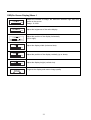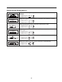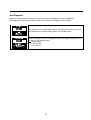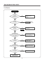
1
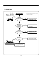
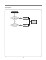
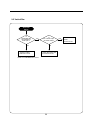
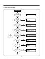
Service Manual
XGA COLOR MONITOR
Model : 710B
DAEWOO ELECTRONICS CO., LTD
OVERSEAS SERVICE DEPT.
CONTENTS
SAFETY PRECAUTIONS
1
GENERAL SAFETY INFORMATION
2
SERVICING PRECAUTIONS
3
TECHNICAL INFORMATION
6
GENERAL INFORMATION
7
PIN CONNECTOR
8
CAUTIONS FOR ADJUSTMENT AND REPAIR
8
OPERATION & ADJUSTMENT
9
TROUBLESHOOTING HINTS
15
ALIGNMENT PROCEDURE
31
BLOCK DIAGRAM
33
PCB LAYOUT
34
SCHEMATIC DIAGRAM
37
EXPLODED VIEW DIAGRAM
38
REPLACEMENT PARTS LIST
39
CIRCUIT BOARD ELECTRICAL PARTS LIST
40
SAFETY PRECAUTIONS
CAUTION: No modifications of any circuit should be attempted. Service work should only be performed after
you are thoroughly familiar with all of the following safety check and servicing guidelines.
Safety Check
Care should be taken while servicing this analog color display because of the high voltages used in the deflection
circuits. These voltages are exposed in such areas as the associated flyback and yoke circuits.
Fire & Shock Hazard
• Insert an isolation transformer between the analog color display and AC power line before servicing chassis.
• In servicing, pay attention to original lead dress especially in the high voltage circuit. if a short circuit is found,
replace all parts which have been overheated as a result of the short circuit.
• All the protective devices must be reinstalled per original design.
• Soldering must be inspected for possible cold solder points, frayed leads, damaged insulation, solder splashes
or sharp solder points. Be certain to remove all foreign materials.
Implosion Protection
Picture tube in this monitor employs integral implosion protection system, but care should be taken to avoid
damage and scratching during installation.
Use only same type replacement picture tubes.
IMPORTANT SAFETY NOTICE: There are special components used in analog color display, which are
important for safety. These parts are shaded on the schematic diagram and
on the replacement parts list. It is essential that these critical parts should be
replaced with manufacturer’s specified parts to prevent X-radiation, shock,
fire or other hazards. Do not modify the original design without getting a
written permission from DAEWOO ELECTRONICS CO. or this will void the
original parts and labor warranty.
X-Radiation
WARNING: The only potential source of X-Radiation is the picture tube. However when the high voltage circuitry
is operating properly, there is no possibility of an X-Radiation problem. The basic precaution which
must be exercised is to keep the high voltage at the following factory recommended level.
NOTE: It is important to use an accurate, periodically calibrated high voltage meter.
• To measure the high voltage, use a high-impedance high-voltage meter.
Connect(-) to chassis and (+) to the CRT anode button.
• Turn the Contrast & brightness control fully counterclockwise.
• Measure the high voltage. The high voltage meter should indicate the following factory recommended
level.
• If the upper meter indication exceeds the maximum level, immediate service is required to prevent the
possibility of premature component failure.
• To prevent X-Radiation possibility, it is essential to use the specified picture tube.
• The normal high voltage is 26.5KV or below, and must not exceed 29KV at zero beam current at rated
voltage.
1
GENERAL SAFETY INFORMATION
Terms in the manual
CAUTION
Statements identify conditions or practices that could result in damage to the equipment or other
property.
WARNING Statements identify conditions or practices that could result in personal injury or loss of life.
Terms as marked on equipment
CAUTION
Statements indicate a personal injury hazard not immediately accessible as one reads the
marking, or a hazard to properly including the equipment itself.
WARNING Statements indicate a personal injury hazard immediately accessible as one reads the marking
Symbols in the manual
This symbol indicates where applicable cautionary or other information is to be found.
Symbols as marked on equipment
Protective GROUND terminal
High Voltage Warning And Critical Component Warning Label
Following warning label is on the CRT PWB shield case inside the unit.
Warning: This product includes critical
mechanical and electrical parts which are
essential for x radiation safety. For continued
safety, replace critical components indicated in
the service manual only with exact
replacement parts given in the parts list.
Operating high voltage for this product is 29Kv
at minimum brightness. Refer to service
manual for measurement procedures and
proper service adjustments.
2
SERVICING PRECAUTIONS
CAUTION: Before servicing instruments covered by this service manual, its supplements and addendum,
read and follow the SAFETY PRECAUTIONS of this manual.
NOTE: If unforeseen circumstances create conflict between the following servicing precautions and any of the
safety precautions on page 1 of this manual, always follow the safety precautions.
Remember: Safety First.
General Servicing Precautions
1. Always unplug the AC power cord from the AC power source before:
a. Removing or reinstalling any component, circuit board, module, or any other instrument assembly.
b. Disconnecting or reconnecting any electrical plug or other electrical connection.
c. Connecting a test substitute in parallel with an electrolytic capacitor in the instrument.
CAUTION: A wrong part substitution or incorrect polarity installation of electrolytic capacitors may result in
a explosion hazard.
d. Discharging the picture tube anode.
2. Test high voltage only by measuring it with an appropriate high voltage meter or other voltage measuring device
(DVM, FETVOM. etc.) equipped with a suitable high voltage probe. Do not test high voltage by “drawing an
arc”.
3. Discharge the picture tube anode only by: (a) first connecting one end of an insulated clip lead to the
degaussing or line grounding system shield at the point where the picture tube socket ground lead is
connected, and then (b) touching the other end of the insulated clip lead to the picture tube anode button, using
an insulating handle to avoid personal contact with high voltage.
4. Do not any spray chemicals on or near this instrument or any or its assemblies.
5. Unless specified otherwise in this service manual, clean electrical contacts by applying the following mixture to
the contacts with a pipe cleaner, cotton-tipped stick or comparable nonabrasive applicator: 10% (by volume)
Acetone and 90% (by volume) isopropyl alcohol (90%-99% strength).
CAUTION: This is a flammable mixture. Unless specified otherwise in this service manual, lubrication of
contacts is not required.
6. Do not defeat any plug/socket B+ voltage interlocks with which instruments covered by this service manual
might be equipped.
7. Do not apply AC power to this instrument and/or any of its electrical assemblies unless all solid-state device
heat sinks are correctly installed.
8. Always connect the test instrument ground lead to the appropriate instrument chassis ground before connecting
the test instrument positive lead. Always remove the test instrument ground lead last.
9. Use only the test fixtures specified in this service manual with this instrument.
CAUTION: Do not connect the test fixture ground strap to any heatsink in this instrument.
3
Electrostatically Sensitive (ES) Devices
Some semiconductor (solid state) devices can be damaged easily by static electricity.
Such components commonly are called Electrostatically Sensitive (ES) Devices.
The examples of typical ES devices are integrated circuits, some field-effect transistors and semiconductor “chip”
components. The following techniques should be used to help reduce the incidence of component damage
caused by static electricity.
1. Immediately before handling any semiconductor component or semiconductor-equipped assembly, drain off any
electrostatic charge on your body by touching a known earth ground. Alternatively, obtain and wear a
commercially available discharging wrist strap device which should be removed for potential shock reasons
prior to applying power to the unit under test.
2. After removing an electrical assembly equipped with ES devices, place the assembly on a conductive surface
such as aluminum foil to prevent electrostatic charge buildup or exposure of the assembly.
3. Use only a grounded-tip soldering iron to solder or unsolder ES devices.
4. Use only an anti-static type solder removal device. Some solder removal devices not classified as “anti-static”
can generate enough electrical charges to damage ES devices.
5. Do not use freon-propelled chemicals. These can generate enough electrical charges to damage ES devices.
6. Do not remove a replacement ES device from its protective package until immediately before you are ready to
install it. (Most replacement ES devices are packaged with leads electrically shorted together by conductive
foam, aluminum foil or comparable conductive material).
7. Immediately before removing the protective material from the leads of a replacement ES device, touch the
protective material to the chassis or circuit assembly into which the device will be installed.
CAUTION: Be sure that no power is applied to the chassis or circuit, and observe all other safety
precautions.
8. Minimize bodily motions when handling unpackaged replacement ES devices. (Otherwise harmful motion such
as the brushing together of your clothes fabric or the lifting of your foot from a carpeted floor can generate
enough static electricity to damage an ES devices).
General Soldering Guidelines
1. Use a grounded-tip, low-wattage soldering iron with appropriate tip size and shape that will maintain tip
temperature within a 550°F-660°F (288°C-316°C) range.
2. Use an appropriate gauge of RMA resin-core solder composed of 60 parts tin/40 parts lead.
3. Keep the soldering iron tip clean.
4. Thoroughly clean the surface to be soldered. Use a small wire-bristle (0.5 inch or 1.25cm) brush with a metal
handle. Do not use freon-propelled spray-on cleaners.
5. Use the following soldering technique:
a. Allow the soldering iron tip to reach normal temperature (550°F to 660°F or 288°C to 316°C)
b. Hold the soldering iron tip and solder strand against the component lead until the solder melts.
c. quickly move the soldering iron tip to the junction of the component lead and the printed circuit foil, and hold it
there only until the solder flows onto and around both the component lead and the foil.
d. Closely inspect the solder area and remove any excess or splashed solder with a small wire-bristle brush.
CAUTION: Work quickly to avoid overheating the circuit board printed foil.
4
FIGURE 1. USE SOLDERING IRON TO PRY LEADS
IC Removal/Replacement
Some utilized chassis circuit boards have slotted (oblong) holes through which the IC leads are inserted and then
bent flat against the circuit foil. When holes are slotted, the following technique should be used to remove and
replace the IC. When working with boards using the familiar round hole, use the standard technique as outlined in
paragraphs 5 on the page under the title of general soldering guidelines.
Removal
1. Desolder and straighten each IC lead in one operation by gently prying up on the lead with the soldering iron tip
as the solder melts.
2. Draw away the melted solder with an anti-static suction-type solder removal device (or with desoldering braid
before removing the IC.
Replacement
1. Carefully insert the replacement IC in the circuit board.
2. Carefully bend each IC lead against the circuit foil pad and solder it.
3. Clean the soldered areas with a small wire-bristle brush. (lt is not necessary to reapply acrylic coating to the
area).
“Small-Signal” Discrete Transistor Removal/Replacement
1. Remove the defective transistor by clipping its leads as close as possible to the component body.
2. Bend the end of each of three leads remaining on the circuit board into a “U” shape.
3. Bend the replacement transistor leads into a “U” shape.
4. Connect the replacement transistor leads to the corresponding leads extending from the circuit board and crimp
the “U” with long nose pliers to insoure metal-to-metal contact, then solder each connection.
5
Power IC, Transistor or Devices Removal/Replacement
1. Heat and remove all solders from the device leads.
2. Remove the heatsink mounting screw (if applicable).
3. Carefully remove the device from the circuit board.
4. Insert new device in circuit board.
5. Solder each device lead, and clip off excess lead.
6. Replace heatsink.
Diode Removal/Replacement
1. Remove defective diode by clipping its leads as close as possible to diode body.
2. Bend the two remaining leads perpendicularly to the circuit board.
3. Observing diode polarity, wrap each lead out of the new diode around the corresponding lead on the circuit
board.
4. Securely crimp each connection and solder it.
5. Inspect the solder joints of the two “original” leads on the circuit board copper side. If they are not shiny, reheat
them and apply additional solder if necessary.
TECHNICAL INFORMATION
Picture Tube
Type : 17-inch, Flat Square Tube type
(16.2-inch, viewing area)
Dot Pitch : 0.28mm
Face Treatment : Non-glare / Anti-static
Video
Input Signal : R.G.B Analog
Amp. Bandwidth : 85 MHz
Input Sync : TTL, separate negative / positive
Scan Frequency
Horizontal : 30-69 KHz
Vertical : 50-160 Hz
Max. Resolution
1280 dots X 1024 lines (at 60Hz)
Power Source
Free Voltage (100-240 Vac, 50/60Hz)
Display Area
Standard Display Area : 310mm(H)X232mm(V)
Full Screen Size : 330mm(H)X250mm(V)
Power Consumption
Max. 100W
State
On
Stand-by
Suspend
Off
Recovery Time
None
3 seconds
7 seconds
Dimension
424(W)X440(H)X447.2(D)mm
(set with stand)
Weight (Net/Gross)
16.8/19.7 kg
Operating Environment
Temperature : 10-40°C/50-104°F
Relative Humidity : 8-80%
Storage Environment
Temperature : -20-45°C/-4-113°F
Relative Humidity : 5-90%
6
Power LED
Green
Green : 1 second
Amber : 0.5 second
Amber
GENERAL INFORMATION
This color monitor automatically scans all horizontal frequencies from 30KHz to 69KHz, and all vertical
frequencies from 50Hz to 160Hz. This color monitor adopted the OSD (On Screen Display), it shows the sync
polarity and frequency and it provides that easily adjust control. This color monitor supports IBM PC, PC/XT,
PC/AT, personal System/2 (PS/2), Apple Macintosh, and compatible users crisp text and vivid color graphics
display when using the following graphics adapters : (VGA, 8514/A, Super VGA, VESA and XGA and Apple
Macintosh Video Card). And so, this color monitor has a maximum horizontal resolution of 1280 dots and a
maximum vertical resolution of 1024 lines for superior clarity of display.
By accepting analog signal inputs which level is zero to 0.7 Volts. This color monitor can display and unlimited
palette of colors depending on the graphics adapter and software being used.
Abbreviations
ADJ
AFC
CRT
Def
D.Y
FBT
H.SYNC
OSC
P.S.U
PWA
R.G.B
V.Sync
Adjustment
Automatic Frequency Control
Cathode Ray Tube
Deflection
Deflection Yoke
Flyback Transformer
Horizontal Synchronization
Oscillator
Power Supply Unit
Printed Circuit Board Wiring Assembly
Red, Green, Blue
Vertical Synchronization
7
PIN CONNECTOR
Pin
Signal
1
2
3
4
5
6
7
8
9
10
11
12
13
14
15
Red
Green
Blue
GND
GND
GND - Red
GND - Green
GND - Blue
Reserved
GND - H.Sync
GND
Bi-directional Data (SDA)
Horizontal Sync
Vertical Sync (VCLK)
Data Clock (SCL)
1
6
10
15
Arrangement of 15-pin D-sub connector
CAUTIONS FOR ADJUSTMENT AND REPAIR
• Degaussing is always required when adjusting purity or convergence.
• The white balance adjustment has been done by a color analyzer in factory. The adjustment procedure,
described in the service manual is made by a visual check.
• Allow 20 minutes warm-up time for the display before checking or adjusting only electrical specification or
function.
• Reform the leadwire after any repair work.
Caution For Servicing
• In case of servicing or replacing CRT, high voltage sometimes remains in the anode of the CRT. Completely
discharge high voltage before servicing or replacing CRT to prevent a shock to the serviceman.
8
OPERATION & ADJUSTMENT
ADJUSTMENT KEY
Launch OSD(On-Screen Display) menus
Select the next function
Increase the value of any selected function
Decrease the value of any selected function
9
ADJUSTMENT PROCESS
R G B
R G B
BRIGHTNESS
50%
CONTRAST
50%
R G B
R G B
PINCUSHION
50%
TRAPEZOID
50%
R G B
R G B
K
K
COLOR TEMP.
9300
RED GAIN
6550
50%
R G B
R G B
ZZ
Z
ZZ
RECALL
NO
YES
STATUS
H : +31.5KHZ
V : +70.5 HZ
When you choose the icon
Z
on the OSD window, you can exit the OSD screen.
10
OSD(On-Screen Display) Menu 1
CONTRAST
50%
Adjust the contrast of image, the difference between light and dark
areas on the screen.
Range : 0-100%
Adjust the brightness of the entire display.
BRIGHTNESS
50%
H.POSITION
50%
Adjust the position of the display horizontally
(left or right).
Adjust the display width (horizontal size).
H.SIZE
50%
V.POSITION
50%
Adjust the position of the display vertically (up or down).
Adjust the display height (vertical size).
V.SIZE
50%
Degauss the display and restore image quality.
11
OSD(On-Screen Display) Menu 2
Adjust the left and right margins for more convex or more concave
margins.
• Image turns to
by
.
• Image turns to
by - .
TRAPEZOID
50%
PARALLELOGRAM
50%
PIN BALANCE
50%
V. MOIRE
50%
ROTATION
50%
Adjust the trapezoid of the screen by moving the lines inward or outward.
• Image turns to
by
.
• Image turns to
by - .
Adjust parallelogram when the screen is leaning left or right.
• Image turns to
by
.
• Image turns to
by - .
Adjust the side balance when the sides of the screen are bowed towards
left or right.
• Image turns to
by
.
• Image turns to
by - .
Adjust the vertical picture moire cancellation.
• Image turns to
by
.
• Image turns to
by
.
Adjust the rotation when the screen is tilted left or right(Optional).
• Image turns to
by
.
• Image turns to
by - .
12
OSD(On-Screen Display) Menu 3
Choose different preset color temperatures or set your own customized
color parameters.
Adjust the red gain.
RED GAIN
50%
Adjust the green gain.
GREEN GAIN
50%
Adjust the blue gain.
BLUE GAIN
50%
Adjust the red bias.
RED BIAS
50%
Adjust the green bias.
GREEN BIAS
50%
Adjust the blue bias.
BLUE BIAS
50%
OSD(On-Screen Display) Menu 4
STATUS
H : +31.5KHZ
V : +70.5 HZ
Display horizontal & vertical frequency and polarity.
Reset the screen to the Factory Preset Display Settings.
YES : VESA DPMS operation.
NO : NO DPMS operation.
Select language for OSD.
13
Self Diagnosis
When the monitor doesn’t display, if you press any key, Self Diagnosis screen is displayed.
Self Diagnosis function checks if the status of the monitor is No Signal or Out of range.
No Signal screen is displayed when the D-Sub signal connector is not
connected or the status of the monitor is on DPMS mode.
Out of Range screen is displayed when the applied frequency is
under or over normal range.
Normal range
H : 30-69 KHz
V : 50-160 Hz
14
TROUBLESHOOTING HINTS
1. No Character
No Character
Are the
Contrast &
Brightness Controls
maximum
No
Change the Contrast &
Brightness control to
maximum
Yes
Is whole
screen bright?
No
No Raster
Refer to
No Raster
Yes
Is CRT
Cathode (Rk, Gk, Bk)
signal level
normal?
No
Is the
output signal of the
(pin 21, 24, 26) pre-amp
(IC801, KA2500)
normal?
Yes
Check the peripheral circuit
of CRT Board
Rk, Gk, Bk
About 45Vpp
Yes
Check the video output
circuit and IC803 (pin 1, 3, 5)
and their ambient circuit
No
Trouble in 12V DC line
of the Main PWB
No
Check the clamping pulse
circuit
No
Is 12V DC line
normal?
Yes
Is clamping
pulse (pin 18 of IC801)
normal?
Yes
Is input signal
normal?
No
Yes
Trouble in IC801 and
its ambient circuit
15
Check the signal cable
2. No Raster
No Raster
Is CRT
heater red-hot?
Is Heater
Voltage (CRT PWB)
about 6V?
No
Yes
No
Trouble in
CRT
Yes
Trouble in
power supply
circuit
Turn the Brightness
& Contrast control
to set Maximum
Refer to trouble in
power supply unit.
Yes
Is whole
screen bright?
No
Trouble in power
supply circuit
No
Trouble in G1
line of Main PWB
Yes
Check
G1 voltage about
-40V?
Yes
Is CRT
G2 (screen) voltage
about 500V?
No
Trouble in FBT
Yes
Is 80V DC
line normal?
No
Trouble in 80/
Refer to trouble
120V DC line of in P,S,U
power supply unit
No
High Voltage
trouble in FBT
Yes
Does
turning the Brightness
control counterclockwise
make screen
bright?
Yes
Trouble in FBT
16
3. A missing Color
One color is
missing
Is input signal
normal?
No
Check video signal
cable or video card.
No
Trouble in IC801 or its
ambient circuit
No
Is video
output IC803 waveform
normal?
0.7Vpp
Yes
Is the
output of pre-amp
(IC801, KA2500)
pin 21, 24, 26 all
normal?
Yes
CRT
Cathode (Rk, Gk, Bk)
is normal?
RK, GK, BK
About 40V p-p
Yes
Yes
Trouble in 80/120V DC
line
Each grid (G1, G2)
voltage normal?
Yes
No
Replace CRT
17
Trouble in 80/120V DC
line
No
Trouble in
video output
circuit, IC803
or ambient
4. Abnormal OSD Font
Abnormal OSD Font
Is menu
key selected?
Is OSD Font
exist?
* If menu key selected.
Is Heater
Voltage (CRT PWB)
about 6V?
No
Yes
Yes
One color is
missing
Troubie in
IC802 or its
ambient circuit
Yes
Is the
output of IC802
(pin 13, 14, 15)
normal?
No
Trouble in IC802
and its ambient
circuit
Yes
Refer to Missing Color
18
No
Trouble in
Heater voltage
line.
Refer to trouble in P.S.U
5. Horizontal Output Circuit
Trouble in Horizontal
output circuit
(No Raster
Is the
B+line voltage
over 45V?
No
Trouble in B+ Booster Circuit
(Check the B+section of IC501,
Check Q603 and its ambient
circuit).
Yes
Is the H-out
waveform of IC501
normal?
11V
0V
No
Trouble in IC501
Yes
Is the Collector
wave form of
Q501 or Q502
normal?
10V
0V
No
Trouble in Q501, Q502
Yes
Is the Collector
waveform of
Q503 normal?
66V
Yes
Trouble in Q504 and
its ambient circuit.
19
No
Trouble in Q503 and its
ambient circuit.
6. Unstable Picture
6-1. Horizontal
Unstable
picture
Is H.Sync
input pin of IC501
correct?
No
Check H.Sync Out of
Micom or its ambient
circuits.
No
Check the value of
C503, R502
Yes
Is the
pin 3 of IC501
5V?
Yes
Trouble in IC501
20
6-2. V.OSC/Deflection Circuit
Unstable or
Abnormal picture
Is
± 13V DC line
correct?
No
Trouble in
power supply unit
Yes
45Vp-p
Is
the output
waveform of IC401
(pin 6) normal?
Yes
V.DY
failure
Yes
Trouble in IC401 or
its ambient circuit
No
Is the
output pulse
of IC501 (pin 23)
normal?
No
Trouble in V.Sync line
or IC501 failure.
21
7. Focus
Monitor remains
unfocused
Check
Focus VR in
FBT
Is
focus
acceptable?
Yes
No
Trouble in Focus
circuit (FBT)
22
OK
7-1. Dynamic Focus
FVH FVV
* Check after adjusting the static focus
finely by VR in FBT
Focus is poor
PHILIPS
: 440V 180V
NEC
: 300V 120V
SAMSUNG : 300V 120V
DF
waveform
FVH
FVV
Is the
waveform of the
DF pin in FBT
correct?
Yes
1. Check the CRT socket
or connector wire
2. Trouble in FBT or CRT
No
1. Check the waveform of
the pin 3 of FBT.
2. Check D575
No
1. Check the 12V DC line.
2. Check Q751,D755
No
Is the
cathode voltage
of the D575
about 600V?
Yes
Is the
base voltage of
the Q751 about
2.6V?
Yes
Is the
waveform of
the pin 10 in IC501
DF
correct?
waveform
4.5V
2V
0V
Yes
0.8V
Trouble in Q752, Q753, Q754,
D751, D752, D753, D754,
Q755, Q756
23
No
Trouble in IC501 or C520
8. Convergence
Poor convergence
Is
convergence
on the center area
bad?
Yes
Adjust static
convergence
Refer to
Adjustment
procedure of
convergence
No
Is
convergence on the
fringe area bad?
Yes
Adjust D.Y
Location
24
9. Abnormal Picture
9-1. Horizontal Size
Abnormal
H.Size
When
the VR601 is
changed, is the H.size
changed?
No
Check pin 15 of IC501
and its ambient circuit
(D604, R605, R606, R607)
Yes
Is the
H.Size about 295mm
at VGAmode and Min. H.Size
in OSD Menu?
No
Yes
It isn't out of order.
25
1.Check B+ section of TDA9109
and its ambient circuit.
2.Check Q601 and its ambient
circuit.
9-2. Vertical Size
Abnormal
V.Size
Is
changeable the
DC voltage of
IC401 pin 1?
No
Is
the 3.5Vdc of pin
23 of the IC501?
Yes
Trouble V.OSC/
Deflection Circuit
No
Check the IC501 and
its ambient circuit
Refer to V.OSC/Deflection circuit
26
Yes
Check the IC401
and its
ambient circuit
10. High Voltage Circuit
Trouble in H.V circuit
(No Raster)
Is
B+(45V) line
voltage normal?
No
Trouble in power
supply circuit
Yes
Trouble in Q574 or FBT
Yes
Trouble in Q572, Q573
12V Line
Yes
Is Q574
base waveform
normal?
No
Is Q571
collector waveform
normal?
No
Is Q501
emitter waveform
normal?
Yes
Trouble in Q571
No
Is IC501
pin 26 waveform
normal?
Yes
Trouble in Q501, Q502
No
Is IC501
pin 29 voltage
about 12V?
No
Trouble in power supply
Yes
Is the
input H.Sync
correct?
Yes
No
Trouble in H.Sync
27
Trouble in IC501
ambient circuit.
11. Side-Pincushion Circuit
Side-Pincusion distortion
is excessive or barrel
Select the
side-pincushion
icon on OSD menu,
and adjust acceptable
position.
Yes
O.K
No
Is the pin 24
waveform of IC501
correct
Yes
Check IC501 or
their ambient circuit
(pin 14, 15, 16)
Yes
Check IC501 or
it's ambient circuit.
No
Is the
waveform of IC501
pin 1, 2
No
Trouble in H.V Sync
28
12. Power Supply Unit (P.S.U)
Trouble in P.S.U
Is
power switch
on?
No
Switch on
Yes
Is
fuse F001
O.K?
No
Check the power cord outlet
and diode D001, D002,
D003, D004
No
Replace R004
Replace C005
No
Trouble in D001, D002,
D003, D004, C004 and
TH001.
No
Trouble in T001, IC001,
IC101, PH001 and D005 etc.
Yes
Is the
voltage of IC001
pin 3 16V?
Yes
Is
voltage of T001
pin 6 130V
(370V)?
Yes
Is the
waveform of IC001
pin 1correct?
400Vpp (620Vpp)
Yes
Is
voltage of C103
45V DC?
No
Trouble in D102, D103 or
B+ Part
Yes
Is
voltage of C101
80V DC?
No
Trouble in D101 or
Video Part
No
Trouble in D108 or
Video Part
Yes
Is
voltage of C113
120V DC?
A
29
A
Is voltage
of C104 13V DC?
No
Trouble in D104, IC102 or
horizontal Part.
No
Trouble in D105 or vertical
Part.
Yes
Is
voltage of C105
-13V DC?
Yes
Is voltage
of C106
8.7V DC?
No
Trouble in D106 or Q103
Yes
P.S.U O.K
30
ALIGNMENT PROCEDURE
Standard Adjustment Conditions
1. Power source voltage : AC 120V, 60Hz./AC 220V, 50Hz
2. Aging : Take at least 20 minutes warm-up time.
3. Signals.
Video : Analog 0.7Vpp 75 terminal positive polarity
Synchronizing : TTL level Negative/Positive Separate/Composite
Deflection frequency
Horizontal Frequency : 30KHz - 69KHz
Vertical Frequency : 50Hz - 160Hz
Pre-Adjustment
1. High voltage Adjustment
Adjust 26 kvdc between Anode cap and ground at a cross hatch pattern of 31.5KHz by using VR551.
2. B+ Adjustment (H.min size)
(a) Receive a cross hatch pattern of 31.5KHz
(b) Set the H-Size control to the minimum.
(c) Adjust H-Size to 295mm by using VR601
Main Adjustment
1. Setting the Controls
Set the value of items as following.
Contrast : Max. (OSD value up to 100)
Brightness : Center (Set the OSD value to 50)
2. H.size, V.size, H.phase, V.position, Pincushion, Trapezoid
Perceive the cross hatch pattern of Factory preset mode.
H.Size, V.size, H.phase, V.position, Pincushion, Trapezoid are adjusted at each mode.
In Factory, Auto Alignment was done at each mode. Therefore, Factory preset mode has it’s own value
according to each control.
3. Focus
(a) Set brightness control to center and contrast control to MAX.
(b) Receive all “H” character pattern of 60KHz mode signal.
(c) Adjust the Focus control of FBT to obtain best Focus (static focus and Dynamic focus).
4. Geometric Distortion Adjustment.
(a) Receive the cross hatch pattern of VGA mode signal by using the signal generator.
(b) Pin balance, Parallelogram are adjusted the best geometric status.
(c) Repeat the adjustment at each mode.
5. White Balance Adjustment
(a) Receive a full white pattern of 60KHz mode.
(b) Select 9300°K on the OSD Menu.
(c) Set the bright control and contrast control to the maximum and receive the all black pattern.
(d) Adjust the FBT screen VR to get the screen luminosity to 1 Ft/L.
(e) Select the R, G, B Bias on the OSD menu and adjust the ADJUST +/– key to get the color coordinates in
X=0.281, Y=0.311
(f) If the screen luminosity is changed adjust the sub brightness control to get the 1 Ft/L screen luminosity.
(g) Set the brightness control to the center and contrast control to the maximum.
(h) Receive a full white pattern.
(i) Select the R, G, B gain on the OSD menu and adjust the ADJUST +/– key to get the color coordinates in
X=0.281±0.03, Y=0.311±0.03
(j) Adjust the sub contrast control to get the screen luminosity to 34 Ft/L/
(k) Select 6550°K on the OSD menu and set the bright control and contrast control to the maximum and receive
the all black pattern.
31
(l) Repeat (e),(f),(g),(h),(i),(j).
Just a difference from 9300°K mode is color coordinates.
Set color coordinates in X=0.313, Y=0.329
6. Static Convergence Adjustment
(a) Apply an magenta cross hatch pattern on display.
(b) Adjust the focus from the best over all focus on the display.
Also adjust the brightness to the desired condition.
(c) Vertical red and blue lines are converged by varying the angle between the two tabs of the 4-pole magnets.
(d) Horizontal red and blue lines are converged by varying the tabs together, keeping the angle between them
constant.
(e) Apply a white cross hatch pattern on display.
(f) Vertical green and magenta lines are converged by varying the the angle between the two tabs of the 6-pole
magnets.
(g) Horizontal green and magenta lines are converged by varying the tabs together, keeping the angle between
them constant.
32
VIDEO OUTPUT
VIDEO
PREAMP
G
LM2407T
OSD IC
B
LSC4525P2
KA2500
OSD
(R.G.B)
BIAS CONTROL
H.VTG
H.V
SCL SDA
H
BIAS(R.G.B)
V
MICOM
SCL
SDA SCL
SDA
EEPROM
24C08B
68HC705BD32
V.DRV AMP
V.DY
KA2142
33
TILT IC
L272M
FBT
H.V
SDA SCL
H.OSC.
&
V.DRV
CF1147DW2300
TDA9109
120V,80V,45V
12V, –12V
L
GND
N
FILTER
SMPS
CONTROL
SMPS
TRANS
H.DRV
KA2S0880
B+
CONTROL
H.DY
H.VTG
B+
CONTROL
KA7500B
SCREEN,
FOCUS
BLOCK DIAGRAM
(R.G.B)
R
PCB LAYOUT
Main PCB Component Side
34
Main PCB Solder Side
35
Video PCB Component Side
Video PCB Solder Side
36
EXPLODED VIEW DIAGRAM
38
REPLACEMENT PARTS LIST
Important Safety Notice
Components identified with the International Symbol have special characteristics important for safety.
When replacing any components, use only manufacturer’s specified parts.
Abbreviation of Description
RESISTOR Description
Allowance
F
± 1%
J
± 5%
K
± 10%
M
± 20%
G
± 2%
Example:
Fig &
Index
Part No
R101
Resistors
RE-42820J
Cabron: 82J
Description
CAPACITOR Description
C
D
F
J
K
P
Z
Allowance
± 0.25pF
± 0.5%
± 1pF
± 5%
± 10%
± 100% ~ 0%
± 80% ~ –
Example:
Fig &
Index
C102
C105
C402
Part No
Description
Capacitors
CCXF1H104Z Ceramic 50V Z
CBSLH200J
Ceramic 50V J
CCXB1H331K Ceramic 50V K
39
CIRCUIT BOARD ELECTRICAL PARTS LIST
The components identified by mark
have special characteristics important for safety and x-ray radiation.
These should be replaced only with the types specified in the parts list.
LOC
PART-CODE
PART-NAME
10010
PCFMCAJ046
COVER FRONT AS
CMC-710B
CT801
9979617018
CDT
M41QAR361X124(E)
CT802
9970710176
CRT GND AS
0.12*5*24+BL102NG=730
DG001
5MG0000062
COIL DEGAUSSING
DG-710B
20010
PCMPM1J046
PCB MAIN MANUAL AS
CMC-710B
CA801
99707A0016
CONN AS
SMH250-10+1007#24#28=160
CA802
9970770019
CONN AS
SMH250-07+1007#24=220
CN001
9970700123
CONN AS
4.3+35404-9002+1015#18=50
C001
CL1UC3224M
C LINE ACROSS
0.22MF 1J(UCVSNDF/SV)+Q/O
C004
CEYP2G221Z
C ELECTRO
400V SMH 220MF (25.4*40)
C006
CCYB3A103K
C CERA
1KV B 0.01MF K
C103
CEXF2A471V
C ELECTRO
100V RSS 470MF 16*31.5
C402
CMXL2A474J
C MYLAR
MEU 100V 0.47MF J
C406
CEXF1C471V
C ELECTRO
16V RSS 470MF (10X12.5)TP
C409
CMXM2A224J
C MYLAR
100V 0.22MF J
C519
CMYH3D532J
C MYLAR
2KV BUP 5300PF J BULK
C553
CMXF2D824J
C MYLAR
MPP 200V 0.82MF J
C578
CMXM2A224J
C MYLAR
100V 0.22MF J
DL001
DLT2462A2D
LED
LT2462-A2-D51
D102
DS3L60----
DIODE
S3L60
D103
DS3L60----
DIODE
S3L60
D104
DS3L60----
DIODE
S3L60
F001
5F3CB3122L
FUSE CERA
SEMKO TL 3.15A 250V MF51
IC001
1KA2S0880-
IC POWER
KA2S0880
IC102
1KA78R12--
IC REGULATOR
KA78R12
IC103
1K1A7805P1
IC REGULATOR
KIA7805PI
IC201
1DWM209T--
IC MICOM
68HC705BD32
IC401
1KA2142---
IC V-OUT
KA2142
IC501
1TDA9109--
IC H.OSC
TDA9109
IC801
1KA2500---
IC
KA2500
L001
5PDLF3055-
FILTER LINE
DLF-3055L
L501
5MH0000051
COIL H-LINEARITY
TRL-195A
L502
5MC0000069
COIL CHOKE
33UH K BULK(14*16)
L571
5MC0000068
COIL CHOKE
CH-85A
L601
5MC0000065
COIL CHOKE
CH-85
PH001
1TLP721GR-
IC PHOTO COUPLER
TLP721D4GR
P001
9979500014
RECEPTACLE
YA03P/FILTER EMI
Q503
TKSC3502E-
TR
KSC3502E
40
PART-DESC
LOC
PART-CODE
PART-NAME
PART-DESC
D504
DDTV32F---
DIODE
DTV32F
Q504
T2SC5387--
TR H.OUT
2SC5387
Q574
TKSC5386--
TR
KSC5386
Q551
T1RF630ATS
FET
IRF630A-TSTU
Q552
T1RF630ATS
FET
IRF630A-TSTU
Q555
T1RF630ATS
FET
IRF630A-TSTU
Q577
T2SK2799--
FET
2SK2799
Q603
T2SK2799--
FET
2SK2799
RL001
5SC0201103
SW RELAY
HR-CR323 2C-1P DC12V
RL501
5SC0101031
SW RELAY
HR-703V DC12V 1C-1P
R754
RS01Z104J-
R M-OXIDE FILM
1W 100K OHM J (TAPPING)
SG900
4SG0D00104
SPARK GAP
S-23 1.5KV
SW001
5S50101Z01
SW TACT
KPT-1115VM 1C-1P
S001
9970800015
CABLE SIGNAL AS
15P+2C/DDC=1.5M (IVY)
TH001
DTP8D15---
THERMISTOR
TP8D15
T001
5RM0000090
TRANS SMPS
DWT-44A1
T002
5RY0000002
TRANS SYNC
DST-603
T501
5RD0000037
TRANS DRIVE
DDT-710B
T571
5RH0000105
FBT
CF1147DW2300
T601
5RF0000003
TRANS DUMMY
TDH-710B
30010
PCMPJ1J046
PCB SMD AS
CMC-710B
C015
HCFK104ZCA
C CHIP CERA
50V Y5V 0.1MF Z 2012
C117
HCFK104ZCA
C CHIP CERA
50V Y5V 0.1MF Z 2012
C119
HCQK101JCA
C CHIP CERA
50V CH 100PF J 2012
C120
HCQK101JCA
C CHIP CERA
50V CH 100PF J 2012
C122
HCFK104ZCA
C CHIP CERA
50V Y5V 0.1MF Z 2012
C203
HCFK104ZCA
C CHIP CERA
50V Y5V 0.1MF Z 2012
C204
HCFK104ZCA
C CHIP CERA
50V Y5V 0.1MF Z 2012
C205
HCQK360JCA
C CHIP CERA
50V CH 36PF J 2012
C206
HCQK360JCA
C CHIP CERA
50V CH 36PF J 2012
C212
HCQK181JCA
C CHIP CERA
50V CH 180PF J 2012
C403
HCFK104ZCA
C CHIP CERA
50V Y5V 0.1MF Z 2012
C502
HCBK223KCA
C CHIP CERA
50V X7R 0.022MF K 2012
C503
HCQK102JCA
C CHIP CERA
50V CH 1000PF J 2012
C506
HCFK333ZCA
C CHIP CERA
Y5V 50V 0.033MF Z 2012
C507
HCFK224ZCA
C CHIP CERA
Y5V 50V 0.22MF Z 2012
C520
HCQK102JCA
C CHIP CERA
50V CH 1000PF J 2012
C532
HCFK104ZCA
C CHIP CERA
50V Y5V 0.1MF Z 2012
C549
HCQK181JCA
C CHIP CERA
50V CH 180PF J 2012
C581
HCFK104ZCA
C CHIP CERA
50V Y5V 0.1MF Z 2012
41
LOC
PART-CODE
PART-NAME
C802
HCFK104ZCA
C CHIP CERA
50V Y5V 0.1MF Z 2012
C803
HCFK104ZCA
C CHIP CERA
50V Y5V 0.1MF Z 2012
C812
HCFK104ZCA
C CHIP CERA
50V Y5V 0.1MF Z 2012
C813
HCFK104ZCA
C CHIP CERA
50V Y5V 0.1MF Z 2012
C814
HCQK101JCA
C CHIP CERA
50V CH 100PF J 2012
C815
HCQK101JCA
C CHIP CERA
50V CH 100PF J 2012
C832
HCFK104ZCA
C CHIP CERA
50V Y5V 0.1MF Z 2012
C833
HCFK104ZCA
C CHIP CERA
50V Y5V 0.1MF Z 2012
C862
HCFK104ZCA
C CHIP CERA
50V Y5V 0.1MF Z 2012
C863
HCFK104ZCA
C CHIP CERA
50V Y5V 0.1MF Z 2012
C878
HCQK122JCA
C CHIP CERA
50V CH 1200PF J 2012
C879
HCQK122JCA
C CHIP CERA
50V CH 1200PF J 2012
C881
HCFK103ZCA
C CHIP CERA
50V Y5V 0.01MF Z 2012
C882
HCFK103ZCA
C CHIP CERA
50V Y5V 0.01MF Z 2012
C883
HCFK103ZCA
C CHIP CERA
50V Y5V 0.01MF Z 2012
C884
HCQK220JCA
C CHIP CERA
50V CH 22PF J 2012
C885
HCQK220JCA
C CHIP CERA
50V CH 22PF J 2012
R117
HRFT272JCA
R CHIP
1/10 2.7K OHM J 2012
R205
HRFT472JCA
R CHIP
1/10 4.7K OHM J 2012
R208
HRFT000JCA
R CHIP
1/10 0 OHM J 2012
R209
HRFT472JCA
R CHIP
1/10 4.7K OHM J 2012
R210
HRFT472JCA
R CHIP
1/10 4.7K OHM J 2012
R216
HRFT151JCA
R CHIP
1/10 150 OHM J 2012
R217
HRFT201JCA
R CHIP
1/10 200 OHM J 2012
R218
HRFT472JCA
R CHIP
1/10 4.7K OHM J 2012
R228
HRFT222JCA
R CHIP
1/10 2.2K OHM J 2012
R234
HRFT101JCA
R CHIP
1/10 100 OHM J 2012
R235
HRFT101JCA
R CHIP
1/10 100 OHM J 2012
R238
HRFT472JCA
R CHIP
1/10 4.7K OHM J 2012
R246
HRFT472JCA
R CHIP
1/10 4.7K OHM J 2012
R247
HRFT472JCA
R CHIP
1/10 4.7K OHM J 2012
R248
HRFT472JCA
R CHIP
1/10 4.7K OHM J 2012
R252
HRFT472JCA
R CHIP
1/10 4.7K OHM J 2012
R272
HRFT563JCA
R CHIP
1/10 56K OHM J 2012
R284
HRFT912JCA
R CHIP
1/10 9.1K OHM J 2012
R285
HRFT912JCA
R CHIP
1/10 9.1K OHM J 2012
R286
HRFT912JCA
R CHIP
1/10 9.1K OHM J 2012
R289
HRFT202JCA
R CHIP
1/10 2K OHM J 2012
R502
HRFT682JCA
R CHIP
1/10 6.8K OHM J 2012
R505
HRFT472JCA
R CHIP
1/10 4.7K OHM J 2012
42
PART-DESC
LOC
PART-CODE
PART-NAME
R506
HRFT272JCA
R CHIP
1/10 2.7K OHM J 2012
R508
HRFT472JCA
R CHIP
1/10 4.7K OHM J 2012
R513
HRFT153JCA
R CHIP
1/10 15K OHM J 2012
R515
HRFT105JCA
R CHIP
1/10 1M OHM J 2012
R516
HRFT122JCA
R CHIP
1/10 1.2K OHM J 2012
R517
HRFT103JCA
R CHIP
1/10 10K OHM J 2012
R531
HRFT103JCA
R CHIP
1/10 10K OHM J 2012
R576
HRFT223JCA
R CHIP
1/10 22K OHM J 2012
R581
HRFT752JCA
R CHIP
1/10 7.5K OHM J 2012
R753
HRFT621JCA
R CHIP
1/10 620 OHM J 2012
R801
HRFT750JCA
R CHIP
1/10 75 OHM J 2012
R831
HRFT750JCA
R CHIP
1/10 75 OHM J 2012
R853
HRFT472JCA
R CHIP
1/10 4.7K OHM J 2012
R856
HRFT472JCA
R CHIP
1/10 4.7K OHM J 2012
R861
HRFT750JCA
R CHIP
1/10 75 OHM J 2012
R880
HRFT101JCA
R CHIP
1/10 100 OHM J 2012
R885
HRFT562JCA
R CHIP
1/10 5.6K OHM J 2012
R886
HRFT105JCA
R CHIP
1/10 1M OHM J 2012
R887
HRFT561JCA
R CHIP
1/10 560 OHM J 2012
R888
HRFT182JCA
R CHIP
1/10 1.8K OHM J 2012
R889
HRFT101JCA
R CHIP
1/10 100 OHM J 2012
R890
HRFT472JCA
R CHIP
1/10 4.7K OHM J 2012
R936
HRFT244JCA
R CHIP
1/10 240K OHM J 2012
R938
HRFT243JCA
R CHIP
1/10 24K OHM J 2012
R942
HRFT562JCA
R CHIP
1/10 5.6K OHM J 2012
40010
PCMPJ0J046
PCB MAIN ODD SHAPE AS
CMC-710B
CW201
485923282S
CONN WAFER
5267-07A STICK TYPE
CW202
485923272S
CONN WAFER
5267-06A STICK TYPE
C002
CH1FDF222M
C CERA AC
HIKB AC400V 222M
C003
CH1FDF222M
C CERA AC
HIKB AC400V 222M
C008
CH1FDF222M
C CERA AC
HIKB AC400V 222M
C010
CH1FDF222M
C CERA AC
HIKB AC400V 222M
C101
CEXF2A470V
C ELECTRO
100V RSS 47MF (10X16) TP
C102
CCXB3D102K
C CERA
2KV B 1000PF K (TAPPING)
C104
CEXF1E471V
C ELECTRO
25V RSS 470MF (10X16) TP
C106
CEXF1C471V
C ELECTRO
16V RSS 470MF (10X12.5)TP
C113
CEXF2C470V
C ELECTRO
160V RSS 47MF (13X25) TP
C116
CCXB3D222K
C CERA
HIKB 2KV 2200PF K
C522
CMXF2G184J
C MYLAR
MPP 400V 0.18MF J
C523
CMXF2G154J
C MYLAR
MPP 400V 0.15MF J
43
PART-DESC
LOC
PART-CODE
PART-NAME
PART-DESC
C531
CEXF1C102V
C ELECTRO
16V RSS 1000MF (10X20) TP
C551
CMXF2D204J
C MYLAR
MPP 200V 0.2MF J (TP)
C552
CMXF2D184J
C MYLAR
MPP 200V 0.18MF J (TP)
C555
CMXF2D334J
C MYLAR
200V MPP 0.33MF J (TP)
C574
CMXH3C102J
C MYLAR
1.6KV BUP 1000PF J
C582
CEXF2A221V
C ELECTRO
100V RSS 220MF (16X25) TP
C584
CMXF2D564J
C MYLAR
MPP 200V 0.56MF J
C587
CEXF2G220D
C ELECTRO
400V KMG 22MF(12.5*25) TP
C588
CEXF2G220D
C ELECTRO
400V KMG 22MF(12.5*25) TP
C592
CEXF2C220V
C ELECTRO
160V RSS 22MF (10X20) TP
C605
CMXF2D474J
C MYLAR
MPP 200V 0.47MF J
C902
CMXF2D104J
C MYLAR
MPP 200V 0.1MF J
D001
D2A05-----
DIODE
2A05
D002
D2A05-----
DIODE
2A05
D003
D2A05-----
DIODE
2A05
D004
D2A05-----
DIODE
2A05
D005
D1N4937GP-
DIODE
1N4937GP (TAPPING)
D006
DHER107---
DIODE
HER107
D101
DRU1P-----
DIODE
RU 1P (TAPPING)
D105
DHER107---
DIODE
HER107
D106
DHER107---
DIODE
HER107
D108
DRU1P-----
DIODE
RU 1P (TAPPING)
D403
D1N4002A--
DIODE
1N4002
D511
DTVR1G----
DIODE
TVR1G TPA1
D512
DTVR1G----
DIODE
TVR1G TPA1
D573
DS2L60---R
DIODE
S2L60
D575
DRU1P-----
DIODE
RU 1P (TAPPING)
D576
DTVR1G----
DIODE
TVR1G TPA1
D577
DTVR1G----
DIODE
TVR1G TPA1
D602
DTVR1G----
DIODE
TVR1G TPA1
D603
DS2L60---R
DIODE
S2L60
D913
DHER107---
DIODE
HER107
D914
DHER107---
DIODE
HER107
IC203
1M24C08BN6
IC EEPROM
M24C08BN6
IC502
1KA7500B--
IC
KA7500B
IC802
1LSC4525P2
IC OSD
LSC4525P2
IC804
1LM358N---
IC OP AMP
LM358N
PR001
DECPAC140M
POSISTOR
ECPAC140M290
P002
9977410800
TERMINAL PIN
BSP1(SN) L=15MM
P003
9977410800
TERMINAL PIN
BSP1(SN) L=15MM
44
LOC
PART-CODE
PART-NAME
PART-DESC
P401
9977410800
TERMINAL PIN
BSP1(SN) L=15MM
P402
9977410800
TERMINAL PIN
BSP1(SN) L=15MM
P403
9977410800
TERMINAL PIN
BSP1(SN) L=15MM
P501
9977410800
TERMINAL PIN
BSP1(SN) L=15MM
P502
9977410800
TERMINAL PIN
BSP1(SN) L=15MM
P503
9977410800
TERMINAL PIN
BSP1(SN) L=15MM
P504
9977410800
TERMINAL PIN
BSP1(SN) L=15MM
R004
RS02Z513J-
R M-OXIDE FILM
2W 51K OHM J
R006
RS01Z683J-
R M-OXIDE FILM
1W 68K OHM J (TAPPING)
R007
RS01Z683J-
R M-OXIDE FILM
1W 68K OHM J (TAPPING)
R107
RS02Z392J-
R M-OXIDE FILM
2W 3.9K OHM J (TAPPING)
R109
RS02Z369J-
R M-OXIDE FILM
2W 3.6 OHM J (TAPPING)
R110
RS02Z399J-
R M-OXIDE FILM
2W 3.9 OHM J
R118
RS02Z100J-
R M-OXIDE FILM
2W 10 OHM J (TAPPING)
R407
RS01Z109J-
R M-OXIDE FILM
1W 1 OHM J (TAPPING)
R408
RS02Z479J-
R M-OXIDE FILM
2W 4.7 OHM J (TAPPING)
R518
RS01Z101J-
R M-OXIDE FILM
1W 100 OHM J (TAPPING)
R520
RS01Z159J-
R M-OXIDE FILM
1W 1.5 OHM J (TAPPING)
R529
RS01Z159J-
R M-OXIDE FILM
1W 1.5 OHM J (TAPPING)
R532
RS01Z101J-
R M-OXIDE FILM
1W 100 OHM J (TAPPING)
R554
RS01Z471J-
R M-OXIDE FILM
1W 470 OHM J (TAPPING)
R573
RS01Z470J-
R M-OXIDE FILM
1W 47 OHM J (TAPPING)
R587
RS02Z102J-
R M-OXIDE FILM
2W 1K OHM J (TAPPING)
R589
RW01Z308JN
R WIRE WOUND
1W 0.30 OHM J NON-INDUCT
R603
RS02Z331J-
R M-OXIDE FILM
2W 330 OHM J TAPPING
R604
RW01Z308JN
R WIRE WOUND
1W 0.30 OHM J NON-INDUCT
R631
RS02Z129J-
R M-OXIDE FILM
2W 1.2 OHM J (TAPPING)
R632
RS02Z129J-
R M-OXIDE FILM
2W 1.2 OHM J (TAPPING)
R633
RS02Z129J-
R M-OXIDE FILM
2W 1.2 OHM J (TAPPING)
R755
RS01Z104J-
R M-OXIDE FILM
1W 100K OHM J (TAPPING)
R756
RS01Z104J-
R M-OXIDE FILM
1W 100K OHM J (TAPPING)
R757
RS01Z104J-
R M-OXIDE FILM
1W 100K OHM J (TAPPING)
SW201
5S50101Z01
SW TACT
KPT-1115VM 1C-1P
SW202
5S50101Z01
SW TACT
KPT-1115VM 1C-1P
SW203
5S50101Z01
SW TACT
KPT-1115VM 1C-1P
SW204
5S50101Z01
SW TACT
KPT-1115VM 1C-1P
VR551
RV6421503P
R SEMI FIXED
CCT 065AT 50K OHM B TAP
VR601
RV6121202P
R SEMI FIXED
CCT 063BT 2K OHM B TAP
50010
PCMPJRJ046
PCB MAIN RADIAL AS
CMC-710B
C005
CEXF1H101V
C ELECTRO
50V RSS 100MF (8X11.5) TP
45
LOC
PART-CODE
PART-NAME
PART-DESC
C011
CEXF1H109V
C ELECTRO
50V RSS 1MF (5X11) TP
C013
CEXF1H109V
C ELECTRO
50V RSS 1MF (5X11) TP
C014
CCXF1H223Z
C CERA
50V F 0.022MF Z (TAPPING)
C105
CEXF1C101V
C ELECTRO
16V RSS 100MF (6.3X11) TP
C107
CCXF1H223Z
C CERA
50V F 0.022MF Z (TAPPING)
C108
CEXF1C101V
C ELECTRO
16V RSS 100MF (6.3X11) TP
C109
CEXF1C101V
C ELECTRO
16V RSS 100MF (6.3X11) TP
C110
CEXF1C221V
C ELECTRO
16V RSS 220MF (8X11.5) TP
C111
CEXF1H100V
C ELECTRO
50V RSS 10MF (5X11) TP
C112
CMXM2A104J
C MYLAR
100V 0.1MF J (TP)
C114
CEXF1C101V
C ELECTRO
16V RSS 100MF (6.3X11) TP
C118
CCXB2H102K
C CERA
500V B 1000PF K (TAPPING)
C202
CEXF1C101V
C ELECTRO
16V RSS 100MF (6.3X11) TP
C209
CCXB1H221K
C CERA
50V B 220PF K (TAPPING)
C210
CCXB1H221K
C CERA
50V B 220PF K (TAPPING)
C211
CEXF1H100V
C ELECTRO
50V RSS 10MF (5X11) TP
C266
CMXM2A104J
C MYLAR
100V 0.1MF J (TP)
C267
CEXD1H220F
C ELECTRO
50V RND 22MF (10*11.5)
C271
CEXF1H100V
C ELECTRO
50V RSS 10MF (5X11) TP
C276
CEXF1H100V
C ELECTRO
50V RSS 10MF (5X11) TP
C277
CEXF1H100V
C ELECTRO
50V RSS 10MF (5X11) TP
C278
CEXF1H100V
C ELECTRO
50V RSS 10MF (5X11) TP
C279
CEXF1H100V
C ELECTRO
50V RSS 10MF (5X11) TP
C281
CEXF1H100V
C ELECTRO
50V RSS 10MF (5X11) TP
C401
CMX12A154J
C MYLAR
MEU 100V 0.15MF J(TP)
C404
CEXF1E470V
C ELECTRO
25V RSS 47MF (5X11) TP
C405
CEXF1C221V
C ELECTRO
16V RSS 220MF (8X11.5) TP
C407
CEXF1H101V
C ELECTRO
50V RSS 100MF (8X11.5) TP
C408
CCXB1H471K
C CERA
50V B 470PF K (TAPPING)
C410
CCXF1H104Z
C CERA
50V F 0.1MF Z
C411
CMXM2A562J
C MYLAR
100V 5600PF J (TP)
C417
CCXF1H104Z
C CERA
50V F 0.1MF Z
C504
CMXM2A182J
C MYLAR
100V 1800PF J (TP)
C505
CEXF1H479V
C ELECTRO
50V RSS 4.7MF (5X11) TP
C509
CCXF1H104Z
C CERA
50V F 0.1MF Z
C510
CEXF1E470V
C ELECTRO
25V RSS 47MF (5X11) TP
C511
CCXB1H102K
C CERA
50V B 1000PF K (TAPPING)
C512
CEXF1H339V
C ELECTRO
50V RSS 3.3MF (5X11) TP
C513
CMXM2A392J
C MYLAR
100V 3900PF J (TP)
C514
CEXF1H109V
C ELECTRO
50V RSS 1MF (5X11) TP
46
LOC
PART-CODE
PART-NAME
C515
CMXM2A104J
C MYLAR
100V 0.1MF J (TP)
C516
CCXF1H104Z
C CERA
50V F 0.1MF Z
C517
CEXF2A100V
C ELECTRO
100V RSS 10MF (6.3X11) TP
C518
CMXM2A104J
C MYLAR
100V 0.1MF J (TP)
C525
CEXF1H100V
C ELECTRO
50V RSS 10MF (5X11) TP
C528
CEXF1H229V
C ELECTRO
50V RSS 2.2MF (5X11) TP
C533
CEXF1C101V
C ELECTRO
16V RSS 100MF (6.3X11) TP
C554
CCXB2H102K
C CERA
500V B 1000PF K (TAPPING)
C556
CMXM2A104J
C MYLAR
100V 0.1MF J (TP)
C570
CEXF1H100V
C ELECTRO
50V RSS 10MF (5X11) TP
C572
CEXF1C221V
C ELECTRO
16V RSS 220MF (8X11.5) TP
C573
CEXF1C101V
C ELECTRO
16V RSS 100MF (6.3X11) TP
C577
CMXM2A562J
C MYLAR
100V 5600PF J (TP)
C579
CEXF1C470V
C ELECTRO
16V RSS 47MF (5X11) TP
C580
CEXF1C101V
C ELECTRO
16V RSS 100MF (6.3X11) TP
C583
CCXB2H471K
C CERA
500V B 470PF K (TAPPING)
C586
CEXF1H100V
C ELECTRO
50V RSS 10MF (5X11) TP
C591
CMXM2A104J
C MYLAR
100V 0.1MF J (TP)
C593
CEXF1H339V
C ELECTRO
50V RSS 3.3MF (5X11) TP
C601
CEXF1H109V
C ELECTRO
50V RSS 1MF (5X11) TP
C603
CCXB2H102K
C CERA
500V B 1000PF K (TAPPING)
C606
CMXM2A473J
C MYLAR
100V 0.047MF J (TP)
C751
CEXF1H100V
C ELECTRO
50V RSS 10MF (5X11) TP
C801
CEXF1H100V
C ELECTRO
50V RSS 10MF (5X11) TP
C804
CEXF1C470V
C ELECTRO
16V RSS 47MF (5X11) TP
C808
CEXF1C470V
C ELECTRO
16V RSS 47MF (5X11) TP
C811
CEXF1C220V
C ELECTRO
RSS 16V 22MF 5*11
C831
CEXF1H100V
C ELECTRO
50V RSS 10MF (5X11) TP
C861
CEXF1H100V
C ELECTRO
50V RSS 10MF (5X11) TP
C880
CEXF1H101V
C ELECTRO
50V RSS 100MF (8X11.5) TP
C901
CMXM2A473J
C MYLAR
100V 0.047MF J (TP)
C996
CEXF1C220V
C ELECTRO
RSS 16V 22MF 5*11
C998
CEXF1H100V
C ELECTRO
50V RSS 10MF (5X11) TP
F001A
9977410900
FUSE CLIP
BSP3-H T0.4 SN 5.2
F001B
9977410900
FUSE CLIP
BSP3-H T0.4 SN 5.2
IC101
1KA431ZTA-
IC SHUNT
KA431ZTA
IC202
1KA7542---
IC VOTAGE DETECTOR
KA7542
Q102
TKSD471ACY
TR
KSD471ACY
Q103
TKTA1273Y-
TR
KTA1273-Y
Q104
TZSR1006--
TR
KSR1006 (AUTO)
47
PART-DESC
LOC
PART-CODE
PART-NAME
Q201
TKSD471ACY
TR
KSD471ACY
Q202
TKSD471ACY
TR
KSD471ACY
Q203
TZSR1006--
TR
KSR1006 (AUTO)
Q204
TZSR1006--
TR
KSR1006 (AUTO)
Q501
TKSD471ACY
TR
KSD471ACY
Q502
TKSA539CY-
TR
KSA539CY
Q516
TKSA539CY-
TR
KSA539CY
Q517
TZSR1006--
TR
KSR1006 (AUTO)
Q525
TZTA1270Y-
TR
KTA1270Y(AUTO)(562Y)
Q553
TZSR1006--
TR
KSR1006 (AUTO)
Q556
TZSR1006--
TR
KSR1006 (AUTO)
Q557
TZSR1006--
TR
KSR1006 (AUTO)
Q558
TZSR1006--
TR
KSR1006 (AUTO)
Q571
T2N3904---
TR
2N3904
Q572
TKSD471ACY
TR
KSD471ACY
Q573
TKSA539CY-
TR
KSA539CY
Q575
TKSD471ACY
TR
KSD471ACY
Q601
TKSA539CY-
TR
KSA539CY
Q602
TKSD471ACY
TR
KSD471ACY
Q751
TKSP45----
TR
KSP45
Q752
TKSP92----
TR
KSP92
Q753
TKSP92----
TR
KSP92
Q754
TKSP45----
TR
KSP45
Q755
TKSP45----
TR
KSP45
Q756
TKSP45----
TR
KSP45
Q871
TZSR1006--
TR
KSR1006 (AUTO)
Q901
TKSA910Y--
TR
KSA910Y
Q902
TZSC945CY-
TR
KSC945C-Y (AUTO)
Q903
TKSD471ACY
TR
KSD471ACY
Q904
TKSA539CY-
TR
KSA539CY
Q905
TZSR1009--
TR
KSR1009
X201
5XJ6R0000E
CRYSTAL QUARTZ
HC-49/S 6MHZ 22PF 30PPM
60010
PCMPJAJ046
PCB MAIN AXIAL AS
CMC-710B
A0001
9979800462
PCB MAIN
T1.6*330*246
B001
5PB13857--
COIL BEAD
BI3857(AXIAL)
B002
5PB13857--
COIL BEAD
BI3857(AXIAL)
B101
5PB13857--
COIL BEAD
BI3857(AXIAL)
B175
5PB13857--
COIL BEAD
BI3857(AXIAL)
B345
5PB13857--
COIL BEAD
BI3857(AXIAL)
B381
5PB13857--
COIL BEAD
BI3857(AXIAL)
48
PART-DESC
LOC
PART-CODE
PART-NAME
PART-DESC
B881
5PB13857--
COIL BEAD
BI3857(AXIAL)
C009
CCZB1H102K
C CERA
50V B 1000PF K
C201
CCZB1H181K
C CERA
50V B 180PF K
C207
CCZB1H221K
C CERA
50V B 220PF K
C208
CCZB1H221K
C CERA
50V B 220PF K
C214
CCZF1H104Z
C CERA
50V HIKF 0.1MF Z
C246
CCZF1H104Z
C CERA
50V HIKF 0.1MF Z
C501
CCZB1H101K
C CERA
50V B 100PF K
C524
CCZB1H471K
C CERA
50V B 470PF K
C534
CCZF1H104Z
C CERA
50V HIKF 0.1MF Z
C548
CCZB1H181K
C CERA
50V B 180PF K
C571
CCZB1H471K
C CERA
50V B 470PF K
C575
CCZB1H103K
C CERA
HIKB 50V 0.01MF K AXIAL
C576
CCZB1H102K
C CERA
50V B 1000PF K
C752
CCZF1H104Z
C CERA
50V HIKF 0.1MF Z
C903
CCZB1H103K
C CERA
HIKB 50V 0.01MF K AXIAL
C941
CCZB1H102K
C CERA
50V B 1000PF K
C994
CCZF1H104Z
C CERA
50V HIKF 0.1MF Z
C995
CCZF1H104Z
C CERA
50V HIKF 0.1MF Z
C997
CCZB1H152K
C CERA
50V B 1500PF K (AXIAL)
C999
CCZF1H104Z
C CERA
50V HIKF 0.1MF Z
DZ001
DDZ4R3BM--
DIODE ZENER
DZ4.3BM
DZ008
DDZ8R2BM--
DIODE ZENER
DZ8.2BM
DZ201
DDZ5R1B---
DIODE ZENER
DZ-5.1B
DZ202
DDZ5R1B---
DIODE ZENER
DZ-5.1B
DZ203
DDZ5R1B---
DIODE ZENER
DZ-5.1B
DZ401
DDZ5R1B---
DIODE ZENER
DZ-5.1B
DZ501
DDZ5R1B---
DIODE ZENER
DZ-5.1B
DZ571
DDZ5R1B---
DIODE ZENER
DZ-5.1B
DZ581
DDZ15BM---
DIODE ZENER
DZ15BM
D012
DZN4148---
DIODE
1N4148 AUTO 52MM
D107
DZN4148---
DIODE
1N4148 AUTO 52MM
D206
DZN4148---
DIODE
1N4148 AUTO 52MM
D207
DZN4148---
DIODE
1N4148 AUTO 52MM
D209
DZN4148---
DIODE
1N4148 AUTO 52MM
D503
DZN4148---
DIODE
1N4148 AUTO 52MM
D525
DZN4148---
DIODE
1N4148 AUTO 52MM
D531
DZN4148---
DIODE
1N4148 AUTO 52MM
D532
DZN4148---
DIODE
1N4148 AUTO 52MM
D571
DZN4148---
DIODE
1N4148 AUTO 52MM
49
LOC
PART-CODE
PART-NAME
PART-DESC
D572
DZN4148---
DIODE
1N4148 AUTO 52MM
D574
DZN4148---
DIODE
1N4148 AUTO 52MM
D578
DFDH400---
DIODE
FDH400
D601
DZN4148---
DIODE
1N4148 AUTO 52MM
D604
DZN4148---
DIODE
1N4148 AUTO 52MM
D751
DZN4148---
DIODE
1N4148 AUTO 52MM
D752
DZN4148---
DIODE
1N4148 AUTO 52MM
D753
DZN4148---
DIODE
1N4148 AUTO 52MM
D754
DZN4148---
DIODE
1N4148 AUTO 52MM
D755
DZN4148---
DIODE
1N4148 AUTO 52MM
D756
DZN4148---
DIODE
1N4148 AUTO 52MM
D757
DZN4148---
DIODE
1N4148 AUTO 52MM
D801
DZN4148---
DIODE
1N4148 AUTO 52MM
D802
DZN4148---
DIODE
1N4148 AUTO 52MM
D831
DZN4148---
DIODE
1N4148 AUTO 52MM
D832
DZN4148---
DIODE
1N4148 AUTO 52MM
D861
DZN4148---
DIODE
1N4148 AUTO 52MM
D862
DZN4148---
DIODE
1N4148 AUTO 52MM
D901
DZN4148---
DIODE
1N4148 AUTO 52MM
D902
DZN4148---
DIODE
1N4148 AUTO 52MM
D912
DZN4148---
DIODE
1N4148 AUTO 52MM
J411
RD-AZ101J-
R CARBON FILM
1/6 100 OHM J
L881
5CPZ101K02
COIL PEAKING
100UH K (AXIAL 3.5MM)
R001
RD-2Z105J-
R CARBON FILM
1/2 1M OHM J
R010
RD-4Z101J-
R CARBON FILM
1/4 100 OHM J
R102
RD-4Z201J-
R CARBON FILM
1/4 200 OHM J
R105
RD-AZ222J-
R CARBON FILM
1/6 2.2K OHM J
R106
RD-AZ511J-
R CARBON FILM
1/6 510 OHM J
R108
RN-AZ2102F
R METAL FILM
1/6 21K OHM F
R111
RD-AZ102J-
R CARBON FILM
1/6 1K OHM J
R112
RD-AZ153J-
R CARBON FILM
1/6 15K OHM J
R113
RD-AZ102J-
R CARBON FILM
1/6 1K OHM J
R115
RN-AZ1211F
R METAL FILM
1/6 1.21K OHM F
R116
RD-AZ472J-
R CARBON FILM
1/6 4.7K OHM J
R201
RD-AZ333J-
R CARBON FILM
1/6 33K OHM J
R202
RD-AZ472J-
R CARBON FILM
1/6 4.7K OHM J
R203
RD-AZ911J-
R CARBON FILM
1/6 910 OHM J
R204
RD-AZ122J-
R CARBON FILM
1/6 1.2K OHM J
R207
RD-AZ472J-
R CARBON FILM
1/6 4.7K OHM J
R211
RN-AZ1212F
R METAL FILM
1/6 12.1K OHM F
50
LOC
PART-CODE
PART-NAME
PART-DESC
R212
RN-AZ9091F
R METAL FILM
1/6 9.09K OHM F
R213
RN-AZ8252F
R METAL FILM
1/6 82.5K OHM F
R214
RN-AZ1502F
R METAL FILM
1/6 15K OHM F
R215
RN-AZ3012F
R METAL FILM
1/6 30.1K OHM F
R226
RD-AZ101J-
R CARBON FILM
1/6 100 OHM J
R227
RD-AZ101J-
R CARBON FILM
1/6 100 OHM J
R229
RD-AZ222J-
R CARBON FILM
1/6 2.2K OHM J
R230
RD-AZ222J-
R CARBON FILM
1/6 2.2K OHM J
R231
RD-AZ222J-
R CARBON FILM
1/6 2.2K OHM J
R232
RD-AZ750J-
R CARBON FILM
1/6 75 OHM J
R241
RD-AZ472J-
R CARBON FILM
1/6 4.7K OHM J
R249
RD-AZ101J-
R CARBON FILM
1/6 100 OHM J
R250
RD-AZ101J-
R CARBON FILM
1/6 100 OHM J
R281
RD-AZ472J-
R CARBON FILM
1/6 4.7K OHM J
R282
RD-AZ472J-
R CARBON FILM
1/6 4.7K OHM J
R283
RD-AZ472J-
R CARBON FILM
1/6 4.7K OHM J
R293
RD-AZ122J-
R CARBON FILM
1/6 1.2K OHM J
R294
RD-AZ563J-
R CARBON FILM
1/6 56K OHM J
R295
RD-AZ331J-
R CARBON FILM
1/6 330 OHM J
R296
RD-AZ331J-
R CARBON FILM
1/6 330 OHM J
R401
RD-AZ102J-
R CARBON FILM
1/6 1K OHM J
R402
RD-AZ103J-
R CARBON FILM
1/6 10K OHM J
R403
RN-AZ1002F
R METAL FILM
1/6 10K OHM F
R405
RN-AZ2211F
R METAL FILM
1/6 2.21K OHM F
R406
RN-4Z4000F
R METAL FILM
1/4W 400 OHM F
R410
RN-AZ5601F
R METAL FILM
1/6 5.6K OHM F
R411
RD-2Z229J-
R CARBON FILM
1/2 2.2 OHM J
R412
RD-2Z209J-
R CARBON FILM
1/2 2 OHM J
R501
RD-AZ102J-
R CARBON FILM
1/6 1K OHM J
R503
RD-AZ182J-
R CARBON FILM
1/6 1.8K OHM J
R504
RD-AZ122J-
R CARBON FILM
1/6 1.2K OHM J
R507
RD-AZ102J-
R CARBON FILM
1/6 1K OHM J
R509
RD-AZ361J-
R CARBON FILM
1/6 360 OHM J
R510
RD-AZ183J-
R CARBON FILM
1/6 18K OHM J
R511
RD-AZ333J-
R CARBON FILM
1/6 33K OHM J
R512
RD-AZ474J-
R CARBON FILM
1/6 470K OHM J
R514
RD-AZ563J-
R CARBON FILM
1/6 56K OHM J
R519
RD-AZ472J-
R CARBON FILM
1/6 4.7K OHM J
R521
RD-4Z200J-
R CARBON FILM
1/4 20 OHM J
51
LOC
PART-CODE
PART-NAME
PART-DESC
R522
RD-AZ203J-
R CARBON FILM
1/6 20K OHM J
R524
RD-4Z101J-
R CARBON FILM
1/4 100 OHM J
R525
RD-4Z121J-
R CARBON FILM
1/4 120 OHM J
R526
RD-AZ473J-
R CARBON FILM
1/6 47K OHM J
R527
RD-4Z433J-
R CARBON FILM
1/4 43K OHM J
R533
RD-AZ472J-
R CARBON FILM
1/6 4.7K OHM J
R535
RD-AZ473J-
R CARBON FILM
1/6 47K OHM J
R541
RD-AZ331J-
R CARBON FILM
1/6 330 OHM J
R543
RD-AZ331J-
R CARBON FILM
1/6 330 OHM J
R545
RD-AZ331J-
R CARBON FILM
1/6 330 OHM J
R551
RD-4Z100J-
R CARBON FILM
1/4 10 OHM J
R552
RD-AZ473J-
R CARBON FILM
1/6 47K OHM J
R553
RD-AZ102J-
R CARBON FILM
1/6 1K OHM J
R556
RD-AZ109J-
R CARBON FILM
1/6 1 OHM J
R557
RD-AZ102J-
R CARBON FILM
1/6 1K OHM J
R558
RD-AZ102J-
R CARBON FILM
1/6 1K OHM J
R559
RD-AZ102J-
R CARBON FILM
1/6 1K OHM J
R560
RD-AZ472J-
R CARBON FILM
1/6 4.7K OHM J
R561
RD-AZ472J-
R CARBON FILM
1/6 4.7K OHM J
R562
RD-AZ472J-
R CARBON FILM
1/6 4.7K OHM J
R571
RD-4Z471J-
R CARBON FILM
1/4 470 OHM J
R572
RD-AZ102J-
R CARBON FILM
1/6 1K OHM J
R574
RD-2Z100J-
R CARBON FILM
1/2 10 OHM J
R575
RD-4Z279J-
R CARBON FILM
1/4 2.7 OHM J
R577
RD-4Z470J-
R CARBON FILM
1/4 47 OHM J
R578
RD-4Z109J-
R CARBON FILM
1/4 1 OHM J
R579
RD-AZ822J-
R CARBON FILM
1/6 8.2K OHM J
R580
RD-AZ332J-
R CARBON FILM
1/6 3.3K OHM J
R582
RD-AZ822J-
R CARBON FILM
1/6 8.2K OHM J
R583
RD-AZ104J-
R CARBON FILM
1/6 100K OHM J
R584
RD-AZ102J-
R CARBON FILM
1/6 1K OHM J
R585
RD-AZ332J-
R CARBON FILM
1/6 3.3K OHM J
R586
RD-4Z229J-
R CARBON FILM
1/4 2.2 OHM J
R591
RN-AZ9092F
R METAL FILM
1/6 90.9K OHM F
R592
RD-AZ512J-
R CARBON FILM
1/6 5.1K OHM J
R594
RD-AZ512J-
R CARBON FILM
1/6 5.1K OHM J
R601
RD-AZ105J-
R CARBON FILM
1/6 1M OHM J
R602
RD-2Z100J-
R CARBON FILM
1/2 10 OHM J
R605
RD-AZ203J-
R CARBON FILM
1/6 20K OHM J
R606
RD-AZ392J-
R CARBON FILM
1/6 3.9K OHM J
52
LOC
PART-CODE
PART-NAME
PART-DESC
R607
RD-AZ153J-
R CARBON FILM
1/6 15K OHM J
R611
RD-AZ103J-
R CARBON FILM
1/6 10K OHM J
R751
RD-AZ153J-
R CARBON FILM
1/6 15K OHM J
R752
RD-AZ332J-
R CARBON FILM
1/6 3.3K OHM J
R758
RD-2Z202J-
R CARBON FILM
1/2 2K OHM J
R759
RD-2Z202J-
R CARBON FILM
1/2 2K OHM J
R802
RD-AZ101J-
R CARBON FILM
1/6 100 OHM J
R803
RD-AZ330J-
R CARBON FILM
1/6 33 OHM J
R814
RD-AZ100J-
R CARBON FILM
1/6 10 OHM J
R832
RD-AZ101J-
R CARBON FILM
1/6 100 OHM J
R833
RD-AZ330J-
R CARBON FILM
1/6 33 OHM J
R844
RD-AZ100J-
R CARBON FILM
1/6 10 OHM J
R855
RD-AZ472J-
R CARBON FILM
1/6 4.7K OHM J
R862
RD-AZ101J-
R CARBON FILM
1/6 100 OHM J
R863
RD-AZ330J-
R CARBON FILM
1/6 33 OHM J
R874
RD-AZ100J-
R CARBON FILM
1/6 10 OHM J
R881
RD-AZ472J-
R CARBON FILM
1/6 4.7K OHM J
R902
RD-AZ154J-
R CARBON FILM
1/6 150K OHM J
R903
RD-AZ623J-
R CARBON FILM
1/6 62K OHM J
R904
RD-AZ472J-
R CARBON FILM
1/6 4.7K OHM J
R905
RD-AZ752J-
R CARBON FILM
1/6 7.5K OHM J
R906
RD-AZ204J-
R CARBON FILM
1/6 200K OHM J
R907
RD-AZ473J-
R CARBON FILM
1/6 47K OHM J
R908
RD-AZ472J-
R CARBON FILM
1/6 4.7K OHM J
R909
RD-AZ202J-
R CARBON FILM
1/6 2K OHM J
R910
RD-AZ562J-
R CARBON FILM
1/6 5.6K OHM J
R911
RD-AZ303J-
R CARBON FILM
1/6 30K OHM J
R916
RD-AZ563J-
R CARBON FILM
1/6 56K OHM J
R935
RD-AZ823J-
R CARBON FILM
1/6 82K OHM J
R937
RD-AZ333J-
R CARBON FILM
1/6 33K OHM J
R939
RD-AZ104J-
R CARBON FILM
1/6 100K OHM J
R940
RD-AZ104J-
R CARBON FILM
1/6 100K OHM J
R941
RD-AZ242J-
R CARBON FILM
1/6 2.4K OHM J
R943
RD-AZ471J-
R CARBON FILM
1/6 470 OHM J
R944
RD-AZ471J-
R CARBON FILM
1/6 470 OHM J
R945
RD-AZ182J-
R CARBON FILM
1/6 1.8K OHM J
R946
RD-AZ101J-
R CARBON FILM
1/6 100 OHM J
R947
RD-AZ272J-
R CARBON FILM
1/6 2.7K OHM J
R994
RD-AZ821J-
R CARBON FILM
1/6 820 OHM J
R997
RD-AZ101J-
R CARBON FILM
1/6 100 OHM J
53
LOC
PART-CODE
PART-NAME
PART-DESC
R998
RD-AZ471J-
R CARBON FILM
1/6 470 OHM J
R999
RD-AZ433J-
R CARBON FILM
1/6 43K OHM J
TP1
85801052GY
WIRE COPPER
1/0.52 TIN COATING
30020
PCCTSWJ046
PCB CRT AS
CMC-710B
CA804
9970710181
CONN AS
1015#18+35068-9812=110
CA805
9970710181
CONN AS
1015#18+35068-9812=110
CT801
9979300008
SOCKET CRT
033 0 7700 44
CW801
9979220025
CONN WAFER
SMAW250-10 (ANGLE)
CW802
9979220022
CONN WAFER
SMAW250-07 (ANGLE)
C851
CMXM2A224J
C MYLAR
100V 0.22MF J
C891
CCXE3D103P
C CERA
HIKE 2KV 0.01MF P
C892
CCXB3D471K
C CERA
2KV B 470PF K (TAPPING)
CA803
9970710179
CONN AS
1015#18+4.3PIEX2=160
IC803
1LM2407T--
IC VIDEO OUTPUT
LM2407T
P11
4859242220
CONN WAFER
YFW800-02
SC801
9977410800
TERMINAL PIN
BSP1(SN) L=15MM
SG891
4SG0D00104
SPARK GAP
S-23 1.5KV
40010
PCCTJRJ046
PCB CRT RADIAL AS
CMC-710B
C805
CEXD1H109F
C ELECTRO
50V RND 1MF (5X11) TP
C806
CMXM2A222J
C MYLAR
100V 2200PF J (TP)
C807
CMXM2A333J
C MYLAR
100V 0.033MF J (TP)
C821
CCXF1H104Z
C CERA
50V F 0.1MF Z
C822
CEXF1E101V
C ELECTRO
25V RSS 100MF (6.3X11) TP
C835
CEXD1H109F
C ELECTRO
50V RND 1MF (5X11) TP
C836
CMXM2A222J
C MYLAR
100V 2200PF J (TP)
C837
CMXM2A333J
C MYLAR
100V 0.033MF J (TP)
C852
CEXF2A470V
C ELECTRO
100V RSS 47MF (10X16) TP
C865
CEXD1H109F
C ELECTRO
50V RND 1MF (5X11) TP
C866
CMXM2A222J
C MYLAR
100V 2200PF J (TP)
C867
CMXM2A333J
C MYLAR
100V 0.033MF J (TP)
C893
CCXB1H103K
C CERA
50V B 0.01MF K
C894
CCXB1H102K
C CERA
50V B 1000PF K (TAPPING)
C895
CEXF2A220V
C ELECTRO
100V RSS 22MF (8*11.5)
Q805
TKSC1009Y-
TR
KSC-1009-Y
Q806
TKSA910Y--
TR
KSA910Y
Q835
TKSC1009Y-
TR
KSC-1009-Y
Q836
TKSA910Y--
TR
KSA910Y
Q865
TKSC1009Y-
TR
KSC-1009-Y
Q866
TKSA910Y--
TR
KSA910Y
50010
PCCTJAJ046
PCB CRT AXIAL AS
CMC-710B
54
LOC
PART-CODE
PART-NAME
PART-DESC
B0001
9979800463
PCB VIDEO
T1.6*244*246
B803
5PB13857--
COIL BEAD
BI3857(AXIAL)
B805
5PB13857--
COIL BEAD
BI3857(AXIAL)
B811
5PB13857--
COIL BEAD
BI3857(AXIAL)
B812
5PB13857--
COIL BEAD
BI3857(AXIAL)
B813
5PB13857--
COIL BEAD
BI3857(AXIAL)
B814
5PB13857--
COIL BEAD
BI3857(AXIAL)
B859
5PB13857--
COIL BEAD
BI3857(AXIAL)
B863
5PB13857--
COIL BEAD
BI3857(AXIAL)
B864
5PB13857--
COIL BEAD
BI3857(AXIAL)
D803
DFDH400---
DIODE
FDH400
D804
DFDH400---
DIODE
FDH400
D805
DFDH400---
DIODE
FDH400
D833
DFDH400---
DIODE
FDH400
D834
DFDH400---
DIODE
FDH400
D835
DFDH400---
DIODE
FDH400
D863
DFDH400---
DIODE
FDH400
D864
DFDH400---
DIODE
FDH400
D865
DFDH400---
DIODE
FDH400
L801
5CPZ568K02
COIL PEAKING
0.56UH K (AXIAL 3.5MM)
L831
5CPZ568K02
COIL PEAKING
0.56UH K (AXIAL 3.5MM)
L861
5CPZ568K02
COIL PEAKING
0.56UH K (AXIAL 3.5MM)
R804
RD-4Z271J-
R CARBON FILM
1/4 270 OHM J
R805
RD-4Z101J-
R CARBON FILM
1/4 100 OHM J
R807
RC-2Z470J-
R CARBON COMP
1/2 47 OHM J
R808
RD-AZ133J-
R CARBON FILM
1/6 13K OHM J
R809
RD-AZ683J-
R CARBON FILM
1/6 68K OHM J
R810
RD-AZ224J-
R CARBON FILM
1/6 220K OHM J
R811
RD-AZ154J-
R CARBON FILM
1/6 150K OHM J
R812
RD-AZ474J-
R CARBON FILM
1/6 470K OHM J
R822
RD-2Z104J-
R CARBON FILM
1/2 100K OHM J
R834
RD-4Z271J-
R CARBON FILM
1/4 270 OHM J
R835
RD-4Z101J-
R CARBON FILM
1/4 100 OHM J
R837
RC-2Z470J-
R CARBON COMP
1/2 47 OHM J
R838
RD-AZ133J-
R CARBON FILM
1/6 13K OHM J
R839
RD-AZ683J-
R CARBON FILM
1/6 68K OHM J
R840
RD-AZ224J-
R CARBON FILM
1/6 220K OHM J
R841
RD-AZ154J-
R CARBON FILM
1/6 150K OHM J
R842
RD-AZ474J-
R CARBON FILM
1/6 470K OHM J
R852
RD-2Z104J-
R CARBON FILM
1/2 100K OHM J
55
LOC
PART-CODE
PART-NAME
PART-DESC
R864
RD-4Z271J-
R CARBON FILM
1/4 270 OHM J
R865
RD-4Z101J-
R CARBON FILM
1/4 100 OHM J
R867
RC-2Z470J-
R CARBON COMP
1/2 47 OHM J
R868
RD-AZ133J-
R CARBON FILM
1/6 13K OHM J
R869
RD-AZ683J-
R CARBON FILM
1/6 68K OHM J
R870
RD-AZ224J-
R CARBON FILM
1/6 220K OHM J
R871
RD-AZ154J-
R CARBON FILM
1/6 150K OHM J
R872
RD-AZ474J-
R CARBON FILM
1/6 470K OHM J
R882
RD-2Z104J-
R CARBON FILM
1/2 100K OHM J
R891
RD-4Z562J-
R CARBON FILM
1/4 5.6K OHM J
R892
RD-4Z564J-
R CARBON FILM
1/4 560K OHM J
R893
RD-AZ103J-
R CARBON FILM
1/6 10K OHM J
SG801
DWSP201M--
SURGE ABSORBER
WSP-201M
SG831
DWSP201M--
SURGE ABSORBER
WSP-201M
SG861
DWSP201M--
SURGE ABSORBER
WSP-201M
56
Serv ce Manual
686, AHYEON-DONG MAPOGU,
SEOUL, KOREA.
C.P.O. BOX 8003 SEOUL KOREA
TELEX: DWELEC K28177-8
CABLE: "DAEWOOELEC"
http://www.dwe.co.kr
PRINTED DATE: NOV.1998
DAEWOO ELECTRONICS CO., LTD
OVERSEAS SERVICE DEPT.
DAEWOO ELECTRONICS CO., LTD