1
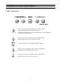
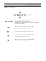
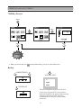
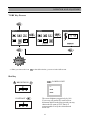
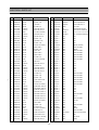
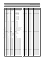
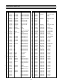
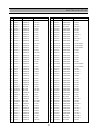
Service Manual
XGA COLOR MONITOR
Model : 719B-3/719BF-3
DAEWOO LUCOMS CO., LTD.
b
http://www.lucoms.com
July, 2003
CONTENTS
SAFETY PRECAUTIONS
1
GENERAL SAFETY INFORMATION
2
SERVICING PRECAUTIONS
3
TECHNICAL INFORMATION
6
GENERAL INFORMATION
7
PIN CONNECTOR
8
CAUTIONS FOR ADJUSTMENT AND REPAIR
8
OPERATION AND ADJUSTMENT
9
ALIGNMENT PROCEDURE
15
TROUBLESHOOTING HINTS
17
BLOCK DIAGRAM
32
SCHEMATIC DIAGRAM
33
EXPLODED VIEW & MECHANICAL PARTS LIST
34
INFORMATION OF PART DESCRIPTION
36
ELECTRICAL PARTS LIST
37
SAFETY PRECAUTIONS
CAUTION: No modifications of any circuits should be attempted. Service work should be performed
only after you are thoroughly familiar with all of the following safety checks and servicing
guidelines.
◆ Safety Check
Care should be taken while servicing this analog color display because of the high voltages used in the
deflection circuits. These voltages are exposed in such areas as the associated flyback and yoke circuits.
◆ Fire & Shock Hazard
• Insert an isolation transformer between the analog color display and AC power line before servicing the
chassis.
• When servicing, pay close attention to the original lead dress especially in the high voltage circuit area;
if a short circuit is found, replace all parts which have been overheated as a result of the short circuit.
• All the protective devices must be reinstalled per original design.
• Soldering must be inspected for possible cold solder points, frayed leads, damaged insulation, solder
splashes or sharp solder points. Be certain to remove all foreign materials.
◆ Implosion Protection
Picture tube in this monitor employs intergral implosion protection system, but care should be taken to
avoid damage and scratching during installation.
Only use same type replacement picture tubes.
IMPORTANT SAFETY NOTICE: There are special components used in this analog color display,
which are important for safety. These parts are shaded on the
schematic diagram and on the replacement parts list. It is essential
that these critical parts should be replaced with manufacturer’s
specified parts to prevent X-Ray, shock, fire or other hazards. Do
not modify the original design without getting written permission
from DAEWOO LUCOMS CO., LTD. or this will void the original
parts and labor warranty.
◆ X-Ray
WARNING: The only potential source of X-Ray is the picture tube. However when the high voltage
circuitry is operating properly, there is no possibility of an X-Ray problem. The basic
precaution which must be exercised is to keep the high voltage at the following factory
recommended level.
NOTE: It is important to use an accurate, periodically, calibrated high voltage meter.
• To measure the high voltage, use a high-impedance high-voltage meter.
Connect(-) to chassis and (+) to the CRT anode button.
• Set the Contrast & Brightness Control to the minimum on OSD Menu.
• Measure the high voltage. The high voltage meter should indicate the following factory
recommended levels.
• If the upper meter indication exceeds the maximum level, immediate service is required to
prevent the possibility of premature component failure.
• To prevent X-Ray possibility, it is essential to use the specified picture tube.
• The normal high voltage is 25.5KV or below and must not exceed 29KV at zero beam current
at rated voltage.
1
GENERAL SAFETY INFORMATION
◆ Terms in the manual
CAUTION
Statements identify conditions or practices that could result in damage to the equipment or
other property.
WARNING Statements identify conditions or practices that could result in personal injury or loss of
life.
◆ Terms as marked on equipment
CAUTION
Statements indicate a personal injury hazard not immediately accessible as one reads the
marking or a hazard which is properly included on the equipment itself.
WARNING Statements are clearly concerning indicated personal injury hazards.
◆ Symbols in the manual
The symbols indicate where applicable cautionary or other information is to be found.
◆ Symbols as marked on equipment
Protective GROUND terminal
◆ High Voltage Warning
And Critical Component Warning Label
The following warning label is on the CRT PWB shield case inside the unit.
Warning: This product includes critical mechanical and electrical parts which are essential for x ray
protection. For continued safety, replace critical components that are indicated in the service
manual with exact replacement parts given in the parts list.
Operating high voltage with this product is 29Kv at minimum brightness. Refer to service
manual for measurement procedures and proper service adjustments.
2
SERVICING PRECAUTIONS
CAUTION: Before servicing instruments covered by this service manual, its supplements, and
addendum, please read and follow the SAFETY PRECAUTIONS of this manual.
NOTE: If unforeseen circumstances create conflict between the following servicing precautions and any
of the safety precautions on page 1 of this manual, always follow the safety precautions.
Remember: Safety First.
◆ General Servicing Precautions
1. Always unplug the AC power cord from the AC power source before:
a. Removing or reinstalling any component, circuit board, module, or any other instrument assembly.
b. Disconnecting or reconnecting any electrical plug or other electrical connection.
c. Connecting a test substitute in parallel with an electrolytic capacitor in the instrument.
CAUTION: A wrong part substitution or incorrect polarity installation of electrolytic capacitors
may result in a explosion.
d. Discharging the picture tube anode.
2. Test high voltage only by measuring it with an appropriate high voltage meter or other voltage
measuring device (DVM, FETVOM. etc.) equipped with a suitable high voltage probe. Do not test high
voltage by “drawing an arc”.
3. Discharge the picture tube anode only by: (a) first connecting one end of an insulated clip lead to the
degaussing or line grounding system shield at the point where the picture tube socket ground lead is
connected, and then (b) touching the other end of the insulated clip lead to the picture tube anode
button, using an insulating handle to avoid personal contact with high voltage.
4. Do not any spray chemicals on or near this instrument, or any of its assemblies.
5. Unless otherwise specified in this service manual, only clean electrical contacts by applying the
following mixture to the contacts with a pipe cleaner, cotton-tipped stick, or comparable nonabrasive
applicator: 10% (by volume) Aceton and 90% (by volume) isopropyl alchohol (90%-99% strength).
CAUTION: This is a flammable mixture. Unless specified in this service manual, lubrication of
contacts is not required.
6. Do not damage any plug/socket B+ voltage interlocks with which instruments covered by this service
manual might be equipped.
7. Do not apply AC power to this instrument and/or any other of its electrical assemblies unless all the
solid-state device heat sinks are correctly installed.
8. Always connect the test instrument ground lead to the appropriate instrument chassis ground before
connecting the test instrument positive lead. Always remove the test instrument ground lead last.
9. Only use the test fixtures specified in this service manual with this instrument.
CAUTION: Do not connect the test fixture ground strap to any heatsink in this instrument.
3
SERVICING PRECAUTIONS
◆ Electrostatically Sensitive (ES) Devices
Some semiconductor (solid state) devices can be damaged easily by static electricity.
Such components are commonly called Electrostatically Sensitive (ES) Devices.
The typical examples of ES devices are integrated circuits, some field-effect transistors, and
semiconductor “chip” components. The following techniques should be used to help reduce the incidence
of component damage caused by static electricity.
1. Immediately before handling any semiconductor component or semiconductor-equipped assembly,
wipe off any electrostatic charge on your body by touching any known earth ground. Alternatively,
obtain and wear a commercially available discharging wrist strap device which should be removed for
potential shock reasons prior to applying power to the unit under testing conditions.
2. After removing the electrical assembly equipped with ES devices, place the assembly on a conductive
surface such as aluminum foil to prevent electrostatic charge buildup or exposure to the assembly.
3. Only use a grounded-tip soldering iron to solder or unsolder ES devices.
4. Only use an anti-static type solder removal device. Some solder removal devices not classified as “antistatic” can generate enough electrical charges to damage ES devices.
5. Do not use freon-propelled chemicals. These can generate enough electrical charges to damage ES devices.
6. Do not remove a replacement ES device from its protective package until immediately before you are
ready to install it. (Most replacement ES devices are packaged with leads electrically shorted together
by conductive foam, aluminum foil, or comparable conductive material).
7. Immediately before removing the protective material from the leads of replacement ES devices, touch
the protective material to the chassis or circuit assembly into which the device will be installed.
CAUTION: Be sure that no power is applied to the chassis or circuit, and observe all other safety
precautions.
8. Minimize bodily movements when handling unpackaged replacement ES devices. (Otherwise harmful
motion such as the brushing together clothes fabric or the lifting your foot from a carpeted floor can
generate enough static electricity to damage ES devices).
◆ General Soldering Guidelines
1. Use a grounded-tip, low-wattage soldering iron with appropriate tip size and shape that will maintain
tip temperature between a 550°F-660°F (288°C-316°C) range.
2. Use an appropriate gauge of RMA resin-core solder composed of 60 parts tin/40 parts lead.
3. Keep the soldering iron tip clean.
4. Throughly clean the surface to be soldered. Use a small wire-bristle (0.5 inch or 1.25cm) brush with a
metal handle. Do not use freon-propelled spray-on cleaners.
5. Use the following soldering technique:
a. Allow the soldering iron tip to reach normal temperature (550°F to 660°F or 288°C to 316°C)
b. Hold the soldering iron tip and solder strand against the component lead until the solder melts.
c. Quickly move the soldering iron tip to the junction of the component lead and the printed circuit foil,
and hold it there until the solder flows onto and around both the component lead and the foil.
d. Closely inspect the solder area and remove any excess or splashed solder with a small wire-bristle brush.
CAUTION: Work quickly to avoid overheating the circuit board printed foil.
4
SERVICING PRECAUTIONS
FIGURE 1. USE SOLDERING IRON TO PRY LEADS
◆ IC Removal/Replacement
Some utilized chassis circuit boards have slotted (oblong) holes through which the IC leads are inserted
and then bent flat against the circuit foil. When holes are slotted, the following technique should be used
to remove and replace the IC. When working with boards using the familiar round hole, use the standard
technique as outlined in paragraphs 5 on the page under the title of general soldering guidelines.
◆ Removal
1. Desolder and straighten each IC lead in one operation by gently prying up on the lead with the
soldering iron tip as the solder melts.
2. Draw away the melted solder with an anti-static suction-type solder removal device (or with
desoldering braid before removing the IC.
◆ Replacement
1. Carefully insert the replacement IC in the circuit board.
2. Carefully bend each IC lead against the circuit foil pad and solder it.
3. Clean the soldered areas with a small wire-bristle brush. (lt is not necessary to reapply acrylic coating
to the area).
◆ “Small-Signal” Discrete Transistor Removal/Replacement
1. Remove the defective transistor by clipping its leads as close as possible to the component body.
2. Bend the ends of each of three leads remaining on the circuit board into a “U” shape.
3. Bend the replacement transistor leads into a “U” shape.
4. Connect the replacement transistor leads to the corresponding leads extending from the circuit board
and crimp the “U” with long nose pliers to ensure metal-to-metal contact, then solder each connection.
5
SERVICING PRECAUTIONS
◆ Power IC, Transistor or Devices Removal/Replacement
1. Heat and remove all solders from the device leads.
2. Remove the heatsink mounting screw (if applicable).
3. Carefully remove the device from the circuit board.
4. Insert new device in circuit board.
5. Solder each device lead and then clip off excess lead.
6. Replace heatsink.
◆ Diode Removal/Replacement
1. Remove defective diode by clipping its leads as close as possible to diode body.
2. Bend the two remaining leads perpendicularly to the circuit board.
3. Observing diode polarity, wrap each lead out of the new diode around the corresponding lead on the
circuit board.
4. Securely crimp each connection and solder it.
5. Inspect the solder joints of the two “original” leads on the circuit board copper side. If they are not
shiny, reheat them and apply additional solder if necessary.
TECHNICAL INFORMATION
Model
719B-3
719BF-3
CDT Size
17-inch
17-inch Flat
Diagonal visible image area
16.2-inch
16.01-inch
Dot Pitch
0.27 mm
0.24 mm
Synchronization
Horizontal
30 - 70 KHz
Vertical
50 - 160 Hz
Plug and Play
VESA DDC Compatible
Power Saving
EPA, VESA DPMS, Nutek Compliant
Power Source
100-240 Vac, 50/60Hz (Free Voltage)
Power Consumption
85W
Dimension-W x H x D
410 x 402 x 425mm
410 x 407 x 419mm
Weight-unpacked(lbs/Kg)
32.0/14.5
35.2/16
Operating Temperature
10 ~ 40°C /50 ~ 104°F
(set with stand)
6
GENERAL INFORMATION
This color monitor automatically scans all horizontal frequencies from 30KHz to 70KHz, and all vertical
frequencies from 50Hz to 160Hz. This color monitor supports IBM PC, PC/XT, PC/AT, personal
System/2 (PS/2), Apple Macintosh, and compatible users crisp text and vivid color graphics display when
using the following graphics adapters : (VGA, 8514/A, Super VGA, VESA and XGA and Apple
Macintosh Video Card). And so, this color monitor has a maximum horizontal resolution of 1280 dots and
a maximum vertical resolution of 1024 lines for superior clarity of display.
By accepting analog signal inputs which level is zero to 0.7 Volts. This color monitor can display and
unlimited palette of colors depending on the graphics adapter and software being used.
◆ Abbreviations
ADJ
AFC
CRT
Def
D.Y
FBT
H.SYNC
OSC
P.S.U
PWA
R.G.B
V.Sync
Adjustment
Automatic Frequency Control
Cathode Ray Tube
Deflection
Deflection Yoke
Flyback Transformer
Horizontal Synchronization
Oscillator
Power Supply Unit
Printed Circuit Board Wiring Assembly
Red, Green, Blue
Vertical Synchronization
7
PIN CONNECTOR
Pin
1
2
3
4
5
6
7
8
9
10
11
12
13
14
15
Signal
1
Red
Green
Blue
GND
GND
GND - Red
GND - Green
GND - Blue
+5Vdc(option)
GND - H.Sync
GND - V.Sync
Bi-directional Data (SDA)
Horizontal Sync
Vertical Sync (VCLK)
Data Clock (SCL)
6
10
15
Arrangement of 15-pin D-sub connector
CAUTIONS FOR ADJUSTMENT AND REPAIR
• Degaussing is always required when adjusting purity or convergence.
• The white balance adjustment has been done by a color analyzer in factroy. The adjustment procedure,
described in the service manual is made by a visual check.
• Allow 20 minutes warm-up time for the display before checking or adjusting only electrical
specification or function.
• Reform the leadwire after any repair work.
◆ Caution For Servicing
• In case of servicing or replacing CRT, high voltage sometimes remains in the anode of the CRT.
Completely discharge high voltage before servicing or replacing CRT to prevent a shock to the
serviceman.
8
OPERATION AND ADJUSTMENT
719B-3 Control Panel
POWER LIGHT
• Move cursor to the right window on the OSD window.
• Increase the value of any selected function.
• While the OSD screen is off, you can adjust the screen brightness
according to each situation.
•
•
Move cursor to the left window on the OSD window.
Decrease the value of any selected function.
•
Launch OSD(On-Screen Display) MENU window.
•
•
Move cursor to the high window on the OSD window.
Increase the value of V.size or V.center.
•
•
Move cursor to the low window on the OSD window.
Decrease the value of V.size or V.center.
9
OPERATION AND ADJUSTMENT
719BF-3 Control Panel
•
•
Move cursor to the right window on the OSD window.
Increase the value of any selected function.
• While the OSD screen is off, you can adjust the screen brightness
according to each situation.
•
•
Move cursor to the left window on the OSD window.
Decrease the value of any selected function.
•
Launch OSD(On-Screen Display) MENU window.
•
•
Move cursor to the high window on the OSD window.
Increase the value of V.size or V.center.
•
•
Move cursor to the low window on the OSD window.
Decrease the value of V.size or V.center.
10
OPERATION AND ADJUSTMENT
719B Key Process
MENU
MENU
MENU
MENU
OSD OFF
•
When you choose the icon
on the OSD window, you can exit the OSD screen.
Hot Key
BRIGHTNESS
POWER LIGHT
PC
GAME
MOVIE
CONTRAST
O
The screen brightens progressively by 10%.
If you carry out general PC works such as
document edition on the Movie mode,you may
shorten the life span of CRT. Thus,it is
recommended to verify the selected mode
before use.
11
OPERATION AND ADJUSTMENT
719BF Key Process
OSD OFF
•
When you choose the icon
on the OSD window, you can exit the OSD screen.
Hot Key
POWER LIGHT
BRIGHTNESS
PC
GAME
MOVIE
CONTRAST
The screen brightens progressively by 10%.
If you carry out general PC works such as
document edition on the Movie mode,you may
shorten the life span of CRT. Thus,it is
recommended to verify the selected mode
before use.
12
OPERATION AND ADJUSTMENT
OSD Functions
ICON
CONTROL
FUNCTIONS
PINCUSHION
Adjust the left and right margins for more convex or more concave margins.
TRAPEZOID
Adjust the trapezoid of the screen by moving the lines inward or outward.
PARALLELOGRAM Adjust the parallelogram when the screen is leaning left or right.
PIN BALANCE
Adjust the side balance when the sides of the screen are bowed towards left or right.
T. PIN CORNER Adjust the pin corner top when the top sides of the screen are bowed.
B. PIN CORNER Adjust the pin corner bottom when the bottom sides of the screen are bowed.
ROTATION
H. CENTER &
V. CENTER
Adjust the rotation when the screen is tilted left or right (719BF only).
Adjust the position of the display horizontally(left or right) and vertically (up or down).
COLOR TEMP
Choose different preset color temperatures or set your own customized color parameters.
RED GAIN
Adjust the red gain.
GREEN GAIN
Adjust the green gain.
BLUE GAIN
Adjust the blue gain.
H. SIZE &
V. SIZE
DEGAUSS
Adjust the width (horizontal size) and the height (vertical size) of the display.
Degauss the display and restore image quality.
13
OPERATION AND ADJUSTMENT
ICON
CONTROL
FUNCTIONS
STATUS
Display horizontal & vertical frequency and polarity.
H. MOIRE
Adjust the horizontal picture moire cancellation.
V. MOIRE
Adjust the vertical picture moire cancellation.
LANGUAGE
Select language for OSD (5 languages).
RECALL
Reset the screen to the Factory Preset Display Settings.
14
ALIGNMENT PROCEDURE
◆ Standard Adjustment Conditions
1. Power source voltage : AC 100~240V, 50/60Hz
2. Aging : Take at least 20 minutes warm-up time.
3. Signals.
Video : Analog 0.7Vpp 75Ω terminal positive polarity
Synchronizing : TTL Level Negative/Positive Separate/Composite
Deflection frequency
Horizontal Frequency : 30KHz - 70KHz
Vertical Frequency : 50Hz - 160Hz
◆ Pre-Adjustment
1. High Voltage Adjustment
Adjust 26K Vdc between Anode cap and ground at a cross hatch pattern of 60KHz by using the factory
mode.
◆ Method to launch the factory mode
Step 1. Turns off the monitor.
Step 2. Push the menu button and then push the power button at once.
◆ Main Adjustment
1. Setting the Controls
Set the value of items as following.
Contrast : Max. (OSD value up to 100)
Brightness : Center (Set the OSD value to 50)
2. H.size, V.size, H.phase, V.position, Pincushion, Trapezoid
Receive the cross hatch pattern of Factory preset mode.
H.size, V.size, H.phase, V.position, Pincushion, Trapezoid are adjusted at each mode.
In Factory, Auto Alignment was done at each mode. Therefore, Factory preset mode has it’s own value
according to each control.
3. Focus
(a) Set brightness control to center and contrast control to MAX.
(b) Receive all “H” character pattern of 60KHz mode signal.
(c) Adjust the Focus control of FBT to obtain best Focus (static focus and Dynamic focus).
4. Geometric Distortion Adjustment
(a) Receive the cross hatch pattern of VGA mode signal by using the signal generator.
(b) Pin balance, Parallelogram are adjusted the best geometric status.
(c) Repeat the adjustment at each mode.
5. White Balance Adjustment
(a) Receive a full white pattern of 60KHz mode.
(b) Set the bright control and contrast control to the maximum and receive the all black pattern.
(c) Select a Temperature function on the R, G, B item of the OSD menu and select 9300.
(d) If the screen luminosity is changed, adjust the sub brightness control to get the 0.6 ~ 0.8 Ft/L screen
luminosity.
(e) Select the R, G, B Bias on the OSD menu and adjust the
/
key to get the color coordinates in
X=0.281, Y=0.311.
(f) Set the brightness control to the maxium and contrast control to the maximum.
15
ALIGNMENT PROCEDURE
(g) Receive the small square white pattern about 50 x 50mm.
(h) Adjust the G-gain control to get the brightness to 50 Ft/L.
(i) Adjust the B-gain control to get the y cordinate to 0.311 ± 0.03.
(j) Adjust the R-gain control to get the x cordinate to 0.281 ± 0.03.
(k) Receive the full white pattern.
(l) Adjust the ABL control to get the brightness to 32 Ft/L.
6. Static Convergence Adjustment
(a) Apply a magenta cross hatch pattern on display.
(b) Adjust the focus from the best over all focus on the display.
Also adjust the brightness to the desired condition.
(c) Vertical red and blue lines are converged by varying the angles between the two tabs of the 4-pole
magnets.
(d) Horizontal red and blue lines are converged by varying the tabs together keeping the angle between
them constant.
(e) Apply a yellow cross hatch pattern on the display.
(f) Vertical green and red lines are converged by varying the angle between the two tabs of the 6-pole
magnets.
(g) Horizontal green and red lines are converged by varying the tabs together and keeping the angle
between them constant.
16
TROUBLESHOOTING HINTS
1. No Character
No Character
Are the
Contrast &
Brightness Controls
maximum
No
Change the Contrast &
Brightness control to
maximum
Yes
Is whole
screen bright?
No
No Raster
Refer to
No Raster
Yes
Is CRT
Cathode (Rk, Gk, Bk)
signal level
normal?
No
Is the
output signal of the
(pin 19,20,21) pre-amp
(IC201) normal?
Yes
Check the peripheral circuit
of CRT Board
Rk, Gk, Bk
About 40Vpp
Yes
Check the video output
(IC203) and their ambient
circuit
No
Trouble in 6.3Vdc line
of the Main PWB
No
Check the blanking pulse
circuit
No
Is 6.3Vdc line
normal?
Yes
Is blanking
pulse (pin 24 of IC201)
normal?
Yes
Is input signal
normal?
No
Yes
Trouble in IC201 and
its ambient circuit
17
Check the signal cable
TROUBLESHOOTING HINTS
2. No Raster
No Raster
Is CRT
heater red-hot?
Is Heater
Voltage (CRT PWB)
about 6V?
No
Yes
Yes
Trouble in
CRT
No
Trouble in
power supply
circuit
Turn the Brightness
& Contrast control
to set Maximum
Refer to trouble in
power supply unit.
Yes
Is whole
screen bright?
No
Trouble in power
supply circuit
No
Trouble in G1
line of Main PWB
No
Trouble in FBT or
peripheral circuit
No
Trouble in 77Vdc
line of power
supply unit
No
High Voltage
trouble in FBT
Yes
Check
G1 voltage about
-72V?
Yes
Is CRT
G2 (screen) voltage
about 450~
600V?
Yes
Is 77Vdc
line normal?
Yes
Does
turning the SubBrightness control to the
maximun on OSD menu
make screen
bright?
Yes
Trouble in FBT
18
Refer to trouble
in P.S.U
TROUBLESHOOTING HINTS
3. A Missing Color
One color is
missing
Is input signal
normal?
No
Check video signal
cable or video card.
No
Trouble in IC201 or its
ambient circuit
0.7Vpp
Yes
Is the
output of pre-amp
(IC201) pin 19,20,21
all normal?
Yes
CRT
No
Cathode (Rk, Gk, Bk)
is normal?
RK, GK, BK
About 40V p-p
Yes
Each grid (G1, G2)
voltage normal?
Is video
output IC(IC203)
normal?
No
Replace Video output IC
Yes
No
Trouble in 77Vdc line
Replace CRT
19
Yes
Trouble in
video output
circuit or
ambient
TROUBLESHOOTING HINTS
4. Horizontal Output Circuit
Trouble in Horizontal
output circuit
(No Raster
Is the
B+line voltage
over 54V?
No
Trouble in B+ Booster Circuit
(Check the B+section of IC501)
Yes
Is the H-out
waveform of IC501
normal?
11V
0V
No
Trouble in IC501
Yes
Is the Collector
waveform of
Q406 normal?
66V
Yes
Trouble in Q406 and
its ambient circuit.
20
No
Trouble in Q406 and its
ambient circuit.
TROUBLESHOOTING HINTS
5. Unstable Picture
5-1. Horizontal
Unstable
picture
Is H.Sync
input pin of IC501
correct?
No
Check H.Sync Out of
Micom or its ambient
circuits.
No
Check the value of
C402, R423.
Yes
Is the
pin 29 of IC501
12~13V?
Yes
Trouble in IC501.
21
TROUBLESHOOTING HINTS
5-2. Vertical
Unstable or
Abnormal picture
Is
13V DC line
correct?
No
Check PWR 13V
ambient circuit.
Yes
Check V.DY
and ambient circuit.
Yes
Check the IC301
or ambient circuit.
Yes
45Vp-p
Is
the output
waveform of IC301
(pin 5)
normal?
No
Is the
output pulse
of IC501 (pin 13)
normal?
No
Trouble in V.Sync line
or IC501 failure.
22
TROUBLESHOOTING HINTS
6. Focus
Monitor remains
unfocused
Check
Focus VR in
FBT
Is
focus
acceptable?
Yes
No
Trouble in Focus
circuit (FBT)
23
OK
TROUBLESHOOTING HINTS
6-1. Dynamic Focus
FVH FVV
* Check after adjusting the static focus
finely by VR in FBT
Focus is poor
ORION
: 300V 120V
SAMSUNG : 300V 120V
DF
waveform
FVH
FVV
Is the
waveform of the
DF pin in FBT
correct?
Yes
1. Check the CRT socket
or connector wire.
2. Trouble in FBT or CRT.
No
Is the
waveform of
the pin 32 in IC501
correct?
Yes
Trouble in Q901,T902,R903
24
No
Trouble in IC501 or C407.
TROUBLESHOOTING HINTS
7. Convergence
Poor convergence
Is
convergence
on the center area
bad?
Yes
Adjust static
convergence
Refer to
Adjustment
procedure of
convergence
No
Is
convergence on the
fringe area bad?
Yes
Adjust D.Y
Location
25
TROUBLESHOOTING HINTS
8. Abnormal Picture
8-1. Horizontal Size
Abnormal
H.Size
When
the H.Size on the
OSD is changed, is the
H.size changed?
No
Yes
It isn’t out of order.
26
Check pin 24 of IC501
and its ambient circuit
TROUBLESHOOTING HINTS
8-2. Vertical Size
Abnormal
V.Size
Is
changeable the
DC voltage of
IC301 pin 5?
No
Is
the 3.5Vdc of pin
23 of the IC501?
No
Yes
Trouble V.OSC/
Deflection Circuit
Check the pin 23 of IC501
and its ambient circuit
Refer to V.OSC/Deflection circuit
27
Yes
Check the IC301
and its
ambient circuit
TROUBLESHOOTING HINTS
9. High Voltage Output Circuit
Trouble in H.V circuit
(No Raster)
Is
B+(54V) line
voltage normal?
No
Trouble in power
supply circuit.
Yes
Trouble in FBT.
Yes
Trouble in IC501
ambient circuit.
Yes
Trouble in IC501
ambient circuit.
Yes
Is Q407
collector waveform
normal?
No
Is IC501
pin 26
normal?
No
Is the
IC501 pin 1 H.trigger
correct?
No
Trouble in H.trigger.
28
TROUBLESHOOTING HINTS
10. Side-Pincushion Circuit
Side-Pincusion distortion
is excessive or barrel
Select the
side-pincushion
icon on OSD menu,
and adjust acceptable
position.
Yes
O.K
No
Is the pin 11
waveform of IC501
correct?
Yes
Check IC501or
their ambient circuit
Yes
Check IC501 or
it’s ambient circuit.
No
Is the
waveform of IC501
pin 14,15?
No
Trouble in H.Size
29
TROUBLESHOOTING HINTS
11. Power Supply Unit (P.S.U)
Trouble in P.S.U
Is
power switch
on?
No
Switch on
Yes
Is
fuse F001
O.K?
No
Check the power cord outlet
and diode D001, D002,
D003, D004, Q001
No
Trouble in D001, D002,
D003, D004, C004 and
TH001.
Yes
Is
voltage of T001
pin 8 130V
(370V)?
Yes
Is the
waveform of Q001
Drain pin
correct?
400Vpp (620Vpp)
No
Trouble in T001, IC001, Q001
and D009 etc.
Yes
Is
voltage of C822
54Vdc?
No
Trouble in D810 or
its ambient circuit
Yes
Is
voltage of C825
77Vdc?
No
Trouble in D813 or
Video Part
Yes
Is
voltage of C824
8Vdc?
No
A
30
Trouble in D812
TROUBLESHOOTING HINTS
A
Is voltage
of C827 13Vdc?
No
Trouble in D814 or
horizontal part
No
Trouble in D908 or
FBT part.
Yes
Is
voltage of C908
-12Vdc?
Yes
P.S.U O.K
31
BLOCK DIAGRAM
719B-3/719BF-3
32
SCHEMATIC DIAGRAM
719B-3/719BF-3
33
EXPLODED VIEW & MECHANICAL PARTS LIST
719B-3
719B
34
EXPLODED VIEW & MECHANICAL PARTS LIST
719BF-3
719B
35
INFORMATION OF PART DESCRIPTION
Important Safety Notice
Components identified with the International Symbol have special characteristics important for safety.
When replacing any components, use only manufacturer’s specified parts.
Abbreviation of Description
RESISTOR Description
Allowance
F
± 1%
J
± 5%
K
± 10%
M
± 20%
G
± 2%
Example:
Fig &
Index
Part No
Description
Resistors
RD-4Z820J
Carbon: 82J
RD-4Z201J
Carbon1/4W-200J
R101
R102
CAPACITOR Description
C
D
F
J
K
P
Z
Allowance
± 0.25pF
± 0.5%
± 1pF
± 5%
± 10%
± 100% ~ 0%
± 80% ~ –
Example:
Fig &
Index
C102
C402
C105
Part No
Description
Capacitors
CCXF1H104Z
Ceramic 50V 0.1µ F Z
CCXB1H331K
Ceramic 50V 330PF K
CMXM 2A224J MYLAR 100V 0.22µ F J
36
ELECTRICAL PARTS LIST
The components identified by mark ! have special characteristics important for safety and x-ray radiation.
These should be replaced only with the types specified in the parts list.
◆ Parts List for 719B-3
LOC
PART-CODE
BC005 5PB13857—
LOC
PART-CODE
COIL BEAD
PART-NAME
BI3857(AXIAL)
PART-DESC
C113
CMXM2A102J
C MYLAR
PART-NAME
100V 1000PF J (TP)
PART-DESC
BC201 5PB13857—
COIL BEAD
BI3857(AXIAL)
C114
CEXF1H109V
C ELECTRO
50V RSS 1MF (5X11) TP
BC202 5PB13857—
COIL BEAD
BI3857(AXIAL)
C115
CEXF1H479V
C ELECTRO
50V RSS 4.7MF (5X11) TP
BC203 5PB13857—
COIL BEAD
BI3857(AXIAL)
C204
CMXM2A104J
C MYLAR
100V 0.1MF J (TP)
BC204 5PB13857—
COIL BEAD
BI3857(AXIAL)
C205
CMXM2A104J
C MYLAR
100V 0.1MF J (TP)
BC205 5PB13857—
COIL BEAD
BI3857(AXIAL)
C206
CMXM2A102J
C MYLAR
100V 1000PF J (TP)
BC206 5PB13857—
COIL BEAD
BI3857(AXIAL)
C207
CMXM2A472J
C MYLAR
100V 4700PF J (TP)
BC207 5PB13857—
COIL BEAD
BI3857(AXIAL)
C209
CCXB1H471K
C CERA
50V B 470PF K (TAPPING)
BC208 5PB13857—
COIL BEAD
BI3857(AXIAL)
C210
CEXF1C470V
C ELECTRO
16V RSS 47MF (5X11) TP
BC209 5PB13857—
COIL BEAD
BI3857(AXIAL)
C211
CCXF1H103Z
C CERA
50V F 0.01MF Z (TAPPING)
BC210 5PB13857—
COIL BEAD
BI3857(AXIAL)
C212
CCXF1H103Z
C CERA
50V F 0.01MF Z (TAPPING)
BC401 5PB13890—
COIL BEAD
BI3890
C222
CEXF1C470V
C ELECTRO
16V RSS 47MF (5X11) TP
BC402 5PB13890—
COIL BEAD
BI3890
C223
CCXF1H103Z
C CERA
50V F 0.01MF Z (TAPPING)
BC403 5PB13857—
COIL BEAD
BI3857(AXIAL)
C226
CEXD2A109F
C ELECTRO
100V RND 1MF(5*11) TP
BC404 5PB13857—
COIL BEAD
BI3857(AXIAL)
C228
CCXB2H102K
C CERA
500V B 1000PF K (TAPPING)
BC801 5PB13890—
COIL BEAD
BI3890
C229
CEXD2A109F
C ELECTRO
100V RND 1MF(5*11) TP
BC802 5PB13890—
COIL BEAD
BI3890
C232
CEXD2A109F
C ELECTRO
100V RND 1MF(5*11) TP
BC901 5PB13890—
COIL BEAD
BI3890
C234
CCXB3D102K
C CERA
2KV B 1000PF K (TAPPING)
C LINE ACROSS
WORLD AC250V 0.1UF M R.47
C235
CMXM2A103J
C MYLAR
100V 0.01MF J (TP)
! C001
CL1UC3104M
C002
CEYP2G221Z
C ELECTRO
400V SMH 220MF (25.4*40)
C236
CEXF2A100V
C ELECTRO
100V RSS 10MF (6.3X11) TP
C005
CEXF1E101V
C ELECTRO
25V RSS 100MF (6.3X11) TP
C242
CCXF1H103Z
C CERA
50V F 0.01MF Z (TAPPING)
C006
CMXM2A103J
C MYLAR
100V 0.01MF J (TP)
C243
CMXM2A103J
C MYLAR
100V 0.01MF J (TP)
C007
CCXB2H472K
C CERA
500V B 4700PF K (TAPPING)
C244
CMXM2A103J
C MYLAR
100V 0.01MF J (TP)
C008
CCXF1H103Z
C CERA
50V F 0.01MF Z (TAPPING)
C245
CMXM2A103J
C MYLAR
100V 0.01MF J (TP)
C010
CMXM2A682J
C MYLAR
100V 6800PF J (TP)
C246
CMXM2A103J
C MYLAR
100V 0.01MF J (TP)
C012
CMXM2A272J
C MYLAR
100V 2700PF J (TP)
C249
CMXM2A103J
C MYLAR
100V 0.01MF J (TP)
C013
CCXB1H681K
C CERA
50V B 680PF K (TAPPING)
C250
CCXF1H103Z
C CERA
50V F 0.01MF Z (TAPPING)
C014
CCXB3A221K
C CERA
1KV B 220PF K (TAPPING)
C251
CCXF1H103Z
C CERA
50V F 0.01MF Z (TAPPING)
C018
CMXM2A224J
C MYLAR
100V 0.22MF J
C252
CCXF1H103Z
C CERA
50V F 0.01MF Z (TAPPING)
C020
CMXM2A332J
C MYLAR
100V 3300PF J (TP)
C260
CCXF1H103Z
C CERA
50V F 0.01MF Z (TAPPING)
C024
CH1FDF222M
C CERA AC
2.5KV 2200PF M AC250V
C263
CCXF1H103Z
C CERA
50V F 0.01MF Z (TAPPING)
! C025
! C026
CH1FDF222M
C CERA AC
2.5KV 2200PF M AC250V
C264
CCXF1H103Z
C CERA
50V F 0.01MF Z (TAPPING)
CH1FDF222M
C CERA AC
2.5KV 2200PF M AC250V
C281
CEXF1H109V
C ELECTRO
50V RSS 1MF (5X11) TP
! C027
CL1UC3104M
C LINE ACROSS
WORLD AC250V 0.1UF M R.47
C302
CMXM2A102J
C MYLAR
100V 1000PF J (TP)
C101
CCXF1H103Z
C CERA
50V F 0.01MF Z (TAPPING)
C303
CEXF1C102V
C ELECTRO
16V RSS 1000MF (10X20) TP
C102
CEXF1C101V
C ELECTRO
16V RSS 100MF (6.3X11) TP
C304
CMXM2A472J
C MYLAR
100V 4700PF J (TP)
C103
CMXM2A102J
C MYLAR
100V 1000PF J (TP)
C305
CEXF1V101V
C ELECTRO
35V RSS 100MF (8X11.5) TP
C104
CCXB1H221K
C CERA
50V B 220PF K (TAPPING)
C307
CMXM2A224J
C MYLAR
100V 0.22MF J
C105
CCXF1H103Z
C CERA
50V F 0.01MF Z (TAPPING)
C308
CEXF1C471V
C ELECTRO
16V RSS 470MF (8X12)TP
C106
CCXF1H103Z
C CERA
50V F 0.01MF Z (TAPPING)
C309
CMXM2A473J
C MYLAR
100V 0.047MF J (TP)
C107
CCXF1H103Z
C CERA
50V F 0.01MF Z (TAPPING)
C401
CCXF1H104Z
C CERA
50V F 0.1MF Z
C108
CEXF1H479V
C ELECTRO
50V RSS 4.7MF (5X11) TP
C402
CEXF1C221V
C ELECTRO
16V RSS 220MF (8X11.5) TP
C109
CEXF1H479V
C ELECTRO
50V RSS 4.7MF (5X11) TP
C403
CMXM2A154J
C MYLAR
100V 0.15MF J (TP)
C110
CCXF1H104Z
C CERA
50V F 0.1MF Z
C404
CMXL1J474J
C MYLAR
63V MEU 0.47MF J
C112
CXCH1H560J
C CERA
50V CH 56PF J (TAPPING)
C405
CEXF1C470V
C ELECTRO
16V RSS 47MF (5X11) TP
37
ELECTRICAL PARTS LIST
LOC
PART-CODE
PART-NAME
C407
CMXM2A104J
C MYLAR
C408
CMXM2A472J
C MYLAR
C409
CMXD2A821J
C410
C411
PART-DESC
LOC
PART-CODE
PART-NAME
PART-DESC
100V 0.1MF J (TP)
C913
CMXM2A102J
C MYLAR
100V 1000PF J (TP)
100V 4700PF J (TP)
C915
CEXF1C471V
C ELECTRO
16V RSS 470MF (8X12)TP
C MYLAR
KD 100V 820PF J
C916
CEXF1C470V
C ELECTRO
16V RSS 47MF (5X11) TP
CMXM2A103J
C MYLAR
100V 0.01MF J (TP)
C917
CCXF1H104Z
C CERA
50V F 0.1MF Z
CEXF1H479V
C ELECTRO
50V RSS 4.7MF (5X11) TP
CDT
9979617037
CDT
M41KXU100XX021 (5X10(5))
C412
CEXF1H479V
C ELECTRO
50V RSS 4.7MF (5X11) TP
CGND 9970710289
CRT GND AS
0.12*16*5+BL101+1015#22=730
C413
CCXF1H103Z
C CERA
50V F 0.01MF Z (TAPPING)
CN101 99707D0007
CONN AS
SMH200-09/04+YBNH200-14+CORE+1007#26=260
C414
CEXF1C470V
C ELECTRO
16V RSS 47MF (5X11) TP
CN201 9970710288
CONN ASS’Y
101R+1310+CORE+1032#22=250
C421
CEXF1H109V
C ELECTRO
50V RSS 1MF (5X11) TP
C422
CMXM2A332J
C MYLAR
C424
CMXE2J682J
C MYLAR
C426
CMXM2A102J
C MYLAR
C428
CCXB2H151K
C CERA
C429
CMYF2E684J
C MYLAR
C431
CMXM2A472J
C MYLAR
C433
CMYF2E105J
C434
CMXF2G394J
C437
DRL205——
DIODE
RL205
100V 3300PF J (TP)
! D001
! D002
DRL205——
DIODE
RL205
PL 630V 6800PF J (TP)
! D003
DRL205——
DIODE
RL205
100V 1000PF J (TP)
! D004
DRL205——
DIODE
RL205
500V B 150PF K (TAPPING)
D007
D1N4937GP-
DIODE
1N4937GP (TAPPING)
250V MPP 0.68MF J
D008
DZN4148—-
DIODE
1N4148 AUTO 52MM
100V 4700PF J (TP)
D009
D1N4935GP-
DIODE
1N4935GP
C MYLAR
MPP 250V 1MF J
D101
DZN4148—-
DIODE
1N4148 AUTO 52MM
C MYLAR
MPP 400V 0.39MF J
D104
DZN4148—-
DIODE
1N4148 AUTO 52MM
CMXF2E224J
C MYLAR
MPP 250V 0.22MF J
D105
DZN4148—-
DIODE
1N4148 AUTO 52MM
C438
CMXM2A103J
C MYLAR
100V 0.01MF J (TP)
D108
DZN4148—-
DIODE
1N4148 AUTO 52MM
C440
CXCH1H100D
C CERA
50V CH 10PF D (TAPPING)
D109
DZN4148—-
DIODE
1N4148 AUTO 52MM
C441
CMXL1J105J
C MYLAR
63V MEU 1MF J
D201
DBAV20——
DIODE
BAV20
C442
CEXF1H479V
C ELECTRO
50V RSS 4.7MF (5X11) TP
D202
DBAV20——
DIODE
BAV20
C443
CMXM2A223J
C MYLAR
100V 0.022MF J TP
D203
DBAV20——
DIODE
BAV20
C444
CEXF1C471V
C ELECTRO
16V RSS 470MF (8X12)TP
D204
DBAV20——
DIODE
BAV20
C445
CEXF1H479V
C ELECTRO
50V RSS 4.7MF (5X11) TP
D205
DBAV20——
DIODE
BAV20
C508
CEXF1H479V
C ELECTRO
50V RSS 4.7MF (5X11) TP
D206
DBAV20——
DIODE
BAV20
C509
CMXM2A103J
C MYLAR
100V 0.01MF J (TP)
D207
DZN4148—-
DIODE
1N4148 AUTO 52MM
C511
CMXM2A102J
C MYLAR
100V 1000PF J (TP)
D208
DZN4148—-
DIODE
1N4148 AUTO 52MM
C512
! C521
CMXM2A222J
C MYLAR
100V 2200PF J (TP)
D209
DZN4148—-
DIODE
1N4148 AUTO 52MM
CMYH3E562J
C MYLAR
BUP 2.5KV 5600PF J BULK
D210
DZN4148—-
DIODE
1N4148 AUTO 52MM
C541
CMXM2A473J
C MYLAR
100V 0.047MF J (TP)
D211
DZN4148—-
DIODE
1N4148 AUTO 52MM
C821
CCXB2H151K
C CERA
500V B 150PF K (TAPPING)
D212
DZN4148—-
DIODE
1N4148 AUTO 52MM
C822
CEXF2A221V
C ELECTRO
100V RSS 220MF (16X25) TP
D213
DBAV20——
DIODE
BAV20
C824
CEXF1C102V
C ELECTRO
16V RSS 1000MF (10X20) TP
D214
DBAV20——
DIODE
BAV20
C825
CEXF2A470V
C ELECTRO
100V RSS 47MF (10X16) TP
D215
DBAV20——
DIODE
BAV20
C827
CEXF1E471V
C ELECTRO
25V RSS 470MF (10X16) TP
D301
D1N4002A—
DIODE
1N4002
C828
CEXF1C101V
C ELECTRO
16V RSS 100MF (6.3X11) TP
D405
DZN4148—-
DIODE
1N4148 AUTO 52MM
C836
CEXF1C101V
C ELECTRO
16V RSS 100MF (6.3X11) TP
D406
DERD07-15-
DIODE
ERD07-15
C839
CEXF1C221V
C ELECTRO
16V RSS 220MF (8X11.5) TP
D407
DZN4148—-
DIODE
1N4148 AUTO 52MM
C901
CCXB2H151K
C CERA
500V B 150PF K (TAPPING)
D408
DDMV1500L-
DIODE
DMV-1500L
C902
CMXE2E123J
C MYLAR
PL 250V 0.012MF J
D410
DUF1G——-
DIODE
UF1G
C903
CMXM2A222J
C MYLAR
100V 2200PF J (TP)
D411
DZN4148—-
DIODE
1N4148 AUTO 52MM
C904
CMXM2A473J
C MYLAR
100V 0.047MF J (TP)
D413
D1N4004—-
DIODE
1N4004
C905
CCXB3A472K
C CERA
1KV B 4700PF K (TAPPING)
D560
D1N4935GP-
DIODE
1N4935GP
C906
CEXF2V109V
C ELECTRO
350V RSS 1MF(8*11.5)
D801
DZN4148—-
DIODE
1N4148 AUTO 52MM
C907
CEXF2C479V
C ELECTRO
160V RSS 4.7MF (8X16) TP
D803
85801065GY
WIRE COPPER
AWG22 1/0.65 TIN COATING
D31DF4——
DIODE
31DF4
DUG2D——-
DIODE
UG2D 200V 2A
DGUF10M—-
DIODE
GUF10M
C908
CEXD1H478F
C ELECTRO
50V RND 0.47MF (5X11) TP
! D810
C909
CCXB2H102K
C CERA
500V B 1000PF K (TAPPING)
C910
CEXF1H479V
C ELECTRO
50V RSS 4.7MF (5X11) TP
! D812
! D813
38
ELECTRICAL PARTS LIST
LOC
PART-CODE
PART-NAME
! D814
DUG2D——-
DIODE
D816
85801065GY
WIRE COPPER
D901
DUG1D——-
DIODE
D903
D1N4937GP-
D904
D1N4937GP-
D905
PART-DESC
LOC
PART-CODE
PART-NAME
PART-DESC
UG2D 200V 2A
J021
85801065GY
WIRE COPPER
AWG22 1/0.65 TIN COATING
AWG22 1/0.65 TIN COATING
J022
85801065GY
WIRE COPPER
AWG22 1/0.65 TIN COATING
UG1D
J023
85801065GY
WIRE COPPER
AWG22 1/0.65 TIN COATING
DIODE
1N4937GP (TAPPING)
J024
85801065GY
WIRE COPPER
AWG22 1/0.65 TIN COATING
DIODE
1N4937GP (TAPPING)
J025
85801065GY
WIRE COPPER
AWG22 1/0.65 TIN COATING
DZN4148—-
DIODE
1N4148 AUTO 52MM
J026
85801065GY
WIRE COPPER
AWG22 1/0.65 TIN COATING
D906
DZN4148—-
DIODE
1N4148 AUTO 52MM
J028
85801065GY
WIRE COPPER
AWG22 1/0.65 TIN COATING
D907
DRP1H——-
DIODE
RP1H
J029
85801065GY
WIRE COPPER
AWG22 1/0.65 TIN COATING
D908
DZN4148—-
DIODE
1N4148 AUTO 52MM
J030
85801065GY
WIRE COPPER
AWG22 1/0.65 TIN COATING
D911
DZN4148—-
DIODE
1N4148 AUTO 52MM
J031
85801065GY
WIRE COPPER
AWG22 1/0.65 TIN COATING
D912
DZN4148—-
DIODE
1N4148 AUTO 52MM
J032
85801065GY
WIRE COPPER
AWG22 1/0.65 TIN COATING
D913
DZN4148—-
DIODE
1N4148 AUTO 52MM
J033
85801065GY
WIRE COPPER
AWG22 1/0.65 TIN COATING
D915
DUG1D——-
DIODE
UG1D
J034
85801065GY
WIRE COPPER
AWG22 1/0.65 TIN COATING
DG001 5MG0000071
COIL DEGAUSSING
DG-719BW-TG
J035
85801065GY
WIRE COPPER
AWG22 1/0.65 TIN COATING
E1
9977916901
EYE LET
BSR T0.2 (R2.0)
J036
85801065GY
WIRE COPPER
AWG22 1/0.65 TIN COATING
E2
9977916901
EYE LET
BSR T0.2 (R2.0)
J037
85801065GY
WIRE COPPER
AWG22 1/0.65 TIN COATING
E3
9977916901
EYE LET
BSR T0.2 (R2.0)
J039
85801065GY
WIRE COPPER
AWG22 1/0.65 TIN COATING
E4
9977916901
EYE LET
BSR T0.2 (R2.0)
J040
85801065GY
WIRE COPPER
AWG22 1/0.65 TIN COATING
E5
9977916901
EYE LET
BSR T0.2 (R2.0)
J041
85801065GY
WIRE COPPER
AWG22 1/0.65 TIN COATING
EMI1
9970710291
CONN AS
0.12*3*16(P)+35072-9712+250REC-1=130
J042
85801065GY
WIRE COPPER
AWG22 1/0.65 TIN COATING
EMI2
9970710292
CONN AS
0.12*3*16(P)+35072-0910=110
J043
85801065GY
WIRE COPPER
AWG22 1/0.65 TIN COATING
EMI4
9970710279
CONN AS
35068-9812+0.16*3*16+35072-9712=200
J044
85801065GY
WIRE COPPER
AWG22 1/0.65 TIN COATING
! F001
5FSPS3152L
FUSE
SR-5 3.15A 250V (RADIAL)
J045
85801065GY
WIRE COPPER
AWG22 1/0.65 TIN COATING
IC001 1KA3842B—
IC POWER
KA3842B
J046
85801065GY
WIRE COPPER
AWG22 1/0.65 TIN COATING
IC101 1S3F8647—
IC MICOM
S3F8647
J047
85801065GY
WIRE COPPER
AWG22 1/0.65 TIN COATING
IC102 1CAT24WC8P
IC EEPROM
CAT24WC08P
J048
85801065GY
WIRE COPPER
AWG22 1/0.65 TIN COATING
! IC201 1LM12371—
IC VIDEO PREAMP
LM1237 BDBC/NA
J050
85801065GY
WIRE COPPER
AWG22 1/0.65 TIN COATING
IC203 1LM2445—-
IC VIDEO OUTPUT
LM2445
J051
85801065GY
WIRE COPPER
AWG22 1/0.65 TIN COATING
IC204 1LM2480—-
IC VIDEO CLAMP
LM2480
J052
85801065GY
WIRE COPPER
AWG22 1/0.65 TIN COATING
IC301 1STV9302A-
IC V-OUT
STV9302A
J053
85801065GY
WIRE COPPER
AWG22 1/0.65 TIN COATING
! IC501 1STV6888—
IC H-OSC
STV6888
J054
85801065GY
WIRE COPPER
AWG22 1/0.65 TIN COATING
J001
85801065GY
WIRE COPPER
AWG22 1/0.65 TIN COATING
J055
85801065GY
WIRE COPPER
AWG22 1/0.65 TIN COATING
J002
85801065GY
WIRE COPPER
AWG22 1/0.65 TIN COATING
J056
85801065GY
WIRE COPPER
AWG22 1/0.65 TIN COATING
J003
85801065GY
WIRE COPPER
AWG22 1/0.65 TIN COATING
J057
85801065GY
WIRE COPPER
AWG22 1/0.65 TIN COATING
J004
85801065GY
WIRE COPPER
AWG22 1/0.65 TIN COATING
J058
85801065GY
WIRE COPPER
AWG22 1/0.65 TIN COATING
J005
85801065GY
WIRE COPPER
AWG22 1/0.65 TIN COATING
J059
85801065GY
WIRE COPPER
AWG22 1/0.65 TIN COATING
J007
85801065GY
WIRE COPPER
AWG22 1/0.65 TIN COATING
J060
85801065GY
WIRE COPPER
AWG22 1/0.65 TIN COATING
J008
85801065GY
WIRE COPPER
AWG22 1/0.65 TIN COATING
J061
85801065GY
WIRE COPPER
AWG22 1/0.65 TIN COATING
J009
85801065GY
WIRE COPPER
AWG22 1/0.65 TIN COATING
J063
85801065GY
WIRE COPPER
AWG22 1/0.65 TIN COATING
J010
85801065GY
WIRE COPPER
AWG22 1/0.65 TIN COATING
J064
85801065GY
WIRE COPPER
AWG22 1/0.65 TIN COATING
J011
85801065GY
WIRE COPPER
AWG22 1/0.65 TIN COATING
J065
85801065GY
WIRE COPPER
AWG22 1/0.65 TIN COATING
J012
85801065GY
WIRE COPPER
AWG22 1/0.65 TIN COATING
J066
85801065GY
WIRE COPPER
AWG22 1/0.65 TIN COATING
J013
85801065GY
WIRE COPPER
AWG22 1/0.65 TIN COATING
J067
85801065GY
WIRE COPPER
AWG22 1/0.65 TIN COATING
J014
85801065GY
WIRE COPPER
AWG22 1/0.65 TIN COATING
J068
85801065GY
WIRE COPPER
AWG22 1/0.65 TIN COATING
J016
85801065GY
WIRE COPPER
AWG22 1/0.65 TIN COATING
J069
85801065GY
WIRE COPPER
AWG22 1/0.65 TIN COATING
J017
85801065GY
WIRE COPPER
AWG22 1/0.65 TIN COATING
J201
85801065GY
WIRE COPPER
AWG22 1/0.65 TIN COATING
J018
85801065GY
WIRE COPPER
AWG22 1/0.65 TIN COATING
J202
85801065GY
WIRE COPPER
AWG22 1/0.65 TIN COATING
J019
85801065GY
WIRE COPPER
AWG22 1/0.65 TIN COATING
J203
85801065GY
WIRE COPPER
AWG22 1/0.65 TIN COATING
J020
85801065GY
WIRE COPPER
AWG22 1/0.65 TIN COATING
J204
85801065GY
WIRE COPPER
AWG22 1/0.65 TIN COATING
39
ELECTRICAL PARTS LIST
LOC
PART-CODE
PART-NAME
J205
85801065GY
WIRE COPPER
J206
85801065GY
WIRE COPPER
J207
85801065GY
J208
J209
PART-DESC
LOC
PART-CODE
PART-NAME
PART-DESC
AWG22 1/0.65 TIN COATING
Q418
TKTD2061—
TR
AWG22 1/0.65 TIN COATING
Q801
TZTC3198Y-
TRANSISTOR
KTC3198Y-(1815Y) (AUTO)
WIRE COPPER
AWG22 1/0.65 TIN COATING
Q803
TKSD1616Y-
TR
KSD1616Y
85801065GY
WIRE COPPER
AWG22 1/0.65 TIN COATING
Q805
TKSB1116Y-
TR
KSB1116Y
85801065GY
WIRE COPPER
AWG22 1/0.65 TIN COATING
Q806
TZTC3198Y-
TRANSISTOR
KTC3198Y-(1815Y) (AUTO)
! L001
5PDLF2445L
FILTER LINE
DLF-2445L
Q807
TKSD1616Y-
TR
KSD1616Y
L203
5CPZ568K03
COIL PEAKING
0.56UH K (AXIAL 7MM)
Q901
TKSP44——
TR
KSP44
L204
5CPZ568K03
COIL PEAKING
0.56UH K (AXIAL 7MM)
Q903
TMPSA92—-
TR
MPSA92
L205
5CPZ568K03
COIL PEAKING
0.56UH K (AXIAL 7MM)
Q904
TKSD1616Y-
TR
KSD1616Y
L401
5CPZ101K03
COIL PEAKING
100UH K (AXIAL 7MM)
Q905
TZTC3198Y-
TRANSISTOR
KTC3198Y-(1815Y) (AUTO)
L402
5MC0000100
COIL CHOKE
CH-180
! R001
RD-2Z105J-
R CARBON FILM
1/2 1M OHM J
L403
5MC0000104
COIL CHOKE
CH-100
R002
RD-AZ363J-
R CARBON FILM
1/6 36K OHM J
L901
5MH0000094
KTD2061
COIL H-LINEARITY
TRL-719B-3
R003
RS01Z333JS
R M-OXIDE FILM
1W 33K OHM J SMALL
LED01 DSV50G——
LED
SV50-R32BA570GG(GREEN)
R004
RS01Z333JS
R M-OXIDE FILM
1W 33K OHM J SMALL
MEI3
9970710293
CONN AS
1015#22+CLIP=100/50/65
R005
RS01Z333JS
R M-OXIDE FILM
1W 33K OHM J SMALL
! P001
9979200320
SOCKET AC INLET
BCP-03A-44
R007
RD-AZ560J-
R CARBON FILM
1/6 56 OHM J
P002
9976411500
PIN B
DA-IB0214(D2.3/DY PIN)
R008
RD-AZ471J-
R CARBON FILM
1/6 470 OHM J
P003
9976411500
PIN B
DA-IB0214(D2.3/DY PIN)
R009
RS01Z104JS
R M-OXIDE FILM
1W 100K OHM J SMALL
P101
9979220102
CONN WAFER
SMW200-07/68162-0710
R010
RS01Z104JS
R M-OXIDE FILM
1W 100K OHM J SMALL
P102
9979220098
CONN WAFER
SMW200-03/68162-0310
R011
RD-AZ224J-
R CARBON FILM
1/6 220K OHM J
P201
9979220087
CONN WAFER
SMAW200-06/68163-0610
R012
RD-AZ330J-
R CARBON FILM
1/6 33 OHM J
P202
9979220090
CONN WAFER
SMAW200-09/68163-0910
R013
RD-AZ102J-
R CARBON FILM
1/6 1K OHM J
P203
9976411500
PIN B
DA-IB0214(D2.3/DY PIN)
R014
RD-AZ102J-
R CARBON FILM
1/6 1K OHM J
P204
9979220085
CONN WAFER
SMAW200-04/68163-0410
R015
RS02Z338JS
R M-OXIDE FILM
2W 0.33 OHM J SMALL
P401
9976411500
PIN B
DA-IB0214(D2.3/DY PIN)
R016
RD-AZ331J-
R CARBON FILM
1/6 330 OHM J
P402
9976411500
PIN B
DA-IB0214(D2.3/DY PIN)
! R017
RN-AZ1503F
R METAL FILM
1/6 150K OHM F
P403
9976411500
PIN B
DA-IB0214(D2.3/DY PIN)
R024
RD-AZ154J-
R CARBON FILM
1/6 150K OHM J
P404
9976411500
PIN B
DA-IB0214(D2.3/DY PIN)
! R026
RN-AZ3302F
R METAL FILM
1/6 33K OHM F
P901
9976411500
PIN B
DA-IB0214(D2.3/DY PIN)
R027
RD-4Z560J-
R CARBON FILM
1/4 56 OHM J
P902
9976411500
PIN B
DA-IB0214(D2.3/DY PIN)
R101
RD-AZ101J-
R CARBON FILM
1/6 100 OHM J
P902A 9970710286
CONN AS
101R+1015#18=400
R102
RD-AZ101J-
R CARBON FILM
1/6 100 OHM J
PCB1
9979800608
PCB MAIN
T=1.6*246*247
R103
RD-AZ102J-
R CARBON FILM
1/6 1K OHM J
PCB2
9979800609
PCB CRT
T=1.6*94*110
R104
RD-AZ101J-
R CARBON FILM
1/6 100 OHM J
! PR003 DECPAC140M
POSISTOR
ECPAC140M290
R105
RD-AZ101J-
R CARBON FILM
1/6 100 OHM J
! Q001
TSSS6N70A-
FET
SSS6N70A
R108
RD-AZ102J-
R CARBON FILM
1/6 1K OHM J
Q105
TZTC3198Y-
TRANSISTOR
KTC3198Y-(1815Y) (AUTO)
R109
RD-AZ103J-
R CARBON FILM
1/6 10K OHM J
Q402
TZTC3198Y-
TRANSISTOR
KTC3198Y-(1815Y) (AUTO)
R110
RD-AZ103J-
R CARBON FILM
1/6 10K OHM J
Q404
TZTC3198Y-
TRANSISTOR
KTC3198Y-(1815Y) (AUTO)
R111
RD-AZ152J-
R CARBON FILM
1/6 1.5K OHM J
Q405
TZTA1266Y-
TR
KTA1266Y- (AUTO)(1015Y)
R112
RD-AZ152J-
R CARBON FILM
1/6 1.5K OHM J
Q406
TKSD1616Y-
TR
KSD1616Y
R114
RD-AZ101J-
R CARBON FILM
1/6 100 OHM J
! Q407
T2SC5404—
TR H-OUTPUT
T2SC5404
R115
RD-AZ103J-
R CARBON FILM
1/6 10K OHM J
Q408
TZTC3198Y-
TRANSISTOR
KTC3198Y-(1815Y) (AUTO)
R116
RD-AZ221J-
R CARBON FILM
1/6 220 OHM J
Q409
TZTA1266Y-
TR
KTA1266Y- (AUTO)(1015Y)
R117
RD-AZ103J-
R CARBON FILM
1/6 10K OHM J
! Q410
T1RFS630B-
FET
IRFS630B
R118
RD-AZ222J-
R CARBON FILM
1/6 2.2K OHM J
Q412
TZTC3198Y-
TRANSISTOR
KTC3198Y-(1815Y) (AUTO)
R119
RD-AZ222J-
R CARBON FILM
1/6 2.2K OHM J
Q413
TZTC3198Y-
TRANSISTOR
KTC3198Y-(1815Y) (AUTO)
R124
RD-AZ102J-
R CARBON FILM
1/6 1K OHM J
Q415
T1RF630B—
FET
IRF630B
R130
RD-AZ472J-
R CARBON FILM
1/6 4.7K OHM J
Q416
TZTA1266Y-
TR
KTA1266Y- (AUTO)(1015Y)
R135
RD-AZ101J-
R CARBON FILM
1/6 100 OHM J
Q417
TZTA1266Y-
TR
KTA1266Y- (AUTO)(1015Y)
R160
RD-AZ102J-
R CARBON FILM
1/6 1K OHM J
40
ELECTRICAL PARTS LIST
LOC
PART-CODE
PART-NAME
PART-DESC
LOC
PART-CODE
PART-NAME
PART-DESC
R161
RD-AZ122J-
R CARBON FILM
1/6 1.2K OHM J
R408
RD-AZ103J-
R CARBON FILM
1/6 10K OHM J
R162
RD-AZ272J-
R CARBON FILM
1/6 2.7K OHM J
R409
RD-AZ101J-
R CARBON FILM
1/6 100 OHM J
R163
RD-AZ512J-
R CARBON FILM
1/6 5.1K OHM J
R410
RD-AZ101J-
R CARBON FILM
1/6 100 OHM J
R164
RD-AZ822J-
R CARBON FILM
1/6 8.2K OHM J
R411
RN-AZ6401F
R METAL FILM
1/6 6.4K OHM F
R201
RD-AZ331J-
R CARBON FILM
1/6 330 OHM J
R412
RD-AZ332J-
R CARBON FILM
1/6 3.3K OHM J
R202
RD-AZ750J-
R CARBON FILM
1/6 75 OHM J
! R414
RD-AZ223J-
R CARBON FILM
1/6 22K OHM J
R203
RD-AZ750J-
R CARBON FILM
1/6 75 OHM J
R415
RD-AZ103J-
R CARBON FILM
1/6 10K OHM J
R204
RD-AZ750J-
R CARBON FILM
1/6 75 OHM J
R421
RD-AZ475J-
R CARBON FILM
1/6 4.7M OHM J
R205
RD-AZ102J-
R CARBON FILM
1/6 1K OHM J
R423
RD-4Z220J-
R CARBON FILM
1/4 22 OHM J
R206
RD-AZ101J-
R CARBON FILM
1/6 100 OHM J
R425
RD-AZ624J-
R CARBON FILM
1/6 620K OHM J
R207
RD-AZ103J-
R CARBON FILM
1/6 10K OHM J
R429
RD-2Z270J-
R CARBON FILM
1/2 27 OHM J
R208
RD-AZ622J-
R CARBON FILM
1/6 6.2K OHM J
R431
RS01Z121JS
R M-OXIDE FILM
1W 120 OHM J SMALL
R209
RD-AZ330J-
R CARBON FILM
1/6 33 OHM J
R434
RS01Z121JS
R M-OXIDE FILM
1W 120 OHM J SMALL
R210
RD-AZ330J-
R CARBON FILM
1/6 33 OHM J
R435
RS01Z121JS
R M-OXIDE FILM
1W 120 OHM J SMALL
R211
RD-AZ330J-
R CARBON FILM
1/6 33 OHM J
R436
RD-AZ101J-
R CARBON FILM
1/6 100 OHM J
R213
RD-AZ101J-
R CARBON FILM
1/6 100 OHM J
R437
RD-AZ102J-
R CARBON FILM
1/6 1K OHM J
R214
RD-AZ334J-
R CARBON FILM
1/6 330K OHM J
R438
RD-2Z151J-
R CARBON FILM
1/2 150 OHM J
R215
RD-AZ334J-
R CARBON FILM
1/6 330K OHM J
R439
RD-4Z220J-
R CARBON FILM
1/4 22 OHM J
R219
RD-AZ334J-
R CARBON FILM
1/6 330K OHM J
R440
RD-AZ103J-
R CARBON FILM
1/6 10K OHM J
R221
RD-AZ332J-
R CARBON FILM
1/6 3.3K OHM J
R441
RD-AZ330J-
R CARBON FILM
1/6 33 OHM J
R234
RD-AZ220J-
R CARBON FILM
1/6 22 OHM J
R442
RD-AZ223J-
R CARBON FILM
1/6 22K OHM J
R236
RD-AZ102J-
R CARBON FILM
1/6 1K OHM J
RS01Z828JS
R M-OXIDE FILM
1W 0.82 OHM J SMALL
R237
RD-AZ102J-
R CARBON FILM
1/6 1K OHM J
! R443
! R444
RS01Z828JS
R M-OXIDE FILM
1W 0.82 OHM J SMALL
R238
RD-AZ102J-
R CARBON FILM
1/6 1K OHM J
R445
RD-AZ105J-
R CARBON FILM
1/6 1M OHM J
R248
RD-4Z151J-
R CARBON FILM
1/4 150 OHM J
R446
RD-2Z472J-
R CARBON FILM
1/2 4.7K OHM J
R250
RD-4Z151J-
R CARBON FILM
1/4 150 OHM J
R447
RD-2Z472J-
R CARBON FILM
1/2 4.7K OHM J
R251
RD-4Z151J-
R CARBON FILM
1/4 150 OHM J
R449
RD-AZ472J-
R CARBON FILM
1/6 4.7K OHM J
R259
RD-4Z330J-
R CARBON FILM
1/4 33 OHM J
R451
RD-AZ103J-
R CARBON FILM
1/6 10K OHM J
R260
RD-4Z330J-
R CARBON FILM
1/4 33 OHM J
R452
RD-AZ472J-
R CARBON FILM
1/6 4.7K OHM J
R261
RD-4Z330J-
R CARBON FILM
1/4 33 OHM J
R453
RD-AZ479J-
R CARBON FILM
1/6 4.7 OHM J
R262
RD-2Z102J-
R CARBON FILM
1/2 1K OHM J
R456
RD-4Z473J-
R CARBON FILM
1/4 47K OHM J
R301
RD-AZ103J-
R CARBON FILM
1/6 10K OHM J
R457
RD-AZ273J-
R CARBON FILM
1/6 27K OHM J
R302
RN-4Z1808F
R METAL FILM
1/4 1.8 OHM F
R458
RD-AZ102J-
R CARBON FILM
1/6 1K OHM J
R303
RN-AZ5601F
R METAL FILM
1/6 5.6K OHM F
R459
RD-AZ563J-
R CARBON FILM
1/6 56K OHM J
R304
RN-AZ5601F
R METAL FILM
1/6 5.6K OHM F
R460
RD-AZ223J-
R CARBON FILM
1/6 22K OHM J
R306
RD-4Z229J-
R CARBON FILM
1/4 2.2 OHM J
R461
RD-4Z681J-
R CARBON FILM
1/4 680 OHM J
R307
RN-4Z2008F
R METAL FILM
1/4 2 OHM F
R462
RD-4Z102J-
R CARBON FILM
1/4 1K OHM J
R309
RD-2Z181J-
R CARBON FILM
1/2 180 OHM J
R463
RN-AZ1002F
R METAL FILM
1/6 10K OHM F
R310
RD-4Z159J-
R CARBON FILM
1/4 1.5 OHM J
R464
RD-AZ184J-
R CARBON FILM
1/6 180K OHM J
R311
RN-AZ3602F
R METAL FILM
1/6 36.0K OHM F
R465
RD-AZ103J-
R CARBON FILM
1/6 10K OHM J
R312
RD-4Z229J-
R CARBON FILM
1/4 2.2 OHM J
R466
RD-4Z184J-
R CARBON FILM
1/4 180K OHM J
R316
RN-AZ1002F
R METAL FILM
1/6 10K OHM F
R467
RD-2Z229J-
R CARBON FILM
1/2 2.2 OHM J
R317
RD-AZ223J-
R CARBON FILM
1/6 22K OHM J
R468
RD-AZ222J-
R CARBON FILM
1/6 2.2K OHM J
R401
RD-AZ101J-
R CARBON FILM
1/6 100 OHM J
R469
RD-AZ822J-
R CARBON FILM
1/6 8.2K OHM J
R402
RD-AZ103J-
R CARBON FILM
1/6 10K OHM J
R470
RD-AZ103J-
R CARBON FILM
1/6 10K OHM J
R403
RD-AZ101J-
R CARBON FILM
1/6 100 OHM J
R507
RD-AZ272J-
R CARBON FILM
1/6 2.7K OHM J
R405
RD-AZ272J-
R CARBON FILM
1/6 2.7K OHM J
! R508
RN-AZ4303F
R METAL FILM
1/6 430K OHM F
R406
RD-AZ102J-
R CARBON FILM
1/6 1K OHM J
R512
RD-AZ564J-
R CARBON FILM
1/6 560K OHM J
R407
RD-AZ225J-
R CARBON FILM
1/6 2.2M OHM J
! R514
RN-AZ2202F
R METAL FILM
1/6 22K OHM F
41
ELECTRICAL PARTS LIST
LOC
PART-CODE
PART-NAME
PART-DESC
LOC
! R515
! R516
RN-AZ1003F
R METAL FILM
1/6 100K OHM F
R929
RD-AZ103J-
R CARBON FILM
1/6 10K OHM J
RD-AZ334J-
R CARBON FILM
1/6 330K OHM J
R930
RD-AZ562J-
R CARBON FILM
1/6 5.6K OHM J
R518
RD-AZ102J-
R CARBON FILM
1/6 1K OHM J
R936
RD-AZ333J-
R CARBON FILM
1/6 33K OHM J
! R552
RN-AZ1203F
R METAL FILM
1/6 120.0K OHM F
R937
RD-AZ432J-
R CARBON FILM
1/6 4.3K OHM J
R801
RD-AZ472J-
R CARBON FILM
1/6 4.7K OHM J
RL001 5SC0101035
SW RELAY
DY3MA-DC12V 1C-1P
R802
RD-4Z470J-
R CARBON FILM
1/4 47 OHM J
RL401 5SC0101035
SW RELAY
DY3MA-DC12V 1C-1P
R807
RD-4Z823J-
R CARBON FILM
1/4 82K OHM J
RS101 5PZTT120MT
RESONATOR CERA
ZTT12.0MT
R824
RD-2Z560J-
R CARBON FILM
1/2 56 OHM J
SC01
CABLE SIGNAL AS
15P+2C/DDC+421C=1.5M
R825
RD-AZ102J-
R CARBON FILM
1/6 1K OHM J
SG201 DWSP201M—
SURGE ABSORBER
WSP-201M
R826
RD-4Z562J-
R CARBON FILM
1/4 5.6K OHM J
SG202 DWSP201M—
SURGE ABSORBER
WSP-201M
R827
RD-4Z109J-
R CARBON FILM
1/4 1 OHM J
SG203 DWSP201M—
SURGE ABSORBER
WSP-201M
R828
RD-4Z154J-
R CARBON FILM
1/4 150K OHM J
SG204 DWSP301M—
SURGE ABSORBER
WSP-301M
R829
RD-AZ103J-
R CARBON FILM
1/6 10K OHM J
SG205 4SG0D00104
SPARK GAP
S-23 1.5KV
R830
RD-4Z220J-
R CARBON FILM
1/4 22 OHM J
SG901 4SG0D00104
SPARK GAP
S-23 1.5KV
R831
RD-4Z681J-
R CARBON FILM
1/4 680 OHM J
SK201 9979300008
SOCKET CRT
033 0 7700 44(ISDW-16S)
R832
RD-4Z202J-
R CARBON FILM
1/4 2K OHM J
SW101 5S50101Z01
SW TACT
KPT-1115VM 1C-1P
R833
RD-AZ222J-
R CARBON FILM
1/6 2.2K OHM J
SW102 5S50101Z01
SW TACT
KPT-1115VM 1C-1P
R835
RD-2Z569J-
R CARBON FILM
1/2 5.6 OHM J
SW103 5S50101Z01
SW TACT
KPT-1115VM 1C-1P
R836
RD-4Z229J-
R CARBON FILM
1/4 2.2 OHM J
SW104 5S50101Z01
SW TACT
KPT-1115VM 1C-1P
R837
RD-AZ101J-
R CARBON FILM
1/6 100 OHM J
SW105 5S50101Z01
SW TACT
KPT-1115VM 1C-1P
R901
RD-2Z151J-
R CARBON FILM
1/2 150 OHM J
SW106 5S50101Z01
SW TACT
KPT-1115VM 1C-1P
R902
RD-2Z151J-
R CARBON FILM
1/2 150 OHM J
T001
5RM0000119
TRANS SMPS
DMT-719B-3
R903
RD-2Z560J-
R CARBON FILM
1/2 56 OHM J
T401
5RM0000121
TRANS DRIVE
DDT-719B-3
R904
RD-4Z331J-
R CARBON FILM
1/4 330 OHM J
! T500
5RH0000147
FBT
KJF-0301A
R905
RD-4Z224J-
R CARBON FILM
1/4 220K OHM J
T902
5RM0000120
TRANS DYNAMIC FOCUS
DYT-719B-3
R906
RD-AZ244J-
R CARBON FILM
1/6 240K OHM J
! TH001 DTP8D13—-
THERMISTOR
TP8D13
R907
RD-AZ122J-
R CARBON FILM
1/6 1.2K OHM J
YF010 99720210A0
COVER FRONT AS
CMC-719B C/FRONT AS
R908
RD-AZ183J-
R CARBON FILM
1/6 18K OHM J
YM010 99741165A0
FRAME MAIN AS
CMC-719B FRAME MAIN AS
R909
RD-4Z223J-
R CARBON FILM
1/4 22K OHM J
YP020 9978136900
CUSHION
E.P.S
R910
RD-4Z223J-
R CARBON FILM
1/4 22K OHM J
YP030 9978043279
BOX CARTON
DW-3 (DECA) DW
R913
RD-4Z104J-
R CARBON FILM
1/4 100K OHM J
YP090 99729221A0
BASE STAND AS
HIPS GY-275A(94-HB)
R914
RD-AZ223J-
R CARBON FILM
1/6 22K OHM J
YR010 9972117000
COVER REAR
FR-ABS GY-275A
R915
RD-4Z304J-
R CARBON FILM
1/4 300K OHM J
ZD101 DDZ5R1B—-
DIODE ZENER
DZ-5.1B
R916
RD-4Z224J-
R CARBON FILM
1/4 220K OHM J
ZD102 DDZ5R1B—-
DIODE ZENER
DZ-5.1B
R917
RD-4Z224J-
R CARBON FILM
1/4 220K OHM J
ZD201 DDZ5R1B—-
DIODE ZENER
DZ-5.1B
R918
RD-4Z105J-
R CARBON FILM
1/4 1M OHM J
ZD202 DDZ5R1B—-
DIODE ZENER
DZ-5.1B
R919
RD-4Z105J-
R CARBON FILM
1/4 1M OHM J
ZD203 DDZ5R1B—-
DIODE ZENER
DZ-5.1B
R920
RD-AZ222J-
R CARBON FILM
1/6 2.2K OHM J
ZD204 DDZ5R1B—-
DIODE ZENER
DZ-5.1B
R921
RD-4Z102J-
R CARBON FILM
1/4 1K OHM J
ZD301 DDZ22BM—-
DIODE ZENER
DZ22BM
R922
RD-4Z394J-
R CARBON FILM
1/4 390K OHM J
ZD400 DDZ12BM—-
DIODE ZENER
DZ12BM
R923
RD-AZ223J-
R CARBON FILM
1/6 22K OHM J
ZD401 DDZ12BM—-
DIODE ZENER
DZ12BM
R924
RD-AZ472J-
R CARBON FILM
1/6 4.7K OHM J
ZD402 DDZ12BM—-
DIODE ZENER
DZ12BM
R925
RD-4Z153J-
R CARBON FILM
1/4 15K OHM J
ZD501 DDZ5R1B—-
DIODE ZENER
DZ-5.1B
R926
RD-AZ123J-
R CARBON FILM
1/6 12K OHM J
ZD803 DDZ5R6BM—
DIODE ZENER
DZ5.6BM
R927
RD-AZ154J-
R CARBON FILM
1/6 150K OHM J
ZD901 DDZ5R1B—-
DIODE ZENER
DZ-5.1B
R928
RD-AZ104J-
R CARBON FILM
1/6 100K OHM J
42
PART-CODE
9970800068
PART-NAME
PART-DESC
ELECTRICAL PARTS LIST
◆ Difference Components List Between 719B-3 and 719BF-3
719B-3
719BF-3
LOC.
Part No.
Part Description
Part No.
Part Description
CDT
9979617041
M41KXU200XX021
9979617081
M41QEC200XX021
R468
RD-AZ302J
1/6W 3K ohm
RD-AZ222J-
1/6W 2.2K ohm