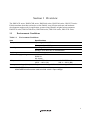
1
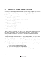
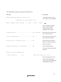
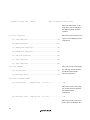
To all our customers
Regarding the change of names mentioned in the document, such as Hitachi
Electric and Hitachi XX, to Renesas Technology Corp.
The semiconductor operations of Mitsubishi Electric and Hitachi were transferred to Renesas
Technology Corporation on April 1st 2003. These operations include microcomputer, logic, analog
and discrete devices, and memory chips other than DRAMs (flash memory, SRAMs etc.)
Accordingly, although Hitachi, Hitachi, Ltd., Hitachi Semiconductors, and other Hitachi brand
names are mentioned in the document, these names have in fact all been changed to Renesas
Technology Corp. Thank you for your understanding. Except for our corporate trademark, logo and
corporate statement, no changes whatsoever have been made to the contents of the document, and
these changes do not constitute any alteration to the contents of the document itself.
Renesas Technology Home Page: http://www.renesas.com
Renesas Technology Corp.
Customer Support Dept.
April 1, 2003
Cautions
Keep safety first in your circuit designs!
1.
Renesas Technology Corporation puts the maximum effort into making semiconductor products better and more reliable, but
there is always the possibility that trouble may occur with them. Trouble with semiconductors may lead to personal injury, fire
or property damage.
Remember to give due consideration to safety when making your circuit designs, with appropriate measures such as (i)
placement of substitutive, auxiliary circuits, (ii) use of nonflammable material or (iii) prevention against any malfunction or
mishap.
Notes regarding these materials
1.
These materials are intended as a reference to assist our customers in the selection of the Renesas Technology Corporation
product best suited to the customer's application; they do not convey any license under any intellectual property rights, or any
other rights, belonging to Renesas Technology Corporation or a third party.
2.
Renesas Technology Corporation assumes no responsibility for any damage, or infringement of any third-party's rights,
originating in the use of any product data, diagrams, charts, programs, algorithms, or circuit application examples contained in
these materials.
3.
All information contained in these materials, including product data, diagrams, charts, programs and algorithms represents
information on products at the time of publication of these materials, and are subject to change by Renesas Technology
Corporation without notice due to product improvements or other reasons. It is therefore recommended that customers contact
Renesas Technology Corporation or an authorized Renesas Technology Corporation product distributor for the latest product
information before purchasing a product listed herein.
The information described here may contain technical inaccuracies or typographical errors.
Renesas Technology Corporation assumes no responsibility for any damage, liability, or other loss rising from these
inaccuracies or errors.
Please also pay attention to information published by Renesas Technology Corporation by various means, including the
Renesas Technology Corporation Semiconductor home page (http://www.renesas.com).
4.
When using any or all of the information contained in these materials, including product data, diagrams, charts, programs, and
algorithms, please be sure to evaluate all information as a total system before making a final decision on the applicability of
the information and products. Renesas Technology Corporation assumes no responsibility for any damage, liability or other
loss resulting from the information contained herein.
5.
Renesas Technology Corporation semiconductors are not designed or manufactured for use in a device or system that is used
under circumstances in which human life is potentially at stake. Please contact Renesas Technology Corporation or an
authorized Renesas Technology Corporation product distributor when considering the use of a product contained herein for
any specific purposes, such as apparatus or systems for transportation, vehicular, medical, aerospace, nuclear, or undersea
repeater use.
6.
The prior written approval of Renesas Technology Corporation is necessary to reprint or reproduce in whole or in part these
materials.
7.
If these products or technologies are subject to the Japanese export control restrictions, they must be exported under a license
from the Japanese government and cannot be imported into a country other than the approved destination.
Any diversion or reexport contrary to the export control laws and regulations of Japan and/or the country of destination is
prohibited.
8.
Please contact Renesas Technology Corporation for further details on these materials or the products contained therein.
Hitachi Microcomputer Development Environment System
H8S/2678, H8S/2678R, H8S/2668,
H8S/2368, H8S/2378 Series
E6000 Emulator
HS2678REPI61H
Supplementary Information
ADE-702-236A
Rev. 2.0
04/17/02
Hitachi, Ltd.
HS2678REPI61HE
Cautions
1. Hitachi neither warrants nor grants licenses of any rights of Hitachi’s or any third party’s
patent, copyright, trademark, or other intellectual property rights for information contained in
this document. Hitachi bears no responsibility for problems that may arise with third party’s
rights, including intellectual property rights, in connection with use of the information
contained in this document.
2. Products and product specifications may be subject to change without notice. Confirm that you
have received the latest product standards or specifications before final design, purchase or
use.
3. Hitachi makes every attempt to ensure that its products are of high quality and reliability.
However, contact Hitachi’s sales office before using the product in an application that
demands especially high quality and reliability or where its failure or malfunction may directly
threaten human life or cause risk of bodily injury, such as aerospace, aeronautics, nuclear
power, combustion control, transportation, traffic, safety equipment or medical equipment for
life support.
4. Design your application so that the product is used within the ranges guaranteed by Hitachi
particularly for maximum rating, operating supply voltage range, heat radiation characteristics,
installation conditions and other characteristics. Hitachi bears no responsibility for failure or
damage when used beyond the guaranteed ranges. Even within the guaranteed ranges,
consider normally foreseeable failure rates or failure modes in semiconductor devices and
employ systemic measures such as fail-safes, so that the equipment incorporating Hitachi
product does not cause bodily injury, fire or other consequential damage due to operation of
the Hitachi product.
5. This product is not designed to be radiation resistant.
6. No one is permitted to reproduce or duplicate, in any form, the whole or part of this document
without written approval from Hitachi.
7. Contact Hitachi’s sales office for any questions regarding this document or Hitachi
semiconductor products.
IMPORTANT INFORMATION
READ FIRST
• READ this user's manual before using this emulator product.
• KEEP the user's manual handy for future reference.
Do not attempt to use the emulator product until you fully understand its mechanism.
Emulator Product:
Throughout this document, the term "emulator product" shall be defined as the following
products produced only by Hitachi, Ltd. excluding all subsidiary products.
• Emulator station
• User system interface cables
• PC interface board
• Optional SIMM memory module
The user system or a host computer is not included in this definition.
Purpose of the Emulator Product:
This emulator product is a software and hardware development tool for systems employing the
Hitachi microcomputer H8S/2678 series, H8S/2678R series, H8S/2668 series, H8S/2368 series,
H8S/2378 series (hereafter referred to as the MCU). This emulator product must only be used for
the above purpose.
Limited Applications:
This emulator product is not authorized for use in MEDICAL, atomic energy, aeronautical or
space technology applications without consent of the appropriate officer of a Hitachi sales
company. Such use includes, but is not limited to, use in life support systems. Buyers of this
emulator product must notify the relevant Hitachi sales offices before planning to use the product
in such applications.
Improvement Policy:
Hitachi, Ltd. (including its subsidiaries, hereafter collectively referred to as Hitachi) pursues a
policy of continuing improvement in design, performance, and safety of the emulator product.
Hitachi reserves the right to change, wholly or partially, the specifications, design, user's manual,
and other documentation at any time without notice.
Target User of the Emulator Product:
This emulator product should only be used by those who have carefully read and thoroughly
understood the information and restrictions contained in the user's manual. Do not attempt to use
the emulator product until you fully understand its mechanism.
It is highly recommended that first-time users be instructed by users that are well versed in the
operation of the emulator product.
I
LIMITED WARRANTY
Hitachi warrants its emulator products to be manufactured in
accordance with published specifications and free from defects in
material and/or workmanship. Hitachi, at its option, will repair or
replace any emulator products returned intact to the factory,
transportation charges prepaid, which Hitachi, upon inspection,
determine to be defective in material and/or workmanship.
The foregoing shall constitute the sole remedy for any breach of
Hitachi's warranty. See the Hitachi warranty booklet for details on
the warranty period. This warranty extends only to you, the original
Purchaser. It is not transferable to anyone who subsequently purchases
the emulator product from you. Hitachi is not liable for any claim
made by a third party or made by you for a third party.
DISCLAIMER
HITACHI MAKES NO WARRANTIES, EITHER EXPRESS OR
IMPLIED, ORAL OR WRITTEN, EXCEPT AS PROVIDED
HEREIN, INCLUDING WITHOUT LIMITATION THEREOF,
WARRANTIES AS TO MARKETABILITY, MERCHANTABILITY,
FITNESS FOR ANY PARTICULAR PURPOSE OR USE, OR
AGAINST INFRINGEMENT OF ANY PATENT. IN NO EVENT
SHALL HITACHI BE LIABLE FOR ANY DIRECT, INCIDENTAL
OR CONSEQUENTIAL DAMAGES OF ANY NATURE, OR
LOSSES OR EXPENSES RESULTING FROM ANY DEFECTIVE
EMULATOR PRODUCT, THE USE OF ANY EMULATOR
PRODUCT, OR ITS DOCUMENTATION, EVEN IF ADVISED
OF THE POSSIBILITY OF SUCH DAMAGES. EXCEPT AS
EXPRESSLY STATED OTHERWISE IN THIS WARRANTY,
THIS EMULATOR PRODUCT IS SOLD "AS IS ", AND YOU
MUST ASSUME ALL RISK FOR THE USE AND RESULTS
OBTAINED FROM THE EMULATOR PRODUCT.
II
State Law:
Some states do not allow the exclusion or limitation of implied warranties or liability for
incidental or consequential damages, so the above limitation or exclusion may not apply to you.
This warranty gives you specific legal rights, and you may have other rights which may vary from
state to state.
The Warranty is Void in the Following Cases:
Hitachi shall have no liability or legal responsibility for any problems caused by misuse, abuse,
misapplication, neglect, improper handling, installation, repair or modifications of the emulator
product without Hitachi's prior written consent or any problems caused by the user system.
All Rights Reserved:
This user's manual and emulator product are copyrighted and all rights are reserved by Hitachi.
No part of this user's manual, all or part, may be reproduced or duplicated in any form, in hardcopy or machine-readable form, by any means available without Hitachi's prior written consent.
Other Important Things to Keep in Mind:
1. Circuitry and other examples described herein are meant merely to indicate the characteristics
and performance of Hitachi's semiconductor products. Hitachi assumes no responsibility for
any intellectual property claims or other problems that may result from applications based on
the examples described herein.
2. No license is granted by implication or otherwise under any patents or other rights of any third
party or Hitachi.
Figures:
Some figures in this user's manual may show items different from your actual system.
Limited Anticipation of Danger:
Hitachi cannot anticipate every possible circumstance that might involve a potential hazard.
The warnings in this user's manual and on the emulator product are therefore not all inclusive.
Therefore, you must use the emulator product safely at your own risk.
III
SAFETY PAGE
READ FIRST
• READ this user's manual before using this emulator product.
• KEEP the user's manual handy for future reference.
Do not attempt to use the emulator product until you fully understand its mechanism.
DEFINITION OF SIGNAL WORDS
This is the safety alert symbol. It is used to alert you to potential personal
injury hazards. Obey all safety messages that follow this symbol to avoid
possible injury or death.
DANGER
WARNING
CAUTION
CAUTION
DANGER indicates an imminently hazardous situation which, if not
avoided, will result in death or serious injury.
WARNING indicates a potentially hazardous situation which, if not
avoided, could result in death or serious injury.
CAUTION indicates a potentially hazardous situation which, if not
avoided, may result in minor or moderate injury.
CAUTION used without the safety alert symbol indicates a
potentially hazardous situation which, if not avoided, may result
in property damage.
NOTE emphasizes essential information.
IV
WARNING
Observe the precautions listed below. Failure to do so
will result in a FIRE HAZARD and will damage the user
system and the emulator product or will result in
PERSONAL INJURY. The USER PROGRAM will be
LOST.
1. Do not repair or remodel the emulator product by
yourself for electric shock prevention and quality
assurance.
2. Always switch OFF the E6000 emulator and user system
before connecting or disconnecting any CABLES or
PARTS.
3. Always before connecting any CABLES, make sure that
pin 1 on both sides are correctly aligned.
4. Supply power according to the power specifications and
do not apply an incorrect power voltage. Use only the
provided power cable.
V
CAUTION
This equipment has been tested and found to comply
with the limits for a Class A digital device, pursuant to part 15
of the FCC Rules. These limits are designed to provide
reasonable protection against harmful interference when the
equipment is operated in a commercial environment. This
equipment generates, uses, and can radiate radio frequency
energy and, if not installed and used in accordance with the
instruction manual, may cause harmful interference to radio
communications. Operation of this equipment in a residential
area is likely to cause harmful interference in which case the
user will be required to correct the interference at his own
expense.
VI
Preface
Thank you for purchasing the H8S/2678 series, H8S/2678R series, H8S/2668 series, H8S/2368
series, H8S/2378 series E6000 emulator.
The H8S/2678 series, H8S/2678R series, H8S/2668 series, H8S/2368 series, H8S/2378 series E6000
emulator (hereafter referred to as the E6000) was designed as a software and hardware development
tool for systems based on Hitachi's original microcomputers HD64F2676, HD6432675, and
HD6412670.
The E6000 provides a CD-R that contains the Hitachi Debugging Interface (HDI) system program,
test program, and the user’s manual.
There are three manuals for the E6000: the H8S series E6000 Emulator User's Manual, this
Supplementary Information, and the Hitachi Debugging Interface User's Manual. The E6000
Emulator User's Manual describes E6000 functions common to all H8S series microcomputers. This
Supplementary Information describes the functions specialized for each microcomputer supported by
the H8S/2678 series, H8S/2678R series, H8S/2668 series, H8S/2368 series, H8S/2378 series E6000
emulator. Please read this manual before using the E6000.
To connect the E6000 to the user system, a user system interface cable for each package type is
available. For details on the user system interface cable, refer to the User System Interface Cable
User's Manual.
The following shows the related manuals:
• H8S Series E6000 Emulator User's Manual (HS2000EPI61HE)
• Hitachi Debugging Interface User's Manual (HS6400DIIW5SE)
• User System Interface Cable User's Manual (HS2678RECH61HE, etc)
• The PC interface board user's manual which will be the following manuals:
ISA Bus Interface Board User's Manual (HS6000EII01HE)
PCI Bus Interface Board User's Manual (HS6000EIC01HE or HS6000EIC02HE)
PCMCIA Interface Card User's Manual (HS6000EIP01HE)
LAN Adapter User's Manual (HS6000ELN01HE)
• Option Memory Board User's Manual
1M SIMM Memory Board User's Manual (HS6000EMS11HE)
4M SIMM Memory Board User's Manual (HS6000EMS12HE)
®
®
®
Note: Microsoft , Windows , and WindowsNT are registered trademarks of Microsoft
Corporation in the United States and/or in other countries.
i
Contents
Section 1 Overview ........................................................................................... 1
1.1
1.2
1.3
Environment Conditions ...................................................................................................1
Supported MCUs and User System Interface Cables........................................................2
Operating Voltage and Frequency Specifications .............................................................3
Section 2 User System Interface ....................................................................... 5
2.1
2.2
Signal Protection ...............................................................................................................5
User System Interface Circuits..........................................................................................5
Section 3 Notes on Use ..................................................................................... 9
3.1
3.2
3.3
3.4
3.5
3.6
3.7
3.8
I/O Register Differences between Actual MCU and E6000..............................................9
Access to the Reserved Area .............................................................................................9
Use of an Internal RAM Area as External Memory..........................................................10
Support of Flash Memory .................................................................................................10
Hardware Standby .............................................................................................................10
EXDMA controller............................................................................................................10
SIMM Memory Module Access........................................................................................10
Power Supply Follower Circuit.........................................................................................10
Section 4 HDI Parameters ................................................................................. 11
4.1
4.2
4.3
Address Areas ...................................................................................................................11
Access Status.....................................................................................................................12
IRQ Signal Trace...............................................................................................................12
Section 5 Diagnostic Test Procedure ................................................................ 13
5.1
5.2
ii
System Set-Up for Test Program Execution .....................................................................13
Diagnostic Test Procedure Using the Test Program..........................................................14
Figures
Figure 2.1
Figure 2.2
Figure 2.3
Figure 2.4
Default User System Interface Circuit...................................................................... 6
User System Interface Circuit for MD2, MD1, MD0, NMI, and WAIT.................. 6
User System Interface Circuit for RESET................................................................ 6
User System Interface Circuit for P40 to P47, P54 to P57, Vcc, AVcc, AVss,
and Vref Signals ....................................................................................................... 7
Tables
Table 1.1
Table 1.2
Table 1.3
Table 1.4
Table 4.1
Table 4.2
Environment Conditions ........................................................................................ 1
H8S/2678 Series, H8S/2678R Series, H8S/2668 Series, H8S/2368 series,
H8S/2378 series MCUs and User System Interface Cable..................................... 2
Operating Voltage and Frequency Specifications .................................................. 3
Clock Selections..................................................................................................... 4
Address Area Parameters ....................................................................................... 11
Access Status Parameters ....................................................................................... 12
iii
Section 1 Overview
The H8S/2678 series, H8S/2678R series, H8S/2668 series, H8S/2368 series, H8S/2378 series
E6000 emulator (hereafter referred to as the E6000) is an efficient software and hardware
development support tool for application systems using Hitachi's original microcomputers
H8S/2678 series, H8S/2678R series, H8S/2668 series, H8S/2368 series, H8S/2378 series.
1.1
Environment Conditions
Table 1.1
Environment Conditions
Item
Specifications
Temperature
Operating: +10 to +35°C
Storage: –10 to +50°C
Humidity
Operating: 35 to 80% RH; no condensation
Storage: 35 to 80% RH; no condensation
Ambient gases
No corrosive gases
AC Power supply voltage
100 V to 240 V AC
50/60 Hz
0.6 A max.
AC input cable*
HS2678REPI61H
100 V – 120 V (UL)
User system voltage (UVcc)
Depends on the target MCU within the range 3.0 V to 3.6 V
HS2678REPI61HB
200 V – 240 V (BS)
Note: HS2678REPI61H must be used at AC100 V-120 V input voltage.
HS2678REPI61HB must be used at AC200 V-240 V input voltage.
1
1.2
Supported MCUs and User System Interface Cables
Tables 1.2 shows the correspondence between the MCUs and the user system interface cables
supported by the E6000.
Table 1.2
H8S/2678 Series, H8S/2678R Series, H8S/2668 Series, H8S/2368 series,
H8S/2378 series MCUs and User System Interface Cable
No.
MCU Type
Number
Package
1
H8S/2678 series
144-pin QFP (FP-144G) HS2678RECH61H
2
H8S/2678R series
144-pin QFP (FP-144H)
E6000 User System Interface Cables
H8S/2668 series
3
H8S/2368 series
128-pin QFP
HS2368ECH61H
(FP-128B)
120-pin TQFP
HS2368ECN61H
(TFP-120)
4
H8S/2378 series
144-pin QFP
(FP-144H)
2
HS2378ECH61H
1.3
Operating Voltage and Frequency Specifications
Table 1.3 shows the MCU operating voltage and frequency specifications supported by the E6000.
If the E6000 is used in an environment that exceeds the operating voltage range and operating
frequency range guaranteed for the MCU operation, normal emulator operation is not guaranteed.
Table 1.3
Operating Voltage and Frequency Specifications
MCU Types
Operating Voltage (V)
Operating Frequency
(φ) (MHz)
H8S/2678 Series
3.0-3.6
2-33
H8S/2678R Series,
H8S/2668 Series,
H8S/2368 Series,
H8S/2378 Series
3.0-3.6
8-33
NOTE
For details on the operating voltage and frequency
specifications, refer to the MCU hardware manual.
3
In the E6000, the clock can be selected by using the Configuration window or the Clock
command.
Table 1.4
Clock Selections
Clock Command
Parameter
Configuration
Window Setting
12
25
33
t
t2
12.5 MHz internal clock
25 MHz internal clock
33 MHz internal clock
Target
Target/2
Notes
Default
Not supported by the actual MCU.
Use this clock only when the required clock
duty cannot be obtained.
NOTE
The system clock (φ) frequency is the same clock
frequency input to the XTAL and EXTAL when external clock
t is specified in the HDI CLOCK command. For example,
when a 20-MHz crystal oscillator is connected to the XTAL
and EXTAL of the user system, the system clock (φ)
frequency is 20 MHz. When external clock t2 is specified in
the HDI CLOCK command, the system clock (φ) frequency is
1/2 of the clock frequency input to the XTAL and EXTAL.
The frequency of the E6000 internal clock specified with
the HDI CLOCK command is applied to the system clock (φ).
4
Section 2 User System Interface
All user system interface signals are directly connected to the MCU in the E6000 with no
buffering except for those listed below which are connected to the MCU through control circuits:
•
•
•
•
•
•
NMI
RESET
MD2, MD1, MD0
XTAL
EXTAL
WAIT
2.1
Signal Protection
All user system interface signals are protected from over- or under-voltage by use of diode arrays
except for the AVcc and Vref.
The Vcc pins (except for the AVcc pin) at the head of the user system interface cable are
connected together. The E6000 monitors the voltage level of the Vcc pins and displays the
power-supply status in the Status Window.
2.2
User System Interface Circuits
The interface circuit between the MCU in the E6000 and the user system has a signal delay of
about 8 ns due to the user system interface cable. Thus high-impedance signals will be pulled up
to the high level by pull-up resistors. When connecting the E6000 to a user system, adjust the user
system hardware to compensate for propagation delays.
The following diagrams show the interface signal circuits.
5
Default:
Figure 2.1 Default User System Interface Circuit
Mode Pins (MD2, MD1 and MD0), NMI, and WAIT: The NMI signal is input to the MCU
through the emulator control circuit. The rising/falling time of the NMI signal must be 8 ns/V or
less. The mode pins are only monitored. The CPU mode depends on the HDI Configuration
settings.
Figure 2.2 User System Interface Circuit for MD2, MD1, MD0, NMI, and WAIT
RESET:
Figure 2.3 User System Interface Circuit for RESET
6
P40 to P47 (pins used for AN0 to AN7 and DA0 to DA1), P54 to P57 (pins used for AN12 to
AN15 and DA2 to DA3) Vcc, AVcc, AVss, and Vref: Pins P50 to P57 are also used for interrupt
inputs. When the user system is not connected and pull-up resistors are removed, input will be
undefined and may illegally detect an interrupt. When P50 to P57 are used to input interrupt
signals, it is recommended to connect the pull-up resistors to these pins.
Figure 2.4 User System Interface Circuit for P40 to P47, P54 to P57, Vcc, AVcc, AVss, and
Vref Signals
7
8
Section 3 Notes on Use
3.1
I/O Register Differences between Actual MCU and E6000
In the E6000, one evaluation chip emulates several types of MCU. Therefore, there are some
differences in I/O registers between an actual MCU and the E6000. Note these differences when
accessing the I/O registers.
I/O port is in the input state at default. The I/O register contents indicate the emulator port status.
When the user system interface cable is not connected, the read value is 1 due to the E6000 pullup resistors.
In the E6000, accesses to the following registers for controlling the flash memory are invalid.
• RAM emulation register (RAMER: H'FEDB)
• System control register 2 (SYSCR2: H'FF42)
• Flash memory control register 1 (FLMCR1: H'FFC8)
• Flash memory control register 2 (FLMCR2: H'FFC9)
• Erase block register 1 (EBR1: H'FFCA)
• Erase block register 2 (EBR2: H'FFCB)
3.2
Access to the Reserved Area
When accessing the reserved area, note the following:
If the reserved area is used, the operation in the actual MCU cannot be guaranteed. If the user
program extends to the reserved area during debugging, select the MCU having the largest ROM
capacity (for example, debug the program for the H8S/2675R with the H8S/2676R memory
mapping).
9
3.3
Use of an Internal RAM Area as External Memory
An internal RAM area can be used as an external address when the RAME bit of the SYSCR is
cleared to "0". Emulator (option memory) cannot be selected for the internal RAM area. Only
user memory can be accessed as an external address. Option memory cannot be accessed as an
external address. In this case, Memory Mapping setting is the same as the Internal RAM setting.
3.4
Support of Flash Memory
The E6000 does not emulate the flash memory control operation in the MCU.
3.5
Hardware Standby
When the User Standby enable check box is selected in the Configuration window, the STBY
signal of the user system is directly input to the E6000, and the MCU operation stops.
When disabling the STBY signal, be sure to keep the oscillator stabilization time and the timing
specifications of the RES signal.
3.6
EXDMA controller
The H8S/2678 series, H8S/2678R series, H8S/2668 series, H8S/2368 series, H8S/2378 series
includes an EXDMA controller that performs direct memory access (DMA) transfers between
external addresses. The EXDMA controller can only access User (user memory) and cannot
access Emulator (option memory).
3.7
SIMM Memory Module Access
When SIMM memory module is used for the external area, memory will always be accessed via
16-bit bus in 3 cycles regardless of the setting of the bus controller.
3.8
Power Supply Follower Circuit
If the Configuration dialog box is used to set [User Vcc Threshold], set the Vcc between 2.7 V
to 3.6 V.
10
Section 4 HDI Parameters
4.1
Address Areas
Table 4.1 lists the parameters for address areas (Area) that can be specified with HDI command
line interface or displayed as trace results.
Table 4.1
Address Area Parameters
HDI Parameter
(Trace Display)
Address Area
Description
rom
On-chip ROM
MCU's on-chip ROM, which can be
read but cannot be written to.
ram
On-chip RAM
MCU's on-chip RAM (except for DTC
RAM), which can be read and written
to.
IO16
(I/O-16)
Internal I/O registers
(16-bit bus)
MCU's internal I/O registers for the 16bit bus.
IO8
(I/O-8)
Internal I/O registers
(8-bit bus)
MCU's internal I/O registers for the
8-bit bus.
ext16
(EXT-16)
External area
(16-bit bus)
External area for the 16-bit bus, which
can be allocated to the user system
memory or the optional SIMM memory
module in the E6000.
ext8
(EXT-8)
External area
(8-bit bus)
External area for the 8-bit bus, which
can be allocated to the user system
memory or the optional SIMM memory
module in the E6000.*
Dtcram
(RAM/DTC)
DTC RAM
MCU's on-chip RAM for DTC.
Note: When SIMM memory module is used for the external area, memory will always be
accessed via 16-bit bus. Therefore, the Trace window will always display EXT-16.
11
4.2
Access Status
Table 4.2 lists the parameters for access status (Status) that can be specified with HDI command
line interface or displayed as trace results.
Table 4.2
Access Status Parameters
HDI Parameter
(Trace Display)
Access Status
Description
dmac
On-chip DMAC
Access by the MCU's DMAC
(Cannot be accessed by the EXDMA
controller.)
dtc
On-chip DTC
Access by the MCU's DTC
refresh
Refresh
Refresh cycle by the MCU's refresh
controller
prefetch
(PROG)
CPU prefetch
Instruction prefetch cycle by the CPU
data
(DATA)
CPU data access
Data access for instruction execution
by the CPU
4.3
IRQ Signal Trace
The H8S/2678 series, H8S/2678R series, H8S/2668 series, H8S/2368 series, H8S/2378 series
MCU has 16 interrupt input pins IRQ0 to IRQ15. The E6000 can trace the state of eight interrupt
pins simultaneously. To do this, select the IRQ0 to IRQ7 or IRQ8 to IRQ15 checkbox in the
configuration window.
12
Section 5 Diagnostic Test Procedure
This section describes the diagnostic test procedure using the E6000 test program.
5.1
System Set-Up for Test Program Execution
To execute the test program, use the following hardware; do not connect the user system interface
cable and user system.
• E6000 (HS2678REPI61H)
• Host computer
• The E6000 PC interface board which will be one of the following boards or card:
Select one interface board from the following depending on the PC interface specifications.
ISA bus interface board (HS6000EII01H)
PCI bus interface board (HS6000EIC01H or HS6000EIC02H)
PCMCIA interface card (HS6000EIP01H)
LAN adapter (HS6000ELN01H)
1. Install the E6000 PC interface board in the host computer and connect the supplied PC
interface cable to the board.
2. Connect the PC interface cable to the E6000.
3. Connect the supplied AC adapter to the E6000.
4. Initiate the host computer to make it enter DOS prompt command input wait state.
5. Turn on the E6000 switch.
13
5.2
Diagnostic Test Procedure Using the Test Program
Insert the CD-R (HS2678REPI61SR supplied with the E6000) into the CD-ROM drive of the host
computer by pressing the Shift key, move the current directory to <Drive>:\Diag with a command
prompt, and enter one of the following commands according to the PC interface board used to
initiate the test program:
1. ISA bus interface boad (HS6000EII01H)
> TM2678R -ISA (RET)
2. PCI bus interface boad (HS6000EIC01H or HS6000EIC02H)
> TM2678R -PCI (RET)
3. PCMCIA interface card (HS6000EIP01H)
> TM2678R -PCCD (RET)
4. LAN adapter (HS6000ELN01H)
> TM2678R -ELN (RET)
The HDI must be installed before the test program is executed.
Be sure to initiate the test program from <Drive>:\Diag. Do not initiate it from a directory other
than <Drive>:\Diag, such as > <Drive>:\Diag\TM2678R -ISA (RET). If the test program is
initiated when the current directory is not <Drive>:\Diag, the test program will not operate
correctly.
When -S is added to the command line such as > TM2678R -ISA -S (RET), steps 1 to 19 will be
repeatedly executed. To stop the execution, enter Q. When -Lfilename is added to the command
line such as > TM2678R -ISA -Lfilename (RET), the log name at the execution is saved in
filename. When -? is added to the command line such as > TM2678R -ISA -? (RET), online help
(option) is displayed.
Notes: 1. When the CD-R is inserted into the CD-ROM drive without pressing the Shift key, the
HDI installation wizard is automatically started.
In such a case, exit the HDI installation wizard.
14
2.
<Drive> is a drive name for the CD-ROM drive.
3.
Do not remove the CD-R from the CD-ROM drive during test program execution.
The following messages are displayed during the test.
Message
Description
E6000 H8S/2678R Emulator Tests Vx.x
Test program start message.
x.x shows the version number.
Copyright (c) 2000 Hitachi Ltd.
Option memory board fitted? ( 1. None
2. 1MB
3. 4MB ) : 1
Enter 1 and press the Enter
key because the SIMM
memory module is not
installed in this example.
Loading driver .........................OK (Use ISA)
Shows that driver software has
been correctly loaded.
Initializing driver ....................OK
Shows that driver software has
been correctly initialized.
Searching for interface card ...........OK
Shows that the PC interface
board is correctly installed in
the host computer.
Checking emulator is connected .........OK
Shows that the E6000 is
correctly connected to the host
computer.
Emulator board information:
Main board ID:
H'5
Emulation board ID:
H'18
Shows the ID number of the
lower board of the E6000
(always 5) and the upper board
of the E6000 (always 18).
15
Companion chip ID:
None
Option memory board: None
Shows the ID number of the
companion chip and whether
the SIMM memory board is
installed.
01) Test Register
A) IDR0 Register .............................OK
Shows the check results for the
registers in the E6000 (normal
completion).
B) PAGE Register .............................OK
C) TRACE G/A Register ........................OK
D) PERFM G/A Register ........................OK
E) CES G/A Register ..........................OK
F) IDR1 Register .............................OK
G) IDR2 Register .............................OK
02) Test DPRAM
A) Decode Test ...............................OK
B) Marching Test .............................OK
Shows the results of decoding
test and step test for the dualport RAM in the E6000
(normal completion).
03) Test Firmware RAM
A) Decode Test
page[H'700 - H'71f] ..............OK
Shows the results of decoding
test for the firmware RAM in
the E6000 (normal
completion).
B) Marching test
page[H'700 - H'71f] ..............OK
Shows the results of step test
for the firmware RAM in the
16
E6000 (normal completion).
04) Test Trace memory
A) Decode Test
page[H'000 - H'04f](Lower 32K) .....OK
Shows the results of decoding
test for the trace RAM (first
half) in the E6000 (normal
completion).
B) Marching test
page[H'000 - H'04f](Lower 32K) .....OK
Shows the results of step test
for the trace RAM (first half)
in the E6000 (normal
completion).
C) Decode Test
page[H'000 - H'04f](Upper 32K) .....OK
Shows the results of decoding
test for the trace RAM (last
half) in the E6000 (normal
completion).
D) Marching test
page[H'000 - H'04f](Upper 32K) .....OK
Shows the results of step test
for the trace RAM (last half)
in the E6000 (normal
completion).
05) Test Map control memory
A) Decode Test
page[H'200 - H'27f] ........OK
B) Marching test
page[H'200 - H'27f] ........OK
06) Test Internal ROM and RAM
Shows the results of decoding
test for the mapping RAM in
the E6000 (normal
completion).
Shows the results of step test
for the mapping RAM in the
E6000 (normal completion).
Shows the results of decoding
test and step test for internal
17
A) Decode Test
(Internal ROM) ..............OK
ROM and RAM in the E6000
(normal completion).
B) Marching test (Internal ROM) ..............OK
C) Decode Test
(Internal RAM) ..............OK
D) Marching Test (Internal RAM) ..............OK
07) Test Option RAM
No option memory board fitted - test skipped
18
Shows the check results for the
optional SIMM memory
module in the E6000 (not
installed).
08) Test Emulation RAM STEP Operation
A) Step Operation ............................OK
09) Test Keybreak
A) Key Break .................................OK
10) Test Emulation RAM Hardware Break
A) GRD Break .................................OK
B) WPT Break .................................OK
Shows the check results for the
step execution controlling
circuits in the E6000 (normal
completion).
Shows the check results for the
forced break controlling
circuits in the E6000 (normal
completion).
Shows the check results for the
illegal access break controlling
circuits in the E6000 (normal
completion).
C) WPT(ROM) Break ............................OK
11) Test Internal ROM Write Protect
A) Write-Protect .............................OK
12) Test Hardware Break
A) Break Point Initialized ...................OK
B) Event Detectors CES channel 1-12 ..........OK
Shows the check results for the
internal ROM write-protection
controlling circuits in the
E6000 (normal completion).
Shows the check results for the
hardware break control circuits
in the E6000 (normal
completion).
C) Test Sequencing 1 .........................OK
D) Check Range Break .........................OK
E) Range Break Test for Data .................OK
F) Check Compare Either ......................OK
13) Test Emulation RAM Trace
A) Free Trace ................................OK
Shows the check results for the
trace controlling circuits in the
E6000 (normal completion).
19
B) Range Trace ...............................OK
C) Point to Point Trace ......................OK
D) Start and Stop Event Trace ................OK
E) Trace memory Overflow .....................OK
F) Time STAMP Trace (33MHz) ..................OK
G) Time STAMP Trace (25MHz) ..................OK
H) Time STAMP Trace (12.5MHz) ................OK
14) Test Runtime Counter
A) Runtime Counter (33.0MHz) .................OK
B) Runtime Counter (25.0MHz) .................OK
C) Runtime Counter (12.5MHz) .................OK
20
Shows the check results for the
run-time counter in the E6000
(normal completion).
15) Test Emulation Monitor
A) EMA23-EMA0 ................................OK
B) ACST2-ACST0 ...............................OK
Shows the check results for the
emulation monitor controlling
circuits in the E6000 (normal
completion).
C) ASEST3-ASEST0 .............................OK
D) ASEBRKACK .................................OK
E) CNN .......................................OK
F) NOCLK .....................................OK
G) WINDOW ....................................OK
16) Test PERFM G/A
A) Time Measurement ..........................OK
B) RESERVED
Shows the check results for the
performance analysis
controlling circuits in the
E6000 (nomal completion).
C) Subroutine Count Measurement ..............OK
D) Timeout Function (TIMOT Bit) ..............OK
E) Timeout Function (TIMOP Bit) ..............OK
17) Test Bus Monitor
A) Register ..................................OK
B) Parallel RAM ..............................OK
Shows the check results for the
bus monitor controlling
circuits in the E6000 (normal
completion).
C) SPRSEL2 ...................................OK
D) RAM Monitor ...............................OK
21
18) Test Parallel Access
A) Internal ROM Parallel Read Access(WORD) .........OK
B) Internal ROM Parallel Write Access(WORD) ........OK
C) Internal ROM Parallel Write Access(High Byte) ...OK
D) Internal ROM Parallel Write Access(Low Byte) ....OK
E) Internal RAM Parallel Read Access(WORD) .........OK
F) Internal RAM Parallel Write Access(WORD) ........OK
G) Internal RAM Parallel Write Access(High Byte) ...OK
H) Internal RAM Parallel Write Access(Low Byte) ....OK
I) Option RAM Parallel Read Access(WORD) ...........SKIP
J) Option RAM Parallel Write Access(WORD) ..........SKIP
K) Option RAM Parallel Write Access(High Byte) .....SKIP
L) Option RAM Parallel Write Access(Low Byte) ......SKIP
Shows the check results for the
parallel access controlling
circuits in the E6000 (normal
completion).
19) Test RTC
A) RTC .......................................OK
Shows the check results for the
RTC controlling circuits in the
E6000 (normal completion).
Tests run for xH:xM:xS
Shows the check time.
Tests passed, emulator functioning correctly
Shows that the E6000 is
correctly operating.
When –S is added to the command line, step 1 will be executed again after step 19.
22