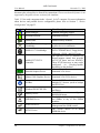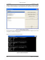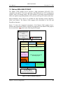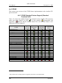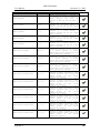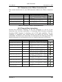
1
AMD SimNow™ Simulator 4.4.5 User’s Manual Revision Date 2.01 November 2008 Advanced Micro Devices, Inc. One AMD Place Sunnyvale, CA 94088 [email protected] AMD © 2004-2008 Advanced Micro Devices, Inc. The Contents of this document are provided in connection with Advanced Micro Devices, Inc. (“AMD”) products. AMD makes no representations or warranties with respect to the accuracy or completeness of the contents of this publication and reserves the right to make changes to specifications and product descriptions at any time without notice. No license, whether express, implied, arising by estoppels or otherwise, to any intellectual property rights is granted by this publication. Except as set forth in AMD‟s Standard Terms and Conditions of Sale, AMD assumes no liability whatsoever, and disclaims any express or implied warranty, relating to its products including, but not limited to, the implied warranty of merchantability, fitness for a particular purpose, or infringement of any intellectual property right. AMD‟s products are not designed, intended, authorized or warranted for use as components in systems intended for surgical implant into the body, or in other applications intended to support or sustain life, or in any other application in which the failure of AMD‟s product could create a situation where personal injury, death, or severe property or environmental damage may occur. AMD reserves the right to discontinue or make changes to its products at any time without notice. Trademarks AMD, the AMD Arrow logo, AMD Athlon, AMD Opteron and combinations thereof, SimNow, 3DNow!, AMD-8111, AMD-8131, AMD-8132 and AMD-8151 are trademarks of Advanced Micro Devices, Inc. HyperTransport is a trademark of the HyperTransport Technology Consortium. Microsoft and Windows are registered trademarks of Microsoft Corporation. PCI-X is a registered trademark of PCI-SIG. Sysmark is a registered trademark of Business Applications Performance Corp. MMX is a trademark of Intel Corporation. Other product names used in this publication are for identification purposes only and may be trademarks of their respective companies. AMD Confidential AMD Confidential User Manual November 21st, 2008 Contents Figures................................................................................................................................ ix Tables ................................................................................................................................. xi 1 2 Overview ..................................................................................................................... 1 Installation................................................................................................................... 3 2.1 System Requirements.......................................................................................... 3 2.2 Installation Procedure ......................................................................................... 3 2.3 Directory Structure and Executable .................................................................... 4 2.4 Setting up Linux for the Simulator ..................................................................... 4 2.5 Configuration File ............................................................................................... 5 2.6 Updates and Questions ........................................................................................ 6 3 Graphical User Interface ............................................................................................. 7 3.1 Tool Bar Buttons ................................................................................................. 7 3.2 Device Window .................................................................................................. 9 3.2.1 Add a New Device .................................................................................... 10 3.2.2 Workspace Popup Menu ........................................................................... 10 3.2.2.1 Add Connection .............................................................................. 11 3.2.2.2 Configure Device ............................................................................ 12 3.2.2.3 Disconnect Device ......................................................................... 12 3.2.2.4 Delete Device.................................................................................. 13 3.2.3 Example Computer Description ................................................................ 13 3.2.4 Device Window – Quick Reference ......................................................... 15 3.3 Device Groups .................................................................................................. 15 3.3.1 Terms ........................................................................................................ 16 3.3.2 Concept Diagrams ..................................................................................... 17 3.3.3 Working with Device Groups ................................................................... 18 3.3.4 Shell Automation Commands for Device Groups .................................... 19 3.3.4.1 Device Tree ..................................................................................... 19 3.3.4.2 Enabled vs. Disabled vs. Mixed ................................................... 20 3.3.5 Device Group Examples ........................................................................... 21 3.3.5.1 Example: 1GB DDR2 memory ..................................................... 21 3.3.5.2 Example: Quad-Core Node .......................................................... 22 3.3.5.3 Example: SuperIO device ............................................................. 24 3.3.6 Creating a Device Group (GUI) ................................................................ 24 3.3.7 Creating a Device Group (Automation Commands) ................................ 27 3.3.8 Ungrouping a created device group .......................................................... 29 3.4 Main Window ................................................................................................... 29 3.4.1 SimStats and Diagnostic Ports .................................................................. 29 3.4.2 CPU-Statistics Graphs .............................................................................. 30 3.4.2.1 Translation Graph........................................................................... 30 3.4.2.2 Real MIPS Graph ........................................................................... 30 3.4.2.3 Invalidation Rate Graph ................................................................ 31 3.4.2.4 Exception Rate Graph ................................................................... 31 Contents iii AMD Confidential User Manual 4 5 6 7 iv November 21st, 2008 3.4.2.5 PIO Rate Graph .............................................................................. 31 3.4.2.6 MMIO Rate Graph .......................................................................... 32 3.4.3 Simulated Video........................................................................................ 32 3.4.4 Hard Disk and Floppy Display ................................................................. 32 3.4.5 Using Hard Drive, DVD-/CD-ROM and Floppy Images ......................... 33 3.4.6 Registry Window ...................................................................................... 33 3.4.7 Help, Problems and Bug Reports .............................................................. 34 Disk Images .............................................................................................................. 35 4.1 Creating A Blank Hard-Drive Image ................................................................ 35 Running the Simulator .............................................................................................. 39 5.1 Command-Line Arguments .............................................................................. 39 5.1.1 Open a Simulation Definition File ............................................................ 40 5.2 Installing an Operating System ......................................................................... 42 5.2.1 Assigning Disk-Images ............................................................................. 42 5.2.2 Run The Simulation .................................................................................. 44 5.2.3 Interaction with the Simulated Machine ................................................... 45 5.2.4 Simulation Reset ....................................................................................... 45 5.3 Multi-Machine Support ..................................................................................... 45 Create a Simulated Computer ................................................................................... 49 6.1 BSD Files .......................................................................................................... 49 6.2 Device Placement.............................................................................................. 49 6.3 Solo.bsd Device Configuration ......................................................................... 51 6.4 Save and Run .................................................................................................... 52 Device Configuration ................................................................................................ 53 7.1 AweSim Processor Device ................................................................................ 55 7.2 Debugger Device .............................................................................................. 58 7.3 DIMM Device ................................................................................................... 59 7.4 Emerald Graphics Device ................................................................................. 65 7.5 Matrox MGA-G400 PCI/AGP .......................................................................... 69 7.6 Super IO Devices: Winbond W83627HF SIO / ITE 8712 SIO ........................ 78 7.7 Memory Device ................................................................................................ 81 7.8 PCA9548 SMB Device ..................................................................................... 84 7.9 PCA9556 SMB Device ..................................................................................... 85 7.10 AMD 8th Generation Integrated Northbridge Device ...................................... 86 7.11 AMD-8111™ Southbridge Devices – IO Hubs ................................................ 90 7.12 PCI BUS Device ............................................................................................... 96 7.13 AMD-8131™ PCI-X® Controller ..................................................................... 98 7.14 AMD-8132™ PCI-X® Controller ..................................................................... 99 7.15 PCI-X Test Device .......................................................................................... 101 7.16 AMD-8151™ AGP Bridge Device ................................................................. 102 7.17 Raid Device: Compaq SmartArray 5304 ........................................................ 104 7.18 SMB Hub Device ............................................................................................ 105 7.19 AT24C Device ................................................................................................ 107 7.20 EXDI Server Device ....................................................................................... 108 7.21 USB Keyboard and USB Mouse Devices ....................................................... 109 7.22 XTR Device .................................................................................................... 110 Contents AMD Confidential User Manual November 21st, 2008 7.22.1 Using XTR .............................................................................................. 111 7.22.1.1 Recoding XTR Trace ................................................................... 111 7.22.1.2 Stop XTR Record ......................................................................... 111 7.22.1.3 XTR Playback ............................................................................... 111 7.22.1.4 Stop XTR Playback ...................................................................... 112 7.22.2 XTR Structure ......................................................................................... 114 7.22.2.1 XML Structure ............................................................................... 114 7.22.2.2 XTR Binary File Contents ........................................................... 116 7.22.3 ModeFlags............................................................................................... 116 7.22.4 Limitations .............................................................................................. 117 7.22.5 Example XTR XML File ........................................................................ 117 7.23 JumpDrive Device .......................................................................................... 123 7.24 E1000 Network Adapter Device ..................................................................... 124 7.24.1 Simulated Link Negotiation .................................................................... 125 7.24.2 The Mediator Daemon ............................................................................ 126 7.24.3 MAC Addresses for use with the Adapter .............................................. 127 7.24.4 Example Configurations ......................................................................... 127 7.24.4.1 Absolute NIC ................................................................................. 127 7.24.4.2 Client-Server simulated network ................................................ 128 7.24.4.3 Isolated Client-Server simulated network (Same process) ... 128 7.24.5 Visibility Diagram .................................................................................. 129 7.25 Plug and Play Monitor Device ........................................................................ 130 7.26 ATI SB400/SB600/SB700 Southbridge Devices............................................ 132 7.27 ATI RS480/RS780/RD790/RD890 Northbridge Devices .............................. 134 7.28 AMD “Istanbul” Device ................................................................................. 135 7.29 AMD “Sao Paulo” Device .............................................................................. 136 7.30 AMD “Magny-Cours” Device ........................................................................ 137 8 PCI Configuration Viewer ...................................................................................... 139 8.1 Scanning PCI Buses ........................................................................................ 140 8.2 Modifying the PCI Configuration contents..................................................... 140 9 Logging ................................................................................................................... 141 9.1 Message Log ................................................................................................... 141 9.2 Error Log ......................................................................................................... 143 9.3 I/O Logging ..................................................................................................... 144 10 CPU Debugger .................................................................................................... 147 10.1 Using the CPU Debugger................................................................................ 147 10.1.1 Setting a Breakpoint ................................................................................ 147 10.1.2 Single Stepping the Simulation............................................................... 148 10.1.3 Stepping Over an Instruction .................................................................. 148 10.1.4 Skipping an Instruction ........................................................................... 149 10.1.5 Viewing a Memory Region ..................................................................... 149 10.1.6 Reading PCI Configuration Registers ..................................................... 150 10.1.7 Reading CPU MSR Contents .................................................................. 150 10.1.8 Find Pattern in Memory .......................................................................... 151 10.2 Debugger Command Reference ...................................................................... 151 11 Debug Interface ................................................................................................... 155 Contents v AMD Confidential User Manual November 21st, 2008 11.1 Kernel Debugger ............................................................................................. 155 11.2 GDB Interface ................................................................................................. 156 11.2.1 Simple Approach .................................................................................... 156 11.2.2 Alternate Approach ................................................................................. 157 11.2.3 Using Another Port on the Same Machine ............................................. 157 11.2.4 Using Two Separate Machines ............................................................... 157 11.3 Linux Host Serial Port Communication .......................................................... 157 12 Command API .................................................................................................... 159 13 DiskTool ............................................................................................................. 161 13.1 Command-Line Mode ..................................................................................... 161 13.2 GUI Mode ....................................................................................................... 162 14 BIOS Developer‟s Quick Start Guide ................................................................. 167 14.1 Loading a BIOS Image ................................................................................... 167 14.2 Changing DRAM Size .................................................................................... 167 14.3 Changing SPD Data ........................................................................................ 168 14.4 Clearing CMOS .............................................................................................. 169 14.5 Logging PCI Configuration Cycles ................................................................ 169 14.6 Logging CPU Cycles ...................................................................................... 170 14.7 Creating a Floppy-Disk Image ........................................................................ 171 15 Frequently Asked Questions (FAQ) ................................................................... 173 A Appendix ................................................................................................................. 177 A.1 Format of Floppy and Hard-Drive Images...................................................... 177 A.2 Bill of Material ................................................................................................ 178 A.2.1 Computer Platform Files (BSD) ............................................................. 178 A.2.2 Device Files (*.BSL) .............................................................................. 178 A.2.3 Product Files (*.ID) ................................................................................ 179 A.2.4 Image Files (*.HDD, *.FDD, *.ROM, *.SPD, *.BIN) ........................... 179 A.2.4.1 Hard-Disk Image Files ........................................................................ 179 A.2.4.2 Memory SPD Files .............................................................................. 180 A.3 Supported Guest Operating Systems .............................................................. 181 A.4 CPUID............................................................................................................. 182 A.4.1 CPUID Standard Feature Support (Standard Function 0x01)................. 182 A.4.2 CPUID AMD Feature Support (Extended Function 0x80000001)......... 183 A.5 Known Issues .................................................................................................. 184 A.5.1 FSAVE/FRSTOR and FSTENV/FLDENV ............................................ 184 A.5.2 Triple Faulting ........................................................................................ 184 A.5.3 Performance-Monitoring Counter Extensions ........................................ 184 A.5.4 Microcode Patching ................................................................................ 184 A.5.5 Instruction Coherency ............................................................................. 184 A.6 Instruction Reference ...................................................................................... 186 A.6.1 Notation................................................................................................... 186 A.6.1.1 Mnemonic Syntax ............................................................................... 186 A.6.1.2 Opcode Syntax .................................................................................... 188 A.6.2 General Purpose Instructions .................................................................. 189 A.6.3 System Instructions ................................................................................. 220 A.6.3.1 INT – Interrupt to Vector .................................................................... 222 vi Contents AMD Confidential User Manual November 21st, 2008 A.6.3.2 IRET – Return from Interrupt ............................................................. 223 A.6.4 Virtualization Instruction Reference ....................................................... 223 A.6.5 64-Bit Media Instruction Reference........................................................ 223 A.6.6 3DNow!™ Instruction Set ...................................................................... 224 A.6.7 Extension to the 3DNow! Instruction Set ............................................... 225 A.6.8 Prescott New Instructions ....................................................................... 225 A.6.8.1 MONITOR – Setup Monitor Address................................................. 226 A.6.8.2 MWAIT – Monitor Wait ..................................................................... 226 A.7 Automation Commands .................................................................................. 227 A.7.1 Shell ........................................................................................................ 228 A.7.2 IDE .......................................................................................................... 232 A.7.3 USB ......................................................................................................... 233 A.7.4 CMOS ..................................................................................................... 234 A.7.5 ACPI ....................................................................................................... 234 A.7.6 Floppy ..................................................................................................... 234 A.7.7 Debug ...................................................................................................... 234 A.7.8 AMD-8151™ AGP Bridge ..................................................................... 235 A.7.9 VGA ........................................................................................................ 235 A.7.10 Serial ....................................................................................................... 235 A.7.11 HyperTransport™ Technology Configuration ....................................... 237 A.7.12 8th Generation Northbridge ..................................................................... 238 A.7.13 DBC ........................................................................................................ 238 A.7.14 AMD-8111™ Device.............................................................................. 238 A.7.15 EHC......................................................................................................... 239 A.7.16 Journal ..................................................................................................... 239 A.7.17 CPU ......................................................................................................... 239 A.7.17.1 Profiling in SimNow™ Technology ............................................... 239 A.7.17.2 CPU Code Generator Commands ................................................... 241 A.7.18 Emerald Graphics.................................................................................... 241 A.7.19 Matrox MGA-G400 Graphics ................................................................. 242 A.7.20 PCI Bus ................................................................................................... 242 A.7.21 SIO .......................................................................................................... 242 A.7.22 Memory Device ...................................................................................... 243 A.7.23 Raid ......................................................................................................... 244 A.7.24 DIMM ..................................................................................................... 245 A.7.25 Keyboard and Mouse .............................................................................. 246 A.7.26 JumpDrive ............................................................................................... 247 A.7.27 E1000 ...................................................................................................... 250 A.7.28 XTR......................................................................................................... 250 A.7.29 ATI SB400/SB600/SB700 ...................................................................... 251 A.7.30 ATI RS480 .............................................................................................. 251 A.7.31 ATI RS780 .............................................................................................. 252 A.7.32 ATI RD790/RD780/RX780 .................................................................... 252 A.7.33 ATI RD890S/RD890/RD780S/RX880 ................................................... 252 Index ............................................................................................................................... 254 Contents vii AMD Confidential User Manual viii November 21st, 2008 Contents AMD Confidential User Manual November 21st, 2008 Figures Figure 3-1: Main Window (In Simulation) ......................................................................... 7 Figure 3-2: Device Window................................................................................................ 9 Figure 3-3: Workspace Popup Menu ................................................................................ 11 Figure 3-4: Add Connection Dialog of Device Properties Window ................................. 12 Figure 3-5: Computer Simulation in “cheetah_1p.bsd” File ............................................ 13 Figure 3-6: Device group: BSD with one machine group and three child devices........... 17 Figure 3-7: Device group (different conceptual view – devices are inside groups) ......... 18 Figure 3-8: Device Group (2 group devices 1 library device) .......................................... 18 Figure 3-9: Modify Group ................................................................................................ 18 Figure 3-10: Device Group ............................................................................................... 19 Figure 3-11: Example DIMM Device Group.................................................................... 21 Figure 3-12: Created DIMM Device Group ..................................................................... 22 Figure 3-13: Children of DIMM Device Group ............................................................... 22 Figure 3-14: Group Devices.............................................................................................. 24 Figure 3-15: Console Window .......................................................................................... 29 Figure 3-16: Progress Meter and Diagnostic Ports ........................................................... 30 Figure 3-17: CPU Translation Graph ................................................................................ 30 Figure 3-18: CPU Real MIPS Graph ................................................................................ 31 Figure 3-19: CPU Invalidation Graph............................................................................... 31 Figure 3-20: CPU Exception Rate Graph ......................................................................... 31 Figure 3-21: CPU PIO Rate Graph ................................................................................... 32 Figure 3-22: CPU MMIO Rate Graph .............................................................................. 32 Figure 3-23: Primary, Secondary, and Floppy Displays ................................................... 33 Figure 3-24: Registry Window ......................................................................................... 34 Figure 4-1: DiskTool Dialogue Window .......................................................................... 36 Figure 4-2: DiskTool Shell Window................................................................................. 36 Figure 4-3: New Image Size ............................................................................................. 37 Figure 4-4: Create Blank Image ........................................................................................ 37 Figure 4-5: DiskTool Operation Successful ..................................................................... 38 Figure 5-1: Main Window (No BSD Loaded) .................................................................. 39 Figure 5-2: Main Window (BSD Loaded) ........................................................................ 41 Figure 5-3: Device Window.............................................................................................. 42 Figure 5-4: Installing WindowsXP ................................................................................... 44 Figure 5-5: Special Keys Generator ................................................................................. 45 Figure 6-1: Solo.bsd Configuration .................................................................................. 49 Figure 6-2: Connections Tab of Device Properties Window ............................................ 50 Figure 6-3: PCI Bus Configuration dialog window .......................................................... 52 Figure 7-1: AweSim Processor-Type Properties .............................................................. 56 Figure 7-2: AweSim Processor Logging Properties Dialog ............................................. 57 Figure 7-3: AMD Opteron™ Processor Virtual Bank-Select Line Configuration ........... 60 Figure 7-4: AMD Athlon™ 64 Processor Bank-Select Line Configuration .................... 60 Figure 7-5: DIMM-Bank Options Properties Dialog ........................................................ 62 Figure 7-6: DIMM Module Properties Dialog .................................................................. 63 Figures ix AMD Confidential User Manual November 21st, 2008 Figure 7-7: Graphics-Device VGA Sub Device Properties Dialog .................................. 66 Figure 7-8: Graphics Device Frame Buffer SubDevice Properties .................................. 67 Figure 7-9: Matrox G400 Block Diagram ........................................................................ 69 Figure 7-10: Matrox G400 Information Property Dialog ................................................. 71 Figure 7-11: Matrox G400 Configuration Properties ....................................................... 72 Figure 7-12: Enable Full Hardware Acceleration on WindowsXP guest ......................... 77 Figure 7-13: Super IO Properties Dialog: Winbond W83627HF ..................................... 79 Figure 7-14: Memory Configuration Properties Dialog ................................................... 82 Figure 7-15: PCA9548 SMB Configuration Properties Dialog ........................................ 84 Figure 7-16: PCA9556 SMB Configuration Properties Dialog ........................................ 85 Figure 7-17: Northbridge Logging Capabilities Properties Dialog .................................. 87 Figure 7-18: Northbridge HT Link Configuration Properties Dialog ............................... 87 Figure 7-19: Northbridge DDR2 Training Properties Dialog ........................................... 88 Figure 7-20: USB Properties Dialog (AMD-8111™ Southbridge) .................................. 91 Figure 7-21: CMOS Properties Dialog (AMD-8111™ Southbridge) .............................. 92 Figure 7-22: HDD Primary Channel Properties Dialog (AMD-8111 Southbridge) ......... 93 Figure 7-23: Device Options Properties Dialog (AMD-8111 chipset) ............................. 94 Figure 7-24: Logging Options Properties Dialog (AMD-8111 chipset) ........................... 95 Figure 7-25: PCI Bus Properties Dialog ........................................................................... 97 Figure 7-26: AMD-8131™ Device Hot Plug Configuration ............................................ 98 Figure 7-27: AMD-8132™ Device Hot Plug Configuration ............................................ 99 Figure 7-28: AMD-8132 Properties Dialog .................................................................... 100 Figure 7-29: AMD-8151™ Device Properties Dialog.................................................... 102 Figure 7-30: SMB Hub Properties Dialog ...................................................................... 106 Figure 7-31: AT24C Device Configuration .................................................................... 107 Figure 7-32: Communication via Mediator .................................................................... 124 Figure 7-33: Multi-Machine Communication without a Mediator ................................. 125 Figure 7-34: Visibility Diagram...................................................................................... 129 Figure 7-35: Plug and Play Monitor Device Configuration............................................ 131 Figure 7-36: ATI SB600 SATA Configuration Dialog .................................................. 133 Figure 8-1: PCI Configuration Viewer ........................................................................... 139 Figure 9-1: Message Log ................................................................................................ 142 Figure 9-2: Error Log ...................................................................................................... 143 Figure 9-3: I/O Logging Dialog ...................................................................................... 144 Figure 10-1: CPU Debugger Window ............................................................................ 147 Figure 13-1: DiskTool Shell Window............................................................................. 163 Figure 13-2: DiskTool GUI Window .............................................................................. 164 Figure 13-3: DiskTool Drive Information ...................................................................... 164 Figure 13-4: DiskTool Progress Window ....................................................................... 165 Figure 14-1: Memory Configurator ................................................................................ 168 Figure 14-2: Diagnostics Display ................................................................................... 169 Figure 14-3: Message Log Window ............................................................................... 170 Figure 15-1: Console Window ........................................................................................ 227 x Figures AMD Confidential User Manual November 21st, 2008 Tables Table 1-1: Feature Overview Public Release versus Full Release ..................................... 2 Table 2-1: Software and Hardware Requirements .............................................................. 3 Table 3-1: Cheetah_1p.bsd Devices ................................................................................. 15 Table 3-2: Device Window - Quick Reference................................................................. 15 Table 3-3: Image Types .................................................................................................... 33 Table 5-1: Command-Line Arguments ............................................................................. 40 Table 5-2: Newmachine Command Arguments ............................................................... 46 Table 7-1: Supported Devices ........................................................................................... 54 Table 7-2: Supported Standard VESA Modes .................................................................. 67 Table 7-3: Supported Custom VESA Modes .................................................................... 68 Table 7-4: Matrox G400 VESA Modes ............................................................................ 75 Table 7-5: Supported Resolutions in Power Graphics Mode............................................ 75 Table 7-6: Supported Guest Operating Systems ............................................................... 76 Table 7-7: Execution Control Flags ................................................................................ 116 Table 7-8: Internal Execution Control Flags .................................................................. 117 Table 7-9: Mediator Command Line Switches ............................................................... 127 Table 7-10: MAC Address Assignments ........................................................................ 128 Table 7-11: Client-Server: Simulator Server .................................................................. 128 Table 7-12: Client-Server: Simulator Client 1 ................................................................ 128 Table 7-13: Isolated Client-Server: Simulator Server .................................................... 128 Table 7-14: Isolated Client-Server: Simulator Client 1 .................................................. 129 Table 10-1: Debugger Breakpoint Command Examples ................................................ 148 Table 10-2: Debugger Memory Dump Command Examples ......................................... 150 Table 10-3: Debugger Pacifica Memory Dump Command Examples ........................... 150 Table 10-4: MSR Read Examples................................................................................... 151 Table 10-5: MSR Write Example ................................................................................... 151 Table 10-6: Find Pattern Example .................................................................................. 151 Table 10-7: Debugger Commands and Definitions ........................................................ 154 Table 15-1: Computer Platform Files (BSD) .................................................................. 178 Table 15-2: Product Files ................................................................................................ 179 Table 15-3: Hard-Disk Images........................................................................................ 180 Table 15-4: Memory SPD Files ...................................................................................... 180 Table 15-5: Supported Guest Operating Systems ........................................................... 181 Table 15-6: CPUID Standard Feature implementation ................................................... 183 Table 15-7: CPUID Extended Feature implementation .................................................. 183 Table 15-8: General-Purpose Instruction Reference....................................................... 220 Table 15-9: System Instruction Reference ...................................................................... 222 Table 15-10: 3DNow!™ Instruction Reference ............................................................. 224 Table 15-11: Extension to 3DNow! Instruction Reference ............................................ 225 Table 15-12: Prescott New Instruction Reference .......................................................... 226 Table 15-13: CodeGen Command Overview ................................................................. 241 Table 15-14: Prefix Sequences (keyboard.text) .............................................................. 247 Tables xi AMD Confidential User Manual xii November 21st, 2008 Figures AMD Confidential User Manual November 21st, 2008 1 Overview The AMD SimNow™ simulator is an AMD64 technology-compatible x86 platform simulator for AMD's family of processors. It is designed to provide an accurate model of a computer system from the program, OS, and programmer's point of view. It allows fast simulation of an entire computer system, plus standard debugging features such as breakpointing, memory-viewing, and single-stepping. The simulator allows such work as BIOS and OS development, memory-parameter tuning, and multi-processor system simulation. Section 2.1, “System Requirements”, on page 3 describes supported host Operating Systems. Section A.3, “Supported Guest Operating Systems”, on page 180 describes supported guest Operating Systems. The simulator has between a 10:1 and 100:1 slowdown rate from the host CPU, depending on whether the workload is in the CPU core or accessing simulated devices intensively. The simulator is designed to create an accurate model of a system from the program‟s view. Device models contain all the program-visible state but the actual functionality is abstracted. In many cases only the functionality needed to satisfy the software is implemented. Software may be run on the simulator in an unmodified form. This includes BIOS, drivers, O/S, and applications. The simulator has a concept of time, but it is not a cycle-accurate simulator. The basic timing mechanism is an instruction; all instructions execute in the same amount of time and are one tick in length. This "tick" time is scaled and used by the rest of the system. Long-latency events, like disk or floppy access, have some minimum latency built in because we found legacy software that relied on the physical latency of these peripherals. The simulator contains all the classic pieces of a PC system (CPU, memory, Northbridge, Southbridge, display, IDE drives, floppy, keyboard, and mouse support). Images (hard disk, DVD/CD-ROM, and floppy) can be created in custom sizes with the DiskTool program (Section 13, “DiskTool”, on page 161) that is provided with the simulator. A simulation can be saved at any point in the simulation to a media file, from which the simulation can be re-run at a later time. A simple diagnostic port model (known as "Port80" device) displays values written by the BIOS in a pane of the simulator's main window. Other panes display guest (simulated machine) and simulator host processor times. The simulator requires several files to be specified. Binary files containing the BIOS and disk images are stored in the images directory. The simulator home directory stores “*.bsd” files which contain the configuration of the system (how models are connected together and their settings) and the logical state of all the devices in the simulator. When starting a simulation from reset, the “*.bsd” file is rather small and only contains the configuration information. When the simulation starts, the simulated memory is allocated. When the simulation is halted and Chapter 1: Overview 1 AMD Confidential November 21st, 2008 User Manual saved, the “*.bsd” file will have grown significantly, slightly larger than the size of simulated memory. The graphics device supplied with the simulator is a 2D and 3D graphics card with linear frame buffer and DirectX 6 support. AMD currently plans to provide a graphics model with the simulator which will also have modern 3D hardware acceleration, including Microsoft® DirectX 9/10 support. The simulator is available in two versions: Public Release and Full Release. Table 1-1 shows the detailed feature matrix: Feature DIMM configuration No 4 Gb limitation of simulated memory Available devices Available platform definition files (BSDs) Devices can be added and removed from platform definition files Connecting and disconnecting devices Ships with a variety of different CPU cores (Product Files) Full product support Analyzer support Support of simulated multi-processor systems (up to 16 CPUs) Public Release Full Release Limited Limited Limited Limited 1 Table 1-1: Feature Overview Public Release versus Full Release To get more information about how to obtain the full release version of the simulator please send an email to [email protected]. 1 Support of up to two cores. 2 Chapter 1: Overview AMD Confidential November 21st, 2008 User Manual 2 Installation 2.1 System Requirements The AMD SimNow™ simulator runs on both Linux 64 for AMD systems and Windows® for 64-bit AMD systems. The requirements for each system are as follows: Linux 64 for AMD64 OS Distribution Recommended Memory Processor Hard Disk Space Other Hardware Windows® XP 64Bit Edition for AMD64 Any of the following 64-Bit Windows XP x64 Edition or Linux distributions for AMD64. Windows Server 2003 x64 Edition for AMD64. SuSE 9 Pro and newer RedHat 64Bit Enterprise 3 and above Fedora Core 2 and newer. SuSE 9.1 or newer for AMD64. Build 1218 or newer. Approx. 64MB of memory, plus Approx. 150 MB of memory for each simulated processor, plus the amount of simulated RAM. AMD Athlon™ 64 or AMD Opteron™. 1 Gigabyte of free hard disk space for the simulator and devices plus 3 Gigabytes free space for disk file images. 3.5-inch, 1.44-MB floppy drive. CD-ROM Drive. Table 2-1: Software and Hardware Requirements Running the simulator on a Linux kernel prior to version 2.6.10 may cause the simulator to malfunction. The bug is in the 64-bit path only, and the symptom is in signals that are not associated with "system calls" still being treated as "system calls" as they go back to user space, i.e. in certain cases it tries to restart the "system call" even when it did not come from a "system call". Updating the Linux kernel to kernel version 2.6.10 or later resolves this problem. The simulator may stress the system more than most applications, including the base operating system. AMD has received reports that the simulator has caused some systems to crash, and in general this has been traced to unstable hardware. Hardware instability can also crash applications or operating systems inside the simulator. 2.2 Installation Procedure Insert the CD-ROM into your system's CD-ROM drive, or download the simulator program and its data files from http://developer.amd.com/simnow.aspx. Browse to the root directory of the CD or to the path where the downloaded simulator is stored, and Chapter 2: Installation 3 AMD Confidential November 21st, 2008 User Manual begin the installation, as follows. To install under Windows, double-click on the selfextracting executable. To install under Linux, extract the zipped tar file as shown below: tar –xzf Simnow-Linux64-<version>.tar.gz 2.3 Directory Structure and Executable After the opening screen and license agreement are displayed, you will be prompted to choose an installation directory. When you select this, the install program will copy the executable files and device models to the selected directory and setup the registry entries necessary to run the simulator. The install program will create the following subdirectories under the install directory: Contains the simulator’s executable, DiskTool, libraries, and BSD files. analyzers Contains CPU analyzers. devices Contains the simulator's device models.1 doc Contains the latest versions of the simulator documentation. help Contains the simulator’s help files. icons Contains icons used by the simulator’s GUI components. images Contains image files. productfile Contains processor-id files. reg Contains register script files used to register simulator components. devel Contains the Emerald BIOS changes and analyzer header files. tools Contains utilities used to prepare images and register components for the simulation. 1 Under Windows each model is a Windows DLL. Under Linux each model is a Linux library. Each model has a ".bsl" extension. 2.4 Setting up Linux for the Simulator Make a file: "/etc/sysctl.conf" (or add to the existing one) # This is here to make sure we get enough "mmap"able virtual address # space, in 4K pages. It defaults to 65536, which is generally # too small. vm.max_map_count = 1048576 # This line doesn't need to be here for newer Linux kernels, but some # early AMD64 Linux kernels would log SEGVs even if a process had a # handler for them, which is what SimNow does. debug.exception-trace = 0 Example 2-1: Setting up Linux for the Simulator Then run "sysctl -p", or make sure the boot sequence does this if you don't want to run it at each reboot. Newer Linux distributions may set a per-process memory limit by default. SimNow allocates a large amount of memory that is never touched. This untouched memory will not be backed by DRAM or swap, but Linux counts it against SimNows process memory limit when it comes to resource limits. 4 Chapter 2: Installation AMD Confidential User Manual November 21st, 2008 You can unset the per-process memory limits by running the following commands as root. ulimit -m unlimited ulimit -v unlimited 2.5 Configuration File The simulator's configuration file is a text file that may be edited and that is stored in different locations depending on which host OS you are using. If you are using Windows as host operating system the configuration file is located in: C:\Documents and Settings\All Users\Application Data\simnowrc If you are using Linux as host operating system the configuration file is located in: $HOME/.qt/simnowrc Here is an example of the contents of this file, with an explanation: [General] [UserKeys] CTL-ESC=Sends a CTL-ESC to the application,1D 01 81 9D ALT-F4=Sends an ALT-F4 to the application,38 3e be b8 [UserBottons] BUTTON0=”MyIconPath\MyIcon.png”,“cpu.name” The configuration file is divided into sections, with each section title enclosed in square brackets. This particular example includes three sections, named [General], [UserKeys] and [UserBottons]. All user key definitions are stored in the [UserKeys] section. Each user key definition is defined by a single line. This example defines two user keys. The string to the left of the equal sign is the string that will be placed in the menu. To the right of the equal sign are two strings, separated by a comma. The first string is the text that is displayed when the user clicks on the "What's This" help button, and the second string is the list of scan codes that are sent when this menu item is selected. The two examples shown can also be generated by the “Generate Key Codes” menu item on the “Special Keyboard” menu, see Section 5.2.3, “Interaction with the Simulated Machine”, on page 45. All user button definitions are stored in the [UserButtons] section. Each user button definition is defined by a single line. This example defines one user button (BUTTON0). The string to the left of the equal sign is the path including the file name of the icon that will be placed in the toolbar menu. To the right of the equal sign is the string that Chapter 2: Installation 5 AMD Confidential User Manual November 21st, 2008 represents the automation command (please refer to Section A.7, “Automation Commands”, on page 227) that will be executes when the user clicks on the defined user button. Note that minimal parsing of the text is done, so it is important that no spaces exist around the separating comma. 2.6 Updates and Questions Please refer to the Release Notes located at "SimNow\docs" to obtain the latest information about the simulator. If you have any question regarding the simulator please refer to Section 15, “Frequently Asked Questions (FAQ)”, on page 173 or contact your AMD account representative. Appendixes are provided that describe: 6 Format of Floppy and Hard-Drive Images, page 177 Bill of Material, page 178 Supported Guest Operating Systems, page 180 CPUID, page 182 Known Issues, page 184 Instruction Reference, page 186 Automation Commands, page 227 Chapter 2: Installation AMD Confidential November 21st, 2008 User Manual 3 Graphical User Interface The simulator has a cross-platform GUI that uses the Qt toolkit. We welcome bug reports and usability feedback on the simulator. Menu Bar Simulator status Main Window Tool Bar 2D Engine Color Space Conversion Figure 3-1: Main Window (CSC) (In Simulation) Numeric Display Components Simulation Display Area 3.1 Tool Bar Buttons Video Scaling Unit The Tool Bar shown in Figure 3-1 contains upPort to eleven control buttons. MAFC Primary CRTC Programmable The simulation can be started by clicking on the “Play” button ( ). Ultra-pipelined Floating Point Setup Engine The simulation can be stopped by clicking on the “Stop” button ( ). To reset the entire simulator, stop the simulation first by clicking on the “Stop” button and then click on the “Reset” button ( ). CPU Graph Area Chapter 3: Graphical User Interface 7 AMD Confidential User Manual November 21st, 2008 The power-management “Soft Power” button ( ) and “Soft Sleep” button ( ) are available only on simulated systems that have an Advanced Configuration and Power Interface (ACPI) BIOS. Clicking on the “Soft Power” button puts the simulated system in a very low power consumption mode. The working context can be restored if it is stored on nonvolatile media. The simulated system appears to be off. Clicking on the “Soft Sleep” button simulates a power-consumption reduction. The power consumption is reduced to one of several levels, depending on how the system is to be used. The lower the level of power consumption, the more time it takes the system to return to the working state. To close a previously loaded system simulation definition file click on the “Close BSD” button ( ). This button is only enabled when a system definition file has been loaded or created earlier. Please make sure you save any changes that you make to the system configuration before clicking on the “Close BSD” button ( ) to close the system definition file. Otherwise all changes will be lost. The “Save BSD” button ( ) is only enabled/active when a system definition (BSD file) has been loaded or created. To save your current system definition click on the “Save BSD” button ( ) or click on the "File" menu item and select "Save BSD". To open a system definition file (BSD file) click on the “Open BSD” button ( ) and select the desired BSD file from the Open File Dialog Window. The "Open BSD" button is only enabled/active when no other system definition file has been open yet. To create a blank or new system definition file click on the “New BSD” button ( ). This button is disabled when a system definition file has been loaded or created earlier. In this case you must close your current system definition file, click on the “Close BSD” button ( ) or click on the "File" menu item and select "Close BSD". Please make sure you save any changes that have been made to the system definition file before you click on the “Close BSD” button ( ). Note, when closing the BSD file all changes will be lost. If you want to modify the current system definition use the “Show Device Window” button ( ) to display the current system configuration. The “Show Device Window” button is disabled when the simulation is currently running. To stop the simulation click on the “Stop Simulation” button ( ). To open the simulator's integrated debugger click on the “Show Debugger” button ( ). The “Show Debugger” button is disabled when the simulation is currently running. To stop the simulation click on the “Stop Simulation” button ( ). 8 Chapter 3: Graphical User Interface AMD Confidential November 21st, 2008 User Manual Click on the “Best Fit To Window” button ( ) to reduce or enlarge the size of the simulated display area so that the entire simulated display area will fit into the simulators main window. If you hold down the CTRL key when clicking on the “best fit” button, it “locks” into a state where the simulated display area is resized whenever the simulated graphics display resolution changes. To clear this locked condition, click on the “best fit” button again. 3.2 Device Window The Devices Window, shown in Figure 3-2, is opened by selecting “View→Show Devices” or clicking on the button. In this window, you can create a simulated computer and modify its properties, BIOS images, memory characteristics, and attached components. This section describes the main components of the Device Window and shows how to build up and configure a simulated computer. It explains the interface using some of the most-often used simulation components. Please also see the walkthrough of building a single-processor system in Section 6, “Create a Simulated Computer”, on page 49. Device Window Represents Message Routing System Configuration Workspace Device List Figure 3-2: Device Window Chapter 3: Graphical User Interface 9 AMD Confidential User Manual November 21st, 2008 The Device Window, shown in Figure 3-2 with the “cheetah1_p.bsd” computer simulation loaded, graphically depicts a simulated computer system. In the simulator, a computer system is defined as a collection of device models that communicate with each other by exchanging messages. The icons in the workspace represent device models; the lines connecting the icons represent message routing. You can set up and alter the simulated computer system by using the workspace popup menu (shown in Figure 3-3). To open the workspace popup menu, right-click on any icon in the workspace area. The Device List, located on the left side of the Device Window, describes all devices available in the simulator along with their configuration options. For further information please refer to Section 7, “Device Configuration”, on page 53. The Show Deprecated Devices checkbox is not checked by default. This checkbox gives the user the opportunity to show or hide deprecated devices. It is not recommended to use deprecated devices in simulation. To show deprecated devices this checkbox must be checked. The Show Deprecated Devices checkbox does not disable the ability to connect or create deprecated devices. Also the automation interface of deprecated devices and loading BSDs which contain deprecated devices are both unaffected. 3.2.1 Add a New Device You can add devices to the workspace by dragging a new device from the Device List on the left side of the workspace window to an appropriate location within the workspace on the right side. Please note that this feature is not supported by the public release version of the simulator. Some devices produce additional windows or dialogs when you add them to the workspace. These windows provide an interface to the device during simulation. For example, adding the Winbond WB83627HF SIO device (see Section 7.5 on page 69) to the workspace adds the floppy byte counts numeric window to the Main Window screen. When you add a device to the workspace, the shell sends a reset message to all of the devices in the workspace. The global reset is equivalent to power-cycling the simulated computer system. 3.2.2 Workspace Popup Menu Changing the system configuration of the simulated system can make the simulation nonfunctional. Right-clicking on any icon in the workspace produces a popup menu as shown in Figure 3-3. 10 Chapter 3: Graphical User Interface AMD Confidential November 21st, 2008 User Manual Please note that these features are not supported by the public release version of the simulator. Figure 3-3: Workspace Popup Menu 3.2.2.1 Add Connection Please note that this feature is not supported by the public release version of the simulator. You can connect a device to another device by holding Shift, left-click, and drag from one device to the other. You will draw a line from the first device to the second. Release the mouse button to create the connection. You can also right-click one device, select "Add Connection", and then click on the device to connect to. Then click Finish. The connection enables simulator-level message exchanges between the connected devices. All connections enable bidirectional message transfers. Some devices contain more than one interface to which a connection can be made. A multi-interface device routes messages out different interfaces, based on the type of message being sent. When you make a connection with a multi-interface device, an interface list dialog appears which enables you to select the appropriate interface. You must choose an interface on either device, even if one or both of the devices has only one interface type. Generally, you shouldn't connect different types of interfaces. For example, interface Type A of Device 1 should only be connected to interface Type A of Device 2. Chapter 3: Graphical User Interface 11 AMD Confidential User Manual November 21st, 2008 Figure 3-4: Add Connection Dialog of Device Properties Window A device's connection appears in the “Connections” tab of the Device Properties window for each device, as shown in Figure 3-4. When you add a connection, the simulator shell sends a reset message to all of the devices in the workspace. The global reset is equivalent to power-cycling the simulated computer system. 3.2.2.2 Configure Device Most devices provide configuration options. Selecting “Configure Device” from the workspace popup menu produces a dialog window containing options for the specified device. Selecting the “Connections” tab in the Device Properties window will display a list of all connections between the specified device and any other devices in the workspace. 3.2.2.3 Disconnect Device Please note that this feature is not supported by the public release version of the simulator. Selecting “Disconnect Device” from the workspace popup menu removes all connections to the specified device. 12 Chapter 3: Graphical User Interface AMD Confidential November 21st, 2008 User Manual 3.2.2.4 Delete Device Please note that this feature is not supported by the public release version of the simulator. Selecting Delete Device from the workspace popup menu removes all connections to the specified device, and removes the device from the workspace. 3.2.3 Example Computer Description In this section we describe the major components of the computer simulation contained in the “cheetah_1p.bsd” file. Figure 3-5: Computer Simulation in “cheetah_1p.bsd” File This computer is a single-processor AMD 8th Generation machine with 256 MB of memory, a Southbridge that supports two IDE chains, VGA output, and a SuperIO that supports a keyboard, mouse, and floppy drive. This computer also comes with a USB JumpDrive and NIC device. Right-clicking on any icon brings up a Workspace Popup menu (Figure 3-3) that allows access to the Device Property window, which includes a list of all components that the selected component is connected to. An example Device Property window is shown in Figure 3-4. The right-click Workspace Popup menu also allows you to delete or Chapter 3: Graphical User Interface 13 AMD Confidential November 21st, 2008 User Manual disconnect the selected device from all its connections. Please note that this feature is not supported by the public release version of the simulator. Table 3-1 lists each component in the “cheetah_1p.bsd” computer. For more information about devices and possible device configuration, please refer to Section 7, “Device Configuration” on page 53. Symbol Device Short Description AMD Debugger Standard debugging support. AweSim Processor Simulated Processor. DIMM Bank DIMM Memory Modules. th AMD 8 Generation Integrated Northbridge AMD-8111™ Southbridge AMD-8132™ PCI-X Controller Emerald Graphics Device Simulated VGA device. Matrox G400 Graphics Device Simulated VGA/SVGA device. PCI Bus Winbond W83627HF SIO Memory Device SMB Hub Device PCA9548 Device AT24C Device 14 Integrated Northbridge treated as a separate device in simulation. Southbridge supporting Hard drives, DVD-/CD-ROM drives, Floppy drives, USB ports, CMOS, and POST ports. The AMD-8132 PCI-X Controller is a HyperTransport tunnel that provides two PCI-X buses and two IOAPICs. These PCI-X buses may or may not be configured as hot-plug-capable, depending on the platform. Simulated PCI Bus which can connect multiple PCI devices (such as bridges and PCI VGA). SuperIO Chip with keyboard, mouse and floppy. Device that contains a configurable BIOS ROM image. The SMB hub device is used to connect one SMBus to any of four SMBus branches. The PCA9548 is an 8-channel System Management Bus (SMB) switch. The AT24C device is a Serial EEPROM device. Chapter 3: Graphical User Interface AMD Confidential November 21st, 2008 User Manual Symbol Device USB JumpDrive Desktop Network Adapter Short Description The JumpDrive device allows easy import and export of data between a host system and a simulation environment. The network adapter device models an Intel Pro/1000 MT Desktop Network Adapter. Table 3-1: Cheetah_1p.bsd Devices 3.2.4 Device Window – Quick Reference Table 3-2 lists common tasks that may be done in the Device Window and describes how to complete them. Task Where to Find the Properties Change CPU Type Change Memory type or size Change a hard drive or DVD/CD-ROM image Change a floppy drive image Change a BIOS image Enter the “AweSim properties page→Processor” tab and select a CPU type. For more information, please refer to Section 7.1, “AweSim Processor Device, Figure 7-1 ”, on page 56. Please refer to Section 14.2, “Changing DRAM Size”, on page 167. Go to the Simulation Display Window “File→Set IDE {Primary, Secondary} {Master, Slave} Image”, as shown in Figure 7-22, on page 93, Or Go to the “Southbridge Properties page→HDD {Primary, Secondary} Channel”. If using a DVD-/CD-ROM image, check the DVD-ROM checkbox, as shown in Figure 7-22, on page 93. Go to the Main Window “File Menu→Set Floppy Image” Or Go to the “SIO properties page→Super IO” tab (see Figure 7-13 on page 79). Go to the “System BIOS Properties page→Memory Configuration” tab (see Figure 7-14, on page 82). Change the Init File entry. Table 3-2: Device Window - Quick Reference 3.3 Device Groups A platform (*.bsd) consists of devices, and each device is an instance of either a device library (*.bsl or *.so) or a device group (*.bsg). A device group is an aggregation of devices into a single composite device that has some customized aspects (includes its name, icon, ports, initial and default state). Device groups are a particular class of devices. They have the same properties and characteristics as traditional devices, but also allow the user to extend and tailor specific Chapter 3: Graphical User Interface 15 AMD Confidential User Manual November 21st, 2008 device(s) to meet a particular hardware implementation or configuration. Device groups provide a method that allows the user to group or collect one or more devices, libraries or groups into one composite device. To the user, the composite device will look and feel no different than a normal device library and, for the most part, the two should be indistinguishable. A device group can consist of one or more child devices, with some optional initialization state associated with each child device, and those devices can optionally be connected to each other. It may be helpful to think of a device group as a BSD within a BSD. However, a device group also has its own identity as a device, and it can support external connection ports that allow it be connected to other devices in the same manner as a traditional device library. 3.3.1 Terms If any of the language and wording used in these Device Groups sections is unclear, it may help to refer to this list of terms. Device: A device library or device group (also, a known device or created device). Device Library: Contains binary implementation of device functionality; has no child devices; associated with a “*.bsl” Windows or “*.bsl” Linux file. Device Group: Grouping of one or more devices (libraries and groups) into a single device; gets its functionality through aggregation of its children, and from its groupspecific properties/aspects; associated with a “*.bsg” file. Known Device: A device that the shell knows about (i.e., the shell has all the necessary information to create an instance of this device). Known devices appear in the left hand pane of the Device Viewer window; and on the console using shell.KnownDevices. Created Device: An instantiation of a known device. All devices in a BSD are created devices. Created devices appear in the right hand pane of the Device Viewer window; and on the console using “shell.CreatedDevices”. Device grouping tree node relationships: Because of device grouping, created devices in a BSD are nodes in a tree, with parents and children, siblings, and end/root tree node relationships. Device connection relationships: Because of device connections, a sibling device can be connected to another sibling device at a connection port of each device. Machine Device Group: Just a device group, but it is special since it is the root node of a machine tree (it has no parent, it can't be deleted, it has no ports, and it has no sibling devices); each machine in a BSD has a single machine created device group. 16 Chapter 3: Graphical User Interface AMD Confidential November 21st, 2008 User Manual Archive Data or Device State: A known device group has archive data for its child devices, which specifies the default and initial state for when a known device group is instantiated as a created device. A known device library also has default and initial state for when it is instantiated as a created device. When a BSD is saved, each device's current state (archive data) (which may be different than the original known device's archive data) is saved to the “*.bsd” file. Internal Connection: A connection between two children of a device group External Connection: A connection between a device's parent group and a sibling of the parent group. Under-the-hood, a connection to a device group is routed to one of its children, via an internal-to-external port mapping between the child device's port and the parent device's port. 3.3.2 Concept Diagrams A device group is a device with its own identity (name, description, icon, help file, etc). But it is also like a BSD; in fact, every BSD has a single created device group called the Machine device. Tthe default user‟s view into SimNow is from the context of looking inside the Machine device. This encapsulation of devices inside device group‟s results in a hierarchy tree, with a Machine device group as the root node. In this way, a device group tree is like a folder/directory tree (folder is to device group as file is to device library), as demonstrated in Figure 3-6. Machine Group Group Library Group Library Library Library Library Library Figure 3-6: Device group: BSD with one machine group and three child devices Any device can also connect to its sibling devices (Figure 3-6 does not depict any port connections). Figure 3-7 depicts the same example device tree, but with a different conceptual view - devices are inside groups; arrows represent possible port connections between sibling devices: Chapter 3: Graphical User Interface 17 AMD Confidential November 21st, 2008 User Manual Machine Group Group Library Group Library Library y Library Library Library Figure 3-7: Device group (different conceptual view – devices are inside groups) The previous diagrams show child devices inside device groups. On the standard top level view (the context of inside the machine device), we would more simply just see three devices, see Figure 3-8 (arrows represent possible port connections between the devices). Machine Device Device Device Figure 3-8: Device Group (2 group devices 1 library device) 3.3.3 Working with Device Groups From the main SimNow window, “View→Show Devices", opens a device viewer GUI window for the machine device group. We can also open a device viewer GUI window that views any device group's children. Right-click the device icon and select "Modify Group (Show Devices)" from the popup menu. If "Modify Group (Show Devices)" is not present, then the device the user has clicked on is not a group. Figure 3-9: Modify Group 18 Chapter 3: Graphical User Interface AMD Confidential November 21st, 2008 User Manual Click on "Modify Group (Show Devices)". This will open a separate show device viewer window. Figure 3-10: Device Group If any modifications are done to the device group, then they will be saved with the BSD. Note that it is possible to modify a device group to a point where its children look nothing like the original device. 3.3.4 Shell Automation Commands for Device Groups The shell automation commands that are used for a device also work for a device group. For example, shell.KnownDevices lists all known devices (both device libraries and device groups). For example, a device group exposes ports and connections, so “shell.AvailablePorts” and “shell.Connect” etc. work with a device (regardless of whether it's a group or a library). 3.3.4.1 Device Tree You can optionally reference a device in the parent and child grouping device tree, using the syntax separator " -> " between device parent and child, and "-> Machine #1" as the root device. Here are some examples, using a machine and platform that just has two "4 core Node" devices... 1 simnow> shell.createddevices "4 core Node #0" "4 core Node #1" 1 simnow> shell.CreatedDevices "-> Machine #1" "4 core Node #0" "4 core Node #1" 1 simnow> shell.createddevices "-> Machine #1 -> 4 core Node #0" Cpu:0 "AweSim Processor #0" Cpu:1 "AweSim Processor #1" Cpu:2 "AweSim Processor #2" Cpu:3 "AweSim Processor #3" sledgenb:0 "AMD 8th Generation Integrated Northbridge #4" 1 simnow> shell.createddevices "-> Machine #1 -> 4 core Node #1" Cpu:4 "AweSim Processor #0" Cpu:5 "AweSim Processor #1" Cpu:6 "AweSim Processor #2" Cpu:7 "AweSim Processor #3" sledgenb:1 "AMD 8th Generation Integrated Northbridge #4" Chapter 3: Graphical User Interface 19 AMD Confidential User Manual November 21st, 2008 1 simnow> shell.modules xtrsvc:0 shell:0 Cpu:0 sledgeldt:0 sledgenb:1 sledgenb:0 Cpu:1 Cpu:2 Cpu:3 sledgeldt:1 Cpu:4 Cpu:5 Cpu:6 Cpu:7 Notice the “shell.modules” list is flat, but the devices are in a tree structure that allows us to have both a "-> Machine #1 -> 4 core Node #0 -> AweSim Processor #0" and a "-> Machine #1 -> 4 core Node #1 -> AweSim Processor #0". Also notice that our default view ignores the tree, and just shows us two devices: "4 core Node #0" and "4 core Node #1". 3.3.4.2 Enabled vs. Disabled vs. Mixed Shell device commands like “shell.Location” or “shell.AddDevice” have generic meanings (regardless of whether the device is a group or library). But some are defined from an aggregation of the children. For example, “shell.GetFastPath” can return “Enabled”, “Disabled”, or “Mixed” (means some children are "Enabled" and some are "Disabled"). 1 simnow> shell.GetLogIO "4 core Node #0 -> AweSim Processor #0" PCI: Disabled IO: Disabled IOfpdis: Enabled MEM: Disabled MEMfpdis: Enabled GETMEMPTR: Disabled 1 simnow> shell.GetLogIO "4 core Node #0 -> AweSim Processor #1" PCI: Disabled IO: Disabled IOfpdis: Disabled MEM: Disabled MEMfpdis: Disabled GETMEMPTR: Disabled In this example, all other child devices of "4 core Node #0" are "Disabled" for all log options. 1 simnow> shell.GetLogIO "4 core Node #0" PCI: Disabled IO: Disabled 20 Chapter 3: Graphical User Interface AMD Confidential November 21st, 2008 User Manual IOfpdis: MEM: MEMfpdis: GETMEMPTR: Mixed Disabled Mixed Disabled 1 simnow> shell.GetLogIO "-> Machine #1" PCI: Disabled IO: Disabled IOfpdis: Mixed MEM: Disabled MEMfpdis: Mixed GETMEMPTR: Disabled 3.3.5 Device Group Examples Device groups can be a powerful building block for SimNow users. These next examples should help give further understanding about device groups, and demonstrate some practical uses. 3.3.5.1 Example: 1GB DDR2 memory When you instantiate a “Dimm Bank” known device into a created device, you get its default state of 8 empty dimm‟s with no configuration. You can then configure the “Dimm Bank”, such as by opening the device‟s GUI configuration properties to specify general options (such as max number of dimm‟s), and to configure each dimm (such as by importing an SPD). You could configure it, for example, to emulate a dimm bank with 2 DDR2 dimm‟s (1GB each). Device groups offer us a potentially simpler alternative - for the user to instantiate a preconfigured device group. For example, we could have a device group “Dimm DDR2 1GBx2”, which has (inside it) only one child and default archive data (state) for that child. The figure below shows that the (theoretical) known device “Dimm DDR2 1GBx2” has inside it a single child device “Dimm Bank #0” that is configured with two dimm‟s (type DDR2, 1GB each). Configured as DDR2, 2 dimm (1GB each) Figure 3-11: Example DIMM Device Group When the user instantiates this (theoretical) known device “Dimm DDR2 1GBx2” as a created device, we get a created device “Dimm DDR2 1GBx2 #0” with a child device “Dimm Bank #0” that is already configured (as DDR2, 2 dimm, 1GB each). Our resulting main device GUI would look like this: Chapter 3: Graphical User Interface 21 AMD Confidential November 21st, 2008 User Manual Figure 3-12: Created DIMM Device Group The device GUI for the children of “Dimm DDR2 1GBx2 #0” would look like this: Figure 3-13: Children of DIMM Device Group If we looked at the options and configuration of the device library “-> Machine #1 -> Dimm DDR2 1GBx2 #0 -> Dimm Bank #0” (either from the GUI or from the console), we would see that it is already configured as DDR2 with 2 dimm slots (1GB each). This example demonstrates a broad concept. An existing device that has a more generic and abstract definition (such as a non-configured “Dimm Bank”) can be wrapped in a device group to give it an identity as a particular hardware implementation (such as an already configured “Dimm DDR2 1GBx2”). More generally, any device can be wrapped by a device group, to give an alternate default configuration for the device‟s state (archive data). 3.3.5.2 Example: Quad-Core Node Next we will consider examples relevant to the ability of a device group to have multiple child devices, default archive data for each child device, and connections between the child devices. These next examples are based on a quad-core processor node. Building a processor node in SimNow has traditionally been a multi-step process. First the user would add the "AMD 8th Generation Northbridge Device", and then add one "AweSim Processor" device for each processing core in the node. These devices then need to be connected together along the respective "CPU Bus" and "Interrupt / IOAPIC" 22 Chapter 3: Graphical User Interface AMD Confidential November 21st, 2008 User Manual connection ports. Once the devices are connected, a user would then need to load a product ID file so that the simulated devices would represent a real and planned piece of hardware. In summary, building a Quad-core node in SimNow could take as many as 14 individual steps, and these steps would need to be repeated each time a processor node is to be added. A device group can both simplify adding a quad-core node, and present the user with a hierarchical view. So we will give some examples with quad-core processor nodes. A device group is not required to specify archive data for its child devices. When such a known device group is instantiated as a created device, it simply lets its children use their own default and initial configuration state. We can create an abstract or generic “4 core Node” device group that does not represent a particular hardware implementation (just like a non-configured “Dimm Bank” does not represent a particular hardware implementation, until it is configured). A device group can optionally specify initial and default archive data (device state) for each of its child devices. A device group with five children could specify archive data for 0, 1, 2, 3, 4, or all 5 children. We could have an “AMD 4-core CPU xxxx” that specifies archive data for all five of its children (configured with the (theoretical) product ID file “amd-xxxx.id”). Configured with product ID file amd-xxxx.id Chapter 3: Graphical User Interface 23 AMD Confidential November 21st, 2008 User Manual This is not the only way we could create a (theoretical) “AMD 4-core CPU xxxx”. A cleaner idea would be to reuse the non-configured abstract and generic “4 core Node”. Configured with product ID file amd-xxxx.id This device group would (externally) be functionally the same as our previous “AMD 4core CPU xxxx” example, although it has the additional layer where it cleanly reuses “4 core Node”. We could also reuse “4 core Node” for other device groups that represent a particular hardware implementation of a 4-core node, such as the (theoretical) “AMD 4core CPU yyyy” configured with the (theoretical) product ID file “amd-yyyy.id”. Or a “DeerHound RevB QuadCore Socket L1” configured with the product ID file “Family10hDR-L1_B0.id”. 3.3.5.3 Example: SuperIO device For SimNow developers, device groups can be a technique for developing SimNow devices in a layered manner, promoting optimal code reuse. Before device groups were available, SuperIO devices were written as device libraries. It is cleaner to implement SuperIO device models with device groups. Typically, SuperIO devices consist of multiple functional blocks such as a UART, LPT, PS2 controller, Floppy controller etc. Device groups provide a way to develop each functional block as discrete devices that can later be grouped to represent a particular SuperIO controller. 3.3.6 Creating a Device Group (GUI) From the Device Viewer window, select the devices you want to group then Ctrl + leftclick a device to add or remove it from being selected; left click drag the background for a rectangle selection. The devices you select will become the children for the device group. An internal connection (see Section 3.3.1, “Terms”, on page 16) will be saved inside the group. An external connection (see Section 3.3.1, “Terms”, on page 16) will be maintained as a connection between the created device group and one of its sibling devices and result in an internal-to-external port mapping. Next right click one of the selected devices and choose "Group Devices", see Figure 3-14. Figure 3-14: Group Devices 24 Chapter 3: Graphical User Interface AMD Confidential November 21st, 2008 User Manual This brings up the device group creation wizard. On the first page, you give the group an identity as a device, by specifying device properties for the device (name, description, icon file, help file, flags). You specify a file path to save the known device group, because the wizard will create both a known device group *.bsg file, and an instance of the known device as a created device inside your current BSD (replacing the devices that you selected for grouping). The internal preview (left side) shows the child devices inside the group; the external preview (right side) shows the group as a device. This preview only shows each device icon, name, number, and internal device connections. Preview of inside the device group Preview of outside the device group Device Identity Properties Figure ? In the second step, we specify options relative to each child device. For each child's device state, the resulting known device group can either save the child device's current state, or it can specify no default device state and thus inherit the default device state for the particular child device. For example, if a child device is an "AweSim Processor", we can either save the current configuration for that "AweSim Processor" as the default state for the known device group we are creating. Or the group's child can just inherit the defaults of the "AweSim Processor" known device. For each child device, we can specify internal to external port mappings. This maps an internal port name to an external port name (a port for the device group). Since existing Chapter 3: Graphical User Interface 25 AMD Confidential November 21st, 2008 User Manual external connections are maintained, we automatically require an internal to external port mapping for an existing external connection. To finish, the wizard requires that the external port names are unique to the device group, since a device must have unique port names. Child Device Name External Port Names Internal Port Names Figure ? The "external ports, device state" page shows you all the internal to external port mappings which are currently specified for the device group. You can also click the "Add/Remove Ports" button for a particular child device, to open a sub-page that allows you to add and remove particular port mappings for the child device. In a child device sub-page, each checkbox turns a particular port mapping on or off. If a checkbox is grayed out, it is because the device has an existing external connection, thus requiring the port to be mapped for the device group. 26 Chapter 3: Graphical User Interface AMD Confidential November 21st, 2008 User Manual Turn This Row's Port Mapping On/Off Internal Port Names External Port Names Figure ? Clicking "OK" causes the "external ports, device state" page to regenerate its list of ports. So if you add a port using the checkbox, it will show up on the "external ports, device state" page. When you are done defining the device group then simply click the "Finish" button. This causes the device group to get created. A known device group file is created using the *.bsg file you specified for "Export to file", and loaded as a known device. The devices you grouped are swapped (deleted and replaced) with a created device instance of your new device group. Its internal connections and device state come from the known device. External connections from the devices you grouped are recreated as connections to your new created device group. All of this is done automatically by the wizard when you click "Finish". 3.3.7 Creating a Device Group (Automation Commands) Although it is simpler to create a device group in the GUI, it is also possible to create a device group on the console using shell automation commands. First we group a set of specified devices into an “Unnamed Group”. Then we can customize our “Unnamed Group”, by specifying device group options. Next we export it to a file as a known device Chapter 3: Graphical User Interface 27 AMD Confidential November 21st, 2008 User Manual with a new identity as a device instead of just the generic “Unnamed Group”. Finally, we can replace our “Unnamed Group” created device with a created device instance of our new known device. Here are the details of these commands: You can specify devices to get grouped into an “Unnamed Group” device: shell.GroupDevices[devices] We can modify an existing created device group‟s options: shell. SetDeviceGroupOption [device group] [ExternalPortMap | ExportDeviceState] [variable args] Specifically, we can add, remove, and rename the internal-to-external port mappings between a device child and its parent device group: shell.SetDeviceGroupOption [device] ExternalPortMap Add [device child] [in] [out] shell.SetDeviceGroupOption [device] ExternalPortMap Delete [out] shell.SetDeviceGroupOption [device] ExternalPortMap Rename [out] [out renamed] And we can specify whether or not to use the created device child‟s device state for each child device (for if/when the group is exported as a known device): shell.SetDeviceGroupOption [device] ExportDeviceState [optional child device] [0|1] There is also a shell command to get the options (ie – to print them to the console/stdout). This can print the values for either options (ExternalPortMap or ExportDeviceState): shell.GetDeviceGroupOption [device group] [ExternalPortMap | ExportDeviceState] [variable args] shell.GetDeviceGroupOption [device group] ExternalPortMap [optional: child device] shell.GetDeviceGroupOption [device group] ExportDeviceState [optional: child device] We can export a created device group (including the options we set) to a known device file. To do this, we also specify values for the known device‟s identity as a device: shell.ExportDeviceGroupToFile [device group] [name] [desc] [icon] [help] [flags] [bsg file path] The previous command only exports the created device group to a file as a known device; it does not change our existing created device group. However, after we export our created device to a file, we can then replace our created device with an instance of the device we exported. By doing this, we give our device a new device identity: shell.SwapDevice [created device] [known device] 28 Chapter 3: Graphical User Interface AMD Confidential November 21st, 2008 User Manual 3.3.8 Ungrouping a created device group Since a device group is really just a container for its child device's, with its own identity as a device, it is simple to ungroup a device group, on either the GUI or the console. In the show devices GUI, right-click a device group, click “Ungroup Device”. Or, in the console, execute the command: shell.UngroupDevice [created device group] 3.4 Main Window The AMD SimNow™ Main Window, shown in Figure 3-1, is the main application window. It contains a Menu Bar with a set of pull down menus, and a Tool Bar, both of which control many aspects of the simulation environment. The console window, shown in Figure 3-15, provides a textual interface for status information and command-line style control, see Section A.7, “Automation Commands”, on page 227. Figure 3-15: Console Window 3.4.1 SimStats and Diagnostic Ports The SimStats and Diagnostic Ports numeric displays appear in the Main Window when a Southbridge device is added to the workspace. The SimStats display shows host and simulation elapsed time and a simulation MIPS counter that is updated as the simulation runs. The simulator effectively has a built-in POST card output, ports 80h to 87h and e0h to e3h. You can see these codes on the right upper part of the Main Window in the "Diagnostic Ports" section. Chapter 3: Graphical User Interface 29 AMD Confidential November 21st, 2008 User Manual These three lines of four bytes each show the values written to the diagnostic programmed I/O ports. Mostly these ports are written by the BIOS and low-level diagnostic software. Host Seconds shows the number of user and system seconds of host CPU time the simulator has uses since it started. Sim Seconds is the number of seconds of simulated time that has past since the simulator started. MIPS are the total number of simulated instructions executed since the simulator started, divided by the Hosts Seconds. Figure 3-16: Progress Meter and Diagnostic Ports MIPS are the instantaneous value of the simulators performance, its dimension is millions of simulated instruction executed per second of host user and system CPU time. The simulation counter measures the number of microseconds of simulated time. However, it is not a performance or cycle-based simulator, so the simulated time is estimated. 3.4.2 CPU-Statistics Graphs There are several graphs that can be displayed on the left side of the Main Window. These graphs can be activated by the “View→CPU Graphs” menu selection. 3.4.2.1 Translation Graph The Translation Graph updates once a second. Full vertical scale means the addressTranslation cache (tcache) is full. Dark color on the bottom of the graph represents percent of tcache containing valid translations. Lighter color above the dark color represents percent of tcache containing invalidated translations. Black color growing from the top represents the meta data that describes the translations. Meta Data that describes the Translations. Percent of tcache containing Invalidated Translations. Percent of tcache containing Valid Translations. Figure 3-17: CPU Translation Graph 3.4.2.2 Real MIPS Graph The Real MIPS Graph updates once a second. If this value exceeds what can be displayed on this graph, the graph line turns red. It shows the instantaneous MIPS, i.e., how many millions of instructions per host CPU-second at which the simulator is running. A value of zero will appear as a one-pixel-high horizontal line. Full scale represents 100 MIPS. 30 Chapter 3: Graphical User Interface AMD Confidential November 21st, 2008 User Manual Million of Instructions per Host CPU second. Exceeds 100 MIPS. Figure 3-18: CPU Real MIPS Graph 3.4.2.3 Invalidation Rate Graph The Invalidation Rate Graph updates once a second. If this value exceeds what can be displayed on this graph, the graph line turns red. A rate of zero will appear as a horizontal line, one pixel high. Full vertical scale represents one invalidatated translation per thousand simulated instructions. The lower, darker color represents plain invalidations. The upper, lighter color represents range invalidations. This upper, lighter color is a minimum of one pixel high, i.e., a value of zero range invalidations still results in a onepixel-high line of the lighter color. Plain Invalidations Range Invalidations Exceeds what can be displayed. Figure 3-19: CPU Invalidation Graph 3.4.2.4 Exception Rate Graph The Exception Rate Graph updates once a second. If this value exceeds what can be displayed on this graph, the graph line turns red. A rate of zero appears as a horizontal line one pixel high. Full vertical scale represents a rate of one exception taken by the simulator per ten simulated instructions. These exceptions may be internal to the simulator and not turn into exceptions in the simulated machine. The lower, darker color represents all such exceptions other than segmentation violation (SEGV) exceptions. The upper, lighter color represents all the SEGV exceptions. This upper, lighter color is a minimum of a one-pixel-high line, i.e., a value of zero SEGV exceptions still shows a one-pixel-high line of the lighter color. All exceptions other than segmentation violations (SEGV). Exceeded what can be displayed. Segmentation violations (SEGV). Figure 3-20: CPU Exception Rate Graph 3.4.2.5 PIO Rate Graph The PIO Rate Graph updates once a second. If the port I/O (PIO) rate exceeds what can be displayed on this graph, the graph line turns red. A rate of zero will appear as a horizontal line one pixel high. Full scale represents one PIO per ten simulated Chapter 3: Graphical User Interface 31 AMD Confidential November 21st, 2008 User Manual instructions. Darker color on the bottom of the graph represents the read PIO's, the lighter color represents the write PIO‟s. Write PIO’s. Exceeded what can be displayed. Read PIO’s. Figure 3-21: CPU PIO Rate Graph 3.4.2.6 MMIO Rate Graph The MMIO Rate Graph updates once a second. If the memory-mapped I/O (MMIO) rate exceeds what can be displayed on this graph, the graph line turns red. A rate of zero will appear as a horizontal line one pixel high. Full vertical scale represents one MMIO per ten simulated instructions. Darker color on the bottom of the graph represents the read MMIO's, the lighter color represents the write MMIO's. Read MMIO’s. Exceeded what can be displayed. Write MMIO’s. Figure 3-22: CPU MMIO Rate Graph 3.4.3 Simulated Video The simulated video area of the Main Window depicts the VGA output screen that appears when a VGA device is added to the workspace. When the mouse focus is over the video area, the simulator captures host keyboard input, enabling you to type most keyboard entries on your real keyboard. This is a convenience and may not accurately position the mouse or grab all keys correctly. For more accurate mouse and keyboard capture, see “Grab the mouse and keyboard” in Section 5.2.3, “Interaction with the Simulated Machine”, on page 45. You can also allow the simulator to take complete control of the mouse and keyboard by selecting “Special Keyboard→Grab Mouse and keyboard”. To return from this mode, press and hold Ctrl then Alt, and then release them in reverse order. 3.4.4 Hard Disk and Floppy Display The IDE Primary byte counts, IDE Secondary byte counts, and Floppy disk byte counts displays appear when a Southbridge device is added to the workspace. 32 Chapter 3: Graphical User Interface AMD Confidential November 21st, 2008 User Manual Figure 3-23: Primary, Secondary, and Floppy Displays When a disk is accessed in simulation, the status information is updated. 3.4.5 Using Hard Drive, DVD-/CD-ROM and Floppy Images Section 4 on page 35 describes how to create disk images. To use a disk image created by DiskTool go to the Main Window File Menu and choose one of the “Set […] Image” menu items. This brings up an open-file dialog. Select your drive image and click on „Ok‟. Standard file extensions for disk images are shown in Table 3-3. Image Type Hard Drive Image Floppy Drive Image DVD-/CD-ROM Image Generic Image File Extension *.hdd *.fdd *.iso *.img Table 3-3: Image Types After an image is selected, any changes to the image are stored in journal form in the “.BSD” file, unless journaling is disabled in the Southbridge (for hard drive images) or SuperIO (for floppy drive images) device. If journaling is disabled, changes are stored to the image file, see also Section 5.2.1, “Assigning Disk-Image”, on page 42. 3.4.6 Registry Window The Registry Window can be viewed by selecting “View→Show Registry”. The registry contains information about various simulator configuration items. They are not intended to be altered by the user, but some can provide useful information. For example, the Instructions per Microsecond and System Bus Frequency both show the frequency values the simulator uses for its simulated processors. Chapter 3: Graphical User Interface 33 AMD Confidential November 21st, 2008 User Manual Figure 3-24: Registry Window 3.4.7 Help, Problems and Bug Reports The simulator has HTML on-line help and documentation, with "Help" menu entries or buttons on the dialogs. In the device view, every device has a context menu (right-click) with "Help" documentation links and "What's this" floater text. In addition to any other support channel you may have, we encourage feedback on any problems encountered. Please send an email to [email protected]. 34 Chapter 3: Graphical User Interface AMD Confidential User Manual November 21st, 2008 4 Disk Images The simulator uses hard-drive images to provide simulated hard disks to the simulated computer. There are several ways to obtain hard drive-images. Install your OS onto a hard drive in a real system, then move it to the secondary drive in a system and use DiskTool to copy the contents of the drive to an “.hdd” image file. Make a blank hard-drive image and a DVD-/CD-ROM “ISO” image, and install a fresh operating system onto the hard-drive image. To make the hard drive and DVD-/CD-ROM images, refer to Section 4.1, "Creating A Blank Hard-Drive Image" and Section 13, “DiskTool”, on page 161. To use a physical DVD-/CD-ROM: Click on the button or select “View→Show Devices” to open the Device Window (Figure 3-2, on page 9). Open the Southbridge's properties window by double-clicking on it, and choose the “HDD Secondary Channel” tab. On a Windows host type “\\.\D:” where “D:” is the drive letter for the DVD/CD-ROM, and on a Linux host type “/dev/cdrom” in the “Master Drive Image Filename” field. Check the DVD-ROM check box below the Filename field. The simulator can access media via the following mechanisms: IDE Hard Disk: DiskTool IDE hard-disk image, is a flat file consisting of a 512-byte header (the IDE probe sector) and a raw image of data from the hard disk (if the raw data is cut off before the end of the disk, the disk-image from there on will just read as zero). IDE DVD-ROM: (The simulator does not simulate DVD-ROM "insert" events) DVD-ROM disk image is a flat file of the raw image of a data DVD-/CDROM. These correspond exactly to ISO file images, for example. IDE DVD-ROM direct access Floppy Disk: Floppy-disk image, a flat file of the raw image of a floppy disk. Floppy direct access Please refer to Section 13, “DiskTool”, on page 161 to find out how to set up a Windows or Linux hard-drive image for the simulator. 4.1 Creating A Blank Hard-Drive Image To create a hard-drive image use DiskTool. You can start DiskTool by launching "disktool.exe" in your install directory. For convenience, you can create a desktop shortcut to launch DiskTool. When you run DiskTool, you will see the DiskTool dialog Chapter 4: Disk Images 35 AMD Confidential November 21st, 2008 User Manual window, as shown in Figure 4-1. It will also open a shell window, as shown in Figure 4-2, that is used to inform the user about all physical drives which DiskTool has detected. Figure 4-1: DiskTool Dialogue Window For information about supported options and modes that DiskTool supports, please refer to Section 13, “DiskTool”, on page 161. Figure 4-2 shows the DiskTool shell window. Figure 4-2: DiskTool Shell Window 36 Chapter 4: Disk Images AMD Confidential November 21st, 2008 User Manual To create a blank disk image click on the "Create Blank Disk Image" button on the right side of the DiskTool dialog window (see Figure 4-1). A "Save As" dialog will ask you for the location and image filename that will be created. Choose the location where you want to store the blank image file and then enter the image filename. Click on the "Save" button. An additional dialog, see Figure 4-3, is presented that allows you to select how large the blank image file should be. Figure 4-3: New Image Size Before you start creating a new blank disk image make sure that the image will be large enough to install Windows or Linux on it. You can enter the image size in MB or in number of sectors. We recommend an image size of 4-GB. Increase the value of "Image Size (MB)" to 4096 and then click on the "Ok" button to create the image file. A progress bar will inform you of the progress being made (see Figure 4-4). Figure 4-4: Create Blank Image Once the image is created successfully DiskTool will display a message box, as shown in Figure 4-5. Click on the "Ok" button. Chapter 4: Disk Images 37 AMD Confidential November 21st, 2008 User Manual Figure 4-5: DiskTool Operation Successful To exit DiskTool click on the "Exit" button on the right side of the DiskTool dialog window (see Figure 4-1). 38 Chapter 4: Disk Images AMD Confidential November 21st, 2008 User Manual 5 Running the Simulator You can start AMD SimNow™ by launching "SimNow.exe" in your install directory. For convenience, you can create a desktop shortcut to launch the simulator. When you run the simulator, you will see the simulator's Main Window as shown in Figure 5-1. It will also open a console window (shown in Figure 3-15) that is used for text interaction. Figure 5-1: Main Window (No BSD Loaded) 5.1 Command-Line Arguments This section describes the command-line arguments supported by the simulator. Table 5-1 shows the command-line arguments. Argument -l <path> -f <file> -e <file> -i <path> -m <path> Description Directory to load devices from. If used, it must be first. Open the .bsd file <file>. Execute commands in <file> on startup. Image search path for loading image files. Mediator connection string for network adapters to use. Chapter 5: Running the Simulator 39 AMD Confidential November 21st, 2008 User Manual Argument -n --novga -c --nogui -d -r --register -h --help -? Description Disable VGA Window. Disable GUI (console mode). Disable mouse and keyboard inputs to simulator. Register the simulator with the O/S as an automation server. Print this help message. Table 5-1: Command-Line Arguments For instance, to open the cheetah_1p.bsd when starting the simulator you can enter the following: C:\SimNow\simnow –f cheetah_1p.bsd 5.1.1 Open a Simulation Definition File Click on and select one of the ".bsd" files located in the “\SimNow” directory. The ".bsd" files contain pre-configured simulation definitions designed to model a specific AMD processor-based computer system. For this example, load the “cheetah_1p.bsd” file, from in the SimNow directory. Upon loading the BSD file, the Main Window (shown in Figure 5-2) will be filled with three sections. The left column contains informational graphs if selected (see Section 3.4.2, “CPU-Statistics Graphs”, on page 30), the top row contains numeric displays of simulation statistics and disk-drive access information, and the remainder contains the Simulation Display Area of the simulated machine. The Simulation Display Area remains blank until the simulated machine is started. 40 Chapter 5: Running the Simulator AMD Confidential November 21st, 2008 User Manual Menu Bar Tool Bar Main Window CPU Graph Area Simulator status Numeric Display Components Simulation Display Area Figure 5-2: Main Window (BSD Loaded) You can view the configuration of the simulated machine by clicking on . A window appears with a graphical representation of the simulated machine, as shown in Figure 5-3. Chapter 5: Running the Simulator 41 AMD Confidential November 21st, 2008 User Manual Figure 5-3: Device Window 5.2 Installing an Operating System This section describes the steps that are necessary to install Windows or Linux using the simulator. Before you can start installing an operating system make sure you have a blank hard-drive image available. To create a blank hard-drive image with DiskTool please follow the steps in Section 4.1, "Creating A Blank Hard-Drive Image", on page 35. 5.2.1 Assigning Disk-Images Assign a blank hard-drive image by selecting “File→Set IDE Primary Master Image...”. Open the directory that contains your hard-drive images and choose a blank hard-drive image that you created earlier (see Section 4.1, "Creating A Blank Hard-Drive Image", on page 35) or use one of the hard-disk images which come with the simulator (see Section A.2.4.1, "Hard-Disk Image Files", on page 179) and un-check the "Journal" check-box (see below "The IDE controller has two important features"), then click on "Ok". Assign the first OS installation ISO image to the IDE Secondary Master Channel of the hard-disk controller by selecting “File→Set IDE Secondary Master Image...“. If you don't have access to any ISO images you have two options: 42 Chapter 5: Running the Simulator AMD Confidential User Manual November 21st, 2008 You can download Linux ISO images from fedora.redhat.com. If you are a MSDN Subscription member you can also download Windows ISO images from Microsoft's MSDN Subscription Webpage. You can assign a physical host DVD-/CD-ROM drive to the simulators IDE Secondary Master Channel and use your hosts physical DVD-/CD-ROM drive to install from a CD or DVD media. Section 4, "Disk Images", on page 35 describes how to assign a physical DVD-/CD-ROM drive When the OS installation prompts you, eject the current ISO image using "File→Clear IDE Secondary Master" and insert the next ISO image using "File→Set IDE Secondary Master". In case you are using a physical DVD/-CD-ROM drive for the OS installation eject the media and insert the next media. The disk-images are now assigned to the device that is connected to the IDE Primary Master and IDE Secondary Master connector of the hard disk controller, as shown in Figure 7-22 on page 93. The IDE controller has two important features: All disk devices (Primary Master, etc.) by default have the disk journaling feature turned on, which allows simulations to write to the disk image during normal operation and not affect the contents of the real disk image. This is useful for being able to kill a simulation in the middle, for multiple copies of the simulator running at the same time, etc. Journal contents are saved in BSD checkpoint files but lost if you don't save a checkpoint before exiting. To change journal settings or commit journal contents to the hard disk image, go to the Device View Window, then the AMD-8111™ Southbridge, then the configuration for the hard disk in question on either the Primary or Secondary IDE controller. Here you can either commit the contents of the journal to the hard-disk image or turn off journaling for the hard disk image in question. Turning off journaling is recommended during the installation process for an operating system. DVD-ROM support is provided through an option in the BSD platform checkpoint file. To install a DVD-ROM at any hard disk device location (Secondary Master, Primary Slave, etc.), turn on the „DVD-ROM‟ checkbox. By default, the Secondary Master in all distributed BSDs has „DVD-ROM‟ checked and is a DVD-ROM device. Copying files into the simulator corresponds to putting data into some media on the Host which will be inserted into the simulation. The choices for doing this are: Create an ISO image with the data inside it then get it into your guest OS. Use the "File→Set IDE Secondary Master Image" item in the Main Window Menu to insert it into the DVD-ROM simulation, which is by default on the secondary master position in all BSDs. Finally, mount it in your guest OS. Chapter 5: Running the Simulator 43 AMD Confidential November 21st, 2008 User Manual Use a raw floppy-disk image in a manner similar to the above. It's a lot smaller and a bit more hassle, so we don't recommend it. Mount a hard-disk image on the host. (On a Linux host, you can use the "loopback device"). Use the JumpDrive USB device to copy files into the simulator and out of the simulator, see. Section A.7.26, “JumpDrive”, on page 247. Copying files out of the simulator corresponds to putting some data into some media in the guest which will then be extracted on the host. To do this, mount a hard-drive image on the host after placing the data on it in the guest. (On a Linux host, you can use the "loopback device"). 5.2.2 Run The Simulation Once the disk-images are assigned, the simulation may be started by clicking on the Play button on the Main Window‟s Tool Bar. Figure 5-4: Installing WindowsXP 44 Chapter 5: Running the Simulator AMD Confidential November 21st, 2008 User Manual 5.2.3 Interaction with the Simulated Machine The simulator will boot and the simulated output screen appears in the bottom right portion of the Main Window, which is the Simulation Display Area. When the focus is on this portion of the window, most keystrokes and mouse operations are passed through to the simulated machine. When moving the mouse cursor outside of the Simulation Display area the Main Window returns the mouse cursor and keyboard control to the host machine. Some keystrokes, such as ALT-combinations, must be entered using the Special Keyboard Menu. At present we have some predefined keystrokes which can be entered by the "Special Keyboard→Special Keys Generator" as shown in Figure 5-5. The simulator superimposes a small square over the screen at the position of the host mouse. You can also allow the simulator to take complete control of the mouse and keyboard by selecting “Special Keyboard→Grab Mouse and Keyboard”. To return from this mode, press and hold Ctrl then Alt, and then release them in reverse order. Figure 5-5: Special Keys Generator 5.2.4 Simulation Reset To reset the entire simulator, stop the simulation with the "Stop" button ( ), then press the "Reset" button ( ), which is to the right of the "Stop" button. At this point, harddrive images may be changed as described in 5.2.1 Assigning Disk-Image on page 42. 5.3 Multi-Machine Support The multiple machine concept allows the simulator to create multiple simulation machines within the same process space, and to load and execute these machines independently. The default shell provided with the simulator includes three new commands that allow the user access to the multiple machine functionality. The „newmachine‟ command creates a new „emtpy‟ simulation machine. The created new machine is in no way related to the current machine. Tou can load BSDs, edit device Chapter 5: Running the Simulator 45 AMD Confidential November 21st, 2008 User Manual configurations, etc., in the new machine, and they are completely independent of any other „machine‟ currently loaded. The leading number before the prompt identifies which machine is currently the active machine. All subsequent automation commands typed into the console window are directed to the current machine. Table 5-2 describes the arguments provided by the newmachine command. Argument --nogui --gui -c --novga --vga -n -d +d -i <path> -m <path> -l <path> Description Disable Graphical User Interface (GUI). Enable Graphical User Interface (GUI). Enable console mode. Disable VGA Window. Enable VGA Window. Disable VGA Window. Disable mouse and keyboard inputs to simulator. Enable mouse and keyboard inputs to simulator. Image search path for loading image files. Mediator connection string for network adapters to use. Directory to load devices from. If used, it must be first. Table 5-2: Newmachine Command Arguments Usage: newmachine[ [--nogui | -c | --gui] [--novga | -n | --vga] [-d | +d] [-i <path>] [-m <path>] [-l <path>] ] The following command creates a new simulation machine: 1 simnow> newmachine 2 simnow> The „switchmachine n‟ command switches the console window to the machine identified by „n‟. All subsequent automation commands typed into the console window are directed to the given machine „n‟. 2 simnow> switchmachine 1 1 simnow> The „listmachines‟ command lists all machines that currently exist. 46 Chapter 5: Running the Simulator AMD Confidential November 21st, 2008 User Manual * = Specifies current Machine ID. +d: Mouse and Keyboard inputs are enabled. -d: Mouse and keyboard inputs are disabled. 2 simnow> listmachines *2 –-gui -–vga +d 1 –-gui –-vga +d 2 simnow> VGA Window is enabled. GUI is enabled (console mode). See also Section 5.1, “Command-Line Arguments”, on page 39 for further information regarding available command-line arguments. . To exit a created simulated machine enter „exit‟, as shown in the following example: 1 simnow> exit 2 simnow> This example exits the simulated machine „1‟. Chapter 5: Running the Simulator 47 AMD Confidential User Manual November 21st, 2008 This page is intentionally blank. 48 Chapter 5: Running the Simulator AMD Confidential November 21st, 2008 User Manual 6 Create a Simulated Computer This section describes how to create a simulated computer from scratch. We will build a computer identical to the “solo.bsd” computer. Please note that this only works if you are not using the public release version of the simulator. The public release version of the simulator does not support the necessary features which are required to create a simulated computer from scratch. Figure 6-1 shows the layout of the existing “solo.bsd” Device Window. The device position is not important because the connections between devices are completely represented by the lines between devices. Figure 6-1: Solo.bsd Configuration The thickness of the connection between devices represents the number of existing connections. 6.1 BSD Files A BSD file contains the configuration of a computer system (how models are connected together and their settings), sometimes called a "virtual motherboard description" and a checkpoint of the state of all devices in the simulator. BSD files are stored in the simulator‟s home directory. For a list of BSD files provided with the simulator, see Appendix A.2.1 on page 178. 6.2 Device Placement To place a device into a simulated computer system: Chapter 6: Create a Simulated Computer 49 AMD Confidential November 21st, 2008 User Manual 1. Open a new simulator instance by launching "SimNow.exe" in your install directory. 2. Select “File→New BSD“ or click on the button to create a new BSD file. 3. Select “View→Show Devices” or click on the button to show the blank Device Window. 4. For each item added, click and drag the icon from the device list on the left side into the workspace area on the right side of the window. 5. Add the Debugger device. This device needs no connections drawn. 6. Add the AweSim Processor and the AMD 8th Generation Integrated Northbridge. When you add the AweSim Processor, CPU Simulation Stats are added to the Main Window. 7. Connect the AweSim Processor and the AMD 8th Generation Integrated Northbridge by shift-click-dragging from one to the other. When the “Connections” tab of Device Properties Window appears (shown in Figure 6-2), choose the CPU Bus 0 for both devices, and click on Ok. The connection appears as a line between the two devices on the Device Window. Then create an additional connection between the two devices using the Interrupt/IOAPIC Bus on each device. The Device Window shows only one line for the two connections between these devices. You can view the connections for each device by rightclicking on the device and looking at the “Connections” tab in the Device Properties Window. Figure 6-2: Connections Tab of Device Properties Window 8. Add the DIMM Device. Connect it to the AMD 8th Generation Integrated Northbridge, using the Northbridge's Memory Bus and the DIMM‟s Generic Bus. 9. Add the AMD-8151™ AGP Tunnel. This is a HyperTransport™ tunnel and AGP bridge. Connect it to the Northbridge using each device's HyperTransport Bus 0. 50 Chapter 6: Create a Simulated Computer AMD Confidential User Manual November 21st, 2008 10. Add the Matrox Millenium G400 Graphics Device. This is the simulated video device. Connect it to the AMD-8151 AGP Tunnel Device using AMD-8151 AGP Tunnel AGP Bus and the Graphics Device's AGP or PCI Bus. 11. Add the Southbridge Device. Connect it to AMD-8151 AGP Tunnel using AMD8151 AGP Tunnel HyperTransport Bus 1 and HyperTransport Bus 0. Also, connect AMD-8111™ to the DIMM device using AMD-8111 System Management Bus 0 and DIMM‟s Generic Bus. 12. Add the Winbond W83627HF SIO device. This is a Super IO device that supports keyboard, mouse, and floppy disk. Connect it to Southbridge using Winbond's Generic Bus and Southbridge's LPC Bus. 13. Add the PCI Bus. Connect it to AMD-8111 Southbridge using both devices' PCI Bus 0. 14. Add the Memory Device. This will contain the System BIOS image. Connect it to AMD-8111 Southbridge device using AMD-8111 LPC Bus and the Memory Device's Generic Bus. 6.3 Solo.bsd Device Configuration To configure each device, right-click on the device and choose Configure Device from the workspace popup menu (see also Section 7, “Device Configuration”, on page 53). 1. Configure the Matrox Millenium G400 Graphics Device. Go to its Configuration tab. Choose the BIOS file Images/g400_897-21.bin. 2. Configure the Memory device. Go to its Memory Configuration tab. Set the base address to fffc0000. Set the Size to 8. Set the Init File to Images/ASLA00-3.BIN. Check the boxes for Read Only, System BIOS ROM, Memory Address Masking, Memory is non-cacheable. Clear the boxes for “Initialized unwritten memory. 3. Configure the PCI device. Go to its PCI Bus Configuration tab. For the PCI Slot 1, add device ID 4, set Base IRQ Pin to PCIIRQ A, and check the Enable Slot box. For the next three devices, use Device IDs 5, 6, and 7, with PCIIRQs B, C, and D, in that order. Check their “Enable Slot” boxes as well. Chapter 6: Create a Simulated Computer 51 AMD Confidential November 21st, 2008 User Manual Figure 6-3: PCI Bus Configuration dialog window 4. Configure the DIMM Memory device. Go to the Dimm 0 tab. Click Import SPD. Open the SPD file Images/simnow_DDR_256M.spd. 5. Configure the AweSim CPU device. Go to the Processor Type tab. Choose the Ahtlon64-754_SH-C0_(800MHz).id product file, as shown in Figure 7-1 on page 56. 6.4 Save and Run The created simulated computer is identical to the “solo.bsd” computer. You can close the Device Window and save the file from the “File→Save BSD” or by clicking on the button. All that remains is to set up disk images (see Section 4.1, “Creating A Blank Hard-Drive Image”, on page 35, Section 5.2.1, “Assigning Disk-Images”, on page 42, and Section 13, “DiskTool”, on page 161) and run the simulation. 52 Chapter 6: Create a Simulated Computer AMD Confidential November 21st, 2008 User Manual 7 Device Configuration Each section in this chapter provides a description of how to configure device models in the simulator‟s Device Properties window. These device models include the CPU, CPU debugger, Northbridge, DIMM memory modules, AMD graphics device, Southbridge, Super IO, memory device, PCA9548- and PCA9556-SMB, PCI bus, AMD-8131™ PCI-X® device, PCI-X test device, AMD-8132™ PCI-X2 device, Raid device, SMB Hub device, EXDI server and the USB keyboard and mouse devices. These sections should be considered as a reference for how to configure a device model and are not intended to document how to use the model within the simulator. The full release version of the simulator ships with more devices then the public release version. Table 7-1 gives an overview of supported devices depending on the simulators version. Symbol Device AMD Debugger Public Release Full Release AweSim Processor DIMM Bank AMD 8th Generation Integrated Northbridge AMD-8111™ Southbridge AMD-8131™ PCI-X® Controller AMD-8132™ PCI-X Controller AMD-8151™ AGP Bridge Device AMD Graphics Device Emerald Graphics Device ® Matrox G400/G450 Graphics Device PCI Bus PCI-X Test Device Winbond W83627HF SIO Memory Device SMB Hub Device PCA9548 Device PCA9556 Device AT24C Device USB JumpDrive Desktop Network Adapter EXDI Server Compaq SmartArray 5304 Chapter 7: Device Configuration 53 AMD Confidential November 21st, 2008 User Manual Symbol Device USB Keyboard Public Release Full Release USB Mouse XTR Device ITE 8712 SIO ATI SB400/SB600/SB700 ATI RS480/RD790/RS780/RD890 AMD “Istanbul”/AMD “Sao Paulo”/AMD “Magny-Cours” Table 7-1: Supported Devices To open a Device Property dialog window, open the Device View window “View→Show Devices” or click on the button. Then Open the workspace popup menu, right-click on a device in the workspace area and select “Configure Device”. 54 Chapter 7: Device Configuration AMD Confidential User Manual November 21st, 2008 7.1 AweSim Processor Device The AweSim processor device provides a simulation of an AMD microprocessor. Interfaces Three interfaces are used in the AweSim device: CPU Bus 0. This interface is used to issue memory and I/O read and write requests, as well as cache control and input/output signal messages. This interface is generally connected to the Northbridge device. Interrupt Bus. This interface is used to communicate interrupt request and acknowledge messages. This interface is connected to whichever device is used to generate and control interrupts - typically the Southbridge device. System Messages Interface. This interface is used by the processor device to output ASCII and binary log information. Initialization and Reset State The processor device's state at initialization is equivalent to an industry-standard x86 processor at initialization. The L1 cache and APIC interfaces are disabled, the debugger is off, and the L1 cache is configured as two 2-way, 512-line, and 64-byte caches. When the processor device receives a reset, the device resets its internal state in a manner consistent with a standard x86 processor. No configuration information is modified. Contents of a BSD The BSD file contains the current state of all internal processor registers, state variables, etc. It also contains all configuration information. Any memory configured locally to the processor is saved in the BSD. Configuration Options The Device Properties Window is used to set various processor identification and behavior options. Figure 7-1 shows the Processor Type tab for the AweSim processor device. Here you can specify which member of the AMD microprocessor family should be simulated. The default is a standard AMD microprocessor. See Section A.2.3, Product Files (*.ID), on page 179. Note: The public release version of the simulator doesn't contain any product files! Chapter 7: Device Configuration 55 AMD Confidential November 21st, 2008 User Manual Figure 7-1: AweSim Processor-Type Properties Figure 7-2 shows the Logging tab for the AweSim processor device. Here you can specify the following configuration options: Check the Log Disassembly check box to log the disassembly of the instructions executed by the processor model. Check the Log Register State Changes check box to log all the processor model register state changes. Check the Log I/O Read/Writes check box to log all real I/O (not memory I/O) generated by the processor model. Check the Log Linear Memory Accesses check box to log all memory accesses based on linear memory. This logs all 'data' memory accesses generated by the processor model. This does not log code fetch memory accesses, nor 'physical' memory accesses (for example, page table access-and dirty-bit updates). Check the Log Exceptions check box to log all exceptions generated by the processor model. 56 Chapter 7: Device Configuration AMD Confidential November 21st, 2008 User Manual Figure 7-2: AweSim Processor Logging Properties Dialog Log Messages This device produces log messages to the Message Log Window as specified by the options in the Message Log Windows (see Section 9 “Logging”, on page 141). Difference from Real Hardware While the processor device is a faithful simulation of the software-visible portion of an AMD microprocessor, it is not a model of the specific AMD microprocessor hardware. Because of this, the processor device is not equivalent in certain areas. Any issues related to timing, such as the time to execute a given instruction, will be different. The TLB models do not exactly match any particular processor, so any software that depends on exact TLB walking behaviors may not function correctly. Chapter 7: Device Configuration 57 AMD Confidential November 21st, 2008 User Manual 7.2 Debugger Device The debugger allows debugging tasks such as break-pointing, single-stepping, and other standard tasks. Interfaces The debugger has no interfaces; the debugger is present if it is in the Device Window. To add the Debugger Device follow these steps: 1. Select “View→Show Devices”. 2. Click and drag the Debugger Device icon from the device list on the left side into the workspace area on the right side of the Device Window. 3. Add an additional debugger for each processor you wish to debug. Initialization and Reset State The debugger initially is disabled and attached to processor 0. Configuration Options In the Main Window, select “View→Show Debugger”. Click the Attach button to configure which processor is being debugged. To use the CPU Debugger, please refer to Section 10.1, “Using the CPU Debugger”, on page 147. Log Messages This device does not create log messages. 58 Chapter 7: Device Configuration AMD Confidential User Manual November 21st, 2008 7.3 DIMM Device The DIMM device provides a simulation model of an array of up to four dual-inlinememory modules (DIMMs). The model provides RAM storage and serial presence detect (SPD) ROM access for each DIMM. Bytes 0, 5, 13, and 31 (zero-based) of the SPD data are used to configure the DIMM model. The remaining SPD entries are available for BIOS probing, but are not used to configure the DIMM model. The RAM array for each DIMM is sized based on parameters contained in the SPD array. SPD array bytes 5 and 31 are used to calculate the size of the DIMM's RAM array. If byte 0 in the SPD array has a value of zero, then the DIMM device does not respond to any SMBUS read attempts on the module. This indicates to the reading device that an SPD ROM is not available on the DIMM module. By appropriately setting bytes 5 and 31, and clearing byte 0, the model simulates a valid DIMM that contains no SPD ROM. Dual data rate (DDR) DIMMs use bidirectional data strobe signals to latch data on transfers. The Northbridge device contains Programmable Delay Lines (PDLs) that are used to delay the Data Qualification Signal (DQS) signals so that the edges are centered on the valid data window. BIOS algorithms are used to locate the valid data window and adjust the PDLs accordingly. Physical DIMMs provide 8 bytes of data per access. On the module, the 8 bytes of data are stored across several memory devices. The data width of the memory devices on the DIMM (SPD byte 13) determines how many PDLs are used. DIMMs that use 8-bit or 16bit memory devices use one PDL per byte of width (eight total PDLs). DIMMs that use 4-bit devices use one PDL per nibble (16 total PDLs). The memory controller in the AMD Opteron™ processor includes two DDR channels that are ganged into a single effective 128-bit interface. Each access to memory hits a pair of 64-bit DIMMs, where one DIMM supplies the lower 64 bits while the other DIMM supplies the upper 64 bits. Each DIMM must have the same arrangement in size and number of banks. For each valid access to DRAM, the memory controller will assert one of eight bankselect lines (CS7:0). Each bank-select line selects one “virtual bank.” A virtual bank is the combination of one bank on the lower DIMM, and the corresponding bank on the upper DIMM. Row and column addresses select the data offset within the virtual bank. Chapter 7: Device Configuration 59 AMD Confidential User Manual November 21st, 2008 Figure 7-3: AMD Opteron™ Processor Virtual Bank-Select Line Configuration Memory controllers in AMD Athlon™ 64 provide eight bank select lines. However, in this case, each bank-select is routed to only one physical DIMM bank, i.e., the banks are not ganged. Figure 7-4: AMD Athlon™ 64 Processor Bank-Select Line Configuration Configuration of the DIMM Device allows the user to specify SPD data for each simulated DIMM. The number of DIMMs supported in the DIMM Device model is dependent on the type of CPU used in the system. If the CPU type is an AMD Opteron processor, then the DIMM Device will assume a 128-bit memory interface and therefore allow configuration of up to eight individual DIMMs. If the CPU type is something other than AMD Opteron, then the DIMM device assumes a 64-bit memory interface and accepts configuration for only four DIMMs. It isn‟t until the simulation is started that the DIMM Device can determine what type of CPU is present. For this reason, the DIMM Device will initially display configuration tabs for 8 DIMMs even when used with a CPU that is not based on the AMD Opteron processor. After the simulation is started, the DIMM device will remove and ignore any configuration of DIMMs 4-7 if a processor other than the AMD Opteron is detected. 60 Chapter 7: Device Configuration AMD Confidential User Manual November 21st, 2008 Once the simulation is started, the DIMM Device allocates memory arrays to hold the DRAM data. One array is allocated for each bank or virtual bank. In the case of 64-bit memory interfaces, memory arrays are allocated to match the size of the physical banks on each DIMM. If the memory interface is 128 bits, then the memory arrays are sized to the sum of the physical bank pairs that make up the virtual banks. For example: Virtual bank0 is the combination of physical bank0 on DIMM0 and physical bank0 on DIMM1. If physical bank0 on each DIMM is 32MB in size, then the array allocated for virtual bank0 is sized at 64MB. Each virtual bank is handled like it is one large bank, rather than two combined smaller banks. The model does not distinguish between addresses that hit in the upper physical bank and addresses that hit in the lower physical bank. Memory read- and write-messages sent to the DIMM Device use the same structure for both 128-bit and 64-bit interfaces. Each message includes a bank select field, an address field, and a data size field. The bank select field implements the CS7:0 lines while the address field specifies the beginning offset within the bank/virtual bank, and the data size field specifies the size of the datum. Interfaces The DIMM device is implemented as a single-interface device. However, the device accepts two distinct classes of messages: RAM read/write messages, and SMBUS reads of SPD data. In most system configurations, the DIMM device is connected to a Northbridge device's DIMM interface as well as a Southbridge device's SMBUS interface. Initialization/Reset State On creation of the DIMM device, all RAM arrays are set to all ones, and SPD ROM arrays are cleared. Reset initializes the RAM arrays to all ones, but does not alter the SPD ROM arrays. Configuration options are not affected by reset. Contents of a BSD The RAM arrays, SPD ROM arrays, and all configuration option settings are saved in the BSD. Configuration Options Chapter 7: Device Configuration 61 AMD Confidential November 21st, 2008 User Manual Figure 7-5: DIMM-Bank Options Properties Dialog Figure 7-5 shows the dialog for configuring DIMM-bank options. The PDL Error Simulation Control section specifies the type of error that the DIMM device will generate, when a memory read is attempted and when a Northbridge PDL is set outside the valid response range. These settings apply to all four simulated DIMMs. If Enable PDL Error Simulation is selected, then the DIMM device monitors PDL settings for all RAM reads. The 0xFF option specifies that the return data should be forced to all ones. The Invert option specifies that the return data should be a bitwise inversion of the valid data. The SMB Base Address entry selects the 8-bit address that this DIMM device responds to. The SMB address is used for the reading of DIMM SPD data 62 Chapter 7: Device Configuration AMD Confidential November 21st, 2008 User Manual Figure 7-6: DIMM Module Properties Dialog The two DIMM module configuration dialogs, shown in Figure 7-6, (DIMM0 – DIMM1) provide module-specific setup options for each simulated DIMM. The two DIMM module configuration dialogs share the same format. Note: The public release of the simulator does not support any of the options shown in Figure 7-6. To change the simulated memory size please use the Memory Configurator, see Section 14.2, "Changing DRAM Size", on page 167. Chapter 7: Device Configuration 63 AMD Confidential User Manual November 21st, 2008 The upper part of the dialog lists some summary information. This information, which is derived from the SPD data, gives a quick indication of the type of device being simulated. The center section of the dialog lists all 256 bytes of data held in the simulated SPD ROM. The list box provides a description of each byte index in the ROM. If a description is selected, the corresponding data byte is displayed in the text box to the right. The Import SPD and Export SPD buttons provide the option of loading and saving SPD ROM data. The file format is an unformatted binary image, with an extension of “*.spd”. The bottom section of the dialog is used to configure DDR PDL Response ranges for the simulated DIMM. PDL response ranges can be individually set for each of 16 PDLs. Adjusting the Low and High value modifies the response range for a particular PDL. When an appropriate response range is set for one PDL, the same range can be applied to all 16 PDLs by clicking on the Match PDLs button. The Reset PDLs button sets all 16 PDL response ranges to their maximum range (0 - 255). Log Messages This device does not produce log messages. Difference from Real Hardware The DIMM device does not simulate timing-related issues except for PDL error simulation. The performance of real DIMM hardware is highly dependent on timing and loading issues. ECC simulation is not provided. 64 Chapter 7: Device Configuration AMD Confidential User Manual November 21st, 2008 7.4 Emerald Graphics Device The Emerald graphics device provides an industry-standard PCI/AGP VGA-compatible video device. The device provides a fully functional set of PCI configuration registers. The AGP interface is currently somewhat minimal, and is not capable of generating AGP cycles nor AGP-specific modes at this time. The Emerald graphics device is comprised of a standard VGA and the Emerald Graphics sub device. The graphics display engine automatically switches between the Emerald Graphics sub device and the VGA as necessary to display the selected video modes, with only one being able to display at a time. The VGA sub device provides an industrystandard VGA interface used by BIOS and DOS. The Emerald Graphics device provides an AGP and PCI graphics device interface controllable either by VESA BIOS extensions or a video driver. In addition to the VGA standard modes, Emerald Graphics supports a wide range of graphics modes from 320x200 at 16-bit color up to 2048x1536 at 32-bit color with either the VESA BIOS extensions or a video driver. Interfaces The Emerald graphics device has both a PCI slot and an AGP bus connection, only one of which can be used at any time to connect to PCI slots or AGP bus ports in other devices. Initialization and Reset State Upon initial creation, this device initializes the internal registers to VGA standard reset state, and creates a display window that acts as the VGA display. The Configuration options are initialized to enable both the VGA and Emerald Graphics. The frame-buffer size is initialized to 16 Mbytes and the Bios File memory area is initialized to all ones. A reset will re-load the default PCI configuration registers and place default values in the Chip and FIFO configuration for the Emerald Graphics device. Contents of a BSD The data saved in the BSD depends on the mode the graphics controller was in when the BSD was saved. If the graphics controller was in VGA mode, the BSD file contains the contents of all VGA registers, a copy of the 256-Kbyte VGA frame buffer, and all configuration information. If the graphics controller was in a high-resolution mode (nonVGA in Windows) the frame buffer, Emerald Graphics registers, and PCI configuration registers are saved in the BSD. When the BSD file is reloaded, all registers and the frame buffer are restored, and a display image is captured and displayed in the display window. Configuration Options VGA Sub Device Configuration Chapter 7: Device Configuration 65 AMD Confidential User Manual November 21st, 2008 Figure 7-7: Graphics-Device VGA Sub Device Properties Dialog In Figure 7-7, the BIOS File option enables you to load different VGA BIOS ROMs into the device. The VGA ROM is assumed to be a maximum of 32-Kbytes, and is assigned to ISA bus address 0x000C0000 - 0x000C7FFF, which is the industry-standard location. This file must be a standard binary file, with the correct header and checksum information already incorporated. The VGA enabled checkbox enables or disables the VGA registers. If it is not checked, the VGA registers are not updated and the display window will not display from the VGA frame buffer. Frame Buffer Sub Device Configuration In Figure 7-8, the Frame Buffer Size (Mbytes) sets the size of the frame-buffer in megabytes. The value placed in this option is only read at reset. The frame-buffer size can not be dynamically modified. The Accelerator Enabled checkbox enables or disables the graphics accelerator. The accelerator is enabled by default. The VESA BIOS Extensions Enabled checkbox enables or disables the VESA BIOS support. The VESA BIOS Extensions are enabled by default. 66 Chapter 7: Device Configuration AMD Confidential November 21st, 2008 User Manual Figure 7-8: Graphics Device Frame Buffer SubDevice Properties Difference from Real Hardware The Emerald Graphics device currently does not simulate any specific graphics hardware, it simulates something functionally “like” a modern graphics adapter, with only 2D acceleration implemented at this time. Drivers are Windows only at the moment. When the VGA display window has the focus, any keyboard messages and mouse-click messages received by the window are routed via a DEVCWINDOWMSG message through the simulators I/O subsystem. The keyboard or mouse device accepts these messages and simulates key-presses and key-releases to match the keys. While certain key combinations do not result in the generation of keyboard messages by the OS, this does enable you to use the real keyboard to interact with the simulation in many cases. Supported VESA BIOS Graphics Modes Only supports flat and linear frame buffer, with 16-bit/64K (5:6:5) colors and 32bit/16.8M (8:8:8:8) colors modes. Table 7-2 shows the subset of "standard" VESA mode numbers supported. Mode Number 10Eh 111h 114h 117h 11Ah Resolution 320x200 640x480 800x600 1024x768 1280x1024 Color depth 16-bit 16-bit 16-bit 16-bit 16-bit Table 7-2: Supported Standard VESA Modes Table 7-3 shows the supported custom VESA mode numbers. Chapter 7: Device Configuration 67 AMD Confidential November 21st, 2008 User Manual Mode Number 140h 141h 142h 143h 144h 145h 146h 147h 148h 149h 14Ah 14Bh 14Ch 14Dh 14Eh 14Fh 150h Resolution 320x200 640x480 800x600 1024x768 1280x720 1280x720 1280x960 1280x960 1280x1024 1600x1200 1600x1200 1920x1080 1920x1080 1920x1200 1920x1200 2048x1536 2048x1536 Color depth 32-bit 32-bit 32-bit 32-bit 16-bit 32-bit 16-bit 32-bit 32-bit 16-bit 32-bit 16-bit 32-bit 16-bit 32-bit 16-bit 32-bit Table 7-3: Supported Custom VESA Modes Improve Graphics Performance When you run Windows in simulation and you open a menu, list box, tool-tips, or other screen element, the object may open very slow. To disable this option, use the following steps: 1. Click Start, point to Settings, and then click Control Panel. 2. Double-click Display. 3. Click Effects, clear the Use the following transition effects for menus and tooltips check box, click ok, and then close Control Panel. 68 Chapter 7: Device Configuration AMD Confidential November 21st, 2008 User Manual 7.5 Matrox MGA-G400 PCI/AGP The Matrox G400 graphics device provides a high performance PCI/AGP VGAcompatible video device. The device provides a fully functional set of PCI configuration registers, and a 2D drawing engine. The AGP interface is currently somewhat minimal, and is not capable of generating neither AGP cycles nor AGP-specific modes at this time. High performance device drivers are available for most operating systems (Windows, Linux, and Solaris). The Matrox G400 supports full acceleration of all GDI and DirectDraw functions. Figure 7-9 shows the integrated components of the Matrox G400 graphics device. Features and components which are currently not supported by the Matrox G400 graphics device model have a symbol in the following block diagram. High Resolution Color Monitor Up to 2056 x 1536 at 32 bpp Not Supported! CPU Graph Area RAMDAC Programmable VIP/VMI Port Ultra-pipelined Second CRTC CODEC Port Unit MAFC Port Primary CRTC Floating Point Setup Engine (CSC) Video Scaling Advanced 3D Texturing and Rendering Engine 2D Engine Color Space Conversion 32bit VGA CRTC 128-bit Frame Buffer Memory Interface PCI or AGP 2x/4x Interface 16- or 32-Mbytes SGRAM or SDRAM Local Frame Buffer Memory Figure 7-9: Matrox G400 Block Diagram Chapter 7: Device Configuration 69 AMD Confidential User Manual November 21st, 2008 Interfaces The Matrox G400 graphics device has both a PCI bus and an AGP bus connection, only one of which can be used at any time to connect to PCI bus or AGP bus ports in other devices. Initialization and Reset State Upon initial creation, this device initializes the internal registers to Matrox G400 standard reset state, and creates a display window that acts as the VGA display. The Configuration options are initialized to enable both the VGA and Matrox Power Graphics Mode. The frame-buffer size is initialized to 32 Mbytes and the Bios File memory area is initialized to all ones. A reset will re-load the default PCI configuration registers and place default values in the Chip and FIFO configuration for the Matrox G400 graphics device. Contents of a BSD The data saved in the BSD depends on the mode the graphics controller was in when the BSD was saved. If the graphics controller was in VGA mode, the BSD file contains the contents of all VGA registers, a copy of the 256-Kbyte VGA frame buffer, and all configuration information. If the graphics controller was in Matrox Power Graphics Mode (non-VGA in Windows) the linear frame buffer, Power Graphics registers, and PCI configuration registers are saved in the BSD. When the BSD file is reloaded, all registers and the frame buffer are restored, and a display image is captured and displayed in the display window. Configuration Options Figure 7-10 shows the Information tab. The following information describes the active configuration of the Matrox G400 graphics device. The Graphics Hardware Model can be set to one of the following models: Matrox Millennium G400 PCI Matrox Millennium G400 AGP Currently there is only support for the Matrox G400 chip with SingleHead feature support available. The Graphics BIOS version is the version of the BIOS that is assigned and used by the graphics device. If you flash the BIOS the version number will change. For more information about flashing the graphics device BIOS see Figure 7-11. The Graphics Memory section shows information about the current memory configuration of the graphics device. Currently supported memory configurations are: 70 32/16 MB SGRAM with 300 MHz RAMDAC 32/16 MB SDRAM with 300 MHz RAMDAC Chapter 7: Device Configuration AMD Confidential November 21st, 2008 User Manual Figure 7-10: Matrox G400 Information Property Dialog The Configuration tab displays details about the active configuration of the Matrox G400 graphics device. If you want to change the active configuration, click on the Configuration Tab (see Figure 7-11). Chapter 7: Device Configuration 71 AMD Confidential November 21st, 2008 User Manual Figure 7-11: Matrox G400 Configuration Properties The BIOS ROM File input field gives you the ability to load different Matrox G400 BIOS ROMs into the device. This is in particular useful if Matrox releases a new BIOS ROM file which has improvements or bug fixes. To check for new Matrox BIOS http://www.matrox.com/mga/support/drivers/bios/. ROM releases go to The Matrox G400 ROM has a maximum size of 32-Kbytes, and is assigned to ISA bus address 0x000C0000 - 0x000C7FFF, which is the industry-standard location. The Configuration tab lets you choose from six different Matrox G400 graphics adapters. For instance, if you prefer to use a Matrox Millennium G400, SingleHead, 16 Mbytes of SDRAM, with a 300 MHz RAMDAC, instead of the default adapter then select this adapter from the Millennium G400 Adapters list. To apply the new configuration, click on the „Ok‟ button. Note if you make any changes in the Configuration tab you must restart or reset your simulation before the new configuration will take effect! Difference from Real Hardware The Matrox G400 graphics device is a faithful simulation of the software-visible portion of a Matrox G400 adapter; it is not a model of the specific Matrox G400 hardware. Because of this, the graphics device is not equivalent in certain areas. Any issues related 72 Chapter 7: Device Configuration AMD Confidential User Manual November 21st, 2008 to timing, such as the vertical retrace time, will be different. Any software that depends on exact timing behavior may not function correctly. The following features are only partially implemented. Any software that depends on these features may not function correctly. Translucency / Full Alpha-Blending Full Texture Mapping Gouraud Shaded Fills (ALPHA, FOG, STENCIL) Trapezoids functions Bitblts a. Color Patterning 8x8 b. Expansion (Character Drawing) 1 bpp Planar Lines a. With Line-style b. With Depth c. Polyline/Polysegment using Vector Pseudo-DMA Mode Image Load (ILOAD) a. Linear-Color Expansion (Character Drawing) 1 bpp b. Loading the Texture Color Palette Loading any accelerator registers through the Pseudo DMA Window ZBuffer Direct Access Procedure when ZBuffer is in AGP Space Table-Fog Video Scaler Texture Unit blending Texture Staging Supported 2D Features Bus-Mastering (PCI/AGP) Raster Operations: 0, ~(D | S), D & S, D & ~S, ~S, (~D) & S, ~D, D ^ S, ~(D & S), D & S, ~(D ^ S), D, D | ~S, S, (~D) | S, D | S, 1 Hardware Clipping Software-/Hardware-Cursor a. Three-Color Cursor b. XGA Cursor c. X-Windows Cursor d. 16-Color Palletized Cursor Bitblts a. Two-Operand b. Transparent Two-Operand c. With Expansion (Character Drawing) 1bpp Image Load (ILOAD) a. Two-operand b. With Expansion (Character Drawing) 1bpp Rectangles Chapter 7: Device Configuration 73 AMD Confidential November 21st, 2008 User Manual a. Patterned Fills b. Constant Shaded c. Gouraud Shaded (partially) d. Texture Mapping (partially) Trapezoids a. Constant Shaded Lines a. Auto-Lines (line open/line close) b. Solid-Lines (line open/line close) 8, 15, 16, 24, and 32 Bits Per Pixel video modes ILOAD Pseudo- DMA Window Transfers Programmable, transparent BLTer Linear packed pixel frame buffer Supported DirectX 6.1 Features Alpha Test0 Alpha Blending Functions a. Normal-Blending b. Transparency-Blending c. Additive-Blending d. Soft-Additive-Blending e. Multiplicative-Blending Depth Test (Z-Buffer) 15-bit, 16-bit, 24-bit, and 32-bit Texel-Width (4-, 8-, 12-, 15-, 16-, and 32-bit UV Texture Coordinate support DMA-Vertex Engine Supported Graphics Modes The Matrox G400 provides three different display modes: text (VGA or SVGA), VGA graphics, and SVGA graphics. Table 7-4 list all of the display modes which are available through BIOS calls. Mode Number 0x00 0x01 0x02 0x03 0x04 0x05 0x06 0x07 0x0D 0x0E 0x0F 0x10 0x11 0x12 0x13 74 Type VGA VGA VGA VGA VGA VGA VGA VGA VGA VGA VGA VGA VGA VGA VGA Organization 40x25 Text 40x25 Text 80x25 Text 80x25 Text Packed-pixel 2 bpp Packed-pixel 2 bpp Packed-pixel 1 bpp 80x25 Text Multi-plane 4 bpp Multi-plane 4 bpp Multi-plane 1 bpp Multi-plane 4 bpp Multi-plane 1 bpp Multi-plane 4 bpp Packed-pixel 8 bpp Resolution 360x400 360x400 720x400 720x400 320x200 320x200 640x200 720x400 320x200 640x200 640x350 640x350 640x480 640x480 320x200 No. of colors Supported 16 16 16 16 4 4 2 2 16 16 2 16 2 16 256 Chapter 7: Device Configuration AMD Confidential November 21st, 2008 User Manual Mode Number 0x0108 0x0109 0x010A 0x010B 0x010C 0x0100 0x0101 0x0110 0x0111 0x0112 0x0102 0x0103 0x0113 0x0114 0x0115 0x0105 0x0116 0x0117 0x0118 0x0107 0x0119 0x011A 0x011B 0x011C 0x011D 0x011E Type VGA VGA VGA VGA VGA SVGA SVGA SVGA SVGA SVGA SVGA SVGA SVGA SVGA SVGA SVGA SVGA SVGA SVGA SVGA SVGA SVGA SVGA SVGA SVGA SVGA Organization Resolution 80x60 Text 132x25 Text 132x43 Text 132x50 Text 132x60 Text Packed-pixel 8 bpp Packed-pixel 8 bpp Packed-pixel 16 bpp Packed-pixel 16 bpp Packed-pixel 16 bpp Multi-plane 4 bpp Packed-pixel 8 bpp Packed-pixel 16 bpp Packed-pixel 16 bpp Packed-pixel 32 bpp Packed-pixel 8 bpp Packed-pixel 16 bpp Packed-pixel 16 bpp Packed-pixel 32 bpp Packed-pixel 8 bpp Packed-pixel 16 bpp Packed-pixel 16 bpp Packed-pixel 32 bpp Packed-pixel 8 bpp Packed-pixel 16 bpp Packed-pixel 16 bpp 640x480 1056x400 1056x350 1056x400 1056x480 640x400 640x480 640x480 640x480 640x480 800x600 800x600 800x600 800x600 800x600 1024x768 1024x768 1024x768 1024x768 1280x1024 1280x1024 1280x1024 1280x1024 1600x1200 1600x1200 1600x1200 No. of colors Supported 16 16 16 16 16 256 256 32K 64K 16M 16 256 32K 64K 16M 256 32K 64K 16M 256 32K 64K 16M 256 32K 64K Table 7-4: Matrox G400 VESA Modes Memory Interface The Matrox G400 supports a total of 32 megabytes of SGRAM/SDRAM memory comprised of one or two banks of 8, 16, or 32 Mbytes each. In Power Graphics Mode, the resolution depends on the amount of available memory. Table 7-5 shows the memory configuration for each standard VESA resolution in pixel depth. Resolution 640x480 720x480 800x600 1024x768 1152x864 1280x1024 1600x1200 1920x1080 1800x1440 1920x1200 2048x1536 Single Frame Buffer Mode No Z 8-bit 16-bit 24-bit 32-bit 8M 8M 8M 8M 8M 8M 8M 8M 8M 8M 8M 8M 8M 8M 8M 8M 8M 8M 8M 8M 8M 8M 8M 8M 8M 8M 8M 8M 8M 8M 8M 8M 8M 8M 8M 16M 8M 8M 8M 8M 8M 8M 16M 16M Single Z-Buffer 8-bit 8M 8M 8M 8M 8M 8M 8M 8M 8M 8M 16M Z 16 bits 16-bit 8M 8M 8M 8M 8M 8M 8M 8M 16M 8M 16M 32-bit 8M 8M 8M 8M 8M 8M 16M 16M 16M 16M 32M 8-bit 8M 8M 8M 8M 8M 8M 16M 16M 16M 16M 16M Z 32 bits 16-bit 8M 8M 8M 8M 8M 8M 16M 16M 16M 16M 32M 32-bit 8M 8M 8M 8M 8M 10M 16M 16M 16M 16M 32M Table 7-5: Supported Resolutions in Power Graphics Mode Chapter 7: Device Configuration 75 AMD Confidential November 21st, 2008 User Manual Supported Guest Operating Systems Table 7-6 shows all operating systems which are tested and known to work with the Matrox G400 graphics device model: Guest Operating System MS-DOS Windows 2000 Windows XP (32-bit/64-bit) Windows Server 2003 (32-bit/64-bit)) Windows Vista Beta 2 Build 5308 (32-bit/64-bit) Linux (32-bit/64-bit), RedHat/SuSE/SuSE Xen Solaris 10 for AMD64 Device Driver Version N/A 5.93.009 5.93.009/1.11.00.114SE 5.93.009/1.11.00.114SE N/A (VESA only) Standard MGA Driver XF86 MGA Solaris Known Issues No known issues. No known issues. No known issues. No known issues. No known issues. No known issues. No known issues. Table 7-6: Supported Guest Operating Systems Improve Graphics Performance When you run Windows in simulation and you open a menu, list box, tool-tips, or other screen element, the object may open slowly. To disable this option, use the following steps: 1. Click Start, point to Settings, and then click Control Panel. 2. Double-click Display. 3. Click Effects, clear the Use the following transition effects for menus and tool tips check box, click ok, and then close Control Panel. Or: 1. 2. 3. 4. Right click on My Computer and select Properties. Click on Advanced, Performance, and then on Settings…. Select the Adjust For Best Performance option. Click on Apply. Also make sure you have installed the Matrox G400 graphics device drivers. You can download the latest Matrox Millennium G400 graphic device drivers for Windows and Linux at http://www.matrox.com/mga/support/drivers/latest/home.cfm. Enabling Graphics Hardware Acceleration on Windows Server Operating Systems Graphics Hardware Acceleration and DirectX are disabled by default on a Windows Server configuration to ensure maximum stability and uptime. But if you need to improve the graphics performance the following steps will guide you through on how you can enable hardware acceleration. 1. 2. 3. 4. 5. 76 Right-click the desktop, and then click Properties on the menu. Click the Settings tab, and then click on Advanced. Click the Troubleshoot tab. Move the Hardware Acceleration slider across to full (see Figure 7-12). Click Ok, and then click Close. Chapter 7: Device Configuration AMD Confidential November 21st, 2008 User Manual Figure 7-12: Enable Full Hardware Acceleration on WindowsXP guest Enabling Hardware Cursor Support Please follow the following steps to enable native hardware cursor support on Windows platforms: 1. 2. 3. 4. 5. 6. Install latest Matrox G400 drivers. Reboot computer. Right click on “My Computer” and select “Properties”. Click on “Advanced‟, “Performance”, and then on “Settings…”. Uncheck “Show shadows under mouse pointer” checkbox. Click on “Apply” Chapter 7: Device Configuration 77 AMD Confidential User Manual November 21st, 2008 7.6 Super IO Devices: Winbond W83627HF SIO / ITE 8712 SIO Device models of the Super IO device contain the keyboard, PS/2 mouse, floppy, COM1, COM2, LPT1, IR, fan, GPIO, MIDI, and joystick devices, as well as PCI support and control information. The COM1 and COM2 devices create named-pipes "SimNow.Com1" and "SimNow.Com2” and send all serial communication through these. Interfaces The Super IO device model has a single interface connection, and is connected to the LPC connection of the Southbridge device. Initialization and Reset State The following conditions represent the keyboard and/or mouse during initialization and reset state: A20 and reset released. Mouse scaling set to 1. Mouse resolution set to 4. Stream mode off. Mouse sample rate set to 100. All sticky keys released. Keyboard output port set to 0xDF. The floppy is initialized with no drive image present. Reset clears the controller to an idle state. If an image is loaded, reset does not unload the image. COM1 and COM2 are initialized with 9600 Baud, no parity, 8-bit words, 1 stop bit, and interrupts off. The parallel port initializes with the data and control ports set to zero. Reset clears these ports to their initial values. The following devices have no functionality behind them at this time, with the exception of their configuration registers. These registers are initialized and reset to the values specified in the Super I/O specification: IR GPIO MIDI Joystick Fan Contents of a BSD 78 Keyboard and Mouse Chapter 7: Device Configuration AMD Confidential November 21st, 2008 User Manual Floppy COM1 and COM2 LPT1 IR GPIO MIDI Joystick Fan All devices store their current state in the BSD files, as well as any data that may be buffered at the time of the save. Register content is also saved for all devices. Configuration Options The Super I/Os have the capability of setting device breakpoints on an event basis. In this case, the event is the sequence of writes to access the Super I/O's device configuration registers. Selecting the PNP Lock/Unlock Registers option in Figure 7-13 activates the breakpoint anytime the lock and unlock sequence is hit. The other option is to set breakpoints to trigger whenever any of the device configuration registers are accessed. Figure 7-13: Super IO Properties Dialog: Winbond W83627HF Chapter 7: Device Configuration 79 AMD Confidential User Manual November 21st, 2008 Floppy Configuration Options The floppy is capable of reading disk images of real floppies created with the DiskTool Utility, described in Section 13, on page 161. To use an image, first create an image file with DiskTool and then specify the floppy image file in the Super I/O configuration dialog page. Difference from Real Hardware Keyboard, Mouse, Floppy, COM1 and COM2 differ from real hardware. Baud rate, parity, and stop bits are ignored. Communication is always available. Baud rate timing is approximate. Modem status and line status always show the device is ready. The default values of the control registers are read-writable or read only as defined by the appropriate Super IO specification. 80 Chapter 7: Device Configuration AMD Confidential User Manual November 21st, 2008 7.7 Memory Device The memory device enables you to add memory devices to the system. You can configure the memory device for emulation of ROM or dynamic memory. You specify the total memory size and the beginning address to which the device should respond. The memory device can also be configured as a LPC flash device. It currently models 2Mb (SST49LF020A), 4Mb (SST49LF040A), 8Mb (SST49LF080A) and 16Mb (SST49LF160C) flash memory devices. Note that we support two command sequences used generally by flash memory - SST and ATMEL. User should configure the flash memory to the appropriate command sequence to get desired results. The SST49LF160C device uses the ATMEL command sequence while SST49LF020A/SST49LF040A/SST49LF080A use the SST command sequence. Interfaces The memory device has a general-purpose interface that you can connect to any other type of port. No selection is necessary when connecting this memory device to another device. Initialization and Reset State The default state of the device is a RAM memory device that is at a base address of 0x00000000 and a size of 4 Gigabytes. The memory has no default content. When an initialization file is specified, the memory device's contents contain the data from that binary file. After a reset, the memory device reverts back to the initialization file contents. Contents of a BSD The contents of memory, as well as all configuration information, are stored in the BSD. Configuration Options The first field of the Memory Configuration tab, shown in Figure 7-14, is the base address of the device in a hexadecimal value. The second field is the total size of the memory device, given in decimal value for the number of 32-Kbyte blocks you would like created (32-Kbyte blocks are used because non-initialized memory is dynamically allocated when addressed in 32-Kbyte chunks). The third field is the name of the binary file you use to initialize the memory contents. The device initializes memory for the content length of the file. If you specify a 512Kbyte ROM and use a 256-Kbyte image file, the first 256 Kbytes are initialized. The Init File selection comes with a browse button for easier selection. Selecting the Read-Only option turns the memory device into a ROM. Writes to the device are ignored when the Read-Only option is selected. Chapter 7: Device Configuration 81 AMD Confidential November 21st, 2008 User Manual Selecting the System BIOS ROM option tells the memory device it is the system BIOS. The memory device only responds to memory address ranges accompanied by a chipselect that is generated by the Southbridge device. Selecting Flash Mode option tells the memory device that it is configured as a flash memory device. There are two command sequences supported by our flash memory device - SST and ATMEL, which can be selected by the drop down below. Selecting the Memory Address Masking option indicates that the address received by the memory device is masked by a bit mask with the same number of bits as the size of the memory device (e.g., a 256-Kbyte ROM uses an 18-bit mask, or it is masked by 0x003FFFF). This enables the ROM to be remapped dynamically into different memory address ranges in conjunction with the aforementioned chip-select. Selecting the Initialized unwritten memory to (hex): option initializes otherwise not initialized memory, with a separate field for specifying the byte to use for initialization. Selecting the Memory is non-cacheable option tells the system if the memory described by the device is non-cacheable. Figure 7-14: Memory Configuration Properties Dialog 82 Chapter 7: Device Configuration AMD Confidential User Manual November 21st, 2008 Difference from Real Hardware The memory device differs in that it is a generic memory model. When configured as a BIOS ROM, it does not contain flash-specific information that a modern flash ROM contains (for programming information purposes). Chapter 7: Device Configuration 83 AMD Confidential November 21st, 2008 User Manual 7.8 PCA9548 SMB Device The PCA9548 is an 8-channel System Management Bus (SMB) switch. Interface The PCA9548 has one input port and eight output ports, as well as a programmable interface that directs the switch which output port to forward messages to. Initialization and Reset State The PCA9548 has the input value specified in its configuration dialog window. Contents of a BSD The PCA9548 saves its SMB base address and input pin value. Configuration Options Figure 7-15: PCA9548 SMB Configuration Properties Dialog The PCA9548 allows you to set its SMB base address. 84 Chapter 7: Device Configuration AMD Confidential November 21st, 2008 User Manual 7.9 PCA9556 SMB Device The PCA9556 is a registered System Management Bus (SMB) interface. When queried from its SMB base address, it returns the value of its input pins. Interfaces The PCA9556 has one output port. Initialization and Reset State The PCA9556 has the input value specified in its configuration dialog window. Contents of a BSD The PCA9556 saves its SMB base address and input pin value. Configuration Options Figure 7-16: PCA9556 SMB Configuration Properties Dialog The PCA9556 allows you to set its SMB base address and input pin values. Chapter 7: Device Configuration 85 AMD Confidential November 21st, 2008 User Manual 7.10 AMD 8th Generation Integrated Northbridge Device The AMD 8th Generation Integrated Northbridge device supports the AMD 8th generation family of processors - AMD Athlon™ 64 and AMD Opteron™ processors. Although the physical processor chip has a Northbridge built in, for simulation purposes, the Northbridge is considered as a separate unit. Features include HyperTransport™ technology (for coherent and non-coherent connections) and a memory controller. The integrated debugging functions of the 8th generation processors are not included. Interface The Northbridge device has several connection points. It has multiple HyperTransport bus ports that connects to the other AMD 8th Generation Integrated Northbridge devices, or to HyperTransport link-capable devices (e.g., AMD-8131 PCI-X device). These ports are mutually exclusive, and should be connected to only one other device. The Northbridge also has a memory bus to the DIMM devices. The CPU bus gives connection points for the CPU. The final port is a system-message bus port for connection with a Log device. A 940-pin 8th generation processor part (AMD Opteron) has three HyperTransport ports; a 754-pin 8th generation processor part (AMD Athlon 64) has one HyperTransport port. Initialization and Reset State When first initialized, the Northbridge device is in the default state. This is described in detail in the 8th generation processor PCI register specification. When reset, the Northbridge device takes on all default register values. Contents of a BSD The BSD file contains the contents of all Northbridge registers. It also saves the contents of any tables and the states of all internal devices (the memory controller, HyperTransport table contents, etc.). When the BSD file is read in, all tables are filled with past data, and all states are restored to their saved states. Configuration Options Figure 7-17 and Figure 7-18 show configuration options for the Northbridge. 86 Chapter 7: Device Configuration AMD Confidential November 21st, 2008 User Manual Figure 7-17: Northbridge Logging Capabilities Properties Dialog If Log PCI Configuration Cycles is selected, the device will produce log messages whenever PCI configuration registers are accessed. If Log HyperTransport Message Routing is selected, the device will log HyperTransport messages. Figure 7-18: Northbridge HT Link Configuration Properties Dialog If the DDR DRAM Controller is selected, the device will support DDR DRAM. In order to use DDR2 DRAM select the DDR2 DRAM Controller. Chapter 7: Device Configuration 87 AMD Confidential November 21st, 2008 User Manual Each HyperTransport link can be enabled separately. Each link can be 8- or 16-bits wide. Only the 940-pin AMD Opteron processor can have three links; a 754-pin AMD Athlon 64 has one HyperTransport port. Figure 7-19: Northbridge DDR2 Training Properties Dialog When the DDR2 DRAM Controller is selected and DDR2 DRAM is being used you can manually modify these values to verify the correctness of the DDR2 training algorithmn. The DDR2 Training Properties Dialog contains the lowest and highest values that the BIOS can program into these registers. While these registers are programmed out of bounds DRAM access will be corrupted. Note the DDR2 Training Properties Dialog is only useful for BIOS developer and the values should only be modified and used by BIOS developers. Log Messages If Log PCI Configuration Cycles is selected, the device produces log messages whenever the PCI configuration data register (0xCFC) is accessed. Log files can get very large. Reads from this I/O-mapped register produce PCI CONFIG READ messages, and writes to the register produce PCI CONFIG WRITE messages. The formats of the PCI CONFIG READ and PCI CONFIG WRITE messages are as follows: PCI CONFIG READ Bus a, Device b, Function c, Register d, Data e PCI CONFIG WRITE Bus a, Device b, Function c, Register d, Data e where a, b, c, d, and e are all hexadecimal numbers. 88 Chapter 7: Device Configuration AMD Confidential User Manual November 21st, 2008 The data value, e, is always one byte (two hex digits) in width. The device will log multiple messages for PCI configuration accesses that are greater than one byte in width. For example, a dword read of 0x11223344 from PCI configuration register 0x40 of device 7, function 1 on bus 0 would produce the following log messages: PCI CONFIG READ Bus 0, Device 7, Function 1, Register 40, Data 44 PCI CONFIG READ Bus 0, Device 7, Function 1, Register 41, Data 33 PCI CONFIG READ Bus 0, Device 7, Function 1, Register 42, Data 22 PCI CONFIG READ Bus 0, Device 7, Function 1, Register 43, Data 11 Differences from Real Hardware The Northbridge device differs from the real hardware in that the simulator does not support the debug hardware registers. The device also does not support memoryinterleaving by node, though this will change in the near future. The device will differ in those things that are of a timing-related nature, such as setting of bus speeds. Full probe transactions are not modeled. Registers that deal with items outside of the testing of transfer protocols at the register level are not functional (buffer count registers, etc.). They are present and read/write able, but do not effect the simulation. Chapter 7: Device Configuration 89 AMD Confidential November 21st, 2008 User Manual 7.11 AMD-8111™ Southbridge Devices – IO Hubs The Southbridge devices provide the basic I/O Southbridge functionality of the system. Features include a PIO-mode IDE controller, register set for the USB controller(s), an LPC/ISA bridge, a system-management bus controller, IOAPIC bus bridge if applicable, and legacy AT devices (PIC, PIT, CMOS, timer, and DMA controller). The legacies AT devices have the standard behavior and IO addresses unless otherwise noted. Interfaces The Southbridge devices have several connection points. Possible connection points include a PCI bus, a SMB bus, a LPC bus, an INT/IOAPIC bus for interrupt signaling, and ISA and HyperTransport ports depending on the device type. The PCI bus acts as a host bus (AMD-8111). The SMB connects to devices such as the DIMM or the SMB hub. The LPC bus provides connectivity to devices such as Super IO's and BIOS ROMs. A HyperTransport port is used for main connectivity for the AMD-8111 device to the reset of the system. Initialization and Reset State When first initialized, the Southbridge devices are in the default state. This is described in detail in the respective datasheets. The legacy CMOS sub device initializes to all zeroes. When reset, a Southbridge device takes on all default register values as above. The exception to this is that the CMOS contents remain the same. Contents of a BSD The BSD file contains the contents of all registers. It also saves the contents of any buffers, and states of all internal devices (HDD controllers, PIT, PIC, etc.). When the BSD file is read in, all buffers are filled with past data, and all states are restored to their saved states. Common Configuration Options The USB dialogue window, shown in Figure 7-20, gives the user the ability to enable or disable USB ports of the USB controller. USB devices which are connected to disabled USB ports won't be identified and detected by an operating system. For instance, in Figure 7-20 the USB Port 0 is disabled and USB Port 1 and 2 are enabled. 90 Chapter 7: Device Configuration AMD Confidential November 21st, 2008 User Manual Figure 7-20: USB Properties Dialog (AMD-8111™ Southbridge) The CMOS dialogue window, shown in Figure 7-21, gives the user the ability to change the contents of CMOS. When first created, the CMOS contains all zeroes to force a CMOS checksum error, resulting in the default settings being loaded by BIOS. The alternative to this is loading a binary file containing the CMOS desired data. The user can create this file by entering changes and using the save feature to create the binary file. Chapter 7: Device Configuration 91 AMD Confidential User Manual November 21st, 2008 Figure 7-21: CMOS Properties Dialog (AMD-8111™ Southbridge) The Primary HDD Channel and Secondary HDD Channel tabs, shown in Figure 7-22, contain the same information for each hard drive channel. The user has two options for drive simulation: an image of a hard drive created with DiskTool (see Section 13 on page 161), or use of a real hard disk. Using a real drive requires Windows® 2000 and a drive that is able to be isolated (locked) from the rest of the system. You cannot use the drive(s) that the OS and/or the simulator reside on. To use a drive image, enter a file name in the Image Filename field. A browse window is activated by pressing the right-most button. All disk devices (Primary Master, etc.) by default have the disk journaling feature turned on, which allows simulations to write to the disk image during normal operation and not affect the contents of the real disk image. This is useful for being able to kill a simulation in the middle, for multiple copies of the simulator running at the same time, etc. Journal contents are saved in BSD checkpoint files but lost if you don't save a checkpoint before exiting. To change journal settings or commit journal contents to the hard disk image, go to the Device View Window, then the AMD-8111 Southbridge, then the configuration for the hard disk in question on either the Primary or Secondary IDE controller. Here you can either commit the contents of the journal to the hard-disk image or turn off journaling for the hard disk image in question. 92 Chapter 7: Device Configuration AMD Confidential User Manual November 21st, 2008 Turning off journaling is recommended during the installation process for an operating system. Figure 7-22: HDD Primary Channel Properties Dialog (AMD-8111 Southbridge) Device Options The AMD-8111 device has specific configuration requirements that relate to device option type and HyperTransport information. The Default Base Unit ID is a way of telling the device of the strapping option for ID selection. The Generate HT Messages for Interrupts selection specifies whether interrupts go out the HyperTransport port in a HyperTransport format, or out the INT/IOAPIC bus as a classic interrupt pin. Chapter 7: Device Configuration 93 AMD Confidential User Manual November 21st, 2008 Figure 7-23: Device Options Properties Dialog (AMD-8111 chipset) Log Messages The AMD-8111 device produces log messages to the Message Log Window as specified by the options in the Logging Option tab, shown in Figure 7-24. The device can log I/Omapped Transactions, Memory-mapped Transactions, and SMI and SCI assertions. 94 Chapter 7: Device Configuration AMD Confidential November 21st, 2008 User Manual Figure 7-24: Logging Options Properties Dialog (AMD-8111 chipset) Differences from Real Hardware The AMD-8111 Southbridge device differs from other devices mainly in those items that deal with real-time operation. Those items cannot be modeled in the current simulator. The model does not include any of the power-management registers. The functionality of the USB 2.0 controller is also absent (PCI registers and memory-mapped registers are the only portion present). For experimental purposes, the AMD-8111 Southbridge device supports an optional IOMMU (based on IOMMU spec. 1.2) that can be enabled and disabled via the automation command "8111.SetIOMMU 0|1". The addition of this block to the device model does not reflect any real or planned hardware. When enabled, the AMD-8111 device‟s IOMMU PCI registers live in a capability block of the PCI Bridge. When enabled, the AMD-8111 device‟s IOMMU delivers interrupts via PCIINTD. The AMD8111 device doesn't support PCI Express. This limits the number of distinct requester ID's available (Three requester ID's: legacy LPC, legacy PCI, internal IDE controller). There are no SimNow PCI models that implement MSI. This means the only APIC-style interrupts the IOMMU can intercept are from a single requester ID, the AMD-8111 device‟s internal IOAPIC. Chapter 7: Device Configuration 95 AMD Confidential User Manual November 21st, 2008 7.12 PCI BUS Device The PCI Bus device enables you to add PCI devices to the system. You can configure the PCI Bus device to provide any number of PCI slots for one to six connections. You configure each PCI slot on the PCI Bus by setting its device number and base IRQrouting pin. Interfaces The PCI Bus device has two types of interfaces, a bus interface and one or more slot interfaces. The bus interface connects to a device that provides a PCI bus, such as a Northbridge. Each PCI-slot interface is capable of connecting to a PCI device, such as a PCI video controller. The PCI bus behaves somewhat differently than other AMD SimNow devices. First, the connection points are not all centered in the middle of the icon; instead each connection point has a discrete location around the perimeter of the icon to provide a visual indication that each PCI device is connected to a different PCI slot. Second, the connection points are exclusive; that is, only one device can connect to each connection point on the PCI bus, because in a real system one cannot install two PCI cards into a single PCI slot. It is planned that these new behaviors will be used in other devices when required. Initialization and Reset State The default state of the device has all slots disabled. This is because each platform configures its PCI Buses in specific ways that make it impossible to provide a generic default. Since the PCI Bus device does not include any state that is altered during the course of a simulation, after a reset, the PCI Bus device remains unchanged Contents of a BSD The configuration of the PCI bus, including which slots are enabled, the device ID for each slot and the base IRQ-routing pin for each slot, and the connection points, are saved in the BSD. Configuration Options Figure 7-25 shows the PCI-Bus configuration options. 96 Chapter 7: Device Configuration AMD Confidential November 21st, 2008 User Manual Figure 7-25: PCI Bus Properties Dialog The first field is the Device ID of the slot. This value may range from zero to 31. The second field is the Base IRQ Pin for the slot. You can choose from pin A, B, C, or D. The third field is an Enable Slot. By default, all slots are disabled. One cannot disable a slot that has a device connected to it. Differences from Real Hardware The PCI Bus device differs from other devices in that it is a generic model. We do not simulate PCI down to a clock-accurate level, so devices do not arbitrate for bus ownership or insert wait states, for example. Chapter 7: Device Configuration 97 AMD Confidential November 21st, 2008 User Manual 7.13 AMD-8131™ PCI-X® Controller The AMD-8131 PCI-X Controller is a HyperTransport tunnel that provides two PCI-X buses and two IOAPICs. These PCI-X buses may or may not be configured as hot-plugcapable, depending on the platform. Interfaces The AMD-8131 has two types of interfaces, HyperTransport and PCI buses. It has two HyperTransport links, HT0 and HT1, that can connected to other non-coherent HyperTransport link-capable devices. The PCI bus interfaces in the AMD-8131 must be connected to a PCI bus device, which provides the Slot interfaces with which to connect devices for simulation. Initialization and Reset State When first initialized, the AMD-8131 tunnel is in its default state. This is described in detail in the AMD-8131 datasheets. Each bridge defaults with hot-plug functionality disabled. When reset, the AMD-8131 takes on all default register values. Contents of a BSD The entire configuration of the AMD-8131 device, including all state and registers for its sub devices, is saved in the BSD. Configuration Options The only configuration options for AMD-8131 are to enable or disable hot-plug for each of its PCI-X bridges, as shown in Figure 7-26. You cannot enable or disable hot-plug after a simulation has already begun. Figure 7-26: AMD-8131™ Device Hot Plug Configuration Differences from Real Hardware Clock-sensitive functionality, like setting bus speeds, is not supported. Neither are system errors or power management. 98 Chapter 7: Device Configuration AMD Confidential November 21st, 2008 User Manual 7.14 AMD-8132™ PCI-X® Controller The AMD-8132 PCI-X Controller is a HyperTransport tunnel that provides two PCI-X buses and two IOAPICs. These PCI-X buses may or may not be configured as hot-plugcapable, depending on the platform. Interface AMD-8132 has two types of interfaces, HyperTransport and PCI buses. It has two HyperTransport links, HT0 and HT1, that can connect to other HyperTransport linkcapable devices. Either HyperTransport link can be set to be the upstream HyperTransport link. The PCI bus interfaces in the AMD-8132 must be connected to a PCI Bus device, which provides the Slot interfaces with which to connect devices for simulation. Initialization and Reset State When first initialized, AMD-8132 device is in its default state. This is described in detail in the AMD-8132 datasheet. Each bridge defaults with hot-plug functionality disabled. When reset, AMD-8132 takes on all default register values. Contents of a BSD The entire configuration of the AMD-8132 chipset, including all state and registers for its sub devices, is saved in the BSD. Configuration Options The Hot Plug tab options for AMD-8132 are to enable or disable hot-plug for each of its PCI-X bridges, as shown in Figure 7-27. You cannot enable or disable hot-plug after a simulation has already begun. Figure 7-27: AMD-8132™ Device Hot Plug Configuration Figure 7-28 shows the HT Link Configuration options. Chapter 7: Device Configuration 99 AMD Confidential November 21st, 2008 User Manual Figure 7-28: AMD-8132 Properties Dialog The Upstream HyperTransport Link selection, shown in Figure 7-28, specifies the HyperTransport Bus that will be used as a upstream link. Differences from Real Hardware Clock-sensitive functionality, like setting bus speed, is not supported. Neither are system errors, nor power management. 100 Chapter 7: Device Configuration AMD Confidential User Manual November 21st, 2008 7.15 PCI-X Test Device This PCI-X Test Device model provides a simulation of a generic PCI-X device. Its main purpose is to provide BIOS programmers with a tool to test the PCI-X configuration cycle. This device is implemented as a single-function device. Interface The interface varies from system to system. In the AMD Athlon 64 or AMD Opteron processor-based system configurations, it can be connected to AMD-8131 PCI-X or AMD-8111 Southbridge devices. Initialization and Reset State At creation and reset states, the PCI-X device registers have the default hard-coded values. By default, the PCI-X device is set to have no I/O, memory-space and interrupt capability. The PCI-X device has a default Device ID and Vendor ID. At reset, the device configuration does not change and the values from the device configuration will be eventually read into the PCI-X registers when the configured system is restarted. Contents of a BSD PCI-X register and interrupt signals are saved in the BSD. Differences from Real Hardware This is a generic PCI-X device. It doesn't have real a memory buffer and I/O buffer. For memory and I/O space transaction, if the transaction belongs to this device's memory or I/O address range, the PCI-X device simply outputs a message to the Log Window which identifies its memory or I/O cycle. Interrupt can be de-asserted by doing an I/O transaction. Interrupts can also be deasserted manually by using the debugger. Chapter 7: Device Configuration 101 AMD Confidential November 21st, 2008 User Manual 7.16 AMD-8151™ AGP Bridge Device The AMD-8151 AGP Bridge Device tunnel is a HyperTransport tunnel that provides an AGP bridge. In general, AMD-8151 would be connected in a non-coherent HyperTransport chain between the host bridge and the Southbridge. Interface The AMD-8151 has three types of interfaces, HyperTransport, AGP, and INT/IOAPIC buses. The AMD-8151 has two HyperTransport links, HT0 and HT1, that can connect to other non-coherent HyperTransport link-capable devices. HT0 should be connected to the upstream link (the one closest to the host bridge) and HyperTransport1 should be connected to the downstream link. The AGP interface should be connected to an AGP graphics device. The INT_IOAPIC bus should be connected to the Southbridge; it routes interrupt signals from the AGP bus to the Southbridge. Initialization and Reset State When first initialized or reset, the AMD-8151 registers are set to their default state. This is described in detail in the AMD-8151 datasheet. Contents of a BSD The current state of all PCI configuration registers and any internal state variables are saved in the BSD. Configuration Options The AMD-8151 device allows you to set its Revision number as shown in Figure 7-29. Figure 7-29: AMD-8151™ Device Properties Dialog 102 Chapter 7: Device Configuration AMD Confidential User Manual November 21st, 2008 Differences from Real Hardware Clock-sensitive functionality, like setting bus speeds, is not supported. The HyperTransport bus protocol is not simulated. Chapter 7: Device Configuration 103 AMD Confidential November 21st, 2008 User Manual 7.17 Raid Device: Compaq SmartArray 5304 The RAID device uses disk images, which are accessed as simulated volumes by the RAID controller. Storage devices like ATA HDD and RAID are implemented with concepts like disk-block cache, journaling, file, and memory stores. This page describes journaling in more detail. A simulated volume in the RAID device is represented by an image file and one or more optional journals. The combination of an image and zero or more optional journals is used to hold the contents of a simulated volume. While creating a volume assign a diskimage file to it (e.g., “raid.image 0 imagefilename”). One or more additional journals can be added to the image file. The image file uses a data block to store the data, and the journal files use sparse indexing to hold just the blocks that have been changed. Not only does journaling provide an efficient way to access the data blocks in the simulated volume, but it also gives the user the flexibility to change the data-block size. Journals can be created either in-memory or as file, depending on the use of “addjournal” command. RAID device supports multi-level journaling; i.e., for a created volume, the user can add multiple journals (however, one cannot add a journal after an in-memory journal). Conceptually, the disk image is equivalent to the image and fixedjournal pair. Journals grow in size as the volumes associated with them are accessed (writes of datablocks which haven‟t been written before). File-based journals are preferred over inmemory Journaling if a large number of writes are going to be made to the simulated volume. The journal architecture is index-based, consisting of super blocks, index blocks, and data blocks. This provides a hierarchical indexing mechanism, in which data blocks are accessed by their LBA (logical block address). Several performance mechanisms are implemented in the RAID device, including Disk Block Cache and Last Sector Hit, which can be viewed at any time using the “raid.status –v” command. AMD tested the RAID device both on SUSE Linux-64 and a 32-bit version of Windows 2003 Enterprise Server, using stock drivers to drive this model. This model emulates devices at the volume level, so that the files used to represent the data correspond to logical volumes, not disks. This model associates one logical volume with one image file. The model does not represent the timing of any real system, because data becomes available almost immediately. 104 Chapter 7: Device Configuration AMD Confidential User Manual November 21st, 2008 7.18 SMB Hub Device The SMB hub device is used to connect one SMBus to any of four SMBus branches. The device is programmed via read-byte and write-byte commands on the SMBus where the 7-bit address field is 0x18. The SMB hub device models the combination of two physical devices manufactured by Philips Semiconductors: the PCA9516 5-channel I2C hub, and the PCA9556 Octal SMBus and I2C registered interface. In the simulator‟s device model the two devices are configurable via GPIO x enables segment x, as shown in Figure 7-30. Interface The SMB hub has five SMBus interfaces. SMB0 can be connected within the SMB hub to any of the four other SMBuses (SMB[1..3]). Typically, SMB0 is connected to a SMBus connection on a Southbridge device, and the other SMBus ports are connected to other devices in the system. Initialization and Reset State When first initialized or reset the SMB hub registers are set to their default state. The internal registers and their default states are described in the PCA9556 data sheet. Contents of a BSD The current state of all internal registers and any internal state variables are saved in the BSD. Configuration Options The SMB Hub device allows you to enable up to eight GPIO segments (GPIO0 – GPIO7) to connect SMB devices to SMB hub device, as shown in Figure 7-30. Chapter 7: Device Configuration 105 AMD Confidential November 21st, 2008 User Manual Figure 7-30: SMB Hub Properties Dialog Differences from Real Hardware This device model is the combination of two physical devices connected in a specific way. The model attempts to match the functionality of the physical devices from a programmer's perspective. The SMBus protocol is not modeled. Also, the SMBus address of the PCA9556 is programmable based on pin-strapping, whereas this model has a fixed SMBus base address. 106 Chapter 7: Device Configuration AMD Confidential November 21st, 2008 User Manual 7.19 AT24C Device The AT24C device is a Serial EEPROM device. It can be configured to store 16, 32, or 64Kb of EEPROM. The device has an SMB bus interface for access to its internal registers. It is typically used to store platform specific configuration data. Interface The AT24C device has a SMB interface. For example, this device can be connected to a PCA9548 or PCA9556 device (see Section 7.8, "PCA9548 SMB Device", on page 84 or Section 7.9, "PCA9556 SMB Device", on page 85). Contents of a BSD The current state of all internal registers and any internal state variables are saved in the BSD. Configuration Options The AT24C device can be configure to store an AT24C16A (16Kb), AT24C32A (32Kb), or AT24C64A (64Kb), 2-Wire Bus serial EEPROM. Figure 7-31: AT24C Device Configuration Chapter 7: Device Configuration 107 AMD Confidential User Manual November 21st, 2008 7.20 EXDI Server Device This interface, and the instructions contained herein, applies only to the Windows operating system-hosted version of the simulator. The simulator provides a special device known as the EXDI Server Device. This device can be added to any BSD. When a BSD containing the EXDI Server Device is loaded, the EXtended Debugging Interface becomes available. This allows client debugging software, such as CmdeXdi and the Windows kernel debugger, to interact with the platform being simulated, as if it were a real hardware platform. The installation of the simulator should provide all the COM registration hooks that are required. If it does not, here are the steps to manually register the EXDI server: 1. Open a command window (run cmd.exe). 2. Change the current directory to the location where the simulator was installed. 3. Execute the command [Regsvr32 exdi64ps.dll]. You should get a message box indicating that registration was successful. 4. Execute the command [Regrgs exdiamdserver.rgs MODULE="path and file name of exdi64ps.dll, usually C:\SimNow\exdi64ps.dll"]. When running the Windows kernel debugger, you must provide command line information that tells the debugger how to attach to the EXDI Server. The command line for this is: kd -kx exdi:clsid={F65E71B3-FEDC-4FA7-A818-5959CD30DD41} 108 Chapter 7: Device Configuration AMD Confidential User Manual November 21st, 2008 7.21 USB Keyboard and USB Mouse Devices USB legacy emulation is not yet supported by the simulator model. USB 2.0 support is very limited, only basic PCI configuration and memory read and write functionality is available. By default, the simulator uses the keyboard device model to send user‟s keystrokes to the simulation. For example, when the user presses Enter with the host mouse on the graphics display window, the simulator sends the internal command, keyboard.key 0x10 0x80, to its command interpreter. If the user has a USB keyboard or mouse in his simulation, he can redirect the simulator to use these USB devices for keyboard and mouse input. He does this by modifying the following simulator registry keys: Gui_Key_Device=usbkey and Gui_Mouse_Device=usbmouse (from the top-level View→Registry). With these changes, when the user presses the Enter key in simulation, the simulator will send the internal command, usbkey.key 0x10 0x80 to its command interpreter. When the user moves the mouse around the simulator display, the simulator will send commands, such as usbmouse.mousemouve 10 10 to the interpreter. Chapter 7: Device Configuration 109 AMD Confidential User Manual November 21st, 2008 7.22 XTR Device XTR is a trace record and playback mechanism that is instrumental for applications that are not dependent on the specific version of the CPU. An XTR trace contains the interaction of the processor with the rest of the system in an XML based log file. The XTR trace file can be played back and could be used to simulate behavior of one or more devices within a system, which in turn may be used to analyze the CPU's performance or to perform conformance analysis between various revs and models of the CPU. XTR may also be used in studies where the behavior of some devices needed but the use of an actual device or its software model is either difficult of impossible due to various constraints. XTR has two files, a binary file which has the memory dump of the system and an XML based text file which contains the log of the events or messages that go in and out a noncoherent port of the Northbridge, including the DMA signals from devices on the (host‟s) secondary bus to the DIMM. XTR playback mechanism essentially replaces all the devices including the Northbridge and downwards and feeds the processor with the data present in the XTR XML file. The structure of both binary file and XML file is discussed below. XTR can be used both in uni-processor (XTR-UP) and multi-processor (XTR-MP) configurations. However, currently only XTR-UP is supported while XTR-MP is under development. There are two modes of XTR, XTR Record and XTR Playback. The simulator supports both modes and one mode does not necessitate the other. The simulator could be used to record XTR traces only or playback XTR traces generated from other sources as far as the XTR specification is followed correctly (see Section 7.22.4, “Limitations”, on page 117). An XTR XML file contains Initialization Data, Events and Instructions. XTR Initialization data stores the state of CPU just before XTR recording is initiated. This data is used to initialize the CPU and memory parameters during Playback (the memory itself is initialized from the contents of the binary file). Any register that does not have corresponding initialization data in XTR XML file will be initialized with zero. XTR events fall into two categories: Dormant Events, which record an event occurrence but do not trigger an event during playback. Active events that are recorded in XTR file and are actively triggered during playback. IOR, IOW, MEMR, MEMW, RDMSR are examples of dormant events and INTR, APIC, DMAW, EOT are examples of Active events. XTR Instructions are commands that are injected in the XTR trace to give special instructions during XTR playback. FJMP (Force Jump) is an XTR Instruction. 110 Chapter 7: Device Configuration AMD Confidential User Manual November 21st, 2008 7.22.1 Using XTR No special setup for XTR Record is required; XTR can be recorded by using the appropriate automation commands as described in Section A.7.28, “XTR”, on page 250. The XTR XML file can easily exceed five Gbytes in size. Please make sure you have enough physical storage before you start XTR Record. 7.22.1.1 Recoding XTR Trace To record XTR, please enter the following commands in the simulator‟s console window: 1 simnow> xtrsvc.xtrfile <filename.xml> 1 simnow> xtrsvc.xtrenable 1 1 simnow> go [or hit Run on the shell] 7.22.1.2 Stop XTR Record To stop XTR record, please enter the following commands in the simulator‟s console window: 1 simnow> stop [Stop the simulation] 1 simnow> xtrsvc.xtrenable 0 7.22.1.3 XTR Playback For XTR Playback, XTR Northbridge (XTRNB) replaces all the devices including any other Northbridge in the system. Hence for UP-XTR Playback, only AweSim and XTRNB are required. Please refer to Section 7.22.1.3, “XTR Playback”, on page 111, on how to connect AweSim and the XTRNB device. It is recommended to also include the Debugger device for debugging or logging needs. To playback XTR, please enter the following commands in the simulator‟s console window: new adddevice "Debugger" adddevice "Awesim Processor" cpu.type K8 cpu.setname Athlon64 cpu.setnumcores 1 cpu.forcefinegrainedevents 1 cpu.SetStartUpFID 12 adddevice xtrnb connect "Awesim Processor #0" "CPU Bus 0" "xtrnb #2" "CPU Bus 0" connect "Awesim Processor #0" "Interrupt / IOAPIC Bus" "xtrnb #2" "Interrupt / IOAPIC Bus" cpu.type K8 modifyregistry "System Bus Frequency" "100" xtrnb.xtrfile <filename.xml> xtrnb.debug 1 xtrnb.xtrlogfile <filename-playback.log> SetLogFile <filename.log> SetLogFileEnabled 1 SetErrorLogFile <filename.errlog> Chapter 7: Device Configuration 111 AMD Confidential November 21st, 2008 User Manual SetErrorLogFileEnabled 1 go [or hit Run on the shell] 7.22.1.4 Stop XTR Playback XTR Playback will stop automatically when End Of Trace (EOT) event is reached. It could also be stopped prematurely by clicking on the stop button or by executing the stop automation command. Initialization and Reset State XTR Record does not have any special Initialization or Reset state. Init from BSD The BSD contents of XTRNB are loaded. The XTR XML file is skipped the number of lines to the last event read and the system prepares itself for playback. Init from Automation Script The CPU is initialized from the initialization data in XML and the system prepares itself for playback. This method does not support persistent storage of XTR state to be replayed later. Reset The XTR file handle is closed. All the queued events are flushed. Simulated DIMM memory is flushed and unallocated. Contents of a BSD XTR Record contains xtrsvc, which is described below, in addition to modules in the simulation. For XTR Playback, the BSD is composed of following modules: shell:0 xtrsvc:0 Debug:0 Cpu:0 xtrnb:0 : The shell under which a simulation is executed. : XTR service which facilitates execution of XTR Playback. : The SimNow Debugger. : AweSim CPU Module. There might be more CPUs for XTR-MP. : XTR Northbridge. In persisted BSD, XTRNB, which is only used during XTR Playback, saves and restores events that have been queued but not triggered yet, DIMM image and internal states of the XTRNB. Complete XTR Playback setup also includes AweSim and optionally the AMD Debugger. Please refer to the documentation of AweSim and AMD Debugger for their respective contents in the BSD file. XTR Record does not store any contents in the persistent BSD file. Log Messages Messages are logged only by XTRNB, which is only used during XTR Playback. Some of the following may only be logged when xtrnb.debug is set to enable. Some of the Log messages are: 112 Chapter 7: Device Configuration AMD Confidential User Manual November 21st, 2008 XTRNB: Attempting to allocate large buffer of size 1074503680 Logged during XTR initialization phase just before XTR tries to allocate memory to simulate DIMM. XTRNB: Sending APIC initialization data to CPU0 Logged during XTR initialization phase just before APIC memory is initialized. XTRNB: Write to TSC ignored. Please use M00000010 for writes to TSC Logged during XTR initialization phase. XTRNB: CPU0 rejected Initialization SREG XXXXXXXXXX with zeros Logged during XTR initialization phase and displayed if the initialization data is invalid for the SREG. This may or may not be an error in the initialization data. XTRNB: CPU0 rejected Initialization of SREG XXXXXXXXX with specific value Logged during XTR initialization phase XTRNB: Skipping write to μCode patch MSR C0010020 Logged during XTR initialization phase XTRNB: Processing GETMEMPTR request for XXXXXXXXXXX:...Denied Logged during XTR execution phase where XXXXXX is the physical address of page requested. The request may be denied if it is requested for a MMIO region. ** DEVMC_READMEM [800000007F1CAD00/296]: 55 8B EC 51 56 8B 75 0C ** DEVMC_WRITEMEM [400000007F294FD4/523]: A9 17 53 80 Logged during XTR execution phase. 800000007F1CAD00 is the address 296 is the instruction count. The data following the ":" is the data that returned and received to and from the CPU. This message is logged for a READ/WRITE MEMORY request but no record is present in XTR XML file for this read. The data is hence served and written from and to backing store (whose contents were originally initialized from the XTR binary file) XTRNB: Ir A03E w/event time = 326, Consume time = 597, CPU ICount = 99: 01 00 XTRNB: Iw A03E w/event time = 345, Consume time = 616, CPU ICount = 118: 00 00 XTRNB: Ia D1 w/event time = 326462, Consume time = 326462, CPU ICount = 326235 Logged during XTR execution phase when IOR/IOW message is received by XTRNB. A03E is the address of IOR/IOW and the data after the ":" is the data that is returned and received to and from the CPU. „Ia‟ is for Interrupt Acknowledgement and D1 is the vector. XTRNB: Time Resync - Adjusting time by -271... Logged during execution when there is a timing discrepancy detected between an event in XTR XML and that received from the CPU. XTRNB adjusts to this discrepancy. In ideal environment this should not occur. XTRNB: Queuing event CPU0[DMAW] for time 8403 Logged during execution when a DMAW event is queued so that it could be triggered at a later point. 8403 is the time when this event should be triggered. Chapter 7: Device Configuration 113 AMD Confidential November 21st, 2008 User Manual XTRNB: Setting event trigger delay for CPU0[DMAW] to 1205 Logged during execution. DMAW event is setup to be triggered at a later point. 1205 is the difference between NOW and event time. XTRNB: Processing queued event CPU0[DMAW] ICount=8403 ShellICount=8403. Logged during execution. Trigger for event setup earlier is invoked. CPU0 and DMAW could have different values depending on which CPU it is (MP-XTR only) and which event is processed. Interfaces XTRNB has eight CPU interfaces and an IO Interrupt / APIC interface to connect to the AweSim‟s CPU Bus and IO Interrupt / APIC interface respectively. For XTR-UP, only one CPU interface may be used. 7.22.2 XTR Structure 7.22.2.1 XML Structure XTR is a text file that contains XML elements for initialization elements, events and instructions. The XML schema or DTD is not formally defined. XTR XML contains an Initialization section followed by events and instruction sections. Last event in the XML must be an EOT event indicating the end of trace. Some XTR elements are explained below. Please refer to Section 7.22.5, “Example XTR XML File”, on page 117, or the exact and complete structure of the XTR XML. All values in the XML are in hexadecimal except for ICount and Length values which are always in decimal. Exceptions will be stated as necessary. <Init Device="DIMM" Type="MEMI" Size="536870912" /> Memory initialization (MEMI) information from and for the DIMM device. The value for "Size" attribute the size of DIMM in bytes in decimal (base 10). Note that this does not require that XTR playback to have a DIMM device <Init Device="MEM" Type="MEMI" File="c:\simnow\xtr\DivergenceAt324303\test_snapshot_3dmarkwof_0.bin" /> Memory initialization file. File path may be relative to the current path. <Init Device="CPU0" Type="CPU" Item="ICount" Data="227"/> Initial instruction count in decimal. Different CPUs can have different initial ICounts. <Init Device="CPU0" Type="CPU" Item="ModeFlags" Data="00000001"/> The upper 32 bit of ModeFlags must contain Execution Control flags. Please refer to Section 7.22.3, “ModeFlags”, on page 116 for more information. <Init Device="CPU0" Type="SREG" Item="TSC" Data="0000000000000000"/> The initialization information for MSRs. Note that initialization information for TSC will be ignored. Please use M00000010 for writes to TSC <Init Device="CPU0" Type="APIC" Length="1024" > 114 Chapter 7: Device Configuration AMD Confidential November 21st, 2008 User Manual . . . </Init> APIC initialization information. <INSTR Device="CPU0" Type="FJMP" ICount="6778" JMP="1" RIP="f86b0619" /> An FJMP Instruction. RIP is optional and is only used to double check whether if the FJMP is taken at the correct instruction. JMP attribute can have the following values: JMP=0: Force Do-not-take-jump for this instruction JMP=1: Force Take-jump for this instruction <Event Device="CPU0" Type="IOW" ICount="6817" Address="a038" Size="2"> <Data Length="2" Value="40af" /> </Event> Defines an IOR or IOW dormant event. <Event Device="CPU0" Type="DMAW" ICount="8403" Address="000000000c254340" Length="64"> <Data Length="64" Value="6d00005f5e5bc3909ac04600b7c04600d4c04600eec0460008c1460022c146003cc146 002fc2460067c2460085c24600a3c24600909090909090909090909090" /> </Event> Defines a DMAW event. <Event Device="CPU0" Type="PIN" ICount="325496" Name="INTR" Level="A" /> Defines an INTR PIN event. Level="A" for Asserted or "D" for Deasserted. Name could be INTR, RESET, A20M, NMI, PAUSE, SMI, and <Unknown>. <Event Device="TO_DO_IN_NB" Type="APIC" ICount="325496" Name="EXTINT" DestinationMode="F" DeliveryMode="07" Level="F" TriggerMode="F" Vector="00" Destination="00" /> Defines an APIC Event. Name could be EOI, INIT, STARTUP, SMI, NMI, INTR, REMOTE READ, EXTINT, LPARB, and Unknown. Device can be the name of the device that issues the interrupt. Current XTR implementation ignores the name of the device. <Event Device="CPU0" Type="INTACK" ICount="325496" Vector="00000000000000d1" /> Defines an INTACK cycle event. <Event Device="XTR" Type="EOT" ICount="400001" /> Defines an End of Trace (EOT) event. <Event Device="CPU0" Type="RDMSR" ICount="1404861740" Address="00000010" Data="0000000053BC7D2C" /> Defines a RDMSR event. <Event Device="CPU0" Type="MEMR" ICount="3133971257" Address="00000000000A88B2" Size="1"> <Data Length="1" Value="FF" /> </Event> Chapter 7: Device Configuration 115 AMD Confidential November 21st, 2008 User Manual <Event Device="CPU0" Type="MEMW" ICount="3133971259" Address="00000000000A88B2" Size="1"> <Data Length="1" Value="01" /> </Event> Defines a Memory Read or Memory Write event. MEMR and MEMW are recorded for MMIO ranges. 7.22.2.2 XTR Binary File Contents XTR Binary file contains the memory image of the system just before the XTR Record started. The binary file contains multiple records where each record contains has the following structure: Physical Address Of the Page: 8 bytes Count of Bytes in this Page: 4 Bytes Data Of the Page: Count of Bytes earlier Currently XTR only supports page size of 4096 bytes. Both the DIMM and MMIO may be present in the XTR Binary file. The last record in the binary file must have a count of zero to indicate end of memory image. 7.22.3 ModeFlags ModeFlags defines some of the states of the CPU that are important for execution. The upper 32 bits store the Execution Control flags e.g. HLT and <ignore interrupts for 1 instruction when we change stack segment>. The lower 32 bits is redundant from other initialization values in the XTR initialization but is there to maintain code consistency. Table 7-7 shows the Execution Control Flags (upper 32 bit): Execution Control Flag BIUI_LOCK BIUI_RESET BIUI_INIT BIUI_INTR BIUI_NMI BIUI_SMI BIUI_IGNNE BIUI_A20M BIUI_PAUSE BIUI_HOLD BIUI_UNUSED BIUI_STOP Value 0x00000001 0x00000002 0x00000004 0x00000008 0x00000010 0x00000020 0x00000040 0x00000080 0x00000100 0x00000200 0x00000400 0x00000800 Description Bus is locked Processor RESET pin. INIT pin Interrupt NMI SMI Floating point IGNNE A20Mask PAUSE HOLD Unused Pseudo pin that stops simulation Table 7-7: Execution Control Flags Table 7-8 shows other internal execution control flags. Some flags may be AweSim specific. Execution Control Flag ECF_SMCRESTART ECF_GENEXCEPTION ECF_VINTR 116 Value 0x00001000 0x00002000 0x00004000 Description SMC detected in current translation (restart required). SVM virtual interrupt pending INIT pin Chapter 7: Device Configuration AMD Confidential November 21st, 2008 User Manual Execution Control Flag ECF_UNUSED ECF_HALT ECF_SHUTDOWN ECF_FPUHANG ECF_APICHOLD ECF_IGNOREINTR ECF_TRAP ECF_EXECBP ECF_LATCHEDSMI ECF_STACKEDSMI ECF_LATCHEDNMI ECF_SMIEDGE ECF_NMIEDGE ECF_APICMSGPENDING ECF_APICACTPENDING ECF_DR7CODEBREAKS ECF_LASTWASIO Value 0x00008000 0x00010000 0x00020000 0x00040000 0x00080000 0x00100000 0x00200000 0x00400000 0x00800000 0x01000000 0x02000000 0x04000000 0x08000000 0x10000000 0x20000000 0x40000000 0x80000000 Description Unused We are in a HALT We are in a SHUTDOWN FPU freeze APIC freeze Ignore INTR for one instruction EFlags.TF bit User execution breakpoints exist A latched SMI was seen A latched SMI from within an SMI A latched NMI was seen An SMI edge has been detected An NMI edge has been detected An APIC message is waiting to be handled Any other APIC activity is pending DR7 has code breakpoints enabled Set if previous. instruction did I/O Table 7-8: Internal Execution Control Flags 7.22.4 Limitations Any line in XTR XML file cannot be greater than 255 characters. Comment start tag "<!--" should start on a new line and end tag "-->" should be last characters on a line. The XML attributes are case sensitive but the values are not. XTR cannot be used to playback BIOS bring-ups. Currently XTR does not support Pacifica platform. Currently XTR traces recorded off SimNow cannot be played back in other XTR playback environments. Although not needed, XTR traces recorded by SimNow might contain data written by the CPU, e.g. IOW. 7.22.5 Example XTR XML File <?xml version="1.0" encoding="utf-8" ?> <AmdEventTrace version="1.0"> <Init Device="DIMM" Type="MEMI" Size="536870912" /> <Init Device="MEM" Type="MEMI" File="xtr1.bin" /> <Init Device="CPU0" Type="CPU" Item="ICount" Data="227" /> <Init Device="CPU0" Type="CPU" Item="RIP" Data="0000000082D6A8E4" /> <Init Device="CPU0" Type="CPU" Item="RAX" Data="0000000000628E01" /> <Init Device="CPU0" Type="CPU" Item="RBX" Data="000000000B0BE41C" /> <Init Device="CPU0" Type="CPU" Item="RCX" Data="000000000B080E20" /> <Init Device="CPU0" Type="CPU" Item="RDX" Data="0000000000000080" /> <Init Device="CPU0" Type="CPU" Item="RSI" Data="0000000000C8FA38" /> <Init Device="CPU0" Type="CPU" Item="RDI" Data="000000000B09A6B8" /> <Init Device="CPU0" Type="CPU" Item="RBP" Data="000000000B0BEFE0" /> <Init Device="CPU0" Type="CPU" Item="RSP" Data="00000000B043ADCC" /> <Init Device="CPU0" Type="CPU" Item="R8" Data="0000000000000000" /> <Init Device="CPU0" Type="CPU" Item="R9" Data="0000000000000000" /> <Init Device="CPU0" Type="CPU" Item="R10" Data="0000000000000000" /> <Init Device="CPU0" Type="CPU" Item="R11" Data="0000000000000000" /> <Init Device="CPU0" Type="CPU" Item="R12" Data="0000000000000000" /> <Init Device="CPU0" Type="CPU" Item="R13" Data="0000000000000000" /> <Init Device="CPU0" Type="CPU" Item="R14" Data="0000000000000000" /> Chapter 7: Device Configuration 117 AMD Confidential User Manual <Init <Init <Init <Init <Init <Init <Init <Init <Init <Init <Init <Init <Init <Init <Init <Init <Init <Init <Init <Init <Init <Init <Init <Init <Init <Init <Init <Init <Init <Init <Init <Init <Init <Init <Init <Init <Init <Init <Init <Init <Init <Init <Init <Init <Init <Init <Init <Init <Init <Init <Init <Init <Init <Init <Init <Init <Init <Init <Init <Init <Init <Init <Init <Init <Init <Init 118 Device="CPU0" Device="CPU0" Device="CPU0" Device="CPU0" Device="CPU0" Device="CPU0" Device="CPU0" Device="CPU0" Device="CPU0" Device="CPU0" Device="CPU0" Device="CPU0" Device="CPU0" Device="CPU0" Device="CPU0" Device="CPU0" Device="CPU0" Device="CPU0" Device="CPU0" Device="CPU0" Device="CPU0" Device="CPU0" Device="CPU0" Device="CPU0" Device="CPU0" Device="CPU0" Device="CPU0" Device="CPU0" Device="CPU0" Device="CPU0" Device="CPU0" Device="CPU0" Device="CPU0" Device="CPU0" Device="CPU0" Device="CPU0" Device="CPU0" Device="CPU0" Device="CPU0" Device="CPU0" Device="CPU0" Device="CPU0" Device="CPU0" Device="CPU0" Device="CPU0" Device="CPU0" Device="CPU0" Device="CPU0" Device="CPU0" Device="CPU0" Device="CPU0" Device="CPU0" Device="CPU0" Device="CPU0" Device="CPU0" Device="CPU0" Device="CPU0" Device="CPU0" Device="CPU0" Device="CPU0" Device="CPU0" Device="CPU0" Device="CPU0" Device="CPU0" Device="CPU0" Device="CPU0" November 21st, 2008 Type="CPU" Item="R15" Data="0000000000000000" /> Type="CPU" Item="ModeFlags" Data="00000001" /> Type="CPU" Item="EFlags" Data="0000000000000002" /> Type="CPU" Item="ES" Data="00000023" /> Type="CPU" Item="ESBase" Data="0000000000000000" /> Type="CPU" Item="ESLimit" Data="00000000FFFFFFFF" /> Type="CPU" Item="ESFlags" Data="00000CF3" /> Type="CPU" Item="CS" Data="00000008" /> Type="CPU" Item="CSBase" Data="0000000000000000" /> Type="CPU" Item="CSLimit" Data="00000000FFFFFFFF" /> Type="CPU" Item="CSFlags" Data="00000C9B" /> Type="CPU" Item="SS" Data="00000010" /> Type="CPU" Item="SSBase" Data="0000000000000000" /> Type="CPU" Item="SSLimit" Data="00000000FFFFFFFF" /> Type="CPU" Item="SSFlags" Data="00000C93" /> Type="CPU" Item="DS" Data="00000023" /> Type="CPU" Item="DSBase" Data="0000000000000000" /> Type="CPU" Item="DSLimit" Data="00000000FFFFFFFF" /> Type="CPU" Item="DSFlags" Data="00000CF3" /> Type="CPU" Item="FS" Data="00000038" /> Type="CPU" Item="FSBase" Data="000000007FFDE000" /> Type="CPU" Item="FSLimit" Data="0000000000000FFF" /> Type="CPU" Item="FSFlags" Data="000004F3" /> Type="CPU" Item="GS" Data="00000000" /> Type="CPU" Item="GSBase" Data="0000000000000000" /> Type="CPU" Item="GSLimit" Data="000000000000FFFF" /> Type="CPU" Item="GSFlags" Data="00000000" /> Type="CPU" Item="LDTR" Data="00000000" /> Type="CPU" Item="LDTBase" Data="0000000000000000" /> Type="CPU" Item="LDTLimit" Data="000000000000FFFF" /> Type="CPU" Item="LDTFlags" Data="00000000" /> Type="CPU" Item="TR" Data="00000028" /> Type="CPU" Item="TSSBase" Data="0000000080042000" /> Type="CPU" Item="TSSLimit" Data="00000000000020AB" /> Type="CPU" Item="TSSFlags" Data="00000089" /> Type="CPU" Item="IDTBase" Data="000000008003F400" /> Type="CPU" Item="IDTLimit" Data="00000000000007FF" /> Type="CPU" Item="GDTBase" Data="000000008003F000" /> Type="CPU" Item="GDTLimit" Data="00000000000003FF" /> Type="CPU" Item="DR0" Data="0000000000000000" /> Type="CPU" Item="DR1" Data="0000000000000000" /> Type="CPU" Item="DR2" Data="0000000000000000" /> Type="CPU" Item="DR3" Data="0000000000000000" /> Type="CPU" Item="DR6" Data="00000000FFFF0FF0" /> Type="CPU" Item="DR7" Data="0000000000000400" /> Type="CPU" Item="CR0" Data="0000000080010031" /> Type="CPU" Item="CR2" Data="000000000000000C" /> Type="CPU" Item="CR3" Data="000000000043D000" /> Type="CPU" Item="CR4" Data="00000000000006D9" /> Type="CPU" Item="CR8" Data="0000000000000000" /> Type="SREG" Item="TSC" Data="00000000000000E3" /> Type="SREG" Item="M00000010" Data="00000000000000E3" /> Type="SREG" Item="MC0010111" Data="0000000001000000" /> Type="SREG" Item="MC0000080" Data="00000000" /> Type="SREG" Item="MC0000100" Data="000000007FFDE000" /> Type="SREG" Item="MC0000101" Data="0000000000000000" /> Type="SREG" Item="MC0000102" Data="0000000000000000" /> Type="SREG" Item="MC0011004" Data="000000008001350C" /> Type="SREG" Item="M000000FE" Data="0000000000000508" /> Type="CPU" Item="FCW" Data="0000107F" /> Type="CPU" Item="FSW" Data="00000020" /> Type="CPU" Item="FTW" Data="0000FFFF" /> Type="CPU" Item="FDS" Data="00000000" /> Type="CPU" Item="FCS" Data="00000000" /> Type="CPU" Item="FIP" Data="0000000000000000" /> Type="CPU" Item="FOP" Data="00000000" /> Chapter 7: Device Configuration AMD Confidential November 21st, 2008 User Manual <Init <Init <Init <Init <Init <Init <Init <Init <Init <Init <Init <Init <Init <Init <Init <Init <Init <Init <Init <Init <Init <Init <Init <Init <Init <Init <Init <Init <Init <Init <Init <Init <Init <Init <Init <Init <Init <Init <Init <Init <Init <Init <Init <Init <Init <Init <Init <Init <Init <Init <Init <Init <Init <Init <Init <Init /> <Init /> <Init /> <Init /> <Init /> Device="CPU0" Device="CPU0" Device="CPU0" Device="CPU0" Device="CPU0" Device="CPU0" Device="CPU0" Device="CPU0" Device="CPU0" Device="CPU0" Device="CPU0" Device="CPU0" Device="CPU0" Device="CPU0" Device="CPU0" Device="CPU0" Device="CPU0" Device="CPU0" Device="CPU0" Device="CPU0" Device="CPU0" Device="CPU0" Device="CPU0" Device="CPU0" Device="CPU0" Device="CPU0" Device="CPU0" Device="CPU0" Device="CPU0" Device="CPU0" Device="CPU0" Device="CPU0" Device="CPU0" Device="CPU0" Device="CPU0" Device="CPU0" Device="CPU0" Device="CPU0" Device="CPU0" Device="CPU0" Device="CPU0" Device="CPU0" Device="CPU0" Device="CPU0" Device="CPU0" Device="CPU0" Device="CPU0" Device="CPU0" Device="CPU0" Device="CPU0" Device="CPU0" Device="CPU0" Device="CPU0" Device="CPU0" Device="CPU0" Device="CPU0" Type="CPU" Item="FP0" Data="00000000000000000000" /> Type="CPU" Item="FP1" Data="00000000000000000000" /> Type="CPU" Item="FP2" Data="3ffee6455d0000000000" /> Type="CPU" Item="FP3" Data="3ffdb139430000000000" /> Type="CPU" Item="FP4" Data="4005c45c6d0000000000" /> Type="CPU" Item="FP5" Data="4004ccf8aa0000000000" /> Type="CPU" Item="FP6" Data="40018ac7100000000000" /> Type="CPU" Item="FP7" Data="40068d00470000000000" /> Type="SREG" Item="MC0000081" Data="0000000000000000" /> Type="SREG" Item="MC0000082" Data="0000000000000000" /> Type="SREG" Item="MC0000083" Data="0000000000000000" /> Type="SREG" Item="M0000001B" Data="00000000FEE00900" /> Type="SREG" Item="M00000200" Data="0000000000000006" /> Type="SREG" Item="M00000202" Data="0000000000000000" /> Type="SREG" Item="M00000204" Data="0000000000000000" /> Type="SREG" Item="M00000206" Data="0000000000000000" /> Type="SREG" Item="M00000208" Data="0000000000000000" /> Type="SREG" Item="M0000020A" Data="0000000000000000" /> Type="SREG" Item="M0000020C" Data="0000000000000000" /> Type="SREG" Item="M0000020E" Data="0000000000000000" /> Type="SREG" Item="M00000201" Data="000000FF80000800" /> Type="SREG" Item="M00000203" Data="0000000000000000" /> Type="SREG" Item="M00000205" Data="0000000000000000" /> Type="SREG" Item="M00000207" Data="0000000000000000" /> Type="SREG" Item="M00000209" Data="0000000000000000" /> Type="SREG" Item="M0000020B" Data="0000000000000000" /> Type="SREG" Item="M0000020D" Data="0000000000000000" /> Type="SREG" Item="M0000020F" Data="0000000000000000" /> Type="SREG" Item="M00000250" Data="1E1E1E1E1E1E1E1E" /> Type="SREG" Item="M00000258" Data="1E1E1E1E1E1E1E1E" /> Type="SREG" Item="M00000259" Data="0000000000000000" /> Type="SREG" Item="M00000268" Data="1515151515151515" /> Type="SREG" Item="M00000269" Data="1010101010101010" /> Type="SREG" Item="M0000026A" Data="0000000000000000" /> Type="SREG" Item="M0000026B" Data="0000000000000000" /> Type="SREG" Item="M0000026C" Data="0404040404040404" /> Type="SREG" Item="M0000026D" Data="0404040404040404" /> Type="SREG" Item="M0000026E" Data="1010101010101010" /> Type="SREG" Item="M0000026F" Data="1010101010101010" /> Type="SREG" Item="M000002FF" Data="0000000000000C00" /> Type="SREG" Item="M00000400" Data="0000000000000000" /> Type="SREG" Item="M00000405" Data="0000000000000000" /> Type="SREG" Item="M00000408" Data="0000000000000000" /> Type="SREG" Item="M0000040C" Data="0000000000000000" /> Type="SREG" Item="M00000410" Data="0000000000000000" /> Type="SREG" Item="M000001D9" Data="0000000000000000" /> Type="SREG" Item="M000001DB" Data="0000000000000000" /> Type="SREG" Item="M000001DC" Data="0000000000000000" /> Type="SREG" Item="M000001DD" Data="0000000000000000" /> Type="SREG" Item="M000001DE" Data="0000000000000000" /> Type="SREG" Item="M00000277" Data="0007010600070106" /> Type="SREG" Item="M00000174" Data="0000000000000008" /> Type="SREG" Item="M00000175" Data="0000000000000000" /> Type="SREG" Item="M00000176" Data="000000008052D480" /> Type="CPU" Item="MXCSR" Data="0000000000001F80" /> Type="CPU" Item="XMM00" Data="00000000000000000000000000000000" Device="CPU0" Type="CPU" Item="XMM00" Data="00000000000000000000000000000000" Device="CPU0" Type="CPU" Item="XMM01" Data="00000000000000000000000000000000" Device="CPU0" Type="CPU" Item="XMM02" Data="00000000000000000000000000000000" Device="CPU0" Type="CPU" Item="XMM03" Data="00000000000000000000000000000000" Chapter 7: Device Configuration 119 AMD Confidential User Manual November 21st, 2008 <Init Device="CPU0" Type="CPU" Item="XMM04" Data="00000000000000000000000000000000" /> <Init Device="CPU0" Type="CPU" Item="XMM05" Data="00000000000000000000000000000000" /> <Init Device="CPU0" Type="CPU" Item="XMM06" Data="00000000000000000000000000000000" /> <Init Device="CPU0" Type="CPU" Item="XMM07" Data="00000000000000000000000000000000" /> <Init Device="CPU0" Type="CPU" Item="XMM08" Data="00000000000000000000000000000000" /> <Init Device="CPU0" Type="CPU" Item="XMM09" Data="00000000000000000000000000000000" /> <Init Device="CPU0" Type="CPU" Item="XMM10" Data="00000000000000000000000000000000" /> <Init Device="CPU0" Type="CPU" Item="XMM11" Data="00000000000000000000000000000000" /> <Init Device="CPU0" Type="CPU" Item="XMM12" Data="00000000000000000000000000000000" /> <Init Device="CPU0" Type="CPU" Item="XMM13" Data="00000000000000000000000000000000" /> <Init Device="CPU0" Type="CPU" Item="XMM14" Data="00000000000000000000000000000000" /> <Init Device="CPU0" Type="CPU" Item="XMM15" Data="00000000000000000000000000000000" /> <Init Device="CPU0" Type="SREG" Item="MC0010010" Data="0000000000160601" /> <Init Device="CPU0" Type="SREG" Item="MC0010015" Data="000000000A000000" /> <Init Device="CPU0" Type="SREG" Item="MC0010016" Data="0000000000000000" /> <Init Device="CPU0" Type="SREG" Item="MC0010017" Data="0000000000000000" /> <Init Device="CPU0" Type="SREG" Item="MC0010018" Data="0000000000000000" /> <Init Device="CPU0" Type="SREG" Item="MC0010019" Data="0000000000000000" /> <Init Device="CPU0" Type="SREG" Item="MC001001A" Data="0000000080000000" /> <Init Device="CPU0" Type="SREG" Item="MC001001D" Data="0000000000000000" /> <Init Device="CPU0" Type="SREG" Item="MC0010030" Data="0000000000000000" /> <Init Device="CPU0" Type="SREG" Item="MC0010031" Data="0000000000000000" /> <Init Device="CPU0" Type="SREG" Item="MC0010032" Data="0000000000000000" /> <Init Device="CPU0" Type="SREG" Item="MC0010033" Data="0000000000000000" /> <Init Device="CPU0" Type="SREG" Item="MC0010034" Data="0000000000000000" /> <Init Device="CPU0" Type="SREG" Item="MC0010035" Data="0000000000000000" /> <Init Device="CPU0" Type="SREG" Item="MC0010112" Data="0000000000000000" /> <Init Device="CPU0" Type="SREG" Item="MC0010113" Data="0000000000000001" /> <Init Device="CPU0" Type="SREG" Item="MC0011020" Data="0000000000000000" /> <Init Device="CPU0" Type="SREG" Item="MC0011023" Data="0000000000000000" /> <Init Device="CPU0" Type="APIC" Length="1024"> <Data Length="16" Value="00000000000000000000000010000400" /> <Data Length="16" Value="00000000000000000000000000000000" /> <Data Length="16" Value="00000000000000000000000000000000" /> <Data Length="16" Value="0000000000000000ffffffffff000000" /> <Data Length="16" Value="00000000000000000000000000000000" /> <Data Length="16" Value="00000000000000000000000000000000" /> <Data Length="16" Value="00000000000000000000000000000000" /> <Data Length="16" Value="00000000000000000000000000000000" /> <Data Length="16" Value="00000000000000000000000000000000" /> <Data Length="16" Value="00000000000000000000000000000000" /> <Data Length="16" Value="00000000000000000000000000000000" /> <Data Length="16" Value="00000000000000000000000000000000" /> <Data Length="16" Value="00000000000000000000010000000000" /> <Data Length="16" Value="00000100000001000000010000000100" /> <Data Length="16" Value="00000000000000000000000000000000" /> <Data Length="16" Value="00000000000000000000000000000000" /> <Data Length="16" Value="00000100000001000000010000000100" /> <Data Length="16" Value="00000100000001000000010000000100" /> <Data Length="16" Value="00000100000001000000010000000100" /> <Data Length="16" Value="00000100000001000000010000000100" /> <Data Length="16" Value="00000100000001000000010000000100" /> <Data Length="16" Value="00000100000001000000010000000100" /> <Data Length="16" Value="00000100000001000000010000000100" /> 120 Chapter 7: Device Configuration AMD Confidential User Manual <Data Length="16" Value="00000100000001000000010000000100" /> <Data Length="16" Value="00000100000001000000010000000100" /> <Data Length="16" Value="00000100000001000000010000000100" /> <Data Length="16" Value="00000100000001000000010000000100" /> <Data Length="16" Value="00000100000001000000010000000100" /> <Data Length="16" Value="00000100000001000000010000000100" /> <Data Length="16" Value="00000100000001000000010000000100" /> <Data Length="16" Value="00000100000001000000010000000100" /> <Data Length="16" Value="00000100000001000000010000000100" /> <Data Length="16" Value="00000100000001000000010000000100" /> <Data Length="16" Value="00000100000001000000010000000100" /> <Data Length="16" Value="00000100000001000000010000000100" /> <Data Length="16" Value="00000100000001000000010000000100" /> <Data Length="16" Value="00000100000001000000010000000100" /> <Data Length="16" Value="00000100000001000000010000000100" /> <Data Length="16" Value="00000100000001000000010000000100" /> <Data Length="16" Value="00000100000001000000010000000100" /> <Data Length="16" Value="00000100000001000000010000000100" /> <Data Length="16" Value="00000100000001000000010000000100" /> <Data Length="16" Value="00000100000001000000010000000100" /> <Data Length="16" Value="00000100000001000000010000000100" /> <Data Length="16" Value="00000100000001000000010000000100" /> <Data Length="16" Value="00000100000001000000010000000100" /> <Data Length="16" Value="00000100000001000000010000000100" /> <Data Length="16" Value="00000100000001000000010000000100" /> <Data Length="16" Value="00000100000001000000010000000100" /> <Data Length="16" Value="00000100000001000000010000000100" /> <Data Length="16" Value="00000100000001000000010000000100" /> <Data Length="16" Value="00000100000001000000010000000100" /> <Data Length="16" Value="00000100000001000000010000000100" /> <Data Length="16" Value="00000100000001000000010000000100" /> <Data Length="16" Value="00000100000001000000010000000100" /> <Data Length="16" Value="00000100000001000000010000000100" /> <Data Length="16" Value="00000100000001000000010000000100" /> <Data Length="16" Value="00000100000001000000010000000100" /> <Data Length="16" Value="00000100000001000000010000000100" /> <Data Length="16" Value="00000100000001000000010000000100" /> <Data Length="16" Value="00000100000001000000010000000100" /> <Data Length="16" Value="00000100000001000000010000000100" /> <Data Length="16" Value="00000100000001000000010000000100" /> <Data Length="16" Value="00000100000001000000010000000100" /> </Init> <!-- Trace started on instruction 227 --> <Event Device="CPU0" Type="IOR" ICount="326" Address="a03e" Size="2"> <Data Length="2" Value="0100" /> </Event> <Event Device="CPU0" Type="IOW" ICount="345" Address="a03c" Size="2"> <Data Length="2" Value="0000" /> </Event> <Event Device="CPU0" Type="IOW" ICount="364" Address="a03e" Size="2"> <Data Length="2" Value="1100" /> </Event> <Event Device="CPU0" Type="IOR" ICount="588" Address="a037" Size="1"> <Data Length="1" Value="0c" /> </Event> <INSTR Device="CPU0" Type="FJMP" ICount="6778" JMP="1" RIP="f86b0619" <INSTR Device="CPU0" Type="FJMP" ICount="6797" JMP="1" RIP="f86b0619" <Event Device="CPU0" Type="IOW" ICount="6817" Address="a038" Size="2"> <Data Length="2" Value="40af" /> </Event> <INSTR Device="CPU0" Type="FJMP" ICount="7081" JMP="1" RIP="f86b0317" <INSTR Device="CPU0" Type="FJMP" ICount="7099" JMP="1" RIP="f86b0317" <Event Device="CPU0" Type="IOR" ICount="7110" Address="a037" Size="1"> <Data Length="1" Value="0d" /> </Event> <Event Device="CPU0" Type="IOR" ICount="7121" Address="a037" Size="1"> Chapter 7: Device Configuration November 21st, 2008 /> /> /> /> 121 AMD Confidential User Manual November 21st, 2008 <Data Length="1" Value="0d" /> </Event> <Event Device="CPU0" Type="IOR" ICount="7137" Address="a03e" Size="2"> <Data Length="2" Value="0000" /> </Event> <Event Device="CPU0" Type="IOW" ICount="7198" Address="a03c" Size="2"> <Data Length="2" Value="5fc0" /> </Event> <Event Device="CPU0" Type="DMAW" ICount="8403" Address="000000000c254340" Length="64"> <Data Length="64" Value="6d00005f5e5bc3909ac04600b7c04600d4c04600eec0460008c1460022c146003cc14600 2fc2460067c2460085c24600a3c24600909090909090909090909090" /> </Event> <Event Device="CPU0" Type="DMAW" ICount="18228" Address="000000000e67dc00" Length="64"> <Data Length="64" Value="00005f5e5d5b64890d0000000081c414040000c218008bff293b47003b3b47003b3b4700 4d3b47004d3b47004d3b4700568bf18b460c85c0c706f4eb5b007406" /> </Event> <Event Device="CPU0" Type="DMAW" ICount="23921" Address="000000000c254340" Length="64"> <Data Length="64" Value="6d00005f5e5bc3909ac04600b7c04600d4c04600eec0460008c1460022c146003cc14600 2fc2460067c2460085c24600a3c24600909090909090909090909090" /> </Event> <Event Device="CPU0" Type="PIN" ICount="326462" Name="INTR" Level="A" /> <Event Device="TO_DO_IN_NB" Type="APIC" ICount="326462" Name="EXTINT" DestinationMode="F" DeliveryMode="07" Level="F" TriggerMode="F" Vector="00" Destination="00" /> <Event Device="CPU0" Type="PIN" ICount="326462" Name="INTR" Level="D" /> <Event Device="CPU0" Type="INTACK" ICount="326462" Vector="00000000000000d1" /> <Event Device="CPU0" Type="IOW" ICount="326532" Address="70" Size="1"> <Data Length="1" Value="0c" /> </Event> <Event Device="CPU0" Type="IOR" ICount="326536" Address="71" Size="1"> <Data Length="1" Value="c0" /> </Event> <Event Device="CPU0" Type="IOW" ICount="326541" Address="70" Size="1"> <Data Length="1" Value="0c" /> </Event> <Event Device="CPU0" Type="IOR" ICount="326545" Address="71" Size="1"> <Data Length="1" Value="00" /> </Event> <Event Device="XTR" Type="EOT" ICount="400967" /> </AmdEventTrace> 122 Chapter 7: Device Configuration AMD Confidential User Manual November 21st, 2008 7.23 JumpDrive Device The purpose of the JumpDrive device is to allow easy import and export of data between a host system and a simulation environment. You can import files from the host system on to the JumpDrive, where they will be accessible by the simulated operating system. Data can also be exported from the JumpDrive back to the host system after the simulation ended. The image file used by the JumpDrive is very different from any other image files that the simulator supports. The only image files that can be loaded are those image files that are saved by the JumpDrive itself. Section A.7.26, “JumpDrive”, on page 247 describes the JumpDrives automation commands. Interface The JumpDrive device has an USB interface that can connect to any USB controller, e.g., you can connect the JumpDrive device to the AMD-8111 I/O Hub. Initialization and Reset State The JumpDrives initialized state is all zero. There is no partition table or any other structure defined. It is totally blank. The default size is 64 Mbytes. The JumpDrive is not modified after a reset. Contents of a BSD The JumpDrive device saves its entire state, including the contents of its memory, to the BSD. Any data that exists on the JumpDrive device will be restored when the BSD is reloaded. Configuration Options Most of the automation commands will return an error if the JumpDrive is "plugged into" the simulated computer, i.e., if the JumpDrive device is connected to a USB controller. The device must be "not connected", i.e., unplugged, to issue commands that alter the JumpDrive image. Chapter 7: Device Configuration 123 AMD Confidential November 21st, 2008 User Manual 7.24 E1000 Network Adapter Device The network adapter device models an Intel Pro/1000 MT Desktop Network Adapter. The adapter depends heavily on MAC address assignment in order to determine how visible it is to real network resources or other simulator network sessions. The adapter model requires a separate mediator process to bridge access to the real network. This device provides a list of automation commands that can be used to configure the adapter model, see Section A.7, “Automation Commands”, on page 227. To model network workloads the following are typically required: 1. One or more BSDs with a NIC device included in each BSD. 2. A mediator process running remotely or locally. The mediator is a background daemon task, whose purpose is to bridge the NIC model to the real network or other SimNow BSDs. The level of network visibility for each simulator session depends on the format of the MAC address that is used for the simulated NIC model. Figure 7-32 shows depicts four simulator sessions communicating via a mediator. HostName: “thehost” Simulator 4 Mediator Host: “theclient1” Simulator 1 External Network Host: “theclient2” Simulator 3 Simulator 2 Figure 7-32: Communication via Mediator 124 Chapter 7: Device Configuration AMD Confidential November 21st, 2008 User Manual Alternatively a multi-machine approach can be used in which multiple BSD‟s are loaded in the same process space. This architecture allows the simulator sessions to pass packets back and forth without the need for a mediator. Running without a mediator isolates the simulator sessions from the real network. For more information on running multiple simulator instances in the same process, see Section 5.3, Multi-Machine Support, on page 45. Figure 7-33 illustrates multi-machine communication of simulator sessions without a mediator. Simulator Process BSD #2 (Machine 2) 04:00:00:00:0:04 10.0.0.2 BSD #1 (Machine 1) 02:02:02:02:02:02 10.0.0.1 BSD #3 (Machine 3) 06:00:00:00:00:06 10.0.0.3 Figure 7-33: Multi-Machine Communication without a Mediator 7.24.1 Simulated Link Negotiation A link will appear connected in the guest system when one of the following occurs: A mediator connection has been established. There is at least one other NIC BSD running in the same process, and are aware of each other. When a new mediator connection string has been specified, a one-shot link negotiation will take place within the simulator. Depending on whether a connection was made with the mediator, the link will appear to be connected or disconnected on the guest. If the mediator was killed and has since been restarted, then the user will need to perform a “linkConnect auto”, to restart link negotiation. Similarly, in a multi-machine setup, the first simulator session will also need to perform a “linkConnect auto” to ensure that the initial guest sees that other simulator peers have been connected. When neither of the above conditions is met, the link appears disconnected in the guest. It may be necessary to re-start link negotiation via “linkConnect auto”. This will cause Chapter 7: Device Configuration 125 AMD Confidential November 21st, 2008 User Manual the NIC model to retry a mediator connection or search for any simulator peers, running in the same process. 7.24.2 The Mediator Daemon The mediator provides several services for the simulator session: Access to real network resources (DHCP servers, etc.). Note that the mediator will need to be run with supervisor privileges in order to snoop network traffic on its host. Bridge communication to other simulator sessions. Group individual sessions into domains so that identical BSD‟s (with identical MAC/IP pairs) can be run simultaneously in separate domains. Provides an optional gateway to block broadcast traffic and to perform Network Address Translation (NAT) on identical BSD‟s in different domains. The mediator can route traffic to and from the real network. This operation requires lowlevel kernel actions, so the mediator must be run by a supervisor with sufficient OS privileges. Users may want to have one machine on the subnet dedicated to running the mediator in this mode. Client machines that connect to the mediator will not require supervisor privileges. The mediator is capable of grouping certain simulator sessions into domains. Domains isolate groups of simulator sessions from each other. This can be useful when the user wants to run replicated groups of BSD‟s simultaneously. The user need to ensure that each group of BSD‟s are using unique domains in the mediator by passing an appropriate connect string to the mediator or supplying it on the command line using the “-m” option, see Section 5.1, Command-Line Arguments, on page 39. The mediator can provide one or more gateways to isolate broadcast traffic from your simulation environment. A gateway will perform NAT in order to ensure that BSD‟s in different domains get their packets routed appropriately. The simulator sessions using the mediator‟s gateway can continue to access network resources, but are essentially hidden from the real network. Table 7-9 shows command line switches that the mediator accepts: Switch -p portNum -l -s -d DeviceNum 126 Description Dictates what port number the mediator will be listening on for incoming traffic. It specifies the base port address used by the mediator, and port usage is based off of this number. The mediator's listening thread uses portNum + 4. Lists possible host adapters that the mediator can use to snoop real network traffic. Tells the mediator to snoop real network traffic. Requires supervisor privileges. Tells the mediator which host adapter to use when snooping real Chapter 7: Device Configuration AMD Confidential November 21st, 2008 User Manual -v[v][v] -m XX:XX network traffic. This device number will need to be one listed using the “-l” command. Turns on verbose output. The verbosity level gets noisier with the number of “v” on the command line. Denotes the two high bytes used to classify the simulator‟s MAC addresses. By default these values are FA:CD, but can be configured to avoid collisions with real hardware. Table 7-9: Mediator Command Line Switches 7.24.3 MAC Addresses for use with the Adapter The MAC address that the simulated adapter is using determines the level of visibility that the model will have with other simulator sessions and with the real network. The mediator routes packets to simulator sessions that have “FA:CD” in the high two bytes of the MAC address. The simulator sessions that have anything other than “FA:CD” can only communicate with other simulator sessions in the same process space using a “multi-machine” approach. MAC Address beginning with “FA:CD” and having a third byte between 0x00 and 0x20, are classified as “absolute”. Simulated adapters using this class of MAC Address are logically equivalent to plugging a real computer into a real network. These sessions can see real network traffic and are visible to all simulator sessions running via the mediator. In addition, all broadcast traffic, including ARP‟s are routed to this class of MAC addresses. Allocations of “absolute” MAC addresses need to be coordinated such that they are not replicated on the same host subnet. MAC addresses beginning with “FA:CD” and having a third byte between 0x21 and 0x80 are classified as “fixed”. The simulator adapters using this class of MAC address can access the real network, but cannot be seen by other simulator sessions outside of its domain. This class of MAC address allows a user to simultaneously run identical BSD‟s using unique domains. This class of MAC addresses will not receive broadcast traffic such as ARP‟s. Allocations of “fixed” MAC addresses need to be coordinated such that they are not replicated in the same mediator domain. 7.24.4 Example Configurations MAC address assignment was designed to satisfy many usability needs. Table 7-10 shows a list of possible usage models for the simulator and MAC Address assignments. 7.24.4.1 Absolute NIC This configuration mimics plugging in a physical computer into whatever network your mediator is running on. The user must select a MAC Address that is not duplicated anywhere else on the mediator‟s subnet. All broadcast and targeted network traffic will be routed to a simulator session using this classification of MAC Address. This provides maximum visibility for the simulator session. Example MAC: IP Address: FA:CD:00:00:00:01 Any. Can be a static IP address assigned by your sys admin, or a Chapter 7: Device Configuration 127 AMD Confidential November 21st, 2008 User Manual Visibility: Mediator String: DHCP acquired address. Can be seen by external network and all simulator sessions running anywhere on the network. “Hostname” Table 7-10: MAC Address Assignments 7.24.4.2 Client-Server simulated network This configuration uses “fixed” MAC addresses to allow this domain to be replicated in the mediator space, without colliding with one another. To allow real network access, we will also run the mediator with a gateway at IP address 192.168.0.1. Example MAC: IP Address: Visibility: Mediator String: FA:CD:21:00:00:01 Static IP address 192.168.0.2 Accesses the real network via the mediator‟s gateway. External network hosts can not directly communicate with this client. mydomain@hostname Table 7-11: Client-Server: Simulator Server Example MAC: IP Address: Visibility: Mediator String: FA:CD:22:00:00:02 Static IP address 192.168.0.3 Accesses the real network via the mediator‟s gateway. External network hosts can not directly communicate with this client. mydomain@hostname Table 7-12: Client-Server: Simulator Client 1 The BSD‟s that contain the server and client can be run simultaneously on the same network without any collisions. They will require the user to input different domains in the mediator connection string, see also Section 5.1, Command-Line Arguments, on page 39 (-m option). 7.24.4.3 Isolated Client-Server simulated network (Same process) This type of setup isolates the simulator sessions from the real network, only allowing visibility to other simulator sessions in the same process. A mediator is not required for this type of setup. Example MAC: IP Address: Visibility: Mediator String: 02:00::00:00:00:01 Static IP address 192.168.0.1 Can only communicate with BSD‟s in the same simulator process using multiple machines. N/A Table 7-13: Isolated Client-Server: Simulator Server Example MAC: IP Address: 128 02:00::00:00:00:02 Static IP address 192.168.0.2 Chapter 7: Device Configuration AMD Confidential November 21st, 2008 User Manual Visibility: Mediator String: Can only communicate with BSD‟s in the same simulator process using multiple machines. N/A Table 7-14: Isolated Client-Server: Simulator Client 1 7.24.5 Visibility Diagram Figure 7-34 depicts the mediator routing packets to and from several simulator sessions in different domains. The session running BSD #3 is using an absolute MAC address, and therefore is globally visible. This session is no different than any other machine running on the external network. All simulator sessions, connected to any mediator, will be able to see this machine. Notice also that domains one and two are using identical BSDs that are running simultaneously. To prevent collisions on the external network, the mediator will not route broadcast packets to these sessions as they are using a fixed MAC classification. The gateway will be able to do network address translation (NAT) for each BSD in each domain to make sure that there are no collisions between the two domains. Figure 7-34: Visibility Diagram Chapter 7: Device Configuration 129 AMD Confidential User Manual November 21st, 2008 7.25 Plug and Play Monitor Device The Plug and Play Monitor device (PnP Monitor) conforms to the VESA Plug and Play Monitor specification and therefore supports the DDC2B standard. DDC (Display Data Channel) is the Plug and Play standard for monitors. DDC monitors are designed to meet the VESA (Video Electronic Standards Association) standard that defines the DDC implementation. If the video card also supports the DDC standard it gets from the PnP monitor device all the information about its features and makes consequently an automatic configuration for the best refresh values depending on the selected resolution. The Plug and Play monitor device supports the DDC1 and DDC2B standards. DDC1 is primitive and a point to point interface. The monitor is always put at transmit-only mode (DDC1). The monitor will continuously transmit data until the monitor will be turned off or switched to the bi-directional mode (DDC2). In DDC2 mode the I2C protocol is being used for data transfers. Interface The Plug and Play Monitor device model has a VGA and DVI interface connection. Connections can be only made to the VGA or DVI interface. It can be connected to the VGA or DVI connection of a video card device. Contents of a BSD The current state of all internal registers and any internal state variables are saved in the BSD. Initialization and Reset State When first initialized or reset the Plug and Play Monitors DDC registers are set to their default state. After initialization the monitor device will operate in DDC1 mode. The device will remain in the DDC1 mode until there is a valid HIGH to LOW transition on the SCL pin, when it will switch to DDC2B mode. Differences from Real Hardware The model attempts to match the functionality of the physical devices from a programmer's perspective. Upon power-up, a “real” Plug and Play monitor will output valid data only after it has been initialized. During initialization, data will not be available until after the first nine clock cycles are sent to the device. This Plug and Play monitor device model does not simulate this behaviour. It will always output valid data. The Page Write, Acknowedge Polling, and the Write Protection feature are currently not supported. Configuration Options The Plug and Play Monitor device gives you the opportunity to choose from different Plug and Play Monitor device models, as shown in Figure 7-35. 130 Chapter 7: Device Configuration AMD Confidential November 21st, 2008 User Manual Figure 7-35: Plug and Play Monitor Device Configuration Chapter 7: Device Configuration 131 AMD Confidential User Manual November 21st, 2008 7.26 ATI SB400/SB600/SB700 Southbridge Devices The ATI Southbridge devices provide the basic I/O Southbridge functionality of the system. Features include 4 or 6 SATA ports, a PIO-mode IDE controller supporting 1 or 2 channels, fully functinoal USB 1.1 Controller supporting legacy emulation, an LPC/ISA bridge, an SMB 2.0 compliant controller, an IOAPIC controller, HPET timer, and legacy AT devices (8259 PIC, 8254 PIT, CMOS, and DMA controller). The legacy AT devices have the standard behavior and IO addresses unless otherwise noted. Interface The Southbridge devices have several connection points. Possible connection points include a PCI bus, an SMB bus, an LPC bus, and an upstream PCI-E link. The PCI bus acts as a host bus, and should connect to a "PCI Bus Device". The SMB connects to devices such as the DIMM, an SMB hub device, or another SMB compatible endpoint. The LPC bus provides connectivity to devices such as Super IO chips and BIOS ROMs. The PCI-E port is used for connectivity upstream to a compatible Northbridge Device. See Section 7.27, "ATI RS480/RS780/RD790/RD890 Northbridge Devices", on page 134 for more information. Initialization and Reset State When first initialized, the Southbridge devices are in the default state. This is described in detail in the respective datasheets. The legacy CMOS sub device initializes to all zeroes. When reset, a Southbridge device takes on all default register values as above. The exception to this is that the CMOS contents remain the same. Contents of a BSD The BSD file contains the contents of all registers. It also saves the contents of any buffers, and states of all internal devices (HDD controllers, PIT, PIC, etc.). When the BSD file is read in, all buffers are filled with past data, and all states are restored to their saved states. Configuration Options These Southbridge devices share many configuration properties with the AMD-8111 Southbridge. For more information please refer to Section 7.11, “AMD-8111™ Southbridge Devices – IO Hubs”, on page 90. Addittionaly these SouthBridge devices contain a SATA configuration page to attatch images to the individual SATA ports. 132 Chapter 7: Device Configuration AMD Confidential November 21st, 2008 User Manual Figure 7-36: ATI SB600 SATA Configuration Dialog Log Messages These SouthBridge devices have the ability to log messages to the Message Log Window as specified by the options in the Logging Option tab. These devices can log I/O-mapped Transactions, Memory-mapped Transactions, and SMI and SCI assertions. Difference from Real Hardware These Southbridge devices differ from other devices mainly in those items that deal with real-time operation. Those items cannot be modeled in the current simulator. The functionality of the USB 2.0 controller is also absent (PCI registers and memory-mapped registers are the only portion present). Hardware supporting HD Audio is also not modelled in SimNow. Chapter 7: Device Configuration 133 AMD Confidential User Manual November 21st, 2008 7.27 ATI RS480/RS780/RD790/RD890 Northbridge Devices The ATI RS480/RD790/RS780 feature set includes an upstream HyperTransport CPU interface, a PCI-E interface, and an A-Link PCI-E dowstream interface to the SouthBridge. Depending on the part and the platform, each device may have some number of available PCI-E slots to connect with endpoint devices. Interface These Northbridge devices provide an upstream HyperTransport interface for communication with the Host. The Downstream link is a 2x or 4x PCI-E link used for communication with a SouthBridge device. Several PCI-E slot interfaces are also available. The number of slots varies by part and platform specifications. Contents of a BSD The current state of all PCI configuration registers and any internal state variables are saved in the BSD. Configuration Options No configuration options currently. Log Messages No logging is provided, other than the global options provided by each device. See Section 9.3, “I/O Logging”, on page 144 for more information. Difference from Real Hardware The ATI RS480 and ATI RS780 device models do not simulate their integrated graphics processors. The RS780 model does not simulate the integrated HD Audio device. 134 Chapter 7: Device Configuration AMD Confidential User Manual November 21st, 2008 7.28 AMD “Istanbul” Device The AMD "Istnabul" device is a 6 core processor node, suitable for an L1 socket. It emulates a planned product that derives from a revision of the AMD Family10h product line. The device iteself is composed of 6 individual AweSim Processor Devices that are connected to a single “AMD 8th Generation Integrated Northbridge Device”. For more information on Group Devices, see Section 3.3, “Device Groups", on page 3.3. Interface AMD “Istanbul” Device has several connection ports. It has 4 HyperTransport links split to form 8 sub-links. Each sub-link can connect to a coherent HyperTransport device (such as another AMD “Istanbul” Device) or a non-Coherent HyperTransport device (such as AMD-8131™ PCI-X® Controller). These ports are mutually exclusive, and should be connected to only one other device. AMD “Istanbul” Device also exposes two DRAM channel interfaces "DCT0" and "DCT1" to interface with system memory. Contents of a BSD See the following sections: - Section 7.1, “AweSim Processor Device”, on page 55 - Section 7.10, “AMD 8th Generation Integrated Northbridge Device”, on page 86 Configuration Options See the following sections: - Section 3.3, "Working with Device Groups", on page 18 - Section 7.1, “AweSim Processor Device”, on page 55 - Section 7.10, “AMD 8th Generation Integrated Northbridge Device”, on page 86 Log Messages See the following sections: - Section 7.1, “AweSim Processor Device”, on page 55 - Section 7.10, “AMD 8th Generation Integrated Northbridge Device”, on page 86 Difference from Real Hardware See the following sections: - Section 7.1, “AweSim Processor Device”, on page 55 - Section 7.10, “AMD 8th Generation Integrated Northbridge Device”, on page 86 Chapter 7: Device Configuration 135 AMD Confidential User Manual November 21st, 2008 7.29 AMD “Sao Paulo” Device The AMD "Sao Paulo" device is a 8 core processor node, suitable for a G34 socket. It emulates a planned product that derives from a revision of the AMD Family10h product line. The device iteself is composed of 8 individual AweSim Processor Devices that are connected to a single “AMD 8th Generation Integrated Northbridge Device”. For more information on Group Devices, see Section 3.3, “Device Groups", on page 3.3. Interface "Sao Paulo" has several connection ports. It has 4 HyperTransport links split to form 8 sub-links. Each sub-link can connect to a coherent HyperTransport device (such as another AMD “Istanbul” Device) or a non-Coherent HyperTransport device (such as AMD-8131™ PCI-X® Controller). These ports are mutually exclusive, and should be connected to only one other device. "Sao Paulo" also exposes two DRAM channel interfaces "DCT0" and "DCT1" to interface with system memory. Contents of a BSD See the following sections: - Section 7.1, “AweSim Processor Device”, on page 55 - Section 7.10, “AMD 8th Generation Integrated Northbridge Device”, on page 86 Configuration Options See the following sections: - Section 3.3, "Working with Device Groups", on page 18 - Section 7.1, “AweSim Processor Device”, on page 55 - Section 7.10, “AMD 8th Generation Integrated Northbridge Device”, on page 86 Log Messages See the following sections: - Section 7.1, “AweSim Processor Device”, on page 55 - Section 7.10, “AMD 8th Generation Integrated Northbridge Device”, on page 86 Difference from Real Hardware See the following sections: - Section 7.1, “AweSim Processor Device”, on page 55 - Section 7.10, “AMD 8th Generation Integrated Northbridge Device”, on page 86 136 Chapter 7: Device Configuration AMD Confidential User Manual November 21st, 2008 7.30 AMD “Magny-Cours” Device The AMD "Magny-Cours" device is a 12 core processor node, suitable for a G34 socket. It emulates a planned product that derives from a revision of the AMD Family10h product line. The device iteself is composed of 12 individual AweSim Processor Devices that are connected to dual AMD 8th Generation Integrated Northbridge Devices. For more information on Group Devices, see Section 3.3, “Device Groups", on page 3.3. Interface "Magny-Cours" has several connection ports. It has 4 HyperTransport links split to form 8 sub-links. Each sub-link can connect to a coherent HyperTransport device (such as another AMD “Istanbul” Device) or a non-Coherent HyperTransport device (such as AMD-8131™ PCI-X® Controller). These ports are mutually exclusive, and should be connected to only one other device. "Magny-Cours" also exposes four DRAM channel interfaces "DCT0", "DCT1", "DCT2" and "DCT3" to interface with system memory. Contents of a BSD See the following sections: - Section 7.1, “AweSim Processor Device”, on page 55 - Section 7.10, “AMD 8th Generation Integrated Northbridge Device”, on page 86 Configuration Options See the following sections: - Section 3.3, "Working with Device Groups", on page 18 - Section 7.1, “AweSim Processor Device”, on page 55 - Section 7.10, “AMD 8th Generation Integrated Northbridge Device”, on page 86 Log Messages See the following sections: - Section 7.1, “AweSim Processor Device”, on page 55 - Section 7.10, “AMD 8th Generation Integrated Northbridge Device”, on page 86 Difference from Real Hardware See the following sections: - Section 7.1, “AweSim Processor Device”, on page 55 - Section 7.10, “AMD 8th Generation Integrated Northbridge Device”, on page 86 Chapter 7: Device Configuration 137 AMD Confidential User Manual November 21st, 2008 This page is intentionally blank. 138 Chapter 7: Device Configuration AMD Confidential November 21st, 2008 User Manual 8 PCI Configuration Viewer The PCI Config Viewer can be used to scan PCI buses and report information about the configuration-space settings for each PCI device. PCI bus number PCI device number List of all PCI devices PCI function number The columns show the low nibble (0-Fh) of the PCI configurationspace register The rows show the high nibble (00F0h) of the PCI configurationspace register PCI configurationspace Figure 8-1: PCI Configuration Viewer Chapter 8: PCI Configuration Viewer 139 AMD Confidential November 21st, 2008 User Manual 8.1 Scanning PCI Buses To view the PCI Config Viewer Dialog select the "View→Show PCI Config Viewer” entry from the Main Window menu. To scan a PCI bus, you must first load a bsd file that contains a CPU device. The dialog should look like the one shown in Figure 8-1. 8.2 Modifying the PCI Configuration contents To modify the PCI configuration registers of a specific PCI device, select a device listed in the PCI Config Viewers list box. The PCI Config Viewer shows the contents of all PCI configuration registers of the selected device. To modify a certain byte of a PCI configuration register, click on the desired hex value and enter a new hex value. To apply the changes, click on the „Apply Register Modifications‟ button. Read-only bits cannot be modified using the PCI Config Viewer. Modified values appear in red in the PCI configuration register list until you click on the „Apply Register Modifications‟ button or close the PCI Config Viewer dialog. To change the byte view of the PCI configuration registers to a dword view, check the „DWORD PCI Access‟ check box. 140 Chapter 8: PCI Configuration Viewer AMD Confidential User Manual November 21st, 2008 9 Logging The simulator provides support for three types of logging: A message log that can provide detailed text data from simulator devices and modules. An error log that provides text messages in response to critical errors or unexpected conditions. I/O Logging that provides detailed information about PCI Configuration, I/O and Memory Space accesses. 9.1 Message Log The simulator shell provides an interface that loaded modules (devices and extensions) may use to report status and events. The messages may be displayed in a window, written to a file, or both. The information log may be enabled and disabled on a module-specific basis. The informational log is controlled via the "Message Log Window" dialog box. To view this dialog, select the "View→Message Log" entry from the Main Window shell menu. A sample of this dialog is shown in Figure 9-1: Chapter 9: Logging 141 AMD Confidential November 21st, 2008 User Manual Figure 9-1: Message Log The left-hand window lists all of the currently loaded modules. The user may individually enable or disable logging from a given module by using the checkbox next to the module's name. In addition, the user may configure module-specific logging options by double-clicking on the module name. The top-right window contains three checkboxes which allow the user to control whether messages are displayed in the log window, written to a file, or logged to the AMD SimNow console. The bottom right window is used to display the informational message if the "Log to Window" option is selected. To open the log file the first time a simulation is started, check the "Log To File" box is checked. The log file will remain open until one of the following events occurs: 142 The BSD is closed or the simulator program terminates. The simulation is stared with the "Log To File" box unchecked. The simulation is started with a new log-file name specified. Chapter 9: Logging AMD Confidential November 21st, 2008 User Manual 9.2 Error Log The simulator provides an interface that loaded modules may use to report critical errors or unexpected conditions. The messages are always written to a file, and the most-recent messages may be displayed in a window. The error log may not be disabled. The most-recent error log entries may be viewed by selecting the "View→Error Log" entry from the Main Window menu, shown in Figure 9-2. The error log file is enabled by checking the "Log to File" check box in the Message log dialog (Figure 9-2) and setting a filename for the error log. This file is created (or truncated to zero length if it already exists) and opened whenever a BSD file is opened or a new BSD is created. The error log is closed whenever the BSD is closed. Figure 9-2: Error Log Chapter 9: Logging 143 AMD Confidential November 21st, 2008 User Manual 9.3 I/O Logging This is a generic feature available on all devices for logging slave accesses (i.e. accesses responded to by this device). Several categories of generic I/O logging are available. Logging is performed to the I/O loggers (see Section 9.1, "Message Log", on page 141) of names similar to the device you are enabling the logging for. Caveat: Currently, devices which route to other devices may appear as if they are responding to the messages themselves, so bridge devices will likely log everything that is behind them. Figure 9-3: I/O Logging Dialog Log PCI Config Space Accesses Checking this will log PCI Config Space accesses made to the device. Log I/O Space Accesses Checking this will log I/O Space accesses made to the device. These are the accesses made with the x86 IO read/write instructions. Disable Fastpath I/O when Logging This item, checked by default, disables the Fastpath I/O mechanism when I/O Space Accesses logging is enabled. If this is unchecked, accesses may not appear in the log. Log Memory Space Accesses Checking this will log Memory Space accesses made to the device. These are the accesses corresponding to standard x86 move, read and write instructions to memory. Disable Fastpath Memory when Logging 144 Chapter 9: Logging AMD Confidential User Manual November 21st, 2008 This item, checked by default, disables the Fastpath Memory mechanism when Memory Space Accesses logging is enabled. If this is unchecked, accesses may not appear in the log. WARNING: Un-checking this item may lead to significantly compromised performance of SimNow if large numbers of accesses are being made to the device in question. For example, logging all accesses to the DIMM device would make SimNow extremely slow. Log Fastpath Memory Requests when Logging This item, when combined with un-checking Disable Fastpath Memory when Logging, will log both memory space accesses and Fastpath Memory requests themselves. What is then logged are slow-path Memory Space Accesses and Fastpath Memory handle requests. Actual calls to Fastpath Memory, i.e. usage of Fastpath Memory handles, are not logged. Chapter 9: Logging 145 AMD Confidential User Manual November 21st, 2008 This page is intentionally blank. 146 Chapter 9: Logging AMD Confidential November 21st, 2008 User Manual 10 CPU Debugger 10.1 Using the CPU Debugger The CPU Debugger provides a list of commands and their descriptions when the “?” command is typed in the bottom line of the debug window, shown in Figure 10-1. CPU Attach Button CPU Registers Disassembly Instruction Opcode cs:[r][e]ip Memory Dump Memory Dump in ASCII Memory Dump Address Information and Message Output Command Line Figure 10-1: CPU Debugger Window 10.1.1 Setting a Breakpoint 1. Stop the simulation as described in Section 3.1, “Tool Bar Buttons”, on page 7. 2. Open the Debugger Window (“View→Show Debugger”) or click on . The simulation will pause and the Debugger Window will appear. 3. The bottom pane in the CPU Debugger Window is the debugger command line. Enter a BX, BM, or BI on the debugger command line to setup and enable a breakpoint. The BX, BM, and BI commands specify breakpoints on execution, data access, or I/O access, respectively. Each of these commands requires an Chapter 10: CPU Debugger 147 AMD Confidential November 21st, 2008 User Manual address parameter that specifies a linear address associated with the breakpoint. An optional parameter can be used to specify the pass count, i.e., the number of times the breakpoint should be hit before breaking into the debugger. In addition, the BM and BI commands accept an optional parameter that specifies whether to break on a read/input, or write/output transaction to the specified address. Examples of each command are shown in Table 10-1. 4. After setting up and enabling the breakpoint(s), enter G on the command line to resume CPU execution. This will execute the debugger's Go command, returning the CPU to continuous execution. If a breakpoint is hit, the simulation will pause, and the debugger will gain attention. Command BX 1234abcd BX 1234ABCD 2 BM abcd1234 r 3 BM abcd1234 3 BI 80 w 3 Description Break on the next execution of the instruction located at linear address, 0x1234ABCD. Break on the third execution of the instruction located at linear address, 0x1234ABCD. Break on the fourth read of the memory location, 0xABCD1234 (linear). Break on the fourth access (read or write) of the memory location, 0xABCD1234 (linear). Break on the fourth write to I/O address, 0x80. Table 10-1: Debugger Breakpoint Command Examples 10.1.2 Single Stepping the Simulation 1. Stop the simulation as described in Section 3.1, “Tool Bar Buttons”, on page 7. 2. Open the Debugger Window (“View→Show Debugger”) or click on . The simulation will pause and the Debugger Window will appear. . 3. The bottom pane in the Debugger Window is the debugger command line. When the Debugger Window has attention, enter T on the debugger command line. The debugger Trace command will execute, causing the CPU device to execute one instruction, and then return attention to the debugger. 4. The debugger will repeat the last entered command, if you just type Enter on the command line. So, you can repeatedly step instructions by entering T once, then repeatedly hitting the Enter key. 5. The simulation can be returned to continuous execution by entering G). This executes the debugger's Go command. 10.1.3 Stepping Over an Instruction 1. Stop the simulation as described in Section 3.1, “Tool Bar Buttons”, on page 7. 2. Open the Debugger Window (“View→Show Debugger”) or click on . The simulation will pause and the Debugger Window will appear. 3. When the Debugger Window has attention, enter P on the debugger command line. The debugger Pretty Trace command will execute, causing the CPU device to execute up to the next instruction in linear order (i.e., step over calls, interrupts, repeated instructions, and loops). This is distinguished from the T command, 148 Chapter 10: CPU Debugger AMD Confidential November 21st, 2008 User Manual which will step into calls, interrupts, etc., executing the next instruction regardless of its type. 4. The debugger will repeat the last entered command, if you just type Enter in the command edit window. So, you can repeatedly execute the pretty trace command by entering P once, then repeatedly hitting the Enter key. 5. The simulation can be returned to continuous execution by entering G. This executes the debugger's Go command. 10.1.4 Skipping an Instruction 1. Stop the simulation as described in Section 3.1, “Tool Bar Buttons”, on page 7. 2. Setup a breakpoint to break at the instruction that you want to step over (see Section 10.1.1, “Setting a Breakpoint”, on page 147). Execute to the breakpoint. 3. Determine the EIP of the next instruction after the one to be skipped. This can easily be determined by viewing the disassembly listing in the debugger. The top line in the disassembly listing is the instruction pointed to by the current EIP (the instruction that you wish to skip). 4. Use the debugger's R command to change the value in the EIP register. This can be done by typing R EIP = new_value on the debugger command line. In this case, new_value is the linear address of the instruction that follows the one that you want to skip. 5. Enter G on the debugger command line. This will execute the debugger's Go command. CPU execution will resume. 10.1.5 Viewing a Memory Region 1. Stop the simulation as described in Section 3.1, “Tool Bar Buttons”, on page 7. 2. Open the Debugger Window (“View→Show Debugger”) or click on . The simulation will pause and the Debugger Window will appear. 3. When the Debugger Window has attention, use the debugger's DB, DW, DD, or DQ command to display the contents of a memory region in the debugger. The second letter of the command specifies the display format for the dump. The DB command displays byte format, DW displays word format, DD displays dword format, and DQ displays qword format. Each of these commands requires a second parameter that specifies the beginning address (in hex) of the memory dump. A linear address can be specified by adding a „,L‟ suffix to the address. Similarly, a physical address can be specified by adding a „,P‟ suffix to the address. Examples of the memory-dump commands are shown in Table 10-2. 4. After the first memory range is displayed, you can repeatedly hit Enter to advance the display to the next sequential memory block. Command DB 010,p DW abcd1234,L DQ c001c0de,L Chapter 10: CPU Debugger Description Dump memory in byte format, starting at physical address, 0x00000010. Dump memory in word format, starting at linear address, 0xABCD1234. Dump memory in quad word format, starting at linear address, 0xC001C0DE. 149 AMD Confidential November 21st, 2008 User Manual Table 10-2: Debugger Memory Dump Command Examples When using Pacifica Virtualization Technology in simulation, the user can tell the debugger to access memory for either the guest or the host. If multiple guests are running under a hypervisor, the debugger will acess memory for the last guest that has run. The user can further qualify an input address using the 'G' (Guest) and 'H' (Host) specifiers. For example: Command Dd c001c0de,HL Dd c001c0de,GL Dd c001c0de,HP Dd c001c0de,GP Description Dump the SVM host linear memory starting at address 0xC001C0DE. Dump the last SVM guest linear memory starting at address 0xC001C0DE. Dump the SVM host physical memory starting at address 0xC001C0DE. Dump the last SVM guest physical memory starting at address 0xC001C0DE. Table 10-3: Debugger Pacifica Memory Dump Command Examples If the user omits the 'G' or the 'H' specifier, the debugger will access memory from the perspective of the attatched CPU's current state. 10.1.6 Reading PCI Configuration Registers 1. Stop the simulation as described in Section 3.1, “Tool Bar Buttons”, on page 7. 2. Open the Debugger Window (“View→Show Debugger”) or click on . The simulation will pause and the Debugger Window will appear. 3. Use the debugger's S command to view the PCI configuration register contents for a particular PCI function. The S command takes three hex parameters: bus, device, function. If the specified bus, device, and function exist in the simulated system, the debugger will display all 256 bytes of configuration data. 10.1.7 Reading CPU MSR Contents 1. Stop the simulation as described in Section 3.1, “Tool Bar Buttons”, on page 7. 2. Open the Debugger Window (“View→Show Debugger”) or click on . The simulation will pause and the Debugger Window will appear. 3. Use the debugger's R command to view the contents of an MSR. This can be accomplished by typing R Maddress on the debugger command line. In this case, address is the 32-bit address (in hex) of the MSR. All leading zeros must be typed in the address. Examples of MSR reads are shown in Table 10-4: Command R M00000250 R MC001001A 150 Description Displays the contents of the MSR with an address of 0x0250. Displays the contents of the MSR with an address of 0xC001001A. Chapter 10: CPU Debugger AMD Confidential November 21st, 2008 User Manual Table 10-4: MSR Read Examples 4. MSR registers can be modified by adding a "= Value" suffix on the above command syntax. Value will be assigned to the MSR register only if the value does not modify any reserved bits in the MSR. If an attempt is made to modify any reserved bits, the MSR write is ignored. An example MSR write is shown in Table 10-5: 5. This command may not allow access to all MSRs that are supported by the CPU model. To view a list of all registers supported by the R command, enter R? on the debugger command line. Command R MC001001A = 0000000004000000 Description Assigns a value of 0x0000000004000000 to the MSR with an address of 0xC001001A. Table 10-5: MSR Write Example 10.1.8 Find Pattern in Memory The find pattern command q1 and qa can be used to search for a specific pattern in memory, The pattern that is searched for can either be an ASCII string or a binary pattern. If the search is for an ASCII string the noncase option (see Table 10-7, "Debugger Commands and Definitions", on page 154) can be used to match any character. Command q1 0x1000,L 0x2000 "PCI" qa noncase 0x1000,L 0x2000 "PCI" qa 0xF0000,P 0xFFFF 0x55 0xAA Description Finds the first occurrence of ASCII pattern "PCI" in the given memory range, 0x1000 - 0x2000. Same as above but finds all occurrence of the ASCII pattern "PCI" using the none case-sensitive search algorithm. Finds all occurrences of the binarypattern 0x55 0xAA in the given memory range, starting at physical address 0xF0000 and ends at 0xF0000+0xFFFF. Table 10-6: Find Pattern Example 10.2 Debugger Command Reference The CPU Debugger Window consists of five areas, as shown in Figure 10-1. The topmost area displays the current CPU integer registers in 16-, 32-, or 64-bit mode, depending on the current mode of the CPU. The next area displays a disassembly of the next six instructions, starting at the current CS:[R|E]IP. The next area displays 128 bytes of memory, as bytes, words, dwords, or qwords. The address, size, and physical or virtual attributes are based on the most recent D command. The next area is a general message window where messages and information are displayed. The bottom area is the command area, where debugger commands are entered. Chapter 10: CPU Debugger 151 AMD Confidential November 21st, 2008 User Manual Table 10-7 lists the debugger commands and their definitions. Debugger Command <blank line> Definition Displays an abbreviated list of the available commands and their syntax. Repeat of previous command. *<automation command> Execute an automation command. #P <Path> [;<Path> Sets the file search path. #L <Symbol File> [Load Address] Loads the named symbol file, optionally offsetting each address by the given load offset. When the load is completed, the module name attached to this group of symbols is displayed. Supported symbol file extentsions are "*.TXT", "*.SYMTEXT", and Linux "symbol.map" file ("*.MAP"). Displays a list of the symbol modules currently loaded. Unloads the named symbol module that had previously been loaded with the #l command. Displays all symbols that contain the given string. Displays the symbol that most closes matches the given address. Clears one or all breakpoints. ? #M #U <Module Name> #? <Symbol> #! <Address> bc {* | list } bd {* | list } be {* | list } bf <vector> <Pass count> bh <vector> <Pass count> bi <address> [r | w] <Pass count> [v[b|w|d] <data>] bl [* | list] 152 Disables one or all breakpoints. Enables one or all breakpoints. Creates and enables a breakpoint for the indicated CPU exception. Sets the pass count to [count], or 0 if not specified. Creates and enables a breakpoint for the indicated hardware interrupt. Sets the pass count to [count], or 0 if not specified. Creates and enables a breakpoint for the indicated I/O address. Sets the pass count to [count], or 0 if not specified. Defaults to read/write, but can be set to read-only or writeonly using the [r] or [w] options. [v] enables the data <data> check capability for [b]yte, [w]ord, or [d]ouble word I/O accesses. For example, “bi 80 w vb c0” stands for break when byte 0xC0 is written to I/O port 0x80. Display the settings of one or all breakpoints. Chapter 10: CPU Debugger AMD Confidential User Manual Debugger Command bm <address> [r | w] <Pass count> [v[b|w|d] <data>] bs <Vector> <Pass count> bx <address> <Pass count> c[r|w] <Bus> <Dev> <Func> <Off> [data] d[b|w|d|q] <address range>[,[l|p] e[b|w|d|q] <address> <data ...>[,[l|p] f[b|w|d|q] <address range> <value> [,[l|p] g [address] h [on | off | clear | <value>] i[b|w|d] <port> o[b|w|d] <port> <data> Chapter 10: CPU Debugger November 21st, 2008 Definition Creates and enables a breakpoint for the indicated memory address. Sets the pass count to [count], or 0 if not specified. Defaults to read or write, but can be set to read-only or writeonly using the [r] or [w] options. [v] enables the data <data> check capability for [b]yte, [w]ord, or [d]ouble word memory accesses. For example, “bm 1000 w vb c0” stands for break when byte 0xC0 is written to memory address 0x1000. Creates and enables a breakpoint for the indicated software interrupt vector. Sets the pass count to [count], or 0 if not specified. Creates and enables a breakpoint for the indicated code fetch address. Sets the pass count to [count], or 0 if not specified. Sets the pass count to [count], or 0 if not specified. Performs a PCI configuration [r]ead or [w]rite. Displays the contents of [p]hysical (default) or [l]inear memory as [b]ytes, [w]ords, [d]ouble words, or [q]uad words, or in the previous format if not specified. Allows the modification of [p]hysical (default) or [l]inear memory, in [b]ytes, [w]ords, [d]ouble words, or [q]uad words, or in the previous format, if not specified. Data values are entered immediately after the address, separated by spaces. Fills the given [p]hysical (default) or [l]inear memory-range with the indicated value. Begins or will resume CPU execution, setting a temporary execution breakpoint on the given address. Controls history-trace collection. [ON] enables trace collection and clears the current trace buffer; [OFF] disables trace collection, and [CLEAR] clears the current trace buffer. Specifying no arguments, or a value, disassembles the most recent <value> instructions executed. Input a [b]yte, [w]ord, or [d]ouble word from the indicated port. Output a [b]yte, [w]ord, or [d]ouble word to the indicated port. 153 AMD Confidential November 21st, 2008 User Manual Debugger Command p r [regname[= <value>]] R16 R32 R64 s <Bus> <Device> <Function> t [count] u [address range] v q<a|1> [noncase] <StartAddress>[,[l|p]] <[[L]Length] | [EndAddress]> <Pattern> Definition Similar to the t command, single steps the simulation one instruction, unless the current instruction is a call, software interrupt, or repeated string instruction, in which case this command sets a temporary execution breakpoint at the instruction sequentially following the current instruction, and starts simulation. Displays, and optionally alters, the contents of various CPU registers. For a list of register names that are supported, type R?. Normally, the display is in the current CPU mode. To force 16-bit, 32-bit, or 64-bit register display, type R16, R32, or R64 respectively. Display 16-bit registers (until the next instruction). Display 32-bit registers (until the next instruction). Display 64-bit registers (until the next instruction). Displays the PCI configuration registers associated with the given Bus, Device, and Function number. Executes [count] instructions. The default value for [count] is 1. Disassembles instructions starting, at the given address and continuing for [length] instructions. Instructions are disassembled using the current CPU execution mode. Displays the version number information for the attached processor device. Search physical (default) or linear Memory for pattern and display all or only first occurrence(s). Table 10-7: Debugger Commands and Definitions In general, address and count values can be specified as constants (hex for addresses, ports, and values; decimal for counts and lengths), or as register names. For addresses, the CS:, DS:, ES:, FS:, GS:, and SS: prefixes are also allowed. Address values may be suffixed by „,L‟ to specify a linear address (the default) or „,P‟ to specify a physical address. Addresses may also be specified by their symbol name. Precede the symbol name with a # character to distinguish it from a hex constant. 154 Chapter 10: CPU Debugger AMD Confidential User Manual November 21st, 2008 11 Debug Interface The simualtor supports Linux and Windows® based debugging. It is recommended to use the GDB interface to debug on Linux based hosts. The kernel debugger interface can be used to debug on Windows based hosts. 11.1 Kernel Debugger This only applies to the Windows® version of the simulator and not to the Linux version. The simulator can interact with the kernel debugger through: EXDI interface (see Section 7.20, "EXDI Server Device", on page 108). Serial port connection. The serial ports can be configured so that any data read from or written to the simulated serial ports is made available to the host machine. The serial ports can each be configured to do this using either a named-pipe, or the actual serial port hardware. The automation commands "GetCommPort" and "SetCommPort" are used for this purpose, see Section A.7.10, “Serial”, on page 235. Use the serial ports "SetCommPort" command to set the simulated serial port to use a specific COM port. For example, to set the second serial port in the simulation to use COM4 for its communication, you would type Serial:1.SetCommPort COM4 57600 The simulator will program the appropriate COM port (COM4 in the above example) to 57600 baud, 8 bits, no parity, 1 stop bit, no flow control. All characters transmitted by the simulation through the serial port (second serial port in the above example) will be sent out to the given COM port (COM4 in the above example). In the same manner, all data received by the simulator through the given COM port (COM4 in the above example) will appear as received data in the simulated COM port. To set the simulated serial port (COM1) to use a named-pipe you would type Serial:1.SetCommPort pipe The simulator will program the appropriate COM port (COM1 in the above example) to use the named-pipe “\\.\pipe\SimNow.Com1” on the host to transfer data between host and the simulated machine. Chapter 11: Debug Interface 155 AMD Confidential November 21st, 2008 User Manual The pipe is not created until the first “go” command will be executed. This can be achieved by clicking on the “go” button followed by a click on the “stop” button. This command sequence will setup the named-pipe. If you try to connect the kernel debugger without setting up the named-pipe as described the kernel debugger will return an error message. In case you have difficulties to establish a connection, or the connection is unstable, or KD has difficulties to stay in sync with the simulated OS. You can set a multiplier to delay the baud rate. The baud rate is normally modeled based on the time elapsed on the simulated system. The simulated system may be running at 1/100 of normal time which will give longer time delays than the kernel debugger can tolerate. Consequently we provide a way to speed up the modeled baud rate by up to 100 times. For example to delay the baud rate by 1/100th of normal you would use the following automation command: Serial:1.SetMultiplier 1 By default, the multiplier is 100 which means the modeled rate is unchanged. The user may set it in the range 1 to 100. When set to 1, the modeled rate is 100 times faster than the baud rate, so the system delays will be that much shorter. See also Section A.7.10, “Serial”, on page 235. The following command will connect the kernel debugger to the simulator using a pipe as communication channel: C:\Program Files\Debugging Tools com:pipe,port=\\.\pipe\SimNow.Com1 for Windows 64-bit\kd –k We recommend not starting the kernel debugger too early. To achieve best results launch the kernel debugger after the O/S kernel has loaded and it is trying to establish a connection with the kernel debugger. 11.2 GDB Interface Getting the gdb interface in the simulator to work involves a sequence of commands in both the simulator and gdb. The current implementation requires the simulator to be started and told to be ready for gdb to connect and then having gdb connect. As long as the gdb command, "target remote ..." is issued last, the interface should be established. It has been observed that after shutting down the simulator, the port used by the gdb interface may not become immediately available for reuse. If this happens just shut down both the simualtor and gdb and start again and the problem should go away. 11.2.1 Simple Approach This assumes you are running the simulator and gdb on the same machine. 156 Start the simualtor Chapter 11: Debug Interface AMD Confidential User Manual November 21st, 2008 Run the following automation command: 1 simnow> shell.gdb <ENTER> Start gdb gdb> set architecture i386:x86-64 <ENTER> gdb> target remote:2222 <ENTER> 11.2.2 Alternate Approach This assumes you are running the simualtor and gdb on the same machine. Start the simulator Run the following automation command: 1 simnow> shell.gdb <ENTER> Add the following to your .gdbinit file define simnow set architecture i386:x86-64 target remote:2222 end Start gdb gdb> simnow <ENTER> 11.2.3 Using Another Port on the Same Machine The simualtor defaults to using port 2222 but can be directed to use another port. Start the simulator Run the following automation command: 1 simnow> shell.gdb 2233 <ENTER> Start gdb gdb> set architecture i386:x86-64 <ENTER> gdb> target remote:2233 <ENTER> 11.2.4 Using Two Separate Machines Start the simualtor on simnow-host Run the following automation command: 1 simnow> shell.gdb <ENTER> Start gdb on gdb-host gdb> set architecture i386:x86-64 <ENTER> gdb> target remote simnow-host:2222 <ENTER> 11.3 Linux Host Serial Port Communication When running the simulator on a Linux host, the serial port is able to communicate with external host applications via either a named-pipe or the host serial port. If the user has configuired named-pipe communication, the simualtor will set up an input pipe and an Chapter 11: Debug Interface 157 AMD Confidential User Manual November 21st, 2008 output pipe at "~./simnow/comX/simnow_in" and "~./simnow/comX/simnow_out". External applications should read data from the simulation using the simnow_out named-pipe. Conversely, external applications should send serial data to the simulation using the simnow_in pipe. Note that it is not possible for two simualtor sessions to communicate with each other on the same host using named-pipes. This is an issue that will be fixed in a future version of the simulator. When the simaultor serial port has been configuired to use the host serial port, the simualtor will open "/dev/ttyS0" or "/dev/ttyS1" (depending on wether it is COM1 or COM2). Note that the user will need to be running the simulator with root privelages to avoid an access denied error when the simualtor attempts to open the device. The simulator can communicate with external applications, such as a kernel debugger in this mode. 158 Chapter 11: Debug Interface AMD Confidential User Manual November 21st, 2008 12 Command API The CMDAPI (cmdapi.dll) gives Windows users a way to script the simulator using any scripting language that can interface with the Microsoft Component Object Model (COM). It gives you the opportunity to create scripts that instantiate a simulator object. You can use this instantiated object to execute any of the SimNow™ automation commands, see Section A.7, “Automation Commands”, on page 227. CMDAPI is installed and registered whenever a SimNow release package has been installed successfully. After instantiating a SimNow.Command object, you can use the following methods to execute automation commands, and retrieve status. Exec The Exec method executes the automation command that arg1 contains. bool Exec(arg1, arg2); Parameters arg1 A string that contains the SimNow automation command to execute. For example, "debug:0.execcmd t". arg2 An input string buffer in which SimNow is to place the response from the command in arg1. Return Value Returns true if command completed successfully; otherwise it returns false. GetLastError The GetLastError method returns the last error code. If Exec returns false you can call GetLastError to retrieve the error code. void GetLastError(arg1); Parameters arg1 An input string buffer, in which SimNow will place the last error that was recorded from the automation interface. The Perl code in Example 12-1 shows how to instantiate a SimNow.Command object and how to interact with the SimNow™ CMDAPI interface. #!perl -w Chapter 12: Command API 159 AMD Confidential November 21st, 2008 User Manual use Win32::OLE; use Win32::OLE::Variant; $Win32::OLE::Warn = 3; $cmd = Win32::OLE->new('SimNow.Command') or die "Cannot open SimNow.Command\n"; $MyResponse = Variant(VT_BSTR | VT_BYREF, ""); do { print "simnow> "; $CmdLine = <>; chomp($CmdLine); if ($CmdLine) { if ($cmd->Exec($CmdLine, $MyResponse)) { print "$MyResponse\n"; } else { $cmd->GetLastError($MyResponse); print "Cannot Exec: $MyResponse\n"; } } } while ($CmdLine); print "\ndone\n"; Example 12-1: Perl Sample CMDAPI Source Code 160 Chapter 12: Command API AMD Confidential User Manual November 21st, 2008 13 DiskTool Use the DiskTool utility to create hard-disk images. DiskTool copies, byte-for-byte, the contents of a secondary hard disk into an .hdd file. This .hdd file can be loaded as a disk image in the simulator. DiskTool runs in two modes, GUI mode, and command-line mode. Double-clicking on the DiskTool icon, or running DiskTool from the command line with no command line options, starts DiskTool in GUI mode. If you run DiskTool from the command line and include any command-line parameters, DiskTool runs in command line mode. To get a list of the command-line options, run "DiskTool -help". 13.1 Command-Line Mode The functions recognized by the DiskTool command line include: Option: G = Copy a physical device to the given image file. Syntax: {/G|-G} <DeviceName> <ImageName> [ImageSize] [ImageSize] = # of sectors of data to copy from the device to the image file 0 = All sectors (this is the default value) 1 = All data to the end of physical partition 1 2 = All data to the end of physical partition 2 3 = All data to the end of physical partition 3 4 = All data to the end of physical partition 4 <Any Other Valid Number> = The number of sectors specified Example: disktool –g /dev/hd0 image.hdd 102400 This command reads the first 102400 sectors from device /dev/hd0 and places them in the image file, image.hdd. Option: P = Put the image file <ImageName> to physical device <DeviceName>. Syntax: {/P|-P} <DeviceName> <ImageName> Example: disktool –p /dev/hd0 image.hdd This command reads image file image.hdd and writes data to physical device /dev/hd0. Chapter 13: DiskTool 161 AMD Confidential User Manual November 21st, 2008 Option: E = Erase (Write zeros to all blocks) physical device. Syntax: {/E|-E} <DeviceName> Example: disktool –e /dev/hd0 This command writes zeros to all sectors on device /dev/hd0. Option: N = Create a new blank image file that represents a freshly formatted device. Syntax: {/N|-N} <ImageName> <ImageSize> Example: disktool –n image.hdd 102400 This command creates an image file named image.hdd that represents a physical hard-disk drive containing 102400 sectors (each sector is 512 bytes). 13.2 GUI Mode The DiskTool GUI window is shown in Figure 13-2. DiskTool will only display floppy drives, and DVD/CD and HDD drives that are connected to either the primary or the secondary IDE controller. It will not display external USB or firewire drives, drives attached to SCSI controllers, etc. DiskTool displays the names of these devices in the Physical Drives list box, using names appropriate for the host operating system. When running under Windows, the Physical Drives list box will show you the physical drives, and in parenthesis, the logical drive letters that are associated with the partitions on that drive. Selecting any of these physical devices causes DiskTool to display information about that device in the lower Drive Information list box. DiskTool also displays information about all identified devices in a shell window. The DiskTool shell window is shown in Figure 13-1. 162 Chapter 13: DiskTool AMD Confidential November 21st, 2008 User Manual Figure 13-1: DiskTool Shell Window DiskTool will only copy drives - not partitions, although it does have the ability to stop copying at the end of a given partition. So, for example, you can copy the contents of a drive starting at the beginning of the drive and ending at the end of the 2nd partition, but you can not copy only the 2nd partition. LINUX Note: The list box always shows /dev/fd0 and /dev/fd1. If you click on one of these and the physical device does not actually exist, the GUI will hang for a short time, and will then display information in the lower list box indicating that a 4Kb media is installed in this device DiskTool only recognizes device names /dev/hda through /dev/hdz. In addition, it looks for the file /proc/ide/hd?/media, and uses the information in that file to determine whether the device is a hard drive or a DVD/CD drive. If the file does not exist, or if its contents cannot be parsed, the device will not be listed. The buttons on the right side of the DiskTool Window correspond to the four command line options listed above. In addition, there are About and Exit buttons that perform the obvious function. When creating a new blank image, or when getting an image from a physical device to an image file, an additional dialog is presented that allows you to select how large the new image file should be. The options in this dialog mirrors the [Image Size] options for the equivalent command line-commands. After launching DiskTool, you are presented with the interface, shown in Figure 13-2. Chapter 13: DiskTool 163 AMD Confidential November 21st, 2008 User Manual Figure 13-2: DiskTool GUI Window You may select any physical drive in your system, including floppy drives. Selecting a drive updates the Drive Information list box as shown in Figure 13-3. Note: DiskTool does not support Serial ATA (SATA) drives! Figure 13-3: DiskTool Drive Information 164 Chapter 13: DiskTool AMD Confidential November 21st, 2008 User Manual When a drive is selected, you have the option to get an image from the drive, put an image onto the drive, or erase the contents of the drive. If you erase the contents of the drive, a dialog will ask for confirmation that you actually wish to permanently destroy the contents of that hard disk. In case DiskTool displays an “Operation failed!” message box, DiskTool was unable to lock or unlock the drive. This can happen if, for example, any files or explorer windows are open on any of the partitions on the selected drive. For example, if the drive that DiskTool is trying to access has partitions for C: and D:, and an explorer window is open on any path within D:, then DiskTool won‟t be able to lock or unlock that drive, and DiskTool will display an “Operation failed!” message box. If you put an image onto the drive, a dialog will again ask for confirmation that you actually wish to permanently destroy the contents of that hard disk. Then a dialog prompts for the location of the image file that should be placed on that hard disk. A progress bar (Figure 13-4) will inform you of the progress being made. If you get an image from a drive, a dialog window will prompt for the path of file that will store the disk image. A progress bar will inform you of the progress being made. Figure 13-4: DiskTool Progress Window Chapter 13: DiskTool 165 AMD Confidential User Manual November 21st, 2008 This page is intentionally blank. 166 Chapter 13: DiskTool AMD Confidential User Manual November 21st, 2008 14 BIOS Developer’s Quick Start Guide This section provides you with instructions on how to perform common tasks within the simulation environment. The tasks described in this section are likely to be of particular interest to BIOS developers. However, developers of other types of software will benefit as well, especially from tasks like logging CPU cycles and using the debugger. 14.1 Loading a BIOS Image 1. Move the BIOS ROM image into your Images directory. 2. Use “View→Show Devices” to show the Devices Window, shown in Figure 3-2 on page 9. 3. Right-click on the system-BIOS memory device icon in the Device Window and select the “Configure Device” option on the Workspace Popup Menu (Figure 3-3 on page 11). 4. Choose the “Memory Configuration” tab. 5. Enter the appropriate base address and size for your BIOS ROM. 6. Browse for your BIOS ROM image file. The browser will only show files that have a ROM or BIN filename extension. 7. Select the read-only option, unless the BIOS code will modify its image within the device. 8. For most BIOS ROM select the system BIOS ROM, memory-address masking, and memory is non-cacheable options. 9. Click OK to close the configuration dialog and accept the changes. 14.2 Changing DRAM Size There are two ways to configure the simulated memory size. For generic memory size configuration in powers of two you can use the Memory Configurator, see Figure 14-1 and for specific or non-symmetric DIMM configurations please follow the steps on page 168. To open the Memory Configurator dialog click on the main menu item View and then choose Show Memory Configurator (View→Show Memory Configurator). The Memory Configurator populates each DIMM device with two DIMMs of all identical size and type. It accounts for DDR and DDR2 and registered or unregistered memory types as required. The SPD files are loaded using the default path for SPD files “./Images/<spdfile>”. Please be advised that memory configurations that are too large will slow down the simulation significantly and may also confuse some BIOS's. Note: The public release of the simulator supports only up to four GB of simulated memory. Chapter 14: BIOS Developer‟s Quick Start Guide 167 AMD Confidential November 21st, 2008 User Manual Figure 14-1: Memory Configurator Note: The public release of the simulator supports no specific or non-symmetric DIMM configurations. To change the simulated memory size please use the Memory Configurator. If you want specific or non-symmetric DIMM configurations please follow these steps: 1. Use “View→Show Devices” to show the Devices Window. 2. Right-click on the DIMM-memory device icon in the Device Window and select the “Configure Device” option on the Workspace Popup Menu (Figure 3-3 on page 11). 3. Select the tab for the DIMM slot that you wish to alter. 4. Click the Import SPD button and browse for an appropriate SPD file. The SPD files should be stored in the Images directory. The SPD filename should give an indication of the size of the DIMM that it represents. 5. A DIMM can be eliminated from the system, by changing the contents of SPD byte 0 (Number of SPD Bytes Used) to zero. 6. Click OK to close the configuration property sheet and accept the changes. 14.3 Changing SPD Data Any byte of SPD data can be altered in order to model DIMM configurations that do not currently exist. The process for modifying a SPD data byte is as follows: 1. Use “View→Show Devices” to show the Devices Window. 2. Right-click on the DIMM Memory device icon in the Device Window and select the “Configure Device” option on the Workspace Popup Menu (Figure 3-3 on page 11). 168 Chapter 14: BIOS Developer‟s Quick Start Guide AMD Confidential November 21st, 2008 User Manual 3. Select the tab for the DIMM slot that you wish to alter. 4. Select an SPD byte description from the large list box. The corresponding data byte will be shown as two hex digits in the small edit box to the right of the list box. 5. Type a new hex value in the edit box. 6. Optionally, the altered SPD data can be saved to a file by clicking the Export SPD button. 7. Click OK to close the configuration property sheet and accept the changes. If the contents of SPD byte 0 (Number of SPD Bytes Used) is set to zero, the DIMM will not respond to any SMBUS accesses. This allows simulation of a DIMM module that does not include an SPD ROM. 14.4 Clearing CMOS View the Devices Window and double-click on the Southbridge. Choose the “CMOS” tab. 1. Save the current CMOS to disk and call it “blank.cmos”. 2. Open the file in Notepad and change all the data fields from their current values to the desired fill pattern (usually 0x00 or 0xFF; do not include the h character in the file). Save the file. These first three steps are needed only once. 3. Reload the file into the simulator whenever you wish to clear CMOS. 4. View the Diagnostic Port Output in the Main Window, as shown in Figure 14-2. Figure 14-2: Diagnostics Display The Diagnostic Display displays data written to three I/O address ranges, 0x80-0x83, 0x84-0x87, 0xE0-0xE3. Currently, the Diagnostic Display is implemented only for Southbridge device. If the system configuration includes a Southbridge device, then the Diagnostic Display will be displayed. 14.5 Logging PCI Configuration Cycles Northbridge devices can be configured to produce PCI configuration-cycle log messages. Complete the following steps to enable and capture of these log messages. 1. Open the Device Window from the Main Window Menu (“View→Show Devices”). Double-click on the Northbridge device. This will bring up the device Properties Window. Click on Logging Capabilities that will display the logging options. Select Log PCI Configuration Cycle to and then click OK to accept the configuration. 2. Select "View→Log Window" from the Main Window Menu. This will bring up a Message Log dialog box similar to the one shown in Figure 14-3. Chapter 14: BIOS Developer‟s Quick Start Guide 169 AMD Confidential November 21st, 2008 User Manual 3. Log messages will only be captured from devices that have a check beside their name. If the Northbridge device does not have a check, then check it by clicking its check box. 4. Select whether to send log messages to the window, and/or to a file. If logging to a file, enter a filename for the log file. 5. Execute the simulation, and the requested information will be logged. Figure 14-3: Message Log Window 14.6 Logging CPU Cycles Setting up the simulator to log CPU cycles requires most of the steps detailed in Section 14.5, “Logging PCI Configuration Cycles”. However, in this case, the messages from the CPU are captured. The steps are: 1. Open the Device Window (“View→Show Devices”). Double-click on the CPU device. This will bring up the device Properties Window that will list available logging options. Select the desired logging options. Click OK to accept the configuration. See Section 7.1, “AweSim Processor Device”, on page 55 to obtain detailed information about CPU Logging options. 2. Select "View→Log Window" from the Main Window Menu. This will bring up a Message Log dialog box similar to the one shown in Figure 14-3. 3. Log messages will only be captured from devices that have a check beside their name. If the CPU device does not have a check, then check it by clicking its check box. 4. Repeat the steps here. 170 Chapter 14: BIOS Developer‟s Quick Start Guide AMD Confidential User Manual November 21st, 2008 14.7 Creating a Floppy-Disk Image Use the DiskTool utility to create a floppy-disk image file suitable for loading into the simulator. DiskTool is located in the “SimNow\Tools" directory. To create an image of a physical floppy disk, see Section 13, “DiskTool”, on page 161. When the image has been created, it can be loaded into the simulation as described in Section 5.1.1, “Open a Simulation Definition”, on page 40. Chapter 14: BIOS Developer‟s Quick Start Guide 171 AMD Confidential User Manual November 21st, 2008 This page is intentionally blank. 172 Chapter 14: BIOS Developer‟s Quick Start Guide AMD Confidential User Manual November 21st, 2008 15 Frequently Asked Questions (FAQ) Why is the mouse cursor very difficult to control inside the simulated display area? The mouse on the Host and in the Guest do not track each other very well in general. We provide another mouse mode to help with this. Click on the menu item "Special Keyboard→Grab Mouse and Keyboard", see Section 5.2.3, “Interaction with the Simulated Machine”, on page 45. Please note that this mode has interaction issues with the Exceed X-server on Windows if you're running a Linux hosted version of the simulator and displaying it over a network to a Windows PC desktop. Why does the on-line help not work on Linux? Quit any local Mozilla browsers before clicking on the on-line help menu items or buttons in the simulator. What is SimNow™ software? See Section 1, “Overview”, on page 1. Is SimNow faster than my old Vax 780? See Section 1, “Overview”, on page 1. What is a "BSD" file? See Section 6.1, “BSD Files”, on page 49. What do you need to run the simulator? See Section 2, “Installation”, on page 3. What generic BSD files are provided with the simulator? See Section A.2.1, “Computer Platform Files”, on page 178. How do I load a BSD file? See Section 5.1.1, “Open a Simulation Definition File”, on page 40. How do I Start, Stop, Reset, Press Soft Sleep, or Press Soft Power for simulations? See Section 3.1, “Tool Bar Buttons”, on page 7. What kind of hardware does the simulator require? See Section 2.1, “System Requirements”, on page 3. What host operating systems can the simulator be run on? See Section 2.1, “System Requirements”, on page 3. What Guest operating systems are supported? See Section A.3, “Supported Guest Operating Systems”, on page 180. Chapter 15: Frequently Asked Questions (FAQ) 173 AMD Confidential November 21st, 2008 User Manual What devices are supported? See Section 7, “Device Configuration”, on page 53. What about graphics/video adapter? See Section 1, “Overview”, on page 1 and Section 7.4, “Emerald Graphics Device on page 65. What about networking? See Section 7.24, “E1000 Network Adapter Device”, on page 124. How does the simulator access media? What are Hard Disk, DVD-/ CD-ROM Disk, or Floppy Disk images? See Section 4, “Disk Images”, on page 35. How do I create Disk images? What is DiskTool? See Section 4, “Disk Images”, on page 35. How do I attach to a Hard Disk, DVD-/CD-ROM Disk, or Floppy Disk image? All three kinds of images, including blank Hard Disk images of the desired size, can be created on both Windows 64 Beta and Linux-64 Hosts with our DiskTool program provided in the simulator release package. The usage is relatively self-explanatory from its GUI, and it can also be run from the command-line. Check out the command-line options via "DiskTool -h". So, this file allows you to save a running simulation to a file. At any later time, you can open this file in SimNow to restore the simulation to the same point where you left off. How do I access the integrated Debugger? See Section 10, “CPU Debugger”, on page 147. How do I copy files into the simulator? See Section 5.2.1, “Assigning Disk-Image”, on page 42. How do I copy files out of the simulator? See Section 5.2.1, “Assigning Disk-Image”, on page 42. Where can I find the POST codes/Diagnostic port values of the simulation? See Section 3.4.1, “SimStats and Diagnostic Ports”, on page 29. How do I edit device configurations in SimNow? See Section 3.2, “Device Window”, on page 9. How do I change a BIOS in a BSD? See Section 7.7, “Memory Device - Configuration Options”, on page 81. 174 Chapter 15: Frequently Asked Questions (FAQ) AMD Confidential User Manual November 21st, 2008 How do I change the amount of system RAM installed in a BSD? See Section 7.3, “DIMM Device”, on page 59. How do I change the processor type of a processor in a BSD? See Section 7.1, “AweSim Processor Device - Configuration Options”, on page 55. How do I enable or disable IDE Hard Disk image journaling? See Section 5.2.1, “Assigning Disk-Image”, on page 42 or A.7.2 IDE on page 232. Why does Windows Server 2003 crash? See Section A.3, “Supported Guest Operating Systems”, on page 181. DiskTool displays an “Operation failed!” message box. See Section 13.2, “GUI Mode”, on page 162. Why doesn’t the simulator work on Linux kernels prior to version 2.6.10? See Section 2.1, “System Requirements”, on page 3. Why is the graphics performance in simulation so slow? See Section 7.4, “Emerald Graphics Device - Improve Graphics Performance”, on page 68. Why doesn’t the simulated Operating System correctly recognize the DVD/CD after I changed the DVD/CD image? When changing DVD/CD images clear the old image, allow the simulation to run for a couple of seconds, and then set the new image. This gives the Operating System a chance to see that the DVD-/CD-ROM is "not ready", and it more correctly detects that the DVD/CD image has changed. For example: <press "Stop" button> 1 simnow>ide:1.image 0 off <press "go" button> <wait 5 seconds> <press "Stop" button> 1 simnow>ide:1.image 0 c:\fc3-x86_64-disc2.iso The serial connection to Microsoft’s KLernel Debugger seems to be unstable. What can I do? See Section 11.1, "Kernel Debugger", on page 155. How can I obtain the full release version of the simulator? See Section 1, “Overview”, on page 1. Why doesn’t the OS find a connected USB device? The USB port may not be soft-enabled. For example to soft-enable USB port: Chapter 15: Frequently Asked Questions (FAQ) 175 AMD Confidential User Manual November 21st, 2008 1 simnow> usb:0.Port enable 0 176 Chapter 15: Frequently Asked Questions (FAQ) AMD Confidential User Manual November 21st, 2008 A Appendix A.1 Format of Floppy and Hard-Drive Images The floppy-disk format assumes a standard 1.44 Mbyte floppy disk, consisting of 80 cylinders, 2 heads, and eighteen 512-byte sectors per head (36 sectors per cylinder). The image file consists simply of each sector, starting with the first sector of the first cylinder on the first head, and proceeding sequentially through the last sector of the last cylinder on the second head. The total size of the image file is identical to the total capacity of a 1.44 Mbyte floppy disk, or 1,474,560 bytes. The hard-disk image is formatted in a similar fashion, with the exception that the total number of cylinders, heads, and sectors per head varies. Because of this, the hard-disk image file contains a 512-byte header before the raw data. This 512-byte header is identical to the information provided by the drive in response to the ATA command "IDENTIFY". Following the 512-byte header is the data for each sector from the device. As with the floppy, the data starts with the first sector of the first cylinder on the first head. Unlike floppies, however, the image file may end before the last sector of the last cylinder on the last head. If an attempt is made by the simulator, to access data on the drive image that is beyond the end of the available data (but still within the bounds defined by the geometry of the device), the simulator will extend the image file dynamically. The BSD file contains the contents of all Viper Plus registers. It also saves the contents of any buffers and the states of all internal devices (HDD controllers, PIT, PIC, etc.). When the BSD file is read in, all buffers are filled with past data, and all states are restored to their saved states. The symbol files that the debugger uses are in a simple text format. Each line contains an address, length, and symbol name. Any line that starts with a semicolon is considered a comment. Following is a sample file: ; SimNow Debugger Symbol File Format ; ; Address Length Symbolic Name 004011f0 3f _main 00401a3c 0 _GetModuleHandleA@4 00401a42 0 _GetCommandLineA@0 The address value may be an absolute address or a module-relative address. For the latter case, the load address may be specified when the symbols are loaded into the debugger with the "load_symbols" command (see Section 10.2, “Debugger Command Reference”, on page 151). Appendix A 177 AMD Confidential November 21st, 2008 User Manual A.2 Bill of Material A.2.1 Computer Platform Files (BSD) This section gives a brief description of the computer platform description (BSD) files, devices, and disk- and ROM-image files that come with AMD SimNow™ Platform Simulator. Note: The public release version of the simulator comes only with the following computer platform description files, the "Cheetah_1p_emerald.bsd" and "Cheetah_1p_jh_emerald.bsd". Public release version 4.4.2 and above contain one additional computer platform description file, the “vp_bd_phase_1.bsd”, see Table 15-1. # CPUs 1 8 1 1 2 2 4 1 2 1 2 4 # Cores per CPU 1 1 1 2 1 2 1 1 2 4 4 4 # PCI Buses 1 4 1 4 4 4 4 3 3 3 3 2 Cat2_Family11h 2 1 1 SB600 Warthog2 Cheetah_1p_emerald Cheetah_1p_jh_emerald Cheetah_2p_emerald Cheetah_2p_jh_emerald Vp_bd_phase1 Vp_bd_phase2 Sahara_Family10h Shiner_family10h Dune Drachma_peso_1p_family10h.bsd 4 1 1 2 2 1 1 1 1 1 2 1 1 2 1 2 1 4 4 4 1 6 1 3 3 3 3 3 3 1 1 1 1 AMD-8111 AMD-8111 AMD-8111 AMD-8111 AMD-8111 AMD-8111 AMD-8111 SB400 SB700 SB400 SB700 File name Solo1 Fuge Melody_1p Melody_1p_jh Melody_2p Melody_2p_jh Quartet Serenade_1p-ami Serenade-ami Family10h_1p Family10h_2p Warthog2_Family10h Southbridge SIO AMD-8111 AMD-8111 AMD-8111 AMD-8111 AMD-8111 AMD-8111 AMD-8111 AMD-8111 AMD-8111 AMD-8111 AMD-8111 AMD-8111 W83627HF W83627HF W83627HF W83627HF W83627HF W83627HF W83627HF W83627HF W83627HF W83627HF W83627HF W83627HF SMSC KBC 1100 W83627HF W83627HF W83627HF W83627HF W83627HF W83627HF W83627HF ITE8712SIO ITE8712SIO ITE8712SIO W83627HF Graphic Type AGP PCI PCI PCI PCI PCI PCI PCI PCI PCI PCI PCI PCI PCI PCI PCI PCI PCI PCI PCI PCI PCI PCI PCI Table 15-1: Computer Platform Files (BSD) A.2.2 Device Files (*.BSL) Please see Section 7, “Device Configuration”, on page 53 for device listings and descriptions. 1 This is the recommended default uniprocessor platform. 178 Appendix A AMD Confidential November 21st, 2008 User Manual A.2.3 Product Files (*.ID) A product file configures the CPU and Northbridge to represent and behave as an actual AMD product. A product file will set the CPUID Family Model and Stepping, the BrandID, the MANID, and fuses. Note: The public release version of the simulator doesn't contain any product files! Product File CPU Type # CPU Cores PIN Rev. Athlon64-754_SH-C0_(800MHz).id Athlon64-754_SH-CG_(800MHz).id Athlon64-754_SH-D0_(800MHz).id Athlon64-754_SH-E0_(800MHz).id Athlon64-939_JH-E0_(800MHz x2).id Athlon64-939_SH-CG_(800MHz).id Athlon64-939_SH-D0_(800MHz).id Athlon64-939_SH-E0_(800MHz).id Athlon64-AM2_JH-F2G_(800MHz x2).id Athlon64-AM2_JH-F0_(800MHz).id Athlon64-S1_JH-F2G_(800MHz x2).id Athlon64-S1_SH-F0_(800MHz).id Opteron-940_JH-E0_(800MHz x2).id Opteron-940_SH-B3_(800MHz).id Opteron-940_SH-C0_(800MHz).id Opteron-940_SH-CG_(800MHz).id Opteron-940_SH-D0_(800MHz).id Opteron-940_SH-E0_(800MHz).id Opteron-L1_JH-F0_(800Mhz x2).id Opteron-L1_JH-F2G_(800Mhz x2).id Opteron-L1_SH-F0_(800Mhz).id Family10hDR-L1_A0.id Family10hDR-L1_B0.id Family10hDR-L1_C0.id Family10hDR-AM2_B0.id Family10hBL-AM3_C2A.id Family10hHY-G3M_D0A.id Family10hHY-G3S_D0A.id Family10hHY-L1_D0A.id Family11h-S1_A0.id Family11h-S1_B0.id AMD Athlon64 AMD Athlon64 AMD Athlon64 AMD Athlon64 AMD Athlon64 AMD Athlon64 AMD Athlon64 AMD Athlon64 AMD Athlon64 AMD Athlon64 AMD Athlon64 AMD Athlon64 AMD Opteron AMD Opteron AMD Opteron AMD Opteron AMD Opteron AMD Opteron AMD Opteron AMD Opteron AMD Opteron Family 10h Family 10h Family 10h Family 10h Family 10h Family 10h Family 10h Family 10h Family 11h Family 11h 1 1 1 1 2 1 1 1 2 1 2 1 2 1 1 1 1 1 2 2 1 4 4 4 4 4 12 or 8 6 or 4 6 2 2 754 754 754 754 939 939 939 939 AM2 AM2 S1 S1 940 940 940 940 940 940 L1 L1 L1 L1 L1 L1 AM2 AM3 G34 G34 L1 S1 S1 C0 CG D0 E0 E0 CG D0 E0 F2G F0 F2G F0 E0 B3 C0 CG D0 E0 F0 F2G F0 A0 B0 C0 B0 C2A D0A D0A D0A A0 B0 AMD Virtualization Table 15-2: Product Files A.2.4 Image Files (*.HDD, *.FDD, *.ROM, *.SPD, *.BIN) An image file is an exact representation of a media including the contents and the logical format. A.2.4.1 Hard-Disk Image Files Table 15-3 shows hard-disk image files present in the simulator. These images can be found in the simulators "/image" folder (see Section 2.3, "Directory Structure and Executable", on page 4). Appendix A 179 AMD Confidential November 21st, 2008 User Manual File name Bare-4gig.hdd Bare-8gig.hdd Description 4-GB bare hard disk image. 8-GB bare hard disk image. Table 15-3: Hard-Disk Images A.2.4.2 Memory SPD Files When a computer is booted (started), serial presence detect (SPD) is information stored in an electrically erasable programmable read-only memory (EEPROM) chip on memory module that tells the BIOS the memory module's size, data width, and speed. The BIOS uses this information to configure the memory properly for maximum reliability and performance. File name simnow_DDR_32M.spd simnow_DDR_64M.spd simnow_DDR_128M.spd simnow_DDR_256M.spd simnow_DDR_512M.spd simnow_DDR_1G.spd simnow_DDR_2G.spd simnow_DDR_4G.spd simnow_DDR_32M_Reg.spd simnow_DDR_64M_Reg.spd simnow_DDR_128M_Reg.spd simnow_DDR_256M_Reg.spd simnow_DDR_512M_Reg.spd simnow_DDR_1G_Reg.spd simnow_DDR_2G_Reg.spd simnow_DDR_4G_Reg.spd simnow_DDR2_128M.spd simnow_DDR2_256M.spd simnow_DDR2_512M.spd simnow_DDR2_1G.spd simnow_DDR2_2G.spd simnow_DDR2_4G.spd simnow_DDR2_8G.spd simnow_DDR2_16G.spd simnow_DDR2_128M_Reg.spd simnow_DDR2_256M_Reg.spd simnow_DDR2_512M_Reg.spd simnow_DDR2_1G_Reg.spd simnow_DDR2_2G_Reg.spd simnow_DDR2_4G_Reg.spd simnow_DDR2_8G_Reg.spd simnow_DDR2_16G_Reg.spd IBM_512_Reg.spd Smart_DDR_128_2_133.spd Description 32MB DDR memory 64MB DDR memory 128MB DDR memory 256MB DDR memory 512MB DDR memory 1024MB DDR memory 2048MB DDR memory 4096MB DDR memory 32MB registered DDR memory 64MB registered DDR memory 128MB registered DDR memory 256MB registered DDR memory 512MB registered DDR memory 1024MB registered DDR memory 2048MB registered DDR memory 4096MB registered DDR memory 128MB DDR2 memory 256MB DDR2 memory 512MB DDR2 memory 1024MB DDR2 memory 2048MB DDR2 memory 4096MB DDR2 memory 8192MB DDR2 memory 16384MB DDR2 memory 128MB registered DDR2 memory 256MB registered DDR2 memory 512MB registered DDR2 memory 1024MB registered DDR2 memory 2048MB registered DDR2 memory 4096MB registered DDR2 memory 8192MB registered DDR2 memory 16384MB registered DDR2 memory 512MB registered DDR memory 128MB DDR memory Present in Public Release Table 15-4: Memory SPD Files 180 Appendix A AMD Confidential November 21st, 2008 User Manual In order to use unbuffered DDR/DDR2 memory we recommend using the “simnow_DDRx_yyyy_.spd” SPD files. To use buffered DDR/DDR2 memory use the “simnow_DDRx_yyyy_reg.spd” SPD files (for DDR2 x = 2 and yyyy = size in Mbytes). A.3 Supported Guest Operating Systems Table 15-5 lists the guest OS compatibility matrix. Operating System Windows 2000 UP Windows XP (32-Bit) UP Windows XP (32 Bit) MP Windows XP (64-Bit) UP Windows Server 2003 (32-Bit) UP Windows Server 2003 (64-Bit) UP Windows Server 2003 (64-Bit) MP Windows Vista (32-Bit/64-Bit) UP/MP Windows Server 2008 MS-DOS Linux (32-bit/64-bit), RedHat/SuSE, UP/MP SUSE LiveCD 9.1 SUSE LiveCD 9.2 SUSE LiveCD 9.3 SUSE 10.1 Red Hat Enterprise Linux 4 Solaris x86 Solaris 10 for AMD64 Known Issues No known issues. No known issues. No known issues. No known issues. No known issues. No known issues. No known issues. No known issues. No known issues. No known issues. Kernel versions 2.4 and 2.6 are all known to work. Hangs during PCMCIA probe when the VESA BIOS Extension is enabled and the active VESA Mode is not 1024x768. No known issues. No support for initial graphical setup screen. Setup screen will appear in text mode. No known issues. No known issues. No known issues. No known issues. Table 15-5: Supported Guest Operating Systems The simulator has recently (but not specifically tested for this release): Successfully completed a 64-bit SpecJBB run on a simulated 4-processor machine. The simulator has also successfully completed the entire SPECint2000 and SPECfp2000 suite. Successfully completed an in-memory run of TPC-C on a simulated multiprocessor system, as well as parts of TPC-C on a simulated RAID device. Successfully completed Sysmark® 2004's Office Productivity section and parts of Internet Content Creation. Appendix A 181 AMD Confidential November 21st, 2008 User Manual A.4 CPUID This section is an overview of the CPUID feature implementation in the AweSim CPU processor model. A.4.1 CPUID Standard Feature Support (Standard Function 0x01) Table 15-6 shows the standard feature bits returned by the AweSim CPU processor model and which features are fully ( ) or only partially ( ) implemented and supported. A indicates that the returned feature bit is zero and this feature is not implemented and not supported. Feature 7th Generation 8th Generation (Base) 8th Generation Pre.-Rev. F 8th Generation Rev. F Floating-Point Unit Virtual Mode Extensions Debugging Extensions1 Page-Size Extension Time Stamp Counter AMD Model-Specific Registers Physical-Address Extensions Machine Check Exception CMPXCHG8B Instruction APIC SYSENTER and SYSEXIT Memory Type Range Registers Page Global Extension Machine Check Architecture Conditional Move Instruction Page Attribute Table Page Size Extensions (PSE-36) CFLUSH Instruction MMX™ Instructions FXSAVE/FXRSTOR SSE SSE2 Hyper Threading SSE3/PNI Monitor/MWAIT 1 Only read and write to debug registers is supported, side affects are not implemented. 182 Appendix A AMD Confidential November 21st, 2008 User Manual Table 15-6: CPUID Standard Feature implementation A.4.2 CPUID AMD Feature Support (Extended Function 0x80000001) Table 15-7 shows the extended feature bits returned by the AweSim CPU processor model and which features are fully ( ) or only partially ( ) implemented and supported. A indicates that the returned feature bit is zero and this feature is not implemented and not supported. 7th Generation Feature 8th Generation (Base) 8th Generation Pre.-Rev. F 8th Generation Rev. F Floating-Point Unit Virtual Mode Extensions Debugging Extensions1 Page-Size Extension Time Stamp Counter AMD Model-Specific Registers Page Address Extensions Machine Check Exception CMPXCHG8B Instruction APIC SYSCALL and SYSRET Memory Type Range Registers Page Global Extension Machine Check Architecture Conditional Move Instruction Page Attribute Table Page Size Extensions (PSE-36) No-execute page protection SEM2 AMD extensions to MMX™ MMX™ FXSAVE/FXRSTOR Fast FXSAVE/FXRSTOR 1 GB Paging feature RDTSCP Long Mode2 AMD Extensions to 3DNow!™ 3DNow! Instructions Virtualization Technology Table 15-7: CPUID Extended Feature implementation 1 2 Only read and write to debug registers is supported, side effects are not implemented. Controlled by FUSE state. Appendix A 183 AMD Confidential November 21st, 2008 User Manual A.5 Known Issues A.5.1 FSAVE/FRSTOR and FSTENV/FLDENV When the simulator is executing FSAVE/FRSTOR and FSTENV/FLDENV in real-mode it is using the 16-bit protected-mode memory format. A.5.2 Triple Faulting If the processor encounters an exception while trying to invoke the double fault (#DF) exception handler, a triple fault exception occurs. This can rarely occur, but is possible. For example, if the invocation of a double fault exception causes the stack to overflow, then this would cause a triple fault. When this happens, the CPU will triple fault and cause a shutdown-cycle to occur. This special cycle should be interpreted by the motherboard hardware, which then pulls RESET, which ultimately resets the CPU and the computer. However, the simulator does not simulate triple faults. In case a triple fault occurs, the simulator stops the simulation. The simulation cannot be restarted until a reset is asserted but the simulation state can be inspected with the simulator‟s debugger. A.5.3 Performance-Monitoring Counter Extensions Setting CR4.PCE (bit 8) to 1 allows software running at any privilege level to use the RDPMC instruction. Software uses the RDPMC instruction to read the four performancemonitoring MSRs, PerfCTR[3:0]. Clearing PCE to 0 allows only the most-privileged software (CPL=0) to use the RDPMC instruction. The simulator does support the RDPMC instruction but there is no logic behind the simulated performance counter MSRs. A.5.4 Microcode Patching Microcode patches do not affect the simulated machine behavior. This may have unintended consequences. A.5.5 Instruction Coherency Instruction coherency does not work when code pages have multiple virtual-mappings. Here is an example that would not work right: 1. 2. 3. 4. 5. 6. 184 There is an x86 physical page that has code on it. This page is mapped by two different virtual addresses, A and B There is a store to virtual page A We execute code from page B We store again to A, modifying some of the x86 code that we executed in step 4 We execute the code from step 4 again Appendix A AMD Confidential User Manual November 21st, 2008 The code we execute in step 6 will probably be the old code because our page-based coherency mechanism depends on the software TLB to write protect pages which have x86 code that has been translated. However, this mechanism protects physical pages through the virtual mapping mechanism and this mechanism only knows about one virtual address mapping, not all possible mappings of any code page. Appendix A 185 AMD Confidential November 21st, 2008 User Manual A.6 Instruction Reference This section specifies the hexadecimal and/or binary encodings for the opcodes that SimNow does ( ), does not ( ) or does partially ( ) simulate when simulating an AMD 8th Generation CPU, Rev. F. A.6.1 Notation A.6.1.1 Mnemonic Syntax Each instruction has a syntax that includes the mnemonic and any operands that the instruction can take. Figure A-1 shows an example of a syntax in which the instruction takes two operands. In most instruction that take two operands, the first (left-most) operand is both a source operand (the first source operand) and the destination operand. The second (right-most) operand serves only as a source, not a destination. ADDPD xmm1, xmm2/mem128 Mnemonic First Operand and Destination Operand Second Source Operand Figure A-1: Syntax for Typical Two-Operand Instruction The following notation is used to denote the size and type of source and destination operands: 186 cReg – Control Register. dReg – Debug register. imm8 – Byte (8-Bit) immediate. imm16 – Word (16-Bit) immediate. imm16/32 – Word (16-bit) or doubleword (32-bit) immediate. imm32 – Doubleword (32-bit) immediate. imm32/64 – Doubleword (32-bit) or quadword (64-bit) immediate. imm64 – Quadword (64-bit) immediate. mem – An operand of unspecified size in memory. mem8 – Byte (8-bit) operand in memory. mem16 – Word (16-bit) operand in memory. mem16/32 – Word (16-bit) or doubleword (32-bit) operand in memory. mem32 – Doubleword (32-bit) operand in memory. mem32/48 – Doubleword (32-bit) or 48-bit operand in memory. mem48 – 48-bit operand in memory. mem64 – Quadword (64-bit) operand in memory. mem16:16 – Two sequential word (16-bit) operands in memory. mem16:32 – A doubleword (32-bit) operand followed by a word (16-bit) operand in memory. mem32real – Single precision (32-bit) floating-point operand in memory. Appendix A AMD Confidential User Manual November 21st, 2008 mem32int – Doubleword (32-bit) integer operand in memory. mem64real – Double-precision (64-bit) floating-point operand in memory. mem64int – Quadword (64-bit) integer operand in memory. mem80real – Double-extended-precision (80-bit) floating-point operand in memory. mem80dec – 80-bit packed BCD operand in memory, containing 18 4-bit BCD digits. mem2env – 16-bit x87 control word or x87 status word. mem14/28env – 14-byte or 28-byte x87 environment. The x87 environment consists of the x87 control word, x87 status word, x87 tag word, last non-control instruction pointer, last data pointer, and opcode of the last non-control instruction completed. mem94/108env – 94-byte or 108-byte x87 environment and register stack. mem512env – 512-byte environment for 128-bit media, 64-bit media, and x87 instructions. mmx – Quadword (64-bit) operand in an MMX™ register. mmx1 – Quadword (64-bit) operand in an MMX register, specified as the leftmost (first) operand in the instruction syntax. mmx2 - Quadword (64-bit) operand in an MMX register, specified as the rightmost (second) operand in the instruction syntax. mmx/mem32 – Doubleword (32-bit) operand in an MMX register or memory. mmx/mem64 – Quadword (64-bit) operand in an MMX register or memory. mmx1/mem64 - Quadword (64-bit) operand in an MMX register or memory, specified as the left-most (first) operand in the instruction syntax. mmx2/mem64 - Quadword (64-bit) operand in an MMX register or memory, specified as the right-most (second) operand in the instruction syntax. moffset – Memory offset of unspecified size. moffset8 – Operand in memory located at the specified byte (8-bit) offset from the instruction pointer. moffset16 - Operand in memory located at the specified word (16-bit) offset from the instruction pointer. moffset32 - Operand in memory located at the specified doubleword (32-bit) offset from the instruction pointer. pntr16:16 – Far pointer with 16-bit selector and 16-bit offset. pntr16:32 - Far pointer with 16-bit selector and 32-bit offset. reg – Operand of unspecified size in a GPR register. reg8 – Byte (8-bit) operand in a GPR register. reg16 – Word (16-bit) operand in a GPR register. reg16/32 - Word (16-bit) or doubleword (32-bit) operand in a GPR register. reg32 – Doubleword (32-bit) operand in a GPR register. reg64 - Quadword (64-bit) operand in a GPR register. reg/mem8 – Byte (8-bit) operand in a GPR register or memory. reg/mem16 – Word (16-bit) operand in a GPR register or memory. reg/mem32 – Doubleword (32-bit) operand in a GPR register or memory. Appendix A 187 AMD Confidential User Manual November 21st, 2008 reg/mem64 – Quadword (64-bit) operand in a GPR register or memory. rel8off – Relative address in the current code segment, in 8-bit offset range. rel16off - Relative address in the current code segment, in 16-bit offset range. rel32off - Relative address in the current code segment, in 32-bit offset range. segReg or sReg – Word (16-bit) operand in a segment register. ST(0) – x87 stack register 0. ST(i) – x87 stack register i, where i is between 0 and 7. xmm – Double quadword (128-bit) operand in an XMM register. xmm1 – Double quadword (128-bit) operand in an XMM register, specified as the left-most (first) operand in the instruction syntax.. xmm2 – Double quadword (128-bit) operand in an XMM register, specified as the right-most (second) operand in the instruction syntax. xmm/mem64 – Quadword (64-bit) operand in a 128-bit XMM register or memory. xmm/mem128 – Double quadword (128-bit) operand in a 128-bit operand in an XMM register or memory. xmm1/mem128 – Double quadword (128-bit) operand in a 128-bit operand in an XMM register or memory, specified as the left-most (first) operand in the instruction syntax.. xmm2/mem128 – Double quadword (128-bit) operand in a 128-bit operand in an XMM register or memory, specified as the right-most (second) operand in the instruction syntax. A.6.1.2 Opcode Syntax In addition to the notation shown in above in “Mnemonic Syntax” on page 186, the following notation indicates the size and type of operands in the syntax of instruction syntax. 188 /digit – Indicates that the ModRM byte specifies only one register or memory (r/m) operand. The digit is specified by the ModRM reg field and is used as an instruction-opcode extension. Valid digit values range from 0 to 7. /r – Indicates that the ModRM byte specifies both a register and operand and a reg/mem (register or memory) operand. cb, cw, cd ,cp – Specified a code-offset value and possibly a new code-segment register value. The value following the opcode is either one byte (cb), two bytes (cw), four bytes (cd), or six bytes (cp). ib, iw, id – Specifies an immediate-operand value. The opcode determines whether the value is signed or unsigned. The value following the opcode, ModRM, or SIB byte is either one byte (ib), two bytes (iw), or four bytes (id). Word and doubleword values start wit the low-order byte. +rb, +rw, +rd, +rq – Specifies a register value that is added to the hexadecimal byte on the left, forming a one-byte opcode. The result is an instruction that operates on the register specified by the register code. Valid register-code values are shown in “AMD x86-64 Architecture: Programmer‟s Manual, Volume 3”. m64 – Specifies a quadword (64-bit) operand in memory. Appendix A AMD Confidential November 21st, 2008 User Manual +i – Specifies an x87 floating-point stack operand, ST(i). The value is used only with x87 floating-point instructions. It is added to the hexadecimal byte on the left, forming a one-byte opcode. Valid values range from 0 to 7. A.6.2 General Purpose Instructions This chapter describes the function, mnemonic syntax, and opcodes that the simulator simulates. General-purpose instructions are used in basic software execution. Most of these instructions load, store, or operate on data location in the general-purpose registers (GPRs), in memory, or in both. The remaining instructions are used to alter the sequential flow of the program by branching to other locations within the program, or to entirely different programs. Instruction Opcode Mnemonic AAA AAD 37 D5 AAM D4 AAS 3F ADC ADC ADC ADC ADC ADC ADC AL,imm8 AL,imm16 EAX,imm32 RAX,imm32 reg/mem8,imm8 reg/mem16,imm16 reg/mem32,imm32 14 14 15 15 80 81 81 ib iw id id /2 ib /2 iw /2 id ADC reg/mem64,imm32 81 /2 id ADC ADC ADC ADC ADC ADC ADC ADC ADC ADC ADC ADD ADD ADD ADD ADD ADD ADD ADD ADD ADD ADD ADD ADD 83 /2 ib 83 /2 ib 83 /2 ib reg/mem16,imm8 reg/mem32,imm8 reg/mem64,imm8 reg/mem8,reg8 reg/mem16,reg16 reg/mem32,reg32 reg/mem64,reg64 reg8,reg/mem8 reg16,reg/mem16 reg32,reg/mem32 reg64,reg/mem64 AL,imm8 AX,imm16 EAX,imm32 RAX,imm64 reg/mem8,imm8 reg/mem16,imm16 reg/mem32,imm32 reg/mem64,imm32 reg/mem16,imm8 reg/mem32,imm8 reg/mem64,imm8 reg/mem8,reg8 reg/mem16,reg16 Appendix A 10 11 11 11 12 13 13 13 04 05 05 05 80 81 81 81 83 83 83 /r /r /r /r /r /r /r /r ib iw id id /0 /0 /0 /0 /0 /0 /0 00 /r 01 /r ib iw id id ib ib ib Description Create an unpacked BCD number. Adjust two BCD digits in AL and AH. Create a pair of unpacked BCD values in AH and AL. Create an unpacked BCD number from the contents of the AL register. Add imm8 to AL + CF. Add imm16 to AX + CF. Add imm32 to EAX + CF. Add sign-ext. imm32 to RAX + CF. Add imm8 to reg/mem8 + CF. Add imm16 to reg/mem16 + CF. Add imm32 to reg/mem32 + CF. Add sign-ext. imm32 to reg/mem64 + CF. Add sign-ext. imm8 to reg/mem16 + CF. Add sign-ext. imm8 to reg/mem32 + CF. Add sign-ext. imm8 to reg/mem64 + CF. Add reg8 to reg/mem8 + CF. Add reg16 to reg/mem16 + CF. Add reg32 to reg/mem32 + CF. Add reg64 to reg/mem64 + CF. Add reg/mem8 to reg8 + CF. Add reg/mem16 to reg16 + CF. Add reg/mem32 to reg32 + CF. Add reg/mem64 to reg64 + CF. Add imm8 to AL. Add imm16 to AX. ADD imm32 to EAX. ADD imm64 to RAX. Add imm8 to reg/mem8. Add imm16 to reg/mem16. Add imm32 to reg/mem32. Add sign-ext. imm32 to reg/mem64. Add sign-ext. imm8 to reg/mem16. Add sign-ext. imm8 to reg/mem32. Add sign-ext. imm8 to reg/mem64. Add reg8 to reg/mem8. Add reg16 to reg/mem16. Supported 189 AMD Confidential November 21st, 2008 User Manual ADD ADD ADD ADD ADD ADD Mnemonic reg/mem32,reg32 reg/mem64,reg64 reg8,reg/mem8 reg16,reg/mem16 reg32,reg/mem32 reg64,reg/mem64 01 01 02 03 03 03 AND AL,imm8 24 AND AX,imm16 25 AND EAX,imm32 25 AND RAX,imm32 25 AND reg/mem8,imm8 80 AND reg/mem16,imm16 81 AND reg/mem32,imm32 81 AND reg/mem64,imm32 81 AND reg/mem16,imm8 83 AND reg/mem32,imm8 83 AND reg/mem64,imm8 83 AND reg/mem8,reg8 20 AND reg/mem16,reg16 21 AND reg/mem32,reg32 21 AND reg/mem64,reg64 21 AND reg8,reg/mem8 22 AND reg16,reg/mem16 23 AND reg32,reg/mem32 23 AND reg64,reg/mem64 23 BOUND reg16,mem16&mem16 62 BOUND reg32,mem32&mem32 62 BSF reg16,reg/mmem8 0F BSF reg32,reg/mmem32 0F 190 Instruction Opcode Description Add reg32 to reg/mem32. /r Add reg64 to reg/mem64. /r Add reg/mem8 to reg8. /r Add reg/mem16 to reg16. /r Add reg/mem32 to reg32. /r Add reg/mem64 to reg64. /r AND the contents of AL with an ib immediate 8-bit value and store the result in AL. AND the contents of AX with an iw immediate 16-bit value and store the result in AX. AND the contents of EAX with an id immediate 32-bit value and store the result in EAX. AND the contents of RAX with a signid extended immediate 32-bit value and store the result in RAX. AND the contents of reg/mem8 with /4 ib imm8. AND the contents of reg/mem16 with /4 iw imm16. AND the contents of reg/mem32 with /4 id imm32. AND the contents of reg/mem64 with a /4 id sign-extended imm32. AND the contents of reg/mem16 with a /4 ib sign-extended 8-bit value. AND the contents of reg/mem32 with a /4 ib sign-extended 8-bit value. AND the contents of reg/mem64 with a /4 ib sign-extended 8-bit value. AND the contents of an 8-bit register /r or memory location with the contents of an 8-bit register. AND the contents of a 16-bit register /r or memory location with the contents of a 16-bit register. AND the contents of a 32-bit register /r or memory location with the contents of a 32-bit register. AND the contents of a 16-bit register /r or memory location with the contents of a 16-bit register. AND the contents of an 8-bit register /r with the contents of an 8-bit memory location or register. AND the contents of a 16-bit register /r with the contents of a 16-bit memory location or register. AND the contents of a 32-bit register /r with the contents of a 32-bit memory location or register. AND the contents of a 64-bit register /r with the contents of a 64-bit memory location or register. Test whether a 16-bit array index is /r within the bounds specified by the two 16-bit values in mem16&mem16. Test whether a 32-bit array index is /r within the bounds specified by the two 32-bit values in mem32&mem32. Bit scan forward on the contents of BC /r reg/mem16. Bit scan forward on the contents of BC /r reg/mem32. Supported Appendix A AMD Confidential November 21st, 2008 User Manual Mnemonic Instruction Opcode BSF reg64,reg/mmem64 0F BC /r BSR reg16,reg/mmem8 0F BD /r BSR reg32,reg/mmem32 0F BD /r BSR reg64,reg/mmem64 0F BD /r BSWAP reg32 BSWAP reg64 0F C8 +rd 0F C8 +rd BT reg/mem16,reg16 0F A3 /r BT reg/mem32,reg32 0F A3 /r BT reg/mem64,reg64 0F A3 /r BT reg/mem16,imm8 0F BA /4 ib BT reg/mem32,imm8 0F BA /4 ib BT reg/mem64,imm8 0F BA /4 ib BTC mem/mem16,reg16 0F BB /r BTC mem/mem32,reg32 0F BB /r BTC mem/mem64,reg64 0F BB /r BTC reg/mem16,imm8 0F BA /7 ib BTC reg/mem32,imm8 0F BA /7 ib BTC reg/mem64,imm8 0F BA /7 ib BTR reg/mem16,reg16 0F B3 /r BTR reg/mem32,reg32 0F B3 /r BTR reg/mem64,reg64 0F B3 /r BTR reg/mem16,imm8 0F BA /6 ib BTR reg/mem32,imm8 0F BA /6 ib BTR reg/mem64,imm64 0F BA /6 ib BTS reg/mem16,reg16 0F AB /r BTS reg/mem32,reg32 0F AB /r BTS reg/mem64,reg64 0F AB /r Appendix A Description Bit scan forward on the contents of reg/mem64. Bit scan reverse on the contents of reg/mem16. Bit scan reverse on the contents of reg/mem32. Bit scan reverse on the contents of reg/mem64. Reverse the byte order of reg32. Reverse the byte order of reg64. Copy the value of the selected bit to the carry flag. Copy the value of the selected bit to the carry flag. Copy the value of the selected bit to the carry flag. Copy the value of the selected bit to the carry flag. Copy the value of the selected bit to the carry flag. Copy the value of the selected bit to the carry flag. Copy the value of the selected bit to the carry flag, and then complement the selected bit. Copy the value of the selected bit to the carry flag, and then complement the selected bit. Copy the value of the selected bit to the carry flag, and then complement the selected bit. Copy the value of the selected bit to the carry flag, and then complement the selected bit. Copy the value of the selected bit to the carry flag, and then complement the selected bit. Copy the value of the selected bit to the carry flag, and then complement the selected bit. Copy the value of the selected bit to the carry flag, and then clear the selected bit. Copy the value of the selected bit to the carry flag, and then clear the selected bit. Copy the value of the selected bit to the carry flag, and then clear the selected bit. Copy the value of the selected bit to the carry flag, and then clear the selected bit. Copy the value of the selected bit to the carry flag, and then clear the selected bit. Copy the value of the selected bit to the carry flag, and then clear the selected bit. Copy the value of the selected bit to the carry flag, and then set the selected bit. Copy the value of the selected bit to the carry flag, and then set the selected bit. Copy the value of the selected bit to the carry flag, and then set the selected bit. Supported 191 AMD Confidential November 21st, 2008 User Manual Instruction Opcode Mnemonic AE /7 Description Copy the value of the selected bit to the carry flag, and then set the selected bit. Copy the value of the selected bit to the carry flag, and then set the selected bit. Copy the value of the selected bit to the carry flag, and then set the selected bit. Near call with the target specified by a 16-bit relative displacement. Near call with the target specified by a 32-bit relative displacement. Near call with the target specified by reg/mem16. Near call with the target specified by reg/mem32. Near call with the target specified by reg/mem64. Far call direct, with the target specified by a far pointer contained in the instruction. Far call direct, with the target specified by a far pointer contained in the instruction. Far call indirect, with the target specified by a far pointer in memory. Far call indirect, with the target specified by a far pointer in memory. Sign-extend AL into AX. Sign-extend AX into EAX. Sign-extend EAX into RAX. Sign-extend AX into DX:AX. Sign-extend EAX into EDX:EAX. Sign-extend RAX into RDX:RAX. Clear the carry flag (CF) to zero. Clear the direction flag (DF) to zero. Flush cache line containing mem8. 40 40 40 41 41 41 42 42 42 42 42 42 42 42 42 43 43 43 43 Complement the carry flag (CF). Move if overflow (OF = 1). Move if overflow (OF = 1). Move if overflow (OF = 1). Move if not overflow (OF = 0). Move if not overflow (OF = 0). Move if not overflow (OF = 0). Move if below (CF = 1). Move if below (CF = 1). Move if below (CF = 1). Move if carry (CF = 1). Move if carry (CF = 1). Move if carry (CF = 1). Move if not above or equal (CF = 1). Move if not above or equal (CF = 1). Move if not above or equal (CF = 1). Move if not below (CF = 0). Move if not below (CF = 0). Move if not below (CF = 0). Move if not carry (CF = 0). BTS reg/mem16,imm8 0F BA /5 ib BTS reg/mem32,imm8 0F BA /5 ib BTS reg/mem64,imm8 0F BA /5 ib CALL rel16off E8 iw CALL rel32off E8 id CALL reg/mem16 FF /2 CALL reg/mem32 FF /2 CALL reg/mem64 FF /2 CALL FAR pntr16:16 9A cd CALL FAR pntr16:32 9A cp CALL FAR mem16:16 FF /3 CALL FAR mem16:32 FF /3 CBW CWDE CDQE CWD CDQ CQO CLC 98 98 98 99 99 99 F8 CLD FC CFLUSH mem8 0F F5 0F 0F 0F 0F 0F 0F 0F 0F 0F 0F 0F 0F 0F 0F 0F 0F 0F 0F 0F CMC CMOVO reg16,reg/mem16 CMOVO reg32,reg/mem32 CMOVO reg64,reg/mem64 CMOVNO reg16,reg/mem16 CMOVNO reg32,reg/mem32 CMOVNO reg64,reg/mem64 CMOVB reg16,reg/mem16 CMOVB reg32,reg/mem32 CMOVB reg64,reg/mem64 CMOVC reg16,reg/mem16 CMOVC reg32,reg/mem32 CMOVC reg64,reg/mem64 CMOVNAE reg16,reg/mem16 CMOVNAE reg32,reg/mem32 CMOVNAE reg64,reg/mem64 CMOVNB reg16,reg/mem16 CMOVNB reg32,reg/mem32 CMOVNB reg64,reg/mem64 CMOVNC reg16,reg/mem16 192 /r /r /r /r /r /r /r /r /r /r /r /r /r /r /r /r /r /r /r Supported Appendix A AMD Confidential November 21st, 2008 User Manual Mnemonic CMOVNC reg32,reg/mem32 CMOVNC reg64,reg/mem64 CMOVAE reg16,reg/mem16 CMOVAE reg32,reg/mem32 CMOVAE reg64,reg/mem64 CMOVZ reg16,reg/mem16 CMOVZ reg32,reg/mem32 CMOVZ reg64,reg/mem64 CMOVE reg16,reg/mem16 CMOVE reg32,reg/mem32 CMOVE reg64,reg/mem64 CMOVNZ reg16,reg/mem16 CMOVNZ reg32,reg/mem32 CMOVNZ reg64,reg/mem64 CMOVNE reg16,reg/mem16 CMOVNE reg32,reg/mem32 CMOVNE reg64,reg/mem64 0F 0F 0F 0F 0F 0F 0F 0F 0F 0F 0F 0F 0F 0F 0F 0F 0F CMOVBE reg16,reg/mem16 0F CMOVBE reg32,reg/mem32 0F CMOVBE reg64,reg/mem64 0F CMOVNA reg16,reg/mem16 CMOVNA reg32,reg/mem32 CMOVNA reg64,reg/mem64 0F 0F 0F CMOVNBE reg16,reg/mem16 0F CMOVNBE reg32,reg/mem32 0F CMOVNBE reg64,reg/mem64 0F CMOVA reg16,reg/mem16 CMOVA reg32,reg/mem32 CMOVA reg64,reg/mem64 CMOVS reg16,reg/mem16 CMOVS reg32,reg/mem32 CMOVS reg64,reg/mem64 CMOVNS reg16,reg/mem16 CMOVNS reg32,reg/mem32 CMOVNS reg64,reg/mem64 CMOVP reg16,reg/mem16 CMOVP reg32,reg/mem32 CMOVP reg64,reg/mem64 CMOVPE reg16,reg/mem16 CMOVPE reg32,reg/mem32 CMOVPE reg64,reg/mem64 CMOVNP reg16,reg/mem16 CMOVNP reg32,reg/mem32 CMOVNP reg64,reg/mem64 CMOVPO reg16,reg/mem16 CMOVPO reg32,reg/mem32 CMOVPO reg64,reg/mem64 CMOVL reg16,reg/mem16 CMOVL reg32,reg/mem32 0F 0F 0F 0F 0F 0F 0F 0F 0F 0F 0F 0F 0F 0F 0F 0F 0F 0F 0F 0F 0F 0F 0F Appendix A Instruction Opcode Description 43 /r Move if not carry (CF = 0). 43 /r Move if not carry (CF = 0). 43 /r Move if above or equal (CF = 0). 43 /r Move if above or equal (CF = 0). 43 /r Move if above or equal (CF = 0). 44 /r Move if zero (ZF = 1). 44 /r Move if zero (ZF = 1). 44 /r Move if zero (ZF = 1). 44 /r Move if equal (ZF = 1). 44 /r Move if equal (ZF = 1). 44 /r Move if equal (ZF = 1). 45 /r Move if not zero (ZF = 0). 45 /r Move if not zero (ZF = 0). 45 /r Move if not zero (ZF = 0). 45 /r Move if not equal (ZF = 0). 45 /r Move if not equal (ZF = 0). 45 /r Move if not equal (ZF = 0). Move if below or equal (CF = 1 or ZF 46 /r = 1). Move if below or equal (CF = 1 or ZF 46 /r = 1). Move if below or equal (CF = 1 or ZF 46 /r = 1). 46 /r Move if not above (CF = 1 or ZF = 1). 46 /r Move if not above (CF = 1 or ZF = 1). 46 /r Move if not above (CF = 1 or ZF = 1). Move if not below or equal (CF = 0 or 47 /r ZF = 0). Move if not below or equal (CF = 0 or 47 /r ZF = 0). Move if not below or equal (CF = 0 or 47 /r ZF = 0). 47 /r Move if above (CF = 1 or ZF = 0). 47 /r Move if above (CF = 1 or ZF = 0). 47 /r Move if above (CF = 1 or ZF = 0). 48 /r Move if sign (SF = 1). 48 /r Move if sign (SF = 1). 48 /r Move if sign (SF = 1). 49 /r Move if not sign (SF = 0). 49 /r Move if not sign (SF = 0). 49 /r Move if not sign (SF = 0). 4A /r Move if parity (PF = 1). 4A /r Move if parity (PF = 1). 4A /r Move if parity (PF = 1). 4A /r Move if parity even (PF = 1). 4A /r Move if parity even (PF = 1). 4A /r Move if parity even (PF = 1). 4B /r Move if not parity (PF = 0). 4B /r Move if not parity (PF = 0). 4B /r Move if not parity (PF = 0). 4B /r Move if parity odd (PF = 0). 4B /r Move if parity odd (PF = 0). 4B /r Move if parity odd (PF = 0). 4C /r Move if less (SF <> OF). 4C /r Move if less (SF <> OF). Supported 193 AMD Confidential November 21st, 2008 User Manual Mnemonic CMOVL reg64,reg/mem64 0F CMOVNGE reg16,reg/mem16 0F CMOVNGE reg32,reg/mem32 0F CMOVNGE reg64,reg/mem64 0F CMOVNL CMOVNL CMOVNL CMOVGE CMOVGE CMOVGE reg16,reg/mem16 reg32,reg/mem32 reg64,reg/mem64 reg16,reg/mem16 reg32,reg/mem32 reg64,reg/mem64 0F 0F 0F 0F 0F 0F CMOVLE reg16,reg/mem16 0F CMOVLE reg32,reg/mem32 0F CMOVLE reg64,reg/mem64 0F CMOVNG reg16,reg/mem16 0F CMOVNG reg32,reg/mem32 0F CMOVNG reg64,reg/mem64 0F CMOVNLE reg16,reg/mem16 0F CMOVNLE reg32,reg/mem32 0F CMOVNLE reg64,reg/mem64 0F CMOVG reg16,reg/mem16 CMOVG reg32,reg/mem32 CMOVG reg64,reg/mem64 0F 0F 0F CMP AL,imm8 3C CMP AX,imm16 3D CMP EAX,imm32 3D CMP RAX,imm32 3D CMP reg/mem8,imm8 80 CMP reg/mem16,imm16 81 CMP reg/mem32,imm32 81 CMP reg/mem64,imm32 81 CMP reg/mem16,imm8 83 CMP reg/mem32,imm8 83 CMP reg/mem64,imm8 83 194 Instruction Opcode Description 4C /r Move if less (SF <> OF). Move if not greater or equal (SF <> 4C /r OF). Move if not greater or equal (SF <> 4C /r OF). Move if not greater or equal (SF <> 4C /r OF). 4D /r Move if not less (SF = OF). 4D /r Move if not less (SF = OF). 4D /r Move if not less (SF = OF). 4D /r Move if greater or equal (SF = OF). 4D /r Move if greater or equal (SF = OF). 4D /r Move if greater or equal (SF = OF). Move if less or equal (ZF = 1 or SF 4E /r <> OF). Move if less or equal (ZF = 1 or SF 4E /r <> OF). Move if less or equal (ZF = 1 or SF 4E /r <> OF). Move if less not greater (ZF = 1 or 4E /r SF <> OF). Move if less not greater (ZF = 1 or 4E /r SF <> OF). Move if less not greater (ZF = 1 or 4E /r SF <> OF). Move if not less or equal (ZF = 0 or 4F /r SF = OF). Move if not less or equal (ZF = 0 or 4F /r SF = OF). Move if not less or equal (ZF = 0 or 4F /r SF = OF). 4F /r Move if greater (ZF = 0 or SF = OF). 4F /r Move if greater (ZF = 0 or SF = OF). 4F /r Move if greater (ZF = 0 or SF = OF). Compare an 8-bit immediate value with ib the contents of the AL register. Compare a 16-bit immediate value with iw the contents of the AX register. Compare a 32-bit immediate value with id the contents of the EAX register. Compare a 32-bit immediate value with id the contents of the RAX register. Compare an 8-bit value with the /7 ib contents of an 8-bit register or memory operand. Compare a 16-bit value with the /7 iw contents of a 16-bit register or memory operand. Compare a 32-bit value with the /7 id contents of a 32-bit register or memory operand. Compare a 32-bit signed immediate /7 id value with the contents of a 64-bit register or memory operand. Compare an 8-bit signed immediate /7 ib value with the contents of a 16-bit register or memory operand. Compare an 8-bit signed immediate /7 id value with the contents of a 32-bit register or memory operand. Compare an 8-bit signed immediate /7 id value with the contents of a 64-bit register or memory operand. Supported Appendix A AMD Confidential November 21st, 2008 User Manual Instruction Opcode Mnemonic CMP reg/mem8,reg8 38 /r CMP reg/mem16,reg16 39 /r CMP reg/mem32,reg32 39 /r CMP reg/mem64,reg64 39 /r CMP reg8,reg/mem8 3A /r CMP reg16,reg/mem16 3B /r CMP reg32,reg/mem32 3B /r CMP reg64,reg/mem64 3B /r CMPS mem8,mem8 A6 CMPS mem16,mem16 A7 CMPS mem32,mem32 A7 CMPS mem64,mem64 A7 CMPSB A6 CMPSW A7 CMPSD A7 CMPSQ A7 CMPXCHG reg/mem8,reg8 0F B0 /r CMPXCHG reg/mem16,reg16 0F B1 /r CMPXCHG reg/mem32,reg32 0F B1 /r CMPXCHG reg/mem64,reg64 0F B1 /r Appendix A Description Compare the contents of an 8-bit register or memory operand with the contents of an 8-bit register. Compare the contents of a 16-bit register or memory operand with the contents of a 16-bit register. Compare the contents of a 32-bit register or memory operand with the contents of a 32-bit register. Compare the contents of a 64-bit register or memory operand with the contents of a 64-bit register. Compare the contents of an 8-bit register with the contents of an 8bit register or memory operand. Compare the contents of a 16-bit register with the contents of a 16bit register or memory operand. Compare the contents of a 32-bit register with the contents of a 32bit register or memory operand. Compare the contents of a 64-bit register with the contents of a 64bit register or memory operand. Compare the byte at DS:rSI with the byte at ES:rDI and then increment or decrement rSI and rDI. Compare the word at DS:rSI with the word at ES:rDI and then increment or decrement rSI and rDI. Compare the doubleword at DS:rSI with the doubleword at ES:rDI and then increment or decrement rSI and rDI. Compare the quadword at DS:rSI with the quadword at ES:rDI and then increment or decrement rSI and rDI. Compare the byte at DS:rSI with the byte at ES:rDI and then increment or decrement rSI and rDI. Compare the word at DS:rSI with the word at ES:rDI and then increment or decrement rSI and rDI. Compare the doubleword at DS:rSI with the doubleword at ES:rDI and then increment or decrement rSI and rDI. Compare the quadword at DS:rSI with the quadword at ES:rDI and then increment or decrement rSI and rDI. Compare AL register with an 8-bit register or memory location. If equal, copy the second operand to the first operand. Otherwise, copy the first operand to AL. Compare AX register with a 16-bit register or memory location. If equal, copy the second operand to the first operand. Otherwise, copy the first operand to AX. Compare EAX register with a 32-bit register or memory location. If equal, copy the second operand to the first operand. Otherwise, copy the first operand to EAX. Compare RAX register with a 64-bit register or memory location. If equal, copy the second operand to the first operand. Otherwise, copy the first operand to RAX. Supported 195 AMD Confidential November 21st, 2008 User Manual Instruction Opcode Mnemonic CMPXCHG8B 0F C7 /1 m64 CPUID 0F A2 DAA DAS 27 2F DEC reg/mem8 FE /1 DEC reg/mem16 FF /1 DEC reg/mem32 FF /1 DEC reg/mem64 FF /1 DEC reg16 48 +rw DEC reg32 48 +rd DIV reg/mem8 F6 /6 DIV reg/mem16 F7 /6 DIV reg/mem32 F7 /6 DIV reg/mem64 F7 /6 ENTER imm16,0 CB iw 00 ENTER imm16,1 CB iw 01 ENTER imm16,imm8 CB iw ib IDIV reg/mem8 F6 /7 IDIV reg/mem16 F7 /7 IDIV reg/mem32 F7 /7 196 Description Compare EDX:EAX register to 64-bit memory location. If equal, set the zero flag (ZF) to 1 and copy the ECX:EBX register to the memory location. Otherwise, copy the memory location to EDX:EAX and clear the zero flag. Executes the CPUID function whose number is in the EAX register. Decimal adjust AL. Decimal adjusts AL after subtraction. Decrement the contents of an 8-bit register or memory location by 1. Decrement the contents of a 16-bit register or memory location by 1. Decrement the contents of a 32-bit register or memory location by 1. Decrement the contents of a 64-bit register or memory location by 1. Decrement the contents of a 16-bit register by 1. Decrement the contents of a 32-bit register by 1. Perform unsigned division of AX by the contents of an 8-bit register or memory location and store the quotient in AL and the remainder in AH. Perform unsigned division of DX:AX by the contents of a 16-bit register or memory location and store the quotient in AX and the remainder in DX. Perform unsigned division of EDX:EAX by the contents of a 32-bit register or memory location and store the quotient in EAX and the remainder in EDX. Perform unsigned division of RDX:RAX by the contents of a 64-bit register or memory location and store the quotient in RAX and the remainder in RDX. Create a procedure stack frame. Create a nested stack frame for a procedure. Create a nested stack frame for a procedure. Perform signed division of AX by the contents of an 8-bit register or memory location and store the quotient in AL and the remainder in AH. Perform signed division of DX:AX by the contents of a 16-bit register or memory location and store the quotient in AX and the remainder in DX. Perform signed division of EDX:EAX by the contents of a 32-bit register or memory location and store the quotient in EAX and the remainder in EDX. Supported Appendix A AMD Confidential November 21st, 2008 User Manual Mnemonic Instruction Opcode IDIV reg/mem64 F7 /7 IMUL reg/mem8 F6 /5 IMUL reg/mem16 F7 /5 IMUL reg/mem32 F7 /5 IMUL reg/mem64 F7 /5 IMUL reg16,reg/mem16 OF AF /r IMUL reg32,reg/mem32 OF AF /r IMUL reg64,reg/mem64 OF AF /r IMUL reg16,reg/mem16,imm8 6B /r ib IMUL reg32,reg/mem32,imm8 6B /r ib IMUL reg64,reg/mem64,imm8 6B /r ib IMUL reg16,reg/mem16,imm16 69 /r iw IMUL reg32,reg/mem32,imm32 69 /r id IMUL reg64,reg/mem64,imm32 69 /r id Appendix A Description Perform signed division of RDX:RAX by the contents of a 64-bit register or memory location and store the quotient in RAX and the remainder in RDX. Multiply the contents of AL by the contents of an 8-bit memory or register operand and put the signed result in AX. Multiply the contents of AX by the contents of a 16-bit memory or register operand and put the signed result in DX:AX. Multiply the contents of EAX by the contents of a 32-bit memory or register operand and put the signed result in EDX:EAX. Multiply the contents of RAX by the contents of a 64-bit memory or register operand and put the signed result in RDX:RAX. Multiply the contents of a 16-bit destination register by the contents of a 16-bit register or memory operand and put the signed result the 16-bit destination register. Multiply the contents of a 32-bit destination register by the contents of a 32-bit register or memory operand and put the signed result the 32-bit destination register. Multiply the contents of a 64-bit destination register by the contents of a 64-bit register or memory operand and put the signed result the 64-bit destination register. Multiply the contents of a 16-bit register or memory operand by a signextended immediate byte and put the signed result in the 16-bit destination register. Multiply the contents of a 32-bit register or memory operand by a signextended immediate byte and put the signed result in the 32-bit destination register. Multiply the contents of a 64-bit register or memory operand by a signextended immediate byte and put the signed result in the 64-bit destination register. Multiply the contents of a 16-bit register or memory operand by a signextended immediate word and put the signed result in the 16-bit destination register. Multiply the contents of a 32-bit register or memory operand by a signextended immediate double and put the signed result in the 32-bit destination register. Multiply the contents of a 64-bit register or memory operand by a signextended immediate double and put the signed result in the 64-bit destination register. Supported 197 AMD Confidential November 21st, 2008 User Manual Instruction Opcode Mnemonic IN AL,imm8 E4 ib IN AX,imm8 E5 ib IN EAX,imm8 E5 ib IN AL,DX EC IN AX,DX ED IN EAX,EDX ED INC reg/mem8 FE /0 INC reg/mem16 FF /0 INC reg/mem32 FF /0 INC reg/mem64 FF /0 INC reg16 40 +rw INC reg32 40 +rd INS mem8,DX 6C INS mem16,DX 6D INS mem32,DX 6D INSB 6C INSW 6D INSD 6D INT imm8 CD ib INTO CE JO rel8off JO rel16off JO rel32off JNO rel8off JNO rel16off JNO rel32off 80 0F 0F 71 0F 0F 198 cb 80 80 cb 81 81 cw cd cw cd Description Input a byte from the port at the address specified by imm8 and put it into the AL register. Input a word from the port at the address specified by imm8 and put it into the AX register. Input a doubleword from the port at the address specified by imm8 and put it into the EAX register. Input a byte from the port at the address specified by the DX register and put it into the AL register. Input a word from the port at the address specified by the DX register and put it into the AX register. Input a doubleword from the port at the address specified by the EDX register and put it into the EAX register. Increment the contents of an 8-bit register or memory location by 1. Increment the contents of a 16-bit register or memory location by 1. Increment the contents of a 32-bit register or memory location by 1. Increment the contents of a 64-bit register or memory location by 1. Increment the contents of a 16-bit register by 1. Increment the contents of a 32-bit register by 1. Input a byte from the port specified by DX, put it into the memory location specified in ES:rDI, and then increment or decrement rDI. Input a word from the port specified by DX, put it into the memory location specified in ES:rDI, and then increment or decrement rDI. Input a doubleword from the port specified by DX, put it into the memory location specified in ES:rDI, and then increment or decrement rDI. Input a byte from the port specified by DX, put it into the memory location specified in ES:rDI, and then increment or decrement rDI. Input a word from the port specified by DX, put it into the memory location specified in ES:rDI, and then increment or decrement rDI. Input a doubleword from the port specified by DX, put it into the memory location specified in ES:rDI, and then increment or decrement rDI. Calls interrupt service routine specified by interrupt vector imm8. Calls overflow exception if the overflow flag is set. Jump if overflow (OF = 1). Jump if overflow (OF = 1). Jump if overflow (OF = 1). Jump if not overflow (OF = 0) Jump if not overflow (OF = 0) Jump if not overflow (OF = 0) Supported Appendix A AMD Confidential November 21st, 2008 User Manual Mnemonic JB rel8off JB rel16off JB rel32off JC rel8off JC rel16off JC rel32off JNAE rel8off JNAE rel16off JNAE rel32off JNB rel8off JNB rel16off JNB rel32off JNC rel8off JNC rel16off JNC rel32off JAE rel8off JAE rel16off JAE rel32off JZ rel8off JZ rel16off JZ rel32off JE rel8off JE rel16off JE rel32off JNZ rel8off JNZ rel16off JNZ rel32off JNE rel8off JNE rel16off JNE rel32off 72 0F 0F 72 0F 0F 72 0F 0F 73 0F 0F 73 0F 0F 73 0F 0F 74 0F 0F 74 0F 0F 75 0F 0F 75 0F 0F JBE rel8off 76 JBE rel16off 0F JBE rel32off 0F JNA rel8off JNA rel16off JNA rel32off 76 0F 0F JNBE rel8off 77 JNBE rel16off 0F JNBE rel32off 0F JA rel8off JA rel16off JA rel32off JS rel8off JS rel16off JS rel32off JNS rel8off JNS rel16off JNS rel32off JP rel8off 77 0F 0F 78 0F 0F 79 0F 0F 7A Appendix A Instruction Opcode Description cb Jump if below (CF = 1). 82 cw Jump if below (CF = 1). 82 cd Jump if below (CF = 1). cb Jump if carry (CF =1). 82 cw Jump if carry (CF =1). 82 cd Jump if carry (CF =1). cb Jump if not above or equal (CF =1). 82 cw Jump if not above or equal (CF =1). 82 cd Jump if not above or equal (CF =1). cb Jump if not below (CF = 0). 83 cw Jump if not below (CF = 0). 83 cd Jump if not below (CF = 0). cb Jump if not carry (CF = 0). 83 cw Jump if not carry (CF = 0). 83 cd Jump if not carry (CF = 0). cb Jump if above or equal (CF = 0). 83 cw Jump if above or equal (CF = 0). 83 cd Jump if above or equal (CF = 0). cb Jump if zero (ZF =1). 84 cw Jump if zero (ZF =1). 84 cd Jump if zero (ZF =1). cb Jump if equal (ZF =1). 84 cw Jump if equal (ZF =1). 84 cd Jump if equal (ZF =1). cb Jump if not zero (ZF = 0). 85 cw Jump if not zero (ZF = 0). 85 cd Jump if not zero (ZF = 0). cb Jump if not equal (ZF = 0). 85 cw Jump if not equal (ZF = 0). 85 cd Jump if not equal (ZF = 0). Jump if below or equal (CF = 1 or ZF cb = 1). Jump if below or equal (CF = 1 or ZF 86 cw = 1). Jump if below or equal (CF = 1 or ZF 86 cd = 1). cb Jump if not above (CF = 1 or ZF = 1). 86 cw Jump if not above (CF = 1 or ZF = 1). 86 cd Jump if not above (CF = 1 or ZF = 1). Jump if not below or equal (CF = 0 or cb ZF = 0). Jump if not below or equal (CF = 0 or 87 cw ZF = 0). Jump if not below or equal (CF = 0 or 87 cd ZF = 0). cb Jump if above (CF = 0 or ZF = 0). 87 cw Jump if above (CF = 0 or ZF = 0). 87 cd Jump if above (CF = 0 or ZF = 0). cb Jump if sign (SF = 1). 88 cw Jump if sign (SF = 1). 88 cd Jump if sign (SF = 1). cb Jump if not sign (SF = 0). 89 cw Jump if not sign (SF = 0). 89 cd Jump if not sign (SF = 0). cb Jump if parity (PF = 1). Supported 199 AMD Confidential November 21st, 2008 User Manual Mnemonic JP rel16off JP rel32off JPE rel8off JPE rel16off JPE rel32off JNP rel8off JNP rel16off JNP rel32off JPO rel8off JPO rel16off JPO rel32off JL rel8off JL rel16off JL rel32off 0F 0F 7A 0F 0F 7B 0F 0F 7B 0F 0F 7C 0F 0F JNGE rel8off 7C JNGE rel16off 0F JNGE rel32off 0F JNL JNL JNL JGE JGE JGE 7D 0F 0F 7D 0F 0F rel8off rel16off rel32off rel8off rel16off rel32off JLE rel8off 7E JLE rel16off 0F JLE rel32off 0F JNG rel8off 7E JNG rel16off 0F JNG rel32off 0F JNLE rel8off 7F JNLE rel16off 0F JNLE rel32off 0F JG rel8off JG rel16off JG rel32off 7F 0F 0F JCXZ rel8off E3 JCXZ rel16off E3 JCXZ rel32off E3 JMP rel8off EB JMP rel16off E9 JMP rel32off E9 200 Instruction Opcode Description 8A cw Jump if parity (PF = 1). 8A cd Jump if parity (PF = 1). cb Jump if parity even (PF = 1). 8A cw Jump if parity even (PF = 1). 8A cd Jump if parity even (PF = 1). cb Jump if not parity (PF = 0). 8B cw Jump if not parity (PF = 0). 8B cd Jump if not parity (PF = 0). cb Jump if parity odd (PF = 0). 8B cw Jump if parity odd (PF = 0). 8B cd Jump if parity odd (PF = 0). cb Jump if less (SF <> OF). 8C cw Jump if less (SF <> OF). 8C cd Jump if less (SF <> OF). Jump if not greater or equal (SF <> cb OF). Jump if not greater or equal (SF <> 8C cw OF). Jump if not greater or equal (SF <> 8C cd OF). cb Jump if not less (SF = OF). 8D cw Jump if not less (SF = OF). 8D cd Jump if not less (SF = OF). cb Jump if greater or equal (SF = OF). 8D cw Jump if greater or equal (SF = OF). 8D cd Jump if greater or equal (SF = OF). Jump if less or equal (ZF = 1 or SF cb <> OF). Jump if less or equal (ZF = 1 or SF 8R cw <> OF). Jump if less or equal (ZF = 1 or SF 8R cd <> OF). Jump if not greater (ZF = 1 or SF <> cb OF). Jump if not greater (ZF = 1 or SF <> 8E cw OF). Jump if not greater (ZF = 1 or SF <> 8E cd OF). Jump if not less or equal (ZF = 0 or cb SF = OF). Jump if not less or equal (ZF = 0 or 8F cw SF = OF). Jump if not less or equal (ZF = 0 or 8F cd SF = OF). cb Jump if greater (ZF = 0 or SF = OF). 8F cw Jump if greater (ZF = 0 or SF = OF). 8F cd Jump if greater (ZF = 0 or SF = OF). Jump short if the 16-bit count cb register (CX) is zero. Jump short if the 32-bit count cb register (ECX) is zero. Jump short if the 32-bit count cb register (RCX) is zero. Short jump with the target specified cb by an 8-bit signed displacement. Short jump with the target specified cw by a 16-bit signed displacement. Short jump with the target specified cd by a 32-bit signed displacement. Supported Appendix A AMD Confidential November 21st, 2008 User Manual Instruction Opcode Mnemonic JMP reg/mem16 FF /4 JMP reg/mem32 FF /4 JMP reg/mem64 FF /4 JMP FAR pntr16:16 EA cd JMP FAR pntr16:32 EA cp JMP FAR mem16:16 FF /5 JMP FAR mem16:32 FF /5 LAHF 9F LDS reg16,mem16:16 C5 /r LDS reg32,mem16:32 C5 /r LES reg16,mem16:16 C4 /r LES reg32,mem16:32 C4 /r LFS reg16,mem16:16 0F B4 /r LFS reg32,mem16:32 0F B4 /r LGS reg16,mem16:16 0F B5 /r LGS reg32,mem16:32 0F B5 /r LSS reg16,mem16:16 0F B2 /r LSS reg32,mem16:32 0F B2 /r LEA reg16,mem 8D /r LEA reg32,mem 8D /r LEA reg64,mem 8D /r LEAVE C9 LEAVE C9 LEAVE C9 LFENCE 0F AE E8 LODS mem8 AC LODS mem16 AD LODS mem32 AD LODS mem64 AD LODSB AC LODSW AD Appendix A Description Near jump with the target specified reg/mem16. Near jump with the target specified reg/mem32. Near jump with the target specified reg/mem64. Far jump direct, with the target specified by a far pointer contained in the instruction. Far jump direct, with the target specified by a far pointer contained in the instruction. Far jump indirect, with the target specified by a far pointer in memory. Far jump indirect, with the target specified by a far pointer in memory. Load the SF, ZF, AF, PF, and CF flags into the AH register. Load DS:reg16 with a far pointer from memory. Load DS:reg32 with a far pointer from memory. Load ES:reg16 with a far pointer from memory. Load ES:reg32 with a far pointer from memory. Load FS:reg16 with a far pointer from memory. Load FS:reg32 with a far pointer from memory. Load GS:reg16 with a far pointer from memory. Load GS:reg32 with a far pointer from memory. Load SS:reg16 with a far pointer from memory. Load SS:reg32 with a far pointer from memory. Store effective address in a 16-bit register. Store effective address in a 32-bit register. Store effective address in a 64-bit register. Set the stack pointer SP to the value in the BP register and pop BP. Set the stack pointer ESP to the value in the EBP register and pop EBP. Set the stack pointer RSP to the value in the RBP register and pop RBP. Force strong ordering of (serialize) load operations. Load byte at DS:rSI into AL and then increment or decrement rSI. Load word at DS:rSI into AX and then increment or decrement rSI. Load doubleword at DS:rSI into EAX and then increment or decrement rSI. Load quadword at DS:rSI into RAX and then increment or decrement rSI. Load byte at DS:rSI into AL and then increment or decrement rSI. Load word at DS:rSI into AX and then increment or decrement rSI. Supported 201 AMD Confidential November 21st, 2008 User Manual Instruction Opcode Mnemonic LODSD AD LODSQ AD LOOP rel8off E2 cb LOOPE rel8off E1 cb LOOPNE rel8off E0 cb LOOPNZ rel8off E0 cb LOOPZ rel8off E1 cb MFENCE 0F AE F0 MOV reg/mem8,reg8 88 /r MOV reg/mem16,reg16 89 /r MOV reg/mem32,reg32 89 /r MOV reg/mem64,reg64 89 /r MOV reg8,reg/mem8 8A /r MOV reg16,reg/mem16 8B /r MOV reg32,reg/mem32 8B /r MOV reg64,reg/mem64 8B /r MOV reg16/32/64/mem16,segReg 8C /r MOV segReg,reg/mem16 8E /r MOV AL,moffset8 A0 MOV AX,moffset16 A1 MOV EAX,moffset32 A1 MOV RAX,moffset64 A1 MOV moffset8,AL A2 MOV moffset16,AX A3 MOV moffset32,EAX A3 MOV moffset64,RAX A3 MOV reg8,imm8 B0 +rb MOV reg16,imm16 B8 +rw 202 Description Load doubleword at DS:rSI into EAX and then increment or decrement rSI. Load quadword at DS:rSI into RAX and then increment or decrement rSI. Decrement rCX and then jump short if rCX is not 0. Decrement rCX and then jump short if rCX is not 0 and ZF is 1. Decrement rCX and then jump short if rCX is not 0 and ZF is 0. Decrement rCX and then jump short if rCX is not 0 and ZF is 0. Decrement rCX and then jump short if rCX is not 0 and ZF is 1. Force strong ordering of (serialized) load and store operations. Move the contents of an 8-bit register to an 8-bit destination register or memory operand. Move the contents of a 16-bit register to a 16-bit destination register or memory operand. Move the contents of a 32-bit register to a 32-bit destination register or memory operand. Move the contents of a 64-bit register to a 64-bit destination register or memory operand. Move the contents of an 8-bit register or memory operand to an 8bit destination register. Move the contents of a 16-bit register or memory operand to a 16bit destination register. Move the contents of a 32-bit register or memory operand to a 32bit destination register. Move the contents of a 64-bit register or memory operand to a 64bit destination register. Move the contents of a segment register to a 16-bit, 32-bit, or 64bit destination register or to a 16bit memory operand. Move the contents of a 16-bit register or memory operand to a segment register. Move 8-bit data at a specified memory offset to the AL register. Move 16-bit data at a specified memory offset to the AX register. Move 32-bit data at a specified memory offset to the EAX register. Move 64-bit data at a specified memory offset to the RAX register. Move the contents of the AL register to an 8-bit memory offset. Move the contents of the AX register to a 16-bit memory offset. Move the contents of the EAX register to a 32-bit memory offset. Move the contents of the RAX register to a 64-bit memory offset. Move an 8-bit immediate value into an 8-bit register. Move a 16-bit immediate value into a 16-bit register. Supported Appendix A AMD Confidential November 21st, 2008 User Manual Instruction Opcode Mnemonic MOV reg32,imm32 B8 +rd MOV reg64,imm64 B8 +rq MOV reg/mem8,imm8 C6 /0 MOV reg/mem16,imm16 C7 /0 MOV reg/mem32,imm32 C7 /0 MOV reg/mem64,imm64 C7 /0 MOVD xmm,reg/mem32 66 0F 6E /r MOVD xmm,reg/mem64 66 0F 6E /r MOVD reg/mem32,xmm 66 0F 7E /r MOVD reg/mem64,xmm 66 0F 7E /r MOVD mmx,reg/mem32 0F 6E /r MOVD mmx,reg/mem64 0F 6E /r MOVD reg/mem32,mmx 0F 7E /r MOVD reg/mem64,mmx 0F 7E /r MOVMSKPD reg32,xmm 66 0F 50 /r MOVMSKPS reg32,xmm 0F 50 /r MOVNTI mem32,reg32 0F C3 /r MOVNTI mem64,reg64 0F C3 /r MOVS mem8,mem8 A4 MOVS mem16,mem16 A5 MOVS mem32,mem32 A5 MOVS mem64,mem64 A5 MOVSB A4 MOVSW A5 Appendix A Description Move a 32-bit immediate value into a 32-bit register. Move a 64-bit immediate value into a 64-bit register. Move an 8-bit immediate value to an 8-bit register or memory operand. Move a 16-bit immediate value to a 16-bit register or memory operand. Move a 32-bit immediate value to a 32-bit register or memory operand. Move a 64-bit immediate value to a 64-bit register or memory operand. Move 32-bit value from a generalpurpose register or 32-bit memory location to an XMM register. Move 64-bit value from a generalpurpose register or 64-bit memory location to an XMM register. Move 32-bit value from an XMM register to a 32-bit general-purpose register or memory location. Move 64-bit value from an XMM register to a 64-bit general-purpose register or memory location. Move 32-bit value from a generalpurpose register or 32-bit memory location to an MMX register. Move 64-bit value from a generalpurpose register or 64-bit memory location to an MMX register. Move 32-bit value from an MMX register to a 32-bit general-purpose register or memory location. Move 64-bit value from an MMX register to a 64-bit general-purpose register or memory location. Move sign bits 127 and 63 in an XMM register t0 a 32-bit general purposeregister. Move sign bits 127, 95, 63, 31 in an XMM register to a 32-bit generalpurpose register. Stores a 32-bit general-purpose register value into a 32-bit memory location, minimizing cache pollution. Stores a 64-bit general-purpose register value into a 64-bit memory location, minimizing cache pollution. Move byte at DS:rSI to ES:rDI, and then increment or decrement rSI and rDI. Move word at DS:rSI to ES:rDI, and then increment or decrement rSI and rDI. Move doubleword at DS:rSI to ES:rDI, and then increment or decrement rSI and rDI. Move quadword at DS:rSI to ES:rDI, and then increment or decrement rSI and rDI. Move byte at DS:rSI to ES:rDI, and then increment or decrement rSI and rDI. Move word at DS:rSI to ES:rDI, and then increment or decrement rSI and rDI. Supported 203 AMD Confidential November 21st, 2008 User Manual Instruction Opcode Mnemonic MOVSD A5 MOVSQ A5 MOVSX reg16,reg/mem8 0F BE /r MOVSX reg32,reg/mem8 0F BE /r MOVSX reg64,reg/mem8 0F BE /r MOVSX reg32,reg/mem16 0F BF /r MOVSX reg64,reg/mem16 0F BF /r MOVSXD reg64,reg/mem32 63 /r MOVZX reg16,reg/mem8 0F B6 /r MOVZX reg32,reg/mem8 0F B6 /r MOVZX reg64,reg/mem8 0F B6 /r MOVZX reg32,reg/mem16 0F B7 /r MOVZX reg64,reg/mem16 0F B7 /r MUL reg/mem8 F6 /4 MUL reg/mem16 F7 /4 MUL reg/mem32 F7 /4 MUL reg/mem64 F7 /4 NEG reg/mem8 F6 /3 NEG reg/mem16 F7 /3 NEG reg/mem32 F7 /3 NEG reg/mem64 F7 /3 204 Description Move doubleword at DS:rSI to ES:rDI, and then increment or decrement rSI and rDI. Move quadword at DS:rSI to ES:rDI, and then increment or decrement rSI and rDI. Move the contents of an 8-bit register or memory location to a 16bit register with sign extension. Move the contents of an 8-bit register or memory location to a 32bit register with sign extension. Move the contents of an 8-bit register or memory location to a 64bit register with sign extension. Move the contents of a 16-bit register or memory location to a 32bit register with sign extension. Move the contents of a 16-bit register or memory location to a 64bit register with sign extension. Move the contents of a 32-bit register or memory operand to a 64bit register with sign extension. Move the contents of an 8-bit register or memory operand to a 16bit register with zero-extension. Move the contents of an 8-bit register or memory operand to a 32bit register with zero-extension. Move the contents of an 8-bit register or memory operand to a 64bit register with zero-extension. Move the contents of a 16-bit register or memory operand to a 32bit register with zero-extension. Move the contents of a 16-bit register or memory operand to a 64bit register with zero-extension. Multiplies an 8-bit register or memory operand by the contents of the AL register and stores the result in the AX register. Multiplies a 16-bit register or memory operand by the contents of the AX register and stores the result in the DX:AX register. Multiplies a 32-bit register or memory operand by the contents of the EAX register and stores the result in the EDX:EAX register. Multiplies a 64-bit register or memory operand by the contents of the RAX register and stores the result in the RDX:RAX register. Performs a tow’s complement negation on an 8-bit register or memory operand. Performs a tow’s complement negation on a 16-bit register or memory operand. Performs a tow’s complement negation on a 32-bit register or memory operand. Performs a tow’s complement negation on a 64-bit register or memory operand. Supported Appendix A AMD Confidential November 21st, 2008 User Manual Instruction Opcode Mnemonic NOP 90 NOT reg/mem8 F6 /2 NOT reg/mem16 F7 /2 NOT reg/mem32 F7 /2 NOT reg/mem64 F7 /2 OR AL,imm8 0C ib OR AX,imm16 0D iw OR EAX,imm32 0D id OR RAX,imm64 0D id OR reg/mem8,imm8 80 /1 ib OR reg/mem16,imm16 81 /1 iw OR reg/mem32,imm32 81 /1 id OR reg/mem64,imm32 81 /1 id OR reg/mem16,imm8 83 /1 ib OR reg/mem32,imm8 83 /1 ib OR reg/mem64,imm8 83 /1 ib OR reg/mem8,reg8 08 /r OR reg/mem16,reg16 09 /r OR reg/mem32,reg32 09 /r OR reg/mem64,reg64 09 /r OR reg8,reg/mem8 0A /r OR reg16,reg/mem16 0B /r OR reg32,reg/mem32 0B /r OR reg64,reg/mem64 0B /r OUT imm8,AL E6 ib Appendix A Description Performs no operation. Complements the bits in an 8-bit register or memory operand. Complements the bits in a 16-bit register or memory operand. Complements the bits in a 32-bit register or memory operand. Complements the bits in a 64-bit register or memory operand. OR the contents of AL with an immediate 8-bit value. OR the contents of AX with an immediate 16-bit value. OR the contents of EAX with an immediate 32-bit value. OR the contents of RAX with an immediate 64-bit value. OR the contents of an 8-bit register or memory operand and an immediate 8bit value. OR the contents of a 16-bit register or memory operand and an immediate 16-bit value. OR the contents of a 32-bit register or memory operand and an immediate 32-bit value. OR the contents of a 64-bit register or memory operand and a sign-extended immediate 32-bit value. OR the contents of a 16-bit register or memory operand and a sign-extended immediate 8-bit value. OR the contents of a 32-bit register or memory operand and a sign-extended immediate 8-bit value. OR the contents of a 64-bit register or memory operand and a sign-extended immediate 8-bit value. OR the contents of an 8-bit register or memory operand with the contents of an 8-bit register. OR the contents of a 16-bit register or memory operand with the contents of a 16-bit register. OR the contents of a 32-bit register or memory operand with the contents of a 32-bit register. OR the contents of a 64-bit register or memory operand with the contents of a 64-bit register. OR the contents of an 8-bit register with the contents of an 8-bit register or memory operand. OR the contents of a 16-bit register with the contents of a 16-bit register or memory operand. OR the contents of a 32-bit register with the contents of a 32-bit register or memory operand. OR the contents of a 64-bit register with the contents of a 64-bit register or memory operand. Output the byte in the AL register to the port specified by an 8-bit immediate value. Supported 205 AMD Confidential November 21st, 2008 User Manual Instruction Opcode Mnemonic OUT imm8,AX E7 ib OUT imm8,EAX E7 ib OUT DX,AL EE OUT DX,AX EE OUT DX,EAX EE OUTS DX,mem8 6E OUTS DX,mem16 6F OUTS DX,mem32 6F OUTSB 6E OUTSW 6F OUTSD 6F POP reg/mem16 8F /0 POP reg/mem32 8F /0 POP reg/mem64 8F /0 POP reg16 58 +rw POP reg32 58 +rd POP reg64 58 +rq POP DS 1F POP ES 07 POP SS 17 POP FS 0F A1 POP GS 0F A9 POPA 61 POPAD 61 POPF 9D POPFD 9D POPFQ 9D PREFETCH mem8 0F 0D /0 PREFETCHW mem8 0F 0D /1 206 Description Output the word in the AX register to the port specified by an 8-bit immediate value. Output the doubleword in the EAX register to the port specified by an 8-bit immediate value. Output the byte in the AL register to the output port specified in DX. Output the word in the AX register to the output port specified in DX. Output the doubleword in the EAX register to the output port specified in DX. Output the byte in DS:rSI to the port specified in DX, and then increment or decrement rSI. Output the word in DS:rSI to the port specified in DX, and then increment or decrement rSI. Output the doubleword in DS:rSI to the port specified in DX, and then increment or decrement rSI. Output the byte in DS:rSI to the port specified in DX, and then increment or decrement rSI. Output the word in DS:rSI to the port specified in DX, and then increment or decrement rSI. Output the doubleword in DS:rSI to the port specified in DX, and then increment or decrement rSI. Pop the top of the stack into a 16bit register or memory location. Pop the top of the stack into a 32bit register or memory location. Pop the top of the stack into a 64bit register or memory location. Pop the top of the stack into a 16bit register. Pop the top of the stack into a 32bit register. Pop the top of the stack into a 64bit register. Pop the top of the stack into the DS register. Pop the top of the stack into the ES register. Pop the top of the stack into the SS register. Pop the top of the stack into the FS register. Pop the top of the stack into the GS register. Pop the DI, SI, BP, SP, BX, DX, CX, and AX registers. Pop the EDI, ESI, EBP, ESP, EBX, EDX, ECX, and EAX registers. Pop a word from the stack into the FLAGS register. Pop a doubleword from the stack into the EFLAGS register. Pop a quadword from the stack into the RFLAGS register. Prefetch processor cache line into L1 data cache. Prefetch processor cache line into L1 data cache and mark it modified. Supported Appendix A AMD Confidential November 21st, 2008 User Manual Instruction Opcode Mnemonic PREFETCHNTA mem8 0F 18 /0 PREFETCHT0 mem8 0F 18 /1 PREFETCHT1 mem8 0F 18 /2 PREFETCHT2 mem8 0F 18 /3 PUSH reg/mem16 FF /6 PUSH reg/mem32 FF /6 PUSH reg/mem64 FF /6 PUSH reg16 50 +rw PUSH reg32 50 +rd PUSH reg64 50 +rq PUSH imm8 6A PUSH imm16 68 PUSH imm32 68 PUSH imm64 68 PUSH CS PUSH SS PUSH DS PUSH ES PUSH FS PUSH GS PUSHF PUSHFD PUSHFQ 0E 16 1E 06 0F A0 0F A8 9C 9C 9C RCL reg/mem8,1 D0 /2 RCL reg/mem8,CL D2 /2 RCL reg/mem8,imm8 C0 /2 ib RCL reg/mem16,1 D1 /2 RCL reg/mem16,CL D3 /2 RCL reg/mem16,imm8 C1 /2 ib Appendix A Description Move data closer to the processor using the NTA reference. Move data closer to the processor using the T0 reference. Move data closer to the processor using the T1 reference. Move data closer to the processor using the T2 reference. Push the contents of a 16-bit register or memory operand onto the stack. Push the contents of a 32-bit register or memory operand onto the stack. Push the contents of a 64-bit register or memory operand onto the stack. Push the contents of a 16-bit register onto the stack. Push the contents of a 32-bit register onto the stack. Push the contents of a 64-bit register onto the stack. Push an 8-bit immediate value (signextended to 16, 32, or 64 bits) onto the stack. Push a 16-=bit immediate value onto the stack. Push the contents of a 32-bit register onto the stack. Push the contents of a 64-bit register onto the stack. Push the CS selector onto the stack. Push the SS selector onto the stack. Push the DS selector onto the stack. Push the ES selector onto the stack. Push the FS selector onto the stack. Push the GS selector onto the stack. Push the FLAGS word onto the stack. Push the EFLAGS word onto the stack. Push the RFLAGS word onto the stack. Rotate the 9 bits consisting of the carry flag and an 8-bit register or memory location left 1 bit. Rotate the 9 bits consisting of the carry flag and an 8-bit register or memory location left the number of bits specified in the CL register. Rotate the 9 bits consisting of the carry flag and an 8-bit register or memory location left the number of bits specified by an 8-bit immediate value. Rotate the 17 bits consisting of the carry flag and a 16-bit register or memory location left 1 bit. Rotate the 17 bits consisting of the carry flag and a 16-bit register or memory location left the number of bits specified in the CL register. Rotate the 17 bits consisting of the carry flag and a 16-bit register or memory location left the number of bits specified by an 8-bit immediate value. Supported 207 AMD Confidential November 21st, 2008 User Manual Mnemonic Instruction Opcode RCL reg/mem32,1 D1 /2 RCL reg/mem32,CL D3 /2 RCL reg/mem32,imm8 C1 /2 ib RCL reg/mem64,1 D1 /2 RCL reg/mem64,CL D3 /2 RCL reg/mem64,imm8 C1 /2 ib RCR reg/mem8,1 D0 /3 RCR reg/mem8,CL D2 /3 RCR reg/mem8,imm8 C0 /3 ib RCR reg/mem16,1 D1 /3 RCR reg/mem16,CL D3 /3 RCR reg/mem16,imm8 C1 /3 ib RCR reg/mem32,1 D1 /3 RCR reg/mem32,CL D3 /3 RCR reg/mem32,imm8 C1 /3 ib RCL reg/mem64,1 D1 /3 Rotate the 65 bits consisting of the carry flag and a 64-bit register or memory location right 1 bit. D3 /3 Rotate the 65 bits consisting of the carry flag and a 64-bit register or memory location right the number of bits specified in the CL register. RCR RCR reg/mem64,CL 208 Description Rotate the 33 bits consisting of the carry flag and a 32-bit register or memory location left 1 bit. Rotate the 33 bits consisting of the carry flag and a 32-bit register or memory location left the number of bits specified in the CL register. Rotate the 33 bits consisting of the carry flag and a 32-bit register or memory location left the number of bits specified by an 8-bit immediate value. Rotate the 65 bits consisting of the carry flag and a 64-bit register or memory location left 1 bit. Rotate the 65 bits consisting of the carry flag and a 64-bit register or memory location left the number of bits specified in the CL register. Rotate the 65 bits consisting of the carry flag and a 64-bit register or memory location left the number of bits specified by an 8-bit immediate value. Rotate the 9 bits consisting of the carry flag and an 8-bit register or memory location right 1 bit. Rotate the 9 bits consisting of the carry flag and an 8-bit register or memory location right the number of bits specified in the CL register. Rotate the 9 bits consisting of the carry flag and an 8-bit register or memory location right the number of bits specified by an 8-bit immediate value. Rotate the 17 bits consisting of the carry flag and a 16-bit register or memory location right 1 bit. Rotate the 17 bits consisting of the carry flag and a 16-bit register or memory location right the number of bits specified in the CL register. Rotate the 17 bits consisting of the carry flag and a 16-bit register or memory location right the number of bits specified by an 8-bit immediate value. Rotate the 33 bits consisting of the carry flag and a 32-bit register or memory location right 1 bit. Rotate the 33 bits consisting of the carry flag and a 32-bit register or memory location right the number of bits specified in the CL register. Rotate the 33 bits consisting of the carry flag and a 32-bit register or memory location right the number of bits specified by an 8-bit immediate value. Supported Appendix A AMD Confidential November 21st, 2008 User Manual Instruction Opcode Mnemonic RCR reg/mem64,imm8 C1 /3 ib RET C3 RET imm16 C2 iw RETF CB RETF imm16 CA iw ROL reg/imm8,1 D0 /0 ROL reg/mem8,CL D2 /0 ROL reg/mem8,imm8 C0 /0 ib ROL reg/imm16,1 D1 /0 ROL reg/mem16,CL D3 /0 ROL reg/mem16,imm8 C1 /0 ib ROL reg/imm32,1 D1 /0 ROL reg/mem32,CL D3 /0 ROL reg/mem32,imm8 C1 /0 ib ROL reg/imm64,1 D1 /0 ROL reg/mem64,CL D3 /0 ROL reg/mem64,imm8 C1 /0 ib ROR reg/imm8,1 D0 /0 ROR reg/mem8,CL D2 /0 ROR reg/mem8,imm8 C0 /0 ib ROR reg/imm16,1 D1 /0 ROR reg/mem16,CL D3 /0 ROR reg/mem16,imm8 C1 /0 ib Appendix A Description Rotate the 65 bits consisting of the carry flag and a 64-bit register or memory location right the number of bits specified by an 8-bit immediate value. Near return to the calling procedure. Near return to the calling procedure and then pop of the specified number of bytes from the stack. Far return to the calling procedure. Far return to the calling procedure and then pop of the specified number of bytes from the stack. Rotate an 8-bit register or memory operand left 1 bit. Rotate an 8-bit register or memory operand left the number of bits specified in the CL register. Rotate an 8-bit register or memory operand left the number of bits specified by an 8-bit immediate value. Rotate a 16-bit register or memory operand left 1 bit. Rotate a 16-bit register or memory operand left the number of bits specified in the CL register. Rotate a 16-bit register or memory operand left the number of bits specified by an 8-bit immediate value. Rotate a 32-bit register or memory operand left 1 bit. Rotate a 32-bit register or memory operand left the number of bits specified in the CL register. Rotate a 32-bit register or memory operand left the number of bits specified by an 8-bit immediate value. Rotate a 64-bit register or memory operand left 1 bit. Rotate a 64-bit register or memory operand left the number of bits specified in the CL register. Rotate a 64-bit register or memory operand left the number of bits specified by an 8-bit immediate value. Rotate an 8-bit register or memory operand right 1 bit. Rotate an 8-bit register or memory operand right the number of bits specified in the CL register. Rotate an 8-bit register or memory operand right the number of bits specified by an 8-bit immediate value. Rotate a 16-bit register or memory operand left 1 bit. Rotate a 16-bit register or memory operand right the number of bits specified in the CL register. Rotate a 16-bit register or memory operand right the number of bits specified by an 8-bit immediate value. Supported 209 AMD Confidential November 21st, 2008 User Manual Instruction Opcode Mnemonic ROR reg/imm32,1 D1 /0 ROR reg/mem32,CL D3 /0 ROR reg/mem32,imm8 C1 /0 ib ROR reg/imm64,1 D1 /0 ROR reg/mem64,CL D3 /0 ROR reg/mem64,imm8 C1 /0 ib SAHF 9E SAL reg/mem8,1 D0 /4 SAL reg/mem8,CL D2 /4 SAL reg/mem8,imm8 C0 /4 ib SAL reg/mem16,1 D1 /4 SAL reg/mem16,CL D3 /4 SAL reg/mem16,imm8 C1 /4 ib SAL reg/mem32,1 D1 /4 SAL reg/mem32,CL D3 /4 SAL reg/mem32,imm8 C1 /4 ib SAL reg/mem64,1 D1 /4 SAL reg/mem64,CL D3 /4 SAL reg/mem64,imm8 C1 /4 ib SHL reg/mem8,1 D0 /4 SHL reg/mem8,CL D2 /4 SHL reg/mem8,imm8 C0 /4 ib 210 Description Rotate a 32-bit register or memory operand left 1 bit. Rotate a 32-bit register or memory operand right the number of bits specified in the CL register. Rotate a 32-bit register or memory operand right the number of bits specified by an 8-bit immediate value. Rotate a 64-bit register or memory operand right 1 bit. Rotate a 64-bit register or memory operand right the number of bits specified in the CL register. Rotate a 64-bit register or memory operand right the number of bits specified by an 8-bit immediate value. Loads the sign flag, the zero flag, the auxiliary flag, the parity flag, and the carry flag from the AH register into the lower 8 bits of the EFLAGS register. Shift an 8-bit register or memory location left 1 bit. Shift an 8-bit register or memory location left the number of bits specified in the CL register. Shift an 8-bit register or memory location left the number of bits specified by an 8-bit immediate value. Shift a 16-bit register or memory location left 1 bit. Shift a 16-bit register or memory location left the number of bits specified in the CL register. Shift a 16-bit register or memory location left the number of bits specified by an 8-bit immediate value. Shift a 32-bit register or memory location left 1 bit. Shift a 32-bit register or memory location left the number of bits specified in the CL register. Shift a 32-bit register or memory location left the number of bits specified by an 8-bit immediate value. Shift a 64-bit register or memory location left 1 bit. Shift a 64-bit register or memory location left the number of bits specified in the CL register. Shift a 64-bit register or memory location left the number of bits specified by an 8-bit immediate value. Shift an 8-bit register or memory location left 1 bit. Shift an 8-bit register or memory location left the number of bits specified in the CL register. Shift an 8-bit register or memory location left the number of bits specified by an 8-bit immediate value. Supported Appendix A AMD Confidential November 21st, 2008 User Manual Mnemonic Instruction Opcode SHL reg/mem16,1 D1 /4 SHL reg/mem16,CL D3 /4 SHL reg/mem16,imm8 C1 /4 ib SHL reg/mem32,1 D1 /4 SHL reg/mem32,CL D3 /4 SHL reg/mem32,imm8 C1 /4 ib SHL reg/mem64,1 D1 /4 SHL reg/mem64,CL D3 /4 SHL reg/mem64,imm8 C1 /4 ib SAR reg/mem8,1 D0 /7 SAR reg/mem8,CL D2 /7 SAR reg/mem8,imm8 C0 /7 ib SAR reg/mem16,1 D1 /7 SAR reg/mem16,CL D3 /7 SAR reg/mem16,imm8 C1 /7 ib SAR reg/mem32,1 D1 /7 SAR reg/mem32,CL D3 /7 SAR reg/mem32,imm8 C1 /7 ib SAR reg/mem64,1 D1 /7 SAR reg/mem64,CL D3 /7 SAR reg/mem64,imm8 C1 /7 ib SBB AL,imm8 1C ib SBB AX,imm16 1D iw Appendix A Description Shift a 16-bit register or memory location left 1 bit. Shift a 16-bit register or memory location left the number of bits specified in the CL register. Shift a 16-bit register or memory location left the number of bits specified by an 8-bit immediate value. Shift a 32-bit register or memory location left 1 bit. Shift a 32-bit register or memory location left the number of bits specified in the CL register. Shift a 32-bit register or memory location left the number of bits specified by an 8-bit immediate value. Shift a 64-bit register or memory location left 1 bit. Shift a 64-bit register or memory location left the number of bits specified in the CL register. Shift a 64-bit register or memory location left the number of bits specified by an 8-bit immediate value. Shift a signed 8-bit register or memory operand right 1 bit. Shift a signed 8-bit register or memory operand right the number of bits specified in the CL register. Shift a signed 8-bit register or memory location right the number of bits specified by an 8-bit immediate value. Shift a signed 16-bit register or memory operand right 1 bit. Shift a signed 16-bit register or memory operand right the number of bits specified in the CL register. Shift a signed 16-bit register or memory location right the number of bits specified by an 8-bit immediate value. Shift a signed 32-bit register or memory location right 1 bit. Shift a signed 32-bit register or memory operand right the number of bits specified in the CL register. Shift a signed 32-bit register or memory operand right the number of bits specified by an 8-bit immediate value. Shift a signed 64-bit register or memory operand left 1 bit. Shift a signed 64-bit register or memory operand right the number of bits specified in the CL register. Shift a signed 64-bit register or memory operand right the number of bits specified by an 8-bit immediate value. Subtract an immediate 8-bit value from the AL register with borrow. Subtract an immediate 16-bit value from the AX register with borrow. Supported 211 AMD Confidential November 21st, 2008 User Manual Instruction Opcode Mnemonic SBB EAX,imm32 1D id SBB RAX,imm32 1D id SBB reg/mem8,imm8 80 /3 ib SBB reg/mem16,imm16 80 /3 iw SBB reg/mem32,imm32 81 /3 id SBB reg/mem64,imm32 81 /3 id SBB reg/mem16,imm8 83 /3 ib SBB reg/mem32,imm8 83 /3 ib SBB reg/mem64,imm8 83 /3 ib SBB reg/mem8,reg8 18 /r SBB reg/mem16,reg16 19 /r SBB reg/mem32,reg32 19 /r SBB reg/mem64,reg64 19 /r SBB reg8,reg/mem8 1A /r SBB reg16,reg/mem16 1B /r SBB reg32,reg/mem32 1B /r SBB reg64,reg/mem64 1B /r SCAS mem8 AE SCAS mem16 AF SCAS mem32 AF 212 Description Subtract an immediate 32-bit value from the EAX register with borrow. Subtract an immediate 32-bit value from the RAX register with borrow. Subtract an immediate 8-bit value from an 8-bit register or memory location with borrow. Subtract an immediate 16-bit value from a 16-bit register or memory location with borrow. Subtract an immediate 32-bit value from a 32-bit register or memory location with borrow. Subtract a sign-extended immediate 32-bit value from a 64-bit register or memory location with borrow. Subtract a sign-extended 8-bit immediate value from a 16-bit register or memory location with borrow. Subtract a sign-extended 8-bit immediate value from a 32-bit register or memory location with borrow. Subtract a sign-extended 8-bit immediate value from a 64-bit register or memory location with borrow. Subtract the contents of an 8-bit register from an 8-bit register or memory location with borrow. Subtract the contents of a 16-bit register from a 16-bit register or memory location with borrow. Subtract the contents of a 32-bit register from a 32-bit register or memory location with borrow. Subtract the contents of a 64-bit register from a 64-bit register or memory location with borrow. Subtract the contents of an 8-bit register or memory location from the contents of an 8-bit register with borrow. Subtract the contents of a 16-bit register or memory location from the contents of a 16-bit register with borrow. Subtract the contents of a 32-bit register or memory location from the contents of a 32-bit register with borrow. Subtract the contents of a 64-bit register or memory location from the contents of a 64-bit register with borrow. Compare the contents of the AL register with the byte at ES:rDI, and then increment or decrement rDI. Compare the contents of the AX register with the word at ES:rDI, and then increment or decrement rDI. Compare the contents of the EAX register with the doubleword at ES:rDI, and then increment or decrement rDI. Supported Appendix A AMD Confidential November 21st, 2008 User Manual Instruction Opcode Mnemonic SCAS mem64 AF SCASB AE SCASW AF SCASD AF SCASQ AF SETO reg/mem8 SETNO reg/mem8 SETB reg/mem8 SETC reg/mem8 0F 0F 0F 0F SETNAE reg/mem8 0F 92 SETNB reg/mem8 SETNC reg/mem8 SETAE reg/mem8 SETZ reg/mem8 SETE reg/mem8 SETNZ reg/mem8 SETNE reg/mem8 0F 0F 0F 0F 0F 0F 0F SETBE reg/mem8 0F 96 SETNA reg/mem8 0F 96 SETNBE reg/mem8 0F 97 SETA reg/mem8 0F 97 SETS reg/mem8 SETNS reg/mem8 SETP reg/mem8 SETPE reg/mem8 SETNP reg/mem8 SETPO reg/mem8 SETL reg/mem8 0F 0F 0F 0F 0F 0F 0F SETNGE reg/mem8 0F 9C SETNL reg/mem8 0F 9D SETGE reg/mem8 0F 9D SETLE reg/mem8 0F 9E SETNG reg/mem8 0F 9E SETNLE reg/mem8 0F 9F SETG reg/mem8 0F 9F SFENCE 0F AE F8 SHL reg/mem8,1 D0 /4 Appendix A 90 91 92 92 93 93 93 94 94 95 95 98 99 9A 9A 9B 9B 9C Description Compare the contents of the RAX register with the quadword at ES:rDI, and then increment or decrement rDI. Compare the contents of the AL register with the byte at ES:rDI, and then increment or decrement rDI. Compare the contents of the AX register with the word at ES:rDI, and then increment or decrement rDI. Compare the contents of the EAX register with the doubleword at ES:rDI, and then increment or decrement rDI. Compare the contents of the RAX register with the quadword at ES:rDI, and then increment or decrement rDI. Set byte if overflow (OF = 1). Set byte if not overflow (OF = 0). Set byte if below (CF = 1). Set byte if carry (CF = 1). Set byte if not above or equal (CF = 1). Set byte if not below (CF = 0). Set byte if not carry (CF = 0). Set byte if above or equal (CF = 0). Set byte if zero (ZF = 1). Set byte if equal (ZF = 1). Set byte if not zero (ZF = 0). Set byte if not equal (ZF = 0). Set byte if below or equal (CF = 1 or ZF = 1). Set byte if not above (CF = 1 or ZF = 1). Set byte if not below or equal (CF = 0 and ZF = 0). Set byte if above (CF = 0 and ZF = 0). Set byte if sign (SF = 1). Set byte if not sign (SF = 0). Set byte if parity (PF = 1). Set byte if parity even (PF = 1). Set byte if not parity (PF = 0). Set byte if parity odd (PF = 0). Set byte if less (SF <> OF). Set byte if not greater or equal (SF <> OF). Set byte if not less (SF =OF). Set byte if greater or equal (SF = OF). Set byte if less or equal (ZF = 1 or SF <> OF). Set byte if not greater (ZF = 1 or SF <> OF). Set byte if not less or equal (ZF = 0 and SF = OF). Set byte if greater (ZF = 0 and SF = OF). Force strong ordering of (serialized) store operations. Shift an 8-bit register or memory location left 1 bit. Supported 213 AMD Confidential November 21st, 2008 User Manual Mnemonic Instruction Opcode SHL reg/mem8,CL D2 /4 SHL reg/mem8,imm8 C0 /4 ib SHL reg/mem16,1 D1 /4 SHL reg/mem16,CL D3 /4 SHL reg/mem16,imm8 C1 /4 ib SHL reg/mem32,1 D1 /4 SHL reg/mem32,CL D3 /4 SHL reg/mem32,imm8 C1 /4 ib SHL reg/mem64,1 D1 /4 SHL reg/mem64,CL D3 /4 SHL reg/mem64,imm8 C1 /4 ib SHLD reg/mem16,reg16,imm8 0F A4 /r ib SHLD reg/mem16,reg16,CL 0F A5 /r SHLD reg/mem32,reg32,imm8 0F A4 /r ib SHLD reg/me326,reg32,CL 0F A5 /r SHLD reg/mem64,reg64,imm8 0F A4 /r ib SHLD reg/mem16,reg16,CL 0F A5 /r 214 Description Shift an 8-bit register or memory location left the number of bits specified in the CL register. Shift an 8-bit register or memory location left the number of bits specified by an 8-bit immediate value. Shift a 16-bit register or memory location left 1 bit. Shift a 16-bit register or memory location left the number of bits specified in the CL register. Shift a 16-bit register or memory location left the number of bits specified by an 8-bit immediate value. Shift a 32-bit register or memory location left 1 bit. Shift a 32-bit register or memory location left the number of bits specified in the CL register. Shift a 32-bit register or memory location left the number of bits specified by an 8-bit immediate value. Shift a 64-bit register or memory location left 1 bit. Shift a 64-bit register or memory location left the number of bits specified in the CL register. Shift a 64-bit register or memory location left the number of bits specified by an 8-bit immediate value. Shift bits of a 16-bit destination register or memory operand to the left the number of bits specified in an 8-bit immediate value, while shifting in bits from the second operand. Shift bits of a 16-bit destination register or memory operand to the left the number of bits specified in the CL register, while shifting in bits from the second operand. Shift bits of a 32-bit destination register or memory operand to the left the number of bits specified in an 8-bit immediate value, while shifting in bits from the second operand. Shift bits of a 32-bit destination register or memory operand to the left the number of bits specified in the CL register, while shifting in bits from the second operand. Shift bits of a 64-bit destination register or memory operand to the left the number of bits specified in an 8-bit immediate value, while shifting in bits from the second operand. Shift bits of a 64-bit destination register or memory operand to the left the number of bits specified in the CL register, while shifting in bits from the second operand. Supported Appendix A AMD Confidential November 21st, 2008 User Manual Mnemonic Instruction Opcode SHR reg/mem8,1 D0 /5 SHR reg/mem8,CL D2 /5 SHR reg/mem8,imm8 C0 /5 ib SHR reg/mem16,1 D1 /5 SHR reg/mem16,CL D3 /5 SHR reg/mem16,imm8 C1 /5 ib SHR reg/mem32,1 D1 /5 SHR reg/mem32,CL D3 /5 SHR reg/mem32,imm8 C1 /5 ib SHR reg/mem64,1 D1 /5 SHR reg/mem64,CL D3 /5 SHR reg/mem64,imm8 C1 /5 ib SHRD reg/mem16,reg16,imm8 0F AC /r ib SHRD reg/mem16,reg16,CL 0F AD /r SHRD reg/mem32,reg32,imm8 0F AC /r ib SHRD reg/me326,reg32,CL 0F AD /r SHRD reg/mem64,reg64,imm8 0F AC /r ib Appendix A Description Shift an 8-bit register or memory operand right 1 bit. Shift an 8-bit register or memory operand right the number of bits specified in the CL register. Shift an 8-bit register or memory operand right the number of bits specified by an 8-bit immediate value. Shift a 16-bit register or memory operand right 1 bit. Shift a 16-bit register or memory operand right the number of bits specified in the CL register. Shift a 16-bit register or memory operand right the number of bits specified by an 8-bit immediate value. Shift a 32-bit register or memory operand right 1 bit. Shift a 32-bit register or memory operand right the number of bits specified in the CL register. Shift a 32-bit register or memory operand right the number of bits specified by an 8-bit immediate value. Shift a 64-bit register or memory operand left 1 bit. Shift a 64-bit register or memory operand right the number of bits specified in the CL register. Shift a 64-bit register or memory operand right the number of bits specified by an 8-bit immediate value. Shift bits of a 16-bit destination register or memory operand to the right the number of bits specified in an 8-bit immediate value, while shifting in bits from the second operand. Shift bits of a 16-bit destination register or memory operand to the right the number of bits specified in the CL register, while shifting in bits from the second operand. Shift bits of a 32-bit destination register or memory operand to the right the number of bits specified in an 8-bit immediate value, while shifting in bits from the second operand. Shift bits of a 32-bit destination register or memory operand to the right the number of bits specified in the CL register, while shifting in bits from the second operand. Shift bits of a 64-bit destination register or memory operand to the right the number of bits specified in an 8-bit immediate value, while shifting in bits from the second operand. Supported 215 AMD Confidential November 21st, 2008 User Manual Instruction Opcode Mnemonic SHRD reg/mem16,reg16,CL 0F AD /r STC STD F9 FD STOS reg8 AA STOS reg16 AB STOS reg32 AB STOS reg64 AB STOSB AA STOSW AB STOSD AB STOSQ AB SUB AL,imm8 2C ib SUB AX,imm16 2D iw SUB EAX,imm32 2D id SUB RAX,imm32 2D id SUB reg/mem8,imm8 80 /5 ib SUB reg/mem16,imm16 81 /5 iw SUB reg/mem32,imm32 81 /5 id SUB reg/mem64,imm32 81 /5 id SUB reg/mem16,imm8 83 /5 ib SUB reg/mem32,imm8 83 /5 ib SUB reg/mem64,imm8 83 /5 ib 216 Description Shift bits of a 64-bit destination register or memory operand to the right the number of bits specified in the CL register, while shifting in bits from the second operand. Set the carry flag (CF) to 1. Set the direction flag (DF) to 1. Store the contents of the AL register to ES:rDI, and then increment or decrement rDI. Store the contents of the AX register to ES:rDI, and then increment or decrement rDI. Store the contents of the EAX register to ES:rDI, and then increment or decrement rDI. Store the contents of the RAX register to ES:rDI, and then increment or decrement rDI. Store the contents of the AL register to ES:rDI, and then increment or decrement rDI. Store the contents of the AX register to ES:rDI, and then increment or decrement rDI. Store the contents of the EAX register to ES:rDI, and then increment or decrement rDI. Store the contents of the RAX register to ES:rDI, and then increment or decrement rDI. Subtract an immediate 8-bit value from the AL register and store the result in AL. Subtract an immediate 16-bit value from the AX register and store the result in AX. Subtract an immediate 32-bit value from the EAX register and store the result in EAX. Subtract a sign-extended immediate 32-bit value from the RAX register and store the result in RAX. Subtract an immediate 8-bit value from an 8-bit destination register or memory location. Subtract an immediate 16-bit value from a 16-bit destination register or memory location. Subtract an immediate 32-bit value from a 32-bit destination register or memory location. Subtract a sign-extended immediate 32-bit value from a 64-bit destination register or memory location. Subtract a sign-extended immediate 8bit value from a 16-bit register or memory location. Subtract a sign-extended immediate 8bit value from a 32-bit register or memory location. Subtract a sign-extended immediate 8bit value from a 64-bit register or memory location. Supported Appendix A AMD Confidential November 21st, 2008 User Manual Mnemonic Instruction Opcode SUB reg/mem8,reg8 28 /r SUB reg/mem16,reg16 29 /r SUB reg/mem32,reg32 29 /r SUB reg/mem64,reg64 29 /r SUB reg8,reg/mem8 2A /r SUB reg16,reg/mem16 2B /r SUB reg32,reg/mem32 2B /r SUB reg64,reg/mem64 2B /r TEST AL,imm8 AB ib TEST AX,imm16 A9 iw TEST EAX,imm32 A9 id TEST RAX,imm32 A9 id TEST reg/mem8,imm8 F6 /0 ib TEST reg/mem16,imm16 F7 /0 iw TEST reg/mem32,imm32 F7 /0 id TEST reg/mem64,imm32 F7 /0 id TEST reg/mem8,reg8 84 /r TEST reg/mem16,reg16 85 /r TEST reg/mem32,reg32 85 /r Appendix A Description Subtract the contents of an 8-bit register from an 8-bit destination register or memory location. Subtract the contents of a 16-bit register from a 16-bit destination register or memory location. Subtract the contents of a 32-bit register from a 32-bit destination register or memory location. Subtract the contents of a 64-bit register from a 64-bit destination register or memory location. Subtract the contents of an 8-bit register or memory operand from an 8bit destination register. Subtract the contents of a 16-bit register or memory operand from a 16bit destination register. Subtract the contents of a 32-bit register or memory operand from a 32bit destination register. Subtract the contents of a 64-bit register or memory operand from a 64bit destination register. AND an immediate 8-bit value with the contents of the AL register and set rFLAGS to reflect the result. AND an immediate 16-bit value with the contents of the AX register and set rFLAGS to reflect the result. AND an immediate 32-bit value with the contents of the EAX register and set rFLAGS to reflect the result. AND a sign-extened immediate 32-bit value with the contents of the RAX register and set rFLAGS to reflect the result. AND an immediate 8-bit value with the contents of an 8-bit register or memory operand and set rFLAGS to reflect the result. AND an immediate 16-bit value with the contents of a 16-bit register or memory operand and set rFLAGS to reflect the result. AND an immediate 32-bit value with the contents of a 32-bit register or memory operand and set rFLAGS to reflect the result. AND a sign-extened immediate 32-bit value with the contents of a 64-bit register or memory operand and set rFLAGS to reflect the result. AND the contents of an 8-bit register with the contents of an 8-bit register or memory operand and set rFLAGS to reflect the result. AND the contents of a 16-bit register with the contents of a 16-bit register or memory operand and set rFLAGS to reflect the result. AND the contents of a 32-bit register with the contents of a 32-bit register or memory operand and set rFLAGS to reflect the result. Supported 217 AMD Confidential November 21st, 2008 User Manual Instruction Opcode Mnemonic TEST reg/mem64,reg64 85 /r XADD reg/mem8,reg8 0F C0 /r XADD reg/mem16,reg16 0F C1 /r XADD reg/mem32,reg32 0F C1 /r XADD reg/mem64,reg64 0F C1 /r XCHG AX,reg16 90 +rw XCHG reg16,AX 90 +rw XCHG AX,reg32 90 +rd XCHG reg32,AX 90 +rd XCHG RAX,reg64 90 +rq XCHG reg64,RAX 90 +rq XCHG reg/mem8,reg8 86 /r XCHG reg8,reg/mem8 86 /r XCHG reg/mem16,reg16 87 /r XCHG reg16,reg/mem16 87 /r XCHG reg/mem32,reg32 87 /r XCHG reg32,reg/mem32 87 /r XCHG reg/mem64,reg64 87 /r XCHG reg64,reg/mem64 87 /r XLAT mem8 D7 218 Description AND the contents of a 64-bit register with the contents of a 64-bit register or memory operand and set rFLAGS to reflect the result. Exchange the contents of an 8-bit register with the contents of 8-bit destination register or memory operand and load their sum into the destination. Exchange the contents of a 16-bit register with the contents of 16-bit destination register or memory operand and load their sum into the destination. Exchange the contents of a 32-bit register with the contents of 32-bit destination register or memory operand and load their sum into the destination. Exchange the contents of a 64-bit register with the contents of 64-bit destination register or memory operand and load their sum into the destination. Exchange the contents of AX register with the contents of a 16-bit register. Exchange the contents of a 16-bit register with the contents of the AX register. Exchange the contents of EAX register with the contents of a 32-bit register. Exchange the contents of a 32-bit register with the contents of the EAX register. Exchange the contents of RAX register with the contents of a 64-bit register. Exchange the contents of a 64-bit register with the contents of the RAX register. Exchange the contents of an 8-bit register with the contents of an 8bit register or memory operand. Exchange the contents of an 8-bit register or memory operand with the contents of an 8-bit register. Exchange the contents of a 16-bit register with the contents of a 16bit register or memory operand. Exchange the contents of a 16-bit register or memory operand with the contents of a 16-bit register. Exchange the contents of a 32-bit register with the contents of a 32bit register or memory operand. Exchange the contents of a 32-bit register or memory operand with the contents of a 32-bit register. Exchange the contents of a 64-bit register with the contents of a 64bit register or memory operand. Exchange the contents of a 64-bit register or memory operand with the contents of a 64-bit register. Set AL to the contents of DS:[rBX + unsigned AL]. Supported Appendix A AMD Confidential November 21st, 2008 User Manual Instruction Opcode Mnemonic XLATB D7 XOR AL,imm8 34 ib XOR AX,imm16 35 iw XOR EAX,imm32 35 id XOR RAX,imm32 35 id XOR reg/mem8,imm8 80 /6 ib XOR reg/mem16,imm16 81 /6 iw XOR reg/mem32,imm32 81 /6 id XOR reg/mem64,imm32 81 /6 id XOR reg/mem16,imm8 83 /6 ib XOR reg/mem32,imm8 83 /6 ib XOR reg/mem64,imm8 83 /6 ib XOR reg/mem8,reg8 30 /r XOR reg/mem16,reg16 31 /r XOR reg/mem32,reg32 31 /r Appendix A Description Set AL to the contents of DS:[rBX + unsigned AL]. XOR the contents of AL with an immediate 8-bit operand and store the result in AL. XOR the contents of AX with an immediate 16-bit operand and store the result in AX. XOR the contents of EAX with an immediate 32-bit operand and store the result in EAX. XOR the contents of RAX with a signextended immediate 32-bit operand and store the result in AX. XOR the contents of an 8-bit destination register or memory operand with an 8-bit immediate value and store the result in the destination. XOR the contents of a 16-bit destination register or memory operand with a 16-bit immediate value and store the result in the destination. XOR the contents of a 32-bit destination register or memory operand with a 32-bit immediate value and store the result in the destination. XOR the contents of a 64-bit destination register or memory operand with a sign-extended 32-bit immediate value and store the result in the destination. XOR the contents of a 16-bit destination register or memory operand with a sign-extended 8-bit immediate value and store the result in the destination. XOR the contents of a 32-bit destination register or memory operand with a sign-extended 8-bit immediate value and store the result in the destination. XOR the contents of a 64-bit destination register or memory operand with a sign-extended 8-bit immediate value and store the result in the destination. XOR the contents of an 8-bit destination register or memory operand with the contents of an 8-bit register and store the result in the destination. XOR the contents of a 16-bit destination register or memory operand with the contents of a 16-bit register and store the result in the destination. XOR the contents of a 32-bit destination register or memory operand with the contents of a 32-bit register and store the result in the destination. Supported 219 AMD Confidential November 21st, 2008 User Manual Instruction Opcode Mnemonic XOR reg/mem64,reg64 31 /r XOR reg8,reg/mem8 32 /r XOR reg16,reg/mem16 33 /r XOR reg32,reg/mem32 33 /r XOR reg64,reg/mem64 33 /r Description XOR the contents of a 64-bit destination register or memory operand with the contents of a 64-bit register and store the result in the destination. XOR the contents of an 8-bit destination register with the contents of an 8-bit register or memory operand and store the result in the destination. XOR the contents of a 16-bit destination register with the contents of a 16-bit register or memory operand and store the result in the destination. XOR the contents of a 32-bit destination register with the contents of a 32-bit register or memory operand and store the result in the destination. XOR the contents of a 64-bit destination register with the contents of a 64-bit register or memory operand and store the result in the destination. Supported Table 15-8: General-Purpose Instruction Reference A.6.3 System Instructions This chapter describes the function, mnemonic syntax and opcodes that the simulator simulates. The system instructions are used to establish the operating mode, access processor resources, handle program and system errors, and manage memory. Many of these instructions can only be executed by privileged software, such as the operating system kernel and interrupt handlers, that run at the highest privilege level. Only system instructions can access certain processor resources, such as the control registers, modelspecific register, and debug registers. Instruction Mnemonic Opcode ARPL reg/mem16,reg16 63 /r CLI FA CLTS 0F 06 HLT F4 INT 3 CC INVD 0F 08 INVLPG mem8 0F 01 /7 IRET CF 1 2 Description Adjust the RPL of a destination segment selector to a level not less than the RPL of the segment selector specifies in the 16-bit source register. Clear the interrupt flag (IF) to zero. Clear the task-switched (TS) flag in CR0 to 0. Halt instruction execution. Trap to debugger at interrupt 3. Flush internal caches and trigger external cache flushes. Invalidate the TLB entry for the page containing a specified memory location. Return from interrupt (16-bit operand size). Supported 1 2 1 In 64-bit mode, this opcode (0x63) is used for the MOVSXD instruction. See Section A.6.3.1, “INT – Interrupt to Vector”, on page 225. 220 Appendix A AMD Confidential November 21st, 2008 User Manual Instruction Mnemonic IRETD Opcode CF Description Return from interrupt (32-bit operand size). IRETQ CF LAR reg16,reg/mem16 0F 02 /r LAR reg32,reg/mem16 0F 02 /r LAR reg64,reg/mem16 0F 02 /r LGDT mem16:32 0F 01 /2 LGDT mem16:64 0F 01 /2 LIDT mem16:32 0F 01 /3 LIDT mem16:64 0F 01 /3 LLDT reg/mem16 0F 00 /2 LMSW reg/mem16 0F 01 /6 LSL reg16,reg/mem16 0F 03 /r LSL reg32,reg/mem16 0F 03 /r LSL reg64,reg/mem16 0F 03 /r LTR reg/mem16 0F 00 /3 MOV CRn,reg32 0F 22 /r MOV CRn,reg64 0F 22 /r MOV reg32,CRn 0F 20 /r MOV reg64,CRn 0F 20 /r MOV DRn,reg32 0F 21 /r MOV DRn,reg64 0F 21 /r MOV reg32,DRn 0F 23 /r MOV reg64,DRn 0F 23 /r RDMSR 0F 32 RDPMC 0F 33 RDTSC RSM 0F 31 0F AA Return from interrupt (64-bit operand size). Reads the GDT/LDT descriptor referenced by the 16-bit source operand masks the attributes with FF00h and saves the result in the 16-bit destination register. Reads the GDT/LDT descriptor referenced by the 16-bit source operand masks the attributes with 00FFFF00h and saves the result in the 32-bit destination register. Reads the GDT/LDT descriptor referenced by the 16-bit source operand, masks the attributes with 00FFFF00h and saves the result in the 64-bit destination register. Loads mem16:32 into the global descriptor table register. Loads mem16:64 into the global descriptor table register. Loads mem16:32 into the interrupt descriptor table register. Loads mem16:64 into the interrupt descriptor table register. Load the 16-bit segment selector into the local descriptor table register and load the LDT descriptor from the GDT. Loads the lower 4 bits of the source into the lower 4 bits of CR0. Loads a 16-bit general-purpose register with the segment limit or a selector specified in a 16-bit memory or register operand. Loads a 32-bit general-purpose register with the segment limit or a selector specified in a 16-bit memory or register operand. Loads a 64-bit general-purpose register with the segment limit or a selector specified in a 16-bit memory or register operand. Load the 16-bit segment selector into the task register and load the TSS descriptor from the GDT. Move the contents of a 32-bit register to CRn. Move the contents of a 64-bit register to CRn. Move the contents of CRn to a 32-bit register. Move the contents of CRn to a 64-bit register. Move the contents of a 32-bit register to DRn. Move the contents of a 64-bit register to DRn. Move the contents of DRn to a 32-bit register. Move the contents of DRn to a 64-bit register. Copy MSR specified by ECX into EDX:EAX. Copy the performance monitor counter specified by ECX into EDX:EAX. Copy the time-stamp counter into EDX:EAX. Resume operation of an interrupted program. 1 Supported 1 1 See Section A.6.3.2, “IRET – Return from Interrupt”, on page 225. Appendix A 221 AMD Confidential November 21st, 2008 User Manual Instruction Mnemonic Opcode SGDT mem16:32 0F 01 /0 SGDT mem16:64 0F 01 /0 SIDT mem16:32 0F 01 /1 SIDT mem16:64 0F 01 /1 SLDT reg16 0F 00 /0 SLDT reg32 0F 00 /0 SLDT reg64 0F 00 /0 SLDT mem16 0F 00 /0 SMSW reg16 0F 01 /4 SMSW reg32 0F 01 /4 SMSW reg64 0F 01 /4 SMSW mem16 STI 0F 01 /4 FB STR reg16 0F 00 /1 STR reg32 0F 00 /1 STR reg64 0F 00 /1 STR mem16 0F 00 /1 SWAPGS SYSCALL SYSENTER SYSEXIT SYSRET UD2 0F 0F 0F 0F 0F 0F VERR reg/mem16 0F 00 /4 VERW 0F 00 /5 WBINVD 0F 09 WRMSR 0F 30 01 F8 05 34 35 07 08 Description Store global descriptor table register to memory. Store global descriptor table register to memory. Store interrupt descriptor table register to memory. Store interrupt descriptor table register to memory. Store the segment selector from the local descriptor table register to a 16-bit register. Store the segment selector from the local descriptor table register to a 32-bit register. Store the segment selector from the local descriptor table register to a 64-bit register. Store the segment selector from the local descriptor table register to a 16-bit memory location. Store the low 16 bits of CR0 to a 16-bit register. Store the low 32 bits of CR0 to a 32-bit register. Store the entire 64 bits of CR0 to a 64-bit register. Store the low 16 bits of CR0 to memory. Set interrupt flag (IF) to 1. Store the segment selector from the task register to a 16-bit general-purpose register. Store the segment selector from the task register to a 32-bit general-purpose register. Store the segment selector from the task register to a 64-bit general-purpose register. Store the segment selector from the task register to a 16-bit memory location. Exchange GS base with KernelGSBase MSR. Call operating system. Call operating system. Return from operating system. Return from operating system. Raise an invalid opcode exception. Set the zero flag (ZF) to 1 if the segment selected can be read. Set the zero flag (ZF) to 1 if the segment selected can be written. Write modified cache lines to main memory, invalidate internal caches, and trigger external cache flushes. Write EDX:EAX to the MSR specified by ECX. Supported Table 15-9: System Instruction Reference A.6.3.1 INT – Interrupt to Vector Opcode Instruction CD CC 222 INT imm8 INT 3 Description Interrupt to Vector. Interrupt to Debug Vector. Appendix A AMD Confidential November 21st, 2008 User Manual Interrupt to task-gate is not implemented. An attempt to execute an interrupt to task-gate results in a „FeatureNotImplemented‟ exception and the simulation will be stopped. When delivering an exception in an attempt to deliver a hardware interrupt the simulation will not push the resume-flag (RF) onto the stack. Always clears VM, NT, TF, and RF bits in rFLAGS. A.6.3.2 IRET – Return from Interrupt Opcode Instruction Description Return from interrupt IRET, IRETD, IRETQ CF The simulator does not support nested task-switching using the rFLAGS nested-task bit (NT) and the TSS back-link field. An interrupt return (IRET) to the previous task (nestedtask) will result in a „FeatureNotImplemented‟ exception and the simulation will be stopped. A.6.4 Virtualization Instruction Reference For more information on Virtualization Technology, see AMD Publication #33047, AMD64 Virtualization Technology. Instruction Mnemonic CLGI Opcode 0F 01 DD INVLPGA 0F 01 DF MOV reg32,CR8 F0 20 /r MOV reg64,CR8 F0 20 /r MOV CR8,reg32 F0 22 /r MOV CR8,reg64 F0 22 /r SKINIT 0F 01 DE STGI VMLOAD VMCALL VMRUN VMSAVE 0F 0F 0F 0F 0F 01 01 01 01 01 DC DA D9 D8 DB Description Clear Global Interrupt Flag. Invalidates the TLB mapping for the virtual page specified in rAX and the ASID specified in ECX. Alternate notation for move from CR8 to register. Alternate notation for move register to CR8. Alternate notation for move from CR8 to register. Alternate notation for move register to CR8. Secure initialization and jump, with attestation. Set Global Interrupt Flag. Load State from VMCB. Call VMM. Run Virtual Machine. Save State to VMCB. Supported A.6.5 64-Bit Media Instruction Reference These instructions described in this section operate on data located in the 64-bit MMX registers. Most of the instructions operate in parallel on sets of packed elements called vectors, although some operate on scalars. The instructions define both integer and floating-point operations, and include the legacy MMX instructions and the AMD extensions to the MMX instruction set. Instruction Mnemonic Appendix A Opcode Description Supported 223 AMD Confidential November 21st, 2008 User Manual Instruction Mnemonic Opcode CVTPD2PI mmx,xmm2/m128 66 0F 2D /r CVTPI2PD xmm,mmx/m64 66 0F 2A /r CVTPI2PS mmx,xmm2/m128 0F 2A /r Description Converts packed double-precision floating-point values in an XMM register or 128-bit memory location to packed doubleword integers values in the destination MMX™ register. Converts two packed doubleword integer values in a MMX™ register or 64-bit memory location to two packed doubleprecision floating-point values in the destination XMM register. Converts packed doubleword integer values in a MMX™ register or 64-bit memory location to single-precision floating-point values in the destination XMM register. Supported A.6.6 3DNow!™ Instruction Set This chapter describes the 3DNow! Instruction Set that the simulator supports and simulates. 3DNow! Technology is a group of new instructions that opens the traditional processing bottlenecks for floating-point-intensive and multimedia applications. Mnemonic FEMMS PAVGUSB mmreg1,mmreg2/m64 PF2ID mmreg1,mmreg2/m64 PFACC mmreg1,mmreg2/m64 PFADD mmreg1,mmreg2/m64 PFCMPEQ mmreg1,mmreg2/m64 PFCMPPGE mmreg1,mmreg2/m64 PFCMPGT mmreg1,mmreg2/m64 PFMAX mmreg1,mmreg2/m64 PFMIN mmreg1,mmreg2/m64 PFMUL mmreg1,mmreg2/m64 PFRCP mmreg1,mmreg2/m64 PFRCPIT1 mmreg1,mmreg2/m64 PFRCPIT2 mmreg1,mmreg2/m64 PFRSQIT1 mmreg1,mmreg2/m64 PFRSQRT mmreg1,mmreg2/m64 PFSUB mmreg1,mmreg2/m64 PFSUBR mmreg1,mmreg2/m64 PI2FD mmreg1,mmreg2/m64 PMULHRW mmreg1,mmreg2/m64 PREFETCH/PREFETCHW Instruction Opcode Description Fast Enter/Exit of the MMX or 0F 0E floating-point state. Average of unsigned packed 8-bit 0F 0F /BF values. Converts packed floating-point 0F 0F /1D operand or packed 32-bit integer. 0F 0F /AE Floating-point accumulate. 0F 0F /9E Packed, floating-point addition. Packed floating-point comparison, 0F 0F /B0 equal to. Packed floating-point comparison, 0F 0F /90 greater than or equal to. Packed floating-point comparison, 0F 0F /A0 greater than. 0F 0F /A4 Packed floating-point maximum. 0F 0F /94 Packed floating-point minimum. Packed floating-point 0F 0F /B4 multiplication. 0F 0F /96 Packed floating-point approximation. Packed floating-point reciprocal, 0F 0F /A6 first iteration step. Packed floating-point reciprocal, 0F 0F /B6 second iteration step. Packed floating-point reciprocal, 0F 0F /A7 square root, first iteration step. Packed floating-point reciprocal, 0F 0F /97 square root approximation. 0F 0F /9A Packed, floating-point subtraction. Packed, floating-point reverse 0F 0F /AA subtraction. Packed 32-bit integer to floating0F 0F /0D point conversion. Multiply signed packed 16-bit values 0F 0F /B7 with rounding and store the high 16 bits. Prefetch processor cache line into 0F 0D L1 data cache (Dcache). Supported Table 15-10: 3DNow!™ Instruction Reference 224 Appendix A AMD Confidential November 21st, 2008 User Manual A.6.7 Extension to the 3DNow! Instruction Set This section describes the five new DSP instructions added to the 3DNow! Instruction set. Instruction Opcode Description Packed floating-point to integer 0F 0F /1C word conversion with sign extend. Packed floating-point negative 0F 0F /8A accumulate. Packed floating-point mixed 0F 0F /8E positive-negative accumulate. Packed 16-bit integer to floating0F 0F /0C point conversion. 0F 0F /BB Packed swap double word. Mnemonic PF2IW mmreg1,mmreg2/m64 PFNACC mmreg1,mmreg2/m64 PFPNACC mmreg1,mmreg2/m64 PI2FW mmreg1,mmreg2/m64 PSWAPD mmreg1,mmreg2/m64 Supported Table 15-11: Extension to 3DNow! Instruction Reference A.6.8 Prescott New Instructions Prescott New Instruction technology for the x64 architecture is a set of 13 new instructions that accelerate performance of Streaming SIMD Extension technology, Streaming SIMD Extension 2 technology, and x87-FP math capabilities. The new technology is compatible with existing software and should run correctly, without modification. The thirteen new instructions are summarized in the following section. For detailed information on each instruction refer to a complete Instruction Set Reference. Mnemonic ADDSUBPD xmm1,xmm2/m128 66 ADDSUBPS xmm1,xmm2/m128 F2 FISTTP m16int DF FISTTP m32int DB FISTTP m64int DD HADDPD xmm1,xmm2/m128 66 HADDPS xmm1,xmm2/m128 F2 HSUBPD xmm1,xmm2/m128 66 HSUBPS xmm1,xmm2/m128 F2 LDDQU xmm,m128 F2 Appendix A Instruction Opcode Description Add/Subtract packed double-precision 0F D0 /r floating-point number from XMM2/Mem to XMM1. Add/Subtract packed single-precision 0F D0 /r floating-point number from XMM2/Mem to XMM1. Store ST as a signed integer /1 (truncate) in m16int and pop ST. Store ST as a signed integer /1 (truncate) in m32int and pop ST. Store ST as a signed integer /1 (truncate) in m16int and pop ST. Add horizontally packed double0F 7C /r precision floating-point numbers from XMM2/Mem to XMM1. Add horizontally packed single0F 7C /r precision floating-point numbers from XMM2/Mem to XMM1. Subtract horizontally packed double0F 7D /r precision floating-point numbers from XMM2/Mem to XMM1. Subtract horizontally packed single0F 7D /r precision floating-point numbers from XMM2/Mem to XMM1. Load 128 bits from Memory to XMM 0F F0 /r register. Supported 225 AMD Confidential November 21st, 2008 User Manual Mnemonic MONITOR EAX,ECX,EDX 0F MOVDDUP xmm1,xmm2/m64 F2 MOVSHDUP xmm1,xmm2/m128 F3 MOVSLDUP xmm1,xmm2/m128 F3 MWAIT EAX,ECX 0F Instruction Opcode Description Sets up a linear address range to be monitored by hardware and activates 01 C8 the monitor. The address range should be of a write-back memory caching type. Move 64 bits representing the lower double-precision data element from 0F 12 /r XMM2/Mem to XMM1 register and duplicate. Move 128 bits representing packed single-precision data elements from 0F 16 /r XMM2/Mem to XMM1 register and duplicate high. Move 128 bits representing packed single-precision data elements from 0F 12 /r XMM2/Mem to XMM1 register and duplicate low. A hint that allows the processor to stop instruction execution and enter 01 C9 an implementation–dependent optimized state until occurrence of a class events. Supported 1 2 Table 15-12: Prescott New Instruction Reference A.6.8.1 MONITOR – Setup Monitor Address Opcode Instruction 0F 01 C8 MONITOR Description Setup Monitor Address. The simulator does not recognize this instruction. Therefore the simulator generates an invalid-opcode exception. A.6.8.2 MWAIT – Monitor Wait Opcode Instruction 0F 01 C9 MWAIT Description Monitor Wait. The simulator does not recognize this instruction. Therefore the simulator generates an invalid-opcode exception. 1 2 See Section A.6.8.1, “MONITOR – Setup Monitor Address”, on page 228. See Section A.6.8.2, “MWAIT – Monitor Wait”, on page 229. 226 Appendix A AMD Confidential November 21st, 2008 User Manual A.7 Automation Commands The simulator can be controlled externally through a scripting interface by issuing automation commands. These commands are directed toward either the shell, or toward any device that is part of the currently loaded BSD. Automation commands are plain ASCII text, and are sent to the simulator‟s automation interface. The method for sending automation commands to the interface, and for retrieving the response, is host dependent on the host OS. Figure 15-1 shows the simulators Console Window. The Console Window is the user interface to the simulators automation interface. All automation commands can be send from the Console Window to the simulators automation interface, as explained in the following sections. Figure 15-1: Console Window The automation commands are sent to a specific device by starting the command with the name of the device, followed by a period. For example, to send the Modules command to the shell device, you would use: 1 simnow> shell.modules If more than one device exists in the currently loaded BSD (for example, most BSDs include two IDE controllers), you identify the specific device by following the device name with a colon, and then the number of the device you are interested in. For example, to send the DVDROMStatus command to the second IDE controller, you would use: 1 simnow> ide:1.DVDROMStatus 0 Omitting the colon and the device number causes the simulator to assume device 0. The following two commands are equivalent: Appendix A 227 AMD Confidential November 21st, 2008 User Manual 1 simnow> ide:0.DVDROMStatus 0 1 simnow> ide.DVDROMStatus 0 In addition to the commands supported by the various devices, detailed below, all devices support the usage and ausage command. These commands return a brief description of each of the commands supported by a specific device. For example, to get a nonalphabetic ordered list of the commands supported by the shell, you could send the command: 1 simnow> shell.usage To get an alphabetic ordered list of the commands supported by the shell, please use the ausage command as shown here: 1 simnow> shell.ausage To get an overview of all automation commands which are not attached to any specific device enter: 1 simnow> help Automation Command exec <file> usage newmachine switchmachine <n> listmachines exit quit ? help Description Execute automation commands in [file]. List shell automation commands, same as “shell.usage”. Create a new SimNow machine, and make that machine the “current” machine for subsequent commands. Switches the “current” machine to the machine identified by „n‟ the given number. Lists the SimNow machines that currently exist. Quits the current SimNow machine. Exits the current SimNow machine. Displays all automation commands which are not attached to any specific device. The same as „?‟. A.7.1 Shell To list all registered shell commands enter 1 simnow> shell.usage Automation Command ECHO <Value> Exit 228 Description Displays value to the standard output device (by default, the screen). Closes all open GUI components and exits the simulator. Appendix A AMD Confidential User Manual Automation Command Quit Go Stop Close Open <FileName> Modules Running Save [<Filename>] RunTimeDuration <time> GetRunTimeDuration ModifyRegistry <key> <value> LogConsoleEnabled SetLogConsoleEnabled <0|1> LogWndEnabled SetLogWndEnabled <0|1> LogFile SetLogFile <filename> LogFileEnabled SetLogFileEnabled <0|1> LogDevice <Device Name> <0 | 1> LoggingEnabled <Device Name> ErrorLogFile SetErrorLogFile <filename> ErrorLogFileEnabled SetErrorLogFileEnabled <0|1> Appendix A November 21st, 2008 Description See Exit. Starts the simulation, see also Section 3.1, “Tool Bar Buttons”, on page 7. Stops the simulation, see also Section 3.1, “Tool Bar Buttons”, on page 7. The Stop command does not return until the simulation has in fact stopped or the stop has failed. Closes a BSD file that was previously opened. Opens a BSD file. Lists all loaded modules. Shell.running returns „No‟ if simulation is currently not running; otherwise it returns „Yes‟. Saves the current system configuration to a file. Default is “simnow.bsd” Runs the simualtion for the given number of microseconds and then stops the simulation. Returns the run time duration in nanoseconds. ModifyKey modifies and updates the given registry key with the given value. Shell.LogConsoleEnabled returns „disabled‟ if console logging is disabled; otherwise it returns „enabled‟. Enables or disables logging. Shell.SetLogConsoleEnabled 1 enables logging and Shell.SetLogConsoleEnabled 0 disables logging. Returns the Log Window status. The status is „enabled‟ or „disabled‟. Sets the Log Window status to „enabled‟ or „disabled‟. Returns the current Log file name. Default is „simnow.log‟. Sets the Log file name. Returns „enabled‟ if file logging is enabled otherwise it returns „disabled‟. Enables or disabled file logging. 0 disables file logging, 1 enables file logging. Enabled (1) or disables (0) device logging for <device>. Returns the logging status of device <Device Name>. This automation command returns enabled or disabled. Returns the current Error Log file name. Default is „simnow.errlog‟. Sets the Error Log file name. Returns „enabled‟ if error file logging is enabled otherwise it returns „disabled‟. Enables or disabled error file logging. 0 disables error file logging; 1 enables error file logging. 229 AMD Confidential User Manual Automation Command Memdump <FileName> Reset CreatedDevices AddDevice <Device Name> [<x> <y>]] Connections <Device Name> Connect <Device Name1> [connect point1] [Device Name2] [connect point2] AvailablePorts <Device Name> Disconnect <Device Name> DeleteDevice <Device Name> KnownDevices MoveDevice <Device Name> <x> <y> New Location DumpRegistry SetMPQuantum <time (nanoseconds)> GetMPQuantum GDB -d [[udp|tcp][::] [<port>]] 230 November 21st, 2008 Description Set the memory dump file name. Resets the simulation, see also Section 3.1, “Tool Bar Buttons”, on page 7. Lists all created devices. Creates a device and adds the device to the device window at position (x, y). „x‟ and „y‟ are pixel coordinates inside the device window. Lists all connections that a device has. Connects „Device Name1‟ and „Device Name2‟ using „connect point1‟ and „connect point2‟. Lists available ports of device „Device Name‟. Disconnects all connections of device „Device Name‟. Deletes device „Device Name‟ from simulated system and removes it from device window. Lists all devices that are known by the simulator. These devices are stored in „devices\‟. Moves the specified device „Device Name‟ to x/y coordinates in device window. This command only work when GUI mode is active. Creates a new BSD file. Returns the location/postion (x, y) of the device <Device Name> in the device window. 'x' and 'y' are pixel coordinates inside the device window. For example, Location "USB JumpDrive" returns "USB JumpDrive" 152 382 where 152 is the 'x' coordinate and 382 is the 'y' coordinate. Displays all information stored in SimNow‟s registry. Sets the time in nanoseconds for a CPU before switching to next CPU in a MP system. Modifying the MP Quantum might have a huge impact on the simulated MP system. Returns the current MP Quantum value (see also SetMPQuantum). Sets up the simulators gdb interface. The default protocol is tcp and the default port is 2222. If you don't define any parameters the default protocol and port will be used. You can override tcp with udp. The following example shows how to override the default protocol and port parameters: "shell.gdb udp::2233". The host parameter [::] can't be changed it is always set to localhost. For more information please refer to Section 11.2, "GDB Interface", on page 156. Appendix A AMD Confidential User Manual Automation Command Swap {X86Sim Processor | AweSim Processor} HasModule <module> GetDisplayIndex SetDisplayIndex <n> Wait NGo DisplayScreenShot <index> <filename> <format> GetScreenShotFormats LogConsoleStdErr SetLogConsoleStdErr <0 | 1> ForceSingleStep <0 | 1> XTRInstDmpFile <FileName> LogIO <device> | <all> <feature> | reset <0 | 1> Appendix A November 21st, 2008 Description Switches CPU model from X86Sim to AweSim or the other way around. Returns „true‟ if module is present; otherwise it returns „false‟. Returns the 0 based index of which VGA device is currently being displayed in the GUI. Only useful if more than one VGA device is active within a BSD file. Sets the 0 based index of which VGA devices output is to be displayed in the GUI. Only useful if more than one VGA device is active within a BSD file. Provides a "WAIT UNTIL STOPPED" feature. Provides a non-blocking "GO" command. “DisplayScreenShot” takes a screen shot. This command supports multiple displays Index is a number that identifies the desired display. An Index of 0 means that a screen shot from display 0 will be taken. Filename is the name of the snapshot file. The file name includes the full pathname for the file, any valid path drive names („C:‟) or server names (\\servername\) can be used. If a pathname is not given the current default path is used. Format must be one of the formats that GetScreenShotFormats returns (e.g., BMP or PNG). This command gives the list of supported formats that can be used. “LogConsoleStdErr” reports if stderr logging is currently enabled. "SetLogConsoleStderr" cause console logging to go to stderr (1) or stdout (0). The default is the current behavior of logging to stderr. Enabled (1) or disables (0) single stepping. Dumps instruction to file <FileName>. Enables (1) or disables (0) IO logging <feature> for <device> or <all> devices. Supported IO logging features are: PCI, IO, IOfpdis, MEM, MEMfpdis and GETMEMPTR. The reset options sets the selected <feature> on <device> or <all> devices to its default value. 231 AMD Confidential November 21st, 2008 User Manual Automation Command GetLogIO <device> Fastpath <device> | <all> <i | m> GetFastpath <device> | all <i | m> SetVGAQuantum <time> GetVGAQuantum GenerateVGASignature <index> SetGoldenVGASignature <index> EnableVGASignature <0 | 1> SetSyncQuantum <time (nanoseconds)> GetSyncQuantum Description Returns IO logging status of <device>. For example, GetLogIO "USB Jumpdrive" returns the following information: PCI: Disabled IO: Disabled IOfpdis: Enabled MEM: Disabled MEMfpdis: Enabled GETMEMPTR: Disabled Enables the IO <i> or MEM <m> fastpath for the given <device> or <all> devices. Returns enabled or disabled depending on if fastpath is enabled or disabled for the given <device> or all devices. The <i> option returns the IO fastpath status. The <m> option returns the MEM fastpath status. Sets the quantum value for the VGA signature mechanism. If the VGA signature matches with any of the preset golden VGA signatures the simulation stops. Returns the quantum value for the VGA signature mechanism. Returns the VGA signature for the present screenshot. It is an MD5 sum generated from the contes of the present screen. Sets golden signature(s) needed for comparision by the VGA signature mechanism. Enables (1) or disables (0) the VGA signature mechansim. Applies the MP Quantum <time> across all machines (see also SetMPQuantum). Returns the MP Quantum value in nanoseconds set via SetSyncQuantum (see also GetMPQuantum). A.7.2 IDE 1 simnow> ide.usage Automation Command Image {master|slave|0|1} <filename> GetImage {master|slave|0|1} Journal {master|slave|0|1} {off|on|0|1} 232 Description Creates a volume for the given disk image (For e.g. „ide.image 0 i:\c0d0.img‟). Displays the disk image for the given volume. Turns journaling on or off for specified drive. For instance, „ide.journal master on‟ turns on journaling for master drive. Appendix A AMD Confidential November 21st, 2008 User Manual Automation Command JournalStatus {master|slave|0|1} JournalSize {master|slave|0|1} JournalSave {master|slave|0|1} <filename> JournalLoad {master|slave|0|1} <filename> JournalCommit {master|slave|0|1} JournalClear {master|slave|0|1} JournalDebug {master|slave|0|1} DVDROMStatus {master|slave|0|1} SetDVDROM {master|slave|0|1} {off|on|0|1} Eject {master|slave|0|1} {off|<filename>} DMADelay {master|slave|0|1} <usec delay> Noise {off|on|0|1} SetImageType {master|slave|0|1} {ID, RAW, AUTO} GetImageType {master|slave|0|1} Description Returns enabled or disabled if journaling is enabled or disabled for specified drive. Returns the journal size for specified dirve. Saves the contents of the primary or slave disk journal to a file. Loads the contents of the primary of slave disk journal from a file. Commits the contents of the disk journal on the master or slave drive to the disk image that drive represents. Clears the journal - discards any changes made to the drive. This may no longer do anything - it originally enabled a debug verification mode. Displays the status for the DVD-ROM device or a particular volume. Sets master or slave to DVD-ROM device. This command is valid only for drives configured as ATAPI. The command will set the "Media Ejected" flag to true, and will optionally set a new image file to [File]. Us the special name "off" (without the quotes) if you want to leave the drive without an image file (i.e. empty) after the eject. Sets the DMA delay for specified drive (master or slave) to „usec delay‟. Turn on to print debug messages. This command is used to tell SimNow which type of hard disk image is used. ID indicates that the hard disk image contains an ID block. RAW indicates that the hard disk image is a sector-by-sector copy (identical to the source). AUTO indicates that SimNow will try to identify the used type of hard disk image automatically. Returns the current image type setting, ID, RAW or AUTO. See SetImageType. A.7.3 USB 1 simnow> usb.usage Automation Command log (enable|disable) {mifsopt} Appendix A Description Enables or disables Memory (m), Interrupt (i), Frame (f), StateChange (s), PCI Config (p), Transfer (t), or/and IO (o) logging. 233 AMD Confidential November 21st, 2008 User Manual A.7.4 CMOS 1 simnow> cmos.usage Automation Command Load <filepath> Save <filepath> SetTime <seconds> <minutes> <hours> <days since Sunday> <day of the month> <months since January> <years since 1900> GetByte <addr> SetByte <addr> <data> GetData GetRamSize ClearTo <value> Description Loads CMOS data stored at „filepath‟. For example „cmos.load c:\cmos.dat‟. Saves CMOS data to „filepath‟, e.g. „cmos.save c:\cmos.dat‟ Sets CMOS Time to specified time. For instance „cmos.SetTime 00 00 12 00 31 12 14‟ sets the CMOS time to Sunday December 31th, 2004, at 12:00:00. Returns byte in CMOS that is stored at address „addr‟. Sets byte in CMOS at address „addr‟ to value stored in „data‟. Dumps complete CMOS. Returns the CMOS RAM size in bytes. Sets entire CMOS to specified value „value‟. A.7.5 ACPI 1 simnow> acpi.usage Automation Command PowerButton SleepButton Description Triggers PowerButton ACPI message. Triggers SleepButton ACPI message. A.7.6 Floppy 1 simnow> floppy.usage Automation Command SetFloppy <A/B(0|1)> <filename> GetFloppy <A/B(0|1)> EjectFloppy <A/B(0|1)> Description Assigns a floppy image file „filename‟ to drive „A‟ or „B‟. Returns the assigned floppy image file of drive „A‟ or „B‟ The command will set the "Media Ejected" flag of drive „A‟ or „B‟. A.7.7 Debug 1 simnow> debug.usage Automation Command Enable 234 Description Enables the Debugger and opens a debug dialog window, if GUI is enabled. Appendix A AMD Confidential November 21st, 2008 User Manual Disable Attach <Processor Num> ExecCmd <Command> MemDump DisDump RegDump MsgDump WhichProc EnableStatus GetConfig Disables the Debugger and closes debug dialog window, if GUI is enabled. Attaches debugger to specified processor. Executes the debug command specified in „command‟, see Section 10.2, “Debugger Command Reference”, on page 151. Dumps 128-bytes of memory. Dumps disassembly. Dumps all CPU registers. Dumps debug messages. Returns the processor number which the debugger is currently attached to. Returns „enabled‟ if debugger is enabled, „disabled‟ if debugger is disabled. Displays the current configuration. A.7.8 AMD-8151™ AGP Bridge 1 simnow> amd8151.usage Automation Command Description Sets the internal Chip revision number of the AMD-8151 AGP device, value must be between 1 and 255. Gets the internal Chip revision number of the AMD-8151 AGP device. SetRev <Rev> GetRev A.7.9 VGA 1 simnow> vga.usage Automation Command Bios <filename> GetBios VGA (0|1) Description Loads the specified BIOS file. Returns the active BIOS file name. 1 enables the VGA, 0 disables it. Returns current status of the VGA registers, true if enabled and false if disabled. Displays VGA configuration. GetVGA GetConfig A.7.10 Serial 1 simnow> serial.usage Previous versions of the simulator always used only the named-pipe format. Because of this, the named-pipe was created as soon as the BSD was loaded. Because the new version allows you to dynamically alter the communications method, the transport is not created until you hit "go" for the first time (or after making any change to the transport method). What this means is that if you are using a named-pipe, you will have to press "go" before the named-pipe is actually created Appendix A 235 AMD Confidential November 21st, 2008 User Manual Automation Command SetLoopback (0|1) GetLoopback Description 0 disables loop back, 1 enables loop back. Returns „true‟ if loop back is enabled; otherwise it returns „false‟. Returns information regarding how the simulated serial port is configured. The result will be either: \\.\pipe\SimNow.COMn This indicates that data is being transported through a named-pipe with the given name. The "n" will be either 1 for the first serial port, or 2 for the second serial port. GetCommPort1 \\.\COMn 57600 This indicates that data is being transported through the given serial port on the host machine using a baud rate of 57600. none This indicates that data written to the simulated serial port is discarded, and no data is ever received. 1 This only applies to the Windows® version of the simulator and not to the Linux version. 236 Appendix A AMD Confidential November 21st, 2008 User Manual Automation Command Description Sets the mode of communication you want to use with the simulated serial port. pipe Tells the simulator to use a named-pipe as the method of transport for serial data to/from the simulated machine. The pipe name will be of the form "\\.\pipe\SimNow.COMn", where "n" will be 1 for serial port 1 and 2 for serial port 2. The name is not user configurable. COMn Tells the simulator to use one of the host serial ports (identified by "n") as the transport for data to and from the simulated machine. "n" can be any value between 1 and 255, and must be an actual COM port that is present on the host system. Regardless of the configuration of the simulated COM port, the host COM ports baud rate is configured depending on the BAUD parameter, with 8 bit data, no parity, 1 stop bit. “BAUD” can be one of the following values (1200, 2400, 4800, 9600, 14400, 38400, 56000, 57600 or 115200). See also Section 11.1, "Kernel Debugger", on page 155. SetCommPort1 <none | pipe | COMn BAUD> none Tells the simulator to discard any written data, and always return "receiver empty" on reads. SetMultiplier nMultiplier GetMultiplier A.7.11 Use the SetMultiplier automation command to specify the baud rate delay time used to make the serial based communication to Microsoft‟s kernel debugger in some cases much more stable. A valid nMultiplier value must be in the range of “nMultiplier>=1 and nMultiplier<=100”. For example to delay the baud rate by 1/00th of normal you would enter “SetMultiplier 1”. The default for nMultiplier is 100. Returns the current value of “nMultiplier”. HyperTransport™ Technology Configuration 1 simnow> sledgeldt.usage Automation Command Link (0|1|2) (0|1) LinkStatus (0|1|2) LinkWidth (0|1|2) (8|16) GetLinkWidth (0|1|2) GetConfig LogDMA (0|1) Appendix A Description Enables or disables link 0, 1 or 2. For example „sledgeldt.link 0 1‟ enables link 0 and „sledgeldt.link 0 0‟ disables link0. Returns the link status of link 0, 1 or 2. Sets link width to 8 or 16 bit of link 0, 1 or 2. Returns link width in bits of link 0, 1 or 2. Displays LDT configuration. Enables (1) or disables (0) DMA logging. 237 AMD Confidential November 21st, 2008 User Manual Returns „enabled‟ if logging is enabled otherwise it returns „disabled‟. DMALogStatus A.7.12 8th Generation Northbridge 1 simnow> sledgenb.usage Automation Command LogHT (0|1) HTLogStatus LogPCIConfig (0|1) PCILogStatus GetConfig ProductFile <FileName> A.7.13 Description Enables (1) or disables (0) logging. Returns „enabled‟ if logging is enabled otherwise it returns „disabled‟. Enables (1) or disables (0) PCI Config logging. Returns „enabled‟ if PCI Config logging is enabled otherwise it returns „disabled‟. Displays Northbridge logging configuration. Loads the specified product file “FileName”. DBC 1 simnow> dbc.usage Automation Command GetParam SetParam <size> <depth> <bits> A.7.14 Description Returns disk block cache parameters (size, depth and bits). Sets disk block cache parameters. AMD-8111™ Device 1 simnow> 8111.usage Automation Command BaseID (00|01) GetBaseID HtInterrupts (0|1) HtIntStatus IoLog (0|1) IoLogStatus MemLog (0|1) MemLogStatus SmiSciLog (0|1) SmiSciLogStatus 238 Description This specifies the HyperTransport™ protocol base unit ID. The IC's logic uses this value to determine the unit IDs for HyperTransport request and response packets. The Base ID must be 00 or 01. Returns the HyperTransport base unit ID (BUID). Enables (1) or disables (0) HyperTransport interrupts. Returns „enabled‟ if HyperTransport interrupts are enabled; otherwise it returns „disabled‟. Enables (1) or disables (0) IO logging. Returns „enabled‟ if IO Logging is enabled; otherwise it returns „disabled‟. Enables (1) or disables (0) IO logging. Returns „enabled‟ if Memory Logging is enabled; otherwise it returns „disabled‟. Enables (1) or disables (0) IO logging. Returns „enabled‟ if SMI SCI Logging is enabled; otherwise it returns „disabled‟. Appendix A AMD Confidential November 21st, 2008 User Manual GetConfig Displays the current AMD-8111 configuration. A.7.15 EHC 1 simnow> ehc.usage Automation Command log (enable | disable) {mp} A.7.16 Description Enables or disables Memory (m) and PCI Configuration (p) logging. Journal 1 simnow> journal.usage Automation Command Description GetParam Returns „Super Block Size‟, „Index Block Size‟, „Index Levels‟, „Disk Block Size‟ and „Maximum Disk Size‟. SetParam <Super Block Size> <Index Block Size> <Index Levels> [ <Disk Block Size> ] Sets journal parameters. A.7.17 CPU 1 simnow> cpu.usage Automation Command Description LoadAnalyzer <analyzer_file> [<args>] ShowAnalyzers EnableAnalyzer <num> <0|1> UnloadAnalyzer <num> MCAFault <bank> <GenerateMCAFault(0|1)> <Status Reg> <Address Reg> Loads the analyzer „analyzer_file‟ with specified arguments „args‟). Shows all loaded analyzers. Enables (1) or disables (0) analyzer specified by „num‟. Unloads analyzer specified by „num‟. Causes a generic MCA fault if GenerateMCAFault is true (1) at specified Bank, AddressReg and status. ProductFile <FileName> CodeGen <command> <args> DumpProfile [<blocks-to-dump>] Use product file to set fuses and configure CPU and Northbridge. Sets or disables and enables code generator settings and options. Command must be one of the commands shown in Table 15-13. Args depends on the command parameter, see Table 15-13. This command is limited to showing a profile of blocks, without symbols, based on the current epoch. For more information please refer to Section A.7.17.1, “Profiling in SimNow”. A.7.17.1 Profiling in SimNow™ Technology Here is an example use of the profiling command and its output: Appendix A 239 AMD Confidential User Manual November 21st, 2008 1 simnow> dumpprofile 3 34962861.000000 instructions executed since the last epoch ------------------------------------------------------------------Executed 3571672 times CS.D=0 LongBit=0 physical_addr=00000000000e41de eip=00000000000041de 00000000000041de: cmp [04f0h],aah 00000000000041e3: jnz $-05h 0000000000000000: This block's execution was 20.431234 percent of the total since the last epoch. ------------------------------------------------------------------Executed 229430 times CS.D=0 LongBit=0 physical_addr=000000000002fd99 eip=000000000000fd99 000000000000fd99: lodsb ds:[esi] 000000000000fd9b: add ah,al 000000000000fd9d: loop $-04h 0000000000000020: This block's execution was 1.968632 percent of the total since the last epoch. ------------------------------------------------------------------Executed 178599 times CS.D=0 LongBit=0 physical_addr=00000000000274b2 eip=00000000000074b2 00000000000074b2: mov ax,[5724h] 00000000000074b5: cmp ax,[371ah] 00000000000074b9: jbe $+61h 0000000000000040: This block's execution was 1.532475 percent of the total since the last epoch. The simulator contains a code profiling facility that is accessed through the dumpprofile automation command. There is no graphical user interface to the profiling facility at this time. Profiling in the simulator has some limitations and features not present in most systems. The limitations are that no symbolic information is present in the output and that only execution since the beginning of the last epoch (see the last paragraph for an explanation of an epoch) is measured. The feature which is most unusual is that the user can ask for a profile at any time, there is no profiling mechanism that needs to be enabled before execution takes place. Another feature is that all code in the system is profiled, even code executed with interrupts off, and code in all modes (16 bit mode, 32-bit legacy mode, 32-bit compatibility mode, long mode, SMM mode, etc.) is measured equally. This profiling mechanism is non-intrusive, no x86 interrupts are taken and profiling does not affect the target machine's selection of code paths at all. The dumpprofile command by itself causes all profile blocks to be displayed. This output can be quite voluminous. The user can select just the most frequently executing blocks by using an optional numeric argument. For example, "dumpprofile 10" will dump the ten most frequently executing blocks. Blocks are ordered by their frequency of execution, not weighted by the number of instructions in a block. Therefore, a short block executing 100 times will be displayed before a long block executing 99 times. In this example, the short block represents fewer total instructions executed. The sense of time that the simulator uses is quite simple, each instruction takes one "instruction count", with REP instructions taking one extra count per iteration. Therefore, profiles from the simulator can differ substantially from those obtained from other tools. 240 Appendix A AMD Confidential November 21st, 2008 User Manual The simulator works by translating guest x86 instructions to long-mode user-mode instructions which it then executes. These translated instructions are grouped into blocks called translations. These translations exist in a translation buffer, which is typically about 64 MB. When the translation buffer is full and space for another translation is needed, the simulator disposes of the contents of the translation buffer and starts a new epoch. An epoch, in SimNow terms, is the period of execution between the flushing of the translation cache. It is only the period from the start of the current epoch to the issuance of the dumpprofile command that the profile will cover. A.7.17.2 CPU Code Generator Commands Table 15-13 describes all available Code Generator commands and their arguments. command args Description Help None param None param parameter param parameter enable Boolean Parameter disable Boolean Parameter optimize accuracy optimize value speed Displays an overview of all available commands. Displays the current state of the configurable code generator parameters. Displays the current value of <parameter>, e.g., “cpu.codegen param FastFloat”. Sets the current value of <parameter> to <value>. For example, “cpu.codegen param FastFloat 0” disables ”FastFloat”. Changes the current value of one boolean parameter to true. For example, “cpu.codegen enable FastFloat” enables “FastFloat”. Changes the current value of one boolean parameter to false. For example, “cpu.codegen disable FastFloat” disables “FastFloat”. Changes several parameters to the conservative setting. Changes several parameters to the default aggressive setting. Table 15-13: CodeGen Command Overview A.7.18 Emerald Graphics 1 simnow> emerald.usage Automation Command FrameBufSize <size> FrameBufGetSize Accel (0|1) GetAccel VBE (0|1) Appendix A Description FrameBufSize sets the size of the frame buffer in Megabytes. The size must be a power of 2. The value placed in this option is only read at reset. The frame buffer size can not be dynamically modified. Returns the size of the frame buffer in Megabytes. Enables (1) or disables (0) the Accelerator used by the Video driver. Returns true if Accelerator is enabled; otherwise it returns false. Enables (1) or disables (0) VESA BIOS Extensions. 241 AMD Confidential November 21st, 2008 User Manual Automation Command GetVBE Description Returns true if VESA BIOS Extensions is enabled; otherwise it returns false. A.7.19 Matrox MGA-G400 Graphics 1 simnow> mgag400.usage Automation Command SetTexmap (0 | 1) SetCardType CARDID GetCardType Description Enables (1) or disables (0) the texture units. By default the texture units are disabled. Sets the MGA-G400 type to CARDID. Valid values for CARDID are: 6648, 888, 6616, and 824. Returns the current CARDID value. A.7.20 PCI Bus 1 simnow> pcibus.usage Automation Command DeviceID <SlotID> <DeviceID> GetDeviceID <SlotID> BaseIRQ <SlotID> (a|b|c|d) GetBaseIRQ <SlotID> Slot <SlotID> (0|1) SlotStatus <SlotID> GetConfig Description Sets the DeviceID to „DeviceID‟ on slot „SlotID‟. Returns the DeviceID of specified slot „SlotID‟. Sets the Base IRQ of slot „SlotID‟ to A, B, C or D. Returns the Base IRQ of slot „SlotID‟. Enables (1) or disables (0) slot wit specified „SlotID‟. Returns enabled if slot „SlotID‟ is enabled, otherwise it returns disabled. Displays PCI Bus configuration information. A.7.21 SIO 1 simnow> sio.usage Automation Command BreakOnLock (0|1) GetLockStatus BreakOnRead (0|1) GetReadStatus BreakOnWrite (0|1) GetWriteStatus GetConfig 242 Description The Lock (1) or Unlock (0) Registers option activates the breakpoint anytime the lock or unlock sequence is hit. Returns enabled if BreakOnLock is enabled; otherwise it returns disabled. Enable (1) or disable (0) breakpoints whenever any of the device configuration registers is read. Returns enabled if BreakOnRead is enabled; otherwise it returns disabled. Enable (1) or disable (0) breakpoints whenever any of the device configuration registers is modified. Returns enabled if BreakOnWrite is enabled; otherwise it returns disabled. Displays SIO configuration information. Appendix A AMD Confidential November 21st, 2008 User Manual A.7.22 Memory Device 1 simnow> memdevice.usage Automation Command Save <filename> Load <filename> BaseAddress <value> GetBaseAddress SizeInBlocks <value> GetSizeInBlocks InitFile <filename> GetInitFile ReadOnly <0|1> GetReadOnly SystemBios <0|1> GetSystemBios MemAddrMask <0|1> GetAddrMask InitValEnable <0|1> InitVal <hex value> Appendix A Description Creates file „filename‟ and saves the contents of the currently loaded ROM „to filename‟. Loads the specified MemDevice „filename‟ to defined address „BaseAddress‟. „Value‟ is the base address of the device in hex. Returns the base address of the device in hex. „Value‟ is the total size of the memory device, given in decimal value for the number of 32-Kbyte blocks (32Kbyte blocks are used because not initialized memory is dynamically allocated when addressed in 32-Kbyte chunks). Returns the number of 32-Kbyte blocks allocated by this device. „filename‟ is the name of the binary file that is used to initialize the memory contents. Note that the device initializes memory for the content length of the file. If you specify a 512-Kbyte ROM and use a 256-Kbyte image file, the first 256 Kbytes are initialized. Returns the path and name of the init file (see above InitFile). Turns (1) the memory device into a ROM. Writes to the device are ignored when the read-only option is selected. Returns true if memory is read-only otherwise it returns false. Tells (1) the memory device that it is the system BIOS. Returns true if memory is used as a System BIOS otherwise it returns false. Enables (1) or disables (0) memory-address masking. If enabled (1) it indicates that the address received by the memory device is masked by a bit mask with the same number of bits as the size of the memory device (e.g., a 256-Kbyte ROM uses an 18-bit mask, or it is masked by 0x003FFFF). This enables the ROM to be remapped dynamically into different memory address ranges in conjunction with the aforementioned chip select. Returns true if memory-address masking is enabled otherwise it returns false. Enables (1) or disables (0) the initialized unwritten memory option. If enabled the memory is initialized using a specified byte (see below InitVal) otherwise the memory is not initialized. Sets byte initializer for memory that needs to be initialized. 243 AMD Confidential November 21st, 2008 User Manual Automation Command InitValStatus DisableCache < 0 | 1 > GetCacheDisabled GetConfig FlashMode < 0 | 1 > FlashUpdateFile < 0 | 1 > ncHTMode < 0 | 1 > ForceInitFile <filename> GetCommandSequence CommandSequence < 0 | 1 > GetFlashMode FlashMode < 0 | 1 > Description Displays information if the initializer is used and if the memory initialization is activated. Sets memory region to cacheable (0) or non-cacheable (1). Returns true if non-cacheable otherwise it returns false. Displays Memory configuration information. Enables (1) or disables (0) this device to be used as a flash ROM. Enables (1) or disbales (0) writes to the flash ROM to update the ROM image. Enables (1) or disables (0) decoding of HyperTransport messages. The ForceInitFile command allows the user to change the BIOS ROM path once the simulation has already started. This is legitimate only when the new BIOS ROM is a byte-for-byte copy of the initial BIOS ROM that simulation began with (i.e., same file, different path). Prints which of the two command sequences the flash device is programmed to. 0-SST, 1-ATMEL. Allows to set the command sequence to SST or ATMEL. Tells you if the device is configured to act as a flash memory. Allows the user to set the memory device as flash memory. A.7.23 Raid 1 simnow> raid.usage Automation Command Noise [ {enable|disable} ] RomImage <File name> SetVolume <Vol #> <Image file> [ <Journal file> ] DeleteVolume <Vol #> Sync Type {5304|5312} Image <Vol #> <Image file> GetImage <Vol #> 244 Description Enable to print debug messages; otherwise disable. Allows a boot ROM image to be supported - at the moment the emulation does not work with any known ROM images. This was the original way to setup the image and journal files - rather than having two separate commands. Undoes the Image or Journal commands and puts the volume back in an unintialized state. This command flushes the in-memory caches out to the files. This was supposed to allow support for both the 5304 (default) and 5312 cards - the 5312 support is not well tested. Creates a volume for the give disk image (For e.g., raid.image 0 i:\c0d0.img). Displays the disk image for the given volume. Appendix A AMD Confidential November 21st, 2008 User Manual Automation Command Journal <Vol #> {0|1} AddJournal <Vol #> [ <Journal file> ] ResizeJournal <Vol #> [ <Old Journal> <New Journal> ] Commit <Vol #> Clear <Vol #> Flatten <Vol #> Status [ <Vol #> ] [-v | -r] SetDBC <Entries> <Depth> <Block Size> SetJournalParameters <Super Block Size> <Index Block Size> <Index Levels> <DiskBlock Size> GetJournalParameters Description Enables (1) or disables journaling for specified volume. Creates a journal for the given volume number (For filebased journal: raid.addjournal 0 i:\c0d0j1.jrn; for inmemory journal: raid.addjournal 0). Resizes the journal for the given volume to the new journal parameters. Commit copies back the modified data blocks from the journal to the disk image and clears the journals. Clears the volume - discards any changes made to the volume. Deletes the journal added last for that particular volume. Displays the status for the RAID device or a particular volume. -v option displays details regarding the statistics of performance meters implemented in the RAID device, while -r option resets the performance counters. Set the parameters for disk block cache (For e.g., raid.setdbc 32768 5 512. Set the Journal Parameters (For e.g., raid.setjournalparameters 8192 512 3 512). Displays the Journal parameters. A.7.24 DIMM 1 simnow> dimm.usage Automation Command PdlErrorSim (0|1) GetPdlErrorSim OutOfRangeResp (0xFF | invert) GetOutOfRangeResp SMBBaseAddr <addr> GetSMBBase ImportSPD <DimmNo> <fullpath> Appendix A Description Enables (1) or disables (0) the PDL Error Simulation. If enabled then the DIMM device monitors PDL settings for all RAM reads. Returns enabled if PdlErrorSim is enabled; otherwise it returns disabled. The „Out of Range Response‟ selection specifies how the data should be altered if a PDL is out of range. The 0xFF option specifies that the return data should be forced to all ones. The Invert option specifies that the return data should be a bitwise inversion of the valid data. Returns the specified options set by OutOfRangeResp. The SMB Base Address entry selects the 8-bit address that this DIMM device responds to. The SMB address is used for the reading of DIMM SPD data. Returns the specified SMB Base address. ImportSPD provides the option of loading SPD ROM data to DimmNo from the file specified by “fullpath”. The file format is an unformatted binary image, with an extension of “.spd”. 245 AMD Confidential November 21st, 2008 User Manual Automation Command Description ExportSPD <DimmNo> <fullpath> ExportSPD provides the option of saving SPD ROM data from DimmNo to the file specified by “fullpath”. The file format is an unformatted binary image, with an extension of ”.spd”. ResetPDLs <DimmNo> ResetPDL sets all 16 PDL response ranges to their maximum range (0 - 255). PDLRespRange <DimmNo> <PDLNo> <High> <Low> GetPDLRespRange <DimmNo> <PDLNo> GetPDLData <DimmNo> GetConfig GetMaxDimms SetMaxDimms <num> GetDimmDescription <DimmNo> GetDimmType <DimmNo> GetDimmSize <DimmNo> GetDimmBanks <DimmNo> GetDimmWidth <DimmNo> GetSpdData <DimmNo> DeleteDimm <DimmNo> GetSpdDataByte <DimmNo> <Addr> SetSpdDataByte <DimmNo> <Addr> <Data> Sets the PDL Response Rage of memory module „DimmNo‟ and PDL „PDLNo‟ to „High‟ and „Low‟. Returns the PDL response range of memory module „DimmNo‟ and PDL „PDLNo‟. Lists the PDL data of memory module „DimmNo‟. Displays DIMM configuration details, like „PdlRespRange‟, „MBBaseAddr‟, „OutOfRangeResp‟ and „PdlErrorSim‟. Returns the maximum number of DIMMs that can be simulated. Sets the maximum number of DIMMs that can be simulated. Returns a short description of the memory module „DimmNo‟. It displays memory type, total size, number of banks and device data width in bits. Returns the DIMM type of memory module „DimmNo‟. Returns the DIMM size of memory module „DimmNo‟. Returns the DIMM banks of memory module „DimmNo‟. Returns the DIMM width of memory module „DimmNo‟. Returns SPD data of memory module „DimmNo‟. Deletes memory module „DimmNo‟ from current configuration. Returns a specific SPD data byte stored at <Addr> on Dimm <DimmNo>. Sets the SPD data byte <Data> at SPD-Address <Addr> on DIMM <DimmNo>. A.7.25 Keyboard and Mouse By default the GUI uses keyboard.key and keyboard.mousemove commands to send input to the simulator. These can be overridden using the Gui_Key_Device and Gui_Mouse_Device registry keys. For example, if you connect a USB keyboard device to the simulation, you can have keystrokes use the USB keyboard rather than the old keyboard. 1 simnow> keyboard.usage Automation Command Key <XX> [XX...] 246 Description Forwards the specified key to the simulated system. E.g., the following command forwards the ENTER keystroke to the simulated system: keyboard.key 1C. Appendix A AMD Confidential November 21st, 2008 User Manual MouseMove <DeltaX> <DeltaY> MouseLeftDown MouseRightDown MouseLeftUp MouseRightUp MouseMoveAbs <X> <Y> Log enable|disable id Text Moves the mouse cursor to relative position DeltaX and DeltaY. Generates a left-mouse-button-down event. Generates a right-mouse-button-down event. Generates a left-mouse-button-up event. Generates a right-mouse-button-up event. Moves the mouse cursor to absolute x-y position. Enables or disables logging. This command injects keyboard input from the command line. It takes basic text such as 'keyboard.text "dir\r"'. This command can handle more complex sequences with other '\' prefixed strings (see Table 15-14). Table 15-14 shows the currently defined prefix sequences: Prefix \r \t \\ \” \’ \{esc} \{f1} \{f2} \{f3} \{f4} \{f5} \{f6} \{f7} Action <RETURN> <TAB> <BACKSLASH> <DOUBLE QUOTE> <SINGLE QUOTE> <ESCAPE> <FUNCTION KEY 1> <FUNCTION KEY 2> <FUNCTION KEY 3> <FUNCTION KEY 4> <FUNCTION KEY 5> <FUNCTION KEY 6> <FUNCTION KEY 7> Prefix \{f8} \{f9} \{f10} \{tab} \{del} \{up} \{down} \{left} \{right} \{ctrl-m} \{ctrl-b} \{alt-m} \{alt-b} Action <FUNCTION KEY 8> <FUNCTION KEY 9> <FUNCTION KEY 10> <TAB> <DELETE> <UP ARROW> <DOWN ARROW> <LEFT ARROW> <RIGHT ARROW> <CONTROL make> <CONTROL BRAKE> <ALT MAKE> <ALT BRAKE> Table 15-14: Prefix Sequences (keyboard.text) A.7.26 JumpDrive 1 simnow> jumpdrive.usage Automation Command LoadImage <HostFileName> SaveImage <HostFileName> ImportFile <HostFileName> <ImageFileName> ExportFile <ImageFileName> <HostFileName> Appendix A Description Loads the contents of the specified image file <HostFileName> to the memory. Saves the contents of the memory to an image file on the host specified by <HostFileName>. Imports the requested file into the image <ImageFileName> using the given host file name <HostFileName>. Exports the requested file from the image <ImageFileName> to the given host file name <HostFileName>. 247 AMD Confidential November 21st, 2008 User Manual Automation Command Initialize <SizeInMB> ImportDir <HostPathName> <ImagePathName> ExportDir < ImagePathName> <HostPathName> Dir <ImagePathName> Free Size <Size in MB> Description Initialize the jump drive image with a single partition of the requested size specified by <SizeInMB>. The JumpDrive supports image-sizes from 64-Mbytes to 8192-Mbytes (8-Gbytes). Imports a directory from the host system into the jump drive. The host path name <HostPathName> can contain wildcards in the last element. If the last element of the <HostPathName> does not contain wildcards, and points to a directory, then “*” is assumed. The image path name <ImagePathName> must be the name of a directory. If it does not exist, it will be created. Exports a directory from the jump drive to the host system. The image path name <ImagePathName> can contain wildcards in the last element. If the last element of the <ImagePathName> does not contain wildcards, and points to a directory, then “*” is assumed. The host path name <HostPathName> must be the name of a directory. If it does not exist, it will be created. Shows the contents of the directory path given by <ImagePathName>. Shows the amount of free space on the JumpDrive device. This command is identical to the Initialize command, only it does not create a FAT32 partition on the drive. It simply sets the physical size of the device. Any formatting or initialization will still need to be done (presumably by the simulated operating system). To initialize the JumpDrive, and copy data to it: 1 simnow>jumpdrive.initialize 64 This creates a 64-Mbyte FAT32 partition on the JumpDrive. The following example copies the file “C:\test.bin“ to the JumpDrive and places it in the “\tmp“ directory. If the “\tmp“ directory does not exits on the JumpDrive, it is created automatically. 1 simnow>jumpdrive.importfile c:\test.bin \tmp\test.bin 62.99 Mbytes Available 248 Appendix A AMD Confidential November 21st, 2008 User Manual 1 simnow> This copies all files from “C:\tmp“ into the root of the JumpDrive. Any subdirectories are also copied. 1 simnow>jumpdrive.importdir c:\tmp \ Importing c:\tmp\test.bin ---> \test1.bin 62.89 Mbytes Available This example shows how to import all “*.exe” files from “C:\tmp” into the root of the JumpDrive. 1 simnow>jumpdrive.importdir c:\tmp\*.exe \ Importing c:\tmp\app1.exe ---> \app1.exe Importing c:\tmp\app2.exe ---> \app2.exe 62.60 Mbytes Available This example shows how to export the “app1.exe” file from the root of the JumpDrive into “C:\tmp” on the host. 1 simnow>jumpdrive.exportfile \app1.exe c:\tmp\ Exporting \app1.exe ---> c:\tmp\app1.exe To find out what is already stored in the root of the JumpDrive device, enter the following: 1 simnow> jumpdrive.dir \ Directory of: \ <DIR> 103936 103936 103936 tmp test.bin app1.exe app2.exe 62.60 Mbytes Available To get information about how much space is left on the JumpDrive device, enter the following: 1 simnow>jumpdrive.free 62.60 Mbytes Available To save the contents of the JumpDrive to the image file “C:\test.img” on the host‟s harddisk, enter 1 simnow>jumpdrive.saveimage c:\test.img This example shows how to load the saved JumpDrive image “C:\test.img” from the host‟s hard-disk into the JumpDrive Appendix A 249 AMD Confidential November 21st, 2008 User Manual 1 simnow>jumpdrive.loadimage c:\test.img A.7.27 E1000 The NIC device provides the following automation commands that can be used to configure the device. 1 simnow> e1000.usage Automation Command log enable|disable cmoidtr logStatus setMediatorHost [domain@]hostname[:port] getMediatorHost setMACAddress XX:XX:XX:XX:XX:XX getMACAddress linkConnect auto|down tune {intthrtl|rxdelay|txdelay} value getTuneValues Description Enables or disables message logging for PCI Config (c), MMIO (m), I/O (o), Unmasked Interrupts (i), MDI (d), Frame Transfers (t), or Frame Receptions (r). Displays the current log-status. Sets the mediator connect string. The domain string and the port number are optional. The default domain string is null. The default port is 8196. The hostname is the host in which the mediator is running. Outputs the current mediator connect string. Sets the MAC Address to be used by the adapter. Retrieves the MAC Address being used by the adapter. Restarts link negotiation (auto) for the adapter, or forces a link disconnect (down). Sets certain synthetic delay- and throttlevalues which gives the user the opportunity to change the default settings to get optimal results. intthrt sets the interrupt throttle rate to value. rxdelay sets the amount of link idle time required before generating an rx interrupt to value. txdelay sets the amount of link idle time required before generating an tx interrupt to value. Displays the values set by using the automation command tune. A.7.28 XTR 1 simnow> xtrnb.usage Automation Command xtrfile <filename.xml> debug <0|1> 250 Description Sets XTR–XML file to use during playback. Enables (1) or Disables (0) extended debug information for XTR Playback. Appendix A AMD Confidential November 21st, 2008 User Manual Automation Command Description Sets name of the log file where XTR messages should be logged. This is optional and if not used the log is directed to the simulators log. Displays the status of XTR playback xtrlogfile <filename.log> status 1 simnow> xtrsvc.usage Automation Command Description Enables (1) or Disables (0) XTR Record. All other values are invalid. Sets the XTR-XML file for XTR Record. Sets number of bits for memory address bits to scan. n= 16, 32 or 48. Default is 32. Displays the status of XTR Record. xtrenable <0|1> xtrfile <filename.xml> XTRMemBits n Xtrstatus A.7.29 ATI SB400/SB600/SB700 1 simnow> sb600.usage Automation Command HtInterrupts (0|1) HtIntStatus IoLog (0|1) IoLogStatus MemLog (0|1) MemLogStatus SmiSciLog (0|1) SmiSciLogStatus Version SetPciIrqMap {BasePciIrq(0-3)} {ChipPciIrq(0-7)} GetPciIrqMap {BasePciIrq(0-3)} GetPciIrqTotal Description Enables (1) or disables (0) HyperTransport interrupts. Returns „enabled‟ if HyperTransport interrupts are enabled; otherwise it returns „disabled‟. Enables (1) or disables (0) IO logging. Returns „enabled‟ if IO Logging is enabled; otherwise it returns „disabled‟. Enables (1) or disables (0) IO logging. Returns „enabled‟ if Memory Logging is enabled; otherwise it returns „disabled‟. Enables (1) or disables (0) IO logging. Returns „enabled‟ if SMI SCI Logging is enabled; otherwise it returns „disabled‟. Displays the binary revision of the RD790 model. Depending on platform configuration, it maps base PCIIRQ#A/B/C/D (0-3) from PCI bridge to ATI chip internal PCIIRQ#A/B/C/D/E/F/G/H (0-7). Returns the ATI chip internal PCIIRQ#A/B/C/D/E/F/G/H (0-7) which the specific base PCIIRQ#A/B/C/D(0-3) is mapped to. Returns the total number of chip internal PCIIRQs. A.7.30 ATI RS480 1 simnow> rs780.usage Appendix A 251 AMD Confidential November 21st, 2008 User Manual Automation Command SetRev <rev > GetRev Description Sets the internal chip revision number of RS480 device to <rev>. Displays the internal chip revision number of the RS480 device. A.7.31 ATI RS780 1 simnow> rs780.usage Automation Command SetRev <rev > GetRev Version Description Sets the internal chip revision number of RS780 device to <rev>. Displays the internal chip revision number of the RS780 device. Displays the binary revision of the RS780 model. A.7.32 ATI RD790/RD780/RX780 1 simnow> rd790.usage Automation Command SetRev <rev > GetRev Version SetPackageType <RD790 | RX780> GetPackageType Description Sets the internal chip revision number of RD790 device to <rev>. Displays the internal chip revision number of the RD790 device. Displays the binary revision of the RD790 model. Sets package type to RD790 or RX780. Displays current package type. A.7.33 ATI RD890S/RD890/RD780S/RX880 1 simnow> rd890.usage Automation Command Description Sets the internal chip revision number to SetRev <rev > <rev>. GetRev Displays the internal chip revision number. Version Displays the binary revision. SetPackageType <RD890S | RD890 | RD870S | Sets package type to RD890S, RD890, RX880> RD870S, or RX880. GetPackageType Displays current package type. 252 Appendix A AMD Confidential User Manual Appendix A November 21st, 2008 253 AMD Confidential User Manual November 21st, 2008 This page is intentionally blank. 254 Appendix A AMD Confidential November 21st, 2008 User Manual Index * *.ROM ............................................................ 180 *.SPD.............................................................. 180 A A20 ................................................................... 78 ACPI ...................................................................8 Address-Translation Cache............................... 30 AGP ............................................................ 65, 69 AMD 3DNow!™ Technology ........................ 220 AMD 8th Generation Integrated Northbridge .. 86 AMD-8111™ Device ....................................... 90 AMD-8132™ PCI-X® Controller .............. 14, 99 AMD-8151™ Device ..................................... 102 AT24C Device .......................................... 14, 107 B Base Address .................................................. 167 Baud Rate ......................................................... 80 BIOS ROM ..................................................... 167 BSD file ...................................................... 40, 49 C Checkpoint........................................................ 49 Chip-Select ....................................................... 82 Clearing CMOS .............................................. 169 CMOS....................................................... 91, 169 Code Generator............................................... 238 Code Pages ..................................................... 184 COM1 ............................................................... 78 COM2 ............................................................... 78 Commit ....................................................... 43, 92 Configuration File ..............................................5 Console Window .............................................. 29 CPUID ............................................................ 182 CR4.PCE ........................................................ 184 Create Device Connection ................................ 11 Creating Floppy-Disk Image .......................... 171 Cycle-Accurate ...................................................1 D Debug Find Pattern................................................ 151 Read/Write MSRs ...................................... 150 Reading CPU MSRs .................................. 150 Reading PCI Configuration Registers ........ 150 Set Breakpoint ........................................... 147 Single-Stepping ......................................... 148 Skip Instruction.......................................... 149 Stepping Over ............................................ 148 View Memory ............................................ 149 Deprecated Devices .......................................... 10 Index Device ID..........................................................97 Device List........................................................10 Devices Window................................................ 9 DHCP .............................................................126 Diagnostic Ports................................................29 DIMM ...............................................................59 Disable USB Port..............................................90 Disk Journaling ...........................................43, 92 DiskTool .........................................................161 Double Fault ...................................................184 DVD-/CD-ROM ...............................................35 E ECC ..................................................................64 EOT ................................................................112 Error Log ........................................................143 EXDI ..............................................................108 F Fan ....................................................................78 FAQ ................................................................173 Flash-ROM .......................................................83 FLDENV ........................................................184 Floppy-Disk ......................................................44 Frame-Buffer ....................................................66 FRSTOR .........................................................184 FSAVE ...........................................................184 FSTENV .........................................................184 G Gateways ........................................................126 GDB................................................................156 GPIO .................................................................78 Graphics ..................................................2, 65, 69 H Host Operating Systems .................................... 3 HyperTransport™ Technology Coherent .......................................................86 Link ..............................................................88 Link-capable devices ...................................86 Messages ......................................................87 Non-Coherent ..............................................86 Tunnel ....................................................14, 99 Upstream Link ...........................................100 I Insert CD-ROM ................................................43 INT/IOAPIC .....................................................90 IR 78 IRQ-Routing Pin ...............................................96 255 AMD Confidential November 21st, 2008 User Manual J Journaling ................................................... 92, 93 Journals........................................................... 104 Joystick ............................................................. 78 K Kernel Debugger .................................... 108, 155 L Linux Loopback Device ......................................... 44 Log CPU Cycles................................................ 170 Dissassembly ............................................... 56 Exceptions ................................................... 56 I/O Logging ............................................... 144 I/O Read/Writes ........................................... 56 Linear Memory Accesses ............................ 56 Register State Changes ................................ 56 LPC/ISA Bridge ............................................... 90 LPT1 ................................................................. 78 M MAC Address ................................................. 127 Mediator Daemon ........................................... 126 Memory Configurator ..................................... 167 Message Log................................................... 141 Microcode Patching ........................................ 184 Microsoft DirectX 9 ...........................................2 MIDI ................................................................. 78 MIPS................................................................. 30 Modify PCI Configuration Space ................... 140 Mouse Cursor ................................................. 173 Multiple Virtual-Mappings ............................. 184 N Named-Pipe .... 155, 156, 157, 158, 232, 233, 234 Nested-Task .................................................... 219 P Pacifica Virtualization Technology ................ 150 Partition .......................................................... 163 PCI-X ............................................................... 98 PCI-X Configuration Cycle ............................ 101 PDL .................................................................. 59 Enable Error Simulation .............................. 62 Error Simulation Control ............................. 62 Reset ............................................................ 64 Performance-Monitoring Counter .................. 219 Physical Drives ............................................... 162 Play .....................................................................7 PnP Monitor ................................................... 130 DDC ........................................................... 130 VESA ......................................................... 130 POST ................................................................ 29 256 Prescott New Instruction ................................221 PS/2 mouse .......................................................78 R RAID ..............................................................104 RAM Memory Device ...........................................81 Size ............................................................168 RDPMC ..........................................................184 Reset .............................................................7, 45 ROM .................................................................81 S Scripting .........................................................224 SEGV............................................................4, 31 SEM ................................................................183 Shell ................................................................224 SimStats ............................................................29 Single-Stepping .................................. See Debug Slowdown .......................................................... 1 SMB...................................................... 14, 84, 85 Hub ......................................................14, 105 SMB Base Address ...........................................62 Soft Power ......................................................... 8 Soft Sleep........................................................... 8 Solo.bsd ............................................................49 SPD .................................................................168 Export ..........................................................64 Import ..........................................................64 SPD Data ........................................................168 Stepping Over ..................................... See Debug Stop .................................................................... 7 Stop XTR ........................................................111 Super IO............................................................78 SVGA .........................................................65, 69 Switching CD Images .....................................175 System Requirements ........................................ 3 T TCache..............................................................30 TLB ..................................................................57 Triple Fault .....................................................184 TSS .................................................................219 U Usage Command.............................................225 User Defined Keys............................................. 5 V VGA ...........................................................65, 69 Virtual-Address Space ....................................... 4 W Winbond W83627HF .......................................78 Workspace ........................................................10 Index AMD Confidential User Manual X XTR ................................................................ 110 Playback..................................................... 111 Index November 21st, 2008 Recording ...................................................111 Stop Recording ..........................................111 XVGA ........................................................65, 69 257