1
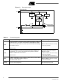
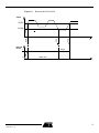
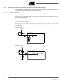
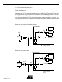
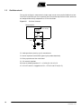
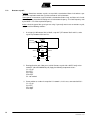
Design Guide
for Atmel’s C51 Standard Devices
C51 MCU’s
Introduction
The aim of this document is to help customers to avoid errors that are frequently done
in order save efforts and time during hardware debugging sessions.
This document relates only to Atmel’s C51 standard devices. It is the responsability of
the user to read the datasheet of his own device and check if the features and procedures described here are applicable.
Abbreviations
• ISP: In-System Programming
• FLIP: FLexible In-system Programmer
• GUI: Graphical User Interface
• BLJB: Boot Loader Jump Bit
• HPC: High Pin Count
• LPC: Low Pin Count
• HSB: Hardware Security Byte
Application Notes used as references
• How to calculate the capacitor of the reset input of a
C51 microcontroller
(doc 4284.pdf)
• External Brown-out Protection for C51
microcontrollers with Active High Reset Input
(doc 4183.pdf)
• How to use a third Overtone crystal with a 80C51
family microcontroller
(doc397c496b2072e.pdf)
7764A–8051–11/07
1. Basics of ATMEL’s C51 Standard devices
1.1
Program memory configurations
1.1.1
Scope
Figure 1-1.
Code fetched from external program memory
External program memory
Standard C51
A15:8
P2
EA
A15:8
ALE
GND
AD7:0
Latch
A7:0
P0
A7:0
D7:0
/PSEN
Figure 1-2.
OE
Code fetched from internal program memory
VCC
Standard C51
EA
VCC
VCC
P2
ALE
10K
P0
/PSEN
Table 1-1.
Pin description
PIN
I/O
External Code
Internal Code
EA
Input
Must be connected to GND
Must be connected to VCC, directly or through a
10K resistor.
ALE
Output
signal
This signal is used to clock the Least Significant Byte into the
address latch.
Not used.
Must be left unconnected in normal operation
PSEN
Output
signal
This signal is used to strobe the external program memory
when the MCU fetches the code byte.
P0
I/O
port
Port 0 serves as a multiplexed address/data bus. It emits the
low byte of the Program Counter (PCL) as an address, and
then goes into a float state awaiting the arrival of the code
byte from the Program Memory.
Can be used as a general purpose I/O port. In
this case external 10K pull-up’s must be
provided.
P2
I/O
port
Port 2 emits the high byte of the Program Counter (PCH)
Can be used as a general purpose I/O port.
No external pull-up’s are needed as this port
owns internal pull-up’s
Not used.
Must be left unconnected in normal operation
2
7764A–8051–11/07
1.1.2
Type of package
In most of the products, two kind of packages are proposed: the HPC (High Pin Count) and the
LPC (Low Pin Count).
The HPC packages support the external code and therefore provide the appropriate pins (EA,
ALE, PSEN, P0, P2), while the LPC packages do not support the external code and do not provide any of the dedicated pins.
1.1.3
Hardware Security Byte (HSB)
WARNING
Parts are delivered by default with HSB set to maximum security (see product datasheet for
further information). This configuration prevents the MCU from fetching external code.
On ROM products the user will need to take care about the HSB configuration at the time he
orders the mask ROM if the external code mode is needed on his application.
On FLASH products the user will need to perform a full chip erase by means of an external
programmer before using the parts if the external code mode is needed on his application.
1.1.4
Reduced EMI Mode
The ALE signal is used to demultiplex address and data buses on port 0 when used with external program or data memory. Nevertheless, during internal code execution, ALE signal is still
generated. In order to reduce EMI, ALE signal can be disabled by setting AO bit.
The AO bit is located in AUXR register at bit location 0. As soon as AO is set, ALE is no longer
output but remains active during MOVX and MOVC instructions and external fetches. During
ALE disabling, ALE pin is weakly pulled high.
1.2
1.2.1
Hardware reset
Internal features
Some C51 devices may implement the following features:
• Power On Reset (POR)
• Power Fail Detector (PFD)
• Hardware Watch-Dog Timer (WDT)
• Internal Pull-up on reset pin
There are different ways to drive the reset pin depending on which features are implemented in
the device. The user is invited to carefully read the product datasheet to know which features are
or are not implemented.
3
7764A–8051–11/07
Figure 1-3.
Reset bock diagram
Microcontroller
Vcc
POR
PFD
C51
Core
Watch Dog
Timer
Internal Reset
RST
Table 1-2.
Features descriptions
Feature
Description
Impact on RST pin
PFD
The role of the PFD is to monitor the power supply drops during a steady state
condition in order to suspend the microcontroller’s activity. When the PFD is
active, it holds the MCU under a reset state to prevent the MCU from having
unpredictable behaviour.
While the PFD is active, the reset pin
is driven by the PFD.
Optional feature
POR
The role of the POR is to monitor the rising of internal power supply of the
microcontroller core. It releases the internal reset only when the internal
voltage is enough for the core to operate.
Optional feature
- No external components or
superviser devices are needed to
drive the reset pin
- While the POR is active, the reset pin
is driven by the POR
- RST pin may be left unconnected
WDT
The WDT automatically resets the chip if the software fails to reset the WDT
before the selected time interval has elapsed.
Basic feature of C51 devices
While the WDT is active, the reset pin
is driven by the WDT.
Internal
Pull-up
Saves an external component
No external pull-up needed
4
7764A–8051–11/07
Figure 1-4.
Behaviour of POR and PFD
VCore
VPFDP
Internal
Reset 1
0
POR
PFD
POR
VPFDM
t
Active
Not active
5
7764A–8051–11/07
1.2.2
1.2.2.1
How to drive the RST pin according to the features implemented on the device
This procedure is only applicable to Active High reset pins. However, this procedure can be easily adapted for microcontrollers with Active Low Reset pins.
POR not implemented
When the POR is not implemented, it is necessary to implement external components to assure
a correct reset of the MCU.
a) Using an external capacitor
Read application note “ How to calculate the capacitor of the reset input of a C51 microcontroller” (doc 4284).
Internal pull-up
VCC
Microcontroller
C
RST
Internal Reset
R
External Pull-up
VCC
Microcontroller
C
RST
Internal Reset
R
6
7764A–8051–11/07
b) Using an external Brown-out device
Read application note “External Brown-out Protection for C51 microcontrollers with Active High
Reset Input“ (doc 4183).
Sometimes the RST pin may be internally forced by the WDT so that the external peripherals if
any are reset at the same time as the MCU. While the WDT is active the RST pin operates as an
output. Therefore the RST pin cannot be externally forced to a permanent level. If the external
Brown-out device operates in this way, an intermediate resistor Rint or a diode must be implemented between the Brown-out device and the RST pin.
Brown-out device with an intermediate resistor
Microcontroller
VCC
Watchdog
Timer
Rint
RST
Brown-out
device
Internal Reset
R
To other on-board
circuitry
Brown-out device with a diode
Microcontroller
VCC
Watchdog
Timer
1N4148
RST
Brown-out
device
Internal Reset
R
To other on-board
circuitry
7
7764A–8051–11/07
1.2.2.2
POR implemented
When the POR is implemented, the use of external components is optional.
The RST pin may be left unconnected.
a) No external components used
Microcontroller
Power On
Reset
VCC
Power Fail
Detector
Watchdog
Timer
RST
Internal Reset
R
b) Using an external capacitor
Microcontroller
Power On
Reset
VCC
Power Fail
Detector
Watchdog
Timer
C
RST
Internal Reset
R
8
7764A–8051–11/07
c) Using an external Brown-out device
Read application note “External Brown-out Protection for C51 microcontrollers with Active High
Reset Input“ (doc 4183).
Sometimes the RST pin may be internally forced by the POR or the PFD or the WDTso that the
external peripherals if any are reset at the same time as the MCU. While the POR or the PFD or
the WDT are active the RST pin operates as an output. Therefore the RST pin cannot be externally forced to a permanent level. If the external Brown-out device operates in this way, an
intermediate resistor Rint or a diode must be implemented between the Brown-out device and
the RST pin.
Brown-out device with an intermediate resistor
Microcontroller
Power On
Reset
Power Fail
Detector
VCC
Rint
Watchdog
Timer
RST
Brown-out
device
Internal Reset
R
To other on-board
circuitry
Brown-out device with a diode
Microcontroller
Power On
Reset
Power Fail
Detector
VCC
1N4148
Watchdog
Timer
RST
Brown-out
device
Internal Reset
R
To other on-board
circuitry
9
7764A–8051–11/07
1.3
Oscillator circuit
The on-chip oscillator is composed of a single-stage inverter and a parallel feedback resistor.
The XTAL1 and XTAL2 pins are respectively the input and the output of the inverter, which can
be configured with off-chip components as a Pierce oscillator.
Figure 1-5.
Oscillator Schematic
Microcontroller
To internal
clock circuitry
Feedback
Resistor
XTAL2
XTAL1
C1
GND
Crystal
C2
GND
CL: load capacitance given by crystal’s manufacturer
CI: internal capacitance of the MCU (given by the product datasheet)
CS: Stray capacitance of the circuit board
C1, C2: external capacitors
We have the following equation: CL = (C1xC2)/(C1+C2)+CI+CS
If C1=C2=CF and CS is negligible then CL = CF/2+CI and CF=2x(CL-CI)
10
7764A–8051–11/07
1.3.1
Test conditions
It is recommended to monitor the clock on XTAL2 pin.
Special care must be taken when measuring XTAL1 signal. A high impedance probe must be
used to avoid any distorsion of the signal.
Microcontroller
XTAL1
XTAL2
High impedance probe
Test condition: probe’s impedance > 1 MOhm
This means that oscilloscope’s active probes are prohibited due to their weak impedance (usually around 100KOhm)
1.3.2
Relationship between oscillator and ALE frequencies
Output pulse for latching the low byte of the address during an access to external memory. In
normal operation, ALE is emitted at a constant rate of the oscillator frequency and can be used
for external timing or clocking.
Note that one ALE pulse is skipped during each access to external data memory.
ALE can be disabled by setting SFR’s AUXR.0 bit. When this bit is set, ALE will be inactive during internal fetches.
MCU’s Clock mode
ALE frequency
X1 mode
Freq(ale) = Freq(osc )/6
X2 mode
Freq(ale) = Freq(osc )/3
11
7764A–8051–11/07
1.3.3
Overtone crystals
Problem: Sometimes overtone crystals are used with a standard oscillator circuit where a specific one is required to make the crystal to oscillate on its third overtone.
Consequence: an overtone crystal used with a standard oscillator circuit, oscillates on its fundamental frequency instead of oscillating on its third overtone frequency. The clock frequency seen
by the MCU is 1/3 of the expected frequency.
Action: check the type of the crystal you are using. If you really want to use an overtone crystal,
apply one of the following solutions.
1. A resistor of 3.9K between Xtal1 et Xtal2, a cap of 4.7 pF between Xtal1 and Vss, and a
cap of 15pF between Xtal2 and Vss
Feedback
Resistor
To internal
clock circuitry
Microcontroller
XTAL1
3.9K
4.7pF
Overtone
Crystal
GND
XTAL2
15pF
GND
2. Read application note “How to use a third Overtone crystal with a 80C51 family microcontroller” (doc397c496b2072e.pdf). Apply the following component values :
L1= 1.5 µH
C3=4.7nF
CP1=12pF
CP2=27pF
C2 : not needed
3. Same solution as number 2 except the LC network is, in this case, connected to Xtal1 :
L1= 1.5 µH
C3=4.7nF
CP1=10pF
CP2=10pF
12
7764A–8051–11/07
1.4
Microcontroller status
During hardware or firmware debugging, it is sometimes interesting to know what the state of the
microcontroller is. See table below for details.
Hardware
conditions
RST
Microcontroller status
EA
ALE
PSEN
XTAL2
Mode
Active
1
1
1
Flat
Reset
Not active
1
Toggling
1
Toggling
Operating mode
Fetches internal code
Not active
1
1
1
Toggling
Idle mode
Does not fetch code
Not active
1
0
0
Flat
Power down mode
Does not fetch code
Active
0
1
1
Flat
Reset
Not active
0
Toggling
1
Toggling
Operating mode
Fetches external code
Not active
0
1
1
Toggling
Not active
0
0
0
Flat
Note:
P0
P1
P2
P3
FF
FF
FF
Port Data(1)
Port Data
Port Data
Port Data
Port Data(1)
Port Data
Port Data
Port Data
FF
FF
FF
FF
Idle mode
Does not fetch code
Floating
Port Data
Address
Port Data
Power down mode
Does not fetch code
Floating
Port Data
Port Data
Port Data
Port 0 can force a 0 level. A "one" will leave port floating.
13
7764A–8051–11/07
2. In-System Programming (ISP)
The In-System Programming feature will be referenced as ISP in the rest of the document.
Most of Atmel’s C51 devices support the ISP mode. This feature enables the user to program
the device directly on his application without having to unsolder the device or using an external
programmer. This feature is made by means of a bootloader firmware embedded in the device
itself. A PC based application like FLIP (FLexible In-system Programmer) or any equivalent custom software enables to communicate with the bootloader to perform the part programming.
FLIP can be downloaded free of charge from the Atmel’s web site. It supports different interfaces
like RS232, USB, and CAN following the used device. Ensure you are always using the latest
version of FLIP.
The ISP mode is invoked by applying an hardware condition. The hardware condition differs
between a HPC and a LPC package (See “Type of package” on page 3.)
2.1
2.1.1
HPC package
Hardware settings
The following hardware settings must be applied in normal mode (execution) before starting the
ISP mode (programming).
• EA pin must be tied to Vcc. The bootloader is only active when internal program memory is
used.
• ALE pin cannot be forced by an external signal. This pin is driven by the MCU. Leave this pin
unconnected if not used.
• PSEN pin cannot be forced by an external signal. This pin is driven by the MCU. Leave this
pin unconnected if not used.
2.1.2
Starting the ISP mode
Software condition: there are some configuration bits available in the part which enables to configure the bootloader behaviour. Refer to the product’s bootloader datasheet for further
information. These bits are accessible from the GUI of FLIP. The BLJB bit is part of these. Most
of the time, it is activated at manufacturing level on new chips to have the device run in ISP
mode at first power on. When the BLJB is active, the user does not need to apply the hardware
condition described here after. It may be usefull at production level for instance. The BLJB bit is
deactivated by the bootloader after the first programming. It is then the responsability of the user
to re-activate it.
Hardware condition: when the BLJB bit is inactive, the only way to have the device run in ISP
mode, is to apply the hardware condition.
The hardware condition consists to apply an hardware reset while pulling the PSEN pin to
ground then to release the PSEN pin once the hardware reset has been applied.
It is recommended to pull the PSEN pin to ground through a 1K resistor to prevent the PSEN pin
from being damaged.
WARNING
Do not apply the hardware condition at power up otherwise the ISP mode may fail to start.
The hardware condition must be applied only when the device has started and when the
power supplies are stables.
14
7764A–8051–11/07
Figure 2-1.
HPC hardware condition
VCC
VCC
VCC
Standard C51
VCC
EA
ALE
Unconnected
PC running FLIP
RST
C2
GND
XTAL2
UART / USB / CAN interfaces
Bootloader
Crystal
XTAL1
/PSEN
1K
VSS
GND
2.2
GND
C1
GND
LPC package
2.2.1
Hardware settings
There are no specific hardware settings to apply.
2.2.2
Starting the ISP mode
Software condition:
WARNING
For LPC packages the BLJB bit is activated at manufacturing level and MUST NEVER be
changed by the user. If this ever occurs, the only way to restore the ISP mode is to re-program the device by an external programmer.
Normally the BSB (Boot Status Byte) is activated (0xFF) at manufacturing level on new chips to
have the device run in ISP mode at first power on. When the BSB is active, the user does not
need to apply the hardware condition described here after. It may be useful at customer’s production level for instance. The BSB is deactivated (0x00) by the bootloader after the first
programming. It is then the responsability of the user to re-activate it.
15
7764A–8051–11/07
Figure 1. Low Pin Count regular boot process
Bit ENBOOT in AUXR1 Register is
Initialized with BLJB Inverted
Hardware
Boot Process
RESET
ENBOOT = 0
PC = 0000h
Yes
CAUTION
Do not change the BLJB bit
BLJB = 1
No
ENBOOT = 1
PC = F400h
Hardware condition
No
Software Boot Process
in Low Pin Count
No
P1_CF = FFh
No
P1_CF = P1
Yes
Yes
No
P3_CF = P3
P3_CF = FFh
No
Yes
P4_CF = FFh
Yes
Yes
No
Yes
BSB = 0
P4_CF = P4
Yes
No
SBV < 7Fh
No
Yes
Start Application
Start User Bootloader
Start Bootloader
Hardware condition: when the BSB is inactive, the only way to have the device run in ISP mode,
is to apply the hardware condition.
As the PSEN pin is not available in LPC packages, a port pin is used instead to apply the hardware condition which consists by default to apply a hardware reset while pulling P1.0 pin to
ground then to release P1.0 pin once the hardware reset has been applied.
P1.0 is an Atmel default setting which can be easily changed by FLIP. The user can select a
another port if P1.0 is inappropriate for his application. Refer to the product’s bootloader
datasheet for further information.
16
7764A–8051–11/07
Figure 2-2.
LPC hardware condition
VCC
VCC
Standard C51
VCC
PC running FLIP
RST
C2
GND
XTAL2
Bootloader
UART / USB / CAN interfaces
Crystal
XTAL1
GND
C1
P1.0
VSS
GND
2.3
2.3.1
GND
Using the ISP mode over RS232 interface
Baudrate
The maximum baudrate supported by the device depends on the crystal value or signal frequency injected on XTAL1 pin. Refer to product datasheet for further information.
2.3.2
Hardware
The schematics of the interface are given here after.
Auto ISP feature: the implementation of this feature is optional.
When this feature is supported by the hardware, the same option can be activated in the preferences menu of FLIP. This option enables FLIP to manage and set automatically the hardware
condition to have the device run in ISP and to proceed with the part programming.
17
7764A–8051–11/07
18
7764A–8051–11/07
1
6
2
7
3
8
4
9
5
DSR
Rx_PC
RTS
Tx_PC
CTS
DTR
SUB-D9 FEMALE
RS232
P1
1
J13
2
1
1
DTR
J12
RTS
J11
2
2
AUTO ISP FEATURE
C23
100n
C21
100n
C18
100n
C16
100n
RS232 INTERFACE
1
3
4
5
13
8
14
7
1
3
4
5
13
8
14
7
Vcc
C1+
C1C2+
C2-
R1IN
R2IN
T1IN
T2IN
6
2
6
2
12
9
11
10
SIPEX-SP3232ECA
U8
V-
V+
R1OUT
R2OUT
T1IN
T2IN
C17
100n
Vcc
C24
100n
Vcc
C22
100n
C19
100n
Vcc
C20
100n
Vcc
C25
100n
2
C26
100n
5
Rx_MCU
12
9
Vcc
Tx_MCU
11
10
SIPEX-SP3232ECA
U7
V-
V+
R1OUT
R2OUT
Vcc
T1OUT
T2OUT
C1+
C1C2+
C2-
R1IN
R2IN
T1OUT
T2OUT
16
GND
15
VCC
VCC
16
GND
15
6
R22
1K
U9A
74HC125/SO_5
3
Vcc
CD2
100n
D11
Green Led
Rx LED
U10B
74HC125/SO_5
14
4
7
14
1
7
Vcc
R24
1K
SW8
ISP
R6
10K
SW1
RESET
R23
1K
D12
Green Led
Tx LED
/PSEN
RST
P3_0/RxD
P3_1/TxD
3. Troubleshooting
3.1
MCU not starting or operating in a reliable way
Possible root
cause
I/O
External Code
Internal Code
- Must be stables
POWERS and
GND delivered
to the device
Input
XTA2 pin
Output
- Monitor XTAL2 to see if the oscillator has started and is working properly. Check if your crystal is not an overtone part.
I/O
- If the device does not have an internal POR, read application note: “how to calculate the capacitor of the reset input of
a C51 microcontroller” (doc 4284)”
- Monitor power supplies
- Check if GND is properly supplied to device
- If RST pin is not correctly driven, MCU is not properly reset.
RST pin
- If an external Brown-out device is used, an intermediate resistor or diode must be implemented between RST pin and
the Brown-out device
EA pin
Input
- Must be connected to GND
- Must be connected to VCC, directly or through a 10K
resistor.
- MCU may not work properly, if this pin is left floatting
ALE pin
Output
signal
PSEN pin
Output
signal
P0
I/O
port
P2
I/O
port
- This signal is used to clock the Least
- Not used.
Significant Byte into the address latch
- Must be left unconnected in normal operation
- the frequency of this signal enables to guess the
frequency that the core runs at.
- If ALE is not disabled by firmware, the frequency of this
signal enables to guess the frequency that the core runs at.
(See “Relationship between oscillator and ALE
frequencies” on page 11.)
See “Relationship between oscillator and ALE frequencies”
on page 11.)
- This signal is used to strobe the external program
memory when the MCU fetches the code byte.
- Monitor ALE and PSEN pins to get the status of the
MCU. ( See “Microcontroller status” on page 13.)
Port 0 serves as a multiplexed address/data bus. It
emits the low byte of the Program Counter (PCL) as an
address, and then goes into a float state awaiting the
arrival of the code byte from the Program Memory
Port 2 emits the high byte of the Program Counter
(PCH)
HSB set to maximum
security
Does not work
Device is damaged
Try another device
- Not used.
- Must be left unconnected in normal operation
- If ALE is not disabled by firmware, monitor ALE and PSEN
pins to get the status of the MCU. ( See “Microcontroller
status” on page 13.)
Can be used as a general purpose I/O port.
In this case external pull-up’s must be provided.
Can be used as a general purpose I/O port.
No external pull-up’s are needed as this port owns internal
pull-up’s
No impact
19
7764A–8051–11/07
3.2
In-System Programming does not work
Possible root cause
External Code
Apply the hardware condition. See “In-System Programming (ISP)” on page
14. and read the device’s bootloader datasheet.
MCU is not working in ISP mode
MCU does not work properly
Device is damaged
Internal Code
NOT
APPLICABLE
Monitor power supplies, XTAL2, RST, EA, ALE, PSEN ( See “MCU not
starting or operating in a reliable way” on page 19.)
Try a new or another device
20
7764A–8051–11/07
Atmel Corporation
2325 Orchard Parkway
San Jose, CA 95131, USA
Tel: 1(408) 441-0311
Fax: 1(408) 487-2600
Regional Headquarters
Europe
Atmel Sarl
Route des Arsenaux 41
Case Postale 80
CH-1705 Fribourg
Switzerland
Tel: (41) 26-426-5555
Fax: (41) 26-426-5500
Asia
Room 1219
Chinachem Golden Plaza
77 Mody Road Tsimshatsui
East Kowloon
Hong Kong
Tel: (852) 2721-9778
Fax: (852) 2722-1369
Japan
9F, Tonetsu Shinkawa Bldg.
1-24-8 Shinkawa
Chuo-ku, Tokyo 104-0033
Japan
Tel: (81) 3-3523-3551
Fax: (81) 3-3523-7581
Atmel Operations
Memory
2325 Orchard Parkway
San Jose, CA 95131, USA
Tel: 1(408) 441-0311
Fax: 1(408) 436-4314
Microcontrollers
2325 Orchard Parkway
San Jose, CA 95131, USA
Tel: 1(408) 441-0311
Fax: 1(408) 436-4314
La Chantrerie
BP 70602
44306 Nantes Cedex 3, France
Tel: (33) 2-40-18-18-18
Fax: (33) 2-40-18-19-60
ASIC/ASSP/Smart Cards
RF/Automotive
Theresienstrasse 2
Postfach 3535
74025 Heilbronn, Germany
Tel: (49) 71-31-67-0
Fax: (49) 71-31-67-2340
1150 East Cheyenne Mtn. Blvd.
Colorado Springs, CO 80906, USA
Tel: 1(719) 576-3300
Fax: 1(719) 540-1759
Biometrics/Imaging/Hi-Rel MPU/
High Speed Converters/RF Datacom
Avenue de Rochepleine
BP 123
38521 Saint-Egreve Cedex, France
Tel: (33) 4-76-58-30-00
Fax: (33) 4-76-58-34-80
Zone Industrielle
13106 Rousset Cedex, France
Tel: (33) 4-42-53-60-00
Fax: (33) 4-42-53-60-01
1150 East Cheyenne Mtn. Blvd.
Colorado Springs, CO 80906, USA
Tel: 1(719) 576-3300
Fax: 1(719) 540-1759
Scottish Enterprise Technology Park
Maxwell Building
East Kilbride G75 0QR, Scotland
Tel: (44) 1355-803-000
Fax: (44) 1355-242-743
Literature Requests
www.atmel.com/literature
Disclaimer: The information in this document is provided in connection with Atmel products. No license, express or implied, by estoppel or otherwise, to any
intellectual property right is granted by this document or in connection with the sale of Atmel products. EXCEPT AS SET FORTH IN ATMEL’S TERMS AND CONDITIONS OF SALE LOCATED ON ATMEL’S WEB SITE, ATMEL ASSUMES NO LIABILITY WHATSOEVER AND DISCLAIMS ANY EXPRESS, IMPLIED OR STATUTORY
WARRANTY RELATING TO ITS PRODUCTS INCLUDING, BUT NOT LIMITED TO, THE IMPLIED WARRANTY OF MERCHANTABILITY, FITNESS FOR A PARTICULAR
PURPOSE, OR NON-INFRINGEMENT. IN NO EVENT SHALL ATMEL BE LIABLE FOR ANY DIRECT, INDIRECT, CONSEQUENTIAL, PUNITIVE, SPECIAL OR INCIDENTAL DAMAGES (INCLUDING, WITHOUT LIMITATION, DAMAGES FOR LOSS OF PROFITS, BUSINESS INTERRUPTION, OR LOSS OF INFORMATION) ARISING OUT
OF THE USE OR INABILITY TO USE THIS DOCUMENT, EVEN IF ATMEL HAS BEEN ADVISED OF THE POSSIBILITY OF SUCH DAMAGES. Atmel makes no
representations or warranties with respect to the accuracy or completeness of the contents of this document and reserves the right to make changes to specifications
and product descriptions at any time without notice. Atmel does not make any commitment to update the information contained herein. Unless specifically providedotherwise, Atmel products are not suitable for, and shall not be used in, automotive applications. Atmel’s products are not intended, authorized, or warranted for use as components in applications intended to support or sustain life.
©2007 Atmel Corporation. All rights reserved. Atmel ®, logo and combinations thereof, and Everywhere You Are ® are the trademarks or registered trademarks, of Atmel Corporation or its subsidiaries. Other terms and product names may be trademarks of others.
Printed on recycled paper.
7764A–8051–11/07