1
1. Basics of ATMEL’s C51 Standard devices
1.1
Program memory configurations
1.1.1
Scope
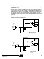
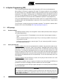
Figure 1-1.
Code fetched from external program memory
External program memory
Standard C51
A15:8
P2
EA
A15:8
ALE
GND
AD7:0
Latch
A7:0
P0
A7:0
D7:0
/PSEN
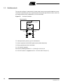
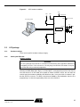
Figure 1-2.
OE
Code fetched from internal program memory
VCC
Standard C51
EA
VCC
VCC
P2
ALE
10K
P0
/PSEN
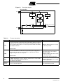
Table 1-1.
Pin description
PIN
I/O
External Code
Internal Code
EA
Input
Must be connected to GND
Must be connected to VCC, directly or through a
10K resistor.
ALE
Output
signal
This signal is used to clock the Least Significant Byte into the
address latch.
Not used.
Must be left unconnected in normal operation
PSEN
Output
signal
This signal is used to strobe the external program memory
when the MCU fetches the code byte.
P0
I/O
port
Port 0 serves as a multiplexed address/data bus. It emits the
low byte of the Program Counter (PCL) as an address, and
then goes into a float state awaiting the arrival of the code
byte from the Program Memory.
Can be used as a general purpose I/O port. In
this case external 10K pull-up’s must be
provided.
P2
I/O
port
Port 2 emits the high byte of the Program Counter (PCH)
Can be used as a general purpose I/O port.
No external pull-up’s are needed as this port
owns internal pull-up’s
Not used.
Must be left unconnected in normal operation
2
7764A–8051–11/07