1
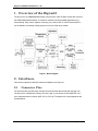
Digi m10 Satellite Modem Hardware Reference Date: 11 January 2013 90033937_K Copyright Notice Digi International has prepared this manual for the use of its employees, agents, and its customers. This manual contains proprietary information, which is protected by copyright. Preparing derivative works or providing instruction based on this manual is prohibited without written permission from Digi International. All information in this manual is accurate and reliable to the best of Digi International's knowledge. Digi International may make improvements and / or changes in this manual at any time without prior notice. Trademarks The Digi m10 is a registered trademark of Digi International Inc. All other company and / or product names mentioned in this manual are the property of their respective owners. Document Revision History Version Description Date A Initial release of the new hardware reference manual 21 Sep 2009 B Extended packet information removed. Images updated. 10 Nov 2009 C Debug port termination (RX) requirements added as well as RTS/CTS implementation section added in chapter 2. Updated Pin descriptions in chapter 2. 18 Jan 2010 D Updated mechanical drawings and added section 2.2.2 “Host Port with Flow Control”. Appendix D added. Industry Canada Notice added to front matter. 20 May 2010 E Fixed error in section 2.7. 4 Nov 2010 F Fixed error in Section 6 and added Appendix E. 12 Sep 2011 G Fixed error in Section 2.2. 13 Oct 2011 Fixed the resolution of Digi m10 Mechanical Drawing: Part D image 26 Jun 2012 H K in Appendix A Updated the Environmental Specifications in Section 3.1 3 Jan 2013 Digi m10 Hardware Reference v 1.20 Table of Contents Digi m10 ....................................................................................................................................... 1-1 Satellite Modem .......................................................................................................................... 1-1 Hardware Reference ................................................................................................................... 1-1 Copyright Notice ......................................................................................................................... 1-2 Trademarks ................................................................................................................................. 1-2 Document Revision History....................................................................................................... 1-3 Table of Contents ......................................................................................................................... iv List of Tables.................................................................................................................................. v List of Figures ................................................................................................................................ v About This Manual......................................................................................................................... 6 Target Audience .......................................................................................................................... 6 Symbols Used in This Manual ..................................................................................................... 6 Reference Documents ................................................................................................................. 6 Industry Canada Notice ............................................................................................................... 8 Caution......................................................................................................................................... 8 Where to Get Help ....................................................................................................................... 8 1. Overview of the Digi m10 ...................................................................................................... 9 2. Interfaces ................................................................................................................................ 9 2.1 Connector Pins ............................................................................................................... 9 2.2 Serial Interface ............................................................................................................. 12 2.2.1 Host Port .................................................................................................................. 12 2.2.2 Host Port (With Flow Control) .................................................................................. 12 2.2.3 Debug Port ............................................................................................................... 12 2.3 Power and Ground ....................................................................................................... 13 2.4 Power Enable ............................................................................................................... 13 2.4.1 Powering Up ............................................................................................................ 13 2.4.2 Powering Down ........................................................................................................ 14 2.5 DA (Data Available) ...................................................................................................... 14 2.6 RTS/CTS Implementation ............................................................................................ 15 2.7 SA (Satellite Available) ................................................................................................. 15 2.8 RF Interface.................................................................................................................. 16 3. Technical Specifications ..................................................................................................... 18 3.1 Environmental .............................................................................................................. 18 3.1.1 Electromagnetic Compatibility ................................................................................. 18 3.1.2 RoHS ....................................................................................................................... 19 3.1.3 Operating Temperature ........................................................................................... 19 3.1.4 Storage Temperature ............................................................................................... 20 3.1.5 Operational Shock ................................................................................................... 20 3.1.6 Operational Vibration ............................................................................................... 20 3.2 Electrical ....................................................................................................................... 20 3.2.1 Power Design........................................................................................................... 21 3.2.2 Digital Input / Output Specifications ......................................................................... 22 3.2.3 Lifespan ................................................................................................................... 22 3.3 Mechanical ................................................................................................................... 22 3.3.1 Module Size ............................................................................................................. 22 3.3.2 Mounting .................................................................................................................. 23 Digi International, Inc. © 2013 iv Digi m10 Hardware Reference v 1.20 4. 5. Approvals and Certifications .............................................................................................. 24 Using the Digi m10 .............................................................................................................. 25 5.1 Interfacing with the Digi m10 ........................................................................................ 25 5.2 The Digi m10 JumpStart Kit ......................................................................................... 26 6. Antenna Information ............................................................................................................ 28 Appendix A: Digi m10 Mechanical Drawings ............................................................................. 29 Appendix B: Development Board Mechanical Drawing ............................................................. 33 Appendix C: Digi m10 Development Board Schematic ............................................................. 34 Appendix D: M10 Modifications for Industry Canada Compliance ............................................ 38 List of Tables Table 1: Connector Pins on the Digi m10 ...................................................................................... 11 Table 2: Host Transmit and Receive Pins ..................................................................................... 12 Table 3: Debug Transmit and Receive Pins .................................................................................. 12 Table 4: Power Pins ...................................................................................................................... 13 Table 5: Power Enable Pin ............................................................................................................ 13 Table 6: DA Pin.............................................................................................................................. 15 Table 7: SA Pin .............................................................................................................................. 15 Table 8: RF Interface Details ......................................................................................................... 16 Table 9: Operating Conditions ....................................................................................................... 20 Table 10: Digital I/O Electrical Specifications ................................................................................ 22 List of Figures Figure 1: Block Diagram .................................................................................................................. 9 Figure 2: Digi m10 Pin Numbering ................................................................................................ 10 Figure 3: Pin Assignment .............................................................................................................. 11 Figure 4: Timing Diagram for Powering Up ................................................................................... 14 Figure 5: Timing Diagram for Powering Down .............................................................................. 14 Figure 6: Timing Diagram for Data Available ................................................................................ 15 Figure 7: Timing Diagram for Satellite Available ........................................................................... 16 Figure 8: RF Connector on the Digi m10 ....................................................................................... 16 Figure 9: Digi m10 Dimensions ..................................................................................................... 23 Figure 10: Interface Between the Host Controller and the Digi m10 ............................................. 25 Figure 11: Layout of the Development Board................................................................................ 26 Figure 12: Digi m10 Mechanical Drawing ...................................................................................... 29 Figure 13: Digi m10 Mechanical Drawing: Part A.......................................................................... 29 Figure 14: Digi m10 Mechanical Drawing: Part B.......................................................................... 30 Figure 15: Digi m10 Mechanical Drawing: Part C ......................................................................... 31 Figure 16: Digi m10 Mechanical Drawing: Part D ......................................................................... 32 Figure 17: Development Board Schematic .................................................................................... 34 Figure 18: Development Board Schematic (Part A) ...................................................................... 35 Figure 19: Development Board Schematic (Part B) ...................................................................... 35 Figure 20: Development Board Schematic (Part C) ...................................................................... 35 Figure 21: Development Board Schematic (Part D) ...................................................................... 36 Digi International, Inc. © 2013 v Digi m10 Hardware Reference v 1.20 About This Manual This manual defines and specifies the functions of the Digi m10 and its usage. It also contains guidelines for using the development board which comes with the Digi m10 JumpStart Kit. Target Audience The target audience for this user manual comprises engineers and business managers who want to augment their company's existing asset-tracking systems with satellite networks. A typical user would be an engineer who is well- versed with wireless data communications. Symbols Used in This Manual Symbol Description Provides additional information corresponding to the topic that is being discussed. Warning! If ignored, may cause permanent damage to the development kit or injury to a person. Caution! Failure to comply with a caution may result in failure or damage to the device. Danger! Failure to comply with a danger symbol may result in serious injury. Reference Documents The following documents have been used in the preparation of this user manual: Department of Defense Test Method Standard for Environmental Engineering Considerations and Laboratory Tests, MIL STD 810E European Telecommunications Standards Institute, EN 300 832 (A1 version 1.1.1), Electromagnetic Compatibility for Mobile Earth Stations. International Electrotechnical Commission, IEC 61000-4-4, Testing and Measurement Techniques -- Immunity to Fast Transient / Burst Immunity Test. International Electrotechnical Commission, IEC 61000-4-6, Testing and Measurement Techniques -- Immunity to Conducted Disturbances, Induced by Radio-Frequency Fields. ORBCOMM Serial Interface Specification, E80050015. ORBCOMM Subscriber Communicator (SC) Standards and Specifications, E25050102. ORBCOMM Subscriber Communicator Type Approval Plan, A25TP0017. ORBCOMM System Overview, A80TD0008. RoHS FAQ -- http://www.rohs.gov.uk/FAQs.aspx#10 Digi International, Inc. © 2013 Page 6 of 38 Digi m10 Hardware Reference v 1.20 Society of Automotive Engineers, SAE J1455, Joint SAE / TMC Recommended Environmental Practices for Electronic Equipment Design (Heavy-Duty Trucks). Technical Requirements for Satellite Earth Stations and Systems (SES); Mobile Earth Stations (MES) Providing Low Bit Rate Data Communications (LBRDC) using Low Earth Orbiting (LEO) satellites operating below 1 GHz, EN 3200 721. Digi International, Inc. © 2013 Page 7 of 38 Digi m10 Hardware Reference v 1.20 Industry Canada Notice This equipment has been tested and found to be in compliance with the limits for Industry Canada requirements. Operation is subject to the following two conditions: 1) this device may not cause harmful interference, and 2) this device must accept any interference received, including interference that may cause undesired operation. Caution To comply with the IC radio frequency exposure requirements, the following antenna installation and device operating configurations must be satisfied: # Product models using external antennas require professional installation. The antennas used for professional installation must be fixed-mounted on indoor/outdoor permanent structures with a separation distance from all persons more than 50 cm (approximately 20 inches). # Antennas must not be co-located and must not operate in conjunction with any other antenna or transmitter. In the event of a problem, please contact the after sales service network. As per Directive 2002/96/EC of the European Parliament and Council on waste and electrical equipment (WEEE), the product should be returned to the distributor after the end of product life. Where to Get Help For additional information or clarifications regarding this user manual, please get in touch with Digi International using the contact information provided below. Address 11001 Bren Road East Minnetonka, MN 55343 Phone 952-912-3456 Email http://www.digi.com/support/eservice/login.jsp Digi International, Inc. © 2013 Page 8 of 38 Digi m10 Hardware Reference v 1.20 1. Overview of the Digi m10 The Digi m10 is an ORBCOMM Subscriber Communicator, which enables modem-like access to the ORBCOMM satellite network. It is ideal for machine-to-machine (M2M) applications (e.g. asset tracking, utility meters, pipeline monitoring, etc.) that monitor or control remote assets. It can be added to an existing tracking system or run as a stand-alone modem. Figure 1: Block Diagram 2. Interfaces This section explains the different interfaces available on the Digi m10. 2.1 Connector Pins The host controller provides power and ground, and communicates serially with the Digi m10. The Digi m10 is outfitted with a factory-mounted, 14pin (7 pins across 2 rows) SAMTEC 1mm pitch, standard socket connector (MLE-107-01-G-DV-K). The details of the pin designations are provided below. Digi International, Inc. © 2013 Page 9 of 38 Digi m10 Hardware Reference v 1.20 Figure 2: Digi m10 Pin Numbering The connector provides the necessary interface signals to communicate over a 3.3V TTL level serial link and to power Digi m10. Basic communication can be established using the Tx & Rx lines and the remaining signals provide additional handshaking (RTS/CTS), status (SA/DA) and debug information (Dbg_Tx/Dbg_Rx) as described in the following sections. Refer to Table 1 for details. The Digi m10 can be connected to the host PCB using a 14-pin SAMTEC 1mm pitch, stacker header connector (MW-07-03-G-D-147-065-P). Digi International, Inc. © 2013 Page 10 of 38 Digi m10 Hardware Reference v 1.20 Figure 3: Pin Assignment Table 1: Connector Pins on the Digi m10 Pin Name Description 1 VCC Supply 2 GND Ground 3 VCC Supply 4 GND Ground 5 PWR_EN Digi m10 Power Enable Digital I/O Comments Direction Input 6 GND 7 RX 3.3 V UART Interface. Host controller to the Digi m10 Input 8 TX 3.3V UART Interface. Digi m10 to host controller. Output 9 SA Satellite Available Output 10 DA Data Available Output 11 Dbg_Tx 3.3V UART Interface Digi M10 to Debug Port Output 12 Dbg_Rx 3.3V UART Interface Debug Port to Digi m10 Input 13 RTS 3.3V UART Interface. Host controller to Digi m10 Input 14 CTS 3.3V UART Interface. Digi m10 to Host controller Output Pulled low using 47KΩ Ground Digi International, Inc. © 2013 Page 11 of 38 Digi m10 Hardware Reference v 1.20 2.2 2.2.1 Serial Interface Host Port The host port is the main serial interface and provides device management and monitoring using 3.3 V levels. The serial data is carried on the Transmit (TX) and Receive (RX) lines. The details of the Transmit and Receive pins are shown in Table 2. An RS232 level shifter is required to connect the Digi m10 to a PC. This is already available on the development board, which comes with the Digi m10 JumpStart Kit. Table 2: Host Transmit and Receive Pins Pin Name Description 8 TX 3.3 V UART interface; Digi m10 to the host controller 7 RX 3.3 V UART interface; host controller to the Digi m10 Note: The RX line (Pin 7) needs to be pulled high using a 10KΩ resistor to 3.3V on the Host board. 2.2.2 Host Port (With Flow Control) Hardware flow control is implemented using RTS (Request to Send) and CTS (Clear To Send) signals. Assertion is set to 0V and De-Assertion is set to 3.3V. At power up RTS is configured as input, CTS is configured as output and is set to asserted state. When flow control is enabled via extended packet by DTE, RTS serves as input to m10 and is controlled by DTE where as CTS is input to DTE and is controlled by m10.When M10 is ready to receive data from DTE, it asserts the CTS line. Similarly, when DTE is ready to receive data from M10, it should assert the RTS line. 2.2.3 Debug Port The Digi m10’s diagnostics (this is an optional interface) can be accessed through this port using a terminal emulation program at 115200 baud rate. Table 3: Debug Transmit and Receive Pins Pin Name 11 Dbg_Tx 3.3 V UART debug interface; Digi m10 to the host controller 12 Dbg_Rx 3.3 V UART debug interface; host controller Digi International, Inc. © 2013 Description Page 12 of 38 Digi m10 Hardware Reference v 1.20 to the Digi m10 Note: The Dbg_Rx line (Pin 12) needs to be pulled high using a 10KΩ resistor to 3.3V on the Host board even if Debug port is not used. 2.3 Power and Ground The Digi m10 is powered using five pins of its 14-pin connector (see Table 4). The five mounting pins on the shield of the Digi m10 are also connected to the ground plane of the Digi m10. Table 4: Power Pins 2.4 Pin Name Description 1 VCC Supply 2 GND Ground 3 VCC Supply 4 GND Ground 6 GND Ground Power Enable The Power Enable signal is used to turn the Digi m10 ON or OFF. It is an active high logic-level signal. The power enable signal can be from 3V min to 18V max. This will help users who do not want separate PWR_EN functionality as they can tie PWR_EN to the Digi m10 supply voltage. However, in this condition, the Digi m10 will be always be powered ON (consuming receive current) unless the user cuts OFF Digi m10 power. This signal has to be maintained at an active high level in order to keep the Digi m10 ON. Table 5: Power Enable Pin Pin Name 5 PWR_EN Description Digi m10 Power Enable This line is pulled low using a 47KΩ resistor. 2.4.1 Powering Up To power on the Digi m10, the host controller must provide an input voltage between 9 V and 18 V DC and then set the PWR_EN pin to active high. Typically, the Digi m10 will take five seconds to be in a ready state. After powering on, the Digi m10 will toggle the DA pin once to let the host controller know that it is ready to receive serial commands. After the DA pin's initial toggle, its subsequent active high state indicates messages from the satellite that are available in the Digi m10's inbound (IB) queue. The Digi m10's timing diagram for powering up is shown in Figure 4. Digi International, Inc. © 2013 Page 13 of 38 Digi m10 Hardware Reference v 1.20 Figure 4: Timing Diagram for Powering Up The delay between PWR_EN going high with respect to VCC going high is not critical. Digi International recommends a 10 milliseconds delay. 2.4.2 Powering Down The host controller can power down the m10 by setting the PWR_EN pin to LOW. The host controller can leave the supply voltage for Digi m10 ON, or remove it at its discretion. If the supply is left ON with PWR_EN set to low, the Digi m10 will be powered down. However, it will consume a leakage current of less than 3 µA. The timing diagram of the Digi m10's power down sequence is shown in Figure 5. Figure 5: Timing Diagram for Powering Down It is the responsibility of the host controller to back up all messages, reports, GlobalGrams, etc. before powering down the Digi m10. 2.5 DA (Data Available) The Data Available signal is an active high signal. It is normally low and is driven high when the Digi m10 receives messages, user commands, or Global Grams from the satellite. The signal Digi International, Inc. © 2013 Page 14 of 38 Digi m10 Hardware Reference v 1.20 goes low only after the host controller has cleared the outbound (OB) queue. The Digi m10's timing diagram for DA is shown in Figure 6. Table 6: DA Pin Pin 10 Name Description DA Data Available Figure 6: Timing Diagram for Data Available 2.6 RTS/CTS Implementation Hardware flow control is disabled by default. When it is enabled, hardware flow control is implemented using RTS (Request to Send ) and (Clear To Send) signals. RTS serves as an input to the Digi m10 and is controlled by DTE. Alternatively, CTS is an input to DTE and is controlled by the Digi m10. The RTS line is level sensitive and assertion is 0V while de-assertion is 3.3V. Pin Name Description 13 RTS 3.3V UART Interface. Host controller to Digi m10 14 CTS 3.3V UART Interface. Digi m10 to Host controller 2.7 SA (Satellite Available) The Satellite Available is an active high signal. It is normally low and is set to high whenever the Digi m10 is receiving on valid downlink channel and has valid downlink/uplink channel information packets. The Digi m10's timing diagram for SA is shown in Figure 7. Table 7: SA Pin Pin 9 Name Description SA Satellite Available Digi International, Inc. © 2013 Page 15 of 38 Digi m10 Hardware Reference v 1.20 Figure 7: Timing Diagram for Satellite Available 2.8 RF Interface The RF connector for the Digi m10 (see Figure 8) is an MMCX plug, with an impedance of 50 Ω nominal. Refer to Table 8 for details. Figure 8: RF Connector on the Digi m10 Table 8: RF Interface Details Parameter Value Transmit Power 5 W (37 + / -1 dBm) TX Frequency 148 MHz to 150.05 MHz RX Frequency 137 MHz to 138 MHz VSWR < 2:1 preferred Sensitivity ≥ -119 dBm Dynamic Range 40 dB Antenna Gain ≥ 0 dBi, in at least one direction Antenna Impedance 50 Ω nominal Digi International, Inc. © 2013 Page 16 of 38 Digi m10 Hardware Reference v 1.20 The Digi m10 is protected from VSWR failure. However, for best performance, Digi International recommends using an antenna with good VSWR readings (see Table 8) at both the RX and TX frequencies. Digi International, Inc. © 2013 Page 17 of 38 Digi m10 Hardware Reference v 1.20 3. Technical Specifications This chapter describes the environmental, electrical, and mechanical specifications of the Digi m10. 3.1 Environmental The Digi m10 conforms to the relevant sections of the following documents: 1. ORBCOMM Subscriber Communicator (SC) Standards and Specifications 2. SAE J1455 Joint SAE / TMC Recommended Environmental Practices for Electronic Equipment Design (Heavy-Duty Trucks) 3. FCC Part 2 and Part 25 4. CE mark (EC directive- 95 / 5 / EC) 0. 5. IC 6. Telec 3.1.1 Electromagnetic Compatibility 3.1.1.1 Radiated Emissions The Digi m10 conforms to Section 4.1 Radiated Emissions of the ORBCOMM Subscriber Communicator (SC) Standards and Specifications document for emission within and outside the 148.000 to 150.050 MHz band. Refer to EN 300 721 for details. 3.1.1.2 Conducted Emissions The RF connector on the Digi m10 complies with the test methodology and test levels for conducted emissions defined in EN 300 832. Refer to Section 4.3 Conducted Emissions of the ORBCOMM Subscriber Communicator (SC) Standards and Specifications document. Exempted from this test as per standard 3.1.1.3 Radiated Immunity The Digi m10 complies with the test methodology and test levels for radiated immunity, defined in EN 300 832 (i.e. 80MHz – 1000MHz at 3V/m.) Refer to Section 4.2 Radiated Immunity of the ORBCOMM Subscriber Communicator (SC) Standards and Specifications document. The Digi m10 shall comply with the test methodology defined in IEC 61000-4-6 for radiated immunity at the following test levels: 1 V for 10 - 150 KHz 10 V for 0.15 - 2 MHz 30 V for 2 - 80 MHz Digi International, Inc. © 2013 Page 18 of 38 Digi m10 Hardware Reference v 1.20 Equipment does not have a conducting cable (ex: mains supply, signal line, or ground connection) which can couple the disturbing RF field into the equipment. Exempted from this test as per standard. 3.1.1.4 Conducted Immunity The RF connector on the Digi m10 complies with the test methodology and test levels for conducted immunity defined in EN 300 832. (Refer to Section 4.4 Conducted Immunity of the ORBCOMM Subscriber Communicator (SC) Standards and Specifications document. Exempted from this test as per standard. 3.1.1.5 Electrostatic Discharge The RF and application connector on the Digi m10 has protection against electrostatic discharge (ESD) events of 8 kV contact discharge and 15 kV air discharge with the Human Body Model. The RF connector also complies with the test methodology and test levels at the RF pin defined in EN 300 832. 3.1.2 RoHS The Digi m10 complies with the European Union’s directive 2002 / 95 / EC, Restriction of Hazardous Substances in Electrical and Electronic Equipments (RoHS), and similar regulations that may be adopted by other countries. The RoHS directive restricts lead, mercury, cadmium, hexavalent chromium, polybrominated biphenyis (PBBs), and polybrominated biphenyl ethers (PBDEs) in electrical and electronics equipment, except for certain maximum concentration levels in homogeneous materials. This specification applies to all materials, parts, components, and / or products used in the Digi m10. 3.1.3 Operating Temperature The Digi m10 operates from -40 °F to +185 °F (-40 °C to +85 °C). The lower temperature limit has been verified in accordance with MIL-STD-810E, Method 502.3, Procedure II, 4-hour test duration. The upper temperature limit has been verified in accordance with MIL-STD-810E, Method 501.3, Procedure II, 3-diurnal-cycle test duration. Refer to Sections 3.2 High Temperature and 3.3 Low Temperature of the ORBCOMM Subscriber Communicator Standards and Specifications for the temperature limits and verification methodology. Digi International, Inc. © 2013 Page 19 of 38 Digi m10 Hardware Reference v 1.20 The Digi m10 has been designed and tested to operate under the conditions shown in Table 9 Table 9: Operating Conditions Operating Temperature Humidity Cycle -40 °F to +185 °F (-40 °C to +85 °C) SAE J1455 4.2.3 , Fig 4a , 8h, For 24 hours with a 12 V supply 3 cycles (90% RH) 3.1.4 Comments Storage Temperature The Digi m10 can be stored for extended periods from -58 °F to +185 °F (-50 °C to +85 °C). It has been subjected to the upper and lower temperature limits for 24 hours each and then checked for stability. 3.1.5 Operational Shock The Digi m10 remains structurally intact and operational after the drop test (as defined in SAEJ1455) from 1.22 m onto each of its corners and its face. The Digi m10 also meets the MIL-STD-810E, Method 516.4, Procedure I as defined in the ORBCOMM Subscriber Communicator (SC) Standards and Specifications. The Digi m10 can withstand 20 g sawtooth shock, 11 ms duration, 3 times along each of 3 orthogonal axes; as per MIL-STD-810E, Method 516.4 Procedure I. 3.1.6 Operational Vibration The Digi m10 meets the MIL-STD-810E, Method 514.4 and ETSI 300 721 as defined in the ORBCOMM Subscriber Communicator (SC) Standards and Specifications. The Digi m10 has also been tested according to SAEJ1455 (as per the practices for heavy duty trucks), which specifies that the vibration profile for CAB-mounted vibration PSD for Vertical Axis (Figure 6, 1.04 g rms) is to be tested in three mutually perpendicular planes and that a sweep rate of ½ octave per minute is to be used. 3.2 Electrical This section describes the electrical specification of the Digi m10. Many of the requirements listed below refer to the ORBCOMM Subscriber Communicator (SC) Standards and Specifications document. Digi International, Inc. © 2013 Page 20 of 38 Digi m10 Hardware Reference v 1.20 3.2.1 Power Design 3.2.1.1 Power Supply The Digi m10 operates on a single unregulated power source of 9 V to 18 V DC (nominal 12 V) supplied through the pins of the host connector. The Power ON / OFF control circuit is outside the Digi m10 and is controlled by host controller. Low: OFF state High: ON state The Digi m10 does not have reverse polarity protection. Therefore, ensure that only positive voltage is supplied to avoid damaging it. 3.2.1.2 Typical Power Consumption The typical current consumption is as follows: Transmitting: ~1.5A at 12V nominal input power, when the RF Module is transmitting at 5 W output power. Receiving: 70mA to 80mA at 12Vnominal input power when searching for or continuously receiving the satellite signal. Powering-down: <3 μA at 12 V when the Digi m10 is in the OFF state. The input supply for the Digi m10 should be in the range of 9 V to 18 V and the input supply should be able to source up to 2 A. The Digi m10 does not need a constant 2 A current. Instead, 2 A will be consumed as pulsed current when the RF transmit is in progress. The power supply must be able to source 2 A instantaneously (<100 µs), otherwise communications will fail. m10 supply voltage ripple should be maintained below 0.3V and supply trace resistance below 0.15ohms. The transmitter ON time can vary from 3.3 milliseconds to 4.8 seconds respectively. Digi International, Inc. © 2013 Page 21 of 38 Digi m10 Hardware Reference v 1.20 3.2.2 Digital Input / Output Specifications The output pins can source / sink up to 10mA. For higher currents, the outputs must be buffered. Table 10: Digital I/O Electrical Specifications Parameter Min (V) Max (V) VInput Low 0 0.8 Not applicable (NA) VInput High 2.0 3.3 NA VOutput Low 0 0.4 2 mA VOutput High 2.4 3.3 2 mA 3.2.3 Maximum Recommended Load Lifespan 3.2.3.1 Design Each major component has a product roadmap of pin-compatible replacements for a minimum of 3 years. 3.2.3.2 Failure Rate The Digi m10 has a Mean Time between Failure (MTBF) of at least 43,800 hours with a transmitter duty cycle of 0.05% and receiver duty cycle of 99.95% over the entire period. Refer to Section 2.2.9 Reliability of the ORBCOMM Subscriber Communicator (SC) Standards and Specifications. 3.3 Mechanical This section describes the mechanical specification of the Digi m10. 3.3.1 Module Size The Digi m10 (see Figure 9 has a maximum footprint of 2.96" x 1.81" x 0.52" (75.30 mm x 46.20 mm x 13.35 mm) with all the RFI covers in place. Digi International, Inc. © 2013 Page 22 of 38 Digi m10 Hardware Reference v 1.20 Figure 9: Digi m10 Dimensions 3.3.2 Mounting The Digi m10 can be mounted directly to the host PCB using a board-to-board connector. The Digi m10 has five solder legs, which must be soldered to the host controller’s common ground reference plane. The host controller’s PCB needs to have five mounting holes to accommodate the Digi m10. The ground reference planes for the Digi m10’s connector and solder legs should be the same as they are connected together within Digi m10. Digi International, Inc. © 2013 Page 23 of 38 Digi m10 Hardware Reference v 1.20 4. Approvals and Certifications The Digi m10 satellite modem carries the following certifications and regulatory approvals and certifications: FCC CE Mark C-Tick (Australia/New Zealand) ORBCOMM Type Approval SAE TELEC IC Digi International, Inc. © 2013 Page 24 of 38 Digi m10 Hardware Reference v 1.20: 5. Using the Digi m10 This chapter describes the details regarding the functioning of the Digi m10. 5.1 Interfacing with the Digi m10 Figure 10 illustrates how the host controller can be interfaced with the Digi m10. Figure 10: Interface Between the Host Controller and the Digi m10 If Digi m10 is being used, then the UART signals are at TTL levels. Digi International, Inc. © 2013 Page 25 of 38 Digi m10 Hardware Reference v 1.20 5.2 The Digi m10 JumpStart Kit The development board (see Figure 11) provides users with an easy way to evaluate the Digi m10. Figure 11: Layout of the Development Board Digi International, Inc. © 2013 Page 26 of 38 Digi m10 Hardware Reference v 1.20: The different components of the development board are as follows: SW1: This switch is used to power ON the JumpStart kit, which is indicated by the glowing of red LEDs (Digi m10 POWER ENABLE). SW2: This switch is used to turn m10 ON continuously(PWR_EN connected to 3.3V) or based on DTR signal from the Host RS232/USB Port. Power Jack: A 9 - 18 V supply can be fed through this jack. Diagnostic Port: The Digi m10’s diagnostics can be accessed through this port using a terminal emulation program. the interface is at RS-232 levels. Amber LEDs next to this port indicate that it is active. Host Port (RS232): Users can send ORBCOMM serial commands to the Digi m10 at RS-232 levels using this port. Amber LEDs next to this port indicate that it is active. Host Port (TTL): Users can send ORBCOMM serial commands to the Digi m10 at TTL levels using this port. USB Port: Users can send ORBCOMM serial commands to the Digi m10 using this port. Signal Rail (TTL): This is a pin- to-pin mapping of the Digi m10 interface connector. Data Available: This blue LED illuminates when the Digi m10 receives messages, user commands, or Global Grams from the satellite. It will also be asserted and de-asserted once after power on, when the Digi m10 is ready to accept commands. Refer to Section 2.5 for further details. Satellite Available: This green LED illuminates when the Digi m10 is receiving valid downlink signals. Refer to Section 2.6 for further details. Only one of the Host port serial interfaces on the development board should be connected at a time. Digi International, Inc. © 2013 Page 27 of 38 Digi m10 Hardware Reference v 1.20 6. Antenna Information 7. Which antenna should be used with the Digi m10? You can find ORBCOMM recommendations at http://www.orbcomm.com/our-partners-antennas.htm. It provides details and comparisons of antennas from different vendors. To know more about the general guidelines for antenna selection and installation when using the ORBCOMM System, refer to the whitepaper A Practical Guide to ORBCOMM Antenna Selection available at http://www.orbcomm.com/resources-white-papers.htm . 8. If the antenna cable is not long enough to reach my installation, how do I pick a suitable RF cable to each it? You can use any 50 Ω impedance, RF coax cable, provided the overall loss from the antenna to the Digi m10 is less than 3 dB at 150 MHz. The lower the cable loss, the costlier the cable, so there is a trade off between price and performance. LMR-400 would be an ideal choice for a 100 feet long cable. LMR-195 is an excellent choice for shorter lengths. 9. What should I consider when I mount my antenna? The antenna should be kept away from metal objects and the objects should not be parallel to the antenna, as this will degrade the performance of the antenna. If a VSWR meter is available, measure the VSWR of the antenna at 137.5 MHz and 149 MHz. A VSWR reading below 2 is required for good performance from the antenna. Digi International, Inc. © 2013 Page 28 of 38 Digi m10 Hardware Reference v 1.20: Appendix A: Digi m10 Mechanical Drawings Figure 12: Digi m10 Host Board’s Recommended Mechanical Drawing Figure 13: Digi m10 Host Board’s Recommended Mechanical Drawing: Part A Digi International, Inc. © 2013 Page 29 of 38 Digi m10 Hardware Reference v 1.20 Figure 14: Digi m10 Host Board’s Recommended Mechanical Drawing: Part B Digi International, Inc. © 2013 Page 30 of 38 Digi m10 Hardware Reference v 1.20: Figure 15: Digi m10 Host Board’s Recommended Mechanical Drawing: Part C Digi International, Inc. © 2013 Page 31 of 38 Digi m10 Hardware Reference v 1.20 Figure 16: Digi m10 Host Board’s Recommended Mechanical Drawing: Part D Digi International, Inc. © 2013 Page 32 of 38 Digi m10 Hardware Reference v 1.20: Appendix B: Development Board Mechanical Drawing Digi International, Inc. © 2013 Page 33 of 38 Digi m10 Hardware Reference v 1.20 Appendix C: Digi m10 Development Board Schematic Figure 17: Development Board Schematic Digi International, Inc. © 2013 Page 34 of 38 Digi m10 Hardware Reference v 1.20: Figure 18: Development Board Schematic (Part A) Figure 19: Development Board Schematic (Part B) Figure 20: Development Board Schematic (Part C) Digi International, Inc. © 2013 Page 35 of 38 Digi m10 Hardware Reference v 1.20 Figure 21: Development Board Schematic (Part D) Digi International, Inc. © 2013 Page 36 of 38 Digi m10 Hardware Reference v 1.20: Digi International, Inc. © 2013 Page 37 of 38 Digi m10 Hardware Reference v 1.20 Appendix D: m10 Modifications for Industry Canada Compliance In order to be compliant with Industry Canada certifications, Digi recommends that the circuit pictured below be added to the Digi m10 host board. Appendix E: Recommendation for improving emission performance To improve the emission performance, it is recommended to add BLM18AG601SN1 on the m10 interfacing signals. Digi International, Inc. © 2013 Page 38 of 38