1
_)
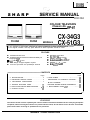
CX-34G3
CX-51 G3
SHARP
SERVICE MANUAL
SX7i2CX-51 G31
COLOUR TELEVISION
Chassis No. SP-67
CX-34G3
CX-51 G3
MODELS
CX-34G3
CX-51 G3
In the interests of user-safety (Required by safety regulations in some countries) the set should be restored
to its original condition and only parts identical to those specified should be used.
FEATURE
n
n
Reminder/ON-Off Timer
English/Arabic/Chinese/French/Russian/Malay six
Language OSD
w Hyper Band PLL Tuner
n Wide Range Chopper Regulator System
n Front A/V Input Rear A/V Input/Output Terminal
n Blue Back Noise Mute
n PAUSECAM Dual System
n NTSC 4.43/3.58 MHz (AV only)
n Direct Access Remote Control
n NTSC Colour-Comb Filter
n Black Strech Circuit
Y
CONTENTS
Page
Page
l
SPECIFICATIONS . . . . . . . . . . . . . . . . . . . . . . . . . . . . . . . . . . . . . . . . . . . . . . . 2
IMPORTANT SERVICE NOTES . . . . . . . . . . . . . . . . . . . . . . . . 2
l
ADJUSTMENT PRECAUTIONS . . . . . . . . . . . . . . . . . . . . . . . . 3
l
l
TROUBLE SHOOTING TABLE . . . . . . . . . . . . . . . . . . . . . . . . 17
SOLID STATE DEVICE BASE DIAGRAM . . . . . . *. 19
l
CHASSIS LAYOUT . . . . . . . . . . . . . . . . . . . . . . . . . . . . . . . . . . . . . . . . . . . 20
l
l
WAVE FORMS . . . . . . . . . . . . . . . . . ..*.............................. 22
. DESCRIPTION OF SCHEMATIC DIAGRAM . . . . . . . 24
. BLOCK DIAGRAM . . . . . . . . . . . . . . . . . . . . . . . . . . . . . . . . . . . . . . . . . . . . 29
. PRINTED WIRING BOARD ASSEMBLIES . . . . . . 33
l
REPLACEMENT PARTS LIST . . . . . . . . . . . ..*........... 35
WARNING
The chassis in this receiver is partially hot. Use an isolation transformer between the line cord plug and power
receptacle, when servicing this chassis. To prevent electric shock, do not remove cover. No user -serviceable
parts inside. Refer servicing to qualified service personnel.
SHARP CORPORATION
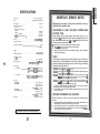
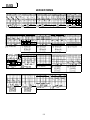
SPECIFICATIONS
IMPORTANT SERVICE NOTES
Convergence. . . . . . . . . . . . . . . . . . . . . . . . . . . . . . . . . . . . . . . . . . . . . . . . . . . . . . . . . . . . . . . . . . . . Self Converging System
Focus . . . . . . . . . . . . . . . . . . . . . . . . . . . . . . . . . . . . . . . . . . . . . . . . . . . . . . . . . . . . . . . . Quadra-Potential Electrostatic
Sweep Deflection . . . . . . . . . . . . . . . . . . . . . . . . . . . . . . . . . . . . . . . . . . . . . . . . . . . . . . . . . . . . . . . . . . . . . . . . . . . . . . . . . . . . . Magnetic
Intermediate Frequencies
Picture IF Carrier . . . . . . . . . . . . . . . . . . . . . . . . . . . . . . . . . . . . . . . . . . . . . . . . . . . . . . . . . . . . . . . . . . . . . . . . . . . . . . . . .
38.9 MHz
Sound IF Carrier Frequency
6.5 MHz . . . . . . . . . . . . . . . . . . . . . . . . . . . . . . . . . . . . . . . . . . . . . . . . . . . . . . . . . . . . . . . . . . . . . . . . . . . . . . . . . . . . . . . . . . 32.4
..
MHz
6.0 MHz . . . . .._...... . . . . . . . . . . . . . . . . . . . . . . . . . . . . . . . . . . . . . . . . . . . . . . . . . . . . . . . . . . . . . . . . . . . . . . . . . . . . . . . 32.9 MHz
5.5 MHz . . . . . . . . . . . . . . . . . . . . . . . . . . . . . . . . . . . . . . . . . . . . . . . . . . . . . . . . . . . . . . . . . . . . . . . . . . . . . . . . . . . . . . . .33.4
. . . . MHz
Colour Sub-Carrier Frequency ._ . . . . . . . . . . . . . . . . . . . . . . . . . . . . . . . . . . . . . . . . . . . . . . . . . . . . . . . . 34.47 MHz
Power Input . . . . . . . . . . . . . . . . . . . . . . . . . . . . . . . . . . . . . . . . . . . . . . . . . . . . . . . . . . . . . . . . . . . . . . . .
1 i O-240V AC 50/60 Hz
Power Consumption . . . . . . . . . . . . . . . . . . . . . . . . . . . . . . . . . . . . . . . . . . . . . . . . . . . . . . . . . . . . . . . . . . . . . . . . . . . . . . . . . . . . . . . 65 W
Audio Power Output Rating . . . .._. ..“.................~...................................,..........
3.0 w
(at Max.)
Speaker
Size . . . . . . . . . . . . . . . . . . . . . . . . . . . . . . . . . . . . . . . . . . . . . . . . . . . . . . . . . . . . . . . . . . . . . . . . . . . . . . . . . . . . . . . . . . . 5cmx9cmlpc
Voice Coil Impedance . . . . . . . . . . . . . . . . . . . . . . . . . . . . . . . . . . . . . . . . . . . . . . . . . . . . . . . . . . . 16 ohms at 400 Hz
Aerial tnput Impedance
VHF/UHF . . . . . . . . . . . . . . . . . . . . . . . . . . . . . . . . . . . . . . . . . . . . . . . . . . . . . . . . . . . . . . . . . . . . . . . . . . . . . 75 ohm Unbalanced
Receiving System . . . . . . . . . . . . . . . . . . . . . . . . . . . . . . . . . . . . . . . . . . . . . . . . . . . . . . . . . . . . . . . . . . . . . . . . . . CCiR PAL 6, G
NTSC 3.58i4.43 MHz (AV Input Only)
Tuner Ranges
l
VHF-Channels . . . . .._..........................
l
E2 (48.25 MHz) thru El2 (224.25 MHz)
Cl (49.75 MHz) thru Cl2 (216.25 MHz)
Sl (105.25 MHz) thru S41 (463.25 MHz)
UHF-Channels . . . . . . . . . . . . . . . . . . . . . . . . . . . . . E21 (471.25 MHz) thru E69 (855.25 MHz)
Cl3 (471.25MHz) thru C57 (863.25 MHz)
Dimensions
CX-34G3 . . .. . . . . . . . . . . . . . . . . . . . . . . . . . . . . . . . . . . . . . . . . . . . . . . . . . . . . . . . . . . . . . . . . . . . . . . . .
Width:
Height:
Depth:
Weight (approx.):
CX-51G3 . . . ..I....... . . . . . . . . . . . . . . . . . . . . . . . . . . . . . . . . . . . . . . . . . . . . . . . . . . . . . . . . . . . . . . . . Width:
Height:
Depth:
Weight (approx.):
Cabinet Material . . . . . . . . . . . . . . . . . . . . . . . . . . . . . . . . . . . . . . . . . . . . . . . . . . . . . . . . . . . . . . . . . . . . . . . . . . . . . . . . . . . .
Specifications are subject to change without prior notice.
2-l
357.0 m m
360.0 mm
359.5 mm
9.5 kg
449.0 m m
475.0 mm
473.0 mm
21.0 kg
All Plastics
1
Maintenance and repair of this receiver should be done by
qualified service personnel only.
SERVICING OF HIGH VOLTAGE SYSTEM AND
PICTURE TUBE
When servicing the high voltage system, remove static charge from it by
connecting a 10k ohm Resistor in series with an insulated wire (such as a
test probe) between picture tube dag and 2nd anode lead. (AC line cord
should be disconnected from AC outlet.)
1.
2.
3.
4.
Picture tube in this receiver employs integral implosion protection.
Replace wlth tube of the same type number for continued safety.
Do not lift picture tube by the neck.
Handle the picture tube only when wearing shatterproof goggles and after discharging
the high voltage completely
X-RAY
This receiver is designed so that any X-Ray radiation is kept to an absolute
minimum. Since certain malfunctions or servicing may produce potentially
hazardous radiation with prolonged exposure at close range, the following
precautions should be observed:
1. CX-34G3:
When repairing the circuit, be sure not to Increase the high voltage to more
than 23.5 kV (at beam 0 PA) for the set.
CX-51G3: When repairing the circuit, be sure not to Increase the high voltage to more
than 29.0 kV (at beam 0 PA) for the set.
2. CX-34G3: To keep the set in a normal operation, be sure to make it function on 22.0 kV
f 1.5 kV (at beam 800 PA) in the case of the set. The set has been factory Adjusted to the above-mentioned high voltage.
CX-51G3: To keep the set in a normal operation, be sure to make it function on 24.8 kV
f 1.5 kV (at beam 1100 PA) in the case of the set. The set has been factory Adjusted to the above-mentioned high voltage.
:. If there is a possibility that the high voltage fluctuates as a result of the repairs, never
forget to check for such high voltage after the work.
3. Do not substitute a picture tube with unauthorized types and/or brands which may cause
excess X-ray radiation.
BEFORE RETURNING THE RECEIVER
Before returning the receiver to the user, perform the following safety
checks.
1. Inspect all lead dress to make certain that leads are not pinched or that hardware is not
lodged between the chassis and other metal parts in the receiver.
2. Inspect all protective devices such as non-metallic control knobs, Insulating fishpapers,
cabinet backs, adjustment and compartment covers or shields, isolation resistorcapacity networks, mechanical Insulators etc.
2-2
ADJUSTMENT PRECAUTIONS
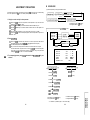
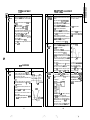
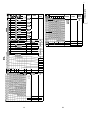
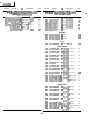
n SERVICE MODE
(1) Press the specific keys to change the modes as follows.
This model’s settings are adjusted in two different ways: through the PC bus control and in the conventional analog
manner. The adjustment via the PC bus control includes preset-only items and variable data.
COLOUR ADJUST mode
1. Calling the service mode by the microprocessor
@ Set the switch S1006 to the service mode position, and the microprocessor is put in the service mode
(adjustment through the PC bus control).
@ Press the CH UP/DOWN keys on the remote controller to select the modes one by one.
@ Press the CH UP/DOWN keys on the remote controller to select the modes in the order opposite to the
above step 0.
@ Using the VOLUME UP/DOWN keys on the remote controller, the data can be modified.
@ Set the switch S1006 to the normal mode (OFF) position, and the microprocessor is put out of the
service mode.
60 Hz ADJUST mode
In the direction of arrow : CH DOWN key
In the opposite direction : CH UP key
{
mode
R-CUT OFF
G-CUT OFF
B-CUT OFF
4
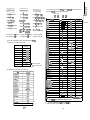
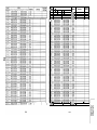
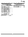
2. Factory presettings
,
@ Set the switch S1006 to the service mode position and turn on the main power switch. Initial values are
automatically preset only when a new E2PROM is used (judgment with the first 4 bytes).
@ The initial data are preset as listed on pages 4 and 5.
@ Keep in mind that some settings should be modified, and the others should remain as preset.
Once the chassis has been put together, be sure to set the switch S1006 to the service mode position
first and then turn on the main power switch (see the step 2.-@ above). Turning on the power without
initializing the E*PROM may cause a flow of excess beam current.
c4.3
CUT-OFF/BKGD
b
4
HORIZONTAL mode
3-set time out
3-set time out
KEY
R-CUT OFF
G-CUT OFF
B-CUT OFF
R-DRIVE
B-DRIVE
HORIZONTAL mode
3. The accompanying memory map (12-page document for the RH-iX2938CE) is for your
reference.
DOWN
UP
1
2
3
7
8
KEY
KEY
KEY
KEY
KEY
4 KEY
5 KEY
6 KEY
F/B KEY
0 KEY
9 KEY
COLOUR ADJUST mode
4
V-AMP 50 Hz (V-AMPSO)
4
V-LINE 50 Hz (V-LINE50)
4
SECAM R-Y (R-Y)
4
SECAM B-Y (R-Y)
4
S-CORRECT 50 Hz (V S-CORRSO)
4
V-PHASE 50 Hz (V-CENTER50)
4
H-PHASE 50 Hz (H-CENTER50)
4
V-BLK START (V-BLK ST50)
4
V-BLK STOP (V-BLK SP50)
In the direction of arrow : CH DOWN key
In the opposite direction : CH UP key
In the direction of arrow : CH DOWN key
In the opposite direction : CH UP key
l
3-1
The characters in parentheses appear on the on-screen display.
3-2
l
4
4
SUB CONT+ST (SUB CON)
V-AMP 60 Hi (V-AMPGO)
Y DELAY PA/- (DT PAL TV/AV)
SUB BRIGHi (SUB BRI)
V-LINE 60 H; (V-LINEGO)
SUB COLO”p (SUB COL)
VS-CORRECT 60 Hz
4
V-PHASE 60 Hz (V-CENTERGO)
4
H-PHASE 60 Hz (H-CENTERGO)
4
V-BLK STABT 60 Hz (V-BLK ST60)
Y DELAY SECAM (DT SECAM TV/AV)
4
Y DELAY N;SC (DT NTSC TVIAV)
SUB SUBTIY ( SUB TIN)
SUB SHAFtTESS (SUB SHARP)
Y-SUB CONTRAST (Y SUB CON)
Y DELAY BtW (DT BW TVIAV)
4
VIDEO MUT; ON/OFF (V-MUTE)
VIDEO 2 ON/OFF (AV2)
(DELAY AN effective in AN mode)
t
V-BLK STOP 60 Hz (V-BLK SP60)
In the direction of arrow : CH DOWN key
In the opposite direction : CH UP key
l
l
In the direction of arrow : CH DOWN key
In the opposite direction : CH UP key
The characters in parentheses
appear on the on-screen display.
User data
MAX (64164)
COLOUR
CENT (32/64)
BRIGHTNESS
TINT
CENT (32/64)
CENT (32/64)
CENT (32/64)
SHARPNESS
S-VOLUME
l
l
When the modes are switched, the last service mode data are stored into the E2PROM.
In the service mode, the user data are preset as follows.
CONTRAST
MIN (l/64)
BLUE BACK
OFF
C SYSTEM
AUTO
S SYSTEM
‘1
The following keys are used to go directly to their respective modes,
To go to the service mode, the data at the E2PROM’s addresses OOH thru 03H are read. If the data are not as
given below, the E2PROM is initialized according to the table below.
*‘1 :
Settings of each channel
before switching to the service
mode.
Address : Data
OOH : 22H
OlH : 29H
E’PROM item
(OOH)
(OlH)
02H
03H
:
:
13H
48H
IData adjustable range)
I
I
W’f-4
(03H)
R CUT OFF
G CUT OFF
B CUT OFF
G DRIVE
B DRIVE
50Hz V-AMP
50Hz V-LINEARITY
50Hz S-CORRECTION
50Hz V-PHASE
50Hz H-PHASE
V-BLK S T 50
V-BLK SP 50
60Hz V-AMP
60Hz V-LINEARITY
60Hz S-CORRECTION
60Hz V-PHASE
60Hz H-PHASE
60Hz V BLK ST
60Hz V BLK SP
SECAM R-Y
SECAM B-Y
SUB-CONTRAST
SUB-BRIGHT
SUB-COLOUR
SUB-TINT
0
0
0
0
0
0
o
0
0
-
255
255
255
255
255
127
31
127
o0 0 .
nv-
31
63
127
1 3IL,7
o0 0 oO-
31
127
7
31
63
I
Data initial value
3c)L-lI
CL,
29H
13H
48H
0
0
0
127
127
58
16
50 (14”)/67 (21”)
Remarks
1
-2
7
‘1
l1
‘1 ‘2
r;
-.-3
l 1
;
58-+63 (50Hz)
25
+5
l1
7
0 127
o 15
o15
0 255
0 255
0 255
0 127
0 63
o 31
0 7
0 I
7
0 7
0 7
ON/OFF
ON/OFF
1
I
l 2
‘4
60-+63 (60Hz)
20
10
6
255
127
110
70
28
18
2l2
414
2f2
2l2
OFF
ON
OFF/ON
‘2
SUB-SHARPNESS
Y SUB-CONTRAST
l 2
DT PAL TVIAV
‘2
DT SECAM TVIAV
‘2
DT NTSC TV/AV
‘2
DT BiW TVIAV
‘2
V-MUTE
AN2
AFT/SKIP
1
0 C-SYSTEM
PIG
S-SYSTEM
YIU
I
I
I
NVM With all the adjustments complete, do not change the data of addresses OOH thru 03H. Otherwise the E*PROM will be initialized when the AC power is turned on.
‘3
VIDEO MUTE
I
BLUE BACK
l 1 : These data are additionally adjusted for 60Hz based on the 50Hz settings.
‘2 : Unless otherwise specified, these data are fixed and need no adjustment.
4-2
l
3 : When the ICI001 is RH-iX2938CEZZ/Nl, change the NVM data from 00 to 01 (address
198H). For the RHiX2938CEN2 and the following ICs, there is no need to change this data
(as from the July 1997 production).
‘4 : Only 0 through 5 must be used in changing the data.
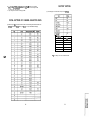
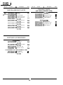
FACTORY SETTING
(1) The following key-in data have been factory-set for the E2PROM.
INITIAL SETTINGS OF CHANNEL SELECTION DATA
(1) Make an entry of MCLI in the service mode in order to set the following channel selection data to the
E2PROM. And select the POSl channel. (An MCL2, -3 or -4 input makes different settings.)
LAST FB POS
1
VOLUME
CONTRAST
MAX
MIN
COLOUR
*I
5-1
BRIGHTNESS
CENT
CENT
TINT
CENT
SHARPNESS
CENT
: For settings, refer to the Job Instruction Sheet.
5-2
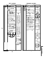
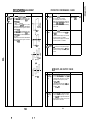
PIF/AFT/AGC ADJUSTMENT
115V ADJUSTMENT
Adjusting point
115v
adjustment:
R71l
Adjusting procedure/conditions
Waveform and others
1. Receive the E-5CH (monoscope pattern) signal.
2. Using the remote controller, call the P-NORM
mode.
3. Connect a beam ammeter between TP602 and
TP603.
0 Ammeter’s full-scale
: 3 mA range
l Ammeter’s positive (+) lead : TP603
l Ammeter’s negative (-) lead : TP602
4. Take the beam ammeter reading to make sure
that the beam current is between 600 pA and
800 uA (14”)/900 pA and 1100 pA (21”).
l
If not, readjust the FBT screen control to obtain the beam current of 600-800 uA (14”)/
900-1100 pA (21”).
5. Connect a digital voltmeter to TP701.
6. Adjust R711 so that the digital voltmeter should
read 115 kO.5 V.
lo. Adjusting point
1 VCO adjustment: T203
2
AFT
adjustment:
T204
PIF CHECKING
Jo. Adjusting point
1 Tuner IF
(preset):
TU201
Adjusting procedure/conditions
1. Get the tuner ready to receive the E-9CH signal.
but with no signal input. Adjust the PLL data.
2. Connect the sweep generator’s output cable to
the tuner antenna. (RF sweep)
3. Adjust the sweep generator’s output level to 80
dBj.rV.
4. Connect the response lead (use a low-impedance
probe with wave detector; see Fig. 7) to the tuner’s IF output terminal.
(This terminal must have the probe alone connected.)
5. Set the RF AGC voltage to O-6 V with no contact
with the waveform.
6. Adjust the tuner IF coil to obtain the waveform as
shown in Fig. 2.
Note: Be sure to keep the tuner cover in position during this adjustment.
6-1
Waveform and others
IF-OUT
1ooop
3
1Okf;!
7s$gfjffjfOPf
Fig. 7
E-9CH
P
- 1.5dB + 0.8dB
u
Fig. 2
RFAGC
cut-in
adjustment:
R216
Waveform and others
Adjusting procedure/conditions
1. Disconnect the antenna from the tuner antenna
terminal.
2. Apply DC voltage to pin (4)(IF AGC) of IC201.
l DC voltage: 6.0 V (allowable +O.l V)
3. Using a digital voltmeter, measure the DC voltage at pin (2O)(PLL FIL) of IC201.
l The digital voltmeter must be able to take readings down to the third decimal place.
4. Relieve pin (4) of lC201 of the DC voltage.
5. Reconnect the antenna in position and receive
the E-12CH signal. (With the AFT off, adjust the
receiving frequency to 224.25 MHz.)
6. Connect the DC digital voltmeter to pin (20) of
IC201. Adjust T203 so that the voltmeter should
read the same voltage as in Step 3.
Allowable error : 0.015 V (20 kHz)
1. Receive the E-12CH (PAL colour bar) signal. If
this signal is not available, any signal above the
E-5CH band is acceptable.
l Field strength : 55-80 dBpV
Make sure the frequency is almost the same as
that of the received channel (i30 kHz).
2. Using the channel setting control, make a frequency of 224.25 MHz appear on the screen (the
AFT turns off). If any other channel than E-12CH
is received, make its frequency on the screen.
(The AFT turns off when the on-screen display
turns yellow.)
3. Turn T204 clockwise to have a 6V point, and
counterclockwise to have a 0.2-V point. Position
the coil at the center of these two points.
4. Adjust T204 so that the DC voltage at pin (1) (AFT
OUT terminal) of IC201 be 3.3 kO.1 V (See Fig. 3)
1. Receive the E-12CH (PAL colour bar) signal.
l Field strength : 57 k.1 dBpV (75 ohms open)
2. Connect the oscilloscope to TP210, as shown in
Fig. 4.
Oscilloscope
m-l-v
...... +
TV Set
TP210
Bias box
+
SF
Fig. 4 l Bias box: About 6.5 V
3. Turn R216 to have the highest voltage.
4. Turn R216 slowly in the opposite direction until the
voltage goes down 0.1 V below the highest level.
5. Adjust thesignal level to 63-67 dBpV and make
sure there is no noise.
6. Now adjust the signal level to 90-95 dBuV and make
sure there is no chrominance modulation beat.
6-2
l
Warm up the unit for longer than
10 minutes in advance.
* 10 kHz at about 0.007 V.
l
Position the T203 core in the
range in which the E-l 2CH signal can be received.
DC voltage at TP201
6V
3.3v
- - - ,
I
I
bL
DOWN A B’ ; B” C UP
Fig. 3
l
Turn the core counterclockwise
for the UP direction, and clock
wise for the DOWN direction.
Adjust the T201 core to point E
(between B’ and B”). (Points F
and C are rejectable.)
Note: If a 500hm field strength
meter is used without a 50/X
impedance converter, set thf
field strength to 55 *l dBpV
Pay attention to a loss tha
would be caused with the con
verter.
PURITY ADJUSTMENT
rlo. j Adiustins point j
Adiusting procedure/conditions
Purity
adjustment
1. Using the remote controller, make the screen colour
green-only. Adjust the contrast control to have a beam
current of about 500 f.tA (14”)/700 pA (21”).
2. Degauss the cathode ray tube enough with the
degaussing coil.
Note: Follow the Job Instruction Sheet to adjust the magnetic field.
Vertical Bv : +0.030 mT (0.30 gauss)
Horizontal Bh : +0.020 mT (0.20 gauss)
See page 10.
3. Keep the purity magnet in the zero magnetic field
in advance. Roughly adjust the convergence.
4. Observe the points “a” and “b”, as shown in Fig.
5-1, through a microscope. Adjust the landing to
the rank “A” requirements.
5. Adjust the raster rotation to “0” eastward.
6. Tighten up the deflection coil.screws.
l Tightening torque: 108 *20 N (11 lt2 kgf)
7. While observing the cathode ray tube corners.
apply the magnet sheet to have the landing at
rank “A”.
Note: Before starting this adjustment, warm
up the unit for 30 minutes or longer at
a beam current of over 500 f.rA (14”)/
700 pA (21 I’).
Note: Set the service switch SlOOl to call the
service mode and press the single-colour key on the process remote controller to get the green-only screen.
l
CONVERGENCE ADJUSTMENT
Waveform and others
I
Blue-only
screen
T
Single-colour
screen cleared
Adiuztino oracedurelconditions
j
I
1. Receive the E-2CH (crosshatch pattern) signal.
2. Using the remote controller, call the Normal mode.
Fig. 5-l
Fig. 5-2
Rank “A” (on the
right of the CRT)
STATIC CONVERGENCE
1. Turn the 4-pole magnet to a proper opening angle in order to superimpose the blue and red colours.
2. Turn the g-pole magnet to a proper opening angle in order to superimpose the green colour over
the blue and red colours.
DYNAMIC CONVERGENCE
1. Adjust the convergence on the fringes of the
screen in the following steps.
a) Fig. 6-7: Drive the wedge at point “a” and
swing the deflection coil upward.
b) Fig. 6-2: Drive the wedges at points ‘lb” and
“c” and swing the deflection coil downward.
c) Fig. 6-3: Drive the “c” wedge deeper and
swing the deflection coil rightward.
d) Fig. 6-4: Drive the “b” wedge deeper and
swing the deflection coil leftward.
2. Fix all the wedges on the cathode ray tube and
apply glass tape over them.
3. Apply lacquer to the deflection yoke lock screw,
magnet unit (purity, 4-pole and 6-pole magnets),
and magnet unit lock screw.
Finally receive the red-only and blue-only signals
and make sure there is no other colour mixed on
the screen.
Each time the single-colour key is pressed, the
screen colour changes as follows.
Green-only
screen
o. j Adiustina
I
Waveform and others
BGR
Fig. 6-i
RGB
I
\ :
I :
‘. . . . . . . . \ :. _--“/-. . . . . . . . . . .4
_--:\
B
: \
: \
: \
Fig. 6-2
Fig. 6-3
Fig. 6-4
Wedge “a”
Red-only
screen
Fig. 5-3
Rank “A” (on the
left of the CRT)
l
Whether in the service mode OI
not, hold down the single-coloul
key for 1 second or longer ant
the service mode is called.
Fig. 6-5
The TEXT key or the R.G.Cy kel
may be used instead to provide
the single-colour screens.
Purity magnet
fig. 6-6
7-2
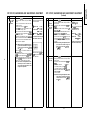
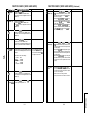
CRT CUT-OFF, BACKGROUND AND SUB-CONTRAST ADJUSTMENT
So. Adjusting point
1
00
CRT cut-off
service mode:
12C bus data
adjustment
Adjusting procedure/conditions
1. Receive the E-5CH (monoscope pattern) signal.
2. Using the remote controller, call up the P-NORM
mode.
3. Turn on the service switch and select the cut-off/
background mode.
4. Set the screen control to O/10 position.
5. Press the “9” key on the remote controller to reach
the horizontal centering mode.
6. Turn the screen control clockwise until the horizontal raster of the first glimmering colour becomes slightly visible.
7. Adjust the cut-off data of the other two colours
until the horizontal raster becomes whitish.
8. Turn the screen control counterclockwise until the
horizontal raster disappears.
Note: Before starting this adjustment, warm
up the unit for 30 minutes or longer at
a beam current of over 500 PA (14”)/
700 PA (21”).
9. Press the “9” key on the remote controller to call
the NORMAL mode.
iO.Using the remote controller, call the sub-brightness setting mode. (Receive the E-2CH signal.)
11. Set the sub-brightness data so that the third black
portion (1st to 5th counted from the left of the
screen) of the window pattern looks sinking.
Note: The service mode adjustment in the
above steps 10. and 11. should be carried out after the white balance and
background adjustments.
CRT CUT-OFF, BACKGROUND AND SUB-CONTRAST ADJUSTMENT
(Continued)
Waveform and others
l
First of all, make sure that the
R/G/B cut-off and B/G drive data
are all initial values.
Note:
R CUT OFF UP
DOWN
G CUT OFF UP
DOWN
6 CUT OFF UP
DOWN
“1”
“4”
“2”
“5”
“3”
“6”
KEY
KEY
KEY
KEY
KEY
KEY
lo. Adjusting point
2
White balance
and
background
service mode:
1% bus data
adjustment
The data can be turned up and
down with the above keys.
12345
Adjusting procedure/conditions
1. Receive the E-5CH (monoscope pattern) signal.
2. Using the remote controller, call up the Video
Normal mode.
3. Connect the beam ammeter between TP601 and
TP602.
4. Make sure the beam current is about 800 PA
(14”)/1,100 PA (21”).
5. Adjust the G-drive and B-drive data to have a
colour temperature of 12,300”K (white).
6. Adjust the contrast and brightness controls to
have the beam current of 200 PA. Now check the
background colour. If the colour temperature is
not as specified, go back to No. 1 on the preceding page.
Note: Before starting this adjustment, warm
up the unit for 30 minutes or longer at a
beam current of over 500 pA (14”)/
700 pA (21”).
II
Make sure all the Ist, 2nd and
3rd black portions are at the
same black level.
3 Maximum
beam current
(check item)
1. Receive the E-5CH (monoscope pattern) signal.
2. Using the remote controller, call up the Video
Normal mode.
3. Connect the beam ammeter between TP602 and
TP603.
l Ammeter’s full-scale
: 3 mA range
l Ammeter’s positive (+) lead : TP603
l Ammeter’s negative (-) lead : TP602
4. Make sure the beam current is 800 *lOO PA (14’11
1,100*100pA (21”).
Note: Before starting this adjustment, warm
up the unit for 30 minutes or longer at
a beam current of over 500 PA (14”)/
700 PA (21”).
8-1
8-2
Waveform and others
See page 5.
l
12300°K X: 0.273
Y : 0.276
(with colour temperature meter
CA-100 (MINOLTA).)
Note:
G-DRIVE UP
DOWN
B-DRIVE UP
DOWN
“7” KEY
“-I--” KEY
“8” KEY
“0” KEY
The data can be turned up and
down with the above keys.
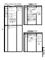
PAL CHROMA ADJUSTMENT
HORIZONTAL AND VERTICAL CIRCUIT ADJUSTMENT
lo. 1 Adlustina ooint 1
Adiustina orocedurekonditions
V-AMP 50
1. Adjust the overscan to 9% (E-5).
V-LINEARITY 50 Hz
1. Adjust to get the best linearity.
V-S CORRECTION - 50 Hz
1. Preset (readjust if the linearity is poor).
V-SHIFT 50 (VCENTER)
1. Align the screen center with the cathode ray tube’s
geometrical center (E-5).
H-SHIFT (50)
(H-CENTER)
1. Align the screen center with the cathode ray tube’s
geometrical center (E-5).
I
Waveform and others
The selected channels in parentheses have the following signals.
(E-2): Crosshatch pattern (50 Hz)
signal
(E-5): Monoscope pattern (50 Hz)
signal
o. Adjusting point
1
Sub-colour
adjustment:
12C bus
adjustment
Adjusting procedure/conditions
4. Using the remote controller, call the sub-colour
adjustment mode. Adjust the sub-colour data so
that the 75% white and red portions of the PAL
colour bar be at the same level. See Fig. 7.
5. Clear the adjustment mode. (Now the 100% white
and red portions will be at the same level. The
sub-colour data is up 20.)
l Pin (3)(K)
may be used instead of TP851 (14”)/
TP852 (21”) (RED cathode) for this adjustment.
In such case, keep in mind that the polarity of the
waveform is inverted.
Note: For the V-HEIGHT 60, V-LINEARITY 60,
V-S CORRECTION 60, V-SHIFT 60 and
H-SHIFT 60 adjustments, their corrected
data are automatically entered when the
corresponding 50 Hz mode adjustments
are made.
Waveform and others
1. Receive the E-l 2CH (PAL colour bar) signal.
2. Using the remote controller, call the Video Normal mode.
3. Connect the oscilloscope to TP851 (14”)1TP852
(21”) (RED cathode). (Use a 10 : 1 probe.)
l Range
: 2 Vldiv.
l Sweep time : 20 usecldiv.
B
w
W Y lOO%WMg R
Fig. 7
Receive the E-5CH (monoscope pattern) signal.
Using the remote controller, call the Video Normal mode.
Adjust the focus control so that the screen be in
good focus.
NTSC CHROMA ADJUSTMENT
lo. Adjusting point
1 Sub-tint
adjustment:
12C bus
adjustment
Adjusting procedure/conditions
1. Call the sub-tint adjustment mode. Receive the
NTSC 3.58 colour bar signal in the A/V mode.
2. Connect the oscilloscope to pin (36)(B-Y) of
IC801.
l Range
: 20 mV/div. (AC)
l Sweep time : 20 psec/div. (Use a 10 : 1 probe.)
3. Adjust the sub-tint data to obtain the waveform
as shown in Fig. 8.
4. Clear the adjustment mode.
Waveform and others
(B-Y)
A 4
B4
c c- - - - - - - - - - - -
@
WYCyGMgRB
Fig. 8
A=B=C
9-1
9-2
PROTECTOR PERFORMANCE CHECK
SECAM CHROMA ADJUSTMENT
lo. Adjusting point
Adjusting procedure/conditions
1 SECAM b l a c k
level (R-Y/B-Y)
adjustment:
1% bus
adjustment
1. Receive the Oi-5CH (SECAM colour bar) signal.
2. Call the SECAM black level adjustment R-Y mode.
3. Connect the oscilloscope to pin (34)(R-Y OUT,
TP802) of IC801.
l Range
: 10 mV/div.
l Sweep time : 20 psec/div. (Use a 10 : 1 probe.)
4. Adjust the R-Y data so that the offset between
the no-signal line and the signal line be minimum.
See Fig. 9-l(b).
5. Call the SECAM black level adjustment B-Y mode.
6. Reconnect the oscilloscope to pin (33)(B-Y OUT,
TP801) of IC801. The conditions are just the same
as in Step 3.
7. Adjust the B-Y data so that the offset between
the no-signal line and the signal line be minimum.
See Fig. 9-2(b).
Waveform and others
1 Beam protector
1.
2.
3.
4.
2 High-voltage
protector
1. Receive the E8CH (monoscope pattern) signal.
2. Connect the bias box to the cathode (R635 side)
of D607.
3. Adjust the bias box voltage to 18 V and make
sure that the protector is not activated.
4. Adjust the bias box voltage to 27 V and make
sure that the protector is not activated.
3 Other protectors
1. In checking the performance of other protectors
- for example, the one against shorting of
smoothing electrolytic capacitor of +B line -, pay
attention not to damage or deteriorate any related
element.
+
- - _ _-_-_ e-v- -e---v
OFF SET
1”Fig. 9-l (a)
4
- - _- -_-_ _-_-_ _ _-_
7-F
Fig. 9-l (b)
Waveform and others
Adjusting procedure/conditions
lo. Adjusting point
Receive the EdCH (monoscope pattern) signal.
Set the contrast control to maximum.
Set the brightness control to maximum.
Make a short-circuit between the collector and
emitter of Q851, Q852 or Cl853 and make sure
that the protector is activated and the stand-by
mode is called.
l
Short-circuit any of the Q851
0852 and 0853.
__ _- -_ _ -- -_ _-_
OFF S:;
!111
Fig. 9-2 (a)
+
-- -- -_ _ -- -_ _
A/v INPUT AND OUTPUT CHECK
_
lo. Adjusting point
@
Fig. 9-2 (b)
1 Video and
audio output
check
1. Receive the E-12CH colour bar (100% white colour bar, 400 Hz, 100% modulation audio) signal.
2. Terminate the video output with a 75 ohm impedance. Make sure the output is as specified
(1 .O Vp-p *3 dB).
3. Terminate the audio output with a 10k ohm impedance. Make sure the output is as specified
(1.76 Vp-p rt3 dB).
2 Video and
audio input
check
1. Using the TV/AV key on the remote controller,
make sure that the modes change in the order of
TV, AV1, AV2 and TV again and that the video
and audio outputs are according to the input and
output terminals for each mode.
10-2
10-l
e
Adjusting procedure/conditions
4
iY
Waveform and others
FUNCTION CHECK (VIDEO AND AUDIO)
1
CONTRAST
key
1. Receive the E-5CH signal.
2. Select the contrast on the P-MODE screen.
3. The contrast must be changeable with the UP/
DOWN key.
2 COLOUR key
I. Receive the E-12CH signal.
2. Select the colour on the P-MODE screen.
3. The colour must be changeable with the UP/
DOWN key.
3
I. Receive the E-5CH signal.
2. Select the brightness on the P-MODE screen.
3. The black level must be changeable with the UP/
DOWN key.
BRIGHTNESS
key
4 TINT key
5 PIC-NOR. k e y
Waveform and others
Adiustina
-.wocedure/conditions
lo. IAdiustina
-.uointl
e
1. Receive the NTSC colour bar signal. (A/V)
2. Select the tint on the P-MODE screen.
3. The tint must be changeable toward green with
the UP key and toward red with the DOWN key.
1. Press the NOR. key on the P-MODE screen to
make sure all the displayed items are at normal
settings.
See below for the normal settings.
l
l
l
l
l
Contrast
Colour
Brightness
Tint
Sharpness
:
:
:
:
:
l
FUNCTION CHECK (VIDEO AND AUDIO) (Continued)
o. Adjusting point
9 COLOUR
SYSTEM key
1. Receive the E-l 2CH PAL colour bar signal. Using the COLOUR SYSTEM key, select a mode
other than PAL and make sure the colour system
does not work properly.
2. Receive the E-37CH NTSC 4.43 colour bar signal. Using the COLOUR SYSTEM key, select a
mode other than N4.43 and make sure the colour
system does not work properly.
3. Receive the NTSC 3.58 colour bar (A/V) signal.
Using the COLOUR SYSTEM key, select a mode
other than N3.58 and make sure the colour system does not work properly.
9 SOUND
SYSTEM key
I. Receive the 01-9CH PAL colour bar signal. Using the SOUND SYSTEM key, select B/G and I
modes and make sure the sound system does
not work properly.
2. Receive the E-23CH monoscope pattern signal.
Using the SOUND SYSTEM key, select B/G and
D/K modes and make sure the sound system does
not work properly.
3. Receive the E-12CH colour bar signal. Using the
SOUND SYSTEM key, select I and D/K modes
and make sure the sound system does not work
properly.
IO Noise mute
check
1. Receive the E-12CH (PAL colour bar) signal.
2. Turn up the sound volume to maximum and make
sure the sound is heard normally from the speakers. Then cut off the signal.
3. Make sure the sound muting functions.
4. Finally turn down the sound volume to minimum.
The contrast, colour, brightness,
tint and sharpness settings are
all normal when these items dc
not appear on the screen.
MAX
CENTER
CENTER
CENTER
CENTER
6 SHARPNESS
key
1. Receive the E-5CH signal.
2. Select the sharpness on the P-MODE screen.
3. The sharpness must be changeable with the UP/
DOWN key.
7 Channel sign
display coiour
1. The display colour of all the channel (O-99) signs
must be green. Keep the AFT on.
11-1
Adjusting procedure/conditions
11-2
Waveform and others
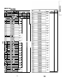
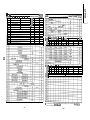
MEMORY MAP (RH-iX2938)
DATA
SUB
DDRESS
7
1
I
6
1I
5
1I
4
1 R-
I 003 II
I 004 II
t ii& I
006 1
007 II
I 008 I
I
t
t
t
7-
012 1
013 I
PLL d a t a (i
PLL data (lower)
017
018
019
OIA
fl1B
OlC
OlD
OlE
OlF
020
021
022
023
024
025
026
027
028
029
02A
028
02c
02D
02E
02F
PLL data (lower)
PLL data (upper)
PLL data iIower)
PLL data (upper)
PLL data il&eri
\
PLL data (uppe;)
PLL data (lower)
PLL d a t a Jeer)
(I
PLL data (lowerj
PLL data &De;)
PLL data ildwerj
PLL data (upper)
PLL data (lower)
PLL data (upper)
PLL data il ower)
PLL data iupper)
PLL data (lower)
PLL data iuDDe;I
-.. ,
PLL data (lower)
PLL data (upper)
PLL data (lower)
PLL data (upper)
PLL data ildwer)
PLL data iucx)e;)
.
.
.
,
PLL data (lower)
.I,
1
1
1
1-
1
1I
1
1
1I
I
1
1
1
1I
I
1
I
iI
1I
1
REMARKS I
n-
initialization judgment data “22”
Initialization judgment data “29”
Initialization *iudament
data “13’
Initialization *iudament
data “48”
”
PLL
(uooerl I
-~-data-\rr
PLL data (lower)
PLL data (L.
wper)
PLL data (lowerj
PLL data iurx)e;I
I
t
FACTORY
CRlTERlA
Other than $22
Other than $29
Other than $13
c )thnr
I
I
.
.
.-.
I SElTlNG
,
I
$22
$29
$13
$48
-
than
. .-. $48
_ .-
CHO
I
CHl
CH2
I
1
I
I
I
I
I
CHIO
CHll
I
CH12
CH13
CH14
CH15
CH16
CH17
I
CH18
CH19
CH20
I
12-1
I
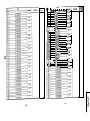
FACTORY
SETTING
SUB
ADDRESS
090
091
092
093
094
095
096
097
098
7
1
6
1
lzF=
09B
09c
09D
09E
09F
OAO
OAl
OA2
OA3
OA4
OA5
OA6
OA7
OA8
OA9
OAA
OAD 1
OAE I
6
DATA
’ - ’ - ’ * ’ n
1 4 131211JU
PLL dz ata (upper)
PLL dz ata (lower)
PLL di ata (upper)
PLL dista (lower)
PLL diata (upper)
PLL diata (lower)
PLL dsata (upper)
PLL dsata (lower)
PLL data (upper)
PLL d
PLL d
PLL d
PLL d
PLL dlata (lower)
PLL dlata (upper)
PLL dlata (lower)
PLL clata (upper)
PLL clata (lower)
PLL clata (upper)
PLL ctata (lower)
late Imnerb
PLL c-.\-TT - ,
PLL data (lower)
PLL data (upper)
:ACTORY
SElTlNG
CH70
CH71
I
1
CH72
CH73
I
CH74
I
CH77
I
I
1
I
1
CH78
CH79
CH80
CH8
pLL +dP /ln!Amr\
PLL
PLL
PLL
PLL
PLL
PLL
PLL
(
(
L,.- \-TT- ,
data (lower)
data (upper)
data (lower)
data (upper)
CH84
CH85
13-2
I SUB
. ~- I
DATA
1 j I
110
2
4
PLL data (upper)
PLL data Ilower\
t --.-‘I
PLL data (upper)
PLL data (lower)
PLL data (upper)
PLL data (lower1
1
PLL data (upper)
I
PCL
. ,
data (lower1
\ -.--.I
PLL data (upper)
PLL data (lower)
PLL data (upper)
PLL data (lower)
POWER/
TVIAV
I’
’
BLUE BACKGROUND 1 One-digit/two-digit
LANGUAGE
-,1 AST POSITION
LAST CONTRkT
LAST COLOUR
LAST BRIGHTNESS
LAST TINT
1
LAST SHARPNESS
I
AST VOLlJMF
ADDRESS
oco
OCI
bC2
oc3
oc4
oc5
OC6
oc7
oca
oc9
OCA
OCB
OCC
OCD
OCE
OCF
000
ODl
OD2
OD3
004
m5
7
1
6
1
5
“Y
I
t
ODE
ODF
OEO
I
I
I
I
I
1 Cl-17 1 CM 1 Cl-i.5 1 CH4
I
I
CH3 I CH2
I
REMARKS
1
CRITERIA
CH94
II
1
I
DATA
SUB I
ADDRESS 7
OF0
CH7
OF1
6
5
CH5
CH5
4
3
2
CH4
CH3
C&’
CHI
’ REMARKS
CHl
CHO
CH96
I
1
CH97
-. .-,
I
CH98
CH99
I
L
I
1I
II
I
I
1 Factorv-set at ON
OFFI .
1
I
I
I
I
I
I
80
5
5
--3iT01
---F-----r----iF----iF-----T-----E---E--
I
OFE
1
OFF
1
I
I
I
I
I
t
I
I
I
I
I
I
I
I
CHI I CHO i
14-1
SKIP
0:OFF
1 :ON
CH95
I
I
FACTORY
SETTING
AFT
I
l
AFTOFF
---FF--
14-2
I
I
CRITERIA
SKIP ON
FACTORY
SETTING
00
DATA
SUB
ADDRESS
7
130
131
132
133
1
6
AUDIO
AUDIO
AUDIO
AUDIO
5
4
SYSTEM
SYSTEM
SYSTEM
SYSTEM
I
15F
3
2
VIDEO
VIDEO
VIDEO
VIDEO
I
1
AUDIO
SYSTEM
CH4B
CH49
CH50
CH51
1
1
VIDEOSYSTEM
FACTORY
SETTING
CRITERIA
REMARKS
1
0
SYSTEM
SYSTEM
SYSTEM
SYSTEM
1
‘iHi
I
1
I
I
i
DATA
SUB 1
7
160
161
162
163
164
165
166
167
168
169
1 6 1 5 1
AUDIO SYSTEM
AUDIO SYSTEM
AUDIO SYSTEM
AUDIO SYSTEM
AUDIO SYSTEM
4
1
I
3
1
2
VIDEO
VIDEO
VIDEO
VIDEO
VIDEO
1
1
1
SYSTEM
SYSTEM
SYSTEM
SYSTEM
SYSTEM
0
I
REMARKS CRITERIA
I
CH96
CH97
CH98
CH99
A/V MODE
cArrfiay
DATA
SUB
. -----I
I
I
I
I
I
198
19c
196
19E
1 S-FIELD pc0~1-r IDEUFJ Foj s GP 1 V-ID
I
I
I
I
I
1AB
1AC
1AD
1AE
IAF
1BO
181
I
I
SW
I
1 s KIL
L
I
I
I
BELLFO
I
1
I
I
1
I
I
1
II
I
I
I
I
I
I
I
I
I
I
I
I
I
I
I
I
I
I
I
I
I
I
I
I
I
I
I
II
I
I
I
I
I
I
I
II
II
I
I
I
I
I
I
I
I
I
* : The initial setting of the RH-iX2938CEZZ/Nl must be changed from 00 to 01. With the RH-iX2938CEN2,
there is no need to change the initial setting.
16-1
;;
16-2
i
I
I
TROUBLE SHOOTING TABLE (Continued)
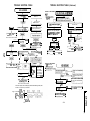
TROUBLE SHOOTING TABLE
NO RASTER
CIRCUITS TO BE CHECKED:
Tuner.
PIF.
l Automatic Gain Control.
l (W), (9V) Power Source.
NO PICTURE, NO SOUN
l
l
I
Check F701.
t
I
Blown out.
Replace the fuse.
I
I
No snow noise.
received.
1 Abnormal
1
I
Check pin (1) of T701 voltage
(Approx. 31 OV at 220V AC) I
I
‘-i
ir’
Abnormal
1
Normal
Main+B
i-i
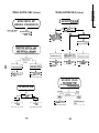
___--------_
1 Check C707, D701,0702, ;
1 --------------_I
D703 and 0704.
Normal
_-------------
1
I
I
1 Abnormal [
Normal 1
+
+
------l--------L-----,
I Check the tuner i I
I circuit.
I l
LED Green) 1
r
I
I
r - - - - - - - - - - l
and its related
1 parts.
I
I
I
I- - - - - - m - e - t
I
Check IC801.
I __--------
I
I
I
I
( CheckANsw
1
1 c i r c u i t s (IC401). I
l - - - - - - - - - - l
C h e c k IC201. i
l - - - - - - , - - - l
Does horizontal circuit
oscillate ?
I+
Bus error
mode.
See Fig. 1
or Check
IC602.
Checking the
protector circuit
(The protector
circuit still works
even if there is no
vertical waveform
at pin (2) of IClOOl
YES
NO
r- - - - - - ‘-------I
!
Check Q1005, Q1006,
I
IC603 and IC801.
I ---------,----J
If a bus error happens, the LED RED (pin 3) indicator starts flashing and the power
is turned off. The power key is still effective.
IC1003
F i g . 1 E E P R O M (ST24C02) 1
IC801
V/C/J
(TB1226CN) TU201
PLL
(CXA3134)
6
uu
2s
17-1
CIRCUITS TO BE CHECKED:
SIF Amplifier Circuit.
Sound Detector Circuit.
l
-I
I
Do noise or signal
appear at pin (1)
of IC801 ?
Abnbrmal)
r-------~---___,
I Check R609 and R611. {
I
I
I
Normal 1
+
Check the tuner AGC.
L NO
1
YES
1
1 C h e c k D7Or3 a n d 0 7 3 2 . 1 ( E!trF k!L connecto,r lzl ~~~~~~Power
y
[T
Dose noise or signal appear at pin (21)
of IC201 ?
Check the tuner supply voltage MB
must be approx, 9V. BP must approx.
5V. BT must be approx 31V, and
channel preset data check.
;
Check R701, R702 and
I
D709.
I ---------------I
S e c o n d a r y
(Approx. 115V)
I
I
Jr
The fuse is again blown out. I
I
C h e c k
Does the noise level increase at max.
l
:
I ---------------1
r--------------_
(
Does signal appear at pins
(1) and (8) of IC302 ?
NO
+
r_--____--------
Does signal appear at pin
(3) of IC351 ?
YES
r--------------_
; Check (5) connector IC351 ;
, and peripheral circuit.
- - - - - - - - - - - - - - - I
0.5s
17-2
NO
I Check IC302 and peripheral r
I
h circuit.
I- - - - - - - - - - - - - - - I
TROUBLE SHOOTING TABLE (Continued)
TROUBLE SHOOTING TABLE (Continued)
NEITHER VERTICAL NOR
HORIZONTAL SYNCHRONIZATION
( NO SPECIFIC COiOU$
NO
CIRCUIT TO BE CHECKED:
l Sync. Separator Circuit.
3,..--------------_
I
Check
IC801
and Q401. I
I
Is some colour produced in
BNJ broadcast reception ?
YES
I
+
- - - - - - -* ---_-__
,yEs I s t h e w h i t e b a l a n c e p r o p e r l y
adjusted ?
i Check IC801, R809, R810, i
, R811, D801, D802, D803, 1
;
I Q801, Q802, Q803,Q804
: and Q805.
I
- - - - - - - - - - - - - - - I
NO
- - - - - - - - - - - - - - -
r----m.---------_
I
I
I Readjust the white balance. I
I- - - - , - - - - - - - - - - I
+,
+
r--------------v
I
Check Q851 and its
*]
I
i _ _ adjacent
-w--vcircuits.
- - - - - - - - I
j/
Vertical linearity is abnormal.
I
1
;
The prcture colour IS magenta.
+,
+,
w
r-------------__
*
r---------_-____
I
;
Check Q853 and its
I
, _ _ adjacent circuits.
- - - - - - - - - - - - - I
I
;
Check Q852 and its
adjacent circuits.
I- - - - - _ _ _ _ - - - _ _ - I
I
I
I
I
*
*
I----------
i- Che-ck R5;10, G-13,-c514- ;
I
1 and C501.
-
_-_-_
] Check C515, C519, R511, ;
, _ FE13 and R514.
- - - - - - - - - - - - , - - I
------,-,-a--J
NO SPECIFIC COLOUR
“PAL”/“SECAM”/“NTSC”
(NO COLOUR SYNCHRONISATION)
NO VERTICAL SCAN
I
Check IC501 bias.
I--
Normal 1
I
Check 0506.
I
l---------------l
I
I
,
I
1 Abnormal J
I
I
Check IC501.
I
I
I ------_------_-I
i Check X801, C810, C815, ;
, _C8_‘6 and R814.
-
------------I
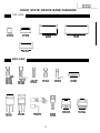
SOLID STATE DEVICE BASE DIAGRAM
TOP VIEW
56
8
-
5
16
a
l-4
1
8
ST24C04
29
9
1
ix1 779CE
1
28
ix2938
TB1226
11
BA7357S
SIDE VIEW
Ii Ii
IL
t-BASE
COLLECTOR
!- EMITTER
2SA1015
2SC1815
2SC1906
1
- BASE
L COLLECTOR
I
EMllTER
2sc2229
2SC2482
123
3 2 1
KiA7045P
TA78L09
UPC78LO5
R
L
L CATHODE
ANODE
iX0037CE
TA7348P
1
7
1
9
1 2 3
B
C
2582586
2SD1877
E
B
C
iX0640CE
E
2SD1884
KA7809
KA7805
PX0003PE
19
TDA7056A
i
.
‘.
CX-34G3
CX-51 G3
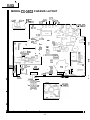
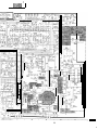
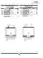
MODEL CX-34G3 CHASSIS LAYOUT
s1003
VOL-UP
3403
vrncn
..“-- . .IM.
3402
AV UNIT
*,,nrn . .1t.l.
,._.,.”
l-“-I-TAWM
-.. s’oo4
“.,....
l-G%
,“I ““..I,
SlOOl
PRE-SET
s1005
CH-UP
I
r
/
II
/II,
1
2 MAIN UNIT
RMClOOl
CFlOOl
ICI003
if=!
ICI002
PBO4
Q607
OQBOI
0
8
PBOS
OQB03
I C60.2
0
4802
4405
1 C60
0
9601
Q606
0
1C603
CB14,,
CB13i
e6
R F
T601
0
0
+ X801
TPBOl
n
0
0
9401
ACC
4404
(F’-
Q602
63
L602
S1006
NOR
SEVON
ooa303
(VA)
0
cl305
P302
T602
IC401
I c202
t
J
\
\
\
[n
[BC)
D604
-qFzq
5401
I
(Hl[
I
LTU20 1
TUNER
“IDEOj
, ///,
[ A U D I O
VIDEO
IN
AUD 10
IN
VI DE0
OUT
AUD 1 0
OUT
TPB54
r-2
I i
1
I
2
I
3
4
20
I
5
I
6
I
CX-34G3
CX-51 G3
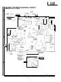
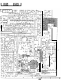
MODELCX-51 G3 CHASSIS LAYOUT
s1003
VOL-UP
51004
CH-DOWN
5402
J403
51005
CH-UP
Y-l
I
I7
a
RMClOOl
PRE-SET
’
q
' ' D1013
CFlOOl
IC1002
4804
g
OQBOl
cl805
ow303
0
QEO2
0
a301
E
S1006
NOR
SEVON
1
I
VIDEO
INI
A UD I O
IN
1
VIDEO
OUT
CRT UNIT
1 PWB-B 1
2
3
:I
1
1
I
2
I
3
I
21
4
I
5
I
6
1
..
‘.
CX-34G3
CX-51 G3
WAVEFORMS
IO1 2.0 VP-p (H)
-1
A-
I
1
2 1.3 Vp-p (H)
IO
,,L..L
3 1.5 Vp-p (H)
IO
l
4o 3.0 Vp-p (H)
n
-7Ttt=w
II7
I
I t
I
@ 0.8 VP-p (I-i)
0 1.8 Vp-p (H)
I
@ 140 VP-p (H)
(CX-34G3)
145 Vp-p (H)
(CX-51 G3)
I
0 9% VP-p (I-i)
@? 150 Vp-p (H)
(CX-34G3)
1000 Vp-p (H)
(CX-51 G3)
22
IO
19 520 Vp-p (H)
IO5 3.0 VP-p
(H)
CX-34G3
CX-51 G3
n Tuner
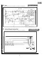
,t&VTki~ST§WD64/
NOTE: The parts here shown are supplied as an assembly but not independently.
n Infrared Remote Control Unit
RRMCGI 342PESA
NOTE: The parts here shown are supplied as an assembly but not independently.
.
03001
2SC3203Y
DxDl
-191.
L
1
2
3
4
23
5
6
I
DESCR~P‘TION OF SCHEMATIC DIAGRAM
SAFETY NOTES:
NOTES:
1. DISCONNECT THEAc PLUG FROM THEAC OUTLET BEFORE
REPLWING PARTS .
2. SEMICONDUCTOR HEAT SINKS SHOULD BE REGARDED AS
POTENT/AL SHOCK HAZARDS WHEN THE CHASSIS IS OPERATING.
7. The unit of resistance ‘ohm” is omitted.
(K = 1000 ohms, M = Meg ohm).
2. All resisfors are I/B watt, unless otherwise noted.
3. All capacitors are pF; unless therwise noted. (P = ppF).
VOLTAGE MEASUREMENT CONDITIONS:
IMPORTANT SAFETY NOTICE:
) ARE IMPORTANT FOR
PARTS MARKED WITH “A ” (
MAINTAINING THESAFETY OF THE SET BE SURE TO REPLACE
THESE PARTS WITH SPECIFIED ONES FOR MAINTAINING THE
SAFETYAND PERFORMANCE OF THE SET
1. Voltage in parenthesis measured with no Signal.
2. Voltages without parenthesis measured with 3m V 8 & W or
Colour-Signal.
3. All the voltages in each point are measured with VTVM.
WAVEFORM MEASUREMENT CONDITIONS:
SERVICE PRECAUTION:
THEAREA ENCLOSED BY THIS LINE (- - - ) Is DIRECTLY
CONNECTED WITH AC MAINS VOLTAGE.
WHEN SERVlClNG THEAREA, CONNECTAN ISOLATING TRANSFORMER BETWEEN TV RECEIVER AND AC LlNE TO ELIMINATE
1 HAZARD OF ELECTRIC SHOCK.
1. Co/our bar generator signal of 1.5V peak to peak applied at
Base of Video Buffer Amp. Q202.
2. Approximate/y 4.0 V AGC bias.
24
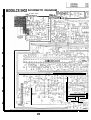
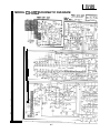
MODELCX-34G3 SCHEMATIC DIAGRAM
PWB-C (AV2 UMT)
DUNTK9324WEVO
B (CRT UNIT)
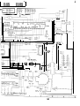
<9323WEV2 ~
PWB-A
(MAIN UNIT)
DUtdTK9322WEW 1
.,
7
Ic80
25
1
T91226CN
iPAL/SECAM/NTSCI
IC603
Th78109S
:N:S
k,
CX-34G3
CX-51 G3
26
CX-34G3
CX-51 G3
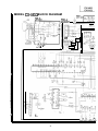
MODEL CX-51 G3 SCHEMATIC DIAGRAM
27
CX-34G3
CX-51 G3
CX-34G3
CX-51 G3
28
J
1
AUDIO-IN
--------w--z-VIDEO-IN ____AUDIO-OUT--______VIDEO-OUTv-,
2
I
3
4
29
5
6
\I
CX-34G3
CX-51 G3
CX-34G3
CX-51 G3
r
l
5701
c----1
d--!
I
1
L-- - -+
-8
I
I
I
1
I-F
& -------__A,
1
L70L
;
LINE FILTER
I*---- - - - - - a-1
j
I
II
I l-4
R E CTI F IER
070 I-0704
PLUSE
CLIP
D602
H-DRIVE
060 I
T60 I
H-OUT
0602
T
-
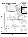
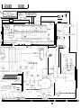
MODEL CX-51 G3 BLOCK DIAGRAM
P*B-B
PWB-A
MAIN UNIT
.
H
G
IC35 I
SPOT
-FOCUS /
------_
-
C I- I - I - ,
*
F
c
-
E
D
C
B
4
i@
@
@ a
---------___----____--------.
AUDIO-IN
1
2
3
4
31
I
5
I
VIDEO-I,,
AUDIO-OUT
6
VIDEO-C
CX-34G3
CX-51 G3
CX-34G3
CX-51 G3
G LED DR.
01004
L----A
2
- - - - - - - - j----y
7
L702
’
LINE
FILTER
&- - - - - - -
I , 18
I
I
I
+ --------- &-,
II
I I L70 I
I
I
,1
1
I
LINE
-I I I
FILTER
;
RECTIFIER
D70 I-0704
t-A
i
i
II
PLUSE
CLIP
D602
Ii-
----e--m---
rh
--~~----~----~-----~--~~~~~~~~~~~~~
_-__--_--___--_-___--------JDIO-IN
VIDEO-IN
AUDIO-OUT
6
VIDEO-OUT
AUDIO
IN
7
VIDEO IN
I
8
9
I
10
32
11
12
CX-34G3
CX-51 G3
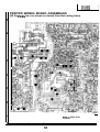
PRINTED WIRING BOARD ASSEMBLIES
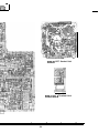
(All the PWBs here are shown as viewed from their wiring sides)
PWB-A: Main Unit
1
1
2
3
4
33
5
6
C
C
‘. I
3463
51G3
--_-_
“-xxIIIIIII
rX
1
___.-“_I-
XI
_““-
PWB-B: CRT Socket Unit
PWB-C: AV-2 Terminal Unit
7
8
10
9
34
11
12
Ref. No.
Description
PWB-A DUNTK9322WEwl/ws
PARTS REPLACEMENT
MAIN UNIT
Code
TUNER
NOTE: THE PARTS HERE SHOWN ARE SUPPLiED AS AN
ASSEMBLY BUT NOT INDEPENDENTLY.
a TU201
VTUVTSTGHD64I
R VHFTuner
BF
INTEGRATED CIRCUITS
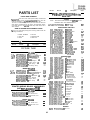
“HOW TO ORDER REPLACEMENT PARTS”
TO
have your order filled promptly and correctly, please furnish the
following informations.
IC201
VHiBA7357S/-1
R BA7357S
IC202
RH-iX0037CEZZ
R 32V Regulator
AF
IC302
VHiTA7348P/-1
AK
AR
1. MODEL NUMBER
2. REF. NO.
lC351
VHiTDA7056A-1
R TA7348P
R TDA7056A
3. PART NO.
4. DESCRIPTION
IC401
VHiTA7348P/-1
R TA7348P
AK
5. CODE
6. QUANTITY
IC501
RH-iX0640CEZZ
AK
IC602
VHiKA7809Pi-1
R LA7830
R KiA7809Pi
iC603
VHiTA78LOSS-1
AC
iC604
VHiKA7805Pi-1
R H-Vcc, 9V Regulator
R 5V Regulator
IC751
RH-iX1779CEZZ
AR
IC801
VHiTB1226CN-1
R TEA2261
R TB1226CN
Ic1001 RH-iX2938CEN2
R M37221 M4-109SP
AW
IC1002 VHiKiA7045P-1
IC1003 VHiST24C04/-1
IC1004 VHiUPC78L054
R KiA7045P
R ST24C04CB6
R UPC78LO5J
AD
AQ
MARK Jr: SPARE PARTS-DELIVERY SECTION
Part No.
*
Description
Code
PICTURE TUBE
MODEL CX-34G3
nv1
VB370BVBKl S-S
R CRT 37 cm (14”)
BZ
a L708
A DYl
RCiLG0023PEZZ
RCiLHO140PEN3
R Degaussing (ADG) Coil
R Deflection Yoke
R ADG Coil Holder, x4
AN
LHLDW0003PEKZ
AK
AB
MSPRTOOOi PEFJ
AC
R CRT Spring
Q201
Q202
AD
MODEL CX-51 G3
VB51 KPD12X/4E
R CRT 54 cm (21”)
CG
RCiLG0025PEZZ
R Degaussing (ADG) Coil
AW
LHLDW0003PEKZ
(with DY)
R ADG Coil Holder, x4
VS2SC1906//1 E
VS2SCl815GW-1
R IF Amp.
R 2SC1815(G)
Q301
Q302
VS2SC1815GW-1
VS2SCl815GW-1
R Mute
R Amplifier
Q303
Q305
VS2SCi 815GW-1
R Amplifier
VS2SC1815GW-1
R Mute
AB
Q401
VS2SA1015Yll E
VS2SCl815GW-1
R Buffer
R Video Buffer
AC
R 2SA1015(G)
AC
AD
AL
Q404
VS2SA1015G/l
E
Q601
VS2SC2482//-1
R Horizontal Drive
VS2SD 1877//l E
R Horizontal Output
PSPAG0003PEZZ R W edge (Gum), x3
MSPRTOOOl PEFJ
R CRT Spring
AD
Q606
VS2SC1815GW-1
R Horizontal Switch
R 2SC1815(G)
A
PRINTED WIRING BOARD ASSEMBLIES
(NOT REPLECEMENT ITEM)
-
- Main Unit
-
PWB-B DUNTK9323WEV3
- CRT Socket Unit
-
p’@B-C DUNTK9324WEV3
- AV-2 Terminal Unit
-
Q701
VS2SC1815GW-1
VS2SD1884//-1
Q801
VS2SC1815GW-1
AB
AB
AB
AB
AB
R Power Output
AN
R Spot Killer
AB
AC
VS2SA1015Y/l
E
R Spot Killer
Q803 VS2SA1015Y/l
E
R R-Buffer
AC
Q804 VS2SA1015Y/l
E
R B-Buffer
AC
Q805 VS2SAlO15Y/l
E
R G-Buffer
QlOOl
MODEL CX-51G3
PWB-A DUNTK9322WEV3
Q607
Q802
MODEL CX-34G3
- AV-2 Terminal Unit
AB
AB
AB
(CX-34G3)
AC
PWB-C DUNTK9324WEVO
AC
AB
VS2SC1815GW-1
A Q602
-
AD
VS2SC1815GW-1
AK
-
BC
Q205
AB
- CRT Socket Unit
AE
Q207
PMAGF3003CEZZ R Purity Magnet
PWB-B DUNTK9323WEV2
AE
R 6MHz (CX-34G3)
R 2SC1815(G)
Q405
PWB-A DUNTK9322WEVl - M a i n U n i t
AP
TRANSISTORS
BC
AB
PMAGF3006CEZZ R Purity Magnet
PSPAG0004PEZZ R W edge (Gum), x3
QEARC1404PEZZ R Grounding Strap
AVl
&J L708
*
PARTS LIST
Replacement parts which have these special safety characteristics
identified in this manual: eleCtfiCa1 Components having such features are identified by “A” in the Replacement Parts Lists.
The use of a substitute replacement part which does not have the
same safety characteristics as the factory recommended replacement parts shown in this Service manual may create shock, fire or
other hazards.
Ref. No.
Part No.
VS2SC1815GW-1
AC
R V-Sync.
Q1002 VS2SCl815GW-1 R H - S y n c .
AB
Q1003 VS2SA1015Y/l E
R R LED Driver
AC
Q1004 VS2SA1015Y/l E
R G LED Driver
Q1005 VS2SA1015Y/l E
R H-Vcc SW
QlOO6 VS2SC1815GW-1 R H-Vcc S
W
AB
AC
AC
AB
DIODES
D201
35
RH-DX0475CEZZ
R Diode
AB
Ref. No.
Part No.
*
Description
Code
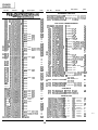
Ref. No.
Description
Code
PACKAGED CIRCUITS
PWB-A DUNTK9322WEwmv3
PR701 RMPTP0028CEZZ R Packaged Circuit (CX-34G3)AG
MAIN UNIT(Continued)
PR701 RMPTPOOOl
D302
RH-DX0224CEZZ
R Diode
AB
D303
RH-DX0475CEZZ
R Diode
AB
RH-DX0475CEZZ R Diode
.
R Diode
AB
D304
*
Part No.
R Packaged Circuit (CX-51 G3)AN
PEZZ
AH
X801
RCRSB0244CEZZ R C r y s t a l , 16.2MHz
AB
CF201
RFiLA0042CEZZ
R Filter
AD
R Filter
AE
AB
COILS AND TRANSFORMERS
D305
RH-DX0475CEZZ
D403
RH-DX0475CEZZ
R Diode
AB
CFl 001 RFiLA0084CEZZ
D404
RH-DX0475CEZZ
R Diode
AB
L201
VP-DF270KOOOO
R Peaking 27pH
D501
RH-DX0279CEZZ
R Diode
AB
L202
VP-DF270KOOOO
R Peaking 27pH
AB
D502
RH-DXO127CEZZ
R Diode
AC
L203
VP-DF270KOOOO
R Peaking 27pH
AB
D503
RH-EX0675GEZZ
R Zener Diode 33V
AB
L204
VP-XFl ROKOOOO
R Peaking 1 pH
AB
RH-EX0675GEZZ
R Zener Diode 33V
AB
L206
VP-XF390KOOOO
R Peaking 39pH
AB
RH-EX0294CEZZ
R Zener Diode 5.1V
AA
L401
VP-CFl 01 KOOOO
R Peaking 100pH
AB
RH-EX0313CEZZ
RH-DX0073CEZZ
R Zener Diode 9.1 V
L602
L605
RCiLP0224CEZZ
R Coil
AE
R Diode
AA
AD
VP-DFl OOKOOOO
R P e a k i n g 10pH (CX-34G3) AB
RH-DX0279CEZZ
R Diode
AB
L605
VP-DFl 01 KOOOO
R Peaking 1OOpH (CX-51G3) AB
A D606
RH-DX0475CEZZ
R Diode
AB
L609
VP-CFl R5MOOOO
A D607
RH-EX0692GEZZ
R Zener Diode 27V (CX-34G3) AB
L609
R Peaking 1.5pH (CX-34G3) AB
AB
R Peaking 1pH (CX-51G3)
A D607
0611
RH-EX0342CEZZ
RH-DX0475CEZZ
R Zener Diode 24V (CX-51G3) AB
AB
R Diode
VP-CFl ROM0000
RCiLP0225CEZZ
a L701
RCiLF0021 PEZZ
R Coil
AK
A D618
RH-DX0475CEZZ
R Diode
AB
&, L702
RCiLF0012PEZZ
R Coil
AN
D619
a D657
RH-DX0475CEZZ
RH-EX0286CEZZ
R Diode
AB
AA
L705
L712
VP-CF3R3KOOOO
VP-CF330KOOOO
R Peaking 3.3pH
AB
RH-DX0055TAZZ
RH-DX0055TAZZ
RH-DX0055TAZZ
R Diode
R Diode
R Diode
AD
L712
AD
AD
L801
L802
VP-CFl OOKOOOO
VP-DFl 01 KOOOO
R Diode
AD
R Diode
AE
Ll 001
SF201
VP-DFl ROKOOOO
0705
RH-DX0055TAZZ
RH-DXO130CEZZ
RFiLC0018PEZZ
AB
AB
R Peaking 1 pH
R Surface Acoustic Wave FilterAL
D706
RH-DXOl30CEZZ
R Diode
AE
T203
RCiLD0238CEZZ
R Detection Coil
D708
D709
RH-EX0639CEZZ
AB
AC
T204
RCiLD0239CEZZ
R Detection Coil
RH-DX0302CEZZ
R Zener Diode 3.9V
R Diode
A T601
RTRNZO179CEZZ
D710
RH-DX0027CEZZ
R Diode
AE
A T601
RTRNZ0026PEZZ R Transformer (CX-51 G3)
D712
D715
RH-DXO130CEZZ
R Diode
AE
n T602
RTRNFO141 PEZZ
RH-EX0323CEZZ
R Zener Diode 13V
AB
D732
RH-DX0388CEZZ
R Diode
AE
D733
RH-DX0302CEZZ
R Diode
AC
D801
RH-DX0475CEZZ
R Diode
AB
n T701
RTRNZOll SPEZZ R Transformer (CX-34G3)
AS
R Diode
AB
A T701
RTRNZOl20PEZZ R Transformer (CX-51 G3)
BB
R Diode
AB
D504
D601
D602
D603
D604
0701
D702
D703
D704
0 8 0 2 RH-DX0475CEZZ
0 8 0 3 RH-DX0475CEZZ
D804
RH-DX0475CEZZ
R Zener Diode 3.9V
L632
R Coil
AF
R P e a k i n g 33pH (CX-34G3) AB
AB
R Peaking 10pH (CX-51 G3)
AB
R Peaking 100pH
VP-DFl 01 KOOOO
R Peaking 100pH
AE
AE
R T r a n s f o r m e r (CX-34G3) AE
AH
R H-Volt Transformer
BC
(CX-34G3)
A T602
RTRNF0147PEZZ R H-Volt Transformer
BC
(CX-51 G3)
CONTROLS
R Diode
AB
D1003 RH-EXO61 SGEZZ
R Zener Diode 6.2V
AA
R216
D1004 RH-EXO61 SGEZZ
R Zener Diode 6.2V
AA
R711
D1008 RH-EXO61 SGEZZ
R Zener Diode 6.2V
AA
D1012 RH-EXO61 SGEZZ
R Zener Diode 6.2V
AA
Dl 013 RH-PX0003PEZZ
R LED, Red/Green
AF
C201 VCEAGAlCW226M R 2
RVR-M4630GEZZ
R
RF-AGC
AB
115V Adj.
AC
47k(B)
RVR-M4324CEZZ R 220(B)
CAPACITORS
2
16V E l e c t r o l y t i c AB
Dl 014
RH-EXO61 SGEZZ
R Zener Diode
AA
C202 VCKYMNlCY103N
R 0 . 0 1
16V
Ceramic
AA
Dl 015
RH-EXO61 SGEZZ
R Zener Diode
AA
C203 VCKYMNlCY103N
R 0 . 0 1
16V
Ceramic
AA
Dl 018 RH-DX0475CEZZ
R Diode
AB
C204 VCEAGAl CW107M R 1 0 0
16V E l e c t r o l y t i c AB
Dl 019 RH-DX0475CEZZ
R Diode
AB
C205 VCEAGAlCW337M R 3 3 0
16V Electrolytic AC
D1020
RH-DX0475CEZZ
R Diode
AB
C206 VCKYPAl HF103Z R 0 . 0 1
50V
D1021
RH-DX0475CEZZ
R Diode
AB
C207 VCEAGAlHWlOGM R 1
5OV Electrolytic AC
0
Ceramic
AA
D1022 RH-EXO61 SGEZZ
R Zener Diode (CX-51G3)
AA
C208 VCKYMNlCY103N
R 0 . 0 1
16v
Ceramic
AA
D1023 RH-EXO61 SGEZZ
R Zener Diode (CX-51 G3)
AA
C209 VCKYMNlCY103N R 0 . 0 1
16v
Ceramic
AA
R Zener Diode
AA
C210 VCKYMNlCY103N
R 0 . 0 1
16v
Ceramic
AA
R Varistor
AE
c211
VCKYMNlCY103N R 0 . 0 1
16v
Ceramic
AA
D1026 RH-EXO61 SGEZZ
n VA702 RH-VX0048CEZZ
36
k-.-
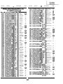
Ref. No.
Description
Part No.
Ref. No.
Code
C408
PWB-A DUNTK9322WEwmV3
c409
MAIN UNIT(Continued)
Part No.
-k
VCKYMNlCY103N
R
Description
0.01
Code
16V C e r a m i c
AA
AA
VCEAGAlCWlOGM
R 10
16V Electrolytic
c410
RC-QZA104TAYK
R 0.1
50V M y l a r
AB
c212
VCKYPAl HFlO3Z R 0.01
5ov
Ceramic
AA
c411
VCEAGAlHW475M
R 4.7
50V Electrolytic
AB
c213
VCFYSAlHB154J
R
0.15
5ov
Mylar
AB
C412
VCKYMNlCY103N
R 0.01
16V Ceramic
AA
C214
VCKYMNlCY103N
R
0.01
16V
Ceramic
AA
c413
VCEAGAlCW107M
R 100
16V Electrolytic
AB
C215
VCEAGAlCWlOGM R 10
16V
Electrolytic
AA
c414
16V Ceramic
AA
C216
VCKYMNlCY103N
R
0.01
16V
Ceramic
AA
c415
VCKYMNl CY 103N R 0.01
R 0.1
RC-QZA104TAY K
50V M y l a r
AB
C217
VCKYMNlCY103N
R
0.01
16V
Ceramic
AA
C416
VCEAGAlCW226M
R 22
16V Electrolytic
AB
C218
VCCCPAlHH150J
R
15~
5ov
Ceramic
AA
c417
VCEAGAlHW105M
R 1
50V Electrolytic
AC
5ov
Ceramic
AA
C418
VCEAGAlCW477M
R 470
16V Electrolytic
AC
5ov
Ceramic
AA
c419
VCCCPAlHH56OJ
c219
c220
VCCCPAlHH220J
VCCCPAlHHlOlJ
R
R
22p
100~
c221
VCFYSAl
R 0.68
5ov
Mylar
AC
c222
VCCCPAlHH120J
R
5ov
Ceramic
AA
C223
RC-QZAl 04TAYK
R 0.1
5ov
Mylar
C224
VCEAGAlCW476M
R 47
16V
Electrolytic
C225
C227
VCKYMNlCY103N
R
0.01
16V
VCCCPAlHH180J
R
18p
C228
RC-QZA104TAYK
R 0.1
5ov
5ov
c229
C231
RC-QZA103TAYK
VCEAGAlHW475M
R 0.01
5ov
R 4.7
C232
C233
VCKYMNl CY103N R 0.01
VCEAGAlHW225M
c301
C302
VCEAGAlCW477M R 470
R 0.1
RC-QZA104TAYK
c303
VCFYSAl
c304
c305
RC-QZAl OBTAY K
VCEAGAl HW104M R 0.1
C306
c307
C308
RC-QZA473TAY K
VCKYPAl HB331 K
VCKYPAl HF103Z
c309
c310
c311
C312
R
50V Ceramic
AA
50V Electrolytic
AC
(CX-34G3)
50V Electrolytic
2.2
AC
56~
c501
VCEACAlHC105M
R 1
AB
AB
c501
VCEACAlHC225M
R
Ceramic
Ceramic
AA
C502
AA
c503
VCKYPAlHB471 K R 470~ 50V C e r a m i c
50V M y l a r
R 0.1
RC-QZA104TAYK
Mylar
AB
c504
AA
c505
5ov
Mylar
Electrolytic
AB
C506
16V
Ceramic
AA
c507
VCEAGAl EW108M R 1000 25V E l e c t r o l y t i c
35V Electrolytic
VCEAGAlVW107M R 100
5ov
16V
Electrolytic
Electrolytic
AB
c509
RC-QZA104TAYK
R 0.1
50V M y l a r
AB
AC
c510
VCEAGAlVW477M
R 470
35V Electrolytic
AD
5ov
Mylar
AB
c511
VCKYPA2HB102K R 1000~ 500V C e r a m i c
AA
5ov
5ov
Mylar
Mylar
AC
AA
C512
VCFYSAlHB824J R 0.82 50V M y l a r
AC
Electrolytic
Mylar
AA
AB
C512
R 0.047
R 330~
R 0.01
5ov
5ov
5ov
5ov
Ceramic
Ceramic
AA
AA
c513
VCKYPAl HF103Z
R 0.01
5ov
Ceramic
AA
c513
VCEAGAlCW106M
R 10
(CX-34G3)
50V Electrolytic
VCEACAl HC105M R 1
(CX-51 G3)
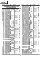
AA
c514
VCEAGAlHW105M
c515
VCEACAl HC105M R 1
HB684J
HB474J
12p
R 2.2
R 0.47
R 0.01
16V Electrolytic
VCKYPA2HB102K
R 1000~ 5oov Ceramic
VCEAGAlCW477M R 470
16V Electrolytic
(CX-51 G3)
AA
VCCSPA2HL471K R 470~ 500V C e r a m i c
50V M y l a r
RC-QZA104TAYK
R 0.1
(CX-34G3)
50V Electrolytic
VCEACAl HC105M R 1
(CX-51 G3)
R 0.82 50V Mylar
VCFYSAl HB824J
R 1
50V Electrolytic
50V Electrolytic
AA
AB
AB
AB
AD
AC
AC
AC
AC
AC
c314
c315
VCKYMNl CY103N R 0.01
16V
Ceramic
AC
AA
C518
VCQYTAlHM392K R 3900p 50V M y l a r
AB
VCEAGAlCWlOGM R 10
16V
Electrolytic
AA
c519
RC-QZA472TAY K
R 0.0047 50V M y l a r
AA
C316
VCKYMNl CY 103N R 0.01
16V
Ceramic
AA
C601
VCEAGAlCW476M
R 47
16V Electrolytic
AB
c317
VCEAGAlCW106M
R 10
16V
Electrolytic
AA
C602
VCKYPAl
R 0.01
50V Ceramic
AA
C318
VCEAGAlHW225M
R 2.2
5ov
Electrolytic
AB
C603
VCKYMNl CY103N R 0.01
16V Ceramic
AA
c319
VCKYD41
16V
Ceramic
AA
C604
VCEAGAlCW107M
R 100
16V Electrolytic
AB
C320
VCEAGAlCW337M
R 330
16V
Electrolytic
AC
C605
VCEAGAlCW476M
R 47
16V Electrolytic
AB
C321
VCKYMNl CY103N R 0.01
16V
Ceramic
AA
C606
VCEAGAlCW476M
R 47
16V Electrolytic
AB
C322
VCEAGAlHW225M
5ov
Electrolytic
AB
C607
RC-QZA104TAYK
R 0.1
50V M y l a r
AB
C323
VCEAGAlHW105M R 1
5ov
Electrolytic
AC
C608
RC-QZA103TAY K
R 0.1
50V M y l a r
AA
R 1
50V Electrolytic
AC
CY103N R 0.01
R 2.2
HF103Z
AC
C324
VCKYMNl HB331 K R 330~
5ov
Ceramic
AA
C609
VCEAGAlHW105M
C327
VCEAGAlHW225M
R 2.2
5ov
Electrolytic
AB
C610
VCFYSB2EB823J R 0.082 250V M y l a r
AD
C328
VCEAGAlCWlOGM R 10
16V
Electrolytic
AA
C611
VCKYPA2HB102K R 1000~ 500V C e r a m i c
AA
c329
VCEAGAlHW105M R 1
5ov
Electrolytic
AC
C613
VCFPPD2DB474J
M-Poly.
AE
c330
RC-QZA473TAY K
R 0.047
5ov
Mylar
AB
c331
VCKYD41
R 1000~ 5ov
Ceramic
AA
200V M-Poly.
AF
c401
VCEAGAlCWlOGM R 10
16V
Electrolytic
AA
C402
VCKYMNl CY103N R 0.01
16V
Ceramic
c403
VCEAGAlCW106M
16V
Electrolytic
HB102K
R 10
0.47
200V
(CX-34G3)
C613
VCFPPD2DB564J
AA
C614
(CX-51 G3)
16V Electrolytic
VCEAGAlCWl 06M R 10
AA
C615
VCQPSD2DA224J
C616
VCFPPD3CA682H R 6800~ 1.6kV M-Poly.
c404
VCKYMNl CY103N R 0.01
16V
Ceramic
AA
c405
VCEAGAlCW106M
16V
Electrolytic
AA
C406
VCEAGAl CW108M R 1000
16V
Electrolytic
AD
R 10
R
R
R
0.56
0.22
200V Mylar
(CX-34G3)
37
AA
AD
AE
CX-34G3
CX-51 G3
Ref. No.
Part No.
Ir
Description
Ref. No.
Code
PWB-A DUNTK9322WEwVws
C616
VCFPPD3CA912H R 9 1
OOp 1.6kV M-Poly.
AE
(CX-51 G3)
Description
Code
50V M y l a r
AA
C805 VCEAGAl CW107M R 1 0 0
16V Electrolytic
AB
C806 VCKYMNl CY103N R 0 . 0 1
16V Ceramic
AA
C807 VCEAGAl CWl07M R 1 0 0
16V Electrolytic
AB
C808 VCKYMNlCY103N R 0 . 0 1
16V Ceramic
AA
C804
MAIN UNIT(Continued)
*
Part No.
RC-QZA103TAYK
R 0.01
50V M y l a r
AB
C809 VCKYMNlCY103N R 0 . 0 1
16V Ceramic
AA
R 1 0
1 OOV Electrolytic
AC
C810
12p
50V Ceramic
AA
VCEAGAlHW105M
R 1
50V Electrolytic
AC
C811
VCKYPAlHF103Z R 0 . 0 1
50V Ceramic
AA
A C622
VCEAGAlHW105M
R 1
50V Electrolytic
AC
C812 VCEAGAlCW107M R 1 0 0
16V Electrolytic
AB
A C630
VCKYMNlCY103N
16V Ceramic
AA
C813
RC-QZAl04TAYK
R 0.1
50V M y l a r
AB
R 0.1
50V M y l a r
AB
50V Electrolytic
AC
50V M y l a r
AA
C617
RC-QZA104TAYK
C619
VCEAGA2AWlOGM
A C620
R 0.1
R 0.01
VCCCMNlHH120J
16V Electrolytic
AB
C814
RC-QZAl04TAYK
C650
VCEAGAlCW476M R 4 7
R 0.22
VCFYSAl HB224J
5OV M y l a r
AB
C815
VCEAGAlHW105M
C653
VCKYATl EX103N R 0 . 0 1
25V Ceramic
AA
C816
RC-QZA103TAYK
C636
R
R
1
R 0.01
C654
VCEAGAlCW476M R 4 7
16V Electrolytic
AB
C817 VCEAGAlCW227M R 2 2 0
16V Electrolytic
AC
C655
VCKYPAl HF103Z R 0 . 0 1
50V Ceramic
AA
C820 VCKYMNlCY103N R 0 . 0 1
16V Ceramic
AA
C656
VCEAGAOJW107M
6.3V Electrolytic
AB
C82i VCKYD41CY103N R 0 . 0 1
16V Ceramic
AA
50V M y l a r
VCCSMNlHL330J
A c701
c703
c704
c705
C706
R 100
RC-FZO17SCEZZ
R 0.22 AC250VSpecil
AD
RC-KZ0029CEZZ
R 0.01 AC250V Ceramic
AC
c901
Cl001
RC-KZ0029CEZZ
RC-KZ0029CEZZ
R 0.01 AC250V Ceramic
AC
Cl002
VCCSPAl
R 0.01 AC250V Ceramic
Cl003
VCCSMNlHL330J
RC-KZ0029CEZZ
R 0.01 AC250V Ceramic
400V Electrolytic
R 68
AC
AC
Cl004
VCCSMNl
C708
c709
R 0.01 AC250V Ceramic
25V Electrolytic
VCEAGAlEW107M R 1 0 0
AQ
AC
AD
c710
c711
VCKYPA2HB102K R 1000~ 500V C e r a m i c
R 470~ 50V M y l a r
RC-QZA471TAYJ
AA
AB
C712
VCFYSAl HB474J
C712
VCFYSAl HB564J R 0 . 5 6
c713
VCKYPA2HB102K R 1000~ 500V C e r a m i c
R 0 . 0 5 6 50V M y l a r
RC-QZA563TAYK
VCEAGAlHWlOGM R 1 0
c707
RC-EZ0545CEZZ
RC-KZ0029CEZZ
R 0.47
RC-QZA104TAYK
R 0.1
33p
50V Ceramic
AB
AA
R 33p
50V Ceramic
AA
R
33p
50V Ceramic
AA
R 33p
50V Ceramic
AA
Cl005 VCEAGAl HW105M R 1
Cl006 VCEAGAlAW107M R 1 0 0
50V Electrolytic
AC
1 OV Electrolytic
Cl007 VCKYMNlCY103N R 0 . 0 1
Cl008 VCEAGAlAW476M R 4 7
16V Ceramic
1 OV Electrolytic
AB
AA
Cl009 VCEAGAlCWlOGM R 1 0
16V Electrolytic
AA
16V Electrolytic
AA
R
HL330J
HL330J
(CX-34G3)
AC
Cl010 VCEAGAlCW106M R 1 0
50V (CX-51 G3)
AC
Cl011 VCKYMNlHBlOlK
50V
AA
AA
AA
R 100~ 50V C e r a m i c
25V Ceramic
Cl012 VCKYATl EX103N R 0 . 0 1
AB
Cl01 3 VCCSPAl HL471 J
50V Electrolytic
AC
C720
C721
AC
AB
50V Ceramic
16V Electrolytic
AA
AA
R 1
50V Electrolytic
63V Electrolytic
VCEAGAlJW476M R 4 7
RC-KZ0341 CEZZ
R 1000~ 2kV C e r a m i c
Cl014 VCCSMNl HL560J R 56~
Cl01 5 VCEAGAlCW476M R 4 7
6.3V Electrolytic
16V Ceramic
AB
AA
C723
VCKYPA2HB102K R 1000~ 500V C e r a m i c
AD
AA
Cl016 VCEAGAOJW107M R 1 0 0
Cl017 VCKYMNlCY103N R 0 . 0 1
Cl 618
VCCSPAl HL680J
R 68p
50V Ceramic
AA
C724
C725
RC-KZ0029CEZZ
VCFYSAl HB474J
R 0.01 AC250V Ceramic
AC
Cl 019 VCCSPAl HL680J
R 68p
50V Ceramic
AA
R 0.47
AC
Cl020 VCEAGAOJW107M
R 1 0 0
6.3V Electrolytic
AB
C726
VCKYPAl HB392K R 3900p 50V C e r a m i c
AB
Cl021
c714
c715
C716
VCEAGAlHW105M
50V M y l a r
(CX-34G3)
AA
R 470~ 50V C e r a m i c
VCCSPAlHLl81J
R 180~ 50V C e r a m i c
AA
AB
AA
Cl022 VCKYMNlCY103N
R 0.01
16V Ceramic
AA
Cl023 VCKYMNlCY103N
R 0.01
16V Ceramic
AA
C726
VCKYPAlHB272K R 2700~ 50V C e r a m i c
Cl024 VCKYD41CY103N R 0 . 0 1
16V Ceramic
AA
c729
VCEAGAlCW477M R 4 7 0
16V Electrolytic
AC
Cl025 VCKYD41CY103N R 0 . 0 1
16V Ceramic
AA
c731
VCEAGH2CW107M
R 100
16OV Electrolytic
AE
Cl026 VCKYD41CY103N R 0 . 0 1
16V Ceramic
AA
C732
RC-KZ0341 CEZZ
R 1000~ 2kV C e r a m i c
AD
Cl027 VCKYD41 CY103N R 0 . 0 1
16V Ceramic
AA
c733
VCKYPA2HB102K R 1000~ 500V C e r a m i c
AA
Cl028 VCKYD41CY103N R 0 . 0 1
16V Ceramic
AA
c734
VCEAGAlCW477M R 4 7 0
AC
Cl029 VCKYD41CY103N R 0 . 0 1
16V Ceramic
AA
C736
RC-KZ0029CEZZ
R 0.01 AC250V Ceramic
AC
c737
VCEAGH2CW107M
R 100
AE
Cl031 VCKYD41CY103N R 0 . 0 1
16V Ceramic
AA
c741
VCKYPA2HB472K R 4700~ 500V C e r a m i c
AB
Cl032 VCKYD41CY103N R 0 . 0 1
16V Ceramic
AA
C742
VCFYSAl HB394J R 0 . 3 9
AC
C742
VCFYSAlHB474J R 0 . 4 7
(CX-51 G3)
a c747
16V Electrolytic
16OV Electrolytic
50V (CX-51 G3)
(CX-34G3)
50V (CX-34G3) AC
RESISTORS
RC-KZ021SCEZZ R 3300~ 4kV C e r a m i c
AE
R201
VRD-MN2BE680J R 6
c750
VCKYPAl HF103Z R 0 . 0 1
50V Ceramic
AA
R202
VRD-MN2BE680J
C801
VCEAGAlHW475M R 4 . 7
50V Electrolytic
AB
R206 VRD-MN2BE680J R 6
C802
RC-QZA103TAY K
R 0.01
50V M y l a r
C803
RC-QZAl03TAYK
R 0.01
50V M y l a r
8
1/8W Carbon
AA
R 68
1/8W Carbon
AA
8
1/8W Carbon
AA
AA
R207 VRD-MN2BE392J R 3.9k 1/8W C a r b o n
AA
AA
R209 VRD-MN2BE122J R 1.2k 1/8W C a r b o n
AA
38
CX-34G3
CX-51 G3
Ref. No.
Part No.
*
Description
Code
Ref. No.
Part No.
*
Description
Code
PWB-A DUNTK9322WEwmM
R324
VRD-MN2BElO2J
R lk
1/8W Carbon
AA
MAIN UNIT(Continued)
R328
VRD-MN2BE472J
R 4.7k 1/8W C a r b o n
AA
R401
VRD-RA2EE750J
R 75
1/4W Carbon
AA
R210
VRD-RA2BE122J
R 1.2k 1/8W C a r b o n
AA
R402
VRD-MN2BElO3J
R 1 Ok 1/8W Carbon
AA
R212
VRD-MN2BElOl J
R 1 0 0 1/8W C a r b o n
AA
R403
VRD-RA2EE750J
R 75
1/4W Carbon
AA
R213
VRD-MN2BE102J
R lk
1/8W Carbon
AA
R406
VRD-RA2BE102J
R lk
1/8W Carbon
AA
R214
VRD-MN2BE222J
R 2.2k 1/8W C a r b o n
AA
R408
VRD-RA2BE222J
R 2.2k 1/8W C a r b o n
AA
R215
VRD-MN2BE102J
R lk
1/8W Carbon
AA
R409
VRD-MN2BE824J
R 820k 1/8W C a r b o n
AA
R415
VRD-RA2BElOl J
R 1 0 0 1/8W C a r b o n
R416
VRD-RM2HD470J
R 47
1/2W Carbon
AB
AA
R216
See Controls
R218
VRD-MN2BE273J
R 27k 1/8W C a r b o n
AA
R219
VRD-MN2BE154J
R 150k 1/8W C a r b o n
AA
R417
VRD-RA2EE750J
R 75
1/4W Carbon
AA
AA
R418
VRD-RA2BE223J
R 22k 1/8W C a r b o n
AA
AA
R419
VRD-RA2BE223J
R 22k 1/8W C a r b o n
AA
AA
R420
VRD-MN2BE103J
R 1 Ok 1/8W Carbon
AA
VRD-RA2BEl53J
(CX-34G3)
R 15k 1/8W C a r b o n
AA
R220
R221
R222
VRD-MN2BE184J
VRD-MN2BE223J
VRD-MN2BE472J
R 180k 1/8W C a r b o n
R 22k 1/8W C a r b o n
R 4.7k 1/8W C a r b o n
R223
VRD-MN2BE472J
R 4.7k 1/8W C a r b o n
AA
R224
R225
VRD-MN2BE472J
R 4.7k 1/8W C a r b o n
AA
R420
(CX-51 G3)
VRD-MN2BE472J
VRD-RA2EE12OJ
R 4.7k 1/8W C a r b o n
AA
R226
R 12
1/4W Carbon
AA
R421
VRD-RM2HD470J
R 47
1/2W Carbon
AA
R227
VRD-RA2EE12OJ
R 12
1/4W Carbon
AA
R422
VRD-RA2BE222J
R 2.2k 1/8W C a r b o n
AA
R228
R229
VRD-MN2BElO3J
VRD-MN2BE103J
R 10k 1/8W C a r b o n
AA
AA
R504
VRD-MN2BE221 J
R 2 2 0 1/8W C a r b o n
AA
R 1 Ok 1/8W Carbon
VRD-RA2BE102J
R lk
1/8W Carbon
AA
R230
VRD-MN2BE153J
R 15k 1/8W C a r b o n
AA
R506
R510
VRD-RM2HDl R5J
R 1 . 5 1/2W C a r b o n
AA
R232
VRD-RA2BE473J
R 47k 1/8W C a r b o n
AA
VRD-RM2HD2R2J
AA
R233
VRD-RA2BE473J
(CX-34G3)
R 47k 1/8W C a r b o n
(CX-34G3)
(CX-51 G3)
R 2 . 2 1/2W C a r b o n
AA
VRD-RA2BE273J
(CX-34G3)
R 27k 1/8W C a r b o n
AA
R234
VRD-RA2BE103J
R235
R237
VRD-MN2BE472J
VRD-MN2BE472J
R 1 Ok 1/8W Carbon
R 4.7k 1/8W C a r b o n
AA
AA
R 4.7k 1/8W C a r b o n
AA
R238
VRS-VV3DB153J
VRD-MN2BE151 J
R
15k 2W
Metal Oxide
R 1 5 0 1/8W C a r b o n
AA
VRD-MN2BE273J
R 27k 1/8W C a r b o n
R 2.2k 1/8W C a r b o n
AA
R242
R244
R247
R249
R250
VRD-MN2BE222J
VRD-MN2BE102J
VRD-MN2BE393J
R510
R511
(CX-34G3)
R511
VRD-RA2BE333J
R 33k 1/8W C a r b o n
(CX-51 G3)
AA
R513
VRD-RA2BE273J
R 27k 1/8W C a r b o n
AA
(CX-51 G3)
AA
R513
VRD-RA2BE333J
R 33k 1/8W C a r b o n
AA
(CX-34G3)
AA
AA
R514
VRD-RA2BE563J
R 56k 1/8W C a r b o n
R 39k 1/8W C a r b o n
R lk
1/8W Carbon
R 3.3k 1/8W C a r b o n
AA
R515
VRD-RA2EE220J
R 22
1/4W Carbon
AA
AA
AA
R516
VRD-RM2HD331 J
R 3 3 0 1/2W C a r b o n
AA
R517
VRD-RA2BE223J
R 22k 1/8W C a r b o n
AA
AA
R518
R519
VRD-RA2BElO2J
VRD-RM2HDl52J
R lk
1/8W Carbon
AA
R 1.5k 1/2W C a r b o n
AA
AA
R lk
1/8W Carbon
AA
R301
R302
VRD-MN2BE102J
R303
VRD-RA2BE392J
R304
VRD-MN2BE392J
R 3.9k 1/8W C a r b o n
R 3.9k 1/8W C a r b o n
R305
VRD-MN2BE473J
R 47k 1/8W C a r b o n
R306
VRD-RA2BEl OOJ
R 10
1/8W Carbon
AA
R601
VRD-MN2BE104J
R 1 OOk 1/8W Carbon
AA
R308
VRD-MN2BE153J
R 15k 1/8W C a r b o n
AA
R602
VRD-RA2BE103J
R 10k 1/8W C a r b o n
AA
VRD-MN2BE332J
AA
(CX-51 G3)
R309
VRD-MN2BE123J
R 12k 1/8W C a r b o n
AA
R604
VRD-RA2BE391 J
R 3 9 0 1/8W C a r b o n
AA
R310
VRD-MN2BE104.J
R 1OOk 1/8W C a r b o n
AA
R605
VRD-MN2BE102J
R lk
1/8W Carbon
AA
R311
VRD-MN2BE123J
R 12k 1/8W C a r b o n
AA
R606
VRD-RA2BE681 J
R 6 8 0 1/8W C a r b o n
AA
R312
VRD-MN2BE153J
R 15k 1/8W C a r b o n
AA
R607
VRD-MN2BE103J
R 10k 1/8W C a r b o n
AA
R313
VRD-RA2BE273J
R 27k 1/8W C a r b o n
AA
R608
VRD-RM2HD392J
R 3.9k 1/2W C a r b o n
AA
R314
VRD-MN2BE332J
R 3.3k 1/8W C a r b o n
AA
R315
VRD-MN2BE563J
R 56k 1/8W C a r b o n
AA
R316
VRD-MN2BE123J
R 12k 1/8W C a r b o n
AA
R317
VRD-MN2BE123J
R 12k 1/8W C a r b o n
AA
R318
VRD-RA2BE681 J
R 6 8 0 1/8W C a r b o n
AA
R319
VRD-RA2BE393J
R 39k 1/8W C a r b o n
AA
R320
VRD-RA2BE223J
R 22k 1/8W C a r b o n
AA
(CX-34G3)
R608
VRD-RM2HD472J
R 4.7k 1/2W C a r b o n
AA
(CX-51 G3)
R609
VRSSV3LB332J
R 3.3k
3W
Metal Oxide
AB
Metal Oxide
AC
(CX-51 G3)
R609
VRS-SV3LB472J
R 4.7k 3W
(CX-34G3)
R321
VRD-RA2BE473J
R 47k 1/8W C a r b o n
AA
R610
VRD-MN2BE822J
R 8.2k 1/8W C a r b o n
AA
R322
VRN-VV3DB2R2J
R
AB
R611
VRW-KQ3HC4R7K
R
AE
2.2
2W
Metal Film
4.7
5W
(CX-34G3)
39
Cement
Ref. No.
*
Part No.
Description
Code
PWB-A DUNTK9322WEwvw3
R661
VRW-KQ3NC4R7K
R 4 . 7
7W
Cement
R661
RR-XZ0073CEZZ
VRG-PD2HD820J
R 270 1/2W Fuse Resistor AB
R 82
1/2W Carbon
AA
8
R33
1W
k
AA
R
1M
li8W
Carbon
AA
R 3.9
Cement
AE
VRS-KT3LB562J
R 5.6k 3W
Metal Oxide
AC
R704
VRS-SV3DB15OJ
R15
Metal Oxide
AA
Metal Film
AB
Metal Film
AA
Metal Film
AA
VRN-RV3DB4R7J
7W
2W
R 4.7
2W
(CX-51 G3)
R705
VRN-VV3AB2R2J
R 2.2
1W
(CX-34G3)
Metal Oxide AA
VRN-VV3AB3R3J
1/2W Carbon
Carbon
VRW-KQSNC3RSK
(CX-51 G3)
R618 VRD-RM2HD102J R 1
1/4W
R703
R704
AA
VRSVV3AB330J
1M
(CX-34G3)
(CX-51 G3)
R617
R
R702
1/2W Fuse Resistor AC
R613 VRD-MN2BE103J R 10k 1/8W C a r b o n
R614 VRD-RM2HD180J R 1
VRD-RA2BElO5J
AE
(CX-34G3)
&, R612
VRD-RA2EE105J
Code
(CX-51 G3)
(CX-51 G3)
A R612
Description
Part No.
(CX-34G3)
MAIN UNIT(Continued)
R611
Ref. No.
R 3.3
1W
(CX-51 G3)
AA
AA
R619 VRD-MN2BE393J R 39k 1/8W C a r b o n
RR-XZ0035TAZZ
R
2
2
1/4W
Fuse
Resistor
AB
n R620
(CX-34G3)
R706
VRD-RA2BEl24J
AA
VRD-RA2BE390J
R 120k 1/8W
lf8W
R 39
(CX-34G3)
Carbon
R707
Carbon
AA
R 3.9 1/4W Fuse Resistor AC
R707
VRD-RA2BE270J
R 27
Carbon
AA
A R620
RR-XZ0085CEZZ
R621
VRN-VV3ABl ROJ
Rl
1W
Metal Film
R709
VRS-KT3LB562J
R 5.6k 3W
Metal Oxide
AC
R710
VRD-RA2BE392J
R 3.9k
Carbon
AA
AB
R711
See Controls
R712
VRD-RA2BE821 J
R 8 2 0 1/8W C a r b o n
AA
AA
R715
VRD-RA2BElO3J
R 10k 1/8W C a r b o n
(CX-34G3)
AA
R715
VRD-RA2BE153J
R 15k 1/8W C a r b o n
AA
R716
VRD-RA2BEl8OJ
(CX-51 G3)
ll8W Carbon
R 18
AA
R717
R718
VRD-RA2BElOl J
VRN-VV3ABR22J
R 1 0 0 1/8W C a r b o n
Metal Film
R 0 . 2 2 1W
AA
b R719
VRC-UA2HG825K
R 8.2M 1/2W S o l i d
AA
& R720
VRC-UA2HG825K
R 8.2M 1/2W S o l i d
AA
AA
(CX-34G3)
R621
R622
VRN-RV3ABR56J
R 0 . 5 6 1W
VRD-RM2HD223J
(CX-51 G3)
R 22k 1/2W C a r b o n
Metal Film
a R623
VRD-RA2BE563G
R 56k 1/8W C a r b o n
(CX-34G3)
AA
A R623
VRD-RA2EE683G
R 68k 1/4W C a r b o n
(CX-51 G3)
AB
n R624
VRD-RA2BE822J
R 8.2k 1/8W C a r b o n
(CX-34G3)
AA
R 12k 1/8W C a r b o n
AA
A R624
VRD-RA2BE123G
ll8W
(CX-51 G3)
(CX-51 G3)
(CX-51 G3)
lf8W
AB
R625
VRD-RA2BE103J
R 10k 1/8W C a r b o n
AA
R721
VRD-RM2HDl ROJ
R 1
A R630
VRD-MN2BE123J
R 12k 1/8W C a r b o n
AA
R722
VRN-SV2HBR47J
AB
A R631
VRD-MN2BE102J
VRD-RA2BE473G
R lk
1/8W Carbon
AA
R 0.47 1/2W Metal Film
(CX-51 G3)
R 47k 1/8W C a r b o n
AA
R723
VRS-VV3LB272J
R 2.7k 3W
AB
R724
VRD-RA2BE102J
R lk
R735
VRD-RM2HD184J
R 180k 1/2W C a r b o n
AA
R736
VRD-RM2HD184J
R 180k 1/2W C a r b o n
AA
R802
VRD-MN2BE561 J
R 5 6 0 1/8W C a r b o n
AA
R803
VRD-MN2BE561 J
R 5 6 0 1/8W C a r b o n
AA
R804
VRD-MN2BE561 J
R 5 6 0 1/8W C a r b o n
AA
R805
VRD-MN2BE222J
R 2.2k 1/8W C a r b o n
AA
a R633
(CX-34G3)
R633
VRD-RA2BE562J
R 5.6k 1/8W C a r b o n
AA
(CX-51 G3)
R634
VRD-RM2HD680J
R 68
1/2W Carbon
AA
(CX-34G3)
R634
VRD-RM2HDlOl J
R 1 0 0 1/2W C a r b o n
AA
(CX-51 G3)
1/2W Carbon
Metal Oxide
1/8W Carbon
AA
AA
A R635
VRD-MN2BE154J
R 150k 1/8W C a r b o n
AA
R809
VRD-RA2BE102J
R lk
1/8W Carbon
AA
R640
VRD-RM2HD682J
R 6.8k 1/2W C a r b o n
AA
R810
VRD-RA2BE102J
R lk
1/8W Carbon
AA
A R642
VRD-MN2BE103J
R 10k 1/8W C a r b o n
AA
R811
VRD-RA2BE102J
R lk
1/8W Carbon
AA
R648
VRD-RM2HD2R7J
R 2 . 7 1/2W C a r b o n
AA
R812
VRD-MN2BElOl J
R 1 0 0 1/8W C a r b o n
AA
R651
VRD-RM2HDlOl J
R 1 0 0 1/2W C a r b o n
AA
R813
VRD-MN2BElOl J
R 1 0 0 1/8W C a r b o n
AA
R653
VRD-MN2BE822J
AA
R814
VRD-RA2BE273J
R 27k 1/8W C a r b o n
AA
R654
VRD-RM2HD560J
R 8.2k 1/8W C a r b o n
R 56
1/2W Carbon
AA
R815
VRD-RA2BE223J
R 22k 1/8W C a r b o n
AA
R655
VRD-RM2HD18OJ
R 18
1/2W Carbon
AA
R816
VRD-MN2BE473J
R 47k 1/8W C a r b o n
AA
R656
VRD-RM2HD2R7J
R 2 . 7 1/2W C a r b o n
AA
R817
VRD-MN2BE473J
R 47k 1/8W C a r b o n
AA
R657
VRD-RA2BE103J
R 1 Ok 1/8W Carbon
AA
R819
VRD-RA2BE102J
R lk
1/8W Carbon
AA
R658
VRD-RM2HD470J
R 47
1/2W Carbon
AA
R820
VRD-RA2BElOl J
R 1 0 0 1/8W C a r b o n
AB
R660
VRD-MN2BE681 J
R 6 8 0 1/8W C a r b o n
AA
R821
VRD-RA2BElOl J
R 1 0 0 1/8W C a r b o n
AB
R822
VRD-RA2BElOl J
R 1 0 0 1/8W C a r b o n
AB
40
CX-34G3
CX-51 G3
*
Ir
Description
Code
Ref. No.
Part No.
PWB-A DUNTK9322WEwVws
R1047
VRD-MN2BE472J
R 4.7k ll8W C a r b o n
AA
MAIN UNIT(Continued)
R1049
VRD-MN2BE473J
R 47k lf8W C a r b o n
AA
R1050
VRD-RA2BE473J
R 47k 1/8W C a r b o n
AA
AA
Ref. No.
Part No.
Description
Code
R1051
VRD-MN2BE393J
R 39k lf8W C a r b o n
VRD-MN2BE272J
R 2.7k ll8W C a r b o n
AA
R823
VRD-RA2BE102J
R lk
lf8W Carbon
AA
R824
VRD-RA2BE102J
R lk
ll8W Carbon
AA
R1052
R825
VRD-RA2BE102J
R lk
lf8W Carbon
AA
Rio55 VRD-RM2HDlOl J
VRD-RA2BE223J
R 22k ll8W C a r b o n
AA
R1057
VRD-MN2BE273J
R 100 ll2W C a r b o n
R 27k ll8W C a r b o n
AA
R826
RlOOl
VRD-RA2BE472J
R 4.7k ll8W C a r b o n
AA
R1058
VRD-MN2BE822J
R 8.2k ll8W C a r b o n
AA
R1002
VRD-RA2BE472J
R 4.7k ll8W C a r b o n
AA
R1059
VRD-MN2BE472J
R 4.7k lf8W C a r b o n
AA
R1003
VRD-MN2BE472J
R 4.7k ll8W C a r b o n
AA
R1060
VRD-MN2BE222J
R 2.2k ll8W C a r b o n
AA
R1004
VRD-MN2BE473J
R 47k ll8W C a r b o n
AA
R1061
VRD-MN2BE103J
R 1 Ok ll8W Carbon
AA
R1005
VRD-RA2BE562J
R 5.6k ll8W C a r b o n
AA
R1062
VRD-RM2HD270J
R
AA
R1006
VRD-RA2BElOl J
R 100 ll8W C a r b o n
AB
lf2W Carbon
27
(CX-34G3)
R1009
VRD-MN2BElOl J
R 100 ll8W C a r b o n
AA
R1062
VRD-RM2HD180J
R
VRD-RA2BE683J
R 68k ll8W C a r b o n
AA
ll2W Carbon
18
(CX-51 G3)
AA
RlOlO
R1063
VRD-MN2BE103J
R 10k ll8W C a r b o n
AA
Rl 010 VRD-MN2BE683J
R 68k ll8W C a r b o n
R1064
R1065
VRD-RA2BElO2J
VRD-MN2BElO2J
R lk
ll8W Carbon
AA
ll8W Carbon
R lk
R 5.6k 1/8W C a r b o n
AA
ll8W Carbon
0
(CX-51 G3)
AA
(CX-34G3)
AA
(CX-51 G3)
AA
RlOll
VRD-RA2BE683J
R 68k ll8W C a r b o n
AA
R1067
VRD-MN2BE562J
R1012
VRD-RA2BE102J
1 l8W Carbon
R lk
R 4.7k ll8W C a r b o n
AA
AA
R1069
VRD-MN2BEOOOJ
R 3.3k ll8W C a r b o n
AA
R1070
VRD-MN2BE562J
R 5.6k ll8W C a r b o n
AA
R 100 ll8W C a r b o n
R 68k ll8W C a r b o n
R 100 ll8W C a r b o n
AB
AA
R1072
R1075
VRD-RA2BE153J
VRD-MN2BE102J
R 15k lf8W C a r b o n
AA
R lk
AA
AB
R1076
VRD-MN2BE102J
R lk
R 100 ll8W C a r b o n
AA
AA
R1014 VRD-RA2BE472J
Rl 015 VRD-MN2BE332J
R1016
R1017
VRD-RA2BElOlJ
VRD-RA2BE683J
R1018
VRD-RA2BElOlJ
R1019
R1021
VRD-MN2BElOlJ
VRD-MN2BE102J
R1023
VRD-MN2BElO2J
R1024
VRD-MN2BE683J
R lk
ll8W Carbon
R
ll8W Carbon
ll8W Carbon
AA
AA
SWITCHES
AP
AA
QSW-P0588CEZZ R M a i n P o w e r
s701
SlOOl QSW-K0079GEZZ R P r e s e t
R 68k lf8W C a r b o n
(CX-51 G3)
AA
S1002 QSW-K0079GEZZ
R Volume Down
AB
R Volume Up
R Channel Down
AB
AA
AA
S1003 QSW-K0079GEZZ
S1004 QSW-K0079GEZZ
S1005 QSW-K0079GEZZ
R Channel Up
AB
S1006 QSW-B0015CEZZ
R Set-up
AC
(CX-34G3)
R lk
ll8W Carbon
AB
R1026
VRD-MN2BE102J
R1027
R1028
VRD-MN2BE562J
ll8W Carbon
R lk
R 5.6k ll8W C a r b o n
R1030
R1031
VRD-MN2BE332J
VRD-RA2BElOl J
R 3.3k ll8W C a r b o n
R 100 ll8W C a r b o n
AA
AB
VRD-RA2BE333J
R 33k ll8W C a r b o n
AA
R1032
VRD-RA2BE683J
R 68k ll8W C a r b o n
AA
A F301
QFS-J1521 CEZZ
R IC Protector
AF
R1034
VRD-MN2BE562J
R 5.6k 1/8W C a r b o n
AA
A F701
QFS-C3224CEZZ
R T3.15A
AD
R1035
VRD-MN2BE562J
R 5.6k ll8W C a r b o n
AA
RBLN-0037CEZZ
R Ferrite Bead
AB
R1036
VRD-MN2BE182J
R 1.8k 1/8W C a r b o n
AA
FB602
RBLN-0037CEZZ
R Ferrite Bead
AB
R1037
VRD-MN2BE103J
R 1 Ok ll8W Carbon
AA
FB702
RBLN-0037CEZZ
R Ferrite Bead
AB
R1038
VRD-MN2BE333J
R 33k ll8W C a r b o n
AA
FB706
RBLN-0037CEZZ
R Ferrite Bead
AB
R1039
VRD-MN2BE271 J
R 270 ll8W C a r b o n
AA
FB731
RBLN-0080CEZZ
R Ferrite Bead
AD
R1040
VRD-MN2BE271 J
R 270 lf8W C a r b o n
AA
FH701 QFSHD1017CEZZ R F u s e H o l d e r
AC
R1041
VRD-MN2BElO3J
R 10k lf8W C a r b o n
AA
FH702 QFSHDl 018CEZZ R Fuse Holder
AC
R1042
VRD-RA2BE562J
R 5.6k ll8W C a r b o n
AA
J401
QTANJ0429CEZZ
AH
R1043
VRD-MN2BE103J
R 1 Ok 1/8W Carbon
AA
P201
QPLGN0241 CEZZ
R1044
VRD-RA2BE562J
R 5.6k ll8W C a r b o n
AA
P301
QPLGN0241CEZZ R P l u g 2-pin (S)
AA
R1045
VRD-RM2HD270J
R 27
AA
P401
QPLGN0441CEZZ R Plug 4-pin (VA)
AB
1 f2W Carbon
MISCELLANEOUS PARTS
FB305
(CX-34G3)
R1045
VRD-RM2HD18OJ
R 18
R1046
VRD-RM2HD270J
R 27
ll2W Carbon
AA
(CX-51 G3)
1 l2W Carbon
AA
(CX-34G3)
R1046
VRD-RM2HD18OJ
R 18
ll2W Carbon
AB
AA
(CX-51 G3)
41
R A/V Terminal
R Plug 2-pin TP210
AA
P502 QPLGN0603CEZZ R P l u g
6-pin (F)
AB
P602 QPLGN0441CEZZ R P l u g
4-pin (H)
AB
P711
QPLGN0207CEZZ R P l u g 2-pin (G)
AA
P712
QPLGN0269GEZZ R Plug 2-pin (A)
AB
P801
QPLGN0541CEZZ R P l u g 5-pin (K)
AB
PlOOl QPLGN0441CEZZ R P l u g 4-pin (BC)
AB
RMClOOl RRMCU0222CEZZ R Infrared R/C Receiver
AL
L
CX-34G3
CX-51 G3
Ref. No.
Part No.
*
Description
PWB-A DUNTK9322WEwmu
PWB-B
MAIN UNIT(Continued)
R Heat Sink, for IC351
AD
RDA501 PRDAR0223PEFW
R Heat Sink, for IC501
AF
SLDl 00 1 PSLDM0233PEFW
SLD201 PSLDM0232PEFW
Code
DUNTK9323WEvmvs
+
TRANSISTORS
Q851
VS2SC22290/1 E
R R-Out (CX-34G3)
AD
VS2SC3789//1 E
R R-Out (CX-51 G3)
AE
R Heat Sink, for Q701
AH
Q851
R Shield, for ICl 001
AC
Q852 VS2SC22290/1 E
R G-Out (CX-34G3)
AD
R Shield, PIF Shield
AD
Q852 VS2SC3789lfl
R G-Out (CX-51G3)
AE
R B-Out (CX-34G3)
AD
R B-Out (CX-51 G3)
AE
R Bias
AC
LX-BZ31 OOCEFD
R Screw, x3
AA
Q853 VS2SC2229Ofl
LX-TZ3004CEFD
R Screw, x2
AA
Q853 VS2SC3789fll
AF
Q854 VS2SA1015Yll
PRDAR0224PEFW
Description
CRT SOCKET UNIT
RDA351 PRDAR0142PEFW
RDA701 PRDAR0222PEFW
sr
Part No.
Ref. No.
Code
R Heat Sink for Q602
E
E
E
E
DIODES
D851
RH-DX0475CEZZ
R Diode
AB
D852
RH-DX0475CEZZ
R Diode
AB
D853
RH-DX0475CEZZ
R Diode
AB
L851
VPCF681 KOOOO
C851
VCCSPAl HL271 J
COIL
R Peaking 680uH
AB
CAPACITORS
R 270~ 50V C e r a m i c
AA
(CX-34G3)
C851
C852
C852
C853
VCCSPAl HL391 J
R 390p 50V C e r a m i c
AA
VCCSPAl HL271 J
(CX-51 G3)
R 270~ 50V C e r a m i c
AA
VCCSPAl HL391 J
(CX-34G3)
R 390p 50V C e r a m i c
AA
VCCSPAl HL271 J
(CX-51 G3)
R 270~ 50V C e r a m i c
AA
(CX-34G3)
C853
C854
VCCSPAl HL391 J
R 390p 50V C e r a m i c
AA
RC-KZOOl GCEZZ
(CX-51 G3)
R 0.01
50V Ceramic
AC
(CX-34G3)
C854
RCKZO150CEZZ
C861
VCEAGAlCWlOGM R 1 0
C865
VCKYPAl HB102K R 1000~ 50V C e r a m i c
AA
C866
VCEAGA2EWlOGM
R 1 0
250V Electrolytic
AC
C870
VCEAGAlCWlOGM R 1 0
16V Electrolytic
AA
R851
VRD-RA2BE821 J
ll8W Carbon
AA
R 1000~ 3kV C e r a m i c
(CX-51 G3)
16V Electrolytic
AB
AA
RESISTORS
R 8 2 0
(CX-34G3)
R851
VRD-MN2BE471 J
R 4 7 0
lf8W Carbon
AA
(CX-51 G3)
R852
VRD-MN2BE561 J
R 5 6 0
ll8W Carbon
AA
R856
VRD-RA2BE821 J
R 8 2 0
ll8W Carbon
AA
(CX-34G3)
R856
VRD-MN2BE471 J
R 4 7 0
ll8W Carbon
AA
(CX-51 G3)
R858
VRD-MN2BE561J R 5
6
R859
VRD-MN2BE152J
1.5k
R860
VRS-VV3DBl23J
R
R862
VRD-RA2BE821 J
R 8 2 0
R
0
12k
ll8W Carbon
Carbon
AA
2W
Metal Oxide
AA
lf8W Carbon
(CX-34G3)
42
AA
lf8W
AA
CX-34G3
CX-51 G3
Part No.
Ref. No.
PWB-B
Ir
Description
Code
Ref. No.
PWB-C
DUNTK9323WEvmm
VRD-MN2BE471 J
R 4 7 0
1/8W Carbon
*
Description
Code
DUNTK9324WEvoIw
AV-2 TERMINAL UNIT
CRT SOCKET UNIT(Continued)
R862
Part No.
MISCELLANEOUS PARTS
AA
(CX-51 G3)
J402
QJAKEOl45CEZZ
R Jack, Audio In
AF
R864
VRD-MN2BE561 J
R 5 6 0
1/8W Carbon
AA
J403
QJAKE0144CEZZ R Jack, Video In
AF
R865
VRD-RA2BE471 J
R 4 7 0
ll8W Carbon
AA
P402
QPLGN0441 CEZZ
AB
R866
VRS-VV3DBl23J
R
12k
Metal Oxide
AA
R867
VRD-RM2HD272J
R
2.7k ll2W
Carbon
AA
R868
VRS-VV3DB123J
R
12k
2W
Metal Oxide
AA
R870
VRD-MN2BE222J
R
2.2k
1/8W
Carbon
AA
R871
VRD-MN2BEl52J
R
1.5k
ll8W
Carbon
AA
R875
VRD-MN2BE560J
R 56
ll8W
Carbon
AA
R876
VRD-MN2BE560J
R 56
VRD-MN2BE560J
R 56
1J8W Carbon
1l8W Carbon
AA
R877
R898
VRD-RM2HD272J
R 2.7k 1/2W
Carbon
AA
R899
VRD-RM2HD272J
R
Carbon
AA
P851
QPLGN0441CEZZ R Plug 4-pin (H)
2W
2.7k 1/2W
AA
MISCELLANEOUS PARTS
P852
QPLGN054lCEZZ R Plug 5-pin (K)
A SC851 QSOCV0842CEZZ R CRT Socket (CX-34G3)
A SC851 QSOCV0931CEZZ R CRT Socket (CX-51 G3)
AB
AB
AH
AK
43
R Plug 4-pin (VA)
CX-34G3
CX-51 G3
Ref. No.
Part No.
*
Description
Code
Part No.
*
Description
Code
PACKING PARTS
MISCELLANEOUS PARTS
(NOT REPLACEMENT ITEM)
VSP905OPBll WA
R Speaker
AP
A ACC701 QACCL3025CESA
R AC Cord
AR
SPl
Ref. No.
MODEL CX-34G3
SPAKC6280PEZZ
- Packing Case
-
LHLDK0005PEOO
R AC Cord Holder
AC
SSAKP0056PEZZ
- Polystyrene Cover
-
QCNW-2128PEZZ
R Connecting Wire (VA)
AK
SSAKA0031 PEZZ
- Polyethylene Bag
-
QCNW-2161 PEZZ
R Connecting Wire (K)
AG
SPAKX2654PEZZ
- Buffer Material
-
(CX-34G3)
QCNW-2162PEZZ
R Connecting Wire (H)
MODEL CX-51 G3
AG
(CX-34G3)
QCNW-2126PEZZ
R Connecting Wire (H)
AG
(CX-51 G3)
QCNW-2127PEZZ
R Connecting Wire (K)
QCNW-2163PEZZ
R Connecting Wire (S)
AG
(CX-51 G3)
AE
(CX-51 G3)
SUPPLIED ACCESSORIES
ACCESSORIES
QANTR0018PEZZ R Rod Antenna
AQ
(CX-34G3)
QPLGJOll BCEZZ
R Antenna Plug Adaptor
(CX-34G3)
RRMCG1342PESA R infrared R/C Unit
TiNS-6222PEZZ
R Operation Manual
AG
AU
AG
ACCESSORIES (NOT REPLACEMENT ITEM)
UBATU0002AJZZ
- Dry Batteries
-
TGAN-0068PEZZ
- Guarantee Cord
-
(CX-34G3)
44
SPAKC5117CEZZ
- Packing Case
-
SSAKP0704CEZZ
- Polystyrene Cover
-
SSAKA0037CEZZ
- Polyethylene Bag
-
SPAKX2802CEZZ
- Buffer Material
-
Ref. No.
1
Part No.
Ref. No.
Part No.
*
Description
(MODEL CX-34G3)
(MODEL CX-51 G3)
CCABA2434WEVO
l-2
GCOVA0079PESA
l-5
Code
CABINET PARTS
Not Available
l-4
Description
CABINET PARTS
l-l
l-3
*
GCOVA0083PESA
CCABA2433WEVO
Code
Front Cabinet Ass’y
R Front Cabinet Ass’y
- Front Cabinet
CA
-
1
l-l
Not Available
R LED Cover
AC
l-2
GCOVA0079PESA
R LED Cover
AC
R R/C Cover
AD
l-3
GCOVA0080PESA
R R/C Cover
AD
AE
l-4
AF
I-5
HBDGB0019PESA R SHARP Badge
R Control Button
JBTN-0273PESA
AD
l-6
JBTN-0274PESA
AA
l-7
MSPRC0068CEFW
AY
2
GCABB2344PEKA
HBDGB0018PESA R SHARP Badge
R Control Button
JBTN-0273PESA
R Power Button
l-6
JBTN-0272PESA
l-7
MSPRC0068CEFW
2
GCABB2345PEKA R Rear Cabinet
R Spring for Power Button
45
- Front Cabinet
R Power Button
R Spring for Power Button
Rear Cabinet
-
AD
AF
AG
AA
CX-34G3
cx-51 G3
SHARP
COPYRIGHT 0 1997 BY SHARP CORPORATION
ALL RIGHTS RESERVED.
No part of this publication may be reproduced,
stored in a retrieval system, or transmitted in
any form or by any means, electronic, mechanical,
photocopying, recording, or otherwise, without
prior written permission of the publisher.
TQ0373-S
Dec. 1997 Printed in Japan
NA. KG
SHARP CORPORATION
AV Systems Group
Quality & Reliability Control Center
Yaita, Tochigi 329-21, Japan