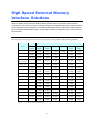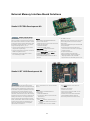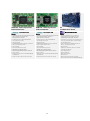
1
ENGLISH Altera Application Solutions Guide Book ® December 2011 Prepared by Group Companies Altera® Application Solutions Guide Book – December 2011 2 Index INTRODUCTION TO MACNICA GROUP ........................................................................ 5 About Macnica Group................................................................................................................................5 Group Structure and Subsidiaries ...........................................................................................................6 ALTERA® APPLICATION SOLUTIONS GUIDE BOOK – NOVEMBER 2011 ................. 7 VIDEO SYSTEM SOLUTIONS ........................................................................................ 8 Your Video System Design Starts Here … ...............................................................................................8 1080p Video Design Framework...............................................................................................................9 Video Reference Designs .........................................................................................................................10 Video Development Board Solutions ......................................................................................................13 Board Solutions from Third Party Board Partners ...........................................................................15 HIGH SPEED EXTERNAL MEMORY INTERFACE SOLUTIONS................................. 19 DRAM Device Overview..........................................................................................................................20 DDR SDRAM........................................................................................................................................20 DDR3 ....................................................................................................................................................20 DDR2 SDRAM .....................................................................................................................................20 DDR ......................................................................................................................................................20 RLDRAM II ..........................................................................................................................................21 RLDRAM III.........................................................................................................................................21 SDR DRAM ..........................................................................................................................................21 SRAM Device Overview ..........................................................................................................................21 QDR and QDR II SRAM Devices ........................................................................................................21 ZBT SRAM Devices..............................................................................................................................22 External Memory Interface Spec Estimator ..........................................................................................22 External Memory Interface Board Solutions.........................................................................................23 Board Solutions from Third Party Board Partners ...........................................................................24 HIGH SPEED INTERFACE SOLUTIONS ...................................................................... 25 Transceiver Portfolio ...............................................................................................................................25 Protocol Solutions ....................................................................................................................................26 Plug & Play Signal Integrity ..................................................................................................................28 High Speed Interface Board Solutions ...................................................................................................29 Board Solutions from Third Party Board Partners ...........................................................................31 EMBEDDED SYSTEM DESIGN SOLUTION ................................................................ 33 Why Use FPGAs in Embedded Designs? ...............................................................................................33 What Do I Need to Know to Get Started? ..............................................................................................33 Step 1: Get the Design Software .........................................................................................................34 Step 2: Evaluate the Software and Develop the Application ............................................................34 Step 3: Purchase Licensing .................................................................................................................35 Nios II IP Core and Related Products ................................................................................................35 Development Tools...................................................................................................................................35 3 Software Development Tools ...............................................................................................................36 Nios II Embedded Design Suite ..........................................................................................................36 Embedded Software Partners .............................................................................................................36 Hardware Development Tools .............................................................................................................36 Quartus II FPGA System Design Tool ................................................................................................37 SOPC Builder System-Level Integration Tool ...................................................................................37 SignalTap II Embedded Logic Analyzer .............................................................................................37 MegaCore IP Library ...........................................................................................................................37 Embedded Systems Board Solutions......................................................................................................38 Board Solutions from Third Party Board Partners ...........................................................................42 ASIC PROTOTYPING ................................................................................................... 44 Why use FPGAs for ASIC prototyping? .................................................................................................44 Advantages of FPGA prototyping ...........................................................................................................44 Frequently Asked Questions ...................................................................................................................46 ASIC Prototyping Board Solutions.........................................................................................................48 Board Solutions from Third Party Board Partners ...........................................................................48 CONTACT INFORMATION............................................................................................ 50 Japan ........................................................................................................................................................50 Hong Kong / China ..................................................................................................................................50 Taiwan / China.........................................................................................................................................50 ASEAN .....................................................................................................................................................50 4 Introduction to Macnica Group Altima Corp., Elsena, Inc., Cytech Technology Ltd. and Galaxy Far East Corp. are the Macnica Group companies with the common supplier - Altera Corporation - in their line card and the common corporate culture aiming at providing the customers with high level of technical solutions in addition to selling the products. About Macnica Group Macnica Group is one of the largest full-service electronics and networking systems distribution companies in the world with the headquarters in Yokohama, Japan. Macnica provides the most advanced and high added-value electronics products including semiconductor devices, electronics components, network related equipment, software products to various electronics OEMs and customers in the world. business relationship with the numerous startups born every day throughout the world… The value proposition presented to customers by truly understanding their technical issues and leading to the best solutions… Those are all the strengths with Macnica. All the employees are sharpening these strengths so that the value they bring to the customer becomes optimal. Macnica also has focused in expanding its global network by establishing subsidiaries in the US, Europe and in Asia Pacific area. With the offices in 34 locations worldwide, Macnica Group looks into becoming the best of the kind in the world in the Engineering Distribution model. Since its foundation in 1972, Macnica has focused in technical support and deepened its technical strengths, leading the industry in establishing the technical-support centric business style. “The Engineering Distributor” is the new category of distribution models in the electronics industry built based on the style of Macnica Group. Now Macnica is climbing to its new height by disrupting the Engineering Distributor model by itself. Becoming more like what we are… Seeking the things only Macnica can attain… With those questions in mind Macnica has reached to the stage to bloom to become “The Demand Creation Distributor” who identifies the potential demand within the customers and in the market by utilizing its business foresight The distinguished technical and engineering strengths… The ability to find new prospering product lines that grew in the wide range of 5 and technical insight. Macnica will find things existed nowhere and bring them here for you. Macnica Group keeps going, with challenges. “NOWHERE, but HERE.” Macnica Group Facts Established October 30, 1972 President & CEO Kiyoshi Nakashima Paid-in Capital JPY 11,194,268,000 (as of March 31, 2011) Publicly traded at The 1st Division of Tokyo Stock Exchange (Symbol: 7631.t) Revenue FY06 FY07 FY08 FY09 FY10 JPY 163.6 Billion JPY 154.1 Billion JPY 131.5 Billion JPY 149.2 Billion JPY 188.4 Billion Employees 1,555 (Group World Wide Total: as of March 31, 2011) Group Structure and Subsidiaries Macnica Group consists of Macnica, Inc. with three internal division companies covering Japan, five subsidiaries covering Japan, Macnica brand subsidiaries in the USA, Europe and Asia, and subsidiaries covering Asia Pacific, ASEAN countries and India. JAPAN KOREA Macnica, Inc. • • Corporate Headquarters SINGAPORE / ASEAN Division Companies Macnica Asia Pacific Ple Ltd. • Clavis Company • • Brilliant Technology Company • Macnica (Thailand) Co. Ltd. • TecStar Company • Cytech Global Pte. Ltd. • Altima Corp. • Elsena, Inc. INDIA • • Kogent, Inc. • Macnica Networks Corp. • Macnica Solutions Corp. Macnica Hong Kong, Limited. • Macnica Shanghai, Limited. • Cytech Technology Ltd. • Macnica USA, Inc. • Macnica Networks USA, Inc. • Macnica Americas, Inc. EUROPE • TAIWAN • Macnica Taiwan, Limited. • Galaxy Far East Corporation Cytech Global Pte. Ltd. USA HONG KONG / CHINA • Macnica Korea, Limited. 6 Macnica GmbH Altera® Application Solutions Guide Book – November 2011 Altima Corp., Elsena, Inc., Cytech Technology Ltd. and Galaxy Far East Corp. are the Macnica Group companies with the common supplier Altera Corporation in their line card and the common corporate culture aiming at providing the customers with high level of technical solutions in addition to selling the products. This guide book “Altera® Applications Solutions Guide Book,” co-edited by Altima, Elsena, Cytech and Galaxy, provides the information beneficial for the customers who are trying to solve their problems in FPGA designs in specific applications such as video processing, high speed memory interface, high speed serial interface, embedded system designs and ASIC prototyping. 1. Video Processing 2. High Speed Memory Interface 4. Embedded System Design 3. High Speed Serial Interface 5. ASIC Prototyping 7 Video System Solutions Your Video System Design Starts Here … Before you start your next video system design, check out the largest, most comprehensive collection of video solutions in the FPGA industry. ® By building your next design using Altera video intellectual property (IP), reference designs and development kits, you’ll be able to take full advantage of Altera's innovative FPGA features, including: • • • • Inherently parallel digital signal processing (DSP) blocks An abundance of embedded memory blocks A large number of registers High-speed DDR memory interfaces Altera video system solutions have three components to help you create the most dependable system design and finish development fast: 1. Altera Video Design Framework – This is a combination of IP cores, interface standards and system level design tools that are developed to enable a plug-and-play video system design flow. Altera provides a comprehensive suite of video function IP blocks that can be connected together to design and build video systems. Plus, designs built using the Altera video design framework are open, allowing you to easily replace an Altera IP with your own custom function block. 2. Suite of Video reference designs – Reference designs created by Altera as well as our partners and built using the Altera video design framework. This substantial suite of image format conversion reference designs are hardware verified and available immediately to serve as the starting point for your application. 3. Range of DSP Dev Kits for Video – Kits, also designed by Altera and our partners, to help you prototype your video system design. These kits support a range of video I/O formats (such as SDI, ASI, DVI, HDMI, Composite and VGA), and are based on our highly regarded Stratix®, Arria® and Cyclone® FPGA families. 8 1080p Video Design Framework Altera developed a video design framework that enables the fastest design cycle for video application. The components of this framework are: • • • • A library of basic building block video image processing intellectual property (IP) cores designed for easy plug-and-play type interface A low-overhead streaming video interface protocol, which is available as an open standard System tools such as SOPC Builder that allow for an automated way of generating control and arbitration logic A suite of HD reference designs that can be used as a starting point for your video datapath designs Figure 1 shows the suite of IP cores that are part of a video image processing suite of IP cores. This suite provides IP that ranges in complexity from a color space converter to a polyphase scaler and motion adaptive de-interlacer. to automatically wire up arbitrated and streaming bus systems. Figure 1 Complete Suite of Video Image Processing IP The Avalon® Streaming interface (ST) video protocol is designed for sending dvideo and control data from one video processing block to the other. This protocol is open and the specification is freely downloadable via the web. Using this specification does not in any way lock you to Altera® FPGAs, but all the Altera video IP and video reference designs utilize this interface. Figure 2 shows how different video functions can be connected using this protocol. More information on this protocol is available in the ‘Interface’ section of the Video and Image Processing Suite User Guide (PDF). Figure 2 Avalon ST Protocol for Video Interfaces and Avalon Memory Mapped (MM) Protocol for Control Plane Interfaces Video systems almost always include an embedded processor and a memory subsystem to manage the video frames in the external memory. The SOPC Builder system tool provided by Altera greatly simplifies embedded system design. This tool includes a library of elements such as soft core processors (Nios® II), interfaces, memory, bridge, and DSP IP cores. It also features a connectivity GUI and generator 9 Finally, the entire video design framework really comes together in the form of an HD reference design that showcases the actual video processing common to many applications. Altera developed several reference designs that were driven by actual customer demand for scaling, mixing, and processing HD video streams over serial digital interfaces (SDI). Figure 4 shows one of the reference designs that processes 1080p quality video. This design was built using the Altera video design framework. For more details on this design contact your local Altera FAE. Figure 3 SOPC-Based Design Flow for Video Datapaths Figure 4 HD Quality Reference Designs to Speed Development Video Reference Designs Altera provides one of the largest portfolios of video processing designs – all built using the Altera VIP suite of video cores. 1. The Altera video and image processing example design demonstrates dynamic scaling and clipping of a standard definition video stream in either NTSC or PAL format and picture-inpicture mixing with a background layer. The video stream is output in high definition resolution (1024×768) over a digital video interface (DVI). This design is fully verified on the Cyclone III Video development kit. 10 2. Core Description Deinterlacer Converts interlaced video formats to progressive video format Color Space Converter Converts image data between a variety of different color spaces Scaler Resizes and clips image frames Alpha Blending Mixer Mixes and blends multiple image streams Gamma Corrector Performs gamma correction on a color space Chroma Resampler Changes the sampling rate of the chroma data for image frames 2D Filter Implements 3x3, 5x5, or 7x7 finite impulse response (FIR) filter on an image data stream to smooth or sharpen images 2D Median Filter 3x3, 5x5, or 7x7 filter that removes noise in an image by replacing each pixel value with the median of neighboring pixel values Line Buffer Compiler Efficiently maps image line buffers to Altera®on-chip memory Various format conversion reference designs that use the SDI video input – primarily used in broadcast applications. These designs feature two-channel up/down/cross conversion that entails polyphase scaling, motion adaptive deinterlacing, mixing and frame rate conversion for resolutions up to 1080p. These designs have been verified on the Stratix II GX Audio Video development kit. Reference Design Demo Board Features UDX 3.1 Reference Design • Multi-channel format conversion with selectable inputs • Stratix® IV GX FPGA Development Kit and outputs • Features multi-port front-end memory controller (with efficiency > 90%) • Supports DVI, HDMI, SDI interfaces • Run-time configurability • Active Format Descriptor (AFD) extraction and insertion *Contact Altera Sales for design Format Conversion Reference Designs (v1) • Stratix II GX Audio/Video Development Kit • Stratix IV GX FPGA Development Kit Format Conversion Reference Designs (v2) • Stratix II GX Audio/Video Development Kit • Stratix IV GX FPGA Development Kit • Arria II GX FPGA Development Kit • Two-channel up/down/cross conversion: polyphase scaling • • • NTSC-to-HD Scaling • Cyclone® III Video Processing Development Kit motion adaptive deinterlacing, mixing and frame rate conversion for resolutions up to 1080p SDI, DVI, DDR2 memory interfaces Run-time configurability of functions using the Nios® II embedded processor Output run-time configurable to 480p/720p/1080p • Two-channel up/down/cross conversion: polyphase scaling • • • motion adaptive deinterlacing, mixing and frame rate conversion for resolutions up to 1080p SDI in/SDI out, DDR2 memory interfaces Run-time configurability of functions using the Nios II embedded processor Outputs both interlaced and progressive • Up conversion of NTSC video to 720p using polyphase multi-tap scaling and motion adaptive deinterlacing • Picture-in-picture (PIP) mixing with test pattern background • Composite in/DVI out • Color space conversion, chroma resampling, frame buffering, alpha blending, and memory controller 11 3. Altera's partner Bitec has developed multiple reference designs that work with Cyclone III Video Dev Kit. Visit Altera web site to get designs that showcase color space conversion, Picture-in-Picture, 4-channel video compositing and even a 1080p H.264 encoder design. 4. Altera's partner Microtronix has also developed a portfolio of video reference designs that are available with their Stratix III Broadcast IP Dev Kit and with their Cyclone III ViClaro Video Dev Kit. These designs use the Altera VIP functions in conjunction with high bandwidth memory efficient, Microtronix Avalon Multi-port DDR2 Memory Controller for building high-resolution video broadcast systems. The designs showcase motion-adaptive deinterlacing, dynamic scaling and graphics overlay. These reference designs are available with the purchase of the development kits from Microtronix. Video Development Board Solutions Audio Video Development Kit, Stratix IV GX Edition Altera Corporation The Audio Video Development Kit, Stratix IV GX Edition, delivers a complete video and image processing development environment for design engineers. The kit facilitates the entire design HDMI video output on the FPGA host board One 3G-SDI video input and output on the FPGA host board Two 4-MByte QDR II + SRAMs with 18-bit data buses 64-MByte sync flash and 2-MByte SSRAM Two additional SDI inputs and outputs for external memory process, from design conception through hardware triple-rate SDI supporting 3G, and • Loopback and debug HSMCs implementation. high-definition (HD) and standard-definition • Design examples: Board Update Portal and Board (SD) standards on the HSMC Features • Two AES inputs and outputs on the HSMC • Altera Stratix IV EP4SGX230KF40C2N • Memory devices • The kit is the combination of: Stratix IV GX FPGA Development Board The transceiver serial digital interface (SDI) high-speed mezzanine card (HSMC) Test System • OpenCore Plus access to the MegaCore® IP library, including the Altera Video and Image Processing 512-MByte DDR3 SDRAM with a 64-bit data bus Suite of intellectual property (IP) cores SDI reference design 128-MByte DDR3 SDRAM with a 16-bit data bus • Video/audio interfaces Arria II GX FPGA Development Kit Altera Corporation The Altera Arria II GX FPGA Development Kit Features delivers a complete system-level design environment • Altera Arria II GX EP2AGX125EF35 FPGA Programmable oscillator, default frequency that includes both the hardware and software needed • On-board ports 125 MHz Programmable oscillator, default frequency to immediately begin developing FPGA designs. With One HSMC expansion port 100 MHz this PCI-SIG-compliant board and a one-year license One gigabit Ethernet port 155.52 MHz for Quartus II design software, you can: • Develop and test PCI Express 1.0 (up to x8 lane) designs • Develop and test memory subsystems consisting of DDR2 and/or DDR3 memory • Develop and test designs based on other Arria II GX supported protocol interfaces such as Gigabit Ethernet, SDI, CPRI, OBSAI, SAS/SATA, and • On-board memory SMA connectors for clock input/output 128-MB 16-bit DDR3 device 1-GB 64-bit DDR2 SODIMM 2-MB SSRAM 64-MB flash • On-board clocking circuitry Four on-board oscillators 100 MHz Serial RapidIO. 13 • General user I/O LEDs/displays Cyclone III FPGA Development Kit Altera Corporation Altera's Cyclone III FPGA Development Kit combines Embedded USB-Blaster™ circuitry (includes Display the largest density low-cost, low-power FPGA an Altera MAX II CPLD) allowing download of available with a robust set of memories and user FPGA configuration files via the flash device or interfaces. The kit dramatically reduces the design the host computer and verification portion of your project, whether it’s • Memory Two HSMCs Dual-channel DDR2 SDRAM (w/ECC 256MB) video processing, or another high-volume, SSRAM (8MB), Flash (64MB) USB type B • Debug tools • Communication ports • Cyclone III FPGA Development Kit CD-ROM 10/100/1000 Ethernet Features 2-line x 16-character LCD • Connectors for automotive, consumer, wireless communications, cost-sensitive application. 128 x 64 graphics LCD (download all CD contents via FTP USB 2.0 • Cyclone III development board Cyclone III EP3C120F780 FPGA • Clocking SMA inputs/outputs V by One HS x8 Daughter Card SDI Daughter Card ALTIMA Corp. ALTIMA Corp. The daughter card to evaluate THine V-by-One®HS x8 signals. The daughter card to evaluate SDI signals. This card is used with a development kit with HSMC connector. This card is used with a development kit with HSMC connector. Features Features • Supports up to 8 pairs of V-by-One HS streams • Supports up to 8 pairs of SDI streams • Supports V-by-One HS IP core developed by Macnica with license from THine • Supports Altera MegaCore SDI IP core Electronics, Inc. • Designed by using active SDI connectors with built-in cable drivers and • FX16 connectors compliant to V-by-One HS standard • Interfaces: equalizers to attain small board size and higher signal integrity • Interfaces: HSMC SDI x 8 channels V-by-One SMA (External CLK input) I2C for clock frequency configuration • Linear Technology LT3029 SMA (CLK output for evaluation) • Linear Technology LT3029 • IDT 5V49EE504 • IDT 5V49EE504, ICS810001-22, ICS8535-21 • HIROSE FX16 Right Angle x51 • Canare • Silicon Lab • Samtec QTH-090-01-L-D-A Si5317 • Samtec QTH-090-01-L-D-A BCA-TL/LF Board Solutions from Third Party Board Partners Daughter Cards USB 2.0 + Gigabit Ethernet SD/HD-SDI 2 CH high speed AD/DA 105M Dual 100M Industrial Ethernet Audio / Video HSMA SMA IO expandable FE-4CGX150 Hangzhou Free Electron Co. Ltd Altera Cyclone IV GX FPGA development platform Features • FPGA:EP4CGX150DF27C8 • Config: support FPP, support 4 different config • Sync SSRAM: CY7C1360C-200AXC • DDR2 SD RAM: 32bit, 128M Byte • SFP: 1 channel, support as fast as 3.125G • Gigabit Ethernet port: 1 Channel, Marvell 88E1111-CAA1 • USB2.0 : slave mode/ FIFO, FT2232HL • PLL circuit : 5M-500MHz • 1 x high precision active X’tal • PCI-E: PCI-E 1.1 X 4 Features Features • Audio AD/DA, 1 x I/P, 2 x O/P • 60 x I/0 • 24bit true color VGA port • 1 x 8bit DIP switch • Video decoding : support ITU-R • High speed transceiver :RX, TX BT.656 YCrCb 4:2:2(16bit/8bit), • Input clock: CLKIN x1; Output • 1 x 8 DIP switch 1 CH S_VIDEO • 4 LED O/P clock: CLKOUT x 2 • 4 LEDs • HSMC expandable slot • 4 SMA signals • Power supply to support 12A to Core chip, 5A configurable VCCIO Digital Application Dev Board Video Dev Board Hangzhou Free Electron Co. Ltd Cyclone III Video Development Kit Hangzhou Free Electron Co. Ltd Bitec Ltd. Features Features Features • ALTERA Cyclone II EP2C35F484C8 • FPGA: ALTERA Cyclone II EP2C35F672C8 • Altera EP3C120F780 Development board • Offer uClinux OS including network support • 8 layer PCB • Bitec HSMC Quad Video daughter card • 64M Byte DDR SDRAM • 8 composite or 4 s-video inputs • 64M Byte SDRAM • 32M Byte FLASH • 1 HD (1080p) DVI Output port or • 32M Byte FLASH • can plug 100M ETHERNET PHY daughter card • 1 TV (PAL/NTSC) output with resolutions to • 2 independent 512K bit SRAM • 1x CVBS, support ITU-R BT.656 YCrCb 4:2:2 (16bit (DHCP, tftp, web) • Two 100M Ethernet interface, one use 100M PHY, / 8bit) 1024x768 and support for composite, s-video or SCART (RGB) outputs can verify Altera trip-speed Ethernet IP, the other • LVDS in/out, support video transport • Bitec HSMC DVI daughter card use 100M Ethernet MAC/PHY • 1 x 24bit VGA input and output • 1 HD (1080p) DVI Output port (HDMI with • Support ITU-R BT.656 YCrCb 4:2:2 (16bit/8bit) video output, 1 CVBS, 1 S-Video interface • 1 x HDMI input/output • 40 x expand IO (2 x CLK, 2 x PLL1output, 36 x IO) • Support SD card external adaptor) • 1 HD (1080p) DVI Input port (HDMI with external adaptor) • USB1.1 interface, 24 bit VGA, PS/2 • Interfaces directly to the Altera Video and Image Processing (VIP) Suit • Collection of video reference designs 15 Broadcast Video Card DVI Input/Output Card Bitec Ltd. Cyclone III SDALTEVK Kit Bitec Ltd. Bitec Ltd. Develop profesional video fpga based systems using Two channel Dual-Link DVI output board for Altera Features the Bitec BVDC. FPGA development kits with HSMC expansion port. • Altera EP3C120F780 Development board Features Features • Dual ASI/SD-SDI transmitter/receiver • Single link operation from 25-165 Megapixels per • National Semiconductor's HSMC SDI video and • Adaptive cable equalizers • Multi-rate cable drivers • 27 Mhz VCXO • 200Mhz Quadrature Modulating 14-bit DAC clocking daughter card (SDALTEVK) second (VGA to UXGA) • Supports SD, HD and 3G-SDI (SMPTE 259M-C, 292M, 424M) • Dual link operation up to 330 Megapixels per second (3200×2400) • LMH0344 Triple-rate SDI Adaptive Cable Equalizer • EDID reading/writing • LMH0340 Triple-rate SDI Serializer with • 12-bit (½ pixel) DDR input with flexible input clocking: Single-clock/dual-edge or dual-clock/single-edge integrated cable driver • LMH0341 Triple-rate SDI deserializer with reclocked loop through • I2C slave programming interface • LMH1981 Multi-Format Video Sync Separator • Cable distance support: Over 10 m • LMH1982 Multi-Rate Video Clock Generator • Monitor detection through Hot-Plug • DS90CP22 2x2 LVDS Crosspoint Switch Compliant with DVI 1.0 • LP3878 Adjustable Low Noise LDO • LM20242 PowerWise Buck Regulator • Interfaces directly to the Altera Video and Image Processing (VIP) Suite Collection of video reference designs ViClaro II HD Video Enhancement ViClaro III Video Host Board Dev. Platform Dual Input HD-SDI Switcher Design Kit Microtronix Datacom Ltd. Microtronix Datacom Ltd. Microtronix Datacom Ltd. The Microtronix ViClaro II HD Video Enhancement The Microtronix ViClaro III HD Display Panel Video The Microtronix Dual Input HD-SDI Video Switcher Development Platform is targetted at the IP Development Kit is targeted at the development of Design Kit provides a hardware platform for development of consumer HD video display and consumer video display and imaging systems. It is developing SDI video processing systems using the imaging systems. The ViClaro II incorporates an designed to demonstrate the capabilities of Altera's Cyclone III FPGA. Altera Cyclone II FPGA to allow display designers Cyclone III for video and image enhancements Features and ASSP vendors to test next-generation picture applications in Video Display Controller ASSP • Altera EP3C120 Cyclone™ III FPGA enhancement features for their products and meets systems. • 2 x Gennum GS2961 3G/HD/SD-SDI SDI Receivers the needs of changing display technology, rather than • 1 x Gennum GS491B HD/SD/Graphics Clock and being tied to lengthy application-specific integrated Features circuit (ASIC) development cycles. • EP3C120F780C7N • 1 x Gennum GS2962 3G/HD/SD-SDI Serializer Timing Generator with GENLOCK • 256 Mbyte DDR2 SDRAM (32 Meg x 64) • 1 x Analog Devices AD7393 SD/HD Video Encoder Features • 4-Lane PCI Express PHY • 2 x HD/SD-SDI inputs (75Ω BNC) • 32-bit DDR2 SDRAM Memory • USB 2.0 PHY • 1 x HD/SD-SDI output (75Ω BNC) • HDMI Transmitter / Receiver • I2C interface port • 1 x analog video: • Analog / Video Receiver • 3 High Speed Mezzanine Connectors (HSMC) • 75Ω BNC composite video output or • Dual LVDS Links • YPbPr component video output • Supports 720p / 1080i / 1080p 50/60 Hz HDTV • RS-232 DB9 serial control port 16 Quad Link LVDS Interface HSMC Gigabit Ethernet PHY / HDMI DVI Receiver / Transmitter HSMC Board Transmitter HSMC Board Board Microtronix Datacom Ltd. Microtronix Datacom Ltd. Microtronix Datacom Ltd. The Quad Link LVDS Interface HSMC The Microtronix Gigabit Ethernet PHY and HDMI The Microtronix DVI Receiver / Transmitter HSMC Daughtercard supports receive and transmit LVDS Transmitter HSMC Daughtercard adds functionality Board is designed to allow developers access to links each consisting of 5 data channels and 1 clock to the ViClaro III, the Altera EP3C120 Development high-quality, high resolution video signals in their for a total of 48 LVDS channels. The standard Kit or other third party FPGA development boards FPGA designs. It integrates both a DVI receiver and configuration of 20 Tx + 4 clk and 20 Rx + 2 clk, is with a HSMC header. transmitter onto the same card giving the flexibility capable of supporting LCD display panels up to 1080p required by high resolution image processing systems. at 100/120Hz. On-board LVDS termination resistors Features can be removed to convert receiver channels into • The Marvell 88E1111 Gigabit Ethernet PHY is Card is shipped with source code examples. transmitters as required to support 12 or 14-bit color fully compatible with Altera's Triple Speed Features applications. Ethernet MAC IP. • Digital Visual Interface Compliant (DVI 1.1) Features • Deep Color 12-bit Deep Color HMDI 1.3 • Optimized for video applications Transmitter using the Analog Devices ADV7510 • Single core provides both LVDS transmitter and video chip. receiver functions • Supports resolutions from VGA to UXGA (1600x1200 and 1920x1080 [1080p@60]) • 25 - 165 Mhz Pixel rates • HSMC compatible daughter card • EDID data reading/writing • Support for both 28-bit and 35-bit parallel data • Monitor detection through Hot-Plug • Supports 1, 2 and 4 link configurations • 15Mbps Optical S-PDIF TX and RX for digital No transmit PLL clock fine tuning required HDMI Rx/Tx HSMC Board audio connectivity Lancelot VGA Controller IP Design High Speed AD/DA FPGA Board Kit Microtronix Datacom Ltd. Microtronix Datacom Ltd. SIGLEAD, Inc. The Microtronix HDMI Receiver / Transmitter HSMC Microtronix is proud to offer the innovative Lancelot Features Daughtercardinterfaces a HDMI receiver and VGA IP Design Kit solution for customers wanting to • Stratix III & IV 1152 pin devices transmitter to your Altera FPGA development kit develop video IP based solutions. The Lancelot Kit • AD/DA Converter SMA Connector differential using the HSMC expansion connector. The receiver comes complete with an IP core written in VHDL that also supports an analog component video (YCbCr) can be synthesized for all Altera FPGA devices. interface. Features • Uses the Analog Device AD9889 HDMI Transmitter and AD9880B HDMI Receiver input/output • ADC: 12 bit 550MSPS dual channel • DAC: 16 bit 1GSPS dual channel Features • 27.000MHz oscillator • Display resolutions: 640 x 480, 800 x 600, 1024 x • MCX input 768 • On-board PLL • Displays up to 24-bit color • CMX differential (single end) output dual channel • Analog YCrCb Video Receiver • 900 LE's • DDR2 SDRAM 240pin DIMM (Max 4GBytes) • Supports 480i / 720p / 1080i / 1080p @ 50/60 Hz • Video & audio development board • DVI Input/Output Max. UXGA (165MHz) • EDID data reading / writing • VGA IP Core reference design & demo • Gigabit Ethernet controller (PCI bus) • Auto detection of monitor through Hot-Plug • Compatible with Microtronix Multi-port SDRAM • USB2.0 A Connector x2 & mini AB connector x1 • Altera compatible HSMC expansion connector IP Core • LVDS Connector input/output 10 pairs each Max 10Gbps • USB Serial I/F • Expansion port 80pin connector (40 user pins) 17 Altera DE4 Development and 5 Mega Pixel Digital Camera Education Board Package Terasic Technologies SDI-HSMC Card Terasic Technologies Terasic Technologies Features Features The Transceiver Serial Digital Interface (SDI) HSMC • Stratix IV GX EP4SGX230/EP4SGX530 with • Reference design with Verilog source code board provides a hardware platform for developing • A User Manual with Live Demo examples video broadcasting systems. It is intended to be used • PCIe 2.0 x8 Connector and 2 DDR2 SO-DIMM • Support exposure time controlling by customers to implement and design SDI and AES • 3 x USB ports (1 x mini AB host/device, 2 x type A • Support motion capture mode systems based on transceiver-based host boards with • Software allows users to upload the picture HSMC interface. It can also be part of an openly sold transceivers host) • SMA connectors for clocks and LVDS signals captured into PC and save the picture into bitmap Development Kit, or bundled with packages of • 4 x SATA connectors format or Joint Photographic Experts Group for software and IP cores. • SD Card socket viewing. • 64MB Flash (16-bit) • Equipped with Micron 5 Mega Pixel CMOS sensor Features • 2MB ZBT SRAM • Support 2,592H x 1,944V active pixels • 2 SDI inputs and outputs • I2C EEPROM • Output data in RGB Bayer Pattern format • 2 AES inputs and outputs • 2 x HSMC connectors • Full resolution frame rate up to 15 frame per • SDI clean up PLL and an AES PLL • 2 sets of 40 pin Extension ports • 50/100MHz Oscillator second (FPS) • Supports triple rate 3G/HD/SD SDI standard • Provide users entire reference design (Frame • 4xGigabit Ethernet ports (4 x RJ-45) Grabber, high-performance multi-port SDRAM 4 x Push Button Switch, 4 x Slide Switch, 1 x frame buffer, image processing IPs) 8-position DIP switch, 2 x 7-Seg, 8 x LEDs HDMI Receiver Daughter Card HDMI Transmitter Daughter Card Vadex Box Meganovo Technologies Co Ltd Terasic Technologies Terasic Technologies HDMI_RX_HSMC is a HDMI receiver daughter board HDMI_TX_HSMC is a HDMI transmitter daughter Features with HSMC (High Speed Mezzanine Connector) board with HSMC (High Speed Mezzanine Connector) • Tilera TILE36Pro or TILE64Pro interface. The board contains the following rich interface. The board contains the following rich • Altera EP2AGX45 or EP2AGX65 features: features: • 6GB of SODIMM memory at 533MHz • One HSMC interface for connection purpose • One HSMC interface for connection purpose • 2 1GigE interfaces • One HDMI receiver with dual receiving ports • One HDMI transmitter with single transmitting • 1 HDMI Out interfaces • Two 2K EEPROM for storing EDID of two receiver ports separately • Powered from 3.3V and 12V pins of HSMC connector port • 1 VGA Out interfaces • One 2K EEPROM • 1 BNC Out interfaces • Powered from 3.3V and 12V pins of HSMC • 1 HDMI In interfaces connector • 2 Audio In and Out • 1 PCI-e 4Lane for debug or extend • Support H.264/MPEG4/MPEG2 decoder • Support 1/4/6multi-picture, it also supports automatic switching of multi-picture with rolling • Support 6 channel HD • Support 1080P@30f,720P@30f,D1@30f • Support RSTP/RSVP/FTP/HTTP/IGMP/NTP protocols • It can seamless connect Telop server, insert Marquee 18 High Speed External Memory Interface Solutions Altera's complete memory interface design solutions address today's high-speed memory interface challenges such as memory controller, I/O design, and board-level signal integrity issues. Altera's solutions include advanced device architectures, customizable MegaCore® functions, Quartus® II design software, reference designs, demonstration boards, and simulation models, accompanied by a rich set of technical documentation. This table lists external memory interfaces supported by Altera FPGAs and HardCopy® ASICs. Memory Type Device DDR3 SDRAM DDR2 SDRAM DDR SDRAM RLDRAM II RLDRAM III QDR II SRAM QDR II+ SRAM Stratix V (1) 1,600 Mbps 800 MHz 800 Mbps 400 MHz 400 Mbps 200 MHz 800 Mbps 400 MHz 1,600 Mbps 800 MHz 1,400 Mbps 350 MHz 1,600 Mbps 400 MHz Stratix IV 1,067 Mbps 533 MHz 800 Mbps 400 MHz 400 Mbps 200 MHz 800 Mbps 400 MHz - 1,400 Mbps 350 MHz 1,600 Mbps 400 MHz Stratix III 1,067 Mbps 533 MHz 800 Mbps 400 MHz 400 Mbps 200 MHz 800 Mbps 400 MHz - 1,400 Mbps 350 MHz 1,600 Mbps 400 MHz Stratix II and Stratix II GX - 667 Mbps 333 MHz 400 Mbps 200 MHz 600 Mbps 300 MHz - 1,200 Mbps 300 MHz 1,200 Mbps 300 MHz Stratix and Stratix GX - - 400 Mbps 200 MHz 400 Mbps 200 MHz - 800 Mbps 200 MHz - Arria V (1) 1,066 Mbps 533 MHz 800 Mbps 400 MHz - 800 Mbps 400 MHz -- 1,400 Mbps 350 MHz 1,600 Mbps 400 MHz Arria II GX 800 Mbps 400 MHz 667 Mbps 333 MHz 400 Mbps 200 MHz - - 1,000 Mbps 250 MHz 1,000 Mbps 250 MHz Arria GX - 466 Mbps 200 MHz 400 Mbps 200 MHz - - - - Cyclone V (1) 1,066 Mbps 533 MHz 800 Mbps 400 MHz - 800 Mbps 400 MHz - 1,400 Mbps 350 MHz 1,600 Mbps 400 MHz Cyclone IV - 400 Mbps 200 MHz 333 Mbps 167 MHz - - 668 Mbps 167 MHz - Cyclone III LS - 333 Mbps 167 MHz 300 Mbps 150 MHz - - 600 Mbps 150 MHz - Cyclone III - 400 Mbps 200 MHz 333 Mbps 167 MHz - - 668 Mbps 167 MHz - Cyclone II - 333 Mbps 167 MHz 333 Mbps 167 MHz - - 668 Mbps 167 MHz - HardCopy IV 1,067 Mbps 533 MHz 667 Mbps 333 MHz 400 Mbps 200 MHz 800 Mbps 400 MHz - 1,200 Mbps 300 MHz 1,400 Mbps 350 MHz HardCopy III 800 Mbps 400 MHz 667 Mbps 333 MHz 400 Mbps 200 MHz 667 Mbps 333 MHz - 1,200 Mbps 300 MHz 1,400 Mbps 350 MHz HardCopy II - 533 Mbps 267 MHz 400 Mbps 200 MHz 500 Mbps 250 MHz - 1,000 Mbps 250 MHz 1,000 Mbps 250 MHz Note (1) Under characterization test. 19 DRAM Device Overview DRAM devices are volatile memories offering a lower cost per bit than SRAM devices. A compact memory cell consisting of a capacitor and a transistor makes this possible over the six-transistor cell used in SRAM. However, the capacitor will discharge, causing the memory cell to lose its state, which means that DRAM memory needs to be refreshed periodically. Generally, you would choose SRAM devices for applications where latency or low interface complexity is important. You would choose DRAM where cost per bit is important. Special types of DRAM challenge this norm by offering improved random access latency, as well as a lower cost per bit. ® Altera provides complete system solutions to help memory designers successfully interface Altera FPGAs to a variety of DRAM devices. DDR SDRAM Double data rate (DDR) SDRAM is an evolution of single data rate (SDR) SDRAM. It offers higher performance through increased bus speeds using a lower I/O voltage (2.5 V), and most importantly, data transfer on both clock edges, doubling the raw bandwidth. DDR SDRAM is a widely established memory technology. It offers the lowest cost per bit, due in part to its broad acceptance in almost any marketplace. DDR3 DDR3 SDRAM is an improvement over its predecessor, DDR2 SDRAM. The primary benefit of DDR3 is the ability to transfer at twice the data rate of DDR2, thus enabling higher bus rates and higher peak rates than earlier memory technologies. In addition, the DDR3 standard allows for greater chip capacities. The advantages of DDR3 architecture over DDR2 architecture are summarized as follows: • Data rate speed ranges from 800 to 1,600Mbps • Device capacity ranges from 512Mb to 8Gb • Power is lower than DDR3 SDRAM due to reduced I/O and core voltage DDR2 SDRAM DDR2 SDRAM is an evolution of DDR SDRAM. It operates using a lower voltage (1.8V). DDR2 offers increased densities and even higher performance through higher bus speeds and an optimized interface. The advantages of DDR2 architecture over DDR architecture are summarized as follows: • Data rate speed ranges from 400 to 667Mbps • Power is lower than DDR SDRAM due to reduced I/O and core voltage • Smaller footprint for FBGA packages DDR DDR SDRAM is an evolution of SDR SDRAM. It offers higher performance through increased bus speeds using a lower I/O voltage (2.5V), and most importantly, data transfer on both clock edges, doubling the raw bandwidth. DDR SDRAM is a widely established memory technology. It offers the lowest cost per bit, due in part to its broad acceptance in almost any marketplace. 20 RLDRAM II RLDRAM II is the second generation of RLDRAM. It is a development of DDR SDRAM, designed to address the low latency requirements of certain applications, such as packet buffers in high-performance line cards. RLDRAM II has a high-performance DDR data bus and offers a non-multiplexed address bus, reducing the number of clock cycles to initiate read or write applications. A banked architecture also reduces access time. In some systems, RLDRAM II eliminates the need for specialized content-addressable memory (CAM) or SRAM. RLDRAM III RLDRAM III is the third generation of RLDRAM. It is a development of DDR SDRAM, designed to address the low latency requirements of certain applications, such as packet buffers in high-performance line cards. RLDRAM III has a high-performance DDR data bus and offers a non-multiplexed address bus, reducing the number of clock cycles to initiate read or write applications. A banked architecture also reduces access time. In some systems, RLDRAM III eliminates the need for specialized content-addressable memory (CAM) or SRAM. SDR DRAM SDR SDRAM is the first generation of synchronous DRAM. It improves memory bandwidth over extended data out (EDO) DRAM by offering data transfer up to once-per-clock cycle. SRAM Device Overview Altera provides a complete system solution to help you successfully interface Altera® FPGAs and HardCopy® ASICs to a variety of SRAM devices. SRAM devices offer extremely fast access times — approximately four times faster than DRAM — but are much more expensive to produce. Unlike DRAM, SRAM does not need to be refreshed periodically to prevent data loss through leakage. SRAM devices are capable of storing data as long as the device is supplied with power. If the power is turned off, the contents are lost. Typical systems require both SRAM (for performance-critical applications) and DRAM memory (for all other applications). QDR and QDR II SRAM Devices QDR memory devices allow two ports to run independently at DDR, which results in four data items per clock cycle. QDR SRAMs enable you to maximize bandwidth by allowing operation at data rates above 200MHz. The QDR architecture allows you to reach these speeds without the possibility of bus contention. The QDR consortium, which consists of Cypress Semiconductor, Integrated Device Technology (IDT), Micron Technology, and NEC Corporation, developed the QDR architecture. QDR is designed to meet the high-performance needs of high-speed networking applications. ZBT SRAM Devices ZBT SRAM is a synchronous burst SRAM with a simplified interface that provides higher bandwidth and efficient bus utilization by eliminating turnaround cycles and idle cycles between read and write operations. IDT, Micron, and Motorola jointly developed the ZBT SRAM architecture, which is optimized for networking and telecommunications applications. External Memory Interface Spec Estimator Altera’s External Memory Interface Spec Estimator, a parametric tool, allows you to find and compare the supported external memory interfaces’ highest performance in our FPGA devices. You’ll have the ability to filter down to specific performances based on your own search specifications, and then compare performances across FPGA devices side-by-side by filtering the criteria you choose for analysis. The External Memory Interface Spec Estimator supports DDR3 SDRAM, DDR2 SDRAM, DDR SDRAM, RLDRAM II, QDRII+ SRAM, and QDRII SRAM interfaces. The stated performances are the maximum clock rates supported in Altera's FPGA devices based on the listed features across supported high speed memory standards. The maximum clock rates are only estimates based on a standalone Altera ALTMEMPHY or UniPHY and High-Performance Controller II instance generated with the default PHY and controller parameters in the MegaCore® IP. For the actual performance of your design, you must always compile and timing-analyze your complete design in the Quartus® II software. The External Memory Interface Spec Estimator replaces the maximum clock rate tables in Volume 1 Section III: “System Performance Specifications” of the External Memory Interfaces Handbook. The FPGA devices supported by the External Memory Interface Spec Estimator are the Stratix® V, Stratix IV, Stratix III, Arria® II GX, Cyclone® IV, and Cyclone III device families. 22 External Memory Interface Board Solutions Stratix IV E FPGA Development Kit Altera Corporation The Altera Stratix IV GX FPGA Development Kit Features • Two HSMC connectors delivers a complete system-level design environment • Altera Stratix IV GX EP4SGX230KF40C2N • HDMI video output 3G SDI video input and output that includes both the hardware and software needed • On-board clock oscillators • Power & Temperature measurement circuitries to immediately begin developing FPGA designs. With this PCI-SIG- compliant board and a 1-year license SMA connectors for external clock input /output • General user input/output • Other features Stratix IV GX FPGA Development Kit CD-ROM for Quartus II design software, you can: LEDs & LCD display Design Examples • Develop and test PCI Express 2.0 (up to x8 lane) Push-button & DIP switches Board Update Portal featuring the Nios II endpoint and rootpoint designs • Develop and test memory subsystems consisting of DDR3 and/or QDR II+ memory • Build designs capable of migrating to Altera's low-cost HardCopy IV ASICs. • DDR3 SDRAM 512-MByte (64-bit data) & 128-MByte (16-bit data) processor web server and remote system update Board Test System • 4-MByte QDR II+ SRAMs (18-bit data) x 2 pcs Complete documentation • 64-MByte Sync Flash & 2-MByte SSRAM Altera's Complete Design Suite DVD • PCI Express x8 edge connector MegaCore IP Library includes PCI Express, • 10/100/1000BASE-T Ethernet PHY with RJ-45 connector Triple-Speed Ethernet, SDI, and DDR3 High-Performance Controller MegaCore IP cores Stratix IV GT 100G Development Kit Altera Corporation The Altera Stratix IV GT 100G Development Kit the kit), a CFP interface, and a 20 lane Interlaken delivers a platform that can be used to implement 100 interface. Four QDRII interfaces x18 bit data buses 400MHz Gigabit serial data communications systems. Stratix • Components and Interfaces IV GT FPGAs are optimized specifically for the latest Features 10 Transceivers to CFP generation of 40G and 100G applications used in • Altera Stratix IV GT EP4S100G5F1932 2 Transceiver to SFP+ (one w/EDC, one w/o) communications systems, high-end test equipment • Configuration 4 Transceivers to QSFP and military communications systems. The 11.3-Gbps Embedded USB Blaster integrated transceivers featured in the Stratix IV GT 1G flash device (FPP via System Controller FPGA provide customers a true single-FPGA 100G solution, enabling 100G optical modules to interface directly with the FPGA. This board will accommodate two SFP+ optical modules (one with EDC and one without (not included in the kit)), a 4 lane QSFP optical module (not included in MAX II Device 20 Transceivers to FCI Airmax (Interlaken) 10/100/1000Mbps Ethernet with RJ-45 • Power & temperature measurement circuitry • Memory Interfaces Two DDR3 interfaces, x32 bit data buses Tree topology; simultaneous operation to 400MHz Should be able to run one at 533 MHz 23 Board Solutions from Third Party Board Partners ALL-IN-ONE Base Board B-11 (Stratix III Edition) Accverinos Co.,Ltd. CycloneIII SOPC board Hangzhou Free Electron Co. Ltd Features This board offer Ethernet, DDR2 interface, enough • EP3SL340F1517 or EP3SL200F1517 (-2 or -3) test port and expend IO. It is suitable for SOPC • DDR2 DIMM system design and small/middle density IP/ASIC • DVI I/O Support: 1 each of input and output port using TI TFP403 & 410 chips. verification. Guaranteed to operate at 165MHz • 1 x Gigabit Ethernet PHY & RJ45 Connector. • 1 x USB2.0 Connector, Cypress EZ-USB and ULPI Features • Cyclone III EP3C80F780C8N or EP3C120F780C8N supporting PHY - Can use either of USB MCU or • 256MB DDR2 SO-DIMM (up to 2GB) PHY • 12 layer PCB • 8 pairs each of input and output signals through C44LVDS connectors. Tested 1.2Gbps/pair operation • SD Card support (connected directly to FPGA and controlled by MegaCore IP) • 1 x Altera standard HSMC connector • 5 x Samtec 120-pin connectors • 216 expand IO/CLK/PLLOUT (include 9 lvds in,lvds out) • Marvel 10M/100M/1000MEathernet PHY • SMA clock/data input/output • 32M FLASH • 4 LED, one reset High Speed Interface Solutions Transceiver Portfolio Altera is a pioneer and leader in integrating transceivers into FPGAs. In 2001, we introduced our first FPGA family with integrated transceivers. Since then, we've introduced many innovations to make transceivers run faster, operate more reliably, and support emerging protocols with each generation of FPGAs and ASICs. With a top-notch, in-house transceiver design team, we're equipped to continue tailoring transceivers for specific applications. At 28 nm, our latest transceiver-related innovations include: • Technology for 12.5-Gbps and 28-Gbps transceivers • Support for driving optical modules directly with built-in: Electronic dispersion compensation (EDC) LC- (inductor-capacitor) based phase-locked loops (PLLs) for ultra low jitter • Support for driving 10G backplanes directly with: Transmitter pre-emphasis Receiver 5-tap distributed feedback equalizer (DFE) Receiver 4-stage continuous time linear equalization (CTLE) Plug & Play Signal Integrity with adaptive dispersion compensation engine (ADCE) • Full-featured physical coding sub-layer (PCS) including: 8b/10b encoder/decoder 64/66 encoder/decoder Gearbox Channel bonding • Support for PCI Express Gen1/2/3 and FPGA configuration through PCI Express • Support for 40G and 100G data path • On-chip instrumentation with EyeQ horizontal and vertical data eye monitor • Dynamic and fine-grained partial reconfiguration • Extensive intellectual property (IP) library of industry-standard transceiver protocols Device Stratix V GT (28 nm) Stratix V GX (28 nm) Stratix IV GT (40 nm) Stratix IV GX (40 nm) HardCopy® IV GX (40 nm) Arria® II GZ (40 nm) Arria II GX (40 nm) Cyclone IV GX (60 nm) Maximum Number of Channels Maximum Data Rate (Gbps) Backplane Support Optical Module Support 66 12.5 Yes Yes 66 8.5 Yes Yes 48 11.3 Yes Yes 48 8.5 Yes Yes 36 6.5 Yes Yes 24 6.375 Yes Yes 16 6.375 - - 8 3.125 - - Altera provides a broad portfolio of FPGAs and ASICs with integrated transceivers to address bandwidth needs from consumer to wireline applications. Within this portfolio, you'll discover a diverse mix of FPGAs and ASICs with as many as 66 28-Gbps backplane transceiver channels in Stratix® V GT FPGAs to as few as two 3.125-Gbps transceiver channels in Cyclone® IV GX FPGAs to fit your system needs. See the table above for more details about our wide breadth of FPGAs and ASICs with integrated transceivers. The portfolio also offers the productivity advantage of the comprehensive Quartus® II 25 design software, a common set of IP cores, sophisticated signal integrity tools, and a variety of supporting reference designs and design examples. Learn the software once, then extend your skills across multiple design platforms. More efficient system resource utilization resulting in higher system integration Higher integration with higher density products Optimized core performance, so you can efficiently close timing on designs and lower your engineering costs The ability to seamlessly connect IP blocks with a simple, intuitive GUI • • • With the transceiver device and Quartus II design software, you’ll experience: • Faster design and compile times • Protocol Solutions Altera® FPGAs and HardCopy® ASICs with integrated transceivers offer a range of data rates to suit all applications from 600 Mbps to 28 Gbps. Stratix® Series FPGAs Protocol V GX/GS V GT HardCopy ASICs IV GX IV GT V GX Arria® Series FPGAs Cyclone® Series FPGAs IV GX II GX IV GX - - - 3G-SDI 10G-SDI - 10 Gigabit Ethernet XAUI ASI - Basic Mode CEI-6G/SR/LR CEI-11G/SR/LR - - - - - - - - CPRI DDR-XAUI DisplayPort - - - - - - Fibre Channel - - Gigabit Ethernet GPON - HiGig+ - HiGig2 - - HyperTransport 3.0 - - - - - - - - - - - IEEE 802.3ae 10GBase-R - IEEE 802.3ba 10GBase-KR - IEEE 802.3ba 40G - 26 - Stratix® Series FPGAs Protocol V GX/GS V GT IEEE 802.3ba 100G HardCopy ASICs IV GX IV GT V GX - Arria® Series FPGAs Cyclone® Series FPGAs IV GX II GX IV GX - - - - - Interlaken Interlaken (10G) - - - - OTU-2 (G.709) - - - - OTU-3 - - - - OTU-4 - - - - - - JESD204A OBSAI PCI Express Gen1 PCI Express Gen2 PCI Express Gen3 - - - - - QDR InfiniBand - - - - - QPI - - - - - SAS - SATA SDI SD/HD SerialLite II - - - - Serial RapidIO® SFP+ - - SFI-4.2 - SFI-5.1 SFI-5.2 - - SGMII - - - - - - SONET OC-3/OC-12/OC-48 - SONET OC-192 - - - - SPI-4.2 SPI-5.1 - SPAUI V-by-One XFP - - - 27 - - - - - - - - Plug & Play Signal Integrity Available in Stratix® and Arria® series FPGAs and HardCopy® ASICs with integrated multi-gigabit transceivers, Plug & Play Signal Integrity lets you change the position of backplane cards on the fly while eliminating the painstaking process of manually reconfiguring your backplane equalization settings With this capability, you can design systems with truly universal cards that plug into multiple card positions in system backplanes (as shown in this picture in the right. Altera’s hot-socketable transceivers, coupled with adaptive dispersion compensation engine (ADCE) technology, deliver Plug & Play Signal Integrity where the same card configuration can be used, irrespective of slot position in most systems. Reduced card-type inventories Increased system flexibility Reduced maintenance and training costs Simplified order code management Reduced effort in the lab, since you no longer need to characterize every card slot to determine the optimal signal integrity setting for each one. When you design with Altera, you can design with the confidence that variations (in manufacturing, materials, temperature, voltage, and silicon process) are continuously monitored and compensated for by the ADCE to deliver the best eye opening and system BER performance. • • • • • In our 28-nm Stratix V FPGAs, the adaptive engine extends beyond linear equalization. When operating high-speed serial links in noisy environments, the benefits of the 5-tap decision feedback equalization (DFE) mitigates the effects of cross-talk to ensure high reliability of a system with a low bit-error ratio (BER). Plug & Play Signal Integrity offers wide-ranging benefits: 28 High Speed Interface Board Solutions Transceiver Signal Integrity Development Kit, Stratix IV GT Edition Altera Corporation Altera's Transceiver Signal Integrity Development • DIP and push-button switches • RJ-45 jack and 10/100/1000Base-T Ethernet PHY Kit, Stratix IV GT Edition enables a thorough • LEDs • Backplane drive capability at 6.5 Gbps evaluation of transceiver interoperability and • LCD • Directly connect the transceiver signal integrity serializer/deserializer (SERDES) signal integrity by • 64-MB sync flash memory (primarily to store FPGA allowing you to evaluate transceiver performance up to 11.3 Gbps (Altera Stratix IV P4SGX230KF40C2N) configurations) through the FCI connector header • Six full-duplex transceiver channels routed to SMA connectors Features • EP4S100G2F40I1N • On-board clock oscillators: 50 MHz, 100 MHz, 644.53 MHz, and 706.25 MHz • SMA connectors for supplying an external differential clock to transceiver reference cloc • Couple with a second signal integrity development kit or FCI daughtercard (not included) for a All channels support up to 11.3-Gbps data rate • Stratix IV GT development board development kit to an FCI backplane (not included) • Six full-duplex transceiver channels routed to FCI Airmax connector complete end-to-end backplane channel analysis • Application GUI • Platform independent • Power measurement circuitry on transceiver-related supplies • The voltage on all (and only) these rails can be supplied via banana jacks • Interfaces to PC via JTAG • Embedded blaster • Quartus II software license is not included and is not required for kit evaluation • Temperature measurement circuitry Stratix IV GX FPGA Development Kit Altera Corporation The Altera Stratix IV GX FPGA Development Kit Features • Two HSMC connectors delivers a complete system-level design environment • Stratix IV GX FPGA development board • HDMI video output that includes both the hardware and software needed • Stratix IV GX FPGA EP4SGX230KF40C2N • 3G SDI video input and output to immediately begin developing FPGA designs. With • On-board clock oscillators • Power & Temperature measurement circuitries this PCI-SIG- compliant board and a 1-year license • SMA connectors for external clock input & output • Stratix IV GX FPGA Development Kit CD-ROM for Quartus II design software, you can: • LEDs & LCD display • Design Examples • Develop and test PCI Express 2.0 (up to x8 lane) • Push-button & DIP switches • Board Update Portal featuring the Nios II endpoint and rootpoint designs • Develop and test memory subsystems consisting of DDR3 and/or QDR II+ memory • Build designs capable of migrating to Altera's low-cost HardCopy IV ASICs. • DDR3 SDRAM processor web server and remote system update 512-MByte (64-bit data) • Board Test System 128-MByte (16-bit data) • Complete documentation • 4-MByte QDR II+ SRAMs (18-bit data) x 2 pcs • Altera's Complete Design Suite DVD • 64-MByte Sync Flash & 2-MByte SSRAM • MegaCore IP Library includes PCI Express, • PCI Express x8 edge connector Triple-Speed Ethernet, SDI, and DDR3 • 10/100/1000BASE-T Ethernet PHY with RJ-45 High-Performance Controller MegaCore IP cores connector 29 Arria II GX FPGA Development Kit Altera Corporation The Altera Arria II GX FPGA Development Kit Features delivers a complete system-level design environment • Arria II GX EP2AGX125EF35 FPGA Programmable oscillator, default frequency that includes both the hardware and software needed • On-board ports 125 MHz Programmable oscillator, default frequency to immediately begin developing FPGA designs. With One HSMC expansion port 100 MHz this PCI-SIG-compliant board and a one-year license One gigabit Ethernet port 155.52 MHz for Quartus II design software, you can: • Develop and test PCI Express 1.0 (up to x8 lane) designs • On-board memory SMA connectors for clock input/output 128-MB 16-bit DDR3 device 1-GB 64-bit DDR2 SODIMM • Develop and test memory subsystems consisting of DDR2 and/or DDR3 memory • Develop and test designs based on other Arria II • General user I/O LEDs/displays 2-MB SSRAM 64-MB flash • On-board clocking circuitry GX supported protocol interfaces such as Gigabit Four on-board oscillators Ethernet, SDI, CPRI, OBSAI, SAS/SATA, and 100 MHz Serial RapidIO. Cyclone IV GX Transceiver Starter Kit Altera Corporation Altera's Cyclone® IV GX Transceiver Starter Kit • Cyclone IV GX EP4CGX15BF14C8N FPGA • 16 MB of flash provides a low-cost platform for developing • MAX® II CPLD EPM2210 System Controller • 2 MB of synchronous SRAM transceiver I/O-based FPGA designs. This kit enabling passive serial (PS) configuration from • PCI Express edge connector includes the complete hardware and software for you flash • 10/100/1000BASE-T Ethernet PHY with RJ-45 • Embedded USB-Blaster™ for using the Quartus II to: • Develop your FPGA design for cost-sensitive applications Programmer connector or one transceiver to SMA connectors (requires a minor board modification) • JTAG header for external USB-Blaster • On-board power measurement circuitry • Measure the FPGA's low power consumption • Altera EPCS serial configuration device • Laptop DC input • Test signal quality of the FPGA transceiver I/Os • FPGA clock sources: 50 MHz, 125 MHz, and SMA • PCI Express edge connector (up to 2.5 Gbps) • Develop and test PCI Express® 1.0 endpoint x1 lane designs (~250-Mbps transfer rate) clock input • Power management solution from Linear • Other on-board oscillators: 6 MHz, 24 MHz, and 25 MHz Technology • PCI Express low-profile (6.6" x 2.713") board form • LEDs factor Features • Two-line character LCD display • Cyclone IV GX transceiver starter board • Push-buttons 30 Board Solutions from Third Party Board Partners 3FAD/D4-AMC 3FDJ/D4-AMC BittWare, Inc. 3FAD/S4-3U-VPX BittWare, Inc. BittWare, Inc. Dual Altera Stratix® IV FPGA AdvancedMC with 1 to Dual Altera Stratix® IV FPGA AdvancedMC with 1 Commercial & Rugged Altera Stratix® IV GX 3U VPX 4 channels 8-bit, up to 5 GSPS ADC or 2 channels 16-bit, up to 1 GSPS DAC Board with 1 to 4 channels 8-bit, up to 5 GSPS ADC Features Features Features • 1 - 4 Channels 8-bit, up to 5 GSPS ADC • 1 - 4 channels 16-bit, up to 1 GSPS DAC • 1 -4 Channels 8-bit, up to 5 GSPS ADC • Dual FPGAs: Altera Stratix IV E and Stratix IV • Dual FPGAs: Altera Stratix IV E and Stratix IV • High density Altera Stratix IV GX supported by GX supported by BittWare’s ATLANTiS™ GX supported by BittWare’s ATLANTiS™ FrameWork FrameWork • BittWare’s FINe™ III Host/Control Bridge • BittWare’s FINe™ III Host/Control Bridge provides control plane processing and interface provides control plane processing and interface • AMC I/O: 18 ports SerDes, 1 port GigE • AMC I/O: 18 ports SerDes, 1 port GigE • Additional I/O: 10/100 Ethernet, 16 GPIO, RS-232, Additional I/O: 10/100 Ethernet, 16 GPIO, RS-232, and JTAG control plane processing and interface • Fully connected to VPX: GigE, 15 SerDes, 32 LVDS • Additional I/O: 10/100 Ethernet, RS-232, JTAG and JTAG 3FAD/S4-AMC D4-AMC BittWare, Inc. 4S-XMC BittWare, Inc. Altera Stratix® IV GX AdvancedMC with 1 to 4 Dual Altera Stratix® IV FPGA AdvancedMC with channels 8-bit, up to 5 GSPS ADC VITA 57 Site Features Features • 1 -4 Channels 8-bit, up to 5 GSPS ADC • VITA 57 FMC site for I/O and processing expansion • High density Altera Stratix IV GX supported by • Dual FPGAs: Altera Stratix IV E and Stratix IV BittWare’s ATLANTiS™ FrameWork • BittWare’s BittWare ATLANTiS™ FrameWork for FPGAs • BittWare FINe™ Host/Control Bridge provides FINe™ III Host/Control GX supported by BittWare’s ATLANTiS™ Bridge provides control plane processing and interface • Fully connected to AMC (16 ports SerDes, 4 ports LVDS) I/O includes 10/100/1000 Ethernet, SerDes, LVDS, RS-232, and JTAG FrameWork • BittWare’s FINe™ III Host/Control Bridge provides control plane processing and interface • AMC I/O: 18 ports SerDes, 1 port GigE • Additional I/O: 10/100 Ethernet, 16 GPIO, RS-232, and JTAG BittWare, Inc. Altera Stratix® IV GX XMC with 4 SFP Transceivers Features • High density Altera Stratix IV GX FPGA • 4 SFP transceivers on front panel • 8 multi-gigabit serial transceivers • On-board oscillators for Fibre Channel, PCI Express, and Serial RapidIO • 44 general purpose digital I/O Back Altera Stratix IV GX/GT PCI / Front HTG-FMC-CX4-SATA-SMA Back / Front HTG-FMC-2CX4 Express Gen 2 / USB 3.0 / SFP+ Development Platform HiTech Global, LLC HiTech Global, LLC HiTech Global, LLC Features FMC daughter card with one CX4, two SATA, and two FMC daughter card with two CX4 connectors • Altera Stratix 4GX EP4SGX230, 290, 360, 530, and SMA ports providing access to two 10Gig ports • x8 PCI Express Gen 2 end-point (40 Gbps) Features Features • DDR3 SO-DIMM (up to 4 GB) • CX4 Connector (x1) • CX4 Connector (x2)- Provides access to total of 8 • 256 MB DDR2 • SATA (x2) • x2 SFP+ with Netlogic AEL2006 dual Physical • SMA (x8 for two Serial Transceivers) • Frequency Synthesizer (x2) layer retimer with an integrated Electronic • Frequency Synthesizer (x2) • Clock Buffe Dispersion Compensation (EDC) engine • Clock Buffer (x2) • EEPROM • x2 Gigabit Ethernet • EEPROM • FMC Connector • USB 3.0 / 2.0 Host (5.0 Gbps) & Device (5.0 Gbps) • FMC Connector 4GT EP4S100G2 Serial Transceivers • x16 SMA (for 4 Serial Transceiver Ports) with external clock interface (connected to 10Gig transceivers with the GT model). • High-speed Expansion Connector with 8 data-rate-adjustable Serial Transceivers and LVDS signals • x8 rate-adjustable Serial Transceivers (SerDes) Back / Front HTG-FMC-SFP-PLUS HTG-FMC-X8SMA HiTech Global, LLC HTG-PCIE-TEST HiTech Global, LLC HiTech Global, LLC FMC daughter card with two SFP+ connectors, two FMC daughter card with 32 SMA connectors for 8 This module can be used for: 10Gbps physical layer transceivers which provide full serial transceiver ports, two SMA connectors for • PCI Express Test - Provides incoming clocks PCS, PMA, and XGXS sub-layer functionality external clock, and on-board super clocks Features Features • SFP+ Connector (x2) • x32 SMA FMC Module- Provides access to total of 8 ranging from 100MHz to 250MHz and power (12V and 3.3V) for quick electrical verification of any • EEPROM • FMC Connector • On-board clock PCI Express card (Gen1 and 2). Serial Transceiver Ports • Frequency Synthesizer and 3 different oscillators sources • PCI Express Loopback Test - PHY or Serial Transceivers used as PHY can be tested for functionality and performance • Serial Transceiver Expansion - Serial Transceivers • SMA connectors for external differential clocks • Clock Buffer used as PCIe PHY can be used for other serial interfaces through SMA cables • EEPROM Features • FMC Connector • x8 PCI Express Gen1 and Gen2 Female Connector • Super clock generating 100MHz, 250MHz and other related frequencies • External Clock Outputs • Breakout SMA Connectors for Tx and Rx lanes 32 Embedded System Design Solution Why Use FPGAs in Embedded Designs? Altera’s powerful development tools let you create custom systems on a programmable chip, making FPGAs the platform of choice. When you think embedded, think FPGAs, think Altera. Here’s why: • Increase productivity Whether you are a hardware designer or software developer, we have tools to provide you with unprecedented time and cost savings. • Protect your software investment from processor obsolescence Altera's embedded solutions protect the most expensive and time consuming part of your embedded design — the software. • Scale system performance Increase your performance at any phase of the design cycle by adding processors, custom instructions, hardware accelerators, and leverage the inherent parallelism of FPGAs. • Reduce cost Reduce your system costs through system-level integration, design productivity, and a migration path to high-volume HardCopy® ASICs. • Establish a competitive advantage with flexible hardware Choose the exact processor and peripherals for your application. Deploy your products quickly, and feature-fill over time to accelerate your time-to-market and establish a competitive advantage. What Do I Need to Know to Get Started? Evaluate our tools and develop software for free. When you are ready to ship your product, you must purchase a Nios® II intellectual property (IP) core license. This royalty-free license never expires and allows you to target your processor design to any Altera® FPGA, so your software investment is preserved even if the underlying hardware changes. Follow the steps below to get started today: 1. 2. 3. 33 Get the Design Software Evaluate the Software and Develop the Application Purchase Licensing Step 1: Get the Design Software There are several ways to get the Nios II processor and Nios II EDS development tools: Web download—All the software tools you need to start development are available for immediate download: the Quartus® II design software, the Nios IDE, and the SOPC Builder system development software. Download software from the Altera site. download cables, reference designs, a perpetual-use royalty-free license for the Nios II processor, and all the design software you need to begin designing embedded systems for FPGAs. Altera subscription—If you already have an Altera software subscription, you automatically receive all of the design software you need with each release. Development kits—Nios II development kits include a hardware development board, Product Web Download Nios II Processor IP Development Kit Altera Software Subscription (1) (1) Nios II Embedded Development Suite NicheStack TCP/IP Network Stack, Nios II (1) (1) (1) Micrium MicroC/OS-II RTOS (1) (1) (1) Nios II C2H Compiler (1) (1) (1) Edition Quartus II FPGA Design Software SOPC Builder System Development Software ModelSim® Altera Edition - ModelSim Altera Web Edition - - JTAG Download Cable - - Development Board - - Note: 1. License sold separately. Step 2: Evaluate the Software and Develop the Application Build your applications and evaluate the Nios II embedded design flow. Design, compile, and generate time-limited Nios II processor systems and hardware accelerators generated by the Nios II C-to-Hardware (C2H) Acceleration Compiler without obtaining a license file by using the OpenCore Plus evaluation feature. Suite. Additionally, training is available on the web and in instructor-led courses. You do not need a license if you are only developing software using the Nios II Embedded Design Suite. Before shipping a product containing one or more Nios II processors or accelerators generated by the Nios II C2H Compiler, you must purchase a license. Many reference designs and tutorials are included with the Nios II Embedded Design 34 Step 3: Purchase Licensing Purchase a license for the Nios II processor IP core and related products. Nios II IP Core and Related Products Nios II Processor IP Get a license file for the Nios II processor, non-time-limited use, by purchasing a Nios II development kit or the stand-alone Nios II processor core license (ordering code: IP-NIOS). Both fixed and floating licenses are available. To obtain a license file, contact your local Altera representative or Altera Tools Support. Nios II C2H Compiler To license the Nios II C2H Compiler, you need an active Nios II processor license. To obtain licenses for the Nios II C2H Compiler (ordering code: IPT-C2H-NIOS) contact your local Altera representative or Altera Tools Support. NicheStack TCP/IP Network Stack—Nios II Edition To purchase a license for the NicheStack TCP/IP Network Stack, Nios II Edition, (ordering code: IPSW-TCPIP-NIOS) contact your local Altera representative or Altera Tools Support. Micrium MicroC/OS-II RTOS To obtain a license for the Micrium MicroC/OS-II RTOS, contact Micrium today. The Nios II processor is supported by a wide range of embedded software partners. Learn more about our embedded software partners. Development Tools Altera offers a variety of development tools to accelerate the embedded design process (see Figure 1). Together with selected partners, Altera offers a range of software development tools, hardware development tools, and development kits that include everything you need to quickly and easily create and implement a design. • • • • Software Development Tools Embedded Software Partners Hardware Development Tools Development Kits Software Development Tools Altera, along with its embedded software partners, offers a range of powerful tools for your software development needs. Nios II Embedded Design Suite The Nios® II Embedded Design Suite (EDS) is a collection of components and tools used to develop embedded software for the Nios II processor, including Nios II Software Build Tools for Eclipse based on the familiar Eclipse development environment. The Nios II IDE is also included to provide support for legacy designs. See what's new in the latest release. Embedded Software Partners Altera is proud to showcase several embedded software partners who provide the following products that support the Nios II processor. • Operating systems • Middleware • • • • Compilers Integrated Design Environments (IDEs) Debuggers Co-verification tools Hardware Development Tools Altera offers a range of hardware development tools that enable the highest levels of productivity and the fastest path to design completion for high-density FPGA designs. 36 Quartus II FPGA System Design Tool Altera’s Quartus® II software leads the industry as the most comprehensive environment available for FPGA designs, providing unmatched performance delivery, efficiency, and ease-of-use. SOPC Builder System-Level Integration Tool SOPC Builder eliminates manual system integration tasks and allows you to focus on custom user logic design to differentiate your system. All versions of the Altera® Quartus II design software include the SOPC Builder system generation tool. SignalTap II Embedded Logic Analyzer The SignalTapTM II logic analyzer is a system-level debugging tool that captures and displays real-time signal behavior in a “system on a programmable chip” (SOPC), allowing you to observe interactions between hardware and software in system designs. MegaCore IP Library You can choose from Altera's comprehensive MegaCore® intellectual property (IP) library of peripheral functions such as IDEs, UARTs, interrupt controllers, and PCI bus bridges to build a custom function optimized for specific applications. board-to-board, or box-to-box connectivity to SOPC designs. The microsystems portfolio also includes megafunctions to seamlessly add external memory, Ethernet interfaces, PCI™, PCIe®, USB, and next-generation processor interfaces. Altera's rapidly growing portfolio of standard bus interfaces allows you to add chip-to-chip, 37 Embedded Systems Board Solutions Altera Embedded System Development Kit, Cyclone III Edition Altera Corporation The Altera Embedded Systems Development Kit, A Cyclone III FPGA-based board with • U-boot files Cyclone III Edition is a complete development high-speed mezzanine card (HSMC) connectors • Out-Of-Box Experience platform for prototyping embedded systems on to interface to a wide range of daughtercards • This board is, in itself, an embedded system. On Altera’s low-cost, low-power FPGA family. LCD multimedia HSMC to interface to common power-up, you can load a menu of “ready-to-run” This kit is an ideal choice for developers running peripherals such as standard definition (SD) demo applications. When connected to a network Linux on the Nios® II processor. Download the Nios II card, LCD color touch panel, etc.Multipurpose port, the Board Update Portal web page is served. Hardware Reference Design for Linux, Cyclone III HSMC for software debugging and developing From there, you can remotely update the board (EP3C120) Edition Release R15 to give your design a interfaces for USB 2.0 and Santa Cruz head start. daughter cards Features • Altera Cyclone III EP3C120F780 • Development Hardware with a new design. See the user guide for details. • This design is provided as a prebuilt processor • The reference design includes: system called the Nios II EP3C120 microprocessor • Quartus II project file compatible with Quartus II system with LCD controller. software version 9.0 and later • Cyclone III FPGA development board design files Nios II Embedded Evaluation Kit (NEEK), Cyclone III Edition Altera Corporation The Nios® II Embedded Evaluation Kit, Cyclone® III The Nios II Embedded Evaluation kit, Cyclone III Edition makes evaluating Altera's embedded Edition comes with a comprehensive suite for Color LCD touch-screen display (800 x 480) solutions easier than ever. You can evaluate a dozen software development—the Nios II Embedded Design 24-bit CD-quality audio CODEC with line-in, different processor systems targeting the low-cost, Suite (EDS)—as well as sample Nios II processor low-power Cyclone III FPGA by simply using the LCD systems that include full source code. color touch panel to scroll through and load your demo • LCD daughter card line-out, and microphone-in jacks 10/100 Ethernet physical layer/media access control (PHY/MAC) of choice. Features • Connectors These processor systems showcase the unique • Cyclone III Starter Board VGA output benefits of FPGA-based processors such as reducing Cyclone III EP3C25F324 FPGA Composite TV-in bill of material (BOM) costs by integrating powerful 32 MB of DDR SDRAM1 MB of synchronous Audio-out, audio-in, and microphone-in graphics engines within the FPGA, reducing SRAM SD card operating costs by upgrading your system over the 16 MB of Intel P30/P33 flash Serial connector (RS-232 DB9 port) Internet, or increasing system performance while Clocking : 50-MHz, on-board oscillator PS/2 reducing power using the C-to-Hardware (C2H) Six push buttons total, four user controlled acceleration compiler. Seven LEDs total, four user controlled 38 Ethernet connector (RJ-45) • Nios II Evaluation Kit CD-ROM MAX II Development Kit Altera Corporation The MAX II Development Kit enables you to evaluate • Power measuring circuit—Allows users to measure the MAX II CPLD feature set or begin prototyping the stand-by and nominal power consumed by the your own design. It includes reference designs (LCD MAX II device controller, PCI, USB, and slot machine), demo designs, software, cables, and all the accessories • Altera expansion prototype header • Prototyping area • Schmitt trigger circuit—Allows users to generate a custom clock using the internal Schmitt trigger needed to ensure fast and easy use of the MAX II • 66-MHz oscillator CPLD. • Temperature sensor • Four user-definable push-button switches Features • Four user-definable LEDs • Altera • 16 x 2 character LCD MAX II CPLD EPM1270F256C5ES • Active I/O sense circuit—Allows users to load VCCINT and observe the effect on MAX II user I/O ramp times • SRAM • USB Interface V1.1 or V2.0 Type B connector • 32-bit PCI edge connector MAX V Starter Kit Galaxy Far East Corp. Galaxy’s “MAX V Starter Kit” is a simulation board • Peripheral parts • The voltage regulator has been built-in to this specially made for the Altera MAX V Family of 4 Bits DIP Switch experimental board; power can be obtained by Devices. Those interested in digitizing design could 2 Push Buttons inserting a USB cable into USB connector. realize their ideas through this experimental board. 8 LEDs The built-in CPLD: 5M1270ZT144C5N provides 1270 1 Oscillator Socket Deliverables LEs with 114 common I/O, 8K bits User Flash 4 Extension I/O Connectors • Altera MAX V Main Board Memory. Detailed information and specifications are available on the DVD enclosed or on the Altera Web • USB Cable • EP5M1270ZT144C5N provides 114 common I/O Site (http://www.altera.com). pins. The expansion I/O ports of this experimental Except IC: 5M1270ZT144C5N, some peripheral parts board connect to JP6 (IO 1), JP5 (IO 2), JP4 (IO 3) connected to it, are available for users upon and JP7 (IO 4), respectively, so that the user can completion of a digital logic design. easily link this connector to other PC boards. Furthermore, JP6, JP5 and JP7 also provide the Features Power Pin and GND pin; Power Pins offer 1.2V, • Altera 1.5V, 2.5V and 3.3V voltages but without current MAX V CPLD EP5M1270ZT144C5N protection. 39 • CD-ROM Cyclone III USB3.0 Board ALTIMA Corp. Altima’s “Cyclone III USB 3.0 Bard” is an evaluation board for USB 3.0 interface by combining FPGA and USB 3.0 PHY devices. The user of this board can attain higher flexibility in setting up different evaluation configurations in USB 3.0 controller functions implemented in Cyclone III low cost FPGA. Also, the user can utilize HSMC connector to bridge to various interface standards at the same time. • Texas Instruments (TI) - TSUB1310 USB 3.0 PHY Can be configured for both host cost and function controllers • External IO RS232C • User I/F Push SW DIP SW Altera’s standard connector HSMC (High Speed Mezzanine Connector) • CPU LED 7-Seg Char LCD ALTRA Nios II (32-bit RISC) • AC Adapter (12V DC-IN) • Memory Features Flash 16M Bytes • Altera DDR2-400 128M Bytes x2 Cyclone III FPGA EP3C80F780C6 Configuration ROM EPCS64 MRAM Everspin MR2A16AYS35 512KByte • I/O Interface USB 3.0 Standard-A Connector Cyclone III Base Board (Aquamarine) GPIO Daughter Board ALTIMA Corp. ALTIMA Corp. Altima’s Cyclone III Base Board is a platform for the • Everspin MRAM (Magnetoresistive RAM) 4Mb GPIO Daughter Board (option) connects with customers designing with FPGA for the first time. (512K ×8 bit) MR2A08AM35 as instruction program Cyclone III Base Board from ALTIMA Corp. through The peripheral user interface such as 7-Seg, LEDs, memory for Nios II processor HSMC connector. While HSMC’s interface is and various switches provides highly visible • DDR2-333 128MB specified to be at 2.5V, the IOs from HSMC can be environment for design circuitry. Also, the on board • FLASH ROM (16M byte) MR2A08AM35 used at 3.3V by using this board. HSMC connector provides flexibility in expanding • IDT Versa Clock various I/O interfaces by connecting daughter boards • 3.3V interface GPIO HSMC daughter board (option) Features such as the option GPIO and EPSD boards from • Serial connector (RS232 DB9) • External IO: Altera HSMC Connector Altima. • 7-Seg display x 2 • Voltage • LED Features • DIP Switch • Altera • Push Switch Cyclone III FPGA EP3C16F484C8, EP3C40F484C8N • Character LCD interface connector (character LCD or EP3C55F484C8N EPCS4 configuration ROM Level Transistor: bidirectional type) 2.5V HSMC 3.3V GPIO • 88 pin User IO is provided separately) • HSMC expand IO connector 40 TXB0108 (8 bit Altera FPGA + Cypress PSoC EVK Cytech Technology, Ltd. Cyctech’s “Altera FPGA + Cypress PSoC EVK” is a • PSoC + FPGA + SRAM integrated starter kit for Altera Cyclone III FPGA and Cypress • CapSense GPIOs pulled out • Documentation and support deliverables PSoC1. The kit provides a set of low cost, easy and Three CapSense Buttons Schematics convenient tool for learning FPGA and PSoC and for One CapSense Slider PCB data R&D using FPGA and PSoC. • User Interfaces BOM list Two 7-Segment LEDs Features User guide Firmware sample source code Buzzer • Altera 2 Switches Cyclone III FPGA EP3C5E144C8 • ADC simulation on board Configuration ROM EPCS4SI8 • External Interface • Cypress I2C / SPI CY8C24894-24LFXI JTAG CY7C1041DV33-10ZSXI USB CY25701 UART Galaxy NIOS Starter Kit Galaxy Far East Corp. Beside FPGA device, Altera provide IP & Features • Galaxy USB Blaster development system for FPGA design, the Nios II is a • Altera • USB Cable 32 bit embedded processor, through Altera’s SOPC Cyclone II FPGA EP2C20F484C8 • Module Board Size : 111mmX90mm (System on programmable Chip) Builder software, • 16M Bytes SDRAM Memory (MT48LC4M32B2) • Extender Board Size: 221mmX172mm designer is very easy to integration Altera’s IP such • 8 M Bytes Flash Memory (AM29LV065D) • Board size: 130mm x 90mm as embedded processor, DDR/DDRII SDRAM memory • 2X16 Character LCD Module interface, UART, LCD module, timer and so on. Just • PS2 Keyboard Interface pickup IP of SOPC Builder and few setting, the • RS232 Serial Communication Port integration IP process is completed. The SOPC Build • 4 Bits DIP Switch is connecting all IP interfaces, locating address range, • 5 Push Button Switchs assigning interrupt number, generating control logic • 8 LEDs and basic simulation model, OS and software driver • 50 Mhz Oscillator automatically. Completing a system level hardware • Provide 185 In/Out Pin & 128 shareable In/Out Pin design need 10 minutes time only. 41 Galaxy MAX II Starter Kit Galaxy Far East Corp. The MAXII Starter kit provide a tool of enter Features FPGA/CPLD world , Anybody can use Altera free web • Altera edition software Quartus II study FPGA/CPLD design MAX II CPLD EPM1270T144C5 technique more easier. The Altera’s MAXII family is a • 4 Digitals seven segment LED Display high volume low cost product, it provide bigger logic • 8 Bits DIP Switch capacity and lower power consumption than tradition • 4 Push Button Switchs CPLD. • 8 LEDs • 1 x 16Mhz Oscillator • 1 UART Connector • 4 Extension I/O Connectors 114 I/O Pin • 44 Pin Socket (for 3.3V 8051 CPU) • JTAG Port Connector Board Solutions from Third Party Board Partners Mini FPGA Dev Kit Network daughter card Hangzhou Free Electron Co. Ltd EDA-004 - Altera Cyclone III USB-FPGA board Hangzhou Free Electron Co. Ltd Humandata Ltd. It’s a mini dev kit for engineers who want to study This card is an option daughter card for Mini FPGA Features FPGA. This kit is small and the price is very low. Dev Kit. • Cyclone III FPGA EP3C55F780C8N (55K LE) Two daughter card are optional for customer if they want to develop Ethernet or Audio application. • Config. ROM: EPCS16SI8N or EPCS16SI16N Features • Resister-protected 100 I/O pad 2.54 mm grid • RJ45 connector • FPGA configuration through JTAG Features • 10/100 Ethernet MAC/PHY • FPGA configuration through USB • FPGA device:EP3C5Q208C8N (upgradeable to • Connects with Mini FPGA Dev Kit with 2 x 24 pin • User communication through USB (FT2232H EP3C10) expand port connectors Sync-FIFO mode is available) • Configuration device: EPCS4 • 50 MHz Oscillator (50 ppm) or External input • RAM:512K SRAM • One User Push-Button Switch • DAC: 10bit, 1.25M DAC, 14bit, 165M • Tree User LEDs DAC(optional) • Two Status LEDs (Power, Done) • ADC: 10bit, 1.25M DAC • MRAM (EVERSPIN, MR2A16AYS35 256Kx16) • One LED, one SW push button, 24MHz Oscillator • Power-on Reset signal for FPGA configuration • Two 24 pin expand port, each can expand 20 IO and • JTAG port (10 pin socket) for ByteBlaster [MV/II] 4 Clock or USB Blaster • Two daughter cards are optional for customers • Credit-Card-Size 3.386" x 2.126" (86 x 54 mm) • Very cheap price 42 ACM-022 - Altera Cyclone III F780 FPGA board ACM-202 - Altera Cyclone III F780 FPGA board Humandata Ltd. Altera DE2-115 Development and Education Board Terasic Technologies Humandata Ltd. Features Features Features • ALTERA Cyclone III FPGA EP3C55F780C8N (55K • ALTERA Cyclone III FPGA EP3C55F780C8N (55K • Cyclone IV EP4CE115 with ~114,480 LEs LE) or EP3C80F780C8N (80K LE) or LE) or EP3C80F780C8N (80K LE) or • 2 Gigabit Ethernet Ports, HSMC connector EP3C120F780C8N (20K LE) EP3C120F780C8N (120K LE) • 128MB SDRAM, 2MB SRAM, 8MB Flash • Configuration Device Altera EPCS64SI16N • Configuration Device Altera EPCS64SI16N • 100 I/O PAD 2.54 mm grid • 100 I/O PAD 2.54 mm grid • Separable VCCIO • Separable VCCIO • 30 MHz/50 MHz Oscillator (50 ppm) or External • 30 MHz/50 MHz Oscillator (50 ppm) or External • One User Push-Button Switch • One User Push-Button Switch • One User LED • One User LED • SD Card Socket • Two Status LEDs (Power, Done) • Two Status LEDs (Power, Done) • USB Type A and B (host and device controller • SDRAM (Micron MT48LC16M16) • SDRAM (Micron MT48LC16M16) • MRAM (EVERSPIN MR2A16AYS35 256Kx16) • MRAM (EVERSPIN MR2A16AYS35 256Kx16) • 40-pin Expansion Port • Power-on Reset • Power-on Reset • VGA-out Connector • JTAG port (10 pin socket) for ByteBlaster[MV/II] • JTAG port (10 pin socket) for ByteBlaster [MV/II] • DB-9 Serial Connector or USB Blaster • Credit-Card-Size 3.386" x 2.126" (86 x 54 mm) • User interfaces: 18 switches and 4 push-buttons, 18 red and 9 green LEDs, Eight 7-segment displays and 16x2 LCD module or USB Blaster • 24-bit encoder/decoder (CODEC) with line-in, line-out, and microphone-in jacks compliant with USB 2.0) • PS/2 Connector • Credit-Card-Size 3.386" x 2.126" (86 x 54 mm) • Remote Control Infrared receiver module • TV-in Connector (TV decoder NTSC/PAL/SECAM) 43 ASIC Prototyping Why use FPGAs for ASIC prototyping? In the modern ASIC design flow, the use of logic simulator software had been a relevant choice of technique for ASIC designers for long time as the older process ASIC had limited size of the designs. Also, the lower cost of the mask iterations allowed the designers to spin the design several times per project. The traditional design and verification flow is a sequential flow as follows: (1) Verify the ASIC design using logic simulator and static timing analyzer tools (2) Develop the evaluation board and ASIC engineering sample (ES) (3) Verify both hardware and software (system verification) using the outcome of (2) (4) Redesign and build (2) if any bugs are found because the mask cost was reasonable The mask cost for the latest ASIC process exceeds multiple million dollars recently, and it is almost prohibitive to reiterate the ASIC design while the product life cycle is shortening and the workload for software verification is widening. The following illustration explains how the introduction of prototyping by FPGA dramatically changes the ASIC development flow. Advantages of FPGA prototyping The verification of design using FPGA can be done at faster speed in operation and in parallel by which shorter time of total verification can be attained. It is also effective for reducing the risk of ASIC chip design reiteration by specification change. Faster operation speed of verification The prototype design in FPGA can operate in the speed of as fast as hundreds of MHz. Even the very expensive emulator costing more than a few million dollars and the high level verification tools using C language can attain only a few MHz at the fastest. The verification speed using FPGA prototype is predominantly higher and closer to the speed of the final product. The recommended verification flow in general is: (1) Design the system architecture by C language and verify (2) Verify the logic between function blocks using logic simulator (3) Build the FPGA prototype and verify the system For instance, it is very difficult to use waveform for evaluating the picture images by different algorithms. The verification using the FPGA prototype enables the engineers actually see the output images against various image source data. Moreover, because the test pattern is input directly from the system, the verification engineers can skip the process of generating detailed test bench and expectation values but the result is observed in the actual system. This will result in reduction of workload to check and match the actual output and the expected results in great deal. 44 Parallel verification The FPGA prototyping method allows the hardware design and software verification simultaneously (hardware-software co-design). The verification period can be dramatically reduced by verifying software by functionality on multiple prototype boards in parallel. The figure shows how the parallel verification improves the verification process in the design flow. Hardware Development FPGA Development Board Development Build multiple FPGA boards First FPGA Design Software Development Software Design Software Verification of Software Spec Change FPGA ASIC Design Redesign & Development Verification Build boards for ASIC ASIC Tape Out First Level FPGA Design The FPGA designers first design the internal block of FPGA to communicate with software and external devices so that the software and board hardware design verification can be started even before the completion of the FPGA design. The FPGA designers pass out the FPGA functional block design to software engineers after verifying basic functionality by logic simulation. Software Verification Software designers verify the software using the FPGA board and FPGA design passed to them as the result of the process 1. It is common that the verification is done in multiple boards by functionality or by the engineer in parallel. (Parallel software verification; Parallel board – software verification) During this process the FPGA designers continue the work on the design to add other functional blocks needed and improve the design quality of the total FPGA design. As the design of the FPGA is improved, it is passed each time to software engineers for verification. (Parallel logic design – software verification) Specification Change As the verification of the system continues, there can be the need to revise the partitioning between hardware and software processes, changes in other devices on the board, I/O specification changes on the FPGA, etc. As needed, project managers discuss the changes in specification and work on the changes to improve the system operation. Going through this process, the risk of revisions in the ASIC design by specification changes can be minimized. (Parallel specification making – system verification) ASIC Design Development As the design quality of the FPGA design continues to improve, the ASIC design development is started in parallel with the system verification using the FPGA prototype. The verification using the FPGA prototype will be continued until the availability of ASIC engineering sample (ES) as small corner bugs can be found. (Parallel ASIC design – system verification) Frequently Asked Questions Following is the list of questions and answers for ASIC designers without experience of using FPGA. the simulation speed is usually very slow as several MHz and the total time needed for FPGA prototyping is much faster. Q1. It is more realistic to use the high level verification for algorithm and FPGA prototyping for system verification. It is also said that while C language is more sophisticated for algorithm development, the experiment on the physical level is very much important to utilize the human intellectual activities in the brain. Do we have to build the FPGA board on our own? A1. There are off the shelf ASIC prototyping board using FPGAs from various vendors. Please consult with your local Altera distributors (Altima, Elsene, Cytech, Galaxy) for details. If these boards satisfy your specifications and functions (FPGA density per board, architecture for scaling the density, I/O types and speed, memory requirements, etc), it is highly recommended to use those to reduce the time and efforts to design, build and verify the board. If not, you are encouraged to build your own board. Q2. This is the reason why the FPGA prototyping method is widely utilized at laboratories for concept building and proof of concept works. High level design: Verify the idea in mind by simulator (no more evolving of the idea) FPGA prototyping: New idea can be found from the results different from initial expectation How do you do the debugging on the FPGA? A2. Unlike in ASICs, you can check the internal operation of the FPGA while it is in operation. You will not need oscilloscope or logic analyzer but you can observe the waveform of internal signals in operation by just preparing the FPGA design environment. However, the debugging with FPGA in operation is not easier compared with the use of logic simulator. It is recommended to use logic simulator for basic and main functionalities first, and move to FPGA system verification for smaller bugs. Q3. Q4. Do you have to design ASIC and FPGA differently? A4. In the case the ASIC design is too big to fit in one FPGA, you have to partition the design. Also in the case the performance of FPGA does not meet requirements, the design need to be changed to fit the architecture of the FPGA. Normally the same RTL design can be shared between ASIC and FPGA. In the logic emulator you can use the ASIC design as is, but in reality the emulators use multiple FPGAs for the hardware part. The emulators tend to operate at lower performance than FPGA prototype as emulators are coupled with gimmicks to automatically partitioning the design and improve the ease of debugging. As the high level design methodology like C language becomes common, will the FPGA prototyping be obsolete? A3. The high level design methodology like C language is effective for applications with frequent update of algorithms as it requires less man power than RTL design. However, Q5. 46 Can you do the timing verification? process of specification writing and logic simulation. A5. Unfortunately, you cannot do the timing verification on the FPGA prototype as the timing for ASIC and FPGA are different. However, doing the functional verification on the FPGA board is a very effective way to reduce reiteration of ASIC designs as the most common reason for ASIC re-spin is the functional errors. Without specification sheet the development can be delayed by going back and forth between physical verification and small specification changes again and again, or it may take more time to debug on the board by skipping logic simulation. However, these are not the disadvantage of FPGA prototyping but it is more of a lack of design flow or project management. Altera FPGAs use the same Synopsys Design Constraints (SDC) used in ASIC design for FPGA timing constraints. So, the transition of timing constraint information is smoothly done between FPGA and ASIC. Q6. The FPGA prototyping method is effective in reducing the total time for development by operating the verification and design in parallel, but it requires more human resources. In the case you choose to employ the FPGA prototyping, our recommendation is to consult with design houses with FPGA design experience. What are the drawbacks in FPGA prototyping? A6. Those relying too much on FPGA prototyping sometimes start skipping the 47 ASIC Prototyping Board Solutions Stratix IV ASIC Prototyping Board EK4SEH40 Galaxy Far East Corp. Altera Stratix IV-E FBGA1517 FPGA Prototyping • Oscillator Socket Altera Stratix IV-E FBGA1517 FPGA Prototyping Module • Provide 757 In/Out Pin (With I/O Protection buffer) Module The module use Altera Stratix IV-E family FPGA • 1 Mictor Connector The module use Altera Stratix IV-E family FPGA with FBGA (Fine Line Ball Array) 1517 pin package • Power System For Altera device (1.1V/3.0V/2.5V) with FBGA (Fine Line Ball Array) 1517 pin package device . Each extended I/O signal through protection • 8 Separate I/O Bank device . Each extended I/O signal through protection buffer, provide 5V tolerance feature. • Heat Sink Fan buffer, provide 5V tolerance feature. • JTAG Port Connector Features • AS Port Connector Features • Altera Stratix IV Family FineLine BGA 1517 pin • Battery for Stratix IV Security System • Altera Stratix IV Family FineLine BGA 1517 pin Package Device(EP4SE530 to P4SE820) up to 813,050 LEs, 23,130K RAM Bits, 960 18X18 • Accessories Package Device(EP4SE530 to P4SE820) up to AC-Adapter x 1 piece(Power Adaptor of AC 110V/220V to DC 12V/5A) Multipliers & 12 PLLs • Altera Serial Configuration Device EPCS128 GFEC USB Download Cable x 1 • 2 UART Serial Communication Port 813,050 LEs, 23,130K RAM Bits, 960 18X18 Multipliers & 12 PLLs • Altera Serial Configuration Device EPCS128 2 UART Serial Communication Port Board Solutions from Third Party Board Partners ALL-IN-ONE Base Board B-11 (Stratix III Edition) Accverinos Co.,Ltd. StarFire-2D820/530/340 Beijing HyperSilicon Co., LTD Cyclone III SOPC board Hangzhou Free Electron Co. Ltd Features Features This board offer Ethernet, DDR2 interface, enough • EP3SL340F1517 or EP3SL200F1517 (-2 or -3) • Two Altera Stratix IV (EP4SE820 / EP4SE530 / test port and expend IO. It is suitable for SOPC • DDR2 DIMM EP3SL340F1760) FPGAs with capacity of 13.6 system design and small/middle density IP/ASIC • DVI I/O Support: 1 each of input and output port Million ASIC gates verification. using TI TFP403 & 410 chips. Max 165MHz • 1 x Gigabit Ethernet PHY & RJ45 Connector. • 1 x USB2.0 Connector, Cypress EZ-USB and ULPI supporting PHY - Can use either of USB MCU or PHY • 8 pairs each of input and output signals through • 760 connections between two FPGAs, with support for the AXI / APB / AHB bus standards. • Stackable for two or more StarFire-2D820/530/340 • Optional SODIMM memory expansion slot, EP3C120F780C8N • 256M DDR2 SO-DIMM (up to 2G) memory, with clock frequency up to 400MHz. • 12 layer PCB • 480 user IOs operation • 4 crystal sockets to provide clock input controlled by MegaCore IP) • Cyclone III EP3C80F780C8N or covering SDRAM, DDR, Mobile DDR, DDRII C44LVDS connectors. Tested 1.2Gbps/pair • SD Card support (connected directly to FPGA and Features • 216 expand IO/CLK/PLLOUT (include 9 LVDS in, LVDS out) • 4 SMA coaxial high speed I/Os • Marvel 10M/100M/1000M Ethernet PHY • A number of high-end power modules guarantee • SMA clock/data input/output • 1 x Altera standard HSMC connector the power for the entire mother board and the • 32M FLASH • 5 x Samtec 120-pin connectors extension of daughter boards as well • 4 x LED, one reset 48 S4 TAI Logic Module for SOC prototype DE3 Development System S2C Inc. Terasic Technologies This platform used 2 pcs Altera StratixIV (EP4SE530 Features /EP4SE820) FPGA, can verify 16.4M ASIC gate • Stratix III 3SL150, 260 or 340 design. • DDR2 SO-DIMM socket Features • 4 push-button switches, 1 DIP switch (x8) and 4 • Up to 66Mbits of FPGA iternal memory slide switches • Up to 2720 embedded 18x8 Multipliers • 8 RGB LEDs • One on-board DDR2 SO-DIMM socket • 2 seven-segment displays • One on-board DDR3 SO-DIMM socket • USB Host/Slave Controller with one mini-AB for • Stackable to meet even larger gate count needs host/device and two type A for device • Up to 416 dedicated IO per FPGA • SD Card socket • Up to 454 shared nets and IOs for dual FPGA • 50MHz onboard oscillator for clock source • 20 user clocks from • 1 SMA connector for external clock input 2 oscillator sockets • 1 SMA connector for PLL clock output 3 pairs of differential SMB clock inputs • Eight 180-pin High Speed Terasic Connectors 3 programmable clock source (1-195MHz) 12 feedback clocks from any user FPGA 20 clock sources from J1 connector (HSTC), where 4 male and 4 female connectors are on the top and bottom of DE3, respectively. • Two 40-pin Expansion Headers 49 Contact Information For product details and inquiries, please contact your local Macnica Group companies with Altera franchise. Japan ALTIMA Corp. Headquarters: Shin-Yokohama 1-5-5 Shin-Yokohama, Kouhoku-ku, Yokohama, 222-8563 Japan Tel: +81-45-476-2155 Fax: +81-45-476-2156 http://www.altima.co.jp Sales Offices Osaka Tel: +81-6-6397-1053 Fax: +81-6-6397-1054 ELSENA, Inc. Nagoya Tel: +81-52-533-0252 Fax: +81-52-533-0253 Utsunomiya Tel: +81-28-627-1071 Fax: +81-28-627-1072 Headquarters: Shinjuku, Tokyo Monolith 28F, 2-3-1 Nishi-Shinjuku, Shinjuku-ku, Tokyo 163-0928 Japan Tel: +81-3-3345-6210 Fax: +81-3-3345-62036 http://www.elsena.co.jp Sales Offices Osaka Tel: +81-6-6397-1016 Fax: +81-6-6397-1017 Nagoya Tel: +81-52-566-2513 Fax: +81-52-566-2514 Matsumoto Tel: +81-263-39-6134 Fax: +81-263-39-6135 Hong Kong / China Cytech Technology, Ltd. Headquarters: Hong Kong Suites 4001-4003, 40/F, Two Landmark East, 100 How Ming Street, Kwun Tong, Kowloon, H.K. Tel: (852) 2375 8866 Fax: (852) 2375 7700 http://www.cytech.com Sales Offices ShenZhen Tel: (86755) 2693 5811 Wuhan Tel: (8627) 8756 8665 Xiamen Tel: (86592) 2681022 Nanjing Tel: (8625) 8481 0877 Fax: (86755) 2693 5400 HangZhou Tel: (86571) 8755 2869 Shanghai Tel: (8621) 6440 1373 Fax: (8621) 6440 0166 Fax: (8627) 8756 8690 QingDao Tel: (86532) 8598 8435 Beijing Tel: (8610) 8260 7990 Fax: (8610) 8260 7570 Fax: (86592) 2681023 ChengDu Tel: (8628) 8652 7116 Fax: (8628) 8652 7556 Guangzhou Tel: (8620) 3839 3844 Fax: (8620) 3839 3848 Fax: (8625) 8480 8023 Xi'An Tel: (8629) 8836 2820 Fax: (8629) 8837 8919 Chongqing Tel: (8623) 6707 1435 Fax: (86571) 8755 2657 Taiwan / China Galaxy Far East Corp. Headquarters: Taipei 231 14F, 207-5, Sec.3,Peihsin Rd., Hsintien,Taipei,Taiwan, R.O.C. Tel: +886-2-8913-2200 Fax: +886-2-8913-2277 http:// www.gfec.com.tw Sales Offices Hsinchu Tel: +886-3-578-6766 Kaohsiung Tel: +886-2-8913-2200 Beijing Tel: +86-512-6269-2461 Qingdao Tel: +886-2-8913-2200 Fax: +886-3-577-4795 Shanghai Tel: +86-21-5445-3155 Fax: +86-21-5445-3157 Chengdu Tel: +86-28-8554-8390 Fax: +86-28-6601-7987 Fax: +886-2-8913-2277 Suzhou Tel: +86-512-6269-2461 Fax: +86-512-6269-2409 Shenzhen Tel: +86-755-8828-5788 Fax: +86-755-8828-5799 Fax: +86-512-6269-2409 Xiamen Tel: +86-592-522-2958 Fax: +86-592-522-7584 Fax: +886-2-8913-2277 Wuhan Tel: +86-27-8730-6822 Fax: +86-27-8803-0741 ASEAN Cytech Global, Pte Ltd Headquarters: Singapore MacPherson Road, #07-01, Pines Industrial Building Singapore 348574 Tel: +65-6396-0200 Fax: +65-6396-3983 http://www.cytechglobal.com Sales Offices Penang, Malaysia Tel: (604) 2618200 Fax: (604) 2613982 Bangkok, Thailand Tel: (66) 2-655-3171 Fax: (66) 2-655-3172 50 51 © 2011 Altima Corp., Elsena, Inc., Cytech Technology, Ltd. & Galaxy Far East Corp. 52