1
Reference Manual
Mpression Beryll Board
Revision 1.0
2014 / 2
2014 / 2
© Mpression by Macnica Group
http://www.m-pression.com
Mpression Beryll Board
© Mpression – Solutions by Macnica Group
Disclaimer
The information in this document (hereinafter called “Information”) is subject to change without notice.
Altima Corp. makes no warranty of any kind regarding this document, or of any liability arising out of the
application or use of information in this document, and assumes no responsibility for any errors that may
appear in this document.
This document is distributed without any charge and reselling or copying without written authorization by
Developer is restricted.
IN NO EVENT WILL DEVELOPER BE LIABLE FOR ANY CONSEQUENTIAL, INDIRECT, EXEMPLARY,
SPECIAL, OR INCIDENTAL DAMAGES, INCLUDING ANY LOST DATA AND LOST PROFITS, ARISING
FROM OR RELATING TO YOUR USE OF THE INFORMATION, EVEN IF YOU HAVE BEEN ADVISED OF
THE POSSIBILITY OF SUCH DAMAGES. THE TOTAL CUMULATIVE LIABILITY OF DEVELOPER IN
CONNECTION WITH YOUR USE OF THE INFORMATION IN THIS DOCUMENT, WHETHER IN
CONTRACT OR TORT OR OTHERWISE, WILL IN NO EVENT EXCEED THE AMOUNT OF FEES PAID BY
YOU TO DEVELOPER HEREUNDER FOR USE OF THE INFORMATION. YOU ACKNOWLEDGE THAT
THE FEES, IF ANY, REFLECT THE ALLOCATION OF RISK SET FORTH IN THIS AGREEMENT AND
THAT DEVELOPER WOULD NOT MAKE AVAILABLE THE DESIGN TO YOU WITHOUT THESE
LIMITATIONS OF LIABILITY.
The Design is not designed or intended for use in the development of on-line control equipment in hazardous
environments requiring failsafe controls, such as in the operation of nuclear facilities, aircraft navigation or
communications systems, air traffic control, life support, or weapons systems (“High-Risk Applications”).
Developer specifically disclaims any express or implied warranties of fitness for such High-Risk Applications.
You represent that use of the Design in such High-Risk Applications is fully at your risk.
2
Reference Manual - Mpression Beryll Board
© Mpression by Macnica Group
Mpression Beryll Board
Index
1. For Ensuring Safe Use __________________________________________________________ 4
1.1 Legend ....................................................................................................................................... 4
1.2 Cautions ..................................................................................................................................... 4
1.3 Developer Information ............................................................................................................ 6
1.4 Inquiries.................................................................................................................................. 7
2. Important Information _________________________________________________________ 8
3. Unboxing ___________________________________________________________________ 10
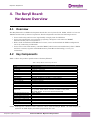
4. The Beryll Board: Hardware Overview ____________________________________________ 11
4.1 Overview .................................................................................................................................. 11
4.2 Key Components ...................................................................................................................... 11
4.3 Block Diagram .......................................................................................................................... 12
4.4 Board Specifications................................................................................................................. 12
5. The Beryll Board Components __________________________________________________ 16
5.1 Featured Device: Cyclone V GX FPGA ...................................................................................... 16
5.2 FPGA and EPCS Configuration ROM Programming .................................................................. 16
5.3 Programming to the EPCS Configuration ROM ........................................................................ 18
5.4 Connector Pin Assignment ....................................................................................................... 20
5.5 Serial Port................................................................................................................................. 22
5.6 DDR3 SDRAM ........................................................................................................................... 23
5.7 FLASH/SRAM ............................................................................................................................ 24
5.8 USB 2.0 ..................................................................................................................................... 25
5.9 10/100/1000 Ethernet ............................................................................................................. 27
5.1024-bit Audio Codec .................................................................................................................. 28
5.11User Interfaces ......................................................................................................................... 28
5.12Clock Circuitry .......................................................................................................................... 30
5.13Power Tree ............................................................................................................................... 32
6. Operating Precautions ________________________________________________________ 33
6.1 Mode Selection for Unused Pins.............................................................................................. 33
7. Document Revision History ____________________________________________________ 34
© Mpression by Macnica Group
Reference Manual - Mpression Beryll Board
3
Mpression Beryll Board
1. For Ensuring Safe Use
Be sure to follow the instructions given in this Manual which are intended to prevent harm to the
user and others as well as material damage.
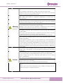
1.1 Legend
Danger
Warning
Caution
Indicates an imminent hazardous situation which if not avoided will result in
death or serious injury.
Indicates a potentially hazardous situation which if not avoided could result in
death or serious injury.
Indicates a potentially hazardous situation which if not avoided may result in
minor or moderate injury or in property damage.
1.2 Cautions
Make sure to use the AC adapter (included in package) that is specified in this
Danger
Manual.
Using an AC adapter not meeting the specifications described in this Manual
will cause the kit to emit heat, explode, or ignite.
Do not apply strong impacts or blows to the kit.
Doing so may cause the kit to emit heat, explode, or ignite, or the equipment in
the kit to fail or malfunction. This may also cause fire.
Do not put the main unit or the AC adapter in cooking appliances such as
microwave ovens, or high-pressure containers.
Doing so might cause the main unit or AC adapter to emit heat, explode, ignite,
or emit smoke, or its parts to break or warp.
Do not wrap the main unit that is in use with cloth or other materials that are
likely to allow heat to build up inside the wrapping.
This will cause heat to build up inside the wrapping which may cause the main
unit to ignite or malfunction.
Warning
When disposing of the main unit, do not dispose of it along with general
household waste.
Throwing the main unit into fire may cause it to explode. Dispose of the
main unit following the laws, regulations, and ordinances governing
waste disposal.
Do not use the kit in places subject to extremely high or low temperatures or
severe temperature changes.
Doing so may cause the kit to fail or to malfunction.
Always be sure to use the kit in a temperatures ranging from 5°C to 35°C and a
humidity range of 0% to 85%.
4
Reference Manual - Mpression Beryll Board
© Mpression by Macnica Group
Mpression Beryll Board
Do not pull the power supply cable with excessive force or place heavy items on
it.
Do not damage, break, bundle, or tamper with the power supply cable.
Damaged parts of the power supply cable might cause a short circuit resulting
in fire or accidents involving electrical shock.
Do not unplug the power plug with wet or moist hands.
This might cause injuries or equipment malfunctions or failures due to
electrical shock.
Plug the power plug securely into the outlet.
If the power plug is not securely plugged into the outlet, it may cause accidents
involving electrical shock or fire due to heat emitted.
Do not connect many electrical cords to a single socket or connect an AC adapter
Warning
(Continued from
previous page)
to an outlet that is not rated for the specified voltage.
Failing to do so may cause the equipment to malfunction or fail, or lead to
accidents involving electrical shock or fire due to heat emitted.
Periodically remove any dust accumulated on the power plug and around the
outlet (socket).
Do not use a power plug with dust accumulated on it because doing so will lead
to insulation failure due to moisture which may lead to fire.
Remove any dust on the power plug and around the outlet with dried cloth.
Do not place any containers such as cups or vases filled with water or other
liquid on this Board.
If this Board is exposed to water or other liquids it may cause the Board to
malfunction or lead to accidents involving electrical shock. If you spilled water
or other liquid on this Board, immediately stop using the Board, turn off the
power, and unplug the power plug. If you have any requests for repairs or
technical consultation, please contact the local Macnica company or Mpression
inquiry URL.
Do not place the kit on unstable places such as shaky stands or tilted locations.
Doing so may cause injuries or cause this Board to malfunction if the Board
should fall.
Do not attempt to use or leave the kit in places subject to strong direct sunlight
or other places subject to high temperatures such as in cars in hot weather.
Doing so might cause the kit to emit heat, break, ignite, run out of control,
warp, or malfunction.
Also, some parts of the equipment might emit heat causing burn injuries.
Caution
Unplug the power supply cable when carrying out maintenance of devices in
which the main unit is embedded.
Failure to do so may lead to accidents involving electrical shock.
Do not place this Board in locations where excessive force is applied to the
Board.
Failure to do so may cause the PC board to warp, leading to breakage of the PC
board, missing parts or malfunctioning parts.
© Mpression by Macnica Group
Reference Manual - Mpression Beryll Board
5
Mpression Beryll Board
When using the kit together with expansion boards or other peripheral devices,
be sure to carefully read each of their manuals and to use them correctly.
Developer does not guarantee the operation of specific expansion boards or
peripheral devices when used in conjunction with this Board unless they are
specifically mentioned in this Manual or their successful operation with this
Board has been confirmed in separate documents.
Be sure to turn off the power switch when moving this Board to connect to other
Caution
(Continued from
previous page)
devices. Failure to do so may cause this Board to fail or lead to accidents
involving electrical shock.
Do not clean this Board by using a rag containing chemicals such as benzine or
thinner. Failure to do so will likely to cause this Board to deteriorate. When
using a chemical cloth be sure to comply with any directions or warnings.
Do not immediately turn on the power if you find that water or moisture had
condensed onto the main unit after removing the board from the package.
Condensation might occur on this Board when taking it out of the box, if the
board is cool yet the room temperature is warm.
Do not apply power to the Board while water or moisture has condensed on it
because the moisture may cause the Board to break or may shorten the service
life of the parts.
When you first take this Board out of the box be sure to leave it at room
temperature for a while before using it. If condensation or moisture has
occurred on this Board, first wait for the moisture to fully evaporate before
installing or connecting the Board to other devices.
Do not disassemble, dismantle, modify, alter, or recycle parts unless they are
clearly described as customizable in this Manual.
Although this kit is customizable, if parts not specified in this Manual as
customizable are modified in any way, then the overall product operation
cannot be guaranteed.
Please consult with developer beforehand if you wish to customize or modify any
parts that are not described in this Manual as customizable.
1.3 Developer Information
The Developer of this product is:
Altima Corp.
1-5-5 Shin-Yokohama, Kouhoku-ku, Yokohama, 222-8563 JAPAN
http://www.altima.co.jp
6
Reference Manual - Mpression Beryll Board
© Mpression by Macnica Group
Mpression Beryll Board
1.4 Inquires
In case you have any inquiries about the use this product, please contact your local Macnica
company or make inquiries through the contact form in the following web site:
http://www.m-pression.com/contact
Macnica companies:
China & HK:
ASEAN & India:
Taiwan:
North America:
Brazil:
Japan:
© Mpression by Macnica Group
Cytech Technology
Cytech Global
Galaxy Far East Corp.
Macnica Americas
Macnica DHW
Altima
Elsena
http://www.cytech.com/
http://www.cytechglobal.com/
http://www.gfec.com.tw/
http://www.macnica-na.com/
http://www.macnicadhw.com.br/en/
http://www.altima.co.jp
http://www.elsena.co.jp
Reference Manual - Mpression Beryll Board
7
Mpression Beryll Board
2. Important Information
READ FIRST:
READ this Reference Manual before using this product.
KEEP the Reference Manual handy for future reference.
Do not attempt to use the product until you fully understand its mechanism.
Purpose of the Product:
This product is the Beryll Board; its purpose is to support the evaluation of a system that uses the
Cyclone® V GX FPGA, manufactured by Altera® Corporation. It provides support for system
development in both software and hardware.
For Users of This Product:
This product can only be used by operators who have carefully read the user’s manual and
understand how to use it. Use of this product requires a basic knowledge of electric circuits, logic
circuits, and FPGAs.
Precautions to be taken when using This Product:
This product is an evaluation supporting board for use in your program development and
evaluation stages. When mass-producing a program you have finished developing, be sure to
decide at your own responsibility whether it can be put to practical use by performing integration
test, evaluation, or some other experiment.
In no event shall Altima Corp. be liable for any consequence arising from the use of this product.
Altima Corp. cannot anticipate every possible circumstance that might involve a potential hazard.
The warnings in this reference manual and on the product are therefore not all-inclusive. The
user is therefore responsible for the safe use of the product at the user’s own responsibility.
This product is to be used for evaluation of a program, and the evaluation stage. You cannot
install the Beryll Board in your product and cannot use the Beryll Board for mass-production.
The operation of any specific USB memories or SD cards cannot be guaranteed.
Connection with the apparatus of any specific LAN interfaces cannot be guaranteed.
This product does not guarantee device functionality.
Remodeling by the customer is not guaranteed.
This product is a lead-free mounting product.
Generally, the brand names carried in this reference manual each constitute a maker’s trademark
or registered trademark.
Improvement Policy:
Altima Corp. pursues a policy of continuous improvement in design, performance, and safety of
the product. Altima Corp. reserves the right to change, wholly or partially, specifications, design,
reference manual, and other documentation at any time without notice.
Warranty:
Altima Corp offers exchange of this product free of charge only in a set range of cases of initial
trouble for this product, and within 30 days from when the customer received delivery of the
Board.
8
Reference Manual - Mpression Beryll Board
© Mpression by Macnica Group
Mpression Beryll Board
Altima Corp. cannot exchange products in cases where breakdown is caused for the following
reasons:
(1) Misuse, abuse of the product or use under abnormal conditions
(2) Remodeling and repair
(3) A fire, earthquake, fall or other accidents
Figures:
Some figures in this reference manual may differ from your system as purchased.
© Mpression by Macnica Group
Reference Manual - Mpression Beryll Board
9
Mpression Beryll Board
3. Unboxing
Package Components
This product consists of the Board and the parts listed in the table below. Please make sure all
components listed below are included as soon as you get the Board.
Customer letter
The Beryll Board
USB Standard-A to Mini-B plug cable
AC adaptor (Output 12 V/3.8 A)
Reference Manual
Download these files from the web
site given in the customer letter.
The Beryll Board circuit diagram
FPGA sample design
10
Reference Manual - Mpression Beryll Board
© Mpression by Macnica Group
Mpression Beryll Board
4. The Beryll Board:
Hardware Overview
4.1 Overview
The Beryll Board is an FPGA development board that uses Cyclone V GX FPGA, which is a low-cost
FPGA manufactured by Altera Corporation. This development board has the following features:
Users can develop and test user logic flexibly using Cyclone V GX FPGA.
Users can expand their own system by preparing a daughter card connector (HSMC)
manufactured by Altera Corporation.
With a built-in On-Board USB-Blaster™ circuit, users can download the FPGA configuration
circuit by connecting a USB cable.
Users can use the hard memory controller (HMC), which has been installed in Cyclone V FPGA
and later versions, together with DDR3 memory from Micron Technology to carry out
evaluations.
4.2 Key Components
Table 1 shows the product specifications of the Beryll Board.
Table 1 Beryll Board Product Specifications
Product Function
FPGA
Power Supply
Dimensions
HSMC
Printed Circuit Board
Configuration ROM
SRAM
DDR-SDRAM
Flash ROM
USB 2.0 (Mini-B)
Audio
Ethernet
Clock (for FPGA)
JTAG Connector
Status LED
FPGA Reconfiguration Push SW
General-purpose LED
General-purpose Push SW
General-purpose Dip SW
General-purpose 7 Segment LED
Character LCD Connector
Power SW
RS-232C
Part or Specification
5CGXFC4C6F27C
DC 12 V 3.8 A
140.00 mm x 155.00 mm
ASP-122953-01
FR4 10-layer
EPCS128SI16N
IDT71V416S10PHG8 (512 KByte)
DDR3-800 256 MBytes (128 MByte x 2) MT41J64MJT
JS28F256M29EWLA (32 MByte)
CY7C68013A-56LTXC
UDA1345TS
DP83865DVH
27 MHz x 1, 33 MHz x 1, 50 MHz x 1, 125 MHz x 1
DIP 10-pin Header, 2.54-mm pitch × 1
12 pcs
(12V_POWER, HSMC PSNTn, nSTATUS, nCONFIG, CONF_DONE,
INIT_DONE, Blaster, ACT,LK10,LK100,LK1000,DUPLEX)
1 (SYS_RESET)
8
4
1 (SW0-SW3)
2
1 (3.3-V) * A character LCD is optional.
1
DB9 Female Connector
(Note) Although the character LCD connector comes with the Beryll Board, the LCD display is
optional. An LCD display should be prepared by the user.
© Mpression by Macnica Group
Reference Manual - Mpression Beryll Board
11
Mpression Beryll Board
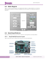
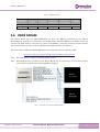
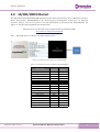
4.3 Block Diagram
Figure 1. shows the block diagram of the Beryll Board. Because the Beryll Board is an evaluation
board using the properties of Cyclone V GX FPGA, all of the functions are integrated in Cyclone V
GX FPGA.
Character LCD
Figure 1 Beryll Board Block Diagram
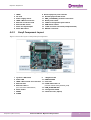
4.4 Board Specifications
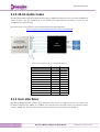
This section describes the layout of switches, connectors, and components on the Beryll Board.
4.4.1
Beryll Switch/Connector Layout
Figure 2 shows the layout of switches and connectors used on the Beryll Board.
Figure 2 Beryll Switch/Connector layout
12
Reference Manual - Mpression Beryll Board
© Mpression by Macnica Group
Mpression Beryll Board
1
2
3
4
5
6
7
8
4.4.2
HSMC
DC Jack
Power supply switch
USB2.0 Mini-B connector
Ethernet connector RJ45
Ethernet DIP switch
Audio line input/output
Audio DIP switch
9
10
11
12
13
14
15
16
General-purpose push switches
General-purpose DIP switch
SMA_CLKIN/SMA_CLKOUT connectors
Reset push switch
FPGA reconfiguration push switch
USB-blaster switch
JTAG connector for FPGA (unimplemented)
RS232C connector
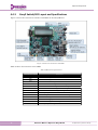
Beryll Component Layout
Figure 3 shows the layout of major Beryll components.
Figure 3 Beryll Component layout
1
2
3
4
5
Cyclone V GX FPGA
Power LED
USB2.0 Device PHY and controller
Ethernet PHY
Ethernet LED × 5
9
10
11
12
(ACT/ LK10/ LK100/ LK1000/ DUPLEX)
13 USB_BLASTER LED
14 Configuration ROM
15 Character LCD ( Option)
6 Audio Codec
7 SRAM
8 FLASH
© Mpression by Macnica Group
7 Segment LED
DDR3 SDRAM
User LED
FPGA status LED × 4
(nSTATUS/ nCONFIG/ CONF_DONE/ INIT_DONE)
Reference Manual - Mpression Beryll Board
13
Mpression Beryll Board
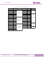
4.4.3
Beryll Switch/LED Layout and Specifications
Figure 4 shows the locations of switches and LEDs on the Beryll Board.
Figure 4 Positions of the Switches and LEDs
Table 2 shows the functions of the LEDs.
Table 2 LED function specifications
Component Location
D1
D2
D3
D4
D5
D6
D7
D8
D9-D16
D17
D18
D19
D22
U24, U25
14
Function
LED for checking FPGA CONF_DONE
LED for checking FPGA nSTATUS
LED for checking FPGA nCONFIG
ACT: LED for checking communication
LK10: LED for checking link in 10-Mbps communication
LK100: LED for checking link in 100-Mbps communication
LK1000: LED for checking link in 1-Gbps communication
DUPLEX: LED for checking full-duplex communication
General-purpose LED × 8
LED for implementation of the HSMC daughter board
LED for checking the USB-Blaster cable
+12V Power Supply LED
LED for checking FPGA INIT_DONE
General-purpose 7 Segment LED × 2
Reference Manual - Mpression Beryll Board
© Mpression by Macnica Group
Mpression Beryll Board
Table 3 shows the functions of the switches
Table 3 shows the functions of the switches.
Component Location
POWER_SW
Default
Slide Down
Function
Slide Down: Power OFF, Slide Up: Power ON
CRS/RGMII_SEL0
Open : RGMII - 3COM
Short : RGMII - HP
ENET_DIPSW
Both OPEN
COL/CLK_MAC_FREQ
Open : 125MHz output
Short : 25MHz output
AUDIO_DIPSW
DIP_SW
CPU_RESETn, PB0, PB1, PB2
FPGA_Reconfig
© Mpression by Macnica Group
Both OPEN
Use both switches in OPEN state.
AUDIO_MP2
Open : StaticPin Low or FPGA Control
Short : StaticPin and Mid Voltage
None
None
None
AUDIO_MP4
Open : StaticPin High or FPGA Control
Audio Setting DIP SWs (×4)
General-purpose Push SW
FPGA Reconfiguration Push SW
Reference Manual - Mpression Beryll Board
15
Mpression Beryll Board
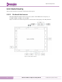
5. The Beryll Board Components
This chapter describes the FPGA and various components installed on the periphery of the FPGA on
the Beryll Board.
5.1 Featured Device: Cyclone V GX FPGA
The Beryll Board carries 28-nm low-cost FPGA Cyclone V GX manufactured by Altera Corporation.
Table 4 shows the specifications of the Cyclone V GX FPGA.
Table 4 Cyclone V GX FPGA Specifications
Core Fabric
Number of
Number of
Memory
LEs
blocks
Device
5CGXC4
50K
250
Block
memory
(Kb)
2,500
Internal Connection
Number of
MLAB
Number of
DSP
PLLs
(Kb)
blocks
295
70
Number of
transceivers
6
Hardware IP
Number of Number of Number of
Number of
LVDS
PCIe
memory
GPIO pins
pairs
blocks
controllers
6
336
90
2
2
5.2 FPGA and EPCS Configuration ROM Programming
To carry out programming to the FPGA and EPCS ROM, connect the Mini USB Cable that comes
with the Beryll Board to USB-Blaster (U27) and write the program in the configuration file.
Therefore, users do not need to prepare programming hardware, such as a USB-Blaster cable from
Altera, separately.
5.2.1
Preface
Use the Quartus® II Programmer to perform programming (writing the programming file into the
configuration file) for the device. When being used for the first time, it is necessary to install the
drivers for each piece of programming hardware.
5.2.2
How to Perform Programming for the FPGA
This section introduces the basic operations for programming.
A.
Starting Programmer
Connect the programming hardware, and then select the Tools Menu in Quartus II and then
“Programmer”, or click the
button.
B.
Selecting a programming mode
From the Mode pull-down list, select a method for writing the programming file into the device.
Select JTAG for the Beryll Board.
C.
Setting the programming hardware
a. Click the Hardware Setup button
b. Select the Hardware Settings tab in the Hardware Setup window.
16
Reference Manual - Mpression Beryll Board
© Mpression by Macnica Group
Mpression Beryll Board
c. From the Current selected hardware pull-down list, select the programming hardware to be
used (Move on to step ).
If there is no programming hardware to use in the pull-down list, click the Add Hardware
button.
d. Select USB-Blaster from Hardware type in the Add Hardware dialog box and click the OK
button.
e. Select USB-Blaster from Currently selected hardware in the Hardware Setup window and
click the Close button.
D.
Programming
a. Click the
button to select a programming file (*.SOF) to write into the device.
b. To write data into the device, check the Program/Configure box as a programming option.
c. Click the
button to start programming.
Reference information
* POF file (*.pof): Programming file for the MAX® CPLD series and configuration device
* SOF file (*.sof): Programming file for FPGA of Stratix® FPGA, Arria® FPGA, and
Cyclone FPGA
* JIC file (*.jic): Programming file for configuration device
Reference information
Program/Configure
Writes programming data (performs programming) into the device.
Verify
Compares the contents of the programming data registered in Programmer with the
contents written in the device to verify the programming data.
Blank-Check
Confirms that the device is completely empty (that the contents in the device have been
completely deleted).
Examine
Loads programming data which has been written in the MAX CPLD devices or
configuration device. The data which has been loaded can be saved as a programming file.
* Data that has been written when the Security Bit option (see the next item) was enabled
cannot be loaded correctly.
* Executing Examine will not delete the data in the device.
* Data that has been loaded cannot be restored to the design file.
© Mpression by Macnica Group
Reference Manual - Mpression Beryll Board
17
Mpression Beryll Board
Security Bit
Prevents the data that has been written into the device from being checked or the data
which has been loaded by Examine from being copied when re-programmed. (This option is
supported only for MAX® 7000 and MAX® 3000.)
Erase
Deletes data stored in the MAX CPLD device or configuration device.
ISP CLAMP
Uses the IPS file (*.ips) to set the I/O pin status in programming. (This option is supported
only for MAX® 7000B and MAX® II.)
5.3 Programming to the EPCS Configuration device
5.3.1
Preface
With the JTAG Indirect Configuration (JIC) file for the FPGA device, you can perform programming
of the EPCS device which does not support the JTAG interface through the JTAG chain.
5.3.2
Outline of JIC
When the EPCS device is used as a configuration device for the Cyclone V device, the data transfer
method supports the active serial configuration mode (AS mode). To perform configuration in AS
mode, a 10-pin header used to perform programming in AS mode is required in the EPCS device. On
the other hand, to configure data for the FPGA through the JTAG port or to perform debugging using
SignalTap® II, another 10-pin header for JTAG is also needed.
However, the JIC function is used, the serial flash loader design in the FPGA works as a bridge, and
so programming for the EPCS device can be performed through the JTAG port. For this reason, the
10-pin header for the AS mode is no longer needed, which allows users to reduce both the board area
and the cost.
5.3.3
Programming method for EPCS configuration ROM
Programming through the serial flash loader is performed using a JIC file, instead of using a
traditional SOF file or POF file. To perform programming, create a JIC file from the SOF file, a
configuration file for FPGA.
The flow of this operation is as follows:
Step 1: Compiling the design (creating a programming file)
Step 2: Creating a JIC file
Step 3: Programming
Step 1: Compiling the design
Compile the design in order to create a configuration file (.sof) which will be the basis for the JIC file.
18
Reference Manual - Mpression Beryll Board
© Mpression by Macnica Group
Mpression Beryll Board
– Select the Processing menu and then Start Compilation, or click the
button.
Step 2: Creating a JIC file
Create a *.jic file which will be the programming file for JIC from the SOF file which has been
generated after compilation.
1) Select the File menu and then Convert Programming Files.
2) In Output Programming File, set a file format to create, configuration device, and output file
name.
Select JTAG Indirect Configuration File (.jic) as a Programming file type.
In Configuration device, set the type of the configuration device for which programming
will be performed.
Select EPCS128 for the Beryll Board.
Specify a generation path of the output file and an output file name for File name.
1. In Input files to convert, select a type of FPGA for which the serial flash loader
design is used.
Select the Flash Loader line and click the Add Device button.
In the Select Device dialog box, select Cyclone V GX for Device family and select Device
name, and click the OK button.
2. Specify a configuration file (.sof) that will be the basis for the JIC file.
Select the SOF Data line and click the Add File button.
Select as SOF file to convert and click the Open button.
3. To compress a programming file, select an SOF to be compressed and click the
Properties button. In the SOF File Properties dialog box, check the Compression
option box and click the OK button.
4. Click the Generate button.
A message reading “Generated <jic file name> successfully” is displayed and creation of the
JIC file is complete.
Step 3 : Programming
Programming of the JIC file you have created to the EPCS device is performed in JTAG mode.
1) Start Programmer.
Select the Tools menu and then Programmer, or click the
button.
2) Select hardware (download cable) to be used and select JTAG for Mode.
3) Click the
button and select a JIC file.
4) Check the Program/Configure option box on the JIC file line.
5) Click the
button to start programming.
The serial flash loader in the FPGA device becomes enabled first, and then EPCS
programming is executed through the serial flash loader. When the programming is completed
successfully, the Progress gauge (in the upper right of the Programmer window) reaches 100%
© Mpression by Macnica Group
Reference Manual - Mpression Beryll Board
19
Mpression Beryll Board
and a message informing you of the successful completion of programming is shown in the
Message dialog box.
You have now completed programming of the EPCS device by JTAG Indirect Configuration.
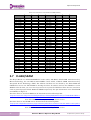
5.4 Connector Pin Assignment
Figure 5 shows the locations of connectors and the pin assignment of each connector.
Figure 5. Beryll Connector Assignment
01. U35 (DC jack)
Pin
1
3
Signal Name
12V
GND
Pin
2
Signal Name
NC
02. U20 (USB 2.0_CONN)
Pin
1
Signal Name
V_BUS
Pin
2
3
5
DG
4
Signal Name
D+
ID
Pin
2
4
6
8
10
12
Signal Name
TD0_N
TD1_N
TD2_N
TD3_N
GND
GND_TAB
Pin
2
4
Signal Name
L
NCl
03. U17 (ENET_CONN)
Pin
1
3
5
7
9
11
Signal Name
TD0_P
TD1_P
TD2_P
TD3_P
VCC
GND_TAB
04. J3 (Audio Line In)
Pin
1
3
20
Signal Name
GND
R
Reference Manual - Mpression Beryll Board
© Mpression by Macnica Group
Mpression Beryll Board
05. J4 (Audio Line Out)
Pin
1
3
Signal Name
GND
R
Pin
2
4
Signal Name
L
NCl
Pin
2
4
Signal Name
NC
NC
Pin
2
4
Signal Name
NC
NC
Pin
2
4
Signal Name
D+
ID
06. J2 (SMA CLKIN)
Pin
1
3
5
Signal Name
SMA_CLK_IN
NC
NC
07. J1 (SMA CLKOUT)
Pin
1
3
5
Signal Name
SMA_CLK_OUT
NC
NC
08. U27 (USB-Blaster)
Pin
1
3
5
Signal Name
V_BUS
DG
9. J6 (RS232C DSub9 Pin Female Connector)
Pin
1
3
5
7
9
Signal Name
NC
UART_RXD
NC
NC
NC
Pin
2
4
6
8
Signal Name
UART_TXD
NC
NC
NC
Pin
2
4
6
8
10
12
14
Signal Name
NC
LCD_RS
LCD_E
LCD_DATA1
LCD_DATA3
LCD_DATA5
LCD_DATA7
10. J5 (Character LCD)
Pin
1
3
5
7
9
11
13
© Mpression by Macnica Group
Signal Name
NC
NC
LCD_RW
LCD_DATA0
LCD_DATA2
LCD_DATA4
LCD_DATA6
Reference Manual - Mpression Beryll Board
21
Mpression Beryll Board
11. J8 (HSMC Connector)
Pin
1
3
5
7
9
11
13
15
17
19
21
23
25
27
29
31
33
35
37
39
41
43
45
47
49
51
53
55
57
59
61
63
65
67
69
71
73
75
77
79
Signal Name
GX_TXD3_P
GX_TXD3_N
GX_TXD2_P
GX_TXD2_N
GX_TXD1_P
GX_TXD1_N
GX_TXD0_P
GX_TXD0_N
HSMC_1_DATA0
HSMC_1_DATA2
HSMC_1_DATA4
HSMC_1_CLKOUT
HSMC_DATA0
HSMC_DATA2
HSMC_2_DATAOUT0_P
HSMC_2_DATAOUT0_N
HSMC_2_DATAOUT1_P
HSMC_2_DATAOUT1_N
HSMC_2_DATAOUT2_P
HSMC_2_DATAOUT2_N
HSMC_2_DATAOUT3_P
HSMC_2_DATAOUT3_N
HSMC_2_DATAOUT4_P
HSMC_2_DATAOUT4_N
HSMC_2_DATAOUT5_P
HSMC_2_DATAOUT5_N
Pin
2
4
6
8
10
12
14
16
18
20
22
24
26
28
30
32
34
36
38
40
42
44
46
48
50
52
54
56
58
60
62
64
66
68
70
72
74
76
78
80
Signal Name
GX_RXD3_P
GX_RXD3_N
GX_RXD2_P
GX_RXD2_N
GX_RXD1_P
GX_RXD1_N
GX_RXD0_P
GX_RXD0_N
HSMC_1_DATA1
HSMC_1_DATA4
HSMC_1_DATA5
HSMC_1_CLKIN
HSMC_DATA1
HSMC_DATA3
HSMC_2_DATAIN0_P
HSMC_2_DATAIN0_N
HSMC_2_DATAIN1_P
HSMC_2_DATAIN1_N
HSMC_2_DATAIN2_P
HSMC_2_DATAIN2_N
HSMC_2_DATAIN3_P
HSMC_2_DATAIN3_N
HSMC_2_DATAIN4_P
HSMC_2_DATAIN4_N
HSMC_2_DATAIN5_P
HSMC_2_DATAIN5_N
Pin
81
83
85
87
89
91
93
95
97
99
101
103
105
107
109
111
113
115
117
119
121
123
125
127
129
131
133
135
137
139
141
143
145
147
149
151
153
155
157
159
Signal Name
HSMC_2_DATAOUT6_P
HSMC_2_DATAOUT6_N
HSMC_2_DATAOUT7_P
HSMC_2_DATAOUT7_N
HSMC_2_CLKOUT_P
HSMC_2_CLKOUT_N
HSMC_3_DATAOUT0_P
HSMC_3_DATAOUT0_N
HSMC_3_DATAOUT1_P
HSMC_3_DATAOUT1_N
HSMC_3_DATAOUT2_P
HSMC_3_DATAOUT2_N
HSMC_3_DATAOUT3_P
HSMC_3_DATAOUT3_N
HSMC_3_DATAOUT4_P
HSMC_3_DATAOUT4_N
HSMC_3_DATAOUT5_P
HSMC_3_DATAOUT5_N
HSMC_3_DATAOUT6_P
HSMC_3_DATAOUT6_N
HSMC_3_DATAOUT7_P
HSMC_3_DATAOUT7_N
HSMC_3_DATAOUT8_P
HSMC_3_DATAOUT8_N
HSMC_3_CLKOUT_P
HSMC_3_CLKOUT_N
Pin
82
84
86
88
90
92
94
96
98
100
102
104
106
108
110
112
114
116
118
120
122
124
126
128
130
132
134
136
138
140
142
144
146
148
150
152
154
156
158
160
Signal Name
HSMC_2_DATAIN6_P
HSMC_2_DATAIN6_N
HSMC_2_DATAIN7_P
HSMC_2_DATAIN7_N
HSMC_2_CLKIN_P
HSMC_2_CLKIN_N
HSMC_3_DATAIN0_P
HSMC_3_DATAIN0_N
HSMC_3_DATAIN1_P
HSMC_3_DATAIN1_N
HSMC_3_DATAIN2_P
HSMC_3_DATAIN2_N
HSMC_3_DATAIN3_P
HSMC_3_DATAIN3_N
HSMC_3_DATAIN4_P
HSMC_3_DATAIN4_N
HSMC_3_DATAIN5_P
HSMC_3_DATAIN5_N
HSMC_3_DATAIN6_P
HSMC_3_DATAIN6_N
HSMC_3_DATAIN7_P
HSMC_3_DATAIN7_N
HSMC_3_DATAIN7_P
HSMC_3_DATAIN7_N
HSMC_3_CLKIN_P
HSMC_3_CLKIN_N
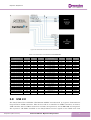
5.5 Serial Port
The Beryll Board has an asynchronous serial port. An LTC2803 FPGA transceiver and a 9-pin D SUB
connector from Linear Technology’s LTC2803 are used for RS232C interface. For pin information on
the FPGA, LTC2803, and D SUB connector, see Figure 6 and the pin list shown below. When
purchasing a serial cable, choose a straight type. For details of Linear Technology’s LTC2803, visit
the following URL:
http://www.linear.com/product/LTC2803
Note: The URL above is subject to change without notice.
Linear Technology
Figure 6 Connections of the FPGA, LTC2803, and DB9 Connector
22
Reference Manual - Mpression Beryll Board
© Mpression by Macnica Group
Mpression Beryll Board
Table 5. RS232C pin list
Schematic
Signal Name
Detail
of Signal
FPGA
Pin Number
UART_TXD
UART_RXD
Transmitter
Receiver
Bank 8A_K6
Bank 8A_L7
LTC2803
Pin Number
(on FPGA side)
14
16
LTC2803
Pin Number
(on D SUB side)
3
1
D SUB
Pin Number
2
3
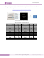
5.6 DDR3 SDRAM
The Beryll Board has two MT41J64M16JT (16 bits, 128 MBytes) manufactured by Micron
Technology, Inc and they are connected to the hard memory controller (HMC) of the FPGA. Users can
evaluate the hard memory controller of Cyclone V GX FPGA by using the attached reference design.
For pin information of the Cyclone V GX FPGA and DDR3 memory, see Figure 7.
The data sheet for Micron’s MT41J64M16JT can be obtained from the following URL:
http://www.micron.com/parts/dram/ddr3-sdram/mt41j64m16jt-15e
Note:
The URL above is subject to change without notice.
Note:
The DDR3 memory installed on the Beryll Board may be replaced by an equivalent product
that satisfies conditions for realizing DDR3 800 Mbps
Micron
Micron
Figure 7 Connections of the FPGA and DDR3 Memory
© Mpression by Macnica Group
Reference Manual - Mpression Beryll Board
23
Mpression Beryll Board
Table 6 Pin Information of the FPGA and DDR3 Memory
Signal Name
FPGA
DDR#0
DDR#1
Signal Name
Pin Number Pin Number Pin Number
FPGA
DDR#0
DDR#1
Pin Number Pin Number Pin Number
DDR3_ADDR0
DDR3_ADDR1
DDR3_ADDR2
DDR3_ADDR3
DDR3_ADDR4
DDR3_ADDR5
DDR3_ADDR6
DDR3_ADDR7
DDR3_ADDR8
DDR3_ADDR9
DDR3_ADDR10
DDR3_ADDR11
DDR3_ADDR12
DDR3_BA0
DDR3_BA1
DDR3_BA2
DDR3_DM0
DDR3_DM1
DDR3_DM2
DDR3_DM3
DDR3_CS_N
DDR3_CAS_N
DDR3_RAS_N
DDR3_WE_N
DDR3_RESET_N
DDR3_ODT
DDR3_DQ0
DDR3_DQ1
DDR3_DQ2
DDR3_DQ3
DDR3_DQ4
DDR3_DQ5
DDR3_DQ6
DDR3_DQ7
AE6
AF6
AF7
AF8
U10
U11
AE9
AF9
AB12
AB11
AC9
AC8
AB10
V10
AD8
AE8
AF11
AE18
AE20
AA14
R11
W10
Y10
T9
AE19
AD13
AA14
Y14
AD11
AD12
Y13
W12
AD10
AF12
AC15
AB15
AC14
AF13
AB16
AA16
AE14
AF18
AD16
AD17
AC18
AF19
AC17
AB17
AF21
AE21
AE15
AE16
AC20
AD21
AF16
AF17
AD23
AF23
N3
P7
P3
N2
P8
P2
R8
R2
T8
R3
I7
R7
N7
M2
N8
M3
E7
D3
E7
L2
K3
J3
L3
T2
K1
F3
F7
F2
F8
H3
H8
G2
H7
N3
P7
P3
N2
P8
P2
R8
R2
T8
R3
I7
R7
N7
M2
N8
M3
D3
L2
K3
J3
L3
T2
K1
DDR3_DQ8
DDR3_DQ9
DDR3_DQ10
DDR3_DQ11
DDR3_DQ12
DDR3_DQ13
DDR3_DQ14
DDR3_DQ15
DDR3_DQ16
DDR3_DQ17
DDR3_DQ18
DDR3_DQ19
DDR3_DQ20
DDR3_DQ21
DDR3_DQ22
DDR3_DQ23
DDR3_DQ24
DDR3_DQ25
DDR3_DQ26
DDR3_DQ27
DDR3_DQ28
DDR3_DQ29
DDR3_DQ30
DDR3_DQ31
DDR3_DQS_P1
DDR3_DQS_N1
DDR3_DQS_P0
DDR3_DQS_N0
DDR3_DQS_P3
DDR3_DQS_N3
DDR3_DQS_P0
DDR3_DQS_N0
DDR3_CLK_P
DDR3_CLK_N
DDR3_CKE
D7
C3
C8
C2
A7
A2
B8
A3
F3
F7
F2
F8
H3
H8
G2
H7
D7
C3
C8
C2
A7
A2
B8
A3
C7
B7
F3
G3
J7
K7
K9
C7
B7
F3
G3
J7
K7
K9
5.7 FLASH/SRAM
The Beryll Board has JS28F256M29EWL (16-bit width, 256 Mbits) Flash ROM manufactured by
Micron Technology, Inc and IDT71V416S10PHG8 (16-bit width, 4 Mbits) SRAM manufactured by
Integrated Device Technology® (IDT). The address and data bus are shared by the Flash ROM and
SRAM. You can use the Flash ROM for booting the Nios® II software and use the SRAM as a cache
ROM for Nios II when you use a Nios II processor for Cyclone V GX FPGA. These devices can also be
used as general-purpose Flash ROM and SRAM respectively. For pin information of the Flash ROM
and SRAM, see Figure 8.
The data sheet for the Flash ROM can be obtained from the following URL:
http://www.micron.com/parts/nor-flash/parallel-nor-flash/js28f256m29ewla?pc={9A9BFAD5-DEE0-4
9F7-ACE8-ED039D2582D6}
Note: The URL above is subject to change without notice.
The data sheet for the SRAM can be obtained from the following URL:
http://ja.idt.com/products/memory-logic/srams/asynchronous-srams/71v416-33v-256k-x-16-asynchro
nous-static-ram-center-pwr-gnd-pinout
Note: The URL above is subject to change without notice.
24
Reference Manual - Mpression Beryll Board
© Mpression by Macnica Group
Mpression Beryll Board
Micron
Figure 8 Pin Information of the FPGA and FLASH/SRAM
Table 7 Pin Information of the FPGA and FLASH/SRAM
Signal Name
FLASH_ADDRESS1
FLASH_ADDRESS2
FLASH_ADDRESS3
FLASH_ADDRESS4
FLASH_ADDRESS5
FLASH_ADDRESS6
FLASH_ADDRESS7
FLASH_ADDRESS8
FLASH_ADDRESS9
FLASH_ADDRESS10
FLASH_ADDRESS11
FLASH_ADDRESS12
FLASH_ADDRESS13
FLASH_ADDRESS14
FLASH_ADDRESS15
FLASH_ADDRESS16
FLASH_ADDRESS17
FLASH_ADDRESS18
FLASH_ADDRESS19
FLASH_ADDRESS20
FLASH_ADDRESS21
FLASH_ADDRESS22
FLASH_ADDRESS23
FLASH_ADDRESS24
FPGA
FLASH
SRAM
Pin Number Pin Number Pin Number
AD26
AF26
AE25
AF24
AE23
AB22
AD22
AF22
AA21
Y20
AD20
V19
Y19
AB19
AC19
AD18
AA18
Y18
W18
V18
V17
U17
Y16
U16
A0
A1
A2
A3
A4
A5
A6
A7
A8
A9
A10
A11
A12
A13
A14
A15
A16
A17
A18
A19
A20
A21
A22
A23
A0
A1
A2
A3
A4
A5
A6
A7
A8
A9
A10
A11
A12
A13
A14
A15
A16
A17
Signal Name
FPGA
FLASH
SRAM
Pin Number Pin Number Pin Number
FLASH_DATA0
FLASH_DATA1
FLASH_DATA2
FLASH_DATA3
FLASH_DATA4
FLASH_DATA5
FLASH_DATA6
FLASH_DATA7
FLASH_DATA8
FLASH_DATA9
FLASH_DATA10
FLASH_DATA11
FLASH_DATA12
FLASH_DATA13
FLASH_DATA14
FLASH_DATA15
FLASH_CS_N
FLASH_READ_N
FLASH_WRITE_N
SRAM_CS_N
SRAM_OE_N
SRAM_WRITE_N
SRAM_BE0_N
SRAM_BE1_N
V24
V23
W26
W25
AA26
AA24
AB26
AB25
AC25
AD25
Y24
Y23
AA23
AA22
AC23
AC22
U22
V22
W21
V20
U15
T17
U20
T19
DQ0
DQ1
DQ2
DQ3
DQ4
DQ5
DQ6
DQ7
DQ8
DQ9
DQ10
DQ11
DQ12
DQ13
DQ14
DQ15/A-1
CE_N
OE_N
WE_N
DQ0
DQ1
DQ2
DQ3
DQ4
DQ5
DQ6
DQ7
DQ8
DQ9
DQ10
DQ11
DQ12
DQ13
DQ14
DQ15
CS_N
OE_N
WE_N
BLE_N
BLH_N
5.8 USB 2.0
The Beryll Board has EZ-USB® CY7C68013A-56LTXC manufactured by Cypress Semiconductor
Corporation for USB2.0 interface. This device works as a controller for USB2.0 interface, in which a
USB controller with a USB2.0 transceiver and 8051 microprocessor, and 16-KB RAM are integrated.
The Cyclone V GX FPGA installed on the Beryll Board receives signals at the GPIF level from
© Mpression by Macnica Group
Reference Manual - Mpression Beryll Board
25
Mpression Beryll Board
Cypress Semiconductor’s EZ-USB. For pin information of the FPGA and CY7C68013, see Figure 9
and the pin assignment list shown below. The data sheet for Cypress Semiconductor’s EZ-USB can be
obtained from the following URL:
http://www.cypress.com/?mpn=CY7C68013A-56LTXC
Note: The URL above is subject to change without notice.
Cypress
Figure 9 Connections of the FPGA and EZ-USB
Table 8. Pin Information of the FPGA and EZ-USB
26
Signal Name
FPGA Pin
Number
USB Pin
Number
Signal Name
FPGA Pin
Number
USB Pin
Number
EZ_PA0
EZ_PA1
EZ_PA2
EZ_PA3
EZ_PA4
EZ_PA5
EZ_PA6
EZ_PA7
EZ_PB0
EZ_PB1
EZ_PB2
EZ_PB3
EZ_PB4
EZ_PB5
EZ_PB6
EZ_PB7
G25
G24
G22
H25
H24
H23
H22
J23
E24
E23
E21
F24
F23
F22
F21
G26
33
34
35
36
37
38
39
40
18
19
20
21
22
23
24
25
EZ_PD0
EZ_PD1
EZ_PD2
EZ_PD3
EZ_PD4
EZ_PD5
EZ_PD6
EZ_PD7
EZ_RDY0
EZ_RDY1
EZ_CLK
EZ_WAKEUP
EZ_RESET_N
EZ_CTL0
EZ_CTL1
EZ_CTL2
B26
B25
C25
D26
D25
D22
E26
E25
J25
J26
K25
K26
L23
K24
K23
L24
45
46
47
48
49
50
51
52
1
2
13
44
32
29
30
31
Reference Manual - Mpression Beryll Board
© Mpression by Macnica Group
Mpression Beryll Board
5.9 10/100/1000 Ethernet
The Beryll Board has DP83865DVH manufactured by Texas Instruments, Inc for Ethernet interface.
Texas Instruments’ DP83865DVH is an ultra-low-power-consumption transceiver for Ethernet
interface using a 1.8-V, 0.18- process. For pin information of the FPGA and DP83865DVH, see
Figure 10 and the pin assignment list shown below.
The data sheet for this LSI can be obtained from the following URL:
http://www.ti.com/product/dp83865
Note:
The URL above is subject to change without notice.
Figure 10. Connection of the FPGA and DP83865DVH
Table 9. Pin Assignment list of the FPGA and DP83865DVH
© Mpression by Macnica Group
Signal Name
FPGA Pin
Number
DP83865 Pin
Number
TSE_MAC_CLK
TSE_RESET_N
TSE_RX_CLK
TSE_RX_DV
TSE_RX_D0
TSE_RX_D1
TSE_RX_D2
TSE_RX_D3
TSE_GTX_CLK
TSE_TX_EN
TSE_TX_D0
TSE_TX_D1
TSE_TX_D2
TSE_TX_D3
TSE_MDIO
TSE_MDC
TSE_INTERRUPT_N
N20
P21
R20
R25
R26
P26
P23
N25
F26
N23
N24
M26
M25
M24
R23
P22
P20
85
33
44
41
56
55
52
51
79
62
76
75
72
71
80
81
3
Reference Manual - Mpression Beryll Board
27
Mpression Beryll Board
5.10 24-bit Audio Codec
The Beryll Board has UDA1345TS manufactured by NXP Semiconductors N.V. for 24-bit CODEC for
audio interface. For pin information of the FPGA and UDA1345TS, see Figure 11 and the pin
assignment list shown below.
The data sheet for this device can be obtained from the following URL:
http://www.nxp.com/documents/data_sheet/UDA1345TS.pdf
Note: The URL above is subject to change without notice.
Figure 11 Connection of the FPGA and UDA1345
Table 10. Pin assignment list of the FPGA and UDA1345
Signal Name
AUDIO_SYSCLK
AUDIO_BCK
AUDIO_DI
AUDIO_WS
AUDIO_DO
AUDIO_MC
AUDIO_MP1
AUDIO_MP2
AUDIO_MP3
AUDIO_MP4
AUDIO_MP5
FPGA Pin Audio Pin
Number
Number
Y25
12
Y26
16
T26
18
U25
17
U26
19
T22
8/21
T24
9
U24
13
V25
14
R24
15
T23
20
5.11 User Interfaces
The Beryll Board provides various input interfaces that can be set uniquely by the user. Those user
interfaces include eight LEDs, two 7-SEGs, four push buttons, one DIP switch, one character LCD,
and one UART. For details of the specifications of each pin, see the pin list shown below.
28
Reference Manual - Mpression Beryll Board
© Mpression by Macnica Group
Mpression Beryll Board
Table 11. Pin Assignment list of the Input Interfaces
Signal Name
LED_N0
LED_N1
LED_N2
LED_N3
LED_N4
LED_N5
LED_N6
LED_N7
SEVEN_SEG0
SEVEN_SEG1
SEVEN_SEG2
SEVEN_SEG3
SEVEN_SEG4
SEVEN_SEG5
SEVEN_SEG6
SEVEN_SEG7
SEVEN_SEG8
SEVEN_SEG9
SEVEN_SEG10
SEVEN_SEG11
SEVEN_SEG12
SEVEN_SEG13
SEVEN_SEG14
SEVEN_SEG15
© Mpression by Macnica Group
FPGA Pin
Number
H19
G20
H20
J20
J21
K21
M22
M21
AD7
AD6
AB6
AA7
AA6
Y9
Y8
W8
V8
U7
T8
T7
R10
R9
R8
P8
Function
LED8∼0
SEVEN SEG 0
SEVEN SEG 1
Signal Name
DIPSW0
DIPSW1
DIPSW2
DIPSW3
LCD_DATA0
LCD_DATA1
LCD_DATA2
LCD_DATA3
LCD_DATA4
LCD_DATA5
LCD_DATA6
LCD_DATA7
LCD_E
LCD_RS
LCD_RW
PUSHSW_N0
PUSHSW_N1
PUSHSW_N2
PUSHSW_N3
UART RXD
UART TXD
FPGA Pin
Function
Number
P12
T12
User DIP SW
U9
V9
H7
H8
H9
G6
G7
Character LCD
F6
F7
E6
J8
J7
K9
AB24
W20
User Push
Button
AC13
V12
L7
UART
K6
Reference Manual - Mpression Beryll Board
29
Mpression Beryll Board
5.12 Clock Circuitry
This section describes the board’s clock inputs and outputs.
5.12.1 On-board clock source
The Beryll Board includes clock sources for Cyclone V GX FPGA with a frequency of
27-MHz, 33MHz, 50-MHz, and 125-MHz.
Figure 12 shows the default frequencies of all external clocks going to the Beryll Board.
Figure 12. Beryll Board Clocks
30
Reference Manual - Mpression Beryll Board
© Mpression by Macnica Group
Mpression Beryll Board
Table 12 lists the clock sources, the relevant I/O standard, and voltages required for the Beryll
Board.
Table 12. On-board clock sources
Source
Schematic
Signal Name
Frequency
I/O Standard
Cyclone V
Pin Number
Description
U7
CLK27M
27 MHz
3.3V
T21
User
U8
CLK33M
33 MHz
1.8V
T13
User
U10
CLK50M
50 MHz
1.8
U12
User
U11
CLK125M
125 MHz
1.8V
P11
User
U3
U18
U22
DIFF0_P
100 MHz
LVDS
V6
Transceiver reference
DIFF0_N
100 MHz
LVDS
W6
Transceiver reference
TSE_MAC_CLK
25 MHz
3.3V
N20
Ethernet PHY
TSE_RX_CLK
25 MHz
3.3V
R20
Ethernet PHY
EZ_CLK
48 MHz
3.3V
K25
USB2.0 PHY & controller
5.12.2 Off-board Inputs/Outputs
The Beryll Board has input and output clocks which can be driven onto the board. Table 13 lists
the clock inputs for the Beryll Board.
Table 13. Off-board Clock Inputs
Source
HSMC
HSMC
HSMC
SMA
Schematic
Signal Name
I/O Standard
Cyclone V
Pin Number
Description
Single-ended
input
from
the
HSMC_1_CLKIN
2.5V
L8
HSMC_2_CLKIN_P
LVDS/ 2.5V
H12
HSMC_2_CLKIN_N
LVDS/ 2.5V
G11
2.5V inputs.
HSMC_3_CLKIN_P
LVDS/ 2.5V
G15
LVDS input from the installed HSMC
HSMC_3_CLKIN_N
LVDS/ 2.5V
G14
2.5V inputs.
SMA_CLKIN
2.5V
N9
User
© Mpression by Macnica Group
installed HSMC cable or board.
LVDS input from the installed HSMC
cable or board. Can also support 2x
cable or board. Can also support 2x
Reference Manual - Mpression Beryll Board
31
Mpression Beryll Board
Table 14 lists the clock outputs for the Beryll Board.
Table 14. Off-board Clock Outputs
Source
HSMC
HSMC
HSMC
SMA
Schematic
Signal Name
I/O Standard
Cyclone V
Pin Number
Description
HSMC_1_CLKOUT
2.5V
A7
FPGA 2.5V output(or GPIO)
HSMC_2_CLKOUT_P
LVDS/ 2.5V
B15
LVDS output. Can also support 2x
HSMC_2_CLKOUT_N
LVDS/ 2.5V
C15
2.5V outputs.
HSMC_3_CLKOUT_P
LVDS/ 2.5V
A23
LVDS output. Can also support 2x
HSMC_3_CLKOUT_N
LVDS/ 2.5V
A22
2.5V outputs.
SMA_CLKOUT
2.5V
M9
User
5.13 Power Tree
The Beryll Board uses a power supply device manufactured by Linear Technology.
Figure 12 shows the tree diagram of the power supply for the Beryll Board.
LTC3605
Figure 12. Beryll Power Tree
32
Reference Manual - Mpression Beryll Board
© Mpression by Macnica Group
Mpression Beryll Board
6. Operating Precautions
6.1 Mode Selection for Unused Pins
This section describes how to handle the pins which are not used on the hardware design (unused
pins).
When using the Beryll Board, the unused pins must be set to the tri-stated mode.
Follow the steps below to make the necessary setting for the unused pins in Quartus® II.
1. Select the Assignments menu and then Device.
2. Click the [Device & Pin Options] button.
The Device & Pin Options window appears.
3. Select the Unused Pins tab.
4. From the Reserve all unused pins item, select As input tri-stated.
5. Click the [OK] button.
6. Click the [OK] button to close the Device & Pin Options window.
© Mpression by Macnica Group
Reference Manual - Mpression Beryll Board
33
Mpression Beryll Board
7. Document Revision History
Date
Revision
Changes
February, 2014
1
34
Document created
Reference Manual - Mpression Beryll Board
© Mpression by Macnica Group